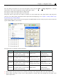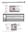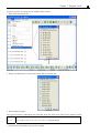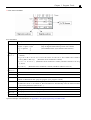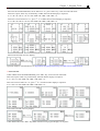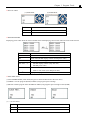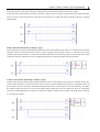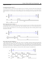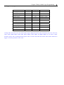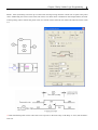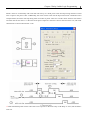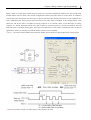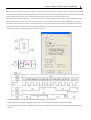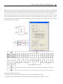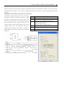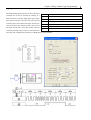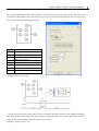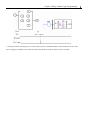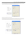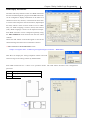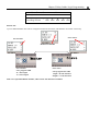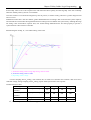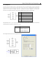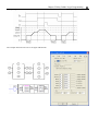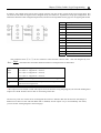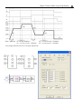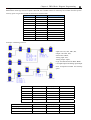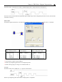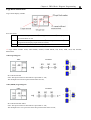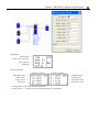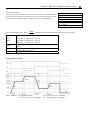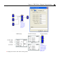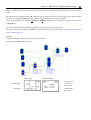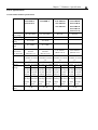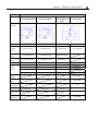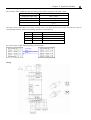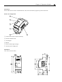
1
SG2 Smart PLC USER Manual
SG2 Programmable Logic Smart Relay
4KA72X023 Version: 04
Apply to:
2010.11.24
SG2 firmware version 3.3,
PC client program software version 3.3
0086-0510-8522-7555
www.taian-technology.com
4KA72X023
I
Content
Content.............................................................................................................................................................................I
Summary of changes..................................................................................................................................................... IV
Chapter 1: Getting Started............................................................................................................................................... 1
Examination before Installation .............................................................................................................................. 3
Environmental Precautions ............................................................................................................................. 3
SG2 Model Identification................................................................................................................................ 3
Quick Start Setup .................................................................................................................................................... 4
Install SG2 Client Software ............................................................................................................................ 4
Connect Power to SG2 smart relay ................................................................................................................. 4
Connect Programming Cable .......................................................................................................................... 5
Establish Communication ............................................................................................................................... 5
Write simple program...................................................................................................................................... 6
Chapter 2: Installation................................................................................................................................................... 10
General Specifications .......................................................................................................................................... 11
Product Specifications........................................................................................................................................... 14
Mounting............................................................................................................................................................... 15
Wiring ................................................................................................................................................................... 17
K type Indicator Light........................................................................................................................................... 19
Chapter 3: Program Tools ............................................................................................................................................. 20
PC Programming Software “SG2 Client” ............................................................................................................. 21
Installing the Software .................................................................................................................................. 21
Connecting the Software ............................................................................................................................... 21
Start Screen ................................................................................................................................................... 21
Ladder Logic Programming Environment .................................................................................................... 22
Menus, Icons and Status Bar ................................................................................................................. 23
Programming......................................................................................................................................... 24
Simulation Mode................................................................................................................................... 25
Establish Communication ..................................................................................................................... 25
Writing Program to smart relay............................................................................................................. 26
Online Monitoring/Editing.................................................................................................................... 27
Operation menu..................................................................................................................................... 28
HMI/TEXT............................................................................................................................................ 29
Program Documentation ....................................................................................................................... 33
Analog Output Set…............................................................................................................................. 35
Data Register Set…............................................................................................................................... 36
View menu ............................................................................................................................................ 38
FBD Programming Environment .................................................................................................................. 39
Menu, Icons and Status Bar................................................................................................................... 39
Programming......................................................................................................................................... 40
Simulation Mode................................................................................................................................... 41
Online Monitoring/Editing.................................................................................................................... 41
Symbol and Parameters list................................................................................................................... 42
Memory Cartridge (sold separately) ..................................................................................................................... 44
4KA72X023
II
LCD Display and Keypad ..................................................................................................................................... 45
Keypad .......................................................................................................................................................... 45
Original Screen ............................................................................................................................................. 46
LCD Display Main Menu.............................................................................................................................. 49
RTC Daylight saving setting ......................................................................................................................... 54
SG2 system error........................................................................................................................................... 58
Chapter 4: Parameter passing........................................................................................................................................ 59
SG2 inner data type............................................................................................................................................... 60
Passing parameter out of range ............................................................................................................................. 61
Chapter 5: Relay Ladder Logic Programming .............................................................................................................. 64
Common Memory Types....................................................................................................................................... 65
Specialty Memory Types....................................................................................................................................... 68
Output Instructions................................................................................................................................................ 69
Analog memory type............................................................................................................................................. 70
Timer Instruction................................................................................................................................................... 71
Counter Instructions.............................................................................................................................................. 78
Real Time Clock (RTC) Instructions..................................................................................................................... 89
Comparator Instructions........................................................................................................................................ 97
HMI Display Instructions...................................................................................................................................... 99
PWM Output Instruction (DC Transistor Output Models Only)......................................................................... 102
IO Link/Remote I/O Instruction (SG2-20Vxxx model only).............................................................................. 105
MU (Modbus) (SG2-20Vxxx model only) ......................................................................................................... 108
SHIFT (shift output)............................................................................................................................................ 115
AQ (Analog Output) ........................................................................................................................................... 116
AS (Add-Subtract) .............................................................................................................................................. 118
MD (MUL-DIV) ................................................................................................................................................. 119
PID (Proportion- Integral- Differential).............................................................................................................. 120
MX (Multiplexer)................................................................................................................................................ 123
AR (Analog-Ramp)............................................................................................................................................. 124
DR (Data register)............................................................................................................................................... 128
Chapter 6: Function Block Diagram Programming .................................................................................................... 130
FBD system memory space................................................................................................................................. 132
Analog................................................................................................................................................................. 134
Analog Input ............................................................................................................................................... 134
Analog Output............................................................................................................................................. 135
Coil Block Instruction......................................................................................................................................... 136
HMI............................................................................................................................................................. 137
PWM function block (only transistor output version)................................................................................. 138
IO Link function block................................................................................................................................ 140
SHIFT function block ................................................................................................................................. 142
Logic Block Instructions..................................................................................................................................... 143
AND Logic Diagram................................................................................................................................... 143
AND (EDGE) Logic Diagram .................................................................................................................... 143
NAND Logic Diagram................................................................................................................................ 144
NAND (EDGE) Logic Diagram.................................................................................................................. 144
OR Logic Diagram...................................................................................................................................... 144
NOR Logic Diagram................................................................................................................................... 145
XOR Logic Diagram................................................................................................................................... 145
4KA72X023
III
SR Logic Diagram ...................................................................................................................................... 145
NOT Logic Diagram ................................................................................................................................... 145
Pulse Logic Diagram................................................................................................................................... 146
BOOLEAN Logic Diagram ........................................................................................................................ 146
Function Block.................................................................................................................................................... 147
Timer Function Block ................................................................................................................................. 148
Common Counter function block................................................................................................................ 156
High Speed Counter Function Block (DC Version Only) ........................................................................... 162
RTC Comparator Function Block ............................................................................................................... 164
Analog Comparator Function Block ........................................................................................................... 169
AS (ADD-SUB) function block .................................................................................................................. 172
MD (MUL-DIV) function block ................................................................................................................. 173
PID (Proportion- Integral- Differential) function block.............................................................................. 174
MX (Multiplexer) function block................................................................................................................ 175
AR (Analog-Ramp) function block............................................................................................................. 176
Example: ..................................................................................................................................................... 179
DR (Data-Register) function block ............................................................................................................. 180
MU (Modbus) function block ..................................................................................................................... 181
Chapter 7: Hardware Specification ............................................................................................................................. 187
Normal Specification .......................................................................................................................................... 188
Product Specifications......................................................................................................................................... 189
Power Specifications........................................................................................................................................... 190
Normal model machine Specifications ....................................................................................................... 190
12V DC model Specifications..................................................................................................................... 191
24V AC model Specifications ..................................................................................................................... 191
Power circuitry diagram.............................................................................................................................. 192
Input Specifications............................................................................................................................................. 193
100~240V AC model .................................................................................................................................. 193
24V AC model ............................................................................................................................................ 193
24V DC, 12 I/O model ................................................................................................................................ 194
24V DC, 20 I/O model ................................................................................................................................ 195
12V DC, 12 I/O model ................................................................................................................................ 196
12V DC, 20 I/O model ................................................................................................................................ 197
Output Specifications.......................................................................................................................................... 198
Output Port wiring notice.................................................................................................................................... 198
Light Load................................................................................................................................................... 198
Inductance Load.......................................................................................................................................... 199
Life of relay................................................................................................................................................. 199
Size diagram of SG2 ................................................................................................................................... 200
Chapter 8: 20 Points RS485 type Models Instruction ................................................................................................. 201
Communication function..................................................................................................................................... 202
Detail instruction................................................................................................................................................. 204
Remote IO function..................................................................................................................................... 204
IO Link Function......................................................................................................................................... 205
MU instruction (Modbus RTU master) ....................................................................................................... 207
Modbus RTU slave function ....................................................................................................................... 209
SG2 Modbus protocol ................................................................................................................................. 209
4KA72X023
IV
Chapter 9: Expansion Module..................................................................................................................................... 211
Summarize .......................................................................................................................................................... 212
Digital IO Module............................................................................................................................................... 216
Analog Module ................................................................................................................................................... 220
Analog Input Module 4AI........................................................................................................................... 220
Temperature Input Module 4PT .................................................................................................................. 221
Analog Output Module 2AO....................................................................................................................... 222
Communication Module ..................................................................................................................................... 224
MBUS Module............................................................................................................................................ 224
DNET Module............................................................................................................................................. 227
PBUS Module ............................................................................................................................................. 230
EN01 (TCP/IP) Module .............................................................................................................................. 233
GSM Module............................................................................................................................................... 239
Appendix: Keypad Programming ............................................................................................................................... 243
Appendix A: Keypad programming in Ladder mode.......................................................................................... 243
Appendix B: Keypad programming in Ladder FUNCTION BLOCK ................................................................ 247
4KA72X023
IV
Summary of changes
This user manual is modified by firmware V3.x and SG2 Client programming software V3.x. SG2 V3.x adds some
new functions with firmware version V3.x to strong SG2 function. The upgrade content is shown as the 2 tables
below simply. More information about idiographic function to see function instruction.
Edit and Display
Ladder
FBD
LCD
SG2 V3.x
300 lines
260blocks
4 lines * 16 characters
SG2 V2.x
200 lines
99blocks
4 lines * 12 characters
Contact and function block
input output
SG2 V3.0
Auxiliary relay M M
M 63(M01~M3F)
Auxiliary relay N
N
N 63(N01~N3F)
temperature input
analog output
PWM
HMI
Timer
AT
Counter
C
RTC
R
T
Analog Comparator G
AS(Add-Sub)
MD(Mul-Div)
PID
MX(Multiplexer)
NO
AR(Analog Ramp)
DR(Data Register)
MU(MODBUS)
Block
B
PM05(3rd)
SG2 V2.x
15(M1~MF)
Ladder: NO
FBD: 15(N1~NF)
4(AT01~AT04)
NO
AQ 4(AQ01~AQ04)
NO
P 2(P01~P02, P01 adds PLSY mode) 1(P1: PWM)
31(H01~H1F)
15(H1~HF)
T Ladder: 31(T01~T1F)
15(T1~TF)
FBD: 250(T01~TFA)
C Ladder: 31(C01~C1F)
15(C1~CF)
FBD: 250(C01~CFA)
R Ladder: 31(R01~R1F)
15(R1~RF)
FBD: 250(R01~RFA)
G Ladder: 31(G01~G1F)
15(G1~GF)
FBD: 250(G01~GFA)
Ladder: 31(AS01~AS1F)
NO
FBD: 250(AS01~ASFA)
Ladder: 31(MD01~MD1F)
NO
FBD: 250(MD01~MDFA)
Ladder: 15(PI01~PI0F)
NO
FBD: 30(PI01~PI1E)
NO Ladder: 15(MX01~MX0F)
NO
FBD: 250(MX01~MXFA)
Ladder: 15(AR01~AR0F)
NO
FBD: 30(AR01~AR1E)
240(DR01~DRF0)
NO
Ladder: 15(MU01~MU0F)
NO
FBD: 250(MU01~MUFA)
Logic function: BOOLEAN
NO
260(B001~B260)The capability of 99(B01~B99)The capability of each
B
each block is alterable, and the total block is fixed
capability of block is 6000bytes
PM05(3rd) can be used with all PM05 can not be used with SG2 V3.x
version of SG2
Chapter 1: Getting Started
1
Chapter 1: Getting Started
Examination before Installation...............................................................................................................................3
Environmental Precautions..............................................................................................................................3
SG2 Model Identification ................................................................................................................................3
Quick Start Setup.....................................................................................................................................................4
Install SG2 Client Software .............................................................................................................................4
Connect Power to SG2 smart relay..................................................................................................................4
Connect Programming Cable...........................................................................................................................5
Establish Communication................................................................................................................................5
Write simple program ......................................................................................................................................6
Chapter 1: Getting Started
2
The SG2 tiny smart Relay is an electronic device. For safety reasons, please carefully read and follow the paragraphs
with "WARNING" or "CAUTION" symbols. They are important safety precautions to be aware of while transporting,
installing, operating, or examining the SG2 Controller.
WARNING: Personal injury may result from improper operation.
CAUTION: The SG2 smart relay may be damaged by improper operation.
Precaution for Installation
Compliance with the installation instructions and the user manual is absolutely necessary. Failure to comply
could lead to improper operation, equipment damage or in extreme cases even death, serious bodily injury or
considerable damage to property.
When installing the open-board models, insure that no wiring or foreign materials can fall into the exposed
circuits and components. Damage to equipment, fire, or considerable damage to property could result.
Always switch off power before you wire, connect, install, or remove any module.
The wiring for the SG2 smart relay is open and exposed. For the open-board models, all electrical components
are exposed. For this reason, it is recommended the SG2 smart relay be installed in an enclosure or cabinet to prevent
accidental contact or exposure to the electrical circuits and components.
Never install the product in an environment beyond the limits specified in this user manual such as high
temperature, humidity, dust, corrosive gas, vibration, etc.
Precaution for Wiring
Improper wiring and installation could lead to death, serious bodily injury or considerable damage to property.
The SG2 smart relay should only be installed and wired by properly experienced and certified personnel.
Make sure the wiring of the SG2 smart relay meets all applicable regulations and codes including local and
national standards and codes.
Be sure to properly size cables for the required current rating.
Always separate AC wiring, DC wiring with high-frequency switching cycles, and low-voltage signal wiring.
Precaution for Operation
To insure safety with the application of the SG2 smart relay, complete functional and safety testing must be
conducted. Only run the SG2 after all testing and confirming safe and proper operation is complete. Any potential
faults in the application should be included in the testing. Failure to do so could lead to improper operation,
equipment damage or in extreme cases even Death, serious bodily injury or considerable damage to property.
When the power is on, never contact the terminals, exposed conductors or electrical components. Failure to
comply could lead to improper operation, equipment damage or in extreme cases even death, serious bodily injury or
considerable damage to property.
It is strongly recommended to add safety protection such as an emergency stop and external interlock circuit in
case the SG2 smart relay operation must be shut down immediately.
Chapter 1: Getting Started
3
Examination before Installation
Every SG2 smart relay has been fully tested and examined before shipment. Please carry out the following
examination procedures after unpacking your SG2 smart relay.
• Check to see if the model number of the SG2 matches the model number that you ordered.
• Check to see whether any damage occurred to the SG2 during shipment. Do not connect the SG2 smart relay to the
power supply if there is any sign of damage.
Contact
if you find any abnormal conditions as mentioned above.
Environmental Precautions
The installation site of the SG2 smart relay is very important. It relates directly to the functionality and the life span
of your SG2. Please carefully choose an installation site that meets the following requirements:
• Mount the unit vertically
• Environment temperature: -4°F - 131°F (-20°C - 55°C)
• Avoid placing SG2 close to any heating equipment
• Avoid dripping water, condensation, or humid environment
• Avoid direct sunlight
• Avoid oil, grease, and gas
• Avoid contact with corrosive gases and liquids
• Prevent foreign dust, flecks, or metal scraps from contacting the SG2 smart relay
• Avoid electric-magnetic interference (soldering or power machinery)
• Avoid excessive vibration; if vibration cannot be avoided, an anti-rattle mounting device should be installed to
reduce vibration.
Disclaim of Liability
We have reviewed the contents of this publication to ensure consistency with the hardware and software described.
Since variance cannot be precluded entirely, we cannot guarantee full consistency. However, the information in this
publication is reviewed regularly and any necessary corrections are included in subsequent editions.
SG2 Model Identification
Chapter 1: Getting Started
4
Quick Start Setup
This section is a simple 5-steps guide to connecting, programming and operating your new SG2 smart relay. This is
not intended to be the complete instructions for programming and installation of your system. Many steps refer to
other sections in the manual for more detailed information.
Install SG2 Client Software
Install the SG2 Client Software from CD or from the free internet download at www.taian-technology.com
Connect Power to SG2 smart relay
Connect power to the Smart Relay using the below wiring diagrams for AC or DC supply for the applicable modules.
See “Chapter 2: Installation” for complete wiring and installation instructions.
Chapter 1: Getting Started
5
Connect Programming Cable
Remove the plastic connector cover from the SG2 using a flathead screwdriver as shown in the figure below. Insert
the plastic connector end of the programming cable into the SG2 smart relay as shown in the figure below. Connect
the opposite end of the cable to an RS232 serial port on the computer.
Establish Communication
a. Open the SG2 Client software and select “New LAD” as shown below left.
b. Select “Operation/Link Com Port…” as shown below right.
Chapter 1: Getting Started
6
c. Select the correct Com Port number where the programming cable is connected to the computer then press the
“link” button.
d. The SG2 Client will then begin to detect the connected smart relay to complete its connection.
Write simple program
a. Write a simple one rung program by clicking on the leftmost cell at line 001 of the programming grid, then click
on the “M” contact icon on the ladder toolbar, as shown below. Select M01 and press the OK button.
See “Chapter 5: Ladder Programming instructions” for complete instruction set definitions.
Note: If the ladder toolbar is not visible at the bottom of the screen, select View/Ladder Toolbar from the menu to
enable.
Chapter 1: Getting Started
7
b. Use the “A” key on your keyboard (or the “A” icon on the ladder toolbar) to draw the horizontal circuit line from
the M contact to the right most cell, as shown below.
c. Select the “Q” coil icon from the ladder toolbar and drop it on the right most cells. Select Q01 from the dialog and
press OK as shown below. See “Chapter 5: Ladder Programming instructions” for complete instruction set
definitions.
Chapter 1: Getting Started
8
d. Test the simple program. From the Operation menu, select the Write function and write the program to the
connected smart relay as shown below.
e. Select the RUN icon from the toolbar, and select “No” when the pop-up message asks “Do you want to read
program from module?”, as shown below.
Chapter 1: Getting Started
9
f. On the Input Status dialog, click on M01 to activate the contact M01 which will turn ON the Output Q01 as shown
below. The highlighted circuit will show active and the first Output (Q01) on the connected smart relay will be ON.
See “Chapter 3: Programming Tools” for more detailed software information.
Chapter 2 Installation
10
Chapter 2: Installation
General Specifications .......................................................................................................................................... 11
Product Specifications........................................................................................................................................... 14
Mounting............................................................................................................................................................... 15
Wiring ................................................................................................................................................................... 17
K type Indicator Light........................................................................................................................................... 19
Chapter 2 Installation
11
General Specifications
SG2 is a miniature smart Relay with a maximum of 44 I/O points and can be programmed in Relay Ladder Logic or
FBD (Function Block Diagram) program. The SG2 can expand to its maximum I/O count by adding 3 groups of
4-input and 4-output modules.
Power Supply
Wire Size (all terminals)
24V DC Models: 20.4-28.8V
12V DC Models: 10.4~14.4V
AC Models: 85-265V
24V AC Models: 20.4-28.8V
24VDC: 12-point :125mA
20-point: 185mA
12VDC: 12-point: 195mA
20-point: 265mA
100-240VAC: 100mA
24VAC: 290mA
26 to 14 AWG
Programming
Programming languages
Program Memory
Programming storage media
Execution Speed
LCD Display
Ladder/Function Block Diagram
300 Lines or 260 Function Blocks
Flash
10ms/cycle
4 lines x 16 characters
Timers
Maximum Number
Timing ranges
Ladder: 31; FBD: 250
0.01s–9999min
Counters
Maximum Number
Highest count
Resolution
Ladder: 31; FBD: 250
999999
1
RTC (Real Time Clock)
Maximum Number
Resolution
Time span available
Ladder: 31; FBD: 250
1min
week, year, month, day, hour, min
Input Power Voltage Range
Power Consumption
Analog compare
Maximum Number
Compare versus other inputs
Ladder: 31; FBD: 250
Numeric values or function block current value, such as
Analog input(A), Timer, Counter, Temperature Input (AT),
Analog Output (AQ), Analog*gain + Offset, AS, MD,
PI, MX, AR , DR …
Chapter 2 Installation
Environmental
Enclosure Type
Maximum Vibration
Operating Temperature Range
Storage Temperature Range
Maximum Humidity
Vibration
Weight
Agency Approvals
12
IP20
1G according to IEC60068-2-6
-4° to 131°F (-20° to 55°C)
-40° to 158°F (-40° to 70°C)
90% (Relative, non-condensing)
0.075mm amplitude, 1.0g acceleration
8-point:190g
10,12-point: 230g (C type: 160g)
20-point: 345g
(C type: 250g)
CUL, CE, UL
Discrete Inputs
Current consumption
Input Signal ”OFF” Threshold
Input Signal ”ON” Threshold
Input On delay
Input Off Delay
Transistor device compatibility
High Speed Input frequency
Standard Input frequency
Required protection
3.2mA @24VDC;
4mA @12VDC
1.3mA @100-240VAC
3.3mA @24VAC
24VDC: < 5VDC; 12VDC: < 2.5VDC
100-240VAC : < 40VAC
24VAC: <6VAC
24VDC: > 15VDC 12VDC: > 7.5VDC
100-240VAC : > 79VAC
24VAC: >14VAC
24, 12VDC: 5ms
240VAC: 25ms 120VAC: 50ms
24VAC: 5ms
24, 12VDC: 3ms
240VAC: 90/85ms 50/60Hz
120VAC: 50/45ms 50/60Hz
24VAC: 3ms
PNP, 3-wire device only
1kHz
< 40 Hz
Inverse voltage protection required
Analog Inputs
Resolution
Voltage Range acceptable
Input Signal ”OFF” Threshold
Input Signal ”ON” Threshold
Isolation
Short circuit protection
Total number available
Basic unit: 12 bit
Expansion unit: 12bit
Basic unit: Analog input: 0-10VDC voltage,
24VDC when used as discrete input;
Expansion unit: Analog input: 0-10VDC voltage or
0-20mA current
< 5VDC (as 24VDC discreet input)
> 9.8VDC (as 24VDC discreet input)
None
Yes
Basic unit: A01-A04
Expansion unit: A05-A08
Chapter 2 Installation
Relay Outputs
Contact material
Current rating
HP rating
Maximum Load
Maximum operating time
Life expectancy (rated load)
Minimum load
Transistor Outputs
PWM max. output frequency
Standard max. output frequency
Voltage specification
Current capacity
Maximum Load
Minimum Load
Ag Alloy
8A
1/3HP@120V 1/2HP@250V
Resistive: 8A /point
Inductive: 4A /point
15ms (normal condition)
100k operations
16.7mA
1.0kHz (0.5ms on,0.5ms off)
100Hz
10-28.8VDC
1A
Resistive: 0.5A/point
Inductive: 0.3A/point
0.2mA
13
Chapter 2 Installation
14
Product Specifications
Part #
SG2-12HR-D
Input Power
Inputs
Outputs
6 DC, 2 Analog 4 Relay
Display & Keypad RS-485 Communications Max I/O
, Z01-Z04
N/A
36 + 4 *1
6 DC, 2 Analog 4 Trans.
, Z01-Z04
N/A
36 + 4 *1
8 DC, 4 Analog 8 Relay
, Z01-Z04
N/A
44 + 4 *1
8 DC, 4 Analog 8 Trans.
, Z01-Z04
N/A
44 + 4 *1
SG2-20VR-D
8 DC, 4 Analog 8 Relay
, Z01-Z04
Built-in MODBUS
44 + 4 *1
SG2-20VT-D
8 DC, 4 Analog 8 Trans.
, Z01-Z04
Built-in MODBUS
44 + 4 *1
SG2-12HR-12D
6 DC, 2 Analog 4 Relay
, Z01-Z04
N/A
36 + 4 *1
SG2-20HR-12D 12 VDC
8 DC, 4 Analog 8 Relay
, Z01-Z04
N/A
44 + 4 *1
SG2-20VR-12D
8 DC, 4 Analog 8 Relay
, Z01-Z04
Built-in MODBUS
44 + 4 *1
6 AC
4 Relay
, Z01-Z04
N/A
34 + 4 *1
12 AC
8 Relay
, Z01-Z04
N/A
44 + 4 *1
8 AC
4 Relay
, Z01-Z04
N/A
36 + 4 *1
SG2-12HT-D
SG2-20HR-D
SG2-20HT-D
SG2-10HR-A
SG2-20HR-A
SG2-12HR-24A
24 VDC
100-240 VAC
24VDC
, Z01-Z04
SG2-20HR-24A
12 AC
8 Relay
N/A
Expansion Modules and Accessories
SG2-8ER-D
4 DC
4 Relay N/A
N/A
24VDC
SG2-8ET-D
4 DC
4 Trans. N/A
N/A
SG2-8ER-A
100-240VAC 4 AC
4 Relay N/A
N/A
SG2-8ER-24A 24VAC
4 AC
4 Relay N/A
N/A
SG2-4AI
4 Analog
N/A
N/A
N/A
SG2-4PT
4 Analog
N/A
N/A
N/A
SG2-2AO
N/A
2 Analog N/A
N/A
SG2-MBUS
Communications Module, RS-485 ModBus RTU slaver
24 VDC
SG2-DNET
Communications Module, DeviceNet Group2 slaver
SG2-PBUS
Communications Module, Profibus-DP slaver
EN01
Communications Module, TCP/IP
GSM
Communications Module, EGSM 900MHz, DCS1800MHz
SG2-PL01
SG2 Programming Cable, SG2 Programming software
SG2-PM05(3rd) SG2 Memory cartridge
OEM “Blind” Models, No Keypad, No Display
SG2-12KR-D
6 DC, 2 Analog 4 Relay X
N/A
SG2-12KT-D
6 DC, 2 Analog 4 Trans. X
N/A
24VDC
SG2-20KR-D
8 DC, 4 Analog 8 Relay X
N/A
SG2-20KT-D
8 DC, 4 Analog 8 Trans. X
N/A
SG2-12KR-12D 12VDC
6 DC, 2 Analog 4 Relay X
N/A
SG2-10KR-A
6 AC
4 Relay X
N/A
100-240VAC
SG2-20KR-A
12 AC
8 Relay X
N/A
OEM “Baseboard” Models, No Keypad, No Display, No Expansion
SG2-12CR-D
6 DC, 2 Analog 4 Relay X
N/A
SG2-12CT-D
6 DC, 2 Analog 4 Trans. X
N/A
24VDC
SG2-20CR-D
8 DC, 4 Analog 8 Relay X
N/A
SG2-20CT-D
8 DC, 4 Analog 8 Trans. X
N/A
SG2-10CR-A
6 AC
4 Relay X
N/A
100-240VAC
SG2-20CR-A
12 AC
8 Relay X
N/A
If module with keypad and display, Max IO can be added keypad input Z01-Z04.
More information about Product Specifications to see “chapter 7: Hardware Specification”.
44 + 4 *1
N/A
N/A
N/A
N/A
N/A
N/A
N/A
36
36
44
44
36
34
44
12
12
20
20
10
20
Chapter 2 Installation
15
Mounting
DIN-rail Mounting
The SG2 smart relay should always be mounted vertically. Press the slots on the back of the SG2 and expansion
module plug CONNECTOR onto the rail until the plastic clamps hold the rails in place. Then connect the expansion
module and CONNECTOR with the Master (press the PRESS-BUTTON simultaneously)
+
-
DC 24V
I1 I2 I3
I4 I5 I6 A1 A2
Input 8 x DC(A1,A2 0~10V)
Input X1 X2 X3 X4
4 AC
L
N AC 100~240V
Run
SG2-8ER-A
SG2-12HR-D
Output 4 x Relay / 8A
Output 4 x Relay / 8A
Q1
Q2
Y1
Q3
Q4
Y3
Y2
Y4
Chapter 2 Installation
16
It is recommended to apply a DIN-rail end clamp to hold the SG2 in place.
+
-
DC 24V
I1 I2 I3
I4
I5 I6 A1 A2
Input X1 X2 X3 X4
4 AC
L
Input 8 x DC(A1,A2 0~10V)
N
AC 100~240V
Run
SG2-8ER-A
SG2-12HR-D
Output 4 x Relay / 8A
Output 4 x Relay / 8A
Q1
Q2
Y1
Q3
Y3
Q4
Y2
Y4
Direct Mounting
Use M4 screws to direct mount the SG2 as shown. For direct installation of the expansion module, slide the
expansion module and connect with the Master after the Master is fixed.
+
-
DC 24V
I1 I2 I3 I4 I5 I6 A1 A2
Input 8 x DC(A1,A2 0~10V)
Input X1 X2 X3 X4
4 AC
L
N AC 100~240V
Run
SG2-8ER-A
SG2-12HR-D
Output 4 x Relay / 8A
Output 4 x Relay / 8A
Q1
Q2
Y1
Q3
Q4
Y3
Y2
Y4
Chapter 2 Installation
17
Wiring
WARNING: The I/O signal cables should not be routed parallel to the power cable, or in the same cable trays
to avoid the signal interference.
To avoid a short circuit on the load side, it is recommended to connect a fuse between each output terminals
and loads.
Wire size and Terminal Torque
2
mm
0.14...1.5
0.14...0.75
0.14...2.5
0.14...2.5
0.14...1.5
AWG
26...16
26...18
26...14
26...14
26...16
C
3.5
(0.14in)
C
Nm
0.6
lb-in
5.4
Input 12/24V DC
+-
A1 A2
A1 A3
A2 A4
+-
A1 A2 A3 A4
12 POINTS
20 POINTS
Input 100~240V /24V AC
10/12 POINTS
20 POINTS
Chapter 2 Installation
18
Sensor Connection
Output (Relay)
Output 8 x Relay / 8A
Output 4 x Relay / 8A
Q1
Q2
Q3
Q1
Q4
Q2
Q3
Q4
Q5
Q6
Q7
Q8
Output (Transistor)
OUTPUT 4 x TR / 0.5A
+Q1-
+Q2-
OUTPUT 8 x TR / 0.5A
+Q3-
+Q4-
+Q1-
+Q2-
+Q3-
+Q4-
+Q5-
+Q6-
+Q7-
+Q8-
IO Link OR Remote I/O Link
A1 A2 A3 A4
A
B
RS485
A1 A2 A3 A4
A
B
RS485
A1 A2 A3 A4
A
B
RS485
Chapter 2 Installation
19
The power supply and the I/O supply should share the same power source. Only short circuit the first and the last
module.
When I/O link, the net can connect 8 products in max. (ID: 0-7).
When Remote I/O is available, it only can connect 2 products max (Master & Slave).
More information about RS485 Model communication to see “Chapter 8 20 Points RS485 type Models
Instruction”.
-1A quick-blowing fuse, circuit-breaker or circuit protector
-Surge absorber (43V DC)
-Surge absorber (Input 24VAC:43V; Input 100~240VAC:430V AC)
-Fuse, circuit-breaker or circuit protector
-Inductive load
-Comply with standard: EIA RS-485.
K type Indicator Light
There is an indicator light to indicate the status of SG2 (K type) smart, and the below table shows the relationship
between the light and the SG2 status.
State of light Description
Power up, SG2 is stopping
Flicker slow(1Hz), SG2 is running
Flicker quick(5Hz), SG2 is under failure status
Flash error
Illogicality in user program
Expansion model error
RTC error
Chapter 3 Program Tools
20
Chapter 3: Program Tools
PC Programming Software “SG2 Client” ............................................................................................................. 21
Installing the Software .................................................................................................................................. 21
Connecting the Software ............................................................................................................................... 21
Start Screen ................................................................................................................................................... 22
Ladder Logic Programming Environment .................................................................................................... 22
Menus, Icons and Status Bar ................................................................................................................. 23
Programming......................................................................................................................................... 24
Simulation Mode................................................................................................................................... 25
Establish Communication ..................................................................................................................... 25
Writing Program to smart relay............................................................................................................. 26
Online Monitoring/Editing.................................................................................................................... 27
Operation menu..................................................................................................................................... 28
HMI/TEXT............................................................................................................................................ 29
Program Documentation ....................................................................................................................... 33
Analog Output Set…............................................................................................................................. 35
Data Register Set…............................................................................................................................... 36
View menu ............................................................................................................................................ 38
FBD Programming Environment .................................................................................................................. 39
Menu, Icons and Status Bar................................................................................................................... 39
Programming......................................................................................................................................... 40
Simulation Mode................................................................................................................................... 41
Online Monitoring/Editing.................................................................................................................... 41
Symbol and Parameters list................................................................................................................... 42
Memory Cartridge (sold separately) ..................................................................................................................... 44
LCD Display and Keypad ..................................................................................................................................... 45
Keypad .......................................................................................................................................................... 45
Original Screen ............................................................................................................................................. 46
LCD Display Main Menu.............................................................................................................................. 49
RTC Daylight saving setting ......................................................................................................................... 54
SG2 system error........................................................................................................................................... 58
Chapter 3 Program Tools
21
PC Programming Software “SG2 Client”
The SG2 Client programming software provides two edit modes, Ladder Logic and Function Block Diagram (FBD).
The SG2 Client software includes the following features:
1. Easy and convenient program creation and editing.
2. Programs can be saved on a computer for archiving and reuse. Programs can also be uploaded directly from a SG2
and saved or edited.
3. Enables users to print programs for reference and review.
4. The Simulation Mode allows users to run and test their program before it is loaded to the controller.
5. Real-time communication allows the user to monitor and force I/O on the SG2 smart relay operation during RUN
mode.
Installing the Software
Install the SG2 Client Software from CD or from the free internet download at www.taian-technology.com.
Connecting the Software
Remove the plastic connector cover from SG2 using a flathead screwdriver as shown in the figure below. Insert the
plastic connector end of the programming cable into the SG2 smart relay as shown in the figure below. Connect the
opposite end of the cable to an RS232C serial port on the computer.
Chapter 3 Program Tools
22
Start Screen
Run the SG2 Client software and the below Start screen will be displayed. From this screen, you can perform the
following functions
New Ladder Program
Select File -->New -->New LAD to enter the development environment for a new Ladder program.
New FBD Program
Select File -->New -->New FBD to enter the development environment for a new FBD (Function Block Diagram)
program.
Open Existing File
Select File -->Open to choose the type of file to open (Ladder or FBD), and choose the desired program file, and
then click Open.
Ladder Logic Programming Environment
The Ladder Logic Programming Environment includes all the functions for programming and testing the SG2 using
the Ladder Logic programming language. To begin a new program select File-->New, and select the desired model of
SG2, and the number of connected expansion units if applicable, as shown below.
Chapter 3 Program Tools
23
Menus, Icons and Status Bar
The Ladder programming environment includes the following Menus, Icons and Status Displays
1. Menu bar – Five menu selections for program development and retrieval, editing, communication to connected
controllers, configuration of special functions and viewing preference selections.
2. Main Toolbar – (From Left to Right)
Icons for create a new program, open a program, save a program and print a program.
Icons for Keypad, Ladder view, HMI/Text edit and Symbol (comments) edit.
Icons for Monitor, Simulator, Simulator Controller, Controller Mode changes (Run, Stop, and Quit), and
Read/Write programs from/to the SG2 smart relay.
3. Usage List – List for all memory types and addresses used with the current open program. Used addresses are
designated by a “*” symbol below each address.
4. Amount of free programming memory available.
5. Current Mode – Program mode, Simulator mode, Monitor mode.
6. Ladder Toolbar – Icons for selecting and entering all available Ladder Logic instructions.
7. Status Bar – Status of current open project and connect SG2 smart relay.
Chapter 3 Program Tools
24
Programming
The SG2 Client software can be programmed by either drag-and-drop of instructions or by using keyboard entry
commands. Below is an example of some common methods of entering programming instructions.
The “A” and “L” keys or icons are used to complete parallel and serial circuits. The right column is for output coils.
Chapter 3 Program Tools
25
Simulation Mode
The SG2 Client software includes a built-in simulator to test and debug programs easily without the need for
downloading to a controller. To activate simulation mode, simply press the RUN icon. The program below is shown
in simulation mode, identifying the significant available features.
Establish Communication
The following is the simple procedure for establishing communication between PC and the SG2 smart relay.
a. Select “Operation/Link Com Port…” as shown below.
b. Select the correct Com Port number where the programming cable is connected to the computer then press the
“link” button.
c. The SG2 Client software will then begin to detect the connected smart relay to complete its connection.
Chapter 3 Program Tools
26
Writing Program to smart relay
From the Operation menu, select the Write function and write the program to the connected smart relay as shown
below, or press Write button to write program to connected smart relay as shown below.
Chapter 3 Program Tools
27
Online Monitoring/Editing
The SG2 Client software allows for online monitoring of the currently running program during runtime. Additional
online functions include, I/O forcing, and Mode changes (Run/Stop/Quit).
The SG2 Client software does not support runtime logic editing changes. All logic edits to contacts, coils,
Timers/Counters, and circuit connecting lines must be written to the connected smart relay while in Stop mode.
Chapter 3 Program Tools
28
Operation menu
The Operation menu, includes several system configuration functions for both online and offline setup. The following
explains the details of each function.
Functional Description
Online function for runtime monitor when connected to a smart relay
Offline function for testing and debugging a program
Self-motion simulator control
Control running or simulator if not connect a smart relay
Stop running or stop simulator
Simulator control power down
Pause simulator
Quit monitor or simulator mode
Read program form smart relay
Write program to smart relay
Read program form smart relay and compare difference with PC program
Online function for setup of the Real-time clock/calendar
Setup analog input A01-A08 gain and offset
Set a password for accessing the current program after upload to the smart relay
Change SG2 smart relay menu language
Dialog for changing important system setup functions including Module ID…
Select the port communication with smart relay
Chapter 3 Program Tools
29
HMI/TEXT
This function block can display information on 16×4 LCD screen:
1, Preset value or current value of function blocks, such as Counter, Timer, RTC, Analog comparator and DR register
etc. Under running mode, to modify the preset value via HMI is available.
2, Coils status, such as input coils I, Z, X and auxiliary coils M. Under running mode, to modify the M status via HMI
is available.
3, Analog input value (A, AT) and analog output value (AQ);
4, Build-in ASCII code and multi-language characters; Build-in Chinese characters; User-defined Chinese characters;
5, Telephone number used by GSM module (SMS Alarm function).
HMI/TEXT editing and parameter setting interface, as shown below.
HMI/TEXT setting (step 1~7):
Chapter 3 Program Tools
30
Enter H01 coil
Into HMI/TEXT edit frame
Choice the “T”
Choice the “E”
Choice T01 current
Choice T01 current (unit)
Choice T01 present (unit), user can modify T01 preset value when H coil enable and display on LCD.
Download to SG2, and I01 turn ON, or press “SEL” if the H coils is set to mode 1, then the SG2 LCD will display the
first H text as shown below.
Stop display
Run display
, Press “↑” or “↓” to choice the nearest H coil
, Press “SEL”+“↑” or “↓”and “OK” update T01
preset value (In this example, 050.0 can update, T01
preset value depends on HMI/TEXT edit frame
setting.)
Build-in ASCII code and multi-language characters:
Multi-language characters including English, French, Spanish, Italian, German, Portuguese, Polish;
Also, according to the different settings, you can display Russian or Turkish characters.
85 Built-in Chinese characters, which read as following left of the HMI/TEXT editor window;
60 characters which user define, edit step 1~6 as follows right of the HMI/TEXT editor window.
Chapter 3 Program Tools
31
Setting telephone number (GSM module SMS function)
Build-in 20 HMI (H01~H14) can be set telephone number for SMS alarm. When HMI which set telephone is enabled,
SG2 save text information. Extension GSM module send this HMI text to telephone after reading this HMI text.
Line1 set telephone number (shown as ).
Only set by dialog
and max 15 number
characters.
Line2~line4 set text information (show as
), include preset value and current value
of function block, coil status (shown as )
and ASCII characters (shown as ).
Stop display
Run display
Example:
1, SG2 saved H01 display information (M01
status and A01 value) when M01 is enabled
rising edge.
2, Extension GSM module send SMS to
telephone (H01 line1 number) after reading
message (H01 line2~line4 text information).
Chapter 3 Program Tools
Example: HMI/TEXT and Z keypad input function
Power ON and RUN (initial display)
Press “↑” (Z01) and display H03 coil
32
Chapter 3 Program Tools
33
Press “SEL” to display cursor
Press “↑”, “↓”, “←”, “→” to move cursor
Press “SEL” again to choice modified position
Press “↑”, “↓” to change number and press “←”, “→” to move cursor
Press “OK” to make sure the modify value
Press “←” (Z02) to disable H03 coil, and the LCD display changes to initial
frame.
Press “↓”(Z03) to reset Timer (T01 T02 T03) as program designed.
Program Documentation
The SG2 Client software includes the ability to document a program using Symbols and Line Comments. Symbols
are used to label each I/O address up to a length of 12 characters. Line Comments are used to document sections of a
program. Each Line Comment can have up to 4 lines with each line containing up to 50 characters in length. Below
are examples of entering Symbols and Line Comments.
Chapter 3 Program Tools
34
Symbol…
The Symbol editing environment can be access through the menu using the Edit>>Symbol… selection or using the
symbol icon on the main toolbar shown below.
The Symbol editing environment allows for documenting all the contact and coil memory types, and selecting display
modes as shown below.
Line Comments
The Line Comment editor is accessed by clicking the “W” icon on the Ladder Toolbar. After clicking on the “W” icon,
to drag the line number you want to comment and release, and then type the desired comments and press OK.
Chapter 3 Program Tools
35
Analog Output Set…
The AQ editing environment can be access through the menu using the Edit>> Analog Output Set… selection
shown below. CH1~CH4 correspond to analog output AQ01~AQ04.
The range is 0~4095 if the output mode is voltage mode.
The range is 0~2047 if the output mode is current mode.
The preset value of AQ can be set as either a constant or a code of other data. The output mode of AQ and preset
value are set as below. More information about output mode and displaying to see: Chapter 5: Relay Ladder Logic
Programming-AQ (Analog Output).
Output mode setting value of AQ saved in the registers of DRD0~DRD3 (current value); the preset value saved in the
registers DRD4~DRD7 (current value).
The figure shows an example register and output:
Mode Register
DRD0=0
Channel1 AQ output mode 1: voltage mode
and reset value when stop;
DRD1=1
Channel2 AQ output mode 2: Current mode
and reset value when stop;
DRD2=2
Channel3 AQ output mode 3: voltage mode
and keep value when stop;
DRD3=3
Channel4 AQ output mode 4: Current mode
and keep value when stop;
Output Value Register
DRD4=3000
AQ output value
AQ01=732
(DRD4/4.095)
AQ output 7.32V
DRD5=A01*4.095
Current mode 0~2047
AQ02=A01
Current mode 0~500
DRD6= V01*4.095
Voltage mode 0~4095
AQ03=V01
Voltage mode 0~1000
DRD7=2047
AQ04=500
(DRD7/4.095)
AQ output 20.00mA
When output value type of AQ is set to constant, AQ output value changed by DR value (AQx=DRx/4.095);
When output value type of AQ is set to other parameters variables, DR value changed by AQ output value
(DRx=AQx*4.095).
Chapter 3 Program Tools
36
Data Register Set…
The content of Data Register is either unsigned or signed, it can be set as shown below.
Selecting Unsigned, the range of DR is 0~65535; and selecting Signed, the range of DR is -32768~32767.
After the operating above, the Data Register editing environment can be access through the menu using the Edit>>
Data Register Set… selection shown below. The preset value of DR can be set as either a constant or a code of other
data type. Data register must used with DR instruction, more information about DR to see: Chapter 5: Relay Ladder
Logic Programming-DR (Data Register).
DR is set as signed shown below.
Chapter 3 Program Tools
37
Special DR Register Function
The current value of DR65~DRF0 holding when stop or power down.
DRD0 ~ DRE3 as special registers used to set parameters, the output value function is as follows:
No.
Function description
DRD0
AQ01 output mode
0, voltage mode and reset value when stop;
1, current mode and reset value when stop;
DRD1
AQ02 output mode
2, voltage mode and keep value when stop;
DRD2
AQ03 output mode
3, current mode and keep value when stop;
DRD3
AQ04 output mode
DRD4
DRD5
DRD6
DRD7
DRD8
DRD9~DRE3
AQ01 output value
AQ02 output value
AQ03 output value
AQ04 output value
I/O interface hidden
Reserved;
Analog output value 0~4095;
Refer to “Chapter3:LCD Display and Keypad > Original screen”
DRC9~DRCF and DRE4~DRF0 as special registers used to store status, the output current value function is as
follows:
No.
Function description
DRC9
Output pulse number of instruction PLSY
DRCA
AT01 current degree Fahrenheit
Used as normal registers when no AT01~AT04 input,
such as don’t connected with extension module 4PT;
DRCB
AT02 current degree Fahrenheit
DRCC
DRCD
DRCE
DRCF
DRE4
DRE5
DRE6
DRE7
DRE8
DRE9
DREA
AT03 current degree Fahrenheit
AT04 current degree Fahrenheit
Reserved
Reserved
A05 input electric current 0~2000
A06 input electric current 0~2000
A07 input electric current 0~2000
A08 input electric current 0~2000
A01 current value 0~4095
A02 current value 0~4095
A03 current value 0~4095
DREB
DREC
DRED
DREE
DREF
DRF0
A04 current value 0~4095
A05 current value 0~4095
A06 current value 0~4095
A07 current value 0~4095
A08 current value 0~4095
Reserved
Used as normal registers when no A05~A08 analog
input, such as don’t connected with extension module
4AI;
Used as normal registers when no A01 and A02 analog
input, such as AC type;
Used as normal registers when no A03 and A04 analog
input, such as AC type or 12points DC type;
Used as normal registers when no A05~A08 analog
input, such as don’t connected with extension module
4AI.
Chapter 3 Program Tools
View menu
The view menu includes software display option selection. The following explains the details of each function.
Functional Description
Display usage list
Display function block and parameter
Display capacity left space
Monitoring or Simulation coil status (I, X, Z, M, N)
Simulation IO Link W status(only RS485 type)
Monitoring or Simulation analog input A01~A04(only DC type)
Monitoring or Simulation expand analog input A05~A08
Simulation high speed input(only DC type)
Monitoring or Simulation expand temperature input AT01~AT04
Display Ladder Toolbar
z Analog input A01~A04, correspond to coil input I09~I0C;
When analog input increased to 9.98v, the coil input set ON;
When analog input reduced to 5.00v, the coil input set OFF;
z Expand analog input A05~A08, the input data value 0~9.99v, and current display mode 0~20.00mA;
z Expand temperature input AT01~AT04, the input data value -100.0~600.0 ;
z High speed input tools, used for simulation high speed input I01&I02.
38
Chapter 3 Program Tools
39
FBD Programming Environment
The FBD Programming Environment includes all the functions
for programming and testing the SG2 using the FBD
programming language. To begin a new program select
File-->New, and select the desired model of SG2, as shown
right.
FBD programming operation is same as Ladder.
Menu, Icons and Status Bar
FBD environment include menu, icon and status bar refer to below figure.
1, Menu: 6 menu options, including file operations, editing, and SG2 communications settings, configure the special
features, display settings, help information and other functions;
2, Tools bar: The first line of icons from left to right in turn is expressed as: new, open, save program icons,
monitoring, simulation, control mode change (RUN, STOP, QUIT), read program form SG2, write program to SG2;
The second line of icons from left to right in turn is expressed as: button panel displays, FBD display, HMI / TEXT
editor, comments Symbol Editor icon, the parameter list, etc.;
3, Programming Area: Coils and logic function blocks will need programming into the editing area, and use the
connection to connect;
4, FBD tools bar: Can choose to edit the coil and function block instructions;
From left to right for normal selection operation, connection, coil,
logic function blocks, special function blocks, scissors operation,
deletion, and annotation tools.
5, Status bar: Indicated that the current program and the connection status and other information SG2;
Chapter 3 Program Tools
40
Programming
SG2 Client Programming software can be programmed using the mouse, the following examples of program
instructions.
Click the right mouse button appears below the left screen and select Constants/Connectors, or simply click on the
FBD the toolbar (see below right), there will be all available coils icon above the toolbar.
Were selected symbol "M" and the "Q", the icon will be put to the editor area, and used to connect the two coils
connected as the left part of (Operation 1~3); if multiple cross-connections, they can use "scissors" functional
separation of the connection shown in the following figure the right part (operation 4);
Chapter 3 Program Tools
41
Simulation Mode
SG2 Client build-in simulation test function, the following diagram shows the display characteristics in simulation
mode.
Online Monitoring/Editing
Chapter 3 Program Tools
42
Symbol and Parameters list
FBD list symbols for coils and function blocks which only been used in program, and will comment tags appear in
the program;
Symbol also can describe the function of main program. The following diagram operation, click the toolbar
"Comments", Comments configuration dialog box appears, edit and click "OK", notes will be displayed in the
programming interface, and can be moved by dragging the mouse position.
Chapter 3 Program Tools
43
Parameters List:
Parameters list display coils and functional blocks which used in program and explain coil functions and tags,
function block settings and markings and other information, as shown below.
Chapter 3 Program Tools
44
Memory Cartridge (sold separately)
PM05 (3rd) is a special kind of PM05, it can be used in all version of SG2. There is an icon
on SG2 V3
smart and side of PM05 (3rd).
About to use PM05 and PM05 (3rd) with SG2V2/3, see next figure:
SG2V2
PM05
PM05 (3rd)
SG2V2
SG2V3
SG2V3
PM05 (3rd)
SG2V3
The optional PM05 (3rd) memory cartridge is used to easily transfer programs from one smart relay to another. The
PM05 (3rd) memory cartridge plugs into the same connector as the programming cable (see procedure below).
1. Remove the plastic connector cover from SG2 using a flathead screwdriver as shown in the figure below.
2. Insert the PM05 (3rd) memory cartridge onto the connector as shown below.
3. From the display keypad on the face of the SG2 smart relay, select either WRITE or READ to transfer the
program to PM05 (3rd) or from the PM05 (3rd) memory cartridge to the smart relay.
4. K type and C type, electrify the product, the program in PM05 (3rd) will automatically download and executed.
5. Program in different types are not compatible, here are the regulations:
A-1: 10/12 point type program ---- available in 20 point type
A-2: 20 point type program ---- unavailable in 10/12 point type
B-1: AC type program ---- available in DC type
B-2: DC type program ---- unavailable in AC type
C-1: Relay type program ---- available in Transistor type
C-2: Transistor type program ---- unavailable in Relay type
D-1: Not-RS485 type Model program ---- available RS485 type Model
D-2: RS485 Model type program ---- unavailable Not-RS485 type Model
E-1: SG2V2 program ---- available SG2V3 type
E-2: SG2V3 program ---- unavailable SG2V2 type
Chapter 3 Program Tools
45
LCD Display and Keypad
Keypad
Most SG2 CPU units include the built-in LCD Display and Keypad. The keypad and display are most often used for
changing timer/counter set points, controller mode changes (Run/Stop), uploading/downloading to the PM05 memory
cartridge, and updating the RTC (Real Time Clock/Calendar). Although, logic programming can be performed from
the keypad and display, it is highly recommended to only perform logic changes using the SG2 Client software.
Below is an overview of the basic keypad and display functions.
Select (SEL) – Used to select the available memory and instruction types for editing. Holding the Select button will
display all “H” HMI/Text messages on the LCD.
OK – Used to accept the selection displayed of an instruction or function. It is also used to select any of the Main
Menu options on the LCD.
Note: Press the “SEL” and “OK” simultaneously to insert a rung above the current active cursor position.
Escape – Used to exit a selected display screen and go to the previous screen. When in a ladder display screen, press
the ESC to display the main menu.
Delete – Used to delete an instruction or rung from the ladder program.
The 4 navigation buttons (↑←↓→) are used to move the cursor throughout the functions of the SG2 display or active
program. The 4 buttons also can be set programmable input coils Z01-Z04 (‘↑’= Z01, ‘←’=Z02, ‘↓’=Z03, ‘→’ =Z04);
Chapter 3 Program Tools
Original Screen
LCD displays 4-line state
Original screen as power on
Press the button:
ESC
Enter Main Menu screen
Under LADDER Mode,DRD8 current value=0, display the state of relays (I/Z/Q ⇔ X/Y
SEL+↑ ↓
⇔ M ⇔ N ⇔ T ⇔ C ⇔ R ⇔ G ⇔ A ⇔ AT ⇔ AQ) ⇔ Original Screen
Or ↑ ↓
Under FBD Mode, DRD8 current value=0, display the state of relays (I/Z/Q ⇔ X/Y ⇔ M
⇔ N ⇔ A ⇔ AT ⇔ AQ) ⇔ Original Screen
SEL+← → When display A05~A08 value, change voltage or current mode
Or ← →
When display AT01~AT04 value, change Celsius display or Fahrenheit display
SEL
H Function will be displayed whose mode is 1 as the button is pressed.
SEL+OK
Enter RTC setting screen
Expansion display State
Expansion module setting: refer to Main Menu “SET”
46
Chapter 3 Program Tools
47
Other Display State
Coils M
N T
C
R G status: (T/C/R/G display only Ladder mode)
Analog input A01~A04: 0~9.99V
Expansion Analog input A05~A08: 0~9.99V or 0~20.00mA
Press key:
, SEL+
, SEL+
Expansion temperature analog input AT01~AT04: -100.0~600.0 Cent degree or -148.0~1112.0 Fahrenheit degree
Press key:
, SEL+
, SEL+
Expansion analog output AQ01~AQ04: 0~10.00V or 0~20.00mA
Setting voltage mode or current mode, more information to see: Chapter 5: Relay Ladder Logic
Programming-AQ(Analog Output).
Run
Stop
Hidden I/O interface function:
There are 14 I/O interfaces. Each bit of DRD8 current value’s low 14bits corresponding one I/O interface. When one
bit equal 1, the corresponding I/O interface is hide(mean you can’t display the I/O interface by pressing SEL+↑ ↓
or ↑ ↓). The table below show the congruent relationship between DRD8 current value and I/O interface:
Num
0
1
2
3
4
5
6
7
8
9
10
11
12
13
I/Z/Q:
X/Y
M1
M2
N1
N2
T
C
R
G
A1
A5
AT
AQ
I/O interface
I01~I0C,Z01~Z04,Q01~Q08
X01~X0C,Y01~Y0C
M01~M1F
M20~M3F
N01~N1F
N20~N3F
T01~T1F
C01~C1F
R01~R1F
G01~G1F
A01~A04
A05~A08
AT01~AT04
AQ01~AQ04
DRD8 current value
Bit0:* =0 Display; =1 Display
Bit1:=0 Display; =1 Not displayed
Bit2:=0 Display; =1 Not displayed
Bit3:=0 Display; =1 Not displayed
Bit4:=0 Display; =1 Not displayed
Bit5:=0 Display; =1 Not displayed
Bit6:=0 Display; =1 Not displayed
Bit7:=0 Display; =1 Not displayed
Bit8:=0 Display; =1 Not displayed
Bit9:=0 Display; =1 Not displayed
Bit10:=0 Display; =1 Not displayed
Bit11:=0 Display; =1 Not displayed
Bit12:=0 Display; =1 Not displayed
Bit13:=0 Display; =1 Not displayed
Chapter 3 Program Tools
48
e.g. In order to hidden some I/O interfaces. You can setting DRD8 current value through running a Ladder/FBD
program, you also can setting it by PC-LINK as shown below:
1. Open “Edit>I/O Display Set…”:
2. Setting “I/O Display Set” as the picture shown below, and click OK :
3. Down load the program.
This time I/O interface “M20~M3F, N20~N3F, R01~R1F, A05~A08, AT01~AT04, AQ01~AQ04” are hide:
SEL+↑ ↓
Under LADDER Mode,DRD8 current value=1750, display the state of relays (I/Z/Q ⇔
Or ↑ ↓
X/Y ⇔ M 1⇔ N2 ⇔ T ⇔ C ⇔ G ⇔ A1) ⇔ Original Screen
I/O interface can be hide in the same way in FBD.
Chapter 3 Program Tools
49
LCD Display Main Menu
(1) The Main Menu as SG2 under ‘STOP’ Mode.
Into ladder main function to press ESC after power on when the user program is ladder type or empty program.
Into FBD main function to press ESC after power on when the user program is FBD type or empty program.
Menu
Description
>
LADDER
Ladder edit
FUN.BLOCK
Ladder function block
(timer/counter/RTC …) edit
FBD display
FBD
PARAMETER
RUN
FBD block or LADDER function
block parameter display
RUN or STOP
DATA REGISTER
DR display
CLEAR PROG.
WRITE
Clear the user program and the
password
Save user program to PM05 (3rd)
READ
Read user Program from PM05
SET
System setting
RTC SET
RTC setting
ANALOG SET
Analog setting
PASSWORD
Password setting
LANGUAGE
Select the language
INITIAL
initially set Edit method
(2) The Main Menu as SG2 under ‘RUN’ Mode.
>
LADDER
FUN.BLOCK
FBD
PARAMETER
STOP
DATA REGISTER
WRITE
RTC SET
PASSWORD
LANGUAGE
Press the Button
↑
↓
Move the Cursor to select Main Menu
OK
Confirm the selected Function
ESC
Skip to Initial Screen
SG2 can be modified, edited, cleared and read user program only when it is under STOP Mode.
As the program is modified, SG2 will automatically backup it to FLASH.
Chapter 3 Program Tools
50
Main Menu LADDER
Press the Button
Button
SEL
Description
1. Ixx ⇒ ixx ⇒ ── ⇒ space ⇒ Ixx (only for digital and character position of 1, 3, 5 column)
2. Qxx ⇒ space ⇒ Qxx
3. ┬ ⇒ Space⇒ ┬
┴
┴
SEL,
then ↑/ ↓
SEL ,
then ←/→
↑↓←→
DEL
ESC
OK
SEL+DEL
SEL+ESC
SEL+↑/ ↓
SEL+OK
(only for digital and character position of 8 column)
(all available but the 2,4,6 column of the first line)
1. I ⇔ X ⇔ Z ⇔Q ⇔ Y⇔ M ⇔ N ⇔ D ⇔ T ⇔ C ⇔ R ⇔ G ⇔ I (the cursor located at 1, 3, 5
column)
2. Q ⇔ Y ⇔ M ⇔ N ⇔ T ⇔ C ⇔ R ⇔ G ⇔H ⇔ L ⇔P ⇔ S ⇔ AS ⇔ MD ⇔ PI ⇔ MX ⇔
AR ⇔ DR ⇔ MU ⇔Q
(When the cursor located at 8 column)
3. ( ⇔ ¿ ⇔ À ⇔ P ⇔ ( (When the cursor located at 7 column, and the 8 column is set as Q,
Y, M, N)
4. ( ⇔ P ⇔ (
(When the cursor located at 7 column, and the 8 column is set as T)
Confirm the input data and move the cursor.
Move the cursor.
Delete an instruction.
1. Cancel the Instruction or action under Edition.
2. Back to Main Menu after query the program (save program to flash).
1. Confirm the data and automatically save, the cursor moves to next input position.
2. When the cursor is on Column 8, Press the button to automatically enter the function blocks
and set the parameters (such as T/C…).
Delete a Line of Instruction.
Display the number of the Lines and operation state of SG2 (RUN/STOP).
Skip up/ down every 4-line program.
Insert a space line
Operation Sample: more detailed to see Appendix A: Keypad programming in Ladder mode.
Chapter 3 Program Tools
FUNCTION BLOCK program input
After into FUNCTION BLOCK, cursor flicker on “T”, press “SEL” key, cursor will into edit mode.
This time if press “SEL” key continuously. Ladder function block display in sequence:
T→C→R→G→H→L→P→S→AS→MD→PI→MX→AR→MU→T…
This time if cursor flicker on “T”, press “↑ /↓”. Ladder function block display in sequence:
T↔C↔R↔G↔H↔L↔P↔S↔AS↔MD↔PI↔MX↔AR↔MU↔T…
Function PI and AR, more key display:
Operation Sample: more detailed to see Appendix B: Keypad programming in Ladder FUNCTION BLOCK.
PARAMETER
Under Ladder mode into PARAMETER, press “SEL” key, cursor will into edit mode.
This time if press “SEL” key continuously. Function blocks display in sequence:
T→C→R→G→AS→MD→PI→MX→AR→MU→T…
This time if cursor flicker on “T”, press “↑ /↓”. Function blocks display in sequence:
T↔C↔R↔G↔AS↔MD↔PI↔MX↔AR↔MU↔T…
Function PI and AR, more key display:
Under FBD mode, Press “SEL” key, Block which used in program displays in sequence.
51
Chapter 3 Program Tools
52
RUN or STOP
(1) RUN Mode
↑
↓
(2) STOP Mode
Move the cursor
OK
Execute the instruction, then back to main menu
ESC
Back to main menu
DATA REGISTER
Displaying preset value when the smart is STOP status and displaying current value when the smart is RUN status.
↑↓←→
Move the cursor
OK
Ensure the edit
SEL
Enter edit (edit DR display number or DR preset value)
‘SEL’ then ‘SEL’
Edit DR preset value type
‘SEL’ then ‘↑ ↓’
1. Edit DR display number (only first line)
2. Edit DR preset value
ESC
1.
Cancel edit.
2.
Back to main menu (save DR preset data)
SEL+↑/ ↓
Tip-up/down page
Other Menu Items
(1) CLEAR PROGRAM (Clear RAM, Program in flash and Password at the same time)
(2) WRITE: save the program (RAM) to PM05 (3rd) program spare cartridge
(3) READ: read the program from the PM05 or PM05 (3rd) program spare cartridge to SG2 (RAM)
(1) ∼ (3) Now Press:
↑
↓
Move the cursor
OK
Execute the instruction
ESC
Back to main menu
Chapter 3 Program Tools
53
(4) SET (system setting)
content
default
ID SET
01
REMOTE I/O
BACK LIGHT
N
×
Æ
ID setting (00~99)
Æ
Remote I/O Mode
(N: none M: Master
S: Slave)
Æ
Back light mode
(√: always light ×: light for 10s after pressed.)
M KEEP
√
Æ
M: non-Volatile (√:Volatile
I/O NUMBER
0
Æ
Setting expansion I/O module number (0~3)
Æ
Siren setting when is not available to Expansion
I/O Points (√:Yes ×:No)
Æ
in stop/run switching, Counter Present Value
Keeping (√:Yes ×:No)
Æ
Enable or disable keypad input Z01-Z04
(√:enable ×:disable)
Æ
Setting the form and baud rate of RS-485
Æ
Setting the Data Register type
(U: 16bit-unsiged S: 16bit-sign)
I/O ALARM
C KEEP
Z SET
√
×
×
RS485 SET
DATA REG.
03
U
×: Non- Volatile)
M KEEP function is available for keeping M status and current value of T0E/T0F when power is re-supplied
after loss.
Now Press:
↑↓←→
SEL
‘SEL’ then ‘←/→’
‘SEL’ then ‘↑ /↓’
OK
ESC
Move the cursor
Begin to edit.
Move the cursor for ‘ID SET’ item and ‘RS485 SET’ item
1. ID SET = 00~99 ; I/O NUMBER = 0~3
2. REMOTE I/O = N⇔M⇔S⇔N
3. BACK LIGHT ; C KEEP ; Z SET = ×⇔√
4. M KEEP; I/O ALARM = √⇔×
5. RS485 SET = (0~3)(0~5)
6. DATA REG. = U⇔S
Confirm the Edition Data
1. Cancel the setting when pressed ‘SEL’
2. Back to Main Menu(save edit data)
When IO LINK is selected, ID setting range is 0~7, which should be continuous.
ID=0 default as Master, ID=1~7 default as Slave.
When REMOTE I/O is selected, the distribution of the remote I/O is as follows:
Remote Input
Master
X01~X0C
←
Slave
I01~I0C
Remote Output
Y01~Y08
→
Q01~Q08
The high bit of RS485 SET detects the form of RS-485, and the low bit detects the baud rate of RS-485.
More detailed to see chapter 8: 20 Points RS485 type Models Instruction.
Chapter 3 Program Tools
54
(5) RTC SET
Now Press
↑↓
SEL
‘SEL’ then ‘←/→’
‘SEL’ then ‘↑/↓’
‘SEL’ then ‘SEL’
OK
ESC
Enter RTC setting or Daylight saving setting
Begin to input parameters
Move the Cursor
1. year=00~99, month=01~12, day=01~31
2. hour = 00~23 , minute = 00~59
Daylight saving setting: NO – EUROPE – USA – OTHER – NO …
Save the Input Data
1. Cancel the Input Data when press ‘SEL’.
2. Back to Main Menu.
According to set the date automatically calculate weeks
RTC precision:
Temperature
+25
-20 /+50
Error
3s/day
6s/day
RTC Daylight saving setting
There are 2 fixed Daylight saving options, EUROPE and USA, 1 editable Daylight saving option in SG2.
Daylight saving options can be set through the two methods as shown below.
1) PC Client
Edit rule:
M: Month range 1~12;
D: Week range 0~5, means the 0 to 5th Sunday of the setting month and 0 said the last Sunday of the
setting month;
H: Hour range 1~22; summer hour and winter hour are the same.
Chapter 3 Program Tools
2) Keypad
Then pressing “→” selects edit location, pressing “↑”, “↓” edit content.
Example:
Year 2009, SUM M: 05 D: 01 → 2009-5-3; M: 10 D: 00 → 2009-10-25.
(6) ANALOG SET
Æ
A 1=GAIN : 010
Æ
OFFSET : +00
A 2=GAIN : 010
OFFSET : +00
A3~A8…Gain + Offset
GAIN (0~999), default 10
OFFSET (-50~+50), default 0
Now Press
↑↓
SEL
‘SEL’ then ‘←/ →’
‘SEL’ then ‘↑/ ↓’
OK
ESC
1. Move downward the Cursor
2. Switch the setting screen from A01/A02Æ A03/A04Æ A50/A06
A07/A08
Begin to input parameters
Move the Cursor
1. GAIN =000~999
2. OFFSET=-50~+50
Save the Input Data
1. Cancel the Input Data when press ‘SEL’.
2. Back to Main Menu (save edit data).
V01 = A01*A01_GAIN + A01_OFFSET
……
V08 = A08*A08_GAIN + A08_OFFSET
Æ
55
Chapter 3 Program Tools
56
(7) PASSWORD (setting password)
Now Press
1. Begin to input numeral
SEL
2. When the password is ON, it will not display 0000, but ****.
‘SEL’ then ‘←/→’
Move the cursor
‘SEL’ then ‘↑/ ↓’
Data changed 0~F
OK
Save the input data, not 0000 or FFFF, as the PASSWORD is ON.
1. Cancel the Input Data when press ‘SEL’.
ESC
2. Back to Main Menu.
A Class: Password number is set to 0001~9FFF.
B Class: Password number is set to A000~FFFE.
Password number = 0000 or FFFF is disabled Password function, Default setting: 0000.
If there are H coils(HMI coils) enable, A/B Class password have same access right; If there are no H coils enable,
A/B password have different access right. A/B Class password Description:
Menu
LADDER
No H coil ON
A Class
B Class
√
√
H coil ON
A Class
B Class
√
FUN.BLOCK
√
√
√
FBD
√
√
√
√
√
PARAMETER
RUN/STOP
√
DATA REGISTER
√
CLEAR PROG.
√
√
WRITE
√
√
READ
√
√
SET
√
RTC SET
ANALOG SET
√
LANGUAGE
√
INITIAL
√
√
√: cannot accessed under password protecting
√
√
√
√
√
√
√
√
√
Chapter 3 Program Tools
57
(8) LANGUAGE (Selection menu language)
Æ
English
Æ
French
Æ
Spanish
Æ
Italian
Æ
German
Æ
Portuguese
Æ
Simplified Chinese
Æ
Polish
Æ
Russian
Æ
Turkish
Now Press
↑↓
Vertically move the Cursor
OK
Select the language the cursor located
ESC
Back to Main Menu
Language display “√” means current selection for menu language;
Language display“*”means current selection for HMI multi-language characters, only Russian or Turkish;
Press key “↑” or “↓” to move cursor and press OK key to select language, if select Russian or Turkish, HMI
multi-language characters also changed; if select other language, HMI multi-language characters don’t changed.
(9) INITIAL (select Ladder Logic and Function Block Diagram (FBD))
Now Press:
↑↓
Vertically move the Cursor
OK
Select the mode the cursor located
ESC
Back to Main Menu
The origin program will be cleared as the change of edition method.
Chapter 3 Program Tools
58
SG2 system error
After power on, SG2 keep detecting the running state. Once system error occurred, the error code will display on
LCD.
At the same time, SG2 will stop or just give error-warning base on the error type. Error types are show in the
table below:
Error code
Explain
Error action
ROM ERROR
System ROM/Flash memory check error
STOP SG2
Vpd ERROR
Power down circuits check error
STOP SG2
PROG ERROR
LOGIC ERROR
EXT. ERROR
Ladder / FBD code invalid in EEPROM.
FBD code logic check error
Expansion I/O error (When disable I/O alarm in “SET” of the main
function, The alarm cannot appear.)
RS485 type communication error
RTC check or work error
Memory pack is empty, when reading from the memory pack.
Memory packs check error, when writing to the memory pack.
STOP SG2
STOP SG2
STOP SG2
COMM ERROR
RTC ERROR
EMPTY PACK
MEM.ERROR
Warning only
Warning only
Warning only
Warning only
Chapter 4 Parameter passing
59
Chapter 4: Parameter passing
SG2 inner data type........................................................................................................................................................ 60
Passing parameter out of range ...................................................................................................................................... 62
Chapter 4 Parameter passing
60
In SG2, almost all the function block can use other function block’s current value as its preset value. This process we
called data transmission. This chapter will describe some regulation about data transmission.
SG2 inner data type
All the data stored in SG2 inner system are integer. Even through some parameter likes “A01 = 9.99V” display in
LED, in fact “9.99” stored in SG2 inner system is “999”. Only in display stage, the decimal point of “9.99” added
according to its physical significance. When analog variable and other function block current value passed to
other function block or analog output as preset value, essentially just integers passed. When need to display
those passed integer preset value in LED, decimal point will be added according to physical significance.
Example1:
A05 current value passing to other function block as preset value:
When A05=2.34V, A05’s inner value 234 is passed to other function block as preset value. Passing to AQ01
automatically as 2.34V, Passing to B001 (G01) automatically as 2.34V, Passing to B002(T01 time base is 0.01s)
automatically as 2.34s, Passing to B003(T02 time base is 0.1s) automatically as 23.4s, Passing to B004(T03 time base
is 1s) automatically as 234s, Passing to B005(C01) automatically as 234:
Chapter 4 Parameter passing
61
Example2:
MD01 current value passing to other function block as preset value:
When B006(MD01)=430, MD01’s inner value 430 is passed to other function block as preset value. Passing to AQ01
automatically as 4.30V, Passing to B001(G01) automatically as 4.30, Passing to B002(T01 time base is 0.01s)
automatically as 4.30s, Passing to B003(T02 time base is 0.1s) automatically as 43.0s, Passing to B004(T03 time base
is 1s) automatically as 430s, Passing to B005(C01) automatically as 430:
Chapter 4 Parameter passing
62
Passing parameter out of range
MD current value data range is -32768~32767, T preset value data range is 0~9999. If MD current value is passed to
T as preset value, obviously sometimes MD current may greater T preset value upper limit, or less than T preset value
down limit. This moment SG2 will use upper limit or down limit value as its preset value. Similar situation of passing
parameter, SG2 will use the same processing method.
Example1:
When B006(MD01)=30000, MD01’s value 30000 is passed to other function block as preset value. Passing to
B002(T01 time base is 0.01s) as preset value. 30000 is greater than upper limit of T01 9999, so automatically as
99.99;
Passing to B003(C01) as preset value. The number 30000 is not out of data range of C01, so C01 preset value
automatically as 30000;
Passing to B004(AR01) as preset value. The number 30000 is greater than upper limit of AR01 20000, so
automatically as 20000;
Chapter 4 Parameter passing
63
Example2:
When AT01=-100.0, AT01’s inner value -1000 is passed to other function block as preset value. Passing to
B002(T01 time base is 0.01s) as preset value. -1000 is less than lower limit of T01 0, so automatically as 00.00;
Passing to B003(C01) as preset value. -1000 is less than lower limit of C01, so C01 preset value automatically as 0;
Passing to B004(AR01) as preset value. -1000 is not out of data range of AR01 -10000, so automatically as -1000;
Chapter 5 Relay Ladder Logic Programming
64
Chapter 5: Relay Ladder Logic Programming
Common Memory Types....................................................................................................................................... 65
Specialty Memory Types....................................................................................................................................... 68
Output Instructions................................................................................................................................................ 69
Analog memory type............................................................................................................................................. 70
Timer Instruction................................................................................................................................................... 71
Counter Instructions.............................................................................................................................................. 79
Real Time Clock (RTC) Instructions .................................................................................................................... 89
Comparator Instructions........................................................................................................................................ 97
HMI Display Instructions...................................................................................................................................... 99
PWM Output Instruction (DC Transistor Output Models Only)......................................................................... 102
IO Link/Remote I/O Instruction (SG2-20Vxxx model only).............................................................................. 105
MU (Modbus) (SG2-20Vxxx model only) ......................................................................................................... 108
SHIFT (shift output)............................................................................................................................................ 115
AQ (Analog Output) ........................................................................................................................................... 116
AS (Add-Subtract) .............................................................................................................................................. 118
MD (MUL-DIV) ................................................................................................................................................. 119
PID (Proportion- Integral- Differential).............................................................................................................. 120
MX (Multiplexer)................................................................................................................................................ 123
AR (Analog-Ramp)............................................................................................................................................. 124
DR (Data register)............................................................................................................................................... 128
Chapter 5 Relay Ladder Logic Programming
65
Common Memory Types
Symbol
Input
contact
Keypad
input
Output coil
Auxiliary
relay
Auxiliary
relay
Counter
Timer
General
output
[
SET
output
¿
RESET
output
À
PULSE
output
P
N.O.
contact
N.C.
contact
Number
(N.O./N.C.)
I
i
12(I01-I0C/i01-i0C)
Z
z
4(Z01-Z04/z01-z04)
Q
Q
Q
Q
Q
q
8(Q01-Q08/q01-q08)
M
M
M
M
M
m
63(M01-M3F/m01-m3F)
N
N
N
N
N
n
63 (N01-N3F/n01-n3F)
T
C
T
c
t
31(C01-C1F/c01-c1F)
31(T01-T1F/t01-t1F)
C
T
Inputs (I memory Type)
The SG2 digital input points are designated I memory types. The number of digital I input points is 6, 8 or 12
depending on each SG2 model.
Keypad inputs (Z Memory type)
The SG2 keypad input points are designated Z memory types. The number of digital Z input points is 4 depending on
SG2 H type model and RS485 type model.
Outputs (Q Memory Type)
The SG2 digital output points are designated Q memory types. The number of digital Q output points is 4 or 8
depending on each SG2 model. In this example, output point Q01 will be turned on when input point I01 is activated.
Chapter 5 Relay Ladder Logic Programming
66
Auxiliary Relays (M memory type)
Auxiliary relays ate digital internal memory bits used to control a ladder logic program. The auxiliary relays are not
physical inputs or outputs that can be wired to any external device, switches, sensors, relays, lamps, etc. The number
of Auxiliary Relays M is 63. Since auxiliary relays are internal bits within the CPU, they can be programmed as
digital inputs (contacts) or digital outputs (coils). In the first rung of this example, auxiliary relay M01 is being used
as an output coil and will energize when input I02 turns on. In the second rung auxiliary relay M01 is being used as
an input and when energized, will turn on outputs Q02 and Q03.
The state of auxiliary relays “M01~M3F” will be kept when the smart powers down if “M Keep” is active. “M
Keep” can be set by the two ways below.
Special Auxiliary Relays: M31~M3F
Code
Signification
M31
User program upstart flag
M32
M33
1second blinking output
Summer/Winter output
M34
M35
M36
M37
M38~M3C
M3D
M3E
M3F
AT01 flag
AT02 flag
AT03 flag
AT04 flag
Reserved
Received flag
Error flag
Time out flag
Description
Outputting ON during the first scanning period; and used as
normal auxiliary relay at other scan period.
0.5s ON, 0.5s OFF
Summer time turn ON, winter time turn OFF, used as normal
auxiliary relay.
Output ON when the first channel of SG2-4PT is error
Output ON when the second channel of SG2-4PT is error
Output ON when the third channel of SG2-4PT is error
Output ON when the fourth channel of SG2-4PT is error
MODBUS function using
(MU instruction)
Chapter 5 Relay Ladder Logic Programming
67
Auxiliary Relays (N memory type)
Auxiliary relays N is the same to auxiliary relays M, but it can’t be kept when the smart powers down.
In the first rung of this example, auxiliary relay N01 is being used as an output coil and will energize when input I03
turns on. In the second rung auxiliary relay N01 is being used as an input and when energized, will turn on outputs
Q04 and Q05.
Timers and Timer Status Bits (T Memory Type)
Timer status bits provide the relationship between the current value and the preset value of a selected timer. The timer
status bit will be on when the current value is equal or greater than the preset value of a selected timer. In this
example, when input I03 turns on, timer T01 will start. When the timer reaches the preset of 5 seconds timer status
contact T01 turns on. When T01 turns on, output Q04 will turn on. Turning off I03 will reset the Timer.
Counters and Counter Status Bits (C Memory Type)
Counter status bits provide the relationship between the current value and the preset value of a selected counter. The
counter status bit will be on when the current value is equal or greater than the preset value of a selected counter. In
this example, each time the input contact I04 transitions from off to on, the counter (C01) increments by one. When
the counter reaches the preset of 2 counts, the counter status contact C01 turns on. When C01 turns on, output Q05
will turn on. When M02 turns on counter C01 will reset. If M09 is turned on, the counter will change from a count-up
to a count-down counter.
Chapter 5 Relay Ladder Logic Programming
68
Specialty Memory Types
Symbol
Expansion input coil
Expansion output coil
Differential (one shot)
RTC
Analog comparator
HMI
PWM
DATA LINK
SHIFT
General
output
[
Y
SET
output
¿
Y
RESET
output
À
Y
R
G
H
P
L
S
PULSE
output
P
Y
N.O.
contact
Lo
X
Y
D
R
G
N.C.
contact
Hi
x
y
d
r
g
Number
(N.O./N.C.)
Used in function block
12(X01-X0C/x01-x0C)
12(Y01-Y0C/y01-y0C)
31(R01-R1F/r01-r1F)
31(G01-G1F/g01-g1F)
31(H01-H1F)
2(P01-P02)
8(L01-L08)
1(S01)
Positive input Differential Instruction (One-Shot)
A positive input differential instruction, or One-Shot, holds its status ON for one CPU scan when the preceding series
contact transitions from OFF to ON. This transition from OFF to ON is called a Positive Input Differential.
Negative Input Differential Instruction (One-Shot)
A negative input differential instruction, or One-Shot, holds its status ON for one CPU scan when the preceding
series contact transitions from ON to OFF. This transition from ON to OFF is called a Negative Input Differential.
Chapter 5 Relay Ladder Logic Programming
69
Output Instructions
Set Output Instruction (Latch) (¿)
A set output instruction, or Latch, turns ON an output coil (Q) or an auxiliary contact (M) when the preceding input
contact transitions from OFF to ON. Once the output is ON or set, it will remain ON until it is reset using the Reset
output instruction. It is not necessary for the preceding input contact controlling the Set output instruction to remain
ON.
Reset Output Instruction (Unlatch) (À)
A reset output instruction, or Unlatch, turns OFF a previous set output coil (Q) or an auxiliary contact (M) when the
preceding input contact transitions from OFF to ON. Once the output is OFF or reset, it will remain OFF until it if
reset using another output instruction. It is not necessary for the preceding input contact controlling the Reset output
instruction to remain ON.
Pulse Output Instruction (Flip-Flop) (P)
A pulse output instruction, or Flip-Flop, turns ON a coil (Q) or an auxiliary contact (M) when the preceding input
contact transition from OFF to ON. Once the output is ON, it will remain ON until the preceding input contact
transitions from OFF to ON a second time. In the example below, when Pushbutton I03 is pressed and released Motor
Q04 will turn on and remain on. When Pushbutton I03 is pressed again, Motor Q04 will turn off and remain off. The
pulse output instruction (P) will “flip-flop” its state from ON to OFF at each press of Pushbutton I03.
Chapter 5 Relay Ladder Logic Programming
70
Analog memory type
Analog input
Analog output
number
Analog input
A
8 (A01~A08)
Analog input parameter
V
8 (V01~V08)
Temperature input
AT
4 (AT01~AT04)
Analog output
AQ
4 (AQ01~AQ04)
Add-Subtract control
AS
AS
31 (AS01~AS1F)
Multiply-Divide control
MD
MD
31 (MD01~MD1F)
PID control
PID
PID
15 (PI01~PI0F)
Data Multiplexer control
MX
MX
15 (MX01~MX0F)
Analog Ramp control
AR
AR
15 (AR01~AR0F)
Data Register
DR
DR
240 (DR01~DRF0)
MODBUS
15 (MU01~MU0F)
Analog value (A01~A08, V01~V08, AT01~AT04, AQ01~AQ04) and current value of functions (T01~T1F, C01~C1F,
AS01~AS1F, MD01~MD1F, PI01~PI0F, MX01~MX0F, AR01~AR0F, and DR01~DRF0) can be used as other
function’s preset value. And the parameter preset value is its limit value when the current value of those functions is
bigger or less than parameter’s limit value.
Chapter 5 Relay Ladder Logic Programming
71
Timer Instruction
The SG2 includes a total of 31 separate Timers that can be used throughout a
program. T0E and T0F keep their current value after a loss of power to the smart
relay if “M Keep” is active, but the other Timers’ current value is non-retentive. Each
Timer has a choice of 8 operation modes, 1 for a pulse Timer and 7 for general
purpose Timer. Additionally, each Timer has 6 parameters for proper configuration.
The table below describes each configuration parameter and lists each compatible
memory type for configuring Timers.
Symbol
Description
Compatible Instructions
Range
Timer Mode (0-7)
Input
I01-I0C/i01-i0C
Timer Unit 1: 0.01s, range: 0.00 - 99.99 sec
Keypad input
Z01-Z04/z01-z04
2: 0.1s,
range: 0.0 - 999.9 sec
Output
Q01-Q08/q01-q08
3: 1s,
range: 0 - 9999 sec
Auxiliary coil
M01-M3F/m01-m3F
4: 1min, range: 0 - 9999 min
Auxiliary coil
N01-N3F/n01-n3F
ON: the Timer reset to 0
Expansion input
X01-X0C/x01-x0C
OFF: the Timer continues timing
Expansion output
Y01-Y0C/y01-y0C
Timer current value
RTC
R01-R1F/r01-r1F
Timer preset value
Counter
C01-C1F/c01-c1F
Timer code(T01~T1F total: 31 Timers)
Timer
T01-T1F/t01-t1F
Analog comparator
G01-G1F/g01-g1F
Normal open contact
Lo
The preset value of Timer could be a constant or other function current value.
The current value of T0E and T0F will be kept when SG2 on a loss of power if the “M-Keep” is active.
Timer Mode 0 (Internal Coil)
Mode 0 Timer (Internal Coil) used as internal auxiliary coils. No timer preset value. The status of T coil becomes
with enable coil as shown below.
I01 is enable coil.
Chapter 5 Relay Ladder Logic Programming
72
Timer Mode 1 (ON-Delay)
Mode 1 Timer (ON-Delay) will time up to a fixed value and stop timing when the current time is equal to the preset
value. Additionally, the Timer current value will reset to zero when Timer is disabled. In the example below, the timer
will stop timing when it reaches the preset value of 5 seconds. Timer status bit T01 will be ON when the current value
is 5.
T0E and T0F keep their current value after a loss of power to the smart relay if “M Keep” is active, but the others’
reset to 0.
Chapter 5 Relay Ladder Logic Programming
73
Timer Mode 2 (ON-Delay with Reset)
Mode 2 Timer is an ON-Delay with reset that will time up to a fixed preset value and stop timing when the current
time is equal to the preset value. Additionally, the Timer current value will be kept when Timer is disabled. In the
example below, the Timer will stop timing when it reaches its preset value of 5 seconds. Timer status bit T01 will be
ON when the current value is 5. The timer reset input is input I01. The timer current value will reset to 0, and Timer
status bit T01 will turn off when I01 is ON.
T0E and T0F keep their current value after a loss of power to the smart relay if “M Keep” is active, but the others’
reset to 0.
Chapter 5 Relay Ladder Logic Programming
74
Timer Mode 3 (OFF-Delay)
Mode 3 Timer is an OFF-Delay with reset that will time up to a fixed preset value and stop timing when the current
time is equal to the preset value. Additionally, the Timer current value will reset to zero when Timer is disabled. In
the example below, the timer reset input is Input I01.Timer status bit T01 will be ON immediately when its rung is
true. The timer will only begin timing up when its rung changes to false. Timer status bit T01 will turn OFF when the
current time value reaches its preset value of 10 seconds.
T0E and T0F keep their current value after a loss of power to the smart relay if “M Keep” is active, but the others’
reset to 0.
Chapter 5 Relay Ladder Logic Programming
75
Timer Mode 4 (OFF-Delay)
Mode 4 Timer is an OFF-Delay with reset that will time up to a fixed preset value and stop timing when the current
time is equal to the preset value. Additionally, the Timer current value will reset to zero when Timer is disabled. In
the example below, the timer reset input is Input I01. The timer status bit T01 will turn ON only after its rung
transitions from true to false. Timer status bit T01 will turn OFF when the current time value reaches its preset value
of 10 seconds.
T0E and T0F keep their current value after a loss of power to the smart relay if “M Keep” is active, but the others’
reset to 0.
Chapter 5 Relay Ladder Logic Programming
76
Timer Mode 5 (FLASH without reset)
Mode 5 Timer is a Flash timer without reset that will time up to a fixed preset value and then change the state of its
status bit. Additionally, the Timer current value will reset to zero when Timer is disabled. In the example below, timer
status bit T01 will be ON immediately when its rung is true and begin its timing sequence. Timer status bit T01 will
turn OFF when the current time value reaches its preset of 10 seconds. This Flash sequence of the Timer status bit
T01 will continue as long as its rung remains true.
The current value of Timer can not be kept on a loss of power to smart.
Chapter 5 Relay Ladder Logic Programming
77
Timer Mode 6 (FLASH with Reset)
Mode 6 Timer is a Flash timer with reset that will time up to a fixed preset value and then change the state of its
status bit. Additionally, the Timer current value will reset to zero when Timer is disabled. In the example below, the
timer reset input is Input I01. Timer status bit T01will be ON immediately when its rung is true and begin its timing
sequence. Timer status bit T01 will turn OFF when the current time value reaches its preset of 10 seconds. This Flash
sequence of the timer status bit T01 will continue as long as its rung remains true.
The current value of Timer can not be kept on a loss of power to smart.
Chapter 5 Relay Ladder Logic Programming
78
Timer Mode 7 (FLASH Cascade without Reset)
Mode 7 Timer is a Flash Timer which using two Timers in a cascade configuration without reset. The second Timer
number follows the first Timer. The cascade configuration connects the timer status bit of first timer to enable the
second timer. The second timer will time up to its preset value then flash and its timer status bit will enable the first
timer. Additionally, the Timer current value will reset to zero when Timer is disabled. In the example below, timer
status T01 will be ON after it completes its timing sequence of 2.5 seconds. Timer 2 will then begin its timing
sequence of 1 second. When the current time value of Timer 2 reaches its preset of 1 second, its status bit T02 will
flash and Timer 1 will begin timing again. This type of cascade timer is of ten used in combination with a counter in
applications where it is necessary to count the number of time cycles completed.
wo timers of Timer Mode 7 that cannot be double used as Timers for other modes in the same program.
The current value of Timer can not be kept on a loss of power to smart.
Chapter 5 Relay Ladder Logic Programming
79
Counter Instructions
The SG2 includes a total 31 separate counters that can be used throughout a
program. Each counter has a choice of 9 operation modes, 1 for pulse counter, 6 for
general purpose counting and 2 for high speed counting. Additionally, each counter
has 6 parameters for proper configuration. The tables below describe each
configuration parameter and lists each compatible memory type for configuring
counters.
Common Counter
Symbol
description
Counting Mode (0-6)
Compatible Instructions
Input
Range
I01-I0C/i01-i0C
Use (I01~g1F) to set counting up or down
OFF: counting up (0, 1, 2, 3……)
ON: counting down (……3, 2, 1, 0)
Use (I01~g1F) to reset the counting value
ON: the counter value reset to 0
OFF: the counter continues to count
Counter current Value, range: 0~999999
Keypad input
Output
Auxiliary coil
Auxiliary coil
Expansion input
Expansion output
RTC
Z01-Z04/z01-z04
Q01-Q08/q01-q08
M01-M3F/m01-m3F
N01-N3F/n01-n3F
X01-X0C/x01-x0C
Y01-Y0C/y01-y0C
R01-R1F/r01-r1F
Counter preset Value, range: 0~999999
Counter
C01-C1F/c01-c1F
Counter Code (C01~C1F total: 31 Counters)
Timer
T01-T1F/t01-t1F
Analog comparator
Normal open contact
G01-F1F/g01-g1F
Lo
The preset value of Counter could be a constant or other function current value.
Counter Mode 0 (Internal coil)
Mode 0 Counter (Internal Coil) used as internal auxiliary coils. No counter preset value. In the example below shows
the relationship among the numbered block diagram for a mode 0 counter, the ladder diagram view, and the software
Edit Contact/Coil dialog box.
Chapter 5 Relay Ladder Logic Programming
80
Counter Mode 1 (Fixed Count, Non-Retentive)
Mode 1 Counter will count up to a fixed preset value and stop counting when the current count is equal to the preset value,
or count down to 0 and stop counting when the current count is equal to 0. Additionally, the current count value is non-retentive
and will reset to init value on a powering up to the smart relay. In the example below, the counter will stop counting when it
reaches the preset value of 20. Counter status bit C01 will be ON when the current value is 20.
Under this mode, the counter current value will be init value when the smart is power up or switching between
RUN and STOP. The init value is 0 if the counter configured as counting up, else, it is preset value.
Chapter 5 Relay Ladder Logic Programming
81
Counter Mode 2 (Continuous Count, Non-Retentive)
Mode 2 Counter will count up to a fixed preset value and continue counting after the preset value, but it won’t count when the
current value equals 0 if it’s configured as down Counter. Additionally, the current count value is non-retentive and will reset
to init value on a powering up to the smart relay or switching between RUN and STOP. In the example below, the counter
will continue counting after its preset value of 20. Counter status bit C01 will be ON when the current value is 20.
Under this mode, Counter will continue counting after reaching preset value if it’s configured as counter up. But it
stops counting when its current value is 0 if it’s configured as counter down.
The counter current value will be init value when the smart’s status switches between RUN and STOP or the smart
is power up. If the counter configured as counting up, the init value is 0, else, it is preset value.
Chapter 5 Relay Ladder Logic Programming
82
Counter Mode 3 (Fixed Count, Retentive)
Mode 3 Counter operation is similar to Mode 1 except its current count value is retentive when Counter powers down. So, the
current value won’t be init value when Counter powers up, but be the value when it powering down. Mode 3 Counter
will count up to a fixed preset value and stop counting at that value, or stop counting when its current value is 0 if it’s configured as
down counter. Additionally, the current count value is retentive when the smart switches between RUN and STOP if “C Keep” is
active. In the example below, the counter will stop counting when it reaches the preset value of 20. Counter status bit C01 will
be ON when the current value is 20.
This mode is similar to mode 1, but:
The current counter value will keep on a loss of power when the smart status is RUN;
The current counter value will keep when the smart switches between RUN and STOP if C-keep is active.
Chapter 5 Relay Ladder Logic Programming
83
Counter Mode 4 (Continuous Count, Retentive)
Mode 4 Counter operation is similar to Mode 2 except its current count value is retentive. The current count value is
retentive and will keep its current count after a loss of power to the smart relay. Mode 4 Counter will count up to a fixed
preset value and then continue counting after the preset value, but it won’t count when the current value equals 0 if it’s
configured as down Counter. Additionally, the current count value is retentive when the smart switches between RUN and
STOP if “C Keep” is active. In the example below, the counter will continue counting after its preset value of 20. Counter
status bit C01 will be ON when the current value isn’t less than 20.
This mode is similar to mode 2, but:
The current counter value will be kept on a loss of power when the smart status is RUN;
The current counter value will be kept when the smart switches between RUN and STOP if “C-keep” is active.
Chapter 5 Relay Ladder Logic Programming
84
Counter Mode 5 (Continuous Count, Up-Down Count, Non-Retentive)
Mode 5 Counter’s operation is similar to Mode 2 except its current count value is continuous and non-retentive. The status bit
is fixed to the non-zero preset value regardless of the state of the direction bit. Its status bit will be ON when the counter current
value isn’t less than its preset value, and will be OFF when the current value is less than its preset value.
The Mode 5 Counter will count up to a fixed preset value and continue counting after the preset value. Additionally, the
current count value is non-retentive and will reset to 0 on a loss of power to the smart relay. Additionally, the Mode 5
counter is always reset to zero, and the current value also is always 0 when the smart switches between RUN and STOP
unrelated to the state of its direction bit. In the example below, the counter will continue counting after its preset value of 20.
Counter status bit C01 will be ON when the current value is 20.
Under this mode, the count will continuous after reaching its preset value;
The current value is always 0 regardless of the state of its direction bit when the reset is availability;
The current value is always 0 regardless of the state of its direction bit when the smart switches between RUN and
STOP.
Chapter 5 Relay Ladder Logic Programming
85
Counter Mode 6 (Continuous Count, Up-Down Count, Retentive)
Mode 6 Counter’s operation is similar to Mode 4 except its current count value is continuous and retentive. The status bit is
fixed to the non-zero preset value regardless of the state of the direction bit. Its status bit will be ON when the counter current
value isn’t less than its preset value, and will be OFF when the current value is less than its preset value. Additionally, the
Mode 6 counter is always reset to zero, unrelated to the state of its direction bit. The current count value is retentive and will
keep its current count after a loss of power to the smart relay. And Counter will keep current value if “C Keep” is active.
In the example below, the counter will continue counting after its preset value of 20. Counter status bit C01 will be ON when
the current value isn’t less than 20.
This mode is similar to mode 5, but:
The current value is kept on a loss of power down to the smart when it status is RUN;
The current value is kept when the smart switches between RUN and STOP if “C Keep” is active.
Chapter 5 Relay Ladder Logic Programming
86
High Speed Counters (DC Version Only)
The DC powered version smart relays include two 1 KHz high speed inputs on terminal I01 and I02. These can be used as
general purpose DC inputs or can be wired to a high speed input device (encoder, etc.) when configured for high speed
counting.
High Speed Counter Mode 7 (DC powered versions only)
The Mode 7 High Speed Counter can use either input
terminals I01 or I02 for forward up-counting to 1 KHz
Description
Counting Mode (7) high speed counting
maximum at 24VDC high speed input signal.
High speed counting input terminal: I01 or I02 only
The
selected Counter Coil (C01-C1F) will turn ON when the
Symbol
example below shows the relationship among the
Use (I01~g1F) to Reset the counting value
ON: the counter reset to 0
OFF: the counter continues to count
Current Count Value, range: 0~999999
numbered block diagram for a Mode 7 Counter, the
Preset Value, range: 0~999999
ladder diagram view, and the software Edit Contact/Coil
Counter Coil Number (C01~C1F total: 31 counters)
pulse count reaches preset value and remain ON. The
counter will reset when the Reset Input is active. In the
dialog box.
Chapter 5 Relay Ladder Logic Programming
Example Q01 output ON with C01, and Q02 output ON with scan time.
87
Chapter 5 Relay Ladder Logic Programming
88
High Speed Counter Mode 8 (DC powered versions only)
The Mode 8 High Speed Counter can use either input
terminals I01 or I02 for forward up-counting to 1
KHz maximum at 24VDC high speed input signal.
The selected Counter Coil (C01-C1F) will turn ON
when the pulse count reaches the target “Preset ON”
value and remain ON until the pulse count reaches
the target “Preset OFF” value. The counter will reset
when the preceding rung is inactive. The table below
Symbol
Description
Counting Mode (8) high speed counting
High speed counting input terminal: I01 or I02 only
Counting interval time: 0~99.99 sec
Counter ‘on’ preset Value, range: 0~999999
Counter ‘off’ preset Value, range: 0~999999
Counter Coil Number (C01~C1F total: 31 counters)
describes each configuration parameter for High Speed Counter Mode 8.
Chapter 5 Relay Ladder Logic Programming
89
Real Time Clock (RTC) Instructions
The SG2 smart relay includes a total of 31 separate RTC instructions that can be used
throughout a program. Each RTC instruction has a choice of 5 operation modes, and has 10
parameters for proper configuration. The initial clock/calendar setting for each connected SG2
is set using the Operation»RTC Set menu selection from the SG2 Client software.
Symbol Description
Input the first week to RTC
Input the second week to RTC
RTC mode 0~2, 0: internal coil 1:daily, 2:consecutive days
RTC displays the hour of present time.
RTC displays the minute of present time
Set RTC hour ON
Set RTC Minute ON
Set RTC Hour OFF
Set RTC Minute OFF
RTC Coil Number (R01~R1F Total: 31 RTC)
RTC Mode 0 (Internal Coil)
Mode 0 RTC (Internal Coil) used as internal auxiliary coils. No preset value. In the example below shows the
relationship among the numbered block diagram for a Mode 0 RTC, the ladder diagram view, and the software
Edit Contact/Coil dialog box.
Chapter 5 Relay Ladder Logic Programming
RTC Mode 1 (Daily)
The Daily Mode 1 allows the Rxx coil to active based on a fixed time across a defined set of days per week. The
configuration dialog below (example 1) allows for selection of the number of days per week (i.e. Mon-Fri) and
the Day and Time for the Rxx coil to activate ON, and the Day and Time for the Rxx coil to deactivate OFF.
Example 1:
Example 2:
90
Chapter 5 Relay Ladder Logic Programming
Example 3:
Example 4:
Example 5:
Example 6:
91
Chapter 5 Relay Ladder Logic Programming
RTC Mode 2 (Interval weekly)
The Interval Time Mode 2 allows the Rxx coil to activate based on time and day per week. The configuration
dialog below (example 1) allows for selection of Day and Time for the Rxx coil to activate ON, and Day and
Time for the Rxx coil to deactivate OFF.
Example 1:
Example 2:
92
Chapter 5 Relay Ladder Logic Programming
Example 3:
Example 4:
RTC Mode 3 (Year-Month-Day)
The Year-Month-Day Mode 3 allows the Rxx coil to activate based on Year, Month, and Date. The
configuration dialog below (example 1) allows for selection of Year and Date for the Rxx coil to activate ON,
and Year and Date for the Rxx coil to deactivate OFF.
Symbol
Description
RTC Year ON
RTC Year OFF
RTC Mode 3, Year-Month-Day
Display RTC present time, Year-Month-Day
RTC month ON
RTC day ON
RTC month OFF
RTC day OFF
RTC code (R01~R1F, total 31 group)
93
Chapter 5 Relay Ladder Logic Programming
Example 1:
Example 2:
Example 3:
94
Chapter 5 Relay Ladder Logic Programming
RTC Mode 4 (30-second adjustment)
The 30-second adjustment Mode 4 allows the Rxx coil to activate based on week, hour, minute and second. The
configuration dialog below shows for selection of week, hour, minute and second for the Rxx coil to activate
ON, and 30-second adjustment then Rxx OFF.
Symbol
Description
RTC adjustment week
RTC mode 4
RTC present hour
RTC present minute
RTC adjustment hour
RTC adjustment minute
RTC adjustment second
RTC code (R01~R1F, total 31 group)
Example 1: preset second < 30s
The present time will be 8:00:00 when it achieves 8:00:20 at first time, and RTC status bit R01 will be ON.
RTC status bit R01 will be OFF when the present time achieves 8:00:20 at second time. Then time continuous
going. So, this means that RTC status bit is ON for 21 seconds.
Example 2: preset second >= 30s
95
Chapter 5 Relay Ladder Logic Programming
The present time will change to be 8:01:00 when it achieves 8:00:40, and RTC status bit R01 turns ON. Then
time is gonging on and R01 turns OFF. This means that the RTC status bit will be ON for one pulse.
96
Chapter 5 Relay Ladder Logic Programming
Comparator Instructions
The SG2 smart relay includes a total of 31 separate comparator instructions that can be used throughout a program.
Each comparator has a choice of 8 operation modes. Additionally, each comparator has 5 parameters for proper
configuration. The table below describes each configuration parameter, and lists each compatible memory type for
configuring Comparators.
Symbol Description
Comparison Mode (0~7)
Ax analog input value (0.00~99.99)
Ay analog input value (0.00~99.99)
Reference comparative value, could be constant, or other data code
Output terminal (G01~G1F)
The preset value
,
and
can be a constant or other function current value.
Comparator Mode 0 (Internal Coil)
Mode 0 Comparator (Internal Coil) used as internal auxiliary coils. No preset value. In the example below shows
the relationship among the numbered block diagram for a Mode 0 Comparator, the ladder diagram view, and the
software Edit Contact/Coil dialog box.
Analog comparator Mode 1~7
(1) Analog Comparator mode 1: Ay −
≤ Ax ≤ Ay +
(2) Analog Comparator mode 2: Ax ≤ Ay ,
ON ;
(3) Analog Comparator mode 3: Ax ≥ Ay ,
ON ;
(4) Analog Comparator mode 4:
≥ Ax,
ON ;
(5) Analog Comparator mode 5:
≤ Ax,
ON ;
(6) Analog Comparator mode 6:
= Ax,
ON ;
(7) Analog Comparator mode 7:
≠ Ax,
ON ;
,
ON ;
97
Chapter 5 Relay Ladder Logic Programming
Example 1: Analog Signal Compare
In the example below, Mode 4 is the selected function that compares the value of analog input A01 to a constant
value (N) of 2.50. Status coil G01 turns ON when A01 is not less than constant 2.50.
Example 2: Timer/Counter present value Compare
The Comparator instruction can be used to compare Timer, Counter, or other function values to a constant value or each
other. In this example below, Mode 5 is the selected function that compares the value of Counter (C01) with the value
of Timer (T01). Status coil G01 turns ON if present value of C01 isn’t less than present value of T01.
98
Chapter 5 Relay Ladder Logic Programming
HMI Display Instructions
The SG2 smart relay includes a total of 31 HMI instructions
that can be used throughout a program. Each HMI instruction
can be configured to display information on the SG2 16×4
character LCD in text, numeric, or bit format for items such
as current value and preset value for functions, Input/Output
bit status, and text. There are three kinds of text in HMI.
They are Multi Language, Chinese (fixed) and Chinese
(edit), Multi Language is shown in the adjacent example.
Each HMI instruction can be configured separately using
the Edit>>HMI/Text menu selection from the SG2 Client
software.
Allows the SEL button on the SG2 keypad to activate the
selected message onto the LCD even the Hxx is inactive.
More information about HMI/TEXT to see:
Chapter 3: Program Tools—Ladder Logic Programming Environment —HMI/TEXT.
H01~H14 can display the setting telephone number and send
alarm message to the setting number by GSM module.
Each HMI instruction has a choice of 2 operation modes. The table below describes each configuration
parameter.
Symbol
Description
Display mode (1-2)
HMI character output terminal (H01~H1F)
99
Chapter 5 Relay Ladder Logic Programming
HMI function instruction
1. HMI can display character, built-in Chinese, user-defined Chinese and GSM telephone number. This
information can not be edited through keypad.
2. HMI can display function current value (T, C, R, G and DR), analog input/output value (A, AT, AQ). This
information can not be edited through keypad.
3. HMI can display preset value of function (T, C, R, G and DR). This information can be edited through
keypad.
4. HMI display state of coil (I, X, Z, M and N), state of M and N can be edited through keypad.
5. Multiple HMI enabled at the same time, by pressing a button next page shows an arbitrary enabled HMI.
6. The new HMI is enabled to determine number greater than the currently displayed HMI numbers showed a
new HMI, or keep the original display.
Keypad instruction
← or →
Under status 1 or 2, go into status 3.
Under status 3, go into status 4.
Under status 4, change function preset type.
Under status 1, find the nearest HMI whose mode is 1.
Under status 2, find the nearest enabled HMI.
Under status 3, move cursor up or down.
Under status 4, change data and number, function preset data; change coil state
Under status 1, find the nearest HMI whose mode is 1.
Under status 2, find the nearest enabled HMI.
Under status 3, move cursor up or down.
Under status3 or 4, move cursor lift or right.
OK
ESC
Validate editing and store automatic.
Abrogate operation.
SEL
↑
or
↓
(SEL+↑ or ↓)
HMI status 1~4:
1. HMI scanning state, press SEL into HIM at IO interface
2. HMI running state, HMI is enabled at IO interface
100
Chapter 5 Relay Ladder Logic Programming
3. HMI edit preparing state, press SEL when HMI is scanning or running state, flicker cursor will show if
there is edited content.
4. HMI editing state, press SEL again under status 3.
101
Chapter 5 Relay Ladder Logic Programming
102
PWM Output Instruction (DC Transistor Output Models Only)
The transistor output model smart relay includes the capability to provide a PWM (Pulse Width Modulation) output
on terminal Q01 and Q02. The PWM instruction is able to output up to an 8-stage PWM waveform. It also provides a
PLSY (Pulse output) output on terminal Q01, whose pulse number and frequency can be changed. The table below
describes number and mode of PWM.
P01
P02
Mode
PWM, PLSY
PWM
Output
Q01
Q02
PWM mode
P01 and P02 both can work under this mode. Each PWM has 8 group preset stages which contents Width and
Period. The 8 group preset values can be constant or other function current value. Each PWM has 10 parameters
for proper configuration. The table below describes each configuration parameter, and lists each compatible memory
type for configuring PWM.
Symbol
Example:
Description
PWM mode (1)
present stages as operating (1~8)
Select1 (I01~g1F)
Select2 (I01~g1F)
Select3 (I01~g1F)
present stages as operating (1~8)
Width of preset stage (0~32767 ms)
Period of preset stage (1~32767 ms)
Output port (Q01~Q02)
PWM code (P01~P02)
Enable
OFF
ON
ON
ON
ON
ON
ON
ON
ON
Select3
X
OFF
OFF
OFF
OFF
ON
ON
ON
ON
Select2
X
OFF
OFF
ON
ON
OFF
OFF
ON
ON
Select1
X
OFF
ON
OFF
ON
OFF
ON
OFF
ON
stage
0
1
2
3
4
5
6
7
8
PWM Output
OFF
Preset stage 1
Preset stage 2
Preset stage 3
Preset stage 4
Preset stage 5
Preset stage 6
Preset stage 7
Preset stage 8
Chapter 5 Relay Ladder Logic Programming
The state of M01, M02 and M03 are 010, so PWM output pulse is stage1 like this as setting above:
The state of M01, M02 and M03 decide PWM output. PWM stages can be changed by the status of M01, M02
and M03 when P01 is running.
displays the number of pulse when P01 is running, but
equals 0 when P01
is disabled.
PLSY mode
Only P01 can work under this mode, and the output is Q01. PLSY has 6 parameters for proper configuration.
The table below describes the information of PLSY parameters.
Symbol
Description
PLSY mode (2)
Total number of pulse (storing in DRC9)
Preset frequency of PLSY (1~1000Hz)
Preset pulse number of PLSY(0~32767)
Output port (Q01)
PWM code (P01)
Example:
The preset frequency and pulse number could be constant or other function current value. They are variable if
the preset are other data code. The PLSY will stop output if it has outputted the number of
pulse. PLSY will
103
Chapter 5 Relay Ladder Logic Programming
run again if it is enabled for a second time.
In the example above, the frequency is other data code (C01). So the wave’s frequency will change following
the current value of C01.
In the example above, frequency is 1000 if the current value of C01 is bigger than 1000.
PLSY stops outputting pulse after it has output 100 pulses.
PLSY will be going on as long as it’s enabled if
is 0.
Example:
Parameter setting:
= 500Hz,
= 5, output as shown below:
PLSY stops outputting when the number of output pulse is completed.
104
Chapter 5 Relay Ladder Logic Programming
105
IO Link/Remote I/O Instruction (SG2-20Vxxx model only)
The SG2-20Vxxx models include the capability to link additional SG2-20Vxx units
via the RS-485 connection terminals. The baud rate and communication format
both can be set using the Operation»Module System Set… menu selection from
the SG2 Client software. They also can be set through keypad like adjacent picture.
The two bits of keypad how to decide the communication format and baud rate
like describing below.
High bit
Low bit
Data
0
1
2
3
0
1
2
3
4
5
Meaning
8/N/2
Data 8bit, No Parity, 2 Stop bit.
8/E/1
Data 8bit, Even Parity, 1 Stop bit.
8/O/1
Data 8bit, Odd Parity, 1 Stop bit.
8/N/1
Data 8bit, No Parity, 1 Stop bit.
4800bps
9600bps
19200bps
38400bps
57600bps
115200bps
IO Link
Up to 8 additional SG2 units can be configured as independent Slave nodes, each running their own logic program and
their I/O linked to one Master smart relay. The Master smart relay’s ID must be 00, and Slave nodes’ ID should
start with 01 and be continuous. If nodes’ ID isn’t continuous, the Master won’t communication with those
nodes which are behind the first broken. For example, the nodes’ ID is 01, 02, 04 and 05. The Master thinks
there are only two Slave nodes whose ID is 01 and 02, and communication with them.
ID
Memory list
location
0
W01~W08
1
W09~W16
2
W17~W24
3
W25~W32
4
W33~W40
5
W41~W48
6
W49~W56
7
W57~W64
One controller can use 8 IO Link (L01~L08). Only one IO Link instruction can work at Mode 1(send mode),
and the other IO Link instructions must be Mode 2 (receive mode).
Chapter 5 Relay Ladder Logic Programming
The Mode 1: Send memory range is determined by the Controller ID. The adjacent table show the memory range of
Wxx locations associated with each controller ID.
The Mode 2: read the selected Wxx status and write to the selected coil. If the select coil type is input coil I or X, coil
status can’t be changed by Wxx status.
Symbol
Description
Setting mode(1,2) 1:sending 2:receiving
Type of points
Inputs
Range
I01~I0C/i01~i0C
Number of send/receive points (1~8)
Outputs
Q01~Q08/q01~q08
Type of send/receive points
Auxiliary coil
M01~M3F/m01~m3F
Send/Receive W Table list location
Auxiliary coil
N01~N3F/n01~n3F
I/O link output terminal (L01~L08)
Expansion inputs
X01~X0C/x01~x0C
Expansion outputs
Y01~Y0C/y01~y0C
Example 1: IO Link Mode 1
Set
= 1,
= 5, set
as the initiate of I03, the state of actual sending terminal I03~I07 is sent to memory list; the
controller ID = 1, the state of corresponding memory list position W09~W13, and relationship of sending terminal is
as below:
=1,
Memory List Position
= 5,
= I03~I07, ID=1 ( :W09~W13)
W09
W10
W11
W12
W13
W14
W15
W16
I03
I04
I05
I06
I07
0
0
0
Corresponding receiving
Or sending terminal
Example 2: IO Link Mode 2
Set
= 2,
ON/OFF
= 5, set
as start from M03, set
as from W17, when enabling the IO Link, the state
of M03~M07 is controlled by the state of memory list position W17~W21.
106
Chapter 5 Relay Ladder Logic Programming
=1,
= 5,
Memory List Position
= M03~M07,
:W17~W21
W17
W18
W19
W20
W21
M03
M04
M05
M06
M07
Corresponding receiving
Or sending terminal
Remote I/O
Up to 2 additional SG2 units can be configured as Remote I/O nodes, and linked to one master smart relay.
Set to slaver
Set to master
Remote I/O disable
Set to master
User program valid
X = slave input
Y = slave output
Set to slave
User program not valid
Input = X coil of master
Output = Y coil of master
Don’t use expansion DI/DO modules, when remote I/O function is enabled.
107
Chapter 5 Relay Ladder Logic Programming
108
MU (Modbus) (SG2-20Vxxx model only)
MU function carries out Modbus RTU master communication at RS485 port. There are
15 MU functions: MU01~MU0F.
Remote IO and IO Link are precedence than MU. MU is executed when the system
setting is N (No Remote IO) and ID isn’t 0.
MU comes into possession of communication port, release the port when disable and
one MU period is completed. There can be a number of communication orders in one
program, but only one order can come into possession of communication port at the same time. And the others keep
their enable state for executing function.
Function mode corresponding communication function code:
mode
1
2
3
4
5
Communication function code
03 (read registers)
06 (write single register)
10 (write multiple registers)
01 (read coils)
05 (write single coil)
The coil used in MU function:
M3D: Received
M3E: Error flag
M3F: Time out flag
M3D is set to ON after received, then check-up for error. Transferring data to
target address if there is no error.
communication error flag
M3F is set to 1 when the time from after sending to start receiving is longer
than setting, and M3D also be set to 1. M3F is automatically reset if M3D reset.
The time out time is depending communication baud rate as shown in the table below:
Baud rate (bps)
4800 9600 19200
Time out (ms)
38400
57600
115200
125
100
80
There are 5 parameters in MU function as shown below.
symbol
Description
MU mode (1~5)
Communication address: slave ID, range: 0~127
Communication content: address and data length:
1) address is constant, range: 0000~ffff;
if mode 1 or 3, data length is fixed at 1 word;
if mode 4, data length is fixed at 16 bits;
2) DR code, get address and length from this DR and the next
DR code, store sending/receiving data from this DR
MU code (MU01~MU0F)
The max data length for Mode 1 and 3 is 25words. The max data length for Mode 4 is 400bits.
Chapter 5 Relay Ladder Logic Programming
The example below shows how to configure DR function.
Address is constant 0003,
Data length is fixed at 1word,
Send data:
01 03 00 03 00 01 CRC16;
Received response form slave1:
01 03 02 data1 data2 CRC16;
Saving date to DRE0:
DRE0 = data1~2
MU mode1: Read Registers
Setting parameter
communication address is constant: as show the previous figure, the data length is fixed at 1.
Setting parameter
communication address is data register DR:
Function parameter display:
Setting address DR03=0001,
Setting data length DR04=0002,
Send data:
01 03 00 01 00 02 CRC16;
Received response from slave1:
01 03 04 data1 data2 data3 data4 CRC16;
Saving data to DRE0~DRE1:
DRE0 = data1~2
DRE1 = data3~4
the max length of data is 25.
109
Chapter 5 Relay Ladder Logic Programming
MU mode2: Write single register
Setting parameter
communication address is constant:
Function parameter display:
Address is constant 0003,
Setting data DRE0=1234 (hex: 04D2),
Send data:
01 06 00 03 04 D2 CRC16;
Received response from slave1:
01 06 00 03 04 D2 CRC16
Setting parameter
communication address is data register DR:
Function parameter display:
Setting address DR03=0001,
Setting data DRE0=1234 (hex: 04D2),
Send data:
01 06 00 01 04 D2 CRC16;
Received response from slave1:
01 06 00 01 04 D2 CRC16;
110
Chapter 5 Relay Ladder Logic Programming
MU mode3: Write Multiple Registers
Setting parameter
communication address is constant:
Function parameter display:
Address is constant 0003,
Data length is fixed at 1word,
Setting data DRE0=1234 (hex: 04D2),
Send data:
01 10 00 03 00 01 02 04 D2 CRC16;
Received response from slave1:
01 10 00 03 00 01 CRC16;
Setting parameter
communication address is data register DR:
Function parameter display:
Setting address DR03=0001,
Setting data length DR04=0002,
Setting data DRE0=1234 (hex: 04D2),
Setting data DRE1=5678 (hex: 162E),
Send data:
01 10 00 01 00 02 04 04 D2 16 2E CRC16;
Received response from slave1:
01 10 00 01 00 02 CRC16;
the max length of data is 25.
111
Chapter 5 Relay Ladder Logic Programming
MU mode4: Read Coils
Setting parameter
communication address is constant:
Function parameter display:
Address is constant 32 (hex: 0020),
Data length is fixed at 16 (hex: 10H, 1word),
Send data:
01 01 00 20 00 10 CRC16;
Received response from slave1:
01 01 02 data1 data2 CRC16;
Saving data to DRE0:
DRE0 = data1~2
Setting parameter
communication address is data register DR:
Function parameter display:
Setting address DR03=0001,
Setting data length R04=0015 (hex: 000F);
Send data:
01 01 00 01 00 0F CRC16;
Received response from slave1:
01 01 02 data1 data2 CRC16;
Saving data to DRE0:
DRE0 = data1~2
the max length of data is 400.
112
Chapter 5 Relay Ladder Logic Programming
MU mode5: Write single coil
Setting parameter
communication address is constant:
Function parameter display:
Address is constant 0003,
Setting data DRE0=65280 (hex: FF00),
Send data:
01 05 00 03 FF 00 CRC16;
Received response from slave1:
01 05 00 03 FF 00 CRC16;
Setting parameter
communication address is data register DR:
Function parameter display:
Setting address DR03=0001,
Setting data DRE0=65280 (hex: FF00),
Send data:
01 05 00 01 FF 00 CRC16;
Received response from slave1:
01 05 00 01 FF 00 CRC16;
113
Chapter 5 Relay Ladder Logic Programming
114
Example
MU sending and receiving data via RS485 port when it’s enabled. It is recommended that you use D-trigger to
control MU.
MU01 and MU05 controlled by T01;
Setting MU01 mode1, read registers, address DR11=14=0x0E, data length
DR12=4, and saving data to registers DR01~DR04;
Setting MU05 mode3, write multiple registers, address DR13=14=0x0E, data
length DR14=4, and getting data from register DR05~DR08
(DR05=10000=0x2710,
DR06=8000=0x1F40,
DR07=6000=0x1770,
DR08=4000=0x0FA0);
T01 ON when running, then trigger MU01 sending command 01 03 00 0E 00 04 CRC16, and saving data to
DR01~DR04 after receiving response. After 0.2s T01 OFF, then trigger MU05 sending command 01 10 00 0E 00 04
08 27 10 1F 40 17 70 0F A0 CRC16. After 0.2s T01 ON then trigger MU01, After 0.2s T01 OFF then trigger
MU05……
Chapter 5 Relay Ladder Logic Programming
SHIFT (shift output)
The SG2 smart relay includes only one SHIFT instruction that can be used throughout a program. This function
output a serial of pulse on selection points depending on SHIFT input pulse. It has 4 parameters for proper
configuration. The table below describes each configuration parameter, and lists each compatible memory type for
configuring SHIFT.
Symbol
Description
Preset number of output pulse (1~8)
SHIFT input coil (I01~g1F)
SHIFT output coils (Q, Y, M, N)
SHIFT code (S01)
In the example below,
= 5,
= I01,
: Q03~Q07.
Q03 is ON, and from Q04 TO Q07 are OFF when ENABLE is active. Q04 turns ON when I01’s rising edge
coming on, and others points turn OFF. The next coil turns ON at each rising edge of SHIFT input, and others
turn OFF.
115
Chapter 5 Relay Ladder Logic Programming
116
AQ (Analog Output)
AQ instructions need to use with extension analog out module 2AO.
The default output of AQ is 0~10V voltage, the 12bits data is 0~4095 and the corresponding value of AQ is
0~1000. It also can be set as 0~20mA current output, the 12bits data is 0~2047 and the corresponding value of
AQ is 0~500. The 12bits data saved in DRD4~DRD4. The output mode of AQ is set by the current value of
DRD0~DRD3
Channel 1: AQ01
Channel 2: AQ02
Channel 3: AQ03
Channel 4: AQ04
Mode
1
2
3
4
Output register
DRD4
DRD5
DRD6
DRD7
Mode register
DRD0
DRD1
DRD2
DRD3
DRD0~DRD3 data definition
0: voltage mode and reset value when stop;
1: Current mode and reset value when stop;
2: voltage mode and keep value when stop;
3: Current mode and keep value when stop;
It will be thought as 0 if the value of DR isn’t in the range of 0~3. That means the output mode of AQ is
mode 1.
AQ display
AQ displays the preset value under STOP mode, and displays the current value under RUN mode.
STOP display
RUN display
When AQ mode is current output, the DR value conversion AQ
output value and display value show as below:
DRD5=2047, conversion AQ02=500, display: 20.00mA
When output value type of AQ is set to constant, AQ output value changed by DR value (AQx=DRx/4.095);
When output value type of AQ is set to other parameters variables, DR value changed by AQ output value
(DRx=AQx*4.095).
More information about expansion analog input to see: Chapter 9 Expansion Module-Analog Module.
Chapter 5 Relay Ladder Logic Programming
Example 1: AQ01 preset value is constant;
When running and disable M01, DRD4 output value is AQ01 setting value 4000, and AQ01 output 9.77V;
When running and enable M01, DRD4 output value is V01, adjust the value of V01, AQ01 output value
changed with V01;
Example 2: AQ01 preset value is other parameters;
When running, DRD4 output value is out control of M01 and V01. AQ01 output value is A01, adjust the value
of A01, DRD4 output value changed with A01;
117
Chapter 5 Relay Ladder Logic Programming
AS (Add-Subtract)
The SG2 smart relay includes a total of 31AS instructions that can be used throughout a program. The ADD-SUB
Addition and/or Subtraction function enables simple operations to be carried out on integers. There are 6
parameters for proper configuration. The table below describes each configuration parameter, and lists each
compatible memory type for configuring AS.
Symbol
Description
AS current value ( -32768~32767)
V1 parameter ( -32768~32767)
V2 parameter ( -32768~32767)
V3 parameter ( -32768~32767)
Error output coil (M, N, NOP)
AS code (AS01~AS1F)
Compute formula: AS = V 1 + V 2 − V 3
AS current value is the result of compute. Parameters V1, V2, and V3 can be a constant or other function
current value. The output coil will be set to 1 when the result is overflow. And the current value is no meaning
at this time. But it will do nothing if the output coil is NOP. The output coil will turns OFF when the result is
right or the function is disabled.
The example below shows how to configure AS function.
Error output coil N01 will turn ON when the compute result is overflow.
118
Chapter 5 Relay Ladder Logic Programming
MD (MUL-DIV)
The SG2 smart relay includes a total of 31MD instructions that can be used throughout a program. The MUL-DIV
Multiplication and Division function enables simple operations to be carried out on integers. There are 6
parameters for proper configuration. The table below describes each configuration parameter, and lists each
compatible memory type for configuring MD.
Symbol
Description
MD current value ( -32768~32767)
V1 parameter ( -32768~32767)
V2 parameter ( -32768~32767)
V3 parameter ( -32768~32767)
Error output coil (M, N, NOP)
MD code (MD01~MD1F)
Compute formula: MD = V 1 * V 2 / V 3
MD current value is the result of compute. Parameters V1, V2, and V3 can be a constant or other function
current value. The output coil will be set to 1 when the result is overflow or parameter V3 is zero. And the
current value is no meaning at this time. But it will do nothing if the output coil is NOP. The output coil will
turns OFF when the result is right or the function is disabled.
The example below shows how to configure MD function.
Error output coil M01 will turn ON when the compute result is overflow.
119
Chapter 5 Relay Ladder Logic Programming
PID (Proportion- Integral- Differential)
The SG2 smart relay includes a total of 15 PID instructions that can be used throughout a program. The PID function
enables simple operations to be carried out on integers. There are 9 parameters for proper configuration. The
table below describes each configuration parameter, and lists each compatible memory type for configuring PID.
Symbol
Description
PI: PID current value (-32768~32767)
SV: Destination value (-32768~32767)
PV: Test value (-32768~32767)
TS: Sampling time (1~32767 * 0.01s)
KP: Proportional gain (1~32767 %)
TI: Integration time (1~32767 * 0.1s)
TD: Differential time (1~32767 * 0.01s)
Error output coil (M, N, NOP)
The parameters from
to
can be constant or
PID code (PI01~PI0F)
other function current value. The error coil will turn ON when either TS or KP is 0. But it will do nothing if the
output coil is NOP. The output coil will turns OFF when the result is right or the function is disabled.
PID computes formula:
EVn = SV − PVn
⎧
⎫
T
∆PI = K P ⎨(EVn − EVn−1 ) + s EVn + Dn ⎬
TI
⎩
⎭
T
Dn = D (2 PVn−1 − PVn − PVn−2 )
TS
PI = ∑ ∆PI
The example below shows how to configure PID function.
120
Chapter 5 Relay Ladder Logic Programming
121
Three types of PID controller:
Proportional loop (P);
Integral loop (I);
Differential loop (D);
(PID controller diagram)
Proportional controller
According to the difference (or error) EV between the target value and measuring value, this alters the adjustable
value (or variables) ∆PI proportionally, then change the output (result) PI of the program control. Proportion
controller can work promptly, but it can’t make the difference to 0. The feature of the proportion controller:
Correspond to the change (or variation) of the process value instantly.
Integral controller
For smooth and stabilize the system once the EV value and is change drastically, integral control can delay the react
of the system and shrink control loop variation.
EV and time automatically adjust variable ∆PI.
Integral controller characteristic: reduce variation, delay reaction time.
Differential controller
System react is depends by PV value then convert to variable ∆PI and control the output result.
∆PI will change depend on the value of PV. Process time is reduced via differential controller.
Differential control characteristic: reduce vibration, increase stability accelerate process time.
The features of PID control: fast, stable and accurate
Description of KP, TI, TD as show next page:
Chapter 5 Relay Ladder Logic Programming
122
The PID function control variable Kp, Ti and Td:
Increase Kp value to has a fast response time and reduce deviation quickly and the large Kp value will eventually
affect the stability of the system or even unstable.
Once the variation is occurred and integral loop start to process, a small Ti setting value has a greater integral result
and vice versa.
Differential control has a fast react feature, greater differential time Td setting is able to increase the system response,
and minimal the variation but the large differential time settings will un-stabilize the system easily. Although the large
Td setting value could reduce response time, user should setting differential time Td value properly to prevent a
system become a ultra sensitive controller.
Illustrate diagram for Kp, Ti , Td variable setting value to SV
1, Td and Ti setting value is large. Kp setting value is small.
2, Td and Ti setting value is small.
3, Kp setting value is large.
A micro sampling time TS setting, will consume lots of resource of controller and variation value won’t have
sufficient change, A huge sampling time TS setting, expect stable system and a slow response.
Variable reference chart:
Control type
Application field
KP (%) TI(*0.1s) TD(*0.01s) TS(*0.01s)
Fast temperature Small space and capacity
625
30
100
50
variation
Slow Temperature Large space and capacity
1250
120
800
100
variation
Slow Pressure
Slow pressure variation
1500
5
400
100
Fast Pressure
Fast pressure variation
3750
2
1000
100
KP, TI, TD is adjustable after observe the application field.
Chapter 5 Relay Ladder Logic Programming
MX (Multiplexer)
The SG2 smart relay includes a total of 15 MX instructions that can be used throughout a program. This special
function transmits 0 or one of 4 preset values to MX current value memory. The MX function enables simple
operations to be carried out on integers. There are 7 parameters for proper configuration. The table below
describes each configuration parameter, and lists each compatible memory type for configuring MX.
symbol
description
V0 parameter ( -32768~32767)
V1 parameter ( -32768~32767)
V2 parameter ( -32768~32767)
V3 parameter ( -32768~32767)
Selection bit 1: S1
Selection bit 2: S2
MX code (MX01~MX0F)
The parameters from
to
can be constant or other function current value. The table below describes the
relationship between parameter and MX current value.
disable
enable
MX = 0;
S1
0,S2 0: MX = V0;
S1
0,S2 1: MX = V1;
S1
1,S2 0: MX = V2;
S1
1,S2 1: MX = V3;
The example below shows how to configure MX function.
123
Chapter 5 Relay Ladder Logic Programming
AR (Analog-Ramp)
The SG2 smart relay includes a total of 15 AR instructions that can be used throughout a program. Each AR
instruction has 2 modes.
AR mode 1
In mode1, AR function enables simple operations to be carried out on integers. Analog Ramp instruction allows
AR current level to be changed by step from starting level to target level at a specified rate. There are 12
parameters for proper configuration. The table below describes each configuration parameter, and lists each
compatible memory type for configuring AR.
symbol
Description
AR current value: 0~32767
Level1:-10000~20000
Level2:-10000~20000
MaxL (max level):-10000~20000
Start/Stop level (StSp): 0~20000
stepping rate (rate): 1~10000
Proportion (A): 0~10.00
Excursion (B): -10000~10000
Level selection coil (Sel)
Stop selection coil (St)
Error output coil (M, N, NOP)
AR code (AR01~AR0F)
AR _ current _ value = ( AR _ current _ level − B) / A
The parameters from
to
can be constant or other function current value. The table below describes
detail information of each parameter of AR.
Sel
Selection level
Sel = 0: target level = Level1
Sel = 1: target level = Level2
MaxL is used as target level if the selected level is bigger than MaxL.
St
Selection stop coil. The St’s state becomes from 0 to 1 will startup the current level decrease
to start/stop level (StSp + excursion “B”), and then keep this level for 100ms. Then AR
current level is set to B which will make AR current value equals 0.
Output coil
The output coil turns ON when A is 0.
The output coil can be M, N or NOP. The output coil is set when the wrong thing happens, but it will do
nothing if the output coil is NOP. And the current value is no meaning at this time.
AR will keep the current level at “StSp + Offset "B"” for 100ms when it’s enabled. Then the current level runs
from StSp + Offset "B" to target level at enactment Rate. If St is set, the current level decreases from current level
to level StSp + B at enactment Rate. Then AR holds the level StSp + Offset "B" for 100ms. After 100ms, AR
current level is set to offset "B", which makes AR current value equals 0.
124
Chapter 5 Relay Ladder Logic Programming
Timing diagram for AR
The example below shows how to configure AR function.
125
Chapter 5 Relay Ladder Logic Programming
126
AR mode2
In mode 2, four output levels can be preset, and at one time only one of this 4 preset levels can be target level. The
current level will switch to target level at a designed rate by user. There are 12 parameters for proper configuration. The
table below describes each configuration parameter, and lists each compatible memory type for configuring AR mode2.
symbol
Description
AR current value:0~32767
Level0:0~32767
Level1:0~32767
Level2:0~32767
Level3:0~32767
MaxL(max level): 0~32767
Ta(acceleration time):0.1~3276.7
AR mode
Level selection coil(Sel1)
Level selection coil(Sel2)
Error output coil(M,N,NOP)
AR code(AR01~AR0F)
The parameters from
Rate =
to
can be constant or other function current value. The rate designed by user:
MaxL
. The table below describes detail information of each parameter of AR mode2.
Ta
Sel1
Sel2
MaxL
Ta
Output coil
S1
0,S2 0: target level = Level 0;
S1
0,S2 1: target level = Level 1;
S1
1,S2 0: target level = Level 2;
S1 1,S2 1: target level = Level 3;
MaxL is used as target level if the selected level is bigger then
MaxL.
The result of MaxL divided by Ta is the change rate from
current level to target level.
The output coil turns ON when A is 0.
The output coil can be M,N or NOP. The output coil is set when the wrong thing happens, but it will do nothing if the
output coil is NOP. And the current value is no meaning at this time.
AR will vary from 0 to current level at a designed rate when it’s enabled. Then the current level will change to
different level base on Sel1 and Sel2.When AR is disabled, current outputs vary to 0 immediately. For detail,
you can see the “Timing diagram” show next page.
Chapter 5 Relay Ladder Logic Programming
Timing diagram for AR
Rate = MaxL/Ta; T1=Level0*Ta/MaxlL;
T3= Level1-Level2 *Ta/MaxL;
T2= Level1-Level0 *Ta/MaxL;
T4= Level3-Level2 *Ta/MaxL;
The example below shows how to configure AR function.
127
Chapter 5 Relay Ladder Logic Programming
128
DR (Data register)
The SG2 smart relay includes a total of 240 DR instructions that can be used throughout a program. The DR function is
transferring data. DR is a temp register. DR sends data from prevention registers to current register when it’s enabled.
The data can be signed or unsigned by Operation>>module system set…menu selection from the SG2 Client software
or keypad set. There are 3 parameters for proper configuration. The table below describes each configuration
parameter, and lists each compatible memory type for configuring DR.
symbol
The parameter
Description
Current value Unsigned: 0~65535
Signed: -32768~32767
Preset value
DR code (DR01~DRF0)
can be a constant or other function current value.
U: unsigned data
S: signed data
The example below shows how to configure DR function.
Chapter 5 Relay Ladder Logic Programming
129
DATA REGISTER menu display DR preset value in stop mode and display DR current value in run mode.
STOP
RUN (DR01 = C01 current value)
The data registers from DR65 to DRF0 will be kept when the smart stop or powers down.
The last 40 DR that from DRC9 to DRF0 are special data register as shown below.
DRD0 ~ DRE3 as special registers used to set parameters, the output value function is as follows:
No.
Function description
DRD0
AQ01 output mode
0, voltage mode and reset value when stop;
1, current mode and reset value when stop;
DRD1
AQ02 output mode
2, voltage mode and keep value when stop;
DRD2
AQ03 output mode
3, current mode and keep value when stop;
DRD3
AQ04 output mode
DRD4
DRD5
DRD6
DRD7
DRD8
DRD9~DRE3
AQ01 output value
AQ02 output value
AQ03 output value
AQ04 output value
I/O interface hidden
Reserved;
Analog output value 0~4095;
Refer to “Chapter3:LCD Display and Keypad > Original screen”
DRC9~DRCF and DRE4~DRF0 as special registers used to store status, the output current value function is as follows:
No.
Function description
DRC9
Output pulse number of instruction PLSY
DRCA
AT01 current degree Fahrenheit
Used as normal registers when no AT01~AT04
input, such as don’t connected with extension
DRCB
AT02 current degree Fahrenheit
module 4PT;
DRCC
AT03 current degree Fahrenheit
DRCD
DRCE
DRCF
DRE4
DRE5
DRE6
DRE7
DRE8
DRE9
DREA
AT04 current degree Fahrenheit
Reserved
Reserved
A05 input electric current 0~2000
A06 input electric current 0~2000
A07 input electric current 0~2000
A08 input electric current 0~2000
A01 current value 0~4095
A02 current value 0~4095
A03 current value 0~4095
DREB
DREC
DRED
DREE
DREF
DRF0
A04 current value 0~4095
A05 current value 0~4095
A06 current value 0~4095
A07 current value 0~4095
A08 current value 0~4095
Reserved
Used as normal registers when no A05~A08 analog
input, such as don’t connected with extension
module 4AI;
Used as normal registers when no A01 and A02
analog input, such as AC type;
Used as normal registers when no A03 and A04
analog input, such as AC type or 12points DC type;
Used as normal registers when no A05~A08 analog
input, such as don’t connected with extension
module 4AI.
Chapter 6 FBD Block Diagram Programming
130
Chapter 6: Function Block Diagram Programming
FBD system memory space................................................................................................................................. 132
Analog................................................................................................................................................................. 134
Analog Input ............................................................................................................................................... 134
Analog Output............................................................................................................................................. 135
Coil Block Instruction......................................................................................................................................... 136
HMI............................................................................................................................................................. 137
PWM function block (only transistor output version)................................................................................. 138
IO Link function block................................................................................................................................ 140
SHIFT function block ................................................................................................................................. 142
Logic Block Instructions..................................................................................................................................... 143
AND Logic Diagram................................................................................................................................... 143
AND (EDGE) Logic Diagram .................................................................................................................... 143
NAND Logic Diagram................................................................................................................................ 144
NAND (EDGE) Logic Diagram.................................................................................................................. 144
OR Logic Diagram...................................................................................................................................... 144
NOR Logic Diagram................................................................................................................................... 145
XOR Logic Diagram................................................................................................................................... 145
SR Logic Diagram ...................................................................................................................................... 145
NOT Logic Diagram ................................................................................................................................... 145
Pulse Logic Diagram................................................................................................................................... 146
BOOLEAN Logic Diagram ........................................................................................................................ 146
Function Block.................................................................................................................................................... 147
Timer Function Block ................................................................................................................................. 148
Common Counter function block................................................................................................................ 156
High Speed Counter Function Block (DC Version Only) ........................................................................... 162
RTC Comparator Function Block ............................................................................................................... 164
Analog Comparator Function Block ........................................................................................................... 169
AS (ADD-SUB) function block .................................................................................................................. 172
MD (MUL-DIV) function block ................................................................................................................. 173
PID (Proportion- Integral- Differential) function block.............................................................................. 174
MX (Multiplexer) function block................................................................................................................ 175
AR (Analog-Ramp) function block............................................................................................................. 176
Example: ..................................................................................................................................................... 179
DR (Data-Register) function block ............................................................................................................. 180
MU (Modbus) function block ..................................................................................................................... 181
Chapter 6 FBD Block Diagram Programming
131
FBD Instructions
Input
Keypad input
Expansion input
Output
Expansion output
Auxiliary coil
Auxiliary coil
HMI
PWM
SHIFT
I/O LINK
Logic/Function Block
Normal ON
Normal OFF
No connection
Analog input
Analog input parameter
Analog output
Analog temperature input
Input
I
Z
X
Q
Y
M
N
B
Hi
Lo
Nop
A
V
Output coil
Q
Y
M
N
H
P
S
L
B
AQ
AT
Range
12 (I01~I0C)
4 (Z01~Z04)
12 (X01~X0C)
8 (Q01~Q08)
12 (Y01~Y0C)
63(M01~M3F)
63(N01~N3F)
31 (H01~H1F)
2 (P01~P02)
1 (S01)
8 (L01~L08)
260 (B001~B260)
8 (A01~A08)
8 (V01~V08)
4(AQ01~AQ04)
4(AT01~AT04)
FBD program can only be edited and modified in the SG2 Client software and write to SG2 controlled equipments
via communication cable. Via controlled equipment, FBD program is available for querying or the parameter of the
function block of the program for modifying. The preset value of Block could be a constant or other block code. That
means the preset value of this block is other block’s current value.
Chapter 6 FBD Block Diagram Programming
132
FBD system memory space
The size of a FBD program in SG2 is limited by the memory space (memory used by the blocks).
Resources available in SG2:
Block number
System memory (byte)
260
6000
Each FBD block’s size isn’t restricted, it depends its function.
Function Block includes three kinds of function: special function, adjust-controlling function and communication
function. Function type and number are shown in the table below.
Function type
Timer (T)
Counter (C)
special function
RTC (R)
Analog Comparator (G)
Addition and Subtraction (AS)
Multiplication and Division (MD)
PID control (PI)
adjust-controlling function
Multiplexer (MX)
Analog Ramp control (AR)
data register (DR)
communication function
Modbus instruction (MU)
Number
250
250
250
250
250
250
30
250
30
240
250
Each function block occupied a BLOCK; the available number is limited by the number of B, system memory
space and function block number.
System
Block
memory
number
(byte)
Total source
260
6000
Timer mode 0
1
5
Timer mode1~6
1
10
Timer mode 7
1
12
Counter mode 0
1
5
Counter mode 1~7
1
14
Counter mode 8
1
16
RTC mode 0
1
5
RTC mode 1~4
1
11
Analog mode 0
1
5
Analog mode 1~7
1
12
AS
1
11
MD
1
11
PID
1
17
MX
1
17
AR
1
23
DR
1
6
MU
1
12
Function Block number
T
C
R
G
AS
MD
PI
MX
AR
DR
MU
250
1
1
2
250
250
250
250
250
30
250
30
240
250
1
1
1
1
1
1
1
1
1
1
1
1
1
1
Chapter 6 FBD Block Diagram Programming
133
Logic Block include: AND, AND EDGE, NAND, NAND EDGE, OR, NOR, XOR, NOT, RS, PULSE,
BOOLEAN. Each logic block occupied a BLOCK; the available number is limited by the number of B and system
memory space. Logic function blocks source show as blow table:
Logic
Block number
System memory (byte)
AND
1
8
AND(EDGE)
1
8
NAND
1
8
NAND(EDGE)
1
8
OR
1
8
NOR
1
8
XOR
1
6
RS
1
6
NOT
1
4
PULSE
1
4
BOOLEAN
1
12
Example: calculating resources
Input coils: I01, X01, M01, I02;
Output coils: H01, N01;
Normal ON: Hi001;
Analog input: A01;
Analog output: AQ01;
Logic and function block: B001~B006.
Coil input/output and analog input/output
don’t occupied B number and memory
space.
Number
B001
B002
B003
B004
B005
B006
Memory space limits in SG2
Resource used by program
Still available in SG2
Function / Logic
AND
Timer mode 7
Counter mode 1
NOT
MD
DR register
Memory bytes
8
12
14
4
11
6
B number
260
6
254
Memory bytes
2600
55
2545
Function number
T01, T02
C01
MD01
DR01
Chapter 6 FBD Block Diagram Programming
Analog
Analog include:
Analog input
A01~A04
Expansion analog input
A05~A08
Analog input count value
V01~V08
Expansion temperature input
AT01~AT04
Expansion analog output
AQ01~AQ04
Analog input and output value can be used as preset value of other function blocks.
Analog Input
Analog input value
Expansion analog input value
Analog input count value
Expansion temperature input value
Number
A01~A04
A05~A08
V01~V08
AT01~AT04
Range
0~999
0~999
0~999999
-1000~6000
Meaning
0~9.99V
0~9.99V
-100.0~600.0
V0x = A0x * Gain + OffSet
Example:
A01=1.23, V01=A01*10-0=12.30;
B001(AS01)=A01+V01-AT01;
More information about expansion analog input to see: Chapter 9 Expansion Module-Analog Module.
134
Chapter 6 FBD Block Diagram Programming
135
Analog Output
AQ instructions need to use with extension analog out module 2AO.
The default output of AQ is 0~10V voltage, the 12bits data is 0~4095 and the corresponding value of AQ is
0~1000. It also can be set as 0~20mA current output, the 12bits data is 0~2047 and the corresponding value of
AQ is 0~500. The 12bits data saved in DRD4~DRD4. The output mode of AQ is set by the current value of
DRD0~DRD3.
Channel 1: AQ01
Channel 2: AQ02
Channel 3: AQ03
Channel 4: AQ04
Output
register
DRD4
DRD5
DRD6
DRD7
Mode
register
DRD0
DRD1
DRD2
DRD3
Mode
1
2
3
4
DRD0~DRD3 data definition
0: voltage mode and reset value when stop;
1: Current mode and reset value when stop;
2: voltage mode and keep value when stop;
3: Current mode and keep value when stop;
It will be thought as 0 if the value of DR isn’t in the range of 0~3. That means the output mode of AQ is
mode 1.
When output value type of AQ is set to constant, AQ output value changed by DR value (AQx=DRx/4.095);
When output value type of AQ is set to other parameters variables, DR value changed by AQ output value
(DRx=AQx*4.095).
More information about expansion analog input to see: Chapter 8 Expansion Module-Analog Module.
Example 1: AQ01 preset value is constant;
When running and disable M01, DRD4 output value is AQ01 setting value 4000, and AQ01 output 9.77V;
When running and enable M01, adjust the value of DRD4, AQ01 output value changed with DRD4;
Example 2: AQ01 preset value is other parameters;
When running, DRD4 output value is out control of I01. AQ01 output value is A01, adjust the value of A01,
DRD4 output value changed with A01;
Chapter 6 FBD Block Diagram Programming
Coil Block Instruction
Output coils including Q, Y, M, N, H, L, P, S.
FBD menu display:
H, L, P, S is special function coil, and press “OK” button into function display.
Press the button:
OK
→
←
↑↓
Into function display when cursor address is output coil and coil type is H, L, P, S.
Move cursor: input terminal → output coil type → output coil number
Move cursor: output coil number → output coil → input terminal →
Logic/Function display (input terminal is block)
Change output coil type when cursor address is output coil:
Q ⇔ Y ⇔ M ⇔ N ⇔ H ⇔ L ⇔ P ⇔ S ⇔ Q…;
Change output coil number when cursor address is output coil number;
136
Chapter 6 FBD Block Diagram Programming
137
HMI
The SG2 smart relay includes a total of 31 HMI instructions that can be used throughout a program. Each HMI instruction
can be configured to display information on the SG2 16×4 character LCD in text, numeric, or bit format for items such as
current value and preset value for functions, Input/Output bit status, and text. There are three kinds of text in HMI. They
are Multi Language, Chinese (fixed) and Chinese (edit).
Only the coils, function blocks and analog value which used in the program can be set in HMI to display status,
preset value and current value.
Each HMI instruction has a choice of 2 operation modes.
Mode1, display mode when pressing key “SEL” can display HMI preset.
Mode2, no display mode when pressing key “SEL” can’t display HMI preset. Displays preset only be enabled.
Example: H01 controlled by M01, and setting H01 mode1, display M01 status, preset value and current value for
block B001 (Timer T01), current value for block B002 (Counter C01).
FBD output coil display
M01: enable input coil
Press “OK” button into
function display
Press “SEL” , “↑ ↓” and “OK” to
edit HMI mode
HMI display and keypad function, same as ladder mode HMI function.
Press “SEL” button when
stopping
Enabled
running
display
when
Press “SEL” , “↑ ↓” and “OK” to
edit preset value, coil status
More information about HMI/TEXT to see:
Chapter 3: Program Tools—Ladder Logic Programming Environment —HMI/TEXT.
Chapter 6 FBD Block Diagram Programming
138
PWM function block (only transistor output version)
The transistor output model smart relay includes the capability to provide a PWM (Pulse Width Modulation) output
on terminal Q01 and Q02. The PWM instruction is able to output up to an 8-stage PWM waveform. It also provides a
PLSY (Pulse output) output on terminal Q01, whose pulse number and frequency can be changed. The table below
describes number and mode of PWM.
PWM mode
The PWM output terminal Q01 or Q02 can output 8 PWM waveforms. Each PWM has 8 group preset stages which
contents Width and Period. The 8 group preset values can be constant or other function current value.
FBD output coil display
M01: enable input coil
Press “OK” button into
function display
Display Description
P01: PWM code (PWM01~PWM02)
M01: Enable Input (I01~ B260)
N01: Select1 (I01~ B260)
N02: Select2 (I01~ B260)
N03: Select3 (I01~ B260)
Mode: PWM mode (1)
SET x: present stages as operating (1~8)
Out: Output port (Q01~Q02)
TPx: Width of preset stage (0~32767 ms)
TTx: Period of preset stage (1~32767 ms)
Enable
OFF
ON
ON
ON
ON
ON
ON
ON
ON
Press “SEL” , “↑ ↓” and “OK” to
select stage and edit preset value
Select3
X
OFF
OFF
OFF
OFF
ON
ON
ON
ON
Select2
X
OFF
OFF
ON
ON
OFF
OFF
ON
ON
Select1
X
OFF
ON
OFF
ON
OFF
ON
OFF
ON
stage
0
1
2
3
4
5
6
7
8
PWM Output
OFF
Preset stage 1
Preset stage 2
Preset stage 3
Preset stage 4
Preset stage 5
Preset stage 6
Preset stage 7
Preset stage 8
Chapter 6 FBD Block Diagram Programming
139
Example:
The state of N01, N02 and N03 are 000, so PWM output pulse is stage1 like this as setting above:
The state of N01, N02 and N03 decide PWM output. PWM stages can be changed by the status of N01, N02 and N03
when P01 is running.
PLSY mode
The PLSY output terminal Q01 can output preset number of pulse whose frequency is variable from 1 to 1000 Hz.
FBD output coil display
M01: enable input coil
Press “OK” button into
function display
Press “SEL” , “↑ ↓” and
“OK” to edit preset value
PF: Preset frequency of PLSY (1~1000Hz); PN: Preset pulse number of PLSY (0~32767);
Total number of pulse storing in DRC9;
PLSY stops outputting pulse after it has output PN pulses.
PLSY will be going on as long as it’s enabled if PN is 0.
Example:
Parameter setting: PF= 500Hz, PN = 5, output as shown below:
PLSY stops outputting when the number of output pulse is completed.
Chapter 6 FBD Block Diagram Programming
IO Link function block
Up to 8 additional SG2 units can be configured as independent Slave nodes, each running their own logic program and
their I/O linked to one Master smart relay. The Master smart relay’s ID must be 00, and Slave nodes’ ID should
start with 01 and be continuous. If nodes’ ID isn’t continuous, the Master won’t communication with those
nodes which are behind the first broken. For example, the nodes’ ID is 01, 02, 04 and 05. The Master thinks
there are only two Slave nodes whose ID is 01 and 02, and communication with them.
Each controller can use 8 IO Link (L01~L08). Only one IO Link instruction can work at Mode 1(send mode),
and the other IO Link instructions must be Mode 2 (receive mode).
The Mode 1: Send memory range is determined by the Controller ID. The adjacent table show the memory range of
Wxx locations associated with each controller ID.
The Mode 2: read the selected Wxx status and write to the selected coil. If the select coil type is input coil I or X, coil
status can’t be changed by Wxx status.
ID
Memory list
location
FBD output coil display
M01: enable input coil
Press “OK” button into
function display
0
W01~W08
1
W09~W16
2
W17~W24
3
W25~W32
4
W33~W40
5
W41~W48
6
W49~W56
7
W57~W64
Press “SEL” , “↑ ↓” and “OK”
to modify mode, coil number,
coil type and W address
Display Description
Type of points
Range
L01: I/O link output terminal (L01~L08)
Inputs
I01~I0C/i01~i0C
M01: Enable Input (I01~ B260)
Outputs
Q01~Q08/q01~q08
Mode: Setting mode(1,2) 1:sending; 2:receiving
Auxiliary coil
M01~M3F/m01~m3F
Num: Number of send/receive points (1~8)
Auxiliary coil
N01~N3F/n01~n3F
I03…I07: Type of send/receive points
Expansion inputs
X01~X0C/x01~x0C
W09…W13: Send/Receive W Table list location
Expansion outputs
Y01~Y0C/y01~y0C
140
Chapter 6 FBD Block Diagram Programming
Example 1: IO Link Mode 1
Set mode=1, num=5, set type of points as I03, the state of actual sending terminal I03~I07 is sent to memory list; the
controller ID=1, the state of corresponding memory list position W09~W13, and relationship of sending terminal is as
below:
mode=1, num=5, type=I03~I07, ID=1 (W09~W13)
Memory List Position
W09 W10 W11 W12 W13 W14
Corresponding receiving
Or sending terminal
I03
I04
I05
I06
I07
0
W15
W16
0
0
Example 2: IO Link Mode 2
Set mode=2, num=5, set type of points as start from M03, set W table as from W17, when enabling the IO Link,
the state “ON/OFF” of M03~M07 is controlled by the state of memory list position W17~W21.
mode=1, num=5, type=M03~M07, W=W17~W21
Memory List Position
W17 W18 W19 W20 W21
Corresponding receiving
Or sending terminal
M03 M04 M05 M06 M07
IO Link diagram as blow:
More information about IO Link to see “Chapter 8 20 Points RS485 type Models Instruction”.
141
Chapter 6 FBD Block Diagram Programming
142
SHIFT function block
The SG2 smart relay includes only one SHIFT instruction that can be used throughout a program. This function output a
serial of pulse on selection points depending on SHIFT input pulse.
FBD output coil display
I01: enable input coil
Press “OK” button into
function display
Display Description
S01: Shift code (S01)
I01: Enable Input (I01~ B260)
I02: Shift input (I01~ B260)
Type: Shift output coils
Num: Preset number of output pulse (1~8)
Timing diagram
Press “SEL” , “↑ ↓” and “OK” to
modify coil number and coil type
Shift output coils
Outputs
Expansion outputs
Auxiliary coil
Auxiliary coil
Range
Q01~Q08
Y01~Y0C
M01~M3F
N01~N3F
Chapter 6 FBD Block Diagram Programming
143
Logic Block Instructions
Logic blocks display in FBD:
Press the button:
→
Move cursor: input terminals
connected block or coil
←
Move cursor: Logic block number
→ input terminals
Logic/Function display (input terminal is block)
Move cursor up or down (when multiple input terminals)
↑↓
→ Logic block number
→ display next
→
Logic Block include: AND, AND EDGE, NAND, NAND EDGE, OR, NOR, XOR, NOT, RS, PULSE,
BOOLEAN.
AND Logic Diagram
FBD:
LADDER:
=
I01 And I02 And I03
Note: The input terminal is NOP which is equivalent to ‘‘Hi”;
The B output ON when all input terminals status are ON;
AND (EDGE) Logic Diagram
FBD:
LADDER:
=
I01 And I02 And I03 And D
Note: The input terminal is NOP which is equivalent to ‘‘Hi”;
The B output ON a scan cycle time when all input terminals status are ON;
Chapter 6 FBD Block Diagram Programming
NAND Logic Diagram
FBD:
LADDER:
=
Not(I01 And I02 And I03)
Note: The input terminal is NOP which is equivalent to ‘‘Hi”;
The B output ON when one of the input terminals status is OFF;
NAND (EDGE) Logic Diagram
FBD:
LADDER:
=
Not(I01 And I02 And I03) And D
Note: The input terminal is NOP which is equivalent to ‘‘Hi”;
If change one input terminal to OFF when all input terminals are ON, the B output ON a scan cycle time;
OR Logic Diagram
FBD:
LADDER:
=
I01 or I02 or I03
Note: The input terminal is NOP which is equivalent to ‘‘Lo”;
The B output ON when one of the input terminals status is ON;
144
Chapter 6 FBD Block Diagram Programming
NOR Logic Diagram
LADDER:
FBD:
=
Not ( I01 or I02 or I03 )
Note: The input terminal is NOP which is equivalent to ‘‘Lo”;
The B output ON when all input terminals status are OFF;
XOR Logic Diagram
LADDER:
FBD:
=
I01 XOR I02
Note: The input terminal is NOP which is equivalent to ‘‘Lo”;
The B output ON when the input terminals status are different;
SR Logic Diagram
FBD:
LADDER:
→
=
Logic Table
I01
I02 B001
0
0
holding
0
1
0
1
0
1
1
1
0
Note: The input terminal is NOP which is equivalent to ‘‘Lo”;
NOT Logic Diagram
FBD:
LADDER:
=
Not I01
Note: The input terminal is NOP which is equivalent to ‘‘Hi”;
145
Chapter 6 FBD Block Diagram Programming
Pulse Logic Diagram
FBD:
LADDER:
=
Note: The input terminal is NOP which is equivalent to ‘‘Lo”;
The B output change status when input terminal OFF ON;
BOOLEAN Logic Diagram
LADDER:
NO
FBD:
=
Note: The input terminal is NOP which is equivalent to ‘‘Lo”;
Description:
The relationship between input and real table is shown below.
Input1 Input2 Input3 Input4 Output (edit) Example
0
0
0
0
0/1
0
1
0
0
0
0/1
0
0
1
0
0
0/1
0
1
1
0
0
0/1
1
0
0
1
0
0/1
0
1
0
1
0
0/1
1
0
1
1
0
0/1
0
1
1
1
0
0/1
1
0
0
0
1
0/1
1
1
0
0
1
0/1
0
0
1
0
1
0/1
1
1
1
0
1
0/1
0
0
0
1
1
0/1
1
1
0
1
1
0/1
0
0
1
1
1
0/1
0
1
1
1
1
0/1
0
Real table
8
A
5
1
146
Chapter 6 FBD Block Diagram Programming
Function Block
Operation rules of FBD function blocks is basically same as ladder mode.
Function blocks display in FBD:
If cursor address is “Par”, user can press “OK” button into parameter display and edit preset value.
Press the button:
→
←
↑↓
OK
Move cursor: input terminals or Parameter → Function block number →
display next connected block or coil
Move cursor: Logic block number → input terminals or parameter →
Logic/Function display (input terminal is block)
Move cursor up or down (input terminals ⇔ set parameter)
Enter parameter display when cursor address is Set parameter
Parameter display:
Press the button:
←→
SEL+↑ ↓
SEL+← →
↑↓
SEL
ESC
OK
Find and display previous or next function block when cursor address is
Block number;
Move cursor left or right when cursor address is Preset value;
Find and display previous or next function block when cursor address is
Block number;
Display parameter1 or parameter2 when B function is PI, MX or AR;
Move cursor up or down (Block number ⇔ Preset value);
Modify data or number when in edit mode;
Enter edit mode when cursor address is Preset value;
Modify preset value type when in edit mode;
Cancel the current edit;
Quite parameter display;
Save the current edit;
147
Chapter 6 FBD Block Diagram Programming
148
Timer Function Block
There is a maximum of 250 timers function blocks under FBD mode, can be set mode 0~7 and the function is same as
Ladder mode.
Timer Mode7 occupied one blocks and two timers.
T0E and T0F keep their current value after a loss of power to the smart relay if “M Keep” is active.
Timer edit and display:
FBD display:
Parameter display:
(1) Timer mode 0 (Internal coil Mode)
Mode 0 Timer (Internal Coil) used as internal auxiliary coils. No timer preset value and no parameter display.
FBD display
Enable Input
→
Chapter 6 FBD Block Diagram Programming
149
(2) Timer mode 1 (ON-Delay A Mode)
Mode 1 Timer will time up to a fixed value and stop timing when the current time is equal to the preset value.
Additionally, the Timer current value will reset to zero when Timer is disabled.
FBD display
Enable Input
Timing Parameter
→
→
Parameter display
←
Current value
←
Preset value
Chapter 6 FBD Block Diagram Programming
150
(3) Timer mode 2 (ON-Delay B Mode)
Mode 2 Timer is an ON-Delay with reset that will time up to a fixed preset value and stop timing when the current
time is equal to the preset value. Additionally, the Timer current value will be kept when Timer is disabled.
FBD display
Parameter display
Enable Input
→
←
Current value
Reset
→
←
Preset value
Timing Parameter
→
Chapter 6 FBD Block Diagram Programming
151
(4) Timer mode 3 (OFF-Delay A Mode)
Mode 3 Timer is an OFF-Delay with reset that will time up to a fixed preset value and stop timing when the current
time is equal to the preset value. Additionally, the Timer current value will reset to zero when Timer is disabled.
FBD display
Parameter display
Enable Input
→
←
Current value
Reset
→
←
Preset value
Timing Parameter
→
Chapter 6 FBD Block Diagram Programming
152
(5) Timer mode 4(OFF-Delay B Mode)
Mode 4 Timer is an OFF-Delay with reset that will time up to a fixed preset value and stop timing when the current
time is equal to the preset value. Additionally, the Timer current value will reset to zero when Timer is disabled.
FBD display
Enable Input
Reset
Timing Parameter
→
→
→
Parameter display
←
←
Current value
Preset value
Chapter 6 FBD Block Diagram Programming
153
(6) Timer mode 5(FLASH A Mode)
Mode 5 Timer is a Flash timer without reset that will time up to a fixed preset value and then change the state of its
status bit. Additionally, the Timer current value will reset to zero when Timer is disabled.
FBD display
Enable Input
→
Timing Parameter
→
Parameter display
←
←
Current value
Preset value
Chapter 6 FBD Block Diagram Programming
154
(7) Timer mode 6(FLASH B Mode)
Mode 6 Timer is a Flash timer with reset that will time up to a fixed preset value and then change the state of its
status bit. Additionally, the Timer current value will reset to zero when Timer is disabled.
FBD display
Parameter display
Enable Input
→
←
Current value
Reset
→
→
←
Preset value
Timing Parameter
Chapter 6 FBD Block Diagram Programming
155
(8) Timer mode 7(FLASH C Mode)
Mode 7 Timer is a Flash Timer which using two Timers in a cascade configuration without reset. The second Timer
number follows the first Timer. The cascade configuration connects the timer status bit of first timer to enable the
second timer. The second timer will time up to its preset value then flash and its timer status bit will enable the first
timer. Additionally, the Timer current value will reset to zero when Timer is disabled.
FBD display
Enable Input
Timing Parameter
Parameter display
→
←
Current value
→
←
←
Preset value1
Preset value2
Chapter 6 FBD Block Diagram Programming
156
Common Counter function block
There is a maximum of 250 counter function blocks under FBD mode, can be set mode 0~6 as common counter and
mode 7~8 as high-speed counter, and the function is same as Ladder mode.
Counter edit and display:
FBD display:
Parameter display:
(1) Counter Mode 0 (internal coil)
Mode 0 counter (Internal Coil) used as internal auxiliary coils. No timer preset value and no parameter display.
FBD display
Enable Input
→
Chapter 6 FBD Block Diagram Programming
157
(2) Counter Mode 1 (Fixed Count, Non-Retentive)
Mode 1 Counter will count up to a fixed preset value and stop counting when the current count is equal to the preset value,
or count down to 0 and stop counting when the current count is equal to 0. Additionally, the current count value is non-retentive
and will reset to init value on a powering up to the smart relay.
FBD display
Counting Input
Up/Down Counting
Reset
Counting Parameter
Parameter display
→
→
←
Current value
→
←
Preset value
→
Under this mode, the counter current value will be init value when the smart is power up or switching between
RUN and STOP. The init value is 0 if the counter configured as counting up, else, it is preset value.
Chapter 6 FBD Block Diagram Programming
158
(3) Counter Mode 2 (Continuous Count, Non-Retentive)
Mode 2 Counter will count up to a fixed preset value and continue counting after the preset value, but it won’t count when the
current value equals 0 if it’s configured as down Counter. Additionally, the current count value is non-retentive and will reset
to init value on a powering up to the smart relay or switching between RUN and STOP.
FBD display
Counting Input
Up/Down Counting
Reset
Counting Parameter
Parameter display
→
→
→
→
←
Current value
←
Preset value
Note: The “>”means the current value appeared will be greater than present value.
Under this mode, Counter will continue counting after reaching preset value if it’s configured as counter up. But it
stops counting when its current value is 0 if it’s configured as counter down.
The counter current value will be init value when the smart’s status switches between RUN and STOP or the smart
is power up. If the counter configured as counting up, the init value is 0, else, it is preset value.
Chapter 6 FBD Block Diagram Programming
159
(4) Counter Mode 3(Fixed Count, Retentive)
Mode 3 Counter operation is similar to Mode 1 except its current count value is retentive when Counter powers down. So, the
current value won’t be init value when Counter powers up, but be the value when it powering down. Mode 3 Counter
will count up to a fixed preset value and stop counting at that value, or stop counting when its current value is 0 if it’s configured as
down counter.
FBD display
Parameter display
Counting Input →
Up/Down Counting
Reset
Counting Parameter
→
→
→
←
←
Current value
Preset value
Note: The “PD” means the current value will be retain until the power recover
This mode is similar to mode 1, but:
First 31 Counter functions (C01~C1F) can keep their current value after a loss of power to the smart relay.
The current counter value will keep when the smart switches between RUN and STOP if C-keep is active.
(5) Counter Mode 4(Continuous Count, Retentive)
Mode 4 Counter operation is similar to Mode 2 except its current count value is retentive. The current count value is
retentive and will keep its current count after a loss of power to the smart relay. Mode 4 Counter will count up to a fixed
preset value and then continue counting after the preset value, but it won’t count when the current value equals 0 if it’s
configured as down Counter.
FBD display
Parameter display
Counting Input
Up/Down Counting
Reset
Counting Parameter
→
→
→
→
←
←
Current value
Preset value
Note: The “>”means the current value appeared will be greater than present value;
The “PD” means the current value will be retain until the power recover
This mode is similar to mode 2, but:
First 31 Counter functions (C01~C1F) can keep their current value after a loss of power to the smart relay.
The current counter value will be kept when the smart switches between RUN and STOP if “C-keep” is active.
Chapter 6 FBD Block Diagram Programming
160
(6) Counter Mode 5 (Continuous Count, Up-Down Count, Non-Retentive)
Mode 5 Counter’s operation is similar to Mode 2 except its current count value is continuous and non-retentive. The status bit
is fixed to the non-zero preset value regardless of the state of the direction bit. Its status bit will be ON when the counter current
value isn’t less than its preset value, and will be OFF when the current value is less than its preset value.
FBD display
Counting Input
Up/Down Counting
Reset
Counting Parameter
Parameter display
→
→
→
→
← Current value
← Preset value
Note: The “C” means compare count;
The “>”means the current value appeared will be greater than present value.
Under this mode, the count will continuous after reaching its preset value;
The current value is always 0 regardless of the state of its direction bit when the reset is availability;
The current value is always 0 regardless of the state of its direction bit when the smart switches between RUN and
STOP.
Chapter 6 FBD Block Diagram Programming
(6) Counter Mode 6(Continuous Count, Up-Down Count, Retentive)
Mode 6 Counter’s operation is similar to Mode 5 except its current count value is continuous and retentive.
FBD display
Counting Input
Up/Down Counting
Reset
Counting Parameter
Parameter display
→
→
→
→
←
←
Current value
Preset value
Note: The “C” means compare count;
The “>”means the current value appeared will be greater than present value;
The “PD” means the current value will be retain until the power recover
First 31 Counter functions (C01~C1F) can keep their current value after a loss of power to the smart relay.
The current counter value will be kept when the smart switches between RUN and STOP if “C-keep” is active.
161
Chapter 6 FBD Block Diagram Programming
162
High Speed Counter Function Block (DC Version Only)
The DC powered version smart relays include two 1 KHz high speed inputs on terminal I01 and I02. These can be used as
general purpose DC inputs or can be wired to a high speed input device (encoder, etc.) when configured for high speed
counting.
(1) Counter Mode 7 (DC powered versions only)
The Mode 7 High Speed Counter can use either input terminals I01 or I02 for forward up-counting to 1 KHz maximum at
24VDC high speed input signal. The selected Counter Coil (B) will turn ON when the pulse count reaches preset value and
remain ON. The counter will reset when the Reset Input is active.
FBD display
High counting input
Enable Input
→
→
Reset
→
Counter Parameter
→
Parameter display
Note: High speed input terminal I01,I02
Example as shown: Q01 output ON with C01 (B001), but Q01 output with scan time.
←
←
Current value
Preset value
Chapter 6 FBD Block Diagram Programming
163
(2) Counter Mode 8 (DC powered versions only)
The Mode 8 High Speed Counter can use either input terminals I01 or I02 for forward up-counting to 1 KHz maximum
at 24VDC high speed input signal. The selected Counter Coil (C01-C1F) will turn ON when the pulse count reaches the
target “Preset ON” value and remain ON until the pulse count reaches the target “Preset OFF” value. The counter will
reset when the preceding rung is inactive.
FBD display
High counting input
Enable Input
→
→
Counter Parameter
→
Note: High speed input terminal I01,I02
Parameter display
←
←
Interval time
On preset Value
←
Off preset Value
Chapter 6 FBD Block Diagram Programming
164
RTC Comparator Function Block
There is a maximum of 250 RTC function blocks under FBD mode, can be set mode 0~4 and the function is same as
Ladder mode.
(1) RTC Mode 0(Internal Coil)
Mode 0 RTC (Internal Coil) used as internal auxiliary coils. No timer preset value and no parameter display.
FBD display
Enable Input
→
Chapter 6 FBD Block Diagram Programming
(2) RTC Mode 1(Daily)
The Daily Mode 1 allows the Bxxx (Rxx) coil to active based on a fixed time across a defined set of days per
week. The below example1 allows for selection of the number of days per week (i.e. Mon-Fri) and the Day and
Time for the B002 (R01) coil to activate ON, and the Day and Time for the B002 (R01) coil to deactivate OFF.
Example 1:
FBD display
Enable Input
→
RTC Parameter
→
Parameter display
Note: Parameter display current time: week, hour and minute;
Parameter display ON/OFF preset value: week, hour and minute.
Example 2:
←
←
←
Current time
ON preset value
OFF preset value
165
Chapter 6 FBD Block Diagram Programming
(3) RTC Mode 2 (Continuous)
The Interval Time Mode 2 allows the Bxxx (Rxx) coil to activate based on time and day per week. The below
example1 allows for selection of Day and Time for the B002 (R01) coil to activate ON, and Day and Time for
the B002 (R01) coil to deactivate OFF.
Example 1:
FBD display
Enable Input
RTC Parameter
Parameter display
→
→
Note: Parameter display current time: week, hour and minute;
Parameter display ON/OFF preset value: week, hour and minute.
Example 2:
←
Current time
←
ON preset value
←
OFF preset value
166
Chapter 6 FBD Block Diagram Programming
(4) RTC Mode 3 (Year Month Day)
The Year-Month-Day Mode 3 allows the Bxxx (Rxx) coil to activate based on Year, Month, and Date. The
below example1 allows for selection of Year and Date for the B002 (R01) coil to activate ON, and Year and
Date for the B002 (R01) coil to deactivate OFF.
Example 1:
FBD display
Parameter display
Enable Input
→
←
←
Current time
ON preset value
RTC Parameter
→
←
OFF preset value
Note: Parameter display current time: year, month and day;
Parameter display ON/OFF preset value: year, month and day.
Example 2:
167
Chapter 6 FBD Block Diagram Programming
(5) RTC Mode 4(30-second adjustment)
The 30-second adjustment Mode 4 allows the Bxxx (Rxx) coil to activate based on week, hour, minute and
second. The below examples show for selection of week, hour, minute and second for the B002 (R01) coil to
activate ON, and 30-second adjustment then B002 (R01) OFF.
Example 1: adjustment preset second < 30s
FBD display
Parameter display
Enable Input
→
←
Current time
RTC Parameter
→
←
Adjustment preset
value
Note: Parameter display current time: week, hour, minute and second;
Parameter display adjustment preset value: week, hour, minute and second.
The present time will be 8:00:00 when it achieves 8:00:20 at first time, and RTC status bit B002 (R01) will
be ON. RTC status bit B002 (R01) will be OFF when the present time achieves 8:00:20 at second time. Then
time continuous going. So, this means that RTC status bit is ON for 21 seconds.
Example 2: adjustment preset second >= 30s
The present time will change to be 8:01:00 when it achieves 8:00:40, and RTC status bit B002 (R01) turns
ON. Then time is gonging on and B002 (R01) turns OFF. This means that the RTC status bit will be ON for one
pulse.
168
Chapter 6 FBD Block Diagram Programming
169
Analog Comparator Function Block
There is a maximum of 250 analog comparator function blocks under FBD mode, can be set mode 0~7 and the
function is same as Ladder mode.
(1) Analog Comparison Mode 0 (Internal coil)
Mode 0 analog comparator (Internal Coil) used as internal auxiliary coils. No timer preset value and no parameter
display.
FBD display
Enable Input
→
Chapter 6 FBD Block Diagram Programming
(2) Analog Comparison Mode 1~7
Analog comparator mode 1~7, setting three parameters, analog input Ax, analog input Ay and reference value G.
Analog Comparator mode 1: (Ay- reference value G) Ax (Ay+ reference value G) , output ON;
Analog Comparator mode 2: Ax
Ay, output ON;
Analog Comparator mode 3: Ax
Ay, output ON;
Analog Comparator mode 4: reference value G Ax, output ON;
Analog Comparator mode 5: reference value G Ax, output ON;
Analog Comparator mode 6: reference value G Ax, output ON;
Analog Comparator mode 7: reference value G Ax, output ON;
Example for program and edit:
Analog Comparison Mode 1
FBD display
Enable Input →
Parameter
Parameter display
→
←
Analog Input
←
Analog Input
Reference
←
B003 (G01) output ON when the value of A01 in between (A05-2.50) ~ (A05+2.50);
Parameter display current value of Ax and Ay when running mode;
Analog Comparison Mode 2
FBD display
Enable Input →
Parameter
→
Parameter display
←
Analog Input
←
Analog Input
Reference
←
B003 (G01) output ON when the value of A01 is not greater than the value of A05;
Parameter display current value of Ax and Ay when running mode;
170
Chapter 6 FBD Block Diagram Programming
Analog Comparison Mode 3
FBD display
Enable Input
Parameter
Parameter display
→
←
Analog Input
←
Analog Input
Reference
←
→
B003 (G01) output ON when the value of A01 is not lower than the value of A05;
Parameter display current value of Ax and Ay when running mode;
Analog Comparison Mode 4
FBD display
Enable Input
Parameter
Parameter display
→
→
←
Analog Input
←
Reference
←
Analog Input
←
Reference
←
Analog Input
←
Reference
←
Analog Input
←
Reference
B003 (G01) output ON when the value of A01 is not greater than 2.50;
Parameter display current value of Ax when running mode;
Analog Comparison Mode 5
FBD display
Enable Input
Parameter
Parameter display
→
→
B003 (G01) output ON when the value of A01 is not low than 2.50;
Parameter display current value of Ax when running mode;
Analog Comparison Mode 6
FBD display
Enable Input
Parameter
Parameter display
→
→
B003 (G01) output ON when the value of A01 is equal to 2.50;
Parameter display current value of Ax when running mode;
Analog Comparison Mode 7
FBD display
Enable Input
Parameter
Parameter display
→
→
B003 (G01) output ON when the value of A01 is not equal to 2.50;
Parameter display current value of Ax when running mode;
171
Chapter 6 FBD Block Diagram Programming
172
AS (ADD-SUB) function block
There is a maximum of 250 AS (Addition and Subtraction) function blocks under FBD mode, and the function is
same as Ladder mode.
Compute formula: AS = V 1 + V 2 − V 3
Parameters V1, V2, and V3 can be a constant or other function current value. The output coil will be set to 1 when the
result is overflow.
Example:
AQ01 = AS01 = 100 + A01 - V02
FBD display:
Enable Input
→
Parameter
→
Parameter display:
Stopping
Preset V1
Preset V2
Preset V3
→
→
→
AS and V1~V3, values range from -32768~32767
Running
←
←
←
←
AS output value
Current value V1
Current value V2
Current value V3
Chapter 6 FBD Block Diagram Programming
173
MD (MUL-DIV) function block
There is a maximum of 250 MD (Multiplication and Division) function blocks under FBD mode, and the function is
same as Ladder mode.
Compute formula: MD = V 1 * V 2 / V 3
Parameters V1, V2, and V3 can be a constant or other function current value. The output coil will be set to 1 when the
result is overflow or parameter V3 is zero.
Example:
AQ02 = MD01 = AT01*15/100
FBD display:
Enable Input
→
Parameter
→
Parameter display:
Stopping
Preset V1
Preset V2
Preset V3
→
→
→
MD and V1~V3, values range from -32768~32767
Running
←
←
←
←
MD output value
Current value V1
Current value V2
Current value V3
Chapter 6 FBD Block Diagram Programming
174
PID (Proportion- Integral- Differential) function block
There is a maximum of 30 PI (PID) function blocks under FBD mode, and the function is same as Ladder mode.
PID computes formula:
EVn = SV − PVn
⎧
⎫
T
∆PI = K P ⎨(EVn − EVn −1 ) + s EVn + Dn ⎬
TI
⎩
⎭
T
Dn = D (2 PVn −1 − PVn − PVn − 2 )
TS
PI = ∑ ∆PI
Parameters can be constant or other function current value. The output coil will turn ON when either TS or KP is 0.
Example:
PI: PID current value (-32768~32767)
SV: Destination value (-32768~32767)
PV: Test value (-32768~32767)
TS: Sampling time (1~32767 * 0.01s)
KP: Proportional gain (1~32767 %)
TI: Integration time (1~32767 * 0.1s)
TD: Differential time (1~32767 * 0.01s)
FBD display:
Enable Input
→
Parameter
→
Parameter display:
Parameter display 1
Parameter display 2
PID current value
Destination value
→
→
← Proportional gain
Test value
Sampling time
→
← Integration time
← Differential time
→
Display PID current value when running mode;
Test value (PV) display code A02 when stopping mode, and display current value (as example PV= 00770)
when running mode.
Press “SEL+←→” button can convert between display1 and display2.
More information about PID function to see Chapter 5: Relay Ladder Logic Programming—PID.
Chapter 6 FBD Block Diagram Programming
175
MX (Multiplexer) function block
There is a maximum of 250 MX (Multiplexer) function blocks under FBD mode, and the function is same as Ladder
mode.
This special function transmits 0 or one of 4 preset values to MX current value memory by selection control coils
S1 and S2. The MX function enables simple operations to be carried out on integers.
The preset value V1~V4 can be constant or other function current value.
The table below describes the relationship between parameter and MX current value.
Control status
MX disable
MX enable
S1
MX output coil
0
1
0, S2 0
MX output value
MX = 0
MX = V0
S1
0, S2 1
1
MX = V1
S1
1, S2 0
1
MX = V2
S1
1, S2 1
1
MX = V3
Example:
FBD display:
Enable Input
Selection coil S1
Selection coil S2
Parameter
→
→
→
→
Parameter display:
Parameter display 1
MX current value
Preset value V0
Preset value V1
→
→
→
Parameter display 2
← Preset value V2
← Preset value V3
Display MX current value when running mode;
Preset Value V3, display code A03 when stopping mode and display current value (as example V3=00111)
when running mode;
Press “SEL+←→” button can convert between display1 and display2.
MX and V0~V3, values range from -32768~32767
Chapter 6 FBD Block Diagram Programming
176
AR (Analog-Ramp) function block
There is a maximum of 30 AR (analog ramp control) function blocks under FBD mode, and the function is same as
Ladder mode.
(1)AR mode1
Function description:
AR will keep the current level at “StSp + Offset "B"” for 100ms when it’s
enabled. Then the current level runs from StSp + Offset "B" to target level at
enactment Rate. If St is set, the current level decreases from current level to
level StSp + B at enactment Rate. Then AR holds the level StSp + Offset "B" for
100ms. After 100ms, AR current level is set to offset "B", which makes AR
current value equals 0.
AR current value: 0~32767
Level1:-10000~20000
Level2:-10000~20000
MaxL (max level):-10000~20000
Start/Stop level (StSp): 0~20000
stepping rate (rate): 1~10000
Proportion (A): 0~10.00
Excursion (B): -10000~10000
AR _ current _ value = ( AR _ current _ level − B) / A
The parameters can be constant or other function current value.
Sel
Selection level
Sel = 0: target level = Level1
Sel = 1: target level = Level2
MaxL is used as target level if the selected level is bigger than MaxL.
St
Selection stop coil. The St’s state becomes from 0 to 1 will startup the current level decrease
to start/stop level (StSp + excursion “B”), and then keep this level for 100ms. Then AR
current level is set to B which will make AR current value equals 0.
Output coil
The output coil turns ON when Proportion (A) is 0.
Timing diagram for AR
Chapter 6 FBD Block Diagram Programming
Example:
FBD display:
Enable Input
Select level input Sel
Stop input St
Parameter
→
→
→
→
Parameter display:
Parameter display 1
Parameter display 2
AR current value
Preset level1
→
← Start/Stop level
→
← Stepping rate
Preset level2
Max level
→
← Proportion value
← Excursion value
→
Display AR current value when running mode;
Press “SEL+←→” button can convert between display1 and display2.
177
Chapter 6 FBD Block Diagram Programming
(2)AR mode2
Function description:
AR will vary form 0 to current level at a preset rate when it’s enabled. Base on
the state of Sel1 and Sel2, Current level will change to other preset level at the
preset rate. When AR is disabled, current output vary to 0 immediately.
The rate designed by user: Rate =
Sel1
Sel2
MaxL
Ta
Output coil
AR current value: 0~32767
Level0:0~32767
Level1:0~32767
Level2:0~32767
Level3:0~32767
MaxL:0~32767
Ta: 0~3276.7
MaxL
. The table below describes detail information of each parameter:
Ta
S1
0,S2 0: target level = Level 0;
S1
0,S2 1: target level = Level 1;
S1
1,S2 0: target level = Level 2;
S1 1,S2 1: target level = Level 3;
MaxL is used as target level if the selected level is bigger then
MaxL.
The result of MaxL divided by Ta is the change rate from
current level to target level.
The output coil turns ON when A is 0.
Timing diagram for AR
Rate = MaxL/Ta; T1=Level0*Ta/MaxlL;
T3= Level1-Level2 *Ta/MaxL;
T2= Level1-Level0 *Ta/MaxL;
T4= Level3-Level2 *Ta/MaxL;
178
Chapter 6 FBD Block Diagram Programming
Example:
FBD display
Enable Input
Select l
Select2
Parameter
→
→
→
→
Display AR current value when running mode;
Parameter display
SEL+←/→
Program display
179
Chapter 6 FBD Block Diagram Programming
180
DR (Data-Register) function block
There is a maximum of 240 DR (data register) function blocks under FBD mode, and the function is same as Ladder
mode.
The DR function is transferring data. DR sends data from prevention registers to current register and output coil Bxxx
ON when it’s enabled. DR holding the out value and output coil Bxxx OFF when it’s disabled.
The data can be signed or unsigned by Operation>>module system set…menu selection from the SG2 Client software
or keypad set.
The data registers from DR65 to DRF0 will be kept when the smart stop or powers down.
The last 40 DR that from DRC9 to DRF0 are special data register, more information to see Chapter 3 Program
Tools—Data Register Set.
Example:
Setting I02 ON, B001 (DR01) output (A05*1/10) count value;
Setting I02 OFF, B001 (DR01) output 0;
FBD display
Enable Input
→
Parameter display
←
←
Parameter
→
Current value
(run mode)
Preset value
(DR01=B003
stop mode)
Chapter 6 FBD Block Diagram Programming
181
MU (Modbus) function block
There is a maximum of 250 MU (Modbus) function blocks under FBD mode, can be set mode 1~5 and the function is
same as Ladder mode.
Remote IO and IO Link are precedence than MU. MU is executed when the system setting is N (No Remote IO) and
ID isn’t 0.
Function mode corresponding communication function code:
mode
1
2
3
4
5
Communication function code
03 (read registers)
06 (write single register)
10 (write multiple registers)
01 (read coils)
05 (write single coil)
The max data length for Mode 1 and 3 is 25words. The max data length for Mode 4 is 400bits.
The coil used in MU function:
M3D: Received
M3E: Error flag
M3F: Time out flag
M3D is set to ON after received, then check-up for error. Transferring data to
target address if there is no error.
communication error flag
M3F is set to 1 when the time from after sending to start receiving is longer
than setting, and M3D also be set to 1. M3F is automatically reset if M3D reset.
The time out time is depending communication baud rate as shown in the table below:
Baud rate (bps)
4800 96001920038400
57600
115200
Time
out (ms)
125
100
80
More information about communication to see: Chapter 8 20 Points RS485 type Models Instruction.
Chapter 6 FBD Block Diagram Programming
MU mode1: Read Registers
Setting communication address is constant:
Address is constant 0003,
Data length is fixed at 1word,
Send data:
01 03 00 03 00 01 CRC16;
Received response form slave1:
01 03 02 data1 data2 CRC16;
Saving date to DRE0: DRE0 = data1~2
Mode1
FBD display
Enable Input
→
Parameter
→
Parameter display
←
←
Slaver ID
Register address
←
Saving data address
←
←
Slaver ID
Register address
←
Saving data address
Setting communication address is data register DR:
Setting address DR03=0001,
Setting data length DR04=0002,
Send data:
01 03 00 01 00 02 CRC16;
Received response from slave1:
01 03 04 data1 data2 data3 data4 CRC16;
Saving data to DRE0~DRE1:
DRE0 = data1~2, DRE1 = data3~4
the max length of data is 25.
Mode1
FBD display
Enable Input
→
Parameter
→
Parameter display
182
Chapter 6 FBD Block Diagram Programming
MU mode2: Write single register
Setting communication address is constant:
Address is constant 0003,
Setting data DRE0=1234 (hex: 04D2),
Send data:
01 06 00 03 04 D2 CRC16;
Received response from slave1:
01 06 00 03 04 D2 CRC16
Mode2
FBD display
Enable Input
→
Parameter
→
Parameter display
←
←
Slaver ID
Register address
←
Source data address
←
←
Slaver ID
Register address
←
Source data address
Setting communication address is data register DR:
Setting address DR03=0001,
Setting data DRE0=1234 (hex: 04D2),
Send data:
01 06 00 01 04 D2 CRC16;
Received response from slave1:
01 06 00 01 04 D2 CRC16;
Mode2
FBD display
Enable Input
→
Parameter
→
Parameter display
183
Chapter 6 FBD Block Diagram Programming
MU mode3: Write Multiple Registers
Setting communication address is constant:
Address is constant 0003,
Data length is fixed at 1word,
Setting data DRE0=1234 (hex: 04D2),
Send data:
01 10 00 03 00 01 02 04 D2 CRC16;
Received response from slave1:
01 10 00 03 00 01 CRC16;
Mode3
FBD display
Enable Input
→
Parameter
→
Parameter display
←
←
Slaver ID
Register address
←
Source data address
←
←
Slaver ID
Register address
←
Source data address
Setting communication address is data register DR:
Setting address DR03=0001,
Setting data length DR04=0002,
Setting data DRE0=1234 (hex: 04D2),
Setting data DRE1=5678 (hex: 162E),
Send data:
01 10 00 01 00 02 04 04 D2 16 2E CRC16;
Received response from slave1:
01 10 00 01 00 02 CRC16;
the max length of data is 25.
Mode3
FBD display
Enable Input
→
Parameter
→
Parameter display
184
Chapter 6 FBD Block Diagram Programming
MU mode4: Read Coils
Setting communication address is constant:
Address is constant 32 (hex: 0020),
Data length is fixed at 16 (hex: 10H, 1word),
Send data:
01 01 00 20 00 10 CRC16;
Received response from slave1:
01 01 02 data1 data2 CRC16;
Saving data to DRE0: DRE0 = data1~2
Mode4
FBD display
Enable Input
→
Parameter
→
Parameter display
←
←
Slaver ID
Register address
←
Saving data address
←
←
Slaver ID
Register address
←
Saving data address
Setting communication address is data register DR:
Setting address DR03=0001,
Setting data length R04=0015 (hex: 000F);
Send data:
01 01 00 01 00 0F CRC16;
Received response from slave1:
01 01 02 data1 data2 CRC16;
Saving data to DRE0: DRE0 = data1~2
the max length of data is 400.
Mode4
FBD display
Enable Input
→
Parameter
→
Parameter display
185
Chapter 6 FBD Block Diagram Programming
MU mode5: Write single coil
Setting communication address is constant:
Address is constant 0003,
Setting data DRE0=65280 (hex: FF00),
Send data:
01 05 00 03 FF 00 CRC16;
Received response from slave1:
01 05 00 03 FF 00 CRC16;
Mode5
FBD display
Enable Input
→
Parameter
→
Parameter display
←
←
Slaver ID
Register address
←
Source data address
←
←
Slaver ID
Register address
←
Source data address
Setting communication address is data register DR:
Setting address DR03=0001,
Setting data DRE0=65280 (hex: FF00),
Send data:
01 05 00 01 FF 00 CRC16;
Received response from slave1:
01 05 00 01 FF 00 CRC16;
Mode5
FBD display
Enable Input
→
Parameter
→
Parameter display
186
Chapter 7 Hardware Specification
187
Chapter 7: Hardware Specification
Normal Specification .......................................................................................................................................... 188
Product Specifications......................................................................................................................................... 189
Power Specifications........................................................................................................................................... 190
Normal model machine Specifications ....................................................................................................... 190
12V DC model Specifications..................................................................................................................... 191
24V AC model Specifications ..................................................................................................................... 191
Power circuitry diagram.............................................................................................................................. 192
Input Specifications............................................................................................................................................. 193
100~240V AC model .................................................................................................................................. 193
24V AC model ............................................................................................................................................ 193
24V DC, 12 I/O model ................................................................................................................................ 194
24V DC, 20 I/O model ................................................................................................................................ 195
12V DC, 12 I/O model ................................................................................................................................ 196
12V DC, 20 I/O model ................................................................................................................................ 197
Output Specifications.......................................................................................................................................... 198
Output Port wiring notice.................................................................................................................................... 198
Light Load................................................................................................................................................... 198
Inductance Load.......................................................................................................................................... 199
Life of relay................................................................................................................................................. 199
Size diagram of SG2 ........................................................................................................................................... 200
Chapter 7 Hardware Specification
Normal Specification
Content
Mode of user program
Operation temperature
Storage temperature
Environmental
Maximum Humidity
Operation Gas
Maximum Vibration
Main machine
Maximum Noise
installation
Wiring
size
Specification
Ladder & FBD
-4° to 131°F (-20° to 55°C)
-40° to 158°F (-40° to 70°C)
90% (Relative, non-condensing)
No corrosive gases
0.075mm amplitude, 1.0g acceleration
according to IEC60068-2-6
Maximum Concussion
peak value 15g, 11ms
according to IEC60068-2-27
ESD
Contact ±4KV, air discharge ±8KV
EFT
Power AC: ±2KV DC: ±1KV
CS
0.15~80MHz
10V/m
RS
80~1000MHz
10V/m
EMI
EN55011 class B
Enclosure Type
Mounting mode
Direction
IP20
Direct Mounting or DIN-rail (35mm) Mounting
According to chapter 2: Installing
AWG 14/ψ2.6mm2
2×90×59.6 mm(W×L×H) Din rail
72×126×59.6 mm(W×L×H) Direct
188
Chapter 7 Hardware Specification
189
Product Specifications
Input Power
1KHz
Input
Output
Analog
LCD
I/O
High
AC
MODE
RTC
expansion
PWM
AC DC DC
point
point
input
keypad
speed
LINK
100~
24V 24V 12V
input
240V
Expansion models
10HR-A
6
4
relay
12HR-D
8* 4
2
relay
12HT-D
8* 4 transistor
2
12HR-12D
8* 4
relay
2
12HR-24A
8
4
relay
OEM “Blind” Models, No Keypad, No Display
10
10KR-A
6 4
relay
/
12KR-D
8* 4
relay
2
12
12KT-D
8* 4 transistor
2
points
12KR-12D
8* 4
relay
2
12KR-24A
8
4
relay
OEM “Baseboard” Models, No Keypad, No Display, No Expansion
10CR-A
6 4
relay
12CR-D
8* 4
relay
2
12CT-D
8* 4 transistor
2
12CR-12D
8* 4
relay
2
Expansion models
20HR-A
12 8
relay
20HR-D
12* 8
relay
4
20HT-D
12* 8 transistor
4
20HR-12D
12* 8
relay
4
20HR-24A
12 8
relay
OEM “Blind” Models, No Keypad, No Display
20KR-A
12 8
relay
20KR-D
12* 8
relay
4
20KT-D
12* 8 transistor
4
20
20KR-12D
12* 8
relay
4
points
20KR-24A
12 8
relay
OEM “Baseboard” Models, No Keypad, No Display, No Expansion
20CR-A
12 8
relay
20CR-D
12* 8
relay
4
20CT-D
12* 8 transistor
4
20CR-12D
12* 8 relay
4
RS485 communication models
20VR-D
12* 8
relay
4
20VT-D
12* 8 transistor
4
20VR-12D
12* 8
relay
4
8ER-A
4
4
relay
8ER-D
4
4
relay
8ET-D
4
4 transistor
8ER-24A
4
4
relay
4AI
4*
4
4PT
4*
4
2AO
2 analog
: exist
* : There are analog input points in.
Chapter 7 Hardware Specification
Power Specifications
Normal model machine Specifications
content
SG2-10HR-A
SG2-10KR-A
SG2-10CR-A
SG2-20HR-A
SG2-20KR-A
SG2-20HR-D
SG2-20KR-D
SG2-20HT-D
SG2-20KT-D
SG2-12HR-D
SG2-12KR-D
SG2-12CR-D
SG2-12HT-D
SG2-12KT-D
SG2-12CT-D
operation
AC 100~240V
AC 100~240V
DC 24V
DC 24V
Power range
Voltage Rating
AC 85~265V
AC 85~265V
DC 20.4~28.8V
DC 20.4~28.8V
Frequency
50 / 60 Hz
50 / 60 Hz
Rating
Frequency
47 63Hz
47 63Hz
range
instantaneous 10 ms(half cycle) / 10 ms(half cycle) /
1ms/10times
10ms/10times
power down
20 times
20 times
(IEC61131-2)
(IEC61131-2)
time allowable
(IEC61131-2)
(IEC61131-2)
fuse
Need connect a fuse Need connect a fuse Need connect a fuse Need connect a fuse
or breaker of current or breaker of current or breaker of current or breaker of current
1A
1A
1A
1A
Isolation
Current
average
None
None
None
None
AC 110V AC 220V AC 110V AC 220V DC 24V DC 28.8V DC 24V DC 28.8V
All inputs All inputs All inputs All inputs All inputs All inputs All inputs All inputs
and relays and relays and relays and relays and relays and relays and relays and relays
are ON are ON are ON are ON are ON are ON are ON are ON
90mA
90mA
100mA 100mA 145mA 185mA 115mA 125mA
All inputs All inputs All inputs All inputs All inputs All inputs All inputs All inputs
and relays and relays and relays and relays and relays and relays and relays and relays
are OFF are OFF are OFF are OFF are OFF are OFF are OFF are OFF
85mA
85mA
90mA
90mA
80mA
120mA 75mA
85mA
Consume
power
7.5 W
12.5 W
5W
4.5W
190
Chapter 7 Hardware Specification
12V DC model Specifications
content
Voltage Rating
operation Power
range
instantaneous
power down time
allowable
fuse
Isolation
Current
average
Consume power
SG2-12HR-12D
DC 12 V
SG2-20HR-12D
DC 12 V
DC 10.4~14.4 V
DC 10.4~14.4 V
10 ms / 10 times (IEC 61131-2)
1ms/ 10 times (IEC 61131-2)
Need connect a fuse or breaker of
Current 1A
Need connect a fuse or breaker of
current 1A
None
None
DC 12V
DC 14.4V
All inputs and
All inputs and
relays are ON
relays are ON
195mA
195mA
All inputs and
All inputs and
Relays are OFF
Relays are OFF
160mA
160mA
2.5W
DC 12V
DC 14.4V
All inputs and
All inputs and
relays are ON
relays are ON
265mA
265mA
All inputs and
All inputs and
Relays are OFF
Relays are OFF
200mA
200mA
3.5 W
SG2-12HR-24A
SG2-12KR-24A
AC 24V
SG2-20HR-24A
SG2-20KR-24A
AC 24V
20.4~28.8V AC
20.4~28.8V AC
10 ms(half cycle) / 20 times
10 ms(half cycle) / 20 times
Need connect a fuse or breaker of
Current 1A
Need connect a fuse or breaker of
current 1A
None
None
24V AC model Specifications
content
Voltage Rating
operation Power
range
instantaneous
power down
time allowable
fuse
Isolation
Current average
Consume power
AC 24V
AC 28.8V
All inputs and
All inputs and
relays are ON
relays are ON
270mA
250mA
All inputs and
All inputs and
Relays are OFF
Relays are OFF
160mA
160mA
6.5W
AC 24V
All inputs and
relays are ON
290mA
All inputs and
Relays are OFF
200mA
AC 28.8V
All inputs and
relays are ON
260mA
All inputs and
Relays are OFF
200mA
7W
191
Chapter 7 Hardware Specification
Power circuitry diagram
1)
AC 10/20 points
2)
DC 12V DC 24V
3)
Mainframe, expansion and communication
192
Chapter 7 Hardware Specification
Input Specifications
100~240V AC model
content
Input circuitry
number
SG2-10HR-A SG2-10KR-A
SG2-10CR-A
I01~I06
6(digital input)
Signal current
AC 110V
AC 220V
input
0.66mA
1.3mA
ON current
> AC 79 V /0.41mA
input
OFF current
< AC 40 V /0.28mA
input
wire length
< / = 100 m
response time
On=>Off
of input
Typical 50/60 Hz 50/45 ms(AC 110 V)
Typical 50/60 Hz 90/85 ms(AC 220 V)
Off=>On
Typical 50/60 Hz 50/45 ms(AC 110 V)
Typical 50/60 Hz 22/18 ms(AC 220 V)
24V AC model
SG2-20HR-A & SG2-20KR-A
I01~I09, I0A, I0B, I0C
12(digital input)
AC 110V
0.55mA
AC 220V
1.2mA
> AC 79 V/ 0.4mA
< AC 40 V / 0.15mA
< / = 100 m
On=>Off
Typical 50/60 Hz 50/45 ms(AC 110 V)
Typical 50/60 Hz 90/85 ms(AC 220 V)
Off=>On
Typical 50/60 Hz 50/45 ms(AC 110 V)
Typical 50/60 Hz 22/18 ms(AC 220 V)
content
Input circuitry
SG2-12HR-24A
I01~I06, I09,I0A
SG2-20HR-24A
I01~I09, I0A, I0B, I0C
number
8(digital input)
12(digital input)
3mA
3mA
> AC 14 V /3mA
> AC 14 V/ 3mA
< AC 6 V /0.85 mA
< AC 6 V / 0.85mA
< / = 100 m
On=>Off
Typical 50/60 Hz
90/90ms
Off=>On
Typical 50/60 Hz
90/90ms
< / = 100 m
On=>Off
Typical 50/60 Hz
90/90ms
Off=>On
Typical 50/60 Hz
90/90ms
Signal current
input
ON current
input
OFF current
input
wire length
response time
of input
193
Chapter 7 Hardware Specification
24V DC, 12 I/O model
content
Input
circuitry
number
Signal
current
input
ON current
input
OFF
current
input
wire length
response
time of
input
Input
voltage
Precision
class
bit of
conversion
error
Conversion
time
sensor
resistance
SG2-12HR-D & SG2-12KR-D & SG2-12CR-D
SG2-12HT-D &S G2-12KT-D & SG2-12CT-D
Analog input used
Normal digital input
High speed input
as normal digital
Analog input
input
I01,I02
I03~I06
I09,I0A
4
2
2
2
3.2mA/24V DC
3.2mA/24V DC
0.63mA/24V
<0.17 mA/10V
>1.875mA/15V
>1.875mA/15V
>0.161mA/9.8V
< 0.625mA/5V
< 0.625mA/5V
< 0.085mA/5V
< / = 100 m
On=>Off
3ms
Off=>On
5ms
< / = 100 m
On=>Off
0.3ms
Off=>On
0.5ms
< / = 100 m
On=>Off
Typical: 5ms
Off=>On
Typical: 3ms
< / = 30 m(shield wire)
0~10 V DC
0.01V DC
12
±2%±0.12V
1 cycle
<1K ohm
194
Chapter 7 Hardware Specification
24V DC, 20 I/O model
content
Input
circuitry
number
Signal
current
input
ON current
input
OFF current
input
wire length
response
time of
input
Input
voltage
Precision
class
bit of
conversion
error
Conversion
time
sensor
resistance
SG2-20HR-D & SG2-20KR-D
SG2-20HT-D & SG2-20KT-D
Analog input used
as normal digital
Analog input
input
I09,I0A,I0B,I0C
Normal digital input
High speed input
I03~I08
I01,I02
6
2
4
4
3.1mA/24V DC
3.1mA/24V DC
0.63mA/24V
<0.17 mA/10V
>1.875mA/15V
>1.875mA/15V
>0.163mA/9.8V
< 0.625mA/5V
< 0.625mA/5V
< 0.083mA/5V
< / = 100 m
On=>Off
5ms
Off=>On
3ms
< / = 100 m
On=>Off
0.5ms
Off=>On
0.3ms
< / = 100 m
On=>Off
Typical: 5ms
Off=>On
Typical: 3ms
< / = 30 m(shield wire)
0~10 V DC
0.01V DC
12
±2%±0.12V
1 cycle
<1K ohm
195
Chapter 7 Hardware Specification
12V DC, 12 I/O model
content
Input
circuitry
number
Signal
current
input
ON current
input
OFF
current
input
wire length
response
time of
input
Input
voltage
Precision
class
bit of
conversion
error
Conversion
time
sensor
resistance
SG2-12HR-12D
Analog input used
as normal digital
Analog input
input
I09,I0A
Normal digital input
High speed input
I03~I06
I01,I02
4
2
2
2
3.2mA/12V DC
3.2mA/12V DC
0.32mA/12V
<0.17 mA/10V
>1.875mA/7.5V
>1.875mA/7.5V
>0.161mA/9.8V
< 0.625mA/2.5V
< 0.625mA/2.5V
< 0.085mA/5V
< / = 100 m
On=>Off
3ms
Off=>On
5ms
< / = 100 m
On=>Off
0.3ms
Off=>On
0.5ms
< / = 100 m
On=>Off
Typical: 5ms
Off=>On
Typical: 3ms
< / = 30 m(shield wire)
0~10 V DC
0.01V DC
12
±2%±0.12V
1 cycle
<1K ohm
196
Chapter 7 Hardware Specification
12V DC, 20 I/O model
content
Input
circuitry
number
Signal
current
input
ON current
input
OFF current
input
wire length
response
time of
input
Input
voltage
Precision
class
bit of
conversion
error
Conversion
time
sensor
resistance
SG2-20HR-12D
Analog input used
as normal digital
Analog input
input
I09,I0A,I0B,I0C
Normal digital input
High speed input
I03~I08
I01,I02
6
2
4
4
3.2mA/12V DC
3.2mA/12V DC
0.63mA/12V
<0.17 mA/10V
>1.875mA/7.5V
>1.875mA/7.5V
>0.163mA/9.8V
< 0.625mA/2.55V
< 0.625mA/2.55V
< 0.083mA/5V
< / = 100 m
On=>Off
5ms
Off=>On
3ms
< / = 100 m
On=>Off
0.5ms
Off=>On
0.3ms
< / = 100 m
On=>Off
Typical: 5ms
Off=>On
Typical: 3ms
< / = 30 m(shield wire)
0~10 V DC
0.01V DC
12
±2%±0.12V
1 cycle
<1K ohm
197
Chapter 7 Hardware Specification
198
Output Specifications
content
relay
transistor
Load
Load
output circuitry
Extern power
Extern power
SG2
Less than AC265
circuitry isolation
Maximal
Resistive
Load
Inductive
light
Open drain current
Extern power
DC30V
SG2
23.9~24.1V
mechanism isolation
8A/point
Photo couplers isolation
200W
10W/DC 24V
<10uA
15 ms
15 ms
25 us
Less than 0.6 ms
0.3A/point
Minimum Load
Response
time
OFF
ON
ON
OFF
Output Port wiring notice
Light Load
The current value will be 10~20 times of normal value for several 10ms when filament is turning-on. A distributaries
resistance or restricted current resistance is added at output port to reduce the concussion current value.
distributaries resistance
restricted current resistance
There is a little current makes light shine
faintness, so the value of resistance must be
careful.
The brightness will be described if the
resistance value is too big.
Chapter 7 Hardware Specification
199
Inductance Load
There will be a concussion voltage (KV) when the inductance load switches between ON and OFF, especially
relay model. The methods of different power mode for absorbing the concussion voltage are shown below.
a.
AC power CR absorbing
b. DC power flywheel diode
Please do can’t use capacitance alone as absorbing as shown below.
Life of relay
The data of picture above is standard, but the life of relay is influenced by the temperature of operation
environmental.
The life is more than 100K times if the current is less than 2A.
Power mode
Mode
DC +12V
DC +24V
Input/Output
AC 100~240V / DC +12V
AC 100~240V / DC +24V
Accessory
MODE
PM05
description
memory cartridge
SG2 Client
SG2 program software
Chapter 7 Hardware Specification
Size diagram of SG2
10/12 points
20 points
+ -
I1 I2
I3
DC 24V
I4
I5 I6
I7
I8
A1 A2 A3 A4
Input 12 x DC(A1...A4=0~10V)
SG2-20HR-D
Output 8 x Relay / 8A
Q1
Q2
Q3
Q4
Q5
Q6
Q7
Q8
200
Chapter 8 20 Points RS485 type Models Instruction
201
Chapter 8: 20 Points RS485 type Models Instruction
Communication function..................................................................................................................................... 202
Detail instruction................................................................................................................................................. 204
Remote IO function..................................................................................................................................... 204
IO Link Function......................................................................................................................................... 205
MU instruction (Modbus RTU master) ....................................................................................................... 207
Modbus RTU slave function ....................................................................................................................... 209
SG2 Modbus protocol ................................................................................................................................. 209
Chapter 8 20 Points RS485 type Models Instruction
202
Only SG2-20VR-D, SG2-20VT-D, SG2-20VR-12D do have RS485 communication function.
Communication function
In order to suit your needs of RS 485 communication, there are many parameters needed to be set. And there are two
ways to set that parameter.
●. Setting parameters via SG2 Client software:
1.
In SG2 Client Soft Select Operation>>Module System Set;
2.
Open the dialog box as show below, setting parameters SET ID, Remote I/O and RS485 Set.
●. Setting parameters via keypad button on SG2.
1.
Press button to enter main menu.
2.
Press UP/DOWN to choose SET menu, and press OK to enter it.
3.
Press UP/DOWN makes the LCD to display the options as show below, setting parameters ID SET, REMOTE
I/O and RS485 SET.
4.
Parameter RS485 SET, high bit means communication format and low bit means Baud Rate.
5.
Press OK button to save setting.
Chapter 8 20 Points RS485 type Models Instruction
203
Function parameters:
ID SET
01
Æ
ID setting (00~99)
REMOTE I/O
N
Æ
Remote I/O Mode
(N: none
M: Master
S: Slave)
Function description:
Function
ID SET
REMOTE I/O
Description
Remote IO function
00~99
M&S
Up to 2 additional SG2 units can be configured as
Remote I/O nodes (master and slave);
IO Link function
0~7
N
Up to 8 additional SG2 units can be configured as IO
Link and ID must be continuous 0~7;
MU instruction
1~99
N
MU can be enabled only when no remote IO function
and IO Link function;
Modbus RTU slave
1~99
N
Modbus RTU slave is effective when no remote IO
function, IO Link function and MU instruction;
Communication parameters:
Content
Format
Baud Rate
Data
0
Meaning
8/N/2
Data 8bits, No Parity, 2 Stop bits.
1
8/E/1
Data 8bits, Even Parity, 1 Stop bit.
2
8/0/1
Data 8bits, Odd Parity, 1 Stop bit.
3
8/N/1
Data 8bits, No Parity, 1 Stop bit.
0
4800 bps
1
9600 bps
2
19200 bps
3
38400 bps
4
57600 bps
5
115200 bps
SG2 default ID SET=1, and REMOTE I/O=N (no remote I/O).
SG2 RS485 port default communication format is 8/N/2 (Data 8bits, No parity, 2 stop bits) and baud rate is
38400bps.
The communication parameter setting takes effect after power up again.
Chapter 8 20 Points RS485 type Models Instruction
204
Detail instruction
Remote IO function
Function Description:
Up to 2 additional SG2 units can be configured as Remote I/O nodes, and linked to one master smart relay.
The Master can run its programming, but the Slave can’t. The Master writes its state of expansion output coil Y to
Slaver’s output coil Q. The Slave writes its state of input coil I to Master’s expansion input coil X.
I/O Address
Master
Slave
Input Coils
I01~I0C
Output Coils
Q01~Q08
Expansion Input Coils
X01~X0C
I01~I0C
Expansion Output Coils
Y01~Y08
Q01~Q08
Hardware Configuration:
1. Link 2 RS485 type SG2 as illustration show below.
2. Set left SG2 in the illustration to master.
3. Set another SG2 to Slave.
Set to slaver
Set to master
Master user program is valid and slave user program is not valid.
Don’t use expansion DI/DO modules, when remote I/O function is enabled.
Example:
Create a Ladder program as show below in SG2 which is master.
X02――――――― Y01
X03――――――― Y02
If input coils I02 and I03 in the Slave are on. X02 and X03 in master will be on state with the influencing of I02 and
I03 in the Slave. Obviously, Y01 and Y02 in the master will be the on state. Then for the influenceing of Y01 and
Y02 in master, Q01 and Q02 in slave will on. You can see the consequence on the IO interface show below.
I/O State on Slave Run mode
I/O State on Master Run mode
I .1 2 3 4 5 6 7 8 9 0 A B C
Z.1 2 3 4
Q.1 2 3 4 5 6 7 8 9 0 A B C
MO 14 : 42
X. 1 2 3 4 5 6 7 8 9 0 A B C
Y. 1 2 3 4 5 6 7 8 9 0 A B C
EXE
2010.05.09
Chapter 8 20 Points RS485 type Models Instruction
205
IO Link Function
Function Description:
Up to 8 additional SG2 units can be configured as independent Slave nodes, each running their own logic program
and their I/O linked to one Master smart relay. The Master smart relay’s ID must be 00, and Slave nodes’ ID
should start with 01 and be continuous. If nodes’ ID isn’t continuous, the Master won’t communication with
those nodes which are behind the first broken. For example, the nodes’ ID is 01, 02, 04 and 05. The Master
thinks there are only two Slave nodes whose ID is 01 and 02, and communication with them.
One controller can use 8 IO Link (L01~L08). Only one IO Link instruction can work at Mode 1(send mode),
and the other IO Link instructions must be Mode 2 (receive mode).
The Mode 1: Send memory range is determined by the Controller ID. The adjacent table show the memory range of
Wxx locations associated with each controller ID.
The Mode 2: read the selected Wxx status and write to the selected coil. If the select coil type is input coil I or X, coil
status can’t be changed by Wxx status.
Hardware Configuration:
1. Link not more 8 RS485 type SG2 as show below.
2. Set all the SG2 in SET menu to No Remote IO.
3. Set those SG2’s ID continuously 00, 01, 02… The max number of the ID is 07.
ID
Memory list
location
0
W01~W08
1
W09~W16
2
W17~W24
3
W25~W32
4
W33~W40
5
W41~W48
6
W49~W56
7
W57~W64
Chapter 8 20 Points RS485 type Models Instruction
Example:
1. Link 8 20 pointes RS485 models SG2 according to the steps of the Hardware Configuration.
2. Create a ladder program as show below in those 8 SG2.
I01
L 01
M01
M02
M03
M04
M05
M06
M07
M08
3. Set L01 of the SG2 which’s ID =7 as fellow illustration.
4. L01 of other 7 SG2 set as fellow illustration.
5. Run program and let I01 of the SG2 which’s ID = 7 on. And M01~M08 will be on state.
6. You will find N01~N08 of other 7 SG2 will be controlled by the M01~M08 of the SG2 which’s ID=7.
206
Chapter 8 20 Points RS485 type Models Instruction
207
MU instruction (Modbus RTU master)
MU function carries out Modbus RTU master communication at RS485 port. There are 15 Modbus functions under
ladder program mode (MU01~MU0F) and up to max 250 Modbus function blocks under FBD program mode.
Modbus comes into possession of communication port, release the port when disable and one Modbus period is
completed. There can be a number of communication orders in one program, but only one order can come into
possession of communication port at the same time (FBD mode coil B output ON). And the others keep their enable
state for executing function (FBD mode coil B output OFF).
Hardware Configuration:
1. Line SG2 RS485 port A, B with other Modbus Slave, as show below;
2. Set SG2 in the SET menu to No Remote IO;
3. Set SG2 ID = 01~99;
Function mode corresponding communication function code:
mode
1
2
3
4
5
Communication function code
03 (Read Registers)
06 (Write Single Register)
10 (Write Multiple Registers)
01 (Read Coils)
05 (Write Single Coil)
The M coil used in Modbus function:
Received (M3D)
M3D is set to ON after received, then check-up for error. Transferring data to
target address if there is no error.
Error flag (M3E)
communication error flag
Time out flag (M3F)
M3F is set to 1 when the time from after sending to start receiving is longer
than setting, and M3D also be set to 1. M3F is automatically reset if M3D reset.
The time out time is depending communication baud rate as shown in the table below:
Baud rate (bps)
4800 9600 19200
57600
115200
Time (ms)
38400
125
100
80
Under Ladder program mode there are 5 parameters in Modbus function as shown below.
Chapter 8 20 Points RS485 type Models Instruction
symbol
208
Description
MU mode (1~5)
Communication address: slave ID, range: 0~127
Communication content: address and data length:
1) address is constant, range: 0000~ffff;
if mode 1 or 3, data length is fixed at 1 word;
if mode 4, data length is fixed at 16 bits;
2) DR code, get address and length from this DR and the next
DR code, store sending/receiving data from this DR
MU code (MU01~MU0F)
More description and examples to see Chapter4: Relay Ladder Logic Programming-MU (Modbus).
The max data length for Mode 1 and 3 is 25words. The max data length for Mode 4 is 400bits.
Under FBD program mode, program, edit and parameter display as shown blow;
Mode1
Enable Input
Parameter
FBD display
→
→
Parameter display
←
Slaver ID
←
Register address
←
Saving data address
More description and examples to see Chapter5: FBD Block Diagram Programming-MU (Modbus) function block.
The max data length for Mode 1 and 3 is 25words. The max data length for Mode 4 is 400bits.
Chapter 8 20 Points RS485 type Models Instruction
209
Modbus RTU slave function
Function Description:
SG2 series PLC can be communication controlled by the computer or other controller with the communication. PC
and other controller can read and write IO state, Function Block preset value. It also can use to read Function Block
current value, control SG Run/Stop mode. Frame length maximum is 128bytes.
Hardware Configuration:
1.
Line some SG2 RS485 port A, B as show below.
2.
Set all the SG2 in the SET menu to No Remote IO.
3.
Set SG2 ID = 01~99, each of those SG2’s ID is different.
SG2 Modbus protocol
If SG2 receive a correct frame, it will carry out the command, it responses a correct frame to computer or other
controller. If the command that SG2 received is not allowed, SG2 responses Exception code to computer or
controller.
● Command format and Response format
CRC verifying range
Slave address
Function code data
Data
CRC-16
● The Response command format, once SG2 receive an unexpected command.
CRC verifying range
Slave address
Command Format:
Slave address
00H: broadcast to all the drivers
01H: to the No.01 driver
0FH: to the No.15 driver
10H: to the No.16 driver
….
63H: to the No.99 driver
Function code
Exception code
Function code
01H Read coils
05H Write single coil
03H Read registers
06H Write single register
10H Write multiple registers
08H diagnostic
CRC-16
Data
CRC-16
Exception code
For detail
please refer
register
address
CRC verifying
range contain
Slave Address
Function Code
Exception Code
For detail,
please refer
Exception Code
Instruction
Chapter 8 20 Points RS485 type Models Instruction
210
Exception Code
Under communication linking, the controller responses the Exception Code and send Function Code add 80H to main
system if there is error happened.
Exception Code
Description
51
Frame error (Function Code error, Register Encoding error, Data Quantity Error)
52
Run mode and command disable
53
Secret mode and command disable
54
Data value over rang
55
Reserved
56
Reserved
57
SG2 the other error
58
Commands do not match SG2 edit mode
59
Reserved
Register Address
Register address
0000H~0016H
0100H~012FH
0200H~0237H, 0260H
0300H~033BH
0400H~043EH
0500H~05FFH
0600H~0630H
0700H~072FH
0800H~11EFH
1200H~2703H
2B00H~2E0FH
Function
Coil status (word) address
Control register
Current value of register
User character address
Preset value of register
Coil status (bit) address
Coil status (word) address
Control register
Current value of register
Preset value of register
Coil status (bit) address
Usable command
03H, 06H, 10H
03H, 06H, 10H
03H
03H, 0H
03H, 10H
01H, 05H
03H, 06H, 10H
03H, 06H, 10H
03H
03H, 06H, 10H
01H, 05H
Get more protocol information form ‘R09-SG2-C03V04(SG2V3 Modbus protocol )’.
New command
for SG2V3
Chapter 9 Expansion Module
211
Chapter 9: Expansion Module
Summarize .......................................................................................................................................................... 212
Digital IO Module............................................................................................................................................... 216
Analog Module ................................................................................................................................................... 220
Analog Input Module 4AI........................................................................................................................... 220
Temperature Input Module 4PT .................................................................................................................. 221
Analog Output Module 2AO....................................................................................................................... 222
Communication Module ..................................................................................................................................... 224
MBUS Module............................................................................................................................................ 224
DNET Module............................................................................................................................................. 227
PBUS Module ............................................................................................................................................. 230
EN01 (TCP/IP) Module .............................................................................................................................. 233
GSM Module............................................................................................................................................... 239
Chapter 9 Expansion Module
212
Summarize
Digital Input/Output module: SG2-8ER-A, SG2-8ER-D, SG2-8ET-D, SG2-8ER-24A
Analog Input module: SG2-4PT, SG2-4AI
Analog Output module: SG2-2AO
Communication module: MBUS, DNET, PBUS, EN01(TCP/IP), GSM
SG2 RS485 type, H type and K type all can connect expansion module. And the maximal expansion team is 3 Digital
IO modes, 2 Analog Output modes, 2 Analog Input modules (one 4PT and one 4AI) and 1 Communication module.
The sequence of these expansion modules connect with SG2 is digital, analog and communication.
SG2-4AI must be the last one of analog module.
The method of all expansion modules (except EN01 and GSM) connecting with SG2 is the same as shown above.
The method of EN01 module and GSM module connecting with SG2 is used programming cable PL01.
The number of digital module must be accord with IO number set if there are other modules after digital module.
But the IO number set can be less than connecting if there is no other expansion module after digital module.
When SG2 unlink expansion module, it’s scanning cycle time is about 2~20ms. Connecting with expansion
module will increase SG2’s scanning cycle. Connecting different expansion module has different influence to
scanning cycle. For details, see the table below.
Expansion module
Add single module Influence
Max connecting num
Max influence to scanning cycle
Digital I/O module
scanning cycle +1ms
3
+1 ms*3=3ms
4PT module
scanning cycle +7ms
1
+7 ms*1=7ms
2AO module
scanning cycle +8ms
2
+8 ms*2=16ms
4AI module
scanning cycle +13ms
1
+13ms*1=13ms
Communication module
scanning cycle +4~16ms
5
+4~16ms*5=20~80ms
* When setting function block’s preset value via communication module during one scanning cycle. scanning cycle
time increase about 50ms.
* When SG2 connecting with 4PT module, every scanning cycle transmits one channel data from 4PT to SG2. All
of the four Channels will be update within four scanning cycles.
Chapter 9 Expansion Module
213
The digital models have 2 kinds: version 1.2 and version 3.0. They can connect with SG2 together.
There are 3 kinds of connecting of expansion modules as shown below.
Connecting communication modules are including MBUS, DNET and PBUS. EN01 and GSM module connected
with SG2 by PL01.
Mainframe + digital IO (V1.2/V3.0) * 3 + 4AI*1+COMM.*1
digital IO: SG2-8ER-A, SG2-8ER-D, SG2-8ET-D, SG2-8ER-24A
Digital IO version can be either 1.2 or 3.0
Mainframe + digital IO (V1.2/V3.0) * 3 + 2AO*1/4PT*1
digital IO: SG2-8ER-A, SG2-8ER-D, SG2-8ET-D, SG2-8ER-24A
Digital IO version can be either 1.2 or 3.0
Either 2AO or 4PT.
Mainframe + digital IO (V3.0) * 3+2AO*2+4PT*1+4AI*1+ COMM.*1
digital IO: SG2-8ER-A, SG2-8ER-D, SG2-8ET-D, SG2-8ER-24A
V3.0: Digital IO version is V3.0
Chapter 9 Expansion Module
214
Size
All the expansion modules’ size is the same as shown below.
INPUT X1 X2 X3 X4
4 AC
L
N
AC 100~240V
RUN
SG2-8ER-A
Output 4 x Relay / 8A
Y1
Y3
Y2
Y4
Installation
All the expansion modules (except EN01 and GSM module) installation method is the same as shown below.
Input X1 X2 X3 X4
4 AC
L
N AC 100~240V
Run
SG2-8ER-A
Output 4 x Relay / 8A
Y1
Y3
Y2
Y4
Chapter 9 Expansion Module
2
mm
0.14...1.5
0.14...0.75
0.14...2.5
0.14...2.5
0.14...1.5
AWG
26...16
26...18
26...14
26...14
26...16
C
3.5
(0.14in)
DANGER:
HAZARDOUS VOLTAGE
Cut off all power before maintenance
Electric shock will result in death or serious injury.
C
Nm
0.6
lb-in
5.4
215
Chapter 9 Expansion Module
216
Digital IO Module
The SG2 must set the number of expansion IO when connect expansion module. The method of setting IO number is
shown below.
1) Keypad
2) SG2 Client software
Chapter 9 Expansion Module
Expansion display State
Installation and Wiring
E type of expansion module: SG2-8ER-D/8ET-D, SG2-8ER-A/8ER-24A
217
Chapter 9 Expansion Module
Wiring
1) 24V DC power input
2) 24V/100~240V AC power input
3) Relay Output
S G 2-8 E R -A
O utp ut 4 x R ela y / 8 A
Y1
Y3
Y2
Y4
218
Chapter 9 Expansion Module
219
4) Transistor output
SG2-8ET-D
OUTPUT 4 x TR/0.5A
+Y1 -
+Y2 -
+Y3 -
+Y4 -
-1A quick-blowing fuse, circuit-breaker or circuit protector
-Surge absorber (43V DC)
-Surge absorber (Input 24VAC:43V; Input 100~240VAC:430V AC)
-Fuse, circuit-breaker or circuit protector
-Inductive load
AC inductive load needs parallel connect Surge absorber to describe noise if the SG2 output is relay. DC
inductive load needs parallel connect commute diode if the SG2 output is relay. The commute diode ‘s inverted
voltage should be more than 5~10 times of load voltage, and the positive current should be more than load
current. Inductive load needs parallel connect commute diode if the SG2 output is transistor.
Digital IO module and Analog module both have orange indicator light. The state of indicator light is the same
The state of indicator light is shown below.
Running status of expansion module
Flick (3Hz), expansion module is fault
data transfer error
connecting is error with module before
Chapter 9 Expansion Module
220
Analog Module
The maximal assembled of Analog expansion module to SG2 is 2*2AO, 1*4PT and 1*4AI.
Analog Input Module 4AI
The 4 channel 12bits analog input of 4AI corresponds with A05~A08. It accepted the 0~10V voltage signal or
0~20mA current signal, and 12bits data 0~4095 stored in data register of DEEC~DREF. When input 0~20mA to
Expand analog input A05~A08, corresponding value (0~2000) will be stored in DRE4~DRE7.
content
standard
Mode
voltage
current
Analog output range
0V~10V
0mA~20mA
Differentiation
10mV
40µA
Digital output
0.00V~9.99V
0.00mA~20.00mA
A05~A08
0~999
0~500
DREC~DREF
0~4095
0~2047
Register
value
DRE4~DRE7
0~200
Definition
2.5%
2.5%
The current value of 4AI input displaying as shown below:
Press key:
SEL+
SEL+
Wiring
PE
PE
I2 V2 C2 PE
I2 V2 C2 PE
INPUT (0...10V/4-20mA)
INPUT (0...10V/4-20mA)
I1 V1 C1
PE
I1 V1 C1
I3 V3 C3 I4 V4 C4
I3 V3 C3 I4 V4 C4
PE
PE
PE
PE
PE
PE
PE
Chapter 9 Expansion Module
221
Temperature Input Module 4PT
The 4 channel 12bits temperature (PT100) analog input of 4PT corresponds with AT01~AT04.
content
standard
Temperature input range
-100 ~600
Digital output
-100.0 ~600.0
Differentiation
Definition
The input value of SG2-4PT is over range if wiring error or no input, SG2 will not receive and store the value of
corresponding channel, and the corresponding channel’s coil M turns ON.
coil
M34
M35
M36
M37
AT number
AT01
AT02
AT03
AT04
SG2-4PT channel 1 error
SG2-4PT channel 2 error
SG2-4PT channel 3 error
SG2-4PT channel 4 error
The current value of 4PT input displaying as shown below:
Press key:
SEL+
SEL+
Wiring
Chapter 9 Expansion Module
222
Analog Output Module 2AO
The 2 channel 12bits analog output and SG2 can connect two 2AO at the same time. The nearer 2AO to SG2
corresponds with AQ01~AQ02, and the farer 2AO to SG2 corresponds with AQ03~AQ04. It can out 0~10V voltage
signal or 0~20mA current signal, and 12bits data 0~4095 stored in data register of DRD4~DRD7.
content
standard
Mode
voltage
current
0V~10V
0mA~20mA
Load impedance should be Load impedance should be
bigger than 500
smaller than 500
Analog output range
Differentiation
10mV
40µA
Digital output
Register AQ01~AQ04
0.00V~10.00V
0.00mA~20.00mA
0~1000
0~4095
0~500
0~2047
2.5%
2.5%
DRD4~DRD7
value
Definition
The output mode of AQ is set by the current value of DRD0~DRD3
Output
Mode
Register
Register
Channel 1: AQ01
DRD4
Channel 2: AQ02
Mode
DRD0~DRD3 data definition
DRD0
1
0: voltage mode and reset value when stop;
DRD5
DRD1
2
1: Current mode and reset value when stop;
Channel 3: AQ03
DRD6
DRD2
3
2: voltage mode and keep value when stop;
Channel 4: AQ04
DRD7
DRD3
4
3: Current mode and keep value when stop;
It will be thought as 0 if the value of DR is not in the range of 0~3.
AQ display
AQ displays the preset value under STOP mode, and displays the current value under RUN mode.
STOP display
RUN display
When AQ mode is current output, the DR value conversion AQ
output value and display value show as below:
DRD5=2047, conversion AQ02=500, display: 20.00mA
Chapter 9 Expansion Module
223
When output value type of AQ is set to constant, AQ output value changed by DR value (AQx=DRx/4.095);
When output value type of AQ is set to other parameters variables, DR value changed by AQ output value
(DRx=AQx*4.095).
More information about AQ correspondence with the DR to see Chapter4: Relay Ladder Logic Programming-AQ
(Analog output).
Wiring
Voltage output
Current output
Chapter 9 Expansion Module
224
Communication Module
MBUS Module
Summarize
MBUS module makes SG2, which doesn’t have communication ability, to communicate with other controller as
master/slave mode. MBUS works as RTU slave node, responses RTU master node’s request, but it can’t communicate
initiatively. MBUS makes the scan period of SG2 become longer; it is different from difference communication order.
Normally, the extend time is less than 20ms, but it will be 100ms if the order is to rework the preset value of function.
MBUS Cell Configuration
: Connecting port
: Power
: SW2, 2-bit switch (terminal resistance selection)
: RUN, running LED light
: COMM. Communication LED light
: Error, state LED light
: RS 485 port
: SW1, 8-bit switch (set format of communication)
Chapter 9 Expansion Module
Connect with electrical source
Input 24VDC
1
+
24V
2
-
-1A quick-blowing fuse, circuit-breaker or circuit protector.
-Surge absorber.
Communication set
The MBUS communication baud rate and format can be set by 8 bits switch (DIP) SW1.
Baud rate
SW1-1~SW1-3 set communication baud rate is 4.8K, 9.6K, 19.2K, 38.4K, 57.6K as shown below.
SW1-1
OFF
ON
OFF
ON
*
*
SW1-2
OFF
OFF
ON
ON
*
*
SW1-3
OFF
OFF
OFF
OFF
ON
*
SW1-6
OFF
OFF
OFF
OFF
OFF
ON
Baud rate (Kbps)
4.8
9.6
19.2
38.4
57.6
38.4
* can be ON or OFF
Parity bit and stop bit
SW1-4~SW1-5, set stop bit and verifying bit
SW1-6, assembled setting
SW1-7~SW1-8, reserved
More information as shown below:
SW1-4
OFF
OFF
ON
ON
SW1-5
OFF
ON
OFF
ON
SW1-6
OFF
OFF
OFF
OFF
SW1-7
*
*
*
*
SW1-8
*
*
*
*
*
*
ON
*
*
* can be ON or OFF
Stop bit, parity bit, assembled set
2 stop bits, no parity bit
1 stop bit, no parity bit
1 stop bit, 1 odd parity bit
1 stop bit, 1 even parity bit
SW1-1~SW1-5 are inefficacy,
communication format is default as
38.4Kbps, 2 stop bits, no parity bit
225
Chapter 9 Expansion Module
226
Address
The ID of MBUS module whose range is from 0H used for broadcast address to 63H must be the one of the SG2
basic unit. The ID of the master device changed if it doesn’t get the ModBus order when it gets power or is running,
the extended module gets the ID itself and renews it.
LED state display
Error
code
56H
State indication
Error type and reason
Manage method
remark
The error LED light
flick slow (2Hz)
The connection between
SG2 and COMM. Mode
is improper
check-up connection
among SG2, IO mode
and COMM. Mode
The question is connection
with the mode before it if
there are many expansion
modes.
55H
The error LED light
is ON
SG2 set error: IO number
set is different from
factual.
check-up SG2 set
51H
54H
The error LED light
flick slow (2Hz)
ModBus order error:
data frames, function
code, address of register,
CRC , data unseemliness,
verifying error, etc.
check-up the order and
communication
set
according
COMM.
protocol
59H
The error LED light
flick quickly(5Hz)
COMM. data error:
Verifying bit error,
Length of data respond
error, CRC error
Make
sure
the
connection
between
SG2 and COMM.
Mode is credible,
describe environment
interfere.
More information to see R06-SG2-MBUS-D01V31(SG2-MBUS Communication User Manual).
Chapter 9 Expansion Module
227
DNET Module
Summarize
DNET makes SG2, which doesn’t have the ability of DeviceNet, to work in DeviceNet network. At DeviceNet side,
DNET is a GROUP 2 ONLY equipment, slave equipment in this network. At PLC side, DNET communicate with
SG2 through SG2 COMM. Port, it is point-to-point communication equipment.
DNET is together with SG2 as one slave equipment in DeviceNet network.
DNET Cell Configuration
: 24V DC power supply port
: Network state LED light NS
: Mode state LED light MS
: 5-pin DeviceNet port
: Button
: Linker
: Port connection with SG2
: SW1, 8-bit switch (set network’s ID and
baud rate)
: SW2, 2-bit switch (network terminal
resistance selection)
: Flexed installation feet
DNET function description
Support predefine master slave connection
Support predefine explicit message connection
Support predefine poll IO message connection
Support explicit and IO message fragment
Support duplicate MAC Id check
UCMM incapable device
No bit-strobe IO message
No change of state and cycle IO message
No device communication faulted message
No device heartbeat message
No device shutdown message
Chapter 9 Expansion Module
228
Connect with electrical source
Input 24VDC
+ -
MS
NS
-1A quick-blowing fuse, circuit-breaker or circuit protector.
-Surge absorber.
Connect with DeviceNet network
Using 5-pin network tie-in connected DNET to DeviceNet bus. Please use network tie-in and cable ordained by
ODVA. The style of cable decides the maximal length of cable and baud rate of communication at more degree.
1: GND
2: CAN_L
3: Shield
4: CAN_H
5: 24V
black
blue
no color
white
red
Address and Baud rate set
In equipment network, each slave node needs a difference MAC ID, and the maximal number of ID is 64 (0~63). The
address of node can be set by SW1-1~SW1-6 of DNET oneself mode. And the baud rate of communication can be set
by SW1-7 and SW1-8, the baud rate set must be the same as equipment network.
SW1_1~SW1_6: ID in network
SW1-1 SW1-2
OFF
OFF
ON
OFF
OFF
ON
ON
ON
OFF
OFF
OFF
ON
ON
ON
SW1-3
OFF
OFF
OFF
OFF
ON
SW1-4
OFF
OFF
OFF
OFF
OFF
SW1-5
OFF
OFF
OFF
OFF
OFF
SW1-6
OFF
OFF
OFF
OFF
OFF
ID
0
1
2
3
4
ON
ON
ON
ON
ON
ON
ON
ON
62
63
Chapter 9 Expansion Module
SW1_7~SW1_8: Baud rate
SW1-7
OFF
ON
OFF
ON
SW1-8
OFF
OFF
ON
ON
Baud Rate
125K
250K
500K
Reserved (default baud rate: 125K)
LED state display
DNET has two LED lights, watching itself and communication Bus’ state.
1) mode state LED (MS)
Double color LED (green and red) indicates DNET state.
Module status LED
Off
Green on
Green flash
Red flash
Red on
Explanation
No power
Normal operation status
No connected with SG2 basic unit
Connect with SG2 but communication error.
Device hardware error.
Correct or prevent fault
Power up
No
Connected with SG2 correctly.
Set SG2 IO number correctly.
Use a new module.
2) network state LED (NS)
Double color LED (green and red) indicates equipment network bus state.
Net status LED
Off
Green on
Green flash
Red flash
Red on
Explanation
·No power.
·The device is a single node in the net.
Normal operation mode, and connected
with master.
Normal operation mode, but not
connected with master or had be set free
IO connection time out, waiting green
flash after a few seconds.
·Dup MAC ID check error
·Communication error and restart
More information about protocol and EDS file to see:
R06-SG2-DNET-D01X30(SG2-DNet user manual)
R09-SG2-DNET-C02X30(04D2000C00020300).eds
Correct or prevent fault
Power up.
Add other device in the net.
No
No
No
Replace node address and
power up again.
229
Chapter 9 Expansion Module
230
PBUS Module
Summarize
PBUS makes SG2, which can’t work in ProfiBus DP network, to work in ProfiBus DP network. At ProfiBus DP side,
PBUS mode is a gateway, a slave node in network. At PLC side, PBUS communicate with SG2 through SG2 COMM.
Port, it is point-to-point communication equipment.
PBUS is together with SG2 as one slave equipment in ProfiBus DP network.
PBUS Cell Configuration
: 2-bit switch (terminal resistance selection)
: 24V DC power supply port
: Power indicate light
: BUS indicate light
: Port connection with SG2
: 8-bit switch (slave node ID set)
: 9-hole PROFIBUS DP socket
Chapter 9 Expansion Module
Connect with electrical source
Input 24VDC
1
+
24V
2
-
-1A quick-blowing fuse, circuit-breaker or circuit protector.
-Surge absorber.
Connection with Profibus Net
Using 9-hole pin to connect with PROFIBUS DP bus, please use the regulated pin and cable.
Ports assign
NO.
1
2
3
4
5
6
7
8
9
name
reserved
reserved
RxD/TxD-P (B- Line)
reserved
DGND (2M)
VP(2 P5)
reserved
RxD/TxD-N (A-Line)
reserved
description
Send/receive data (positive)
Digital GND
+5V DC (supply bus expansion)
Send/receive data (negative)
231
Chapter 9 Expansion Module
232
Baud rate adapt oneself and address set
After PBUS mode powers up, it can identify the baud rate on Profibus automatically when at least one master sends
right message. The baud rate range is: 9.6Kbit/s ~6Mbit/s. In equipment network, each slave node has a difference ID,
and the maximal number of ID is 127 (0~126). Its ID can be set by 8-bit switch integration on itself.
SW-1
OFF
ON
OFF
ON
OFF
SW-2
OFF
OFF
ON
ON
OFF
SW-3
OFF
OFF
OFF
OFF
ON
SW-4
OFF
OFF
OFF
OFF
OFF
SW-5
OFF
OFF
OFF
OFF
OFF
SW-6
OFF
OFF
OFF
OFF
OFF
SW_7
OFF
OFF
OFF
OFF
OFF
SW_8
*
*
*
*
*
*
ID
0
1
2
3
4
ON
OFF
OFF
ON
ON
ON
ON
ON
ON
ON
ON
ON
ON
ON
*
*
125
126
The SW_8 bit is reserved.
LED state display
PBUS module has two number of double color LED (green and red) used for fast diagnostics, to indicate the state of
COMM. Bus and itself.
1) power LED
State of LED
Description
Green ON
natural
Yellow (red and green) flash (4Hz)
Hardware error
Yellow (red and green) flash (2Hz)
IO number error
Red flash (2Hz)
Connection with SG2 error
Red flash (1Hz)
Read/write order COMM. With Network bus error
OFF
Power down
2) BUS LED
State of LED
Description
Green ON
Connect with DP Net and communication right
OFF
Not connect with DP Net
More information about protocol and GSD file to see:
R09-SG2-DP-C04 X 30SG2-PROFIBUS-DP manual E
TECO_SG2.GSD
Chapter 9 Expansion Module
EN01 (TCP/IP) Module
Summarize
EN01 makes SG2 to work in TCP/IP network, read, write and monitor program by software PC Link.
EN01 Cell Configuration
06
05
04
03
02
: 9-hole socket (PL01 connect with SG2)
: Flexed installation feet
: TCP/TP port
: Button
: Power indicate light (orange)
: 24V DC power supply port
Dimensions
Unit: mm (1inch=25.4mm)
01
233
Chapter 9 Expansion Module
Connect with electrical source
-1A quick-blowing fuse, circuit-breaker or circuit protector.
-Surge absorber.
Communication (product EN01)
Verification Check: If powered up correctly, the EN01 Evaluation Board power LED indicator lights orange and
remains on.
Install Device
1. Select dotnetfx.exe and Run.
2. Select XPortInstallerSetup.msi and Run.
3. Select red32bit_3.0.0.2.exe and Run.
Note: Obtain the software from supplier and after you complete the installation, please restart your Computer.
234
Chapter 9 Expansion Module
235
Configure
You can use Local area network or Ethernet to configure this module. In the Ethernet this module need to have the IP
address that can visit. You can obtain the IP address through the Network address Translation or The manager of the
Ethernet. In the Local area network, please be sure to follow the procedures given below.
1. Click Start in the Windows Taskbar → Programs → XPortInstaller → XPortInstaller.
2. Click the Search icon
and choose it.
A. Hardware Address
The format: 00-20-4A-XX-XX-XX, where the XXs are unique numbers assigned to the product.
B. IP Address
EN01 must have a unique IP address on your network. The systems administrator generally provides the IP
address, subnet mask, and gateway. The IP address must be within a valid range, unique to your network, and in
the same subnet as your PC. The format: 0.0.0.0 (e.g. 10.128.19.119).
3. Click the Assign IP icon
.
Click the Assign IP icon
Enter the IP address Format and click OK
Note: Enter the IP address Format: 0.0.0.0, and click OK.
Waiting for about 10Sec and the window displays in your window, click OK.
Chapter 9 Expansion Module
4. Click the Search icon
5. Click the Ping icon
236
and choose it.
→ Ping button. The results display in the Status area, make sure the unit is properly
attached to the network and that the IP address assigned is valid for the particular network segment you are working
with. Click the Close button.
6. Click the Ports. Rework the Baud Rate member, Data Bits member, Stop Bits member. But make sure these
members accord with the Main type module. Write down the Local Port member: 10001. When you are finished
then click OK. Click the Update Settings button to save your settings.
Note1: We recommend Baud Rate: 19200bps; Data Bits: 8; Stop Bits: 1; Parity bit: no parity.
Note2: When you click the Update Settings button to save your settings, the “status: online” will turn to “status:
busy”; Waiting for about 5 Sec. the “status: busy” will turn to “status: online”. After this you are configuring
successful.
Click Ports
Chapter 9 Expansion Module
237
7. Click Start in the Windows Taskbar, → Programs → Lantronix → Redirector → Configuration. Click Com
Setup button, A Port Setup dialog box displays; Click all the logical ports to which the PC will be redirected.
Click Com Setup
8. Clik Add IP button
Enter the hardware address
Enter the Local Port member and click OK
Note: The Host member is the Automation obtain IP to your unit (e.g. 10.128.19.119);
The TCP Port member is the Local Port member: 10001.
9. Click Port Setting button; Choose the Raw Mode option and click OK
Chapter 9 Expansion Module
10. To hide the pop-up window, check Silent Mode on the Com Port Redirector Configuration window.
11. Click Save button and Close button.
Note: After completing this Configure, you can Link and control your product.
Choose the Com port and click Link button.
238
Chapter 9 Expansion Module
239
GSM Module
Summarize
With a GSM module, SG2(V3.2 and above vision)/TP03 can be monitored and controlled by sending and receiving
short massage. Module support dual band EGSM900MHz/DCS1800MHz, those frequency channel support all the
world except North America.
GSM Cell Configuration
MS
NS
GS
M
: Flexed installation feet
: 24V DC power supply port
: Mode state LED light MS
: Network state LED light NS
: Button
: SIM card port
: 9-hole socket (PL01 connect with SG2)
: Antenna (SMA port)
:Sucked type antenna (SMA port)
Chapter 9 Expansion Module
Connect with electrical source
Input 24VDC
+
24V
-
MS
NS
-1A quick-blowing fuse, circuit-breaker or circuit protector.
-Surge absorber.
Insert SIM card
Step 1: uncover the tag paper;
Step 2: insert SIM card, as the picture above show;
Step 3: recover the tag paper;
Warning :Before inserting and removing SIM card, must cut off the power of GSM module.
240
Chapter 9 Expansion Module
Installation of antenna
2
ANT.
DC 24V
DC 24V
ANT.
1
1
MS
NS
MS
NS
2
GSM
GSM
* Sucked type antenna can attracts to any metal form.
Connect to SG2 with the PL01 cable
DC 24V
MS
ANT.
NS
SG2-10HR-A
GSM
Connect to TP03 with the TP03-302PC cable
COM COM
0
1
2
3
4
5
6
7
RUN
10
11
12
13
RUN
PWR
+24V
STOP
output
0V
IN
SG
0
1
2
3
4
5
6
7
0
1
2
3
4
5
6
7
10
11
12
13
OUT
B
A
20SR-A
COM0 0
1
2
3 COM1 4
5
6
7
N
241
Chapter 9 Expansion Module
LED state display
GSM module has two number of double color LED used for fast diagnostics, to indicate the state.
MSModule State LED
State of LED
Description
ON when the moment
power on, then OFF
Power on program initialization
ON
Link to PLC normally
Flash2Hz
Fail to link to PLC
Flash1Hz
System configuration mode
Flash5Hz
Hardware error
OFF
No power
NSNet State LED
State of LED
Description
Flash5Hz
Search net signal (about 20s)
Flash0.5Hz
GSM net readysignal weak
Flash1Hz
GSM net readysignal strength
ON
Network error
OFF
No power or module error
More information to see “SG2-GSM Module User Manual”.
242
Appendix: Keypad Programming
Appendix: Keypad Programming
Appendix A: Keypad programming in Ladder mode
Operation Sample:
1
2
Line 1 > L A D
2
F U N
3
P A R
4
R U N
Procedure 1:
Press ‘OK’
Enter LADDER Edition
Procedure 2 :
Press ‘SEL’
(When cursor located at character or
digital, press the button to show I01)
Procedure 3 :
Press ‘↑’ 3 times
(Press ‘↑ ↓’, and the digital cursor
located will change from I to G).
Procedure 4 :
Press ‘SEL’
(start /end modifying parameter)
Procedure 5 :
Press ‘→’ 2 times
(Press ‘← →’,
the cursor located in digital)
Procedure 6 :
Press ‘↑’ for 3 times
(Press ‘↑ ↓’,
the digital the cursor located will
change from 1 to 4)
1
3
4 5
D E R
. B L O C K
A M E T E R
6 7 8
Column
2 3
4 5
6 7 8
Column
1
2 3
Line 1 I 0 1
2
3
4
4 5
6 7 8
Column
1
2 3
Line 1 Q 0 1
2
3
4
4 5
6 7 8
Column
1
2 3
Line 1 q 0 1
2
3
4
4 5
6 7 8
Column
1
2 3
Line 1 q 0 1
2
3
4
4 5
6 7 8
Column
1
2 3
Line 1 q 0 4
2
3
4
4 5
6 7 8
Column
Line 1
2
3
4
243
Appendix: Keypad Programming
Procedure 7 :
Press ‘←’ 2 times
(Press ‘SEL’ + ‘← →’
to move the cursor to the position
Required revision.
OR
4 5
6 7 8
Column
4 5
6 7 8
Column
4 5
6 7 8
Column
Automatically Link
Procedure 7 :
Press ‘OK’
(Move the cursor to character in
column 3)
OR
1
2 3
Line 1 q 0 4
2
3
4
1
2 3
Line 1 q 0 4 ⎯
2
3
4
Automatically Link
Procedure 7 :
Press ‘→’
(move the cursor to the link location
in column 2)
1
2 3
Line 1 q 0 4 ⎯
2
3
4
Repeat the step1~7, and input M01, I03 Instruction to column 3, 5.
Procedure 8 :
1
2 3
4 5
6 7 8
Press ‘OK’ in Column 5
Line 1 q 0 4 ⎯ M 0 1 ⎯ I 0 3 ⎯
2
(move the cursor to the character in
3
column 8)
4
Procedure 9 :
Press ‘SEL’
(when the cursor located at character
and digital, press ‘SEL’ to show
‘ ( Q01’
Column
1
2 3
4 5
6 7 8
Column
Line 1 q 0 4 ⎯ M 0 1 ⎯ I 0 3 ⎯ ( Q 0 1
2
3
4
Auto Add “(”
Procedure 10 :
Press ‘OK’
Save the input program data, the
position of the cursor will not move.
Procedure 11 :
Press ‘→’ 3 times
(Move the cursor to column 1 and
Line 2.)
1
2 3
4 5
6 7 8
Column
Line 1 q 0 4 ⎯ M 0 1 ⎯ I 0 3 ⎯ ( Q 0 1
2
3
4
1
2 3
4 5
6 7 8
Column
Line 1 q 0 4 ⎯ M 0 1 ⎯ I 0 3 ⎯ ( Q 0 1
2
3
4
244
Appendix: Keypad Programming
Procedure 12 :
Press ‘→’ 3 times
(move the cursor to column 2)
1
2 3
4 5
6 7 8
Column
Line 1 q 0 4 ⎯ M 0 1 ⎯ I 0 3 ⎯ ( Q 0 1
2
3
4
Note: never press ‘SEL’ before hand
Change Wire ‘ ’ to ‘ I ’
Procedure 13 :
Press ‘SEL’
(A vertical line emerges)
Procedure 14 :
Press ‘OK’
(Move the cursor to character in
column 3.)
1
2 3
4 5
6 7 8
Line 1 q 0 4 ┬ M 0 1 ⎯ I 0 3 ⎯ ( Q 0 1
┴
2
3
4
Column
1
2 3
4 5
6 7 8
Column
Line 1 q 0 4 ┬ M 0 1 ⎯ I 0 3 ⎯ ( Q 0 1
┴
2
3
4
Repeat the step 1~7 and key in ‘r0 3’ , ‘ ―’ at Line 2 and column 3~6.
Procedure 15 :
1
2 3
4 5
6 7 8
Column
Press ‘OK’ in column 5
Line 1 q 0 4 ┬ M 0 1 ⎯ I 0 3 ⎯ ( Q 0 1
┴ r 0 3 ⎯⎯⎯⎯⎯
2
(move the cursor to the character in
3
Column 8)
4
Procedure 16 :
Press ‘SEL’
(When the cursor located in digital
or character, press ‘SEL’, ‘Q01’ will
emerges)
1
2 3
4 5
6 7 8
Column
Line 1 q 0 4 ┬ M 0 1 ⎯ I 0 3 ⎯ ( Q 0 1
┴ r 0 3 ⎯⎯⎯⎯⎯ ( Q 0 1
2
3
4
Auto Add “(”
Procedure 17 :
Press ‘↑’ for 5 times
(Press ‘SEL’ + ‘↑ ↓’
(The character Q the cursor
locating will change to C.)
Procedure 18 :
Press ‘→’ 2 times
1
2 3
4 5
6 7 8
Column
Line 1 q 0 4 ┬ M 0 1 ⎯ I 0 3 ⎯ ( Q 0 1
┴ r 0 3 ⎯⎯⎯⎯⎯ ( C 0 1
2
3
4
1
2 3
4 5
6 7 8
Column
Line 1 q 0 4 ┬ M 0 1 ⎯ I 0 3 ⎯ ( Q 0 1
┴ r 0 3 ⎯⎯⎯⎯⎯ ( C 0 1
2
3
4
245
Appendix: Keypad Programming
Procedure 19 :
Press ‘↑’ for 6 times
(The digital 1 the cursor locating
will change to 7)
246
1
2 3
4 5
6 7 8
Column
Line 1 q 0 4 ┬ M 0 1 ⎯ I 0 3 ⎯ ( Q 0 1
┴ r 0 3 ⎯⎯⎯⎯⎯ ( C 0 7
2
3
4
Auto Enter Function
Block Edition
Procedure 20 :
Press ‘OK’
(Auto shift to FUNCTION BLOCK
and the counter input parameter)
Procedure 21 :
Press ‘ESC’ back to
LADDER edition screen
1
2 3
4 5
6 7 8
Column
┌ 1
┐
Line 1
│
2 L o w ┤
│
├ C 0 7
3
0 0 0 0 0 0
┘
4 L o w ┴
1
2 3
4 5
6 7 8
Column
Line 1 q 0 4 ┬ M 0 1 ⎯ I 0 3 ⎯ ( Q 0 1
┴ r 0 3 ⎯⎯⎯⎯⎯ ( C 0 7
2
3
4
Delete the Program Element
1
2 3
4 5
6 7 8
Column
Line 1 q 0 4 ┬ M 0 1 ⎯ I 0 3 ⎯ ( Q 0 1
┴ r 0 3 ⎯⎯⎯⎯⎯ ( C 0 7
2
3
4
Procedure :
Press ‘DEL’
(to delete the element C07 the cursor
locating)
1
2 3
4 5
6 7 8
Column
Line 1 q 0 4 ┬ M 0 1 ⎯ I 0 3 ⎯ ( Q 0 1
┴ r 0 3 ⎯⎯⎯⎯⎯
2
3
4
Display the present Line the cursor locating and operation state of SG2.
Procedure :
1
2 3
4 5
6 7 8
Column
┬
Press ‘SEL+ESC’ (simultaneously)
Line 1 q 0 4
M 0 1 ⎯ I 0 3 ⎯ ( Q 0 1
┴ r 0 3 ⎯⎯⎯⎯⎯ ( C 0 7
2
(The Line 4 displays where the cursor
3
locating and operation state of SG2)
4 S T O P
L I N E
0 0 2
Delete the whole Line
1
2 3
4 5
6 7 8
Column
Line 1 q 0 4 ┬ M 0 1 ⎯ I 0 3 ⎯ ( Q 0 1
┴ r 0 3 ⎯⎯⎯⎯⎯ ( C 0 7
2
3
4
Appendix: Keypad Programming
Procedure :
Press ‘SEL+DEL’ (Simultaneously)
(‘ESC’ Cancel , ‘OK’ Execute)
1
Line 1 q 0 4
2
3 C L E
4 E S C
2
┬
┴
A
3
4 5
6 7 8
Column
M 0 1 ⎯ I 0 3 ⎯ ( Q 0 1
r 0 3 ⎯⎯⎯⎯⎯ ( C 0 7
R
L n
0 0 2
?
O K
?
Insert a whole line.
1
2 3
4 5
6 7 8
column
line 1 q 0 4 ┬ M 0 1 ⎯ I 0 3 ⎯ ( Q 0 1
┴ r 0 3 ⎯⎯⎯⎯⎯ ( C 0 7
2
3
4
Step:
Press“SEL+OK” ( at the same time)
1
2 3
4 5
6 7 8
column
Line 1 q 0 4 ⎯ M 0 1 ⎯ I 0 3 ⎯ ( Q 0 1
┬
2
┴ r 0 3 ⎯⎯⎯⎯⎯ ( C 0 7
3
4
Turn page (move upward/ downward 4 lines program):
1
2 3
4 5
6 7 8
column
line 1 q 0 4 ┬ M 0 1 ⎯ I 0 3 ⎯ ( Q 0 1
┴ r 0 3 ⎯⎯⎯⎯⎯ ( C 0 7
2
3
4
5
Step:
Press ‘SEL+↑/↓’
(at the same time)
1
2 3
4 5
6 7 8
column
line 1 q 0 4 ┬ M 0 1 ⎯ I 0 3 ⎯ ( Q 0 1
┴ r 0 3 ⎯⎯⎯⎯⎯ ( C 0 7
2
3
4
5
Appendix B: Keypad programming in Ladder FUNCTION BLOCK
1
Line 1
L A
2 > F U
3
P A
4
R U
2
D
N
R
N
3
4 5
D E R
. B L O C K
A M E T E R
6 7 8
Column
Present action area
The present value will appear when SG2 is under ‘RUN’ mode.
Procedure 1:
Press ‘OK’
(Enter FUNCTION BLOCK edition)
1
Line 1
2
3
4
2 3
4 5
6 7 8
Column
┌ 1
┐
│
1 ┤
│ 0 0 . 0 0 S e c ├ T 0 1
┴
┘
Preset action value area
247
Appendix: Keypad Programming
If you want to edit T02
Press ‘SEL+↑’(simultaneously)
Step 2: modify present target value
1
2 3
4 5
6 7 8
Column
┌ 4
┐
Line 1
│
2
1 ┤
│ 2 2 . 2 2 S e c ├ T 0 2
3
┘
4 N 0 1 ┴
preset the action relay
Preset the target value
Procedure 2-1:
Press ‘←’
(move the cursor to the preset action
area )
Procedure 2-2:
Press ‘SEL’
(begin input the target value)
Procedure 2-3:
Press ‘↑’ for 3 times
(Press ‘SEL’ and followed by ‘↑,↓’
The digital ‘0’ is changed to ‘3’)
Procedure 2-4:
Press ‘OK’
(Save the input data)
Procedure 2-5:
Press ‘←’
1
2 3
4 5
6 7 8
Column
┌ 1
┐
│
1 ┤
│ 0 0 . 0 0 S e c ├ T 0 1
┴
┘
1
2 3
4 5
6 7 8
Column
┌ 1
┐
│
1 ┤
│ 0 0 . 0 0 S e c ├ T 0 1
┴
┘
1
2 3
4 5
6 7 8
Column
┌ 1
┐
│
1 ┤
│ 0 0 . 0 3 S e c ├ T 0 1
┴
┘
1
2 3
4 5
6 7 8
Column
┌ 1
┐
│
1 ┤
│ 0 0 . 0 3 S e c ├ T 0 1
┴
┘
1
2 3
4 5
6 7 8
Column
┌ 1
┐
│
1 ┤
│ 0 0 . 0 3 S e c ├ T 0 1
┴
┘
Line 1
2
3
4
Line 1
2
3
4
Line 1
2
3
4
Line 1
2
3
4
Line 1
2
3
4
Repeat Step 2-2 ~ step 2-4 for 3 times, to enter the following screen:
Procedure 2-6:
1
2 3
4 5
6 7 8
Column
┌ 1
┐
Line 1
│
2
1 ┤
│ 3 3 . 3 3 S e c ├ T 0 1
3
┴
┘
4
248
Appendix: Keypad Programming
As the present value of the timer, counter, analog input (A01-A08) and analog gain value (V01-V08) is set
as the preset value of them. Next to the step 2-2, to execute the following operation:
Step2-3A:
1
2 3
4 5
6 7 8
column
┌ 1
┐
Press ‘SEL’
line 1
│
2
1 ┤
│
3
V 0 1
S e c ├ T 0 1
┴
┘
4
Repeat the step 2-3A, following screen will be shown in turn:
Step2-3B:
1
2 3
4 5
6 7 8
column
┌ 1
┐
Press ‘SEL’
line 1
│
2
1 ┤
│
3
A 0 1
S e c ├ T 0 1
┴
┘
4
Step 2-3C:
press ‘SEL’
Step 2-3D:
Press ‘SEL’
Step 2-3E:
Press ‘SEL’
Step 2-3F:
Press ‘SEL’
Step 2-3G:
Press ‘SEL’
Step 2-3H:
Press ‘SEL’
1
2 3
4 5
6 7 8
column
┌ 1
┐
│
1 ┤
│
T 0 1
S e c ├ T 0 1
┴
┘
1
2 3
4 5
6 7 8
column
┌ 1
┐
│
1 ┤
│
├
C 0 1
S e c
T 0 1
┴
┘
1
2 3
4 5
6 7 8
column
┌ 1
┐
│
1 ┤
│ A T 0 1
S e c ├ T 0 1
┴
┘
1
2 3
4 5
6 7 8
column
┌ 1
┐
│
1 ┤
│ A Q 0 1
├
S e c
T 0 1
┴
┘
1
2 3
4 5
6 7 8
column
┌ 1
┐
│
1 ┤
│ D R 0 1
S e c ├ T 0 1
┴
┘
1
2 3
4 5
6 7 8
column
┌ 1
┐
│
1 ┤
│ A S 0 1
S e c ├ T 0 1
┴
┘
line 1
2
3
4
line 1
2
3
4
line 1
2
3
4
line 1
2
3
4
line 1
2
3
4
line 1
2
3
4
249
Appendix: Keypad Programming
Step 2-3I:
Press ‘SEL’
Step 2-3J:
Press ‘SEL’
Step 2-3K:
Press ‘SEL’
Step 2-3L:
Press ‘SEL’
1
2 3
4 5
6 7 8
column
┌ 1
┐
│
1 ┤
│ M D 0 1
S e c ├ T 0 1
┴
┘
1
2 3
4 5
6 7 8
column
┌ 1
┐
│
1 ┤
│ P I 0 1
S e c ├ T 0 1
┴
┘
1
2 3
4 5
6 7 8
column
┌ 1
┐
│
1 ┤
│ M X 0 1
S e c ├ T 0 1
┴
┘
1
2 3
4 5
6 7 8
column
┌ 1
┐
│
1 ┤
│ A R 0 1
├
S e c
T 0 1
┴
┘
line 1
2
3
4
line 1
2
3
4
line 1
2
3
4
line 1
2
3
4
Next to step 2-3B, the following screen will be shown.
step 2-4B:
1
line1
Press ‘→’, press ‘↑’
2
1
3
4
2 3
4 5
6 7 8
column
┌ 1
┐
┤
│
│
A 0 2
S e c ├ T 0 1
┴
┘
Repeat step2-4B (press ‘↓’ is also available), the preset value of A01-A08 will be periodically changed. And
so on. ‘Analog*gain + offset’ value (V01-V08) and the other function blocks (time, counter…) present
value is set as preset value, to repeat the step to select T01-T1F, C01-C1F, V01-V08.
step 2-5B:
1
2 3
4 5
6 7 8
column
┌ 1
┐
press ‘OK’
line 1
│
2
1 ┤
│
Save the present data.
3
S e c ├ T 0 1
A 0 2
┴
┘
4
Procedure 2-7:
Press ‘↑’
1
Line 1
2
3
4
2 3
6 7 8
Column
4 5
┌ 1
┐
│
1 ┤
│ 3 3 . 3 3 S e c ├ T 0 1
┴
┘
250
Appendix: Keypad Programming
Procedure 2-8:
Press ‘SEL’
(begin to edit data)
Procedure 2-9:
Press ‘↑’
(Press ‘SEL’ + ‘ ↑/↓’
to change ‘1’ to ‘ 2’)
Procedure 2-10:
Press ‘OK’
(save the input data)
Procedure 2-11:
Press ‘↑’
(move the cursor to ‘1” position)
Procedure 2-12:
Press ‘SEL’
(begin to edit data)
2-13:
Press ‘↑’ for 3 times
(Press ‘SEL’ and followed by ‘↑ ↓’
to change 1 to 4)
Procedure 2-14:
Press ‘OK’
(save input data)
Procedure 2-15:
Press ‘↓’ for 3 times
(this step leads to editing the action
relay)
1
2 3
4 5
6 7 8
Column
┌ 1
┐
│
1 ┤
│ 3 3 . 3 3 S e c ├ T 0 1
┴
┘
1
2 3
4 5
6 7 8
Column
┌ 1
┐
│
2 ┤
│ 3 3 . 3 3 S e c ├ T 0 1
┴
┘
1
2 3
4 5
6 7 8
Column
┌ 1
┐
│
2 ┤
│ 3 3 . 3 3 S e c ├ T 0 1
┴
┘
1
2 3
4 5
6 7 8
Column
┐
┌ 1
│
2 ┤
│ 3 3 . 3 3 S e c ├ T 0 1
┴
┘
1
2 3
4 5
6 7 8
Column
┌ 1
┐
│
2 ┤
│ 3 3 . 3 3 S e c ├ T 0 1
┴
┘
Line 1
2
3
4
Line 1
2
3
4
Line 1
2
3
4
Line 1
2
3
4
Line 1
2
3
4
1
2 3
4 5
6 7 8
Column
┐
┌ 4
Line 1
│
2
2 ┤
│ 3 3 . 3 3 S e c ├ T 0 1
3
┘
4 L o w ┴
1
2 3
4 5
6 7 8
Column
┌ 4
┐
Line 1
│
2
2 ┤
│ 3 3 . 3 3 S e c ├ T 0 1
3
┘
4 L o w ┴
1
2 3
4 5
6 7 8
Column
┌ 4
┐
Line 1
│
2
2 ┤
│
3
3 3 . 3 3 S e c ├ T 0 1
┴
┘
4 L o w
251
Appendix: Keypad Programming
Edit action program and preset the action relay
Procedure 2-16:
1
2 3
6 7 8
4 5
Column
┌ 4
┐
Line 1
Press ‘‘→’’ 2 times, Press ‘SEL’
│
2
2 ┤
│ 3 3 . 3 3 S e c ├ T 0 1
(Begin to modify )
3
┘
4 L o w ┴
Procedure 2-16A:
Press ‘SEL’
(Begin to modify )
1
2 3
4 5
6 7 8
Column
┌ 4
┐
Line 1
│
2
2 ┤
│
3
3 3 . 3 3 S e c ├ T 0 1
┴
┘
4 I 0 1
Repeat the step 2-16A, the following screen will be shown in turn:
2 3
Column
Procedure 2-16B:
1
4 5
6 7 8
┌ 4
┐
Press ‘SEL’
Line 1
│
2
2 ┤
│ 3 3 . 3 3 S e c ├ T 0 1
3
┘
4 i 0 1 ┴
Procedure 2-16C:
Press ‘SEL’
2 3
Column
1
4 5
6 7 8
┌ 4
┐
Line 1
│
2
2 ┤
│ 3 3 . 3 3 S e c ├ T 0 1
3
┘
4 L o w ┴
Next to step 2-16A, then ‘↑’, the following screen will be shown.
1
4 5
6 7 8
Procedure 2-17:
2 3
Column
┌ 4
┐
Line 1
Press ‘↑’ for 5 times
│
2
2 ┤
│ 3 3 . 3 3 S e c ├ T 0 1
3
(Press ‘SEL’ + ‘↑ /↓’
┘
to change I to M )
4M 0 1 ┴
Procedure 2-18:
Press ‘→’ 2 times
(Press ‘SEL’ + ‘← →’ to move
the cursor to digital location)
Procedure 2-19:
Press ‘↑’for 3 times
(Press ‘SEL’ + ‘↑ ↓’ to change ‘1’ to
‘4’)
1
2 3
4 5
6 7 8
Column
┌ 4
┐
Line 1
│
2
2 ┤
│ 3 3 . 3 3 S e c ├ T 0 1
3
┘
4M 0 1 ┴
4 5
6 7 8
Column
1
2 3
┌ 4
┐
Line 1
│
2
2 ┤
│ 3 3 . 3 3 S e c ├ T 0 1
3
┘
4M 0 4 ┴
252
Appendix: Keypad Programming
Procedure 2-20:
Press ‘OK’
(save the input data)
Procedure 2-21:
Press ‘↑’
(Move the cursor to preset action
value area to repeat the step 2-1)
Procedure 2-22:
Press ‘↑’
(Move the cursor to position ‘2’ to
repeat the 2-8)
1
2 3
4 5
6 7 8
Column
┌ 4
┐
Line 1
│
2
2 ┤
│ 3 3 . 3 3 S e c ├ T 0 1
3
┘
4M 0 4 ┴
1
Line 1
2
3
4
2 3
4 5
6 7 8
Column
┌ 4
┐
│
2 ┤
│ 3 3 . 3 3 S e c ├ T 0 1
┘
M 0 4 ┴
1
2 3
4 5
6 7 8
Column
┌ 4
┐
Line 1
│
2
2 ┤
│
3
3 3 . 3 3 S e c ├ T 0 1
┴
┘
4M 0 4
The detail operation of modify the analog comparator Ax, Ay:
1
2 3
┌ 1
Line 1
│
2
A
│
3
A
┴
4
0 0
step 2-23:
Press ‘←’, press ‘SEL’
(press ‘↑ ↓’,Select A01-A08 )
Step 2-24:
Press ‘←’, Press ‘SEL’
(press ‘SEL’ Select A02 – T01 –
C01–AT01–AQ01–DR01–AS01–
MD01–PI01–MX01–AR01–00.00–
V01–A01)
Step 2-25:
Press ‘→’, press ‘↑’
(Select T01~T1F, C01~C1F,
A01~A08, V01~V08…)
2 3
4 5
6 7 8
column
┌ 1
┐
│
│
A 0 1
V
│
├ G 0 1
V
A 0 2
┴
┘
0 0 . 0 0 V
1
2 3
4 5
6 7 8
column
┐
┌ 1
│
│
A 0 1
V
│
├ G 0 1
T 0 1
V
┴
┘
0 0 . 0 0 V
1
2 3
4 5
6 7 8
column
┐
┌ 1
│
│
A 0 1
V
│
├ G 0 1
T 0 2
V
┴
┘
0 0 . 0 0 V
line 1
2
3
4
1
2
3
4
6 7 8
column
┐
│
0 1
V
├
G 0 1
0 2
V
┘
. 0 0 V
1
line 1
2
3
4
line
4 5
253
Appendix: Keypad Programming
Step 2-26:
Press ‘OK’
Save the present data
1
line 1
2
3
4
2 3
4 5
6 7 8
column
┌ 1
┐
│
│
A 0 1
V
├ G 0 1
│
V
T 0 2
┴
┘
0 0 . 0 0 V
Continue to input Function Block
Method1: Next Function Block
1
2 3
4 5
6 7 8
Column
┌ 4
┐
Line 1
│
2
2 ┤
│ 3 3 . 3 3 S e c ├ T 0 1
3
┘
4M 0 4 ┴
1
Press ‘SEL+↑’ (Simultaneously)
Line 1
2
3
4
2 3
4 5
6 7 8
Column
┐
┌ 1
│
1 ┤
│ 0 0 . 0 0 S e c ├ T 0 2
┴
┘
Last Function Block
1
Line 1
2
3
4
2 3
4 5
6 7 8
Column
┌ 4
┐
│
2 ┤
│ 3 3 . 3 3 S e c ├ T 0 1
┘
M 0 4 ┴
1
Press ‘SEL+↓’ (Simultaneously)
v1
2
3
4
2 3
4 5
6 7 8
Column
┌ 1
┐
│
1 ┤
│ 0 0 . 0 0 S e c ├ T 1 F
┴
┘
Method 2: Next Function Block
Column
1
2 3
4 5
6 7 8
┌ 4
┐
Line 1
│
2
2 ┤
│ 3 3 . 3 3 S e c ├ T 0 1
3
┘
4M 0 4 ┴
Press ‘→’1 times
1
2 3
4 5
6 7 8
Column
┌ 4
┐
Line 1
│
2
2 ┤
│ 3 3 . 3 3 S e c ├ T 0 1
3
┘
4M 0 4 ┴
254
Appendix: Keypad Programming
1
Press ‘SEL’
Line 1
2
3
4
2 3
4 5
6 7 8
Column
┐
┌ 4
│
2 ┤
│ 3 3 . 3 3 S e c ├ T 0 1
┘
M 0 4 ┴
1
Press ‘↓’or ‘↑’ 1times
Press ‘→’ 1times
Press ‘↑’ 4times
or Press ‘↓’11times
v1
2
3
4
2 3
4 5
6 7 8
Column
┐
┌ 4
│
2 ┤
│ 3 3 . 3 3 S e c ├ T 1 1
┘
M 0 4 ┴
1
2 3
4 5
6 7 8
Column
┌ 4
┐
v1
│
2
2 ┤
│ 3 3 . 3 3 S e c ├ T 1 1
3
┘
4M 0 4 ┴
1
2 3
4 5
6 7 8
Column
┌ 4
┐
v1
│
2
2 ┤
│ 3 3 . 3 3 S e c ├ T 1 6
3
┘
4M 0 4 ┴
1
Press ‘OK’
v1
2
3
4
2 3
4 5
6 7 8
Column
┌ 1
┐
│
2 ┤
│ 2 0 . 2 0 S e c ├ T 1 6
┴
┘
Clear Function Block
Press ‘SEL+DEL’ (Simultaneously)
(‘ESC’: Cancel ;
‘OK’: Execute)
1
2 3
┌ 1
Line 1
2
2 ┤
3 C L E A R
4 E S C
?
4 5
6 7 8
┐
│
B L O C K !
O K
?
Column
Back to Main Menu:
Press ‘ESC’
1
Line 1
L A
2 > F U
3
P A
4
R U
2
D
N
R
N
3
4 5
D E R
. B L O C K
A M E T E R
6 7 8
Column
255
Appendix: Keypad Programming
Change Function Block Category:
Line
Method 1:
1
2 3
4 5
6 7 8
Column
┌ 4
┐
1
│
2
1 ┤
│ 3 3 . 3 3 S e c ├ T 0 1
3
┘
4M 0 4 ┴
Move the cursor to change to T, C, R, G, H, L, P, S, AS, MD, PI, MX, AR, MU
Step 1:
Press ‘SEL’
1
2 3
4 5
6 7 8
Column
┌ 4
┐
Line 1
│
2
1 ┤
│ 3 3 . 3 3 S e c ├ T 0 1
3
┘
4M 0 4 ┴
Step 2:
Press ‘SEL’
1
2 3
4 5
6 7 8
Column
┌ 1
┐
Line 1
│
2 L o w ┤
│
├ C 0 1
3
0 0 0 0 0 0
┘
4 L o w ┴
Step 3:
Press ‘SEL’
Step4:
Press ‘SEL’
Step5:
Press ‘SEL’
Step6:
Press ‘SEL’
1
Line 1
2
3
4
5
S u
0 0
0 0
6 7 8
Column
┐
│
├ R 0 1
┘
1
2 3
4 5
6 7 8
Column
┌ 1
┐
│
│
A 0 1
V
│
├ G 0 1
A 0 2
V
┴
┘
0 0 . 0 0 V
1
2 3
┌ 1
│
│
┴
Line 1
2
3
4
Line 1
2
3
4
1
Line 1
2
3
4
2 3
4
┌
S u ⎯
1 ┤
│
0 0 :
┴
0 0 :
2
┌
1 ┤
│
┴
4 5
6 7 8
Column
┐
│
├ H 0 1
┘
3
4 5
6 7 8
Column
┐
1
│
I 0 1 ⎯ I 0 1
├
L 0 1
↓
↓
┘
W 0 9 ⎯W 0 9
256
Appendix: Keypad Programming
Step 7:
Press ‘SEL’
Step8:
Press ‘SEL’
Step 9:
Press ‘SEL’
Step 10:
Press ‘SEL’
Step 11-A:
Press ‘SEL’
Step 11-B:
Press ‘SEL + →’
1
Line 1
2 L o w
3 L o w
4 L o w
2 3
4 5
6 7 8
Column
┌ 1
┐
┤
├ Q 0 1
┤
├ P 0 1
0 0 0 0 0 0
┘
┴
0 0 0 0 0 1
1
4 5
6 7 8
Column
2 3
┌ 1
┐
Line 1
│
2
1 ┤
├ S 0 1
3 L o w ┤ Q 0 1 ⎯ Q 0 1
┘
┴
4
1
Line 1
2
3
4
1
Line 1
2
3
4
1
2
3
4
2 3
4
┌
│
0 0 0
│
0 0 0
┴
0 0 0
5
0 0
0 0
0 0
5
0 1
0 1
0 1
6 7 8
Column
┐
├ N o p
├ A S 0 1
┘
6 7 8
Column
┐
├ N o p
├ M D 0 1
┘
1
2 3
4
┌
│
0 0 0
│
0 0 0
┴
0 0 0
6 7 8
Column
┐
├ N o p
0 0
├ P I 0 1
0 0
. 0 1 ┘
1
1
2 3
4
┌
│
0 0 0
│
0 0 0
┴
0 0 0
5
Line 1
2
3
4
Line
4
2 3
┌
│
0 0 0
│
0 0 0
┴
0 0 0
5
6 7 8
Column
┐
├ N o p
0 1
0 . 1 ├ P I 0 1
. 0 1 ┘
2
Step 12:
Press ‘SEL’
2 3
4 5
1
┌
Line 1
0 0 0 0
2 L o w ┤
0 0 0 0
3 L o w ┤
0 0 0 0
┴
4
0 0 0 0
Step 13-A:
Press ‘SEL’
1
4
2 3
┌
Line 1
2 L o w ┤
0 0 0
3 L o w ┤
0 0 0
┴
4
0 1 0
0
0
0
0
5
0 0
0 0
0 0
Column
6 7 8
┐
│
├ M X 0 1
┘
6 7 8
Column
┐
├ N o p
├ A R 0 1
┘
1
257
Appendix: Keypad Programming
Step 13-B:
Press ‘SEL + →’
Step 14:
Press ‘SEL’
Step 15:
Press ‘OK’
Method 2:
Step 1:
Press ‘SEL’
Line
1
2 3
4 5
┌
0 0 0 0
1
2 L o w ┤
0 0 0 1
3 L o w ┤
0 1 . 0
┴
4
0 0 0 0
1
Line 1
2
3
4
1
Line 1
2
3
4
2 3
┌ 1
│
│
0 0
┴
D R
2 3
┌ 1
│
│
0 0
┴
D R
0
0
0
0
4 5
0 1
0 1
0 1
4 5
0 1
0 1
0 1
6 7 8
Column
┐
├ N o p
├ A R 0 1
┘
2
6 7 8
Column
┐
│
├ M U 0 1
┘
6 7 8
Column
┐
│
├ M U 0 1
┘
1
2 3
4 5
6 7 8
Column
┌ 4
┐
Line 1
│
2
2 ┤
│ 3 3 . 3 3 S e c ├ T 0 1
3
┘
4M 0 4 ┴
Press ‘↓’
Step 2:
Line
1
2 3
4 5
6 7 8
Column
┌ 1
┐
1
│
2 L o w ┤
│
├ C 0 1
3
0 0 0 0 0 0
┘
4 L o w ┴
Press ‘↓’
Press ‘↑’
Step 3:
1
Line
1
2
3
4
2 3
4
┌
S u ⎯
1 ┤
│
0 0 :
┴
0 0 :
5
S u
0 0
0 0
6 7 8
Column
┐
│
├ R 0 1
┘
Press ‘↓’
Step4:
1
Line
1
2
3
4
Press ‘↑’
2 3
4 5
6 7 8
Column
┌ 1
┐
│
│
A 0 1
V
│
├ G 0 1
A 0 2
V
┴
┘
0 0 . 0 0 V
258
Appendix: Keypad Programming
Press ‘↓’
Step5:
1
Line
1
2
3
4
2 3
┌ 1
│
│
┴
Press ‘↑’
4 5
6 7 8
Column
┐
│
├ H 0 1
┘
Press ‘↓’
Step6:
1
Line
1
2
3
4
2
┌
1 ┤
│
┴
Press ‘↑’
4 5
3
6 7 8
Column
┐
1
│
I 0 1 ⎯ I 0 1
├ L 0 1
↓
↓
┘
W 0 9 ⎯W 0 9
Press ‘↓’
Step 7:
Press ‘↑’
2 3
4 5
6 7 8
Column
┌ 1
┐
├ Q 0 1
L o w ┤
├ P 0 1
L o w ┤
0 0 0 0 0 0
┘
L o w ┴
0 0 0 0 0 1
1
Line
1
2
3
4
Press ‘↓’
Press ‘↑’
4 5
Step8:
Line
1
2 3
6 7 8
Column
┌ 1
┐
1
│
2
1 ┤
├ S 0 1
3 L o w ┤ Q 0 1 ⎯ Q 0 1
┴
┘
4
Press ‘↓’
Step 9:
1
Line
1
2
3
4
Press ‘↑’
4 5
2 3
┌
│
0 0 0 0 0
│
0 0 0 0 0
┴
0 0 0 0 0
6 7 8
Column
┐
├ N o p
├ A S 0 1
┘
Press ‘↓’
Step 10:
1
Line
1
2
3
4
Press ‘↑’
2 3
4 5
┌
│
0 0 0 0 1
│
0 0 0 0 1
┴
0 0 0 0 1
6 7 8
Column
┐
├ N o p
├ M D 0 1
┘
259
Appendix: Keypad Programming
Press ‘↓’
Step 11-A:
1
Line
Step 11-B:
Press ‘SEL + →’
1
2
3
4
1
Line
1
2
3
4
Press ‘↑’
2 3
4 5
┌
│
0 0 0 0 0
│
0 0 0 0 0
┴
0 0 0 . 0 1
2 3
4
┌
│
0 0 0
│
0 0 0
┴
0 0 0
6 7 8
Column
┐
├ N o p
├ P I 0 1
┘
1
5
6 7 8
Column
┐
├ N o p
0 1
0 . 1 ├ P I 0 1
. 0 1 ┘
2
Press ‘↓’
Step 12:
Press ‘↑’
2 3
4 5
┌
Line 1
0 0 0 0 0
2 L o w ┤
0 0 0 0 0
3 L o w ┤
0 0 0 0 0
┴
4
0 0 0 0 0
1
6 7 8
Column
┐
│
├ M X 0 1
┘
Press ‘↓’
Step 13-A:
Step 13-B:
Press ‘SEL + →’
Press ‘↑’
2 3
4 5
┌
Line 1
2 L o w ┤
0 0 0 0 0
3 L o w ┤
0 0 0 0 0
┴
4
0 1 0 0 0
1
6 7 8
Column
┐
├ N o p
├ A R 0 1
┘
1
1
6 7 8
Column
┐
├ N o p
├ A R 0 1
┘
2
2 3
4 5
┌
0 0 0 0
Line 1
2 L o w ┤
0 0 0 1
3 L o w ┤
0 1 . 0
┴
4
0 0 0 0
0
0
0
0
Press ‘↓’
Step 14:
1
Line
1
2
3
4
2 3
┌ 1
│
│
0 0
┴
D R
Press ‘↑’
4 5
0 1
0 1
0 1
6 7 8
Column
┐
│
├ M U 0 1
┘
260
Appendix: Keypad Programming
Jump from T01 to T09
Step 15:
Press ‘→’
Step 16:
Press ‘↑’ 8 times
or Press ‘↓’ 7 times
Step 17:
Press ‘OK’
Press ‘↑’
2 3
4 5
6 7 8
Column
┌ 4
┐
│
2 ┤
│ 3 3 . 3 3 S e c ├ T 0 1
┘
M 0 4 ┴
1
Line
Line
Line
1
2
3
4
1
2 3
4 5
6 7 8
Column
┌ 4
┐
1
│
2
2 ┤
│
3
3 3 . 3 3 S e c ├ T 0 9
┘
4M 0 4 ┴
1
2 3
4 5
6 7 8
Column
┌ 4
┐
1
│
2
2 ┤
│ 3 3 . 3 3 S e c ├ T 0 9
3
┘
4M 0 4 ┴
261