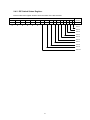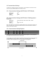
1
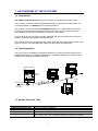
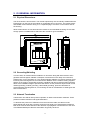
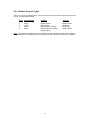
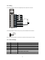
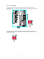
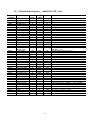
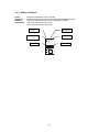
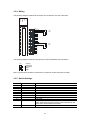
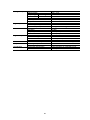
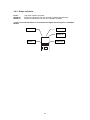
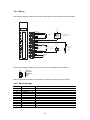
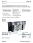
NetBiter I/O Extender 4RO – 6RTD – 8DIO - DAIO User Manual Revision 1.00 IntelliCom Innovation AB Linjegatan 3D SE-302 50 Halmstad SWEDEN Phone Fax email www +46 35 18 21 70 +46 35 18 21 99 [email protected] www.intellicom.se 1. 1.1 1.2 1.3 2. AN OVERVIEW OF THE IO SYSTEM .................................................... 3 INTRODUCTION ............................................................................................................... 3 DATA ACQUISITION ......................................................................................................... 3 MODULE SELECTION TABLE ............................................................................................ 3 IO GENERAL INFORMATION................................................................ 4 2.1 PHYSICAL DIMENSIONS ................................................................................................... 4 2.2 GROUNDING/SHIELDING .................................................................................................. 4 2.3 NETWORK TERMINATION................................................................................................. 4 2.4 SETTING THE MODBUS NODE ID ..................................................................................... 5 2.4.1 Node ID Table ....................................................................................................... 5 2.4.2 DIP Switch Status Register. .................................................................................. 6 2.5 COMMUNICATIONS SETTINGS .......................................................................................... 7 2.5.1 Communications Settings with DIP Switch 10 OFF (Default) ............................... 7 2.5.2 Communications Settings with DIP Switch 10 ON (Programmed Baud Rate) ..... 7 2.5.3 Communications Settings Registers ..................................................................... 7 2.5.4 Modbus Register Types ........................................................................................ 8 3. IO MODULES ......................................................................................... 9 3.1 IOX-4RO - RELAY OUTPUTS ...................................................................................... 9 3.1.1 Description ............................................................................................................ 9 3.1.2 Technical Specification of IOX-4RO ..................................................................... 9 3.1.3 Status Indicators ................................................................................................. 10 3.1.4 Wiring .................................................................................................................. 11 3.1.5 Switch Setting ..................................................................................................... 11 3.1.6 IOX-4RO Data Registers (MODULE TYPE = 113) ............................................. 12 3.2 IOX-8DIO - DIGITAL INPUTS / OUTPUTS ................................................................ 13 3.2.1 Description .......................................................................................................... 13 3.2.2 Technical Specification of IOX-DIO .................................................................... 14 3.2.3 Status Indicators ................................................................................................. 14 3.2.4 Wiring .................................................................................................................. 15 3.2.5 Switch Settings .................................................................................................... 15 3.2.6 Jumper Settings .................................................................................................. 16 3.2.7 IOX-8DIO Data Registers (MODULE TYPE = 102) ........................................ 17 3.3 IOX-6RTD - RTD INPUTS .......................................................................................... 19 3.3.1 Description .......................................................................................................... 19 3.3.2 Technical Specification of IOX-6RTD ................................................................. 19 3.3.3 Status Indicators ................................................................................................. 20 3.3.4 Wiring .................................................................................................................. 21 3.3.5 Switch Settings .................................................................................................... 21 3.3.6 IOX-6RTD Data Registers (MODULE TYPE = 109) ........................................... 22 3.4 IOX-DAIO – DIGITAL + ANALOG INPUTS AND OUTPUTS ...................................... 23 3.4.1 Description .......................................................................................................... 23 3.4.2 Technical Specification of IOX-DAIO .................................................................. 25 3.4.3 Status Indicators ................................................................................................. 27 3.4.4 Wiring .................................................................................................................. 28 3.4.5 Switch Settings .................................................................................................... 28 3.4.6 Jumper Settings .................................................................................................. 29 3.4.7 IOX-DAIO Data Registers (MODULE TYPE = 112) ............................................ 30 4. 4.1 4.2 SPECIFICATIONS ................................................................................ 31 ENVIRONMENTAL .................................................................................................... 31 EMC INSTALLATION INSTRUCTIONS ..................................................................... 31 2 1. AN OVERVIEW OF THE IO SYSTEM 1.1 Introduction The NetBiter I/O Extender series provides a solution for distributed I/O requirements. The IO system consists of stand-alone Digital and Analog - Input/Output modules which are connected together on a RS485 two wire multi-drop network. The modules communicate using the MODBUS RTU protocol. A 32bit ARM CPU is used in the modules to provide high speed data processing and fast communications turnaround times. Multiple baud rates are selectable from 2400 to 115200 baud. All IO modules plug directly onto an industry standard DIN rail. All modules have a minimum isolation of 1000VAC rms between the field and logic. The modules have been equipped with status led’s which are used to indicate the status of the Inputs or outputs. This visual indication assists with fault finding and diagnostics. 1.2 Data Acquisition The primary use of the NetBiter I/O Extender Modules is for Data Acquisition together with a NetBiter WebSCADA. The NetBiter WebSCADA is a MODBUS Master and can retrieve and send data from NetBiter I/O Extender Modules. I/O Ex te n d e r DAIO O NetBiter webSCADA N 1 Swi tch 1 2 3 4 5 6 7 8 9 0 DI P 2 3 4 5 Funct ion ID ID ID ID ID DI DI BaudRate 6 7 8 9 0 ON +1 +2 +4 +8 +16 +32 +64 Conf ig OFF +0 +0 +0 +0 +0 +0 +0 9600 I/O Ex te n d e r DAIO O N 1 Swi tch 1 2 3 4 5 6 7 8 9 0 Modbus Master DI P 2 3 4 5 Funct ion ID ID ID ID ID DI DI BaudRate 6 7 8 9 0 ON +1 +2 +4 +8 +16 +32 +64 Conf ig OFF +0 +0 +0 +0 +0 +0 +0 9600 Modbus Slaves Requests RS485 Network Response 120 Ohm Termi nati on I/O Ex te n d e r DAIO O N 1 Swi tch 1 2 3 4 5 6 7 8 9 0 DI P 2 3 4 5 Funct ion ID ID ID ID ID DI DI BaudRate 6 7 8 9 0 ON +1 +2 +4 +8 +16 +32 +64 Conf ig OFF +0 +0 +0 +0 +0 +0 +0 9600 1.3 Module Selection Table MODEL NetBiter I/O Extender 4RO NetBiter I/O Extender 8DIO NetBiter I/O Extender 6RTD NetBiter I/O Extender DAIO MODULE TYPE 4 RELAY OUTPUT MODULE 8 DIGITAL INPUT / 8 DIGITAL OUTPUT MODULE 6 RTD INPUT MODULE - PT100, Ni120, PT1000, Ni1000, Ni1000LG & Ohms 2 RTD I/P, 2 ANALOG INPUT 0(4) - 20mA / 0(2) - 10V, 1 ANALOG OUTPUT 0(4) - 20mA / 0(2) - 10V, 4 DIGITAL INPUTS, 2 DIGITAL OUTPUTS 3 2. IO GENERAL INFORMATION 2.1 Physical Dimensions The IO enclosure is shown below. The module clips directly onto an industry standard DIN rail. Field wiring is on the front of the module via a separate plug in connector. The module power and RS485 communications wiring is on a separate plug in connector on the bottom side of the housing. Allow at least 25mm on front and below the module to accommodate the wiring. Ensure that enough space is available above and below the module for good ventilation. P R V 1234 I/O Extender DAIO ON 1 1C 1NC 2NC DIP 1 2 3 4 5 6 7 8 9 0 Switch 1 2 3 4 5 6 7 8 9 0 Function ID ID ID ID ID DI DI Baud Rate ON OFF +1 +2 +4 +8 +16 +32 +64 Config +0 +0 +0 +0 +0 +0 +0 9600 2C 2NC 2NC 3C 3NC 3NC 4C 4NC 4NC 1 2 3 4 5 6 7 8 9 10 11 12 13 14 15 16 17 18 2.2 Grounding/Shielding In most cases, IO modules will be installed in an enclosure along with other devices which generate electromagnetic radiation. Examples of these devices are relays and contactors, transformers, motor controllers etc. This electromagnetic radiation can induce electrical noise into both power and signal lines, as well as direct radiation into the module causing negative effects on the system. Appropriate grounding, shielding and other protective steps should be taken at the installation stage to prevent these effects. These protective steps include control cabinet grounding, module grounding, cable shield grounding, protective elements for electromagnetic switching devices, correct wiring as well as consideration of cable types and their cross sections. 2.3 Network Termination Transmission line effects often present a problem on data communication networks. These problems include reflections and signal attenuation. To eliminate the presence of reflections from the end of the cable, the cable must be terminated at both ends with a resistor across the line equal to its characteristic impedance. Both ends must be terminated since the direction of propagation is bi-directional. In the case of an RS485 twisted pair cable this termination is typically 120 ohms. 4 2.4 Setting the Modbus Node ID 2.4.1 Node ID Table The following table assists with the setting up of DIP switches for the required NODE ID. 0 1 2 3 4 5 6 7 8 9 10 11 12 13 14 15 16 17 18 19 20 21 22 23 24 25 26 27 28 29 30 31 1234567 ▄▄▄▄▄▄▄ ▀▄▄▄▄▄▄ ▄▀▄▄▄▄▄ ▀▀▄▄▄▄▄ ▄▄▀▄▄▄▄ ▄▀▄▄▄▄ ▄▀▀▄▄▄▄ ▀▀▀▄▄▄▄ ▄▄▄▀▄▄▄ ▀▄▄▀▄▄▄ ▄▀▄▀▄▄▄ ▀▀▄▀▄▄▄ ▄▄▀▀▄▄▄ ▀▄▀▀▄▄▄ ▄▀▀▀▄▄▄ ▀▀▀▀▄▄▄ ▄▄▄▄▀▄▄ ▀▄▄▄▀▄▄ ▄▀▄▄▀▄▄ ▀▀▄▄▀▄▄ ▄▄▀▄▀▄▄ ▀▄▀▄▀▄▄ ▄▀▀▄▀▄▄ ▀▀▀▄▀▄▄ ▄▄▄▀▀▄▄ ▀▄▄▀▀▄▄ ▄▀▄▀▀▄▄ ▀▀▄▀▀▄▄ ▄▄▀▀▀▄▄ ▀▄▀▀▀▄▄ ▄▀▀▀▀▄▄ ▀▀▀▀▀▄▄ 32 33 34 35 36 37 38 39 40 41 42 43 44 45 46 47 48 49 50 51 52 53 54 55 56 57 58 59 60 61 62 63 1234567 ▄▄▄▄▄▀▄ ▀▄▄▄▄▀▄ ▄▀▄▄▄▀▄ ▀▀▄▄▄▀▄ ▄▄▀▄▄▀▄ ▀▄▀▄▄▀▄ ▄▀▀▄▄▀▄ ▀▀▀▄▄▀▄ ▄▄▄▀▄▀▄ ▀▄▄▀▄▀▄ ▄▀▄▀▄▀▄ ▀▀▄▀▄▀▄ ▄▄▀▀▄▀▄ ▀▄▀▀▄▀▄ ▄▀▀▀▄▀▄ ▀▀▀▀▄▀▄ ▄▄▄▄▀▀▄ ▀▄▄▄▀▀▄ ▄▀▄▄▀▀▄ ▀▀▄▄▀▀▄ ▄▄▀▄▀▀▄ ▀▄▀▄▀▀▄ ▄▀▀▄▀▀▄ ▀▀▀▄▀▀▄ ▄▄▄▀▀▀▄ ▀▄▄▀▀▀▄ ▄▀▄▀▀▀▄ ▀▀▄▀▀▀▄ ▄▄▀▀▀▀▄ ▀▄▀▀▀▀▄ ▄▀▀▀▀▀▄ ▀▀▀▀▀▀▄ 64 65 66 67 68 69 70 71 72 73 74 75 76 77 78 79 80 81 82 83 84 85 86 87 88 89 90 91 92 93 94 95 All modules will respond to a default Node ID of 254. 5 1234567 ▄▄▄▄▄▄▀ ▀▄▄▄▄▄▀ ▄▀▄▄▄▄▀ ▀▀▄▄▄▄▀ ▄▄▀▄▄▄▀ ▀▄▀▄▄▄▀ ▄▀▀▄▄▄▀ ▀▀▀▄▄▄▀ ▄▄▄▀▄▄▀ ▀▄▄▀▄▄▀ ▄▀▄▀▄▄▀ ▀▀▄▀▄▄▀ ▄▄▀▀▄▄▀ ▀▄▀▀▄▄▀ ▄▀▀▀▄▄▀ ▀▀▀▀▄▄▀ ▄▄▄▄▀▄▀ ▀▄▄▄▀▄▀ ▄▀▄▄▀▄▀ ▀▀▄▄▀▄▀ ▄▄▀▄▀▄▀ ▀▄▀▄▀▄▀ ▄▀▀▄▀▄▀ ▀▀▀▄▀▄▀ ▄▄▄▀▀▄▀ ▀▄▄▀▀▄▀ ▄▀▄▀▀▄▀ ▀▀▄▀▀▄▀ ▄▄▀▀▀▄▀ ▀▄▀▀▀▄▀ ▄▀▀▀▀▄▀ ▀▀▀▀▀▄▀ 96 97 98 99 100 101 102 103 104 105 106 107 108 109 110 111 112 113 114 115 116 117 118 119 120 121 122 123 124 125 126 127 1234567 ▄▄▄▄▄▀▀ ▀▄▄▄▄▀▀ ▄▀▄▄▄▀▀ ▀▀▄▄▄▀▀ ▄▄▀▄▄▀▀ ▀▄▀▄▄▀▀ ▄▀▀▄▄▀▀ ▀▀▀▄▄▀▀ ▄▄▄▀▄▀▀ ▀▄▄▀▄▀▀ ▄▀▄▀▄▀▀ ▀▀▄▀▄▀▀ ▄▄▀▀▄▀▀ ▀▄▀▀▄▀▀ ▄▀▀▀▄▀▀ ▀▀▀▀▄▀▀ ▄▄▄▄▀▀▀ ▀▄▄▄▀▀▀ ▄▀▄▄▀▀▀ ▀▀▄▄▀▀▀ ▄▄▀▄▀▀▀ ▀▄▀▄▀▀▀ ▄▀▀▄▀▀▀ ▀▀▀▄▀▀▀ ▄▄▄▀▀▀▀ ▀▄▄▀▀▀▀ ▄▀▄▀▀▀▀ ▀▀▄▀▀▀▀ ▄▄▀▀▀▀▀ ▀▄▀▀▀▀▀ ▄▀▀▀▀▀▀ ▀▀▀▀▀▀▀ 2.4.2 DIP Switch Status Register. Each module uses register 30100 to store the status of the DIP switches. MSB 15 32768 0 14 16384 13 8192 12 4096 0 0 0 DIP SWITCH REGISTER 11 10 9 8 7 2048 1024 512 256 128 0 6 64 5 32 4 16 3 8 2 4 1 2 LSB 0 1 ADDRESS 30100 0 SW 1 SW 2 SW 3 SW 4 SW 5 SW 6 SW 7 SW 8 SW 9 SW 10 6 2.5 Communications Settings The data in the modules is stored in 16 bit registers. These registers are accessed over the network using the MODBUS RTU communication protocol. 2.5.1 Communications Settings with DIP Switch 10 OFF (Default) BAUD RATE DATA BITS PARITY STOP BITS 9600 8 NONE 1 2.5.2 Communications Settings with DIP Switch 10 ON (Programmed Baud Rate) BAUD RATE DATA BITS PARITY STOP BITS 2400, 4800, 9600, 19200, 38400, 57600, 115200 8 None, Even, Odd 1, 2 Note: These settings are changed from a Modbus Master device. During these changes, DIP switch10 should be OFF such that, the Master device can communicate with IO module on default communication settings. 2.5.3 Communications Settings Registers 40121 40122 40123 40124 Baud Rate Parity Stop Bits Reply Delay 2400 0 1 0 11520 2 2 65535 R/W R/W R/W R/W 2400, 4800, 9600, 19200, 38400,57600,11520 0 = none, 1 = even, 2 = odd 1 = 1 stop bit, 2 = 2 stop bits (x10ms) The baud rate value is programmed directly into the baud rate register. The only exception is the 115200 baud rate where the value 11520 is used. The reply delay is a time delay between the Modbus message received to the reply being sent. In some applications where a modem or radio is used in the RS485 network, it may be necessary to add a reply delay due to turn around delays in the equipment. Reply Delay Rx Request Tx Reply Time (x10ms) 7 2.5.4 Modbus Register Types There are 4 types of variables which can be accessed from the module. Each module has one or more of these data variables. Type Start Address Variable 1 2 3 4 00001 10001 30001 40001 Digital Outputs Digital Inputs Input registers (Analog) Output registers (Analog) (Holding type) Access Read & Write Read Only Read Only Read & Write Note: The Modbus message length must be limited to 100 consecutive read or write registers. If more registers are required then a new poll group must be added for the next xxx registers. 8 3. IO MODULES 3.1 IOX-4RO - RELAY OUTPUTS 3.1.1 Description The IOX-4RO module has 4 normally open/ normally closed relay outputs. These modules may be used when a higher drive capability is required, or when isolation between outputs are required. When switch 9 is off, the module is configured as a slave module for the Modbus master device such as a PC / PLC / HMI. When used as a slave module, the outputs are written to by the Modbus master device such as a PC/PLC/HMI. Each output can be individually switched on or off, or all outputs can be set up at the same time by writing a single number to the output register which represents the status of all outputs. An output watchdog timer can be configured to switch off all the outputs if there has been no communications with the module for up to 255 seconds. A value of 0 seconds will disable this timer and the outputs will remain in the last programmed state. 3.1.2 Technical Specification of IOX-4RO Power Supply Relay Outputs Temperature Connectors Logic Supply Voltage Logic Supply Current Output Points Maximum Current Isolation Operating Temperature. Storage Temperature Logic Power and Comms. Outputs 9 24 Vdc 42 mA 4 0.5A @ 220VAC / 1A @ 28VDC 1000Vrms between field and logic 1000Vrms between outputs -10°C to + 50°C -40°C to + 85°C 4 Pin Connector on underside of unit 18 Way screw connector on front 3.1.3 Status Indicators Power: Flashes to indicate the CPU is running. RS485 Rx: Flashes to indicate the unit has received a valid Modbus message. RS485 Tx: Flashes to indicate the unit has sent a Modbus message. Output Status: “OFF” when the output is off “ON” when the output is on. Power RS485 Rx Output Status 1-4 RS485 Tx Switch 1 Switch 10 10 3.1.4 Wiring The following diagram shows how the digital outputs are connected to the coil of a relay. The coil is connected to positive and switched to negative. Relay 1 Common Relay 1 Normally Open Relay 1 Normally Closed Relay 2 Common +24Vdc / 220Vac Relay 2 Normally Open + Relay 2 Normally Closed RELAY Relay 3 Common Relay 3 Normally Open 0Vdc / 220Vac Relay 3 Normally Closed Relay 4 Common Relay 4 Normally Open Relay 4 Normally Closed The following diagram shows the wiring for the power and RS485 communications. Pin Connection 1 2 - 24Vdc + @42mA 3 4 + Comms - RS485 Note: If power/communication connections are reversed, module may become faulty. 3.1.5 Switch Setting SWITCH FUNCTION 1 2 3 4 5 6 7 8 9 10 NODE ID +1 NODE ID +2 NODE ID +4 NODE ID +8 NODE ID +16 NODE ID +32 NODE ID +64 MODE BAUD RATE DESCRIPTION Node ID’s from 0 to 127 are set up using switches 1 to 7 “ “ “ “ “ “ Not Used. Slave (Off) Selects 9600 (off) or Programmed Baud Rate (on) 11 3.1.6 IOX-4RO Data Registers (MODULE TYPE = 113) Modbus Address 00001 00002 00003 00004 30001 Register Name Relay Output 1 Relay Output 2 Relay Output 3 Relay Output 4 S/W Version / Module Type Digital Outputs DIP Switch Watchdog Timer Baud Rate Parity Stop Bits Reply Delay 40002 30100 40101 40121 40122 40123 40124 Low Limit 0 0 0 0 High Limit 1 1 1 1 Access N/A N/A R N/A 0 0 2400 0 1 0 N/A 65535 255 11520 2 2 65535 R/W R R/W R/W R/W R/W R/W Comments R/W R/W R/W R/W Status of Digital Outputs. " " " High Byte = Software Version Low Byte = 113 Digital Outputs in bits. 4(msb) – 1(lsb). Status of DIP Switch on Front Panel Timer in seconds. 0 = disabled. 1 - 255 = enabled. 2400, 4800, 9600,19200, 38400,57600,115200 0 = none, 1 = even, 2 = odd 1 = 1 stop bit, 2 = 2 stop bits 0 = Disable, >0 = Enable. (x10ms) 3.1.6.1 Relay Output Register The relay outputs can be read /written in a single register as follows MSB 15 32768 14 16384 13 8192 12 4096 - - - - IOX-4RO DIGITAL OUTPUTS 11 10 9 8 7 2048 1024 512 256 128 - - - - - 6 64 5 32 4 16 3 8 2 4 - - - 4 3 LSB 1 0 2 1 2 1 Relay Output Number 3.1.6.2 Output Watchdog Timer The watchdog timer is used to switch off all of the outputs in the event of a communications failure. When set to zero (register 40101) the watchdog timer is disabled. 12 ADDRESS 40002 3.2 IOX-8DIO - DIGITAL INPUTS / OUTPUTS 3.2.1 Description The IOX-8DIO module is an 8 channel digital input and 8 channel digital output module. The inputs are isolated from the logic by bi-directional opto-couplers. The common is connected internally to either the -volts or +volts field power supply terminals using a jumper link which is situated inside the housing. The inputs have internal counters associated with them. These counters are 32 bit counters allowing a count value from 0 to 4294967295. The count value can be cleared by writing a zero to the associated registers or preset to any other value using the same method. The counters can also be reset automatically when read. This is done by setting on DIP switch 9 on the front panel. Note: The count values are not battery backed-up and will be lost if power is turned off. The format of the registers allows the status of the inputs to be read as either single bits or all at once as a single register on the Modbus network. The 8 digital outputs are open collector (NPN). The outputs may be used to drive lamps or external relays when more drive capability is required. The outputs are isolated from the logic and they share a common negative terminal. The module may be configured as slave, where PC/ PLC/ HMI acting as master on the Modbus network. Dip switch 9 should be switched off to make this module as slave. Each output on the module can be individually switched on or off, or all outputs can be set up at the same time by writing a single number to the output register which represents the status of all outputs. 13 3.2.2 Technical Specification of IOX-DIO Power Supply Digital Inputs Digital Outputs Counters Temperature Connectors Logic Supply Voltage Logic Supply Current Field Supply Voltage Field Supply Current Input Points Input Voltage Range Input Current per input Isolation Output Points Maximum Voltage Maximum Current Vceon Isolation Inputs Resolution Frequency Pulse Width Operating Temperature. Storage Temperature Logic Power and Comms. Outputs 12 -24 Vdc 33mA @ 12V / 19mA @ 24V 12 -24 Vdc 6mA @ 12V / 6mA @ 24V 8 12 -24 Vdc 5mA@12Vdc / 11mA @24Vdc 1500Vrms between field and logic 8 36 Vdc 100 mA per output 1.1V Max. 1500Vrms between field and logic 1 to 8 32 Bits 1KHz (max) 500us (min) -10°C to + 50°C -40°C to + 85°C 4 Pin Connector on underside of unit 18 Way screw connector on front Note: Inputs 1 to 8 are used as both digital inputs and counter inputs. 3.2.3 Status Indicators Power: RS485 Rx: RS485 Tx: Input Status: Flashes to indicate the CPU is running. Flashes to indicate the unit has received a valid Modbus message. Flashes to indicate the unit has sent a Modbus message. “OFF” when the input is off “ON” when the input is on. Output Status: “OFF” when the output is off “ON” when the output is on. Power RS485 Rx Input Status 1-8 RS485 Tx Output Status 1-8 Switch 10 Switch 1 14 3.2.4 Wiring The following diagram shows how the digital inputs and outputs are connected. Input 1 Input 2 Input 3 Input 4 Input 5 Input 6 Input 7 ( Set internal jumper ) Input 8 +12-24Vdc Output 1 0Vdc or Output 2 +12-24Vdc Output 3 Output 4 + RELAY Output 5 - Output 6 Output 7 Output 8 +V +12-24Vdc 0V 0Vdc The following diagram shows the wiring for the power and RS485 communications. Pin C onnection 1 2 - 12Vdc@33m A + 24Vdc@19m A 3 4 +C om m s - R S485 Note: If power/communication connections are reversed, module may become faulty. 3.2.5 Switch Settings SWITCH FUNCTION 1 2 3 4 5 6 7 8 NODE ID NODE ID NODE ID NODE ID NODE ID NODE ID NODE ID INVERT +1 +2 +4 +8 +16 +32 +64 9 10 MODE BAUD RATE DESCRIPTION Node ID’s from 0 to 127 are set up using switches 1 to 7 “ “ “ “ “ “ When switched ON the status of the inputs is inverted in the Modbus status register (30002). Off (Slave) Selects 9600 (off) or Programmed Baud Rate (on) 15 3.2.6 Jumper Settings The Digital inputs can be configured as NPN inputs. This means that the inputs can be operated by switching to 0V. Open the IO Module. Change the link LK1 to the NPN position as shown below. LK1 The Digital inputs can be configured as PNP inputs. This means that the inputs can be operated by switching to +12V to +24V. Open the IO Module. Change the link LK1 to the PNP position as shown below. 16 3.2.7 IOX-8DIO Data Registers Modbus Address 10001 10002 10003 10004 10005 10006 10007 10008 00017 00018 00019 00020 00021 00022 00023 00024 30001 30002 40003 40004 40005 40006 40007 40008 40009 40010 40011 40012 40013 40014 40015 40016 40017 40018 40019 30100 40101 40105 40106 40121 40122 40123 40124 Register Name Digital Input 1 Digital Input 2 Digital Input 3 Digital Input 4 Digital Input 5 Digital Input 6 Digital Input 7 Digital Input 8 Digital Output 1 Digital Output 2 Digital Output 3 Digital Output 4 Digital Output 5 Digital Output 6 Digital Output 7 Digital Output 8 S/W Version / Module Type Digital Inputs Digital Outputs Counter 1 MSB Counter 1 LSB Counter 2 MSB Counter 2 LSB Counter 3 MSB Counter 3 LSB Counter 4 LSB Counter 4 LSB Counter 5 MSB Counter 5 LSB Counter 6 MSB Counter 6 LSB Counter 7 MSB Counter 7 LSB Counter 8 MSB Counter 8 LSB DIP Switch Watchdog Timer Counter Mode Input Filter Baud Rate Parity Stop Bits Reply Delay (MODULE TYPE = 102) Low Limit 0 0 0 0 0 0 0 0 0 0 0 0 0 0 0 0 High Limit 1 1 1 1 1 1 1 1 1 1 1 1 1 1 1 1 Access N/A N/A R N/A N/A 0 0 0 0 0 0 0 0 0 0 0 0 0 0 0 0 0 0 0 0 2400 0 1 0 N/A N/A 65535 65535 65535 65535 65535 65535 65535 65535 65535 65535 65535 65535 65535 65535 65535 65535 65535 255 2 65535 11520 2 2 65535 R R/W R/W R/W R/W R/W R/W R/W R/W R/W R/W R/W R/W R/W R/W R/W R/W R/W R R/W R/W R/W R/W R/W R/W R/W R R R R R R R R R/W R/W R/W R/W R/W R/W R/W R/W 17 Comments Status of Digital Inputs. " " " " " " " Status of Digital Outputs. " " " " " " " High Byte = Software Version Low Byte = 102 Digital Inputs in lower 8 bits. 8 - 1. Digital Outputs in lower 8 bits. 8 - 1. Counter MSB and LSB combine to give a 32 bit Counter with range 0 to 4294967295. " " " " " " " " " " " " " " Status of DIP Switch on Front Panel Timer in seconds. 0 = disabled. 1 - 255 = enabled. 0=Disable, 1=Up Counting, 2=Up/Down Count 0 = Disable, >0 = Enable. (x10ms) 2400, 4800, 9600, 19200, 38400,57600,115200 0 = none, 1 = even, 2 = odd 1 = 1 stop bit, 2 = 2 stop bits 0 = Disable, >0 = Enable. (x10ms) 3.2.7.1 Digital Input Register. The digital inputs can be read in a single register as follows: MSB 15 32768 14 16384 13 8192 12 4096 0 0 0 0 IOX-8DIO DIGITAL INPUTS 11 10 9 8 7 2048 1024 512 256 128 0 0 0 0 8 6 64 5 32 4 16 3 8 2 4 LSB 1 0 2 1 7 6 5 4 3 2 5 32 4 16 3 8 2 4 LSB 1 0 2 1 6 5 4 3 2 ADDRESS 30002 1 Digital Input Number 3.2.7.2 Digital Output Register The digital outputs can be read /written in a single register as follows: MSB 15 32768 14 16384 13 8192 12 4096 0 0 0 0 IOX-8DIO DIGITAL OUTPUTS 11 10 9 8 7 6 2048 1024 512 256 128 64 0 0 0 0 8 7 ADDRESS 40003 1 Digital Output Number 3.2.7.3 Counter Registers. The counters are stored in two 16 bit registers. The first register is the High Register and the second register is the Low Register. To get the actual 32 bit count value the registers must be combined as follows: Counter High Value = Register 40003. Counter Low Value = Register 40004. Counter Value = (Counter High Value X 65535) + Counter Low Value. 3.2.7.4 Output Watchdog Timer The watchdog timer is used to switch off all of the outputs in the event of a communications failure. When set to zero (register 40101) the watchdog timer is disabled. 18 3.3 IOX-6RTD - RTD INPUTS 3.3.1 Description The IOX-6RTD module is a 6 RTD input module. The module can accommodate either 2 or 3 wire RTD sensors. The RTD inputs are isolated from the logic. The RTD resistance is read by the module circuitry, linearised and converted to degrees Centigrade. No ranging is required as the module covers the full range of the RTD as indicated in the RTD table. The value that is read from the Modbus register is the actual temperature in degrees centigrade to 0.1°C resolution. ie: a value of 3451 corresponds to a temperature of 345.1°C. The RTD type is setup by writing a value to the RTD Type register. The value is obtained from the table below. For example to select a PT100 RTD, the value "1" must be written to the RTD Type register. All 6 RTD inputs adopt the same RTD type. The DIP switch 9 is used to select upscale or downscale burnout for break detection. A value of 32768 is used to indicate upscale burnout and a value of -32767 is used to indicate downscale burnout. Note: As there is no inter-channel isolation, isolated RTD's must be used in order to prevent ground loops and reading errors. 3.3.2 Technical Specification of IOX-6RTD Power Supply RTD Inputs RTD Type Logic Supply Voltage Logic Supply Current Input Points RTD Configuration Resolution Drift Line resistance effect Max. line resistance Isolation Number Type 1 PT100 2 3 4 5 Temperature Connectors Ni120 PT1000 Ni1000-DIN Ni1000Landys&Gyr 6 Ohms 7 Ohms Operating Temperature. Storage Temperature Logic Power and Comms. Inputs 19 12 -24 Vdc 87mA @ 12V / 45mA @ 24V 6 2 or 3 Wire 0.1°C 100ppm/°C Typ. < 0.1°C balanced 100ohms 1500Vrms between field and logic Range Accuracy -200 to 850°C ± 0.3°C,IEC 751:1983 -80 to 320°C ± 0.3°C -200 to 850°C ± 0.3°C -200 to 850°C ± 0.3°C -200 to 850°C ± 0.3°C 10 - 400 ohms ± 0.05% 100-4000ohms ± 0.05% -10°C to + 50°C -40°C to + 85°C 4 Pin Connector on underside of unit 18 Way screw connector on front 3.3.3 Status Indicators Power: RS485 Rx: RS485 Tx: Input Status: Flashes to indicate the CPU is running. Flashes to indicate the unit has received a valid Modbus message. Flashes to indicate the unit has sent a Modbus message. “ON” when the RTD is open circuit. “OFF” when the RTD is connected. RS485 Rx Power RS485 Tx Input Status 1-6 Switch 1 Switch 10 20 3.3.4 Wiring The following diagram shows how the inputs are connected to a 2 and 3 wire RTD. Input 1a Input 1b RTD 3 Wire Input 1c Input 2a Input 2b Input 2c Input 3a Input 3b Input 3c Input 4a Input 4b RTD 2 Wire Input 4c Input 5a Input 5b Input 5c Input 6a Input 6b Input 6c The following diagram shows the wiring for the power and RS485 communications. Pin C onnection 1 2 - 12Vdc@87m A + 24Vdc@45m A 3 4 +C om m s - R S485 Note: If power/communication connections are reversed, module may become faulty. 3.3.5 Switch Settings SWITCH FUNCTION 1 2 3 4 5 6 7 8 9 NODE ID +1 NODE ID +2 NODE ID +4 NODE ID +8 NODE ID +16 NODE ID +32 NODE ID +64 BREAK 10 BAUD RATE DESCRIPTION Node ID’s from 0 to 127 are set up using switches 1 to 7 “ “ “ “ “ “ Not used. RTD break. When switched off the RTD value will loaded with -32767 when the RTD is faulty. When switched on the RTD value will be loaded with 32768. Selects 9600 (off) or Programmed Baud Rate (on) 21 3.3.6 IOX-6RTD Data Registers (MODULE TYPE = 109) Modbus Address 30001 30002 30003 30004 30005 30006 30007 30008 30100 40101 40102 40103 40121 40122 40123 40124 Register Name S/W Version / Module Type RTD Input 1 RTD Input 2 RTD Input 3 RTD Input 4 RTD Input 5 RTD Input 6 Input Status DIP Switch RTD Type Line Frequency Units Type Baud Rate Parity Stop Bits Reply Delay Low Limit N/A High Limit N/A Access -xxx.x -xxx.x -xxx.x -xxx.x -xxx.x -xxx.x 0 0 1 50 1 2400 0 1 0 yyyy.y yyyy.y yyyy.y yyyy.y yyyy.y yyyy.y 65535 65535 7 60 2 11520 2 2 65535 R R R R R R R R R/W R/W R/W R/W R/W R/W R/W R Description High Byte = Software Version Low Byte = 109 RTD Inputs. See table for range. Resolution in 0.1°C. " " " " bit1 = 0(OK),bit1 = 1(error or open circuit) Status of DIP Switch on Front Panel See RTD Tables. Line Frequency 1=°C, 2=°F 2400, 4800, 9600, 19200, 38400,57600,115200 0 = none, 1 = even, 2 = odd 1 = 1 stop bit, 2 = 2 stop bits 0 = Disable, >0 = Enable. (x10ms) 3.3.6.1 RTD Input Status. There is one status bits associated with each RTD input. These bits are used to indicate if the input is open circuit or over range. If the input is open circuit or over range, then the error bit will be set. Bit 1- Error 0 1 Bit 2-Not Used 0 0 Condition Input working OK Open circuit / Over range Status LED (LED OFF) (LED ON) The analog input status can be read in a single register as follows MSB 15 32768 14 16384 13 8192 IOX-6RTD ANALOG INPUT STATUS 12 11 10 9 8 7 6 4096 2048 1024 512 256 128 64 5 32 4 16 3 8 2 4 LSB 1 0 2 1 ADDRESS 30008 IP1 Error IP2 Error IP3 Error IP4 Error IP5 Error IP6 Error 22 3.4 IOX-DAIO – DIGITAL + ANALOG INPUTS AND OUTPUTS 3.4.1 Description The IOX-DAIO module is a multipurpose combination of inputs and outputs. The module can accommodate either 2 or 3 wire RTD sensors, current (0-20mA) and voltage (0-10V) inputs, current (0-20mA) or voltage (0-10V) output, and digital inputs and outputs. RTD INPUTS: There are 2 RTD inputs on the module. The RTD resistance is read by the module circuitry, linearised and converted to degrees Centigrade. No ranging is required as the module covers the full range of the RTD as indicated in the RTD table. The value that is read from the Modbus register is the actual temperature in degrees centigrade to 0.1°C resolution. ie: a value of 3451 corresponds to a temperature of 345.1°C. The RTD type is setup by writing a value to the RTD Type register. The value is obtained from the table below. For example to select a PT100 RTD, the value "1" must be written to the RTD Type register. A value of -32767 is used to indicate downscale burnout. Note: As there is no inter-channel isolation, isolated RTD's must be used in order to prevent ground loops and reading errors. ANALOG INPUTS: The Analog Inputs (2) can be configured by internal jumpers as either a current input (020mA) or a voltage input (0-10V). An input of 0 - 20mA input current or 0 – 10V input voltage represents an output value of 0 4095 (12 bits) in the corresponding Modbus register. ANALOG OUTPUT: There is a single analog output which can be configured with internal jumpers for a current output (0-20mA) or voltage output (0-10V). The resolution is 12 bits, so writing a value to the Modbus register for each output of 0 - 4095 would give an output current of 0 - 20mA. A value of 819 ± 1LSB will give a current output of 4mA. 23 DIGITAL INPUTS: There are 4 digital inputs on the module. The inputs share a common terminal and can be configured for common positive or common negative. The inputs have got counters associated with them. The counters operate in three modes. In mode 0 all the counters are disabled. In mode 1 all counters are 32 bit counters allowing a count value from 0 to 4294967295. The count value can be cleared by writing a zero to the associated registers or preset to any other value using the same method. In mode 2 the inputs are connected as up/down counters. Input 1 will increment counter 1 while input 2 decrements counter1. Note: The count values are not battery backed-up and will be lost if power is turned off. The format of the registers allows the status of the inputs to be read as either single bits or all at once as a single register on the Modbus network. DIGITAL OUTPUTS: The module has 2 open collector (NPN) digital outputs. The outputs may be used to drive lamps or external relays when more drive capability is required. The outputs are written to by the Modbus master device such as a PC/ PLC/ HMI. Each output can be individually switched on or off, or all outputs can be set up at the same time by writing a single number to the output register which represents the status of all outputs. An output watchdog timer can be configured to switch off all the outputs if there has been no communications with the module for up to 255 seconds. A value of 0 seconds will disable this timer and the outputs will remain in the last programmed state. 24 3.4.2 Technical Specification of IOX-DAIO Power Supply RTD Inputs RTD Type Current Inputs Voltage Inputs Current Output Logic Supply Voltage Logic Supply Current Field Supply Voltage Field Supply Current Input Points RTD Configuration Resolution Drift Line resistance effect Max. line resistance Isolation Number Type 1 PT100 2 Ni120 3 PT1000 4 Ni1000-DIN 5 Ni1000Landys&Gyr 6 Ohms 7 Ohms Input Points Input Current Input Resistance Input Type Range 1 0 – 4095 2 0–20.000mA 3 +/-20.000mA Drift Accuracy Isolation Input Points Input Voltage Input Resistance Input Type Range 4 0 – 4095 5 0 – 10.000 V 6 +/- 10.000 V 7 0 – 1.0000 V 8 +/- 1.0000 V Drift Accuracy Isolation Output Points Output Current Output Type Range 1 0 – 4095 Drift Accuracy Compliance 25 12 -24 Vdc 115mA @ 12V / 58mA @ 24V 24 Vdc 25mA 2 2 or 3 Wire 0.1°C 100ppm/°C Typ. < 0.1°C balanced 100ohms 1500Vrms between field and logic Range Accuracy -200 to 850°C ± 0.3°CIEC 751:1983 -80 to 320°C ± 0.3°C -200 to 850°C ± 0.3°C -200 to 850°C ± 0.3°C -200 to 850°C ± 0.3°C 10 - 400 ohms ± 0.05% 100-4000ohms ± 0.05% 2 0(4) - 20 mA 250ohms Resolution 12 bits 1uA 1uA 100ppm/°C 0.2% of span 1000Vrms between field and logic 2 0 - 1 Vdc or 0 – 10 Vdc 190kohms Resolution 12 bits 1mV 1mV 0.1mV 0.1mV 100ppm/°C 0.2% of span 1000Vrms between field and logic 1 0(4) - 20 mA Resolution 12 bits 100ppm/°C 0.05% of span 1000 ohms max. @ 24Vdc 500 ohms max. @ 12Vdc Voltage Output Digital Inputs Counters Digital Outputs Isolation Temperature Connectors Output Points Output Voltage Output Type Range 2 0 – 4095 Drift Accuracy Compliance Input Points Input Voltage Range Input Current per input Inputs Resolution Frequency Pulse Width Output Points Maximum Voltage Maximum Current Vceon Between field and logic Operating Temperature. Storage Temperature Logic Power and Comms. Inputs 26 1 0(2) - 10 V Resolution 12 bits 100ppm/°C 0.05% of span 2000 ohms min. load 4 10 - 26 Vdc 4mA@12Vdc / 8mA @24Vdc 1 to 4 32 Bits 50 Hz (max) 20 ms (min) 2 36 Vdc 100 mA per output 1.1V Max. 1500Vrms between field and logic -10°C to + 50°C -40°C to + 85°C 4 Pin Connector on underside of unit 18 Way screw connector on front 3.4.3 Status Indicators Power: RS485 Rx: RS485 Tx: “ON” when module has power. Flashes to indicate the unit has received a valid Modbus message. Flashes to indicate the unit has sent a Modbus message. * Please note that LED status is not available for Digital and Analog IO’s in IOX-DAIO Module RS485 Rx Power RS485 Tx Switch 1 Switch 10 27 3.4.4 Wiring The following diagram shows how the inputs and outputs are connected to the DAIO module. +24Vdc RTD Input 1a + RTD Input 1b RTD 3 Wire RTD Input 2a RTD Input 2c Two Wire Transmitter 0(4)-20mA Common/0V - Analog Input 1 Analog Input 2 Analog Output 1 Common/0V Digital Input 1 Digital Input 2 +24Vdc Digital Input 3 +24Vdc Digital Input 4 0Vdc 0Vdc + + or +24Vdc - Digital Input Common Digital Output 1 RELAY - Analog Load 0 - 20mA or 0 - 10V Digital Output 2 0Vdc +V Common/0V +24Vdc 0Vdc The following diagram shows the wiring for the power and RS485 communications. P in C onnection 1 2 - 12V dc@ 1 15m A + 24V dc@58m A 3 4 +C om m s - R S 485 Note: If power/communication connections are reversed, module may become faulty. 3.4.5 Switch Settings SWITCH FUNCTION 1 2 3 4 5 6 7 8 9 10 NODE ID +1 NODE ID +2 NODE ID +4 NODE ID +8 NODE ID +16 NODE ID +32 NODE ID +64 BAUD RATE DESCRIPTION Node ID’s from 0 to 127 are set up using switches 1 to 7 “ “ “ “ “ “ Not used. Not used. Selects 9600 (off) or Programmed Baud Rate (on) 28 3.4.6 Jumper Settings 3.4.6.1 Current Input and Output The Analog inputs can be configured as a current 0(4)-20mA input by placing the jumper on J7 for AI1 and J8 for AI2. The Analog output can be configured as a current 0(4)-20mA output by placing the jumpers J9, J10 and J11 on the “I” position as shown below. J7 J8 J9 J10 J11 3.4.6.2 Voltage Input and Output The Analog inputs can be configured as a voltage 0-10V input by removing the jumper from J7 for AI1 and J8 for AI2. The Analog output can be configured as a voltage 0-10V output by placing the jumpers J9, J10 and J11 on the “V” position as shown below J7 J8 J9 J10 J11 29 3.4.7 IOX-DAIO Data Registers (MODULE TYPE = 112) Modbus Address 10001 10002 10003 10004 00017 00018 30001 30002 40003 40004 40005 40006 40007 40008 40009 40010 40011 40012 40013 40014 40015 40016 30100 40101 40102 40103 40104 40105 40106 40107 40108 40109 40110 40121 40122 40123 40124 Register Name Digital Input 1 Digital Input 2 Digital Input 3 Digital Input 4 Digital Output 1 Digital Output 2 S/W Version / Module Type Digital Inputs Digital Outputs RTD Input 1 RTD Input 2 Analog Input 1 Analog Input 2 Analog Output 1 Counter 1 MSB Counter 1 LSB Counter 2 MSB Counter 2 LSB Counter 3 MSB Counter 3 LSB Counter 4 MSB Counter 4 LSB DIP Switch Watchdog Timer Counter Mode Input Filter RTD 1 Type RTD 2 Type AI 1 Type AI 2 Type AO Type Line Frequency Units Type Baud Rate Parity Stop Bits Reply Delay Low Limit 0 0 0 0 0 0 High Limit 1 1 1 1 1 1 Access N/A N/A R N/A N/A -xxx.x -xxx.x 0 0 0 0 0 0 0 0 0 0 0 0 0 0 0 1 1 1 1 1 50 1 2400 0 1 0 N/A N/A yyyy.y yyyy.y 4095 4095 4095 65535 65535 65535 65535 65535 65535 65535 65535 65535 255 2 65535 7 7 2 2 2 60 2 11520 2 2 65535 R R/W R R R R R/W R/W R/W R/W R/W R/W R/W R/W R/W R R/W R/W R/W R/W R/W R/W R/W R/W R/W R/W R/W R/W R/W R/W R R R R R/W R/W 30 Comments Status of Digital Inputs. " " " Status of Digital Outputs. " High Byte = Software Version Low Byte = 112 Digital Inputs in lower 8 bits. 8 - 1. Digital Outputs in lower 8 bits. 8 - 1. RTD Inputs. See table for range. Resolution in 0.1°C. Analog Input lower 12 Bits Analog Input lower 12 Bits Analog Output lower 12 Bits Counter MSB and LSB combine to give a 32 bit Counter with range 0 to 4294967295. “ “ “ “ “ “ Status of DIP Switch on Front Panel Timer in seconds. 0 = disabled. 1 - 255 = enabled. 0=Disable, 1=Up Counting, 2=Up/Down Count 0 = Disable, >0 = Enable. (x10ms) See RTD Tables. See RTD Tables. 1 = 0-20mA, 2 = 0-10V " " Line Frequency 1=°C, 2=°F 2400, 4800, 9600, 19200, 38400,57600,115200 0 = none, 1 = even, 2 = odd 1 = 1 stop bit, 2 = 2 stop bits 0 = Disable, >0 = Enable. (x10ms) 4. SPECIFICATIONS 4.1 ENVIRONMENTAL Operating Temperature Storage Temperature Humidity -10°C to +50°C -40°C to +85°C Up to 95% non condensing 4.2 EMC INSTALLATION INSTRUCTIONS 1. Screened twisted pair RS485 cable must be used with the screen grounded at one point only. 2. The RS485 cable must be terminated at both ends using a 120ohm resistor. 3. Use should be made of screened I/O, T/C, RTD cable with the screens grounded at one point as close to the IO module as possible. 31