1
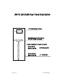
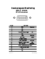
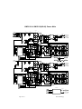
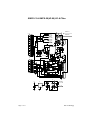
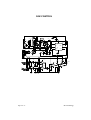
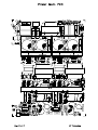
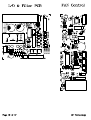
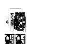
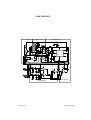
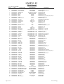
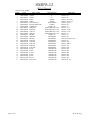
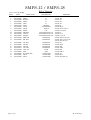
SMPS-12
Eclipse Use Switching Power Supply
SERVICE MANUAL
V2.00
Copyright 2001 , RF Technology
Contents
A. General Description...................................3
B. Rear Panel Description
Power output 25P D-sub connector........4
I/O 15P D-sub connector........................5
C. Circuit Diagram
Power Main ...........................................6
I/O & Filter ............................................7
FAN Control...........................................8
D. Layout
Power Main PCB....................................9
I/O & Filter FAN Control PCB..............10
E. Circuit Description in Block mode
Power Main . I/O & Filter ....................11
FAN Control..........................................12
F. Specification..............................................13
G. Bill of Material..........................................14
Page 2 of 17
RF Technology
1. This Switching mode Power supply is special design and use in professional
RF equipments. It provided an excellent efficiency and reliability only in
very small 4 U space to high power output. It also providing an I/O interface
to user to develop and monitoring feature.
2. SMPS-12 can use 110V and 220V AC power for input, the AC Voltage
switch is in the top of the power supply sub-rack. Before plug in please
check the voltage position is correct or not otherwise may take a permanent
damage in this power supply. If the output inquiry of power supply will
more than 20 Amp. We strongly recommend to use 220V input to prevent
overloading in AC power input.
3. The FAN control circuit will making self-test when the power is turn “ON”.
The LED in front panel will change to orange color from green color and
FAN starting to run, if LED flash in red color and alarm beep coming out
this is show out the fail of FAN and need to be check.
4. The states of LED in front panel :
I. Green color : when power supply turn ON and in normal running.
II. Orange color : when power supply turn ON and FAN starting self-test.
III. Flash red color : FAN fail in running.
5. The FAN will automatically running when the system temperature higher
then 50oC, and will beep alarm if FAN fail.
6. When output of power supply is fail, please check the AC input and output
circuit first. If the fuse burn out that means must has some serious damage
inside of circuit, because of the wrong operation or AC input. The circuit has
a very good protection design usually will not damage in normal operation.
7. Output power in 13.8 Volts can be from 0 Amp. up to 35 Amp. within the
environments temperature 0oC to 60oC. If the continuously output current
may more than 25 Amp. and up, beware the environments temperature
should not higher than 40oC.
8. The input Voltage should between 95V/AC ~ 130V/AC ( 115V/AC )
and 190V/AC ~ 260V/AC ( 230V/AC )
9. The 25 pin D-sub for power output should keep contact clean otherwise may
cause connector burn out.
Page 3 of 17
RF Technology
SMPS-12(V2.00) Rear Panel Description
AC input plug housing
Developing and monitoring
I/O 15P D-sub connector
Power output 25P D-sub connector
Page 4 of 17
1PIN~6PIN
14PIN~19PIN
="+"VCC(+13.8V)
7PIN~13PIN
20PIN~25PIN
="- "VDD(0V)
RF Technology
Developing and Monitoring
SMPS -12 - 28 (V2.00)
15P I/O D-sub connector
11
15
10
6
5
1
Number
Deccription
1
GND
2
N.C
3
N.C
4
Power OFF Control Input
5
N.C
6
GND
7
O.P.P Test
8
1/2 Output Voltage
9
Over Load Output
10
11
12
13
Power OFF Control Input
O.P.P O.S.C Vo
+5V
Secondary
to GND
+5V(5mA)
COM
about 0.45S
TEMP. Monitoring Linear Output
FAN Fail Alarm +12V
14
N.C
15
N.C
Page 5 of 17
Secondary
RF Technology
SMPS-12 & SMPS-28(V2.00) Power Main
L5
L4
C24
C23
D14 1/2
L2
D1
C5
3
Vss
4
R38
Vss
JP1
D10
Q2
D5
Q1
D2
C9
R6
Vss Vss
R12
R10
D4
D8
C10
R8
C12
R14
R13
C18
Vss Vss Vss
D13
D12
R19
R18
R25
R31
R16
R33
Q4
Q6
9
10
E1
E2
Vss
D16 D15
R32
R34
3
4
5
6
8
11
13
14
L3
Q3
R26
COMP
DTC
CT
RT
C1
C2
OC
VREF
R27
+V1
-V1
+V2
-V2
C20
1
2
16
15
AC N
C3
110/220V
R17
R35
C22
IC1
2
R11 R9
Vss
Vss Vss
C21
AC
Vss D7
Q5
R28
AC L
C1
RT1
R7 R5
Vss
FUSE A
L1
1
D9
VR2
CR1
Vss
C8
D6
C11
R3
C19
AC
C4
C6
R20
R30
-
C7
R37
Vss
D11
Vss
+
C2
R2
F2
R4
ZD2
Vss
D14 1/2
ZD1
F1
VR1
C47
R24
VO~A~
D3
Vss Vss
C13
Vss Vss
Vss Vss
L11
1
2
3
4
CC-CT A
Vss
L10
L9
C54
C53
D34 1/2
AC L
FR1
L7
CC-OT B
AC N
VO~A~
C35
D21
3
R77
4
JP2
C36
ZD3
R54
R53
D28
Vss Vss
C40
Q12
D25
R48
R46
C39
Q11
D23
Vss Vss
C43
Vss Vss
R52
R50
D30
D33
R66
C48
Vss Vss Vss
Q14
L8
D29
R56
R71
R73
R72
Q16
C42
D32
R59
R58
Q13
D36 D35
9
10
110/220V
R57
R65
C52
R78
E1
E2
3
4
5
6
8
11
13
14
R67
COMP
DTC
CT
RT
C1
C2
OC
VREF
C50
+V1
-V1
+V2
-V2
AC N
Vss D27
R75
C51
R74
Vss
AC
D24
Vss
Vss Vss
IC2
Vss
-
D31
VR4
CR2
Vss
R43
C38
D26
C51
Q15
R68
AC L
C31
RT2
2
C34 C33
C59
Vss
FUSE B
L1
1
C32
R60
R70
1
2
16
15
AC
D22
Vss
+
C37
R44
Vss
R42
Vss
D34 1/2
ZD4
C17
Vss
R51 R49
VR3
R47 R45
R64
Vss Vss
1
2
3
4
EMI Filter
Vss
AC IN
AC SW
AC L
GND
AC N
AC IN
Page 6 of 17
RF Technology
SMPS-12 & SMPS-28(V2.00) I/O & Filter
SMPS-12
DC VO.
JP3
L1 1/4
13
25
12
24
11
23
10
22
9
21
8
20
7
19
6
18
5
17
4
16
3
15
2
14
1
VO~A~
SMPS-28
L11/4
LM7812
VO~B~
L1 1/4
C2
VssA
D6
L1 1/4
D4
C3
D5
C4
C8
VssB
VCC
R10
IC2
16
12
Q1
D1
6
C5
R3
R1
R7
10
9
C7
11
R6
13.8V Del
R4
R8
8
R2
R9
C6
R5
3
Q2
Q3
I/O
8
15
7
14
6
13
5
12
4
11
3
10
2
9
1
R11
IC5
D3
D3
JP6
1
2
3
4
5
6
7
8
R13
R14
R15
IC3
IC4
1
2
3
4
5
R12
JP2
D9
VCC
IC1
D10
CC-CT A
C9
D8
C1
Page 7 of 17
C10
D7
CC-CT B
RF Technology
FAN CONTROL
R9
D4
IC4
3
D3
7
C3
C4
D1
IC3 1/2
Q
DIS
R
TRIG
R8
6
VCC
R10
Q6
VCC
D5
C2
THR
CVolt
R6
BB
C1
8
VCC
GND
1
2
3
4
5
R4
R5
C6
IC1
D2
Q1
IC2
R1
3
2
1
VCC
1
2
4
2
5
IC3 1/2
R3
R12
R7
C11
C5
1
RT1
R21
R16
C10
D8
R11
LED 1/2
IC5 1/4
R13
LED1/2
R17
D5
IC5 1/4
R18
C9
F2
IC5 1/4
IC5 1/4
D7
Page 8 of 17
D6
R22
R19
R20
C7
R15
C8
R14
F1
RF Technology
SMPS-12& SMPS-28 (V2.00)Power supply circuit
DC VO.
I/O
13
25
12
24
11
23
10
22
9
21
8
20
7
19
6
18
5
17
4
16
3
15
2
14
1
8
15
7
14
6
13
5
12
4
11
3
10
2
9
1
VCC
C4
C6
C1
C3
R10
R7
C2
Q1
JP3
LM7812
D1
SMPS-12
SMPS-28
Fan power
C5
C8
Q3
JP6
1
2
3
4
5
6
7
8
1
2
3
4
5
JP2
Vss
JP1
+V1
-V1
+V2
-V2
IC1
Vss
R24
Vss
Vss
E1
E2
COMP
DTC
CT
RT
C1
C2
OC
VREF
C21
R30
R37
VR1
Secondary Rectify
and Filter Circuit
R28
R34
1
2
16
15
VO~A~
Vss
1
2
3
4
R64
Vss
E1
E2
COMP
DTC
CT
RT
C1
C2
OC
VREF
C51
R70
R77
VR1
Secondary Rectify
and Filter Circuit
VO~B~
Vss
IC1
+V1
-V1
+V2
-V2
JP2
Vss
L5
L4
Vss
Vss
L9
C53
R60
C49
Q15
C11
Vss Vss
C41
Vss Vss
Q5
C19
R20
C23
Vss
Vss
C24
Vss Vss
3
4
5
6
8
11
13
14
C54
L10
Vss Vss Vss
9
10
Vss
Vss Vss
3
4
5
6
8
11
13
14
Vss Vss Vss
9
10
Vss
D14 1/2
D14 1/2
L2
R4
C8
Q3
R17
4
3
R13
L7
Vss Vss
C35
R44
3
4
R57
R53
+
AC
AC
D21
+
-
AC
AC
L8
110/220V
Primary
Rectify & Circuit
C38
Q13
Q14
Vss Vss
L3
110/220V
-
D1
Primary
Rectify & Circuit
Q4
Vss Vss
Control & Drive Circuit
Vss Vss
C5
Power Main PCB 1/2
Vss
D6
C13
Vss Vss
D15
Vss D7
D16
C18
D34 1/2
D34 1/2
D26
D35
Vss Vss
C43
Vss D27
Vss
Power Main PCB 1/2
Q6
Vss
D36
Q16
C48
Control & Drive Circuit
1
2
1
2
C2
C4
C10
R10
C9
C32
C34
C40
R50
L1
C3
D5
D3
L5
C33
D25
D23
C39
Port
Port
Q2
Q1
Port
Port
Q12
Q11
Primay Driver
R48
R52
C31
RT2
FUSE B
AC IN
Input Filter Circuit
Primay Driver
R8
R12
C1
RT1
FUSE A
AC IN
Input Filter Circuit
R11 R9
I/O & Filter PCB
3
8
Q2
CC-CT A
D3
D3
R3
CC-CT B
R68
1
2
16
15
R74
Vss
ZD2
VO~A~
IC2
R11
D6
L1 1/4
VO~B~
Vss~A~
Vss~B~
16
IC3
IC4
D5
O.P.P Rest power
O.P.P Rest
L11/4
VCC
6
12
IC5
R13
R14
R12
D9
I/O Port
D10
D8
D7
AC IN
Vss
D10
L1 1/4
L1 1/4
13.8V Del
C9
C10
L11
D4
R1
Filter
IC1
R9
I/O & Filter PCB Power
CC-CT A
AC IN
Vss
R35
C7
C6
D13
C12
D4
D2
D8
D11
D28
D31
R8
CC-CT B
4
3
2
1
D12
D32
10
R2
R3
R42
R43
R2
RF Technology
Page 11 of 17
R19
R59
11
R4
ZD1
ZD4
ZD3
C37
C36
D33
C12
D24
D22
R25
R65
R7 R5
R41 R49
R47 R45
R16
R56
D9
D30
D29
R31
R71
R6
R46
R18
R14
R15
R58
R54
R55
R32
R72
R33
R73
C22
C52
R6
VR2
C20
VR2
C50
R26
R35
R66
R15
CR1
CR1
R27
R67
9
C7
FR1
R38
R78
R5
FAN CONTROL
TEMP Sensor
1
2
R9
D4
IC4
3
D3
7
C3
C4
D1
IC3 1/2
Q
DIS
R
TRIG
R8
6
VCC
R10
Q6
VCC
D5
C2
THR
CVolt
R6
BB
C1
8
VCC
GND
1
2
3
4
5
R4
R5
C6
IC1
D2
Q1
IC2
R1
3
2
1
RT1
VCC
ALARM Driver
4
2
5
IC3 1/2
R3
R12
R7
C11
C5
1
FAN Driver
R21
R16
C10
D8
R11
LED 1/2
IC5 1/4
R13
LED1/2
R17
D5
IC5 1/4
R18
C9
F2
IC5 1/4
IC5 1/4
D7
RPM Sensor
Page 12 of 17
D6
R22
R19
R20
C7
R15
C8
R14
F1
LED Driver
RF Technology
Specification
1. Input Voltage
: 115V/AC or 230V/AC
2. Start-up Input Voltage :
a : 105 ~ 125V *At Full Load
b : 210 ~ 260V *At Full Load
3. Input Frequency
: 50Hz ~ 60Hz
4. Input Current
: 10A/110V or 5.5A/220V (Max.)
@
5. Efficiency Full Load : Vin = 110V/AC 75% and up
Vin = 220V/AC 78% and up
6. Output Voltage
: 13.8 Volt + 0.4V at Full Load
7. Output Current
:
a. 35 Amp. current output continuously in 25oC environment temperature.
b. 30 Amp. current output continuously in 35oC environment temperature.
c. 25 Amp. current output continuously in 40oC environment temperature.
8. Ripple & Noise
: 50mV ~ 100mV (Vp-p) at full Load.
9. Protection
: Continuously Short (38A up) Protection Circuit with
automatically recover feature.
10.Line Isolation
: up to 1.2KV
11.Cooling FAN
: 50mm x 15mm 4600 rpm viper bearing
12.EMI Filtering
: Twofold EMI Filter installed
13.Output Filtering
: Input Isolation RF EMI Filter.
14.Outline Dimension : 4U standard (302mm/L x 174mm/H x 62mm/W)
15.Weight
:2.7Kg
Page 13 of 17
RF Techology
SMPS-12
Bill of Material
Power Main PCB(V2.00)
ITEM
PART
PART NAME
1
RFP500/01/01 2SC2625P
2
RFP500/01/02 2SC1815/2SC945
3
RFP500/01/03 2SA733/2SA1015
4
RFP500/02/01 MBR4045PT
5
RFP500/02/02 PBU407
6
RFP500/02/03 FR107
7
RFP500/02/04 FR102
8
RFP500/02/05 1N4148
9
RFP500/03/01 TL494/AK7500
10
RFP500/04/01 221V/50A
11
RFP500/05/01 152/100V/65V
12
RFP500/05/02 223/100V/65V
13
RFP500/06/01 102/1KV
14
RFP500/06/02 472 275V/400VAC
15
RFP500/06/03 103/50V
16
RFP500/06/04 103/1KV
17
RFP500/07/01 105/250V
18
RFP500/07/02 104/275VAC
19
RFP500/08/01 470uF/200V
20
RFP500/08/02 2200uF/16V
21
RFP500/08/03 22uF/50V
22
RFP500/08/04 4.7uF/50V
23
RFP500/08/05 1uF/50V
24
RFP500/08/06 2.2uF/50V
25
RFP500/09/01 6 /8A
26
RFP500/09/02 TDC05C310
27
RFP500/10/01 100 2W
28
RFP500/10/02 100 1WS
29
RFP500/10/03 4.7 1/2Ws
30
RFP500/10/04 330K 1/2Ws
31
RFP500/10/05 150K 1/2Ws
32
RFP500/10/06 2.2 1/2Ws
33
RFP500/10/07 4.7 1/2Ws
34
RFP500/10/08 1M 1/2Ws
35
RFP500/10/09 2.7K 1/2Ws
36
RFP500/10/10 27 1/2Ws
37
RFP500/10/11 1K 1/8W
38
RFP500/10/12 1.5K 1/8W
39
RFP500/10/13 3.3K 1/8W
40
RFP500/10/14 10 1/8W
41
RFP500/10/15 7.5K 1/8W
42
RFP500/10/16 680 1/8W
43
RFP500/10/17 1.5K 1/8W
44
RFP500/10/18 470 1/8W
45
RFP500/10/19 3.0K 1/8W
46
RFP500/10/20 4.7K 1/8W
47
RFP500/10/21 2.2K 1/8W
48
RFP500/10/22 20K 1/8W
49
RFP500/10/18 10K 1/8W
50
RFP500/11/01 1K(GF06P-B1K)
51
RFP500/12/01 RFP-500-ERL35-12
52
RFP500/12/02 RFP-500-EEL16-COM
53
RFP500/12/03 RFP-500-EE25-COM
54
RFP500/12/04 RFP-500-R630
55
RFP500/12/05 RFP-500-T106-12
56
RFP500/12/06 RFP-500-EE45
57
RFP500/13/01 10GEEG3G
58
RFP500/14/01 HF-308
59
RFP500/15/01 SR-1(250/10A)
Page 14 of 17
DESCRIPTION
TRANSISTOR
TRANSISTOR
TRANSISTOR
SCHOTTKY DIODE
BRIDGE DIODE
DIODE
DIODE
DIODE
IC
Z.N.R
FILM CAP
FILM CAP
CAP
CAP
CAP
CAP
FILM CAP
FILM CAP
ELECTROLYTIC CAP
ELECTROLYTIC CAP
ELECTROLYTIC CAP
ELECTROLYTIC CAP
ELECTROLYTIC CAP
ELECTROLYTIC CAP
THERMISTOR
THERMISTOR
RESISTORS
RESISTORS
RESISTORS
RESISTORS
RESISTORS
RESISTORS
RESISTORS
RESISTORS
RESISTORS
RESISTORS
RESISTORS
RESISTORS
RESISTORS
RESISTORS
RESISTORS
RESISTORS
RESISTORS
RESISTORS
RESISTORS
RESISTORS
RESISTORS
RESISTORS
RESISTORS
S.V.R
TRANSFORMER
TRANSFORMER
TRANSFORMER
CHOKE
CHOKE
TRANSFORMER
E.M.I FILTER
110V/220V SW
AC SW
REMARKS
RFP500-Q1,Q2,Q11,Q12
RFP500-Q3,Q4,Q5,13,14,15
RFP500-Q6, 16
RFP500-D14,D34
RFP500-D1,D21
RFP500-D2,4,22,24
RFP500-D3,5,6,7,8,11,23,25,26,27,28,31
RFP500-D9~16,D29~36
RFP500-IC1,IC2
RFP500-ZN1,ZN2,ZN3,ZN4
RFP500-C20, C50
RFP500-C21, C51
RFP500-C8, C38
RFP500-C3,4,33,34
RFP500-C14,15,16,44,45,46,55
RFP500-C17, C47
RFP500-C5, C35
RFP500-C1, C2, C31, C32
RFP500-C6, C7, C36, C37
RFP500-C23,24,53,54
RFP500-C11, C41
RFP500-C18,19,22,48,49,52
RFP500-C9,10,12,39,40,42
RFP500-C13, C43
RFP500-RT1,RT2
RFP500-RT5,CR1,CR2
RFP500-R4, R44
RFP500-R24, R64
RFP500-RF1
RFP500-R12,8,48,52
RFP500-R2,3,42,43
RFP500-R7,11,47,51
RFP500-R21,22,23,61,62,63
RFP500-R1, R41
RFP500-R5,9,45,49
RFP500-R6, R10, R46, R50
RFP500-R13,14,15,26,32,53,54,55,66,72
RFP500-R17, R57
RFP500-R18,19,37,58,59,77
RFP500-R20,60
RFP500-R25,R65
RFP500-R31,71
RFP500-R27, R67
RFP500-R35,75
RFP500-R29, R69
RFP500-R34,38,74,78
RFP500-R30,33,70,73
RFP500-R16,56
RFP500-R28,68
RFP500-VR1,VR2,VR3,VR4
RFP500-L2,L7
RFP500-L3,L8
RFP500-L1,L6
RFP500-L5,L10
RFP500-L4,L9
RFP500-L11
RFP500-EMI.F
RFP500-SW1
RFP500-SW2
RF Technology
SMPS- 12
Bill of Material
Power Main PCB(V2.00)
ITEM
PART
PART NAME
60
RFP500/16/01 275V/6.5A
61 RFP500/17/001 KD1205PHV1
62 RFP500/17/001 KD1205PHB1
63
RFP500/18/01 XH-2P
64
RFP500/18/01 VH-2P
65
RFP500/18/01 XH-4P
Page 15 of 17
DESCRIPTION
FUSE(2mm)
DC FAN 50mm x 15mm
DC FAN 52mm x 15mm
CONNECTOR
CONNECTOR
CONNECTOR
REMARKS
RFP500-FUSE A,B
RFP500-FAN(2001)
RFP500-FAN
RFP500-TEMP,TO-CC
RFP500-AC IN
RFP500-JP1,JP2
RF Technology
SMPS-12
Bill of Material
I/O Filfer PCB(V2.00)
ITEM
PART
PART NAME
1
RFPVO/01/05 PC817
2
RFPVO/01/06 CD4060
3
RFPVO/01/07 LM7805
4
RFPVO/02/02 FR125
5
RFPVO/02/03 1N4148
6
RFPVO/02/04 2SC1815/2SC945
7
RFPVO/03/01 RFP-500-T106-COM
8
RFPVO/04/02 223/100V/65V
9
RFPVO/05/01 2200uF/25V
10
RFPVO/05/02 330uF/35V
11
RFPVO/05/03 22uF/25V
12
RFPVO/05/04 10uF/50V
13
RFPVO/07/01 104 400V
14
RFPVO/10/01 10K 1/8W
15
RFPVO/10/05 1K 1/8W
16
RFPVO/10/10 20K 1/8W
17
RFPVO/10/11 75K 1/8W
18
RFPVO/10/12 3.3K 1/8W
19
RFPVO/10/13 30K 1/8W
20
RFPVO/10/13 4.7K 1/8W
21
RFPVO/01/01 PH-4P
22
RFPVO/11/01 PH-9P
23
RFPVO/11/02 XH-3P
24
RFPVO/11/03 XH 5P
25
RFPVO/11/04 XH 8P
26
RFPVO/11/05 XH-2P
27
RFPVO/11/07 D-SUB25P
Page 16 of 17
DESCRIPTION
IC
IC
IC
DIODE
DIODE
TRANSISTOR
CHOKE
FILM CAP
ELECTROLYTIC CAP
ELECTROLYTIC CAP
ELECTROLYTIC CAP
ELECTROLYTIC CAP
FILM CAP
RESISTORS
RESISTORS
RESISTORS
RESISTORS
RESISTORS
RESISTORS
RESISTORS
CONNECTOR
CONNECTOR
CONNECTOR
CONNECTOR
CONNECTOR
CONNECTOR
CONNECTOR
REMARKS
RFPVO- IC3,4,5
RFPVO-IC2
RFPVO-IC1
RFPVO- D7,8,9,10
RFPVO- D1,2,3,4,6
RFPVO- Q1,2,3
RFPVO- L1
RFPVO- C7
RFPVO- C3,4
RFPVO- C9,10
RFPVO- C1,5,6
RFPVO- C8
RFPVO- C2
RFPVO-R5
RFPVO-R2,3,8,11,13,14
RFPVO-R7
RFPVO-R4,6
RFPVO-R10,12
RFPVO-R1
RFPVO-R15
RFPVO-JP1
RFPVO-JP3
RFPVO-JP4
RFPVO-JP2
RFPVO-JP6
RFPVO-JP5
RFPVO-DC VO
RF Technology
SMPS-12 / SMPS-28
Fan Control PCB(V2.00)
ITEM
PART
PART NAME
1
FAN2O/01/01 LM393
2
FAN2O/01/02 LM339
3
FAN2O/01/03 M51957B
4
FAN2O/01/04 LM555
5
FAN2O/01/05 78L05
6
FAN2O/02/01 45N03
7
FAN2O/02/02 2SC945
8
FAN2O/03/01 1N4148
9
FAN2O/04/01 104/50V
10
FAN2O/05/01 100uF/35V
11
FAN2O/05/02 22uF/25V
12
FAN2O/05/03 10uF/50V
13
FAN2O/05/04 100K 1/8W
14
FAN2O/05/05 10K 1/8W
15
16
17
18
20
21
22
23
24
FAN2O/05/06
FAN2O/05/09
FAN2O/05/11
FAN2O/05/12
FAN2O/07/01
FAN2O/08/01
FAN2O/09/01
FAN2O/09/02
FAN2O/09/03
Page 17 of 17
12K 1/8W
1K 1/8W
820 1/8W
4.7K 1/8W
14mm 12V
LED
D-SUB15P(HD)
PH-3P
PH-2P
Bill of Material
DESCRIPTION
IC
IC
IC
IC
IC
MOSFET
TRANSISTOR
DIODE
CAP
ELECTROLYTIC CAP
ELECTROLYTIC CAP
ELECTROLYTIC CAP
RESISTORS
RESISTORS
RESISTORS
RESISTORS
RESISTORS
RESISTORS
BUZZ
5MM
CONNECTOR
CONNECTOR
CONNECTOR
REMARKS
FAN2O-IC3
FAN2O-IC5
FAN2O-IC1
FAN2O-IC4
FAN2O-IC2
FAN2O-Q6
FAN2O-Q1,Q2
FAN2O-D1,2,3,4,5,6,7,8
FAN2O-C3,7,8,9,10
FAN2O-C6
FAN2O-C1,C5
FAN2O-C2,C4,C11
FAN2O-R3,14,15,17,18,19
FAN2O-R2,5,7,8,9,12,13,16
FAN2O-16,21,22,27,28
FAN2O-R1
FAN2O-R6,20
FAN2O-R11
FAN2O-R4,10
FAN2O-BB
FAN2O-LED1
FAN2O-I/O
FAN2O-F1,F2
FAN2O-RT(VDD NC)
RF Technology