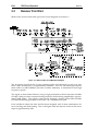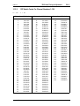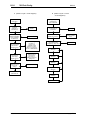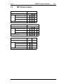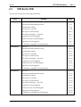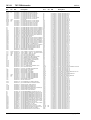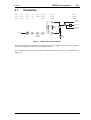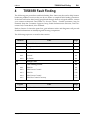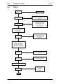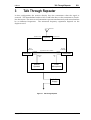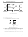
1
1
M850-00
T850 Series
Base Station Equipment
Service Manual
Issue 101
November 1996
M850-00-101
Copyright TEL
30/11/96
2
M850-00
France
Taiwan
Tait France Sarl
2 Avenue de la Cristallerie
92 316 Sèvres, Cedex
France
Phone: 33 1 41 14-05-50
Fax: 33 1 41 14-05-55
Tait Electronics (Taiwan) Ltd
1104, No. 142 Chung Hsiao E. Rd
Sec. 4
Taipei
Taiwan
Phone: 886 2 731-1290
Fax: 886 2 711-6351
Germany
Tait Mobilfunk GmbH
Willstätterstraße 50
D-90449 Nürnberg 60
Germany
Phone: 49 911 96 746-0
Fax: 49 911 96 746-79
Head Office
New Zealand
Tait Electronics Ltd
558 Wairakei Road
P.O. Box 1645
Christchurch
New Zealand
Phone: 64 3 358-3399
Fax: 64 3 358-3636
Hong Kong
Tait Mobile Radio (HK) Ltd
Room 703A
New East Ocean Centre
9, Science Museum Road
Tsim Sha Tsui East
Hong Kong
Phone: 852 2369-3040
Fax: 852 2369-3009
Radio Infrastructure Division
535 Wairakei Road
P.O. Box 1645
Christchurch
New Zealand
Phone: 64 3 358-3399
Fax: 64 3 358-2825
New Zealand
Tait Communications Ltd
Unit 4, 75 Blenheim Road
P.O. Box 1185
Christchurch
Phone: 64 3 348-3301
Fax: 64 3 343-0558
United Kingdom
Tait Mobile Radio Ltd
Ermine Business Park
Ermine Road
Huntingdon
Cambridgeshire PE18 6YA
United Kingdom
Phone: 44 1480-52255
Fax: 44 1480-411996
USA
Tait Electronics (USA) Inc.
9434 Old Katy Road
Suite 110
Houston
Texas 77055
USA
Phone: 1 713 984-8684
Toll Free: 1 800 222-1255
Fax: 1 713 468-6944
Australia
Tait Electronics (Aust) Pty Ltd
275 Toombul Road
Northgate 4013
P.O. Box 679
Virginia
Queensland 4014
Australia
Phone: 61 7 3260-7799
Toll Free: 1800 077-112
Fax: 61 7 3260-7990
Canada
Tait Mobile Radio Inc.
Unit 5, 158 Anderson Avenue
Markham
Ontario L6E1A9
Canada
Phone: 1 905 472-1100
Toll Free: 1 800 890-8248
Fax: 1 905 472-5300
30/11/96
Singapore
Tait Electronics (Far East) Pte Ltd
4 Leng Kee Road
SIS Building #05-11A
Singapore 159088
Phone: 65 471-2688
Fax: 65 479-7778
Thailand
Tait Mobile Radio Ltd
14/1 Suwan Tower
Ground Floor
Soi Saladaeng 1
North Sathorn Road
Bangrak
Bangkok 10500
Thailand
Phone: 662 267-6290-2
Fax: 662 267-6293
Copyright TEL
3
M850-00
About This Manual
This manual contains general, technical and servicing information on T850 25W, 50W and 100W base stations which comprise
the following equipment:
Scope
25W base station
T855 receiver
T856 25W transmitter
50W base station
T855 receiver
T857 exciter
T858 50W power amplifier
100W base station
T855 receiver
T857 exciter
T859 100W power amplifier
Format
We have published this manual in a ring binder so that "revision
packages" containing additional information pertaining to new
issues of PCBs can be added as required.
Revision Packages
Revision packages will normally be published to coincide with
the release of information on a new PCB, and may also contain
additions or corrections pertaining to other parts of the manual.
If you return the registration form at the front of this manual,
you will be notified when revision packages containing new
PCB information and/or text are available. You may then order
as many packages as you require from your local Tait Company.
Revision packages are supplied ready-punched for inclusion in
your manual.
Revision Control
2
Each page in this manual has a date of issue. This is to comply
with various Quality Standards, but will also serve to identify
which pages have been updated and when. Each page and its
publication date is listed in the "List of Effective Pages", and a
new list containing any new/revised pages and their publication dates will be sent with each revision package.
Any portion of text that has been changed is marked by a vertical line (as shown at left) in the outer margin of the page. Where
the removal of an entire paragraph means there is no text left to
mark, an arrow (as shown at left) will appear in the outer margin. The number beside the arrow will indicate how many paragraphs have been deleted.
The manual issue and revision status are indicated by the last
three digits of the manual IPN. These digits start at 100 and will
increment through 101, 102, 103, etc., as revision packages are
published, e.g:
1 0 3
issue status
Copyright TEL
revision status
30/11/96
4
M850-00
Thus, Issue 103 indicates the third revision to issue 1 and means
that three packages should have been added to the manual. The
issue digit will only change if there is a major product revision,
or if the number of revision packages to be included means that
the manual becomes difficult to use, at which point a new issue
manual will be published in a new ring binder.
PCB Information
PCB information is provided for all current issue PCBs, as well
as all previous issue PCBs manufactured in production quantities, and is grouped according to PCB. Thus, you will find the
parts list, grid reference index (if necessary), PCB layouts and
circuit diagram(s) for each individual PCB grouped together.
Errors
If you find an error in this manual, or have a suggestion on how
it might be improved, please do not hesitate to contact the Technical Writer, Tait Radio Infrastructure Division, Tait Electronics
Ltd, P.O. Box 1645, Christchurch, New Zealand.
Technical Information
Any enquiries regarding this manual or the equipment it describes should be addressed
in the first instance to your nearest approved Tait Dealer or Service Centre. Further
technical assistance may be obtained from the Customer Support Group, Radio Infrastructure Division, Tait Electronics Ltd, Christchurch, New Zealand.
Updating Equipment And Manuals
In the interests of improving performance, reliability or servicing, Tait Electronics Ltd
reserve the right to update their equipment and/or manuals without prior notice.
Copyright
All information contained in this manual is the property of Tait Electronics Ltd. All
rights are reserved. This manual may not, in whole or part, be copied, photocopied,
reproduced, translated stored or reduced to any electronic medium or machine readable
form without prior written permission from Tait Electronics Ltd.
Ordering Tait Service Manuals
Service Manuals should be ordered from your nearest Tait Branch or approved Dealer.
When ordering, quote the Tait Internal Part Number (IPN) and, where applicable, the
version.
Date Of Issue
IPN M850-00-101
T850 Series Service Manual
Issue 101 published November 1996
30/11/96
Copyright TEL
5
M850-00
Table Of Contents
This manual is divided into eight parts as listed below, with each part being further subdivided into sections. There is a detailed table of contents at the start of each part
and/or section.
Part
Title
A
Introduction To Servicing
B
T855 Receiver
C
T856 Transmitter & T857 Exciter
D
T858/859 Power Amplifiers
E
T800 Memory & T850 VCO PCB Information
F
Installation
G
System Configurations
H
T800 Ancillary Equipment
Copyright TEL
30/11/96
6
M850-00
List Of Effective Pages
The total number of pages in this Manual is 436, as listed below.
Page
Issue Date
Page
Issue Date
1
2
3
4
5
6
7
8
9
10
11
12
30/11/96
30/11/96
30/11/96
30/11/96
30/11/96
30/11/96
30/11/96
30/11/96
30/11/96
30/11/96
30/11/96
30/11/96 (blank)
9.1
9.2
30/11/96
30/11/96 (blank)
Part A
I
II
30/11/96
30/11/96 (blank)
1.1
1.2
30/11/96
30/11/96
2.1
2.2
30/11/96
30/11/96 (blank)
3.1
3.2
30/11/96
30/11/96
4.1
4.2
30/11/96
30/11/96 (blank)
5.1
5.2
30/11/96
30/11/96 (blank)
6.1
6.2
30/11/96
30/11/96 (blank)
7.1
7.2
30/11/96
30/11/96
8.1
8.2
8.3
8.4
30/11/96
30/11/96
30/11/96
30/11/96 (blank)
30/11/96
Part B
I
II
30/11/96
30/11/96 (blank)
1.1
1.2
1.3
1.4
1.5
1.6
1.7
1.8
30/11/96
30/11/96 (blank)
30/11/96
30/11/96
30/11/96
30/11/96
30/11/96
30/11/96
2.1
2.2
2.3
2.4
2.5
2.6
2.7
2.8
2.9
2.10
2.11
2.12
30/11/96
30/11/96 (blank)
30/11/96
30/11/96
30/11/96
30/11/96
30/11/96
30/11/96
30/11/96
30/11/96
30/11/96
30/11/96 (blank)
3.1
3.2
3.3
3.4
3.5
3.6
3.7
3.8
3.9
3.10
3.11
3.12
3.13
3.14
30/11/96
30/11/96
30/11/96
30/11/96
30/11/96
30/11/96
30/11/96
30/11/96
30/11/96
30/11/96
30/11/96
30/11/96
30/11/96
30/11/96 (blank)
Copyright TEL
7
M850-00
Page
Issue Date
Page
Issue Date
4.1
4.2
4.3
4.4
4.5
4.6
4.7
4.8
30/11/96
30/11/96 (blank)
30/11/96
30/11/96
30/11/96
30/11/96
30/11/96
30/11/96 (blank)
5.1
5.2
5.3
5.4
5.5
5.6
5.7
5.8
5.9
5.10
5.11
5.12
5.13
5.14
30/11/96
30/11/96
30/11/96
30/11/96
30/11/96
30/11/96
30/11/96
30/11/96
30/11/96
30/11/96
30/11/96
30/11/96
30/11/96
30/11/96
6.1.1
6.1.2
6.1.3
6.1.4
30/11/96
30/11/96 (blank)
30/11/96
30/11/96
6.4.10
6.4.11
6.4.12
6.4.13
6.4.14
6.4.15
6.4.16
6.4.17
6.4.18
6.4.19
6.4.20
6.4.21
6.4.22
6.4.23
6.4.24
6.4.25
6.4.26
6.4.27
6.4.28
6.4.29
6.4.30
6.4.31
6.4.32
6.4.33
6.4.34
6.4.35
6.4.36
6.4.37
6.4.38
30/11/96
30/11/96
30/11/96
30/11/96
30/11/96
30/11/96
30/11/96
30/11/96
30/11/96
30/11/96
30/11/96
30/11/96
30/11/96
30/11/96
30/11/96
30/11/96
30/11/96
30/11/96
30/11/96
30/11/96
30/11/96
30/11/96
30/11/96
30/11/96
30/11/96
30/11/96
30/11/96
30/11/96
30/11/96
6.2.1
6.2.2
6.2.3
6.2.4
6.2.5
6.2.6
6.2.7
6.2.8
30/11/96
30/11/96
30/11/96
30/11/96
30/11/96
30/11/96
30/11/96
30/11/96
6.3.1
6.3.2
6.3.3
6.3.4
30/11/96
30/11/96
30/11/96
30/11/96 (blank)
6.4.1
6.4.2
6.4.3
6.4.4
6.4.5
6.4.6
6.4.7
6.4.8
6.4.9
30/11/96
30/11/96 (blank)
30/11/96
30/11/96
30/11/96
30/11/96
30/11/96
30/11/96 (blank)
30/11/96
Copyright TEL
(blank)
(fold-out)
(fold-out)
(fold-out)
(fold-out)
(fold-out)
(fold-out)
(fold-out)
(fold-out)
(blank)
(blank)
(fold-out)
(fold-out)
(fold-out)
(fold-out)
(fold-out)
(fold-out)
(fold-out)
(fold-out)
(blank)
Part C
(blank)
(fold-out)
(fold-out) (blank)
I
II
30/11/96
30/11/96 (blank)
1.1
1.2
1.3
1.4
1.5
1.6
1.7
1.8
1.9
1.10
30/11/96
30/11/96 (blank)
30/11/96
30/11/96
30/11/96
30/11/96
30/11/96
30/11/96
30/11/96
30/11/96 (blank)
2.1
2.2
2.3
2.4
2.5
30/11/96
30/11/96
30/11/96
30/11/96
30/11/96
30/11/96
8
M850-00
Page
Issue Date
Page
Issue Date
2.6
2.7
2.8
2.9
2.10
2.11
2.12
30/11/96
30/11/96
30/11/96
30/11/96
30/11/96
30/11/96
30/11/96 (blank)
3.1
3.2
3.3
3.4
3.5
3.6
3.7
3.8
3.9
3.10
3.11
3.12
3.13
3.14
30/11/96
30/11/96
30/11/96
30/11/96
30/11/96
30/11/96
30/11/96
30/11/96
30/11/96
30/11/96
30/11/96
30/11/96
30/11/96
30/11/96 (blank)
4.1
4.2
4.3
4.4
4.5
4.6
30/11/96
30/11/96 (blank)
30/11/96
30/11/96
30/11/96
30/11/96
5.1
5.2
5.3
5.4
5.5
5.6
5.7
5.8
5.9
5.10
5.11
5.12
5.13
5.14
30/11/96
30/11/96 (blank)
30/11/96
30/11/96
30/11/96
30/11/96
30/11/96
30/11/96
30/11/96
30/11/96
30/11/96
30/11/96
30/11/96
30/11/96 (blank)
6.2.3
6.2.4
6.2.5
6.2.6
6.2.7
6.2.8
6.2.9
6.2.10
6.2.11
6.2.12
6.2.13
6.2.14
6.2.15
6.2.16
6.2.17
6.2.18
6.2.19
6.2.20
6.2.21
6.2.22
6.2.23
6.2.24
6.2.25
6.2.26
6.2.27
6.2.28
6.2.29
6.2.30
6.2.31
6.2.32
6.2.33
6.2.34
6.2.35
6.2.36
6.2.37
6.2.38
6.2.39
6.2.40
30/11/96
30/11/96
30/11/96
30/11/96
30/11/96
30/11/96
30/11/96
30/11/96
30/11/96
30/11/96
30/11/96
30/11/96
30/11/96
30/11/96
30/11/96
30/11/96
30/11/96
30/11/96
30/11/96
30/11/96
30/11/96
30/11/96
30/11/96
30/11/96
30/11/96
30/11/96
30/11/96
30/11/96
30/11/96
30/11/96
30/11/96
30/11/96
30/11/96
30/11/96
30/11/96
30/11/96
30/11/96
30/11/96
6.1.1
6.1.2
6.1.3
6.1.4
30/11/96
30/11/96 (blank)
30/11/96
30/11/96
6.2.1
6.2.2
30/11/96
30/11/96 (blank)
6.3.1
6.3.2
6.3.3
6.3.4
6.3.5
6.3.6
6.3.7
6.3.8
6.3.9
6.3.10
6.3.11
6.3.12
6.3.13
30/11/96
30/11/96
30/11/96
30/11/96
30/11/96
30/11/96
30/11/96
30/11/96
30/11/96
30/11/96
30/11/96
30/11/96
30/11/96
30/11/96
(blank)
(blank)
(fold-out)
(fold-out)
(fold-out)
(fold-out) (blank)
(fold-out)
(fold-out)
(fold-out)
(fold-out)
(blank)
(blank)
(fold-out)
(fold-out)
(fold-out)
(fold-out) (blank)
(fold-out)
(fold-out)
(fold-out)
(fold-out)
(blank)
(fold-out)
(fold-out)
(fold-out)
Copyright TEL
9
M850-00
Page
Issue Date
6.3.14
6.3.15
6.3.16
6.3.17
6.3.18
6.3.19
6.3.20
6.3.21
6.3.22
6.3.23
6.3.24
6.3.25
6.3.26
6.3.27
6.3.28
6.3.29
6.3.30
6.3.31
6.3.32
6.3.33
6.3.34
6.3.35
6.3.36
6.3.37
6.3.38
6.3.39
6.3.40
6.3.41
6.3.42
6.3.43
6.3.44
6.3.45
6.3.46
6.3.47
6.3.48
6.3.49
6.3.50
6.3.51
6.3.52
6.3.53
6.3.54
6.3.55
6.3.56
6.3.57
6.3.58
6.3.59
6.3.60
6.3.61
6.3.62
6.3.63
6.3.64
6.3.65
30/11/96
30/11/96
30/11/96
30/11/96
30/11/96
30/11/96
30/11/96
30/11/96
30/11/96
30/11/96
30/11/96
30/11/96
30/11/96
30/11/96
30/11/96
30/11/96
30/11/96
30/11/96
30/11/96
30/11/96
30/11/96
30/11/96
30/11/96
30/11/96
30/11/96
30/11/96
30/11/96
30/11/96
30/11/96
30/11/96
30/11/96
30/11/96
30/11/96
30/11/96
30/11/96
30/11/96
30/11/96
30/11/96
30/11/96
30/11/96
30/11/96
30/11/96
30/11/96
30/11/96
30/11/96
30/11/96
30/11/96
30/11/96
30/11/96
30/11/96
30/11/96
30/11/96
Copyright TEL
(fold-out) (blank)
(fold-out)
(fold-out)
(fold-out)
(fold-out)
(blank)
(blank)
(fold-out)
(fold-out)
(fold-out)
(fold-out) (blank)
(fold-out)
(fold-out)
(fold-out)
(fold-out)
(blank)
(blank)
(fold-out)
(fold-out)
(fold-out)
(fold-out) (blank)
(fold-out)
(fold-out)
(fold-out)
(fold-out)
(blank)
(blank)
(fold-out)
(fold-out)
(fold-out)
(fold-out) (blank)
(fold-out)
(fold-out)
(fold-out)
Page
Issue Date
6.3.66
30/11/96 (fold-out)
Part D
I
II
30/11/96
30/11/96 (blank)
1.1
1.2
1.3
1.4
1.5
1.6
30/11/96
30/11/96 (blank)
30/11/96
30/11/96
30/11/96
30/11/96
2.1
2.2
2.3
2.4
2.5
2.6
2.7
2.8
30/11/96
30/11/96 (blank)
30/11/96
30/11/96
30/11/96
30/11/96
30/11/96
30/11/96 (blank)
3.1
3.2
3.3
3.4
3.5
3.6
3.7
3.8
3.9
3.10
30/11/96
30/11/96 (blank)
30/11/96
30/11/96
30/11/96
30/11/96
30/11/96
30/11/96
30/11/96
30/11/96 (blank)
4.1
4.2
4.3
4.4
4.5
4.6
4.7
4.8
4.9
4.10
4.11
4.12
30/11/96
30/11/96 (blank)
30/11/96
30/11/96
30/11/96 (fold-out)
30/11/96 (fold-out) (blank)
30/11/96
30/11/96
30/11/96
30/11/96
30/11/96
30/11/96
5.1.1
5.1.2
5.1.3
5.1.4
30/11/96
30/11/96 (blank)
30/11/96
30/11/96
30/11/96
10
M850-00
Page
Issue Date
5.2.1
5.2.2
5.2.3
5.2.4
5.2.5
5.2.6
5.2.7
5.2.8
5.2.9
5.2.10
5.2.11
5.2.12
30/11/96
30/11/96
30/11/96
30/11/96
30/11/96
30/11/96
30/11/96
30/11/96
30/11/96
30/11/96
30/11/96
30/11/96
5.3.1
5.3.2
5.3.3
5.3.4
5.3.5
5.3.6
5.3.7
5.3.8
5.3.9
5.3.10
5.3.11
5.3.12
5.3.13
5.3.14
30/11/96
30/11/96
30/11/96
30/11/96
30/11/96
30/11/96
30/11/96
30/11/96
30/11/96
30/11/96
30/11/96
30/11/96
30/11/96
30/11/96
(blank)
Page
Issue Date
3.9
3.10
3.11
3.12
30/11/96
30/11/96
30/11/96 (fold-out)
30/11/96 (fold-out) (blank)
Part F
(blank)
(fold-out)
(fold-out)
(fold-out)
(fold-out)
(blank)
(blank)
I
II
30/11/96
30/11/96 (blank)
1.1
1.2
1.3
1.4
30/11/96
30/11/96
30/11/96
30/11/96 (blank)
2.1
2.2
2.3
2.4
30/11/96
30/11/96
30/11/96
30/11/96 (blank)
Part G
(fold-out)
(fold-out)
(fold-out)
(fold-out)
I
II
30/11/96
30/11/96
1.1
1.2
30/11/96
30/11/96
2.1
2.2
30/11/96
30/11/96
3.1
3.2
30/11/96
30/11/96 (blank)
4.1
4.2
30/11/96
30/11/96
5.1
5.2
30/11/96
30/11/96
Part E
I
II
30/11/96
30/11/96 (blank)
1.1
1.2
30/11/96
30/11/96
2.1
2.2
2.3
2.4
2.5
2.6
30/11/96
30/11/96
30/11/96
30/11/96
30/11/96 (fold-out)
30/11/96 (fold-out) (blank)
Part H
3.1
3.2
3.3
3.4
3.5
3.6
3.7
3.8
30/11/96
30/11/96
30/11/96
30/11/96
30/11/96
30/11/96 (fold-out)
30/11/96 (fold-out) (blank)
30/11/96
30/11/96 (blank)
I
II
30/11/96
30/11/96
1
2
3
4
30/11/96
30/11/96
30/11/96
30/11/96
Copyright TEL
11
M850-00
Page
Issue Date
5
6
7
8
30/11/96
30/11/96
30/11/96
30/11/96
Copyright TEL
Page
Issue Date
30/11/96
12
30/11/96
M850-00
Copyright TEL
AI
M850-00
Part A
Introduction To Servicing
This part of the manual is divided into the sections listed below. These sections provide
some general and advisory information on servicing procedures, a brief history of T800
programming software, and a list of Technical Instructions pertaining to T850 Series
equipment.
Section
1
Title
Page
General
1.1
1.1
Caution: CMOS Devices
1.1
1.2
Caution: Aerial Load
1.2
1.3
Caution: Beryllium Oxide & Power Transistors
1.2
Mechanical
2.1
2.1
Pozidriv Recess Head Screws
2.1
2.2
2.2.1
2.2.2
Disassembly/Reassembly
Receivers/Exciters
Power Amplifiers
2.1
2.1
2.1
2.3
Cover Screw Torques
2.1
Component Replacement
3.1
3.1
3.1.1
3.1.2
Leaded Components
Desoldering Iron Method
Component Cutting Method
3.1
3.1
3.1
3.2
Surface Mount Devices
3.2
4
To Replace PA Transistors
4.1
5
To Remove The T858/859 PA PCB From The Heatsink
5.1
6
To Remove Cased Mica Capacitors
6.1
7
To Fit The Optional T800-55 High Sensitivity Preamplifier
To The T855 Receiver
7.1
8
Software History
8.1
8.1
BASEPROG V1/PGM800 V2
8.1
8.2
PGM800 V2.01
8.1
8.3
PGM800 V2.21
8.2
8.4
PGM800Win V1.0
8.2
Technical Instructions
9.1
2
3
9
Figure
Title
Page
1.1
Typical Anti-static Bench Set-up
1.1
7.1
Location of T800-55 Preamplifier on T855 Receiver
7.1
Copyright TEL
30/11/96
AII
30/11/96
M850-00
Copyright TEL
General
M850-00
1
A1.1
General
If further information is required about T850 Series equipment or this Manual, it may be
obtained from Tait Electronics Ltd or accredited agents. When requesting this information, please quote the product type number (e.g. T855-10) and serial number. In the case
of the Service Manual quote the Tait Internal Part Number (IPN), e.g. M850-00-101, and
for circuit diagrams quote the 'Title', 'IPN' and 'Issue'.
1.1
Caution: CMOS Devices
This equipment contains CMOS Devices which are susceptible to damage from static
charges. Care when handling these devices is essential. For correct handling procedures refer to the manufacturers' data books, e.g. Philips data books covering CMOS
devices, or Motorola CMOS data books, etc.
conductive
wrist strap
conductive rubber
bench mat
to building earth
(not mains earth)
via 1M series resistor
metal frame
Figure 1.1 Typical Anti-static Bench Set-up
An anti-static bench kit (refer to Figure 1.1) is available from Tait Electronics Ltd under
the usual consumable goods ordering system. The kit is held in stock under IPN
937-00000-34 and contains:
• 1 conductive rubber bench mat
• 1 earth lead to connect the mat to ground (c/w 1M series resistor)
• 1 wrist strap
• information leaflet.
Copyright TEL
30/11/96
A1.2
General
1.2
Caution: Aerial Load
M850-00
The equipment has been designed to operate safely under a wide range of aerial loading
conditions. However, it is strongly recommended that the transmitter should not be
operated in the absence of a suitable load. Failure to observe this warning may result in
damage to the transmitter power output stage.
1.3
Caution: Beryllium Oxide & Power Transistors
The RF power transistors in current use all contain some beryllium oxide. This substance, while perfectly harmless in its normal solid form, can become a severe health
hazard when it has been reduced to dust. For this reason the RF power transistors
should not be broken open, mutilated, filed, machined, or physically damaged in any
way that can produce dust particles.
30/11/96
Copyright TEL
Mechanical
M850-00
2
Mechanical
2.1
Pozidriv Recess Head Screws
A2.1
Pozidriv recess head screws are the preferred standard on all Tait manufactured equipment. The very real advantages of this type of screw will not be realised unless the correct screwdrivers are used by servicing personnel.
2.2
Disassembly/Reassembly
2.2.1
Receivers/Exciters
To carry out alignment or change option links it is necessary to remove only the top
cover, i.e. the one adjacent to the front panel handle and on the opposite side to the main
D-range connector.
Removal of the bottom cover is necessary to:
• access SMD components
• change solder blob links
• fit test leads to circuit block access points.
2.2.2
Power Amplifiers
We recommend that the power output and alarm level setting procedures be carried out
with the cover shield on.
2.3
Cover Screw Torques
Receivers/Exciters
.. 12lb-in./1.36Nm
Power Amplifiers
.. 8lb-in./0.9Nm
Copyright TEL
30/11/96
A2.2
30/11/96
Mechanical
M850-00
Copyright TEL
Component Replacement
M850-00
3
Component Replacement
3.1
Leaded Components
A3.1
Whenever components are removed from or fitted to the PCB, care must be taken to
avoid damage to the track. The two satisfactory methods of removing components from
PTH PCBs are detailed below.
Note:
The first method requires the use of a desoldering station, e.g. Philips SBC
314 or Pace MBT-100E.
3.1.1
Desoldering Iron Method
Place the tip over the lead and, as the solder starts to melt, move the tip in a circular motion.
Start the suction and continue the movement until 3 or 4 circles have been completed.
Remove the tip while continuing suction to ensure that all solder is removed from
the joint, then stop the suction.
Before pulling the lead out, ensure it is not stuck to the plating.
If the lead is still not free, resolder the joint and try again.
Note:
The desoldering iron does not usually have enough heat to desolder leads
from the ground plane. Additional heat may be applied by holding a soldering iron on the tip of the desoldering iron (this may require some additional help).
3.1.2
Component Cutting Method
Cut the leads on the component side of the PCB.
Heat the solder joint sufficiently to allow easy removal of the lead by drawing it
out from the component side: do not use undue force.
Fill the hole with solder and then clear with solderwick.
Copyright TEL
30/11/96
A3.2
Component Replacement
3.2
Surface Mount Devices
Caution:
30/11/96
M850-00
Surface mount devices (SMD's) require special storage, handling,
removal and replacement techniques. This equipment should be serviced only by an approved Tait Dealer or Service Centre equipped with
the necessary facilities. Repairs attempted with incorrect equipment or
by untrained personnel may result in permanent damage. If in doubt,
contact Tait Electronics Ltd or your nearest Tait Branch or Subsidiary.
Copyright TEL
To Replace PA Transistors
M850-00
4
A4.1
To Replace PA Transistors
Caution:
Failure to comply with the following procedure can result in failure of
the device due to poor heatsinking, or worse, can endanger the health
of the assembler if the beryllium oxide die carrier is smashed during
assembly.
Although exact spacing between transistors and capacitors is not critical in
the T858/859 PA, we recommend that, before attempting to remove a transistor, you note the location of these and any other components that will also
need to be removed. Replacing each component in its original location will
assist in maintaining the performance of the PA.
Note:
Desolder the tabs by heating with a soldering iron and lifting away from the PCB
with a screwdriver or thin stainless steel spike. Unscrew the transistor stud nut
and remove the device.
Trim the tabs of the replacement transistor so that the device sits neatly on the
PCB lands provided.
Lightly tin the underside of the transistor tabs.
Apply a small amount of heatsink compound (Dow-Corning 340 or equivalent) to
the transistor mounting surface. Sufficient compound should be used to ensure a
thin even film over the entire mounting surface.
Place the transistor on the PCB in the correct orientation and ensure the tabs are
flush to the surface. Lightly solder one tab to the PCB. Torque down the retaining
nut to the correct torque (8lb-in./0.9Nm).
Caution:
Do not solder all the tabs before torquing down otherwise the device
may be broken.
Solder all transistor tabs to the PCB.
Copyright TEL
30/11/96
A4.2
30/11/96
To Replace PA Transistors
M850-00
Copyright TEL
To Remove The T858/859 PA PCB From The Heatsink
M850-00
5
A5.1
To Remove The T858/859 PA PCB
From The Heatsink
Most components are soldered topside only, but in some cases access to the underside of
the PCB is necessary.
Remove the D-range connector.
T859 Only:
Disconnect the power feed to the fan.
Remove the PCB retaining screws (2 are hidden beneath the harmonic filter
shield):
T858
T859
Qty 14
Qty 11
Remove the transistor stud nuts and mounting screws.
Remove the mounting screws for the TO-220 devices:
T858/859 Q16, R89, R90 and R91
T859
R92, R93 and R94.
Remove the retaining screws for the wireline couplers (L19 and L39).
Remove the output 50 ohm coaxial connector by unscrewing it from the heatsink
casting and unsoldering it from the PCB.
Disconnect the input 50 ohm coaxial cable by unplugging it at the PCB.
Disconnect the battery positive and negative feed wires from the PCB.
Disconnect the alarm and metering wires from the PCB.
Lift the PCB gently from the heatsink to gain access to the underside of the PCB.
Caution:
Do not operate the PA with the PCB detached as the heatsink is used
for earthing and for the dissipation of heat generated within the transistors.
To replace the PCB, reverse the order of removal, taking care that the wiring is correctly routed and is not subjected to 'pinching'.
Copyright TEL
30/11/96
A5.2
30/11/96
To Remove The T858/859 PA PCB From The Heatsink
M850-00
Copyright TEL
M850-00
6
To Remove Cased Mica Capacitors
A6.1
To Remove Cased Mica Capacitors
Cased mica capacitors can be removed by heating the top with a heavy-duty soldering
iron and gently lifting the capacitor off the PCB with a solder-resistant spike or equivalent.
Copyright TEL
30/11/96
A6.2
30/11/96
To Remove Cased Mica Capacitors
M850-00
Copyright TEL
M850-00
To Fit The Optional T800-55 High Sensitivity Preamplifier to the T855
7
A7.1
To Fit The Optional T800-55 High
Sensitivity Preamplifier to the T855
The high sensitivity preamplifier option PCB fits onto the main PCB. It is a single stage
broad band low noise preamplifier offering a 3dB improvement in sensitivity with a
minimum degradation of other parameters.
Refer to the diagram below. The preamplifier fits on the bottom side of the PCB under
the helical filter FL300.
Remove R308
from this
position.
Figure 7.1 Location of T800-55 Preamplifier on T855 Receiver
To fit the preamplifier proceed as follows:
Remove the bottom cover from the receiver
Remove the zero ohm resistor R308
Remove the two screws that secure the helical filter, FL300, to the PCB
Fit the T800-55 to the bottom side of the main PCB, under the helical filter FL300
ensuring that the slot in the T800-55 fits around the pads of the removed R308.
Secure with the helical mounting screws which must be tightened to 6lb-in/
0.66Nm as they provide the earth connection for the RF amp and the helical housing. Check that the RF amp fits comfortably and does not short out on L307.
With link wire connect the input pad of R308 to the input pad (A) of the preamplifier.
Connect the pad of R308 that is closest to the helical filter to the output pad (B) of
the preamplifier.
Connect the junction of L307 and R318 to the +9v supply (C) of the preamplifier.
Refit the bottom cover to the receiver.
Copyright TEL
30/11/96
A7.2
To Fit The Optional T800-55 High Sensitivity Preamplifier to the T855
M850-00
The alignment procedure of the receiver remains unchanged (refer to Section B3.6 or
Section B3.7).
30/11/96
Copyright TEL
Software History
M850-00
8
A8.1
Software History
23/11/89
23/08/90
11/06/91
03/10/95
28/06/96
8.1
BASEPROG Version 1
PGM800 Version 2
PGM800 Version 2.01
PGM800 Version 2.21
PGM800Win Version 1.0
BASEPROG V1/PGM800 V2
T800 programming software was originally developed as BASEPROG V1 and released
as PGM800 V2.
8.2
PGM800 V2.01
The major changes introduced with V2.01 are as follows:
•
Full support for different display adaptors.
•
Programming of CTCSS frequency data (optional) for individual channels.
•
Full cursor control in edit mode.
•
User selectable output file format (hex or binary).
•
Support for wider range of T800 equipment.
•
DOS shell facility implemented.
•
CTCSS defeat possible when CTCSS tone is not selected.
•
Channel numbering changed from 0-127 to 1-128.
•
An "X" included on the printout to indicate that there are 8 switches on the DIP
switch and the state of the MSB is dependent on the size of the EPROM used.
Note:
Copyright TEL
The data files produced by BASEPROG V1.0 are still compatible with
PGM800 V2.01.
30/11/96
A8.2
Software History
8.3
PGM800 V2.21
M850-00
PGM800 V2.21 is an updated and expanded version of the earlier PGM800 V2.01 software.
PGM800 V2.21 includes many new and improved features over PGM800 V2.01. There
are a number of changes to the user interface to make data entry and editing significantly easier.
Major changes are outlined below:
•
Includes several new radio models which are not programmable with PGM800
V2.01.
•
Default file names with ‘dash’ are saved with ‘dash’ instead of ‘underscore’.
•
Default file extension in Save File page is BIN instead of HEX.
•
Out of range frequencies will result in warning messages, but will still be accepted
as valid entries.
•
Channel numbers are selectable between 0-127 and 1-128.
•
Automatic insertion feature to input frequencies.
Note:
The datafiles produced by BASEPROG V1.0 and PGM800 V2.01 are still
compatible with PGM800 V2.21.
8.4
PGM800Win V1.0
PGM800Win V1.0 is different in concept from DOS versions of PGM800 in that it is Windows1 driven. It includes many new and improved features over DOS versions of
PGM800.
Major changes are outlined below:
•
The Windows environment makes data entry and editing significantly easier.
•
Includes several new radio models which are not programmable with DOS versions of PGM800.
•
Out of range frequencies will result in warning messages and will not be accepted
for entry into the standard library module. User defined modules can be created,
allowing variation from the standard library module.
•
Channel numbers default to 0-127 to match the EPROM memory locations, however the user can change this setting so that the channel numbers run from 1-128
to suit his/her particular needs.
1. Windows is a registered trademark of Microsoft Corporation.
30/11/96
Copyright TEL
M850-00
Note:
Copyright TEL
Software History
A8.3
The datafiles produced by BASEPROG V1.0 and all DOS versions of
PGM800 are still compatible with PGM800Win V1.0.
30/11/96
A8.4
30/11/96
Software History
M850-00
Copyright TEL
Technical Instructions
M850-00
9
A9.1
Technical Instructions
From time to time Technical Instructions (TIs) are issued by the Radio Infrastructure
Engineering Division of Tait Electronics. These TIs may be used to update equipment or
information, or to meet specific operational requirements.
Printed below is a list of TIs applicable to T800 and T850 Series equipment. You may
wish to file a copy of each TI in this Section for your own reference.
TI No.
Title
Date
346D
T800-02 CTCSS encoder/decoder
07/11/94
356D
T800-07 multichannel memory PCB
22/03/94
358
T807/808 remote sensing of output voltage
10/06/91
365
T807/808 improved earthing for noise interference suppression
29/07/91
T800-30/35 DFSK modulator PCB
16/11/94
T800 group delay
07/11/94
T800 Series VCO trimmer replacement
06/09/94
418
T800 Selcall: T800 Sigtec S1530 installation
03/11/95
422
T800 Series: Rx de-sensing by auxiliary boards
23/08/95
431
T800 Series: Pre-tinning of power transistor tabs
23/04/96
373A
403
416B
Copyright TEL
30/11/96
A9.2
30/11/96
Technical Instructions
M850-00
Copyright TEL
BI
M850-00
Part B
T855 Receiver
This part of the manual is divided into six sections, as listed below. There is a detailed
table of contents at the start of each section.
Section
Title
1
General Information
2
Circuit Operation
3
Initial Tuning & Adjustment
4
Functional Testing
5
Fault Finding
6
PCB Information
Copyright TEL
30/11/96
BII
30/11/96
M850-00
Copyright TEL
T855 General Information
M850-00
1
B1.1
T855 General Information
This section provides a brief description of the T855 receiver, along with detailed specifications and a list of types available.
The following topics are covered in this section.
Section
Title
Page
1.1
Introduction
1.3
1.2
Specifications
1.4
1.2.1
Introduction
1.4
1.2.2
General
1.4
1.2.3
RF Section
1.2.4
Audio Section
1.3
Copyright TEL
Product Codes
1.5
1.6
1.8
30/11/96
B1.2
30/11/96
T855 General Information
M850-00
Copyright TEL
T855 General Information
M850-00
1.1
B1.3
Introduction
The T855 is a high performance FM base station receiver designed for single or multichannel operation in the 400 to 530MHz frequency range.
The receiver is a dual conversion superhet with a synthesised local oscillator. The first
IF is 45MHz, allowing exceptionally high spurious signal rejection to be achieved in the
receiver front end. The second IF section (455kHz) combines amplitude limiting, detection and audio pre-amplification within a single integrated circuit. It also drives carrier
and noise level detectors for signal strength indication and gating the audio output.
The audio section output can be adjusted to deliver >+10dBm to a 600 ohm balanced
output, and 1W to a local monitor speaker. A flat or de-emphasised audio response is
link selectable.
The synthesiser frequency is programmed via an EPROM which is attached to a separate plug-in memory board. A DIP switch on the memory PCB allows fast single channel selection from a multichannel programmed EPROM, but for true multichannel
capability the EPROM must be addressed separately via an additional D-range plug at
the rear of the set.
All components except those on the VCO and memory boards are mounted on a single
PCB. This is secured to a die-cast chassis which is divided into compartments to individually shield each section of circuitry. Access to both sides of the main PCB is
obtained by removing each of the two chassis lids. There is provision within the chassis
to mount small option PCBs.
The front panel controls include gate sensitivity, line level, monitor volume and a mute
disable switch. This switch disables the mute (squelch) signal to the monitor amplifier
as an aid to servicing.
Copyright TEL
30/11/96
B1.4
T855 General Information
1.2
Specifications
1.2.1
Introduction
M850-00
The performance figures given are minimum figures, unless otherwise indicated, for
equipment tuned with the maximum switching band and operating at standard room
temperature (+22°C to +28°C).
Where applicable, the test methods used to obtain the following performance figures are
those described in the EIA specification. However, there are several parameters for
which performance according to the CEPT specification is given.
Details of test methods and the conditions which apply for Type Approval testing in all
countries can be obtained from Tait Electronics Ltd.
1.2.2
General
Frequency Range
.. 400-530MHz
Type
.. dual conversion superheterodyne
Frequency Increment
.. 6.25 or 12.5kHz
Switching Range
.. 5MHz
Number Of Channels:
Standard
Optional .
Internally Selectable
.. 1
.. 8
.. 128
Supply Voltage:
Operating Voltage
Standard Test Voltage
Polarity
Polarity Protection
..
..
..
..
10.8 to 16V DC
13.8V DC
negative earth only
crowbar diode
Supply Current:
Standby
Full Audio
.. 300mA
.. 700mA
Input Impedance
.. 50 ohms
Operating Temperature Range
.. -30°C to +60°C
Frequency Stability:
Standard Version
High Stability Version
Very High Stability Option
.. ±2.5ppm, -30°C to +60°C
.. ±2ppm, -10°C to +60°C
.. ±1ppm, 0°C to +60°C
30/11/96
Copyright TEL
T855 General Information
M850-00
Received Signal Strength Indicator(RSSI)
(optional)
B1.5
.. -115dBm to -70dBm, 0 to 5V at
10dB/V
Dimensions:
Height
Width
Length
Weight
1.2.3
.. 191mm
.. 60mm
.. 322mm
.. 2.2kg
RF Section
IF Amplifiers:
Frequencies
BandwidthsNarrow Band (NB)
Wide Band (WB)
Ultra-Wide Band (UWB)
.. 45MHz and 455kHz
.. 7.5kHz
.. 15kHz
.. 30kHz
Sensitivity:
Single Channel (NB & WB)
Single Channel(UWB)
Bandspread (12dB Sinad) (NB & WB)
Bandspread (12dB Sinad) (UWB)
..
..
..
..
-117dBm
-114dBm
-115dBm
-112dBm
Signal+Noise To Noise Ratio:
RF Level -107dBm
RF Level -83dBm (NB)
RF Level -57dBm (WB)
.. 30dB
.. 50dB CEPT (typical)
.. 55dB EIA (typical)
Selectivity:
Narrow Band (±12.5kHz)
Wide Band (±25kHz)
.. 85dB CEPT (typical)
.. 90dB
Offset Selectivity (Canada only)
.. 20dB
Spurious Response Attenuation
.. 100dB
Intermodulation Response Attenuation:
Narrow Band
Wide Band
.. 80dB CEPT (typical)
.. 85dB EIA
Blocking
.. 100dB
Co-channel Rejection
.. 6dB
Amplitude Characteristic
.. 3dB
Copyright TEL
30/11/96
B1.6
T855 General Information
M850-00
Spurious Emissions:
Conducted
Radiated
1.2.4
.. -90dBm to 4GHz
.. -57dBm to 1GHz
-47dBm to 4GHz
Audio Section
Outputs Available
.. line and monitor
Frequency Response
.. flat or de-emphasised (link selectable)
Flat Response (15kHz IF BW):
Bandwidth
Response
.. 67 to 3400Hz
.. within +1, -2dB of output level
at 1kHz
De-emphasised Response:
CTCSS BandBandwidth
Response
Speech BandBandwidth
Response
.. 67 to 260Hz
.. within +1, -2dB of output level
at 100Hz
.. 300 to 3400Hz
.. within +1, -3dB of a 6dB/octave
de-emphasis characteristic (ref. 1kHz)
Line Output:
Power
Load Impedance
Distortion(@ -70dBm signal level, links
set to de-emphasis)
WB and NB
(@ -70dBm signal level, links
set to flat)
WB
NB
.. adjustable to >+10dBm
.. 600 ohms
.. ≤2%
.. ≤2%
.. ≤4%
Monitor Output:
Power
.. 1W
Speaker Impedance
.. 3.5 ohms
Distortion.. ≤3%
(@ -70dBm signal level, links set to de-emphasis)
30/11/96
Copyright TEL
T855 General Information
M850-00
B1.7
Mute Operation (Gate)
Systems Available
.. noise mute and RSSI mute
Noise Mute:
Operating Range
Hysteresis
Threshold
Opening Time
Closing Time
..
..
..
..
..
6-20dB sinad
1.5 to 6dB
adjustable to -105dBm
20ms
50ms
..
..
..
..
-115 to -70dBm
2 to 10dB
5ms
50ms
RSSI Mute (Optional):
Operating Range
Hysteresis
Opening Time
Closing Time
Copyright TEL
30/11/96
B1.8
T855 General Information
1.3
Product Codes
M850-00
Frequency Range (MHz)
400-440
IF Bandwidth (kHz)
7.5
12
•
±2.5ppm -30°C to +60°C
TCXO
±2ppm -10°C to +60°C
15
17
7.5
25
27
14
30
•
•
•
23
20
22
24
480-530
7.5
15
30
•
±2.5ppm -30°C to +60°C
•
•
•
±1ppm 0°C to +60°C
30/11/96
12
15
•
IF Bandwidth (kHz)
Receiver Type: T855-
10
•
Frequency Range (MHz)
±2ppm -10°C to +60°C
13
•
±1ppm 0°C to +60°C
TCXO
•
12
±2.5ppm -30°C to +60°C
Receiver Type: T855-
•
440-480
IF Bandwidth (kHz)
±2ppm -10°C to +60°C
•
•
Frequency Range (MHz)
TCXO
30
•
±1ppm 0°C to +60°C
Receiver Type: T855-
15
35
37
•
30
32
34
Copyright TEL
T855 Circuit Operation
M850-00
2
B2.1
T855 Circuit Operation
This section provides a basic description of the circuit operation of the T855 receiver.
Refer to Section 6 where the parts lists, grid reference index and diagrams will provide
detailed information on identifying and locating components and test points on the
main PCB. The parts lists and diagrams for the memory and VCO PCBs are in Part E.
The following topics are covered in this section.
Section
Title
Page
2.1
Introduction
2.3
2.2
Receiver Front End
2.4
2.3
Mixer
2.5
2.4
IF Circuitry
2.5
2.5
Noise Mute (Squelch)
2.6
2.6
Carrier Mute
2.6
2.7
Audio Processor
2.7
2.8
Power Supply And Regulator
2.8
2.9
Synthesised Local Oscillator
2.9
2.10
Received Signal Strength Indicator (RSSI)
2.10
2.11
High Sensitivity Preamplifier
2.11
Figure
Title
Page
2.1
T855 High Level Block Diagram
2.3
2.2
T855 Front End, IF and Mute Block Diagram
2.4
2.3
T855 Audio Processor Block Diagram
2.7
2.4
T855 Power Supply And Regulator Block Diagram
2.8
2.5
T855 Synthesiser Block Diagram
2.9
2.6
T855 RSSI Block Diagram
2.10
Copyright TEL
30/11/96
B2.2
30/11/96
T855 Circuit Operation
M850-00
Copyright TEL
T855 Circuit Operation
M850-00
2.1
B2.3
Introduction
Figure 2.1 T855 High Level Block Diagram
The T855 receiver consists of a number of distinct stages:
• front end
• mixer
• synthesised local oscillator
• IF
• audio processor
• mute (squelch)
• regulator circuits
• received signal strength indicator (RSSI).
These stages are clearly identifiable in Figure 2.1. Refer to the circuit diagrams in Section 6 for further detail.
Copyright TEL
30/11/96
B2.4
T855 Circuit Operation
2.2
Receiver Front End
M850-00
(Refer to the receiver and audio processor circuit diagrams in Section 6.)
Figure 2.2 T855 Front End, IF and Mute Block Diagram
The incoming signal from the N-type antenna socket is fed through a 9-pole, low pass
filter with a cut frequency of approximately 600MHz. This low loss filter (typically less
than 0.5dB over 400-530MHz) provides excellent immunity to interference from high
frequency signals.
The signal is then further filtered, using a high performance helical resonator doublet
(FL300) which provides exceptional image rejection, before being amplified by approximately 8dB (Q303). The signal is then passed through a further helical filter doublet
(FL301) before being presented to the mixer via a 2dB attenuator pad.
Each sub-block within the front end has been designed with 50 ohm terminations for
ease of testing and fault finding. The overall gain from the antenna socket to the mixer
input is approximately 2dB.
30/11/96
Copyright TEL
T855 Circuit Operation
M850-00
2.3
B2.5
Mixer
(Refer to the receiver circuit diagram in Section 6 and Figure 2.2.)
IC301 is a high level mixer requiring a local oscillator (LO) drive level of +17dBm (nominal). The voltage controlled oscillator (VCO) generates a level of +20dBm (typical) and
this is fed to the mixer via a 4dB attenuator pad. A diplexer terminates the IF port of the
mixer in a good 50 ohms, thus preventing unnecessary intermodulation distortion.
2.4
IF Circuitry
(Refer to the receiver circuit diagram in Section 6 and Figure 2.2.)
Losses in the mixer are made up for in a tuned, common gate, post mixer amplifier
(Q305). Several stages of amplification and filtering are employed in the IF circuitry.
The first crystal filter is a 4-pole device (&XF300) which is matched into 50 ohms on both
its input and output ports. This stage is followed by a common base amplifier (Q302)
whose output is matched into a 2-pole crystal filter (&XF301). The signal is then amplified using a high gain MOSFET amplifier (Q304) before being mixed down to 455kHz
with the second local oscillator (44.545MHz).
The 455kHz signal is filtered using a 6-pole ceramic filter (&XF302) before being limited
and detected. Q306 provides a buffered 455kHz output for use with the optional RF
level detector (RSSI).
The second IF mixer, limiter and detector is in a 16-pin IC (IC300). Quadrature detection
is employed, using L316, and the recovered audio on pin 9 of IC300 is typically 1V p-p
for 60% system deviation.
Copyright TEL
30/11/96
B2.6
T855 Circuit Operation
2.5
Noise Mute (Squelch)
M850-00
(Refer to the receiver circuit diagram in Section 6 and Figure 2.2.)
The noise mute operates on the detected noise outside the audio bandwidth. The operational amplifier in IC300 is used as an active band pass filter centred on 70kHz to filter
out audio components. The noise spectrum is then further amplified in a variable gain,
two-stage amplifier (Q300 & Q301) with additional filtering. The noise is then rectified
(D300) and filtered to produce a DC voltage proportional to the noise amplitude. The
lowest average DC voltage corresponds to a high RF signal strength and the highest DC
voltage corresponds to no signal at the RF input.
The rectified noise voltage is compared with a threshold voltage set up on RV100, the
front panel mute potentiometer. Hysteresis is introduced by the feedback resistor
(R106) to prevent the received message from being chopped when the average noise
voltage is close to the threshold. R111 and R110 determine the mute opening and closing times. The mute control signal at pin 7 of IC100 is used to disable the speaker and
line audio outputs. The speaker output can be separately enabled for test purposes by
operating the front panel mute disable switch, SW100.
The mute control line is available on pad 101 (Rx gate out) for control of external circuitry. A high (9V) on pad 101 indicates that the audio is disabled and a low (0V) indicates that a signal above the mute threshold level is being received.
The audio can also be disabled using the "Rx-disable" inputs, pads 100 or 113, having
connected the "Rx-disable" link between pins 1 & 2 of PL100. An adjustable time delay
(RV101) is provided on these lines. In order to disable the audio, either pad must be
pulled to 0V.
The red front panel LED (D102) indicates the status of the mute circuit. When a signal
above the mute threshold is received, the LED is illuminated. An undedicated relay is
provided (RL100) for transmitter keying or other functions and this can be operated
from the mute line by linking PL102.
2.6
Carrier Mute
(Refer to the receiver circuit diagram in Section 6 and Figure 2.2.)
A high level carrier mute facility is also available when the RSSI option PCB is fitted.
The RSSI (refer to Section 2.10) provides a DC voltage proportional to the signal
strength. This voltage is compared with a preset level, set up on RV104, and may be
linked into the mute timing circuit using PL104. PL104 selects either the noise mute or
the carrier mute. From this point both mute circuits operate in the same manner, using
common circuitry.
30/11/96
Copyright TEL
T855 Circuit Operation
M850-00
2.7
B2.7
Audio Processor
(Refer to the audio processor circuit diagram in Section 6.)
Mute
Open
5V
0V
Mute
Closed
Selectable
Volume
Audio
Control
Filter
Mute
Switch
Driver
Amp
Speaker
Output
Line
Monitor
Mute
Switch
}
Line Level
Adjustment
Driver
Amp
Line
Output
Transformer
Figure 2.3 T855 Audio Processor Block Diagram
The recovered audio on pin 9 of IC300 is processed in a third order elliptic active filter to
give the required response. Linking (PL101 & PL103) is available to give either a flat or
de-emphasised audio response, with de-emphasis giving a 6dB/octave roll off. The output of IC101 is split to provide separate paths for the speaker and line outputs.
The speaker volume is set using the front panel volume knob (RV103) and the line level
is set using the recessed potentiometer (RV102). The signals are passed to audio drive
amplifiers IC102 and IC103. Under muted conditions the inputs of these amplifiers are
shunted to ground via transistors Q105 and Q106 respectively.
The audio output of IC102 has a DC component which is removed by C122, and this
then drives a speaker directly. The output of IC103 is fed into a line transformer to provide a balanced 2-wire or 4-wire, 600 ohm output.
Copyright TEL
30/11/96
B2.8
T855 Circuit Operation
2.8
Power Supply And Regulator
M850-00
(Refer to the regulator circuit diagram in Section 6.)
13.8V Nom.
From Rear
D-Range
Switching
Power Supply
5V
Reg
PS
13.8V
5V
9V
20V
Nom.
Figure 2.4 T855 Power Supply And Regulator Block Diagram
The T855 is designed to operate off a 10.8-16V DC supply (13.8V nominal). A 5.3V regulator (IC202) runs directly off the 13.8V rail, driving much of the synthesiser circuitry.
This is used as the reference for a DC amplifier (IC201, Q200 & Q201) which provides a
medium current capability 9V supply. A switching power supply, based on Q202 and
Q203, runs off the 9V supply and provides a low current capability +20V supply. This is
used to drive the synthesiser loop filter (IC4), giving a VCO control voltage of up to 20V.
The 13.8V supply drives both output audio amplifiers without additional regulation.
30/11/96
Copyright TEL
T855 Circuit Operation
M850-00
2.9
B2.9
Synthesised Local Oscillator
(Refer to the synthesiser circuit diagram in Section 6 and the VCO circuit diagram in
Part E.)
Figure 2.5 T855 Synthesiser Block Diagram
The synthesiser employs a phase-locked loop (PLL) to lock a VCO to a given reference
frequency.
A reference oscillator at 12.8MHz (=IC2) is buffered, divided by two and then divided
down to 12.5kHz or 6.25kHz within the synthesiser IC (IC3). A buffered output of the
VCO is fed to a programmable divider, comprising a UHF prescaler (&IC1) and a
divider internal to IC3. These two signals are applied to the phase detectors in IC3. A
digital phase detector PDB (IC3 pin 2) provides rapid coarse tuning of the VCO until the
phase error is within the range of the high gain sample and hold detector PDA (IC3 pin
1). The phase detector outputs are passed through an active loop filter (IC4a) which
produces a DC voltage between 0 and 20V to tune the VCO. This VCO control line is
further filtered to attenuate noise and spurs. As the control line voltage increases, the
VCO frequency also increases.
The division ratio of the programmable divider is stored within EPROM memory (IC1).
Up to 128 frequencies can be stored within the memory and are addressable using the
internal DIP switches. Three of the address lines are also available for external frequency control via an extra D-range connector at the rear of the chassis. A change of
state of any of these three lines (CH SEL 0-2) commences a programming cycle during
which the frequency data in the EPROM is down-loaded to a divider within IC3. 32 bits
of data are loaded in eight 4-bit words.
The VCO transistor (Q1) operates in common source and uses a transmission line resonator (TL1). The transmission line is used in a two port configuration with varicaps
Copyright TEL
30/11/96
B2.10
T855 Circuit Operation
M850-00
positioned at one end. The VCO control voltage from the loop filter (IC4a) is applied to
the varicaps (D1 & D2) to facilitate tuning. The VCO output is coupled into a cascode
amplifier stage (Q2, Q3) which gives a +10dBm (nominal) output. This output is used to
drive the divider buffer for the UHF prescaler which is either a divide by 64/65 for
25kHz channel increments or divide by 80/81 for 12.5kHz channel increments. Further
amplification in Q5 brings the output drive level to +20dBm to drive the mixer.
The VCO frequency spans from either 355-395MHz, 395-435MHz or 435-475MHz
according to version. The VCO is tuned to 45MHz below the desired receive frequency
to produce a 45MHz IF signal on the output of the mixer.
2.10
Received Signal Strength Indicator (RSSI)
(Refer to the receiver circuit diagram in Section 6.)
Figure 2.6 T855 RSSI Block Diagram
The RSSI option PCB plugs directly into the main PCB (support circuitry being fitted as
standard). It is fitted to the T855 whenever receiver signal strength monitoring is
required, e.g. trunking or voting. Its function is to provide a DC voltage proportional to
the signal level at the receiver input.
The variable gain stage (Q1A) is a common emitter amplifier with its emitter grounded
and the AGC control loop voltage applied to its base. Since the AGC loop will maintain
a constant signal level at the collector, the gain of Q1 must be proportional to the incoming 455kHz signal level. The gain of Q1 is linearly proportional to its collector current
which itself is exponentially related to the base-emitter voltage. Thus there is a logarithmic relationship between the base-emitter voltage and the gain. The circuit therefore
produces a feedback voltage, and an output voltage, logarithmically related to the RF
input signal.
The AGC loop is followed by a DC amplifier which provides level shifting, temperature
30/11/96
Copyright TEL
T855 Circuit Operation
M850-00
B2.11
compensation and gain to give a nominal 1V/10dB at the RSSI output. RV301 on the
main PCB is used to set the RSSI voltage to a fixed value at a given RF input signal
strength.
2.11
High Sensitivity Preamplifier
(Refer to the preamplifier circuit diagram in Section 6. Refer to fitting instructions in
Section A7)
The high sensitivity preamplifier option PCB fits onto the main PCB. It is a single stage
broad band low noise preamplifier offering a 3dB improvement in sensitivity with a
minimum degradation of other parameters. All performance figures still meet the ETS
300 086:1991 specifications for base stations.
The amplifier fits inside the receiver between the aerial input filter and the first helical
filter. Power is derived from the regulated +9v supply.
A table of typical results is given below.
Unmodified
T855
T855 With
Preamp Fitted
T855 With Modified
Preamp Fitted
(See Note)
-117dBm
-119dBm
-121dBm
@ 12dB Sinad
@ 12dB Sinad
@ 12dB Sinad
-107 dBm
-110dBm
-113dBm
@ 20dB Sinad
@ 20dB Sinad
@ 20dB Sinad
De-emphasised
Selectivity
85dB
83dB
81dB
De-emphasised
Intermodulation
80dB
76dB
72dB
Amplifier
Performance
De-emphasised
Sensitivity
Flat Audio Sensitivity
(CCITT Weighted)
Note:
Copyright TEL
A modified preamplifier is one which has been fitted with a 100P 0805 chip
capacitor across the 10ohm emitter resistor R5 in order to increase the gain.
30/11/96
B2.12
30/11/96
T855 Circuit Operation
M850-00
Copyright TEL
T855 Initial Tuning & Adjustment
M850-00
3
B3.1
T855 Initial Tuning & Adjustment
The following section describes the full tuning and adjustment procedure and provides
information on:
• channel programming
• channel selection
• selecting required audio links
• synthesiser alignment
• receiver front end and IF alignment
• noise mute adjustment
• setting line output level
• setting monitor output level
• setting up the RSSI
• carrier level mute adjustment.
Refer to Section 6 where the parts lists, grid reference index and diagrams will provide
detailed information on identifying and locating components and test points on the
main PCB. The parts lists and diagrams for the memory and VCO PCBs are in Part E.
Section
Title
Page
3.1
Channel Programming
3.3
3.2
DIP Switch Codes For Channel Addresses
3.3
3.3
Audio Processor Links
3.4
3.3.1
General
3.4
3.3.2
Audio Processor Linking Details For CTCSS
3.5
3.4
Test Equipment Set-up
3.6
3.5
Synthesiser Alignment
3.6
3.6
Alignment Of Receiver Front End And IF
3.7
3.7
Alignment Of Ultra-Wide Band Receivers (30kHz IF BW)
3.8
3.8
Noise Mute Adjustment
3.9
3.9
Audio Processor
3.9
3.9.1
Line Amplifier Output
3.9
3.9.2
Monitor Amplifier Output (Speaker Output)
3.9
3.10
RSSI
3.10
3.11
Carrier Level Mute
3.10
Copyright TEL
30/11/96
B3.2
T855 Initial Tuning & Adjustment
Section
3.12
M850-00
Title
Page
PGM800 DIP Switch Codes
3.11
3.12.1
DIP Switch Codes For Channel Numbers 0-127
3.12
3.12.2
DIP Switch Codes For Channel Numbers 1-128
3.13
Figure
Title
Page
3.1
Channel DIP Switch Setting
3.3
3.2
Test Equipment Set-up
3.6
30/11/96
Copyright TEL
T855 Initial Tuning & Adjustment
M850-00
3.1
B3.3
Channel Programming
Up to 128 channel frequencies can be stored in the EPROM memory (IC1). Each channel
can be addressed using the bank of 8 switches (SW1). The most significant bit of this
switch is set according to the type of EPROM fitted:
ON = 27C16
OFF = 27C64
Up to 8 channels may be addressed externally when the optional extra rear D-range
connector is fitted.
Programming is accomplished by using an IBM1 PC, a PROM programmer and the
PGM800 software package. For a full description of the programming procedure, refer
to the T800 Programming Software User's Manual.
3.2
DIP Switch Codes For Channel Addresses
27C64 Shown
Off Position = 0
O
F
F
2
1
4
3
6
5
8
7
The PGM800 software used to
programme the EPROM will
present the user with a DIP
switch code for each channel
address (refer to Section 3.12).
For example, channel 125 will
be assigned a switch code of
X0000011 (1-128 channel numbering), in which case the
switches should be set as
shown in Figure 3.1, i.e.
00000011.
On Position = 1
Figure 3.1 Channel DIP Switch Setting
Note 1:
For remote multichannel applications using the T800-07 multichannel memory PCB, the DIP switch is not used and should have the first 3 least significant bits (1-3) in the off position. The next 4 bits (4-7) should be on, while
the most significant bit (8) is selected according to the EPROM used (refer to
Section 3.1). This will allow the existing CHSEL lines to be used to select up
to 8 channels. It is possible to address blocks of 8 channels throughout the
128 channel EPROM capacity by switching bits 4 to 7 on the DIP switch.
Note 2:
Alternatively, all 128 channels may be remotely addressed on the T800-07,
but bits 1-7 of the DIP switch should be in the off position. In this case it will
be necessary to drill a hole to route the 7 channel select lines from the synthesiser compartment to the D-range connector. Later models have an
access slot between these two compartments.
1. IBM is a registered trademark of International Business Machines.
Copyright TEL
30/11/96
B3.4
T855 Initial Tuning & Adjustment
3.3
Audio Processor Links
3.3.1
General
M850-00
The links available for various circuit block options are listed by function as follows:
Plug
Link
Function
PL100
1-2
2-3
Rx disable link
not connected
PL101
1-2
2-3
flat response
de-emphasised response
PL102
1-2
2-3
relay link
not connected
PL103
1-2
2-3
de-emphasised response
flat response
PL104
1-2
2-3
noise mute
carrier mute
1-2
bypass high pass filter
2-3
or
3-4
300Hz high pass filter in circuit
4-5
audio input via audio 2 or 3
1-2
2-3
audio input via audio 2 pad
audio input via audio 3 pad
PL105*
PL106
*Refer to Section 3.3.2 for further details.
The required options should be selected before alignment of the receiver is attempted.
30/11/96
Copyright TEL
T855 Initial Tuning & Adjustment
M850-00
3.3.2
B3.5
Audio Processor Linking Details For CTCSS
The audio processor links must be appropriately connected for the CTCSS option used,
as shown in the table below.
CTCSS Option
PL105
PL106
standard, no CTCSS
2-3
2-3
CTCSS tone + speech to line output
1-2
2-3
internal CTCSS
4-5
2-3
external CTCSS
4-5
1-2
The conditions stated in the above table are defined as follows:
•
standard, no CTCSS
- CTCSS or other sub-audio signalling used
- audio bandwidth 300Hz to 3kHz
- hum & noise -55dB
•
CTCSS tone + speech to
line output
-
•
internal CTCSS
- decoding performed in receiver by T800-02 or
similar
- re-encoded tone output via "audio 2", speech sent
down 600 ohm line
•
external CTCSS
- decoding performed through the receiver (but
externally) by T310-05 or similar
- speech injected back into receiver via "audio 2"
and sent down 600 ohm line
Copyright TEL
tone and speech transmitted down 600 ohm line
audio bandwidth 10Hz to 3kHz
hum & noise -45dB
decoding performed in exciter/transmitter
30/11/96
B3.6
T855 Initial Tuning & Adjustment
3.4
Test Equipment Set-up
M850-00
Set up the test equipment as shown below:
Distortion
Meter
+13.8V
PSU
Sinad
Meter
Audio
Voltmeter Oscilloscope
RF In
External
Modulation
Receiver Line
GND
600Ω
Speaker
Output
GND
Line
RF Signal
Generator
CH2
CH1
-Ve
Probe
Audio Signal
Generator
4Ω Speaker
(Or 4Ω Resistor)
Figure 3.2 Test Equipment Set-up
3.5
Synthesiser Alignment
•
Ensure that the EPROM (IC1) has been programmed with the required frequencies using PGM800 software.
•
Single Channel
Select a channel on the EPROM PCB DIP switch.
Multichannel
Select the middle channel via the EPROM PCB DIP switch.
If there is no channel near the middle of the required
switching range, it may be necessary to programme an
additional channel specifically for alignment purposes.
•
Connect a high impedance voltmeter to the long lead of L1 in the VCO (this measures the synthesiser loop voltage).
•
Single Channel
Tune VCO trimmer C6 for a synthesiser loop voltage of
10V.
Multichannel
Tune VCO trimmer C6 for a synthesiser loop voltage of
10V on the middle channel.
All channels should lie within the upper and lower limits
of 16V and 3V respectively.
Do not attempt to programme channels with a greater frequency separation than the specified switching range of
5MHz.
•
The TCXO (=IC2) output frequency should be trimmed when the IF is tuned refer to Section 3.6.
30/11/96
Copyright TEL
T855 Initial Tuning & Adjustment
M850-00
B3.7
3.6
Alignment Of Receiver Front End And IF
Note 1:
In this and following sections deviation settings are given first for wide
band sets, followed by settings in brackets for narrow band [ ] and ultrawide band( ) sets.
Note 2:
Refer to Section 3.8 for the alignment procedure for ultra-wide band receivers.
Align the synthesiser as instructed in Section 3.5. For multichannel operation the
receiver should be aligned on a frequency in the middle of the required band.
Inject a strong on-channel RF signal with 3kHz deviation [1.5kHz] at 1kHz into
the antenna socket and adjust the helicals (FL300 & FL301) to give best sinad.
Continually decrease the RF level to maintain 12dB sinad.
Roughly tune IF coils L313, L301, L304, L306, L308, L309, L314 and L316 for best
sinad.
While maintaining a low level unmodulated RF input to the receiver, loosely couple into the first IF an additional high level signal at 45MHz - a beat note will be
heard.
Trim the synthesiser TCXO (=IC2) for zero beat.
While maintaining the low level RF input to the receiver, loosely couple into the
second IF an additional high level signal at 455kHz - a beat note will be heard.
Tune L314 for zero beat.
Readjust the front end helicals (FL300 & FL301) to give best sinad.
Change the RF signal level to -75dBm and modulate with 3kHz deviation
[1.5kHz] at 1kHz.
Connect an oscilloscope probe to SK300/3 (RSSI 455kHz input and connect plugs
PL101 and PL103 to give a flat audio response (refer to Section 3.3).
Readjust IF coils L313, L301, L304, L306, L308 and L309 to give a maximum amplitude response on the oscilloscope with minimal amplitude modulation.
Further adjust these coils along with L316 for minimum audio distortion, ensuring that the 455kHz level (on the oscilloscope) does not fall significantly.
Check that the distortion reading is less than 2% [2%] (links set to de-emphasised)
or 2% [4%] (links set to flat).
Reconnect plugs PL101 and PL103 to give a de-emphasised audio response (if
required) and reduce the RF level until 12dB sinad is reached. The receiver sensitivity should be better than -117dBm (de-emphasised), assuming that the audio
levels are not being overdriven (refer to Section 3.9).
Copyright TEL
30/11/96
B3.8
T855 Initial Tuning & Adjustment
3.7
Alignment Of Ultra-Wide Band Receivers
(30kHz IF BW)
M850-00
The 30kHz IF requires a different alignment procedure to achieve minimum distortion.
Inject a strong on-channel RF signal with 4kHz deviation at 1kHz into the antenna
socket and adjust helicals FL300 and FL301 to give best sinad.
Continually decrease the RF level to maintain 12dB sinad.
Roughly tune IF coils L313, L301, L304, L306, L308, L309, L314 and L316 for best
sinad.
While maintaining a low level unmodulated RF input to the receiver, loosely couple into the first IF an additional high level signal at 45MHz - a beat note will be
heard.
Trim the synthesiser TCXO (=IC2) for zero beat.
While maintaining a low level RF input to the receiver, loosely couple into the second IF an additional high level signal at 455kHz - a beat note will be heard.
Tune L314 for zero beat.
Readjust the front end helicals (FL300 & FL301) to give best sinad.
Apply an on-channel RF signal modulated at 10Hz with 30kHz deviation at an
amplitude of -80dBm.
With the oscilloscope switched to "X-Y" connect the modulating 10Hz audio signal
to the "X" input and apply the 455kHz RSSI input (SK300/3) via a suitable RF
probe to the "Y" input; also connect an audio voltmeter to SK300/3 with a suitable
RF probe.
The "X" input should be DC coupled.
Note:
The oscilloscope will display the amplitude response of the IF filters.
Readjust IF coils L313, L301, L304, L306, L308 & L309 to give a maximum amplitude rounded top trace on the oscilloscope, then fine adjust to give a maximum
voltage on the audio voltmeter, ensuring that the shape of the IF trace remains
rounded and without excessive ripple.
Restore the equipment to the standard test set-up.
Change the modulating signal to give 4kHz deviation at 1kHz at an RF level of
-60dBm.
Set the audio links to give a flat response.
Adjust L316 for minimum audio distortion.
30/11/96
Copyright TEL
T855 Initial Tuning & Adjustment
M850-00
B3.9
Vary the modulating frequency between 300Hz and 8kHz. The audio distortion
should be better than 3%.
3.8
Noise Mute Adjustment
Connect pins 1 & 2 of PL104 to enable the noise mute.
Align the receiver as instructed in Section 3.5 and Section 3.6 or Section 3.7.
Set the RF level to -105dBm with 3kHz deviation [1.5kHz] (4kHz) at 1kHz.
Set RV100 (gate sensitivity) fully anticlockwise.
Adjust RV300 to close the mute (if necessary turn off the RF signal and then turn it
on again).
Rotate RV300 anticlockwise until the mute just opens.
Once the mute has been set up as described above, RV100 (gate sensitivity) on the front
panel may be adjusted for the required opening sinad.
3.9
Audio Processor
3.9.1
Line Amplifier Output
Apply an on-channel signal from the RF generator at a level of -70dBm with 3kHz
deviation [1.5kHz] (4kHz) at 1kHz.
Adjust the front panel line level pot. (RV102) to give an output of +10dBm on the
600 ohm line.
Check for any clipping or distortion on the oscilloscope.
Set the line level to the required output level.
3.9.2
Monitor Amplifier Output (Speaker Output)
Adjust the front panel monitor volume control (RV103) to give an output of 2V
rms (5.6V peak to peak) into a 3.5 ohm resistive load.
Check for any clipping or distortion on the oscilloscope.
Switch to a 3.5 ohm speaker load and adjust RV103 to the required level.
Copyright TEL
30/11/96
B3.10
T855 Initial Tuning & Adjustment
3.10
T800-04 RSSI
M850-00
The RSSI is an optional PCB giving signal strength monitoring and high level mute
facilities to the basic receiver
Ensure the T800-04 PCB is fitted in the main board sockets (SK300 & SK301).
Align the receiver as instructed in Section 3.5 and Section 3.6 or Section 3.7.
Apply an on-channel signal from the RF generator at a level of -110dBm with
3kHz deviation [1.5kHz] (4kHz) at 1kHz.
Adjust RV301 to give 2.0V RSSI output on pin 5 on the rear D-range connector
when measured with a high impedance DMM.
3.11
Carrier Level Mute
Connect pins 2 and 3 of PL104 to enable the carrier mute and disable the noise
mute.
Apply an on-channel signal from the RF generator at the required mute opening
level with 3kHz deviation [1.5kHz] (4kHz) at 1kHz.
Adjust the carrier mute pot. (RV104) to close the mute (if necessary, momentarily
turn off the RF), then slowly adjust it until the mute just opens. The mute should
now open at this preset level.
30/11/96
Copyright TEL
T855 Initial Tuning & Adjustment
M850-00
3.12
B3.11
PGM800 DIP Switch Codes
PGM800 channel numbers can range from 0-127 or 1-128, depending on which version
you are using:
Version
Channel Numbers
V2 and earlier
0-127
V2.01
1-128
V2.21 and later
PGM800Win
0-127 or 1-128
The following sections provide DIP switch code lists for both numbering systems.
Copyright TEL
30/11/96
B3.12
T855 Initial Tuning & Adjustment
3.12.1
DIP Switch Codes For Channel Numbers 0-127
0 = off
1 = on
M850-00
Channel
DIP Code
Channel
DIP Code
Channel
DIP Code
0
1
2
3
4
5
6
7
8
9
10
11
12
13
14
15
16
17
18
19
20
21
22
23
24
25
26
27
28
29
30
31
32
33
34
35
36
37
38
39
40
41
42
43
44
X1111111
X1111110
X1111101
X1111100
X1111011
X1111010
X1111001
X1111000
X1110111
X1110110
X1110101
X1110100
X1110011
X1110010
X1110001
X1110000
X1101111
X1101110
X1101101
X1101100
X1101011
X1101010
X1101001
X1101000
X1100111
X1100110
X1100101
X1100100
X1100011
X1100010
X1100001
X1100000
X1011111
X1011110
X1011101
X1011100
X1011011
X1011010
X1011001
X1011000
X1010111
X1010110
X1010101
X1010100
X1010011
45
46
47
48
49
50
51
52
53
54
55
56
57
58
59
60
61
62
63
64
65
66
67
68
69
70
71
72
73
74
75
76
77
78
79
80
81
82
83
84
85
86
87
88
89
X1010010
X1010001
X1010000
X1001111
X1001110
X1001101
X1001100
X1001011
X1001010
X1001001
X1001000
X1000111
X1000110
X1000101
X1000100
X1000011
X1000010
X1000001
X1000000
X0111111
X0111110
X0111101
X0111100
X0111011
X0111010
X0111001
X0111000
X0110111
X0110110
X0110101
X0110100
X0110011
X0110010
X0110001
X0110000
X0101111
X0101110
X0101101
X0101100
X0101011
X0101010
X0101001
X0101000
X0100111
X0100110
90
91
92
93
94
95
96
97
98
99
100
101
102
103
104
105
106
107
108
109
110
111
112
113
114
115
116
117
118
119
120
121
122
123
124
125
126
127
X0100101
X0100100
X0100011
X0100010
X0100001
X0100000
X0011111
X0011110
X0011101
X0011100
X0011011
X0011010
X0011001
X0011000
X0010111
X0010110
X0010101
X0010100
X0010011
X0010010
X0010001
X0010000
X0001111
X0001110
X0001101
X0001100
X0001011
X0001010
X0001001
X0001000
X0000111
X0000110
X0000101
X0000100
X0000011
X0000010
X0000001
X0000000
30/11/96
Copyright TEL
T855 Initial Tuning & Adjustment
M850-00
3.12.2
DIP Switch Codes For Channel Numbers 1-128
0 = off
1 = on
B3.13
Channel
DIP Code
Channel
DIP Code
Channel
DIP Code
1
2
3
4
5
6
7
8
9
10
11
12
13
14
15
16
17
18
19
20
21
22
23
24
25
26
27
28
29
30
31
32
33
34
35
36
37
38
39
40
41
42
43
44
45
X1111111
X1111110
X1111101
X1111100
X1111011
X1111010
X1111001
X1111000
X1110111
X1110110
X1110101
X1110100
X1110011
X1110010
X1110001
X1110000
X1101111
X1101110
X1101101
X1101100
X1101011
X1101010
X1101001
X1101000
X1100111
X1100110
X1100101
X1100100
X1100011
X1100010
X1100001
X1100000
X1011111
X1011110
X1011101
X1011100
X1011011
X1011010
X1011001
X1011000
X1010111
X1010110
X1010101
X1010100
X1010011
46
47
48
49
50
51
52
53
54
55
56
57
58
59
60
61
62
63
64
65
66
67
68
69
70
71
72
73
74
75
76
77
78
79
80
81
82
83
84
85
86
87
88
89
90
X1010010
X1010001
X1010000
X1001111
X1001110
X1001101
X1001100
X1001011
X1001010
X1001001
X1001000
X1000111
X1000110
X1000101
X1000100
X1000011
X1000010
X1000001
X1000000
X0111111
X0111110
X0111101
X0111100
X0111011
X0111010
X0111001
X0111000
X0110111
X0110110
X0110101
X0110100
X0110011
X0110010
X0110001
X0110000
X0101111
X0101110
X0101101
X0101100
X0101011
X0101010
X0101001
X0101000
X0100111
X0100110
91
92
93
94
95
96
97
98
99
100
101
102
103
104
105
106
107
108
109
110
111
112
113
114
115
116
117
118
119
120
121
122
123
124
125
126
127
128
X0100101
X0100100
X0100011
X0100010
X0100001
X0100000
X0011111
X0011110
X0011101
X0011100
X0011011
X0011010
X0011001
X0011000
X0010111
X0010110
X0010101
X0010100
X0010011
X0010010
X0010001
X0010000
X0001111
X0001110
X0001101
X0001100
X0001011
X0001010
X0001001
X0001000
X0000111
X0000110
X0000101
X0000100
X0000011
X0000010
X0000001
X0000000
Copyright TEL
30/11/96
B3.14
30/11/96
T855 Initial Tuning & Adjustment
M850-00
Copyright TEL
T855 Functional Testing
M850-00
4
B4.1
T855 Functional Testing
The following test procedures will confirm that the T855 has been tuned and adjusted
correctly and is fully operational.
In this and following sections deviation settings are given first for wide
band sets, followed by settings in brackets for narrow band [ ] and ultrawide band ( ) sets.
Note:
Refer to Section 6 where the parts lists, grid reference index and diagrams will provide
detailed information on identifying and locating components and test points on the
main PCB. The parts lists and diagrams for the memory and VCO PCBs are in Part E.
The following topics are covered in this section.
Section
Title
Page
4.1
Current Consumption
4.3
4.2
Sensitivity
4.3
4.3
Switching Band (Multichannel Only)
4.3
4.4
Audio Distortion
4.4
4.5
Ultimate Signal-To-Noise Ratio
4.4
4.6
De-emphasised Audio Frequency Response
4.5
4.7
Noise Mute (If Linked In)
4.6
4.8
RSSI (If Fitted)
4.6
4.9
Carrier Level Mute (RSSI Fitted & Carrier Mute Linked In)
4.7
Title
Page
Figure
4.1
De-emphasised Audio Frequency Response
4.5
4.2
RSSI Voltage vs Signal Strength
4.6
Copyright TEL
30/11/96
B4.2
30/11/96
T855 Functional Testing
M850-00
Copyright TEL
T855 Functional Testing
M850-00
4.1
B4.3
Current Consumption
Connect the T855 to a 13.8V power supply.
Rotate the front panel mute pot. anticlockwise until the mute LED is extinguished.
Turn the front panel "Monitor Mute" switch to the on position.
Check that the current in the 13.8V power cable is less than 300mA.
Rotate the mute pot. clockwise until the mute LED is lit.
Rotate the line level adjuster and the volume control to give maximum outputs.
Check that the current is less than 700mA.
4.2
Sensitivity
Apply an on-channel signal from the RF generator with 3kHz deviation [1.5kHz]
(4kHz) at 1kHz.
Adjust the RF level to give 12dB audio sinad.
Check that the sensitivity is better than -117dBm (UWB -114dBm).
4.3
Switching Band (Multichannel Only)
Apply an on-channel signal from the RF generator at various frequencies within
the 5MHz front end bandwidth, corresponding to pre-programmed channels.
Measure the sensitivity at each frequency as described in Section 4.2.
Ensure that the sensitivity is better than -115dBm (UWB -112dBm) across the
whole band.
Copyright TEL
30/11/96
B4.4
T855 Functional Testing
4.4
Audio Distortion
M850-00
The level of distortion measured at the line output gives a good indication of the accuracy of the IF alignment.
Apply an accurate on-channel signal from the RF generator at a level of -70dBm
with 3kHz deviation [1.5kHz] (4kHz) at 1kHz.
Adjust the front panel line level control (RV102) to give +10dBm into 600 ohms.
Check that the distortion is approximately 1% THD.
For a de-emphasised response, the distortion should always be better than
2%.
Note:
Adjust the front panel monitor volume control (RV103) to give 2V rms into a 4
ohm resistive load.
Check that the distortion at the monitor output is better than 3% THD.
4.5
Ultimate Signal-To-Noise Ratio
Apply a signal from the RF generator at a level of -57dBm with 3kHz deviation
[1.5kHz] (4kHz) at 1kHz.
Select de-emphasis on the links provided in the audio processor (refer to Section
3.3), and link pins 2 & 3 of PL105 to include the 300Hz filter.
Adjust RV102 (line level) to provide +10dBm output.
Switch off the modulation, checking that the residual noise is lower than -45dBm
at the line output (this corresponds to S/N of 55dB and is in accordance with EIA
measurement conditions).
Note:
30/11/96
The measurement can be made without the 300Hz high pass filter but will
give a result which is 10dB worse.
Copyright TEL
T855 Functional Testing
M850-00
4.6
B4.5
De-emphasised Audio Frequency Response
Set RV102 (line level) to provide 0dBm output at 1kHz modulating frequency.
Sweep the modulating frequency, checking that the response closely follows that
shown in Figure 4.1 - the limits should not be exceeded.
The curve is shown for wide band sets with the 300Hz high pass filter linked
out (refer to Section 3.3.1). The narrow band response is similar, but rolls off
earlier at 2.5kHz.
Note:
25°C 13.8V
+25
+20
Ref. audio power:
+0.0dBm @ 1kHz
+15
Audio Level (dB ref. to O/P @ 1kHz)
+10
+5
+0
-5
-10
-15
-20
-25
-30
-35
-40
-45
-50
-55
100
200
300
500
1k
2k
3k
5k
10k
Frequency (Hz)
Figure 4.1 De-emphasised Audio Frequency Response
Copyright TEL
30/11/96
B4.6
T855 Functional Testing
4.7
Noise Mute (If Linked In)
M850-00
Rotate the front panel mute pot. (RV100) fully anticlockwise.
Apply an on-channel signal from the RF generator at a level of -110dBm with
3kHz deviation [1.5kHz] (4kHz) at 1kHz.
Increase the RF level in 1dB steps, checking that the mute opens for an RF input
level of approximately -105dBm.
Turn the RF off and check that the mute closes.
Rotate the mute pot. clockwise and check that the mute opens.
Reset the mute pot. to give the required opening sinad.
4.8
RSSI (If Fitted)
Apply an on-channel signal from the RF generator at a level of -110dBm with
3kHz deviation [1.5kHz] (4kHz) at 1kHz.
Using a high impedance DMM, check that the RSSI output voltage on pin 5 of the
rear D-range connector is 2V (nominal).
Vary the RF level in 5dB steps and check that the RSSI output voltage changes at a
rate of approximately 0.5V/5dB over the range of -115dBm to -70dBm (refer to
Figure 4.2 for RSSI voltage vs signal strength).
8
7
RSSI Voltage
6
5
4
3
2
1
-130
-120
-110
-100
-90
RF Level (dBm)
-80
-70
-60
Figure 4.2 RSSI Voltage vs Signal Strength
30/11/96
Copyright TEL
M850-00
4.9
T855 Functional Testing
B4.7
Carrier Level Mute (RSSI Fitted & Carrier Mute
Linked In)
Apply an on-channel signal from the RF generator at a level of -120dBm with
3kHz deviation [1.5kHz] (4kHz) at 1kHz.
Increase the RF level in 2dB steps and check that the mute opens at an RF level
which corresponds with the preset level on RV104 (i.e. between -115dBm and
-70dBm).
Copyright TEL
30/11/96
B4.8
30/11/96
T855 Functional Testing
M850-00
Copyright TEL
T855 Fault Finding
M850-00
5
B5.1
T855 Fault Finding
The following test procedures and fault finding flow charts may be used to help locate a
hardware problem, however they are by no means a complete fault finding procedure.
If the fault still exists after having progressed through them in a logical manner, contact
your nearest authorised Tait Dealer or Service Centre. Further assistance may be
obtained from the Customer Support Group, Radio Infrastructure Division, Tait Electronics Ltd, Christchurch, New Zealand.
Refer to Section 6 where the parts lists, grid reference index and diagrams will provide
detailed information on identifying and locating components and test points on the
main PCB. The parts lists and diagrams for the memory and VCO PCBs are in Part E.
The following topics are covered in this section.
Section
Title
Page
5.1
Visual Checks
5.3
5.2
Component Checks
5.3
5.3
DC Checks
5.4
5.3.1
Power Rails
5.4
5.3.2
VCO Locking
5.4
5.3.3
Mute Operation
5.4
RF Checks
5.5
5.4.1
VCO Frequency
5.5
5.4.2
RF Sensitivity
5.5
5.4.3
TCXO Stability
5.6
5.4.4
IF Distortion
5.6
Fault Finding Charts
5.8
5.5.1
Regulator
5.8
5.5.2
Synthesiser
5.9
5.5.3
Noise Mute
5.11
5.5.4
Carrier Mute
5.12
5.5.5
Receiver
5.13
5.5.6
Audio
5.14
5.4
5.5
Copyright TEL
30/11/96
B5.2
T855 Fault Finding
Figure
M850-00
Title
Page
5.1
RF Test Cable
5.5
5.2
IF Swept Response
5.6
5.3
Ceramic Filter Swept Response
5.7
30/11/96
Copyright TEL
T855 Fault Finding
M850-00
5.1
B5.3
Visual Checks
Remove the covers from the T855 and inspect the PCB for damaged or broken components, paying particular attention to the surface mounted devices (SMDs).
Check for defective solder joints. If repair or replacement is considered necessary, refer
to Section 3 of Part A.
5.2
Component Checks
If a transistor is suspected of faulty operation, an indication of its performance can be
assessed by measuring the forward and reverse resistance of the junctions. First make
sure that the transistor is not shunted by some circuit resistance (unless the device is
completely desoldered). A 20k ohm/V or better multimeter should be used for taking
the measurements, using only the medium or low resistance ranges.
The collector current drawn by multi-junction transistors is a further guide to their performance.
If an IC is suspect, the most reliable check is to measure the DC operating voltages. Due
to the catastrophic nature of most IC failures, the pin voltages will usually be markedly
different from the recommended values in the presence of a fault. The recommended
values can be obtained from either the circuit diagram or the component data catalogue.
Copyright TEL
30/11/96
B5.4
T855 Fault Finding
5.3
DC Checks
5.3.1
Power Rails
M850-00
Refer to the test points & options diagrams for test point locations, and to the regulator
fault finding chart (Section 5.5.1) for fault diagnosis.
Check the 9V (TP2) and 13.8V (TP1) power supply test points in the audio compartment with a DMM.
Check the 20V regulator output at the test point (TP3) in the regulator compartment.
Check the 5V regulator output at the test point (TP4) in the regulator compartment and on pin 4 of IC300.
5.3.2
VCO Locking
Using a DMM, monitor the VCO control voltage on the long lead of L1 (located
adjacent to the electrolytic capacitor on the VCO PCB).
If the synthesiser is locked and the VCO aligned, the voltage at this point should
be between 3 and 16V.
If the VCO is not locked, refer to the synthesiser fault finding chart (Section 5.5.2).
5.3.3
Mute Operation
The front panel LED will show the status of the mute circuitry. It will be lit when a signal is received above the threshold level. It should always be possible to open the mute
gate by rotating the mute potentiometer fully clockwise, or by enabling the monitor
with the front panel switch.
If the mute fails to operate correctly, refer to the mute fault finding chart (Section 5.5.3).
30/11/96
Copyright TEL
T855 Fault Finding
M850-00
5.4
RF Checks
5.4.1
VCO Frequency
B5.5
Check that the VCO is phase locked (refer to Section 5.3.2).
Connect a frequency counter (level +20dBm) to the VCO input to the mixer
(IC301).
Monitor the local oscillator frequency and check that it is 45MHz below the
required receive frequency.
Refer to the synthesiser fault finding chart (Section 5.5.2) for further information.
5.4.2
RF Sensitivity
Ensure that the VCO is on the correct frequency and the receiver correctly aligned.
Check that the sensitivity into the front end is -118dBm (UWB -115 dBm) (typical)
If the sensitivity is poor, the fault can be traced by measuring the sensitivity into
successive circuit blocks. Prepare a test cable by connecting a 1nF capacitor to the
end of a length of coax cable as shown in Figure 5.1.
1nF
To Test Cable
Coax
Connect To Earth
Figure 5.1 RF Test Cable
Before using the test cable, ensure the coax braid is connected to an earth
point on the PCB.
Note:
Using the RF test cable, apply a modulated 45MHz signal to the test points in the
IF section, or an on-channel RF signal to the front end test points.
Check that the sensitivity at each test point is within 2dB of the levels shown on
the circuit diagram (NB & WB only).
Poor sensitivity indicates a fault in one of the circuit blocks following the test point.
Note:
Poor sensitivity into the mixer (TP8) can be caused by lack of drive level
from the VCO (the drive level should be >+17dBm).
Refer to the receiver fault finding charts (Section 5.5.5) for further information.
Copyright TEL
30/11/96
B5.6
T855 Fault Finding
5.4.3
TCXO Stability
M850-00
While maintaining a low level unmodulated RF input to the receiver, loosely couple into the first IF an additional high level signal at 45MHz - a constant low frequency beat note should be heard.
Tap the TCXO with a finger and replace it if the beat note permanently changes.
5.4.4
IF Distortion
If after careful IF alignment (Section 3.6) the audio distortion is still high the IF should
be swept to investigate the bandpass response.
Apply an on channel RF signal modulated at 10Hz with 12kHz [6kHz] (25kHz)
deviation at an amplitude of -80dBm.
Connect the modulating 10Hz audio signal to the "X" input of an oscilloscope and
apply the 455kHz RSSI input (SK300/3) via a suitable RF probe to the "Y" input.
The X input should be DC coupled.
Note:
Check that the swept response has a rounded top and no sharp non-linearities
(refer to Figure 5.2).
Figure 5.2 IF Swept Response
Increase the RF level to -50dBm; the trace will now show the shape of the 455kHz
ceramic filter (&XF302).
Check that the response has no sharp non-linearities.
30/11/96
Copyright TEL
M850-00
T855 Fault Finding
B5.7
If sharp non-linearities do occur, replace the filter and sweep to confirm a satisfactory solution (refer to Figure 5.3).
Figure 5.3 Ceramic Filter Swept Response
Copyright TEL
30/11/96
B5.8
T855 Fault Finding
5.5
Fault Finding Charts
Note:
The standard test point designations as used in this section are as follows:
TP1
TP2
TP3
TP4
TP5
TP12
5.5.1
M850-00
13.8V
9V
20V
5V
Tx reg.
lock detect
Regulator
Check for
overheating
components &
short circuits.
13.8V present on
IC202 pin 3?
N
Check continuity
from D-range
connector pin 9.
Y
5.3V present on
IC202 pin 1?
N
Replace IC202.
Y
9.0V present
on TP2?
N
Check Q200,
Q201 & IC201.
Y
20V present
on TP3?
30/11/96
N
Check Q202 is
switching at
approx. 150kHz.
Copyright TEL
T855 Fault Finding
M850-00
5.5.2
B5.9
Synthesiser
A (Refer to VCO circuit diagram)
B (Refer to synth. circuit diagram)
No VCO RF output.
9V present at
VCO Q4/Q5?
VCO out of lock.
N
+5V present at
TCXO, IC3, IC5,
IC6, &IC1 & EPROM?
Check 9V reg.
N
Check 5V reg. &
supply resistor
to each IC.
Y
Y
DC V present
at Q4 & Q5?
Check biasing
resistors, Q4 & Q5.
N
20V present
on IC4 pin 8?
N
20V inverter
supply faulty.
Y
Y
8.3V present
at VCO?
Check Q4 C
multiplier
(synth).
N
9V present on
Q1 divider buffer?
N
Check 9V supply.
Y
Y
DC V present at
VCO, Q1, Q2 & Q3?
Check biasing
resistors, Q1,
Q2 & Q3.
N
DC V present
on Q1?
Y
Capacitors OK?
Check for cracks,
shorts, etc.
Check biasing
resistors & Q1.
N
Y
N
Correct ref. freq.
on IC3 pin 8?
Replace if faulty.
Check TCXO
& reference
divider path.
N
Y
Y
Prescaler output
freq. present on
IC3 pin 4?
Replace VCO.
N
Check at &IC1
pin 3; replace
&IC1 if no output.
Y
Check VCO tuning
caps & trimmer.
N
VCO trimmer
freq. range OK?
N
Does VCO trimmer
adjust for stable
control line
between 3 & 16V?
Y
Y
Check C1, L1, L2,
D1 & D2 in VCO.
N
Is 8MHz VCO range
achieved between
3 & 16V?
VCO freq. correct?
N
Go to C.
Y
Y
VCO OK.
N
Y
Check signal
path from VCO
to prescaler.
N
Does VCO trimmer
adjust for required
frequency range
between 3 & 16V?
Y
Does &IC1 pin 3 O/P
freq. change with
VCO trimmer when
VCO not locked?
Synthesiser OK.
Y
Check synth. data
loading ccts;
change EPROM;
change synth. IC3.
N
Does IC3 pin 1
PDA change level
at the programmed
synth. freq?
Y
Check loop filter
cct around IC4.
N
Does control line
O/P level change
on IC4 pin 1?
Y
Check continuity
between VCO &
IC4 pin 1 O/P.
Synthesiser OK.
Continued on next page.
Copyright TEL
30/11/96
B5.10
T855 Fault Finding
C (Refer to synth. circuit diagram)
VCO locked on
wrong freq?
M850-00
D (Refer to synth. & VCO
circuit diagrams)
Noisy synth; poor
selectivity &/or
poor residual FM.
Y
Correct channel
selected?
(switches on
external lines)
N
Set correct
channel.
N
Repair tracks.
Go to B.
N
Correct DC V
present on Q1 VCO?
Check inductors,
biasing resistors
& Q1.
Y
Y
Does toggling
each of the 3 LSB
DIP switches
change the freq?
N
Y
Y
Continuity OK
between EPROM &
IC3 on 3 address
& 4 data lines?
VCO phase locked?
3-16V present on
control line?
N
Y
Check for edge
transition on
IC3 pin 14 for
3 LSB DIP switch
operation; if wrong,
check C15, C16 & C2,
C4, C6 on EPROM PCB.
Loop filter &
components around
integrator op. amp. OK?
N
Replace if faulty.
Y
N
Change trimmer;
still noisy?
Y
Does freq. update correctly
when supply
toggled off & on?
N
Check presence
of low level on
IC3 pin 14 for
>200ms at switch-on;
change IC3.
Change Q1;
still noisy?
N
Y
Y
Substitute EPROM
with known good
unit; is freq.
wrong?
Y
Replace IC3;
synthesiser OK.
Change TCXO;
still noisy?
N
Provide new EPROM.
N
Y
Change varactors;
still noisy?
N
Y
Replace VCO
assembly.
Y
Synthesiser OK.
30/11/96
Copyright TEL
T855 Fault Finding
M850-00
5.5.3
B5.11
Noise Mute
Ensure PL104 is set
for noise mute operation.
*Modulated 3kHz [1.5kHz]
(4kHz) deviation @ 1kHz.
Apply on channel signal
@ -117dBm* to receiver.
Y
Rotate mute pot. c/w
& cc/w & view LED.
Audio on
IC300 pin 9?
Refer to Rx
fault finding
chart.
N
Noise on
IC300 pin 11?
N
Check components
around active filter.
Y
Does LED
toggle on/off?
Amplified noise
on C319?
N
N
Check Q300
& Q301.
Y
Y
Switch SW100 to ensure
mute is not disabled.
Approx. 0.6V DC
rect. noise on TP13?
Check D300 is
rectifying noise.
N
Y
OK
Y
Check Q103, Q105 &
Q106 for operation.
Vary RF level &
observe voltage
on TP13.
Mutable audio
on outputs?
TP13 voltage
varies 0-1.8V?
Check adj.
of RV300
(gain adj.).
N
Y
N
Refer to audio
fault finding chart.
Adjust mute
pot. RV100 &
observe voltage
IC100 pin 3.
Voltage varies
0-2.5V?
Check 9V rail &
resistors R149,
R100 & R101.
N
Y
Set RF signal level to
-117dBm. Rotate mute
pot. RV100 c/w & cc/w.
Monitor voltage on
IC100 pin 1. Switching
0-8V as pot. rotated?
N
Replace IC100.
Y
Monitor voltage on
IC100 pin 7. Switching
0-8V as pot. rotated?
N
Check/replace
IC100 & D100.
Y
Monitor voltage on
pad 101. Switching
0-8V as pot. rotated?
N
Replace Q100.
Y
Y
Copyright TEL
Does LED toggle?
N
Check/replace
Q102 & D102.
30/11/96
B5.12
T855 Fault Finding
5.5.4
Carrier Mute
M850-00
Ensure PL104 is set
for carrier mute operation
& RSSI board is fitted.
*Modulated by 1kHz signal with
3kHz [1.5kHz] (4kHz) deviation.
Apply on channel signal
@ -110dBm* to receiver.
Audio on
IC300 pin 9?
Refer to Rx
fault finding
chart.
N
Y
Approx. 2V at
D-range pin 5?
N
1. Check setting of RV301.
2. Check operation of
regulator IC302.
3. Check action of Q306.
4. Replace RSSI board.
N
Check/replace IC104
& adjoining components.
Y
Rotate carrier mute
pot. RV104 c/w &
cc/w & view LED.
Y
Does LED
toggle on/off?
N
Switch SW100 to ensure
mute is not disabled.
Approx. 5V on
IC104 pin 1?
Y
Adjust carrier mute
pot. RV104 &
observe voltage
on IC104 pin 6.
Check Q103, Q105 &
Q106 for operation.
OK
Y
Mutable audio
on outputs?
Voltage varies
0-6V?
Check 9V rail &
resistors R154,
R156 & RV104.
N
N
Y
Refer to audio
fault finding chart.
Set RF signal level
to -110dBm. Rotate
carrier mute pot.
RV104 c/w & cc/w.
Monitor voltage on
IC104 pin 7. Switching
0-8V as pot. rotated?
N
Replace IC104.
Y
Monitor voltage on
IC100 pin 7. Switching
0-8V as pot. rotated?
N
Check/replace
IC100 & D100.
Y
Monitor voltage on
pad 101. Switching
0-8V as pot. rotated?
N
Replace Q100.
Y
Y
30/11/96
Does LED toggle?
N
Check/replace
Q102 & D102.
Copyright TEL
T855 Fault Finding
M850-00
5.5.5
B5.13
Receiver
A
Poor sensitivity:
worse than -117dBm
(-114dBm for UWB).
Ensure VCO RF
& IF correctly
aligned.
High audio
distortion?
Y
See Chart B
(below).
N
Check DC
conditions OK?
(see cct diagram)
N
Replace
faulty device.
Y
B
Check sensitivity
into each stage
(see 5.4.2)
High audio
distortion.
Quad coil L316
tuned for min.
distortion (flat
audio response)?
Check/repair faulty
stage or component.
N
Adjust L316.
Retune all
IF coils.
Y
Check VCO
frequency OK?
N
Readjust TCXO
frequency.
Y
Check IF
alignment OK?
N
Adjust IF coils.
Y
Check distortion
IC300 pin 9 OK?
Y
N
Check distortion
IC300 pin 9,
injecting 45MHz @
-47dBm into TP10
at Q302. Input OK?
N
Fault in IC300,
&XF302, Q304,
Q302, &XF301 or
surrounding circuitry.
Check/replace.
Y
Fault find audio.
Inject 45MHz
after mixer IF
output TP15.
Measure distortion.
OK?
N
Check
sensitivity
into each
IF stage.
Repair stage.
Y
Inject on-channel
RF into mixer TP8.
Measure distortion.
OK?
Y
OK
Copyright TEL
N
Check TCXO
stability OK?
(see 5.4.3)
Y
Refer to synth.
fault finding
chart.
N
Replace TCXO.
30/11/96
B5.14
T855 Fault Finding
5.5.6
Audio
M850-00
*Modulated 3kHz [1.5kHz]
(4kHz) deviation @ 1kHz.
Apply on channel signal
@ -117dBm* to receiver.
Audio on
IC300 pin 9?
Refer to Rx
fault finding
chart.
N
Y
Audio on
IC101 pin 1?
Check components
around IC101.
N
Y
Audio at
top of RV102
& RV103?
N
Replace C112.
Y
Ensure mute
pot. fully
clockwise.
Refer to mute
fault finding
chart.
N
Mute LED on?
Y
Audio on
C115/C116?
Refer to mute
fault finding
chart.
N
Y
Audio on
IC102 pin 2 &
IC103 pin 2?
Replace
faulty device.
N
Y
Audio on
speaker?
Replace C122 &
check continuity.
N
Y
Audio on line
monitor (pad 117)
& line output?
N
Check/replace
output components.
Y
OK
30/11/96
Copyright TEL
T855 PCB Information
M850-00
6
B6.1.1
T855 PCB Information
This section provides parts lists, a grid reference index, PCB layouts, test points and options drawings and circuit diagrams for the T855 receiver.
This section contains the following information.
Section
Title
IPN
Page
6.1
Introduction
6.2
T800-04 RSSI PCB
220-01138-00
6.2.1
6.3
T800-55 High Sensitivity Preamplifier PCB
220-01391-00
6.3.1
6.4
T855 Receiver PCB
220-01139-00
6.4.1
220-01139-02
6.4.21
Copyright TEL
6.1.3
30/11/96
B6.1.2
30/11/96
T855 PCB Information
M850-00
Copyright TEL
T855 PCB Information
M850-00
6.1
B6.1.3
Introduction
PCB Identification
All PCBs are identified by a unique 10 digit “internal part number” (IPN), e.g. 220-12345-00, which
is screen printed onto the PCB (usually on the top side). The last 2 digits of this number define the
issue status, which starts at 00 and increments through 01, 02, 03, etc. as the PCB is updated. Some
issue PCBs never reach full production status and are therefore not included in this manual. A letter following the 10 digit IPN has no relevance in identifying the PCB for service purposes.
Note:
It is important that you identify which issue PCB you are working on so that you can
refer to the appropriate set of PCB information.
Parts Lists
The 10 digit numbers (000-00000-00) in this Parts List are “internal part numbers” (IPNs). Your
spare parts orders can be handled more efficiently if you quote the IPN and provide a brief description of the part.
The components listed in this parts list are divided into two main types: those with a circuit reference (e.g. C2, D1, R121, etc.) and those without (miscellaneous and mechanical).
Those with a circuit reference are grouped in alphabetical order and then in numerical order within
each group. Each component entry comprises three or four columns, as shown below:
circuit reference lists components
in alphanumeric
order
variant column indicates that this is
a variant component
which is fitted only to
the product type listed
description gives a brief description
of the component
Internal Part Number order the component
by this number
The miscellaneous and mechanical section lists the variant and common parts in IPN order.
Variant Components
A variant component is one that has the same circuit reference but different value or specification in
different product types. Variant components are indicated by a character prefix such as “&”, “#” or
“=”.
Copyright TEL
30/11/96
B6.1.4
T855 PCB Information
M850-00
Grid Reference Index
To assist in locating components and labelled pads on the PCB layouts and circuit diagrams, a component grid reference index has been provided. This index lists the components and pads in alphanumeric order, along with the appropriate alphanumeric grid references, as shown below:
components listed
in alphanumeric order
PCB layout
reference
circuit diagram
reference
component location
on the sheet
sheet number
component location
on the layer
layer number 1 = top side layer
2 = bottom side layer
Using CAD Circuit Diagrams
Reading a CAD circuit diagram is similar to reading a road map, in that both have an alphanumeric
border. The circuit diagrams in this manual use letters to represent the horizontal axis, and numbers for the vertical axis. These circuit diagram “grid references” are useful in following a circuit
that is spread over two or more sheets.
When a line representing part of the circuitry is discontinued, a reference will be given at the end of
the line to indicate where the rest of the circuitry is located. The first digit refers to the sheet number
and the last two characters refer to the location on that sheet of the continuation of the circuit (e.g.
1-D4).
If more than one line is represented (indicated by a double thickness line), a dot with a reference
label will follow the route each individual line represents.
30/11/96
Copyright TEL
T855 PCB Information
M850-00
6.2
B6.2.1
T800-04 RSSI PCB
This section contains the following information.
IPN
220-01138-00
Copyright TEL
Section
Page
Parts List
6.2.3
PCB Layout - Bottom Side
6.2.5
PCB Layout - Top Side
6.2.6
T800-04 Circuit Diagram
6.2.7
30/11/96
B6.2.2
30/11/96
T855 PCB Information
M850-00
Copyright TEL
T855 PCB Information
M850-00
B6.2.3
T800-04 Parts List (IPN 220-01138-00)
How To Use This Parts List
The components listed in this parts list are divided into two main types: those with a circuit reference (e.g. C2, D1, R121, etc) and
those without (miscellaneous and mechanical).
Those with a circuit reference are grouped in alphabetical order and then in numerical order within each group. Each component
entry comprises three or four columns: the circuit reference, variant (if applicable), IPN and description. A number in the variant column indicates that this is a variant component which is fitted only to the product type listed.
The miscellaneous and mechanical section lists the variant and common parts in IPN order.
Parts List Amendments
There were no amendments to the parts list at the time of publication.
Ref
Var
IPN
Description
C1
C2
C3
C4
C5
C6
C7
C8
C9
015-24100-08
015-24100-08
015-23330-08
015-25100-08
015-24100-08
015-25100-08
015-24470-08
015-25100-08
015-24100-08
CAP CER 0805 CHIP 1N 10% X7R 50V
CAP CER 0805 CHIP 1N 10% X7R 50V
CAP CER 0805 CHIP 330P 10% X7R 50V
CAP CER 0805 CHIP 10N 10% X7R 50V
CAP CER 0805 CHIP 1N 10% X7R 50V
CAP CER 0805 CHIP 10N 10% X7R 50V
CAP CER 0805 CHIP 4N7 10% X7R 50V
CAP CER 0805 CHIP 10N 10% X7R 50V
CAP CER 0805 CHIP 1N 10% X7R 50V
D1
001-10000-99
(S) DIODE SMD BAV99 DUAL SWTCH SOT23
IC1
002-10003-24
(S) IC SMD 324 QUAD OP AMP SO14
Q1
002-10033-46
(S) IC SMD MC3346D XSTR ARRAY SO14
R3
R4
R5
R6
R7
R8
R9
R10
R11
R12
R13
R14
R15
R16
R17
R18
R19
R20
R21
R22
R23
R24
R25
R26
R29
R30
R31
R32
036-14100-00
036-14220-00
036-15560-00
036-15390-00
036-15100-00
036-13680-00
036-14820-00
036-16220-00
036-13470-00
036-16330-00
036-16100-00
036-16180-00
036-15220-00
036-17100-00
036-15330-00
036-14100-00
036-15100-00
036-15100-00
036-16330-00
036-14470-00
036-15100-00
036-16150-00
036-16180-00
036-15820-00
036-14470-00
036-15100-00
036-15220-00
036-14470-00
RES M/F 0805 CHIP 1K 5%
RES M/F 0805 CHIP 2K2 5%
RES M/F 0805 CHIP 56K 5%
RES M/F 0805 CHIP 39K 5%
RES M/F 0805 CHIP 10K 5%
RES M/F 0805 CHIP 680E 5%
RES M/F 0805 CHIP 8K2 5%
RES M/F 0805 CHIP 220K 5%
RES M/F 0805 CHIP 470E 5%
RES M/F 0805 CHIP 330K 5%
RES M/F 0805 CHIP 100K 5%
RES M/F 0805 CHIP 180K 5%
RES M/F 0805 CHIP 22K 5%
RES M/F 0805 CHIP 1M 5%
RES M/F 0805 CHIP 33K 5%
RES M/F 0805 CHIP 1K 5%
RES M/F 0805 CHIP 10K 5%
RES M/F 0805 CHIP 10K 5%
RES M/F 0805 CHIP 330K 5%
RES M/F 0805 CHIP 4K7 5%
RES M/F 0805 CHIP 10K 5%
RES M/F 0805 CHIP 150K 5%
RES M/F 0805 CHIP 180K 5%
RES M/F 0805 CHIP 82K 5%
RES M/F 0805 CHIP 4K7 5%
RES M/F 0805 CHIP 10K 5%
RES M/F 0805 CHIP 22K 5%
RES M/F 0805 CHIP 4K7 5%
220-01138-00
PCB T700 RSSI
356-00010-52
PIN EDGE MTG 0.8MM PCB WAKO
Copyright TEL
Ref
Var
IPN
Description
30/11/96
B6.2.4
30/11/96
T855 PCB Information
M850-00
Copyright TEL
M850-00
T855 PCB Information
B6.2.5
T800-04 RSSI PCB (IPN 220-01138-00) - Bottom Side
Copyright TEL
30/11/96
B6.2.6
T855 PCB Information
M850-00
T800-04 RSSI PCB (IPN 220-01138-00) - Top Side
30/11/96
Copyright TEL
T855 PCB Information
M850-00
6.3
B6.3.1
T800-55 High Sensitivity Preamplifier PCB
This section contains the following information.
IPN
220-01391-00
Copyright TEL
Section
Page
Parts List
6.3.2
PCB Layout - Top Side
6.3.3
T800-04 Circuit Diagram
6.3.3
30/11/96
B6.3.2
T855 PCB Information
M850-00
T838 Parts List (IPN 220-01100-03)
How To Use This Parts List
The components listed in this parts list are divided into two main types: those with a circuit reference (e.g. C2, D1, R121, etc) and
those without (miscellaneous and mechanical).
Those with a circuit reference are grouped by component type in numerical order. Each component entry comprises three or four columns: the circuit reference, variant number (if applicable), IPN and description. A number in the variant column indicates that this
component is fitted only to that variant.
The miscellaneous and mechanical section lists the variant and common parts in IPN order.
Parts List Amendments
To be decided.
Ref
IPN
Description
C1
C2
C3
C4
C5
C6
Var
016-08100-01
015-23100-01
015-22270-01
015-22100-01
015-21270-01
015-21270-01
CAP ELECT 6*4MM CHIP 10M 20% 16V
CAP CER 0805 CHIP 100P 5% NPO 50V
CAP CER 0805 CHIP 27P 5% NPO 50V
CAP CER 0805 CHIP 10P +/-0.5P NPO 50V
CAP CER 0805 CHIP 2P7 +/-0.25P NPO 50V
CAP CER 0805 CHIP 2P7 +/-0.25P NPO 50V
Q1
000-10057-10
(S) XSTR SMD MMBR571 NPN SOT-23 UHF LO PW
R1
R2
R3
R4
R5
036-12100-00
036-13150-00
036-14100-00
036-13330-00
036-12100-00
RES M/F 0805 CHIP 10E 5%
RES M/F 0805 CHIP 150E 5%
RES M/F 0805 CHIP 1K 5%
RES M/F 0805 CHIP 330E 5%
RES M/F 0805 CHIP 10E 5%
220-01391-00
PCB T800-55 HIGH SENSITIVITY PREAMPLIFIER
30/11/96
Ref
Var
IPN
Description
Copyright TEL
T855 PCB Information
M850-00
C5
C4
A
R3
B6.3.3
C2
R4
R2
B
R5
Q1
C3
C6
C1
+
R1
220-01391-00
C
T800-55 PCB Layout
C
R1
+9V
10
+
C2
100P
R2
150
GND
C3
C1
10u
GND
PRTD
B
R3
27P
1K0
PRTD
C4
Q1
MMBR571
A
10P
C5
2P7
GND
C6
2P7
R4
330
GND
R5
10
GND
M1
M2
GND GND
T800-55 Circuit Diagram
Copyright TEL
30/11/96
B6.3.4
30/11/96
T855 PCB Information
M850-00
Copyright TEL
T855 PCB Information
M850-00
6.4
B6.4.1
T855 Receiver PCB
This section contains the following information.
IPN
220-01139-00
220-01139-02
Copyright TEL
Section
Page
Parts List
6.4.3
Mechanical & Miscellaneous Parts
6.4.7
Grid Reference Index
6.4.9
PCB Layout - Top Side
6.4.13
PCB Layout - Bottom Side
6.4.14
Test Points & Options - Top Side
6.4.15
Test Points & Options - Bottom Side
6.4.16
Synthesiser Circuit Diagram
6.4.17
Audio Processor Circuit Diagram
6.4.18
Regulator Circuit Diagram
6.4.19
Receiver Circuit Diagram
6.4.20
Parts List
6.4.21
Mechanical & Miscellaneous Parts
6.4.25
Grid Reference Index
6.4.27
PCB Layout - Top Side
6.4.31
PCB Layout - Bottom Side
6.4.32
Test Points & Options - Top Side
6.4.33
Test Points & Options - Bottom Side
6.4.34
Synthesiser Circuit Diagram
6.4.35
Audio Processor Circuit Diagram
6.4.36
Regulator Circuit Diagram
6.4.37
Receiver Circuit Diagram
6.4.38
30/11/96
B6.4.2
30/11/96
T855 PCB Information
M850-00
Copyright TEL
T855 PCB Information
M850-00
B6.4.3
T855 Parts List (IPN 220-01139-00)
How To Use This Parts List
The components listed in this parts list are divided into two main types: those with a circuit reference (e.g. C2, D1, R121, etc) and
those without (miscellaneous and mechanical).
Those with a circuit reference are grouped in alphabetical order and then in numerical order within each group. Each component
entry comprises three or four columns: the circuit reference, variant (if applicable), IPN and description. A number in the variant column indicates that this is a variant component which is fitted only to the product type listed.
The miscellaneous and mechanical section lists the variant and common parts in IPN order.
Parts List Amendments
R334
R336 & R337
L316
L100
C369 & C370
C371
Q307
R374
R375
R376
Ref
C1
C2
C3
C4
C5
C6
C7
C8
C9
C13
C14
C15
C16
C17
C19
C20
C21
C22
C23
C24
C25
C26
C27
C28
C30
C31
C32
C33
C34
C35
C36
C100
&C101
&C101
C102
&C103
&C103
&C104
&C104
C105
&C106
&C106
C107
C108
C110
C111
C112
C113
C114
C115
Var
NB
WB
NB
WB
NB
WB
NB
WB
Changed from 10e (036-12100-00) to 22e. Oscillator drive reduced to prevent sig. freq. breakthrough (89/06-318).
Changed from 470e (036-13470-00) to 220e. Oscillator drive reduced to prevent sig. freq. b/through (89/06-318).
Changed from Coil Tait No 631 (050-00016-31) to Coil Tait No 655 (89/08-455A).
100uh choke added in series with 13.8V bus to Audio Processor to eliminate spikes on 13.8V bus (89/11-658).
100n added. To meet -55dB EIA hum and noise (90/01-029).
10u added. To meet -55dB EIA hum and noise (90/01-029).
BCW60/BC848 added. To meet -55dB EIA hum and noise (90/01-029).
15K added. To meet -55dB EIA hum and noise (90/01-029).
3K9 added. To meet -55dB EIA hum and noise (90/01-029).
470e added. To meet -55dB EIA hum and noise (90/01-029).
IPN
Description
Ref
015-23120-01
015-06100-08
015-21820-01
015-23120-01
015-23120-01
015-23120-01
015-23120-01
015-23120-01
015-06100-08
020-58100-03
015-06100-08
015-22560-01
015-23680-08
015-23470-08
015-06100-08
020-58100-03
015-25100-08
015-25150-08
022-06330-03
020-58100-03
015-05470-08
025-08100-02
025-08100-02
015-06100-08
015-06100-08
015-06100-08
015-06100-08
015-24100-08
015-21820-01
015-06100-08
025-08100-02
020-57100-02
015-24470-08
015-24470-08
020-58470-02
015-05470-08
015-05470-08
015-21220-01
015-21220-01
015-06100-08
015-22470-01
015-22470-01
015-24470-08
015-24100-08
020-09100-03
015-24470-08
020-58100-03
015-24100-08
015-24100-08
015-06100-08
CAP CER 0805 CHIP 120P 5% NPO 50V
CAP CER 1206 CHIP 100N 10% X7R 50V
CAP CER 0805 CHIP 8P2 +/-0.25P NPO 50V
CAP CER 0805 CHIP 120P 5% NPO 50V
CAP CER 0805 CHIP 120P 5% NPO 50V
CAP CER 0805 CHIP 120P 5% NPO 50V
CAP CER 0805 CHIP 120P 5% NPO 50V
CAP CER 0805 CHIP 120P 5% NPO 50V
CAP CER 1206 CHIP 100N 10% X7R 50V
CAP ELECT AI RDL 10M 50V 5X11MM
CAP CER 1206 CHIP 100N 10% X7R 50V
CAP CER 0805 CHIP 56P 5% NPO 50V
CAP CER 0805 CHIP 680P 10% X7R 50V
CAP CER 0805 CHIP 470P 10% X7R 50V
CAP CER 1206 CHIP 100N 10% X7R 50V
CAP ELECT AI RDL 10M 50V 5X11MM
CAP CER 0805 CHIP 10N 10% X7R 50V
CAP CER 0805 CHIP 15N 10% X7R 50V
CAP METAL POLYES 330N 10% 50V 5MM L/S
CAP ELECT AI RDL 10M 50V 5X11MM
CAP CER 1206 CHIP 47N 10% X7R 50V
CAP TANT BEAD 10M 10% 16V
CAP TANT BEAD 10M 10% 16V
CAP CER 1206 CHIP 100N 10% X7R 50V
CAP CER 1206 CHIP 100N 10% X7R 50V
CAP CER 1206 CHIP 100N 10% X7R 50V
CAP CER 1206 CHIP 100N 10% X7R 50V
CAP CER 0805 CHIP 1N 10% X7R 50V
CAP CER 0805 CHIP 8P2 +/-0.25P NPO 50V
CAP CER 1206 CHIP 100N 10% X7R 50V
CAP TANT BEAD 10M 10% 16V
CAP ELECT AI RDL 1M 50V 5X11MM
CAP CER 0805 CHIP 4N7 10% X7R 50V
CAP CER 0805 CHIP 4N7 10% X7R 50V
CAP ELECT AI RDL 47M 16V 6X11MM
CAP CER 1206 CHIP 47N 10% X7R 50V
CAP CER 1206 CHIP 47N 10% X7R 50V
CAP CER 0805 CHIP 2P2 +/-0.25P NPO 50V
CAP CER 0805 CHIP 2P2 +/-0.25P NPO 50V
CAP CER 1206 CHIP 100N 10% X7R 50V
CAP CER 0805 CHIP 47P 5% NPO 50V
CAP CER 0805 CHIP 47P 5% NPO 50V
CAP CER 0805 CHIP 4N7 10% X7R 50V
CAP CER 0805 CHIP 1N 10% X7R 50V
CAP ELECT RADL 100M 16V 8X11MM
CAP CER 0805 CHIP 4N7 10% X7R 50V
CAP ELECT AI RDL 10M 50V 5X11MM
CAP CER 0805 CHIP 1N 10% X7R 50V
CAP CER 0805 CHIP 1N 10% X7R 50V
CAP CER 1206 CHIP 100N 10% X7R 50V
C116
C117
C118
C119
C120
C121
C122
C123
C124
C125
C126
C127
C128
C129
&C130
&C130
&C131
&C131
&C132
&C132
C133
C134
C135
C136
C137
C138
C200
C201
C202
C203
C204
C205
C206
C207
C210
C211
C212
C213
C214
C215
C216
C217
C218
C219
C220
C221
C222
&C300
&C300
C301
Copyright TEL
Var
NB
WB
NB
WB
NB
WB
NB
WB
IPN
Description
015-06100-08
020-09100-03
020-09100-03
015-24100-08
015-24100-08
015-06100-08
020-09470-07
015-06100-08
020-09100-03
020-09220-01
015-06100-08
020-09220-01
015-06100-08
015-06100-08
015-24470-08
015-25100-08
015-24100-08
015-24100-08
015-25100-08
015-24470-08
015-05470-08
020-07470-92
020-07470-92
015-24100-08
015-24100-08
015-06100-08
015-06100-08
020-58100-03
015-06100-08
015-24100-08
020-09470-07
015-24470-08
015-24100-08
020-58100-03
015-06100-08
025-08100-02
025-07330-01
015-24470-08
020-57100-02
020-58100-03
015-06100-08
015-23120-01
015-23120-01
015-06100-08
015-23120-01
015-06100-08
015-06100-08
015-21820-01
015-21820-01
015-22390-01
CAP CER 1206 CHIP 100N 10% X7R 50V
CAP ELECT RADL 100M 16V 8X11MM
CAP ELECT RADL 100M 16V 8X11MM
CAP CER 0805 CHIP 1N 10% X7R 50V
CAP CER 0805 CHIP 1N 10% X7R 50V
CAP CER 1206 CHIP 100N 10% X7R 50V
CAP 470M 16V 20% ELEC VERT 8*20 3.5MM L/
CAP CER 1206 CHIP 100N 10% X7R 50V
CAP ELECT RADL 100M 16V 8X11MM
CAP ELECT RADL 220M 16V 10X12.5MM
CAP CER 1206 CHIP 100N 10% X7R 50V
CAP ELECT RADL 220M 16V 10X12.5MM
CAP CER 1206 CHIP 100N 10% X7R 50V
CAP CER 1206 CHIP 100N 10% X7R 50V
CAP CER 0805 CHIP 4N7 10% X7R 50V
CAP CER 0805 CHIP 10N 10% X7R 50V
CAP CER 0805 CHIP 1N 10% X7R 50V
CAP CER 0805 CHIP 1N 10% X7R 50V
CAP CER 0805 CHIP 10N 10% X7R 50V
CAP CER 0805 CHIP 4N7 10% X7R 50V
CAP CER 1206 CHIP 47N 10% X7R 50V
CAP BI-POLAR RADL 4M7 50V 6X11MM 5MM L/S
CAP BI-POLAR RADL 4M7 50V 6X11MM 5MM L/S
CAP CER 0805 CHIP 1N 10% X7R 50V
CAP CER 0805 CHIP 1N 10% X7R 50V
CAP CER 1206 CHIP 100N 10% X7R 50V
CAP CER 1206 CHIP 100N 10% X7R 50V
CAP ELECT AI RDL 10M 50V 5X11MM
CAP CER 1206 CHIP 100N 10% X7R 50V
CAP CER 0805 CHIP 1N 10% X7R 50V
CAP 470M 16V 20% ELEC VERT 8*20 3.5MM L/
CAP CER 0805 CHIP 4N7 10% X7R 50V
CAP CER 0805 CHIP 1N 10% X7R 50V
CAP ELECT AI RDL 10M 50V 5X11MM
CAP CER 1206 CHIP 100N 10% X7R 50V
CAP TANT BEAD 10M 10% 16V
CAP TANT BEAD 3M3 35V
CAP CER 0805 CHIP 4N7 10% X7R 50V
CAP ELECT AI RDL 1M 50V 5X11MM
CAP ELECT AI RDL 10M 50V 5X11MM
CAP CER 1206 CHIP 100N 10% X7R 50V
CAP CER 0805 CHIP 120P 5% NPO 50V
CAP CER 0805 CHIP 120P 5% NPO 50V
CAP CER 1206 CHIP 100N 10% X7R 50V
CAP CER 0805 CHIP 120P 5% NPO 50V
CAP CER 1206 CHIP 100N 10% X7R 50V
CAP CER 1206 CHIP 100N 10% X7R 50V
CAP CER 0805 CHIP 8P2 +/-0.25P NPO 50V
CAP CER 0805 CHIP 8P2 +/-0.25P NPO 50V
CAP CER 0805 CHIP 39P 5% NPO 50V
30/11/96
B6.4.4
Ref
C302
C303
C304
C305
C306
C307
C308
C310
C311
C312
C313
C314
&C315
&C315
C316
C317
C318
C319
C320
C322
C323
C324
&C325
&C325
C326
C327
C328
C330
&C332
&C332
C333
C335
C336
C337
C338
C339
C340
C341
C342
C343
C344
C345
C346
C347
C350
C351
C352
C353
C354
C355
C356
C357
C359
C360
&C361
&C361
C362
C363
C364
C365
&C366
&C366
&C367
&C367
C368
C369
C370
C371
Var
NB
WB
NB
WB
NB
WB
NB
WB
NB
WB
NB
WB
D1
D2
D100
D101
D102
D103
D104
D105
D106
D107
D108
D200
D201
D203
D300
FL300
FL300
FL300
FL300
FL300
FL300
FL301
FL301
FL301
FL301
FL301
FL301
LOW
LOW
MID
MID
HI
HI
LOW
LOW
MID
MID
HI
HI
30/11/96
T855 PCB Information
M850-00
IPN
Description
Ref
Var
IPN
Description
015-21330-01
015-21330-01
015-22390-01
015-21680-01
015-21820-01
015-05470-08
015-21680-01
015-21330-01
015-24470-08
015-23120-01
015-21330-01
015-05470-08
015-21820-01
015-21820-01
015-23120-01
015-21270-01
015-22100-01
015-25100-08
015-24100-08
015-24470-08
015-22270-01
015-23100-01
015-22100-01
015-22120-01
020-58100-03
015-21270-01
020-58100-03
015-05470-08
015-22100-01
015-22120-01
015-24470-08
015-22100-01
015-22560-01
015-24470-08
015-23120-01
015-24470-08
015-21270-01
015-24470-08
015-24470-08
025-08100-02
015-24470-08
015-24470-08
015-24100-08
015-22150-01
015-05470-08
015-22150-01
020-58100-03
015-22150-01
015-24470-08
025-08100-02
015-05470-08
015-05470-08
015-24470-08
015-25100-08
015-21820-01
015-21820-01
015-24470-08
015-25100-08
015-24470-08
015-05470-08
015-24470-08
015-22470-01
015-24470-08
015-22470-01
015-24470-08
015-06100-08
015-06100-08
020-58100-03
CAP CER 0805 CHIP 3P3 +/-0.25P NPO 50V
CAP CER 0805 CHIP 3P3 +/-0.25P NPO 50V
CAP CER 0805 CHIP 39P 5% NPO 50V
CAP CER 0805 CHIP 6P8 +/-0.25P NPO 50V
CAP CER 0805 CHIP 8P2 +/-0.25P NPO 50V
CAP CER 1206 CHIP 47N 10% X7R 50V
CAP CER 0805 CHIP 6P8 +/-0.25P NPO 50V
CAP CER 0805 CHIP 3P3 +/-0.25P NPO 50V
CAP CER 0805 CHIP 4N7 10% X7R 50V
CAP CER 0805 CHIP 120P 5% NPO 50V
CAP CER 0805 CHIP 3P3 +/-0.25P NPO 50V
CAP CER 1206 CHIP 47N 10% X7R 50V
CAP CER 0805 CHIP 8P2 +/-0.25P NPO 50V
CAP CER 0805 CHIP 8P2 +/-0.25P NPO 50V
CAP CER 0805 CHIP 120P 5% NPO 50V
CAP CER 0805 CHIP 2P7 +/-0.25P NPO 50V
CAP CER 0805 CHIP 10P +/-0.5P NPO 50V
CAP CER 0805 CHIP 10N 10% X7R 50V
CAP CER 0805 CHIP 1N 10% X7R 50V
CAP CER 0805 CHIP 4N7 10% X7R 50V
CAP CER 0805 CHIP 27P 5% NPO 50V
CAP CER 0805 CHIP 100P 5% NPO 50V
CAP CER 0805 CHIP 10P +/-0.5P NPO 50V
CAP CER 0805 CHIP 12P 5% NPO 50V
CAP ELECT AI RDL 10M 50V 5X11MM
CAP CER 0805 CHIP 2P7 +/-0.25P NPO 50V
CAP ELECT AI RDL 10M 50V 5X11MM
CAP CER 1206 CHIP 47N 10% X7R 50V
CAP CER 0805 CHIP 10P +/-0.5P NPO 50V
CAP CER 0805 CHIP 12P 5% NPO 50V
CAP CER 0805 CHIP 4N7 10% X7R 50V
CAP CER 0805 CHIP 10P +/-0.5P NPO 50V
CAP CER 0805 CHIP 56P 5% NPO 50V
CAP CER 0805 CHIP 4N7 10% X7R 50V
CAP CER 0805 CHIP 120P 5% NPO 50V
CAP CER 0805 CHIP 4N7 10% X7R 50V
CAP CER 0805 CHIP 2P7 +/-0.25P NPO 50V
CAP CER 0805 CHIP 4N7 10% X7R 50V
CAP CER 0805 CHIP 4N7 10% X7R 50V
CAP TANT BEAD 10M 10% 16V
CAP CER 0805 CHIP 4N7 10% X7R 50V
CAP CER 0805 CHIP 4N7 10% X7R 50V
CAP CER 0805 CHIP 1N 10% X7R 50V
CAP CER 0805 CHIP 15P 5% NPO 50V
CAP CER 1206 CHIP 47N 10% X7R 50V
CAP CER 0805 CHIP 15P 5% NPO 50V
CAP ELECT AI RDL 10M 50V 5X11MM
CAP CER 0805 CHIP 15P 5% NPO 50V
CAP CER 0805 CHIP 4N7 10% X7R 50V
CAP TANT BEAD 10M 10% 16V
CAP CER 1206 CHIP 47N 10% X7R 50V
CAP CER 1206 CHIP 47N 10% X7R 50V
CAP CER 0805 CHIP 4N7 10% X7R 50V
CAP CER 0805 CHIP 10N 10% X7R 50V
CAP CER 0805 CHIP 8P2 +/-0.25P NPO 50V
CAP CER 0805 CHIP 8P2 +/-0.25P NPO 50V
CAP CER 0805 CHIP 4N7 10% X7R 50V
CAP CER 0805 CHIP 10N 10% X7R 50V
CAP CER 0805 CHIP 4N7 10% X7R 50V
CAP CER 1206 CHIP 47N 10% X7R 50V
CAP CER 0805 CHIP 4N7 10% X7R 50V
CAP CER 0805 CHIP 47P 5% NPO 50V
CAP CER 0805 CHIP 4N7 10% X7R 50V
CAP CER 0805 CHIP 47P 5% NPO 50V
CAP CER 0805 CHIP 4N7 10% X7R 50V
CAP CER 1206 CHIP 100N 10% X7R 50V
CAP CER 1206 CHIP 100N 10% X7R 50V
CAP ELECT AI RDL 10M 50V 5X11MM
&IC1
&IC1
=IC2
=IC2
=IC2
IC3
IC4
IC5
IC6
IC100
IC101
IC102
IC103
IC104
IC201
IC202
IC300
IC301
IC302
NB
WB
2.5pp
2pp
1pp
002-00017-47
002-00017-45
539-00010-41
539-00010-43
539-00010-44
002-00017-63
002-00012-47
002-74000-04
002-74000-74
002-00012-40
002-00012-40
002-00014-05
002-00014-05
002-00012-40
002-00012-40
002-00014-62
002-00014-72
002-00022-01
002-00014-58
(S) IC SP8719 UHF 80/81 PRESC
(S) IC SP8718 UHF 64/65 PRESC
TCXO 12.8MHZ +-2.5PPM -30 TO +70C NDK NS
TCXO 12.8MHZ +/- 2PPM -10 TO +60C NDK TI
TCXO 12.8MHZ +-1PPM 0 TO +60C
(S) IC NJ8820DP FREQ SYNTHESIZER
(S) IC MC33078 DUAL OP AMP LO NOISE
(S) IC 74HCU04 UNBUFF HEX INVERTER
(S) IC 74HC74 DUAL D F/F
(S) IC 358P DUAL OP AMP
(S) IC 358P DUAL OP AMP
(S) IC TDA7231 1.6W AF PWR
(S) IC TDA7231 1.6W AF PWR
(S) IC 358P DUAL OP AMP
(S) IC 358P DUAL OP AMP
(S) IC 317L 100MA REG 3 TERMINAL TO-92
(S) IC MC3361 LO PWR FM IF
(S) MIXER DOUBLE BLNCD TAK-1WH MIXER 2-7
(S) IC 78L05 5V 100MA REG TO-92
L1
L100
L300
L301
L302
L303
L304
L305
L306
L307
L308
L309
L310
L311
L312
L313
L314
L316
052-08125-15
056-00021-02
052-08125-25
050-00016-22
052-08140-15
052-08140-15
050-00016-22
052-08125-25
050-00016-22
056-00021-04
050-00016-22
050-00016-22
056-00021-04
050-00016-21
050-00016-22
050-00016-22
050-00016-22
050-00016-55
COIL A/W 1.5T/2.5MM HOR 0.8MM WIRE
IND FXD 100UH AXIAL
COIL A/W 2.5T/2.5MM HOR 0.8MM WIRE
COIL TAIT NO 622 20-120MHZ 7MM CAN
COIL A/W 1.5T/4.0MM HOR 0.8MM WIRE
COIL A/W 1.5T/4.0MM HOR 0.8MM WIRE
COIL TAIT NO 622 20-120MHZ 7MM CAN
COIL A/W 2.5T/2.5MM HOR 0.8MM WIRE
COIL TAIT NO 622 20-120MHZ 7MM CAN
IND FXD 330NH AXIAL
COIL TAIT NO 622 20-120MHZ 7MM CAN
COIL TAIT NO 622 20-120MHZ 7MM CAN
IND FXD 330NH AXIAL
COIL TAIT NO 621 FXD 10.7MHZ 7MM CAN
COIL TAIT NO 622 20-120MHZ 7MM CAN
COIL TAIT NO 622 20-120MHZ 7MM CAN
COIL TAIT NO 622 20-120MHZ 7MM CAN
COIL TAIT NO 655 455KHZ QUAD COIL 7MM CA
LED1
LED2
008-00013-32
008-00013-35
(S) LED 3MM RED LO CURRENT NO MTG
(S) LED 3MM GREEN LO CURRENT NO MTG
PL1
PL2
PL3
PL4
PL5
PL100
PL101
PL102
PL103
PL104
PL105
PL106
240-00020-48
240-00020-48
240-00020-58
240-00020-58
240-00020-57
240-00020-59
240-00020-59
240-00020-59
240-00020-59
240-00020-59
240-00020-58
240-00020-59
HEADER 36 WAY 1 ROW PCB MTG
HEADER 36 WAY 1 ROW PCB MTG
HEADER 5 WAY 1 ROW PCB MTG
HEADER 5 WAY 1 ROW PCB MTG
HEADER 10 WAY 1 ROW PCB MTG
HEADER 3 WAY 1 ROW PCB MTG
HEADER 3 WAY 1 ROW PCB MTG
HEADER 3 WAY 1 ROW PCB MTG
HEADER 3 WAY 1 ROW PCB MTG
HEADER 3 WAY 1 ROW PCB MTG
HEADER 5 WAY 1 ROW PCB MTG
HEADER 3 WAY 1 ROW PCB MTG
001-10000-70
001-10000-70
001-10000-99
001-10000-56
008-00013-32
001-10000-70
001-10000-70
008-00013-35
001-00011-70
001-00011-70
001-00011-70
001-10000-99
001-00011-60
001-10000-70
001-10000-56
(S) DIODE SMD BAV70 DUAL SWITCH SOT-23 C
(S) DIODE SMD BAV70 DUAL SWITCH SOT-23 C
(S) DIODE SMD BAV99 DUAL SWTCH SNGLE INL
(S) DIODE SMD BAW56 DUAL SWITCH SOT-23 C
(S) LED 3MM RED LO CURRENT NO MTG
(S) DIODE SMD BAV70 DUAL SWITCH SOT-23 C
(S) DIODE SMD BAV70 DUAL SWITCH SOT-23 C
(S) LED 3MM GREEN LO CURRENT NO MTG
(S) DIODE 1N4001 1A/50V
(S) DIODE 1N4001 1A/50V
(S) DIODE 1N4001 1A/50V
(S) DIODE SMD BAV99 DUAL SWTCH SNGLE INL
(S) DIODE SR2607 6A/30V
(S) DIODE SMD BAV70 DUAL SWITCH SOT-23 C
(S) DIODE SMD BAW56 DUAL SWITCH SOT-23 C
Q1
Q3
Q4
Q100
Q101
Q102
Q103
Q104
Q105
Q106
Q107
Q108
Q200
Q201
Q202
Q203
Q300
Q301
Q302
Q303
Q304
Q305
Q306
Q307
000-10057-10
000-10008-48
000-10008-48
000-10008-48
000-10008-57
000-10008-57
000-10008-57
000-10008-17
000-10008-48
000-10008-48
000-10008-48
000-10008-48
000-00011-30
000-00012-15
000-10008-17
000-10008-57
000-10008-48
000-10008-48
000-10008-92
000-10057-10
000-10009-91
000-00020-18
000-10008-48
000-10008-48
(S) XSTR SMD MMBR571 NPN SOT-23 UHF LO P
(S) XSTR SMD BCW60/BC848B215 NPN SOT23 A
(S) XSTR SMD BCW60/BC848B215 NPN SOT23 A
(S) XSTR SMD BCW60/BC848B215 NPN SOT23 A
(S) XSTR SMD BCW70/BC857-215 PNP SOT23 A
(S) XSTR SMD BCW70/BC857-215 PNP SOT23 A
(S) XSTR SMD BCW70/BC857-215 PNP SOT23 A
(S) XSTR SMD BC817-25 NPN SOT-23 AF LO P
(S) XSTR SMD BCW60/BC848B215 NPN SOT23 A
(S) XSTR SMD BCW60/BC848B215 NPN SOT23 A
(S) XSTR SMD BCW60/BC848B215 NPN SOT23 A
(S) XSTR SMD BCW60/BC848B215 NPN SOT23 A
(S) XSTR BC557B PNP AF SML SIG TO92
(S) XSTR BD234 PNP AF PWR TO126
(S) XSTR SMD BC817-25 NPN SOT-23 AF LO P
(S) XSTR SMD BCW70/BC857-215 PNP SOT23 A
(S) XSTR SMD BCW60/BC848B215 NPN SOT23 A
(S) XSTR SMD BCW60/BC848B215 NPN SOT23 A
(S) XSTR SMD BFS17 NPN SOT-23 UHF SMALL
(S) XSTR SMD MMBR571 NPN SOT-23 UHF LO P
(S) XSTR SMD BF991 DGMOSFET
(S) XSTR BF247A JFET TO-92 VHF SMALL SIG
(S) XSTR SMD BCW60/BC848B215 NPN SOT23 A
(S) XSTR SMD BCW60/BC848B215 NPN SOT23 A
051-00005-47
051-00005-47
051-00005-48
051-00005-48
051-00005-49
051-00005-49
051-00005-47
051-00005-47
051-00005-48
051-00005-48
051-00005-49
051-00005-49
COIL A/W 5.25T/8MM 400-450MHZ HELIC
COIL A/W 5.25T/8MM 400-450MHZ HELIC
COIL A/W 5T/8MM 430-480MHZ HELIC
COIL A/W 5T/8MM 430-480MHZ HELIC
COIL A/W 4.5T/8MM 470-520MHZ HELIC
COIL A/W 4.5T/8MM 470-520MHZ HELIC
COIL A/W 5.25T/8MM 400-450MHZ HELIC
COIL A/W 5.25T/8MM 400-450MHZ HELIC
COIL A/W 5T/8MM 430-480MHZ HELIC
COIL A/W 5T/8MM 430-480MHZ HELIC
COIL A/W 4.5T/8MM 470-520MHZ HELIC
COIL A/W 4.5T/8MM 470-520MHZ HELIC
R1
R2
R3
R4
R5
R6
R7
R8
R9
R10
R11
R12
R13
R14
R15
R16
R20
R21
036-12100-00
036-17100-00
036-14100-00
036-17100-00
036-14330-00
036-13120-00
036-13100-00
036-17100-00
036-12180-00
036-17100-00
036-12680-00
036-17100-00
036-17100-00
036-12100-00
036-17100-00
036-12220-00
036-12220-00
036-15120-00
RES M/F 0805 CHIP 10E 5%
RES M/F 0805 CHIP 1M 5%
RES M/F 0805 CHIP 1K 5%
RES M/F 0805 CHIP 1M 5%
RES M/F 0805 CHIP 3K3 5%
RES M/F 0805 CHIP 120E 5%
RES M/F 0805 CHIP 100E 5%
RES M/F 0805 CHIP 1M 5%
RES M/F 0805 CHIP 18E 5%
RES M/F 0805 CHIP 1M 5%
RES M/F 0805 CHIP 68E 5%
RES M/F 0805 CHIP 1M 5%
RES M/F 0805 CHIP 1M 5%
RES M/F 0805 CHIP 10E 5%
RES M/F 0805 CHIP 1M 5%
RES M/F 0805 CHIP 22E 5%
RES M/F 0805 CHIP 22E 5%
RES M/F 0805 CHIP 12K 5%
Copyright TEL
T855 PCB Information
M850-00
Ref
R22
R23
R24
R25
R26
R27
R28
R29
R30
R31
R32
R33
R34
R35
R36
R37
R38
R39
R40
R41
R42
R100
RL100
RV100
R101
RV101
R102
RV102
R103
RV103
R104
RV104
R105
R106
&R107
&R107
R108
&R109
&R109
R110
R111
&R112
&R112
R113
R114
R115
R116
R117
R119
R120
R121
&R122
&R122
R123
R124
R125
&R126
&R126
&R127
&R127
R128
R129
R130
R131
R132
R133
R134
R135
R136
R137
R138
R139
R140
R141
R142
R143
R144
R145
R146
R147
R148
R149
R150
R151
&R152
&R152
R153
R154
R155
R156
R157
R158
R159
R160
R161
R200
R201
R203
Var
NB
WB
NB
WB
NB
WB
NB
WB
NB
WB
NB
WB
NB
WB
IPN
Description
Ref
036-15100-00
036-16470-00
036-13100-00
036-14100-00
036-17100-00
036-17100-00
036-15100-00
036-16100-00
036-15100-00
036-15100-00
036-16470-00
036-16470-00
036-14680-00
036-12220-00
036-14150-00
036-14100-00
036-15150-00
036-16100-00
036-12220-00
036-12100-00
036-12100-00
036-15270-00
237-00010-22
040-05100-21
036-13100-00
042-05100-06
036-14220-00
040-05100-21
036-15220-00
040-05100-22
036-15100-00
042-05100-06
036-16220-00
036-16390-00
036-15180-00
036-15220-00
036-14820-00
036-15150-00
036-15150-00
036-16100-00
036-14470-00
036-15390-00
036-15390-00
036-16100-00
036-14470-00
036-14270-00
036-13100-00
036-15470-00
036-15100-00
036-14390-00
036-14100-00
036-14470-00
036-14820-00
036-14680-00
036-14680-00
036-14100-00
036-15470-00
036-15470-00
036-16100-00
036-16100-00
036-13560-00
036-14100-00
036-14220-00
036-14470-00
036-14680-00
036-14120-00
036-15390-00
036-14820-00
036-15470-00
036-15470-00
036-14470-00
036-14470-00
036-14820-00
036-15470-00
036-15470-00
036-15470-00
036-11470-00
036-11470-00
036-14100-00
036-13150-00
036-14100-00
036-13100-00
036-14100-00
036-14470-00
036-14330-00
036-14470-00
036-15100-00
036-13100-00
036-15120-00
036-14560-00
036-16220-00
036-14470-00
036-14470-00
036-14680-00
036-16100-00
036-12220-00
036-14470-00
036-14100-00
RES M/F 0805 CHIP 10K 5%
RES M/F 0805 CHIP 470K 5%
RES M/F 0805 CHIP 100E 5%
RES M/F 0805 CHIP 1K 5%
RES M/F 0805 CHIP 1M 5%
RES M/F 0805 CHIP 1M 5%
RES M/F 0805 CHIP 10K 5%
RES M/F 0805 CHIP 100K 5%
RES M/F 0805 CHIP 10K 5%
RES M/F 0805 CHIP 10K 5%
RES M/F 0805 CHIP 470K 5%
RES M/F 0805 CHIP 470K 5%
RES M/F 0805 CHIP 6K8 5%
RES M/F 0805 CHIP 22E 5%
RES M/F 0805 CHIP 1K5 5%
RES M/F 0805 CHIP 1K 5%
RES M/F 0805 CHIP 15K 5%
RES M/F 0805 CHIP 100K 5%
RES M/F 0805 CHIP 22E 5%
RES M/F 0805 CHIP 10E 5%
RES M/F 0805 CHIP 10E 5%
RES M/F 0805 CHIP 27K 5%
RELAY 12V DPDT 8PIN DIL PCB MTG FUJITSU
POT 10K LIN VERT PCB MTG 15MM SLOT SHAFT
RES M/F 0805 CHIP 100E 5%
RES PRESET 10K CARBON 6MM FLAT
RES M/F 0805 CHIP 2K2 5%
POT 10K LIN VERT PCB MTG 15MM SLOT SHAFT
RES M/F 0805 CHIP 22K 5%
POT 10K LOG DUAL PCB MTG 6MM OD SHAFT
RES M/F 0805 CHIP 10K 5%
RES PRESET 10K CARBON 6MM FLAT
RES M/F 0805 CHIP 220K 5%
RES M/F 0805 CHIP 390K 5%
RES M/F 0805 CHIP 18K 5%
RES M/F 0805 CHIP 22K 5%
RES M/F 0805 CHIP 8K2 5%
RES M/F 0805 CHIP 15K 5%
RES M/F 0805 CHIP 15K 5%
RES M/F 0805 CHIP 100K 5%
RES M/F 0805 CHIP 4K7 5%
RES M/F 0805 CHIP 39K 5%
RES M/F 0805 CHIP 39K 5%
RES M/F 0805 CHIP 100K 5%
RES M/F 0805 CHIP 4K7 5%
RES M/F 0805 CHIP 2K7 5%
RES M/F 0805 CHIP 100E 5%
RES M/F 0805 CHIP 47K 5%
RES M/F 0805 CHIP 10K 5%
RES M/F 0805 CHIP 3K9 5%
RES M/F 0805 CHIP 1K 5%
RES M/F 0805 CHIP 4K7 5%
RES M/F 0805 CHIP 8K2 5%
RES M/F 0805 CHIP 6K8 5%
RES M/F 0805 CHIP 6K8 5%
RES M/F 0805 CHIP 1K 5%
RES M/F 0805 CHIP 47K 5%
RES M/F 0805 CHIP 47K 5%
RES M/F 0805 CHIP 100K 5%
RES M/F 0805 CHIP 100K 5%
RES M/F 0805 CHIP 560E 5%
RES M/F 0805 CHIP 1K 5%
RES M/F 0805 CHIP 2K2 5%
RES M/F 0805 CHIP 4K7 5%
RES M/F 0805 CHIP 6K8 5%
RES M/F 0805 CHIP 1K2 5%
RES M/F 0805 CHIP 39K 5%
RES M/F 0805 CHIP 8K2 5%
RES M/F 0805 CHIP 47K 5%
RES M/F 0805 CHIP 47K 5%
RES M/F 0805 CHIP 4K7 5%
RES M/F 0805 CHIP 4K7 5%
RES M/F 0805 CHIP 8K2 5%
RES M/F 0805 CHIP 47K 5%
RES M/F 0805 CHIP 47K 5%
RES M/F 0805 CHIP 47K 5%
RES M/F 0805 CHIP 4E7 10%
RES M/F 0805 CHIP 4E7 10%
RES M/F 0805 CHIP 1K 5%
RES M/F 0805 CHIP 150E 5%
RES M/F 0805 CHIP 1K 5%
RES M/F 0805 CHIP 100E 5%
RES M/F 0805 CHIP 1K 5%
RES M/F 0805 CHIP 4K7 5%
RES M/F 0805 CHIP 3K3 5%
RES M/F 0805 CHIP 4K7 5%
RES M/F 0805 CHIP 10K 5%
RES M/F 0805 CHIP 100E 5%
RES M/F 0805 CHIP 12K 5%
RES M/F 0805 CHIP 5K6 5%
RES M/F 0805 CHIP 220K 5%
RES M/F 0805 CHIP 4K7 5%
RES M/F 0805 CHIP 4K7 5%
RES M/F 0805 CHIP 6K8 5%
RES M/F 0805 CHIP 100K 5%
RES M/F 0805 CHIP 22E 5%
RES M/F 0805 CHIP 4K7 5%
RES M/F 0805 CHIP 1K 5%
R204
R205
R206
R207
R208
R209
R212
R213
R214
R215
R216
R217
R300
RV300
R301
RV301
R302
R303
R304
R305.
R306
R307
R308
R309
R310
R311
R313
R314
R315
R316
R317
R318
R319
R320
R321
R322
R323
R324
R325
R326
R327
R328
R329
R330
R332
R333
R334
R335
R336
R337
R338
R339
R340
R341
R342
R343
R344
R345
R346
R347
R348
R349
R350
R352
R353
R354
R355
R356
R357
R358
&R359
&R359
R360
R361
R362
R363
R364
R365
R366
R367
R368
R369
R370
R371
R372
R373
R374
R375
R376
Copyright TEL
IPN
Description
032-33270-00
032-31100-00
036-14680-00
036-15100-00
032-31100-00
036-13100-00
036-12100-00
036-15150-00
036-16100-00
036-15560-00
036-14150-00
036-13470-00
036-15180-00
042-04220-06
036-15100-00
042-04220-06
036-16390-00
036-12470-00
036-14330-00
036-15150-00
036-14330-00
036-14100-00
036-10000-00
036-16100-00
036-15220-00
036-10000-00
036-14270-00
036-14330-00
036-13330-00
036-14470-00
036-14100-00
036-12100-00
036-14100-00
036-13150-00
036-12100-00
036-12470-00
036-15100-00
036-16100-00
036-15100-00
036-14390-00
036-15470-00
036-10000-00
036-15470-00
036-13470-00
036-12100-00
036-13470-00
036-12220-00
036-14820-00
036-13220-00
036-13220-00
036-12470-00
036-15100-00
036-15100-00
036-15220-00
036-15120-00
045-05100-01
036-10000-00
036-13330-00
036-15100-00
036-14100-00
036-12470-00
036-12390-00
036-10000-00
036-14270-00
036-14100-00
036-15100-00
036-13390-00
036-12100-00
036-13820-00
036-14220-00
036-15820-00
036-15560-00
045-05100-01
036-13220-00
036-10000-00
036-12100-00
036-15100-00
036-17100-00
036-13180-00
036-12100-00
036-10000-00
045-03150-01
036-13470-00
036-12470-00
036-16150-00
036-12560-00
036-15150-00
036-14390-00
036-13470-00
RES M/F PWR 270E 5% 1W 12X4.5MM
RES M/F PWR 1E0 5% 1W 12X4.5MM
RES M/F 0805 CHIP 6K8 5%
RES M/F 0805 CHIP 10K 5%
RES M/F PWR 1E0 5% 1W 12X4.5MM
RES M/F 0805 CHIP 100E 5%
RES M/F 0805 CHIP 10E 5%
RES M/F 0805 CHIP 15K 5%
RES M/F 0805 CHIP 100K 5%
RES M/F 0805 CHIP 56K 5%
RES M/F 0805 CHIP 1K5 5%
RES M/F 0805 CHIP 470E 5%
RES M/F 0805 CHIP 18K 5%
RES PRESET 2K2 CARBON 6MM FLAT
RES M/F 0805 CHIP 10K 5%
RES PRESET 2K2 CARBON 6MM FLAT
RES M/F 0805 CHIP 390K 5%
RES M/F 0805 CHIP 47E 5%
RES M/F 0805 CHIP 3K3 5%
RES M/F 0805 CHIP 15K 5%
RES M/F 0805 CHIP 3K3 5%
RES M/F 0805 CHIP 1K 5%
RES M/F 0805 CHIP ZERO OHM
RES M/F 0805 CHIP 100K 5%
RES M/F 0805 CHIP 22K 5%
RES M/F 0805 CHIP ZERO OHM
RES M/F 0805 CHIP 2K7 5%
RES M/F 0805 CHIP 3K3 5%
RES M/F 0805 CHIP 330E 5%
RES M/F 0805 CHIP 4K7 5%
RES M/F 0805 CHIP 1K 5%
RES M/F 0805 CHIP 10E 5%
RES M/F 0805 CHIP 1K 5%
RES M/F 0805 CHIP 150E 5%
RES M/F 0805 CHIP 10E 5%
RES M/F 0805 CHIP 47E 5%
RES M/F 0805 CHIP 10K 5%
RES M/F 0805 CHIP 100K 5%
RES M/F 0805 CHIP 10K 5%
RES M/F 0805 CHIP 3K9 5%
RES M/F 0805 CHIP 47K 5%
RES M/F 0805 CHIP ZERO OHM
RES M/F 0805 CHIP 47K 5%
RES M/F 0805 CHIP 470E 5%
RES M/F 0805 CHIP 10E 5%
RES M/F 0805 CHIP 470E 5%
RES M/F 0805 CHIP 22E 5%
RES M/F 0805 CHIP 8K2 5%
RES M/F 0805 CHIP 220E 5%
RES M/F 0805 CHIP 220E 5%
RES M/F 0805 CHIP 47E 5%
RES M/F 0805 CHIP 10K 5%
RES M/F 0805 CHIP 10K 5%
RES M/F 0805 CHIP 22K 5%
RES M/F 0805 CHIP 12K 5%
RES NTC 10K 20% 5MM DISC
RES M/F 0805 CHIP ZERO OHM
RES M/F 0805 CHIP 330E 5%
RES M/F 0805 CHIP 10K 5%
RES M/F 0805 CHIP 1K 5%
RES M/F 0805 CHIP 47E 5%
RES M/F 0805 CHIP 39E 5%
RES M/F 0805 CHIP ZERO OHM
RES M/F 0805 CHIP 2K7 5%
RES M/F 0805 CHIP 1K 5%
RES M/F 0805 CHIP 10K 5%
RES M/F 0805 CHIP 390E 5%
RES M/F 0805 CHIP 10E 5%
RES M/F 0805 CHIP 820E 5%
RES M/F 0805 CHIP 2K2 5%
RES M/F 0805 CHIP 82K 5%
RES M/F 0805 CHIP 56K 5%
RES NTC 10K 20% 5MM DISC
RES M/F 0805 CHIP 220E 5%
RES M/F 0805 CHIP ZERO OHM
RES M/F 0805 CHIP 10E 5%
RES M/F 0805 CHIP 10K 5%
RES M/F 0805 CHIP 1M 5%
RES M/F 0805 CHIP 180E 5%
RES M/F 0805 CHIP 10E 5%
RES M/F 0805 CHIP ZERO OHM
RES NTC 150E 0.5W 5MM DISC
RES M/F 0805 CHIP 470E 5%
RES M/F 0805 CHIP 47E 5%
RES M/F 0805 CHIP 150K 5%
RES M/F 0805 CHIP 56E 5%
RES M/F 0805 CHIP 15K 5%
RES M/F 0805 CHIP 3K9 5%
RES M/F 0805 CHIP 470E 5%
SK1
SW100
240-04020-57
230-00010-30
SKT 10 WAY 1ROW PCB MTG TOP ENTRY
SWITCH TOGGLE SPDT RT ANGLE PCB MT PARA
T100
T200
053-00010-17
050-00016-31
XFMR T4030 LINE MATCH POTCORE
COIL TAIT NO 631 455KHZ IF 7MM CAN
274-00010-22
276-00010-57
XTAL 44.545MHZ SPEC TE/22 HC45-U C/W TEF
FLTR XTAL 45MHZ 7.5K BW 4POLE 45N7.5BA 2
X300
&XF300
Var
B6.4.5
NB
WB
NB
30/11/96
B6.4.6
T855 PCB Information
Ref
Var
IPN
Description
&XF300
&XF301
&XF301
&XF302
&XF302
WB
NB
WB
NB
WB
276-00010-58
276-00010-54
276-00010-56
276-00010-13
276-00010-14
FLTR XTAL 45M 15K B/W 4P 2 PCS C/W TEFLO
FLTR XTAL 45M 7K5 B/W 2P 45N7.5A C/W TEF
FLTR XTAL 45MHZ 14KHZ B/W 2 POLE 45N14AB
FLTR CER 455KHZ 9KHZ B/W CFW455G
FLTR CER 455KHZ 15KHZ B/W CFW455E
LOW
MID
HI
= 400-440MHZ
= 440-480MHZ
= 480-530MHZ
NB
WB
= 7.5KHZ IF BANDWIDTH
= 15KHZ IF BANDWIDTH
1PPM
2PPM
2.5PPM
= 1PPM TCXO
= 2PPM TCXO
= 2.5PPM TCXO
NOTE:
M850-00
Ref
Var
IPN
Description
(REFER TO PART B, SECTION 1.3)
30/11/96
Copyright TEL
T855 PCB Information
M850-00
B6.4.7
T855 Mechanical & Miscellaneous Parts (220-01139-00)
IPN
Description
IPN
Description
012-04150-01
CAP CER F/THRU 1N5 NO LEAD
C1-C15 On 15 Way D Range.
345-00040-09
SCREW M3*6mm CSK POZI TRUNCATED HEAD ST BZ
For Final Installation Kit x2.
061-00010-20
FORMER PTFE A4M765 HELIC RESNTR
Fit on FL300 x2 and FL301 x2.
345-00040-10
SCREW M3*6mm PAN POZI ST BZ
Guide Skt to Float Plate x4, Rail x4, Final Installation Kit x2
062-00010-13
CAN 10MM SQ X 11mm SANWA 613 A4M1017
Fit Over Coil T200.
345-00040-20
SCREW M3*8mm BUTTON SKT HD BLACK ZINC PHOS
Front Panel Mtg x4.
065-00010-13
BEAD FERRITE 7D 1.9*0.9*3.8mm STACK POLE
15 Way D Range x15.
349-00020-03
SCREW TAPTITE 4-40X1/4IN PAN POZI BZ
Helical Resonator Mounting x4.
066-00010-20
SLUG BRASS A4M764 T196 HELIC RESNTR
For FL300 x2 and FL301 x2.
349-00020-32
SCREW TAPTITE M3X8mm PAN POZI BZ
Pcb Mounting x8, N Connector x4.
201-00030-02
WIRE #1 T/C WIRE 7/0.2mm PVC RED
2 x30mm LEDs.
349-00020-43
SCREW TAPTITE M4X12mm PAN POZI BZ
Top Cover Mtg x14.
201-00030-10
WIRE #1 T/C WIRE 7/0.2mm PVC BLACK
2 x35mm LEDs.
349-00020-45
SCREW TAPTITE M4X20mm PAN POZI BZ
Bottom Cover Mtg x14.
220-01139-00
PCB T855 RX
352-00010-08
NUT M3 COLD FORM HEX ST BZ
D Range x2, D Range Cover x2, Vco Mtg x2.
230-00010-31
COVER LEVER FOR TOGGLE SW 230-00010-30
352-00010-29
240-00010-55
PLUG 15 WAY D RANGE WIRE WRAP PINS PNL M
NUT M4 NYLOC HEX
Handle x2.
240-02010-54
352-00010-50
SKT 15WAY DRANGE PNL MTG 105 DEG C
Guide Rail Assembly Component, Part of Installation Kit x1
NUT TRIM SCREEN 1/4 UNF SPIRE SNO 2780
For Securing FL300 x2 and FL301 x2.
240-02100-06
SKT COAX N TYPE PNL MTG OPEN TERMINAL
353-00010-12
WASHER M3 SPRING BZ
D Range x2, D Range Cover x2.
240-04020-62
SKT 2 WAY RECEPTL SHORTING LINK
For PLs100, 101, 102, 103, 104, 105 & 106 x1 Each.
353-00010-13
WASHER M3 SHAKEPROOF INT BZ
Vco Mtg x2.
SKT JACK AN 0.98mm PCB MTG 64 WAY SIL STRIP
7 Sockets, SK300 (3), SK301(4)
360-00010-40
BUSH SNAP BLACK HEYCO SB-375-4
240-04020-65
SKT JACK PIN 1.3mm PCB MTG 64 WAY SIL STRIP
362-00010-23
GASKET SIL INSULATING TO-220 CLIP MTD
Q201 x1.
303-11168-00
CHASSIS HSINK PNTD CMPLT A1M2364 800 SERIES
362-00010-33
303-23118-00
COVER A3M2247 D RANGE HOLE T855/7
Blanking Plate On Rear For Extra D Range Connector x1.
GROMMET LED MTG 3mm LO CURRENT LEDS
Used To Secure LEDs to Front Panel x3.
365-00011-03
LABEL TEST REPORT INSIDE A4A267
303-50074-00
CLIP A3M2246 SPRING XSTR CLAMP T857
Q201 x1.
365-00100-03
LABEL BLANK 10.8X30MM S/A METLSD POLYES
365-00100-20
LABEL WHITE S/A 28X11MM QUIKSTIK RW718/4
400-00020-05
SLEEVING 1.5MM SIL RUBBER
410-00010-42
PKG CARTON 60MM FXD EQUIP MODULE UEB 150
410-01056-00
CRTN STK#10 PRINTED 510X380X584MM
410-01076-00
PKG 340X50X20MM POLYST FOAM SL TYPE
240-04020-64
306-01010-00
FERRULE A4M948 HANDLE FXD EQUIP
For Handle x2.
308-01007-00
HANDLE A4M949 FXD EQUIP
308-01047-00
HOUSING A2M2330 HELIC RESNTR COMPL T855
Fit Over FL300 x1 and FL301 x1
311-01015-00
KNOB SATO K34 AG 15mm & SKIRT 6mm SHFT FXDEQ
Monitor Volume On Front Panel x1.
312-01052-00
LID TOP PNTD COMPL A1M2364 800 SERIES
312-01053-00
LID BOTTOM PNTD COMPL A1M2364 800 SERIES
316-06368-01
PNL FRT COMPL T855 A3M2208/1 A3M2208/2
316-85015-00
*USE 316-85015-01 PIN A4M775 LOCATING D
For Securing D Range x2.
316-85099-00
PLATE FLOAT A2M2248 DUAL D RANGE SKT BOX
Guide Rail Assembly Component, Part of Installation Kit x1
316-85100-00
PLATE FRT A2M2249 DUAL D RANGE SKT BOX
Guide Rail Assembly Component, Part of Installation Kit x1
318-01014-00
RAIL A2M2214 FOR 800 SERIES FXD EQUIP
Guide Rail Assembly Component, Part of Installation Kit x2
319-01152-00
SHIELD A3M2250 F/THRU MTG T857
Attached To D Range Plug x1.
345-00040-08
SCREW M3*12mm PAN POZI ST BZ
D Range Blanking Cover Mtg x2.
Copyright TEL
30/11/96
B6.4.8
30/11/96
T855 PCB Information
M850-00
Copyright TEL
T855 PCB Information
M850-00
B6.4.9
T855 Grid Reference Index (IPN 220-01139-00)
How To Use This Grid Reference Index
The first digit in the PCB layout reference is a "1" or "2", indicating the top or bottom side layout respectively, and the last two characters give the location of the component on that diagram.
The first digit in the circuit diagram reference is the sheet number, and the last two characters give the location of the component on
that sheet.
Device
PCB
Circuit
Device
PCB
Circuit
Device
PCB
Circuit
Device
PCB
Circuit
C1
C2
C3
C4
C5
C6
C7
C8
C9
C13
C14
C15
C16
C17
C19
C20
C21
C22
C23
C24
C25
C26
C27
C28
C30
C31
C32
C33
C34
C35
C36
C100
&C101
C102
&C103
&C104
C105
&C106
C107
C108
C110
C111
C112
C113
C114
C115
C116
C117
C118
C119
C120
C121
C122
C123
C124
C125
C126
C127
C128
2:K5
2:L5
2:K5
2:L5
2:K5
2:L4
2:M5
2:L5
2:R4
1:L5
2:M4
2:L3
2:P3
2:N3
2:Q4
1:P5
2:M5
2:N5
1:N4
1:M5
2:P8
1:R4
1:R5
2:R5
2:P7
2:L4
2:L7
2:Q4
2:T4
2:S3
1:S3
1:E9
2:D10
1:D9
2:D10
2:D10
2:B11
2:D10
2:C12
2:C10
1:D11
2:C9
1:B9
2:B9
2:C8
2:D7
2:B9
1:C7
1:C8
2:B6
2:B8
2:B6
1:B7
2:B8
1:B8
1:C6
2:A6
1:A8
2:B7
1-B4
1-B5
1-B4
1-B5
1-C4
1-D5
1-D5
1-D4
1-A8
1-F4
1-F4
1-G2
1-G2
1-H3
1-J2
1-K5
1-M2
1-L5
1-L5
1-P4
1-M5
1-Q8
1-Q7
1-R7
1-R8
1-D5
1-Q5
1-C7
1-C8
1-E9
1-E9
2-C8
2-D7
2-D8
2-E7
2-E7
2-D2
2-E7
2-F1
2-R6
2-G5
2-H6
2-J8
2-M2
2-M5
2-N7
2-M3
2-P7
2-N2
2-Q8
2-P4
2-Q8
2-Q7
2-P4
2-P3
2-R8
2-R7
2-P4
2-P2
C129
&C130
&C131
&C132
C133
C134
C135
C136
C137
C138
C200
C201
C202
C203
C204
C205
C206
C207
C210
C211
C212
C213
C214
C215
C216
C217
C218
C219
C220
C221
C222
&C300
C301
C302
C303
C304
C305
C306
C307
C308
C310
C311
C312
C313
C314
&C315
C316
C317
C318
C319
C320
C322
C323
C324
&C325
C326
C327
C328
C330
2:C12
2:D8
2:C9
2:D8
2:D6
1:D3
1:D3
2:D7
2:C10
2:D5
2:S7
1:S6
2:R6
2:S6
1:T7
2:T7
2:T8
1:R7
2:R9
1:Q8
1:R7
2:R7
1:R8
1:R9
2:S7
2:S6
2:T9
2:R7
2:R8
2:R6
2:R9
2:G12
2:G7
2:V8
2:G12
2:G7
2:V9
2:V10
2:H7
2:V11
2:U11
2:H4
2:H5
2:G11
2:J5
2:G11
2:G4
2:R11
2:Q12
2:G4
2:H9
2:G10
2:Q11
2:Q11
2:G10
1:H4
2:P10
1:R10
2:G5
2-E3
2-B8
2-H6
2-B8
2-E1
2-R2
2-R2
2-M6
2-L2
2-C0
3-D1
3-F1
3-G1
3-J3
3-L1
3-M1
3-M1
3-N6
3-G6
3-G6
3-L5
3-J6
3-H6
3-E8
3-H1
3-J2
3-K3
3-N6
3-G6
3-M6
3-F8
4-A4
4-A2
4-A7
4-B4
4-B2
4-B7
4-C7
4-C1
4-C7
4-D7
4-D3
4-E2
4-E4
4-E0
4-E4
4-E2
4-E7
4-F7
4-F2
4-F5
4-G4
4-G8
4-G8
4-H4
4-G3
4-G7
4-G8
4-H2
&C332
C333
C335
C336
C337
C338
C339
C340
C341
C342
C343
C344
C345
C346
C347
C350
C351
C352
C353
C354
C355
C356
C357
C359
C360
&C361
C362
C363
C364
C365
&C366
&C367
C368
C369
C370
C371
DUMMY
D1
2:G10
2:G9
2:L12
2:K12
2:G9
2:J12
2:G8
2:H12
2:G8
2:F7
1:F8
2:H11
2:F6
2:H11
2:G6
2:H4
2:H12
1:H11
2:G6
2:H11
1:H7
2:G7
2:H7
2:H6
2:F8
2:G11
2:F8
2:H12
2:G5
2:F6
2:H9
2:G9
2:G10
2:C9
2:C9
1:C9
0:B1
2:Q3
4-J4
4-K4
4-K7
4-L8
4-L4
4-L8
4-M5
4-M7
4-M6
4-L2
4-M2
4-M7
4-M2
4-N7
4-N4
4-P2
4-P8
4-P7
4-P5
4-P7
4-N6
4-Q5
4-Q6
4-R6
4-R4
4-C4
4-K5
4-N7
4-C1
4-J2
4-H4
4-J4
4-F4
2-J9
2-H9
2-J8
D300
2:G5
FL300
FL301
&IC1
=IC2
IC3
IC4
1:T11
1:N11
1:M4
1:R5
1:N4
1:N4
IC5
1:T4
IC6
1:T3
IC100
1:C12
IC101
1:C10
IC102
IC103
IC104
1:B7
1:B8
1:D6
IC201
1:T6
IC202
IC300
1:S7
1:H6
D2
2:M4
D100
2:C11
D101
2:E11
D102
D103
1:B11
2:B10
D104
2:D8
D105
D106
D107
D108
D200
1:B10
1:E3
1:D3
1:D3
2:T8
D201
D203
1:V6
2:Q7
1-K2
1-K2
1-M3
1-L3
2-D2
2-D2
2-E4
2-E4
2-H2
2-J2
2-H2
2-J4
2-J5
2-K1
2-L1
2-L0
2-L0
3-K3
3-K3
3-C7
3-L7
3-L6
IC301
IC302
L1
L100
L300
L301
L302
L303
L304
L305
L306
L307
L308
L309
L310
L311
L312
L313
L314
L316
PAD100
PAD101
1:L12
1:H4
1:K5
1:E3
1:V8
1:F12
1:V9
1:V10
1:F11
1:V11
1:F10
1:S10
1:H9
1:F10
1:K12
1:G8
1:H12
1:H12
1:G5
1:H8
1:E11
1:C10
4-G2
4-G1
4-E7
4-H8
1-D4
1-B8
1-F3
1-K5
1-N3
1-J8
1-D7
1-D7
1-E7
1-J8
1-K8
1-L8
1-H8
1-F8
1-F7
2-F3
2-B2
2-E1
2-R6
2-F7
2-G7
2-P7
2-N2
2-E0
2-D0
2-B0
3-H3
3-H1
3-R0
3-E1
4-B2
4-N5
4-Q4
4-J8
4-N2
1-B4
2-K2
4-B7
4-B4
4-B7
4-C7
4-C4
4-D7
4-E4
4-F8
4-G5
4-J4
4-L8
4-L6
4-M7
4-N8
4-M5
4-Q5
2-A4
2-A3
Copyright TEL
30/11/96
B6.4.10
T855 PCB Information
Device
PCB
Circuit
PAD103
PAD104
PAD105
PAD106
PAD107
PAD108
PAD109
PAD110
PAD111
PAD112
PAD113
PAD114
PAD115
PAD116
PAD117
PAD118
PAD119
PAD120
PAD121
PAD122
PL1
PL2
PL3
1:C3
1:E3
1:E3
1:C2
1:C2
1:C3
1:C2
1:E3
1:E8
1:C3
1:D11
1:D12
1:E4
1:C11
1:B4
1:E3
1:D9
1:B4
1:E5
1:C2
1:L8
1:L7
1:P8
PL4
1:K8
PL5
1:P5
PL100
1:D11
PL101
1:D9
PL102
1:D3
PL103
1:D9
PL104
1:C12
PL105
1:B9
PL106
1:B2
PL200
1:V5
2-L0
2-R1
2-R0
2-P1
2-P0
2-Q1
2-Q0
2-A9
2-A8
2-A5
2-A4
2-A1
2-A1
2-G2
2-Q3
2-A8
2-H9
2-L8
2-A5
2-K9
1-A4
1-R5
1-R6
1-R7
1-R6
1-R5
1-R9
1-R3
1-R4
1-R4
1-R3
1-R4
1-R0
1-R0
1-R1
1-R2
1-R1
1-R2
1-R3
1-R2
1-R2
1-R1
2-H3
2-H3
2-H3
2-H7
2-H6
2-H7
2-L0
2-L1
2-L1
2-B9
2-B8
2-B8
2-C1
2-C1
2-C2
2-K7
2-K7
2-K7
2-K7
2-K8
2-L8
2-L9
2-L8
3-B7
3-B6
3-B8
3-B7
3-B6
3-B5
3-B5
3-B9
3-B9
3-B8
3-B8
30/11/96
Device
M850-00
PCB
Q1
Q3
Q4
Q100
Q101
Q102
Q103
Q104
Q105
Q106
Q107
Q108
Q200
Q201
Q202
Q203
Q300
Q301
Q302
Q303
Q304
Q305
Q306
Q307
R1
R2
R3
R4
R5
R6
R7
R8
R9
R10
R11
R12
R13
R14
R15
R16
R20
R21
R22
R23
R24
R25
R26
R27
R28
R29
R30
R31
R32
R33
R34
R35
R36
R37
R38
R39
R40
R41
R42
R100
RL100
2:K4
2:P3
2:S4
2:C11
2:D11
2:B11
2:C8
2:C3
2:D7
2:B9
2:D7
2:C10
1:S6
1:T9
2:Q7
2:S8
2:H5
2:G5
2:H10
2:Q11
2:F9
1:H12
2:G7
2:C9
2:L5
2:M3
2:K5
2:M3
2:K5
2:K4
2:K5
2:M3
2:L4
2:K4
2:L4
2:L4
2:L3
2:M5
2:L3
2:R4
2:M4
2:M3
2:L4
2:N4
2:M4
2:M4
2:Q3
2:P3
2:M5
2:M5
2:P5
2:P5
2:N5
2:N5
2:N4
2:N5
2:P8
2:S4
2:T4
2:S4
2:R3
2:L5
2:L4
2:B11
1:D2
RV100
R101
RV101
R102
RV102
1:B11
2:B12
1:E11
2:C12
1:B9
Circuit
Device
PCB
Circuit
Device
PCB
Circuit
3-B6
3-B6
3-B8
3-B7
1-C4
1-J2
1-Q9
2-G2
2-H4
2-H2
2-J4
2-K0
2-N6
2-M2
2-M6
2-L2
3-K1
3-L2
3-K6
3-H7
4-D1
4-E2
4-F4
4-G7
4-L4
4-N8
4-P4
2-J9
1-B6
1-B1
1-B4
1-B1
1-C5
1-C5
1-C4
1-C1
1-C5
1-C1
1-C5
1-D1
1-D1
1-D6
1-D1
1-B9
1-G5
1-H3
1-H4
1-J4
1-J3
1-K3
1-J2
1-J2
1-L4
1-M3
1-J5
1-K6
1-M4
1-M2
1-L5
1-N4
1-M5
1-Q8
1-C7
1-D8
1-D9
1-B5
1-D6
2-A3
2-K1
2-N1
2-N0
2-A2
2-A2
2-F5
2-B1
2-K3
R103
RV103
R104
RV104
R105
R106
&R107
R108
&R109
R110
R111
&R112
R113
R114
R115
R116
R117
R119
R120
R121
&R122
R123
R124
R125
&R126
&R127
R128
R129
R130
R131
R132
R133
R134
R135
R136
R137
R138
R139
R140
R141
R142
R143
R144
R145
R146
R147
R148
R149
R150
R151
&R152
R153
R154
R155
R156
R157
R158
R159
R160
R161
R200
R201
R203
R204
R205
R206
R207
R208
R209
R212
R213
R214
R215
R216
R217
R300
2:B11
1:B8
2:D9
1:D5
2:D9
2:C12
2:D10
2:D9
2:D10
2:D12
2:C12
2:D10
2:C11
2:C12
2:C10
2:D11
2:C11
2:C11
2:D9
2:E11
2:C10
2:D11
2:C11
2:D11
2:C9
2:C9
2:C4
2:C3
2:B10
2:C10
2:B10
2:A9
2:B9
2:B10
2:B9
2:B8
2:C8
2:C8
2:D7
2:D7
2:C7
2:C8
2:A7
2:B7
2:B6
2:B5
2:C4
2:C11
2:B11
2:E8
2:E9
2:D8
2:D6
2:D6
2:D6
2:D6
2:D8
2:C10
2:C11
2:C6
2:T8
2:S7
2:T8
1:U9
1:U8
2:T6
2:T7
1:U8
2:R7
2:Q9
2:R7
2:S7
2:S8
2:S7
2:S7
2:G8
2-B2
2-M7
2-C9
2-C0
2-C8
2-C2
2-D8
2-D8
2-D8
2-D2
2-D2
2-E8
2-E2
2-F1
2-G6
2-F4
2-F2
2-F2
2-F8
2-F5
2-G7
2-G4
2-G3
2-G5
2-H7
2-H7
2-H1
2-H0
2-J4
2-J7
2-J2
2-K1
2-K3
2-L3
2-M3
2-M7
2-M4
2-M3
2-M7
2-N7
2-N7
2-N3
2-R6
2-P2
2-R7
2-Q3
2-Q3
2-F3
2-G3
2-B8
2-B7
2-J3
2-C1
2-C1
2-C0
2-C1
2-L6
2-L3
2-G2
2-A0
3-D2
3-G1
3-K3
3-K2
3-K3
3-L1
3-L0
3-L3
3-M7
3-G8
3-J6
3-J5
3-H5
3-E0
3-F1
4-A2
RV300
R301
RV301
R302
R303
R304
R305
R306
R307
R308
R309
R310
R311
R313
R314
R315
R316
R317
R318
R319
R320
R321
R322
R323
R324
R325
R326
R327
R328
R329
R330
R332
R333
R334
R335
R336
R337
R338
R339
R340
R341
R342
R343
R344
R345
R346
R347
R348
R349
R350
R352
R353
R354
R355
R356
R357
R358
&R359
R360
R361
R362
R363
R364
R365
R366
R367
R368
R369
R370
R371
R372
R373
R374
R375
R376
SK1
1:H5
2:G8
1:G4
2:G7
2:H4
2:G5
2:H4
2:H4
2:H4
2:T11
2:G4
2:G5
2:R11
2:G4
2:H10
2:Q11
2:G10
2:G5
2:R10
2:Q11
2:Q11
2:Q11
2:H10
2:H10
2:F5
2:G5
2:H9
2:F5
2:P11
2:F6
2:L11
2:L11
2:L12
2:K11
2:G9
2:K11
2:K11
2:L12
2:F9
2:G8
2:F9
2:G7
1:F7
2:F6
2:G9
2:G6
2:G8
2:G8
2:H11
2:H3
2:H12
2:H5
2:G6
2:G3
2:H10
2:G3
2:F4
2:H8
1:F4
2:G8
2:G12
2:H11
2:G6
2:G7
2:H5
2:H6
2:F5
1:G9
2:G9
2:F7
2:G7
2:L8
2:D9
2:C9
2:C9
1:K5
4-E1
4-A2
4-Q2
4-B2
4-D3
4-D1
4-D2
4-D2
4-D1
4-D7
4-E2
4-E1
4-E7
4-E3
4-F4
4-F7
4-F4
4-F2
4-F8
4-F8
4-G8
4-G7
4-G6
4-G5
4-G3
4-G2
4-G5
4-G2
4-H8
4-H2
4-H7
4-J8
4-J7
4-J8
4-K4
4-K9
4-K8
4-K7
4-K4
4-K6
4-K5
4-L3
4-L2
4-L1
4-L4
4-L3
4-L6
4-M6
4-M7
4-N2
4-N8
4-N6
4-N4
4-P2
4-P8
4-Q2
4-Q1
4-R6
4-R1
4-R4
4-A5
4-P7
4-P3
4-B2
4-C1
4-R6
4-F1
4-L4
4-M4
4-M2
4-Q5
1-A4
2-H9
2-J8
2-J8
1-A1
Copyright TEL
T855 PCB Information
M850-00
Device
PCB
Circuit
SK300
1:F7
SK301
1:F4
SW100
T100
T200
T200CAN
TP8
TP9
TP10
TP300
TP301
TP302
X300
&XF300A
&XF300B
&XF301
&XF302
1:B6
1:C4
1:R8
1:R8
2:L11
2:G12
2:G10
2:K12
2:F5
2:G8
1:H5
1:G12
1:G11
1:G9
1:H7
1-A3
1-A3
1-A3
1-A2
1-A2
1-A2
1-A2
1-A1
1-A1
4-L0
4-M0
4-L0
4-R0
4-R0
4-Q0
4-Q0
2-A6
2-Q2
3-K7
Copyright TEL
Device
PCB
Circuit
Device
PCB
Circuit
Device
PCB
B6.4.11
Circuit
4-H8
4-A4
4-E5
4-L8
4-J2
4-R5
4-M6
4-C4
4-D4
4-H4
4-P5
30/11/96
B6.4.12
30/11/96
T855 PCB Information
M850-00
Copyright TEL
T855 PCB Information
M850-00
B6.4.21
T855 Parts List (IPN 220-01139-02)
How To Use This Parts List
The components listed in this parts list are divided into two main types: those with a circuit reference (e.g. C2, D1, R121, etc) and
those without (miscellaneous and mechanical).
Those with a circuit reference are grouped in alphabetical order and then in numerical order within each group. Each component
entry comprises three or four columns: the circuit reference, variant (if applicable), IPN and description. A number in the variant column indicates that this is a variant component which is fitted only to the product type listed.
The miscellaneous and mechanical section lists the variant and common parts in IPN order.
Parts List Amendments
C143
Added to the audio processor circuitry to de-couple the +9V supply to prevent de-sensing of the Rx by CTCSS (pos
itive to +9V, negative to ground). Fit this capacitor as close as possible to the 9V supply point pads. PCB layout grid
reference 1:E6 (94/07-331)
Changed from 4K7 (036-14470-00) to 1K (95/09-7075).
276-00010-76 added to create Mid Band Rx for Czech Republic (95/08-7043).
Changed from Coil No 655 (050-00016-55) to Coil No 631. Less susceptible to mechanical vibration (96/10-7176).
R131
&XF302
L316
Ref
C1
C2
C3
C4
C5
C6
C7
C8
C9
C13
C14
C15
C16
C17
C19
C20
C21
C22
C23
C24
C25
C26
C27
C28
C30
C31
C32
C33
C34
C35
C36
C100
&C101
&C101
&C101
&C101
C102
&C103
&C103
&C103
&C103
&C104
&C104
&C104
&C104
C105
&C106
&C106
&C106
&C106
C107
C108
C110
C111
C112
Var
NB
MB
WB
UWB
NB
MB
WB
UWB
NB
MB
WB
UWB
NB
MB
WB
UWB
IPN
Description
Ref
015-23120-01
015-06100-08
015-21820-01
015-23120-01
015-23120-01
015-23120-01
015-23120-01
015-23120-01
015-06100-08
020-58100-03
015-06100-08
015-22560-01
015-23680-08
015-23470-08
015-06100-08
020-58100-03
015-25100-08
015-25150-08
022-06330-03
020-58100-03
015-05470-08
025-08100-02
025-08100-02
015-06100-08
015-06100-08
015-06100-08
015-06100-08
015-24100-08
015-21820-01
015-06100-08
025-08100-02
020-57100-02
015-24470-08
015-24470-08
015-24470-08
CAP CER 0805 CHIP 120P 5% NPO 50V
CAP CER 1206 CHIP 100N 10% X7R 50V
CAP CER 0805 CHIP 8P2 +/-0.25P NPO 50V
CAP CER 0805 CHIP 120P 5% NPO 50V
CAP CER 0805 CHIP 120P 5% NPO 50V
CAP CER 0805 CHIP 120P 5% NPO 50V
CAP CER 0805 CHIP 120P 5% NPO 50V
CAP CER 0805 CHIP 120P 5% NPO 50V
CAP CER 1206 CHIP 100N 10% X7R 50V
CAP ELECT AI RDL 10M 50V 5X11MM
CAP CER 1206 CHIP 100N 10% X7R 50V
CAP CER 0805 CHIP 56P 5% NPO 50V
CAP CER 0805 CHIP 680P 10% X7R 50V
CAP CER 0805 CHIP 470P 10% X7R 50V
CAP CER 1206 CHIP 100N 10% X7R 50V
CAP ELECT AI RDL 10M 50V 5X11MM
CAP CER 0805 CHIP 10N 10% X7R 50V
CAP CER 0805 CHIP 15N 10% X7R 50V
CAP METAL POLYES 330N 10% 50V 5MM L/S
CAP ELECT AI RDL 10M 50V 5X11MM
CAP CER 1206 CHIP 47N 10% X7R 50V
CAP TANT BEAD 10M 10% 16V
CAP TANT BEAD 10M 10% 16V
CAP CER 1206 CHIP 100N 10% X7R 50V
CAP CER 1206 CHIP 100N 10% X7R 50V
CAP CER 1206 CHIP 100N 10% X7R 50V
CAP CER 1206 CHIP 100N 10% X7R 50V
CAP CER 0805 CHIP 1N 10% X7R 50V
CAP CER 0805 CHIP 8P2 +/-0.25P NPO 50V
CAP CER 1206 CHIP 100N 10% X7R 50V
CAP TANT BEAD 10M 10% 16V
CAP ELECT AI RDL 1M 50V 5X11MM
CAP CER 0805 CHIP 4N7 10% X7R 50V
CAP CER 0805 CHIP 4N7 10% X7R 50V
CAP CER 0805 CHIP 4N7 10% X7R 50V
NOT FITTED
CAP ELECT AI RDL 47M 16V 6X11MM
CAP CER 1206 CHIP 47N 10% X7R 50V
CAP CER 1206 CHIP 47N 10% X7R 50V
CAP CER 1206 CHIP 47N 10% X7R 50V
CAP CER 0805 CHIP 470P 10% X7R 50V
CAP CER 0805 CHIP 2P2 +/-0.25P NPO 50V
CAP CER 0805 CHIP 2P2 +/-0.25P NPO 50V
CAP CER 0805 CHIP 2P2 +/-0.25P NPO 50V
NOT FITTED
CAP CER 1206 CHIP 100N 10% X7R 50V
CAP CER 0805 CHIP 47P 5% NPO 50V
CAP CER 0805 CHIP 47P 5% NPO 50V
CAP CER 0805 CHIP 47P 5% NPO 50V
CAP CER 0805 CHIP 220P 5% NPO 50V
CAP CER 0805 CHIP 4N7 10% X7R 50V
CAP CER 0805 CHIP 1N 10% X7R 50V
CAP ELECT RADL 100M 16V 8X11MM
CAP CER 0805 CHIP 4N7 10% X7R 50V
CAP ELECT AI RDL 10M 50V 5X11MM
C113
C114
C115
C116
C117
C118
C119
C120
C121
C122
C123
C124
C125
C126
C127
C128
C129
&C130
&C130
&C130
&C130
&C131
&C131
&C131
&C131
&C132
&C132
&C132
&C132
C133
C134
C135
C136
C137
C138
C169
C170
C171
C200
C201
C202
C203
C204
C205
C206
C207
C210
C211
C212
C213
C214
C215
C216
C217
C218
020-58470-02
015-05470-08
015-05470-08
015-05470-08
015-23470-08
015-21220-01
015-21220-01
015-21220-01
015-06100-08
015-22470-01
015-22470-01
015-22470-01
015-23220-01
015-24470-08
015-24100-08
020-09100-03
015-24470-08
020-58100-03
Copyright TEL
Var
NB
MB
WB
UWB
NB
MB
WB
UWB
NB
MB
WB
UWB
IPN
Description
015-24100-08
015-24100-08
015-06100-08
015-06100-08
020-09100-03
020-09100-03
015-24100-08
015-24100-08
015-06100-08
020-09470-07
015-06100-08
020-09100-03
020-09220-01
015-06100-08
020-09220-01
015-06100-08
015-06100-08
015-24470-08
015-25100-08
015-25100-08
CAP CER 0805 CHIP 1N 10% X7R 50V
CAP CER 0805 CHIP 1N 10% X7R 50V
CAP CER 1206 CHIP 100N 10% X7R 50V
CAP CER 1206 CHIP 100N 10% X7R 50V
CAP ELECT RADL 100M 16V 8X11MM
CAP ELECT RADL 100M 16V 8X11MM
CAP CER 0805 CHIP 1N 10% X7R 50V
CAP CER 0805 CHIP 1N 10% X7R 50V
CAP CER 1206 CHIP 100N 10% X7R 50V
CAP 470M 16V 20% ELECVERT8*20 3.5MM LO-ES
CAP CER 1206 CHIP 100N 10% X7R 50V
CAP ELECT RADL 100M 16V 8X11MM
CAP ELECT RADL 220M 16V 10X12.5MM
CAP CER 1206 CHIP 100N 10% X7R 50V
CAP ELECT RADL 220M 16V 10X12.5MM
CAP CER 1206 CHIP 100N 10% X7R 50V
CAP CER 1206 CHIP 100N 10% X7R 50V
CAP CER 0805 CHIP 4N7 10% X7R 50V
CAP CER 0805 CHIP 10N 10% X7R 50V
CAP CER 0805 CHIP 10N 10% X7R 50V
NOT FITTED
CAP CER 0805 CHIP 1N 10% X7R 50V
CAP CER 0805 CHIP 1N 10% X7R 50V
CAP CER 0805 CHIP 1N 10% X7R 50V
CAP CER 0805 CHIP 2N2 10% X7R 50V
CAP CER 0805 CHIP 10N 10% X7R 50V
CAP CER 0805 CHIP 4N7 10% X7R 50V
CAP CER 0805 CHIP 4N7 10% X7R 50V
CAP CER 0805 CHIP 4N7 10% X7R 50V
CAP CER 1206 CHIP 47N 10% X7R 50V
CAP BI-POLAR RADL 4M7 50V 6X11MM 5MM L/S
CAP BI-POLAR RADL 4M7 50V 6X11MM 5MM L/S
CAP CER 0805 CHIP 1N 10% X7R 50V
CAP CER 0805 CHIP 1N 10% X7R 50V
CAP CER 1206 CHIP 100N 10% X7R 50V
CAP CER 1206 CHIP 100N 10% X7R 50V
CAP CER 1206 CHIP 100N 10% X7R 50V
CAP ELECT AI RDL 10M 50V 5X11MM
CAP CER 1206 CHIP 100N 10% X7R 50V
CAP ELECT AI RDL 10M 50V 5X11MM
CAP CER 1206 CHIP 100N 10% X7R 50V
CAP CER 0805 CHIP 1N 10% X7R 50V
CAP 470M 16V 20% ELEC VERT 8*20 3.5MM LO-E
CAP CER 0805 CHIP 4N7 10% X7R 50V
CAP CER 0805 CHIP 1N 10% X7R 50V
CAP ELECT AI RDL 10M 50V 5X11MM
CAP CER 1206 CHIP 100N 10% X7R 50V
CAP TANT BEAD 10M 10% 16V
CAP TANT BEAD 3M3 35V
CAP CER 0805 CHIP 4N7 10% X7R 50V
CAP ELECT AI RDL 1M 50V 5X11MM
CAP ELECT AI RDL 10M 50V 5X11MM
CAP CER 1206 CHIP 100N 10% X7R 50V
CAP CER 0805 CHIP 120P 5% NPO 50V
CAP CER 0805 CHIP 120P 5% NPO 50V
015-24100-08
015-24100-08
015-24100-08
015-24220-08
015-25100-08
015-24470-08
015-24470-08
015-24470-08
015-05470-08
020-07470-92
020-07470-92
015-24100-08
015-24100-08
015-06100-08
015-06100-08
015-06100-08
020-58100-03
015-06100-08
020-58100-03
015-06100-08
015-24100-08
020-09470-07
015-24470-08
015-24100-08
020-58100-03
015-06100-08
025-08100-02
025-07330-01
015-24470-08
020-57100-02
020-58100-03
015-06100-08
015-23120-01
015-23120-01
30/11/96
B6.4.22
Ref
C219
C220
C221
C222
&C300
&C300
&C300
&C300
C301
C302
C303
C304
C305
C306
C307
C308
C310
C311
C312
C313
C314
&C315
&C315
&C315
&C315
C316
C317
C318
C319
C320
C322
C323
C324
&C325
&C325
&C325
&C325
C326
C327
C328
C330
&C332
&C332
&C332
&C332
C333
C335
C336
C337
C338
C339
C340
C341
C342
C343
C344
C345
C346
C347
C350
C351
C352
C353
C354
C355
C356
C357
C359
C360
&C361
&C361
&C361
&C361
C362
C363
C364
C365
&C366
&C366
&C366
&C366
&C367
&C367
&C367
&C367
C368
Var
NB
MB
WB
UWB
NB
MB
WB
UWB
NB
MB
WB
UWB
NB
MB
WB
UWB
NB
MB
WB
UWB
NB
MB
WB
UWB
NB
MB
WB
UWB
D1
D2
D100
D101
D102
D103
D104
D105
D106
D107
D108
30/11/96
T855 PCB Information
M850-00
IPN
Description
Ref
015-06100-08
015-23120-01
015-06100-08
015-06100-08
015-21820-01
015-21820-01
015-21820-01
015-22180-01
015-22390-01
015-21330-01
015-21330-01
015-22390-01
015-21680-01
015-21820-01
015-05470-08
015-21680-01
015-21330-01
015-24470-08
015-23120-01
015-21330-01
015-05470-08
015-21820-01
015-21820-01
015-21820-01
015-22180-01
015-23120-01
015-21270-01
015-22100-01
015-25100-08
015-24100-08
015-24470-08
015-22270-01
015-23100-01
015-22100-01
015-22120-01
015-22120-01
015-22270-01
020-58100-03
015-21270-01
020-58100-03
015-05470-08
015-22100-01
015-22120-01
015-22120-01
015-22270-01
015-24470-08
015-22100-01
015-22560-01
015-24470-08
015-23120-01
015-24470-08
015-21270-01
015-24470-08
015-24470-08
025-08100-02
015-24470-08
015-24470-08
015-24100-08
015-22150-01
015-05470-08
015-22150-01
020-58100-03
015-22150-01
015-24470-08
025-08100-02
015-05470-08
015-05470-08
015-24470-08
015-25100-08
015-21820-01
015-21820-01
015-21820-01
015-22150-01
015-24470-08
015-25100-08
015-24470-08
015-05470-08
015-24470-08
015-22470-01
015-22470-01
015-22220-01
015-24470-08
015-22470-01
015-22470-01
015-22220-01
015-24470-08
CAP CER 1206 CHIP 100N 10% X7R 50V
CAP CER 0805 CHIP 120P 5% NPO 50V
CAP CER 1206 CHIP 100N 10% X7R 50V
CAP CER 1206 CHIP 100N 10% X7R 50V
CAP CER 0805 CHIP 8P2 +/-0.25P NPO 50V
CAP CER 0805 CHIP 8P2 +/-0.25P NPO 50V
CAP CER 0805 CHIP 8P2 +/-0.25P NPO 50V
CAP CER 0805 CHIP 18P +/-0.25P NPO 50V
CAP CER 0805 CHIP 39P 5% NPO 50V
CAP CER 0805 CHIP 3P3 +/-0.25P NPO 50V
CAP CER 0805 CHIP 3P3 +/-0.25P NPO 50V
CAP CER 0805 CHIP 39P 5% NPO 50V
CAP CER 0805 CHIP 6P8 +/-0.25P NPO 50V
CAP CER 0805 CHIP 8P2 +/-0.25P NPO 50V
CAP CER 1206 CHIP 47N 10% X7R 50V
CAP CER 0805 CHIP 6P8 +/-0.25P NPO 50V
CAP CER 0805 CHIP 3P3 +/-0.25P NPO 50V
CAP CER 0805 CHIP 4N7 10% X7R 50V
CAP CER 0805 CHIP 120P 5% NPO 50V
CAP CER 0805 CHIP 3P3 +/-0.25P NPO 50V
CAP CER 1206 CHIP 47N 10% X7R 50V
CAP CER 0805 CHIP 8P2 +/-0.25P NPO 50V
CAP CER 0805 CHIP 8P2 +/-0.25P NPO 50V
CAP CER 0805 CHIP 8P2 +/-0.25P NPO 50V
CAP CER 0805 CHIP 18P +/-0.25P NPO 50V
CAP CER 0805 CHIP 120P 5% NPO 50V
CAP CER 0805 CHIP 2P7 +/-0.25P NPO 50V
CAP CER 0805 CHIP 10P +/-0.5P NPO 50V
CAP CER 0805 CHIP 10N 10% X7R 50V
CAP CER 0805 CHIP 1N 10% X7R 50V
CAP CER 0805 CHIP 4N7 10% X7R 50V
CAP CER 0805 CHIP 27P 5% NPO 50V
CAP CER 0805 CHIP 100P 5% NPO 50V
CAP CER 0805 CHIP 10P +/-0.5P NPO 50V
CAP CER 0805 CHIP 12P 5% NPO 50V
CAP CER 0805 CHIP 12P 5% NPO 50V
CAP CER 0805 CHIP 27P 5% NPO 50V
CAP ELECT AI RDL 10M 50V 5X11MM
CAP CER 0805 CHIP 2P7 +/-0.25P NPO 50V
CAP ELECT AI RDL 10M 50V 5X11MM
CAP CER 1206 CHIP 47N 10% X7R 50V
CAP CER 0805 CHIP 10P +/-0.5P NPO 50V
CAP CER 0805 CHIP 12P 5% NPO 50V
CAP CER 0805 CHIP 12P 5% NPO 50V
CAP CER 0805 CHIP 27P 5% NPO 50V
CAP CER 0805 CHIP 4N7 10% X7R 50V
CAP CER 0805 CHIP 10P +/-0.5P NPO 50V
CAP CER 0805 CHIP 56P 5% NPO 50V
CAP CER 0805 CHIP 4N7 10% X7R 50V
CAP CER 0805 CHIP 120P 5% NPO 50V
CAP CER 0805 CHIP 4N7 10% X7R 50V
CAP CER 0805 CHIP 2P7 +/-0.25P NPO 50V
CAP CER 0805 CHIP 4N7 10% X7R 50V
CAP CER 0805 CHIP 4N7 10% X7R 50V
CAP TANT BEAD 10M 10% 16V
CAP CER 0805 CHIP 4N7 10% X7R 50V
CAP CER 0805 CHIP 4N7 10% X7R 50V
CAP CER 0805 CHIP 1N 10% X7R 50V
CAP CER 0805 CHIP 15P 5% NPO 50V
CAP CER 1206 CHIP 47N 10% X7R 50V
CAP CER 0805 CHIP 15P 5% NPO 50V
CAP ELECT AI RDL 10M 50V 5X11MM
CAP CER 0805 CHIP 15P 5% NPO 50V
CAP CER 0805 CHIP 4N7 10% X7R 50V
CAP TANT BEAD 10M 10% 16V
CAP CER 1206 CHIP 47N 10% X7R 50V
CAP CER 1206 CHIP 47N 10% X7R 50V
CAP CER 0805 CHIP 4N7 10% X7R 50V
CAP CER 0805 CHIP 10N 10% X7R 50V
CAP CER 0805 CHIP 8P2 +/-0.25P NPO 50V
CAP CER 0805 CHIP 8P2 +/-0.25P NPO 50V
CAP CER 0805 CHIP 8P2 +/-0.25P NPO 50V
CAP CER 0805 CHIP 15P +/-0.25P NPO 50V
CAP CER 0805 CHIP 4N7 10% X7R 50V
CAP CER 0805 CHIP 10N 10% X7R 50V
CAP CER 0805 CHIP 4N7 10% X7R 50V
CAP CER 1206 CHIP 47N 10% X7R 50V
CAP CER 0805 CHIP 4N7 10% X7R 50V
CAP CER 0805 CHIP 47P 5% NPO 50V
CAP CER 0805 CHIP 47P 5% NPO 50V
CAP CER 0805 CHIP 22P 5% NPO 50V
CAP CER 0805 CHIP 4N7 10% X7R 50V
CAP CER 0805 CHIP 47P 5% NPO 50V
CAP CER 0805 CHIP 47P 5% NPO 50V
CAP CER 0805 CHIP 22P 5% NPO 50V
CAP CER 0805 CHIP 4N7 10% X7R 50V
D200
D201
D203
D300
001-10000-70
001-10000-70
001-10000-99
001-10000-56
008-00013-32
001-10000-70
001-10000-70
008-00013-35
001-00011-70
001-00011-70
001-00011-70
(S) DIODE SMD BAV70 DUALSWSOT-23 COMCATH
(S) DIODE SMD BAV70 DUALSWSOT-23 COMCATH
(S) DIODE SMD BAV99 DUAL SW SNGLE INLINE
(S) DIODE SMD BAW56 DUAL SWISOT-23 COM AN
(S) LED 3MM RED LO CURRENT NO MTG
(S) DIODE SMD BAV70 DUALSWSOT-23 COMCATH
(S) DIODE SMD BAV70 DUALSWSOT-23 COMCATH
(S) LED 3MM GREEN LO CURRENT NO MTG
(S) DIODE 1N4001 1A/50V
(S) DIODE 1N4001 1A/50V
R1
(S) DIODE 1N4001 1A/50V
R2
Var
IPN
Description
001-10000-99
001-00011-60
001-10000-70
001-10000-56
(S) DIODE SMD BAV99 DUAL SW SNGLE INLINE
(S) DIODE SR2607 6A/30V
(S) DIODE SMD BAV70 DUALSWSOT-23 COMCATH
(S) DIODE SMD BAW56 DUAL SWISOT-23 COM AN
#FL300
#FL300
#FL300
#FL300
#FL300
#FL300
#FL301
#FL301
#FL301
#FL301
#FL301
#FL301
LOW
LOW
MID
MID
HI
HI
LOW
LOW
MID
MID
HI
HI
051-00005-47
051-00005-47
051-00005-48
051-00005-48
051-00005-49
051-00005-49
051-00005-47
051-00005-47
051-00005-48
051-00005-48
051-00005-49
051-00005-49
COIL A/W 5.25T/8MM 400-450MHZ HELIC
COIL A/W 5.25T/8MM 400-450MHZ HELIC
COIL A/W 5T/8MM 430-480MHZ HELIC
COIL A/W 5T/8MM 430-480MHZ HELIC
COIL A/W 4.5T/8MM 470-520MHZ HELIC
COIL A/W 4.5T/8MM 470-520MHZ HELIC
COIL A/W 5.25T/8MM 400-450MHZ HELIC
COIL A/W 5.25T/8MM 400-450MHZ HELIC
COIL A/W 5T/8MM 430-480MHZ HELIC
COIL A/W 5T/8MM 430-480MHZ HELIC
COIL A/W 4.5T/8MM 470-520MHZ HELIC
COIL A/W 4.5T/8MM 470-520MHZ HELIC
&IC1
&IC1
&IC1
&IC1
=IC2
=IC2
=IC2
IC3
IC4
IC5
IC6
IC100
IC101
IC102
IC103
IC104
IC201
IC202
IC300
IC301
IC302
NB
MB
WB
UWB
2.5ppm
2ppm
1ppm
002-00017-47
002-00017-45
002-00017-45
002-00017-45
539-00010-41
539-00010-43
539-00010-44
002-00017-63
002-00012-47
002-74000-04
002-74000-74
002-00012-40
002-00012-40
002-00014-05
002-00014-05
002-00012-40
002-00012-40
002-00014-62
002-00014-72
002-00022-01
002-00014-58
(S) IC SP8719 UHF 80/81 PRESC
(S) IC SP8718 UHF 64/65 PRESC
(S) IC SP8718 UHF 64/65 PRESC
(S) IC SP8718 UHF 64/65 PRESC
TCXO 12.8MHZ +-2.5PPM -30+70C NDK NSA0175A
TCXO 12.8MHZ +/- 2PPM -10-+60C NDK TIC3002A
TCXO 12.8MHZ +-1PPM 0 TO +60C
(S) IC NJ8820DP FREQ SYNTHESIZER
(S) IC MC33078 DUAL OP AMP LO NOISE
(S) IC 74HCU04 UNBUFF HEX INVERTER
(S) IC 74HC74 DUAL D F/F
(S) IC 358P DUAL OP AMP
(S) IC 358P DUAL OP AMP
(S) IC TDA7231 1.6W AF PWR
(S) IC TDA7231 1.6W AF PWR
(S) IC 358P DUAL OP AMP
(S) IC 358P DUAL OP AMP
(S) IC 317L 100MA REG 3 TERMINAL TO-92
(S) IC MC3361 LO PWR FM IF
(S) MIXER DOUBLE BLNCD TAK-1WH MXR
(S) IC 78L05 5V 100MA REG TO-92
L1
L100
L300
L301
L302
L303
L304
L305
L306
L307
L308
L309
L310
L311
L312
L313
L314
L316
052-08125-15
056-00021-02
052-08125-25
050-00016-22
052-08140-15
052-08140-15
050-00016-22
052-08125-25
050-00016-22
056-00021-04
050-00016-22
050-00016-22
056-00021-04
050-00016-21
050-00016-22
050-00016-22
050-00016-22
050-00016-31
COIL A/W 1.5T/2.5MM HOR 0.8MM WIRE
IND FXD 100UH AXIAL
COIL A/W 2.5T/2.5MM HOR 0.8MM WIRE
COIL TAIT NO 622 20-120MHZ 7MM CAN
COIL A/W 1.5T/4.0MM HOR 0.8MM WIRE
COIL A/W 1.5T/4.0MM HOR 0.8MM WIRE
COIL TAIT NO 622 20-120MHZ 7MM CAN
COIL A/W 2.5T/2.5MM HOR 0.8MM WIRE
COIL TAIT NO 622 20-120MHZ 7MM CAN
IND FXD 330NH AXIAL
COIL TAIT NO 622 20-120MHZ 7MM CAN
COIL TAIT NO 622 20-120MHZ 7MM CAN
IND FXD 330NH AXIAL
COIL TAIT NO 621 FXD 10.7MHZ 7MM CAN
COIL TAIT NO 622 20-120MHZ 7MM CAN
COIL TAIT NO 622 20-120MHZ 7MM CAN
COIL TAIT NO 622 20-120MHZ 7MM CAN
COIL TAIT NO 631 455KHZ IF 7MM CAN
LED1
LED2
008-00013-32
008-00013-35
(S) LED 3MM RED LO CURRENT NO MTG
(S) LED 3MM GREEN LO CURRENT NO MTG
PL5
PL100
PL101
PL102
PL103
PL104
PL105
PL106
240-00020-57
240-00020-59
240-00020-59
240-00020-59
240-00020-59
240-00020-59
240-00020-58
240-00020-59
HEADER 10 WAY 1 ROW PCB MTG
HEADER 3 WAY 1 ROW PCB MTG
HEADER 3 WAY 1 ROW PCB MTG
HEADER 3 WAY 1 ROW PCB MTG
HEADER 3 WAY 1 ROW PCB MTG
HEADER 3 WAY 1 ROW PCB MTG
HEADER 5 WAY 1 ROW PCB MTG
HEADER 3 WAY 1 ROW PCB MTG
Q1
Q3
Q4
Q100
Q101
Q102
Q103
Q104
Q105
Q106
Q107
Q108
Q109
Q200
Q201
Q202
Q203
Q300
Q301
Q302
Q303
Q304
Q305
Q306
000-10057-10
000-10008-48
000-10008-48
000-10008-48
000-10008-57
000-10008-57
000-10008-57
000-10008-17
000-10008-48
000-10008-48
000-10008-48
000-10008-48
000-10008-48
000-00011-30
000-00012-15
000-10008-17
000-10008-57
000-10008-48
000-10008-48
000-10008-92
000-10057-10
000-10009-91
000-00020-18
000-10008-48
(S) XSTR SMD MMBR571 NPN SOT-23 UHF LO PW
(S) XSTR SMD BCW60/BC848B215 NPN SOT23 AF
(S) XSTR SMD BCW60/BC848B215 NPN SOT23 AF
(S) XSTR SMD BCW60/BC848B215 NPN SOT23 AF
(S) XSTR SMD BCW70/BC857-215 PNP SOT23 AF
(S) XSTR SMD BCW70/BC857-215 PNP SOT23 AF
(S) XSTR SMD BCW70/BC857-215 PNP SOT23 AF
(S) XSTR SMD BC817-25 NPN SOT-23 AF LO PWR
(S) XSTR SMD BCW60/BC848B215 NPN SOT23 AF
(S) XSTR SMD BCW60/BC848B215 NPN SOT23 AF
(S) XSTR SMD BCW60/BC848B215 NPN SOT23 AF
(S) XSTR SMD BCW60/BC848B215 NPN SOT23 AF
(S) XSTR SMD BCW60/BC848B215 NPN SOT23 AF
(S) XSTR BC557B PNP AF SML SIG TO92
(S) XSTR BD234 PNP AF PWR TO126
(S) XSTR SMD BC817-25 NPN SOT-23 AF LO PWR
(S) XSTR SMD BCW70/BC857-215 PNP SOT23 AF
(S) XSTR SMD BCW60/BC848B215 NPN SOT23 AF
(S) XSTR SMD BCW60/BC848B215 NPN SOT23 AF
(S) XSTR SMD BFS17 NPN SOT-23 UHF SMALL SG
(S) XSTR SMD MMBR571 NPN SOT-23 UHF LO PW
(S) XSTR SMD BF991 DGMOSFET
(S) XSTR BF247A JFET TO-92 VHF SMALL SIG
(S) XSTR SMD BCW60/BC848B215 NPN SOT23 AF
036-12100-00
036-17100-00
RES M/F 0805 CHIP 10E 5%
RES M/F 0805 CHIP 1M 5%
Copyright TEL
T855 PCB Information
M850-00
Ref
R3
R4
R5
R6
R7
R8
R9
R10
R11
R12
R13
R14
R15
R16
R20
R21
R22
R23
R24
R25
R26
R27
R28
R29
R30
R31
R32
R33
R34
R35
R36
R37
R38
R39
R40
R41
R42
R100
RL100
RV100
R101
RV101
R102
RV102
R103
RV103
R104
RV104
R105
R106
&R107
&R107
&R107
&R107
R108
&R109
&R109
&R109
&R109
R110
R111
&R112
&R112
&R112
&R112
R113
R114
R115
R116
R117
R119
R120
R121
&R122
&R122
&R122
&R122
R123
R124
R125
&R126
&R126
&R126
&R126
&R127
&R127
&R127
&R127
R128
R129
R130
R131
R132
R133
R134
R135
R136
R137
Var
NB
MB
WB
UWB
NB
MB
WB
UWB
NB
MB
WB
UWB
NB
MB
WB
UWB
NB
MB
WB
UWB
NB
MB
WB
UWB
IPN
Description
Ref
036-14100-00
036-17100-00
036-14330-00
036-13120-00
036-13100-00
036-17100-00
036-12180-00
036-17100-00
036-12680-00
036-17100-00
036-17100-00
036-12100-00
036-17100-00
036-12220-00
036-12220-00
036-15120-00
036-15100-00
036-16470-00
036-13100-00
036-14100-00
036-17100-00
036-17100-00
036-15100-00
036-16100-00
036-15100-00
036-15100-00
036-16470-00
036-16470-00
036-14560-00
036-12220-00
036-14150-00
036-14100-00
036-15150-00
036-16100-00
036-12220-00
036-12100-00
036-12100-00
036-15270-00
237-00010-22
040-05100-21
036-13100-00
042-05100-06
036-14220-00
040-05100-23
036-15220-00
040-05100-22
036-15100-00
042-05100-06
036-16220-00
036-16390-00
036-15180-00
036-15220-00
036-15220-00
036-15220-00
036-14820-00
036-15150-00
036-15150-00
036-15150-00
036-10000-00
036-16100-00
036-14470-00
036-15390-00
036-15390-00
036-15390-00
036-15220-00
036-16100-00
036-14470-00
036-14270-00
036-13100-00
036-15470-00
036-15100-00
036-14390-00
036-14100-00
036-14470-00
036-14820-00
036-14820-00
036-14390-00
036-14680-00
036-14680-00
036-14100-00
036-15470-00
036-15470-00
036-15470-00
036-15270-00
036-16100-00
036-16100-00
036-16100-00
036-16330-00
036-13560-00
036-14100-00
036-14220-00
036-14100-00
036-14680-00
036-14120-00
036-15390-00
036-14820-00
036-15470-00
036-15470-00
RES M/F 0805 CHIP 1K 5%
RES M/F 0805 CHIP 1M 5%
RES M/F 0805 CHIP 3K3 5%
RES M/F 0805 CHIP 120E 5%
RES M/F 0805 CHIP 100E 5%
RES M/F 0805 CHIP 1M 5%
RES M/F 0805 CHIP 18E 5%
RES M/F 0805 CHIP 1M 5%
RES M/F 0805 CHIP 68E 5%
RES M/F 0805 CHIP 1M 5%
RES M/F 0805 CHIP 1M 5%
RES M/F 0805 CHIP 10E 5%
RES M/F 0805 CHIP 1M 5%
RES M/F 0805 CHIP 22E 5%
RES M/F 0805 CHIP 22E 5%
RES M/F 0805 CHIP 12K 5%
RES M/F 0805 CHIP 10K 5%
RES M/F 0805 CHIP 470K 5%
RES M/F 0805 CHIP 100E 5%
RES M/F 0805 CHIP 1K 5%
RES M/F 0805 CHIP 1M 5%
RES M/F 0805 CHIP 1M 5%
RES M/F 0805 CHIP 10K 5%
RES M/F 0805 CHIP 100K 5%
RES M/F 0805 CHIP 10K 5%
RES M/F 0805 CHIP 10K 5%
RES M/F 0805 CHIP 470K 5%
RES M/F 0805 CHIP 470K 5%
RES M/F 0805 CHIP 5K6 5%
RES M/F 0805 CHIP 22E 5%
RES M/F 0805 CHIP 1K5 5%
RES M/F 0805 CHIP 1K 5%
RES M/F 0805 CHIP 15K 5%
RES M/F 0805 CHIP 100K 5%
RES M/F 0805 CHIP 22E 5%
RES M/F 0805 CHIP 10E 5%
RES M/F 0805 CHIP 10E 5%
RES M/F 0805 CHIP 27K 5%
RELAY 12V DPDT 8PIN DIL PCB MTG FUJITSU 244
POT 10K LIN VERT PCB MTG 15MM SLOT SHAFT
RES M/F 0805 CHIP 100E 5%
RES PRESET 10K CARBON 6MM FLAT
RES M/F 0805 CHIP 2K2 5%
POT 10K LOG VERT PCB MTG 15MM SLOT SHAFT
RES M/F 0805 CHIP 22K 5%
POT 10K LOG DUAL PCB MTG 6MM OD SHAFT
RES M/F 0805 CHIP 10K 5%
RES PRESET 10K CARBON 6MM FLAT
RES M/F 0805 CHIP 220K 5%
RES M/F 0805 CHIP 390K 5%
RES M/F 0805 CHIP 18K 5%
RES M/F 0805 CHIP 22K 5%
RES M/F 0805 CHIP 22K 5%
RES M/F 0805 CHIP 22K 5%
RES M/F 0805 CHIP 8K2 5%
RES M/F 0805 CHIP 15K 5%
RES M/F 0805 CHIP 15K 5%
RES M/F 0805 CHIP 15K 5%
RES M/F 0805 CHIP ZERO OHM
RES M/F 0805 CHIP 100K 5%
RES M/F 0805 CHIP 4K7 5%
RES M/F 0805 CHIP 39K 5%
RES M/F 0805 CHIP 39K 5%
RES M/F 0805 CHIP 39K 5%
RES M/F 0805 CHIP 22K 5%
RES M/F 0805 CHIP 100K 5%
RES M/F 0805 CHIP 4K7 5%
RES M/F 0805 CHIP 2K7 5%
RES M/F 0805 CHIP 100E 5%
RES M/F 0805 CHIP 47K 5%
RES M/F 0805 CHIP 10K 5%
RES M/F 0805 CHIP 3K9 5%
RES M/F 0805 CHIP 1K 5%
RES M/F 0805 CHIP 4K7 5%
RES M/F 0805 CHIP 8K2 5%
RES M/F 0805 CHIP 8K2 5%
RES M/F 0805 CHIP 3K9 5%
RES M/F 0805 CHIP 6K8 5%
RES M/F 0805 CHIP 6K8 5%
RES M/F 0805 CHIP 1K 5%
RES M/F 0805 CHIP 47K 5%
RES M/F 0805 CHIP 47K 5%
RES M/F 0805 CHIP 47K 5%
RES M/F 0805 CHIP 27K 5%
RES M/F 0805 CHIP 100K 5%
RES M/F 0805 CHIP 100K 5%
RES M/F 0805 CHIP 100K 5%
RES M/F 0805 CHIP 330K 5%
RES M/F 0805 CHIP 560E 5%
RES M/F 0805 CHIP 1K 5%
RES M/F 0805 CHIP 2K2 5%
RES M/F 0805 CHIP 1K 5%
RES M/F 0805 CHIP 6K8 5%
RES M/F 0805 CHIP 1K2 5%
RES M/F 0805 CHIP 39K 5%
RES M/F 0805 CHIP 8K2 5%
RES M/F 0805 CHIP 47K 5%
RES M/F 0805 CHIP 47K 5%
R138
R139
R140
R141
R142
R143
R144
R145
R146
R147
R148
R149
R150
R151
&R152
&R152
&R152
&R152
R153
R154
R155
R156
R157
R158
R159
R160
R161
R174
R175
R176
R200
R201
R203
R204
R205
R206
R207
R208
R209
R212
R213
R214
R215
R216
R217
R300
RV300
R301
RV301
R302
R303
R304
R305
R306
R307
R308
R309
R310
R311
R313
R314
R315
R316
R317
R318
R319
R320
R321
R322
R323
R324
R325
R326
R327
R328
R329
R330
R332
R333
R334
R335
R336
R337
R338
R339
R340
R341
R342
R343
R344
R345
R346
R347
R348
R349
R350
R352
R353
Copyright TEL
Var
NB
MB
WB
UWB
B6.4.23
IPN
Description
036-14470-00
036-14470-00
036-14820-00
036-15470-00
036-15470-00
036-15470-00
036-11470-00
036-11470-00
036-14100-00
036-13150-00
036-14100-00
036-13100-00
036-14100-00
036-14470-00
036-14330-00
036-14470-00
036-14470-00
036-14470-00
036-15100-00
036-13100-00
036-15120-00
036-14560-00
036-16220-00
036-14470-00
036-14470-00
036-14680-00
036-16100-00
036-15150-00
036-14390-00
036-13470-00
036-12220-00
036-14470-00
036-14100-00
032-33270-00
032-31100-00
036-14680-00
036-15100-00
032-31100-00
036-13100-00
036-12100-00
036-15150-00
036-16100-00
036-15560-00
036-14150-00
036-13470-00
036-15180-00
042-04220-06
036-15100-00
042-04220-06
036-16390-00
036-12470-00
036-14330-00
036-15150-00
036-14330-00
036-14100-00
036-10000-00
036-16100-00
036-15220-00
036-10000-00
036-14270-00
036-14330-00
036-13330-00
036-14470-00
036-14100-00
036-12100-00
036-14100-00
036-13150-00
036-12100-00
036-12470-00
036-15100-00
036-16100-00
036-15100-00
036-14390-00
036-15470-00
036-10000-00
036-15470-00
036-13470-00
036-12100-00
036-13470-00
036-12220-00
036-14820-00
036-13220-00
036-13220-00
036-12470-00
036-15100-00
036-15100-00
036-15220-00
036-15120-00
045-05100-01
036-10000-00
036-13330-00
036-15100-00
036-14100-00
036-12470-00
036-12390-00
036-10000-00
036-14270-00
036-14100-00
RES M/F 0805 CHIP 4K7 5%
RES M/F 0805 CHIP 4K7 5%
RES M/F 0805 CHIP 8K2 5%
RES M/F 0805 CHIP 47K 5%
RES M/F 0805 CHIP 47K 5%
RES M/F 0805 CHIP 47K 5%
RES M/F 0805 CHIP 4E7 10%
RES M/F 0805 CHIP 4E7 10%
RES M/F 0805 CHIP 1K 5%
RES M/F 0805 CHIP 150E 5%
RES M/F 0805 CHIP 1K 5%
RES M/F 0805 CHIP 100E 5%
RES M/F 0805 CHIP 1K 5%
RES M/F 0805 CHIP 4K7 5%
RES M/F 0805 CHIP 3K3 5%
RES M/F 0805 CHIP 4K7 5%
RES M/F 0805 CHIP 4K7 5%
RES M/F 0805 CHIP 4K7 5%
RES M/F 0805 CHIP 10K 5%
RES M/F 0805 CHIP 100E 5%
RES M/F 0805 CHIP 12K 5%
RES M/F 0805 CHIP 5K6 5%
RES M/F 0805 CHIP 220K 5%
RES M/F 0805 CHIP 4K7 5%
RES M/F 0805 CHIP 4K7 5%
RES M/F 0805 CHIP 6K8 5%
RES M/F 0805 CHIP 100K 5%
RES M/F 0805 CHIP 15K 5%
RES M/F 0805 CHIP 3K9 5%
RES M/F 0805 CHIP 470E 5%
RES M/F 0805 CHIP 22E 5%
RES M/F 0805 CHIP 4K7 5%
RES M/F 0805 CHIP 1K 5%
RES M/F PWR 270E 5% 1W 12X4.5MM
RES M/F PWR 1E0 5% 1W 12X4.5MM
RES M/F 0805 CHIP 6K8 5%
RES M/F 0805 CHIP 10K 5%
RES M/F PWR 1E0 5% 1W 12X4.5MM
RES M/F 0805 CHIP 100E 5%
RES M/F 0805 CHIP 10E 5%
RES M/F 0805 CHIP 15K 5%
RES M/F 0805 CHIP 100K 5%
RES M/F 0805 CHIP 56K 5%
RES M/F 0805 CHIP 1K5 5%
RES M/F 0805 CHIP 470E 5%
RES M/F 0805 CHIP 18K 5%
RES PRESET 2K2 CARBON 6MM FLAT
RES M/F 0805 CHIP 10K 5%
RES PRESET 2K2 CARBON 6MM FLAT
RES M/F 0805 CHIP 390K 5%
RES M/F 0805 CHIP 47E 5%
RES M/F 0805 CHIP 3K3 5%
RES M/F 0805 CHIP 15K 5%
RES M/F 0805 CHIP 3K3 5%
RES M/F 0805 CHIP 1K 5%
RES M/F 0805 CHIP ZERO OHM
RES M/F 0805 CHIP 100K 5%
RES M/F 0805 CHIP 22K 5%
RES M/F 0805 CHIP ZERO OHM
RES M/F 0805 CHIP 2K7 5%
RES M/F 0805 CHIP 3K3 5%
RES M/F 0805 CHIP 330E 5%
RES M/F 0805 CHIP 4K7 5%
RES M/F 0805 CHIP 1K 5%
RES M/F 0805 CHIP 10E 5%
RES M/F 0805 CHIP 1K 5%
RES M/F 0805 CHIP 150E 5%
RES M/F 0805 CHIP 10E 5%
RES M/F 0805 CHIP 47E 5%
RES M/F 0805 CHIP 10K 5%
RES M/F 0805 CHIP 100K 5%
RES M/F 0805 CHIP 10K 5%
RES M/F 0805 CHIP 3K9 5%
RES M/F 0805 CHIP 47K 5%
RES M/F 0805 CHIP ZERO OHM
RES M/F 0805 CHIP 47K 5%
RES M/F 0805 CHIP 470E 5%
RES M/F 0805 CHIP 10E 5%
RES M/F 0805 CHIP 470E 5%
RES M/F 0805 CHIP 22E 5%
RES M/F 0805 CHIP 8K2 5%
RES M/F 0805 CHIP 220E 5%
RES M/F 0805 CHIP 220E 5%
RES M/F 0805 CHIP 47E 5%
RES M/F 0805 CHIP 10K 5%
RES M/F 0805 CHIP 10K 5%
RES M/F 0805 CHIP 22K 5%
RES M/F 0805 CHIP 12K 5%
RES NTC 10K 20% 5MM DISC
RES M/F 0805 CHIP ZERO OHM
RES M/F 0805 CHIP 330E 5%
RES M/F 0805 CHIP 10K 5%
RES M/F 0805 CHIP 1K 5%
RES M/F 0805 CHIP 47E 5%
RES M/F 0805 CHIP 39E 5%
RES M/F 0805 CHIP ZERO OHM
RES M/F 0805 CHIP 2K7 5%
RES M/F 0805 CHIP 1K 5%
30/11/96
B6.4.24
Ref
IPN
Description
036-15100-00
036-13390-00
036-12100-00
036-13820-00
036-14220-00
036-15820-00
036-15560-00
036-15560-00
036-15150-00
045-05100-01
036-13220-00
036-10000-00
036-12100-00
036-15100-00
036-17100-00
036-13180-00
036-12100-00
036-10000-00
045-03150-01
036-13470-00
036-12470-00
036-16150-00
036-12560-00
RES M/F 0805 CHIP 10K 5%
RES M/F 0805 CHIP 390E 5%
RES M/F 0805 CHIP 10E 5%
RES M/F 0805 CHIP 820E 5%
RES M/F 0805 CHIP 2K2 5%
RES M/F 0805 CHIP 82K 5%
RES M/F 0805 CHIP 56K 5%
RES M/F 0805 CHIP 56K 5%
RES M/F 0805 CHIP 15K 5%
RES NTC 10K 20% 5MM DISC
RES M/F 0805 CHIP 220E 5%
RES M/F 0805 CHIP ZERO OHM
RES M/F 0805 CHIP 10E 5%
RES M/F 0805 CHIP 10K 5%
RES M/F 0805 CHIP 1M 5%
RES M/F 0805 CHIP 180E 5%
RES M/F 0805 CHIP 10E 5%
RES M/F 0805 CHIP ZERO OHM
RES NTC 150E 0.5W 5MM DISC
RES M/F 0805 CHIP 470E 5%
RES M/F 0805 CHIP 47E 5%
RES M/F 0805 CHIP 150K 5%
RES M/F 0805 CHIP 56E 5%
SK1
SW100
240-04020-57
230-00010-30
SKT 10 WAY 1ROW PCB MTG TOP ENTRY
SWITCH TOGGLE SPDT RT ANGLE PCB MT
T100
T200
053-00010-17
050-00016-31
XFMR T4030 LINE MATCH POTCORE
COIL TAIT NO 631 455KHZ IF 7MM CAN
274-00010-22
276-00010-57
276-00010-58
276-00010-58
276-00010-59
276-00010-54
276-00010-56
276-00010-56
276-00010-60
276-00010-13
276-00010-76
276-00010-14
276-00010-16
XTAL 44.545MHZ SPEC TE/22 HC45-UC/W TEF INS
FLTR XTAL 45MHZ 7.5K BW4POLE 45N7.5BA 2PCS
FLTR XTAL 45M 15K B/W 4P 2 PCS C/W TEF INS
FLTR XTAL 45M 15K B/W 4P 2 PCS C/W TEF INS
FLTR XTAL 45MHZ 30KHZ B/W 4 POLE 2 PCS
FLTR XTAL 45M 7K5 B/W 2P 45N7.5A C/W TEF INS
FLTR XTAL 45MHZ 14KHZ B/W 2 POLE 45N14AB
FLTR XTAL 45MHZ 14KHZ B/W 2 POLE 45N14AB
FLTR XTAL 45MHZ 30KHZ B/W 2 POLE 45F30A
FLTR CER 455KHZ 9KHZ B/W CFW455G
FLTR CER 455KHZ 12KHZ B/W CFWS455F
FLTR CER 455KHZ 15KHZ B/W CFW455E
FLTR CER 455KHZ 30KHZ B/W SFH455B
LOW
MID
HI
= 400-440MHZ
= 440-480MHZ
= 480-530MHZ
NB
MB
WB
UWB
= 7.5KHZ IF BANDWIDTH
= 12KHZ IF BANDWIDTH
= 15KHZ IF BANDWIDTH
= 30KHZ IF BANDWIDTH
1PPM
2PPM
2.5PPM
= 1PPM TCXO
= 2PPM TCXO
= 2.5PPM TCXO
R354
R355
R356
R357
R358
&R359
&R359
&R359
&R359
R360
R361
R362
R363
R364
R365
R366
R367
R368
R369
R370
R371
R372
R373
X300
&XF300
&XF300
&XF300
&XF300
&XF301
&XF301
&XF301
&XF301
&XF302
&XF302
&XF302
&XF302
Var
T855 PCB Information
NB
MB
WB
UWB
NB
MB
WB
UWB
NB
MB
WB
UWB
NB
MB
WB
UWB
NOTE:
30/11/96
M850-00
Ref
Var
IPN
Description
Copyright TEL
T855 PCB Information
M850-00
B6.4.25
T855 Mechanical & Miscellaneous Parts (220-01139-02)
IPN
Description
012-04150-01
CAP CER F/THRU 1N5 NO LEAD
C1-C15 On 15 Way D Range.
051-00006-02
SOLDER SPRING 1.3MM A4M1877
LED1 x2, LED2 x2.
345-00040-06
SCREW M3*8mm PAN POZI ST BZ
For Final Installation Kit x2.
061-00010-20
FORMER PTFE A4M765 HELIC RESNTR
Fit on FL300 x2 and FL301 x2.
345-00040-08
SCREW M3*12mm PAN POZI ST BZ
D Range Blanking Cover Mtg x2.
062-00010-13
CAN 10MM SQ X 11mm SANWA 613 A4M1017
Fit Over Coil T200.
345-00040-09
SCREW M3*6mm CSK POZI TRUNCATED HEAD ST BZ
For Final Installation Kit x2.
065-00010-13
BEAD FERRITE 7D 1.9*0.9*3.8mm STACK POLE
15 Way D Range x15.
345-00040-10
SCREW M3*6mm PAN POZI ST BZ
Guide Skt to Float Plate x4, Rail x4, Final Installation Kit x2
066-00010-20
SLUG BRASS A4M764 T196 HELIC RESNTR
For FL300 x2 and FL301 x2.
345-00040-11
SCREW M3*10mm PAN POZI ST BZ
For Final Installation Kit x4.
201-00030-02
WIRE #1 T/C WIRE 7/0.2mm PVC RED
2 x30mm LEDs.
345-00040-20
SCREW M3*8mm BUTTON SKT HD BLACK ZINC PHOS
Front Panel Mtg x4.
201-00030-10
WIRE #1 T/C WIRE 7/0.2mm PVC BLACK
2 x35mm LEDs.
349-00020-03
SCREW TAPTITE 4-40X1/4IN PAN POZI BZ
Helical Resonator Mounting x4.
220-01139-02
PCB T855 RX
349-00020-31
SCREW TAPTITE M3X10mm PAN POZI BZ
N Connector x4.
230-00010-31
COVER LEVER FOR TOGGLE SW 230-00010-30
349-00020-32
240-00010-55
PLUG 15 WAY D RANGE WIRE WRAP PINS PNL MTG
SCREW TAPTITE M3X8mm PAN POZI BZ
Pcb Mounting x8.
240-02010-54
349-00020-43
SKT 15WAY DRANGE PNL MTG 105 DEG C
Guide Rail Assembly Component, Part of Installation Kit x1
SCREW TAPTITE M4X12mm PAN POZI BZ
Top Cover Mtg x14.
240-02100-06
SKT COAX N TYPE PNL MTG OPEN TERMINAL
349-00020-45
SCREW TAPTITE M4X20mm PAN POZI BZ
Bottom Cover Mtg x14.
240-04020-62
SKT 2 WAY RECEPTL SHORTING LINK
For PLs100, 101, 102, 103, 104, 105 & 106 x1 Each.
352-00010-08
NUT M3 COLD FORM HEX ST BZ
D Range x2, D Range Cover x2, Vco Mtg x2.
SKT JACK AN 0.98mm PCB MTG 64 WAY SIL STRIP
7 Sockets, SK300 (3), SK301(4)
352-00010-29
NUT M4 NYLOC HEX
Handle x2.
SKT JACK PIN 1.3mm PCB MTG 64 WAY SIL STRIP
For SJ2-1, SJ3-1, SJ4-1 TO SJ4-5, SJ5-1 TO SJ5-5
352-00010-50
NUT TRIM SCREEN 1/4 UNF SPIRE SNO 2780
For Securing FL300 x2 and FL301 x2.
353-00010-10
WASHER M3 FLAT 7mm*0.6MM ST BZ
Float Plate x4.
353-00010-11
WASHER M3 Flat 9.5mm*0.9mm ST BZ
For Final Installation Kit x4.
353-00010-12
WASHER M3 SPRING BZ
D Range x2, D Range Cover x2.
353-00010-13
WASHER M3 SHAKEPROOF INT BZ
Vco Mtg x2.
240-04020-64
240-04020-65
IPN
Description
Attached To D Range Plug x1.
303-11168-00
CHASSIS HSINK PNTD CMPLT A1M2364 800 SERIES
303-23118-00
COVER A3M2247 D RANGE HOLE T855/7
Blanking Plate On Rear For Extra D Range Connector x1.
303-50074-00
CLIP A3M2246 SPRING XSTR CLAMP T857
Q201 x1.
306-01010-00
FERRULE A4M948 HANDLE FXD EQUIP
For Handle x2.
308-01007-00
HANDLE A4M949 FXD EQUIP
308-01047-00
HOUSING A2M2330 HELIC RESNTR COMPL T855
Fit Over FL300 x1 and FL301 x1
362-00010-23
GASKET SIL INSULATING TO-220 CLIP MTD
Q201 x1.
311-01015-00
KNOB SATO K34 AG 15mm & SKIRT 6mm SHFT FXDEQ
Monitor Volume On Front Panel x1.
362-00010-33
GROMMET LED MTG 3mm LO CURRENT LEDS
365-00011-53
312-01052-00
LID TOP PNTD COMPL A1M2364 800 SERIES
LABEL WHITE RW2365/1 104*37mm SPECIAL ADHSIVE
Item Description On Outside Of Box x1.
312-01053-00
LID BOTTOM PNTD COMPL A1M2364 800 SERIES
365-00100-20
316-06368-02
PNL FRT COMPL T855 A3M2208/1 & 2
LABEL WHITE S/A 28X11mm QUIKSTIK RW718/4
Rev No x1, EPROM x1, Helical Coils x2, T100 x1,
‘Test Report Inside’ x1.
316-85015-01
PIN A4M775 LOCATING D RANGE
For Securing D Range x2.
365-01391-01
LABEL 30*10.8mm TAMPERMARK VOID MATT
FCC Rules Pt 15 x1, FCC ID x1, Aust DOTC Cert x1,
Ser No x1, Canadian DOC x1.
316-85099-00
PLATE FLOAT A2M2248 DUAL D RANGE SKT BOX
Guide Rail Assembly Component, Part of Installation Kit x1 365-01391-01
316-85100-00
318-01014-00
319-01152-00
Copyright TEL
399-00010-51
PLATE FRT A2M2249 DUAL D RANGE SKT BOX
Guide Rail Assembly Component, Part of Installation Kit x1
400-00010-07
RAIL A2M2214 FOR 800 SERIES FXD EQUIP
Guide Rail Assembly Component, Part of Installation Kit x2 410-01081-00
SHIELD A3M2250 F/THRU MTG T857
410-01082-00
LABEL 24*12mm CE CONFORMITY
BAG PLASTIC 75*100mm
SLEEVING 2mm SIL RUBBER
CRTN T800 MODULE KIWI REF22860 PRTD
CRTN 10 T800 KIWI REF24417 423X410X360
30/11/96
B6.4.26
30/11/96
T855 PCB Information
M850-00
Copyright TEL
T855 PCB Information
M850-00
B6.4.27
T855 Grid Reference Index (IPN 220-01139-02)
How To Use This Grid Reference Index
The first digit in the PCB layout reference is a "1" or "2", indicating the top or bottom side layout respectively, and the last two characters give the location of the component on that diagram.
The first digit in the circuit diagram reference is the sheet number, and the last two characters give the location of the component on
that sheet.
Device
PCB
Circuit
Device
PCB
Circuit
Device
PCB
Circuit
C1
C2
C3
C4
C5
C6
C7
C8
C9
C13
C14
C15
C16
C17
C19
C20
C21
C22
C23
C24
C25
C26
C27
C28
C30
C31
C32
C33
C34
C35
C36
C100
&C101
C102
&C103
&C104
C105
&C106
C107
C108
C110
C111
C112
C113
C114
C115
C116
C117
C118
C119
C120
C121
C122
C123
C124
C125
C126
C127
C128
2:K5
2:L5
2:K5
2:L5
2:K5
2:L4
2:M5
2:L5
2:R4
1:L5
2:M4
2:L3
2:P3
2:N3
2:Q4
1:P5
2:M5
2:N5
1:N4
1:M5
2:P8
1:R4
1:R5
2:R5
2:P7
2:L4
2:L7
2:Q4
2:T4
2:S3
1:S3
1:E9
2:D10
1:D9
2:D10
2:D10
2:B11
2:D10
2:C12
2:C10
1:D11
2:C9
1:B9
2:B9
2:C8
2:D7
2:B9
1:C7
1:C8
2:B6
2:B8
2:B6
1:B7
2:B8
1:B8
1:C6
2:A6
1:A8
2:B7
1-B4
1-B5
1-B4
1-B5
1-C4
1-D5
1-D5
1-D4
1-A8
1-F4
1-F4
1-G2
1-G2
1-H3
1-J2
1-K5
1-M2
1-L5
1-L5
1-P8
1-M5
1-Q8
1-Q7
1-R7
1-R8
1-D5
1-Q5
1-C7
1-C8
1-E9
1-E9
2-C8
2-D7
2-D8
2-E7
2-E7
2-D2
2-E7
2-F1
2-R6
2-G5
2-H6
2-J8
2-M2
2-M5
2-N7
2-M3
2-P7
2-N2
2-Q8
2-P4
2-Q8
2-Q7
2-P4
2-P3
2-R8
2-R7
2-P4
2-P2
C129
&C130
&C131
&C132
C133
C134
C135
C136
C137
C138
C169
C170
C171
C200
C201
C202
C203
C204
C205
C206
C207
C210
C211
C212
C213
C214
C215
C216
C217
C218
C219
C220
C221
C222
&C300
C301
C302
C303
C304
C305
C306
C307
C308
C310
C311
C312
C313
C314
&C315
C316
C317
C318
C319
C320
C322
C323
C324
&C325
C326
2:C12
2:D8
2:C9
2:D8
2:D6
1:D3
1:D3
2:D7
2:C10
2:D5
2:C9
2:C9
1:C9
2:S7
1:S6
2:R6
2:S6
1:T7
2:T7
2:T8
1:R7
2:R9
1:Q8
1:R7
2:R7
1:R8
1:R9
2:S7
2:S6
2:T9
2:R7
2:R8
2:R6
2:R9
2:G12
2:G7
2:V8
2:G12
2:G7
2:V9
2:V10
2:H7
2:V11
2:U11
2:H4
2:H5
2:G11
2:J5
2:G11
2:G4
2:R11
2:Q12
2:G4
2:H9
2:G10
2:Q11
2:Q11
2:G10
1:H4
2-E3
2-B8
2-H6
2-B8
2-E1
2-R2
2-R2
2-M6
2-L2
2-C0
2-J9
2-H9
2-J8
3-D1
3-F1
3-G1
3-J3
3-L1
3-M1
3-M1
3-N6
3-G6
3-G6
3-L5
3-J6
3-H6
3-E8
3-H1
3-J2
3-K3
3-N6
3-G6
3-M6
3-F8
4-A4
4-A2
4-A7
4-B4
4-B2
4-B7
4-C7
4-C1
4-C7
4-D7
4-D3
4-E2
4-E4
4-E0
4-E4
4-E2
4-E7
4-F7
4-F2
4-F5
4-G4
4-G8
4-G8
4-H4
4-G3
C327
C328
C330
&C332
C333
C335
C336
C337
C338
C339
C340
C341
C342
C343
C344
C345
C346
C347
C350
C351
C352
C353
C354
C355
C356
C357
C359
C360
&C361
C362
C363
C364
C365
&C366
&C367
C368
D1
2:P10
1:R10
2:G5
2:G10
2:G9
2:L12
2:K12
2:G9
2:J12
2:G8
2:H12
2:G8
2:F7
1:F8
2:H11
2:F6
2:H11
2:G6
2:H4
2:H12
1:H11
2:G6
2:H11
1:H7
2:G7
2:H7
2:H6
2:F8
2:G11
2:F8
2:H12
2:G5
2:F6
2:H9
2:G9
2:G10
2:Q3
D2
2:M4
D100
2:C11
D101
2:E11
D102
D103
1:B11
2:B10
D104
2:D8
D105
D106
D107
D108
D200
1:B10
1:E3
1:D3
1:D3
2:T8
D201
D203
1:V6
2:Q7
D300
2:G5
4-G7
4-G8
4-H2
4-J4
4-K4
4-K7
4-L8
4-L4
4-L8
4-M5
4-M7
4-M6
4-L2
4-M2
4-M7
4-M2
4-N7
4-N4
4-P2
4-P8
4-P7
4-P5
4-P7
4-N6
4-Q5
4-Q6
4-R6
4-R4
4-C4
4-K5
4-N7
4-C1
4-J2
4-H4
4-J4
4-F4
1-K2
1-K2
1-M3
1-L3
2-D2
2-D2
2-E4
2-E4
2-H2
2-J2
2-H2
2-J4
2-J5
2-K1
2-L1
2-L0
2-L0
3-K3
3-K3
3-C7
3-L7
3-L6
4-G2
Copyright TEL
Device
PCB
#FL300
#FL301
&IC1
=IC2
IC3
IC4
1:T11
1:N11
1:M4
1:R5
1:N4
1:N4
IC5
1:T4
IC6
1:T3
IC100
1:C12
IC101
1:C10
IC102
IC103
IC104
1:B7
1:B8
1:D6
IC201
1:T6
IC202
IC300
1:S7
1:H6
IC301
IC302
L1
L100
L300
L301
L302
L303
L304
L305
L306
L307
L308
L309
L310
L311
L312
L313
L314
L316
PAD8
PAD9
1:L12
1:H4
1:K5
1:E3
1:V8
1:F12
1:V9
1:V10
1:F11
1:V11
1:F10
1:S10
1:H9
1:F10
1:K12
1:G8
1:H12
1:H12
1:G5
1:H8
Circuit
4-G1
4-E8
4-H8
1-D4
1-B8
1-F3
1-N8
1-L5
1-N3
1-J8
1-E7
1-D7
1-D7
1-L8
1-K8
1-J8
1-H8
1-F8
1-F7
2-F3
2-B2
2-E1
2-R6
2-G7
2-F7
2-P7
2-N2
2-E0
2-B0
2-D0
3-H3
3-R0
3-H1
3-E1
4-B2
4-N5
4-Q4
4-J8
4-N2
1-B4
2-K2
4-B7
4-B4
4-B7
4-C7
4-C4
4-D7
4-E4
4-F8
4-G5
4-J4
4-L8
4-L6
4-M7
4-N8
4-M5
4-Q5
1-Q0
1-Q0
30/11/96
B6.4.28
Device
T855 PCB Information
PCB
PAD10
PAD11
PAD100
PAD101
PAD103
PAD104
PAD105
PAD106
PAD107
PAD108
PAD109
PAD110
PAD111
PAD112
PAD113
PAD114
PAD115
PAD116
PAD117
PAD118
PAD119
PAD120
PAD121
PAD122
PAD123
PAD124
PAD125
PAD126
PAD127
PAD128
PL1
1:E11
1:C10
1:C3
1:E3
1:E3
1:C2
1:C2
1:C3
1:C2
1:E3
1:E8
1:C3
1:D11
1:D12
1:E4
1:C11
1:B4
1:E3
1:D9
1:B4
1:E5
1:C2
1:C10
1:B3
1:B3
1:D9
1:C10
1:B3
1:P5
PL100
1:D11
PL101
1:D9
PL102
1:D3
PL103
1:D9
PL104
1:C12
PL105
1:B9
PL106
1:B2
PL200
1:V5
30/11/96
Circuit
1-Q0
1-Q1
2-A4
2-A3
2-L0
2-R1
2-R0
2-P1
2-P0
2-Q1
2-Q0
2-A9
2-A8
2-A5
2-A4
2-A1
2-A1
2-G2
2-Q3
2-A8
2-H9
2-L8
2-A5
2-K9
2-G2
2-A8
2-A8
2-H9
2-A4
2-K9
1-R0
1-R1
1-R2
1-R2
1-R2
1-R2
1-R3
1-R1
1-R1
2-H3
2-H3
2-H3
2-H7
2-H6
2-H7
2-L0
2-L1
2-L1
2-B9
2-B8
2-B8
2-C1
2-C1
2-C2
2-K7
2-K7
2-K7
2-K7
2-K8
2-L8
2-L9
2-L8
3-B7
3-B6
3-B8
3-B7
3-B6
3-B6
3-B5
3-B5
3-B9
3-B9
3-B8
3-B8
3-B6
3-B8
Device
M850-00
PCB
Q1
Q3
Q4
Q100
Q101
Q102
Q103
Q104
Q105
Q106
Q107
Q108
Q109
Q200
Q201
Q202
Q203
Q300
Q301
Q302
Q303
Q304
Q305
Q306
R1
R2
R3
R4
R5
R6
R7
R8
R9
R10
R11
R12
R13
R14
R15
R16
R20
R21
R22
R23
R24
R25
R26
R27
R28
R29
R30
R31
R32
R33
R34
R35
R36
R37
R38
R39
R40
R41
R42
R100
RL100
2:K4
2:P3
2:S4
2:C11
2:D11
2:B11
2:C8
2:C3
2:D7
2:B9
2:D7
2:C10
2:C9
1:S6
1:T9
2:Q7
2:S8
2:H5
2:G5
2:H10
2:Q11
2:F9
1:H12
2:G7
2:L5
2:M3
2:K5
2:M3
2:K5
2:K4
2:K5
2:M3
2:L4
2:K4
2:L4
2:L4
2:L3
2:M5
2:L3
2:R4
2:M4
2:M3
2:L4
2:N4
2:M4
2:M4
2:Q3
2:P3
2:M5
2:M5
2:P5
2:P5
2:N5
2:N5
2:N4
2:N5
2:P8
2:S4
2:T4
2:S4
2:R3
2:L5
2:L4
2:B11
1:D2
RV100
R101
RV101
R102
RV102
R103
RV103
R104
1:B11
2:B12
1:E11
2:C12
1:B9
2:B11
1:B8
2:D9
Circuit
Device
PCB
Circuit
Device
PCB
Circuit
3-B7
1-C4
1-J2
1-Q9
2-G2
2-H4
2-H2
2-J4
2-K0
2-N6
2-M2
2-M6
2-L2
2-J9
3-K1
3-L2
3-K6
3-H7
4-D1
4-E2
4-F4
4-G7
4-L4
4-N8
4-P4
1-B6
1-B1
1-B4
1-B1
1-C5
1-C5
1-C4
1-C1
1-C5
1-C1
1-C5
1-D1
1-D1
1-D6
1-D1
1-B9
1-G5
1-H3
1-H4
1-J4
1-J3
1-K3
1-J2
1-J2
1-L4
1-M3
1-J5
1-K6
1-M4
1-M2
1-L5
1-N9
1-M5
1-Q8
1-C7
1-D8
1-D9
1-B5
1-D6
2-A3
2-K1
2-N1
2-N0
2-A2
2-A2
2-F5
2-B1
2-K3
2-B2
2-M7
2-C9
RV104
R105
R106
&R107
R108
&R109
R110
R111
&R112
R113
R114
R115
R116
R117
R119
R120
R121
&R122
R123
R124
R125
&R126
&R127
R128
R129
R130
R131
R132
R133
R134
R135
R136
R137
R138
R139
R140
R141
R142
R143
R144
R145
R146
R147
R148
R149
R150
R151
&R152
R153
R154
R155
R156
R157
R158
R159
R160
R161
R174
R175
R176
R200
R201
R203
R204
R205
R206
R207
R208
R209
R212
R213
R214
R215
R216
R217
R300
1:D5
2:D9
2:C12
2:D10
2:D9
2:D10
2:D12
2:C12
2:D10
2:B11
2:C12
2:C10
2:D11
2:C11
2:C11
2:D9
2:E11
2:C10
2:D11
2:C11
2:D11
2:C9
2:C9
2:C4
2:C3
2:B10
2:C10
2:B10
2:A9
2:B9
2:B10
2:B9
2:B8
2:C8
2:C8
2:D7
2:D7
2:C7
2:C8
2:A7
2:B7
2:B6
2:B5
2:C4
2:C11
2:B11
2:E8
2:E9
2:D8
2:D6
2:D6
2:D6
2:D6
2:D8
2:C10
2:C11
2:C6
2:D9
2:C9
2:C9
2:T8
2:S7
2:T8
1:U9
1:U8
2:T6
2:T7
1:U8
2:R7
2:Q9
2:R7
2:S7
2:S8
2:S7
2:S7
2:G8
2-C0
2-C8
2-C2
2-D8
2-D8
2-D8
2-D2
2-D2
2-E8
2-E2
2-F1
2-G6
2-F4
2-F2
2-F2
2-F8
2-F5
2-G7
2-G4
2-G3
2-G5
2-H7
2-H7
2-H1
2-H0
2-J4
2-J7
2-J2
2-K1
2-K3
2-L3
2-M3
2-M7
2-M4
2-M3
2-M7
2-N7
2-N7
2-N3
2-R6
2-P2
2-R7
2-Q3
2-Q3
2-F3
2-G3
2-B8
2-B7
2-J3
2-C1
2-C1
2-C0
2-C1
2-L6
2-L3
2-G2
2-A0
2-H9
2-J8
2-J8
3-D2
3-G1
3-K3
3-K2
3-K3
3-L1
3-L0
3-L3
3-M7
3-G8
3-J6
3-J5
3-H5
3-E0
3-F1
4-A2
RV300
R301
RV301
R302
R303
R304
R305
R306
R307
R308
R309
R310
R311
R313
R314
R315
R316
R317
R318
R319
R320
R321
R322
R323
R324
R325
R326
R327
R328
R329
R330
R332
R333
R334
R335
R336
R337
R338
R339
R340
R341
R342
R343
R344
R345
R346
R347
R348
R349
R350
R352
R353
R354
R355
R356
R357
R358
&R359
R360
R361
R362
R363
R364
R365
R366
R367
R368
R369
R370
R371
R372
R373
SJ2
SJ3
SJ4-1
SJ4-2
1:H5
2:G8
1:G4
2:G7
2:H4
2:G5
2:H4
2:H4
2:H4
2:T11
2:G4
2:G5
2:R11
2:G4
2:H10
2:Q11
2:G10
2:G5
2:R10
2:Q11
2:Q11
2:Q11
2:H10
2:H10
2:F5
2:G5
2:H9
2:F5
2:P11
2:F6
2:L11
2:L11
2:L12
2:K11
2:G9
2:K11
2:K11
2:L12
2:F9
2:G8
2:F9
2:G7
1:F7
2:F6
2:G9
2:G6
2:G8
2:G8
2:H11
2:H3
2:H12
2:H5
2:G6
2:G3
2:H10
2:G3
2:F4
2:H8
1:F4
2:G8
2:G12
2:H11
2:G6
2:G7
2:H5
2:H6
2:F5
1:G9
2:G9
2:F7
2:G7
2:L8
1:L8
1:L7
1:P8
1:P8
4-E1
4-A2
4-Q2
4-B2
4-D3
4-D1
4-D2
4-D2
4-D1
4-D7
4-E2
4-E1
4-E7
4-E3
4-F4
4-F7
4-F4
4-F2
4-F8
4-F8
4-G8
4-G7
4-G6
4-G5
4-G3
4-G2
4-G5
4-G2
4-H8
4-H2
4-H7
4-J8
4-J7
4-J8
4-K4
4-K9
4-K8
4-K7
4-K4
4-K6
4-K5
4-L3
4-L2
4-L1
4-L4
4-L3
4-L6
4-M6
4-M7
4-N2
4-N8
4-N6
4-N4
4-P2
4-P8
4-Q2
4-Q1
4-R6
4-R1
4-R4
4-A5
4-P7
4-P3
4-B2
4-C1
4-R6
4-F1
4-L4
4-M4
4-M2
4-Q5
1-A4
1-A4
1-R5
1-R5
1-R7
Copyright TEL
T855 PCB Information
M850-00
Device
PCB
Circuit
SJ4-3
SJ4-4
SJ4-5
SJ5-1
SJ5-2
SJ5-3
SJ5-4
SJ5-5
SK1
1:P7
1:P7
1:P7
1:K8
1:K8
1:K8
1:K7
1:K7
1:K5
SK300
1:F7
SK301
1:F4
SW100
TP1
TP2
TP3
TP4
TP5
TP6
TP7
TP8
TP9
TP10
TP11
TP12
TP13
TP14
TP15
T100
T200
T200CAN
X300
&XF300A
&XF300B
&XF301
&XF302
1:B6
1:E4
1:D6
1:R6
1:R6
1-R6
1-R6
1-R9
1-R4
1-R4
1-R3
1-R3
1-R4
1-A1
1-A3
1-A3
1-A3
1-A2
1-A2
1-A2
1-A2
1-A1
1-A1
4-L0
4-M0
4-L0
4-R0
4-R0
4-Q0
4-Q0
2-A6
2-P8
2-D9
3-N7
3-G2
4-D8
4-E8
4-H8
4-H8
4-A4
4-E5
4-M5
1-P3
4-J2
4-R5
4-L8
2-Q2
3-K7
1:G12
1:G10
1:G6
1:N4
1:F5
1:G8
1:K12
1:C4
1:R8
1:R8
1:H5
1:G12
1:G11
1:G9
1:H7
Copyright TEL
Device
PCB
Circuit
Device
PCB
Circuit
Device
PCB
B6.4.29
Circuit
4-M6
4-C4
4-D4
4-H4
4-P5
30/11/96
B6.4.30
30/11/96
T855 PCB Information
M850-00
Copyright TEL
CI
M850-00
Part C
T856 Transmitter & T857 Exciter
This part of the manual is divided into six sections, as listed below. There is a detailed
table of contents at the start of each section.
Section
Title
1
General Information
2
Circuit Operation
3
Initial Tuning & Adjustment
4
Functional Testing
5
Fault Finding
6
PCB Information
Copyright TEL
30/11/96
CII
30/11/96
M850-00
Copyright TEL
T856/857 General Information
M850-00
1
C1.1
T856/857 General Information
This section provides a brief description of the T856 transmitter and T857 exciter, along
with detailed specifications and a list of types available.
The following topics are covered in this section.
Section
Title
Page
1.1
Introduction
1.3
1.2
Specifications
1.4
1.2.1
Introduction
1.4
1.2.2
General
1.4
1.2.3
RF Section
1.5
1.2.4
Audio Processor
1.6
1.3
T856 Product Codes
1.8
1.4
T857 Product Codes
1.9
Copyright TEL
30/11/96
C1.2
30/11/96
T856/857 General Information
M850-00
Copyright TEL
T856/857 General Information
M850-00
1.1
C1.3
Introduction
The T856 is a synthesised, FM base station transmitter for single or multichannel operation in the 400 to 520MHz frequency range with a standard power output of 25W. The
RF section of the transmitter comprises a frequency synthesiser which provides 100mW
of frequency modulated RF drive to a two stage, wide band output driver followed by a
25W power amplifier.
A thermal shutdown feature is provided in the T856 should operating temperatures
exceed acceptable levels.
The T857 is a synthesised, FM base station exciter for single or multichannel operation
in the 400 to 520MHz frequency range. With a standard power output of only 1W, the
exciter is designed for use with either the T858 50W or T859 100W power amplifier. The
RF section of the exciter comprises a frequency synthesiser which provides 100mW of
frequency modulated RF drive to a two stage, wide band output amplifier.
The synthesiser frequency is programmed via an EPROM which is attached to a separate plug-in memory PCB. A DIP switch on the memory PCB allows fast single channel
selection from a multichannel programmed EPROM, but for true multichannel capability the EPROM must be addressed separately via an additional D-range connector at the
rear of the set.
A wide selection of audio characteristics may be obtained from the audio processor.
Optional circuit blocks are an audio compressor and a pre-emphasis stage. They can be
bypassed or linked to one or both audio inputs (line or mic), and then back into the
remaining audio circuitry in almost any combination. All audio processor options are
link selectable.
All components except those of the VCO and memory PCBs are mounted on a single
PCB. This is secured to a die-cast chassis which is divided into compartments to individually shield each section of circuitry. Access to both sides of the main circuit board is
obtained by removing each of the chassis lids. There is provision within the chassis to
mount small option PCBs.
Copyright TEL
30/11/96
C1.4
T856/857 General Information
1.2
Specifications
1.2.1
Introduction
M850-00
The performance figures given are minimum figures, unless otherwise indicated, for
equipment tuned with the maximum switching band and operating at standard room
temperature (+22°C to +28°C).
Where applicable, the test methods used to obtain the following performance figures are
those described in the EIA specification. However, there are several parameters for
which performance according to the CEPT specification is given.
Details of test methods and the conditions which apply for Type Approval testing in all
countries can be obtained from Tait Electronics Ltd.
1.2.2
General
Frequency Range
.. 400-520MHz (refer to Section 1.3)
Modulation Type
.. direct FM
Frequency Increment
.. 6.25 or 12.5kHz
Switching Range
.. 8MHz
Number Of Channels:
Standard
Optional
Internally Selectable
.. 1
.. 8
.. 128
Supply Voltage:
Operating Voltage
Standard Test Voltage
Polarity
Polarity Protection
Keying Supply (if required)
..
..
..
..
..
10.8 to 16V DC
13.8V DC
negative earth only
diode
-50V DC
Supply Current:
Transmit
- T856
- T857
Standby
.. 5A (typical)
.. 750mA
.. 120mA
Load Impedance
.. 50 ohms
Operating Temperature Range
.. -30°C to +60°C
30/11/96
Copyright TEL
T856/857 General Information
M850-00
Frequency Stability:
Standard Version
High Stability Version
Very High Stability Option
C1.5
.. ±2.5ppm, -30°C to +60°C
.. ±2ppm, -10°C to +60°C
.. ±1ppm, 0°C to +60°C
Dimensions:
Height
Width
Length
- T856
- T857
..
..
..
..
191mm
60mm
322mm
316mm
Weight
.. 2.1kg
Time-Out Timer (optional)
.. 1 to 4 minutes (adjustable)
Tail Timer
.. 5ms to 4 seconds (adjustable)
Transmit Key Time:
Standard
Short
Duty Cycle (T856 Only)
1.2.3
.. <25ms
.. <2ms
.. 100% @ 25W at +25°C
.. 25% @ 25W at +60°C
.. 100% @ 10W at +40°C
RF Section
Adjacent Channel Power (full deviation):
Wide Band (±25kHz/15kHz B/W)
.. -75dBc
Narrow Band (±12.5kHz/7.5kHz B/W) .. -65dBc
Transmitter Side Band Noise:
(no modulation, 15kHz bandwidth)
At ±25kHz
At ±1MHz
.. -95dBc
.. -105dBc
Radiated Spurious Emissions
T856 Early Issue PCBs:
Transmit
Standby
.. -36dBm to 1GHz
-30dBm to 4GHz
.. -57dBm to 1GHz
-47dBm to 4GHz
T856 Issue -03 & Later PCBs
Transmit
Copyright TEL
.. -36dBm to 1GHz
-30dBm to 4GHz
-54dBm between 470 and 862MHz
-54dBm between 10.7 and 12.75GHz
30/11/96
C1.6
T856/857 General Information
M850-00
Standby
.. -57dBm to 1GHz
-47dBm to 4GHz
Transmit
.. -36dBm to 1GHz
-30dBm to 4GHz
.. -57dBm to 1GHz
-47dBm to 4GHz
T857:
Standby
Conducted Spurious Emissions
T856 Early Issue PCBs:
Transmit
Standby
.. -36dBm to 1GHz
-30dBm to 4GHz
.. -57dBm to 1GHz
-47dBm to 4GHz
T856 Issue -03 & Later PCBs:
Transmit
Standby
.. -36dBm to 1GHz
-30dBm to 4GHz
-54dBm between 470 and 862MHz
-54dBm between 10.7 and 12.75GHz
.. -57dBm to 1GHz
-47dBm to 4GHz
Power Output:
T856
- Rated Power
- Range Of Adjustment
T857
1.2.4
.. 25W
.. 5-25W
.. 1W ±300mW
Audio Processor
Inputs Available
.. line, microphone and CTCSS
Line Input:
Impedance
Sensitivity (60% modulation @ 1kHz)With Compressor
Without Compressor
.. 600 ohms (balanced)
.. -50dBm
.. -30dBm
Microphone Input:
Impedance
Sensitivity (60% modulation @ 1kHz)With Compressor
Without Compressor
30/11/96
.. 600 ohms
.. -70dBm
.. -50dBm
Copyright TEL
M850-00
T856/857 General Information
C1.7
Modulation Characteristics
Frequency Response
(below limiting)
.. flat or pre-emphasised (optional)
Line And Microphone Inputs:
Pre-emphasised ResponseBandwidth
Below Limiting
Flat Response
.. 300Hz to 3kHz
.. within +1, -3dB of a 6dB/octave
pre-emphasis characteristic
.. within +1, -2dB of output at 1kHz
Above Limiting Response
.. within +1, -2dB of a flat response
(ref. 1kHz)
Distortion
.. 2%
Hum And Noise:
Narrow Band
- T856
- T857
.. -50dB (CEPT)
.. -45dB (CEPT)
Wide Band
.. -55dB (300Hz to 3kHz [EIA]) typical
Compressor (optional):
Attack Time
Decay Time
Range
.. 10ms
.. 800ms
.. 50dB
CTCSS Input:
Bandwidth
Response
Copyright TEL
.. 65 to 250Hz
.. within ±1dB of a flat response
(ref. 150Hz)
30/11/96
C1.8
T856/857 General Information
1.3
T856 Product Codes
Frequency Range (MHz)
400-440
Deviation (kHz)
2.5
4
±2ppm -10°C to +60°C
15
17
2.5
12
5
14
10
•
•
25
Frequency Range (MHz)
480-512
Deviation (kHz)
27
•
•
23
20
22
24
480-520
2.5
5
10
•
±2.5ppm -30°C to +60°C
•
•
•
±1ppm 0°C to +60°C
30/11/96
10
•
Transmitter Type: T856-
Transmitter Type: T856-
13
•
±1ppm 0°C to +60°C
±2ppm -10°C to +60°C
•
4
±2.5ppm -30°C to +60°C
TCXO
•
440-480
Deviation (kHz)
±2ppm -10°C to +60°C
•
•
Frequency Range (MHz)
TCXO
10
•
±1ppm 0°C to +60°C
Transmitter Type: T856-
5
•
±2.5ppm -30°C to +60°C
TCXO
M850-00
35
37
•
30
32
34
Copyright TEL
T856/857 General Information
M850-00
1.4
T857 Product Codes
Frequency Range (MHz)
400-440
Deviation (kHz)
2.5
±2.5ppm -30°C to +60°C
TCXO
±2ppm -10°C to +60°C
Exciter Type: T857-
5
•
•
13
10
•
15
17
Frequency Range (MHz)
440-480
Deviation (kHz)
2.5
4
5
•
±2.5ppm -30°C to +60°C
±2ppm -10°C to +60°C
4
•
±1ppm 0°C to +60°C
TCXO
•
•
•
±1ppm 0°C to +60°C
25
Frequency Range (MHz)
480-512
480-520
2.5
5
Deviation (kHz)
27
•
Exciter Type: T857-
±2ppm -10°C to +60°C
Copyright TEL
20
22
•
•
±1ppm 0°C to +60°C
Exciter Type: T857-
23
•
±2.5ppm -30°C to +60°C
TCXO
C1.9
35
37
30
30/11/96
C1.10
30/11/96
T856/857 General Information
M850-00
Copyright TEL
T856/857 Circuit Operation
M850-00
2
C2.1
T856/857 Circuit Operation
This section provides a basic description of the circuit operation of the T856 transmitter
and T857 exciter.
Refer to Section 6 where the parts lists, grid reference index and diagrams will provide
detailed information on identifying and locating components and test points on the
main PCB. The parts lists and diagrams for the memory and VCO PCBs are in Part E.
The following topics are covered in this section.
Section
Title
Page
2.1
Introduction
2.3
2.2
Synthesiser
2.5
2.3
VCO
2.6
2.3.1
Two-Point Modulation
2.6
2.3.2
VCO Supply
2.6
2.3.2.1
Early Issue T856/857 PCBs
2.6
2.3.2.2
T856 PCB Issue 220-01171-03 & Later
2.7
2.3.2.3
T857 PCB Issue 220-01140-04 & Later
2.7
2.4
Audio Processor
2.8
2.4.1
General
2.8
2.4.2
Audio Inputs
2.8
2.4.3
Keying Inputs
2.9
2.4.4
Compressor
2.9
2.4.5
Outputs To Modulators
2.9
2.5
Power Supply & Regulator Circuits
2.10
2.6
T856 Drive Amplifier & PA
2.11
2.6.1
Early Issue PCBs
2.11
2.6.2
Issue -03 & Later PCBs
2.11
T857 Exciter Drive Amplifier
2.11
2.7
Copyright TEL
30/11/96
C2.2
T856/857 Circuit Operation
Figure
M850-00
Title
Page
2.1
T856 High Level Block Diagram (Early Issue PCBs)
2.3
2.2
T856 High Level Block Diagram (Issue -03 & Later PCBs)
2.3
2.3
T827 High Level Block Diagram
2.4
2.4
T826/827 Synthesiser Block Diagram
2.4
2.5
T826/827 Audio Processor Block Diagram
2.8
2.6
T826/827 Power Supply & Regulator Block Diagram
2.10
30/11/96
Copyright TEL
T856/857 Circuit Operation
M850-00
2.1
C2.3
Introduction
The individual circuit blocks which make up the T856 and T857 are:
• synthesiser
• VCO
• audio processor
• drive amplifier
• power amplifier (T856 only)
• low pass filter (T826 only)
• voltage regulators.
Each of these circuit blocks is set in its own shielded compartment, formed as an integral part of the main chassis.
The configuration of the circuit blocks may be seen on a functional level in Figure 2.1,
Figure 2.2, and Figure 2.3. Refer to the circuit diagrams for more detail.
Power Control
Channel
Memory
Lock
Detect
Reference
Oscillator
12.8MHz
Synthesiser
Drive
Amp
Microphone
Low Pass
Filter
Exciter
Output
(+28 to -31dBm)
PA
Transmitter
Output
(25W)
Directional
Coupler
Audio
Processor
Line
Transformer
Figure 2.1 T856 High Level Block Diagram (Early Issue PCBs)
Tx. Reg.
t
Channel
Memory
Lock Detect
Reference
Oscillator
12.8MHz
Power Control
Pad
Drive
Amp
Microphone
Line
1ms
Off Delay
Only
Low Pass
Filter
Exciter
Output
(+28 to -31dBm)
RF Switch
Synthesiser +20dBm
Audio
Processor
1ms
Delay
PA
Transmitter
Output
(25W)
Directional
Coupler
t
Tx. Reg.
Transformer
Figure 2.2 T856 High Level Block Diagram (Issue -03 & Later PCBs)
Copyright TEL
30/11/96
C2.4
T856/857 Circuit Operation
M850-00
Figure 2.3 T857 High Level Block Diagram
VCO
Modulation
Fixed
Phase
Divider Modulator
12.8MHz
Reference
Oscillator
/64
Reference
Divider
Phase
Detector
Loop
Filter
VCO PCB
VCO
Buffer
Output
Buffer
+20dBm
L.O.
/R
Reference
Modulation
Programmable
Divider
/N
EPROM
UHF
Prescaler
64/65
or
80/81
Channel
Memory
0
1
2
Channel
Select Switches
Divider
Buffer
Remote
Channel
Select
EPROM PCB
Figure 2.4 T856/857 Synthesiser Block Diagram
30/11/96
Copyright TEL
T856/857 Circuit Operation
M850-00
2.2
C2.5
Synthesiser
(Refer to the T856 or T857 synthesiser circuit diagrams in Section 6 and Figure 2.4.)
The synthesiser employs a phase-locked loop (PLL) to lock a voltage controlled oscillator (VCO) to a given reference frequency. A reference oscillator at 12.8MHz (=IC1) is
buffered (IC7a, b & c) and divided down to 200kHz (IC4). This 200kHz square wave is
then summed with the modulating audio and passed to an integrator (IC7f). This produces a ramping waveform which is centred around a DC level determined by the
incoming audio. IC7e performs as a comparator, ultimately producing a phase-modulated 200kHz square wave which is divided down to 12.5 or 6.25kHz within the synthesiser IC (IC5).
A buffered output of the VCO is divided with a programmable divider, comprising a
UHF prescaler (&IC3) and a divider within IC5. This signal is compared with the phase
modulated reference signal at the phase detectors in IC5. A digital phase detector PDB
(IC5 pin 2) provides rapid coarse tuning of the VCO until the phase error is within the
range of the high gain sample and hold detector PDA (IC5 pin 1). The phase detector
outputs are passed through an active loop filter (IC6a) which produces a DC voltage
between 0V and 20V to tune the VCO. This VCO control line is further filtered to attenuate noise and other spurious signals. Note that the VCO frequency increases with
increasing control voltage.
If the synthesiser loop loses lock, a pulsed signal appears at LD (pin 3) of IC5. This signal is filtered and buffered by IC6b, producing the lock detect signal used to gate either
the RF output of the T857 exciter or the VCO output to the T856 drive amplifier.
The division ratio of the programmable divider is stored within EPROM memory. Up to
128 frequencies can be stored within the EPROM and are addressed using the internal
DIP switches. Three of the address lines are also available for external frequency control
via an extra D-range connector at the rear of the chassis. A change of state of any of
these three lines commences a programming cycle, during which time the frequency
data in the EPROM is down loaded to the divider (IC5). 32 bits of data are loaded in
eight 4-bit words.
Note:
Copyright TEL
The three address lines must change their state decisively and simultaneously. External frequency control should therefore be achieved by use of the
T800-07 multichannel memory PCB. Methods which allow the states of the
three lines during transition to be undefined for indeterminate lengths of
time, as with some mechanical BCD switches, are unsuitable.
30/11/96
C2.6
T856/857 Circuit Operation
2.3
VCO
M850-00
(Refer to the VCO circuit diagram in Part E.)
The VCO transistor (Q1) operates in common emitter mode and uses a low loss transmission line resonator (TL1). The transmission line is used in a two port configuration
with varicaps positioned at one of its ends. The VCO control voltage from the loop filter
(IC6a) is applied to the varicaps (D1 & D2) to facilitate tuning. The output from the
oscillator circuit drives a cascode amplifier stage (Q2, Q3) which supplies +10dBm (typically) to a further stage of amplification, Q5. This is the final amplifier on the VCO
PCB, and delivers +20dBm (typically) to the exciter drive amplifier.
A low level "sniff" is taken from the input to Q5 and used to drive the divider buffer for
the UHF prescaler. The prescaler divides by 64/65 for 12.5kHz channel increments, or
80/81 for 6.25kHz channel increments.
The VCO operates at the actual output frequency of the exciter, i.e. there are no multiplier stages. It is modulated by superimposing the audio signal onto the control voltage. A compensation stage (Q8) is fitted in the synthesiser to smooth out variations in
VCO sensitivity to modulation across the switching band.
2.3.1
Two-Point Modulation
Both the VCO and reference oscillator are modulated so that the phase detectors of IC5
see no frequency error under modulation. Thus, the synthesiser loop will not attempt to
correct for modulation and the response of the transmitter remains unaffected.
2.3.2
VCO Supply
2.3.2.1
Early Issue T856/857 PCBs
The VCO is supplied with two switched supplies from the +9V rail under the control of
the Tx reg. supply:
- VCO
- output buffer amplifier
The VCO supply is switched by Q6 via the C multiplier Q5, C34. The buffer supply is
switched by Q10.
30/11/96
Copyright TEL
T856/857 Circuit Operation
M850-00
2.3.2.2
C2.7
T856 PCB Issue 220-01171-03 & Later
The VCO is supplied with two switched supplies from the +9V rail under the control of
the Tx reg. supply:
- VCO
- output buffer amplifier
The VCO supply is switched by Q6 via the C multiplier Q5, C34. The buffer supply is
switched by Q10.
C41, R53 provide a 1ms delay when Tx reg. is keyed off. The VCO is kept on for this
time to allow the power control to turn off the drive amplifiers (Q300, Q301) in the
exciter in a controlled manner.
LINK A is provided to enable the VCO to run continuously to achieve the short transmit
key time option. Refer to Section 2.7 in Part G.
2.3.2.3
T857 PCB Issue 220-01140-04 & Later
The VCO is supplied with two switched supplies from the +9V rail under the control of
the Tx reg. supply:
- VCO
- output buffer amplifier
The VCO supply is switched by Q6 via the C multiplier Q5, C34. The buffer supply is
switched by Q10.
LINKS A & B and R78 are provided to enable the VCO to run continuously to achieve
the short transmit key time option. Refer to Section 2.7 in Part G.
Copyright TEL
30/11/96
C2.8
T856/857 Circuit Operation
2.4
Audio Processor
M850-00
(Refer to the T856 or T857 audio processor circuit diagrams in Section 6.
Note:
IC102, IC103 and RV106 are designated "&IC102", "&IC103" and "&RV106"
in the T856.)
PTT
CTCSS
Control
Mic.
Pre-amp.
Compressor
IC102a
IC102b
Q103, Q104
PreSet
emphasis Limiter Deviation
Microphone
Low Pass
Filter
Buffer
IC103c
IC104b
Q101
VCO Mod.
Audio Inhibit
Line
Input
Transformer
Carrier
On
IC102c
IC102d
IC103a
RV106
IC103b
Integrator
Ref. Mod.
Adjust
RV105
Ref. Mod.
IC103d
Tx Enable
Tx Key
D100
D103
+
Opto Key
Q106
Optocoupler
IC100
Figure 2.5 T856/857 Audio Processor Block Diagram
2.4.1
General
The audio processor comprises several link selectable circuit blocks which may be configured in a variety of combinations to suit individual requirements. The pre-emphasis
network and compressor may be linked individually or cascaded between either or both
audio inputs and the limiter.
Refer to Section 3.3.1 for linking details.
2.4.2
Audio Inputs
Two audio inputs are available: one from a 600 ohm balanced (or unbalanced) line, and
the other from a local microphone. The microphone signal is passed first to a Preamplifier (Q101) and ultimately to a multiplexer (IC101), but in between may pass through
the compressor (depending on the linking details). The line transformer is also connected to the multiplexer and is disabled by the microphone PTT switch.
A third input for CTCSS tones is also provided.
30/11/96
Copyright TEL
T856/857 Circuit Operation
M850-00
2.4.3
C2.9
Keying Inputs
There are four ways to key the exciter:
• pulling the Tx-key line low (pin 13 on the D-range connector at the rear of the
set);
• pushing the "Carrier" button on the front panel - this will inhibit all audio;
• using the PTT button on the local microphone, disabling audio from the line;
• via the opto-key inputs (pins 11 and 12 on the D-range connector) where electrical isolation is required. This features a constant current source (Q106) to
ensure reliable activation of the opto-coupler (IC100) at low keying voltages.
2.4.4
Compressor
The input signal is fed via a current controlled attenuator (Q103, Q104) to a high gain
stage (IC102a) from which the output signal is taken. This signal is passed to a comparator (IC102b) which toggles whenever the audio signal exceeds a DC threshold determined by RV104. Thus, the comparator produces a square wave whose mark-space
ratio is determined by the amplitude of the audio signal. This square wave pumps up
the reservoir capacitor (C129) which controls the attenuator (Q103, Q104), thus completing the feedback loop.
The compression level is set by adjustment of the comparator threshold (RV104).
Note:
Although the high dynamic range of the compressor allows the use of very
low audio signal levels, such conditions will be accompanied by a degradation of the signal to noise ratio. Very low audio input levels should therefore
be avoided where possible.
2.4.5
Outputs To Modulators
The output signal from the limiter (IC102d, IC103a) is added to any incoming CTCSS
tone at a summing amplifier (IC103b). The signal is then low pass filtered (IC103c) and
split to supply the two modulators.
Since the VCO modulator is a true frequency modulator, its audio is simply buffered
(IC104b). The reference modulator, however, is a phase modulator and its audio must
first be integrated (IC103d).
It is vital that the audio levels to the modulators are accurately set, relative to each
other. Hence the inclusion of level adjustment in the reference modulator path (RV105).
Once set, adjustments to absolute deviation may be made only via the deviation pot
(RV106).
Note:
Copyright TEL
If the two point modulation is incorrectly set it is possible for the synthesiser
to believe it is in an out of lock condition when audio is applied.
30/11/96
C2.10
T856/857 Circuit Operation
2.5
Power Supply & Regulator Circuits
M850-00
(Refer to the T856 regulators or T857 regulators & exciter circuit diagrams in Section 6.)
+9V
Buffer
Tx Timer
Tail Timer
Tx Enable
Q211
IC202a
IC202b
IC202c
Tx Reg.
13.8V
Nominal
Switching
Power Supply
DC
Amp.
5V
REG
PS
IC202d
Q209
Q210
IC201
13.8V
Nominal
5V
Q208
Q212
9V
20V
Figure 2.6 T826/827 Power Supply & Regulator Block Diagram
The T856 and T857 are designed to operate from a 10.8-16V DC supply, although the
standard test voltage is 13.8V. A 5.3V regulator (IC201) running directly from the 13.8V
rail drives much of the synthesiser circuitry. It is also used as the reference for a DC
amplifier (IC202d, Q209, Q210) which provides a medium current capability 9V supply.
A self-oscillating, switching power supply (Q208, Q212) runs from the 9V supply, producing a low current capability +20V supply. This is used to supply the synthesiser
loop filter (IC6), giving a VCO control voltage range of up to 20V.
Ultimate control of the transmitter is via the Tx reg. supply, switched from 9V by Q211.
This is enabled by the Tx enable signal from the audio processor, but is subject to gating
by the transmit timer (IC202b). If the transmitter is keyed continuously for a time
exceeding that set by RV201 and C222, the Tx timer will force the Tx reg. supply off until
the transmitter is keyed again. If required, the Tx timer may be disabled by transferring
the link on PL201 from pins 1-2 to pins 2-3.
The tail timer provides a repeater tail of up to several seconds and is adjusted by RV202.
30/11/96
Copyright TEL
T856/857 Circuit Operation
M850-00
2.6
T856 Drive Amplifier & PA
2.6.1
Early Issue PCBs
C2.11
(Refer to the relevant T856 PA circuit diagram in Section 6 and Figure 2.1.)
A two-stage, wide band amplifier (Q300, Q301) provides an output level of approximately 1W (+30dBm) for an input of 100mW (+20dBm) from the VCO. The amplifier is
powered from the +13.8V rail via a series pass transistor (Q352).
The PA consists of Q401 & Q402 and a directional coupler for power control feedback,
followed by a low pass harmonic filter. The RF output is taken from a rear mounted "N"
type connector.
2.6.2
Issue -03 & Later PCBs
(Refer to the relevant T856 PA circuit diagram in Section 6 and Figure 2.2.)
The output from the VCO at +20dBm is applied through a pad and PIN diode switch to
a two-stage, wide band amplifier (Q300, Q301) which provides an output level of
approximately +30dBm.
The amplifier is powered from the +13.8V rail via the power control circuitry. To reduce
spurious transmissions when keyed on and off, the power control line is turned on and
off in a controlled manner by the "Millar" action of Q350 and C354..
The RF switch is controlled by Tx reg. through an off-delay circuit (C310, R310) of
approximately 1ms. The switch provides the isolation between the VCO and output to
the PA when the VCO is run continuously for the short key time option. The off-delay
allows the controlled turn-off action to function.
The PA consists of an input pad, Q401/Q402, a directional coupler for power control
feedback and a low pass harmonic filter. The RF output is taken from a rear mounted
"N" type connector.
2.7
T857 Exciter Drive Amplifier
(Refer to the T857 regulators & exciter circuit diagram in Section 6 and Figure 2.3.)
A two-stage, wide band amplifier (Q300, Q301) provides an output level of approximately 1W (+30dBm) for an input of 100mW (+20dBm) from the VCO. The amplifier
powered from the 9V rail.
To reduce the spurious output level when the synthesiser is not locked, an RF switch
(also gated by lock detect) is included at the input to the amplifier.
Copyright TEL
30/11/96
C2.12
30/11/96
T856/857 Circuit Operation
M850-00
Copyright TEL
T856/857 Initial Tuning & Adjustment
M850-00
3
C3.1
T856/857 Initial Tuning & Adjustment
The following section describes the full tuning and adjustment procedure and provides
information on:
• channel programming
• channel selection
• selecting required audio links
• synthesiser alignment
• PA alignment (T856 only)
• modulator adjustment
• limiter adjustment
• setting line level
• compressor adjustment
• timer adjustment.
Refer to Section 6 where the parts lists, grid reference index and diagrams will provide
detailed information on identifying and locating components and test points on the
main PCB. The parts lists and diagrams for the memory and VCO PCBs are in Part E.
Section
Title
Page
3.1
Channel Programming
3.3
3.2
DIP Switch Codes For Channel Addresses
3.3
3.3
Audio Processor Links
3.4
3.3.1
Link Details
3.4
3.3.2
Typical Options
3.4
3.4
Test Equipment Set-up
3.5
3.5
Synthesiser Alignment
3.6
3.6
PA Alignment (T856 Only)
3.7
3.7
Thermal Shutdown (T856 Only)
3.7
3.8
Audio Processor
3.8
3.8.1
Two Point Modulation
3.8
3.8.2
Modulator Adjustment
3.8
3.8.3
Limiter Adjustment
3.8
3.8.4
Line Level Without Compressor
3.9
3.8.5
3.8.5.1
3.8.5.2
3.8.5.3
Compressor
Compressor On Line Input Only
Compressor On Microphone Input Only
Compressor On Both Line & Microphone Inputs
3.9
3.9
3.10
3.10
Copyright TEL
30/11/96
C3.2
T856/857 Initial Tuning & Adjustment
Section
3.9
Title
M850-00
Page
PGM800 DIP Switch Codes
3.11
3.9.1
DIP Switch Codes For Channel Numbers 0-127
3.12
3.9.2
DIP Switch Codes For Channel Numbers 1-128
3.13
Figure
Title
Page
3.1
Channel DIP Switch Setting
3.3
3.2
T856/857 Test Equipment Set-up
3.5
30/11/96
Copyright TEL
T856/857 Initial Tuning & Adjustment
M850-00
3.1
C3.3
Channel Programming
Up to 128 channel frequencies can be stored in the EPROM memory (IC1). Each channel
can be addressed using the bank of 8 switches (SW1). The most significant bit of this
switch is set according to the type of EPROM fitted:
ON = 27C16
OFF = 27C64
Up to 8 channels may be addressed externally when the optional extra rear D-range
connector is fitted.
Programming is accomplished by using an IBM1 PC, a PROM programmer and the
PGM800 software package. For a full description of the programming procedure, refer
to the T800 Programming Software User's Manual.
3.2
DIP Switch Codes For Channel Addresses
27C64 Shown
Off Position = 0
O
F
F
2
1
4
3
6
5
8
7
The PGM800 software used to
programme the EPROM will
present the user with a DIP
switch code for each channel
address (refer to Section 3.10).
For example, channel 125 will
be assigned a switch code of
X0000011 (1-128 channel numbering), in which case the
switches should be set as
shown in Figure 3.1, i.e.
00000011.
On Position = 1
Figure 3.1 Channel DIP Switch Setting
Note 1:
For remote multichannel applications using the T800-07 multichannel memory PCB, the DIP switch is not used and should have the first 3 least significant bits (1-3) in the off position. The next 4 bits (4-7) should be on, while
the most significant bit (8) is selected according to the EPROM used (refer to
Section 3.1). This will allow the existing CHSEL lines to be used to select up
to 8 channels. It is possible to address blocks of 8 channels throughout the
128 channel EPROM capacity by switching bits 4 to 7 on the DIP switch.
Note 2:
Alternatively, all 128 channels may be remotely addressed on the T800-07,
but bits 1-7 of the DIP switch should be in the off position. In this case it
will be necessary to drill a hole to route the 7 channel select lines from the
synthesiser compartment to the D-range connector. Later models have an
access slot between these two compartments.
1. IBM is a registered trademark of International Business Machines.
Copyright TEL
30/11/96
C3.4
T856/857 Initial Tuning & Adjustment
3.3
Audio Processor Links
3.3.1
Link Details
M850-00
The links available for various circuit block options are listed by function as follows:
Plug
PL100
PL101
PL102
PL103
3.3.2
Link
Function
1-2
not connected
3-4
microphone pre-amp. output to compressor input
5-6
microphone pre-amp. output to multiplexer input
1-2
multiplexer output to pre-emphasis input
3-4
multiplexer output to compressor input
5-6
multiplexer output to limiter input
1-2
not connected
3-4
not connected
5-6
compressor output to pre-emphasis input
7-8
compressor output to limiter input
9-10
compressor output to multiplexer input
1-2
pre-emphasis output to multiplexer input
3-4
pre-emphasis output to limiter input
5-6
not connected
Typical Options
microphone pre-amp. compressed
and pre-emphasised;
line input pre-emphasised
(standard set-up)
microphone pre-amp. compressed
and pre-emphasised;
PL100
PL101
PL102
PL103
3-4
1-2
9-10
3-4
3-4
5-6
5-6
1-2
5-6
3-4
5-6
3-4
3-4
5-6
9-10
5-6
line input unprocessed
line and microphone compressed
and pre-emphasised
microphone pre-amp. compressed;
line and microphone flat response
30/11/96
Copyright TEL
T856/857 Initial Tuning & Adjustment
M850-00
3.4
Test Equipment Set-up
Frequency
Counter
20dB pad: exciter
40dB pad: transmitter
Line I/P
Audio
Generator
C3.5
RF O/P
Modulation
Meter
Exciter/
Transmitter
600 Ω
CTCSS I/P
AF O/P
Key
Audio
Voltmeter
RF Power
Meter
Audio
Voltmeter
Oscilloscope
Figure 3.2 T856/857 Test Equipment Set-up
Copyright TEL
30/11/96
C3.6
T856/857 Initial Tuning & Adjustment
3.5
Synthesiser Alignment
M850-00
•
Ensure that the EPROM (IC1) has been programmed with the required frequencies using PGM800 software.
•
Single Channel
Select a channel on the EPROM PCB DIP switch.
Multichannel
Select the lowest channel via the EPROM PCB DIP switch.
•
Connect a high impedance voltmeter to the long lead of L1 in the VCO (this measures the synthesiser loop voltage).
•
Earth the Tx key line.
Single Channel
Tune VCO trimmer C6 for a synthesiser loop voltage of
10V.
Multichannel
Tune VCO trimmer C6 for a synthesiser loop voltage of
10V on the middle channel.
If there is no middle channel, tune C6 so that the channels
are symmetrically placed around a loop voltage of 10V.
All channels should lie within the upper and lower limits
of 16V and 3V respectively.
Do not attempt to programme channels with a greater frequency separation than the specified switching range
(8MHz).
•
T857 Only
•
Measure the exciter output frequency and adjust the TCXO (=IC1) trimmer if
required.
Caution:
30/11/96
Check that the exciter output power is 1W ±300mW.
This trimmer is susceptible to physical damage. Do not exert a downward force of more than 500g (1lb) when adjusting.
Copyright TEL
M850-00
T856/857 Initial Tuning & Adjustment
C3.7
3.6
PA Alignment (T856 Only)
Note:
Before the following measurement is taken ensure the heatsink is at ambient
temperature (20°C to 25°C).
Measure and note the voltage on L420 (this is for later adjustment of the thermal
shutdown circuitry).
Connect an RF power meter to the output socket and key the transmitter.
Set power control RV356 fully clockwise.
Adjust #CV414 for maximum output power and check that this exceeds 30W.
Adjust power control RV356 for 25W.
Readjust #CV414 to reduce the supply current by up to 0.5A.
3.7
Thermal Shutdown (T856 Only)
Key the transmitter and set the output power to 25W as described in Section 3.6.
Short L420 to ground and key the transmitter.
Set RV355 (shutdown level) for an output power of 5W.
Set RV351 (temperature set) to 0.16VL volts (measured at IC350 pin 5), where VL
is the voltage measured at L420 in Section 3.6.
Copyright TEL
30/11/96
C3.8
T856/857 Initial Tuning & Adjustment
3.8
Audio Processor
3.8.1
Two Point Modulation
M850-00
The T856 and T857 utilise two point modulation to obtain a wide audio bandwidth
independent of the synthesiser loop filter response. This is achieved by simultaneously
frequency modulating the VCO and phase modulating the synthesiser reference frequency. The relative signal levels fed to the two modulators are quite critical and cause
interaction when setting up.
Both modulating signals require readjustment when the exciter is shifted in frequency
greater than the switching range (i.e. ∆F>±4MHz).
Note:
In this and following sections deviation settings are given first for wide
band sets, followed by settings in brackets for narrow band [ ] and T856
ultra-wide band ( ) sets.
3.8.2
Modulator Adjustment
1.
Inject an audio signal of 250Hz 1.5V rms (+5dBm) into the CTCSS input (D-range
pin 8).
Earth the key line.
2.
Adjust the output from the audio generator to obtain ±3kHz [±1.5kHz] (±4kHz)
deviation at 250Hz.
3.
Change the input frequency to 100Hz and adjust RV105 (ref. mod.) to obtain
±3kHz [±1.5kHz] (±4kHz) deviation.
4.
Change the input frequency back to 250Hz.
Repeat steps 2 and 3 above until the deviations achieved at the two input frequencies are within 0.2dB of each other. This will need to be done at least four times.
5.
Sweep the audio between 50Hz and 300Hz for peaks.
A peak between 50Hz and 300Hz will indicate a fault condition, i.e:
Note:
or
- incorrectly set-up
- modulation circuitry fault.
The specification window is ±1dB relative to 150Hz from 65 to 260Hz.
3.8.3
Limiter Adjustment
Set the audio processor links as appropriate for the required audio configuration
(refer to Section 3.3).
Inject 1kHz at -10dBm into the line input (D-range pins 1 & 4; pins 2 & 3 shorted
30/11/96
Copyright TEL
T856/857 Initial Tuning & Adjustment
M850-00
C3.9
and 6 & 7 shorted; refer to Section 1.2 of Part F).
Adjust RV100 (line sensitivity) fully clockwise and earth the key line. Adjust
&RV106 (T856) or RV106 (T857) [deviation] to set the peak deviation to ±4.7kHz
[±2.3kHz] (±10kHz).
Sweep the audio frequency from 100Hz to 4kHz and ensure that the maximum
deviation does not exceed 4.7kHz [2.3kHz] (10kHz). Readjust &RV106/RV106 if
necessary.
Note:
For multichannel operation this test should be performed on the channel
with the highest deviation.
3.8.4
Line Level Without Compressor
This section assumes that the compressor is not used. If the compressor is required,
refer to Section 3.8.5.
Adjust the line sensitivity as follows:
• set the injected signal at the line input to the required line level (typically
-10 to -20dBm);
• adjust RV100 (line sensitivity) to provide ±3kHz [±1.5kHz] (±4kHz) deviation.
3.8.5
Compressor
The compressor may be used on the line input only, the microphone input only, or on
both the line and microphone inputs. If the compressor is used, refer to one of the following sections as appropriate.
3.8.5.1
Compressor On Line Input Only
Set RV100 (line sensitivity) fully clockwise and earth the key line.
Reduce the line level to -50dBm at 1kHz and set RV104 (compression level) fully
clockwise.
Check that 3kHz deviation [1.5kHz] (6kHz) is still available.
Slowly increase the audio input level until the demodulated waveform shows significant signs of clipping (approximately 4.5kHz [2.3kHz] (9kHz) deviation).
Adjust RV104 (compression level) anticlockwise until the demodulated waveform
is just clipping (approximately 4kHz [2kHz] (8kHz) deviation).
Increase the input level to -10dBm and check that the test tone is still held just into
clipping. The input line level should be typically -10 to -20dBm.
Copyright TEL
30/11/96
C3.10
T856/857 Initial Tuning & Adjustment
3.8.5.2
Compressor On Microphone Input Only
M850-00
Open the key line and plug a microphone jack into the front panel socket.
Adjust RV104 (compression level) fully clockwise.
Acoustically couple the microphone to a tone box (1kHz) and close the PTT
switch.
Increase the audio level until the demodulated waveform shows significant signs
of clipping (approximately 4.5kHz [2.3kHz] (9kHz) deviation).
Adjust RV104 (compression level) anticlockwise until the demodulated waveform
is just clipping (approximately 4kHz [2kHz] (8kHz) deviation).
Increase the audio level by 10dB and verify that the test tone is held just into clipping.
Whistle steadily into the microphone, checking that approximately 4kHz [2kHz]
(9kHz) deviation is produced. The modulated waveform should be basically
sinusoidal.
Speak into the microphone, checking that the modulation peaks reach about 5kHz
[2.5kHz] (10kHz) deviation.
As the line is to be used without compression, set the line sensitivity (RV100) as
described in Section 3.8.4.
3.8.5.3
Compressor On Both Line & Microphone Inputs
Set up as described in Section 3.8.5.1.
30/11/96
Copyright TEL
T856/857 Initial Tuning & Adjustment
M850-00
3.9
C3.11
PGM800 DIP Switch Codes
PGM800 channel numbers can range from 0-127 or 1-128, depending on which version
you are using:
Version
Channel Numbers
V2 and earlier
0-127
V2.01
1-128
V2.21 and later
PGM800Win
0-127 or 1-128
The following sections provide DIP switch code lists for both numbering systems.
Copyright TEL
30/11/96
C3.12
T856/857 Initial Tuning & Adjustment
3.9.1
DIP Switch Codes For Channel Numbers 0-127
0 = off
1 = on
M850-00
Channel
DIP Code
Channel
DIP Code
Channel
DIP Code
0
1
2
3
4
5
6
7
8
9
10
11
12
13
14
15
16
17
18
19
20
21
22
23
24
25
26
27
28
29
30
31
32
33
34
35
36
37
38
39
40
41
42
43
44
X1111111
X1111110
X1111101
X1111100
X1111011
X1111010
X1111001
X1111000
X1110111
X1110110
X1110101
X1110100
X1110011
X1110010
X1110001
X1110000
X1101111
X1101110
X1101101
X1101100
X1101011
X1101010
X1101001
X1101000
X1100111
X1100110
X1100101
X1100100
X1100011
X1100010
X1100001
X1100000
X1011111
X1011110
X1011101
X1011100
X1011011
X1011010
X1011001
X1011000
X1010111
X1010110
X1010101
X1010100
X1010011
45
46
47
48
49
50
51
52
53
54
55
56
57
58
59
60
61
62
63
64
65
66
67
68
69
70
71
72
73
74
75
76
77
78
79
80
81
82
83
84
85
86
87
88
89
X1010010
X1010001
X1010000
X1001111
X1001110
X1001101
X1001100
X1001011
X1001010
X1001001
X1001000
X1000111
X1000110
X1000101
X1000100
X1000011
X1000010
X1000001
X1000000
X0111111
X0111110
X0111101
X0111100
X0111011
X0111010
X0111001
X0111000
X0110111
X0110110
X0110101
X0110100
X0110011
X0110010
X0110001
X0110000
X0101111
X0101110
X0101101
X0101100
X0101011
X0101010
X0101001
X0101000
X0100111
X0100110
90
91
92
93
94
95
96
97
98
99
100
101
102
103
104
105
106
107
108
109
110
111
112
113
114
115
116
117
118
119
120
121
122
123
124
125
126
127
X0100101
X0100100
X0100011
X0100010
X0100001
X0100000
X0011111
X0011110
X0011101
X0011100
X0011011
X0011010
X0011001
X0011000
X0010111
X0010110
X0010101
X0010100
X0010011
X0010010
X0010001
X0010000
X0001111
X0001110
X0001101
X0001100
X0001011
X0001010
X0001001
X0001000
X0000111
X0000110
X0000101
X0000100
X0000011
X0000010
X0000001
X0000000
30/11/96
Copyright TEL
T856/857 Initial Tuning & Adjustment
M850-00
3.9.2
DIP Switch Codes For Channel Numbers 1-128
0 = off
1 = on
C3.13
Channel
DIP Code
Channel
DIP Code
Channel
DIP Code
1
2
3
4
5
6
7
8
9
10
11
12
13
14
15
16
17
18
19
20
21
22
23
24
25
26
27
28
29
30
31
32
33
34
35
36
37
38
39
40
41
42
43
44
45
X1111111
X1111110
X1111101
X1111100
X1111011
X1111010
X1111001
X1111000
X1110111
X1110110
X1110101
X1110100
X1110011
X1110010
X1110001
X1110000
X1101111
X1101110
X1101101
X1101100
X1101011
X1101010
X1101001
X1101000
X1100111
X1100110
X1100101
X1100100
X1100011
X1100010
X1100001
X1100000
X1011111
X1011110
X1011101
X1011100
X1011011
X1011010
X1011001
X1011000
X1010111
X1010110
X1010101
X1010100
X1010011
46
47
48
49
50
51
52
53
54
55
56
57
58
59
60
61
62
63
64
65
66
67
68
69
70
71
72
73
74
75
76
77
78
79
80
81
82
83
84
85
86
87
88
89
90
X1010010
X1010001
X1010000
X1001111
X1001110
X1001101
X1001100
X1001011
X1001010
X1001001
X1001000
X1000111
X1000110
X1000101
X1000100
X1000011
X1000010
X1000001
X1000000
X0111111
X0111110
X0111101
X0111100
X0111011
X0111010
X0111001
X0111000
X0110111
X0110110
X0110101
X0110100
X0110011
X0110010
X0110001
X0110000
X0101111
X0101110
X0101101
X0101100
X0101011
X0101010
X0101001
X0101000
X0100111
X0100110
91
92
93
94
95
96
97
98
99
100
101
102
103
104
105
106
107
108
109
110
111
112
113
114
115
116
117
118
119
120
121
122
123
124
125
126
127
128
X0100101
X0100100
X0100011
X0100010
X0100001
X0100000
X0011111
X0011110
X0011101
X0011100
X0011011
X0011010
X0011001
X0011000
X0010111
X0010110
X0010101
X0010100
X0010011
X0010010
X0010001
X0010000
X0001111
X0001110
X0001101
X0001100
X0001011
X0001010
X0001001
X0001000
X0000111
X0000110
X0000101
X0000100
X0000011
X0000010
X0000001
X0000000
Copyright TEL
30/11/96
C3.14
30/11/96
T856/857 Initial Tuning & Adjustment
M850-00
Copyright TEL
T856/857 Functional Testing
M850-00
4
C4.1
T856/857 Functional Testing
The following test procedures will confirm that the T856/857 has been tuned and
adjusted correctly and is fully operational.
Refer to Figure 3.2 for the test equipment set-up.
In this and following sections deviation settings are given first for wide
band sets, followed by settings in brackets for narrow band [ ] and T856
Ultra-wide band sets.
Note:
Refer to Section 6 where the parts lists, grid reference index and diagrams will provide
detailed information on identifying and locating components and test points on the
main PCB. The parts lists and diagrams for the memory and VCO PCBs are in Part E.
The following topics are covered in this section.
Section
Title
Page
4.1
Current Consumption
4.3
4.2
Output Power
4.3
4.3
Output Frequency
4.3
4.4
Tail Timer
4.3
4.5
Transmit Timer
4.4
4.6
Frequency Response
4.4
4.7
Audio Level Input Sensitivity
4.6
Figure
Title
Page
4.1
T856/857 Pre-emphasis Response
4.5
4.2
T856/857 Limiting Response
4.5
Copyright TEL
30/11/96
C4.2
30/11/96
T856/857 Functional Testing
M850-00
Copyright TEL
T856/857 Functional Testing
M850-00
4.1
C4.3
Current Consumption
Connect the T856/857 to a 13.8V power supply.
Connect an RF power meter to the T856/857 output socket.
Check that the current in the 13.8V power cable is less than 120mA.
Key the T856/857 (the "Carrier On" LED should light).
Check that the current is as follows:
T856
T857
4.2
<5.5A
<750mA.
Output Power
Connect an RF power meter to the T856/857 output socket.
Key the T856/857.
Check that:
T856
T857
4.3
the output power adjusts to 25W
the output power is 1W ±300mW.
Output Frequency
Connect the T856/857 output to a frequency counter via an attenuator pad:
T856
T857
40dB pad
20dB pad.
Measure the output frequency and, if necessary, adjust the TCXO (=IC1) to trim to
the nominal frequency (±100Hz).
4.4
Tail Timer
Adjust RV202 fully anticlockwise.
Connect the key line to earth, then disconnect, and check that the T856/857
remains on for at least 3 seconds.
Reset RV202 fully clockwise.
Connect the key line to earth, then disconnect, ensuring that the T856/857 turns
Copyright TEL
30/11/96
C4.4
T856/857 Functional Testing
M850-00
off immediately the key line is broken.
Set RV202 for the required tail time.
4.5
Transmit Timer
Select the Tx timer by linking pins 1-2 of PL201.
Adjust RV201 fully anticlockwise.
Earth the key line.
Check that the T856/857 turns off after approximately 1 minute.
Adjust RV201 fully clockwise.
Earth the key line.
Check that the T856/857 turns off after approximately 3 minutes.
Set RV201 for the required transmit time.
4.6
Frequency Response
If the T856/857 has been correctly adjusted, the pre-emphasis and limiting responses
should closely match those shown in Figure 4.1 and Figure 4.2 respectively.
Note 1:
The limits shown on these graphs should not be exceeded.
Note 2:
The curves are shown for wide band sets.
•
Measure the pre-emphasis response as follows:
Reduce the line level to give 1kHz [0.5kHz] deviation at 1kHz.
Sweep the modulation frequency.
The response should closely match that shown in Figure 4.1.
•
Measure the limiting response as follows:
Set the line level to give 3kHz [1.5kHz] deviation at 1kHz.
Increase the line level 20dB and sweep the modulation frequency.
The response should closely match that shown in Figure 4.2.
30/11/96
Copyright TEL
T856/857 Functional Testing
M850-00
C4.5
Peak + max. dev. = +1.0kHz @ 1000Hz
Peak - max. dev. = -1.0kHz @ 1000Hz
+10
+8
+6
Modulation Level (dB ref. to dev. @ 1kHz)
+4
+2
+0
-2
-4
-6
-8
-10
-12
-14
-16
-20
-22
100
200
300
500
1k
2k
3k
5k
10k
Frequency (Hz)
Figure 4.1 T856/857 Pre-emphasis Response
Peak + max. dev. = +4.9kHz @ 1500Hz
Peak - max. dev. = -4.4kHz @ 2500Hz
Above limiting (steady-state)
+10
+8
+6
Modulation Level (dB ref. to max. dev.)
+4
+2
+0
-2
-4
-6
-8
-10
-12
-14
-16
-18
-20
-22
10
20
30
50
100
200
300
500
1k
2k
3k
5k
10k
Frequency (Hz)
Figure 4.2 T856/857 Limiting Response
Copyright TEL
30/11/96
C4.6
T856/857 Functional Testing
4.7
Audio Level Input Sensitivity
M850-00
•
Adjust RV100 (line sensitivity) fully clockwise.
•
Check that the input sensitivities are better than those specified below:
Line Input
Microphone Input
CTCSS Input
Note:
30/11/96
600 ohms, 3kHz [1.5kHz] (6kHz) deviation at 1kHz:
with compressor
-50dBm
without compressor
-30dBm
600 ohms, 3kHz [1.5kHz] (6kHz) deviation at 1kHz:
with compressor
-75dBm
without compressor
-55dBm
1kHz deviation at 150Hz
500mV rms
A degraded signal to noise ratio can be expected with the compressor
selected. The extent of the degradation is dependent on the audio input
level.
Copyright TEL
T856/857 Fault Finding
M850-00
5
C5.1
T856/857 Fault Finding
The following test procedures and fault finding flow charts may be used to help locate a
hardware problem, however they are by no means a complete fault finding procedure.
If the fault still exists after having progressed through them in a logical manner, contact
your nearest authorised Tait Dealer or Service Centre. Further assistance may be
obtained from the Customer Support Group, Radio Infrastructure Division, Tait Electronics Ltd, Christchurch, New Zealand.
Refer to Section 6 where the parts lists, grid reference index and diagrams will provide
detailed information on identifying and locating components and test points on the
main PCB. The parts lists and diagrams for the memory and VCO PCBs are in Part E.
The following topics are covered in this section.
Section
Title
Page
5.1
Visual Checks
5.3
5.2
Component Checks
5.3
5.3
DC Checks
5.4
5.3.1
Power Rails
5.4
5.3.2
VCO Locking
5.4
RF Checks
5.5
5.4.1
T856 Drive Power
5.5
5.4.2
T856 PA Output Power
5.5
5.4.3
T857 Output Power
5.5
5.4.4
Audio And Modulation
5.6
Fault Finding Charts
5.7
5.5.1
Regulator
5.7
5.5.2
Synthesiser
5.8
5.5.3
T856 Drive Amplifier
5.10
5.5.4
T856 PA & Power Control
5.11
5.5.5
T857 Exciter Drive Amplifier
5.12
5.5.6
Audio Processor
5.13
5.4
5.5
Copyright TEL
30/11/96
C5.2
30/11/96
T856/857 Fault Finding
M850-00
Copyright TEL
T856/857 Fault Finding
M850-00
5.1
C5.3
Visual Checks
Remove the covers from the T856/857 and inspect the PCB for damaged or broken components, paying particular attention to the surface mounted devices (SMD's).
Check for defective solder joints. If repair or replacement is considered necessary, refer
to Section 3 of Part A.
5.2
Component Checks
If a transistor is suspected of faulty operation, an indication of its performance can be
assessed by measuring the forward and reverse resistance of the junctions. First make
sure that the transistor is not shunted by some circuit resistance (unless the device is
completely desoldered). A 20k ohm/V or better multimeter should be used for taking
the measurements, using only the medium or low resistance ranges.
The collector current drawn by multi-junction transistors is a further guide to their performance.
If an IC is suspect, the most reliable check is to measure the DC operating voltages. Due
to the catastrophic nature of most IC failures, the pin voltages will usually be markedly
different from the recommended values in the presence of a fault. The recommended
values can be obtained from either the circuit diagram or the component data catalogue.
Copyright TEL
30/11/96
C5.4
T856/857 Fault Finding
5.3
DC Checks
5.3.1
Power Rails
M850-00
Refer to the test points and options diagrams (Section 6) for test point locations, and to
the regulator fault finding chart (Section 5.5.1) for fault diagnosis.
Check the 9V (TP2) and 13.8V (TP1) power supply test points in the directional
coupler compartment with a DMM.
Check the 5V (TP4) and 20V (TP3) rails at their respective test points in the synthesiser compartment.
Check that Tx reg. (TP5) comes up to 8.8V when the exciter is keyed.
Check for short circuits.
5.3.2
VCO Locking
Key the exciter.
Using a DMM, monitor the VCO control voltage on the long lead of L1 (located
adjacent to the electrolytic capacitor on the VCO PCB.
If the synthesiser is locked and the VCO aligned, the voltage at this point should
be between 3 and 16V.
If the VCO is not locked, refer to the synthesiser fault finding chart (Section 5.5.2).
Note:
30/11/96
When changing frequencies, only the three least significant bits of the
EPROM address (e.g. DIP switch) will initiate a synthesiser programme
cycle. Changing a high order bit will therefore not result in a change of frequency unless a low order bit is also changed last.
Copyright TEL
T856/857 Fault Finding
M850-00
5.4
C5.5
RF Checks
In-circuit RF levels may be measured with an RF probe on which the earth lead has been
shortened to a minimum (i.e. 13mm). Refer to the circuit diagrams for typical levels.
5.4.1
T856 Drive Power
Refer to the drive amplifier fault finding chart (Section 5.5.3).
Ensure that the VCO locks (refer to Section 5.3.2).
Connect the drive output to a power meter and key the transmitter.
Check that the output power is between 700 and 1300mW.
Note:
The lock detector (synthesiser, IC5 pin 3) will not allow the RF signal to
reach the PA if the synthesiser is out of lock.
5.4.2
T856 PA Output Power
Refer to the PA & power control fault finding chart (Section 5.5.4).
Reconnect the drive output to the PA input.
Connect the PA to a power meter and key the transmitter.
Check that the output power is >30W with power control RV356 adjusted fully
clockwise.
5.4.3
T857 Output Power
Refer to the exciter drive amplifier fault finding chart (Section 5.5.5).
Ensure that the VCO locks (refer to Section 5.3.2).
Connect the exciter output to a power meter and key the exciter.
Check that the output power is between 700 and 1300mW.
Note:
Copyright TEL
The lock detector (synthesiser, IC5 pin 3) will not allow the RF signal to
reach the drive amplifier if the synthesiser is out of lock. This is achieved by
the use of a diode switch formed by D302, D303 and D304.
30/11/96
C5.6
T856/857 Fault Finding
5.4.4
Audio And Modulation
M850-00
Refer to the audio processor fault finding chart (Section 5.5.6).
Set up the audio processor as described in Section 3.8.
Check that the demodulated RF output has the frequency response referred to in
Section 4.6 with at least 5kHz [2.5kHz] (10kHz) deviation available at 1kHz modulating frequency.
If the above result is not achieved, either the two modulators are incorrectly adjusted or
a fault condition exists.
30/11/96
Copyright TEL
T856/857 Fault Finding
M850-00
5.5
Fault Finding Charts
5.5.1
Regulator
C5.7
Check for
overheating
components &
short circuits.
13.8V present on
IC201 pin 3?
N
Check continuity
from D-range
connector pin 9.
Y
5.3V present on
IC201 pin 1?
N
Replace IC201.
Y
9.0V present
on TP2?
N
Check Q210,
Q209 & IC202d.
Y
20V present
on TP3?
Check Q208 is
switching at
approx. 150kHz.
N
Y
Key Tx.
Y
8.8V present
on Tx reg. TP5?
Regulators
OK.
N
Y
0V present
on IC202 pin 8?
Replace Q211.
N
IC202 pin 9
>2.5V?
Y
Check IC202c &
associated circuitry.
N
Tx timer may
have timed out;
re-key exciter.
Y
8.8V present
on Tx reg. TP5?
Regulators &
timers OK.
N
IC202 pin 1
at 12V?
Y
Check IC202b &
associated circuitry.
Copyright TEL
N
0V present
on IC202 pin 2?
Y
Check IC202a &
associated circuitry.
N
Check presence
of Tx enable signal.
30/11/96
C5.8
T856/857 Fault Finding
5.5.2
Synthesiser
M850-00
A (Refer to VCO circuit diagram)
B (Refer to synth. circuit diagram)
No VCO RF output.
VCO out of lock.
9V reg. present at
VCO amp. Q4/Q5?
N
Check Tx reg.,
Q211 & 9V reg.
+5V present at
TCXO, IC7, IC4,
&IC3, IC5 & EPROM?
Y
DC V present
at Q4 & Q5?
N
20V present
on IC6 pin 8?
N
9V present on
Q1 divider buffer?
Check biasing
resistors, Q1,
Q2 & Q3.
N
N
Check 9V supply.
Y
DC V present
on Q1?
Y
NB: <0.6V VBE on VCO
Q1 = oscillation.
Capacitors OK? Check
for cracks, shorts, etc.
20V inverter
supply faulty.
N
Y
Check Q5 C
multiplier (synth).
Y
DC V present at
VCO, Q1, Q2 & Q3?
Check 5V reg. &
supply resistor
to each IC.
Y
Check biasing
resistors, Q4 & Q5.
Y
8.3V present
at VCO?
N
Check biasing
resistors & Q1.
N
Y
N
Correct ref.
on IC5 pin 8?
Replace
if faulty.
Check TCXO
& reference
divider path.
N
Y
Y
Prescaler output
freq. present on
IC5 pin 4?
Replace VCO.
N
Check at &IC3
pin 3; replace
&IC3 if no output.
Y
Check VCO tuning
caps & trimmer.
N
N
VCO trimmer
freq. range OK?
Does VCO trimmer
adjust for stable
control line
between 3 & 16V?
Y
Y
Check C1, L1, L2,
D1 & D2 in VCO.
N
Is 8MHz VCO range
achieved between
3 & 16V?
VCO freq. correct?
N
Go to C.
Y
Y
VCO OK.
N
Y
Check signal
path from VCO
to prescaler.
N
Y
Does &IC3 pin 3 O/P
freq. change with
VCO trimmer when
VCO not locked?
Does synthesiser stay
locked when
modulation applied
Y
Check synth. data
loading ccts;
change EPROM;
change synth. IC5.
N
Does VCO trimmer
adjust for required
frequency range
between 3 & 16V?
N
Check two
point modulation
adjustment
Y
Does IC5 pin 1
PDA change level
at the programmed
synth. freq?
Synthesiser OK.
Y
Check loop filter
cct around IC6.
N
Does control line
O/P level change
on IC6 pin 1?
Y
Check continuity
between VCO &
IC6 pin 1 O/P.
Synthesiser OK.
Continued on next page.
30/11/96
Copyright TEL
T856/857 Fault Finding
M850-00
C (Refer to synth. circuit diagram)
VCO locked on
wrong freq?
C5.9
D (Refer to synth. & VCO
circuit diagrams)
Noisy synth;
poor residual FM.
Y
Correct channel
selected?
(switches on
external lines)
N
Set correct
channel.
N
Correct DC V
present on Q1 VCO?
N
Repair tracks.
Go to B.
Check inductors,
biasing resistors
& Q1.
Y
Y
Does toggling
each of the 3 LSB
DIP switches
change the freq?
N
Y
Y
Continuity OK
between EPROM &
IC3 on 3 address
& 4 data lines?
VCO phase locked?
3-16V present on
control line?
N
Y
Check for edge
transition on
IC3 pin 14 for
3 LSB DIP switch
operation; if wrong,
check C15, C16 & C2,
C4, C6 on EPROM PCB.
Loop filter &
components around
integrator op. amp. OK?
N
Replace if faulty.
Y
Change trimmer;
still noisy?
N
Y
Does freq. update correctly
when supply
toggled off & on?
N
Check presence
of low level on
IC3 pin 14 for
>200ms on switch-on;
change IC3.
Y
Substitute EPROM
with known good
unit; is freq.
wrong?
Y
Change Q1;
still noisy?
Y
Change TCXO;
still noisy?
N
Provide new EPROM.
N
N
Y
Change varactors;
still noisy?
N
Y
Replace IC3;
synthesiser OK.
Replace VCO
assembly.
Y
Synthesiser OK.
Copyright TEL
30/11/96
C5.10
T856/857 Fault Finding
5.5.3
T856 Drive Amplifier
Note:
On early issue PCBs RV356 acts on pin 3 of IC350.
M850-00
Key exciter
& lock
synthesiser.
12V on Q300 collector?
12V on Q301 collector?
0.4V on Q300 base?
N
Y
13.8V at TP1?
Y
Tx Reg. (TP5)
at 8.8V?
Y
N
N
Check
Regulators.
>1.4V RF at
*R300/* R301?
N
Check VCO.
Repair
power rails.
N
Check continuity
of power rails.
Y
>1.0V RF at
*R301/*R302?
Y
Check
attenuator pad
*R300, *R301,
*R302.
N
Check lock det.
path back to
synth. IC5.
N
Y
>0.5V RF at
Q300 base?
Y
Check C335,
C317, C318,
Q300.
N
Check temp.
shutdown
circuit.
N
Does RV356
adjust voltage
at IC350 pin 2?
(See Note Above)
Y
Y
>3V RF at
C319, *R314?
Check 0V
at Q350b.
Check signal
path between
Q300 & Q301.
N
Check Q351,
Q352 circuitry
& IC350.
Y
>0.6V RF at
Q301 base?
N
Check signal
path between
Q300 & Q301.
Y
>3.5V RF at
Q301 collector?
N
Check Q301.
Y
Check signal
path to output
incl. output
socket (SK300).
30/11/96
Copyright TEL
T856/857 Fault Finding
M850-00
5.5.4
C5.11
T826 PA & Power Control
Normal operating conditions:
Set RV356
power control
fully clockwise;
synth. locked;
key Tx.
Forward power
Reverse power
IC350a pin 1
IC350a pin 2
IC350a pin 3
=
=
=
=
=
7V approx.
0.3V approx.
13.1V
2.5V
6V
Check Q401, Q402
& circuitry,
Input pad
LP filter.
Y
Tx delivering
full power
(>28W)?
N
11.5V
at L300?
Check drive
at SK300 is
700-1300mW.
Y
N
Y
N
Refer to Drive Amp.
Fault Finding Chart.
6V on
IC350 pin 3?
Y
Y
Check +13.8V at
Q401 & Q402.
N
Check supply
circuitry.
Check IC350,
Q351, Q352
& circuitry,
+13.8V supply.
N
Check lock det. circuit;
Q350 base should be 0V.
Temp. shutdown circuit
IC350 pin 7 should be 0V.
Check Q353.
Check RV356 divider
chain.
Turn RV356 ccw.
Check power
drops to zero
slowly in a
controlled manner.
N
Does variation
of RV356
cause either
full power
or no power?
Y
Check for break
in power sense
circuitry; directional
coupler D401,
D402 & circuitry.
Y
Set RV356 for
2.4V at IC350
pin 3 & monitor
L300: should be
approx. = 7V;
momentarily
remove Tx load.
Voltage at L300
decreases to
approx. 4V?
Copyright TEL
Y
Power control
circuitry OK.
30/11/96
C5.12
T856/857 Fault Finding
5.5.5
T827 Exciter Drive Amplifier
M850-00
Key exciter &
lock synthesiser.
9V Q300 collector?
9V Q301 collector?
0.4V Q300 base?
N
9V at TP2?
Y
Tx reg. (TP5)
at 8.8V?
N
Y
Y
Check regulators.
Check continuity
of power rails.
N
>1.4V RF at
#R300/#R301?
N
Repair
power rails.
Check VCO.
Y
>1.0V RF at
#R301/#R302?
N
Check attenuator pad
#R300, #R301, #R302.
Y
0.8V RF at
D302/C336?
N
L318 at 8.8V?
N
Check Q304.
Y
N
Check diode switch
D302, D303, D304, C335.
>0.5V RF at
Q300 base?
N
Check C336, C317,
C318 & Q300.
Y
>3V RF at
C319, #R314?
N
Check Q300.
Y
>0.6V RF at
Q301 base?
N
Check signal path
between Q300 & Q301.
Y
>3.5V RF at
Q301 collector?
N
Check Q301.
Y
Check signal path
to output including
output socket (SK300).
30/11/96
Copyright TEL
T856/857 Fault Finding
M850-00
5.5.6
C5.13
Audio Processor
Key exciter &
lock synthesiser.
Connect 1kHz audio
to CTCSS input.
Does exciter
modulate?
N
Audio output at
IC104 pin 7?
Y
Y
Check audio
path to VCO
control line.
N
Check alignment
of modulators.
Audio output at
&IC103c pin 8?
Y
Check
buffer IC104b.
Y
Check low pass
filter &IC103c.
N
Demodulated audio
frequency response
flat between
50Hz & 300Hz?
Y
Audio output at
&IC103b pin 7?
N
N
Check low
pass filter
&IC103c.
Check &IC103b.
Audio frequency
response &IC103c
pin 8 flat 300Hz
to 3kHz?
N
Y
Audio frequency
response &IC103d
pin 14 6dB/octave
slope?
N
Check integrator
&IC103d.
Y
Audio superimposed
on 200kHz signal
IC7 pin 13 (synth)?
N
Check audio
path between
integrator &
phase modulator.
Y
200kHz clipped
triangle wave
at IC7 pin 12?
N
Check IC7f & C44.
Y
Check loop filter
(IC6a) & associated
components.
Audio signal at
&IC103a pin 1?
Y
Check audio path between
limiter &IC103a & summing
amp. &IC103b.
N
Select standard
audio configuration.
Audio signal at
&IC102d pin 14?
Y
Check &IC103a.
N
Demodulated
audio frequency
response as
per Section 4.6?
Connect audio
to line input;
key exciter.
Audio signal at
&IC102c pin 8?
Y
Audio processor
OK.
Copyright TEL
Check &IC102d or audio
path between pre-emphasis
network & limiter.
N
N
Check pre-emphasis
network &IC102c
&/or low pass
filter &IC103c.
Y
Y
Does exciter
modulate?
N
Audio signal at
IC101 pin 4?
Y
Check &IC102c or audio
path between multiplexer
& pre-emphasis network.
N
IC101 pin 6
at 9V?
Y
Check IC101 or audio
path between line transformer & multiplexer.
N
Check Q102 is not faulty or
being turned on inadvertently.
30/11/96
C5.14
30/11/96
T856/857 Fault Finding
M850-00
Copyright TEL
T856/857 PCB Information
M850-00
6
C6.1.1
T856/857 PCB Information
This section provides parts lists, grid reference indices, PCB layouts, test points and options drawings and circuit diagrams for the T856 transmitter and T857 exciter.
This section contains the following information.
Section
Title
6.1
Introduction
6.2
T856 Transmitter PCB
6.3
Copyright TEL
T857 Exciter PCB
IPN
Page
6.1.3
220-01171-01
6.2.1
220-01171-03
6.2.21
220-01171-04
6.2.23
220-01140-00
6.3.1
220-01140-01
6.3.17
220-01140-02
6.3.33
220-01140-04
6.3.49
30/11/96
C6.1.2
30/11/96
T856/857 PCB Information
M850-00
Copyright TEL
T856/857 PCB Information
M850-00
6.1
C6.1.3
Introduction
PCB Identification
All PCBs are identified by a unique 10 digit “internal part number” (IPN), e.g. 220-12345-00, which
is screen printed onto the PCB (usually on the top side). The last 2 digits of this number define the
issue status, which starts at 00 and increments through 01, 02, 03, etc. as the PCB is updated. Some
issue PCBs never reach full production status and are therefore not included in this manual. A letter following the 10 digit IPN has no relevance in identifying the PCB for service purposes.
Note:
It is important that you identify which issue PCB you are working on so that you can
refer to the appropriate set of PCB information.
Parts Lists
The 10 digit numbers (000-00000-00) in this Parts List are “internal part numbers” (IPNs). Your
spare parts orders can be handled more efficiently if you quote the IPN and provide a brief description of the part.
The components listed in this parts list are divided into two main types: those with a circuit reference (e.g. C2, D1, R121, etc.) and those without (miscellaneous and mechanical).
Those with a circuit reference are grouped in alphabetical order and then in numerical order within
each group. Each component entry comprises three or four columns, as shown below:
circuit reference lists components
in alphanumeric
order
variant column indicates that this is
a variant component
which is fitted only to
the product type listed
description gives a brief description
of the component
Internal Part Number order the component
by this number
The miscellaneous and mechanical section lists the variant and common parts in IPN order.
Variant Components
A variant component is one that has the same circuit reference but different value or specification in
different product types. Variant components are indicated by a character prefix such as “&”, “#” or
“=”.
Copyright TEL
30/11/96
C6.1.4
T856/857 PCB Information
M850-00
Grid Reference Index
To assist in locating components and labelled pads on the PCB layouts and circuit diagrams, a component grid reference index has been provided. This index lists the components and pads in alphanumeric order, along with the appropriate alphanumeric grid references, as shown below:
components listed
in alphanumeric order
PCB layout
reference
circuit diagram
reference
component location
on the sheet
sheet number
component location
on the layer
layer number 1 = top side layer
2 = bottom side layer
Using CAD Circuit Diagrams
Reading a CAD circuit diagram is similar to reading a road map, in that both have an alphanumeric
border. The circuit diagrams in this manual use letters to represent the horizontal axis, and numbers for the vertical axis. These circuit diagram “grid references” are useful in following a circuit
that is spread over two or more sheets.
When a line representing part of the circuitry is discontinued, a reference will be given at the end of
the line to indicate where the rest of the circuitry is located. The first digit refers to the sheet number
(printed on the bottom right hand corner of the CAD diagram) and the last two characters refer to
the location on that sheet of the continuation of the circuit (e.g. 1-D4).
If more than one line is represented (indicated by a double thickness line), a dot with a reference
label will follow the route each individual line represents.
30/11/96
Copyright TEL
T856 PCB Information
M850-00
6.2
C6.2.1
T856 Transmitter PCB
This section contains the following information.
IPN
Section
Page
Parts List
6.2.3
Mechanical & Miscellaneous Parts
6.2.7
Grid Reference Index
6.2.9
PCB Layout - Top Side
6.2.13
PCB Layout - Bottom Side
6.2.14
Test Points & Options - Top Side
6.2.15
Synthesiser Circuit Diagram
6.2.17
Audio Processor Circuit Diagram
6.2.18
Regulator Circuit Diagram
6.2.19
Exciter/PA Circuit Diagram
6.2.20
220-01171-03
Parts List
6.2.21
220-01171-04
Parts List
6.2.23
Mechanical & Miscellaneous Parts
6.2.27
Grid Reference Index
6.2.29
PCB Layout - Top Side
6.2.33
PCB Layout - Bottom Side
6.2.34
Test Points & Options - Top Side
6.2.35
Synthesiser Circuit Diagram
6.2.37
Audio Processor Circuit Diagram
6.2.38
Regulator Circuit Diagram
6.2.39
Exciter/PA Circuit Diagram
6.2.40
220-01171-01
Copyright TEL
30/11/96
C6.2.2
30/11/96
T856 PCB Information
M850-00
Copyright TEL
T856 PCB Information
M850-00
C6.2.3
T856 Parts List (IPN 220-01171-01)
How To Use This Parts List
The components listed in this parts list are divided into two main types: those with a circuit reference (e.g. C2, D1, R121, etc) and
those without (miscellaneous and mechanical).
Those with a circuit reference are grouped in alphabetical order and then in numerical order within each group. Each component
entry comprises three or four columns: the circuit reference, variant (if applicable), IPN and description. A number in the variant column indicates that this is a variant component which is fitted only to the product type listed.
The miscellaneous and mechanical section lists the variant and common parts in IPN order.
Parts List Amendments
There were no amendments to the parts list at the time of publication.
Ref
C1
C2
C3
C4
C5
C6
C9
C10
C11
C12
C13
C14
C15
C16
C17
C19
C20
C25
C26
C29
C30
C33
C34
C35
C36
C39
C40
C42
C43
C44
C45
C46
C101
C102
C103
C104
C105
C106
C107
C108
C109
C110
C111
C112
C113
C115
C118
C119
C121
C123
&C124
&C124
&C124
C126
C128
C129
&C133
&C133
&C133
&C135
&C135
Var
NB
WB
UWB
NB
WB
UWB
NB
WB
IPN
Description
Ref
Var
IPN
Description
015-06100-08
015-23120-01
015-06100-08
015-21820-01
015-23120-01
015-24100-08
015-23120-01
015-23120-01
015-23120-01
015-23120-01
015-06100-08
020-58100-03
020-58100-03
015-06100-08
015-22560-01
015-23680-08
015-23470-08
020-58100-03
015-25100-08
022-06330-03
020-58100-03
015-05470-08
020-58100-03
020-58100-03
015-06100-08
015-06100-08
015-21820-01
015-25150-08
015-25100-08
015-23220-01
015-24470-08
015-06100-08
020-58100-03
020-07470-92
020-07470-92
015-24100-08
015-24100-08
015-24220-08
020-08220-05
015-24100-08
015-24100-08
015-24100-08
015-22470-01
020-08220-05
015-25100-08
015-06100-08
015-06100-08
020-07470-92
015-06100-08
015-23150-01
015-21470-01
015-21470-01
CAP CER 1206 CHIP 100N 10% X7R 50V
CAP CER 0805 CHIP 120P 5% NPO 50V
CAP CER 1206 CHIP 100N 10% X7R 50V
CAP CER 0805 CHIP 8P2 +/-0.25P NPO 50V
CAP CER 0805 CHIP 120P 5% NPO 50V
CAP CER 0805 CHIP 1N 10% X7R 50V
CAP CER 0805 CHIP 120P 5% NPO 50V
CAP CER 0805 CHIP 120P 5% NPO 50V
CAP CER 0805 CHIP 120P 5% NPO 50V
CAP CER 0805 CHIP 120P 5% NPO 50V
CAP CER 1206 CHIP 100N 10% X7R 50V
CAP ELECT AI RDL 10M 50V 5X11MM
CAP ELECT AI RDL 10M 50V 5X11MM
CAP CER 1206 CHIP 100N 10% X7R 50V
CAP CER 0805 CHIP 56P 5% NPO 50V
CAP CER 0805 CHIP 680P 10% X7R 50V
CAP CER 0805 CHIP 470P 10% X7R 50V
CAP ELECT AI RDL 10M 50V 5X11MM
CAP CER 0805 CHIP 10N 10% X7R 50V
CAP METAL POLYES 330N 10% 50V 5MM L/S
CAP ELECT AI RDL 10M 50V 5X11MM
CAP CER 1206 CHIP 47N 10% X7R 50V
CAP ELECT AI RDL 10M 50V 5X11MM
CAP ELECT AI RDL 10M 50V 5X11MM
CAP CER 1206 CHIP 100N 10% X7R 50V
CAP CER 1206 CHIP 100N 10% X7R 50V
CAP CER 0805 CHIP 8P2 +/-0.25P NPO 50V
CAP CER 0805 CHIP 15N 10% X7R 50V
CAP CER 0805 CHIP 10N 10% X7R 50V
CAP CER 0805 CHIP 220P 5% NPO 50V
CAP CER 0805 CHIP 4N7 10% X7R 50V
CAP CER 1206 CHIP 100N 10% X7R 50V
CAP ELECT AI RDL 10M 50V 5X11MM
CAP BI-POLAR RADL 4M7 50V 6X11MM 5MM L/S
CAP BI-POLAR RADL 4M7 50V 6X11MM 5MM L/S
CAP CER 0805 CHIP 1N 10% X7R 50V
CAP CER 0805 CHIP 1N 10% X7R 50V
CAP CER 0805 CHIP 2N2 10% X7R 50V
CAP ELECT RADL 22M 16V 5X11MM 5MM L/S
CAP CER 0805 CHIP 1N 10% X7R 50V
CAP CER 0805 CHIP 1N 10% X7R 50V
CAP CER 0805 CHIP 1N 10% X7R 50V
CAP CER 0805 CHIP 47P 5% NPO 50V
CAP ELECT RADL 22M 16V 5X11MM 5MM L/S
CAP CER 0805 CHIP 10N 10% X7R 50V
CAP CER 1206 CHIP 100N 10% X7R 50V
CAP CER 1206 CHIP 100N 10% X7R 50V
CAP BI-POLAR RADL 4M7 50V 6X11MM 5MM L/S
CAP CER 1206 CHIP 100N 10% X7R 50V
CAP CER 0805 CHIP 150P 5% NPO 50V
CAP CER 0805 CHIP 4P7 +/-0.25P NPO 50V
CAP CER 0805 CHIP 4P7 +/-0.25P NPO 50V
NOT FITTED
CAP CER 1206 CHIP 100N 10% X7R 50V
CAP CER 0805 CHIP 150P 5% NPO 50V
CAP ELECT AI RDL 47M 16V 6X11MM
CAP CER 0805 CHIP 4N7 10% X7R 50V
CAP CER 0805 CHIP 4N7 10% X7R 50V
NOT FITTED
CAP CER 0805 CHIP 47P 5% NPO 50V
CAP CER 0805 CHIP 47P 5% NPO 50V
&C135
C137
C139
&C141
&C141
&C141
C145
C146
C147
C148
C149
C150
&C151
&C151
&C151
C152
C153
C154
C156
&C157
&C157
&C157
C158
&C160
&C160
&C160
&C161
&C161
&C161
C162
C163
C164
C166
&C167
&C167
&C167
C168
&C169
&C169
&C169
&C170
&C170
&C170
C171
C209
C212
C213
C214
C215
C216
C217
C218
C219
C220
C221
C222
C223
C224
C225
C226
C227
UWB
015-23220-01
020-08220-05
015-06100-08
015-05470-08
015-05470-08
CAP CER 0805 CHIP 220P 5% NPO 50V
CAP ELECT RADL 22M 16V 5X11MM 5MM L/S
CAP CER 1206 CHIP 100N 10% X7R 50V
CAP CER 1206 CHIP 47N 10% X7R 50V
CAP CER 1206 CHIP 47N 10% X7R 50V
NOT FITTED
CAP CER 1206 CHIP 100N 10% X7R 50V
CAP CER 0805 CHIP 1N 10% X7R 50V
CAP ELECT AI RDL 1M 50V 5X11MM
CAP CER 1206 CHIP 22N 10% X7R 50V
CAP CER 1206 CHIP 100N 10% X7R 50V
CAP ELECT AI RDL 10M 50V 5X11MM
CAP CER 0805 CHIP 4P7 +/-0.25P NPO 50V
CAP CER 0805 CHIP 4P7 +/-0.25P NPO 50V
NOT FITTED
CAP ELECT AI RDL 100M 16V 6.3X11MM
CAP CER 0805 CHIP 1N 10% X7R 50V
CAP ELECT AI RDL 100M 16V 6.3X11MM
CAP BI-POLAR RADL 4M7 50V 6X11MM 5MM L/S
CAP CER 0805 CHIP 4P7 +/-0.25P NPO 50V
CAP CER 0805 CHIP 1P5 +/-0.25P NPO 50V
NOT FITTED
CAP CER 1206 CHIP 47N 10% X7R 50V
CAP CER 1206 CHIP 47N 10% X7R 50V
CAP CER 1206 CHIP 47N 10% X7R 50V
NOT FITTED
CAP CER 0805 CHIP 1N 10% X7R 50V
CAP CER 0805 CHIP 1N 10% X7R 50V
CAP CER 0805 CHIP 220P 5% NPO 50V
CAP BI-POLAR RADL 4M7 50V 6X11MM 5MM L/S
CAP BI-POLAR RADL 4M7 50V 6X11MM 5MM L/S
CAP CER 0805 CHIP 120P 5% NPO 50V
CAP CER 1206 CHIP 47N 10% X7R 50V
NOT FITTED
NOT FITTED
CAP CER 1206 CHIP 100N 10% X7R 50V
CAP CER 0805 CHIP 10N 10% X7R 50V
NOT FITTED
NOT FITTED
CAP CER 1206 CHIP 22N 10% X7R 50V
NOT FITTED
NOT FITTED
CAP CER 1206 CHIP 47N 10% X7R 50V
CAP CER 0805 CHIP 470P 10% X7R 50V
CAP ELECT AI RDL 10M 50V 5X11MM
CAP CER 1206 CHIP 100N 10% X7R 50V
CAP TANT BEAD 10M 10% 16V
CAP CER 1206 CHIP 100N 10% X7R 50V
CAP TANT BEAD 10M 10% 16V
CAP CER 1206 CHIP 100N 10% X7R 50V
CAP CER 0805 CHIP 1N 10% X7R 50V
CAP CER 0805 CHIP 1N 10% X7R 50V
CAP 470M 16V 20% ELEC VERT 8*20 3.5MM L/S
CAP CER 0805 CHIP 4N7 10% X7R 50V
CAP CER 0805 CHIP 1N 10% X7R 50V
CAP ELECT AI RDL 100M 16V 6.3X11MM
CAP ELECT RADL 2M2 50V 5X11MM 5MM L/S
CAP TANT BEAD 3M3 35V
CAP CER 0805 CHIP 4N7 10% X7R 50V
CAP ELECT AI RDL 1M 50V 5X11MM
CAP ELECT AI RDL 10M 50V 5X11MM
015-06100-08
015-23150-01
020-58470-02
015-24470-08
015-24470-08
015-22470-01
015-22470-01
Copyright TEL
NB
WB
UWB
NB
WB
UWB
NB
WB
UWB
NB
WB
UWB
NB
WB
UWB
NB
WB
UWB
NB
WB
UWB
NB
WB
UWB
015-06100-08
015-24100-08
020-57100-02
015-05220-08
015-06100-08
020-58100-03
015-21470-01
015-21470-01
020-59100-06
015-24100-08
020-59100-06
020-07470-92
015-21470-01
015-21150-01
015-05470-08
015-05470-08
015-05470-08
015-24100-08
015-24100-08
015-23220-01
020-07470-92
020-07470-92
015-23120-01
015-05470-08
015-06100-08
015-25100-08
015-05220-08
015-05470-08
015-23470-08
020-58100-03
015-06100-08
025-08100-02
015-06100-08
025-08100-02
015-06100-08
015-24100-08
015-24100-08
020-09470-07
015-24470-08
015-24100-08
020-59100-06
020-07220-02
025-07330-01
015-24470-08
020-57100-02
020-58100-03
30/11/96
C6.2.4
Ref
C228
C229
C230
C231
C232
C233
C234
C302
C303
C306
C308
C309
C311
C312
*C313
*C313
*C313
C317
C318
C319
C320
C321
*C322
*C322
*C322
C330
C335
C350
C351
C352
C354
C355
C356
C357
C358
C359
C360
C361
C362
C363
C401
*C402
*C402
*C402
C403
C404
C405
C406
C407
*C408
*C408
*C408
*C409
*C409
*C409
*C410
*C410
*C410
*C411
*C411
*C411
C412
C413
C414
*CV414
*CV414
*CV414
C415
C416
C417
C418
*C419
*C419
*C419
*C421
*C421
*C421
*C422
*C422
*C422
*C425
*C425
*C425
*C426
*C426
*C426
*C429
*C429
*C429
C431
C433
*C434
*C434
*C434
Var
LOW
MID
HI
LOW
MID
HI
LOW
MID
HI
LOW
MID
HI
LOW
MID
HI
LOW
MID
HI
LOW
MID
HI
LOW
MID
HI
LOW
MID
HI
LOW
MID
HI
LOW
MID
HI
LOW
MID
HI
LOW
MID
HI
LOW
MID
HI
LOW
MID
HI
D4
D5
D6
30/11/96
T856 PCB Information
M850-00
IPN
Description
Ref
015-23120-01
015-23120-01
015-23120-01
015-23120-01
015-06100-08
015-06100-08
015-23120-01
015-24100-08
015-24100-08
015-24100-08
015-24100-08
015-24100-08
025-08100-02
015-06100-08
015-22120-01
015-21680-01
015-21560-01
015-22120-01
015-22330-01
015-22100-01
015-22120-01
015-22330-01
015-21390-01
015-21220-01
015-21220-01
015-06100-08
015-23150-01
015-23150-01
015-23150-01
025-08100-02
015-25100-08
015-23150-01
015-23150-01
015-25100-08
015-23150-01
015-23150-01
015-23150-01
015-23150-01
015-24470-08
015-23150-01
015-22120-01
029-02390-02
029-02390-02
029-02330-02
029-02330-02
029-02680-02
015-03100-02
015-24100-08
020-58470-02
029-02390-02
029-02390-02
029-02330-02
029-02390-02
029-02330-02
029-02330-02
029-02220-02
029-02270-02
029-02220-02
029-02220-02
029-02270-02
029-02220-02
015-03100-02
020-07470-05
015-03100-03
028-02160-03
028-02100-03
028-02100-03
015-23150-01
015-23150-01
015-23150-01
015-23150-01
015-01470-03
015-01390-03
015-01390-03
015-01470-03
015-01390-03
015-01390-03
015-01560-03
015-01390-03
015-01390-03
015-01470-03
015-01390-03
015-01390-03
015-01560-03
015-01390-03
015-01390-03
015-01470-03
015-01390-03
015-01390-03
015-23150-01
015-23150-01
CAP CER 0805 CHIP 120P 5% NPO 50V
CAP CER 0805 CHIP 120P 5% NPO 50V
CAP CER 0805 CHIP 120P 5% NPO 50V
CAP CER 0805 CHIP 120P 5% NPO 50V
CAP CER 1206 CHIP 100N 10% X7R 50V
CAP CER 1206 CHIP 100N 10% X7R 50V
CAP CER 0805 CHIP 120P 5% NPO 50V
CAP CER 0805 CHIP 1N 10% X7R 50V
CAP CER 0805 CHIP 1N 10% X7R 50V
CAP CER 0805 CHIP 1N 10% X7R 50V
CAP CER 0805 CHIP 1N 10% X7R 50V
CAP CER 0805 CHIP 1N 10% X7R 50V
CAP TANT BEAD 10M 10% 16V
CAP CER 1206 CHIP 100N 10% X7R 50V
CAP CER 0805 CHIP 12P 5% NPO 50V
CAP CER 0805 CHIP 6P8 +/-0.25P NPO 50V
CAP CER 0805 CHIP 5P6 +/-0.25P NPO 50V
CAP CER 0805 CHIP 12P 5% NPO 50V
CAP CER 0805 CHIP 33P 5% NPO 50V
CAP CER 0805 CHIP 10P +/-0.5P NPO 50V
CAP CER 0805 CHIP 12P 5% NPO 50V
CAP CER 0805 CHIP 33P 5% NPO 50V
CAP CER 0805 CHIP 3P9 +/-0.25P NPO 50V
CAP CER 0805 CHIP 2P2 +/-0.25P NPO 50V
CAP CER 0805 CHIP 2P2 +/-0.25P NPO 50V
CAP CER 1206 CHIP 100N 10% X7R 50V
CAP CER 0805 CHIP 150P 5% NPO 50V
CAP CER 0805 CHIP 150P 5% NPO 50V
CAP CER 0805 CHIP 150P 5% NPO 50V
CAP TANT BEAD 10M 10% 16V
CAP CER 0805 CHIP 10N 10% X7R 50V
CAP CER 0805 CHIP 150P 5% NPO 50V
CAP CER 0805 CHIP 150P 5% NPO 50V
CAP CER 0805 CHIP 10N 10% X7R 50V
CAP CER 0805 CHIP 150P 5% NPO 50V
CAP CER 0805 CHIP 150P 5% NPO 50V
CAP CER 0805 CHIP 150P 5% NPO 50V
CAP CER 0805 CHIP 150P 5% NPO 50V
CAP CER 0805 CHIP 4N7 10% X7R 50V
CAP CER 0805 CHIP 150P 5% NPO 50V
CAP CER 0805 CHIP 12P 5% NPO 50V
CAP MICA 5MM CASE 39P 5%
CAP MICA 5MM CASE 39P 5%
CAP MICA 5MM CASE 33P 5%
CAP MICA 5MM CASE 33P 5%
CAP MICA 5MM CASE 68P 5%
CAP CER HIQ 1210 CHIP 100P 5% NPO 200V
CAP CER 0805 CHIP 1N 10% X7R 50V
CAP ELECT AI RDL 47M 16V 6X11MM
CAP MICA 5MM CASE 39P 5%
CAP MICA 5MM CASE 39P 5%
CAP MICA 5MM CASE 33P 5%
CAP MICA 5MM CASE 39P 5%
CAP MICA 5MM CASE 33P 5%
CAP MICA 5MM CASE 33P 5%
CAP MICA 5MM CASE 22P 5%
CAP MICA 5MM CASE 27P 5%
CAP MICA 5MM CASE 22P 5%
CAP MICA 5MM CASE 22P 5%
CAP MICA 5MM CASE 27P 5%
CAP MICA 5MM CASE 22P 5%
CAP CER HIQ 1210 CHIP 100P 5% NPO 200V
CAP ELECT RADL 4M7 50V 5X11MM 5MM L/S
CAP CER CHIP 100P 5% NPO 500V HIQ GRH111
CAP TRIM 2/16P JOHNSON 187-0109-175
CAP TRIM 2/10P JOHNSON 187-0106-175
CAP TRIM 2/10P JOHNSON 187-0106-175
CAP CER 0805 CHIP 150P 5% NPO 50V
CAP CER 0805 CHIP 150P 5% NPO 50V
CAP CER 0805 CHIP 150P 5% NPO 50V
CAP CER 0805 CHIP 150P 5% NPO 50V
CAP CER 1206 CHIP 4P7 5% NPO 500V
CAP CER 1206 CHIP 3P9 5% NPO 500V
CAP CER 1206 CHIP 3P9 5% NPO 500V
CAP CER 1206 CHIP 4P7 5% NPO 500V
CAP CER 1206 CHIP 3P9 5% NPO 500V
CAP CER 1206 CHIP 3P9 5% NPO 500V
CAP CER 1206 CHIP 5P6 5% NPO 500V
CAP CER 1206 CHIP 3P9 5% NPO 500V
CAP CER 1206 CHIP 3P9 5% NPO 500V
CAP CER 1206 CHIP 4P7 5% NPO 500V
CAP CER 1206 CHIP 3P9 5% NPO 500V
CAP CER 1206 CHIP 3P9 5% NPO 500V
CAP CER 1206 CHIP 5P6 5% NPO 500V
CAP CER 1206 CHIP 3P9 5% NPO 500V
CAP CER 1206 CHIP 3P9 5% NPO 500V
CAP CER 1206 CHIP 4P7 5% NPO 500V
CAP CER 1206 CHIP 3P9 5% NPO 500V
CAP CER 1206 CHIP 3P9 5% NPO 500V
CAP CER 0805 CHIP 150P 5% NPO 50V
CAP CER 0805 CHIP 150P 5% NPO 50V
NOT FITTED
CAP CER HIQ 1210 CHIP 4P7 5% NPO 200V
NOT FITTED
D100
D101
D102
D103
D104
D106
D204
D205
D206
D207
D208
D209
D210
D211
D300
D300
D401
D402
D403
015-01470-02
001-10000-70
001-10000-70
001-10000-70
IPN
Description
001-10000-56
001-10000-99
001-10000-56
001-10000-56
001-10000-99
001-00015-29
001-10000-70
001-10000-70
001-10000-99
001-10000-70
001-10000-70
001-10000-70
001-00015-17
001-10000-70
001-00011-70
065-00010-04
001-00013-45
001-00013-45
001-00011-60
(S) DIODE SMD BAW56 DUAL SW SOT-23 COMAN
(S) DIODE SMD BAV99 DUAL SWTCH SNGLE INL
(S) DIODE SMD BAW56 DUAL SW SOT-23 COMAN
(S) DIODE SMD BAW56 DUAL SW SOT-23 COMAN
(S) DIODE SMD BAV99 DUAL SWTCH SNGLE IN
(S) DIODE ZENER 33V 0.4W BZX79/C33
(S) DIODE SMD BAV70 DUAL SW SOT-23 COMCAT
(S) DIODE SMD BAV70 DUAL SW SOT-23 COMCAT
(S) DIODE SMD BAV99 DUAL SWTCH SNGLE INL
(S) DIODE SMD BAV70 DUAL SW SOT-23 COMCAT
(S) DIODE SMD BAV70 DUAL SW SOT-23 COMCAT
(S) DIODE SMD BAV70 DUAL SW SOT-23 COMCAT
(S) DIODE ZENER 9V1 0.4W BZX79/C9V1
(S) DIODE SMD BAV70 DUAL SW SOT-23 COMCAT
(S) DIODE 1N4001 1A/50V
BEAD FERRITE F8 4X2X5MM
(S) DIODE SCHOTTKY 1SS97/2
(S) DIODE SCHOTTKY 1SS97/2
(S) DIODE SR2607 6A/30V
539-00010-41
539-00010-43
539-00010-44
002-00017-47
002-00017-45
002-00017-45
002-74045-20
002-00017-63
002-00012-47
002-74000-04
002-00020-50
002-00015-30
002-00014-40
002-00014-40
002-00012-25
002-00014-40
002-00014-40
002-00012-25
002-00012-40
002-00014-62
002-00014-40
002-00012-40
TCXO 12.8MHZ +-2.5PPM -30+70C NDK NSA0175A
TCXO 12.8MHZ +/- 2PPM -10-+60C NDK TIC3002A
TCXO 12.8MHZ +-1PPM 0 TO +60C
(S) IC SP8719 UHF 80/81 PRESC
(S) IC SP8718 UHF 64/65 PRESC
(S) IC SP8718 UHF 64/65 PRESC
(S) IC 74HC4520 DUAL 4BIT SYNCRO CNTR
(S) IC NJ8820DP FREQ SYNTHESIZER
(S) IC MC33078 DUAL OP AMP LO NOISE
(S) IC 74HCU04 UNBUFF HEX INVERTER
(S) IC 4N25A OPTOCOUPLER
(S) IC 4053B 2CHAN MUX/DEMUX
(S) IC 324P QUAD OP AMP
(S) IC 324P QUAD OP AMP
(S) IC TL084 QUAD OP AMP JFET I/P
(S) IC 324P QUAD OP AMP
(S) IC 324P QUAD OP AMP
(S) IC TL084 QUAD OP AMP JFET I/P
(S) IC 358P DUAL OP AMP
(S) IC 317L 100MA REG 3 TERMINAL TO-92
(S) IC 324P QUAD OP AMP
(S) IC 358P DUAL OP AMP
052-08125-15
065-00010-04
065-00010-01
065-00010-04
052-08130-65
052-08125-15
052-08130-25
052-08125-15
052-08160-15
065-00010-04
052-08160-15
065-00010-04
052-08130-35
065-00010-04
065-00010-04
051-00005-53
051-00005-56
056-00021-04
056-00021-04
052-08145-15
052-08140-15
052-08140-15
052-08150-15
052-08145-15
052-08145-15
052-08145-15
052-08140-15
052-08140-15
056-00021-04
056-00021-04
COIL A/W 1.5T/2.5MM HOR 0.8MM WIRE
BEAD FERRITE F8 4X2X5MM
BEAD FERRITE 3B 6 HOLE
BEAD FERRITE F8 4X2X5MM
COIL A/W 6.5T/3.0MM HOR 0.8MM WIRE
COIL A/W 1.5T/2.5MM HOR 0.8MM WIRE
COIL A/W 2.5T/3.0MM HOR 0.8MM WIRE
COIL A/W 1.5T/2.5MM HOR 0.8MM WIRE
COIL A/W 1.5T/6.0MM HOR 0.8MM WIRE
BEAD FERRITE F8 4X2X5MM
COIL A/W 1.5T/6.0MM HOR 0.8MM WIRE
BEAD FERRITE F8 4X2X5MM
COIL A/W 3.5T/3.0MM HOR 0.8MM WIRE
BEAD FERRITE F8 4X2X5MM
BEAD FERRITE F8 4X2X5MM
COIL TAIT NO 553 A/W 10MM LINK T858/9
COIL TAIT NO 556 13MM FORMED COPPER STRIP
IND FXD 330NH AXIAL
IND FXD 330NH AXIAL
COIL A/W 1.5T/4.5MM HOR 0.8MM WIRE
COIL A/W 1.5T/4.0MM HOR 0.8MM WIRE
COIL A/W 1.5T/4.0MM HOR 0.8MM WIRE
COIL A/W 1.5T/5.0MM HOR 0.8MM WIRE
COIL A/W 1.5T/4.5MM HOR 0.8MM WIRE
COIL A/W 1.5T/4.5MM HOR 0.8MM WIRE
COIL A/W 1.5T/4.5MM HOR 0.8MM WIRE
COIL A/W 1.5T/4.0MM HOR 0.8MM WIRE
COIL A/W 1.5T/4.0MM HOR 0.8MM WIRE
IND FXD 330NH AXIAL
IND FXD 330NH AXIAL
LED1
LED2
008-00013-32
008-00013-35
(S) LED 3MM RED LO CURRENT NO MTG
(S) LED 3MM GREEN LO CURRENT NO MTG
PL1
PL100
PL101
PL102
PL103
240-00020-57
240-00020-67
240-00020-67
240-00020-44
240-00020-67
HEADER 10 WAY 1 ROW PCB MTG
HEADER 6WAY 2X3 PCB MTG STD
HEADER 6WAY 2X3 PCB MTG STD
HEADER 10WAY 2ROW STRAIGHT PCB MTG (5*2)
HEADER 6WAY 2X3 PCB MTG STD
000-10057-10
000-10008-48
000-10008-57
000-10008-48
000-10008-48
000-10008-48
000-10008-57
000-10008-17
000-10008-48
000-10008-17
000-00011-91
000-10008-17
000-00011-30
000-00012-15
000-10008-07
(S) XSTR SMD MMBR571 NPN SOT-23 UHF LO PW
(S) XSTR SMD BCW60/BC848B215 NPN SOT23 AF
(S) XSTR SMD BCW70/BC857-215 PNP SOT23 AF
(S) XSTR SMD BCW60/BC848B215 NPN SOT23 AF
(S) XSTR SMD BCW60/BC848B215 NPN SOT23 AF
(S) XSTR SMD BCW60/BC848B215 NPN SOT23 AF
(S) XSTR SMD BCW70/BC857-215 PNP SOT23 AF
(S) XSTR SMD BC817-25 NPN SOT-23 AF LO PWR
(S) XSTR SMD BCW60/BC848B215 NPN SOT23 AF
(S) XSTR SMD BC817-25 NPN SOT-23 AF LO PWR
(S) XSTR BD139 NPN AF PWR TO126
(S) XSTR SMD BC817-25 NPN SOT-23 AF LO PWR
(S) XSTR BC557B PNP AF SML SIG TO92
(S) XSTR BD234 PNP AF PWR TO126
(S) XSTR SMD BC807 PNP SOT-23 AF LO PWR
IC1
IC1
IC1
IC3
IC3
IC3
IC4
IC5
IC6
IC7
IC100
IC101
&IC102
&IC102
&IC102
&IC103
&IC103
&IC103
IC104
IC201
IC202
IC350
L1
L300
L302
L303
L308
L309
L310
L401
L402
L403
L404
L405
L406
L407
L408
L409
L410
L411
L412
*L413
*L413
*L413
*L414
*L414
*L414
*L415
*L415
*L415
L420
L422
Q1
Q5
Q6
Q7
Q8
Q101
Q102
Q103
Q104
Q105
Q106
Q208
(S) DIODE SMD BAV70 DUAL SW SOT-23 COMCAT Q209
(S) DIODE SMD BAV70 DUAL SW SOT-23 COMCAT Q210
(S) DIODE SMD BAV70 DUAL SW SOT-23 COMCAT Q211
Var
2.5ppm
2ppm
1ppm
NB
WB
UWB
NB
WB
UWB
NB
WB
UWB
LOW
MID
HI
LOW
MID
HI
LOW
MID
HI
Copyright TEL
T856 PCB Information
M850-00
Ref
IPN
Description
Ref
Var
IPN
Description
Q212
Q300
Q301
Q350
Q351
Q352
Q353
Q401
Q402
Var
000-10008-57
000-00005-55
000-00032-56
000-10008-48
000-10008-17
000-00012-15
000-10008-48
000-00022-75
000-00022-80
(S) XSTR SMD BCW70/BC857-215 PNP SOT23 AF
(S) XSTR MRF555 NPN RF LOW POWER
(S) XSTR MRF630 NPN TO-39 UHF PWR 3W
(S) XSTR SMD BCW60/BC848B215 NPN SOT23 AF
(S) XSTR SMD BC817-25 NPN SOT-23 AF LO PWR
(S) XSTR BD234 PNP AF PWR TO126
(S) XSTR SMD BCW60/BC848B215 NPN SOT23 AF
(S) XSTR SD1433 NPN STUD MTG UHF PWR 10W
(S) XSTR SD1488 NPN 6LFL UHF PWR 40W
UWB
NB
WB
UWB
036-15150-00
036-14270-00
036-14270-00
R1
R2
R3
R5
R6
R7
R9
R10
R11
R13
R14
R15
R16
R18
R19
R20
R21
R24
R25
R29
R30
R32
R35
R36
R37
R38
R39
R40
R42
R43
R46
R47
R48
R49
R50
R51
R52
R54
R55
R56
R60
R64
R65
R67
R68
R69
R70
R71
R72
R73
R74
R75
R100
RV100
R101
R102
R103
R104
RV104
R105
RV105
R106
&RV106
&RV106
&RV106
R107
R108
R109
R110
R111
R112
R113
&R115
&R115
&R115
R116
R117
&R118
&R118
&R118
R119
R120
R121
&R122
&R122
&R122
&R123
&R123
036-12100-00
036-12220-00
036-17100-00
036-14100-00
036-17100-00
036-14330-00
036-13120-00
036-13390-00
036-17100-00
036-12180-00
036-17100-00
036-12680-00
036-17100-00
036-12100-00
036-17100-00
036-17100-00
036-12220-00
036-12220-00
036-15120-00
036-16470-00
036-13100-00
036-14100-00
036-15100-00
036-16470-00
036-15100-00
036-15100-00
036-16470-00
036-16470-00
036-14680-00
036-12220-00
036-14150-00
036-14100-00
036-14470-00
036-14470-00
036-15100-00
036-15100-00
036-15100-00
036-14100-00
036-13100-00
036-17100-00
036-12330-00
036-15150-00
036-16100-00
036-14270-00
036-15560-00
036-15100-00
036-15100-00
036-14560-00
036-15150-00
036-13330-00
036-12100-00
036-12100-00
036-13100-00
040-05100-21
036-15100-00
036-13470-00
036-13560-00
036-13560-00
042-05470-06
036-15100-00
042-06100-06
036-14220-00
042-04470-06
042-04470-06
042-05100-06
036-15100-00
036-14100-00
036-14390-00
036-15100-00
036-16390-00
036-16100-00
036-16100-00
036-14820-00
036-14820-00
036-15120-00
036-16100-00
036-15100-00
036-13560-00
036-13560-00
036-10000-00
036-16100-00
036-16100-00
036-16100-00
036-15120-00
036-15120-00
036-15150-00
036-15150-00
036-15150-00
RES M/F 0805 CHIP 10E 5%
RES M/F 0805 CHIP 22E 5%
RES M/F 0805 CHIP 1M 5%
RES M/F 0805 CHIP 1K 5%
RES M/F 0805 CHIP 1M 5%
RES M/F 0805 CHIP 3K3 5%
RES M/F 0805 CHIP 120E 5%
RES M/F 0805 CHIP 390E 5%
RES M/F 0805 CHIP 1M 5%
RES M/F 0805 CHIP 18E 5%
RES M/F 0805 CHIP 1M 5%
RES M/F 0805 CHIP 68E 5%
RES M/F 0805 CHIP 1M 5%
RES M/F 0805 CHIP 10E 5%
RES M/F 0805 CHIP 1M 5%
RES M/F 0805 CHIP 1M 5%
RES M/F 0805 CHIP 22E 5%
RES M/F 0805 CHIP 22E 5%
RES M/F 0805 CHIP 12K 5%
RES M/F 0805 CHIP 470K 5%
RES M/F 0805 CHIP 100E 5%
RES M/F 0805 CHIP 1K 5%
RES M/F 0805 CHIP 10K 5%
RES M/F 0805 CHIP 470K 5%
RES M/F 0805 CHIP 10K 5%
RES M/F 0805 CHIP 10K 5%
RES M/F 0805 CHIP 470K 5%
RES M/F 0805 CHIP 470K 5%
RES M/F 0805 CHIP 6K8 5%
RES M/F 0805 CHIP 22E 5%
RES M/F 0805 CHIP 1K5 5%
RES M/F 0805 CHIP 1K 5%
RES M/F 0805 CHIP 4K7 5%
RES M/F 0805 CHIP 4K7 5%
RES M/F 0805 CHIP 10K 5%
RES M/F 0805 CHIP 10K 5%
RES M/F 0805 CHIP 10K 5%
RES M/F 0805 CHIP 1K 5%
RES M/F 0805 CHIP 100E 5%
RES M/F 0805 CHIP 1M 5%
RES M/F 0805 CHIP 33E 5%
RES M/F 0805 CHIP 15K 5%
RES M/F 0805 CHIP 100K 5%
RES M/F 0805 CHIP 2K7 5%
RES M/F 0805 CHIP 56K 5%
RES M/F 0805 CHIP 10K 5%
RES M/F 0805 CHIP 10K 5%
RES M/F 0805 CHIP 5K6 5%
RES M/F 0805 CHIP 15K 5%
RES M/F 0805 CHIP 330E 5%
RES M/F 0805 CHIP 10E 5%
RES M/F 0805 CHIP 10E 5%
RES M/F 0805 CHIP 100E 5%
POT 10K LIN VERT PCB MTG 15MM SLOT SHAFT
RES M/F 0805 CHIP 10K 5%
RES M/F 0805 CHIP 470E 5%
RES M/F 0805 CHIP 560E 5%
RES M/F 0805 CHIP 560E 5%
RES PRESET 47K CARBON 6MM FLAT TOP ADJ
RES M/F 0805 CHIP 10K 5%
RES PRESET 100K CARBON 6MM FLAT
RES M/F 0805 CHIP 2K2 5%
RES PRESET 4K7*CARBON 6MM FLAT
RES PRESET 4K7*CARBON 6MM FLAT
RES PRESET 10K*CARBON 6MM FLAT
RES M/F 0805 CHIP 10K 5%
RES M/F 0805 CHIP 1K 5%
RES M/F 0805 CHIP 3K9 5%
RES M/F 0805 CHIP 10K 5%
RES M/F 0805 CHIP 390K 5%
RES M/F 0805 CHIP 100K 5%
RES M/F 0805 CHIP 100K 5%
RES M/F 0805*CHIP 8K2 5%
RES M/F 0805*CHIP 8K2 5%
RES M/F 0805*CHIP 12K 5%
RES M/F 0805 CHIP 100K 5%
RES M/F 0805 CHIP 10K 5%
RES M/F 0805*CHIP 560E 5%
RES M/F 0805*CHIP 560E 5%
RES M/F 0805*CHIP ZERO OHM
RES M/F 0805 CHIP 100K 5%
RES M/F 0805 CHIP 100K 5%
RES M/F 0805 CHIP 100K 5%
RES M/F 0805*CHIP 12K 5%
RES M/F 0805*CHIP 12K 5%
RES M/F 0805*CHIP 15K 5%
RES M/F 0805*CHIP 15K 5%
RES M/F 0805*CHIP 15K 5%
&R123
&R124
&R124
&R124
R127
R128
R131
&R136
&R136
&R136
R141
R143
R146
&R147
&R147
&R147
R148
R149
R150
&R151
&R151
&R151
&R152
&R152
&R152
R155
R159
R162
&R163
&R163
&R163
R164
R166
R167
R168
R169
&R170
&R170
&R170
R171
R172
R173
R174
R175
R176
R177
R178
&R179
&R179
&R179
R180
&R181
&R181
&R181
&R182
&R182
&R182
&R183
&R183
&R183
&R184
&R184
&R184
&R185
&R185
&R185
R186
R187
R188
&R189
&R189
&R189
&R190
&R190
&R190
R192
R194
R195
R196
&R197
&R197
&R197
&R198
&R198
&R198
RV201
RV202
R224
R227
R228
R230
R231
R232
R233
R234
R235
R236
R237
RES M/F 0805*CHIP 15K 5%
RES M/F 0805*CHIP 2K7 5%
RES M/F 0805*CHIP 2K7 5%
NOT FITTED
RES M/F 0805 CHIP 100K 5%
RES M/F 0805 CHIP 100K 5%
RES M/F 0805 CHIP 1M 5%
RES M/F 0805*CHIP 10K 5%
RES M/F 0805*CHIP 10K 5%
NOT FITTED
RES M/F 0805 CHIP 150K 5%
RES M/F 0805 CHIP 2K2 5%
RES M/F 0805 CHIP 22K 5%
RES M/F 0805*CHIP 47K 5%
RES M/F 0805*CHIP 47K 5%
RES M/F 0805*CHIP 39K 5%
RES M/F 0805 CHIP 150K 5%
RES M/F 0805 CHIP 47K 5%
RES M/F 0805 CHIP 47K 5%
RES M/F 0805*CHIP 4K7 5%
RES M/F 0805*CHIP 4K7 5%
NOT FITTED
RES M/F 0805*CHIP 27K 5%
RES M/F 0805*CHIP 22K 5%
RES M/F 0805*CHIP 22K 5%
RES M/F 0805 CHIP 4K7 5%
RES M/F 0805 CHIP 2K2 5%
RES M/F 0805 CHIP 680E 5%
RES M/F 0805*CHIP 1K 5%
RES M/F 0805*CHIP 1K 5%
RES M/F 0805*CHIP ZERO OHM
RES M/F 0805 CHIP 680E 5%
RES M/F 0805 CHIP 1M 5%
RES M/F 0805 CHIP 6K8 5%
RES M/F 0805 CHIP 1M 5%
RES M/F 0805 CHIP 120K 5%
RES M/F 0805*CHIP 10K 5%
RES M/F 0805*CHIP 10K 5%
RES M/F 0805*CHIP 47K 5%
RES M/F 0805 CHIP 2K2 5%
RES M/F 0805 CHIP 470K 5%
RES M/F 0805 CHIP 10K 5%
RES M/F 0805 CHIP 330K 5%
RES M/F 0805 CHIP 1K 5%
RES M/F 0805 CHIP 100K 5%
RES M/F 0805 CHIP 100K 5%
RES M/F 0805 CHIP 56K 5%
RES M/F 0805*CHIP 56K 5%
RES M/F 0805*CHIP 56K 5%
RES M/F 0805*CHIP 1M 5%
RES M/F 0805 CHIP 1M 5%
RES M/F 0805*CHIP 2K2 5%
RES M/F 0805*CHIP 2K2 5%
NOT FITTED
RES M/F 0805*CHIP 2K2 5%
RES M/F 0805*CHIP 2K2 5%
NOT FITTED
RES M/F 0805*CHIP 8K2 5%
RES M/F 0805*CHIP 8K2 5%
RES M/F 0805*CHIP 2K2 5%
RES M/F 0805*CHIP 22K 5%
RES M/F 0805*CHIP 15K 5%
RES M/F 0805*CHIP ZERO OHM
RES M/F 0805*CHIP 56K 5%
RES M/F 0805*CHIP 47K 5%
RES M/F 0805*CHIP 22K 5%
RES M/F 0805 CHIP 10K 5%
RES M/F 0805 CHIP 56K 5%
RES M/F 0805 CHIP 1M 5%
RES M/F 0805*CHIP 560E 5%
RES M/F 0805*CHIP 560E 5%
RES M/F 0805*CHIP ZERO OHM
RES M/F 0805*CHIP 2K2 5%
RES M/F 0805*CHIP 2K2 5%
NOT FITTED
RES M/F 0805 CHIP 2K7 5%
RES M/F 0805 CHIP 47K 5%
RES M/F 0805 CHIP 4K7 5%
RES M/F 0805 CHIP 4K7 5%
RES M/F 0805*CHIP 2K7 5%
RES M/F 0805*CHIP 2K7 5%
NOT FITTED
RES M/F 0805*CHIP ZERO OHM
RES M/F 0805*CHIP ZERO OHM
NOT FITTED
RES PRESET 1M CARBON 6MM FLAT
RES PRESET 1M CARBON 6MM FLAT
RES M/F 0805 CHIP 100E 5%
RES M/F 0805 CHIP 10E 5%
RES M/F 0805 CHIP 22E 5%
RES M/F 0805 CHIP 4K7 5%
RES M/F 0805 CHIP 1K 5%
RES M/F PWR 270E 5% 1W 12X4.5MM
RES M/F PWR 1E0 5% 1W 12X4.5MM
RES M/F PWR 1E0 5% 1W 12X4.5MM
RES M/F 0805 CHIP 6K8 5%
RES M/F 0805 CHIP 10K 5%
RES M/F 0805 CHIP 10K 5%
NB
WB
UWB
NB
WB
UWB
NB
WB
UWB
NB
WB
UWB
NB
WB
Copyright TEL
NB
WB
UWB
NB
WB
UWB
NB
WB
UWB
NB
WB
UWB
NB
WB
UWB
NB
WB
UWB
NB
WB
UWB
NB
WB
UWB
NB
WB
UWB
NB
WB
UWB
NB
WB
UWB
NB
WB
UWB
NB
WB
UWB
NB
WB
UWB
NB
WB
UWB
NB
WB
UWB
036-16100-00
036-16100-00
036-17100-00
036-15100-00
036-15100-00
036-16150-00
036-14220-00
036-15220-00
036-15470-00
036-15470-00
036-15390-00
036-16150-00
036-15470-00
036-15470-00
036-14470-00
036-14470-00
036-15270-00
036-15220-00
036-15220-00
036-14470-00
036-14220-00
036-13680-00
036-14100-00
036-14100-00
036-10000-00
036-13680-00
036-17100-00
036-14680-00
036-17100-00
036-16120-00
036-15100-00
036-15100-00
036-15470-00
036-14220-00
036-16470-00
036-15100-00
036-16330-00
036-14100-00
036-16100-00
036-16100-00
036-15560-00
036-15560-00
036-15560-00
036-17100-00
036-17100-00
036-14220-00
036-14220-00
036-14220-00
036-14220-00
036-14820-00
036-14820-00
036-14220-00
036-15220-00
036-15150-00
036-10000-00
036-15560-00
036-15470-00
036-15220-00
036-15100-00
036-15560-00
036-17100-00
036-13560-00
036-13560-00
036-10000-00
036-14220-00
036-14220-00
036-14270-00
036-15470-00
036-14470-00
036-14470-00
036-14270-00
036-14270-00
036-10000-00
036-10000-00
042-07100-06
042-07100-06
036-13100-00
036-12100-00
036-12220-00
036-14470-00
036-14100-00
032-33270-00
032-31100-00
032-31100-00
036-14680-00
036-15100-00
036-15100-00
C6.2.5
30/11/96
C6.2.6
Ref
M850-00
IPN
Description
Ref
036-16100-00
036-16100-00
036-15470-00
036-16470-00
036-14100-00
036-16100-00
036-16100-00
036-14150-00
036-15470-00
036-16330-00
036-16120-00
036-16330-00
036-14100-00
036-13560-00
036-16100-00
036-15150-00
036-15560-00
036-15100-00
036-15100-00
036-10000-00
036-15100-00
036-14150-00
036-13470-00
036-13150-00
036-13330-00
036-13330-00
036-12180-00
036-12330-00
036-12180-00
036-12180-00
036-13150-00
036-13330-00
036-13330-00
036-12470-00
036-13470-00
036-12470-00
030-03470-10
036-14100-00
030-53270-20
030-53470-20
030-53470-20
030-52180-20
030-02120-20
030-02120-20
030-53270-20
030-53470-20
030-53470-20
036-12100-00
036-15100-00
042-04220-06
036-14100-00
036-14470-00
036-16220-00
036-15100-00
042-05100-06
042-05100-06
036-14470-00
036-14220-00
036-14100-00
036-13100-00
036-15150-00
036-14470-00
036-12100-00
036-14220-00
030-53470-20
030-53820-20
030-53820-20
030-52220-20
030-52100-20
030-52100-20
030-52220-20
030-52100-20
030-52100-20
030-53470-20
030-53820-20
030-53820-20
032-32220-00
036-13100-00
036-13100-00
036-15470-00
036-15470-00
045-04470-01
036-12560-00
036-17100-00
036-15470-00
036-14470-00
036-14470-00
036-14470-00
RES M/F 0805 CHIP 100K 5%
RES M/F 0805 CHIP 100K 5%
RES M/F 0805 CHIP 47K 5%
RES M/F 0805 CHIP 470K 5%
RES M/F 0805 CHIP 1K 5%
RES M/F 0805 CHIP 100K 5%
RES M/F 0805 CHIP 100K 5%
RES M/F 0805 CHIP 1K5 5%
RES M/F 0805 CHIP 47K 5%
RES M/F 0805 CHIP 330K 5%
RES M/F 0805 CHIP 120K 5%
RES M/F 0805 CHIP 330K 5%
RES M/F 0805 CHIP 1K 5%
RES M/F 0805 CHIP 560E 5%
RES M/F 0805 CHIP 100K 5%
RES M/F 0805 CHIP 15K 5%
RES M/F 0805 CHIP 56K 5%
RES M/F 0805 CHIP 10K 5%
RES M/F 0805 CHIP 10K 5%
RES M/F 0805 CHIP ZERO OHM
RES M/F 0805 CHIP 10K 5%
RES M/F 0805 CHIP 1K5 5%
RES M/F 0805 CHIP 470E 5%
RES M/F 0805*CHIP 150E 5%
RES M/F 0805*CHIP 330E 5%
RES M/F 0805*CHIP 330E 5%
RES M/F 0805 CHIP 18E 5%
RES M/F 0805*CHIP 33E 5%
RES M/F 0805*CHIP 18E 5%
RES M/F 0805*CHIP 18E 5%
RES M/F 0805*CHIP 150E 5%
RES M/F 0805*CHIP 330E 5%
RES M/F 0805*CHIP 330E 5%
RES M/F 0805 CHIP 47E 5%
RES M/F 0805 CHIP 470E 5%
RES M/F 0805 CHIP 47E 5%
RES FILM 470E 5% 0.5W 7X2.5MM
RES M/F 0805 CHIP 1K 5%
RES FILM AI 270E 5% 0.4W 4X1.6MM
RES FILM AI 470E 5% 0.4W 4X1.6MM
RES FILM AI 470E 5% 0.4W 4X1.6MM
RES FILM AI 18E 5% 0.4W 4X1.6MM
RES FILM 12E 5% 0.4W 4X1.6MM
RES FILM 12E 5% 0.4W 4X1.6MM
RES FILM AI 270E 5% 0.4W 4X1.6MM
RES FILM AI 470E 5% 0.4W 4X1.6MM
RES FILM AI 470E 5% 0.4W 4X1.6MM
RES M/F 0805 CHIP 10E 5%
RES M/F 0805 CHIP 10K 5%
RES PRESET 2K2 CARBON 6MM FLAT
RES M/F 0805 CHIP 1K 5%
RES M/F 0805 CHIP 4K7 5%
RES M/F 0805 CHIP 220K 5%
RES M/F 0805 CHIP 10K 5%
RES PRESET 10K CARBON 6MM FLAT
RES PRESET 10K CARBON 6MM FLAT
RES M/F 0805 CHIP 4K7 5%
RES M/F 0805 CHIP 2K2 5%
RES M/F 0805 CHIP 1K 5%
RES M/F 0805 CHIP 100E 5%
RES M/F 0805 CHIP 15K 5%
RES M/F 0805 CHIP 4K7 5%
RES M/F 0805 CHIP 10E 5%
RES M/F 0805 CHIP 2K2 5%
RES FILM AI 470E 5% 0.4W 4X1.6MM
RES FILM AI 820E 5% 0.4W 4X1.6MM
RES FILM AI 820E 5% 0.4W 4X1.6MM
RES FILM AI 22E 5% 0.4W 4X1.6MM
RES FILM AI 10E 5% 0.4W 4X1.6MM
RES FILM AI 10E 5% 0.4W 4X1.6MM
RES FILM AI 22E 5% 0.4W 4X1.6MM
RES FILM AI 10E 5% 0.4W 4X1.6MM
RES FILM AI 10E 5% 0.4W 4X1.6MM
RES FILM AI 470E 5% 0.4W 4X1.6MM
RES FILM AI 820E 5% 0.4W 4X1.6MM
RES FILM AI 820E 5% 0.4W 4X1.6MM
RES M/F PWR 22E 5% 1W 12X4.5MM
RES M/F 0805 CHIP 100E 5%
RES M/F 0805 CHIP 100E 5%
RES M/F 0805 CHIP 47K 5%
RES M/F 0805 CHIP 47K 5%
RES NTC 4K7 20% 5MM DISC
RES M/F 0805 CHIP 56E 5%
RES M/F 0805 CHIP 1M 5%
RES M/F 0805 CHIP 47K 5%
RES M/F 0805 CHIP 4K7 5%
RES M/F 0805 CHIP 4K7 5%
RES M/F 0805 CHIP 4K7 5%
NOTE:
SK1
SK100
SK300
SK401
SW1
240-04020-57
240-02020-05
240-02100-44
240-02100-44
232-00010-26
SKT 10 WAY 1ROW PCB MTG TOP ENTRY
SKT STEREO PHONE JACK PCB MTG
SKT COAX MINI JACK PCB MTG ANGLED
SKT COAX MINI JACK PCB MTG ANGLED
SWITCH PUSH SPDT RT ANGLE PCB MTG NO BT
T100
T200
053-00010-17
050-00016-31
XFMR T4030 LINE MATCH POTCORE
COIL TAIT NO 631 455KHZ IF 7MM CAN
R238
R239
R240
R241
R242
R243
R244
R245
R246
R247
R248
R249
R250
R251
R252
R253
R254
R255
R256
R257
R258
R259
R260
*R300
*R300
*R300
R301
*R301
*R301
*R301
*R302
*R302
*R302
R303
R305
R306
R307
R313
*R314
*R314
*R314
*R315
*R315
*R315
*R316
*R316
*R316
R317
R350
RV351
R352
R353
R354
R355
RV355
RV356
R357
R358
R359
R360
R361
R362
R364
R366
*R401
*R401
*R401
*R402
*R402
*R402
*R403
*R403
*R403
*R404
*R404
*R404
R405
R406
R407
R408
R409
R415
R416
R417
R418
R419
R420
R421
Var
T856 PCB Information
LOW
MID
HI
LOW
MID
HI
LOW
MID
HI
LOW
MID
HI
LOW
MID
HI
LOW
MID
HI
LOW
MID
HI
LOW
MID
HI
LOW
MID
HI
LOW
MID
HI
30/11/96
Var
IPN
Description
LOW
MID
HI
= 400-440MHZ
= 440-480MHZ
= 480-520MHZ
NB
WB
UWB
= 2.5KHZ DEVIATION
= 5KHZ DEVIATION
= 10KHZ DEVIATION
1PPM
2PPM
2.5PPM
= 1PPM TCXO
= 2PPM TCXO
= 2.5PPM TCXO
Copyright TEL
T856 PCB Information
M850-00
C6.2.7
T856 Mechanical & Miscellaneous Parts (220-01171-01)
IPN
Description
IPN
Description
012-04150-01
CAP CER F/THRU 1N5 NO LEAD
C1-C15 On 15 Way D Range Plug.
319-01152-00
SHIELD A3M2250 F/THRU MTG T857
Attached To D Range Plug x1.
051-00006-02
SOLDER SPRING 1.3MM A4M1877
LED1 x2, LED2 x2.
345-00040-06
SCREW M3*8MM PAN POZI ST BZ
For Final Installation Kit x2.
065-00010-13
BEAD FERRITE 7D 1.9*0.9*3.8MM STACK POLE
15 Way D Range Plug x15.
345-00040-08
SCREW M3*12MM PAN POZI ST BZ
D Range Blanking Cover Mtg x2.
201-00030-02
WIRE #1 T/C WIRE 7/0.2MM PVC RED
2x70mm for LEDs
345-00040-09
SCREW M3*6MM CSK POZI TRUNCATED HEAD ST BZ
For Final Installation Kit x2.
201-00030-10
WIRE #1 T/C WIRE 7/0.2MM PVC BLACK
2X70mm For LEDs
345-00040-10
SCREW M3*6MM PAN POZI ST BZ
Guide Skt to Float Plate x4, Rail x4, Final Installation Kit x2
206-00010-11
CABLE COAX 50 OHM RG316-U PTFE
120MM EXCITER/PA
345-00040-20
SCREW M3*8MM BUTTON SKT HD BLACK ZINC PHOS
Front Panel Mtg x4.
220-01171-01
PCB T856 TX
345-00040-26
SCREW M3X8MM SKT HEAD CAP BLACK ZINC PHOS
232-00020-26
BUTTON PUSH FOR 232-00010-26 SWITCH
For SW101.
349-00020-32
SCREW TAPTITE M3X8MM PAN POZI BZ
Pcb Mounting x8.
240-00010-55
PLUG 15 WAY D RANGE WIRE WRAP PINS PNL MTG
D Range Mounted On Rear Panel x1.
349-00020-34
SCREW TAPTITE M3X12MM PAN POZI BZ
N Connector x2.
240-00025-36
PLUG 32WAY 1ROW PC MTG HARWIN
PL2,PL3,PL4,PL5
349-00020-43
SCREW TAPTITE M4X12MM PAN POZI BZ
Top Cover Mtg x14, Copper H/sink Mtg x1.
240-00100-43
PLUG COAX MINI PIN PLUG CRIMP 1.5D COAX
Exciter/PA Connectors x2.
349-00020-45
SCREW TAPTITE M4X20MM PAN POZI BZ
Bottom Cover Mtg x14.
240-02010-54
252-00010-12
350-00016-42
SKT 15WAY DRANGE PNL MTG 105 DEG C
Guide Rail Assembly Component, Part of Installation Kit x1
352-00010-08
SKT COAX N TYPE PNL MTG OPEN TERMN
N Connector Mounted On Rear Panel x1.
352-00010-29
SKT 2 WAY RECEPTL SHORTING LINK
For PLs100, 101, 102, 103 & 201 x1 Each.
352-00010-35
SKT JACK PIN 1.3MM PCB MTG 64 WAY SIL STRAP
For SJ2-1, SJ3-1, SJ4-1 TO SJ4-5, SJ5-1 TO SJ5-5
353-00010-10
MIC 600 OHM WITH HANGER CONN FOSTER
303-11169-00
CHASSIS HSINK T856 COMPL A3M2411
353-00010-12
WASHER M3 SPRING BZ
D Range x2, D Range Cover x2.
303-23118-00
COVER A3M2247 D RANGE HOLE T855/7
Blanking Plate On Rear For Extra D Range Connector x1.
353-00010-13
WASHER M3 SHAKEPROOF INT BZ
Vco Mtg x2.
CLIP A3M2246 SPRING XSTR CLAMP T857
Q210 x1, Q352 x1.
353-00010-24
WASHER M4 FLAT ST BZ A4M1957
H/sink Mtg x1.
CLIP A4M2630 0.1MM SPR WIRE CABLE CLAMP T800
For Securing 140mm Coax Cable x1
360-00010-40
BUSH SNAP BLACK HEYCO SB-375-4
240-02100-06
240-04020-62
240-04020-65
303-50074-00
303-50078-00
SPACER 5MM HI 8MM X M3 STUD 2.5MM X M3 HOLE
NUT M3 COLD FORM HEX ST BZ
D Range x2, D Range Cover x2, Vco Mtg x2.
NUT M4 NYLOC HEX
Handle x2.
NUT 8-32 UNC HEX RF PWR XSTR MTG
Q401 Mtg x1.
WASHER M3 FLAT 7MM*0.6MM ST BZ
Float Plate x4.
306-01010-00
FERRULE A4M948 HANDLE FXD EQUIP
For Handle x2.
362-00010-23
GASKET SIL INSULATING TO-220 CLIP MTD
Q201 x1, Q352 x1.
308-01007-00
HANDLE A4M949 FXD EQUIP
362-00010-33
GROMMET LED MTG 3MM LO CURRENT LEDS
308-13090-00
HSINK A4M2361 BRKT COPPER T856
365-00011-53
LABEL WHITE RW2365/1 SPECIAL ADHESIVE
312-01052-00
LID TOP PNTD COMPL A1M2364 800 SERIES
365-00100-03
LABEL BLANK 10.8X30MM S/A METLSD POLYES
312-01053-00
LID BOTTOM PNTD COMPL A1M2364 800 SERIES
365-00100-20
LABEL WHITE S/A 28X11MM QUIKSTIK RW718/4
316-06386-00
PNL FRT COMPL A3M2335/2 T856
365-01391-01
316-85015-01
PIN A4M775 LOCATING D RANGE
For Securing D Range x2.
LABEL 30*10.8MM TAMPERMARK VOID MATT
FCC Rules x1, FCC ID x1, Aust DOTC Cert x1, Ser No x1,
Canadian DOC x1.
316-85099-00
316-85100-00
318-01014-00
Copyright TEL
365-01500-00
PLATE FLOAT A2M2248 DUAL D RANGE SKT BOX
Guide Rail Assembly Component, Part of Installation Kit x1 399-00010-51
LABEL 24*12MM CE CONFORMITY
400-00020-07
PLATE FRT A2M2249 DUAL D RANGE SKT BOX
Guide Rail Assembly Component, Part of Installation Kit x1
410-01081-00
RAIL A2M2214 FOR 800 SERIES FXD EQUIP
Guide Rail Assembly Component, Part of Installation Kit x2 410-01082-00
SLEEVING 2MM SIL RUBBER
BAG PLASTIC 75*100MM
CRTN T800 MODULE KIWI REF22860 PRTD
CRTN 10 T800 KIWI REF24417 423X410X360
30/11/96
C6.2.8
30/11/96
T856 PCB Information
M850-00
Copyright TEL
T856 PCB Information
M850-00
C6.2.9
T856 Grid Reference Index (IPN 220-01171-01)
How To Use This Grid Reference Index
The first digit in the PCB layout reference is a "1" or "2", indicating the top or bottom side layout respectively, and the last two characters give the location of the component on that diagram.
The first part of the circuit diagram reference is the abbreviated sheet name, and the last two characters give the location of the component on that sheet.
Device
PCB
Circuit
Device
PCB
Circuit
Device
PCB
Circuit
C1
C2
C3
C4
C5
C6
C9
C10
C11
C12
C13
C14
C15
C16
C17
C19
C20
C25
C26
C29
C30
C33
C34
C35
C36
C39
C40
C42
C43
C44
C45
C46
C101
C102
C103
C104
C105
C106
C107
C108
C109
C110
C111
C112
C113
C115
C118
C119
C121
C123
&C124
C126
C128
C129
&C133
&C135
C137
C139
&C141
2:R5
2:K5
2:L5
2:K5
2:L5
2:Q4
2:L5
2:L5
2:M4
2:M5
2:S4
1:T4
1:M5
2:M4
2:M3
2:P3
2:N3
1:P5
2:N5
1:N4
1:N5
2:P8
1:U4
1:S5
2:S5
2:Q7
2:R4
2:P4
2:S3
2:S4
2:P8
2:M5
1:D8
1:B3
1:C4
2:D11
2:D8
2:D8
1:E8
2:D11
2:D11
2:C11
2:D11
1:D7
2:D9
2:D9
2:C8
1:E9
2:B6
2:B6
2:C6
2:C6
2:B6
1:B5
2:E4
2:E5
1:E7
2:D5
2:E4
1-A8
1-B4
1-B5
1-B4
1-B5
1-B7
1-C4
1-D5
1-E5
1-E4
1-E8
1-F8
1-G4
1-G4
1-G2
1-G2
1-H3
1-K5
1-K2
1-L5
1-L4
1-M5
1-N8
1-Q7
1-R7
1-Q9
1-C7
1-L5
1-G6
1-H7
1-N5
1-D5
2-B7
2-C3
2-C3
2-C3
2-C6
2-C7
2-C8
2-D2
2-D3
2-D3
2-E2
2-E6
2-E2
2-F6
2-F7
2-G3
2-G7
2-H7
2-J1
2-J4
2-J7
2-K7
2-P4
2-Q4
2-N2
2-K4
2-Q5
C145
C146
C147
C148
C149
C150
&C151
C152
C153
C154
C156
&C157
C158
&C160
&C161
C162
C163
C164
C166
&C167
C168
&C169
&C170
C171
C209
C212
C213
C214
C215
C216
C217
C218
C219
C220
C221
C222
C223
C224
C225
C226
C227
C228
C229
C230
C231
C232
C233
C234
C302
C303
C306
C308
C309
C311
C312
*C313
C317
C318
C319
2:C9
2:B6
1:B7
2:C7
2:C6
1:C5
2:E6
1:D6
2:C4
1:D4
1:D4
2:E4
2:E6
2:C7
2:D5
1:E2
1:E2
2:E4
2:E6
2:B9
2:D7
2:C7
2:D6
2:E4
1:R6
2:R9
1:R9
2:T6
1:T6
2:T6
2:V5
2:S7
1:T8
2:T8
2:T8
1:T7
1:R7
1:R7
2:R7
1:S8
1:R9
2:R6
2:T9
2:R7
2:T8
2:R6
2:S9
2:S8
2:H7
2:H6
2:H6
2:G11
2:H9
1:G11
2:H9
2:G9
2:H5
2:H5
2:H6
2-D5
2-F6
2-G4
2-H2
2-H5
2-J6
2-L2
2-L2
2-L6
2-M1
2-N6
2-Q4
2-P1
2-Q3
2-F1
2-A3
2-A3
2-D0
2-P2
2-D5
2-E2
2-H2
2-J2
2-Q6
3-K6
3-Q7
3-Q7
3-A2
3-C2
3-C3
3-C5
3-H1
3-F3
3-F3
3-F3
3-J3
3-N1
3-L6
3-N6
3-N6
3-Q7
3-D3
3-E4
3-P7
3-R2
3-K6
3-R7
3-M2
4-M7
4-M6
4-M6
4-Q7
4-Q6
4-R7
4-R6
4-R5
4-K4
4-L4
4-M5
C320
C321
*C322
C330
C335
C350
C351
C352
C354
C355
C356
C357
C358
C359
C360
C361
C362
C363
C401
*C402
C403
C404
C405
C406
C407
*C408
*C409
*C410
*C411
C412
C413
C414
*CV414
C415
C416
C417
C418
*C419
*C421
*C422
*C425
*C426
*C429
C431
C433
*C434
D4
2:G7
2:H8
2:G9
2:S7
2:H5
2:H11
2:G11
1:G10
2:H12
2:H11
2:H10
2:H10
2:J11
2:H11
2:J11
2:J12
2:J10
2:H12
2:M11
2:M11
2:M11
2:P11
2:N10
2:N10
1:T10
2:Q11
2:Q11
2:R11
2:R11
2:S10
1:S10
2:S11
1:S11
2:U12
2:S12
2:U10
2:T12
2:W11
2:W10
2:W10
2:W9
2:W9
2:W8
2:P12
2:L10
2:S11
2:N5
D5
2:P4
D6
2:P7
D100
2:D11
D101
2:D4
D102
2:D3
D103
2:D11
4-N4
4-P4
4-R4
3-C2
4-K5
4-C5
4-C5
4-C7
4-E6
4-F7
4-F7
4-G8
4-H8
4-H7
4-J8
4-J8
4-H9
4-G5
4-C1
4-D1
4-E1
4-E1
4-E3
4-F3
4-G3
4-F1
4-G1
4-H1
4-H1
4-H2
4-H2
4-J2
4-J1
4-J2
4-J2
4-L0
4-L0
4-M1
4-N1
4-N1
4-P1
4-P1
4-R1
4-B6
4-D3
4-J1
1-J3
1-K3
1-N3
1-N3
1-N7
1-N7
2-C2
2-D2
2-B1
2-B1
2-B2
2-B2
2-C3
Copyright TEL
Device
PCB
D104
2:B5
D106
D107
D108
D204
1:C12
1:C4
1:B4
2:R7
D205
2:V5
D206
2:U9
D207
2:S7
D208
2:S8
D209
2:S9
D210
D211
1:S8
2:S8
D300
D401
D402
D403
IC1
IC3
IC4
1:H7
1:T12
1:T10
1:V5
1:R5
1:M4
1:T3
IC5
IC6
1:N4
1:P4
IC7
1:T5
IC100
IC101
&IC102
1:E4
1:C10
1:C7
&IC103
1:E6
IC104
1:D8
IC201
IC202
1:T6
1:S6
Circuit
2-D3
2-M5
2-L5
2-R8
2-B4
2-C4
3-L7
3-L6
3-C6
3-C6
3-D4
3-D5
3-H3
3-J2
3-L3
3-L3
3-P2
3-P2
3-L1
3-M1
3-M1
4-L7
4-K2
4-L1
3-D7
1-B8
1-E4
1-F7
1-G8
1-F3
1-K5
1-K3
1-E8
1-D7
1-D7
1-E7
1-G7
1-H7
1-J7
2-D1
2-E4
2-J4
2-G5
2-K5
2-F1
2-H2
2-K4
2-K2
2-N4
2-R4
2-P1
2-R1
2-R2
2-M3
3-A2
3-C2
3-H2
3-K2
3-N1
30/11/96
C6.2.10
Device
T856 PCB Information
PCB
IC350
1:H10
L1
L300
L302
L303
L308
L309
L310
L401
L402
L403
L404
L405
L406
L407
L408
L409
L410
L411
L412
*L413
*L414
*L415
L420
L422
PAD1
PAD2
PAD3
PAD4
PAD5
PAD6
PAD7
PL1
1:K5
1:H6
1:G8
1:G10
1:G9
1:G9
1:H6
1:M11
1:M10
1:K10
1:P10
1:N10
1:P10
1:N10
1:S10
1:R11
2:R11
1:S12
1:U12
1:V10
1:V9
1:V8
1:N12
1:N10
1:D1
1:C11
1:D10
1:D10
1:E3
1:D1
1:B4
1:P5
PL100
1:D9
PL101
1:D10
PL102
1:D10
PL103
1:D9
PL200
1:W5
30/11/96
Circuit
3-G1
4-D9
4-D6
4-G8
1-B4
4-L6
4-P4
4-Q7
4-Q6
4-Q5
4-M5
4-C1
4-D1
4-D0
4-E2
4-F3
4-F1
4-F1
4-G3
4-G2
4-J2
4-K3
4-L1
4-M2
4-P2
4-Q2
4-B6
4-E3
2-R8
2-R9
2-B2
2-R6
2-N6
2-R6
2-R7
1-Q1
1-Q0
1-Q0
1-Q2
1-Q2
1-Q2
1-Q3
1-Q2
1-Q1
1-Q1
2-E8
2-D8
2-D7
2-D7
2-E7
2-E7
2-E3
2-E3
2-E3
2-F3
2-F3
2-F3
2-F3
2-G3
2-G4
2-F4
2-G3
2-G3
2-G3
2-F3
2-F3
2-F3
2-G1
2-G1
2-G2
2-G1
2-G2
2-G1
3-B7
3-B7
3-B8
Device
P401
Q1
Q5
Q6
Q7
Q8
Q101
Q102
Q103
Q104
Q105
Q106
Q208
Q209
Q210
Q211
Q212
Q300
Q301
Q350
Q351
Q352
Q353
Q401
Q402
R1
R2
R3
R5
R6
R7
R9
R10
R11
R13
R14
R15
R16
R18
R19
R20
R21
R24
R25
R29
R30
R32
R35
R36
R37
R38
R39
R40
R42
R43
R46
R47
R48
R49
R50
R51
R52
R54
R55
M850-00
PCB
Circuit
Device
PCB
Circuit
Device
PCB
Circuit
1:V8
2:L4
2:T5
2:T4
2:T4
2:P7
2:D8
2:C11
2:B6
2:B6
2:C11
1:C4
2:R7
1:R6
1:T9
2:T8
2:R8
2:H6
1:H8
2:H12
2:J11
1:J12
2:G12
2:N11
2:Q11
2:M5
2:R4
2:M3
2:K5
2:M3
2:L5
2:L4
2:L5
2:M3
2:L4
2:L4
2:L4
2:L4
2:M5
2:L3
2:L3
2:S4
2:M4
2:N3
2:N4
2:N4
2:N4
2:M5
2:N5
2:P5
2:P5
2:P5
2:N5
2:N4
2:P5
2:Q8
2:U5
2:T4
2:T3
2:T3
2:T4
2:M3
2:R3
2:S4
3-B6
3-B5
3-B9
3-B9
3-B8
3-B8
3-B8
3-B7
3-B6
3-B6
3-B7
3-B6
4-R2
1-C4
1-N9
1-P9
1-P7
1-M7
2-D7
2-E3
2-H7
2-J8
2-Q8
2-C1
3-M6
3-D2
3-E4
3-R2
3-P7
4-L5
4-Q5
4-F5
4-H7
4-J8
4-E6
4-E1
4-G1
1-B6
1-B9
1-B1
1-B4
1-B1
1-C5
1-C5
1-C4
1-C1
1-C5
1-C1
1-C5
1-D1
1-D6
1-D1
1-D1
1-F8
1-G5
1-G3
1-H3
1-H3
1-J3
1-J3
1-J3
1-J5
1-K6
1-K3
1-K2
1-L5
1-L4
1-M5
1-N8
1-P8
1-P7
1-P7
1-P7
1-H4
1-G6
1-H6
R56
R60
R64
R65
R67
R68
R69
R70
R71
R72
R73
R74
R75
R100
RV100
R101
R102
R103
R104
RV104
R105
RV105
R106
&RV106
R107
R108
R109
R110
R111
R112
R113
&R115
R116
R117
&R118
R119
R120
R121
&R122
&R123
&R124
R127
R128
R131
&R136
R141
R143
R146
&R147
R148
R149
R150
&R151
&R152
R155
R159
R162
&R163
R164
R166
R167
R168
R169
R170
R171
R172
R173
R174
R175
R176
R177
R178
&R179
R180
&R181
&R182
2:S4
2:P8
2:R4
2:S4
2:S3
2:S3
2:P7
2:P7
2:P7
2:P8
2:P8
2:L5
2:M5
2:C4
1:B9
2:D4
2:D4
2:D8
2:B4
1:C5
2:D8
1:D7
2:D8
1:D5
2:D8
2:D8
2:D8
2:C11
2:E4
2:C8
2:C11
2:E8
2:D11
2:E8
2:D9
2:C10
2:D9
2:D9
2:E7
2:D5
2:D6
2:D6
2:C7
2:D6
2:C7
2:B5
2:B5
2:D4
2:D5
2:D4
2:D6
2:E5
2:E5
2:E4
2:C11
2:C11
2:C11
2:C2
2:C10
2:C6
2:B7
2:C7
2:D7
2:C7
2:B7
2:D5
2:C6
2:C6
2:B6
2:C5
2:C6
2:D6
2:D6
2:D6
2:E6
2:C5
1-H6
1-M5
1-C7
1-D7
1-G7
1-G6
1-L6
1-L6
1-M6
1-N5
1-N5
1-B5
1-E5
2-B0
2-B4
2-B1
2-C1
2-C7
2-C4
2-J6
2-C5
2-Q3
2-C6
2-L1
2-D7
2-D8
2-D7
2-D5
2-D0
2-D4
2-D3
2-D6
2-E3
2-E8
2-E2
2-E6
2-E4
2-E6
2-E2
2-F1
2-F1
2-H3
2-G7
2-J2
2-J1
2-K7
2-L7
2-M6
2-M1
2-N5
2-N5
2-N4
2-P4
2-P5
2-Q8
2-Q8
2-R9
2-R6
2-R6
2-G6
2-G4
2-H5
2-H3
2-H4
2-H4
2-J7
2-J5
2-J5
2-J8
2-J6
2-J5
2-K2
2-K3
2-L1
2-L1
2-L5
&R183
&R184
&R185
R186
R187
R188
&R189
&R190
R192
R194
R195
R196
&R197
&R198
RV201
RV202
R224
R227
R228
R230
R231
R232
R233
R234
R235
R236
R237
R238
R239
R240
R241
R242
R243
R244
R245
R246
R247
R248
R249
R250
R251
R252
R253
R254
R255
R256
R257
R258
R259
R260
*R300
*R301
*R302
R303
R305
R306
R307
R313
*R314
*R315
*R316
R317
R350
RV351
R352
R353
R354
R355
RV355
RV356
R357
R358
R359
R360
R361
R362
2:D6
2:E4
2:E4
2:E7
2:E7
2:E6
2:E5
2:E5
2:E8
2:D7
2:E7
2:E7
2:E6
2:D6
1:T7
1:S8
2:R6
2:R8
2:T7
2:S6
2:U8
1:T9
1:U8
1:U7
2:S6
2:S7
2:S6
2:T7
2:S7
2:S7
2:T7
2:T7
2:T7
2:S7
2:S8
2:T8
2:S8
2:R8
2:S9
2:T8
2:T8
2:R7
2:R7
2:R7
2:S7
2:T8
2:S8
2:S9
2:T6
2:T6
2:K7
2:K7
2:K7
2:H5
2:H6
2:G8
1:H9
2:H5
1:G6
1:H7
1:G7
2:H9
2:H11
1:G12
2:G11
2:H10
2:G11
2:H11
1:H12
1:J10
2:J10
2:J10
2:J11
2:J11
2:J12
2:H12
2-L2
2-Q5
2-Q5
2-N3
2-P2
2-P1
2-Q4
2-R4
2-R2
2-Q3
2-R2
2-Q3
2-Q0
2-J2
3-J3
3-M1
3-K6
3-Q7
3-A3
3-C2
3-D5
3-D3
3-E5
3-E5
3-E3
3-E2
3-G3
3-G3
3-G2
3-H3
3-J3
3-J3
3-K3
3-K2
3-K1
3-L3
3-N2
3-N1
3-P2
3-Q2
3-Q2
3-M5
3-N6
3-P5
3-H3
3-L3
3-L2
3-P2
3-B1
3-B2
4-J4
4-J5
4-K4
4-L4
4-L5
4-P4
4-P6
4-L5
4-M4
4-N5
4-N4
4-R6
4-B6
4-B5
4-B5
4-B7
4-D5
4-E6
4-E6
4-D7
4-D7
4-G9
4-G7
4-H9
4-G5
4-G5
Copyright TEL
T856 PCB Information
M850-00
Device
PCB
Circuit
R364
R366
*R401
*R402
*R403
*R404
R405
R406
R407
R408
R409
R415
R416
R417
R418
R419
R420
R421
SK1
2:H10
2:H12
2:L12
2:M12
2:L12
2:L11
1:L10
2:T11
2:T12
2:J12
2:J12
1:N12
2:M8
2:H10
2:H11
2:U10
2:S12
2:H10
1:K5
SK2-1
SK3-1
SK4-1
SK4-2
SK4-3
SK4-4
SK4-5
SK5-1
SK5-2
SK5-3
SK5-4
SK5-5
SK100
SK300
SK401
SW101
TP1
TP2
TP3
TP4
T100
T200
1:M8
1:L7
1:Q8
1:Q8
1:Q7
1:Q7
1:Q7
1:K8
1:K8
1:K8
1:K7
1:K7
1:B8
1:G10
1:L12
1:C11
1:U10
1:T9
1:R5
1:R5
1:D3
1:R8
4-C7
4-E5
4-B0
4-B1
4-B1
4-C0
4-C0
4-K1
4-K2
4-F8
4-F8
4-A6
1-A4
4-E8
4-E7
4-K0
4-K2
4-D7
1-B1
1-B3
1-B2
1-A4
1-R8
1-R5
1-R8
1-R8
1-R9
1-R9
1-Q3
1-Q3
1-Q4
1-Q4
1-Q4
2-A7
4-R5
4-A1
2-B5
4-G3
4-B8
3-K6
1-R7
2-B3
3-M7
Copyright TEL
Device
PCB
Circuit
Device
PCB
Circuit
Device
PCB
C6.2.11
Circuit
30/11/96
C6.2.12
30/11/96
T856 PCB Information
M850-00
Copyright TEL
T856 PCB Information
M850-00
C6.2.21
T856 Parts List (IPN 220-01171-03)
How To Use This Parts List
The circuitry and PCB component layout for issue -03 T856 PCB is the same as issue -04 PCB with the exception of the components
noted below. Refer instead to the following list and to the information given for issue -04 PCB.
Parts List Differences Between -03 and -04 PCBs
Component
C356
#C421
#C422 (low band only)
#L414 (low band only)
RV100
R359
R375
Issue -03 PCB
150pF
3p3
3p3
15/5
10k lin.
1k0
1k5
015-23150-01
015-01330-06
015-01330-06
052-08150-15
040-05100-21
036-14100-01
036-14150-00*
Issue -04 PCB
3p9
3p9
15/5.5
10k log.
2k2
1k5
deleted
015-01390-06
015-01390-06
052-08155-15
040-05100-23
036-14220-00
036-14150-00
*This component was a manually placed addition to the board from the Tx reg. line to ground and may be positioned close to C313 in
the exciter
Copyright TEL
30/11/96
C6.2.22
30/11/96
T856 PCB Information
M850-00
Copyright TEL
T856 PCB Information
M850-00
C6.2.23
T856 Parts List (IPN 220-01171-04)
How To Use This Parts List
The components listed in this parts list are divided into two main types: those with a circuit reference (e.g. C2, D1, R121, etc) and
those without (miscellaneous and mechanical).
Those with a circuit reference are grouped in alphabetical order and then in numerical order within each group. Each component
entry comprises three or four columns: the circuit reference, variant (if applicable), IPN and description. A number in the variant column indicates that this is a variant component which is fitted only to the product type listed.
The miscellaneous and mechanical section lists the variant and common parts in IPN order.
Parts List Amendments
C405A
C405A
C406
Ref
100nF (015-06100-08) added across C405 to cure 10MHz sprog at 400MHz (with MRF646 as final) (95/02-064).
Deleted from Parts List to cure 27 & 75 MHZ instability (95/07-7006).
Changed from 1n (015-24100-08) to 100n to cure 27 & 75 MHz instability (95/07-7006).
Var
IPN
Description
Note: %D107 and %D108 are optional level limiting diodes for
special applications.
=R17 (47 ohm) and =SK2 are fitted in place of =IC1
when an external frequency reference is used. These
two components are supplied with the T800-06 auxiliary
D-range kit.
C1
C2
C3
C4
C5
C6
C9
C10
C11
C12
C13
C14
C15
C16
C17
C19
C20
C25
C26
C29
C30
C33
C34
C35
C36
C39
C40
C41
C42
C43
C44
C45
C46
C101
C102
C103
C104
C105
C106
C107
C108
C109
C110
C111
C112
C113
015-06100-08
015-23120-01
015-06100-08
015-21820-01
015-23120-01
015-24100-08
015-23120-01
015-23120-01
015-23120-01
015-23120-01
015-06100-08
020-58100-03
020-58100-03
015-06100-08
015-22560-01
015-23680-08
015-23470-08
020-58100-03
015-25100-08
022-06330-03
020-58100-03
015-05470-08
020-58100-03
020-58100-03
015-06100-08
015-06100-08
015-21820-01
015-25100-08
015-25150-08
015-25100-08
015-23220-01
015-24470-08
015-06100-08
020-58100-03
020-07470-92
020-07470-92
015-24100-08
015-24100-08
015-24220-08
020-08220-05
015-24100-08
015-24100-08
015-24100-08
015-22470-01
020-08220-05
015-25100-08
Copyright TEL
CAP CER 1206 CHIP 100N 10% X7R 50V
CAP CER 0805 CHIP 120P 5% NPO 50V
CAP CER 1206 CHIP 100N 10% X7R 50V
CAP CER 0805 CHIP 8P2 +/-0.25P NPO 50V
CAP CER 0805 CHIP 120P 5% NPO 50V
CAP CER 0805 CHIP 1N 10% X7R 50V
CAP CER 0805 CHIP 120P 5% NPO 50V
CAP CER 0805 CHIP 120P 5% NPO 50V
CAP CER 0805 CHIP 120P 5% NPO 50V
CAP CER 0805 CHIP 120P 5% NPO 50V
CAP CER 1206 CHIP 100N 10% X7R 50V
CAP ELECT AI RDL 10M 50V 5X11MM
CAP ELECT AI RDL 10M 50V 5X11MM
CAP CER 1206 CHIP 100N 10% X7R 50V
CAP CER 0805 CHIP 56P 5% NPO 50V
CAP CER 0805 CHIP 680P 10% X7R 50V
CAP CER 0805 CHIP 470P 10% X7R 50V
CAP ELECT AI RDL 10M 50V 5X11MM
CAP CER 0805 CHIP 10N 10% X7R 50V
CAP METAL POLYES 330N 10% 50V 5MM L/S
CAP ELECT AI RDL 10M 50V 5X11MM
CAP CER 1206 CHIP 47N 10% X7R 50V
CAP ELECT AI RDL 10M 50V 5X11MM
CAP ELECT AI RDL 10M 50V 5X11MM
CAP CER 1206 CHIP 100N 10% X7R 50V
CAP CER 1206 CHIP 100N 10% X7R 50V
CAP CER 0805 CHIP 8P2 +/-0.25P NPO 50V
CAP CER 0805 CHIP 10N 10% X7R 50V
CAP CER 0805 CHIP 15N 10% X7R 50V
CAP CER 0805 CHIP 10N 10% X7R 50V
CAP CER 0805 CHIP 220P 5% NPO 50V
CAP CER 0805 CHIP 4N7 10% X7R 50V
CAP CER 1206 CHIP 100N 10% X7R 50V
CAP ELECT AI RDL 10M 50V 5X11MM
CAP BI-POLAR RADL 4M7 50V 6X11MM 5MM L/S
CAP BI-POLAR RADL 4M7 50V 6X11MM 5MM L/S
CAP CER 0805 CHIP 1N 10% X7R 50V
CAP CER 0805 CHIP 1N 10% X7R 50V
CAP CER 0805 CHIP 2N2 10% X7R 50V
CAP ELECT RADL 22M 16V 5X11MM 5MM L/S
CAP CER 0805 CHIP 1N 10% X7R 50V
CAP CER 0805 CHIP 1N 10% X7R 50V
CAP CER 0805 CHIP 1N 10% X7R 50V
CAP CER 0805 CHIP 47P 5% NPO 50V
CAP ELECT RADL 22M 16V 5X11MM 5MM L/S
CAP CER 0805 CHIP 10N 10% X7R 50V
Ref
C115
C118
C119
C121
C123
&C124
&C124
C126
C128
C129
&C133
&C133
&C135
&C135
&C135
C137
C139
&C141
&C141
C145
C146
C147
C148
C149
C150
&C151
&C151
C152
C153
C154
C156
&C157
&C157
C158
&C160
&C160
&C161
&C161
&C161
C162
C163
C164
C166
&C167
C168
&C169
&C170
C171
C209
C212
C213
C214
C215
C216
C217
C218
C219
C220
Var
WB
NB
WB
NB
UWB
WB
NB
WB
NB
WB
NB
WB
NB
WB
NB
UWB
WB
NB
UWB
UWB
UWB
IPN
Description
015-06100-08
015-06100-08
020-07470-92
015-06100-08
015-23150-01
015-21470-01
015-21470-01
015-06100-08
015-23150-01
020-58470-02
015-24470-08
015-24470-08
015-23220-01
015-22470-01
015-22470-01
020-08220-05
015-06100-08
015-05470-08
015-05470-08
015-06100-08
015-24100-08
020-57100-02
015-05220-08
015-06100-08
020-58100-03
015-21470-01
015-21470-01
020-59100-06
015-24100-08
020-59100-06
020-07470-92
015-21150-01
015-21470-01
015-05470-08
015-05470-08
015-05470-08
015-23220-01
015-24100-08
015-24100-08
020-07470-92
020-07470-92
015-23120-01
015-05470-08
015-06100-08
015-25100-08
015-05220-08
015-05470-08
015-23470-08
020-58100-03
015-06100-08
025-08100-02
015-06100-08
025-08100-02
015-06100-08
015-24100-08
015-24100-08
020-09470-07
015-24470-08
CAP CER 1206 CHIP 100N 10% X7R 50V
CAP CER 1206 CHIP 100N 10% X7R 50V
CAP BI-POLAR RADL 4M7 50V 6X11MM 5MM L/S
CAP CER 1206 CHIP 100N 10% X7R 50V
CAP CER 0805 CHIP 150P 5% NPO 50V
CAP CER 0805 CHIP 4P7 +/-0.25P NPO 50V
CAP CER 0805 CHIP 4P7 +/-0.25P NPO 50V
CAP CER 1206 CHIP 100N 10% X7R 50V
CAP CER 0805 CHIP 150P 5% NPO 50V
CAP ELECT AI RDL 47M 16V 6X11MM
CAP CER 0805 CHIP 4N7 10% X7R 50V
CAP CER 0805 CHIP 4N7 10% X7R 50V
CAP CER 0805 CHIP 220P 5% NPO 50V
CAP CER 0805 CHIP 47P 5% NPO 50V
CAP CER 0805 CHIP 47P 5% NPO 50V
CAP ELECT RADL 22M 16V 5X11MM 5MM L/S
CAP CER 1206 CHIP 100N 10% X7R 50V
CAP CER 1206 CHIP 47N 10% X7R 50V
CAP CER 1206 CHIP 47N 10% X7R 50V
CAP CER 1206 CHIP 100N 10% X7R 50V
CAP CER 0805 CHIP 1N 10% X7R 50V
CAP ELECT AI RDL 1M 50V 5X11MM
CAP CER 1206 CHIP 22N 10% X7R 50V
CAP CER 1206 CHIP 100N 10% X7R 50V
CAP ELECT AI RDL 10M 50V 5X11MM
CAP CER 0805 CHIP 4P7 +/-0.25P NPO 50V
CAP CER 0805 CHIP 4P7 +/-0.25P NPO 50V
CAP ELECT AI RDL 100M 16V 6.3X11MM
CAP CER 0805 CHIP 1N 10% X7R 50V
CAP ELECT AI RDL 100M 16V 6.3X11MM
CAP BI-POLAR RADL 4M7 50V 6X11MM 5MM L/S
CAP CER 0805 CHIP 1P5 +/-0.25P NPO 50V
CAP CER 0805 CHIP 4P7 +/-0.25P NPO 50V
CAP CER 1206 CHIP 47N 10% X7R 50V
CAP CER 1206 CHIP 47N 10% X7R 50V
CAP CER 1206 CHIP 47N 10% X7R 50V
CAP CER 0805 CHIP 220P 5% NPO 50V
CAP CER 0805 CHIP 1N 10% X7R 50V
CAP CER 0805 CHIP 1N 10% X7R 50V
CAP BI-POLAR RADL 4M7 50V 6X11MM 5MM L/S
CAP BI-POLAR RADL 4M7 50V 6X11MM 5MM L/S
CAP CER 0805 CHIP 120P 5% NPO 50V
CAP CER 1206 CHIP 47N 10% X7R 50V
CAP CER 1206 CHIP 100N 10% X7R 50V
CAP CER 0805 CHIP 10N 10% X7R 50V
CAP CER 1206 CHIP 22N 10% X7R 50V
CAP CER 1206 CHIP 47N 10% X7R 50V
CAP CER 0805 CHIP 470P 10% X7R 50V
CAP ELECT AI RDL 10M 50V 5X11MM
CAP CER 1206 CHIP 100N 10% X7R 50V
CAP TANT BEAD 10M 10% 16V
CAP CER 1206 CHIP 100N 10% X7R 50V
CAP TANT BEAD 10M 10% 16V
CAP CER 1206 CHIP 100N 10% X7R 50V
CAP CER 0805 CHIP 1N 10% X7R 50V
CAP CER 0805 CHIP 1N 10% X7R 50V
CAP 470M 16V 20% ELEC VERT 8*20 3.5MM L/S
CAP CER 0805 CHIP 4N7 10% X7R 50V
30/11/96
C6.2.24
Ref
C221
C222
C223
C224
C225
C226
C227
C228
C229
C230
C231
C232
C233
C234
C235
C300
C302
C303
C304
C305
C306
C307
C308
C309
C310
C311
C312
C313
#C313
#C313
#C313
C314
C315
C317
C318
C319
C320
C321
#C322
#C322
#C322
C335
C342
C350
C351
C352
C353
C354
C355
C357
C358
C359
C360
C361
C362
C363
C401
#C402
#C402
#C402
C403
C404
C405
C406
C407
#C408
#C408
#C408
#C409
#C409
#C409
#C410
#C410
#C410
#C411
#C411
#C411
C412
C413
C414
#CV414
#CV414
#CV414
C415
C416
C417
C418
#C419
#C419
#C419
#C421
#C421
#C421
#C422
#C422
#C422
#C425
#C425
Var
LOW
MID
HI
LOW
MID
HI
LOW
MID
HI
LOW
MID
HI
LOW
MID
HI
LOW
MID
HI
LOW
MID
HI
LOW
MID
HI
LOW
MID
HI
LOW
MID
HI
LOW
MID
HI
LOW
MID
30/11/96
T856 PCB Information
M850-00
IPN
Description
Ref
Var
IPN
Description
015-24100-08
020-59100-06
020-07220-02
025-07330-01
015-24470-08
020-57100-02
020-58100-03
015-23120-01
015-23120-01
015-23120-01
015-23120-01
015-06100-08
015-06100-08
015-23120-01
015-06100-08
015-23150-01
015-24100-08
015-24100-08
015-22220-01
015-23150-01
015-24100-08
015-23150-01
015-24100-08
015-24100-08
015-25100-08
020-07470-04
015-06100-08
015-23150-01
015-22120-01
015-21680-01
015-21560-01
015-23150-01
015-23150-01
015-22120-01
015-22330-01
015-22100-01
015-22120-01
015-22330-01
015-21390-01
015-21220-01
015-21220-01
015-23150-01
015-23150-01
015-23150-01
015-23150-01
025-08100-02
015-23150-01
015-24470-08
015-23150-01
015-25100-08
015-23150-01
015-23150-01
015-23150-01
015-23150-01
015-24470-08
015-23150-01
015-22120-01
029-02390-02
029-02390-02
029-02330-02
029-02330-02
029-02680-02
015-03100-02
015-06100-08
020-58470-02
029-02390-02
029-02390-02
029-02330-02
029-02390-02
029-02330-02
029-02330-02
029-02220-02
029-02270-02
029-02220-02
029-02220-02
029-02270-02
029-02220-02
015-03100-02
020-07470-05
015-03100-03
028-02160-03
028-02100-03
028-02100-03
015-23150-01
015-23150-01
015-23150-01
015-23150-01
015-01470-06
015-01390-06
015-01390-06
015-01390-06
015-01390-06
015-01390-06
015-01390-06
015-01470-06
015-01470-06
015-01390-06
015-01390-06
CAP CER 0805 CHIP 1N 10% X7R 50V
CAP ELECT AI RDL 100M 16V 6.3X11MM
CAP ELECT RADL 2M2 50V 5X11MM 5MM L/S
CAP TANT BEAD 3M3 35V
CAP CER 0805 CHIP 4N7 10% X7R 50V
CAP ELECT AI RDL 1M 50V 5X11MM
CAP ELECT AI RDL 10M 50V 5X11MM
CAP CER 0805 CHIP 120P 5% NPO 50V
CAP CER 0805 CHIP 120P 5% NPO 50V
CAP CER 0805 CHIP 120P 5% NPO 50V
CAP CER 0805 CHIP 120P 5% NPO 50V
CAP CER 1206 CHIP 100N 10% X7R 50V
CAP CER 1206 CHIP 100N 10% X7R 50V
CAP CER 0805 CHIP 120P 5% NPO 50V
CAP CER 1206 CHIP 100N 10% X7R 50V
CAP CER 0805 CHIP 150P 5% NPO 50V
CAP CER 0805 CHIP 1N 10% X7R 50V
CAP CER 0805 CHIP 1N 10% X7R 50V
CAP CER 0805 CHIP 22P 5% NPO 50V
CAP CER 0805 CHIP 150P 5% NPO 50V
CAP CER 0805 CHIP 1N 10% X7R 50V
CAP CER 0805 CHIP 150P 5% NPO 50V
CAP CER 0805 CHIP 1N 10% X7R 50V
CAP CER 0805 CHIP 1N 10% X7R 50V
CAP CER 0805 CHIP 10N 10% X7R 50V
CAP ELECT RADL 4M7 25V 20% 8X13MM SOLID
CAP CER 1206 CHIP 100N 10% X7R 50V
CAP CER 0805 CHIP 150P 5% NPO 50V
CAP CER 0805 CHIP 12P 5% NPO 50V
CAP CER 0805 CHIP 6P8 +/-0.25P NPO 50V
CAP CER 0805 CHIP 5P6 +/-0.25P NPO 50V
CAP CER 0805 CHIP 150P 5% NPO 50V
CAP CER 0805 CHIP 150P 5% NPO 50V
CAP CER 0805 CHIP 12P 5% NPO 50V
CAP CER 0805 CHIP 33P 5% NPO 50V
CAP CER 0805 CHIP 10P +/-0.5P NPO 50V
CAP CER 0805 CHIP 12P 5% NPO 50V
CAP CER 0805 CHIP 33P 5% NPO 50V
CAP CER 0805 CHIP 3P9 +/-0.25P NPO 50V
CAP CER 0805 CHIP 2P2 +/-0.25P NPO 50V
CAP CER 0805 CHIP 2P2 +/-0.25P NPO 50V
CAP CER 0805 CHIP 150P 5% NPO 50V
CAP CER 0805 CHIP 150P 5% NPO 50V
CAP CER 0805 CHIP 150P 5% NPO 50V
CAP CER 0805 CHIP 150P 5% NPO 50V
CAP TANT BEAD 10M 10% 16V
CAP CER 0805 CHIP 150P 5% NPO 50V
CAP CER 0805 CHIP 4N7 10% X7R 50V
CAP CER 0805 CHIP 150P 5% NPO 50V
CAP CER 0805 CHIP 10N 10% X7R 50V
CAP CER 0805 CHIP 150P 5% NPO 50V
CAP CER 0805 CHIP 150P 5% NPO 50V
CAP CER 0805 CHIP 150P 5% NPO 50V
CAP CER 0805 CHIP 150P 5% NPO 50V
CAP CER 0805 CHIP 4N7 10% X7R 50V
CAP CER 0805 CHIP 150P 5% NPO 50V
CAP CER 0805 CHIP 12P 5% NPO 50V
CAP MICA 5MM CASE 39P 5%
CAP MICA 5MM CASE 39P 5%
CAP MICA 5MM CASE 33P 5%
CAP MICA 5MM CASE 33P 5%
CAP MICA 5MM CASE 68P 5%
CAP CER HIQ 1210 CHIP 100P 5% NPO 200V
CAP CER 1206 CHIP 100N 10% X7R 50V
CAP ELECT AI RDL 47M 16V 6X11MM
CAP MICA 5MM CASE 39P 5%
CAP MICA 5MM CASE 39P 5%
CAP MICA 5MM CASE 33P 5%
CAP MICA 5MM CASE 39P 5%
CAP MICA 5MM CASE 33P 5%
CAP MICA 5MM CASE 33P 5%
CAP MICA 5MM CASE 22P 5%
CAP MICA 5MM CASE 27P 5%
CAP MICA 5MM CASE 22P 5%
CAP MICA 5MM CASE 22P 5%
CAP MICA 5MM CASE 27P 5%
CAP MICA 5MM CASE 22P 5%
CAP CER HIQ 1210 CHIP 100P 5% NPO 200V
CAP ELECT RADL 4M7 50V 5X11MM 5MM L/S
CAP CER CHIP 100P 5% NPO 500V HIQ GRH111
CAP TRIM 2/16P JOHNSON 187-0109-175
CAP TRIM 2/10P JOHNSON 187-0106-175
CAP TRIM 2/10P JOHNSON 187-0106-175
CAP CER 0805 CHIP 150P 5% NPO 50V
CAP CER 0805 CHIP 150P 5% NPO 50V
CAP CER 0805 CHIP 150P 5% NPO 50V
CAP CER 0805 CHIP 150P 5% NPO 50V
CAP CER 1210 CHIP 4P7 NPO 500V GRM42-2
CAP CER 1210 CHIP 3P9 NPO 500V GRM42-2
CAP CER 1210 CHIP 3P9 NPO 500V GRM42-2
CAP CER 1210 CHIP 3P9 NPO 500V GRM42-2
CAP CER 1210 CHIP 3P9 NPO 500V GRM42-2
CAP CER 1210 CHIP 3P9 NPO 500V GRM42-2
CAP CER 1210 CHIP 3P9 NPO 500V GRM42-2
CAP CER 1210 CHIP 4P7 NPO 500V GRM42-2
CAP CER 1210 CHIP 4P7 NPO 500V GRM42-2
CAP CER 1210 CHIP 3P9 NPO 500V GRM42-2
CAP CER 1210 CHIP 3P9 NPO 500V GRM42-2
#C425
#C426
#C426
#C426
#C427
#C427
#C427
#C428
#C428
#C428
#C429
#C429
#C429
#C430
C431
#C431
C433
#C434
C435
HI
LOW
MID
HI
LOW
MID
HI
LOW
MID
HI
LOW
MID
HI
LOW
015-01390-06
015-01470-06
015-01390-06
015-01390-06
015-01560-06
015-01390-06
015-01390-06
015-01390-06
015-01390-06
015-01390-06
015-01560-06
015-01390-06
015-01390-06
015-21100-01
015-23150-01
015-21100-01
015-23150-01
015-01470-02
015-03100-03
CAP CER 1210 CHIP 3P9 NPO 500V GRM42-2
CAP CER 1210 CHIP 4P7 NPO 500V GRM42-2
CAP CER 1210 CHIP 3P9 NPO 500V GRM42-2
CAP CER 1210 CHIP 3P9 NPO 500V GRM42-2
CAP CER 1210 CHIP 5P6 NPO 500V GRM42-2
CAP CER 1210 CHIP 3P9 NPO 500V GRM42-2
CAP CER 1210 CHIP 3P9 NPO 500V GRM42-2
CAP CER 1210 CHIP 3P9 NPO 500V GRM42-2
CAP CER 1210 CHIP 3P9 NPO 500V GRM42-2
CAP CER 1210 CHIP 3P9 NPO 500V GRM42-2
CAP CER 1210 CHIP 5P6 NPO 500V GRM42-2
CAP CER 1210 CHIP 3P9 NPO 500V GRM42-2
CAP CER 1210 CHIP 3P9 NPO 500V GRM42-2
CAP CER 0805 CHIP 1PO +/-0.25P NPO 50V
CAP CER 0805 CHIP 150P 5% NPO 50V
CAP CER 0805 CHIP 1PO +/-0.25P NPO 50V
CAP CER 0805 CHIP 150P 5% NPO 50V
CAP CER HIQ 1210 CHIP 4P7 5% NPO 200V
CAP CER CHIP 100P 5% NPO 500V HIQ GRH111
001-10000-70
001-10000-70
001-10000-70
001-10000-56
001-10000-99
001-10000-56
001-10000-56
001-10000-99
001-00015-29
001-10000-70
001-10000-70
001-10000-99
001-10000-70
001-10000-70
001-10000-70
001-00015-17
001-10000-70
001-00011-70
065-00010-04
001-10000-18
001-10000-18
001-10000-18
001-00013-45
001-00013-45
001-00011-60
(S) DIODE SMD BAV70 DUAL SW COMCATH
(S) DIODE SMD BAV70 DUAL SW COMCATH
(S) DIODE SMD BAV70 DUAL SW COMCATH
(S) DIODE SMD BAW56 DUAL SWITCH COMAN
(S) DIODE SMD BAV99 DUAL SWTCH SNGLE
(S) DIODE SMD BAW56 DUAL SWITCH COMAN
(S) DIODE SMD BAW56 DUAL SWITCH COMAN
(S) DIODE SMD BAV99 DUAL SWTCH SNGLE
(S) DIODE ZENER 33V 0.4W BZX79/C33
(S) DIODE SMD BAV70 DUAL SW COMCATH
(S) DIODE SMD BAV70 DUAL SW COMCATH
(S) DIODE SMD BAV99 DUAL SWTCH SNGLE
(S) DIODE SMD BAV70 DUAL SW COMCATH
(S) DIODE SMD BAV70 DUAL SW COMCATH
(S) DIODE SMD BAV70 DUAL SW COMCATH
(S) DIODE ZENER 9V1 0.4W BZX79/C9V1
(S) DIODE SMD BAV70 DUAL SW COMCATH
(S) DIODE 1N4001 1A/50V
BEAD FERRITE F8 4X2X5MM
(S) DIODE SMD BAT18 BANDSWITCH SOT-23
(S) DIODE SMD BAT18 BANDSWITCH SOT-23
(S) DIODE SMD BAT18 BANDSWITCH SOT-23
(S) DIODE SCHOTTKY 1SS97/2
(S) DIODE SCHOTTKY 1SS97/2
(S) DIODE SR2607 6A/30V
LOW
MID
D4
D5
D6
D100
D101
D102
D103
D104
D106
D204
D205
D206
D207
D208
D209
D210
D211
D300
D300
D302
D303
D304
D401
D402
D403
=IC1
=IC1
=IC1
IC3
&IC3
&IC3
&IC3
IC4
IC5
IC6
IC7
IC100
IC101
&IC102
&IC102
&IC102
&IC103
&IC103
&IC103
IC104
IC201
IC202
IC350
L1
L300
L301
L302
L303
L308
L309
L310
L401
L402
L403
L404
L405
L406
L407
L408
L409
L410
L411
L412
#L413
#L413
#L413
#L414
#L414
#L414
#L415
#L415
2.5ppm 539-00010-41
2ppm 539-00010-43
1ppm 539-00010-44
800-00000-20
UWB 002-00017-45
WB
002-00017-45
NB
002-00017-47
002-74045-20
002-00017-63
002-00012-47
002-74000-04
002-00020-50
002-00015-30
UWB 002-00012-25
WB
002-00014-40
NB
002-00014-40
UWB 002-00012-25
WB
002-00014-40
NB
002-00014-40
002-00012-40
002-00014-62
002-00014-40
002-00012-40
TCXO12.8MHZ +-2.5PPM -30 - +70C NDK NSA0175
TCXO 12.8MHZ +/-2PPM -10 -O +60C NDK TIC3002
TCXO 12.8MHZ +-1PPM 0 TO +60C
SKT IC 8 DIL LO PROF STD PINS
(S) IC SP8718 UHF 64/65 PRESC
(S) IC SP8718 UHF 64/65 PRESC
(S) IC SP8719 UHF 80/81 PRESC
(S) IC 74HC4520 DUAL 4BIT SYNCRO CNTR
(S) IC NJ8820DP FREQ SYNTHESIZER
(S) IC MC33078 DUAL OP AMP LO NOISE
(S) IC 74HCU04 UNBUFF HEX INVERTER
(S) IC 4N25A OPTOCOUPLER
(S) IC 4053B 2CHAN MUX/DEMUX
(S) IC TL084 QUAD OP AMP JFET I/P
(S) IC 324P QUAD OP AMP
(S) IC 324P QUAD OP AMP
(S) IC TL084 QUAD OP AMP JFET I/P
(S) IC 324P QUAD OP AMP
(S) IC 324P QUAD OP AMP
(S) IC 358P DUAL OP AMP
(S) IC 317L 100MA REG 3 TERMINAL TO-92
(S) IC 324P QUAD OP AMP
(S) IC 358P DUAL OP AMP
052-08125-15
065-00010-04
056-00021-04
065-00010-01
065-00010-04
052-08130-65
052-08125-15
052-08130-25
052-08125-15
052-08160-15
065-00010-04
052-08160-15
065-00010-04
052-08130-35
065-00010-04
065-00010-04
051-00005-53
051-00005-56
056-00021-04
056-00021-04
052-08150-15
052-08150-15
052-08150-15
052-08155-15
052-08150-15
052-08150-15
052-08150-15
052-08145-15
COIL A/W 1.5T/2.5MM HOR 0.8MM WIRE
BEAD FERRITE F8 4X2X5MM
IND FXD 330NH AXIAL
BEAD FERRITE 3B 6 HOLE
BEAD FERRITE F8 4X2X5MM
COIL A/W 6.5T/3.0MM HOR 0.8MM WIRE
COIL A/W 1.5T/2.5MM HOR 0.8MM WIRE
COIL A/W 2.5T/3.0MM HOR 0.8MM WIRE
COIL A/W 1.5T/2.5MM HOR 0.8MM WIRE
COIL A/W 1.5T/6.0MM HOR 0.8MM WIRE
BEAD FERRITE F8 4X2X5MM
COIL A/W 1.5T/6.0MM HOR 0.8MM WIRE
BEAD FERRITE F8 4X2X5MM
COIL A/W 3.5T/3.0MM HOR 0.8MM WIRE
BEAD FERRITE F8 4X2X5MM
BEAD FERRITE F8 4X2X5MM
COIL TAIT NO 553 A/W 10MM LINK T858/9
COIL TAIT NO 556 13MM FORMED COPPER STRIP
IND FXD 330NH AXIAL
IND FXD 330NH AXIAL
COIL A/W 1.5T/5.0MM HOR 0.8MM WIRE
COIL A/W 1.5T/5.0MM HOR 0.8MM WIRE
COIL A/W 1.5T/5.0MM HOR 0.8MM WIRE
COIL A/W 1.5T/5.5MM HOR 0.8MM WIRE
COIL A/W 1.5T/5.0MM HOR 0.8MM WIRE
COIL A/W 1.5T/5.0MM HOR 0.8MM WIRE
COIL A/W 1.5T/5.0MM HOR 0.8MM WIRE
COIL A/W 1.5T/4.5MM HOR 0.8MM WIRE
LOW
MID
HI
LOW
MID
HI
LOW
MID
Copyright TEL
T856 PCB Information
M850-00
Ref
Var
IPN
Description
#L415
#L416
#L416
#L416
L420
L422
HI
LOW
MID
HI
052-08145-15
052-08150-15
052-08145-15
052-08145-15
056-00021-04
056-00021-04
COIL A/W 1.5T/4.5MM HOR 0.8MM WIRE
COIL A/W 1.5T/5.0MM HOR 0.8MM WIRE
COIL A/W 1.5T/4.5MM HOR 0.8MM WIRE
COIL A/W 1.5T/4.5MM HOR 0.8MM WIRE
IND FXD 330NH AXIAL
IND FXD 330NH AXIAL
LED1
LED2
008-00013-32
008-00013-35
PL1
PL100
PL101
PL102
PL103
PL201
240-00020-57
240-00020-67
240-00020-67
240-00020-44
240-00020-67
240-00020-59
Q1
Q5
Q6
Q7
Q8
Q9
Q10
Q101
Q102
Q103
Q104
Q105
Q106
Q208
Q209
Q210
Q211
Q212
Q300
Q301
Q302
Q303
Q304
Q350
Q351
Q352
Q353
Q354
Q401
Q402
000-10057-10
000-10008-48
000-10008-07
000-10008-07
000-10008-48
000-10008-07
000-10008-07
000-10008-48
000-10008-57
000-10008-17
000-10008-48
000-10008-17
000-00011-91
000-10008-17
000-00011-30
000-00012-15
000-10008-07
000-10008-57
000-00005-55
000-00032-56
000-10008-07
000-10008-07
000-10008-07
000-10008-48
000-10008-17
000-00012-15
000-10008-48
000-10008-07
000-00022-75
000-00022-80
R1
R2
R3
R4
R5
R6
R7
R9
R10
R11
R13
R14
R15
R16
R18
R19
R20
R21
R24
R25
R29
R30
R32
R35
R36
R37
R38
R39
R40
R42
R43
R46
R47
R48
R49
R50
R51
R52
R53
R54
R55
R56
R57
R58
R59
R60
R64
R65
R67
R68
036-12100-00
036-12220-00
036-17100-00
036-12560-00
036-14100-00
036-17100-00
036-14330-00
036-13120-00
036-13390-00
036-17100-00
036-12180-00
036-17100-00
036-12680-00
036-17100-00
036-12100-00
036-17100-00
036-17100-00
036-12220-00
036-12220-00
036-15120-00
036-16470-00
036-13100-00
036-14100-00
036-15100-00
036-16470-00
036-15100-00
036-15100-00
036-16470-00
036-16470-00
036-14680-00
036-12220-00
036-14150-00
036-14100-00
036-14470-00
036-14220-00
036-15100-00
036-15220-00
036-15100-00
036-16100-00
036-14100-00
036-13100-00
036-17100-00
036-15470-00
036-14220-00
036-14470-00
036-12330-00
036-15150-00
036-16100-00
036-14270-00
036-15560-00
Copyright TEL
Ref
R69
R70
R71
R72
R73
R74
R75
(S) LED 3MM RED LO CURRENT NO MTG
R100
(S) LED 3MM GREEN LO CURRENT NO MTG
RV100
R101
HEADER 10 WAY 1 ROW PCB MTG
R102
HEADER 6WAY 2X3 PCB MTG STD
R103
HEADER 6WAY 2X3 PCB MTG STD
R104
HEADER 10WAY 2ROW STRAIGHT PCB MTG (5*2) RV104
HEADER 6WAY 2X3 PCB MTG STD
R105
HEADER 3 WAY 1 ROW PCB MTG
RV105
R106
(S) XSTR SMD MMBR571 NPN SOT-23 UHF LO PW &RV106
(S) XSTR SMD BCW60/BC848B215 NPN SOT23 AF &RV106
(S) XSTR SMD BC807 PNP SOT-23 AF LO PWR
&RV106
(S) XSTR SMD BC807 PNP SOT-23 AF LO PWR
R107
(S) XSTR SMD BCW60/BC848B215 NPN SOT23 AF R108
(S) XSTR SMD BC807 PNP SOT-23 AF LO PWR
R109
(S) XSTR SMD BC807 PNP SOT-23 AF LO PWR
R110
(S) XSTR SMD BCW60/BC848B215 NPN SOT23 AF R111
(S) XSTR SMD BCW70/BC857-215 PNP SOT23 AF R112
(S) XSTR SMD BC817-25 NPN SOT-23 AF LO PWR R113
(S) XSTR SMD BCW60/BC848B215 NPN SOT23 AF &R115
(S) XSTR SMD BC817-25 NPN SOT-23 AF LO PWR &R115
(S) XSTR BD139 NPN AF PWR TO126
&R115
(S) XSTR SMD BC817-25 NPN SOT-23 AF LO PWR R116
(S) XSTR BC557B PNP AF TO92
R117
(S) XSTR BD234 PNP AF PWR TO126
&R118
(S) XSTR SMD BC807 PNP SOT-23 AF LO PWR
&R118
(S) XSTR SMD BCW70/BC857-215 PNP SOT23 AF &R118
(S) XSTR MRF555 NPN RF LOW POWER
R119
(S) XSTR MRF630 NPN TO-39 UHF PWR 3W
R120
(S) XSTR SMD BC807 PNP SOT-23 AF LO PWR
R121
(S) XSTR SMD BC807 PNP SOT-23 AF LO PWR
&R122
(S) XSTR SMD BC807 PNP SOT-23 AF LO PWR
&R122
(S) XSTR SMD BCW60/BC848B215 NPN SOT23 AF &R122
(S) XSTR SMD BC817-25 NPN SOT-23 AF LO PWR R123
(S) XSTR BD234 PNP AF PWR TO126
&R124
(S) XSTR SMD BCW60/BC848B215 NPN SOT23 AF &R124
(S) XSTR SMD BC807 PNP SOT-23 AF LO PWR
R127
(S) XSTR SD1433 NPN STUD MTG UHF PWR 10W R128
(S) XSTR SD1488 NPN 6LFL UHF PWR 40W
R131
R132
RES M/F 0805 CHIP 10E 5%
R133
RES M/F 0805 CHIP 22E 5%
R134
RES M/F 0805 CHIP 1M 5%
R135
RES M/F 0805 CHIP 56E 5%
&R136
RES M/F 0805 CHIP 1K 5%
&R136
RES M/F 0805 CHIP 1M 5%
R141
RES M/F 0805 CHIP 3K3 5%
R143
RES M/F 0805 CHIP 120E 5%
R146
RES M/F 0805 CHIP 390E 5%
&R147
RES M/F 0805 CHIP 1M 5%
&R147
RES M/F 0805 CHIP 18E 5%
&R147
RES M/F 0805 CHIP 1M 5%
R148
RES M/F 0805 CHIP 68E 5%
R149
RES M/F 0805 CHIP 1M 5%
R150
RES M/F 0805 CHIP 10E 5%
&R151
RES M/F 0805 CHIP 1M 5%
&R151
RES M/F 0805 CHIP 1M 5%
&R152
RES M/F 0805 CHIP 22E 5%
&R152
RES M/F 0805 CHIP 22E 5%
&R152
RES M/F 0805 CHIP 12K 5%
R155
RES M/F 0805 CHIP 470K 5%
R159
RES M/F 0805 CHIP 100E 5%
R162
RES M/F 0805 CHIP 1K 5%
&R163
RES M/F 0805 CHIP 10K 5%
&R163
RES M/F 0805 CHIP 470K 5%
&R163
RES M/F 0805 CHIP 10K 5%
R164
RES M/F 0805 CHIP 10K 5%
R166
RES M/F 0805 CHIP 470K 5%
R167
RES M/F 0805 CHIP 470K 5%
R168
RES M/F 0805 CHIP 6K8 5%
R169
RES M/F 0805 CHIP 22E 5%
&R170
RES M/F 0805 CHIP 1K5 5%
&R170
RES M/F 0805 CHIP 1K 5%
&R170
RES M/F 0805 CHIP 4K7 5%
R171
RES M/F 0805 CHIP 2K2 5%
R172
RES M/F 0805 CHIP 10K 5%
R173
RES M/F 0805 CHIP 22K 5%
R174
RES M/F 0805 CHIP 10K 5%
R175
RES M/F 0805 CHIP 100K 5%
R176
RES M/F 0805 CHIP 1K 5%
R177
RES M/F 0805 CHIP 100E 5%
R178
RES M/F 0805 CHIP 1M 5%
&R179
RES M/F 0805 CHIP 47K 5%
&R179
RES M/F 0805 CHIP 2K2 5%
&R179
RES M/F 0805 CHIP 4K7 5%
R180
RES M/F 0805 CHIP 33E 5%
&R181
RES M/F 0805 CHIP 15K 5%
&R181
RES M/F 0805 CHIP 100K 5%
&R182
RES M/F 0805 CHIP 2K7 5%
&R182
RES M/F 0805 CHIP 56K 5%
&R183
Var
UWB
WB
NB
UWB
WB
NB
UWB
WB
NB
UWB
WB
NB
WB
NB
WB
NB
UWB
WB
NB
WB
NB
UWB
WB
NB
UWB
WB
NB
UWB
WB
NB
UWB
WB
NB
WB
NB
WB
NB
UWB
C6.2.25
IPN
Description
036-15100-00
036-15100-00
036-14560-00
036-15150-00
036-13330-00
036-12100-00
036-12100-00
036-13100-00
040-05100-23
036-15100-00
036-13470-00
036-13560-00
036-13560-00
042-05470-06
036-15100-00
042-06100-06
036-14220-00
042-05100-06
042-04470-06
042-04470-06
036-15100-00
036-14100-00
036-14390-00
036-15100-00
036-16390-00
036-16100-00
036-16100-00
036-15120-00
036-14820-00
036-14820-00
036-16100-00
036-15100-00
036-10000-00
036-13560-00
036-13560-00
036-16100-00
036-16100-00
036-16100-00
036-15150-00
036-15120-00
036-15120-00
036-15150-00
036-14270-00
036-14270-00
036-16100-00
036-16100-00
036-17100-00
030-50000-20
030-50000-20
030-50000-20
030-50000-20
036-15100-00
036-15100-00
036-16150-00
036-14220-00
036-15220-00
036-15390-00
036-15470-00
036-15470-00
036-16150-00
036-15470-00
036-15470-00
036-14470-00
036-14470-00
036-15220-00
036-15220-00
036-15270-00
036-14470-00
036-14220-00
036-13680-00
036-10000-00
036-14100-00
036-14100-00
036-13680-00
036-17100-00
036-14680-00
036-17100-00
036-16120-00
036-15470-00
036-15100-00
036-15100-00
036-14220-00
036-16470-00
036-15100-00
036-16330-00
036-14100-00
036-16100-00
036-16100-00
036-15560-00
036-17100-00
036-15560-00
036-15560-00
036-17100-00
036-14220-00
036-14220-00
036-14220-00
036-14220-00
036-14220-00
RES M/F 0805 CHIP 10K 5%
RES M/F 0805 CHIP 10K 5%
RES M/F 0805 CHIP 5K6 5%
RES M/F 0805 CHIP 15K 5%
RES M/F 0805 CHIP 330E 5%
RES M/F 0805 CHIP 10E 5%
RES M/F 0805 CHIP 10E 5%
RES M/F 0805 CHIP 100E 5%
POT 10K LOG VERT PCB MTG 15MM SLOT SHAFT
RES M/F 0805 CHIP 10K 5%
RES M/F 0805 CHIP 470E 5%
RES M/F 0805 CHIP 560E 5%
RES M/F 0805 CHIP 560E 5%
RES PRESET 47K CARBON 6MM FLAT TOP ADJ
RES M/F 0805 CHIP 10K 5%
RES PRESET 100K CARBON 6MM FLAT
RES M/F 0805 CHIP 2K2 5%
RES PRESET 10K CARBON 6MM FLAT
RES PRESET 4K7 CARBON 6MM FLAT
RES PRESET 4K7 CARBON 6MM FLAT
RES M/F 0805 CHIP 10K 5%
RES M/F 0805 CHIP 1K 5%
RES M/F 0805 CHIP 3K9 5%
RES M/F 0805 CHIP 10K 5%
RES M/F 0805 CHIP 390K 5%
RES M/F 0805 CHIP 100K 5%
RES M/F 0805 CHIP 100K 5%
RES M/F 0805 CHIP 12K 5%
RES M/F 0805 CHIP 8K2 5%
RES M/F 0805 CHIP 8K2 5%
RES M/F 0805 CHIP 100K 5%
RES M/F 0805 CHIP 10K 5%
RES M/F 0805 CHIP ZERO OHM
RES M/F 0805 CHIP 560E 5%
RES M/F 0805 CHIP 560E 5%
RES M/F 0805 CHIP 100K 5%
RES M/F 0805 CHIP 100K 5%
RES M/F 0805 CHIP 100K 5%
RES M/F 0805 CHIP 15K 5%
RES M/F 0805 CHIP 12K 5%
RES M/F 0805 CHIP 12K 5%
RES M/F 0805 CHIP 15K 5%
RES M/F 0805 CHIP 2K7 5%
RES M/F 0805 CHIP 2K7 5%
RES M/F 0805 CHIP 100K 5%
RES M/F 0805 CHIP 100K 5%
RES M/F 0805 CHIP 1M 5%
RES AI ZERO OHM 4X1.6MM
RES AI ZERO OHM 4X1.6MM
RES AI ZERO OHM 4X1.6MM
RES AI ZERO OHM 4X1.6MM
RES M/F 0805 CHIP 10K 5%
RES M/F 0805 CHIP 10K 5%
RES M/F 0805 CHIP 150K 5%
RES M/F 0805 CHIP 2K2 5%
RES M/F 0805 CHIP 22K 5%
RES M/F 0805 CHIP 39K 5%
RES M/F 0805 CHIP 47K 5%
RES M/F 0805 CHIP 47K 5%
RES M/F 0805 CHIP 150K 5%
RES M/F 0805 CHIP 47K 5%
RES M/F 0805 CHIP 47K 5%
RES M/F 0805 CHIP 4K7 5%
RES M/F 0805 CHIP 4K7 5%
RES M/F 0805 CHIP 22K 5%
RES M/F 0805 CHIP 22K 5%
RES M/F 0805 CHIP 27K 5%
RES M/F 0805 CHIP 4K7 5%
RES M/F 0805 CHIP 2K2 5%
RES M/F 0805 CHIP 680E 5%
RES M/F 0805 CHIP ZERO OHM
RES M/F 0805 CHIP 1K 5%
RES M/F 0805 CHIP 1K 5%
RES M/F 0805 CHIP 680E 5%
RES M/F 0805 CHIP 1M 5%
RES M/F 0805 CHIP 6K8 5%
RES M/F 0805 CHIP 1M 5%
RES M/F 0805 CHIP 120K 5%
RES M/F 0805 CHIP 47K 5%
RES M/F 0805 CHIP 10K 5%
RES M/F 0805 CHIP 10K 5%
RES M/F 0805 CHIP 2K2 5%
RES M/F 0805 CHIP 470K 5%
RES M/F 0805 CHIP 10K 5%
RES M/F 0805 CHIP 330K 5%
RES M/F 0805 CHIP 1K 5%
RES M/F 0805 CHIP 100K 5%
RES M/F 0805 CHIP 100K 5%
RES M/F 0805 CHIP 56K 5%
RES M/F 0805 CHIP 1M 5%
RES M/F 0805 CHIP 56K 5%
RES M/F 0805 CHIP 56K 5%
RES M/F 0805 CHIP 1M 5%
RES M/F 0805 CHIP 2K2 5%
RES M/F 0805 CHIP 2K2 5%
RES M/F 0805 CHIP 2K2 5%
RES M/F 0805 CHIP 2K2 5%
RES M/F 0805 CHIP 2K2 5%
30/11/96
C6.2.26
T856 PCB Information
M850-00
Ref
Var
IPN
Description
Ref
&R183
&R183
&R184
&R184
&R184
&R185
&R185
&R185
R186
R187
R188
&R189
&R189
&R189
&R190
&R190
R192
R194
R195
R196
&R197
&R197
&R198
&R198
RV201
RV202
R224
R227
R228
R230
R231
R232
R233
R234
R235
R236
R237
R238
R239
R240
R241
R242
R243
R244
R245
R246
R247
R248
R249
R250
R251
R252
R253
R254
R255
R256
R258
R259
R260
#R300
#R300
#R300
#R301
#R301
#R301
#R302
#R302
#R302
R303
R304
R305
R306
R307
R308
R309
R310
R311
R312
R313
#R314
#R314
#R314
#R315
#R315
#R315
#R316
#R316
#R316
R317
R318
R319
R320
R321
R322
R323
R350
RV351
R352
WB
NB
UWB
WB
NB
UWB
WB
NB
036-14820-00
036-14820-00
036-10000-00
036-15150-00
036-15180-00
036-15220-00
036-15470-00
036-15560-00
036-15100-00
036-15560-00
036-17100-00
036-10000-00
036-13560-00
036-13560-00
036-14220-00
036-14220-00
036-14270-00
036-15470-00
036-14470-00
036-14470-00
036-14270-00
036-14270-00
036-10000-00
036-10000-00
042-07100-06
042-07100-06
036-13100-00
036-12100-00
036-12220-00
036-14470-00
036-14100-00
032-33270-00
032-31100-00
032-31100-00
036-14680-00
036-15100-00
036-15100-00
036-16100-00
036-16100-00
036-15470-00
036-16470-00
036-14100-00
036-16100-00
036-16100-00
036-14150-00
036-15470-00
036-16330-00
036-16120-00
036-16330-00
036-14100-00
036-13560-00
036-16100-00
036-15150-00
036-15560-00
036-15100-00
036-15100-00
036-15100-00
036-14150-00
036-13470-00
036-13150-00
036-13330-00
036-13330-00
036-12330-00
036-12180-00
036-12180-00
036-13150-00
036-13330-00
036-13330-00
036-12470-00
036-14100-00
036-13470-00
036-12470-00
030-03470-10
036-12470-00
036-13560-00
036-16100-00
036-15470-00
036-15220-00
036-14100-00
030-53270-20
030-53470-20
030-53470-20
030-52180-20
030-02120-20
030-02120-20
030-53270-20
030-53470-20
030-53470-20
036-12100-00
036-15100-00
036-14100-00
036-15220-00
036-14100-00
036-14220-00
036-12100-00
036-15100-00
042-04220-06
036-14100-00
RES M/F 0805 CHIP 8K2 5%
RES M/F 0805 CHIP 8K2 5%
RES M/F 0805 CHIP ZERO OHM
RES M/F 0805 CHIP 15K 5%
RES M/F 0805 CHIP 18K 5%
RES M/F 0805 CHIP 22K 5%
RES M/F 0805 CHIP 47K 5%
RES M/F 0805 CHIP 56K 5%
RES M/F 0805 CHIP 10K 5%
RES M/F 0805 CHIP 56K 5%
RES M/F 0805 CHIP 1M 5%
RES M/F 0805 CHIP ZERO OHM
RES M/F 0805 CHIP 560E 5%
RES M/F 0805 CHIP 560E 5%
RES M/F 0805 CHIP 2K2 5%
RES M/F 0805 CHIP 2K2 5%
RES M/F 0805 CHIP 2K7 5%
RES M/F 0805 CHIP 47K 5%
RES M/F 0805 CHIP 4K7 5%
RES M/F 0805 CHIP 4K7 5%
RES M/F 0805 CHIP 2K7 5%
RES M/F 0805 CHIP 2K7 5%
RES M/F 0805 CHIP ZERO OHM
RES M/F 0805 CHIP ZERO OHM
RES PRESET 1M CARBON 6MM FLAT
RES PRESET 1M CARBON 6MM FLAT
RES M/F 0805 CHIP 100E 5%
RES M/F 0805 CHIP 10E 5%
RES M/F 0805 CHIP 22E 5%
RES M/F 0805 CHIP 4K7 5%
RES M/F 0805 CHIP 1K 5%
RES M/F PWR 270E 5% 1W 12X4.5MM
RES M/F PWR 1E0 5% 1W 12X4.5MM
RES M/F PWR 1E0 5% 1W 12X4.5MM
RES M/F 0805 CHIP 6K8 5%
RES M/F 0805 CHIP 10K 5%
RES M/F 0805 CHIP 10K 5%
RES M/F 0805 CHIP 100K 5%
RES M/F 0805 CHIP 100K 5%
RES M/F 0805 CHIP 47K 5%
RES M/F 0805 CHIP 470K 5%
RES M/F 0805 CHIP 1K 5%
RES M/F 0805 CHIP 100K 5%
RES M/F 0805 CHIP 100K 5%
RES M/F 0805 CHIP 1K5 5%
RES M/F 0805 CHIP 47K 5%
RES M/F 0805 CHIP 330K 5%
RES M/F 0805 CHIP 120K 5%
RES M/F 0805 CHIP 330K 5%
RES M/F 0805 CHIP 1K 5%
RES M/F 0805 CHIP 560E 5%
RES M/F 0805 CHIP 100K 5%
RES M/F 0805 CHIP 15K 5%
RES M/F 0805 CHIP 56K 5%
RES M/F 0805 CHIP 10K 5%
RES M/F 0805 CHIP 10K 5%
RES M/F 0805 CHIP 10K 5%
RES M/F 0805 CHIP 1K5 5%
RES M/F 0805 CHIP 470E 5%
RES M/F 0805 CHIP 150E 5%
RES M/F 0805 CHIP 330E 5%
RES M/F 0805 CHIP 330E 5%
RES M/F 0805 CHIP 33E 5%
RES M/F 0805 CHIP 18E 5%
RES M/F 0805 CHIP 18E 5%
RES M/F 0805 CHIP 150E 5%
RES M/F 0805 CHIP 330E 5%
RES M/F 0805 CHIP 330E 5%
RES M/F 0805 CHIP 47E 5%
RES M/F 0805 CHIP 1K 5%
RES M/F 0805 CHIP 470E 5%
RES M/F 0805 CHIP 47E 5%
RES FILM 470E 5% 0.5W 7X2.5MM
RES M/F 0805 CHIP 47E 5%
RES M/F 0805 CHIP 560E 5%
RES M/F 0805 CHIP 100K 5%
RES M/F 0805 CHIP 47K 5%
RES M/F 0805 CHIP 22K 5%
RES M/F 0805 CHIP 1K 5%
RES FILM AI 270E 5% 0.4W 4X1.6MM
RES FILM AI 470E 5% 0.4W 4X1.6MM
RES FILM AI 470E 5% 0.4W 4X1.6MM
RES FILM AI 18E 5% 0.4W 4X1.6MM
RES FILM 12E 5% 0.4W 4X1.6MM
RES FILM 12E 5% 0.4W 4X1.6MM
RES FILM AI 270E 5% 0.4W 4X1.6MM
RES FILM AI 470E 5% 0.4W 4X1.6MM
RES FILM AI 470E 5% 0.4W 4X1.6MM
RES M/F 0805 CHIP 10E 5%
RES M/F 0805 CHIP 10K 5%
RES M/F 0805 CHIP 1K 5%
RES M/F 0805 CHIP 22K 5%
RES M/F 0805 CHIP 1K 5%
RES M/F 0805 CHIP 2K2 5%
RES M/F 0805 CHIP 10E 5%
RES M/F 0805 CHIP 10K 5%
RES PRESET 2K2 CARBON 6MM FLAT
RES M/F 0805 CHIP 1K 5%
R353
R354
R355
RV355
RV356
R357
R358
R359
R360
R361
R362
R363
R364
R365
R366
R367
R368
R369
R370
R371
R372
R373
R374
R375
#R401
#R401
#R401
#R402
#R402
#R402
#R403
#R403
#R403
#R404
#R404
#R404
R405
R406
R407
R408
R409
R415
R419
R420
UWB
WB
NB
WB
NB
WB
NB
WB
NB
LOW
MID
HI
LOW
MID
HI
LOW
MID
HI
LOW
MID
HI
LOW
MID
HI
LOW
MID
HI
30/11/96
IPN
Description
036-14470-00
036-16220-00
036-15100-00
042-06470-06
042-05100-06
036-15100-00
036-14220-00
036-14220-00
036-13100-00
036-15150-00
036-15150-00
036-14470-00
036-12100-00
036-17100-00
036-14220-00
036-15470-00
036-15470-00
036-16330-00
036-16100-00
036-15100-00
036-16100-00
036-15100-00
036-15220-00
036-14150-00
030-53470-20
030-53820-20
030-53820-20
030-52220-20
030-52100-20
030-52100-20
030-52220-20
030-52100-20
030-52100-20
030-53470-20
030-53820-20
030-53820-20
032-32220-00
036-13100-00
036-13100-00
036-15470-00
036-15470-00
045-04470-01
036-14470-00
036-14470-00
RES M/F 0805 CHIP 4K7 5%
RES M/F 0805 CHIP 220K 5%
RES M/F 0805 CHIP 10K 5%
RES PRESET 470/500K 25% 6MM RND TOP ADJ
RES PRESET 10K CARBON 6MM FLAT
RES M/F 0805 CHIP 10K 5%
RES M/F 0805 CHIP 2K2 5%
RES M/F 0805 CHIP 2K2 5%
RES M/F 0805 CHIP 100E 5%
RES M/F 0805 CHIP 15K 5%
RES M/F 0805 CHIP 15K 5%
RES M/F 0805 CHIP 4K7 5%
RES M/F 0805 CHIP 10E 5%
RES M/F 0805 CHIP 1M 5%
RES M/F 0805 CHIP 2K2 5%
RES M/F 0805 CHIP 47K 5%
RES M/F 0805 CHIP 47K 5%
RES M/F 0805 CHIP 330K 5%
RES M/F 0805 CHIP 100K 5%
RES M/F 0805 CHIP 10K 5%
RES M/F 0805 CHIP 100K 5%
RES M/F 0805 CHIP 10K 5%
RES M/F 0805 CHIP 22K 5%
RES M/F 0805 CHIP 1K5 5%
RES FILM AI 470E 5% 0.4W 4X1.6MM
RES FILM AI 820E 5% 0.4W 4X1.6MM
RES FILM AI 820E 5% 0.4W 4X1.6MM
RES FILM AI 22E 5% 0.4W 4X1.6MM
RES FILM AI 10E 5% 0.4W 4X1.6MM
RES FILM AI 10E 5% 0.4W 4X1.6MM
RES FILM AI 22E 5% 0.4W 4X1.6MM
RES FILM AI 10E 5% 0.4W 4X1.6MM
RES FILM AI 10E 5% 0.4W 4X1.6MM
RES FILM AI 470E 5% 0.4W 4X1.6MM
RES FILM AI 820E 5% 0.4W 4X1.6MM
RES FILM AI 820E 5% 0.4W 4X1.6MM
RES M/F PWR 22E 5% 1W 12X4.5MM
RES M/F 0805 CHIP 100E 5%
RES M/F 0805 CHIP 100E 5%
RES M/F 0805 CHIP 47K 5%
RES M/F 0805 CHIP 47K 5%
RES NTC 4K7 20% 5MM DISC
RES M/F 0805 CHIP 4K7 5%
RES M/F 0805 CHIP 4K7 5%
240-04020-57
240-02020-05
240-02100-44
240-02100-44
SKT 10 WAY 1ROW PCB MTG TOP ENTRY
SKT STEREO PHONE JACK PCB MTG
SKT COAX MINI JACK PCB MTG ANGLED
SKT COAX MINI JACK PCB MTG ANGLED
SW101
232-00010-26
SWITCH PUSH SPDT RT ANGLE PCB MTG NO BT
T100
T200
053-00010-17
050-00016-31
XFMR T4030 LINE MATCH POTCORE
COIL TAIT NO 631 455KHZ IF 7MM CAN
NOTE:
LOW
MID
HI
= 400-440MHZ
= 440-480MHZ
= 480-520MHZ
NB
WB
UWB
= 2.5KHZ DEVIATION
= 5KHZ DEVIATION
= 10KHZ DEVIATION
1PPM
2PPM
2.5PPM
= 1PPM TCXO
= 2PPM TCXO
= 2.5PPM TCXO
SK1
SK100
SK300
SK401
Var
LOW
MID
HI
LOW
MID
HI
LOW
MID
HI
LOW
MID
HI
(REFER TO PART C, SECTION 1.3)
Copyright TEL
T856 PCB Information
M850-00
C6.2.27
T856 Mechanical & Miscellaneous Parts (220-01171-04)
IPN
Description
IPN
Description
012-04150-01
CAP CER F/THRU 1N5 NO LEAD
C1-C15 On 15 Way D Range Plug.
319-01152-00
SHIELD A3M2250 F/THRU MTG
Attached To D Range Plug x1.
051-00006-02
SOLDER SPRING 1.3MM A4M1877
LED1 x2, LED2 x2.
319-01173-00
(L) SHIELD A3M2880 D RANGE T856
Fitted Across Rear of D Range Plug & Blanking Panel x1.
065-00010-13
BEAD FERRITE 7D 1.9*0.9*3.8MM STACK POLE
15 Way D Range Plug x15.
319-01174-00
(L) SHIELD A4M2881 N-CONNECTOR T856
Fitted Across Rear of N Connector x1.
201-00030-02
WIRE #1 T/C WIRE 7/0.2MM PVC RED
2 x70mm for LEDs.
345-00040-06
SCREW M3*8MM PAN POZI ST BZ
For Final Installation Kit x2.
201-00030-10
WIRE #1 T/C WIRE 7/0.2MM PVC BLACK
2 x70mm for LEDs.
345-00040-08
SCREW M3*12MM PAN POZI ST BZ
D Range Blanking Cover Mtg x2.
206-00010-11
CABLE COAX 50 OHM RG316-U PTFE
140mm Exciter/PA Connection x1.
345-00040-09
SCREW M3*6MM CSK POZI TRUNCATED HEAD ST BZ
For Final Installation Kit x2.
220-01171-04
PCB T856 TX
345-00040-10
SCREW M3*6MM PAN POZI ST BZ
Guide Skt to Float Plate x4, Rail x4, Final Installation Kit x2
232-00020-26
BUTTON PUSH FOR 232-00010-26 SWITCH
For SW101.
345-00040-11
SCREW M3*10MM PAN POZI ST BZ
Final Installation Kit x4
PLUG 15 WAY D RANGE WIRE WRAP PINS PNL MTG
D Range Mounted On Rear Panel x1.
345-00040-20
SCREW M3*8MM BUTTON SKT HD BLACK ZINC PHOS
Front Panel Mtg x4.
PLUG COAX MINI PIN PLUG CRIMP 1.5D COAX
Exciter/PA Connectors x2.
349-00020-09
SCREW 4-40 x 3/8 PAN POZI TAPTITE BLACK
Q402 Mtg To Heatsink x2
240-00010-55
240-00100-43
240-02010-54
240-02100-06
240-04020-62
240-04020-65
303-00010-01
303-00010-05
SKT 15WAY DRANGE PNL MTG 125 DEG C
Guide Rail Assembly Component, Part of Installation Kit x1 349-00020-31
SCREW TAPTITE M3X10MM PAN POZI BZ
N Connector x2.
SKT COAX N TYPE PNL MTG OPEN TERMINAL
N Connector Mounted On Rear Panel x1.
349-00020-32
SCREW TAPTITE M3X8MM PAN POZI BZ
Pcb Mounting x8.
SKT 2 WAY RECEPTL SHORTING LINK
For PLs100, 101, 102, 103 & 201 x1 Each.
349-00020-34
SCREW TAPTITE M3X12MM PAN POZI BZ
N Connector x2.
SKT JACK PIN 1.3MM PCB MTG 64 WAY SIL STRIP
For SJ2-1, SJ3-1, SJ4-1 TO SJ4-5, SJ5-1 TO SJ5-5
349-00020-43
SCREW TAPTITE M4X12MM PAN POZI BZ
Top Cover Mtg x14, Copper H/sink Mtg x1.
TAG SOLDER 3MM SHORT M6132/3.2
For Positioning Q402 x2.
349-00020-45
SCREW TAPTITE M4X20MM PAN POZI BZ
Bottom Cover Mtg x14.
TAG SOLDER 4MM LONG M6142/4.2
For Positioning Q401 x1.
352-00010-08
NUT M3 COLD FORM HEX ST BZ
D Range x2, D Range Cover x2, Vco Mtg x2.
352-00010-29
NUT M4 NYLOC HEX
Handle x2.
352-00010-35
NUT 8-32 UNC HEX RF POWER XSTR MTG
Q401 Mtg x1.
353-00010-10
WASHER M3 FLAT 7MM*0.6MM ST BZ
Float Plate x4.
353-00010-11
WASHER M3 FLAT 9.5MM*0.9MM ST BZ
Final Installation Kit x4.
353-00010-12
WASHER M3 SPRING BZ
D Range x2, D Range Cover x2.
353-00010-13
WASHER M3 SHAKEPROOF INT BZ
Vco Mtg x2.
353-00010-24
WASHER M4 FLAT ST BZ A4M1957
H/sink Mtg x1.
303-11169-01
CHASSIS HSINK T856 A3M2411
303-23118-00
COVER A3M2247 D RANGE HOLE T855/7
Blanking Plate On Rear For Extra D Range Connector x1.
303-50074-00
CLIP A3M2246 SPRING XSTR CLAMP T857
Q210 x1, Q352 x1.
303-50078-00
CLIP A4M2630 0.1MM SPRIWIRE CABLE CLAMP T800
For Securing 140mm Coax Cable x1
306-01010-00
FERRULE A4M948 HANDLE FXD EQUIP
For Handle x2.
308-01007-00
HANDLE A4M949 FXD EQUIP
308-13090-00
HSINK A4M2361 BRKT COPPER T856
312-01052-00
LID TOP PNTD COMPL A1M2364 800 SERIES
312-01053-00
LID BOTTOM PNTD COMPL A1M2364 800 SERIES
316-06386-01
PNL FRT COMPL A3M2335/2 T856
362-00010-23
GASKET SIL INSULATING TO-220 CLIP MTD
Q201 x1, Q352 x1.
316-85015-01
PIN A4M775 LOCATING D RANGE
For Securing D Range x2.
362-00010-33
GROMMET LED MTG 3MM LO CURRENT LEDS
316-85099-00
365-00011-53
PLATE FLOAT A2M2248 DUAL D RANGE SKT BOX
Guide Rail Assembly Component, Part of Installation Kit x1
LABEL WHITE RW2365/1 104*37MM SPECIAL ADHSIVE
Item Description On Outside Of Box x1.
316-85100-00
365-00100-03
PLATE FRT A2M2249 DUAL D RANGE SKT BOX
Guide Rail Assembly Component, Part of Installation Kit x1
365-00100-20
RAIL A2M2214 FOR 800 SERIES FXD EQUIP
Guide Rail Assembly Component, Part of Installation Kit x2
LABEL BLANK 10.8X30MM S/A METLSD POLYES
318-01014-00
Copyright TEL
LABEL WHITE S/A 28X11MM QUIKSTIK RW718/4
Rev No x1, EPROM x1, T100 x1, ‘Test Report Inside’ x1.
30/11/96
C6.2.28
T856 PCB Information
IPN
Description
365-01391-01
LABEL 30*10.8MM TAMPERMARK VOID MATT
FCC Rules x1, FCC ID x1, Aust DOTC Cert x1, Ser No x1,
Canadian DOC x1.
365-01500-00
LABEL 24*12MM CE CONFORMITY
399-00010-51
BAG PLASTIC 75*100MM
400-00010-07
SLEEVING 2MM SIL RUBBER
410-01081-00
CRTN T800 MODULE KIWI REF22860 PRTD
410-01082-00
CRTN 10 T800 KIWI REF24417 423X410X360
30/11/96
M850-00
IPN
Description
Copyright TEL
T856 PCB Information
M850-00
C6.2.29
T856 Grid Reference Index (IPN 220-01171-04)
How To Use This Grid Reference Index
The first digit in the PCB layout reference is a "1" or "2", indicating the top or bottom side layout respectively, and the last two characters give the location of the component on that diagram.
The first part of the circuit diagram reference is the abbreviated sheet name, and the last two characters give the location of the component on that sheet.
Device
PCB
Circuit
Device
PCB
Circuit
Device
PCB
Circuit
Device
PCB
Circuit
C1
C2
C3
C4
C5
C6
C9
C10
C11
C12
C13
C14
C15
C16
C17
C19
C20
C25
C26
C29
C30
C33
C34
C35
C36
C39
C40
C41
C42
C43
C44
C45
C46
C101
C102
C103
C104
C105
C106
C107
C108
C109
C110
C111
C112
C113
C115
C118
C119
C121
C123
&C124
C126
C128
C129
&C133
&C135
C137
C139
2:Q5
2:K5
2:L5
2:K5
2:L5
2:Q4
2:K5
2:L5
2:M4
2:L5
2:S4
1:S4
1:M5
2:M4
2:L3
2:P3
2:N3
1:P5
2:M5
1:N4
1:N5
2:P8
1:T4
1:R5
2:R5
2:Q7
2:Q4
2:T3
2:N4
2:R3
2:S4
2:P8
2:M5
1:C8
1:B3
1:B4
2:D11
2:C8
2:C8
1:D8
2:D11
2:C11
2:C11
2:D11
1:D7
2:D9
2:D9
2:B8
1:D9
2:B6
2:A6
2:C6
2:B6
2:B6
1:A5
2:D4
2:E5
1:D7
2:D5
1-A8
1-B4
1-B5
1-B4
1-B5
1-B7
1-C4
1-D5
1-E5
1-E4
1-E8
1-F8
1-G4
1-G4
1-G2
1-G2
1-H3
1-K5
1-K2
1-L5
1-M2
1-M5
1-P8
1-Q7
1-R7
1-Q9
1-C7
1-N7
1-L5
1-G6
1-H7
1-N6
1-D5
2-B7
2-C4
2-C4
2-C3
2-C6
2-D7
2-C7
2-D2
2-D3
2-D3
2-E2
2-E6
2-E2
2-E6
2-F7
2-G3
2-H6
2-H7
2-J1
2-J4
2-J7
2-K7
2-P4
2-Q4
2-Q2
2-K4
&C141
C145
C146
C147
C148
C149
C150
&C151
C152
C153
C154
C156
&C157
C158
&C160
&C161
C162
C163
C164
C166
&C167
C168
&C169
&C170
C171
C209
C212
C213
C214
C215
C216
C217
C218
C219
C220
C221
C222
C223
C224
C225
C226
C227
C228
C229
C230
C231
C232
C233
C234
C235
C300
C302
C303
C304
C305
C306
C307
C308
C309
2:E4
2:B9
2:B6
1:B6
2:C7
2:C6
1:B5
2:D6
1:D6
2:B4
1:C4
1:D4
2:E4
2:D6
2:C7
2:C5
1:D2
1:E2
2:E4
2:E6
2:B9
2:D7
2:B7
2:C6
2:E4
1:R6
2:R9
1:R9
2:T6
1:S6
2:S7
2:U5
2:S7
1:T8
2:T8
2:T8
1:S7
1:R7
1:Q7
2:R7
1:R8
1:R9
2:R6
2:T9
2:R7
2:T8
2:R6
2:R9
2:S8
2:R7
2:H5
2:H7
2:G6
2:H5
2:H5
2:G6
2:H4
2:G11
2:G9
2-R5
2-D5
2-G6
2-H4
2-H2
2-H5
2-J6
2-L2
2-L2
2-L6
2-M1
2-N6
2-Q4
2-R1
2-Q3
2-F1
2-A3
2-B3
2-C1
2-Q2
2-D5
2-E2
2-H2
2-J2
2-R5
3-K6
3-N7
3-P7
3-A2
3-C2
3-C3
3-C6
3-H1
3-F3
3-F3
3-F3
3-J3
3-N1
3-K6
3-M6
3-N6
3-P7
3-D3
3-E4
3-N7
3-Q2
3-K6
3-Q7
3-M2
3-C2
4-K4
4-M7
4-M6
4-K5
4-K5
4-M6
4-K6
4-Q7
4-Q7
C310
C311
C312
#C313
C313
C314
C315
C317
C318
C319
C320
C321
#C322
C335
C342
C350
C351
C352
C353
C354
C355
C357
C358
C359
C360
C361
C362
C363
C401
#C402
C403
C404
C405
C406
C407
#C408
#C409
#C410
#C411
C412
C413
C414
#CV414
C415
C416
C417
C418
#C419
#C421
#C422
#C425
#C426
#C427
#C428
#C429
#C430
C431
#C431
C433
2:H4
1:G10
2:H9
2:F9
2:H3
2:H4
2:H4
2:G5
2:G5
2:G6
2:G7
2:G8
2:F9
2:H6
2:G11
2:G11
2:G11
1:G10
2:G12
2:H12
2:H11
2:H10
2:J11
2:J11
2:H11
2:J12
2:H10
2:H12
2:L11
2:M11
2:M11
2:P11
2:N10
2:M10
1:T10
2:P11
2:P11
2:R11
2:R11
2:R10
1:S10
2:R11
1:S11
2:U12
2:S12
2:U10
2:T12
2:V11
2:V10
2:V10
2:V9
2:V9
2:U11
2:V11
2:V8
2:V11
2:N12
2:V10
2:L10
4-H7
4-R7
4-Q7
4-R6
4-R9
4-K7
4-L7
4-K5
4-L5
4-M5
4-N5
4-P5
4-R5
4-H5
4-B7
4-C5
4-D5
4-C8
4-H6
4-G6
4-F7
4-G9
4-H8
4-H7
4-J8
4-J9
4-H9
4-G5
4-C1
4-D0
4-E0
4-E1
4-E2
4-F2
4-G2
4-F1
4-G1
4-H1
4-H1
4-H2
4-H2
4-J1
4-J1
4-J2
4-J2
4-L0
4-L0
4-N1
4-P1
4-P1
4-Q1
4-Q1
4-M1
4-M1
4-R1
4-N1
4-A6
4-P1
4-E2
#C434
C435
D4
2:S11
2:S11
2:M5
D5
2:N4
D6
2:P7
D100
2:D11
D101
2:C4
D102
2:D3
D103
2:C11
D104
2:B5
D106
%D107
%D108
D204
1:B12
1:B4
1:B4
2:Q7
D205
2:U5
D206
2:T9
D207
2:S7
D208
2:S7
D209
2:S9
D210
D211
1:R8
2:R8
D300
D302
D303
D304
D401
D402
D403
=IC1
&IC3
IC4
1:H7
2:H5
2:H5
2:H5
1:S12
1:T10
1:V5
1:R5
1:M4
1:T3
IC5
IC6
1:N4
1:N4
IC7
1:S5
IC100
1:D4
4-J1
4-J1
1-J3
1-K3
1-N3
1-N3
1-M6
1-M6
2-B2
2-D2
2-B1
2-B1
2-B2
2-B2
2-C3
2-D3
2-M5
2-L5
2-R8
2-B4
2-C4
3-L7
3-L6
3-C6
3-C6
3-E4
3-E4
3-H3
3-J2
3-L3
3-L3
3-P2
3-P2
3-L1
3-M1
3-M1
4-L7
4-J5
4-K5
4-J5
4-K2
4-L1
3-D7
1-B8
1-E4
1-F7
1-G8
1-F3
1-L1
1-L3
1-K5
1-E8
1-D7
1-D7
1-E7
1-G7
1-H7
1-J7
2-D1
Copyright TEL
30/11/96
C6.2.30
T856 PCB Information
M850-00
Device
PCB
Circuit
Device
PCB
Circuit
Device
PCB
Circuit
Device
PCB
Circuit
IC101
&IC102
1:B10
1:B7
PAD20
PAD25
PL100
1:U3
1:B2
1:D9
&IC103
1:D6
2-E4
2-H5
2-J4
2-K5
2-F1
2-H2
2-K4
2-K2
2-N4
2-R4
2-R1
2-R0
2-R3
2-M3
3-A2
3-C2
3-H2
3-K2
3-N1
3-G1
4-D9
4-D6
4-G8
1-P7
1-B4
4-L7
4-K5
4-P5
4-Q7
4-Q6
4-Q6
4-M6
4-C0
4-D1
4-D0
4-E2
4-F2
4-F1
4-F0
4-G2
4-G2
4-H1
4-K2
4-L1
4-N1
4-P1
4-R1
4-M1
4-A6
4-E2
2-R9
1-Q1
1-Q0
1-Q0
1-Q2
1-Q3
1-Q2
1-Q1
1-Q2
1-Q2
1-Q1
1-Q0
2-R9
2-A2
2-R6
2-N7
2-R7
2-N6
2-R5
2-R6
2-R8
2-R8
2-R7
1-Q1
1-Q0
1-Q0
PL101
1:C10
PAD101
PL102
1:E1
1:D10
PAD102
PL103
1:E2
1:C9
PAD104
PAD105
PL200
1:E2
1:E2
1:V5
PL201
1:S8
Q1
Q5
Q6
Q7
Q8
Q9
Q10
Q101
Q102
Q103
Q104
Q105
Q106
Q208
Q209
Q210
Q211
Q212
2:K4
2:T5
2:T5
2:T3
2:P7
2:T3
2:T4
2:C8
2:C11
2:A6
2:B6
2:B11
1:C4
2:Q7
1:R6
1:T9
2:T8
2:R8
1-Q0
2-R7
2-E8
2-D8
2-D7
2-D7
2-E7
2-E7
2-D8
2-E3
2-E3
2-E3
2-F3
2-F3
2-F3
2-E3
2-A3
2-G3
2-F4
2-F3
2-G4
2-G3
2-G3
2-G3
2-F3
2-F3
2-F3
2-F4
2-A2
2-G1
2-G1
2-G1
2-G2
2-G2
2-G1
2-G0
2-A1
2-A1
3-B7
3-B7
3-B8
3-B7
3-B8
3-B6
3-B5
3-B9
3-B9
3-B8
3-B8
3-B6
3-B6
3-B7
3-B6
3-A5
3-M3
3-M2
3-M2
3-M3
1-C4
1-P9
1-Q9
1-P7
1-M6
1-P7
1-Q8
2-D7
2-E3
2-H7
2-J8
2-Q8
2-C1
3-M6
3-D2
3-E4
3-Q2
3-N6
Q300
Q301
Q302
Q303
Q304
Q350
Q351
Q352
Q353
Q354
Q401
Q402
R1
R2
R3
R4
R5
R6
R7
R9
R10
R11
R13
R14
R15
R16
=R17
R18
R19
R20
R21
R24
R25
R29
R30
R32
R35
R36
R37
R38
R39
R40
R42
R43
R46
R47
R48
R49
R50
R51
R52
R53
R54
R55
R56
R57
R58
R59
R60
R64
R65
R67
R68
R69
R70
R71
R72
R73
R74
R75
R100
RV100
R101
R102
R103
RV104
2:G6
1:G8
2:H4
2:H4
2:H4
2:H12
2:J11
1:J12
2:G11
2:G12
2:N11
2:Q11
2:L5
2:R4
2:M3
2:L8
2:K5
2:M3
2:K5
2:K4
2:K5
2:M3
2:L4
2:K4
2:L4
2:L4
1:Q5
2:M5
2:L3
2:L3
2:R4
2:L4
2:M3
2:N4
2:M4
2:M4
2:M5
2:M5
2:P5
2:P5
2:N5
2:N5
2:N4
2:N5
2:P8
2:T5
2:T4
2:T3
2:T4
2:T4
2:L3
2:T3
2:R3
2:R4
2:R4
2:T3
2:T3
2:T3
2:P8
2:Q4
2:R4
2:S3
2:R3
2:P7
2:P7
2:P7
2:P8
2:P8
2:L5
2:L5
2:C4
1:B9
2:D4
2:D4
2:D8
1:C5
4-L5
4-Q5
4-J7
4-K7
4-L6
4-F6
4-H8
4-J8
4-E6
4-G6
4-E1
4-G1
1-B6
1-B9
1-B1
1-A4
1-B4
1-B1
1-C5
1-C5
1-C4
1-C1
1-C5
1-C1
1-C5
1-D1
1-B7
1-D6
1-D1
1-D1
1-F8
1-G5
1-G3
1-H3
1-H3
1-J3
1-J3
1-J3
1-J5
1-K6
1-K3
1-K2
1-L5
1-L2
1-M5
1-P8
1-P9
1-P7
1-P7
1-N7
1-H4
1-N8
1-G6
1-H6
1-H6
1-N7
1-Q7
1-Q7
1-M5
1-C7
1-D7
1-G7
1-G6
1-L6
1-L6
1-M6
1-M6
1-N6
1-B5
1-E5
2-B0
2-B5
2-B1
2-C1
2-C7
2-J6
R104
RV105
R105
R106
&RV106
R107
R108
R109
R110
R111
R112
R113
&R115
R116
R117
&R118
R119
R120
R121
&R122
&R123
&R124
R127
R128
R131
R132
R133
R134
R135
&R136
R141
R143
R146
&R147
R148
R149
R150
&R151
&R152
R155
R159
R162
&R163
R164
R166
R167
R168
R169
&R170
R171
R172
R173
R174
R175
R176
R177
R178
&R179
R180
&R181
&R182
&R183
&R184
&R185
R186
R187
R188
&R189
&R190
R192
R194
R195
R196
&R197
&R198
RV201
2:B4
1:D7
2:C8
2:D8
1:D5
2:D8
2:D8
2:D8
2:C11
2:E4
2:C8
2:C11
2:E8
2:C11
2:E8
2:D9
2:C10
2:C9
2:C9
2:D7
2:D5
2:C6
2:C6
2:B7
2:C6
1:D2
1:D2
1:D2
1:D1
2:C7
2:A5
2:B5
2:D4
2:D4
2:D4
2:D6
2:D5
2:D5
2:D4
2:B11
2:B11
2:B11
2:C2
2:B10
2:B6
2:B7
2:B7
2:D7
2:B7
2:B7
2:D5
2:C6
2:C6
2:B6
2:C5
2:C6
2:D6
2:D6
2:D6
2:D6
2:B5
2:D6
2:E4
2:E4
2:D7
2:E7
2:E6
2:D5
2:E5
2:E8
2:D7
2:D7
2:E7
2:E6
2:D6
1:T7
2-C4
2-P3
2-C5
2-C6
2-L1
2-C7
2-C8
2-C7
2-D5
2-D1
2-D4
2-D3
2-D6
2-E3
2-D7
2-E2
2-E6
2-F5
2-E6
2-E2
2-F1
2-F1
2-H3
2-G7
2-J2
2-A2
2-A1
2-A3
2-A3
2-J1
2-K7
2-L7
2-N5
2-M1
2-N5
2-N5
2-P4
2-P4
2-P5
2-Q8
2-Q8
2-R9
2-R7
2-R6
2-G6
2-H4
2-H5
2-H3
2-H4
2-H4
2-J7
2-J5
2-J5
2-J8
2-J6
2-J5
2-K2
2-K3
2-L1
2-L1
2-L5
2-L2
2-P5
2-Q5
2-P2
2-Q2
2-R1
2-Q4
2-R4
2-R3
2-Q3
2-R3
2-Q4
2-R1
2-J2
3-J3
IC104
1:D8
IC201
IC202
1:T6
1:S6
IC350
1:H10
LINKA
L1
L300
L301
L302
L303
L308
L309
L310
L401
L402
L403
L404
L405
L406
L407
L408
L409
L410
L411
L412
#L413
#L414
#L415
#L416
L420
L422
PAD1
PL1
2:T4
1:K5
1:H6
1:H5
1:G8
1:G10
1:G9
1:G9
1:G6
1:L11
1:M10
1:K10
1:N10
1:M10
1:P10
1:M10
1:S10
1:R11
2:R11
1:S12
1:T12
1:V10
1:V9
1:V8
1:V11
1:N12
1:M10
1:C1
1:P5
PAD2
PAD3
PAD4
PAD5
PAD6
PAD7
PAD8
PAD9
PAD10
PAD11
PAD12
PAD15
PAD16
PAD17
30/11/96
1:B11
1:C10
1:D10
1:E3
1:C1
1:E3
1:D10
1:D1
1:B12
1:C2
1:C2
1:U3
1:U3
1:U4
Copyright TEL
T856 PCB Information
M850-00
Device
PCB
Circuit
Device
PCB
Circuit
RV202
R224
R227
R228
R230
R231
R232
R233
R234
R235
R236
R237
R238
R239
R240
R241
R242
R243
R244
R245
R246
R247
R248
R249
R250
R251
R252
R253
R254
R255
R256
R258
R259
R260
#R300
#R301
#R302
R303
R304
R305
R306
R307
R308
R309
R310
R311
R312
R313
#R314
#R315
#R316
R317
R318
R319
R320
R321
R322
R323
R350
RV351
R352
R353
R354
R355
RV355
RV356
R357
R358
R359
R360
R361
R362
R363
R364
R365
R366
1:S8
2:R6
2:R8
2:T7
2:R6
2:T8
1:T9
1:U8
1:U7
2:S6
2:S7
2:S6
2:S7
2:S7
2:S7
2:T7
2:T7
2:S7
2:R7
2:R8
2:S8
2:R8
2:R8
2:S9
2:S8
2:T8
2:R7
2:R7
2:R7
2:S7
2:S8
2:S9
2:T6
2:T6
2:K7
2:K7
2:K7
2:G5
2:J5
2:G6
2:G8
1:H9
2:H5
2:H5
2:H4
2:H4
2:H4
2:H5
1:G6
1:G6
1:G7
2:G9
2:H4
2:H4
2:H4
2:H5
2:H7
2:G10
2:F11
1:G12
2:G11
2:G11
2:G11
2:G11
1:G12
1:H10
2:H10
2:H10
2:J11
2:J12
2:H12
2:H12
2:J9
2:H10
2:H10
2:G11
3-L1
3-K6
3-P7
3-A3
3-C2
3-D4
3-D3
3-E4
3-E4
3-E3
3-E2
3-G3
3-G3
3-G2
3-H3
3-J3
3-J3
3-K3
3-K2
3-K1
3-L3
3-N2
3-N1
3-N2
3-Q2
3-Q2
3-M6
3-M6
3-N5
3-H3
3-L3
3-P2
3-B1
3-B2
4-G5
4-H5
4-H5
4-L5
4-H5
4-L6
4-P5
4-P6
4-J5
4-K5
4-H7
4-J7
4-J6
4-L6
4-M5
4-N5
4-N5
4-Q7
4-K7
4-K6
4-K6
4-L6
4-M7
4-R7
4-B7
4-B6
4-C6
4-C7
4-D6
4-E6
4-E7
4-D8
4-D8
4-G9
4-G8
4-H9
4-G6
4-G5
4-D8
4-C8
4-E8
4-E6
R367
R368
R369
R370
R371
R372
R373
R374
R375
#R401
#R402
#R403
#R404
R405
R406
R407
R408
R409
R415
R419
R420
SUPPLY
SK1
2:H11
2:G12
2:G12
2:H11
2:H12
2:H12
2:G12
2:G12
2:F12
1:L12
1:L12
1:L12
1:L11
1:L10
2:S11
2:T12
2:J12
2:H12
1:N12
2:T10
2:S12
1:B10
1:K5
=SK2
SK100
SW101
SJ2-1
SJ3-1
SK300
SJ4-1
SJ4-2
SJ4-3
SJ4-4
SJ4-5
S401
SK401
SJ5-1
SJ5-2
SJ5-3
SJ5-4
SJ5-5
TX-LED
TP1
TP2
TP3
TP4
TP5
TP12
T100
T200
1:Q5
1:B8
1:C11
1:L8
1:L7
1:F10
1:P8
1:P8
1:P7
1:P7
1:P7
1:W8
1:K12
1:K8
1:K8
1:K8
1:K7
1:K7
1:B11
1:T10
1:R9
1:Q5
1:R5
1:H4
1:N4
1:C3
1:R8
4-E8
4-E7
4-F6
4-G7
4-G6
4-G6
4-G6
4-H6
4-R9
4-B0
4-B1
4-B0
4-C0
4-C0
4-K1
4-L2
4-F9
4-F9
4-A6
4-K0
4-K2
2-R6
1-B1
1-B3
1-B3
1-B3
1-B2
1-B2
1-B2
1-B2
1-B1
1-B1
1-A0
1-A8
2-A7
2-B5
1-A4
1-R8
4-R6
1-R5
1-R8
1-R8
1-R9
1-R9
4-R1
4-A1
1-Q3
1-Q3
1-Q4
1-Q4
1-Q4
2-R9
4-F3
4-B8
1-M2
1-R7
4-S9
1-M4
2-B3
3-M7
Copyright TEL
Device
PCB
Circuit
Device
PCB
C6.2.31
Circuit
30/11/96
C6.2.32
30/11/96
T856 PCB Information
M850-00
Copyright TEL
T857 PCB Information
M850-00
6.3
C6.3.1
T857 Exciter PCB
This section contains the following information.
IPN
220-01140-00
220-01140-01
220-01140-02
Copyright TEL
Section
Page
Parts List
6.3.3
Mechanical & Miscellaneous Parts
6.3.7
Grid Reference Index
6.3.9
PCB Layout - Top Side
6.3.11
PCB Layout - Bottom Side
6.3.12
Test Points & Options - Top Side
6.3.13
Synthesiser Circuit Diagram
6.3.15
Audio Processor Circuit Diagram
6.3.16
Regulator Circuit Diagram
6.3.17
Exciter Drive Amplifier Circuit Diagram
6.3.18
Parts List
6.3.19
Mechanical & Miscellaneous Parts
6.3.23
Grid Reference Index
6.3.25
PCB Layout - Top Side
6.3.27
PCB Layout - Bottom Side
6.3.28
Test Points & Options - Top Side
6.3.29
Synthesiser Circuit Diagram
6.3.31
Audio Processor Circuit Diagram
6.3.32
Regulator Circuit Diagram
6.3.33
Exciter Drive Amplifier Circuit Diagram
6.3.34
Parts List
6.3.35
Mechanical & Miscellaneous Parts
6.3.39
Grid Reference Index
6.3.41
PCB Layout - Top Side
6.3.43
PCB Layout - Bottom Side
6.3.44
Test Points & Options - Top Side
6.3.45
Synthesiser Circuit Diagram
6.3.47
Audio Processor Circuit Diagram
6.3.48
Regulator Circuit Diagram
6.3.49
Exciter Drive Amplifier Circuit Diagram
6.3.50
30/11/96
C6.3.2
T857 PCB Information
IPN
220-01140-04
30/11/96
M850-00
Section
Page
Parts List
6.3.51
Mechanical & Miscellaneous Parts
6.3.55
Grid Reference Index
6.3.57
PCB Layout - Top Side
6.3.59
PCB Layout - Bottom Side
6.3.60
Test Points & Options - Top Side
6.3.61
Synthesiser Circuit Diagram
6.3.63
Audio Processor Circuit Diagram
6.3.64
Regulator Circuit Diagram
6.3.65
Exciter Drive Amplifier Circuit Diagram
6.3.66
Copyright TEL
T857 PCB Information
M850-00
C6.3.3
T857 Parts List (IPN 220-01140-00)
How To Use This Parts List
The components listed in this parts list are divided into two main types: those with a circuit reference (e.g. C2, D1, R121, etc) and
those without (miscellaneous and mechanical).
Those with a circuit reference are grouped in alphabetical order and then in numerical order within each group. Each component
entry comprises three or four columns: the circuit reference, variant (if applicable), IPN and description. A number in the variant column indicates that this is a variant component which is fitted only to the product type listed.
The miscellaneous and mechanical section lists the variant and common parts in IPN order.
Parts List Amendments
C157
C160
R185
IC6
C157
R152
R185
C161
R185
C315 & C316
Q302 & Q303
R309 & R310
L320 & RV301
C314
Q304
R30
R322
C300 & C301
D304
R296 & R304
R297 & R298
R327
R248
R245
R298 & R325
C313
C313
C313
C319
C322
R300 & R302
R301
R314 & R316
R315
L309
L319
C322
R155
Ref
C1
C2
C3
C4
C5
C6
C9
C10
C11
C12
C13
Var
(WB) changed from 2p2 (015-21220-01) to 1p5. Low pass filter optimisation for EIA and FCC spec. (89/03-099).
Changed from 15n (015-25150-01) to 47n. Low pass filter optimisation for EIA and FCC spec. (89/03-099).
(WB) changed from 39K (036-15390-00) to 56K. Low pass filter optimisation for EIA and FCC spec. (89/03-099).
Changed from NE5532 (002-00012-45) to MC33078. Improved synth. lock-up times (89/03-110).
(NB) changed from 5p6 (015-21560-01) to 4p7.Low pass filter optimisation for NB CEPT spec.(89/03-131).
(NB) changed from 33K (036-15330-00) to 27K. Low pass filter optimisation for NB CEPT spec.(89/03-131).
(NB) changed from 47K (036-15470-00) to 56K. Low pass filter optimisation for NB CEPT spec.(89/03-131).
Changed from 2n2 (015-24220-01) to 1n. Filter specs. for EIA, FCC & Asia (89/05-238).
(WB) changed from 56K (036-15560-00) to 47K. Filter specs. for EIA, FCC & Asia (89/05-238).
Deleted. Updated after pilot run (89/05-240).
Deleted. Updated after pilot run (89/05-240).
Deleted. Updated after pilot run (89/05-240).
Deleted. Updated after pilot run (89/05-240).
Changed from 1n (015-24100-08) to 150p. Updated after pilot run (89/05-240).
Changed from BC848 (000-10008-48) to BC857. Updated after pilot run (89/05-240).
Changed from 270e (036-13270-00) to 100e. Updated after pilot run (89/05-240).
Changed from 4K7 (036-14470-00) to 1K. Updated after pilot run (89/05-240).
150p added. Updated after pilot run (89/05-240).
BAT18 added. Updated after pilot run (89/05-240).
56e added. Updated after pilot run (89/05-240).
1K added. Updated after pilot run (89/05-240).
4K7 added. Updated after pilot run (89/05-240).
Changed from 100K (036-16100-00) to 120K. Tx timer unable to operate with Op Amp O/P low (89/05-265).
Changed from 1K (036-14100-00) to 1K5. So that Tx timer still functions at high supply voltage (89/06-332).
Changed from 1K (036-14100-00) to 2K7. To improve operation of diode switch at I/P to drive amp. (89/05-409).
(Low) changed from 22p (015-22220-01) to 12p (89/09-456).
(Mid) changed from 15p (015-22150-01) to 6p8 (89/09-456).
(Hi) changed from 15p (015-22150-01) to 3p3 (89/09-456).
Changed from 1n (015-24100-08) to 10p (89/09-456).
(Hi) changed from 3p3 (015-21330-01) to 2p2 (89/09-456).
(Low & Mid) changed from 330e (036-13330-00) to 150e (89/09-456).
(Low & Mid) changed from 18e (036-12180-00) to 33e (89/09-456).
(Mid & Hi) changed from 270e (030-03270-20) to 470e (89/09-456).
(Mid & Hi) changed from 18e (030-02180-00) to 12e (89/09-456).
(Hi) changed from 1.5T/2.5 HOR (052-08125-00) to 1.5T/3.0 HOR (89/09-456).
Deleted (89/09-456).
(Low) 3p9 added (89/09-456).
Changed from 10K (036-15100-00) to 4K7. To ensure Q105 remains saturated when dr ext relay (89/09-466).
IPN
Description
Ref
015-06100-08
015-23120-01
015-06100-08
015-21820-01
015-23120-01
015-24100-08
015-23120-01
015-23120-01
015-23120-01
015-23120-01
015-06100-08
CAP CER 1206 CHIP 100N 10% X7R 50V
CAP CER 0805 CHIP 120P 5% NPO 50V
CAP CER 1206 CHIP 100N 10% X7R 50V
CAP CER 0805 CHIP 8P2 +/-0.25P NPO 50V
CAP CER 0805 CHIP 120P 5% NPO 50V
CAP CER 0805 CHIP 1N 10% X7R 50V
CAP CER 0805 CHIP 120P 5% NPO 50V
CAP CER 0805 CHIP 120P 5% NPO 50V
CAP CER 0805 CHIP 120P 5% NPO 50V
CAP CER 0805 CHIP 120P 5% NPO 50V
CAP CER 1206 CHIP 100N 10% X7R 50V
C14
C15
C16
C17
C19
C20
C25
C26
C29
C30
C33
Copyright TEL
Var
IPN
Description
020-08100-07
020-08100-07
015-06100-08
015-22560-01
015-23680-08
015-23470-08
020-08100-07
015-25100-08
022-06330-03
020-08100-07
015-05470-08
CAP ELECT AI RDL 10M 50V 5X11MM
CAP ELECT AI RDL 10M 50V 5X11MM
CAP CER 1206 CHIP 100N 10% X7R 50V
CAP CER 0805 CHIP 56P 5% NPO 50V
CAP CER 0805 CHIP 680P 10% X7R 50V
CAP CER 0805 CHIP 470P 10% X7R 50V
CAP ELECT AI RDL 10M 50V 5X11MM
CAP CER 0805 CHIP 10N 10% X7R 50V
CAP METAL POLYES 330N 10% 50V 5MM L/S
CAP ELECT AI RDL 10M 50V 5X11MM
CAP CER 1206 CHIP 47N 10% X7R 50V
30/11/96
C6.3.4
Ref
C34
C35
C36
C39
C40
C42
C43
C44
C45
C46
C101
C102
C103
C104
C105
C106
C107
C108
C109
C110
C111
C112
C113
C115
C118
C119
C121
C123
C124
C126
C128
C129
C133
C135
C137
C139
C141
C145
C146
C147
C148
C149
C150
C151
C152
C153
C154
C156
&C157
&C157
C158
C160
C161
C162
C163
C164
C166
C209
C212
C213
C214
C215
C216
C217
C218
C219
C220
C221
C222
C223
C224
C225
C226
C227
C228
C229
C230
C231
C232
C233
C300
C301
C302
C303
C305
C306
C309
C312
#C313
#C313
#C313
C314
C317
C318
C319
C320
C321
#C322
T857 PCB Information
M850-00
Var
IPN
Description
Ref
Var
IPN
Description
CAP ELECT AI RDL 10M 50V 5X11MM
CAP ELECT AI RDL 10M 50V 5X11MM
CAP CER 1206 CHIP 100N 10% X7R 50V
CAP CER 1206 CHIP 100N 10% X7R 50V
CAP CER 0805 CHIP 8P2 +/-0.25P NPO 50V
CAP CER 0805 CHIP 15N 10% X7R 50V
CAP CER 0805 CHIP 10N 10% X7R 50V
CAP CER 0805 CHIP 220P 5% NPO 50V
CAP CER 0805 CHIP 4N7 10% X7R 50V
CAP CER 1206 CHIP 100N 10% X7R 50V
CAP ELECT AI RDL 10M 50V 5X11MM
CAP BI-POLAR RADL 4M7 50V 6X11MM 5MM L/S
CAP BI-POLAR RADL 4M7 50V 6X11MM 5MM L/S
CAP CER 0805 CHIP 1N 10% X7R 50V
CAP CER 0805 CHIP 1N 10% X7R 50V
CAP CER 0805 CHIP 2N2 10% X7R 50V
CAP ELECT RADL 22M 16V 5X11MM 5MM L/S
CAP CER 0805 CHIP 1N 10% X7R 50V
CAP CER 0805 CHIP 1N 10% X7R 50V
CAP CER 0805 CHIP 1N 10% X7R 50V
CAP CER 0805 CHIP 47P 5% NPO 50V
CAP ELECT RADL 22M 16V 5X11MM 5MM L/S
CAP CER 0805 CHIP 10N 10% X7R 50V
CAP CER 1206 CHIP 100N 10% X7R 50V
CAP CER 1206 CHIP 100N 10% X7R 50V
CAP BI-POLAR RADL 4M7 50V 6X11MM 5MM L/S
CAP CER 1206 CHIP 100N 10% X7R 50V
CAP CER 0805 CHIP 150P 5% NPO 50V
CAP CER 0805 CHIP 12P +/-0.25P NPO 50V
CAP CER 1206 CHIP 100N 10% X7R 50V
CAP CER 0805 CHIP 150P 5% NPO 50V
CAP ELECT AI RDL 47M 16V 6X11MM
CAP CER 0805 CHIP 4N7 10% X7R 50V
CAP CER 0805 CHIP 47P 5% NPO 50V
CAP ELECT RADL 22M 16V 5X11MM 5MM L/S
CAP CER 1206 CHIP 100N 10% X7R 50V
CAP CER 1206 CHIP 47N 10% X7R 50V
CAP CER 1206 CHIP 100N 10% X7R 50V
CAP CER 0805 CHIP 1N 10% X7R 50V
CAP ELECT AI RDL 1M 50V 5X11MM
CAP CER 0805 CHIP 10N 10% X7R 50V
CAP CER 1206 CHIP 100N 10% X7R 50V
CAP ELECT AI RDL 10M 50V 5X11MM
CAP CER 0805 CHIP 4P7 +/-0.25P NPO 50V
CAP ELECT AI RDL 100M 16V 6.3X11MM
CAP CER 0805 CHIP 1N 10% X7R 50V
CAP ELECT AI RDL 100M 16V 6.3X11MM
CAP BI-POLAR RADL 4M7 50V 6X11MM 5MM L/S
CAP CER 0805 CHIP 4P7 +/-0.25P NPO 50V
CAP CER 0805 CHIP 1P5 +/-0.25P NPO 50V
CAP CER 1206 CHIP 47N 10% X7R 50V
CAP CER 1206 CHIP 47N 10% X7R 50V
CAP CER 0805 CHIP 1N 10% X7R 50V
CAP BI-POLAR RADL 4M7 50V 6X11MM 5MM L/S
CAP BI-POLAR RADL 4M7 50V 6X11MM 5MM L/S
CAP CER 0805 CHIP 120P 5% NPO 50V
CAP CER 1206 CHIP 47N 10% X7R 50V
CAP ELECT AI RDL 10M 50V 5X11MM
CAP CER 1206 CHIP 100N 10% X7R 50V
CAP TANT BEAD 10M 10% 16V
CAP CER 1206 CHIP 100N 10% X7R 50V
CAP TANT BEAD 10M 10% 16V
CAP CER 1206 CHIP 100N 10% X7R 50V
CAP CER 0805 CHIP 1N 10% X7R 50V
CAP CER 0805 CHIP 1N 10% X7R 50V
CAP 470M 16V 20% ELEC VERT 8*20 3.5MM L/S
CAP CER 0805 CHIP 4N7 10% X7R 50V
CAP CER 0805 CHIP 1N 10% X7R 50V
CAP ELECT AI RDL 100M 16V 6.3X11MM
CAP ELECT RADL 2M2 50V 5X11MM 5MM L/S
CAP TANT BEAD 3M3 35V
CAP CER 0805 CHIP 4N7 10% X7R 50V
CAP ELECT AI RDL 1M 50V 5X11MM
CAP ELECT AI RDL 10M 50V 5X11MM
CAP CER 0805 CHIP 120P 5% NPO 50V
CAP CER 0805 CHIP 120P 5% NPO 50V
CAP CER 0805 CHIP 120P 5% NPO 50V
CAP CER 0805 CHIP 120P 5% NPO 50V
CAP CER 1206 CHIP 100N 10% X7R 50V
CAP CER 1206 CHIP 100N 10% X7R 50V
CAP CER 0805 CHIP 150P 5% NPO 50V
CAP CER 0805 CHIP 150P 5% NPO 50V
CAP CER 0805 CHIP 1N 10% X7R 50V
CAP CER 0805 CHIP 1N 10% X7R 50V
CAP ELECT RADL 22M 16V 5X11MM 5MM L/S
CAP CER 0805 CHIP 1N 10% X7R 50V
CAP CER 0805 CHIP 1N 10% X7R 50V
CAP CER 1206 CHIP 100N 10% X7R 50V
CAP CER 0805 CHIP 12P 5% NPO 50V
CAP CER 0805 CHIP 6P8 5% NPO 50V
CAP CER 0805 CHIP 3P3 +/-0.25P NPO 50V
CAP CER 0805 CHIP 150P 5% NPO 50V
CAP CER 0805 CHIP 12P 5% NPO 50V
CAP CER 0805 CHIP 33P 5% NPO 50V
CAP CER 0805 CHIP 10P 5% NPO 50V
CAP CER 0805 CHIP 12P +/-0.25P NPO 50V
CAP CER 0805 CHIP 33P 5% NPO 50V
CAP CER 0805 CHIP 3P9 +/-0.25P NPO 50V
#C322
#C322
C330
C335
C336
C337
MID
HI
015-21220-01
015-21220-01
015-06100-08
015-23150-01
015-23150-01
015-23150-01
CAP CER 0805 CHIP 2P2 +/-0.25P NPO 50V
CAP CER 0805 CHIP 2P2 +/-0.25P NPO 50V
CAP CER 1206 CHIP 100N 10% X7R 50V
CAP CER 0805 CHIP 150P 5% NPO 50V
CAP CER 0805 CHIP 150P 5% NPO 50V
CAP CER 0805 CHIP 150P 5% NPO 50V
001-10000-70
001-10000-70
001-10000-70
001-10000-56
001-10000-99
001-10000-56
001-10000-56
001-10000-99
001-00010-40
001-10000-70
001-10000-70
001-10000-99
001-10000-70
001-10000-70
001-10000-70
001-00015-17
001-10000-70
001-10000-18
001-10000-18
001-10000-18
(S) DIODE SMD BAV70 DUAL SW SOT-23 COMCAT
(S) DIODE SMD BAV70 DUAL SW SOT-23 COMCAT
(S) DIODE SMD BAV70 DUAL SW SOT-23 COMCAT
(S)DIODE SMD BAW56 DUAL SW SOT-23COM AN
(S) DIODE SMD BAV99 DUAL SWTCH SNGLE INLI
(S)DIODE SMD BAW56 DUAL SW SOT-23COM AN
(S)DIODE SMD BAW56 DUAL SW SOT-23COM AN
(S) DIODE SMD BAV99 DUAL SWTCH SNGLE INLI
(S) DIODE ZENER BZT03/C33
((S)DIODE SMD BAV70 DUAL SW SOT-23 COMCAT
(S) DIODE SMD BAV70 DUAL SW SOT-23 COMCAT
(S) DIODE SMD BAV99 DUAL SWTCH SNGLE INLI
(S) DIODE SMD BAV70 DUAL SW SOT-23 COMCAT
(S) DIODE SMD BAV70 DUAL SW SOT-23 COMCAT
(S) DIODE SMD BAV70 DUAL SW SOT-23 COMCAT
(S) DIODE ZENER 9V1 0.4W BZX79/C9V1
(S) DIODE SMD BAV70 DUAL SW SOT-23 COMCAT
(S) DIODE SMD BAT18 BANDSWITCH SOT-23
(S) DIODE SMD BAT18 BANDSWITCH SOT-23
(S) DIODE SMD BAT18 BANDSWITCH SOT-23
539-00010-41
539-00010-43
539-00010-44
002-00017-47
002-00017-45
002-74045-20
002-00017-63
002-00012-47
002-74000-04
002-00020-50
002-00015-30
002-00014-40
002-00014-40
002-00012-40
002-00014-62
002-00014-40
TCXO 12.8MHZ +-2.5PPM -30-+70C NDK NSA0175
TCXO 12.8MHZ +/- 2PPM -10 - +60C NDK TIC3002A
TCXO 12.8MHZ +-1PPM 0 TO +60C
(S) IC SP8719 UHF 80/81 PRESC
(S) IC SP8718 UHF 64/65 PRESC
(S) IC 74HC4520 DUAL 4BIT SYNCRO CNTR
(S) IC NJ8820DP FREQ SYNTHESIZER
(S) IC MC33078 DUAL OP AMP LO NOISE
(S) IC 74HCU04 UNBUFF HEX INVERTER
(S) IC 4N25A OPTOCOUPLER
(S) IC 4053B 2CHAN MUX/DEMUX
(S) IC 324P QUAD OP AMP
(S) IC 324P QUAD OP AMP
(S) IC 358P DUAL OP AMP
(S) IC 317L 100MA REG 3 TERMINAL TO-92
(S) IC 324P QUAD OP AMP
NB
WB
020-08100-07
020-08100-07
015-06100-08
015-06100-08
015-21820-01
015-25150-08
015-25100-08
015-23220-01
015-24470-08
015-06100-08
020-08100-07
020-07470-92
020-07470-92
015-24100-08
015-24100-08
015-24220-08
020-08220-05
015-24100-08
015-24100-08
015-24100-08
015-22470-01
020-08220-05
015-25100-08
015-06100-08
015-06100-08
020-07470-92
015-06100-08
015-23150-01
015-22120-01
015-06100-08
015-23150-01
020-08470-08
015-24470-08
015-22470-01
020-08220-05
015-06100-08
015-05470-08
015-06100-08
015-24100-08
020-07100-52
015-25100-08
015-06100-08
020-08100-07
015-21470-01
020-09100-06
015-24100-08
020-09100-06
020-07470-92
015-21470-01
015-21150-01
015-05470-08
015-05470-08
015-24100-08
020-07470-92
020-07470-92
015-23120-01
015-05470-08
020-08100-07
015-06100-08
025-08100-02
015-06100-08
025-08100-02
015-06100-08
015-24100-08
015-24100-08
020-09470-07
015-24470-08
015-24100-08
020-09100-06
020-07220-02
025-07330-01
015-24470-08
020-07100-52
020-08100-07
015-23120-01
015-23120-01
015-23120-01
015-23120-01
015-06100-08
015-06100-08
015-23150-01
015-23150-01
015-24100-08
015-24100-08
020-08220-05
015-24100-08
015-24100-08
015-06100-08
015-22120-01
015-21680-01
015-21330-01
015-23150-01
015-22120-01
015-22330-01
015-22100-01
015-22120-01
015-22330-01
015-21390-01
L1
L300
L302
L303
L307
L308
L309
L310
L317
L318
052-08125-15
065-00010-04
065-00010-01
065-00010-04
065-00010-04
052-08130-65
052-08130-15
052-08130-25
065-00010-04
056-00021-04
COIL A/W 1.5T/2.5MM HOR 0.8MM WIRE
BEAD FERRITE F8 4X2X5MM
BEAD FERRITE 3B 6 HOLE
BEAD FERRITE F8 4X2X5MM
BEAD FERRITE F8 4X2X5MM
COIL A/W 6.5T/3.0MM HOR 0.8MM WIRE
COIL A/W 1.5T/3.0MM HOR 0.8MM WIRE
COIL A/W 2.5T/3.0MM HOR 0.8MM WIRE
BEAD FERRITE F8 4X2X5MM
IND FXD 330NH AXIAL
LED1
LED2
008-00013-32
008-00013-35
(S) LED 3MM RED LO CURRENT NO MTG
(S) LED 3MM GREEN LO CURRENT NO MTG
PL1
PL100
PL101
PL102
PL103
PL201
240-00020-57
240-00020-67
240-00020-67
240-00020-44
240-00020-67
240-00020-59
HEADER 10 WAY 1 ROW PCB MTG
HEADER 6WAY 2X3 PCB MTG STD
HEADER 6WAY 2X3 PCB MTG STD
HEADER 10WAY 2ROW STRAIGHT PCB MTG (5*2)
HEADER 6WAY 2X3 PCB MTG STD
HEADER 3 WAY 1 ROW PCB MTG
Q1
Q5
Q6
Q7
Q8
Q101
Q102
Q103
Q104
Q105
Q106
Q208
Q209
Q210
Q211
Q212
Q300
Q301
Q304
000-10057-10
000-10008-48
000-10008-57
000-10008-48
000-10008-48
000-10008-48
000-10008-57
000-10008-17
000-10008-48
000-10008-17
000-00011-91
000-10008-17
000-00011-30
000-00012-15
000-10008-07
000-10008-57
000-00032-47
000-00032-56
000-10008-57
(S) XSTR SMD MMBR571 NPN SOT-23 UHF LO
(S) XSTR SMD BCW60/BC848B215 NPN SOT23 AF
(S) XSTR SMD BCW70/BC857-215 PNP SOT23 AF
(S) XSTR SMD BCW60/BC848B215 NPN SOT23 AF
(S) XSTR SMD BCW60/BC848B215 NPN SOT23 AF
(S) XSTR SMD BCW60/BC848B215 NPN SOT23 AF
(S) XSTR SMD BCW70/BC857-215 PNP SOT23 AF
(S) XSTR SMD BC817-25 NPN SOT-23 AF LO PWR
(S) XSTR SMD BCW60/BC848B215 NPN SOT23 AF
(S) XSTR SMD BC817-25 NPN SOT-23 AF LO PWR
(S) XSTR BD139 NPN AF PWR TO126
(S) XSTR SMD BC817-25 NPN SOT-23 AF LO PWR
(S) XSTR BC557B PNP AF TO92
(S) XSTR BD234 PNP AF PWR TO126
(S) XSTR SMD BC807 PNP SOT-23 AF LO PWR
(S) XSTR SMD BCW70/BC857-215 PNP SOT23 AF
(S) XSTR MRF559 NPN RF LOW POWER
(S) XSTR MRF630 NPN TO-39 UHF PWR 3W
(S) XSTR SMD BCW70/BC857-215 PNP SOT23 AF
R1
R2
R3
R5
R6
R7
R9
R10
R11
R13
R14
R15
036-12100-00
036-12220-00
036-17100-00
036-14100-00
036-17100-00
036-14330-00
036-13120-00
036-13390-00
036-17100-00
036-12180-00
036-17100-00
036-12680-00
RES M/F 0805 CHIP 10E 5%
RES M/F 0805 CHIP 22E 5%
RES M/F 0805 CHIP 1M 5%
RES M/F 0805 CHIP 1K 5%
RES M/F 0805 CHIP 1M 5%
RES M/F 0805 CHIP 3K3 5%
RES M/F 0805 CHIP 120E 5%
RES M/F 0805 CHIP 390E 5%
RES M/F 0805 CHIP 1M 5%
RES M/F 0805 CHIP 18E 5%
RES M/F 0805 CHIP 1M 5%
RES M/F 0805 CHIP 68E 5%
LOW
MID
HI
LOW
30/11/96
D4
D5
D6
D100
D101
D102
D103
D104
D106
D204
D205
D206
D207
D208
D209
D210
D211
D302
D303
D304
=IC1
=IC1
=IC1
&IC3
&IC3
IC4
IC5
IC6
IC7
IC100
IC101
IC102
IC103
IC104
IC201
IC202
2.5ppm
2ppm
1ppm
NB
WB
Copyright TEL
T857 PCB Information
M850-00
Ref
R16
R18
R19
R20
R21
R24
R25
R29
R30
R32
R35
R36
R37
R38
R39
R40
R42
R43
R46
R47
R48
R49
R50
R51
R52
R54
R55
R56
R60
R64
R65
R67
R68
R69
R70
R71
R72
R73
R74
R75
R100
RV100
R101
R102
R103
R104
RV104
R105
RV105
R106
RV106
R107
R108
R109
R110
R111
R112
R113
R115
R116
R117
R118
R119
R120
R121
R122
R123
R124
R127
R128
R131
R136
R141
R143
R146
R147
R148
R149
R150
R151
&R152
&R152
R155
R159
R162
R163
R164
R166
R167
R168
R169
R170
R171
R172
R173
R174
R175
R176
Var
NB
WB
IPN
Description
Ref
036-17100-00
036-12100-00
036-17100-00
036-17100-00
036-12220-00
036-12220-00
036-15120-00
036-16470-00
036-13100-00
036-14100-00
036-15100-00
036-16470-00
036-15100-00
036-15100-00
036-16470-00
036-16470-00
036-14680-00
036-12220-00
036-14150-00
036-14100-00
036-14470-00
036-14470-00
036-15100-00
036-15100-00
036-15100-00
036-14100-00
036-13100-00
036-17100-00
036-12330-00
036-15150-00
036-16100-00
036-14270-00
036-15560-00
036-15100-00
036-15100-00
036-14560-00
036-15150-00
036-13330-00
036-12100-00
036-12100-00
036-13100-00
040-05100-21
036-15100-00
036-13470-00
036-13560-00
036-13560-00
042-05470-06
036-15100-00
042-06100-06
036-14220-00
042-04470-06
036-15100-00
036-14100-00
036-14390-00
036-15100-00
036-16390-00
036-16100-00
036-16100-00
036-14820-00
036-16100-00
036-15100-00
036-13560-00
036-16100-00
036-16100-00
036-16100-00
036-15120-00
036-15120-00
036-14270-00
036-16180-00
036-16100-00
036-16390-00
036-15100-00
036-16150-00
036-14220-00
036-15220-00
036-15470-00
036-16150-00
036-15470-00
036-15470-00
036-14470-00
036-15270-00
036-15220-00
036-14470-00
036-14220-00
036-13680-00
036-14100-00
036-13680-00
036-17100-00
036-14680-00
036-17100-00
036-15470-00
036-15100-00
036-14220-00
036-16470-00
036-15100-00
036-16330-00
036-14100-00
036-16100-00
RES M/F 0805 CHIP 1M 5%
RES M/F 0805 CHIP 10E 5%
RES M/F 0805 CHIP 1M 5%
RES M/F 0805 CHIP 1M 5%
RES M/F 0805 CHIP 22E 5%
RES M/F 0805 CHIP 22E 5%
RES M/F 0805 CHIP 12K 5%
RES M/F 0805 CHIP 470K 5%
RES M/F 0805 CHIP 100E 5%
RES M/F 0805 CHIP 1K 5%
RES M/F 0805 CHIP 10K 5%
RES M/F 0805 CHIP 470K 5%
RES M/F 0805 CHIP 10K 5%
RES M/F 0805 CHIP 10K 5%
RES M/F 0805 CHIP 470K 5%
RES M/F 0805 CHIP 470K 5%
RES M/F 0805 CHIP 6K8 5%
RES M/F 0805 CHIP 22E 5%
RES M/F 0805 CHIP 1K5 5%
RES M/F 0805 CHIP 1K 5%
RES M/F 0805 CHIP 4K7 5%
RES M/F 0805 CHIP 4K7 5%
RES M/F 0805 CHIP 10K 5%
RES M/F 0805 CHIP 10K 5%
RES M/F 0805 CHIP 10K 5%
RES M/F 0805 CHIP 1K 5%
RES M/F 0805 CHIP 100E 5%
RES M/F 0805 CHIP 1M 5%
RES M/F 0805 CHIP 33E 5%
RES M/F 0805 CHIP 15K 5%
RES M/F 0805 CHIP 100K 5%
RES M/F 0805 CHIP 2K7 5%
RES M/F 0805 CHIP 56K 5%
RES M/F 0805 CHIP 10K 5%
RES M/F 0805 CHIP 10K 5%
RES M/F 0805 CHIP 5K6 5%
RES M/F 0805 CHIP 15K 5%
RES M/F 0805 CHIP 330E 5%
RES M/F 0805 CHIP 10E 5%
RES M/F 0805 CHIP 10E 5%
RES M/F 0805 CHIP 100E 5%
POT 10K LOG VERT PCB MTG 15MM SLOT SHAFT
RES M/F 0805 CHIP 10K 5%
RES M/F 0805 CHIP 470E 5%
RES M/F 0805 CHIP 560E 5%
RES M/F 0805 CHIP 560E 5%
RES PRESET 47K CARBON 6MM FLAT TOP ADJ
RES M/F 0805 CHIP 10K 5%
RES PRESET 100K CARBON 6MM FLAT
RES M/F 0805 CHIP 2K2 5%
RES PRESET 4K7 CARBON 6MM FLAT
RES M/F 0805 CHIP 10K 5%
RES M/F 0805 CHIP 1K 5%
RES M/F 0805 CHIP 3K9 5%
RES M/F 0805 CHIP 10K 5%
RES M/F 0805 CHIP 390K 5%
RES M/F 0805 CHIP 100K 5%
RES M/F 0805 CHIP 100K 5%
RES M/F 0805 CHIP 8K2 5%
RES M/F 0805 CHIP 100K 5%
RES M/F 0805 CHIP 10K 5%
RES M/F 0805 CHIP 560E 5%
RES M/F 0805 CHIP 100K 5%
RES M/F 0805 CHIP 100K 5%
RES M/F 0805 CHIP 100K 5%
RES M/F 0805 CHIP 12K 5%
RES M/F 0805 CHIP 12K 5%
RES M/F 0805 CHIP 2K7 5%
RES M/F 0805 CHIP 180K 5%
RES M/F 0805 CHIP 100K 5%
RES M/F 0805 CHIP 390K 5%
RES M/F 0805 CHIP 10K 5%
RES M/F 0805 CHIP 150K 5%
RES M/F 0805 CHIP 2K2 5%
RES M/F 0805 CHIP 22K 5%
RES M/F 0805 CHIP 47K 5%
RES M/F 0805 CHIP 150K 5%
RES M/F 0805 CHIP 47K 5%
RES M/F 0805 CHIP 47K 5%
RES M/F 0805 CHIP 4K7 5%
RES M/F 0805 CHIP 27K 5%
RES M/F 0805 CHIP 22K 5%
RES M/F 0805 CHIP 4K7 5%
RES M/F 0805 CHIP 2K2 5%
RES M/F 0805 CHIP 680E 5%
RES M/F 0805 CHIP 1K 5%
RES M/F 0805 CHIP 680E 5%
RES M/F 0805 CHIP 1M 5%
RES M/F 0805 CHIP 6K8 5%
RES M/F 0805 CHIP 1M 5%
RES M/F 0805 CHIP 47K 5%
RES M/F 0805 CHIP 10K 5%
RES M/F 0805 CHIP 2K2 5%
RES M/F 0805 CHIP 470K 5%
RES M/F 0805 CHIP 10K 5%
RES M/F 0805 CHIP 330K 5%
RES M/F 0805 CHIP 1K 5%
RES M/F 0805 CHIP 100K 5%
R177
R178
R179
R180
R181
R182
R183
&R184
&R184
&R185
&R185
R186
R187
R188
R189
R190
R192
R194
R195
R196
R197
RV201
RV202
R224
R227
R228
R230
R231
R232
R233
R234
R235
R236
R237
R238
R239
R240
R241
R242
R243
R244
R245
R246
R247
R248
R249
R250
R251
R252
R253
R254
R255
R256
R257
R258
R259
R260
R296
R297
R298
#R300
#R300
#R300
#R301
#R301
#R301
#R302
#R302
#R302
R303
R304
R305
R306
#R307
R313
#R314
#R314
#R314
#R315
#R315
#R315
#R316
#R316
#R316
R317
R322
R323
R324
R325
R326
R327
Copyright TEL
Var
C6.3.5
IPN
Description
036-16100-00
036-15560-00
036-15560-00
036-17100-00
036-14220-00
036-14220-00
036-14820-00
036-15220-00
036-15150-00
036-15560-00
036-15470-00
036-15100-00
036-15560-00
036-17100-00
036-13560-00
036-14220-00
036-14270-00
036-15470-00
036-14470-00
036-14470-00
036-14270-00
042-07100-06
042-07100-06
036-13100-00
036-12100-00
036-12220-00
036-14470-00
036-14100-00
032-33270-00
032-31100-00
032-31100-00
036-14680-00
036-15100-00
036-15100-00
036-16100-00
036-16100-00
036-15470-00
036-16470-00
036-14100-00
036-16100-00
036-16100-00
036-14150-00
036-15470-00
036-16330-00
036-16120-00
036-16330-00
036-14100-00
036-13560-00
036-16100-00
036-15150-00
036-15560-00
036-15100-00
036-15100-00
036-10000-00
036-15100-00
036-14150-00
036-13470-00
036-12560-00
036-14100-00
036-14270-00
036-13150-00
036-13150-00
036-13330-00
036-12330-00
036-12330-00
036-12180-00
036-13150-00
036-13150-00
036-13330-00
036-12470-00
036-12560-00
036-13470-00
036-12470-00
032-33100-10
036-14100-00
030-03270-10
030-03470-10
030-03470-10
030-02180-10
030-02120-10
030-02120-10
030-03270-10
030-03470-10
030-03470-10
036-12100-00
036-14100-00
036-15150-00
036-14100-00
036-14270-00
036-14100-00
036-14470-00
RES M/F 0805 CHIP 100K 5%
RES M/F 0805 CHIP 56K 5%
RES M/F 0805 CHIP 56K 5%
RES M/F 0805 CHIP 1M 5%
RES M/F 0805 CHIP 2K2 5%
RES M/F 0805 CHIP 2K2 5%
RES M/F 0805 CHIP 8K2 5%
RES M/F 0805 CHIP 22K 5%
RES M/F 0805 CHIP 15K 5%
RES M/F 0805 CHIP 56K 5%
RES M/F 0805 CHIP 47K 5%
RES M/F 0805 CHIP 10K 5%
RES M/F 0805 CHIP 56K 5%
RES M/F 0805 CHIP 1M 5%
RES M/F 0805 CHIP 560E 5%
RES M/F 0805 CHIP 2K2 5%
RES M/F 0805 CHIP 2K7 5%
RES M/F 0805 CHIP 47K 5%
RES M/F 0805 CHIP 4K7 5%
RES M/F 0805 CHIP 4K7 5%
RES M/F 0805 CHIP 2K7 5%
RES PRESET 1M CARBON 6MM FLAT
RES PRESET 1M CARBON 6MM FLAT
RES M/F 0805 CHIP 100E 5%
RES M/F 0805 CHIP 10E 5%
RES M/F 0805 CHIP 22E 5%
RES M/F 0805 CHIP 4K7 5%
RES M/F 0805 CHIP 1K 5%
RES M/F PWR 270E 5% 1W 12X4.5MM
RES M/F PWR 1E0 5% 1W 12X4.5MM
RES M/F PWR 1E0 5% 1W 12X4.5MM
RES M/F 0805 CHIP 6K8 5%
RES M/F 0805 CHIP 10K 5%
RES M/F 0805 CHIP 10K 5%
RES M/F 0805 CHIP 100K 5%
RES M/F 0805 CHIP 100K 5%
RES M/F 0805 CHIP 47K 5%
RES M/F 0805 CHIP 470K 5%
RES M/F 0805 CHIP 1K 5%
RES M/F 0805 CHIP 100K 5%
RES M/F 0805 CHIP 100K 5%
RES M/F 0805 CHIP 1K5 5%
RES M/F 0805 CHIP 47K 5%
RES M/F 0805 CHIP 330K 5%
RES M/F 0805 CHIP 120K 5%
RES M/F 0805 CHIP 330K 5%
RES M/F 0805 CHIP 1K 5%
RES M/F 0805 CHIP 560E 5%
RES M/F 0805 CHIP 100K 5%
RES M/F 0805 CHIP 15K 5%
RES M/F 0805 CHIP 56K 5%
RES M/F 0805 CHIP 10K 5%
RES M/F 0805 CHIP 10K 5%
RES M/F 0805 CHIP ZERO OHM
RES M/F 0805 CHIP 10K 5%
RES M/F 0805 CHIP 1K5 5%
RES M/F 0805 CHIP 470E 5%
RES M/F 0805 CHIP 56E 5%
RES M/F 0805 CHIP 1K 5%
RES M/F 0805 CHIP 2K7 5%
RES M/F 0805 CHIP 150E 5%
RES M/F 0805 CHIP 150E 5%
RES M/F 0805 CHIP 330E 5%
RES M/F 0805 CHIP 33E 5%
RES M/F 0805 CHIP 33E 5%
RES M/F 0805 CHIP 18E 5%
RES M/F 0805 CHIP 150E 5%
RES M/F 0805 CHIP 150E 5%
RES M/F 0805 CHIP 330E 5%
RES M/F 0805 CHIP 47E 5%
RES M/F 0805 CHIP 56E 5%
RES M/F 0805 CHIP 470E 5%
RES M/F 0805 CHIP 47E 5%
RES M/F PWR 100E 5% 2W 12X4.5MM NON PREF
RES M/F 0805 CHIP 1K 5%
RES FILM AI 270E 5% 0.4W 4X1.6MM
RES FILM AI 470E 5% 0.4W 4X1.6MM
RES FILM AI 470E 5% 0.4W 4X1.6MM
RES FILM AI 18E 5% 0.4W 4X1.6MM
RES FILM AI 12E 5% 0.4W 4X1.6MM
RES FILM AI 12E 5% 0.4W 4X1.6MM
RES FILM AI 270E 5% 0.4W 4X1.6MM
RES FILM AI 470E 5% 0.4W 4X1.6MM
RES FILM AI 470E 5% 0.4W 4X1.6MM
RES M/F 0805 CHIP 10E 5%
RES M/F 0805 CHIP 1K 5%
RES M/F 0805 CHIP 15K 5%
RES M/F 0805 CHIP 1K 5%
RES M/F 0805 CHIP 2K7 5%
RES M/F 0805 CHIP 1K 5%
RES M/F 0805 CHIP 4K7 5%
SK1
SK100
SK300
SW101
240-04020-57
240-02020-05
240-02100-44
232-00010-26
SKT 10 WAY 1ROW PCB MTG TOP ENTRY
SKT STEREO PHONE JACK PCB MTG
SKT COAX MINI JACK PCB MTG ANGLED
SWITCH PUSH SPDT RT ANGLE PCB MTG NO BU
T100
053-00010-17
XFMR T4030 LINE MATCH POTCORE
NB
WB
NB
WB
LOW
MID
HI
LOW
MID
HI
LOW
MID
HI
LOW
MID
HI
LOW
MID
HI
LOW
MID
HI
30/11/96
C6.3.6
Ref
Var
T857 PCB Information
IPN
Description
T200
050-00016-31
COIL TAIT NO 631 455KHZ IF 7MM CAN
NOTE:
LOW
MID
HI
= 400-440MHZ
= 440-480MHZ
= 480-520MHZ
NB
WB
= 2.5KHZ DEVIATION
= 5KHZ DEVIATION
1PPM
2PPM
2.5PPM
= 1PPM TCXO
= 2PPM TCXO
= 2.5PPM TCXO
M850-00
Ref
Var
IPN
Description
(REFER TO PART C, SECTION 1.3)
30/11/96
Copyright TEL
T857 PCB Information
M850-00
C6.3.7
T857 Mechanical & Miscellaneous Parts (220-01140-00)
IPN
Description
IPN
Description
012-04150-01
CAP CER F/THRU 1N5 NO LEAD
C1-C15 On 15 Way D Range.
319-01152-00
SHIELD A3M2250 F/THRU MTG T857
Attached To D Range Plug x1.
051-00006-02
SOLDER SPRING 1.3MM A4M1877
LED1 x2, LED2 x2.
345-00040-06
SCREW M3*8MM PAN POZI ST BZ
For Final Installation Kit x2.
065-00010-13
BEAD FERRITE 7D 1.9*0.9*3.8MM STACK POLE
15 Way D Range x15.
345-00040-08
SCREW M3*12MM PAN POZI ST BZ
D Range Blanking Cover Mtg x2.
201-00030-02
WIRE #1 T/C WIRE 7/0.2MM PVC RED
2 x70mm for LEDs.
345-00040-09
SCREW M3*6MM CSK POZI TRUNCATED HEAD ST BZ
For Final Installation Kit x2.
201-00030-10
WIRE #1 T/C WIRE 7/0.2MM PVC BLACK
2 x70mm for LEDs.
345-00040-10
SCREW M3*6MM PAN POZI ST BZ
Guide Skt to Float Plate x4, Rail x4.
206-00010-11
CABLE COAX 50 OHM RG316-U PTFE
140mm SK300/Front Panel x1, 90mm Final Inst Kit x1.
345-00040-20
SCREW M3*8MM BUTTON SKT HD BLACK ZINC PHOS
Front Panel Mtg x4.
220-01140-00
PCB T857 MAIN BD
349-00020-31
SCREW TAPTITE M3X10MM PAN POZI BZ
N Connector Cover x4.
232-00020-26
BUTTON PUSH FOR 232-00010-26 SWITCH
For SW101.
349-00020-32
SCREW TAPTITE M3*8MM PAN POZI BZ
PCB Mounting x8.
PLUG 15 WAY D RANGE WIRE WRAP PINS PNL MTG
PL200
349-00020-43
SCREW TAPTITE M4*12MM PAN POZI BZ
Top Cover Mtg x14.
PLUG COAX MINI PIN PLUG CRIMP 1.5D COAX
140mm Coax Cable to SK300 x1.
349-00020-45
SCREW TAPTITE M4*20MM PAN POZI BZ
Bottom Cover Mtg x14.
PLUG COAX PNL JACK SUHNER 24 SMC50-2-10C
140mm Coax Cable to Front Panel x1.
352-00010-08
NUT M3 COLD FORM HEX ST BZ
D Range x2, D Range Cover x2, Vco Mtg x2.
240-00010-55
240-00100-43
240-00100-46
240-02010-54
240-02100-46
240-04020-62
240-04020-65
SKT 15WAY DRANGE PNL MTG 105 DEG C
Guide Rail Assembly Component, Part of Installation Kit x1 352-00010-29
NUT M4 NYLOC HEX
Handle x2.
SKT COAX ELBOW SUHNER 16SMC50-2-10C
90mm Coax Cable For Exciter/PA Connection x2
353-00010-10
WASHER M3 FLAT 7MM*0.6MM ST BZ
Float Plate x4.
SKT 2 WAY RECEPTL SHORTING LINK
For PLs100, 101, 102, 103 & 201 x1 Each.
353-00010-12
WASHER M3 SPRING BZ
D Range x2, D Range Cover x2.
SKT JACK PIN 1.3MM PCB MTG 64 WAY SIL STRIP
For SJ2-1, SJ3-1, SJ4-1 TO SJ4-5, SJ5-1 TO SJ5-5
362-00010-23
GASKET SIL INSULATING TO-220 CLIP MTD
Q210 x1.
303-11168-00
CHASSIS HSINK PNTD CMPLT A1M2364 800 SERIES
362-00010-33
GROMMET LED MTG 3MM LO CURRENT LEDS
303-23055-00
COVER A4M955 N CONN HOLE T857
Blanking Plate On Rear For N Connector x1.
365-00011-53
LABEL WHITE RW2365/1 104*37MM SPECIAL ADHSIVE
Item Description On Outside Of Box x1.
COVER A3M2247 D RANGE HOLE T855/7
Blanking Plate On Rear For Extra D Range Connector x1.
365-00100-03
LABEL BLANK 10.8*30MM S/A METLSD POLYES
303-23118-00
303-50074-00
CLIP A3M2246 SPRING XSTR CLAMP T857
Q210 x1.
365-00100-20
LABEL WHITE S/A 28*11MM QUIKSTIK RW718/4
Rev No x1, EPROM x1, T100 x1, ‘Test Report Inside’ x1.
303-50078-00
CLIP A4M2630 0.1MM SPRIWIRE CABLE CLAMP T800
For Securing 140mm Coax Cable x1
365-01391-01
LABEL 30*10.8MM TAMPERMARK VOID MATT
FCC Rules Pt 15 x1, FCC ID x1, Aust DOTC Cert x1,
Ser No x1, Canadian DOC x1.
306-01010-00
FERRULE A4M948 HANDLE FXD EQUIP
For Handle x2.
365-01500-00
LABEL 24*12MM CE CONFORMITY
308-01007-00
HANDLE A4M949 FXD EQUIP
399-00010-51
BAG PLASTIC 75*100MM
312-01052-00
LID TOP PNTD COMPL A1M2364 800 SERIES
400-00020-05
SLEEVING 1.5MM SIL RUBBER
312-01053-00
LID BOTTOM PNTD COMPL A1M2364 800 SERIES
410-01081-00
CRTN T800 MODULE KIWI REF22860 PRTD
316-06392-00
PNL FRT COMPL T857 EX A3M2218/2
410-01082-00
CRTN 10 T800 KIWI REF24417 423X410X360
316-85015-00
PIN A4M775 LOCATING D RANGE
For Securing D Range x2.
316-85099-00
PLATE FLOAT A2M2248 DUAL D RANGE SKT BOX
Guide Rail Assembly Component, Part of Installation Kit x1
316-85100-00
PLATE FRT A2M2249 DUAL D RANGE SKT BOX
Guide Rail Assembly Component, Part of Installation Kit x1
318-01014-00
RAIL A2M2214 FOR 800 SERIES FXD EQUIP
Guide Rail Assembly Component, Part of Installation Kit x2
Copyright TEL
30/11/96
C6.3.8
30/11/96
T857 PCB Information
M850-00
Copyright TEL
T857 PCB Information
M850-00
C6.3.9
T857 Grid Reference Index (IPN 220-01140-00)
How To Use This Grid Reference Index
The first digit in the PCB layout reference is a "1" or "2", indicating the top or bottom side layout respectively, and the last two characters give the location of the component on that diagram.
The first digit in the circuit diagram reference is the sheet number, and the last two characters give the location of the component on
that sheet.
Device
PCB
CHSELGND1:U3
CHSEL0 1:U3
C1
2:R5
CHSEL1 1:U4
C2
2:K5
CHSEL2 1:U4
C3
2:L5
C4
2:K5
C5
2:L5
C6
2:Q4
C9
2:L5
C10
2:L5
C11
2:M4
C12
2:M5
C13
2:S4
C14
1:S4
C15
1:M5
C16
2:M4
C17
2:M3
C19
2:P3
C20
2:N3
C25
1:P5
C26
2:N5
C29
1:N4
C30
1:N5
C33
2:P8
C34
1:T4
C35
1:R5
C36
2:R5
C39
2:Q7
C40
2:R4
C42
2:N4
C43
2:R3
C44
2:S4
C45
2:P8
C46
2:M5
C101
1:D8
C102
1:B3
C103
1:B4
C104
2:D11
C105
2:D8
C106
2:D8
C107
1:D8
C108
2:D11
C109
2:C11
C110
2:C11
C111
2:D11
C112
1:D7
C113
2:D9
C115
2:D9
C118
2:C8
C119
1:D9
C121
2:B6
C123
2:B6
C124
2:C6
C126
2:B6
C128
2:B6
C129
1:B5
C133
2:E4
Copyright TEL
Circuit
Device
PCB
Circuit
Device
PCB
Circuit
1-Q0
1-Q1
1-A8
1-Q0
1-B4
1-Q0
1-B5
1-B4
1-B5
1-B7
1-C4
1-D5
1-E5
1-E4
1-E8
1-F8
1-G4
1-G4
1-G2
1-G2
1-H3
1-K5
1-K2
1-L5
1-L4
1-M5
1-N8
1-Q7
1-R7
1-Q9
1-C7
1-L5
1-G6
1-H7
1-N5
1-D5
2-B7
2-C3
2-C3
2-C3
2-C6
2-C7
2-C8
2-D2
2-D3
2-D3
2-E2
2-E6
2-E2
2-F6
2-F7
2-G3
2-G7
2-H7
2-J1
2-H0
2-J7
2-K7
2-P4
C135
C137
C139
C141
C145
C146
C147
C148
C149
C150
C151
C152
C153
C154
C156
&C157
C158
C160
C161
C162
C163
C164
C166
C209
C212
C213
C214
C215
C216
C217
C218
C219
C220
C221
C222
C223
C224
C225
C226
C227
C228
C229
C230
C231
C232
C233
C300
C301
C302
C303
C305
C306
C309
C312
#C313
C314
C317
C318
C319
2:E5
1:E7
2:D5
2:E4
2:B9
2:B6
1:B7
2:C7
2:C6
1:B5
2:E6
1:D6
2:C4
1:D4
1:D4
2:E4
2:E6
2:C7
2:D5
1:E2
1:D2
2:E4
2:E6
1:R6
2:R9
1:R9
2:T6
1:S6
2:T6
2:V5
2:S7
1:T8
2:T8
2:T8
1:S7
1:R7
1:R7
2:R7
1:R8
1:R9
2:R6
2:T9
2:R7
2:T8
2:R6
2:R9
2:J11
2:H7
2:H9
2:H7
1:H9
2:H7
2:H10
2:H10
2:G11
2:J11
2:H6
2:H6
2:G7
2-Q4
2-Q1
2-H0
2-R5
2-C5
2-F6
2-G4
2-H2
2-H5
2-J6
2-K2
2-L2
2-L6
2-M1
2-N6
2-Q4
2-R0
2-Q3
2-F1
2-A3
2-A3
2-D0
2-Q1
3-K6
3-Q7
3-Q7
3-A2
3-C2
3-C3
3-C5
3-H1
3-F3
3-F3
3-F3
3-J3
3-N1
3-L6
3-N6
3-N6
3-Q7
3-D3
3-E4
3-P7
3-R2
3-K6
3-R7
4-K2
4-A1
4-E4
4-E3
4-E4
4-E3
4-H3
4-J3
4-H3
4-J1
4-C2
4-C2
4-D3
C320
C321
#C322
C330
C335
C336
C337
D4
2:G8
2:G9
2:F11
2:S7
2:J6
2:H6
2:J5
2:N5
D5
2:N4
D6
2:P7
D100
2:D11
D101
2:C4
D102
2:D4
D103
2:D11
D104
2:B5
D106
D204
1:B12
2:R7
D205
2:V5
D206
2:U9
D207
2:S7
D208
2:S8
D209
2:S9
D210
D211
1:S8
2:S8
D302
D303
D304
=IC1
&IC3
IC4
2:J7
2:J6
2:J7
1:R5
1:M4
1:T3
IC5
IC6
1:N4
1:P4
IC7
1:T5
4-F2
4-G2
4-H2
3-C2
4-B2
4-B2
4-C0
1-J3
1-K3
1-M3
1-M3
1-N7
1-N7
2-C2
2-D2
2-B1
2-B1
2-B2
2-B2
2-C3
2-D3
2-M5
2-L5
2-R8
3-L7
3-L6
3-C6
3-C6
3-D4
3-D5
3-H3
3-J2
3-L3
3-L3
3-P2
3-P2
3-L1
3-M1
3-M1
4-B1
4-C1
4-B1
1-B8
1-E4
1-F7
1-G8
1-F3
1-K5
1-K3
1-E8
1-D7
1-D7
1-E7
1-G7
1-H7
1-J7
2-D1
2-E4
2-G5
IC100
IC101
IC102
1:E4
1:C10
1:C7
Device
PCB
IC103
1:D6
IC104
1:D8
IC201
IC202
1:T6
1:S6
L1
L300
L302
L303
L307
L308
L309
L310
#L317
L318
PAD1
PAD2
PAD3
PAD4
PAD5
PAD6
PL1
1:K5
1:H7
1:G8
1:H11
1:G11
1:G10
1:G11
1:H7
1:H8
1:J8
1:C1
1:C11
1:D10
1:D10
1:E3
1:D1
1:P5
PL2
1:K8
PL3
1:Q8
PL4
PL5
PL100
1:M8
1:L7
1:D9
Circuit
2-K5
2-F1
2-H2
2-G0
2-K2
2-N4
2-R4
2-R1
2-H0
2-R2
2-M0
2-J0
3-A2
3-C2
3-H2
3-K2
3-N1
3-G1
1-B4
4-D4
4-F2
4-H4
4-F4
4-H3
4-H3
4-D3
4-D5
4-D1
2-R8
2-R9
2-B2
2-R6
2-N6
2-R6
1-Q1
1-Q0
1-Q0
1-Q3
1-Q2
1-Q2
1-Q2
1-Q1
1-Q2
1-Q1
1-Q4
1-Q4
1-Q3
1-Q4
1-Q4
1-R8
1-R9
1-R8
1-R5
1-R9
1-A4
1-R8
2-E8
2-D7
2-D8
30/11/96
C6.3.10
Device
T857 PCB Information
PCB
PL101
1:C10
PL102
1:D10
PL103
1:C9
PL200
1:W5
Q1
Q5
Q6
Q7
Q8
Q101
Q102
Q103
Q104
Q105
Q106
Q208
Q209
Q210
Q211
Q212
Q300
Q301
Q304
R1
R2
R3
R5
R6
R7
R9
R10
R11
R13
R14
R15
R16
R18
R19
R20
R21
30/11/96
2:K4
2:T5
2:T4
2:T4
2:P7
2:C8
2:C11
2:B6
2:B6
2:B11
1:C4
2:R7
1:R6
1:T9
2:T8
2:R8
2:G6
1:G9
2:J11
2:L5
2:R4
2:M3
2:K5
2:M3
2:K5
2:L4
2:K5
2:M3
2:L4
2:L4
2:L4
2:L4
2:M5
2:L3
2:L3
2:R4
M850-00
Circuit
Device
PCB
Circuit
Device
PCB
Circuit
Device
PCB
Circuit
2-D7
2-E7
2-E7
2-E3
2-E3
2-E3
2-F3
2-F3
2-F3
2-F4
2-F3
2-G3
2-G4
2-G3
2-G3
2-G3
2-F3
2-F3
2-F3
2-G1
2-G1
2-G1
2-G2
2-G2
2-G1
3-B7
3-B7
3-B8
3-B6
3-B5
3-B9
3-B9
3-B8
3-B8
3-B8
3-B7
3-B6
3-B6
3-B7
3-B6
1-C4
1-N9
1-P9
1-P7
1-M7
2-D7
2-E3
2-H7
2-J8
2-Q8
2-C1
3-M6
3-D2
3-E4
3-R2
3-P7
4-D2
4-G3
4-K2
1-B6
1-B9
1-B1
1-B4
1-B1
1-C5
1-C5
1-C4
1-C1
1-C5
1-C1
1-C5
1-D1
1-D6
1-D1
1-D1
1-F8
R24
R25
R29
R30
R32
R35
R36
R37
R38
R39
R40
R42
R43
R46
R47
R48
R49
R50
R51
R52
R54
R55
R56
R60
R64
R65
R67
R68
R69
R70
R71
R72
R73
R74
R75
R100
RV100
R101
R102
R103
R104
RV104
R105
RV105
R106
RV106
R107
R108
R109
R110
R111
R112
R113
R115
R116
R117
R118
R119
R120
R121
R122
R123
R124
R127
R128
R131
R136
R141
R143
R146
R147
R148
R149
R150
R151
&R152
2:M4
2:N3
2:N4
2:N4
2:M4
2:M5
2:M5
2:P5
2:P5
2:N5
2:N5
2:N4
2:N5
2:P8
2:T5
2:T4
2:T3
2:T3
2:T4
2:L3
2:R3
2:S4
2:R4
2:P8
2:Q4
2:S4
2:S3
2:S3
2:P7
2:P7
2:P7
2:P8
2:P8
2:L5
2:M5
2:C4
1:B9
2:D4
2:D4
2:D8
2:B4
1:C5
2:C8
1:D7
2:D8
1:D5
2:D8
2:D8
2:D8
2:C11
2:E4
2:C8
2:C11
2:E8
2:C11
2:E8
2:D9
2:C10
2:C9
2:D9
2:D7
2:D5
2:C6
2:C6
2:B7
2:C6
2:C7
2:B5
2:B5
2:D4
2:D5
2:D4
2:D6
2:E5
2:D4
2:E4
1-G5
1-G3
1-H3
1-H3
1-J3
1-J3
1-J3
1-J5
1-K6
1-K3
1-K2
1-L5
1-L4
1-M5
1-N8
1-P8
1-P7
1-P7
1-P7
1-H4
1-G6
1-H6
1-H6
1-M5
1-C7
1-D7
1-G7
1-G6
1-L6
1-L6
1-M6
1-N5
1-N5
1-B5
1-E5
2-B0
2-B4
2-B1
2-C1
2-C7
2-C4
2-J6
2-C5
2-Q3
2-C6
2-L1
2-D7
2-D8
2-D7
2-D5
2-D0
2-D4
2-D3
2-D6
2-E3
2-E8
2-E2
2-E6
2-E4
2-E6
2-E2
2-F1
2-F1
2-H3
2-G7
2-J2
2-J1
2-K7
2-L7
2-M6
2-M1
2-N5
2-N5
2-N4
2-P4
2-P5
R155
R159
R162
R163
R164
R166
R167
R168
R169
R170
R171
R172
R173
R174
R175
R176
R177
R178
R179
R180
R181
R182
R183
&R184
&R185
R186
R187
R188
R189
R190
R192
R194
R195
R196
R197
RV201
RV202
R224
R227
R228
R230
R231
R232
R233
R234
R235
R236
R237
R238
R239
R240
R241
R242
R243
R244
R245
R246
R247
R248
R249
R250
R251
R252
R253
R254
R255
R256
R257
R258
R259
R260
R296
R297
R298
#R300
#R301
2:C11
2:C11
2:B11
2:C2
2:B10
2:B6
2:B7
2:B7
2:D7
2:B7
2:B7
2:D5
2:C6
2:C6
2:B6
2:C5
2:C6
2:D6
2:D6
2:D6
2:D6
2:B5
2:D6
2:E4
2:E4
2:D7
2:E7
2:E6
2:E5
2:E5
2:E8
2:D7
2:D7
2:E7
2:E6
1:T7
1:S8
2:R6
2:R8
2:T7
2:S6
2:U8
1:T9
1:U8
1:U7
2:S6
2:S7
2:S6
2:T7
2:S7
2:S7
2:T7
2:T7
2:S7
2:S7
2:R8
2:S8
2:S8
2:R8
2:S9
2:T8
2:T8
2:R7
2:R7
2:R7
2:S7
2:T8
2:S8
2:S9
2:T6
2:T6
2:H7
2:H7
2:J7
2:K7
2:K7
2-Q8
2-Q8
2-R9
2-R6
2-R6
2-G6
2-G4
2-H5
2-H3
2-H4
2-H4
2-J7
2-J5
2-J5
2-J8
2-J6
2-J5
2-K2
2-K3
2-K1
2-L1
2-L5
2-L2
2-Q5
2-Q5
2-Q2
2-Q1
2-R0
2-Q4
2-R4
2-R2
2-Q3
2-R2
2-Q3
2-R0
3-J3
3-M1
3-K6
3-Q7
3-A3
3-C2
3-D5
3-D3
3-E5
3-E5
3-E3
3-E2
3-G3
3-G3
3-G2
3-H3
3-J3
3-J3
3-K3
3-K2
3-K1
3-L3
3-N2
3-N1
3-P2
3-Q2
3-Q2
3-M5
3-N6
3-P5
3-H3
3-L3
3-L2
3-P2
3-B1
3-B2
4-A0
4-A1
4-A0
4-A2
4-A2
#R302
R303
R304
R305
R306
#R307
R313
#R314
#R315
#R316
R317
R322
R323
R324
R325
R326
R327
SK1
2:K7
2:H6
2:M8
2:H7
2:G9
1:H10
2:H6
1:G7
1:G7
1:G8
2:H10
2:H11
2:J11
2:J6
2:H5
2:J6
2:J11
1:K5
SK100
SK300
SW101
T100
T200
1:B8
1:G11
1:C11
1:C3
1:R8
4-B2
4-D2
1-A4
4-D3
4-F2
4-G3
4-D3
4-E2
4-E3
4-E2
4-H4
4-K1
4-L2
4-B0
4-C1
4-C0
4-K2
1-B1
1-B3
1-B3
1-B3
1-B2
1-B2
1-B2
1-B2
1-B1
1-B1
2-A7
4-J3
2-B5
2-B3
3-M7
Copyright TEL
T857 PCB Information
M850-00
C6.3.19
T857 Parts List (IPN 220-01140-01)
How To Use This Parts List
The components listed in this parts list are divided into two main types: those with a circuit reference (e.g. C2, D1, R121, etc) and
those without (miscellaneous and mechanical).
Those with a circuit reference are grouped in alphabetical order and then in numerical order within each group. Each component
entry comprises three or four columns: the circuit reference, variant (if applicable), IPN and description. A number in the variant column indicates that this is a variant component which is fitted only to the product type listed.
The miscellaneous and mechanical section lists the variant and common parts in IPN order.
Parts List Amendments
There were no amendments to the parts list at the time of publication.
Ref
C1
C2
C3
C4
C5
C6
C9
C10
C11
C12
C13
C14
C15
C16
C17
C19
C20
C25
C26
C29
C30
C33
C34
C35
C36
C39
C40
C42
C43
C44
C45
C46
C101
C102
C103
C104
C105
C106
C107
C108
C109
C110
C111
C112
C113
C115
C118
C119
C121
C123
C124
C126
C128
C129
C133
C135
C137
C139
C141
C145
C146
Var
IPN
015-06100-08
015-23120-01
015-06100-08
015-21820-01
015-23120-01
015-24100-08
015-23120-01
015-23120-01
015-23120-01
015-23120-01
015-06100-08
020-08100-07
020-08100-07
015-06100-08
015-22560-01
015-23680-08
015-23470-08
020-08100-07
015-25100-08
022-06330-03
020-08100-07
015-05470-08
020-08100-07
020-08100-07
015-06100-08
015-06100-08
015-21820-01
015-25150-08
015-25100-08
015-23220-01
015-24470-08
015-06100-08
020-08100-07
020-07470-92
020-07470-92
015-24100-08
015-24100-08
015-24220-08
020-08220-05
015-24100-08
015-24100-08
015-24100-08
015-22470-01
020-08220-05
015-25100-08
015-06100-08
015-06100-08
020-07470-92
015-06100-08
015-23150-01
015-22120-01
015-06100-08
015-23150-01
020-08470-08
015-24470-08
015-22470-01
020-08220-05
015-06100-08
015-05470-08
015-06100-08
015-24100-08
Copyright TEL
Description
Ref
CAP CER 1206 CHIP 100N 10% X7R 50V
CAP CER 0805 CHIP 120P 5% NPO 50V
CAP CER 1206 CHIP 100N 10% X7R 50V
CAP CER 0805 CHIP 8P2 +/-0.25P NPO 50V
CAP CER 0805 CHIP 120P 5% NPO 50V
CAP CER 0805 CHIP 1N 10% X7R 50V
CAP CER 0805 CHIP 120P 5% NPO 50V
CAP CER 0805 CHIP 120P 5% NPO 50V
CAP CER 0805 CHIP 120P 5% NPO 50V
CAP CER 0805 CHIP 120P 5% NPO 50V
CAP CER 1206 CHIP 100N 10% X7R 50V
CAP ELECT AI RDL 10M 50V 5X11MM
CAP ELECT AI RDL 10M 50V 5X11MM
CAP CER 1206 CHIP 100N 10% X7R 50V
CAP CER 0805 CHIP 56P 5% NPO 50V
CAP CER 0805 CHIP 680P 10% X7R 50V
CAP CER 0805 CHIP 470P 10% X7R 50V
CAP ELECT AI RDL 10M 50V 5X11MM
CAP CER 0805 CHIP 10N 10% X7R 50V
CAP METAL POLYES 330N 10% 50V 5MM L/S
CAP ELECT AI RDL 10M 50V 5X11MM
CAP CER 1206 CHIP 47N 10% X7R 50V
CAP ELECT AI RDL 10M 50V 5X11MM
CAP ELECT AI RDL 10M 50V 5X11MM
CAP CER 1206 CHIP 100N 10% X7R 50V
CAP CER 1206 CHIP 100N 10% X7R 50V
CAP CER 0805 CHIP 8P2 +/-0.25P NPO 50V
CAP CER 0805 CHIP 15N 10% X7R 50V
CAP CER 0805 CHIP 10N 10% X7R 50V
CAP CER 0805 CHIP 220P 5% NPO 50V
CAP CER 0805 CHIP 4N7 10% X7R 50V
CAP CER 1206 CHIP 100N 10% X7R 50V
CAP ELECT AI RDL 10M 50V 5X11MM
CAP BI-POLAR RADL 4M7 50V 6X11MM 5MM L/S
CAP BI-POLAR RADL 4M7 50V 6X11MM 5MM L/S
CAP CER 0805 CHIP 1N 10% X7R 50V
CAP CER 0805 CHIP 1N 10% X7R 50V
CAP CER 0805 CHIP 2N2 10% X7R 50V
CAP ELECT RADL 22M 16V 5X11MM 5MM L/S
CAP CER 0805 CHIP 1N 10% X7R 50V
CAP CER 0805 CHIP 1N 10% X7R 50V
CAP CER 0805 CHIP 1N 10% X7R 50V
CAP CER 0805 CHIP 47P 5% NPO 50V
CAP ELECT RADL 22M 16V 5X11MM 5MM L/S
CAP CER 0805 CHIP 10N 10% X7R 50V
CAP CER 1206 CHIP 100N 10% X7R 50V
CAP CER 1206 CHIP 100N 10% X7R 50V
CAP BI-POLAR RADL 4M7 50V 6X11MM 5MM L/S
CAP CER 1206 CHIP 100N 10% X7R 50V
CAP CER 0805 CHIP 150P 5% NPO 50V
CAP CER 0805 CHIP 12P +/-0.25P NPO 50V
CAP CER 1206 CHIP 100N 10% X7R 50V
CAP CER 0805 CHIP 150P 5% NPO 50V
CAP ELECT AI RDL 47M 16V 6X11MM
CAP CER 0805 CHIP 4N7 10% X7R 50V
CAP CER 0805 CHIP 47P 5% NPO 50V
CAP ELECT RADL 22M 16V 5X11MM 5MM L/S
CAP CER 1206 CHIP 100N 10% X7R 50V
CAP CER 1206 CHIP 47N 10% X7R 50V
CAP CER 1206 CHIP 100N 10% X7R 50V
CAP CER 0805 CHIP 1N 10% X7R 50V
C147
C148
C149
C150
C151
C152
C153
C154
C156
&C157
&C157
C158
C160
C161
C162
C163
C164
C166
C209
C212
C213
C214
C215
C216
C217
C218
C219
C220
C221
C222
C223
C224
C225
C226
C227
C228
C229
C230
C231
C232
C233
C300
C301
C302
C303
C305
C306
C309
C312
#C313
#C313
#C313
C314
C317
C318
C319
C320
C321
#C322
#C322
#C322
Var
NB
WB
LOW
MID
HI
LOW
MID
HI
IPN
Description
020-07100-52
015-25100-08
015-06100-08
020-08100-07
015-21470-01
020-09100-06
015-24100-08
020-09100-06
020-07470-92
015-21470-01
015-21150-01
015-05470-08
015-05470-08
015-24100-08
020-07470-92
020-07470-92
015-23120-01
015-05470-08
020-08100-07
015-06100-08
025-08100-02
015-06100-08
025-08100-02
015-06100-08
015-24100-08
015-24100-08
020-09470-07
015-24470-08
015-24100-08
020-09100-06
020-07220-02
025-07330-01
015-24470-08
020-07100-52
020-08100-07
015-23120-01
015-23120-01
015-23120-01
015-23120-01
015-06100-08
015-06100-08
015-23150-01
015-23150-01
015-24100-08
015-24100-08
020-08220-05
015-24100-08
015-24100-08
015-06100-08
015-22220-01
015-22150-01
015-22150-01
015-23150-01
015-22120-01
015-22330-01
015-22100-01
015-22120-01
015-22330-01
CAP ELECT AI RDL 1M 50V 5X11MM
CAP CER 0805 CHIP 10N 10% X7R 50V
CAP CER 1206 CHIP 100N 10% X7R 50V
CAP ELECT AI RDL 10M 50V 5X11MM
CAP CER 0805 CHIP 4P7 +/-0.25P NPO 50V
CAP ELECT AI RDL 100M 16V 6.3X11MM
CAP CER 0805 CHIP 1N 10% X7R 50V
CAP ELECT AI RDL 100M 16V 6.3X11MM
CAP BI-POLAR RADL 4M7 50V 6X11MM 5MM L/S
CAP CER 0805 CHIP 4P7 +/-0.25P NPO 50V
CAP CER 0805 CHIP 1P5 +/-0.25P NPO 50V
CAP CER 1206 CHIP 47N 10% X7R 50V
CAP CER 1206 CHIP 47N 10% X7R 50V
CAP CER 0805 CHIP 1N 10% X7R 50V
CAP BI-POLAR RADL 4M7 50V 6X11MM 5MM L/S
CAP BI-POLAR RADL 4M7 50V 6X11MM 5MM L/S
CAP CER 0805 CHIP 120P 5% NPO 50V
CAP CER 1206 CHIP 47N 10% X7R 50V
CAP ELECT AI RDL 10M 50V 5X11MM
CAP CER 1206 CHIP 100N 10% X7R 50V
CAP TANT BEAD 10M 10% 16V
CAP CER 1206 CHIP 100N 10% X7R 50V
CAP TANT BEAD 10M 10% 16V
CAP CER 1206 CHIP 100N 10% X7R 50V
CAP CER 0805 CHIP 1N 10% X7R 50V
CAP CER 0805 CHIP 1N 10% X7R 50V
CAP 470M 16V 20% ELEC VERT 8*20 3.5MM L/S
CAP CER 0805 CHIP 4N7 10% X7R 50V
CAP CER 0805 CHIP 1N 10% X7R 50V
CAP ELECT AI RDL 100M 16V 6.3X11MM
CAP ELECT RADL 2M2 50V 5X11MM 5MM L/S
CAP TANT BEAD 3M3 35V
CAP CER 0805 CHIP 4N7 10% X7R 50V
CAP ELECT AI RDL 1M 50V 5X11MM
CAP ELECT AI RDL 10M 50V 5X11MM
CAP CER 0805 CHIP 120P 5% NPO 50V
CAP CER 0805 CHIP 120P 5% NPO 50V
CAP CER 0805 CHIP 120P 5% NPO 50V
CAP CER 0805 CHIP 120P 5% NPO 50V
CAP CER 1206 CHIP 100N 10% X7R 50V
CAP CER 1206 CHIP 100N 10% X7R 50V
CAP CER 0805 CHIP 150P 5% NPO 50V
CAP CER 0805 CHIP 150P 5% NPO 50V
CAP CER 0805 CHIP 1N 10% X7R 50V
CAP CER 0805 CHIP 1N 10% X7R 50V
CAP ELECT RADL 22M 16V 5X11MM 5MM L/S
CAP CER 0805 CHIP 1N 10% X7R 50V
CAP CER 0805 CHIP 1N 10% X7R 50V
CAP CER 1206 CHIP 100N 10% X7R 50V
CAP CER 0805 CHIP 22P 5% NPO 50V
CAP CER 0805 CHIP 15P 5% NPO 50V
CAP CER 0805 CHIP 15P 5% NPO 50V
CAP CER 0805 CHIP 150P 5% NPO 50V
CAP CER 0805 CHIP 12P 5% NPO 50V
CAP CER 0805 CHIP 33P 5% NPO 50V
CAP CER 0805 CHIP 10P 5% NPO 50V
CAP CER 0805 CHIP 12P +/-0.25P NPO 50V
CAP CER 0805 CHIP 33P 5% NPO 50V
NOT FITTED
CAP CER 0805 CHIP 2P2 +/-0.25P NPO 50V
CAP CER 0805 CHIP 2P2 +/-0.25P NPO 50V
015-21220-01
015-21220-01
30/11/96
C6.3.20
Ref
M850-00
IPN
Description
Ref
C330
C335
C336
C337
015-06100-08
015-23150-01
015-23150-01
015-23150-01
CAP CER 1206 CHIP 100N 10% X7R 50V
CAP CER 0805 CHIP 150P 5% NPO 50V
CAP CER 0805 CHIP 150P 5% NPO 50V
CAP CER 0805 CHIP 150P 5% NPO 50V
D4
D5
D6
D100
D101
D102
D103
D104
D106
D204
D205
D206
D207
D208
D209
D210
D211
D302
D303
D304
D305
D306
001-10000-70
001-10000-70
001-10000-70
001-10000-56
001-10000-99
001-10000-56
001-10000-56
001-10000-99
001-00010-40
001-10000-70
001-10000-70
001-10000-99
001-10000-70
001-10000-70
001-10000-70
001-00015-17
001-10000-70
001-10000-18
001-10000-18
001-10000-18
065-00010-04
065-00010-04
(S) DIODE SMD BAV70 DUAL SW SOT-23 COMCAT
(S) DIODE SMD BAV70 DUAL SW SOT-23 COMCAT
(S) DIODE SMD BAV70 DUAL SW SOT-23 COMCAT
(S)DIODE SMD BAW56 DUAL SW SOT-23COM AN
(S) DIODE SMD BAV99 DUAL SWTCH SNGLE INLI
(S)DIODE SMD BAW56 DUAL SW SOT-23COM AN
(S)DIODE SMD BAW56 DUAL SW SOT-23COM AN
(S) DIODE SMD BAV99 DUAL SWTCH SNGLE INLI
(S) DIODE ZENER BZT03/C33
((S)DIODE SMD BAV70 DUAL SW SOT-23 COMCAT
(S) DIODE SMD BAV70 DUAL SW SOT-23 COMCAT
(S) DIODE SMD BAV99 DUAL SWTCH SNGLE INLI
(S) DIODE SMD BAV70 DUAL SW SOT-23 COMCAT
(S) DIODE SMD BAV70 DUAL SW SOT-23 COMCAT
(S) DIODE SMD BAV70 DUAL SW SOT-23 COMCAT
(S) DIODE ZENER 9V1 0.4W BZX79/C9V1
(S) DIODE SMD BAV70 DUAL SW SOT-23 COMCAT
(S) DIODE SMD BAT18 BANDSWITCH SOT-23
(S) DIODE SMD BAT18 BANDSWITCH SOT-23
(S) DIODE SMD BAT18 BANDSWITCH SOT-23
BEAD FERRITE F8 4X2X5MM
BEAD FERRITE F8 4X2X5MM
539-00010-41
539-00010-43
539-00010-44
002-00017-47
002-00017-45
002-74045-20
002-00017-63
002-00012-47
002-74000-04
002-00020-50
002-00015-30
002-00014-40
002-00014-40
002-00012-40
002-00014-62
002-00014-40
TCXO 12.8MHZ +-2.5PPM -30-+70C NDK NSA0175
TCXO 12.8MHZ +/- 2PPM -10 - +60C NDK TIC3002A
TCXO 12.8MHZ +-1PPM 0 TO +60C
(S) IC SP8719 UHF 80/81 PRESC
(S) IC SP8718 UHF 64/65 PRESC
(S) IC 74HC4520 DUAL 4BIT SYNCRO CNTR
(S) IC NJ8820DP FREQ SYNTHESIZER
(S) IC MC33078 DUAL OP AMP LO NOISE
(S) IC 74HCU04 UNBUFF HEX INVERTER
(S) IC 4N25A OPTOCOUPLER
(S) IC 4053B 2CHAN MUX/DEMUX
(S) IC 324P QUAD OP AMP
(S) IC 324P QUAD OP AMP
(S) IC 358P DUAL OP AMP
(S) IC 317L 100MA REG 3 TERMINAL TO-92
(S) IC 324P QUAD OP AMP
052-08125-15
065-00010-04
065-00010-01
065-00010-04
065-00010-04
052-08130-65
052-08130-15
052-08130-15
052-08125-15
052-08130-25
065-00010-04
056-00021-04
COIL A/W 1.5T/2.5MM HOR 0.8MM WIRE
BEAD FERRITE F8 4X2X5MM
BEAD FERRITE 3B 6 HOLE
BEAD FERRITE F8 4X2X5MM
BEAD FERRITE F8 4X2X5MM
COIL A/W 6.5T/3.0MM HOR 0.8MM WIRE
COIL A/W 1.5T/3.0MM HOR 0.8MM WIRE
COIL A/W 1.5T/3.0MM HOR 0.8MM WIRE
COIL A/W 1.5T/2.5MM HOR 0.8MM WIRE
COIL A/W 2.5T/3.0MM HOR 0.8MM WIRE
BEAD FERRITE F8 4X2X5MM
IND FXD 330NH AXIAL
LED1
LED2
008-00013-32
008-00013-35
(S) LED 3MM RED LO CURRENT NO MTG
(S) LED 3MM GREEN LO CURRENT NO MTG
PL1
PL100
PL101
PL102
PL103
PL201
240-00020-57
240-00020-67
240-00020-67
240-00020-44
240-00020-67
240-00020-59
HEADER 10 WAY 1 ROW PCB MTG
HEADER 6WAY 2X3 PCB MTG STD
HEADER 6WAY 2X3 PCB MTG STD
HEADER 10WAY 2ROW STRAIGHT PCB MTG (5*2)
HEADER 6WAY 2X3 PCB MTG STD
HEADER 3 WAY 1 ROW PCB MTG
Q1
Q5
Q6
Q7
Q8
Q101
Q102
Q103
Q104
Q105
Q106
Q208
Q209
Q210
Q211
Q212
Q300
Q301
Q304
000-10057-10
000-10008-48
000-10008-57
000-10008-48
000-10008-48
000-10008-48
000-10008-57
000-10008-17
000-10008-48
000-10008-17
000-00011-91
000-10008-17
000-00011-30
000-00012-15
000-10008-07
000-10008-57
000-00032-47
000-00032-56
000-10008-57
(S) XSTR SMD MMBR571 NPN SOT-23 UHF LO
(S) XSTR SMD BCW60/BC848B215 NPN SOT23 AF
(S) XSTR SMD BCW70/BC857-215 PNP SOT23 AF
(S) XSTR SMD BCW60/BC848B215 NPN SOT23 AF
(S) XSTR SMD BCW60/BC848B215 NPN SOT23 AF
(S) XSTR SMD BCW60/BC848B215 NPN SOT23 AF
(S) XSTR SMD BCW70/BC857-215 PNP SOT23 AF
(S) XSTR SMD BC817-25 NPN SOT-23 AF LO PWR
(S) XSTR SMD BCW60/BC848B215 NPN SOT23 AF
(S) XSTR SMD BC817-25 NPN SOT-23 AF LO PWR
(S) XSTR BD139 NPN AF PWR TO126
(S) XSTR SMD BC817-25 NPN SOT-23 AF LO PWR
(S) XSTR BC557B PNP AF TO92
(S) XSTR BD234 PNP AF PWR TO126
(S) XSTR SMD BC807 PNP SOT-23 AF LO PWR
(S) XSTR SMD BCW70/BC857-215 PNP SOT23 AF
(S) XSTR MRF559 NPN RF LOW POWER
(S) XSTR MRF630 NPN TO-39 UHF PWR 3W
(S) XSTR SMD BCW70/BC857-215 PNP SOT23 AF
R1
R2
R3
R5
R6
R7
R9
R10
R11
R13
036-12100-00
036-12220-00
036-17100-00
036-14100-00
036-17100-00
036-14330-00
036-13120-00
036-13390-00
036-17100-00
036-12180-00
RES M/F 0805 CHIP 10E 5%
RES M/F 0805 CHIP 22E 5%
RES M/F 0805 CHIP 1M 5%
RES M/F 0805 CHIP 1K 5%
RES M/F 0805 CHIP 1M 5%
RES M/F 0805 CHIP 3K3 5%
RES M/F 0805 CHIP 120E 5%
RES M/F 0805 CHIP 390E 5%
RES M/F 0805 CHIP 1M 5%
RES M/F 0805 CHIP 18E 5%
R14
R15
R16
R18
R19
R20
R21
R24
R25
R29
R30
R32
R35
R36
R37
R38
R39
R40
R42
R43
R46
R47
R48
R49
R50
R51
R52
R54
R55
R56
R60
R64
R65
R67
R68
R69
R70
R71
R72
R73
R74
R75
R100
RV100
R101
R102
R103
R104
RV104
R105
RV105
R106
RV106
R107
R108
R109
R110
R111
R112
R113
R115
R116
R117
R118
R119
R120
R121
R122
R123
R124
R127
R128
R131
R136
R141
R143
R146
R147
R148
R149
R150
R151
&R152
&R152
R155
R159
R162
R163
R164
R166
R167
R168
R169
R170
R171
R172
R173
R174
=IC1
=IC1
=IC1
&IC3
&IC3
IC4
IC5
IC6
IC7
IC100
IC101
IC102
IC103
IC104
IC201
IC202
L1
L300
L302
L303
L307
L308
L309
L309
L309
L310
L317
L318
Var
T857 PCB Information
2.5ppm
2ppm
1ppm
NB
WB
LOW
MID
HI
30/11/96
Var
NB
WB
IPN
Description
036-17100-00
036-12680-00
036-17100-00
036-12100-00
036-17100-00
036-17100-00
036-12220-00
036-12220-00
036-15120-00
036-16470-00
036-13100-00
036-14100-00
036-15100-00
036-16470-00
036-15100-00
036-15100-00
036-16470-00
036-16470-00
036-14680-00
036-12220-00
036-14150-00
036-14100-00
036-14470-00
036-14470-00
036-15100-00
036-15100-00
036-15100-00
036-14100-00
036-13100-00
036-17100-00
036-12330-00
036-15150-00
036-16100-00
036-14270-00
036-15560-00
036-15100-00
036-15100-00
036-14560-00
036-15150-00
036-13330-00
036-12100-00
036-12100-00
036-13100-00
040-05100-21
036-15100-00
036-13470-00
036-13560-00
036-13560-00
042-05470-06
036-15100-00
042-06100-06
036-14220-00
042-04470-06
036-15100-00
036-14100-00
036-14390-00
036-15100-00
036-16390-00
036-16100-00
036-16100-00
036-14820-00
036-16100-00
036-15100-00
036-13560-00
036-16100-00
036-16100-00
036-16100-00
036-15120-00
036-15120-00
036-14270-00
036-16180-00
036-16100-00
036-16390-00
036-15100-00
036-16150-00
036-14220-00
036-15220-00
036-15470-00
036-16150-00
036-15470-00
036-15470-00
036-14470-00
036-15270-00
036-15220-00
036-14470-00
036-14220-00
036-13680-00
036-14100-00
036-13680-00
036-17100-00
036-14680-00
036-17100-00
036-15470-00
036-15100-00
036-14220-00
036-16470-00
036-15100-00
036-16330-00
RES M/F 0805 CHIP 1M 5%
RES M/F 0805 CHIP 68E 5%
RES M/F 0805 CHIP 1M 5%
RES M/F 0805 CHIP 10E 5%
RES M/F 0805 CHIP 1M 5%
RES M/F 0805 CHIP 1M 5%
RES M/F 0805 CHIP 22E 5%
RES M/F 0805 CHIP 22E 5%
RES M/F 0805 CHIP 12K 5%
RES M/F 0805 CHIP 470K 5%
RES M/F 0805 CHIP 100E 5%
RES M/F 0805 CHIP 1K 5%
RES M/F 0805 CHIP 10K 5%
RES M/F 0805 CHIP 470K 5%
RES M/F 0805 CHIP 10K 5%
RES M/F 0805 CHIP 10K 5%
RES M/F 0805 CHIP 470K 5%
RES M/F 0805 CHIP 470K 5%
RES M/F 0805 CHIP 6K8 5%
RES M/F 0805 CHIP 22E 5%
RES M/F 0805 CHIP 1K5 5%
RES M/F 0805 CHIP 1K 5%
RES M/F 0805 CHIP 4K7 5%
RES M/F 0805 CHIP 4K7 5%
RES M/F 0805 CHIP 10K 5%
RES M/F 0805 CHIP 10K 5%
RES M/F 0805 CHIP 10K 5%
RES M/F 0805 CHIP 1K 5%
RES M/F 0805 CHIP 100E 5%
RES M/F 0805 CHIP 1M 5%
RES M/F 0805 CHIP 33E 5%
RES M/F 0805 CHIP 15K 5%
RES M/F 0805 CHIP 100K 5%
RES M/F 0805 CHIP 2K7 5%
RES M/F 0805 CHIP 56K 5%
RES M/F 0805 CHIP 10K 5%
RES M/F 0805 CHIP 10K 5%
RES M/F 0805 CHIP 5K6 5%
RES M/F 0805 CHIP 15K 5%
RES M/F 0805 CHIP 330E 5%
RES M/F 0805 CHIP 10E 5%
RES M/F 0805 CHIP 10E 5%
RES M/F 0805 CHIP 100E 5%
POT 10K LOG VERT PCB MTG 15MM SLOT SHAFT
RES M/F 0805 CHIP 10K 5%
RES M/F 0805 CHIP 470E 5%
RES M/F 0805 CHIP 560E 5%
RES M/F 0805 CHIP 560E 5%
RES PRESET 47K CARBON 6MM FLAT TOP ADJ
RES M/F 0805 CHIP 10K 5%
RES PRESET 100K CARBON 6MM FLAT
RES M/F 0805 CHIP 2K2 5%
RES PRESET 4K7 CARBON 6MM FLAT
RES M/F 0805 CHIP 10K 5%
RES M/F 0805 CHIP 1K 5%
RES M/F 0805 CHIP 3K9 5%
RES M/F 0805 CHIP 10K 5%
RES M/F 0805 CHIP 390K 5%
RES M/F 0805 CHIP 100K 5%
RES M/F 0805 CHIP 100K 5%
RES M/F 0805 CHIP 8K2 5%
RES M/F 0805 CHIP 100K 5%
RES M/F 0805 CHIP 10K 5%
RES M/F 0805 CHIP 560E 5%
RES M/F 0805 CHIP 100K 5%
RES M/F 0805 CHIP 100K 5%
RES M/F 0805 CHIP 100K 5%
RES M/F 0805 CHIP 12K 5%
RES M/F 0805 CHIP 12K 5%
RES M/F 0805 CHIP 2K7 5%
RES M/F 0805 CHIP 180K 5%
RES M/F 0805 CHIP 100K 5%
RES M/F 0805 CHIP 390K 5%
RES M/F 0805 CHIP 10K 5%
RES M/F 0805 CHIP 150K 5%
RES M/F 0805 CHIP 2K2 5%
RES M/F 0805 CHIP 22K 5%
RES M/F 0805 CHIP 47K 5%
RES M/F 0805 CHIP 150K 5%
RES M/F 0805 CHIP 47K 5%
RES M/F 0805 CHIP 47K 5%
RES M/F 0805 CHIP 4K7 5%
RES M/F 0805 CHIP 27K 5%
RES M/F 0805 CHIP 22K 5%
RES M/F 0805 CHIP 4K7 5%
RES M/F 0805 CHIP 2K2 5%
RES M/F 0805 CHIP 680E 5%
RES M/F 0805 CHIP 1K 5%
RES M/F 0805 CHIP 680E 5%
RES M/F 0805 CHIP 1M 5%
RES M/F 0805 CHIP 6K8 5%
RES M/F 0805 CHIP 1M 5%
RES M/F 0805 CHIP 47K 5%
RES M/F 0805 CHIP 10K 5%
RES M/F 0805 CHIP 2K2 5%
RES M/F 0805 CHIP 470K 5%
RES M/F 0805 CHIP 10K 5%
RES M/F 0805 CHIP 330K 5%
Copyright TEL
T857 PCB Information
M850-00
Ref
IPN
Description
Ref
036-14100-00
036-16100-00
036-16100-00
036-15560-00
036-15560-00
036-17100-00
036-14220-00
036-14220-00
036-14820-00
036-15220-00
036-15150-00
036-15560-00
036-15470-00
036-15100-00
036-15560-00
036-17100-00
036-13560-00
036-14220-00
036-14270-00
036-15470-00
036-14470-00
036-14470-00
036-14270-00
042-07100-06
042-07100-06
036-13100-00
036-12100-00
036-12220-00
036-14470-00
036-14100-00
032-33270-00
032-31100-00
032-31100-00
036-14680-00
036-15100-00
036-15100-00
036-16100-00
036-16100-00
036-15470-00
036-16470-00
036-14100-00
036-16100-00
036-16100-00
036-14150-00
036-15470-00
036-16330-00
036-16120-00
036-16330-00
036-14100-00
036-13560-00
036-16100-00
036-15150-00
036-15560-00
036-15100-00
036-15100-00
036-10000-00
036-15100-00
036-14150-00
036-13470-00
036-12560-00
036-14100-00
036-14270-00
036-13330-00
036-12180-00
036-13330-00
036-12470-00
036-12560-00
036-13470-00
036-12470-00
032-33100-10
036-13680-00
036-14100-00
030-03270-10
030-02180-10
030-03270-10
036-12100-00
036-14100-00
036-15150-00
036-14100-00
036-14270-00
036-14100-00
036-14470-00
RES M/F 0805 CHIP 1K 5%
RES M/F 0805 CHIP 100K 5%
RES M/F 0805 CHIP 100K 5%
RES M/F 0805 CHIP 56K 5%
RES M/F 0805 CHIP 56K 5%
RES M/F 0805 CHIP 1M 5%
RES M/F 0805 CHIP 2K2 5%
RES M/F 0805 CHIP 2K2 5%
RES M/F 0805 CHIP 8K2 5%
RES M/F 0805 CHIP 22K 5%
RES M/F 0805 CHIP 15K 5%
RES M/F 0805 CHIP 56K 5%
RES M/F 0805 CHIP 47K 5%
RES M/F 0805 CHIP 10K 5%
RES M/F 0805 CHIP 56K 5%
RES M/F 0805 CHIP 1M 5%
RES M/F 0805 CHIP 560E 5%
RES M/F 0805 CHIP 2K2 5%
RES M/F 0805 CHIP 2K7 5%
RES M/F 0805 CHIP 47K 5%
RES M/F 0805 CHIP 4K7 5%
RES M/F 0805 CHIP 4K7 5%
RES M/F 0805 CHIP 2K7 5%
RES PRESET 1M CARBON 6MM FLAT
RES PRESET 1M CARBON 6MM FLAT
RES M/F 0805 CHIP 100E 5%
RES M/F 0805 CHIP 10E 5%
RES M/F 0805 CHIP 22E 5%
RES M/F 0805 CHIP 4K7 5%
RES M/F 0805 CHIP 1K 5%
RES M/F PWR 270E 5% 1W 12X4.5MM
RES M/F PWR 1E0 5% 1W 12X4.5MM
RES M/F PWR 1E0 5% 1W 12X4.5MM
RES M/F 0805 CHIP 6K8 5%
RES M/F 0805 CHIP 10K 5%
RES M/F 0805 CHIP 10K 5%
RES M/F 0805 CHIP 100K 5%
RES M/F 0805 CHIP 100K 5%
RES M/F 0805 CHIP 47K 5%
RES M/F 0805 CHIP 470K 5%
RES M/F 0805 CHIP 1K 5%
RES M/F 0805 CHIP 100K 5%
RES M/F 0805 CHIP 100K 5%
RES M/F 0805 CHIP 1K5 5%
RES M/F 0805 CHIP 47K 5%
RES M/F 0805 CHIP 330K 5%
RES M/F 0805 CHIP 120K 5%
RES M/F 0805 CHIP 330K 5%
RES M/F 0805 CHIP 1K 5%
RES M/F 0805 CHIP 560E 5%
RES M/F 0805 CHIP 100K 5%
RES M/F 0805 CHIP 15K 5%
RES M/F 0805 CHIP 56K 5%
RES M/F 0805 CHIP 10K 5%
RES M/F 0805 CHIP 10K 5%
RES M/F 0805 CHIP ZERO OHM
RES M/F 0805 CHIP 10K 5%
RES M/F 0805 CHIP 1K5 5%
RES M/F 0805 CHIP 470E 5%
RES M/F 0805 CHIP 56E 5%
RES M/F 0805 CHIP 1K 5%
RES M/F 0805 CHIP 2K7 5%
RES M/F 0805 CHIP 330E 5%
RES M/F 0805 CHIP 18E 5%
RES M/F 0805 CHIP 330E 5%
RES M/F 0805 CHIP 47E 5%
RES M/F 0805 CHIP 56E 5%
RES M/F 0805 CHIP 470E 5%
RES M/F 0805 CHIP 47E 5%
RES M/F PWR 100E 5% 2W 12X4.5MM NON PREF
RES M/F 0805 CHIP 680E 5%
RES M/F 0805 CHIP 1K 5%
RES FILM AI 270E 5% 0.4W 4X1.6MM
RES FILM AI 18E 5% 0.4W 4X1.6MM
RES FILM AI 270E 5% 0.4W 4X1.6MM
RES M/F 0805 CHIP 10E 5%
RES M/F 0805 CHIP 1K 5%
RES M/F 0805 CHIP 15K 5%
RES M/F 0805 CHIP 1K 5%
RES M/F 0805 CHIP 2K7 5%
RES M/F 0805 CHIP 1K 5%
RES M/F 0805 CHIP 4K7 5%
NOTE:
SK1
SK100
SK300
SW101
240-04020-57
240-02020-05
240-02100-44
232-00010-26
SKT 10 WAY 1ROW PCB MTG TOP ENTRY
SKT STEREO PHONE JACK PCB MTG
SKT COAX MINI JACK PCB MTG ANGLED
SWITCH PUSH SPDT RT ANGLE PCB MTG NO BU
T100
T200
053-00010-17
050-00016-31
XFMR T4030 LINE MATCH POTCORE
COIL TAIT NO 631 455KHZ IF 7MM CAN
R175
R176
R177
R178
R179
R180
R181
R182
R183
&R184
&R184
&R185
&R185
R186
R187
R188
R189
R190
R192
R194
R195
R196
R197
RV201
RV202
R224
R227
R228
R230
R231
R232
R233
R234
R235
R236
R237
R238
R239
R240
R241
R242
R243
R244
R245
R246
R247
R248
R249
R250
R251
R252
R253
R254
R255
R256
R257
R258
R259
R260
R296
R297
R298
R300
R301
R302
R303
R304
R305
R306
R307
R312
R313
R314
R315
R316
R317
R322
R323
R324
R325
R326
R327
Var
NB
WB
NB
WB
Copyright TEL
Var
IPN
Description
LOW
MID
HI
= 400-440MHZ
= 440-480MHZ
= 480-520MHZ
NB
WB
= 2.5KHZ DEVIATION
= 5KHZ DEVIATION
1PPM
2PPM
2.5PPM
= 1PPM TCXO
= 2PPM TCXO
= 2.5PPM TCXO
C6.3.21
(REFER TO PART C, SECTION 1.3)
30/11/96
C6.3.22
30/11/96
T857 PCB Information
M850-00
Copyright TEL
T857 PCB Information
M850-00
C6.3.23
T857 Mechanical & Miscellaneous Parts (220-01140-01)
IPN
Description
IPN
Description
012-04150-01
CAP CER F/THRU 1N5 NO LEAD
C1-C15 On 15 Way D Range.
319-01152-00
SHIELD A3M2250 F/THRU MTG T857
Attached To D Range Plug x1.
051-00006-02
SOLDER SPRING 1.3MM A4M1877
LED1 x2, LED2 x2.
345-00040-06
SCREW M3*8MM PAN POZI ST BZ
For Final Installation Kit x2.
065-00010-13
BEAD FERRITE 7D 1.9*0.9*3.8MM STACK POLE
15 Way D Range x15.
345-00040-08
SCREW M3*12MM PAN POZI ST BZ
D Range Blanking Cover Mtg x2.
201-00030-02
WIRE #1 T/C WIRE 7/0.2MM PVC RED
2 x70mm for LEDs.
345-00040-09
SCREW M3*6MM CSK POZI TRUNCATED HEAD ST BZ
For Final Installation Kit x2.
201-00030-10
WIRE #1 T/C WIRE 7/0.2MM PVC BLACK
2 x70mm for LEDs.
345-00040-10
SCREW M3*6MM PAN POZI ST BZ
Guide Skt to Float Plate x4, Rail x4.
206-00010-11
CABLE COAX 50 OHM RG316-U PTFE
140mm SK300/Front Panel x1, 90mm Final Inst Kit x1.
345-00040-20
SCREW M3*8MM BUTTON SKT HD BLACK ZINC PHOS
Front Panel Mtg x4.
220-01140-01
PCB T857 MAIN BD
349-00020-31
SCREW TAPTITE M3X10MM PAN POZI BZ
N Connector Cover x4.
232-00020-26
BUTTON PUSH FOR 232-00010-26 SWITCH
For SW101.
349-00020-32
SCREW TAPTITE M3*8MM PAN POZI BZ
PCB Mounting x8.
PLUG 15 WAY D RANGE WIRE WRAP PINS PNL MTG
PL200
349-00020-43
SCREW TAPTITE M4*12MM PAN POZI BZ
Top Cover Mtg x14.
PLUG COAX MINI PIN PLUG CRIMP 1.5D COAX
140mm Coax Cable to SK300 x1.
349-00020-45
SCREW TAPTITE M4*20MM PAN POZI BZ
Bottom Cover Mtg x14.
PLUG COAX PNL JACK SUHNER 24 SMC50-2-10C
140mm Coax Cable to Front Panel x1.
352-00010-08
NUT M3 COLD FORM HEX ST BZ
D Range x2, D Range Cover x2, Vco Mtg x2.
240-00010-55
240-00100-43
240-00100-46
240-02010-54
240-02100-46
240-04020-62
240-04020-65
SKT 15WAY DRANGE PNL MTG 105 DEG C
Guide Rail Assembly Component, Part of Installation Kit x1 352-00010-29
NUT M4 NYLOC HEX
Handle x2.
SKT COAX ELBOW SUHNER 16SMC50-2-10C
90mm Coax Cable For Exciter/PA Connection x2
353-00010-10
WASHER M3 FLAT 7MM*0.6MM ST BZ
Float Plate x4.
SKT 2 WAY RECEPTL SHORTING LINK
For PLs100, 101, 102, 103 & 201 x1 Each.
353-00010-12
WASHER M3 SPRING BZ
D Range x2, D Range Cover x2.
SKT JACK PIN 1.3MM PCB MTG 64 WAY SIL STRIP
For SJ2-1, SJ3-1, SJ4-1 TO SJ4-5, SJ5-1 TO SJ5-5
362-00010-23
GASKET SIL INSULATING TO-220 CLIP MTD
Q210 x1.
303-11168-00
CHASSIS HSINK PNTD CMPLT A1M2364 800 SERIES
362-00010-33
GROMMET LED MTG 3MM LO CURRENT LEDS
303-23055-00
COVER A4M955 N CONN HOLE T857
Blanking Plate On Rear For N Connector x1.
365-00011-53
LABEL WHITE RW2365/1 104*37MM SPECIAL ADHSIVE
Item Description On Outside Of Box x1.
COVER A3M2247 D RANGE HOLE T855/7
Blanking Plate On Rear For Extra D Range Connector x1.
365-00100-03
LABEL BLANK 10.8*30MM S/A METLSD POLYES
303-23118-00
303-50074-00
CLIP A3M2246 SPRING XSTR CLAMP T857
Q210 x1.
365-00100-20
LABEL WHITE S/A 28*11MM QUIKSTIK RW718/4
Rev No x1, EPROM x1, T100 x1, ‘Test Report Inside’ x1.
303-50078-00
CLIP A4M2630 0.1MM SPRIWIRE CABLE CLAMP T800
For Securing 140mm Coax Cable x1
365-01391-01
LABEL 30*10.8MM TAMPERMARK VOID MATT
FCC Rules Pt 15 x1, FCC ID x1, Aust DOTC Cert x1,
Ser No x1, Canadian DOC x1.
306-01010-00
FERRULE A4M948 HANDLE FXD EQUIP
For Handle x2.
365-01500-00
LABEL 24*12MM CE CONFORMITY
308-01007-00
HANDLE A4M949 FXD EQUIP
399-00010-51
BAG PLASTIC 75*100MM
312-01052-00
LID TOP PNTD COMPL A1M2364 800 SERIES
400-00020-05
SLEEVING 1.5MM SIL RUBBER
312-01053-00
LID BOTTOM PNTD COMPL A1M2364 800 SERIES
410-01081-00
CRTN T800 MODULE KIWI REF22860 PRTD
316-06392-00
PNL FRT COMPL T857 EX A3M2218/2
410-01082-00
CRTN 10 T800 KIWI REF24417 423X410X360
316-85015-00
PIN A4M775 LOCATING D RANGE
For Securing D Range x2.
316-85099-00
PLATE FLOAT A2M2248 DUAL D RANGE SKT BOX
Guide Rail Assembly Component, Part of Installation Kit x1
316-85100-00
PLATE FRT A2M2249 DUAL D RANGE SKT BOX
Guide Rail Assembly Component, Part of Installation Kit x1
318-01014-00
RAIL A2M2214 FOR 800 SERIES FXD EQUIP
Guide Rail Assembly Component, Part of Installation Kit x2
Copyright TEL
30/11/96
C6.3.24
30/11/96
T857 PCB Information
M850-00
Copyright TEL
T857 PCB Information
M850-00
C6.3.25
T857 Grid Reference Index (IPN 220-01140-01)
How To Use This Grid Reference Index
The first digit in the PCB layout reference is a "1" or "2", indicating the top or bottom side layout respectively, and the last two characters give the location of the component on that diagram.
The first digit in the circuit diagram reference is the sheet number, and the last two characters give the location of the component on
that sheet.
Device
PCB
Circuit
Device
PCB
Circuit
Device
PCB
Circuit
CHSLGND
1:U3
1:U3
1:U4
1:U4
2:R5
2:K5
2:L5
2:K5
2:L5
2:Q4
2:L5
2:L5
2:M4
2:M5
2:S4
1:S4
1:M5
2:M4
2:M3
2:P3
2:N3
1:P5
2:N5
1:N4
1:N5
2:P8
1:T4
1:R5
2:R5
2:Q7
2:R4
2:N4
2:R3
2:S4
2:P8
2:M5
1:D8
1:B3
1:B4
2:D11
2:D8
2:D8
1:D8
2:D11
2:C11
2:C11
2:D11
1:D7
2:D9
2:D9
2:C8
1:D9
2:B6
2:B6
2:C6
2:B6
2:B6
1:B5
2:E4
1-Q0
1-Q1
1-Q0
1-Q0
1-A8
1-B4
1-B5
1-B4
1-B5
1-B7
1-C4
1-D5
1-E5
1-E4
1-E8
1-F8
1-G4
1-G4
1-G2
1-G2
1-H3
1-K5
1-K2
1-L5
1-L4
1-M5
1-N8
1-Q7
1-R7
1-Q9
1-C7
1-L5
1-G6
1-H7
1-N5
1-D5
2-B7
2-C3
2-C3
2-C3
2-C6
2-C7
2-C8
2-D2
2-D3
2-D3
2-E2
2-E6
2-E2
2-F6
2-F7
2-G3
2-G7
2-H7
2-J1
2-H0
2-J7
2-K7
2-P4
C135
C137
C139
C141
C145
C146
C147
C148
C149
C150
C151
C152
C153
C154
C156
&C157
C158
C160
C161
C162
C163
C164
C166
C209
C212
C213
C214
C215
C216
C217
C218
C219
C220
C221
C222
C223
C224
C225
C226
C227
C228
C229
C230
C231
C232
C233
C300
C301
C302
C303
C305
C306
C309
C312
#C313
C314
C317
C318
C319
2:E5
1:E7
2:D5
2:E4
2:B9
2:B6
1:B7
2:C7
2:C6
1:B5
2:E6
1:D6
2:C4
1:D4
1:D4
2:E4
2:E6
2:C7
2:D5
1:E2
1:D2
2:E4
2:E6
1:R6
2:R9
1:R9
2:T6
1:S6
2:T6
2:V5
2:S7
1:T8
2:T8
2:T8
1:S7
1:R7
1:R7
2:R7
1:R8
1:R9
2:R6
2:T9
2:R7
2:T8
2:R6
2:R9
2:J11
2:H7
2:H9
2:H7
1:H9
2:H7
2:H10
2:H10
2:G11
2:J11
2:H6
2:H6
2:G7
2-Q4
2-Q1
2-H0
2-R5
2-C5
2-F6
2-G4
2-H2
2-H5
2-J6
2-K2
2-L2
2-L6
2-M1
2-N6
2-Q4
2-R0
2-Q3
2-F1
2-A3
2-A3
2-D0
2-Q1
3-K6
3-Q7
3-Q7
3-A2
3-C2
3-C3
3-C5
3-H1
3-F3
3-F3
3-F3
3-J3
3-N1
3-L6
3-N6
3-N6
3-Q7
3-D3
3-E4
3-P7
3-R2
3-K6
3-R7
4-K2
4-A1
4-E4
4-E3
4-E4
4-E3
4-H3
4-J3
4-H3
4-J1
4-C2
4-C2
4-D3
C320
C321
#C322
C330
C335
C336
C337
D4
2:G8
2:G9
2:F11
2:S7
2:J6
2:H6
2:J5
2:N5
4-F2
4-G2
D5
2:N4
D6
2:P7
D100
2:D11
D101
2:C4
D102
2:D4
D103
2:D11
D104
2:B5
D106
D107
D108
D204
1:B12
1:C4
1:B4
2:R7
D205
2:V5
D206
2:U9
D207
2:S7
D208
2:S8
D209
2:S9
D210
D211
1:S8
2:S8
D302
D303
D304
D305
D306
=IC1
&IC3
IC4
2:J7
2:J6
2:J7
1:H9
1:H10
1:R5
1:M4
1:T3
IC5
IC6
1:N4
1:P4
IC7
1:T5
CHSEL0
CHSEL1
CHSEL2
C1
C2
C3
C4
C5
C6
C9
C10
C11
C12
C13
C14
C15
C16
C17
C19
C20
C25
C26
C29
C30
C33
C34
C35
C36
C39
C40
C42
C43
C44
C45
C46
C101
C102
C103
C104
C105
C106
C107
C108
C109
C110
C111
C112
C113
C115
C118
C119
C121
C123
C124
C126
C128
C129
C133
Copyright TEL
3-C2
4-B2
4-B2
4-C0
1-J3
1-K3
1-M3
1-M3
1-N7
1-N7
2-C2
2-D2
2-B1
2-B1
2-B2
2-B2
2-C3
2-D3
2-M5
2-L5
2-R8
2-B4
2-C4
3-L7
3-L6
3-C6
3-C6
3-D4
3-D5
3-H3
3-J2
3-L3
3-L3
3-P2
3-P2
3-L1
3-M1
3-M1
4-B1
4-C1
4-B1
4-F4
4-F4
1-B8
1-E4
1-F7
1-G8
1-F3
1-K5
1-K3
1-E8
1-D7
1-D7
1-E7
1-G7
1-H7
Device
PCB
IC100
IC101
IC102
1:E4
1:C10
1:C7
IC103
1:D6
IC104
1:D8
IC201
IC202
1:T6
1:S6
L1
L300
L302
L303
L307
L308
#L309
L310
L317
L318
PAD1
PAD2
PAD3
PAD4
PAD5
PAD6
PL1
1:K5
1:H7
1:G8
1:H11
1:H10
1:G10
1:G11
1:H7
1:H8
1:J8
1:C1
1:C11
1:D10
1:D10
1:E3
1:D1
1:P5
PL2
1:K8
PL3
1:Q8
PL4
1:M8
Circuit
1-J7
2-D1
2-E4
2-G5
2-K5
2-F1
2-H2
2-G0
2-K2
2-N4
2-R4
2-R1
2-H0
2-R2
2-M0
2-J0
3-A2
3-C2
3-H2
3-K2
3-N1
3-G1
1-B4
4-D4
4-F2
4-H4
4-G4
4-H3
4-H3
4-D3
4-D5
4-D1
2-R8
2-R9
2-B2
2-R6
2-N6
2-R6
1-Q1
1-Q0
1-Q0
1-Q2
1-Q2
1-Q2
1-Q2
1-Q3
1-Q1
1-Q1
1-Q3
1-Q4
1-Q4
1-Q4
1-Q4
1-R8
1-R9
1-R8
1-R5
1-R9
1-A4
30/11/96
C6.3.26
T857 PCB Information
M850-00
Device
PCB
Circuit
Device
PCB
Circuit
Device
PCB
Circuit
Device
PCB
Circuit
PL5
PL100
1:L7
1:D9
PL101
1:C10
PL102
1:D10
PL200
1:W5
2:M5
2:L3
2:L3
2:R4
2:M4
2:N3
2:N4
2:N4
2:M4
2:M5
2:M5
2:P5
2:P5
2:N5
2:N5
2:N4
2:N5
2:P8
2:T5
2:T4
2:T3
2:T3
2:T4
2:L3
2:R3
2:S4
2:R4
2:P8
2:Q4
2:S4
2:S3
2:S3
2:P7
2:P7
2:P7
2:P8
2:P8
2:L5
2:M5
2:C4
1:B9
2:D4
2:D4
2:D8
2:B4
1:C5
2:C8
1:D7
2:D8
1:D5
2:D8
2:D8
2:D8
2:C11
2:E4
2:C8
2:C11
2:E8
2:C11
2:E8
2:D9
2:C10
2:C9
2:D9
2:D7
2:D5
2:C6
2:C6
2:B7
2:C6
2:C7
2:B5
2:B5
2:D4
2:D5
2:D4
1-D6
1-D1
1-D1
1-F8
1-G5
1-G3
1-H3
1-H3
1-J3
1-J3
1-J3
1-J5
1-K6
1-K3
1-K2
1-L5
1-L4
1-M5
1-N8
1-P8
1-P7
1-P7
1-P7
1-H4
1-G6
1-H6
1-H6
1-M5
1-C7
1-D7
1-G7
1-G6
1-L6
1-L6
1-M6
1-N5
1-N5
1-B5
1-E5
2-B0
2-B4
2-B1
2-C1
2-C7
2-C4
2-J6
2-C5
2-Q3
2-C6
2-L1
2-D7
2-D8
2-D7
2-D5
2-D0
2-D4
2-D3
2-D6
2-E3
2-E8
2-E2
2-E6
2-E4
2-E6
2-E2
2-F1
2-F1
2-H3
2-G7
2-J2
2-J1
2-K7
2-L7
2-M6
2-M1
2-N5
R149
R150
R151
&R152
R155
R159
R162
R163
R164
R166
R167
R168
R169
R170
R171
R172
R173
R174
R175
R176
R177
R178
R179
R180
R181
R182
R183
&R184
&R185
R186
R187
R188
R189
R190
R192
R194
R195
R196
R197
RV201
RV202
R224
R227
R228
R230
R231
R232
R233
R234
R235
R236
R237
R238
R239
R240
R241
R242
R243
R244
R245
R246
R247
R248
R249
R250
R251
R252
R253
R254
R255
R256
R257
R258
R259
R260
R296
2:D6
2:E5
2:D4
2:E4
2:C11
2:C11
2:B11
2:C2
2:B10
2:B6
2:B7
2:B7
2:D7
2:B7
2:B7
2:D5
2:C6
2:C6
2:B6
2:C5
2:C6
2:D6
2:D6
2:D6
2:D6
2:B5
2:D6
2:E4
2:E4
2:D7
2:E7
2:E6
2:E5
2:E5
2:E8
2:D7
2:D7
2:E7
2:E6
1:T7
1:S8
2:R6
2:R8
2:T7
2:S6
2:U8
1:T9
1:U8
1:U7
2:S6
2:S7
2:S6
2:T7
2:S7
2:S7
2:T7
2:T7
2:S7
2:S7
2:R8
2:S8
2:S8
2:R8
2:S9
2:T8
2:T8
2:R7
2:R7
2:R7
2:S7
2:T8
2:S8
2:S9
2:T6
2:T6
2:H7
2-N5
2-N4
2-P4
2-P5
2-Q8
2-Q8
2-R9
2-R6
2-R6
2-G6
2-G4
2-H5
2-H3
2-H4
2-H4
2-J7
2-J5
2-J5
2-J8
2-J6
2-J5
2-K2
2-K3
2-K1
2-L1
2-L5
2-L2
2-Q5
2-Q5
2-Q2
2-Q1
2-R0
2-Q4
2-R4
2-R2
2-Q3
2-R2
2-Q3
2-R0
3-J3
3-M1
3-K6
3-Q7
3-A3
3-C2
3-D5
3-D3
3-E5
3-E5
3-E3
3-E2
3-G3
3-G3
3-G2
3-H3
3-J3
3-J3
3-K3
3-K2
3-K1
3-L3
3-N2
3-N1
3-P2
3-Q2
3-Q2
3-M5
3-N6
3-P5
3-H3
3-L3
3-L2
3-P2
3-B1
3-B2
4-A0
2:H7
2:J7
2:K7
2:K7
2:K7
2:H6
2:M8
2:H7
2:G9
1:H10
2:H6
1:G7
1:G7
1:G8
2:H10
2:H11
2:J11
2:J6
2:H5
2:J6
2:J11
1:K5
1:C9
R18
R19
R20
R21
R24
R25
R29
R30
R32
R35
R36
R37
R38
R39
R40
R42
R43
R46
R47
R48
R49
R50
R51
R52
R54
R55
R56
R60
R64
R65
R67
R68
R69
R70
R71
R72
R73
R74
R75
R100
RV100
R101
R102
R103
R104
RV104
R105
RV105
R106
RV106
R107
R108
R109
R110
R111
R112
R113
R115
R116
R117
R118
R119
R120
R121
R122
R123
R124
R127
R128
R131
R136
R141
R143
R146
R147
R148
R297
R298
R300
R301
R302
R303
R304
R305
R306
R307
R313
R314
R315
R316
R317
R322
R323
R324
R325
R326
R327
SK1
PL103
1-R8
2-E8
2-D8
2-D7
2-D7
2-E7
2-E7
2-E3
2-E3
2-E3
2-F3
2-F3
2-F3
2-G4
2-F4
2-F3
2-G3
2-G3
2-G3
2-G3
2-F3
2-F3
2-F3
2-G1
2-G1
2-G2
2-G1
2-G2
2-G1
3-B7
3-B7
3-B8
3-B5
3-B6
3-B9
3-B9
3-B8
3-B8
3-B8
3-B7
3-B6
3-B6
3-B7
3-B6
1-C4
1-N9
1-P9
1-P7
1-M7
2-D7
2-E3
2-H7
2-J8
2-Q8
2-C1
3-M6
3-D2
3-E4
3-R2
3-P7
4-D2
4-G3
4-K2
1-B6
1-B9
1-B1
1-B4
1-B1
1-C5
1-C5
1-C4
1-C1
1-C5
1-C1
1-C5
1-D1
SK100
SK300
SW101
T100
T200
1:B8
1:G11
1:C11
1:C3
1:R8
4-A1
4-A0
4-A2
4-A2
4-B2
4-D2
1-A4
4-D3
4-F2
4-G3
4-D3
4-E2
4-E3
4-E2
4-H4
4-K1
4-L2
4-B0
4-C1
4-C0
4-K2
1-B1
1-B3
1-B3
1-B3
1-B2
1-B2
1-B2
1-B2
1-B1
1-B1
2-A7
4-J3
2-B5
2-B3
3-M7
Q1
Q5
Q6
Q7
Q8
Q101
Q102
Q103
Q104
Q105
Q106
Q208
Q209
Q210
Q211
Q212
Q300
Q301
Q304
R1
R2
R3
R5
R6
R7
R9
R10
R11
R13
R14
R15
R16
30/11/96
2:K4
2:T5
2:T4
2:T4
2:P7
2:C8
2:C11
2:B6
2:B6
2:B11
1:C4
2:R7
1:R6
1:T9
2:T8
2:R8
2:G6
1:G9
2:J11
2:L5
2:R4
2:M3
2:K5
2:M3
2:K5
2:L4
2:K5
2:M3
2:L4
2:L4
2:L4
2:L4
Copyright TEL
T857 PCB Information
M850-00
C6.3.35
T857 Parts List (IPN 220-01140-02)
How To Use This Parts List
The components listed in this parts list are divided into two main types: those with a circuit reference (e.g. C2, D1, R121, etc) and
those without (miscellaneous and mechanical).
Those with a circuit reference are grouped in alphabetical order and then in numerical order within each group. Each component
entry comprises three or four columns: the circuit reference, variant (if applicable), IPN and description. A number in the variant column indicates that this is a variant component which is fitted only to the product type listed.
The miscellaneous and mechanical section lists the variant and common parts in IPN order.
Parts List Amendments
C124
C148
R127
R131
R169
Ref
C1
C2
C3
C4
C5
C6
C9
C10
C11
C12
C13
C14
C15
C16
C17
C19
C20
C25
C26
C29
C30
C33
C34
C35
C36
C39
C40
C42
C43
C44
C45
C46
C101
C102
C103
C104
C105
C106
C107
C108
C109
C110
C111
C112
C113
C115
C118
C119
C121
C123
C124
C126
C128
C129
C133
Changed from 12p (015-22120-01) to 4p7. Limiter offset problems due to DC coupled stages (90/06-275).
Changed from 10n (015-25100-08) to 22n. Limiter offset problems due to DC coupled stages (90/06-275).
Changed from 180K (036-16180-00) to 100K. Limiter offset problems due to DC coupled stages (90/06-275).
Changed from 390K (036-16390-00) to 1M. Limiter offset problems due to DC coupled stages (90/06-275).
Changed from 47K (036-15470-00) to 120K. Limiter offset problems due to DC coupled stages (90/06-275).
Var
IPN
015-06100-08
015-23120-01
015-06100-08
015-21820-01
015-23120-01
015-24100-08
015-23120-01
015-23120-01
015-23120-01
015-23120-01
015-06100-08
020-08100-07
020-08100-07
015-06100-08
015-22560-01
015-23680-08
015-23470-08
020-08100-07
015-25100-08
022-06330-03
020-08100-07
015-05470-08
020-08100-07
020-08100-07
015-06100-08
015-06100-08
015-21820-01
015-25150-08
015-25100-08
015-23220-01
015-24470-08
015-06100-08
020-08100-07
020-07470-92
020-07470-92
015-24100-08
015-24100-08
015-24220-08
020-08220-05
015-24100-08
015-24100-08
015-24100-08
015-22470-01
020-08220-05
015-25100-08
015-06100-08
015-06100-08
020-07470-92
015-06100-08
015-23150-01
015-21470-01
015-06100-08
015-23150-01
020-08470-08
015-24470-08
Copyright TEL
Description
Ref
CAP CER 1206 CHIP 100N 10% X7R 50V
CAP CER 0805 CHIP 120P 5% NPO 50V
CAP CER 1206 CHIP 100N 10% X7R 50V
CAP CER 0805 CHIP 8P2 +/-0.25P NPO 50V
CAP CER 0805 CHIP 120P 5% NPO 50V
CAP CER 0805 CHIP 1N 10% X7R 50V
CAP CER 0805 CHIP 120P 5% NPO 50V
CAP CER 0805 CHIP 120P 5% NPO 50V
CAP CER 0805 CHIP 120P 5% NPO 50V
CAP CER 0805 CHIP 120P 5% NPO 50V
CAP CER 1206 CHIP 100N 10% X7R 50V
CAP ELECT AI RDL 10M 50V 5X11MM
CAP ELECT AI RDL 10M 50V 5X11MM
CAP CER 1206 CHIP 100N 10% X7R 50V
CAP CER 0805 CHIP 56P 5% NPO 50V
CAP CER 0805 CHIP 680P 10% X7R 50V
CAP CER 0805 CHIP 470P 10% X7R 50V
CAP ELECT AI RDL 10M 50V 5X11MM
CAP CER 0805 CHIP 10N 10% X7R 50V
CAP METAL POLYES 330N 10% 50V 5MM L/S
CAP ELECT AI RDL 10M 50V 5X11MM
CAP CER 1206 CHIP 47N 10% X7R 50V
CAP ELECT AI RDL 10M 50V 5X11MM
CAP ELECT AI RDL 10M 50V 5X11MM
CAP CER 1206 CHIP 100N 10% X7R 50V
CAP CER 1206 CHIP 100N 10% X7R 50V
CAP CER 0805 CHIP 8P2 +/-0.25P NPO 50V
CAP CER 0805 CHIP 15N 10% X7R 50V
CAP CER 0805 CHIP 10N 10% X7R 50V
CAP CER 0805 CHIP 220P 5% NPO 50V
CAP CER 0805 CHIP 4N7 10% X7R 50V
CAP CER 1206 CHIP 100N 10% X7R 50V
CAP ELECT AI RDL 10M 50V 5X11MM
CAP BI-POLAR RADL 4M7 50V 6X11MM 5MM L/S
CAP BI-POLAR RADL 4M7 50V 6X11MM 5MM L/S
CAP CER 0805 CHIP 1N 10% X7R 50V
CAP CER 0805 CHIP 1N 10% X7R 50V
CAP CER 0805 CHIP 2N2 10% X7R 50V
CAP ELECT RADL 22M 16V 5X11MM 5MM L/S
CAP CER 0805 CHIP 1N 10% X7R 50V
CAP CER 0805 CHIP 1N 10% X7R 50V
CAP CER 0805 CHIP 1N 10% X7R 50V
CAP CER 0805 CHIP 47P 5% NPO 50V
CAP ELECT RADL 22M 16V 5X11MM 5MM L/S
CAP CER 0805 CHIP 10N 10% X7R 50V
CAP CER 1206 CHIP 100N 10% X7R 50V
CAP CER 1206 CHIP 100N 10% X7R 50V
CAP BI-POLAR RADL 4M7 50V 6X11MM 5MM L/S
CAP CER 1206 CHIP 100N 10% X7R 50V
CAP CER 0805 CHIP 150P 5% NPO 50V
CAP CER 0805 CHIP 4P7 +/-0.25P NPO 50V
CAP CER 1206 CHIP 100N 10% X7R 50V
CAP CER 0805 CHIP 150P 5% NPO 50V
CAP ELECT AI RDL 47M 16V 6X11MM
CAP CER 0805 CHIP 4N7 10% X7R 50V
C135
C137
C139
C141
C145
C146
C147
C148
C149
C150
C151
C152
C153
C154
C156
&C157
&C157
C158
C160
C161
C162
C163
C164
C166
C209
C212
C213
C214
C215
C216
C217
C218
C219
C220
C221
C222
C223
C224
C225
C226
C227
C228
C229
C230
C231
C232
C233
C300
C301
C302
C303
C305
C306
C309
C312
#C313
Var
NB
WB
LOW
IPN
Description
015-22470-01
020-08220-05
015-06100-08
015-05470-08
015-06100-08
015-24100-08
020-07100-52
015-05220-08
015-06100-08
020-08100-07
015-21470-01
020-09100-06
015-24100-08
020-09100-06
020-07470-92
015-21470-01
015-21150-01
015-05470-08
015-05470-08
015-24100-08
020-07470-92
020-07470-92
015-23120-01
015-05470-08
020-08100-07
015-06100-08
025-08100-02
015-06100-08
025-08100-02
015-06100-08
015-24100-08
015-24100-08
020-09470-07
015-24470-08
015-24100-08
020-09100-06
020-07220-02
025-07330-01
015-24470-08
020-07100-52
020-08100-07
015-23120-01
015-23120-01
015-23120-01
015-23120-01
015-06100-08
015-06100-08
015-23150-01
015-23150-01
015-24100-08
015-24100-08
020-08220-05
015-24100-08
015-24100-08
015-06100-08
015-22220-01
CAP CER 0805 CHIP 47P 5% NPO 50V
CAP ELECT RADL 22M 16V 5X11MM 5MM L/S
CAP CER 1206 CHIP 100N 10% X7R 50V
CAP CER 1206 CHIP 47N 10% X7R 50V
CAP CER 1206 CHIP 100N 10% X7R 50V
CAP CER 0805 CHIP 1N 10% X7R 50V
CAP ELECT AI RDL 1M 50V 5X11MM
CAP CER 1206 CHIP 22N 10% X7R 50V
CAP CER 1206 CHIP 100N 10% X7R 50V
CAP ELECT AI RDL 10M 50V 5X11MM
CAP CER 0805 CHIP 4P7 +/-0.25P NPO 50V
CAP ELECT AI RDL 100M 16V 6.3X11MM
CAP CER 0805 CHIP 1N 10% X7R 50V
CAP ELECT AI RDL 100M 16V 6.3X11MM
CAP BI-POLAR RADL 4M7 50V 6X11MM 5MM L/S
CAP CER 0805 CHIP 4P7 +/-0.25P NPO 50V
CAP CER 0805 CHIP 1P5 +/-0.25P NPO 50V
CAP CER 1206 CHIP 47N 10% X7R 50V
CAP CER 1206 CHIP 47N 10% X7R 50V
CAP CER 0805 CHIP 1N 10% X7R 50V
CAP BI-POLAR RADL 4M7 50V 6X11MM 5MM L/S
CAP BI-POLAR RADL 4M7 50V 6X11MM 5MM L/S
CAP CER 0805 CHIP 120P 5% NPO 50V
CAP CER 1206 CHIP 47N 10% X7R 50V
CAP ELECT AI RDL 10M 50V 5X11MM
CAP CER 1206 CHIP 100N 10% X7R 50V
CAP TANT BEAD 10M 10% 16V
CAP CER 1206 CHIP 100N 10% X7R 50V
CAP TANT BEAD 10M 10% 16V
CAP CER 1206 CHIP 100N 10% X7R 50V
CAP CER 0805 CHIP 1N 10% X7R 50V
CAP CER 0805 CHIP 1N 10% X7R 50V
CAP 470M 16V 20% ELEC VERT 8*20 3.5MM L/S
CAP CER 0805 CHIP 4N7 10% X7R 50V
CAP CER 0805 CHIP 1N 10% X7R 50V
CAP ELECT AI RDL 100M 16V 6.3X11MM
CAP ELECT RADL 2M2 50V 5X11MM 5MM L/S
CAP TANT BEAD 3M3 35V
CAP CER 0805 CHIP 4N7 10% X7R 50V
CAP ELECT AI RDL 1M 50V 5X11MM
CAP ELECT AI RDL 10M 50V 5X11MM
CAP CER 0805 CHIP 120P 5% NPO 50V
CAP CER 0805 CHIP 120P 5% NPO 50V
CAP CER 0805 CHIP 120P 5% NPO 50V
CAP CER 0805 CHIP 120P 5% NPO 50V
CAP CER 1206 CHIP 100N 10% X7R 50V
CAP CER 1206 CHIP 100N 10% X7R 50V
CAP CER 0805 CHIP 150P 5% NPO 50V
CAP CER 0805 CHIP 150P 5% NPO 50V
CAP CER 0805 CHIP 1N 10% X7R 50V
CAP CER 0805 CHIP 1N 10% X7R 50V
CAP ELECT RADL 22M 16V 5X11MM 5MM L/S
CAP CER 0805 CHIP 1N 10% X7R 50V
CAP CER 0805 CHIP 1N 10% X7R 50V
CAP CER 1206 CHIP 100N 10% X7R 50V
CAP CER 0805 CHIP 22P 5% NPO 50V
30/11/96
C6.3.36
T857 PCB Information
M850-00
Ref
Var
IPN
Description
Ref
IPN
Description
#C313
#C313
C314
C317
C318
C319
C320
C321
#C322
#C322
#C322
C330
C335
C336
C337
MID
HI
015-22150-01
015-21680-01
015-23150-01
015-22120-01
015-22330-01
015-22100-01
015-22120-01
015-22330-01
Q304
000-10008-57
(S) XSTR SMD BCW70/BC857-215 PNP SOT23 AF
015-21220-01
015-21220-01
015-06100-08
015-23150-01
015-23150-01
015-23150-01
CAP CER 0805 CHIP 15P 5% NPO 50V
CAP CER 0805 CHIP 6P8 5% NPO 50V
CAP CER 0805 CHIP 150P 5% NPO 50V
CAP CER 0805 CHIP 12P 5% NPO 50V
CAP CER 0805 CHIP 33P 5% NPO 50V
CAP CER 0805 CHIP 10P 5% NPO 50V
CAP CER 0805 CHIP 12P +/-0.25P NPO 50V
CAP CER 0805 CHIP 33P 5% NPO 50V
NOT FITTED
CAP CER 0805 CHIP 2P2 +/-0.25P NPO 50V
CAP CER 0805 CHIP 2P2 +/-0.25P NPO 50V
CAP CER 1206 CHIP 100N 10% X7R 50V
CAP CER 0805 CHIP 150P 5% NPO 50V
CAP CER 0805 CHIP 150P 5% NPO 50V
CAP CER 0805 CHIP 150P 5% NPO 50V
001-10000-70
001-10000-70
001-10000-70
001-10000-56
001-10000-99
001-10000-56
001-10000-56
001-10000-99
001-00010-40
001-00011-60
001-10000-70
001-10000-70
001-10000-99
001-10000-70
001-10000-70
001-10000-70
001-00015-17
001-10000-70
001-10000-18
001-10000-18
001-10000-18
065-00010-04
065-00010-04
(S) DIODE SMD BAV70 DUAL SW SOT-23 COMCAT
(S) DIODE SMD BAV70 DUAL SW SOT-23 COMCAT
(S) DIODE SMD BAV70 DUAL SW SOT-23 COMCAT
(S)DIODE SMD BAW56 DUAL SW SOT-23COM AN
(S) DIODE SMD BAV99 DUAL SWTCH SNGLE INLI
(S)DIODE SMD BAW56 DUAL SW SOT-23COM AN
(S)DIODE SMD BAW56 DUAL SW SOT-23COM AN
(S) DIODE SMD BAV99 DUAL SWTCH SNGLE INLI
(S) DIODE ZENER BZT03/C33
((S)DIODE SR2607 6A/30V
((S)DIODE SMD BAV70 DUAL SW SOT-23 COMCAT
(S) DIODE SMD BAV70 DUAL SW SOT-23 COMCAT
(S) DIODE SMD BAV99 DUAL SWTCH SNGLE INLI
(S) DIODE SMD BAV70 DUAL SW SOT-23 COMCAT
(S) DIODE SMD BAV70 DUAL SW SOT-23 COMCAT
(S) DIODE SMD BAV70 DUAL SW SOT-23 COMCAT
(S) DIODE ZENER 9V1 0.4W BZX79/C9V1
(S) DIODE SMD BAV70 DUAL SW SOT-23 COMCAT
(S) DIODE SMD BAT18 BANDSWITCH SOT-23
(S) DIODE SMD BAT18 BANDSWITCH SOT-23
(S) DIODE SMD BAT18 BANDSWITCH SOT-23
BEAD FERRITE F8 4X2X5MM
BEAD FERRITE F8 4X2X5MM
539-00010-41
539-00010-43
539-00010-44
002-00017-47
002-00017-45
002-74045-20
002-00017-63
002-00012-47
002-74000-04
002-00020-50
002-00015-30
002-00014-40
002-00014-40
002-00012-40
002-00014-62
002-00014-40
TCXO 12.8MHZ +-2.5PPM -30-+70C NDK NSA0175
TCXO 12.8MHZ +/- 2PPM -10 - +60C NDK TIC3002A
TCXO 12.8MHZ +-1PPM 0 TO +60C
(S) IC SP8719 UHF 80/81 PRESC
(S) IC SP8718 UHF 64/65 PRESC
(S) IC 74HC4520 DUAL 4BIT SYNCRO CNTR
(S) IC NJ8820DP FREQ SYNTHESIZER
(S) IC MC33078 DUAL OP AMP LO NOISE
(S) IC 74HCU04 UNBUFF HEX INVERTER
(S) IC 4N25A OPTOCOUPLER
(S) IC 4053B 2CHAN MUX/DEMUX
(S) IC 324P QUAD OP AMP
(S) IC 324P QUAD OP AMP
(S) IC 358P DUAL OP AMP
(S) IC 317L 100MA REG 3 TERMINAL TO-92
(S) IC 324P QUAD OP AMP
052-08125-15
065-00010-04
065-00010-01
065-00010-04
065-00010-04
052-08130-65
052-08130-15
052-08130-15
052-08125-15
052-08130-25
065-00010-04
056-00021-04
COIL A/W 1.5T/2.5MM HOR 0.8MM WIRE
BEAD FERRITE F8 4X2X5MM
BEAD FERRITE 3B 6 HOLE
BEAD FERRITE F8 4X2X5MM
BEAD FERRITE F8 4X2X5MM
COIL A/W 6.5T/3.0MM HOR 0.8MM WIRE
COIL A/W 1.5T/3.0MM HOR 0.8MM WIRE
COIL A/W 1.5T/3.0MM HOR 0.8MM WIRE
COIL A/W 1.5T/2.5MM HOR 0.8MM WIRE
COIL A/W 2.5T/3.0MM HOR 0.8MM WIRE
BEAD FERRITE F8 4X2X5MM
IND FXD 330NH AXIAL
LED1
LED2
008-00013-32
008-00013-35
(S) LED 3MM RED LO CURRENT NO MTG
(S) LED 3MM GREEN LO CURRENT NO MTG
PL1
PL100
PL101
PL102
PL103
PL201
240-00020-57
240-00020-67
240-00020-67
240-00020-44
240-00020-67
240-00020-59
HEADER 10 WAY 1 ROW PCB MTG
HEADER 6WAY 2X3 PCB MTG STD
HEADER 6WAY 2X3 PCB MTG STD
HEADER 10WAY 2ROW STRAIGHT PCB MTG (5*2)
HEADER 6WAY 2X3 PCB MTG STD
HEADER 3 WAY 1 ROW PCB MTG
Q1
Q5
Q6
Q7
Q8
Q101
Q102
Q103
Q104
Q105
Q106
Q208
Q209
Q210
Q211
Q212
Q300
Q301
000-10057-10
000-10008-48
000-10008-57
000-10008-48
000-10008-48
000-10008-48
000-10008-57
000-10008-17
000-10008-48
000-10008-17
000-00011-91
000-10008-17
000-00011-30
000-00012-15
000-10008-07
000-10008-57
000-00032-47
000-00032-56
(S) XSTR SMD MMBR571 NPN SOT-23 UHF LO
(S) XSTR SMD BCW60/BC848B215 NPN SOT23 AF
(S) XSTR SMD BCW70/BC857-215 PNP SOT23 AF
(S) XSTR SMD BCW60/BC848B215 NPN SOT23 AF
(S) XSTR SMD BCW60/BC848B215 NPN SOT23 AF
(S) XSTR SMD BCW60/BC848B215 NPN SOT23 AF
(S) XSTR SMD BCW70/BC857-215 PNP SOT23 AF
(S) XSTR SMD BC817-25 NPN SOT-23 AF LO PWR
(S) XSTR SMD BCW60/BC848B215 NPN SOT23 AF
(S) XSTR SMD BC817-25 NPN SOT-23 AF LO PWR
(S) XSTR BD139 NPN AF PWR TO126
(S) XSTR SMD BC817-25 NPN SOT-23 AF LO PWR
(S) XSTR BC557B PNP AF TO92
(S) XSTR BD234 PNP AF PWR TO126
(S) XSTR SMD BC807 PNP SOT-23 AF LO PWR
(S) XSTR SMD BCW70/BC857-215 PNP SOT23 AF
(S) XSTR MRF559 NPN RF LOW POWER
(S) XSTR MRF630 NPN TO-39 UHF PWR 3W
R1
R2
R3
R5
R6
R7
R9
R10
R11
R13
R14
R15
R16
R18
R19
R20
R21
R24
R25
R29
R30
R32
R35
R36
R37
R38
R39
R40
R42
R43
R46
R47
R48
R49
R50
R51
R52
R54
R55
R56
R60
R64
R65
R67
R68
R69
R70
R71
R72
R73
R74
R75
R100
RV100
R101
R102
R103
R104
RV104
R105
RV105
R106
RV106
R107
R108
R109
R110
R111
R112
R113
R115
R116
R117
R118
R119
R120
R121
R122
R123
R124
R127
R128
R131
R136
R141
R143
R146
R147
R148
R149
R150
R151
&R152
&R152
R155
R159
036-12100-00
036-12220-00
036-17100-00
036-14100-00
036-17100-00
036-14330-00
036-13120-00
036-13390-00
036-17100-00
036-12180-00
036-17100-00
036-12680-00
036-17100-00
036-12100-00
036-17100-00
036-17100-00
036-12220-00
036-12220-00
036-15120-00
036-16470-00
036-13100-00
036-14100-00
036-15100-00
036-16470-00
036-15100-00
036-15100-00
036-16470-00
036-16470-00
036-14680-00
036-12220-00
036-14150-00
036-14100-00
036-14470-00
036-14470-00
036-15100-00
036-15100-00
036-15100-00
036-14100-00
036-13100-00
036-17100-00
036-12330-00
036-15150-00
036-16100-00
036-14270-00
036-15560-00
036-15100-00
036-15100-00
036-14560-00
036-15150-00
036-13330-00
036-12100-00
036-12100-00
036-13100-00
040-05100-21
036-15100-00
036-13470-00
036-13560-00
036-13560-00
042-05470-06
036-15100-00
042-06100-06
036-14220-00
042-04470-06
036-15100-00
036-14100-00
036-14390-00
036-15100-00
036-16390-00
036-16100-00
036-16100-00
036-14820-00
036-16100-00
036-15100-00
036-13560-00
036-16100-00
036-16100-00
036-16100-00
036-15120-00
036-15120-00
036-14270-00
036-16100-00
036-16100-00
036-17100-00
036-15100-00
036-16150-00
036-14220-00
036-15220-00
036-15470-00
036-16150-00
036-15470-00
036-15470-00
036-14470-00
036-15270-00
036-15220-00
036-14470-00
036-14220-00
RES M/F 0805 CHIP 10E 5%
RES M/F 0805 CHIP 22E 5%
RES M/F 0805 CHIP 1M 5%
RES M/F 0805 CHIP 1K 5%
RES M/F 0805 CHIP 1M 5%
RES M/F 0805 CHIP 3K3 5%
RES M/F 0805 CHIP 120E 5%
RES M/F 0805 CHIP 390E 5%
RES M/F 0805 CHIP 1M 5%
RES M/F 0805 CHIP 18E 5%
RES M/F 0805 CHIP 1M 5%
RES M/F 0805 CHIP 68E 5%
RES M/F 0805 CHIP 1M 5%
RES M/F 0805 CHIP 10E 5%
RES M/F 0805 CHIP 1M 5%
RES M/F 0805 CHIP 1M 5%
RES M/F 0805 CHIP 22E 5%
RES M/F 0805 CHIP 22E 5%
RES M/F 0805 CHIP 12K 5%
RES M/F 0805 CHIP 470K 5%
RES M/F 0805 CHIP 100E 5%
RES M/F 0805 CHIP 1K 5%
RES M/F 0805 CHIP 10K 5%
RES M/F 0805 CHIP 470K 5%
RES M/F 0805 CHIP 10K 5%
RES M/F 0805 CHIP 10K 5%
RES M/F 0805 CHIP 470K 5%
RES M/F 0805 CHIP 470K 5%
RES M/F 0805 CHIP 6K8 5%
RES M/F 0805 CHIP 22E 5%
RES M/F 0805 CHIP 1K5 5%
RES M/F 0805 CHIP 1K 5%
RES M/F 0805 CHIP 4K7 5%
RES M/F 0805 CHIP 4K7 5%
RES M/F 0805 CHIP 10K 5%
RES M/F 0805 CHIP 10K 5%
RES M/F 0805 CHIP 10K 5%
RES M/F 0805 CHIP 1K 5%
RES M/F 0805 CHIP 100E 5%
RES M/F 0805 CHIP 1M 5%
RES M/F 0805 CHIP 33E 5%
RES M/F 0805 CHIP 15K 5%
RES M/F 0805 CHIP 100K 5%
RES M/F 0805 CHIP 2K7 5%
RES M/F 0805 CHIP 56K 5%
RES M/F 0805 CHIP 10K 5%
RES M/F 0805 CHIP 10K 5%
RES M/F 0805 CHIP 5K6 5%
RES M/F 0805 CHIP 15K 5%
RES M/F 0805 CHIP 330E 5%
RES M/F 0805 CHIP 10E 5%
RES M/F 0805 CHIP 10E 5%
RES M/F 0805 CHIP 100E 5%
POT 10K LOG VERT PCB MTG 15MM SLOT SHAFT
RES M/F 0805 CHIP 10K 5%
RES M/F 0805 CHIP 470E 5%
RES M/F 0805 CHIP 560E 5%
RES M/F 0805 CHIP 560E 5%
RES PRESET 47K CARBON 6MM FLAT TOP ADJ
RES M/F 0805 CHIP 10K 5%
RES PRESET 100K CARBON 6MM FLAT
RES M/F 0805 CHIP 2K2 5%
RES PRESET 4K7 CARBON 6MM FLAT
RES M/F 0805 CHIP 10K 5%
RES M/F 0805 CHIP 1K 5%
RES M/F 0805 CHIP 3K9 5%
RES M/F 0805 CHIP 10K 5%
RES M/F 0805 CHIP 390K 5%
RES M/F 0805 CHIP 100K 5%
RES M/F 0805 CHIP 100K 5%
RES M/F 0805 CHIP 8K2 5%
RES M/F 0805 CHIP 100K 5%
RES M/F 0805 CHIP 10K 5%
RES M/F 0805 CHIP 560E 5%
RES M/F 0805 CHIP 100K 5%
RES M/F 0805 CHIP 100K 5%
RES M/F 0805 CHIP 100K 5%
RES M/F 0805 CHIP 12K 5%
RES M/F 0805 CHIP 12K 5%
RES M/F 0805 CHIP 2K7 5%
RES M/F 0805 CHIP 100K 5%
RES M/F 0805 CHIP 100K 5%
RES M/F 0805 CHIP 1M 5%
RES M/F 0805 CHIP 10K 5%
RES M/F 0805 CHIP 150K 5%
RES M/F 0805 CHIP 2K2 5%
RES M/F 0805 CHIP 22K 5%
RES M/F 0805 CHIP 47K 5%
RES M/F 0805 CHIP 150K 5%
RES M/F 0805 CHIP 47K 5%
RES M/F 0805 CHIP 47K 5%
RES M/F 0805 CHIP 4K7 5%
RES M/F 0805 CHIP 27K 5%
RES M/F 0805 CHIP 22K 5%
RES M/F 0805 CHIP 4K7 5%
RES M/F 0805 CHIP 2K2 5%
LOW
MID
HI
D4
D5
D6
D100
D101
D102
D103
D104
D106
D203
D204
D205
D206
D207
D208
D209
D210
D211
D302
D303
D304
D305
D306
=IC1
=IC1
=IC1
&IC3
&IC3
IC4
IC5
IC6
IC7
IC100
IC101
IC102
IC103
IC104
IC201
IC202
L1
L300
L302
L303
L307
L308
L309
L309
L309
L310
L317
L318
2.5ppm
2ppm
1ppm
NB
WB
LOW
MID
HI
30/11/96
Var
NB
WB
Copyright TEL
T857 PCB Information
M850-00
Ref
R162
R163
R164
R166
R167
R168
R169
R170
R171
R172
R173
R174
R175
R176
R177
R178
R179
R180
R181
R182
R183
&R184
&R184
&R185
&R185
R186
R187
R188
R189
R190
R192
R194
R195
R196
R197
RV201
RV202
R224
R227
R228
R230
R231
R232
R233
R234
R235
R236
R237
R238
R239
R240
R241
R242
R243
R244
R245
R246
R247
R248
R249
R250
R251
R252
R253
R254
R255
R256
R257
R258
R259
R260
R296
R297
R298
R300
R301
R302
R303
R304
R305
R306
R307
R312
R313
R314
R315
R316
R317
R322
R323
R324
R325
R326
R327
SK1
SK100
SK300
Var
NB
WB
NB
WB
IPN
Description
Ref
IPN
Description
036-13680-00
036-14100-00
036-13680-00
036-17100-00
036-14680-00
036-17100-00
036-16120-00
036-15100-00
036-14220-00
036-16470-00
036-15100-00
036-16330-00
036-14100-00
036-16100-00
036-16100-00
036-15560-00
036-15560-00
036-17100-00
036-14220-00
036-14220-00
036-14820-00
036-15220-00
036-15150-00
036-15560-00
036-15470-00
036-15100-00
036-15560-00
036-17100-00
036-13560-00
036-14220-00
036-14270-00
036-15470-00
036-14470-00
036-14470-00
036-14270-00
042-07100-06
042-07100-06
036-13100-00
036-12100-00
036-12220-00
036-14470-00
036-14100-00
032-33270-00
032-31100-00
032-31100-00
036-14680-00
036-15100-00
036-15100-00
036-16100-00
036-16100-00
036-15470-00
036-16470-00
036-14100-00
036-16100-00
036-16100-00
036-14150-00
036-15470-00
036-16330-00
036-16120-00
036-16330-00
036-14100-00
036-13560-00
036-16100-00
036-15150-00
036-15560-00
036-15100-00
036-15100-00
036-10000-00
036-15100-00
036-14150-00
036-13470-00
036-12560-00
036-14100-00
036-14270-00
036-13330-00
036-12180-00
036-13330-00
036-12470-00
036-12560-00
036-13470-00
036-12470-00
032-33100-10
036-13680-00
036-14100-00
030-03270-10
030-02180-10
030-03270-10
036-12100-00
036-14100-00
036-15150-00
036-14100-00
036-14270-00
036-14100-00
036-14470-00
RES M/F 0805 CHIP 680E 5%
RES M/F 0805 CHIP 1K 5%
RES M/F 0805 CHIP 680E 5%
RES M/F 0805 CHIP 1M 5%
RES M/F 0805 CHIP 6K8 5%
RES M/F 0805 CHIP 1M 5%
RES M/F 0805 CHIP 120K 5%
RES M/F 0805 CHIP 10K 5%
RES M/F 0805 CHIP 2K2 5%
RES M/F 0805 CHIP 470K 5%
RES M/F 0805 CHIP 10K 5%
RES M/F 0805 CHIP 330K 5%
RES M/F 0805 CHIP 1K 5%
RES M/F 0805 CHIP 100K 5%
RES M/F 0805 CHIP 100K 5%
RES M/F 0805 CHIP 56K 5%
RES M/F 0805 CHIP 56K 5%
RES M/F 0805 CHIP 1M 5%
RES M/F 0805 CHIP 2K2 5%
RES M/F 0805 CHIP 2K2 5%
RES M/F 0805 CHIP 8K2 5%
RES M/F 0805 CHIP 22K 5%
RES M/F 0805 CHIP 15K 5%
RES M/F 0805 CHIP 56K 5%
RES M/F 0805 CHIP 47K 5%
RES M/F 0805 CHIP 10K 5%
RES M/F 0805 CHIP 56K 5%
RES M/F 0805 CHIP 1M 5%
RES M/F 0805 CHIP 560E 5%
RES M/F 0805 CHIP 2K2 5%
RES M/F 0805 CHIP 2K7 5%
RES M/F 0805 CHIP 47K 5%
RES M/F 0805 CHIP 4K7 5%
RES M/F 0805 CHIP 4K7 5%
RES M/F 0805 CHIP 2K7 5%
RES PRESET 1M CARBON 6MM FLAT
RES PRESET 1M CARBON 6MM FLAT
RES M/F 0805 CHIP 100E 5%
RES M/F 0805 CHIP 10E 5%
RES M/F 0805 CHIP 22E 5%
RES M/F 0805 CHIP 4K7 5%
RES M/F 0805 CHIP 1K 5%
RES M/F PWR 270E 5% 1W 12X4.5MM
RES M/F PWR 1E0 5% 1W 12X4.5MM
RES M/F PWR 1E0 5% 1W 12X4.5MM
RES M/F 0805 CHIP 6K8 5%
RES M/F 0805 CHIP 10K 5%
RES M/F 0805 CHIP 10K 5%
RES M/F 0805 CHIP 100K 5%
RES M/F 0805 CHIP 100K 5%
RES M/F 0805 CHIP 47K 5%
RES M/F 0805 CHIP 470K 5%
RES M/F 0805 CHIP 1K 5%
RES M/F 0805 CHIP 100K 5%
RES M/F 0805 CHIP 100K 5%
RES M/F 0805 CHIP 1K5 5%
RES M/F 0805 CHIP 47K 5%
RES M/F 0805 CHIP 330K 5%
RES M/F 0805 CHIP 120K 5%
RES M/F 0805 CHIP 330K 5%
RES M/F 0805 CHIP 1K 5%
RES M/F 0805 CHIP 560E 5%
RES M/F 0805 CHIP 100K 5%
RES M/F 0805 CHIP 15K 5%
RES M/F 0805 CHIP 56K 5%
RES M/F 0805 CHIP 10K 5%
RES M/F 0805 CHIP 10K 5%
RES M/F 0805 CHIP ZERO OHM
RES M/F 0805 CHIP 10K 5%
RES M/F 0805 CHIP 1K5 5%
RES M/F 0805 CHIP 470E 5%
RES M/F 0805 CHIP 56E 5%
RES M/F 0805 CHIP 1K 5%
RES M/F 0805 CHIP 2K7 5%
RES M/F 0805 CHIP 330E 5%
RES M/F 0805 CHIP 18E 5%
RES M/F 0805 CHIP 330E 5%
RES M/F 0805 CHIP 47E 5%
RES M/F 0805 CHIP 56E 5%
RES M/F 0805 CHIP 470E 5%
RES M/F 0805 CHIP 47E 5%
RES M/F PWR 100E 5% 2W 12X4.5MM NON PREF
RES M/F 0805 CHIP 680E 5%
RES M/F 0805 CHIP 1K 5%
RES FILM AI 270E 5% 0.4W 4X1.6MM
RES FILM AI 18E 5% 0.4W 4X1.6MM
RES FILM AI 270E 5% 0.4W 4X1.6MM
RES M/F 0805 CHIP 10E 5%
RES M/F 0805 CHIP 1K 5%
RES M/F 0805 CHIP 15K 5%
RES M/F 0805 CHIP 1K 5%
RES M/F 0805 CHIP 2K7 5%
RES M/F 0805 CHIP 1K 5%
RES M/F 0805 CHIP 4K7 5%
SW101
232-00010-26
SWITCH PUSH SPDT RT ANGLE PCB MTG NO BU
T100
T200
053-00010-17
050-00016-31
XFMR T4030 LINE MATCH POTCORE
COIL TAIT NO 631 455KHZ IF 7MM CAN
NOTE:
LOW
MID
HI
= 400-440MHZ
= 440-480MHZ
= 480-520MHZ
NB
WB
= 2.5KHZ DEVIATION
= 5KHZ DEVIATION
1PPM
2PPM
2.5PPM
= 1PPM TCXO
= 2PPM TCXO
= 2.5PPM TCXO
240-04020-57
240-02020-05
240-02100-44
SKT 10 WAY 1ROW PCB MTG TOP ENTRY
SKT STEREO PHONE JACK PCB MTG
SKT COAX MINI JACK PCB MTG ANGLED
Copyright TEL
Var
C6.3.37
(REFER TO PART C, SECTION 1.3)
30/11/96
C6.3.38
30/11/96
T857 PCB Information
M850-00
Copyright TEL
T857 PCB Information
M850-00
C6.3.39
T857 Mechanical & Miscellaneous Parts (220-01140-02)
IPN
Description
012-04150-01
CAP CER F/THRU 1N5 NO LEAD
C1-C15 On 15 Way D Range.
IPN
051-00006-02
SOLDER SPRING 1.3MM A4M1877
LED1 x2, LED2 x2.
345-00040-08
BEAD FERRITE 7D 1.9*0.9*3.8MM STACK POLE
15 Way D Range x15.
345-00040-09
SCREW M3*6MM CSK POZI TRUNCATED HEAD ST BZ
For Final Installation Kit x2.
WIRE #1 T/C WIRE 7/0.2MM PVC RED
2 x70mm for LEDs.
345-00040-10
SCREW M3*6MM PAN POZI ST BZ
Guide Skt to Float Plate x4, Rail x4.
WIRE #1 T/C WIRE 7/0.2MM PVC BLACK
2 x70mm for LEDs.
345-00040-20
SCREW M3*8MM BUTTON SKT HD BLACK ZINC PHOS
Front Panel Mtg x4.
CABLE COAX 50 OHM RG316-U PTFE
140mm SK300/Front Panel x1, 90mm Final Inst Kit x1.
349-00020-31
SCREW TAPTITE M3X10MM PAN POZI BZ
N Connector Cover x4.
349-00020-32
SCREW TAPTITE M3*8MM PAN POZI BZ
PCB Mounting x8.
349-00020-43
SCREW TAPTITE M4*12MM PAN POZI BZ
Top Cover Mtg x14.
349-00020-45
SCREW TAPTITE M4*20MM PAN POZI BZ
Bottom Cover Mtg x14.
352-00010-08
NUT M3 COLD FORM HEX ST BZ
D Range x2, D Range Cover x2, Vco Mtg x2.
352-00010-29
NUT M4 NYLOC HEX
Handle x2.
353-00010-10
WASHER M3 FLAT 7MM*0.6MM ST BZ
Float Plate x4.
353-00010-12
WASHER M3 SPRING BZ
D Range x2, D Range Cover x2.
362-00010-23
GASKET SIL INSULATING TO-220 CLIP MTD
Q210 x1.
362-00010-33
GROMMET LED MTG 3MM LO CURRENT LEDS
365-00011-53
LABEL WHITE RW2365/1 104*37MM SPECIAL ADHSIVE
Item Description On Outside Of Box x1.
345-00040-06
065-00010-13
201-00030-02
201-00030-10
206-00010-11
Description
Attached To D Range Plug x1.
SCREW M3*8MM PAN POZI ST BZ
For Final Installation Kit x2.
SCREW M3*12MM PAN POZI ST BZ
D Range Blanking Cover Mtg x2.
220-01140-02
PCB T857 MAIN BD
232-00020-26
BUTTON PUSH FOR 232-00010-26 SWITCH
For SW101.
240-00010-55
PLUG 15 WAY D RANGE WIRE WRAP PINS PNL MTG
PL200
240-00100-43
PLUG COAX MINI PIN PLUG CRIMP 1.5D COAX
140mm Coax Cable to SK300 x1.
240-00100-46
PLUG COAX PNL JACK SUHNER 24 SMC50-2-10C
140mm Coax Cable to Front Panel x1.
240-02010-54
SKT 15WAY DRANGE PNL MTG 105 DEG C
Guide Rail Assembly Component, Part of Installation Kit x1
240-02100-46
SKT COAX ELBOW SUHNER 16SMC50-2-10C
90mm Coax Cable For Exciter/PA Connection x2
240-04020-62
SKT 2 WAY RECEPTL SHORTING LINK
For PLs100, 101, 102, 103 & 201 x1 Each.
240-04020-65
SKT JACK PIN 1.3MM PCB MTG 64 WAY SIL STRIP
For SJ2-1, SJ3-1, SJ4-1 TO SJ4-5, SJ5-1 TO SJ5-5
303-11168-00
CHASSIS HSINK PNTD CMPLT A1M2364 800 SERIES
303-23055-00
COVER A4M955 N CONN HOLE T857
Blanking Plate On Rear For N Connector x1.
365-00100-03
LABEL BLANK 10.8*30MM S/A METLSD POLYES
303-23118-00
COVER A3M2247 D RANGE HOLE T855/7
Blanking Plate On Rear For Extra D Range Connector x1.
365-00100-20
LABEL WHITE S/A 28*11MM QUIKSTIK RW718/4
Rev No x1, EPROM x1, T100 x1, ‘Test Report Inside’ x1.
CLIP A3M2246 SPRING XSTR CLAMP T857
Q210 x1.
365-01391-01
LABEL 30*10.8MM TAMPERMARK VOID MATT
FCC Rules Pt 15 x1, FCC ID x1, Aust DOTC Cert x1,
Ser No x1, Canadian DOC x1.
303-50074-00
303-50078-00
CLIP A4M2630 0.1MM SPRIWIRE CABLE CLAMP T800
For Securing 140mm Coax Cable x1
365-01500-00
LABEL 24*12MM CE CONFORMITY
306-01010-00
FERRULE A4M948 HANDLE FXD EQUIP
For Handle x2.
399-00010-51
BAG PLASTIC 75*100MM
308-01007-00
HANDLE A4M949 FXD EQUIP
400-00020-05
SLEEVING 1.5MM SIL RUBBER
312-01052-00
LID TOP PNTD COMPL A1M2364 800 SERIES
410-01081-00
CRTN T800 MODULE KIWI REF22860 PRTD
312-01053-00
LID BOTTOM PNTD COMPL A1M2364 800 SERIES
410-01082-00
CRTN 10 T800 KIWI REF24417 423X410X360
316-06392-00
PNL FRT COMPL T857 EX A3M2218/2
316-85015-00
PIN A4M775 LOCATING D RANGE
For Securing D Range x2.
316-85099-00
PLATE FLOAT A2M2248 DUAL D RANGE SKT BOX
Guide Rail Assembly Component, Part of Installation Kit x1
316-85100-00
PLATE FRT A2M2249 DUAL D RANGE SKT BOX
Guide Rail Assembly Component, Part of Installation Kit x1
318-01014-00
RAIL A2M2214 FOR 800 SERIES FXD EQUIP
Guide Rail Assembly Component, Part of Installation Kit x2
319-01152-00
SHIELD A3M2250 F/THRU MTG T857
Copyright TEL
30/11/96
C6.3.40
30/11/96
T857 PCB Information
M850-00
Copyright TEL
T857 PCB Information
M850-00
C6.3.41
T857 Grid Reference Index (IPN 220-01140-02)
How To Use This Grid Reference Index
The first digit in the PCB layout reference is a "1" or "2", indicating the top or bottom side layout respectively, and the last two characters give the location of the component on that diagram.
The first digit in the circuit diagram reference is the sheet number, and the last two characters give the location of the component on
that sheet.
Device
PCB
Circuit
Device
PCB
Circuit
Device
PCB
Circuit
CHSLGND
1:U3
1:U3
1:U4
1:U4
2:R5
2:K5
2:L5
2:K5
2:L5
2:Q4
2:L5
2:L5
2:M4
2:M5
2:S4
1:S4
1:M5
2:M4
2:M3
2:P3
2:N3
1:P5
2:N5
1:N4
1:N5
2:P8
1:T4
1:R5
2:R5
2:Q7
2:R4
2:N4
2:R3
2:S4
2:P8
2:M5
1:D8
1:B3
1:B4
2:D11
2:D8
2:D8
1:D8
2:D11
2:C11
2:C11
2:D11
1:D7
2:D9
2:D10
2:C8
1:D9
2:B6
2:B6
2:C6
2:B6
2:B6
1:B5
2:E4
1-Q0
1-Q1
1-Q0
1-Q0
1-A8
1-B4
1-B5
1-B4
1-B5
1-B7
1-C4
1-D5
1-E5
1-E4
1-E8
1-F8
1-G4
1-G4
1-G2
1-G2
1-H3
1-K5
1-K2
1-L5
1-P3
1-M5
1-N8
1-Q7
1-R7
1-Q9
1-C7
1-L5
1-G6
1-H7
1-N5
1-D5
2-B7
2-C3
2-C3
2-C3
2-C6
2-C7
2-C8
2-D2
2-D3
2-D3
2-E2
2-E6
2-E2
2-F6
2-F7
2-G3
2-G7
2-H7
2-J1
2-H0
2-J7
2-K7
2-P4
C135
C137
C139
C141
C145
C146
C147
C148
C149
C150
C151
C152
C153
C154
C156
&C157
C158
C160
C161
C162
C163
C164
C166
C209
C212
C213
C214
C215
C216
C217
C218
C219
C220
C221
C222
C223
C224
C225
C226
C227
C228
C229
C230
C231
C232
C233
C300
C301
C302
C303
C305
C306
C309
C312
#C313
C314
C317
C318
C319
2:E5
1:E7
2:D5
2:E4
2:B9
2:B6
1:B7
2:C7
2:C6
1:B5
2:E6
1:D6
2:C4
1:D4
1:D4
2:E4
2:E6
2:C7
2:D5
1:E2
1:D2
2:E4
2:E6
1:R6
2:R9
1:R9
2:T6
1:S6
2:T6
2:V5
2:S7
1:T8
2:T8
2:T8
1:S7
1:R7
1:R7
2:R7
1:R8
1:R9
2:R6
2:T9
2:R7
2:T8
2:R6
2:R9
2:J11
2:H7
2:H9
2:H7
1:H9
2:H7
2:H10
2:H10
2:G11
2:J11
2:H6
2:H6
2:G7
2-Q4
2-Q1
2-J0
2-R5
2-C5
2-F6
2-G4
2-H2
2-H5
2-J6
2-K2
2-L2
2-L6
2-M1
2-N6
2-Q4
2-R0
2-Q3
2-F1
2-A3
2-A3
2-D0
2-Q1
3-K6
3-Q7
3-Q7
3-A2
3-C2
3-C3
3-C5
3-H1
3-F3
3-F3
3-F3
3-J3
3-N1
3-L6
3-N6
3-N6
3-Q7
3-D3
3-E4
3-P7
3-R2
3-K6
3-R7
4-K2
4-A1
4-E4
4-E3
4-E4
4-E3
4-H3
4-J3
4-H3
4-J1
4-C2
4-C2
4-D3
C320
C321
#C322
C330
C335
C336
C337
D4
2:G8
2:G9
2:F11
2:S7
2:J6
2:H6
2:J5
2:N5
D5
2:N4
D6
2:P7
D100
2:D11
D101
2:C4
D102
2:D4
D103
2:D11
D104
2:B5
D106
D107
D108
D203
D204
1:B12
1:C4
1:B4
1:V6
2:R7
D205
2:V5
D206
2:U9
D207
2:S7
D208
2:S8
D209
2:S9
D210
D211
1:S8
2:S8
D302
D303
D304
D305
D306
=IC1
&IC3
IC4
2:J7
2:J6
2:J7
1:H9
1:H10
1:R5
1:M4
1:T3
IC5
IC6
1:N4
1:P4
IC7
1:T5
4-F2
4-G2
4-H2
3-C2
4-B2
4-B2
4-C0
1-J3
1-K3
1-M3
1-M3
1-N7
1-N7
2-C2
2-D2
2-B1
2-B1
2-B2
2-B2
2-C3
2-D3
2-M5
2-L5
2-R8
2-B4
2-C4
3-E6
3-L7
3-L6
3-C6
3-C6
3-D4
3-D5
3-H3
3-J2
3-L3
3-L3
3-P2
3-P2
3-L1
3-M1
3-M1
4-B1
4-C1
4-B1
4-F4
4-F4
1-B8
1-E4
1-F7
1-G8
1-F3
1-L5
1-L3
1-P3
1-E8
1-D7
1-D7
1-E7
CHSEL0
CHSEL1
CHSEL2
C1
C2
C3
C4
C5
C6
C9
C10
C11
C12
C13
C14
C15
C16
C17
C19
C20
C25
C26
C29
C30
C33
C34
C35
C36
C39
C40
C42
C43
C44
C45
C46
C101
C102
C103
C104
C105
C106
C107
C108
C109
C110
C111
C112
C113
C115
C118
C119
C121
C123
C124
C126
C128
C129
C133
Copyright TEL
Device
PCB
IC100
IC101
IC102
1:E4
1:C10
1:C7
IC103
1:D6
IC104
1:D8
IC201
IC202
1:T6
1:S6
L1
L300
L302
L303
L307
L308
#L309
L310
L317
L318
PAD1
PAD2
PAD3
PAD4
PAD5
PAD6
PAD7
PAD8
PAD9
PAD10
PAD11
PAD12
PAD13
PAD14
PAD15
PAD16
PAD18
PAD19
PL1
1:K5
1:H7
1:G8
1:H11
1:G11
1:G10
1:G11
1:H7
1:H8
1:J8
1:C1
1:C11
1:D10
1:D10
1:E3
1:D1
1:E3
1:D10
1:D1
1:C12
1:C2
1:C2
1:B9
1:E10
1:C9
1:D9
1:E2
1:E2
1:P5
Circuit
1-G7
1-H7
1-J7
2-D1
2-E4
2-G5
2-K5
2-F1
2-H2
2-H0
2-K2
2-N4
2-R4
2-R1
2-J0
2-R2
2-M0
2-K0
3-A2
3-H2
3-K2
3-N1
3-C2
3-G1
1-B4
4-D4
4-F2
4-H4
4-G4
4-H3
4-H3
4-D3
4-D5
4-D1
2-R8
2-R9
2-B2
2-R6
2-N6
2-R6
2-N6
2-R6
2-R7
2-R8
2-R9
2-R9
2-A7
2-A9
2-G1
2-G1
2-A1
2-A1
1-Q1
1-Q0
1-Q0
1-Q2
1-Q1
1-Q2
1-Q3
30/11/96
C6.3.42
Device
T857 PCB Information
PCB
PL100
1:D9
PL101
1:C10
PL102
1:D10
PL103
1:C9
PL200
1:W5
Q1
Q5
Q6
Q7
Q8
Q101
Q102
Q103
Q104
Q105
Q106
Q208
Q209
Q210
Q211
Q212
Q300
Q301
Q304
R1
R2
R3
R5
R6
R7
R9
R10
R11
R13
R14
30/11/96
2:K4
2:T5
2:T4
2:T4
2:P7
2:C8
2:C11
2:B6
2:B6
2:B11
1:C4
2:R7
1:R6
1:T9
2:T8
2:R8
2:G6
1:G9
2:J11
2:L5
2:R4
2:M3
2:K5
2:M3
2:K5
2:L4
2:K5
2:M3
2:L4
2:L4
M850-00
Circuit
Device
PCB
Circuit
Device
PCB
Circuit
Device
PCB
Circuit
1-Q2
1-Q2
1-Q1
2-E8
2-D7
2-D7
2-D8
2-E7
2-E7
2-E3
2-E3
2-E3
2-F3
2-F3
2-F3
2-F3
2-G3
2-G3
2-G3
2-G3
2-F3
2-F4
2-F3
2-F3
2-G4
2-G1
2-G1
2-G2
2-G1
2-G2
2-G1
3-B7
3-B7
3-B8
3-B7
3-B8
3-B6
3-B5
3-B9
3-B9
3-B8
3-B8
3-B6
3-B6
3-B7
3-B6
1-C4
1-N9
1-P9
1-P7
1-M7
2-D7
2-E3
2-H7
2-J8
2-Q8
2-C1
3-M6
3-D2
3-E4
3-R2
3-P7
4-D2
4-G3
4-K2
1-B6
1-B9
1-B1
1-B4
1-B1
1-C5
1-C5
1-C4
1-C1
1-C5
1-C1
R15
R16
R18
R19
R20
R21
R24
R25
R29
R30
R32
R35
R36
R37
R38
R39
R40
R42
R43
R46
R47
R48
R49
R50
R51
R52
R54
R55
R56
R60
R64
R65
R67
R68
R69
R70
R71
R72
R73
R74
R75
R100
RV100
R101
R102
R103
RV104
R104
RV105
R105
R106
RV106
R107
R108
R109
R110
R111
R112
R113
R115
R116
R117
R118
R119
R120
R121
R122
R123
R124
R127
R128
R131
R136
R141
R143
R146
2:L4
2:L4
2:M5
2:L3
2:L3
2:R4
2:M4
2:N3
2:N4
2:N4
2:M4
2:M5
2:M5
2:P5
2:P5
2:N5
2:N5
2:N4
2:N5
2:P8
2:T5
2:T4
2:T3
2:T3
2:T4
2:L3
2:R3
2:S4
2:R4
2:P8
2:Q4
2:S4
2:S3
2:S3
2:P7
2:P7
2:P7
2:P8
2:P8
2:L5
2:M5
2:C4
1:B9
2:D4
2:D4
2:D8
1:C5
2:B4
1:D7
2:C8
2:D8
1:D5
2:D8
2:D8
2:D8
2:C11
2:E4
2:C8
2:C11
2:E8
2:C11
2:E8
2:D9
2:C10
2:C10
2:D10
2:D7
2:D5
2:C6
2:C6
2:B7
2:C6
2:C7
2:B5
2:B5
2:D4
1-C5
1-D1
1-D6
1-D1
1-D1
1-F8
1-G5
1-G3
1-H3
1-H3
1-J3
1-J3
1-J3
1-J5
1-K6
1-K3
1-K2
1-L5
1-P3
1-M5
1-N8
1-P8
1-P7
1-P7
1-P7
1-H4
1-G6
1-H6
1-H6
1-M5
1-C7
1-D7
1-G7
1-G6
1-L6
1-L6
1-M6
1-N5
1-N5
1-B5
1-E5
2-B0
2-B4
2-B1
2-C1
2-C7
2-J6
2-C4
2-Q3
2-C5
2-C6
2-L1
2-D7
2-D8
2-D7
2-D5
2-D0
2-D4
2-D3
2-D6
2-E3
2-E8
2-E2
2-E6
2-E4
2-E6
2-E2
2-F1
2-F1
2-H3
2-G7
2-J2
2-J1
2-K7
2-L7
2-M6
R147
R148
R149
R150
R151
&R152
R155
R159
R162
R163
R164
R166
R167
R168
R169
R170
R171
R172
R173
R174
R175
R176
R177
R178
R179
R180
R181
R182
R183
&R184
&R185
R186
R187
R188
R189
R190
R192
R194
R195
R196
R197
RV201
RV202
R224
R227
R228
R230
R231
R232
R233
R234
R235
R236
R237
R238
R239
R240
R241
R242
R243
R244
R245
R246
R247
R248
R249
R250
R251
R252
R253
R254
R255
R256
R257
R258
R259
2:D5
2:D4
2:D6
2:E5
2:D4
2:E4
2:C11
2:C11
2:B11
2:C2
2:B10
2:B6
2:B7
2:B7
2:D7
2:B7
2:B7
2:D5
2:C6
2:C6
2:B6
2:C5
2:C6
2:D6
2:D6
2:D6
2:D6
2:B5
2:D6
2:E4
2:E4
2:D7
2:E7
2:E6
2:E5
2:E5
2:E8
2:D7
2:D7
2:E7
2:E6
1:T7
1:S8
2:R6
2:R8
2:T7
2:S6
2:U8
1:T9
1:U8
1:U7
2:S6
2:S7
2:S6
2:T7
2:S7
2:S7
2:T7
2:T7
2:S7
2:S7
2:R8
2:S8
2:S8
2:R8
2:S9
2:T8
2:T8
2:R7
2:R7
2:R7
2:S7
2:T8
2:S8
2:S9
2:T6
2-M1
2-N5
2-N5
2-N4
2-P4
2-P5
2-Q8
2-Q8
2-R9
2-R6
2-R6
2-G6
2-G4
2-H5
2-H3
2-H4
2-H4
2-J7
2-J5
2-J5
2-J8
2-J6
2-J5
2-K2
2-K3
2-K1
2-L1
2-L5
2-L2
2-Q5
2-Q5
2-Q2
2-Q1
2-R0
2-Q4
2-R4
2-R2
2-Q3
2-R2
2-Q3
2-R0
3-J3
3-M1
3-K6
3-Q7
3-A3
3-C2
3-D5
3-D3
3-E5
3-E5
3-E3
3-E2
3-G3
3-G3
3-G2
3-H3
3-J3
3-J3
3-K3
3-K2
3-K1
3-L3
3-N2
3-N1
3-P2
3-Q2
3-Q2
3-M5
3-N6
3-P5
3-H3
3-L3
3-L2
3-P2
3-B1
R260
R296
R297
R298
R300
R301
R302
R303
R304
R305
R306
R307
R313
R314
R315
R316
R317
R322
R323
R324
R325
R326
R327
SK1
2:T6
2:H7
2:H7
2:J7
2:K7
2:K7
2:K7
2:H6
2:M8
2:H7
2:G9
1:H10
2:H6
1:G7
1:G7
1:G8
2:H10
2:H11
2:J11
2:J6
2:H5
2:J6
2:J11
1:K5
SK4
SK5
SK100
SW101
SK2-1
SK2-2
SK2-3
SK2-4
SK2-5
SK3-1
SK3-2
SK3-3
SK3-4
SK3-5
SK300
TP1
TP2
TP3
TP4
TP5
T100
T200
1:M8
1:L7
1:B8
1:C11
1:K8
1:K8
1:K8
1:K7
1:K7
1:Q8
1:Q8
1:Q7
1:Q7
1:Q7
1:G11
1:R10
1:R10
1:P5
1:P5
1:J5
1:C3
1:R8
3-B2
4-A0
4-A1
4-A0
4-A2
4-A2
4-B2
4-D2
1-A4
4-D3
4-F2
4-G3
4-D3
4-E2
4-E3
4-E2
4-H4
4-K1
4-L2
4-B0
4-C1
4-C0
4-K2
1-B1
1-B3
1-B3
1-B3
1-B2
1-B2
1-B2
1-B2
1-B1
1-B1
1-A4
1-R8
2-A7
2-B5
1-Q4
1-Q4
1-Q4
1-Q3
1-Q4
1-R5
1-R9
1-R8
1-R8
1-R9
4-J3
4-L7
4-P6
1-N3
1-R7
4-C3
2-B3
3-M7
Copyright TEL
T857 PCB Information
M850-00
C6.3.51
T857 Parts List (IPN 220-01140-04)
How To Use This Parts List
The components listed in this parts list are divided into two main types: those with a circuit reference (e.g. C2, D1, R121, etc) and
those without (miscellaneous and mechanical).
Those with a circuit reference are grouped in alphabetical order and then in numerical order within each group. Each component
entry comprises three or four columns: the circuit reference, variant (if applicable), IPN and description. A number in the variant column indicates that this is a variant component which is fitted only to the product type listed.
The miscellaneous and mechanical section lists the variant and common parts in IPN order.
Parts List Amendments
C324
R123
C324
#C313
#C322
C319
C320
L310
#C322
R132,R133,
R134 & R135
D106
Ref
Var
4p7 (015-01470-06) added across Q301 to increase stability and power at 512 & 520MHz (92/04-289).
Changed from 12K (036-15120-00) to 15K. To increase line sensitivity (92/07-530).
Deleted from circuit. To increase line sensitivity & reduce Tx current (92/09-684).
(Hi Band) changed from 6p8 (015-21680-01) to 8p2. To improve power o/p at 520MHz (93/05-261).
(Hi Band) changed from 3p3 (015-21330-01) to 2p2. To improve power o/p at 520MHz (93/05-261).
Changed from 10p (015-22100-01) to 22p. To improve power o/p at 520MHz (93/05-261).
Changed from 12p (015-22120-01) to 6p8. To improve power o/p at 520MHz (93/05-261).
Changed from 2.5T/3.0mm (052-08130-25) to 1.5T/3.0mm. To improve power o/p at 520MHz (93/05-261).
(Low Band) added (2p2). To improve power o/p at 520MHz (93/05-261).
Changed from Res AI 0 ohms (030-50000-20) to wire link (94/06-276).
Changed from BZT03-C33 to BZX79/C33 to conform with T856 (96/01-7008).
IPN
Description
Note: %D107 and %D108 are optional level limiting diodes for
special applications.
C1
C2
C3
C4
C5
C6
C9
C10
C11
C12
C13
C14
C15
C16
C17
C19
C20
C25
C26
C29
C30
C33
C34
C35
C36
C39
C40
C42
C43
C44
C45
C46
C101
C102
C103
C104
C105
C106
C107
C108
C109
015-06100-08
015-23120-01
015-06100-08
015-21820-01
015-23120-01
015-24100-08
015-23120-01
015-23120-01
015-23120-01
015-23120-01
015-06100-08
020-58100-03
020-58100-03
015-06100-08
015-22560-01
015-23680-08
015-23470-08
020-58100-03
015-25100-08
022-06330-03
020-58100-03
015-05470-08
020-58100-03
020-58100-03
015-06100-08
015-06100-08
015-21820-01
015-25150-08
015-25100-08
015-23220-01
015-24470-08
015-06100-08
020-58100-03
020-07470-92
020-07470-92
015-24100-08
015-24100-08
015-24220-08
020-08220-05
015-24100-08
015-24100-08
Copyright TEL
CAP CER 1206 CHIP 100N 10% X7R 50V
CAP CER 0805 CHIP 120P 5% NPO 50V
CAP CER 1206 CHIP 100N 10% X7R 50V
CAP CER 0805 CHIP 8P2 +/-0.25P NPO 50V
CAP CER 0805 CHIP 120P 5% NPO 50V
CAP CER 0805 CHIP 1N 10% X7R 50V
CAP CER 0805 CHIP 120P 5% NPO 50V
CAP CER 0805 CHIP 120P 5% NPO 50V
CAP CER 0805 CHIP 120P 5% NPO 50V
CAP CER 0805 CHIP 120P 5% NPO 50V
CAP CER 1206 CHIP 100N 10% X7R 50V
CAP ELECT AI RDL 10M 50V 5X11MM
CAP ELECT AI RDL 10M 50V 5X11MM
CAP CER 1206 CHIP 100N 10% X7R 50V
CAP CER 0805 CHIP 56P 5% NPO 50V
CAP CER 0805 CHIP 680P 10% X7R 50V
CAP CER 0805 CHIP 470P 10% X7R 50V
CAP ELECT AI RDL 10M 50V 5X11MM
CAP CER 0805 CHIP 10N 10% X7R 50V
CAP METAL POLYES 330N 10% 50V 5MM L/S
CAP ELECT AI RDL 10M 50V 5X11MM
CAP CER 1206 CHIP 47N 10% X7R 50V
CAP ELECT AI RDL 10M 50V 5X11MM
CAP ELECT AI RDL 10M 50V 5X11MM
CAP CER 1206 CHIP 100N 10% X7R 50V
CAP CER 1206 CHIP 100N 10% X7R 50V
CAP CER 0805 CHIP 8P2 +/-0.25P NPO 50V
CAP CER 0805 CHIP 15N 10% X7R 50V
CAP CER 0805 CHIP 10N 10% X7R 50V
CAP CER 0805 CHIP 220P 5% NPO 50V
CAP CER 0805 CHIP 4N7 10% X7R 50V
CAP CER 1206 CHIP 100N 10% X7R 50V
CAP ELECT AI RDL 10M 50V 5X11MM
CAP BI-POLAR RADL 4M7 50V 6X11MM 5MM L/S
CAP BI-POLAR RADL 4M7 50V 6X11MM 5MM L/S
CAP CER 0805 CHIP 1N 10% X7R 50V
CAP CER 0805 CHIP 1N 10% X7R 50V
CAP CER 0805 CHIP 2N2 10% X7R 50V
CAP ELECT RADL 22M 16V 5X11MM 5MM L/S
CAP CER 0805 CHIP 1N 10% X7R 50V
CAP CER 0805 CHIP 1N 10% X7R 50V
Ref
C110
C111
C112
C113
C115
C118
C119
C121
C123
C124
C126
C128
C129
C133
C135
C137
C139
C141
C145
C146
C147
C148
C149
C150
C151
C152
C153
C154
C156
&C157
&C157
C158
C160
C161
C162
C163
C164
C166
C209
C212
C213
C214
C215
C216
C217
C218
C219
Var
WB
NB
IPN
Description
015-24100-08
015-22470-01
020-08220-05
015-25100-08
015-06100-08
015-06100-08
020-07470-92
015-06100-08
015-23150-01
015-21470-01
015-06100-08
015-23150-01
020-58470-02
015-24470-08
015-22470-01
020-08220-05
015-06100-08
015-05470-08
015-06100-08
015-24100-08
020-57100-02
015-05220-08
015-06100-08
020-58100-03
015-21470-01
020-59100-06
015-24100-08
020-59100-06
020-07470-92
015-21150-01
015-21470-01
015-05470-08
015-05470-08
015-24100-08
020-07470-92
020-07470-92
015-23120-01
015-05470-08
020-58100-03
015-06100-08
025-08100-02
015-06100-08
025-08100-02
015-06100-08
015-24100-08
015-24100-08
020-09470-07
CAP CER 0805 CHIP 1N 10% X7R 50V
CAP CER 0805 CHIP 47P 5% NPO 50V
CAP ELECT RADL 22M 16V 5X11MM 5MM L/S
CAP CER 0805 CHIP 10N 10% X7R 50V
CAP CER 1206 CHIP 100N 10% X7R 50V
CAP CER 1206 CHIP 100N 10% X7R 50V
CAP BI-POLAR RADL 4M7 50V 6X11MM 5MM L/S
CAP CER 1206 CHIP 100N 10% X7R 50V
CAP CER 0805 CHIP 150P 5% NPO 50V
CAP CER 0805 CHIP 4P7 +/-0.25P NPO 50V
CAP CER 1206 CHIP 100N 10% X7R 50V
CAP CER 0805 CHIP 150P 5% NPO 50V
CAP ELECT AI RDL 47M 16V 6X11MM
CAP CER 0805 CHIP 4N7 10% X7R 50V
CAP CER 0805 CHIP 47P 5% NPO 50V
CAP ELECT RADL 22M 16V 5X11MM 5MM L/S
CAP CER 1206 CHIP 100N 10% X7R 50V
CAP CER 1206 CHIP 47N 10% X7R 50V
CAP CER 1206 CHIP 100N 10% X7R 50V
CAP CER 0805 CHIP 1N 10% X7R 50V
CAP ELECT AI RDL 1M 50V 5X11MM
CAP CER 1206 CHIP 22N 10% X7R 50V
CAP CER 1206 CHIP 100N 10% X7R 50V
CAP ELECT AI RDL 10M 50V 5X11MM
CAP CER 0805 CHIP 4P7 +/-0.25P NPO 50V
CAP ELECT AI RDL 100M 16V 6.3X11MM
CAP CER 0805 CHIP 1N 10% X7R 50V
CAP ELECT AI RDL 100M 16V 6.3X11MM
CAP BI-POLAR RADL 4M7 50V 6X11MM 5MM L/S
CAP CER 0805 CHIP 1P5 +/-0.25P NPO 50V
CAP CER 0805 CHIP 4P7 +/-0.25P NPO 50V
CAP CER 1206 CHIP 47N 10% X7R 50V
CAP CER 1206 CHIP 47N 10% X7R 50V
CAP CER 0805 CHIP 1N 10% X7R 50V
CAP BI-POLAR RADL 4M7 50V 6X11MM 5MM L/S
CAP BI-POLAR RADL 4M7 50V 6X11MM 5MM L/S
CAP CER 0805 CHIP 120P 5% NPO 50V
CAP CER 1206 CHIP 47N 10% X7R 50V
CAP ELECT AI RDL 10M 50V 5X11MM
CAP CER 1206 CHIP 100N 10% X7R 50V
CAP TANT BEAD 10M 10% 16V
CAP CER 1206 CHIP 100N 10% X7R 50V
CAP TANT BEAD 10M 10% 16V
CAP CER 1206 CHIP 100N 10% X7R 50V
CAP CER 0805 CHIP 1N 10% X7R 50V
CAP CER 0805 CHIP 1N 10% X7R 50V
CAP 470M 16V 20% ELEC VERT 8*20 3.5MM L/S
30/11/96
C6.3.52
Ref
M850-00
IPN
Description
Ref
IPN
Description
015-24470-08
015-24100-08
020-59100-06
020-07220-02
025-07330-01
015-24470-08
020-57100-02
020-58100-03
015-23120-01
015-23120-01
015-23120-01
015-23120-01
015-06100-08
015-06100-08
015-06100-08
015-23150-01
015-23150-01
015-24100-08
015-24100-08
020-08220-05
015-24100-08
015-24100-08
015-06100-08
015-22220-01
015-22150-01
015-21820-01
015-23150-01
015-22120-01
015-22330-01
015-22220-01
015-21680-01
015-22330-01
015-21220-01
015-21220-01
015-21220-01
015-23150-01
015-23150-01
015-22180-01
CAP CER 0805 CHIP 4N7 10% X7R 50V
CAP CER 0805 CHIP 1N 10% X7R 50V
CAP ELECT AI RDL 100M 16V 6.3X11MM
CAP ELECT RADL 2M2 50V 5X11MM 5MM L/S
CAP TANT BEAD 3M3 35V
CAP CER 0805 CHIP 4N7 10% X7R 50V
CAP ELECT AI RDL 1M 50V 5X11MM
CAP ELECT AI RDL 10M 50V 5X11MM
CAP CER 0805 CHIP 120P 5% NPO 50V
CAP CER 0805 CHIP 120P 5% NPO 50V
CAP CER 0805 CHIP 120P 5% NPO 50V
CAP CER 0805 CHIP 120P 5% NPO 50V
CAP CER 1206 CHIP 100N 10% X7R 50V
CAP CER 1206 CHIP 100N 10% X7R 50V
CAP CER 1206 CHIP 100N 10% X7R 50V
CAP CER 0805 CHIP 150P 5% NPO 50V
CAP CER 0805 CHIP 150P 5% NPO 50V
CAP CER 0805 CHIP 1N 10% X7R 50V
CAP CER 0805 CHIP 1N 10% X7R 50V
CAP ELECT RADL 22M 16V 5X11MM 5MM L/S
CAP CER 0805 CHIP 1N 10% X7R 50V
CAP CER 0805 CHIP 1N 10% X7R 50V
CAP CER 1206 CHIP 100N 10% X7R 50V
CAP CER 0805 CHIP 22P 5% NPO 50V
CAP CER 0805 CHIP 15P 5% NPO 50V
CAP CER 0805 CHIP 8P2 +/-0.25P NPO 50V
CAP CER 0805 CHIP 150P 5% NPO 50V
CAP CER 0805 CHIP 12P 5% NPO 50V
CAP CER 0805 CHIP 33P 5% NPO 50V
CAP CER 0805 CHIP 22P 5% NPO 50V
CAP CER 0805 CHIP 6P8 +/-0.25P NPO 50V
CAP CER 0805 CHIP 33P 5% NPO 50V
CAP CER 0805 CHIP 2P2 +/-0.25P NPO 50V
CAP CER 0805 CHIP 2P2 +/-0.25P NPO 50V
CAP CER 0805 CHIP 2P2 +/-0.25P NPO 50V
CAP CER 0805 CHIP 150P 5% NPO 50V
CAP CER 0805 CHIP 150P 5% NPO 50V
CAP CER 0805 CHIP 18P 5% NPO 50V
PL100
PL101
PL102
PL103
PL201
240-00020-67
240-00020-67
240-00020-44
240-00020-67
240-00020-59
HEADER 6WAY 2X3 PCB MTG STD
HEADER 6WAY 2X3 PCB MTG STD
HEADER 10WAY 2ROW STRAIGHT PCB MTG (5*2)
HEADER 6WAY 2X3 PCB MTG STD
HEADER 3 WAY 1 ROW PCB MTG
Q1
Q5
Q6
Q7
Q8
Q101
Q102
Q103
Q104
Q105
Q106
Q208
Q209
Q210
Q211
Q212
Q300
Q301
Q304
000-10057-10
000-10008-48
000-10008-57
000-10008-48
000-10008-48
000-10008-48
000-10008-57
000-10008-17
000-10008-48
000-10008-17
000-00011-91
000-10008-17
000-00011-30
000-00012-15
000-10008-07
000-10008-57
000-00005-55
000-00032-56
000-10008-57
(S) XSTR SMD MMBR571 NPN SOT-23 UHF LO
(S) XSTR SMD BCW60/BC848B215 NPN SOT23 AF
(S) XSTR SMD BCW70/BC857-215 PNP SOT23 AF
(S) XSTR SMD BCW60/BC848B215 NPN SOT23 AF
(S) XSTR SMD BCW60/BC848B215 NPN SOT23 AF
(S) XSTR SMD BCW60/BC848B215 NPN SOT23 AF
(S) XSTR SMD BCW70/BC857-215 PNP SOT23 AF
(S) XSTR SMD BC817-25 NPN SOT-23 AF LO PWR
(S) XSTR SMD BCW60/BC848B215 NPN SOT23 AF
(S) XSTR SMD BC817-25 NPN SOT-23 AF LO PWR
(S) XSTR BD139 NPN AF PWR TO126
(S) XSTR SMD BC817-25 NPN SOT-23 AF LO PWR
(S) XSTR BC557B PNP AF TO92
(S) XSTR BD234 PNP AF PWR TO126
(S) XSTR SMD BC807 PNP SOT-23 AF LO PWR
(S) XSTR SMD BCW70/BC857-215 PNP SOT23 AF
(S) XSTR MRF555 NPN RF LOW POWER
(S) XSTR MRF630 NPN TO-39 UHF PWR 3W
(S) XSTR SMD BCW70/BC857-215 PNP SOT23 AF
001-10000-70
001-10000-70
001-10000-70
001-10000-56
001-10000-99
001-10000-56
001-10000-56
001-10000-99
001-00015-29
001-00011-60
001-10000-70
001-10000-70
001-10000-99
001-10000-70
001-10000-70
001-10000-70
001-00015-17
001-10000-70
001-10000-18
001-10000-18
001-10000-18
065-00010-04
065-00010-04
(S) DIODE SMD BAV70 DUAL SW SOT-23 COMCAT
(S) DIODE SMD BAV70 DUAL SW SOT-23 COMCAT
(S) DIODE SMD BAV70 DUAL SW SOT-23 COMCAT
(S)DIODE SMD BAW56 DUAL SW SOT-23COM AN
(S) DIODE SMD BAV99 DUAL SWTCH SNGLE INLI
(S)DIODE SMD BAW56 DUAL SW SOT-23COM AN
(S)DIODE SMD BAW56 DUAL SW SOT-23COM AN
(S) DIODE SMD BAV99 DUAL SWTCH SNGLE INLI
(S) DIODE ZENER 33V 0.4W BZX79/C33
(S) DIODE SR2607 6A/30V
((S)DIODE SMD BAV70 DUAL SW SOT-23 COMCAT
(S) DIODE SMD BAV70 DUAL SW SOT-23 COMCAT
(S) DIODE SMD BAV99 DUAL SWTCH SNGLE INLI
(S) DIODE SMD BAV70 DUAL SW SOT-23 COMCAT
(S) DIODE SMD BAV70 DUAL SW SOT-23 COMCAT
(S) DIODE SMD BAV70 DUAL SW SOT-23 COMCAT
(S) DIODE ZENER 9V1 0.4W BZX79/C9V1
(S) DIODE SMD BAV70 DUAL SW SOT-23 COMCAT
(S) DIODE SMD BAT18 BANDSWITCH SOT-23
(S) DIODE SMD BAT18 BANDSWITCH SOT-23
(S) DIODE SMD BAT18 BANDSWITCH SOT-23
BEAD FERRITE F8 4X2X5MM
BEAD FERRITE F8 4X2X5MM
539-00010-41
539-00010-43
539-00010-44
002-00017-45
002-00017-47
002-74045-20
002-00017-63
002-00012-47
002-74000-04
002-00020-50
002-00015-30
002-00014-40
002-00014-40
002-00012-40
002-00014-62
002-00014-40
TCXO 12.8MHZ +-2.5PPM -30-+70C NDK NSA0175
TCXO 12.8MHZ +/- 2PPM -10 - +60C NDK TIC3002A
TCXO 12.8MHZ +-1PPM 0 TO +60C
(S) IC SP8718 UHF 64/65 PRESC
(S) IC SP8719 UHF 80/81 PRESC
(S) IC 74HC4520 DUAL 4BIT SYNCRO CNTR
(S) IC NJ8820DP FREQ SYNTHESIZER
(S) IC MC33078 DUAL OP AMP LO NOISE
(S) IC 74HCU04 UNBUFF HEX INVERTER
(S) IC 4N25A OPTOCOUPLER
(S) IC 4053B 2CHAN MUX/DEMUX
(S) IC 324P QUAD OP AMP
(S) IC 324P QUAD OP AMP
(S) IC 358P DUAL OP AMP
(S) IC 317L 100MA REG 3 TERMINAL TO-92
(S) IC 324P QUAD OP AMP
052-08125-15
065-00010-04
065-00010-01
065-00010-04
065-00010-04
052-08130-65
052-08125-15
052-08130-15
052-08130-15
052-08125-15
052-08130-15
065-00010-04
056-00021-04
COIL A/W 1.5T/2.5MM HOR 0.8MM WIRE
BEAD FERRITE F8 4X2X5MM
BEAD FERRITE 3B 6 HOLE
BEAD FERRITE F8 4X2X5MM
BEAD FERRITE F8 4X2X5MM
COIL A/W 6.5T/3.0MM HOR 0.8MM WIRE
COIL A/W 1.5T/2.5MM HOR 0.8MM WIRE
COIL A/W 1.5T/3.0MM HOR 0.8MM WIRE
COIL A/W 1.5T/3.0MM HOR 0.8MM WIRE
COIL A/W 1.5T/2.5MM HOR 0.8MM WIRE
COIL A/W 1.5T/3.0MM HOR 0.8MM WIRE
BEAD FERRITE F8 4X2X5MM
IND FXD 330NH AXIAL
LED1
LED2
008-00013-32
008-00013-35
(S) LED 3MM RED LO CURRENT NO MTG
(S) LED 3MM GREEN LO CURRENT NO MTG
PL1
240-00020-57
HEADER 10 WAY 1 ROW PCB MTG
R1
R2
R3
R5
R6
R7
R9
R10
R11
R13
R14
R15
R16
R18
R19
R20
R21
R24
R25
R29
R30
R32
R35
R36
R37
R38
R39
R40
R42
R43
R46
R47
R48
R49
R50
R51
R52
R54
R55
R56
R60
R64
R65
R67
R68
R69
R70
R71
R72
R73
R74
R75
R78
R100
RV100
R101
R102
R103
R104
RV104
R105
RV105
R106
RV106
R107
R108
R109
R110
R111
R112
R113
R115
036-12100-00
036-12220-00
036-17100-00
036-14100-00
036-17100-00
036-14330-00
036-13120-00
036-13390-00
036-17100-00
036-12180-00
036-17100-00
036-12680-00
036-17100-00
036-12100-00
036-17100-00
036-17100-00
036-12220-00
036-12220-00
036-15120-00
036-16470-00
036-13100-00
036-14100-00
036-15100-00
036-16470-00
036-15100-00
036-15100-00
036-16470-00
036-16470-00
036-14680-00
036-12220-00
036-14150-00
036-14100-00
036-14470-00
036-14470-00
036-15100-00
036-15100-00
036-15100-00
036-14100-00
036-13100-00
036-17100-00
036-12330-00
036-15150-00
036-16100-00
036-14270-00
036-15560-00
036-15100-00
036-15100-00
036-14560-00
036-15150-00
036-13330-00
036-12100-00
036-12100-00
036-10000-00
036-13100-00
040-05100-23
036-15100-00
036-13470-00
036-13560-00
036-13560-00
042-05470-06
036-15100-00
042-06100-06
036-14220-00
042-04470-06
036-15100-00
036-14100-00
036-14390-00
036-15100-00
036-16390-00
036-16100-00
036-16100-00
036-14820-00
RES M/F 0805 CHIP 10E 5%
RES M/F 0805 CHIP 22E 5%
RES M/F 0805 CHIP 1M 5%
RES M/F 0805 CHIP 1K 5%
RES M/F 0805 CHIP 1M 5%
RES M/F 0805 CHIP 3K3 5%
RES M/F 0805 CHIP 120E 5%
RES M/F 0805 CHIP 390E 5%
RES M/F 0805 CHIP 1M 5%
RES M/F 0805 CHIP 18E 5%
RES M/F 0805 CHIP 1M 5%
RES M/F 0805 CHIP 68E 5%
RES M/F 0805 CHIP 1M 5%
RES M/F 0805 CHIP 10E 5%
RES M/F 0805 CHIP 1M 5%
RES M/F 0805 CHIP 1M 5%
RES M/F 0805 CHIP 22E 5%
RES M/F 0805 CHIP 22E 5%
RES M/F 0805 CHIP 12K 5%
RES M/F 0805 CHIP 470K 5%
RES M/F 0805 CHIP 100E 5%
RES M/F 0805 CHIP 1K 5%
RES M/F 0805 CHIP 10K 5%
RES M/F 0805 CHIP 470K 5%
RES M/F 0805 CHIP 10K 5%
RES M/F 0805 CHIP 10K 5%
RES M/F 0805 CHIP 470K 5%
RES M/F 0805 CHIP 470K 5%
RES M/F 0805 CHIP 6K8 5%
RES M/F 0805 CHIP 22E 5%
RES M/F 0805 CHIP 1K5 5%
RES M/F 0805 CHIP 1K 5%
RES M/F 0805 CHIP 4K7 5%
RES M/F 0805 CHIP 4K7 5%
RES M/F 0805 CHIP 10K 5%
RES M/F 0805 CHIP 10K 5%
RES M/F 0805 CHIP 10K 5%
RES M/F 0805 CHIP 1K 5%
RES M/F 0805 CHIP 100E 5%
RES M/F 0805 CHIP 1M 5%
RES M/F 0805 CHIP 33E 5%
RES M/F 0805 CHIP 15K 5%
RES M/F 0805 CHIP 100K 5%
RES M/F 0805 CHIP 2K7 5%
RES M/F 0805 CHIP 56K 5%
RES M/F 0805 CHIP 10K 5%
RES M/F 0805 CHIP 10K 5%
RES M/F 0805 CHIP 5K6 5%
RES M/F 0805 CHIP 15K 5%
RES M/F 0805 CHIP 330E 5%
RES M/F 0805 CHIP 10E 5%
RES M/F 0805 CHIP 10E 5%
RES M/F 0805 CHIP ZERO OHM
RES M/F 0805 CHIP 100E 5%
POT 10K LOG VERT PCB MTG 15MM SLOT SHAFT
RES M/F 0805 CHIP 10K 5%
RES M/F 0805 CHIP 470E 5%
RES M/F 0805 CHIP 560E 5%
RES M/F 0805 CHIP 560E 5%
RES PRESET 47K CARBON 6MM FLAT TOP ADJ
RES M/F 0805 CHIP 10K 5%
RES PRESET 100K CARBON 6MM FLAT
RES M/F 0805 CHIP 2K2 5%
RES PRESET 4K7 CARBON 6MM FLAT
RES M/F 0805 CHIP 10K 5%
RES M/F 0805 CHIP 1K 5%
RES M/F 0805 CHIP 3K9 5%
RES M/F 0805 CHIP 10K 5%
RES M/F 0805 CHIP 390K 5%
RES M/F 0805 CHIP 100K 5%
RES M/F 0805 CHIP 100K 5%
RES M/F 0805 CHIP 8K2 5%
C220
C221
C222
C223
C224
C225
C226
C227
C228
C229
C230
C231
C232
C233
C234
C300
C301
C302
C303
C305
C306
C309
C312
#C313
#C313
#C313
C314
C317
C318
C319
C320
C321
#C322
#C322
#C322
C335
C336
C337
Var
T857 PCB Information
LOW
MID
HI
LOW
MID
HI
D4
D5
D6
D100
D101
D102
D103
D104
D106
D203
D204
D205
D206
D207
D208
D209
D210
D211
D302
D303
D304
D305
D306
=IC1
=IC1
=IC1
&IC3
&IC3
IC4
IC5
IC6
IC7
IC100
IC101
IC102
IC103
IC104
IC201
IC202
L1
L300
L302
L303
L307
L308
L309
#L309
#L309
#L309
L310
L317
L318
2.5ppm
2ppm
1ppm
WB
NB
LOW
MID
HI
30/11/96
Var
Copyright TEL
T857 PCB Information
M850-00
Ref
R116
R117
R118
R119
R120
R121
R122
R123
R124
R127
R128
R131
R132
R133
R134
R135
R136
R141
R143
R146
R147
R148
R149
R150
R151
&R152
&R152
R155
R159
R162
R163
R164
R166
R167
R168
R169
R170
R171
R172
R173
R174
R175
R176
R177
R178
R179
R180
R181
R182
R183
&R184
&R184
&R185
&R185
R186
R187
R188
R189
R190
R192
R194
R195
R196
R197
RV201
RV202
R224
R227
R228
R230
R231
R232
R233
R234
R235
R236
R237
R238
R239
R240
R241
R242
R243
R244
R245
R246
R247
R248
R249
R250
R251
R252
R253
R254
R255
R256
R258
R259
Var
WB
NB
WB
NB
WB
NB
IPN
Description
Ref
IPN
Description
036-16100-00
036-15100-00
036-13560-00
036-16100-00
036-16100-00
036-16100-00
036-15120-00
036-15150-00
036-14270-00
036-16100-00
036-16100-00
036-17100-00
200-00010-05
200-00010-05
200-00010-05
200-00010-05
036-15100-00
036-16150-00
036-14220-00
036-15220-00
036-15470-00
036-16150-00
036-15470-00
036-15470-00
036-14470-00
036-15220-00
036-15270-00
036-14470-00
036-14220-00
036-13680-00
036-14100-00
036-13680-00
036-17100-00
036-14680-00
036-17100-00
036-16120-00
036-15100-00
036-14220-00
036-16470-00
036-15100-00
036-16330-00
036-14100-00
036-16100-00
036-16100-00
036-15560-00
036-15560-00
036-17100-00
036-14220-00
036-14220-00
036-14820-00
036-15150-00
036-15220-00
036-15470-00
036-15560-00
036-15100-00
036-15560-00
036-17100-00
036-13560-00
036-14220-00
036-14270-00
036-15470-00
036-14470-00
036-14470-00
036-14270-00
042-07100-06
042-07100-06
036-13100-00
036-12100-00
036-12220-00
036-14470-00
036-14100-00
032-33270-00
032-31100-00
032-31100-00
036-14680-00
036-15100-00
036-15100-00
036-16100-00
036-16100-00
036-15470-00
036-16470-00
036-14100-00
036-16100-00
036-16100-00
036-14150-00
036-15470-00
036-16330-00
036-16120-00
036-16330-00
036-14100-00
036-13560-00
036-16100-00
036-15150-00
036-15560-00
036-15100-00
036-15100-00
036-15100-00
036-14150-00
RES M/F 0805 CHIP 100K 5%
RES M/F 0805 CHIP 10K 5%
RES M/F 0805 CHIP 560E 5%
RES M/F 0805 CHIP 100K 5%
RES M/F 0805 CHIP 100K 5%
RES M/F 0805 CHIP 100K 5%
RES M/F 0805 CHIP 12K 5%
RES M/F 0805 CHIP 15K 5%
RES M/F 0805 CHIP 2K7 5%
RES M/F 0805 CHIP 100K 5%
RES M/F 0805 CHIP 100K 5%
RES M/F 0805 CHIP 1M 5%
LINK WIRE T/C 0.5MM
LINK WIRE T/C 0.5MM
LINK WIRE T/C 0.5MM
LINK WIRE T/C 0.5MM
RES M/F 0805 CHIP 10K 5%
RES M/F 0805 CHIP 150K 5%
RES M/F 0805 CHIP 2K2 5%
RES M/F 0805 CHIP 22K 5%
RES M/F 0805 CHIP 47K 5%
RES M/F 0805 CHIP 150K 5%
RES M/F 0805 CHIP 47K 5%
RES M/F 0805 CHIP 47K 5%
RES M/F 0805 CHIP 4K7 5%
RES M/F 0805 CHIP 22K 5%
RES M/F 0805 CHIP 27K 5%
RES M/F 0805 CHIP 4K7 5%
RES M/F 0805 CHIP 2K2 5%
RES M/F 0805 CHIP 680E 5%
RES M/F 0805 CHIP 1K 5%
RES M/F 0805 CHIP 680E 5%
RES M/F 0805 CHIP 1M 5%
RES M/F 0805 CHIP 6K8 5%
RES M/F 0805 CHIP 1M 5%
RES M/F 0805 CHIP 120K 5%
RES M/F 0805 CHIP 10K 5%
RES M/F 0805 CHIP 2K2 5%
RES M/F 0805 CHIP 470K 5%
RES M/F 0805 CHIP 10K 5%
RES M/F 0805 CHIP 330K 5%
RES M/F 0805 CHIP 1K 5%
RES M/F 0805 CHIP 100K 5%
RES M/F 0805 CHIP 100K 5%
RES M/F 0805 CHIP 56K 5%
RES M/F 0805 CHIP 56K 5%
RES M/F 0805 CHIP 1M 5%
RES M/F 0805 CHIP 2K2 5%
RES M/F 0805 CHIP 2K2 5%
RES M/F 0805 CHIP 8K2 5%
RES M/F 0805 CHIP 15K 5%
RES M/F 0805 CHIP 22K 5%
RES M/F 0805 CHIP 47K 5%
RES M/F 0805 CHIP 56K 5%
RES M/F 0805 CHIP 10K 5%
RES M/F 0805 CHIP 56K 5%
RES M/F 0805 CHIP 1M 5%
RES M/F 0805 CHIP 560E 5%
RES M/F 0805 CHIP 2K2 5%
RES M/F 0805 CHIP 2K7 5%
RES M/F 0805 CHIP 47K 5%
RES M/F 0805 CHIP 4K7 5%
RES M/F 0805 CHIP 4K7 5%
RES M/F 0805 CHIP 2K7 5%
RES PRESET 1M CARBON 6MM FLAT
RES PRESET 1M CARBON 6MM FLAT
RES M/F 0805 CHIP 100E 5%
RES M/F 0805 CHIP 10E 5%
RES M/F 0805 CHIP 22E 5%
RES M/F 0805 CHIP 4K7 5%
RES M/F 0805 CHIP 1K 5%
RES M/F PWR 270E 5% 1W 12X4.5MM
RES M/F PWR 1E0 5% 1W 12X4.5MM
RES M/F PWR 1E0 5% 1W 12X4.5MM
RES M/F 0805 CHIP 6K8 5%
RES M/F 0805 CHIP 10K 5%
RES M/F 0805 CHIP 10K 5%
RES M/F 0805 CHIP 100K 5%
RES M/F 0805 CHIP 100K 5%
RES M/F 0805 CHIP 47K 5%
RES M/F 0805 CHIP 470K 5%
RES M/F 0805 CHIP 1K 5%
RES M/F 0805 CHIP 100K 5%
RES M/F 0805 CHIP 100K 5%
RES M/F 0805 CHIP 1K5 5%
RES M/F 0805 CHIP 47K 5%
RES M/F 0805 CHIP 330K 5%
RES M/F 0805 CHIP 120K 5%
RES M/F 0805 CHIP 330K 5%
RES M/F 0805 CHIP 1K 5%
RES M/F 0805 CHIP 560E 5%
RES M/F 0805 CHIP 100K 5%
RES M/F 0805 CHIP 15K 5%
RES M/F 0805 CHIP 56K 5%
RES M/F 0805 CHIP 10K 5%
RES M/F 0805 CHIP 10K 5%
RES M/F 0805 CHIP 10K 5%
RES M/F 0805 CHIP 1K5 5%
R260
R296
R297
R298
R300
R301
R302
R303
R304
R305
R306
R307
R313
R314
R315
R316
R317
R322
R323
R324
R325
R326
R327
036-13470-00
036-12560-00
036-14100-00
036-14270-00
036-13330-00
036-12180-00
036-13330-00
036-12470-00
036-12560-00
036-13470-00
036-12470-00
032-33100-10
036-14100-00
030-53270-20
030-52180-20
030-53270-20
036-12100-00
036-14100-00
036-15150-00
036-14100-00
036-14270-00
036-14100-00
036-14470-00
RES M/F 0805 CHIP 470E 5%
RES M/F 0805 CHIP 56E 5%
RES M/F 0805 CHIP 1K 5%
RES M/F 0805 CHIP 2K7 5%
RES M/F 0805 CHIP 330E 5%
RES M/F 0805 CHIP 18E 5%
RES M/F 0805 CHIP 330E 5%
RES M/F 0805 CHIP 47E 5%
RES M/F 0805 CHIP 56E 5%
RES M/F 0805 CHIP 470E 5%
RES M/F 0805 CHIP 47E 5%
RES M/F PWR 100E 5% 2W 12X4.5MM NON PREF
RES M/F 0805 CHIP 1K 5%
RES FILM AI 270E 5% 0.4W 4X1.6MM
RES FILM AI 18E 5% 0.4W 4X1.6MM
RES FILM AI 270E 5% 0.4W 4X1.6MM
RES M/F 0805 CHIP 10E 5%
RES M/F 0805 CHIP 1K 5%
RES M/F 0805 CHIP 15K 5%
RES M/F 0805 CHIP 1K 5%
RES M/F 0805 CHIP 2K7 5%
RES M/F 0805 CHIP 1K 5%
RES M/F 0805 CHIP 4K7 5%
SK1
SK100
SK300
240-04020-57
240-02020-05
240-02100-44
SKT 10 WAY 1ROW PCB MTG TOP ENTRY
SKT STEREO PHONE JACK PCB MTG
SKT COAX MINI JACK PCB MTG ANGLED
SW101
232-00010-26
SWITCH PUSH SPDT RT ANGLE PCB MTG NO BU
T100
T200
053-00010-17
050-00016-31
XFMR T4030 LINE MATCH POTCORE
COIL TAIT NO 631 455KHZ IF 7MM CAN
NOTE:
LOW
MID
HI
= 400-440MHZ
= 440-480MHZ
= 480-520MHZ
NB
WB
= 2.5KHZ DEVIATION
= 5KHZ DEVIATION
1PPM
2PPM
2.5PPM
= 1PPM TCXO
= 2PPM TCXO
= 2.5PPM TCXO
Copyright TEL
Var
C6.3.53
(REFER TO PART C, SECTION 1.3)
30/11/96
C6.3.54
30/11/96
T857 PCB Information
M850-00
Copyright TEL
T857 PCB Information
M850-00
C6.3.55
T857 Mechanical & Miscellaneous Parts (220-01140-04)
IPN
Description
IPN
Description
012-04150-01
CAP CER F/THRU 1N5 NO LEAD
C1-C15 On 15 Way D Range.
345-00040-06
SCREW M3*8MM PAN POZI ST BZ
For Final Installation Kit x2.
SCREW M3*12MM PAN POZI ST BZ
D Range Blanking Cover Mtg x2.
051-00006-02
SOLDER SPRING 1.3MM A4M1877
LED1 x2, LED2 x2.
345-00040-08
065-00010-13
BEAD FERRITE 7D 1.9*0.9*3.8MM STACK POLE
15 Way D Range x15.
345-00040-09
SCREW M3*6MM CSK POZI TRUNCATED HEAD ST BZ
For Final Installation Kit x2.
201-00030-02
WIRE #1 T/C WIRE 7/0.2MM PVC RED
2 x70mm for LEDs.
345-00040-10
SCREW M3*6MM PAN POZI ST BZ
Guide Skt to Float Plate x4, Rail x4, Final Installation Kit x2
201-00030-10
WIRE #1 T/C WIRE 7/0.2MM PVC BLACK
2 x70mm for LEDs.
345-00040-11
SCREW M3*10MM PAN POZI ST BZ
Final Installation Kit x4
206-00010-11
CABLE COAX 50 OHM RG316-U PTFE
140mm SK300/Front Panel x1, 90mm Final Inst Kit x1.
345-00040-20
SCREW M3*8MM BUTTON SKT HD BLACK ZINC PHOS
Front Panel Mtg x4.
220-01140-04
PCB T857 MAIN BD
349-00020-31
SCREW TAPTITE M3X10MM PAN POZI BZ
N Connector Cover x4.
232-00020-26
BUTTON PUSH FOR 232-00010-26 SWITCH
SW101.
349-00020-32
SCREW TAPTITE M3*8MM PAN POZI BZ
PCB Mounting x8.
349-00020-43
SCREW TAPTITE M4*12MM PAN POZI BZ
Top Cover Mtg x14.
349-00020-45
SCREW TAPTITE M4*20MM PAN POZI BZ
Bottom Cover Mtg x14.
352-00010-08
NUT M3 COLD FORM HEX ST BZ
D Range x2, D Range Cover x2, Vco Mtg x2.
352-00010-29
NUT M4 NYLOC HEX
Handle x2.
353-00010-10
WASHER M3 FLAT 7MM*0.6MM ST BZ
Float Plate x4.
353-00010-11
WASHER M3 FLAT 9.5MM*0.9MM ST BZ
Final Installation Kit x4.
353-00010-12
WASHER M3 SPRING BZ
D Range x2, D Range Cover x2.
240-00010-55
PLUG 15 WAY D RANGE WIRE WRAP PINS PNL MTG
240-00100-43
PLUG COAX MINI PIN PLUG CRIMP 1.5D COAX
140mm Coax Cable to SK300 x1.
240-00100-46
PLUG COAX PNL JACK SUHNER 24 SMC50-2-10C
140mm Coax Cable to Front Panel x1.
240-02010-54
SKT 15WAY DRANGE PNL MTG 105 DEG C
Guide Rail Assembly Component, Part of Installation Kit x1
240-02100-46
SKT COAX ELBOW SUHNER 16SMC50-2-10C
90mm Coax Cable For Exciter/PA Connection x2
240-04020-62
SKT 2 WAY RECEPTL SHORTING LINK
For PLs100, 101, 102, 103 & 201 x1 Each.
240-04020-65
SKT JACK PIN 1.3MM PCB MTG 64 WAY SIL STRIP
For SJ2-1, SJ3-1, SJ4-1 TO SJ4-5, SJ5-1 TO SJ5-5
303-11168-00
CHASSIS HSINK PNTD CMPLT A1M2364 800 SERIES
303-23055-00
COVER A4M955 N CONN HOLE T857
Blanking Plate On Rear For N Connector x1.
362-00010-23
GASKET SIL INSULATING TO-220 CLIP MTD
Q210 x1.
303-23118-00
COVER A3M2247 D RANGE HOLE T855/7
Blanking Plate On Rear For Extra D Range Connector x1.
362-00010-33
GROMMET LED MTG 3MM LO CURRENT LEDS
365-00011-53
303-50074-00
CLIP A3M2246 SPRING XSTR CLAMP T857
Q210 x1.
LABEL WHITE RW2365/1 104*37MM SPECIAL ADHSIVE
Item Description On Outside Of Box x1.
365-00100-03
LABEL BLANK 10.8*30MM S/A METLSD POLYES
303-50078-00
CLIP A4M2630 0.1MM SPRIWIRE CABLE CLAMP T800
For Securing 140mm Coax Cable x1
365-00100-20
LABEL WHITE S/A 28*11MM QUIKSTIK RW718/4
Rev No x1, EPROM x1, T100 x1, ‘Test Report Inside’ x1.
FERRULE A4M948 HANDLE FXD EQUIP
For Handle x2.
365-01391-01
LABEL 30*10.8MM TAMPERMARK VOID MATT
FCC Rules Pt 15 x1, FCC ID x1, Aust DOTC Cert x1,
Ser No x1, Canadian DOC x1.
306-01010-00
308-01007-00
HANDLE A4M949 FXD EQUIP
312-01052-00
LID TOP PNTD COMPL A1M2364 800 SERIES
365-01500-00
LABEL 24*12MM CE CONFORMITY
312-01053-00
LID BOTTOM PNTD COMPL A1M2364 800 SERIES
399-00010-51
BAG PLASTIC 75*100MM
316-06364-01
PNL FRT COMPL T857 EX A3M2218/2
400-00010-07
SLEEVING 2MM SIL RUBBER
316-85015-01
PIN A4M775 LOCATING D RANGE
For Securing D Range x2.
410-01081-00
CRTN T800 MODULE KIWI REF22860 PRTD
410-01082-00
CRTN 10 T800 KIWI REF24417 423X410X360
316-85099-00
PLATE FLOAT A2M2248 DUAL D RANGE SKT BOX
Guide Rail Assembly Component, Part of Installation Kit x1
316-85100-00
PLATE FRT A2M2249 DUAL D RANGE SKT BOX
Guide Rail Assembly Component, Part of Installation Kit x1
318-01014-00
RAIL A2M2214 FOR 800 SERIES FXD EQUIP
Guide Rail Assembly Component, Part of Installation Kit x2
319-01152-00
SHIELD A3M2250 F/THRU MTG T857
Attached To D Range Plug x1.
Copyright TEL
30/11/96
C6.3.56
30/11/96
T857 PCB Information
M850-00
Copyright TEL
T857 PCB Information
M850-00
C6.3.57
T857 Grid Reference Index (IPN 220-01140-04)
How To Use This Grid Reference Index
The first digit in the PCB layout reference is a "1" or "2", indicating the top or bottom side layout respectively, and the last two characters give the location of the component on that diagram.
The first digit in the circuit diagram reference is the sheet number, and the last two characters give the location of the component on
that sheet.
Device
PCB
Circuit
Device
PCB
Circuit
Device
PCB
Circuit
Device
PCB
Circuit
C1
C2
C3
C4
C5
C6
C9
C10
C11
C12
C13
C14
C15
C16
C17
C19
C20
C25
C26
C29
C30
C33
C34
C35
C36
C39
C40
C42
C43
C44
C45
C46
C101
C102
C103
C104
C105
C106
C107
C108
C109
C110
C111
C112
C113
C115
C118
C119
C121
C123
C124
C126
C128
C129
C133
C135
C137
C139
C141
2:Q6
2:K6
2:L6
2:K6
2:L6
2:Q5
2:K6
2:L6
2:M5
2:L6
2:S5
1:S5
1:M6
2:M5
2:L4
2:P4
2:N4
1:P6
2:N6
1:N5
1:M6
2:P9
1:T5
1:R6
2:R6
2:Q8
2:Q5
2:N5
2:R4
2:S5
2:P9
2:M6
1:C9
1:B4
1:B5
2:D12
2:C9
2:C9
1:D9
2:D12
2:C12
2:C12
2:D12
1:D8
2:D10
2:D11
2:B9
1:D10
2:B7
2:A7
2:C7
2:B7
2:B7
1:A6
2:D5
2:E6
1:D8
2:D6
2:E5
1-A8
1-B4
1-B5
1-B4
1-B5
1-B7
1-C4
1-D5
1-E5
1-E4
1-E8
1-F8
1-G4
1-G4
1-G2
1-G2
1-H3
1-J5
1-J2
1-K5
1-N3
1-L5
1-M8
1-Q7
1-P7
1-Q9
1-C7
1-K5
1-G6
1-H7
1-M5
1-D5
2-C7
2-D3
2-D3
2-D3
2-D6
2-D7
2-D8
2-E2
2-E3
2-E4
2-F2
2-F6
2-F2
2-G6
2-G7
2-H3
2-H6
2-J7
2-I1
2-H0
2-J7
2-K7
2-N4
2-Q4
2-Q1
2-I0
2-P5
C145
C146
C147
C148
C149
C150
C151
C152
C153
C154
C156
&C157
C158
C160
C161
C162
C163
C164
C166
C209
C212
C213
C214
C215
C216
C217
C218
C219
C220
C221
C222
C223
C224
C225
C226
C227
C228
C229
C230
C231
C232
C233
C234
C300
C301
C302
C303
C305
C306
C309
C312
#C313
C314
C317
C318
C319
C320
C321
#C322
2:B10
2:B7
1:B8
2:C8
2:C7
1:B6
2:D7
1:D7
2:B5
1:C5
1:D5
2:E5
2:D7
2:C8
2:C6
1:D3
1:E3
2:E5
2:E7
1:R7
2:R10
1:R10
2:T7
1:S7
2:S7
2:U6
2:S8
1:T9
2:T9
2:T9
1:S8
1:R8
1:R8
2:R8
1:R9
1:R10
2:R7
2:T10
2:R8
2:T9
2:R7
2:R10
2:R8
2:J12
2:H8
2:H10
2:H8
1:H10
2:G8
2:H11
2:H11
2:F12
2:H12
2:H7
2:G7
2:G8
2:G9
2:G10
2:F12
2-D5
2-G6
2-H4
2-H2
2-J5
2-J6
2-K2
2-K2
2-K6
2-L1
2-M6
2-Q4
2-P0
2-Q3
2-G1
2-B3
2-C3
2-E0
2-Q1
3-J6
3-Q7
3-Q7
3-A2
3-C2
3-C3
3-C5
3-H1
3-F3
3-F3
3-F3
3-I3
3-M1
3-K6
3-M6
3-M6
3-Q7
3-D3
3-E4
3-N7
3-P2
3-J6
3-P7
3-C2
4-J2
4-A1
4-E4
4-E3
4-E4
4-E3
4-H3
4-I3
4-H3
4-I1
4-C2
4-C2
4-D3
4-F2
4-G2
4-H2
C335
C336
C337
D4
2:J7
2:H7
2:H6
2:M6
IC101
IC102
1:B11
1:B8
D5
2:N5
IC103
1:D7
D6
2:P8
D100
2:D12
D101
2:C5
IC104
1:D9
D102
2:D5
D103
2:C12
IC201
IC202
1:T7
1:S7
D104
2:B6
D106
%D107
%D108
D203
D204
1:B13
1:C5
1:B5
1:V7
2:Q8
D205
2:U6
D206
2:T10
D207
2:R8
D208
2:S8
D209
2:S10
D210
D211
1:R9
2:R9
D302
D303
D304
D305
D306
=IC1
&IC3
IC4
2:J8
2:H7
2:J8
1:H10
1:H11
1:R6
1:M5
1:T4
IC5
IC6
1:N5
1:N5
IC7
1:S6
LINKB
LINKA
L1
L300
L302
L303
L307
L308
#L309
L310
L317
L318
PAD1
PAD2
PAD3
PAD4
PAD5
PAD6
PAD7
PAD8
PAD9
PAD10
PAD11
PAD12
PAD15
PAD16
PAD17
PAD20
PAD21
PAD22
PAD23
PAD24
PAD25
PAD101
PAD102
PAD104
PAD105
PL1
2:T5
2:T4
1:K6
1:H8
1:G10
1:G12
1:G12
1:G11
1:F12
1:G8
1:H9
1:H9
1:C2
1:B12
1:C11
1:D11
1:E4
1:D2
1:E4
1:D11
1:D2
1:B13
1:C3
1:C3
1:U4
1:U5
1:U5
1:U4
1:R13
1:S13
1:S11
1:R11
1:B4
1:E2
1:E3
1:E4
1:E3
1:P6
IC100
1:D5
4-B2
4-B2
4-C0
1-I3
1-J3
1-L3
1-L3
1-M7
1-M7
2-C2
2-E2
2-C1
2-D1
2-C2
2-D2
2-D3
2-E3
2-L5
2-L5
2-P8
2-C4
2-D4
3-E6
3-K7
3-K6
3-C6
3-C6
3-D4
3-D5
3-H3
3-I2
3-K3
3-K3
3-N2
3-N2
3-K1
3-L1
3-L1
4-B1
4-C1
4-B1
4-F4
4-F4
1-B8
1-E4
1-F7
1-G8
1-F3
1-K5
1-K3
1-N3
1-E8
1-D7
1-D7
1-E7
1-G7
1-H7
1-I7
2-E1
2-F4
2-H5
2-K5
2-F1
2-I2
2-H0
2-J2
2-M4
2-P4
2-P1
2-I0
2-P2
2-L0
2-J0
3-A2
3-H2
3-J2
3-M1
3-C2
3-G1
1-N7
1-Q8
1-B4
4-D4
4-F2
4-H4
4-G4
4-H3
4-H3
4-D3
4-D5
4-D1
2-P8
2-P9
2-A2
2-P6
2-M6
2-P6
2-M6
2-P6
2-P7
2-P8
2-P9
2-P9
1-Q1
1-Q0
1-Q0
1-Q0
5-I5
5-I4
5-G2
5-G2
2-P7
2-A3
2-A3
2-A1
2-A0
1-Q1
1-Q0
Copyright TEL
30/11/96
C6.3.58
Device
T857 PCB Information
PCB
PL100
1:D10
PL101
1:C11
PL102
1:D11
PL103
1:C10
PL200
1:V6
PL201
1:S9
Q1
Q5
Q6
Q7
Q8
Q101
Q102
Q103
Q104
Q105
Q106
Q208
Q209
Q210
Q211
Q212
Q300
Q301
Q304
R1
R2
R3
R5
R6
R7
2:K5
2:T6
2:T5
2:T5
2:P8
2:C9
2:C12
2:A7
2:B7
2:B12
1:C5
2:Q8
1:R7
1:T10
2:T9
2:R9
2:G7
1:G10
2:H12
2:L6
2:R5
2:M4
2:K6
2:M4
2:K6
30/11/96
M850-00
Circuit
Device
PCB
Circuit
Device
PCB
Circuit
Device
PCB
Circuit
1-Q0
1-Q2
1-Q2
1-Q3
1-Q2
1-Q2
1-Q1
1-Q1
2-F8
2-E7
2-E7
2-E8
2-F7
2-F7
2-F3
2-F3
2-F3
2-G3
2-G3
2-G3
2-G3
2-H3
2-H3
2-H3
2-H3
2-G3
2-G3
2-G3
2-G1
2-H1
2-G2
2-G1
2-H2
2-H1
3-B7
3-B7
3-B8
3-B7
3-B8
3-B6
3-B5
3-B9
3-B9
3-B8
3-B8
3-B6
3-B6
3-B7
3-B6
3-K2
3-K2
1-C4
1-M9
1-N9
1-N7
1-L7
2-E7
2-F3
2-I7
2-J8
2-Q8
2-D1
3-L6
3-D2
3-E4
3-P2
3-N7
4-D2
4-G3
4-J2
1-B6
1-B9
1-B1
1-B4
1-B1
1-C5
R9
R10
R11
R13
R14
R15
R16
=R17
R18
R19
R20
R21
R24
R25
R29
R30
R32
R35
R36
R37
R38
R39
R40
R42
R43
R46
R47
R48
R49
R50
R51
R52
R54
R55
R56
R60
R64
R65
R67
R68
R69
R70
R71
R72
R73
R74
R75
R78
R100
RV100
R101
R102
R103
RV104
R104
RV105
R105
R106
RV106
R107
R108
R109
R110
R111
R112
R113
R115
R116
R117
R118
R119
R120
R121
R122
R123
R124
2:K5
2:K6
2:M4
2:L5
2:K5
2:L5
2:L5
1:Q6
2:M6
2:L4
2:L4
2:R5
2:L5
2:M4
2:N5
2:M5
2:M5
2:M6
2:M6
2:P6
2:P6
2:N6
2:N6
2:N5
2:N6
2:P9
2:T6
2:T5
2:T4
2:T4
2:T5
2:L4
2:R4
2:R5
2:R5
2:P9
2:Q5
2:R5
2:S4
2:R4
2:P8
2:P8
2:P8
2:P9
2:P9
2:L6
2:L6
2:T4
2:C5
1:B10
2:D5
2:D5
2:D9
1:C6
2:B5
1:D8
2:C9
2:D9
1:D6
2:D9
2:D9
2:D9
2:C12
2:E5
2:C9
2:C12
2:E9
2:C12
2:E9
2:D10
2:C11
2:C11
2:D11
2:D8
2:D6
2:C7
1-C5
1-C4
1-C1
1-C5
1-C1
1-C5
1-D1
1-B7
1-D6
1-D1
1-D1
1-F8
1-G5
1-G3
1-H3
1-H3
1-I3
1-I3
1-I3
1-I5
1-J6
1-J3
1-J2
1-K5
1-N3
1-L5
1-M8
1-N8
1-N7
1-N7
1-N7
1-H4
1-G6
1-H6
1-H6
1-L5
1-C7
1-D7
1-G7
1-G6
1-K6
1-K6
1-L6
1-M5
1-M5
1-B5
1-E5
1-Q8
2-D0
2-C5
2-D1
2-D1
2-D7
2-J6
2-D4
2-Q3
2-D5
2-D6
2-L1
2-E7
2-E8
2-E7
2-E5
2-E0
2-E4
2-E3
2-E6
2-F3
2-F8
2-F2
2-F6
2-F4
2-F6
2-F2
2-G1
2-G1
R127
R128
R131
R132
R133
R134
R135
R136
R141
R143
R146
R147
R148
R149
R150
R151
&R152
R155
R159
R162
R163
R164
R166
R167
R168
R169
R170
R171
R172
R173
R174
R175
R176
R177
R178
R179
R180
R181
R182
R183
&R184
&R185
R186
R187
R188
R189
R190
R192
R194
R195
R196
R197
RV201
RV202
R224
R227
R228
R230
R231
R232
R233
R234
R235
R236
R237
R238
R239
R240
R241
R242
R243
R244
R245
R246
R247
R248
2:C7
2:B8
2:C7
1:E4
1:E3
1:E3
1:E2
2:C8
2:A6
2:B6
2:D5
2:D6
2:D5
2:D7
2:D6
2:D5
2:E5
2:B12
2:B12
2:B12
2:C3
2:B11
2:B7
2:B8
2:B8
2:D8
2:B8
2:B8
2:D6
2:C7
2:C7
2:B7
2:C6
2:C7
2:C7
2:D7
2:D7
2:D7
2:B6
2:D7
2:E5
2:E5
2:D8
2:E8
2:E7
2:D6
2:E6
2:E9
2:D8
2:D8
2:E8
2:E7
1:T8
1:S9
2:Q7
2:R9
2:T8
2:R7
2:T9
1:T10
1:U9
1:U8
2:S7
2:S8
2:S7
2:S8
2:S8
2:S8
2:T8
2:T8
2:S8
2:R8
2:R9
2:S9
2:R9
2:R9
2-I3
2-H7
2-I2
2-B2
2-B1
2-B3
2-B3
2-J1
2-J7
2-K7
2-L6
2-L1
2-M5
2-M5
2-M4
2-N4
2-N5
2-Q8
2-Q8
2-P9
2-Q7
2-P6
2-H6
2-H4
2-I5
2-I3
2-I4
2-I4
2-J6
2-J6
2-J5
2-J8
2-J6
2-J5
2-J2
2-J3
2-K1
2-K1
2-K6
2-L2
2-Q5
2-Q5
2-Q2
2-Q1
2-P0
2-Q4
2-P4
2-P2
2-Q3
2-P2
2-Q3
2-P0
3-I3
3-L1
3-J6
3-Q7
3-A3
3-C2
3-D5
3-D3
3-E5
3-E5
3-E3
3-E2
3-G3
3-G3
3-G2
3-H3
3-I3
3-I3
3-J3
3-J2
3-J1
3-K3
3-M2
3-M1
R249
R250
R251
R252
R253
R254
R255
R256
R258
R259
R260
R296
R297
R298
R300
R301
R302
R303
R304
R305
R306
R307
R313
R314
R315
R316
R317
R322
R323
R324
R325
R326
R327
SK1
2:S10
2:S9
2:T9
2:R8
2:R8
2:R8
2:S8
2:S9
2:S10
2:T7
2:T7
2:H8
2:H8
2:H8
2:K8
2:K8
2:K8
2:G7
2:L9
2:H8
2:G10
1:H11
2:H7
1:G8
1:G8
1:G9
2:H11
2:H12
2:J12
2:H7
2:H6
2:J7
2:J12
1:K6
SJ2
=SK2
SJ3
SK100
SW101
SK300
SJ4-1
SJ4-2
SJ4-3
SJ4-4
SJ4-5
SJ5-1
SJ5-2
SJ5-3
SJ5-4
SJ5-5
TP1
TP2
TP3
TP4
TP5
TP12
T100
T200
1:L9
1:Q6
1:L8
1:B9
1:C12
1:G12
1:P9
1:P9
1:P8
1:P8
1:P8
1:K9
1:K9
1:K9
1:K8
1:K8
1:R11
1:R11
1:N6
1:P6
1:H6
1:M6
1:C4
1:R9
3-N2
3-Q2
3-Q2
3-L5
3-M6
3-N5
3-H3
3-K3
3-N2
3-B1
3-B2
4-A0
4-A1
4-A0
4-A2
4-A2
4-B2
4-D2
1-A4
4-D3
4-F2
4-G3
4-D3
4-E2
4-E3
4-E2
4-H4
4-J1
4-K2
4-B0
4-C1
4-C0
4-J2
1-B1
1-B3
1-B3
1-B3
1-B2
1-B2
1-B2
1-B2
1-B1
1-B1
1-A4
1-A8
1-P8
2-A7
2-B5
4-I3
1-P5
1-P9
1-P8
1-P8
1-P9
1-Q4
1-Q4
1-Q4
1-Q3
1-Q4
4-J4
4-J3
1-M3
1-P7
4-C3
1-K4
2-C3
3-L7
Copyright TEL
DI
M850-00
Part D
T858 & T859 Power Amplifiers
This part of the manual is divided into five sections, as listed below. There is a detailed
table of contents at the start of each section.
Section
Title
1
General Information
2
Circuit Operation
3
Initial Adjustment
4
Fault Finding
5
PCB Information
Copyright TEL
30/11/96
DII
30/11/96
M850-00
Copyright TEL
T858/859 General Information
M850-00
1
D1.1
T858/859 General Information
This section provides a brief description of the T858 & T859 power amplifiers, along
with detailed specifications and a list of types available.
The following topics are covered in this section.
Section
Title
Page
1.1
Introduction
1.3
1.2
Specifications
1.4
1.2.1
Introduction
1.4
1.2.2
General
1.4
Product Codes
1.6
1.3
Copyright TEL
30/11/96
D1.2
30/11/96
T858/859 General Information
M850-00
Copyright TEL
T858/859 General Information
M850-00
1.1
D1.3
Introduction
The T858 and T859 are FM base station power amplifiers designed for single or multichannel operation within the frequency range 400 to 520MHz. The output power
capabilities are as follows:
T858 T859 -
10 to 60W
20 to 110W
The PA comprises a broad band, three stage drive amplifier whose output is split to
drive two separate output stages. The outputs from these final stages are then recombined and filtered before being fed to the output socket. This type of balanced output
stage offers two advantages over single ended types:
• improved intermodulation performance in the presence of high signal levels
from adjacent transmitters;
• enhanced reliability: if one of the two output stages fails, the transmitter can
still produce one quarter of its rated power.
VSWR and thermal protection are incorporated into the basic design, while monitoring
and alarm signals are available for both forward and reverse power. The output power
is adjustable from the front panel.
The circuitry is built on a single PCB which is mounted directly on a die-cast chassis/
heatsink. Extensive use is made of surface mount technology.
Forced air cooling for the heatsink is provided on the T859 by a fan, which is activated
whenever the transmitter is keyed. Thermal sensors will also activate the fan automatically if the internal temperature reaches an unacceptable level.
The T858 has a width of 60mm, occupying a single module in a Tait rack shelf (T99-770)
which will accommodate up to seven standard modules to give an attractive and convenient installation. The T859 has a width of 120mm and occupies a double module.
Copyright TEL
30/11/96
D1.4
T858/859 General Information
1.2
Specifications
1.2.1
Introduction
M850-00
The performance figures given are minimum figures, unless otherwise indicated, for
equipment tuned with the maximum switching band and operating at standard room
temperature (+22°C to +28°C).
Where applicable, the test methods used to obtain the following performance figures are
those described in the EIA specification. However, there are several parameters for
which performance according to the CEPT specification is given.
Details of test methods and the conditions which apply for Type Approval testing in all
countries can be obtained from Tait Electronics Ltd.
1.2.2
General
Power Output:
T858
T859
- Rated Power
- Range Of Adjustment
- Rated Power
- Range Of Adjustment
..
..
..
..
50W
10 to 60W (typical)
100W
20 to 105W (typical)
Duty Cycle Rating
T858
.. 50W continuous to +60°C
.. 60W continuous to +40°C
.. 100W continuous to +60°C
T859
Intermodulation
(PA with output isolator)
.. -70dBc or -40dBi1 with 25dB isolation
& interfering signal of -30dBc
Mismatch Capability:
Ruggedness ..
Stability
..
.. infinite VSWR
.. 5:1 VSWR (all phase angles)
Supply Voltage:
Operating Voltage ..
Standard Test Voltage ..
Polarity
..
Polarity Protection..
..
..
..
..
10.8 to 16V DC
13.8V DC
negative earth only
diode
Maximum Supply Current (T858 @ 50W, T859 @ 100W):
Standby
Transmit
..
- T858
- T859
.. 50mA
.. 11A
.. 22A
1. dBi denotes the level of intermodulation product relative to the interfering signal.
30/11/96
Copyright TEL
T858/859 General Information
M850-00
D1.5
Spurious Emissions:
Conducted - Transmit ..
- Standby ..
Radiated
- Transmit ..
- Standby ..
Operating Temperature Range
-36dBm to 1GHz
-30dBm to 4GHz
-57dBm to 1GHz
-47dBm to 4GHz
-36dBm to 1GHz
-30dBm to 4GHz
-57dBm to 1GHz
-47dBm to 4GHz
.. -30°C to +60°C
Dimensions:
Height
Width
- T858
- T859
..
..
..
..
..
..
3.1kg
3.5kg
Length
191mm
60mm
120mm
340mm
Weight:
T858
T859
Copyright TEL
30/11/96
D1.6
T858/859 General Information
1.3
Product Codes
Output Power (W)
Frequency Range (MHz)
PA Type: T858PA Type: T859-
30/11/96
M850-00
50
100
400-440
440-480
480-520
10
20
30
400-440
440-480
480-520
10
20
30
Copyright TEL
T858/859 Circuit Operation
M850-00
2
D2.1
T858/859 Circuit Operation
This section provides a basic description of the circuit operation of the T858 and T859
power amplifiers.
Refer to Section 5 where the parts lists, grid reference index and diagrams will provide
detailed information on identifying and locating components.
The following topics are covered in this section.
Section
Title
Page
2.1
Introduction
2.3
2.2
RF Circuitry
2.4
2.3
Control Circuitry
2.5
2.3.1
Power Control
2.6
2.3.2
T859 Driver Power Level
2.6
2.3.3
Thermal Protection
2.6
2.3.4
Forward And Reverse Power Alarms
2.6
2.3.5
Forward And Reverse Power Metering
2.7
2.3.6
T859 Fan Control Circuitry
2.7
Figure
Title
Page
2.1
T858/859 High Level Block Diagram
2.3
2.2
T858/859 RF Circuitry Block Diagram
2.4
2.3
T858/859 Control Circuitry Block Diagram
2.5
2.4
T859 Fan Control Logic Diagram
2.7
Copyright TEL
30/11/96
D2.2
30/11/96
T858/859 Circuit Operation
M850-00
Copyright TEL
T858/859 Circuit Operation
M850-00
2.1
D2.3
Introduction
0.7-1W
2-3dB
2W
8-10W
20-30W
35-40W
60-70W
T859
0.7-1W
2dB
5W
15-20W
40-50W
60-70W
105-120W
T878
0.7-1.8W
4dB
5W
20-35W
35-40W
60-80W
T858
Forward
Power
Q6
LPF
HPF
50Ω
Load
L19
L39
RF Out
Reverse
Power
RF In
Pad
Q1
Q3
(T858 &
T859 Only)
Q4
Q7
50Ω
Load
Figure 2.1 T858/859 High Level Block Diagram
The T858 and T859 comprise a five-stage RF power amplifier, the final two stages of
which are combined, and extensive control circuitry.
The configuration of each of the main circuit blocks may be seen on a functional level in
Figure 2.1.
Copyright TEL
30/11/96
D2.4
T858/859 Circuit Operation
2.2
RF Circuitry
M850-00
(Refer to the RF section circuit diagram in Section 5.)
Figure 2.2 T858/859 RF Circuitry Block Diagram
The driver stage of the T858/859 consists of a three-stage transistor amplifier (Q1, Q3 &
Q4) which delivers 30W in the T858 and 50W in the T859. This signal is split via a 3dB
coupler (L19) and used to drive the two final amplifiers (Q6 & Q7). The outputs from
the finals are passed to the antenna socket via the harmonic filter.
The diplexer presents the final amplifiers with a good load at harmonic frequencies,
which helps to achieve the expected harmonic attenuation in the output filter.
The directional coupler senses forward and reflected power, which is rectified (D1 & D2)
and passed to the control circuitry for metering, alarm and power control purposes.
Power control is via a series pass transistor (Q16), which controls the supply voltage on
the collector of the driver transistor (Q1).
30/11/96
Copyright TEL
T858/859 Circuit Operation
M850-00
2.3
D2.5
Control Circuitry
(Refer to the control section circuit diagram in Section 5.)
Figure 2.3 T858/859 Control Circuitry Block Diagram
Copyright TEL
30/11/96
D2.6
T858/859 Circuit Operation
2.3.1
Power Control
M850-00
The DC voltages from the directional coupler representing forward and reflected power
are buffered by the two voltage followers IC3 pins 1, 2 & 3 and pins 5, 6 & 7. Their outputs are summed at an integrator (IC1 pins 8, 9 & 10), which drives the series pass control element (Q16).
Forward and reflected power are summed so that, under high output VSWR, the power
control turns the PA down. This is because the control loop adjusts for the same DC
voltage from the directional coupler that would have been present if there were no
reflected power.
2.3.2
T859 Driver Power Level
A ceiling is placed on the output power available from driver stages Q1, Q3 and Q4 to
ensure final stages Q6 and Q7 are not overdriven. This is achieved by RV69 and IC4
controlling the supply voltage of power control error amplifier IC1c, which in turn limits the maximum supply voltage that can be applied to driver Q4 by power control transistor Q16.
Note:
T859 PAs with serial numbers prior to 217262 do not have this feature.
2.3.3
Thermal Protection
At excessively high temperatures, the output power will automatically reduce to a preset level, thus preventing the PA from overheating.
A thermistor controlled voltage divider (R68, R72) applies a voltage to a comparator
with hysteresis (IC1 pins 12, 13 & 14). In all T858 PAs and T859 PAs with serial numbers
prior to 217262, the threshold of the comparator is independently set by RV69 which
sets the shutdown temperature.
Note:
On later model T859 PAs this threshold is fixed.
The output current from the comparator is summed into the power control network via
RV74 so that the power level to which the PA must turn down may be set.
2.3.4
Forward And Reverse Power Alarms
If forward power drops below, or reverse power rises above, presettable limits, alarms
may be triggered.
The alarm outputs are open drain configuration and are low under normal conditions
(i.e. forward and reverse power levels are normal).
IC1 pins 1, 2 & 3 and pins 5, 6 & 7 form comparators with thresholds adjusted via RV48
and RV52 respectively. The inputs are from the forward and reverse power signals from
30/11/96
Copyright TEL
T858/859 Circuit Operation
M850-00
D2.7
the directional coupler, buffered by IC3 pins 1, 2 & 3 and pins 5, 6 & 7. Thus, the power
levels at which the alarms are triggered are defined by RV48 and RV52.
2.3.5
Forward And Reverse Power Metering
Forward and reverse power signals from the two IC3 buffers are available for metering
purposes. The output currents are adjustable via RV43 and RV57.
2.3.6
T859 Fan Control Circuitry
Invert
13.8V
Filtered
Tx Key
Q19
OR
NAND
Q17 Q18
Comparator
NTC
Ref
High Temp.
Sense
+
R72
IC3C
NTC
Comparator
Low Temp.
Sense
Ref
R116
Q20,
R106, R107
Q20, Q21,
R119, R120
Fan
Fan Driver
+
IC3D
Figure 2.4 T859 Fan Control Logic Diagram
Comparator IC3 pins 8, 9 & 10 are set to trigger at heatsink temperatures greater than
+70°C, and pins 12, 13 & 14 at temperatures greater than -10°C.
A logic AND function is applied to the comparator outputs by Q20 and Q21, thereby
turning on the fan unconditionally (via Q17 and Q18) if the heatsink temperature
exceeds +70°C.
A logic OR function is applied to the comparator IC3 pins 8, 9 & 10 and Tx KEY signals,
thereby turning on the fan when the transmitter is keyed and the temperature is
between -10°C and +70°C.
If the temperature drops below -10°C, Q21 is turned off, preventing either Q19 or Q20
from activating the fan.
Fan operation may be summarised as follows:
T < -10°C
-10°C < T < +70°C
T > +70°C
Copyright TEL
- fan unconditionally turned off.
- fan turned on only when transmitter keyed.
- fan unconditionally turned on.
30/11/96
D2.8
30/11/96
T858/859 Circuit Operation
M850-00
Copyright TEL
T858/859 Initial Adjustment
M850-00
3
D3.1
T858/859 Initial Adjustment
The following section describes the full adjustment procedure to be carried out before
operating the T858/859.
Refer to Section 5 where the parts lists, grid reference index and diagrams will provide
detailed information on identifying and locating components.
The following topics are covered in this section.
Section
Title
Page
3.1
Test Equipment Required
3.3
3.2
Preliminary Checks
3.3
3.3
RF Alignment
3.4
3.3.1
Tuning Control Settings
3.5
3.3.2
Tuning for best efficiency
3.5
3.4
Setting The Output Power
3.6
3.5
Limiting The Maximum Output Power
3.7
3.6
Temperature Shutdown (T858 Only)
3.7
3.7
Temperature Shutdown (T859 Only)
3.8
3.8
Remote Forward Power Meter Calibration
3.8
3.9
Remote Reverse Power Meter Calibration
3.8
3.10
Setting Alarm Levels
3.8
3.10.1
Forward Power
3.8
3.10.2
Reverse Power
3.9
Figure
Title
Page
3.1
Test Equipment Set-up
3.3
3.2
Tuning Control Settings
3.5
3.3
Modifications To Limit Maximum Output Power
3.7
Copyright TEL
30/11/96
D3.2
30/11/96
T858/859 Initial Adjustment
M850-00
Copyright TEL
T858/859 Initial Adjustment
M850-00
3.1
•
D3.3
Test Equipment Required
DC power supply capable of delivering the following at 13.8V:
T858
T859
>16A (e.g. Tait T807).
>25A (e.g. Tait T808).
•
Multimeter or DMM (e.g. Fluke 77).
•
RF power meter usable 400-520MHz (e.g. Bird 43 with 5 & 100W elements for the
T858 or 5 & 250W elements for the T859).
•
150W 20dB 50 ohm pad (e.g. Weinschel 40-20-34), or other suitable load.
•
300W 3dB 50 ohm pad (e.g. Weinschel 40-3-34).
•
'BNC' to 'N' type adaptors (e.g. Amphenol, Greenpar).
•
Appropriate trimming tools.
•
Special connector 50 ohm BNC to SMC female.
Tx Enable
RF Power
Meter
Exciter
PA
Load
Tx Key
Figure 3.1 Test Equipment Set-up
3.2
Preliminary Checks
Check for short circuits between the positive rail and earth.
Set up the test equipment as in Figure 3.1.
Connect the T858/859 to a 13.8V DC supply.
Check that the quiescent current is approximately 45mA.
To key the transmitter, earth the key line (D Range pin 13) on the exciter.
Copyright TEL
30/11/96
D3.4
T858/859 Initial Adjustment
M850-00
Check that the power supply is still at 13.8V under load.
Check that the regulated power control supply is approximately 7V (pin 1 of IC2).
Note:
The output power and alarm levels should be set with the cover shield on.
If the cover is removed for other adjustment procedures, make a final check
of the output power and alarm levels with the cover shield on.
3.3
RF Alignment
T859 Only:
For sets with serial numbers following 217262, set RV69
(driver power level) fully clockwise.
Preset all trimmers as shown in Figure 3.1.
Set RV63 (power control) fully clockwise.
Key on the drive source.
T859 Only:
Adjust CV1 for maximum output.
Adjust CV8 for maximum output.
Adjust CV32 for maximum output.
Adjust CV51 and CV57 for maximum output.
Adjust CV34 and CV35 for maximum output.
Recheck all settings. The power output should exceed:
T858
T859
T859 Only:
60W
110W.
For sets with serial numbers following 217262, adjust RV69
(driver power level) until the output power drops to 110W.
Adjust RV63 to reduce the power output to the required level (e.g. 50W for T858,
100W for T859).
30/11/96
Copyright TEL
T858/859 Initial Adjustment
M850-00
3.3.1
D3.5
Tuning Control Settings
After alignment the settings of the tuning controls should approximate those shown in
Figure 3.2
450MHz
485MHz
520MHz
CV32, CV51, CV57
CV34, CV35
CV8, CV1
Figure 3.2 T858/859 Tuning Control Settings
3.3.2
Tuning For Best Efficiency
Retune CV32, CV51 and CV57 towards maximum capacitance to obtain minimum
supply current, but do not exceed a maximum drop of 0.5A per control.
Check that the supply current is:
T858
T859
Note:
Copyright TEL
<12A for 50W output power
<22A for 100W output power.
These control settings are normally very close to minimum supply current.
If the current is reduced too far, maximum power output will drop and 2f
rejection may degrade.
30/11/96
D3.6
T858/859 Initial Adjustment
3.4
Setting The Output Power
Caution:
M850-00
If the temperature shutdown power level has not yet been set or is
unknown, check that the unit does not overheat while setting the output power.
Note 1:
Cables and connectors can easily cause a power loss of several watts if either
too long or poorly terminated. Always use the shortest possible lead
between the T858/859 and power meter.
Note 2:
With the T858/859 partially withdrawn from the rack frame for tuning, the
T006-80 (formerly TA-068) lead is required to connect the T858/859 to the
T857 exciter.
Note 3:
The actual power used may be limited by regulatory requirements.
Connect the exciter output to the PA input via a thru-line wattmeter with a 5W
full scale reading. Special SMC/BNC leads will be required.
Connect an RF power meter to the PA output. Set the front panel power control
preset (RV63) fully clockwise.
Key on the drive source.
Check that the exciter power is 700mW to 1.3W.
Check that the power output exceeds:
T858
T859
60W
110W
Adjust RV63 to reduce the power output to the required level (e.g. 50W for T858,
100W for T859).
30/11/96
Copyright TEL
M850-00
3.5
T858/859 Initial Adjustment
D3.7
Limiting The Maximum Output Power (T858 Only)
Refer to the control section circuit diagram in Section 5.
Two chip resistors are provided on the PCB if
there is a requirement to limit the maximum output power. These two resistors are normally
bypassed by a section of track.
Cut the track as shown in Figure 3.3 to bring
R99 & R100 into circuit.
cut this track to bring
R99 & R100 into circuit
R98
R99
R100
RV63
Set the maximum output power by selecting
the values of R99 & R100 according to the
table on the control section circuit diagram.
The values of R99 & R100 are factory
set for 50W maximum output power.
Note:
Figure 3.3 Modifications To Limit
Maximum Output Power
3.6
Temperature Shutdown (T858 Only)
Note 1:
The temperature shutdown circuit is factory set to approximately 130°C and
20W. RV69 and RV74 should not be readjusted if normal operation is
required.
Note 2:
This Section applies only to T858 PAs, and T859 PAs with serial numbers
prior to 217262.
Power up the T858 and adjust the power control pot (RV63) for the normal operating power level.
Turn the temperature set pot. (RV69) fully anticlockwise to avoid RF power
cycling between the levels set by RV63 and RV74.
Apply heat to the NTC (R72) with the tip of a soldering iron.
Adjust the shutdown power level pot. (RV74) to the desired level. For continuous
operation during fault conditions, set the shutdown power to 20W
Adjust RV69 so that the voltage at IC1 pin 13 is 380mV.
Copyright TEL
30/11/96
D3.8
T858/859 Initial Adjustment
3.7
Temperature Shutdown (T859 Only)
Note 1:
The temperature shutdown circuit is factory set to approximately 130°C and
40W. RV74 should not be readjusted if normal operation is required. Temperature adjustment is not provided on the T859.
Note 2:
This Section applies only to T859s with serial numbers from 217263
onwards. For T859s with serial numbers prior to this refer to Section 3.6
above.
M850-00
Power up the T859 and adjust the drive level clamp (RV69) and the power control
pot (RV63) for the normal operating power level.
Apply heat to the NTC (R72) with the tip of a soldering iron.
Adjust the shutdown power level pot. (RV74) to the desired level. For continuous
operation during fault conditions, set the shutdown power to 40W
3.8
Remote Forward Power Meter Calibration
If a remote meter is connected, adjust the forward power meter calibration control
(RV43) for the remote reading to agree with the RF power meter reading.
3.9
Remote Reverse Power Meter Calibration
If a remote meter is connected, connect a 50 ohm 3dB pad (with the output open
circuit) to the PA output.
Apply RF drive and Tx key.
Adjust the reverse power meter calibration control (RV57) for a quarter of the forward power reading.
3.10
Setting Alarm Levels
Note:
If forward and reverse power metering is being used, set up their calibration
(Section 3.8 and Section 3.9) before setting the alarm levels.
3.10.1
Forward Power
Power up the T858/859 and adjust the front panel power control (RV63) so that
the output power is at the alarm level required (e.g. 40W if the PA normally oper-
30/11/96
Copyright TEL
T858/859 Initial Adjustment
M850-00
D3.9
ates at 50W).
Adjust the forward power alarm set control (RV48) so that the forward power
alarm LED lights.
Check the alarm level setting by adjusting the power up and down and observing
the alarm LED. A few watts hysteresis can be expected.
Readjust RV63 for the normal operating level.
Note:
Remote indication is available at D-range pin 3.
3.10.2
Reverse Power
Power up the T858/859 and adjust the front panel power control (RV63) for the
normal operating power level.
Place a known mismatch of the required value (e.g. 5:1 VSWR) and adjust the
reverse power alarm set control (RV52) so that the reverse power alarm LED
lights.
Example:
A VSWR of 3:1 can be simulated by connecting an unterminated 3dB pad to
the PA output. This will result in a return loss of 6dB.
Note:
Remote indication is available at D-range pin 4.
Copyright TEL
30/11/96
D3.10
30/11/96
T858/859 Initial Adjustment
M850-00
Copyright TEL
T858/859 Fault Finding
M850-00
4
D4.1
T858/859 Fault Finding
The following test procedures and fault finding flow charts may be used to help locate a
hardware problem, however they are by no means a complete fault finding procedure.
If the fault still exists after having progressed through them in a logical manner, contact
your nearest authorised Tait Dealer or Service Centre. Further assistance may be
obtained from the Customer Support Group, Radio Infrastructure Division, Tait Electronics Ltd, Christchurch, New Zealand.
Refer to Section 5 where the parts lists, grid reference index and diagrams will provide
detailed information on identifying and locating components.
The following topics are covered in this section.
Section
Title
Page
4.1
Visual Checks
4.3
4.2
Component Checks
4.3
4.3
DC Checks
4.3
4.4
RF Checks
4.4
4.4.1
General
4.4
4.4.2
PA Faults
4.4
4.5
Voltage Chart
4.7
4.6
Fault Finding Charts
4.8
4.6.1
T858 PA
4.8
4.6.2
T858 Power Control
4.9
4.6.3
T859 PA
4.10
4.6.4
T859 Power Control
4.11
4.6.5
T859 Fan Control Circuitry
4.12
Figure
4.1
Copyright TEL
Title
Test Break Point Location
Page
4.5
30/11/96
D4.2
30/11/96
T858/859 Fault Finding
M850-00
Copyright TEL
T858/859 Fault Finding
M850-00
4.1
D4.3
Visual Checks
Remove the cover from the T858/859 and inspect the PCB for damaged or broken
components, paying particular attention to the surface mounted devices (SMD's).
Check for defective solder joints. If repair or replacement is considered necessary,
refer to Sections 3, 4 and 5 of Part A.
4.2
Component Checks
If a transistor is suspected of faulty operation, an indication of its performance can be
assessed by measuring the forward and reverse resistance of the junctions. First make
sure that the transistor is not shunted by some circuit resistance (unless the device is
completely desoldered). A 20k ohm/V or better multimeter should be used for taking
the measurements, using only the medium or low resistance ranges.
The collector current drawn by multi-junction transistors is a further guide to their performance.
If an IC is suspect, the most reliable check is to measure the DC operating voltages. Due
to the catastrophic nature of most IC failures, the pin voltages will usually be markedly
different from the recommended values in the presence of a fault. The recommended
values can be obtained from either the circuit diagram or the component data catalogue.
4.3
DC Checks
Note:
No RF power is to be applied during these checks.
Check that +13.8V is present on the collectors of Q3, Q4, Q5, Q6 and Q7. Make
this measurement when the transmitter is not keyed.
Check that approximately 12-13V is present on the collector of Q1 (in the T859 the
level is dependent on RV69 being set to maximum).
T858 Only
Check that +13.8V is present at pin 4 of IC1 and IC3.
T859 Only
Check that +13.8V is present at pin 4 of IC3.
Check that approximately +12V is present at pin 4 of IC1 (the
level is dependent on RV69 being set to maximum).
Check that +7.0V is present at the output of regulator IC2.
Copyright TEL
30/11/96
D4.4
T858/859 Fault Finding
4.4
RF Checks
4.4.1
General
M850-00
In circuit RF levels around Q1 and Q3 may be measured with an RF probe on which the
earth lead has been shortened to a minimum (i.e. 13mm); refer to the PA Fault Finding
Charts (Section 4.6.1 or Section 4.6.3 as appropriate). All other stages must be measured
with a power meter at the 50 ohm points in the circuit.
For problems with the power control circuitry, refer to the Power Control Fault Finding
Charts (Section 4.6.2 or Section 4.6.4 as appropriate).
4.4.2
PA Faults
If a PA fault has occurred, or is suspected, it is easier to find if the various stages are isolated by use of the test breaks (refer to Figure 4.1) and each stage analysed individually.
Eight 50 ohm test break points have been included throughout the RF circuitry to enable
individual transistor stages to be tested.
Test point A can be accessed from the input drive plug on the front panel and test point
H from the N connector on the rear. No desoldering is required for these two test
points. Testing may be performed from test break points B-G by desoldering the appropriate wireline and soldering a 50 ohm test lead in its place or to the wireline as appropriate in order to inject and/or measure RF power.
30/11/96
Copyright TEL
M850-00
T858/859 Fault Finding
D4.5
T858/859 Test Break Point Location
replace A4 pages D4.5/D4.6 with A3
pages D4.5/D4.6, file name 8500d4.101
Copyright TEL
30/11/96
D4.6
T858/859 Fault Finding
M850-00
T858/859 Test Break Point Location
replace A4 pages D4.5/D4.6 with A3
pages D4.5/D4.6, file name 8500d4.101
30/11/96
Copyright TEL
T858/859 Fault Finding
M850-00
4.5
D4.7
Voltage Chart
Test conditions:
• typical DC voltages measured with Fluke 77 DVM
• supply voltage 13.8V at socket
• transmitter unkeyed
• allow ±20% for spread of transistor characteristics.
Copyright TEL
Device
Emitter
Base
Collector
Q1
0.0V
0.0V
13.0V
Q3
0.0V
0.0V
13.8V
Q4
0.0V
0.0V
13.8V
Q6
0.0V
0.0V
13.8V
Q7
0.0V
0.0V
13.8V
Q11
1.8V
2.2V
5.9V
Q13
0.0V
0.0V
5.9V
Q15
13.0V
13.6V
13.6V
Q16
13.8V
13.6V
13.0V
30/11/96
D4.8
T858/859 Fault Finding
4.6
Fault Finding Charts
4.6.1
T858 PA
Key exciter.
Is input power
to PA >0.7W?
N
M850-00
Repair exciter.
Y
>9.6V RF present
at base of Q1?
N
Check for shorts on base of Q1,
chips, input matching components
and input pad.
Y
>3.5V RF present
at base of Q3?
N
Y
Check for Unelco shorts at base
or around chips. Check CV8.
Check Q3 collector >13V.
Check Q16 & Q15. Check
IC1 pin 8 is high (>12V).
Check input voltages
on IC1 pin 10.
Remove lead #2 of wireline
L19 from PCB and replace
with flying lead into
power meter.
Q4 output
power >20W?
N
Y
Check for shorts on Q4 base.
Check Q3 collector voltage.
Check CV32.
Check Q4 collector voltage.
Check Q3 & Q4.
Replace lead #2 of L19.
Remove leads #2 & #4
of wireline L39 and replace
with flying leads: one to a
wattmeter & one to a 50 ohm
load (or second wattmeter).
Q6 output
power >35W?
N
Check for shorts on Q6 base,
CV35 & CV51. Check wireline
L19 & Q6.
Y
Q7 output
power >35W?
N
Check for shorts on Q7 base,
CV34 & CV57. Check wireline
L19 & Q7.
Y
Replace leads #2 & #4 of L39
PA output
power >60W?
Y
N
Check wireline L19.
Check diplexer &
low pass filter.
Check R90-R94
and matching.
PA OK.
30/11/96
Copyright TEL
T858/859 Fault Finding
M850-00
4.6.2
D4.9
T858 Power Control
Approximate voltages under normal operating conditions:
Output Power
Measurement
20W
50W
forward power at "FWD-PWR" pad (beside IC3)
2.5V
4V
RV63/R64 (RV63 wiper)
1.4V
2.1V
N
Does power control work?
Y
Does forward power
alarm output work?
Check 12V DC present
on IC1 pin 14.
Check sense voltages
from directional coupler.
Check IC3 pins 7 & 1.
Check Q10 & Q11.
Check IC1 pin 1 >12V DC
when forward power low.
N
Y
Does reverse power
alarm output work?
Check Q12 & Q13.
Check IC1 pin 7 >12V DC
when reverse power high.
N
Y
Heat R72 with tip
of soldering iron.
Does temperature
shut down circuit
turn down output power?
Y
N
Heat R72 with tip
of soldering iron.
Check IC1 pin 13 is 0 to 1.4V
as set by RV69.
Check IC1 pin 14 goes from
high to low as R72 heats up.
Check D17.
Power control OK.
Copyright TEL
30/11/96
D4.10
T858/859 Fault Finding
4.6.3
T859 PA
Key exciter.
Is input power
to PA >0.7W?
N
M850-00
Repair exciter.
Y
>2.5V RF present
at base of Q1?
N
Check for shorts on base of Q1,
chips, input matching components
and input pad.
Y
>3.0V RF present
at base of Q3?
N
Y
Check for Unelco shorts at base
or around chips. Check CV8.
Check Q3 collector >13V.
Check Q16 & Q15. Check
IC1 pin 8 is high (>12V).
Check input voltages
on IC1 pin 10.
Remove lead #2 of wireline
L19 from PCB and replace
with flying lead into
power meter.
Q4 output
power >40W?
N
Y
Check for shorts on Q4 base.
Check Q3 collector voltage.
Check CV32.
Check Q4 collector voltage.
Check Q3 & Q4.
Replace lead #2 of L19.
Remove leads #2 & #4
of wireline L39 and replace
with flying leads: one to a
wattmeter & one to a 50 ohm
load (or second wattmeter).
Q6 output
power >60W?
N
Check for shorts on Q6 base,
CV35 & CV51. Check wireline
L19 & Q6.
Y
Q7 output
power >60W?
N
Check for shorts on Q7 base,
CV34 & CV57. Check wireline
L19 & Q7.
Y
Replace leads #2 & #4 of L39.
PA output
power >110W?
Y
N
Check wireline L19.
Check diplexer &
low pass filter.
Check R90-R94
and matching.
PA OK.
30/11/96
Copyright TEL
T858/859 Fault Finding
M850-00
4.6.4
D4.11
T859 Power Control
Approximate voltages under normal operating conditions:
Output Power
Measurement
20W
50W
forward power at "FWD-PWR" pad (beside IC3)
2.5V
4V
RV63/R64 (RV63 wiper)
1.4V
2.1V
CAUTION
The following voltage checks
are all done with RV69
(drive level clamp)
set to maximum.
N
Does power control work?
Y
Does forward power
alarm output work?
Check 12V DC present
on IC1 pin 14.
Check sense voltages
from directional coupler.
Check IC3 pins 7 & 1.
Check Q10 & Q11.
Check IC1 pin 1 >12V DC
when forward power low.
N
Y
Does reverse power
alarm output work?
Check Q12 & Q13.
Check IC1 pin 7 >12V DC
when reverse power high.
N
Y
Heat R72 with tip
of soldering iron.
Does temperature
shut down circuit
turn down output power?
Y
N
Heat R72 with tip
of soldering iron.
Check IC1 pin 13 is at 0.6V.
Check IC1 pin 14 goes from
high to low as R72 heats up.
Check D17.
Power control OK.
Copyright TEL
30/11/96
D4.12
T858/859 Fault Finding
4.6.5
T859 Fan Control Circuitry
M850-00
Key transmitter.
Does fan run at
room temperature?
Check Q20 & Q21 collector
voltages. Check Q17 & Q18.
Check IC3 pin 14 <1V.
Check Q19.
Check Tx-key is low (at ground).
N
Y
Spray "freeze" on R116
or short R113.
Does the low temperature
inhibit circuit stop the fan?
N
Spray "freeze" on R116
OR short R113.
Check IC3 pin 14 >11V.
Check Q21 & Q20.
Y
Do not key
transmitter.
Heat R72 to >70°C with
tip of soldering iron.
Does high temperature control
circuit activate fan?
N
Heat R72 with tip
of soldering iron.
Check IC3 pin 8 >11V.
Check Q21 & Q20.
Y
Fan control OK.
30/11/96
Copyright TEL
T858/859 PCB Information
M850-00
5
D5.1.1
T858/859 PCB Information
This section provides parts lists, a grid reference index, PCB layouts and circuit diagrams for the
T858 and T859 power amplifiers.
This section contains the following information.
Section
Title
IPN
Page
5.1
Introduction
5.2
T858 PA PCB
220-01141-01
5.2.1
5.3
T859 PA PCB
220-01159-01
5.3.1
Copyright TEL
5.1.3
30/11/96
D5.1.2
30/11/96
T858/859 PCB Information
M850-00
Copyright TEL
T858/859 PCB Information
M850-00
5.1
D5.1.3
Introduction
PCB Identification
All PCBs are identified by a unique 10 digit “internal part number” (IPN), e.g. 220-12345-00, which
is screen printed onto the PCB (usually on the top side). The last 2 digits of this number define the
issue status, which starts at 00 and increments through 01, 02, 03, etc. as the PCB is updated. Some
issue PCBs never reach full production status and are therefore not included in this manual. A letter following the 10 digit IPN has no relevance in identifying the PCB for service purposes.
Note:
It is important that you identify which issue PCB you are working on so that you can
refer to the appropriate set of PCB information.
Parts Lists
The 10 digit numbers (000-00000-00) in this Parts List are “internal part numbers” (IPNs). Your
spare parts orders can be handled more efficiently if you quote the IPN and provide a brief description of the part.
The components listed in this parts list are divided into two main types: those with a circuit reference (e.g. C2, D1, R121, etc.) and those without (miscellaneous and mechanical).
Those with a circuit reference are grouped in alphabetical order and then in numerical order within
each group. Each component entry comprises three or four columns, as shown below:
circuit reference lists components
in alphanumeric
order
variant column indicates that this is
a variant component
which is fitted only to
the product type listed
description gives a brief description
of the component
Internal Part Number order the component
by this number
The miscellaneous and mechanical section lists the variant and common parts in IPN order.
Variant Components
A variant component is one that has the same circuit reference but different value or specification in
different product types. Variant components are indicated by a character prefix such as “&”, “#” or
“=”.
Copyright TEL
30/11/96
D5.1.4
T858/859 PCB Information
M850-00
Grid Reference Index
To assist in locating components and labelled pads on the PCB layouts and circuit diagrams, a component grid reference index has been provided. This index lists the components and pads in alphanumeric order, along with the appropriate alphanumeric grid references, as shown below:
components listed
in alphanumeric order
PCB layout
reference
circuit diagram
reference
component location
on the sheet
sheet number
component location
on the layer
layer number 1 = top side layer
2 = bottom side layer
Using CAD Circuit Diagrams
Reading a CAD circuit diagram is similar to reading a road map, in that both have an alphanumeric
border. The circuit diagrams in this manual use letters to represent the horizontal axis, and numbers for the vertical axis. These circuit diagram “grid references” are useful in following a circuit
that is spread over two or more sheets.
When a line representing part of the circuitry is discontinued, a reference will be given at the end of
the line to indicate where the rest of the circuitry is located. The first digit refers to the sheet number
and the last two characters refer to the location on that sheet of the continuation of the circuit (e.g.
1-D4).
If more than one line is represented (indicated by a double thickness line), a dot with a reference
label will follow the route each individual line represents.
30/11/96
Copyright TEL
T858 PCB Information
M850-00
5.2
D5.2.1
T858 PA PCB
This section contains the following information.
IPN
220-01141-01
Copyright TEL
Section
Page
Parts List
5.2.3
Mechanical & Miscellaneous Parts
5.2.5
Grid Reference Index
5.2.7
PCB Layout - Bottom Side
5.2.9
PCB Layout - Top Side
5.2.10
RF Section Circuit Diagram
5.2.11
Control Section Circuit Diagram
5.2.12
30/11/96
D5.2.2
30/11/96
T858 PCB Information
M850-00
Copyright TEL
T858 PCB Information
M850-00
D5.2.3
T858 Parts List (IPN 220-01141-01)
How To Use This Parts List
The components listed in this parts list are divided into two main types: those with a circuit reference (e.g. C2, D1, R121, etc) and
those without (miscellaneous and mechanical).
Those with a circuit reference are grouped in alphabetical order and then in numerical order within each group. Each component
entry comprises three or four columns: the circuit reference, variant (if applicable), IPN and description. A number in the variant column indicates that this is a variant component which is fitted only to the product type listed.
The miscellaneous and mechanical section lists the variant and common parts in IPN order.
Parts List Amendments
C33,C52 & C58
R67
R99
R100
C62
C63 & C65
C66
C70
L42
L45
L46
L47
L14,L15 & L23
C33,C52 & C58
R47
R93
L27 & L31
R1 & R3
R2
L1
C80 & C86
R11
Ref
C1
C2
C3
C6
C7
CV8
C11
C12
C15
C16
C17
C18
C19
C20
C22
C23
C24
*C27
*C27
*C27
*C28
*C28
*C28
C29
CV32
*C33
*C33
*C33
CV34
CV35
C36
C37
C40
C41
Var
LOW
MID
HI
LOW
MID
HI
LOW
MID
HI
(Low Band) changed from 8p2 (029-01820-02) to 10p (89/06-341).
Changed from 4K7 (036-14470-00) to 10K (89/06-341).
2K7 added in series with RV63 (89/06-341).
4K7 added in series with RV63 (89/06-341).
(Low Band) changed from 3p3 (015-01330-02) to 3p9 (89/07-411).
(Low Band) changed from 10p (029-02100-01) to 12p (89/07-411).
(Low Band) changed from 4p7 (029-01470-02) to 5p6 (89/07-411).
(Low Band) changed from 3p9 (015-01390-02) to 4p7 (89/07-411).
(Low Band) changed from 1T/3.0mm (052-08330-10) to 1T/4.0mm (89/07-411).
(Low Band) changed from 2T/3.5mm (052-08335-20) to 2T/4.5mm (89/07-411).
(Low Band) changed from 2T/4.0mm (052-08330-10) to 2T/4.5mm (89/07-411).
(Low Band) changed from 2T/3.5mm (052-08335-20) to 2T/4.0mm (89/07-411).
Inductor Tait No.545 added. To remove heat sources from PCB (89/08-438).
(Mid Band) changed from 3p3 (015-01330-02) to 3p9 Case Mica type (89/08-460).
Changed from 100K (036-16100-00) to 47K. To improve control range of forward power alarm (89/09-506).
Change from 10K (036-15100-00) to 4K7. To raise limits of reverse power alarm switching point (3/10/89).
Changed from 1.5T/6.0mm (052-08160-15) to 2.5T/6.0mm. To reduce heating in base ferrite beads (89/10-568).
(Low Band) changed from 270e (030-03270-00) to 150e. To reduce power into the driver (90/07-341).
(Low Band) changed from 18e (030-02180-00) to 39e. To reduce power into the driver (90/07-341).
(Low Band) changed from 1T/3.0mm (052-08330-10) to 1T/4.0mm . To meet rated power (90/10-534).
150p deleted. To prevent 800kHz instability (94/05-234).
Changed from 100e (030-03100-00) to SOT (Min value 22e). To reduce gain in drive stage (96/07-7104).
IPN
Description
Ref
Var
IPN
Description
015-02120-02
015-02180-02
015-02220-02
015-03100-02
015-02150-02
028-02200-01
015-02220-02
015-02180-02
015-03100-02
015-24470-08
020-07470-04
015-24470-08
020-07470-04
015-03100-02
015-02680-02
029-02270-02
029-02330-02
029-02330-02
029-02270-02
029-02270-02
029-02330-02
029-02330-02
029-02220-02
029-03100-02
028-02100-03
029-02100-02
029-01390-02
CAP CER HIQ 1210 CHIP 12P 5% NPO 200V
CAP CER HIQ 1210 CHIP 18P 5% NPO 200V
CAP CER HIQ 1210 CHIP 22P 5% NPO 200V
CAP CER HIQ 1210 CHIP 100P 5% NPO 200V
CAP CER HIQ 1210 CHIP 15P 5% NPO 200V
CAP TRIM 4/20P N750 TOP ADJ RED MUR TZ
CAP CER HIQ 1210 CHIP 22P 5% NPO 200V
CAP CER HIQ 1210 CHIP 18P 5% NPO 200V
CAP CER HIQ 1210 CHIP 100P 5% NPO 200V
CAP CER 0805 CHIP 4N7 10% X7R 50V
CAP ELECT RADL 4M7 25V 20% 8X13MM SOLID
CAP CER 0805 CHIP 4N7 10% X7R 50V
CAP ELECT RADL 4M7 25V 20% 8X13MM SOLID
CAP CER HIQ 1210 CHIP 100P 5% NPO 200V
CAP CER HIQ 1210 CHIP 68P 5% NPO 200V
CAP MICA 5MM CASE 27P 5%
CAP MICA 5MM CASE 33P 5%
CAP MICA 5MM CASE 33P 5%
CAP MICA 5MM CASE 27P 5%
CAP MICA 5MM CASE 27P 5%
CAP MICA 5MM CASE 33P 5%
CAP MICA 5MM CASE 33P 5%
CAP MICA 5MM CASE 22P 5%
CAP MICA 5MM CASE 100P 5%
CAP TRIM 2/10P JOHNSON 187-0106-175
CAP MICA 5MM CASE 10P 5%
CAP MICA 5MM CASE 3P9 5%
NOT FITTED
CAP TRIM 2/10P JOHNSON 187-0106-175
CAP TRIM 2/10P JOHNSON 187-0106-175
CAP MICA 5MM CASE 27P 5%
CAP MICA 5MM CASE 27P 5%
CAP MICA 5MM CASE 27P 5%
CAP MICA 5MM CASE 27P 5%
*C42
*C42
*C42
*C43
*C43
*C43
C45
C46
*C47
*C47
*C47
*C49
*C49
*C49
C50
CV51
*C52
*C52
*C52
C54
C55
C56
CV57
*C58
*C58
*C58
C60
C61
*C62
*C62
*C62
*C63
*C63
*C63
LOW
MID
HI
LOW
MID
HI
029-02330-02
029-02270-02
029-02220-02
029-02330-02
029-02330-02
029-02270-02
015-03100-02
015-03100-02
029-02330-02
029-02270-02
029-02220-02
029-02330-02
029-02330-02
029-02270-02
029-03100-02
028-02100-03
029-02100-02
029-01390-02
CAP MICA 5MM CASE 33P 5%
CAP MICA 5MM CASE 27P 5%
CAP MICA 5MM CASE 22P 5%
CAP MICA 5MM CASE 33P 5%
CAP MICA 5MM CASE 33P 5%
CAP MICA 5MM CASE 27P 5%
CAP CER HIQ 1210 CHIP 100P 5% NPO 200V
CAP CER HIQ 1210 CHIP 100P 5% NPO 200V
CAP MICA 5MM CASE 33P 5%
CAP MICA 5MM CASE 27P 5%
CAP MICA 5MM CASE 22P 5%
CAP MICA 5MM CASE 33P 5%
CAP MICA 5MM CASE 33P 5%
CAP MICA 5MM CASE 27P 5%
CAP MICA 5MM CASE 100P 5%
CAP TRIM 2/10P JOHNSON 187-0106-175
CAP MICA 5MM CASE 10P 5%
CAP MICA 5MM CASE 3P9 5%
NOT FITTED
CAP CER 0805 CHIP 4N7 10% X7R 50V
CAP ELECT RADL 4M7 25V 20% 8X13MM SOLID
CAP MICA 5MM CASE 100P 5%
CAP TRIM 2/10P JOHNSON 187-0106-175
CAP MICA 5MM CASE 10P 5%
CAP MICA 5MM CASE 3P9 5%
NOT FITTED
CAP CER 0805 CHIP 150P 5% NPO 50V
CAP CER 0805 CHIP 4N7 10% X7R 50V
CAP CER HIQ 1210 CHIP 3P9 5% NPO 200V
CAP CER HIQ 1210 CHIP 3P3 5% NPO 200V
CAP CER HIQ 1210 CHIP 3P3 5% NPO 200V
CAP MICA 10MM CASE 12P 5%
CAP MICA 10MM CASE 10P 10%
CAP MICA 10MM CASE 10P 10%
028-02100-03
028-02100-03
029-02270-02
029-02270-02
029-02270-02
029-02270-02
Copyright TEL
LOW
MID
HI
LOW
MID
HI
LOW
MID
HI
LOW
MID
HI
LOW
MID
HI
LOW
MID
HI
015-24470-08
020-07470-04
029-03100-02
028-02100-03
029-02100-02
029-01390-02
015-23150-01
015-24470-08
015-01390-02
015-01330-02
015-01330-02
029-02120-01
029-02100-01
029-02100-01
30/11/96
D5.2.4
T858 PCB Information
M850-00
Ref
Var
IPN
Description
Ref
Var
IPN
Description
*C65
*C65
*C65
*C66
*C66
*C66
C67
C68
*C70
*C70
*C70
C72
C73
C76
C77
C78
C81
C84
C85
C87
C90
C91
C92
C93
C95
C96
C97
C98
C99
C100
C101
C102
C103
C104
C105
C106
C107
C108
C109
C110
C111
C112
C113
LOW
MID
HI
LOW
MID
HI
029-02120-01
029-02100-01
029-02100-01
029-01560-02
029-01470-02
029-01470-02
015-21220-01
015-21220-01
015-21470-01
015-21390-01
015-21390-01
015-24470-08
015-23150-01
015-24470-08
015-23150-01
015-23150-01
015-23150-01
015-24470-08
015-23150-01
015-23150-01
015-06100-08
025-08100-02
015-25100-08
015-23150-01
015-06100-08
015-23150-01
015-23150-01
015-24470-08
015-23150-01
015-23150-01
015-25100-08
015-23150-01
015-23150-01
015-24470-08
015-23150-01
015-23150-01
015-06100-08
015-23150-01
015-23150-01
015-01470-02
015-23150-01
015-23150-01
015-23150-01
CAP MICA 10MM CASE 12P 5%
CAP MICA 10MM CASE 10P 10%
CAP MICA 10MM CASE 10P 10%
CAP MICA 5MM CASE 5P6 5%
CAP MICA 5MM CASE 4P7 5%
CAP MICA 5MM CASE 4P7 5%
CAP CER 0805 CHIP 2P2 +/-0.25P NPO 50V
CAP CER 0805 CHIP 2P2 +/-0.25P NPO 50V
CAP CER 0805 CHIP 4P7 +/-0.25P NPO 50V
CAP CER 0805 CHIP 3P9 +/-0.25P NPO 50V
CAP CER 0805 CHIP 3P9 +/-0.25P NPO 50V
CAP CER 0805 CHIP 4N7 10% X7R 50V
CAP CER 0805 CHIP 150P 5% NPO 50V
CAP CER 0805 CHIP 4N7 10% X7R 50V
CAP CER 0805 CHIP 150P 5% NPO 50V
CAP CER 0805 CHIP 150P 5% NPO 50V
CAP CER 0805 CHIP 150P 5% NPO 50V
CAP CER 0805 CHIP 4N7 10% X7R 50V
CAP CER 0805 CHIP 150P 5% NPO 50V
CAP CER 0805 CHIP 150P 5% NPO 50V
CAP CER 1206 CHIP 100N 10% X7R 50V
CAP TANT BEAD 10M 10% 16V
CAP CER 0805 CHIP 10N 10% X7R 50V
CAP CER 0805 CHIP 150P 5% NPO 50V
CAP CER 1206 CHIP 100N 10% X7R 50V
CAP CER 0805 CHIP 150P 5% NPO 50V
CAP CER 0805 CHIP 150P 5% NPO 50V
CAP CER 0805 CHIP 4N7 10% X7R 50V
CAP CER 0805 CHIP 150P 5% NPO 50V
CAP CER 0805 CHIP 150P 5% NPO 50V
CAP CER 0805 CHIP 10N 10% X7R 50V
CAP CER 0805 CHIP 150P 5% NPO 50V
CAP CER 0805 CHIP 150P 5% NPO 50V
CAP CER 0805 CHIP 4N7 10% X7R 50V
CAP CER 0805 CHIP 150P 5% NPO 50V
CAP CER 0805 CHIP 150P 5% NPO 50V
CAP CER 1206 CHIP 100N 10% X7R 50V
CAP CER 0805 CHIP 150P 5% NPO 50V
CAP CER 0805 CHIP 150P 5% NPO 50V
CAP CER HIQ 1210 CHIP 4P7 5% NPO 200V
CAP CER 0805 CHIP 150P 5% NPO 50V
CAP CER 0805 CHIP 150P 5% NPO 50V
CAP CER 0805 CHIP 150P 5% NPO 50V
*L46
*L46
*L46
*L47
*L47
*L47
L49
L51
L52
LOW
MID
HI
LOW
MID
HI
052-08345-20
052-08340-20
052-08340-20
052-08340-20
052-08335-20
052-08335-20
056-00021-04
056-00021-04
051-00005-53
COIL A/W 2T/4.5MM SMD 0.8MM WIRE
COIL A/W 2T/4.0MM SMD 0.8MM WIRE
COIL A/W 2T/4.0MM SMD 0.8MM WIRE
COIL A/W 2T/4.0MM SMD 0.8MM WIRE
COIL A/W 2T/3.5MM SMD 0.8MM WIRE
COIL A/W 2T/3.5MM SMD 0.8MM WIRE
IND FXD 330NH AXIAL
IND FXD 330NH AXIAL
COIL TAIT NO 553 A/W 10MM LINK T858/9
000-00022-70
000-00022-75
000-00022-80
000-00022-80
000-00022-80
000-00020-70
000-10008-17
000-00020-70
000-10008-17
000-10008-17
000-00030-95
(S) XSTR SD1134 NPN STUD MTG UHF PWR 2W
(S) XSTR SD1433 NPN STUD MTG UHF PWR 10W
(S) XSTR SD1488 NPN 6LFL UHF PWR 40W
(S) XSTR SD1488 NPN 6LFL UHF PWR 40W
(S) XSTR SD1488 NPN 6LFL UHF PWR 40W
(S) XSTR BS170 JFET TO-92 SMALL SIG
(S) XSTR SMD BC817-25 NPN SOT-23 AF LO PWR
(S) XSTR BS170 JFET TO-92 SMALL SIG
(S) XSTR SMD BC817-25 NPN SOT-23 AF LO PWR
(S) XSTR SMD BC817-25 NPN SOT-23 AF LO PWR
(S) XSTR 2N6107 PNP TO-220 AF PWR
032-33150-02
030-03270-00
030-03470-00
032-32390-02
030-02180-00
030-02120-00
030-03150-00
030-03270-00
030-03470-00
030-02100-00
032-33100-00
030-03100-00
030-03100-00
030-03100-00
030-02820-00
030-02820-00
036-13680-00
036-17100-00
036-16100-00
036-15100-00
042-05470-09
036-14470-00
036-15470-00
042-04500-08
036-13680-00
036-13680-00
042-04500-08
036-17100-00
036-15100-00
042-05470-09
036-14470-00
036-13220-00
036-14100-00
044-04200-03
036-14470-00
036-15100-00
036-14470-00
042-04220-02
045-04470-01
036-16220-00
042-05100-10
036-14220-00
036-14100-00
036-13100-00
036-14100-00
036-14470-00
036-14100-00
036-14470-00
036-14100-00
036-14100-00
036-15100-00
036-15100-00
039-02500-01
039-02500-01
039-02500-01
036-14100-00
036-15100-00
036-14100-00
036-14100-00
036-14100-00
036-14100-00
036-12100-00
036-14270-00
036-14470-00
RES M/F PWR 150E 5% 1W 8X2.5MM 12MML/S
RES FILM 270E 5% 0.25W 7X2.5MM
RES FILM 470E 5% 0.25W 7X2.5MM
RES M/F PWR 39E 5% 1W 8X2.5MM 12MML/S
RES FILM 18E 5% 0.25W 7X2.5
RES FILM 12E 5% 0.25W 7X2.5W
RES FILM 150E 5% 0.25W 7X2.5MM
RES FILM 270E 5% 0.25W 7X2.5MM
RES FILM 470E 5% 0.25W 7X2.5MM
RES FILM 10E 5% 0.25W 7X2.5MM
RES M/F PWR 100E 5% 1W 10X4MM
RES FILM 100E 5% 0.25W 7X2.5MM
RES FILM 100E 5% 0.25W 7X2.5MM
RES FILM 100E 5% 0.25W 7X2.5MM
RES FILM 82E 5% 0.25W 7X2.5MM
RES FILM 82E 5% 0.25W 7X2.5MM
RES M/F 0805 CHIP 680E 5%
RES M/F 0805 CHIP 1M 5%
RES M/F 0805 CHIP 100K 5%
RES M/F 0805 CHIP 10K 5%
RES PRESET 50K CERMET 9.5MM SQ FLAT
RES M/F 0805 CHIP 4K7 5%
RES M/F 0805 CHIP 47K 5%
RES PRESET 5K CERMET 9.5MM SQ FLAT
RES M/F 0805 CHIP 680E 5%
RES M/F 0805 CHIP 680E 5%
RES PRESET 5K CERMET 9.5MM SQ FLAT
RES M/F 0805 CHIP 1M 5%
RES M/F 0805 CHIP 10K 5%
RES PRESET 50K CERMET 9.5MM SQ FLAT
RES M/F 0805 CHIP 4K7 5%
RES M/F 0805 CHIP 220E 5%
RES M/F 0805 CHIP 1K 5%
RES PRESET MULTITURN 2K 10T PNL MTG
RES M/F 0805 CHIP 4K7 5%
RES M/F 0805 CHIP 10K 5%
RES M/F 0805 CHIP 4K7 5%
RES PRESET 2K CERMET 9.5MM SQ FLAT
RES NTC 4K7 20% 5MM DISC
RES M/F 0805 CHIP 220K 5%
RES PRESET 10K CERMET 9.5MM SQ FLAT
RES M/F 0805 CHIP 2K2 5%
RES M/F 0805 CHIP 1K 5%
RES M/F 0805 CHIP 100E 5%
RES M/F 0805 CHIP 1K 5%
RES M/F 0805 CHIP 4K7 5%
RES M/F 0805 CHIP 1K 5%
RES M/F 0805 CHIP 4K7 5%
RES M/F 0805 CHIP 1K 5%
RES M/F 0805 CHIP 1K 5%
RES M/F 0805 CHIP 10K 5%
RES M/F 0805 CHIP 10K 5%
DUMMY LOAD 50E 1% 10W TO-220 NIKKOHM
DUMMY LOAD 50E 1% 10W TO-220 NIKKOHM
DUMMY LOAD 50E 1% 10W TO-220 NIKKOHM
RES M/F 0805 CHIP 1K 5%
RES M/F 0805 CHIP 10K 5%
RES M/F 0805 CHIP 1K 5%
RES M/F 0805 CHIP 1K 5%
RES M/F 0805 CHIP 1K 5%
RES M/F 0805 CHIP 1K 5%
RES M/F 0805 CHIP 10E 5%
RES M/F 0805 CHIP 2K7 5%
RES M/F 0805 CHIP 4K7 5%
240-02100-44
SKT COAX MINI JACK PCB MTG ANGLED
LOW
MID
HI
= 400-440MHZ
= 440-480MHZ
= 480-520MHZ
LOW
MID
HI
D1
D2
D3
D5
D6
D10
D11
D13
D17
001-00013-45
001-00013-45
001-00011-60
008-00013-32
001-10000-70
008-00013-35
008-00013-32
001-10000-70
001-10000-70
IC1
IC2
IC3
002-10003-24
002-00014-62
002-10003-58
*L1
*L1
*L1
L2
L3
L5
L6
L7
L8
L11
L12
L13
L14
L15
L16
L17
L18
L19
L21
L22
L23
L25
L26
L27
L28
L31
L32
L35
L36
L37
L38
L39
L41
*L42
*L42
*L42
L43
*L45
*L45
*L45
LOW
MID
HI
LOW
MID
HI
LOW
MID
HI
30/11/96
052-08340-10
052-08330-10
052-08330-10
052-08160-25
065-00010-04
065-00010-04
052-08160-25
052-08160-25
065-00010-04
065-00010-04
065-00010-04
052-08160-15
051-00005-45
051-00005-45
065-00010-04
065-00010-04
051-00005-53
051-00005-39
052-08160-15
065-00010-04
051-00005-45
052-08330-10
052-08330-10
052-08160-25
065-00010-04
052-08160-25
065-00010-04
051-00005-53
065-00010-04
065-00010-04
051-00005-53
051-00005-39
056-00021-04
052-08340-10
052-08330-10
052-08330-10
052-08335-10
052-08345-20
052-08335-20
052-08335-20
Q1
Q3
Q4
Q6
Q7
Q10
Q11
Q12
Q13
Q15
Q16
*R1
*R1
*R1
*R2
*R2
*R2
*R3
*R3
*R3
R7
R8
R11
R30
R31
R32
R33
R36
R38
R39
R42
RV43
R44
(S) DIODE SCHOTTKY 1SS97/2
R47
(S) DIODE SCHOTTKY 1SS97/2
RV48
(S) DIODE SR2607 6A/30V
R49
(S) LED 3MM RED LO CURRENT NO MTG
R50
(S) DIODE SMD BAV70 DUAL SW SOT-23 COMCTH RV52
(S) LED 3MM GREEN LO CURRENT NO MTG
R55
(S) LED 3MM RED LO CURRENT NO MTG
R56
(S) DIODE SMD BAV70 DUAL SW SOT-23 COMCTH RV57
(S) DIODE SMD BAV70 DUAL SW SOT-23 COMCTH R58
R61
(S) IC SMD 324 QUAD OP AMP SO14
R62
(S) IC 317L 100MA REG 3 TERMINAL TO-92
RV63
(S) IC SMD LM358 DUAL OP AMP
R64
R67
COIL A/W 1T/4.0MM SMD 0.8MM WIRE
R68
COIL A/W 1T/3.0MM SMD 0.8MM WIRE
RV69
COIL A/W 1T/3.0MM SMD 0.8MM WIRE
R72
COIL A/W 2.5T/6.0MM HOR 0.8MM WIRE
R73
BEAD FERRITE F8 4X2X5MM
RV74
BEAD FERRITE F8 4X2X5MM
R77
COIL A/W 2.5T/6.0MM HOR 0.8MM WIRE
R78
COIL A/W 2.5T/6.0MM HOR 0.8MM WIRE
R80
BEAD FERRITE F8 4X2X5MM
R81
BEAD FERRITE F8 4X2X5MM
R82
BEAD FERRITE F8 4X2X5MM
R83
COIL A/W 1.5T/6.0MM HOR 0.8MM WIRE
R84
COIL IND 18MM FORMED COPPER STRIP
R85
COIL IND 18MM FORMED COPPER STRIP
R86
BEAD FERRITE F8 4X2X5MM
R87
BEAD FERRITE F8 4X2X5MM
R88
COIL TAIT NO 553 A/W 10MM LINK T858/9
R89
COUPLER WIRELINE TAIT COIL DWG NO 539
R90
COIL A/W 1.5T/6.0MM HOR 0.8MM WIRE
R91
BEAD FERRITE F8 4X2X5MM
R92
COIL IND 18MM FORMED COPPER STRIP
R93
COIL A/W 1T/3.0MM SMD 0.8MM WIRE
R94
COIL A/W 1T/3.0MM SMD 0.8MM WIRE
R95
COIL A/W 2.5T/6.0MM HOR 0.8MM WIRE
R96
BEAD FERRITE F8 4X2X5MM
R97
COIL A/W 2.5T/6.0MM HOR 0.8MM WIRE
R98
BEAD FERRITE F8 4X2X5MM
R99
COIL TAIT NO 553 A/W 10MM LINK T858/9
R100
BEAD FERRITE F8 4X2X5MM
BEAD FERRITE F8 4X2X5MM
SK1
COIL TAIT NO 553 A/W 10MM LINK T858/9
COUPLER WIRELINE TAIT COIL DWG NO 539
IND FXD 330NH AXIAL
COIL A/W 1T/4.0MM SMD 0.8MM WIRE
NOTE:
COIL A/W 1T/3.0MM SMD 0.8MM WIRE
COIL A/W 1T/3.0MM SMD 0.8MM WIRE
COIL A/W 1T/3.5MM SMD 0.8MM WIRE
COIL A/W 2T/4.5MM SMD 0.8MM WIRE
COIL A/W 2T/3.5MM SMD 0.8MM WIRE
COIL A/W 2T/3.5MM SMD 0.8MM WIRE
LOW
MID
HI
LOW
MID
HI
LOW
MID
HI
Copyright TEL
T858 PCB Information
M850-00
D5.2.5
T858 Mechanical & Miscellaneous Parts (220-01141-01)
IPN
Description
IPN
Description
012-04150-01
CAP CER F/THRU 1N5 NO LEAD
C1-C15 On 15 Way D Range.
306-01010-00
FERRULE A4M948 HANDLE FXD EQUIP
For Handle x2.
051-00006-02
SOLDER SPRING 1.3MM A4M1877
LED1 x2, LED2 x2, LED3 x2.
308-01007-00
HANDLE A4M949 FXD EQUIP
308-13085-00
065-00010-13
BEAD FERRITE 7D 1.9*0.9*3.8MM STACK POLE
15 Way D Range x15.
HSINK A1M2275 T859 50W PA
Diecast Chassis.
308-13086-00
065-00010-20
BEAD FERRITE BALUN 4B1 PHILIPS
Placed On 13.8V Cables At D Range End x1.
HSINK A3M2271 2MM THICK WIRELINE T859 50W PA
Wireline Heatsink x4.
316-06366-00
PNL FRT COMPL T858 PA A3M2219/2
200-00010-05
WIRE T/C 0.5MM
10mm Lengths For Ferrite Beads x12.
316-85018-00
PIN A4M1397 COAX CONDUCTOR T316 346 377PA
Soldered To N Type Skt x1.
WIRE T/C 7/0.2MM PVC BROWN
Fwd Pwr Alm. 1 x410mm.
318-01011-00
RAIL A2M1872 BOTTOM T377 PA
Part Of Installation Kit x1.
WIRE T/C 7/0.2MM PVC RED
LEDs 1, 2 & 3 x20mm Each.
318-01012-00
RAIL A3M1873 TOP T377 PA
Part Of Installation Kit x1.
WIRE T/C 7/0.2MM PVC ORANGE
Rev Pwr Met. 1 x235mm.
319-01147-00
SHIELD A3M2224 WALL T859 PA
Goes Around Filter At N Connector End Of Board x1.
WIRE T/C 7/0.2MM PVC YELLOW
Reverse Pwr. 1 x325mm.
319-01148-00
SHIELD A3M2225 LID T859 PA
Goes On Top Of Shield Wall (319-01148-00) Above x1.
WIRE T/C 7/0.2MM PVC GREEN
Fwd Pwr Met. 1 x265mm.
319-01152-00
SHIELD A3M2250 F/THRU MTG T857
Attached To D Range Plug x1.
WIRE T/C 7/0.2MM PVC BLUE
Tx Key. 1 x410mm.
319-30033-00
SPACER A4M1339 UHF PA
Q1 x1, Q3 x1.
WIRE T/C 7/0.2MM PVC VIOLET
Rev Pwr Alm. 1 x410mm.
345-00040-06
SCREW M3*8MM PAN POZI ST BZ
Part Of Installation Kit x2.
WIRE T/C 7/0.2MM PVC WHITE
Temp Sense. 1 x285mm.
345-00040-09
SCREW M3*6MM CSK POZI TRUNCATED HEAD ST BZ
Part Of Installation Kit x4.
WIRE T/C 7/0.2MM PVC BLACK
Fwd Pwr. 1 x310mm, LEDs 1, 2 & 3 x25mm Each.
345-00040-16
SCREW M3X20MM PAN POZI ST BZ
D Range x2.
CABLE AUTO 152 RED 28/0.3MM PVC
13.8v. 1 x290mm, 1 x220mm.
345-00040-20
SCREW M3*8MM BUTTON SKT HD BLACK ZINC PHOS
Front Panel x4.
CABLE AUTO 152 BLACK 28/0.3MM PVC
Ground. 1 x40mm.
349-00020-07
SCREW 4-40 X 5/16 PAN POZI TAPTITE BLACK
Top Cover x18, PCB Mounting x12, N Type x4, Q16 x1,
Blanking Cover x2, R89 - R91 x1 Ea., Q4, Q6 & Q7 x2 Ea.
349-00020-35
SCREW TAPTITE M3X16MM PAN POZI BZ
Wireline Heatsink x4.
352-00010-29
NUT M4 NYLOC HEX
For Handle x2.
352-00010-35
NUT 8-32 UNC HEX RF PWR XSTR MTG
Q1 x1, Q3 x1.
353-00010-10
WASHER M3 FLAT 7MM*0.6MM ST BZ
Q16 x1.
356-00010-01
TAG SOLDER 3MM SHORT M6132/3.2
Q4, Q6 & Q7 x2 Each
356-00010-03
TAG SOLDER 3MM LONG M614/3.2
Loom Restraints x5. D Range Earthing x2.
201-00030-01
201-00030-02
201-00030-03
201-00030-04
201-00030-05
201-00030-06
201-00030-07
201-00030-09
201-00030-10
201-00050-12
201-00050-20
206-00010-11
CABLE COAX 50 OHM RG316-U PTFE
190mm SK1/Front Panel x1.
220-01141-01
PCB T858 50W PA
220-01152-00
PCB T858/859 DIRNL COUPLER
240-00010-55
PLUG 15 WAY D RANGE WIRE WRAP PINS PNL MTG
240-00100-43
PLUG COAX MINI PIN PLUG CRIMP 1.5D COAX
Connects Coax Cable To Sk1 x1.
240-00100-46
PLUG COAX PNL JACK SUHNER 24 SMC50-2-10C
Input Drive On Front Panel x1.
240-02010-54
SKT 15WAY D RANGE PNL MTG 125 DEG C
Part of Installation Kit x1.
240-02100-06
SKT COAX N TYPE PNL MTG OPEN TERMN
240-06010-14
CLAMP LATCHING 15 WAY D RANGE
Part Of Installation Kit x1.
360-00010-41
BUSH SHORTY BLACK HEYCO B-187-125
For Power Adjustment Hole On Front Panel x1
240-06010-15
BLOCK LATCHING 15WAY D RANGE
For Securing D Range To Rear x2.
362-00010-07
GASKET SIL INSULATING TO-220
Q16 x1.
303-23117-00
COVER COMPL A2M2223/2 A2M2223/1 SIDE
362-00010-13
BUSH INSULATING 1.1MM TOP HAT
Q16 x1.
303-23120-00
COVER A3M2288 HOLE BLANKING T858
On Rear Next To N Type Connector x1.
362-00010-33
GROMMET LED MTG 3MM LO CURRENT LEDS
Used To Secure LEDs to Front Panel x3.
CONTACT A4M2311 SPRING EARTH T858
Solders On To Shield Lid (319-01148-00) x1.
365-00011-53
LABEL WHITE RW2365/1 104*37mm SPECIAL ADHSIVE
Item Description On Outside Of Box x1.
303-50005-00
Copyright TEL
30/11/96
D5.2.6
T858 PCB Information
IPN
Description
365-00100-20
LABEL WHITE S/A 28X11mm QUIKSTIK RW718/4
Rev No x1, ‘Test Report Inside’ x1.
365-01391-01
LABEL 30*10.8mm TAMPERMARK VOID MATT
FCC ID x1, Aust DOTC Cert x2, Can DOC x1, Ser No x1.
365-01391-01
LABEL 24*12mm CE CONFORMITY
369-00010-14
TIE CABLE NYLON 100*2.6MM
For Looms x6.
399-00010-56
BAG PLASTIC 200*250MM
400-00020-07
SLEEVING 2MM SIL RUBBER
For Solder Tags Used as Loom Restraints. 5 x25mm.
For LEDs. 6 x35mm.
410-01081-00
CRTN T800 MODULE KIWI REF22860 PRTD
410-01082-00
CRTN 10 T800 KIWI REF24417 423X410X360
30/11/96
M850-00
IPN
Description
Copyright TEL
T858 PCB Information
M850-00
D5.2.7
T858 Grid Reference Index (IPN 220-01141-01)
How To Use This Grid Reference Index
The first digit in the PCB layout reference is a "1" or "2", indicating the top or bottom side layout respectively, and the last two characters give the location of the component on that diagram.
The first digit in the circuit diagram reference is the sheet number, and the last two characters give the location of the component on
that sheet.
Device
PCB
C1
C2
C3
C6
C7
CV8
C11
C12
C15
C16
C17
C18
C19
C20
C22
C23
C24
*C27
*C28
C29
CV32
*C33
CV34
CV35
C36
C37
C40
C41
*C42
*C43
C45
C46
*C47
*C49
C50
CV51
*C52
C54
C55
C56
CV57
*C58
C60
C61
*C62
*C63
*C65
*C66
C67
C68
*C70
C72
C73
C76
C77
C78
C80
C81
C84
1:Q9
1-C7
1:Q9
1-C6
1:R9
1-C6
1:S8
1-D7
1:Q7
1-E7
1:R7
1-E7
1:R6
1-A1
1:Q6
1-A1
1:S5
1-B2
1:S5
1-C3
1:T6
1-C3
1:S2
1-D3
1:T3
1-D3
1:S3
1-E3
1:Q5
1-B2
1:Q5
1-C2
1:R5
1-C2
1:Q3
1-D2
1:R3
1-D2
1:P3
1-E2
1:P2
1-E2
1:P3
1-F2
1:M4
1-G2
1:M8
1-G5
1:L8
1-G4
1:L8
1-H4
1:L4
1-G2
1:L3
1-H2
1:K4
1-J2
1:K3
1-J2
1:K4
1-J3
1:K7
1-J4
1:K8
1-J4
1:K8
1-J4
1:H8
1-K5
1:H8
1-L4
1:J8
1-K4
1:K6
1-K3
1:K6
1-K3
1:H4
1-L2
1:H3
1-L2
1:J3
1-K2
1:E9
1-N4
1:F9
1-N4
See Note 1-P4
1:C9
1-P5
1:C9
1-Q5
1:B8
1-Q4
See Note 1-P4
1:D7
1-P4
1:D6
1-Q4
1:E6
1-M6
1:F6
1-M5
1:V10
2-B7
1:V10
2-C7
1:U10
2-D6
1:V5
2-F7
1:U2
2-G6
1:V9
2-C5
Copyright TEL
Circuit
Device
PCB
Circuit
Device
PCB
Circuit
C85
C86
C87
C90
C91
C92
C93
C95
C96
C97
C98
C99
C100
C101
C102
C103
C104
C105
C106
C107
C108
C109
C110
C111
C112
C113
D1
D2
D3
D5
D6
1:V9
1:V5
1:S2
1:V7
1:W8
1:U5
1:U5
1:V5
1:U5
1:K10
1:L10
1:U5
1:T5
1:V3
1:U8
1:U8
1:U7
1:T9
1:T8
1:U4
1:T4
1:T4
1:G3
1:W10
1:V9
1:V3
1:F6
1:E9
1:T2
1:W9
1:U2
L16
L17
L18
L19
L21
L22
L23
L25
L26
L27
L28
L31
L32
L35
L36
L37
L38
L39
L41
*L42
L43
*L45
*L46
*L47
L49
L51
L52
PL1
1:S4
1:S3
1:R3
1:N6
1:P5
1:P6
1:K4
1:M3
1:M9
1:L9
1:M9
1:M3
1:M2
1:J7
1:J6
1:J5
1:J4
1:H6
1:F9
1:D7
1:C6
1:C8
1:C9
1:B8
1:F6
1:L10
1:C7
1:G5
D10
D11
D13
1:W10
1:W9
1:R2
D17
1:V3
IC1
1:U5
IC2
IC3
1:V8
1:T4
* L1
L2
L3
L5
L6
L7
L8
L11
L12
L13
L14
L15
1:R9
1:P8
1:P9
1:T8
1:R7
1:P7
1:P8
1:T7
1:S5
1:R5
1:Q3
1:K8
2-C5
2-F4
2-G3
2-K5
2-N5
2-N5
2-N5
2-H1
2-N3
1-J1
1-J1
2-M2
2-N4
2-P2
2-Q5
2-Q4
2-R6
2-R5
2-R5
2-H8
2-J7
2-J4
1-L3
2-A7
2-B5
2-N4
1-M5
1-N4
2-A2
2-C7
2-G6
2-G6
2-C5
2-D5
2-F3
2-F3
2-N4
2-M4
2-H1
2-F7
2-E5
2-N5
2-N3
2-K5
2-J8
2-H7
2-H4
1-C6
1-D6
1-D5
1-D8
1-D7
1-E6
1-E6
1-B4
1-B3
1-B2
1-E2
1-K5
Q1
Q3
Q4
Q6
Q7
Q10
Q11
Q12
Q13
Q15
Q16
*R1
*R2
*R3
R7
R8
R11
1:Q8
1:Q6
1:Q4
1:K8
1:K4
1:V10
1:V10
1:V9
1:V9
1:U8
1:T10
1:R10
1:R10
1:R9
1:R8
1:S7
1:R6
1-D3
1-D3
1-D2
1-F3
1-C1
1-C1
1-K2
1-F2
1-F4
1-G4
1-G4
1-G2
1-G1
1-J4
1-J4
1-J3
1-J3
1-L4
1-N4
1-P4
1-Q4
1-P5
1-P5
1-Q5
1-M6
1-J1
1-P4
2-A3
2-A2
2-A2
2-A2
2-A3
2-A8
2-A8
2-A1
2-A1
2-A1
2-A1
2-A0
2-A5
2-A3
2-A7
1-D7
1-B2
1-D2
1-H5
1-H2
2-B7
2-D7
2-C5
2-D5
2-Q5
2-R5
1-B6
1-B7
1-B6
1-C6
1-D7
1-F7
Device
PCB
Circuit
R30
R31
R32
R33
R36
R38
R39
R42
RV43
R44
R47
RV48
R49
R50
RV52
R55
R56
RV57
R58
R61
R62
RV63
R64
R67
R68
RV69
R72
R73
RV74
R77
R78
R80
R81
R82
R83
R84
R85
R86
R87
R88
R89
R90
R91
R92
R93
R94
R95
R96
R97
R98
R99
R100
SK1
1:G9
1:E7
1:D6
1:D6
1:W9
1:V5
1:V5
1:V5
1:V1
1:U4
1:V4
1:W1
1:W10
1:W8
1:T1
1:V5
1:V5
1:S1
1:U5
1:V8
1:V8
1:V6
1:T5
1:V3
1:U4
1:V2
1:K10
1:U4
1:W2
1:U6
1:U8
1:U8
1:V4
1:V4
1:V5
1:V5
1:U4
1:U4
1:T4
1:T5
1:N10
1:G1
1:F1
1:S1
1:U1
1:U2
1:U4
1:T4
1:T5
1:W8
1:W7
1:W7
1:R10
1-M4
1-N5
1-Q4
1-Q4
2-C6
2-E7
2-E6
2-F7
2-G7
2-H6
2-F6
2-F6
2-C6
2-D6
2-F5
2-E4
2-F4
2-F4
2-H5
2-L5
2-L5
2-M5
2-N5
2-M4
2-L3
2-M3
1-H1
2-N2
2-P2
2-P6
2-Q5
2-Q6
2-D7
2-D7
2-D4
2-D5
2-F4
2-G7
2-J7
2-J4
1-F3
1-M3
1-M3
2-D3
2-F6
2-F8
2-M2
2-K7
2-K5
2-M5
2-M5
2-M5
1-A7
Note:
*C62 & C67 are mounted on the
Directional Coupler PCB (22001152-00).
30/11/96
D5.2.8
30/11/96
T858 PCB Information
M850-00
Copyright TEL
T859 PCB Information
M850-00
5.3
D5.3.1
T859 PA PCB
This section contains the following information.
IPN
220-01159-01
Copyright TEL
Section
Page
Parts List
5.3.3
Mechanical & Miscellaneous Parts
5.3.7
Grid Reference Index
5.3.9
PCB Layout - Bottom Side
5.3.11
PCB Layout - Top Side
5.3.12
RF Section Circuit Diagram
5.3.13
Control Section Circuit Diagram
5.3.14
30/11/96
D5.3.2
30/11/96
T859 PCB Information
M850-00
Copyright TEL
T859 PCB Information
M850-00
D5.3.3
T859 Parts List (IPN 220-01159-01)
How To Use This Parts List
The components listed in this parts list are divided into two main types: those with a circuit reference (e.g. C2, D1, R121, etc) and
those without (miscellaneous and mechanical).
Those with a circuit reference are grouped in alphabetical order and then in numerical order within each group. Each component
entry comprises three or four columns: the circuit reference, variant (if applicable), IPN and description. A number in the variant column indicates that this is a variant component which is fitted only to the product type listed.
The miscellaneous and mechanical section lists the variant and common parts in IPN order.
Parts List Amendments
R96
C23
C27,C43 & C47
L18, L35 & L38
L27 & L31
R98
C22
C22
C23
C23
C24
C24
C24
C28 & C49
C69
C70A
C130 & C131
L21
IC4
R34 & R35
R37
R69
R70
R11
C11 & C12
R7
R82 & R84
C80 & C86
C102
C27, C28, C42,
C43, C47 & C49
Ref
Var
Changed from 10K (036-15100-00) to 4K7. To raise limits of reverse power alarm switching point (3/10/89).
(Hi Band) changed from 47p (029-02470-02) to 39p. To accommodate power variations across the band (89/10-547)
(Hi Band) changed from 33p (029-02330-02) to 27p. To accommodate power variations across the band (89/10-547)
Changed from coil 1.5T/8.0mm (052-08180-15) to Inductor Hairpin 10mm Tall (89/10-566).
Changed from coil 1.5T/6.0mm (052-08160-15) to 2.5T/6.0mm (89/10-566).
Changed from 1K (036-14100-00) to 3K9. To provide adequate setting margin for forward power alarm (89/11-581).
(Low Band) changed from 100p (015-03100-02) to 33p. To eliminate instability &improve power out (90/01-023).
(Mid & Hi Bands) changed from 100p (015-03100-02) to 22p.To eliminate instability &improve powr out (90/01-023).
(Low Band) changed from 47p (029-02470-02) to 27p. To eliminate instability &improve power out (90/01-023).
(Mid & Hi Bands) changed from 39p (029-02390-02) to 18p. To eliminate instability &improve power out (90/01-023).
(Low Band) changed from 39p (029-02390-02) to 22p. To eliminate instability &improve power out (90/01-023).
(Mid Band) changed from 39p (029-02390-02) to 18p. To eliminate instability &improve power out (90/01-023).
(Hi Band) changed from 33p (029-02330-02) to 18p. To eliminate instability &improve power out (90/01-023).
(Mid & Hi Bands) changed from 33p (029-02330-02) to 27p. To eliminate instability &improve power out (90/01-023).
10u added. To eliminate instability &improve power out (90/01-023).
100n added. To eliminate instability &improve power out (90/01-023).
150p added. To eliminate instability &improve power out (90/01-023).
Changed from coil 1.5T/6.0mm (052-08160-15) to 2.5T/6.0mm (90/01-023).
LM317L added. To eliminate instability &improve power out (90/01-023).
(Low & Mid Bands) 180e added across base & emitter of Q6. To eliminate instability &improve pwr out (90/01-023).
1K added. To eliminate instability &improve power out (90/01-023).
10e added. To eliminate instability &improve power out (90/01-023).
220e added. To eliminate instability &improve power out (90/01-023).
(Hi Band) changed from 10e (032-32100-00) to 22e. To improve power output from driver stages (90/06-240).
(Hi Band) 10p added across base & emitters of Q3. To ensure adequate drive pwr on hi band versions (90/08-390).
(Hi Band) changed from 33e (030-02330-20) to 68e. To ensure adequate drive pwr on hi band versions (90/08-390).
Changed from 4K7 (036-14470-00) to 2K2. To ensure proper operation of alarm circuits (92/07-501).
150p deleted. To prevent 800kHz instability (93/03-155).
150p deleted. To prevent 800kHz instability of Q15 & Q16 (95/08-7040 & 96/08-7113).
Changed from mica case type to ceramic chip type. All values remain the same. To eliminate 3MHz & 90 MHz
instabilities (95/08-7040 & 96/07-7106)).
IPN
Description
Ref
Var
IPN
Description
BRKT
012-04100-05
CAP F/THRU 1N SUPPR FLTR STUD MTG
CV1
C2
C3
C6
C7
CV8
*C11
*C11
*C11
*C12
*C12
*C12
C15
C16
C17
C18
C19
C20
028-02100-06
015-02270-02
015-02270-02
015-03100-02
015-02220-02
028-02200-01
CAP TRIM 3/10P NPO TOP ADJ BLUE MUR TZ
CAP CER HIQ 1210 CHIP 27P 5% NPO 200V
CAP CER HIQ 1210 CHIP 27P 5% NPO 200V
CAP CER HIQ 1210 CHIP 100P 5% NPO 200V
CAP CER HIQ 1210 CHIP 22P 5% NPO 200V
CAP TRIM 4/20P N750 TOP ADJ RED MUR TZ
NOT FITTED
NOT FITTED
CAP CER HIQ 1210 CHIP 10P 5% NPO 200V
NOT FITTED
NOT FITTED
CAP CER HIQ 1210 CHIP 10P 5% NPO 200V
CAP CER HIQ 1210 CHIP 100P 5% NPO 200V
CAP CER 0805 CHIP 4N7 10% X7R 50V
CAP ELECT RADL 4M7 25V 20% 8X13MM SOLID
CAP CER 0805 CHIP 4N7 10% X7R 50V
CAP ELECT RADL 4M7 25V 20% 8X13MM SOLID
CAP CER HIQ 1210 CHIP 100P 5% NPO 200V
*C22
*C22
*C22
*C23
*C23
*C23
*C24
*C24
*C24
*C27
*C27
*C27
*C28
*C28
*C28
C29
CV32
*C33
*C33
*C33
LOW
MID
HI
LOW
MID
HI
LOW
MID
HI
LOW
MID
HI
LOW
MID
HI
029-02330-02
029-02220-02
029-02220-02
029-02270-02
029-02180-02
029-02180-02
029-02220-02
029-02180-02
029-02180-02
029-02330-02
029-02330-02
029-02270-02
029-02330-02
029-02270-02
029-02270-02
029-03100-02
028-02100-03
015-01560-02
CAP MICA 5MM CASE 33P 5%
CAP MICA 5MM CASE 22P 5%
CAP MICA 5MM CASE 22P 5%
CAP MICA 5MM CASE 27P 5%
CAP MICA 5MM CASE 18P 5%
CAP MICA 5MM CASE 18P 5%
CAP MICA 5MM CASE 22P 5%
CAP MICA 5MM CASE 18P 5%
CAP MICA 5MM CASE 18P 5%
CAP MICA 5MM CASE 33P 5%
CAP MICA 5MM CASE 33P 5%
CAP MICA 5MM CASE 27P 5%
CAP MICA 5MM CASE 33P 5%
CAP MICA 5MM CASE 27P 5%
CAP MICA 5MM CASE 27P 5%
CAP MICA 5MM CASE 100P 5%
CAP TRIM 2/10P JOHNSON 187-0106-175
CAP CER HIQ 1210 CHIP 5P6 5% NPO 200V
NOT FITTED
NOT FITTED
LOW
MID
HI
LOW
MID
HI
015-02100-02
015-02100-02
015-03100-02
015-24470-08
020-07470-04
015-24470-08
020-07470-04
015-03100-02
Copyright TEL
LOW
MID
HI
30/11/96
D5.3.4
Ref
CV34
CV35
*C36
*C36
*C36
C37
*C40
*C40
*C40
C41
*C42
*C42
*C42
*C43
*C43
*C43
C45
C46
*C47
*C47
*C47
*C49
*C49
*C49
C50
CV51
*C52
*C52
*C52
C54
C55
C56
CV57
*C58
*C58
*C58
C60
C61
*C62
*C62
*C62
*C63
*C63
*C63
*C65
*C65
*C65
*C66
*C66
*C66
C67
C68
C69
*C70
*C70
*C70
C70A
C72
C73
C76
C77
C78
C81
C84
C85
C87
C90
C91
C92
C93
C96
C97
C98
C99
C100
C101
C102
C103
C104
C105
C106
C108
C109
C110
C111
C112
C113
C114
C115
C116
C117
C118
C119
C120
C121
C122
C123
C124
Var
LOW
MID
HI
LOW
MID
HI
LOW
MID
HI
LOW
MID
HI
LOW
MID
HI
LOW
MID
HI
LOW
MID
HI
LOW
MID
HI
LOW
MID
HI
LOW
MID
HI
LOW
MID
HI
LOW
MID
HI
LOW
MID
HI
30/11/96
T859 PCB Information
M850-00
IPN
Description
Ref
IPN
Description
028-02100-03
028-02100-03
029-02390-02
029-02330-02
029-02270-02
029-02330-02
029-02390-02
029-02330-02
029-02270-02
029-02330-02
029-02330-02
029-02330-02
029-02270-02
029-02330-02
029-02270-02
029-02270-02
015-03100-02
015-03100-02
029-02330-02
029-02330-02
029-02270-02
029-02330-02
029-02270-02
029-02270-02
029-03100-02
028-02100-03
015-01560-02
CAP TRIM 2/10P JOHNSON 187-0106-175
CAP TRIM 2/10P JOHNSON 187-0106-175
CAP MICA 5MM CASE 39P 5%
CAP MICA 5MM CASE 33P 5%
CAP MICA 5MM CASE 27P 5%
CAP MICA 5MM CASE 33P 5%
CAP MICA 5MM CASE 39P 5%
CAP MICA 5MM CASE 33P 5%
CAP MICA 5MM CASE 27P 5%
CAP MICA 5MM CASE 33P 5%
CAP MICA 5MM CASE 33P 5%
CAP MICA 5MM CASE 33P 5%
CAP MICA 5MM CASE 27P 5%
CAP MICA 5MM CASE 33P 5%
CAP MICA 5MM CASE 27P 5%
CAP MICA 5MM CASE 27P 5%
CAP CER HIQ 1210 CHIP 100P 5% NPO 200V
CAP CER HIQ 1210 CHIP 100P 5% NPO 200V
CAP MICA 5MM CASE 33P 5%
CAP MICA 5MM CASE 33P 5%
CAP MICA 5MM CASE 27P 5%
CAP MICA 5MM CASE 33P 5%
CAP MICA 5MM CASE 27P 5%
CAP MICA 5MM CASE 27P 5%
CAP MICA 5MM CASE 100P 5%
CAP TRIM 2/10P JOHNSON 187-0106-175
CAP CER HIQ 1210 CHIP 5P6 5% NPO 200V
NOT FITTED
NOT FITTED
CAP CER 0805 CHIP 4N7 10% X7R 50V
CAP ELECT RADL 4M7 25V 20% 8X13MM SOLID
CAP MICA 5MM CASE 100P 5%
CAP TRIM 2/10P JOHNSON 187-0106-175
CAP CER HIQ 1210 CHIP 5P6 5% NPO 200V
NOT FITTED
NOT FITTED
CAP CER 0805 CHIP 150P 5% NPO 50V
CAP CER 0805 CHIP 4N7 10% X7R 50V
CAP CER HIQ 1210 CHIP 3P9 5% NPO 200V
CAP CER HIQ 1210 CHIP 3P3 5% NPO 200V
CAP CER HIQ 1210 CHIP 3P3 5% NPO 200V
CAP MICA 10MM CASE 12P 5%
CAP MICA 10MM CASE 10P 10%
CAP MICA 10MM CASE 10P 10%
CAP MICA 10MM CASE 12P 5%
CAP MICA 10MM CASE 10P 10%
CAP MICA 10MM CASE 10P 10%
CAP MICA 5MM CASE 5P6 5%
CAP MICA 5MM CASE 4P7 5%
CAP MICA 5MM CASE 4P7 5%
CAP CER 0805 CHIP 2P2 +/-0.25P NPO 50V
CAP CER 0805 CHIP 2P2 +/-0.25P NPO 50V
CAP TANT BEAD 10M 10% 16V
CAP CER 0805 CHIP 4P7 +/-0.25P NPO 50V
CAP CER 0805 CHIP 3P9 +/-0.25P NPO 50V
CAP CER 0805 CHIP 3P9 +/-0.25P NPO 50V
CAP CER 1206 CHIP 100N 10% X7R 50V
CAP CER 0805 CHIP 4N7 10% X7R 50V
CAP CER 0805 CHIP 150P 5% NPO 50V
CAP CER 0805 CHIP 4N7 10% X7R 50V
CAP CER 0805 CHIP 150P 5% NPO 50V
CAP CER 0805 CHIP 150P 5% NPO 50V
CAP CER 0805 CHIP 150P 5% NPO 50V
CAP CER 0805 CHIP 4N7 10% X7R 50V
CAP CER 0805 CHIP 150P 5% NPO 50V
CAP CER 0805 CHIP 150P 5% NPO 50V
CAP CER 1206 CHIP 100N 10% X7R 50V
CAP TANT BEAD 10M 10% 16V
CAP CER 0805 CHIP 10N 10% X7R 50V
CAP CER 0805 CHIP 150P 5% NPO 50V
CAP CER 0805 CHIP 150P 5% NPO 50V
CAP CER 0805 CHIP 150P 5% NPO 50V
CAP CER 0805 CHIP 4N7 10% X7R 50V
CAP CER 0805 CHIP 150P 5% NPO 50V
CAP CER 0805 CHIP 150P 5% NPO 50V
CAP CER 0805 CHIP 10N 10% X7R 50V
CAP CER 0805 CHIP 150P 5% NPO 50V
CAP CER 0805 CHIP 150P 5% NPO 50V
CAP CER 0805 CHIP 4N7 10% X7R 50V
CAP CER 0805 CHIP 150P 5% NPO 50V
CAP CER 0805 CHIP 150P 5% NPO 50V
CAP CER 0805 CHIP 150P 5% NPO 50V
CAP CER 0805 CHIP 150P 5% NPO 50V
CAP CER HIQ 1210 CHIP 6P8 5% NPO 200V
CAP CER HIQ 1210 CHIP 5P6 5% NPO 200V
CAP CER 1210 CHIP 8P2 NPO 500V GRM42-2
CAP CER 1210 CHIP 8P2 NPO 500V GRM42-2
CAP CER 0805 CHIP 150P 5% NPO 50V
CAP CER 0805 CHIP 150P 5% NPO 50V
CAP CER 0805 CHIP 150P 5% NPO 50V
CAP CER 0805 CHIP 150P 5% NPO 50V
CAP CER 0805 CHIP 150P 5% NPO 50V
CAP CER 0805 CHIP 150P 5% NPO 50V
CAP CER 0805 CHIP 150P 5% NPO 50V
CAP CER 0805 CHIP 150P 5% NPO 50V
CAP CER 0805 CHIP 150P 5% NPO 50V
CAP CER 0805 CHIP 150P 5% NPO 50V
CAP CER 0805 CHIP 150P 5% NPO 50V
C125
C126
C127
C128
C129
C130
C131
015-23150-01
015-23150-01
015-23150-01
015-23150-01
015-23150-01
015-23150-01
015-23150-01
CAP CER 0805 CHIP 150P 5% NPO 50V
CAP CER 0805 CHIP 150P 5% NPO 50V
CAP CER 0805 CHIP 150P 5% NPO 50V
CAP CER 0805 CHIP 150P 5% NPO 50V
CAP CER 0805 CHIP 150P 5% NPO 50V
CAP CER 0805 CHIP 150P 5% NPO 50V
CAP CER 0805 CHIP 150P 5% NPO 50V
D1
D2
D3
D5
D6
D10
D11
D13
D17
001-00013-45
001-00013-45
001-00011-60
008-00013-32
001-10000-70
008-00013-35
008-00013-32
001-10000-70
001-10000-70
(S) DIODE SCHOTTKY 1SS97/2
(S) DIODE SCHOTTKY 1SS97/2
(S) DIODE SR2607 6A/30V
(S) LED 3MM RED LO CURRENT NO MTG
(S) DIODE SMD BAV70 DUAL SW SOT-23 COM CA
(S) LED 3MM GREEN LO CURRENT NO MTG
(S) LED 3MM RED LO CURRENT NO MTG
(S) DIODE SMD BAV70 DUAL SWSOT-23 COM CA
(S) DIODE SMD BAV70 DUAL SW SOT-23 COM CA
IC1
IC2
IC3
IC4
002-10003-24
002-00014-62
002-10003-24
002-00014-62
(S) IC SMD 324 QUAD OP AMP SO14
(S) IC 317L 100MA REG 3 TERMINAL TO-92
(S) IC SMD 324 QUAD OP AMP SO14
(S) IC 317L 100MA REG 3 TERMINAL TO-92
L1
L2
L3
L5
L6
L7
L8
L11
L12
L13
L14
L15
L16
L17
L18
L19
L20
L21
L22
L23
L24
L25
L26
L27
L28
L31
L32
L35
L36
L37
L38
L39
L41
*L42
*L42
*L42
L43
*L45
*L45
*L45
*L46
*L46
*L46
*L47
*L47
*L47
L49
L51
L52
052-08330-10
052-08160-25
065-00010-04
065-00010-04
052-08160-25
052-08160-25
065-00010-04
065-00010-04
065-00010-04
052-08160-15
051-00005-45
051-00005-45
065-00010-04
065-00010-04
051-00005-60
051-00005-39
052-08340-20
052-08160-25
065-00010-04
051-00005-45
052-08340-20
052-08130-15
052-08130-15
052-08160-25
065-00010-04
052-08160-25
065-00010-04
051-00005-60
065-00010-04
065-00010-04
051-00005-60
051-00005-54
056-00021-04
052-08340-10
052-08330-10
052-08330-10
052-08335-10
052-08345-20
052-08335-20
052-08335-20
052-08345-20
052-08340-20
052-08340-20
052-08340-20
052-08335-20
052-08335-20
056-00021-04
056-00021-04
051-00005-53
COIL A/W 1T/3.0MM SMD 0.8MM WIRE
COIL A/W 2.5T/6.0MM HOR 0.8MM WIRE
BEAD FERRITE F8 4X2X5MM
BEAD FERRITE F8 4X2X5MM
COIL A/W 2.5T/6.0MM HOR 0.8MM WIRE
COIL A/W 2.5T/6.0MM HOR 0.8MM WIRE
BEAD FERRITE F8 4X2X5MM
BEAD FERRITE F8 4X2X5MM
BEAD FERRITE F8 4X2X5MM
COIL A/W 1.5T/6.0MM HOR 0.8MM WIRE
COIL IND 18MM FORMED COPPER STRIP
COIL IND 18MM FORMED COPPER STRIP
BEAD FERRITE F8 4X2X5MM
BEAD FERRITE F8 4X2X5MM
IND HAIRPIN 10MM TALL T859
COUPLER WIRELINE TAIT COIL DWG NO 539
COIL A/W 2T/4.0MM SMD 0.8MM WIRE
COIL A/W 2.5T/6.0MM HOR 0.8MM WIRE
BEAD FERRITE F8 4X2X5MM
COIL IND 18MM FORMED COPPER STRIP
COIL A/W 2T/4.0MM SMD 0.8MM WIRE
COIL A/W 1.5T/3.0MM HOR 0.8MM WIRE
COIL A/W 1.5T/3.0MM HOR 0.8MM WIRE
COIL A/W 2.5T/6.0MM HOR 0.8MM WIRE
BEAD FERRITE F8 4X2X5MM
COIL A/W 2.5T/6.0MM HOR 0.8MM WIRE
BEAD FERRITE F8 4X2X5MM
IND HAIRPIN 10MM TALL T859
BEAD FERRITE F8 4X2X5MM
BEAD FERRITE F8 4X2X5MM
IND HAIRPIN 10MM TALL T859
COUPLER WIRELINE TAIT COIL DWG NO 554
IND FXD 330NH AXIAL
COIL A/W 1T/4.0MM SMD 0.8MM WIRE
COIL A/W 1T/3.0MM SMD 0.8MM WIRE
COIL A/W 1T/3.0MM SMD 0.8MM WIRE
COIL A/W 1T/3.5MM SMD 0.8MM WIRE
COIL A/W 2T/4.5MM SMD 0.8MM WIRE
COIL A/W 2T/3.5MM SMD 0.8MM WIRE
COIL A/W 2T/3.5MM SMD 0.8MM WIRE
COIL A/W 2T/4.5MM SMD 0.8MM WIRE
COIL A/W 2T/4.0MM SMD 0.8MM WIRE
COIL A/W 2T/4.0MM SMD 0.8MM WIRE
COIL A/W 2T/4.0MM SMD 0.8MM WIRE
COIL A/W 2T/3.5MM SMD 0.8MM WIRE
COIL A/W 2T/3.5MM SMD 0.8MM WIRE
IND FXD 330NH AXIAL
IND FXD 330NH AXIAL
COIL TAIT NO 553 A/W 10MM LINK T858/9
Q1
Q3
Q4
Q6
Q7
Q10
Q11
Q12
Q13
Q15
Q16
Q17
Q18
Q19
Q20
Q21
000-00022-71
000-00032-79
000-00032-67
000-00032-67
000-00032-67
000-00020-70
000-10008-17
000-00020-70
000-10008-17
000-10008-17
000-00030-95
000-10008-57
000-00011-70
000-10008-57
000-10008-17
000-10008-17
(S) XSTR SD1135 NPN STUD MTG UHF PWR 5W
(S) XSTR MRF654 UHF PWR 15W STUD
(S) XSTR MRF648 UHF PWR 60W 6LFL
(S) XSTR MRF648 UHF PWR 60W 6LFL
(S) XSTR MRF648 UHF PWR 60W 6LFL
(S) XSTR BS170 JFET TO-92 SMALL SIG
(S) XSTR SMD BC817-25 NPN SOT-23 AF LO PWR
(S) XSTR BS170 JFET TO-92 SMALL SIG
(S) XSTR SMD BC817-25 NPN SOT-23 AF LO PWR
(S) XSTR SMD BC817-25 NPN SOT-23 AF LO PWR
(S) XSTR 2N6107 PNP TO-220 AF PWR
(S) XSTR SMD BCW70/BC857-215 PNP SOT23 AF
(S) XSTR BD136 PNP AF PWR TO126
(S) XSTR SMD BCW70/BC857-215 PNP SOT23 AF
(S) XSTR SMD BC817-25 NPN SOT-23 AF LO PWR
(S) XSTR SMD BC817-25 NPN SOT-23 AF LO PWR
R1
R2
R3
*R7
*R7
*R7
R8
*R11
030-53470-20
030-02120-20
030-53470-20
030-52330-20
030-52330-20
030-52680-20
032-33100-00
032-32100-00
RES FILM AI 470E 5% 0.4W 4X1.6MM
RES FILM 12E 5% 0.4W 4X1.6MM
RES FILM AI 470E 5% 0.4W 4X1.6MM
RES FILM AI 33E 5% 0.4W 4X1.6MM
RES FILM AI 33E 5% 0.4W 4X1.6MM
RES FILM AI 68E 5% 0.4W 4X1.6MM
RES M/F PWR 100E 5% 1W 10X4MM
RES M/F PWR 10E 5% 1W 10X4MM
015-24470-08
020-07470-04
029-03100-02
028-02100-03
015-01560-02
015-23150-01
015-24470-08
015-01390-02
015-01330-02
015-01330-02
029-02120-01
029-02100-01
029-02100-01
029-02120-01
029-02100-01
029-02100-01
029-01560-02
029-01470-02
029-01470-02
015-21220-01
015-21220-01
025-08100-02
015-21470-01
015-21390-01
015-21390-01
015-06100-08
015-24470-08
015-23150-01
015-24470-08
015-23150-01
015-23150-01
015-23150-01
015-24470-08
015-23150-01
015-23150-01
015-06100-08
025-08100-02
015-25100-08
015-23150-01
015-23150-01
015-23150-01
015-24470-08
015-23150-01
015-23150-01
015-25100-08
015-23150-01
015-23150-01
015-24470-08
015-23150-01
015-23150-01
015-23150-01
015-23150-01
015-01680-02
015-01560-02
015-01820-06
015-01820-06
015-23150-01
015-23150-01
015-23150-01
015-23150-01
015-23150-01
015-23150-01
015-23150-01
015-23150-01
015-23150-01
015-23150-01
015-23150-01
Var
LOW
MID
HI
LOW
MID
HI
LOW
MID
HI
LOW
MID
HI
LOW
MID
HI
LOW
Copyright TEL
T859 PCB Information
M850-00
Ref
Var
IPN
Description
*R11
*R11
R30
R31
R32
R33
*R34
*R34
*R34
*R35
*R35
*R35
R36
R37
R38
R42
RV43
R44
R47
RV48
R49
R50
RV52
R55
R56
RV57
R58
R61
R62
*RV63
*RV63
*RV63
R64
R67
R68
R69
RV69
R70
R72
R73
RV74
R77
R78
R80
R81
R82
R83
R84
R85
R86
R87
R88
R89
R90
R91
R92
R93
R94
R95
R96
R97
R98
R99
R100
R101
R102
R103
R104
R105
R106
R107
R108
R109
R110
R111
R112
R113
R115
R116
R117
R118
R119
R120
R121
R122
R123
R124
MID
HI
032-32100-00
032-32220-00
030-53100-20
030-53100-20
030-02820-20
030-02820-20
032-33180-01
032-33180-01
036-13680-00
036-14100-00
036-17100-00
036-15100-00
042-05470-09
036-14470-00
036-16100-00
042-04500-08
036-13680-00
036-13680-00
042-04500-08
036-17100-00
036-15100-00
042-05470-09
036-14470-00
036-13220-00
036-14100-00
044-04200-03
044-04200-03
044-04200-03
036-14470-00
036-15100-00
036-14470-00
036-12100-00
042-04220-02
036-13220-00
045-04470-01
036-16220-00
042-05100-10
036-14220-00
036-14100-00
036-13100-00
036-14100-00
036-14220-00
036-14100-00
036-14220-00
036-14100-00
036-14100-00
036-15100-00
036-15100-00
039-02500-01
039-02500-01
039-02500-01
039-02500-01
039-02500-01
039-02500-01
036-14100-00
036-14470-00
036-14100-00
036-14390-00
036-14100-00
036-14100-00
036-12100-00
036-16220-00
036-15330-00
036-15150-00
036-16470-00
036-15150-00
036-14390-00
036-15100-00
036-14330-00
036-16100-00
036-16220-00
036-16220-00
036-15270-00
036-16470-00
045-04470-01
036-15150-00
036-14390-00
036-14820-00
036-14680-00
036-14100-00
036-14100-00
036-13470-00
036-13220-00
RES M/F PWR 10E 5% 1W 10X4MM
RES M/F PWR 22E 5% 1W 12X4.5MM
RES FILM AI 100E 5% 0.4W 4X1.6MM
RES FILM AI 100E 5% 0.4W 4X1.6MM
RES FILM 82E 5% 0.4W 4X1.6MM
RES FILM 82E 5% 0.4W 4X1.6MM
RES M/F PWR 180E 5% 2.5W 17X5MM
RES M/F PWR 180E 5% 2.5W 17X5MM
NOT FITTED
RES M/F PWR 180E 5% 2.5W 17X5MM
RES M/F PWR 180E 5% 2.5W 17X5MM
NOT FITTED
RES M/F 0805 CHIP 680E 5%
RES M/F 0805 CHIP 1K 5%
RES M/F 0805 CHIP 1M 5%
RES M/F 0805 CHIP 10K 5%
RES PRESET 50K CERMET 9.5MM SQ FLAT
RES M/F 0805 CHIP 4K7 5%
RES M/F 0805 CHIP 100K 5%
RES PRESET 5K CERMET 9.5MM SQ FLAT
RES M/F 0805 CHIP 680E 5%
RES M/F 0805 CHIP 680E 5%
RES PRESET 5K CERMET 9.5MM SQ FLAT
RES M/F 0805 CHIP 1M 5%
RES M/F 0805 CHIP 10K 5%
RES PRESET 50K CERMET 9.5MM SQ FLAT
RES M/F 0805 CHIP 4K7 5%
RES M/F 0805 CHIP 220E 5%
RES M/F 0805 CHIP 1K 5%
RES PRESET MULTITURN 2K 10T PNL MTG
RES PRESET MULTITURN 2K 10T PNL MTG
RES PRESET MULTITURN 2K 10T PNL MTG
RES M/F 0805 CHIP 4K7 5%
RES M/F 0805 CHIP 10K 5%
RES M/F 0805 CHIP 4K7 5%
RES M/F 0805 CHIP 10E 5%
RES PRESET 2K CERMET 9.5MM SQ FLAT
RES M/F 0805 CHIP 220E 5%
RES NTC 4K7 20% 5MM DISC
RES M/F 0805 CHIP 220K 5%
RES PRESET 10K CERMET 9.5MM SQ FLAT
RES M/F 0805 CHIP 2K2 5%
RES M/F 0805 CHIP 1K 5%
RES M/F 0805 CHIP 100E 5%
RES M/F 0805 CHIP 1K 5%
RES M/F 0805 CHIP 2K2 5%
RES M/F 0805 CHIP 1K 5%
RES M/F 0805 CHIP 2K2 5%
RES M/F 0805 CHIP 1K 5%
RES M/F 0805 CHIP 1K 5%
RES M/F 0805 CHIP 10K 5%
RES M/F 0805 CHIP 10K 5%
DUMMY LOAD 50E 1% 10W TO-220 NIKKOHM
DUMMY LOAD 50E 1% 10W TO-220 NIKKOHM
DUMMY LOAD 50E 1% 10W TO-220 NIKKOHM
DUMMY LOAD 50E 1% 10W TO-220 NIKKOHM
DUMMY LOAD 50E 1% 10W TO-220 NIKKOHM
DUMMY LOAD 50E 1% 10W TO-220 NIKKOHM
RES M/F 0805 CHIP 1K 5%
RES M/F 0805 CHIP 4K7 5%
RES M/F 0805 CHIP 1K 5%
RES M/F 0805 CHIP 3K9 5%
RES M/F 0805 CHIP 1K 5%
RES M/F 0805 CHIP 1K 5%
RES M/F 0805 CHIP 10E 5%
RES M/F 0805 CHIP 220K 5%
RES M/F 0805 CHIP 33K 5%
RES M/F 0805 CHIP 15K 5%
RES M/F 0805 CHIP 470K 5%
RES M/F 0805 CHIP 15K 5%
RES M/F 0805 CHIP 3K9 5%
RES M/F 0805 CHIP 10K 5%
RES M/F 0805 CHIP 3K3 5%
RES M/F 0805 CHIP 100K 5%
RES M/F 0805 CHIP 220K 5%
RES M/F 0805 CHIP 220K 5%
RES M/F 0805 CHIP 27K 5%
RES M/F 0805 CHIP 470K 5%
RES NTC 4K7 20% 5MM DISC
RES M/F 0805 CHIP 15K 5%
RES M/F 0805 CHIP 3K9 5%
RES M/F 0805 CHIP 8K2 5%
RES M/F 0805 CHIP 6K8 5%
RES M/F 0805 CHIP 1K 5%
RES M/F 0805 CHIP 1K 5%
RES M/F 0805 CHIP 470E 5%
RES M/F 0805 CHIP 220E 5%
SK1
240-02100-44
SKT COAX MINI JACK PCB MTG ANGLED
NOTE:
LOW
MID
HI
= 400-440MHZ
= 440-480MHZ
= 480-520MHZ
LOW
MID
HI
LOW
MID
HI
LOW
MID
HI
032-33180-01
032-33180-01
Copyright TEL
Ref
Var
IPN
D5.3.5
Description
30/11/96
D5.3.6
30/11/96
T859 PCB Information
M850-00
Copyright TEL
T859 PCB Information
M850-00
D5.3.7
T859 Mechanical & Miscellaneous Parts (220-01159-01)
IPN
Description
IPN
Description
012-04150-01
CAP CER F/THRU 1N5 NO LEAD
C1-C15 On 15 Way D Range.
303-50005-00
CONTACT A4M2311 SPRING EARTH T858
Solders On To Shield Lid (319-01148-00) x1.
051-00006-02
SOLDER SPRING 1.3MM A4M1877
LED1 x2, LED2 x2, LED3 x2.
306-01010-00
FERRULE A4M948 HANDLE FXD EQUIP
For Handle x2.
065-00010-13
BEAD FERRITE 7D 1.9*0.9*3.8MM STACK POLE
15 Way D Range x15.
308-01007-00
HANDLE A4M949 FXD EQUIP
308-13085-00
065-00010-20
BEAD FERRITE BALUN 4B1 PHILIPS
Placed On 13.8V Cables At D Range End x1.
HSINK A1M2275 T859 50W PA
Diecast Chassis.
308-13086-00
200-00010-05
WIRE T/C 0.5MM
10mm Lengths For Ferrite Beads x12.
HSINK A3M2271 2MM THICK WIRELINE T859 50W PA
Wireline Heatsink x4.
316-06378-00
PNL FRT COMPL A3M2316/2 T859
201-00030-01
WIRE #1 T/C WIRE 7/0.2MM PVC BROWN
Fwd Pwr Alm. 1 x410mm.
316-85018-00
PIN A4M1397 COAX CONDUCTOR T316 346 377PA
Soldered To N Type Skt x1.
WIRE T/C 7/0.2MM PVC RED
LEDs 1, 2 & 3 x20mm Each. Fan. 1 x350mm.
318-01011-00
RAIL A2M1872 BOTTOM T377 PA
Part Of Installation Kit x1.
WIRE T/C 7/0.2MM PVC ORANGE
Rev Pwr Met. 1 x235mm.
318-01012-00
RAIL A3M1873 TOP T377 PA
Part Of Installation Kit x1.
WIRE T/C 7/0.2MM PVC YELLOW
Reverse Pwr. 1 x325mm.
319-01147-00
SHIELD A3M2224 WALL T859 PA
Goes Around Filter At N Connector End Of Board x1.
WIRE T/C 7/0.2MM PVC GREEN
Fwd Pwr Met. 1 x265mm.
319-01148-00
SHIELD A3M2225 LID T859 PA
Goes On Top Of Shield Wall (319-01148-00) Above x1.
WIRE T/C 7/0.2MM PVC BLUE
Tx Key. 1 x410mm.
319-01152-00
SHIELD A3M2250 F/THRU MTG T857
Attached To D Range Plug x1.
WIRE T/C 7/0.2MM PVC VIOLET
Rev Pwr Alm. 1 x410mm.
319-30033-00
SPACER A4M1339 UHF PA
Q1 x1, Q3 x1.
WIRE T/C 7/0.2MM PVC WHITE
Temp Sense. 1 x285mm.
345-00040-06
SCREW M3*8MM PAN POZI ST BZ
Part Of Installation Kit x2.
WIRE T/C 7/0.2MM PVC BLACK
Fwd Pwr. 1 x310mm, LEDs 1, 2 & 3 x25mm Each.
345-00040-09
SCREW M3*6MM CSK POZI TRUNCATED HEAD ST BZ
Part Of Installation Kit x4.
CABLE AUTO 152 RED 28/0.3MM PVC
13.8v. 1 x290mm, 1 x220mm.
345-00040-16
SCREW M3X20MM PAN POZI ST BZ
D Range x2.
CABLE AUTO 152 BLACK 28/0.3MM PVC
Ground. 1 x40mm.
345-00040-20
SCREW M3*8MM BUTTON SKT HD BLACK ZINC PHOS
Front Panel x4.
CABLE COAX 50 OHM RG316-U PTFE
190mm SK1/Front Panel x1.
349-00020-07
SCREW 4-40 X 5/16 PAN POZI TAPTITE BLACK
Top Cover x18, PCB Mounting x12, N Type x4, Q16 x1,
Fan Bracket x2, R89 - R94 x1 Ea., Q4, Q6 & Q7 x2 Ea.
349-00020-35
SCREW TAPTITE M3X16MM PAN POZI BZ
Wireline Heatsink x4.
349-00020-43
SCREW TAPTITE M4X12MM PAN POZI BZ
Cable Clamp x2. Torque to 8lb.
349-00020-49
SCREW TAPTITE M4X35MM PAN POZI BZ
Fan x4. Torque to 10lbs
352-00010-29
NUT M4 NYLOC HEX
For Handle x2.
352-00010-35
NUT 8-32 UNC HEX RF PWR XSTR MTG
Q1 x1, Q3 x1.
201-00030-02
201-00030-03
201-00030-04
201-00030-05
201-00030-06
201-00030-07
201-00030-09
201-00030-10
201-00050-12
201-00050-20
206-00010-11
220-01152-00
PCB T858/859 DIRNL COUPLER
220-01159-01
PCB T859 100W PA A1C674
240-00010-55
PLUG 15 WAY D RANGE WIRE WRAP PINS PNL MTG
240-00100-43
PLUG COAX MINI PIN PLUG CRIMP 1.5D COAX
Connects Coax Cable To Sk1 x1.
240-00100-46
PLUG COAX PNL JACK SUHNER 24 SMC50-2-10C
Input Drive On Front Panel x1.
240-02010-54
SKT 15WAY D RANGE PNL MTG 125 DEG C
Part of Installation Kit x1.
240-02100-06
SKT COAX N TYPE PNL MTG OPEN TERMN
240-06010-14
CLAMP LATCHING 15 WAY D RANGE
Part Of Installation Kit x1.
353-00010-10
WASHER M3 FLAT 7MM*0.6MM ST BZ
Q16 x1.
240-06010-15
BLOCK LATCHING 15WAY D RANGE
For Securing D Range To Rear x2.
356-00010-01
TAG SOLDER 3MM SHORT M6132/3.2
Q4,Q6,Q7 x2 Each
258-00010-03
FAN 12V 119 X 119 X 25MM TUBE AXIAL
Fit To Bottom Of Chassis.
356-00010-03
TAG SOLDER 3MM LONG M614/3.2
Loom Restraints x5. D Range Earthing x2.
302-05204-00
BRKT A3M2314 F/THRU MTG T859
Fit To Rear Chassis For Electrical Connection Of Fan x1
357-00010-44
CLAMP CABLE 3.2MM P CLIP NYLON
Assemble Fan Wires To Heatsink x2.
303-23117-00
COVER COMPL A2M2223/2 A2M2223/1 SIDE
360-00010-41
BUSH SHORTY BLACK HEYCO B-187-125
For Power Adjustment Hole On Front Panel x1
Copyright TEL
30/11/96
D5.3.8
T859 PCB Information
IPN
Description
362-00010-07
GASKET SIL INSULATING TO-220
Q16 x1.
362-00010-13
BUSH INSULATING 1.1MM TOP HAT
Q16 x1.
362-00010-33
GROMMET LED MTG 3MM LO CURRENT LEDS
Used To Secure LEDs to Front Panel x3.
365-00011-53
LABEL WHITE RW2365/1 104*37mm SPECIAL ADHSIVE
Item Description On Outside Of Box x1.
365-00100-20
LABEL WHITE S/A 28X11mm QUIKSTIK RW718/4
Rev No x1, ‘Test Report Inside’ x1.
365-01391-01
LABEL 30*10.8mm TAMPERMARK VOID MATT
FCC ID x1, Aust DOTC Cert x2, Ser No x1.
369-00010-14
TIE CABLE NYLON 100*2.6MM
For Looms x6.
399-00010-56
BAG PLASTIC 200*250MM
400-00020-07
SLEEVING 2MM SIL RUBBER
For Solder Tags Used as Loom Restraints. 5 x25mm.
For LEDs. 6 x35mm.
400-00020-30
HEATSHRINK 3MM
MTG FAN WIRES.
410-00010-43
PKG T296 AMPAC REF 73-46
30/11/96
M850-00
IPN
Description
Copyright TEL
T859 PCB Information
M850-00
D5.3.9
T859 Grid Reference Index (IPN 220-01159-01)
How To Use This Grid Reference Index
The first digit in the PCB layout reference is a "1" or "2", indicating the top or bottom side layout respectively, and the last two characters give the location of the component on that diagram.
The first digit in the circuit diagram reference is the sheet number, and the last two characters give the location of the component on
that sheet.
Device
PCB
Circuit
Device
PCB
Circuit
CV1
C2
C3
C6
C7
CV8
C15
C16
C17
C18
C19
C20
*C22
*C23
*C24
*C27
*C28
C29
CV32
*C33
CV34
CV35
*C36
C37
*C40
C41
*C42
*C43
C45
C46
*C47
*C49
C50
CV51
*C52
C54
C55
C56
CV57
*C58
C60
C61
*C62
*C63
*C65
*C66
C67
C68
C69
*C70
C70A
C72
C73
C76
C77
C78
C80
C81
C84
1:Q9
1:Q8
1:R8
1:S8
1:Q7
1:R7
1:S5
1:S5
1:S6
1:T3
1:S2
1:S3
1:Q5
1:Q5
1:R5
1:Q3
1:R3
1:P3
1:P2
1:P3
1:M4
1:M8
1:L8
1:L8
1:L4
1:L3
1:K4
1:K3
1:K4
1:K7
1:K8
1:K8
1:H8
1:H8
1:J8
1:K6
1:K6
1:H4
1:H3
1:J3
1:E9
1:F9
See Note
1:C9
1:C9
1:B8
See Note
1:D7
1:W6
1:D6
See Note
1:E6
1:F6
1:V10
1:V10
1:U10
1:U6
1:U2
1:V9
1-E7
1-E7
1-E7
1-B8
1-C8
1-B7
1-B2
1-B3
1-C3
1-C3
1-D3
1-E3
1-B2
1-C2
1-C1
1-D2
1-E2
1-E2
1-E1
1-F1
1-G2
1-G5
1-G5
1-H5
1-G1
1-H1
1-J1
1-J1
1-J3
1-J6
1-J5
1-J5
1-K5
1-L5
1-K5
1-K3
1-K3
1-L2
1-L1
1-K1
1-N5
1-N5
1-P5
1-P5
1-Q5
1-R5
1-P4
1-Q4
2-G1
1-Q4
2-J1
1-L6
1-L6
2-B8
2-B8
2-C7
2-H8
2-F6
2-B4
C85
C86
C87
C90
C91
C92
C93
C96
C97
C98
C99
C100
C101
C102
C103
C104
C105
C106
C108
C109
C110
C111
C112
C113
C114
C115
C116
C117
C118
C119
C120
C121
C122
C123
C124
C125
C126
C127
C128
C129
C130
C131
D1
D2
D3
D5
D6
D10
D11
D13
D17
1:V9
1:W6
1:T2
1:V7
1:W8
1:U6
1:U6
1:U5
1:J10
1:K10
1:U6
1:U6
1:V3
1:U8
1:U8
1:T6
1:T9
1:T8
1:T4
1:T4
1:E3
1:N8
1:F3
1:D3
1:V10
1:V9
1:V3
1:W5
1:V4
1:U4
1:U4
1:V4
1:V4
1:T5
1:U5
1:T5
1:U3
1:U3
1:V3
1:U3
1:V10
1:V9
1:F6
1:E9
1:S3
1:W9
1:U2
1:W10
1:W9
1:T2
1:V3
IC1
1:V6
IC2
IC3
1:V8
1:U4
2-B4
2-G3
2-E2
2-C0
2-M2
2-P2
2-N2
2-K0
1-Q8
1-R8
2-L0
2-N1
2-N0
2-Q2
2-Q1
2-R3
2-R2
2-R1
2-J8
2-H3
1-N3
1-F5
1-M1
1-P1
2-A8
2-A4
2-N1
2-P8
2-P8
2-P7
2-P6
2-P5
2-P5
2-Q7
2-Q7
2-R8
2-N6
2-M7
2-M4
2-N5
2-C8
2-C4
1-M6
1-N5
2-B1
2-C8
2-G6
2-B5
2-C5
2-E2
2-N1
2-N1
2-E8
2-D5
2-P2
2-L1
2-G1
2-D0
2-H8
Copyright TEL
Device
IC4
L1
L2
L3
L5
L6
L7
L8
L11
L12
L13
L14
L15
L16
L17
L18
L19
L20
L21
L22
L23
L24
L25
L26
L27
L28
L31
L32
L35
L36
L37
L38
L39
L41
*L42
L43
*L45
*L46
*L47
L49
L51
L52
PL1
PCB
1:V5
1:R9
1:P9
1:P9
1:T8
1:R7
1:P7
1:P8
1:S7
1:S5
1:R5
1:Q3
1:K8
1:S4
1:S3
1:R3
1:N6
1:F3
1:P5
1:P6
1:K4
1:D3
1:M3
1:M8
1:L9
1:M9
1:M3
1:M2
1:J7
1:J6
1:J5
1:J4
1:H6
1:F9
1:D7
1:C7
1:C8
1:C9
1:B8
1:F6
1:K10
1:C7
1:J5
Circuit
2-G4
2-N6
2-N5
2-F1
2-H1
1-E7
1-D7
1-D7
1-D9
1-C8
1-B7
1-B7
1-A4
1-A3
1-A2
1-E2
1-K5
1-C3
1-D3
1-D2
1-F3
1-M2
1-B2
1-B1
1-K2
1-P2
1-F1
1-F5
1-G5
1-G5
1-G2
1-G1
1-J6
1-J6
1-J3
1-J2
1-L4
1-N5
1-P4
1-Q4
1-P5
1-Q5
1-Q5
1-M6
1-Q9
1-P4
2-A2
2-A1
2-A2
2-A2
2-A1
2-A9
2-A6
2-A0
2-A0
2-A1
2-A1
2-A0
2-A5
Device
PCB
Q1
Q3
Q4
Q6
Q7
Q10
Q11
Q12
Q13
Q15
Q16
Q17
Q18
Q19
Q20
Q21
R1
R2
R3
R7
R8
R11
R30
R31
R32
R33
*R34
*R35
R36
R37
R38
R42
RV43
R44
R47
RV48
R49
R50
RV52
R55
R56
RV57
R58
R61
R62
*RV63
R64
R67
R68
R69
RV69
R70
R72
R73
RV74
R77
R78
2-A3
2-A8
1:Q8
1-C7
1:Q6
1-A2
1:Q4
1-D2
1:K8
1-H5
1:K4
1-H2
1:V10
2-B8
1:U10
2-C8
1:V9
2-B5
1:U9
2-C4
1:U8
2-Q2
1:T10
2-R2
1:T5
2-R7
1:T5
2-R8
1:V4
2-P8
1:U5
2-Q7
1:V4
2-Q5
1:R10
1-F7
1:R9
1-F7
1:R9
1-F7
1:R9
1-D7
1:S7
1-C8
1:R6
1-A7
1:G9
1-M5
1:E7
1-N6
1:D6
1-Q4
1:D6
1-R4
See Note 1-G5
See Note 1-H5
1:W9
2-C7
1:W4
2-K0
1:W5
2-E8
1:V5
2-F8
1:V1
2-G6
1:U6
2-G6
1:W5
2-F8
1:W1
2-F8
1:W10
2-B6
1:W8
2-C5
1:T1
2-F5
1:V6
2-D4
1:V6
2-E4
1:S1
2-E3
1:U6
2-G5
1:V8
2-E0
1:V8
2-D0
1:V6
2-M2
1:U6
2-N2
1:W5
2-K2
1:U5
2-L2
1:V6
2-G1
1:V2
2-H1
1:V5
2-G1
1:J10
1-Q8
1:U5
2-L0
1:W2
2-M0
1:V6
2-P3
1:U8
2-Q2
Circuit
30/11/96
D5.3.10
T859 PCB Information
Device
PCB
Circuit
R80
R81
R82
R83
R84
R85
R86
R87
R88
R89
R90
R91
R92
R93
R94
R95
R96
R97
R98
R99
R100
R101
R102
R103
R104
R105
R106
R107
R108
R109
R110
R111
R112
R113
R115
R116
R117
R118
R119
R120
R121
R122
R123
R124
SK1
1:U8
1:W5
1:V5
1:V6
1:V6
1:T6
1:W3
1:T3
1:T4
1:N10
1:G1
1:F1
1:P10
1:D1
1:C1
1:S1
1:U2
1:U2
1:U3
1:T4
1:U5
1:W8
1:U2
1:U2
1:U4
1:U3
1:U4
1:U4
1:W4
1:V3
1:U3
1:U3
1:U2
1:U3
1:V3
1:V3
1:V3
1:V4
1:U5
1:U5
1:T5
1:V5
1:W7
1:W7
1:R10
2-Q3
2-D7
2-D8
2-C4
2-C4
2-E3
2-G7
2-J8
2-H3
1-E5
1-M1
1-N1
1-D5
1-P2
1-Q2
2-C3
2-F5
2-D6
2-J9
2-H4
2-L2
2-M2
2-N8
2-N6
2-P7
2-N7
2-P7
2-P6
2-N8
2-P9
2-M5
2-M4
2-M4
2-N4
2-N5
2-M5
2-P5
2-P4
2-Q7
2-Q8
2-Q8
2-M6
2-M3
2-M2
1-G7
Device
M850-00
PCB
Circuit
Device
PCB
Circuit
Device
PCB
Circuit
Note:
*C62 & C67 are mounted on the
Directional Coupler PCB (22001152-00).
C70A with the grid references of:
PCB 1:V5 & Circuit 2-J1 is incorrectly shown in the artwork as C70.
*R34 & *R35 are mounted across
the base and emitter of Q6.
30/11/96
Copyright TEL
EI
M850-00
Part E
T800 Memory & T850 VCO
PCB Information
This part of the manual is divided into the sections listed below. These sections provide parts lists,
PCB layouts and circuit diagrams for the T800 memory and T850 VCO PCBs. There is a detailed
table of contents at the start of each section.
Section
Title
IPN
Page
1
Introduction
2
T800 Memory PCB
220-01144-00
2.1
3
T850 VCO PCB
220-01145-00
3.1
3
T850 VCO PCB
220-01145-02
3.7
Copyright TEL
1.1
30/11/96
EII
30/11/96
M850-00
Copyright TEL
Introduction
M850-00
1
E1.1
Introduction
PCB Identification
All PCBs are identified by a unique 10 digit “internal part number” (IPN), e.g. 220-12345-00, which
is screen printed onto the PCB (usually on the top side). The last 2 digits of this number define the
issue status, which starts at 00 and increments through 01, 02, 03, etc. as the PCB is updated. Some
issue PCBs never reach full production status and are therefore not included in this manual. A letter following the 10 digit IPN has no relevance in identifying the PCB for service purposes.
Note:
It is important that you identify which issue PCB you are working on so that you can
refer to the appropriate set of PCB information.
Parts Lists
The 10 digit numbers (000-00000-00) in this Parts List are "internal part numbers" (IPNs). Your
spare parts orders can be handled more efficiently if you quote the IPN and provide a brief description of the part.
The components listed in this parts list are divided into two main types: those with a circuit reference (e.g. C2, D1, R121, etc.) and those without (miscellaneous and mechanical).
Those with a circuit reference are grouped in alphabetical order and then in numerical order within
each group. Each component entry comprises three or four columns, as shown below:
circuit reference lists components
in alphanumeric
order
variant column indicates that this is
a variant component
which is fitted only to
the product type listed
description gives a brief description
of the component
Internal Part Number order the component
by this number
The miscellaneous and mechanical parts are listed in IPN order at the end of the parts list.
Copyright TEL
30/11/96
E1.2
Introduction
M850-00
Variant Components
A variant component is one that has the same circuit reference but different value or specification in
different product types. Variant components are indicated by a character prefix such as “&”, “#” or
“=”.
30/11/96
Copyright TEL
T800 Memory PCB Information
M850-00
2
E2.1
T800 Memory PCB
This section contains the following information.
IPN
220-01144-00
Copyright TEL
Section
Page
Parts List
2.2
Mechanical & Miscellaneous Parts
2.2
PCB Layout - Top Side
2.3
PCB Layout - Bottom Side
2.4
Circuit Diagram
2.5
30/11/96
E2.2
T800 Memory PCB Information
M850-00
T800 Memory PCB Parts List (IPN 220-01144-00)
How To Use This Parts List
The components listed in this parts list are divided into two main types: those with a circuit reference (e.g. C2, D1, R121, etc) and
those without (miscellaneous and mechanical).
Those with a circuit reference are grouped in alphabetical order and then in numerical order within each group. Each component
entry comprises three or four columns: the circuit reference, variant (if applicable), IPN and description. A number in the variant column indicates that this is a variant component which is fitted only to the product type listed.
The miscellaneous and mechanical section lists the variant and common parts in IPN order.
Parts List Amendments
There were no amendments to the parts list at the time of publication.
Ref
IPN
Description
C1
C2
C3
C4
C5
C6
C7
C8
Var
015-24100-08
015-24100-08
015-24100-08
015-24100-08
015-24100-08
015-24100-08
015-06100-08
025-08100-02
CAP CER 0805 CHIP 1N 10% X7R 50V
CAP CER 0805 CHIP 1N 10% X7R 50V
CAP CER 0805 CHIP 1N 10% X7R 50V
CAP CER 0805 CHIP 1N 10% X7R 50V
CAP CER 0805 CHIP 1N 10% X7R 50V
CAP CER 0805 CHIP 1N 10% X7R 50V
CAP CER 1206 CHIP 100N 10% X7R 50V
CAP TANT BEAD 10M 10% 16V
D1
001-10000-70
D2
D3
001-10000-70
001-10000-70
(S) DIODE SMD BAV70 DUAL SW SOT-23 COMCATH
(S) DIODE SMD BAV70 DUAL SW SOT-23 CO CATH
(S) DIODE SMD BAV70 DUAL SW SOT-23 COM
CATH
IC1
002-00018-04
PL1
240-00020-57
HEADER 10 WAY 1 ROW PCB MTG
R1
R2
R3
R4
R5
R6
R7
R8
R9
036-15100-00
036-15100-00
036-15100-00
036-15100-00
036-15100-00
036-15100-00
036-15100-00
036-15100-00
036-12220-00
RES M/F 0805 CHIP 10K 5%
RES M/F 0805 CHIP 10K 5%
RES M/F 0805 CHIP 10K 5%
RES M/F 0805 CHIP 10K 5%
RES M/F 0805 CHIP 10K 5%
RES M/F 0805 CHIP 10K 5%
RES M/F 0805 CHIP 10K 5%
RES M/F 0805 CHIP 10K 5%
RES M/F 0805 CHIP 22E 5%
SW1
SKT1
230-00010-19
240-04020-57
SWITCH*8 SPST DIP PKG
SKT 10 WAY 1ROW PCB MTG TOP ENTRY
30/11/96
Ref
Var
IPN
Description
(S) IC 27C64 CMOS 8K*8 UV EPROM 250NS 150NS
220-01144-00
PCB T855/856/857 MEM
240-04020-35
SKT 28 PIN DIL IC LO PROF IC1
365-00011-38
LABEL STATIC WARNING YELLOW A4A315
365-00011-54
LABEL WHITE RW1556/2 SPECIAL ADHESIVE
399-00010-86
BAG STATIC SHIELDING 127X203MM
410-00010-64
PKG HEADER CARD A3M2392
Copyright TEL
M850-00
T800 Memory PCB Information
E2.3
T800 Memory PCB (IPN 220-01144-00) - Top Side
Copyright TEL
30/11/96
E2.4
T800 Memory PCB Information
M850-00
T800 Memory PCB (IPN 220-01144-00) - Bottom Side
30/11/96
Copyright TEL
T850 VCO PCB Information
M850-00
3
E3.1
T850 VCO PCB
This section contains the following information.
IPN
220-01145-00
220-01145-02
Copyright TEL
Section
Page
Parts List
3.2
Mechanical & Miscellaneous Parts
3.2
PCB Layout - Bottom Side
3.3
PCB Layout - Top Side
3.4
Circuit Diagram
3.5
Parts List
3.7
Mechanical & Miscellaneous Parts
3.7
PCB Layout - Bottom Side
3.9
PCB Layout - Top Side
3.10
Circuit Diagram
3.11
30/11/96
E3.2
T850 VCO PCB Information
M850-00
T850 VCO PCB Parts List (IPN 220-01145-00)
How To Use This Parts List
The components listed in this parts list are divided into two main types: those with a circuit reference (e.g. C2, D1, R121, etc) and
those without (miscellaneous and mechanical).
Those with a circuit reference are grouped in alphabetical order and then in numerical order within each group. Each component entry
comprises three or four columns: the circuit reference, variant (if applicable), IPN and description. An entry in the variant column indicates that this is a variant component which is fitted only to the T825 (RX) or T826/827 (TX).
The miscellaneous and mechanical section lists the variant and common parts in IPN order.
Parts List Amendments
There were no amendments to the parts list at the time of publication.
Ref
Var
IPN
Description
Ref
Var
IPN
Description
C1
C1
C1
C1
C2
C3
C4
C5
C6
C7
C7
C7
C7
C8
C8
C8
C8
C9
C10
C11
C12
C13
C14
C16
C17
C18
C19
C21
C22
C23
C24
A
B
C
D
015-21150-01
015-21180-01
015-21220-01
015-21220-01
025-08100-02
015-24100-08
015-21100-01
015-06100-08
028-02100-08
015-21680-01
015-21470-01
015-21680-01
015-21820-01
015-22270-01
015-22270-01
015-22330-01
015-22330-01
015-23120-01
015-21180-01
015-21330-01
015-24100-08
015-24100-08
015-23120-01
015-23120-01
015-23120-01
015-22220-01
015-05470-08
015-23120-01
015-23120-01
015-21820-01
015-05470-08
CAP CER 0805 CHIP 1P5 +/-0.25P NPO 50V
CAP CER 0805 CHIP 1P8 +/-0.25 NPO 50V
CAP CER 0805 CHIP 2P2 +/-0.25P NPO 50V
CAP CER 0805 CHIP 2P2 +/-0.25P NPO 50V
CAP TANT BEAD 10M 10% 16V
CAP CER 0805 CHIP 1N 10% X7R 50V
CAP CER 0805 CHIP 1PO +/-0.25P NPO 50V
CAP CER 1206 CHIP 100N 10% X7R 50V
CAP TRIM 2/10P CER 5MM TOP ADJ
CAP CER 0805 CHIP 6P8 +/-0.25P NPO 50V
CAP CER 0805 CHIP 4P7 +/-0.25P NPO 50V
CAP CER 0805 CHIP 6P8 +/-0.25P NPO 50V
CAP CER 0805 CHIP 8P2 +/-0.25P NPO 50V
CAP CER 0805 CHIP 27P 5% NPO 50V
CAP CER 0805 CHIP 27P 5% NPO 50V
CAP CER 0805 CHIP 33P 5% NPO 50V
CAP CER 0805 CHIP 33P 5% NPO 50V
CAP CER 0805 CHIP 120P 5% NPO 50V
CAP CER 0805 CHIP 1P8 +/-0.25 NPO 50V
CAP CER 0805 CHIP 3P3 +/-0.25P NPO 50V
CAP CER 0805 CHIP 1N 10% X7R 50V
CAP CER 0805 CHIP 1N 10% X7R 50V
CAP CER 0805 CHIP 120P 5% NPO 50V
CAP CER 0805 CHIP 120P 5% NPO 50V
CAP CER 0805 CHIP 120P 5% NPO 50V
CAP CER 0805 CHIP 22P 5% NPO 50V
CAP CER 1206 CHIP 47N 10% X7R 50V
CAP CER 0805 CHIP 120P 5% NPO 50V
CAP CER 0805 CHIP 120P 5% NPO 50V
CAP CER 0805 CHIP 8P2 +/-0.25P NPO 50V
CAP CER 1206 CHIP 47N 10% X7R 50V
R6
R6
R7
R8
R9
R10
R11
R12
R13
R14
R15
R17
R18
R19
R20
R21
R22
C
D
036-12820-00
036-13120-00
036-14100-00
036-12220-00
036-14270-00
036-14120-00
036-13150-00
036-12100-00
036-12560-00
036-13330-00
036-12100-00
036-14680-00
036-14180-00
036-14100-00
036-12180-00
036-13330-00
036-12100-00
RES M/F 0805 CHIP 82E 5%
RES M/F 0805 CHIP 120E 5%
RES M/F 0805 CHIP 1K 5%
RES M/F 0805 CHIP 22E 5%
RES M/F 0805 CHIP 2K7 5%
RES M/F 0805 CHIP 1K2 5%
RES M/F 0805 CHIP 150E 5%
RES M/F 0805 CHIP 10E 5%
RES M/F 0805 CHIP 56E 5%
RES M/F 0805 CHIP 330E 5%
RES M/F 0805 CHIP 10E 5%
RES M/F 0805 CHIP 6K8 5%
RES M/F 0805 CHIP 1K8 5%
RES M/F 0805 CHIP 1K 5%
RES M/F 0805 CHIP 18E 5%
RES M/F 0805 CHIP 330E 5%
RES M/F 0805 CHIP 10E 5%
TL1
TL1
TL1
TL1
A
B
C
D
051-00005-43
051-00005-42
051-00005-41
051-00005-40
RESNTR TAIT NO 543 480-520MHZ T855/7
RESNTR TAIT NO 542 435-480MHZ T855/7
RESNTR TAIT NO 541 395-440MHZ T855/7
RESNTR TAIT NO 540 355-395MHZ T855/7
065-00010-13
BEAD FERRITE 7D 1.9*0.9*3.8MM STACK POLE
Place On Lead Of L4, Secure With Loctite 454-16 Gel
220-01145-00
PCB T855/856/857 VCO
240-00025-36
PLUG 32WAY 1ROW PC MTG HARWIN
345-00040-10
SCREW M3*6MM PAN POZI ST BZ
350-00016-42
SPACER 5MM HI 8MM X M3 STUD 2.5MM X M3
353-00010-10
WASHER M3 FLAT 7MM*0.6MM ST BZ
353-00010-13
WASHER M3 SHAKEPROOF INT BZ
A
B
C
D
A
B
C
D
D1
D2
001-00012-63
001-00012-63
(S) DIODE VARICAP BB809
(S) DIODE VARICAP BB809
L1
L2
L3
L4
L5
056-00021-60
056-00021-60
056-00021-60
056-00021-60
052-08135-35
IND FXD 330NH 6.6X2.7MM AXIAL NON MAGNET
IND FXD 330NH 6.6X2.7MM AXIAL NON MAGNET
IND FXD 330NH 6.6X2.7MM AXIAL NON MAGNET
IND FXD 330NH 6.6X2.7MM AXIAL NON MAGNET
COIL A/W 3.5T/3.5MM HOR 0.8MM WIRE
PL2
PL3
PL4
PL5
240-00025-36
240-00025-36
240-00025-36
240-00025-36
PLUG 32WAY 1ROW PC MTG HARWIN
PLUG 32WAY 1ROW PC MTG HARWIN
PLUG 32WAY 1ROW PC MTG HARWIN
PLUG 32WAY 1ROW PC MTG HARWIN
Q1
Q2
Q3
Q4
Q5
000-10057-10
000-10057-10
000-10057-10
000-10008-57
000-00032-47
(S) XSTR SMD MMBR571 NPN SOT-23 UHF LO PW
(S) XSTR SMD MMBR571 NPN SOT-23 UHF LO PW
(S) XSTR SMD MMBR571 NPN SOT-23 UHF LO PW
(S) XSTR SMD BCW70/BC857-215 PNP SOT23AF
(S) XSTR MRF559 NPN XPACK UHF PWR 0.5W
R1
R2
R3
R4
R5
R6
R6
036-14390-00
036-14100-00
036-13100-00
036-12220-00
036-12270-00
036-12820-00
036-12820-00
RES M/F 0805 CHIP 3K9 5%
RES M/F 0805 CHIP 1K 5%
RES M/F 0805 CHIP 100E 5%
RES M/F 0805 CHIP 22E 5%
RES M/F 0805 CHIP 27E 5%
RES M/F 0805 CHIP 82E 5%
RES M/F 0805 CHIP 82E 5%
A
B
30/11/96
Variant
Code
Description
T855
(MHz)
T856/857
(MHz)
A
Tx High
-
480-520
B
Tx Mid/Rx High
480-530
440-480
C
Tx Low/Rx Mid
440-480
400-440
D
Rx Low
400-440
-
Copyright TEL
M850-00
T850 VCO PCB Information
E3.3
T850 VCO PCB (IPN 220-01145-00) - Bottom Side
Copyright TEL
30/11/96
E3.4
T850 VCO PCB Information
M850-00
T850 VCO PCB (IPN 220-01145-00) - Top Side
30/11/96
Copyright TEL
T850 VCO PCB Information
M850-00
E3.7
T850 VCO Parts List (IPN 220-01145-02)
How To Use This Parts List
The components listed in this parts list are divided into two main types: those with a circuit reference (e.g. C2, D1, R121, etc) and
those without (miscellaneous and mechanical).
Those with a circuit reference are grouped by component type in numerical order. Each component entry comprises three or four columns: the circuit reference, variant number (if applicable), IPN and description. A number in the variant column indicates that this
component is fitted only to that variant.
The miscellaneous and mechanical section lists the variant and common parts in IPN order.
Parts List Amendments
There were no amendments to the parts list at the time of publication.
Ref
Var
IPN
Description
Ref
Var
IPN
Description
C1
C1
C1
C1
C2
C3
C4
C5
C6
C7
C7
C7
C7
C8
C8
C8
C8
C9
C10
C11
C12
C13
C14
C16
C17
C18
C19
C21
C22
C23
C24
A
B
C
D
015-21150-01
015-21180-01
015-21220-01
015-21220-01
025-08100-02
015-24100-08
015-21100-01
015-06100-08
028-02100-08
015-21680-01
015-21470-01
015-21680-01
015-21820-01
015-22270-01
015-22270-01
015-22330-01
015-22330-01
015-23120-01
015-21180-01
015-21330-01
015-24100-08
015-24100-08
015-23120-01
015-23120-01
015-23120-01
015-22220-01
015-05470-08
015-23120-01
015-23120-01
015-21820-01
015-05470-08
CAP CER 0805 CHIP 1P5 +/-0.25P NPO 50V
CAP CER 0805 CHIP 1P8 +/-0.25 NPO 50V
CAP CER 0805 CHIP 2P2 +/-0.25P NPO 50V
CAP CER 0805 CHIP 2P2 +/-0.25P NPO 50V
CAP TANT BEAD 10M 10% 16V
CAP CER 0805 CHIP 1N 10% X7R 50V
CAP CER 0805 CHIP 1PO +/-0.25P NPO 50V
CAP CER 1206 CHIP 100N 10% X7R 50V
CAP TRIM 2/10P CER 5MM TOP ADJ
CAP CER 0805 CHIP 6P8 +/-0.25P NPO 50V
CAP CER 0805 CHIP 4P7 +/-0.25P NPO 50V
CAP CER 0805 CHIP 6P8 +/-0.25P NPO 50V
CAP CER 0805 CHIP 8P2 +/-0.25P NPO 50V
CAP CER 0805 CHIP 27P 5% NPO 50V
CAP CER 0805 CHIP 27P 5% NPO 50V
CAP CER 0805 CHIP 33P 5% NPO 50V
CAP CER 0805 CHIP 33P 5% NPO 50V
CAP CER 0805 CHIP 120P 5% NPO 50V
CAP CER 0805 CHIP 1P8 +/-0.25 NPO 50V
CAP CER 0805 CHIP 3P3 +/-0.25P NPO 50V
CAP CER 0805 CHIP 1N 10% X7R 50V
CAP CER 0805 CHIP 1N 10% X7R 50V
CAP CER 0805 CHIP 120P 5% NPO 50V
CAP CER 0805 CHIP 120P 5% NPO 50V
CAP CER 0805 CHIP 120P 5% NPO 50V
CAP CER 0805 CHIP 22P 5% NPO 50V
CAP CER 1206 CHIP 47N 10% X7R 50V
CAP CER 0805 CHIP 120P 5% NPO 50V
CAP CER 0805 CHIP 120P 5% NPO 50V
CAP CER 0805 CHIP 8P2 +/-0.25P NPO 50V
CAP CER 1206 CHIP 47N 10% X7R 50V
R6
R6
R7
R8
R9
R10
R11
R12
R13
R14
R15
R17
R18
R19
R20
R21
R22
C
D
036-12820-00
036-13120-00
036-14100-00
036-12220-00
036-14270-00
036-14120-00
036-13150-00
036-12100-00
036-12560-00
036-13330-00
036-12100-00
036-14680-00
036-14180-00
036-14100-00
036-12180-00
036-13330-00
036-12100-00
RES M/F 0805 CHIP 82E 5%
RES M/F 0805 CHIP 120E 5%
RES M/F 0805 CHIP 1K 5%
RES M/F 0805 CHIP 22E 5%
RES M/F 0805 CHIP 2K7 5%
RES M/F 0805 CHIP 1K2 5%
RES M/F 0805 CHIP 150E 5%
RES M/F 0805 CHIP 10E 5%
RES M/F 0805 CHIP 56E 5%
RES M/F 0805 CHIP 330E 5%
RES M/F 0805 CHIP 10E 5%
RES M/F 0805 CHIP 6K8 5%
RES M/F 0805 CHIP 1K8 5%
RES M/F 0805 CHIP 1K 5%
RES M/F 0805 CHIP 18E 5%
RES M/F 0805 CHIP 330E 5%
RES M/F 0805 CHIP 10E 5%
TL1
TL1
TL1
TL1
A
B
C
D
051-00005-43
051-00005-42
051-00005-41
051-00005-40
RESNTR TAIT NO 543 480-520MHZ T855/7
RESNTR TAIT NO 542 435-480MHZ T855/7
RESNTR TAIT NO 541 395-440MHZ T855/7
RESNTR TAIT NO 540 355-395MHZ T855/7
065-00010-13
BEAD FERRITE 7D 1.9*0.9*3.8MM STACK POLE
Place On Lead Of L4, Secure With Loctite 454-16 Gel
220-01145-00
PCB T855/856/857 VCO
240-00025-36
PLUG 32WAY 1ROW PC MTG HARWIN
345-00040-10
SCREW M3*6MM PAN POZI ST BZ
350-00016-42
SPACER 5MM HI 8MM X M3 STUD 2.5MM X M3
353-00010-10
WASHER M3 FLAT 7MM*0.6MM ST BZ
353-00010-13
WASHER M3 SHAKEPROOF INT BZ
A
B
C
D
A
B
C
D
D1
D2
001-00012-63
001-00012-63
(S) DIODE VARICAP BB809
(S) DIODE VARICAP BB809
L1
L2
L3
L4
L5
056-00021-60
056-00021-60
056-00021-60
056-00021-60
052-08135-35
IND FXD 330NH 6.6X2.7MM AXIAL NON MAGNET
IND FXD 330NH 6.6X2.7MM AXIAL NON MAGNET
IND FXD 330NH 6.6X2.7MM AXIAL NON MAGNET
IND FXD 330NH 6.6X2.7MM AXIAL NON MAGNET
COIL A/W 3.5T/3.5MM HOR 0.8MM WIRE
PL2
PL3
PL4
PL5
240-00025-36
240-00025-36
240-00025-36
240-00025-36
PLUG 32WAY 1ROW PC MTG HARWIN
PLUG 32WAY 1ROW PC MTG HARWIN
PLUG 32WAY 1ROW PC MTG HARWIN
PLUG 32WAY 1ROW PC MTG HARWIN
Q1
Q2
Q3
Q4
Q5
000-10057-10
000-10057-10
000-10057-10
000-10008-57
000-00032-47
(S) XSTR SMD MMBR571 NPN SOT-23 UHF LO PW
(S) XSTR SMD MMBR571 NPN SOT-23 UHF LO PW
(S) XSTR SMD MMBR571 NPN SOT-23 UHF LO PW
(S) XSTR SMD BCW70/BC857-215 PNP SOT23AF
(S) XSTR MRF559 NPN XPACK UHF PWR 0.5W
R1
R2
R3
R4
R5
R6
R6
036-14390-00
036-14100-00
036-13100-00
036-12220-00
036-12270-00
036-12820-00
036-12820-00
RES M/F 0805 CHIP 3K9 5%
RES M/F 0805 CHIP 1K 5%
RES M/F 0805 CHIP 100E 5%
RES M/F 0805 CHIP 22E 5%
RES M/F 0805 CHIP 27E 5%
RES M/F 0805 CHIP 82E 5%
RES M/F 0805 CHIP 82E 5%
A
B
Copyright TEL
Variant
Code
Description
T855
(MHz)
T856/857
(MHz)
A
Tx High
-
480-500
B
Tx Mid/Rx High
480-520
440-480
C
Tx Low/Rx Mid
440-480
400-440
D
Rx Low
400-440
-
30/11/96
E3.8
30/11/96
T850 VCO PCB Information
M850-00
Copyright TEL
M850-00
T850 VCO PCB Information
E3.9
T850 VCO PCB (IPN 220-01145-02) - Bottom Side
Copyright TEL
30/11/96
E3.10
T850 VCO PCB Information
M850-00
T850 VCO PCB (IPN 220-01145-02) - Top Side
30/11/96
Copyright TEL
FI
M850-00
Part F
Installation
This part of the manual is divided into the sections listed below. These sections give a
brief description of the basic rack mounting and wiring procedures for the T855
receiver, T856 transmitter, T857 exciter and T858/859 power amplifiers.
Section
1
Title
Page
T855/856/857 Installation
1.1
1.1
Rack Mounting
1.1
1.2
Rack Wiring
1.2
1.3
T856/857 Non-standard D-Range Connections
1.3
1.4
Power Supply
1.3
1.5
Reverse Polarity Protection
1.3
T858/859 Installation
2.1
2.1
Rack Mounting
2.1
2.2
Rack Wiring
2.2
2.3
Power Supply
2.3
2.4
Reverse Polarity Protection
2.3
2
Figure
Title
Page
1.1
T800 Series Guide
1.1
1.2
T855/856 Chassis Connectors
1.1
1.3
T857 Chassis Connectors
1.1
1.4
T855 D-Range Wiring - Rear View
1.2
1.5
T856/857 D-Range Wiring - Rear View
1.2
2.1
T858/859 Guide
2.1
2.2
T858 Chassis Connectors
2.1
2.3
T859 Chassis Connectors
2.1
2.4
T858/859 Latched Position
2.2
2.5
T858/859 D-Range Wiring - Rear View
2.2
Copyright TEL
30/11/96
FII
30/11/96
M850-00
Copyright TEL
T855/856/857 Installation
M850-00
1
T855/856/857 Installation
1.1
Rack Mounting
F1.1
The T855 receiver, T856 transmitter and T857 exciter are designed for use in a standard
483mm rack frame using a Tait T800 Series guide which locates and mates the rear
D-range connectors (refer to Figure 1.1, Figure 1.2 and Figure 1.3).
A T800 Series guide is supplied with each unit. The guide is located in the rack frame
with four screws, two at the rear and two at the front, and the T800 unit is secured into
the guide with two front panel mounting screws.
A rear mounted N-type connector is used for RF input on the T855 receiver and RF output on the T856 transmitter, while the T857 exciter RF output is via the front panel SMC
connector. All DC, audio and control connections are via the rear mounted D-range
connector. An additional rear D-range connector (T800-03) is fitted when remote multichannel operation, or additional control or low frequency lines are required.
Figure 1.1 T800 Series Guide
è
Figure 1.2 T855/856 Chassis Connectors
è
ç Figure 1.3
Copyright TEL
T857 Chassis Connectors
30/11/96
F1.2
T855/856/857 Installation
1.2
Rack Wiring
M850-00
Wire the D-range connector as shown in Figure 1.4 or Figure 1.5. Ensure that the cables
are not subjected to any stresses due to tight bends or incorrect lengths.
The RF coaxial cable to the N-type connector should be free from acute bends or twists.
If access to the rear of the rack frame is restricted, the cable should be long enough to
permit full withdrawal of the chassis from the guide.
Pin 9
+Ve
Pin 1
Line I/P1
Line I/P2
Line I/P3
Gate O/P
Relay
Common 1
N.O. 1
Short together for
normal operation
Line I/P4
RSSI
Audio 1
Audio 2
Gnd
Pin 15
Speaker
Pin 8
Figure 1.4 T855 D-Range Wiring - Rear View
Pin 9
+13.8V
Pin 1
Line I/P1
Line I/P2
Line I/P3
Opto Key +
Opto Key Tx Key
Line I/P4
Tx Enable
Audio 2
Audio 1
Gnd
Pin 15
Short together for
normal operation
Short together for
normal operation
CTCSS
Pin 8
Note:
Audio 1 formerly Line 1
Audio 2 formerly Line 2
Figure 1.5 T856/857 D-Range Wiring - Rear View
30/11/96
Copyright TEL
T855/856/857 Installation
M850-00
1.3
F1.3
T856/857 Non-standard D-Range Connections
(Refer to the audio processor circuit diagram and Figure 1.5.)
To enable non-standard connections to be made via the existing D-range connector, pins
2, 3, 11 and 12 have been provided with I/O pads and removable links in the form of
zero ohm resistors (R132, R133, R134 and R135).
In the standard configuration pins 2 and 3 are shorted together externally. To make use
of these pins, remove R134 and R135, then link "LINE-I/P-2" to "LINE-I/P-3" internally.
Connections made to pads 101 and 102 will now be available at D-range pins 2 and 3
respectively. However, in this case, external access to the centre of the line transformer
will be disabled.
Similarly, the removal of R132 and R133 will enable connections made to pads 104 and
105 to be available at D-range pins 11 and 12 respectively. However, in this case, external access to the optocoupler will be disabled.
1.4
Power Supply
If a power supply other than an appropriate Tait model is used, ensure that it is capable
of providing enough current to drive the T800 system and is also free from excessive
ripple or noise.
The system should be protected by the use of appropriately rated fuses in the power
supply.
Note:
It is particularly important when the prime power source is a battery that
fuses be employed in all supply lines.
1.5
Reverse Polarity Protection
A shunt diode is fitted to all T855 receivers, T856 transmitters and T857 exciters for protection against connection to a power supply of incorrect polarity.
Note:
Copyright TEL
A fuse must be fitted in the power supply line for the diode to provide effective protection.
30/11/96
F1.4
30/11/96
T855/856/857 Installation
M850-00
Copyright TEL
T858/859 Installation
M850-00
2
T858/859 Installation
2.1
Rack Mounting
F2.1
The T858 50W PA and T859 100W PA are designed for use in a standard 483mm rack
frame using the supporting guide rails supplied with the units (refer to Figure 2.1).
The lower guide rail is located in the rack frame with three screws, two at the rear and
one at the front. The short upper guide rail is located with just one screw. The PA is
secured into the guide with two front panel mounting screws.
The RF input via the front panel SMC connector should be connected to an adjacent
T857 exciter. The RF output is via the rear N-type connector, whilst all DC, audio and
control connections are via the D-range connector.
The guide rails will allow the PA to be latched in the extended position (refer to Figure
2.4).
Caution:
If continuous operation of the T858 is required, the rack module position immediately adjacent to the finned heatsink should be left vacant.
Adequate airflow over the fins should be maintained at all times.
ç Figure 2.1
Figure 2.2 T858 Chassis Connectors
T858/859 Guide
è
Front Panel mounting Holes
ç Figure 2.3
Copyright TEL
T859 Chassis Connectors
30/11/96
F2.2
T858/859 Installation
M850-00
Figure 2.4 T858/859 Latched Position
2.2
Rack Wiring
Wire the D-range connector as shown in Figure 2.5. Ensure that the cables are not subjected to any stresses due to tight bends or incorrect lengths.
The RF coaxial cable to the N-type connector should be free from acute bends or twists.
If access to the rear of the rack frame is restricted, the cable should be long enough to
permit full withdrawal of the chassis from the guide.
Pin 9
Pin 1
+13.8V
Forward Power Alarm
Tx Key
Reverse Power Alarm
Forward Power Metering
Reverse Power Metering
Gnd
Pin 15
Pin 8
Figure 2.5 T858/859 D-Range Wiring - Rear View
30/11/96
Copyright TEL
T858/859 Installation
M850-00
2.3
F2.3
Power Supply
If a power supply other than an appropriate Tait model is used, ensure that it is capable
of providing enough current to drive the T800 system and is also free from excessive
ripple or noise.
2.4
Reverse Polarity Protection
A shunt diode is fitted to all T858/859 power amplifiers for protection against connection to a power supply of incorrect polarity.
Note:
Copyright TEL
A fuse must be fitted in the power supply line for the diode to provide effective protection.
30/11/96
F2.4
30/11/96
T858/859 Installation
M850-00
Copyright TEL
GI
M850-00
Part G
System Configurations
This part of the manual is divided into the sections listed below. These sections provide
some brief information on basic system types and how to configure T850 equipment for
use in them.
Section
1
Title
Page
T855 Link Selectable Features
1.1
1.1
Flat Or De-emphasised Response
1.1
1.2
Mute Relay Control
1.1
1.3
Mute Selection
1.1
1.4
Receiver Disable
1.1
1.5
CTCSS Configuration
1.2
1.6
300Hz High Pass Filter
1.2
T856/857 Optional Features
2.1
2.1
Audio Processor
2.1
2.2
Line Transformer Inputs And Outputs
2.1
2.3
Opto Key
2.1
2.4
Relay Driver
2.1
2.5
Local Microphone
2.2
2.6
Keying With Option PCBs
2.2
2.7
Transmit Key Time
2.2
2.7.1
T856 Issue -03 & Later PCBs
2.2
2.7.2
T857 Issue -04 & Later PCBs
2.2
3
Talk Through Repeater
3.1
4
Line Controlled Base Without Talk Through
4.1
4.1
General
4.1
4.2
Transmitter Tail Timer
4.2
DC Line Keying
5.1
2
5
Copyright TEL
30/11/96
GII
M850-00
Figure
Title
Page
3.1
Talk Through Repeater
3.1
4.1
Basic Configuration
4.1
4.2
Remote Line Controlled Base Station
4.1
4.3
4-Wire to 2-Wire Convertor
4.2
4.4
Receiver Disable Time vs Tail Time
4.2
5.1
DC Loop Keying With Common Earth
5.1
5.2
Isolated Constant Current Loop Current Detector
5.1
5.3
Isolated Loop Current Switch
5.2
5.4
Typical System
5.2
30/11/96
Copyright TEL
T855 Link Selectable Features
M850-00
1
G1.1
T855 Link Selectable Features
The T855 comes with a number of link selectable features which give added system flexibility
1.1
Flat Or De-emphasised Response
The links of PL101 and PL103 may be set to give either a flat or de-emphasised audio
frequency response (refer to Section 3.3 in Part B for further details).
1.2
Mute Relay Control
A relay with undedicated contacts (RL100) is available in the audio processor circuit
block for various switching applications. A link (PL102) is available for control of the
relay from the mute circuit (refer to Section 3.3 in Part B). This makes the relay suitable
for controlling the keying of a transmitter in repeater applications.
1.3
Mute Selection
Link PL104 may be set to operate with noise mute or carrier mute (refer to Section 3.3 in
Part B).
1.4
Receiver Disable
The receiver audio can be disabled by pulling the "Rx disable" line low. When the circuit
is pulled from low to high, the receiver audio cannot be re-enabled until the disable
timer completes its operation. This time is variable from 15ms to 200ms by adjusting
RV101 in the audio processor section.
If required, the operation of this circuit can be disabled by changing the link of PL100
from 1-2 to 2-3.
Typical applications of the receiver disable are as an extra mute for signalling purposes,
or when the T855 is configured as a line controlled base station (refer to Section 4 in Part
G).
Copyright TEL
30/11/96
G1.2
T855 Link Selectable Features
1.5
CTCSS Configuration
M850-00
Links PL105 & PL106 select various CTCSS options (refer to Section 3.3.2 in Part B).
1.6
300Hz High Pass Filter
Link PL105 also allows the insertion of this filter to improve hum and noise performance.
30/11/96
Copyright TEL
T856/857 Optional Features
M850-00
2
T856/857 Optional Features
2.1
Audio Processor
G2.1
The T856 and T857 come with a number of link selectable features which give added
system flexibility.
Refer to Section 3.3 in Part C for further details.
2.2
Line Transformer Inputs And Outputs
The line transformer (T100) is designed to provide a balanced interface to 600 ohm lines.
For normal operation the two centre connections (LINE I/P 2, LINE I/P 3) are shorted
together, and the 600 ohm line is connected between LINE I/P 1 and LINE I/P 4.
The secondary winding of the transformer is connected via a 1k resistor to pin 7 of the
D-range connector and may be used to monitor audio on the line. It is normally shorted
at the connector socket to pin 6 to route the audio signal back into the processor. If
required, the audio path may be broken at this point for use with signalling options, e.g.
CTCSS (refer to TI-346).
Note:
Ultra-wide band versions of the T856 have a zero ohm resistor in the line to
pin 7 of the D-range.
2.3
Opto Key
The keying circuitry may be completely isolated from the rest of the system by means of
the optocoupler (IC100) connected between pins 11 and 12 of the D-range connector. A
constant current source (Q106) allows keying voltages between 6 and 50V.
2.4
Relay Driver
A dedicated transistor (Q105) is provided for the purpose of switching an external (e.g.
coaxial) relay. The output is open collector and is activated by the Tx-reg rail.
This output is not normally connected to the standard D-range connector, and use of the
relay driver will necessitate manual wiring to an additional D-range connector, as supplied with the T800-03 auxiliary D-range.
Copyright TEL
30/11/96
G2.2
T856/857 Optional Features
2.5
Local Microphone
M850-00
Use of the local microphone (via the front panel stereo socket) will disable the audio
input from the line. The audio switching occurs when the PTT switch is closed.
2.6
Keying With Option PCBs
If an option PCB (e.g. CTCSS) is fitted to the exciter, keying may then be accomplished
via the TX-EN-OPT pad in the audio processor. The line must be pulled low to key.
2.7
Transmit Key Time
2.7.1
T856 Issue -03 & Later PCBs
•
Standard
Leave LINK A open circuit.
•
Short
Make LINK A.
2.7.2
•
T857 Issue -04 & Later PCBs
Standard
Ensure that zero ohm resistor R78 is in circuit, and that solder links A & B in the
synthesiser are not made.
The key time will be approximately 25ms.
•
Short
Remove R78 and make solder links A & B.
The key time should now be <2ms.
In this configuration the standby spurious emission should be <-65dBm.
30/11/96
Copyright TEL
Talk Through Repeater
M850-00
3
G3.1
Talk Through Repeater
In this configuration the receiver directly keys the transmitter when the signal is
received. The demodulated audio is fed via 600 ohm lines to the transmitter to modulate the carrier. The receiver and transmitter operate simultaneously and must therefore
be on different frequencies. The minimum frequency separation depends on the
duplexer used.
Antenna
Receive Port
Transmit Port
Duplexer
RF In
'N' Socket
Line Out
Receiver
RF Out
'N' Socket
Typical line level -15dBm
Tx Key Out
Line In
Tx Key In
Monitor
Out
Transmitter
Mic.
In
Monitor
Speaker
Local
Microphone
+
-
13.8V
Supply
Figure 3.1 Talk Through Repeater
Copyright TEL
30/11/96
G3.2
30/11/96
Talk Through Repeater
M850-00
Copyright TEL
Line Controlled Base Without Talk Through
M850-00
G4.1
4
Line Controlled Base Without Talk
Through
4.1
General
This installation contains a transmitter and receiver which may or may not be on the
same frequency, thus simultaneous transmission and reception is not possible. When
the transmitter is keyed, the coaxial relay is also energised. When the relay is in its rest
position, signals from the aerial are passed to the receiver and the demodulated output
is fed via 600 ohm lines to the RCU.
The receiver is disabled when the transmitter is energised to prevent the receiver mute
opening from RF due to lack of isolation in the relay, direct radiation or the noise skirt of
the dual frequency link.
Since the base station may be controlled via a 2-wire line and a 4-wire to 2-wire hybrid,
there is a possibility of system oscillation if the receiver is not disabled during transmit.
This occurs when the transmit energy enters the receiver and produces an audio
response which can pass from the receive to the transmit audio part of the hybrid
(impedance imbalance, etc).
Antenna
DC
Key
Logic
DC Relay
Control
Tx
Enable
Tx
RF Out
Coax
Relay
RF In
Rx
Rx Disable
Figure 4.1 Basic Configuration
Antenna
Tx
RF Out
Coax
Relay
Rx
RF In
Hybrid
Rx AF
Tx AF
Remote
Control
Microphone
Speaker
PTT
Figure 4.2 Remote Line Controlled Base Station
Copyright TEL
30/11/96
G4.2
Line Controlled Base Without Talk Through
M850-00
Receiver
Transmitter
RV1
1k
C1
approx. 2µ
Hybrid Balance
C2
2-Wire Line
Figure 4.3 4-Wire to 2-Wire Converter
4.2
Transmitter Tail Timer
If the transmitter has a tail timer fitted:
•
the receiver disable timer must be set so that tRx/Dis > tTx/Tail;
Tx Enable
& Rx Disable
On
Tx Reg.
Rx Off
Rx Disable Time
No Tx or Rx
Tail Time
Figure 4.4 Receiver Disable Time vs Tail Time
•
if the system configuration also uses an aerial changeover relay as well as the tail
timer, the changeover relay must be driven from the relay driver (Q105) in the
audio processor rather than by Tx key or Tx enable;
•
depending on tail time requirements, it is possible for the transmitter tail time to
exceed the receiver disable time capability; in this situation the receiver disable
line should also be driven from relay driver Q105.
30/11/96
Copyright TEL
DC Line Keying
M850-00
5
G5.1
DC Line Keying
Where the transmitter and receiver are separated by only a short distance and DC isolation is not required, DC loop keying may be employed.
A small DC current (usually less than 10mA) can be fed via the balanced 2-wire line to
provide remote control of various functions.
In a duplex system the receiver mute is used to key a transmitter, provided there is a
common earth between the two units (refer to Figure 5.1).
Receiver
Audio
Out
Transmitter
Pin 1 (PL200)
T100
Pin 4 (PL200)
Short Line
T100
1
8
1
8
2
7
2
7
3
6
3
6
4
5
4
5
Pin 2
Pin 3
Pin 3
C134
C135
Pin 2
Pin 4
C162
Pin 1
C163
+9V
RL100
Pin 12
R237
Pin 13
Tx Key Pin 13
Pin 11
Optional:
Relay contact or
Q104 collector
can be used.
Q104
D205
+
Opto Key
Pin 12
Audio
Processor
Keying Logic
-
Pin 14
Pin 14
Pin 15
Pin 15
Earth
Figure 5.1 DC Loop Keying With Common Earth
Where the receiver and transmitter (or remote control) are distant, DC loop keying is
provided by an isolated supply, driver and detector because an earth cannot be relied on
(refer to Figure 5.2, Figure 5.3 & Figure 5.4).
3-B6
OPTO-KEY +
1 D102 3
3 D102 2
BAW56
BAW56
1
5
+
IC100
4N25A
3-C6
OPTO-KEY -
R101
10k
O
R102
470
2
6
4
Det.
1 D101 3
3 D101 2
BAV99
BAV99
Q106
BD139
R111
390k
C164
120p
O
-
R100
100
Figure 5.2 Isolated Constant Current Loop Current Detector
(Opto-key input on T856 & T857)
Copyright TEL
30/11/96
G5.2
DC Line Keying
M850-00
+
O
+
O
O
SW
O
-
O
-
Figure 5.3 Isolated Loop Current Switch
Long Line
Unit 1
+
Isolated
Supply
-
SW
Unit 2
Optional bridge
to protect against
polarity reversals
(T223 only).
Det
Figure 5.4 Typical System
30/11/96
Copyright TEL
HI
M850-00
Part H
T800 Ancillary Equipment
This part of the manual gives a brief description of the ancillary equipment and accessory kits available for use with T800 series base station equipment.
Section
Page
T318-02 Receiver/Transmitter Monitor
1
T708-91/92 Mains Power Supplies
1
T800-01-001 Programming Kit
1
T800-02 CTCSS Dencoder
1
T800-03 Auxiliary D-Range
2
T800-04 RSSI
2
T800-05 Guide Rail
2
T800-06 External Frequency Reference Kit
2
T800-07 Multichannel Kit
2
T800-10 Memory Module
2
T800-13 Extender Rail
3
T800-14 Extender Rail
3
T800-15 Speaker Panel
3
T800-16 Speaker Panel (formerly T359-01)
3
T800-19 Rack Mounting Fan
3
T800-20 Pre-wired Rack
3
T800-21 Pre-wired Rack With Interface PCB
3
T800-30 & T800-35 DFSK Modulators
4
T800-60 Slimline Repeater Mounting Kit
4
T800-80 Local Microphone
4
T800-81 Narrow Band Conversion Kit
4
T800-82 Narrow Band Conversion Kit
4
T800-83 Narrow Band Conversion Kit
4
T800-84 Narrow Band Conversion Kit
4
T801 Frequency Reference Module
5
T801-10 OCXO Module
5
T802-00 Remote Monitor
5
T802-10 RF Splitter
5
T802-20 Modem & Programming Kit
5
T802-21 Programming Kit
6
Copyright TEL
30/11/96
HII
M850-00
Section
Page
T802-22 Modem
6
T806 Mains Power Supply
6
T807 Mains Power Supply
6
T808 Mains Power Supply
6
T1500-50 Trunking Extra D-Range (formerly T800-50)
6
T1500-51 Trunking Transmitter Interface (formerly T800-51)
7
KS820 Spares Kit
7
KS830 Spares Kit
7
KS850 Spares Kit
7
KS880 Spares Kit
7
30/11/96
Copyright TEL
T800 Ancillary Equipment
M850-00
H1
T800 Ancillary Equipment
This Part of the manual features a brief description of the major ancillaries that may be
used with T800 series equipment. For a comprehensive list of available ancillary equipment, please contact your nearest approved Tait Dealer or Service Centre.
T318-02 Receiver/Transmitter Monitor
The T318-02 is designed to monitor the basic operational functions of one T800 receiver
and transmitter. The meter and selector switches for monitoring the required functions
are mounted on the front panel, as is the monitor speaker which is driven by a built-in
amplifier. An optional mute circuit may be used to silence the audio when no carrier is
present.
Refer to M318-02.
T708-91/92 Mains Power Supplies
The T708-91/92 mains power supplies are designed to power the T800-60 Slimline
Repeater and mount on the front panel instead of the options tray. Two versions are
available:
T708-91 230V/50Hz mains supply
T708-92 120V/60Hz mains supply.
The units are electrically the same as (although mechanically different from) the T708-01
and T708-02 respectively.
Refer to M700-00 or M708-01.
T800-01-001 Programming Kit
The T800-01-001 kit is used for programming T800 series base station equipment and
must be used in conjunction with a PC, an EPROM programming device and appropriate software capable of programming an EPROM from an Intel hex format or binary file.
The kit comprises the following items:
PGM800Win programming software user's manual
PGM800Win programming software on 3 " floppy discs.
2
T800-02 CTCSS Dencoder
The T800-02 CTCSS unit is designed to operate with the T800 range of receivers and
transmitters. It will encode and decode CTCSS tone frequencies within the range 67 to
250.3Hz and is compatible with any other CTCSS unit which conforms to EIA RS220.
Refer to TI-346.
Copyright TEL
30/11/96
H2
T800 Ancillary Equipment
M850-00
T800-03 Auxiliary D-Range
The T800-03 is an additional D-range kit comprising 1 D-range plug assembly, 1
D-range socket and 2 locating pins, nuts & washers.
T800-04 RSSI
The T800-04 RSSI option PCB plugs directly into the main PCB (support circuitry being
fitted as standard). It is fitted to the T855, T875 and T885 whenever receiver signal
strength monitoring is required, e.g. trunking or voting. Its function is to provide a DC
voltage proportional to the signal level at the receiver input.
Refer to the appropriate service manual.
T800-05 Guide Rail
The standard T800 series guide with one D-range socket for mounting in the standard
483mm rack frame assembly.
T800-06 External Frequency Reference Kit
The T800-06 kit features an additional D-range plug which incorporates a miniature RF
connector to carry an externally generated 12.8MHz reference signal into a T800 module. This enables the use of very high stability external reference oscillators for special
applications.
T800-07 Multichannel Kit
The T800-07 is a plug-in multichannel memory PCB (supplied with connecting cable)
which is intended as a substitute for the T800-10 memory PCB. Up to 128 channels may
be addressed via the on-board DIP switch or remotely via the T800-03 D-range kit.
CTCSS frequencies may also be stored alongside channel information within the
EPROM.
Refer to TI-356.
T800-10 Memory Module
The T800-10 is the standard, plug-in T800 channel memory PCB.
30/11/96
Copyright TEL
M850-00
T800 Ancillary Equipment
H3
T800-13 Extender Rail
The T800-13 extender rail allows a T800 unit to be operated out of the rack with the covers off for tuning purposes. It is fitted with two 15-way D-range connectors.
T800-14 Extender Rail
The T800-14 extender rail allows a T800 unit to be operated out of the rack with the covers off for tuning purposes. It is fitted with one 15-way D-range connector and one
11-way D-range incorporating a miniature RF connector for an externally generated reference signal.
T800-15 Speaker Panel
A 60mm speaker panel fitted with a 4Ω speaker and complete with mounting hardware.
T800-16 Speaker Panel (formerly T359-01)
A 120mm speaker panel fitted with a 75mm x 125mm 4Ω speaker and complete with
mounting hardware.
T800-19 Rack Mounting Fan
The T800-19 kit features a rack mounting fan which is designed to fit into the base of
any standard 483mm rack frame without affecting its ability to house 7 modules. The
kit contains all mounting hardware.
T800-20 Pre-wired Rack
The T800-20 is a standard 5U high rack which is wired to accommodate one 25, 50 or
100W base station or repeater. It comes complete with a T800-15 speaker panel and
T992-01 blank panel.
T800-21 Pre-wired Rack With Interface PCB
The T800-21 is a standard 5U high rack which is wired to accommodate one 25, 50 or
100W base station or repeater. It is also fitted with an interface PCB containing a 25-way
D-range to allow the easy integration of OEM products into the base station or repeater
configuration. The T800-21 comes complete with a T800-15 speaker panel and T992-01
blank panel.
Copyright TEL
30/11/96
H4
T800 Ancillary Equipment
M850-00
T800-30 & T800-35 DFSK Modulators
The T800-30 and T800-35 are DFSK modulators for T800 transmitters, suitable for POCSAG or similar paging data formats. Analogue transmissions (e.g. tone or speech) are
still possible by disabling the data path via a control line. 512 or 1200 baud data rates
are link selectable. The T800-35 is adapted for use with an external reference oscillator
for simulcast transmission.
Refer to TI-373.
T800-60 Slimline Repeater Mounting Kit
The T800-60 Slimline Repeater kit enables one T800 receiver and one T800 transmitter to
be mounted horizontally side-by-side in a standard 483mm rack frame. The kit contains
a front panel complete with speaker, an options tray (for mounting a power supply,
duplexer, etc.), and a wiring loom to connect the two T800 modules to the terminal
blocks mounted on the rear of the options tray. The T708-91/92 mains power supplies
(available separately) are designed for use with the T800-60. The rack height of the
assembled unit is 2U.
T800-80 Local Microphone
A 600Ω microphone complete with 300mm cord terminated in a ¼" stereo plug.
T800-81 Narrow Band Conversion Kit
The T800-81 kit provides the components required to convert one T835 receiver from
25kHz channel spacing to 12.5kHz channel spacing for narrow band operation.
T800-82 Narrow Band Conversion Kit
The T800-82 kit provides the components required to convert one T836 transmitter or
one T837 exciter from 5kHz deviation to 2.5kHz deviation for narrow band operation.
T800-83 Narrow Band Conversion Kit
The T800-83 kit provides the components required to convert one T855 receiver from
25kHz channel spacing to 12.5kHz channel spacing for narrow band operation.
T800-84 Narrow Band Conversion Kit
The T800-84 kit provides the components required to convert one T856 transmitter or
one T857 exciter from 5kHz deviation to 2.5kHz deviation for narrow band operation.
30/11/96
Copyright TEL
M850-00
T800 Ancillary Equipment
H5
T801 Frequency Reference Module
The T801 frequency reference module provides a high stability frequency source to
which the synthesiser within a T800 base station can be locked. The master standard
within the T801 is primarily intended to be rubidium, although high quality ovenised
crystal oscillators can also be used in applications where more frequent readjustment of
frequency is acceptable. The T801 converts the output frequency from its master standard to the 12.8MHz required by the T800 base station.
Refer to M801-00.
T801-10 OCXO Module
The T801-10 OCXO module provides a high stability frequency source to which the synthesiser within a T800 base station can be locked. This will provide T800 transmitters
with the frequency stability required for simulcast transmission. The master standard
within the T801-10 is a high quality ovenised crystal oscillator (OCXO). Three outputs
are provided on the rear panel, which allows up to three T800 transmitters to be referenced to the source oscillator.
T802-00 Remote Monitor
The T802-00 is a microprocessor controlled remote monitor unit designed for use with
Tait base station equipment. Each remote base requires one T802-00 which communicates via its integral modem with a centrally located PC based controller. The PC controller runs software to convert the raw data from the T802-00 into a user friendly form.
Refer to M802-00.
T802-10 RF Splitter
The T802-10 RF splitters are used to take attenuated RF from the transmitter to the
T802–00 where it is mixed onto the receiver frequency by the shift mixer. This RF is then
inserted via another splitter into the receiver. Each T802-10 kit contains 2 identical RF
splitter modules.
Refer to M802-00.
T802-20 Modem & Programming Kit
The T802-20 kit provides a modem and the operating software for the T802-00 remote
monitor PC controller and comprises the following items:
a CCITT V.23 modem
T802-00 PC software user's manual
T802-00 PC software on a 5¼" floppy disc.
Copyright TEL
30/11/96
H6
T800 Ancillary Equipment
M850-00
T802-21 Programming Kit
The T802-21 kit provides the operating software for the T802-00 remote monitor PC controller and comprises the following items:
T802-00 PC software user's manual
T802-00 PC software on a 5¼" floppy disc.
T802-22 Modem
A CCITT V.23 modem for use with the T802-00 PC controller.
T806 Mains Power Supply
The T806 is a power supply capable of supplying up to 6A at 11-14V DC and is available
in 2 versions to suit a mains supply of either 230V/50Hz or 115V/60Hz (nominal values). The T806 is designed to power T800 series 25W transmitters (plus receivers, etc.)
and comes complete with a guide to mount in a standard 60mm rack frame assembly.
Refer to M806-00.
T807 Mains Power Supply
The T807 is a switching power supply capable of supplying up to 15A at 11-14V DC. It
requires a mains supply of 230V/50Hz or 115V/60Hz (nominal values) which can be
internally selected with a switch or wire links. The T807 is designed to power T800
series 50W transmitters (plus receivers, etc.) and comes complete with a guide to mount
in a standard 60mm rack frame assembly.
Refer to M807-00.
T808 Mains Power Supply
The T808 is a switching power supply capable of supplying up to 25A at 11-14V DC. It
requires a mains supply of 230V/50Hz or 115V/60Hz (nominal values) which can be
internally selected with a switch or wire links. The T808 is designed to power T800
series 100W transmitters (plus receivers, etc.) and comes complete with a guide to
mount in a standard 60mm rack frame assembly.
Refer to M807-00.
T1500-50 Trunking Extra D-Range (formerly T800-50)
Trunking systems require additional outputs for flat audio (FFSK) and Rx line monitoring. This kit provides the components to connect these outputs via a second D-range.
30/11/96
Copyright TEL
T800 Ancillary Equipment
M850-00
H7
T1500-51 Trunking Transmitter Interface (formerly T800-51)
When fitted to a T800 series transmitter, the T1500-51 trunking transmitter interface PCB
allows the trunking system to switch the audio processor between FFSK and normal
audio. The PCB comes complete with wires, sockets and screws, but a T800-03 auxiliary
D-range kit will also be required.
KS820 Spares Kit
The KS820 spares kit contains all the parts on the T820 series recommended spares list
and is intended to provided enough spares to maintain a single installation of up to ten
channels. Included in the kit are electrical and mechanical parts that are either unique
to Tait equipment, hard to obtain or susceptible to damage or wear and tear. All parts
are securely packed in clearly labelled screw top containers in a handy plastic carry
case.
Note:
The kit does not contain standard chip capacitors or resistors.
KS830 Spares Kit
The KS830 spares kit contains all the parts on the T830 series recommended spares list
and is intended to provided enough spares to maintain a single installation of up to ten
channels. Included in the kit are electrical and mechanical parts that are either unique
to Tait equipment, hard to obtain or susceptible to damage or wear and tear. All parts
are securely packed in clearly labelled screw top containers in a handy plastic carry
case.
Note:
The kit does not contain standard chip capacitors or resistors.
KS850 Spares Kit
The KS850 spares kit contains all the parts on the T850 series recommended spares list
and is intended to provided enough spares to maintain a single installation of up to ten
channels. Included in the kit are electrical and mechanical parts that are either unique
to Tait equipment, hard to obtain or susceptible to damage or wear and tear. All parts
are securely packed in clearly labelled screw top containers in a handy plastic carry
case.
Note:
The kit does not contain standard chip capacitors or resistors.
KS880 Spares Kit
The KS880 spares kit contains all the parts on the T880 series recommended spares list
and is intended to provided enough spares to maintain a single installation of up to ten
channels. Included in the kit are electrical and mechanical parts that are either unique
to Tait equipment, hard to obtain or susceptible to damage or wear and tear. All parts
Copyright TEL
30/11/96
H8
T800 Ancillary Equipment
M850-00
are securely packed in clearly labelled screw top containers in a handy plastic carry
case.
Note:
30/11/96
The kit does not contain standard chip capacitors or resistors.
Copyright TEL