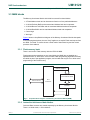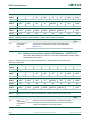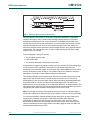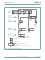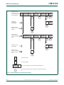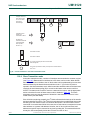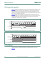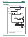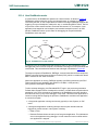
1
UM10120 LPC2131/2/4/6/8 User manual Rev. 4 — 23 April 2012 User manual Document information Info Content Keywords LPC2131, LPC2132, LPC2134, LPC2136, LPC2138, LPC2131/01, LPC2132/01, LPC2134/01, LPC2136/01, LPC2138/01, LPC2000, LPC213x, LPC213x/01, ARM, ARM7, embedded, 32-bit, microcontroller Abstract LPC213x and LPC213x/01 User manual UM10120 NXP Semiconductors LPC213x and LPC213x/01 UM Revision history Rev Date Description v4 20120423 Modifications: • • v3 02 20101004 20060918 Device revision register added (see Section 20.8.11). Reset value of the PCONP register for parts LPC2138/36/34 added (see Section 4.9.3). Modifications: • • • • New document template applied. • • RTC usage note updated (Section 17.5 “RTC usage notes”). • PINSEL2 register description updated (Section 6.4.3 “Pin function Select register 2 (PINSEL2 - 0xE002 C014)”). • PWM TCR register bit 3 description updated (Section 15.4.2 “PWM Timer Control Register (PWMTCR - 0xE001 4004)”). • U0IER register bit description corrected (Section 9.3.6 “UART0 Interrupt Enable Register (U0IER - 0xE000 C004, when DLAB = 0)”). • U1IER register bit description corrected (Section 10.3.6 “UART1 Interrupt Enable Register (U1IER - 0xE001 0004, when DLAB = 0)”). • • Pin description updated for VBAT, VREF, and RTCX1/2 (Table 35 “Pin description”). • • ADC maximum voltage updated (Table 213 “ADC pin description”). • • CRP levels updated (Section 20.7 “Code Read Protection (CRP)”). I2C chapter: multiple errors corrected (Chapter 13). IAP call example updated (Section 20.9 on page 257). WDFEED register description updated (Section 16.4.3 “Watchdog Feed register (WDFEED - 0xE000 0008)”). CTCR register bit description corrected (Section 17.4.4 “Clock Tick Counter Register (CTCR - 0xE002 4004)”). SSP CR0 register corrected (Section 12.4.1 “SSP Control Register 0 (SSPCR0 0xE006 8000)”). Minimum DLL value for use with fractional divider corrected (Section 9.3.4 “UART0 Fractional Divider Register (U0FDR - 0xE000 C028)” and Section 10.3.4 “UART1 Fractional Divider Register (U1FDR - 0xE001 0028)”). Numerous editorial updated throughout the user manual. Updated edition of the User Manual covering both LPC213x and LPC213x/01 devices. For detailed list of enhancements introduced by LPC213x/01 see Section 1.2 “Enhancements introduced with LPC213x/01 devices” on page 3. Other changes applied to Rev 01: 01 20050624 • • ECC information in Section 20.6 “Flash content protection mechanism” corrected • Bit SPIE description corrected in Section 11.4.1 “SPI Control Register (S0SPCR 0xE002 0000)” • Details on VBAT setup added in Section 17.5 “RTC usage notes” The SSEL signal description corrected for CPHA = 0 and CPHA = 1 (Section 11.2.2 “SPI data transfers”) Initial version Contact information For more information, please visit: http://www.nxp.com For sales office addresses, please send an email to: [email protected] UM10120 User manual All information provided in this document is subject to legal disclaimers. Rev. 4 — 23 April 2012 © NXP B.V. 2012. All rights reserved. 2 of 297 UM10120 Chapter 1: Introductory information Rev. 4 — 23 April 2012 User manual 1.1 Introduction The LPC213x and LPC213x/01 microcontrollers are based on a 16/32 bit ARM7TDMI-S CPU with real-time emulation and embedded trace support that combines the microcontroller with embedded high speed Flash memory ranging from 32 kB to 512 kB. A 128-bit wide memory interface and a unique accelerator architecture enable 32-bit code execution at maximum clock rate. For critical code size applications, the alternative 16-bit Thumb Mode reduces code by more than 30 % with minimal performance penalty. Due to their tiny size and low power consumption, these microcontrollers are ideal for applications where miniaturization is a key requirement, such as access control and point-of-sale. With a wide range of serial communications interfaces and on-chip SRAM options of 8/16/32 kB, they are very well suited for communication gateways and protocol converters, soft modems, voice recognition and low end imaging, providing both large buffer size and high processing power. Various 32-bit timers, single or dual 10-bit 8 channel ADC(s), 10-bit DAC, PWM channels and 47 fast GPIO lines with up to nine edge or level sensitive external interrupt pins make these microcontrollers particularly suitable for industrial control and medical systems. Important: The term “LPC213x“ in the following text will be used both for devices with and without /01 suffix. Only when needed “LPC213x/01” will be used to identify the latest ones: LPC2131/01, LPC2132/01, LPC2134/01, LPC2136/01, and/or LPC2138/01. 1.2 Enhancements introduced with LPC213x/01 devices • Fast GPIO ports enable pin toggling up to 3.5x faster than the original LPC213x. Also, Enhanced parallel ports allow for a port pin to be read at any time regardless of the function selected on it. For details see GPIO chapter on page 79. • Dedicated result registers for AD converter(s) reduce interrupt overhead. For details see ADC chapter on page 231. • UART0/1 include Fractional Baudrate Generator, auto-bauding capabilities and handshake control fully implemented in hardware. For more details see UART0 chapter on page 93 and UART1 chapter on page 109. • Enhanced BOD control enables further reduction of power consumption. For details see Table 30 “Power Control register (PCON - address 0xE01F C0C0) bit description” on page 41 1.3 Features • 16/32-bit ARM7TDMI-S microcontroller in a tiny LQFP64 package • 8/16/32 kB of on-chip static RAM and 32/64/128/256/512 kB of on-chip Flash program memory. 128 bit wide interface/accelerator enables high speed 60 MHz operation. • In-System/In-Application Programming (ISP/IAP) via on-chip boot-loader software. Single Flash sector or full chip erase in 400 ms and 256 bytes programming in 1 ms. UM10120 User manual All information provided in this document is subject to legal disclaimers. Rev. 4 — 23 April 2012 © NXP B.V. 2012. All rights reserved. 3 of 297 UM10120 NXP Semiconductors Chapter 1: Introductory information • EmbeddedICE and Embedded Trace interfaces offer real-time debugging with the on-chip RealMonitor software and high speed tracing of instruction execution. • One (LPC2131/2) or two (LPC2134/6/8) 8 channel 10-bit A/D converters provide a total of up to 16 analog inputs, with conversion times as low as 2.44 s per channel. • Single 10-bit D/A converter provides variable analog output. (LPC2132/4/6/8 only). • Two 32-bit timers/external event counters (with four capture and four compare channels each), PWM unit (six outputs) and watchdog. • Low power Real-time clock with independent power and dedicated 32 kHz clock input. • Multiple serial interfaces including two UARTs (16C550), two Fast I2C (400 kbit/s), SPI and SSP with buffering and variable data length capabilities. • • • • Vectored interrupt controller with configurable priorities and vector addresses. Up to 47 of 5 V tolerant general purpose I/O pins in a tiny LQFP64 package. Up to nine edge or level sensitive external interrupt pins available. 60 MHz maximum CPU clock available from programmable on-chip Phase-Locked Loop (PLL) with settling time of 100 s. • On-chip integrated oscillator operates with external crystal from 1 MHz to 25 MHz. • Power saving modes include Idle and Power-down. • Individual enable/disable of peripheral functions as well as peripheral clock scaling down for additional power optimization. • Processor wake-up from Power-down mode via external interrupt or Real-time Clock. • Single power supply chip with Power-On Reset (POR) and Brown-Out Detection (BOD) circuits: – CPU operating voltage range of 3.0 V to 3.6 V (3.3 V ± 10 %) with 5 V tolerant I/O pads 1.4 Applications • • • • • • • UM10120 User manual Industrial control Medical systems General purpose applications Communication gateway Embedded soft modem Access control Point-of-sale All information provided in this document is subject to legal disclaimers. Rev. 4 — 23 April 2012 © NXP B.V. 2012. All rights reserved. 4 of 297 UM10120 NXP Semiconductors Chapter 1: Introductory information 1.5 Device information Table 1. LPC213x and LPC213x/01 device information Device Pins SRAM FLASH Number of Number of UART1 10-bit ADC 10-bit DAC with channels channels modem interface LPC2131 64 8 kB 32 kB 8 LPC2131/01 64 8 kB 32 kB 8 LPC2132 64 16 kB 64 kB 8 1 LPC2132/01 64 16 kB 64 kB 8 1 LPC2134 64 16 kB 128 kB 16 1 + LPC2134/01 64 16 kB 128 kB 16 1 + LPC2136 64 32 kB 256 kB 16 1 + LPC2136/01 64 32 kB 256 kB 16 1 + LPC2138 64 32 kB 512 kB 16 1 + LPC2138/01 64 32 kB 512 kB 16 1 + UARTs with BRG and autobaud UART1 with hw auto CTS/RTS Fast ADC with GPIOs individual result registers + + + + + + + + + + + + + + + + + + 1.6 Architectural overview The LPC213x consists of an ARM7TDMI-S CPU with emulation support, the ARM7 Local Bus for interface to on-chip memory controllers, the AMBA Advanced High-performance Bus (AHB) for interface to the interrupt controller, and the VLSI Peripheral Bus (APB, a compatible superset of ARM’s AMBA Advanced Peripheral Bus) for connection to on-chip peripheral functions. The LPC213x configures the ARM7TDMI-S processor in little-endian byte order. AHB peripherals are allocated a 2 megabyte range of addresses at the very top of the 4 gigabyte ARM memory space. Each AHB peripheral is allocated a 16 kB address space within the AHB address space. LPC213x peripheral functions (other than the interrupt controller) are connected to the APB bus. The AHB to APB bridge interfaces the APB bus to the AHB bus. APB peripherals are also allocated a 2 megabyte range of addresses, beginning at the 3.5 gigabyte address point. Each APB peripheral is allocated a 16 kB address space within the APB address space. The connection of on-chip peripherals to device pins is controlled by a Pin Connect Block. This must be configured by software to fit specific application requirements for the use of peripheral functions and pins. 1.7 ARM7TDMI-S processor The ARM7TDMI-S is a general purpose 32-bit microprocessor, which offers high performance and very low power consumption. The ARM architecture is based on Reduced Instruction Set Computer (RISC) principles, and the instruction set and related decode mechanism are much simpler than those of microprogrammed Complex Instruction Set Computers. This simplicity results in a high instruction throughput and impressive real-time interrupt response from a small and cost-effective processor core. UM10120 User manual All information provided in this document is subject to legal disclaimers. Rev. 4 — 23 April 2012 © NXP B.V. 2012. All rights reserved. 5 of 297 UM10120 NXP Semiconductors Chapter 1: Introductory information Pipeline techniques are employed so that all parts of the processing and memory systems can operate continuously. Typically, while one instruction is being executed, its successor is being decoded, and a third instruction is being fetched from memory. The ARM7TDMI-S processor also employs a unique architectural strategy known as THUMB, which makes it ideally suited to high-volume applications with memory restrictions, or applications where code density is an issue. The key idea behind THUMB is that of a super-reduced instruction set. Essentially, the ARM7TDMI-S processor has two instruction sets: • The standard 32-bit ARM instruction set. • A 16-bit THUMB instruction set. The THUMB set’s 16-bit instruction length allows it to approach twice the density of standard ARM code while retaining most of the ARM’s performance advantage over a traditional 16-bit processor using 16-bit registers. This is possible because THUMB code operates on the same 32-bit register set as ARM code. THUMB code is able to provide up to 65% of the code size of ARM, and 160% of the performance of an equivalent ARM processor connected to a 16-bit memory system. The ARM7TDMI-S processor is described in detail in the ARM7TDMI-S Data sheet that can be found on official ARM website. 1.8 On-chip Flash memory system The LPC213x incorporates a 32, 64, 128, 256 or 512 kB Flash memory system. This memory may be used for both code and data storage. Programming of the Flash memory may be accomplished in several ways: over the serial built-in JTAG interface, using In System Programming (ISP) and UART0, or by means of In Application Programming (IAP) capabilities. The application program, using the IAP functions, may also erase and/or program the Flash while the application is running, allowing a great degree of flexibility for data storage field firmware upgrades, etc. When the LPC213x on-chip bootloader is used, 32/64/128/256/500 kB of Flash memory is available for user code and/or data storage. The LPC213x Flash memory provides minimum of 100,000 erase/write cycles and 20 years of data-retention. 1.9 On-chip Static RAM (SRAM) On-chip Static RAM (SRAM) may be used for code and/or data storage. The on-chip SRAM may be accessed as 8-bits, 16-bits, and 32-bits. The LPC213x provide 8/16/32 kB of static RAM. The LPC213x SRAM is designed to be accessed as a byte-addressed memory. Word and halfword accesses to the memory ignore the alignment of the address and access the naturally-aligned value that is addressed (so a memory access ignores address bits 0 and 1 for word accesses, and ignores bit 0 for halfword accesses). Therefore valid reads and writes require data accessed as halfwords to originate from addresses with address line 0 being 0 (addresses ending with 0, 2, 4, 6, 8, A, C, and E in hexadecimal notation) and UM10120 User manual All information provided in this document is subject to legal disclaimers. Rev. 4 — 23 April 2012 © NXP B.V. 2012. All rights reserved. 6 of 297 UM10120 NXP Semiconductors Chapter 1: Introductory information data accessed as words to originate from addresses with address lines 0 and 1 being 0 (addresses ending with 0, 4, 8, and C in hexadecimal notation). This rule applies to both off and on-chip memory usage. The SRAM controller incorporates a write-back buffer in order to prevent CPU stalls during back-to-back writes. The write-back buffer always holds the last data sent by software to the SRAM. This data is only written to the SRAM when another write is requested by software (the data is only written to the SRAM when software does another write). If a chip reset occurs, actual SRAM contents will not reflect the most recent write request (i.e. after a "warm" chip reset, the SRAM does not reflect the last write operation). Any software that checks SRAM contents after reset must take this into account. Two identical writes to a location guarantee that the data will be present after a Reset. Alternatively, a dummy write operation before entering idle or power-down mode will similarly guarantee that the last data written will be present in SRAM after a subsequent Reset. UM10120 User manual All information provided in this document is subject to legal disclaimers. Rev. 4 — 23 April 2012 © NXP B.V. 2012. All rights reserved. 7 of 297 UM10120 NXP Semiconductors Chapter 1: Introductory information 1.10 Block diagram TMS(3) TRST(3) LPC2131, LPC2131/01 LPC2132, LPC2132/01 LPC2134, LPC2134/01 LPC2136, LPC2136/01 LPC2138, LPC2138/01 P1[31:16] trace TEST/DEBUG INTERFACE ARM7TDMI-S FAST GENERAL PURPOSE I/O XTAL2 RESET XTAL1 TDO(3) signals EMULATION TRACE MODULE P0[31:0] TDI(3) TCK(3) AHB BRIDGE PLL system clock SYSTEM FUNCTIONS VECTORED INTERRUPT CONTROLLER AMBA AHB (Advanced High-performance Bus) ARM7 local bus INTERNAL SRAM CONTROLLER INTERNAL FLASH CONTROLLER 8/16/32 kB SRAM 32/64/128/ 256/512 kB FLASH AHB DECODER AHB TO APB BRIDGE APB DIVIDER APB (ARM peripheral bus) EINT[3:0] 8 CAP 8 MAT AD0[7:0] AD1[7:0](1) AOUT(2) EXTERNAL INTERRUPTS I2C SERIAL INTERFACES 0 AND 1 CAPTURE/ COMPARE TIMER 0/TIMER 1 SPI AND SSP SERIAL INTERFACES SCL0,1 SDA0,1 SCK0,1 MOSI0,1 MISO0,1 SSEL0,1 A/D CONVERTERS 0 AND 1(1) TXD0,1 RXD0,1 DSR1(1),CTS1(1) RTS1(1), DTR1(1) DCD1(1), RI1(1) UART0/UART1 D/A CONVERTER(2) RTCX1 P0[31:0] P1[31:16] REAL TIME CLOCK RTCX2 VBAT GENERAL PURPOSE I/O WATCHDOG TIMER PWM[6:1] PWM0 SYSTEM CONTROL 002aab067 (1) Not available on LPC2131 and LPC2131/01. (2) Not available on LPC2131, LPC2131/01, LPC2132, and LPC2132/01. (3) Pins shared with GPIO. Fig 1. LPC213x block diagram. UM10120 User manual All information provided in this document is subject to legal disclaimers. Rev. 4 — 23 April 2012 © NXP B.V. 2012. All rights reserved. 8 of 297 UM10120 Chapter 2: LPC213x Memory map Rev. 4 — 23 April 2012 User manual 2.1 Memory maps The LPC213x incorporates several distinct memory regions, shown in the following figures. Figure 2 shows the overall map of the entire address space from the user program viewpoint following reset. The interrupt vector area supports address remapping, which is described later in this section. 4.0 GB 0xFFFF FFFF AHB PERIPHERALS 0xF000 0000 3.75 GB APB PERIPHERALS 0xE000 0000 3.5 GB 3.0 GB RESERVED ADDRESS SPACE 2.0 GB 0xC000 0000 0x8000 0000 BOOT BLOCK (12 kB REMAPPED FROM ON-CHIP FLASH MEMORY) 0x7FFF D000 RESERVED ADDRESS SPACE 32 kB ON-CHIP STATIC RAM (LPC2136, LPC2136/01, LPC2138, LPC2138/01) 16 kB ON-CHIP STATIC RAM (LPC2132, LPC2132/01, LPC2134, LPC2134/01) 8 kB ON-CHIP STATIC RAM (LPC2131, LPC2131/01) 1.0 GB 0x4000 8000 0x4000 7FFF 0x4000 4000 0x4000 3FFF 0x4000 2000 0x4000 1FFF 0x4000 0000 RESERVED ADDRESS SPACE TOTAL OF 512 kB ON-CHIP NON-VOLATILE MEMORY (LPC2138, LPC2138/01) TOTAL OF 256 kB ON-CHIP NON-VOLATILE MEMORY (LPC2136, LPC2136/01) TOTAL OF 128 kB ON-CHIP NON-VOLATILE MEMORY (LPC2134, LPC2134/01) TOTAL OF 64 kB ON-CHIP NON-VOLATILE MEMORY (LPC2132, LPC2132/01) 0.0 GB Fig 2. UM10120 User manual TOTAL OF 32 kB ON-CHIP NON-VOLATILE MEMORY (LPC2131, LPC2131/01) 0x0008 0000 0x0007 FFFF 0x0004 0000 0x0003 FFFF 0x0002 0000 0x0001 FFFF 0x0001 0000 0x0000 FFFF 0x0000 8000 0x0000 7FFF 0x0000 0000 System memory map All information provided in this document is subject to legal disclaimers. Rev. 4 — 23 April 2012 © NXP B.V. 2012. All rights reserved. 9 of 297 UM10120 NXP Semiconductors Chapter 2: LPC213x Memory map 4.0 GB 0xFFFF FFFF AHB PERIPHERALS 0xFFE0 0000 0xFFDF FFFF 4.0 GB - 2 MB RESERVED 0xF000 0000 0xEFFF FFFF 3.75 GB RESERVED 0xE020 0000 0xE01F FFFF 3.5 GB + 2 MB APB PERIPHERALS 0xE000 0000 3.5 GB AHB section is 128 x 16 kB blocks (totaling 2 MB). APB section is 128 x 16 kB blocks (totaling 2MB). Fig 3. Peripheral memory map Figure 3 through Figure 4 and Table 2 show different views of the peripheral address space. Both the AHB and APB peripheral areas are 2 megabyte spaces which are divided up into 128 peripherals. Each peripheral space is 16 kilobytes in size. This allows simplifying the address decoding for each peripheral. All peripheral register addresses are UM10120 User manual All information provided in this document is subject to legal disclaimers. Rev. 4 — 23 April 2012 © NXP B.V. 2012. All rights reserved. 10 of 297 UM10120 NXP Semiconductors Chapter 2: LPC213x Memory map word aligned (to 32-bit boundaries) regardless of their size. This eliminates the need for byte lane mapping hardware that would be required to allow byte (8-bit) or half-word (16-bit) accesses to occur at smaller boundaries. An implication of this is that word and half-word registers must be accessed all at once. For example, it is not possible to read or write the upper byte of a word register separately. VECTORED INTERRUPT CONTROLLER 0xFFFF F000 (4G - 4K) 0xFFFF C000 (AHB PERIPHERAL #126) 0xFFFF 8000 (AHB PERIPHERAL #125) 0xFFFF 4000 (AHB PERIPHERAL #124) 0xFFFF 0000 0xFFE1 0000 (AHB PERIPHERAL #3) 0xFFE0 C000 (AHB PERIPHERAL #2) 0xFFE0 8000 (AHB PERIPHERAL #1) 0xFFE0 4000 (AHB PERIPHERAL #0) 0xFFE0 0000 Fig 4. UM10120 User manual AHB peripheral map All information provided in this document is subject to legal disclaimers. Rev. 4 — 23 April 2012 © NXP B.V. 2012. All rights reserved. 11 of 297 UM10120 NXP Semiconductors Chapter 2: LPC213x Memory map Table 2. APB peripheries and base addresses APB peripheral Base address Peripheral name 0 0xE000 0000 Watchdog timer 1 0xE000 4000 Timer 0 2 0xE000 8000 Timer 1 3 0xE000 C000 UART0 4 0xE001 0000 UART1 5 0xE001 4000 PWM 6 0xE001 8000 Not used 7 0xE001 C000 I2C0 8 0xE002 0000 SPI0 9 0xE002 4000 RTC 10 0xE002 8000 GPIO 11 0xE002 C000 Pin connect block 12 0xE003 0000 Not used 13 0xE003 4000 10 bit AD0 14-22 0xE003 8000 0xE005 8000 Not used 23 0xE005 C000 I2C1 24 0xE006 0000 10 bit AD1 25 0xE006 4000 Not used 26 0xE006 8000 SSP 27 0xE006 C000 DAC 28 - 126 0xE007 0000 0xE01F 8000 Not used 127 0xE01F C000 System control block 2.2 LPC213x memory re-mapping and boot block 2.2.1 Memory map concepts and operating modes The basic concept on the LPC213x is that each memory area has a "natural" location in the memory map. This is the address range for which code residing in that area is written. The bulk of each memory space remains permanently fixed in the same location, eliminating the need to have portions of the code designed to run in different address ranges. Because of the location of the interrupt vectors on the ARM7 processor (at addresses 0x0000 0000 through 0x0000 001C, as shown in Table 3 below), a small portion of the Boot Block and SRAM spaces need to be re-mapped in order to allow alternative uses of interrupts in the different operating modes described in Table 4. Re-mapping of the interrupts is accomplished via the Memory Mapping Control feature (Section 4.7 “Memory mapping control” on page 32). UM10120 User manual All information provided in this document is subject to legal disclaimers. Rev. 4 — 23 April 2012 © NXP B.V. 2012. All rights reserved. 12 of 297 UM10120 NXP Semiconductors Chapter 2: LPC213x Memory map Table 3. ARM exception vector locations Address Exception 0x0000 0000 Reset 0x0000 0004 Undefined Instruction 0x0000 0008 Software Interrupt 0x0000 000C Prefetch Abort (instruction fetch memory fault) 0x0000 0010 Data Abort (data access memory fault) 0x0000 0014 Reserved Note: Identified as reserved in ARM documentation, this location is used by the Boot Loader as the Valid User Program key. This is described in detail in "Flash Memory System and Programming" chapter. 0x0000 0018 IRQ 0x0000 001C FIQ Table 4. LPC213x memory mapping modes Mode Activation Usage Boot Loader mode Hardware activation by any Reset The Boot Loader always executes after any reset. The Boot Block interrupt vectors are mapped to the bottom of memory to allow handling exceptions and using interrupts during the Boot Loading process. User Flash mode Software activation by Boot code Activated by Boot Loader when a valid User Program Signature is recognized in memory and Boot Loader operation is not forced. Interrupt vectors are not re-mapped and are found in the bottom of the Flash memory. User RAM Software Activated by a User Program as desired. Interrupt vectors are mode activation by re-mapped to the bottom of the Static RAM. User program 2.2.2 Memory re-mapping In order to allow for compatibility with future derivatives, the entire Boot Block is mapped to the top of the on-chip memory space. In this manner, the use of larger or smaller flash modules will not require changing the location of the Boot Block (which would require changing the Boot Loader code itself) or changing the mapping of the Boot Block interrupt vectors. Memory spaces other than the interrupt vectors remain in fixed locations. Figure 5 shows the on-chip memory mapping in the modes defined above. The portion of memory that is re-mapped to allow interrupt processing in different modes includes the interrupt vector area (32 bytes) and an additional 32 bytes, for a total of 64 bytes. The re-mapped code locations overlay addresses 0x0000 0000 through 0x0000 003F. A typical user program in the Flash memory can place the entire FIQ handler at address 0x0000 001C without any need to consider memory boundaries. The vector contained in the SRAM, external memory, and Boot Block must contain branches to the actual interrupt handlers, or to other instructions that accomplish the branch to the interrupt handlers. There are three reasons this configuration was chosen: 1. To give the FIQ handler in the Flash memory the advantage of not having to take a memory boundary caused by the remapping into account. UM10120 User manual All information provided in this document is subject to legal disclaimers. Rev. 4 — 23 April 2012 © NXP B.V. 2012. All rights reserved. 13 of 297 UM10120 NXP Semiconductors Chapter 2: LPC213x Memory map 2. Minimize the need to for the SRAM and Boot Block vectors to deal with arbitrary boundaries in the middle of code space. 3. To provide space to store constants for jumping beyond the range of single word branch instructions. Re-mapped memory areas, including the Boot Block and interrupt vectors, continue to appear in their original location in addition to the re-mapped address. Details on re-mapping and examples can be found in Section 4.7 “Memory mapping control” on page 32. UM10120 User manual All information provided in this document is subject to legal disclaimers. Rev. 4 — 23 April 2012 © NXP B.V. 2012. All rights reserved. 14 of 297 UM10120 NXP Semiconductors Chapter 2: LPC213x Memory map 2.0 GB 0x8000 0000 12 kB BOOT BLOCK (RE-MAPPED FROM ON-CHIP FLASH MEMORY) 2.0 GB - 12 kB BOOT BLOCK INTERRUPT VECTORS 0x7FFF FFFF 0x7FFF D000 0x7FFF CFFF RESERVED FOR ON-CHIP MEMORY 0x4000 8000 0x4000 7FFF 32 kB ON-CHIP SRAM 1.0 GB (SRAM INTERRUPT VECTORS) 0x4000 0000 0x3FFF FFFF RESERVED FOR ON-CHIP MEMORY 0x0008 0000 12 kB BOOT BLOCK RE-MAPPED TO HIGHER ADDRESS RANGE 0x0007 FFFF 512 kB ON-CHIP NON-VOLATILE MEMORY 0.0 GB Fig 5. UM10120 User manual ACTIVE INTERRUPT VECTORS (FROM FLASH, SRAM, BOOT ROM, OR EXT MEMORY) 0x0000 0000 Map of lower memory is showing re-mapped and re-mappable areas (LPC2138 and LPC2138/01 with 512 kB Flash) All information provided in this document is subject to legal disclaimers. Rev. 4 — 23 April 2012 © NXP B.V. 2012. All rights reserved. 15 of 297 UM10120 NXP Semiconductors Chapter 2: LPC213x Memory map 2.3 Prefetch abort and data abort exceptions The LPC213x generates the appropriate bus cycle abort exception if an access is attempted for an address that is in a reserved or unassigned address region. The regions are: • Areas of the memory map that are not implemented for a specific ARM derivative. For the LPC213x, this is: – Address space between On-Chip Non-Volatile Memory and On-Chip SRAM, labelled "Reserved Address Space" in Figure 2 and Figure 5. For 32 kB Flash device this is memory address range from 0x0000 8000 to 0x3FFF FFFF, for 64 kB Flash device this is memory address range from 0x0001 0000 to 0x3FFF FFFF, for 128 kB Flash device this is memory address range from 0x0002 0000 to 0x3FFF FFFF, for 256 kB Flash device this is memory address range from 0x0004 0000 to 0x3FFF FFFF while for 512 kB Flash device this range is from 0x0008 0000 to 0x3FFF FFFF. – Address space between On-Chip Static RAM and the Boot Block. Labelled "Reserved Address Space" in Figure 2. For 8 kB SRAM device this is memory address range from 0x4000 2000 to 0x7FFF CFFF, for 16 kB SRAM device this is memory address range from 0x4000 4000 to 0x7FFF CFFF, while for 32 kB SRAM device this range is from 0x4000 8000 to 0x7FFF CFFF. – Address space between 0x8000 0000 and 0xDFFF FFFF, labelled "Reserved Address Space". – Reserved regions of the AHB and APB spaces. See Figure 3. • Unassigned AHB peripheral spaces. See Figure 4. • Unassigned APB peripheral spaces. See Table 2. For these areas, both attempted data access and instruction fetch generate an exception. In addition, a Prefetch Abort exception is generated for any instruction fetch that maps to an AHB or APB peripheral address. Within the address space of an existing APB peripheral, a data abort exception is not generated in response to an access to an undefined address. Address decoding within each peripheral is limited to that needed to distinguish defined registers within the peripheral itself. For example, an access to address 0xE000 D000 (an undefined address within the UART0 space) may result in an access to the register defined at address 0xE000 C000. Details of such address aliasing within a peripheral space are not defined in the LPC213x documentation and are not a supported feature. Note that the ARM core stores the Prefetch Abort flag along with the associated instruction (which will be meaningless) in the pipeline and processes the abort only if an attempt is made to execute the instruction fetched from the illegal address. This prevents accidental aborts that could be caused by prefetches that occur when code is executed very near a memory boundary. UM10120 User manual All information provided in this document is subject to legal disclaimers. Rev. 4 — 23 April 2012 © NXP B.V. 2012. All rights reserved. 16 of 297 UM10120 Chapter 3: LPC213x Memory accelerator module Rev. 4 — 23 April 2012 User manual 3.1 Introduction The MAM block in the LPC213x maximizes the performance of the ARM processor when it is running code in Flash memory but does so using a single Flash bank. 3.2 Operation Simply put, the Memory Accelerator Module (MAM) attempts to have the next ARM instruction that will be needed in its latches in time to prevent CPU fetch stalls. The LPC213x uses one bank of Flash memory, compared to the two banks used on predecessor devices. It includes three 128-bit buffers called the Prefetch Buffer, the Branch Trail Buffer and the data buffer. When an Instruction Fetch is not satisfied by either the Prefetch or Branch Trail Buffer, nor has a prefetch been initiated for that line, the ARM is stalled while a fetch is initiated for the 128-bit line. If a prefetch has been initiated but not yet completed, the ARM is stalled for a shorter time. Unless aborted by a data access, a prefetch is initiated as soon as the Flash has completed the previous access. The prefetched line is latched by the Flash module, but the MAM does not capture the line in its prefetch buffer until the ARM core presents the address from which the prefetch has been made. If the core presents a different address from the one from which the prefetch has been made, the prefetched line is discarded. The Prefetch and Branch Trail buffers each include four 32-bit ARM instructions or eight 16-bit Thumb instructions. During sequential code execution, typically the Prefetch Buffer contains the current instruction and the entire Flash line that contains it. The MAM differentiates between instruction and data accesses. Code and data accesses use separate 128-bit buffers. 3 of every 4 sequential 32-bit code or data accesses "hit" in the buffer without requiring a Flash access (7 of 8 sequential 16-bit accesses, 15 of every 16 sequential byte accesses). The fourth (eighth, 16th) sequential data access must access Flash, aborting any prefetch in progress. When a Flash data access is concluded, any prefetch that had been in progress is re-initiated. Timing of Flash read operations is programmable and is described later in this section. In this manner, there is no code fetch penalty for sequential instruction execution when the CPU clock period is greater than or equal to one fourth of the Flash access time. The average amount of time spent doing program branches is relatively small (less than 25%) and may be minimized in ARM (rather than Thumb) code through the use of the conditional execution feature present in all ARM instructions. This conditional execution may often be used to avoid small forward branches that would otherwise be necessary. Branches and other program flow changes cause a break in the sequential flow of instruction fetches described above. The Branch Trail Buffer captures the line to which such a non-sequential break occurs. If the same branch is taken again, the next instruction is taken from the Branch Trail Buffer. When a branch outside the contents of the Prefetch and Branch Trail Buffer is taken, a stall of several clocks is needed to load the Branch Trail buffer. Subsequently, there will typically be no further instruction fetch delays until a new and different branch occurs. UM10120_2 User manual All information provided in this document is subject to legal disclaimers. Rev. 4 — 23 April 2012 © NXP B.V. 2012. All rights reserved. 17 of 297 UM10120 NXP Semiconductors Chapter 3: LPC213x Memory accelerator module 3.3 MAM blocks The Memory Accelerator Module is divided into several functional blocks: • • • • • • A Flash Address Latch and an incrementor function to form prefetch addresses A 128-bit Prefetch Buffer and an associated Address latch and comparator A 128-bit Branch Trail Buffer and an associated Address latch and comparator A 128-bit Data Buffer and an associated Address latch and comparator Control logic Wait logic Figure 6 shows a simplified block diagram of the Memory Accelerator Module data paths. In the following descriptions, the term “fetch” applies to an explicit Flash read request from the ARM. “Pre-fetch” is used to denote a Flash read of instructions beyond the current processor fetch address. 3.3.1 Flash memory bank There is one bank of Flash memory with the LPC213x MAM. Flash programming operations are not controlled by the MAM, but are handled as a separate function. A “boot block” sector contains Flash programming algorithms that may be called as part of the application program, and a loader that may be run to allow serial programming of the Flash memory. MEMORY ADDRESS FLASH MEMORY BANK ARM LOCAL BUS BUS INTERFACE BUFFERS Fig 6. Simplified block diagram of the Memory Accelerator Module (MAM) 3.3.2 Instruction latches and data latches Code and Data accesses are treated separately by the Memory Accelerator Module. There is a 128-bit Latch, a 15-bit Address UM10120_2 User manual All information provided in this document is subject to legal disclaimers. Rev. 4 — 23 April 2012 © NXP B.V. 2012. All rights reserved. 18 of 297 UM10120 NXP Semiconductors Chapter 3: LPC213x Memory accelerator module Latch, and a 15-bit comparator associated with each buffer (prefetch, branch trail, and data). Each 128-bit latch holds 4 words (4 ARM instructions, or 8 Thumb instructions). Also associated with each buffer are 32 4:1 Multiplexers that select the requested word from the 128-bit line. Each Data access that is not in the Data latch causes a Flash fetch of 4 words of data, which are captured in the Data latch. This speeds up sequential Data operations, but has little or no effect on random accesses. 3.3.3 Flash programming issues Since the Flash memory does not allow accesses during programming and erase operations, it is necessary for the MAM to force the CPU to wait if a memory access to a Flash address is requested while the Flash module is busy. (This is accomplished by asserting the ARM7TDMI-S local bus signal CLKEN.) Under some conditions, this delay could result in a Watchdog time-out. The user will need to be aware of this possibility and take steps to insure that an unwanted Watchdog reset does not cause a system failure while programming or erasing the Flash memory. In order to preclude the possibility of stale data being read from the Flash memory, the LPC213x MAM holding latches are automatically invalidated at the beginning of any Flash programming or erase operation. Any subsequent read from a Flash address will cause a new fetch to be initiated after the Flash operation has completed. 3.4 MAM operating modes Three modes of operation are defined for the MAM, trading off performance for ease of predictability: Mode 0: MAM off. All memory requests result in a Flash read operation (see note 2 below). There are no instruction prefetches. Mode 1: MAM partially enabled. Sequential instruction accesses are fulfilled from the holding latches if the data is present. Instruction prefetch is enabled. Non-sequential instruction accesses initiate Flash read operations (see note 2 below). This means that all branches cause memory fetches. All data operations cause a Flash read because buffered data access timing is hard to predict and is very situation dependent. Mode 2: MAM fully enabled. Any memory request (code or data) for a value that is contained in one of the corresponding holding latches is fulfilled from the latch. Instruction prefetch is enabled. Flash read operations are initiated for instruction prefetch and code or data values not available in the corresponding holding latches. Table 5. MAM responses to program accesses of various types Program Memory Request Type MAM Mode 0 1 2 Sequential access, data in latches Initiate Fetch[2] Use Latched Data[1] Use Latched Data[1] Sequential access, data not in latches Initiate Fetch Initiate Fetch[1] Initiate Fetch[1] Non-sequential access, data in latches Initiate Fetch[2] Initiate Fetch[1][2] Use Latched Data[1] Non-sequential access, data not in latches Initiate Fetch UM10120_2 User manual All information provided in this document is subject to legal disclaimers. Rev. 4 — 23 April 2012 Initiate Fetch[1] Initiate Fetch[1] © NXP B.V. 2012. All rights reserved. 19 of 297 UM10120 NXP Semiconductors Chapter 3: LPC213x Memory accelerator module [1] Instruction prefetch is enabled in modes 1 and 2. [2] The MAM actually uses latched data if it is available, but mimics the timing of a Flash read operation. This saves power while resulting in the same execution timing. The MAM can truly be turned off by setting the fetch timing value in MAMTIM to one clock. Table 6. MAM responses to data and DMA accesses of various types Data Memory Request Type MAM Mode 0 1 2 Sequential access, data in latches Initiate Fetch[1] Initiate Fetch[1] Use Latched Data Sequential access, data not in latches Initiate Fetch Initiate Fetch Initiate Fetch Non-sequential access, data in latches Initiate Fetch[1] Non-sequential access, data not in latches Initiate Fetch [1] Initiate Fetch[1] Initiate Fetch Use Latched Data Initiate Fetch The MAM actually uses latched data if it is available, but mimics the timing of a Flash read operation. This saves power while resulting in the same execution timing. The MAM can truly be turned off by setting the fetch timing value in MAMTIM to one clock. 3.5 MAM configuration After reset the MAM defaults to the disabled state. Software can turn memory access acceleration on or off at any time. This allows most of an application to be run at the highest possible performance, while certain functions can be run at a somewhat slower but more predictable rate if more precise timing is required. 3.6 Register description All registers, regardless of size, are on word address boundaries. Details of the registers appear in the description of each function. Table 7. Name Summary of MAM registers Description Access Reset Address value[1] MAMCR Memory Accelerator Module Control Register. Determines the MAM functional mode, that is, to what extent the MAM performance enhancements are enabled. See Table 8. R/W 0x0 0xE01F C000 MAMTIM Memory Accelerator Module Timing control. Determines the number of clocks used for Flash memory fetches (1 to 7 processor clocks). R/W 0x07 0xE01F C004 [1] Reset value reflects the data stored in used bits only. It does not include reserved bits content. 3.7 MAM Control Register (MAMCR - 0xE01F C000) Two configuration bits select the three MAM operating modes, as shown in Table 8. Following Reset, MAM functions are disabled. Changing the MAM operating mode causes the MAM to invalidate all of the holding latches, resulting in new reads of Flash information as required. UM10120_2 User manual All information provided in this document is subject to legal disclaimers. Rev. 4 — 23 April 2012 © NXP B.V. 2012. All rights reserved. 20 of 297 UM10120 NXP Semiconductors Chapter 3: LPC213x Memory accelerator module Table 8. MAM Control Register (MAMCR - address 0xE01F C000) bit description Bit Symbol Value 1:0 MAM_mode 00 _control 01 10 7:2 - Description Reset value MAM functions disabled 0 MAM functions partially enabled MAM functions fully enabled 11 Reserved. Not to be used in the application. - Reserved, user software should not write ones to reserved NA bits. The value read from a reserved bit is not defined. 3.8 MAM Timing register (MAMTIM - 0xE01F C004) The MAM Timing register determines how many CCLK cycles are used to access the Flash memory. This allows tuning MAM timing to match the processor operating frequency. Flash access times from 1 clock to 7 clocks are possible. Single clock Flash accesses would essentially remove the MAM from timing calculations. In this case the MAM mode may be selected to optimize power usage. Table 9. MAM Timing register (MAMTIM - address 0xE01F C004) bit description Bit Symbol Value Description Reset value 2:0 MAM_fetch_ cycle_timing 000 0 - Reserved. 07 001 1 - MAM fetch cycles are 1 processor clock (CCLK) in duration 010 2 - MAM fetch cycles are 2 CCLKs in duration 011 3 - MAM fetch cycles are 3 CCLKs in duration 100 4 - MAM fetch cycles are 4 CCLKs in duration 101 5 - MAM fetch cycles are 5 CCLKs in duration 110 6 - MAM fetch cycles are 6 CCLKs in duration 111 7 - MAM fetch cycles are 7 CCLKs in duration Warning: These bits set the duration of MAM Flash fetch operations as listed here. Improper setting of this value may result in incorrect operation of the device. 7:3 - - Reserved, user software should not write ones to reserved bits. The value read from a reserved bit is not defined. NA 3.9 MAM usage notes When changing MAM timing, the MAM must first be turned off by writing a zero to MAMCR. A new value may then be written to MAMTIM. Finally, the MAM may be turned on again by writing a value (1 or 2) corresponding to the desired operating mode to MAMCR. For system clock slower than 20 MHz, MAMTIM can be 001. For system clock between 20 MHz and 40 MHz, Flash access time is suggested to be 2 CCLKs, while in systems with system clock faster than 40 MHz, 3 CCLKs are proposed. UM10120_2 User manual All information provided in this document is subject to legal disclaimers. Rev. 4 — 23 April 2012 © NXP B.V. 2012. All rights reserved. 21 of 297 UM10120 Chapter 4: LPC213x System control Rev. 4 — 23 April 2012 User manual 4.1 Summary of system control block functions The System Control Block includes several system features and control registers for a number of functions that are not related to specific peripheral devices. These include: • • • • • • • • • Crystal Oscillator External Interrupt Inputs Miscellaneous System Controls and Status Memory Mapping Control PLL Power Control Reset APB Divider Wake-up Timer Each type of function has its own register(s) if any are required and unneeded bits are defined as reserved in order to allow future expansion. Unrelated functions never share the same register addresses 4.2 Pin description Table 10 shows pins that are associated with System Control block functions. Table 10. Pin summary Pin name Pin direction Pin description XTAL1 Input Crystal Oscillator Input - Input to the oscillator and internal clock generator circuits XTAL2 Output Crystal Oscillator Output - Output from the oscillator amplifier EINT0 Input External Interrupt Input 0 - An active low/high level or falling/rising edge general purpose interrupt input. This pin may be used to wake up the processor from Idle or Power-down modes. Pins P0.1 and P0.16 can be selected to perform EINT0 function. EINT1 Input External Interrupt Input 1 - See the EINT0 description above. Pins P0.3 and P0.14 can be selected to perform EINT1 function. Important: LOW level on pin P0.14 immediately after reset is considered as an external hardware request to start the ISP command handler. More details on ISP and Serial Boot Loader can be found in "Flash Memory System and Programming" chapter. UM10120 User manual All information provided in this document is subject to legal disclaimers. Rev. 4 — 23 April 2012 © NXP B.V. 2012. All rights reserved. 22 of 297 UM10120 NXP Semiconductors Chapter 4: LPC213x System control Table 10. Pin summary Pin name Pin direction Pin description EINT2 Input External Interrupt Input 2 - See the EINT0 description above. Pins P0.7 and P0.15 can be selected to perform EINT2 function. EINT3 Input External Interrupt Input 3 - See the EINT0 description above. Pins P0.9, P0.20 and P0.30 can be selected to perform EINT3 function. Input RESET External Reset input - A LOW on this pin resets the chip, causing I/O ports and peripherals to take on their default states, and the processor to begin execution at address 0x0000 0000. 4.3 Register description All registers, regardless of size, are on word address boundaries. Details of the registers appear in the description of each function. Table 11. Summary of system control registers Name Description Access Reset value[1] Address External Interrupts EXTINT External Interrupt Flag Register R/W 0 0xE01F C140 INTWAKE External Interrupt Wakeup Register R/W 0 0xE01F C144 EXTMODE External Interrupt Flag register R/W 0 0xE01F C148 EXTPOLAR External Interrupt Wakeup Register R/W 0 0xE01F C14C R/W 0 0xE01F C040 R/W 0 0xE01F C080 Memory Mapping Control MEMMAP Memory Mapping Control Phase Locked Loop PLLCON PLL Control Register PLLCFG PLL Configuration Register R/W 0 0xE01F C084 PLLSTAT PLL Status Register RO 0 0xE01F C088 PLLFEED PLL Feed Register WO NA 0xE01F C08C Power Control PCON Power Control Register R/W 0 0xE01F C0C0 PCONP Power Control for Peripherals R/W 0x03BE 0xE01F C0C4 APB Divider Control R/W 0 0xE01F C100 Reset Source Identification Register R/W 0 0xE01F C180 RO o 0xE01F C184 R/W 0 0xE01F C1A0 APB Divider APBDIV Reset RSID Code Security/Debugging CSPR Code Security Protection Register Syscon Miscellaneous SCS UM10120 User manual Registers[2] System Controls and Status [1] Reset value reflects the data stored in used bits only. It does not include reserved bits content. [2] Available in LPC213x/01devices only. All information provided in this document is subject to legal disclaimers. Rev. 4 — 23 April 2012 © NXP B.V. 2012. All rights reserved. 23 of 297 UM10120 NXP Semiconductors Chapter 4: LPC213x System control 4.4 Crystal oscillator While an input signal of 50-50 duty cycle within a frequency range from 1 MHz to 50 MHz can be used by the LPC213x if supplied to its input XTAL1 pin, this microcontroller’s onboard oscillator circuit supports external crystals in the range of 1 MHz to 30 MHz only. If the on-chip PLL system or the boot-loader is used, the input clock frequency is limited to an exclusive range of 10 MHz to 25 MHz. The oscillator output frequency is called FOSC and the ARM processor clock frequency is referred to as CCLK for purposes of rate equations, etc. elsewhere in this document. FOSC and CCLK are the same value unless the PLL is running and connected. Refer to the Section 4.8 “Phase Locked Loop (PLL)” on page 33 for details and frequency limitations. The onboard oscillator in the LPC213x can operate in one of two modes: slave mode and oscillation mode. In slave mode the input clock signal should be coupled by means of a capacitor of 100 pF (CC in Figure 7, drawing a), with an amplitude of at least 200 mVrms. The X2 pin in this configuration can be left not connected. If slave mode is selected, the FOSC signal of 50-50 duty cycle can range from 1 MHz to 50 MHz. External components and models used in oscillation mode are shown in Figure 7, drawings b and c, and in Table 12. Since the feedback resistance is integrated on chip, only a crystal and the capacitances CX1 and CX2 need to be connected externally in case of fundamental mode oscillation (the fundamental frequency is represented by L, CL and RS). Capacitance CP in Figure 7, drawing c, represents the parallel package capacitance and should not be larger than 7 pF. Parameters FC, CL, RS and CP are supplied by the crystal manufacturer. Choosing an oscillation mode as an on-board oscillator mode of operation limits FOSC clock selection to 1 MHz to 30 MHz. LPC213x XTAL1 XTAL2 LPC213x XTAL1 XTAL2 L <=> CC CL CP Xtal Clock a) Fig 7. CX1 CX2 b) RS c) Oscillator modes and models: a) slave mode of operation, b) oscillation mode of operation, c) external crystal model used for CX1/X2 evaluation UM10120 User manual All information provided in this document is subject to legal disclaimers. Rev. 4 — 23 April 2012 © NXP B.V. 2012. All rights reserved. 24 of 297 UM10120 NXP Semiconductors Chapter 4: LPC213x System control Table 12. Recommended values for CX1/X2 in oscillation mode (crystal and external components parameters) Fundamental Crystal load oscillation frequency capacitance CL FC Maximum crystal series resistance RS External load capacitors CX1, CX2 1 MHz - 5 MHz NA NA 20 pF NA NA 30 pF < 300 58 pF, 58 pF 10 pF < 300 18 pF, 18 pF 20 pF < 300 38 pF, 38 pF 30 pF < 300 58 pF, 58 pF 10 pF < 300 18 pF, 18 pF 20 pF < 220 38 pF, 38 pF 30 pF < 140 58 pF, 58 pF 10 pF 5 MHz - 10 MHz 10 MHz - 15 MHz 15 MHz - 20 MHz 20 MHz - 25 MHz 25 MHz - 30 MHz 10 pF < 220 18 pF, 18 pF 20 pF < 140 38 pF, 38 pF 30 pF < 80 58 pF, 58 pF 10 pF < 160 18 pF, 18 pF 20 pF < 90 38 pF, 38 pF 30 pF < 50 58 pF, 58 pF 10 pF < 130 18 pF, 18 pF 20 pF < 50 38 pF, 38 pF 30 pF NA NA f OSC selection true on-chip PLL used in application? false true ISP used for initial code download? false external crystal oscillator used? true false Fig 8. UM10120 User manual MIN fOSC = 10 MHz MAX fOSC = 25 MHz MIN fOSC = 1 MHz MAX fOSC = 50 MHz MIN fOSC = 1 MHz MAX fOSC = 30 MHz mode a and/or b mode a mode b FOSC selection algorithm All information provided in this document is subject to legal disclaimers. Rev. 4 — 23 April 2012 © NXP B.V. 2012. All rights reserved. 25 of 297 UM10120 NXP Semiconductors Chapter 4: LPC213x System control 4.5 External interrupt inputs The LPC213x includes four External Interrupt Inputs as selectable pin functions. The External Interrupt Inputs can optionally be used to wake up the processor from Power-down mode. 4.5.1 Register description The external interrupt function has four registers associated with it. The EXTINT register contains the interrupt flags, and the EXTWAKEUP register contains bits that enable individual external interrupts to wake up the microcontroller from Power-down mode. The EXTMODE and EXTPOLAR registers specify the level and edge sensitivity parameters. Table 13. External interrupt registers Name Description Access Reset Address value[1] EXTINT The External Interrupt Flag Register contains interrupt flags for EINT0, EINT1, EINT2 and EINT3. See Table 14. R/W 0 0xE01F C140 INTWAKE The Interrupt Wake-up Register contains four enable bits that control whether each external interrupt will cause the processor to wake up from Power-down mode. See Table 15. R/W 0 0xE01F C144 EXTMODE The External Interrupt Mode Register controls whether each pin is edge- or level sensitive. R/W 0 0xE01F C148 EXTPOLAR The External Interrupt Polarity Register controls R/W which level or edge on each pin will cause an interrupt. 0 0xE01F C14C [1] Reset value reflects the data stored in used bits only. It does not include reserved bits content. 4.5.2 External Interrupt Flag register (EXTINT - 0xE01F C140) When a pin is selected for its external interrupt function, the level or edge on that pin (selected by its bits in the EXTPOLAR and EXTMODE registers) will set its interrupt flag in this register. This asserts the corresponding interrupt request to the VIC, which will cause an interrupt if interrupts from the pin are enabled. Writing ones to bits EINT0 through EINT3 in EXTINT register clears the corresponding bits. In level-sensitive mode this action is efficacious only when the pin is in its inactive state. Once a bit from EINT0 to EINT3 is set and an appropriate code starts to execute (handling wake-up and/or external interrupt), this bit in EXTINT register must be cleared. Otherwise the event that was just triggered by activity on the EINT pin will not be recognized in the future. Important: whenever a change of external interrupt operating mode (i.e. active level/edge) is performed (including the initialization of an external interrupt), the corresponding bit in the EXTINT register must be cleared! For details see Section 4.5.4 “External Interrupt Mode register (EXTMODE - 0xE01F C148)” and Section 4.5.5 “External Interrupt Polarity register (EXTPOLAR - 0xE01F C14C)”. UM10120 User manual All information provided in this document is subject to legal disclaimers. Rev. 4 — 23 April 2012 © NXP B.V. 2012. All rights reserved. 26 of 297 UM10120 NXP Semiconductors Chapter 4: LPC213x System control For example, if a system wakes up from power-down using a low level on external interrupt 0 pin, its post-wake-up code must reset the EINT0 bit in order to allow future entry into the power-down mode. If the EINT0 bit is left set to 1, subsequent attempt(s) to invoke power-down mode will fail. The same goes for external interrupt handling. More details on power-down mode will be discussed in the following chapters. Table 14. External Interrupt Flag register (EXTINT - address 0xE01F C140) bit description Bit Symbol Description Reset value 0 EINT0 In level-sensitive mode, this bit is set if the EINT0 function is selected for its pin, and the pin is in 0 its active state. In edge-sensitive mode, this bit is set if the EINT0 function is selected for its pin, and the selected edge occurs on the pin. Up to two pins can be selected to perform the EINT0 function (see P0.1 and P0.16 description in "Pin Configuration" chapter) This bit is cleared by writing a one to it, except in level sensitive mode when the pin is in its active state (e.g. if EINT0 is selected to be low level sensitive and a low level is present on the corresponding pin, this bit can not be cleared; this bit can be cleared only when the signal on the pin becomes high). 1 EINT1 In level-sensitive mode, this bit is set if the EINT1 function is selected for its pin, and the pin is in 0 its active state. In edge-sensitive mode, this bit is set if the EINT1 function is selected for its pin, and the selected edge occurs on the pin. Up to two pins can be selected to perform the EINT1 function (see P0.3 and P0.14 description in "Pin Configuration" chapter) This bit is cleared by writing a one to it, except in level sensitive mode when the pin is in its active state (e.g. if EINT1 is selected to be low level sensitive and a low level is present on the corresponding pin, this bit can not be cleared; this bit can be cleared only when the signal on the pin becomes high). 2 EINT2 In level-sensitive mode, this bit is set if the EINT2 function is selected for its pin, and the pin is in 0 its active state. In edge-sensitive mode, this bit is set if the EINT2 function is selected for its pin, and the selected edge occurs on the pin. Up to two pins can be selected to perform the EINT2 function (see P0.7 and P0.15 description in "Pin Configuration" chapter ) This bit is cleared by writing a one to it, except in level sensitive mode when the pin is in its active state (e.g. if EINT2 is selected to be low level sensitive and a low level is present on the corresponding pin, this bit can not be cleared; this bit can be cleared only when the signal on the pin becomes high). 3 EINT3 In level-sensitive mode, this bit is set if the EINT3 function is selected for its pin, and the pin is in 0 its active state. In edge-sensitive mode, this bit is set if the EINT3 function is selected for its pin, and the selected edge occurs on the pin. Up to three pins can be selected to perform the EINT3 function (see P0.9, P0.20 and P0.30 description in "Pin Configuration" chapter) This bit is cleared by writing a one to it, except in level sensitive mode when the pin is in its active state (e.g. if EINT3 is selected to be low level sensitive and a low level is present on the corresponding pin, this bit can not be cleared; this bit can be cleared only when the signal on the pin becomes high). 7:4 - UM10120 User manual Reserved, user software should not write ones to reserved bits. The value read from a reserved NA bit is not defined. All information provided in this document is subject to legal disclaimers. Rev. 4 — 23 April 2012 © NXP B.V. 2012. All rights reserved. 27 of 297 UM10120 NXP Semiconductors Chapter 4: LPC213x System control 4.5.3 Interrupt Wake-up register (INTWAKE - 0xE01F C144) Enable bits in the INTWAKE register allow the external interrupts to wake up the processor if it is in Power-down mode. The related EINTn function must be mapped to the pin in order for the wake-up process to take place. It is not necessary for the interrupt to be enabled in the Vectored Interrupt Controller for a wake-up to take place. This arrangement allows additional capabilities, such as having an external interrupt input wake up the processor from Power-down mode without causing an interrupt (simply resuming operation), or allowing an interrupt to be enabled during Power-down without waking the processor up if it is asserted (eliminating the need to disable the interrupt if the wake-up feature is not desirable in the application). For an external interrupt pin to be a source that would wake up the microcontroller from Power-down mode, it is also necessary to clear the corresponding bit in the External Interrupt Flag register (Section 4.5.2 on page 26). Table 15. Interrupt Wakeup register (INTWAKE - address 0xE01F C144) bit description Bit Symbol Description Reset value 0 EXTWAKE0 When one, assertion of EINT0 will wake up the processor from 0 Power-down mode. 1 EXTWAKE1 When one, assertion of EINT1 will wake up the processor from 0 Power-down mode. 2 EXTWAKE2 When one, assertion of EINT2 will wake up the processor from 0 Power-down mode. 3 EXTWAKE3 When one, assertion of EINT3 will wake up the processor from 0 Power-down mode. 13:4 - Reserved, user software should not write ones to reserved bits. NA The value read from a reserved bit is not defined. 14 BODWAKE When one, a BOD interrupt will wake up the processor from Power-down mode. 0 15 RTCWAKE When one, assertion of an RTC interrupt will wake up the processor from Power-down mode. 0 4.5.4 External Interrupt Mode register (EXTMODE - 0xE01F C148) The bits in this register select whether each EINT pin is level- or edge-sensitive. Only pins that are selected for the EINT function (see chapter Pin Connect Block on page 58) and enabled via the VICIntEnable register (Section 7.4.4 “Interrupt Enable register (VICIntEnable - 0xFFFF F010)” on page 68) can cause interrupts from the External Interrupt function (though of course pins selected for other functions may cause interrupts from those functions). Note: Software should only change a bit in this register when its interrupt is disabled in the VICIntEnable register, and should write the corresponding 1 to the EXTINT register before enabling (initializing) or re-enabling the interrupt, to clear the EXTINT bit that could be set by changing the mode. UM10120 User manual All information provided in this document is subject to legal disclaimers. Rev. 4 — 23 April 2012 © NXP B.V. 2012. All rights reserved. 28 of 297 UM10120 NXP Semiconductors Chapter 4: LPC213x System control Table 16. External Interrupt Mode register (EXTMODE - address 0xE01F C148) bit description Bit Symbol Value 0 EXTMODE0 0 1 1 EXTMODE1 0 1 2 EXTMODE2 0 1 3 7:4 EXTMODE3 0 - Description Reset value Level-sensitivity is selected for EINT0. 0 EINT0 is edge sensitive. Level-sensitivity is selected for EINT1. 0 EINT1 is edge sensitive. Level-sensitivity is selected for EINT2. 0 EINT2 is edge sensitive. Level-sensitivity is selected for EINT3. 0 1 EINT3 is edge sensitive. - Reserved, user software should not write ones to reserved bits. The value read from a reserved bit is not defined. NA 4.5.5 External Interrupt Polarity register (EXTPOLAR - 0xE01F C14C) In level-sensitive mode, the bits in this register select whether the corresponding pin is high- or low-active. In edge-sensitive mode, they select whether the pin is rising- or falling-edge sensitive. Only pins that are selected for the EINT function (see "Pin Connect Block" chapter) and enabled in the VICIntEnable register (Section 7.4.4 “Interrupt Enable register (VICIntEnable - 0xFFFF F010)” on page 68) can cause interrupts from the External Interrupt function (though of course pins selected for other functions may cause interrupts from those functions). Note: Software should only change a bit in this register when its interrupt is disabled in the VICIntEnable register, and should write the corresponding 1 to the EXTINT register before enabling (initializing) or re-enabling the interrupt, to clear the EXTINT bit that could be set by changing the polarity. Table 17. External Interrupt Polarity register (EXTPOLAR - address 0xE01F C14C) bit description Bit Symbol 0 1 2 UM10120 User manual Value Description Reset value EXTPOLAR0 0 EINT0 is low-active or falling-edge sensitive (depending on EXTMODE0 selection). 1 EINT0 is high-active or rising-edge sensitive (depending on EXTMODE0 selection). EXTPOLAR1 0 EINT1 is low-active or falling-edge sensitive (depending on EXTMODE1 selection). 1 EINT1 is high-active or rising-edge sensitive (depending on EXTMODE1 selection). EXTPOLAR2 0 EINT2 is low-active or falling-edge sensitive (depending on EXTMODE2 selection). 1 EINT2 is high-active or rising-edge sensitive (depending on EXTMODE2 selection). All information provided in this document is subject to legal disclaimers. Rev. 4 — 23 April 2012 0 0 0 © NXP B.V. 2012. All rights reserved. 29 of 297 UM10120 NXP Semiconductors Chapter 4: LPC213x System control Table 17. External Interrupt Polarity register (EXTPOLAR - address 0xE01F C14C) bit description Bit Symbol 3 Value Description Reset value EXTPOLAR3 0 EINT3 is low-active or falling-edge sensitive (depending on EXTMODE3 selection). 1 EINT3 is high-active or rising-edge sensitive (depending on EXTMODE3 selection). - Reserved, user software should not write ones to reserved bits. The value read from a reserved bit is not defined. 7:4 - 0 NA 4.5.6 Multiple external interrupt pins Software can select multiple pins for each of EINT3:0 in the Pin Select registers, which are described in chapter Pin Connect Block on page 58. The external interrupt logic for each of EINT3:0 receives the state of all of its associated pins from the pins’ receivers, along with signals that indicate whether each pin is selected for the EINT function. The external interrupt logic handles the case when more than one pin is so selected, differently according to the state of its Mode and Polarity bits: • In Low-Active Level Sensitive mode, the states of all pins selected for the same EINTx functionality are digitally combined using a positive logic AND gate. • In High-Active Level Sensitive mode, the states of all pins selected for the same EINTx functionality are digitally combined using a positive logic OR gate. • In Edge Sensitive mode, regardless of polarity, the pin with the lowest GPIO port number is used. (Selecting multiple pins for an EINTx in edge-sensitive mode could be considered a programming error.) The signal derived by this logic is the EINTi signal in the following logic schematic Figure 9. For example, if the EINT3 function is selected in the PINSEL0 and PINSEL1 registers for pins P0.9, P0.20 and P0.30, and EINT3 is configured to be low level sensitive, the inputs from all three pins will be logically ANDed. When more than one EINT pin is logically ORed, the interrupt service routine can read the states of the pins from the GPIO port using the IO0PIN and IO1PIN registers, to determine which pin(s) caused the interrupt. UM10120 User manual All information provided in this document is subject to legal disclaimers. Rev. 4 — 23 April 2012 © NXP B.V. 2012. All rights reserved. 30 of 297 UM10120 NXP Semiconductors Chapter 4: LPC213x System control wakeup enable (one bit of EXTWAKE) D APB Bus Data GLITCH FILTER EINTi APB Read of EXTWAKE EINTi to wakeup timer1 Q PCLK interrupt flag (one bit of EXTINT) EXTPOLARi 1 D S S S Q Q R EXTMODEi to VIC Q R PCLK APB read of EXTINT PCLK reset write 1 to EXTINTi (1) See Figure 11 “Reset block diagram including the wakeup timer” Fig 9. External interrupt logic 4.6 Other system controls Some aspects of controlling LPC213x/01 operation that do not fit into peripheral or other registers are grouped here. 4.6.1 System Control and Status flags register (SCS - 0xE01F C1A0) Table 18. System Control and Status flags register (SCS - address 0xE01F C1A0) bit description Bit Symbol 0 GPIO0M UM10120 User manual Value Description Reset value GPIO port 0 mode selection. 0 0 GPIO port 0 is accessed via APB addresses in a fashion compatible with previous LCP2000 devices. 1 High speed GPIO is enabled on GPIO port 0, accessed via addresses in the on-chip memory range. This mode includes the port masking feature described in the GPIO chapter on page page 79. All information provided in this document is subject to legal disclaimers. Rev. 4 — 23 April 2012 © NXP B.V. 2012. All rights reserved. 31 of 297 UM10120 NXP Semiconductors Chapter 4: LPC213x System control Table 18. System Control and Status flags register (SCS - address 0xE01F C1A0) bit description Bit Symbol 1 GPIO1M 31:2 - Value Description Reset value GPIO port 1 mode selection. 0 0 GPIO port 1 is accessed via APB addresses in a fashion compatible with previous LCP2000 devices. 1 High speed GPIO is enabled on GPIO port 1, accessed via addresses in the on-chip memory range. This mode includes the port masking feature described in the GPIO chapter on page page 79. Reserved, user software should not write ones to reserved bits. The value read from a reserved bit is not defined. NA 4.7 Memory mapping control The Memory Mapping Control alters the mapping of the interrupt vectors that appear beginning at address 0x0000 0000. This allows code running in different memory spaces to have control of the interrupts. 4.7.1 Memory Mapping control register (MEMMAP - 0xE01F C040) Whenever an exception handling is necessary, the microcontroller will fetch an instruction residing on the exception corresponding address as described in Table 3 “ARM exception vector locations” on page 13. The MEMMAP register determines the source of data that will fill this table. Table 19. Memory Mapping control register (MEMMAP - address 0xE01F C040) bit description Bit Symbol Value Description Reset value 1:0 MAP 00 Boot Loader Mode. Interrupt vectors are re-mapped to Boot Block. 00 01 User Flash Mode. Interrupt vectors are not re-mapped and reside in Flash. 10 User RAM Mode. Interrupt vectors are re-mapped to Static RAM. 11 Reserved. Do not use this option. Warning: Improper setting of this value may result in incorrect operation of the device. 7:2 - - Reserved, user software should not write ones to reserved bits. The value read from a reserved bit is not defined. NA 4.7.2 Memory mapping control usage notes The Memory Mapping Control simply selects one out of three available sources of data (sets of 64 bytes each) necessary for handling ARM exceptions (interrupts). For example, whenever a Software Interrupt request is generated, the ARM core will always fetch 32-bit data "residing" on 0x0000 0008 see Table 3 “ARM exception vector locations” on page 13. This means that when MEMMAP[1:0]=10 (User RAM Mode), a UM10120 User manual All information provided in this document is subject to legal disclaimers. Rev. 4 — 23 April 2012 © NXP B.V. 2012. All rights reserved. 32 of 297 UM10120 NXP Semiconductors Chapter 4: LPC213x System control read/fetch from 0x0000 0008 will provide data stored in 0x4000 0008. In case of MEMMAP[1:0]=00 (Boot Loader Mode), a read/fetch from 0x0000 0008 will provide data available also at 0x7FFF E008 (Boot Block remapped from on-chip Bootloader). 4.8 Phase Locked Loop (PLL) The PLL accepts an input clock frequency in the range of 10 MHz to 25 MHz only. The input frequency is multiplied up into the CCLK with the range of 10 MHz to 60 MHz using a Current Controlled Oscillator (CCO). The multiplier can be an integer value from 1 to 32 (in practice, the multiplier value cannot be higher than 6 on the LPC213x due to the upper frequency limit of the CPU). The CCO operates in the range of 156 MHz to 320 MHz, so there is an additional divider in the loop to keep the CCO within its frequency range while the PLL is providing the desired output frequency. The output divider may be set to divide by 2, 4, 8, or 16 to produce the output clock. Since the minimum output divider value is 2, it is insured that the PLL output has a 50% duty cycle. A block diagram of the PLL is shown in Figure 10. PLL activation is controlled via the PLLCON register. The PLL multiplier and divider values are controlled by the PLLCFG register. These two registers are protected in order to prevent accidental alteration of PLL parameters or deactivation of the PLL. Since all chip operations, including the Watchdog Timer, are dependent on the PLL when it is providing the chip clock, accidental changes to the PLL setup could result in unexpected behavior of the microcontroller. The protection is accomplished by a feed sequence similar to that of the Watchdog Timer. Details are provided in the description of the PLLFEED register. The PLL is turned off and bypassed following a chip Reset and when by entering Power-down mode. The PLL is enabled by software only. The program must configure and activate the PLL, wait for the PLL to Lock, then connect to the PLL as a clock source. 4.8.1 Register description The PLL is controlled by the registers shown in Table 20. More detailed descriptions follow. Warning: Improper setting of the PLL values may result in incorrect operation of the device! UM10120 User manual All information provided in this document is subject to legal disclaimers. Rev. 4 — 23 April 2012 © NXP B.V. 2012. All rights reserved. 33 of 297 UM10120 NXP Semiconductors Chapter 4: LPC213x System control Table 20. Name Description PLLCON PLL Control Register. Holding register for R/W updating PLL control bits. Values written to this register do not take effect until a valid PLL feed sequence has taken place. 0 0xE01F C080 PLLCFG PLL Configuration Register. Holding register for R/W updating PLL configuration values. Values written to this register do not take effect until a valid PLL feed sequence has taken place. 0 0xE01F C084 PLLSTAT PLL Status Register. Read-back register for RO PLL control and configuration information. If PLLCON or PLLCFG have been written to, but a PLL feed sequence has not yet occurred, they will not reflect the current PLL state. Reading this register provides the actual values controlling the PLL, as well as the status of the PLL. 0 0xE01F C088 PLLFEED WO PLL Feed Register. This register enables loading of the PLL control and configuration information from the PLLCON and PLLCFG registers into the shadow registers that actually affect PLL operation. NA 0xE01F C08C [1] UM10120 User manual PLL registers Access Reset Address value[1] Reset value reflects the data stored in used bits only. It does not include reserved bits content. All information provided in this document is subject to legal disclaimers. Rev. 4 — 23 April 2012 © NXP B.V. 2012. All rights reserved. 34 of 297 UM10120 NXP Semiconductors Chapter 4: LPC213x System control PLLC CLOCK SYNCHRONIZATION 0 direct PSEL[1:0] PD PD PLLE 0 bypass FOSC 1 PHASEFREQUENCY DETECTOR PLOCK CCO FCCO CD 0 /2P 0 0 CCLK 1 1 PD FOUT CD DIV-BY-M MSEL<4:0> MSEL[4:0] Fig 10. PLL block diagram 4.8.2 PLL Control register (PLLCON - 0xE01F C080) The PLLCON register contains the bits that enable and connect the PLL. Enabling the PLL allows it to attempt to lock to the current settings of the multiplier and divider values. Connecting the PLL causes the processor and all chip functions to run from the PLL output clock. Changes to the PLLCON register do not take effect until a correct PLL feed sequence has been given (see Section 4.8.7 “PLL Feed register (PLLFEED 0xE01F C08C)” and Section 4.8.3 “PLL Configuration register (PLLCFG - 0xE01F C084)” on page 36). UM10120 User manual All information provided in this document is subject to legal disclaimers. Rev. 4 — 23 April 2012 © NXP B.V. 2012. All rights reserved. 35 of 297 UM10120 NXP Semiconductors Chapter 4: LPC213x System control Table 21. PLL Control register (PLLCON - address 0xE01F C080) bit description Bit Symbol Description Reset value 0 PLLE 0 PLL Enable. When one, and after a valid PLL feed, this bit will activate the PLL and allow it to lock to the requested frequency. See PLLSTAT register, Table 23. 1 PLLC PLL Connect. When PLLC and PLLE are both set to one, and after a 0 valid PLL feed, connects the PLL as the clock source for the microcontroller. Otherwise, the oscillator clock is used directly by the microcontroller. See PLLSTAT register, Table 23. 7:2 - Reserved, user software should not write ones to reserved bits. The value read from a reserved bit is not defined. NA The PLL must be set up, enabled, and Lock established before it may be used as a clock source. When switching from the oscillator clock to the PLL output or vice versa, internal circuitry synchronizes the operation in order to ensure that glitches are not generated. Hardware does not insure that the PLL is locked before it is connected or automatically disconnect the PLL if lock is lost during operation. In the event of loss of PLL lock, it is likely that the oscillator clock has become unstable and disconnecting the PLL will not remedy the situation. 4.8.3 PLL Configuration register (PLLCFG - 0xE01F C084) The PLLCFG register contains the PLL multiplier and divider values. Changes to the PLLCFG register do not take effect until a correct PLL feed sequence has been given (see Section 4.8.7 “PLL Feed register (PLLFEED - 0xE01F C08C)” on page 37). Calculations for the PLL frequency, and multiplier and divider values are found in the PLL Frequency Calculation section on page 38. Table 22. PLL Configuration register (PLLCFG - address 0xE01F C084) bit description Bit Symbol Description Reset value 4:0 MSEL PLL Multiplier value. Supplies the value "M" in the PLL frequency calculations. 0 Note: For details on selecting the right value for MSEL see Section 4.8.9 “PLL frequency calculation” on page 38. 6:5 PSEL PLL Divider value. Supplies the value "P" in the PLL frequency calculations. 0 Note: For details on selecting the right value for PSEL see Section 4.8.9 “PLL frequency calculation” on page 38. 7 - Reserved, user software should not write ones to reserved bits. The NA value read from a reserved bit is not defined. 4.8.4 PLL Status register (PLLSTAT - 0xE01F C088) The read-only PLLSTAT register provides the actual PLL parameters that are in effect at the time it is read, as well as the PLL status. PLLSTAT may disagree with values found in PLLCON and PLLCFG because changes to those registers do not take effect until a proper PLL feed has occurred (see Section 4.8.7 “PLL Feed register (PLLFEED 0xE01F C08C)”). UM10120 User manual All information provided in this document is subject to legal disclaimers. Rev. 4 — 23 April 2012 © NXP B.V. 2012. All rights reserved. 36 of 297 UM10120 NXP Semiconductors Chapter 4: LPC213x System control Table 23. PLL Status register (PLLSTAT - address 0xE01F C088) bit description Bit Symbol Description Reset value 4:0 MSEL Read-back for the PLL Multiplier value. This is the value currently used by the PLL. 0 6:5 PSEL Read-back for the PLL Divider value. This is the value currently used by the PLL. 0 7 - Reserved, user software should not write ones to reserved bits. The NA value read from a reserved bit is not defined. 8 PLLE Read-back for the PLL Enable bit. When one, the PLL is currently 0 activated. When zero, the PLL is turned off. This bit is automatically cleared when Power-down mode is activated. 9 PLLC Read-back for the PLL Connect bit. When PLLC and PLLE are both 0 one, the PLL is connected as the clock source for the microcontroller. When either PLLC or PLLE is zero, the PLL is bypassed and the oscillator clock is used directly by the microcontroller. This bit is automatically cleared when Power-down mode is activated. 10 PLOCK Reflects the PLL Lock status. When zero, the PLL is not locked. When one, the PLL is locked onto the requested frequency. 15:11 - Reserved, user software should not write ones to reserved bits. The NA value read from a reserved bit is not defined. 0 4.8.5 PLL Interrupt The PLOCK bit in the PLLSTAT register is connected to the interrupt controller. This allows for software to turn on the PLL and continue with other functions without having to wait for the PLL to achieve lock. When the interrupt occurs (PLOCK = 1), the PLL may be connected, and the interrupt disabled. 4.8.6 PLL Modes The combinations of PLLE and PLLC are shown in Table 24. Table 24. PLL Control bit combinations PLLC PLLE PLL Function 0 0 PLL is turned off and disconnected. The system runs from the unmodified clock input. 0 1 The PLL is active, but not yet connected. The PLL can be connected after PLOCK is asserted. 1 0 Same as 00 combination. This prevents the possibility of the PLL being connected without also being enabled. 1 1 The PLL is active and has been connected as the system clock source. 4.8.7 PLL Feed register (PLLFEED - 0xE01F C08C) A correct feed sequence must be written to the PLLFEED register in order for changes to the PLLCON and PLLCFG registers to take effect. The feed sequence is: 1. Write the value 0xAA to PLLFEED. 2. Write the value 0x55 to PLLFEED. UM10120 User manual All information provided in this document is subject to legal disclaimers. Rev. 4 — 23 April 2012 © NXP B.V. 2012. All rights reserved. 37 of 297 UM10120 NXP Semiconductors Chapter 4: LPC213x System control The two writes must be in the correct sequence, and must be consecutive APB bus cycles. The latter requirement implies that interrupts must be disabled for the duration of the PLL feed operation. If either of the feed values is incorrect, or one of the previously mentioned conditions is not met, any changes to the PLLCON or PLLCFG register will not become effective. Table 25. PLL Feed register (PLLFEED - address 0xE01F C08C) bit description Bit Symbol Description Reset value 7:0 PLLFEED The PLL feed sequence must be written to this register in order for PLL configuration and control register changes to take effect. 0x00 4.8.8 PLL and Power-down mode Power-down mode automatically turns off and disconnects the PLL. Wake-up from Power-down mode does not automatically restore the PLL settings, this must be done in software. Typically, a routine to activate the PLL, wait for lock, and then connect the PLL can be called at the beginning of any interrupt service routine that might be called due to the wake-up. It is important not to attempt to restart the PLL by simply feeding it when execution resumes after a wake-up from Power-down mode. This would enable and connect the PLL at the same time, before PLL lock is established. 4.8.9 PLL frequency calculation The PLL equations use the following parameters: Table 26. Elements determining PLL’s frequency Element Description FOSC the frequency from the crystal oscillator/external oscillator FCCO the frequency of the PLL current controlled oscillator CCLK the PLL output frequency (also the processor clock frequency) M PLL Multiplier value from the MSEL bits in the PLLCFG register P PLL Divider value from the PSEL bits in the PLLCFG register The PLL output frequency (when the PLL is both active and connected) is given by: CCLK = M FOSC or CCLK = FCCO / (2 P) The CCO frequency can be computed as: FCCO = CCLK 2 P or FCCO = FOSC M 2 P The PLL inputs and settings must meet the following: • FOSC is in the range of 10 MHz to 25 MHz. • CCLK is in the range of 10 MHz to Fmax (the maximum allowed frequency for the microcontroller - determined by the system microcontroller is embedded in). • FCCO is in the range of 156 MHz to 320 MHz. UM10120 User manual All information provided in this document is subject to legal disclaimers. Rev. 4 — 23 April 2012 © NXP B.V. 2012. All rights reserved. 38 of 297 UM10120 NXP Semiconductors Chapter 4: LPC213x System control 4.8.10 Procedure for determining PLL settings If a particular application uses the PLL, its configuration may be determined as follows: 1. Choose the desired processor operating frequency (CCLK). This may be based on processor throughput requirements, need to support a specific set of UART baud rates, etc. Bear in mind that peripheral devices may be running from a lower clock than the processor (see Section 4.11 “APB divider” on page 45). 2. Choose an oscillator frequency (FOSC). CCLK must be the whole (non-fractional) multiple of FOSC. 3. Calculate the value of M to configure the MSEL bits. M = CCLK / FOSC. M must be in the range of 1 to 32. The value written to the MSEL bits in PLLCFG is M 1 (see Table 28. 4. Find a value for P to configure the PSEL bits, such that FCCO is within its defined frequency limits. FCCO is calculated using the equation given above. P must have one of the values 1, 2, 4, or 8. The value written to the PSEL bits in PLLCFG is 00 for P = 1; 01 for P = 2; 10 for P = 4; 11 for P = 8 (see Table 27). Table 27. PLL Divider values PSEL Bits (PLLCFG bits [6:5]) Value of P 00 1 01 2 10 4 11 8 Table 28. PLL Multiplier values MSEL Bits (PLLCFG bits [4:0]) Value of M 00000 1 00001 2 00010 3 00011 4 ... ... 11110 31 11111 32 4.8.11 PLL example System design asks for FOSC= 10 MHz and requires CCLK = 60 MHz. Based on these specifications, M = CCLK / Fosc = 60 MHz / 10 MHz = 6. Consequently, M - 1 = 5 will be written as PLLCFG[4:0]. Value for P can be derived from P = FCCO / (CCLK x 2), using condition that FCCO must be in range of 156 MHz to 320 MHz. Assuming the lowest allowed frequency for FCCO = 156 MHz, P = 156 MHz / (2 x 60 MHz) = 1.3. The highest FCCO frequency criteria produces P = 2.67. The only solution for P that satisfies both of these requirements and is listed in Table 27 is P = 2. Therefore, PLLCFG[6:5] = 1 will be used. UM10120 User manual All information provided in this document is subject to legal disclaimers. Rev. 4 — 23 April 2012 © NXP B.V. 2012. All rights reserved. 39 of 297 UM10120 NXP Semiconductors Chapter 4: LPC213x System control 4.9 Power control The LPC213x supports two reduced power modes: Idle mode and Power-down mode. In Idle mode, execution of instructions is suspended until either a Reset or interrupt occurs. Peripheral functions continue operation during Idle mode and may generate interrupts to cause the processor to resume execution. Idle mode eliminates power used by the processor itself, memory systems and related controllers, and internal buses. In Power-down mode, the oscillator is shut down and the chip receives no internal clocks. The processor state and registers, peripheral registers, and internal SRAM values are preserved throughout Power-down mode and the logic levels of chip pins remain static. The Power-down mode can be terminated and normal operation resumed by either a Reset or certain specific interrupts that are able to function without clocks. Since all dynamic operation of the chip is suspended, Power-down mode reduces chip power consumption to nearly zero. Entry to Power-down and Idle modes must be coordinated with program execution. Wake-up from Power-down or Idle modes via an interrupt resumes program execution in such a way that no instructions are lost, incomplete, or repeated. Wake up from Power-down mode is discussed further in Section 4.12 “Wake-up timer” on page 46. A Power Control for Peripherals feature allows individual peripherals to be turned off if they are not needed in the application, resulting in additional power savings. 4.9.1 Register description The Power Control function contains two registers, as shown in Table 29. More detailed descriptions follow. Table 29. Power control registers Access Reset value[1] Name Description PCON Power Control Register. This register contains control bits R/W that enable the two reduced power operating modes of the microcontroller. See Table 30. PCONP Power Control for Peripherals Register. This register contains control bits that enable and disable individual peripheral functions, Allowing elimination of power consumption by peripherals that are not needed. [1] R/W Address 0x00 0xE01F C0C0 0x0008 17BE (for LPC2132/31) 0x0018 17BE (for LPC2138/36/34) 0xE01F C0C4 Reset value reflects the data stored in used bits only. It does not include reserved bits content. 4.9.2 Power Control register (PCON - 0xE01F C0C0) The PCON register contains two bits. Writing a one to the corresponding bit causes entry to either the Power-down or Idle mode. If both bits are set, Power-down mode is entered. UM10120 User manual All information provided in this document is subject to legal disclaimers. Rev. 4 — 23 April 2012 © NXP B.V. 2012. All rights reserved. 40 of 297 UM10120 NXP Semiconductors Chapter 4: LPC213x System control Table 30. Power Control register (PCON - address 0xE01F C0C0) bit description Bit Symbol 0 IDL 1 2 3 4 7:5 Value Description Idle mode control. 0 0 Idle mode is off. 1 The processor clock is stopped, while on-chip peripherals remain active. Any enabled interrupt from a peripheral or an external interrupt source will cause the processor to resume execution. PD Power-down mode control. 0 0 Power-down mode is off. 1 The oscillator and all on-chip clocks are stopped. A wakeup condition from an external interrupt can cause the oscillator to restart, the PD bit to be cleared, and the processor to resume execution. BODPDM Brown Out Power-down Mode. 0 0 Brown Out Detection (BOD) remains operative during Power-down mode, and its Reset can release the microcontroller from Power-down mode[1]. 1 The BOD circuitry will go into power down mode when PD = 1, resulting in a further reduction in power. In this case the BOD can not be used as a wakeup source from Power Down mode. BOGD[2] Brown Out Global Disable. 0 0 The BOD circuitry is enabled. 1 The BOD is fully disabled at all times, consuming no power. BORD[2] - Reset value Brown Out Reset Disable. 0 0 The reset is enabled. The first stage of low voltage detection (2.9 V) Brown Out interrupt is not affected. 1 The second stage of low voltage detection (2.6 V) will not cause a chip reset. Reserved, user software should not write ones to reserved bits. The value read from a reserved bit is not defined. NA [1] Since execution is delayed until after the Wake-up Timer has allowed the main oscillator to resume stable operation, there is no guarantee that execution will resume before VDD has fallen below the lower BOD threshold, which prevents execution. If execution does resume, there is no guarantee of how long the microcontroller will continue execution before the lower BOD threshold terminates execution. These issues depend on the slope of the decline of VDD. High decoupling capacitance (between VDD and ground) in the vicinity of the microcontroller will improve the likelihood that software will be able to do what needs to be done when power is being lost. [2] This feature is available in LPC213x/01 only. 4.9.3 Power Control for Peripherals register (PCONP - 0xE01F C0C4) The PCONP register allows turning off selected peripheral functions for the purpose of saving power. This is accomplished by gating off the clock source to the specified peripheral blocks. A few peripheral functions cannot be turned off (i.e. the Watchdog timer, GPIO, the Pin Connect block, and the System Control block). Some peripherals, particularly those that include analog functions, may consume power that is not clock dependent. These peripherals may contain a separate disable control that turns off additional circuitry to reduce power. Each bit in PCONP controls one of the peripherals. UM10120 User manual All information provided in this document is subject to legal disclaimers. Rev. 4 — 23 April 2012 © NXP B.V. 2012. All rights reserved. 41 of 297 UM10120 NXP Semiconductors Chapter 4: LPC213x System control The bit numbers correspond to the related peripheral number as shown in the APB peripheral map Figure 4 “AHB peripheral map” in the "LPC2131/2/4/6/8 Memory Addressing" chapter. If a peripheral control bit is 1, that peripheral is enabled. If a peripheral bit is 0, that peripheral is disabled to conserve power. For example if bit 19 is 1, the I2C1 interface is enabled. If bit 19 is 0, the I2C1 interface is disabled. Important: valid read from a peripheral register and valid write to a peripheral register is possible only if that peripheral is enabled in the PCONP register! Table 31. Power Control for Peripherals register (PCONP - address 0xE01F C0C4) bit description Bit Symbol Description Reset value 0 - Reserved, user software should not write ones to reserved bits. The value read from a reserved bit is not defined. NA 1 PCTIM0 Timer/Counter 0 power/clock control bit. 1 2 PCTIM1 Timer/Counter 1 power/clock control bit. 1 3 PCUART0 UART0 power/clock control bit. 1 4 PCUART1 UART1 power/clock control bit. 1 5 PCPWM0 PWM0 power/clock control bit. 1 6 - Reserved, user software should not write ones to reserved bits. The value read from a reserved bit is not defined. NA 7 PCI2C0 The I2C0 interface power/clock control bit. 1 8 PCSPI0 The SPI0 interface power/clock control bit. 1 9 PCRTC The RTC power/clock control bit. 1 10 PCSPI1 The SSP interface power/clock control bit. 1 11 - Reserved, user software should not write ones to reserved bits. The value read from a reserved bit is not defined. NA 12 PCAD0 A/D converter 0 (ADC0) power/clock control bit. 1 Note: Clear the PDN bit in the AD0CR before clearing this bit, and set this bit before setting PDN. 18:13 - Reserved, user software should not write ones to reserved bits. The value read from a reserved bit is not defined. NA 19 PCI2C1 The I2C1 interface power/clock control bit. 1 20 PCAD1 A/D converter 1 (ADC1) power/clock control bit. 1 This bit is set to one by default on parts LPC2138/36/34 and set to zero on parts LPC2132/32. Note: Clear the PDN bit in the AD1CR before clearing this bit, and set this bit before setting PDN. 31:21 - Reserved, user software should not write ones to reserved bits. The value read from a reserved bit is not defined. NA 4.9.4 Power control usage notes After every reset, the PCONP register contains the value that enables all interfaces and peripherals controlled by the PCONP to be enabled. Therefore, apart from proper configuring via peripheral dedicated registers, the user’s application has no need to access the PCONP in order to start using any of the on-board peripherals. UM10120 User manual All information provided in this document is subject to legal disclaimers. Rev. 4 — 23 April 2012 © NXP B.V. 2012. All rights reserved. 42 of 297 UM10120 NXP Semiconductors Chapter 4: LPC213x System control Power saving oriented systems should have 1s in the PCONP register only in positions that match peripherals really used in the application. All other bits, declared to be "Reserved" or dedicated to the peripherals not used in the current application, must be cleared to 0. 4.10 Reset Reset has three sources on the LPC213x: the RESET pin, Watchdog Reset and Brown-Out-Detector (BOD) Reset. The RESET pin is a Schmitt trigger input pin with an additional glitch filter. Assertion of chip Reset by any source starts the Wake-up Timer (see description in Section 4.12 “Wake-up timer” in this chapter), causing reset to remain asserted until the external Reset is de-asserted, the oscillator is running, a fixed number of clocks have passed, and the on-chip circuitry has completed its initialization. The relationship between Reset, the oscillator, and the Wake-up Timer are shown in Figure 11. The Reset glitch filter allows the processor to ignore external reset pulses that are very short, and also determines the minimum duration of RESET that must be asserted in order to guarantee a chip reset. Once asserted, RESET pin can be deasserted only when crystal oscillator is fully running and an adequate signal is present on the X1 pin of the microcontroller. Assuming that an external crystal is used in the crystal oscillator subsystem, after power on, the RESET pin should be asserted for 10 ms. For all subsequent resets when crystal oscillator is already running and stable signal is on the X1 pin, the RESET pin needs to be asserted for 300 ns only. When the internal Reset is removed, the processor begins executing at address 0, which is initially the Reset vector mapped from the Boot Block. At that point, all of the processor and peripheral registers have been initialized to predetermined values. External and internal Resets have some small differences. An external Reset causes the value of certain pins to be latched to configure the part. External circuitry cannot determine when an internal Reset occurs in order to allow setting up those special pins, so those latches are not reloaded during an internal Reset. Pins that are examined during an external Reset for various purposes are: P1.20/TRACESYNC, P1.26/RTCK (see chapters "Pin Configuration" and "Pin Connect Block" ). Pin P0.14 (see "Flash Memory System and Programming" chapter) is examined by on-chip bootloader when this code is executed after every Reset. It is possible for a chip Reset to occur during a Flash programming or erase operation. The Flash memory will interrupt the ongoing operation and hold off the completion of Reset to the CPU until internal Flash high voltages have settled. UM10120 User manual All information provided in this document is subject to legal disclaimers. Rev. 4 — 23 April 2012 © NXP B.V. 2012. All rights reserved. 43 of 297 UM10120 NXP Semiconductors Chapter 4: LPC213x System control external reset Reset to the on-chip circuitry C Q watchdog reset Reset to PCON.PD S WAKEUP TIMER START power down COUNT 2n EINT0 wakeup EINT1 wakeup EINT2 wakeup EINT3 wakeup RTC wakeup BOD wakeup C Q oscillator output (FOSC) S write “1” from APB reset ABP read of PDBIT in PCON FOSC to other blocks Fig 11. Reset block diagram including the wakeup timer 4.10.1 Reset Source Identification Register (RSIR - 0xE01F C180) This register contains one bit for each source of Reset. Writing a 1 to any of these bits clears the corresponding read-side bit to 0. The interactions among the four sources are described below. Table 32. UM10120 User manual Reset Source Identification Register (RSIR - address 0xE01F C180) bit description Bit Symbol Description 0 POR Assertion of the POR signal sets this bit, and clears all of the other bits in see text this register. But if another Reset signal (e.g., External Reset) remains asserted after the POR signal is negated, then its bit is set. This bit is not affected by any of the other sources of Reset. 1 EXTR Assertion of the RESET signal sets this bit. This bit is cleared by POR, but is not affected by WDT or BOD reset. All information provided in this document is subject to legal disclaimers. Rev. 4 — 23 April 2012 Reset value see text © NXP B.V. 2012. All rights reserved. 44 of 297 UM10120 NXP Semiconductors Chapter 4: LPC213x System control Table 32. Reset Source Identification Register (RSIR - address 0xE01F C180) bit description Bit Symbol Description Reset value 2 WDTR This bit is set when the Watchdog Timer times out and the WDTRESET see text bit in the Watchdog Mode Register is 1. It is cleared by any of the other sources of Reset. 3 BODR This bit is set when the 3.3 V power reaches a level below 2.6 V. If the see text VDD voltage dips from 3.3 V to 2.5 V and backs up, the BODR bit will be set to 1. Also, if the VDD voltage rises continuously from below 1 V to a level above 2.6 V, the BODR will be set to 1, too. This bit is not affected by External Reset nor Watchdog Reset. Note: only in case a reset occurs and the POR = 0, the BODR bit indicates if the VDD voltage was below 2.6 V or not. 7:4 - Reserved, user software should not write ones to reserved bits. The value read from a reserved bit is not defined. NA 4.11 APB divider The APB Divider determines the relationship between the processor clock (CCLK) and the clock used by peripheral devices (PCLK). The APB Divider serves two purposes. The first is to provides peripherals with desired PCLK via APB bus so that they can operate at the speed chosen for the ARM processor. In order to achieve this, the APB bus may be slowed down to one half or one fourth of the processor clock rate. Because the APB bus must work properly at power up (and its timing cannot be altered if it does not work since the APB divider control registers reside on the APB bus), the default condition at reset is for the APB bus to run at one quarter speed. The second purpose of the APB Divider is to allow power savings when an application does not require any peripherals to run at the full processor rate. The connection of the APB Divider relative to the oscillator and the processor clock is shown in Figure 12. Because the APB Divider is connected to the PLL output, the PLL remains active (if it was running) during Idle mode. 4.11.1 Register description Only one register is used to control the APB Divider. Table 33. APB divider register map Name Description APBDIV Controls the rate of the APB clock in relation to R/W the processor clock. [1] Access Reset Address value[1] 0x00 0xE01F C100 Reset value reflects the data stored in used bits only. It does not include reserved bits content. 4.11.2 APBDIV register (APBDIV - 0xE01F C100) The APB Divider register contains two bits, allowing three divider values, as shown in Table 34. UM10120 User manual All information provided in this document is subject to legal disclaimers. Rev. 4 — 23 April 2012 © NXP B.V. 2012. All rights reserved. 45 of 297 UM10120 NXP Semiconductors Chapter 4: LPC213x System control Table 34. APB Divider register (APBDIV - address 0xE01F C100) bit description Bit Symbol Value Description Reset value 1:0 APBDIV 00 APB bus clock is one fourth of the processor clock. 00 01 APB bus clock is the same as the processor clock. 10 APB bus clock is one half of the processor clock. 11 Reserved. If this value is written to the APBDIV register, it has no effect (the previous setting is retained). - Reserved, user software should not write ones to reserved bits. The value read from a reserved bit is not defined. 7:2 - crystal oscillator or external clock source (FOSC) NA processor clock (CCLK) PLL0 APB DIVIDER APB clock (PCLK) Fig 12. APB divider connections 4.12 Wake-up timer The purpose of the wake-up timer is to ensure that the oscillator and other analog functions required for chip operation are fully functional before the processor is allowed to execute instructions. This is important at power on, all types of Reset, and whenever any of the aforementioned functions are turned off for any reason. Since the oscillator and other functions are turned off during Power-down mode, any wake-up of the processor from Power-down mode makes use of the Wake-up Timer. The Wake-up Timer monitors the crystal oscillator as the means of checking whether it is safe to begin code execution. When power is applied to the chip, or some event caused the chip to exit Power-down mode, some time is required for the oscillator to produce a signal of sufficient amplitude to drive the clock logic. The amount of time depends on many factors, including the rate of VDD ramp (in the case of power on), the type of crystal and its electrical characteristics (if a quartz crystal is used), as well as any other external circuitry (e.g. capacitors), and the characteristics of the oscillator itself under the existing ambient conditions. Once a clock is detected, the Wake-up Timer counts 4096 clocks, then enables the on-chip circuitry to initialize. When the onboard modules initialization is complete, the processor is released to execute instructions if the external Reset has been deasserted. In the case where an external clock source is used in the system (as opposed to a crystal connected to the oscillator pins), the possibility that there could be little or no delay for UM10120 User manual All information provided in this document is subject to legal disclaimers. Rev. 4 — 23 April 2012 © NXP B.V. 2012. All rights reserved. 46 of 297 UM10120 NXP Semiconductors Chapter 4: LPC213x System control oscillator start-up must be considered. The Wake-up Timer design then ensures that any other required chip functions will be operational prior to the beginning of program execution. Any of the various Resets can bring the microcontroller out of power-down mode, as can the external interrupts EINT3:0, plus the RTC interrupt if the RTC is operating from its own oscillator on the RTCX1-2 pins. When one of these interrupts is enabled for wake-up and its selected event occurs, an oscillator wake-up cycle is started. The actual interrupt (if any) occurs after the wake-up timer expires, and is handled by the Vectored Interrupt Controller. However, the pin multiplexing on the LPC213x (see chapters "Pin Configuration" and "Pin Connect Block") was designed to allow other peripherals to, in effect, bring the device out of Power-down mode. The following pin-function pairings allow interrupts from events relating to UART0 or 1, SPI 0 or 1, or the I2C: RxD0 / EINT0, SDA / EINT1, SSEL0 / EINT2, RxD1 / EINT3, DCD1 / EINT1, RI1 / EINT2, SSEL1 / EINT3. To put the device in Power-down mode and allow activity on one or more of these buses or lines to power it back up, software should reprogram the pin function to External Interrupt, select the appropriate mode and polarity for the Interrupt, and then select Power-down mode. Upon wake-up software should restore the pin multiplexing to the peripheral function. All of the bus- or line-activity indications in the list above happen to be low-active. If software wants the device to come out of power -down mode in response to activity on more than one pin that share the same EINTi channel, it should program low-level sensitivity for that channel, because only in level mode will the channel logically OR the signals to wake the device. The only flaw in this scheme is that the time to restart the oscillator prevents the LPC213x from capturing the bus or line activity that wakes it up. Idle mode is more appropriate than power-down mode for devices that must capture and respond to external activity in a timely manner. To summarize: on the LPC213x, the Wake-up Timer enforces a minimum reset duration based on the crystal oscillator, and is activated whenever there is a wake-up from Power-down mode or any type of Reset. 4.13 Brown-out detection The LPC213x includes 2-stage monitoring of the voltage on the VDD pins. If this voltage falls below 2.9 V, the Brown-Out Detector (BOD) asserts an interrupt signal to the Vectored Interrupt Controller. This signal can be enabled for interrupt in the Interrupt Enable register (see Section 7.4.4 “Interrupt Enable register (VICIntEnable 0xFFFF F010)” on page 68); if not, software can monitor the signal by reading the Raw Interrupt Status register (see Section 7.4.3 “Raw Interrupt status register (VICRawIntr 0xFFFF F008)” on page 68). The second stage of low-voltage detection asserts Reset to inactivate the LPC213x when the voltage on the VDD pins falls below 2.6 V. This Reset prevents alteration of the Flash as operation of the various elements of the chip would otherwise become unreliable due to low voltage. The BOD circuit maintains this reset down below 1 V, at which point the Power-On Reset circuitry maintains the overall Reset. UM10120 User manual All information provided in this document is subject to legal disclaimers. Rev. 4 — 23 April 2012 © NXP B.V. 2012. All rights reserved. 47 of 297 UM10120 NXP Semiconductors Chapter 4: LPC213x System control Both the 2.9 V and 2.6 V thresholds include some hysteresis. In normal operation, this hysteresis allows the 2.9 V detection to reliably interrupt, or a regularly-executed event loop to sense the condition. But when Brown-Out Detection is enabled to bring the LPC213x out of Power-Down mode (which is itself not a guaranteed operation -- see Section 4.9.2 “Power Control register (PCON - 0xE01F C0C0)”), the supply voltage may recover from a transient before the Wake-up Timer has completed its delay. In this case, the net result of the transient BOD is that the part wakes up and continues operation after the instructions that set Power-Down Mode, without any interrupt occurring and with the BOD bit in the RISR being 0. Since all other wake-up conditions have latching flags (see Section 4.5.2 “External Interrupt Flag register (EXTINT - 0xE01F C140)” and Section 17.4.3 “Interrupt Location Register (ILR 0xE002 4000)” on page 220), a wake-up of this type, without any apparent cause, can be assumed to be a Brown-Out that has gone away. 4.14 Code security vs debugging Applications in development typically need the debugging and tracing facilities in the LPC213x. Later in the life cycle of an application, it may be more important to protect the application code from observation by hostile or competitive eyes. The following feature of the LPC213x allows an application to control whether it can be debugged or protected from observation. Details on the way Code Read Protection works can be found in the "Flash Memory System and Programming" chapter. UM10120 User manual All information provided in this document is subject to legal disclaimers. Rev. 4 — 23 April 2012 © NXP B.V. 2012. All rights reserved. 48 of 297 UM10120 Chapter 5: LPC213x Pin configuration Rev. 4 — 23 April 2012 User manual 49 VBAT 50 VSS 51 VDD 52 P1.30/TMS 53 P0.18/CAP1.3/MISO1/MAT1.3 54 P0.19/MAT1.2/MOSI1/CAP1.2 55 P0.20/MAT1.3/SSEL1/EINT3 56 P1.29/TCK 57 RESET 58 P0.23 59 VSSA 60 P1.28/TDI 61 XTAL2 62 XTAL1 63 VREF 64 P1.27/TDO 5.1 LPC213x pinout P0.21/PWM5/CAP1.3 1 48 P1.20/TRACESYNC P0.22/CAP0.0/MAT0.0 2 47 P0.17/CAP1.2/SCK1/MAT1.2 RTCX1 3 46 P0.16/EINT0/MAT0.2/CAP0.2 P1.19/TRACEPKT3 4 45 P0.15/EINT2 RTCX2 5 44 P1.21/PIPESTAT0 VSS 6 43 VDD VDDA 7 42 VSS P1.18/TRACEPKT2 8 P0.25/AD0.4 9 41 P0.14/EINT1/SDA1 LPC2131 LPC2131/01 40 P1.22/PIPESTAT1 P0.26/AD0.5 10 39 P0.13/MAT1.1 P0.27/AD0.0/CAP0.1/MAT0.1 11 38 P0.12/MAT1.0 P1.17/TRACEPKT1 12 37 P0.11/CAP1.1/SCL1 P0.28/AD0.1/CAP0.2/MAT0.2 13 36 P1.23/PIPESTAT2 P0.29/AD0.2/CAP0.3/MAT0.3 14 35 P0.10/CAP1.0 P0.30/AD0.3/EINT3/CAP0.0 15 34 P0.9/RXD1/PWM6/EINT3 P1.16/TRACEPKT0 16 P1.24/TRACECLK 32 P0.7/SSEL0/PWM2/EINT2 31 P0.6/MOSI0/CAP0.2 30 P0.5/MISO0/MAT0.1/AD0.7 29 P1.25/EXTIN0 28 P0.4/SCK0/CAP0.1/AD0.6 27 P0.3/SDA0/MAT0.0/EINT1 26 VSS 25 P1.26/RTCK 24 VDD 23 P0.2/SCL0/CAP0.0 22 P0.1/RXD0/PWM3/EINT0 21 P1.31/TRST 20 P0.0/TXD0/PWM1 19 VSS 18 P0.31 17 33 P0.8/TXD1/PWM4 002aab068 Fig 13. LPC2131 and LPC2131/01 64-pin package UM10120 User manual All information provided in this document is subject to legal disclaimers. Rev. 4 — 23 April 2012 © NXP B.V. 2012. All rights reserved. 49 of 297 UM10120 NXP Semiconductors 49 VBAT 50 VSS 51 VDD 52 P1.30/TMS 53 P0.18/CAP1.3/MISO1/MAT1.3 54 P0.19/MAT1.2/MOSI1/CAP1.2 55 P0.20/MAT1.3/SSEL1/EINT3 56 P1.29/TCK 57 RESET 58 P0.23 59 VSSA 60 P1.28/TDI 61 XTAL2 62 XTAL1 63 VREF 64 P1.27/TDO Chapter 5: LPC213x Pin configuration P0.21/PWM5/CAP1.3 1 48 P1.20/TRACESYNC P0.22/CAP0.0/MAT0.0 2 47 P0.17/CAP1.2/SCK1/MAT1.2 RTCX1 3 46 P0.16/EINT0/MAT0.2/CAP0.2 P1.19/TRACEPKT3 4 45 P0.15/EINT2 RTCX2 5 44 P1.21/PIPESTAT0 VSS 6 43 VDD VDDA 7 42 VSS P1.18/TRACEPKT2 8 P0.25/AD0.4/AOUT 9 41 P0.14/EINT1/SDA1 LPC2132 LPC2132/01 40 P1.22/PIPESTAT1 P0.26/AD0.5 10 39 P0.13/MAT1.1 P0.27/AD0.0/CAP0.1/MAT0.1 11 38 P0.12/MAT1.0 P1.17/TRACEPKT1 12 37 P0.11/CAP1.1/SCL1 P0.28/AD0.1/CAP0.2/MAT0.2 13 36 P1.23/PIPESTAT2 P0.29/AD0.2/CAP0.3/MAT0.3 14 35 P0.10/CAP1.0 P0.30/AD0.3/EINT3/CAP0.0 15 34 P0.9/RXD1/PWM6/EINT3 P1.16/TRACEPKT0 16 P1.24/TRACECLK 32 P0.7/SSEL0/PWM2/EINT2 31 P0.6/MOSI0/CAP0.2 30 P0.5/MISO0/MAT0.1/AD0.7 29 P1.25/EXTIN0 28 P0.4/SCK0/CAP0.1/AD0.6 27 P0.3/SDA0/MAT0.0/EINT1 26 VSS 25 P1.26/RTCK 24 VDD 23 P0.2/SCL0/CAP0.0 22 P0.1/RXD0/PWM3/EINT0 21 P1.31/TRST 20 P0.0/TXD0/PWM1 19 VSS 18 P0.31 17 33 P0.8/TXD1/PWM4 002aab406 Fig 14. LPC2132 and LPC2132/01 64-pin package UM10120 User manual All information provided in this document is subject to legal disclaimers. Rev. 4 — 23 April 2012 © NXP B.V. 2012. All rights reserved. 50 of 297 UM10120 NXP Semiconductors 49 VBAT 50 VSS 51 VDD 52 P1.30/TMS 53 P0.18/CAP1.3/MISO1/MAT1.3 54 P0.19/MAT1.2/MOSI1/CAP1.2 55 P0.20/MAT1.3/SSEL1/EINT3 56 P1.29/TCK 57 RESET 58 P0.23 59 VSSA 60 P1.28/TDI 61 XTAL2 62 XTAL1 63 VREF 64 P1.27/TDO Chapter 5: LPC213x Pin configuration P0.21/PWM5/AD1.6/CAP1.3 1 48 P1.20/TRACESYNC P0.22/AD1.7/CAP0.0/MAT0.0 2 47 P0.17/CAP1.2/SCK1/MAT1.2 RTCX1 3 46 P0.16/EINT0/MAT0.2/CAP0.2 P1.19/TRACEPKT3 4 45 P0.15/RI1/EINT2/AD1.5 RTCX2 5 44 P1.21/PIPESTAT0 VSS 6 43 VDD VDDA 7 42 VSS P1.18/TRACEPKT2 8 P0.25/AD0.4/AOUT 9 41 P0.14/DCD1/EINT1/SDA1 LPC2134, LPC2134/01 LPC2136, LPC2136/01 LPC2138, LPC2138/01 P0.26/AD0.5 10 40 P1.22/PIPESTAT1 39 P0.13/DTR1/MAT1.1/AD1.4 P0.27/AD0.0/CAP0.1/MAT0.1 11 38 P0.12/DSR1/MAT1.0/AD1.3 P1.17/TRACEPKT1 12 37 P0.11/CTS1/CAP1.1/SCL1 P0.28/AD0.1/CAP0.2/MAT0.2 13 36 P1.23/PIPESTAT2 P0.29/AD0.2/CAP0.3/MAT0.3 14 35 P0.10/RTS1/CAP1.0/AD1.2 P1.24/TRACECLK 32 P0.7/SSEL0/PWM2/EINT2 31 P0.6/MOSI0/CAP0.2/AD1.0 30 P0.5/MISO0/MAT0.1/AD0.7 29 P1.25/EXTIN0 28 P0.4/SCK0/CAP0.1/AD0.6 27 P0.3/SDA0/MAT0.0/EINT1 26 VSS 25 P1.26/RTCK 24 VDD 23 P0.2/SCL0/CAP0.0 22 P0.1/RXD0/PWM3/EINT0 21 P1.31/TRST 20 P0.0/TXD0/PWM1 19 33 P0.8/TXD1/PWM4/AD1.1 VSS 18 34 P0.9/RXD1/PWM6/EINT3 P1.16/TRACEPKT0 16 P0.31 17 P0.30/AD0.3/EINT3/CAP0.0 15 002aab407 Fig 15. LPC2134, LPC2136, LPC2138, LPC2134/01, LPC2136/01 and LPC2138/01 64-pin package 5.2 Pin description for LPC213x Pin description for LPC213x and a brief explanation of corresponding functions are shown in the following table. UM10120 User manual All information provided in this document is subject to legal disclaimers. Rev. 4 — 23 April 2012 © NXP B.V. 2012. All rights reserved. 51 of 297 UM10120 NXP Semiconductors Chapter 5: LPC213x Pin configuration Table 35. Pin description Symbol Pin P0.0 to P0.31 Type Description I/O Port 0: Port 0 is a 32-bit I/O port with individual direction controls for each bit. Total of 30 pins of the Port 0 can be used as a general purpose bi-directional digital I/Os while P0.31 is output only pin. The operation of port 0 pins depends upon the pin function selected via the pin connect block. Pin P0.24 is not available. P0.0/TXD0/ PWM1 19[1] P0.1/RxD0/ PWM3/EINT0 21[2] P0.2/SCL0/ CAP0.0 22[3] P0.3/SDA0/ MAT0.0/EINT1 26[3] P0.4/SCK0/ CAP0.1/AD0.6 P0.5/MISO0/ MAT0.1/AD0.7 P0.6/MOSI0/ CAP0.2/AD1.0 P0.7/SSEL0/ PWM2/EINT2 P0.8/TXD1/ PWM4/AD1.1 UM10120 User manual 27[4] 29[4] 30[4] 31[2] 33[4] I/O P0.0 — General purpose digital input/output pin. O TXD0 — Transmitter output for UART0. O PWM1 — Pulse Width Modulator output 1. I/O P0.1 — General purpose digital input/output pin. I RxD0 — Receiver input for UART0. O PWM3 — Pulse Width Modulator output 3. I EINT0 — External interrupt 0 input. I/O P0.2 — General purpose digital input/output pin. I/O SCL0 — I2C0 clock input/output. Open drain output (for I2C compliance). I CAP0.0 — Capture input for Timer 0, channel 0. I/O P0.3 — General purpose digital input/output pin. I/O SDA0 — I2C0 data input/output. Open drain output (for I2C compliance). O MAT0.0 — Match output for Timer 0, channel 0. I EINT1 — External interrupt 1 input. I/O P0.4 — General purpose digital input/output pin. I/O SCK0 — Serial clock for SPI0. SPI clock output from master or input to slave. I CAP0.1 — Capture input for Timer 0, channel 1. I AD0.6 — A/D converter 0, input 6. I/O P0.5 — General purpose digital input/output pin. I/O MISO0 — Master In Slave Out for SPI0. Data input to SPI master or data output from SPI slave. O MAT0.1 — Match output for Timer 0, channel 1. I AD0.7 — A/D converter 0, input 7. I/O P0.6 — General purpose digital input/output pin. I/O MOSI0 — Master Out Slave In for SPI0. Data output from SPI master or data input to SPI slave. I CAP0.2 — Capture input for Timer 0, channel 2 I AD1.0 — A/D converter 1, input 0 (LPC2134/6/8 and matching /01 only). I/O P0.7 — General purpose digital input/output pin. I SSEL0 — Slave Select for SPI0. Selects the SPI interface as a slave. O PWM2 — Pulse Width Modulator output 2. I EINT2 — External interrupt 2 input. I/O P0.8 — General purpose digital input/output pin. O TXD1 — Transmitter output for UART1. O PWM4 — Pulse Width Modulator output 4. I AD1.1 — A/D converter 1, input 1 (LPC2134/6/8 and matching /01 only). All information provided in this document is subject to legal disclaimers. Rev. 4 — 23 April 2012 © NXP B.V. 2012. All rights reserved. 52 of 297 UM10120 NXP Semiconductors Chapter 5: LPC213x Pin configuration Table 35. Pin description …continued Symbol Pin Type Description P0.9/RxD1/ PWM6/EINT3 34[2] I/O P0.9 — General purpose digital input/output pin. I RxD1 — Receiver input for UART1. O PWM6 — Pulse Width Modulator output 6. I EINT3 — External interrupt 3 input. I/O P0.10 — General purpose digital input/output pin. O RTS1 — Request to Send output for UART1; available in LPC2134/6/8 and matching /01 devices only. I CAP1.0 — Capture input for Timer 1, channel 0. I AD1.2 — A/D converter 1, input 2 (LPC2134/6/8 and matching /01 only). I/O P0.11 — General purpose digital input/output pin. I CTS1 — Clear to Send input for UART1; available in LPC2134/6/8 and matching /01 devices only I CAP1.1 — Capture input for Timer 1, channel 1. I/O SCL1 — I2C1 clock input/output. Open drain output (for I2C compliance) I/O P0.12 — General purpose digital input/output pin I DSR1 — Data Set Ready input for UART1. Available in LPC2134/6/8 only. O MAT1.0 — Match output for Timer 1, channel 0. I AD1.3 — A/D converter input 3 (LPC2134/6/8 and matching /01 only). I/O P0.13 — General purpose digital input/output pin O DTR1 — Data Terminal Ready output for UART1; available in LPC2134/6/8 and matching /01 devices only. O MAT1.1 — Match output for Timer 1, channel 1. P0.10/RTS1/ CAP1.0/AD1.2 P0.11/CTS1/ CAP1.1/SCL1 P0.12/DSR1/ MAT1.0/AD1.3 P0.13/DTR1/ MAT1.1/AD1.4 P0.14/DCD1/ EINT1/SDA1 35[4] 37[3] 38[4] 39[4] 41[3] I AD1.4 — A/D converter input 4 (LPC2134/6/8 and matching /01 only). I/O P0.14 — General purpose digital input/output pin. I DCD1 — Data Carrier Detect input for UART1; available in LPC2134/6/8 and matching /01 devices only. I EINT1 — External interrupt 1 input. I/O SDA1 — I2C1 data input/output. Open drain output (for I2C compliance) Note: LOW on this pin while RESET is LOW forces on-chip boot-loader to take over control of the part after reset. P0.15/RI1/ EINT2/AD1.5 P0.16/EINT0/ MAT0.2/CAP0.2 UM10120 User manual 45[4] 46[2] I/O P0.15 — General purpose digital input/output pin. I RI1 — Ring Indicator input for UART1; available in LPC2134/6/8 and matching /01 devices only. I EINT2 — External interrupt 2 input. I AD1.5 — A/D converter 1, input 5 (LPC2134/6/8 and matching /01 only). I/O P0.16 — General purpose digital input/output pin. I EINT0 — External interrupt 0 input. O MAT0.2 — Match output for Timer 0, channel 2. I CAP0.2 — Capture input for Timer 0, channel 2. All information provided in this document is subject to legal disclaimers. Rev. 4 — 23 April 2012 © NXP B.V. 2012. All rights reserved. 53 of 297 UM10120 NXP Semiconductors Chapter 5: LPC213x Pin configuration Table 35. Pin description …continued Symbol Pin Type Description P0.17/CAP1.2/ SCK1/MAT1.2 47[1] I/O P0.17 — General purpose digital input/output pin. I CAP1.2 — Capture input for Timer 1, channel 2. P0.18/CAP1.3/ MISO1/MAT1.3 P0.19/MAT1.2/ MOSI1/CAP1.2 P0.20/MAT1.3/ SSEL1/EINT3 P0.21/PWM5/ AD1.6/CAP1.3 P0.22/AD1.7/ CAP0.0/MAT0.0 53[1] 54[1] 55[2] 1[4] 2[4] I/O SCK1 — Serial Clock for SSP. Clock output from master or input to slave. O MAT1.2 — Match output for Timer 1, channel 2. I/O P0.18 — General purpose digital input/output pin. I CAP1.3 — Capture input for Timer 1, channel 3. I/O MISO1 — Master In Slave Out for SSP. Data input to SPI master or data output from SSP slave. O MAT1.3 — Match output for Timer 1, channel 3. I/O P0.19 — General purpose digital input/output pin. O MAT1.2 — Match output for Timer 1, channel 2. I/O MOSI1 — Master Out Slave In for SSP. Data output from SSP master or data input to SSP slave. I CAP1.2 — Capture input for Timer 1, channel 2. I/O P0.20 — General purpose digital input/output pin. O MAT1.3 — Match output for Timer 1, channel 3. I SSEL1 — Slave Select for SSP. Selects the SSP interface as a slave. I EINT3 — External interrupt 3 input. I/O P0.21 — General purpose digital input/output pin. O PWM5 — Pulse Width Modulator output 5. I AD1.6 — A/D converter 1, input 6 (LPC2134/6/8 and matching /01 only). I CAP1.3 — Capture input for Timer 1, channel 3. I/O P0.22 — General purpose digital input/output pin. I AD1.7 — A/D converter 1, input 7 (LPC2134/6/8 and matching /01 only). I CAP0.0 — Capture input for Timer 0, channel 0. O MAT0.0 — Match output for Timer 0, channel 0. P0.23 58[1] I/O P0.23 — General purpose digital input/output pin. P0.25/AD0.4/ AOUT 9[5] I/O P0.25 — General purpose digital input/output pin. I AD0.4 — A/D converter 0, input 4. O AOUT — D/A converter output; available in LPC2132/4/6/8 and matching /01 devices only. I/O P0.26 — General purpose digital input/output pin. I AD0.5 — A/D converter 0, input 5. I/O P0.27 — General purpose digital input/output pin. I AD0.0 — A/D converter 0, input 0. I CAP0.1 — Capture input for Timer 0, channel 1. O MAT0.1 — Match output for Timer 0, channel 1. I/O P0.28 — General purpose digital input/output pin. I AD0.1 — A/D converter 0, input 1. I CAP0.2 — Capture input for Timer 0, channel 2. O MAT0.2 — Match output for Timer 0, channel 2. P0.26/AD0.5 10[4] P0.27/AD0.0/ CAP0.1/MAT0.1 11[4] P0.28/AD0.1/ CAP0.2/MAT0.2 UM10120 User manual 13[4] All information provided in this document is subject to legal disclaimers. Rev. 4 — 23 April 2012 © NXP B.V. 2012. All rights reserved. 54 of 297 UM10120 NXP Semiconductors Chapter 5: LPC213x Pin configuration Table 35. Pin description …continued Symbol Pin Type Description P0.29/AD0.2/ CAP0.3/MAT0.3 14[4] I/O P0.29 — General purpose digital input/output pin. I AD0.2 — A/D converter 0, input 2. I CAP0.3 — Capture input for Timer 0, Channel 3. O MAT0.3 — Match output for Timer 0, channel 3. I/O P0.30 — General purpose digital input/output pin. I AD0.3 — A/D converter 0, input 3. I EINT3 — External interrupt 3 input. I CAP0.0 — Capture input for Timer 0, channel 0. O P0.31 — General purpose digital output only pin P0.30/AD0.3/ EINT3/CAP0.0 P0.31 15[4] 17[6] Note: This pin MUST NOT be externally pulled LOW when RESET pin is LOW or the JTAG port will be disabled. P1.0 to P1.31 P1.16/ TRACEPKT0 16[6] P1.17/ TRACEPKT1 12[6] P1.18/ TRACEPKT2 8[6] P1.19/ TRACEPKT3 4[6] P1.20/ TRACESYNC 48[6] I/O Port 1: Port 1 is a 32-bit bi-directional I/O port with individual direction controls for each bit. The operation of port 1 pins depends upon the pin function selected via the pin connect block. Pins 0 through 15 of port 1 are not available. I/O P1.16 — General purpose digital input/output pin. O TRACEPKT0 — Trace Packet, bit 0. Standard I/O port with internal pull-up. I/O P1.17 — General purpose digital input/output pin. O TRACEPKT1 — Trace Packet, bit 1. Standard I/O port with internal pull-up. I/O P1.18 — General purpose digital input/output pin. O TRACEPKT2 — Trace Packet, bit 2. Standard I/O port with internal pull-up. I/O P1.19 — General purpose digital input/output pin. O TRACEPKT3 — Trace Packet, bit 3. Standard I/O port with internal pull-up. I/O P1.20 — General purpose digital input/output pin. O TRACESYNC — Trace Synchronization. Standard I/O port with internal pull-up. Note: LOW on this pin while RESET is LOW enables pins P1.25:16 to operate as Trace port after reset P1.21/ PIPESTAT0 44[6] P1.22/ PIPESTAT1 40[6] P1.23/ PIPESTAT2 36[6] P1.24/ TRACECLK 32[6] P1.25/EXTIN0 28[6] UM10120 User manual I/O P1.21 — General purpose digital input/output pin. O PIPESTAT0 — Pipeline Status, bit 0. Standard I/O port with internal pull-up. I/O P1.22 — General purpose digital input/output pin. O PIPESTAT1 — Pipeline Status, bit 1. Standard I/O port with internal pull-up. I/O P1.23 — General purpose digital input/output pin. O PIPESTAT2 — Pipeline Status, bit 2. Standard I/O port with internal pull-up. I/O P1.24 — General purpose digital input/output pin. O TRACECLK — Trace Clock. Standard I/O port with internal pull-up. I/O P1.25 — General purpose digital input/output pin. I EXTIN0 — External Trigger Input. Standard I/O with internal pull-up. All information provided in this document is subject to legal disclaimers. Rev. 4 — 23 April 2012 © NXP B.V. 2012. All rights reserved. 55 of 297 UM10120 NXP Semiconductors Chapter 5: LPC213x Pin configuration Table 35. Pin description …continued Symbol Pin Type Description P1.26/RTCK 24[6] I/O P1.26 — General purpose digital input/output pin. I/O RTCK — Returned Test Clock output. Extra signal added to the JTAG port. Assists debugger synchronization when processor frequency varies. Bi-directional pin with internal pull-up. Note: LOW on this pin while RESET is LOW enables pins P1.31:26 to operate as Debug port after reset P1.27/TDO 64[6] P1.28/TDI 60[6] I TDI — Test Data in for JTAG interface. P1.29/TCK 56[6] I/O P1.29 — General purpose digital input/output pin. I TCK — Test Clock for JTAG interface. P1.30/TMS 52[6] I/O P1.30 — General purpose digital input/output pin. I TMS — Test Mode Select for JTAG interface. P1.31/TRST 20[6] I/O P1.31 — General purpose digital input/output pin. I TRST — Test Reset for JTAG interface. RESET 57[7] I External reset input: A LOW on this pin resets the device, causing I/O ports and peripherals to take on their default states, and processor execution to begin at address 0. TTL with hysteresis, 5 V tolerant. XTAL1 62[8] I Input to the oscillator circuit and internal clock generator circuits. XTAL2 61[8] O Output from the oscillator amplifier. RTCX1 3[8] I Input to the RTC oscillator circuit. Can be left floating if the RTC is not used. RTCX2 5[8] O Output from the RTC oscillator circuit. Can be left floating if the RTC is not used. VSS 6, 18, 25, 42, I 50 Ground: 0 V reference. VSSA 59 I Analog Ground: 0 V reference. This should nominally be the same voltage as VSS, but should be isolated to minimize noise and error. This pin must be grounded if the ADC/DAC are not used. VDD 23, 43, 51 I 3.3 V Power Supply: This is the power supply voltage for the core and I/O ports. VDDA 7 I Analog 3.3 V Power Supply: This should be nominally the same voltage as VDD but should be isolated to minimize noise and error. This voltage is used to power the ADC(s) and DAC (where available). This pin must be tied to VDD when the ADC/DAC are not used. VREF 63 I A/D Converter Reference: This should be nominally the same voltage as VDD but should be isolated to minimize noise and error. Level on this pin is used as a reference for A/D converter and DAC (where available). This pin must be tied to VDD when the ADC/DAC are not used. VBAT 49 I RTC Power Supply: 3.3 V on this pin supplies the power to the RTC. I/O P1.27 — General purpose digital input/output pin. O TDO — Test Data out for JTAG interface. I/O P1.28 — General purpose digital input/output pin. [1] Bidirectional pin; Plain input; 3 State Output; 10 ns Slew rate Control; TTL with Hysteresis; 5 V Tolerant. [2] Bidirectional; 5 V tolerant; Input Glitch Filter (pulses shorter than 4 ns are ignored); 3 State Output; 10 ns Slew rate Control; TTL with Hysteresis. [3] I2C Pad; 400 kHz Specification; Open Drain; 5 V Tolerant. [4] Bidirectional; Input Glitch Filter (pulses shorter than 4 ns are ignored); Analog I/O; digital receiver disable; 3 State Output; 10 ns Slew Rate Control; TTL with Hysteresis; 5 V Tolerant UM10120 User manual All information provided in this document is subject to legal disclaimers. Rev. 4 — 23 April 2012 © NXP B.V. 2012. All rights reserved. 56 of 297 UM10120 NXP Semiconductors Chapter 5: LPC213x Pin configuration [5] Bidirectional; 5 V tolerant; Analog I/O; digital receiver disable; 3 State Output; 10 ns Slew Rate Control; TTL with Hysteresis; DAC enable output. [6] Bidirectional pin; Plain input; 3 State Output; 10 ns Slew rate Control; TTL with Hysteresis; Pull-up; 5 V Tolerant. [7] Input; TTL with Hysteresis; 5 V Tolerant (pulses shorter than 20 ns are ignored). [8] Analog like pads having ESD structures only. UM10120 User manual All information provided in this document is subject to legal disclaimers. Rev. 4 — 23 April 2012 © NXP B.V. 2012. All rights reserved. 57 of 297 UM10120 Chapter 6: LPC213x Pin connect block Rev. 4 — 23 April 2012 User manual 6.1 Features Allows individual pin configuration. 6.2 Applications The purpose of the Pin Connect Block is to configure the microcontroller pins to the desired functions. 6.3 Description The pin connect block allows selected pins of the microcontroller to have more than one function. Configuration registers control the multiplexers to allow connection between the pin and the on chip peripherals. Peripherals should be connected to the appropriate pins prior to being activated, and prior to any related interrupt(s) being enabled. Activity of any enabled peripheral function that is not mapped to a related pin should be considered undefined. Selection of a single function on a port pin completely excludes all other functions otherwise available on the same pin. The only partial exception from the above rule of exclusion is the case of inputs to the A/D converter. Regardless of the function that is selected for the port pin that also hosts the A/D input, this A/D input can be read at any time and variations of the voltage level on this pin will be reflected in the A/D readings. However, valid analog reading(s) can be obtained if and only if the function of an analog input is selected. Only in this case proper interface circuit is active in between the physical pin and the A/D module. In all other cases, a part of digital logic necessary for the digital function to be performed will be active, and will disrupt proper behavior of the A/D. 6.4 Register description The Pin Control Module contains 2 registers as shown in Table 36 below. Table 36. Reset value[1] Address Pin function select Read/Write register 0. 0x0000 0000 0xE002 C000 PINSEL1 Pin function select Read/Write register 1. 0x0000 0000 0xE002 C004 PINSEL2 Pin function select Read/Write register 2. See Table 39 0xE002 C014 Name Description PINSEL0 [1] UM10120 User manual Pin connect block register map Access Reset value reflects the data stored in used bits only. It does not include reserved bits content. All information provided in this document is subject to legal disclaimers. Rev. 4 — 23 April 2012 © NXP B.V. 2012. All rights reserved. 58 of 297 UM10120 NXP Semiconductors Chapter 6: LPC213x Pin connect block 6.4.1 Pin Function Select Register 0 (PINSEL0 - 0xE002 C000) The PINSEL0 register controls the functions of the pins as per the settings listed in Table 40. The direction control bit in the IO0DIR register is effective only when the GPIO function is selected for a pin. For other functions, direction is controlled automatically. Table 37. Bit Symbol 1:0 P0.0 3:2 5:4 7:6 9:8 11:10 13:12 15:14 17:16 UM10120 User manual Pin function Select register 0 (PINSEL0 - address 0xE002 C000) bit description P0.1 P0.2 P0.3 P0.4 P0.5 P0.6 P0.7 P0.8 Value Function Reset value 0 00 GPIO Port 0.0 01 TXD (UART0) 10 PWM1 11 Reserved 00 GPIO Port 0.1 01 RxD (UART0) 10 PWM3 11 EINT0 00 GPIO Port 0.2 01 SCL0 (I2C0) 10 Capture 0.0 (Timer 0) 11 Reserved 00 GPIO Port 0.3 01 SDA0 (I2C0) 10 Match 0.0 (Timer 0) 11 EINT1 00 GPIO Port 0.4 01 SCK0 (SPI0) 10 Capture 0.1 (Timer 0) 11 AD0.6 00 GPIO Port 0.5 01 MISO0 (SPI0) 10 Match 0.1 (Timer 0) 11 AD0.7 00 GPIO Port 0.6 01 MOSI0 (SPI0) 10 Capture 0.2 (Timer 0) 11 Reserved[1][2] or AD1.0[3] 00 GPIO Port 0.7 01 SSEL0 (SPI0) 10 PWM2 11 EINT2 00 GPIO Port 0.8 01 TXD UART1 10 PWM4 11 Reserved[1][2] or AD1.1[3] All information provided in this document is subject to legal disclaimers. Rev. 4 — 23 April 2012 0 0 0 0 0 0 0 0 © NXP B.V. 2012. All rights reserved. 59 of 297 UM10120 NXP Semiconductors Chapter 6: LPC213x Pin connect block Table 37. Pin function Select register 0 (PINSEL0 - address 0xE002 C000) bit description Bit Symbol Value Function Reset value 19:18 P0.9 00 GPIO Port 0.9 0 01 RxD (UART1) 21:20 23:22 25:24 27:26 29:28 31:30 P0.10 P0.11 P0.12 P0.13 P0.14 P0.15 10 PWM6 11 EINT3 00 GPIO Port 0.10 01 Reserved[1][2] 10 Capture 1.0 (Timer 1) 11 Reserved[1][2] or AD1.2[3] 00 GPIO Port 0.11 01 Reserved[1][2] 10 Capture 1.1 (Timer 1) 11 SCL1 (I2C1) 00 GPIO Port 0.12 01 Reserved[1][2] 10 Match 1.0 (Timer 1) 11 Reserved[1][2] or AD1.3[3] 00 GPIO Port 0.13 01 Reserved[1][2] 10 Match 1.1 (Timer 1) 11 Reserved[1][2] or AD1.4[3] 00 GPIO Port 0.14 01 Reserved[1][2] 0 or RTS 0 or CTS EINT1 00 GPIO Port 0.15 01 Reserved[1][2] or RI (UART1)[3] 0 or DCD SDA1 (I2C1) (UART1)[3] 0 or DTR 11 (UART1)[3] 0 or DSR 10 (UART1)[3] (UART1)[3] 0 (UART1)[3] 10 EINT2 11 Reserved[1][2] or AD1.5[3] [1] Available on LPC2131 and LPC2131/01. [2] Available on LPC2132 and LPC2132/01. [3] Available on LPC2134/6/8, LPC2134/01, LPC2136/01, and LPC2138/01. 6.4.2 Pin function Select register 1 (PINSEL1 - 0xE002 C004) The PINSEL1 register controls the functions of the pins as per the settings listed in following tables. The direction control bit in the IO0DIR register is effective only when the GPIO function is selected for a pin. For other functions direction is controlled automatically. UM10120 User manual All information provided in this document is subject to legal disclaimers. Rev. 4 — 23 April 2012 © NXP B.V. 2012. All rights reserved. 60 of 297 UM10120 NXP Semiconductors Chapter 6: LPC213x Pin connect block Table 38. Pin function Select register 1 (PINSEL1 - address 0xE002 C004) bit description Bit Symbol Value Function Reset value 1:0 P0.16 00 GPIO Port 0.16 0 01 EINT0 10 Match 0.2 (Timer 0) 11 Capture 0.2 (Timer 0) 00 GPIO Port 0.17 01 Capture 1.2 (Timer 1) 10 SCK (SSP) 11 Match 1.2 (Timer 1) 00 GPIO Port 0.18 01 Capture 1.3 (Timer 1) 10 MISO (SSP) 11 Match 1.3 (Timer 1) 00 GPIO Port 0.19 01 Match 1.2 (Timer 1) 10 MOSI (SSP) 11 Capture 1.2 (Timer 1) 00 GPIO Port 0.20 01 Match 1.3 (Timer 1) 10 SSEL (SSP) 11 EINT3 00 GPIO Port 0.21 01 PWM5 10 Reserved[1][2] or AD1.6[3] 11 Capture 1.3 (Timer 1) 3:2 5:4 7:6 9:8 11:10 13:12 15:14 17:16 19:18 UM10120 User manual P0.17 P0.18 P0.19 P0.20 P0.21 P0.22 P0.23 P0.24 P0.25 00 GPIO Port 0.22 01 Reserved[1][2] or AD1.7[3] 10 Capture 0.0 (Timer 0) 11 Match 0.0 (Timer 0) 00 GPIO Port 0.23 01 Reserved 10 Reserved 11 Reserved 00 Reserved 01 Reserved 10 Reserved 11 Reserved 00 GPIO Port 0.25 01 AD0.4 10 Reserved[1] or AOUT(DAC)[2][3] 11 Reserved All information provided in this document is subject to legal disclaimers. Rev. 4 — 23 April 2012 0 0 0 0 0 0 0 0 0 © NXP B.V. 2012. All rights reserved. 61 of 297 UM10120 NXP Semiconductors Chapter 6: LPC213x Pin connect block Table 38. Pin function Select register 1 (PINSEL1 - address 0xE002 C004) bit description Bit Symbol Value Function Reset value 21:20 P0.26 00 GPIO Port 0.26 0 01 AD0.5 23:22 25:24 27:26 29:28 31:30 P0.27 P0.28 P0.29 P0.30 P0.31 10 Reserved 11 Reserved 00 GPIO Port 0.27 01 AD0.0 10 Capture 0.1 (Timer 0) 11 Match 0.1 (Timer 0) 00 GPIO Port 0.28 01 AD0.1 10 Capture 0.2 (Timer 0) 11 Match 0.2 (Timer 0) 00 GPIO Port 0.29 01 AD0.2 10 Capture 0.3 (Timer 0) 11 Match 0.3 (Timer 0) 00 GPIO Port 0.30 01 AD0.3 10 EINT3 11 Capture 0.0 (Timer 0) 00 GPO Port only 01 Reserved 10 Reserved 11 Reserved [1] Available on LPC2131 and LPC2131/01. [2] Available on LPC2132 and LPC2132/01. [3] Available on LPC2134/6/8, LPC2134/01, LPC2136/01, and LPC2138/01. 0 0 0 0 0 6.4.3 Pin function Select register 2 (PINSEL2 - 0xE002 C014) The PINSEL2 register controls the functions of the pins as per the settings listed in Table 39. The direction control bit in the IO1DIR register is effective only when the GPIO function is selected for a pin. For other functions direction is controlled automatically. Warning: use read-modify-write operation when accessing PINSEL2 register. Accidental write of 0 to bit 2 and/or bit 3 results in loss of debug and/or trace functionality! Changing of either bit 2 or bit 3 from 1 to 0 may cause an incorrect code execution! The Debug modes are entered as follows: • During reset, if P1.26 is pulled low (weak bias resistor is connected from P1.26 to Vss), JTAG pins will be available. • During reset, if P1.20 is pulled low (weak bias resistor is connected from P1.20 to Vss), Trace port will be available. UM10120 User manual All information provided in this document is subject to legal disclaimers. Rev. 4 — 23 April 2012 © NXP B.V. 2012. All rights reserved. 62 of 297 UM10120 NXP Semiconductors Chapter 6: LPC213x Pin connect block Reset value for bit 2 of PINSEL2 register will be inverse of the external state of the P1.26/RTCK. Reset value for bit 2 will be set to 1 if P1.26/RTCK is externally pulled low and reset value for bit 2 will be set to 0 if there is no pull-down. Reset value for bit 3 of PINSEL2 register will be inverse of the external state of the P1.20/TRACESYNC. Reset value for bit 3 will be set to 1 if P1.20/TRACESYNC IS externally pulled low and reset value for bit 3 will be set to 0 if there is no pull-down. Pins P1.31 thru 16 can be determined via hardware pins prior to de-asserting of reset. Table 39. Pin function Select register 2 (PINSEL2 - 0xE002 C014) bit description Bit Symbol Value Function 1:0 - - 2 GPIO/DEBUG 0 1 3 GPIO/TRACE 0 31:4 - Reset value Reserved, user software should not write ones NA to reserved bits. The value read from a reserved bit is not defined. Pins P1.36-26 are used as GPIO pins. P1.26/RTCK Pins P1.36-26 are used as a Debug port. Pins P1.25-16 are used as GPIO pins. P1.20/ TRACESYNC 1 Pins P1.25-16 are used as a Trace port. - Reserved, user software should not write ones NA to reserved bits. The value read from a reserved bit is not defined. 6.4.4 Pin function select register values The PINSEL registers control the functions of device pins as shown below. Pairs of bits in these registers correspond to specific device pins. Table 40. Pin function select register bits PINSEL0 and PINSEL1 Values Function Value after Reset 00 Primary (default) function, typically GPIO port 00 01 First alternate function 10 Second alternate function 11 Reserved The direction control bit in the IO0DIR/IO1DIR register is effective only when the GPIO function is selected for a pin. For other functions, direction is controlled automatically. Each derivative typically has a different pinout and therefore a different set of functions possible for each pin. Details for a specific derivative may be found in the appropriate data sheet. UM10120 User manual All information provided in this document is subject to legal disclaimers. Rev. 4 — 23 April 2012 © NXP B.V. 2012. All rights reserved. 63 of 297 UM10120 Chapter 7: LPC213x VIC Rev. 4 — 23 April 2012 User manual 7.1 Features • • • • • ARM PrimeCell Vectored Interrupt Controller 32 interrupt request inputs 16 vectored IRQ interrupts 16 priority levels dynamically assigned to interrupt requests Software interrupt generation 7.2 Description The Vectored Interrupt Controller (VIC) takes 32 interrupt request inputs and programmably assigns them into 3 categories, FIQ, vectored IRQ, and non-vectored IRQ. The programmable assignment scheme means that priorities of interrupts from the various peripherals can be dynamically assigned and adjusted. Fast Interrupt reQuest (FIQ) requests have the highest priority. If more than one request is assigned to FIQ, the VIC ORs the requests to produce the FIQ signal to the ARM processor. The fastest possible FIQ latency is achieved when only one request is classified as FIQ, because then the FIQ service routine can simply start dealing with that device. But if more than one request is assigned to the FIQ class, the FIQ service routine can read a word from the VIC that identifies which FIQ source(s) is (are) requesting an interrupt. Vectored IRQs have the middle priority, but only 16 of the 32 requests can be assigned to this category. Any of the 32 requests can be assigned to any of the 16 vectored IRQ slots, among which slot 0 has the highest priority and slot 15 has the lowest. Non-vectored IRQs have the lowest priority. The VIC ORs the requests from all the vectored and non-vectored IRQs to produce the IRQ signal to the ARM processor. The IRQ service routine can start by reading a register from the VIC and jumping there. If any of the vectored IRQs are requesting, the VIC provides the address of the highest-priority requesting IRQs service routine, otherwise it provides the address of a default routine that is shared by all the non-vectored IRQs. The default routine can read another VIC register to see what IRQs are active. All registers in the VIC are word registers. Byte and halfword reads and write are not supported. Additional information on the Vectored Interrupt Controller is available in the ARM PrimeCell Vectored Interrupt Controller (PL190) documentation. 7.3 Register description The VIC implements the registers shown in Table 41. More detailed descriptions follow. UM10120 User manual All information provided in this document is subject to legal disclaimers. Rev. 4 — 23 April 2012 © NXP B.V. 2012. All rights reserved. 64 of 297 UM10120 NXP Semiconductors Chapter 7: LPC213x VIC Table 41. VIC register map Name Description Access Reset value[1] Address VICIRQStatus IRQ Status Register. This register reads out the state of those interrupt requests that are enabled and classified as IRQ. RO 0 0xFFFF F000 VICFIQStatus FIQ Status Requests. This register reads out the state of those interrupt requests that are enabled and classified as FIQ. RO 0 0xFFFF F004 VICRawIntr Raw Interrupt Status Register. This register reads out the state of the 32 interrupt requests / software interrupts, regardless of enabling or classification. RO 0 0xFFFF F008 VICIntSelect Interrupt Select Register. This register classifies each of the R/W 32 interrupt requests as contributing to FIQ or IRQ. 0 0xFFFF F00C VICIntEnable Interrupt Enable Register. This register controls which of the R/W 32 interrupt requests and software interrupts are enabled to contribute to FIQ or IRQ. 0 0xFFFF F010 VICIntEnClr Interrupt Enable Clear Register. This register allows software to clear one or more bits in the Interrupt Enable register. WO 0 0xFFFF F014 VICSoftInt Software Interrupt Register. The contents of this register are R/W ORed with the 32 interrupt requests from various peripheral functions. 0 0xFFFF F018 VICSoftIntClear Software Interrupt Clear Register. This register allows software to clear one or more bits in the Software Interrupt register. WO 0 0xFFFF F01C VICProtection Protection enable register. This register allows limiting R/W access to the VIC registers by software running in privileged mode. 0 0xFFFF F020 VICVectAddr Vector Address Register. When an IRQ interrupt occurs, the R/W IRQ service routine can read this register and jump to the value read. 0 0xFFFF F030 VICDefVectAddr Default Vector Address Register. This register holds the address of the Interrupt Service routine (ISR) for non-vectored IRQs. R/W 0 0xFFFF F034 VICVectAddr0 Vector address 0 register. Vector Address Registers 0-15 hold the addresses of the Interrupt Service routines (ISRs) for the 16 vectored IRQ slots. R/W 0 0xFFFF F100 VICVectAddr1 Vector address 1 register. R/W 0 0xFFFF F104 VICVectAddr2 Vector address 2 register. R/W 0 0xFFFF F108 VICVectAddr3 Vector address 3 register. R/W 0 0xFFFF F10C VICVectAddr4 Vector address 4 register. R/W 0 0xFFFF F110 VICVectAddr5 Vector address 5 register. R/W 0 0xFFFF F114 VICVectAddr6 Vector address 6 register. R/W 0 0xFFFF F118 VICVectAddr7 Vector address 7 register. R/W 0 0xFFFF F11C VICVectAddr8 Vector address 8 register. R/W 0 0xFFFF F120 VICVectAddr9 Vector address 9 register. R/W 0 0xFFFF F124 VICVectAddr10 Vector address 10 register. R/W 0 0xFFFF F128 VICVectAddr11 Vector address 11 register. R/W 0 0xFFFF F12C UM10120 User manual All information provided in this document is subject to legal disclaimers. Rev. 4 — 23 April 2012 © NXP B.V. 2012. All rights reserved. 65 of 297 UM10120 NXP Semiconductors Chapter 7: LPC213x VIC Table 41. VIC register map Name Description Access Reset value[1] Address VICVectAddr12 Vector address 12 register. R/W 0 0xFFFF F130 VICVectAddr13 Vector address 13 register. R/W 0 0xFFFF F134 VICVectAddr14 Vector address 14 register. R/W 0 0xFFFF F138 VICVectAddr15 Vector address 15 register. R/W 0 0xFFFF F13C VICVectCntl0 Vector control 0 register. Vector Control Registers 0-15 each R/W control one of the 16 vectored IRQ slots. Slot 0 has the highest priority and slot 15 the lowest. 0 0xFFFF F200 VICVectCntl1 Vector control 1 register. R/W 0 0xFFFF F204 VICVectCntl2 Vector control 2 register. R/W 0 0xFFFF F208 VICVectCntl3 Vector control 3 register. R/W 0 0xFFFF F20C VICVectCntl4 Vector control 4 register. R/W 0 0xFFFF F210 VICVectCntl5 Vector control 5 register. R/W 0 0xFFFF F214 VICVectCntl6 Vector control 6 register. R/W 0 0xFFFF F218 VICVectCntl7 Vector control 7 register. R/W 0 0xFFFF F21C VICVectCntl8 Vector control 8 register. R/W 0 0xFFFF F220 VICVectCntl9 Vector control 9 register. R/W 0 0xFFFF F224 VICVectCntl10 Vector control 10 register. R/W 0 0xFFFF F228 VICVectCntl11 Vector control 11 register. R/W 0 0xFFFF F22C VICVectCntl12 Vector control 12 register. R/W 0 0xFFFF F230 VICVectCntl13 Vector control 13 register. R/W 0 0xFFFF F234 VICVectCntl14 Vector control 14 register. R/W 0 0xFFFF F238 VICVectCntl15 Vector control 15 register. R/W 0 0xFFFF F23C [1] Reset value reflects the data stored in used bits only. It does not include reserved bits content. 7.4 VIC registers The following section describes the VIC registers in the order in which they are used in the VIC logic, from those closest to the interrupt request inputs to those most abstracted for use by software. For most people, this is also the best order to read about the registers when learning the VIC. 7.4.1 Software Interrupt register (VICSoftInt - 0xFFFF F018) The contents of this register are ORed with the 32 interrupt requests from the various peripherals, before any other logic is applied. Table 42. Software Interrupt register (VICSoftInt - address 0xFFFF F018) bit allocation Reset value: 0x0000 0000 Bit 31 30 29 28 27 26 25 24 Symbol - - - - - - - - Access R/W R/W R/W R/W R/W R/W R/W R/W UM10120 User manual All information provided in this document is subject to legal disclaimers. Rev. 4 — 23 April 2012 © NXP B.V. 2012. All rights reserved. 66 of 297 UM10120 NXP Semiconductors Chapter 7: LPC213x VIC 23 22 21 20 19 18 17 16 Symbol Bit - - AD1 BOD I2C1 AD0 EINT3 EINT2 Access R/W R/W R/W R/W R/W R/W R/W R/W 15 14 13 12 11 10 9 8 Symbol EINT1 EINT0 RTC PLL SPI1/SSP SPI0 I2C0 PWM0 Access R/W R/W R/W R/W R/W R/W R/W R/W 7 6 5 4 3 2 1 0 Symbol UART1 UART0 TIMER1 TIMER0 ARMCore1 ARMCore0 - WDT Access R/W R/W R/W R/W R/W R/W R/W R/W Bit Bit Table 43. Software Interrupt register (VICSoftInt - address 0xFFFF F018) bit description Bit Symbol Value 31:0 See VICSoftInt 0 bit allocation table. 1 Description Reset value Do not force the interrupt request with this bit number. Writing zeroes to bits in VICSoftInt has no effect, see VICSoftIntClear (Section 7.4.2). 0 Force the interrupt request with this bit number. 7.4.2 Software Interrupt Clear register (VICSoftIntClear - 0xFFFF F01C) This register allows software to clear one or more bits in the Software Interrupt register, without having to first read it. Table 44. Software Interrupt Clear register (VICSoftIntClear - address 0xFFFF F01C) bit allocation Reset value: 0x0000 0000 Bit 31 30 29 28 27 26 25 24 Symbol - - - - - - - - Access WO WO WO WO WO WO WO WO 23 22 21 20 19 18 17 16 Symbol - - AD1 BOD I2C1 AD0 EINT3 EINT2 Access WO WO WO WO WO WO WO WO Bit 15 14 13 12 11 10 9 8 Symbol Bit EINT1 EINT0 RTC PLL SPI1/SSP SPI0 I2C0 PWM0 Access WO WO WO WO WO WO WO WO 7 6 5 4 3 2 1 0 Symbol UART1 UART0 TIMER1 TIMER0 ARMCore1 ARMCore0 - WDT Access WO WO WO WO WO WO WO WO Bit Table 45. Software Interrupt Clear register (VICSoftIntClear - address 0xFFFF F01C) bit description Bit Symbol 31:0 See 0 VICSoftIntClea 1 r bit allocation table. UM10120 User manual Value Description Reset value Writing a 0 leaves the corresponding bit in VICSoftInt unchanged. 0 Writing a 1 clears the corresponding bit in the Software Interrupt register, thus releasing the forcing of this request. All information provided in this document is subject to legal disclaimers. Rev. 4 — 23 April 2012 © NXP B.V. 2012. All rights reserved. 67 of 297 UM10120 NXP Semiconductors Chapter 7: LPC213x VIC 7.4.3 Raw Interrupt status register (VICRawIntr - 0xFFFF F008) This is a read only register. This register reads out the state of the 32 interrupt requests and software interrupts, regardless of enabling or classification. Table 46. Raw Interrupt status register (VICRawIntr - address 0xFFFF F008) bit allocation Reset value: 0x0000 0000 Bit 31 30 29 28 27 26 25 24 Symbol - - - - - - - - Access RO RO RO RO RO RO RO RO Bit 23 22 21 20 19 18 17 16 Symbol - - AD1 BOD I2C1 AD0 EINT3 EINT2 Access RO RO RO RO RO RO RO RO Bit 15 14 13 12 11 10 9 8 Symbol EINT1 EINT0 RTC PLL SPI1/SSP SPI0 I2C0 PWM0 Access RO RO RO RO RO RO RO RO 7 6 5 4 3 2 1 0 Symbol UART1 UART0 TIMER1 TIMER0 ARMCore1 ARMCore0 - WDT Access RO RO RO RO RO RO RO RO Bit Table 47. Raw Interrupt status register (VICRawIntr - address 0xFFFF F008) bit description Bit Symbol Value Description Reset value 31:0 See VICRawIntr bit allocation table. 0 The interrupt request or software interrupt with this bit number is negated. 0 1 The interrupt request or software interrupt with this bit number is negated. 7.4.4 Interrupt Enable register (VICIntEnable - 0xFFFF F010) This is a read/write accessible register. This register controls which of the 32 interrupt requests and software interrupts contribute to FIQ or IRQ. Table 48. Interrupt Enable register (VICIntEnable - address 0xFFFF F010) bit allocation Reset value: 0x0000 0000 Bit 31 30 29 28 27 26 25 24 Symbol - - - - - - - - Access R/W R/W R/W R/W R/W R/W R/W R/W 23 22 21 20 19 18 17 16 Symbol - - AD1 BOD I2C1 AD0 EINT3 EINT2 Access R/W R/W R/W R/W R/W R/W R/W R/W Bit 15 14 13 12 11 10 9 8 Symbol Bit EINT1 EINT0 RTC PLL SPI1/SSP SPI0 I2C0 PWM0 Access R/W R/W R/W R/W R/W R/W R/W R/W 7 6 5 4 3 2 1 0 Symbol UART1 UART0 TIMER1 TIMER0 ARMCore1 ARMCore0 - WDT Access R/W R/W R/W R/W R/W R/W R/W R/W Bit UM10120 User manual All information provided in this document is subject to legal disclaimers. Rev. 4 — 23 April 2012 © NXP B.V. 2012. All rights reserved. 68 of 297 UM10120 NXP Semiconductors Chapter 7: LPC213x VIC Table 49. Interrupt Enable register (VICIntEnable - address 0xFFFF F010) bit description Bit Symbol Description Reset value 31:0 See VICIntEnable bit allocation table. When this register is read, 1s indicate interrupt requests or software interrupts that are enabled to contribute to FIQ or IRQ. 0 When this register is written, ones enable interrupt requests or software interrupts to contribute to FIQ or IRQ, zeroes have no effect. See Section 7.4.5 “Interrupt Enable Clear register (VICIntEnClear - 0xFFFF F014)” on page 69 and Table 51 below for how to disable interrupts. 7.4.5 Interrupt Enable Clear register (VICIntEnClear - 0xFFFF F014) This is a write only register. This register allows software to clear one or more bits in the Interrupt Enable register (see Section 7.4.4 “Interrupt Enable register (VICIntEnable 0xFFFF F010)” on page 68), without having to first read it. Table 50. Software Interrupt Clear register (VICIntEnClear - address 0xFFFF F014) bit allocation Reset value: 0x0000 0000 Bit 31 30 29 28 27 26 25 24 Symbol - - - - - - - - Access WO WO WO WO WO WO WO WO 23 22 21 20 19 18 17 16 Symbol Bit - - AD1 BOD I2C1 AD0 EINT3 EINT2 Access WO WO WO WO WO WO WO WO 15 14 13 12 11 10 9 8 Symbol EINT1 EINT0 RTC PLL SPI1/SSP SPI0 I2C0 PWM0 Access WO WO WO WO WO WO WO WO 7 6 5 4 3 2 1 0 Symbol UART1 UART0 TIMER1 TIMER0 ARMCore1 ARMCore0 - WDT Access WO WO WO WO WO WO WO WO Bit Bit Table 51. Software Interrupt Clear register (VICIntEnClear - address 0xFFFF F014) bit description Bit Symbol Value Description Reset value 31:0 See VICIntEnClear bit allocation table. 0 Writing a 0 leaves the corresponding bit in VICIntEnable unchanged. 0 1 Writing a 1 clears the corresponding bit in the Interrupt Enable register, thus disabling interrupts for this request. 7.4.6 Interrupt Select register (VICIntSelect - 0xFFFF F00C) This is a read/write accessible register. This register classifies each of the 32 interrupt requests as contributing to FIQ or IRQ. Table 52. Interrupt Select register (VICIntSelect - address 0xFFFF F00C) bit allocation Reset value: 0x0000 0000 Bit 31 30 29 28 27 26 25 24 Symbol - - - - - - - - Access R/W R/W R/W R/W R/W R/W R/W R/W UM10120 User manual All information provided in this document is subject to legal disclaimers. Rev. 4 — 23 April 2012 © NXP B.V. 2012. All rights reserved. 69 of 297 UM10120 NXP Semiconductors Chapter 7: LPC213x VIC 23 22 21 20 19 18 17 16 Symbol Bit - - AD1 BOD I2C1 AD0 EINT3 EINT2 Access R/W R/W R/W R/W R/W R/W R/W R/W 15 14 13 12 11 10 9 8 Symbol EINT1 EINT0 RTC PLL SPI1/SSP SPI0 I2C0 PWM0 Access R/W R/W R/W R/W R/W R/W R/W R/W 7 6 5 4 3 2 1 0 Symbol UART1 UART0 TIMER1 TIMER0 ARMCore1 ARMCore0 - WDT Access R/W R/W R/W R/W R/W R/W R/W R/W Bit Bit Table 53. Interrupt Select register (VICIntSelect - address 0xFFFF F00C) bit description Bit Symbol Value Description Reset value 31:0 See VICIntSelect bit allocation table. 0 The interrupt request with this bit number is assigned to the IRQ category. 0 1 The interrupt request with this bit number is assigned to the FIQ category. 7.4.7 IRQ Status register (VICIRQStatus - 0xFFFF F000) This is a read only register. This register reads out the state of those interrupt requests that are enabled and classified as IRQ. It does not differentiate between vectored and non-vectored IRQs. Table 54. IRQ Status register (VICIRQStatus - address 0xFFFF F000) bit allocation Reset value: 0x0000 0000 Bit 31 30 29 28 27 26 25 24 Symbol - - - - - - - - Access RO RO RO RO RO RO RO RO Bit 23 22 21 20 19 18 17 16 Symbol - - AD1 BOD I2C1 AD0 EINT3 EINT2 Access RO RO RO RO RO RO RO RO Bit 15 14 13 12 11 10 9 8 Symbol EINT1 EINT0 RTC PLL SPI1/SSP SPI0 I2C0 PWM0 Access RO RO RO RO RO RO RO RO 7 6 5 4 3 2 1 0 Symbol UART1 UART0 TIMER1 TIMER0 ARMCore1 ARMCore0 - WDT Access RO RO RO RO RO RO RO RO Bit Table 55. IRQ Status register (VICIRQStatus - address 0xFFFF F000) bit description Bit Symbol Description Reset value 31:0 See VICIRQStatus bit allocation table. A bit read as 1 indicates a corresponding interrupt request being enabled, classified as IRQ, and asserted 0 UM10120 User manual All information provided in this document is subject to legal disclaimers. Rev. 4 — 23 April 2012 © NXP B.V. 2012. All rights reserved. 70 of 297 UM10120 NXP Semiconductors Chapter 7: LPC213x VIC 7.4.8 FIQ Status register (VICFIQStatus - 0xFFFF F004) This is a read only register. This register reads out the state of those interrupt requests that are enabled and classified as FIQ. If more than one request is classified as FIQ, the FIQ service routine can read this register to see which request(s) is (are) active. Table 56. FIQ Status register (VICFIQStatus - address 0xFFFF F004) bit allocation Reset value: 0x0000 0000 31 30 29 28 27 26 25 24 Symbol Bit - - - - - - - - Access RO RO RO RO RO RO RO RO Bit 23 22 21 20 19 18 17 16 Symbol - - AD1 BOD I2C1 AD0 EINT3 EINT2 Access RO RO RO RO RO RO RO RO Bit 15 14 13 12 11 10 9 8 Symbol EINT1 EINT0 RTC PLL SPI1/SSP SPI0 I2C0 PWM0 Access RO RO RO RO RO RO RO RO 7 6 5 4 3 2 1 0 Symbol UART1 UART0 TIMER1 TIMER0 ARMCore1 ARMCore0 - WDT Access RO RO RO RO RO RO RO RO Bit Table 57. FIQ Status register (VICFIQStatus - address 0xFFFF F004) bit description Bit Symbol Description Reset value 31:0 See VICFIQStatus bit allocation table. A bit read as 1 indicates a corresponding interrupt request being enabled, classified as IRQ, and asserted 0 7.4.9 Vector Control registers 0-15 (VICvectCntl0-15 - 0xFFFF F200-23C) These are a read/write accessible registers. Each of these registers controls one of the 16 vectored IRQ slots. Slot 0 has the highest priority and slot 15 the lowest. Note that disabling a vectored IRQ slot in one of the VICVectCntl registers does not disable the interrupt itself, the interrupt is simply changed to the non-vectored form. Table 58. Vector Control registers 0-15 (VICvectCntl0-15 - 0xFFFF F200-23C) bit description Bit Symbol Description Reset value 4:0 int_request/ sw_int_assig The number of the interrupt request or software interrupt assigned to this vectored IRQ slot. As a matter of good programming practice, software should not assign the same interrupt number to more than one enabled vectored IRQ slot. But if this does occur, the lower numbered slot will be used when the interrupt request or software interrupt is enabled, classified as IRQ, and asserted. 0 5 IRQslot_en When 1, this vectored IRQ slot is enabled, and can produce a unique ISR address when its assigned interrupt request or software interrupt is enabled, classified as IRQ, and asserted. 0 31:6 - Reserved, user software should not write ones to reserved bits. The value read NA from a reserved bit is not defined. UM10120 User manual All information provided in this document is subject to legal disclaimers. Rev. 4 — 23 April 2012 © NXP B.V. 2012. All rights reserved. 71 of 297 UM10120 NXP Semiconductors Chapter 7: LPC213x VIC For example, the following two lines assign slot 0 to SPI0 IRQ interrupt request(s) and slot 1 to TIMER0 IRQ interrupt request(s): VICVectCntl0 = 0x20 | 10; VICVectCntl1 = 0x20 | 4; See Table 63 “Connection of interrupt sources to the Vectored Interrupt Controller (VIC)” on page 73 for details on interrupt source channels. 7.4.10 Vector Address registers 0-15 (VICVectAddr0-15 - 0xFFFF F100-13C) These are a read/write accessible registers. These registers hold the addresses of the Interrupt Service routines (ISRs) for the 16 vectored IRQ slots. Table 59. Vector Address registers (VICVectAddr0-15 - addresses 0xFFFF F100-13C) bit description Bit Symbol Description 31:0 IRQ_vector When one or more interrupt request or software interrupt is (are) enabled, 0x0000 0000 classified as IRQ, asserted, and assigned to an enabled vectored IRQ slot, the value from this register for the highest-priority such slot will be provided when the IRQ service routine reads the Vector Address register -VICVectAddr (Section 7.4.10). Reset value 7.4.11 Default Vector Address register (VICDefVectAddr - 0xFFFF F034) This is a read/write accessible register. This register holds the address of the Interrupt Service routine (ISR) for non-vectored IRQs. Table 60. Default Vector Address register (VICDefVectAddr - address 0xFFFF F034) bit description Bit Symbol Description Reset value 31:0 IRQ_vector When an IRQ service routine reads the Vector Address register 0x0000 0000 (VICVectAddr), and no IRQ slot responds as described above, this address is returned. 7.4.12 Vector Address register (VICVectAddr - 0xFFFF F030) This is a read/write accessible register. When an IRQ interrupt occurs, the IRQ service routine can read this register and jump to the value read. Table 61. Vector Address register (VICVectAddr - address 0xFFFF F030) bit description Bit Symbol Description 31:0 IRQ_vector If any of the interrupt requests or software interrupts that are assigned to a 0x0000 0000 vectored IRQ slot is (are) enabled, classified as IRQ, and asserted, reading from this register returns the address in the Vector Address Register for the highest-priority such slot (lowest-numbered) such slot. Otherwise it returns the address in the Default Vector Address Register. Reset value Writing to this register does not set the value for future reads from it. Rather, this register should be written near the end of an ISR, to update the priority hardware. 7.4.13 Protection Enable register (VICProtection - 0xFFFF F020) This is a read/write accessible register. This one-bit register controls access to the VIC registers by software running in User mode. UM10120 User manual All information provided in this document is subject to legal disclaimers. Rev. 4 — 23 April 2012 © NXP B.V. 2012. All rights reserved. 72 of 297 UM10120 NXP Semiconductors Chapter 7: LPC213x VIC Table 62. Protection Enable register (VICProtection - address 0xFFFF F020) bit description Bit Symbol Value Description Reset value 0 VIC_access 0 VIC registers can be accessed in User or privileged mode. 0 1 The VIC registers can only be accessed in privileged mode. 31:1 - Reserved, user software should not write ones to reserved bits. The NA value read from a reserved bit is not defined. 7.5 Interrupt sources Table 63 lists the interrupt sources for each peripheral function. Each peripheral device has one interrupt line connected to the Vectored Interrupt Controller, but may have several internal interrupt flags. Individual interrupt flags may also represent more than one interrupt source. Table 63. Connection of interrupt sources to the Vectored Interrupt Controller (VIC) Block Flag(s) VIC Channel # and Hex Mask WDT Watchdog Interrupt (WDINT) 0 0x0000 0001 - Reserved for Software Interrupts only 1 0x0000 0002 ARM Core Embedded ICE, DbgCommRx 2 0x0000 0004 ARM Core Embedded ICE, DbgCommTX 3 0x0000 0008 TIMER0 Match 0 - 3 (MR0, MR1, MR2, MR3) 4 0x0000 0010 5 0x0000 0020 6 0x0000 0040 7 0x0000 0080 Capture 0 - 3 (CR0, CR1, CR2, CR3) TIMER1 Match 0 - 3 (MR0, MR1, MR2, MR3) Capture 0 - 3 (CR0, CR1, CR2, CR3) UART0 Rx Line Status (RLS) Transmit Holding Register Empty (THRE) Rx Data Available (RDA) Character Time-out Indicator (CTI) UART1 Rx Line Status (RLS) Transmit Holding Register Empty (THRE) Rx Data Available (RDA) Character Time-out Indicator (CTI) Modem Status Interrupt (MSI)[1] PWM0 Match 0 - 6 (MR0, MR1, MR2, MR3, MR4, MR5, MR6) 8 0x0000 0100 I2C0 SI (state change) 9 0x0000 0200 SPI0 SPI Interrupt Flag (SPIF) 10 0x0000 0400 11 0x0000 0800 Mode Fault (MODF) SPI1 (SSP) TX FIFO at least half empty (TXRIS) Rx FIFO at least half full (RXRIS) Receive Timeout condition (RTRIS) Receive overrun (RORRIS) PLL PLL Lock (PLOCK) 12 0x0000 1000 RTC Counter Increment (RTCCIF) 13 0x0000 2000 Alarm (RTCALF) UM10120 User manual All information provided in this document is subject to legal disclaimers. Rev. 4 — 23 April 2012 © NXP B.V. 2012. All rights reserved. 73 of 297 UM10120 NXP Semiconductors Chapter 7: LPC213x VIC Table 63. Connection of interrupt sources to the Vectored Interrupt Controller (VIC) Block Flag(s) VIC Channel # and Hex Mask System Control External Interrupt 0 (EINT0) 14 0x0000 4000 External Interrupt 1 (EINT1) 15 0x0000 8000 External Interrupt 2 (EINT2) 16 0x0001 0000 External Interrupt 3 (EINT3) 17 0x0002 0000 ADC0 A/D Converter 0 end of conversion 18 0x0004 0000 I2C1 SI (state change) 19 0x0008 0000 BOD Brown Out detect 20 0x0010 0000 21 0x0020 0000 ADC1 [1] A/D Converter 1 end of conversion[1] Not available in LPC2131, LPC2131/01, LPC2132, and LPC2132/01. interrupt request, masking and selection nVICFIQIN SOFTINTCLEAR [31:0] INTENABLECLEAR [31:0] SOFTINT [31:0] INTENABLE [31:0] VICINT SOURCE [31:0] non-vectored FIQ interrupt logic FIQSTATUS[31:0] FIQSTATUS [31:0] nVICFIQ non-vectored IRQ interrupt logic IRQSTATUS[31:0] RAWINTERRUPT [31:0] vector interrupt 0 IRQSTATUS [31:0] INTSELECT [31:0] IRQ NonVectIRQ priority 0 interrupt priority logic HARDWARE PRIORITY LOGIC VECTIRQ0 SOURCE ENABLE VECTCNTL[5:0] vector interrupt 1 VECTADDR [31:0] priority1 IRQ nVICIRQ address select for highest priority interrupt VECTADDR0[31:0] VECTADDR [31:0] VECTIRQ1 VECTADDR1[31:0] VICVECT ADDROUT [31:0] priority2 vector interrupt 15 priority15 VECTIRQ15 VECTADDR15[31:0] DEFAULT VECTADDR [31:0] nVICIRQIN VICVECTADDRIN[31:0] Fig 16. Block diagram of the Vectored Interrupt Controller (VIC) UM10120 User manual All information provided in this document is subject to legal disclaimers. Rev. 4 — 23 April 2012 © NXP B.V. 2012. All rights reserved. 74 of 297 UM10120 NXP Semiconductors Chapter 7: LPC213x VIC 7.6 Spurious interrupts Spurious interrupts are possible in the ARM7TDMI based microcontrollers such as the LPC213x due to asynchronous interrupt handling. The asynchronous character of the interrupt processing has its roots in the interaction of the core and the VIC. If the VIC state is changed between the moments when the core detects an interrupt, and the core actually processes an interrupt, problems may be generated. Real-life applications may experience the following scenarios: 1. VIC decides there is an IRQ interrupt and sends the IRQ signal to the core. 2. Core latches the IRQ state. 3. Processing continues for a few cycles due to pipelining. 4. Core loads IRQ address from VIC. Furthermore, It is possible that the VIC state has changed during step 3. For example, VIC was modified so that the interrupt that triggered the sequence starting with step 1) is no longer pending -interrupt got disabled in the executed code. In this case, the VIC will not be able to clearly identify the interrupt that generated the interrupt request, and as a result the VIC will return the default interrupt VicDefVectAddr (0xFFFF F034). This potentially disastrous chain of events can be prevented in two ways: 1. Application code should be set up in a way to prevent the spurious interrupts from occurring. Simple guarding of changes to the VIC may not be enough since, for example, glitches on level sensitive interrupts can also cause spurious interrupts. 2. VIC default handler should be set up and tested properly. 7.6.1 Details and case studies on spurious interrupts This chapter contains details that can be obtained from the official ARM website, FAQ section. What happens if an interrupt occurs as it is being disabled? Applies to: ARM7TDMI If an interrupt is received by the core during execution of an instruction that disables interrupts, the ARM7 family will still take the interrupt. This occurs for both IRQ and FIQ interrupts. For example, consider the following instruction sequence: MRS r0, cpsr ORR r0, r0, #I_Bit:OR:F_Bit MSR cpsr_c, r0 ;disable IRQ and FIQ interrupts If an IRQ interrupt is received during execution of the MSR instruction, then the behavior will be as follows: • The IRQ interrupt is latched. • The MSR cpsr, r0 executes to completion setting both the I bit and the F bit in the CPSR. UM10120 User manual All information provided in this document is subject to legal disclaimers. Rev. 4 — 23 April 2012 © NXP B.V. 2012. All rights reserved. 75 of 297 UM10120 NXP Semiconductors Chapter 7: LPC213x VIC • The IRQ interrupt is taken because the core was committed to taking the interrupt exception before the I bit was set in the CPSR. • The CPSR (with the I bit and F bit set) is moved to the SPSR_IRQ. This means that, on entry to the IRQ interrupt service routine, you can see the unusual effect that an IRQ interrupt has just been taken while the I bit in the SPSR is set. In the example above, the F bit will also be set in both the CPSR and SPSR. This means that FIQs are disabled upon entry to the IRQ service routine, and will remain so until explicitly re-enabled. FIQs will not be reenabled automatically by the IRQ return sequence. Although the example shows both IRQ and FIQ interrupts being disabled, similar behavior occurs when only one of the two interrupt types is being disabled. The fact that the core processes the IRQ after completion of the MSR instruction which disables IRQs does not normally cause a problem, since an interrupt arriving just one cycle earlier would be expected to be taken. When the interrupt routine returns with an instruction like: SUBS pc, lr, #4 the SPSR_IRQ is restored to the CPSR. The CPSR will now have the I bit and F bit set, and therefore execution will continue with all interrupts disabled. However, this can cause problems in the following cases: Problem 1: A particular routine maybe called as an IRQ handler, or as a regular subroutine. In the latter case, the system guarantees that IRQs would have been disabled prior to the routine being called. The routine exploits this restriction to determine how it was called (by examining the I bit of the SPSR), and returns using the appropriate instruction. If the routine is entered due to an IRQ being received during execution of the MSR instruction which disables IRQs, then the I bit in the SPSR will be set. The routine would therefore assume that it could not have been entered via an IRQ. Problem 2: FIQs and IRQs are both disabled by the same write to the CPSR. In this case, if an IRQ is received during the CPSR write, FIQs will be disabled for the execution time of the IRQ handler. This may not be acceptable in a system where FIQs must not be disabled for more than a few cycles. 7.6.2 Workaround There are 3 suggested workarounds. Which of these is most applicable will depend upon the requirements of the particular system. 7.6.3 Solution 1: test for an IRQ received during a write to disable IRQs Add code similar to the following at the start of the interrupt routine. SUB STMFD MRS TST LDMNEFD UM10120 User manual lr, lr, #4 sp!, {..., lr} lr, SPSR lr, #I_Bit sp!, {..., pc}^ ; ; ; ; ; ; ; ; ; Adjust LR to point to return Get some free regs See if we got an interrupt while interrupts were disabled. If so, just return immediately. The interrupt will remain pending since we haven’t acknowledged it and will be reissued when interrupts are next enabled. Rest of interrupt routine All information provided in this document is subject to legal disclaimers. Rev. 4 — 23 April 2012 © NXP B.V. 2012. All rights reserved. 76 of 297 UM10120 NXP Semiconductors Chapter 7: LPC213x VIC This code will test for the situation where the IRQ was received during a write to disable IRQs. If this is the case, the code returns immediately - resulting in the IRQ not being acknowledged (cleared), and further IRQs being disabled. Similar code may also be applied to the FIQ handler, in order to resolve the first issue. This is the recommended workaround, as it overcomes both problems mentioned above. However, in the case of problem two, it does add several cycles to the maximum length of time FIQs will be disabled. 7.6.4 Solution 2: disable IRQs and FIQs using separate writes to the CPSR MRS ORR MSR ORR MSR r0, cpsr r0, r0, #I_Bit cpsr_c, r0 r0, r0, #F_Bit cpsr_c, r0 ;disable IRQs ;disable FIQs This is the best workaround where the maximum time for which FIQs are disabled is critical (it does not increase this time at all). However, it does not solve problem one, and requires extra instructions at every point where IRQs and FIQs are disabled together. 7.6.5 Solution 3: re-enable FIQs at the beginning of the IRQ handler As the required state of all bits in the c field of the CPSR are known, this can be most efficiently be achieved by writing an immediate value to CPSR_C, for example: MSR cpsr_c, #I_Bit:OR:irq_MODE ;IRQ should be disabled ;FIQ enabled ;ARM state, IRQ mode This requires only the IRQ handler to be modified, and FIQs may be re-enabled more quickly than by using workaround 1. However, this should only be used if the system can guarantee that FIQs are never disabled while IRQs are enabled. It does not address problem one. 7.7 VIC usage notes If user code is running from an on-chip RAM and an application uses interrupts, interrupt vectors must be re-mapped to on-chip address 0x0. This is necessary because all the exception vectors are located at addresses 0x0 and above. This is easily achieved by configuring the MEMMAP register (see Section 4.7.1 “Memory Mapping control register (MEMMAP - 0xE01F C040)” on page 32) to User RAM mode. Application code should be linked such that at 0x4000 0000 the Interrupt Vector Table (IVT) will reside. Although multiple sources can be selected (VICIntSelect) to generate FIQ request, only one interrupt service routine should be dedicated to service all available/present FIQ request(s). Therefore, if more than one interrupt sources are classified as FIQ the FIQ interrupt service routine must read VICFIQStatus to decide based on this content what to do and how to process the interrupt request. However, it is recommended that only one interrupt source should be classified as FIQ. Classifying more than one interrupt sources as FIQ will increase the interrupt latency. UM10120 User manual All information provided in this document is subject to legal disclaimers. Rev. 4 — 23 April 2012 © NXP B.V. 2012. All rights reserved. 77 of 297 UM10120 NXP Semiconductors Chapter 7: LPC213x VIC Following the completion of the desired interrupt service routine, clearing of the interrupt flag on the peripheral level will propagate to corresponding bits in VIC registers (VICRawIntr, VICFIQStatus and VICIRQStatus). Also, before the next interrupt can be serviced, it is necessary that write is performed into the VICVectAddr register before the return from interrupt is executed. This write will clear the respective interrupt flag in the internal interrupt priority hardware. In order to disable the interrupt at the VIC you need to clear corresponding bit in the VICIntEnClr register, which in turn clears the related bit in the VICIntEnable register. This also applies to the VICSoftInt and VICSoftIntClear in which VICSoftIntClear will clear the respective bits in VICSoftInt. For example, if VICSoftInt = 0x0000 0005 and bit 0 has to be cleared, VICSoftIntClear = 0x0000 0001 will accomplish this. Before the new clear operation on the same bit in VICSoftInt using writing into VICSoftIntClear is performed in the future, VICSoftIntClear = 0x0000 0000 must be assigned. Therefore writing 1 to any bit in Clear register will have one-time-effect in the destination register. If the watchdog is enabled for interrupt on underflow or invalid feed sequence only then there is no way of clearing the interrupt. The only way you could perform return from interrupt is by disabling the interrupt at the VIC (using VICIntEnClr). Example: Assuming that UART0 and SPI0 are generating interrupt requests that are classified as vectored IRQs (UART0 being on the higher level than SPI0), while UART1 and I2C are generating non-vectored IRQs, the following could be one possibility for VIC setup: VICIntSelect = 0x0000 0000 VICIntEnable = 0x0000 06C0 VICDefVectAddr = 0x... VICVectAddr0 = 0x... VICVectAddr1 = 0x... VICVectCntl0 = 0x0000 0026 VICVectCntl1 = 0x0000 002A ; SPI0, I2C, UART1 and UART0 are IRQ => ; bit10, bit9, bit7 and bit6=0 ; SPI0, I2C, UART1 and UART0 are enabled interrupts => ; bit10, bit9, bit 7 and bit6=1 ; holds address at what routine for servicing ; non-vectored IRQs (i.e. UART1 and I2C) starts ; holds address where UART0 IRQ service routine starts ; holds address where SPI0 IRQ service routine starts ; interrupt source with index 6 (UART0) is enabled as ; the one with priority 0 (the highest) ; interrupt source with index 10 (SPI0) is enabled ; as the one with priority 1 After any of IRQ requests (SPI0, I2C, UART0 or UART1) is made, microcontroller will redirect code execution to the address specified at location 0x0000 0018. For vectored and non-vectored IRQ’s the following instruction could be placed at 0x0000 0018: LDR pc, [pc,#-0xFF0] This instruction loads PC with the address that is present in VICVectAddr register. In case UART0 request has been made, VICVectAddr will be identical to VICVectAddr0, while in case SPI0 request has been made value from VICVectAddr1 will be found here. If neither UART0 nor SPI0 have generated IRQ request but UART1 and/or I2C were the reason, content of VICVectAddr will be identical to VICDefVectAddr. UM10120 User manual All information provided in this document is subject to legal disclaimers. Rev. 4 — 23 April 2012 © NXP B.V. 2012. All rights reserved. 78 of 297 UM10120 Chapter 8: LPC213x GPIO Rev. 4 — 23 April 2012 User manual 8.1 Features • Every physical GPIO port is accessible via either the group of registers providing an enhanced features and accelerated port access or the legacy group of registers • Accelerated GPIO functions available on LPC213x/01 include: – GPIO registers are relocated to the ARM local bus so that the fastest possible I/O timing can be achieved – Mask registers allow treating sets of port bits as a group, leaving other bits unchanged – All registers are byte and half-word addressable – Entire port value can be written in one instruction • Bit-level set and clear registers allow a single instruction set or clear of any number of bits in one port (LPC213x/01 only) • Direction control of individual bits • All I/O default to inputs after reset • Backward compatibility with other earlier devices is maintained with legacy registers appearing at the original addresses on the APB bus 8.2 Applications • • • • General purpose I/O Driving LEDs, or other indicators Controlling off-chip devices Sensing digital inputs 8.3 Pin description Table 64. GPIO pin description Pin Type Description P0.0-P.31 P1.16-P1.31 Input/ Output General purpose input/output. The number of GPIOs actually available depends on the use of alternate functions. 8.4 Register description LPC213x has two 32-bit General Purpose I/O ports. Total of 30 input/output and a single output only pin out of 32 pins are available on PORT0. PORT1 has up to 16 pins available for GPIO functions. PORT0 and PORT1 are controlled via two groups of 4 registers as shown in Table 65 and Table 66. Legacy registers shown in Table 65 allow backward compatibility with earlier family devices, using existing code. The functions and relative timing of older GPIO implementations is preserved. UM10120 User manual All information provided in this document is subject to legal disclaimers. Rev. 4 — 23 April 2012 © NXP B.V. 2012. All rights reserved. 79 of 297 UM10120 NXP Semiconductors Chapter 8: LPC213x GPIO The registers in Table 66 represent the enhanced GPIO features available on the LPC213x/01 only. All of these registers are located directly on the local bus of the CPU for the fastest possible read and write timing. An additional feature has been added that provides byte addressability of all GPIO registers. A mask register allows treating groups of bits in a single GPIO port separately from other bits on the same port. The user must select whether a GPIO will be accessed via registers that provide enhanced features or a legacy set of registers (see Section 4.6.1 “System Control and Status flags register (SCS - 0xE01F C1A0)” on page 31). While both of a port’s fast and legacy GPIO registers are controlling the same physical pins, these two port control branches are mutually exclusive and operate independently. For example, changing a pin’s output via a fast register will not be observable via the corresponding legacy register. The following text will refer to the legacy GPIO as "the slow" GPIO, while GPIO equipped with the enhanced features will be referred as "the fast" GPIO. Table 65. GPIO register map (legacy APB accessible registers) Generic Name Description IOPIN GPIO Port Pin value register. The current R/W state of the GPIO configured port pins can always be read from this register, regardless of pin direction. NA 0xE002 8000 IO0PIN 0xE002 8010 IO1PIN IOSET GPIO Port Output Set register. This register controls the state of output pins in conjunction with the IOCLR register. Writing ones produces highs at the corresponding port pins. Writing zeroes has no effect. R/W 0x0000 0000 0xE002 8004 IO0SET 0xE002 8014 IO1SET IODIR GPIO Port Direction control register. This register individually controls the direction of each port pin. R/W 0x0000 0000 0xE002 8008 IO0DIR 0xE002 8018 IO1DIR IOCLR GPIO Port Output Clear register. This register controls the state of output pins. Writing ones produces lows at the corresponding port pins and clears the corresponding bits in the IOSET register. Writing zeroes has no effect. WO 0x0000 0000 0xE002 800C IO0CLR 0xE002 801C IO1CLR [1] Access Reset value[1] PORT0 PORT1 Address & Name Address & Name Reset value reflects the data stored in used bits only. It does not include reserved bits content. UM10120 User manual All information provided in this document is subject to legal disclaimers. Rev. 4 — 23 April 2012 © NXP B.V. 2012. All rights reserved. 80 of 297 UM10120 NXP Semiconductors Chapter 8: LPC213x GPIO Table 66. GPIO register map (local bus accessible registers - enhanced GPIO features on LPC213x/01 only) Generic Name Description Access Reset value[1] FIODIR Fast GPIO Port Direction control register. This register individually controls the direction of each port pin. R/W 0x0000 0000 0x3FFF C000 FIO0DIR 0x3FFF C020 FIO1DIR FIOMASK Fast Mask register for port. Writes, sets, R/W clears, and reads to port (done via writes to FIOPIN, FIOSET, and FIOCLR, and reads of FIOPIN) alter or return only the bits enabled by zeros in this register. 0x0000 0000 0x3FFF C010 FIO0MASK 0x3FFF C030 FIO1MASK FIOPIN Fast Port Pin value register using FIOMASK. R/W The current state of digital port pins can be read from this register, regardless of pin direction or alternate function selection (as long as pin is not configured as an input to ADC). The value read is value of the physical pins masked by ANDing the inverted FIOMASK. Writing to this register affects only port bits enabled by ZEROES in FIOMASK. 0x0000 0000 0x3FFF C014 FIO0PIN 0x3FFF C034 FIO1PIN FIOSET Fast Port Output Set register using R/W FIOMASK. This register controls the state of output pins. Writing 1s produces highs at the corresponding port pins. Writing 0s has no effect. Reading this register returns the current contents of the port output register. Only bits enabled by ZEROES in FIOMASK can be altered. 0x0000 0000 0x3FFF C018 FIO0SET 0x3FFF C038 FIO1SET FIOCLR Fast Port Output Clear register using WO FIOMASK. This register controls the state of output pins. Writing 1s produces lows at the corresponding port pins. Writing 0s has no effect. Only bits enabled by ZEROES in FIOMASK can be altered. 0x0000 0000 0x3FFF C01C FIO0CLR 0x3FFF C03C FIO1CLR [1] PORT0 PORT1 Address & Name Address & Name Reset value reflects the data stored in used bits only. It does not include reserved bits content. 8.4.1 GPIO port Direction register (IODIR, Port 0: IO0DIR - 0xE002 8008 and Port 1: IO1DIR - 0xE002 8018; FIODIR, Port 0: FIO0DIR - 0x3FFF C000 and Port 1:FIO1DIR - 0x3FFF C020) This word accessible register is used to control the direction of the pins when they are configured as GPIO port pins. Direction bit for any pin must be set according to the pin functionality. Legacy registers are the IO0DIR and IO1DIR, while the enhanced GPIO functions are supported via the FIO0DIR and FIO1DIR registers. Table 67. GPIO port 0 Direction register (IO0DIR - address 0xE002 8008) bit description Bit Symbol 31:0 P0xDIR UM10120 User manual Value Description Reset value Slow GPIO Direction control bits. Bit 0 controls P0.0 ... bit 30 controls P0.30. 0 Controlled pin is input. 1 Controlled pin is output. All information provided in this document is subject to legal disclaimers. Rev. 4 — 23 April 2012 0x0000 0000 © NXP B.V. 2012. All rights reserved. 81 of 297 UM10120 NXP Semiconductors Chapter 8: LPC213x GPIO Table 68. GPIO port 1 Direction register (IO1DIR - address 0xE002 8018) bit description Bit Symbol 31:0 P1xDIR Table 69. Value Description Reset value Slow GPIO Direction control bits. Bit 0 in IO1DIR controls P1.0 ... Bit 30 in IO1DIR controls P1.30. 0 Controlled pin is input. 1 Controlled pin is output. 0x0000 0000 Fast GPIO port 0 Direction register (FIO0DIR - address 0x3FFF C000) bit description Bit Symbol 31:0 FP0xDIR Table 70. Value Description Reset value Fast GPIO Direction control bits. Bit 0 in FIO0DIR controls P0.0 ... Bit 30 in FIO0DIR controls P0.30. 0 Controlled pin is input. 1 Controlled pin is output. 0x0000 0000 Fast GPIO port 1 Direction register (FIO1DIR - address 0x3FFF C020) bit description Bit Symbol 31:0 FP1xDIR Value Description Reset value Fast GPIO Direction control bits. Bit 0 in FIO1DIR controls P1.0 ... Bit 30 in FIO1DIR controls P1.30. 0 Controlled pin is input. 1 Controlled pin is output. 0x0000 0000 Aside from the 32-bit long and word only accessible FIODIR register, every fast GPIO port can also be controlled via several byte and half-word accessible registers listed in Table 71 and Table 72, too. Next to providing the same functions as the FIODIR register, these additional registers allow easier and faster access to the physical port pins. Table 71. Fast GPIO port 0 Direction control byte and half-word accessible register description Register name Register Address length (bits) & access Description Reset value FIO0DIR0 8 (byte) 0x3FFF C000 Fast GPIO Port 0 Direction control register 0. Bit 0 in FIO0DIR0 register corresponds to P0.0 ... bit 7 to P0.7. 0x00 FIO0DIR1 8 (byte) 0x3FFF C001 Fast GPIO Port 0 Direction control register 1. Bit 0 in FIO0DIR1 register corresponds to P0.8 ... bit 7 to P0.15. 0x00 FIO0DIR2 8 (byte) 0x3FFF C002 Fast GPIO Port 0 Direction control register 2. Bit 0 in FIO0DIR2 register corresponds to P0.16 ... bit 7 to P0.23. 0x00 FIO0DIR3 8 (byte) 0x3FFF C003 Fast GPIO Port 0 Direction control register 3. Bit 0 in FIO0DIR3 register corresponds to P0.24 ... bit 7 to P0.31. 0x00 FIO0DIRL 16 (half-word) 0x3FFF C000 Fast GPIO Port 0 Direction control Lower half-word register. Bit 0 in FIO0DIRL register corresponds to P0.0 ... bit 15 to P0.15. 0x0000 FIO0DIRU 16 (half-word) 0x3FFF C002 Fast GPIO Port 0 Direction control Upper half-word register. Bit 0 in FIO0DIRU register corresponds to P0.16 ... bit 15 to P0.31. 0x0000 UM10120 User manual All information provided in this document is subject to legal disclaimers. Rev. 4 — 23 April 2012 © NXP B.V. 2012. All rights reserved. 82 of 297 UM10120 NXP Semiconductors Chapter 8: LPC213x GPIO Table 72. Fast GPIO port 1 Direction control byte and half-word accessible register description Register name Register Address length (bits) & access Description Reset value FIO1DIR0 8 (byte) 0x3FFF C020 Fast GPIO Port 1 Direction control register 0. Bit 0 in FIO1DIR0 register corresponds to P1.0 ... bit 7 to P1.7. 0x00 FIO1DIR1 8 (byte) 0x3FFF C021 Fast GPIO Port 1 Direction control register 1. Bit 0 in FIO1DIR1 register corresponds to P1.8 ... bit 7 to P1.15. 0x00 FIO1DIR2 8 (byte) 0x3FFF C022 Fast GPIO Port 1 Direction control register 2. Bit 0 in FIO1DIR2 register corresponds to P1.16 ... bit 7 to P1.23. 0x00 FIO1DIR3 8 (byte) 0x3FFF C023 Fast GPIO Port 1 Direction control register 3. Bit 0 in FIO1DIR3 register corresponds to P1.24 ... bit 7 to P1.31. 0x00 FIO1DIRL 16 (half-word) 0x3FFF C020 Fast GPIO Port 1 Direction control Lower half-word register. Bit 0 in FIO1DIRL register corresponds to P1.0 ... bit 15 to P1.15. 0x0000 FIO1DIRU 16 (half-word) 0x3FFF C022 Fast GPIO Port 1 Direction control Upper half-word register. Bit 0 in FIO1DIRU register corresponds to P1.16 ... bit 15 to P1.31. 0x0000 8.4.2 Fast GPIO port Mask register (FIOMASK, Port 0: FIO0MASK 0x3FFF C010 and Port 1:FIO1MASK - 0x3FFF C030) This register is available in the enhanced group of registers only. It is used to select port’s pins that will and will not be affected by a write accesses to the FIOPIN, FIOSET or FIOSLR register. Mask register also filters out port’s content when the FIOPIN register is read. A zero in this register’s bit enables an access to the corresponding physical pin via a read or write access. If a bit in this register is one, corresponding pin will not be changed with write access and if read, will not be reflected in the updated FIOPIN register. For software examples, see Section 8.5 “GPIO usage notes” on page 90 Table 73. Fast GPIO port 0 Mask register (FIO0MASK - address 0x3FFF C010) bit description Bit Symbol 31:0 FP0xMASK Table 74. Value Description Reset value Fast GPIO physical pin access control. 0x0000 0000 0 Pin is affected by writes to the FIOSET, FIOCLR, and FIOPIN registers. Current state of the pin will be observable in the FIOPIN register. 1 Physical pin is unaffected by writes into the FIOSET, FIOCLR and FIOPIN registers. When the FIOPIN register is read, this bit will not be updated with the state of the physical pin. Fast GPIO port 1 Mask register (FIO1MASK - address 0x3FFF C030) bit description Bit Symbol 31:0 FP1xMASK UM10120 User manual Value Description Reset value Fast GPIO physical pin access control. 0x0000 0000 0 Pin is affected by writes to the FIOSET, FIOCLR, and FIOPIN registers. Current state of the pin will be observable in the FIOPIN register. 1 Physical pin is unaffected by writes into the FIOSET, FIOCLR and FIOPIN registers. When the FIOPIN register is read, this bit will not be updated with the state of the physical pin. All information provided in this document is subject to legal disclaimers. Rev. 4 — 23 April 2012 © NXP B.V. 2012. All rights reserved. 83 of 297 UM10120 NXP Semiconductors Chapter 8: LPC213x GPIO Aside from the 32-bit long and word only accessible FIOMASK register, every fast GPIO port can also be controlled via several byte and half-word accessible registers listed in Table 75 and Table 76, too. Next to providing the same functions as the FIOMASK register, these additional registers allow easier and faster access to the physical port pins. Table 75. Fast GPIO port 0 Mask byte and half-word accessible register description Register name Register Address length (bits) & access Description Reset value FIO0MASK0 8 (byte) 0x3FFF C010 Fast GPIO Port 0 Mask register 0. Bit 0 in FIO0MASK0 register corresponds to P0.0 ... bit 7 to P0.7. 0x00 FIO0MASK1 8 (byte) 0x3FFF C011 Fast GPIO Port 0 Mask register 1. Bit 0 in FIO0MASK1 register corresponds to P0.8 ... bit 7 to P0.15. 0x00 FIO0MASK2 8 (byte) 0x3FFF C012 Fast GPIO Port 0 Mask register 2. Bit 0 in FIO0MASK2 register corresponds to P0.16 ... bit 7 to P0.23. 0x00 FIO0MASK3 8 (byte) 0x3FFF C013 Fast GPIO Port 0 Mask register 3. Bit 0 in FIO0MASK3 register corresponds to P0.24 ... bit 7 to P0.31. 0x00 FIO0MASKL 16 (half-word) 0x3FFF C010 Fast GPIO Port 0 Mask Lower half-word register. Bit 0 in FIO0MASKL register corresponds to P0.0 ... bit 15 to P0.15. 0x0000 FIO0MASKU 16 (half-word) 0x3FFF C012 Fast GPIO Port 0 Mask Upper half-word register. Bit 0 in FIO0MASKU register corresponds to P0.16 ... bit 15 to P0.31. 0x0000 Table 76. Fast GPIO port 1 Mask byte and half-word accessible register description Register name Register Address length (bits) & access Description Reset value FIO1MASK0 8 (byte) 0x3FFF C010 Fast GPIO Port 1 Mask register 0. Bit 0 in FIO1MASK0 register corresponds to P1.0 ... bit 7 to P1.7. 0x00 FIO1MASK1 8 (byte) 0x3FFF C011 Fast GPIO Port 1 Mask register 1. Bit 0 in FIO1MASK1 register corresponds to P1.8 ... bit 7 to P1.15. 0x00 FIO1MASK2 8 (byte) 0x3FFF C012 Fast GPIO Port 1 Mask register 2. Bit 0 in FIO1MASK2 register corresponds to P1.16 ... bit 7 to P1.23. 0x00 FIO1MASK3 8 (byte) 0x3FFF C013 Fast GPIO Port 1 Mask register 3. Bit 0 in FIO1MASK3 register corresponds to P1.24 ... bit 7 to P1.31. 0x00 FIO1MASKL 16 (half-word) 0x3FFF C010 Fast GPIO Port 1 Mask Lower half-word register. Bit 0 in FIO1MASKL register corresponds to P1.0 ... bit 15 to P1.15. 0x0000 FIO1MASKU 16 (half-word) 0x3FFF C012 Fast GPIO Port 1 Mask Upper half-word register. Bit 0 in FIO1MASKU register corresponds to P1.16 ... bit 15 to P1.31. 0x0000 8.4.3 GPIO port Pin value register (IOPIN, Port 0: IO0PIN - 0xE002 8000 and Port 1: IO1PIN - 0xE002 8010; FIOPIN, Port 0: FIO0PIN - 0x3FFF C014 and Port 1: FIO1PIN - 0x3FFF C034) This register provides the value of port pins that are configured to perform only digital functions. The register will give the logic value of the pin regardless of whether the pin is configured for input or output, or as GPIO or an alternate digital function. As an example, a particular port pin may have GPIO input, GPIO output, UART receive, and PWM output as selectable functions. Any configuration of that pin will allow its current logic state to be read from the IOPIN register. UM10120 User manual All information provided in this document is subject to legal disclaimers. Rev. 4 — 23 April 2012 © NXP B.V. 2012. All rights reserved. 84 of 297 UM10120 NXP Semiconductors Chapter 8: LPC213x GPIO If a pin has an analog function as one of its options, the pin state cannot be read if the analog configuration is selected. Selecting the pin as an A/D input disconnects the digital features of the pin. In that case, the pin value read in the IOPIN register is not valid. Writing to the IOPIN register stores the value in the port output register, bypassing the need to use both the IOSET and IOCLR registers to obtain the entire written value. This feature should be used carefully in an application since it affects the entire port. Legacy registers are the IO0PIN and IO1PIN, while the enhanced GPIOs are supported via the FIO0PIN and FIO1PIN registers. Access to a port pins via the FIOPIN register is conditioned by the corresponding FIOMASK register (see Section 8.4.2 “Fast GPIO port Mask register (FIOMASK, Port 0: FIO0MASK - 0x3FFF C010 and Port 1:FIO1MASK 0x3FFF C030)”). Only pins masked with zeros in the Mask register (see Section 8.4.2 “Fast GPIO port Mask register (FIOMASK, Port 0: FIO0MASK - 0x3FFF C010 and Port 1:FIO1MASK 0x3FFF C030)”) will be correlated to the current content of the Fast GPIO port pin value register. Table 77. GPIO port 0 Pin value register (IO0PIN - address 0xE002 8000) bit description Bit Symbol Description Reset value 31:0 P0xVAL Slow GPIO pin value bits. Bit 0 in IO0PIN corresponds to P0.0 ... Bit 31 in IO0PIN corresponds to P0.31. NA Table 78. GPIO port 1 Pin value register (IO1PIN - address 0xE002 8010) bit description Bit Symbol Description Reset value 31:0 P1xVAL Slow GPIO pin value bits. Bit 0 in IO1PIN corresponds to P1.0 ... Bit 31 in IO1PIN corresponds to P1.31. NA Table 79. Fast GPIO port 0 Pin value register (FIO0PIN - address 0x3FFF C014) bit description Bit Symbol Description Reset value 31:0 FP0xVAL Fast GPIO pin value bits. Bit 0 in FIO0PIN corresponds to P0.0 ... Bit 31 in FIO0PIN corresponds to P0.31. NA Table 80. Fast GPIO port 1 Pin value register (FIO1PIN - address 0x3FFF C034) bit description Bit Symbol Description Reset value 31:0 FP1xVAL Fast GPIO pin value bits. Bit 0 in FIO1PIN corresponds to P1.0 ... Bit 31 in FIO1PIN corresponds to P1.31. NA Aside from the 32-bit long and word only accessible FIOPIN register, every fast GPIO port can also be controlled via several byte and half-word accessible registers listed in Table 81 and Table 82, too. Next to providing the same functions as the FIOPIN register, these additional registers allow easier and faster access to the physical port pins. UM10120 User manual All information provided in this document is subject to legal disclaimers. Rev. 4 — 23 April 2012 © NXP B.V. 2012. All rights reserved. 85 of 297 UM10120 NXP Semiconductors Chapter 8: LPC213x GPIO Table 81. Fast GPIO port 0 Pin value byte and half-word accessible register description Register name Register Address length (bits) & access Description Reset value FIO0PIN0 8 (byte) 0x3FFF C014 Fast GPIO Port 0 Pin value register 0. Bit 0 in FIO0PIN0 register corresponds to P0.0 ... bit 7 to P0.7. 0x00 FIO0PIN1 8 (byte) 0x3FFF C015 Fast GPIO Port 0 Pin value register 1. Bit 0 in FIO0PIN1 register corresponds to P0.8 ... bit 7 to P0.15. 0x00 FIO0PIN2 8 (byte) 0x3FFF C016 Fast GPIO Port 0 Pin value register 2. Bit 0 in FIO0PIN2 register corresponds to P0.16 ... bit 7 to P0.23. 0x00 FIO0PIN3 8 (byte) 0x3FFF C017 Fast GPIO Port 0 Pin value register 3. Bit 0 in FIO0PIN3 register corresponds to P0.24 ... bit 7 to P0.31. 0x00 FIO0PINL 16 (half-word) 0x3FFF C014 Fast GPIO Port 0 Pin value Lower half-word register. Bit 0 in FIO0PINL register corresponds to P0.0 ... bit 15 to P0.15. 0x0000 FIO0PINU 16 (half-word) 0x3FFF C016 Fast GPIO Port 0 Pin value Upper half-word register. Bit 0 in FIO0PINU register corresponds to P0.16 ... bit 15 to P0.31. 0x0000 Table 82. Fast GPIO port 1 Pin value byte and half-word accessible register description Register name Register Address length (bits) & access Description Reset value FIO1PIN0 8 (byte) 0x3FFF C034 Fast GPIO Port 1 Pin value register 0. Bit 0 in FIO1PIN0 register corresponds to P1.0 ... bit 7 to P1.7. 0x00 FIO1PIN1 8 (byte) 0x3FFF C035 Fast GPIO Port 1 Pin value register 1. Bit 0 in FIO1PIN1 register corresponds to P1.8 ... bit 7 to P1.15. 0x00 FIO1PIN2 8 (byte) 0x3FFF C036 Fast GPIO Port 1 Pin value register 2. Bit 0 in FIO1PIN2 register corresponds to P1.16 ... bit 7 to P1.23. 0x00 FIO1PIN3 8 (byte) 0x3FFF C037 Fast GPIO Port 1 Pin value register 3. Bit 0 in FIO1PIN3 register corresponds to P1.24 ... bit 7 to P1.31. 0x00 FIO1PINL 16 (half-word) 0x3FFF C034 Fast GPIO Port 1 Pin value Lower half-word register. Bit 0 in FIO1PINL register corresponds to P1.0 ... bit 15 to P1.15. 0x0000 FIO1PINU 16 (half-word) 0x3FFF C036 Fast GPIO Port 1 Pin value Upper half-word register. Bit 0 in FIO1PINU register corresponds to P1.16 ... bit 15 to P1.31. 0x0000 8.4.4 GPIO port output Set register (IOSET, Port 0: IO0SET - 0xE002 8004 and Port 1: IO1SET - 0xE002 8014; FIOSET, Port 0: FIO0SET 0x3FFF C018 and Port 1: FIO1SET - 0x3FFF C038) This register is used to produce a HIGH level output at the port pins configured as GPIO in an OUTPUT mode. Writing 1 produces a HIGH level at the corresponding port pins. Writing 0 has no effect. If any pin is configured as an input or a secondary function, writing 1 to the corresponding bit in the IOSET has no effect. Reading the IOSET register returns the value of this register, as determined by previous writes to IOSET and IOCLR (or IOPIN as noted above). This value does not reflect the effect of any outside world influence on the I/O pins. UM10120 User manual All information provided in this document is subject to legal disclaimers. Rev. 4 — 23 April 2012 © NXP B.V. 2012. All rights reserved. 86 of 297 UM10120 NXP Semiconductors Chapter 8: LPC213x GPIO Legacy registers are the IO0SET and IO1SET, while the enhanced GPIOs are supported via the FIO0SET and FIO1SET registers. Access to a port pins via the FIOSET register is conditioned by the corresponding FIOMASK register (see Section 8.4.2 “Fast GPIO port Mask register (FIOMASK, Port 0: FIO0MASK - 0x3FFF C010 and Port 1:FIO1MASK 0x3FFF C030)”). Table 83. GPIO port 0 output Set register (IO0SET - address 0xE002 8004 bit description Bit Symbol Description 31:0 P0xSET Slow GPIO output value Set bits. Bit 0 in IO0SET corresponds to P0.0 ... Bit 31 0x0000 0000 in IO0SET corresponds to P0.31. Table 84. Reset value GPIO port 1 output Set register (IO1SET - address 0xE002 8014) bit description Bit Symbol Description 31:0 P1xSET Slow GPIO output value Set bits. Bit 0 in IO1SET corresponds to P1.0 ... Bit 31 0x0000 0000 in IO1SET corresponds to P1.31. Table 85. Reset value Fast GPIO port 0 output Set register (FIO0SET - address 0x3FFF C018) bit description Bit Symbol Description 31:0 FP0xSET Fast GPIO output value Set bits. Bit 0 in FIO0SET corresponds to P0.0 ... Bit 31 0x0000 0000 in FIO0SET corresponds to P0.31. Table 86. Reset value Fast GPIO port 1 output Set register (FIO1SET - address 0x3FFF C038) bit description Bit Symbol Description Reset value 31:0 FP1xSET Fast GPIO output value Set bits. Bit 0 Fin IO1SET corresponds to P1.0 ... Bit 31 in FIO1SET corresponds to P1.31. 0x0000 0000 Aside from the 32-bit long and word only accessible FIOSET register, every fast GPIO port can also be controlled via several byte and half-word accessible registers listed in Table 87 and Table 88, too. Next to providing the same functions as the FIOSET register, these additional registers allow easier and faster access to the physical port pins. Table 87. Fast GPIO port 0 output Set byte and half-word accessible register description Register name Register Address length (bits) & access Description Reset value FIO0SET0 8 (byte) 0x3FFF C018 Fast GPIO Port 0 output Set register 0. Bit 0 in FIO0SET0 register corresponds to P0.0 ... bit 7 to P0.7. 0x00 FIO0SET1 8 (byte) 0x3FFF C019 Fast GPIO Port 0 output Set register 1. Bit 0 in FIO0SET1 register corresponds to P0.8 ... bit 7 to P0.15. 0x00 FIO0SET2 8 (byte) 0x3FFF C01A Fast GPIO Port 0 output Set register 2. Bit 0 in FIO0SET2 register corresponds to P0.16 ... bit 7 to P0.23. 0x00 FIO0SET3 8 (byte) 0x3FFF C01B Fast GPIO Port 0 output Set register 3. Bit 0 in FIO0SET3 register corresponds to P0.24 ... bit 7 to P0.31. 0x00 FIO0SETL 16 (half-word) 0x3FFF C018 Fast GPIO Port 0 output Set Lower half-word register. Bit 0 in FIO0SETL register corresponds to P0.0 ... bit 15 to P0.15. 0x0000 FIO0SETU 16 (half-word) 0x3FFF C01A Fast GPIO Port 0 output Set Upper half-word register. Bit 0 in FIO0SETU register corresponds to P0.16 ... bit 15 to P0.31. 0x0000 UM10120 User manual All information provided in this document is subject to legal disclaimers. Rev. 4 — 23 April 2012 © NXP B.V. 2012. All rights reserved. 87 of 297 UM10120 NXP Semiconductors Chapter 8: LPC213x GPIO Table 88. Fast GPIO port 1 output Set byte and half-word accessible register description Register name Register Address length (bits) & access Description Reset value FIO1SET0 8 (byte) 0x3FFF C038 Fast GPIO Port 1 output Set register 0. Bit 0 in FIO1SET0 register corresponds to P1.0 ... bit 7 to P1.7. 0x00 FIO1SET1 8 (byte) 0x3FFF C039 Fast GPIO Port 1 output Set register 1. Bit 0 in FIO1SET1 register corresponds to P1.8 ... bit 7 to P1.15. 0x00 FIO1SET2 8 (byte) 0x3FFF C03A Fast GPIO Port 1 output Set register 2. Bit 0 in FIO1SET2 register corresponds to P1.16 ... bit 7 to P1.23. 0x00 FIO1SET3 8 (byte) 0x3FFF C03B Fast GPIO Port 1 output Set register 3. Bit 0 in FIO1SET3 register corresponds to P1.24 ... bit 7 to P1.31. 0x00 FIO1SETL 16 (half-word) 0x3FFF C038 Fast GPIO Port 1 output Set Lower half-word register. Bit 0 in FIO1SETL register corresponds to P1.0 ... bit 15 to P1.15. 0x0000 FIO1SETU 16 (half-word) 0x3FFF C03A Fast GPIO Port 1 output Set Upper half-word register. Bit 0 in FIO1SETU register corresponds to P1.16 ... bit 15 to P1.31. 0x0000 8.4.5 GPIO port output Clear register (IOCLR, Port 0: IO0CLR 0xE002 800C and Port 1: IO1CLR - 0xE002 801C; FIOCLR, Port 0: FIO0CLR - 0x3FFF C01C and Port 1: FIO1CLR - 0x3FFF C03C) This register is used to produce a LOW level output at port pins configured as GPIO in an OUTPUT mode. Writing 1 produces a LOW level at the corresponding port pin and clears the corresponding bit in the IOSET register. Writing 0 has no effect. If any pin is configured as an input or a secondary function, writing to IOCLR has no effect. Legacy registers are the IO0CLR and IO1CLR, while the enhanced GPIOs are supported via the FIO0CLR and FIO1CLR registers. Access to a port pins via the FIOCLR register is conditioned by the corresponding FIOMASK register (see Section 8.4.2 “Fast GPIO port Mask register (FIOMASK, Port 0: FIO0MASK - 0x3FFF C010 and Port 1:FIO1MASK 0x3FFF C030)”). Table 89. GPIO port 0 output Clear register 0 (IO0CLR - address 0xE002 800C) bit description Bit Symbol Description 31:0 P0xCLR Slow GPIO output value Clear bits. Bit 0 in IO0CLR corresponds to P0.0 ... Bit 0x0000 0000 31 in IO0CLR corresponds to P0.31. Table 90. Reset value GPIO port 1 output Clear register 1 (IO1CLR - address 0xE002 801C) bit description Bit Symbol Description Reset value 31:0 P1xCLR Slow GPIO output value Clear bits. Bit 0 in IO1CLR corresponds to P1.0 ... Bit 31 in IO1CLR corresponds to P1.31. 0x0000 0000 Table 91. Fast GPIO port 0 output Clear register 0 (FIO0CLR - address 0x3FFF C01C) bit description Bit Symbol Description 31:0 FP0xCLR Fast GPIO output value Clear bits. Bit 0 in FIO0CLR corresponds to P0.0 ... Bit 0x0000 0000 31 in FIO0CLR corresponds to P0.31. UM10120 User manual Reset value All information provided in this document is subject to legal disclaimers. Rev. 4 — 23 April 2012 © NXP B.V. 2012. All rights reserved. 88 of 297 UM10120 NXP Semiconductors Chapter 8: LPC213x GPIO Table 92. Fast GPIO port 1 output Clear register 1 (FIO1CLR - address 0x3FFF C03C) bit description Bit Symbol Description Reset value 31:0 FP1xCLR Fast GPIO output value Clear bits. Bit 0 in FIO1CLR corresponds to P1.0 ... Bit 0x0000 0000 31 in FIO1CLR corresponds to P1.31. Aside from the 32-bit long and word only accessible FIOCLR register, every fast GPIO port can also be controlled via several byte and half-word accessible registers listed in Table 93 and Table 94, too. Next to providing the same functions as the FIOCLR register, these additional registers allow easier and faster access to the physical port pins. Table 93. Fast GPIO port 0 output Clear byte and half-word accessible register description Register name Register Address length (bits) & access FIO0CLR0 8 (byte) 0x3FFF C01C Fast GPIO Port 0 output Clear register 0. Bit 0 in FIO0CLR0 register 0x00 corresponds to P0.0 ... bit 7 to P0.7. FIO0CLR1 8 (byte) 0x3FFF C01D Fast GPIO Port 0 output Clear register 1. Bit 0 in FIO0CLR1 register 0x00 corresponds to P0.8 ... bit 7 to P0.15. FIO0CLR2 8 (byte) 0x3FFF C01E Fast GPIO Port 0 output Clear register 2. Bit 0 in FIO0CLR2 register 0x00 corresponds to P0.16 ... bit 7 to P0.23. FIO0CLR3 8 (byte) 0x3FFF C01F FIO0CLRL 16 (half-word) 0x3FFF C01C Fast GPIO Port 0 output Clear Lower half-word register. Bit 0 in FIO0CLRL register corresponds to P0.0 ... bit 15 to P0.15. 0x0000 FIO0CLRU 16 (half-word) 0x3FFF C01E Fast GPIO Port 0 output Clear Upper half-word register. Bit 0 in FIO0SETU register corresponds to P0.16 ... bit 15 to P0.31. 0x0000 Table 94. Description Reset value Fast GPIO Port 0 output Clear register 3. Bit 0 in FIO0CLR3 register 0x00 corresponds to P0.24 ... bit 7 to P0.31. Fast GPIO port 1 output Clear byte and half-word accessible register description Register name Register Address length (bits) & access FIO1CLR0 8 (byte) 0x3FFF C03C Fast GPIO Port 1 output Clear register 0. Bit 0 in FIO1CLR0 register 0x00 corresponds to P1.0 ... bit 7 to P1.7. FIO1CLR1 8 (byte) 0x3FFF C03D Fast GPIO Port 1 output Clear register 1. Bit 0 in FIO1CLR1 register 0x00 corresponds to P1.8 ... bit 7 to P1.15. FIO1CLR2 8 (byte) 0x3FFF C03E Fast GPIO Port 1 output Clear register 2. Bit 0 in FIO1CLR2 register 0x00 corresponds to P1.16 ... bit 7 to P1.23. FIO1CLR3 8 (byte) 0x3FFF C03F FIO1CLRL 16 (half-word) 0x3FFF C03C Fast GPIO Port 1 output Clear Lower half-word register. Bit 0 in FIO1CLRL register corresponds to P1.0 ... bit 15 to P1.15. 0x0000 FIO1CLRU 16 (half-word) 0x3FFF C03E Fast GPIO Port 1 output Clear Upper half-word register. Bit 0 in FIO1CLRU register corresponds to P1.16 ... bit 15 to P1.31. 0x0000 UM10120 User manual Description Reset value Fast GPIO Port 1 output Clear register 3. Bit 0 in FIO1CLR3 register 0x00 corresponds to P1.24 ... bit 7 to P1.31. All information provided in this document is subject to legal disclaimers. Rev. 4 — 23 April 2012 © NXP B.V. 2012. All rights reserved. 89 of 297 UM10120 NXP Semiconductors Chapter 8: LPC213x GPIO 8.5 GPIO usage notes 8.5.1 Example 1: sequential accesses to IOSET and IOCLR affecting the same GPIO pin/bit State of the output configured GPIO pin is determined by writes into the pin’s port IOSET and IOCLR registers. Last of these accesses to the IOSET/IOCLR register will determine the final output of a pin. In case of a code: IO0DIR IO0CLR IO0SET IO0CLR = = = = 0x0000 0x0000 0x0000 0x0000 0080 0080 0080 0080 ;pin P0.7 configured as output ;P0.7 goes LOW ;P0.7 goes HIGH ;P0.7 goes LOW pin P0.7 is configured as an output (write to IO0DIR register). After this, P0.7 output is set to low (first write to IO0CLR register). Short high pulse follows on P0.7 (write access to IO0SET), and the final write to IO0CLR register sets pin P0.7 back to low level. 8.5.2 Example 2: an immediate output of 0s and 1s on a GPIO port Write access to port’s IOSET followed by write to the IOCLR register results with pins outputting 0s being slightly later then pins outputting 1s. There are systems that can tolerate this delay of a valid output, but for some applications simultaneous output of a binary content (mixed 0s and 1s) within a group of pins on a single GPIO port is required. This can be accomplished by writing to the port’s IOPIN register. Following code will preserve existing output on PORT0 pins P0.[31:16] and P0.[7:0] and at the same time set P0.[15:8] to 0xA5, regardless of the previous value of pins P0.[15:8]: IO0PIN = (IO0PIN && 0xFFFF00FF) || 0x0000A500 The same outcome can be obtained using the fast port access. Solution 1: using 32-bit (word) accessible fast GPIO registers FIO0MASK = 0xFFFF00FF; FIO0PIN = 0x0000A500; Solution 2: using 16-bit (half-word) accessible fast GPIO registers FIO0MASKL = 0x00FF; FIO0PINL = 0xA500; Solution 3: using 8-bit (byte) accessible fast GPIO registers FIO0PIN1 = 0xA5; UM10120 User manual All information provided in this document is subject to legal disclaimers. Rev. 4 — 23 April 2012 © NXP B.V. 2012. All rights reserved. 90 of 297 UM10120 NXP Semiconductors Chapter 8: LPC213x GPIO 8.5.3 Writing to IOSET/IOCLR vs IOPIN Write to the IOSET/IOCLR register allows easy change of the port’s selected output pin(s) to high/low level at a time. Only pin/bit(s) in the IOSET/IOCLR written with 1 will be set to high/low level, while those written as 0 will remain unaffected. However, by just writing to either IOSET or IOCLR register it is not possible to instantaneously output arbitrary binary data containing mixture of 0s and 1s on a GPIO port. Write to the IOPIN register enables instantaneous output of a desired content on the parallel GPIO. Binary data written into the IOPIN register will affect all output configured pins of that parallel port: 0s in the IOPIN will produce low level pin outputs and 1s in IOPIN will produce high level pin outputs. In order to change output of only a group of port’s pins, application must logically AND readout from the IOPIN with mask containing 0s in bits corresponding to pins that will be changed, and 1s for all others. Finally, this result has to be logically ORred with the desired content and stored back into the IOPIN register. Example 2 from above illustrates output of 0xA5 on PORT0 pins 15 to 8 while preserving all other PORT0 output pins as they were before. 8.5.4 Output signal frequency considerations when using the legacy and enhanced GPIO registers The enhanced features of the fast GPIO ports available on this microcontroller make GPIO pins more responsive to the code that has task of controlling them. In particular, software access to a GPIO pin is 3.5 times faster via the fast GPIO registers than it is when the legacy set of registers is used. As a result of the access speed increase, the maximum output frequency of the digital pin is increased 3.5 times, too. This tremendous increase of the output frequency is not always that visible when a plain C code is used, and a portion of an application handling the fast port output might have to be written in an assembly code and executed in the ARM mode. Here is a code where the pin control section is written in assembly language for ARM. It illustrates the difference between the fast and slow GPIO port output capabilities. Once this code is compiled in the ARM mode, its execution from the on-chip Flash will yield the best results when the MAM module is configured as described in Section 3.9 “MAM usage notes” on page 21. Execution from the on-chip SRAM is independent from the MAM setup. ldr r0,=0xe01fc1a0 /*register address--enable fast port*/ mov r1,#0x1 str r1,[r0] /*enable fast port0*/ ldr r1,=0xffffffff ldr r0,=0x3fffc000 /*direction of fast port0*/ str r1,[r0] ldr r0,=0xe0028018 /*direction of slow port 1*/ str r1,[r0] ldr r0,=0x3fffc018 /*FIO0SET -- fast port0 register*/ ldr r1,=0x3fffc01c /*FIO0CLR0 -- fast port0 register*/ ldr r2,=0xC0010000 /*select fast port 0.16 for toggle*/ ldr r3,=0xE0028014 /*IO1SET -- slow port1 register*/ ldr r4,=0xE002801C /*IO1CLR -- slow port1 register*/ ldr r5,=0x00100000 /*select slow port 1.20 for toggle*/ /*Generate 2 pulses on the fast port*/ str r2,[r0] UM10120 User manual All information provided in this document is subject to legal disclaimers. Rev. 4 — 23 April 2012 © NXP B.V. 2012. All rights reserved. 91 of 297 UM10120 NXP Semiconductors Chapter 8: LPC213x GPIO str r2,[r1] str r2,[r0] str r2,[r1] /*Generate 2 pulses on the slow port*/ str r5,[r3] str r5,[r4] str r5,[r3] str r5,[r4] loop: b loop Figure 17 illustrates the code from above executed from the LPC213x/01 Flash memory. The PLL generated FCCLK =60 MHz out of external FOSC = 12 MHz. The MAM was fully enabled with MEMCR = 2 and MEMTIM = 3, and APBDIV = 1 (PCLK = CCLK). Fig 17. Illustration of the fast and slow GPIO access and output showing 3.5 x increase of the pin output frequency UM10120 User manual All information provided in this document is subject to legal disclaimers. Rev. 4 — 23 April 2012 © NXP B.V. 2012. All rights reserved. 92 of 297 UM10120 Chapter 9: LPC213x UART0 Rev. 4 — 23 April 2012 User manual 9.1 Features • • • • 16 byte Receive and Transmit FIFOs Register locations conform to ‘550 industry standard. Receiver FIFO trigger points at 1, 4, 8, and 14 bytes. Mechanism that enables software and hardware flow control implementation. 9.1.1 Enhancements introduced with LPC213x/01 devices Powerful Fractional baud rate generator with autobauding capabilities provides standard baud rates such as 115200 with any crystal frequency above 2 MHz. 9.2 Pin description Table 95: UART0 pin description Pin Type Description RXD0 Input Serial Input. Serial receive data. TXD0 Output Serial Output. Serial transmit data. 9.3 Register description UART0 contains registers organized as shown in Table 96. The Divisor Latch Access Bit (DLAB) is contained in U0LCR[7] and enables access to the Divisor Latches. UM10120 User manual All information provided in this document is subject to legal disclaimers. Rev. 4 — 23 April 2012 © NXP B.V. 2012. All rights reserved. 93 of 297 xxxxxxxxxxxxxxxxxxxxx xxxxxxxxxxxxxxxxxxxxxxxxxx xxxxxxx x x x xxxxxxxxxxxxxxxxxxxxxxxxxxxxxx xxxxxxxxxxxxxxxxxxx xx xx xxxxx xxxxxxxxxxxxxxxxxxxxxxxxxxx xxxxxxxxxxxxxxxxxxx xxxxxx xxxxxxxxxxxxxxxxxxxxxxxxxxxxxxxxxxx xxxxxxxxxxxx x x xxxxxxxxxxxxxxxxxxxxx xxxxxxxxxxxxxxxxxxxxxxxxxxxxxx xxxxx xxxxxxxxxxxxxxxxxxxxxxxxxxxxxxxxxxxxxxxxxxxxxxxxxx xxxxxxxx xxxxxxxxxxxxxxxxxxxxxxxxx xxxxxxxxxxxxxxxxxxxx xxx Name NXP Semiconductors UM10120 User manual Table 96: UART0 register map Description Bit functions and addresses MSB BIT7 LSB BIT6 BIT5 BIT4 BIT3 BIT2 BIT1 Access Reset Address value[1] BIT0 Rev. 4 — 23 April 2012 All information provided in this document is subject to legal disclaimers. U0RBR Receiver Buffer Register 8-bit Read Data RO NA 0xE000 C000 (DLAB=0) U0THR Transmit Holding Register 8-bit Write Data WO NA 0xE000 C000 (DLAB=0) U0DLL Divisor Latch LSB 8-bit Data R/W 0x01 0xE000 C000 (DLAB=1) U0DLM Divisor Latch MSB 8-bit Data R/W 0x00 0xE000 C004 (DLAB=1) U0IER Interrupt Enable Register En.ABTO En.ABEO R/W 0x00 0xE000 C004 (DLAB=0) RO 0x01 0xE000 C008 - - - - - - - - - - U0LCR Line Control Register DLAB U0LSR Line Status Register RX FIFO Error U0SCR Scratch Pad Reg. U0ACR Auto-baud Control Register[2] [2] En.RX Enable En.RxDat Lin.St.Int THRE Int Av.Int - ABTO Int[2] ABEO Int[2] - - IIR3 IIR2 IIR1 IIR0 RX Trigger - - - TX FIFO Reset RX FIFO Reset FIFO Enable WO 0x00 0xE000 C008 Set Break Stick Parity Even Par.Selct. Parity Enable No. of Stop Bits Word Length Select R/W 0x00 0xE000 C00C TEMT THRE BI FE PE RO 0x60 0xE000 C014 R/W 0x00 0xE000 C01C R/W 0x00 0xE000 C020 0x10 0xE000 C028 0x80 0xE000 C030 OE DR 8-bit Data - - - - - - ABTO Int.Clr ABEO Int.Clr - - - - - Aut.Rstrt. Mode Start Reserved[31:8] MulVal TXEN - DivAddVal - - - [1] Reset value reflects the data stored in used bits only. It does not include reserved bits content. [2] LPC213x/01 devices only. - - - R/W UM10120 94 of 297 © NXP B.V. 2012. All rights reserved. FIFOs Enabled Chapter 9: LPC213x UART0 FIFO Control Register TX. Enable Reg. - - U0FCR U0TER - Interrupt ID Reg. Fractional Divider Register[2] - [2] U0IIR U0FDR - UM10120 NXP Semiconductors Chapter 9: LPC213x UART0 9.3.1 UART0 Receiver Buffer Register (U0RBR - 0xE000 C000, when DLAB = 0, Read Only) The U0RBR is the top byte of the UART0 Rx FIFO. The top byte of the Rx FIFO contains the oldest character received and can be read via the bus interface. The LSB (bit 0) represents the “oldest” received data bit. If the character received is less than 8 bits, the unused MSBs are padded with zeroes. The Divisor Latch Access Bit (DLAB) in U0LCR must be zero in order to access the U0RBR. The U0RBR is always Read Only. Since PE, FE and BI bits correspond to the byte sitting on the top of the RBR FIFO (i.e. the one that will be read in the next read from the RBR), the right approach for fetching the valid pair of received byte and its status bits is first to read the content of the U0LSR register, and then to read a byte from the U0RBR. Table 97: UART0 Receiver Buffer Register (U0RBR - address 0xE000 C000, when DLAB = 0, Read Only) bit description Bit Symbol Description Reset value 7:0 RBR The UART0 Receiver Buffer Register contains the oldest received byte in the UART0 Rx FIFO. undefined 9.3.2 UART0 Transmit Holding Register (U0THR - 0xE000 C000, when DLAB = 0, Write Only) The U0THR is the top byte of the UART0 TX FIFO. The top byte is the newest character in the TX FIFO and can be written via the bus interface. The LSB represents the first bit to transmit. The Divisor Latch Access Bit (DLAB) in U0LCR must be zero in order to access the U0THR. The U0THR is always Write Only. Table 98: UART0 Transmit Holding Register (U0THR - address 0xE000 C000, when DLAB = 0, Write Only) bit description Bit Symbol Description Reset value 7:0 THR Writing to the UART0 Transmit Holding Register causes the data NA to be stored in the UART0 transmit FIFO. The byte will be sent when it reaches the bottom of the FIFO and the transmitter is available. 9.3.3 UART0 Divisor Latch Registers (U0DLL - 0xE000 C000 and U0DLM 0xE000 C004, when DLAB = 1) The UART0 Divisor Latch is part of the UART0 Fractional Baud Rate Generator and holds the value used to divide the clock supplied by the fractional prescaler in order to produce the baud rate clock, which must be 16x the desired baud rate (Equation 1). The U0DLL and U0DLM registers together form a 16 bit divisor where U0DLL contains the lower 8 bits of the divisor and U0DLM contains the higher 8 bits of the divisor. A 0x0000 value is treated like a 0x0001 value as division by zero is not allowed.The Divisor Latch Access Bit (DLAB) in U0LCR must be one in order to access the UART0 Divisor Latches. Details on how to select the right value for U0DLL and U0DLM can be found later on in this chapter. UM10120 User manual All information provided in this document is subject to legal disclaimers. Rev. 4 — 23 April 2012 © NXP B.V. 2012. All rights reserved. 95 of 297 UM10120 NXP Semiconductors Chapter 9: LPC213x UART0 Table 99: UART0 Divisor Latch LSB register (U0DLL - address 0xE000 C000, when DLAB = 1) bit description Bit Symbol Description Reset value 7:0 DLL The UART0 Divisor Latch LSB Register, along with the U0DLM register, determines the baud rate of the UART0. 0x01 Table 100: UART0 Divisor Latch MSB register (U0DLM - address 0xE000 C004, when DLAB = 1) bit description Bit Symbol Description Reset value 7:0 DLM The UART0 Divisor Latch MSB Register, along with the U0DLL register, determines the baud rate of the UART0. 0x00 9.3.4 UART0 Fractional Divider Register (U0FDR - 0xE000 C028) This register is available in LPC213x/01 devices only. The UART0 Fractional Divider Register (U0FDR) controls the clock pre-scaler for the baud rate generation and can be read and written at user’s discretion. This pre-scaler takes the APB clock and generates an output clock per specified fractional requirements. Important: If the fractional divider is active (DIVADDVAL > 0) and DLM = 0, the value of the DLL register must be 3 or greater. Table 101: UART0 Fractional Divider Register (U0FDR - address 0xE000 C028) bit description Bit Function 3:0 DIVADDVAL Baudrate generation pre-scaler divisor value. If this field is 0, fractional baudrate generator will not impact the UART0 baudrate. Description Reset value 7:4 MULVAL Baudrate pre-scaler multiplier value. This field must be greater 1 or equal 1 for UART0 to operate properly, regardless of whether the fractional baudrate generator is used or not. 31:8 - Reserved, user software should not write ones to reserved bits. NA The value read from a reserved bit is not defined. 0 This register controls the clock pre-scaler for the baud rate generation. The reset value of the register keeps the fractional capabilities of UART0 disabled making sure that UART0 is fully software and hardware compatible with UARTs not equipped with this feature. UART0 baudrate can be calculated as: (1) PCLK UART0 baudrate = ---------------------------------------------------------------------------------------------------------------------------------DivAddVal 16 256 U0DLM + U0DLL 1 + ----------------------------- MulVal Where PCLK is the peripheral clock, U0DLM and U0DLL are the standard UART0 baud rate divider registers, and DIVADDVAL and MULVAL are UART0 fractional baudrate generator specific parameters. The value of MULVAL and DIVADDVAL should comply to the following conditions: UM10120 User manual All information provided in this document is subject to legal disclaimers. Rev. 4 — 23 April 2012 © NXP B.V. 2012. All rights reserved. 96 of 297 UM10120 NXP Semiconductors Chapter 9: LPC213x UART0 1. 0 < MULVAL 15 2. 0 DIVADDVAL 15 If the U0FDR register value does not comply to these two requests then the fractional divider output is undefined. If DIVADDVAL is zero then the fractional divider is disabled and the clock will not be divided. The value of the U0FDR should not be modified while transmitting/receiving data or data may be lost or corrupted. Usage Note: For practical purposes, UART0 baudrate formula can be written in a way that identifies the part of a UART baudrate generated without the fractional baudrate generator, and the correction factor that this module adds: (2) PCLK MulVal UART0 baudrate = -------------------------------------------------------------------------------- -----------------------------------------------------------16 256 U0DLM + U0DLL MulVal + DivAddVal Based on this representation, fractional baudrate generator contribution can also be described as a prescaling with a factor of MULVAL / (MULVAL + DIVADDVAL). 9.3.5 UART0 baudrate calculation Example 1: Using UART0baudrate formula from above, it can be determined that system with PCLK = 20 MHz, U0DL = 130 (U0DLM = 0x00 and U0DLL = 0x82), DIVADDVAL = 0 and MULVAL = 1 will enable UART0 with UART0baudrate = 9615 bauds. Example 2: Using UART0baudrate formula from above, it can be determined that system with PCLK = 20 MHz, U0DL = 93 (U0DLM = 0x00 and U0DLL = 0x5D), DIVADDVAL = 2 and MULVAL = 5 will enable UART0 with UART0baudrate = 9600 bauds. Table 102: Baudrates available when using 20 MHz peripheral clock (PCLK = 20 MHz) Desired baudrate MULVAL = 0 DIVADDVAL = 0 U0DLM:U0DLL % error[3] hex[2] dec[1] 50 UM10120 User manual 61A8 Optimal MULVAL & DIVADDVAL U0DLM:U0DLL dec[1] Fractional pre-scaler value % error[3] MULDIV MULDIV + DIVADDVAL 25000 0.0000 25000 1/(1+0) 0.0000 75 411B 16667 0.0020 12500 3/(3+1) 0.0000 110 2C64 11364 0.0032 6250 11/(11+9) 0.0000 134.5 244E 9294 0.0034 3983 3/(3+4) 0.0001 150 208D 8333 0.0040 6250 3/(3+1) 0.0000 300 1047 4167 0.0080 3125 3/(3+1) 0.0000 600 0823 2083 0.0160 1250 3/(3+2) 0.0000 1200 0412 1042 0.0320 625 3/(3+2) 0.0000 1800 02B6 694 0.0640 625 9/(9+1) 0.0000 2000 0271 625 0.0000 625 1/(1+0) 0.0000 All information provided in this document is subject to legal disclaimers. Rev. 4 — 23 April 2012 © NXP B.V. 2012. All rights reserved. 97 of 297 UM10120 NXP Semiconductors Chapter 9: LPC213x UART0 Table 102: Baudrates available when using 20 MHz peripheral clock (PCLK = 20 MHz) Desired baudrate MULVAL = 0 DIVADDVAL = 0 U0DLM:U0DLL % error[3] hex[2] dec[1] Optimal MULVAL & DIVADDVAL U0DLM:U0DLL dec[1] Fractional pre-scaler value % error[3] MULDIV MULDIV + DIVADDVAL 2400 0209 521 0.0320 250 12/(12+13) 0.0000 3600 015B 347 0.0640 248 5/(5+2) 0.0064 4800 0104 260 0.1600 125 12/(12+13) 0.0000 7200 00AE 174 0.2240 124 5/(5+2) 0.0064 9600 0082 130 0.1600 93 5/(5+2) 0.0064 19200 0041 65 0.1600 31 10/(10+11) 0.0064 38400 0021 33 1.3760 12 7/(7+12) 0.0594 56000 0021 22 1.4400 13 7/(7+5) 0.0160 57600 0016 22 1.3760 19 7/(7+1) 0.0594 112000 000B 11 1.4400 6 7/(7+6) 0.1600 115200 000B 11 1.3760 4 7/(7+12) 0.0594 224000 0006 6 7.5200 3 7/(7+6) 0.1600 448000 0003 3 7.5200 2 5/(5+2) 0.3520 [1] Values in the row represent decimal equivalent of a 16 bit long content (DLM:DLL). [2] Values in the row represent hex equivalent of a 16 bit long content (DLM:DLL). [3] Refers to the percent error between desired and actual baudrate. 9.3.6 UART0 Interrupt Enable Register (U0IER - 0xE000 C004, when DLAB = 0) The U0IER is used to enable UART0 interrupt sources. Table 103: UART0 Interrupt Enable Register (U0IER - address 0xE000 C004, when DLAB = 0) bit description Bit Symbol 0 RBR Interrupt Enable 1 2 UM10120 User manual THRE Interrupt Enable RX Line Status Interrupt Enable Value Description Reset value U0IER[0] enables the Receive Data Available interrupt for UART0. It also controls the Character Receive Time-out interrupt. 0 0 Disable the RDA interrupts. 1 Enable the RDA interrupts. U0IER[1] enables the THRE interrupt for UART0. The status of this can be read from U0LSR[5]. 0 Disable the THRE interrupts. 1 Enable the THRE interrupts. 0 U0IER[2] enables the UART0 RX line status interrupts. 0 The status of this interrupt can be read from U0LSR[4:1]. 0 Disable the RX line status interrupts. 1 Enable the RX line status interrupts. All information provided in this document is subject to legal disclaimers. Rev. 4 — 23 April 2012 © NXP B.V. 2012. All rights reserved. 98 of 297 UM10120 NXP Semiconductors Chapter 9: LPC213x UART0 Table 103: UART0 Interrupt Enable Register (U0IER - address 0xE000 C004, when DLAB = 0) bit description Bit Symbol 7:4 - 8 ABEOIntEn[1] - 31:10 Description Reset value Reserved, user software should not write ones to reserved bits. The value read from a reserved bit is not defined. NA U1IER9 enables the end of auto-baud interrupt. 0 0 Disable End of Auto-baud Interrupt. 1 Enable End of Auto-baud Interrupt. ABTOIntEn[1] 9 [1] Value U1IER8 enables the auto-baud time-out interrupt. - 0 Disable Auto-baud Time-out Interrupt. 1 Enable Auto-baud Time-out Interrupt. - Reserved, user software should not write ones to reserved bits. The value read from a reserved bit is not defined. 0 NA This feature is available in LPC213x/01 devices only. 9.3.7 UART0 Interrupt Identification Register (U0IIR - 0xE000 C008, Read Only) The U0IIR provides a status code that denotes the priority and source of a pending interrupt. The interrupts are frozen during an U0IIR access. If an interrupt occurs during an U0IIR access, the interrupt is recorded for the next U0IIR access. Table 104: UART0 Interrupt Identification Register (UOIIR - address 0xE000 C008, read only) bit description Bit Symbol 0 Interrupt Pending 3:1 User manual Reset value Note that U0IIR[0] is active low. The pending interrupt can be determined by evaluating U0IIR[3:1]. 0 At least one interrupt is pending. 1 No pending interrupts. Interrupt Identification U0IER[3:1] identifies an interrupt corresponding to the UART0 Rx FIFO. All other combinations of U0IER[3:1] not listed above are reserved (000,100,101,111). 011 1 - Receive Line Status (RLS). 010 2a - Receive Data Available (RDA). 110 2b - Character Time-out Indicator (CTI). 001 3 - THRE Interrupt 1 0 5:4 - Reserved, user software should not write ones to reserved bits. The value read from a reserved bit is not defined. NA 7:6 FIFO Enable These bits are equivalent to U0FCR[0]. 0 8 ABEOInt[1] End of auto-baud interrupt. True if auto-baud has finished successfully and interrupt is enabled. 0 9 ABTOInt[1] Auto-baud time-out interrupt. True if auto-baud has timed out and interrupt is enabled. 0 Reserved, user software should not write ones to reserved bits. The value read from a reserved bit is not defined. NA 31:10 UM10120 Value Description All information provided in this document is subject to legal disclaimers. Rev. 4 — 23 April 2012 © NXP B.V. 2012. All rights reserved. 99 of 297 UM10120 NXP Semiconductors Chapter 9: LPC213x UART0 [1] This feature is available in LPC213x/01 devices only. Interrupts are handled as described in Table 105. Given the status of U0IIR[3:0], an interrupt handler routine can determine the cause of the interrupt and how to clear the active interrupt. The U0IIR must be read in order to clear the interrupt prior to exiting the Interrupt Service Routine. The UART0 RLS interrupt (U0IIR[3:1] = 011) is the highest priority interrupt and is set whenever any one of four error conditions occur on the UART0 Rx input: overrun error (OE), parity error (PE), framing error (FE) and break interrupt (BI). The UART0 Rx error condition that set the interrupt can be observed via U0LSR[4:1]. The interrupt is cleared upon an U0LSR read. The UART0 RDA interrupt (U0IIR[3:1] = 010) shares the second level priority with the CTI interrupt (U0IIR[3:1] = 110). The RDA is activated when the UART0 Rx FIFO reaches the trigger level defined in U0FCR[7:6] and is reset when the UART0 Rx FIFO depth falls below the trigger level. When the RDA interrupt goes active, the CPU can read a block of data defined by the trigger level. The CTI interrupt (U0IIR[3:1] = 110) is a second level interrupt and is set when the UART0 Rx FIFO contains at least one character and no UART0 Rx FIFO activity has occurred in 3.5 to 4.5 character times. Any UART0 Rx FIFO activity (read or write of UART0 RSR) will clear the interrupt. This interrupt is intended to flush the UART0 RBR after a message has been received that is not a multiple of the trigger level size. For example, if a peripheral wished to send a 105 character message and the trigger level was 10 characters, the CPU would receive 10 RDA interrupts resulting in the transfer of 100 characters and 1 to 5 CTI interrupts (depending on the service routine) resulting in the transfer of the remaining 5 characters. Table 105: UART0 interrupt handling U0IIR[3:0] value[1] Priority Interrupt Type Interrupt Source Interrupt Reset 0001 - None None - 0110 Highest RX Line Status / Error OE[2] or PE[2] or FE[2] or BI[2] 0100 Second RX Data Available Rx data available or trigger level reached in FIFO U0RBR Read[3] or (U0FCR0=1) UART0 FIFO drops below trigger level 1100 Second Character Time-out indication Minimum of one character in the Rx FIFO and no character input or removed during a time period depending on how many characters are in FIFO and what the trigger level is set at (3.5 to 4.5 character times). U0LSR Read[2] U0RBR Read[3] The exact time will be: [(word length) 7 2] 8 + [(trigger level number of characters) 8 + 1] RCLKs 0010 Third THRE THRE[2] U0IIR Read (if source of interrupt) or THR write[4] [1] Values "0000", “0011”, “0101”, “0111”, “1000”, “1001”, “1010”, “1011”,”1101”,”1110”,”1111” are reserved. [2] For details see Section 9.3.10 “UART0 Line Status Register (U0LSR - 0xE000 C014, Read Only)” [3] For details see Section 9.3.1 “UART0 Receiver Buffer Register (U0RBR - 0xE000 C000, when DLAB = 0, Read Only)” UM10120 User manual All information provided in this document is subject to legal disclaimers. Rev. 4 — 23 April 2012 © NXP B.V. 2012. All rights reserved. 100 of 297 UM10120 NXP Semiconductors Chapter 9: LPC213x UART0 [4] For details see Section 9.3.7 “UART0 Interrupt Identification Register (U0IIR - 0xE000 C008, Read Only)” and Section 9.3.2 “UART0 Transmit Holding Register (U0THR - 0xE000 C000, when DLAB = 0, Write Only)” The UART0 THRE interrupt (U0IIR[3:1] = 001) is a third level interrupt and is activated when the UART0 THR FIFO is empty provided certain initialization conditions have been met. These initialization conditions are intended to give the UART0 THR FIFO a chance to fill up with data to eliminate many THRE interrupts from occurring at system start-up. The initialization conditions implement a one character delay minus the stop bit whenever THRE=1 and there have not been at least two characters in the U0THR at one time since the last THRE = 1 event. This delay is provided to give the CPU time to write data to U0THR without a THRE interrupt to decode and service. A THRE interrupt is set immediately if the UART0 THR FIFO has held two or more characters at one time and currently, the U0THR is empty. The THRE interrupt is reset when a U0THR write occurs or a read of the U0IIR occurs and the THRE is the highest interrupt (U0IIR[3:1] = 001). 9.3.8 UART0 FIFO Control Register (U0FCR - 0xE000 C008) The U0FCR controls the operation of the UART0 Rx and TX FIFOs. Table 106: UART0 FIFO Control Register (U0FCR - address 0xE000 C008) bit description Bit Symbol Value 0 FIFO Enable 0 Description Reset value UART0 FIFOs are disabled. Must not be used in the 0 application. 1 Active high enable for both UART0 Rx and TX FIFOs and U0FCR[7:1] access. This bit must be set for proper UART0 operation. Any transition on this bit will automatically clear the UART0 FIFOs. RX FIFO Reset 0 No impact on either of UART0 FIFOs. 1 Writing a logic 1 to U0FCR[1] will clear all bytes in UART0 Rx FIFO and reset the pointer logic. This bit is self-clearing. TX FIFO Reset 0 No impact on either of UART0 FIFOs. 1 Writing a logic 1 to U0FCR[2] will clear all bytes in UART0 TX FIFO and reset the pointer logic. This bit is self-clearing. 5:3 - 0 Reserved, user software should not write ones to reserved bits. The value read from a reserved bit is not defined. NA 7:6 RX Trigger Level These two bits determine how many receiver UART0 FIFO characters must be written before an interrupt is activated. 0 1 2 00 0 0 Trigger level 0 (1 character or 0x01) 01 Trigger level 1 (4 characters or 0x04) 10 Trigger level 2 (8 characters or 0x08) 11 Trigger level 3 (14 characters or 0x0E) 9.3.9 UART0 Line Control Register (U0LCR - 0xE000 C00C) The U0LCR determines the format of the data character that is to be transmitted or received. UM10120 User manual All information provided in this document is subject to legal disclaimers. Rev. 4 — 23 April 2012 © NXP B.V. 2012. All rights reserved. 101 of 297 UM10120 NXP Semiconductors Chapter 9: LPC213x UART0 Table 107: UART0 Line Control Register (U0LCR - address 0xE000 C00C) bit description Bit Symbol Value Description Reset value 1:0 Word Length Select 00 5 bit character length 0 01 6 bit character length 10 7 bit character length 11 8 bit character length 2 Stop Bit Select 3 Parity Enable 5:4 Parity Select 6 Break Control 7 0 1 stop bit. 1 2 stop bits (1.5 if U0LCR[1:0]=00). 0 0 Disable parity generation and checking. 1 Enable parity generation and checking. 00 Odd parity. Number of 1s in the transmitted character and the attached parity bit will be odd. 01 Even Parity. Number of 1s in the transmitted character and the attached parity bit will be even. 10 Forced "1" stick parity. 11 Forced "0" stick parity. 0 Disable break transmission. 1 Enable break transmission. Output pin UART0 TXD is forced to logic 0 when U0LCR[6] is active high. Divisor Latch 0 Access Bit (DLAB) 1 0 0 0 Disable access to Divisor Latches. 0 Enable access to Divisor Latches. 9.3.10 UART0 Line Status Register (U0LSR - 0xE000 C014, Read Only) The U0LSR is a read-only register that provides status information on the UART0 TX and RX blocks. Table 108: UART0 Line Status Register (U0LSR - address 0xE000 C014, read only) bit description Bit Symbol 0 Receiver Data Ready (RDR) Value Description 0 1 1 2 Reset value U0LSR0 is set when the U0RBR holds an unread character and is cleared when the UART0 RBR FIFO is empty. Overrun Error (OE) 0 U0RBR is empty. U0RBR contains valid data. The overrun error condition is set as soon as it occurs. An U0LSR read clears 0 U0LSR1. U0LSR1 is set when UART0 RSR has a new character assembled and the UART0 RBR FIFO is full. In this case, the UART0 RBR FIFO will not be overwritten and the character in the UART0 RSR will be lost. 0 Overrun error status is inactive. 1 Overrun error status is active. Parity Error (PE) When the parity bit of a received character is in the wrong state, a parity error 0 occurs. An U0LSR read clears U0LSR[2]. Time of parity error detection is dependent on U0FCR[0]. Note: A parity error is associated with the character at the top of the UART0 RBR FIFO. UM10120 User manual 0 Parity error status is inactive. 1 Parity error status is active. All information provided in this document is subject to legal disclaimers. Rev. 4 — 23 April 2012 © NXP B.V. 2012. All rights reserved. 102 of 297 UM10120 NXP Semiconductors Chapter 9: LPC213x UART0 Table 108: UART0 Line Status Register (U0LSR - address 0xE000 C014, read only) bit description Bit Symbol 3 Value Description Framing Error (FE) Reset value When the stop bit of a received character is a logic 0, a framing error occurs. 0 An U0LSR read clears U0LSR[3]. The time of the framing error detection is dependent on U0FCR0. Upon detection of a framing error, the Rx will attempt to resynchronize to the data and assume that the bad stop bit is actually an early start bit. However, it cannot be assumed that the next received byte will be correct even if there is no Framing Error. Note: A framing error is associated with the character at the top of the UART0 RBR FIFO. 0 1 4 Break Interrupt (BI) Framing error status is inactive. Framing error status is active. When RXD0 is held in the spacing state (all 0’s) for one full character 0 transmission (start, data, parity, stop), a break interrupt occurs. Once the break condition has been detected, the receiver goes idle until RXD0 goes to marking state (all 1’s). An U0LSR read clears this status bit. The time of break detection is dependent on U0FCR[0]. Note: The break interrupt is associated with the character at the top of the UART0 RBR FIFO. 5 6 7 Transmitter Holding Register Empty (THRE)) Transmitter Empty (TEMT) 0 Break interrupt status is inactive. 1 Break interrupt status is active. THRE is set immediately upon detection of an empty UART0 THR and is cleared on a U0THR write. 0 U0THR contains valid data. 1 U0THR is empty. 1 TEMT is set when both U0THR and U0TSR are empty; TEMT is cleared when 1 either the U0TSR or the U0THR contain valid data. 0 U0THR and/or the U0TSR contains valid data. 1 U0THR and the U0TSR are empty. Error in RX FIFO (RXFE) U0LSR[7] is set when a character with a Rx error such as framing error, parity 0 error or break interrupt, is loaded into the U0RBR. This bit is cleared when the U0LSR register is read and there are no subsequent errors in the UART0 FIFO. 0 U0RBR contains no UART0 RX errors or U0FCR[0]=0. 1 UART0 RBR contains at least one UART0 RX error. 9.3.11 UART0 Scratch pad register (U0SCR - 0xE000 C01C) The U0SCR has no effect on the UART0 operation. This register can be written and/or read at user’s discretion. There is no provision in the interrupt interface that would indicate to the host that a read or write of the U0SCR has occurred. Table 109: UART0 Scratch pad register (U0SCR - address 0xE000 C01C) bit description Bit Symbol Description Reset value 7:0 Pad A readable, writable byte. 0x00 9.3.12 UART0 Auto-baud Control Register (U0ACR - 0xE000 C020) This feature is available in LPC213x/01 devices only. UM10120 User manual All information provided in this document is subject to legal disclaimers. Rev. 4 — 23 April 2012 © NXP B.V. 2012. All rights reserved. 103 of 297 UM10120 NXP Semiconductors Chapter 9: LPC213x UART0 The UART0 Auto-baud Control Register (U0ACR) controls the process of measuring the incoming clock/data rate for the baud rate generation and can be read and written at user’s discretion. Table 110: Auto-baud Control Register (U0ACR - 0xE000 C020) bit description Bit Symbol 0 Start 1 2 Value Description Reset value This bit is automatically cleared after auto-baud completion. 0 0 Auto-baud stop (auto-baud is not running). 1 Auto-baud start (auto-baud is running).Auto-baud run bit. This bit is automatically cleared after auto-baud completion. Mode Auto-baud mode select bit. 0 Mode 0. 1 Mode 1. AutoRestart 0 0 No restart 0 1 Restart in case of time-out (counter restarts at next UART0 Rx falling edge) NA Reserved, user software should not write ones to 0 reserved bits. The value read from a reserved bit is not defined. 7:3 - 8 ABEOIntClr End of auto-baud interrupt clear bit (write only accessible). Writing a 1 will clear the corresponding interrupt in the U0IIR. Writing a 0 has no impact. 0 9 ABTOIntClr Auto-baud time-out interrupt clear bit (write only accessible). Writing a 1 will clear the corresponding interrupt in the U0IIR. Writing a 0 has no impact. 0 31:10 - NA 0 Reserved, user software should not write ones to reserved bits. The value read from a reserved bit is not defined. 9.3.13 Auto-baud This feature is available in LPC213x/01 devices only. The UART0 auto-baud function can be used to measure the incoming baud-rate based on the ”AT" protocol (Hayes command). If enabled the auto-baud feature will measure the bit time of the receive data stream and set the divisor latch registers U0DLM and U0DLL accordingly. Auto-baud is started by setting the U0ACR Start bit. Auto-baud can be stopped by clearing the U0ACR Start bit. The Start bit will clear once auto-baud has finished and reading the bit will return the status of auto-baud (pending/finished). Two auto-baud measuring modes are available which can be selected by the U0ACR Mode bit. In mode 0 the baud-rate is measured on two subsequent falling edges of the UART0 Rx pin (the falling edge of the start bit and the falling edge of the least significant bit). In mode 1 the baud-rate is measured between the falling edge and the subsequent rising edge of the UART0 Rx pin (the length of the start bit). UM10120 User manual All information provided in this document is subject to legal disclaimers. Rev. 4 — 23 April 2012 © NXP B.V. 2012. All rights reserved. 104 of 297 UM10120 NXP Semiconductors Chapter 9: LPC213x UART0 The U0ACR AutoRestart bit can be used to automatically restart baud-rate measurement if a time-out occurs (the rate measurement counter overflows). If this bit is set the rate measurement will restart at the next falling edge of the UART0 Rx pin. The auto-baud function can generate two interrupts. • The U0IIR ABTOInt interrupt will get set if the interrupt is enabled (U0IER ABToIntEn is set and the auto-baud rate measurement counter overflows). • The U0IIR ABEOInt interrupt will get set if the interrupt is enabled (U0IER ABEOIntEn is set and the auto-baud has completed successfully). The auto-baud interrupts have to be cleared by setting the corresponding U0ACR ABTOIntClr and ABEOIntEn bits. Typically the fractional baud-rate generator is disabled (DIVADDVAL = 0) during auto-baud. However, if the fractional baud-rate generator is enabled (DIVADDVAL > 0), it is going to impact the measuring of UART0 Rx pin baud-rate, but the value of the U0FDR register is not going to be modified after rate measurement. Also, when auto-baud is used, any write to U0DLM and U0DLL registers should be done before U0ACR register write. The minimum and the maximum baudrates supported by UART0 are function of PCLK, number of data bits, stop-bits and parity bits. (3) 2 P CLK PCLK ratemin = ------------------------- UART0 baudrate ------------------------------------------------------------------------------------------------------------ = ratemax 16 2 15 16 2 + databits + paritybits + stopbits 9.3.13.1 Auto-baud Modes When the software is expecting an ”AT" command, it configures the UART0 with the expected character format and sets the U0ACR Start bit. The initial values in the divisor latches U0DLM and U0DLM don‘t care. Because of the ”A" or ”a" ASCII coding (”A" = 0x41, ”a" = 0x61), the UART0 Rx pin sensed start bit and the LSB of the expected character are delimited by two falling edges. When the U0ACR Start bit is set, the auto-baud protocol will execute the following phases: 1. On U0ACR Start bit setting, the baud-rate measurement counter is reset and the UART0 U0RSR is reset. The U0RSR baud rate is switch to the highest rate. 2. A falling edge on UART0 Rx pin triggers the beginning of the start bit. The rate measuring counter will start counting PCLK cycles optionally pre-scaled by the fractional baud-rate generator. 3. During the receipt of the start bit, 16 pulses are generated on the RSR baud input with the frequency of the (fractional baud-rate pre-scaled) UART0 input clock, guaranteeing the start bit is stored in the U0RSR. 4. During the receipt of the start bit (and the character LSB for mode = 0) the rate counter will continue incrementing with the pre-scaled UART0 input clock (PCLK). 5. If Mode = 0 then the rate counter will stop on next falling edge of the UART0 Rx pin. If Mode = 1 then the rate counter will stop on the next rising edge of the UART0 Rx pin. UM10120 User manual All information provided in this document is subject to legal disclaimers. Rev. 4 — 23 April 2012 © NXP B.V. 2012. All rights reserved. 105 of 297 UM10120 NXP Semiconductors Chapter 9: LPC213x UART0 6. The rate counter is loaded into U0DLM/U0DLL and the baud-rate will be switched to normal operation. After setting the U0DLM/U0DLL the end of auto-baud interrupt U0IIR ABEOInt will be set, if enabled. The U0RSR will now continue receiving the remaining bits of the ”A/a" character. 'A' (0x41) or 'a' (0x61) start bit0 bit1 bit2 bit3 bit4 bit5 bit6 bit7 parity stop UART0 RX start bit LSB of 'A' or 'a' U0ACR start rate counter 16xbaud_rate 16 cycles 16 cycles a. Mode 0 (start bit and LSB are used for auto-baud) 'A' (0x41) or 'a' (0x61) start bit0 bit1 bit2 bit3 bit4 bit5 bit6 bit7 parity stop UART0 RX start bit LSB of 'A' or 'a' U0ACR start rate counter 16xbaud_rate 16 cycles b. Mode 1 (only start bit is used for auto-baud) Fig 18. Autobaud a) mode 0 and b) mode 1 waveform. 9.3.14 UART0 Transmit Enable Register (U0TER - 0xE000 C030) LPC213x’s U0TER enables implementation of software flow control. When TXEn=1, UART0 transmitter will keep sending data as long as they are available. As soon as TXEn becomes 0, UART0 transmission will stop. Table 111 describes how to use TXEn bit in order to achieve software flow control. UM10120 User manual All information provided in this document is subject to legal disclaimers. Rev. 4 — 23 April 2012 © NXP B.V. 2012. All rights reserved. 106 of 297 UM10120 NXP Semiconductors Chapter 9: LPC213x UART0 Table 111: UART0 Transmit Enable Register (U0TER - address 0xE000 C030) bit description Bit Symbol Description Reset value 6:0 - Reserved, user software should not write ones to reserved bits. The value read from a reserved bit is not defined. NA 7 TXEN When this bit is 1, as it is after a Reset, data written to the THR is output 1 on the TXD pin as soon as any preceding data has been sent. If this bit is cleared to 0 while a character is being sent, the transmission of that character is completed, but no further characters are sent until this bit is set again. In other words, a 0 in this bit blocks the transfer of characters from the THR or TX FIFO into the transmit shift register. Software implementing software-handshaking can clear this bit when it receives an XOFF character (DC3). Software can set this bit again when it receives an XON (DC1) character. 9.4 Architecture The architecture of the UART0 is shown below in the block diagram. The APB interface provides a communications link between the CPU or host and the UART0. The UART0 receiver block, U0RX, monitors the serial input line, RXD0, for valid input. The UART0 RX Shift Register (U0RSR) accepts valid characters via RXD0. After a valid character is assembled in the U0RSR, it is passed to the UART0 RX Buffer Register FIFO to await access by the CPU or host via the generic host interface. The UART0 transmitter block, U0TX, accepts data written by the CPU or host and buffers the data in the UART0 TX Holding Register FIFO (U0THR). The UART0 TX Shift Register (U0TSR) reads the data stored in the U0THR and assembles the data to transmit via the serial output pin, TXD0. The UART0 Baud Rate Generator block, U0BRG, generates the timing enables used by the UART0 TX block. The U0BRG clock input source is the APB clock (PCLK). The main clock is divided down per the divisor specified in the U0DLL and U0DLM registers. This divided down clock is a 16x oversample clock, NBAUDOUT. The interrupt interface contains registers U0IER and U0IIR. The interrupt interface receives several one clock wide enables from the U0TX and U0RX blocks. Status information from the U0TX and U0RX is stored in the U0LSR. Control information for the U0TX and U0RX is stored in the U0LCR. UM10120 User manual All information provided in this document is subject to legal disclaimers. Rev. 4 — 23 April 2012 © NXP B.V. 2012. All rights reserved. 107 of 297 UM10120 NXP Semiconductors Chapter 9: LPC213x UART0 U0TX U0THR NTXRDY U0TSR TXD0 U0BRG U0DLL NBAUDOUT U0DLM RCLK U0RX NRXRDY INTERRUPT U0RBR U0INTR U0RSR RXD0 U0IER U0IIR U0FCR U0LSR U0SCR U0LCR PA[2:0] PSEL PSTB PWRITE APB INTERFACE PD[7:0] DDIS AR MR PCLK Fig 19. UART0 block diagram UM10120 User manual All information provided in this document is subject to legal disclaimers. Rev. 4 — 23 April 2012 © NXP B.V. 2012. All rights reserved. 108 of 297 UM10120 Chapter 10: LPC213x UART1 Rev. 4 — 23 April 2012 User manual 10.1 Features • • • • • UART1 is identical to UART0, with the addition of a modem interface and flow control. 16 byte Receive and Transmit FIFOs. Register locations conform to ‘550 industry standard. Receiver FIFO trigger points at 1, 4, 8, and 14 bytes. Mechanism that enables software and hardware flow control implementation. 10.1.1 Enhancements introduced with LPC213x/01 devices Powerful Fractional baud rate generator with autobauding provides standard baud rates such as 115200 with any crystal frequency above 2 MHz. Flow-control handshake (auto-CTS/RTS) is fully implemented in hardware. 10.2 Pin description Table 112: UART1 pin description Pin Type Description RXD1 Input Serial Input. Serial receive data. TXD1 Output Serial Output. Serial transmit data. CTS1[1] Input Clear To Send. Active low signal indicates if the external modem is ready to accept transmitted data via TXD1 from the UART1. In normal operation of the modem interface (U1MCR[4] = 0), the complement value of this signal is stored in U1MSR[4]. State change information is stored in U1MSR[0] and is a source for a priority level 4 interrupt, if enabled (U1IER[3] = 1). DCD1[1] Input Data Carrier Detect. Active low signal indicates if the external modem has established a communication link with the UART1 and data may be exchanged. In normal operation of the modem interface (U1MCR[4]=0), the complement value of this signal is stored in U1MSR[7]. State change information is stored in U1MSR3 and is a source for a priority level 4 interrupt, if enabled (U1IER[3] = 1). DSR1[1] Input Data Set Ready. Active low signal indicates if the external modem is ready to establish a communications link with the UART1. In normal operation of the modem interface (U1MCR[4] = 0), the complement value of this signal is stored in U1MSR[5]. State change information is stored in U1MSR[1] and is a source for a priority level 4 interrupt, if enabled (U1IER[3] = 1). DTR1[1] Output Data Terminal Ready. Active low signal indicates that the UART1 is ready to establish connection with external modem. The complement value of this signal is stored in U1MCR[0]. RI1[1] Input Ring Indicator. Active low signal indicates that a telephone ringing signal has been detected by the modem. In normal operation of the modem interface (U1MCR[4] = 0), the complement value of this signal is stored in U1MSR[6]. State change information is stored in U1MSR[2] and is a source for a priority level 4 interrupt, if enabled (U1IER[3] = 1). RTS1[1] Output Request To Send. Active low signal indicates that the UART1 would like to transmit data to the external modem. The complement value of this signal is stored in U1MCR[1]. [1] Not available in LPC2131, LPC2132, LPC2131/01, and LPC2132/01. 10.3 Register description UM10120 User manual All information provided in this document is subject to legal disclaimers. Rev. 4 — 23 April 2012 © NXP B.V. 2012. All rights reserved. 109 of 297 xxxxxxxxxxxxxxxxxxxxx xxxxxxxxxxxxxxxxxxxxxxxxxx xxxxxxx x x x xxxxxxxxxxxxxxxxxxxxxxxxxxxxxx xxxxxxxxxxxxxxxxxxx xx xx xxxxx xxxxxxxxxxxxxxxxxxxxxxxxxxx xxxxxxxxxxxxxxxxxxx xxxxxx xxxxxxxxxxxxxxxxxxxxxxxxxxxxxxxxxxx xxxxxxxxxxxx x x xxxxxxxxxxxxxxxxxxxxx xxxxxxxxxxxxxxxxxxxxxxxxxxxxxx xxxxx xxxxxxxxxxxxxxxxxxxxxxxxxxxxxxxxxxxxxxxxxxxxxxxxxx xxxxxxxx xxxxxxxxxxxxxxxxxxxxxxxxx xxxxxxxxxxxxxxxxxxxx xxx NXP Semiconductors UM10120 User manual Table 113: UART1 register map Name Description Bit functions and addresses MSB BIT7 LSB BIT6 BIT5 BIT4 BIT3 BIT2 BIT1 Access Reset value Address BIT0 Rev. 4 — 23 April 2012 All information provided in this document is subject to legal disclaimers. U1RBR Receiver Buffer Register 8-bit Read Data RO NA 0xE001 0000 (DLAB=0) U1THR Transmit Holding Register 8-bit Write Data WO NA 0xE001 0000 (DLAB=0) U1DLL Divisor Latch LSB 8-bit Data R/W 0x01 0xE001 0000 (DLAB=1) U1DLM Divisor Latch MSB 8-bit Data R/W 0x00 0xE001 0004 (DLAB=1) U1IER Interrupt Enable Register EABTO[2] EABEO[2] R/W 0x00 0xE001 0004 (DLAB=0) RO 0x01 0xE001 0008 U1IIR Interrupt ID Reg. U1FCR FIFO Control Register U1LCR Line Control Register U1MCR[1] - - - - - - En.CTS Int[1] - - - - - - - - - ABTOI[2] ABEOI[2] FIFOs Enabled - - IIR3 IIR2 IIR1 IIR0 RX Trigger - - - TX FIFO Reset RX FIFO Reset FIFO Enable WO 0x00 0xE001 0008 Word Length Select R/W 0x00 0xE001 000C E.Modem En. RX Enable En. RX Stat.Int[1] Lin.St. Int THRE Int Dat.Av.Int Stick Parity Even Par.Selct. Parity Enable No. of Stop Bits Modem Ctrl. Reg. CTSen[2] RTSen[2] - LoopBck. - - RTS DTR R/W 0x00 0xE001 0010 U1LSR Line Status Register RX FIFO Error TEMT THRE BI FE PE OE DR RO 0x60 0xE001 0014 U1MSR[1] Modem Status Register DCD RI DSR CTS Delta DCD Trailing Edge RI Delta DSR Delta CTS RO 0x00 0xE001 0018 U1SCR Scratch Pad Reg. R/W 0x00 0xE001 001C U1ACR[2] Auto-baud Control Register - - - - - - ABTO IntClr ABEO IntClr R/W 0x00 0xE001 0020 - - - - - Aut.Rstrt. Mode Start R/W 0x10 0xE001 0028 R/W 0x80 0xE001 0030 U1FDR[2] U1TER 8-bit Data Fractional Divider Register TX. Enable Reg. Reserved[31:8] MulVal TXEN - [1] Modem specific features are available in LPC213x only. [2] Available in LPC213x/01 devices only. DivAddVal - - - - - - UM10120 Set Break Chapter 10: LPC213x UART1 110 of 297 © NXP B.V. 2012. All rights reserved. DLAB UM10120 NXP Semiconductors Chapter 10: LPC213x UART1 10.3.1 UART1 Receiver Buffer Register (U1RBR - 0xE001 0000, when DLAB = 0 Read Only) The U1RBR is the top byte of the UART1 RX FIFO. The top byte of the RX FIFO contains the oldest character received and can be read via the bus interface. The LSB (bit 0) represents the “oldest” received data bit. If the character received is less than 8 bits, the unused MSBs are padded with zeroes. The Divisor Latch Access Bit (DLAB) in U1LCR must be zero in order to access the U1RBR. The U1RBR is always Read Only. Since PE, FE and BI bits correspond to the byte sitting on the top of the RBR FIFO (i.e. the one that will be read in the next read from the RBR), the right approach for fetching the valid pair of received byte and its status bits is first to read the content of the U1LSR register, and then to read a byte from the U1RBR. Table 114: UART1 Receiver Buffer Register (U1RBR - address 0xE001 0000, when DLAB = 0 Read Only) bit description Bit Symbol Description Reset value 7:0 RBR The UART1 Receiver Buffer Register contains the oldest received byte in the UART1 RX FIFO. undefined 10.3.2 UART1 Transmitter Holding Register (U1THR - 0xE001 0000, when DLAB = 0 Write Only) The U1THR is the top byte of the UART1 TX FIFO. The top byte is the newest character in the TX FIFO and can be written via the bus interface. The LSB represents the first bit to transmit. The Divisor Latch Access Bit (DLAB) in U1LCR must be zero in order to access the U1THR. The U1THR is always Write Only. Table 115: UART1 Transmitter Holding Register (U1THR - address 0xE001 0000, when DLAB = 0 Write Only) bit description Bit Symbol Description Reset value 7:0 THR Writing to the UART1 Transmit Holding Register causes the data NA to be stored in the UART1 transmit FIFO. The byte will be sent when it reaches the bottom of the FIFO and the transmitter is available. 10.3.3 UART1 Divisor Latch Registers 0 and 1 (U1DLL - 0xE001 0000 and U1DLM - 0xE001 0004, when DLAB = 1) The UART1 Divisor Latch is part of the UART1 Fractional Baud Rate Generator and holds the value used to divide the clock supplied by the fractional prescaler in order to produce the baud rate clock, which must be 16x the desired baud rate (Equation 4). The U1DLL and U1DLM registers together form a 16 bit divisor where U1DLL contains the lower 8 bits of the divisor and U1DLM contains the higher 8 bits of the divisor. A 0x0000 value is treated like a 0x0001 value as division by zero is not allowed.The Divisor Latch Access Bit (DLAB) in U1LCR must be one in order to access the UART1 Divisor Latches. Details on how to select the right value for U1DLL and U1DLM can be found later on in this chapter. UM10120 User manual All information provided in this document is subject to legal disclaimers. Rev. 4 — 23 April 2012 © NXP B.V. 2012. All rights reserved. 111 of 297 UM10120 NXP Semiconductors Chapter 10: LPC213x UART1 Table 116: UART1 Divisor Latch LSB register (U1DLL - address 0xE001 0000, when DLAB = 1) bit description Bit Symbol Description Reset value 7:0 DLLSB The UART1 Divisor Latch LSB Register, along with the U1DLM register, determines the baud rate of the UART1. 0x01 Table 117: UART1 Divisor Latch MSB register (U1DLM - address 0xE001 0004, when DLAB = 1) bit description Bit Symbol Description Reset value 7:0 DLMSB The UART1 Divisor Latch MSB Register, along with the U1DLL register, determines the baud rate of the UART1. 0x00 10.3.4 UART1 Fractional Divider Register (U1FDR - 0xE001 0028) This register is available in LPC213x/01 devices only. The UART1 Fractional Divider Register (U1FDR) controls the clock pre-scaler for the baud rate generation and can be read and written at user’s discretion. This pre-scaler takes the APB clock and generates an output clock per specified fractional requirements. Important: If the fractional divider is active (DIVADDVAL > 0) and DLM = 0, the value of the DLL register must be 3 or greater. Table 118: UART1 Fractional Divider Register (U1FDR - address 0xE001 0028) bit description Bit Function Description Reset value 3:0 DIVADDVAL Baudrate generation pre-scaler divisor value. If this field is 0, fractional baudrate generator will not impact the UART1 baudrate. 7:4 MULVAL Baudrate pre-scaler multiplier value. This field must be greater 1 or equal 1 for UART1 to operate properly, regardless of whether the fractional baudrate generator is used or not. 31:8 - Reserved, user software should not write ones to reserved bits. NA The value read from a reserved bit is not defined. 0 This register controls the clock pre-scaler for the baud rate generation. The reset value of the register keeps the fractional capabilities of UART1 disabled making sure that UART1 is fully software and hardware compatible with UARTs not equipped with this feature. UART1 baudrate can be calculated as: (4) PCLK UART1 baudrate = ---------------------------------------------------------------------------------------------------------------------------------DivAddVal 16 256 U1DLM + U1DLL 1 + ----------------------------- MulVal Where PCLK is the peripheral clock, U1DLM and U1DLL are the standard UART1 baud rate divider registers, and DIVADDVAL and MULVAL are UART1 fractional baudrate generator specific parameters. The value of MULVAL and DIVADDVAL should comply to the following conditions: UM10120 User manual All information provided in this document is subject to legal disclaimers. Rev. 4 — 23 April 2012 © NXP B.V. 2012. All rights reserved. 112 of 297 UM10120 NXP Semiconductors Chapter 10: LPC213x UART1 1. 0 < MULVAL 15 2. 0 DIVADDVAL 15 If the U1FDR register value does not comply to these two requests then the fractional divider output is undefined. If DIVADDVAL is zero then the fractional divider is disabled and the clock will not be divided. The value of the U1FDR should not be modified while transmitting/receiving data or data may be lost or corrupted. Usage Note: For practical purposes, UART1 baudrate formula can be written in a way that identifies the part of a UART baudrate generated without the fractional baudrate generator, and the correction factor that this module adds: (5) PCLK MulVal UART1 baudrate = -------------------------------------------------------------------------------- -----------------------------------------------------------16 256 U1DLM + U1DLL MulVal + DivAddVal Based on this representation, fractional baudrate generator contribution can also be described as a prescaling with a factor of MULVAL / (MULVAL + DIVADDVAL). 10.3.5 UART1 baudrate calculation Example 1: Using UART1baudrate formula from above, it can be determined that system with PCLK = 20 MHz, U1DL = 130 (U1DLM = 0x00 and U1DLL = 0x82), DIVADDVAL = 0 and MULVAL = 1 will enable UART1 with UART1baudrate = 9615 bauds. Example 2: Using UART1baudrate formula from above, it can be determined that system with PCLK = 20 MHz, U1DL = 93 (U1DLM = 0x00 and U1DLL = 0x5D), DIVADDVAL = 2 and MULVAL = 5 will enable UART1 with UART1baudrate = 9600 bauds. Table 119: Baudrates available when using 20 MHz peripheral clock (PCLK = 20 MHz) Desired baudrate MULVAL = 0 DIVADDVAL = 0 U1DLM:U1DLL % error[3] hex[2] dec[1] 50 UM10120 User manual 61A8 Optimal MULVAL & DIVADDVAL U1DLM:U1DLL dec[1] Fractional pre-scaler value % error[3] MULDIV MULDIV + DIVADDVAL 25000 0.0000 25000 1/(1+0) 0.0000 75 411B 16667 0.0020 12500 3/(3+1) 0.0000 110 2C64 11364 0.0032 6250 11/(11+9) 0.0000 134.5 244E 9294 0.0034 3983 3/(3+4) 0.0001 150 208D 8333 0.0040 6250 3/(3+1) 0.0000 300 1047 4167 0.0080 3125 3/(3+1) 0.0000 600 0823 2083 0.0160 1250 3/(3+2) 0.0000 1200 0412 1042 0.0320 625 3/(3+2) 0.0000 1800 02B6 694 0.0640 625 9/(9+1) 0.0000 2000 0271 625 0.0000 625 1/(1+0) 0.0000 All information provided in this document is subject to legal disclaimers. Rev. 4 — 23 April 2012 © NXP B.V. 2012. All rights reserved. 113 of 297 UM10120 NXP Semiconductors Chapter 10: LPC213x UART1 Table 119: Baudrates available when using 20 MHz peripheral clock (PCLK = 20 MHz) Desired baudrate MULVAL = 0 DIVADDVAL = 0 U1DLM:U1DLL % error[3] hex[2] dec[1] Optimal MULVAL & DIVADDVAL U1DLM:U1DLL dec[1] % error[3] Fractional pre-scaler value MULDIV MULDIV + DIVADDVAL 2400 0209 521 0.0320 250 12/(12+13) 0.0000 3600 015B 347 0.0640 248 5/(5+2) 0.0064 4800 0104 260 0.1600 125 12/(12+13) 0.0000 7200 00AE 174 0.2240 124 5/(5+2) 0.0064 9600 0082 130 0.1600 93 5/(5+2) 0.0064 19200 0041 65 0.1600 31 10/(10+11) 0.0064 38400 0021 33 1.3760 12 7/(7+12) 0.0594 56000 0021 22 1.4400 13 7/(7+5) 0.0160 57600 0016 22 1.3760 19 7/(7+1) 0.0594 112000 000B 11 1.4400 6 7/(7+6) 0.1600 115200 000B 11 1.3760 4 7/(7+12) 0.0594 224000 0006 6 7.5200 3 7/(7+6) 0.1600 448000 0003 3 7.5200 2 5/(5+2) 0.3520 [1] Values in the row represent decimal equivalent of a 16 bit long content (DLM:DLL). [2] Values in the row represent hex equivalent of a 16 bit long content (DLM:DLL). [3] Refers to the percent error between desired and actual baudrate. 10.3.6 UART1 Interrupt Enable Register (U1IER - 0xE001 0004, when DLAB = 0) The U1IER is used to enable UART1 interrupt sources. Table 120: UART1 Interrupt Enable Register (U1IER - address 0xE001 0004, when DLAB = 0) bit description Bit Symbol 0 RBR Interrupt Enable 1 2 UM10120 User manual Value Description Reset value U1IER[0] enables the Receive Data Available interrupt for UART1. It also controls the Character Receive Time-out interrupt. 0 Disable the RDA interrupts. 1 Enable the RDA interrupts. THRE Interrupt Enable U1IER[1] enables the THRE interrupt for UART1. The status of this interrupt can be read from U1LSR[5]. 0 Disable the THRE interrupts. 1 Enable the THRE interrupts. RX Line Interrupt Enable U1IER[2] enables the UART1 RX line status interrupts. The status of this interrupt can be read from U1LSR[4:1]. 0 Disable the RX line status interrupts. 1 Enable the RX line status interrupts. All information provided in this document is subject to legal disclaimers. Rev. 4 — 23 April 2012 0 0 0 © NXP B.V. 2012. All rights reserved. 114 of 297 UM10120 NXP Semiconductors Chapter 10: LPC213x UART1 Table 120: UART1 Interrupt Enable Register (U1IER - address 0xE001 0004, when DLAB = 0) bit description Bit Symbol 3 Modem Status Interrupt Enable[1] Value Description Reset value U1IER[3] enables the modem interrupt. The status of this interrupt can be read from U1MSR[3:0]. 6:4 - 7 CTS Interrupt Enable[1] 0 Disable the modem interrupt. 1 Enable the modem interrupt. - Reserved, user software should not write ones to reserved bits. The value read from a reserved bit is not defined. 0 NA If auto-CTS mode is enabled this bit 0 enables/disables the modem status interrupt generation on a CTS1 signal transition. If auto-CTS mode is disabled a CTS1 transition will generate an interrupt if Modem Status Interrupt Enable (U1IER[3]) is set. In normal operation a CTS1 signal transition will generate a Modem Status Interrupt unless the interrupt has been disabled by clearing the U1IER[3] bit in the U1IER register. In auto-CTS mode a transition on the CTS1 bit will trigger an interrupt only if both the U1IER[3] and U1IER[7] bits are set. 8 9 0 Disable the CTS interrupt. 1 Enable the CTS interrupt. ABEOIntEn[2] U1IER9 enables the end of auto-baud interrupt. 0 Disable End of Auto-baud Interrupt. 1 Enable End of Auto-baud Interrupt. ABTOIntEn[2] 31:10 - 0 U1IER8 enables the auto-baud time-out interrupt. 0 Disable Auto-baud Time-out Interrupt. 1 Enable Auto-baud Time-out Interrupt. - Reserved, user software should not write ones to reserved bits. The value read from a reserved bit is not defined. 0 NA [1] Available in LPC2134, LPC2136, LPC2138, LPC2134/01, LPC2136/01, and LPC2138/01 only. [2] Available in LPC2134/01, LPC2136/01, and LPC2138/01 only. 10.3.7 UART1 Interrupt Identification Register (U1IIR - 0xE001 0008, Read Only) The U1IIR provides a status code that denotes the priority and source of a pending interrupt. The interrupts are frozen during an U1IIR access. If an interrupt occurs during an U1IIR access, the interrupt is recorded for the next U1IIR access. UM10120 User manual All information provided in this document is subject to legal disclaimers. Rev. 4 — 23 April 2012 © NXP B.V. 2012. All rights reserved. 115 of 297 UM10120 NXP Semiconductors Chapter 10: LPC213x UART1 Table 121: UART1 Interrupt Identification Register (U1IIR - address 0xE001 0008, read only) bit description Bit Symbol 0 Interrupt Pending 3:1 Value Description Reset value Note that U1IIR[0] is active low. The pending interrupt can be determined by evaluating U1IIR[3:1]. 1 0 At least one interrupt is pending. 1 No interrupt is pending. Interrupt Identification U1IER[3:1] identifies an interrupt corresponding to the UART1 Rx FIFO. All other combinations of U1IER[3:1] not listed above are reserved (100,101,111). 011 1 - Receive Line Status (RLS). 010 2a - Receive Data Available (RDA). 110 2b - Character Time-out Indicator (CTI). 001 3 - THRE Interrupt. 000 4 - Modem Interrupt.[1] 0 5:4 - Reserved, user software should not write ones to reserved bits. The value read from a reserved bit is not defined. NA 7:6 FIFO Enable These bits are equivalent to U1FCR[0]. 0 8 ABEOInt[2] End of auto-baud interrupt. True if auto-baud has finished successfully and interrupt is enabled. 0 9 ABTOInt[2] Auto-baud time-out interrupt. True if auto-baud has timed out and interrupt is enabled. 0 Reserved, user software should not write ones to reserved bits. The value read from a reserved bit is not defined. NA 31:10 - [1] LPC2134, LPC2136, LPC2138, LPC2134/01, LPC2136/01, and LPC2138/01 only. For all other LPC213x devices ’000’ combination is Reserved. [2] Available in LPC2134/01, LPC2136/01, and LPC2138/01 only. Interrupts are handled as described in Table 83. Given the status of U1IIR[3:0], an interrupt handler routine can determine the cause of the interrupt and how to clear the active interrupt. The U1IIR must be read in order to clear the interrupt prior to exiting the Interrupt Service Routine. The UART1 RLS interrupt (U1IIR[3:1] = 011) is the highest priority interrupt and is set whenever any one of four error conditions occur on the UART1RX input: overrun error (OE), parity error (PE), framing error (FE) and break interrupt (BI). The UART1 Rx error condition that set the interrupt can be observed via U1LSR[4:1]. The interrupt is cleared upon an U1LSR read. The UART1 RDA interrupt (U1IIR[3:1] = 010) shares the second level priority with the CTI interrupt (U1IIR[3:1] = 110). The RDA is activated when the UART1 Rx FIFO reaches the trigger level defined in U1FCR7:6 and is reset when the UART1 Rx FIFO depth falls below the trigger level. When the RDA interrupt goes active, the CPU can read a block of data defined by the trigger level. UM10120 User manual All information provided in this document is subject to legal disclaimers. Rev. 4 — 23 April 2012 © NXP B.V. 2012. All rights reserved. 116 of 297 UM10120 NXP Semiconductors Chapter 10: LPC213x UART1 The CTI interrupt (U1IIR[3:1] = 110) is a second level interrupt and is set when the UART1 Rx FIFO contains at least one character and no UART1 Rx FIFO activity has occurred in 3.5 to 4.5 character times. Any UART1 Rx FIFO activity (read or write of UART1 RSR) will clear the interrupt. This interrupt is intended to flush the UART1 RBR after a message has been received that is not a multiple of the trigger level size. For example, if a peripheral wished to send a 105 character message and the trigger level was 10 characters, the CPU would receive 10 RDA interrupts resulting in the transfer of 100 characters and 1 to 5 CTI interrupts (depending on the service routine) resulting in the transfer of the remaining 5 characters. Table 122: UART1 interrupt handling U1IIR[3:0] Priority value[1] Interrupt Type Interrupt Source 0001 None None - Interrupt Reset - 0110 Highest RX Line Status / Error OE[3] 0100 Second RX Data Available Rx data available or trigger level reached in FIFO U1RBR Read[4] or (U1FCR0=1) UART1 FIFO drops below trigger level 1100 Second Character Time-out indication Minimum of one character in the RX FIFO and no U1RBR Read[4] character input or removed during a time period depending on how many characters are in FIFO and what the trigger level is set at (3.5 to 4.5 character times). or PE[3] or FE[3] or BI[3] U1LSR Read[3] The exact time will be: [(word length) 7 2] 8 + [(trigger level number of characters) 8 + 1] RCLKs 0010 Third THRE THRE[3] U1IIR Read[5] (if source of interrupt) or THR write 0000[2] Fourth Modem Status CTS or DSR or RI or DCD MSR Read [1] Values "0000" (see Table note 2), “0011”, “0101”, “0111”, “1000”, “1001”, “1010”, “1011”,”1101”,”1110”,”1111” are reserved. [2] LPC2134/6/8only. [3] For details see Section 10.3.11 “UART1 Line Status Register (U1LSR - 0xE001 0014, Read Only)” [4] For details see Section 10.3.1 “UART1 Receiver Buffer Register (U1RBR - 0xE001 0000, when DLAB = 0 Read Only)” [5] For details see Section 10.3.7 “UART1 Interrupt Identification Register (U1IIR - 0xE001 0008, Read Only)” and Section 10.3.2 “UART1 Transmitter Holding Register (U1THR - 0xE001 0000, when DLAB = 0 Write Only)” The UART1 THRE interrupt (U1IIR[3:1] = 001) is a third level interrupt and is activated when the UART1 THR FIFO is empty provided certain initialization conditions have been met. These initialization conditions are intended to give the UART1 THR FIFO a chance to fill up with data to eliminate many THRE interrupts from occurring at system start-up. The initialization conditions implement a one character delay minus the stop bit whenever THRE = 1 and there have not been at least two characters in the U1THR at one time since the last THRE = 1 event. This delay is provided to give the CPU time to write data to U1THR without a THRE interrupt to decode and service. A THRE interrupt is set immediately if the UART1 THR FIFO has held two or more characters at one time and currently, the U1THR is empty. The THRE interrupt is reset when a U1THR write occurs or a read of the U1IIR occurs and the THRE is the highest interrupt (U1IIR[3:1] = 001). UM10120 User manual All information provided in this document is subject to legal disclaimers. Rev. 4 — 23 April 2012 © NXP B.V. 2012. All rights reserved. 117 of 297 UM10120 NXP Semiconductors Chapter 10: LPC213x UART1 The modem interrupt (U1IIR[3:1] = 000) is available in LPC2134/6/8 and matching /01 only. It is the lowest priority interrupt and is activated whenever there is any state change on modem inputs pins, DCD, DSR or CTS. In addition, a low to high transition on modem input RI will generate a modem interrupt. The source of the modem interrupt can be determined by examining U1MSR[3:0]. A U1MSR read will clear the modem interrupt. 10.3.8 UART1 FIFO Control Register (U1FCR - 0xE001 0008) The U1FCR controls the operation of the UART1 RX and TX FIFOs. Table 123: UART1 FIFO Control Register (U1FCR - address 0xE001 0008) bit description Bit Symbol 0 FIFO Enable 1 2 RX FIFO Reset TX FIFO Reset Value Description Reset value 0 0 UART1 FIFOs are disabled. Must not be used in the application. 1 Active high enable for both UART1 Rx and TX FIFOs and U1FCR[7:1] access. This bit must be set for proper UART1 operation. Any transition on this bit will automatically clear the UART1 FIFOs. 0 No impact on either of UART1 FIFOs. 1 Writing a logic 1 to U1FCR[1] will clear all bytes in UART1 Rx FIFO and reset the pointer logic. This bit is self-clearing. 0 No impact on either of UART1 FIFOs. 1 Writing a logic 1 to U1FCR[2] will clear all bytes in UART1 TX FIFO and reset the pointer logic. This bit is self-clearing. 0 0 5:3 - Reserved, user software should not write ones to reserved bits. The value read from a reserved bit is not defined. NA 7:6 RX Trigger Level These two bits determine how many receiver UART1 FIFO characters must be written before an interrupt is activated. 0 00 trigger level 0 (1 character or 0x01). 01 trigger level 1 (4 characters or 0x04). 10 trigger level 2 (8 characters or 0x08). 11 trigger level 3 (14 characters or 0x0E). 10.3.9 UART1 Line Control Register (U1LCR - 0xE001 000C) The U1LCR determines the format of the data character that is to be transmitted or received. Table 124: UART1 Line Control Register (U1LCR - address 0xE001 000C) bit description Bit Symbol Value Description Reset value 1:0 Word Length Select 00 5 bit character length. 0 01 6 bit character length. 10 7 bit character length. 11 8 bit character length. 0 1 stop bit. 1 2 stop bits (1.5 if U1LCR[1:0]=00). 0 Disable parity generation and checking. 1 Enable parity generation and checking. 2 3 Stop Bit Select Parity Enable UM10120 User manual 0 All information provided in this document is subject to legal disclaimers. Rev. 4 — 23 April 2012 0 © NXP B.V. 2012. All rights reserved. 118 of 297 UM10120 NXP Semiconductors Chapter 10: LPC213x UART1 Table 124: UART1 Line Control Register (U1LCR - address 0xE001 000C) bit description Bit Symbol Value Description Reset value 5:4 Parity Select 00 Odd parity. Number of 1s in the transmitted character and the attached parity bit will be odd. 0 01 Even Parity. Number of 1s in the transmitted character and the attached parity bit will be even. 10 Forced "1" stick parity. 11 Forced "0" stick parity. 0 Disable break transmission. 1 Enable break transmission. Output pin UART1 TXD is forced to logic 0 when U1LCR[6] is active high. 6 7 Break Control Divisor Latch 0 Access Bit (DLAB) 1 0 Disable access to Divisor Latches. 0 Enable access to Divisor Latches. 10.3.10 UART1 Modem Control Register (U1MCR - 0xE001 0010) This register is available in LPC2134, LPC2136, LPC2138, LPC2134/01, LPC2136/01, and LPC2138/01 only. The U1MCR enables the modem loopback mode and controls the modem output signals. Table 125: UART1 Modem Control Register (U1MCR - address 0xE001 0010) bit description Bit Symbol Description Reset value 0 DTR Control Source for modem output pin, DTR. This bit reads as 0 when modem loopback mode is active. 0 1 RTS Control Source for modem output pin RTS. This bit reads as 0 when modem loopback mode is active. 0 3:2 - Reserved, user software should not write ones to reserved bits. NA The value read from a reserved bit is not defined. 4 Loopback Mode Select The modem loopback mode provides a mechanism to perform 0 diagnostic loopback testing. Serial data from the transmitter is connected internally to serial input of the receiver. Input pin, RXD1, has no effect on loopback and output pin, TXD1 is held in marking state. The four modem inputs (CTS, DSR, RI and DCD) are disconnected externally. Externally, the modem outputs (RTS, DTR) are set inactive. Internally, the four modem outputs are connected to the four modem inputs. As a result of these connections, the upper four bits of the U1MSR will be driven by the lower four bits of the U1MCR rather than the four modem inputs in normal mode. This permits modem status interrupts to be generated in loopback mode by writing the lower four bits of U1MCR. 5:3 - 6 RTSen[1] UM10120 User manual Value 0 Disable modem loopback mode. 1 Enable modem loopback mode. Reserved, user software should not write ones to reserved bits. NA The value read from a reserved bit is not defined. Auto-RTS control bit. 0 Disable auto-RTS flow control. 1 Enable auto-RTS flow control. All information provided in this document is subject to legal disclaimers. Rev. 4 — 23 April 2012 0 © NXP B.V. 2012. All rights reserved. 119 of 297 UM10120 NXP Semiconductors Chapter 10: LPC213x UART1 Table 125: UART1 Modem Control Register (U1MCR - address 0xE001 0010) bit description Bit Symbol 7 CTSen[1] [1] Value Description Reset value Auto-CTS control bit. 0 0 Disable auto-CTS flow control. 1 Enable auto-CTS flow control. This feature is available in LPC213x/01 devices only. 10.3.10.1 Auto-flow control This feature is available in LPC2134/01, LPC2136, LPC2138/01 devices only. If auto-RTS mode is enabled the UART1‘s receiver FIFO hardware controls the RTS1 output of the UART1. If the auto-CTS mode is enabled the UART1‘s U1TSR hardware will only start transmitting if the CTS1 input signal is asserted. Auto-RTS The auto-RTS function is enabled by setting the CTSen bit. Auto-RTS data flow control originates in the U1RBR module and is linked to the programmed receiver FIFO trigger level. If auto-RTS is enabled, when the receiver FIFO level reaches the programmed trigger level RTS1 is deasserted (to a high value). The sending UART may send an additional byte after the trigger level is reached (assuming the sending UART has another byte to send) because it may not recognize the deassertion of RTS1 until after it has begun sending the additional byte. RTS1 is automatically reasserted (to a low value) once the receiver FIFO has reached the previous trigger level. The reassertion of RTS1 signals the sending UART to continue transmitting data. If auto-RTS mode is disabled the RTSen bit controls the RTS1 output of the UART1. If auto-RTS mode is enabled hardware controls the RTS1 output and the actual value of RTS1 will be copied in the RTSen bit of the UART1. As long as auto-RTS is enabled the value if the RTSen bit is read-only for software. Example: Suppose the UART1 operating in type 550 has trigger level in U1FCR set to 0x2 then if auto-RTS is enabled the UART1 will deassert the RTS1 output as soon as the receive FIFO contains 8 bytes (Table 123 on page 118). The RTS1 output will be reasserted as soon as the receive FIFO hits the previous trigger level: 4 bytes. ~ ~ UART1 Rx byte N stop start bits0..7 stop N-1 N-2 start bits0..7 stop ~ ~ start RTS1 pin N-1 N N-1 N-2 M+2 M+1 M M-1 ~ ~ UART1 Rx FIFO level ~ ~~ ~ UART1 Rx FIFO read Fig 20. Auto-RTS functional timing UM10120 User manual All information provided in this document is subject to legal disclaimers. Rev. 4 — 23 April 2012 © NXP B.V. 2012. All rights reserved. 120 of 297 UM10120 NXP Semiconductors Chapter 10: LPC213x UART1 Auto-CTS The auto-CTS function is enabled by setting the CTSen bit. If auto-CTS is enabled the transmitter circuitry in the U1TSR module checks CTS1 input before sending the next data byte. When CTS1 is active (low), the transmitter sends the next byte. To stop the transmitter from sending the following byte, CTS1 must be released before the middle of the last stop bit that is currently being sent. In auto-CTS mode a change of the CTS1 signal does not trigger a modem status interrupt unless the CTS Interrupt Enable bit is set, Delta CTS bit in the U1MSR will be set though. Table 126 lists the conditions for generating a Modem Status interrupt. Table 126. Modem status interrupt generation Enable Modem CTSen Status (U1MCR[7]) Interrupt (U1IER[3]) CTS Interrupt Delta CTS Delta DCD or Modem Status Enable (U1MSR[0]) Trailing Edge RI or Interrupt (U1IER[7]) Delta DSR (U1MSR[3] or U1MSR[2] or (U1MSR[1])) 0 x x x x no 1 0 x 0 0 no 1 0 x 1 x yes 1 0 x x 1 yes 1 1 0 x 0 no 1 1 0 x 1 yes 1 1 1 0 0 no 1 1 1 1 x yes 1 1 1 x 1 yes ~ ~ UART1 TX bits0..7 stop start bits0..7 stop start bits0..7 stop ~ ~ start ~ ~ The auto-CTS function reduces interrupts to the host system. When flow control is enabled, a CTS1 state change does not trigger host interrupts because the device automatically controls its own transmitter. Without auto-CTS, the transmitter sends any data present in the transmit FIFO and a receiver overrun error can result. Figure 21 illustrates the auto-CTS functional timing. ~ ~ CTS1 pin Fig 21. Auto-CTS functional timing While starting transmission of the initial character the CTS1 signal is asserted. Transmission will stall as soon as the pending transmission has completed. The UART will continue transmitting a 1 bit as long as CTS1 is deasserted (high). As soon as CTS1 gets deasserted transmission resumes and a start bit is sent followed by the data bits of the next character. 10.3.11 UART1 Line Status Register (U1LSR - 0xE001 0014, Read Only) The U1LSR is a read-only register that provides status information on the UART1 TX and RX blocks. UM10120 User manual All information provided in this document is subject to legal disclaimers. Rev. 4 — 23 April 2012 © NXP B.V. 2012. All rights reserved. 121 of 297 UM10120 NXP Semiconductors Chapter 10: LPC213x UART1 Table 127: UART1 Line Status Register (U1LSR - address 0xE001 0014, read only) bit description Bit Symbol 0 Receiver Data Ready (RDR) Value Description U1LSR[0] is set when the U1RBR holds an unread character and is cleared when the UART1 RBR FIFO is empty. 0 1 1 2 Reset value Overrun Error (OE) 0 U1RBR is empty. U1RBR contains valid data. The overrun error condition is set as soon as it occurs. An U1LSR read clears 0 U1LSR[1]. U1LSR[1] is set when UART1 RSR has a new character assembled and the UART1 RBR FIFO is full. In this case, the UART1 RBR FIFO will not be overwritten and the character in the UART1 RSR will be lost. 0 Overrun error status is inactive. 1 Overrun error status is active. Parity Error (PE) When the parity bit of a received character is in the wrong state, a parity error occurs. An U1LSR read clears U1LSR[2]. Time of parity error detection is dependent on U1FCR[0]. 0 Note: A parity error is associated with the character at the top of the UART1 RBR FIFO. 3 0 Parity error status is inactive. 1 Parity error status is active. When the stop bit of a received character is a logic 0, a framing error occurs. An 0 U1LSR read clears U1LSR[3]. The time of the framing error detection is dependent on U1FCR0. Upon detection of a framing error, the RX will attempt to resynchronize to the data and assume that the bad stop bit is actually an early start bit. However, it cannot be assumed that the next received byte will be correct even if there is no Framing Error. Framing Error (FE) Note: A framing error is associated with the character at the top of the UART1 RBR FIFO. 4 0 Framing error status is inactive. 1 Framing error status is active. When RXD1 is held in the spacing state (all 0’s) for one full character transmission 0 (start, data, parity, stop), a break interrupt occurs. Once the break condition has been detected, the receiver goes idle until RXD1 goes to marking state (all 1’s). An U1LSR read clears this status bit. The time of break detection is dependent on U1FCR[0]. Break Interrupt (BI) Note: The break interrupt is associated with the character at the top of the UART1 RBR FIFO. 5 6 Transmitter Holding Register Empty (THRE) Transmitter Empty (TEMT) UM10120 User manual 0 Break interrupt status is inactive. 1 Break interrupt status is active. THRE is set immediately upon detection of an empty UART1 THR and is cleared on 1 a U1THR write. 0 U1THR contains valid data. 1 U1THR is empty. TEMT is set when both U1THR and U1TSR are empty; TEMT is cleared when either the U1TSR or the U1THR contain valid data. 0 U1THR and/or the U1TSR contains valid data. 1 U1THR and the U1TSR are empty. All information provided in this document is subject to legal disclaimers. Rev. 4 — 23 April 2012 1 © NXP B.V. 2012. All rights reserved. 122 of 297 UM10120 NXP Semiconductors Chapter 10: LPC213x UART1 Table 127: UART1 Line Status Register (U1LSR - address 0xE001 0014, read only) bit description Bit Symbol 7 Value Description Error in RX FIFO (RXFE) Reset value U1LSR[7] is set when a character with a RX error such as framing error, parity error 0 or break interrupt, is loaded into the U1RBR. This bit is cleared when the U1LSR register is read and there are no subsequent errors in the UART1 FIFO. 0 U1RBR contains no UART1 RX errors or U1FCR[0]=0. 1 UART1 RBR contains at least one UART1 RX error. 10.3.12 UART1 Modem Status Register (U1MSR - 0xE001 0018) This register is available in LPC2134, LPC2136, LPC2138, LPC2134/01, LPC2136/01, and LPC2138/01 devices only. The U1MSR is a read-only register that provides status information on the modem input signals. U1MSR[3:0] is cleared on U1MSR read. Note that modem signals have no direct affect on UART1 operation, they facilitate software implementation of modem signal operations. Table 128: UART1 Modem Status Register (U1MSR - address 0xE001 0018) bit description Bit Symbol 0 1 2 3 Value Description Delta CTS Reset value Set upon state change of input CTS. Cleared on an U1MSR read. 0 No change detected on modem input, CTS. 1 State change detected on modem input, CTS. Delta DSR Set upon state change of input DSR. Cleared on an U1MSR read. 0 No change detected on modem input, DSR. 1 State change detected on modem input, DSR. Trailing Edge RI Set upon low to high transition of input RI. Cleared on an U1MSR read. 0 No change detected on modem input, RI. 1 Low-to-high transition detected on RI. Delta DCD Set upon state change of input DCD. Cleared on an U1MSR read. 0 No change detected on modem input, DCD. 1 State change detected on modem input, DCD. 0 0 0 0 4 CTS Clear To Send State. Complement of input signal CTS. This bit is connected to 0 U1MCR[1] in modem loopback mode. 5 DSR Data Set Ready State. Complement of input signal DSR. This bit is connected 0 to U1MCR[0] in modem loopback mode. 6 RI Ring Indicator State. Complement of input RI. This bit is connected to U1MCR[2] in modem loopback mode. 7 DCD Data Carrier Detect State. Complement of input DCD. This bit is connected to 0 U1MCR[3] in modem loopback mode. 0 10.3.13 UART1 Scratch pad register (U1SCR - 0xE001 001C) The U1SCR has no effect on the UART1 operation. This register can be written and/or read at user’s discretion. There is no provision in the interrupt interface that would indicate to the host that a read or write of the U1SCR has occurred. UM10120 User manual All information provided in this document is subject to legal disclaimers. Rev. 4 — 23 April 2012 © NXP B.V. 2012. All rights reserved. 123 of 297 UM10120 NXP Semiconductors Chapter 10: LPC213x UART1 Table 129: UART1 Scratch pad register (U1SCR - address 0xE001 0014) bit description Bit Symbol Description Reset value 7:0 Pad A readable, writable byte. 0x00 10.3.14 UART1 Auto-baud Control Register (U1ACR - 0xE001 0020) This feature is available in LPC213x/01 devices only. The UART1 Auto-baud Control Register (U1ACR) controls the process of measuring the incoming clock/data rate for the baud rate generation and can be read and written at user’s discretion. Table 130: Auto-baud Control Register (U1ACR - 0xE001 0020) bit description Bit Symbol 0 Start 1 2 Value Description Reset value This bit is automatically cleared after auto-baud completion. 0 0 Auto-baud stop (auto-baud is not running). 1 Auto-baud start (auto-baud is running).Auto-baud run bit. This bit is automatically cleared after auto-baud completion. Mode Auto-baud mode select bit. 0 Mode 0. 1 Mode 1. AutoRestart 0 0 No restart 0 1 Restart in case of time-out (counter restarts at next UART1 Rx falling edge) NA Reserved, user software should not write ones to 0 reserved bits. The value read from a reserved bit is not defined. 7:3 - 8 ABEOIntClr End of auto-baud interrupt clear bit (write only accessible). Writing a 1 will clear the corresponding interrupt in the U1IIR. Writing a 0 has no impact. 0 9 ABTOIntClr Auto-baud time-out interrupt clear bit (write only accessible). Writing a 1 will clear the corresponding interrupt in the U1IIR. Writing a 0 has no impact. 0 31:10 - NA 0 Reserved, user software should not write ones to reserved bits. The value read from a reserved bit is not defined. 10.3.15 Auto-baud The UART1 auto-baud function can be used to measure the incoming baud-rate based on the ”AT" protocol (Hayes command). If enabled the auto-baud feature will measure the bit time of the receive data stream and set the divisor latch registers U1DLM and U1DLL accordingly. Auto-baud is started by setting the U1ACR Start bit. Auto-baud can be stopped by clearing the U1ACR Start bit. The Start bit will clear once auto-baud has finished and reading the bit will return the status of auto-baud (pending/finished). UM10120 User manual All information provided in this document is subject to legal disclaimers. Rev. 4 — 23 April 2012 © NXP B.V. 2012. All rights reserved. 124 of 297 UM10120 NXP Semiconductors Chapter 10: LPC213x UART1 Two auto-baud measuring modes are available which can be selected by the U1ACR Mode bit. In mode 0 the baud-rate is measured on two subsequent falling edges of the UART1 Rx pin (the falling edge of the start bit and the falling edge of the least significant bit). In mode 1 the baud-rate is measured between the falling edge and the subsequent rising edge of the UART1 Rx pin (the length of the start bit). The U1ACR AutoRestart bit can be used to automatically restart baud-rate measurement if a time-out occurs (the rate measurement counter overflows). If this bit is set the rate measurement will restart at the next falling edge of the UART1 Rx pin. The auto-baud function can generate two interrupts. • The U1IIR ABTOInt interrupt will get set if the interrupt is enabled (U1IER ABToIntEn is set and the auto-baud rate measurement counter overflows). • The U1IIR ABEOInt interrupt will get set if the interrupt is enabled (U1IER ABEOIntEn is set and the auto-baud has completed successfully). The auto-baud interrupts have to be cleared by setting the corresponding U1ACR ABTOIntClr and ABEOIntEn bits. Typically the fractional baud-rate generator is disabled (DIVADDVAL = 0) during auto-baud. However, if the fractional baud-rate generator is enabled (DIVADDVAL > 0), it is going to impact the measuring of UART1 Rx pin baud-rate, but the value of the U1FDR register is not going to be modified after rate measurement. Also, when auto-baud is used, any write to U1DLM and U1DLL registers should be done before U1ACR register write. The minimum and the maximum baudrates supported by UART1 are function of PCLK, number of data bits, stop-bits and parity bits. (6) 2 P CLK PCLK ratemin = ------------------------- UART 1 baudrate ------------------------------------------------------------------------------------------------------------ = ratemax 16 2 15 16 2 + databits + paritybits + stopbits 10.3.16 Auto-baud Modes When the software is expecting an ”AT" command, it configures the UART1 with the expected character format and sets the U1ACR Start bit. The initial values in the divisor latches U1DLM and U1DLM don‘t care. Because of the ”A" or ”a" ASCII coding (”A" = 0x41, ”a" = 0x61), the UART1 Rx pin sensed start bit and the LSB of the expected character are delimited by two falling edges. When the U1ACR Start bit is set, the auto-baud protocol will execute the following phases: 1. On U1ACR Start bit setting, the baud-rate measurement counter is reset and the UART1 U1RSR is reset. The U1RSR baud rate is switch to the highest rate. 2. A falling edge on UART1 Rx pin triggers the beginning of the start bit. The rate measuring counter will start counting PCLK cycles optionally pre-scaled by the fractional baud-rate generator. 3. During the receipt of the start bit, 16 pulses are generated on the RSR baud input with the frequency of the (fractional baud-rate pre-scaled) UART1 input clock, guaranteeing the start bit is stored in the U1RSR. UM10120 User manual All information provided in this document is subject to legal disclaimers. Rev. 4 — 23 April 2012 © NXP B.V. 2012. All rights reserved. 125 of 297 UM10120 NXP Semiconductors Chapter 10: LPC213x UART1 4. During the receipt of the start bit (and the character LSB for mode = 0) the rate counter will continue incrementing with the pre-scaled UART1 input clock (PCLK). 5. If Mode = 0 then the rate counter will stop on next falling edge of the UART1 Rx pin. If Mode = 1 then the rate counter will stop on the next rising edge of the UART1 Rx pin. 6. The rate counter is loaded into U1DLM/U1DLL and the baud-rate will be switched to normal operation. After setting the U1DLM/U1DLL the end of auto-baud interrupt U1IIR ABEOInt will be set, if enabled. The U1RSR will now continue receiving the remaining bits of the ”A/a" character. 'A' (0x41) or 'a' (0x61) start bit0 bit1 bit2 bit3 bit4 bit5 bit6 bit7 parity stop UART1 RX start bit LSB of 'A' or 'a' U1ACR start rate counter 16xbaud_rate 16 cycles 16 cycles a. Mode 0 (start bit and LSB are used for auto-baud) 'A' (0x41) or 'a' (0x61) start bit0 bit1 bit2 bit3 bit4 bit5 bit6 bit7 parity stop UART1 RX start bit LSB of 'A' or 'a' U1ACR start rate counter 16xbaud_rate 16 cycles b. Mode 1 (only start bit is used for auto-baud) Fig 22. Autobaud a) mode 0 and b) mode 1 waveform. 10.3.17 UART1 Transmit Enable Register (U1TER - 0xE001 0030) LPC213x’s U1TER enables implementation of software and hardware flow control. When TXEn=1, UART1 transmitter will keep sending data as long as they are available. As soon as TXEn becomes 0, UART1 transmission will stop. UM10120 User manual All information provided in this document is subject to legal disclaimers. Rev. 4 — 23 April 2012 © NXP B.V. 2012. All rights reserved. 126 of 297 UM10120 NXP Semiconductors Chapter 10: LPC213x UART1 Table 131 describes how to use TXEn bit in order to achieve software flow control. Table 131: UART1 Transmit Enable Register (U1TER - address 0xE001 0030) bit description Bit Symbol Description 6:0 - Reserved, user software should not write ones to reserved bits. NA The value read from a reserved bit is not defined. Reset value 7 TXEN When this bit is 1, as it is after a Reset, data written to the THR 1 is output on the TXD pin as soon as any preceding data has been sent. If this bit cleared to 0 while a character is being sent, the transmission of that character is completed, but no further characters are sent until this bit is set again. In other words, a 0 in this bit blocks the transfer of characters from the THR or TX FIFO into the transmit shift register. Software can clear this bit when it detects that the a hardware-handshaking TX-permit signal (LPC2134/6/8 and matching /01: CTS - otherwise any GPIO/external interrupt line) has gone false, or with software handshaking, when it receives an XOFF character (DC3). Software can set this bit again when it detects that the TX-permit signal has gone true, or when it receives an XON (DC1) character. 10.4 Architecture The architecture of the UART1 is shown below in the block diagram. The APB interface provides a communications link between the CPU or host and the UART1. The UART1 receiver block, U1RX, monitors the serial input line, RXD1, for valid input. The UART1 RX Shift Register (U1RSR) accepts valid characters via RXD1. After a valid character is assembled in the U1RSR, it is passed to the UART1 RX Buffer Register FIFO to await access by the CPU or host via the generic host interface. The UART1 transmitter block, U1TX, accepts data written by the CPU or host and buffers the data in the UART1 TX Holding Register FIFO (U1THR). The UART1 TX Shift Register (U1TSR) reads the data stored in the U1THR and assembles the data to transmit via the serial output pin, TXD1. The UART1 Baud Rate Generator block, U1BRG, generates the timing enables used by the UART1 TX block. The U1BRG clock input source is the APB clock (PCLK). The main clock is divided down per the divisor specified in the U1DLL and U1DLM registers. This divided down clock is a 16x oversample clock, NBAUDOUT. The modem interface contains registers U1MCR and U1MSR. This interface is responsible for handshaking between a modem peripheral and the UART1. The interrupt interface contains registers U1IER and U1IIR. The interrupt interface receives several one clock wide enables from the U1TX and U1RX blocks. Status information from the U1TX and U1RX is stored in the U1LSR. Control information for the U1TX and U1RX is stored in the U1LCR. UM10120 User manual All information provided in this document is subject to legal disclaimers. Rev. 4 — 23 April 2012 © NXP B.V. 2012. All rights reserved. 127 of 297 UM10120 NXP Semiconductors Chapter 10: LPC213x UART1 MODEM U1TX U1THR CTS NTXRDY U1TSR TXD1 U1MSR DSR RI U1BRG DCD DTR RTS U1DLL NBAUDOUT U1DLM RCLK U1MCR U1RX NRXRDY INTERRUPT U1RBR U1RSR RXD1 U1IER U1INTR U1IIR U1FCR U1LSR U1SCR U1LCR PA[2:0] PSEL PSTB PWRITE APB INTERFACE PD[7:0] DDIS AR MR PCLK Fig 23. UART1 block diagram UM10120 User manual All information provided in this document is subject to legal disclaimers. Rev. 4 — 23 April 2012 © NXP B.V. 2012. All rights reserved. 128 of 297 UM10120 Chapter 11: LPC213x SPI Rev. 4 — 23 April 2012 User manual 11.1 Features • • • • • • Single complete and independent SPI controller. Compliant with Serial Peripheral Interface (SPI) specification. Synchronous, Serial, Full Duplex Communication. Combined SPI master and slave. Maximum data bit rate of one eighth of the input clock rate. 8 to 16 bits per transfer 11.2 Description 11.2.1 SPI overview SPI is a full duplex serial interface. It can handle multiple masters and slaves being connected to a given bus. Only a single master and a single slave can communicate on the interface during a given data transfer. During a data transfer the master always sends 8 to 16 bits of data to the slave, and the slave always sends a matching number of bits to the master. 11.2.2 SPI data transfers Figure 24 is a timing diagram that illustrates the four different data transfer formats that are available with the SPI. This timing diagram illustrates a single 8 bit data transfer. The first thing you should notice in this timing diagram is that it is divided into three horizontal parts. The first part describes the SCK and SSEL signals. The second part describes the MOSI and MISO signals when the CPHA variable is 0. The third part describes the MOSI and MISO signals when the CPHA variable is 1. In the first part of the timing diagram, note two points. First, the SPI is illustrated with CPOL set to both 0 and 1. The second point to note is the activation and de-activation of the SSEL signal. When CPHA = 0, the SSEL signal will always go inactive between data transfers. This is not guaranteed when CPHA = 1 (the signal can remain active). UM10120 User manual All information provided in this document is subject to legal disclaimers. Rev. 4 — 23 April 2012 © NXP B.V. 2012. All rights reserved. 129 of 297 UM10120 NXP Semiconductors Chapter 11: LPC213x SPI SCK (CPOL = 0) SCK (CPOL = 1) SSEL CPHA = 0 Cycle # CPHA = 0 1 2 3 4 5 6 7 8 MOSI (CPHA = 0) BIT 1 BIT 2 BIT 3 BIT 4 BIT 5 BIT 6 BIT 7 BIT 8 MISO (CPHA = 0) BIT 1 BIT 2 BIT 3 BIT 4 BIT 5 BIT 6 BIT 7 BIT 8 CPHA = 1 Cycle # CPHA = 1 1 2 3 4 5 6 7 8 MOSI (CPHA = 1) BIT 1 BIT 2 BIT 3 BIT 4 BIT 5 BIT 6 BIT 7 BIT 8 MISO (CPHA = 1) BIT 1 BIT 2 BIT 3 BIT 4 BIT 5 BIT 6 BIT 7 BIT 8 Fig 24. SPI data transfer format (CPHA = 0 and CPHA = 1) The data and clock phase relationships are summarized in Table 132. This table summarizes the following for each setting of CPOL and CPHA. • When the first data bit is driven • When all other data bits are driven • When data is sampled Table 132. SPI data to clock phase relationship CPOL CPHA First data driven Other data driven Data sampled 0 0 Prior to first SCK rising edge SCK falling edge SCK rising edge 0 1 First SCK rising edge SCK rising edge SCK falling edge 1 0 Prior to first SCK falling edge SCK rising edge SCK falling edge 1 1 First SCK falling edge SCK falling edge SCK rising edge The definition of when an 8 bit transfer starts and stops is dependent on whether a device is a master or a slave, and the setting of the CPHA variable. When a device is a master, the start of a transfer is indicated by the master having a byte of data that is ready to be transmitted. At this point, the master can activate the clock, and begin the transfer. The transfer ends when the last clock cycle of the transfer is complete. UM10120 User manual All information provided in this document is subject to legal disclaimers. Rev. 4 — 23 April 2012 © NXP B.V. 2012. All rights reserved. 130 of 297 UM10120 NXP Semiconductors Chapter 11: LPC213x SPI When a device is a slave, and CPHA is set to 0, the transfer starts when the SSEL signal goes active, and ends when SSEL goes inactive. When a device is a slave, and CPHA is set to 1, the transfer starts on the first clock edge when the slave is selected, and ends on the last clock edge where data is sampled. 11.2.3 General information There are four registers that control the SPI peripheral. They are described in detail in Section 11.4 “Register description” on page 133. The SPI control register contains a number of programmable bits used to control the function of the SPI block. The settings for this register must be set up prior to a given data transfer taking place. The SPI status register contains read only bits that are used to monitor the status of the SPI interface, including normal functions, and exception conditions. The primary purpose of this register is to detect completion of a data transfer. This is indicated by the SPIF bit. The remaining bits in the register are exception condition indicators. These exceptions will be described later in this section. The SPI data register is used to provide the transmit and receive data bytes. An internal shift register in the SPI block logic is used for the actual transmission and reception of the serial data. Data is written to the SPI data register for the transmit case. There is no buffer between the data register and the internal shift register. A write to the data register goes directly into the internal shift register. Therefore, data should only be written to this register when a transmit is not currently in progress. Read data is buffered. When a transfer is complete, the receive data is transferred to a single byte data buffer, where it is later read. A read of the SPI data register returns the value of the read data buffer. The SPI clock counter register controls the clock rate when the SPI block is in master mode. This needs to be set prior to a transfer taking place, when the SPI block is a master. This register has no function when the SPI block is a slave. The I/Os for this implementation of SPI are standard CMOS I/Os. The open drain SPI option is not implemented in this design. When a device is set up to be a slave, its I/Os are only active when it is selected by the SSEL signal being active. 11.2.4 Master operation The following sequence describes how one should process a data transfer with the SPI block when it is set up to be the master. This process assumes that any prior data transfer has already completed. 1. Set the SPI clock counter register to the desired clock rate. 2. Set the SPI control register to the desired settings. 3. Write the data to transmitted to the SPI data register. This write starts the SPI data transfer. 4. Wait for the SPIF bit in the SPI status register to be set to 1. The SPIF bit will be set after the last cycle of the SPI data transfer. 5. Read the SPI status register. 6. Read the received data from the SPI data register (optional). 7. Go to step 3 if more data is required to transmit. UM10120 User manual All information provided in this document is subject to legal disclaimers. Rev. 4 — 23 April 2012 © NXP B.V. 2012. All rights reserved. 131 of 297 UM10120 NXP Semiconductors Chapter 11: LPC213x SPI Note that a read or write of the SPI data register is required in order to clear the SPIF status bit. Therefore, if the optional read of the SPI data register does not take place, a write to this register is required in order to clear the SPIF status bit. 11.2.5 Slave operation The following sequence describes how one should process a data transfer with the SPI block when it is set up to be a slave. This process assumes that any prior data transfer has already completed. It is required that the system clock driving the SPI logic be at least 8X faster than the SPI. 1. Set the SPI control register to the desired settings. 2. Write the data to transmitted to the SPI data register (optional). Note that this can only be done when a slave SPI transfer is not in progress. 3. Wait for the SPIF bit in the SPI status register to be set to 1. The SPIF bit will be set after the last sampling clock edge of the SPI data transfer. 4. Read the SPI status register. 5. Read the received data from the SPI data register (optional). 6. Go to step 2 if more data is required to transmit. Note that a read or write of the SPI data register is required in order to clear the SPIF status bit. Therefore, at least one of the optional reads or writes of the SPI data register must take place, in order to clear the SPIF status bit. 11.2.6 Exception conditions Read Overrun A read overrun occurs when the SPI block internal read buffer contains data that has not been read by the processor, and a new transfer has completed. The read buffer containing valid data is indicated by the SPIF bit in the status register being active. When a transfer completes, the SPI block needs to move the received data to the read buffer. If the SPIF bit is active (the read buffer is full), the new receive data will be lost, and the read overrun (ROVR) bit in the status register will be activated. Write Collision As stated previously, there is no write buffer between the SPI block bus interface, and the internal shift register. As a result, data must not be written to the SPI data register when a SPI data transfer is currently in progress. The time frame where data cannot be written to the SPI data register is from when the transfer starts, until after the status register has been read when the SPIF status is active. If the SPI data register is written in this time frame, the write data will be lost, and the write collision (WCOL) bit in the status register will be activated. Mode Fault The SSEL signal must always be inactive when the SPI block is a master. If the SSEL signal goes active, when the SPI block is a master, this indicates another master has selected the device to be a slave. This condition is known as a mode fault. When a mode fault is detected, the mode fault (MODF) bit in the status register will be activated, the SPI signal drivers will be de-activated, and the SPI mode will be changed to be a slave. UM10120 User manual All information provided in this document is subject to legal disclaimers. Rev. 4 — 23 April 2012 © NXP B.V. 2012. All rights reserved. 132 of 297 UM10120 NXP Semiconductors Chapter 11: LPC213x SPI Slave Abort A slave transfer is considered to be aborted, if the SSEL signal goes inactive before the transfer is complete. In the event of a slave abort, the transmit and receive data for the transfer that was in progress are lost, and the slave abort (ABRT) bit in the status register will be activated. 11.3 Pin description Table 133. SPI pin description Pin Name Type Pin Description SCK0 Input/Output Serial Clock. The SPI is a clock signal used to synchronize the transfer of data across the SPI interface. The SPI is always driven by the master and received by the slave. The clock is programmable to be active high or active low. The SPI is only active during a data transfer. Any other time, it is either in its inactive state, or tri-stated. SSEL0 Input Slave Select. The SPI slave select signal is an active low signal that indicates which slave is currently selected to participate in a data transfer. Each slave has its own unique slave select signal input. The SSEL must be low before data transactions begin and normally stays low for the duration of the transaction. If the SSEL signal goes high any time during a data transfer, the transfer is considered to be aborted. In this event, the slave returns to idle, and any data that was received is thrown away. There are no other indications of this exception. This signal is not directly driven by the master. It could be driven by a simple general purpose I/O under software control. On the LPC213x (unlike earlier Philips ARM devices) the SSEL0 pin can be used for a different function when the SPI0 interface is only used in Master mode. For example, pin hosting the SSEL0 function can be configured as an output digital GPIO pin and used to select one of the SPI0 slaves. MISO0 Input/Output Master In Slave Out. The MISO signal is a unidirectional signal used to transfer serial data from the slave to the master. When a device is a slave, serial data is output on this signal. When a device is a master, serial data is input on this signal. When a slave device is not selected, the slave drives the signal high impedance. MOSI0 Input/Output Master Out Slave In. The MOSI signal is a unidirectional signal used to transfer serial data from the master to the slave. When a device is a master, serial data is output on this signal. When a device is a slave, serial data is input on this signal. 11.4 Register description The SPI contains 5 registers as shown in Table 134. All registers are byte, half word and word accessible. Table 134. SPI register map UM10120 User manual Name Description Access Reset value[1] Address S0SPCR SPI Control Register. This register controls the operation of the SPI. R/W 0x00 0xE002 0000 S0SPSR SPI Status Register. This register shows the status of the SPI. RO 0x00 0xE002 0004 All information provided in this document is subject to legal disclaimers. Rev. 4 — 23 April 2012 © NXP B.V. 2012. All rights reserved. 133 of 297 UM10120 NXP Semiconductors Chapter 11: LPC213x SPI Table 134. SPI register map Name Description Access S0SPDR SPI Data Register. This bi-directional register R/W provides the transmit and receive data for the SPI. Transmit data is provided to the SPI0 by writing to this register. Data received by the SPI0 can be read from this register. Reset value[1] Address 0x00 0xE002 0008 S0SPCCR SPI Clock Counter Register. This register controls the frequency of a master’s SCK0. R/W 0x00 0xE002 000C S0SPINT R/W 0x00 0xE002 001C [1] SPI Interrupt Flag. This register contains the interrupt flag for the SPI interface. Reset value reflects the data stored in used bits only. It does not include reserved bits content. 11.4.1 SPI Control Register (S0SPCR - 0xE002 0000) The S0SPCR register controls the operation of the SPI0 as per the configuration bits setting. Table 135: SPI Control Register (S0SPCR - address 0xE002 0000) bit description Bit Symbol 1:0 - 2 BitEnable 3 Value Description Reserved, user software should not write ones to reserved bits. The value read from a reserved bit is not defined. NA 0 The SPI controller sends and receives 8 bits of data per transfer. 0 1 The SPI controller sends and receives the number of bits selected by bits 11:8. CPHA Clock phase control determines the relationship between 0 the data and the clock on SPI transfers, and controls when a slave transfer is defined as starting and ending. 0 1 4 CPOL 1 MSTR 1 UM10120 User manual Data is sampled on the second (trailing) clock edge of the SCK. A transfer starts with the first clock edge, and ends with the last sampling edge when the SSEL signal is active. 0 SCK is active high. SCK is active low. Master mode select. 0 6 Data is sampled on the first (leading) clock edge of SCK. A transfer starts and ends with activation and deactivation of the SSEL signal. Clock polarity control. 0 5 Reset value LSBF 0 The SPI operates in Slave mode. The SPI operates in Master mode. LSB First controls which direction each byte is shifted when transferred. 0 SPI data is transferred MSB (bit 7) first. 1 SPI data is transferred LSB (bit 0) first. All information provided in this document is subject to legal disclaimers. Rev. 4 — 23 April 2012 0 © NXP B.V. 2012. All rights reserved. 134 of 297 UM10120 NXP Semiconductors Chapter 11: LPC213x SPI Table 135: SPI Control Register (S0SPCR - address 0xE002 0000) bit description Bit Symbol 7 SPIE 11:8 Value Description Serial peripheral interrupt enable. - 0 0 SPI interrupts are inhibited. 1 A hardware interrupt is generated each time the SPIF or MODF bits are activated. BITS 15:12 Reset value When bit 2 of this register is 1, this field controls the number of bits per transfer: 1000 8 bits per transfer 1001 9 bits per transfer 1010 10 bits per transfer 1011 11 bits per transfer 1100 12 bits per transfer 1101 13 bits per transfer 1110 14 bits per transfer 1111 15 bits per transfer 0000 16 bits per transfer 0000 Reserved, user software should not write ones to reserved bits. The value read from a reserved bit is not defined. NA 11.4.2 SPI Status Register (S0SPSR - 0xE002 0004) The S0SPSR register controls the operation of the SPI0 as per the configuration bits setting. Table 136: SPI Status Register (S0SPSR - address 0xE002 0004) bit description Bit Symbol Description Reset value 2:0 - Reserved, user software should not write ones to reserved bits. The value read from a reserved bit is not defined. NA 3 ABRT Slave abort. When 1, this bit indicates that a slave abort has occurred. This bit is cleared by reading this register. 0 4 MODF Mode fault. when 1, this bit indicates that a Mode fault error has 0 occurred. This bit is cleared by reading this register, then writing the SPI control register. 5 ROVR Read overrun. When 1, this bit indicates that a read overrun has 0 occurred. This bit is cleared by reading this register. 6 WCOL Write collision. When 1, this bit indicates that a write collision has 0 occurred. This bit is cleared by reading this register, then accessing the SPI data register. 7 SPIF SPI transfer complete flag. When 1, this bit indicates when a SPI 0 data transfer is complete. When a master, this bit is set at the end of the last cycle of the transfer. When a slave, this bit is set on the last data sampling edge of the SCK. This bit is cleared by first reading this register, then accessing the SPI data register. Note: this is not the SPI interrupt flag. This flag is found in the SPINT register. UM10120 User manual All information provided in this document is subject to legal disclaimers. Rev. 4 — 23 April 2012 © NXP B.V. 2012. All rights reserved. 135 of 297 UM10120 NXP Semiconductors Chapter 11: LPC213x SPI 11.4.3 SPI Data Register (S0SPDR - 0xE002 0008) This bi-directional data register provides the transmit and receive data for the SPI. Transmit data is provided to the SPI by writing to this register. Data received by the SPI can be read from this register. When a master, a write to this register will start a SPI data transfer. Writes to this register will be blocked from when a data transfer starts to when the SPIF status bit is set, and the status register has not been read. Table 137: SPI Data Register (S0SPDR - address 0xE002 0008) bit description Bit Symbol Description Reset value 7:0 DataLow SPI Bi-directional data port. 0x00 15:8 DataHigh If bit 2 of the SPCR is 1 and bits 11:8 are other than 1000, some 0x00 or all of these bits contain the additional transmit and receive bits. When less than 16 bits are selected, the more significant among these bits read as zeroes. 11.4.4 SPI Clock Counter Register (S0SPCCR - 0xE002 000C) This register controls the frequency of a master’s SCK. The register indicates the number of PCLK cycles that make up an SPI clock. The value of this register must always be an even number. As a result, bit 0 must always be 0. The value of the register must also always be greater than or equal to 8. Violations of this can result in unpredictable behavior. Table 138: SPI Clock Counter Register (S0SPCCR - address 0xE002 000C) bit description Bit Symbol Description Reset value 7:0 Counter SPI0 Clock counter setting. 0x00 The SPI0 rate may be calculated as: PCLK / SPCCR0 value. The PCLK rate is CCLK /APB divider rate as determined by the APBDIV register contents. 11.4.5 SPI Interrupt register (S0SPINT - 0xE002 001C) This register contains the interrupt flag for the SPI0 interface. Table 139: SPI Interrupt register (S0SPINT - address 0xE002 001C) bit description Bit Symbol Description Reset value 0 SPI Interrupt Flag SPI interrupt flag. Set by the SPI interface to generate an interrupt. Cleared by writing a 1 to this bit. 0 Note: this bit will be set once when SPIE = 1 and at least one of SPIF and MODF bits changes from 0 to 1. However, only when the SPI Interrupt bit is set and SPI Interrupt is enabled in the VIC, SPI based interrupt can be processed by interrupt handling software. 7:1 - Reserved, user software should not write ones to reserved bits. The NA value read from a reserved bit is not defined. 11.5 Architecture The block diagram of the SPI solution implemented in SPI0 interface is shown in the Figure 25. UM10120 User manual All information provided in this document is subject to legal disclaimers. Rev. 4 — 23 April 2012 © NXP B.V. 2012. All rights reserved. 136 of 297 UM10120 NXP Semiconductors Chapter 11: LPC213x SPI MOSI_IN MOSI_OUT MISO_IN MISO_OUT SPI SHIFT REGISTER SPI CLOCK SCK_IN SCK_OUT SS_IN GENERATOR & DETECTOR SPI Interrupt APB Bus SPI REGISTER INTERFACE SPI STATE CONTROL OUTPUT ENABLE LOGIC SCK_OUT_EN MOSI_OUT_EN MISO_OUT_EN Fig 25. SPI block diagram UM10120 User manual All information provided in this document is subject to legal disclaimers. Rev. 4 — 23 April 2012 © NXP B.V. 2012. All rights reserved. 137 of 297 UM10120 Chapter 12: LPC213x SPI1/SSP Rev. 4 — 23 April 2012 User manual 12.1 Features • Compatible with Motorola SPI, 4-wire TI SSI, and National Semiconductor Microwire buses. • • • • • Synchronous Serial Communication Master or slave operation 8-frame FIFOs for both transmit and receive. 4 to 16 bits frame Maximum bit rate of PCLK/2 in master mode and PCLK/12 in slave mode. 12.2 Description The SSP is a Synchronous Serial Port (SSP) controller capable of operation on a SPI, 4-wire SSI, or Microwire bus. It can interact with multiple masters and slaves on the bus. Only a single master and a single slave can communicate on the bus during a given data transfer. Data transfers are in principle full duplex, with frames of 4 to 16 bits of data flowing from the master to the slave and from the slave to the master. In practice it is often the case that only one of these data flows carries meaningful data. UM10120 User manual All information provided in this document is subject to legal disclaimers. Rev. 4 — 23 April 2012 © NXP B.V. 2012. All rights reserved. 138 of 297 UM10120 NXP Semiconductors Chapter 12: LPC213x SPI1/SSP Table 140. SSP pin descriptions Pin Name Type SCK1 Interface pin name/function Pin Description SPI SSI Microwire I/O SCK CLK SK Serial Clock. SCK/CLK/SK is a clock signal used to synchronize the transfer of data. It is driven by the master and received by the slave. When SPI interface is used the clock is programmable to be active high or active low, otherwise it is always active high. SCK1 only switches during a data transfer. Any other time, the SSP either holds it in its inactive state, or does not drive it (leaves it in high impedance state). SSEL1 I/O SSEL FS CS Slave Select/Frame Sync/Chip Select. When the SSP is a bus master, it drives this signal from shortly before the start of serial data, to shortly after the end of serial data, to signify a data transfer as appropriate for the selected bus and mode. When the SSP is a bus slave, this signal qualifies the presence of data from the Master, according to the protocol in use. When there is just one bus master and one bus slave, the Frame Sync or Slave Select signal from the Master can be connected directly to the slave’s corresponding input. When there is more than one slave on the bus, further qualification of their Frame Select/Slave Select inputs will typically be necessary to prevent more than one slave from responding to a transfer. MISO1 I/O MISO DR(M) DX(S) SI(M) SO(S) Master In Slave Out. The MISO signal transfers serial data from the slave to the master. When the SSP is a slave, serial data is output on this signal. When the SSP is a master, it clocks in serial data from this signal. When the SSP is a slave and is not selected by SSEL, it does not drive this signal (leaves it in high impedance state). MOSI1 I/O MOSI DX(M) DR(S) SO(M) SI(S) Master Out Slave In. The MOSI signal transfers serial data from the master to the slave. When the SSP is a master, it outputs serial data on this signal. When the SSP is a slave, it clocks in serial data from this signal. 12.3 Bus description 12.3.1 Texas Instruments Synchronous Serial (SSI) frame format Figure 26 shows the 4-wire Texas Instruments synchronous serial frame format supported by the SSP module. UM10120 User manual All information provided in this document is subject to legal disclaimers. Rev. 4 — 23 April 2012 © NXP B.V. 2012. All rights reserved. 139 of 297 UM10120 NXP Semiconductors Chapter 12: LPC213x SPI1/SSP CLK FS DX/DR MSB LSB 4 to 16 bits a. Single frame transfer CLK FS DX/DR MSB LSB MSB 4 to 16 bits LSB 4 to 16 bits b. Continuous/back-to-back frames transfer Fig 26. Texas Instruments synchronous serial frame format: a) single frame transfer and b) continuous/back-to-back two frames. For device configured as a master in this mode, CLK and FS are forced LOW, and the transmit data line DX is tristated whenever the SSP is idle. Once the bottom entry of the transmit FIFO contains data, FS is pulsed HIGH for one CLK period. The value to be transmitted is also transferred from the transmit FIFO to the serial shift register of the transmit logic. On the next rising edge of CLK, the MSB of the 4 to 16-bit data frame is shifted out on the DX pin. Likewise, the MSB of the received data is shifted onto the DR pin by the off-chip serial slave device. Both the SSP and the off-chip serial slave device then clock each data bit into their serial shifter on the falling edge of each CLK. The received data is transferred from the serial shifter to the receive FIFO on the first rising edge of CLK after the LSB has been latched. 12.3.2 SPI frame format The SPI interface is a four-wire interface where the SSEL signal behaves as a slave select. The main feature of the SPI format is that the inactive state and phase of the SCK signal are programmable through the CPOL and CPHA bits within the SSPCR0 control register. 12.3.3 Clock Polarity (CPOL) and Clock Phase (CPHA) control When the CPOL clock polarity control bit is LOW, it produces a steady state low value on the SCK pin. If the CPOL clock polarity control bit is HIGH, a steady state high value is placed on the CLK pin when data is not being transferred. UM10120 User manual All information provided in this document is subject to legal disclaimers. Rev. 4 — 23 April 2012 © NXP B.V. 2012. All rights reserved. 140 of 297 UM10120 NXP Semiconductors Chapter 12: LPC213x SPI1/SSP The CPHA control bit selects the clock edge that captures data and allows it to change state. It has the most impact on the first bit transmitted by either allowing or not allowing a clock transition before the first data capture edge. When the CPHA phase control bit is LOW, data is captured on the first clock edge transition. If the CPHA clock phase control bit is HIGH, data is captured on the second clock edge transition. 12.3.4 SPI format with CPOL=0,CPHA=0 Single and continuous transmission signal sequences for SPI format with CPOL = 0, CPHA = 0 are shown in Figure 28. SCK SSEL MSB MOSI MISO LSB MSB LSB Q 4 to 16 bits a. Single transfer with CPOL=0 and CPHA=0 SCK SSEL MOSI MISO MSB LSB MSB LSB MSB Q LSB MSB LSB Q 4 to 16 bits 4 to 16 bits b. Continuous transfer with CPOL=0 and CPHA=0 Fig 27. Motorola SPI frame format with CPOL=0 and CPHA=0 ( a) single transfer and b) continuous transfer) In this configuration, during idle periods: • The CLK signal is forced LOW • SSEL is forced HIGH • The transmit MOSI/MISO pad is in high impedance If the SSP is enabled and there is valid data within the transmit FIFO, the start of transmission is signified by the SSEL master signal being driven LOW. This causes slave data to be enabled onto the MISO input line of the master. Master’s MOSI is enabled. One half SCK period later, valid master data is transferred to the MOSI pin. Now that both the master and slave data have been set, the SCK master clock pin goes HIGH after one further half SCK period. The data is now captured on the rising and propagated on the falling edges of the SCK signal. UM10120 User manual All information provided in this document is subject to legal disclaimers. Rev. 4 — 23 April 2012 © NXP B.V. 2012. All rights reserved. 141 of 297 UM10120 NXP Semiconductors Chapter 12: LPC213x SPI1/SSP In the case of a single word transmission, after all bits of the data word have been transferred, the SSEL line is returned to its idle HIGH state one SCK period after the last bit has been captured. However, in the case of continuous back-to-back transmissions, the SSEL signal must be pulsed HIGH between each data word transfer. This is because the slave select pin freezes the data in its serial peripheral register and does not allow it to be altered if the CPHA bit is logic zero. Therefore the master device must raise the SSEL pin of the slave device between each data transfer to enable the serial peripheral data write. On completion of the continuous transfer, the SSEL pin is returned to its idle state one SCK period after the last bit has been captured. 12.3.5 SPI format with CPOL=0,CPHA=1 The transfer signal sequence for SPI format with CPOL = 0, CPHA = 1 is shown in Figure 28, which covers both single and continuous transfers. SCK SSEL MOSI MISO Q MSB LSB MSB LSB Q 4 to 16 bits Fig 28. SPI frame format with CPOL=0 and CPHA=1 In this configuration, during idle periods: • The CLK signal is forced LOW • SSEL is forced HIGH • The transmit MOSI/MISO pad is in high impedance If the SSP is enabled and there is valid data within the transmit FIFO, the start of transmission is signified by the SSEL master signal being driven LOW. Master’s MOSI pin is enabled. After a further one half SCK period, both master and slave valid data is enabled onto their respective transmission lines. At the same time, the SCK is enabled with a rising edge transition. Data is then captured on the falling edges and propagated on the rising edges of the SCK signal. In the case of a single word transfer, after all bits have been transferred, the SSEL line is returned to its idle HIGH state one SCK period after the last bit has been captured. For continuous back-to-back transfers, the SSEL pin is held LOW between successive data words and termination is the same as that of the single word transfer. UM10120 User manual All information provided in this document is subject to legal disclaimers. Rev. 4 — 23 April 2012 © NXP B.V. 2012. All rights reserved. 142 of 297 UM10120 NXP Semiconductors Chapter 12: LPC213x SPI1/SSP 12.3.6 SPI format with CPOL = 1,CPHA = 0 Single and continuous transmission signal sequences for SPI format with CPOL=1, CPHA=0 are shown in Figure 29. SCK SSEL MSB MOSI MISO LSB MSB LSB Q 4 to 16 bits a. Single transfer with CPOL=1 and CPHA=0 SCK SSEL MOSI MISO MSB LSB MSB LSB MSB Q LSB MSB LSB Q 4 to 16 bits 4 to 16 bits b. Continuous transfer with CPOL=1 and CPHA=0 Fig 29. SPI frame format with CPOL = 1 and CPHA = 0 ( a) single and b) continuous transfer) In this configuration, during idle periods: • The CLK signal is forced HIGH • SSEL is forced HIGH • The transmit MOSI/MISO pad is in high impedance If the SSP is enabled and there is valid data within the transmit FIFO, the start of transmission is signified by the SSEL master signal being driven LOW, which causes slave data to be immediately transferred onto the MISO line of the master. Master’s MOSI pin is enabled. One half period later, valid master data is transferred to the MOSI line. Now that both the master and slave data have been set, the SCK master clock pin becomes LOW after one further half SCK period. This means that data is captured on the falling edges and be propagated on the rising edges of the SCK signal. In the case of a single word transmission, after all bits of the data word are transferred, the SSEL line is returned to its idle HIGH state one SCK period after the last bit has been captured. However, in the case of continuous back-to-back transmissions, the SSEL signal must be pulsed HIGH between each data word transfer. This is because the slave select pin freezes the data in its serial peripheral register and does not allow it to be altered if the UM10120 User manual All information provided in this document is subject to legal disclaimers. Rev. 4 — 23 April 2012 © NXP B.V. 2012. All rights reserved. 143 of 297 UM10120 NXP Semiconductors Chapter 12: LPC213x SPI1/SSP CPHA bit is logic zero. Therefore the master device must raise the SSEL pin of the slave device between each data transfer to enable the serial peripheral data write. On completion of the continuous transfer, the SSEL pin is returned to its idle state one SCK period after the last bit has been captured. 12.3.7 SPI format with CPOL = 1,CPHA = 1 The transfer signal sequence for SPI format with CPOL = 1, CPHA = 1 is shown in Figure 30, which covers both single and continuous transfers. SCK SSEL MOSI MISO Q MSB LSB MSB LSB Q 4 to 16 bits Fig 30. SPI frame format with CPOL = 1 and CPHA = 1 In this configuration, during idle periods: • The CLK signal is forced HIGH • SSEL is forced HIGH • The transmit MOSI/MISO pad is in high impedance If the SSP is enabled and there is valid data within the transmit FIFO, the start of transmission is signified by the SSEL master signal being driven LOW. Master’s MOSI is enabled. After a further one half SCK period, both master and slave data are enabled onto their respective transmission lines. At the same time, the SCK is enabled with a falling edge transition. Data is then captured on the rising edges and propagated on the falling edges of the SCK signal. After all bits have been transferred, in the case of a single word transmission, the SSEL line is returned to its idle HIGH state one SCK period after the last bit has been captured. For continuous back-to-back transmissions, the SSEL pins remains in its active LOW state, until the final bit of the last word has been captured, and then returns to its idle state as described above. In general, for continuous back-to-back transfers the SSEL pin is held LOW between successive data words and termination is the same as that of the single word transfer. 12.3.8 Semiconductor Microwire frame format Figure 31 shows the Microwire frame format for a single frame. Figure 44 shows the same format when back-to-back frames are transmitted. UM10120 User manual All information provided in this document is subject to legal disclaimers. Rev. 4 — 23 April 2012 © NXP B.V. 2012. All rights reserved. 144 of 297 UM10120 NXP Semiconductors Chapter 12: LPC213x SPI1/SSP SK CS SO SI MSB LSB 8 bit control 0 MSB LSB 4 to 16 bits output data Fig 31. Microwire frame format (single transfer) Microwire format is very similar to SPI format, except that transmission is half-duplex instead of full-duplex, using a master-slave message passing technique. Each serial transmission begins with an 8-bit control word that is transmitted from the SSP to the off-chip slave device. During this transmission, no incoming data is received by the SSP. After the message has been sent, the off-chip slave decodes it and, after waiting one serial clock after the last bit of the 8-bit control message has been sent, responds with the required data. The returned data is 4 to 16 bits in length, making the total frame length anywhere from 13 to 25 bits. In this configuration, during idle periods: • The SK signal is forced LOW • CS is forced HIGH • The transmit data line SO is arbitrarily forced LOW A transmission is triggered by writing a control byte to the transmit FIFO.The falling edge of CS causes the value contained in the bottom entry of the transmit FIFO to be transferred to the serial shift register of the transmit logic, and the MSB of the 8-bit control frame to be shifted out onto the SO pin. CS remains LOW for the duration of the frame transmission. The SI pin remains tristated during this transmission. The off-chip serial slave device latches each control bit into its serial shifter on the rising edge of each SK. After the last bit is latched by the slave device, the control byte is decoded during a one clock wait-state, and the slave responds by transmitting data back to the SSP. Each bit is driven onto SI line on the falling edge of SK. The SSP in turn latches each bit on the rising edge of SK. At the end of the frame, for single transfers, the CS signal is pulled HIGH one clock period after the last bit has been latched in the receive serial shifter, that causes the data to be transferred to the receive FIFO. Note: The off-chip slave device can tristate the receive line either on the falling edge of SK after the LSB has been latched by the receive shiftier, or when the CS pin goes HIGH. For continuous transfers, data transmission begins and ends in the same manner as a single transfer. However, the CS line is continuously asserted (held LOW) and transmission of data occurs back to back. The control byte of the next frame follows directly after the LSB of the received data from the current frame. Each of the received values is transferred from the receive shifter on the falling edge SK, after the LSB of the frame has been latched into the SSP. UM10120 User manual All information provided in this document is subject to legal disclaimers. Rev. 4 — 23 April 2012 © NXP B.V. 2012. All rights reserved. 145 of 297 UM10120 NXP Semiconductors Chapter 12: LPC213x SPI1/SSP SK CS SO LSB MSB LSB 8 bit control SI 0 MSB LSB MSB 4 to 16 bits output data LSB 4 to 16 bits output data Fig 32. Microwire frame format (continuos transfers) 12.3.9 Setup and hold time requirements on CS with respect to SK in Microwire mode In the Microwire mode, the SSP slave samples the first bit of receive data on the rising edge of SK after CS has gone LOW. Masters that drive a free-running SK must ensure that the CS signal has sufficient setup and hold margins with respect to the rising edge of SK. Figure 33 illustrates these setup and hold time requirements. With respect to the SK rising edge on which the first bit of receive data is to be sampled by the SSP slave, CS must have a setup of at least two times the period of SK on which the SSP operates. With respect to the SK rising edge previous to this edge, CS must have a hold of at least one SK period. t HOLD= tSK tSETUP=2*tSK SK CS SI Fig 33. Microwire frame format (continuos transfers, details) 12.4 Register description The SSP contains 9 registers as shown in Table 141. All registers are byte, half word and word accessible. UM10120 User manual All information provided in this document is subject to legal disclaimers. Rev. 4 — 23 April 2012 © NXP B.V. 2012. All rights reserved. 146 of 297 UM10120 NXP Semiconductors Chapter 12: LPC213x SPI1/SSP Table 141. SSP register map Access Reset value[1] Address Name Description SSPCR0 Control Register 0. Selects the serial clock R/W rate, bus type, and data size. 0x0000 0xE006 8000 SSPCR1 Control Register 1. Selects master/slave and other modes. 0x00 0xE006 8004 SSPDR Data Register. Writes fill the transmit FIFO, R/W and reads empty the receive FIFO. 0x0000 0xE006 8008 SSPSR Status Register RO 0x03 0xE006 800C R/W 0x00 0xE006 8010 SSPCPSR Clock Prescale Register R/W SSPIMSC Interrupt Mask Set and Clear Register R/W 0x00 0xE006 8014 SSPRIS Raw Interrupt Status Register R/W 0x04 0xE006 8018 SSPMIS Masked Interrupt Status Register RO 0x00 0xE006 801C SSPICR SSPICR Interrupt Clear Register WO NA 0xE006 8020 [1] Reset value reflects the data stored in used bits only. It does not include reserved bits content. 12.4.1 SSP Control Register 0 (SSPCR0 - 0xE006 8000) This register controls the basic operation of the SSP controller. Table 142: SSP Control Register 0 (SSPCR0 - address 0xE006 8000) bit description Bit Symbol 3:0 DSS 5:4 UM10120 User manual Value Description Reset value Data Size Select. This field controls the number of bits transferred in each frame. Values 0000-0010 are not supported and should not be used. 0000 0011 4 bit transfer 0100 5 bit transfer 0101 6 bit transfer 0110 7 bit transfer 0111 8 bit transfer 1000 9 bit transfer 1001 10 bit transfer 1010 11 bit transfer 1011 12 bit transfer 1100 13 bit transfer 1101 14 bit transfer 1110 15 bit transfer 1111 16 bit transfer FRF Frame Format. 00 00 SPI 01 SSI 10 Microwire 11 This combination is not supported and should not be used. All information provided in this document is subject to legal disclaimers. Rev. 4 — 23 April 2012 © NXP B.V. 2012. All rights reserved. 147 of 297 UM10120 NXP Semiconductors Chapter 12: LPC213x SPI1/SSP Table 142: SSP Control Register 0 (SSPCR0 - address 0xE006 8000) bit description Bit Symbol 6 CPOL 7 15:8 Value Description Reset value Clock Out Polarity. This bit is only used in SPI mode. 0 0 SSP controller maintains the bus clock low between frames. 1 SSP controller maintains the bus clock high between frames. CPHA Clock Out Phase. This bit is only used in SPI mode. 0 SSP controller captures serial data on the first clock transition of the frame, that is, the transition away from the inter-frame state of the clock line. 1 SSP controller captures serial data on the second clock transition of the frame, that is, the transition back to the inter-frame state of the clock line. 0 Serial Clock Rate. The number of prescaler-output clocks per 0x00 bit on the bus, minus one. Given that CPSDVR is the prescale divider, and the APB clock PCLK clocks the prescaler, the bit frequency is PCLK / (CPSDVSR * [SCR+1]). SCR 12.4.2 SSP Control Register 1 (SSPCR1 - 0xE006 8004) This register controls certain aspects of the operation of the SSP controller. Table 143: SSP Control Register 1 (SSPCR1 - address 0xE006 8004) bit description Bit Symbol 0 LBM 1 2 Value Loop Back Mode. 0 During normal operation. 1 Serial input is taken from the serial output (MOSI or MISO) rather than the serial input pin (MISO or MOSI respectively). SSP Enable. SSE 0 0 The SSP controller is disabled. 1 The SSP controller will interact with other devices on the serial bus. Software should write the appropriate control information to the other SSP registers and interrupt controller registers, before setting this bit. MS Master/Slave Mode.This bit can only be written when the SSE bit is 0. 1 User manual Reset value 0 0 UM10120 Description 0 The SSP controller acts as a master on the bus, driving the SCLK, MOSI, and SSEL lines and receiving the MISO line. The SSP controller acts as a slave on the bus, driving MISO line and receiving SCLK, MOSI, and SSEL lines. 3 SOD Slave Output Disable. This bit is relevant only in slave mode (MS = 1). If it is 1, this blocks this SSP controller from driving the transmit data line (MISO). 7:4 - Reserved, user software should not write ones to reserved NA bits. The value read from a reserved bit is not defined. All information provided in this document is subject to legal disclaimers. Rev. 4 — 23 April 2012 0 © NXP B.V. 2012. All rights reserved. 148 of 297 UM10120 NXP Semiconductors Chapter 12: LPC213x SPI1/SSP 12.4.3 SSP Data Register (SSPDR - 0xE006 8008) Software can write data to be transmitted to this register, and read data that has been received. Table 144: SSP Data Register (SSPDR - address 0xE006 8008) bit description Bit Symbol Description 15:0 DATA Write: software can write data to be sent in a future frame to this 0x0000 register whenever the TNF bit in the Status register is 1, indicating that the Tx FIFO is not full. If the Tx FIFO was previously empty and the SSP controller is not busy on the bus, transmission of the data will begin immediately. Otherwise the data written to this register will be sent as soon as all previous data has been sent (and received). If the data length is less than 16 bits, software must right-justify the data written to this register. Reset value Read: software can read data from this register whenever the RNE bit in the Status register is 1, indicating that the Rx FIFO is not empty. When software reads this register, the SSP controller returns data from the least recent frame in the Rx FIFO. If the data length is less than 16 bits, the data is right-justified in this field with higher order bits filled with 0s. 12.4.4 SSP Status Register (SSPSR - 0xE006 800C) This read-only register reflects the current status of the SSP controller. Table 145: SSP Status Register (SSPSR - address 0xE006 800C) bit description Bit Symbol Description Reset value 0 TFE Transmit FIFO Empty. This bit is 1 is the Transmit FIFO is empty, 0 if not. 1 1 TNF Transmit FIFO Not Full. This bit is 0 if the Tx FIFO is full, 1 if not. 1 2 RNE Receive FIFO Not Empty. This bit is 0 if the Receive FIFO is empty, 1 if not. 0 3 RFF Receive FIFO Full. This bit is 1 if the Receive FIFO is full, 0 if not. 0 4 BSY Busy. This bit is 0 if the SSP controller is idle, or 1 if it is currently sending/receiving a frame and/or the Tx FIFO is not empty. 0 7:5 - Reserved, user software should not write ones to reserved bits. NA The value read from a reserved bit is not defined. 12.4.5 SSP Clock Prescale Register (SSPCPSR - 0xE006 8010) This register controls the factor by which the Prescaler divides the APB clock PCLK to yield the prescaler clock that is, in turn, divided by the SCR factor in SSPCR0, to determine the bit clock. Table 146: SSP Clock Prescale Register (SSPCPSR - address 0xE006 8010) bit description UM10120 User manual Bit Symbol Description 7:0 CPSDVSR This even value between 2 and 254, by which PCLK is divided 0 to yield the prescaler output clock. Bit 0 always reads as 0. All information provided in this document is subject to legal disclaimers. Rev. 4 — 23 April 2012 Reset value © NXP B.V. 2012. All rights reserved. 149 of 297 UM10120 NXP Semiconductors Chapter 12: LPC213x SPI1/SSP Important: the SSPCPSR value must be properly initialized or the SSP controller will not be able to transmit data correctly. In case of a SSP operating in the master mode, the CPSDVSRmin = 2. While SSPCPSR and SCR do not affect operations of a SSP controller in the slave mode, the SSP in slave mode can not receive data at clock rate higher than PCLK/12. 12.4.6 SSP Interrupt Mask Set/Clear register (SSPIMSC - 0xE006 8014) This register controls whether each of the four possible interrupt conditions in the SSP controller are enabled. Note that ARM uses the word “masked” in the opposite sense from classic computer terminology, in which “masked” meant “disabled”. ARM uses the word “masked” to mean “enabled”. To avoid confusion we will not use the word “masked”. Table 147: SSP Interrupt Mask Set/Clear register (SSPIMSC - address 0xE006 8014) bit description Bit Symbol Description Reset value 0 RORIM Software should set this bit to enable interrupt when a Receive 0 Overrun occurs, that is, when the Rx FIFO is full and another frame is completely received. The ARM spec implies that the preceding frame data is overwritten by the new frame data when this occurs. 1 RTIM Software should set this bit to enable interrupt when a Receive 0 Timeout condition occurs. A Receive Timeout occurs when the Rx FIFO is not empty, and no new data has been received, nor has data been read from the FIFO, for 32 bit times. 2 RXIM Software should set this bit to enable interrupt when the Rx FIFO is at least half full. 0 3 TXIM Software should set this bit to enable interrupt when the Tx FIFO is at least half empty. 0 7:4 - Reserved, user software should not write ones to reserved bits. The value read from a reserved bit is not defined. NA 12.4.7 SSP Raw Interrupt Status register (SSPRIS - 0xE006 8018) This read-only register contains a 1 for each interrupt condition that is asserted, regardless of whether or not the interrupt is enabled in the SSPIMSC. Table 148: SSP Raw Interrupt Status register (SSPRIS - address 0xE006 8018) bit description UM10120 User manual Bit Symbol Description 0 RORRIS This bit is 1 if another frame was completely received while the 0 RxFIFO was full. The ARM spec implies that the preceding frame data is overwritten by the new frame data when this occurs. 1 RTRIS This bit is 1 if when there is a Receive Timeout condition. Note 0 that a Receive Timeout can be negated if further data is received. 2 RXRIS This bit is 1 if the Rx FIFO is at least half full. 0 3 TXRIS This bit is 1 if the Tx FIFO is at least half empty. 1 7:4 - Reserved, user software should not write ones to reserved bits. The value read from a reserved bit is not defined. NA All information provided in this document is subject to legal disclaimers. Rev. 4 — 23 April 2012 Reset value © NXP B.V. 2012. All rights reserved. 150 of 297 UM10120 NXP Semiconductors Chapter 12: LPC213x SPI1/SSP 12.4.8 SSP Masked Interrupt register (SSPMIS - 0xE006 801C) This read-only register contains a 1 for each interrupt condition that is asserted and enabled in the SSPIMSC. When an SSP interrupt occurs, the interrupt service routine should read this register to determine the cause(s) of the interrupt. Table 149: SSP Masked Interrupt Status register (SSPMIS -address 0xE006 801C) bit description Bit Symbol Description 0 RORMIS This bit is 1 if another frame was completely received while the 0 RxFIFO was full, and this interrupt is enabled. Reset value 1 RTMIS This bit is 1 when there is a Receive Timeout condition and this interrupt is enabled. Note that a Receive Timeout can be negated if further data is received. 2 RXMIS This bit is 1 if the Rx FIFO is at least half full, and this interrupt 0 is enabled. 3 TXMIS This bit is 1 if the Tx FIFO is at least half empty, and this interrupt is enabled. 0 7:5 - Reserved, user software should not write ones to reserved bits. The value read from a reserved bit is not defined. NA 0 12.4.9 SSP Interrupt Clear Register (SSPICR - 0xE006 8020) Software can write one or more one(s) to this write-only register, to clear the corresponding interrupt condition(s) in the SSP controller. Note that the other two interrupt conditions can be cleared by writing or reading the appropriate FIFO, or disabled by clearing the corresponding bit in SSPIMSC. Table 150: SSP interrupt Clear Register (SSPICR - address 0xE006 8020) bit description UM10120 User manual Bit Symbol Description Reset value 0 RORIC Writing a 1 to this bit clears the “frame was received when RxFIFO was full” interrupt. NA 1 RTIC Writing a 1 to this bit clears the Receive Timeout interrupt. NA 7:2 - Reserved, user software should not write ones to reserved bits. The value read from a reserved bit is not defined. NA All information provided in this document is subject to legal disclaimers. Rev. 4 — 23 April 2012 © NXP B.V. 2012. All rights reserved. 151 of 297 UM10120 Chapter 13: LPC213x I2C-bus interfaces I2C0/1 Rev. 4 — 23 April 2012 User manual 13.1 Features • Standard I2C compliant bus interfaces that may be configured as Master, Slave, or Master/Slave. • Arbitration between simultaneously transmitting masters without corruption of serial data on the bus. • Programmable clock to allow adjustment of I2C transfer rates. • Bidirectional data transfer between masters and slaves. • Serial clock synchronization allows devices with different bit rates to communicate via one serial bus. • Serial clock synchronization can be used as a handshake mechanism to suspend and resume serial transfer. • The I2C bus may be used for test and diagnostic purposes. 13.2 Applications Interfaces to external I2C standard parts, such as serial RAMs, LCDs, tone generators, etc. 13.3 Description A typical I2C bus configuration is shown in Figure 34. Depending on the state of the direction bit (R/W), two types of data transfers are possible on the I2C bus: • Data transfer from a master transmitter to a slave receiver. The first byte transmitted by the master is the slave address. Next follows a number of data bytes. The slave returns an acknowledge bit after each received byte. • Data transfer from a slave transmitter to a master receiver. The first byte (the slave address) is transmitted by the master. The slave then returns an acknowledge bit. Next follows the data bytes transmitted by the slave to the master. The master returns an acknowledge bit after all received bytes other than the last byte. At the end of the last received byte, a “not acknowledge” is returned. The master device generates all of the serial clock pulses and the START and STOP conditions. A transfer is ended with a STOP condition or with a repeated START condition. Since a repeated START condition is also the beginning of the next serial transfer, the I2C bus will not be released. Each of the two I2C interfaces on the LPC213x is byte oriented and has four operating modes: master transmitter mode, master receiver mode, slave transmitter mode and slave receiver mode. The two I2C interfaces are identical except for the pin I/O characteristics. I2C0 complies with entire I2C specification, supporting the ability to turn power off to the LPC213x without causing a problem with other devices on the same I2C bus (see "The I2C-bus specification" description under the heading "Fast-Mode", and notes for the table titled UM10120 User manual All information provided in this document is subject to legal disclaimers. Rev. 4 — 23 April 2012 © NXP B.V. 2012. All rights reserved. 152 of 297 UM10120 NXP Semiconductors Chapter 13: LPC213x I2C-bus interfaces I2C0/1 "Characteristics of the SDA and SCL I/O stages for F/S-mode I2C-bus devices"). This is sometimes a useful capability, but intrinsically limits alternate uses for the same pins if the I2C interface is not used. Seldom is this capability needed on multiple I2C interfaces within the same microcontroller. Therefore, I2C1 and I2C2 are implemented using standard port pins, and do not support the ability to turn power off to the LPC213x while leaving the I2C bus functioning between other devices. This difference should be considered during system design while assigning uses for the I2C interfaces. pull-up resistor pull-up resistor SDA I 2C bus SCL SDA SCL LPC213x OTHER DEVICE WITH I 2C INTERFACE OTHER DEVICE WITH I 2C INTERFACE Fig 34. I2C bus configuration 13.4 Pin description Table 151. I2C Pin Description Pin Type Description SDA0/1 Input/Output I2C Serial Data SCL0/1 Input/Output I2C Serial Clock 13.5 I2C operating modes In a given application, the I2C block may operate as a master, a slave, or both. In the slave mode, the I2C hardware looks for its own slave address and the general call address. If one of these addresses is detected, an interrupt is requested. If the processor wishes to become the bus master, the hardware waits until the bus is free before the master mode is entered so that a possible slave operation is not interrupted. If bus arbitration is lost in the master mode, the I2C block switches to the slave mode immediately and can detect its own slave address in the same serial transfer. 13.5.1 Master Transmitter mode In this mode data is transmitted from master to slave. Before the master transmitter mode can be entered, the I2CONSET register must be initialized as shown in Table 152. I2EN must be set to 1 to enable the I2C function. If the AA bit is 0, the I2C interface will not UM10120 User manual All information provided in this document is subject to legal disclaimers. Rev. 4 — 23 April 2012 © NXP B.V. 2012. All rights reserved. 153 of 297 UM10120 NXP Semiconductors Chapter 13: LPC213x I2C-bus interfaces I2C0/1 acknowledge any address when another device is master of the bus, so it can not enter slave mode. The STA, STO and SI bits must be 0. The SI Bit is cleared by writing 1 to the SIC bit in the I2CONCLR register. Table 152. I2CnCONSET used to configure Master mode Bit 7 6 5 4 3 2 1 0 Symbol - I2EN STA STO SI AA - - Value - 1 0 0 0 0 - - The first byte transmitted contains the slave address of the receiving device (7 bits) and the data direction bit. In this mode the data direction bit (R/W) should be 0 which means Write. The first byte transmitted contains the slave address and Write bit. Data is transmitted 8 bits at a time. After each byte is transmitted, an acknowledge bit is received. START and STOP conditions are output to indicate the beginning and the end of a serial transfer. The I2C interface will enter master transmitter mode when software sets the STA bit. The I2C logic will send the START condition as soon as the bus is free. After the START condition is transmitted, the SI bit is set, and the status code in the I2STAT register is 0x08. This status code is used to vector to a state service routine which will load the slave address and Write bit to the I2DAT register, and then clear the SI bit. SI is cleared by writing a 1 to the SIC bit in the I2CONCLR register. The STA bit should be cleared after writing the slave address. When the slave address and R/W bit have been transmitted and an acknowledgment bit has been received, the SI bit is set again, and the possible status codes now are 0x18, 0x20, or 0x38 for the master mode, or 0x68, 0x78, or 0xB0 if the slave mode was enabled (by setting AA to 1). The appropriate actions to be taken for each of these status codes are shown in Table 167 to Table 170. S SLAVE ADDRESS RW A DATA “0” - write “1” - read A A/A DATA P data transferred (n Bytes + Acknowledge) A = Acknowledge (SDA low) from Master to Slave A = Not acknowledge (SDA high) from Slave to Master S = START condition P = STOP condition Fig 35. Format in the Master Transmitter mode 13.5.2 Master Receiver mode In the master receiver mode, data is received from a slave transmitter. The transfer is initiated in the same way as in the master transmitter mode. When the START condition has been transmitted, the interrupt service routine must load the slave address and the data direction bit to the I2C Data Register (I2DAT), and then clear the SI bit. In this case, the data direction bit (R/W) should be 1 to indicate a read. UM10120 User manual All information provided in this document is subject to legal disclaimers. Rev. 4 — 23 April 2012 © NXP B.V. 2012. All rights reserved. 154 of 297 UM10120 NXP Semiconductors Chapter 13: LPC213x I2C-bus interfaces I2C0/1 When the slave address and data direction bit have been transmitted and an acknowledge bit has been received, the SI bit is set, and the Status Register will show the status code. For master mode, the possible status codes are 0x40, 0x48, or 0x38. For slave mode, the possible status codes are 0x68, 0x78, or 0xB0. For details, refer to Table 168. S SLAVE ADDRESS R A DATA A “0” - write “1” - read A DATA P data transferred (n Bytes + Acknowledge) A = Acknowledge (SDA low) from Master to Slave A = Not acknowledge (SDA high) from Slave to Master S = START condition P = STOP condition Fig 36. Format of Master Receive mode After a repeated START condition, I2C may switch to the master transmitter mode. S SLA R A DATA A DATA A RS SLA W A DATA A P data transferred (n Bytes + Acknowledge) A = Acknowledge (SDA low) From master to slave A = Not acknowledge (SDA high) From slave to master S = START condition P = STOP condition SLA = Slave Address Fig 37. A master receiver switch to master Transmitter after sending repeated START 13.5.3 Slave Receiver mode In the slave receiver mode, data bytes are received from a master transmitter. To initialize the slave receiver mode, user write the Slave Address Register (I2ADR) and write the I2C Control Set Register (I2CONSET) as shown in Table 153. Table 153. I2CnCONSET used to configure Slave mode Bit 7 6 5 4 3 2 1 0 Symbol - I2EN STA STO SI AA - - Value - 1 0 0 0 1 - - I2EN must be set to 1 to enable the I2C function. AA bit must be set to 1 to acknowledge its own slave address or the general call address. The STA, STO and SI bits are set to 0. After I2ADR and I2CONSET are initialized, the I2C interface waits until it is addressed by its own address or general address followed by the data direction bit. If the direction bit is 0 (W), it enters slave receiver mode. If the direction bit is 1 (R), it enters slave transmitter UM10120 User manual All information provided in this document is subject to legal disclaimers. Rev. 4 — 23 April 2012 © NXP B.V. 2012. All rights reserved. 155 of 297 UM10120 NXP Semiconductors Chapter 13: LPC213x I2C-bus interfaces I2C0/1 mode. After the address and direction bit have been received, the SI bit is set and a valid status code can be read from the Status Register (I2STAT). Refer to Table 169 for the status codes and actions. S SLAVE ADDRESS W A DATA “0” - write “1” - read A A/A DATA P/RS data transferred (n Bytes + Acknowledge) A = Acknowledge (SDA low) from Master to Slave from Slave to Master A = Not acknowledge (SDA high) S = START condition P = STOP condition RS = Repeated START condition Fig 38. Format of Slave Receiver mode 13.5.4 Slave Transmitter mode The first byte is received and handled as in the slave receiver mode. However, in this mode, the direction bit will be 1, indicating a read operation. Serial data is transmitted via SDA while the serial clock is input through SCL. START and STOP conditions are recognized as the beginning and end of a serial transfer. In a given application, I2C may operate as a master and as a slave. In the slave mode, the I2C hardware looks for its own slave address and the general call address. If one of these addresses is detected, an interrupt is requested. When the microcontrollers wishes to become the bus master, the hardware waits until the bus is free before the master mode is entered so that a possible slave action is not interrupted. If bus arbitration is lost in the master mode, the I2C interface switches to the slave mode immediately and can detect its own slave address in the same serial transfer. S SLAVE ADDRESS R A DATA “0” - write “1” - read A A DATA P data transferred (n Bytes + Acknowledge) A = Acknowledge (SDA low) from Master to Slave A = Not acknowledge (SDA high) from Slave to Master S = START condition P = STOP condition Fig 39. Format of Slave Transmitter mode UM10120 User manual All information provided in this document is subject to legal disclaimers. Rev. 4 — 23 April 2012 © NXP B.V. 2012. All rights reserved. 156 of 297 UM10120 NXP Semiconductors Chapter 13: LPC213x I2C-bus interfaces I2C0/1 13.6 I2C implementation and operation 13.6.1 Input filters and output stages Input signals are synchronized with the internal clock, and spikes shorter than three clocks are filtered out. The output for I2C is a special pad designed to conform to the I2C specification. The outputs for I2C1 and I2C2 are standard port I/Os that support a subset of the full I2C specification. Figure 40 shows how the on-chip I2C bus interface is implemented, and the following text describes the individual blocks. UM10120 User manual All information provided in this document is subject to legal disclaimers. Rev. 4 — 23 April 2012 © NXP B.V. 2012. All rights reserved. 157 of 297 UM10120 NXP Semiconductors Chapter 13: LPC213x I2C-bus interfaces I2C0/1 8 I2ADR ADDRESS REGISTER COMPARATOR INPUT FILTER SDA OUTPUT STAGE SHIFT REGISTER ACK I2DAT BIT COUNTER/ ARBITRATION & SYNC LOGIC INPUT FILTER PCLK APB BUS 8 TIMING & CONTROL LOGIC SCL OUTPUT STAGE interrupt SERIAL CLOCK GENERATOR I2CONSET I2CONCLR I2SCLH I2SCLL CONTROL REGISTER & SCL DUTY CYCLE REGISTERS 16 status bus STATUS DECODER STATUS REGISTER I2STAT 8 Fig 40. I2C Bus serial interface block diagram UM10120 User manual All information provided in this document is subject to legal disclaimers. Rev. 4 — 23 April 2012 © NXP B.V. 2012. All rights reserved. 158 of 297 UM10120 NXP Semiconductors Chapter 13: LPC213x I2C-bus interfaces I2C0/1 13.6.2 Address Register I2ADDR This register may be loaded with the 7 bit slave address (7 most significant bits) to which the I2C block will respond when programmed as a slave transmitter or receiver. The LSB (GC) is used to enable general call address (0x00) recognition. 13.6.3 Comparator The comparator compares the received 7 bit slave address with its own slave address (7 most significant bits in I2ADR). It also compares the first received 8 bit byte with the general call address (0x00). If an equality is found, the appropriate status bits are set and an interrupt is requested. 13.6.4 Shift register I2DAT This 8 bit register contains a byte of serial data to be transmitted or a byte which has just been received. Data in I2DAT is always shifted from right to left; the first bit to be transmitted is the MSB (bit 7) and, after a byte has been received, the first bit of received data is located at the MSB of I2DAT. While data is being shifted out, data on the bus is simultaneously being shifted in; I2DAT always contains the last byte present on the bus. Thus, in the event of lost arbitration, the transition from master transmitter to slave receiver is made with the correct data in I2DAT. 13.6.5 Arbitration and synchronization logic In the master transmitter mode, the arbitration logic checks that every transmitted logic 1 actually appears as a logic 1 on the I2C bus. If another device on the bus overrules a logic 1 and pulls the SDA line low, arbitration is lost, and the I2C block immediately changes from master transmitter to slave receiver. The I2C block will continue to output clock pulses (on SCL) until transmission of the current serial byte is complete. Arbitration may also be lost in the master receiver mode. Loss of arbitration in this mode can only occur while the I2C block is returning a “not acknowledge: (logic 1) to the bus. Arbitration is lost when another device on the bus pulls this signal LOW. Since this can occur only at the end of a serial byte, the I2C block generates no further clock pulses. Figure 41 shows the arbitration procedure. (1) (1) (2) 1 2 3 (3) SDA line SCL line 4 8 9 ACK (1) A device transmits serial data. (2) Another device overrules a logic 1 (dotted line), transmitted by this I2C master, by pulling the SDA line low. Arbitration is lost, and this I2C enters Slave Receiver mode. (3) This I2C is in Slave Receiver mode but still generates clock pulses until the current byte has been transmitted. This I2C will not generate clock pulses for the next byte. Data on SDA originates from the new master once it has won arbitration. Fig 41. Arbitration procedure UM10120 User manual All information provided in this document is subject to legal disclaimers. Rev. 4 — 23 April 2012 © NXP B.V. 2012. All rights reserved. 159 of 297 UM10120 NXP Semiconductors Chapter 13: LPC213x I2C-bus interfaces I2C0/1 The synchronization logic will synchronize the serial clock generator with the clock pulses on the SCL line from another device. If two or more master devices generate clock pulses, the “mark” duration is determined by the device that generates the shortest “marks,” and the “space” duration is determined by the device that generates the longest “spaces”. Figure 42 shows the synchronization procedure. SDA line (1) (3) (1) SCL line (2) high period low period (1) Another device pulls the SCL line low before this I2C has timed a complete high time. The other device effectively determines the (shorter) HIGH period. (2) Another device continues to pull the SCL line low after this I2C has timed a complete low time and released SCL. The I2C clock generator is forced to wait until SCL goes HIGH. The other device effectively determines the (longer) LOW period. (3) The SCL line is released , and the clock generator begins timing the HIGH time. Fig 42. Serial clock synchronization A slave may stretch the space duration to slow down the bus master. The space duration may also be stretched for handshaking purposes. This can be done after each bit or after a complete byte transfer. the I2C block will stretch the SCL space duration after a byte has been transmitted or received and the acknowledge bit has been transferred. The serial interrupt flag (SI) is set, and the stretching continues until the serial interrupt flag is cleared. 13.6.6 Serial clock generator This programmable clock pulse generator provides the SCL clock pulses when the I2C block is in the master transmitter or master receiver mode. It is switched off when the I2C block is in a slave mode. The I2C output clock frequency and duty cycle is programmable via the I2C Clock Control Registers. See the description of the I2CSCLL and I2CSCLH registers for details. The output clock pulses have a duty cycle as programmed unless the bus is synchronizing with other SCL clock sources as described above. 13.6.7 Timing and control The timing and control logic generates the timing and control signals for serial byte handling. This logic block provides the shift pulses for I2DAT, enables the comparator, generates and detects start and stop conditions, receives and transmits acknowledge bits, controls the master and slave modes, contains interrupt request logic, and monitors the I2C bus status. 13.6.8 Control register I2CONSET and I2CONCLR The I2C control register contains bits used to control the following I2C block functions: start and restart of a serial transfer, termination of a serial transfer, bit rate, address recognition, and acknowledgment. UM10120 User manual All information provided in this document is subject to legal disclaimers. Rev. 4 — 23 April 2012 © NXP B.V. 2012. All rights reserved. 160 of 297 UM10120 NXP Semiconductors Chapter 13: LPC213x I2C-bus interfaces I2C0/1 The contents of the I2C control register may be read as I2CONSET. Writing to I2CONSET will set bits in the I2C control register that correspond to ones in the value written. Conversely, writing to I2CONCLR will clear bits in the I2C control register that correspond to ones in the value written. 13.6.9 Status decoder and status register The status decoder takes all of the internal status bits and compresses them into a 5 bit code. This code is unique for each I2C bus status. The 5 bit code may be used to generate vector addresses for fast processing of the various service routines. Each service routine processes a particular bus status. There are 26 possible bus states if all four modes of the I2C block are used. The 5 bit status code is latched into the five most significant bits of the status register when the serial interrupt flag is set (by hardware) and remains stable until the interrupt flag is cleared by software. The three least significant bits of the status register are always zero. If the status code is used as a vector to service routines, then the routines are displaced by eight address locations. Eight bytes of code is sufficient for most of the service routines (see the software example in this section). 13.7 Register description Each I2C interface contains 7 registers as shown in Table 154 below. Table 154. Summary of I2C registers Generic Name Description Access I2CONSET I2C Control Set Register. When a one is written to a R/W bit of this register, the corresponding bit in the I2C control register is set. Writing a zero has no effect on the corresponding bit in the I2C control register. Reset I2Cn Register value[1] Name & Address 0x00 I2C0CONSET - 0xE001 C000 I2C1CONSET - 0xE005 C000 0xF8 I2C0STAT - 0xE001 C004 I2C1STAT - 0xE005 C004 I2STAT I2C Status Register. During I2C operation, this register provides detailed status codes that allow software to determine the next action needed. I2DAT I2C Data Register. During master or slave transmit R/W mode, data to be transmitted is written to this register. During master or slave receive mode, data that has been received may be read from this register. 0x00 I2C0DAT - 0xE001 C008 I2C1DAT - 0xE005 C008 I2ADR I2C Slave Address Register. Contains the 7 bit slave R/W address for operation of the I2C interface in slave mode, and is not used in master mode. The least significant bit determines whether a slave responds to the general call address. 0x00 I2C0ADR - 0xE001 C00C I2C1ADR - 0xE005 C00C UM10120 User manual RO All information provided in this document is subject to legal disclaimers. Rev. 4 — 23 April 2012 © NXP B.V. 2012. All rights reserved. 161 of 297 UM10120 NXP Semiconductors Chapter 13: LPC213x I2C-bus interfaces I2C0/1 Table 154. Summary of I2C registers Generic Name Description Access Reset I2Cn Register value[1] Name & Address I2SCLH SCH Duty Cycle Register High Half Word. Determines the high time of the I2C clock. R/W 0x04 I2C0SCLH - 0xE001 C010 I2C1SCLH - 0xE005 C010 I2SCLL R/W SCL Duty Cycle Register Low Half Word. Determines the low time of the I2C clock. I2nSCLL and I2nSCLH together determine the clock frequency generated by an I2C master and certain times used in slave mode. 0x04 I2C0SCLL - 0xE001 C014 I2C1SCLL - 0xE005 C014 NA I2C0CONCLR - 0xE001 C018 I2C1CONCLR - 0xE005 C018 I2CONCLR I2C Control Clear Register. When a one is written to WO a bit of this register, the corresponding bit in the I2C control register is cleared. Writing a zero has no effect on the corresponding bit in the I2C control register. [1] Reset Value reflects the data stored in used bits only. It does not include reserved bits content. 13.7.1 I2C Control Set Register (I2C[0/1]CONSET: 0xE001 C000, 0xE005 C000) The I2CONSET registers control setting of bits in the I2CON register that controls operation of the I2C interface. Writing a one to a bit of this register causes the corresponding bit in the I2C control register to be set. Writing a zero has no effect. Table 155. I2C Control Set Register (I2C[0/1]CONSET - addresses: 0xE001 C000, 0xE005 C000) bit description Bit Symbol Description Reset Value 1:0 - Reserved. User software should not write ones to reserved bits. The NA value read from a reserved bit is not defined. 2 AA Assert acknowledge flag. See the text below. 3 SI I2C interrupt flag. 4 STO STOP flag. See the text below. 0 5 STA START flag. See the text below. 0 6 I2EN I2C interface enable. See the text below. 0 7 - Reserved. User software should not write ones to reserved bits. The NA value read from a reserved bit is not defined. 0 I2EN I2C Interface Enable. When I2EN is 1, the I2C interface is enabled. I2EN can be cleared by writing 1 to the I2ENC bit in the I2CONCLR register. When I2EN is 0, the I2C interface is disabled. When I2EN is “0”, the SDA and SCL input signals are ignored, the I2C block is in the “not addressed” slave state, and the STO bit is forced to “0”. I2EN should not be used to temporarily release the I2C bus since, when I2EN is reset, the I2C bus status is lost. The AA flag should be used instead. STA is the START flag. Setting this bit causes the I2C interface to enter master mode and transmit a START condition or transmit a repeated START condition if it is already in master mode. UM10120 User manual All information provided in this document is subject to legal disclaimers. Rev. 4 — 23 April 2012 © NXP B.V. 2012. All rights reserved. 162 of 297 UM10120 NXP Semiconductors Chapter 13: LPC213x I2C-bus interfaces I2C0/1 When STA is 1 and the I2C interface is not already in master mode, it enters master mode, checks the bus and generates a START condition if the bus is free. If the bus is not free, it waits for a STOP condition (which will free the bus) and generates a START condition after a delay of a half clock period of the internal clock generator. If the I2C interface is already in master mode and data has been transmitted or received, it transmits a repeated START condition. STA may be set at any time, including when the I2C interface is in an addressed slave mode. STA can be cleared by writing 1 to the STAC bit in the I2CONCLR register. When STA is 0, no START condition or repeated START condition will be generated. If STA and STO are both set, then a STOP condition is transmitted on the I2C bus if it the interface is in master mode, and transmits a START condition thereafter. If the I2C interface is in slave mode, an internal STOP condition is generated, but is not transmitted on the bus. STO is the STOP flag. Setting this bit causes the I2C interface to transmit a STOP condition in master mode, or recover from an error condition in slave mode. When STO is 1 in master mode, a STOP condition is transmitted on the I2C bus. When the bus detects the STOP condition, STO is cleared automatically. In slave mode, setting this bit can recover from an error condition. In this case, no STOP condition is transmitted to the bus. The hardware behaves as if a STOP condition has been received and it switches to “not addressed” slave receiver mode. The STO flag is cleared by hardware automatically. SI is the I2C Interrupt Flag. This bit is set when the I2C state changes. However, entering state F8 does not set SI since there is nothing for an interrupt service routine to do in that case. While SI is set, the low period of the serial clock on the SCL line is stretched, and the serial transfer is suspended. When SCL is high, it is unaffected by the state of the SI flag. SI must be reset by software, by writing a 1 to the SIC bit in I2CONCLR register. AA is the Assert Acknowledge Flag. When set to 1, an acknowledge (low level to SDA) will be returned during the acknowledge clock pulse on the SCL line on the following situations: 1. The address in the Slave Address Register has been received. 2. The general call address has been received while the general call bit (GC) in I2ADR is set. 3. A data byte has been received while the I2C is in the master receiver mode. 4. A data byte has been received while the I2C is in the addressed slave receiver mode. The AA bit can be cleared by writing 1 to the AAC bit in the I2CONCLR register. When AA is 0, a not acknowledge (high level to SDA) will be returned during the acknowledge clock pulse on the SCL line on the following situations: 1. A data byte has been received while the I2C is in the master receiver mode. 2. A data byte has been received while the I2C is in the addressed slave receiver mode. UM10120 User manual All information provided in this document is subject to legal disclaimers. Rev. 4 — 23 April 2012 © NXP B.V. 2012. All rights reserved. 163 of 297 UM10120 NXP Semiconductors Chapter 13: LPC213x I2C-bus interfaces I2C0/1 13.7.2 I2C Control Clear Register (I2C[0/1]CONCLR: 0xE001 C018, 0xE005 C018) The I2CONCLR registers control clearing of bits in the I2CON register that controls operation of the I2C interface. Writing a one to a bit of this register causes the corresponding bit in the I2C control register to be cleared. Writing a zero has no effect. Table 156. I2C Control Set Register (I2C[0/1]CONCLR - addresses 0xE001 C018, 0xE005 C018) bit description Bit Symbol Description Reset Value 1:0 - Reserved. User software should not write ones to reserved bits. The value read from a reserved bit is not defined. NA 2 AAC Assert acknowledge Clear bit. 3 SIC I2C interrupt Clear bit. 0 4 - Reserved. User software should not write ones to reserved bits. The value read from a reserved bit is not defined. NA 5 STAC START flag Clear bit. 0 6 I2ENC I2C 0 7 - Reserved. User software should not write ones to reserved bits. The value read from a reserved bit is not defined. interface Disable bit. NA AAC is the Assert Acknowledge Clear bit. Writing a 1 to this bit clears the AA bit in the I2CONSET register. Writing 0 has no effect. SIC is the I2C Interrupt Clear bit. Writing a 1 to this bit clears the SI bit in the I2CONSET register. Writing 0 has no effect. STAC is the Start flag Clear bit. Writing a 1 to this bit clears the STA bit in the I2CONSET register. Writing 0 has no effect. I2ENC is the I2C Interface Disable bit. Writing a 1 to this bit clears the I2EN bit in the I2CONSET register. Writing 0 has no effect. 13.7.3 I2C Status Register (I2C[0/1]STAT - 0xE001 C004, 0xE005 C004) Each I2C Status register reflects the condition of the corresponding I2C interface. The I2C Status register is Read-Only. Table 157. I2C Status Register (I2C[0/1]STAT - addresses 0xE001 C004, 0xE005 C004) bit description Bit Symbol Description 2:0 - These bits are unused and are always 0. 7:3 Status These bits give the actual status information about the Reset Value 0 I2C interface. 0x1F The three least significant bits are always 0. Taken as a byte, the status register contents represent a status code. There are 26 possible status codes. When the status code is 0xF8, there is no relevant information available and the SI bit is not set. All other 25 status codes correspond to defined I2C states. When any of these states entered, the SI bit will be set. For a complete list of status codes, refer to tables from Table 167 to Table 170. UM10120 User manual All information provided in this document is subject to legal disclaimers. Rev. 4 — 23 April 2012 © NXP B.V. 2012. All rights reserved. 164 of 297 UM10120 NXP Semiconductors Chapter 13: LPC213x I2C-bus interfaces I2C0/1 13.7.4 I2C Data Register (I2C[0/1]DAT - 0xE001 C008, 0xE005 C008) This register contains the data to be transmitted or the data just received. The CPU can read and write to this register only while it is not in the process of shifting a byte, when the SI bit is set. Data in I2DAT remains stable as long as the SI bit is set. Data in I2DAT is always shifted from right to left: the first bit to be transmitted is the MSB (bit 7), and after a byte has been received, the first bit of received data is located at the MSB of I2DAT. Table 158. I2C Data Register (I2C[0/1]DAT - addresses 0xE001 C008, 0xE005 C008) bit description Bit Symbol Description Reset Value 7:0 Data This register holds data values that have been received, or are to 0 be transmitted. 13.7.5 I2C Slave Address Register (I2C[0/1]ADR - 0xE001 C00C, 0xE005 C00C) These registers are readable and writable, and is only used when an I2C interface is set to slave mode. In master mode, this register has no effect. The LSB of I2ADR is the general call bit. When this bit is set, the general call address (0x00) is recognized. Table 159. I2C Slave Address register (I2C[0/1]ADR - addresses 0xE001 C00C, 0xE005 C00C) bit description Bit Symbol Description Reset Value 0 General Call enable bit. 0 The I2C device address for slave mode. 0x00 GC 7:1 Address 13.7.6 I2C SCL High Duty Cycle Register (I2C[0/1]SCLH - 0xE001 C010, 0xE005 C010) Table 160. I2C SCL High Duty Cycle register (I2C[0/1]SCLH - addresses 0xE001 C010, 0xE005 C010) bit description Bit Symbol Description Reset Value 15:0 SCLH Count for SCL HIGH time period selection. 0x0004 13.7.7 I2C SCL Low Duty Cycle Register (I2C[0/1]SCLL - 0xE001 C014, 0xE005 C014) Table 161. I2C SCL Low Duty Cycle register (I2C[0/1]SCLL - addresses 0xE001 C014, 0xE005 C014) bit description Bit Symbol Description Reset Value 15:0 SCLL Count for SCL LOW time period selection. 0x0004 13.7.8 Selecting the appropriate I2C data rate and duty cycle Software must set values for the registers I2SCLH and I2SCLL to select the appropriate data rate and duty cycle. I2SCLH defines the number of PCLK cycles for the SCL high time, I2SCLL defines the number of PCLK cycles for the SCL low time. The frequency is determined by the following formula (fPCLK being the frequency of PCLK): UM10120 User manual All information provided in this document is subject to legal disclaimers. Rev. 4 — 23 April 2012 © NXP B.V. 2012. All rights reserved. 165 of 297 UM10120 NXP Semiconductors Chapter 13: LPC213x I2C-bus interfaces I2C0/1 (7) f PCLK I 2 C bitfrequency = -------------------------------------------------------I2CSCLH + I2CSCLL The values for I2SCLL and I2SCLH should not necessarily be the same. Software can set different duty cycles on SCL by setting these two registers. For example, the I2C bus specification defines the SCL low time and high time at different values for a 400 kHz I2C rate. The value of the register must ensure that the data rate is in the I2C data rate range of 0 through 400 kHz. Each register value must be greater than or equal to 4. Table 162 gives some examples of I2C bus rates based on PCLK frequency and I2SCLL and I2SCLH values. Table 162. Example I2C clock rates I2C Bit Frequency (kHz) at PCLK (MHz) I2SCLL + I2SCLH 1 8 125 10 100 25 5 10 16 20 40 200 400 50 20 100 100 10 50 160 6.25 200 40 60 200 320 400 100 160 200 400 31.25 62.5 100 125 250 375 5 25 50 80 100 200 300 400 2.5 12.5 25 40 50 100 150 800 1.25 6.25 12.5 20 25 50 75 13.8 Details of I2C operating modes The four operating modes are: • • • • Master Transmitter Master Receiver Slave Receiver Slave Transmitter Data transfers in each mode of operation are shown in Figures 43 to 47. Table 163 lists abbreviations used in these figures when describing the I2C operating modes. Table 163. Abbreviations used to describe an I2C operation UM10120 User manual Abbreviation Explanation S Start Condition SLA 7 bit slave address R Read bit (high level at SDA) W Write bit (low level at SDA) A Acknowledge bit (low level at SDA) All information provided in this document is subject to legal disclaimers. Rev. 4 — 23 April 2012 © NXP B.V. 2012. All rights reserved. 166 of 297 UM10120 NXP Semiconductors Chapter 13: LPC213x I2C-bus interfaces I2C0/1 Table 163. Abbreviations used to describe an I2C operation Abbreviation Explanation A Not acknowledge bit (high level at SDA) Data 8 bit data byte P Stop condition In Figures 43 to 47, circles are used to indicate when the serial interrupt flag is set. The numbers in the circles show the status code held in the I2STAT register. At these points, a service routine must be executed to continue or complete the serial transfer. These service routines are not critical since the serial transfer is suspended until the serial interrupt flag is cleared by software. When a serial interrupt routine is entered, the status code in I2STAT is used to branch to the appropriate service routine. For each status code, the required software action and details of the following serial transfer are given in tables from Table 167 to Table 171. 13.8.1 Master Transmitter mode In the master transmitter mode, a number of data bytes are transmitted to a slave receiver (see Figure 43). Before the master transmitter mode can be entered, I2CON must be initialized as follows: Table 164. I2CONSET used to initialize Master Transmitter mode Bit 7 6 5 4 3 2 1 0 Symbol - I2EN STA STO SI AA - - Value - 1 0 0 0 x - - The I2C rate must also be configured in the I2SCLL and I2SCLH registers. I2EN must be set to logic 1 to enable the I2C block. If the AA bit is reset, the I2C block will not acknowledge its own slave address or the general call address in the event of another device becoming master of the bus. In other words, if AA is reset, the I2C interface cannot enter a slave mode. STA, STO, and SI must be reset. The master transmitter mode may now be entered by setting the STA bit. The I2C logic will now test the I2C bus and generate a start condition as soon as the bus becomes free. When a START condition is transmitted, the serial interrupt flag (SI) is set, and the status code in the status register (I2STAT) will be 0x08. This status code is used by the interrupt service routine to enter the appropriate state service routine that loads I2DAT with the slave address and the data direction bit (SLA+W). The SI bit in I2CON must then be reset before the serial transfer can continue. When the slave address and the direction bit have been transmitted and an acknowledgment bit has been received, the serial interrupt flag (SI) is set again, and a number of status codes in I2STAT are possible. There are 0x18, 0x20, or 0x38 for the master mode and also 0x68, 0x78, or 0xB0 if the slave mode was enabled (AA = logic 1). The appropriate action to be taken for each of these status codes is detailed in Table 167. After a repeated start condition (state 0x10). The I2C block may switch to the master receiver mode by loading I2DAT with SLA+R). UM10120 User manual All information provided in this document is subject to legal disclaimers. Rev. 4 — 23 April 2012 © NXP B.V. 2012. All rights reserved. 167 of 297 UM10120 NXP Semiconductors Chapter 13: LPC213x I2C-bus interfaces I2C0/1 13.8.2 Master Receiver mode In the master receiver mode, a number of data bytes are received from a slave transmitter (see Figure 44). The transfer is initialized as in the master transmitter mode. When the start condition has been transmitted, the interrupt service routine must load I2DAT with the 7 bit slave address and the data direction bit (SLA+R). The SI bit in I2CON must then be cleared before the serial transfer can continue. When the slave address and the data direction bit have been transmitted and an acknowledgment bit has been received, the serial interrupt flag (SI) is set again, and a number of status codes in I2STAT are possible. These are 0x40, 0x48, or 0x38 for the master mode and also 0x68, 0x78, or 0xB0 if the slave mode was enabled (AA = 1). The appropriate action to be taken for each of these status codes is detailed in Table 168. After a repeated start condition (state 0x10), the I2C block may switch to the master transmitter mode by loading I2DAT with SLA+W. 13.8.3 Slave Receiver mode In the slave receiver mode, a number of data bytes are received from a master transmitter (see Figure 45). To initiate the slave receiver mode, I2ADR and I2CON must be loaded as follows: Table 165. I2C0ADR and I2C1ADR usage in Slave Receiver mode Bit 7 6 5 Symbol 4 3 2 1 own slave 7 bit address 0 GC The upper 7 bits are the address to which the I2C block will respond when addressed by a master. If the LSB (GC) is set, the I2C block will respond to the general call address (0x00); otherwise it ignores the general call address. Table 166. I2C0CONSET and I2C1CONSET used to initialize Slave Receiver mode Bit 7 6 5 4 3 2 1 0 Symbol - I2EN STA STO SI AA - - Value - 1 0 0 0 1 - - The I2C bus rate settings do not affect the I2C block in the slave mode. I2EN must be set to logic 1 to enable the I2C block. The AA bit must be set to enable the I2C block to acknowledge its own slave address or the general call address. STA, STO, and SI must be reset. When I2ADR and I2CON have been initialized, the I2C block waits until it is addressed by its own slave address followed by the data direction bit which must be “0” (W) for the I2C block to operate in the slave receiver mode. After its own slave address and the W bit have been received, the serial interrupt flag (SI) is set and a valid status code can be read from I2STAT. This status code is used to vector to a state service routine. The appropriate action to be taken for each of these status codes is detailed in Table 169. The slave receiver mode may also be entered if arbitration is lost while the I2C block is in the master mode (see status 0x68 and 0x78). UM10120 User manual All information provided in this document is subject to legal disclaimers. Rev. 4 — 23 April 2012 © NXP B.V. 2012. All rights reserved. 168 of 297 UM10120 NXP Semiconductors Chapter 13: LPC213x I2C-bus interfaces I2C0/1 If the AA bit is reset during a transfer, the I2C block will return a not acknowledge (logic 1) to SDA after the next received data byte. While AA is reset, the I2C block does not respond to its own slave address or a general call address. However, the I2C bus is still monitored and address recognition may be resumed at any time by setting AA. This means that the AA bit may be used to temporarily isolate the I2C block from the I2C bus. UM10120 User manual All information provided in this document is subject to legal disclaimers. Rev. 4 — 23 April 2012 © NXP B.V. 2012. All rights reserved. 169 of 297 UM10120 NXP Semiconductors Chapter 13: LPC213x I2C-bus interfaces I2C0/1 MT successful transmission to a Slave Receiver S SLA W A DATA A 18H 08H P 28H next transfer started with a Repeated Start condition S SLA W 10H Not Acknowledge received after the Slave address A P R 20H Not Acknowledge received after a Data byte A P to Master receive mode, entry = MR 30H arbitration lost in Slave address or Data byte A OR A other Master continues A OR A 38H arbitration lost and addressed as Slave A other Master continues 38H other Master continues 68H 78H B0H to corresponding states in Slave mode from Master to Slave from Slave to Master DATA n any number of data bytes and their associated Acknowledge bits this number (contained in I2STA) corresponds to a defined state of the I2C bus Fig 43. Format and States in the Master Transmitter mode UM10120 User manual All information provided in this document is subject to legal disclaimers. Rev. 4 — 23 April 2012 © NXP B.V. 2012. All rights reserved. 170 of 297 UM10120 NXP Semiconductors Chapter 13: LPC213x I2C-bus interfaces I2C0/1 MR successful transmission to a Slave transmitter S 08H SLA R A DATA 40H A DATA 50H A P 58H next transfer started with a Repeated Start condition S SLA R 10H Not Acknowledge received after the Slave address A P W 48H to Master transmit mode, entry = MT arbitration lost in Slave address or Acknowledge bit other Master continues A OR A A 38H arbitration lost and addressed as Slave A other Master continues 38H other Master continues 68H 78H B0H to corresponding states in Slave mode from Master to Slave from Slave to Master DATA n A any number of data bytes and their associated Acknowledge bits this number (contained in I2STA) corresponds to a defined state of the I2C bus Fig 44. Format and States in the Master Receiver mode UM10120 User manual All information provided in this document is subject to legal disclaimers. Rev. 4 — 23 April 2012 © NXP B.V. 2012. All rights reserved. 171 of 297 UM10120 NXP Semiconductors Chapter 13: LPC213x I2C-bus interfaces I2C0/1 reception of the own Slave address and one or more Data bytes all are acknowledged S SLA R A DATA 60H A DATA 80H last data byte received is Not acknowledged A P OR S 80H A0H A P OR S 88H arbitration lost as Master and addressed as Slave A 68H reception of the General Call address and one or more Data bytes GENERAL CALL A DATA 70h A DATA 90h last data byte is Not acknowledged A P OR S 90h A0H A P OR S 98h arbitration lost as Master and addressed as Slave by General Call A 78h from Master to Slave from Slave to Master DATA n A any number of data bytes and their associated Acknowledge bits this number (contained in I2STA) corresponds to a defined state of the 2IC bus Fig 45. Format and States in the Slave Receiver mode UM10120 User manual All information provided in this document is subject to legal disclaimers. Rev. 4 — 23 April 2012 © NXP B.V. 2012. All rights reserved. 172 of 297 UM10120 NXP Semiconductors Chapter 13: LPC213x I2C-bus interfaces I2C0/1 reception of the own Slave address and one or more Data bytes all are acknowledged S SLA R A DATA A8H arbitration lost as Master and addressed as Slave A DATA B8H A P OR S C0H A B0H last data byte transmitted. Switched to Not Addressed Slave (AA bit in I2CON = “0”) A ALL ONES P OR S C8H from Master to Slave from Slave to Master DATA n A any number of data bytes and their associated Acknowledge bits this number (contained in I2STA) corresponds to a defined state of the I2C bus Fig 46. Format and States in the Slave Transmitter mode 13.8.4 Slave Transmitter mode In the slave transmitter mode, a number of data bytes are transmitted to a master receiver (see Figure 46). Data transfer is initialized as in the slave receiver mode. When I2ADR and I2CON have been initialized, the I2C block waits until it is addressed by its own slave address followed by the data direction bit which must be “1” (R) for the I2C block to operate in the slave transmitter mode. After its own slave address and the R bit have been received, the serial interrupt flag (SI) is set and a valid status code can be read from I2STAT. This status code is used to vector to a state service routine, and the appropriate action to be taken for each of these status codes is detailed in Table 170. The slave transmitter mode may also be entered if arbitration is lost while the I2C block is in the master mode (see state 0xB0). If the AA bit is reset during a transfer, the I2C block will transmit the last byte of the transfer and enter state 0xC0 or 0xC8. The I2C block is switched to the not addressed slave mode and will ignore the master receiver if it continues the transfer. Thus the master receiver receives all 1s as serial data. While AA is reset, the I2C block does not respond to its own slave address or a general call address. However, the I2C bus is still monitored, and address recognition may be resumed at any time by setting AA. This means that the AA bit may be used to temporarily isolate the I2C block from the I2C bus. UM10120 User manual All information provided in this document is subject to legal disclaimers. Rev. 4 — 23 April 2012 © NXP B.V. 2012. All rights reserved. 173 of 297 UM10120 NXP Semiconductors Chapter 13: LPC213x I2C-bus interfaces I2C0/1 Table 167. Master Transmitter mode Status Status of the I2C bus Application software response Code and hardware To/From I2DAT To I2CON (I2CSTAT) STA STO SI AA 0x08 A START condition Load SLA+W has been transmitted. Clear STA X 0 0 X SLA+W will be transmitted; ACK bit will be received. 0x10 A repeated START condition has been transmitted. Load SLA+W or X 0 0 X As above. Load SLA+R X 0 0 X SLA+W will be transmitted; the I2C block will be switched to MST/REC mode. SLA+W has been transmitted; ACK has been received. Load data byte or 0 0 0 X Data byte will be transmitted; ACK bit will be received. No I2DAT action or 1 0 0 X Repeated START will be transmitted. No I2DAT action or 0 1 0 X STOP condition will be transmitted; STO flag will be reset. No I2DAT action 1 1 0 X STOP condition followed by a START condition will be transmitted; STO flag will be reset. 0 0 0 X Data byte will be transmitted; ACK bit will be received. 1 0 0 X Repeated START will be transmitted. No I2DAT action or 0 1 0 X STOP condition will be transmitted; STO flag will be reset. No I2DAT action 1 1 0 X STOP condition followed by a START condition will be transmitted; STO flag will be reset. 0 0 0 X Data byte will be transmitted; ACK bit will be received. 1 0 0 X Repeated START will be transmitted. No I2DAT action or 0 1 0 X STOP condition will be transmitted; STO flag will be reset. No I2DAT action 1 1 0 X STOP condition followed by a START condition will be transmitted; STO flag will be reset. 0 0 0 X Data byte will be transmitted; ACK bit will be received. 1 0 0 X Repeated START will be transmitted. No I2DAT action or 0 1 0 X STOP condition will be transmitted; STO flag will be reset. No I2DAT action 1 1 0 X STOP condition followed by a START condition will be transmitted; STO flag will be reset. No I2DAT action or 0 0 0 X I2C bus will be released; not addressed slave will be entered. No I2DAT action 1 0 0 X A START condition will be transmitted when the bus becomes free. 0x18 0x20 0x28 0x30 0x38 UM10120 User manual Clear STA SLA+W has been Load data byte or transmitted; NOT ACK has been received. No I2DAT action or Data byte in I2DAT Load data byte or has been transmitted; ACK has been No I2DAT action received. or Data byte in I2DAT Load data byte or has been transmitted; NOT ACK has been No I2DAT action received. or Arbitration lost in SLA+R/W or Data bytes. Next action taken by I2C hardware All information provided in this document is subject to legal disclaimers. Rev. 4 — 23 April 2012 © NXP B.V. 2012. All rights reserved. 174 of 297 UM10120 NXP Semiconductors Chapter 13: LPC213x I2C-bus interfaces I2C0/1 Table 168. Master Receiver mode Status Status of the I2C bus Application software response Code and hardware To/From I2DAT To I2CON (I2CSTAT) STA STO SI AA 0x08 A START condition Load SLA+R has been transmitted. X 0 0 X SLA+R will be transmitted; ACK bit will be received. 0x10 A repeated START condition has been transmitted. Load SLA+R or X 0 0 X As above. Load SLA+W X 0 0 X SLA+W will be transmitted; the I2C block will be switched to MST/TRX mode. Arbitration lost in NOT No I2DAT action ACK bit. or 0 0 0 X I2C bus will be released; the I2C block will enter a slave mode. No I2DAT action 1 0 0 X A START condition will be transmitted when the bus becomes free. No I2DAT action or 0 0 0 0 Data byte will be received; NOT ACK bit will be returned. No I2DAT action 0 0 0 1 Data byte will be received; ACK bit will be returned. SLA+R has been No I2DAT action transmitted; NOT ACK or has been received. No I2DAT action or 1 0 0 X Repeated START condition will be transmitted. 0 1 0 X STOP condition will be transmitted; STO flag will be reset. No I2DAT action 1 1 0 X STOP condition followed by a START condition will be transmitted; STO flag will be reset. Data byte has been received; ACK has been returned. Read data byte or 0 0 0 0 Data byte will be received; NOT ACK bit will be returned. Read data byte 0 0 0 1 Data byte will be received; ACK bit will be returned. Data byte has been received; NOT ACK has been returned. Read data byte or 1 0 0 X Repeated START condition will be transmitted. Read data byte or 0 1 0 X STOP condition will be transmitted; STO flag will be reset. Read data byte 1 0 X STOP condition followed by a START condition will be transmitted; STO flag will be reset. 0x38 0x40 0x48 0x50 0x58 UM10120 User manual SLA+R has been transmitted; ACK has been received. 1 Next action taken by I2C hardware All information provided in this document is subject to legal disclaimers. Rev. 4 — 23 April 2012 © NXP B.V. 2012. All rights reserved. 175 of 297 UM10120 NXP Semiconductors Chapter 13: LPC213x I2C-bus interfaces I2C0/1 Table 169. Slave Receiver Mode Status Status of the I2C bus Application software response Code and hardware To/From I2DAT To I2CON (I2CSTAT) STA STO SI AA 0x60 0x68 0x70 0x78 0x80 0x88 0x90 UM10120 User manual Next action taken by I2C hardware Own SLA+W has been received; ACK has been returned. No I2DAT action or X 0 0 0 Data byte will be received and NOT ACK will be returned. No I2DAT action X 0 0 1 Data byte will be received and ACK will be returned. Arbitration lost in SLA+R/W as master; Own SLA+W has been received, ACK returned. No I2DAT action or X 0 0 0 Data byte will be received and NOT ACK will be returned. No I2DAT action X 0 0 1 Data byte will be received and ACK will be returned. General call address (0x00) has been received; ACK has been returned. No I2DAT action or X 0 0 0 Data byte will be received and NOT ACK will be returned. No I2DAT action X 0 0 1 Data byte will be received and ACK will be returned. Arbitration lost in SLA+R/W as master; General call address has been received, ACK has been returned. No I2DAT action or X 0 0 0 Data byte will be received and NOT ACK will be returned. No I2DAT action X 0 0 1 Data byte will be received and ACK will be returned. Previously addressed with own SLV address; DATA has been received; ACK has been returned. Read data byte or X 0 0 0 Data byte will be received and NOT ACK will be returned. Read data byte X 0 0 1 Data byte will be received and ACK will be returned. Previously addressed with own SLA; DATA byte has been received; NOT ACK has been returned. Read data byte or 0 0 0 0 Switched to not addressed SLV mode; no recognition of own SLA or General call address. Read data byte or 0 0 0 1 Switched to not addressed SLV mode; Own SLA will be recognized; General call address will be recognized if I2ADR[0] = logic 1. Read data byte or 1 0 0 0 Switched to not addressed SLV mode; no recognition of own SLA or General call address. A START condition will be transmitted when the bus becomes free. Read data byte 1 0 0 1 Switched to not addressed SLV mode; Own SLA will be recognized; General call address will be recognized if I2ADR[0] = logic 1. A START condition will be transmitted when the bus becomes free. Read data byte or X 0 0 0 Data byte will be received and NOT ACK will be returned. Read data byte 0 0 1 Data byte will be received and ACK will be returned. Previously addressed with General Call; DATA byte has been received; ACK has been returned. X All information provided in this document is subject to legal disclaimers. Rev. 4 — 23 April 2012 © NXP B.V. 2012. All rights reserved. 176 of 297 UM10120 NXP Semiconductors Chapter 13: LPC213x I2C-bus interfaces I2C0/1 Table 169. Slave Receiver Mode Status Status of the I2C bus Application software response Code and hardware To/From I2DAT To I2CON (I2CSTAT) STA STO SI AA 0x98 0xA0 UM10120 User manual Previously addressed with General Call; DATA byte has been received; NOT ACK has been returned. A STOP condition or repeated START condition has been received while still addressed as SLV/REC or SLV/TRX. Next action taken by I2C hardware Read data byte or 0 0 0 0 Switched to not addressed SLV mode; no recognition of own SLA or General call address. Read data byte or 0 0 0 1 Switched to not addressed SLV mode; Own SLA will be recognized; General call address will be recognized if I2ADR[0] = logic 1. Read data byte or 1 0 0 0 Switched to not addressed SLV mode; no recognition of own SLA or General call address. A START condition will be transmitted when the bus becomes free. Read data byte 1 0 0 1 Switched to not addressed SLV mode; Own SLA will be recognized; General call address will be recognized if I2ADR[0] = logic 1. A START condition will be transmitted when the bus becomes free. No STDAT action or 0 0 0 0 Switched to not addressed SLV mode; no recognition of own SLA or General call address. No STDAT action or 0 0 0 1 Switched to not addressed SLV mode; Own SLA will be recognized; General call address will be recognized if I2ADR[0] = logic 1. No STDAT action or 1 0 0 0 Switched to not addressed SLV mode; no recognition of own SLA or General call address. A START condition will be transmitted when the bus becomes free. No STDAT action 1 0 0 1 Switched to not addressed SLV mode; Own SLA will be recognized; General call address will be recognized if I2ADR[0] = logic 1. A START condition will be transmitted when the bus becomes free. All information provided in this document is subject to legal disclaimers. Rev. 4 — 23 April 2012 © NXP B.V. 2012. All rights reserved. 177 of 297 UM10120 NXP Semiconductors Chapter 13: LPC213x I2C-bus interfaces I2C0/1 Table 170. Tad_105: Slave Transmitter mode Status Status of the I2C bus Application software response Code and hardware To/From I2DAT To I2CON (I2CSTAT) STA STO SI AA 0xA8 0xB0 0xB8 0xC0 0xC8 UM10120 User manual Own SLA+R has been Load data byte or received; ACK has been returned. Load data byte Next action taken by I2C hardware X 0 0 0 Last data byte will be transmitted and ACK bit will be received. X 0 0 1 Data byte will be transmitted; ACK will be received. X 0 0 0 Last data byte will be transmitted and ACK bit will be received. X 0 0 1 Data byte will be transmitted; ACK bit will be received. X 0 0 0 Last data byte will be transmitted and ACK bit will be received. X 0 0 1 Data byte will be transmitted; ACK bit will be received. No I2DAT action Data byte in I2DAT has been transmitted; or NOT ACK has been received. No I2DAT action or 0 0 0 0 Switched to not addressed SLV mode; no recognition of own SLA or General call address. 0 0 0 1 Switched to not addressed SLV mode; Own SLA will be recognized; General call address will be recognized if I2ADR[0] = logic 1. No I2DAT action or 1 0 0 0 Switched to not addressed SLV mode; no recognition of own SLA or General call address. A START condition will be transmitted when the bus becomes free. No I2DAT action 1 0 0 1 Switched to not addressed SLV mode; Own SLA will be recognized; General call address will be recognized if I2ADR[0] = logic 1. A START condition will be transmitted when the bus becomes free. No I2DAT action or 0 0 0 0 Switched to not addressed SLV mode; no recognition of own SLA or General call address. No I2DAT action or 0 0 0 1 Switched to not addressed SLV mode; Own SLA will be recognized; General call address will be recognized if I2ADR[0] = logic 1. No I2DAT action or 1 0 0 0 Switched to not addressed SLV mode; no recognition of own SLA or General call address. A START condition will be transmitted when the bus becomes free. No I2DAT action 1 0 0 1 Switched to not addressed SLV mode; Own SLA will be recognized; General call address will be recognized if I2ADR.0 = logic 1. A START condition will be transmitted when the bus becomes free. Arbitration lost in Load data byte or SLA+R/W as master; Own SLA+R has been Load data byte received, ACK has been returned. Data byte in I2DAT Load data byte or has been transmitted; ACK has been Load data byte received. Last data byte in I2DAT has been transmitted (AA = 0); ACK has been received. All information provided in this document is subject to legal disclaimers. Rev. 4 — 23 April 2012 © NXP B.V. 2012. All rights reserved. 178 of 297 UM10120 NXP Semiconductors Chapter 13: LPC213x I2C-bus interfaces I2C0/1 13.8.5 Miscellaneous states There are two I2STAT codes that do not correspond to a defined I2C hardware state (see Table 171). These are discussed below. 13.8.5.1 I2STAT = 0xF8 This status code indicates that no relevant information is available because the serial interrupt flag, SI, is not yet set. This occurs between other states and when the I2C block is not involved in a serial transfer. 13.8.5.2 I2STAT = 0x00 This status code indicates that a bus error has occurred during an I2C serial transfer. A bus error is caused when a START or STOP condition occurs at an illegal position in the format frame. Examples of such illegal positions are during the serial transfer of an address byte, a data byte, or an acknowledge bit. A bus error may also be caused when external interference disturbs the internal I2C block signals. When a bus error occurs, SI is set. To recover from a bus error, the STO flag must be set and SI must be cleared. This causes the I2C block to enter the “not addressed” slave mode (a defined state) and to clear the STO flag (no other bits in I2CON are affected). The SDA and SCL lines are released (a STOP condition is not transmitted). UM10120 User manual All information provided in this document is subject to legal disclaimers. Rev. 4 — 23 April 2012 © NXP B.V. 2012. All rights reserved. 179 of 297 UM10120 NXP Semiconductors Chapter 13: LPC213x I2C-bus interfaces I2C0/1 Table 171. Miscellaneous states Status Status of the I2C bus Application software response Code and hardware To/From I2DAT To I2CON (I2CSTAT) STA STO SI 0xF8 No relevant state information available; SI = 0. No I2DAT action 0x00 Bus error during MST No I2DAT action or selected slave modes, due to an illegal START or STOP condition. State 0x00 can also occur when interference causes the I2C block to enter an undefined state. Next action taken by I2C hardware AA No I2CON action 0 1 0 X Wait or proceed current transfer. Only the internal hardware is affected in the MST or addressed SLV modes. In all cases, the bus is released and the I2C block is switched to the not addressed SLV mode. STO is reset. 13.8.6 Some special cases The I2C hardware has facilities to handle the following special cases that may occur during a serial transfer: 13.8.7 Simultaneous repeated START conditions from two masters A repeated START condition may be generated in the master transmitter or master receiver modes. A special case occurs if another master simultaneously generates a repeated START condition (see Figure 47). Until this occurs, arbitration is not lost by either master since they were both transmitting the same data. If the I2C hardware detects a repeated START condition on the I2C bus before generating a repeated START condition itself, it will release the bus, and no interrupt request is generated. If another master frees the bus by generating a STOP condition, the I2C block will transmit a normal START condition (state 0x08), and a retry of the total serial data transfer can commence. 13.8.8 Data transfer after loss of arbitration Arbitration may be lost in the master transmitter and master receiver modes (see Figure 41). Loss of arbitration is indicated by the following states in I2STAT; 0x38, 0x68, 0x78, and 0xB0 (see Figure 43 and Figure 44). If the STA flag in I2CON is set by the routines which service these states, then, if the bus is free again, a START condition (state 0x08) is transmitted without intervention by the CPU, and a retry of the total serial transfer can commence. 13.8.9 Forced access to the I2C bus In some applications, it may be possible for an uncontrolled source to cause a bus hang-up. In such situations, the problem may be caused by interference, temporary interruption of the bus or a temporary short-circuit between SDA and SCL. UM10120 User manual All information provided in this document is subject to legal disclaimers. Rev. 4 — 23 April 2012 © NXP B.V. 2012. All rights reserved. 180 of 297 UM10120 NXP Semiconductors Chapter 13: LPC213x I2C-bus interfaces I2C0/1 If an uncontrolled source generates a superfluous START or masks a STOP condition, then the I2C bus stays busy indefinitely. If the STA flag is set and bus access is not obtained within a reasonable amount of time, then a forced access to the I2C bus is possible. This is achieved by setting the STO flag while the STA flag is still set. No STOP condition is transmitted. The I2C hardware behaves as if a STOP condition was received and is able to transmit a START condition. The STO flag is cleared by hardware (see Figure 48). 13.8.10 I2C Bus obstructed by a Low level on SCL or SDA An I2C bus hang-up occurs if SDA or SCL is pulled LOW by an uncontrolled source. If the SCL line is obstructed (pulled LOW) by a device on the bus, no further serial transfer is possible, and the I2C hardware cannot resolve this type of problem. When this occurs, the problem must be resolved by the device that is pulling the SCL bus line LOW. If the SDA line is obstructed by another device on the bus (e.g., a slave device out of bit synchronization), the problem can be solved by transmitting additional clock pulses on the SCL line (see Figure 49). The I2C hardware transmits additional clock pulses when the STA flag is set, but no START condition can be generated because the SDA line is pulled LOW while the I2C bus is considered free. The I2C hardware attempts to generate a START condition after every two additional clock pulses on the SCL line. When the SDA line is eventually released, a normal START condition is transmitted, state 0x08 is entered, and the serial transfer continues. If a forced bus access occurs or a repeated START condition is transmitted while SDA is obstructed (pulled LOW), the I2C hardware performs the same action as described above. In each case, state 0x08 is entered after a successful START condition is transmitted and normal serial transfer continues. Note that the CPU is not involved in solving these bus hang-up problems. 13.8.11 Bus error A bus error occurs when a START or STOP condition is present at an illegal position in the format frame. Examples of illegal positions are during the serial transfer of an address byte, a data bit, or an acknowledge bit. The I2C hardware only reacts to a bus error when it is involved in a serial transfer either as a master or an addressed slave. When a bus error is detected, the I2C block immediately switches to the not addressed slave mode, releases the SDA and SCL lines, sets the interrupt flag, and loads the status register with 0x00. This status code may be used to vector to a state service routine which either attempts the aborted serial transfer again or simply recovers from the error condition as shown in Table 171. S 08H SLA W A 18H DATA A S OTHER MASTER CONTINUES 28H other Master sends repeated START earlier P S SLA 08H retry Fig 47. Simultaneous repeated START conditions from 2 masters UM10120 User manual All information provided in this document is subject to legal disclaimers. Rev. 4 — 23 April 2012 © NXP B.V. 2012. All rights reserved. 181 of 297 UM10120 NXP Semiconductors Chapter 13: LPC213x I2C-bus interfaces I2C0/1 time limit STA flag STO flag SDA line SCL line start condition Fig 48. Forced access to a busy I2C bus STA flag (2) (1) SDA line (3) (1) SCL line start condition (1) Unsuccessful attempt to send a start condition. (2) SDA line is released. (3) Successful attempt to send a start condition. State 08H is entered. Fig 49. Recovering from a bus obstruction caused by a low level on SDA 13.8.12 I2C State service routines This section provides examples of operations that must be performed by various I2C state service routines. This includes: • Initialization of the I2C block after a Reset. • I2C Interrupt Service. • The 26 state service routines providing support for all four I2C operating modes. 13.8.12.1 Initialization In the initialization example, the I2C block is enabled for both master and slave modes. For each mode, a buffer is used for transmission and reception. The initialization routine performs the following functions: • I2ADR is loaded with the part’s own slave address and the general call bit (GC). • The I2C interrupt enable and interrupt priority bits are set. • The slave mode is enabled by simultaneously setting the I2EN and AA bits in I2CON and the serial clock frequency (for master modes) is defined by loading CR0 and CR1 in I2CON. The master routines must be started in the main program. UM10120 User manual All information provided in this document is subject to legal disclaimers. Rev. 4 — 23 April 2012 © NXP B.V. 2012. All rights reserved. 182 of 297 UM10120 NXP Semiconductors Chapter 13: LPC213x I2C-bus interfaces I2C0/1 The I2C hardware now begins checking the I2C bus for its own slave address and general call. If the general call or the own slave address is detected, an interrupt is requested and I2STAT is loaded with the appropriate state information. 13.8.12.2 I2C interrupt service When the I2C interrupt is entered, I2STAT contains a status code which identifies one of the 26 state services to be executed. 13.8.12.3 The state service routines Each state routine is part of the I2C interrupt routine and handles one of the 26 states. 13.8.12.4 Adapting state services to an application The state service examples show the typical actions that must be performed in response to the 26 I2C state codes. If one or more of the four I2C operating modes are not used, the associated state services can be omitted, as long as care is taken that the those states can never occur. In an application, it may be desirable to implement some kind of time-out during I2C operations, in order to trap an inoperative bus or a lost service routine. 13.9 Software example 13.9.1 Initialization routine Example to initialize I2C Interface as a Slave and/or Master. 1. Load I2ADR with own Slave Address, enable general call recognition if needed. 2. Enable I2C interrupt. 3. Write 0x44 to I2CONSET to set the I2EN and AA bits, enabling Slave functions. For Master only functions, write 0x40 to I2CONSET. 13.9.2 Start master transmit function Begin a Master Transmit operation by setting up the buffer, pointer, and data count, then initiating a Start. 1. Initialize Master data counter. 2. Set up the Slave Address to which data will be transmitted, and add the Write bit. 3. Write 0x20 to I2CONSET to set the STA bit. 4. Set up data to be transmitted in Master Transmit buffer. 5. Initialize the Master data counter to match the length of the message being sent. 6. Exit 13.9.3 Start master receive function Begin a Master Receive operation by setting up the buffer, pointer, and data count, then initiating a Start. 1. Initialize Master data counter. UM10120 User manual All information provided in this document is subject to legal disclaimers. Rev. 4 — 23 April 2012 © NXP B.V. 2012. All rights reserved. 183 of 297 UM10120 NXP Semiconductors Chapter 13: LPC213x I2C-bus interfaces I2C0/1 2. Set up the Slave Address to which data will be transmitted, and add the Read bit. 3. Write 0x20 to I2CONSET to set the STA bit. 4. Set up the Master Receive buffer. 5. Initialize the Master data counter to match the length of the message to be received. 6. Exit 13.9.4 I2C interrupt routine Determine the I2C state and which state routine will be used to handle it. 1. Read the I2C status from I2STA. 2. Use the status value to branch to one of 26 possible state routines. 13.9.5 Non mode specific states 13.9.5.1 State: 0x00 Bus Error. Enter not addressed Slave mode and release bus. 1. Write 0x14 to I2CONSET to set the STO and AA bits. 2. Write 0x08 to I2CONCLR to clear the SI flag. 3. Exit 13.9.6 Master states State 08 and State 10 are for both Master Transmit and Master Receive modes. The R/W bit decides whether the next state is within Master Transmit mode or Master Receive mode. 13.9.6.1 State: 0x08 A Start condition has been transmitted. The Slave Address + R/W bit will be transmitted, an ACK bit will be received. 1. Write Slave Address with R/W bit to I2DAT. 2. Write 0x04 to I2CONSET to set the AA bit. 3. Write 0x08 to I2CONCLR to clear the SI flag. 4. Set up Master Transmit mode data buffer. 5. Set up Master Receive mode data buffer. 6. Initialize Master data counter. 7. Exit 13.9.6.2 State: 0x10 A repeated Start condition has been transmitted. The Slave Address + R/W bit will be transmitted, an ACK bit will be received. 1. Write Slave Address with R/W bit to I2DAT. 2. Write 0x04 to I2CONSET to set the AA bit. 3. Write 0x08 to I2CONCLR to clear the SI flag. UM10120 User manual All information provided in this document is subject to legal disclaimers. Rev. 4 — 23 April 2012 © NXP B.V. 2012. All rights reserved. 184 of 297 UM10120 NXP Semiconductors Chapter 13: LPC213x I2C-bus interfaces I2C0/1 4. Set up Master Transmit mode data buffer. 5. Set up Master Receive mode data buffer. 6. Initialize Master data counter. 7. Exit 13.9.7 Master Transmitter states 13.9.7.1 State: 0x18 Previous state was State 8 or State 10, Slave Address + Write has been transmitted, ACK has been received. The first data byte will be transmitted, an ACK bit will be received. 1. Load I2DAT with first data byte from Master Transmit buffer. 2. Write 0x04 to I2CONSET to set the AA bit. 3. Write 0x08 to I2CONCLR to clear the SI flag. 4. Increment Master Transmit buffer pointer. 5. Exit 13.9.7.2 State: 0x20 Slave Address + Write has been transmitted, NOT ACK has been received. A Stop condition will be transmitted. 1. Write 0x14 to I2CONSET to set the STO and AA bits. 2. Write 0x08 to I2CONCLR to clear the SI flag. 3. Exit 13.9.7.3 State: 0x28 Data has been transmitted, ACK has been received. If the transmitted data was the last data byte then transmit a Stop condition, otherwise transmit the next data byte. 1. Decrement the Master data counter, skip to step 5 if not the last data byte. 2. Write 0x14 to I2CONSET to set the STO and AA bits. 3. Write 0x08 to I2CONCLR to clear the SI flag. 4. Exit 5. Load I2DAT with next data byte from Master Transmit buffer. 6. Write 0x04 to I2CONSET to set the AA bit. 7. Write 0x08 to I2CONCLR to clear the SI flag. 8. Increment Master Transmit buffer pointer 9. Exit 13.9.7.4 State: 0x30 Data has been transmitted, NOT ACK received. A Stop condition will be transmitted. 1. Write 0x14 to I2CONSET to set the STO and AA bits. 2. Write 0x08 to I2CONCLR to clear the SI flag. 3. Exit UM10120 User manual All information provided in this document is subject to legal disclaimers. Rev. 4 — 23 April 2012 © NXP B.V. 2012. All rights reserved. 185 of 297 UM10120 NXP Semiconductors Chapter 13: LPC213x I2C-bus interfaces I2C0/1 13.9.7.5 State: 0x38 Arbitration has been lost during Slave Address + Write or data. The bus has been released and not addressed Slave mode is entered. A new Start condition will be transmitted when the bus is free again. 1. Write 0x24 to I2CONSET to set the STA and AA bits. 2. Write 0x08 to I2CONCLR to clear the SI flag. 3. Exit 13.9.8 Master Receive states 13.9.8.1 State: 0x40 Previous state was State 08 or State 10. Slave Address + Read has been transmitted, ACK has been received. Data will be received and ACK returned. 1. Write 0x04 to I2CONSET to set the AA bit. 2. Write 0x08 to I2CONCLR to clear the SI flag. 3. Exit 13.9.8.2 State: 0x48 Slave Address + Read has been transmitted, NOT ACK has been received. A Stop condition will be transmitted. 1. Write 0x14 to I2CONSET to set the STO and AA bits. 2. Write 0x08 to I2CONCLR to clear the SI flag. 3. Exit 13.9.8.3 State: 0x50 Data has been received, ACK has been returned. Data will be read from I2DAT. Additional data will be received. If this is the last data byte then NOT ACK will be returned, otherwise ACK will be returned. 1. Read data byte from I2DAT into Master Receive buffer. 2. Decrement the Master data counter, skip to step 5 if not the last data byte. 3. Write 0x0C to I2CONCLR to clear the SI flag and the AA bit. 4. Exit 5. Write 0x04 to I2CONSET to set the AA bit. 6. Write 0x08 to I2CONCLR to clear the SI flag. 7. Increment Master Receive buffer pointer 8. Exit 13.9.8.4 State: 0x58 Data has been received, NOT ACK has been returned. Data will be read from I2DAT. A Stop condition will be transmitted. UM10120 User manual All information provided in this document is subject to legal disclaimers. Rev. 4 — 23 April 2012 © NXP B.V. 2012. All rights reserved. 186 of 297 UM10120 NXP Semiconductors Chapter 13: LPC213x I2C-bus interfaces I2C0/1 1. Read data byte from I2DAT into Master Receive buffer. 2. Write 0x14 to I2CONSET to set the STO and AA bits. 3. Write 0x08 to I2CONCLR to clear the SI flag. 4. Exit 13.9.9 Slave Receiver states 13.9.9.1 State: 0x60 Own Slave Address + Write has been received, ACK has been returned. Data will be received and ACK returned. 1. Write 0x04 to I2CONSET to set the AA bit. 2. Write 0x08 to I2CONCLR to clear the SI flag. 3. Set up Slave Receive mode data buffer. 4. Initialize Slave data counter. 5. Exit 13.9.9.2 State: 0x68 Arbitration has been lost in Slave Address and R/W bit as bus Master. Own Slave Address + Write has been received, ACK has been returned. Data will be received and ACK will be returned. STA is set to restart Master mode after the bus is free again. 1. Write 0x24 to I2CONSET to set the STA and AA bits. 2. Write 0x08 to I2CONCLR to clear the SI flag. 3. Set up Slave Receive mode data buffer. 4. Initialize Slave data counter. 5. Exit. 13.9.9.3 State: 0x70 General call has been received, ACK has been returned. Data will be received and ACK returned. 1. Write 0x04 to I2CONSET to set the AA bit. 2. Write 0x08 to I2CONCLR to clear the SI flag. 3. Set up Slave Receive mode data buffer. 4. Initialize Slave data counter. 5. Exit 13.9.9.4 State: 0x78 Arbitration has been lost in Slave Address + R/W bit as bus Master. General call has been received and ACK has been returned. Data will be received and ACK returned. STA is set to restart Master mode after the bus is free again. 1. Write 0x24 to I2CONSET to set the STA and AA bits. 2. Write 0x08 to I2CONCLR to clear the SI flag. UM10120 User manual All information provided in this document is subject to legal disclaimers. Rev. 4 — 23 April 2012 © NXP B.V. 2012. All rights reserved. 187 of 297 UM10120 NXP Semiconductors Chapter 13: LPC213x I2C-bus interfaces I2C0/1 3. Set up Slave Receive mode data buffer. 4. Initialize Slave data counter. 5. Exit 13.9.9.5 State: 0x80 Previously addressed with own Slave Address. Data has been received and ACK has been returned. Additional data will be read. 1. Read data byte from I2DAT into the Slave Receive buffer. 2. Decrement the Slave data counter, skip to step 5 if not the last data byte. 3. Write 0x0C to I2CONCLR to clear the SI flag and the AA bit. 4. Exit. 5. Write 0x04 to I2CONSET to set the AA bit. 6. Write 0x08 to I2CONCLR to clear the SI flag. 7. Increment Slave Receive buffer pointer. 8. Exit 13.9.9.6 State: 0x88 Previously addressed with own Slave Address. Data has been received and NOT ACK has been returned. Received data will not be saved. Not addressed Slave mode is entered. 1. Write 0x04 to I2CONSET to set the AA bit. 2. Write 0x08 to I2CONCLR to clear the SI flag. 3. Exit 13.9.9.7 State: 0x90 Previously addressed with general call. Data has been received, ACK has been returned. Received data will be saved. Only the first data byte will be received with ACK. Additional data will be received with NOT ACK. 1. Read data byte from I2DAT into the Slave Receive buffer. 2. Write 0x0C to I2CONCLR to clear the SI flag and the AA bit. 3. Exit 13.9.9.8 State: 0x98 Previously addressed with general call. Data has been received, NOT ACK has been returned. Received data will not be saved. Not addressed Slave mode is entered. 1. Write 0x04 to I2CONSET to set the AA bit. 2. Write 0x08 to I2CONCLR to clear the SI flag. 3. Exit 13.9.9.9 State: 0xA0 A Stop condition or repeated Start has been received, while still addressed as a Slave. Data will not be saved. Not addressed Slave mode is entered. UM10120 User manual All information provided in this document is subject to legal disclaimers. Rev. 4 — 23 April 2012 © NXP B.V. 2012. All rights reserved. 188 of 297 UM10120 NXP Semiconductors Chapter 13: LPC213x I2C-bus interfaces I2C0/1 1. Write 0x04 to I2CONSET to set the AA bit. 2. Write 0x08 to I2CONCLR to clear the SI flag. 3. Exit 13.9.10 Slave Transmitter States 13.9.10.1 State: 0xA8 Own Slave Address + Read has been received, ACK has been returned. Data will be transmitted, ACK bit will be received. 1. Load I2DAT from Slave Transmit buffer with first data byte. 2. Write 0x04 to I2CONSET to set the AA bit. 3. Write 0x08 to I2CONCLR to clear the SI flag. 4. Set up Slave Transmit mode data buffer. 5. Increment Slave Transmit buffer pointer. 6. Exit 13.9.10.2 State: 0xB0 Arbitration lost in Slave Address and R/W bit as bus Master. Own Slave Address + Read has been received, ACK has been returned. Data will be transmitted, ACK bit will be received. STA is set to restart Master mode after the bus is free again. 1. Load I2DAT from Slave Transmit buffer with first data byte. 2. Write 0x24 to I2CONSET to set the STA and AA bits. 3. Write 0x08 to I2CONCLR to clear the SI flag. 4. Set up Slave Transmit mode data buffer. 5. Increment Slave Transmit buffer pointer. 6. Exit 13.9.10.3 State: 0xB8 Data has been transmitted, ACK has been received. Data will be transmitted, ACK bit will be received. 1. Load I2DAT from Slave Transmit buffer with data byte. 2. Write 0x04 to I2CONSET to set the AA bit. 3. Write 0x08 to I2CONCLR to clear the SI flag. 4. Increment Slave Transmit buffer pointer. 5. Exit 13.9.10.4 State: 0xC0 Data has been transmitted, NOT ACK has been received. Not addressed Slave mode is entered. 1. Write 0x04 to I2CONSET to set the AA bit. 2. Write 0x08 to I2CONCLR to clear the SI flag. UM10120 User manual All information provided in this document is subject to legal disclaimers. Rev. 4 — 23 April 2012 © NXP B.V. 2012. All rights reserved. 189 of 297 UM10120 NXP Semiconductors Chapter 13: LPC213x I2C-bus interfaces I2C0/1 3. Exit 13.9.10.5 State: 0xC8 The last data byte has been transmitted, ACK has been received. Not addressed Slave mode is entered. 1. Write 0x04 to I2CONSET to set the AA bit. 2. Write 0x08 to I2CONCLR to clear the SI flag. 3. Exit UM10120 User manual All information provided in this document is subject to legal disclaimers. Rev. 4 — 23 April 2012 © NXP B.V. 2012. All rights reserved. 190 of 297 UM10120 Chapter 14: LPC213x Timer Rev. 4 — 23 April 2012 User manual 14.1 Features • • • • A 32-bit Timer/Counter with a programmable 32-bit Prescaler. Counter or Timer operation. External Event Counting capabilities (LPC213x/01 devices only). Up to four 32-bit capture channels per timer, that can take a snapshot of the timer value when an input signal transitions. A capture event may also optionally generate an interrupt. • Four 32-bit match registers that allow: – Continuous operation with optional interrupt generation on match. – Stop timer on match with optional interrupt generation. – Reset timer on match with optional interrupt generation. • Up to four external outputs corresponding to match registers, with the following capabilities: – Set low on match. – Set high on match. – Toggle on match. – Do nothing on match. 14.2 Applications • • • • Interval Timer for counting internal events. Pulse Width Demodulator via Capture inputs. Free running timer. External Event/Clock counter. 14.3 Description The Timer/Counter is designed to count cycles of the peripheral clock (PCLK) or an externally-supplied clock, and can optionally generate interrupts or perform other actions at specified timer values, based on four match registers. It also includes four capture inputs to trap the timer value when an input signal transitions, optionally generating an interrupt. 14.4 Pin description Table 172 gives a brief summary of each of the Timer/Counter related pins. UM10120 User manual All information provided in this document is subject to legal disclaimers. Rev. 4 — 23 April 2012 © NXP B.V. 2012. All rights reserved. 191 of 297 UM10120 NXP Semiconductors Chapter 14: LPC213x Timer Table 172. Timer/Counter pin description Pin Type Description CAP0.3..0 CAP1.3..0 Input Capture Signals- A transition on a capture pin can be configured to load one of the Capture Registers with the value in the Timer Counter and optionally generate an interrupt. Capture functionality can be selected from a number of pins. When more than one pin is selected for a Capture input on a single TIMER0/1 channel, the pin with the lowest Port number is used. If for example pins 30 (P0.6) and 46 (P0.16) are selected for CAP0.2, only pin 30 will be used by TIMER0 to perform CAP0.2 function. Here is the list of all CAPTURE signals, together with pins on where they can be selected: • • • • • • • • CAP0.0 (3 pins) : P0.2, P0.22 and P0.30 CAP0.1 (2 pins) : P0.4 and P0.27 CAP0.2 (3 pin) : P0.6, P0.16 and P0.28 CAP0.3 (1 pin) : P0.29 CAP1.0 (1 pin) : P0.10 CAP1.1 (1 pin) : P0.11 CAP1.2 (2 pins) : P0.17 and P0.19 CAP1.3 (2 pins) : P0.18 and P0.21 Timer/Counter block can select a capture signal as a clock source instead of the PCLK derived clock. For more details see Section 14.5.3 “Count Control Register (CTCR, TIMER0: T0CTCR - 0xE000 4070 and TIMER1: T1CTCR - 0xE000 8070)” on page 195. MAT0.3..0 MAT1.3..0 Output External Match Output 0/1- When a match register 0/1 (MR3:0) equals the timer counter (TC) this output can either toggle, go low, go high, or do nothing. The External Match Register (EMR) controls the functionality of this output. Match Output functionality can be selected on a number of pins in parallel. It is also possible for example, to have 2 pins selected at the same time so that they provide MAT1.3 function in parallel. Here is the list of all MATCH signals, together with pins on where they can be selected: • • • • • • • • MAT0.0 (2 pins) : P0.3 and P0.22 MAT0.1 (2 pins) : P0.5 and P0.27 MAT0.2 (2 pin) : P0.16 and P0.28 MAT0.3 (1 pin) : P0.29 MAT1.0 (1 pin) : P0.12 MAT1.1 (1 pin) : P0.13 MAT1.2 (2 pins) : P0.17 and P0.19 MAT1.3 (2 pins) : P0.18 and P0.20 14.5 Register description Each Timer/Counter contains the registers shown in Table 173. More detailed descriptions follow. UM10120 User manual All information provided in this document is subject to legal disclaimers. Rev. 4 — 23 April 2012 © NXP B.V. 2012. All rights reserved. 192 of 297 UM10120 NXP Semiconductors Chapter 14: LPC213x Timer Table 173. TIMER/COUNTER0 and TIMER/COUNTER1 register map Generic Description Name Access Reset TIMER/ TIMER/ value[1] COUNTER0 COUNTER1 Address & Name Address & Name IR Interrupt Register. The IR can be written to clear interrupts. The IR can be read to identify which of eight possible interrupt sources are pending. R/W 0 0xE000 4000 T0IR 0xE000 8000 T1IR TCR Timer Control Register. The TCR is used to control R/W the Timer Counter functions. The Timer Counter can be disabled or reset through the TCR. 0 0xE000 4004 T0TCR 0xE000 8004 T1TCR TC Timer Counter. The 32-bit TC is incremented every PR+1 cycles of PCLK. The TC is controlled through the TCR. R/W 0 0xE000 4008 T0TC 0xE000 8008 T1TC PR Prescale Register. The Prescale Counter (below) is R/W equal to this value, the next clock increments the TC and clears the PC. 0 0xE000 400C T0PR 0xE000 800C T1PR PC Prescale Counter. The 32-bit PC is a counter which is incremented to the value stored in PR. When the value in PR is reached, the TC is incremented and the PC is cleared. The PC is observable and controllable through the bus interface. R/W 0 0xE000 4010 T0PC 0xE000 8010 T1PC MCR Match Control Register. The MCR is used to control if an interrupt is generated and if the TC is reset when a Match occurs. R/W 0 0xE0004014 T0MCR 0xE000 8014 T1MCR MR0 Match Register 0. MR0 can be enabled through the MCR to reset the TC, stop both the TC and PC, and/or generate an interrupt every time MR0 matches the TC. R/W 0 0xE000 4018 T0MR0 0xE000 8018 T1MR0 MR1 Match Register 1. See MR0 description. R/W 0 0xE000 401C T0MR1 0xE000 801C T1MR1 MR2 Match Register 2. See MR0 description. R/W 0 0xE000 4020 T0MR2 0xE000 8020 T1MR2 MR3 Match Register 3. See MR0 description. R/W 0 0xE000 4024 T0MR3 0xE000 8024 T1MR3 CCR R/W Capture Control Register. The CCR controls which edges of the capture inputs are used to load the Capture Registers and whether or not an interrupt is generated when a capture takes place. 0 0xE000 4028 T0CCR 0xE000 8028 T1CCR CR0 Capture Register 0. CR0 is loaded with the value of RO TC when there is an event on the CAPn.0(CAP0.0 or CAP1.0 respectively) input. 0 0xE000 402C T0CR0 0xE000 802C T1CR0 CR1 Capture Register 1. See CR0 description. RO 0 0xE000 4030 T0CR1 0xE000 8030 T1CR1 CR2 Capture Register 2. See CR0 description. RO 0 0xE000 4034 T0CR2 0xE000 8034 T1CR2 UM10120 User manual All information provided in this document is subject to legal disclaimers. Rev. 4 — 23 April 2012 © NXP B.V. 2012. All rights reserved. 193 of 297 UM10120 NXP Semiconductors Chapter 14: LPC213x Timer Table 173. TIMER/COUNTER0 and TIMER/COUNTER1 register map Generic Description Name Access Reset TIMER/ TIMER/ value[1] COUNTER0 COUNTER1 Address & Name Address & Name CR3 Capture Register 3. See CR0 description. RO 0 0xE000 4038 T0CR3 0xE000 8038 T1CR3 EMR External Match Register. The EMR controls the external match pins MATn.0-3 (MAT0.0-3 and MAT1.0-3 respectively). R/W 0 0xE000 403C T0EMR 0xE000 803C T1EMR CTCR Count Control Register. The CTCR selects between R/W Timer and Counter mode, and in Counter mode selects the signal and edge(s) for counting. 0 0xE000 4070 T0CTCR 0xE000 8070 T1CTCR [1] Reset value reflects the data stored in used bits only. It does not include reserved bits content. 14.5.1 Interrupt Register (IR, TIMER0: T0IR - 0xE000 4000 and TIMER1: T1IR - 0xE000 8000) The Interrupt Register consists of four bits for the match interrupts and four bits for the capture interrupts. If an interrupt is generated then the corresponding bit in the IR will be high. Otherwise, the bit will be low. Writing a logic one to the corresponding IR bit will reset the interrupt. Writing a zero has no effect. Table 174: Interrupt Register (IR, TIMER0: T0IR - address 0xE000 4000 and TIMER1: T1IR - address 0xE000 8000) bit description Bit Symbol Description Reset value 0 MR0 Interrupt Interrupt flag for match channel 0. 0 1 MR1 Interrupt Interrupt flag for match channel 1. 0 2 MR2 Interrupt Interrupt flag for match channel 2. 0 3 MR3 Interrupt Interrupt flag for match channel 3. 0 4 CR0 Interrupt Interrupt flag for capture channel 0 event. 0 5 CR1 Interrupt Interrupt flag for capture channel 1 event. 0 6 CR2 Interrupt Interrupt flag for capture channel 2 event. 0 7 CR3 Interrupt Interrupt flag for capture channel 3 event. 0 14.5.2 Timer Control Register (TCR, TIMER0: T0TCR - 0xE000 4004 and TIMER1: T1TCR - 0xE000 8004) The Timer Control Register (TCR) is used to control the operation of the Timer/Counter. UM10120 User manual All information provided in this document is subject to legal disclaimers. Rev. 4 — 23 April 2012 © NXP B.V. 2012. All rights reserved. 194 of 297 UM10120 NXP Semiconductors Chapter 14: LPC213x Timer Table 175: Timer Control Register (TCR, TIMER0: T0TCR - address 0xE000 4004 and TIMER1: T1TCR - address 0xE000 8004) bit description Bit Symbol 0 Counter Enable When one, the Timer Counter and Prescale Counter are 0 enabled for counting. When zero, the counters are disabled. Description Reset value 1 Counter Reset When one, the Timer Counter and the Prescale Counter 0 are synchronously reset on the next positive edge of PCLK. The counters remain reset until TCR[1] is returned to zero. 7:2 - Reserved, user software should not write ones to reserved bits. The value read from a reserved bit is not defined. NA 14.5.3 Count Control Register (CTCR, TIMER0: T0CTCR - 0xE000 4070 and TIMER1: T1CTCR - 0xE000 8070) The Count Control Register (CTCR) is used to select between Timer and Counter mode, and in Counter mode to select the pin and edge(s) for counting. When Counter Mode is chosen as a mode of operation, the CAP input (selected by the CTCR bits 3:2) is sampled on every rising edge of the PCLK clock. After comparing two consecutive samples of this CAP input, one of the following four events is recognized: rising edge, falling edge, either of edges or no changes in the level of the selected CAP input. Only if the identified event corresponds to the one selected by bits 1:0 in the CTCR register, the Timer Counter register will be incremented. Effective processing of the externally supplied clock to the counter has some limitations. Since two successive rising edges of the PCLK clock are used to identify only one edge on the CAP selected input, the frequency of the CAP input can not exceed one fourth of the PCLK clock. Consequently, duration of the high/low levels on the same CAP input in this case can not be shorter than 1/(2PCLK). Table 176: Count Control Register (CTCR, TIMER0: T0CTCR - address 0xE000 4070 and TIMER1: T1CTCR - address 0xE000 8070) bit description UM10120 User manual Bit Symbol 1:0 Counter/ Timer Mode Value Description Reset value This field selects which rising PCLK edges can increment Timer’s Prescale Counter (PC), or clear PC and increment Timer Counter (TC). 00 00 Timer Mode: every rising PCLK edge 01 Counter Mode: TC is incremented on rising edges on the CAP input selected by bits 3:2. 10 Counter Mode: TC is incremented on falling edges on the CAP input selected by bits 3:2. 11 Counter Mode: TC is incremented on both edges on the CAP input selected by bits 3:2. All information provided in this document is subject to legal disclaimers. Rev. 4 — 23 April 2012 © NXP B.V. 2012. All rights reserved. 195 of 297 UM10120 NXP Semiconductors Chapter 14: LPC213x Timer Table 176: Count Control Register (CTCR, TIMER0: T0CTCR - address 0xE000 4070 and TIMER1: T1CTCR - address 0xE000 8070) bit description Bit Symbol 3:2 Count Input Select Value Description Reset value When bits 1:0 in this register are not 00, these bits select which CAP pin is sampled for clocking: 00 00 CAPn.0 (CAP0.0 for TIMER0 and CAP1.0 for TIMER1) 01 CAPn.1 (CAP0.1 for TIMER0 and CAP1.1 for TIMER1) 10 CAPn.2 (CAP0.2 for TIMER0 and CAP1.2 for TIMER1) 11 CAPn.3 (CAP0.3 for TIMER0 and CAP1.3 for TIMER1) Note: If Counter mode is selected for a particular CAPn input in the TnCTCR, the 3 bits for that input in the Capture Control Register (TnCCR) must be programmed as 000. However, capture and/or interrupt can be selected for the other 3 CAPn inputs in the same timer. 7:4 - - Reserved, user software should not write ones to reserved bits. The value read from a reserved bit is not defined. NA 14.5.4 Timer Counter (TC, TIMER0: T0TC - 0xE000 4008 and TIMER1: T1TC - 0xE000 8008) The 32-bit Timer Counter is incremented when the Prescale Counter reaches its terminal count. Unless it is reset before reaching its upper limit, the TC will count up through the value 0xFFFF FFFF and then wrap back to the value 0x0000 0000. This event does not cause an interrupt, but a Match register can be used to detect an overflow if needed. 14.5.5 Prescale Register (PR, TIMER0: T0PR - 0xE000 400C and TIMER1: T1PR - 0xE000 800C) The 32-bit Prescale Register specifies the maximum value for the Prescale Counter. 14.5.6 Prescale Counter Register (PC, TIMER0: T0PC - 0xE000 4010 and TIMER1: T1PC - 0xE000 8010) The 32-bit Prescale Counter controls division of PCLK by some constant value before it is applied to the Timer Counter. This allows control of the relationship of the resolution of the timer versus the maximum time before the timer overflows. The Prescale Counter is incremented on every PCLK. When it reaches the value stored in the Prescale Register, the Timer Counter is incremented and the Prescale Counter is reset on the next PCLK. This causes the TC to increment on every PCLK when PR = 0, every 2 PCLKs when PR = 1, etc. 14.5.7 Match Registers (MR0 - MR3) The Match register values are continuously compared to the Timer Counter value. When the two values are equal, actions can be triggered automatically. The action possibilities are to generate an interrupt, reset the Timer Counter, or stop the timer. Actions are controlled by the settings in the MCR register. UM10120 User manual All information provided in this document is subject to legal disclaimers. Rev. 4 — 23 April 2012 © NXP B.V. 2012. All rights reserved. 196 of 297 UM10120 NXP Semiconductors Chapter 14: LPC213x Timer 14.5.8 Match Control Register (MCR, TIMER0: T0MCR - 0xE000 4014 and TIMER1: T1MCR - 0xE000 8014) The Match Control Register is used to control what operations are performed when one of the Match Registers matches the Timer Counter. The function of each of the bits is shown in Table 177. Table 177: Match Control Register (MCR, TIMER0: T0MCR - address 0xE000 4014 and TIMER1: T1MCR - address 0xE000 8014) bit description Bit Symbol 0 MR0I 1 2 3 4 5 6 7 8 9 10 11 15:12 MR0R MR0S MR1I MR1R MR1S MR2I MR2R MR2S MR3I MR3R MR3S - Value Description Reset value 0 1 Interrupt on MR0: an interrupt is generated when MR0 matches the value in the TC. 0 This interrupt is disabled 1 Reset on MR0: the TC will be reset if MR0 matches it. 0 Feature disabled. 0 1 Stop on MR0: the TC and PC will stop and TCR[0]=0 if MR0 matches the TC. 0 Feature disabled. 1 Interrupt on MR1: an interrupt is generated when MR1 matches the value in the TC. 0 This interrupt is disabled 1 Reset on MR1: the TC will be reset if MR1 matches it. 0 Feature disabled. 1 Stop on MR1: the TC and PC will stop and TCR[0]=0 if MR1 matches the TC. 0 Feature disabled. 0 0 0 1 Interrupt on MR2: an interrupt is generated when MR2 matches the value in the TC. 0 This interrupt is disabled 1 Reset on MR2: the TC will be reset if MR2 matches it. 0 Feature disabled. 0 0 0 1 Stop on MR2: the TC and PC will stop and TCR[0]=0 if MR2 matches the TC. 0 Feature disabled. 1 Interrupt on MR3: an interrupt is generated when MR3 matches the value in the TC. 0 This interrupt is disabled 1 Reset on MR3: the TC will be reset if MR3 matches it. 0 Feature disabled. 1 Stop on MR3: the TC and PC will stop and TCR[0]=0 if MR3 matches the TC. 0 Feature disabled. 0 0 0 Reserved, user software should not write ones to reserved bits. The value read from a reserved bit is not defined. 0 NA 14.5.9 Capture Registers (CR0 - CR3) Each Capture register is associated with a device pin and may be loaded with the Timer Counter value when a specified event occurs on that pin. The settings in the Capture Control Register register determine whether the capture function is enabled, and whether a capture event happens on the rising edge of the associated pin, the falling edge, or on both edges. UM10120 User manual All information provided in this document is subject to legal disclaimers. Rev. 4 — 23 April 2012 © NXP B.V. 2012. All rights reserved. 197 of 297 UM10120 NXP Semiconductors Chapter 14: LPC213x Timer 14.5.10 Capture Control Register (CCR, TIMER0: T0CCR - 0xE000 4028 and TIMER1: T1CCR - 0xE000 8028) The Capture Control Register is used to control whether one of the four Capture Registers is loaded with the value in the Timer Counter when the capture event occurs, and whether an interrupt is generated by the capture event. Setting both the rising and falling bits at the same time is a valid configuration, resulting in a capture event for both edges. In the description below, n represents the Timer number, 0 or 1. Table 178: Capture Control Register (CCR, TIMER0: T0CCR - address 0xE000 4028 and TIMER1: T1CCR - address 0xE000 8028) bit description Bit Symbol Value Description 0 CAP0RE 1 0 1 CAP0FE 1 2 CAP0I 3 This feature is disabled. 0 This feature is disabled. CAP1FE 1 5 CAP1I This feature is disabled. 0 This feature is disabled. CAP2FE 1 8 CAP2I Capture on CAPn.2 falling edge: a sequence of 1 then 0 on CAPn.2 will cause CR2 to be 0 loaded with the contents of TC. This feature is disabled. Interrupt on CAPn.2 event: a CR2 load due to a CAPn.2 event will generate an interrupt. 0 This feature is disabled. 10 CAP3FE 1 11 CAP3I User manual This feature is disabled. 0 0 0 Capture on CAPn.2 rising edge: A sequence of 0 then 1 on CAPn.2 will cause CR2 to be 0 loaded with the contents of TC. 1 CAP3RE 1 UM10120 Capture on CAPn.1 falling edge: a sequence of 1 then 0 on CAPn.1 will cause CR1 to be 0 loaded with the contents of TC. Interrupt on CAPn.1 event: a CR1 load due to a CAPn.1 event will generate an interrupt. 7 0 This feature is disabled. 0 0 0 Capture on CAPn.1 rising edge: a sequence of 0 then 1 on CAPn.1 will cause CR1 to be loaded with the contents of TC. 1 CAP2RE 1 15:12 - Capture on CAPn.0 falling edge: a sequence of 1 then 0 on CAPn.0 will cause CR0 to be 0 loaded with the contents of TC. Interrupt on CAPn.0 event: a CR0 load due to a CAPn.0 event will generate an interrupt. CAP1RE 1 0 This feature is disabled. 0 4 9 Capture on CAPn.0 rising edge: a sequence of 0 then 1 on CAPn.0 will cause CR0 to be loaded with the contents of TC. 1 0 6 Reset value 0 Capture on CAPn.3 rising edge: a sequence of 0 then 1 on CAPn.3 will cause CR3 to be loaded with the contents of TC. 0 This feature is disabled. Capture on CAPn.3 falling edge: a sequence of 1 then 0 on CAPn.3 will cause CR3 to be 0 loaded with the contents of TC 0 This feature is disabled. 1 Interrupt on CAPn.3 event: a CR3 load due to a CAPn.3 event will generate an interrupt. 0 This feature is disabled. Reserved, user software should not write ones to reserved bits. The value read from a reserved bit is not defined. All information provided in this document is subject to legal disclaimers. Rev. 4 — 23 April 2012 0 NA © NXP B.V. 2012. All rights reserved. 198 of 297 UM10120 NXP Semiconductors Chapter 14: LPC213x Timer 14.5.11 External Match Register (EMR, TIMER0: T0EMR - 0xE000 403C; and TIMER1: T1EMR - 0xE000 803C) The External Match Register provides both control and status of the external match pins MAT(0-3). Table 179: External Match Register (EMR, TIMER0: T0EMR - address 0xE000 403C and TIMER1: T1EMR address0xE000 803C) bit description Bit Symbol Description Reset value 0 EM0 External Match 0. This bit reflects the state of output MAT0.0/MAT1.0, whether or not this 0 output is connected to its pin. When a match occurs between the TC and MR0, this output of the timer can either toggle, go low, go high, or do nothing. Bits EMR[5:4] control the functionality of this output. 1 EM1 External Match 1. This bit reflects the state of output MAT0.1/MAT1.1, whether or not this 0 output is connected to its pin. When a match occurs between the TC and MR1, this output of the timer can either toggle, go low, go high, or do nothing. Bits EMR[7:6] control the functionality of this output. 2 EM2 External Match 2. This bit reflects the state of output MAT0.2/MAT1.2, whether or not this 0 output is connected to its pin. When a match occurs between the TC and MR2, this output of the timer can either toggle, go low, go high, or do nothing. Bits EMR[9:8] control the functionality of this output. 3 EM3 External Match 3. This bit reflects the state of output MAT0.3/MAT1.3, whether or not this 0 output is connected to its pin. When a match occurs between the TC and MR3, this output of the timer can either toggle, go low, go high, or do nothing. Bits EMR[11:10] control the functionality of this output. 5:4 EMC0 External Match Control 0. Determines the functionality of External Match 0. Table 180 shows the encoding of these bits. 00 7:6 EMC1 External Match Control 1. Determines the functionality of External Match 1. Table 180 shows the encoding of these bits. 00 9:8 EMC2 External Match Control 2. Determines the functionality of External Match 2. Table 180 shows the encoding of these bits. 00 11:10 EMC3 External Match Control 3. Determines the functionality of External Match 3. Table 180 shows the encoding of these bits. 00 15:12 - Reserved, user software should not write ones to reserved bits. The value read from a reserved bit is not defined. NA Table 180. External match control EMR[11:10], EMR[9:8], EMR[7:6], or EMR[5:4] UM10120 User manual Function 00 Do Nothing. 01 Clear the corresponding External Match bit/output to 0 (MATn.m pin is LOW if pinned out). 10 Set the corresponding External Match bit/output to 1 (MATn.m pin is HIGH if pinned out). 11 Toggle the corresponding External Match bit/output. All information provided in this document is subject to legal disclaimers. Rev. 4 — 23 April 2012 © NXP B.V. 2012. All rights reserved. 199 of 297 UM10120 NXP Semiconductors Chapter 14: LPC213x Timer 14.6 Example timer operation Figure 50 shows a timer configured to reset the count and generate an interrupt on match. The prescaler is set to 2 and the match register set to 6. At the end of the timer cycle where the match occurs, the timer count is reset. This gives a full length cycle to the match value. The interrupt indicating that a match occurred is generated in the next clock after the timer reached the match value. Figure 51 shows a timer configured to stop and generate an interrupt on match. The prescaler is again set to 2 and the match register set to 6. In the next clock after the timer reaches the match value, the timer enable bit in TCR is cleared, and the interrupt indicating that a match occurred is generated. PCLK prescale counter 2 timer counter 4 0 1 2 0 1 5 2 0 6 1 0 2 0 1 1 timer counter reset interrupt Fig 50. A timer cycle in which PR=2, MRx=6, and both interrupt and reset on match are enabled PCLK prescale counter timer counter TCR[0] (counter enable) 2 4 0 1 5 1 2 0 6 0 interrupt Fig 51. A timer cycle in which PR=2, MRx=6, and both interrupt and stop on match are enabled 14.7 Architecture The block diagram for TIMER/COUNTER0 and TIMER/COUNTER1 is shown in Figure 52. UM10120 User manual All information provided in this document is subject to legal disclaimers. Rev. 4 — 23 April 2012 © NXP B.V. 2012. All rights reserved. 200 of 297 UM10120 NXP Semiconductors Chapter 14: LPC213x Timer MATCH REGISTER 0 MATCH REGISTER 1 MATCH REGISTER 2 MATCH REGISTER 3 MATCH CONTROL REGISTER EXTERNAL MATCH REGISTER INTERRUPT REGISTER CONTROL = MAT[3:0] INTERRUPT = CAP[3:0] = STOP ON MATCH RESET ON MATCH LOAD[3:0] = CAPTURE CONTROL REGISTER CSN CAPTURE REGISTER 0 TIMER COUNTER CAPTURE REGISTER 1 CE CAPTURE REGISTER 2 CAPTURE REGISTER 3 TCI PCLK PRESCALE COUNTER reset enable TIMER CONTROL REGISTER MAXVAL PRESCALE REGISTER Fig 52. Timer block diagram UM10120 User manual All information provided in this document is subject to legal disclaimers. Rev. 4 — 23 April 2012 © NXP B.V. 2012. All rights reserved. 201 of 297 UM10120 Chapter 15: LPC213x PWM Rev. 4 — 23 April 2012 User manual 15.1 Features • Seven match registers allow up to 6 single edge controlled or 3 double edge controlled PWM outputs, or a mix of both types. The match registers also allow: – Continuous operation with optional interrupt generation on match. – Stop timer on match with optional interrupt generation. – Reset timer on match with optional interrupt generation. • Supports single edge controlled and/or double edge controlled PWM outputs. Single edge controlled PWM outputs all go high at the beginning of each cycle unless the output is a constant low. Double edge controlled PWM outputs can have either edge occur at any position within a cycle. This allows for both positive going and negative going pulses. • Pulse period and width can be any number of timer counts. This allows complete flexibility in the trade-off between resolution and repetition rate. All PWM outputs will occur at the same repetition rate. • Double edge controlled PWM outputs can be programmed to be either positive going or negative going pulses. • Match register updates are synchronized with pulse outputs to prevent generation of erroneous pulses. Software must release new match values before they can become effective. • May be used as a standard timer if the PWM mode is not enabled. • A 32-bit Timer/Counter with a programmable 32-bit Prescaler. 15.2 Description The PWM is based on the standard Timer block and inherits all of its features, although only the PWM function is pinned out on the LPC213x. The Timer is designed to count cycles of the peripheral clock (PCLK) and optionally generate interrupts or perform other actions when specified timer values occur, based on seven match registers. It also includes four capture inputs to save the timer value when an input signal transitions, and optionally generate an interrupt when those events occur. The PWM function is in addition to these features, and is based on match register events. The ability to separately control rising and falling edge locations allows the PWM to be used for more applications. For instance, multi-phase motor control typically requires three non-overlapping PWM outputs with individual control of all three pulse widths and positions. Two match registers can be used to provide a single edge controlled PWM output. One match register (PWMMR0) controls the PWM cycle rate, by resetting the count upon match. The other match register controls the PWM edge position. Additional single edge controlled PWM outputs require only one match register each, since the repetition rate is the same for all PWM outputs. Multiple single edge controlled PWM outputs will all have a rising edge at the beginning of each PWM cycle, when an PWMMR0 match occurs. UM10120 User manual All information provided in this document is subject to legal disclaimers. Rev. 4 — 23 April 2012 © NXP B.V. 2012. All rights reserved. 202 of 297 UM10120 NXP Semiconductors Chapter 15: LPC213x PWM Three match registers can be used to provide a PWM output with both edges controlled. Again, the PWMMR0 match register controls the PWM cycle rate. The other match registers control the two PWM edge positions. Additional double edge controlled PWM outputs require only two match registers each, since the repetition rate is the same for all PWM outputs. With double edge controlled PWM outputs, specific match registers control the rising and falling edge of the output. This allows both positive going PWM pulses (when the rising edge occurs prior to the falling edge), and negative going PWM pulses (when the falling edge occurs prior to the rising edge). Figure 53 shows the block diagram of the PWM. The portions that have been added to the standard timer block are on the right hand side and at the top of the diagram. UM10120 User manual All information provided in this document is subject to legal disclaimers. Rev. 4 — 23 April 2012 © NXP B.V. 2012. All rights reserved. 203 of 297 UM10120 NXP Semiconductors Chapter 15: LPC213x PWM MATCH REGISTER 0 SHADOW REGISTER 0 LOAD ENABLE MATCH REGISTER 1 SHADOW REGISTER 1 LOAD ENABLE MATCH REGISTER 2 SHADOW REGISTER 2 LOAD ENABLE MATCH REGISTER 3 SHADOW REGISTER 3 LOAD ENABLE MATCH REGISTER 4 SHADOW REGISTER 4 LOAD ENABLE MATCH REGISTER 5 SHADOW REGISTER 5 LOAD ENABLE MATCH REGISTER 6 SHADOW REGISTER 6 LOAD ENABLE Match 0 PWM1 S Q R EN Match 1 PWMENA1 MATCH 0 PWMSEL2 PWM2 LATCH ENABLE REGISTER CLEAR MUX MATCH CONTROL REGISTER S Q R EN Match 2 PWMENA2 = INTERRUPT REGISTER PWMSEL3 = PWM3 MUX CONTROL = M[6:0] S Q R EN Match 3 PWMENA3 INTERRUPT = PWMSEL4 STOP ON MATCH = CSN PWM4 = RESET ON MATCH MUX S Q R EN Match 4 PWMENA4 = PWMSEL5 PWM5 MUX S Q R EN Match 5 TIMER COUNTER PWMENA5 PWMSEL6 CE MUX PWM6 S Q R EN TCI Match 6 PRESCALE COUNTER ENABLE PWMENA1..6 PWMENA6 PWMSEL2..6 MAXVAL RESET TIMER CONTROL REGISTER PRESCALE REGISTER PWM CONTROL REGISTER Fig 53. PWM block diagram UM10120 User manual All information provided in this document is subject to legal disclaimers. Rev. 4 — 23 April 2012 © NXP B.V. 2012. All rights reserved. 204 of 297 UM10120 NXP Semiconductors Chapter 15: LPC213x PWM A sample of how PWM values relate to waveform outputs is shown in Figure 54. PWM output logic is shown in Figure 53 that allows selection of either single or double edge controlled PWM outputs via the muxes controlled by the PWMSELn bits. The match register selections for various PWM outputs is shown in Table 181. This implementation supports up to N-1 single edge PWM outputs or (N-1)/2 double edge PWM outputs, where N is the number of match registers that are implemented. PWM types can be mixed if desired. PWM2 PWM4 PWM5 1 27 41 53 65 78 100 (counter is reset) The waveforms below show a single PWM cycle and demonstrate PWM outputs under the following conditions: The timer is configured for PWM mode. Match 0 is configured to reset the timer/counter when a match event occurs. All PWM related Match registers are configured for toggle on match. Control bits PWMSEL2 and PWMSEL4 are set. The Match register values are as follows: MR0 = 100 (PWM rate) MR1 = 41, MR2 = 78 (PWM2 output) MR3 = 53, MR4 = 27 (PWM4 output) MR5 = 65 (PWM5 output) Fig 54. Sample PWM waveforms Table 181. Set and reset inputs for PWM Flip-Flops PWM Channel User manual Double Edge PWM (PWMSELn = 1) Set by Reset by Set by Reset by 1 Match 0 Match 1 Match 0[1] Match 1[1] 2 Match 0 Match 2 Match 1 Match 2 3 UM10120 Single Edge PWM (PWMSELn = 0) Match 0 Match 3 Match 2[2] Match 3[2] 4 Match 0 Match 4 Match 3 Match 4 5 Match 0 Match 5 Match 4[2] Match 5[2] 6 Match 0 Match 6 Match 5 Match 6 [1] Identical to single edge mode in this case since Match 0 is the neighboring match register. Essentially, PWM1 cannot be a double edged output. [2] It is generally not advantageous to use PWM channels 3 and 5 for double edge PWM outputs because it would reduce the number of double edge PWM outputs that are possible. Using PWM 2, PWM4, and PWM6 for double edge PWM outputs provides the most pairings. All information provided in this document is subject to legal disclaimers. Rev. 4 — 23 April 2012 © NXP B.V. 2012. All rights reserved. 205 of 297 UM10120 NXP Semiconductors Chapter 15: LPC213x PWM 15.2.1 Rules for single edge controlled PWM outputs 1. All single edge controlled PWM outputs go high at the beginning of a PWM cycle unless their match value is equal to 0. 2. Each PWM output will go low when its match value is reached. If no match occurs (i.e. the match value is greater than the PWM rate), the PWM output remains continuously high. 15.2.2 Rules for double edge controlled PWM outputs Five rules are used to determine the next value of a PWM output when a new cycle is about to begin: 1. The match values for the next PWM cycle are used at the end of a PWM cycle (a time point which is coincident with the beginning of the next PWM cycle), except as noted in rule 3. 2. A match value equal to 0 or the current PWM rate (the same as the Match channel 0 value) have the same effect, except as noted in rule 3. For example, a request for a falling edge at the beginning of the PWM cycle has the same effect as a request for a falling edge at the end of a PWM cycle. 3. When match values are changing, if one of the old match values is equal to the PWM rate, it is used again once if the neither of the new match values are equal to 0 or the PWM rate, and there was no old match value equal to 0. 4. If both a set and a clear of a PWM output are requested at the same time, clear takes precedence. This can occur when the set and clear match values are the same as in, or when the set or clear value equals 0 and the other value equals the PWM rate. 5. If a match value is out of range (i.e. greater than the PWM rate value), no match event occurs and that match channel has no effect on the output. This means that the PWM output will remain always in one state, allowing always low, always high, or no change outputs. 15.3 Pin description Table 182 gives a brief summary of each of PWM related pins. Table 182. Pin summary Pin Type Description PWM1 Output Output from PWM channel 1. PWM2 Output Output from PWM channel 2. PWM3 Output Output from PWM channel 3. PWM4 Output Output from PWM channel 4. PWM5 Output Output from PWM channel 5. PWM6 Output Output from PWM channel 6. 15.4 Register description The PWM function adds new registers and registers bits as shown in Table 183 below. UM10120 User manual All information provided in this document is subject to legal disclaimers. Rev. 4 — 23 April 2012 © NXP B.V. 2012. All rights reserved. 206 of 297 UM10120 NXP Semiconductors Chapter 15: LPC213x PWM Table 183. Pulse Width Modulator (PWM) register map Name Description Access Reset value[1] Address PWMIR PWM Interrupt Register. The PWMIR can be written to clear interrupts. The PWMIR can be read to identify which of the possible interrupt sources are pending. R/W 0 0xE001 4000 PWMTCR PWM Timer Control Register. The PWMTCR is used to control the Timer R/W Counter functions. The Timer Counter can be disabled or reset through the PWMTCR. 0 0xE001 4004 PWMTC PWM Timer Counter. The 32-bit TC is incremented every PWMPR+1 cycles of PCLK. The PWMTC is controlled through the PWMTCR. R/W 0 0xE001 4008 PWMPR PWM Prescale Register. The PWMTC is incremented every PWMPR+1 cycles of PCLK. R/W 0 0xE001 400C PWMPC PWM Prescale Counter. The 32-bit PC is a counter which is incremented R/W to the value stored in PR. When the value in PWMPR is reached, the PWMTC is incremented. The PWMPC is observable and controllable through the bus interface. 0 0xE001 4010 R/W 0 0xE001 4014 PWMMR0 PWM Match Register 0. PWMMR0 can be enabled through PWMMCR to R/W reset the PWMTC, stop both the PWMTC and PWMPC, and/or generate an interrupt when it matches the PWMTC. In addition, a match between PWMMR0 and the PWMTC sets all PWM outputs that are in single-edge mode, and sets PWM1 if it is in double-edge mode. 0 0xE001 4018 PWMMR1 PWM Match Register 1. PWMMR1 can be enabled through PWMMCR to R/W reset the PWMTC, stop both the PWMTC and PWMPC, and/or generate an interrupt when it matches the PWMTC. In addition, a match between PWMMR1 and the PWMTC clears PWM1 in either single-edge mode or double-edge mode, and sets PWM2 if it is in double-edge mode. 0 0xE001 401C PWMMR2 PWM Match Register 2. PWMMR2 can be enabled through PWMMCR to R/W reset the PWMTC, stop both the PWMTC and PWMPC, and/or generate an interrupt when it matches the PWMTC. In addition, a match between PWMMR2 and the PWMTC clears PWM2 in either single-edge mode or double-edge mode, and sets PWM3 if it is in double-edge mode. 0 0xE001 4020 PWMMR3 PWM Match Register 3. PWMMR3 can be enabled through PWMMCR to R/W reset the PWMTC, stop both the PWMTC and PWMPC, and/or generate an interrupt when it matches the PWMTC. In addition, a match between PWMMR3 and the PWMTC clears PWM3 in either single-edge mode or double-edge mode, and sets PWM4 if it is in double-edge mode. 0 0xE001 4024 PWMMR4 PWM Match Register 4. PWMMR4 can be enabled through PWMMCR to R/W reset the PWMTC, stop both the PWMTC and PWMPC, and/or generate an interrupt when it matches the PWMTC. In addition, a match between PWMMR4 and the PWMTC clears PWM4 in either single-edge mode or double-edge mode, and sets PWM5 if it is in double-edge mode. 0 0xE001 4040 PWMMR5 PWM Match Register 5. PWMMR5 can be enabled through PWMMCR to R/W reset the PWMTC, stop both the PWMTC and PWMPC, and/or generate an interrupt when it matches the PWMTC. In addition, a match between PWMMR5 and the PWMTC clears PWM5 in either single-edge mode or double-edge mode, and sets PWM6 if it is in double-edge mode. 0 0xE001 4044 PWMMCR PWM Match Control Register. The PWMMCR is used to control if an interrupt is generated and if the PWMTC is reset when a Match occurs. UM10120 User manual All information provided in this document is subject to legal disclaimers. Rev. 4 — 23 April 2012 © NXP B.V. 2012. All rights reserved. 207 of 297 UM10120 NXP Semiconductors Chapter 15: LPC213x PWM Table 183. Pulse Width Modulator (PWM) register map Name Reset value[1] Address PWMMR6 PWM Match Register 6. PWMMR6 can be enabled through PWMMCR to R/W reset the PWMTC, stop both the PWMTC and PWMPC, and/or generate an interrupt when it matches the PWMTC. In addition, a match between PWMMR6 and the PWMTC clears PWM6 in either single-edge mode or double-edge mode. 0 0xE001 4048 PWMPCR PWM Control Register. Enables PWM outputs and selects PWM channel R/W types as either single edge or double edge controlled. 0 0xE001 404C PWMLER 0 0xE001 4050 [1] Description Access PWM Latch Enable Register. Enables use of new PWM match values. R/W Reset value reflects the data stored in used bits only. It does not include reserved bits content. 15.4.1 PWM Interrupt Register (PWMIR - 0xE001 4000) The PWM Interrupt Register consists of eleven bits (Table 184), seven for the match interrupts and four reserved for the future use. If an interrupt is generated then the corresponding bit in the PWMIR will be high. Otherwise, the bit will be low. Writing a logic one to the corresponding IR bit will reset the interrupt. Writing a zero has no effect. Table 184: PWM Interrupt Register (PWMIR - address 0xE001 4000) bit description Bit Symbol Description Reset value 0 PWMMR0 Interrupt Interrupt flag for PWM match channel 0. 0 1 PWMMR1 Interrupt Interrupt flag for PWM match channel 1. 0 2 PWMMR2 Interrupt Interrupt flag for PWM match channel 2. 0 3 PWMMR3 Interrupt Interrupt flag for PWM match channel 3. 0 7:4 - Reserved, user software should not write ones to reserved bits. The value read from a reserved bit is not defined. NA 8 PWMMR4 Interrupt Interrupt flag for PWM match channel 4. 0 9 PWMMR5 Interrupt Interrupt flag for PWM match channel 5. 0 10 PWMMR6 Interrupt Interrupt flag for PWM match channel 6. 0 Reserved, user software should not write ones to reserved bits. The value read from a reserved bit is not defined. NA 15:11 - 15.4.2 PWM Timer Control Register (PWMTCR - 0xE001 4004) The PWM Timer Control Register (PWMTCR) is used to control the operation of the PWM Timer Counter. The function of each of the bits is shown in Table 185. UM10120 User manual All information provided in this document is subject to legal disclaimers. Rev. 4 — 23 April 2012 © NXP B.V. 2012. All rights reserved. 208 of 297 UM10120 NXP Semiconductors Chapter 15: LPC213x PWM Table 185: PWM Timer Control Register (PWMTCR - address 0xE001 4004) bit description Bit Symbol Description Reset value 0 Counter Enable When one, the PWM Timer Counter and PWM Prescale 0 Counter are enabled for counting. When zero, the counters are disabled. 1 Counter Reset When one, the PWM Timer Counter and the PWM Prescale Counter are synchronously reset on the next positive edge of PCLK. The counters remain reset until TCR[1] is returned to zero. 0 2 - Reserved, user software should not write ones to reserved bits. The value read from a reserved bit is not defined. NA 3 PWM Enable When one, PWM mode is enabled. PWM mode causes 0 shadow registers to operate in connection with the Match registers. A program write to a Match register will not have an effect on the Match result until the corresponding bit in PWMLER has been set, followed by the occurrence of a PWM Match 0 event. Note that the PWM Match register that determines the PWM rate (PWM Match 0) must be set up prior to the PWM being enabled. Otherwise a Match event will not occur to cause shadow register contents to become effective. Remark: The PWM Enable bit (bit 3 in the PWMxTCR) needs to be always set to 1 for PWM operation. Otherwise, the PWM will behave as standard timer. 7:4 - Reserved, user software should not write ones to reserved bits. The value read from a reserved bit is not defined. NA 15.4.3 PWM Timer Counter (PWMTC - 0xE001 4008) The 32-bit PWM Timer Counter is incremented when the Prescale Counter reaches its terminal count. Unless it is reset before reaching its upper limit, the PWMTC will count up through the value 0xFFFF FFFF and then wrap back to the value 0x0000 0000. This event does not cause an interrupt, but a Match register can be used to detect an overflow if needed. 15.4.4 PWM Prescale Register (PWMPR - 0xE001 400C) The 32-bit PWM Prescale Register specifies the maximum value for the PWM Prescale Counter. 15.4.5 PWM Prescale Counter register (PWMPC - 0xE001 4010) The 32-bit PWM Prescale Counter controls division of PCLK by some constant value before it is applied to the PWM Timer Counter. This allows control of the relationship of the resolution of the timer versus the maximum time before the timer overflows. The PWM Prescale Counter is incremented on every PCLK. When it reaches the value stored in the PWM Prescale Register, the PWM Timer Counter is incremented and the PWM Prescale Counter is reset on the next PCLK. This causes the PWM TC to increment on every PCLK when PWMPR = 0, every 2 PCLKs when PWMPR = 1, etc. UM10120 User manual All information provided in this document is subject to legal disclaimers. Rev. 4 — 23 April 2012 © NXP B.V. 2012. All rights reserved. 209 of 297 UM10120 NXP Semiconductors Chapter 15: LPC213x PWM 15.4.6 PWM Match Registers (PWMMR0 - PWMMR6) The 32-bit PWM Match register values are continuously compared to the PWM Timer Counter value. When the two values are equal, actions can be triggered automatically. The action possibilities are to generate an interrupt, reset the PWM Timer Counter, or stop the timer. Actions are controlled by the settings in the PWMMCR register. 15.4.7 PWM Match Control Register (PWMMCR - 0xE001 4014) The PWM Match Control Register is used to control what operations are performed when one of the PWM Match Registers matches the PWM Timer Counter. The function of each of the bits is shown in Table 186. Table 186: PWM Match Control Register (PWMMCR - address 0xE001 4014) bit description Bit Symbol Value Description 0 PWMMR0I 1 Interrupt on PWMMR0: an interrupt is generated when PWMMR0 matches the value 0 in the PWMTC. 0 This interrupt is disabled. 1 PWMMR0R 1 0 2 PWMMR0S 1 3 PWMMR1I 1 0 0 This interrupt is disabled. 6 PWMMR2I Reset on PWMMR1: the PWMTC will be reset if PWMMR1 matches it. 0 This feature is disabled. Stop on PWMMR1: the PWMTC and PWMPC will be stopped and PWMTCR[0] will be set to 0 if PWMMR1 matches the PWMTC. 0 0 This feature is disabled. 1 Interrupt on PWMMR2: an interrupt is generated when PWMMR2 matches the value 0 in the PWMTC. 0 This interrupt is disabled. PWMMR2R 1 0 8 PWMMR2S 1 9 PWMMR3I Reset on PWMMR2: the PWMTC will be reset if PWMMR2 matches it. 0 This feature is disabled. Stop on PWMMR2: the PWMTC and PWMPC will be stopped and PWMTCR[0] will be set to 0 if PWMMR2 matches the PWMTC. 0 0 This feature is disabled 1 Interrupt on PWMMR3: an interrupt is generated when PWMMR3 matches the value 0 in the PWMTC. 0 This interrupt is disabled. PWMMR3R 1 0 PWMMR3S 1 0 User manual Stop on PWMMR0: the PWMTC and PWMPC will be stopped and PWMTCR[0] will be set to 0 if PWMMR0 matches the PWMTC. This feature is disabled PWMMR1R 1 UM10120 This feature is disabled. Interrupt on PWMMR1: an interrupt is generated when PWMMR1 matches the value 0 in the PWMTC. PWMMR1S 1 11 0 0 5 10 Reset on PWMMR0: the PWMTC will be reset if PWMMR0 matches it. 1 0 7 Reset value Reset on PWMMR3: the PWMTC will be reset if PWMMR3 matches it. 0 This feature is disabled Stop on PWMMR3: The PWMTC and PWMPC will be stopped and PWMTCR[0] will be set to 0 if PWMMR3 matches the PWMTC. 0 This feature is disabled All information provided in this document is subject to legal disclaimers. Rev. 4 — 23 April 2012 © NXP B.V. 2012. All rights reserved. 210 of 297 UM10120 NXP Semiconductors Chapter 15: LPC213x PWM Table 186: PWM Match Control Register (PWMMCR - address 0xE001 4014) bit description Bit Symbol Value Description 12 PWMMR4I 1 Interrupt on PWMMR4: An interrupt is generated when PWMMR4 matches the value 0 in the PWMTC. 0 This interrupt is disabled. 13 PWMMR4R 1 Reset on PWMMR4: the PWMTC will be reset if PWMMR4 matches it. 0 14 15 16 Stop on PWMMR4: the PWMTC and PWMPC will be stopped and PWMTCR[0] will be set to 0 if PWMMR4 matches the PWMTC. 18 This feature is disabled 1 Interrupt on PWMMR5: An interrupt is generated when PWMMR5 matches the value 0 in the PWMTC. 0 This interrupt is disabled. PWMMR5R 1 Reset on PWMMR5: the PWMTC will be reset if PWMMR5 matches it. 19 Stop on PWMMR5: the PWMTC and PWMPC will be stopped and PWMTCR[0] will be set to 0 if PWMMR5 matches the PWMTC. 0 0 This feature is disabled 1 Interrupt on PWMMR6: an interrupt is generated when PWMMR6 matches the value 0 in the PWMTC. 0 This interrupt is disabled. PWMMR6R 1 Reset on PWMMR6: the PWMTC will be reset if PWMMR6 matches it. 0 20 0 This feature is disabled. PWMMR5S 1 PWMMR6I 0 0 0 17 0 This feature is disabled. PWMMR4S 1 PWMMR5I Reset value 0 This feature is disabled. PWMMR6S 1 Stop on PWMMR6: the PWMTC and PWMPC will be stopped and PWMTCR[0] will be set to 0 if PWMMR6 matches the PWMTC. 0 0 This feature is disabled 31:21 - Reserved, user software should not write ones to reserved bits. The value read from a reserved bit is not defined. NA 15.4.8 PWM Control Register (PWMPCR - 0xE001 404C) The PWM Control Register is used to enable and select the type of each PWM channel. The function of each of the bits are shown in Table 187. Table 187: PWM Control Register (PWMPCR - address 0xE001 404C) bit description Bit Symbol 1:0 - 2 PWMSEL2 3 4 PWMSEL3 PWMSEL4 UM10120 User manual Value Description Reset value Reserved, user software should not write ones to reserved bits. The value read from NA a reserved bit is not defined. 1 Selects double edge controlled mode for the PWM2 output. 0 Selects single edge controlled mode for PWM2. 1 Selects double edge controlled mode for the PWM3 output. 0 Selects single edge controlled mode for PWM3. 1 Selects double edge controlled mode for the PWM4 output. 0 Selects single edge controlled mode for PWM4. All information provided in this document is subject to legal disclaimers. Rev. 4 — 23 April 2012 0 0 0 © NXP B.V. 2012. All rights reserved. 211 of 297 UM10120 NXP Semiconductors Chapter 15: LPC213x PWM Table 187: PWM Control Register (PWMPCR - address 0xE001 404C) bit description Bit Symbol Value Description Reset value 5 PWMSEL5 1 Selects double edge controlled mode for the PWM5 output. 0 0 Selects single edge controlled mode for PWM5. 6 PWMSEL6 1 Selects double edge controlled mode for the PWM6 output. 0 Selects single edge controlled mode for PWM6. 8:7 - 9 PWMENA1 0 Reserved, user software should not write ones to reserved bits. The value read from NA a reserved bit is not defined. 1 The PWM1 output enabled. 0 The PWM1 output disabled. The PWM2 output enabled. 10 PWMENA2 1 0 The PWM2 output disabled. 11 PWMENA3 1 The PWM3 output enabled. 0 The PWM3 output disabled. The PWM4 output enabled. 12 PWMENA4 1 0 The PWM4 output disabled. 13 PWMENA5 1 The PWM5 output enabled. 0 The PWM5 output disabled. 1 The PWM6 output enabled. 14 PWMENA6 15 - 0 0 0 0 0 0 0 The PWM6 output disabled. Reserved, user software should not write ones to reserved bits. The value read from NA a reserved bit is not defined. 15.4.9 PWM Latch Enable Register (PWMLER - 0xE001 4050) The PWM Latch Enable Register is used to control the update of the PWM Match registers when they are used for PWM generation. When software writes to the location of a PWM Match register while the Timer is in PWM mode, the value is held in a shadow register. When a PWM Match 0 event occurs (normally also resetting the timer in PWM mode), the contents of shadow registers will be transferred to the actual Match registers if the corresponding bit in the Latch Enable Register has been set. At that point, the new values will take effect and determine the course of the next PWM cycle. Once the transfer of new values has taken place, all bits of the LER are automatically cleared. Until the corresponding bit in the PWMLER is set and a PWM Match 0 event occurs, any value written to the PWM Match registers has no effect on PWM operation. For example, if PWM2 is configured for double edge operation and is currently running, a typical sequence of events for changing the timing would be: • • • • UM10120 User manual Write a new value to the PWM Match1 register. Write a new value to the PWM Match2 register. Write to the PWMLER, setting bits 1 and 2 at the same time. The altered values will become effective at the next reset of the timer (when a PWM Match 0 event occurs). All information provided in this document is subject to legal disclaimers. Rev. 4 — 23 April 2012 © NXP B.V. 2012. All rights reserved. 212 of 297 UM10120 NXP Semiconductors Chapter 15: LPC213x PWM The order of writing the two PWM Match registers is not important, since neither value will be used until after the write to PWMLER. This insures that both values go into effect at the same time, if that is required. A single value may be altered in the same way if needed. The function of each of the bits in the PWMLER is shown in Table 188. Table 188: PWM Latch Enable Register (PWMLER - address 0xE001 4050) bit description UM10120 User manual Bit Symbol Description Reset value 0 Enable PWM Match 0 Latch Writing a one to this bit allows the last value written to the PWM Match 0 register to be become effective when the timer is next reset by a PWM Match event. See Section 15.4.7 “PWM Match Control Register (PWMMCR - 0xE001 4014)”. 0 1 Enable PWM Match 1 Latch Writing a one to this bit allows the last value written to the PWM Match 1 register to be become effective when the timer is next reset by a PWM Match event. See Section 15.4.7 “PWM Match Control Register (PWMMCR - 0xE001 4014)”. 0 2 Enable PWM Match 2 Latch Writing a one to this bit allows the last value written to the PWM Match 2 register to be become effective when the timer is next reset by a PWM Match event. See Section 15.4.7 “PWM Match Control Register (PWMMCR - 0xE001 4014)”. 0 3 Enable PWM Match 3 Latch Writing a one to this bit allows the last value written to the PWM Match 3 register to be become effective when the timer is next reset by a PWM Match event. See Section 15.4.7 “PWM Match Control Register (PWMMCR - 0xE001 4014)”. 0 4 Enable PWM Match 4 Latch Writing a one to this bit allows the last value written to the PWM Match 4 register to be become effective when the timer is next reset by a PWM Match event. See Section 15.4.7 “PWM Match Control Register (PWMMCR - 0xE001 4014)”. 0 5 Enable PWM Match 5 Latch Writing a one to this bit allows the last value written to the PWM Match 5 register to be become effective when the timer is next reset by a PWM Match event. See Section 15.4.7 “PWM Match Control Register (PWMMCR - 0xE001 4014)”. 0 6 Enable PWM Match 6 Latch Writing a one to this bit allows the last value written to the PWM Match 6 register to be become effective when the timer is next reset by a PWM Match event. See Section 15.4.7 “PWM Match Control Register (PWMMCR - 0xE001 4014)”. 0 7 - Reserved, user software should not write ones to reserved bits. The value read from a reserved bit is not defined. NA All information provided in this document is subject to legal disclaimers. Rev. 4 — 23 April 2012 © NXP B.V. 2012. All rights reserved. 213 of 297 UM10120 Chapter 16: LPC213x WDT Rev. 4 — 23 April 2012 User manual 16.1 Features • Internally resets chip if not periodically reloaded. • Debug mode. • Enabled by software but requires a hardware reset or a watchdog reset/interrupt to be disabled. • • • • Incorrect/Incomplete feed sequence causes reset/interrupt if enabled. Flag to indicate Watchdog reset. Programmable 32-bit timer with internal pre-scaler. Selectable time period from (TPCLK x 256 x 4) to (TPCLK x 232 x 4) in multiples of TPCLK x 4. 16.2 Applications The purpose of the watchdog is to reset the microcontroller within a reasonable amount of time if it enters an erroneous state. When enabled, the watchdog will generate a system reset if the user program fails to feed (or reload) the watchdog within a predetermined amount of time. For interaction of the on-chip watchdog and other peripherals, especially the reset and boot-up procedures, please read Section 4.10 “Reset” on page 43 of this document. 16.3 Description The watchdog consists of a divide by 4 fixed pre-scaler and a 32-bit counter. The clock is fed to the timer via a pre-scaler. The timer decrements when clocked. The minimum value from which the counter decrements is 0xFF. Setting a value lower than 0xFF causes 0xFF to be loaded in the counter. Hence the minimum watchdog interval is (TPCLK x 256 x 4) and the maximum watchdog interval is (TPCLK x 232 x 4) in multiples of (TPCLK x 4). The watchdog should be used in the following manner: • • • • Set the watchdog timer constant reload value in WDTC register. Setup mode in WDMOD register. Start the watchdog by writing 0xAA followed by 0x55 to the WDFEED register. Watchdog should be fed again before the watchdog counter underflows to prevent reset/interrupt. When the Watchdog counter underflows, the program counter will start from 0x0000 0000 as in the case of external reset. The Watchdog Time-Out Flag (WDTOF) can be examined to determine if the watchdog has caused the reset condition. The WDTOF flag must be cleared by software. UM10120 User manual All information provided in this document is subject to legal disclaimers. Rev. 4 — 23 April 2012 © NXP B.V. 2012. All rights reserved. 214 of 297 UM10120 NXP Semiconductors Chapter 16: LPC213x WDT 16.4 Register description The watchdog contains 4 registers as shown in Table 189 below. Table 189. Watchdog register map Name Description Access Reset Address value[1] WDMOD Watchdog Mode register. This register contains the R/W basic mode and status of the Watchdog Timer. 0 0xE000 0000 WDTC Watchdog Timer Constant register. This register determines the time-out value. R/W 0xFF 0xE000 0004 WO NA 0xE000 0008 0xFF 0xE000 000C WDFEED Watchdog Feed sequence register. Writing 0xAA followed by 0x55 to this register reloads the Watchdog timer to its preset value. WDTV [1] Watchdog Timer Value register. This register reads RO out the current value of the Watchdog timer. Reset value reflects the data stored in used bits only. It does not include reserved bits content. 16.4.1 Watchdog Mode register (WDMOD - 0xE000 0000) The WDMOD register controls the operation of the watchdog as per the combination of WDEN and RESET bits. Table 190. Watchdog operating modes selection WDEN WDRESET Mode of Operation 0 X (0 or 1) Debug/Operate without the watchdog running. 1 0 Watchdog Interrupt Mode: debug with the Watchdog interrupt but no WDRESET enabled. When this mode is selected, a watchdog counter underflow will set the WDINT flag and the watchdog interrupt request will be generated. 1 1 Watchdog Reset Mode: operate with the watchdog interrupt and WDRESET enabled. When this mode is selected, a watchdog counter underflow will reset the microcontroller. While the watchdog interrupt is also enabled in this case (WDEN = 1) it will not be recognized since the watchdog reset will clear the WDINT flag. Once the WDEN and/or WDRESET bits are set they can not be cleared by software. Both flags are cleared by an external reset or a watchdog timer underflow. WDTOF The Watchdog Time-Out Flag is set when the watchdog times out. This flag is cleared by software. WDINT The Watchdog Interrupt Flag is set when the watchdog times out. This flag is cleared when any reset occurs. Once the watchdog interrupt is serviced, it can be disabled in the VIC or the watchdog interrupt request will be generated indefinitely. UM10120 User manual All information provided in this document is subject to legal disclaimers. Rev. 4 — 23 April 2012 © NXP B.V. 2012. All rights reserved. 215 of 297 UM10120 NXP Semiconductors Chapter 16: LPC213x WDT Table 191: Watchdog Mode register (WDMOD - address 0xE000 0000) bit description Bit Symbol Description Reset value 0 WDEN WDEN Watchdog interrupt Enable bit (Set Only). 0 1 WDRESET WDRESET Watchdog Reset Enable bit (Set Only). 0 2 WDTOF WDTOF Watchdog Time-Out Flag. 0 (Only after external reset) 3 WDINT WDINT Watchdog interrupt Flag (Read Only). 0 7:4 - Reserved, user software should not write ones to reserved bits. The value read from a reserved bit is not defined. NA 16.4.2 Watchdog Timer Constant register (WDTC - 0xE000 0004) The WDTC register determines the time-out value. Every time a feed sequence occurs the WDTC content is reloaded in to the watchdog timer. It’s a 32-bit register with 8 LSB set to 1 on reset. Writing values below 0xFF will cause 0xFF to be loaded to the WDTC. Thus the minimum time-out interval is TPCLK 256 4. Table 192: Watchdog Timer Constant register (WDTC - address 0xE000 0004) bit description Bit Symbol Description Reset value 31:0 Count Watchdog time-out interval. 0x0000 00FF 16.4.3 Watchdog Feed register (WDFEED - 0xE000 0008) Writing 0xAA followed by 0x55 to this register will reload the watchdog timer to the WDTC value. This operation will also start the watchdog if it is enabled via the WDMOD register. Setting the WDEN bit in the WDMOD register is not sufficient to enable the watchdog. A valid feed sequence must first be completed before the Watchdog is capable of generating an interrupt/reset. Until then, the watchdog will ignore feed errors. Once 0xAA is written to the WDFEED register the next operation in the Watchdog register space should be a WRITE (0x55) to the WDFEED register otherwise the watchdog is triggered. The interrupt/reset will be generated during the second PCLK following an incorrect access to a watchdog timer register during a feed sequence. Interrupts should be disabled during the feed sequence. An abort condition will occur if an interrupt happens during the feed sequence. Table 193: Watchdog Feed register (WDFEED - address 0xE000 0008) bit description Bit Symbol Description Reset value 7:0 Feed Feed value should be 0xAA followed by 0x55. NA 16.4.4 Watchdog Timer Value register (WDTV - 0xE000 000C) The WDTV register is used to read the current value of watchdog timer. Table 194: Watchdog Timer Value register (WDTV - address 0xE000 000C) bit description UM10120 User manual Bit Symbol Description Reset value 31:0 Count Counter timer value. 0x0000 00FF All information provided in this document is subject to legal disclaimers. Rev. 4 — 23 April 2012 © NXP B.V. 2012. All rights reserved. 216 of 297 UM10120 NXP Semiconductors Chapter 16: LPC213x WDT 16.5 Block diagram The block diagram of the Watchdog is shown below in the Figure 55. WDTC feed sequence feed error feed ok WDFEED 32 BIT DOWN COUNTER PLCK /4 underflow enable count 1 WDTV register CURRENT WD TIMER COUNT SHADOW BIT WDMOD register WDEN 2 WDTOF WDINT WDRESET 2 reset interrupt (1) Counter is enabled only when the WDEN bit is set and a valid feed sequence is done. (2) WDEN and WDRESET are sticky bits. Once set they can’t be cleared until the watchdog underflows or an external reset occurs. Fig 55. Watchdog block diagram UM10120 User manual All information provided in this document is subject to legal disclaimers. Rev. 4 — 23 April 2012 © NXP B.V. 2012. All rights reserved. 217 of 297 UM10120 Chapter 17: LPC213x RTC Rev. 4 — 23 April 2012 User manual 17.1 Features • Measures the passage of time to maintain a calendar and clock. • Ultra Low Power design to support battery powered systems. • Provides Seconds, Minutes, Hours, Day of Month, Month, Year, Day of Week, and Day of Year. • Dedicated 32 kHz oscillator or programmable prescaler from APB clock. • Dedicated power supply pin can be connected to a battery or to the main 3.3 V. 17.2 Description The Real Time Clock (RTC) is a set of counters for measuring time when system power is on, and optionally when it is off. It uses little power in Power-down mode. On the LPC213x, the RTC can be clocked by a separate 32.768 KHz oscillator or by a programmable prescale divider based on the APB clock. Also, the RTC is powered by its own power supply pin, VBAT, which can be connected to a battery or to the same 3.3 V supply used by the rest of the device. 17.3 Architecture RTC OSCILLATOR CLK32k MUX CLOCK GENERATOR REFERENCE CLOCK DIVIDER (PRESCALER) strobe CLK1 CCLK TIME COUNTERS counter enables ALARM REGISTERS COMPARATORS COUNTER INCREMENT ALARM MASK INTERRUPT ENABLE REGISTER INTERRUPT GENERATOR Fig 56. RTC block diagram UM10120 User manual All information provided in this document is subject to legal disclaimers. Rev. 4 — 23 April 2012 © NXP B.V. 2012. All rights reserved. 218 of 297 UM10120 NXP Semiconductors Chapter 17: LPC213x RTC 17.4 Register description The RTC includes a number of registers. The address space is split into four sections by functionality. The first eight addresses are the Miscellaneous Register Group (Section 17.4.2). The second set of eight locations are the Time Counter Group (Section 17.4.12). The third set of eight locations contain the Alarm Register Group (Section 17.4.14). The remaining registers control the Reference Clock Divider. The Real Time Clock includes the register shown in Table 195. Detailed descriptions of the registers follow. Table 195. Real Time Clock (RTC) register map Name Size Description Access Reset value[1] Address ILR 2 Interrupt Location Register R/W * 0xE002 4000 CTC 15 Clock Tick Counter RO * 0xE002 4004 CCR 4 Clock Control Register R/W * 0xE002 4008 CIIR 8 Counter Increment Interrupt Register R/W * 0xE002 400C AMR 8 Alarm Mask Register R/W * 0xE002 4010 CTIME0 32 Consolidated Time Register 0 RO * 0xE002 4014 CTIME1 32 Consolidated Time Register 1 RO * 0xE002 4018 CTIME2 32 Consolidated Time Register 2 RO * 0xE002 401C SEC 6 Seconds Counter R/W * 0xE002 4020 MIN 6 Minutes Register R/W * 0xE002 4024 HOUR 5 Hours Register R/W * 0xE002 4028 DOM 5 Day of Month Register R/W * 0xE002 402C DOW 3 Day of Week Register R/W * 0xE002 4030 DOY 9 Day of Year Register R/W * 0xE002 4034 MONTH 4 Months Register R/W * 0xE002 4038 YEAR 12 Years Register R/W * 0xE002 403C ALSEC 6 Alarm value for Seconds R/W * 0xE002 4060 ALMIN 6 Alarm value for Minutes R/W * 0xE002 4064 ALHOUR 5 Alarm value for Seconds R/W * 0xE002 4068 ALDOM 5 Alarm value for Day of Month R/W * 0xE002 406C ALDOW 3 Alarm value for Day of Week R/W * 0xE002 4070 ALDOY 9 Alarm value for Day of Year R/W * 0xE002 4074 ALMON 4 Alarm value for Months R/W * 0xE002 4078 ALYEAR 12 Alarm value for Year R/W * 0xE002 407C PREINT 13 Prescaler value, integer portion R/W 0 0xE002 4080 PREFRAC 15 Prescaler value, integer portion R/W 0 0xE002 4084 [1] UM10120 User manual Registers in the RTC other than those that are part of the Prescaler are not affected by chip Reset. These registers must be initialized by software if the RTC is enabled. Reset value reflects the data stored in used bits only. It does not include reserved bits content. All information provided in this document is subject to legal disclaimers. Rev. 4 — 23 April 2012 © NXP B.V. 2012. All rights reserved. 219 of 297 UM10120 NXP Semiconductors Chapter 17: LPC213x RTC 17.4.1 RTC interrupts Interrupt generation is controlled through the Interrupt Location Register (ILR), Counter Increment Interrupt Register (CIIR), the alarm registers, and the Alarm Mask Register (AMR). Interrupts are generated only by the transition into the interrupt state. The ILR separately enables CIIR and AMR interrupts. Each bit in CIIR corresponds to one of the time counters. If CIIR is enabled for a particular counter, then every time the counter is incremented an interrupt is generated. The alarm registers allow the user to specify a date and time for an interrupt to be generated. The AMR provides a mechanism to mask alarm compares. If all nonmasked alarm registers match the value in their corresponding time counter, then an interrupt is generated. The RTC interrupt can bring the microcontroller out of power-down mode if the RTC is operating from its own oscillator on the RTCX1-2 pins. When the RTC interrupt is enabled for wake-up and its selected event occurs, XTAL1/2 pins associated oscillator wake-up cycle is started. For details on the RTC based wake-up process see Section 4.5.3 “Interrupt Wake-up register (INTWAKE - 0xE01F C144)” on page 28 and Section 4.12 “Wake-up timer” on page 46. 17.4.2 Miscellaneous register group Table 196 summarizes the registers located from 0 to 7 of A[6:2]. More detailed descriptions follow. Table 196. Miscellaneous registers Name Size Description Access ILR 2 Interrupt Location. Reading this location R/W indicates the source of an interrupt. Writing a one to the appropriate bit at this location clears the associated interrupt. 0xE002 4000 CTC 15 Clock Tick Counter. Value from the clock divider. 0xE002 4004 CCR 4 Clock Control Register. Controls the function of R/W the clock divider. 0xE002 4008 CIIR 8 Counter Increment Interrupt. Selects which counters will generate an interrupt when they are incremented. R/W 0xE002 400C AMR 8 Alarm Mask Register. Controls which of the alarm registers are masked. R/W 0xE002 4010 CTIME0 32 Consolidated Time Register 0 RO 0xE002 4014 RO Address CTIME1 32 Consolidated Time Register 1 RO 0xE002 4018 CTIME2 32 Consolidated Time Register 2 RO 0xE002 401C 17.4.3 Interrupt Location Register (ILR - 0xE002 4000) The Interrupt Location Register is a 2-bit register that specifies which blocks are generating an interrupt (see Table 197). Writing a one to the appropriate bit clears the corresponding interrupt. Writing a zero has no effect. This allows the programmer to read this register and write back the same value to clear only the interrupt that is detected by the read. UM10120 User manual All information provided in this document is subject to legal disclaimers. Rev. 4 — 23 April 2012 © NXP B.V. 2012. All rights reserved. 220 of 297 UM10120 NXP Semiconductors Chapter 17: LPC213x RTC Table 197: Interrupt Location Register (ILR - address 0xE002 4000) bit description Bit Symbol Description Reset value 0 RTCCIF When one, the Counter Increment Interrupt block generated an interrupt. NA Writing a one to this bit location clears the counter increment interrupt. 1 RTCALF When one, the alarm registers generated an interrupt. Writing a one to this bit location clears the alarm interrupt. NA 7:2 - Reserved, user software should not write ones to reserved bits. The value read from a reserved bit is not defined. NA 17.4.4 Clock Tick Counter Register (CTCR - 0xE002 4004) The Clock Tick Counter is read only. It can be reset to zero through the Clock Control Register (CCR). The CTC consists of the bits of the clock divider counter. Table 198: Clock Tick Counter Register (CTCR - address 0xE002 4004) bit description Bit Symbol Description Reset value 1 - Reserved - 14:1 NA Clock Tick Prior to the Seconds counter, the CTC counts 32,768 clocks per Counter second. Due to the RTC Prescaler, these 32,768 time increments may not all be of the same duration. Refer to the Section 17.6 “Reference clock divider (prescaler)” on page 226 for details. 15 - Reserved, user software should not write ones to reserved bits. The value read from a reserved bit is not defined. NA If the RTC is driven by the external 32.786 kHz oscillator, subsequent read operations of the CTCR may yield an incorrect result. The CTCR is implemented as a 15-bit ripple counter so that not all 15 bits change simultaneously. The LSB changes first, then the next, and so forth. Since the 32.786 kHz oscillator is asynchronous to the CPU clock, it is possible for a CTC read to occur during the time when the CTCR bits are changing resulting in an incorrect large difference between back-to-back reads. If the RTC is driven by the PCLK, the CPU and the RTC are synchronous because both of their clocks are driven from the PLL output. Therefore, incorrect consecutive reads can not occur. 17.4.5 Clock Control Register (CCR - 0xE002 4008) The clock register is a 5-bit register that controls the operation of the clock divide circuit. Each bit of the clock register is described in Table 199. Table 199: Clock Control Register (CCR - address 0xE002 4008) bit description UM10120 User manual Bit Symbol Description Reset value 0 CLKEN Clock Enable. When this bit is a one the time counters are enabled. When it is a zero, they are disabled so that they may be initialized. NA 1 CTCRST CTC Reset. When one, the elements in the Clock Tick Counter are reset. The elements remain reset until CCR[1] is changed to zero. NA All information provided in this document is subject to legal disclaimers. Rev. 4 — 23 April 2012 © NXP B.V. 2012. All rights reserved. 221 of 297 UM10120 NXP Semiconductors Chapter 17: LPC213x RTC Table 199: Clock Control Register (CCR - address 0xE002 4008) bit description Bit Symbol Description Reset value 3:2 CTTEST Test Enable. These bits should always be zero during normal operation. NA 4 CLKSRC If this bit is 0, the Clock Tick Counter takes its clock from the Prescaler. NA If this bit is 1, the CTC takes its clock from the 32 kHz oscillator that’s connected to the RTCX1 and RTCX2 pins (see Section 17.7 “RTC external 32 kHz oscillator component selection” for hardware details). 7:5 - Reserved, user software should not write ones to reserved bits. The value read from a reserved bit is not defined. NA 17.4.6 Counter Increment Interrupt Register (CIIR - 0xE002 400C) The Counter Increment Interrupt Register (CIIR) gives the ability to generate an interrupt every time a counter is incremented. This interrupt remains valid until cleared by writing a one to bit zero of the Interrupt Location Register (ILR[0]). Table 200: Counter Increment Interrupt Register (CIIR - address 0xE002 400C) bit description Bit Symbol Description Reset value 0 IMSEC When 1, an increment of the Second value generates an interrupt. NA 1 IMMIN When 1, an increment of the Minute value generates an interrupt. NA 2 IMHOUR When 1, an increment of the Hour value generates an interrupt. NA 3 IMDOM When 1, an increment of the Day of Month value generates an interrupt. NA 4 IMDOW When 1, an increment of the Day of Week value generates an interrupt. NA 5 IMDOY When 1, an increment of the Day of Year value generates an interrupt. NA 6 IMMON When 1, an increment of the Month value generates an interrupt. NA 7 IMYEAR When 1, an increment of the Year value generates an interrupt. NA 17.4.7 Alarm Mask Register (AMR - 0xE002 4010) The Alarm Mask Register (AMR) allows the user to mask any of the alarm registers. Table 201 shows the relationship between the bits in the AMR and the alarms. For the alarm function, every non-masked alarm register must match the corresponding time counter for an interrupt to be generated. The interrupt is generated only when the counter comparison first changes from no match to match. The interrupt is removed when a one is written to the appropriate bit of the Interrupt Location Register (ILR). If all mask bits are set, then the alarm is disabled. Table 201: Alarm Mask Register (AMR - address 0xE002 4010) bit description UM10120 User manual Bit Symbol Description Reset value 0 AMRSEC When 1, the Second value is not compared for the alarm. NA 1 AMRMIN When 1, the Minutes value is not compared for the alarm. 2 AMRHOUR When 1, the Hour value is not compared for the alarm. NA 3 AMRDOM When 1, the Day of Month value is not compared for the alarm. NA 4 AMRDOW When 1, the Day of Week value is not compared for the alarm. NA All information provided in this document is subject to legal disclaimers. Rev. 4 — 23 April 2012 NA © NXP B.V. 2012. All rights reserved. 222 of 297 UM10120 NXP Semiconductors Chapter 17: LPC213x RTC Table 201: Alarm Mask Register (AMR - address 0xE002 4010) bit description Bit Symbol Description Reset value 5 AMRDOY When 1, the Day of Year value is not compared for the alarm. NA 6 AMRMON When 1, the Month value is not compared for the alarm. NA 7 AMRYEAR When 1, the Year value is not compared for the alarm. NA 17.4.8 Consolidated time registers The values of the Time Counters can optionally be read in a consolidated format which allows the programmer to read all time counters with only three read operations. The various registers are packed into 32-bit values as shown in Table 202, Table 203, and Table 204. The least significant bit of each register is read back at bit 0, 8, 16, or 24. The Consolidated Time Registers are read only. To write new values to the Time Counters, the Time Counter addresses should be used. 17.4.9 Consolidated Time register 0 (CTIME0 - 0xE002 4014) The Consolidated Time Register 0 contains the low order time values: Seconds, Minutes, Hours, and Day of Week. Table 202: Consolidated Time register 0 (CTIME0 - address 0xE002 4014) bit description Bit Symbol Description Reset value 5:0 Seconds Seconds value in the range of 0 to 59 NA 7:6 - Reserved, user software should not write ones to reserved bits. The value read from a reserved bit is not defined. NA 13:8 Minutes Minutes value in the range of 0 to 59 NA 15:14 - Reserved, user software should not write ones to reserved bits. The value read from a reserved bit is not defined. NA 20:16 Hours Hours value in the range of 0 to 23 NA 23:21 - Reserved, user software should not write ones to reserved bits. The value read from a reserved bit is not defined. NA 26:24 Day Of Week Day of week value in the range of 0 to 6 NA 31:27 - NA Reserved, user software should not write ones to reserved bits. The value read from a reserved bit is not defined. 17.4.10 Consolidated Time register 1 (CTIME1 - 0xE002 4018) The Consolidate Time register 1 contains the Day of Month, Month, and Year values. Table 203: Consolidated Time register 1 (CTIME1 - address 0xE002 4018) bit description UM10120 User manual Bit Symbol Description 4:0 Day of Month Day of month value in the range of 1 to 28, 29, 30, or 31 (depending on the month and whether it is a leap year). NA 7:5 - Reserved, user software should not write ones to reserved bits. The value read from a reserved bit is not defined. NA 11:8 Month Month value in the range of 1 to 12. NA All information provided in this document is subject to legal disclaimers. Rev. 4 — 23 April 2012 Reset value © NXP B.V. 2012. All rights reserved. 223 of 297 UM10120 NXP Semiconductors Chapter 17: LPC213x RTC Table 203: Consolidated Time register 1 (CTIME1 - address 0xE002 4018) bit description Bit Symbol Description Reset value 15:12 - Reserved, user software should not write ones to reserved bits. The value read from a reserved bit is not defined. NA 27:16 Year Year value in the range of 0 to 4095. NA 31:28 - Reserved, user software should not write ones to reserved bits. The value read from a reserved bit is not defined. NA 17.4.11 Consolidated Time register 2 (CTIME2 - 0xE002 401C) The Consolidate Time register 2 contains just the Day of Year value. Table 204: Consolidated Time register 2 (CTIME2 - address 0xE002 401C) bit description Bit Symbol Description Reset value 11:0 Day of Year Day of year value in the range of 1 to 365 (366 for leap years). NA 31:12 - Reserved, user software should not write ones to reserved bits. The value read from a reserved bit is not defined. NA 17.4.12 Time counter group The time value consists of the eight counters shown in Table 205 and Table 206. These counters can be read or written at the locations shown in Table 206. Table 205. Time counter relationships and values Counter Size Enabled by Minimum value Maximum value Second 6 Clk1 (see Figure 56) 0 59 Minute 6 Second 0 59 Hour 5 Minute 0 23 Day of Month 5 Hour 1 28, 29, 30 or 31 Day of Week 3 Hour 0 6 Day of Year 9 Hour 1 365 or 366 (for leap year) Month 4 Day of Month 1 12 Year 12 Month or day of Year 0 4095 Table 206. Time counter registers UM10120 User manual Name Size Description Access Address SEC 6 Seconds value in the range of 0 to 59 R/W 0xE002 4020 MIN 6 Minutes value in the range of 0 to 59 R/W 0xE002 4024 HOUR 5 Hours value in the range of 0 to 23 R/W 0xE002 4028 DOM 5 Day of month value in the range of 1 to 28, 29, 30, R/W or 31 (depending on the month and whether it is a leap year).[1] 0xE002 402C DOW 3 Day of week value in the range of 0 to 6[1] 0xE002 4030 All information provided in this document is subject to legal disclaimers. Rev. 4 — 23 April 2012 R/W © NXP B.V. 2012. All rights reserved. 224 of 297 UM10120 NXP Semiconductors Chapter 17: LPC213x RTC Table 206. Time counter registers Name Size Description DOY 9 Day of year value in the range of 1 to 365 (366 for R/W leap years)[1] 0xE002 4034 MONTH 4 Month value in the range of 1 to 12 R/W 0xE002 4038 YEAR 12 Year value in the range of 0 to 4095 R/W 0xE002 403C [1] Access Address These values are simply incremented at the appropriate intervals and reset at the defined overflow point. They are not calculated and must be correctly initialized in order to be meaningful. 17.4.13 Leap year calculation The RTC does a simple bit comparison to see if the two lowest order bits of the year counter are zero. If true, then the RTC considers that year a leap year. The RTC considers all years evenly divisible by 4 as leap years. This algorithm is accurate from the year 1901 through the year 2099, but fails for the year 2100, which is not a leap year. The only effect of leap year on the RTC is to alter the length of the month of February for the month, day of month, and year counters. 17.4.14 Alarm register group The alarm registers are shown in Table 207. The values in these registers are compared with the time counters. If all the unmasked (See Section 17.4.7 “Alarm Mask Register (AMR - 0xE002 4010)” on page 222) alarm registers match their corresponding time counters then an interrupt is generated. The interrupt is cleared when a one is written to bit one of the Interrupt Location Register (ILR[1]). Table 207. Alarm registers Name Size Description Access Address ALSEC 6 Alarm value for Seconds R/W 0xE002 4060 ALMIN 6 Alarm value for Minutes R/W 0xE002 4064 ALHOUR 5 Alarm value for Hours R/W 0xE002 4068 ALDOM 5 Alarm value for Day of Month R/W 0xE002 406C ALDOW 3 Alarm value for Day of Week R/W 0xE002 4070 ALDOY 9 Alarm value for Day of Year R/W 0xE002 4074 ALMON 4 Alarm value for Months R/W 0xE002 4078 ALYEAR 12 Alarm value for Years R/W 0xE002 407C 17.5 RTC usage notes The VBAT pin must be connected to a voltage source supplying at least 1.8V all the time. This means that in case no external battery is used the VBAT can be connected to VDD. If the VBAT is left floating or tied to ground (VSS), the microcontroller will consume more current especially in a low power (idle or power down) mode. In case the RTC is not used at all, it is suggested that the RTCX1 pin (input to the RTC oscillator circuit) is tied to either VSS or VDD, while the RTCX2 pin is left floating. No provision is made in the LPC213x to retain RTC status upon the VBAT power loss, or to maintain time incrementation if the clock source is lost, interrupted, or altered. UM10120 User manual All information provided in this document is subject to legal disclaimers. Rev. 4 — 23 April 2012 © NXP B.V. 2012. All rights reserved. 225 of 297 UM10120 NXP Semiconductors Chapter 17: LPC213x RTC Since the RTC operates using one of two available clocks (the APB clock (PCLK) or the 32 kHz signal coming from the RTCX1-2pins), any interruption of the selected clock will cause the time to drift away from the time value it would have provided otherwise. The variance could be to actual clock time if the RTC was initialized to that, or simply an error in elapsed time since the RTC was activated. While the signal from RTCX1-2 pins can be used to supply the RTC clock at anytime, selecting the PCLK as the RTC clock and entering the Power-down mode will cause a lapse in the time update. Also, feeding the RTC with the PCLK and altering this time base during system operation (by reconfiguring the PLL, the APB divider, or the RTC prescaler) will result in some form of accumulated time error. Accumulated time errors may occur in case RTC clock source is switched between the PCLK to the RTCX pins, too. Once the 32 kHz signal from RTCX1-2 pins is selected as a clock source, the RTC can operate completely without the presence of the APB clock (PCLK). Therefore, power sensitive applications (i.e. battery powered application) utilizing the RTC will reduce the power consumption by using the signal from RTCX1-2 pins, and writing a 0 into the PCRTC bit in the PCONP power control register (see Section 4.9 “Power control” on page 40). When the RTC is running using the 32 kHz clock and the battery supply, the internal registers can be read.However, internal registers cannot be written to without setting the RTC power control bit PCRTC in the PCONP register to 1. If the RTC is used to wake up from Power-down mode, the PLL will be disabled. If needed in the application, the PLL must be enabled and connected again before it can be used as a clock source after waking up from Power-down mode. 17.6 Reference clock divider (prescaler) The reference clock divider (hereafter referred to as the prescaler) allows generation of a 32.768 kHz reference clock from any peripheral clock frequency greater than or equal to 65.536 kHz (2 32.768 kHz). This permits the RTC to always run at the proper rate regardless of the peripheral clock rate. Basically, the Prescaler divides the peripheral clock (PCLK) by a value which contains both an integer portion and a fractional portion. The result is not a continuous output at a constant frequency, some clock periods will be one PCLK longer than others. However, the overall result can always be 32,768 counts per second. The reference clock divider consists of a 13-bit integer counter and a 15-bit fractional counter. The reasons for these counter sizes are as follows: 1. For frequencies that are expected to be supported by the LPC213x, a 13-bit integer counter is required. This can be calculated as 160 MHz divided by 32,768 minus 1 = 4881 with a remainder of 26,624. Thirteen bits are needed to hold the value 4881, but actually supports frequencies up to 268.4 MHz (32,768 8192). 2. The remainder value could be as large as 32,767, which requires 15 bits. Table 208. Reference clock divider registers Name Size Description PREINT 13 Prescale Value, integer portion R/W 0xE002 4080 Prescale Value, fractional portion R/W 0xE002 4084 PREFRAC 15 UM10120 User manual All information provided in this document is subject to legal disclaimers. Rev. 4 — 23 April 2012 Access Address © NXP B.V. 2012. All rights reserved. 226 of 297 UM10120 NXP Semiconductors Chapter 17: LPC213x RTC 17.6.1 Prescaler Integer register (PREINT - 0xE002 4080) This is the integer portion of the prescale value, calculated as: PREINT = int (PCLK / 32768) 1. The value of PREINT must be greater than or equal to 1. Table 209: Prescaler Integer register (PREINT - address 0xE002 4080) bit description Bit Symbol Description Reset value 12:0 Prescaler Integer Contains the integer portion of the RTC prescaler value. 0 15:13 - Reserved, user software should not write ones to reserved bits. The value read from a reserved bit is not defined. NA 17.6.2 Prescaler Fraction register (PREFRAC - 0xE002 4084) This is the fractional portion of the prescale value, and may be calculated as: PREFRAC = PCLK ((PREINT + 1) 32768). Table 210: Prescaler Integer register (PREFRAC - address 0xE002 4084) bit description Bit Symbol Description Reset value 14:0 Prescaler Fraction Contains the integer portion of the RTC prescaler value. 0 15 - Reserved, user software should not write ones to reserved bits. The value read from a reserved bit is not defined. NA 17.6.3 Example of prescaler usage In a simplistic case, the PCLK frequency is 65.537 kHz. So: PREINT = int (PCLK / 32768) 1 = 1 and PREFRAC = PCLK - ([PREINT + 1] 32768) = 1 With this prescaler setting, exactly 32,768 clocks per second will be provided to the RTC by counting 2 PCLKs 32,767 times, and 3 PCLKs once. In a more realistic case, the PCLK frequency is 10 MHz. Then, PREINT = int (PCLK / 32768) 1 = 304 and PREFRAC = PCLK ([PREINT + 1] 32768) = 5,760. In this case, 5,760 of the prescaler output clocks will be 306 (305 + 1) PCLKs long, the rest will be 305 PCLKs long. In a similar manner, any PCLK rate greater than 65.536 kHz (as long as it is an even number of cycles per second) may be turned into a 32 kHz reference clock for the RTC. The only caveat is that if PREFRAC does not contain a zero, then not all of the 32,768 per second clocks are of the same length. Some of the clocks are one PCLK longer than others. While the longer pulses are distributed as evenly as possible among the remaining pulses, this jitter could possibly be of concern in an application that wishes to observe the contents of the Clock Tick Counter (CTC) directly(Section 17.4.4 “Clock Tick Counter Register (CTCR - 0xE002 4004)” on page 221). UM10120 User manual All information provided in this document is subject to legal disclaimers. Rev. 4 — 23 April 2012 © NXP B.V. 2012. All rights reserved. 227 of 297 UM10120 NXP Semiconductors Chapter 17: LPC213x RTC PCLK (APB clock) to clock tick counter CLK CLK UNDERFLOW 15 BIT FRACTION COUNTER 13 BIT INTEGER COUNTER (DOWN COUNTER) RELOAD 15 COMBINATORIAL LOGIC 13 extend reload 15 13 BIT RELOAD INTEGER REGISTER (PREINT) 15 BIT FRACTION REGISTER (PREFRAC) 13 15 APB bus Fig 57. RTC prescaler block diagram 17.6.4 Prescaler operation The Prescaler block labelled Combination Logic in Figure 57 determines when the decrement of the 13-bit PREINT counter is extended by one PCLK. In order to both insert the correct number of longer cycles, and to distribute them evenly, the combinatorial Logic associates each bit in PREFRAC with a combination in the 15-bit Fraction Counter. These associations are shown in the following Table 211. For example, if PREFRAC bit 14 is a one (representing the fraction 1/2), then half of the cycles counted by the 13-bit counter need to be longer. When there is a 1 in the LSB of the Fraction Counter, the logic causes every alternate count (whenever the LSB of the Fraction Counter=1) to be extended by one PCLK, evenly distributing the pulse widths. Similarly, a one in PREFRAC bit 13 (representing the fraction 1/4) will cause every fourth cycle (whenever the two LSBs of the Fraction Counter=10) counted by the 13-bit counter to be longer. UM10120 User manual All information provided in this document is subject to legal disclaimers. Rev. 4 — 23 April 2012 © NXP B.V. 2012. All rights reserved. 228 of 297 UM10120 NXP Semiconductors Chapter 17: LPC213x RTC Table 211. Prescaler cases where the Integer Counter reload value is incremented Fraction Counter PREFRAC Bit 14 13 12 11 10 9 8 7 6 5 4 3 2 1 0 --- ---- ---- ---1 1 - - - - - - - - - - - - - - --- ---- ---- --10 - 1 - - - - - - - - - - - - - --- ---- ---- -100 - - 1 - - - - - - - - - - - - --- ---- ---- 1000 - - - 1 - - - - - - - - - - - --- ---- ---1 0000 - - - - 1 - - - - - - - - - - --- ---- --10 0000 - - - - - 1 - - - - - - - - - --- ---- -100 0000 - - - - - - 1 - - - - - - - - --- ---- 1000 0000 - - - - - - - 1 - - - - - - - --- ---1 0000 0000 - - - - - - - - 1 - - - - - - --- --10 0000 0000 - - - - - - - - - 1 - - - - - --- -100 0000 0000 - - - - - - - - - - 1 - - - - --- 1000 0000 0000 - - - - - - - - - - - 1 - - - --1 0000 0000 0000 - - - - - - - - - - - - 1 - - -10 0000 0000 0000 - - - - - - - - - - - - - 1 - 100 0000 0000 0000 - - - - - - - - - - - - - - 1 17.7 RTC external 32 kHz oscillator component selection The RTC external oscillator circuit is shown in Figure 58. Since the feedback resistance is integrated on chip, only a crystal, the capacitances CX1 and CX2 need to be connected externally to the microcontroller. LPC213x RTCX1 CX1 RTCX2 32 kHz Xtal CX2 Fig 58. RTC 32kHz crystal oscillator circuit Table 212 gives the crystal parameters that should be used. CL is the typical load capacitance of the crystal and is usually specified by the crystal manufacturer. The actual CL influences oscillation frequency. When using a crystal that is manufactured for a UM10120 User manual All information provided in this document is subject to legal disclaimers. Rev. 4 — 23 April 2012 © NXP B.V. 2012. All rights reserved. 229 of 297 UM10120 NXP Semiconductors Chapter 17: LPC213x RTC different load capacitance, the circuit will oscillate at a slightly different frequency (depending on the quality of the crystal) compared to the specified one. Therefore for an accurate time reference it is advised to use the load capacitors as specified in Table 212 that belong to a specific CL. The value of external capacitances CX1 and CX2 specified in this table are calculated from the internal parasitic capacitances and the CL. Parasitics from PCB and package are not taken into account. Table 212. Recommended values for the RTC external 32 kHz oscillator CX1/X2 components UM10120 User manual Crystal load capacitance Maximum crystal series CL resistance RS External load capacitors CX1, CX2 11 pF < 100 k 18 pF, 18 pF 13 pF < 100 k 22 pF, 22 pF 15 pF < 100 k 27 pF, 27 pF All information provided in this document is subject to legal disclaimers. Rev. 4 — 23 April 2012 © NXP B.V. 2012. All rights reserved. 230 of 297 UM10120 Chapter 18: LPC213x ADC Rev. 4 — 23 April 2012 User manual 18.1 Features • 10 bit successive approximation analog to digital converter (one in LPC2131, LPC2132, LPC2131/01, and LPC2132/01 and two in other LPC213x devices). • • • • • • • Input multiplexing among 8 pins (ADC0 and ADC1). Power-down mode. Measurement range 0 V to VREF (typically 3 V; not to exceed VDDA voltage level). 10 bit conversion time 2.44 s. Burst conversion mode for single or multiple inputs. Optional conversion on transition on input pin or Timer Match signal. Global Start command for both converters (LPC2134/6/8 and matching /01 devices). 18.1.1 Enhancements introduced with LPC213x/01 devices Dedicated result register for every analog input reduces interrupt overhead. 18.2 Description Basic clocking for the A/D converters is provided by the APB clock. A programmable divider is included in each converter, to scale this clock to the 4.5 MHz (max) clock needed by the successive approximation process. A fully accurate conversion requires 11 of these clocks. 18.3 Pin description Table 213 gives a brief summary of each of ADC related pins. Table 213. ADC pin description Pin Type AD0.7:0 & Input AD1.7:0 (LPC2134/6/8 and matching /01 parts) Description Analog Inputs. The ADC cell can measure the voltage on any of these input signals. Note: if the ADC is used, signal levels on analog input pins must not be above the level of V3A at any time. Otherwise, A/D converter readings will be invalid. If the A/D converter is not used in an application then the pins associated with A/D inputs can be used as 5 V tolerant digital IO pins. Warning: while the ADC pins are specified as 5 V tolerant (see Section 5.2 “Pin description for LPC213x” on page 51), the analog multiplexing in the ADC block is not. More than 3.3 V (VDDA) should not be applied to any pin that is selected as an ADC input, or the ADC reading will be incorrect. If for example AD0.0 and AD0.1 are used as the ADC0 inputs and voltage on AD0.0 = 4.5 V while AD0.1 = 2.5 V, an excessive voltage on the AD0.0 can cause an incorrect reading of the AD0.1, although the AD0.1 input voltage is within the right range. VREF Reference Voltage Reference. This pin provides a voltage reference level for the A/D converter(s). VDDA, VSSA Power Analog Power and Ground. These should be nominally the same voltages as VDD and VSS, but should be isolated to minimize noise and error. UM10120 User manual All information provided in this document is subject to legal disclaimers. Rev. 4 — 23 April 2012 © NXP B.V. 2012. All rights reserved. 231 of 297 UM10120 NXP Semiconductors Chapter 18: LPC213x ADC 18.4 Register description The A/D Converter registers are shown in Table 214. Remark: ADC1 is available on parts LPC2134/36/38 and LPC2134/36/38/01 only. Table 214. ADC registers Generic Name Description Access Reset value[1] ADCR A/D Control Register. The ADCR register must be written to select the operating mode before A/D conversion can occur. R/W 0x0000 0001 0xE003 4000 0xE006 0000 AD0CR AD1CR ADGDR A/D Global Data Register. This register contains the ADC’s DONE bit and the result of the most recent A/D conversion. R/W NA ADSTAT A/D Status Register. This register contains DONE and OVERRUN flags for all of the A/D channels, as well as the A/D interrupt flag. RO 0x0000 0000 0xE003 4030 0xE006 0030 AD0STAT AD1STAT A/D Global Start Register. This address can be written (in the AD0 address range) to start conversions in both A/D converters simultaneously. WO 0x00 ADINTEN A/D Interrupt Enable Register. This register contains enable bits that allow the DONE flag of each A/D channel to be included or excluded from contributing to the generation of an A/D interrupt. R/W 0x0000 0100 0xE003 400C 0xE006 000C AD0INTEN AD1INTEN [2] ADGSR AD0 Address & Name AD1 Address & Name 0xE003 4004 0xE006 0004 AD0GDR AD1GDR 0xE003 4008 ADGSR ADDR0[2] A/D Channel 0 Data Register. This register contains the RO result of the most recent conversion completed on channel 0. NA 0xE003 4010 0xE006 0010 AD0DR0 AD1DR0 ADDR1[2] A/D Channel 1 Data Register. This register contains the RO result of the most recent conversion completed on channel 1. NA 0xE003 4014 0xE006 0014 AD0DR1 AD1DR1 ADDR2[2] A/D Channel 2 Data Register. This register contains the RO result of the most recent conversion completed on channel 2. NA 0xE003 4018 0xE006 0018 AD0DR2 AD1DR2 ADDR3[2] A/D Channel 3 Data Register. This register contains the RO result of the most recent conversion completed on channel 3. NA 0xE003 401C 0xE006 001C AD0DR3 AD1DR3 ADDR4[2] A/D Channel 4 Data Register. This register contains the RO result of the most recent conversion completed on channel 4. NA 0xE003 4020 0xE006 0020 AD0DR4 AD1DR4 ADDR5[2] A/D Channel 5 Data Register. This register contains the RO result of the most recent conversion completed on channel 5. NA 0xE003 4024 0xE006 0024 AD0DR5 AD1DR5 ADDR6[2] A/D Channel 6 Data Register. This register contains the RO result of the most recent conversion completed on channel 6. NA 0xE003 4028 0xE006 0028 AD0DR6 AD1DR6 ADDR7[2] A/D Channel 7 Data Register. This register contains the RO result of the most recent conversion completed on channel 7. NA 0xE003 402C 0xE006 002C AD0DR7 AD1DR7 [1] Reset value reflects the data stored in used bits only. It does not include reserved bits content. [2] Available in LPC213x/01 only. UM10120 User manual All information provided in this document is subject to legal disclaimers. Rev. 4 — 23 April 2012 © NXP B.V. 2012. All rights reserved. 232 of 297 UM10120 NXP Semiconductors Chapter 18: LPC213x ADC 18.4.1 A/D Control Register (AD0CR - 0xE003 4000 and AD1CR 0xE006 0000) Table 215: A/D Control Register (AD0CR - address 0xE003 4000 and AD1CR - address 0xE006 0000) bit description Bit Symbol Value Description 7:0 SEL Selects which of the AD0.7:0/AD1.7:0 pins is (are) to be sampled and converted. For 0x01 AD0, bit 0 selects Pin AD0.0, and bit 7 selects pin AD0.7. In software-controlled mode, only one of these bits should be 1. In hardware scan mode, any value containing 1 to 8 ones. All zeroes is equivalent to 0x01. 15:8 CLKDIV The APB clock (PCLK) is divided by (this value plus one) to produce the clock for the 0 A/D converter, which should be less than or equal to 4.5 MHz. Typically, software should program the smallest value in this field that yields a clock of 4.5 MHz or slightly less, but in certain cases (such as a high-impedance analog source) a slower clock may be desirable. 16 BURST 1 Reset value The AD converter does repeated conversions at the rate selected by the CLKS field, 0 scanning (if necessary) through the pins selected by 1s in the SEL field. The first conversion after the start corresponds to the least-significant 1 in the SEL field, then higher numbered 1-bits (pins) if applicable. Repeated conversions can be terminated by clearing this bit, but the conversion that’s in progress when this bit is cleared will be completed. Important: START bits must be 000 when BURST = 1 or conversions will not start. 0 19:17 CLKS 20 - 21 PDN 23:22 - UM10120 User manual Conversions are software controlled and require 11 clocks. This field selects the number of clocks used for each conversion in Burst mode, and the 000 number of bits of accuracy of the result in the RESULT bits of ADDR, between 11 clocks (10 bits) and 4 clocks (3 bits). 000 11 clocks / 10 bits 001 10 clocks / 9bits 010 9 clocks / 8 bits 011 8 clocks / 7 bits 100 7 clocks / 6 bits 101 6 clocks / 5 bits 110 5 clocks / 4 bits 111 4 clocks / 3 bits Reserved, user software should not write ones to reserved bits. The value read from a reserved bit is not defined. NA 1 The A/D converter is operational. 0 0 The A/D converter is in power-down mode. Reserved, user software should not write ones to reserved bits. The value read from a reserved bit is not defined. All information provided in this document is subject to legal disclaimers. Rev. 4 — 23 April 2012 NA © NXP B.V. 2012. All rights reserved. 233 of 297 UM10120 NXP Semiconductors Chapter 18: LPC213x ADC Table 215: A/D Control Register (AD0CR - address 0xE003 4000 and AD1CR - address 0xE006 0000) bit description Bit Symbol Value Description 26:24 START 27 When the BURST bit is 0, these bits control whether and when an A/D conversion is started: 000 No start (this value should be used when clearing PDN to 0). 001 Start conversion now. 010 Start conversion when the edge selected by bit 27 occurs on P0.16/EINT0/MAT0.2/CAP0.2 pin[1]. 011 Start conversion when the edge selected by bit 27 occurs on P0.22/AD1.7/CAP0.0/MAT0.0 pin[1]. 100 Start conversion when the edge selected by bit 27 occurs on MAT0.1[1]. 101 Start conversion when the edge selected by bit 27 occurs on MAT0.3[1]. 110 Start conversion when the edge selected by bit 27 occurs on MAT1.0[1]. 111 Start conversion when the edge selected by bit 27 occurs on MAT1.1[1]. EDGE 0 This bit is significant only when the START field contains 010-111. In these cases: 1 Start conversion on a falling edge on the selected CAP/MAT signal. 0 Start conversion on a rising edge on the selected CAP/MAT signal. 31:28 - [1] Reset value 0 Reserved, user software should not write ones to reserved bits. The value read from a reserved bit is not defined. NA MATx.y output does not need to selected in a PINSEL register at all. It is important though that the right external match control is selected in the Timer0/1 External Match Register. 18.4.2 A/D Global Data Register (AD0GDR - 0xE003 4004 and AD1GDR 0xE006 0004) Table 216: A/D Global Data Register (AD0GDR - address 0xE003 4004 and AD1GDR - address 0xE006 0004) bit description Bit Symbol Description 5:0 - Reserved, user software should not write ones to reserved bits. The value read from NA a reserved bit is not defined. 15:6 RESULT When DONE is 1, this field contains a binary fraction representing the voltage on the AD0 or AD1 pin selected by the SEL field, divided by the voltage on the VDDA pin (V/VREF). Zero in the field indicates that the voltage on the AD0 or AD1 pin was less than, equal to, or close to that on VSSA, while 0x3FF indicates that the voltage on AD0/1 was close to, equal to, or greater than that on VREF. 23:16 - Reserved, user software should not write ones to reserved bits. The value read from NA a reserved bit is not defined. 26:24 CHN These bits contain the channel from which the RESULT bits were converted (e.g. 000 identifies channel 0, 001 channel 1...). 29:27 - Reserved, user software should not write ones to reserved bits. The value read from NA a reserved bit is not defined. 30 OVERUN This bit is 1 in burst mode if the results of one or more conversions was (were) lost and overwritten before the conversion that produced the result in the RESULT bits. This bit is cleared by reading this register. 0 31 DONE This bit is set to 1 when an A/D conversion completes. It is cleared when this register is read and when the ADCR is written. If the ADCR is written while a conversion is still in progress, this bit is set and a new conversion is started. 0 UM10120 User manual Reset value All information provided in this document is subject to legal disclaimers. Rev. 4 — 23 April 2012 NA NA © NXP B.V. 2012. All rights reserved. 234 of 297 UM10120 NXP Semiconductors Chapter 18: LPC213x ADC 18.4.3 A/D Global Start Register (ADGSR - 0xE003 4008) Software can write this register to simultaneously initiate conversions on both A/D controllers. This register is available in LPC2134/6/8 and matching /01 devices only. Table 217: A/D Global Start Register (ADGSR - address 0xE003 4008) bit description Bit Symbol 15:0 - 16 BURST Value Description Reset value Reserved, user software should not write ones to reserved bits. The value read from a reserved bit is not defined. 1 NA The AD converters do repeated conversions at the rate selected by their CLKS fields, 0 scanning (if necessary) through the pins selected by 1s in their SEL field. The first conversion after the start corresponds to the least-significant 1 in the SEL field, then higher numbered 1-bits (pins) if applicable. Repeated conversions can be terminated by clearing this bit, but the conversion that’s in progress when this bit is cleared will be completed. Important: START bits must be 000 when BURST = 1 or conversions will not start. 0 Conversions are software controlled and require 11 clocks. 23:17 - Reserved, user software should not write ones to reserved bits. The value read from a reserved bit is not defined. NA 26:24 START When the BURST bit is 0, these bits control whether and when an A/D conversion is started: 0 27 000 No start (this value should be used when clearing PDN to 0). 001 Start conversion now. 010 Start conversion when the edge selected by bit 27 occurs on P0.16/EINT0/MAT0.2/CAP0.2 pin. 011 Start conversion when the edge selected by bit 27 occurs on P0.22/AD1.7/CAP0.0/MAT0.0 pin. 100 Start conversion when the edge selected by bit 27 occurs on MAT0.1. 101 Start conversion when the edge selected by bit 27 occurs on MAT0.3. 110 Start conversion when the edge selected by bit 27 occurs on MAT1.0. 111 Start conversion when the edge selected by bit 27 occurs on MAT1.1. EDGE 31:28 - This bit is significant only when the START field contains 010-111. In these cases: 1 Start conversion on a falling edge on the selected CAP/MAT signal. 0 Start conversion on a rising edge on the selected CAP/MAT signal. Reserved, user software should not write ones to reserved bits. The value read from a reserved bit is not defined. 0 NA 18.4.4 A/D Status Register (ADSTAT, ADC0: AD0STAT - 0xE003 4030 and ADC1: AD1STAT - 0xE006 0030) This register is available in LPC213x/01 devices only. The A/D Status register allows checking the status of all A/D channels simultaneously. The DONE and OVERRUN flags appearing in the ADDRn register for each A/D channel are mirrored in ADSTAT. The interrupt flag (the logical OR of all DONE flags) is also found in ADSTAT. UM10120 User manual All information provided in this document is subject to legal disclaimers. Rev. 4 — 23 April 2012 © NXP B.V. 2012. All rights reserved. 235 of 297 UM10120 NXP Semiconductors Chapter 18: LPC213x ADC Table 218: A/D Status Register (ADSTAT, ADC0: AD0STAT - address 0xE003 4030 and ADC1: AD1STAT - address 0xE006 0030) bit description Bit Symbol Description Reset value 0 DONE0 This bit mirrors the DONE status flag from the result register for A/D channel 0. 0 1 DONE1 This bit mirrors the DONE status flag from the result register for A/D channel 1. 0 2 DONE2 This bit mirrors the DONE status flag from the result register for A/D channel 2. 0 3 DONE3 This bit mirrors the DONE status flag from the result register for A/D channel 3. 0 4 DONE4 This bit mirrors the DONE status flag from the result register for A/D channel 4. 0 5 DONE5 This bit mirrors the DONE status flag from the result register for A/D channel 5. 0 6 DONE6 This bit mirrors the DONE status flag from the result register for A/D channel 6. 0 7 DONE7 This bit mirrors the DONE status flag from the result register for A/D channel 7. 0 8 OVERRUN0 This bit mirrors the OVERRRUN status flag from the result register for A/D channel 0. 0 9 OVERRUN1 This bit mirrors the OVERRRUN status flag from the result register for A/D channel 1. 0 10 OVERRUN2 This bit mirrors the OVERRRUN status flag from the result register for A/D channel 2. 0 11 OVERRUN3 This bit mirrors the OVERRRUN status flag from the result register for A/D channel 3. 0 12 OVERRUN4 This bit mirrors the OVERRRUN status flag from the result register for A/D channel 4. 0 13 OVERRUN5 This bit mirrors the OVERRRUN status flag from the result register for A/D channel 5. 0 14 OVERRUN6 This bit mirrors the OVERRRUN status flag from the result register for A/D channel 6. 0 15 OVERRUN7 This bit mirrors the OVERRRUN status flag from the result register for A/D channel 7. 0 16 ADINT This bit is the A/D interrupt flag. It is one when any of the individual A/D channel Done 0 flags is asserted and enabled to contribute to the A/D interrupt via the ADINTEN register. 31:17 - Reserved, user software should not write ones to reserved bits. The value read from a reserved bit is not defined. NA 18.4.5 A/D Interrupt Enable Register (ADINTEN, ADC0: AD0INTEN 0xE003 400C and ADC1: AD1INTEN - 0xE006 000C) This register is available in LPC213x/01 devices only. This register allows control over which A/D channels generate an interrupt when a conversion is complete. For example, it may be desirable to use some A/D channels to monitor sensors by continuously performing conversions on them. The most recent results are read by the application program whenever they are needed. In this case, an interrupt is not desirable at the end of each conversion for some A/D channels. Table 219: A/D Status Register (ADSTAT, ADC0: AD0STAT - address 0xE003 4004 and ADC1: AD1STAT - address 0xE006 0004) bit description Bit Symbol Value Description Reset value 0 ADINTEN0 0 Completion of a conversion on ADC channel 0 will not generate an interrupt. 0 1 Completion of a conversion on ADC channel 0 will generate an interrupt. 0 Completion of a conversion on ADC channel 1 will not generate an interrupt. 1 Completion of a conversion on ADC channel 1 will generate an interrupt. 0 Completion of a conversion on ADC channel 2 will not generate an interrupt. 1 Completion of a conversion on ADC channel 2 will generate an interrupt. 1 ADINTEN1 2 ADINTEN2 UM10120 User manual All information provided in this document is subject to legal disclaimers. Rev. 4 — 23 April 2012 0 0 © NXP B.V. 2012. All rights reserved. 236 of 297 UM10120 NXP Semiconductors Chapter 18: LPC213x ADC Table 219: A/D Status Register (ADSTAT, ADC0: AD0STAT - address 0xE003 4004 and ADC1: AD1STAT - address 0xE006 0004) bit description Bit Symbol 3 ADINTEN3 4 5 6 7 ADINTEN4 ADINTEN5 ADINTEN6 ADINTEN1 8 ADGINTEN 31:17 - Value Description Reset value 0 0 Completion of a conversion on ADC channel 3 will not generate an interrupt. 1 Completion of a conversion on ADC channel 3 will generate an interrupt. 0 Completion of a conversion on ADC channel 4 will not generate an interrupt. 1 Completion of a conversion on ADC channel 4 will generate an interrupt. 0 Completion of a conversion on ADC channel 5 will not generate an interrupt. 1 Completion of a conversion on ADC channel 5 will generate an interrupt. 0 Completion of a conversion on ADC channel 6 will not generate an interrupt. 1 Completion of a conversion on ADC channel 6 will generate an interrupt. 0 Completion of a conversion on ADC channel 7 will not generate an interrupt. 1 Completion of a conversion on ADC channel 7 will generate an interrupt. 0 Only the individual ADC channels enabled by ADINTEN7:0 will generate interrupts. 1 0 0 0 0 1 Only the global DONE flag in ADDR is enabled to generate an interrupt. Reserved, user software should not write ones to reserved bits. The value read from a reserved bit is not defined. NA 18.4.6 A/D Data Registers (ADDR0 to ADDR7, ADC0: AD0DR0 to AD0DR7 0xE003 4010 to 0xE003 402C and ADC1: AD1DR0 to AD1DR70xE006 0010 to 0xE006 402C) These registers are available in LPC213x/01 devices only. The A/D Data Register hold the result when an A/D conversion is complete, and also include the flags that indicate when a conversion has been completed and when a conversion overrun has occurred. Table 220: A/D Data Registers (ADDR0 to ADDR7, ADC0: AD0DR0 to AD0DR7 - 0xE003 4010 to 0xE003 402C and ADC1: AD1DR0 to AD1DR7- 0xE006 0010 to 0xE006 402C) bit description Bit Symbol Description Reset value 5:0 - Reserved, user software should not write ones to reserved bits. The value read from a reserved bit is not defined. NA 15:6 RESULT When DONE is 1, this field contains a binary fraction representing the voltage on the AIN pin, NA divided by the voltage on the VREF pin (V/VREF). Zero in the field indicates that the voltage on the AIN pin was less than, equal to, or close to that on VSSA, while 0x3FF indicates that the voltage on AIN was close to, equal to, or greater than that on VREF. 29:16 - Reserved, user software should not write ones to reserved bits. The value read from a reserved bit is not defined. 30 OVERRUN This bit is 1 in burst mode if the results of one or more conversions was (were) lost and overwritten before the conversion that produced the result in the RESULT bits.This bit is cleared by reading this register. 31 DONE UM10120 User manual NA This bit is set to 1 when an A/D conversion completes. It is cleared when this register is read. NA All information provided in this document is subject to legal disclaimers. Rev. 4 — 23 April 2012 © NXP B.V. 2012. All rights reserved. 237 of 297 UM10120 NXP Semiconductors Chapter 18: LPC213x ADC 18.5 Operation 18.5.1 Hardware-triggered conversion If the BURST bit in the ADCR is 0 and the START field contains 010-111, the ADC will start a conversion when a transition occurs on a selected pin or Timer Match signal. The choices include conversion on a specified edge of any of 4 Match signals, or conversion on a specified edge of either of 2 Capture/Match pins. The pin state from the selected pad or the selected Match signal, XORed with ADCR bit 27, is used in the edge detection logic. 18.5.2 Interrupts An interrupt request is asserted to the Vectored Interrupt Controller (VIC) when the DONE bit is 1. Software can use the Interrupt Enable bit for the A/D Converter in the VIC to control whether this assertion results in an interrupt. DONE is negated when the ADDR is read. 18.5.3 Accuracy vs. digital receiver The AD0 or AD1 function must be selected in corresponding Pin Select register (see "Pin Connect Block") in order to get accurate voltage readings on the monitored pin. For a pin hosting an ADC input, it is not possible to have a digital function selected and yet get valid ADC readings. An inside circuit disconnects ADC hardware from the associated pin whenever a digital function is selected on that pin. 18.5.4 Suggested ADC interface It is suggested that RVSI is kept below 40 k. LPC2XXX 20 kΩ ADx.y ADx.ySAMPLE 3 pF Rvsi 5 pF VEXT VSS Fig 59. Suggested ADC interface UM10120 User manual All information provided in this document is subject to legal disclaimers. Rev. 4 — 23 April 2012 © NXP B.V. 2012. All rights reserved. 238 of 297 UM10120 Chapter 19: LPC213x DAC Rev. 4 — 23 April 2012 User manual 19.1 Features Remark: This peripheral is available in LPC2132/4/6/8 and matching /01 devices. • • • • • 10 bit digital to analog converter Resistor string architecture Buffered output Power-down mode Selectable speed vs. power 19.2 Pin description Table 221 gives a brief summary of each of DAC related pins. Table 221. DAC pin description Pin Type Description AOUT Output Analog Output. After the selected settling time after the DACR is written with a new value, the voltage on this pin (with respect to VSSA) is VALUE/1024 VREF. VREF Reference Voltage Reference. This pin provides a voltage reference level for the D/A converter. VDDA, VSSA Power Analog Power and Ground. These should be nominally the same voltages as V3 and VSSD, but should be isolated to minimize noise and error. 19.3 DAC Register (DACR - 0xE006 C000) This read/write register includes the digital value to be converted to analog, and a bit that trades off performance vs. power. Bits 5:0 are reserved for future, higher-resolution D/A converters. Table 222: DAC Register (DACR - address 0xE006 C000) bit description Bit Symbol Value Description Reset value 5:0 - Reserved, user software should not write ones to reserved bits. The value read from a reserved bit is not defined. NA 15:6 VALUE 0 After the selected settling time after this field is written with a new VALUE, the voltage on the AOUT pin (with respect to VSSA) is VALUE/1024 VREF. 16 BIAS 31:17 - UM10120 User manual 0 The settling time of the DAC is 1 s max, and the maximum current is 700 A. 1 The settling time of the DAC is 2.5 s and the maximum current is 350 A. Reserved, user software should not write ones to reserved bits. The value read from a reserved bit is not defined. All information provided in this document is subject to legal disclaimers. Rev. 4 — 23 April 2012 0 NA © NXP B.V. 2012. All rights reserved. 239 of 297 UM10120 NXP Semiconductors Chapter 19: LPC213x DAC 19.4 Operation Bits 19:18 of the PINSEL1 register (Section 6.4.2 “Pin function Select register 1 (PINSEL1 - 0xE002 C004)” on page 60) control whether the DAC is enabled and controlling the state of pin P0.25/AD0.4/AOUT. When these bits are 10, the DAC is powered on and active. The settling times noted in the description of the BIAS bit are valid for a capacitance load on the AOUT pin not exceeding 100 pF. A load impedance value greater than that value will cause settling time longer than the specified time. UM10120 User manual All information provided in this document is subject to legal disclaimers. Rev. 4 — 23 April 2012 © NXP B.V. 2012. All rights reserved. 240 of 297 UM10120 Chapter 20: LPC213x Flash memory Rev. 4 — 23 April 2012 User manual 20.1 Flash boot loader The Boot Loader controls initial operation after reset, and also provides the means to accomplish programming of the Flash memory. This could be initial programming of a blank device, erasure and re-programming of a previously programmed device, or programming of the Flash memory by the application program in a running system. 20.2 Features • In-System Programming: In-System programming (ISP) is programming or reprogramming the on-chip flash memory, using the boot loader software and a serial port. This can be done when the part resides in the end-user board. • In Application Programming: In-Application (IAP) programming is performing erase and write operation on the on-chip flash memory, as directed by the end-user application code. 20.3 Applications The flash boot loader provides both In-System and In-Application programming interfaces for programming the on-chip flash memory. 20.4 Description The flash boot loader code is executed every time the part is powered on or reset. The loader can execute the ISP command handler or the user application code. A LOW level after reset at the P0.14 pin is considered as an external hardware request to start the ISP command handler. Assuming that proper signal is present on XTAL1 pin when the rising edge on RESET pin is generated, it may take up to 3 ms before P0.14 is sampled and the decision on whether to continue with user code or ISP handler is made. If P0.14 is sampled low and the watchdog overflow flag is set, the external hardware request to start the ISP command handler is ignored. If there is no request for the ISP command handler execution (P0.14 is sampled HIGH after reset), a search is made for a valid user program. If a valid user program is found then the execution control is transferred to it. If a valid user program is not found, the auto-baud routine is invoked. Pin P0.14 that is used as hardware request for ISP requires special attention. Since P0.14 is in high impedance mode after reset, it is important that the user provides external hardware (a pull-up resistor or other device) to put the pin in a defined state. Otherwise unintended entry into ISP mode may occur. 20.4.1 Memory map after any reset The boot block is 12 kB in size and resides in the top portion (starting from 0x0007 D000) of the on-chip flash memory. After any reset the entire boot block is also mapped to the top of the on-chip memory space i.e. the boot block is also visible in the memory region starting from the address 0x7FFF D000. The flash boot loader is designed to run from this UM10120 User manual All information provided in this document is subject to legal disclaimers. Rev. 4 — 23 April 2012 © NXP B.V. 2012. All rights reserved. 241 of 297 UM10120 NXP Semiconductors Chapter 20: LPC213x Flash memory memory area but both the ISP and IAP software use parts of the on-chip RAM. The RAM usage is described later in this chapter. The interrupt vectors residing in the boot block of the on-chip flash memory also become active after reset, i.e., the bottom 64 bytes of the boot block are also visible in the memory region starting from the address 0x0000 0000. The reset vector contains a jump instruction to the entry point of the flash boot loader software. 0x7FFF FFFF 2.0 GB 12 kB BOOT BLOCK RE-MAPPED FROM TOP OF FLASH MEMORY 2.0 GB - 12 kB (BOOT BLOCK INTERRUPT VECTORS) 12 kB BOOT BLOCK RE-MAPPED FROM TO HIGHER ADDRESS RANGE 0x7FFF D000 0x0007 FFFF 0x0007 D000 ON-CHIP FLASH MEMORY ACTIVE INTERRUPT VECTORS FROM BOOT BLOCK 0.0 GB 0x0000 0000 Fig 60. Map of lower memory after reset 20.4.2 Criterion for valid user code Criterion for valid user code: The reserved ARM interrupt vector location (0x0000 0014) should contain the 2’s complement of the check-sum of the remaining interrupt vectors. This causes the checksum of all of the vectors together to be 0. The boot loader code disables the overlaying of the interrupt vectors from the boot block, then checksums the interrupt vectors in sector 0 of the flash. If the signatures match then the execution control is transferred to the user code by loading the program counter with 0x0000 0000. Hence the user flash reset vector should contain a jump instruction to the entry point of the user application code. If the signature is not valid, the auto-baud routine synchronizes with the host via serial port 0. The host should send a ’?’ (0x3F) as a synchronization character and wait for a response. The host side serial port settings should be 8 data bits, 1 stop bit and no parity. The auto-baud routine measures the bit time of the received synchronization character in terms of its own frequency and programs the baud rate generator of the serial port. It also sends an ASCII string ("Synchronized<CR><LF>") to the Host. In response to this host should send the same string ("Synchronized<CR><LF>"). The auto-baud routine looks at UM10120 User manual All information provided in this document is subject to legal disclaimers. Rev. 4 — 23 April 2012 © NXP B.V. 2012. All rights reserved. 242 of 297 UM10120 NXP Semiconductors Chapter 20: LPC213x Flash memory the received characters to verify synchronization. If synchronization is verified then "OK<CR><LF>" string is sent to the host. Host should respond by sending the crystal frequency (in kHz) at which the part is running. For example, if the part is running at 10 MHz , the response from the host should be "10000<CR><LF>". "OK<CR><LF>" string is sent to the host after receiving the crystal frequency. If synchronization is not verified then the auto-baud routine waits again for a synchronization character. For auto-baud to work correctly, the crystal frequency should be greater than or equal to 10 MHz. The on-chip PLL is not used by the boot code. Once the crystal frequency is received the part is initialized and the ISP command handler is invoked. For safety reasons an "Unlock" command is required before executing the commands resulting in flash erase/write operations and the "Go" command. The rest of the commands can be executed without the unlock command. The Unlock command is required to be executed once per ISP session. The Unlock command is explained in Section 20.8 “ISP commands” on page 250. 20.4.3 Communication protocol All ISP commands should be sent as single ASCII strings. Strings should be terminated with Carriage Return (CR) and/or Line Feed (LF) control characters. Extra <CR> and <LF> characters are ignored. All ISP responses are sent as <CR><LF> terminated ASCII strings. Data is sent and received in UU-encoded format. 20.4.4 ISP command format "Command Parameter_0 Parameter_1 ... Parameter_n<CR><LF>" "Data" (Data only for Write commands) 20.4.5 ISP response format "Return_Code<CR><LF>Response_0<CR><LF>Response_1<CR><LF> ... Response_n<CR><LF>" "Data" (Data only for Read commands) 20.4.6 ISP data format The data stream is in UU-encode format. The UU-encode algorithm converts 3 bytes of binary data in to 4 bytes of printable ASCII character set. It is more efficient than Hex format which converts 1 byte of binary data in to 2 bytes of ASCII hex. The sender should send the check-sum after transmitting 20 UU-encoded lines. The length of any UU-encoded line should not exceed 61 characters (bytes) i.e. it can hold 45 data bytes. The receiver should compare it with the check-sum of the received bytes. If the check-sum matches then the receiver should respond with "OK<CR><LF>" to continue further transmission. If the check-sum does not match the receiver should respond with "RESEND<CR><LF>". In response the sender should retransmit the bytes. A description of UU-encode is available at the website wotsit.org. 20.4.7 ISP flow control A software XON/XOFF flow control scheme is used to prevent data loss due to buffer overrun. When the data arrives rapidly, the ASCII control character DC3 (stop) is sent to stop the flow of data. Data flow is resumed by sending the ASCII control character DC1 (start). The host should also support the same flow control scheme. UM10120 User manual All information provided in this document is subject to legal disclaimers. Rev. 4 — 23 April 2012 © NXP B.V. 2012. All rights reserved. 243 of 297 UM10120 NXP Semiconductors Chapter 20: LPC213x Flash memory 20.4.8 ISP command abort Commands can be aborted by sending the ASCII control character "ESC". This feature is not documented as a command under "ISP Commands" section. Once the escape code is received the ISP command handler waits for a new command. 20.4.9 Interrupts during ISP The boot block interrupt vectors located in the boot block of the flash are active after any reset. 20.4.10 Interrupts during IAP The on-chip flash memory is not accessible during erase/write operations. When the user application code starts executing the interrupt vectors from the user flash area are active. The user should either disable interrupts, or ensure that user interrupt vectors are active in RAM and that the interrupt handlers reside in RAM, before making a flash erase/write IAP call. The IAP code does not use or disable interrupts. 20.4.11 RAM used by ISP command handler ISP commands use on-chip RAM from 0x4000 0120 to 0x4000 01FF. The user could use this area, but the contents may be lost upon reset. Flash programming commands use the top 32 bytes of on-chip RAM. The stack is located at RAM top 32. The maximum stack usage is 256 bytes and it grows downwards. 20.4.12 RAM used by IAP command handler Flash programming commands use the top 32 bytes of on-chip RAM. The maximum stack usage in the user allocated stack space is 128 bytes and it grows downwards. 20.4.13 RAM used by RealMonitor The RealMonitor uses on-chip RAM from 0x4000 0040 to 0x4000 011F. he user could use this area if RealMonitor based debug is not required. The Flash boot loader does not initialize the stack for RealMonitor. UM10120 User manual All information provided in this document is subject to legal disclaimers. Rev. 4 — 23 April 2012 © NXP B.V. 2012. All rights reserved. 244 of 297 UM10120 NXP Semiconductors Chapter 20: LPC213x Flash memory 20.4.14 Boot process flowchart RESET INITIALIZE CRP1/2/3 ENABLED? no ENABLE DEBUG yes WATCHDOG FLAG SET? A yes no USER CODE VALID? CRP3 ENABLED? yes no no yes EXECUTE INTERNAL USER CODE USER CODE VALID? no no boot from UART RUN AUTO-BAUD yes A no AUTO-BAUD SUCCESSFUL? yes RECEIVE CRYSTAL FREQUENCY RUN UART ISP COMMAND HANDLER Fig 61. Boot process flowchart UM10120 User manual All information provided in this document is subject to legal disclaimers. Rev. 4 — 23 April 2012 © NXP B.V. 2012. All rights reserved. 245 of 297 UM10120 NXP Semiconductors Chapter 20: LPC213x Flash memory 20.5 Sector numbers Some IAP and ISP commands operate on "sectors" and specify sector numbers. The following table indicate the correspondence between sector numbers and memory addresses for LPC213x devices containing 32, 64, 128, 256 and 512K bytes of Flash respectively. IAP, ISP, and RealMonitor routines are located in the boot block. The boot block is present at addresses 0x0007 D000 to 0x0007 FFFF in all devices. ISP and IAP commands do not allow write/erase/go operation on the boot block. Because of the boot block, the amount of Flash available for user code and data is 500 K bytes in "512K" devices. On the other hand, in case of the LPC2131/2/4/6 microcontroller and matching /01 devices all 32/64/128/256 K of Flash are available for user’s application. UM10120 User manual Sector Number Sector Size [kB] Address Range 32 kB: LPC2131 and LPC2131/01 64 kB: LPC2132 and LPC2132/01 128 kB: LPC2134 and LPC2134/01 256 kB: LPC2136 and LPC2136/01 512 kB: LPC2138 and LPC2138/01 Table 223. Flash sectors in LPC2131, LPC2132, LPC2134, LPC2136 and LPC2138 0 4 0X0000 0000 - 0X0000 0FFF + + + + + 1 4 0X0000 1000 - 0X0000 1FFF + + + + + 2 4 0X0000 2000 - 0X0000 2FFF + + + + + 3 4 0X0000 3000 - 0X0000 3FFF + + + + + 4 4 0X0000 4000 - 0X0000 4FFF + + + + + 5 4 0X0000 5000 - 0X0000 5FFF + + + + + 6 4 0X0000 6000 - 0X0000 6FFF + + + + + 7 4 0X0000 7000 - 0X0000 7FFF + 8 32 0x0000 8000 - 0X0000 FFFF 9 32 10 (0x0A) + + + + + + + + 0x0001 0000 - 0X0001 7FFF + + + 32 0x0001 8000 - 0X0001 FFFF + + + 11 (0x0B) 32 0x0002 0000 - 0X0002 7FFF + + 12 (0x0C) 32 0x0002 8000 - 0X0002 FFFF + + 13 (0x0D) 32 0x0003 0000 - 0X0003 7FFF + + 14 (0X0E) 32 0x0003 8000 - 0X0003 FFFF + + All information provided in this document is subject to legal disclaimers. Rev. 4 — 23 April 2012 © NXP B.V. 2012. All rights reserved. 246 of 297 UM10120 NXP Semiconductors Chapter 20: LPC213x Flash memory Table 223. Flash sectors in LPC2131, LPC2132, LPC2134, LPC2136 and LPC2138 0x0004 0000 - 0X0004 7FFF + 32 0x0004 8000 - 0X0004 FFFF + 17 (0x11) 32 0x0005 0000 - 0X0005 7FFF + 18 (0x12) 32 0x0005 8000 - 0X0005 FFFF + 19 (0x13) 32 0x0006 0000 - 0X0006 7FFF + 20 (0x14) 32 0x0006 8000 - 0X0006 FFFF + 21 (0x15) 32 0x0007 0000 - 0X0007 7FFF + 22 (0x16) 4 0x0007 8000 - 0X0007 8FFF + 512 kB: LPC2138 and LPC2138/01 32 16 (0x10) 256 kB: LPC2136 and LPC2136/01 15 (0x0F) 128 kB: LPC2134 and LPC2134/01 Address Range 64 kB: LPC2132 and LPC2132/01 Sector Size [kB] 32 kB: LPC2131 and LPC2131/01 Sector Number 23 (0x17) 4 0x0007 9000 - 0X0007 9FFF + 24 (0x18) 4 0x0007 A000 - 0X0007 AFFF + 25 (0x19) 4 0x0007 B000 - 0X0007 BFFF + 26 (0x1A) 4 0x0007 C000 - 0X0007 CFFF + 20.6 Flash content protection mechanism The LPC213x is equipped with the Error Correction Code (ECC) capable Flash memory. The purpose of an error correction module is twofold. Firstly, it decodes data words read from the memory into output data words. Secondly, it encodes data words to be written to the memory. The error correction capability consists of single bit error correction with Hamming code. The operation of ECC is transparent to the running application. The ECC content itself is stored in a flash memory not accessible by user’s code to either read from it or write into it on its own. A byte of ECC corresponds to every consecutive 128 bits of the user accessible Flash. Consequently, Flash bytes from 0x0000 0000 to 0x0000 000F are protected by the first ECC byte, Flash bytes from 0x0000 0010 to 0x0000 001F are protected by the second ECC byte, etc. Whenever the CPU requests a read from user’s Flash, both 128 bits of raw data containing the specified memory location and the matching ECC byte are evaluated. If the ECC mechanism detects a single error in the fetched data, a correction will be applied before data are provided to the CPU. When a write request into the user’s Flash is made, write of user specified content is accompanied by a matching ECC value calculated and stored in the ECC memory. When a sector of user’s Flash memory is erased, corresponding ECC bytes are also erased. Once an ECC byte is written, it can not be updated unless it is erased first. Therefore, for the implemented ECC mechanism to perform properly, data must be written into the Flash memory in groups of 16 bytes (or multiples of 4), aligned as described above. UM10120 User manual All information provided in this document is subject to legal disclaimers. Rev. 4 — 23 April 2012 © NXP B.V. 2012. All rights reserved. 247 of 297 UM10120 NXP Semiconductors Chapter 20: LPC213x Flash memory 20.7 Code Read Protection (CRP) Code Read Protection is a mechanism that allows user to enable different levels of security in the system so that access to the on-chip Flash and use of the ISP can be restricted. When needed, CRP is invoked by programming a specific pattern in Flash location at 0x0000 01FC. IAP commands are not affected by the code read protection. Important: CRP is active/inactive once the device has gone through a power cycle. Table 224. Code Read Protection levels Name Pattern Description programmed in 0x000001FC NO_I SP 0x4E69 7370 CRP1 0x12345678 Prevents sampling of pin P0.14 for entering ISP mode. P0.14 is available for other uses. Access to chip via the JTAG pins is disabled. This mode allows partial Flash update using the following ISP commands and restrictions: • • • Write to RAM command can not access RAM below 0x40000200 • Compare command is disabled Copy RAM to Flash command can not write to Sector 0 Erase command can erase Sector 0 only when all sectors are selected for erase This mode is useful when CRP is required and Flash field updates are needed but all sectors can not be erased. Since compare command is disabled in case of partial updates the secondary loader should implement checksum mechanism to verify the integrity of the Flash. CRP2 0x87654321 Access to chip via the JTAG pins is disabled. The following ISP commands are disabled: • • • • • Read Memory Write to RAM Go Copy RAM to Flash Compare When CRP2 is enabled the ISP erase command only allows erasure of all user sectors. CRP3 0x43218765 Access to chip via the JTAG pins is disabled. ISP entry by pulling P0.14 LOW is disabled if a valid user code is present in Flash sector 0. This mode effectively disables ISP override using P0.14 pin. It is up to the user’s application to provide Flash update mechanism using IAP calls if necessary. Caution: If CRP3 is selected, no future factory testing can be performed on the device. Table 225. Code Read Protection hardware/software interaction UM10120 User manual CRP option User Code Valid P0.14 pin at reset JTAG enabled enter ISP mode partial Flash update in ISP mode No No No Yes X Yes Yes Yes High Yes No NA No Yes Low Yes Yes Yes All information provided in this document is subject to legal disclaimers. Rev. 4 — 23 April 2012 © NXP B.V. 2012. All rights reserved. 248 of 297 UM10120 NXP Semiconductors Chapter 20: LPC213x Flash memory Table 225. Code Read Protection hardware/software interaction CRP option User Code Valid P0.14 pin at reset JTAG enabled enter ISP mode partial Flash update in ISP mode CRP1 Yes High No No NA CRP1 Yes Low No Yes Yes CRP2 Yes High No No NA CRP2 Yes Low No Yes No CRP3 Yes x No No NA CRP1 No x No Yes Yes CRP2 No x No Yes No CRP3 No x No Yes No In case a CRP mode is enabled and access to the chip is allowed via the ISP, an unsupported or restricted ISP command will be terminated with return code CODE_READ_PROTECTION_ENABLED. 20.7.1 Bootloader options The levels of code read protection implemented depend on the boot loader code version.The following options can be selected by the user in various revisions of the bootloader code (see Table 226). Table 226. Code read protection options for different bootloader revisions Option 1 (CRP1) Option 2 (CRP2) JTAG access is blocked. Supports partial flash updates. JTAG access is blocked. • • ISP commands allowed: Echo; Set Baud; Erase (except sector 0, must erase all to erase sector 0); Blank Check (fail returns value 0 at location 0); Prepare Sector; Unlock; Read Part ID; Read Boot code version; Write to RAM (addresses above 0x4000 0200); Copy RAM to Flash (except sector 0) • • Option 3 (CRP 3) Option NO_ISP JTAG access is blocked. Prevents sampling of ISP commands allowed: No ISP commands are allowed pin P0.14 for entering Echo; Set Baud; Erase (all when P0.14 is pulled LOW and ISP mode. P0.14 is sectors only); Blank Check a valid user program is present available for other uses. JTAG remains enabled (fail returns value 0 at in flash sector 0. for flash location 0); Prepare erase/programming Sector; Unlock; Read Part operation. ID; Read Boot code version. ISP commands not allowed: Write to RAM; Read Memory; Copy RAM to Flash; Go; Compare. ISP commands not allowed: Write to RAM below address 0x4000 0200; Read Memory; Copy RAM to Flash (write to sector 0); Erase sector 0; Go; Compare. Table 227 shows which code read protection options can be selected for any implemented boot loader revision. UM10120 User manual All information provided in this document is subject to legal disclaimers. Rev. 4 — 23 April 2012 © NXP B.V. 2012. All rights reserved. 249 of 297 UM10120 NXP Semiconductors Chapter 20: LPC213x Flash memory Table 227. Bootloader revisions Revision Pattern programmed @ location 0x1FC: 0x1234 5678 0x8765 4321 0x4321 8765 0x4E69 7370 2.13 option 1 option 2 option 3 option NO_ISP 2.12 option 1 option 2 option 3 - 2.0 to 2.11 - option 2 - - 20.8 ISP commands The following commands are accepted by the ISP command handler. Detailed status codes are supported for each command. The command handler sends the return code INVALID_COMMAND when an undefined command is received. Commands and return codes are in ASCII format. CMD_SUCCESS is sent by ISP command handler only when received ISP command has been completely executed and the new ISP command can be given by the host. Exceptions from this rule are "Set Baud Rate", "Write to RAM", "Read Memory", and "Go" commands. Table 228. ISP command summary ISP Command Usage Described in Unlock U <Unlock Code> Table 229 Set Baud Rate B <Baud Rate> <stop bit> Table 230 Echo A <setting> Table 232 Write to RAM W <start address> <number of bytes> Table 233 Read Memory R <address> <number of bytes> Table 234 Prepare sector(s) for write operation P <start sector number> <end sector number> Table 235 Copy RAM to Flash C <Flash address> <RAM address> <number of bytes> Table 236 Go G <address> <Mode> Table 237 Erase sector(s) E <start sector number> <end sector number> Table 238 Blank check sector(s) I <start sector number> <end sector number> Table 239 Read Part ID J Table 240 Read Boot code version K Table 242 Compare M <address1> <address2> <number of bytes> Table 243 20.8.1 Unlock <unlock code> Table 229. ISP Unlock command Command U Input Unlock code: 2313010 Return Code CMD_SUCCESS | INVALID_CODE | PARAM_ERROR UM10120 User manual Description This command is used to unlock flash Write, Erase, and Go commands. Example "U 23130<CR><LF>" unlocks the flash Write/Erase & Go commands. All information provided in this document is subject to legal disclaimers. Rev. 4 — 23 April 2012 © NXP B.V. 2012. All rights reserved. 250 of 297 UM10120 NXP Semiconductors Chapter 20: LPC213x Flash memory 20.8.2 Set Baud Rate <baud rate> <stop bit> Table 230. ISP Set Baud Rate command Command B Input Baud Rate: 9600 | 19200 | 38400 | 57600 | 115200 | 230400 Stop bit: 1 | 2 Return Code CMD_SUCCESS | INVALID_BAUD_RATE | INVALID_STOP_BIT | PARAM_ERROR Description This command is used to change the baud rate. The new baud rate is effective after the command handler sends the CMD_SUCCESS return code. Example "B 57600 1<CR><LF>" sets the serial port to baud rate 57600 bps and 1 stop bit. Table 231. Correlation between possible ISP baudrates and external crystal frequency (in MHz) ISP Baudrate .vs. External Crystal Frequency 9600 19200 38400 + 10.0000 + + 11.0592 + + 12.2880 + + + 14.7456 + + + 15.3600 + 18.4320 + + 19.6608 + + + 24.5760 + + + 25.0000 + + + 57600 115200 230400 + + + + + 20.8.3 Echo <setting> Table 232. ISP Echo command Command A Input Setting: ON = 1 | OFF = 0 Return Code CMD_SUCCESS | PARAM_ERROR Description The default setting for echo command is ON. When ON the ISP command handler sends the received serial data back to the host. Example "A 0<CR><LF>" turns echo off. 20.8.4 Write to RAM <start address> <number of bytes> The host should send the data only after receiving the CMD_SUCCESS return code. The host should send the check-sum after transmitting 20 UU-encoded lines. The checksum is generated by adding raw data (before UU-encoding) bytes and is reset after transmitting 20 UU-encoded lines. The length of any UU-encoded line should not exceed 61 characters(bytes) i.e. it can hold 45 data bytes. When the data fits in less then 20 UU-encoded lines then the check-sum should be of the actual number of bytes sent. The UM10120 User manual All information provided in this document is subject to legal disclaimers. Rev. 4 — 23 April 2012 © NXP B.V. 2012. All rights reserved. 251 of 297 UM10120 NXP Semiconductors Chapter 20: LPC213x Flash memory ISP command handler compares it with the check-sum of the received bytes. If the check-sum matches, the ISP command handler responds with "OK<CR><LF>" to continue further transmission. If the check-sum does not match, the ISP command handler responds with "RESEND<CR><LF>". In response the host should retransmit the bytes. Table 233. ISP Write to RAM command Command W Input Start Address: RAM address where data bytes are to be written. This address should be a word boundary. Number of Bytes: Number of bytes to be written. Count should be a multiple of 4 Return Code CMD_SUCCESS | ADDR_ERROR (Address not on word boundary) | ADDR_NOT_MAPPED | COUNT_ERROR (Byte count is not multiple of 4) | PARAM_ERROR | CODE_READ_PROTECTION_ENABLED Description This command is used to download data to RAM. Data should be in UU-encoded format. This command is blocked when code read protection is enabled. Example "W 1073742336 4<CR><LF>" writes 4 bytes of data to address 0x4000 0200. 20.8.5 Read memory <address> <no. of bytes> The data stream is followed by the command success return code. The check-sum is sent after transmitting 20 UU-encoded lines. The checksum is generated by adding raw data (before UU-encoding) bytes and is reset after transmitting 20 UU-encoded lines. The length of any UU-encoded line should not exceed 61 characters(bytes) i.e. it can hold 45 data bytes. When the data fits in less then 20 UU-encoded lines then the check-sum is of actual number of bytes sent. The host should compare it with the checksum of the received bytes. If the check-sum matches then the host should respond with "OK<CR><LF>" to continue further transmission. If the check-sum does not match then the host should respond with "RESEND<CR><LF>". In response the ISP command handler sends the data again. Table 234. ISP Read memory command Command R Input Start Address: Address from where data bytes are to be read. This address should be a word boundary. Number of Bytes: Number of bytes to be read. Count should be a multiple of 4. Return Code CMD_SUCCESS followed by <actual data (UU-encoded)> | ADDR_ERROR (Address not on word boundary) | ADDR_NOT_MAPPED | COUNT_ERROR (Byte count is not a multiple of 4) | PARAM_ERROR | CODE_READ_PROTECTION_ENABLED UM10120 User manual Description This command is used to read data from RAM or Flash memory. This command is blocked when code read protection is enabled. Example "R 1073741824 4<CR><LF>" reads 4 bytes of data from address 0x4000 0000. All information provided in this document is subject to legal disclaimers. Rev. 4 — 23 April 2012 © NXP B.V. 2012. All rights reserved. 252 of 297 UM10120 NXP Semiconductors Chapter 20: LPC213x Flash memory 20.8.6 Prepare sector(s) for write operation <start sector number> <end sector number> This command makes flash write/erase operation a two step process. Table 235. ISP Prepare sector(s) for write operation command Command P Input Start Sector Number End Sector Number: Should be greater than or equal to start sector number. Return Code CMD_SUCCESS | BUSY | INVALID_SECTOR | PARAM_ERROR Description This command must be executed before executing "Copy RAM to Flash" or "Erase Sector(s)" command. Successful execution of the "Copy RAM to Flash" or "Erase Sector(s)" command causes relevant sectors to be protected again. The boot block can not be prepared by this command. To prepare a single sector use the same "Start" and "End" sector numbers. Example "P 0 0<CR><LF>" prepares the flash sector 0. 20.8.7 Copy RAM to Flash <Flash address> <RAM address> <no of bytes> Table 236. ISP Copy command Command C Input Flash Address(DST): Destination Flash address where data bytes are to be written. The destination address should be a 256 byte boundary. RAM Address(SRC): Source RAM address from where data bytes are to be read. Number of Bytes: Number of bytes to be written. Should be 256 | 512 | 1024 | 4096. Return Code CMD_SUCCESS | SRC_ADDR_ERROR (Address not on word boundary) | DST_ADDR_ERROR (Address not on correct boundary) | SRC_ADDR_NOT_MAPPED | DST_ADDR_NOT_MAPPED | COUNT_ERROR (Byte count is not 256 | 512 | 1024 | 4096) | SECTOR_NOT_PREPARED_FOR WRITE_OPERATION | BUSY | CMD_LOCKED | PARAM_ERROR | CODE_READ_PROTECTION_ENABLED UM10120 User manual Description This command is used to program the flash memory. The "Prepare Sector(s) for Write Operation" command should precede this command. The affected sectors are automatically protected again once the copy command is successfully executed. The boot block cannot be written by this command. This command is blocked when code read protection is enabled. Example "C 0 1073774592 512<CR><LF>" copies 512 bytes from the RAM address 0x4000 8000 to the flash address 0. All information provided in this document is subject to legal disclaimers. Rev. 4 — 23 April 2012 © NXP B.V. 2012. All rights reserved. 253 of 297 UM10120 NXP Semiconductors Chapter 20: LPC213x Flash memory 20.8.8 Go <address> <mode> Table 237. ISP Go command Command G Input Address: Flash or RAM address from which the code execution is to be started. This address should be on a word boundary. Mode: T (Execute program in Thumb Mode) | A (Execute program in ARM mode). Return Code CMD_SUCCESS | ADDR_ERROR | ADDR_NOT_MAPPED | CMD_LOCKED | PARAM_ERROR | CODE_READ_PROTECTION_ENABLED Description This command is used to execute a program residing in RAM or Flash memory. It may not be possible to return to the ISP command handler once this command is successfully executed. This command is blocked when code read protection is enabled. Example "G 0 A<CR><LF>" branches to address 0x0000 0000 in ARM mode. 20.8.9 Erase sector(s) <start sector number> <end sector number> Table 238. ISP Erase sector command Command E Input Start Sector Number End Sector Number: Should be greater than or equal to start sector number. Return Code CMD_SUCCESS | BUSY | INVALID_SECTOR | SECTOR_NOT_PREPARED_FOR_WRITE_OPERATION | CMD_LOCKED | PARAM_ERROR | CODE_READ_PROTECTION_ENABLED UM10120 User manual Description This command is used to erase one or more sector(s) of on-chip Flash memory. The boot block can not be erased using this command. This command only allows erasure of all user sectors when the code read protection is enabled. Example "E 2 3<CR><LF>" erases the flash sectors 2 and 3. All information provided in this document is subject to legal disclaimers. Rev. 4 — 23 April 2012 © NXP B.V. 2012. All rights reserved. 254 of 297 UM10120 NXP Semiconductors Chapter 20: LPC213x Flash memory 20.8.10 Blank check sector(s) <sector number> <end sector number> Table 239. ISP Blank check sector command Command I Input Start Sector Number: End Sector Number: Should be greater than or equal to start sector number. Return Code CMD_SUCCESS | SECTOR_NOT_BLANK (followed by <Offset of the first non blank word location> <Contents of non blank word location>) | INVALID_SECTOR | PARAM_ERROR | Description This command is used to blank check one or more sectors of on-chip Flash memory. Blank check on sector 0 always fails as first 64 bytes are re-mapped to flash boot block. Example "I 2 3<CR><LF>" blank checks the flash sectors 2 and 3. 20.8.11 Read Part Identification number Table 240. ISP Read Part Identification number command Command J Input None. Return Code CMD_SUCCESS followed by part identification number in ASCII (see Table 241). Description This command is used to read the part identification number. Table 241. LPC213x Part Identification numbers Device ASCII/dec coding Hex coding LPC2131 and LPC2131/01 196353 0x0002 FF01 LPC2132 and LPC2132/01 196369 0x0002 FF11 LPC2134 and LPC2134/01 196370 0x0002 FF12 LPC2136 and LPC2136/01 196387 0x0002 FF23 LPC2138 and LPC2138/01 196389 0x0002 FF25 In addition to the part identification numbers, the user can determine the device revision by reading the register contents at address 0x0007D070. The register value is encoded as follows: 0x0 corresponds to revision '-', 0x01 corresponds to revision A, 0x02 corresponds to revision B,..., 0x1A corresponds to revision Z. This feature is implemented starting with device revision E, so the register read will yield a value of 0x05 (for revision E) or larger. 20.8.12 Read Boot code version number Table 242. ISP Read Boot code version number command Command K Input None Return Code CMD_SUCCESS followed by 2 bytes of boot code version number in ASCII format. It is to be interpreted as <byte1(Major)>.<byte0(Minor)>. Description UM10120 User manual This command is used to read the boot code version number. All information provided in this document is subject to legal disclaimers. Rev. 4 — 23 April 2012 © NXP B.V. 2012. All rights reserved. 255 of 297 UM10120 NXP Semiconductors Chapter 20: LPC213x Flash memory 20.8.13 Compare <address1> <address2> <no of bytes> Table 243. ISP Compare command Command M Input Address1 (DST): Starting Flash or RAM address of data bytes to be compared. This address should be a word boundary. Address2 (SRC): Starting Flash or RAM address of data bytes to be compared. This address should be a word boundary. Number of Bytes: Number of bytes to be compared; should be a multiple of 4. Return Code CMD_SUCCESS | (Source and destination data are equal) COMPARE_ERROR | (Followed by the offset of first mismatch) COUNT_ERROR (Byte count is not a multiple of 4) | ADDR_ERROR | ADDR_NOT_MAPPED | PARAM_ERROR | Description This command is used to compare the memory contents at two locations. Compare result may not be correct when source or destination address contains any of the first 64 bytes starting from address zero. First 64 bytes are re-mapped to flash boot sector Example "M 8192 1073741824 4<CR><LF>" compares 4 bytes from the RAM address 0x4000 0000 to the 4 bytes from the flash address 0x2000. 20.8.14 ISP Return codes Table 244. ISP Return codes Summary UM10120 User manual Return Mnemonic Code Description 0 CMD_SUCCESS Command is executed successfully. Sent by ISP handler only when command given by the host has been completely and successfully executed. 1 INVALID_COMMAND Invalid command. 2 SRC_ADDR_ERROR Source address is not on word boundary. 3 DST_ADDR_ERROR Destination address is not on a correct boundary. 4 SRC_ADDR_NOT_MAPPED Source address is not mapped in the memory map. Count value is taken in to consideration where applicable. 5 DST_ADDR_NOT_MAPPED Destination address is not mapped in the memory map. Count value is taken in to consideration where applicable. 6 COUNT_ERROR Byte count is not multiple of 4 or is not a permitted value. 7 INVALID_SECTOR Sector number is invalid or end sector number is greater than start sector number. 8 SECTOR_NOT_BLANK Sector is not blank. 9 SECTOR_NOT_PREPARED_FOR_ Command to prepare sector for write operation WRITE_OPERATION was not executed. 10 COMPARE_ERROR Source and destination data not equal. 11 BUSY Flash programming hardware interface is busy. All information provided in this document is subject to legal disclaimers. Rev. 4 — 23 April 2012 © NXP B.V. 2012. All rights reserved. 256 of 297 UM10120 NXP Semiconductors Chapter 20: LPC213x Flash memory Table 244. ISP Return codes Summary Return Mnemonic Code Description 12 PARAM_ERROR Insufficient number of parameters or invalid parameter. 13 ADDR_ERROR Address is not on word boundary. 14 ADDR_NOT_MAPPED Address is not mapped in the memory map. Count value is taken in to consideration where applicable. 15 CMD_LOCKED Command is locked. 16 INVALID_CODE Unlock code is invalid. 17 INVALID_BAUD_RATE Invalid baud rate setting. 18 INVALID_STOP_BIT Invalid stop bit setting. 19 CODE_READ_PROTECTION_ ENABLED Code read protection enabled. 20.9 IAP Commands For in application programming the IAP routine should be called with a word pointer in register r0 pointing to memory (RAM) containing command code and parameters. Result of the IAP command is returned in the result table pointed to by register r1. The user can reuse the command table for result by passing the same pointer in registers r0 and r1. The parameter table should be big enough to hold all the results in case if number of results are more than number of parameters. Parameter passing is illustrated in the Figure 62. The number of parameters and results vary according to the IAP command. The maximum number of parameters is 5, passed to the "Copy RAM to FLASH" command. The maximum number of results is 2, returned by the "Blankcheck sector(s)" command. The command handler sends the status code INVALID_COMMAND when an undefined command is received. The IAP routine resides at 0x7FFF FFF0 location and it is thumb code. The IAP function could be called in the following way using C. Define the IAP location entry point. Since the 0th bit of the IAP location is set there will be a change to Thumb instruction set when the program counter branches to this address. #define IAP_LOCATION 0x7ffffff1 Define data structure or pointers to pass IAP command table and result table to the IAP function: unsigned long command[5]; unsigned long result[3]; or unsigned long * command; unsigned long * result; command=(unsigned long *) 0x…… result= (unsigned long *) 0x…… Define pointer to function type, which takes two parameters and returns void. Note the IAP returns the result with the base address of the table residing in R1. UM10120 User manual All information provided in this document is subject to legal disclaimers. Rev. 4 — 23 April 2012 © NXP B.V. 2012. All rights reserved. 257 of 297 UM10120 NXP Semiconductors Chapter 20: LPC213x Flash memory typedef void (*IAP)(unsigned int [],unsigned int[]); IAP iap_entry; Setting function pointer: iap_entry=(IAP) IAP_LOCATION; Whenever you wish to call IAP you could use the following statement. iap_entry (command, result); The IAP call could be simplified further by using the symbol definition file feature supported by ARM Linker in ADS (ARM Developer Suite). You could also call the IAP routine using assembly code. The following symbol definitions can be used to link IAP routine and user application: #<SYMDEFS># ARM Linker, ADS1.2 [Build 826]: Last Updated: Wed May 08 16:12:23 2002 0x7fffff90 T rm_init_entry 0x7fffffa0 A rm_undef_handler 0x7fffffb0 A rm_prefetchabort_handler 0x7fffffc0 A rm_dataabort_handler 0x7fffffd0 A rm_irqhandler 0x7fffffe0 A rm_irqhandler2 0x7ffffff0 T iap_entry As per the ARM specification (The ARM Thumb Procedure Call Standard SWS ESPC 0002 A-05) up to 4 parameters can be passed in the r0, r1, r2 and r3 registers respectively. Additional parameters are passed on the stack. Up to 4 parameters can be returned in the r0, r1, r2 and r3 registers respectively. Additional parameters are returned indirectly via memory. Some of the IAP calls require more than 4 parameters. If the ARM suggested scheme is used for the parameter passing/returning then it might create problems due to difference in the C compiler implementation from different vendors. The suggested parameter passing scheme reduces such risk. The flash memory is not accessible during a write or erase operation. IAP commands, which results in a flash write/erase operation, use 32 bytes of space in the top portion of the on-chip RAM for execution. The user program should not be use this space if IAP flash programming is permitted in the application. Table 245. IAP Command Summary UM10120 User manual IAP Command Command Code Described in Prepare sector(s) for write operation 5010 Table 246 Copy RAM to Flash 5110 Table 247 Erase sector(s) 5210 Table 248 Blank check sector(s) 5310 Table 249 Read Part ID 5410 Table 250 Read Boot code version 5510 Table 251 Compare 5610 Table 252 Reinvoke ISP 5710 Table 253 All information provided in this document is subject to legal disclaimers. Rev. 4 — 23 April 2012 © NXP B.V. 2012. All rights reserved. 258 of 297 UM10120 NXP Semiconductors Chapter 20: LPC213x Flash memory COMMAND CODE PARAMETER 1 command parameter table PARAMETER 2 ARM REGISTER r0 PARAMETER n ARM REGISTER r1 STATUS CODE RESULT 1 command result table RESULT 2 RESULT n Fig 62. IAP Parameter passing 20.9.1 Prepare sector(s) for write operation This command makes flash write/erase operation a two step process. Table 246. IAP Prepare sector(s) for write operation command Command Prepare sector(s) for write operation Input Command code: 5010 Param0: Start Sector Number Param1: End Sector Number (should be greater than or equal to start sector number). Return Code CMD_SUCCESS | BUSY | INVALID_SECTOR UM10120 User manual Result None Description This command must be executed before executing "Copy RAM to Flash" or "Erase Sector(s)" command. Successful execution of the "Copy RAM to Flash" or "Erase Sector(s)" command causes relevant sectors to be protected again. The boot sector can not be prepared by this command. To prepare a single sector use the same "Start" and "End" sector numbers. All information provided in this document is subject to legal disclaimers. Rev. 4 — 23 April 2012 © NXP B.V. 2012. All rights reserved. 259 of 297 UM10120 NXP Semiconductors Chapter 20: LPC213x Flash memory 20.9.2 Copy RAM to Flash Table 247. IAP Copy RAM to Flash command Command Copy RAM to Flash Input Command code: 5110 Param0(DST): Destination Flash address where data bytes are to be written. This address should be a 256 byte boundary. Param1(SRC): Source RAM address from which data bytes are to be read. This address should be a word boundary. Param2: Number of bytes to be written. Should be 256 | 512 | 1024 | 4096. Param3: System Clock Frequency (CCLK) in kHz. Return Code CMD_SUCCESS | SRC_ADDR_ERROR (Address not a word boundary) | DST_ADDR_ERROR (Address not on correct boundary) | SRC_ADDR_NOT_MAPPED | DST_ADDR_NOT_MAPPED | COUNT_ERROR (Byte count is not 256 | 512 | 1024 | 4096) | SECTOR_NOT_PREPARED_FOR_WRITE_OPERATION | BUSY | Result None Description This command is used to program the flash memory. The affected sectors should be prepared first by calling "Prepare Sector for Write Operation" command. The affected sectors are automatically protected again once the copy command is successfully executed. The boot sector can not be written by this command. 20.9.3 Erase sector(s) Table 248. IAP Erase sector(s) command Command Erase Sector(s) Input Command code: 5210 Param0: Start Sector Number Param1: End Sector Number (should be greater than or equal to start sector number). Param2: System Clock Frequency (CCLK) in kHz. Return Code CMD_SUCCESS | BUSY | SECTOR_NOT_PREPARED_FOR_WRITE_OPERATION | INVALID_SECTOR UM10120 User manual Result None Description This command is used to erase a sector or multiple sectors of on-chip Flash memory. The boot sector can not be erased by this command. To erase a single sector use the same "Start" and "End" sector numbers. All information provided in this document is subject to legal disclaimers. Rev. 4 — 23 April 2012 © NXP B.V. 2012. All rights reserved. 260 of 297 UM10120 NXP Semiconductors Chapter 20: LPC213x Flash memory 20.9.4 Blank check sector(s) Table 249. IAP Blank check sector(s) command Command Blank check sector(s) Input Command code: 5310 Param0: Start Sector Number Param1: End Sector Number (should be greater than or equal to start sector number). Return Code CMD_SUCCESS | BUSY | SECTOR_NOT_BLANK | INVALID_SECTOR Result Result0: Offset of the first non blank word location if the Status Code is SECTOR_NOT_BLANK. Result1: Contents of non blank word location. Description This command is used to blank check a sector or multiple sectors of on-chip Flash memory. To blank check a single sector use the same "Start" and "End" sector numbers. 20.9.5 Read Part Identification number Table 250. IAP Read Part Identification command Command Read part identification number Input Command code: 5410 Parameters: None Return Code CMD_SUCCESS | Result Result0: Part Identification Number (see Table 241 “LPC213x Part Identification numbers” on page 255 for details) Description This command is used to read the part identification number. 20.9.6 Read Boot code version number Table 251. IAP Read Boot code version number command Command Read boot code version number Input Command code: 5510 Return Code CMD_SUCCESS | Result Result0: 2 bytes of boot code version number in ASCII format. It is to be interpreted as <byte1(Major)>.<byte0(Minor)> Description This command is used to read the boot code version number. Parameters: None UM10120 User manual All information provided in this document is subject to legal disclaimers. Rev. 4 — 23 April 2012 © NXP B.V. 2012. All rights reserved. 261 of 297 UM10120 NXP Semiconductors Chapter 20: LPC213x Flash memory 20.9.7 Compare <address1> <address2> <no of bytes> Table 252. IAP Compare command Command Compare Input Command code: 5610 Param0(DST): Starting Flash or RAM address of data bytes to be compared. This address should be a word boundary. Param1(SRC): Starting Flash or RAM address of data bytes to be compared. This address should be a word boundary. Param2: Number of bytes to be compared; should be a multiple of 4. Return Code CMD_SUCCESS | COMPARE_ERROR | COUNT_ERROR (Byte count is not a multiple of 4) | ADDR_ERROR | ADDR_NOT_MAPPED Result Result0: Offset of the first mismatch if the Status Code is COMPARE_ERROR. Description This command is used to compare the memory contents at two locations. The result may not be correct when the source or destination includes any of the first 64 bytes starting from address zero. The first 64 bytes can be re-mapped to RAM. 20.9.8 Reinvoke ISP Table 253. Reinvoke ISP Command Compare Input Command code: 5710 Return Code None Result None. Description This command is used to invoke the bootloader in ISP mode. This command maps boot vectors, configures P0.1 as an input and sets the APB divider register to 0 before entering the ISP mode. This command may be used when a valid user program is present in the internal flash memory and the P0.14 pin is not accessible to force the ISP mode. This command does not disable the PLL hence it is possible to invoke the bootloader when the part is running off the PLL. In such case the ISP utility should pass the PLL frequency after autobaud handshake. Another option is to disable the PLL before making this IAP call. 20.9.9 IAP Status codes Table 254. IAP Status codes Summary UM10120 User manual Status Mnemonic Code Description 0 Command is executed successfully. CMD_SUCCESS 1 INVALID_COMMAND Invalid command. 2 SRC_ADDR_ERROR Source address is not on a word boundary. 3 DST_ADDR_ERROR Destination address is not on a correct boundary. 4 SRC_ADDR_NOT_MAPPED Source address is not mapped in the memory map. Count value is taken in to consideration where applicable. All information provided in this document is subject to legal disclaimers. Rev. 4 — 23 April 2012 © NXP B.V. 2012. All rights reserved. 262 of 297 UM10120 NXP Semiconductors Chapter 20: LPC213x Flash memory Table 254. IAP Status codes Summary Status Mnemonic Code Description 5 DST_ADDR_NOT_MAPPED Destination address is not mapped in the memory map. Count value is taken in to consideration where applicable. 6 COUNT_ERROR Byte count is not multiple of 4 or is not a permitted value. 7 INVALID_SECTOR Sector number is invalid. 8 SECTOR_NOT_BLANK Sector is not blank. 9 SECTOR_NOT_PREPARED_ FOR_WRITE_OPERATION Command to prepare sector for write operation was not executed. 10 COMPARE_ERROR Source and destination data is not same. 11 BUSY Flash programming hardware interface is busy. 20.10 JTAG Flash programming interface Debug tools can write parts of the flash image to the RAM and then execute the IAP call "Copy RAM to Flash" repeatedly with proper offset. UM10120 User manual All information provided in this document is subject to legal disclaimers. Rev. 4 — 23 April 2012 © NXP B.V. 2012. All rights reserved. 263 of 297 UM10120 Chapter 21: LPC213x EmbeddedTrace Rev. 4 — 23 April 2012 User manual 21.1 Features • • • • • • Closely track the instructions that the ARM core is executing. One external trigger input 10 pin interface All registers are programmed through JTAG interface. Does not consume power when trace is not being used. THUMB instruction set support 21.2 Applications As the microcontroller has significant amounts of on-chip memories, it is not possible to determine how the processor core is operating simply by observing the external pins. The ETM provides real-time trace capability for deeply embedded processor cores. It outputs information about processor execution to a trace port. A software debugger allows configuration of the ETM using a JTAG interface and displays the trace information that has been captured, in a format that a user can easily understand. 21.3 Description The ETM is connected directly to the ARM core and not to the main AMBA system bus. It compresses the trace information and exports it through a narrow trace port. An external Trace Port Analyzer captures the trace information under software debugger control. Trace port can broadcast the Instruction trace information. Instruction trace (or PC trace) shows the flow of execution of the processor and provides a list of all the instructions that were executed. Instruction trace is significantly compressed by only broadcasting branch addresses as well as a set of status signals that indicate the pipeline status on a cycle by cycle basis. Trace information generation can be controlled by selecting the trigger resource. Trigger resources include address comparators, counters and sequencers. Since trace information is compressed the software debugger requires a static image of the code being executed. Self-modifying code can not be traced because of this restriction. 21.3.1 ETM configuration The following standard configuration is selected for the ETM macrocell. Table 255. ETM configuration UM10120 User manual Resource number/type Small[1] Pairs of address comparators 1 Data Comparators 0 (Data tracing is not supported) Memory Map Decoders 4 Counters 1 Sequencer Present No All information provided in this document is subject to legal disclaimers. Rev. 4 — 23 April 2012 © NXP B.V. 2012. All rights reserved. 264 of 297 UM10120 NXP Semiconductors Chapter 21: LPC213x EmbeddedTrace Table 255. ETM configuration Resource number/type Small[1] External Inputs 2 External Outputs 0 FIFOFULL Present Yes (Not wired) FIFO depth 10 bytes Trace Packet Width 4/8 [1] For details refer to ARM documentation "Embedded Trace Macrocell Specification (ARM IHI 0014E)". 21.4 Pin description Table 256. ETM pin description Pin Name Type Description TRACECLK Output Trace Clock. The trace clock signal provides the clock for the trace port. PIPESTAT[2:0], TRACESYNC, and TRACEPKT[3:0] signals are referenced to the rising edge of the trace clock. This clock is not generated by the ETM block. It is to be derived from the system clock. The clock should be balanced to provide sufficient hold time for the trace data signals. Half rate clocking mode is supported. Trace data signals should be shifted by a clock phase from TRACECLK. Refer to Figure 3.14 page 3.26 and figure 3.15 page 3.27 in "ETM7 Technical Reference Manual" (ARM DDI 0158B), for example circuits that implements both half-rate clocking and shifting of the trace data with respect to the clock. For TRACECLK timings refer to section 5.2 on page 5-13 in "Embedded Trace Macrocell Specification" (ARM IHI 0014E). PIPESTAT[2:0] Output Pipe Line status. The pipeline status signals provide a cycle-by-cycle indication of what is happening in the execution stage of the processor pipeline. TRACESYNC Output Trace synchronization. The trace sync signal is used to indicate the first packet of a group of trace packets and is asserted HIGH only for the first packet of any branch address. TRACEPKT[3:0] Output Trace Packet. The trace packet signals are used to output packaged address and data information related to the pipeline status. All packets are eight bits in length. A packet is output over two cycles. In the first cycle, Packet[3:0] is output and in the second cycle, Packet[7:4] is output. EXTIN0 Input External Trigger Input 21.5 Reset state of multiplexed pins On the LPC213x, the ETM pin functions are multiplexed with P1.25-16. To have these pins come as a Trace port, connect a weak bias resistor (4.7 k) between the P1.20/TRACESYNC pin and VSS. To have them come up as port pins, do not connect a bias resistor to P1.20/TRACESYNC, and ensure that any external driver connected to P1.20/TRACESYNC is either driving high, or is in high-impedance state, during Reset. UM10120 User manual All information provided in this document is subject to legal disclaimers. Rev. 4 — 23 April 2012 © NXP B.V. 2012. All rights reserved. 265 of 297 UM10120 NXP Semiconductors Chapter 21: LPC213x EmbeddedTrace 21.6 Register description The ETM contains 29 registers as shown in Table 257 below. They are described in detail in the ARM IHI 0014E document published by ARM Limited, which is available via the Internet. Table 257. ETM registers UM10120 User manual Name Description Access Register encoding ETM Control Controls the general operation of the ETM. R/W 000 0000 ETM Configuration Code Allows a debugger to read the number of each type of resource. RO 000 0001 Trigger Event Holds the controlling event. WO 000 0010 Memory Map Decode Control Eight-bit register, used to statically configure WO the memory map decoder. 000 0011 ETM Status Holds the pending overflow status bit. RO 000 0100 System Configuration Holds the configuration information using the RO SYSOPT bus. 000 0101 Trace Enable Control 3 Holds the trace on/off addresses. WO 000 0110 Trace Enable Control 2 Holds the address of the comparison. WO 000 0111 Trace Enable Event Holds the enabling event. WO 000 1000 Trace Enable Control 1 Holds the include and exclude regions. WO 000 1001 FIFOFULL Region Holds the include and exclude regions. WO 000 1010 FIFOFULL Level Holds the level below which the FIFO is considered full. WO 000 1011 ViewData event Holds the enabling event. WO 000 1100 ViewData Control 1 Holds the include/exclude regions. WO 000 1101 ViewData Control 2 Holds the include/exclude regions. WO 000 1110 ViewData Control 3 Holds the include/exclude regions. WO 000 1111 Address Comparator 1 to 16 Holds the address of the comparison. WO 001 xxxx Address Access Type 1 to 16 Holds the type of access and the size. WO 010 xxxx Reserved - - 000 xxxx Reserved - - 100 xxxx Initial Counter Value 1 to 4 Holds the initial value of the counter. WO 101 00xx Counter Enable 1 to 4 Holds the counter clock enable control and event. WO 101 01xx Counter reload 1 to 4 Holds the counter reload event. WO 101 10xx Counter Value 1 to 4 Holds the current counter value. RO 101 11xx Sequencer State and Control Holds the next state triggering events. - 110 00xx External Output 1 to 4 Holds the controlling events for each output. WO 110 10xx Reserved - - 110 11xx Reserved - - 111 0xxx Reserved - - 111 1xxx All information provided in this document is subject to legal disclaimers. Rev. 4 — 23 April 2012 © NXP B.V. 2012. All rights reserved. 266 of 297 UM10120 NXP Semiconductors Chapter 21: LPC213x EmbeddedTrace 21.7 Block diagram The block diagram of the ETM debug environment is shown below in Figure 63. APPLICATION PCB CONNECTOR TRACE PORT ANALYZER TRACE 10 ETM TRIGGER PERIPHERAL PERIPHERAL CONNECTOR Host running debugger RAM JTAG INTERFACE UNIT ARM 5 ROM EMBEDDED ICE LAN Fig 63. ETM debug environment block diagram UM10120 User manual All information provided in this document is subject to legal disclaimers. Rev. 4 — 23 April 2012 © NXP B.V. 2012. All rights reserved. 267 of 297 UM10120 Chapter 22: LPC213x EmbeddedICE Rev. 4 — 23 April 2012 User manual 22.1 Features • No target resources are required by the software debugger in order to start the debugging session. • Allows the software debugger to talk via a JTAG (Joint Test Action Group) port directly to the core. • Inserts instructions directly in to the ARM7TDMI-S core. • The ARM7TDMI-S core or the System state can be examined, saved or changed depending on the type of instruction inserted. • Allows instructions to execute at a slow debug speed or at a fast system speed. 22.2 Applications The EmbeddedICE logic provides on-chip debug support. The debugging of the target system requires a host computer running the debugger software and an EmbeddedICE protocol convertor. EmbeddedICE protocol convertor converts the Remote Debug Protocol commands to the JTAG data needed to access the ARM7TDMI-S core present on the target system. 22.3 Description The ARM7TDMI-S Debug Architecture uses the existing JTAG1 port as a method of accessing the core. The scan chains that are around the core for production test are reused in the debug state to capture information from the databus and to insert new information into the core or the memory. There are two JTAG-style scan chains within the ARM7TDMI-S. A JTAG-style Test Access Port Controller controls the scan chains. In addition to the scan chains, the debug architecture uses EmbeddedICE logic which resides on chip with the ARM7TDMI-S core. The EmbeddedICE has its own scan chain that is used to insert watchpoints and breakpoints for the ARM7TDMI-S core. The EmbeddedICE logic consists of two real time watchpoint registers, together with a control and status register. One or both of the watchpoint registers can be programmed to halt the ARM7TDMI-S core. Execution is halted when a match occurs between the values programmed into the EmbeddedICE logic and the values currently appearing on the address bus, databus and some control signals. Any bit can be masked so that its value does not affect the comparison. Either watchpoint register can be configured as a watchpoint (i.e. on a data access) or a break point (i.e. on an instruction fetch). The watchpoints and breakpoints can be combined such that: • The conditions on both watchpoints must be satisfied before the ARM7TDMI core is stopped. The CHAIN functionality requires two consecutive conditions to be satisfied before the core is halted. An example of this would be to set the first breakpoint to 1.For more details refer to IEEE Standard 1149.1 - 1990 Standard Test Access Port and Boundary Scan Architecture. UM10120 User manual All information provided in this document is subject to legal disclaimers. Rev. 4 — 23 April 2012 © NXP B.V. 2012. All rights reserved. 268 of 297 UM10120 NXP Semiconductors Chapter 22: LPC213x EmbeddedICE trigger on an access to a peripheral and the second to trigger on the code segment that performs the task switching. Therefore when the breakpoints trigger the information regarding which task has switched out will be ready for examination. • The watchpoints can be configured such that a range of addresses are enabled for the watchpoints to be active. The RANGE function allows the breakpoints to be combined such that a breakpoint is to occur if an access occurs in the bottom 256 bytes of memory but not in the bottom 32 bytes. The ARM7TDMI-S core has a Debug Communication Channel function in-built. The debug communication channel allows a program running on the target to communicate with the host debugger or another separate host without stopping the program flow or even entering the debug state. The debug communication channel is accessed as a co-processor 14 by the program running on the ARM7TDMI-S core. The debug communication channel allows the JTAG port to be used for sending and receiving data without affecting the normal program flow. The debug communication channel data and control registers are mapped in to addresses in the EmbeddedICE logic. 22.4 Pin description Table 258. EmbeddedICE pin description Pin Name Type Description TMS Input Test Mode Select. The TMS pin selects the next state in the TAP state machine. TCK Input Test Clock. This allows shifting of the data in, on the TMS and TDI pins. It is a positive edge triggered clock with the TMS and TCK signals that define the internal state of the device. TDI Input Test Data In. This is the serial data input for the shift register. TDO Output Test Data Output. This is the serial data output from the shift register. Data is shifted out of the device on the negative edge of the TCK signal. TRST Input Test Reset. The nTRST pin can be used to reset the test logic within the EmbeddedICE logic. RTCK Output Returned Test Clock. Extra signal added to the JTAG port. Required for designs based on ARM7TDMI-S processor core. Multi-ICE (Development system from ARM) uses this signal to maintain synchronization with targets having slow or widely varying clock frequency. For details refer to "Multi-ICE System Design considerations Application Note 72 (ARM DAI 0072A)". 22.5 Reset state of multiplexed pins On the LPC213x, the pins above are multiplexed with P1.31-26. To have them come up as a Debug port, connect a weak bias resistor (4.7-10 k depending on the external JTAG circuitry) between VSS and the P1.26/RTCK pin. To have them come up as GPIO pins, do not connect a bias resistor, and ensure that any external driver connected to P1.26/RTCK is either driving high, or is in high-impedance state, during Reset. UM10120 User manual All information provided in this document is subject to legal disclaimers. Rev. 4 — 23 April 2012 © NXP B.V. 2012. All rights reserved. 269 of 297 UM10120 NXP Semiconductors Chapter 22: LPC213x EmbeddedICE 22.6 Register description The EmbeddedICE logic contains 16 registers as shown in Table 259 below. The ARM7TDMI-S debug architecture is described in detail in "ARM7TDMI-S (rev 4) Technical Reference Manual" (ARM DDI 0234A) published by ARM Limited and is available via Internet. Table 259. EmbeddedICE logic registers Name Width Description Address Debug Control 6 Force debug state, disable interrupts 00000 Debug Status 5 Status of debug 00001 Debug Comms Control Register 32 Debug communication control register 00100 Debug Comms Data Register 32 Debug communication data register 00101 Watchpoint 0 Address Value 32 Holds watchpoint 0 address value 01000 Watchpoint 0 Address Mask 32 Holds watchpoint 0 address mask 01001 Watchpoint 0 Data Value 32 Holds watchpoint 0 data value 01010 Watchpoint 0 Data Mask 32 Holds watchpoint 0 data mask 01011 Watchpoint 0 Control Value 9 Holds watchpoint 0 control value 01100 Watchpoint 0 Control Mask 8 Holds watchpoint 0 control mask 01101 Watchpoint 1 Address Value 32 Holds watchpoint 1 address value 10000 Watchpoint 1 Address Mask 32 Holds watchpoint 1 address mask 10001 Watchpoint 1 Data Value 32 Holds watchpoint 1 data value 10010 Watchpoint 1 Data Mask 32 Holds watchpoint 1 data mask 10011 Watchpoint 1 Control Value 9 Holds watchpoint 1 control value 10100 Watchpoint 1 Control Mask 8 Holds watchpoint 1 control mask 10101 22.7 Block diagram The block diagram of the debug environment is shown below in Figure 64. JTAG PORT serial parallel interface EMBEDDED ICE INTERFACE PROTOCOL CONVERTER 5 EMBEDDED ICE host running debugger ARM7TDMI-S TARGET BOARD Fig 64. EmbeddedICE debug environment block diagram UM10120 User manual All information provided in this document is subject to legal disclaimers. Rev. 4 — 23 April 2012 © NXP B.V. 2012. All rights reserved. 270 of 297 UM10120 Chapter 23: LPC213x RealMonitor Rev. 4 — 23 April 2012 User manual 23.1 Features Remark: RealMonitor is a configurable software module which enables real time debug. RealMonitor is developed by ARM Inc. Information presented in this chapter is taken from the ARM document RealMonitor Target Integration Guide (ARM DUI 0142A). It applies to a specific configuration of RealMonitor software programmed in the on-chip ROM boot memory of this device. Refer to the white paper "Real Time Debug for System-on-Chip" available at the ARM webpage. • Allows user to establish a debug session to a currently running system without halting or resetting the system. • Allows user time-critical interrupt code to continue executing while other user application code is being debugged. 23.2 Applications Real time debugging. 23.3 Description RealMonitor is a lightweight debug monitor that allows interrupts to be serviced while user debug their foreground application. It communicates with the host using the DCC (Debug Communications Channel), which is present in the EmbeddedICE logic. RealMonitor provides advantages over the traditional methods for debugging applications in ARM systems. The traditional methods include: • Angel (a target-based debug monitor) • Multi-ICE or other JTAG unit and EmbeddedICE logic (a hardware-based debug solution). Although both of these methods provide robust debugging environments, neither is suitable as a lightweight real-time monitor. Angel is designed to load and debug independent applications that can run in a variety of modes, and communicate with the debug host using a variety of connections (such as a serial port or ethernet). Angel is required to save and restore full processor context, and the occurrence of interrupts can be delayed as a result. Angel, as a fully functional target-based debugger, is therefore too heavyweight to perform as a real-time monitor. Multi-ICE is a hardware debug solution that operates using the EmbeddedICE unit that is built into most ARM processors. To perform debug tasks such as accessing memory or the processor registers, Multi-ICE must place the core into a debug state. While the processor is in this state, which can be millions of cycles, normal program execution is suspended, and interrupts cannot be serviced. UM10120 User manual All information provided in this document is subject to legal disclaimers. Rev. 4 — 23 April 2012 © NXP B.V. 2012. All rights reserved. 271 of 297 UM10120 NXP Semiconductors Chapter 23: LPC213x RealMonitor RealMonitor combines features and mechanisms from both Angel and Multi-ICE to provide the services and functions that are required. In particular, it contains both the Multi-ICE communication mechanisms (the DCC using JTAG), and Angel-like support for processor context saving and restoring. RealMonitor is pre-programmed in the on-chip ROM memory (boot sector). When enabled It allows user to observe and debug while parts of application continue to run. Refer to Section 23.4 “How to enable Realmonitor” on page 274 for details. 23.3.1 RealMonitor components As shown in Figure 65, RealMonitor is split in to two functional components: DEBUGGER RDI 1.5.1 host REALMONITOR.DLL RMHOST RDI 1.5.1 RT JTAG UNIT RealMonitor protocol DCC transmissions over the JTAG link target TARGET BOARD AND PROCESSOR RMTARGET APPLICATION Fig 65. RealMonitor components 23.3.2 RMHost This is located between a debugger and a JTAG unit. The RMHost controller, RealMonitor.dll, converts generic Remote Debug Interface (RDI) requests from the debugger into DCC-only RDI messages for the JTAG unit. For complete details on debugging a RealMonitor-integrated application from the host, see the ARM RMHost User Guide (ARM DUI 0137A). 23.3.3 RMTarget This is pre-programmed in the on-chip ROM memory (boot sector), and runs on the target hardware. It uses the EmbeddedICE logic, and communicates with the host using the DCC. For more details on RMTarget functionality, see the RealMonitor Target Integration Guide (ARM DUI 0142A). UM10120 User manual All information provided in this document is subject to legal disclaimers. Rev. 4 — 23 April 2012 © NXP B.V. 2012. All rights reserved. 272 of 297 UM10120 NXP Semiconductors Chapter 23: LPC213x RealMonitor 23.3.4 How RealMonitor works In general terms, the RealMonitor operates as a state machine, as shown in Figure 66. RealMonitor switches between running and stopped states, in response to packets received by the host, or due to asynchronous events on the target. RMTarget supports the triggering of only one breakpoint, watchpoint, stop, or semihosting SWI at a time. There is no provision to allow nested events to be saved and restored. So, for example, if user application has stopped at one breakpoint, and another breakpoint occurs in an IRQ handler, RealMonitor enters a panic state. No debugging can be performed after RealMonitor enters this state. SWI abort undef stop SWI abort undef RUNNING STOPPED PANIC go Fig 66. RealMonitor as a state machine A debugger such as the ARM eXtended Debugger (AXD) or other RealMonitor aware debugger, that runs on a host computer, can connect to the target to send commands and receive data. This communication between host and target is illustrated in Figure 65. The target component of RealMonitor, RMTarget, communicates with the host component, RMHost, using the Debug Communications Channel (DCC), which is a reliable link whose data is carried over the JTAG connection. While user application is running, RMTarget typically uses IRQs generated by the DCC. This means that if user application also wants to use IRQs, it must pass any DCC-generated interrupts to RealMonitor. To allow nonstop debugging, the EmbeddedICE-RT logic in the processor generates a Prefetch Abort exception when a breakpoint is reached, or a Data Abort exception when a watchpoint is hit. These exceptions are handled by the RealMonitor exception handlers that inform the user, by way of the debugger, of the event. This allows user application to continue running without stopping the processor. RealMonitor considers user application to consist of two parts: • a foreground application running continuously, typically in User, System, or SVC mode • a background application containing interrupt and exception handlers that are triggered by certain events in user system, including: – IRQs or FIQs – Data and Prefetch aborts caused by user foreground application. This indicates an error in the application being debugged. In both cases the host is notified and the user application is stopped. UM10120 User manual All information provided in this document is subject to legal disclaimers. Rev. 4 — 23 April 2012 © NXP B.V. 2012. All rights reserved. 273 of 297 UM10120 NXP Semiconductors Chapter 23: LPC213x RealMonitor – Undef exception caused by the undefined instructions in user foreground application. This indicates an error in the application being debugged. RealMonitor stops the user application until a "Go" packet is received from the host. When one of these exceptions occur that is not handled by user application, the following happens: • RealMonitor enters a loop, polling the DCC. If the DCC read buffer is full, control is passed to rm_ReceiveData() (RealMonitor internal function). If the DCC write buffer is free, control is passed to rm_TransmitData() (RealMonitor internal function). If there is nothing else to do, the function returns to the caller. The ordering of the above comparisons gives reads from the DCC a higher priority than writes to the communications link. • RealMonitor stops the foreground application. Both IRQs and FIQs continue to be serviced if they were enabled by the application at the time the foreground application was stopped. 23.4 How to enable Realmonitor The following steps must be performed to enable RealMonitor. A code example which implements all the steps can be found at the end of this section. 23.4.1 Adding stacks User must ensure that stacks are set up within application for each of the processor modes used by RealMonitor. For each mode, RealMonitor requires a fixed number of words of stack space. User must therefore allow sufficient stack space for both RealMonitor and application. RealMonitor has the following stack requirements: Table 260. RealMonitor stack requirement Processor Mode RealMonitor Stack Usage (Bytes) Undef 48 Prefetch Abort 16 Data Abort 16 IRQ 8 23.4.2 IRQ mode A stack for this mode is always required. RealMonitor uses two words on entry to its interrupt handler. These are freed before nested interrupts are enabled. 23.4.3 Undef mode A stack for this mode is always required. RealMonitor uses 12 words while processing an undefined instruction exception. 23.4.4 SVC mode RealMonitor makes no use of this stack. UM10120 User manual All information provided in this document is subject to legal disclaimers. Rev. 4 — 23 April 2012 © NXP B.V. 2012. All rights reserved. 274 of 297 UM10120 NXP Semiconductors Chapter 23: LPC213x RealMonitor 23.4.5 Prefetch Abort mode RealMonitor uses four words on entry to its Prefetch abort interrupt handler. 23.4.6 Data Abort mode RealMonitor uses four words on entry to its data abort interrupt handler. 23.4.7 User/System mode RealMonitor makes no use of this stack. 23.4.8 FIQ mode RealMonitor makes no use of this stack. 23.4.9 Handling exceptions This section describes the importance of sharing exception handlers between RealMonitor and user application. 23.4.10 RealMonitor exception handling To function properly, RealMonitor must be able to intercept certain interrupts and exceptions. Figure 67 illustrates how exceptions can be claimed by RealMonitor itself, or shared between RealMonitor and application. If user application requires the exception sharing, they must provide function (such as app_IRQDispatch ()). Depending on the nature of the exception, this handler can either: • Pass control to the RealMonitor processing routine, such as rm_irqhandler2(). • Claim the exception for the application itself, such as app_IRQHandler (). In a simple case where an application has no exception handlers of its own, the application can install the RealMonitor low-level exception handlers directly into the vector table of the processor. Although the irq handler must get the address of the Vectored Interrupt Controller. The easiest way to do this is to write a branch instruction (<address>) into the vector table, where the target of the branch is the start address of the relevant RealMonitor exception handler. UM10120 User manual All information provided in this document is subject to legal disclaimers. Rev. 4 — 23 April 2012 © NXP B.V. 2012. All rights reserved. 275 of 297 UM10120 NXP Semiconductors Chapter 23: LPC213x RealMonitor RealMonitor supplied exception vector handlers RM_UNDEF_HANDLER() RM_PREFETCHABORT_HANDLER() RM_DATAABORT_HANDLER() RM_IRQHANDLER() RESET UNDEF SWI sharing IRQs between RealMonitor and user IRQ handler PREFETCH ABORT RM_IRQHANDLER2() DATA ABORT APP_IRQDISPATCH RESERVED APP_IRQHANDLER2() OR IRQ FIQ Fig 67. Exception handlers 23.4.11 RMTarget initialization While the processor is in a privileged mode, and IRQs are disabled, user must include a line of code within the start-up sequence of application to call rm_init_entry(). 23.4.12 Code example The following example shows how to setup stack, VIC, initialize RealMonitor and share non vectored interrupts: IMPORT rm_init_entry IMPORT rm_prefetchabort_handler IMPORT rm_dataabort_handler IMPORT rm_irqhandler2 IMPORT rm_undef_handler IMPORT User_Entry ;Entry point of user application. CODE32 ENTRY ;Define exception table. Instruct linker to place code at address 0x0000 0000 AREA exception_table, CODE LDR LDR LDR LDR LDR NOP UM10120 User manual pc, Reset_Address pc, Undefined_Address pc, SWI_Address pc, Prefetch_Address pc, Abort_Address ; Insert User code valid signature here. All information provided in this document is subject to legal disclaimers. Rev. 4 — 23 April 2012 © NXP B.V. 2012. All rights reserved. 276 of 297 UM10120 NXP Semiconductors Chapter 23: LPC213x RealMonitor LDR pc, [pc, #-0xFF0] ;Load IRQ vector from VIC LDR PC, FIQ_Address Reset_Address Undefined_Address SWI_Address Prefetch_Address Abort_Address FIQ_Address DCD DCD DCD DCD DCD DCD __init ;Reset Entry point rm_undef_handler ;Provided by RealMonitor 0 ;User can put address of SWI handler here rm_prefetchabort_handler ;Provided by RealMonitor rm_dataabort_handler ;Provided by RealMonitor 0 ;User can put address of FIQ handler here AREA init_code, CODE ram_end EQU 0x4000xxxx ; Top of on-chip RAM. __init ; /********************************************************************* ; * Set up the stack pointers for various processor modes. Stack grows ; * downwards. ; *********************************************************************/ LDR r2, =ram_end ;Get top of RAM MRS r0, CPSR ;Save current processor mode ; Initialize the Undef mode stack for RealMonitor use BIC r1, r0, #0x1f ORR r1, r1, #0x1b MSR CPSR_c, r1 ;Keep top 32 bytes for flash programming routines. ;Refer to Flash Memory System and Programming chapter SUB sp,r2,#0x1F ; Initialize the Abort mode stack for RealMonitor BIC r1, r0, #0x1f ORR r1, r1, #0x17 MSR CPSR_c, r1 ;Keep 64 bytes for Undef mode stack SUB sp,r2,#0x5F ; Initialize the IRQ mode stack for RealMonitor and User BIC r1, r0, #0x1f ORR r1, r1, #0x12 MSR CPSR_c, r1 ;Keep 32 bytes for Abort mode stack SUB sp,r2,#0x7F ; Return to the original mode. MSR CPSR_c, r0 ; Initialize the stack for user application ; Keep 256 bytes for IRQ mode stack SUB sp,r2,#0x17F ; /********************************************************************* UM10120 User manual All information provided in this document is subject to legal disclaimers. Rev. 4 — 23 April 2012 © NXP B.V. 2012. All rights reserved. 277 of 297 UM10120 NXP Semiconductors Chapter 23: LPC213x RealMonitor ; ; ; ; ; ; ; * Setup Vectored Interrupt controller. DCC Rx and Tx interrupts * generate Non Vectored IRQ request. rm_init_entry is aware * of the VIC and it enables the DBGCommRX and DBGCommTx interrupts. * Default vector address register is programmed with the address of * Non vectored app_irqDispatch mentioned in this example. User can setup * Vectored IRQs or FIQs here. *********************************************************************/ VICBaseAddr EQU 0xFFFFF000 ; VIC Base address VICDefVectAddrOffset EQU 0x34 LDR LDR STR ; ; ; ; ; ; r0, =VICBaseAddr r1, =app_irqDispatch r1, [r0,#VICDefVectAddrOffset] BL rm_init_entry ;Initialize RealMonitor ;enable FIQ and IRQ in ARM Processor MRS r1, CPSR ; get the CPSR BIC r1, r1, #0xC0 ; enable IRQs and FIQs MSR CPSR_c, r1 ; update the CPSR /********************************************************************* * Get the address of the User entry point. *********************************************************************/ LDR lr, =User_Entry MOV pc, lr /********************************************************************* * Non vectored irq handler (app_irqDispatch) *********************************************************************/ AREA app_irqDispatch, CODE VICVectAddrOffset EQU 0x30 app_irqDispatch ;enable interrupt nesting STMFD sp!, {r12,r14} MRS r12, spsr MSR cpsr_c,0x1F ;Save SPSR in to r12 ;Re-enable IRQ, go to system mode ;User should insert code here if non vectored Interrupt sharing is ;required. Each non vectored shared irq handler must return to ;the interrupted instruction by using the following code. ; MSR cpsr_c, #0x52 ;Disable irq, move to IRQ mode ; MSR spsr, r12 ;Restore SPSR from r12 ; STMFD sp!, {r0} ; LDR r0, =VICBaseAddr ; STR r1, [r0,#VICVectAddrOffset] ;Acknowledge Non Vectored irq has finished ; LDMFD sp!, {r12,r14,r0} ;Restore registers ; SUBS pc, r14, #4 ;Return to the interrupted instruction ;user interrupt did not happen so call rm_irqhandler2. This handler ;is not aware of the VIC interrupt priority hardware so trick UM10120 User manual All information provided in this document is subject to legal disclaimers. Rev. 4 — 23 April 2012 © NXP B.V. 2012. All rights reserved. 278 of 297 UM10120 NXP Semiconductors Chapter 23: LPC213x RealMonitor ;rm_irqhandler2 to return here STMFD sp!, {ip,pc} LDR pc, rm_irqhandler2 ;rm_irqhandler2 returns here MSR cpsr_c, #0x52 MSR spsr, r12 STMFD sp!, {r0} LDR r0, =VICBaseAddr STR r1, [r0,#VICVectAddrOffset] LDMFD sp!, {r12,r14,r0} SUBS pc, r14, #4 ;Disable irq, move to IRQ mode ;Restore SPSR from r12 ;Acknowledge Non Vectored irq has finished ;Restore registers ;Return to the interrupted instruction END 23.5 RealMonitor build options RealMonitor was built with the following options: RM_OPT_DATALOGGING=FALSE This option enables or disables support for any target-to-host packets sent on a non RealMonitor (third-party) channel. RM_OPT_STOPSTART=TRUE This option enables or disables support for all stop and start debugging features. RM_OPT_SOFTBREAKPOINT=TRUE This option enables or disables support for software breakpoints. RM_OPT_HARDBREAKPOINT=TRUE Enabled for cores with EmbeddedICE-RT. This device uses ARM-7TDMI-S Rev 4 with EmbeddedICE-RT. RM_OPT_HARDWATCHPOINT=TRUE Enabled for cores with EmbeddedICE-RT. This device uses ARM-7TDMI-S Rev 4 with EmbeddedICE-RT. RM_OPT_SEMIHOSTING=FALSE This option enables or disables support for SWI semi-hosting. Semi-hosting provides code running on an ARM target use of facilities on a host computer that is running an ARM debugger. Examples of such facilities include the keyboard input, screen output, and disk I/O. RM_OPT_SAVE_FIQ_REGISTERS=TRUE This option determines whether the FIQ-mode registers are saved into the registers block when RealMonitor stops. RM_OPT_READBYTES=TRUE UM10120 User manual All information provided in this document is subject to legal disclaimers. Rev. 4 — 23 April 2012 © NXP B.V. 2012. All rights reserved. 279 of 297 UM10120 NXP Semiconductors Chapter 23: LPC213x RealMonitor RM_OPT_WRITEBYTES=TRUE RM_OPT_READHALFWORDS=TRUE RM_OPT_WRITEHALFWORDS=TRUE RM_OPT_READWORDS=TRUE RM_OPT_WRITEWORDS=TRUE Enables/Disables support for 8/16/32 bit read/write. RM_OPT_EXECUTECODE=FALSE Enables/Disables support for executing code from "execute code" buffer. The code must be downloaded first. RM_OPT_GETPC=TRUE This option enables or disables support for the RealMonitor GetPC packet. Useful in code profiling when real monitor is used in interrupt mode. RM_EXECUTECODE_SIZE=NA "execute code" buffer size. Also refer to RM_OPT_EXECUTECODE option. RM_OPT_GATHER_STATISTICS=FALSE This option enables or disables the code for gathering statistics about the internal operation of RealMonitor. RM_DEBUG=FALSE This option enables or disables additional debugging and error-checking code in RealMonitor. RM_OPT_BUILDIDENTIFIER=FALSE This option determines whether a build identifier is built into the capabilities table of RMTarget. Capabilities table is stored in ROM. RM_OPT_SDM_INFO=FALSE SDM gives additional information about application board and processor to debug tools. RM_OPT_MEMORYMAP=FALSE This option determines whether a memory map of the board is built into the target and made available through the capabilities table RM_OPT_USE_INTERRUPTS=TRUE This option specifies whether RMTarget is built for interrupt-driven mode or polled mode. RM_FIFOSIZE=NA This option specifies the size, in words, of the data logging FIFO buffer. UM10120 User manual All information provided in this document is subject to legal disclaimers. Rev. 4 — 23 April 2012 © NXP B.V. 2012. All rights reserved. 280 of 297 UM10120 NXP Semiconductors Chapter 23: LPC213x RealMonitor CHAIN_VECTORS=FALSE This option allows RMTarget to support vector chaining through µHAL (ARM HW abstraction API). UM10120 User manual All information provided in this document is subject to legal disclaimers. Rev. 4 — 23 April 2012 © NXP B.V. 2012. All rights reserved. 281 of 297 UM10120 Chapter 24: Supplementary information Rev. 4 — 23 April 2012 User manual 24.1 Abbreviations Table 261. Abbreviations UM10120 User manual Acronym Description ADC Analog-to-Digital Converter BOD Brown-Out Detection CPU Central Processing Unit DAC Digital-to-Analog Converter DCC Debug Communications Channel FIFO First In, First Out GPIO General Purpose Input/Output NA Not Applicable PLL Phase-Locked Loop POR Power-On Reset PWM Pulse Width Modulator RAM Random Access Memory SRAM Static Random Access Memory UART Universal Asynchronous Receiver/Transmitter VIC Vector Interrupt Controller APB ARM Peripheral Bus All information provided in this document is subject to legal disclaimers. Rev. 4 — 23 April 2012 © NXP B.V. 2012. All rights reserved. 282 of 297 UM10120 NXP Semiconductors Chapter 24: Supplementary information 24.2 Legal information 24.2.1 Definitions Draft — The document is a draft version only. The content is still under internal review and subject to formal approval, which may result in modifications or additions. NXP Semiconductors does not give any representations or warranties as to the accuracy or completeness of information included herein and shall have no liability for the consequences of use of such information. 24.2.2 Disclaimers Limited warranty and liability — Information in this document is believed to be accurate and reliable. However, NXP Semiconductors does not give any representations or warranties, expressed or implied, as to the accuracy or completeness of such information and shall have no liability for the consequences of use of such information. NXP Semiconductors takes no responsibility for the content in this document if provided by an information source outside of NXP Semiconductors. In no event shall NXP Semiconductors be liable for any indirect, incidental, punitive, special or consequential damages (including - without limitation - lost profits, lost savings, business interruption, costs related to the removal or replacement of any products or rework charges) whether or not such damages are based on tort (including negligence), warranty, breach of contract or any other legal theory. Notwithstanding any damages that customer might incur for any reason whatsoever, NXP Semiconductors’ aggregate and cumulative liability towards customer for the products described herein shall be limited in accordance with the Terms and conditions of commercial sale of NXP Semiconductors. Right to make changes — NXP Semiconductors reserves the right to make changes to information published in this document, including without limitation specifications and product descriptions, at any time and without notice. This document supersedes and replaces all information supplied prior to the publication hereof. Suitability for use — NXP Semiconductors products are not designed, authorized or warranted to be suitable for use in life support, life-critical or safety-critical systems or equipment, nor in applications where failure or UM10120 User manual malfunction of an NXP Semiconductors product can reasonably be expected to result in personal injury, death or severe property or environmental damage. NXP Semiconductors and its suppliers accept no liability for inclusion and/or use of NXP Semiconductors products in such equipment or applications and therefore such inclusion and/or use is at the customer’s own risk. Applications — Applications that are described herein for any of these products are for illustrative purposes only. NXP Semiconductors makes no representation or warranty that such applications will be suitable for the specified use without further testing or modification. Customers are responsible for the design and operation of their applications and products using NXP Semiconductors products, and NXP Semiconductors accepts no liability for any assistance with applications or customer product design. It is customer’s sole responsibility to determine whether the NXP Semiconductors product is suitable and fit for the customer’s applications and products planned, as well as for the planned application and use of customer’s third party customer(s). Customers should provide appropriate design and operating safeguards to minimize the risks associated with their applications and products. NXP Semiconductors does not accept any liability related to any default, damage, costs or problem which is based on any weakness or default in the customer’s applications or products, or the application or use by customer’s third party customer(s). Customer is responsible for doing all necessary testing for the customer’s applications and products using NXP Semiconductors products in order to avoid a default of the applications and the products or of the application or use by customer’s third party customer(s). NXP does not accept any liability in this respect. Export control — This document as well as the item(s) described herein may be subject to export control regulations. Export might require a prior authorization from competent authorities. 24.2.3 Trademarks Notice: All referenced brands, product names, service names and trademarks are the property of their respective owners. I2C-bus — logo is a trademark of NXP B.V. All information provided in this document is subject to legal disclaimers. Rev. 4 — 23 April 2012 © NXP B.V. 2012. All rights reserved. 283 of 297 UM10120 NXP Semiconductors Chapter 24: Supplementary information 24.3 Tables Table 1. Table 2. Table 3. Table 4. Table 5. Table 6. Table 7. Table 8. Table 9. Table 10. Table 11. Table 12. Table 13. Table 14. Table 15. Table 16. Table 17. Table 18. Table 19. Table 20. Table 21. Table 22. Table 23. Table 24. Table 25. Table 26. Table 27. Table 28. Table 29. Table 30. Table 31. Table 32. Table 33. Table 34. Table 35. Table 36. LPC213x and LPC213x/01 device information . .5 APB peripheries and base addresses . . . . . . .12 ARM exception vector locations . . . . . . . . . . . .13 LPC213x memory mapping modes . . . . . . . . .13 MAM responses to program accesses of various types . . . . . . . . . . . . . . . . . . . . . . . . . . . . . . . . .19 MAM responses to data and DMA accesses of various types . . . . . . . . . . . . . . . . . . . . . . . . . .20 Summary of MAM registers . . . . . . . . . . . . . . .20 MAM Control Register (MAMCR - address 0xE01F C000) bit description . . . . . . . . . . . . . .21 MAM Timing register (MAMTIM - address 0xE01F C004) bit description . . . . . . . . . . . . . .21 Pin summary. . . . . . . . . . . . . . . . . . . . . . . . . . .22 Summary of system control registers . . . . . . . .23 Recommended values for CX1/X2 in oscillation mode (crystal and external components parameters) . . . . . . . . . . . . . . . . . . . . . . . . . . .25 External interrupt registers . . . . . . . . . . . . . . . .26 External Interrupt Flag register (EXTINT - address 0xE01F C140) bit description . . . . . . . . . . . . . .27 Interrupt Wakeup register (INTWAKE - address 0xE01F C144) bit description . . . . . . . . . . . . . .28 External Interrupt Mode register (EXTMODE address 0xE01F C148) bit description . . . . . . .29 External Interrupt Polarity register (EXTPOLAR address 0xE01F C14C) bit description . . . . . . .29 System Control and Status flags register (SCS address 0xE01F C1A0) bit description . . . . . . .31 Memory Mapping control register (MEMMAP address 0xE01F C040) bit description . . . . . . .32 PLL registers . . . . . . . . . . . . . . . . . . . . . . . . . .34 PLL Control register (PLLCON - address 0xE01F C080) bit description . . . . . . . . . . . . . .36 PLL Configuration register (PLLCFG - address 0xE01F C084) bit description . . . . . . . . . . . . . .36 PLL Status register (PLLSTAT - address 0xE01F C088) bit description . . . . . . . . . . . . . .37 PLL Control bit combinations . . . . . . . . . . . . . .37 PLL Feed register (PLLFEED - address 0xE01F C08C) bit description. . . . . . . . . . . . . .38 Elements determining PLL’s frequency . . . . . .38 PLL Divider values . . . . . . . . . . . . . . . . . . . . . .39 PLL Multiplier values . . . . . . . . . . . . . . . . . . . .39 Power control registers . . . . . . . . . . . . . . . . . . .40 Power Control register (PCON - address 0xE01F C0C0) bit description. . . . . . . . . . . . . .41 Power Control for Peripherals register (PCONP address 0xE01F C0C4) bit description . . . . . . .42 Reset Source Identification Register (RSIR address 0xE01F C180) bit description . . . . . . .44 APB divider register map . . . . . . . . . . . . . . . . .45 APB Divider register (APBDIV - address 0xE01F C100) bit description . . . . . . . . . . . . . .46 Pin description . . . . . . . . . . . . . . . . . . . . . . . . .52 Pin connect block register map . . . . . . . . . . . .58 UM10120 User manual Table 37. Pin function Select register 0 (PINSEL0 - address 0xE002 C000) bit description . . . . . . . . . . . . . 59 Table 38. Pin function Select register 1 (PINSEL1 - address 0xE002 C004) bit description . . . . . . . . . . . . . 61 Table 39. Pin function Select register 2 (PINSEL2 0xE002 C014) bit description . . . . . . . . . . . . . 63 Table 40. Pin function select register bits . . . . . . . . . . . . 63 Table 41. VIC register map . . . . . . . . . . . . . . . . . . . . . . . 65 Table 42. Software Interrupt register (VICSoftInt - address 0xFFFF F018) bit allocation . . . . . . . . . . . . . . 66 Table 43. Software Interrupt register (VICSoftInt - address 0xFFFF F018) bit description. . . . . . . . . . . . . . 67 Table 44. Software Interrupt Clear register (VICSoftIntClear - address 0xFFFF F01C) bit allocation . . . . . . 67 Table 45. Software Interrupt Clear register (VICSoftIntClear - address 0xFFFF F01C) bit description . . . . . 67 Table 46. Raw Interrupt status register (VICRawIntr address 0xFFFF F008) bit allocation . . . . . . . 68 Table 47. Raw Interrupt status register (VICRawIntr address 0xFFFF F008) bit description . . . . . . . 68 Table 48. Interrupt Enable register (VICIntEnable - address 0xFFFF F010) bit allocation . . . . . . . . . . . . . . 68 Table 49. Interrupt Enable register (VICIntEnable - address 0xFFFF F010) bit description. . . . . . . . . . . . . . 69 Table 50. Software Interrupt Clear register (VICIntEnClear address 0xFFFF F014) bit allocation . . . . . . . 69 Table 51. Software Interrupt Clear register (VICIntEnClear address 0xFFFF F014) bit description . . . . . . . 69 Table 52. Interrupt Select register (VICIntSelect - address 0xFFFF F00C) bit allocation . . . . . . . . . . . . . . 69 Table 53. Interrupt Select register (VICIntSelect - address 0xFFFF F00C) bit description . . . . . . . . . . . . . 70 Table 54. IRQ Status register (VICIRQStatus - address 0xFFFF F000) bit allocation . . . . . . . . . . . . . . 70 Table 55. IRQ Status register (VICIRQStatus - address 0xFFFF F000) bit description. . . . . . . . . . . . . . 70 Table 56. FIQ Status register (VICFIQStatus - address 0xFFFF F004) bit allocation . . . . . . . . . . . . . . 71 Table 57. FIQ Status register (VICFIQStatus - address 0xFFFF F004) bit description. . . . . . . . . . . . . . 71 Table 58. Vector Control registers 0-15 (VICvectCntl0-15 0xFFFF F200-23C) bit description . . . . . . . . . . 71 Table 59. Vector Address registers (VICVectAddr0-15 addresses 0xFFFF F100-13C) bit description . 72 Table 60. Default Vector Address register (VICDefVectAddr - address 0xFFFF F034) bit description. . . . . . 72 Table 61. Vector Address register (VICVectAddr - address 0xFFFF F030) bit description. . . . . . . . . . . . . . 72 Table 62. Protection Enable register (VICProtection address 0xFFFF F020) bit description . . . . . . . 73 Table 63. Connection of interrupt sources to the Vectored Interrupt Controller (VIC) . . . . . . . . . . . . . . . . . 73 Table 64. GPIO pin description . . . . . . . . . . . . . . . . . . . . 79 Table 65. GPIO register map (legacy APB accessible registers) . . . . . . . . . . . . . . . . . . . . . . . . . . . . . 80 Table 66. GPIO register map (local bus accessible registers All information provided in this document is subject to legal disclaimers. Rev. 4 — 23 April 2012 © NXP B.V. 2012. All rights reserved. 284 of 297 UM10120 NXP Semiconductors Chapter 24: Supplementary information Table 67. Table 68. Table 69. Table 70. Table 71. Table 72. Table 73. Table 74. Table 75. Table 76. Table 77. Table 78. Table 79. Table 80. Table 81. Table 82. Table 83. Table 84. Table 85. Table 86. Table 87. Table 88. Table 89. Table 90. Table 91. Table 92. Table 93. - enhanced GPIO features on LPC213x/01 only) . . . . . . . . . . . . . . . . . . . . . . . . . . . . . . . . .81 GPIO port 0 Direction register (IO0DIR - address 0xE002 8008) bit description . . . . . . . . . . . . . .81 GPIO port 1 Direction register (IO1DIR - address 0xE002 8018) bit description . . . . . . . . . . . . . .82 Fast GPIO port 0 Direction register (FIO0DIR address 0x3FFF C000) bit description . . . . . . .82 Fast GPIO port 1 Direction register (FIO1DIR address 0x3FFF C020) bit description . . . . . . .82 Fast GPIO port 0 Direction control byte and half-word accessible register description . . . . .82 Fast GPIO port 1 Direction control byte and half-word accessible register description . . . . .83 Fast GPIO port 0 Mask register (FIO0MASK address 0x3FFF C010) bit description . . . . . . .83 Fast GPIO port 1 Mask register (FIO1MASK address 0x3FFF C030) bit description . . . . . . .83 Fast GPIO port 0 Mask byte and half-word accessible register description . . . . . . . . . . . . .84 Fast GPIO port 1 Mask byte and half-word accessible register description . . . . . . . . . . . . .84 GPIO port 0 Pin value register (IO0PIN - address 0xE002 8000) bit description . . . . . . . . . . . . . .85 GPIO port 1 Pin value register (IO1PIN - address 0xE002 8010) bit description . . . . . . . . . . . . . .85 Fast GPIO port 0 Pin value register (FIO0PIN address 0x3FFF C014) bit description . . . . . . .85 Fast GPIO port 1 Pin value register (FIO1PIN address 0x3FFF C034) bit description . . . . . . .85 Fast GPIO port 0 Pin value byte and half-word accessible register description . . . . . . . . . . . . .86 Fast GPIO port 1 Pin value byte and half-word accessible register description . . . . . . . . . . . . .86 GPIO port 0 output Set register (IO0SET - address 0xE002 8004 bit description . . . . . . . . . . . . . . .87 GPIO port 1 output Set register (IO1SET - address 0xE002 8014) bit description . . . . . . . . . . . . . .87 Fast GPIO port 0 output Set register (FIO0SET address 0x3FFF C018) bit description . . . . . . .87 Fast GPIO port 1 output Set register (FIO1SET address 0x3FFF C038) bit description . . . . . . .87 Fast GPIO port 0 output Set byte and half-word accessible register description . . . . . . . . . . . . .87 Fast GPIO port 1 output Set byte and half-word accessible register description . . . . . . . . . . . . .88 GPIO port 0 output Clear register 0 (IO0CLR address 0xE002 800C) bit description . . . . . . .88 GPIO port 1 output Clear register 1 (IO1CLR address 0xE002 801C) bit description . . . . . . .88 Fast GPIO port 0 output Clear register 0 (FIO0CLR - address 0x3FFF C01C) bit description . . . . . . . . . . . . . . . . . . . . . . . . . . . .88 Fast GPIO port 1 output Clear register 1 (FIO1CLR - address 0x3FFF C03C) bit description . . . . . . . . . . . . . . . . . . . . . . . . . . . .89 Fast GPIO port 0 output Clear byte and half-word accessible register description . . . . . . . . . . . . .89 UM10120 User manual Table 94. Fast GPIO port 1 output Clear byte and half-word accessible register description. . . . . . . . . . . . . 89 Table 95: UART0 pin description . . . . . . . . . . . . . . . . . . . 93 Table 96: UART0 register map . . . . . . . . . . . . . . . . . . . . 94 Table 97: UART0 Receiver Buffer Register (U0RBR address 0xE000 C000, when DLAB = 0, Read Only) bit description . . . . . . . . . . . . . . . . . . . . 95 Table 98: UART0 Transmit Holding Register (U0THR address 0xE000 C000, when DLAB = 0, Write Only) bit description . . . . . . . . . . . . . . . . . . . . . 95 Table 99: UART0 Divisor Latch LSB register (U0DLL address 0xE000 C000, when DLAB = 1) bit description . . . . . . . . . . . . . . . . . . . . . . . . . . . . 96 Table 100: UART0 Divisor Latch MSB register (U0DLM address 0xE000 C004, when DLAB = 1) bit description . . . . . . . . . . . . . . . . . . . . . . . . . . . . 96 Table 101: UART0 Fractional Divider Register (U0FDR address 0xE000 C028) bit description . . . . . . . 96 Table 102: Baudrates available when using 20 MHz peripheral clock (PCLK = 20 MHz). . . . . . . . . . 97 Table 103: UART0 Interrupt Enable Register (U0IER address 0xE000 C004, when DLAB = 0) bit description . . . . . . . . . . . . . . . . . . . . . . . . . . . . 98 Table 104: UART0 Interrupt Identification Register (UOIIR address 0xE000 C008, read only) bit description . . . . . . . . . . . . . . . . . . . . . . . . . . . . 99 Table 105: UART0 interrupt handling . . . . . . . . . . . . . . . 100 Table 106: UART0 FIFO Control Register (U0FCR - address 0xE000 C008) bit description. . . . . . . . . . . . . 101 Table 107: UART0 Line Control Register (U0LCR - address 0xE000 C00C) bit description . . . . . . . . . . . . 102 Table 108: UART0 Line Status Register (U0LSR - address 0xE000 C014, read only) bit description . . . . 102 Table 109: UART0 Scratch pad register (U0SCR - address 0xE000 C01C) bit description . . . . . . . . . . . . 103 Table 110: Auto-baud Control Register (U0ACR 0xE000 C020) bit description. . . . . . . . . . . . . 104 Table 111: UART0 Transmit Enable Register (U0TER address 0xE000 C030) bit description . . . . . . 107 Table 112: UART1 pin description. . . . . . . . . . . . . . . . . . 109 Table 113: UART1 register map . . . . . . . . . . . . . . . . . . . 110 Table 114: UART1 Receiver Buffer Register (U1RBR address 0xE001 0000, when DLAB = 0 Read Only) bit description . . . . . . . . . . . . . . . . . . . 111 Table 115: UART1 Transmitter Holding Register (U1THR address 0xE001 0000, when DLAB = 0 Write Only) bit description . . . . . . . . . . . . . . . . . . . . 111 Table 116: UART1 Divisor Latch LSB register (U1DLL address 0xE001 0000, when DLAB = 1) bit description . . . . . . . . . . . . . . . . . . . . . . . . . . . 112 Table 117: UART1 Divisor Latch MSB register (U1DLM address 0xE001 0004, when DLAB = 1) bit description . . . . . . . . . . . . . . . . . . . . . . . . . . . 112 Table 118: UART1 Fractional Divider Register (U1FDR address 0xE001 0028) bit description . . . . . . 112 Table 119: Baudrates available when using 20 MHz peripheral clock (PCLK = 20 MHz). . . . . . . . . 113 Table 120: UART1 Interrupt Enable Register (U1IER - All information provided in this document is subject to legal disclaimers. Rev. 4 — 23 April 2012 © NXP B.V. 2012. All rights reserved. 285 of 297 UM10120 NXP Semiconductors Chapter 24: Supplementary information address 0xE001 0004, when DLAB = 0) bit description . . . . . . . . . . . . . . . . . . . . . . . . . . . 114 Table 121: UART1 Interrupt Identification Register (U1IIR address 0xE001 0008, read only) bit description . . . . . . . . . . . . . . . . . . . . . . . . . . . 116 Table 122: UART1 interrupt handling . . . . . . . . . . . . . . . 117 Table 123: UART1 FIFO Control Register (U1FCR - address 0xE001 0008) bit description . . . . . . . . . . . . . 118 Table 124: UART1 Line Control Register (U1LCR - address 0xE001 000C) bit description . . . . . . . . . . . . . 118 Table 125: UART1 Modem Control Register (U1MCR address 0xE001 0010) bit description . . . . . . 119 Table 126. Modem status interrupt generation . . . . . . . .121 Table 127: UART1 Line Status Register (U1LSR - address 0xE001 0014, read only) bit description . . . . .122 Table 128: UART1 Modem Status Register (U1MSR address 0xE001 0018) bit description . . . . . .123 Table 129: UART1 Scratch pad register (U1SCR - address 0xE001 0014) bit description . . . . . . . . . . . . .124 Table 130: Auto-baud Control Register (U1ACR 0xE001 0020) bit description . . . . . . . . . . . . .124 Table 131: UART1 Transmit Enable Register (U1TER address 0xE001 0030) bit description . . . . . .127 Table 132. SPI data to clock phase relationship . . . . . . .130 Table 133. SPI pin description . . . . . . . . . . . . . . . . . . . . .133 Table 134. SPI register map . . . . . . . . . . . . . . . . . . . . . .133 Table 135: SPI Control Register (S0SPCR - address 0xE002 0000) bit description . . . . . . . . . . . . .134 Table 136: SPI Status Register (S0SPSR - address 0xE002 0004) bit description . . . . . . . . . . . . .135 Table 137: SPI Data Register (S0SPDR - address 0xE002 0008) bit description . . . . . . . . . . . . .136 Table 138: SPI Clock Counter Register (S0SPCCR - address 0xE002 000C) bit description . . . . . . . . . . . . .136 Table 139: SPI Interrupt register (S0SPINT - address 0xE002 001C) bit description . . . . . . . . . . . . .136 Table 140. SSP pin descriptions . . . . . . . . . . . . . . . . . . .139 Table 141. SSP register map. . . . . . . . . . . . . . . . . . . . . .147 Table 142: SSP Control Register 0 (SSPCR0 - address 0xE006 8000) bit description . . . . . . . . . . . . .147 Table 143: SSP Control Register 1 (SSPCR1 - address 0xE006 8004) bit description . . . . . . . . . . . . .148 Table 144: SSP Data Register (SSPDR - address 0xE006 8008) bit description . . . . . . . . . . . . .149 Table 145: SSP Status Register (SSPSR - address 0xE006 800C) bit description . . . . . . . . . . . . .149 Table 146: SSP Clock Prescale Register (SSPCPSR address 0xE006 8010) bit description . . . . . .149 Table 147: SSP Interrupt Mask Set/Clear register (SSPIMSC - address 0xE006 8014) bit description . . . . .150 Table 148: SSP Raw Interrupt Status register (SSPRIS address 0xE006 8018) bit description . . . . . .150 Table 149: SSP Masked Interrupt Status register (SSPMIS -address 0xE006 801C) bit description. . . . . .151 Table 150: SSP interrupt Clear Register (SSPICR - address 0xE006 8020) bit description . . . . . . . . . . . . .151 Table 151. I2C Pin Description. . . . . . . . . . . . . . . . . . . . .153 Table 152. I2CnCONSET used to configure Master UM10120 User manual mode . . . . . . . . . . . . . . . . . . . . . . . . . . . . . . . 154 Table 153. I2CnCONSET used to configure Slave mode 155 Table 154. Summary of I2C registers . . . . . . . . . . . . . . . 161 Table 155. I2C Control Set Register (I2C[0/1]CONSET addresses: 0xE001 C000, 0xE005 C000) bit description . . . . . . . . . . . . . . . . . . . . . . . . . . . 162 Table 156. I2C Control Set Register (I2C[0/1]CONCLR addresses 0xE001 C018, 0xE005 C018) bit description . . . . . . . . . . . . . . . . . . . . . . . . . . . 164 Table 157. I2C Status Register (I2C[0/1]STAT - addresses 0xE001 C004, 0xE005 C004) bit description . 164 Table 158. I2C Data Register (I2C[0/1]DAT - addresses 0xE001 C008, 0xE005 C008) bit description . 165 Table 159. I2C Slave Address register (I2C[0/1]ADR addresses 0xE001 C00C, 0xE005 C00C) bit description . . . . . . . . . . . . . . . . . . . . . . . . . . . 165 Table 160. I2C SCL High Duty Cycle register (I2C[0/1]SCLH - addresses 0xE001 C010, 0xE005 C010) bit description . . . . . . . . . . . . . . . . . . . . . . . . . . . 165 Table 161. I2C SCL Low Duty Cycle register (I2C[0/1]SCLL addresses 0xE001 C014, 0xE005 C014) bit description . . . . . . . . . . . . . . . . . . . . . . . . . . . 165 Table 162. Example I2C clock rates . . . . . . . . . . . . . . . . 166 Table 163. Abbreviations used to describe an I2C operation . . . . . . . . . . . . . . . . . . . . . . . . . . . . 166 Table 164. I2CONSET used to initialize Master Transmitter mode . . . . . . . . . . . . . . . . . . . . . . . . . . . . . . . 167 Table 165. I2C0ADR and I2C1ADR usage in Slave Receiver mode . . . . . . . . . . . . . . . . . . . . . . . . . . . . . . . 168 Table 166. I2C0CONSET and I2C1CONSET used to initialize Slave Receiver mode . . . . . . . . . . . . 168 Table 167. Master Transmitter mode . . . . . . . . . . . . . . . 174 Table 168. Master Receiver mode . . . . . . . . . . . . . . . . . 175 Table 169. Slave Receiver Mode . . . . . . . . . . . . . . . . . . 176 Table 170. Tad_105: Slave Transmitter mode . . . . . . . . 178 Table 171. Miscellaneous states . . . . . . . . . . . . . . . . . . . 180 Table 172. Timer/Counter pin description . . . . . . . . . . . . 192 Table 173. TIMER/COUNTER0 and TIMER/COUNTER1 register map . . . . . . . . . . . . . . . . . . . . . . . . . . 193 Table 174: Interrupt Register (IR, TIMER0: T0IR - address 0xE000 4000 and TIMER1: T1IR - address 0xE000 8000) bit description . . . . . . . . . . . . . 194 Table 175: Timer Control Register (TCR, TIMER0: T0TCR address 0xE000 4004 and TIMER1: T1TCR address 0xE000 8004) bit description . . . . . . 195 Table 176: Count Control Register (CTCR, TIMER0: T0CTCR - address 0xE000 4070 and TIMER1: T1CTCR - address 0xE000 8070) bit description . . . . . . . . . . . . . . . . . . . . . . . . . . . 195 Table 177: Match Control Register (MCR, TIMER0: T0MCR address 0xE000 4014 and TIMER1: T1MCR address 0xE000 8014) bit description . . . . . . 197 Table 178: Capture Control Register (CCR, TIMER0: T0CCR - address 0xE000 4028 and TIMER1: T1CCR address 0xE000 8028) bit description . . . . . . 198 Table 179: External Match Register (EMR, TIMER0: T0EMR - address 0xE000 403C and TIMER1: T1EMR address0xE000 803C) bit description . . . . . . 199 All information provided in this document is subject to legal disclaimers. Rev. 4 — 23 April 2012 © NXP B.V. 2012. All rights reserved. 286 of 297 UM10120 NXP Semiconductors Chapter 24: Supplementary information Table 180. External match control . . . . . . . . . . . . . . . . . .199 Table 181. Set and reset inputs for PWM Flip-Flops . . . .205 Table 182. Pin summary . . . . . . . . . . . . . . . . . . . . . . . . .206 Table 183. Pulse Width Modulator (PWM) register map .207 Table 184: PWM Interrupt Register (PWMIR - address 0xE001 4000) bit description . . . . . . . . . . . . .208 Table 185: PWM Timer Control Register (PWMTCR address 0xE001 4004) bit description . . . . . .209 Table 186: PWM Match Control Register (PWMMCR address 0xE001 4014) bit description . . . . . .210 Table 187: PWM Control Register (PWMPCR - address 0xE001 404C) bit description . . . . . . . . . . . . . 211 Table 188: PWM Latch Enable Register (PWMLER - address 0xE001 4050) bit description . . . . . . . . . . . . .213 Table 189. Watchdog register map . . . . . . . . . . . . . . . . .215 Table 190. Watchdog operating modes selection . . . . . .215 Table 191: Watchdog Mode register (WDMOD - address 0xE000 0000) bit description . . . . . . . . . . . . .216 Table 192: Watchdog Timer Constant register (WDTC address 0xE000 0004) bit description . . . . . .216 Table 193: Watchdog Feed register (WDFEED - address 0xE000 0008) bit description . . . . . . . . . . . . .216 Table 194: Watchdog Timer Value register (WDTV - address 0xE000 000C) bit description . . . . . . . . . . . . .216 Table 195. Real Time Clock (RTC) register map . . . . . . .219 Table 196. Miscellaneous registers . . . . . . . . . . . . . . . . .220 Table 197: Interrupt Location Register (ILR - address 0xE002 4000) bit description . . . . . . . . . . . . .221 Table 198: Clock Tick Counter Register (CTCR - address 0xE002 4004) bit description . . . . . . . . . . . . .221 Table 199: Clock Control Register (CCR - address 0xE002 4008) bit description . . . . . . . . . . . . .221 Table 200: Counter Increment Interrupt Register (CIIR address 0xE002 400C) bit description . . . . . .222 Table 201: Alarm Mask Register (AMR - address 0xE002 4010) bit description . . . . . . . . . . . . .222 Table 202: Consolidated Time register 0 (CTIME0 - address 0xE002 4014) bit description . . . . . . . . . . . . .223 Table 203: Consolidated Time register 1 (CTIME1 - address 0xE002 4018) bit description . . . . . . . . . . . . .223 Table 204: Consolidated Time register 2 (CTIME2 - address 0xE002 401C) bit description . . . . . . . . . . . . .224 Table 205. Time counter relationships and values . . . . .224 Table 206. Time counter registers . . . . . . . . . . . . . . . . . .224 Table 207. Alarm registers. . . . . . . . . . . . . . . . . . . . . . . .225 Table 208. Reference clock divider registers. . . . . . . . . .226 Table 209: Prescaler Integer register (PREINT - address 0xE002 4080) bit description . . . . . . . . . . . . .227 Table 210: Prescaler Integer register (PREFRAC - address 0xE002 4084) bit description . . . . . . . . . . . . .227 Table 211. Prescaler cases where the Integer Counter reload value is incremented. . . . . . . . . . . . . . . . . . . .229 Table 212. Recommended values for the RTC external 32 kHz oscillator CX1/X2 components . . . . . . .230 Table 213. ADC pin description . . . . . . . . . . . . . . . . . . . .231 Table 214. ADC registers. . . . . . . . . . . . . . . . . . . . . . . . .232 Table 215: A/D Control Register (AD0CR - address 0xE003 4000 and AD1CR - address UM10120 User manual 0xE006 0000) bit description . . . . . . . . . . . . . 233 Table 216: A/D Global Data Register (AD0GDR - address 0xE003 4004 and AD1GDR - address 0xE006 0004) bit description . . . . . . . . . . . . . 234 Table 217: A/D Global Start Register (ADGSR - address 0xE003 4008) bit description . . . . . . . . . . . . . 235 Table 218: A/D Status Register (ADSTAT, ADC0: AD0STAT address 0xE003 4030 and ADC1: AD1STAT address 0xE006 0030) bit description . . . . . . 236 Table 219: A/D Status Register (ADSTAT, ADC0: AD0STAT address 0xE003 4004 and ADC1: AD1STAT address 0xE006 0004) bit description . . . . . . 236 Table 220: A/D Data Registers (ADDR0 to ADDR7, ADC0: AD0DR0 to AD0DR7 - 0xE003 4010 to 0xE003 402C and ADC1: AD1DR0 to AD1DR7- 0xE006 0010 to 0xE006 402C) bit description . . . . . . 237 Table 221. DAC pin description . . . . . . . . . . . . . . . . . . . 239 Table 222: DAC Register (DACR - address 0xE006 C000) bit description . . . . . . . . . . . . . . . . . . . . . . . . . . . 239 Table 223. Flash sectors in LPC2131, LPC2132, LPC2134, LPC2136 and LPC2138 . . . . . . . . . . . . . . . . . 246 Table 224. Code Read Protection levels. . . . . . . . . . . . . 248 Table 225. Code Read Protection hardware/software interaction . . . . . . . . . . . . . . . . . . . . . . . . . . . 248 Table 226. Code read protection options for different bootloader revisions. . . . . . . . . . . . . . . . . . . . 249 Table 227. Bootloader revisions . . . . . . . . . . . . . . . . . . . 250 Table 228. ISP command summary . . . . . . . . . . . . . . . . 250 Table 229. ISP Unlock command . . . . . . . . . . . . . . . . . . 250 Table 230. ISP Set Baud Rate command . . . . . . . . . . . . 251 Table 231. Correlation between possible ISP baudrates and external crystal frequency (in MHz) . . . . . . . . 251 Table 232. ISP Echo command . . . . . . . . . . . . . . . . . . . 251 Table 233. ISP Write to RAM command . . . . . . . . . . . . . 252 Table 234. ISP Read memory command . . . . . . . . . . . . 253 Table 235. ISP Prepare sector(s) for write operation command . . . . . . . . . . . . . . . . . . . . . . . . . . . . 253 Table 236. ISP Copy command . . . . . . . . . . . . . . . . . . . 254 Table 237. ISP Go command . . . . . . . . . . . . . . . . . . . . . 254 Table 238. ISP Erase sector command . . . . . . . . . . . . . 255 Table 239. ISP Blank check sector command . . . . . . . . 255 Table 240. ISP Read Part Identification number command . . . . . . . . . . . . . . . . . . . . . . . . . . . . 255 Table 241. LPC213x Part Identification numbers . . . . . . 256 Table 242. ISP Read Boot code version number command . . . . . . . . . . . . . . . . . . . . . . . . . . . . 256 Table 243. ISP Compare command . . . . . . . . . . . . . . . . 256 Table 244. ISP Return codes Summary . . . . . . . . . . . . . 257 Table 245. IAP Command Summary . . . . . . . . . . . . . . . 259 Table 246. IAP Prepare sector(s) for write operation command . . . . . . . . . . . . . . . . . . . . . . . . . . . . 260 Table 247. IAP Copy RAM to Flash command . . . . . . . . 260 Table 248. IAP Erase sector(s) command . . . . . . . . . . . 261 Table 249. IAP Blank check sector(s) command . . . . . . 261 Table 250. IAP Read Part Identification command . . . . . 261 Table 251. IAP Read Boot code version number command . . . . . . . . . . . . . . . . . . . . . . . . . . . . 262 Table 252. IAP Compare command . . . . . . . . . . . . . . . . 262 All information provided in this document is subject to legal disclaimers. Rev. 4 — 23 April 2012 © NXP B.V. 2012. All rights reserved. 287 of 297 UM10120 NXP Semiconductors Chapter 24: Supplementary information Table 253. Reinvoke ISP . . . . . . . . . . . . . . . . . . . . . . . . .262 Table 254. IAP Status codes Summary . . . . . . . . . . . . . .263 Table 255. ETM configuration . . . . . . . . . . . . . . . . . . . . .264 Table 256. ETM pin description . . . . . . . . . . . . . . . . . . . .265 Table 257. ETM registers. . . . . . . . . . . . . . . . . . . . . . . . .266 Table 258. EmbeddedICE pin description . . . . . . . . . . . .269 Table 259. EmbeddedICE logic registers . . . . . . . . . . . .270 Table 260. RealMonitor stack requirement . . . . . . . . . . .274 Table 261. Abbreviations . . . . . . . . . . . . . . . . . . . . . . . .282 UM10120 User manual All information provided in this document is subject to legal disclaimers. Rev. 4 — 23 April 2012 © NXP B.V. 2012. All rights reserved. 288 of 297 UM10120 NXP Semiconductors Chapter 24: Supplementary information 24.4 Figures Fig 1. Fig 2. Fig 3. Fig 4. Fig 5. Fig 6. Fig 7. Fig 8. Fig 9. Fig 10. Fig 11. Fig 12. Fig 13. Fig 14. Fig 15. Fig 16. Fig 17. Fig 18. Fig 19. Fig 20. Fig 21. Fig 22. Fig 23. Fig 24. Fig 25. Fig 26. Fig 27. Fig 28. Fig 29. Fig 30. Fig 31. Fig 32. Fig 33. Fig 34. Fig 35. Fig 36. Fig 37. Fig 38. Fig 39. LPC213x block diagram. . . . . . . . . . . . . . . . . . . . .8 System memory map . . . . . . . . . . . . . . . . . . . . . . .9 Peripheral memory map. . . . . . . . . . . . . . . . . . . .10 AHB peripheral map . . . . . . . . . . . . . . . . . . . . . . 11 Map of lower memory is showing re-mapped and re-mappable areas (LPC2138 and LPC2138/01 with 512 kB Flash). . . . . . . . . . . . . . . . . . . . . . . . . . . .15 Simplified block diagram of the Memory Accelerator Module (MAM) . . . . . . . . . . . . . . . . . . . . . . . . . . .18 Oscillator modes and models: a) slave mode of operation, b) oscillation mode of operation, c) external crystal model used for CX1/X2 evaluation24 FOSC selection algorithm . . . . . . . . . . . . . . . . . . .25 External interrupt logic . . . . . . . . . . . . . . . . . . . . .31 PLL block diagram . . . . . . . . . . . . . . . . . . . . . . . .35 Reset block diagram including the wakeup timer.44 APB divider connections . . . . . . . . . . . . . . . . . . .46 LPC2131 and LPC2131/01 64-pin package . . . .49 LPC2132 and LPC2132/01 64-pin package . . . .50 LPC2134, LPC2136, LPC2138, LPC2134/01, LPC2136/01 and LPC2138/01 64-pin package . .51 Block diagram of the Vectored Interrupt Controller (VIC) . . . . . . . . . . . . . . . . . . . . . . . . . . . . . . . . . .74 Illustration of the fast and slow GPIO access and output showing 3.5 x increase of the pin output frequency . . . . . . . . . . . . . . . . . . . . . . . . . . . . . . .92 Autobaud a) mode 0 and b) mode 1 waveform..106 UART0 block diagram . . . . . . . . . . . . . . . . . . . .108 Auto-RTS functional timing . . . . . . . . . . . . . . . .120 Auto-CTS functional timing . . . . . . . . . . . . . . . .121 Autobaud a) mode 0 and b) mode 1 waveform..126 UART1 block diagram . . . . . . . . . . . . . . . . . . . .128 SPI data transfer format (CPHA = 0 and CPHA = 1) . . . . . . . . . . . . . . . . . . . . . . . . . . . . .130 SPI block diagram . . . . . . . . . . . . . . . . . . . . . . .137 Texas Instruments synchronous serial frame format: a) single frame transfer and b) continuous/back-to-back two frames. . . . . . . . .140 Motorola SPI frame format with CPOL=0 and CPHA=0 ( a) single transfer and b) continuous transfer) . . . . . . . . . . . . . . . . . . . . . . . . . . . . . . .141 SPI frame format with CPOL=0 and CPHA=1 . .142 SPI frame format with CPOL = 1 and CPHA = 0 ( a) single and b) continuous transfer) . . . . . . . . . . .143 SPI frame format with CPOL = 1 and CPHA = 1144 Microwire frame format (single transfer) . . . . . .145 Microwire frame format (continuos transfers) . .146 Microwire frame format (continuos transfers, details) . . . . . . . . . . . . . . . . . . . . . . . . . . . . . . . .146 I2C bus configuration . . . . . . . . . . . . . . . . . . . . .153 Format in the Master Transmitter mode. . . . . . .154 Format of Master Receive mode . . . . . . . . . . . .155 A master receiver switch to master Transmitter after sending repeated START. . . . . . . . . . . . . . . . . .155 Format of Slave Receiver mode . . . . . . . . . . . .156 Format of Slave Transmitter mode . . . . . . . . . .156 UM10120 User manual Fig 40. Fig 41. Fig 42. Fig 43. Fig 44. Fig 45. Fig 46. Fig 47. Fig 48. Fig 49. Fig 50. Fig 51. Fig 52. Fig 53. Fig 54. Fig 55. Fig 56. Fig 57. Fig 58. Fig 59. Fig 60. Fig 61. Fig 62. Fig 63. Fig 64. Fig 65. Fig 66. Fig 67. I2C Bus serial interface block diagram . . . . . . . 158 Arbitration procedure. . . . . . . . . . . . . . . . . . . . . 159 Serial clock synchronization . . . . . . . . . . . . . . . 160 Format and States in the Master Transmitter mode . . . . . . . . . . . . . . . . . . . . . . . . . . . . . . . . . 170 Format and States in the Master Receiver mode . . . . . . . . . . . . . . . . . . . . . . . . . . . . . . . . . 171 Format and States in the Slave Receiver mode 172 Format and States in the Slave Transmitter mode . . . . . . . . . . . . . . . . . . . . . . . . . . . . . . . . . 173 Simultaneous repeated START conditions from 2 masters . . . . . . . . . . . . . . . . . . . . . . . . . . . . . . . 181 Forced access to a busy I2C bus . . . . . . . . . . . 182 Recovering from a bus obstruction caused by a low level on SDA . . . . . . . . . . . . . . . . . . . . . . . . . . . 182 A timer cycle in which PR=2, MRx=6, and both interrupt and reset on match are enabled . . . . . 200 A timer cycle in which PR=2, MRx=6, and both interrupt and stop on match are enabled . . . . . 200 Timer block diagram . . . . . . . . . . . . . . . . . . . . . 201 PWM block diagram . . . . . . . . . . . . . . . . . . . . . 204 Sample PWM waveforms . . . . . . . . . . . . . . . . . 205 Watchdog block diagram. . . . . . . . . . . . . . . . . . 217 RTC block diagram . . . . . . . . . . . . . . . . . . . . . . 218 RTC prescaler block diagram . . . . . . . . . . . . . . 228 RTC 32kHz crystal oscillator circuit. . . . . . . . . . 229 Suggested ADC interface . . . . . . . . . . . . . . . . . 238 Map of lower memory after reset . . . . . . . . . . . 242 Boot process flowchart . . . . . . . . . . . . . . . . . . . 245 IAP Parameter passing . . . . . . . . . . . . . . . . . . . 259 ETM debug environment block diagram . . . . . . 267 EmbeddedICE debug environment block diagram . . . . . . . . . . . . . . . . . . . . . . . . . . . . . . . 270 RealMonitor components . . . . . . . . . . . . . . . . . 272 RealMonitor as a state machine . . . . . . . . . . . . 273 Exception handlers . . . . . . . . . . . . . . . . . . . . . . 276 All information provided in this document is subject to legal disclaimers. Rev. 4 — 23 April 2012 © NXP B.V. 2012. All rights reserved. 289 of 297 UM10120 NXP Semiconductors Chapter 24: Supplementary information 24.5 Contents Chapter 1: Introductory information 1.1 1.2 1.3 1.4 1.5 Introduction . . . . . . . . . . . . . . . . . . . . . . . . . . . . Enhancements introduced with LPC213x/01 devices . . . . . . . . . . . . . . . . . . . . . . . . . . . . . . . . Features . . . . . . . . . . . . . . . . . . . . . . . . . . . . . . . Applications . . . . . . . . . . . . . . . . . . . . . . . . . . . . Device information . . . . . . . . . . . . . . . . . . . . . . 3 3 3 4 5 1.6 1.7 1.8 1.9 1.10 Architectural overview . . . . . . . . . . . . . . . . . . . ARM7TDMI-S processor . . . . . . . . . . . . . . . . . . On-chip Flash memory system . . . . . . . . . . . . On-chip Static RAM (SRAM). . . . . . . . . . . . . . . Block diagram . . . . . . . . . . . . . . . . . . . . . . . . . . 5 5 6 6 8 2.2.1 2.2.2 2.3 Memory map concepts and operating modes 12 Memory re-mapping. . . . . . . . . . . . . . . . . . . . 13 Prefetch abort and data abort exceptions . . 16 3.5 3.6 3.7 MAM configuration . . . . . . . . . . . . . . . . . . . . . Register description . . . . . . . . . . . . . . . . . . . . MAM Control Register (MAMCR 0xE01F C000). . . . . . . . . . . . . . . . . . . . . . . . . . MAM Timing register (MAMTIM 0xE01F C004). . . . . . . . . . . . . . . . . . . . . . . . . . MAM usage notes . . . . . . . . . . . . . . . . . . . . . . Chapter 2: LPC213x Memory map 2.1 2.2 Memory maps. . . . . . . . . . . . . . . . . . . . . . . . . . . 9 LPC213x memory re-mapping and boot block . . 12 Chapter 3: LPC213x Memory accelerator module 3.1 3.2 3.3 3.3.1 3.3.2 3.3.3 3.4 Introduction . . . . . . . . . . . . . . . . . . . . . . . . . . . Operation . . . . . . . . . . . . . . . . . . . . . . . . . . . . . MAM blocks . . . . . . . . . . . . . . . . . . . . . . . . . . . Flash memory bank . . . . . . . . . . . . . . . . . . . . Instruction latches and data latches . . . . . . . . Flash programming issues . . . . . . . . . . . . . . . MAM operating modes . . . . . . . . . . . . . . . . . . 17 17 18 18 18 19 19 3.8 3.9 20 20 20 21 21 Chapter 4: LPC213x System control 4.1 4.2 4.3 4.4 4.5 4.5.1 4.5.2 4.5.3 4.5.4 4.5.5 4.5.6 4.6 4.6.1 4.7 4.7.1 4.7.2 4.8 4.8.1 4.8.2 Summary of system control block functions 22 Pin description . . . . . . . . . . . . . . . . . . . . . . . . . 22 Register description . . . . . . . . . . . . . . . . . . . . 23 Crystal oscillator . . . . . . . . . . . . . . . . . . . . . . . 24 External interrupt inputs . . . . . . . . . . . . . . . . . 26 Register description . . . . . . . . . . . . . . . . . . . . 26 External Interrupt Flag register (EXTINT 0xE01F C140) . . . . . . . . . . . . . . . . . . . . . . . . 26 Interrupt Wake-up register (INTWAKE 0xE01F C144) . . . . . . . . . . . . . . . . . . . . . . . . 28 External Interrupt Mode register (EXTMODE 0xE01F C148) . . . . . . . . . . . . . . . . . . . . . . . . 28 External Interrupt Polarity register (EXTPOLAR 0xE01F C14C) . . . . . . . . . . . . . . . . . . . . . . . . 29 Multiple external interrupt pins . . . . . . . . . . . . 30 Other system controls. . . . . . . . . . . . . . . . . . . 31 System Control and Status flags register (SCS 0xE01F C1A0) . . . . . . . . . . . . . . . . . . . . . . . . 31 Memory mapping control . . . . . . . . . . . . . . . . 32 Memory Mapping control register (MEMMAP 0xE01F C040) . . . . . . . . . . . . . . . . . . . . . . . . 32 Memory mapping control usage notes . . . . . . 32 Phase Locked Loop (PLL). . . . . . . . . . . . . . . . 33 Register description . . . . . . . . . . . . . . . . . . . . 33 PLL Control register (PLLCON 0xE01F C080) . . . . . . . . . . . . . . . . . . . . . . . . 35 UM10120 User manual 4.8.3 PLL Configuration register (PLLCFG 0xE01F C084) . . . . . . . . . . . . . . . . . . . . . . . . 36 4.8.4 PLL Status register (PLLSTAT 0xE01F C088) . . . . . . . . . . . . . . . . . . . . . . . . 36 4.8.5 PLL Interrupt . . . . . . . . . . . . . . . . . . . . . . . . . 37 4.8.6 PLL Modes. . . . . . . . . . . . . . . . . . . . . . . . . . . 37 4.8.7 PLL Feed register (PLLFEED - 0xE01F C08C) 37 4.8.8 PLL and Power-down mode. . . . . . . . . . . . . . 38 4.8.9 PLL frequency calculation . . . . . . . . . . . . . . . 38 4.8.10 Procedure for determining PLL settings. . . . . 39 4.8.11 PLL example . . . . . . . . . . . . . . . . . . . . . . . . . 39 4.9 Power control . . . . . . . . . . . . . . . . . . . . . . . . . 40 4.9.1 Register description . . . . . . . . . . . . . . . . . . . . 40 4.9.2 Power Control register (PCON 0xE01F C0C0) . . . . . . . . . . . . . . . . . . . . . . . . 40 4.9.3 Power Control for Peripherals register (PCONP 0xE01F C0C4) . . . . . . . . . . . . . . . . . . . . . . . . 41 4.9.4 Power control usage notes . . . . . . . . . . . . . . 42 4.10 Reset . . . . . . . . . . . . . . . . . . . . . . . . . . . . . . . . 43 4.10.1 Reset Source Identification Register (RSIR 0xE01F C180) . . . . . . . . . . . . . . . . . . . . . . . . 44 4.11 APB divider . . . . . . . . . . . . . . . . . . . . . . . . . . . 45 4.11.1 Register description . . . . . . . . . . . . . . . . . . . . 45 4.11.2 APBDIV register (APBDIV - 0xE01F C100) . . 45 4.12 Wake-up timer . . . . . . . . . . . . . . . . . . . . . . . . . 46 4.13 Brown-out detection . . . . . . . . . . . . . . . . . . . . 47 4.14 Code security vs debugging . . . . . . . . . . . . . 48 All information provided in this document is subject to legal disclaimers. Rev. 4 — 23 April 2012 © NXP B.V. 2012. All rights reserved. 290 of 297 UM10120 NXP Semiconductors Chapter 24: Supplementary information Chapter 5: LPC213x Pin configuration 5.1 LPC213x pinout . . . . . . . . . . . . . . . . . . . . . . . . 49 5.2 Pin description for LPC213x . . . . . . . . . . . . . 51 Chapter 6: LPC213x Pin connect block 6.1 6.2 6.3 6.4 6.4.1 Features . . . . . . . . . . . . . . . . . . . . . . . . . . . . . . Applications . . . . . . . . . . . . . . . . . . . . . . . . . . . Description . . . . . . . . . . . . . . . . . . . . . . . . . . . . Register description . . . . . . . . . . . . . . . . . . . . Pin Function Select Register 0 (PINSEL0 0xE002 C000). . . . . . . . . . . . . . . . . . . . . . . . . 58 58 58 58 6.4.2 6.4.3 6.4.4 Pin function Select register 1 (PINSEL1 0xE002 C004) . . . . . . . . . . . . . . . . . . . . . . . . 60 Pin function Select register 2 (PINSEL2 0xE002 C014) . . . . . . . . . . . . . . . . . . . . . . . . 62 Pin function select register values . . . . . . . . . 63 59 Chapter 7: LPC213x VIC 7.1 7.2 7.3 7.4 7.4.1 7.4.2 7.4.3 7.4.4 7.4.5 7.4.6 7.4.7 7.4.8 7.4.9 Features . . . . . . . . . . . . . . . . . . . . . . . . . . . . . . 64 Description . . . . . . . . . . . . . . . . . . . . . . . . . . . . 64 Register description . . . . . . . . . . . . . . . . . . . . 64 VIC registers. . . . . . . . . . . . . . . . . . . . . . . . . . . 66 Software Interrupt register (VICSoftInt 0xFFFF F018). . . . . . . . . . . . . . . . . . . . . . . . . 66 Software Interrupt Clear register (VICSoftIntClear - 0xFFFF F01C) . . . . . . . . . . . . . . . . . . . . . . . 67 Raw Interrupt status register (VICRawIntr 0xFFFF F008). . . . . . . . . . . . . . . . . . . . . . . . . 68 Interrupt Enable register (VICIntEnable 0xFFFF F010). . . . . . . . . . . . . . . . . . . . . . . . . 68 Interrupt Enable Clear register (VICIntEnClear 0xFFFF F014). . . . . . . . . . . . . . . . . . . . . . . . . 69 Interrupt Select register (VICIntSelect 0xFFFF F00C) . . . . . . . . . . . . . . . . . . . . . . . . 69 IRQ Status register (VICIRQStatus 0xFFFF F000). . . . . . . . . . . . . . . . . . . . . . . . . 70 FIQ Status register (VICFIQStatus 0xFFFF F004). . . . . . . . . . . . . . . . . . . . . . . . . 71 Vector Control registers 0-15 (VICvectCntl0-15 0xFFFF F200-23C) . . . . . . . . . . . . . . . . . . . . . 71 7.4.10 Vector Address registers 0-15 (VICVectAddr0-15 0xFFFF F100-13C) . . . . . . . . . . . . . . . . . . . . 72 7.4.11 Default Vector Address register (VICDefVectAddr - 0xFFFF F034) . . . . . . . . . . . . . . . . . . . . . . . 72 7.4.12 Vector Address register (VICVectAddr 0xFFFF F030) . . . . . . . . . . . . . . . . . . . . . . . . 72 7.4.13 Protection Enable register (VICProtection 0xFFFF F020) . . . . . . . . . . . . . . . . . . . . . . . . 72 7.5 Interrupt sources. . . . . . . . . . . . . . . . . . . . . . . 73 7.6 Spurious interrupts . . . . . . . . . . . . . . . . . . . . . 75 7.6.1 Details and case studies on spurious interrupts . . . . . . . . . . . . . . . . . . . . . . . . . . . . 75 7.6.2 Workaround . . . . . . . . . . . . . . . . . . . . . . . . . . 76 7.6.3 Solution 1: test for an IRQ received during a write to disable IRQs . . . . . . . . . . . . . . . . . . . . . . . 76 7.6.4 Solution 2: disable IRQs and FIQs using separate writes to the CPSR. . . . . . . . . . . . . . . . . . . . . 77 7.6.5 Solution 3: re-enable FIQs at the beginning of the IRQ handler . . . . . . . . . . . . . . . . . . . . . . . . . . 77 7.7 VIC usage notes . . . . . . . . . . . . . . . . . . . . . . . 77 Chapter 8: LPC213x GPIO 8.1 8.2 8.3 8.4 8.4.1 8.4.2 8.4.3 Features . . . . . . . . . . . . . . . . . . . . . . . . . . . . . . 79 Applications . . . . . . . . . . . . . . . . . . . . . . . . . . . 79 Pin description . . . . . . . . . . . . . . . . . . . . . . . . . 79 Register description . . . . . . . . . . . . . . . . . . . . 79 GPIO port Direction register (IODIR, Port 0: IO0DIR - 0xE002 8008 and Port 1: IO1DIR 0xE002 8018; FIODIR, Port 0: FIO0DIR 0x3FFF C000 and Port 1:FIO1DIR 0x3FFF C020) . . . . . . . . . . . . . . . . . . . . . . . . 81 Fast GPIO port Mask register (FIOMASK, Port 0: FIO0MASK - 0x3FFF C010 and Port 1:FIO1MASK - 0x3FFF C030) . . . . . . . . . . . . 83 GPIO port Pin value register (IOPIN, Port 0: IO0PIN - 0xE002 8000 and Port 1: IO1PIN 0xE002 8010; FIOPIN, Port 0: FIO0PIN 0x3FFF C014 and Port 1: FIO1PIN 0x3FFF C034) . . . . . . . . . . . . . . . . . . . . . . . . 84 UM10120 User manual 8.4.4 8.4.5 8.5 8.5.1 8.5.2 8.5.3 GPIO port output Set register (IOSET, Port 0: IO0SET - 0xE002 8004 and Port 1: IO1SET 0xE002 8014; FIOSET, Port 0: FIO0SET 0x3FFF C018 and Port 1: FIO1SET 0x3FFF C038) . . . . . . . . . . . . . . . . . . . . . . . . 86 GPIO port output Clear register (IOCLR, Port 0: IO0CLR - 0xE002 800C and Port 1: IO1CLR 0xE002 801C; FIOCLR, Port 0: FIO0CLR 0x3FFF C01C and Port 1: FIO1CLR 0x3FFF C03C) . . . . . . . . . . . . . . . . . . . . . . . . 88 GPIO usage notes . . . . . . . . . . . . . . . . . . . . . . 90 Example 1: sequential accesses to IOSET and IOCLR affecting the same GPIO pin/bit . . . . . 90 Example 2: an immediate output of 0s and 1s on a GPIO port . . . . . . . . . . . . . . . . . . . . . . . . . . 90 Writing to IOSET/IOCLR vs IOPIN. . . . . . . . . 91 All information provided in this document is subject to legal disclaimers. Rev. 4 — 23 April 2012 © NXP B.V. 2012. All rights reserved. 291 of 297 UM10120 NXP Semiconductors Chapter 24: Supplementary information 8.5.4 Output signal frequency considerations when using the legacy and enhanced GPIO registers . . 91 Chapter 9: LPC213x UART0 9.1 9.1.1 9.2 9.3 9.3.1 9.3.2 9.3.3 9.3.4 9.3.5 9.3.6 Features . . . . . . . . . . . . . . . . . . . . . . . . . . . . . . 93 Enhancements introduced with LPC213x/01 devices . . . . . . . . . . . . . . . . . . . . . . . . . . . . . . 93 Pin description . . . . . . . . . . . . . . . . . . . . . . . . . 93 Register description . . . . . . . . . . . . . . . . . . . . 93 UART0 Receiver Buffer Register (U0RBR 0xE000 C000, when DLAB = 0, Read Only). . 95 UART0 Transmit Holding Register (U0THR 0xE000 C000, when DLAB = 0, Write Only) . . 95 UART0 Divisor Latch Registers (U0DLL 0xE000 C000 and U0DLM - 0xE000 C004, when DLAB = 1) . . . . . . . . . . . . . . . . . . . . . . . . . . . . 95 UART0 Fractional Divider Register (U0FDR 0xE000 C028). . . . . . . . . . . . . . . . . . . . . . . . . 96 UART0 baudrate calculation. . . . . . . . . . . . . . 97 UART0 Interrupt Enable Register (U0IER 0xE000 C004, when DLAB = 0) . . . . . . . . . . . 98 9.3.7 UART0 Interrupt Identification Register (U0IIR 0xE000 C008, Read Only) . . . . . . . . . . . . . . . 99 9.3.8 UART0 FIFO Control Register (U0FCR 0xE000 C008) . . . . . . . . . . . . . . . . . . . . . . . 101 9.3.9 UART0 Line Control Register (U0LCR 0xE000 C00C) . . . . . . . . . . . . . . . . . . . . . . . 101 9.3.10 UART0 Line Status Register (U0LSR 0xE000 C014, Read Only) . . . . . . . . . . . . . . 102 9.3.11 UART0 Scratch pad register (U0SCR 0xE000 C01C) . . . . . . . . . . . . . . . . . . . . . . . 103 9.3.12 UART0 Auto-baud Control Register (U0ACR 0xE000 C020) . . . . . . . . . . . . . . . . . . . . . . . 103 9.3.13 Auto-baud . . . . . . . . . . . . . . . . . . . . . . . . . . 104 9.3.13.1 Auto-baud Modes. . . . . . . . . . . . . . . . . . . . . 105 9.3.14 UART0 Transmit Enable Register (U0TER 0xE000 C030) . . . . . . . . . . . . . . . . . . . . . . . 106 9.4 Architecture . . . . . . . . . . . . . . . . . . . . . . . . . . 107 Chapter 10: LPC213x UART1 10.1 10.1.1 10.2 10.3 10.3.1 10.3.2 10.3.3 10.3.4 10.3.5 10.3.6 10.3.7 Features . . . . . . . . . . . . . . . . . . . . . . . . . . . . . 109 Enhancements introduced with LPC213x/01 devices . . . . . . . . . . . . . . . . . . . . . . . . . . . . . 109 Pin description . . . . . . . . . . . . . . . . . . . . . . . . 109 Register description . . . . . . . . . . . . . . . . . . . 109 UART1 Receiver Buffer Register (U1RBR 0xE001 0000, when DLAB = 0 Read Only) . 111 UART1 Transmitter Holding Register (U1THR 0xE001 0000, when DLAB = 0 Write Only) . 111 UART1 Divisor Latch Registers 0 and 1 (U1DLL 0xE001 0000 and U1DLM - 0xE001 0004, when DLAB = 1) . . . . . . . . . . . . . . . . . . . . . . . . . . . 111 UART1 Fractional Divider Register (U1FDR 0xE001 0028) . . . . . . . . . . . . . . . . . . . . . . . . 112 UART1 baudrate calculation. . . . . . . . . . . . . 113 UART1 Interrupt Enable Register (U1IER 0xE001 0004, when DLAB = 0) . . . . . . . . . . 114 UART1 Interrupt Identification Register (U1IIR 0xE001 0008, Read Only) . . . . . . . . . . . . . . 115 10.3.8 UART1 FIFO Control Register (U1FCR 0xE001 0008). . . . . . . . . . . . . . . . . . . . . . . . . 118 10.3.9 UART1 Line Control Register (U1LCR 0xE001 000C) . . . . . . . . . . . . . . . . . . . . . . . . 118 10.3.10 UART1 Modem Control Register (U1MCR 0xE001 0010). . . . . . . . . . . . . . . . . . . . . . . . . 119 10.3.10.1 Auto-flow control . . . . . . . . . . . . . . . . . . . . . 120 10.3.11 UART1 Line Status Register (U1LSR 0xE001 0014, Read Only) . . . . . . . . . . . . . . 121 10.3.12 UART1 Modem Status Register (U1MSR 0xE001 0018). . . . . . . . . . . . . . . . . . . . . . . . 123 10.3.13 UART1 Scratch pad register (U1SCR 0xE001 001C) . . . . . . . . . . . . . . . . . . . . . . . 123 10.3.14 UART1 Auto-baud Control Register (U1ACR 0xE001 0020). . . . . . . . . . . . . . . . . . . . . . . . 124 10.3.15 Auto-baud . . . . . . . . . . . . . . . . . . . . . . . . . . 124 10.3.16 Auto-baud Modes. . . . . . . . . . . . . . . . . . . . . 125 10.3.17 UART1 Transmit Enable Register (U1TER 0xE001 0030). . . . . . . . . . . . . . . . . . . . . . . . 126 10.4 Architecture . . . . . . . . . . . . . . . . . . . . . . . . . . 127 Chapter 11: LPC213x SPI 11.1 11.2 11.2.1 11.2.2 11.2.3 11.2.4 11.2.5 11.2.6 11.3 Features . . . . . . . . . . . . . . . . . . . . . . . . . . . . . Description . . . . . . . . . . . . . . . . . . . . . . . . . . . SPI overview. . . . . . . . . . . . . . . . . . . . . . . . . SPI data transfers . . . . . . . . . . . . . . . . . . . . . General information . . . . . . . . . . . . . . . . . . . Master operation. . . . . . . . . . . . . . . . . . . . . . Slave operation. . . . . . . . . . . . . . . . . . . . . . . Exception conditions. . . . . . . . . . . . . . . . . . . Pin description . . . . . . . . . . . . . . . . . . . . . . . . UM10120 User manual 129 129 129 129 131 131 132 132 133 11.4 11.4.1 11.4.2 11.4.3 11.4.4 11.4.5 Register description . . . . . . . . . . . . . . . . . . . SPI Control Register (S0SPCR 0xE002 0000). . . . . . . . . . . . . . . . . . . . . . . . SPI Status Register (S0SPSR 0xE002 0004). . . . . . . . . . . . . . . . . . . . . . . . SPI Data Register (S0SPDR - 0xE002 0008) SPI Clock Counter Register (S0SPCCR 0xE002 000C) . . . . . . . . . . . . . . . . . . . . . . . SPI Interrupt register (S0SPINT 0xE002 001C) . . . . . . . . . . . . . . . . . . . . . . . All information provided in this document is subject to legal disclaimers. Rev. 4 — 23 April 2012 133 134 135 136 136 136 © NXP B.V. 2012. All rights reserved. 292 of 297 UM10120 NXP Semiconductors Chapter 24: Supplementary information 11.5 Architecture . . . . . . . . . . . . . . . . . . . . . . . . . . 136 Chapter 12: LPC213x SPI1/SSP 12.1 Features . . . . . . . . . . . . . . . . . . . . . . . . . . . . . 138 12.2 Description . . . . . . . . . . . . . . . . . . . . . . . . . . . 138 12.3 Bus description . . . . . . . . . . . . . . . . . . . . . . . 139 12.3.1 Texas Instruments Synchronous Serial (SSI) frame format . . . . . . . . . . . . . . . . . . . . . . . . . 139 12.3.2 SPI frame format . . . . . . . . . . . . . . . . . . . . . 140 12.3.3 Clock Polarity (CPOL) and Clock Phase (CPHA) control . . . . . . . . . . . . . . . . . . . . . . . . . . . . . . 140 12.3.4 SPI format with CPOL=0,CPHA=0 . . . . . . . . 141 12.3.5 SPI format with CPOL=0,CPHA=1 . . . . . . . . 142 12.3.6 SPI format with CPOL = 1,CPHA = 0 . . . . . . 143 12.3.7 SPI format with CPOL = 1,CPHA = 1 . . . . . . 144 12.3.8 Semiconductor Microwire frame format . . . . 144 12.3.9 Setup and hold time requirements on CS with respect to SK in Microwire mode . . . . . . . . . 146 12.4 Register description . . . . . . . . . . . . . . . . . . . 146 12.4.1 12.4.2 12.4.3 12.4.4 12.4.5 12.4.6 12.4.7 12.4.8 12.4.9 SSP Control Register 0 (SSPCR0 0xE006 8000). . . . . . . . . . . . . . . . . . . . . . . . 147 SSP Control Register 1 (SSPCR1 0xE006 8004). . . . . . . . . . . . . . . . . . . . . . . . 148 SSP Data Register (SSPDR - 0xE006 8008) 149 SSP Status Register (SSPSR 0xE006 800C) . . . . . . . . . . . . . . . . . . . . . . . 149 SSP Clock Prescale Register (SSPCPSR 0xE006 8010). . . . . . . . . . . . . . . . . . . . . . . . 149 SSP Interrupt Mask Set/Clear register (SSPIMSC - 0xE006 8014) . . . . . . . . . . . . . . . . . . . . . . 150 SSP Raw Interrupt Status register (SSPRIS 0xE006 8018). . . . . . . . . . . . . . . . . . . . . . . . 150 SSP Masked Interrupt register (SSPMIS 0xE006 801C) . . . . . . . . . . . . . . . . . . . . . . . 151 SSP Interrupt Clear Register (SSPICR 0xE006 8020). . . . . . . . . . . . . . . . . . . . . . . . 151 Chapter 13: LPC213x I2C-bus interfaces I2C0/1 13.1 13.2 13.3 13.4 13.5 13.5.1 13.5.2 13.5.3 13.5.4 13.6 13.6.1 13.6.2 13.6.3 13.6.4 13.6.5 13.6.6 13.6.7 13.6.8 13.6.9 13.7 13.7.1 13.7.2 13.7.3 13.7.4 13.7.5 13.7.6 13.7.7 Features . . . . . . . . . . . . . . . . . . . . . . . . . . . . . 152 Applications . . . . . . . . . . . . . . . . . . . . . . . . . . 152 Description . . . . . . . . . . . . . . . . . . . . . . . . . . . 152 Pin description . . . . . . . . . . . . . . . . . . . . . . . . 153 I2C operating modes . . . . . . . . . . . . . . . . . . . 153 Master Transmitter mode . . . . . . . . . . . . . . . 153 Master Receiver mode . . . . . . . . . . . . . . . . . 154 Slave Receiver mode . . . . . . . . . . . . . . . . . . 155 Slave Transmitter mode . . . . . . . . . . . . . . . . 156 I2C implementation and operation . . . . . . . . 157 Input filters and output stages. . . . . . . . . . . . 157 Address Register I2ADDR . . . . . . . . . . . . . . 159 Comparator. . . . . . . . . . . . . . . . . . . . . . . . . . 159 Shift register I2DAT. . . . . . . . . . . . . . . . . . . . 159 Arbitration and synchronization logic . . . . . . 159 Serial clock generator . . . . . . . . . . . . . . . . . . 160 Timing and control . . . . . . . . . . . . . . . . . . . . 160 Control register I2CONSET and I2CONCLR 160 Status decoder and status register . . . . . . . . 161 Register description . . . . . . . . . . . . . . . . . . . 161 I2C Control Set Register (I2C[0/1]CONSET: 0xE001 C000, 0xE005 C000) . . . . . . . . . . . . 162 I2C Control Clear Register (I2C[0/1]CONCLR: 0xE001 C018, 0xE005 C018) . . . . . . . . . . . . 164 I2C Status Register (I2C[0/1]STAT 0xE001 C004, 0xE005 C004) . . . . . . . . . . . . 164 I2C Data Register (I2C[0/1]DAT - 0xE001 C008, 0xE005 C008). . . . . . . . . . . . . . . . . . . . . . . . 165 I2C Slave Address Register (I2C[0/1]ADR 0xE001 C00C, 0xE005 C00C) . . . . . . . . . . . 165 I2C SCL High Duty Cycle Register (I2C[0/1]SCLH - 0xE001 C010, 0xE005 C010). . . . . . . . . . . 165 I2C SCL Low Duty Cycle Register (I2C[0/1]SCLL 0xE001 C014, 0xE005 C014) . . . . . . . . . . . . 165 UM10120 User manual Selecting the appropriate I2C data rate and duty cycle. . . . . . . . . . . . . . . . . . . . . . . . . . . . . . . 165 13.8 Details of I2C operating modes . . . . . . . . . . 166 13.8.1 Master Transmitter mode . . . . . . . . . . . . . . . 167 13.8.2 Master Receiver mode. . . . . . . . . . . . . . . . . 168 13.8.3 Slave Receiver mode. . . . . . . . . . . . . . . . . . 168 13.8.4 Slave Transmitter mode . . . . . . . . . . . . . . . . 173 13.8.5 Miscellaneous states . . . . . . . . . . . . . . . . . . 179 13.8.5.1 I2STAT = 0xF8 . . . . . . . . . . . . . . . . . . . . . . . 179 13.8.5.2 I2STAT = 0x00 . . . . . . . . . . . . . . . . . . . . . . . 179 13.8.6 Some special cases . . . . . . . . . . . . . . . . . . . 180 13.8.7 Simultaneous repeated START conditions from two masters . . . . . . . . . . . . . . . . . . . . . . . . . 180 13.8.8 Data transfer after loss of arbitration . . . . . . 180 13.8.9 Forced access to the I2C bus. . . . . . . . . . . . 180 13.8.10 I2C Bus obstructed by a Low level on SCL or SDA . . . . . . . . . . . . . . . . . . . . . . . . . . . . . . . 181 13.8.11 Bus error . . . . . . . . . . . . . . . . . . . . . . . . . . . 181 13.8.12 I2C State service routines. . . . . . . . . . . . . . . 182 13.8.12.1 Initialization . . . . . . . . . . . . . . . . . . . . . . . . . 182 13.8.12.2 I2C interrupt service . . . . . . . . . . . . . . . . . . . 183 13.8.12.3 The state service routines . . . . . . . . . . . . . . 183 13.8.12.4 Adapting state services to an application. . . 183 13.9 Software example . . . . . . . . . . . . . . . . . . . . . 183 13.9.1 Initialization routine . . . . . . . . . . . . . . . . . . . 183 13.9.2 Start master transmit function . . . . . . . . . . . 183 13.9.3 Start master receive function . . . . . . . . . . . . 183 13.9.4 I2C interrupt routine . . . . . . . . . . . . . . . . . . . 184 13.9.5 Non mode specific states . . . . . . . . . . . . . . . 184 13.9.5.1 State: 0x00 . . . . . . . . . . . . . . . . . . . . . . . . . . 184 13.9.6 Master states . . . . . . . . . . . . . . . . . . . . . . . . 184 13.9.6.1 State: 0x08 . . . . . . . . . . . . . . . . . . . . . . . . . . 184 13.9.6.2 State: 0x10 . . . . . . . . . . . . . . . . . . . . . . . . . . 184 13.9.7 Master Transmitter states . . . . . . . . . . . . . . 185 13.9.7.1 State: 0x18 . . . . . . . . . . . . . . . . . . . . . . . . . . 185 13.7.8 All information provided in this document is subject to legal disclaimers. Rev. 4 — 23 April 2012 © NXP B.V. 2012. All rights reserved. 293 of 297 UM10120 NXP Semiconductors Chapter 24: Supplementary information 13.9.7.2 13.9.7.3 13.9.7.4 13.9.7.5 13.9.8 13.9.8.1 13.9.8.2 13.9.8.3 13.9.8.4 13.9.9 13.9.9.1 13.9.9.2 13.9.9.3 State: 0x20 . . . . . . . . . . . . . . . . . . . . . . . . . . State: 0x28 . . . . . . . . . . . . . . . . . . . . . . . . . . State: 0x30 . . . . . . . . . . . . . . . . . . . . . . . . . . State: 0x38 . . . . . . . . . . . . . . . . . . . . . . . . . . Master Receive states . . . . . . . . . . . . . . . . . State: 0x40 . . . . . . . . . . . . . . . . . . . . . . . . . . State: 0x48 . . . . . . . . . . . . . . . . . . . . . . . . . . State: 0x50 . . . . . . . . . . . . . . . . . . . . . . . . . . State: 0x58 . . . . . . . . . . . . . . . . . . . . . . . . . . Slave Receiver states . . . . . . . . . . . . . . . . . . State: 0x60 . . . . . . . . . . . . . . . . . . . . . . . . . . State: 0x68 . . . . . . . . . . . . . . . . . . . . . . . . . . State: 0x70 . . . . . . . . . . . . . . . . . . . . . . . . . . 185 185 185 186 186 186 186 186 186 187 187 187 187 13.9.9.4 13.9.9.5 13.9.9.6 13.9.9.7 13.9.9.8 13.9.9.9 13.9.10 13.9.10.1 13.9.10.2 13.9.10.3 13.9.10.4 13.9.10.5 State: 0x78 . . . . . . . . . . . . . . . . . . . . . . . . . . State: 0x80 . . . . . . . . . . . . . . . . . . . . . . . . . . State: 0x88 . . . . . . . . . . . . . . . . . . . . . . . . . . State: 0x90 . . . . . . . . . . . . . . . . . . . . . . . . . . State: 0x98 . . . . . . . . . . . . . . . . . . . . . . . . . . State: 0xA0. . . . . . . . . . . . . . . . . . . . . . . . . . Slave Transmitter States . . . . . . . . . . . . . . . State: 0xA8. . . . . . . . . . . . . . . . . . . . . . . . . . State: 0xB0. . . . . . . . . . . . . . . . . . . . . . . . . . State: 0xB8. . . . . . . . . . . . . . . . . . . . . . . . . . State: 0xC0 . . . . . . . . . . . . . . . . . . . . . . . . . State: 0xC8 . . . . . . . . . . . . . . . . . . . . . . . . . 187 188 188 188 188 188 189 189 189 189 189 190 Chapter 14: LPC213x Timer 14.1 14.2 14.3 14.4 14.5 14.5.1 Features . . . . . . . . . . . . . . . . . . . . . . . . . . . . . 191 Applications . . . . . . . . . . . . . . . . . . . . . . . . . . 191 Description . . . . . . . . . . . . . . . . . . . . . . . . . . . 191 Pin description . . . . . . . . . . . . . . . . . . . . . . . . 191 Register description . . . . . . . . . . . . . . . . . . . 192 Interrupt Register (IR, TIMER0: T0IR 0xE000 4000 and TIMER1: T1IR 0xE000 8000) . . . . . . . . . . . . . . . . . . . . . . . . 194 14.5.2 Timer Control Register (TCR, TIMER0: T0TCR 0xE000 4004 and TIMER1: T1TCR 0xE000 8004) . . . . . . . . . . . . . . . . . . . . . . . . 194 14.5.3 Count Control Register (CTCR, TIMER0: T0CTCR - 0xE000 4070 and TIMER1: T1CTCR 0xE000 8070) . . . . . . . . . . . . . . . . . . . . . . . . 195 14.5.4 Timer Counter (TC, TIMER0: T0TC 0xE000 4008 and TIMER1: T1TC 0xE000 8008) . . . . . . . . . . . . . . . . . . . . . . . . 196 14.5.5 Prescale Register (PR, TIMER0: T0PR 0xE000 400C and TIMER1: T1PR - 0xE000 800C) . . . . . . . . . . . . . . . . . 196 14.5.6 Prescale Counter Register (PC, TIMER0: T0PC 0xE000 4010 and TIMER1: T1PC 0xE000 8010). . . . . . . . . . . . . . . . . . . . . . . . 196 14.5.7 Match Registers (MR0 - MR3) . . . . . . . . . . . 196 14.5.8 Match Control Register (MCR, TIMER0: T0MCR 0xE000 4014 and TIMER1: T1MCR 0xE000 8014). . . . . . . . . . . . . . . . . . . . . . . . 197 14.5.9 Capture Registers (CR0 - CR3) . . . . . . . . . . 197 14.5.10 Capture Control Register (CCR, TIMER0: T0CCR - 0xE000 4028 and TIMER1: T1CCR 0xE000 8028). . . . . . . . . . . . . . . . . . . . . . . . 198 14.5.11 External Match Register (EMR, TIMER0: T0EMR - 0xE000 403C; and TIMER1: T1EMR 0xE000 803C) . . . . . . . . . . . . . . . . . . . . . . . 199 14.6 Example timer operation . . . . . . . . . . . . . . . 200 14.7 Architecture . . . . . . . . . . . . . . . . . . . . . . . . . . 200 Chapter 15: LPC213x PWM 15.1 15.2 15.2.1 Features . . . . . . . . . . . . . . . . . . . . . . . . . . . . . Description . . . . . . . . . . . . . . . . . . . . . . . . . . . Rules for single edge controlled PWM outputs . . . . . . . . . . . . . . . . . . . . . . . . 15.2.2 Rules for double edge controlled PWM outputs . . . . . . . . . . . . . . . . . . . . . . . . . . . . . 15.3 Pin description . . . . . . . . . . . . . . . . . . . . . . . . 15.4 Register description . . . . . . . . . . . . . . . . . . . 15.4.1 PWM Interrupt Register (PWMIR 0xE001 4000) . . . . . . . . . . . . . . . . . . . . . . . . 15.4.2 PWM Timer Control Register (PWMTCR 0xE001 4004) . . . . . . . . . . . . . . . . . . . . . . . . 202 202 15.4.3 15.4.4 206 206 206 206 15.4.5 15.4.6 15.4.7 208 15.4.8 208 15.4.9 214 214 214 215 16.4.1 PWM Timer Counter (PWMTC 0xE001 4008). . . . . . . . . . . . . . . . . . . . . . . . 209 PWM Prescale Register (PWMPR 0xE001 400C) . . . . . . . . . . . . . . . . . . . . . . . 209 PWM Prescale Counter register (PWMPC 0xE001 4010). . . . . . . . . . . . . . . . . . . . . . . . 209 PWM Match Registers (PWMMR0 PWMMR6) . . . . . . . . . . . . . . . . . . . . . . . . . . 210 PWM Match Control Register (PWMMCR 0xE001 4014). . . . . . . . . . . . . . . . . . . . . . . . 210 PWM Control Register (PWMPCR 0xE001 404C) . . . . . . . . . . . . . . . . . . . . . . . . 211 PWM Latch Enable Register (PWMLER 0xE001 4050). . . . . . . . . . . . . . . . . . . . . . . . 212 Chapter 16: LPC213x WDT 16.1 16.2 16.3 16.4 Features . . . . . . . . . . . . . . . . . . . . . . . . . . . . . Applications . . . . . . . . . . . . . . . . . . . . . . . . . . Description . . . . . . . . . . . . . . . . . . . . . . . . . . . Register description . . . . . . . . . . . . . . . . . . . UM10120 User manual 16.4.2 Watchdog Mode register (WDMOD 0xE000 0000). . . . . . . . . . . . . . . . . . . . . . . . 215 Watchdog Timer Constant register (WDTC 0xE000 0004). . . . . . . . . . . . . . . . . . . . . . . . 216 All information provided in this document is subject to legal disclaimers. Rev. 4 — 23 April 2012 © NXP B.V. 2012. All rights reserved. 294 of 297 UM10120 NXP Semiconductors Chapter 24: Supplementary information 16.4.3 Watchdog Feed register (WDFEED 0xE000 0008) . . . . . . . . . . . . . . . . . . . . . . . . 216 16.4.4 16.5 Watchdog Timer Value register (WDTV 0xE000 000C) . . . . . . . . . . . . . . . . . . . . . . . 216 Block diagram . . . . . . . . . . . . . . . . . . . . . . . . 217 Chapter 17: LPC213x RTC 17.1 17.2 17.3 17.4 17.4.1 17.4.2 17.4.3 17.4.4 17.4.5 17.4.6 17.4.7 17.4.8 17.4.9 Features . . . . . . . . . . . . . . . . . . . . . . . . . . . . . 218 Description . . . . . . . . . . . . . . . . . . . . . . . . . . . 218 Architecture . . . . . . . . . . . . . . . . . . . . . . . . . . 218 Register description . . . . . . . . . . . . . . . . . . . 219 RTC interrupts . . . . . . . . . . . . . . . . . . . . . . . 220 Miscellaneous register group . . . . . . . . . . . . 220 Interrupt Location Register (ILR 0xE002 4000) . . . . . . . . . . . . . . . . . . . . . . . . 220 Clock Tick Counter Register (CTCR 0xE002 4004) . . . . . . . . . . . . . . . . . . . . . . . . 221 Clock Control Register (CCR - 0xE002 4008) 221 Counter Increment Interrupt Register (CIIR 0xE002 400C). . . . . . . . . . . . . . . . . . . . . . . . 222 Alarm Mask Register (AMR - 0xE002 4010). 222 Consolidated time registers . . . . . . . . . . . . . 223 Consolidated Time register 0 (CTIME0 0xE002 4014) . . . . . . . . . . . . . . . . . . . . . . . . 223 17.4.10 17.4.11 17.4.12 17.4.13 17.4.14 17.5 17.6 17.6.1 17.6.2 17.6.3 17.6.4 17.7 Consolidated Time register 1 (CTIME1 0xE002 4018). . . . . . . . . . . . . . . . . . . . . . . . Consolidated Time register 2 (CTIME2 0xE002 401C) . . . . . . . . . . . . . . . . . . . . . . . Time counter group . . . . . . . . . . . . . . . . . . . Leap year calculation . . . . . . . . . . . . . . . . . . Alarm register group . . . . . . . . . . . . . . . . . . RTC usage notes. . . . . . . . . . . . . . . . . . . . . . Reference clock divider (prescaler) . . . . . . Prescaler Integer register (PREINT 0xE002 4080). . . . . . . . . . . . . . . . . . . . . . . . Prescaler Fraction register (PREFRAC 0xE002 4084). . . . . . . . . . . . . . . . . . . . . . . . Example of prescaler usage . . . . . . . . . . . . Prescaler operation . . . . . . . . . . . . . . . . . . . RTC external 32 kHz oscillator component selection. . . . . . . . . . . . . . . . . . . . . . . . . . . . . 223 224 224 225 225 225 226 227 227 227 228 229 Chapter 18: LPC213x ADC 18.1 18.1.1 Features . . . . . . . . . . . . . . . . . . . . . . . . . . . . . 231 Enhancements introduced with LPC213x/01 devices . . . . . . . . . . . . . . . . . . . . . . . . . . . . . 231 18.2 Description . . . . . . . . . . . . . . . . . . . . . . . . . . . 231 18.3 Pin description . . . . . . . . . . . . . . . . . . . . . . . . 231 18.4 Register description . . . . . . . . . . . . . . . . . . . 232 18.4.1 A/D Control Register (AD0CR - 0xE003 4000 and AD1CR - 0xE006 0000) . . . . . . . . . . . . . . . . 233 18.4.2 A/D Global Data Register (AD0GDR 0xE003 4004 and AD1GDR - 0xE006 0004) 234 18.4.3 A/D Global Start Register (ADGSR 0xE003 4008) . . . . . . . . . . . . . . . . . . . . . . . . 235 18.4.4 18.5 18.5.1 18.5.2 18.5.3 18.5.4 A/D Status Register (ADSTAT, ADC0: AD0STAT 0xE003 4030 and ADC1: AD1STAT 0xE006 0030). . . . . . . . . . . . . . . . . . . . . . . . 235 A/D Interrupt Enable Register (ADINTEN, ADC0: AD0INTEN - 0xE003 400C and ADC1: AD1INTEN - 0xE006 000C) . . . . . . . . . . . . . 236 A/D Data Registers (ADDR0 to ADDR7, ADC0: AD0DR0 to AD0DR7 - 0xE003 4010 to 0xE003 402C and ADC1: AD1DR0 to AD1DR70xE006 0010 to 0xE006 402C) . . . . . . . . . . 237 Operation . . . . . . . . . . . . . . . . . . . . . . . . . . . . 238 Hardware-triggered conversion . . . . . . . . . . 238 Interrupts . . . . . . . . . . . . . . . . . . . . . . . . . . . 238 Accuracy vs. digital receiver . . . . . . . . . . . . 238 Suggested ADC interface . . . . . . . . . . . . . . 238 19.3 19.4 DAC Register (DACR - 0xE006 C000) . . . . . 239 Operation . . . . . . . . . . . . . . . . . . . . . . . . . . . . 240 18.4.5 18.4.6 Chapter 19: LPC213x DAC 19.1 19.2 Features . . . . . . . . . . . . . . . . . . . . . . . . . . . . . 239 Pin description . . . . . . . . . . . . . . . . . . . . . . . . 239 Chapter 20: LPC213x Flash memory 20.1 20.2 20.3 20.4 20.4.1 20.4.2 20.4.3 20.4.4 20.4.5 Flash boot loader . . . . . . . . . . . . . . . . . . . . . . Features . . . . . . . . . . . . . . . . . . . . . . . . . . . . . Applications . . . . . . . . . . . . . . . . . . . . . . . . . . Description . . . . . . . . . . . . . . . . . . . . . . . . . . . Memory map after any reset. . . . . . . . . . . . . Criterion for valid user code . . . . . . . . . . . . . Communication protocol . . . . . . . . . . . . . . . . ISP command format . . . . . . . . . . . . . . . . . . ISP response format . . . . . . . . . . . . . . . . . . . UM10120 User manual 241 241 241 241 241 242 243 243 243 20.4.6 20.4.7 20.4.8 20.4.9 20.4.10 20.4.11 20.4.12 20.4.13 20.4.14 ISP data format . . . . . . . . . . . . . . . . . . . . . . ISP flow control . . . . . . . . . . . . . . . . . . . . . . ISP command abort . . . . . . . . . . . . . . . . . . . Interrupts during ISP . . . . . . . . . . . . . . . . . . Interrupts during IAP . . . . . . . . . . . . . . . . . . RAM used by ISP command handler. . . . . . RAM used by IAP command handler. . . . . . RAM used by RealMonitor . . . . . . . . . . . . . . Boot process flowchart. . . . . . . . . . . . . . . . . All information provided in this document is subject to legal disclaimers. Rev. 4 — 23 April 2012 243 243 244 244 244 244 244 244 245 © NXP B.V. 2012. All rights reserved. 295 of 297 UM10120 NXP Semiconductors Chapter 24: Supplementary information 20.5 Sector numbers . . . . . . . . . . . . . . . . . . . . . . . 246 20.6 Flash content protection mechanism . . . . . 247 20.7 Code Read Protection (CRP) . . . . . . . . . . . . 248 20.7.1 Bootloader options . . . . . . . . . . . . . . . . . . . . 249 20.8 ISP commands . . . . . . . . . . . . . . . . . . . . . . . . 250 20.8.1 Unlock <unlock code> . . . . . . . . . . . . . . . . . 250 20.8.2 Set Baud Rate <baud rate> <stop bit> . . . . . 251 20.8.3 Echo <setting> . . . . . . . . . . . . . . . . . . . . . . . 251 20.8.4 Write to RAM <start address> <number of bytes> . . . . . . . . . . . . . . . . . . . . 252 20.8.5 Read memory <address> <no. of bytes> . . . 252 20.8.6 Prepare sector(s) for write operation <start sector number> <end sector number> . . . . . . . . . . 253 20.8.7 Copy RAM to Flash <Flash address> <RAM address> <no of bytes> . . . . . . . . . . . . . . . . 254 20.8.8 Go <address> <mode>. . . . . . . . . . . . . . . . . 254 20.8.9 Erase sector(s) <start sector number> <end sector number>. . . . . . . . . . . . . . . . . . . . . . . 255 20.8.10 20.9.8 20.9.9 20.10 Blank check sector(s) <sector number> <end sector number> . . . . . . . . . . . . . . . . . . . . . . 255 Read Part Identification number . . . . . . . . . 255 Read Boot code version number . . . . . . . . . 256 Compare <address1> <address2> <no of bytes> . . . . . . . . . . . . . . . . . . . . . . . . 256 ISP Return codes. . . . . . . . . . . . . . . . . . . . . 257 IAP Commands . . . . . . . . . . . . . . . . . . . . . . . 257 Prepare sector(s) for write operation . . . . . . 259 Copy RAM to Flash . . . . . . . . . . . . . . . . . . . 260 Erase sector(s). . . . . . . . . . . . . . . . . . . . . . . 261 Blank check sector(s). . . . . . . . . . . . . . . . . . 261 Read Part Identification number . . . . . . . . . 261 Read Boot code version number . . . . . . . . . 262 Compare <address1> <address2> <no of bytes> . . . . . . . . . . . . . . . . . . . . . . . . 262 Reinvoke ISP . . . . . . . . . . . . . . . . . . . . . . . . 262 IAP Status codes . . . . . . . . . . . . . . . . . . . . . 263 JTAG Flash programming interface . . . . . . 263 264 264 264 264 21.4 21.5 21.6 21.7 Pin description . . . . . . . . . . . . . . . . . . . . . . . Reset state of multiplexed pins . . . . . . . . . . Register description . . . . . . . . . . . . . . . . . . . Block diagram . . . . . . . . . . . . . . . . . . . . . . . . 268 268 268 269 22.5 22.6 22.7 Reset state of multiplexed pins . . . . . . . . . . 269 Register description . . . . . . . . . . . . . . . . . . . 270 Block diagram . . . . . . . . . . . . . . . . . . . . . . . . 270 271 271 271 272 272 272 273 274 274 274 274 274 275 23.4.6 Data Abort mode . . . . . . . . . . . . . . . . . . . . . 23.4.7 User/System mode . . . . . . . . . . . . . . . . . . . 23.4.8 FIQ mode . . . . . . . . . . . . . . . . . . . . . . . . . . . 23.4.9 Handling exceptions. . . . . . . . . . . . . . . . . . . 23.4.10 RealMonitor exception handling. . . . . . . . . . 23.4.11 RMTarget initialization . . . . . . . . . . . . . . . . . 23.4.12 Code example . . . . . . . . . . . . . . . . . . . . . . . 23.5 RealMonitor build options . . . . . . . . . . . . . . 20.8.11 20.8.12 20.8.13 20.8.14 20.9 20.9.1 20.9.2 20.9.3 20.9.4 20.9.5 20.9.6 20.9.7 Chapter 21: LPC213x EmbeddedTrace 21.1 21.2 21.3 21.3.1 Features . . . . . . . . . . . . . . . . . . . . . . . . . . . . . Applications . . . . . . . . . . . . . . . . . . . . . . . . . . Description . . . . . . . . . . . . . . . . . . . . . . . . . . . ETM configuration . . . . . . . . . . . . . . . . . . . . 265 265 266 267 Chapter 22: LPC213x EmbeddedICE 22.1 22.2 22.3 22.4 Features . . . . . . . . . . . . . . . . . . . . . . . . . . . . . Applications . . . . . . . . . . . . . . . . . . . . . . . . . . Description . . . . . . . . . . . . . . . . . . . . . . . . . . . Pin description . . . . . . . . . . . . . . . . . . . . . . . . Chapter 23: LPC213x RealMonitor 23.1 23.2 23.3 23.3.1 23.3.2 23.3.3 23.3.4 23.4 23.4.1 23.4.2 23.4.3 23.4.4 23.4.5 Features . . . . . . . . . . . . . . . . . . . . . . . . . . . . . Applications . . . . . . . . . . . . . . . . . . . . . . . . . . Description . . . . . . . . . . . . . . . . . . . . . . . . . . . RealMonitor components . . . . . . . . . . . . . . . RMHost. . . . . . . . . . . . . . . . . . . . . . . . . . . . . RMTarget . . . . . . . . . . . . . . . . . . . . . . . . . . . How RealMonitor works . . . . . . . . . . . . . . . . How to enable Realmonitor. . . . . . . . . . . . . . Adding stacks . . . . . . . . . . . . . . . . . . . . . . . . IRQ mode . . . . . . . . . . . . . . . . . . . . . . . . . . . Undef mode . . . . . . . . . . . . . . . . . . . . . . . . . SVC mode . . . . . . . . . . . . . . . . . . . . . . . . . . Prefetch Abort mode. . . . . . . . . . . . . . . . . . . 275 275 275 275 275 276 276 279 continued >> UM10120 User manual All information provided in this document is subject to legal disclaimers. Rev. 4 — 23 April 2012 © NXP B.V. 2012. All rights reserved. 296 of 297 UM10120 NXP Semiconductors Chapter 24: Supplementary information Chapter 24: Supplementary information 24.1 24.2 24.2.1 24.2.2 24.2.3 Abbreviations . . . . . . . . . . . . . . . . . . . . . . . . . Legal information. . . . . . . . . . . . . . . . . . . . . . Definitions . . . . . . . . . . . . . . . . . . . . . . . . . . . Disclaimers . . . . . . . . . . . . . . . . . . . . . . . . . . Trademarks. . . . . . . . . . . . . . . . . . . . . . . . . . 297 282 283 283 283 283 24.3 24.4 24.5 Tables . . . . . . . . . . . . . . . . . . . . . . . . . . . . . . . 284 Figures . . . . . . . . . . . . . . . . . . . . . . . . . . . . . . 289 Contents. . . . . . . . . . . . . . . . . . . . . . . . . . . . . 290 Please be aware that important notices concerning this document and the product(s) described herein, have been included in section ‘Legal information’. © NXP B.V. 2012. All rights reserved. For more information, please visit: http://www.nxp.com For sales office addresses, please send an email to: [email protected] Date of release: 23 April 2012 Document identifier: UM10120