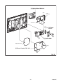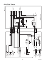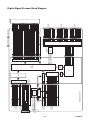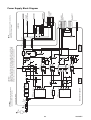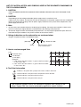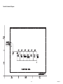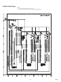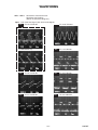
1
SERVICE MANUAL
This Service Manual is for the LED24-H9001M (A13L0EP) model.
For the LED24-H9001M (A13L0EP) model, the letter (A13L0EP) is printed
on the Serial Number Label on the back of the unit. Refer to the Serial
Number Label below.
Serial No. Label
"A13L0EP"
24″ COLOR LCD TELEVISION
LED24-H9001M
24″ COLOR LCD TELEVISION
LED24-H9001M
TABLE OF CONTENTS
Specifications . . . . . . . . . . . . . . . . . . . . . . . . . . . . . . . . . . . . . . . . . . . . . . . . . . . . . . . . . . . . . . . . . . . . . . . . . . . 1-1
Important Safety Precautions. . . . . . . . . . . . . . . . . . . . . . . . . . . . . . . . . . . . . . . . . . . . . . . . . . . . . . . . . . . . . . . 2-1
Standard Notes for Servicing . . . . . . . . . . . . . . . . . . . . . . . . . . . . . . . . . . . . . . . . . . . . . . . . . . . . . . . . . . . . . . . 3-1
Cabinet Disassembly Instructions . . . . . . . . . . . . . . . . . . . . . . . . . . . . . . . . . . . . . . . . . . . . . . . . . . . . . . . . . . . 4-1
Electrical Adjustment Instructions . . . . . . . . . . . . . . . . . . . . . . . . . . . . . . . . . . . . . . . . . . . . . . . . . . . . . . . . . . . 5-1
How to Initialize the LCD Television. . . . . . . . . . . . . . . . . . . . . . . . . . . . . . . . . . . . . . . . . . . . . . . . . . . . . . . . . . 6-1
Firmware Renewal Mode . . . . . . . . . . . . . . . . . . . . . . . . . . . . . . . . . . . . . . . . . . . . . . . . . . . . . . . . . . . . . . . . . . 7-1
Troubleshooting . . . . . . . . . . . . . . . . . . . . . . . . . . . . . . . . . . . . . . . . . . . . . . . . . . . . . . . . . . . . . . . . . . . . . . . . . 8-1
Block Diagrams . . . . . . . . . . . . . . . . . . . . . . . . . . . . . . . . . . . . . . . . . . . . . . . . . . . . . . . . . . . . . . . . . . . . . . . . . 9-1
Schematic Diagrams / CBA and Test Points . . . . . . . . . . . . . . . . . . . . . . . . . . . . . . . . . . . . . . . . . . . . . . . . . . 10-1
Waveforms . . . . . . . . . . . . . . . . . . . . . . . . . . . . . . . . . . . . . . . . . . . . . . . . . . . . . . . . . . . . . . . . . . . . . . . . . . . . 11-1
Wiring Diagram . . . . . . . . . . . . . . . . . . . . . . . . . . . . . . . . . . . . . . . . . . . . . . . . . . . . . . . . . . . . . . . . . . . . . . . . 12-1
Exploded View . . . . . . . . . . . . . . . . . . . . . . . . . . . . . . . . . . . . . . . . . . . . . . . . . . . . . . . . . . . . . . . . . . . . . . . . . 13-1
Mechanical Parts List . . . . . . . . . . . . . . . . . . . . . . . . . . . . . . . . . . . . . . . . . . . . . . . . . . . . . . . . . . . . . . . . . . . . 14-1
Electrical Parts List. . . . . . . . . . . . . . . . . . . . . . . . . . . . . . . . . . . . . . . . . . . . . . . . . . . . . . . . . . . . . . . . . . . . . . 15-1
The LCD panel is manufactured to provide many years of useful life.
Occasionally a few non active pixels may appear as a tiny spec of color.
This is not to be considered a defect in the LCD screen.
SPECIFICATIONS
< TUNER >
VHS/UHF Input ----------- 75Ω unbal., IEC Connector
Center IF ------------------- SECAM-L 38.9MHz, SECAM-L’ 33.9MHz
Description
Condition
Unit
Nominal
Limit
1. Video S/N
80
dB
---
40
2. Audio S/N
---
dB
---
40/40
Condition
Unit
Nominal
Limit
1. Number of Pixels
Horizontal
Vertical
pixels
pixels
1920
1080
-----
2. Viewing Angle
Horizontal
Vertical
°
°
-89 to 89
-89 to 89
-----
< LCD PANEL >
Description
<DVB-T>
Description
Condition
Unit
Nominal
Limit
1. RECEIVED FREQ.RANGE
(-60dBm, 45ch.) *1, *2
+
-
kHz
kHz
1000
900
500
167
c:*1 VHF HIGH 8ch.
UHF
45ch.
dBuV
dBuV
25/101
25/101
28/98
29/98
d:*2 VHF HIGH 8ch.
UHF
45ch.
dBuV
dBuV
18/101
18/101
21/98
21/98
c:*1 VHF HIGH 8ch.
UHF
45ch.
dB
dB
15
15
≦18
≦18
d:*2 VHF HIGH 8ch.
UHF
45ch.
dB
dB
11
11
≦14
≦14
dB
dB
dB
dB
18.7
14.0
19.1
13.0
≦23
≦20
≦23
≦18
2. INPUT DYNAMIC
RANGE (mix./max)
3. C/N PERFORMANCE
(-50dBm)
4. MULTIPATH (-50dBm)
a. Performance with
short delay echoes
b. Performance with
long delay echoes
*1: modulation parameters = [8k
*2: modulation parameters = [8k
*3: modulation parameters = [2k
*4: modulation parameters = [2k
UHF
c:*3
d:*4
c:*3
d:*4
64QAM
16QAM
64QAM
16QAM
45ch.
CR=2/3
CR=3/4
CR=2/3
CR=3/4
GI=1/32]
GI=1/8]
GI=1/32]
GI=1/32]
< VIDEO >
Description
Condition
Unit
Nominal
Limit
Horizontal
Vertical
%
%
5
5
-----
AT 70% WHITE FIELD
x
y
°K
12000
0.272
0.278
--±0.005
±0.005
3. Resolution
Horizontal
Vertical
line
line
400
350
-----
4. Brightness
AT 100% WHITE FIELD
(AT RETAIL MODE)
cd/m2
270
192
1. Over Scan
2. Color Temperature
1-1
A13L0_L2SP
< AUDIO >
All items are measured across 16 Ω load at speaker output terminal.
Description
1. Audio Output Power
2. Audio Distortion
3. Audio Freq. Response
4. Audio S/N
Condition
Unit
Nominal
Limit
10% THD: Lch/Rch
W
3.0/3.0
2.4/2.4
500mW: Lch/Rch
%
1.5/1.5
3.0/3.0
-6dB: Lch
-6dB: Rch
Hz
Hz
70 to 8 k
70 to 8 k
-----
Lch/Rch
dB
---
≧45/45
Note: Nominal specifications represent the design specifications. All units should be able to approximate these.
Some will exceed and some may drop slightly below these specifications. Limit specifications represent
the absolute worst condition that still might be considered acceptable. In no case should a unit fail to meet
limit specifications.
1-2
A13L0_L2SP
IMPORTANT SAFETY PRECAUTIONS
Prior to shipment from the factory, our products are strictly inspected for recognized product safety and electrical
codes of the countries in which they are to be sold. However, in order to maintain such compliance, it is equally
important to implement the following precautions when a set is being serviced.
Safety Precautions for LCD TV
Circuit
National Standards Institute (ANSI) C101.1
Leakage Current for Appliances and
Underwriters Laboratories (UL) 1410, (50.7).
With the instrument AC switch first in the on
position and then in the off position, measure
from a known earth ground (metal water pipe,
conduit, etc.) to all exposed metal parts of the
instrument (antennas, handle brackets, metal
cabinet, screw heads, metallic overlays, control
shafts, etc.), especially any exposed metal
parts that offer an electrical return path to the
chassis. Any current measured must not
exceed 0.5 milli-ampere. Reverse the
instrument power cord plug in the outlet and
repeat the test.
1. Before returning an instrument to the
customer, always make a safety check of the
entire instrument, including, but not limited to, the
following items:
a. Be sure that no built-in protective devices are
defective and have been defeated during
servicing. (1) Protective shields are provided
on this chassis to protect both the technician
and the customer. Correctly replace all missing
protective shields, including any removed for
servicing convenience. (2) When reinstalling
the chassis and/or other assembly in the
cabinet, be sure to put back in place all
protective devices, including but not limited to,
nonmetallic control knobs, insulating
fishpapers, adjustment and compartment
covers/shields, and isolation resistor/capacitor
networks. Do not operate this instrument or
permit it to be operated without all
protective devices correctly installed and
functioning. Servicers who defeat safety
features or fail to perform safety checks
may be liable for any resulting damage.
READING SHOULD
NOT BE ABOVE 0.5 mA
DEVICE
BEING
TESTED
LEAKAGE
CURRENT
TESTER
_
+
TEST ALL EXPOSED
METAL SURFACES
b. Be sure that there are no cabinet openings
through which an adult or child might be able to
insert their fingers and contact a hazardous
voltage. Such openings include, but are not
limited to, (1) spacing between the LCD module
and the cabinet mask, (2) excessively wide
cabinet ventilation slots, and (3) an improperly
fitted and/or incorrectly secured cabinet back
cover.
ALSO TEST WITH
PLUG REVERSED
USING AC
ADAPTER PLUG
AS REQUIRED
EARTH
GROUND
ANY MEASUREMENTS NOT WITHIN THE
LIMITS SPECIFIED HEREIN INDICATE A
POTENTIAL SHOCK HAZARD THAT MUST
BE ELIMINATED BEFORE RETURNING THE
INSTRUMENT TO THE CUSTOMER OR
BEFORE CONNECTING THE ANTENNA OR
ACCESSORIES.
c. Antenna Cold Check - With the instrument AC
plug removed from any AC source, connect an
electrical jumper across the two AC plug
prongs. Place the instrument AC switch in the
on position. Connect one lead of an ohmmeter
to the AC plug prongs tied together and touch
the other ohmmeter lead in turn to each tuner
antenna input exposed terminal screw and, if
applicable, to the coaxial connector. If the
measured resistance is less than 1.0 megohm
or greater than 5.2 megohm, an abnormality
exists that must be corrected before the
instrument is returned to the customer. Repeat
this test with the instrument AC switch in the off
position.
2. Read and comply with all caution and safetyrelated notes on or inside the receiver cabinet, on
the receiver chassis, or on the LCD module.
3. Design Alteration Warning - Do not alter or add
to the mechanical or electrical design of this LCD
TV receiver. Design alterations and additions,
including, but not limited to circuit modifications
and the addition of items such as auxiliary audio
and/or video output connections, might alter the
safety characteristics of this receiver and create a
hazard to the user. Any design alterations or
additions will void the manufacturer's warranty and
may make you, the servicer, responsible for
personal injury or property damage resulting
therefrom.
d. Leakage Current Hot Check - With the
instrument completely reassembled, plug the
AC line cord directly into a 230 V AC outlet. (Do
not use an isolation transformer during this
test.) Use a leakage current tester or a
metering system that complies with American
2-1
LTVP_ISP
7. Product Safety Notice - Some electrical and
mechanical parts have special safety-related
characteristics which are often not evident from
visual inspection, nor can the protection they give
necessarily be obtained by replacing them with
components rated for higher voltage, wattage, etc..
Parts that have special safety characteristics are
identified by a ! on schematics and in parts lists.
Use of a substitute replacement that does not
have the same safety characteristics as the
recommended replacement part might create
shock, fire, and/or other hazards. The product's
safety is under review continuously and new
instructions are issued whenever appropriate.
Prior to shipment from the factory, our products
are strictly inspected to confirm they comply with
the recognized product safety and electrical codes
of the countries in which they are to be sold.
However, in order to maintain such compliance, it
is equally important to implement the following
precautions when a set is being serviced.
4. Hot Chassis Warning a. Some TV receiver chassis are electrically
connected directly to one conductor of the AC
power cord and maybe safety-serviced without
an isolation transformer only if the AC power
plug is inserted so that the chassis is
connected to the ground side of the AC power
source. To confirm that the AC power plug is
inserted correctly, with an AC voltmeter,
measure between the chassis and a known
earth ground. If a voltage reading in excess of
1.0 V is obtained, remove and reinsert the AC
power plug in the opposite polarity and again
measure the voltage potential between the
chassis and a known earth ground.
b. Some TV receiver chassis normally have 85V
AC(RMS) between chassis and earth ground
regardless of the AC plug polarity. This chassis
can be safety-serviced only with an isolation
transformer inserted in the power line between
the receiver and the AC power source, for both
personnel and test equipment protection.
c. Some TV receiver chassis have a secondary
ground system in addition to the main chassis
ground. This secondary ground system is not
isolated from the AC power line. The two
ground systems are electrically separated by
insulation material that must not be defeated or
altered.
5. Observe original lead dress. Take extra care to
assure correct lead dress in the following areas: a.
near sharp edges, b. near thermally hot parts-be
sure that leads and components do not touch
thermally hot parts, c. the AC supply, d. high
voltage, and, e. antenna wiring. Always inspect in
all areas for pinched, out of place, or frayed wiring.
Check AC power cord for damage.
6. Components, parts, and/or wiring that appear to
have overheated or are otherwise damaged
should be replaced with components, parts, or
wiring that meet original specifications.
Additionally, determine the cause of overheating
and/or damage and, if necessary, take corrective
action to remove any potential safety hazard.
2-2
LTVP_ISP
Precautions during Servicing
A. Parts identified by the ! symbol are critical for
safety.
Replace only with part number specified.
B. In addition to safety, other parts and assemblies
are specified for conformance with regulations
applying to spurious radiation. These must also be
replaced only with specified replacements.
Examples: RF converters, RF cables, noise
blocking capacitors, and noise blocking filters, etc.
C. Use specified internal wiring. Note especially:
1) Wires covered with PVC tubing
2) Double insulated wires
3) High voltage leads
D. Use specified insulating materials for hazardous
live parts. Note especially:
1) Insulation Tape
2) PVC tubing
3) Spacers
4) Insulators for transistors.
E. When replacing AC primary side components
(transformers, power cord, etc.), wrap ends of
wires securely about the terminals before
soldering.
F. Observe that the wires do not contact heat
producing parts (heat sinks, oxide metal film
resistors, fusible resistors, etc.)
G. Check that replaced wires do not contact sharp
edged or pointed parts.
H. When a power cord has been replaced, check that
5~6 kg of force in any direction will not loosen it.
I.
Also check areas surrounding repaired locations.
J. Use care that foreign objects (screws, solder
droplets, etc.) do not remain inside the set.
K. When connecting or disconnecting the internal
connectors, first, disconnect the AC plug from the
AC supply outlet.
L. When installing parts or assembling the cabinet
parts, be sure to use the proper screws and
tighten certainly.
2-3
LTVP_ISP
Safety Check after Servicing
Examine the area surrounding the repaired location
for damage or deterioration. Observe that screws,
parts and wires have been returned to original positions. Afterwards, perform the following tests and confirm the specified values in order to verify compliance
with safety standards.
Chassis or Secondary Conductor
Primary Circuit
d'
d
1. Clearance Distance
When replacing primary circuit components, confirm
specified clearance distance (d) and (d') between soldered terminals, and between terminals and surrounding metallic parts. (See Fig. 1)
Table 1 : Ratings for selected area
AC Line Voltage
Clearance Distance (d), (d’)
220 to 240 V
≥ 3mm(d)
≥ 8mm(d’)
Fig. 1
Note: This table is unofficial and for reference only.
Be sure to confirm the precise values.
Exposed Accessible Part
2. Leakage Current Test
Confirm the specified (or lower) leakage current between B (earth ground, power cord plug prongs) and
externally exposed accessible parts (RF terminals, antenna terminals, video and audio input and output terminals, microphone jacks, earphone jacks, etc.).
Z
AC Voltmeter
(High Impedance)
Measuring Method : (Power ON)
Insert load Z between B (earth ground, power cord
plug prongs) and exposed accessible parts. Use an
AC voltmeter to measure across both terminals of load
Z. See Fig. 2 and following table.
B
One side of
Power Cord Plug Prongs
Fig. 2
Table 2: Leakage current ratings for selected areas
AC Line Voltage
220 to 240 V
Load Z
Leakage Current (i)
One side of power cord plug
prongs (B) to:
2kΩ RES.
Connected in
parallel
i≤0.7mA AC Peak
i≤2mA DC
RF or
Antenna terminals
50kΩ RES.
Connected in
parallel
i≤0.7mA AC Peak
i≤2mA DC
A/V Input, Output
Note: This table is unofficial and for reference only. Be sure to confirm the precise values.
2-4
LTVP_ISP
STANDARD NOTES FOR SERVICING
Circuit Board Indications
How to Remove / Install Flat Pack-IC
1. The output pin of the 3 pin Regulator ICs is
indicated as shown.
1. Removal
Top View
Out
With Hot-Air Flat Pack-IC Desoldering Machine:
1. Prepare the hot-air flat pack-IC desoldering
machine, then apply hot air to the Flat Pack-IC
(about 5 to 6 seconds). (Fig. S-1-1)
Bottom View
In
Input
2. For other ICs, pin 1 and every fifth pin are
indicated as shown.
5
Pin 1
10
Fig. S-1-1
3. The 1st pin of every male connector is indicated as
shown.
2. Remove the flat pack-IC with tweezers while
applying the hot air.
3. Bottom of the flat pack-IC is fixed with glue to the
CBA; when removing entire flat pack-IC, first apply
soldering iron to center of the flat pack-IC and heat
up. Then remove (glue will be melted). (Fig. S-1-6)
4. Release the flat pack-IC from the CBA using
tweezers. (Fig. S-1-6)
Pin 1
Pb (Lead) Free Solder
Pb free mark will be found on PCBs which use Pb
free solder. (Refer to figure.) For PCBs with Pb free
mark, be sure to use Pb free solder. For PCBs
without Pb free mark, use standard solder.
CAUTION:
1. The Flat Pack-IC shape may differ by models. Use
an appropriate hot-air flat pack-IC desoldering
machine, whose shape matches that of the Flat
Pack-IC.
2. Do not supply hot air to the chip parts around the
flat pack-IC for over 6 seconds because damage
to the chip parts may occur. Put masking tape
around the flat pack-IC to protect other parts from
damage. (Fig. S-1-2)
3. The flat pack-IC on the CBA is affixed with glue, so
be careful not to break or damage the foil of each
pin or the solder lands under the IC when
removing it.
Pb free mark
CBA
Masking
Tape
Tweezers
Hot-air
Flat Pack-IC
Desoldering
Machine
Flat Pack-IC
Fig. S-1-2
3-1
TVP_SN
With Soldering Iron:
With Iron Wire:
1. Using desoldering braid, remove the solder from
all pins of the flat pack-IC. When you use solder
flux which is applied to all pins of the flat pack-IC,
you can remove it easily. (Fig. S-1-3)
1. Using desoldering braid, remove the solder from
all pins of the flat pack-IC. When you use solder
flux which is applied to all pins of the flat pack-IC,
you can remove it easily. (Fig. S-1-3)
Flat Pack-IC
2. Affix the wire to a workbench or solid mounting
point, as shown in Fig. S-1-5.
Desoldering Braid
3. While heating the pins using a fine tip soldering
iron or hot air blower, pull up the wire as the solder
melts so as to lift the IC leads from the CBA
contact pads as shown in Fig. S-1-5.
4. Bottom of the flat pack-IC is fixed with glue to the
CBA; when removing entire flat pack-IC, first apply
soldering iron to center of the flat pack-IC and heat
up. Then remove (glue will be melted). (Fig. S-1-6)
Soldering Iron
Fig. S-1-3
5. Release the flat pack-IC from the CBA using
tweezers. (Fig. S-1-6)
2. Lift each lead of the flat pack-IC upward one by
one, using a sharp pin or wire to which solder will
not adhere (iron wire). When heating the pins, use
a fine tip soldering iron or a hot air desoldering
machine. (Fig. S-1-4)
Note: When using a soldering iron, care must be
taken to ensure that the flat pack-IC is not
being held by glue. When the flat pack-IC is
removed from the CBA, handle it gently
because it may be damaged if force is applied.
Hot Air Blower
Sharp
Pin
Fine Tip
Soldering Iron
or
Iron Wire
Fig. S-1-4
Soldering Iron
3. Bottom of the flat pack-IC is fixed with glue to the
CBA; when removing entire flat pack-IC, first apply
soldering iron to center of the flat pack-IC and heat
up. Then remove (glue will be melted). (Fig. S-1-6)
To Solid
Mounting Point
Fig. S-1-5
4. Release the flat pack-IC from the CBA using
tweezers. (Fig. S-1-6)
CBA
Fine Tip
Soldering Iron
Flat Pack-IC
Tweezers
Fig. S-1-6
3-2
TVP_SN
Instructions for Handling Semiconductors
2. Installation
1. Using desoldering braid, remove the solder from
the foil of each pin of the flat pack-IC on the CBA
so you can install a replacement flat pack-IC more
easily.
Electrostatic breakdown of the semi-conductors may
occur due to a potential difference caused by
electrostatic charge during unpacking or repair work.
2. The “ I ” mark on the flat pack-IC indicates pin 1.
(See Fig. S-1-7.) Be sure this mark matches the
pin 1 on the PCB when positioning for installation.
Then presolder the four corners of the flat pack-IC.
(See Fig. S-1-8.)
1. Ground for Human Body
Be sure to wear a grounding band (1 MΩ) that is
properly grounded to remove any static electricity that
may be charged on the body.
3. Solder all pins of the flat pack-IC. Be sure that
none of the pins have solder bridges.
2. Ground for Workbench
Be sure to place a conductive sheet or copper plate
with proper grounding (1 MΩ) on the workbench or
other surface, where the semi-conductors are to be
placed. Because the static electricity charge on
clothing will not escape through the body grounding
band, be careful to avoid contacting semi-conductors
with your clothing.
Example :
<Incorrect>
Pin 1 of the Flat Pack-IC
is indicated by a " " mark.
Fig. S-1-7
Presolder
CBA
Flat Pack-IC
<Correct>
Grounding Band
CBA
Fig. S-1-8
1MΩ
CBA
1MΩ
Conductive Sheet or
Copper Plate
3-3
TVP_SN
CABINET DISASSEMBLY INSTRUCTIONS
1. Disassembly Flowchart
Step/
Loc.
No.
This flowchart indicates the disassembly steps for the
cabinet parts and the CBA in order to gain access to
items to be serviced. When reassembling, follow the
steps in reverse order. Bend, route and dress the
cables as they were.
[1] Stand
Assembly
[3] Tuner Shield
[2] Rear Cabinet
[4] Digital Main
CBA Unit
[6] Power Supply
CBA Unit
[5] Jack CBA
[7] Speaker
[11] Function
CBA
Part
Fig.
No.
Removal
Note
[10]
IR Sensor
CBA
D3 CL202B, Sensor LED
D4 Lens, Sensor Shield
---
[11]
Function
CBA
D3
Function Knob
D4
---
[12]
Front
Cabinet
D3 ---------------
---
↓
(1)
↓
(2)
↓
(3)
↓
(5)
↓
(4)
Note:
(1) Order of steps in procedure. When reassembling,
follow the steps in reverse order. These numbers
are also used as the Identification (location) No. of
parts in figures.
(2) Parts to be removed or installed.
[8] PCB Holder
(3) Fig. No. showing procedure of part location
[9] LCD Module
Assembly
(4) Identification of parts to be removed, unhooked,
unlocked, released, unplugged, unclamped, or
desoldered.
N = Nut, L = Locking Tab, S = Screw,
H = Hex Screw, CN = Connector
e.g. 2(S-2) = two Screws of (S-2),
2(L-2) = two Locking Tabs of (L-2)
[10] IR Sensor
CBA
[12] Front
Cabinet
(5) Refer to the following "Reference Notes in the
Table."
2. Disassembly Method
Step/
Loc.
No.
Part
Fig.
No.
Removal
Note
[1]
Stand
Assembly
D1 2(S-1)
[2]
Rear
Cabinet
D1
[3]
Tuner
Shield
D2 3(S-5)
---
[4]
4(S-6), CN2103,
Digital Main D2 CN2104, CN2105,
CBA Unit
D4 CN3901, Shield Box,
Jack Holder(D)
---
14(L-1), 4(S-2),
4(S-3), 4(S-4)
-----
[5]
Jack CBA
2(S-7), CN2, CN3,
D2 CN2102, CN2801,
D4 CN2802,
Jack Holder(A)
[6]
Power
Supply
CBA Unit
D2 8(S-8), CN1, CN4,
D4 Separation Sheet
---
[7]
Speaker
D3 ---------------
---
[8]
PCB Holder D3
[9]
LCD
Module
Assembly
3(S-9), Switch Power,
CL204
D3 ---------------
---
-----
4-1
A13L0DC
(L-1)
(S-4)
(L-1)
(L-1)
(S-3)
(L-1)
(L-1)
(S-3)
(L-1)
(S-2)
[2] Rear Cabinet
(S-3)
(L-1)
(S-2)
(S-2)
(S-1)
(S-4)
[1] Stand Assembly
Fig. D1
4-2
A13L0DC
[4] Digital Main CBA Unit
(S-6)
Jack
Holder(D)
Shield Box
(S-6)
Jack
Holder(A)
[3] Tuner
Shield
(S-5)
(S-7)
[5] Jack CBA
Separation Sheet
(S-8)
[6] Power Supply CBA Unit
(S-8)
Fig. D2
4-3
A13L0DC
[12] Front Cabinet
[9] LCD Module
Assembly
Sensor Shield
[8] PCB Holder
Sensor
LED Lens
(S-9)
[10] IR Sensor
CBA
(S-9)
Function
Knob
[11] Function CBA
(S-9)
Switch Power
[7] Speaker
CL204
[7] Speaker
Fig. D3
4-4
A13L0DC
TV Cable Wiring Diagram
To LCD Module Assembly
Digital Main CBA Unit
Power Supply CBA Unit
CN4
CN3901
CN3701
CN3702
CN3703
CN2
CN3
CN1
CL104
To Main Power
Switch
CN2105 CN2104 CN2103
CL105
Function
CBA
CN2102
CN2801
CN2802
To AC Inlet
Jack CBA
IR Sensor CBA
CL202B
To Speaker
To Speaker
CL201A
CL202A
Fig. D4
4-5
A13L0DC
ELECTRICAL ADJUSTMENT INSTRUCTIONS
1. Purity Check Mode
General Note: “CBA” is abbreviation for
“Circuit Board Assembly.”
This mode cycles through full-screen displays of red,
green, blue, and white to check for non-active pixels.
Note: Electrical adjustments are required after
replacing circuit components and certain
mechanical parts. It is important to perform
these adjustments only after all repairs and
replacements have been completed.
Also, do not attempt these adjustments unless
the proper equipment is available.
1. Enter the Service mode.
2. Each time the [7] button on the remote control unit
is pressed, the display changes as follows.
Purity Check Mode
Test Equipment Required
White mode
1. Remote control unit
[7] button
2. Color Analyzer,
CA-310 (KONICA MINOLTA Luminance meter) or
measuring instrument as good as CA-310.
[7] button
How to set up the service mode:
Black mode
Service mode:
1. Turn the power on.
2. Press [MENU] button to display Setup menu.
3. Select “Software” in “OTHERS” and press [OK]
button.
[7] button
Red mode
4. Press [0], [4], [2], [5], [7], [4] and [ ] buttons on
the remote control unit in this order. The following
screen appears.
"*" differs depending on the models.
Code:
Pic code:
Inch:
Total:
[7] button
*************-***-**
*** *** ***
*****_***_**_****
Push 0 key
Green mode
Exit/Beenden/Quitter/Zakoñcz
Safety: Safety Non
[7] button
Blue mode
Total Watch Time: *****
Light sensor: ****
***h ***min
[7] button
White 20% mode
Note:
When entering this mode, the default setting is White mode.
3. To cancel or to exit from the Purity Check Mode,
press [BACK] button.
5-1
LC9P(LED)EA
The White Balance Adjustment should be
performed when replacing the LCD Panel
or Digital Main CBA.
6. Press [MENU] button. The internal Raster signal
appears on the screen. (“Internal (Single)”
appears on the upper right of the screen as shown
below.)
2. White Balance Adjustment
Purpose: To mix red and blue beams correctly for
pure white.
Internal (Single)
Symptom of Misadjustment: White becomes bluish
or reddish.
ITEM
SPECIFICATION
Color temperature
x= 0.272 ± 0.002
y= 0.278 ± 0.002
Input Signal
Internal pattern
(40/70% raster)
HDB
0
7. Press [P
/ ] buttons to adjust the color
temperature becomes 12000°K
(x= 0.272 / y= 0.278 ±0.002).
Measurement point Screen center
M. EQ.
CA-310 (KONICA MINOLTA
Luminance meter) or
measuring instrument as
good as CA-310.
8. Press [1] button to select the “HDR” for High Drive
Red adjustment (“HDR” appears on the screen.)
and press [P
/ ] buttons to adjust the color
temperature.
Aging time
60min.
(Retail MODE/100IRE Raster
HDMI 1080i@60)
9. If necessary, adjust the “HDB” or “HDR” again.
MODE setting of TV
Shipment setting/
Retail MODE
Ambient
temperature
25°C ± 5°C
10. Press [6] button to select the “LDB” for Low Drive
Blue adjustment (“LDB” appears on the screen.)
and press [P
/ ] buttons to adjust the color
temperature.
Internal (Single)
1. Operate the unit for more than 60 minutes.
2. Set the color analyzer at the CHROMA mode and
zero point calibration. Bring the optical receptor
pointing at the center of the LCD-Panel.
To avoid interference from ambient
light, this adjustment should be
performed in a dark room.
LDB
Perpendicularity
0
11. Press [4] button to select the “LDR” for Low Drive
Red adjustment (“LDR” appears on the screen.)
and press [P
/ ] buttons to adjust the color
temperature.
12. If necessary, adjust the “LDB” or “LDR” again.
13. Press [BACK] button to enter the Service mode
again.
Color Analyzer
14. Press [ ] button on the remote control unit to shift
to the self check mode screen.
If “WB OK” is displayed, this adjustment
completes.
If “WB NG” is displayed, turn the AC switch (on the
lower left of the back of the unit) off and on. Then
repeat above steps from 3. to 13. Check the self
check mode screen again. If “WB NG” is
displayed, replace the LCD Panel or Digital Main
CBA.
Note: The optical receptor must be set
perpendicularly to the LCD Panel surface.
3. Enter the Service mode.
4. Press [
-] button three times on the remote control
unit to select “Drive setting” mode. “Drive” appears on
the screen.
5. Press [3] button to select the “HDB” for High Drive
Blue adjustment. (“HDB” appears on the screen.)
15. To cancel or to exit from the White Balance
Adjustment, press [BACK] button.
5-2
LC9P(LED)EA
HOW TO INITIALIZE THE LCD TELEVISION
How to initialize the LCD television:
1. Turn the power on.
2. Enter the service mode. (Refer to page 5-1.)
- To cancel the service mode, press [ ] button on
the remote control unit.
3. Press [ ] button on the remote control unit to
initialize the LCD television.
4. After confirming that “INITIALIZED : OK” appears
on the screen, turn the AC switch (on the lower left
of the back of the unit) off.
6-1
LC9PINT
FIRMWARE RENEWAL MODE
Equipment Required
[Update procedure]
a. USB storage device
b. Remote Control Unit
1. Turn the AC switch (on the lower left of the back of
the unit) off.
2. Insert USB storage device with F/W to TV set.
3. Turn the AC switch on.
Firmware Update Procedure
4. Updating starts automatically. Red LED flashes.
Note: Do not turn off the TV set and do not
remove the USB storage device while this
procedure.
[Check the current version]
1. Press [MENU] button on the remote control unit to
display the menu mode.
5. When updating is completed, the TV set will turn
back on automatically.
2. Press [ÅK] or [ÅL] to select “Others”, then press
[OK] button.
6. To shift the TV set to standby mode, press [ ]
button on the remote control unit.
3. Press [ÅK] or [ÅL] to select “Software”, then press
[OK] button.
7. Remove USB storage device from TV set.
The current FW version will be displayed.
8. Press [ ] button again to turn the power on.
9. Press [MENU] button on the remote control unit to
display the menu mode.
[Preparation]
10. Select “Parental” - “PIN CODE:”.
1. Prepare USB storage device.
11. Press [4], [7], [3] and [7] buttons on the remote
control unit.
2. Copy F/W-file (pkg file) to USB storage device.
Note: Make sure to use the blank USB Storage.
12. Select “Factory Reset” and press [OK] button.
3. Rename the F/W-file’s name to “upgrade.pkg”.
7-1
LC9P_FW
TROUBLESHOOTING
FLOW CHART NO.1
The power cannot be turned on.
Are the voltage of each pin of CL104 and CL105
become as shown below?
CL105
CL105
CL104
9, 10PIN
1, 2 ,3PIN
8PIN
+24V
+12V
+4.3V
No
AMP+24V
P-ON+12V
STBY+4.3V
Check SW601 and their periphery circuit, and service
it if defective.
Or replace Power Supply CBA Unit.
Yes
Check if there is any leak or short-circuit on the
loaded circuit, and service it if defective.
FLOW CHART NO.2
P-ON+3.3V is not output.
Is approximately 12V voltage supplied to Pin(2) of
IC2602?
No
Check F2602, P-ON+12V line and their periphery
circuit, and service it if defective.
Yes
Replace IC2602.
FLOW CHART NO.3
P-ON+6V is not output. (P-ON+3.3V is outputted normally.)
Is approximately 12V voltage supplied to Pin(2) of
IC2603?
No
Check F2603, P-ON+12V line and their periphery
circuit, and service it if defective.
Yes
Replace IC2603.
FLOW CHART NO.4
P-ON+5V is not output.
Is approximately 6V voltage supplied to Pin(7) of
IC2605?
No
See FLOW CHART NO.3 <P-ON+6V is not output.
(P-ON+3.3V is outputted normally.)>
Yes
Replace IC2605.
FLOW CHART NO.5
The key operation is not functioning.
Are the contact point and installation state of the key
switches (SW2150-SW2156) normal?
No
Re-install the switches (SW2150-SW2156) correctly
or replace the poor switch.
Yes
When pressing each switches (SW2150-SW2156) do
the voltage of Pin(1) on CN2104 decrease?
No
Check the switches (SW2150-SW2156) and their
periphery, and service it if defective.
Yes
Replace Digital Main CBA Unit.
8-1
A13L0TR
FLOW CHART NO.6
No operation is possible from the remote control unit. (Operation is possible from the unit.)
Is 3.3V voltage supplied to Pin(3) of RS2161 (remote
control receiver)?
No
Check AL+3.3V line and service it if defective.
Yes
Is the "L" pulse sent out Pin(1) of RS2161 (remote control No
receiver) when the infrared remote control is activated?
Replace RS2161 (remote control receiver) or
remote control unit.
Yes
Is the "L" pulse supplied to Pin(2) of CN2104?
No
Yes
Check the line between Pin(1) of RS2161 (remote
control receiver) and Pin(2) of CN2104, and service
it if defective.
Replace Digital Main CBA Unit.
FLOW CHART NO.7
Picture does not appear normally. (Video input/Y/Pb/Pr input/RGB input)
Are the video signals outputted to the specific
terminal?
Are the component video(Y/Pb/Pr) signals outputted
to Pin(18, 20, 22) of CN2104?
No
Check the line between each pin of CN2104 and
CN2103 and input terminal and service it if defective.
Check the component video(Y/Pb/Pr) signal line,
and service it if defective.
Are the RGB video signals outputted to Pin(1, 3, 5)
of CN2103?
No
Check the RGB video signal line, and service it if
defective.
Are the composite video signals outputted to
Pin(7) of CN2103?
No
Check the composite video signal line, and service it
if defective.
Yes
Replace Digital Main CBA Unit or LCD Module
Assembly.
FLOW CHART NO.8
Picture does not appear normally. (Tuner input)
Are the DIF signals outputted to Pin(17, 18) of CN2103?
No
Yes
Check the line between Pin(17, 18) of CN2103 and
Pin(10, 11) of TU2301, and TU2301(Tuner Unit), and
service it if defective.
Replace Digital Main CBA Unit or LCD Module
Assembly.
8-2
A13L0TR
FLOW CHART NO.9
Audio is not outputted normally. (Tuner input)
Are the DIF signals outputted to Pin(17,18) of CN2103?
No
Yes
No
Are the audio(L/R) signals outputted to Pin(9,10) of
CN2104?
Yes (Output to headphone) Yes (Output to speakers)
Check the line between Pin(17, 18) of CN2103 and
Pin(10, 11) of TU2301, and TU2301(Tuner Unit), and
service it if defective.
Replace Digital Main CBA Unit.
Are the audio(L/R) signals inputted to the Pin(19, 32)
of IC2801?
Yes
No
Check the line between Pin(9,10) of CN2104 and
Pin(19, 32) of IC2801, and service it if defective.
Are the audio(L/R) signals outputted to CN2801 and
CN2802?
Yes
No
Check IC2801 and the periphery circuit, and service it
if defective.
Check CL2801, CL2802 and their periphery circuit,
and service it if defective.
Are the audio(L/R) signals outputted to Pin(1, 7) of
IC2701?
Yes
No
Is 5V voltage supplied to Pin(8) of IC2701?
Yes
No
Replace IC2701?
Check JK2708 and their periphery circuit, and service
it if defective.
Check P-ON+5V line and
their periphery, and service
it if defective.
FLOW CHART NO.10
Audio is not outputted normally. (Audio input terminals)
Are the audio(L/R) signals outputted to the specific
terminal?
Are the audio(L/R) signals outputted to Pin(14, 15) of
CN2103?
No
Check the line between each pin of CN2103 and
CN2104 and input terminal and service it if defective.
Check the audio(L/R) signal line, and service it if
defective.
Are the component audio(L/R) signals outputted to
Pin(24, 25) of CN2104?
No
Check the component audio(L/R) signal line, and
service it if defective.
Are the PC audio(L/R) signals outputted to Pin(12, 13)
of CN2104?
Yes
No
Check the PC audio(L/R) signal line, and service it if
defective.
No
Are the audio(L/R) signals outputted to Pin(9,10) of
CN2104?
Yes (Output to headphone) Yes (Output to speakers)
Replace Digital Main CBA Unit.
Are the audio(L/R) signals inputted to the Pin(19, 32)
of IC2801?
Yes
No
Check the line between Pin(9,10) of CN2104 and
Pin(19, 32) of IC2801, and service it if defective.
Are the audio(L/R) signals outputted to CN2801 and
CN2802?
Yes
No
Check IC2801 and the periphery circuit, and service it
if defective.
Check CL2801, CL2802 and their periphery circuit,
and service it if defective.
Are the audio(L/R) signals outputted to Pin(1, 7) of
IC2701?
Yes
No
Is 5V voltage supplied to Pin(8) of IC2701?
Yes
No
Replace IC2701?
Check JK2708 and their periphery circuit, and service
it if defective.
8-3
Check P-ON+5V line and
their periphery, and service
it if defective.
A13L0TR
COMP-DET
9-1
X3101
27MHz
OSC
SCL 6
SDA 5
IC3101 (MEMORY)
TO VIDEO
BLOCK
DIAGRAM
TO AUDIO
BLOCK
DIAGRAM
AUDIO-MUTE
SCART-MUTE
HP-MUTE
HP-DET
STBYL-ON
AUDIO-MUTE
SCART-MUTE
HP-MUTE
HP-DET
STBYL-ON
RESET Y8
DIGITAL MAIN CBA UNIT
TUNER-CLK 42
TUNER-DATA 41
IC3901
(CI CONTROL)
AE19 XIN
AD19 XOUT
J23 OSCL0
J22 OSDA0
Y11
AB9
AD8
AA11
U6
R7
LIGHT W9
KEY-IN1 W10
REMOTE AC8
RED-LED AE6
PROTECT1
P-ON-H2
P-ON-H1
PROTECT3
BACKLIGHT-SW
BACKLIGHT-ADJ
P3 COMP-DET
H25
G23
U5
P5
Y7
IC3301
(MAIN MICRO CONTROLLER)
IC3102
RESET
BUFFER
Q3701
8 SCL
7 SDA
CN3703
AL+3.3V
KEY-IN1
REMOTE
RED-LED
LIGHT
23 PROTECT1
25 P-ON-H2
26 P-ON-H1
29 PROTECT3
27 BACKLIGHT-SW
24 BACKLIGHT-ADJ
28 RESET
CN3701
CN3702
29
28
LED DRIVE
26
Q3702
25
CN2103
22
23
CN2105
7
5
4
1
3
6
2
CN2104
1
2
4
5
7 SCL
6 SDA
TU2301 (TUNER UNIT)
REMOTE
RED-LED
KEY-IN1
LIGHT
JACK CBA
PROTECT1
CN2102
3
4
1
6
IC2161
LIGHT
SENSOR
TO
POWER SUPPLY
BLOCK DIAGRAM
5
1
3
6
4
2
CL104
CL202B
1 KEY-IN1
D2161
STANDBY
IR SENSOR CBA
CL201A
3
4
1
6
REMOTE
SENSOR
RS2161
P-ON-H2
PROTECT3
BACKLIGHT-SW
BACKLIGHT-ADJ
P-ON-H1
RESET
TO
POWER
BLOCK
DIAGRAM
(CN2)
FUNCTION CBA
CL202A
KEY SWITCH
1
System Control Block Diagram
BLOCK DIAGRAMS
A13L0BLS
15
9-2
JK2704
COMPONENT
-Y/VIDEO-IN
JK2705
COMPONENT
-Pb-IN
JK2706
COMPONENT
-Pr-IN
7
19
VIDEO-B
VIDEO-OUT
11
VIDEO-R
VIDEO-G
20
RGBVIDEO-IN
JK2701
DIF-OUT2 11
DIF-OUT1 10
RF-AGC 4
TU2301
(TUNER UNIT)
JACK CBA
WF2
WF1
WF5
WF6
WF3
WF7
CN2104
18
20
22
21
CN2103
9
5
3
1
7
COM-Y/VIDEO-IN
COM-Pb-IN
COM-Pr-IN
COMP-DET
RGB-VIDEO-IN
VIDEO-R
VIDEO-G
VIDEO-B
RGB-VIDEO-OUT
CN2103
17 DIF-OUT2
18 DIF-OUT1
25 RF-AGC
CN3702
12
10
8
9
CN3703
21
25
27
29
23
CN3703
13
12
5
DIGITAL MAIN CBA UNIT
COMP-DET
VIDEO-IN
COM-Y-IN
COM-Pb-IN
COM-Pr-IN
RGB-VIDEO-IN
VIDEO-R
VIDEO-G
VIDEO-B
RGB-VIDEO-OUT
DIF-OUT2
DIF-OUT1
RF-AGC
VIDEO SIGNAL
TO SYSTEM CONTROL
BLOCK DIAGRAM
TO DIGITAL SIGNAL
PROCESS
BLOCK DIAGRAM
TO DIGITAL SIGNAL
PROCESS
BLOCK DIAGRAM
AUDIO SIGNAL
Video Block Diagram
A13L0BLV
3
1
RGB-AUDIO(L)-OUT
RGB-AUDIO(R)-OUT
9-3
SP2801
SPEAKER
R-CH
SP2802
SPEAKER
L-CH
2
RGB-AUDIO(R)-IN
CN2801
SP(R) 1
SP-GND 2
CN2802
SP(L) 1
SP-GND 2
JK2708
HEADPHONE
JACK
6
JK2701
RGB-AUDIO(L)-IN
JK2707
PC-AUDIO-IN
JK2703
AUDIO(R)-IN
JK2702
AUDIO(L)-IN
JK2709
DIGITAL
AUDIO-OUT
(COAXIAL)
11,12
39,40
19
32
34
STANDBY 17
MUTE CONTROL
PWM
PWM
JACK CBA
DRIVE
DRIVE
IC2801 (AUDIO AMP)
3
1
MUTE
2
5
7
IC2701 (HP AMP)
Q2801
Q2803 P-ON+5V
WF4
CN2104
10
9
7
6
AMP(L)-OUT
AMP(R)-OUT
AUDIO-MUTE
STBYL-ON
CN3702
20
21
23
24
1
7
1
7
2
6
2
6
Q3706
P-ON+5V
Q3705
HP-MUTE
HP-DET
AUDIO-MUTE
STBYL-ON
SCART-MUTE
SPDIF
AUDIO(L)
PC-AUDIO(L)
AUDIO(R)
PC-AUDIO(R)
RGB-AUDIO(L)-OUT
RGB-AUDIO(R)-OUT
RGB-AUDIO(L)-IN
RGB-AUDIO(R)-IN
AMP(L)-OUT
AMP(R)-OUT
DIGITAL MAIN CBA UNIT
Q3809
DRIVE
IC3801
(OP AMP)
IC3802 (OP AMP)
Q3807
MUTE
Q3806
MUTE
CN3703
16
15
2
1
CN2103
14
15
28
29
RGB-AUDIO(L)-IN
RGB-AUDIO(R)-IN
HP-MUTE
HP-DET
CN3702
SPDIF
14
AUDIO(L)
6
PC-AUDIO(L) 18
AUDIO(R)
5
PC-AUDIO(R) 17
RGB-AUDIO(L)-OUT 2
RGB-AUDIO(R)-OUT 3
CN2104
16
24
12
25
13
28
27
TO SYSTEM
CONTROL
BLOCK DIAGRAM
TO DIGITALSIGNAL
PROCESS
BLOCK DIAGRAM
AUDIO SIGNAL
Audio Block Diagram
A13L0BLA
CI
CARD
SLOT
1
2
3
13
14
12
15
9-4
TO AUDIO
BLOCK
DIAGRAM
TO VIDEO
BLOCK
DIAGRAM
Q3305
DESCRAMBLE
/TS INTERFACE
CI
CONTROL
IC3901 (CI CONTROL)
DIGITAL MAIN CBA UNIT
AUDIO(L)
PC-AUDIO(L)
AUDIO(R)
PC-AUDIO(R)
RGB-AUDIO(L)-OUT
RGB-AUDIO(R)-OUT
RGB-AUDIO(L)-IN
RGB-AUDIO(R)-IN
AMP(L)-OUT
AMP(R)-OUT
SPDIF
DIF-OUT2
DIF-OUT1
RF-AGC
CI-A(0-14)
CI-D(0-7)
JK3704
PC-RGB-IN
RED
GREEN
BLUE
HSYNC
VSYNC
DATA
CLOCK
TO VIDEO
BLOCK
DIAGRAM
VIDEO-IN
COM-Y-IN
COM-Pb-IN
COM-Pr-IN
VIDEO-R
VIDEO-G
VIDEO-B
RGB-VIDEO-IN
HSYNC
VSYNC
VGA-SDA
VGA-SCL
SW
AD22
AB21
AC25
AE25
Y25
V24
AE22
AD25
AA25
Y23
V20
AE17
AD17
P23 RF-AGC
AC10
AC9
AD9
AE9
W12
W11
AC11
AB12
AC17
AD11
AD12
AE12
AC14
AB14
AB13
AB17
AUDIO
DECODER
AUDIO I/F
DEMODULATOR
/MPEG DECODER
A/D
CONVERTER
HDMI I/F
IC3301 (DIGITAL SIGNAL PROCESS)
VIDEO
DECODER
DIGITAL
SIGNAL
PROCESS
W13
LVDS
TX
DAC
AE2
AD2
AE3
AD3
AE4
AD4
AE5
AD5
ADDESS(0-13)
DATA(0-31)
B17
A17
B18
A18
B19
A19
B21
A21
B22
A22
B20
A20
C17
D17
D19
C19
C20
D20
C23
D23
D24
C24
D21
C21
RA(0-13)
RDQ(0-31)
IC3401, IC3402
(SDRAM)
26
27
23
24
20
21
17
18
HDMI
SW
IC3403 (HDMI SW)
57
56
60
59
63
62
54
53
51
52
TMDS-D0(+)
7
TMDS-D0(-)
9
TMDS-D1(+)
4
TMDS-D1(-)
6
TMDS-D2(+)
1 JK3703
HDMI-IN1
TMDS-D2(-)
3
TMDS-CLOCK(+)
10
TMDS-CLOCK(-)
12
SDA
16
SCL
15
TMDS-D0(+)
7
TMDS-D0(-)
9
TMDS-D1(+)
4
TMDS-D1(-)
6
TMDS-D2(+)
1 JK3702
HDMI-IN3
TMDS-D2(-)
3
TMDS-CLOCK(+)
10
TMDS-CLOCK(-)
12
SDA
16
SCL
15
8
7
11
10
14
13
5
4
1
2
LVDS-OD0(-)
LVDS-OD0(+)
LVDS-OD1(-)
LVDS-OD1(+)
LVDS-OD2(-)
LVDS-OD2(+)
LVDS-OD3(-)
LVDS-OD3(+)
LVDS-OD4(-)
LVDS-OD4(+)
LVDS-OCLK(-)
LVDS-OCLK(+)
LVDS-ED0(-)
LVDS-ED0(+)
LVDS-ED1(-)
LVDS-ED1(+)
LVDS-ED2(-)
LVDS-ED2(+)
LVDS-ED3(-)
LVDS-ED3(+)
LVDS-ED4(-)
LVDS-ED4(+)
LVDS-ECLK(-)
LVDS-ECLK(+)
TMDS-D0(+)
7
TMDS-D0(-)
9
TMDS-D1(+)
4
TMDS-D1(-)
6
TMDS-D2(+)
1 JK3701
HDMI-IN2
TMDS-D2(-)
3
TMDS-CLOCK(+)
10
TMDS-CLOCK(-)
12
SDA
16
SCL
15
TO VIDEO
BLOCK DIAGRAM
CN3901
40
39
38
37
36
35
30
29
28
27
33
32
24
23
22
21
20
19
14
13
12
11
17
16
AUDIO SIGNAL
42
41
45
44
48
47
39
38
36
37
RGB-VIDEO-OUT
VIDEO SIGNAL
LCD MODULE
ASSEMBLY
Digital Signal Process Block Diagram
A13L0BLD
AC601
AC CORD
9-5
LINE
FILTER
LINE
FILTER
FB 2
ZC 1
HOT
6
1
2
3
PC901
(FEED BACK)
7
4
2
1
VCC 7
Q900
3
DRV 5
T901
2
4
1
3
IC901
(SWITCHING CONTROL)
FPO 1
4
2
PC902
(ISOLATOR)
1
3
IC1 (AC DET)
6 IN
7
2
PC601
(FEED BACK)
10
1
9
8
4
Q601,
Q604
SWITCHING
4
6
11
FB 6
Q902
BRIDGE
RECTIFIER
BD1
T601
Q700
IC951
SHUNT
REG.
Q903
IC800
SHUNT
REG.
Q243
Q701
Q244
Q241
CN2
8 AL+4.3V
Q703
CL104
7
F2602
F2603
CN4
10-14 LED+24V
TO LCD MODULE
ASSEMBLY
TO SYSTEM
CONTROL
BLOCK DIAGRAM
CL104
TO DIGITAL
MAIN CBA
UNIT
CN3701
P-ON+5V
AL+3.3V
TO SYSTEM
CONTROL
BLOCK DIAGRAM
AMP+24V
P-ON+6V
P-ON+12V
P-ON+3.3V
AL+4.3V
AL+3.3V
RESET
P-ON-H2
P-ON-H1
PROTECT3
BACKLIGHT-SW
BACKLIGHT-ADJ
CN2105
20,21
26-29
15-17
9,10
11
1 BACKLIGHT-ADJ
3 BACKLIGHT-SW
4 PROTECT3
CN4
CN2
2
5
4
1
3
6
IC2605
+5V REG.
IC2602
+3.3V REG.
IC2603
+6V REG.
PROTECT1
JACK CBA
NOTE:
The voltage for parts in hot circuit is measured using
hot GND as a common terminal.
CN3
CL105
1,2 AMP+24V 9,10
8-10 P-ON+12V 1-3
COLD
Q242
Q240
SW+24V
CAUTION !
Fixed voltage (or Auto voltage selectable) power supply circuit is used in this unit.
If Main Fuse (F1) is blown , check to see that all components in the power supply
circuit are not defective before you connect the AC plug to the AC power supply.
Otherwise it may cause some components in the power supply circuit to fail.
VCC 10
ZCD 4
OPP 1
DRV 9
IC601
(SWITCHING CONTROL)
FL2
FL1
POWER SUPPLY CBA UNIT
F1
SW601 CN1 T3.15AH
/250V
2
1
HOT CIRCUIT. BE CAREFUL.
CAUTION !
For continued protection against fire hazard,
replace only with the same type fuse.
Power Supply Block Diagram
A13L0BLP
SCHEMATIC DIAGRAMS / CBA AND TEST POINTS
Standard Notes
WARNING
Many electrical and mechanical parts in this chassis
have special characteristics. These characteristics
often pass unnoticed and the protection afforded by
them cannot necessarily be obtained by using
replacement components rated for higher voltage,
wattage, etc. Replacement parts that have these
special safety characteristics are identified in this
manual and its supplements; electrical components
having such features are identified by the mark “!” in
the schematic diagram and the parts list. Before
replacing any of these components, read the parts list
in this manual carefully. The use of substitute
replacement parts that do not have the same safety
characteristics as specified in the parts list may create
shock, fire, or other hazards.
Notes:
1. Do not use the part number shown on these
drawings for ordering. The correct part number is
shown in the parts list, and may be slightly
different or amended since these drawings were
prepared.
2. All resistance values are indicated in ohms
(K = 103, M = 106).
3. Resistor wattages are 1/4W or 1/6W unless
otherwise specified.
4. All capacitance values are indicated in µF
(P = 10-6 µF).
5. All voltages are DC voltages unless otherwise
specified.
6. Electrical parts such as capacitors, connectors,
diodes, IC’s, transistors, resistors, switches, and
fuses are identified by four digits. The first two
digits are not shown for each component. In each
block of the diagram, there is a note such as
shown below to indicate these abbreviated two
digits.
10-1
LCDP2_SC
LIST OF CAUTION, NOTES, AND SYMBOLS USED IN THE SCHEMATIC DIAGRAMS ON
THE FOLLOWING PAGES:
1. CAUTION:
FOR CONTINUED PROTECTION AGAINST FIRE HAZARD, REPLACE ONLY WITH THE SAME TYPE
FUSE.
2. CAUTION:
Fixed Voltage (or Auto voltage selectable) power supply circuit is used in this unit.
If Main Fuse (F1) is blown, first check to see that all components in the power supply circuit are not defective
before you connect the AC plug to the AC power supply. Otherwise it may cause some components in the
power supply circuit to fail.
3. Note:
1. Do not use the part number shown on the drawings for ordering. The correct part number is shown in the
parts list, and may be slightly different or amended since the drawings were prepared.
2. To maintain original function and reliability of repaired units, use only original replacement parts which are
listed with their part numbers in the parts list section of the service manual.
4. Voltage indications on the schematics are as shown below:
Plug the TV power cord into a standard AC outlet.:
1
(Unit: Volt)
5.0
Voltage
2
3
5.0
Power on mode
Indicates that the voltage
is not consistent here.
5. How to read converged lines
1-D3
3
Distinction Area
Line Number
(1 to 3 digits)
2
Examples:
1. "1-D3" means that line number "1" goes to the line number
1
"1" of the area "D3".
2. "1-B1" means that line number "1" goes to the line number
"1" of the area "B1".
AREA D3
1-B1
AREA B1
1-D3
A
B
C
D
6. Test Point Information
: Indicates a test point with a jumper wire across a hole in the PCB.
: Used to indicate a test point with a component lead on foil side.
: Used to indicate a test point with no test pin.
: Used to indicate a test point with a test pin.
The reference number of parts on Schematic Diagrams/CBA, except for the
Power Supply CBA Unit, can be retrieved by application search function.
10-2
LCDP2_SC
Jack 1 Schematic Diagram
JK2701
SCART JACK
2
4
CONTINUE
JACK 1
DIF-OUT1
DIF-OUT2
SCL
SDA
RF-AGC
4
3
1
1
5
8
7
10
9
12
11
14
13
16
15
18
17
JACK CBA
20
19
21
L2701
12uH
TO DIGITAL MAIN
CBA UNIT CN3703 CN2103
VIDEO-B 1 0
GND 2 0
VIDEO-G 3 0
GND 4 0
VIDEO-R 5 0
GND 6 0
RGB-VIDEO-OUT 7 0
GND 8 0
RGB-VIDEO-IN 9 0
GND 10 0
FBIN 11 0
SLOW-SW-IN 12 0
GND 13 0
RGB-AUDIO(L)-IN
14 0.7
RGB-AUDIO(R)-IN
15 0.7
GND 16 0
DIF-OUT2 17 2.1
DIF-OUT1 18 2.1
GND 19 0
GND 20 0
GND 21 0
SCL 22 5.1
SDA 23 5.1
GND 24 0
RF-AGC 25 0.2
GND 26 0
GND 27 0
HP-MUTE 28 0
HP-DET 29 0.7
WF5
CONTINUE
JACK 1
P-ON+5V
AL+3.3V
R2757
0
WF6
R2755
0
WF7
R2721
0
C2729
33P
D2715
EDZTE615.6B
C2728
33P
D2714
EDZTE615.6B
C2707
33P
D2710
EDZTE615.6B
C2709
33P
D2712
EDZTE615.6B
R2723
0
R2742
820
R2709
470
R2725
75
R2710
75
D2709
EDZTE613.9B
R2719
51K
R2764
0
C2726
47P
C2739
47P
C2731
1
R2739
2.7K
R2760
27K
C2735
2200P
D2703
EDZTE615.6B
D2704
EDZTE615.6B
R2740
2.7K
D2717
C2724 R2737 EDZTE613.9B
220/10V 10
C2737
1
D2707
EDZTE615.6B
D2708
EDZTE615.6B
2701
EDZTE615.6B
D2702
EDZTE615.6B
R2701
470
D2716
1SS400
R2711 R2713
0
560
R2712
0
D2711
5V6BSB-T26
R2759
0
D2713
EDZTE613.9B
R2720
10K
R2717
0
C2706
330P
R2714
0
C2704
330P
C2708
220/6.3V
L2708
1.8uH
R2724
100
CONTINUE
JACK 1
STBYL-ON
AUDIO-MUTE
AMP(R)-OUT
AMP(L)-OUT
2
3
6
0
4
GND
2.1 0 2.1
3 2 1
MUTE
IC2701
BH3547F
(HP AMP)
BIAS
VCC
5 6 7 8
2.1 2.1 2.1 5.1
C2711
100P L2703
4.7uH
JK2708
C2730
0.047
D2718
EDZTE615.6B
D2719
EDZTE615.6B
HEADPHONE
JACK
L2704
4.7uH
D2720
EDZTE615.6B
D2721
EDZTE615.6B
C2720
100P
C2732
0.047
C2738
1
R2761
27K
C2736
2200P
C2719
47/10
C2723
220/10V R2738
10
C2721
0.1
C2722
10
R2101
4.7K
R2105
220
R2716
560
D2705
EDZTE615.6B
D2706
EDZTE615.6B
C2105
100P
TO DIGITAL MAIN
CBA UNIT CN3702 CN2104
KEY-IN1 1 3.4
REMOTE 2 3.4
NU 3
RED-LED 4 0
LIGHT 5 0.8
STBYL-ON 6 4.4
AUDIO-MUTE 7 3.4
GND 8 0
AMP(R)-OUT 9 0
AMP(L)-OUT 10 0
GND 11 0
PC-AUDIO(L) 12 0.8
PC-AUDIO(R) 13 0.8
GND 14 0
GND 15 0
SPDIF 16 1.7
GND 17 0
COM-Y/VIDEO-IN 18 0
GND 19 0
COM-Pb-IN 20 0
COMP-DET 21 0
COM-Pr-IN 22 0
GND 23 0
AUDIO(L) 24 0
AUDIO(R) 25 0
GND 26 0
RGB-AUDIO(R)-OUT
27 0
RGB-AUDIO(L)-OUT
28 0
GND 29 0
A
R2830
0
C2104
100P
R2766
0
R2707
100
C2702
100P
R2765
0
R2705
100
C2109
100P
C2106
100P
C2107
100P
C2110
100P
CN2102
1
2
3
4
5
6
7
TO IR SENSOR
CBA CL201A
KEY-IN1
AL+3.3V
REMOTE
RED-LED
P-ON+5V
LIGHT
GND
JK2707
PC-AUDIO-IN
C2701
100P
C2717 R2754
1
300
JK2709 DIGITAL
AUDIO-OUT
(COAXIAL)
C2718
33P
R2753
22K
L2705
0.22uH
JK2704
L2706
0.22uH
JK2705
C2119
39P
C2120
39P
WF1
L2707
0.22uH
WF2
WF3
JK2706
C2121
39P
R2769
0
WF4
R2768
0
R2762
0
R2726
0
COMPONENT
-Y/VIDEO-IN
COMPONENT
-Pb-IN
COMPONENT
-Pr-IN
JK2702
AUDIO(L)-IN
R2763
0
R2728
0
JK2703
AUDIO(R)-IN
B
C
D
10-3
E
F
A13L0SCJ1
Jack 2 Schematic Diagram
JACK CBA
TU2301 TUNER UNIT
R2306
100
IC2605
MM1565AFBE
(+5V REG.)
C2306
33P
R2307
10K
C2303
1
C2304
0.047
CONTINUE
JACK 1
STBYL-ON
AUDIO-MUTE
AMP(R)-OUT
AMP(L)-OUT
R2814
1.8K
C2806
1
R2801
47K
C2814
0.1
C2827
220/35V
C2817
10
C2819
0.1
D2804
EDZTE6130B
ROSC
AVCC
GND
GND
2.5 32
33
4.4 34
0 35 GND
0 36 GND
17 4.4
GND 16 0
GND 15 0
PWM
GENE.
VDD 14 23.9
VDD 13 23.9
12 11.1
PWM
GENE.
GND
GND
5
0
6
0
7
0
8
0
C2828
10
C2812
0.1
CN2801
SP(R) 1
SP-GND 2
SP2801
SPEAKER
R-CH
1
CN2802
SP(L) 1
SP-GND 2
SP2802
SPEAKER
L-CH
G
R2804
10
C2802
1000P
C2830
0.1
D2803
EDZTE6130B
R2823
0
C2831
1000P
R2827
1K
R2829
1K
C2813
0.1
D2805
EDZTE6130B
SS 8 3.6
12.0 2 VIN
EN 7 3.1
0 4 GND
L2603
10uH
0.01
10K
0.01
0.01
10K
0.01
C2609
C2617
R2639
C2606
BC2603
BEAD
C2637
100/16V
C2646
4.7
C2103
0.1
R2622
100K
R2625
39K
C2841
0.01
C2638
220/10V
C2634
4.7
IC2602
BD9329EFJ-E2
(+3.3V REG.)
C2640 D2611
0.1
6V8BSB-T26
R2621
OPEN
SS 8 2.5
12.0 2 VIN
EN 7 10.4
0 4 GND
L2602
10uH
C2635
0.1
C2114
R2634 0.1
15K
D2612
R2624
12K
R2635
15K
BC2602
BEAD
C2629
100/16V
C2111
0.1
FB 5 0.9
C2633
220/6.3V
R2615
43K
R2614
47K
R2825
47K
D2608
CRY68
R2616
30K
R2618
0
JS2601
OPEN
R2636
100K D2613
R2637
15K
I
F2601
OPEN
C2648
220/35V
J
10-4
TO POWER SUPPLY
CBA UNIT CN3
P-ON+12V
P-ON+12V
P-ON+12V
GND
GND
GND
GND
GND
AMP+24V
AMP+24V
R2606
12K
D2601
1ZB18BB
JS2605
JS2604
CL105
12.0 1
12.0 2
12.0 3
0 4
0 5
0 6
0 7
0 8
23.9 9
23.9 10
R2605
33K D2616
C2605
0.1
R2805
10
L2803
22uH
TO DIGITAL MAIN
CBA UNIT CN3701
PROTECT3
RESET
BACKLIGHT-SW
P-ON-H1
P-ON-H2
BACKLIGHT-ADJ
PROTECT1
GND
AL+4.3V
AL+4.3V
AL+3.3V
GND
GND
GND
P-ON+3.3V
P-ON+3.3V
P-ON+3.3V
GND
GND
P-ON+6V
P-ON+6V
GND
GND
GND
GND
P-ON+12V
P-ON+12V
P-ON+12V
P-ON+12V
C2624
0.1
3.3
R2301
0
CN2105
3.4 1
2.5 2
3.3 3
3.3 4
2.5 5
2.5 6
3.3 7
0 8
4.4 9
4.4 10
3.4 11
0 12
0 13
0 14
3.4 15
3.4 16
3.4 17
0 18
0 19
6.0 20
6.0 21
0 22
0 23
0 24
0 25
12.0 26
12.0 27
12.0 28
12.0 29
C2627
680P
Q2802
KTC3875S-Y-RTK/P 0
(SWITCHING)
C2810
0.1
TO POWER SUPPLY
CBA UNIT CN2
GND
GND
GND
AL+4.3V
GND
BACKLIGHT-ADJ
P-ON-H2
P-ON-H1
BACKLIGHT-SW
RESET
PROTECT3
C2840
0.01
R2617
11K
C2826
220/35V
CL104
0 11
0 10
0 9
4.4 8
0 7
2.5 6
2.5 5
3.3 4
3.3 3
2.5 2
3.3 1
C2628
0.47
COMP 6 1.1
C2632
10
R2623
68K
R2626
0
R2613
100K
10.0 1 BST
3.4 3 SW
C2113
0.1
C2644
680P
FB 5 1.0
C2630
1
C2829
220/35V
C2115
0.1
C2642
0.22
COMP 6 1.0
C2639
10
D2802
EDZTE6130B
C2832
0.01
15uH
15uH
15uH
15uH
C2809
0.1
BC2804 C2808
BEAD
220/35V
H
8.8 1 BST
JS2801
0
C2804
1000P
C2641
1
F2602
FMC16302AHTP
C2625
1000P
R2612
10
R2803
10
C2801
1000P
C2616
0.01
L2605
L2601
L2609
L2607
C2803
0.1
C2811
0.1
L2801
68uH
R2824
100K
C2839
R2826
100/16V 100K
D2808
30BSB-T26
D2809
30BSB-T26
C2647
1000P
R2633
10
9 10
20.1 0
R2816
0
C2615
0.01
D2614
D2602
1SS133
6.0 3 SW
R2619
68
C2631
0.01
BC2801 C2807
BEAD
220/35V
D2806
30BSB-T26
D2807
30BSB-T26
R2627
68
C2643
0.01
GND
GND
2 3 4
20.1 9.7 0
HB1
GND
1
0
DVDD1
GND
IC2801
R2A15122FP
-W00R
(AUDIO AMP)
4
0.9
C2659
470P
IC2603
BD9329EFJ-E2
(+6V REG.)
11 11.1
GND
11.1 40
L2802
68uH
R2802
0
C2818
10
CBIAS 20 4.1
C2805
1
19 2.5
R2806
C2821
0
470P
18 0
CONTROL
LOGIC
23.9 37 VDD
23.9 38 VDD
11.1 39
3
0
F2603
FMC16302AHTP
R2809
33K
31 GND
C2650
1000P
2.4
5
R2812
1.8K
0 0 0 0 0 4.9 2.3
27 26 25 24 23 22 21
GND
0
NU
4.9 2.5
30 29 28
5.0
C2822
470P
R2820
47K
2
C2816
10
GND
C2815
0.47
GND
0
Q2803
KTA1504S
-Y-RTK/P
(AUDIO-MUTE)
PROT
R2810
10K
R2811
10K
0
Q2801
KTC3875S
-Y-RTK/P
(AUDIO-MUTE)
C2823
0
5.1
5.0
VREFF
R2818
10K
0
6
1 2
5.1
C2660
2.2
C2820
0
HB2
3
C2302
220/6.3V
L2301
WIRE
6.0
7
C2305
33P
C2612
100/6.3V
C2842
220/10V
CONT
D2604
SB/40
C2319
56P
R2305
100
C2308
5.6P
R2641
18K
CN
C2314
220P
C2310
0.01
SUB
L2303
0.12uH
C2662
1
D2618
R2640
27K
C2318
56P
GND
C2312
270P R2309
0
VIN
L2304
0.22uH
C2309
0.01
NU
C2313
220P
R2308
0
VOUT
4
1 2 3 4 5 6 7 8 9 10 11
C2307
5.6P
L2302
0.12uH
CONTINUE
JACK 1
DIF-OUT1
DIF-OUT2
SCL
SDA
RF-AGC
C2607
R2638
NU
NU
NU
RF-AGC
+5V
SDA
SCL
NU
NU
DIF-OUT1
DIF-OUT2
CONTINUE
JACK 1
P-ON+5V
AL+3.3V
K
C2649
0.1
C2604
100/16V
UNLESS OTHERWISE SPECIFIED:
DIODES ARE 1SS400.
L
A13L0SCJ2
IR Sensor Schematic Diagram
2
R2165
100
C2165
0.1
R2160
3.3K
R2161
1K
R2167
220
C2164
0.1
VCC
GND
VOUT
RS2161
KSM-2002TN2M-FU
(REMOTE SENSOR)
CL201A
1
2
3
4
5
6
7
R2166
220
3 2 1
D2161
LTL-1CHEE
STANDBY
C2162
10
C2166
10
C2167
0.1
TO JACK CBA
CN2102
KEY-IN1
AL+3.3V
REMOTE
RED-LED
P-ON+5V
LIGHT
GND
5.1
IC2161
JSA-3113B
0.8 LIGHT-SENSOR
C2163
0.01
R2163
2.4K
R2164
330K
C2160
0.1
C2161
10
TO FUNCTION
CBA CL202A
CL202B
1 KEY-IN1
2 GND
1
IR SENSOR CBA
A
B
C
10-5
A13L0SCIR
Function Schematic Diagram
2
TO IR SENSOR
CBA CL202B
CL202A
KEY-IN1 1
GND 2
R2156
1K
C2150
0.1
R2155
330
SW2155
POWER
R2154
680
SW2156
MENU
R2153
1K
SW2154
SOURCE
R2152
1.8K
SW2153
CH
DOWN
R2151
3K
SW2152
CH UP
R2150
6.8K
SW2151
VOL
DOWN
SW2150
VOL
UP
1
FUNCTION CBA
A
UNLESS OTHERWISE SPECIFIED:
SWITCHES ARE SKQSAB.
B
C
10-6
A13L0SCF
Power Supply Schematic Diagram
CAUTION !
Fixed voltage (or Auto voltage selectable) power supply circuit is used in this unit.
If Main Fuse (F1) is blown , check to see that all components in the power supply
circuit are not defective before you connect the AC plug to the AC power supply.
Otherwise it may cause some components in the power supply circuit to fail.
AC601
AC CORD
CAUTION !
For continued protection against fire hazard,
replace only with the same type fuse.
NOTE:
The voltage for parts in hot circuit is measured using
hot GND as a common terminal.
HOT CIRCUIT. BE CAREFUL.
POWER SUPPLY CBA UNIT
GT1
YP-201M-A52-F-2K-E
FL1
HFH-DP10220
NTC1 NTC2
2L
2L
FL2
HFH-DP10220
BD1
KBJ406G
CX3
100
/275V
CX1
100
/275V
ZD1
P6KE220A-E3
ZD2
P6KE220A-E3
C808B
100
/400V
C808A
100
/400V
D901
STTH110
3 VCC
NU 4
R1C
1M
R1B
1M
C906 R907
1
25.5K
IC901
DDA010
(SWITCHING CONTROL)
ZD906
PDZ5.6B
C905
1
ZD903
NZX13B
1 ZC
GND 8
2 FB
VCC 7
3 CS
NU 6
4 NU
DRV 5
R905A
3.01
ZD907
1N4752A-TAP
D902
RGP10GAMP
2
C900
22/100V
R903
11K
Q900
PMBT4401
(SWITCHING)
ZD905
UDZSTE-1718B
PC901
PC123Y82FZ0F
(FEEDBACK)
6
R608
20K
R609
100K
C602
10
R600
R618
47K/3W 47K/3W
D603
1N5407GPAMPD
D602
1N5407GPAMPD
11
4
IC601
DAP013CDR2G
(SWITCHING CONTROL)
9
C610
150P
3 Timer
4 ZCD
BO 11
5 Ct
VCC 10
6 FB
DRV 9
7 CS
1
C609
1
ZD605
NZX13B
D607
BAV21W-V-GS08
OVP 12
GND 8
C612
220P
R603
10K
R611
49.9K
R611A
42.2K
ZD603
UDZ10B-7
D
D606
R606
BAS321 4.7
R610
20
Q604
C608
PBSS5240T
100
C608A (SWITCHING)
100
R607
1K
2
G
S
R605
10K
R957
30.1K
R958
12.1K
IC951
TLV431ASN1T1G
(SHUNT REG.)
R711
15K
D754
BAS321
R707
30
C613
2.2
PC601
PC123Y82FZ0F
(FEEDBACK)
R602
2K
C
Q700
PMBT4403
(SWITCHING)
R706
30
R713
OPEN
R712
OPEN
R705
OPEN
R700
10K
Q701
PMBT4401
(SWITCHING)
C242B
220/50V
C242C
220/50V
C120 C121
2.2
R120 2.2
/200V /200V
22
Q243
PMBT4401
(SWITCHING)
R701
10K
C701
100
ZD241
HZ33-1
R252
1K
R242
49.9K
D245
STPS5L60
Q240
AP9561GI-HF
(SW+24V)
L241
S
D CB-3.0-06
G
R243
49.9K
R251
2K
D120
STPS20H100CFP
CN2
1
2
3
4
5
6
7
8
9
10
11
TO JACK CBA
CL104
PROTECT3
RESET
BACKLIGHT-SW
P-ON-H1
P-ON-H2
BACKLIGHT-ADJ
GND
AL+4.3V
GND
GND
GND
CN4
1
2
3
4
5
6
7
8
9
10
11
12
13
14
TO LCD MODULE
ASSEMBLY
BACKLIGHT-ADJ
NU
BACKLIGHT-SW
PROTECT3
GND
GND
GND
GND
GND
LED+24V
LED+24V
LED+24V
LED+24V
LED+24V
C246
100
R702
10K
R241A-C
C242D
220/50V 2K/2W
FB241
3.5
C700
1
R703
499
R704
499
C240 C241
1
R240 1
22
/100V /100V
D240
MBRF20200CTG
C242E
470/35V
R247
2.55K
R245
100K
R248
3.01K
CN3
1
2
C242F
100/35V 3
4
5
6
7
8
9
10
TO JACK CBA
CL105
AMP+24V
AMP+24V
GND
GND
GND
GND
GND
P-ON+12V
P-ON+12V
P-ON+12V
FB120
3.5
C122C
2200/16V
C122A
2200/16V
C122D
2200/16V
C214
100
Q241
PMBT4401
(SWITCHING)
C248
OPEN
R801
2K
C800
1
R802
1K
C801 C802
100 100
C803
4.7
C804
4.7
IC800
AP431ARL-7
(SHUNT REG.)
R246A
3.01K
D925
Q244
BAS316
PMBT4403
(SWITCHING)
R244
100K
C247
100
R246B
3.01K
ZD242
NZX6V2B
C245
1
R254
2K
Q242
PMBT4401
(SWITCHING)
R800
3K
D
10-7
R709
47K
ZD710
NZX15B
C763 R760
1
2K
R255
10K
C606
33P
D608
BAV21W-V-GS08
Q703
PMBT4401
(SWITCHING) R710
15K
C962
100P
R253
0
R250
10K
R604
0.13/3W
B
C956
22
Q601
STF14NM65N
(SWITCHING)
HOT
A
C958
1
7
3
R614
1.69K
NU 13
10
2
R617
4.32K
C611
100
2 OTP
D605
BAS321
R601
1K
4
R616
20K
HV 14
D953
BAS321
8
1
R613
OPEN
1 OPP
C960
1
C242A
220/50V
1
R615
300K
R956
10K
R708
1K
FB601
3.5
NTC602
428K
Q903
PMBT4401
(SWITCHING)
C959
1
R761
1K
T601
POWER TRANS
R900
0.1/1W
ZD604
NZX13B
R955
2K
C957
1
PC902
PC123Y82FZ0F
(ISOLATOR)
R906
2K
2
R959
OPEN
SCR701
2N5064RLRMG
ZD902
UDZSTE-1722B
Q902
PMBT4401
(SWITCHING)
C961
OPEN
ZD950 R952
NZX3V3B 20K
R904
2K
C901
100
R953
56.2K
R954
300
R902
78.7K
C903
33P
C952A
1000/16V
7
CY5
FB902 1.5 FB901
3.5 /250V 3.5
C902
33P
/1KV
ZD904
NZX16A
C904
1
R901
2.2
D903
BAS321
3
CD 5
R1A
1M
FB951
3.5
R952C
C953
OPEN
100
C952B
OPEN
C954
1
C955
2.2/50V
2
2 VSS
3
FB900
3.5
4
3
R1D
1M
L950
CB-3.0-06
R951
22
D951
D952
RGP10GAMP RGP10GAMP
1
CY3
470P
/250V
IC1
ST9S101-T6G
(AC-DET)
1 FPO IN1 6
C950 C951
2.2
R950 2.2
22
/200V /200V
D950
STPS5L60
3
CY4
470P
/250V
6
4
CY1
OPEN
4
ZD901
P6KE150AAMP
C808C
100
/400V
GT2
YP-201M-A52-F-2K-E
CY2
OPEN
T901
POWER TRANS
R806
2.2/1/2W
1
Z1
TVR10681KSUQW
R8
0.47/5W
2
F1
T3.15AH/250V
1
4
SW601
CN1
2
1
R246
10K
R249
10K
R804
4.34K
R805
75K
R803
1K
C805
OPEN
COLD
E
F
A13L0SCP
Digital Main 1 Schematic Diagram
1 NOTE:
The order of pins shown in this diagram is different from that of actual IC3301.
IC3301 is divided into seven and shown as IC3301 (1/7) ~ IC3301 (7/7) in this Digital Main Schematic Diagram Section.
DIGITAL MAIN CBA UNIT
CONTINUE
DIGITAL 5
4
R3911
R3912
SCL2
SDA2
CONTINUE
DIGITAL 5
FRC-CTRL-1
FRC-CTRL-2
FRC-CTRL-3
FRC-RESET
100
100
R3913
R3914
100
100
R3915
R3910
100
100
R3981
0
L3907
EXC28CG900U
*1
IC3301(1/7)
MT5366EHXG
DIGITAL SIGNAL PROCESS
/MAIN MICRO CONTROLLER
3
L3906
EXC28CG900U
NU
NU
NU
NU
LVDS
TX
2
D25
C25
A23
B23
B17
A17
B18
A18
B19
A19
B20
A20
B21
A21
B22
A22
C17
D17
D19
C19
C20
D20
D21
C21
C23
D23
D24
C24
AVDD33-LVDSA1 E18
TO DIGITAL
MAIN 5
AVDD33_LVDSA2 E19
IC3301(5/7)
AVSS33-LVDSA1 E16
AVSS33-LVDSA2 E17
L3905
EXC28CG900U
L3904
EXC28CG900U
L3903
EXC28CG900U
L3902
EXC28CG900U
L3212
BEAD
C3258
10
C3259
0.1
C3260
1
L3211
BEAD
C3261
10
C3262
0.1
C3263
1
C3909
220/16V
C3907
4.7
R3917
0
C3908
1000P
CN3901
51
50
49
48
47
46
45
44
43
42
41
40
39
38
37
36
35
34
33
32
31
30
29
28
27
26
25
24
23
22
21
20
19
18
17
16
15
14
13
12
11
10
9
8
7
6
5
4
3
2
1
TO LCD MODULE
ASSEMBLY
GND
SDA2
SCL2
NU
FRC-CTRL-1
FRC-CTRL-2
NU
FRC-CTRL-3
FRC-RESET
NU
GND
LVDS-OD0(-)
LVDS-OD0(+)
LVDS-OD1(-)
LVDS-OD1(+)
LVDS-OD2(-)
LVDS-OD2(+)
GND
LVDS-OCLK(-)
LVDS-OCLK(+)
GND
LVDS-OD3(-)
LVDS-OD3(+)
LVDS-OD4(-)
LVDS-OD4(+)
GND
GND
LVDS-ED0(-)
LVDS-ED0(+)
LVDS-ED1(-)
LVDS-ED1(+)
LVDS-ED2(-)
LVDS-ED2(+)
GND
LVDS-ECLK(-)
LVDS-ECLK(+)
GND
LVDS-ED3(-)
LVDS-ED3(+)
LVDS-ED4(-)
LVDS-ED4(+)
GND
GND
GND
GND
GND
NU
LCD+12V
LCD+12V
LCD+12V
LCD+12V
1
CONTINUE
DIGITAL 2
P-ON+12V
P-ON+3.3V
A
B
C
D
10-8
E
F
A13L0SCD1
Digital Main 2 Schematic Diagram
1 NOTE:
The order of pins shown in this diagram is different from that of actual IC3301.
IC3301 is divided into seven and shown as IC3301 (1/7) ~ IC3301 (7/7) in this Digital Main Schematic Diagram Section.
CONTINUE
DIGITAL 5
P-ON+3.3V
AL+3.3V
P-ON+5V
*1
IC3301(2/7)
MT5366EHXG
DIGITAL SIGNAL PROCESS
/MAIN MICRO CONTROLLER
NU 11
7 CS
GND 10
8 DATA-OUT1
L3508
BEAD
C3551
1
C3550
0.1
C3556
0.1
C3557
1
C3553
0.1
C3552
470/4V
C3549
10
C3624
4.7
L3604
220uH
VMID-AADC AA18
AVDD33-DAC V22
AVSS33-DAC AA22
WP 9
AVDD33-DAC1 V23
AVSS33-DAC1 W22
3
C3625
4.7
C3626
0.1
C3629
0.1
R3501
47
C3555
0.1
C3554
470/4V
C3207
4.7
C3208
0.1
C3209
0.1
C3211
0.1
C3212
0.1
C3213
0.1
2 VIN
EN 7
3 SW
2
NU
POOEN
NU
POCE0N
PDD7
PDD6
NU
NU
NU
NU
NU
NU
NU
NU
NU
VCC3IO
VCC3IO
VCC3IO
VCC3IO
VCC3IO
VCC3IO
T8
U8
V8
H19
M18
N18
AVDD12-PLL AB15
AVSS12-PLL AA17
AVDD12-VPLL F19
AVSS12-VPLL G19
AVDD12-RGB AD14
AVSS12-RGB Y14
R3616
10K
FB 5
L3603
10uH
C3630
10
C3632
10
C3202
0.1
C3203
0.1
C3619
0.1
3
4
5
C3618
10
C3231
10
L3203
BEAD
C3236
1
C3235
0.1
C3250
0.1
AVDD33-VGA AA7
AVSS33-VGA W8
C3234
10
C3640
0.1
*B DVSS
L3201
BEAD
C3228
10
R3172
1.3K
AVDD10-LD0 AA12
3
4
5
C3639
10
C3638
0.1
C3641
10
R3622
20K
R3621
150K
C3642
10
L3602
220uH
C3603
4.7
C3604
4.7
C3605
0.1
C3608
0.1
2 VIN
3 SW
4 GND
*A:K9~K11,L9~L11,M1~M6,N1~N6,R9,
R15~R17,T9~T17,K15,K16,L15,L16,
*B:A25,B25,C9,E10,F10~F12,H6,H11,
H12,J6,K6,K7,K12~K14,K17,L3~L6,
L12~L14,L17,M9~M16,N9~N17,P9~P17,
R10~R14,V19,W17,W19~W21,Y19~Y22,
AA20,AA23,AB22~AB25,AC23,AC24
R3702 100
R3705 100
CONTINUE
DIGITAL 5
BACKLIGHT-ADJ
RESET
C3703
C3707
C3704
C3705
R3704
R3701
R3706
R3703
CONTINUE
DIGITAL 5
PROTECT1
BACKLIGHT-SW
P-ON-H2
P-ON-H1
PROTECT3
1000P
1000P
1000P
1000P
EN 7
COMP 6
FB 5
C3636
330/6.3V
C3606
1
C3709
0.1
R3625
0
C3611
10
C3607
4700P
C3610
0.1
C3601
100/16V
3 CB
H
I
J
10-9
C3712
0.1
C3711
10
C3713
100/16V
C3715
0.1
C3714
10
C3716
100/16V
C3718
0.1
C3717
10
C3701
100/16V
NU 4
R3603
30K
DIGITAL MAIN CBA UNIT
G
C3710
100/16V
C3723
10
2 GND
R3605 R3603
22K
0
C3609
10
C3708
10
IC3601
AP2121AK-3.3TRE1
(+3.3V REG.)
1 VIN VOUT 5
R3604
12K
L3601
10uH
100
100
100
100
R3623
30K
C3722
10
IC3602
BD9329EFJ-E2
(DC-DC CONVERTER) C3602
0.1
1 BST
SS 8
C3131
4.7
1
C3615
100/16V
2
C3706 1000P
C3702 1000P
R3610
27K
R3601
22K
C3237
10
C3229
0.1
C3621
10
C3249
10
L3204
BEAD
C3230
1
C3620
10
1
R3627
56K
L3208
BEAD
C3251
1
R3609
8.2K
R3608
8.2K
C3617
0.1
IC3605
BD7820FP-E2
(+5V REG.)
L3202
BEAD
C3232
0.1
CONTINUE
DIGITAL 1
P-ON+12V
P-ON+3.3V
2
C3616
0.1
C3233
1
R3614
47K
C3622
100/16V
1
C3637
0.1
AVDD33 AC18
AVSS33 AE18
C3631
0.1
IC3603
BD7820FP-E2
(+1.2V REG.)
C3210
0.1
R3611
56K
C3201
4.7
CONTINUE
DIGITAL 4
P-ON+5V
P-ON+12V
AL+3.3V
P-ON+3.3V
R3617 R3615
4.7K 6.8K
VCCK *A
J19
K21
K22
J21
K23
L23
L24
L25
K20
K19
L22
M23
J20
J24
J25
CONTINUE
DIGITAL 6
P-ON+3.3V
AL+3.3V
P-ON+1.2V
C3628
3300P
COMP 6
4 GND
R3502
47
C3627
0.1
IC3604
BD9329EFJ-E2
(DC-DC CONVERTER) C3623
0.047
1 BST
SS 8
C
6 NU
R3613
22K
C3246
10
OUT
NU 12
C3247
0.1
C
NU 13
5 NU
C3248
1
GND
4 NU
AVDD33-AADC AA19
AVSS33-AADC AA21
L3207
BEAD
OUT
NU 14
CONTINUE
DIGITAL 7
P-ON+1.12V
P-ON+3.3V
P-ON+1.2V
P-ON+5V
C3243
10
VCC
DATA-IN 15
3 NU
C3244
0.1
GND
2 VCC
R3148
4.7K
AVDD33-VDAC AA14
AVSS33-VDAC W15
CLOCK 16
C3245
1
CTL
1 HOLD
C3134
0.1
L3206
BEAD
VCC
R3145
4.7K
IC3105
S25FL064P0XMFI000
SERIAL FLASH
MEMORY 64Mbit
AVDD33-CVBS W14
AVSS33-CVBS W16
CTL
4
CONTINUE
DIGITAL 3
DDR+1.5V
P-ON+1.2V
K
CN3701
29
28
27
26
25
24
23
22
21
20
19
18
17
16
15
14
13
12
11
10
9
8
7
6
5
4
3
2
1
TO JACK CBA
CN2105
PROTECT3
RESET
BACKLIGHT-SW
P-ON-H1
P-ON-H2
BACKLIGHT-ADJ
PROTECT1
GND
AL+4.3V
AL+4.3V
AL+3.3V
GND
GND
GND
P-ON+3.3V
P-ON+3.3V
P-ON+3.3V
GND
GND
P-ON+6V
P-ON+6V
GND
GND
GND
GND
P-ON+12V
P-ON+12V
P-ON+12V
P-ON+12V
L
A13L0SCD2
Digital Main 3 Schematic Diagram
1 NOTE:
The order of pins shown in this diagram is different from that of actual IC3301.
IC3301 is divided into seven and shown as IC3301 (1/7) ~ IC3301 (7/7) in this Digital Main Schematic Diagram Section.
DIGITAL MAIN CBA UNIT
4
CONTINUE
DIGITAL 2
DDR+1.5V
P-ON+1.2V
L3402
BEAD
C3401
0.1
R3402
1K
C3402
0.1
RDQ31
RDQ30
RDQ29
RDQ28
RDQ27
RDQ26
RDQ25
RDQ24
RDQ23
RDQ22
RDQ21
RDQ20
RDQ19
RDQ18
RDQ17
RDQ16
RDQ15
RDQ14
RDQ13
RDQ12
RDQ11
RDQ10
RDQ9
RDQ8
RDQ7
RDQ6
RDQ5
RDQ4
RDQ3
RDQ2
RDQ1
RDQ0
3
2
1
R3401
1K
1-O2
2-O2
3-O2
4-O2
5-P2
6-P2
7-P2
8-P2
9-O2
10-O2
11-P2
12-P2
13-P2
14-R2
C3404
0.1
*1
IC3301(3/7)
MT5366EHXG
DIGITAL SIGNAL PROCESS
/MAIN MICRO CONTROLLER
E3 RVREF
E2
J3
D1
H3
C1
J2
D2
J1
K3
G4
K4
H4
J4
H5
J5
G5
C14
C10
C15
C11
A15
A10
B15
B10
E11
E14
E12
D14
D11
E13
D12
D13
RDQ31
RDQ30
RDQ29
RDQ28
RDQ27
RDQ26
RDQ25
RDQ24
RDQ23
RDQ22
RDQ21
RDQ20
RDQ19
RDQ18
RDQ17
RDQ16
RDQ15
RDQ14
RDQ13
RDQ12
RDQ11
RDQ10
RDQ9
RDQ8
RDQ7
RDQ6
RDQ5
RDQ4
RDQ3
RDQ2
RDQ1
RDQ0
B13
A13
A12
B12
F2
F1
G1
G2
C12
C13
G3
E1
C6
RDQS0
RDQS0N
RDQS1
RDQS1N
RDQS2
RDQS2N
RDQS3
RDQS3N
RDQM0
RDQM1
RDQM2
RDQM3
RESET
VCC2IO *C
AVDD12-MEMPLL H9
AVSS12-MEMPLL H10
NU D8
NU C8
RA13
RA12
RA11
RA10
RA9
RA8
RA7
RA6
RA5
RA4
RA3
RA2
RA1
RA0
RBA0
RBA1
RBA2
RCLK0
RCLK0#
RCLK1
RCLK1#
WE
ODT
CAS
CS#
RAS
CKE
C3412
10
C3406
0.1
C3407
0.1
C3409
0.1
C3410
0.1
C3411
0.1
MRA13
MRA12
MRA11
MRA10
MRA9
MRA8
MRA7
MRA6
MRA5
MRA4
MRA3
MRA2
MRA1
MRA0
MRBA0
MRBA1
MRBA2
B6
D6
F7
E8
B7
E6
A6
D7
D5
F8
A7
C5
F9
C4
E7
E9
C7
A9
B9
K1
K2
B4
A3
B3
A4
A2
D9
MEMORY
I/F
TO DIGITAL
MAIN 5
IC3301(5/7)
R3429
R3430
R3431
R3432
0
0
0
0
C3408
0.1
IC3401
H5TQ1G63BFR-H9C
(DDR3 SDRAM)
*D VDD
C3490
10
C3491
10
C3414
0.1
C3415
0.1
C3416
0.1
C3417
0.1
C3418
0.1
C3419
0.1
15-P2
16-P2
17-R2
18-R2
19-P1
20-P1
21-P1
22-P1
23-P1
24-P1
25-R1
26-R1
27-R1
28-R1
29-R1
30-R1
C3403
0.1
R3404
1K
C3405
0.1
VREFDQ H1
1-M2
2-M2
3-M2
4-M1
9-M1
10-M1
RDQ15
RDQ14
RDQ13
RDQ12
RDQ11
RDQ10
RDQ9
RDQ8
RDQ7
RDQ6
RDQ5
RDQ4
RDQ3
RDQ2
RDQ1
RDQ0
VREFCA M8
R3403
1K
R3457
240
J1
J9
L1
L9
T7
NU
NU
NU
NU
NU
F3
G3
C7
B7
E7
D3
RDQS0
RDQS0N
RDQS1
RDQS1N
RDQM0
RDQM1
A3
B8
A2
A7
C2
C8
C3
D7
H7
G2
H8
H3
F8
F2
F7
E3
DQ15
DQ14
DQ13
DQ12
DQ11
DQ10
DQ9
DQ8
DQ7
DQ6
DQ5
DQ4
DQ3
DQ2
DQ1
DQ0
L8 ZQ
BA2
BA1
BA0
A13
A12
A11
A10/AP
A9
A8
A7
A6
A5
A4
A3
A2
A1
A0
M3
N8
M2
T3
N7
R7
L7
R3
T8
R2
R8
P2
P8
N2
P3
P7
N3
C3487
0.1
R3456
R3424
R3412
R3411
R3425
R3420
R3413
R3415
R3414
R3428
R3422
R3426
R3421
R3423
R3417
R3427
R3406
0
0
0
0
0
0
0
0
0
0
0
0
0
0
0
0
0
R3458
1K
C3421
100/16V C3492
10
R3459
1K
MRBA2
MRBA1
MRBA0
MRA13
MRA12
MRA11
MRA10
MRA9
MRA8
MRA7
MRA6
MRA5
MRA4
MRA3
MRA2
MRA1
MRA0
C3425
0.1
T2
J7
K7
L3
K1
K3
L2
J3
K9
M7
*E
R3409
R3407
R3410
R3418
R3408
R3416
13-M1
15-O2
16-O2
19-O2
20-O2
21-O2
22-O2
23-O2
24-O1
0
0
0
0
0
0
C3493
10
C3422
0.1
C3423
0.1
C3424
0.1
C3426
0.1
C3427
0.1
5-M1
6-M1
7-M1
8-M1
11-M1
12-M1
R3405
100
RESET
CK
CK#
WE#
ODT
CAS#
CS#
RAS#
CKE
NU
VSS
IC3402
H5TQ1G63DFR-H9C
(DDR3 SDRAM)
C3486
0.1
RDQ31
RDQ30
RDQ29
RDQ28
RDQ27
RDQ26
RDQ25
RDQ24
RDQ23
RDQ22
RDQ21
RDQ20
RDQ19
RDQ18
RDQ17
RDQ16
R3462
240
VREFCA M8
*F VDD
R3434
1K
C3430
0.1
R3435
1K
C3431
0.1
VREFDQ H1
J1
J9
L1
L9
T7
NU
NU
NU
NU
NU
F3
G3
C7
B7
E7
D3
RDQS2
RDQS2N
RDQS3
RDQS3N
RDQM2
RDQM3
A3
B8
A2
A7
C2
C8
C3
D7
H7
G2
H8
H3
F8
F2
F7
E3
DQ31
DQ30
DQ29
DQ28
DQ27
DQ26
DQ25
DQ24
DQ23
DQ22
DQ21
DQ20
DQ19
DQ18
DQ17
DQ16
BA2
BA1
BA0
A13
A12
A11
A10/AP
A9
A8
A7
A6
A5
A4
A3
A2
A1
A0
M3
N8
M2
T3
N7
R7
L7
R3
T8
R2
R8
P2
P8
N2
P3
P7
N3
C3489
0.1
R3486
R3485
R3484
R3480
R3483
R3482
R3481
R3472
R3471
R3479
R3475
R3477
R3474
R3476
R3473
R3478
R3470
0
0
0
0
0
0
0
0
0
0
0
0
0
0
0
0
0
R3460
1K
C3488
0.1
R3461
1K
MRBA2
MRBA1
MRBA0
MRA13
MRA12
MRA11
MRA10
MRA9
MRA8
MRA7
MRA6
MRA5
MRA4
MRA3
MRA2
MRA1
MRA0
R3433
100
RESET
CK
CK#
WE#
ODT
CAS#
CS#
RAS#
CKE
NU
VSS
L8 ZQ
T2
J7
K7
L3
K1
K3
L2
J3
K9
M7
*G
R3466
R3464
R3467
R3468
R3465
R3469
0
0
0
0
0
0
14-M1
17-O2
18-O2
25-O1
26-O1
27-O1
28-O1
29-O1
30-O1
*F:A1,A8,B2,C1,C9,D2,D9,E9,F1,
G7,H2,H9,K2,K8,N1,N9,R1,R9
*G:A9,B1,B3,B9,D1,D8,E1,E2,E8,
F9,G1,G8,G9,J2,J8,M1,M9,P1,
P9,T1,T9,
*D:A1,A8,B2,C1,C9,D2,D9,E9,F1,
G7,H2,H9,K2,K8,N1,N9,R1,R9
*E:A9,B1,B3,B9,D1,D8,E1,E2,E8,
F9,G1,G8,G9,J2,J8,M1,M9,P1,
P9,T1,T9,
*C:A1,B1,B2,C2,C3,D3,D4,E4,E5,F5,
F6,G6,H8,J8,K8,A16,B16,C16,D15,
E15,F14,F15,H13,H14
M
N
O
P
10-10
Q
R
A13L0SCD3
Digital Main 4 Schematic Diagram
1 NOTE:
The order of pins shown in this diagram is different from that of actual IC3301.
IC3301 is divided into seven and shown as IC3301 (1/7) ~ IC3301 (7/7) in this Digital Main Schematic Diagram Section.
CONTINUE
DIGITAL 5
RGB-AUDIO(L)-IN
RGB-AUDIO(R)-IN
REMOTE
MUTE-CTL
AUDIO-MUTE
KEY-IN1
4
3
TO JACK CBA
CN3702
CN2104
KEY-IN1 29
REMOTE 28
NU 27
RED-LED 26
LIGHT 25
STBYL-ON 24
AUDIO-MUTE 23
GND 22
AMP(R)-OUT 21
AMP(L)-OUT 20
GND 19
PC-AUDIO(L) 18
PC-AUDIO(R) 17
GND 16
GND 15
SPDIF 14
GND 13
COM-Y/VIDEO-IN 12
GND 11
COM-Pb-IN 10
COMP-DET 9
COM-Pr-IN 8
GND 7
AUDIO(L) 6
AUDIO(R) 5
GND 4
RGB-AUDIO(R)-OUT
3
RGB-AUDIO(L)-OUT
2
GND 1
*1
IC3301(4/7)
MT5366EHXG
DIGITAL SIGNAL PROCESS
/MAIN MICRO CONTROLLER
R3848 0
C3739
C3740
C3756
C3755
C3738
C3737
R3711 100
R3710 100
C3729
1000P
C3733
1000P
C3719
1000P
C3725
1000P
C3731
1000P R3873 100
R3707
R3712
C3728
1000P R3714
R3713
C3724
1000P
100
100
22
22
R3729 18
C3726
47P
R3723 0
R3728
56
R3722 100
R3730
56
C3727
1000P
C3736
47P
R3732
56
C3815
C3818
100/16V 0.1
R3708 0
R3709 0
CONTINUE
DIGITAL 2
P-ON+5V
P-ON+12V
AL+3.3V
P-ON+3.3V
R3870
10
R3131
R3135
R3137
R3130
C3116
C3118
C3120
C3115
C3106
100
100
100
100
R3725
10K
C3730
1000P
R3726
39K
R3735
10K
2
R3737
10K
Q3702
KTA1504S
-Y-RTK/P
(LED DRIVE)
R3881
R3880
5.6K
47K
Q3706
KTA1504S
-Y-RTK/P
(SWITCHING)
Q3705
KTC3875S
-GR-RTK/P
(SWITCHING)
R3877 R3878
10K
10K
D3801
1SS400
Q3801
2SA1576AT106Q
(MUTE)
D3803
1SS400
R3844
3.3K
R3845
10K
Q3803
2SC4081UBTLQ
(MUTE DRIVE)
R3841
1K
Q3804
2SC4081UBTLQ
(MUTE DRIVE)
8
VCC
1
D3808
MM5Z9V1B
L3801
BEAD
7
6
5
3
GND
4
2
R3832
10K
C3819
100/16V
TO DIGITAL
MAIN 5
IC3301(5/7)
C3816
10.
C3813 R3824 R3825
100P 9.1K 15K
R3854
100K
Q3802
2SC4081UBTLQ
(MUTE DRIVE)
R3860
10K
Q3807
2SC4081UBTLQ
(MUTE)
R3867
1K
R3868
47K
R3843
10K
Q3809
2SA1576AT106Q
(MUTE DRIVE)
R3859
10K
R3840
1K
Q3805
2SC4081UBTLQ
(MUTE DRIVE)
R3846
1K
R3836
4.7K
Q3806
2SC4081UBTLQ
(MUTE)
R3865
1K
R3864
820
R3863
100K
D3807
1SS400
CONTINUE
DIGITAL 5
VGA-H-SYNC
VGA-V-SYNC
VGA-R
VGA-G
VGA-B
VGA-COM
AB20 NU
AD23 NU
AC21 NU
AE24 NU
AC20 NU
AE23 NU
AC22 NU
AD24 NU
W23 NU
AA24 NU
V25 NU
Y24 NU
V21 NU
T21 NU
U24 NU
U25 NU
R21 NU
R20 NU
T19 NU
T20 NU
AD15 NU
AC15 NU
AE15 NU
AE16 NU
AC16 NU
C3811
1000P
C3124
10
R3819
47K
C3805 R3816
100P 9.1K R3817
15K
C3801
R3810 10
560
D3802
1SS400
R3856
100K
8
VCC
7
6
5
1
2
3
GND
4
R3820
47K
C3803
1000P
C3808
100/16V
IC3801
NJM4558M
(OP AMP)
R3811 C3809
10
560
R3855
100K
C3123
10
C3804 R3812 R3813
100P 9.1K 15K
C3802
1000P
Q3808
2SA1576AT106Q
(MUTE DRIVE)
C3822 R3862
470K
10
AE11
AD12
AE12
AD11
AB11
C3812
1000P
C3806
C3807
100/16V 0.1
R3837
10K
C3821
220P
R3831
10K
R3823 C3820
10
0
R3838
47K
R3879
47K
R3842
10K
C3823
100/16V
0.01
0.01
0.01
0.01
3300P
AC17
AB17
Y15
IC3802
NJM4558M
(OP AMP)
Q3810
2SC5344SY
(SWITCHING)
R3871
1K
CONTINUE
DIGITAL 5
COMP-DET
LIGHT
STBYL-ON
RED-LED
SCART-MUTE
RGB-VIDEO-IN
AUDIO
I/F
A/D
CONVERTER
L3802
BEAD
D3806
1SS400
Q3701
KTC3875S
-GR-RTK/P
(BUFFER)
AB21
AE25
AE22
AD25
AD22
AC25
Y23
AA25
V24
Y25
V20 SPDIF
U23 NU
C3817
10
C3814 R3828
100P 9.1K R3829
15K
R3822 C3810
10
0
R3852
100K
R3834
0
1
C3121 0.047
C3105 0.047
C3122 1
R3731 18
C3735
47P
30K
30K
30K
30K
30K
30K
5.1K
5.1K
5.1K
5.1K
100
10K
R3138 100
R3123 100
R3738 0
R3721 0
C3734
47P
R3715
R3718
R3752
R3751
R3720
R3719
R3827
R3833
R3815
R3821
R3886
R3153
TO DIGITAL TO DIGITAL
MAIN 6
MAIN 5
IC3301(5/7) IC3301(6/7)
R3733 0
R3727 18
10
10
10
10
10
10
R3861
0
CONTINUE
DIGITAL 5
COM0
VIDEO-G
VIDEO-R
VIDEO-B
FBIN
R3125
R3126
R3127
R3128
100
100
100
100
C3109
C3110
C3111
C3112
C3113
0.01
0.01
0.01
0.01
1500P
R3132
R3134
R3136
R3129
100
100
100
100
C3108
C3117
C3119
C3114
0.01
0.01
0.01
0.01
SW
W12 HSYNC
W11 VSYNC
AC10
AC9
AD9
AB10 VGA-GND
AE9
AC13
AB14
AC14
AB13
AC12
DIGITAL MAIN CBA UNIT
S
T
U
V
10-11
W
X
A13L0SCD4
Digital Main 5 Schematic Diagram
1 NOTE:
The order of pins shown in this diagram is different from that of actual IC3301.
IC3301 is divided into seven and shown as IC3301 (1/7) ~ IC3301 (7/7) in this Digital Main Schematic Diagram Section.
CONTINUE
DIGITAL 4
DIGITAL MAIN CBA UNIT
COM0
VIDEO-G
VIDEO-R
VIDEO-B
FBIN
4
3
TO JACK CBA
CN3703
CN2103
VIDEO-B 29
GND 28
VIDEO-G 27
GND 26
VIDEO-R 25
GND 24
RGB-VIDEO-OUT 23
GND 22
RGB-VIDEO-IN 21
GND 20
FBIN 19
SLOW-SW-IN 18
GND 17
RGB-AUDIO(L)-IN
16
RGB-AUDIO(R)-IN
15
GND 14
DIF-OUT2 13
DIF-OUT1 12
GND 11
GND 10
GND 9
SCL 8
SDA 7
GND 6
RF-AGC 5
GND 4
GND 3
HP-MUTE 2
HP-DET 1
CONTINUE
DIGITAL 7
DIF-OUT2
DIF-OUT1
TU-SDA
TU-SCL
RF-AGC
*1
IC3301(5/7)
MT5366EHXG
DIGITAL SIGNAL PROCESS
/MAIN MICRO CONTROLLER
R3749
0
R3750 0
R3745 0
R3747 0
R3741 0
C3743
100P
C3741
100P
C3749
22P
R3744
75
C3745
47P
R3746
75
C3746
47P
R3748
75
C3747
47P
R3122 75
R3739 0
R3740 0
R3742 0
C3742
100P
R3345
0
R3336
180
R3346
0
R3335
180
TO DIGITAL
MAIN 7
IC3301(7/7)
DEMODULATOR
/MPEG DECODER
NU
NU
NU
NU
NU
OSDA0
OSCL0
TO DIGITAL
NU
MAIN 1
IC3301(1/7)
NU
NU
TO DIGITAL
MAIN 4
NU
IC3301(4/7)
U0TX
TO DIGITAL
U0RX
MAIN 6
IC3301(6/7)
NU
NU
SYS-EEPROM-WP
EDID-WP
AD17
TO DIGITAL
MAIN 4
IC3301(4/7)
R3756 100
R3755 100
C3754
1000P
U5 HP-MUTE
P5 HP-DET
DIGITAL
SIGNAL
PROCESS
R3165
10K
E24
G21
H21
E22
V6
Y10
R6
H24
F22
F21
G20
G25
H20
P6
CONTINUE
DIGITAL 4
RGB-AUDIO(L)-IN
RGB-AUDIO(R)-IN
REMOTE
MUTE-CTL
AUDIO-MUTE
KEY-IN1
AD20
Y8
AC8
E23
A24
R7
T5
T6
NU
NU
NU
NU
NU
NU
NU
NU
FRC-CTRL-1
FRC-CTRL-2
FRC-CTRL-3
FRC-RESET
NU
NU
R3164
10K
P3
W9
Y7
AE6
G23
AA8
Y
R3119
4.7K
Z
R3162
27K
2 VDD
R3103
R3101
R3104
R3105
R3102
R3113
R3114
R3115
R3116
R3117
R3118
R3160
R3159
R3151
R4
T1
R3
T3
T2
J22
J23
U4
U3
T22
T23
AB8
AC7
U2
U1
P4
AB7
10K
10K
10K
10K
10K
4.7K
4.7K
4.7K
4.7K
4.7K
4.7K
100
100
10K
C3103
0.1
R3139
1K
R3144
100
C3125
1000P
CD 3
C3128
0.047
CONTINUE
DIGITAL 2
P-ON+3.3V
AL+3.3V
P-ON+5V
IC3101
M24C32-WMN6TP
(MEMORY)
1 E0
VCC 8
2 E1
WP 7
3 E2
SCL 6
4 GND
SDA 5
CONTINUE
DIGITAL 6
EDID-WPB
SDA0
SCL0
R3120
4.7K
R3154
0
CN3102
1
2
3
4
R3108 4.7K
R3107 4.7K
C3102
0.1
C3770
1
USB1-EN R5
NU
NU
AVDD33-USB-2P
GND
USB-2P-VRT
ETCOL
NU
NU
NU
NU
NU
NU
ETRXDV
ETRXD0
ETRXD1
ETRXD2
ETRXD3
NU
NU
NU
NU
VGA-SDA
VGA-SCL
COMP-DET
LIGHT
STBYL-ON
RED-LED
SCART-MUTE
NU
U7 NU
Y11 PROTECT1
U6 BACKLIGHT-SW
AB9 P-ON-H2
AD8 P-ON-H1
AA11 PROTECT3
R3161
4.7K
C3126
0.22
IC3102
PST8420UR
(RESET)
1 GND OUT 4
3 /EN
AC2
AD1
AB1
V7
AC3
AA3
W5
Y1
Y2
Y3
Y5
W2
Y4
V4
V3
W4
W3
W1
AA4
V5
W6
AC11
AB12
R3807
100
C3773
1
2 GND
CN3705
1
2
3
4
C3772
220/6.3V
CONTINUE
DIGITAL 4
VGA-H-SYNC
VGA-V-SYNC
VGA-R
VGA-G
VGA-B
VGA-COM
L3511
BEAD
R3204 5.1K
R3201 10K
C3564
10
C3565
0.1
(USB JACK)
VOUT
USB0-DM
USB0-DP
GND
/OC 4
R3806
10K
R3850
4.7K
(NO CONNECTION)
AL+3.3V
UART0-TX
UART0-RX
GND
CONTINUE
DIGITAL 1
SCL2
SDA2
L3707
EXC24CG900U
IC3701
BD2224G-TR
(HIGH SIDE SW)
1 VIN VOUT 5
F23 5V-SENS-3
G24 5V-SENS-2
E25 5V-SENS-1
R3170
4.7K
R3140
10K
USB1-N AC1
USB1-P AB2
R3169
1K
CONTINUE
DIGITAL 2
PROTECT1
BACKLIGHT-SW
P-ON-H2
P-ON-H1
PROTECT3
D3102
1SS400
TO DIGITAL
MAIN 3
IC3301(3/7)
AE8 MUTE-CTL
H25 AUDIO-MUTE
W10 KEY-IN1
R3150
10K
CONTINUE
DIGITAL 2
BACKLIGHT-ADJ
RESET
R3168
51
R3143 4.7K
USB-PWR-ERR G22
CONTINUE
DIGITAL 6
5V-SENS-3
5V-SENS-2
5V-SENS-1
C3130
27P
R3142
0
AE17
R3753 100
R3754 100
C3748
22P
CONTINUE
DIGITAL 4
COMP-DET
LIGHT
STBYL-ON
RED-LED
SCART-MUTE
RGB-VIDEO-IN
1
XTALO
RESET
REMOTE
FSRC-WR
NU
BACKLIGHT-ADJ
NU
NU
D/A
CONVERTER
AA9 SLOW-SW-IN
CONTINUE
DIGITAL 1
FRC-CTRL-1
FRC-CTRL-2
FRC-CTRL-3
FRC-RESET
2
AA15 FS-VDAC
W13
Y12 NU
R3167
51
X3101
27MHz
R3155
0
XOUT AD19
C3750
100P
C3753
1000P
C3129
27P
XIN AE19
R3124 560
CONTINUE
DIGITAL 7
XTALI
XTALO
R3141
0
XTALI AE20
R3743 0
C3566
1
R3798
100
R3795
0
R3794
100
R3792
0
JK3704
PC-RGB-IN
R3209
R3210
R3211
R3212
R3213
10K
10K
10K
10K
10K
R3805
0
R3112
4.7K
AA
AB
10-12
11
6
1
R3803
75
12
7
2
R3800
75
13
8
3
14
9
4
15 10
5
C3769
15P
R3804
56
C3768
15P
R3802
56
C3767
15P
R3799
56
R3801
75
D3705
1SS400
D3704
1SS400
R3791
100
R3789
4.7K
R3788
4.7K
R3790
100
C3764
10P
C3763
10P
AC
AD
A13L0SCD5
Digital Main 6 Schematic Diagram
1 NOTE:
The order of pins shown in this diagram is different from that of actual IC3301.
IC3301 is divided into seven and shown as IC3301 (1/7) ~ IC3301 (7/7) in this Digital Main Schematic Diagram Section.
CONTINUE
DIGITAL 5
P-ON+3.3V
AL+3.3V
P-ON+1.2V
C3462
10
C3463
0.1
C3464
0.1
C3465
0.1
C3466
0.1
C3467
0.1
C3468
0.1
C3469
0.1
C3470
0.1
C3471
0.1
C3472
0.1
C3473
0.1
C3474
0.01
C3475
0.01
C3476
0.01
C3477
0.01
C3478
0.01
C3479
0.01
C3480
0.01
C3481
0.01
C3482
0.01
C3485
0.01
L3701
EXC28CG900U
L3702
EXC28CG900U
L3509
BEAD
C3560
1
C3559
0.1
C3558
10
C3563
1
C3562
0.1
C3561
10
L3510
BEAD
D3401
RB751S-40TE61
*1
IC3301(6/7)
MT5366EHXG
DIGITAL SIGNAL PROCESS
/MAIN MICRO CONTROLLER
R3448
27K
R3772 33
R3773 33
R3445
4.64K
14
13
12
11
10
9
8
7
5
6
4
3
2
18
HDMI
I/F
3
62
19 VCC
20
VCC 61
21
60
24
R3449
0
R3450
0
56
53
29 SCL-SINK
52
51
R3419
10K
31 HOT-PLUGDETECT-SINK
32 HDMISEL0
R3717
10K
33
34
HOT-PLUG- 50
DETECT2
NU 49
L3703
EXC28CG900U
L3704
EXC28CG900U
35
36
37
38
39
40
41
42
43
44
45
46
R3774 33
R3775 33
R3766
47K
R3875
1K
VCC
R3454
10K
54
28 GND
GND
HDMI-SEL0 P2
HDMI-SEL1 P1
27
30 SDA-SINK
R3453
0
HDMI-HPD AC6
VCC 55
VCC
TO DIGITAL
MAIN 5
IC3301(5/7)
26
HOT-PLUGDETECT1
HDMI-SDA AB5
R3784
1K
47
R3765
47K
C3762 D3703
EDZTE615.6B
0.1
R3771
0
48
R3779
1K
L3705
EXC28CG900U
L3706
EXC28CG900U
2
R3776 33
R3777 33
C3433
0.1
1
CONTINUE
DIGITAL 5
EDID-WPB
SDA0
SCL0
R3437
0
1 VCC1
VCC2 16
2 SCL1
SCL2 15
3 SDA1
SDA2 14
4 WPB
C3432 0.1
R3761
47K
IC3404
BU9883FV-WE2
(HDMI SERIAL EEPROM)
NU 13
5 VCC-OUT
6 SDA0
R3876
1K
C3434
0.1
R3883
1K
SDA3 11
SCL3 10
8 VCC0
VCC3 9
C3436
0.1
JK3703
1
2
3
4
5
6
7
8
9
10
11
12
13
R3786
0
14
15
16
17
18
19
HDMICONNECTOR-1
TMDS-D2(+)
D-SHIELD0
TMDS-D2(-)
TMDS-D1(+)
D-SHIELD1
TMDS-D1(-)
TMDS-D0(+)
D-SHIELD2
TMDS-D0(-)
TMDS-CLOCK(+)
C-SHIELD0
TMDS-CLOCK(-)
HDMI-CEC
NU
SCL
SDA
GND
+5V
HOT PLUG DETECT
JK3701
1
2
3
4
5
6
7
8
9
10
11
12
13
R3787
0
14
15
16
17
18
19
HDMICONNECTOR-2
TMDS-D2(+)
D-SHIELD0
TMDS-D2(-)
TMDS-D1(+)
D-SHIELD1
TMDS-D1(-)
TMDS-D0(+)
D-SHIELD2
TMDS-D0(-)
TMDS-CLOCK(+)
C-SHIELD0
TMDS-CLOCK(-)
HDMI-CEC
NU
SCL
SDA
GND
+5V
HOT PLUG DETECT
R3757
0
R3778
1K
R3769
100K
CONTINUE
DIGITAL 5
5V-SENS-3
5V-SENS-2
5V-SENS-1
GND 12
7 SCL0
R3760
47K
C3759 D3702
EDZTE615.6B
0.1
Q3707
2SC4081UBTLQ
(SWITCHING)
HDMICONNECTOR-3
TMDS-D2(+)
D-SHIELD0
TMDS-D2(-)
TMDS-D1(+)
D-SHIELD1
TMDS-D1(-)
TMDS-D0(+)
D-SHIELD2
TMDS-D0(-)
TMDS-CLOCK(+)
C-SHIELD0
TMDS-CLOCK(-)
HDMI-CEC
NU
SCL
SDA
GND
+5V
HOT PLUG DETECT
R3764
100K
Q3709
2SC4081UBTLQ
(SWITCHING)
R3885
1K
JK3702
1
2
3
4
5
6
7
8
9
10
11
12
13
R3785
0
14
15
16
17
18
19
R3768
100K
Q3708
2SC4081UBTLQ
(SWITCHING)
R3884
1K
R3770
0
57
HDMI SW
HDMISEL1
NU
HDMI-SCL AC5
TO DIGITAL
MAIN 4
IC3301(4/7)
R3447
4.7K
R3446
4.7K
R3762
47K
C3757 D3701
EDZTE615.6B
0.1
GND 58
23
VIDEO
DECODER
R3763
47K
R3874
1K
59
22 GND
25 VCC
AUDIO
DECODER
IC3403
BU16027KV
(HDMI SW)
HOT-PLUG- 64
DETECT3
63
17
AE5
AD5
AE4
AD4
AE3
AD3
AE2
AD2
1
GND
HDMI-CEC AB6
15
VCC
16
GND
R3455
0
VCC
AA6
AE1
AD6
AC4
NU
AVDD12-HDMI
AVDD33-HDMI
NU
GND
GND
4
L3401
BK1608HM102-T
C3461
10
C3435
0.1
DIGITAL MAIN CBA UNIT
AE
AF
AG
AH
10-13
AI
AJ
A13L0SCD6
Digital Main 7 Schematic Diagram
1 NOTE:
The order of pins shown in this diagram is different from that of actual IC3301.
IC3301 is divided into seven and shown as IC3301 (1/7) ~ IC3301 (7/7) in this Digital Main Schematic Diagram Section.
CI-A12
CI-INDATA6
CI-A7
CI-A6
CI-A5
CI-A4
CI-A3
CI-A2
CI-A1
CI-A0
CI-D0
CI-OUTDATA0
CI-D1
CI-INDATA7
22AO3
17-AO2
R3930 47
R3931 47
R3932 47
R3933 47
R3934 47
R3935 47
R3936 47
R3937 47
R3949 22
R3947 22
R3978 47
R3946 22
R3945 22
R3944 22
R3943 22
CI-INDATA3 92
5 PVR-TSDATA0
6 PVR-TSSYNC
WEN 91
7 PVR-TSVAL
GND 90
8 PVR-TSCLK
R3939 47
L3205
BEAD
10 CI-TSSYNC
11 CI-TSVAL
CI-INDATA1 86
12 CI-TSCLK
R3964
470K
C3257
0.1
L3209
BEAD
14 DVDD33
15 DEMOD-TSDATA0
R3941 47
18 DEMOD-TSCLK
L3908
BEAD
CI-INSYNC 80
CI
CONTROL
C3932
10
C3928
0.1
CI-A11 77
21 AVDD12
IORDN 76
22 AVDD33
OEN 75
23 ADIN0
REGN 74
25 NU
GND 72
26 TP
DVDD33 71
CI-D7 68
CI-D6 66
R3958 22
CI-A8
28-AO2
CI-A9
CI-OUTDATA4
CI-D5
CI-D4
CI-OUTDATA3
CI-D3
CD1N
NU
NU
NU
NU
NU
NU
NU
NU
DVDD33
GND
NU
NU
NU
NU
RF-AGC
IF-AGC
TUNER-CLK
DVDD10
TUNER-DATA
GND
C3941
0.1
R3344
0
R3340
49.9
R3342 R3343
75
0
C3309
0.01
C3940
0.1
C3938
0.1
C3939
0.1
C3308
0.01
R3924
4.7K
R3976
10K
25-AO2
26-AO2
27-AO2
28-AO3
27-AO2
CI-A11
26-AO2
18-AO4
25-AO2
CI-A10
R3959 22
CI-OUTDATA7
17-AO4
CI-D7
R3960 22
CI-OUTDATA6
CI-INDATA0
CI-INDATA1
CI-INDATA2
CI-INDATA3
CI-INDATA4
CI-INDATA5
CI-INDATA6
CI-INDATA7
CI-D6
R3961 22
CI-OUTDATA5
R3970
10K
29-AN4
30-AN4
31-AN4
32-AM4
33-AM4
34-AM4
33 34 35 36 37 38 39 40 41 42 43 44 45 46 47 48 49 50 51 52 53 54 55 56 57 58 59 60 61 62 63 64
R3341
49.9
CI-OUTDATA3
CI-OUTDATA4
CI-OUTDATA5
CI-OUTDATA6
CI-OUTDATA7
CI-OUTDATA0
CI-OUTDATA1
CI-OUTDATA2
R3967
10K
C3945
0.1
35-AM4
R3966
10K
CN3902
1
2
3
4
5
6
7
8
9
10
11
12
13
14
15
16
17
18
19
20
21
22
23
24
25
26
27
28
29
30
31
32
33
34
C3944
0.1
35
36
37
38
39
40
41
42
43
44
45
46
47
48
49
50
51
52
53
54
55
56
57
58
59
60
61
62
63
64
65
66
67
68
(TO CI CARD SLOT)
GND
D3
D4
D5
D6
D7
CE1N
A10
OEN
A11
A9/DRX
A8/CRX
A13
A14
WEN
IREQN/READY
VCC0
VPP1
MIVAL
MCLK
A12
A7/QTX
A6/ETX
A5/ITX
A4/CTX
A3
A2
A1
A0
D0
D1
D2
NU
GND
GND
CD1N
D11/MDO3
D12/MDO4
D13/MDO5
D14/MDO6
D15/MDO7
CE2N
VS1N
IORDN
IOWRN
MISTRT
MDIO
MDI1
MDI2
MDI3
VCC1
VPP2
MDI4
MDI5
MDI6
MDI7
MOCLK/VS2N
CI-RESET
WAITN
NU
REGN
MOVAL/BVD2
MOSTR/BVD1
D8/MDO0
D9/MDO1
D10/MDO2
CD2N
GND
R3968
10K
CI-D5
C3936
0.1
R3927
4.7K
CI-OUTDATA5 65
CI-D4 R3950 22
CI-OUTDATA4
C3935
0.1
CI-OUTDATA6 67
CI-D3 R3948 22
CI-OUTDATA3
C3937
10
DESCRAMBLER
31 XTALI0
C3933
10
23-AN1
CE1N 70
CI-OUTDATA7 69
30 GND
32 AVDD33
C3929
0.1
CI-A13
CI-INDATA0
CI-A10 73
28 GND
R3982
0
R3957 22
IOWRN 78
20 DVDD10
29 XTALI
R3985
0
CI-A14
CI-INDATA1
CI-A9 79
27 CI-OUTDATA4
R3984
0
CI-INDATA2
CI-A8 81
TS INTERFACE
24 GND
R3965
330K
R3955 22
VCC18 82
19 DEMOD-RST
C3927
0.1
19-AO4
CI-A12
CI-A7
CI-A6
CI-A5
CI-A4
CI-A3
CI-A2
CI-A1
CI-A0
CI-D0
CI-D1
CI-D2
DVDD10 83
AVDD33
C3254
0.1
C3931
10
20-AO4
CI-INDATA3
CI-A13 85
CI-INDATA0 84
R3940 47
C3241
0.1
CI-INDATA4
R3956 22
21-AO3
22-AN4
21-AO3
R3954 22
CI-A14 87
16 DEMOD-TSSYNC
17 DEMOD-TSVAL
C3240
10
R3952 22 CI-INDATA5
R3953 22
DVDD33 89
CI-INDATA2 88
9 CI-TSDATA0
19-AO3
20-AO3
R3951 22
IREQN/READY 93
4 PVR-TSDATA1
R3971
10K
VCC33
CI-A12
CI-INDATA6
CI-A7
CI-INDATA7
CI-A6
MOCLK/VS2N
CI-A5
CI-RESET
WAITN
CI-A4
GND
CI-A3
DVDD33
GND
REGN
CI-A2
DVDD10
CI-A1
MOVAL/BVD2
CI-A0
MOVAL/BVD1
CI-OUTDATA0
CI-D0
CI-D1
CI-OUTDATA1
CI-INDATA4 94
13 GND
R3938 47
C3946
10P
CI-INDATA5 96
3 SPI-CLK
R3929 47
CI-A11
CI-A9
CI-A8
CI-A13
CI-A14
C3947
10P
MIVAL 95
AVDD12
C3253
0.1
R3977
47
2 SPI-DATA
DIF-OUT1
C3252
10
C3256
0.1
GND
1 SPI-CLE
R3922
0
L3910
BEAD
1
29AO2
30AO2
128 127 126 125 124 123 122 121 120 119 118 117 116 115 114 113 112 111 110 109 108 107 106 105 104 103 102 101 100 99 98 97
DVDD33
M24
M25
M22
N21
N22
M19
M20
M21
P22
P24
P21
N20
P25
N19
R22
R24
R25
R23
Y16
AB18
Y18
AB19
AC19
P23
R19
L3210
BEAD
C3255
10
R3942 22
IC3901
MT5135AE
(CI CONTROL)
GND
DIF-OUT2
CI-INT
SPI-CLE
SPI-DATA
SPI-CLK
PVR-TSDATA1
PVR-TSDATA0
PVR-TSSYNC
PVR-TSVAL
PVR-TSCLK
CI-TSDATA0
CI-TSSYNC
CI-TSVAL
CI-TSCLK
DEMOD-TSDATA0
DEMOD-TSSYNC
DEMOD-TSVAL
DEMOD-TSCLK
DEMOD-RST
GND
AVDD12
TO DIGITAL
MAIN 5
GND
IC3301(5/7)
AVDD33
AVDD33
RF-AGC
NU
CONTINUE
DIGITAL 5
XTALI
XTALO
31AO2
32AO2
18-AO2
C3921
0.1
C3926
0.1
CI-OUTDATA2
C3925
0.1
CD2N
C3924
0.1
CI-D2
C3923
0.1
CI-INT
C3922
0.1
C3242
1
R3921
0
2
33AO2
CI-D3
CI-D4
CI-D5
CI-D6
CI-D7
CI-A10
*1
IC3301(7/7)
MT5366EHXG
DIGITAL SIGNAL PROCESS
/MAIN MICRO CONTROLLER
3
34AO2
35AO1
CONTINUE
DIGITAL 2
P-ON+1.12V
P-ON+3.3V
P-ON+1.2V
P-ON+5V
EXT-CLKSEL
4
R3980
0
CI-OUTDATA1
CI-D2
CI-OUTDATA2
DIGITAL MAIN CBA UNIT
L3909
BEAD
CONTINUE
DIGITAL 5
DIF-OUT2
DIF-OUT1
TU-SDA
TU-SCL
RF-AGC
R3928
0
R3333
10K
C3934
10
C3930
0.1
R3975 0
R3974 0
C3331
0.047
R3963
0
R3327
4.7K
AK
AL
R3328
4.7K
Q3305
2SA1576AT106Q
(SWITCHING)
C3943
10/16V
R3337
100K
23AO3
AM
AN
10-14
AO
AP
A13L0SCD7
Jack CBA, IR Sensor CBA & Function CBA Top View
Jack CBA
2
C2723
C2302
C2311
J2054
J2031
C2724
SW2155
POWER
SW2156
MENU
J2100
J2092
J2101
J2009 GND
J2012
L2702
C
SW2154
SOURCE
SW2153
CH DOWN
SW2152
CH UP
SW2151
VOL DOWN
R2151
R2150
A3
JK2708
4
R2153
R2152
C7A3
RS2161
TU2301
GND J2002
3
BA13L0F0101 1
R2156
R2154
A3
P-ON+5.0V
J2007
D2711
D2808
D2161
C7A3
J2045 GND
J2018
C2708
GND
J2005
GND
J2001
R2155
2
CN2802 JK2701
D2150
IC2161
L2802
GND
J2015
GND
JK2706
L2301
J2019
CL202B
IR Sensor CBA
L2706
JK2705
J2026 GND
JK2703
CL202A
B
JS2605
C2827
D2301
GND
J2055
C2839
C2808
D2809
J2004 GND
J2003
GNDA
J2057
C7A3 A3
P-ON+5.0V
J2021
J2006
J2088
J2067 P-ON+5.0V
D2302
L2707
JK2702
JS2603
BC2804
J2011
GNDA
1
CL201A
J2089
JK2704
J2068
J2062
P-ON+5.0V
J2065
J2051
C2719
J2071
GND
GND
J2091
D2806
BA13L0F0101 1
JK2709
J2090
GNDA
J2014
BC2801
D2807
JK2707
J2036
GND
C2725
C2831
GND 29
J2081
CN2103
J2008
GND
J2017 GND
1
L2705
J2094
C2842
J2022
L2801
C2807
JS2604
28
2
J2072
D2604
L2803
29
1
29
J2069
ALL+3.3V
J2034
C2624
ALL+3.3V
J2039
J2093
GND
J2029
P-ON+3.3V
J2046
C2626
P-ON+12V
J2042
J2041 GND
C2829
28
J2074
J2050
+12V
for3.3V
C2635
C2640
C2638
P-ON+3.3V
D2801 JS2801
J2033
GNDA
J2024
GNDA
C2104
CN2801
J2025
P-ON+5.0V
C2633
D2611
C2826
CN2104
A
2
HP-MUTE
P-ON+6.4V
J2040
C2648
C2637
GND
L2602
J2063
D2617
GND
J2053
PROTECT1
D2601
BC2602
J2038
CN2102
A
BC2603
P-ON+12V
JS2601
1
CL105
10
J2010
GND
J2052 GND
CN2105
J2056 GND
L2603
C2604
C2105
B
C2629
PROTECT1
1
C
1
C2612
CL104
D2602
28
J2082
GND
BA13L0F0101 1
C2617
GND J2030
C2606
11
SW2150
VOL UP
Function CBA
10-15
BA13L0F01011
Jack CBA, IR Sensor CBA & Function CBA Bottom View
F2601
1 CL105
C2646
IC2603
C2639
C2613
10
R2637
D2613
R2101
C2104
C2109
CN2102
J2024
GNDA
R2105
C2832
R2636
JS2801 D2801
J2033
GNDA
R2625
R2626
C2106
C2110
CN2801
J2025
P-ON+5.0V
R2827
L2801
C2811
C2809
C2825
R2803
D2802
D2805
C2813
C2805
R2805
C2818
C2816
R2641
R2818
R2819
R2810
R2825
Q2801
BC2804
R2829
D2704
GND J2004
C2801
C2812
C2814
GNDA
J2014
R2821
C2815
D2702
C2660
Q2803
J2022 C2822 R2815
Q2802
C2842
R2640
D2705
D2715 C2729
D2714
C2728
R2756
D2711
R2723
R2752
R2823
C2828
C2802
R2804
D2804
D2803
C2810
R2807
R2817
R2801
R2820
C2824
C2808
D2809
C2837
R2715
C2704
J2005
GND
R2714
R2718
D2707
D2708
C2706
C2804
R2717
R2719
D2709
D2713
R2720
R2709
R2710
C2709
R2725
D2712
R2724
C2710
J2084
GND
P-ON+5.0V
J2007
J2008
GND
D2719
J2101
GND J2009
J2092
C2318
C2319 J2016
J2020 GND
GND
R2739
C2730
D2718
R2760
J2100
J2012
L2702
C2309
C2735
C2732
L2703
01
R2813
C2640 C2821
R2806
R2809
C2635
C2638
R2624
C2645
R2632
C2644
R2622
C2841
J2040 P-ON+3.3V
R2621
R2812
C2803
C2820
C2817
R2808
GND J2041
R2614
P-ON+12V
J2042
R2814
R2712
R2757
J2026
D2706
R2716
R2711
R2713
C2703
D2618
C2823
R2811
C2662
P-ON+6.4V
J2029 GND
J2093
P-ON+3.3V
J2046
R2802
C2626
J2034
R2617
R2618
C2627
R2615
C2840
R2616
C2624
ALL+3.3V
J2039
C2113
C2115
C2103
GND
R2763
R2755
D2710
L2701
C2307
L2704
D2721
C2310
L2302
R2308
J2023
GND
J2015 R2737
C2733
GND
C2737
D2720
28
J2050
R2613
C2632
C2630
+12V
for3.3V
GND
C2648
C2637
C2605 C2649
J2053
PROTECT1
D2601
R2605
C2608
P-ON+12V
JS2601
R2627
C2647
F2602
R2619
C2634
R2633
J2063
D2616 F2603
D2617 C2641
BC2603
R2635
R2639
C2643
R2638
R2606
C2650
C2616
R2634
L2605
D2612
L2601
C2609
L2609
C2607
C2631
L2602
C2625
PROTECT1
C2612
L2607
C2615
D2614
R2620
J2069
ALL+3.3V
R2830
D2725
R2705
R2765
R2706
R2729
R2762
J2086
R2722
C2707
R2721
GND
Q2702
R2744
R2751
R2746 R2745
J2085
J2030
R2764
R2747
R2768
R2769
C2712 C2713
R2727
R2734
C2716
L2707
C2739
C2726
L2303
C2312
C2313
L2304
C2320 C2308
C2304 C2315
L2305
J2044 C2314
R2309
GND
C2306
C2305
GND
J2037
R2301
R2302
C2722
C2734
C2731
J2051
C2303 R2740
C2719
IC2701
C2738
C2736
R2307
R2305
J2048
GND
R2315
GND GND
J2047 J2043
L2708
R2742
JK2705
R2732
C2702
R2708
R2726
C2311
L2706
R2730
C2717
C2718 C2701
R2766
D2724
J2071
GND
C2114
J2074
R2612
D2605
C2614
D2608
R2753
C2122
C2121
C2116
C2123
J2097
L2705
J2098 J2099
C2119
D2723
J2094
R2707
C2111
J2095
J2087
J2082
GND
C2301
R2316
C2302
R2761
C2105
R2738
TP2166
R2160
C2163
R2166
C2161
R2164
C2160
C2167
R2163
C2164
R2167
C2165
R2165
TP2150
CL202A
TP2151
D2150
C2150
R2155
R2156
R2154
R2153
R2152
R2151
R2150
BA13L0F01011
10-16
IC
C2132
C2720
D2716
J2080
GND
J2077
GND
C2127 J2066
GND
C2131
D2717
C2711
R2701
R2759
J2054
R2736
C2723
SW2155
POWER
IR Sensor CBA
Function CBA
TP2162
CL201A
TP2164
TP2163
TP2160
RS2161
SOURCE
SW2156
MENU
SW2154
SW2153
CH UP SW2152
VOL UP
SW2150
SW2151
VOL DOWN
CH DOWN
C2162
CL202B
BA13L0F0101 1
TP2167
TP2165
TP2168
B
IC2161
D2161
R2161
1
L2802
2
D2808
3
4
TP2161
D2807
J2088
R2826
GND
J2001
J2002 GND
C2166
BA13L0F0101 1
C
C2830
J2003
GNDA
C2819
C2827
JS2605
A
J2006
R2824
D2806
C2835
1
40
C2831
J2011
GNDA
C2659
C2806
CN2802
20
BC2801
C2708
C2107
11
30
4
1
D2703
L2803
J2010
GND
C2839
R2623
C2807
JS2604
GND J2017
10
R2816
31
TU2301
J2090
21
5
7
D2701
J2018
JK2701
JK2708
J2027
GND
C2724
R2758 C2705
P-ON+5.0V
J2021
IC2605
C2727
J2019
C2826
4
1
J2031
C2725
D2604
JK2703
JK2706
GND
C2829
JS2603
D2602
J2038
B
J2091
C2642
8
GND
R2728
5
C2715
J2055
D2611
5
5 IC2602
8
BC2602
GND J2052
1
4
C2604
L2603
GND
J2036
1
4
C2633
C2628
JK2707
JK2709
JK2704
R2754
GND
GND
GND J2056
C2629
J2068
C2714
J2065
J2062
P-ON+5.0V
J2067 R2306
P-ON+5.0V
D2302
J2089
L2301
D2722
C2126
J2072
JK2702
J2045
C2721
8
GND
HP-MUTE
J2057
D2301
C
1
GND
J2076
C2606
C2617
BA13L0F0101 1
CL104
1
CN2105
29
1
C2124
C2125
C2120
J2096
1
CN2103
11
2
28
2
A
CN2104
2
28
28
29
29 GND
J2081
WF4
WF1
WF2
WF3
PIN 24 OF PIN 22 OF PIN 20 OF PIN 18 OF
CN2104
CN2104
CN2104
CN2104
WF5
WF6
PIN 3 OF PIN 1 OF
CN2103 CN2103
WF7
PIN 5 OF
CN2103
Jack CBA
Power Supply CBA Top View
Because a hot chassis ground is present in the power supply
circuit, an isolation transformer must be used when repairing.
Also, in order to have the ability to increase the input slowly,
when troubleshooting this type of power supply circuit,
a variable isolation transformer is required.
CAUTION !
Fixed voltage (or Auto voltage selectable) power supply circuit is used in this unit.
If Main Fuse (F1) is blown , check to see that all components in the power supply
circuit are not defective before you connect the AC plug to the AC power supply.
Otherwise it may cause some components in the power supply circuit to fail.
10-17
NOTE:
The voltage for parts in hot circuit is measured using
hot GND as a common terminal.
CAUTION !
For continued protection against fire hazard,
replace only with the same type fuse.
UPBPSPDEL006
Power Supply CBA Bottom View
Because a hot chassis ground is present in the power supply
circuit, an isolation transformer must be used when repairing.
Also, in order to have the ability to increase the input slowly,
when troubleshooting this type of power supply circuit,
a variable isolation transformer is required.
CAUTION !
Fixed voltage (or Auto voltage selectable) power supply circuit is used in this unit.
If Main Fuse (F1) is blown , check to see that all components in the power supply
circuit are not defective before you connect the AC plug to the AC power supply.
Otherwise it may cause some components in the power supply circuit to fail.
10-18
NOTE:
The voltage for parts in hot circuit is measured using
hot GND as a common terminal.
CAUTION !
For continued protection against fire hazard,
replace only with the same type fuse.
UPBPSPDEL006
WAVEFORMS
WF1 ~ WF7 = Waveforms to be observed at
Waveform check points.
(Shown in Schematic Diagram.)
Input: PAL Color Bar Signal (with 1kHz Audio Signal)
WF1
Pin 18 of CN2104
WF4
WF4
Pin 24 of CN2104
(VIDEO IN)
AUDIO(L)
VIDEO
0.2V
WF2
WF5
20µs
20
0.2V
WF6
0.2V
WF7
20µs
20
VIDEO-R
11-1
0.5V
20µs
20
Pin 3 of CN2103
VIDEO-G
20µs
20
Pin 22 of CN2104
VIDEO-Pr
Pin 1 of CN2103
VIDEO-B
Pin 20 of CN2104
VIDEO-Pb
WF3
0.2V
0.5ms
0.5m
20µs
20
(COMPONENT IN)
VIDEO-Y
0.5V
0.5V
20µs
20
Pin 5 of CN2103
0.5V
20µs
20
LC9PWF
12-1
SCART
JACK
HEADPHONE
JACK
DIGITAL
AUDIO-OUT
(COAXIAL)
PCAUDIO-IN
AUDIO(R)
-IN
AUDIO(L)
-IN
COMPONENT
-Pr-IN
COMPONENT
-Pb-IN
COMPONENT
-Y/VIDEO-IN
CN2105
1
2
3
4
5
6
7
8
9
10
11
12
13
14
15
16
17
18
19
20
21
22
23
24
25
26
27
28
29
CN2104
1
2
3
4
5
6
7
8
9
10
11
12
13
14
15
16
17
18
19
20
21
22
23
24
25
26
27
28
29
CL101
PROTECT3
RESET
BACKLIGHT-SW
P-ON-H1
P-ON-H2
BACKLIGHT-ADJ
PROTECT1
GND
AL+4.3V
AL+4.3V
AL+3.3V
GND
GND
GND
P-ON+3.3V
P-ON+3.3V
P-ON+3.3V
GND
GND
P-ON+6V
P-ON+6V
GND
GND
GND
GND
P-ON+12V
P-ON+12V
P-ON+12V
P-ON+12V
CL102
KEY-IN1
REMOTE
NU
RED-LED
LIGHT
STBYL-ON
AUDIO-MUTE
GND
AMP(R)-OUT
AMP(L)-OUT
GND
PC-AUDIO(L)
PC-AUDIO(R)
GND
GND
SPDIF
GND
COM-Y/VIDEO-IN
GND
COM-Pb-IN
COMP-DET
COM-Pr-IN
GND
AUDIO(L)
AUDIO(R)
GND
RGB-AUDIO(R)-OUT
RGB-AUDIO(L)-OUT
GND
CN3701
29
28
27
26
25
24
23
22
21
20
19
18
17
16
15
14
13
12
11
10
9
8
7
6
5
4
3
2
1
CN3702
29
28
27
26
25
24
23
22
21
20
19
18
17
16
15
14
13
12
11
10
9
8
7
6
5
4
3
2
1
CN3703
29
28
27
26
25
24
23
22
21
20
19
18
17
16
15
14
13
12
11
10
9
8
7
6
5
4
3
2
1
CL103
VIDEO-B
GND
VIDEO-G
GND
VIDEO-R
GND
RGB-VIDEO-OUT
GND
RGB-VIDEO-IN
GND
FBIN
SLOW-SW-IN
GND
RGB-AUDIO(L)-IN
RGB-AUDIO(R)-IN
GND
DIF-OUT2
DIF-OUT1
GND
GND
GND
SCL
SDA
GND
RF-AGC
GND
GND
HP-MUTE
HP-DET
CN2103
1
2
3
4
5
6
7
8
9
10
11
12
13
14
15
16
17
18
19
20
21
22
23
24
25
26
27
28
29
KEY-IN1
AL+3.3V
REMOTE
RED-LED
P-ON+5V
LIGHT
GND
CL105
1
2
3
4
5
6
7
8
9
10
CL104
1
2
3
4
5
6
7
8
9
10
11
CL202B
1
2
CL204
CN3
10
9
8
7
6
5
4
3
2
1
CN2
1
2
3
4
5
6
7
8
9
10
11
IR SENSOR CBA
CL201A
1
2
3
4
5
6
7
SP2802
SPEAKER
L-CH
SP2801
SPEAKER
R-CH
P-ON+12V
P-ON+12V
P-ON+12V
GND
GND
GND
GND
GND
AMP+24V
AMP+24V
PROTECT3
RESET
BACKLIGHT-SW
P-ON-H1
P-ON-H2
BACKLIGHT-ADJ
GND
AL+4.3V
GND
GND
GND
CN1
KEY-IN1
GND
CL203
AC CORD
CL401
LCD+12V
LCD+12V
LCD+12V
LCD+12V
NU
GND
GND
GND
GND
GND
LVDS-ED4(+)
LVDS-ED4(-)
LVDS-ED3(+)
LVDS-ED3(-)
GND
LVDS-ECLK(+)
LVDS-ECLK(-)
GND
LVDS-ED2(+)
LVDS-ED2(-)
LVDS-ED1(+)
LVDS-ED1(-)
LVDS-ED0(+)
LVDS-ED0(-)
GND
GND
LVDS-OD4(+)
LVDS-OD4(-)
LVDS-OD3(+)
LVDS-OD3(-)
GND
LVDS-OCLK(+)
LVDS-OCLK(-)
GND
LVDS-OD2(+)
LVDS-OD2(-)
LVDS-OD1(+)
LVDS-OD1(-)
LVDS-OD0(+)
LVDS-OD0(-)
GND
NU
FRC-RESET
FRC-CTRL-3
NU
FRC-CTRL-2
FRC-CTRL-1
NU
SCL2
SDA2
GND
LCD MODULE ASSEMBLY
BACKLIGHT-ADJ
NU
BACKLIGHT-SW
PROTECT3
GND
GND
GND
GND
GND
LED+24V
LED+24V
LED+24V
LED+24V
LED+24V
FUNCTION CBA
CL202A
1
2
AC
INLET
SW601
MAIN POWER
SWITCH
CN4
1
2
3
4
5
6
7
8
9
10
11
12
13
14
POWER SUPPLY CBA UNIT
1
2
CN2102
1
2
3
4
5
6
7
CN2802
SP(L) 2
SP-GND 1
CN2801
SP(R) 1
SP-GND 2
TUNER UNIT
JACK CBA
DIGITAL MAIN CBA UNIT
CN3901
1
2
3
4
5
6
7
8
9
10
11
12
13
14
15
16
17
18
19
20
21
22
23
24
25
26
27
28
29
30
31
32
33
34
35
36
37
38
39
40
41
42
43
44
45
46
47
48
49
50
51
USB JACK
CI
CARD SLOT
PC-RGB-IN
HDMICONNECTOR-3
HDMICONNECTOR-2
HDMICONNECTOR-1
WIRING DIAGRAMS
A13L0WI
EXPLODED VIEWS
Cabinet
A1
A13
See Electrical Parts List
for parts with this mark.
Digital Main CBA Unit
CL401
CL203
B18
L14
LCD1
B9
A9
A11
B18
CL101 CL103
CL102
X3301 B18
B12
L1
IR Sensor CBA
B1
L14
A8
Function CBA
A10
B23
L1
A4
SP2802
B18
L5
L1
SW601
L14
A2
L8
Jack CBA
L14
CL204
B13
B5
SP2801
Power Supply CBA Unit
L14
L5
L1
L5
A12
L1
L5
L1
A22
13-1
L8
X5
S6
A13L0CEX
Packing
X5
Some Ref. Numbers are
not in sequence.
X3
X2-1
X2-2
X4
AC601
Tape
Tape
A22
X1
S3
S5
S6
Packing Tape
S15
S4
S14
FR
ON
T
S13
FRO
NT
S1
Packing Tape
13-2
A13L0_L1PEX
MECHANICAL PARTS LIST
PRODUCT SAFETY NOTE: Products marked with a
! have special characteristics important to safety.
Before replacing any of these components, read
carefully the product safety notice in this service
manual. Don’t degrade the safety of the product
through improper servicing.
Ref. No.
NOTE: Parts that are not assigned part numbers
(---------) are not available.
Ref. No.
Description
Part No.
Description
Part No.
A12!
RATING LABEL A13L0EP
----------
A22
STAND ASSEMBLY A0CN6EP
1EM125593
B18
GASKET A8AF0UH
1EM425861
B23
TUNER SHIELD A13L0EP
1EM330117
CL203
WIRE ASSEMBLY 14PIN 14PIN/35MM/AWG28/ WX1A13L0-208
RB
CL401
WIRE ASSEMBLY 51PIN FFC 51PIN/240MM
WX1A13L0-402
L1
SCREW P-TIGHT 3X10 BIND HEAD+
GBHP3100
L5
SCREW S-TIGHT M3X8 BIND HEAD+
GBHS3080
L8
DOUBLE SEMS SCREW M4X12 + BLAK
FPH34120
A1
FRONT CABINET A13L0EP
1EM027027
L14
SCREW S-TIGHT M3X6 BIND HEAD+
GBJS3060
A2
REAR CABINET A13L0EP
1EM027030
LCD1
LCD MODULE T240HW01 V0
UDULCD07A007
A4
FUNCTION KNOB(LOW) A13L0EP
1EM225545
A8
JACK HOLDER(A) A13L0EP
1EM225543
S1
CARTON A13L0EP
1EM330277
A9
JACK HOLDER(D) A13L0EP
1EM225544
S3
STYROFOAM TOP A13L0EP
1EM027885
PACKING
A10
CONTROL PLATE A13L0EP
1EM330197
S4
STYROFOAM BOTTOM A13L0EP
1EM027886
A11
SENSOR LED LENS A13L0EP
1EM225546
S6
SERIAL NO. LABEL L9750UA
----------
A13
POP LABEL A13L0EP
----------
S13
HANDLE A0CN6EP
1EM330037
B1
SHIELD BOX A13L0EP
1EM125875
S14
HANDLE PAD A0CN6EP
1EM433697
B5
STAND HOLDER(TILT) A13L0EP
1EM330118
S15
HANDLE BASE A0CN6EP
1EM433957
B9
SENSOR SHIELD A13L0EP
1EM330119
B12
PCB HOLDER A13L0EP
1EM027035
AC601!
CORD W/O A GND WIRE CB/162/NO/BLACK or WAE0162LW003
B13
SEPARATION SHEET A13L0EP
1EM226203
!
GASKET A8AF0UH
1EM425861
AC CORD W/O A GND WIRE CEE/ 162/ NO/
BLACK
WAE0162LTE01
B18
CL101
WIRE ASSEMBLY 29PIN FFC 29PIN/40MM
WX1A13L0-101
X1
BAG POLYETHYLENE 235X365XT0.03
0EM408420A
CL102
WIRE ASSEMBLY 29PIN FFC 29PIN/40MM
WX1A13L0-101
X2-1!
OWNERS MANUAL(WE-10) A13L0EP
1EMN27519
CL103
WIRE ASSEMBLY 29PIN FFC 29PIN/40MM
WX1A13L0-101
X2-2!
OWNERS MANUAL(PL-14) A13L0EP
1EMN27520
CL204
WIRE ASSEMBLY 2PIN 2PIN/135+90MM/
AWG18
WX1A13L0-236
X4
BATTERY DRY R03REL/2PA
XB00M00MS001
X5
STAND SCREW KIT A13L0EP
1ESA27727
L1
SCREW P-TIGHT 3X10 BIND HEAD+
GBHP3100
L14
SCREW S-TIGHT M3X6 BIND HEAD+
GBJS3060
SP2801
SPEAKER MAGNETIC S0208N08-D
DS16110XQ004
SP2802
SPEAKER MAGNETIC S0208N08-C
DS16110XQ003
SW601!
SWITCH POWER SDDJE35600
SPEVBA0AL003
X3301
THERMOSTAR TMS-L-2(12*12HC)
XK10000X4003
S5
SET BAG A81N0UH
ACCESSORIES
PACKING
1EM323958A
ACCESSORY
X3
REMOTE CONTROL NH208RD
2011/04/27
NH208RD
14-1
A13L0CA.fm
ELECTRICAL PARTS LIST
PRODUCT SAFETY NOTE: Products marked with a
! have special characteristics important to safety.
Before replacing any of these components, read
carefully the product safety notice in this service
manual. Don't degrade the safety of the product
through improper servicing.
Ref. No.
C2303
NOTES:
1. Parts that are not assigned part numbers (---------)
are not available.
2. Tolerance of Capacitors and Resistors are noted
with the following symbols.
C.....±0.25%
D.....±0.5%
F.....±1%
G.....±2%
J......±5%
K.....±10%
M.....±20%
N.....±30%
Z.....+80/-20%
DIGITAL MAIN CBA UNIT
Ref. No.
Description
DIGITAL MAIN CBA UNIT
Part No.
A13L0MMA-002
JACK ASSEMBLY
Ref. No.
Description
JACK ASSEMBLY
Consists of the following:
A13L0MJC-001
JACK CBA
FUNCTION CBA
IR SENSOR CBA
----------------------------
Ref. No.
Description
CAP CHIP 1608 K/X7R/0.047µF/50V
CHD473EYA032
CHD1JJ3CH330
CAP CHIP 1608 J/C0G/33pF/50V
CHD330EYA030
C2306
CHIP CERAMIC CAP.(1608) CH J 33pF/50V or
CHD1JJ3CH330
CAP CHIP 1608 J/C0G/33pF/50V
CHD330EYA030
C2307
CHIP CERAMIC CAP.(1608) CH D 5.6pF/50V
CHD1JD3CH5R6
C2308
CHIP CERAMIC CAP.(1608) CH D 5.6pF/50V
CHD1JD3CH5R6
C2309
CHIP CERAMIC CAP. F Z 0.01µF/50V
CHD1JZ30F103
C2310
CHIP CERAMIC CAP. F Z 0.01µF/50V
CHD1JZ30F103
C2312
CHIP CERAMIC CAP.(1608) CH J 270pF/50V or CHD1JJ3CH271
CAP CHIP 1608 J/C0G/270pF/50V
CHD271EYA030
C2313
CHIP CERAMIC CAP. CH J 220pF/50V or
CHD1JJ3CH221
CAP CHIP 1608 J/C0G/220pF/50V
CHD221EYA030
C2314
CHIP CERAMIC CAP. CH J 220pF/50V or
CHD1JJ3CH221
CAP CHIP 1608 J/C0G/220pF/50V
CHD221EYA030
C2318
CHIP CERAMIC CAP. CH J 56pF/50V
CHD1JJ3CH560
C2319
CHIP CERAMIC CAP. CH J 56pF/50V
CHD1JJ3CH560
C2604
ELECTROLYTIC CAP. 100µF/16V M H7 or
CE1CMAVSL101
C2609
C2615
---------C2616
CAPACITORS
C2103
CHD105EYA052
CHIP CERAMIC CAP.(1608) CH J 33pF/50V or
C2607
Part No.
CHD1AZ30F105
C2305
C2612
JACK CBA
Consists of the following:
CHIP CERAMIC CAP. F Z 1µF/10V or
CAP CHIP 1608 Z/Y5V/1µF/10V
CHIP CERAMIC CAP.(1608) B K 0.047µF/50V or CHD1JK30B473
C2606
JACK CBA
Part No.
CEA221KSN003
C2304
C2605
Part No.
Description
CAP ELE 220µF/6.3V/M/85 H7
CAP ELE 100µF/16V/M/85 H7
CEC101KSN003
CHIP CERAMIC CAP.(1608) F Z 0.1µF/50V or
CHD1JZ30F104
CAP CHIP 1608 Z/Y5V/0.1µF/50V
CHD104EYA036
CERAMIC CAP.(AX) F Z 0.01µF/25V or
CCA1EZTFZ103
CAP CERAMIC (AX) 0.01µF/25V/F/Z
CA1E103TU055
CHIP CERAMIC CAP.(1608) B K 0.01µF/50V or
CHD1JK30B103
CAP CHIP 1608 K/X7R/0.01µF/50V
CHD103EYA032
CHIP CERAMIC CAP.(1608) B K 0.01µF/50V or
CHD1JK30B103
CAP CHIP 1608 K/X7R/0.01µF/50V
CHD103EYA032
CAP ELE 100µF/6.3V/M/85 H7 or
CEA101KSN003
ELECTROLYTIC CAP. 100µF/6.3V H7
CE0KMAVSL101
CHIP CERAMIC CAP.(1608) B K 0.01µF/50V or
CHD1JK30B103
CAP CHIP 1608 K/X7R/0.01µF/50V
CHD103EYA032
CHIP CERAMIC CAP.(1608) B K 0.01µF/50V or
CHD1JK30B103
CAP CHIP 1608 K/X7R/0.01µF/50V
CHD103EYA032
CHIP CERAMIC CAP.(1608) F Z 0.1µF/50V or
CHD1JZ30F104
CAP CHIP 1608 Z/Y5V/0.1µF/50V
CHD104EYA036
C2104
CAP CERAMIC (AX) 100pF/50V/CH/J
CA1J101TU059
C2624
CAP CERAMIC (AX) 0.1µF/50V/F/Z
CA1J104TU062
C2105
CAP CERAMIC (AX) 100pF/50V/CH/J
CA1J101TU059
C2625
CHIP CERAMIC CAP.(1608) CH J 1000pF/50V
CHD1JJ3CH102
CHIP CERAMIC CAP.(1608) CH J 100pF/50V or CHD1JJ3CH101
C2627
CHIP CERAMIC CAP. CH J 680pF/50V
CHD1JJ3CH681
CAP CHIP 1608 J/C0G/100pF/50V
CHD101EYA030
C2628
CHIP CERAMIC CAP.(1608) B K 0.47µF/16V
CHD1CK30B474
CHIP CERAMIC CAP.(1608) CH J 100pF/50V or CHD1JJ3CH101
C2629
ELECTROLYTIC CAP. 100µF/16V M H7 or
CE1CMAVSL101
C2106
C2107
CAP CHIP 1608 J/C0G/100pF/50V
C2109
C2110
C2111
C2113
C2114
C2115
C2119
C2120
C2121
C2302
C2617
CHD101EYA030
CHIP CERAMIC CAP.(1608) CH J 100pF/50V or CHD1JJ3CH101
C2630
CAP CHIP 1608 J/C0G/100pF/50V
C2631
CHD101EYA030
CHIP CERAMIC CAP.(1608) CH J 100pF/50V or CHD1JJ3CH101
CERAMIC CAP.(AX) F Z 0.01µF/25V or
CCA1EZTFZ103
CAP CERAMIC (AX) 0.01µF/25V/F/Z
CA1E103TU055
CAP ELE 100µF/16V/M/85 H7
CEC101KSN003
CHIP CERAMIC CAP. (1608) F Z 1µF/16V
CHD1CZ30F105
CHIP CERAMIC CAP.(1608) B K 0.01µF/50V or
CHD1JK30B103
CAP CHIP 1608 K/X7R/0.01µF/50V
CHD103EYA032
CAP CHIP 1608 J/C0G/100pF/50V
CHD101EYA030
C2632
CHIP CERAMIC CAP.(2125) F Z 10µF/10V
CHE1AZ30F106
CHIP CERAMIC CAP.(1608) F Z 0.1µF/50V or
CHD1JZ30F104
C2633
ELECTROLYTIC CAP. 220µF/6.3V M H7 or
CE0KMAVSL221
CAP CHIP 1608 Z/Y5V/0.1µF/50V
CHD104EYA036
CAP ELE 220µF/6.3V/M/85 H7
CEA221KSN003
CHIP CERAMIC CAP.(1608) F Z 0.1µF/50V or
CHD1JZ30F104
C2634
CHIP CERAMIC CAP.(2125) B K 4.7µF/16V
CHE1CK30B475
CAP CHIP 1608 Z/Y5V/0.1µF/50V
CHD104EYA036
C2635
CAP CERAMIC (AX) 0.1µF/50V/F/Z
CA1J104TU062
C2637
ELECTROLYTIC CAP. 100µF/16V M H7 or
CE1CMAVSL101
CHIP CERAMIC CAP.(1608) F Z 0.1µF/50V or
CHD1JZ30F104
CAP CHIP 1608 Z/Y5V/0.1µF/50V
CHD104EYA036
CHIP CERAMIC CAP.(1608) F Z 0.1µF/50V or
CHD1JZ30F104
C2638
CAP ELE 100µF/16V/M/85 H7
CEC101KSN003
ELECTROLYTIC CAP. 220µF/10V M H7 or
CE1AMAVSL221
CAP ELE 220µF/10V/M/85 H7
CEB221KSN003
CAP CHIP 1608 Z/Y5V/0.1µF/50V
CHD104EYA036
CHIP CERAMIC CAP. CH J 39pF/50V or
CHD1JJ3CH390
C2639
CHIP CERAMIC CAP.(2125) F Z 10µF/10V
CHE1AZ30F106
CAP CHIP 1608 J/C0G/39pF/50V
CHD390EYA030
C2640
CAP CERAMIC (AX) 0.1µF/50V/F/Z
CA1J104TU062
CHIP CERAMIC CAP. CH J 39pF/50V or
CHD1JJ3CH390
C2641
CHIP CERAMIC CAP. (1608) F Z 1µF/16V
CHD1CZ30F105
CAP CHIP 1608 J/C0G/39pF/50V
CHD390EYA030
C2642
CHIP CERAMIC CAP.(1608) B K 0.22µF/25V or
CHD1EK30B224
CHIP CERAMIC CAP. CH J 39pF/50V or
CHD1JJ3CH390
CAP CHIP 1608 J/C0G/39pF/50V
CHD390EYA030
ELECTROLYTIC CAP. 220µF/6.3V M H7 or
CE0KMAVSL221
2011/04/27
C2643
15-1
CAP CHIP 1608 BJ/+-10/0.22µF/25V
CHD2240TU011
CHIP CERAMIC CAP.(1608) B K 0.01µF/50V or
CHD1JK30B103
CAP CHIP 1608 K/X7R/0.01µF/50V
CHD103EYA032
A13L0EL.fm
Ref. No.
C2644
Description
CHIP CERAMIC CAP. CH J 680pF/50V
C2646
CHIP CERAMIC CAP.(2125) B K 4.7µF/16V
CHE1CK30B475
C2647
CHIP CERAMIC CAP.(1608) CH J 1000pF/50V
CHD1JJ3CH102
C2648
CAP ELE KR1 220µF/35V/M/85 H9.0 or
CEM221KSN014
C2649
CAP ELE 85 220µF/35V/M/85
CEB2210V8005
CHIP CERAMIC CAP.(1608) F Z 0.1µF/50V or
CHD1JZ30F104
CAP CHIP 1608 Z/Y5V/0.1µF/50V
CHD104EYA036
C2650
CHIP CERAMIC CAP.(1608) CH J 1000pF/50V
CHD1JJ3CH102
C2659
CHIP CERAMIC CAP. B K 470pF/50V
CHD1JK30B471
C2660
CHIP CERAMIC CAP.(1608) B K 2.2µF/10V
CHD1AK30B225
C2662
CHIP CERAMIC CAP. (1608) F Z 1µF/16V
CHD1CZ30F105
C2701
CHIP CERAMIC CAP.(1608) CH J 100pF/50V or CHD1JJ3CH101
CAP CHIP 1608 J/C0G/100pF/50V
Ref. No.
Part No.
CHD1JJ3CH681
C2808
C2809
C2810
C2811
C2812
C2813
CHD101EYA030
C2702
CHIP CERAMIC CAP.(1608) CH J 100pF/50V or CHD1JJ3CH101
CAP CHIP 1608 J/C0G/100pF/50V
CHD101EYA030
C2704
CHIP CERAMIC CAP. CH J 330pF/50V or
CHD1JJ3CH331
C2815
CAP CHIP 1608 J/C0G/330pF/50V
CHD331EYA030
C2816
C2706
CHIP CERAMIC CAP. CH J 330pF/50V or
CHD1JJ3CH331
CAP CHIP 1608 J/C0G/330pF/50V
CHD331EYA030
CHIP CERAMIC CAP.(1608) CH J 33pF/50V or
CHD1JJ3CH330
CAP CHIP 1608 J/C0G/33pF/50V
CHD330EYA030
C2707
C2708
C2709
C2814
C2817
C2818
ELECTROLYTIC CAP. 220µF/6.3V M H7 or
CE0KMAVSL221
CAP ELE 220µF/6.3V/M/85 H7
CEA221KSN003
C2819
CHIP CERAMIC CAP.(1608) CH J 33pF/50V or
CHD1JJ3CH330
C2820
CAP CHIP 1608 J/C0G/33pF/50V
CHD330EYA030
Description
Part No.
CAP ELE 85 220µF/35V/M/85
CEB2210V8005
CAP ELE KR1 220µF/35V/M/85 H9.0 or
CEM221KSN014
CAP ELE 85 220µF/35V/M/85
CEB2210V8005
CHIP CERAMIC CAP.(1608) F Z 0.1µF/50V or
CHD1JZ30F104
CAP CHIP 1608 Z/Y5V/0.1µF/50V
CHD104EYA036
CHIP CERAMIC CAP.(1608) F Z 0.1µF/50V or
CHD1JZ30F104
CAP CHIP 1608 Z/Y5V/0.1µF/50V
CHD104EYA036
CHIP CERAMIC CAP.(1608) B K 0.1µF/50V or
CHD1JK30B104
CAP CHIP 1608 K/X7R/0.1µF/50V
CHD104EYA032
CHIP CERAMIC CAP.(1608) B K 0.1µF/50V or
CHD1JK30B104
CAP CHIP 1608 K/X7R/0.1µF/50V
CHD104EYA032
CHIP CERAMIC CAP.(1608) B K 0.1µF/50V or
CHD1JK30B104
CAP CHIP 1608 K/X7R/0.1µF/50V
CHD104EYA032
CHIP CERAMIC CAP.(1608) B K 0.1µF/50V or
CHD1JK30B104
CAP CHIP 1608 K/X7R/0.1µF/50V
CHD104EYA032
CHIP CERAMIC CAP.(1608) B K 0.47µF/16V
CHD1CK30B474
CAP CHIP 3216 B M 10µF/16V or
CA1C106TE143
CHIP CERAMIC CAP. B K 10µF/16V
CHF1CK30B106
CAP CHIP 3216 B M 10µF/16V or
CA1C106TE143
CHIP CERAMIC CAP. B K 10µF/16V
CHF1CK30B106
CAP CHIP 3216 B M 10µF/16V or
CA1C106TE143
CHIP CERAMIC CAP. B K 10µF/16V
CHF1CK30B106
CHIP CERAMIC CAP.(1608) B K 0.1µF/16V
CHD1CK30B104
RES CHIP 1608 1/10W 0 Ω or
RRXA000HH014
RES CHIP 1608 1/10W J 0 Ω or
RRXA000YF002
CHIP CERAMIC CAP.(1608) CH J 100pF/50V or CHD1JJ3CH101
RES CHIP 1608 1/10W 0 Ω or
RRZ000RYL002
CAP CHIP 1608 J/C0G/100pF/50V
CHD101EYA030
RES CHIP 1608 1/10W 0 Ω
RRJ000WAL002
CHIP CERAMIC CAP. F Z 1µF/10V or
CHD1AZ30F105
C2821
CHIP CERAMIC CAP. B K 470pF/50V
CHD1JK30B471
CAP CHIP 1608 Z/Y5V/1µF/10V
CHD105EYA052
C2822
CHIP CERAMIC CAP. B K 470pF/50V
CHD1JK30B471
C2718
CHIP CERAMIC CAP.(1608) CH J 33pF/50V or
CHD1JJ3CH330
C2823
RES CHIP 1608 1/10W 0 Ω or
RRXA000HH014
CAP CHIP 1608 J/C0G/33pF/50V
CHD330EYA030
RES CHIP 1608 1/10W J 0 Ω or
RRXA000YF002
C2719
ELECTROLYTIC CAP. 47µF/10V M H7 or
CE1AMAVSL470
RES CHIP 1608 1/10W 0 Ω or
RRZ000RYL002
CAP ELE 47µF/10V/M/85 H7
CEB470KSN003
RES CHIP 1608 1/10W 0 Ω
RRJ000WAL002
CAP ELE KR1 220µF/35V/M/85 H9.0 or
CEM221KSN014
C2711
C2717
C2720
CHIP CERAMIC CAP.(1608) CH J 100pF/50V or CHD1JJ3CH101
CAP CHIP 1608 J/C0G/100pF/50V
CHD101EYA030
CHIP CERAMIC CAP.(1608) F Z 0.1µF/25V
CHD1EZ30F104
C2722
CHIP CERAMIC CAP.(2125) F Z 10µF/10V
CHE1AZ30F106
C2723
ELECTROLYTIC CAP. 220µF/10V M H7 or
CE1AMAVSL221
CAP ELE 220µF/10V/M/85 H7
CEB221KSN003
C2724
ELECTROLYTIC CAP. 220µF/10V M H7 or
CE1AMAVSL221
CAP ELE 220µF/10V/M/85 H7
CEB221KSN003
C2726
CHIP CERAMIC CAP.(1608) CH J 47pF/50V or
CHD1JJ3CH470
CAP CHIP 1608 J/C0G/47pF/50V
CHD470EYA030
C2728
CHIP CERAMIC CAP.(1608) CH J 33pF/50V or
CHD1JJ3CH330
CAP CHIP 1608 J/C0G/33pF/50V
CHD330EYA030
CHIP CERAMIC CAP.(1608) CH J 33pF/50V or
CHD1JJ3CH330
CAP CHIP 1608 J/C0G/33pF/50V
CHD330EYA030
C2721
C2729
C2730
C2731
C2732
C2826
C2827
C2828
C2829
C2830
C2831
C2832
CHIP CERAMIC CAP.(1608) B K 0.047µF/50V or CHD1JK30B473
CAP CHIP 1608 K/X7R/0.047µF/50V
CHD473EYA032
CHIP CERAMIC CAP. F Z 1µF/10V or
CHD1AZ30F105
CAP CHIP 1608 Z/Y5V/1µF/10V
CHD105EYA052
C2839
C2840
CHIP CERAMIC CAP.(1608) B K 0.047µF/50V or CHD1JK30B473
CAP CHIP 1608 K/X7R/0.047µF/50V
CHD473EYA032
C2735
CHIP CERAMIC CAP. B K 2200pF/50V
CHD1JK30B222
C2736
CHIP CERAMIC CAP. B K 2200pF/50V
CHD1JK30B222
C2737
CHIP CERAMIC CAP. (1608) B K 1µF/16V
CHD1CK30B105
C2738
CHIP CERAMIC CAP. (1608) B K 1µF/16V
CHD1CK30B105
C2739
CHIP CERAMIC CAP.(1608) CH J 47pF/50V or
CHD1JJ3CH470
CAP CHIP 1608 J/C0G/47pF/50V
CHD470EYA030
C2801
CHIP CERAMIC CAP.(1608) B K 1000pF/50V
CHD1JK30B102
C2802
CHIP CERAMIC CAP.(1608) B K 1000pF/50V
CHD1JK30B102
C2803
CHIP CERAMIC CAP.(1608) B K 0.1µF/50V or
CHD1JK30B104
CAP CHIP 1608 K/X7R/0.1µF/50V
CHD104EYA032
C2804
CHIP CERAMIC CAP.(1608) CH J 1000pF/50V
CHD1JJ3CH102
C2805
CHIP CERAMIC CAP. (1608) B K 1µF/16V
CHD1CK30B105
C2806
CHIP CERAMIC CAP. (1608) B K 1µF/16V
C2807
CAP ELE KR1 220µF/35V/M/85 H9.0 or
2011/04/27
CAP ELE 85 220µF/35V/M/85
CEB2210V8005
CAP ELE KR1 220µF/35V/M/85 H9.0 or
CEM221KSN014
CAP ELE 85 220µF/35V/M/85
CEB2210V8005
CAP CHIP 3216 B M 10µF/16V or
CA1C106TE143
CHIP CERAMIC CAP. B K 10µF/16V
CHF1CK30B106
CAP ELE KR1 220µF/35V/M/85 H9.0 or
CEM221KSN014
CAP ELE 85 220µF/35V/M/85
CEB2210V8005
CHIP CERAMIC CAP.(1608) F Z 0.1µF/50V or
CHD1JZ30F104
CAP CHIP 1608 Z/Y5V/0.1µF/50V
CHD104EYA036
CAP CERAMIC (AX) 1000pF/50V/B/K or
CA1J102TU061
CAP CERAMIC (AX) 1000pF/50V/CH/J
CA1J102TU059
CHIP CERAMIC CAP.(1608) B K 0.01µF/50V or
CHD1JK30B103
CAP CHIP 1608 K/X7R/0.01µF/50V
CHD103EYA032
ELECTROLYTIC CAP. 100µF/16V M H7 or
CE1CMAVSL101
CAP ELE 100µF/16V/M/85 H7
CEC101KSN003
CHIP CERAMIC CAP.(1608) B K 0.01µF/50V or
CHD1JK30B103
CAP CHIP 1608 K/X7R/0.01µF/50V
CHD103EYA032
C2841
CHIP CERAMIC CAP.(1608) B K 0.01µF/50V or
CHD1JK30B103
CAP CHIP 1608 K/X7R/0.01µF/50V
CHD103EYA032
C2842
ELECTROLYTIC CAP. 220µF/10V M H7 or
CE1AMAVSL221
CAP ELE 220µF/10V/M/85 H7
CEB221KSN003
CONNECTORS
CN2102
CN2103
CONNECTOR PRINT OSU S7B-PH-KS(LF)(SN) or
J3PHC07JG030
CONNECTOR PRINT OSU C R 440055-7 or
J344C07AP006
CONNECTOR PRINT OSU JS 1125R
J3JT07CHY003
FFC CONNECTOR IMSA-9615S-29A-PP-A or
JC96J29ER007
CONNECTOR PRINT MES 00 6232 029 006
800+ or
JC62G29UG026
CONNECTOR PRINT MES 29 S 1.0-11-29P
JC1129JSH001
FFC CONNECTOR IMSA-9615S-29A-PP-A or
JC96J29ER007
CHD1CK30B105
CONNECTOR PRINT MES 00 6232 029 006
800+ or
JC62G29UG026
CEM221KSN014
CONNECTOR PRINT MES 29 S 1.0-11-29P
JC1129JSH001
CN2104
15-2
A13L0EL.fm
Ref. No.
CN2105
CN2801
CN2802
Description
Part No.
FFC CONNECTOR IMSA-9615S-29A-PP-A or
JC96J29ER007
CONNECTOR PRINT MES 00 6232 029 006
800+ or
JC62G29UG026
CONNECTOR PRINT MES 29 S 1.0-11-29P
JC1129JSH001
PH CONNECTOR SIDE 2P S2B-PH-KS(LF)(SN) or
J3PHC02JG030
Ref. No.
D2706
D2602
Part No.
ND1BMM5Z5V6B
DIODE ZENER SMD RKZ5.6B2KJR1
QD1B00RKZ5R6
ZENER DIODE EDZTE61 5.6B or
QD1B00EDZ5R6
DIODE ZENER SMD 015AZ5.6 Y or
QD1Y015AZ5R6
ZENER DIODE MM5Z5V6B or
ND1BMM5Z5V6B
DIODE ZENER SMD RKZ5.6B2KJR1
QD1B00RKZ5R6
CONNECTOR PRINT OSU C R 440055-2 or
J344C02AP006
CONNECTOR PRINT OSU JS 1125R
J3JT02CHY003
ZENER DIODE EDZTE61 5.6B or
QD1B00EDZ5R6
PH CONNECTOR SIDE 2P S2B-PH-KS(LF)(SN) or
J3PHC02JG030
DIODE ZENER SMD 015AZ5.6 Y or
QD1Y015AZ5R6
ZENER DIODE MM5Z5V6B or
ND1BMM5Z5V6B
CONNECTOR PRINT OSU C R 440055-2 or
J344C02AP006
DIODE ZENER SMD RKZ5.6B2KJR1
QD1B00RKZ5R6
CONNECTOR PRINT OSU JS 1125R
J3JT02CHY003
ZENER DIODE EDZTE61 5.6B or
QD1B00EDZ5R6
DIODE ZENER SMD 015AZ5.6 Y or
QD1Y015AZ5R6
D2707
D2708
DIODES
D2601
Description
ZENER DIODE MM5Z5V6B or
DIODE ZENER 1ZB18BB or
NDWZ0001ZB18
ZENER DIODE MM5Z5V6B or
ND1BMM5Z5V6B
DIODE ZENER 1N4746A B0 18V
NDLZ01N4746A
DIODE ZENER SMD RKZ5.6B2KJR1
QD1B00RKZ5R6
ZENER DIODE EDZTE61 3.9B or
QD1B00EDZ3R9
SWITCHING DIODE 1SS133(T-77) or
QDTZ001SS133
DIODE SWITCHING HSS4148TE-E or
QDTZ0HSS4148
ZENER DIODE MM5Z3V9B or
ND1BMM5Z3V9B
DIODE SWITCHING 1N4148-F0021
NDTZ01N4148F
ZENER DIODE RKZ3.9B2KJR1
QD1B00RKZ3R9
D2709
D2604
SCHOTTKY BARRIER DIODE SB140
NDWZ000SB140
ZENER DIODE EDZTE61 5.6B or
QD1B00EDZ5R6
D2608
DIODE ZENER SMD CRY68(TE85L Q
QD1Z00CRY68Q
DIODE ZENER SMD 015AZ5.6 Y or
QD1Y015AZ5R6
D2611
DIODE ZENER 6V8BSB-T26 or
NDTB6R8BST26
ZENER DIODE MM5Z5V6B or
ND1BMM5Z5V6B
DIODE ZENER HZS6.8NB2TE-EQ
QDTB0HZS6R8N
DIODE ZENER SMD RKZ5.6B2KJR1
QD1B00RKZ5R6
SWITCHING DIODE 1SS400 TE61 or
QD1Z001SS400
SWITCHING DIODE KDS160E-RTK/P or
ND1ZKDS160EP
DIODE SWITCHING HSC119 TRF -E or
QD1Z00HSC119
D2612
D2710
D2711
D2712
DIODE SWITCHING SMD 1SS400ST(SOD-523) ND1Z1SS400ST
or
D2613
SWITCHING DIODE 1SS400T1
ND1Z001SS400
SWITCHING DIODE 1SS400 TE61 or
QD1Z001SS400
SWITCHING DIODE KDS160E-RTK/P or
ND1ZKDS160EP
DIODE SWITCHING HSC119 TRF -E or
QD1Z00HSC119
D2713
DIODE SWITCHING SMD 1SS400ST(SOD-523) ND1Z1SS400ST
or
D2614
D2616
SWITCHING DIODE 1SS400T1
ND1Z001SS400
SWITCHING DIODE 1SS400 TE61 or
QD1Z001SS400
SWITCHING DIODE KDS160E-RTK/P or
ND1ZKDS160EP
DIODE SWITCHING HSC119 TRF -E or
QD1Z00HSC119
D2714
D2715
D2702
D2703
D2704
D2705
QDTB0HZS5R6N
ZENER DIODE EDZTE61 5.6B or
QD1B00EDZ5R6
DIODE ZENER SMD 015AZ5.6 Y or
QD1Y015AZ5R6
ZENER DIODE MM5Z5V6B or
ND1BMM5Z5V6B
DIODE ZENER SMD RKZ5.6B2KJR1
QD1B00RKZ5R6
ZENER DIODE EDZTE61 3.9B or
QD1B00EDZ3R9
ZENER DIODE MM5Z3V9B or
ND1BMM5Z3V9B
ZENER DIODE RKZ3.9B2KJR1
QD1B00RKZ3R9
ZENER DIODE EDZTE61 5.6B or
QD1B00EDZ5R6
DIODE ZENER SMD 015AZ5.6 Y or
QD1Y015AZ5R6
ZENER DIODE MM5Z5V6B or
ND1BMM5Z5V6B
DIODE ZENER SMD RKZ5.6B2KJR1
QD1B00RKZ5R6
ZENER DIODE EDZTE61 5.6B or
QD1B00EDZ5R6
DIODE ZENER SMD 015AZ5.6 Y or
QD1Y015AZ5R6
ZENER DIODE MM5Z5V6B or
ND1BMM5Z5V6B
SWITCHING DIODE 1SS400T1
ND1Z001SS400
DIODE ZENER SMD RKZ5.6B2KJR1
QD1B00RKZ5R6
SWITCHING DIODE 1SS400 TE61 or
QD1Z001SS400
SWITCHING DIODE 1SS400 TE61 or
QD1Z001SS400
SWITCHING DIODE KDS160E-RTK/P or
ND1ZKDS160EP
SWITCHING DIODE KDS160E-RTK/P or
ND1ZKDS160EP
DIODE SWITCHING HSC119 TRF -E or
QD1Z00HSC119
DIODE SWITCHING HSC119 TRF -E or
QD1Z00HSC119
D2716
SWITCHING DIODE 1SS400T1
ND1Z001SS400
SWITCHING DIODE 1SS400 TE61 or
QD1Z001SS400
DIODE SWITCHING SMD 1SS400ST(SOD-523) ND1Z1SS400ST
or
D2717
SWITCHING DIODE 1SS400T1
ND1Z001SS400
ZENER DIODE EDZTE61 3.9B or
QD1B00EDZ3R9
SWITCHING DIODE KDS160E-RTK/P or
ND1ZKDS160EP
ZENER DIODE MM5Z3V9B or
ND1BMM5Z3V9B
DIODE SWITCHING HSC119 TRF -E or
QD1Z00HSC119
ZENER DIODE RKZ3.9B2KJR1
QD1B00RKZ3R9
ZENER DIODE EDZTE61 5.6B or
QD1B00EDZ5R6
DIODE ZENER SMD 015AZ5.6 Y or
QD1Y015AZ5R6
DIODE SWITCHING SMD 1SS400ST(SOD-523) ND1Z1SS400ST
or
D2701
NDTB5R6BST26
DIODE ZENER HZS5.6NB2TE-EQ
DIODE SWITCHING SMD 1SS400ST(SOD-523) ND1Z1SS400ST
or
DIODE SWITCHING SMD 1SS400ST(SOD-523) ND1Z1SS400ST
or
D2618
DIODE ZENER 5V6BSB-T26 or
SWITCHING DIODE 1SS400T1
ND1Z001SS400
ZENER DIODE EDZTE61 5.6B or
QD1B00EDZ5R6
DIODE ZENER SMD 015AZ5.6 Y or
QD1Y015AZ5R6
ZENER DIODE MM5Z5V6B or
ND1BMM5Z5V6B
DIODE ZENER SMD RKZ5.6B2KJR1
QD1B00RKZ5R6
ZENER DIODE EDZTE61 5.6B or
QD1B00EDZ5R6
DIODE ZENER SMD 015AZ5.6 Y or
QD1Y015AZ5R6
ZENER DIODE MM5Z5V6B or
ND1BMM5Z5V6B
DIODE ZENER SMD RKZ5.6B2KJR1
QD1B00RKZ5R6
ZENER DIODE EDZTE61 5.6B or
QD1B00EDZ5R6
DIODE ZENER SMD 015AZ5.6 Y or
QD1Y015AZ5R6
ZENER DIODE MM5Z5V6B or
ND1BMM5Z5V6B
DIODE ZENER SMD RKZ5.6B2KJR1
QD1B00RKZ5R6
ZENER DIODE EDZTE61 5.6B or
QD1B00EDZ5R6
DIODE ZENER SMD 015AZ5.6 Y or
QD1Y015AZ5R6
ZENER DIODE MM5Z5V6B or
ND1BMM5Z5V6B
DIODE ZENER SMD RKZ5.6B2KJR1
QD1B00RKZ5R6
ZENER DIODE EDZTE61 5.6B or
QD1B00EDZ5R6
DIODE ZENER SMD 015AZ5.6 Y or
QD1Y015AZ5R6
2011/04/27
D2718
D2719
D2720
D2721
D2802
D2803
15-3
ZENER DIODE MM5Z5V6B or
ND1BMM5Z5V6B
DIODE ZENER SMD RKZ5.6B2KJR1
QD1B00RKZ5R6
ZENER DIODE EDZTE61 5.6B or
QD1B00EDZ5R6
DIODE ZENER SMD 015AZ5.6 Y or
QD1Y015AZ5R6
ZENER DIODE MM5Z5V6B or
ND1BMM5Z5V6B
DIODE ZENER SMD RKZ5.6B2KJR1
QD1B00RKZ5R6
ZENER DIODE EDZTE61 5.6B or
QD1B00EDZ5R6
DIODE ZENER SMD 015AZ5.6 Y or
QD1Y015AZ5R6
ZENER DIODE MM5Z5V6B or
ND1BMM5Z5V6B
DIODE ZENER SMD RKZ5.6B2KJR1
QD1B00RKZ5R6
ZENER DIODE EDZTE61 5.6B or
QD1B00EDZ5R6
DIODE ZENER SMD 015AZ5.6 Y or
QD1Y015AZ5R6
ZENER DIODE MM5Z5V6B or
ND1BMM5Z5V6B
DIODE ZENER SMD RKZ5.6B2KJR1
QD1B00RKZ5R6
DIODE ZENER SMD EDZTE6130B or
QD1Z00EDZ30B
ZENER DIODE MM5Z30B or
ND1B0MM5Z30B
DIODE ZENER SMD RKZ30BKJR1
QD1B000RKZ30
DIODE ZENER SMD EDZTE6130B or
QD1Z00EDZ30B
A13L0EL.fm
Ref. No.
Description
ZENER DIODE MM5Z30B or
D2804
D2805
D2806
D2807
D2808
D2809
Part No.
Ref. No.
ND1B0MM5Z30B
DIODE ZENER SMD RKZ30BKJR1
QD1B000RKZ30
DIODE ZENER SMD EDZTE6130B or
QD1Z00EDZ30B
ZENER DIODE MM5Z30B or
ND1B0MM5Z30B
DIODE ZENER SMD RKZ30BKJR1
QD1B000RKZ30
DIODE ZENER SMD EDZTE6130B or
QD1Z00EDZ30B
ZENER DIODE MM5Z30B or
ND1B0MM5Z30B
DIODE ZENER SMD RKZ30BKJR1
QD1B000RKZ30
DIODE ZENER 30BSB-T26 or
NDTB030BST26
DIODE ZENER HZS30NB2TE-EQ
QDTBHZS30NB2
DIODE ZENER 30BSB-T26 or
NDTB030BST26
DIODE ZENER HZS30NB2TE-EQ
QDTBHZS30NB2
DIODE ZENER 30BSB-T26 or
NDTB030BST26
DIODE ZENER HZS30NB2TE-EQ
QDTBHZS30NB2
DIODE ZENER 30BSB-T26 or
NDTB030BST26
DIODE ZENER HZS30NB2TE-EQ
QDTBHZS30NB2
IC DC-DC CONVERTER BD9329EFJ-E2
QSCA0T0RM201
IC2603
IC DC-DC CONVERTER BD9329EFJ-E2
QSCA0T0RM201
IC2605
REGULATOR MM1565AFBE or
QSZBA0TMM165
IC REGULATOR MM1565AFBEH
QSCA0T0MM326
IC2701
IC HEADPHONE AMP BH3547F SOP 8PIN
QSZBA0TRM119
IC2801
IC D-CLASS POWER AMPLIFER R2A15122FP- QSCA0T0HT005
W00R/HQFP
COIL CHIP INDUCTANS CL160808T-4R7K-N
LLF4R70GN002
INDUCTOR 0.22µH-J-26T
LLAXJATTUR22
L2706
INDUCTOR 0.22µH-J-26T
LLAXJATTUR22
L2707
INDUCTOR 0.22µH-J-26T
LLAXJATTUR22
L2708
CHIP INDUCTOR LK16081R8K-T 1.8µH or
LLACKB3TU1R8
COIL CHIP FERITE INDUCTOR
SDFL1608Q1R8KT(F) or
LLF1R8SSN011
L2801
L2302
L2303
L2304
WIRE CP STP-S-0.50 or
XZ40F0REN001
WIRE CP STP-S-0.60 or
XZ40F0REN002
WIRE CP 6113-05603-0220 or
XZ40F0SHG001
WIRE CP CP0.56
XZ40F0XRC001
CHIP INDUCTOR LK1608R12K-T or
LLACKB3TUR12
COIL CHIP FERITE INDUCTOR
SDFL1608LR12KT(F) or
LLFR12SSN011
COIL CHIP INDUCTANS CL160808T-R12K-N
LLFR120GN002
CHIP INDUCTOR LK1608R12K-T or
LLACKB3TUR12
COIL CHIP FERITE INDUCTOR
SDFL1608LR12KT(F) or
LLFR12SSN011
COIL CHIP INDUCTANS CL160808T-R12K-N
LLFR120GN002
CHIP INDUCTOR LK1608R22K-T or
LLACKB3TUR22
COIL CHIP FERITE INDUCTOR
SDFL1608LR22KT(F) or
LLFR22SSN011
COIL (CHIP BEADS) CL160808T-R22K-N
LLFR220GN002
CHIP INDUCTER LK1608150M-T or
LLACMB3TU150
COIL CHIP FERITE INDUCTOR
SDFL1608T150MT(F) or
LLF150SSN012
COIL CHIP FERITE INDUCTOR
SDFL1608T150KT(F)
LLF150SSN011
COIL POWER INDUCTORS DIP RCR1010NP100M
LLF1000SF012
L2603
COIL POWER INDUCTORS DIP RCR1010NP100M
LLF1000SF012
L2605
CHIP INDUCTER LK1608150M-T or
LLACMB3TU150
COIL CHIP FERITE INDUCTOR
SDFL1608T150MT(F) or
LLF150SSN012
COIL CHIP FERITE INDUCTOR
SDFL1608T150KT(F)
LLF150SSN011
CHIP INDUCTER LK1608150M-T or
LLACMB3TU150
COIL CHIP FERITE INDUCTOR
SDFL1608T150MT(F) or
LLF150SSN012
COIL CHIP FERITE INDUCTOR
SDFL1608T150KT(F)
LLF150SSN011
CHIP INDUCTER LK1608150M-T or
LLACMB3TU150
COIL CHIP FERITE INDUCTOR
SDFL1608T150MT(F) or
LLF150SSN012
COIL CHIP FERITE INDUCTOR
SDFL1608T150KT(F)
LLF150SSN011
CHIP INDUCTOR LK1608120K-T or
L2601
L2602
L2607
L2609
L2701
L2703
L2704
COIL CHIP INDUCTANS CL160808T-1R8K-N
LLF1R80GN002
COIL RADIAL LHLP10NB680M 68µH
LLF6800TU003
L2802
COIL RADIAL LHLP10NB680M 68µH
LLF6800TU003
L2803
INDUCTOR 22µH-J-26T
LLAXJATTU220
Q2801
CHIP TRANSISTOR KTC3875S-Y-RTK/P or
NQ1YKTC3875S
CHIP TRANSISTOR 2SC3928A-T112-1Z or
QQ1Z2SC3928A
TRANSISTORS
Q2802
Q2803
COILS
L2301
Part No.
LLF4R7SSN011
L2705
ICS
IC2602
Description
COIL CHIP FERITE INDUCTOR
SDFL1608Q4R7KT(F) or
CHIP TRANSISTOR 2SC2412K T146Z or
QQ1Z2SC2412K
NPN TRANSISTOR SMD 2SC5343SFG
NQ1G2SC5343S
CHIP TRANSISTOR KTC3875S-Y-RTK/P or
NQ1YKTC3875S
CHIP TRANSISTOR 2SC3928A-T112-1Z or
QQ1Z2SC3928A
CHIP TRANSISTOR 2SC2412K T146Z or
QQ1Z2SC2412K
NPN TRANSISTOR SMD 2SC5343SFG
NQ1G2SC5343S
CHIP TRANSISTOR KTA1504S-Y-RTK/P or
NQ1YKTA1504S
CHIP TRANSISTOR KTA1504S-GR-RTK/P or
NQ14KTA1504S
PNP TRANSISTOR SMD 2SA1980SFY or
NQ1Y2SA1980S
PNP TRANSISTOR SMD 2SA1980SFG or
NQ1G2SA1980S
PNP TRANSISTOR EPITAXIAL SMD
ISA1530AC1-T112U-1Q
QQ1Q1SA1530A
RESISTORS
R2101
R2105
R2301
R2305
R2306
R2307
R2308
RES CHIP 1608 1/10W F 4.70k Ω or
RTW4701HH008
RES CHIP 1608 1/10W F 4.70k Ω or
RTW4701YF002
RES CHIP 1608 1/10W F 4.70k Ω or
RT4701RYL002
RES CHIP 1608 1/10W F 4.70k Ω
RT4701WAL002
RES CHIP 1608 1/10W J 220 Ω or
RRXA221HH013
RES CHIP 1608 1/10W J 220 Ω or
RRXA221YF002
RES CHIP 1608 1/10W J 220 Ω or
RRJ221RYL002
RES CHIP 1608 1/10W J 220 Ω
RRJ221WAL002
RES CHIP 3216 1/4W 0 Ω or
RRX4000HH036
RES CHIP 3216 1/4W J 0 Ω or
RRX4000YF004
RES CHIP 3216 1/4W J 0 Ω
RRJ000WAL004
RES CHIP 1608 1/10W J 100 Ω or
RRXA101HH013
RES CHIP 1608 1/10W J 100 Ω or
RRXA101YF002
RES CHIP 1608 1/10W J 100 Ω or
RRJ101RYL002
RES CHIP 1608 1/10W J 100 Ω
RRJ101WAL002
RES CHIP 1608 1/10W J 100 Ω or
RRXA101HH013
RES CHIP 1608 1/10W J 100 Ω or
RRXA101YF002
RES CHIP 1608 1/10W J 100 Ω or
RRJ101RYL002
RES CHIP 1608 1/10W J 100 Ω
RRJ101WAL002
RES CHIP 1608 1/10W J 10k Ω or
RRXA103HH013
RES CHIP 1608 1/10W J 10k Ω or
RRXA103YF002
RES CHIP 1608 1/10W J 10k Ω or
RRJ103RYL002
RES CHIP 1608 1/10W J 10k Ω
RRJ103WAL002
RES CHIP 1608 1/10W 0 Ω or
RRXA000HH014
RES CHIP 1608 1/10W J 0 Ω or
RRXA000YF002
RES CHIP 1608 1/10W 0 Ω or
RRZ000RYL002
RES CHIP 1608 1/10W 0 Ω
RRJ000WAL002
RES CHIP 1608 1/10W 0 Ω or
RRXA000HH014
RES CHIP 1608 1/10W J 0 Ω or
RRXA000YF002
RES CHIP 1608 1/10W 0 Ω or
RRZ000RYL002
RES CHIP 1608 1/10W 0 Ω
RRJ000WAL002
RES CHIP 1608 1/10W J 33k Ω or
RRXA333HH013
LLACKB3TU120
RES CHIP 1608 1/10W J 33k Ω or
RRXA333YF002
COIL CHIP FERITE INDUCTOR
SDFL1608S120KT(F)
LLF120SSN011
RES CHIP 1608 1/10W J 33k Ω or
RRJ333RYL002
RES CHIP 1608 1/10W J 33k Ω
RRJ333WAL002
RES CHIP 1608 1/10W J 12k Ω or
RRXA123HH013
RES CHIP 1608 1/10W J 12k Ω or
RRXA123YF002
CHIP INDUCTOR LK16084R7K-T or
LLACKB3TU4R7
COIL CHIP FERITE INDUCTOR
SDFL1608Q4R7KT(F) or
LLF4R7SSN011
COIL CHIP INDUCTANS CL160808T-4R7K-N
LLF4R70GN002
CHIP INDUCTOR LK16084R7K-T or
LLACKB3TU4R7
2011/04/27
R2309
R2605
R2606
15-4
RES CHIP 1608 1/10W J 12k Ω or
RRJ123RYL002
RES CHIP 1608 1/10W J 12k Ω
RRJ123WAL002
A13L0EL.fm
Ref. No.
R2612
R2613
R2614
R2615
R2616
R2617
R2618
R2619
R2622
R2623
R2624
R2625
R2626
R2627
R2633
R2634
R2635
Description
Part No.
Ref. No.
Description
Part No.
RES CHIP 1608 1/10W J 10 Ω or
RRXA100HH013
RES CHIP 1608 1/10W J 10 Ω or
RRXA100YF002
RES CHIP 1608 1/10W J 10 Ω or
RRJ100RYL002
RES CHIP 1608 1/10W J 10 Ω
RRJ100WAL002
RES CHIP 1608 1/10W J 100k Ω or
RRJ104RYL002
RES CHIP 1608 1/10W J 100k Ω or
RRXA104HH013
RES CHIP 1608 1/10W J 100k Ω
RRJ104WAL002
R2636
RES CHIP 1608 1/10W J 15k Ω
RRJ153WAL002
RES CHIP 1608 1/10W J 100k Ω or
RRXA104HH013
RES CHIP 1608 1/10W J 100k Ω or
RRXA104YF002
RES CHIP 1608 1/10W J 100k Ω or
RRXA104YF002
RES CHIP 1608 1/10W J 15k Ω or
RRXA153HH013
RES CHIP 1608 1/10W J 100k Ω or
RRJ104RYL002
RES CHIP 1608 1/10W J 15k Ω or
RRXA153YF002
RES CHIP 1608 1/10W J 100k Ω
RRJ104WAL002
RES CHIP 1608 1/10W J 15k Ω or
RRJ153RYL002
RES CHIP 1608 1/10W J 47k Ω or
RRXA473HH013
RES CHIP 1608 1/10W J 15k Ω
RRJ153WAL002
RES CHIP 1608 1/10W J 47k Ω or
RRXA473YF002
RES CHIP 1608 1/10W J 10k Ω or
RRXA103HH013
RES CHIP 1608 1/10W J 47k Ω or
RRJ473RYL002
RES CHIP 1608 1/10W J 10k Ω or
RRXA103YF002
RES CHIP 1608 1/10W J 47k Ω
RRJ473WAL002
RES CHIP 1608 1/10W J 10k Ω or
RRJ103RYL002
RES CHIP 1608 1/10W F 43.0k Ω or
RTW4302HH008
RES CHIP 1608 1/10W J 10k Ω
RRJ103WAL002
R2637
R2638
RES CHIP 1608 1/10W F 43.0k Ω or
RTW4302YF002
RES CHIP 1608 1/10W J 10k Ω or
RRXA103HH013
RES CHIP 1608 1/10W F 43k Ω or
RT4302RYL002
RES CHIP 1608 1/10W J 10k Ω or
RRXA103YF002
RES CHIP 1608 1/10W F 43.0k Ω
RT4302WAL002
RES CHIP 1608 1/10W J 10k Ω or
RRJ103RYL002
RES CHIP 1608 1/10W F 30.0k Ω or
RTW3002HH008
RES CHIP 1608 1/10W J 10k Ω
RRJ103WAL002
R2639
RES CHIP 1608 1/10W F 30.0k Ω or
RTW3002YF002
RES CHIP 1608 1/10W J 27k Ω or
RRXA273HH013
RES CHIP 1608 1/10W F 30k Ω or
RT3002RYL002
RES CHIP 1608 1/10W J 27k Ω or
RRXA273YF002
RES CHIP 1608 1/10W F 30.0k Ω
RT3002WAL002
RES CHIP 1608 1/10W J 27k Ω or
RRJ273RYL002
RES CHIP 1608 1/10W F 11.0k Ω or
RTW1102HH008
RES CHIP 1608 1/10W J 27k Ω
RRJ273WAL002
R2640
RES CHIP 1608 1/10W F 11.0k Ω or
RTW1102YF002
RES CHIP 1608 1/10W J 18k Ω or
RRXA183HH013
RES CHIP 1608 1/10W F 11k Ω or
RT1102RYL002
RES CHIP 1608 1/10W J 18k Ω or
RRXA183YF002
RES CHIP 1608 1/10W F 11.0k Ω
RT1102WAL002
RES CHIP 1608 1/10W J 18k Ω or
RRJ183RYL002
RES CHIP 1608 1/10W 0 Ω or
RRXA000HH014
RES CHIP 1608 1/10W J 18k Ω
RRJ183WAL002
R2641
RES CHIP 1608 1/10W J 0 Ω or
RRXA000YF002
RES CHIP 1608 1/10W J 470 Ω or
RRXA471HH013
RES CHIP 1608 1/10W 0 Ω or
RRZ000RYL002
RES CHIP 1608 1/10W J 470 Ω or
RRXA471YF002
RES CHIP 1608 1/10W 0 Ω
RRJ000WAL002
RES CHIP 1608 1/10W J 470 Ω or
RRJ471RYL002
RES CHIP 1608 1/10W J 68 Ω or
RRXA680HH013
RES CHIP 1608 1/10W J 470 Ω
RRJ471WAL002
RES CHIP 1608 1/10W J 68 Ω or
RRXA680YF002
RES CHIP 1608 1/10W J 100 Ω or
RRXA101HH013
R2701
R2705
RES CHIP 1608 1/10W J 68 Ω or
RRJ680RYL002
RES CHIP 1608 1/10W J 100 Ω or
RRXA101YF002
RES CHIP 1608 1/10W J 68 Ω
RRJ680WAL002
RES CHIP 1608 1/10W J 100 Ω or
RRJ101RYL002
RES CHIP 1608 1/10W J 100 Ω or
RRXA101HH013
RES CHIP 1608 1/10W J 100 Ω
RRJ101WAL002
RES CHIP 1608 1/10W J 100 Ω or
RRXA101YF002
RES CHIP 1608 1/10W J 100 Ω or
RRXA101HH013
R2707
RES CHIP 1608 1/10W J 100 Ω or
RRJ101RYL002
RES CHIP 1608 1/10W J 100 Ω or
RRXA101YF002
RES CHIP 1608 1/10W J 100 Ω
RRJ101WAL002
RES CHIP 1608 1/10W J 100 Ω or
RRJ101RYL002
RES CHIP 1608 1/10W F 68.0k Ω or
RTW6802HH008
RES CHIP 1608 1/10W J 100 Ω
RRJ101WAL002
RES CHIP 1608 1/10W F 68.0k Ω or
RTW6802YF002
RES CHIP 1608 1/10W J 470 Ω or
RRXA471HH013
RES CHIP 1608 1/10W F 68k Ω or
RT6802RYL002
RES CHIP 1608 1/10W J 470 Ω or
RRXA471YF002
RES CHIP 1608 1/10W F 68.0k Ω
RT6802WAL002
RES CHIP 1608 1/10W J 470 Ω or
RRJ471RYL002
RES CHIP 1608 1/10W F 12.0k Ω or
RTW1202HH008
RES CHIP 1608 1/10W J 470 Ω
RRJ471WAL002
RES CHIP 1608 1/10W F 12.0k Ω or
RTW1202YF002
RES CHIP 1608 1/10W J 75 Ω or
RRXA750HH013
RES CHIP 1608 1/10W F 12k Ω or
RT1202RYL002
RES CHIP 1608 1/10W J 75 Ω or
RRXA750YF002
RES CHIP 1608 1/10W F 12.0k Ω
RT1202WAL002
RES CHIP 1608 1/10W J 75 Ω or
RRJ750RYL002
RES CHIP 1608 1/10W F 39.0k Ω or
RTW3902HH008
RES CHIP 1608 1/10W J 75 Ω
RRJ750WAL002
RES CHIP 1608 1/10W F 39.0k Ω or
RTW3902YF002
RES CHIP 1608 1/10W F 39k Ω or
R2709
R2710
RES CHIP 1608 1/10W 0 Ω or
RRXA000HH014
RT3902RYL002
RES CHIP 1608 1/10W J 0 Ω or
RRXA000YF002
RES CHIP 1608 1/10W F 39.0k Ω
RT3902WAL002
RES CHIP 1608 1/10W 0 Ω or
RRZ000RYL002
RES CHIP 1608 1/10W 0 Ω or
RRXA000HH014
RES CHIP 1608 1/10W 0 Ω
RRJ000WAL002
RES CHIP 1608 1/10W J 0 Ω or
RRXA000YF002
RES CHIP 1608 1/10W 0 Ω or
R2711
RES CHIP 1608 1/10W 0 Ω or
RRXA000HH014
RRZ000RYL002
RES CHIP 1608 1/10W J 0 Ω or
RRXA000YF002
RES CHIP 1608 1/10W 0 Ω
RRJ000WAL002
RES CHIP 1608 1/10W 0 Ω or
RRZ000RYL002
RES CHIP 1608 1/10W J 68 Ω or
RRXA680HH013
RES CHIP 1608 1/10W 0 Ω
RRJ000WAL002
RES CHIP 1608 1/10W J 68 Ω or
RRXA680YF002
RES CHIP 1608 1/10W J 560 Ω or
RRXA561HH013
R2712
R2713
RES CHIP 1608 1/10W J 68 Ω or
RRJ680RYL002
RES CHIP 1608 1/10W J 560 Ω or
RRXA561YF002
RES CHIP 1608 1/10W J 68 Ω
RRJ680WAL002
RES CHIP 1608 1/10W J 560 Ω or
RRJ561RYL002
RES CHIP 1608 1/10W J 10 Ω or
RRXA100HH013
RES CHIP 1608 1/10W J 560 Ω
RRJ561WAL002
RES CHIP 1608 1/10W J 10 Ω or
RRXA100YF002
RES CHIP 1608 1/10W J 10 Ω or
RES CHIP 1608 1/10W 0 Ω or
RRXA000HH014
RRJ100RYL002
RES CHIP 1608 1/10W J 0 Ω or
RRXA000YF002
RES CHIP 1608 1/10W J 10 Ω
RRJ100WAL002
RES CHIP 1608 1/10W 0 Ω or
RRZ000RYL002
RES CHIP 1608 1/10W J 15k Ω or
RRXA153HH013
RES CHIP 1608 1/10W 0 Ω
RRJ000WAL002
RES CHIP 1608 1/10W J 15k Ω or
RRXA153YF002
RES CHIP 1608 1/10W J 560 Ω or
RRXA561HH013
R2714
R2716
RES CHIP 1608 1/10W J 15k Ω or
RRJ153RYL002
RES CHIP 1608 1/10W J 560 Ω or
RRXA561YF002
RES CHIP 1608 1/10W J 15k Ω
RRJ153WAL002
RES CHIP 1608 1/10W J 560 Ω or
RRJ561RYL002
RES CHIP 1608 1/10W J 15k Ω or
RRXA153HH013
RES CHIP 1608 1/10W J 560 Ω
RRJ561WAL002
RES CHIP 1608 1/10W J 15k Ω or
RRXA153YF002
RES CHIP 1608 1/10W J 15k Ω or
RRJ153RYL002
2011/04/27
R2717
15-5
RES CHIP 1608 1/10W 0 Ω or
RRXA000HH014
RES CHIP 1608 1/10W J 0 Ω or
RRXA000YF002
A13L0EL.fm
Ref. No.
R2719
R2720
R2721
R2723
R2724
R2725
R2726
R2728
R2737
R2738
R2739
R2740
R2742
R2753
R2754
R2755
R2757
Description
Part No.
Ref. No.
Description
Part No.
RES CHIP 1608 1/10W 0 Ω or
RRZ000RYL002
RES CHIP 1608 1/10W J 0 Ω or
RRXA000YF002
RES CHIP 1608 1/10W 0 Ω
RRJ000WAL002
RES CHIP 1608 1/10W 0 Ω or
RRZ000RYL002
RES CHIP 1608 1/10W J 51k Ω or
RRXA513HH013
RES CHIP 1608 1/10W 0 Ω
RRJ000WAL002
RES CHIP 1608 1/10W J 51k Ω or
RRXA513YF002
RES CHIP 1608 1/10W J 51k Ω or
RES CHIP 1608 1/10W 0 Ω or
RRXA000HH014
RRJ513RYL002
RES CHIP 1608 1/10W J 0 Ω or
RRXA000YF002
RES CHIP 1608 1/10W J 51k Ω
RRJ513WAL002
RES CHIP 1608 1/10W 0 Ω or
RRZ000RYL002
RES CHIP 1608 1/10W J 10k Ω or
RRXA103HH013
RES CHIP 1608 1/10W 0 Ω
RRJ000WAL002
RES CHIP 1608 1/10W J 10k Ω or
RRXA103YF002
RES CHIP 1608 1/10W J 27k Ω or
RRXA273HH013
RES CHIP 1608 1/10W J 10k Ω or
RRJ103RYL002
RES CHIP 1608 1/10W J 27k Ω or
RRXA273YF002
RES CHIP 1608 1/10W J 10k Ω
RRJ103WAL002
RES CHIP 1608 1/10W J 27k Ω or
RRJ273RYL002
RES CHIP 1608 1/10W 0 Ω or
RRXA000HH014
RES CHIP 1608 1/10W J 27k Ω
RRJ273WAL002
R2759
R2760
RES CHIP 1608 1/10W J 0 Ω or
RRXA000YF002
RES CHIP 1608 1/10W J 27k Ω or
RRXA273HH013
RES CHIP 1608 1/10W 0 Ω or
RRZ000RYL002
RES CHIP 1608 1/10W J 27k Ω or
RRXA273YF002
RES CHIP 1608 1/10W 0 Ω
RRJ000WAL002
RES CHIP 1608 1/10W J 27k Ω or
RRJ273RYL002
RES CHIP 1608 1/10W 0 Ω or
RRXA000HH014
RES CHIP 1608 1/10W J 27k Ω
RRJ273WAL002
R2761
RES CHIP 1608 1/10W J 0 Ω or
RRXA000YF002
RES CHIP 1608 1/10W 0 Ω or
RRXA000HH014
RES CHIP 1608 1/10W 0 Ω or
RRZ000RYL002
RES CHIP 1608 1/10W J 0 Ω or
RRXA000YF002
RES CHIP 1608 1/10W 0 Ω
RRJ000WAL002
RES CHIP 1608 1/10W 0 Ω or
RRZ000RYL002
RES CHIP 1608 1/10W J 100 Ω or
RRXA101HH013
RES CHIP 1608 1/10W 0 Ω
RRJ000WAL002
RES CHIP 1608 1/10W J 100 Ω or
RRXA101YF002
RES CHIP 1608 1/10W J 100 Ω or
R2762
RES CHIP 1608 1/10W 0 Ω or
RRXA000HH014
RRJ101RYL002
RES CHIP 1608 1/10W J 0 Ω or
RRXA000YF002
RES CHIP 1608 1/10W J 100 Ω
RRJ101WAL002
RES CHIP 1608 1/10W 0 Ω or
RRZ000RYL002
RES CHIP 1608 1/10W J 75 Ω or
RRXA750HH013
RES CHIP 1608 1/10W 0 Ω
RRJ000WAL002
RES CHIP 1608 1/10W J 75 Ω or
RRXA750YF002
RES CHIP 1608 1/10W J 75 Ω or
R2763
RES CHIP 1608 1/10W 0 Ω or
RRXA000HH014
RRJ750RYL002
RES CHIP 1608 1/10W J 0 Ω or
RRXA000YF002
RES CHIP 1608 1/10W J 75 Ω
RRJ750WAL002
RES CHIP 1608 1/10W 0 Ω or
RRZ000RYL002
RES CHIP 1608 1/10W 0 Ω or
RRXA000HH014
RES CHIP 1608 1/10W 0 Ω
RRJ000WAL002
RES CHIP 1608 1/10W J 0 Ω or
RRXA000YF002
RES CHIP 1608 1/10W 0 Ω or
R2764
RES CHIP 1608 1/10W 0 Ω or
RRXA000HH014
RRZ000RYL002
RES CHIP 1608 1/10W J 0 Ω or
RRXA000YF002
RES CHIP 1608 1/10W 0 Ω
RRJ000WAL002
RES CHIP 1608 1/10W 0 Ω or
RRZ000RYL002
RES CHIP 1608 1/10W 0 Ω or
RRXA000HH014
RES CHIP 1608 1/10W 0 Ω
RRJ000WAL002
RES CHIP 1608 1/10W J 0 Ω or
RRXA000YF002
RES CHIP 1608 1/10W 0 Ω or
R2765
RES CHIP 1608 1/10W 0 Ω or
RRXA000HH014
RRZ000RYL002
RES CHIP 1608 1/10W J 0 Ω or
RRXA000YF002
RES CHIP 1608 1/10W 0 Ω
RRJ000WAL002
RES CHIP 1608 1/10W 0 Ω or
RRZ000RYL002
RES CHIP 1608 1/10W J 10 Ω or
RRXA100HH013
RES CHIP 1608 1/10W 0 Ω
RRJ000WAL002
RES CHIP 1608 1/10W J 10 Ω or
RRXA100YF002
RES CHIP 1608 1/10W J 10 Ω or
R2766
RES CHIP 1608 1/10W 0 Ω or
RRXA000HH014
RRJ100RYL002
RES CHIP 1608 1/10W J 0 Ω or
RRXA000YF002
RES CHIP 1608 1/10W J 10 Ω
RRJ100WAL002
RES CHIP 1608 1/10W 0 Ω or
RRZ000RYL002
RES CHIP 1608 1/10W J 10 Ω or
RRXA100HH013
RES CHIP 1608 1/10W 0 Ω
RRJ000WAL002
RES CHIP 1608 1/10W J 10 Ω or
RRXA100YF002
RES CHIP 1608 1/10W J 10 Ω or
R2768
RES CHIP 1608 1/10W 0 Ω or
RRXA000HH014
RRJ100RYL002
RES CHIP 1608 1/10W J 0 Ω or
RRXA000YF002
RES CHIP 1608 1/10W J 10 Ω
RRJ100WAL002
RES CHIP 1608 1/10W 0 Ω or
RRZ000RYL002
RES CHIP 1608 1/10W J 2.7k Ω or
RRXA272HH013
RES CHIP 1608 1/10W 0 Ω
RRJ000WAL002
RES CHIP 1608 1/10W J 2.7k Ω or
RRXA272YF002
RES CHIP 1608 1/10W J 47k Ω or
RRXA473HH013
R2769
R2801
RES CHIP 1608 1/10W J 2.7k Ω or
RRJ272RYL002
RES CHIP 1608 1/10W J 47k Ω or
RRXA473YF002
RES CHIP 1608 1/10W J 2.7k Ω
RRJ272WAL002
RES CHIP 1608 1/10W J 47k Ω or
RRJ473RYL002
RES CHIP 1608 1/10W J 2.7k Ω or
RRXA272HH013
RES CHIP 1608 1/10W J 47k Ω
RRJ473WAL002
RES CHIP 1608 1/10W J 2.7k Ω or
RRXA272YF002
RES CHIP 1608 1/10W J 2.7k Ω or
RES CHIP 1608 1/10W 0 Ω or
RRXA000HH014
RRJ272RYL002
RES CHIP 1608 1/10W J 0 Ω or
RRXA000YF002
RES CHIP 1608 1/10W J 2.7k Ω
RRJ272WAL002
RES CHIP 1608 1/10W 0 Ω or
RRZ000RYL002
RES CHIP 1608 1/10W J 820 Ω or
RRXA821HH013
RES CHIP 1608 1/10W 0 Ω
RRJ000WAL002
RES CHIP 1608 1/10W J 820 Ω or
RRXA821YF002
RES CHIP 1608 1/10W J 10 Ω or
RRXA100HH013
RES CHIP 1608 1/10W J 820 Ω or
RRJ821RYL002
RES CHIP 1608 1/10W J 10 Ω or
RRXA100YF002
RES CHIP 1608 1/10W J 820 Ω
RRJ821WAL002
RES CHIP 1608 1/10W J 10 Ω or
RRJ100RYL002
RES CHIP 1608 1/10W J 22k Ω or
RRXA223HH013
RES CHIP 1608 1/10W J 10 Ω
RRJ100WAL002
RES CHIP 1608 1/10W J 22k Ω or
RRXA223YF002
RES CHIP 1608 1/10W J 10 Ω or
RRXA100HH013
R2802
R2803
R2804
RES CHIP 1608 1/10W J 22k Ω or
RRJ223RYL002
RES CHIP 1608 1/10W J 10 Ω or
RRXA100YF002
RES CHIP 1608 1/10W J 22k Ω
RRJ223WAL002
RES CHIP 1608 1/10W J 10 Ω or
RRJ100RYL002
RES CHIP 1608 1/10W J 300 Ω or
RRXA301HH013
RES CHIP 1608 1/10W J 10 Ω
RRJ100WAL002
RES CHIP 1608 1/10W J 300 Ω or
RRXA301YF002
RES CHIP 1608 1/10W J 10 Ω or
RRXA100HH013
RES CHIP 1608 1/10W J 300 Ω or
RRJ301RYL002
RES CHIP 1608 1/10W J 10 Ω or
RRXA100YF002
RES CHIP 1608 1/10W J 300 Ω
RRJ301WAL002
RES CHIP 1608 1/10W J 10 Ω or
RRJ100RYL002
RES CHIP 1608 1/10W 0 Ω or
RRXA000HH014
RES CHIP 1608 1/10W J 10 Ω
RRJ100WAL002
RES CHIP 1608 1/10W J 0 Ω or
RRXA000YF002
RES CHIP 1608 1/10W 0 Ω or
R2805
RES CHIP 1608 1/10W 0 Ω or
RRXA000HH014
RRZ000RYL002
RES CHIP 1608 1/10W J 0 Ω or
RRXA000YF002
RES CHIP 1608 1/10W 0 Ω
RRJ000WAL002
RES CHIP 1608 1/10W 0 Ω or
RRZ000RYL002
RES CHIP 1608 1/10W 0 Ω or
RRXA000HH014
RES CHIP 1608 1/10W 0 Ω
RRJ000WAL002
2011/04/27
R2806
15-6
A13L0EL.fm
Ref. No.
R2809
R2810
R2811
R2812
R2814
R2816
R2818
R2820
R2823
R2824
R2825
R2826
R2827
R2829
R2830
Description
Part No.
RES CHIP 1608 1/10W J 33k Ω or
RRXA333HH013
RES CHIP 1608 1/10W J 33k Ω or
RRXA333YF002
RES CHIP 1608 1/10W J 33k Ω or
RRJ333RYL002
RES CHIP 1608 1/10W J 33k Ω
RRJ333WAL002
RES CHIP 1608 1/10W J 10k Ω or
RRXA103HH013
RES CHIP 1608 1/10W J 10k Ω or
RRXA103YF002
RES CHIP 1608 1/10W J 10k Ω or
RRJ103RYL002
RES CHIP 1608 1/10W J 10k Ω
RRJ103WAL002
RES CHIP 1608 1/10W J 10k Ω or
RRXA103HH013
RES CHIP 1608 1/10W J 10k Ω or
RRXA103YF002
RES CHIP 1608 1/10W J 10k Ω or
RRJ103RYL002
RES CHIP 1608 1/10W J 10k Ω
RRJ103WAL002
RES CHIP 1608 1/10W J 1.8k Ω or
RRXA182HH013
RES CHIP 1608 1/10W J 1.8k Ω or
RRXA182YF002
RES CHIP 1608 1/10W J 1.8k Ω or
RRJ182RYL002
RES CHIP 1608 1/10W J 1.8k Ω
RRJ182WAL002
RES CHIP 1608 1/10W J 1.8k Ω or
RRXA182HH013
RES CHIP 1608 1/10W J 1.8k Ω or
RRXA182YF002
RES CHIP 1608 1/10W J 1.8k Ω or
RRJ182RYL002
RES CHIP 1608 1/10W J 1.8k Ω
RRJ182WAL002
RES CHIP 1608 1/10W 0 Ω or
RRXA000HH014
RES CHIP 1608 1/10W J 0 Ω or
RRXA000YF002
RES CHIP 1608 1/10W 0 Ω or
RRZ000RYL002
RES CHIP 1608 1/10W 0 Ω
RRJ000WAL002
RES CHIP 1608 1/10W J 10k Ω or
RRXA103HH013
RES CHIP 1608 1/10W J 10k Ω or
RRXA103YF002
RES CHIP 1608 1/10W J 10k Ω or
RRJ103RYL002
RES CHIP 1608 1/10W J 10k Ω
RRJ103WAL002
RES CHIP 1608 1/10W J 47k Ω or
RRXA473HH013
RES CHIP 1608 1/10W J 47k Ω or
RRXA473YF002
RES CHIP 1608 1/10W J 47k Ω or
RRJ473RYL002
RES CHIP 1608 1/10W J 47k Ω
RRJ473WAL002
RES CHIP 1608 1/10W 0 Ω or
RRXA000HH014
RES CHIP 1608 1/10W J 0 Ω or
RRXA000YF002
RES CHIP 1608 1/10W 0 Ω or
RRZ000RYL002
RES CHIP 1608 1/10W 0 Ω
RRJ000WAL002
RES CHIP 1608 1/10W J 100k Ω or
RRXA104HH013
RES CHIP 1608 1/10W J 100k Ω or
RRXA104YF002
RES CHIP 1608 1/10W J 100k Ω or
RRJ104RYL002
RES CHIP 1608 1/10W J 100k Ω
RRJ104WAL002
RES CHIP 1608 1/10W J 47k Ω or
RRXA473HH013
RES CHIP 1608 1/10W J 47k Ω or
RRXA473YF002
RES CHIP 1608 1/10W J 47k Ω or
RRJ473RYL002
RES CHIP 1608 1/10W J 47k Ω
RRJ473WAL002
RES CHIP 1608 1/10W J 100k Ω or
RRXA104HH013
RES CHIP 1608 1/10W J 100k Ω or
RRXA104YF002
RES CHIP 1608 1/10W J 100k Ω or
RRJ104RYL002
RES CHIP 1608 1/10W J 100k Ω
RRJ104WAL002
RES CHIP 3216 1/4W J 1k Ω or
RRX4102HH034
RES CHIP 3216 1/4W J 1.0k Ω or
RRX4102YF004
RES CHIP 3216 1/4W J 1.0k Ω
RRJ102WAL004
RES CHIP 3216 1/4W J 1k Ω or
RRX4102HH034
RES CHIP 3216 1/4W J 1.0k Ω or
RRX4102YF004
RES CHIP 3216 1/4W J 1.0k Ω
RRJ102WAL004
RES CHIP 1608 1/10W 0 Ω or
RRXA000HH014
RES CHIP 1608 1/10W J 0 Ω or
RRXA000YF002
RES CHIP 1608 1/10W 0 Ω or
RRZ000RYL002
RES CHIP 1608 1/10W 0 Ω
RRJ000WAL002
Ref. No.
BC2603
BC2801
BC2804
LLBF00STU030
BEAD INDUCTOR B29 RID 2.3X7.5X7.5T
LLEF0S0XM002
BEADS INDUCTOR FBR07HA121SB-00 or
LLBF00STU030
BEAD INDUCTOR B29 RID 2.3X7.5X7.5T
LLEF0S0XM002
BEADS INDUCTOR FBR07HA121SB-00 or
LLBF00STU030
BEAD INDUCTOR B29 RID 2.3X7.5X7.5T
LLEF0S0XM002
BEADS INDUCTOR FBR07HA121SB-00 or
LLBF00STU030
BEAD INDUCTOR B29 RID 2.3X7.5X7.5T
LLEF0S0XM002
2011/04/27
CL105
WIRE ASSEMBLY 10PIN 10PIN/38MM/AWG26/ WX1A13L0-002
RG
F2602
FUSE CHIP FMC16302AHTP
F2603
FUSE CHIP FMC16302AHTP
PDDFMC0KE302
JK2701
JACK RGB PCB S 21/RGB-55H
JXGJ21YUQ002
PDDFMC0KE302
JACK RCA PCB S WHITE 01/RCA-101H(WH) or JXRJ010YUQ02
JACK RCA PCB S (WHITE) 01 MTJ-032-04B-41 JXRJ010LY031
FE or
JACK RCA PCB S WHITE 01 / RCA-101HF(WH) JXRJ01YUQ008
JK2703
JK2704
JACK SW RCA PCB S RED RCA-102H(RD) or
JYRJ010YUQ03
JACK SW RCA PCB S(RED) 01 MTJ-032-04A75 FE
JYRJ010LY031
JACK RCA PCB S GREEN 01/RCA-101H(GN)
or
JXRJ010YUQ03
JACK RCA PCB S(GREEN) 01 MTJ-032-04B-73 JXRJ010LY030
FE or
JK2705
JK2706
JK2707
JK2708
JK2709
JACK RCA PCB S GREEN 01 / RCA101HF(GN)
JXRJ01YUQ009
JACK RCA PCB S BLUE 01/RCA-101H(BL) or
JXRJ010YUQ04
JACK RCA PCB S(BLUE) 01 MTJ-032-04B-74
FE or
JXRJ010LY033
JACK RCA PCB S BLUE 01 / RCA-101HF(BL)
JXRJ01YUQ010
JACK SW RCA PCB S RED RCA-102H(RD) or
JYRJ010YUQ03
JACK SW RCA PCB S(RED) 01 MTJ-032-04A75 FE
JYRJ010LY031
JACK HPEP SML PCB S PJ-358H or
JXSJ020YUQ01
JACK HPEP SML PCB S 02 MSJ-035-29D
(ABS)
JXSJ020LY001
JACK SW HPEP SML PCB L PJ-350 or
JYSL010YUQ03
JACK SW HPEP SML PCB L MSJ-2000
AG(B110)
JYSL010LY005
JACK RCA PCB S ORANGE 01/RCA-101H(OR) JXRJ010YUQ06
or
JACK RCA PCB S(ORANGE) 01 MTJ-032-04B- JXRJ010LY029
76 FE
JS2604
JS2605
JS2801
WIRE CP STP-S-0.50 or
XZ40F0REN001
WIRE CP STP-S-0.60 or
XZ40F0REN002
WIRE CP 6113-05603-0220 or
XZ40F0SHG001
WIRE CP CP0.56
XZ40F0XRC001
WIRE CP STP-S-0.50 or
XZ40F0REN001
WIRE CP STP-S-0.60 or
XZ40F0REN002
WIRE CP 6113-05603-0220 or
XZ40F0SHG001
WIRE CP CP0.56
XZ40F0XRC001
WIRE CP STP-S-0.50 or
XZ40F0REN001
WIRE CP STP-S-0.60 or
XZ40F0REN002
WIRE CP 6113-05603-0220 or
XZ40F0SHG001
WIRE CP CP0.56
XZ40F0XRC001
FUNCTION CBA
Ref. No.
Description
FUNCTION CBA
Consists of the following:
Part No.
----------
CAPACITORS
C2150
CHIP CERAMIC CAP.(1608) F Z 0.1µF/50V or
CHD1JZ30F104
CAP CHIP 1608 Z/Y5V/0.1µF/50V
CHD104EYA036
RESISTORS
R2150
R2151
R2152
BEADS INDUCTOR FBR07HA121SB-00 or
Part No.
WIRE ASSEMBLY 11PIN 11PIN/80MM/AWG26/ WX1A13L0-001
RG
JK2702
MISCELLANEOUS
BC2602
Description
CL104
RCX4682T1002
RCG682PAK001
RES CARBON FILM T 1/4W G 3.0k Ω or
RCX4302T1002
RES CARBON FILM 1/4W G 3.0k Ω
RCG302PAK001
RES CARBON FILM T 1/4W G 1.8k Ω or
RCX4182T1002
RES CARBON FILM 1/4W G 1.8k Ω
RCG182PAK001
R2153
RES CARBON FILM T 1/4W G 1.0k Ω or
RCX4102T1002
RES CARBON FILM 1/4W G 1.0k Ω
RCG102PAK001
R2154
RES CARBON FILM T 1/4W G 680 Ω or
RCX4681T1002
RES CARBON FILM 1/4W G 680 Ω
RCG681PAK001
R2155
RES CARBON FILM T 1/4W G 330 Ω or
RCX4331T1002
R2156
15-7
RES CARBON FILM T 1/4W G 6.8k Ω or
RES CARBON FILM 1/4W G 6.8k Ω
RES CARBON FILM 1/4W G 330 Ω
RCG331PAK001
RES CARBON FILM T 1/4W G 1.0k Ω or
RCX4102T1002
A13L0EL.fm
Ref. No.
Description
RES CARBON FILM 1/4W G 1.0k Ω
Ref. No.
Part No.
RCG102PAK001
SWITCHES
SW2150
SW2151
SW2152
SW2153
SW2154
TACT SWITCH SKQSAB or
SST0101AL038
TACT SWITCH KSM0612B
SST0101HH003
TACT SWITCH SKQSAB or
SST0101AL038
TACT SWITCH KSM0612B
SST0101HH003
TACT SWITCH SKQSAB or
SST0101AL038
TACT SWITCH KSM0612B
SST0101HH003
TACT SWITCH SKQSAB or
SST0101AL038
TACT SWITCH KSM0612B
SST0101HH003
TACT SWITCH SKQSAB or
SST0101AL038
TACT SWITCH KSM0612B
SW2155
SW2156
SST0101AL038
TACT SWITCH KSM0612B
SST0101HH003
TACT SWITCH SKQSAB or
SST0101AL038
TACT SWITCH KSM0612B
SST0101HH003
Part No.
RRXA221YF002
RES CHIP 1608 1/10W J 220 Ω or
RRJ221RYL002
RES CHIP 1608 1/10W J 220 Ω
RRJ221WAL002
MISCELLANEOUS
CL201A
WIRE ASSEMBLY 7PIN 7PIN/225MM/AWG28/R WX1A13L0-211
B
RS2161
SENSOR REMOTE RECEIVER KSM2002TN2M-FU
Ref. No.
SST0101HH003
TACT SWITCH SKQSAB or
Description
RES CHIP 1608 1/10W J 220 Ω or
TU2301
Description
USEJRS0KK009
Part No.
POWER SUPPLY CBA UNIT
UPBPSPDEL006
TUNER UNIT TDTK-G731D
UTNPSG0GS001
MISCELLANEOUS
CL202A
WIRE ASSEMBLY 2PIN 2PIN/77MM/AWG28/R
B
WX1A13L0-212
IR SENSOR CBA
Ref. No.
Description
IR SENSOR CBA
Consists of the following:
Part No.
----------
CAPACITORS
C2160
CHIP CERAMIC CAP.(1608) B K 0.1µF/16V
CHD1CK30B104
C2161
CHIP CERAMICCAP B M 10µF 6.3V or
CHD0KM30B106
C2162
CAP CHIP 1608 B M 10µF/6.3V
CA0K106TE073
CHIP CERAMICCAP B M 10µF 6.3V or
CHD0KM30B106
CAP CHIP 1608 B M 10µF/6.3V
CA0K106TE073
C2163
CHIP CERAMIC CAP. F Z 0.01µF/50V
CHD1JZ30F103
C2164
CHIP CERAMIC CAP.(1608) B K 0.1µF/16V
CHD1CK30B104
C2165
CHIP CERAMIC CAP.(1608) B K 0.1µF/16V
CHD1CK30B104
C2166
CHIP CERAMICCAP B M 10µF 6.3V or
CHD0KM30B106
CAP CHIP 1608 B M 10µF/6.3V
CA0K106TE073
C2167
CHIP CERAMIC CAP.(1608) B K 0.1µF/16V
CHD1CK30B104
D2161
LED(RED) LTL-1CHEE or
NPQZLTL1CHEE
LED(RED) 1254IT
NPQZ0012541T
DIODES
IC
IC2161
O-E DEVICE PHOTO TRANSISTOR JSA-3113B NPWZJSA3113B
R2160
RES CHIP 1608 1/10W J 3.3k Ω or
RRXA332HH013
RES CHIP 1608 1/10W J 3.3k Ω or
RRXA332YF002
RESISTORS
R2161
R2163
R2164
R2165
R2166
R2167
RES CHIP 1608 1/10W J 3.3k Ω or
RRJ332RYL002
RES CHIP 1608 1/10W J 3.3k Ω
RRJ332WAL002
RES CHIP 1608 1/10W J 1.0k Ω or
RRXA102HH013
RES CHIP 1608 1/10W J 1.0k Ω or
RRXA102YF002
RES CHIP 1608 1/10W J 1k Ω or
RRJ102RYL002
RES CHIP 1608 1/10W J 1.0k Ω
RRJ102WAL002
RES CHIP 1608 1/10W J 2.4k Ω or
RRXA242HH013
RES CHIP 1608 1/10W J 2.4k Ω or
RRXA242YF002
RES CHIP 1608 1/10W J 2.4k Ω or
RRJ242RYL002
RES CHIP 1608 1/10W J 2.4k Ω
RRJ242WAL002
RES CHIP 1608 1/10W J 330k Ω or
RRXA334HH013
RES CHIP 1608 1/10W J 330k Ω or
RRXA334YF002
RES CHIP 1608 1/10W J 330k Ω or
RRJ334RYL002
RES CHIP 1608 1/10W J 330k Ω
RRJ334WAL002
RES CHIP 1608 1/10W J 100 Ω or
RRXA101HH013
RES CHIP 1608 1/10W J 100 Ω or
RRXA101YF002
RES CHIP 1608 1/10W J 100 Ω or
RRJ101RYL002
RES CHIP 1608 1/10W J 100 Ω
RRJ101WAL002
RES CHIP 1608 1/10W J 220 Ω or
RRXA221HH013
RES CHIP 1608 1/10W J 220 Ω or
RRXA221YF002
RES CHIP 1608 1/10W J 220 Ω or
RRJ221RYL002
RES CHIP 1608 1/10W J 220 Ω
RRJ221WAL002
RES CHIP 1608 1/10W J 220 Ω or
RRXA221HH013
2011/04/27
15-8
A13L0EL.fm
LED24-H9001M
A13L0EP
2011-05-02
Ver.1