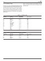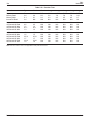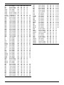
1
Z80380 CPU
USER'S MANUAL
PREFACE
Thank you for your interest in the Z380™ Central Processing Unit (CPU) and its
associated family of products. This Technical Manual describes programming
and operation of the Z380™ Superintegration™ Core CPU, which is found in the
Z380 Microprocessor Unit (MPU), and products built around Z380™ CPU core.
This Z380 User's Manual consists of the following Sections:
DC-8297-03
1.
Z380™ Architectural Overview
Chapter 1 is an introductory section covering the key features and
giving an overview of the architecture of the device.
2.
Address Spaces
Chapter 2 explains the address spaces the Z380 CPU can handle.
Also, this chapter includes a brief description of the on-chip registers.
3.
Native/Extended Mode, Word/Long Word Mode of Operation,
and Decoder Directives
This chapter provides a detailed explanation on the Z380’s unique
features, operation modes, and the Decoder Directives.
4.
Addressing Modes and Data Types
Chapter 4 describes the Addressing mode and data types which the
Z380 can handle.
5.
Instruction Set
Chapter 5 contains an overview of the instruction set; as well as a
detailed instruction-by-instruction description in alphabetical order.
6.
Interrupts and Traps
Chapter 6 explains the interrupts and traps features of the Z380.
7.
Reset
Chapter 7 describes the Reset function.
8.
Z380 Benchmark Appnote
9.
Z380 Questions & Answers
ZILOG
Appendix A
Appendix A covers the Z380’s instruction format.
Appendix B
Appendix B contains all Z380 instructions sorted in Alphabetical
Order.
Appendix C
Appendix C contains all Z380 instructions sorted in Numerical
Order.
Appendix D
The Tables in Appendix D lists all the Z380 instructions in instruction
affected by Native/Extended mode and Word/Long Word mode.
Appendix E
The Tables in Appendix E lists all the Z380 instructions in instruction
affected by DDIR IM (Immediate Decoder Directives) mode.
Index
A to Z listing of Z380™ User's Manual key words and phrases.
This manual assumes the reader has a basic knowledge of CPUbased system architectures and software development systems,
such as the use of the text editor, and invoking the assembler/
compiler. Also, knowledge of the Z80® CPU architecture is desirable.
© 1994, 1995, 1996, 1997 by Zilog, Inc. All rights reserved. No
part of this document may be copied or reproduced in any form
or by any means without the prior written consent of Zilog, Inc.
The information in this document is subject to change without
notice. Devices sold by Zilog, Inc. are covered by warranty and
patent indemnification provisions appearing in Zilog, Inc. Terms
and Conditions of Sale only.
ZILOG, INC. MAKES NO WARRANTY, EXPRESS, STATUTORY,
IMPLIED OR BY DESCRIPTION, REGARDING THE INFORMATION SET FORTH HEREIN OR REGARDING THE FREEDOM OF
THE DESCRIBED DEVICES FROM INTELLECTUAL PROPERTY
INFRINGEMENT. ZILOG, INC. MAKES NO WARRANTY OF MERCHANTABILITY OR FITNESS FOR ANY PURPOSE.
Zilog, Inc. shall not be responsible for any errors that may appear
in this document. Zilog, Inc. makes no commitment to update or
keep current the information contained in this document.
Zilog’s products are not authorized for use as critical components in life support devices or systems unless a specific written
agreement pertaining to such intended use is executed between
the customer and Zilog prior to use. Life support devices or
systems are those which are intended for surgical implantation
into the body, or which sustains life whose failure to perform,
when properly used in accordance with instructions for use
provided in the labeling, can be reasonably expected to result in
significant injury to the user.
Zilog, Inc. 210 East Hacienda Ave.
Campbell, CA 95008-6600
Telephone (408) 370-8000
Telex 910-338-7621
FAX 408 370-8056
Internet: http://www.zilog.com
DC-8297-03
USER 'S M ANUAL
ZILOG
USER’s MANUAL
CHAPTER 1
Z380™ ARCHITECTURAL OVERVIEW
1.1 INTRODUCTION
The Z380 CPU incorporates advanced architectural features that allow fast and efficient throughput and increased
memory addressing capabilities while maintaining Z80®
CPU and Z180® MPU object-code compatibility. The Z380
CPU core provides a continuing growth path for present
Z80- or Z180®-based designs and offers the following key
features:
■
Full Static CMOS Design with Low Power Standby
Mode Support
■
DC to 18 MHz Operating Frequency @ 5 Volts VCC
■
DC to 10 MHz Operating Frequency @ 33 Volts VCC
■
Enhanced Instruction Set that Maintains Object-Code
Compatibility with Z80 and Z180 Microprocessors
■
16-Bit (64K) or 32-Bit (4G) Linear Address Space
■
16-Bit Internal Data Bus
■
Two Clock Cycle Instruction Execution (Minimum)
■
Multiple On-Chip Register Files (Z380 MPU has Four
Banks)
■
BC/DE/HL/IX/IY Registers are Augmented by 16-Bit
Extended Registers (BCz/DEz/HLz/IXz/IYz), PC/SP/I
Registers are Augmented by Extended Registers (PCz/
SPz/Iz) for 32-Bit Addressing Capability.
■
Newly Added IX’ and IY’ Registers with Extended
Registers (IXz’/IYz’)
■
Enhanced Interrupt Capabilities, Including 16-Bit
Vector
■
Undefined Opcode Trap for Full Z380 CPU Instruction
Set
The Z380 CPU, an enhanced version of the Z80 CPU,
retains the Z80 CPU instruction set to maintain complete
binary-code compatiblity with present Z80 and Z180 codes.
The basic addressing modes of the Z80 microprocessor
have been augmented with Stack Pointer Relative loads
and stores, 16-bit and 24-bit Indexed offsets, and increased Indirect register addressing flexibility, with all of
the addressing modes allowing access to the entire 32-bit
address space. Significant additions have been made to
the instruction set iincorporating16-bit arithmetic and logical operations, 16-bit I/O operations, multiply and divide,
a complete set of register-to-register loads and exchanges,
plus 32-bit load and exchange, and 32-bit arithmetic
operation for address calculation.
The basic register file of the Z80 microprocessor is expanded to include alternate register versions of the IX and
IY registers. There are four sets of this basic Z80 microprocessor register file present in the Z380 MPU, along with the
necessary resources to manage switching between the
different register sets. All of the register pairs and index
registers in the basic Z80 microprocessor register file are
expanded to 32 bits.
The Z380 CPU expands the basic 64 Kbyte Z80 and Z180
address space to a full 4 Gbyte (32-bit) address space.
This address space is linear and completely accessible to
the user program. The external I/O address space is
similarly expanded to a full 4 Gbyte (32-bit) range, and 16bit I/O, both simple and block move are included. A 256
byte-wide internal I/O space has been added. This space
will be used to access on-chip I/O resources on future
Superintegration implementation of this CPU core.
Figure 1-1 provides a detailed description of the basic
register architecture of the Z380 CPU with the size of the
register banks shown at four each, however, the Z380 CPU
architecture allows future expansion of up to 128 sets of
each.
Z380™
USER'S MANUAL
ZILOG
1.1 INTRODUCTION (Continued)
4 Sets of Registers
BCz
A
B
F
C
DEz
HLz
IXz
IYz
D
H
IXU
IYU
E
L
IXL
IYL
BCz'
A'
B'
F'
C'
DEz'
HLz'
IXz'
D'
H'
IXU'
E'
L'
IXL'
IYz'
IYU'
IYL'
Iz
SPz
PCz
R
I
SP
PC
Figure 1-1. Z380™ CPU Register Architecture
1-2
DC-8297-03
Z380™
USER'S MANUAL
ZILOG
1.2 CPU ARCHITECTURE
The Z380 CPU is a binary-compatible extension of the Z80
CPU and the Z180 CPU architecture. High throughput
rates are achieved by a high clock rate, high bus bandwidth, and instruction fetch/execute overlap. Communicating to the external world through an 8-bit or 16-bit data
bus, the Z380 CPU is a full 32-bit machine internally, with
a 32-bit ALU and 32-bit registers.
1.2.1 Modes of Operation
To maintain compatibility with the Z80/Z180 CPU while
having the capability to manipulate 4 Gbytes of memory
address range, the Z380 CPU has two bits in the Select
Register (SR) to control the modes of operation. One bit
controls the address manipulation mode: Native mode or
Extended mode; and the other bit controls the data manipulation mode: Word mode or Long Word mode. In
result, the Z380 CPU has four modes of operation. On
reset, the Z380 CPU is in Native/Word mode, which is
compatible to the Z80/Z180’s operation mode. For details
on this subject, refer to Chapter 3, “Native/Extended Mode,
Word/Long Word Mode of Operation, and Decoder Directive Instructions.”
1.2.1.1 Native Mode and Extended Mode
The Z380 CPU can operate in either Native or Extended
mode, as controlled by a bit in the Select Register (SR). In
Native mode (the Reset configuration), all address manipulations are performed modulo 65536 (216). In this
mode, the Program Counter (PC) only increments across
16 bits, all address manipulation instructions (increment,
decrement, add, subtract, indexed, stack relative, and PC
relative) only operate on 16 bits, and the Stack Pointer (SP)
only increments and decrements across 16 bits. The PC
high-order word is left at all zeros, as the high-order words
of the SP and the I register. Thus, Native mode is fully
compatible with the Z80 CPU’s 64 Kbyte address mode. It
is still possible to address memory outside of 64 Kbyte
address space for data storage and retrieval in Native
mode, however, since direct addresses, indirect addresses,
and the high-order word of the SP, I, and the IX and IY
registers may be loaded with non-zero values. Executed
code and interrupt service routines must reside in the
lowest 64 Kbytes of the address space.
In Extended mode, however, all address manipulation
instructions operate on 32 bits, allowing access to the
entire 4 Gbyte address space of the Z380 CPU. In both
Native and Extended modes, the Z380 drives all 32 bits of
the address onto the external address bus; only the width
of the manipulated addresses distinguishes Native from
Extended mode. The Z380 CPU implements one instruction to allow switching from Native to Extended mode
(SETC XM); however, once in Extended mode, only Reset
DC-8297-03
will return the Z380 CPU to Native mode. This restriction
applies because of the possibility of “misplacing” interrupt
service routines or vector tables during the transition from
Extended mode back to Native mode.
1.2.1.2 Word or Long Word Mode
In addition to Native and Extended mode, which are
specific to memory space addressing, the Z380 CPU can
operate in either Word or Long Word mode specific to data
load and exchange operations. In Word mode (the Reset
configuration), all word load and exchange operations
manipulate 16-bit quantities. For example, only the loworder words of the source and destination are exchanged
in an exchange operation, with the high-order words
unaffected.
In the Long Word mode, all 32 bits of the source and
destination are exchanged. The Z380 CPU implements
two instructions plus decoder directives to allow switching
between Word and Long Word mode; SETC LW (Set
Control Long Word) and RESC LW (Reset Control Long
Word) perform a global switch, while DDIR W, DDIR LW
and their variants are decoder directives that select a
particular mode only for the instruction that they precede.
Note that all word data arithmetic (as opposed to address
manipulation arithmetic), rotate, shift, and logical operations are always in 16-bit quantities. They are not controlled by either the Native/Extended or Word/Long Word
selections. The exceptions to the 16-bit quantities are, of
course, those multiply and divide operations with 32-bit
products or dividends.
All word Input/Output operations are performed on 16-bit
values, regardless of Word/Long Word operation.
1.2.2 Address Spaces
Addressing spaces in the Z380 CPU include the CPU
register, the CPU control register, the memory address,
on-chip I/O address, and the external I/O address. The
CPU register space is a superset of the Z80 CPU register
set, and consists of all of the registers in the CPU register
file. These CPU registers are used for data and address
manipulation, and are an extension of the Z80 CPU register
set, with four sets of this extended Z80 CPU register set
present in the Z380 CPU. Access to these registers is
specified in the instruction, with the active register set
selected by bits in the Select Register (SR) in the CPU
control register space.
1-3
Z380™
USER'S MANUAL
ZILOG
1.2.2 Address Spaces (Continued)
1.2.4. Addressing Modes
Each register set includes the primary registers A, F, B, C,
D, E, H, L, IX, and IY, as well as the alternate registers A’,
F’, B’, C’, D’, E’, H’, L’, IX’, and IY’. Also, IX, IX’, IY, and IY’
registers are accessible as two byte registers, each named
as IXU, IXL, IXU’ IXL’, IYU, IYL, IYU’, and IYL’. These byte
registers can be paired B with C, D with E, H with L, B’ with
C’, D’ with E’, and H’ with L’ to form word registers, and
these word registers are extended to 32 bits with the “z”
extension to the register. This register extension is only
accessible when using the register as a 32-bit register (in
the Long Word mode) or when swapping between the
most-significant and least-significant word of a 32-bit
register using SWAP instructions. Whenever an instruction
refers to a word register, the implicit size is controlled by
Word or Long Word mode. Also included are the R, I, and
SP registers, as well as the PC.
Addressing modes are used by the Z380 CPU to calculate
the effective address of an operand needed for execution
of an instruction. Seven addressing modes are supported
by the Z380 CPU. Of these seven, one is an addition to the
Z80 CPU addressing modes (Stack Pointer Relative) and
the remaining six modes are either existing or extensions
to Z80 CPU addressing modes.
The Select Register (SR) determines the operation of the
Z380 CPU. The contents of this register determine the CPU
operating mode, which register bank will be used, the
interrupt mode in effect, and so on.
The Z380 CPU’s memory address space is linear 4 Gbytes.
To keep compatibility with the Z80 CPU memory addressing model, it has two control bits to change its operation
modes—Native or Extended, Word or Long Word.
The Z380 CPU architecture also distinguishes between
the memory and I/O addressing space and, therefore,
requires specific I/O instructions. Furthermore, I/O addressing space is subdivided into the on-chip I/O address
space and the external I/O addressing space. External
I/O addressing space in the Z380 CPU is 32 bits long, and
internal I/O addressing space is 8-bits long. There are
separate sets of I/O instructions for each I/O addressing
space.
■
■
■
■
■
■
■
Register
Immediate
Indirect Register
Direct Address
Indexed
Program Counter Relative
Stack Pointer Relative
All addressing modes are available on the 8-bit load,
arithmetic, and logical instructions; the 8-bit shift, rotate,
and bit manipulation instructions are limited to the registers and Indirect register addressing modes. The 16-bit
loads on the addressing registers support all addressing
modes except Index, while other 16-bit operations are
limited to the Register, Immediate, Indirect Register, Index, Direct Address, and PC Relative addressing modes.
For details on this subject, refer to Chapter 4, “Addressing
Modes and Data Types.”
1.2.5. Instruction Set
The Z380 CPU instruction set is an expansion of the Z80
instruction set; the enhancements include support for
additional addressing modes for the Z80 instructions as
well as the addition of new instructions. The Z380 CPU
instruction set provides a full complement of 8-bit, 16-bit,
and 32-bit operation, including multiplication and division.
Some of the Internal I/O registers are used to control the
functionality of the device, such as to program/read status
of Trap, Assigned Vector Base address, enabling of interrupts, and to get Chip version ID.
For details on this subject, refer to Chapter 5, “Instruction
Set.”
For details on this topic, refer to Chapter 2, “Address
Spaces.”
The Z380 CPU supports three types of exceptions (conditions that alter the normal flow of program execution);
interrupts, traps, and resets.
1.2.6 Exception Conditions
1.2.3 Data Types
Many data types are supported by the Z380 CPU architecture. The basic data type is the 8-bit byte, which is also the
basic addressable memory element. The architecture also
supports operations on bits, BCD (Binary Coded Decimal)
digits, words (16 bits or 32 bits), byte strings and word
strings. For details on this topic, refer to Section 4.3, “Data
Types.”
1-4
Interrupts are asynchronous events typically triggered by
peripherals requiring attention. The Z380 CPU interrupt
structure has been significantly enhanced by increasing
the number of interrupt request lines and by adding an
efficient means for handling nested interrupts. The Z380
CPU has five interrupt lines. These are: Nonmaskable
Interrupt line (/NMI) and Maskable interrupt lines (/INT0,
/INT1, /INT2, and /INT3). Interrupt requests on /INT3-/INT1
DC-8297-03
Z380™
USER'S MANUAL
ZILOG
are handled by a newly added interrupt handing mode,
“Assigned Vectored Mode,” which is a fixed vectored
interrupt mode similar in interrupt handling to the Z180’s
interrupts from on-chip peripherals. For handling interrupt
requests on the /INT0 line, there are four modes available:
■
■
8080 compatible (Mode 0), in which the interrupting
device provides the first instruction of the interrupt
routine.
Dedicated interrupts (Mode 1), in which the CPU
jumps to a dedicated address when an interrupt
occurs.
■
Vectored interrupt mode (Mode 2), in which the
interrupting peripheral device provides a vector into a
table of jump address.
■
Enhanced vectored interrupt mode (Mode 3), wherein
the CPU expects 16-bit vector, instead of 8-bit interrupt
vectors in Mode 2.
The first three modes are compatible with Z80 interrupt
modes; the fourth mode provides more flexibility.
Traps are synchronous events that trigger a special CPU
response when an undefined instruction is executed. It
can be used to increase system reliability, or used as a
“software trap instruction.”
Hardware resets occur when the /RESET line is activated
and override all other conditions. A /RESET causes certain
CPU control registers to be initialized.
For details on this subject, refer to Chapter 6, “Interrupts
and Traps.”
1.3 BENEFITS OF THE ARCHITECTURE
The Z380 CPU architecture provides several significant
benefits, including increased program throughput achieved
by higher bus bandwidth (16-bit wide bus), reduction to
two clocks/basic machine cycle (vs four clocks/cycle on
the Z80 CPU), prefetch cue, access to the larger linear
addressing space, enhanced instructions/new addressing mode, data/address manipulation in 16/32 bits, and
faster context switching by utilizing multiple register banks.
1.3.1 High Throughput
Very high throughput rates can be achieved with the Z380
CPU, due to the basic machine cycle’s reduction to two
clocks/cycle from four clocks/cycle on the Z80 CPU, fine
tuned four staged pipeline with prefetch cue. This well
designed pipeline and prefetch cue are both totally transparent to the user, thus maximizing the efficiency of the
pipeline all the time. The Z380 CPU implemented onto the
Z380 MPU is configured with a 16-bit wide data bus, which
doubles the bus bandwidth. These architectural features
result in two clocks/instructions execution minimum, three
clocks/instruction on average. The high clock rates (up to
40 MHz) achievable with this processor. Make the overall
performance of the Z380 CPU more than ten times that of
the Z80.
the technology improved over time, applications started to
demand more complicated processing, multitasking, faster
processing, etc., with the high level language needed to
develop software. As a result, 64 Kbytes of memory addressing space is not enough for some Z80 CPU based
applications. In order to handle more than 64 Kbytes of
memory, the Z80 CPU requires a Memory Banking scheme,
or MMU (Memory Management Unit), like the Z180 MPU or
Z280 MPU. These provide the overhead to access more
than 64 Kbytes of memory.
The Z380 CPU architecture allows access to a full 4 Gbytes
(232) of memory addressing space as well as 4 Gbytes of
I/O addressing area, without using a Memory Banking
scheme, or MMU.
1.3.3. Enhanced Instruction Set with 16-Bit
and 32-Bit Manipulation Capability
The Z380 CPU instruction set is 100% upward compatible
to the Z80 CPU instruction set; that is all the Z80 instructions have been preserved at the binary level. New instructions added to the Z380 CPU include:
■
Less restricted operand source/destination
combinations.
■
More flexible register exchange instructions.
■
Stack Pointer Relative addressing mode.
1.3.2 Linear Memory Address Space
Z380 CPU architecture has 4 Gbytes of linear memory
address space. The Z80 CPU architecture allows 64
Kbytes of memory addressing space. This was more than
sufficient when the Z80 CPU was first developed. But as
DC-8297-03
1-5
Z380™
USER'S MANUAL
ZILOG
1.3.3. Enhanced Instruction Set with 16-Bit
and 32-Bit Manipulation Capability
(Continued)
■
DDIR (Decoder Directive Instructions) to enhance
addressing capability to cover 4 Gbytes of memory
space, as well as data manipulation capability.
■
Jump relative/Call relative instructions with 8-bit,
16-bit, or 24-bit displacement.
■
Full complements of 16-bit arithmetic instructions.
■
32-bit manipulate instructions for address manipulation.
These new instructions help to compact the code, as well
as shorten the program’s overall execution speed.
For details on this subject, refer to Chapter 5, “Instruction
Set.”
register pairs (including each register's Extended portion).
When doing context switching, by exceptional condition
(trap or interrupts) or by subroutine/procedure calls, the
CPU has to save the contents of the registers currently in
use, along with the current CPU status.
Traditionally in the Z80 CPU architecture, this is done by
saving the contents of the register into memory, usually
using push/pop instructions or the auxiliary register file.
Register contents are then restored when the process is
finished.
With the Z380 CPU’s multiple register banks, saving the
contents of the working register set currently in use is just
a matter of an instruction to change the field in the Select
Register, which allows fast context switching.
1.3.4 Faster Context Switching
The Z380 CPU architecture allows multiple sets of register
banks for AF/AF’, BC/DE/HL, BC’/DE’/HL’, IX/IX’, IY/IY’
1.4 SUMMARY
The Z380 CPU is a high-performance 16-bit Central Processing Unit Superintegration™ core. Code-compatible
with the Z80 CPU, the Z380 CPU architecture has been
expanded to include features such as multiple register
banks, 4 Gbytes of linear memory addressing space, and
efficient handling of nested interrupts. The benefits of this
architecture, including high throughput rates, code density, and compiler efficiency, greatly enhance the power
and versatility of the Z380 CPU. Thus, the Z380 CPU
provides both a growth path for existing Z80-based designs and a powerful processor for applications and the
products to be developed around this CPU core.
© 1994, 1995, 1996, 1997 by Zilog, Inc. All rights reserved. No
part of this document may be copied or reproduced in any form
or by any means without the prior written consent of Zilog, Inc.
The information in this document is subject to change without
notice. Devices sold by Zilog, Inc. are covered by warranty and
patent indemnification provisions appearing in Zilog, Inc. Terms
and Conditions of Sale only.
Zilog’s products are not authorized for use as critical components in life support devices or systems unless a specific written
agreement pertaining to such intended use is executed between
the customer and Zilog prior to use. Life support devices or
systems are those which are intended for surgical implantation
into the body, or which sustains life whose failure to perform,
when properly used in accordance with instructions for use
provided in the labeling, can be reasonably expected to result in
significant injury to the user.
ZILOG, INC. MAKES NO WARRANTY, EXPRESS, STATUTORY,
IMPLIED OR BY DESCRIPTION, REGARDING THE INFORMATION SET FORTH HEREIN OR REGARDING THE FREEDOM OF
THE DESCRIBED DEVICES FROM INTELLECTUAL PROPERTY
INFRINGEMENT. ZILOG, INC. MAKES NO WARRANTY OF MERCHANTABILITY OR FITNESS FOR ANY PURPOSE.
Zilog, Inc. shall not be responsible for any errors that may appear
in this document. Zilog, Inc. makes no commitment to update or
keep current the information contained in this document.
1-6
Zilog, Inc. 210 East Hacienda Ave.
Campbell, CA 95008-6600
Telephone (408) 370-8000
Telex 910-338-7621
FAX 408 370-8056
Internet: http://www.zilog.com
DC-8297-03
Z380™
USER'S MANUAL
ZILOG
USER’s MANUAL
CHAPTER 2
ADDRESS SPACES
2.1 INTRODUCTION
The Z380 CPU supports five address spaces corresponding to the different types of locations that can be addressed and the method by which the logical addresses
are formed. These five address spaces are:
■
CPU Register Space. This consists of all the register
addresses in the CPU register file.
■
CPU Control Register Space. This consists of the
Select Register (SR).
■
Memory Address Space. This consists of the
addresses of all locations in the main memory.
■
External I/O Address Space. This consists of all
external I/O ports addresses through which peripheral
devices are accessed.
■
On-Chip I/O Address Space. This consists of all
internal I/O port addresses through which peripheral
devices are accessed. Also, this addressing space
contains registers to control the functionality of the
device, giving status information.
■
Four sets of Index registers (IX, IY, IX’, IY’)
■
Stack Pointer (SP)
■
Program Counter, Interrupt register, Refresh register
(PC, I, R)
2.2 CPU REGISTER SPACE
The Z380 register file is illustrated in Figure 2-1. Note that
this figure shows the configuration of the register on the
Z380 CPU, and the number of the register files may vary on
future Superintegration devices. The Z380 CPU contains
abundant register resources. At any given time, the program has immediate access to both primary and alternate
registers in the selected register set. Changing register
sets is a simple matter of an LDCTL instruction to program
the Select Register (SR).
Register addresses are either specified explicitly in the
instruction or are implied by the semantics of the instruction.
The CPU register file is divided into five groups of registers
(an apostrophe indicates a register in the auxiliary registers).
■
Four sets of Flag and Accumulator registers (F, A, F’,
A’)
■
Four sets of Primary and Working registers (B, C, D, E,
H, L, B’, C’, D’, E’, H’, L’)
DC-8297-03
2-1
Z380™
USER'S MANUAL
ZILOG
2.2 CPU REGISTER SPACE (Continued)
4 Sets of Registers
BCz
A
B
F
C
DEz
HLz
IXz
IYz
D
H
IXU
IYU
E
L
IXL
IYL
BCz'
A'
B'
F'
C'
DEz'
HLz'
IXz'
D'
H'
IXU'
E'
L'
IXL'
IYz'
IYU'
IYL'
R
I
Iz
SPz
PCz
SP
PC
Figure 2-1. Register File Organization (Z380 MPU)
2-2
DC-8297-03
Z380™
USER'S MANUAL
ZILOG
2.2.1 Primary and Working Registers
The working register set is divided into two register files:
the primary file and the alternate file (designated by prime
(‘)). Each file contains an 8-bit accumulator (A), a Flag
register (F), and six 8-bit general-purpose registers (B, C,
D, E, H, and L) with their Extended registers. Only one file
can be active at any given time, although data in the
inactive file can still be accessed by using EX R, R’
instructions for the byte-wide registers, EX RR, RR’ instructions for register pairs (either in 16-bit or 32-bit wide
depending on the LW status). Exchange instructions allow
the programmer to exchange the active file with the inactive file. The EX AF, AF’, EXX, or EXALL instructions
changes the register files in use. Upon reset, the primary
register file in register set 0 is active. Changing register
sets is a simple matter of an LDCTL instruction to program
SR.
The accumulator is the destination register for 8-bit arithmetic and logical operations. The six general-purpose
registers can be paired (BC, DE, and HL), and are extended to 32 bits by the extension to the register (with suffix
“z”; BCz/DEz/HLz), to form three 32-bit general-purpose
registers. The HL register serves as the 16-bit or 32-bit
accumulator for word operations. Access to the Extended
portion of the registers is possible using the SWAP instruction or word Load instructions in Long Word operation
mode.
The Flag register contains eight status flags. Four can be
individually used for control of program branching, two are
used to support decimal arithmetic, and two are reserved.
These flags are set or reset by various CPU operations. For
details on Flag operations, refer to Section 5.2, “Flag
Register.”
for the IX and IX’ registers, and IYU, IYU’, IYL, and IYL’ for
the IY and IY’ registers.
Selection of primary or auxiliary Index registers can be
made by EXXX, EXXY, or EXALL instructions, or programming of SR. Upon reset, the primary registers in register set
0 is active. Changing register sets is a simple matter of an
LDCTL instruction to program SR.
2.2.3. Interrupt Register
The Interrupt register (I) is used in interrupt modes 2 and
3 for /INT0 to generate a 32-bit indirect address to an
interrupt service routine. The I register supplies the upper
24 or 16 bits of the indirect address and the interrupting
peripheral supplies the lower eight or 16 bits. In Assigned
Vectors mode for /INT3-/INT1, the upper 16 bits of the
vector are supplied by the I register; bits 15-9 are supplied
from the Assigned Vector Base register, and bits 8-0 are
the assigned vector unique to each of /INT3-/INT1.
2.2.4. Program Counter
The Program Counter (PC) is used to sequence through
instructions in the currently executing program and to
generate relative addresses. The PC contains the 32-bit
address of the current instruction being fetched from
memory. In Native mode, the PC is effectively only 16 bits
long, since the upper word [PC31-PC16] of the PC is
forced to zero, and when carried from bit 15 to bit 16 (Lower
word [PC15-PC0] to Upper word [PC31-PC16]) are inhibited in this mode. In Extended mode, the PC is allowed to
increment across all 32 bits.
2.2.5. R Register
2.2.2. Index Registers
The four index registers, IX, IX’, IY, and IY’, are extended
to 32 bits by the extension to the register (with suffix “z”;
IXz/IYz), to form 32-bit index registers. To access the
Extended portion of the registers use the SWAP instruction
or word Load instructions in Long Word operation mode.
These Index registers hold a 32-bit base address that is
used in the Index addressing mode.
Only one register of each can be active at any given time,
although data in the inactive file can still be accessed by
using EX IX, IX’ and EX IY, IY’ (either in 16-bit or 32-bit wide
depending on the LW bit status). Index registers can also
function as general-purpose registers with the upper and
lower bytes of the lower 16 bits being accessed individually. These byte registers are called IXU, IXU’, IXL, and IXL’
DC-8297-03
The R register can be used as a general-purpose 8-bit
read/write register. The R register is not associated with
the refresh controller and its contents are changed only by
the user.
2.2.6. Stack Pointer
The Stack Pointer (SP) is used for saving information when
an interrupt or trap occurs and for supporting subroutine
calls and returns. Stack Pointer relative addressing allows
parameter passing using the SP. The SP is 16 bits wide, but
is extended by the SPz register to 32 bits wide.
2-3
ZILOG
Z380™
USER'S MANUAL
2.2.6 Stack Pointer (Continued)
Increment/decrement of the Stack Pointer is affected by
modes of operation (Native or Extended). In Native mode,
the stack operates in modulo 216, and in Extended mode,
it operates in modulo 232. For example, SP holds 0001FFFEH,
and does the Word size Pop operation. After the operation,
SP holds 00010000H in Native mode, and 00020000H in
Extended mode. In either case, SPz can be programmed
to set Stack frame. This is done by the Load- to-Stack
pointer instructions in Long Word mode.
2.3. CPU CONTROL REGISTER SPACE
The CPU control register space consists of the 32-bit
Select Register (SR). The SR may be accessed as a whole
or the upper three bytes of the SR may be accessed
individually as YSR, XSR, and DSR. In addition, these
upper three bytes can be loaded with the same byte value.
The SR may also be PUSHed and POPed and is cleared to
zeros on Reset. For details on this register, refer to Chapter
5.3, “Select Register.”
2.4 MEMORY ADDRESS SPACE
The memory address space can be viewed as a string of
4 Gbytes numbered consecutively in ascending order.
The 8-bit byte is the basic addressable element in the Z380
MPU memory address space. However, there are other
addressable data elements: bits, 2-byte words, byte strings,
and 4-byte words.
The size of the data element being addressed depends on
the instruction being executed as well as the Word/Long
Word mode. A bit can be addressed by specifying a byte
and a bit within that byte. Bits are numbered from right to
left, with the least significant bit being 0, as illustrated in
Figure 2-2.
either even or odd memory addresses. A word (either 2byte or 4-byte entity) is aligned if its address is even;
otherwise it is unaligned. Multiple bus transactions, which
may be required to access multiple-byte entities, can be
minimized if alignment is maintained.
The format of multiple-byte data types is also shown in
Figure 2-2. Note that when a word is stored in memory, the
least significant byte precedes the more significant byte of
the word, as in the Z80 CPU architecture. Also, the loweraddressed byte is present on the upper byte of the external
data bus.
The address of a multiple-byte entity is the same as the
address of the byte with the lowest memory address in the
entity. Multiple-byte entities can be stored beginning with
2-4
DC-8297-03
Z380™
USER'S MANUAL
ZILOG
Bits within a byte:
7
6
5
4
3
2
1
0
16-bit word at address n:
Least Significant Byte
Address n
Most Significant Byte
Address n+1
32-bit word at address n:
D7-0 (Least Significant Byte)
Address n
D15-8
Address n+1
D23-16
Address n+2
D31-24 (Most Significant Byte)
Address n+3
Memory addresses:
Even address (A0=0)
Odd address (A0=1)
Least Significant Byte
15
14
13
12
11
10
Most Significant Byte
9
8
7
6
5
4
3
2
1
0
Figure 2-2. Bit/Byte Ordering Conventions
DC-8297-03
2-5
Z380™
USER'S MANUAL
ZILOG
2.5. EXTERNAL I/O ADDRESS SPACE
External I/O address space is 4 Gbytes in size and External
I/O addresses are generated by I/O instructions except
those reserved for on-chip I/O address space accesses. It
can take a variety of forms, as shown in Table 2.1. An
external I/O read or write is always one transaction, regardless of the bus size and the type of I/O instruction.
Table 2-1. I/O Addressing Options
Address Bus
A15-A8
I/O Instruction
A31-A24
A23-A16
A7-A0
IN A, (n)
IN dst,(C)
INA(W) dst,(mn)
00000000
BC31-B24
00000000
00000000
BC23-B16
00000000
A7-A0
BC15-B8
m
n
BC7-B0
n
DDIR IB INA(W) dst,(lmn)
DDIR IW INA(W) dst,(klmn)
Block Input
00000000
k
BC31-B24
l
l
BC23-B16
m
m
BC15-B8
n
n
BC7-B0
OUT (n),A
OUT (C),dst
OUTA(W) (mn),dst
00000000
BC31-B24
00000000
00000000
BC23-B16
00000000
A7-A0
BC15-B8
m
n
BC7-B0
n
DDIR IB OUTA(W) (lmn),dst
DDIR IW OUTA(W) (klmn),dst
Block Output
00000000
k
BC31-B24
l
l
BC23-B16
m
m
BC15-B8
n
n
BC7-B0
2.6. ON-CHIP I/O ADDRESS SPACE
The Z380 CPU has the on-chip I/O address space to
control on-chip peripheral functions of the Superintegration™ version of the devices. A portion of its interrupt
functions are also controlled by several on-chip registers,
which occupy an on-chip I/O address space. This on-chip
I/O address space can be accessed only with the following
reserved on-chip I/O instructions which are identical to the
Z180 original I/O instructions to access Page 0 I/O addressing area.
IN0
IN0
OUT0
TSTIO
R,(n)
(n)
(n),R
n
OTIM
OTIMR
OTDM
OTDMR
When one of these I/O instructions is executed, the Z380
MPU outputs the register address being accessed in a
pseudo-transaction of two BUSCLK cycles duration, with
the address signals A31-A8 at zero. In the pseudo-transactions, all bus control signals are at their inactive state.
Register Name
Interrupt Enable Register
Assigned Vector Base Register
Trap and Break Register
Chip Version ID Register
Internal I/O Address
17H
18H
19H
0FFH
The Chip Version ID register returns one byte data, which
indicates the version of the CPU, or the specific implementation of the Z380 CPU based Superintegration device.
Currently, the value 00H is assigned to the Z380 MPU, and
other values are reserved.
For the other three registers, refer to Chapter 6, “Interrupts
and Traps.”
Also, the Z380 MPU has registers to control chip selects,
refresh, waits, and I/O clock divide to Internal I/O address
00H to 10H. For these registers, refer to the Z380 MPU
Product specification (DC-3003-01).
The following four registers are assigned to this addressing space as a part of the Z380 CPU core:
2-6
DC-8297-03
Z380™
USER'S MANUAL
ZILOG
© 1994, 1995, 1996, 1997 by Zilog, Inc. All rights reserved. No
part of this document may be copied or reproduced in any form
or by any means without the prior written consent of Zilog, Inc.
The information in this document is subject to change without
notice. Devices sold by Zilog, Inc. are covered by warranty and
patent indemnification provisions appearing in Zilog, Inc. Terms
and Conditions of Sale only.
ZILOG, INC. MAKES NO WARRANTY, EXPRESS, STATUTORY,
IMPLIED OR BY DESCRIPTION, REGARDING THE INFORMATION SET FORTH HEREIN OR REGARDING THE FREEDOM OF
THE DESCRIBED DEVICES FROM INTELLECTUAL PROPERTY
INFRINGEMENT. ZILOG, INC. MAKES NO WARRANTY OF MERCHANTABILITY OR FITNESS FOR ANY PURPOSE.
Zilog, Inc. shall not be responsible for any errors that may appear
in this document. Zilog, Inc. makes no commitment to update or
keep current the information contained in this document.
DC-8297-03
Zilog’s products are not authorized for use as critical components in life support devices or systems unless a specific written
agreement pertaining to such intended use is executed between
the customer and Zilog prior to use. Life support devices or
systems are those which are intended for surgical implantation
into the body, or which sustains life whose failure to perform,
when properly used in accordance with instructions for use
provided in the labeling, can be reasonably expected to result in
significant injury to the user.
Zilog, Inc. 210 East Hacienda Ave.
Campbell, CA 95008-6600
Telephone (408) 370-8000
Telex 910-338-7621
FAX 408 370-8056
Internet: http://www.zilog.com
2-7
Z380™
USER'S MANUAL
ZILOG
USER’s MANUAL
CHAPTER 3
NATIVE EXTENDED MODE, WORD/LONG
WORD MODE OF OPERATIONS
AND DECODER DIRECTIONS
3.1 INTRODUCTION
The Z380™ CPU architecture allows access to 4 Gbytes
(232) of memory addressing space, and 4G locations of
I/O. It offers 16/32-bit manipulation capability while maintaining object-code compatibility with the Z80 CPU. In
order to implement these capabilities and new instruction
sets, it has two modes of operation for address manipulation (Native or Extended mode), two modes of operation for
data manipulation (Word or Long Word mode), and a
special set of new Decoder Directives.
On Reset, the Z380 CPU defaults in Native mode and Word
mode. In this condition, it behaves exactly the same as the
Z80 CPU, even though it has access to the entire 4 Gbytes
of memory for data access and 4G locations of I/O space,
access to the newly added registers which includes Extended registers and register banks, and the capability of
executing all the Z380 instructions.
As described below, the Z380 CPU can be switched
between Word mode and Long Word mode during operation through the SETC LW and RESC LW instructions, or
Decoder Directives. The Native and Extended modes are
a key exception— it defaults up in Native mode, and can
be set to Extended mode by the instruction. Only Reset can
return it to Native mode. Figure 3-1 illustrates the relationship between these modes of operation.
Z380
Native
Extended
Word
Long Word
Z80 Native Mode
Figure 3-1. Z380™ CPU Operation Modes
For the instructions which work with the DDIR instructions, refer to Appendix D and E.
DC-8297-03
3-1
Z380™
USER'S MANUAL
ZILOG
3.2 DECODER DIRECTIVES
The Decoder Directive is not an instruction, but rather a
directive to the instruction decoder. The instruction decoder may be directed to fetch an additional byte or word
of immediate data or address with the instruction, as well
as tagging the instruction for execution in either Word or
Long Word mode. Since the Z80 CPU architecture’s addressing convention in the memory is “least significant
byte first, followed by more significant bytes,” it is possible
to have such instructions to direct the instruction decoder
to fetch additional byte(s) of address information or immediate data to extend the instruction.
All eight combinations of the two options are supported, as
shown below. Instructions which do not support decoder
directives are assembled by the instruction decoder as if
the decoder directive were not present.
■
■
■
■
■
■
■
DDIR W
DDIR IB,W
DDIR IW,W
DDIR IB
DDIR LW
DDIR IB,LW
DDIR IW,LW
■
DDIR IW
Word mode
Immediate byte, Word mode
Immediate Word, Word mode
Immediate byte
Long Word mode
Immediate byte, Long Word mode
Immediate Word, Long Word
mode
Immediate Word
The IB decoder directive causes the decoder to fetch an
additional byte immediately after the existing immediate
data or direct address, and in front of any trailing opcode
bytes (with instructions starting with DD-CB or FD-CB, for
example).
Likewise, the IW decoder directive causes the decoder to
fetch an additional word immediately after the existing
immediate data or direct address, and in front of any
trailing opcode bytes.
Byte ordering within the instruction follows the usual convention; least significant byte first, followed by more significant bytes. More-significant immediate data or direct
address bytes not specified in the instruction are read as
all zeros by the processor.
The W decoder directive causes the instruction decoder to
tag the instruction for execution in Word mode. This is
useful while the Long Word (LW) bit in the Select Register
(SR) is set, but 16-bit data manipulation is required for this
instruction.
The LW decoder directive causes the instruction decoder
to tag the instruction for execution in Long Word mode.
This is useful while the LW bit in the SR is cleared, but 32bit data manipulation is required for this instruction.
3.3 NATIVE MODE AND EXTENDED MODE
The Z380 CPU can operate in either Native or Extended
mode, as a way to manipulate addresses.
In Native mode (the Reset configuration), the Program
Counter only increments across 16 bits, and all stack Push
and Pop operations manipulate 16-bit quantities (two
bytes). Thus, Native mode is fully compatible with the Z80
CPU’s 64 Kbyte address space and programming model.
The extended portion of the Program Counter (PC31PC15) is forced to 0 and program address location next to
0000FFFFH is 00000000H in this mode. This means in
Native mode, program have to reside within the first 64
Kbytes of the memory addressing space.
In Extended mode, however, the PC increments across all
32 bits and all stack Push and Pop operations manipulate
32-bit quantities. Thus, Extended mode allows access to
the entire 4 Gbyte address space. In both Native and
Extended modes, the Z380 CPU drives all 32 bits of the
address onto the external address bus; only the PC increments and stack operations distinguish Native from Extended mode.
3-2
Note that regardless of Native or Extended mode, a 32-bit
address is always used for the data access. Thus, for data
reference, the complete 4 Gbytes of memory area may be
accessed. For example:
LD
BC, (HL)
uses the 32-bit address value stored in HL31-HL0 (HLz
and HL) as a source location address. However, on Reset,
the HL31-HL16 portion (HLz) initializes to 00H. Unless HLz
is modified to other than 00H, operation of this instruction
is identical to the one with the Z80 CPU. Modifying the
extended portion of the register is done either by using a
32-bit load instruction (in Long Word mode, or with DDIR
LW instructions), or using a 16-bit load instruction with
SWAP instructions.
DC-8297-03
Z380™
USER'S MANUAL
ZILOG
The Z380 CPU implements one instruction to switch to
Extended mode from Native mode; SETC XM (set Extended mode) places the Z380 CPU in Extended mode.
Once in Extended mode, only Reset can return it to Native
mode. On Reset, the Z380 is in Native mode. Refer to
Sections 4 and 5 for more examples.
3.4 WORD AND LONG WORD MODE OF OPERATION
The Z380 CPU can operate in either Word or Long Word
mode. In Word mode (the Reset configuration), all word
operations manipulate 16-bit quantities, and are compatible with the Z80 CPU 16-bit operations. In the Long Word
mode, all word operations can manipulate 32-bit quantities. Note that the Native/Extended and Word/Long Word
selections are independent of one another, as Word/Long
Word pertains to data and operand address manipulation
only. The Z380 CPU implements two instructions and two
decoder directives to allow switching between these two
modes; SETC LW (Set Long Word) and RESC LW (Reset
Long Word) perform a global switch, while DDIR LW and
DDIR W are decoder directives that select a particular
mode only for the instruction that they precede.
2.
Immediate data load with DDIR instructions
DDIR IW,LW
LD
HL,12345678H
Loads 12345678H into HL31-HL0.
DDIR IB,LW
LD
HL,123456H
Loads 00123456H into HL31-HL0.
00H is appended as the Most significant byte as
HL31-HL24.
DDIR LW
LD
HL,1234H
Examples:
1.
Effect of Word mode and Long Word mode
Loads 00001234H into HL31-HL0.
0000H is appended as the HL31-HL16 portion.
DDIR W
LD
BC, (HL)
Loads BC15-BC0 from the location (HL) and
(HL+1), and BCz (BC31-BC16) remains unchanged.
DDIR LW
LD
BC, (HL)
Loads BC31-BC0 from the locations (HL) to (HL+3).
© 1994, 1995, 1996, 1997 by Zilog, Inc. All rights reserved. No
part of this document may be copied or reproduced in any form
or by any means without the prior written consent of Zilog, Inc.
The information in this document is subject to change without
notice. Devices sold by Zilog, Inc. are covered by warranty and
patent indemnification provisions appearing in Zilog, Inc. Terms
and Conditions of Sale only.
ZILOG, INC. MAKES NO WARRANTY, EXPRESS, STATUTORY,
IMPLIED OR BY DESCRIPTION, REGARDING THE INFORMATION SET FORTH HEREIN OR REGARDING THE FREEDOM OF
THE DESCRIBED DEVICES FROM INTELLECTUAL PROPERTY
INFRINGEMENT. ZILOG, INC. MAKES NO WARRANTY OF MERCHANTABILITY OR FITNESS FOR ANY PURPOSE.
Zilog, Inc. shall not be responsible for any errors that may appear
in this document. Zilog, Inc. makes no commitment to update or
keep current the information contained in this document.
DC-8297-03
Zilog’s products are not authorized for use as critical components in life support devices or systems unless a specific written
agreement pertaining to such intended use is executed between
the customer and Zilog prior to use. Life support devices or
systems are those which are intended for surgical implantation
into the body, or which sustains life whose failure to perform,
when properly used in accordance with instructions for use
provided in the labeling, can be reasonably expected to result in
significant injury to the user.
Zilog, Inc. 210 East Hacienda Ave.
Campbell, CA 95008-6600
Telephone (408) 370-8000
Telex 910-338-7621
FAX 408 370-8056
Internet: http://www.zilog.com
3-3
Z380™
USER'S MANUAL
ZILOG
USER’s MANUAL
CHAPTER 4
ADDRESSING MODES AND DATA TYPES
4.1 INSTRUCTION
An instruction is a consecutive list of one or more bytes in
memory. Most instructions act upon some data; the term
operand refers to the data to be operated upon. For Z380™
CPU instructions, operands can reside in CPU registers,
memory locations, or I/O ports (internal or external). The
method used to designate the location of the operands for
an instruction are called addressing modes. The Z380
CPU supports seven addressing modes; Register, Immediate, Indirect Register, Direct Address, Indexed, Program
Counter Relative Address, and Stack Pointer Relative. A
wide variety of data types can be accessed using these
addressing modes.
4.2 ADDRESSING MODE DESCRIPTIONS
The following pages contain descriptions of the addressing modes for the Z380 CPU. Each description explains
how the operand’s location is calculated, indicates which
address spaces can be accessed with that particular
addressing mode, and gives an example of an instruction
using that mode, illustrating the assembly language format
for the addressing modes.
4.2.1 Register (R, RX)
When this addressing mode is used, the instruction processes data taken from one of the 8-bit registers A, B, C,
D, E, H, L, IXU, IXL, IYU, IYL, one of the 16-bit registers BC,
DE, HL, IX, IY, SP, or one of the special byte registers I or
R.
Example of R mode:
1. Load register in Word mode.
DDIR W
;Next instruction in Word mode
LD BC,HL ;Load the contents of HL into BC
Before instruction
execution
After instruction
execution
BCz
BC
HLz
1234
5678
9ABC DEF0
1234
DEF0
9ABC DEF0
2. Load register in Long Word mode.
DDIR LW ;Next instruction in Long Word mode
LD BC,HL ;Load the contents of HL into BC
BCz
BC
HLz
1234
5678
9ABC DEF0
9ABC DEF0
9ABC DEF0
Storing data in a register allows shorter instructions and
faster execution that occur with instructions that access
memory.
Before instruction
execution
After instruction
execution
Instruction
OPERATION
4.2.2 Immediate (IM)
REGISTER
→
OPERAND
The operand value is the contents of the register.
The operand is always in the register address space. The
register length (byte or word) is specified by the instruction
opcode. In the case of Long Word register operation, it is
specified either through the SETC LW instruction or the
DDIR LW decoder directive.
DC-8297-03
HL
HL
When the Immediate addressing mode is used, the data
processed is in the instruction.
The Immediate addressing mode is the only mode that
does not indicate a register or memory address as the
source operand.
4-1
Z380™
USER'S MANUAL
ZILOG
4.2.2 Immediate (IM) (Continued)
Instruction
OPERATION
OPERAND
2. Load 24-bit
register
DDIR IB, LW
The operand value is in the instruction
LD HL, 123456H
Immediate mode is often used to initialize registers. Also,
this addressing mode is affected by the DDIR Immediate
Data Directives to expand the immediate value to 24 bits
or 32 bits.
Example of IM mode:
immediate
value
into
HL
;next instruction is in Long Word
mode, with ;an additional
immediate data
;load HLz, and HL with constant
123456H
This case, the Z380 CPU appends 00H as a MSB byte.
HLz
0987
0012
Before instruction execution
After instruction execution
HL
6543
3456
1. Load immediate value into accumulator
LD A,55H ;Load hex 55 into the accumulator.
Before instruction execution
After instruction execution
A
12
55
4.2.3 Indirect Register (IR)
In Indirect Register addressing mode, the register specified in the instruction holds the address of the operand.
Memory or
Instruction
OPERATION
REGISTER
→
The data to be processed is in the location specified by the
BC, DE, or HL register (depending on the instruction) for
memory accesses, or C register for I/O.
Register
Address
I/O Port
OPERAND
→
The operand value is the contents of the location whose address is in the register.
Depending on the instruction, the operand specified by IR
mode is located in either the I/O address space (I/O
instruction) or memory address space (all other instructions).
Indirect Register mode can save space and reduce execution time when consecutive locations are referenced or
one location is repeatedly accessed. This mode can also
be used to simulate more complex addressing modes,
since addresses can be computed before data is accessed.
The address in this mode is always treated as a 32-bit
mode. After reset, the contents of the extend registers
(registers with “z” suffix) are initialized as 0's; hence, these
instructions will be executed just as for the Z80/Z180.
4-2
Example of IR mode:
1. Load accumulator from the contents of memory
pointed by (HL)
LD A, (HL) ;Load the accumulator with the data
;addressed by the contents of HL
Before instruction
execution
After instruction
execution
Memory location
A
HLz,HL
0F
12345678
0B
12345678
12345678
0B
DC-8297-03
Z380™
USER'S MANUAL
ZILOG
4.2.4 Direct Address (DA)
When Direct Address mode is used, the data processed is
at the location whose memory or I/O port address is in the
instruction.
Instruction
OPERATION
ADDRESS
→
Memory or
I/O Port
OPERAND
The operand value is the contents of the location whose
address is in the instruction.
Depending on the instruction, the operand specified by
DA mode is either in the I/O address space (I/O instruction)
or memory address space (all other instructions).
This mode is also used by Jump and Call instructions to
specify the address of the next instruction to be executed.
(The address serves as an immediate value that is loaded
into the program counter.)
Also, DDIR Immediate Data Directives are used to expand
the direct address to 24 or 32 bits. Operand width is
affected by LW bit status for the load and exchange
instructions.
Example of DA mode:
1. Load BC register from memory location 00005E22H in Word mode
LD BC, (5E22H)
;Load BC with the data in address
;00005E22H
Before instruction execution
After instruction execution
Memory location
BC
1234
0301
00005E22
00005E23
01
03
2. Load BC register from memory location 12345E22H in Word mode
DDIR IW
;extend direct address by one word
LD BC, (12345E22H)
;Load BC with the data in address
;12345E22H
Before instruction execution
After instruction execution
Memory location
BC
1234
0301
12345E22
12345E23
01
03
3. Load BC register from memory location 12345E22H in Long Word mode
DDIR IW,LW
;extend direct address by one word,
;and operation in Long Word
LD BC, (12345E22H)
;Load BC with the data in address
;12345E22H
Before instruction execution
After instruction execution
Memory location
DC-8297-03
BCz
1234
0705
BC
5678
0301
12345E22
12345E23
12345E24
12345E25
01
03
05
07
4-3
Z380™
USER'S MANUAL
ZILOG
4.2.5 Indexed (X)
When the Indexed addressing mode is used, the data
processed is at the location whose address is the contents
of IX or IY in use, offset by an 8-bit signed displacement in
the instruction.
The Indexed address is computed by adding the 8-bit
two’s complement signed displacement specified in the
instruction to the contents of the IX or IY register in use, also
specified by the instruction. Indexed addressing allows
random access to tables or other complex data structures
where the address of the base of the table is known, but the
particular element index must be computed by the program.
The offset portion can be expanded to 16 or 24 bits,
instead of eight bits by using DDIR Immediate Data Directives (DDIR IB for 16-bit offset, DDIR IW for 24-bit offset).
Note that computation of the effective address is affected
by the operation mode (Native or Extended). In Native
mode, address computation is done in modulo 216, and in
Extended mode, address computation is done in modulo
232.
Instruction
REGISTER
OPERATION REGISTER →
ADDRESS
→+
OPERAND
DISPLACEMENT
_____________________________________
MEMORY
↑
Example of X mode:
1.
Load accumulator from location (IX-1) in Native mode
LD A, (IX-1)
;Load into the accumulator the
;contents of the memory location
;whose address is one less than
;the contents of IX
;Assume it is in Native mode
Before instruction execution
After instruction execution
A
01
23
IXz
0001
0001
Memory location
0001FFFF
23
Address calculation: In Native mode, 0FFH encoding in
the instruction is sign extended to a 16-bit value before the
address calculation, but calculation is done in modulo 216
and does not take into account the index register’s
extended portion.
4-4
IX
0000
0000
+
0000
FFFF
FFFF
DC-8297-03
Z380™
USER'S MANUAL
ZILOG
2.
Load accumulator from location (IX-1) in Extended mode
SETC XM
;Set Extended mode
LD
A, (IX-1)
;Load into the accumulator the
;contents of the memory location
;whose address is one less than
;the contents of IX
Before instruction execution
After instruction execution
A
01
23
IXz
0001
0001
Memory location
0000FFFF
23
IX
0000
0000
Address calculation: In Extended mode, 0FFH encoding in
the instruction is sign extended to a 32-bit value before the
address calculation, but calculation is done in modulo 232
and takes into account the index register’s extended
portion.
+
00010000
FFFFFFFF
0000FFFF
4.2.6 Program Counter Relative Mode (RA)
The Program Counter Relative Addressing mode is used
by certain program control instructions to specify the
address of the next instruction to be executed (specifically,
the sum of the Program Counter value and the displacement value is loaded into the Program Counter). Relative
addressing allows reference forward or backward from the
current Program Counter value; it is used for program
control instructions such as Jumps and Calls that access
constants in the memory.
Note that computation of the effective address is affected
by the mode of operation (Native or Extended). In Native
mode, address computation is done in modulo 216, and the
PC Extend (PC31-PC16) is forced to 0 and will not affect
this portion. In Extended mode, address computation is
done is modulo 232, and will affect the contents of PC
extend if there is a carry or borrow operation.
As a displacement, an 8-bit, 16-bit, or 24-bit value can be
used. The address to be loaded into the Program Counter
is computed by adding the two’s complement signed
displacement specified in the instruction to the current
Program Counter.
Also, in Native mode,
Instruction
PC
OPERATION
ADDRESS
DISPLACEMENT
→+
—↑
MEMORY
OPERAND
Example of RA mode:
1.
Jump relative in Native mode, 8-bit displacement
JR
DC-8297-03
$-2
;Jumps to the location
;(Current PC value) – 2
;’$’ represents for current PC value
;This instruction jumps to itself.
;since after the execution of this instruction,
;PC points to the next instruction.
4-5
Z380™
USER'S MANUAL
ZILOG
4.2.6 Program Counter Relative Mode (RA) (Continued)
Before instruction execution
After instruction execution
PCz
0000
0000
PC
1000
0FFE
Address calculation: In Native mode, –2 is encoded as
0FEH in the instruction, and it is sign extended to a 16-bit
value before added to the Program Counter. Calculation is
done in modulo 216 and does not affect the Extended
portion of the Program Counter.
+
1000
FFFE
FFFE
2. Jump relative in Extended mode, 16-bit displacement
SETC
JR
XM
$-5000H
;Put it in Extended mode of operation
;Jumps to the location
;(Current PC value) – 5000H
;$ stands for current PC value
;This instruction jumps to itself.
Before instruction execution
After instruction execution
PCz
1959
1958
PC
0807
B80B
Address calculation: Since this is a 4-byte instruction, the
PC value after fetch but before jump taking place is:
+
19590807
00000004
1959080B
The displacement portion, –5000H, is sign extended to a
32-bit value before being added to the Program Counter.
Calculation is done in modulo 232 and affects the Extended
portion of the Program Counter.
+
4-6
1959080B
FFFFB000
1958B80B
DC-8297-03
Z380™
USER'S MANUAL
ZILOG
4.2.7 Stack Pointer Relative Mode (SR)
For Stack Pointer Relative addressing mode, the data
processed is at the location whose address is the contents
of the Stack Pointer, offset by an 8-bit displacement in the
instruction.
The Stack Pointer Relative address is computed by adding
the 8-bit two’s complement signed displacement specified in the instruction to the contents of the SP, also
specified by the instruction. Stack Pointer Relative addressing mode is used to specify data items to be found in
the stack, such as parameters passed to procedures.
Note that computation of the effective address is affected
by the operation mode (Native or Extended). In Native
mode, address computation is done in modulo 216, meaning computation is done in 16-bit and does not affect upper
half of the SP portion for calculation (wrap around within the
16-bit). In Extended mode, address computation is done
in modulo 232.
Also, the size of the data transfer is affected by the LW
mode bit. In Word mode, transfer is done in 16 bits, and in
Long Word mode, transfer is done in 32 bits.
Offset portion can be expanded to 16 or 24 bits by using
DDIR immediate instructions (DDIR IB for a 16-bit offset,
DDIR IW for a 24-bit offset).
Instruction
OPERATION
DISPLACEMENT
SP
ADDRESS
——|
——+
MEMORY
OPERAND
Example of SR mode:
1. Load HL from location (SP – 4) in Native mode, Word mode
LD HL, (SP–4)
;Load into the HL from the
;contents of the memory location
;whose address is four less than
;the contents of SP.
;Assume it is in Native/Word mode.
Before instruction execution
After instruction execution
Memory location
HLz
HL
1234 5678
EFCD AB89
SPz
07FF
07FF
07FF7EFC
07FF7EFD
89
AB
Address calculation: In Native mode, FCH (–4 in Decimal)
encoding in the instruction is sign extended to a 16-bit
value before the address calculation. Calculation is done
in modulo 216 and does not take into account the Stack
Pointer’s extended portion.
DC-8297-03
SP
7F00
7F00
+
7F00
FFFC
7EFC
4-7
Z380™
USER'S MANUAL
ZILOG
4.2.7 Stack Pointer Relative Mode (SR) (Continued)
2. Load HL from location (SP – 4) in Extended mode, Long Word mode
SETC
XM
;In Extended mode
DDIR LW
;operate next instruction in Long Word mode
LD HL, (SP–4)
;Load into the HL from the
;contents of the memory location
;whose address is four less than
;the contents of SP.
Before instruction execution
After instruction execution
Memory location
HLz
HL
1234 5678
EFCD AB89
07FF7EFC
07FF7EFD
07FF7EFE
07FF7EFF
SPz
07FF
07FF
SP
7F00
7F00
89
AB
CD
EF
Address calculation: In Extended mode, FCH (–4 in Decimal) encoding in the instruction is sign extended to a 32bit value before the address calculation, and calculation is
done in modulo 232.
+
07FF7F00
FFFFFFFC
07FF7EFC
3. Load HL from location (SP + 10000H) in Extended mode, Long Word mode
SETC
XM
;In Extended mode,
DDIR
IW,LW
;operate next instruction in Long Word mode
;with a word immediate data.
LD HL, (SP+10000)
;Load into the HL from the
;contents of the memory location
;whose address is 10000H more than
;the contents of SP.
Before instruction execution
After instruction execution
Memory location
HLz
HL
1234 5678
EFCD AB89
08007F00
08007F01
08007F02
08007F03
SPz
07FF
07FF
89
AB
CD
EF
Address calculation: In Extended mode, 010000H encoding in the instruction is sign extended to a 32-bit value
before the address calculation, and calculation is done in
modulo 232.
4-8
SP
7F00
7F00
+
07FF7F00
00010000
08007F00
DC-8297-03
Z380™
USER'S MANUAL
ZILOG
4.3 DATA TYPES
The Z380 CPU can operate on bits, binary-coded decimal
(BCD) digits (four bits), bytes (eight bits), words (16 bits or
32 bits), byte strings, and word strings. Bits in registers can
be set, cleared, and tested.
The basic data type is a byte, which is also the basic
accessible element in the register, memory, and I/O address
space. The 8-bit load, arithmetic, logical, shift, and rotate
instructions operate on bytes in registers or memory. Bytes
can be treated as logical, signed numeric, or unsigned
numeric value.
Words are operated on in a similar manner by the word
load, arithmetic, logical, and shift and rotate instructions.
Operation on 2-byte words is also supported. Sixteen-bit
load and arithmetic instructions operate on words in
registers or memory; words can be treated as signed or
unsigned numeric values. I/O reads and writes can be
8-bit or 16-bit operations. Also, the Z380 CPU architecture
supports operation in Long Word mode to handle a 32-bit
address manipulation. For that purpose, 16-bit wide
registers originally on the Z80 have been expanded to 32
bits wide, along with the support of the arithmetic instruction
needed for a 32-bit address manipulation.
Operation on binary-coded decimal (BCD) digits are supported by Decimal Adjust Accumulator (DAA) and Rotate
Digit (RLD and RRD) instructions. BCD digits are stored in
byte registers or memory locations, two per byte. The DAA
instruction is used after a binary addition or subtraction of
BCD numbers. Rotate Digit instructions are used to shift
BCD digit strings in memory.
Strings of up to 65536 (64K) bytes of Byte data or Word
data can be manipulated by the Z380 CPU’s block move,
block search, and block I/O instructions. The block move
instructions allow strings of bytes/words in memory to be
moved from one location to another. Block search instructions provide for scanning strings of bytes/words in memory
to locate a particular value. Block I/O instructions allow
strings of bytes or words to be transferred between memory
and a peripheral device.
Arrays are supported by Indexed mode (with 8-bit, 16-bit,
or 24-bit displacement). Stack is supported by the Indexed
and the Stack Pointer Relative addressing modes, and by
special instructions such as Call, Return, Push, and Pop.
Bits are fully supported and addressed by number within
a byte (see Figure 2-2). Bits within byte registers or
memory locations can be tested, set, or cleared.
© 1994, 1995, 1996, 1997 by Zilog, Inc. All rights reserved. No
part of this document may be copied or reproduced in any form
or by any means without the prior written consent of Zilog, Inc.
The information in this document is subject to change without
notice. Devices sold by Zilog, Inc. are covered by warranty and
patent indemnification provisions appearing in Zilog, Inc. Terms
and Conditions of Sale only.
ZILOG, INC. MAKES NO WARRANTY, EXPRESS, STATUTORY,
IMPLIED OR BY DESCRIPTION, REGARDING THE INFORMATION SET FORTH HEREIN OR REGARDING THE FREEDOM OF
THE DESCRIBED DEVICES FROM INTELLECTUAL PROPERTY
INFRINGEMENT. ZILOG, INC. MAKES NO WARRANTY OF MERCHANTABILITY OR FITNESS FOR ANY PURPOSE.
Zilog, Inc. shall not be responsible for any errors that may appear
in this document. Zilog, Inc. makes no commitment to update or
keep current the information contained in this document.
DC-8297-03
Zilog’s products are not authorized for use as critical components in life support devices or systems unless a specific written
agreement pertaining to such intended use is executed between
the customer and Zilog prior to use. Life support devices or
systems are those which are intended for surgical implantation
into the body, or which sustains life whose failure to perform,
when properly used in accordance with instructions for use
provided in the labeling, can be reasonably expected to result in
significant injury to the user.
Zilog, Inc. 210 East Hacienda Ave.
Campbell, CA 95008-6600
Telephone (408) 370-8000
Telex 910-338-7621
FAX 408 370-8056
Internet: http://www.zilog.com
4-9
Z380™
USER'S MANUAL
ZILOG
USER’s MANUAL
CHAPTER 5
INSTRUCTION SET
5.1 INTRODUCTION
The Z380™ CPU instruction set is a superset of the Z80 CPU
and the Z180 MPU; the Z380 CPU is opcode compatible
with the Z80 CPU/Z180 MPU. Thus, a Z80/Z180 program
can be executed on a Z380 CPU without modification. The
instruction set is divided into 12 groups by function:
■
Program Control Group
■
Input and Output Operations for External I/O Space
■
Input and Output Operations for Internal I/O Space
■
8-Bit Load/Exchange Group
■
CPU Control Group
■
16/32-Bit Load, Exchange, SWAP and Push/Pop Group
■
Decoder Directives
■
Block Transfers, and Search Group
■
8-Bit Arithmetic and Logic Operations
■
16/32-Bit Arithmetic Operations
■
8-Bit Bit Manipulation, Rotate and Shift Group
■
16-Bit Rotates and Shifts
This chapter describes the instruction set of the Z380 CPU.
Flags and condition codes are discussed in relation to the
instruction set. Then, the interpretability of instructions and
trap are discussed. The last part of this chapter is a
detailed description of each instruction, listed in alphabetical order by mnemonic. This section is intended as a
reference for Z380 CPU programmers. The entry for each
instruction contains a complete description of the instruction, including addressing modes, assembly language
mnemonics, and instruction opcode formats.
5.2 PROCESSOR FLAGS
The Flag register contains six bits of status information that
are set or cleared by CPU operations (Figure 5-1). Four of
these bits are testable (C, P/V, Z, and S) for use with
conditional jump, call, or return instructions. Two flags are
not testable (H and N) and are used for binary-coded
decimal (BCD) arithmetic.
S
Z
X
H
X
P/V
N
C
7
6
5
4
3
2
1
0
The Flag register provides a link between sequentially
executed instructions, in that the result of executing one
instruction may alter the flags, and the resulting value of the
flags can be used to determine the operation of a subsequent instruction. The program control instructions, whose
operation depends on the state of the flags, are the Jump,
Jump Relative, subroutine Call, Call Relative, and subroutine Return instructions; these instructions are referred to
as conditional instructions.
Figure 5-1. Flag Register
DC-8297-03
5-1
Z380™
USER'S MANUAL
ZILOG
5.2.1 Carry Flag (C)
The Carry flag is set or cleared depending on the operation
being performed. For add instructions that generate a
carry and subtract instruction generating a borrow, the
Carry flag is set to 1. The Carry flag is cleared to 0 by an add
that does not generate a carry or a subtract that generates
no borrow. This saved carry facilitates software routines for
extended precision arithmetic. The multiply instructions
use the Carry flag to signal information about the precision
of the result. Also, the Decimal Adjust Accumulator (DAA)
instruction leaves the Carry flag set to 1 if a carry occurs
when adding BCD quantities.
For rotate instructions, the Carry flag is used as a link
between the least significant and most significant bits for
any register or memory location. During shift instructions,
the Carry flag contains the last value shifted out of any
register or memory location. For logical instructions the
Carry flag is cleared. The Carry flag can also be set and
complemented with explicit instructions.
5.2.2 Add/Subtract Flag (N)
The Add/Subtract flag is used for BCD arithmetic. Since
the algorithm for correcting BCD operations is different for
addition and subtraction, this flag is used to record when
an add or subtract was last executed, allowing a subsequent Decimal Adjust Accumulator instruction to perform
correctly. See the discussion of the DAA instruction for
further information.
5.2.3 Parity/Overflow Flag (P/V)
This flag is set to a particular state depending on the
operation being performed.
For signed arithmetic, this flag, when set to 1, indicates that
the result of an operation on two’s complement numbers
has exceeded the largest number, or less than the smallest
number, that can be represented using two’s complement
notation. This overflow condition can be determined by
examining the sign bits of the operands and the result.
The P/V flag is also used with logical operations and rotate
instructions to indicate the parity of the result. The of bits
set to 1 in a byte are counted. If the total is odd, this flag is
reset indicates odd parity (P = 0). If the total is even, this
flag is set indicates even parity (P = 1).
During block search and block transfer instructions, the P/
V flag monitors the state of the Byte Count register (BC).
When decrementing the byte counter results in a zero
value, the flag is cleared to 0; otherwise the flag is set to 1.
5-2
During Load Accumulator with I or R register instruction,
the P/V flag is loaded with the IEF2 flag. For details on this
topic,.refer to Chapter 6, “Interrupts and Traps.”
When a byte is inputted to a register from an I/O device
addressed by the C register, the flag is adjusted to indicate
the parity of the data.
5.2.4 Half-Carry Flag (H)
The Half-Carry flag (H) is set to 1 or cleared to 0 depending
on the carry and borrow status between bits 3 and 4 of an
8-bit arithmetic operation and between bits 11 and 12 of a
16-bit arithmetic operation. This flag is used by the Decimal Adjust Accumulator instruction to correct the result of
an addition or subtraction operation on packed BCD data.
5.2.5 Zero Flag (Z)
The Zero flag (Z) is set to 1 if the result generated by the
execution of certain instruction is a zero.
For arithmetic and logical operations, the Zero flag is set to
1 if the result is zero. If the result is not zero, the Zero flag
is cleared to 0.
For block search instructions, the Zero flag is set to 1 if a
comparison is found between the value in the Accumulator
and the memory location pointed to by the contents of the
register pair HL.
When testing a bit in a register or memory location, the Zero
flag contains the complemented state of the tested bit (i.e.,
the Zero flag is set to 1 if the tested bit is a 0, and viceversa).
For block I/O instructions, if the result of decrements B is
zero, the Zero flag is set to 1; otherwise, it is cleared to 0.
Also, for byte inputs to registers from I/O devices addressed by the C register, the Zero flag is set to 1 to
indicate a zero byte input.
5.2.6 Sign Flag (S)
The Sign flag (S) stores the state of the most significant bit
of the result. When the Z380 CPU performs arithmetic
operation on signed numbers, binary two’s complement
notation is used to represent and process numeric information. A positive number is identified by a 0 in the most
significant bit. A negative number is identified by a 1 in the
most significant bit.
When inputting a byte from an I/O device addressed by the
C register to a CPU register, the Sign flag indicates either
positive (S = 0) or negative (S = 1) data.
DC-8297-03
Z380™
USER'S MANUAL
ZILOG
5.2.7 Condition Codes
The Carry, Zero, Sign, and Parity/Overflow flags are used
to control the operation of the conditional instructions. The
operation of these instructions is a function of the state of
one of the flags. Special mnemonics called condition
codes are used to specify the flag setting to be tested
during execution of a conditional instruction; the condition
codes are encoded into a 3-bit field in the instruction
opcode itself.
Table 5-1 lists the condition code mnemonic, the flag
setting it represents, and the binary encoding for each
condition code.
Table 5-1. Condition codes
Condition Codes for Jump, Call, and Return Instructions
Mnemonic
Meaning
Flag Setting
Binary Code
NZ
Z
NC
C
NV
PO
V
PE
NS
P
S
M
000
001
010
011
100
100
101
101
110
110
111
111
Not Zero*
Zero*
No Carry*
Carry*
No Overflow
Parity Odd
Overflow
Parity Even
No Sign
Plus
Sign
Minus
Z=0
Z=1
C=0
C=1
V=0
V=0
V=1
V=1
S=0
S=0
S=1
S=1
*Abbreviated set
Condition Codes for Jump Relative and Call Relative Instructions
Mnemonic
Meaning
Flag Setting
Binary Code
NZ
Z
NC
C
100
101
110
111
DC-8297-03
Not Zero
Zero
No Carry
Carry
Z=0
Z=1
C=0
C=1
5-3
Z380™
USER'S MANUAL
ZILOG
5.3 SELECT REGISTER
The Select Register (SR) controls the register set selection
and the operating modes of the Z380 CPU. The reserved
bits in the SR are for future expansion; they will always read
as zeros and should be written with zeros for future
compatibility. Access to this register is done by using the
newly added LDCTL instruction. Also, some of the instructions like EXX, IM p, and DI/EI change the bit(s). The SR
was shown in Figure 5-2.
YSR
XSR
Reserved (0)
31
30
29
28
27
IYBANK
IYP
26
25
24
23
22
21
MAINBANK
ALT
XM
LW
IEF1
8
7
6
5
IXBANK
Reserved (0)
20
19
IXP
18
17
0
LCK
2
1
16
DSR
Reserved (0)
15
14
13
12
11
10
9
IM
4
3
AFP
0
Figure 5-2. Select Register
5.3.1. IY Bank Select (IYBANK)
5.3.5. Main Bank Select (MAINBANK)
This 2-bit field selects the register set to be used for the IY
and IY’ registers. This field can be set independently of the
register set selection for the other Z380 CPU registers.
Reset selects Bank 0 for IY and IY’.
This 2-bit field selects the register set to be used for the A,
F, BC, DE, HL, A’, F’, BC’, DE’, and HL’ registers. This field
can be set independently of the register set selection for
the other Z380 CPU registers. Reset selects Bank 0 for
these registers.
5.3.2. IY or IY’ Register Select (IY’)
This bit controls and reports whether IY or IY’ is the
currently active register. IY is selected when this bit is
cleared, and IY’ is selected when this bit is set. Reset
clears this bit, selecting IY.
5.3.3. IX Bank Select (IXBANK)
This 2-bit field selects the register set to be used for the IX
and IX’ registers. This field can be set independently of the
register set selection for the other Z380 CPU registers.
Reset selects Bank 0 for IX and IX’.
5.3.4. IX or IX’ Register Select (IX’)
This bit controls and reports whether IX or IX’ is the
currently active register. IX is selected when this bit is
cleared, and IX’ is selected when this bit is set. Reset
clears this bit, selecting IX.
5-4
5.3.6. BC/DE/HL or BC’/DE’/HL’ Register
Select (ALT)
This bit controls and reports whether BC/DE/HL or BC’/DE’/
HL’ is the currently active bank of registers. BC/DE/HL is
selected when this bit is cleared, and BC’/DE’/HL’ is
selected when this bit is set. Reset clears this bit, selecting
BC/DE/HL.
5.3.7. Extended Mode (XM)
This bit controls the Extended/Native mode selection for
the Z380 CPU. This bit is set by the SETC XM instruction.
This bit can not be reset by software, only by Reset. When
this bit is set, the Z380 CPU is in Extended mode. Reset
clears this bit, and the Z380 CPU is in Native mode.
DC-8297-03
Z380™
USER'S MANUAL
ZILOG
5.3.8. Long Word Mode (LW)
5.3.11. Lock (LCK)
This bit controls the Long Word/Word mode selection for
the Z380 CPU. This bit is set by the SETC LW instruction
and cleared by the RESC LW instruction. When this bit is
set, the Z380 CPU is in Long Word mode; when this bit is
cleared the Z380 CPU is in Word mode. Reset clears this
bit. Note that individual Word load and exchange instructions may be executed in either Word or Long Word mode
using the DDIR W and DDIR LW decoder directives.
This bit controls the Lock/Unlock status of the Z380 CPU.
This bit is set by the SETC LCK instruction and cleared by
the RESC LCK instruction. When this bit is set, no bus
requests will be accepted, providing exclusive access to
the bus by the Z380 CPU. When this bit is cleared, the Z380
CPU will grant bus requests in the normal fashion. Reset
clears this bit.
5.3.12. AF or AF’ Register Select (AF’)
5.3.9. Interrupt Enable Flag (IEF)
This bit is the master Interrupt Enable for the Z380 CPU.
This bit is set by the EI instruction and cleared by the DI
instruction, or on acknowledgment of an interrupt request.
When this bit is set, interrupts are enabled; when this bit is
cleared, interrupts are disabled. Reset clears this bit.
This bit controls and reports whether AF or AF’ is the
currently active pair of registers. AF is selected when this
bit is cleared, and AF’ is selected when this bit is set. Reset
clears this bit, selecting AF.
5.3.10. Interrupt Mode (IM)
This 2-bit field controls the interrupt mode for the /INT0
interrupt request. These bits are controlled by the IM
instructions (00 = IM 0, 01 = IM 1, 10 = IM 2, 11 = IM 3).
Reset clears both of these bits, selecting Interrupt Mode 0.
5.4 INSTRUCTION EXECUTION AND EXCEPTIONS
Three types of exception conditions—interrupts, trap, and
Reset—can alter the normal flow of program execution.
Interrupts are asynchronous events generated by a device
external to the CPU; peripheral devices use interrupts to
request service from the CPU. Trap is a synchronous event
generated internally in the CPU by executing undefined
instructions. Reset is an asynchronous event generated by
outside circuits. It terminates all current activities and puts
the CPU into a known state. Interrupts and Traps are
discussed in detail in Chapter 6, and Reset is discussed in
detail in Chapter 7. This section examines the relationship
between instructions and the exception conditions.
5.4.1 Instruction Execution and Interrupts
When the CPU receives an interrupt request, and it is
enabled for interrupts of that class, the interrupt is normally
processed at the end of the current instruction. However,
the block transfer and search instructions are designed to
be interruptible so as to minimize the length of time it takes
the CPU to respond to an interrupt. If an interrupt request
is received during a block move, block search, or block
I/O instruction, the instruction is suspended after the
current iteration. The address of the instruction itself, rather
than the address of the following instruction, is saved on
the stack, so that the same instruction is executed again
when the interrupt handler executes an interrupt return
DC-8297-03
instruction. The contents of the repetition counter and the
registers that index into the block operands are such that,
after each iteration, when the instruction is reissued upon
returning from an interrupt, the effect is the same as if the
instruction were not interrupted. This assumes, of course,
that the interrupt handler preserves the registers.
5.4.2 Instruction Execution and Trap
The Z380 MPU generates a Trap when an undefined
opcode is encountered. The action of the CPU in response
to Trap is to jump to address 00000000H with the status
bit(s) set. This response is similar to the Z180 MPU’s action
on execution of an undefined instruction. The Trap is
enabled immediately after reset, and it is not maskable.
This feature can be used to increase software reliability or
to implement “extended” instructions. An undefined opcode can be fetched from the instruction stream, or it can
be returned as a vector in an interrupt acknowledge
transaction in Interrupt mode 0.
Since it jumps to address 00000000H, it is necessary to
have a Trap handling routine at the beginning of the
program if processing is to proceed. Otherwise, it behaves
just like a reset for the CPU. For a detailed description, refer
to Chapter 6.
5-5
Z380™
USER'S MANUAL
ZILOG
5.5 INSTRUCTION SET FUNCTIONAL GROUPS
This section presents an overview of the Z380 instruction
set, arranged by functional groups. (See Section 5.5 for an
explanation of the notation used in Tables 5-2 through 511).
An Exchange instruction is available for swapping the
contents of the accumulator with another register or with
memory, as well as between registers. Also, exchange
instructions are available which swap the contents of the
register in the primary register bank and auxiliary register
bank.
5.5.1 8-Bit Load/Exchange Group
This group of instructions (Table 5-2) includes load instructions for transferring data between byte registers, transferring data between a byte register and memory, and loading immediate data into byte register or memory. For the
supported source/destination combinations, refer to Table
5-3.
The instruction in this group does not affect the flags.
Table 5-2. 8-Bit Load Group Instructions
Instruction Name
Format
Note
Exchange with Accumulator
EX A,r
EX A,(HL)
EX r,r’
LD A,src
LD dst,A
LD dst,n
LD (HL),n
LD R,src
LD R,(HL)
LD dst,R
LD (HL),R
r=A, B, C, D, E, H or L
See Table 5-3
See Table 5-3
See Table 5-3
See Table 5-3
See Table 5-3
See Table 5-3
See Table 5-3
See Table 5-3
Exchange r and r’
Load Accumulator
Load Immediate
Load Register (Byte)
Table 5-3. 8-Bit Load Group Allowed Source/Destination Combinations
Source
Dist.
A
B
C
D
E
H
L
IXH
IXL
IYH
IYL
n
(nn)
(BC) (DE) (HL)
(IX+d) (IY+d)
A
B
C
D
√
√
√
√
√
√
√
√
√
√
√
√
√
√
√
√
√
√
√
√
√
√
√
√
√
√
√
√
√
√
√
√
√
√
√
√
√
√
√
√
√
√
√
√
√
√
√
√
√
√
√
√
√
√
√
√
√
√
√
√
√
√
E
H
L
IXH
√
√
√
√
√
√
√
√
√
√
√
√
√
√
√
√
√
√
√
√
√
√
√
√
√
√
√
√
√
√
√
√
√
√
√
√
√
√
√
√
√
√
√
√
√
IXL
IYH
IYL
(BC)
√
√
√
√
√
√
√
√
√
√
√
√
√
√
√
√
√
√
√
√
√
√
(DE)
(HL)
(nn)
(IX+d)
(IY+d)
√
√
√
√
√
√
√
√
√
√
√
√
√
√
√
√
√
√
√
√
√
√
√
√
√
√
√
√
√
√
Note: √ are supported combinations.
5-6
DC-8297-03
Z380™
USER'S MANUAL
ZILOG
5.5.2 16-Bit and 32-Bit Load, Exchange,
SWAP, and PUSH/POP Group
This group of load, exchange, and PUSH/POP instructions
(Table 5-4) allows one or two words of data (two bytes
equal one word) to be transferred between registers and
memory.
The exchange instructions (Table 5-5) allow for switching
between the primary and alternate register files, exchanging the contents of two register files, exchanging the
contents of an addressing register with the top word on the
stack. For possible combinations of the word exchange
instructions, refer to Table 5-5. The 16-bit and 32-bit loads
include transfer between registers and memory and immediate loads of registers or memory. The Push and Pop
stack instructions are also included in this group. None of
these instructions affect the CPU flags, except for EX AF,
AF’.
Table 5-6 has the supported source/destination combination for the 16-bit and 32-bit load instructions. The transfer
size, 16-bit or 32-bit, is determined by the status of LW bit
in SR, or by DDIR Decoder Directives.
PUSH/POP instructions are used to save/restore the contents of a register onto the stack. It can be used to
exchange data between procedures, save the current
register file on context switching, or manipulate data on the
stack, such as return addresses. Supported sources are
listed in Table 5-7.
Swap instructions allows swapping of the contents of the
Word wide register (BC, DE, HL, IX, or IY) with its Extended
portion. These instructions are useful to manipulate the
upper word of the register to be set in Word mode. For
example, when doing data accesses, other than
00000000H-0000FFFFH address range, use this instruction to set “data frame” addresses.
This group of instructions is affected by the status of the LW
bit in SR (Select Register), and Decoder Directives which
specifies the operation mode in Word or Long Word.
Table 5-4. 16-Bit and 32-Bit Load, Exchange, PUSH/POP Group Instructions
Instruction Name
Format
Note
Exchange Word/Long Word Registers
Exchange Byte/Word Registers with Alternate Bank
Exchange Register Pair with Alternate Bank
EX dst,src
EXX
EX RR,RR’
See Table 5-5
Exchange Index Register with Alternate Bank
EXXX
EXXY
EXALL
LD dst,src
LDW dst,src
POP dst
PUSH src
SWAP dst
Exchange All Registers with Alternate Bank
Load Word/Long Word Registers
POP
PUSH
Swap Contents of D31-D16 and D15-D0
Table 5-5. Supported Source and Destination
Combination for 16-Bit and 32-Bit
Exchange Instructions
Source
HL
Destination
BC
DE
BC
DE
HL
IX
(SP)
√
√
√
√
√
√
√
√
DC-8297-03
IX
√
√
√
√
√
IY
RR = AF, BC, DE, or HL
See Table 5-6
See Table 5-6
See Table 5-7
See Table 5-7
dst = BC, DE, HL, IX, or IY
Note: √ are supported combinations. The exchange instructions which designate IY register as destination are
covered by the other combinations. These Exchange
Word instructions are affected by Long Word mode.
5-7
Z380™
USER'S MANUAL
ZILOG
5.5.2 16-Bit and 32-Bit Load, Exchange,
SWAP and PUSH/POP Group (Continued)
Table 5-6. Supported Source and Destination Combination for 16-Bit and 32-Bit Load Instructions.
Destination
BC
DE
HL
IX
IY
SP
(BC)
(DE)
(HL)
(nn)
(IX+d)
(IY+d)
(SP+d)
Source
BC DE
L
L
L
L
L
L
L
L
L
L
L
L
L
IL
IL
IL
IL
L
L
L
IL
IL
IL
IL
HL
IX
IY
L
L
L
L
L
L
L
L
L
IL
IL
IL
IL
L
L
L
L
L
L
L
L
L
L
L
L
IL
L
L
L
L
IL
IL
IL
IL
SP
nn
(nn)
(BC) (DE)
(HL)
(IX+d) (IY+d) (SP+d)
IL
IL
IL
IL
IL
IL
ILW
ILW
ILW
IL
IL
IL
IL
IL
IL
L
L
L
L
L
L
L
L
L
L
IL
IL
IL
L
L
L
L
L
IL
IL
IL
IL
IL
IL
IL
IL
IL
IL
IL
IL
Note: The column with the character(s) are the allowed
source/destination combinations. The combination with
“L” means that the instruction is affected by Long Word
mode, “I” means that the instruction is can be used with
DDIR Immediate instruction. Also, “W” means the instruction uses the mnemonic of “LDW” instead of “LD”.
Table 5-7. Supported Operand for PUSH/POP Instructions
PUSH
POP
AF
BC
DE
HL
IX
IY
SR
nn
√
√
√
√
√
√
√
√
√
√
√
√
√
√
√
Note: These PUSH/POP instructions are affected by Long Word mode of operations.
5.5.3 Block Transfer and Search Group
This group of instructions (Table 5-8) supports block
transfer and string search functions. Using these instructions, a block of up to 65536 bytes of byte, Word, or Long
Word data can be moved in memory, or a byte string can
be searched until a given value is found. All the operations
can proceed through the data in either direction. Furthermore, the operations can be repeated automatically while
decrementing a length counter until it reaches zero, or they
can operate on one storage unit per execution with the
length counter decremented by one and the source and
destination pointer register properly adjusted. The latter
form is useful for implementing more complex operations
in software by adding other instructions within a loop
containing the block instructions.
5-8
Various Z380 CPU registers are dedicated to specific
functions for these instructions—the BC register for a
counter, the DEz/DE and HLz/HL registers for memory
pointers, and the accumulator for holding the byte value
being sought. The repetitive forms of these instructions are
interruptible; this is essential since the repetition count can
be as high as 65536. The instruction can be interrupted
after any interaction, in which case the address of the
instruction itself, rather than next one, is saved on the
stack. The contents of the operand pointer registers, as
well as the repetition counter, are such that the instruction
can simply be reissued after returning from the interrupt
without any visible difference in the instruction execution.
In case of Word or Long Word block transfer instructions,
the counter value held in the BC register is decremented
by two or four, depending on the LW bit status. Since
exiting from these instructions will be done when counter
value gets to 0, the count value stored in the BC registers
DC-8297-03
Z380™
USER'S MANUAL
ZILOG
has to be an even number (D0 = 0) in Word mode transfer,
and a multiple of four in Long Word mode (D1 and D0 are
both 0). Also, in Word or Long Word Block transfer,
memory pointer values are recommended to be even
numbers so the number of the transactions will be minimized.
Note that regardless of the Z380’s operation mode, Native
or Extended, memory pointer increment/decrement will be
done in modulo 232. For example, if the operation is LDI and
HL31-HL0 (HLz and HL) hold 0000FFFF, after the operation the value in the HL31-HL0 will be 0010000.
5.5.4 8-bit Arithmetic and Logical Group
This group of instructions (Table 5-9) perform 8-bit arithmetic and logical operations. The Add, Add with Carry,
Subtract, Subtract with Carry, AND, OR, Exclusive OR, and
Compare takes one input operand from the accumulator
and the other from a register, from immediate data in the
instruction itself, or from memory. For memory addressing
modes, follows are supported—Indirect Register, Indexed,
and Direct Address—except multiplies, which returns the
16-bit result to the same register by multiplying the upper
and lower bytes of one of the register pair (BC, DE, HL, or
SP).
Table 5-8. Block Transfer and Search Group
Instruction Name
Format
Compare and Decrement
CPD
Compare, Decrement and Repeat
CPDR
Compare and Increment
CPI
Compare, Increment and Repeat
CPIR
Load and Decrement
LDD
Load , Decrement and Repeat
LDDI
Load and Increment
LDI
Load, Increment and Repeat
LDIR
Load and Decrement in Word/Long Word
LDDW
Load, Decrement and Repeat in Word/Long Word
LDDRW
Load and Increment in Word/Long Word
LDIW
Load, Increment and Repeat in Word/Long Word
LDIRW
The Increment and Decrement instructions operate on
data in a register or in memory; all memory addressing
modes are supported. These instructions operate only on
the accumulator—Decimal Adjust, Complement, and Negate. The final instruction in this group, Extend Sign, sets
the CPU flags according to the computed result.
The EXTS instruction extends the sign bit and leaves the
result in the HL register. If it is in Long Word mode, HLz
(HL31-HL16) portion is also affected.
The TST instruction is a nondestructive AND instruction. It
ANDs "A" register and source, and changes flags according to the result of operation. Both source and destination
values will be preserved.
Table 5-9. Supported Source/Destination for 8-Bit Arithmetic and Logic Group
Instruction Name
Format
src/
dst
A
B
C
D
E
H
L
IXH IXL
IYH IYL n
(HL) (IX+d) (IY+x)
Add With Carry (Byte)
Add (Byte)
AND
Compare (Byte)
ADC A,src
ADD A,src
AND [A,]src
CP [A,]src
src
src
src
src
√
√
√
√
√
√
√
√
√
√
√
√
√
√
√
√
√
√
√
√
√
√
√
√
√
√
√
√
√
√
√
√
√
√
√
√
√
√
√
√
√
√
√
√
√
√
√
√
√
√
√
√
√
√
√
√
√
√
√
√
Complement Accumulator
Decimal Adjust Accumulator
Decrement (Byte)
Extend Sign (Byte)
CPL [A]
DAA
DEC dst
EXTS [A]
dst
dst
dst
dst
√
√
√
√
√
√
√
√
√
√
√
√
√
√
√
√
√
√
Increment (Byte)
Multiply (Byte)
Negate Accumulator
OR
INC dst
MLT src
NEG [A]
OR [A,]src
dst
√
Note 1
dst
√
src
√
√
√
√
√
√
√
√
√
√
√
√
√
√
√
√
√
√
√
√
√
√
√
√
√
√
√
√
√
Subtract with Carry (Byte)
Subtract (Byte)
Nondestructive Test
Exclusive OR
SBC A,src
SUB [A,]src
TST dst
XOR [A,]src
src
src
src
src
√
√
√
√
√
√
√
√
√
√
√
√
√
√
√
√
√
√
√
√
√
√
√
√
√
√
√
√
√
√
√
√
√
√
√
√
√
√
√
√
√
√
√
√
√
√
√
√
√
√
√
√
√
√
Note 1: dst = BC, DE, HL, or SP.
DC-8297-03
5-9
Z380™
USER'S MANUAL
ZILOG
5.5.5 16-Bit Arithmetic Operation
This group of instructions (Table 5-10) provide 16-bit
arithmetic instructions. The Add, Add with Carry, Subtract,
Subtract with Carry, AND, OR, Exclusive OR, and Compare takes one input operand from an addressing register
and the other from a 16-bit register, or from the instruction
itself; the result is returned to the addressing register. The
16-bit Increment and Decrement instructions operate on
data found in a register or in memory; the Indirect Register
or Direct Address addressing mode can be used to
specify the memory operand.
or Direct Address addressing mode. The 32-bit result of a
multiply is returned to the HLz and HL (HL31-HL0). The
unsigned divide instruction takes a 16-bit dividend from
the HL register and a 16-bit divisor from a register, from the
instruction, or memory using the Indexed mode. The 16-bit
quotient is returned in the HL register and the 16-bit
reminder is returned to the HLz (HL31-HL16). The Extend
Sign instruction takes the contents of the HL register and
delivers the 32-bit result to the HLz and HL registers. The
Negate HL instruction negates the contents of the HL
register.
The remaining 16-bit instructions provide general arithmetic capability using the HL register as one of the input
operands. The word Add, Subtract, Compare, and signed
and unsigned Multiply instructions take one input operand
from the HL register and the other from a 16-bit register,
from the instruction itself, or from memory using Indexed
Except for Increment, Decrement, and Extend Sign, all the
instructions in this group set the CPU flags to reflect the
computed result.
Table 5-10. 16-Bit Arithmetic Operation
Instruction Name
Format
src/
dst
Add With Carry (Word)
ADC HL,src
ADCW [HL],src
ADD HL,src
ADD IX,src
ADD IY,src
ADDW [HL,]src
ADD SP,nn
ANDW [HL,]src
CPLW [HL]
CPW [HL,]src
DEC[W] dst
DIVUW [HL,]src
EXTSW [HL]
INC[W] dst
MULT [HL,]src
MULTUW [HL,]src
NEGW [A]
ORW [HL,]src
SBC HL,src
SBCW [HL],src
SUB HL,(nn)
SUBW [HL,]src
SUB SP,nn
XORW [HL,]src
src
src
src
src
src
src
src
src
dst
src
dst
src
dst
dst
src
src
dst
src
src
src
src
src
src
src
Add (Word)
Add to Stack Pointer
AND Word
Complement Accumulator
Compare (Word)
Decrement (Word)
Divide Unsigned
Extend Sign (Word)
Increment (Word)
Multiply Word Signed
Multiply Word Unsigned
Negate Accumulator
OR Word
Subtract with Carry (Word)
Subtract (Word)
Subtract from Stack Pointer
Exclusive OR
BC
DE
HL SP IX
IY nn (nn) (IX+d) (IY+d)
√
√
√
√
√
√
√
√
√
√
√
√
√
√
√
√
√
√
√
√
√
√
√
√
√
√
√
√
√
√
√
√
√
√
√
√
√
√
√
√
√
√
√
√
√
√
√
√
√
√
√
√
√
√
√
√
√
√
√
√
√
√
√
√
√
√
√
√
√
√
√
√
√
√
√
√
√
√
√
√
√
√
√
√
√
√
√
√
√
√
√
√
√
√
√
√
√
√
√
√
√
√
√
√
√
√
√
√
√
√
√
√
√
√
√
√
√
√
√
√
√
√
√
√
√
√
√
√
X
X
X
X
X
X
X
X
Note: that the instructions with “X” at the rightmost column is affected by
Extended mode. These operate across all the 32 bits in Modulo 232 for
address calculation.
5-10
DC-8297-03
Z380™
USER'S MANUAL
ZILOG
5.5.6 8-Bit Manipulation, Rotate and Shift
Group
Instructions in this group (Table 5-11) test, set, and reset
bits within bytes, and rotate and shift byte data one bit
position. Bits to be manipulated are specified by a field
within the instruction. Rotate can optionally concatenate
the Carry flag to the byte to be manipulated. Both left and
right shifting is supported. Right shifts can either shift 0 into
bit 7 (logical shifts), or can replicate the sign in bits 6 and
7 (arithmetic shifts). All these instructions, Set Bit and
Reset Bit, set the CPU flags according to the calculated
result; the operand can be a register or a memory location
specified by the Indirect Register or Indexed addressing
mode.
The RLD and RRD instructions are provided for manipulating strings of BCD digits; these rotate 4-bit quantities in
memory specified by the Indirect Register. The low-order
four bits of the accumulator are used as a link between
rotation of successive bytes.
Table 5-11. Bit Set/Reset/Test, Rotate and Shift Group
Instruction Name
Format
A
B
C
D
E
H
L
(HL) (IX+d) (IY+d)
Bit Test
Reset Bit
Rotate Left
Rotate Left Accumulator
BIT dst
RES dst
RL dst
RLA
√
√
√
√
√
√
√
√
√
√
√
√
√
√
√
√
√
√
√
√
√
√
√
√
√
√
√
√
√
√
√
Rotate Left Circular
Rotate Left Circular (Accumulator)
Rotate Left Digit
Rotate Right
RLC dst
RLCA
RLD
RR dst
√
√
√
√
√
√
√
√
√
√
√
√
√
√
√
√
√
√
√
√
√
√
Rotate Right Accumulator
Rotate Right Circular
Rotate Right Circular (Accumulator)
Rotate Right Digit
RRA
RRC dst
RRCA
RRD
√
√
√
√
√
√
√
√
√
√
√
√
√
Set Bit
Shift Left Arithmetic
Shift Right Arithmetic
Shift Right Logical
SET dst
SLA dst
SRA dst
SRL
√
√
√
√
√
√
√
√
√
√
√
√
√
√
√
√
√
√
√
√
√
√
√
√
√
√
√
√
√
√
√
√
√
√
√
√
√
√
√
√
5.5.7 16-Bit Manipulation, Rotate and Shift
Group
Instructions in this group (Table 5-12) rotate and shift word
data one bit position. Rotate can optionally concatenate
the Carry flag to the word to be manipulated. Both left and
right shifting is supported. Right shifts can either shift 0 into
bit 15 (logical shifts), or can replicate the sign in bits 14 and
15 (arithmetic shifts). The operand can be a register pair or
memory location specified by the Indirect Register or
Indexed addressing mode, as shown below.
Table 5-12. 16-Bit Rotate and Shift Group.
Instruction Name
Format
Rotate Left Word
Rotate Left Circular Word
Rotate Right Word
Rotate Right Circular Word
Shift Left Arithmetic Word
Shift Right Arithmetic Word
Shift Right Logical Word
RLW dst
RLCW dst
RRW dst
RRCW dst
SLAW dst
SRAW dst
SRLW
DC-8297-03
BC
DE
HL
√
√
√
√
√
√
√
√
√
√
√
√
√
√
√
√
√
√
√
√
√
Destination
IX
IY (HL) (HL) (IX+d) (IY+d)
√
√
√
√
√
√
√
√
√
√
√
√
√
√
√
√
√
√
√
√
√
√
√
√
√
√
√
√
√
√
√
√
√
√
√
√
√
√
√
√
√
√
5-11
Z380™
USER'S MANUAL
ZILOG
5.5.8 Program Control Group
This group of instructions (Table 5-13) affect the Program
Counter (PC) and thereby control program flow. The CPU
registers and memory are not altered except for the Stack
Pointer and the Stack, which play a significant role in
procedures and interrupts. (An exception is Decrement
and Jump if Non-Zero [DJNZ], which uses a register as a
loop counter.) The flags are also preserved except for the
two instructions specifically designed to set and complement the Carry flag.
The Set/Reset Condition flag instructions can be used with
Conditional Jump, conditional Jump Relative, Conditional
Call, and Conditional Return instructions to control the
program flow.
The Jump and Jump Relative (JR) instructions provide a
conditional transfer of control to a new location if the
processor flags satisfy the condition specified in the instruction. Jump Relative, with an 8-bit offset (JR e), is a two
byte instruction that jumps any instructions within the
range –126 to +129 bytes from the location of this instruction. Most conditional jumps in programs are made to
locations only a few bytes away; the Jump Relative, with an
8-bit offset, exploits this fact to improve code compactness and efficiency. Jump Relative, with a 16-bit offset (JR
[cc,]ee), is a four byte instruction that jumps any instructions within the range –32765 to +32770 bytes from the
location of this instruction, and Jump Relative, with a 24-bit
offset (JR [cc,] eee), is a five byte instruction that jumps any
instructions within the range –8388604 to +8388611 bytes
from the location of this instruction. By using these Jump
Relative instructions with 16-bit or 24-bit offsets allows to
write relocatable (or location independent) programs.
into the PC. The use of a procedure address stack in this
manner allows straightforward implementation of nested
and recursive procedures. Call, Jump, and Jump Relative
can be unconditional or based on the setting of a CPU flag.
Call Relative (CALR) instructions work just like ordinary
Call instructions, but with Relative address. An 8-bit, 16bit, or 24-bit offset value can be used, and that allows to call
procedure within the range of –126 to +129 bytes (8-bit
offset;CALR [cc,]e), –32765 to +32770 bytes (16-bit offset;
CALR [cc,]ee), or –8388604 to +8388611 bytes (JR [cc,]
eee) are supported. These instructions are really useful to
program relocatable programs.
Jump is available with Indirect Register mode in addition
to Direct Address mode. It can be useful for implementing
complex control structures such as dispatch tables. When
using Direct Address mode for a Jump or Call, the operand
is used as an immediate value that is loaded into the PC to
specify the address of the next instruction to be executed.
The conditional Return instruction is a companion to the
call instruction; if the condition specified in the instruction
is satisfied, it loads the PC from the stack and pops the
stack.
A special instruction, Decrement and Jump if Non-Zero
(DJNZ), implements the control part of the basic Pascal
FOR loop which can be implemented in an instruction. It
supports 8-bit, 16-bit, and 24-bit displacement.
Note that Jump Relative, Call Relative, and DJNZ instructions use modulo 216 in Native mode, and 232 in Extended
mode for address calculation. So it is possible that the
Z380 CPU can jump to an unexpected address.
Call and Restart are used for calling subroutines; the
current contents of the PC are pushed onto the stack and
the effective address indicated by the instruction is loaded
Table 5-13. Program Control Group Instructions
Instruction Name
Format
Call
Complement Carry Flag
Call Relative
Decrement and Jump if Non-zero
CALL cc,dst
CCF
CALR cc,dst
DJNZ dst
√
Jump
JP cc,dst
JP dst
JR cc,dst
RET cc
RST p
SCF
√
Jump Relative
Return
Restart
Set Carry Flag
5-12
nn
(PC+d)
(HL)
(IX)
(IY)
√
√
√
√
√
√
√
DC-8297-03
ZILOG
Z380™
USER'S MANUAL
5.5.9 External Input/Output Instruction
Group
the contents of C, E, or L appear D15-D7. These instructions do not affect the CPU flags.
This group of instructions (Table 5-14) are used for transferring a byte, a word, or string of bytes or words between
peripheral devices and the CPU registers or memory. Byte
I/O port addresses transfer bytes on D7-D0 only. These 8bit peripherals in a 16-bit data bus environment must be
connected to data line D7-D0. In an 8-bit data bus environment, word I/O instructions to external I/O peripherals
should not be used; however, on-chip peripherals which is
external to the CPU core and assigned as word I/O device
can still be accessed by word I/O instructions.
Also, there are I/O instructions available which allow to
specify 16-bit absolute I/O address (with DDIR decoder
directives, a 24-bit or 32-bit address is specified) is available. These instructions do not affect the CPU flags.
The instructions for transferring a single byte (IN, OUT) can
transfer data between any 8-bit CPU register or memory
address specified in the instruction and the peripheral port
specified by the contents of the C register. The IN instruction sets the CPU flags according to the input data;
however, special instructions restricted to using the CPU
accumulator and Direct Address mode and do not affect
the CPU flags. Another variant tests an input port specified
by the contents of the C register and sets the CPU flags
without modifying CPU registers or memory.
The remaining instructions in this group form a powerful
and complete complement of instructions for transferring
blocks of data between I/O ports and memory. The operation of these instructions is very similar to that of the block
move instructions described earlier, with the exception
that one operand is always an I/O port whose address
remains unchanged while the address of the other operand (a memory location) is incremented or decremented.In
Word mode of transfer, the counter (i.e., BC register) holds
the number of transfers, rather than number of bytes to
transfer in memory-to-memory word block transfer. Both
byte and word forms of these instructions are available.
The automatically repeating forms of these instructions are
interruptible, like memory-to-memory transfer.
The I/O addresses output on the address bus is dependant on the I/O instruction, as listed in Table 2-1.
The instructions for transferring a single word (INW, OUTW)
can transfer data between the register pair and the peripheral port specified by the contents of the C register. For
Word I/O, the contents of B, D, or H appear on D7-D0 and
DC-8297-03
5-13
Z380™
USER'S MANUAL
ZILOG
5.5.9 External Input/Output Instruction Group (Continued)
Table 5-14. External I/O Group Instructions.
Instruction Name
Format
Input
Input Accumulator
Input to Word-Wide Register
Input Byte from Absolute Address
IN dst,(C)
IN A,(n)
INW dst,(C)
INAW A,(nn)
Input Word from Absolute Address
Input and Decrement (Byte)
Input and Decrement (Word)
Input, Decrement, and Repeat (Byte)
INAW HL,(nn)
IND
INDW
INDR
Input, Decrement, and Repeat (Word)
Input and Increment (Byte)
Input and Increment (Word)
Input, Increment, and Repeat (Byte)
INDRW
INI
INIW
INIR
Input, Increment, and Repeat (Word)
Output
Output Accumulator
Output from Word-Wide Register
INIRW
OUT (C),src
OUT (n),A
OUTW (C), src
Output Byte from Absolute Address
Output Word from Absolute Address
Output and Decrement (Byte)
Output and Decrement (Word)
OUTAW (nn),A
OUTAW (nn),HL
OUTD
OUTDW
Output, Decrement, and Repeat (Byte)
Output, Decrement, and Repeat (Word)
Output and Increment (Byte)
Output and Increment (Word)
Output, Increment, and Repeat (Byte)
Output, Increment, and Repeat (Word)
OTDR
OTDRW
OUTI
OTIW
OTIR
OTIRW
5-14
dst=A, B, C, D, E, H or L
dst=BC, DE or HL
src = A, B, C, D, E, H, L, or n
src = BC, DE, HL, or nn
DC-8297-03
Z380™
USER'S MANUAL
ZILOG
5.5.10 Internal I/O Instruction Group
This group (Table 5-15) of instructions is used to access
on-chip I/O addressing space on the Z380 CPU. This
group consists of instructions for transferring a byte from/
to Internal I/O locations and the CPU registers or memory,
or a blocks of bytes from the memory to the same size of
Internal I/O locations for initialization purposes. These
instructions are originally assigned as newly added I/O
instructions on the Z180 MPU to access Page 0 I/O
addressing space. There is 256 Internal I/O locations, and
all of them are byte-wide. When one of these I/O instructions is executed, the Z380 MPU outputs the register
address being accessed in a pseudo transaction of two
BUSCLK durations cycle, with the address signals A31-A8
at 0. In the pseudo transactions, all bus control signals are
at their inactive state.
The instructions for transferring a single byte (IN0, OUT0)
can transfer data between any 8-bit CPU register and the
Internal I/O address specified in the instruction. The IN0
instruction sets the CPU flags according to the input data;
however, special instructions which do not have a destina-
tion in the instruction with Direct Address (IN0 (n)), do not
affect the CPU register, but alters flags accordingly. Another variant, the TSTIO instruction, does a logical AND to
the instruction operand with the internal I/O location specified by the C register and changes the CPU flags without
modifying CPU registers or memory.
The remaining instructions in this group form a powerful
and complete complement of instructions for transferring
blocks of data from memory to Internal I/O locations. The
operation of these instructions is very similar to that of the
block move instructions described earlier, with the exception that one operand is always an Internal I/O location
whose address also increments or decrements by one
automatically, Also, the address of the other operand (a
memory location) is incremented or decremented. Since
Internal I/O space is byte-wide, only byte forms of these
instructions are available. Automatically repeating forms
of these instructions are interruptible, like memory-tomemory transfer.
Table 5-15. Internal I/O Instruction Group
Instruction Name
Format
Input from Internal I/O Location
Input from Internal I/O Location(Nondestructive)
Test I/O
Output to Internal I/O Location
Output to Internal I/O and Decrement
Output to Internal I/O and Increment
Output to Internal I/O, Decrement and Repeat
Output to Internal I/O, Increment and Repeat
IN0 dst,(n)
IN0 (n)
TSTIO n
OUT0 (n),src
OTDM
OTIM
OTDMR
OTIMR
dst=A, B, C, D, E, H or L
src=A, B, C, D, E, H or L
Currently, the Z380 CPU core has the following registers as a part of the CPU core:
Register Name
Internal I/O address
Interrupt Enable Register
Assigned Vector Base Register
Trap Register
Chip Version ID Register
16H
17H
18H
0FFH
Chip Version ID register returns one byte data, which
indicates the version of the CPU, or the specific implementation of the Z380 CPU based Superintegration device.
Currently, the value 00H is assigned to the Z380 MPU, and
other values are reserved.
Also, the Z380 MPU has registers to control chip selects,
refresh, waits, and I/O clock divide to Internal I/O address
00H to 10H. For these register, refer to Z380 MPU Product
specification.
For the other three registers, refer to Chapter 6, “Interrupt
and Trap.”
DC-8297-03
5-15
Z380™
USER'S MANUAL
ZILOG
5.5.11 CPU Control Group
The instructions in this group (Table 5-16) act upon the
CPU control and status registers or perform other functions
that do not fit into any of the other instruction groups. These
include two instructions used for returning from an interrupt service routine. Return from Nonmaskable Interrupt
(RETN) and Return from Interrupt (RETI) are used to pop
the Program Counter from the stack and manipulate the
Interrupt Enable Flag (IEF1 and IEF2), or to signal a reset
to the Z80 peripherals family.
The Disable and Enable Interrupt instructions are used to
set/reset interrupt mask. Without a mask parameters, it
disables/enables maskable interrupt globally. With mask
data, it enables/disables interrupts selectively.
HALT and SLEEP instructions stop the CPU and waits for
an event to happen, or puts the system into the power save
mode.
into a flag register. For example, this instruction is useful to
implement the recursive program, which uses the alternate bank to save a register for the first time, and saves
registers into memory thereafter.
Mode Test instructions reports the current mode of operation, Native/Extended, Word/Long Word, Locked or not.
This instruction can be used to switch procedures depending on the mode of operation.
Load Accumulator from R or I Register instructions are
used to report current interrupt mask status. Load from/to
register instructions are used to initialize the I register.
Load Control register instructions are used to read/write
the Status Register, set/reset control bit instructions and to
set/reset the control bits in the SR.
The No Operation instruction does nothing, and can be
used as a filler, for debugging purposes, or for timing
adjustment.
Bank Test instructions reports which register file, primary
or alternate bank, is in use at the time, and reflect the status
Table 5-16. CPU Control Group
Instruction Name
Format
Bank Test
Disable Interrupt
Enable Interrupt
HALT
Interrupt Mode Select
Load Accumulator from I or R Register
Load I or R Register from Accumulator
Load I Register from HL Register
Load HL Register from I Register
Load Control
Mode Test
No Operation
Return from Interrupt
Return from Nonmaskable Interrupt
Reset Control Bit
Set Control Bit
Sleep
BTEST
DI [mask]
EI [mask]
HALT
IM p
LD A,src
LD dst,A
LD[W] HL,I
LD[W] HL,I
LDCTL dst,src
MTEST
NOP
RETI
RETN
RESC dst
SETC dst
SLP
5-16
dst=LCK, LW
dst=LCK, LW, XM
DC-8297-03
Z380™
USER'S MANUAL
ZILOG
5.5.12 Decoder Directives
The Decoder Directives (Table 5-17) are a special instructions to expand the Z80 instruction set to handle the Z380’s
4 Gbytes of linear memory addressing space. For details
on this instruction, refer to Chapter 3.
Table 5-17. Decoder Directive Instructions
DDIR W
DDIR IB,W
DDIR IW,W
DDIR IB
DDIR LW
DDIR IB,LW
DDIR IW,LW
DDIR IW
Word Mode
Immediate Byte, Word Mode
Immediate Word, Word Mode
Immediate Byte
Long Word Mode
Immediate Byte, Long Word Mode
Immediate Word, Long Word Mode
Immediate Word
5.6 NOTATION AND BINARY ENCODING
The rest of this chapter consists of a detailed description
of the Z380 CPU instructions, arranged in alphabetical
order by mnemonic. This section describes the notational
conventions used in the instruction descriptions and the
binary encoding for register fields within the instruction’s
operation codes (opcodes).
The description of each instruction begins on a new page.
The instruction mnemonic and name are printed in bold
letters at the top of each page to enable the reader to easily
locate a desired description. The assembly language
syntax is then given in a single generic form that covers all
the variants of the instruction, along with a list of applicable
addressing modes. This is followed by a description of the
operation performed by the instruction in “pseudo Pascal”
fashion, a detailed description, a listing of all the flags that
are affected by the instruction, and illustrations of the
opcodes for all variants of the instruction.
Symbols. The following symbols are used to describe the
instruction set.
n
nn
d
src
dst
SR
R
IR
RX
SP
(C)
cc
[]
()
An 8-bit constant
A 16-bit constant
An 8-bit offset. (two’s complement)
Source of the instruction
Destination of the instruction
Select Register
Any register. In Word operation, any register pair.
Any 8-bit register (A, B, C, D, E, H, or L) for Byte
operation.
Indirect register
Indexed register (IX or IY) in Word operation, IXH,
IXL, IYH, or IYL for Byte operation.
Current Stack Pointer
I/O Port pointed by C register
Condition Code
Optional field
Indirect Address Pointer or Direct Address
DC-8297-03
Assignment of a value is indicated by the symbol "←”. For
example,
dst ← dst + src
indicates that the source data is added to the destination
data and the result is stored in the destination location.
The symbol “↔” indicates that the source and destination
is swapping. For example,
dst ↔ src
indicates that the source data is swapped with the data in
the destination; after the operation, data at “src” is in the
“dst” location, and data in “dst “ is in the “src” location.
The notation “dst (b)” is used to refer to bit “b” of a given
location, “dst(m-n)” is used to refer to bit location m to n of
the destination. For example,
HL(7) specifies bit 7 of the destination.
and
HL(23-16) specifies bit location 23 to 16 of the HL
register.
Flags. The F register contains the following flags followed
by symbols.
S
Z
H
P/V
N
C
Sign Flag
Zero Flag
Half Carry Flag
Parity/Overflow Flag
Add/Subtract Flag
Carry Flag
5-17
Z380™
USER'S MANUAL
ZILOG
5.6 NOTATION AND BINARY ENCODING (Continued)
Condition Codes. The following symbols describe the
condition codes.
Z
NZ
C
NC
S
NS
NV
V
PE
PO
P
M
Zero*
Not Zero*
Carry*
No Carry*
Sign
No Sign
No Overflow
Overflow
Parity Even
Parity Odd
Positive
Minus
On the bottom of the each instruction, there are the field
encodings, if applicable. For the cases which call out “per
convention,” then use the following encoding:
r
000
001
010
011
100
101
111
Reg
B
C
D
E
H
L
A
To form the opcode, first, look for the “y” field value for IX
register, which is 0.
*Abbreviated set
Field Encoding. For opcode binary format in the Tables,
use the following convention:
For example, to get the opcode format on the instruction
LD (IX+12h), C
Then find “r” field value for the C register, which is 001.
Replace “y” and “r” field with the value from the table,
replace “d” value with the real number. The results being:
76 543 210
11 011 101
01 110 001
00 010 010
HEX
DD
71
21
First, find out the entry for “LD (XY+d),R”. That entry has
a opcode format of
11 y11 101
01 110 -r-
←
d →
5.7 EXECUTION TIME
Table 5-18 details the execution time for each instruction
encoding. All execution times are for instruction execution
only. Clock cycles required for fetch and decode are not
included because most of the time the clocks required for
these operations occur in parallel with execution of the
previous instruction(s).
r in the execution time column indicates a memory read
operation. The time required for a read operation is shown
in the Table 5-18 below.
i in the execution time column indicates an I/O read
operation. The time required for a read operation is shown
in the Table 5-18 below.
o in the execution time column indicates an I/O write
operation. The time required for a write operation is shown
in the Table 5-18 below.
All entries in the table below assume no wait states. The
number of wait states per operation must be added to
these numbers.
w in the execution time column indicates a memory write
operation. The time required for a write operation is shown
in the Table 5-18 below.
5-18
DC-8297-03
Z380™
USER'S MANUAL
ZILOG
Table 5-18. Execution Time
Operation
Byte
Word
Word
Long
Long
Long
Long
Long
Sequence
Memory Read
Memory Write
Internal I/O Read
B
3-4
0-1
3-4
W
3-4
0-1
N/A
B/B
5-6
2-3
N/A
W/W
5-6
2-3
N/A
W/B/B
7-8
4-5
N/A
B/W/B
7-8
4-5
N/A
B/B/W
7-8
4-5
N/A
B/B/B/B
9-10
6-7
N/A
Internal I/O Write
1X External I/O Read
1X External I/O Write
2X External I/O Read
2X External I/O Write
0-1
4-5
1-2
9-11
1-3
N/A
4-5
1-2
9-11
1-3
N/A
N/A
N/A
N/A
N/A
N/A
N/A
N/A
N/A
N/A
N/A
N/A
N/A
N/A
N/A
N/A
N/A
N/A
N/A
N/A
N/A
N/A
N/A
N/A
N/A
N/A
N/A
N/A
N/A
N/A
4X External I/O Read
4X External I/O Write
6X External I/O Read
6X External I/O Write
8X External I/O Read
8X External I/O Write
17-21
1-5
25-31
1-7
33-41
1-9
17-21
1-5
25-31
1-7
33-41
1-9
N/A
N/A
N/A
N/A
N/A
N/A
N/A
N/A
N/A
N/A
N/A
N/A
N/A
N/A
N/A
N/A
N/A
N/A
N/A
N/A
N/A
N/A
N/A
N/A
N/A
N/A
N/A
N/A
N/A
N/A
N/A
N/A
N/A
N/A
N/A
N/A
Note: Units are in Clocks. “N/A” is not applicable for that particular transaction.
DC-8297-03
5-19
Z380™
USER'S MANUAL
ZILOG
ADC
ADD WITH CARRY (BYTE)
ADC A,src
Operation:
A
src = R, RX, IM, IR, X
← A + src + C
The source operand together with the Carry flag is added to the accumulator and the sum
is stored in the accumulator. The contents of the source is unaffected. Two’s complement
addition is performed.
Flags:
Addressing
Mode
R:
RX:
IM:
IR:
X:
S:
Z:
H:
V:
N:
C:
Set if the result is negative; cleared otherwise
Set if the result is zero; cleared otherwise
Set if there is a carry from bit 3 of the result; cleared otherwise
Set if arithmetic overflow occurs, that is, if both operands cleared otherwise
Cleared
Set if there is a carry from the most significant bit of the result; cleared otherwise
Syntax
ADC A,R
ADC A,RX
ADC A,n
ADC A,(HL)
ADC A,(XY+d)
Instruction Format
10001-r11y11101 1000110w
11001110 —n—
10001110
11y11101 10001110—d—
Execute
Time
2
2
2
2+r
4+r
Note
I
Field Encodings: r: per convention
y: 0 for IX, 1 for IY
w: 0 for high byte, 1 for low byte
5-20
DC-8297-03
Z380™
USER'S MANUAL
ZILOG
ADC
ADD WITH CARRY (WORD)
ADC HL,src
Operation:
HL(15-0)
dst = HL
src = BC, DE, HL, SP
← HL(15-0) + src(15-0) + C
The source operand together with the Carry flag is added to the HL register and the sum is
stored in the HL register. The contents of the source are unaffected. Two’s complement
addition is performed.
Flags:
S:
Z:
H:
V:
N:
C:
Addressing
Mode
R:
Syntax
ADC HL,R
Field Encodings:
DC-8297-03
Set if the result is negative; cleared otherwise
Set if the result is zero; cleared otherwise
Set if there is a carry from bit 11 of the result; cleared otherwise
Set if arithmetic overflow occurs, that is, if both operands are of the same sign and the
result is of the opposite sign; cleared otherwise
Cleared
Set if there is a carry from the most significant bit of the result; cleared otherwise
Instruction Format
11101101 01rr1010
Execute
Time
2
Note
rr: 00 for BC, 01 for DE, 10 for HL, 11 for SP
5-21
Z380™
USER'S MANUAL
ZILOG
ADCW
ADD WITH CARRY (WORD)
ADCW [HL,]src
Operation:
HL(15-0)
src = R, RX, IM, X
← HL(15-0) + src(15-0) + C
The source operand together with the Carry flag is added to the HL register and the sum is
stored in the HL register. The contents of the source are unaffected. Two’s complement
addition is performed.
Flags:
S:
Z:
H:
V:
N:
C:
Addressing
Mode
R:
RX:
IM:
X:
Set if the result is negative; cleared otherwise
Set if the result is zero; cleared otherwise
Set if there is a carry from bit 11 of the result; cleared otherwise
Set if arithmetic overflow occurs, that is, if both operands are of the same sign and the
result is of the opposite sign; cleared otherwise
Cleared
Set if there is a carry from the most significant bit of the result; cleared otherwise
Syntax
ADCW [HL,]R
ADCW [HL,]RX
ADCW [HL,]nn
ADCW [HL,](XY+d)
Instruction Format
11101101 100011rr
11y11101 10001111
11101101 10001110 -n(low)- n(high)11y11101 11001110 ——d—
Execute
Time
2
2
2
4+r
Note
I
Field Encodings: rr: 00 for BC, 01 for DE, 11 for HL
y: 0 for IX, 1 for IY
5-22
DC-8297-03
Z380™
USER'S MANUAL
ZILOG
ADD
ADD (BYTE)
ADD A,src src = R, RX, IM, IR, X
Operation:
← A + src
A
The source operand is added to the accumulator and the sum is stored in the accumulator.
The contents of the source are unaffected. Two’s complement addition is performed.
Flags:
S:
Z:
H:
V:
N:
C:
Addressing
Mode
R:
RX:
IM:
IR:
X:
Set if the result is negative; cleared otherwise
Set if the result is zero; cleared otherwise
Set if there is a carry from bit 3 of the result; cleared otherwise
Set if arithmetic overflow occurs, that is, if both operands are of the same sign and the
result is of the opposite sign; cleared otherwise
Cleared
Set if there is a carry from the most significant bit of the result; cleared otherwise
Syntax
ADD A,R
ADD A,RX
ADD A,n
ADD A,(HL)
ADD A,(XY+d)
Instruction Format
10000-r11y11101 1000010w
11000110 ——n—
10000110
11y11101 10000110 ——d—
Execute
Time
2
2
2
2+r
4+r
Note
I
Field Encodings: r: per convention
y: 0 for IX, 1 for IY
w: 0 for high byte, 1 for low byte
DC-8297-03
5-23
Z380™
USER'S MANUAL
ZILOG
ADD
ADD (WORD)
ADD dst,src
Operation:
dst = HL; src = BC, DE, HL, SP, DA
or
dst = IX; src = BC, DE, IX, SP
or
dst = IY; src = BC, DE, IY, SP
If (XM) then begin
dst(31-0) ← dst(31-0) + src(31-0)
end
else begin
dst(15-0) ← dst(15-0) + src(15-0)
end
The source operand is added to the destination and the sum is stored in the destination. The
contents of the source are unaffected. Two’s complement addition is performed. Note that
the length of the operand is controlled by the Extended/Native mode selection, which is
consistent with the manipulation of an address by the instruction.
Flags:
Addressing
Mode
R:
RX:
DA:
S:
Z:
H:
V:
N:
C:
Unaffected
Unaffected
Set if there is a carry from bit 11 of the result; cleared otherwise
Unaffected
Cleared
Set if there is a carry from the most significant bit of the result; cleared otherwise
Syntax
ADD HL,R
ADD XY,R
ADD HL,(nn)
Instruction Format
00rr1001
11y11101 00rr1001
11101101 11000110 -n(low)-
n(high)-
Execute
Time
2
2
2+r
Note
X
X
I, X
Field Encodings: rr: 00 for BC, 01 for DE, 10 for register to itself, 11 for SP
y: 0 for IX, 1 for IY
5-24
DC-8297-03
Z380™
USER'S MANUAL
ZILOG
ADD
ADD TO STACK POINTER (WORD)
ADD SP,src src = IM
Operation:
if (XM) then begin
SP(31-0)
←
end
else begin
SP(15-0)
←
end
SP(31-0) + src(31-0)
SP(15-0) + src(15-0)
The source operand is added to the SP register and the sum is stored in the SP register. This
has the effect of allocating or allocating space on the stack. Two’s complement addition is
performed.
Flags:
Addressing
Mode
IM:
DC-8297-03
S:
Z:
H:
V:
N:
C:
Unaffected
Unaffected
Set if there is a carry from bit 11 of the result; cleared otherwise
Unaffected
Cleared
Set if there is a carry from the most significant bit of the result; cleared otherwise
Syntax
ADD SP,nn
Instruction Format
11101101 10000010 -n(low)- -n(high)
Execute
Time
2
Note
I, X
5-25
Z380™
USER'S MANUAL
ZILOG
ADDW
ADD (WORD)
ADDW [HL,]src
Operation:
HL(15-0)
src = R, RX, IM, X
← HL(15-0) + src(15-0)
The source operand is added to the HL register and the sum is stored in the HL register. The
contents of the source are unaffected. Two’s complement addition is performed.
Flags:
S:
Z:
H:
V:
N:
C:
Addressing
Mode
R:
RX:
IM:
X:
Set if the result is negative; cleared otherwise
Set if the result is zero; cleared otherwise
Set if there is a carry from bit 11 of the result; cleared otherwise
Set if arithmetic overflow occurs, that is, if both operands are of the same sign and the
result is of the opposite sign; cleared otherwise
Cleared
Set if there is a carry from the most significant bit of the result; cleared otherwise
Syntax
ADDW [HL,]R
ADDW [HL,]RX
ADDW [HL,]nn
ADDW [HL,](XY+d)
Instruction Format
11101101 100001rr
11y11101 10000111
11101101 10000110 -n(low)- n(high)11y11101 11000110 —d—
Execute
Time
2
2
2
4+r
Note
I
Field Encodings: rr: 00 for BC, 01 for DE, 11 for HL
y: 0 for IX, 1 for IY
5-26
DC-8297-03
Z380™
USER'S MANUAL
ZILOG
AND
AND (BYTE)
AND [A,]src
Operation:
A
src = R, RX, IM, IR, X
← A AND src
A logical AND operation is performed between the corresponding bits of the source operand
and the accumulator and the result is stored in the accumulator. A 1 is stored wherever the
corresponding bits in the two operands are both 1s; otherwise a 0 is stored. The contents
of the source are unaffected.
Flags:
Addressing
Mode
R:
RX:
IM:
IR:
X:
S:
Z:
H:
P:
N:
C:
Set if the most significant bit of the result is set; cleared otherwise
Set if all bits of the result are zero; cleared otherwise
Set
Set if the parity is even; cleared otherwise
Cleared
Cleared
Syntax
AND [A,]R
AND [A,]RX
AND [A,]n
AND [A,](HL)
AND [A,](XY+d)
Instruction Format
10100-r11y11101 1010010w
11100110 ——n—
10100110
11y11101 10100110——d—
Execute
Time
2
2
2
2+r
4+r
Note
I
Field Encodings: r: per convention
y: 0 for IX, 1 for IY
w: 0 for high byte, 1 for low byte
DC-8297-03
5-27
Z380™
USER'S MANUAL
ZILOG
ANDW
AND (WORD)
ANDW [HL,]src
Operation:
HL(15-0)
src = R, RX, IM, X
← HL(15-0) AND src(15-0)
A logical AND operation is performed between the corresponding bits of the source operand
and the HL register and the result is stored in the HL register. A 1 is stored wherever the
corresponding bits in the two operands are both 1s; otherwise a 0 is stored. The contents
of the source are unaffected.
Flags:
Addressing
Mode
R:
RX:
IM:
X:
S:
Z:
H:
P:
N:
C:
Set if the most significant bit of the result is set; cleared otherwise
Set if all bits of the result are zero; cleared otherwise
Set
Set if the parity is even; cleared otherwise
Cleared
Cleared
Syntax
ANDW [HL,]R
ANDW [HL,]RX
ANDW [HL,]nn
ANDW [HL,](XY+d)
Instruction Format
11101101 101001rr
11y11101 10100111
1110110110100110 n(low)- n(high)11y11101 11100110 ——d—
Execute
Time
2
2
2
4+r
Note
I
Field Encodings: rr: 00 for BC, 01 for DE, 11 for HL
y: 0 for IX, 1 for IY
5-28
DC-8297-03
Z380™
USER'S MANUAL
ZILOG
BIT
BIT TEST
BIT b,dst
Operation:
Z
dst = R, IR, X
← NOT dst(b)
The specified bit b within the destination operand is tested, and the Zero flag is set to 1 if
the specified bit is 0, otherwise the Zero flag is cleared to 0. The contents of the destination
are unaffected. The bit to be tested is specified by a 3-bit field in the instruction; this field
contains the binary encoding for the bit number to be tested. The bit number b must be
between 0 and 7.
Flags:
Addressing
Mode
R:
IR:
X:
S:
Z:
H:
V:
N:
C:
Unaffected
Set if the specified bit is zero; cleared otherwise
Set
Unaffected
Cleared
Unaffected
Syntax
BIT b,R
BIT b,(HL)
BIT b,(XY+d)
Field Encodings: r:
y:
DC-8297-03
Instruction Format
11001011 01bbb-r11001011 01bbb110
11y11101 11001011 ——d— 01bbb110
Execute
Time Note
2
2+r
4+r
I
per convention
0 for IX, 1 for IY
5-29
Z380™
USER'S MANUAL
ZILOG
BTEST
BANK TEST
BTEST
Operation:
S
Z
V
C
←
←
←
←
SR(16)
SR(24)
SR(0)
SR(8)
The Alternate Register bits in the Select Register (SR) are transferred to the flags. This allows
the program to determine the state of the machine.
Flags:
Addressing
Mode
5-30
S:
Z:
H:
V:
N:
C:
Set if the alternate bank IX is in use; cleared otherwise
Set if the alternate bank IY is in use; cleared otherwise
Unaffected
Set if the alternate bank AF is in use; cleared otherwise
Unaffected
Set if the alternate bank of BC, DE and HL is in use; cleared otherwise
Syntax
BTEST
Instruction Format
11101101 11001111
Execute
Time
2
Note
DC-8297-03
Z380™
USER'S MANUAL
ZILOG
CALL
CALL
CALL [cc,]dst
Operation:
dst = DA
if (cc is TRUE) then begin
if (XM) then begin
SP
←
(SP)
←
(SP+1)
←
(SP+2)
←
(SP+3)
←
PC(31-0)
←
else begin
SP
←
(SP)
←
(SP+1)
←
PC(15-0)
←
end
end
SP - 4
PC(7-0)
PC(15-8)
PC(23-16)
PC(31-24)
dst(31-0)
SP - 2
PC(7-0)
PC(15-8)
dst(15-0)
A conditional Call transfers program control to the destination address if the setting of a
selected flag satisfies the condition code “cc” specified in the instruction; an Unconditional
Call always transfers control to the destination address. The current contents of the Program
Counter (PC) are pushed onto the top of the stack; the PC value used is the address of the
first instruction byte following the Call instruction. The destination address is then loaded
into the PC and points to the first instruction of the called procedure. At the end of a
procedure a Return instruction (RET) can be used to return to the original program.
Each of the Zero, Carry, Sign, and Overflow Flags can be individually tested and a call
performed conditionally on the setting of the flag.
The operand is not enclosed in parentheses with the CALL instruction.
Flags:
Addressing
Mode
DA:
S:
Z:
H:
V:
N:
C:
Syntax
CALL CC,addr
CALL addr
Field Encodings:
Note:
DC-8297-03
Unaffected
Unaffected
Unaffected
Unaffected
Unaffected
Unaffected
Instruction Format
11-cc100 -a(low)- -a(high)
11001101 -a(low)- -a(high)
Execute
Time
note
4+w
Note
I, X
I, X
cc: 000 for NZ, 001 for Z, 010 for NC, 011 for C,
100 for PO or NV, 101 for PE or V, 110 for P or NS, 111 for M or S
2 if CC is false, 4+w if CC is true
5-31
Z380™
USER'S MANUAL
ZILOG
CALR
CALL RELATIVE
CALR [cc,]dst
Operation:
dst = RA
if (cc is true) then begin
dst
←
if (XM) then begin
SP
←
(SP)
←
(SP+1)
←
(SP+2)
←
(SP+3)
←
PC(31-0)
←
end
else begin
SP
←
(SP)
←
(SP+1)
←
PC(15-0)
←
end
end
SIGN EXTEND dst
SP - 4
PC(7-0)
PC(15-8)
PC(23-16)
PC(31-24)
PC(31-0) + dst(31-0)
SP - 2
PC(7-0)
PC(15-8)
PC(15-0) + dst(15-0)
A conditional Call transfers program control to the destination address if the setting of a
selected flag satisfies the condition code “cc” specified in the instruction; an unconditional
call always transfers control to the destination address. The current contents of the Program
Counter (PC) are pushed onto the top of the stack; the PC value used is the address of the
first instruction byte following the Call instruction. The destination address is then loaded into
the PC and points to the first instruction of the called procedure. At the end of a procedure
a RETurn instruction is used to return to the original program. These instructions employ
either an 8-bit, 16-bit, or 24-bit signed, two’s complement displacement from the PC to
permit calls within the range of -126 to +129 bytes, –32,765 to +32,770 bytes or –8,388,604
to +8,388,611 bytes from the location of this instruction.
Each of the Zero, Carry, Sign, and Overflow flags can be individually tested and a call
performed conditionally on the setting of the flag.
S:
Z:
H:
V:
N:
C:
Flags:
Addressing
Mode
RA:
Unaffected
Unaffected
Unaffected
Unaffected
Unaffected
Unaffected
Syntax
CALR CC,addr
CALR addr
CALR CC,addr
CALR addr
CALR CC,addr
CALR addr
Instruction Format
11101101 11-cc100 —disp—
11101101 11001101 —disp—
11011101 11-cc100 -d(low)- -d(high)
11011101 11001101 -d(low)- -d(high)
11111101 11-cc100 -d(low)- -d(mid)- -d(high)
11111101 11001101 -d(low)- -d(mid) -d(high)
Execute
Time
note
4+w
note
4+w
note
4+w
Note
X
X
X
X
X
X
Field Encodings: cc: 000 for NZ, 001 for Z, 010 for NC, 011 for C, 100 for PO or NV, 101 for PE or V,
110 for P or NS, 111 for M or S
Note:
5-32
2 if CC is false, 4+w if CC is true
DC-8297-03
Z380™
USER'S MANUAL
ZILOG
CCF
COMPLEMENT CARRY FLAG
CCF
Operation:
C
← NOT C
The Carry flag is inverted.
Flags:
Addressing
Mode
DC-8297-03
S:
Z:
H:
V:
N:
C:
Unaffected
Unaffected
The previous state of the Carry flag
Unaffected
Cleared
Set if the Carry flag was clear before the operation; cleared otherwise
Syntax
CCF
Instruction Format
00111111
Execute
Time Note
2
5-33
Z380™
USER'S MANUAL
ZILOG
CP
COMPARE (BYTE)
CP [A,]src
Operation:
src = R, RX, IM, IR, X
A – src
The source operand is compared with the accumulator and the flags are set accordingly.
The contents of the accumulator and the source are unaffected. Two’s complement
subtraction is performed.
Flags:
S:
Z:
H:
V:
N:
C:
Addressing
Mode
R:
RX:
IM:
IR:
X:
Set if the result is negative; cleared otherwise
Set if the result is zero; cleared otherwise
Set if there is a borrow from bit 4 of the result; cleared otherwise
Set if arithmetic overflow occurs, that is, if the operands are of different signs and the
result is of the same sign as the source; cleared otherwise
Set
Set if there is a borrow from the most significant bit of the result; cleared otherwise
Syntax
CP [A,]R
CP [A,]RX
CP [A,]n
CP [A,](HL)
CP [A,](XY+d)
Instruction Format
10111-r11y11101 1011110w
11111110 ——n—
10111110
11y11101 10111110 ——d—
Execute
Time
2
2
2
2+r
4+r
Note
I
Field Encodings: r: per convention
y: 0 for IX, 1 for IY
w: 0 for high byte, 1 for low byte
5-34
DC-8297-03
Z380™
USER'S MANUAL
ZILOG
CPW
COMPARE (WORD)
CPW [HL,]src
Operation:
src = R, RX, IM, X
HL(15-0) – src(15-0)
The source operand is compared with the HL register and the flags are set accordingly. The
contents of the HL register and the source are unaffected. Two’s complement subtraction
is performed.
Flags:
S:
Z:
H:
V:
N:
C:
Addressing
Mode
R:
RX:
IM:
X:
Syntax
CPW [HL,]R
CPW [HL,]RX
CPW [HL,]nn
CPW [HL,](XY+d)
Field Encodings:
DC-8297-03
Set if the result is negative; cleared otherwise
Set if the result is zero; cleared otherwise
Set if there is a borrow from bit 12 of the result; cleared otherwise
Set if arithmetic overflow occurs, that is, if the operands are of different signs and the
result is of the same sign as the source; cleared otherwise
Set
Set if there is a borrow from the most significant bit of the result; cleared otherwise
rr:
y:
Instruction Format
11101101 101111rr
11y11101 10111111
11101101 10111110 -n(low)- n(high)11y11101 11111110 ——d—
Execute
Time
2
2
2
4+r
Note
I
00 for BC, 01 for DE, 11 for HL
0 for IX, 1 for IY
5-35
Z380™
USER'S MANUAL
ZILOG
CPD
COMPARE AND DECREMENT (BYTE)
CPD
Operation:
A - (HL)
if (XM) then begin
HL(31-0) ←
end
else begin
HL(15-0) ←
end
BC(15-0)
←
HL(31-0) - 1
HL(15-0) - 1
BC(15-0) - 1
This instruction is used for searching strings of byte data. The byte of data at the location
addressed by the HL register is compared with the contents of the accumulator and the Sign
and Zero flags are set to reflect the result of the comparison. The contents of the accumulator
and the memory bytes are unaffected. Two’s complement subtraction is performed. Next
the HL register is decremented by one, thus moving the pointer to the previous element in
the string. The BC register, used as a counter, is then decremented by one.
Flags:
S:
Z:
H:
V:
N:
C:
Addressing
Mode
5-36
Set if the result is negative; cleared otherwise
Set if the result is zero, indicating that the contents of the accumulator and the memory
byte are equal; cleared otherwise
Set if there is a borrow from bit 4 of the result; cleared otherwise
Set if the result of decrementing BC is not equal to zero; cleared otherwise
Set
Unaffected
Syntax
CPD
Instruction Format
11101101 10101001
Execute
Time
3+r
Note
X
DC-8297-03
Z380™
USER'S MANUAL
ZILOG
CPDR
COMPARE, DECREMENT AND REPEAT (BYTE)
CPDR
Operation:
Repeat until (BC=0 OR match) begin
A - (HL)
if (XM) then begin
HL(31-0)
←
HL(31-0) - 1
end
else begin
HL(15-0)
←
HL(15-0) - 1
end
BC(15-0)
←
BC(15-0) - 1
end
This instruction is used for searching strings of byte data. The bytes of data starting at the
location addressed by the HL register are compared with the contents of the accumulator
until either an exact match is found or the string length is exhausted becuase the BC register
has decremented to zero. The Sign and Zero flags are set to reflect the result of the
comparison. The contents of the accumulator and the memory bytes are unaffected.Two’s
complement subtraction is performed.
After each comparison, the HL register is decremented by one, thus moving the pointer to
the previous element in the string.
The BC register, used as a counter, is then decremented by one. If the result of decrementing
the BC register is not zero and no match has been found, the process is repeated. If the
contents of the BC register are zero at the start of this instruction, a string length of 65,536
is indicated.
This instruction can be interrupted after each execution of the basic operation. The PC value
at the start of this instruction is pushed onto the stack so that the instruction can be resumed.
Flags:
Addressing
Mode
DC-8297-03
S:
Z:
H:
V:
N:
C:
Set if the last result is negative; cleared otherwise
Set if the last result is zero, indicating a match; cleared otherwise
Set if there is a borrow from bit 4 of the last result; cleared otherwise
Set if the result of decrementing BC is not equal to zero; cleared otherwise
Set
Unaffected
Syntax
CPDR
Instruction Format
11101101 10111001
Execute
Time
(3+r)n
Note
X
5-37
Z380™
USER'S MANUAL
ZILOG
CPI
COMPARE AND INCREMENT (BYTE)
CPI
Operation:
A - (HL)
if (XM) then begin
HL(31-0) ←
end
else begin
HL(15-0) ←
end
BC(15-0)
←
HL(31-0) + 1
HL(15-0) + 1
BC(15-0) - 1
This instruction is used for searching strings of byte data. The byte of data at the location
addressed by the HL register is compared with the contents of the accumulator and the Sign
and Zero flags are set to reflect the result of the comparison. The contents of the accumulator
and the memory bytes are unaffected. Two’s complement subtraction is performed. Next the
HL register is incremented by one, thus moving the pointer to the next element in the string.
The BC register, used as a counter, is then decremented by one.
Flags:
Addressing
Mode
5-38
S: Set if the result is negative; cleared otherwise
Z: Set if the result is zero, indicating that the contents of the accumulator and the memory
byte are equal; cleared otherwise
H: Set if there is a borrow from bit 4 of the result; cleared otherwise
V: Set if the result of decrementing BC is not equal to zero; cleared otherwise
N: Set
C: Unaffected
Syntax
CPI
Instruction Format
11101101 10100001
Execute
Time
3+r
Note
X
DC-8297-03
Z380™
USER'S MANUAL
ZILOG
CPIR
COMPARE, INCREMENT AND REPEAT (BYTE)
CPIR
Operation:
Repeat until (BC=0 OR match) begin
A - (HL)
if (XM) then begin
HL(31-0)
←
HL(31-0) + 1
end
else begin
HL(15-0)
←
HL(15-0) + 1
end
BC(15-0)
←
BC(15-0) - 1
end
This instruction is used for searching strings of byte data. The bytes of data starting at the
location addressed by the HL register are compared with the contents of the accumulator
until either an exact match is found or the string length is exhausted becuase the BC register
has decremented to zero. The Sign and Zero flags are set to reflect the result of the
comparison. The contents of the accumulator and the memory bytes are unaffected.
Two’s complement subtraction is performed.
After each comparison, the HL register is incremented by one, thus moving the pointer to
the next element in the string. The BC register, used as a counter, is then decremented by
one. If the result of decrementing the BC register is not zero and no match has been found,
the process is repeated. If the contents of the BC register are zero at the start of this
instruction, a string length of 65,536 is indicated.
This instruction can be interrupted after each execution of the basic operation. The PC value
at the start of this instruction is pushed onto the stack so that the instruction can be resumed.
Flags:
Addressing
Mode
DC-8297-03
S:
Z:
H:
V:
N:
C:
Set if the last result is negative; cleared otherwise
Set if the last result is zero, indicating a match; cleared otherwise
Set if there is a borrow from bit 4 of the last result; cleared otherwise
Set if the result of decrementing BC is not equal to zero; cleared otherwise
Set
Unaffected
Syntax
CPIR
Instruction Format
11101101 10110001
Execute
Time
(3+r)n
Note
X
5-39
Z380™
USER'S MANUAL
ZILOG
CPL
COMPLEMENT ACCUMULATOR
CPL [A]
Operation:
A
← NOT A
The contents of the accumulator are complemented (one's complement); all 1s are changed
to 0 and vice-versa.
Flags:
Addressing
Mode
5-40
S:
Z:
H:
V:
N:
C:
Unaffected
Unaffected
Set
Unaffected
Set
Unaffected
Syntax
CPL [A]
Instruction Format
00101111
Execute
Time
2
Note
DC-8297-03
Z380™
USER'S MANUAL
ZILOG
CPLW
COMPLEMENT HL REGISTER (WORD)
CPLW [HL]
Operation:
HL(15-0)
← NOT HL(15-0)
The contents of the HL register are complemented (ones complement); all 1s are changed
to 0 and vice-versa.
Flags:
Addressing
Mode
DC-8297-03
S:
Z:
H:
V:
N:
C:
Unaffected
Unaffected
Set
Unaffected
Set
Unaffected
Syntax
CPLW [HL]
Instruction Format
11011101 00101111
Execute
Time
2
Note
5-41
Z380™
USER'S MANUAL
ZILOG
DAA
DECIMAL ADJUST ACCUMULATOR
DAA
Operation:
A
← Decimal Adjust A
The accumulator is adjusted to form two 4-bit BCD digits following a binary, two’s
complement addition or subtraction on two BCD-encoded bytes. The table below indicates
the operation performed for addition (ADD, ADC, INC) or subtraction (SUB, SBC, DEC,
NEG).
Operation
ADD
ADC
INC
(N=0)
SUB
SBC
DEC
NEG
(N=1)
Flags:
Addressing
Mode
5-42
C
Before
DAA
Hex Value
Upper Digit
(Bits 7-4)
H
Before
DAA
Hex Value
Lower Digit
(Bits 3-0)
Number
Added
to Byte
C
After
DAA
H
After
DAA
0
0
0
0
0
0
1
1
1
0-9
0-8
0-9
A-F
9-F
A-F
0-2
0-2
0-3
0
0
1
0
0
1
0
0
1
0-9
A-F
0-3
0-9
A-F
0-3
0-9
A-F
0-3
00
06
06
60
66
66
60
66
66
0
0
0
1
1
1
1
1
1
0
1
0
0
1
0
0
1
0
0
0
1
1
0-9
0-8
7-F
6-F
0
1
0
1
0-9
6-F
0-9
6-F
00
FA
A0
9A
0
0
1
1
0
1
0
1
S:
Z:
H:
P:
N:
C:
Set if the most significant bit of the result is set; cleared otherwise
Set if the result is zero; cleared otherwise
See table above
Set if the parity of the result is even; cleared otherwise
Not affected
See table above
Syntax
DAA
Instruction Format
00100111
Execute
Time
3
Note
DC-8297-03
Z380™
USER'S MANUAL
ZILOG
DDIR
DECODER DIRECTIVE
DDIR mode mode = W or LW, IB or IW
Operation:
None, decoder directive only
This is not an instruction, but rather a directive to the instruction decoder.
The instruction decoder may be directed to fetch an additional byte or word of immediate
data or address with the instruction, as well as tagging the instruction for execution in either
Word or Long Word mode. All eight combinations of the two options are supported, as shown
in the encoding below. Instructions which do not support decoder directives are assembled
by the instruction decoder as if the decoder directive were not present.
The IB decoder directive causes the decoder to fetch an additional byte immediately after
the existing immediate data or direct address, and in front of any trailing opcode bytes (with
instructions starting with DD-CB or FD-CB, for example).
Likewise, the IW decoder directive causes the decoder to fetch an additional word
immediately after the existing immediate data or direct address, and in front of any trailing
opcode bytes.
Byte ordering within the instruction follows the usual convention; least significant byte first,
followed by more significant bytes. More-significant immediate data or direct address bytes
not specified in the instruction are taken as all zeros by the processor.
The W decoder directive causes the instruction decoder to tag the instruction for execution
in Word mode. This is useful while the Long Word (LW) bit in the Select Register (SR) is set,
but 16-bit data manipulation is required for this instruction.
The LW decoder directive causes the instruction decoder to tag the instruction for execution
in Long Word mode. This is useful while the LW bit in the SR is cleared, but 32-bit data
manipulation is required for this instruction.
Flags:
Addressing
Mode
S:
Z:
H:
V:
N:
C:
Syntax
DDIR mode
Field Encodings:
DC-8297-03
Unaffected
Unaffected
Unaffected
Unaffected
Unaffected
Unaffected
wim: 000 W
001 IB,W
010 IW,W
011 IB
100 LW
101 IB,LW
110 IW,LW
111 IW
Instruction Format
11w11101 110000im
Execute
Time
0
Note
Word mode
Immediate byte, Word mode
Immediate word, Word mode
Immediate byte
Long Word mode
Immediate byte, Long Word mode
Immediate word, Long Word mode
Immediate word
5-43
Z380™
USER'S MANUAL
ZILOG
DEC
DECREMENT (BYTE)
DEC dst
Operation:
dst = R, RX, IR, X
dst ← dst – 1
The destination operand is decremented by one and the result is stored in the destination.
Two’s complement subtraction is performed.
Flags:
Addressing
Mode
R:
RX:
IR:
X:
S:
Z:
H:
V:
N:
C:
Set if the result is negative; cleared otherwise
Set if the result is zero; cleared otherwise
Set if there is a borrow from bit 4 of the result; cleared otherwise
Set if arithmetic overflow occurs, that is, if the destination was 80H; cleared otherwise
Set
Unaffected
Syntax
DEC R
DEC RX
DEC (HL)
DEC (XY+d)
Instruction Format
00-r-101
11y11101 0010w101
00110101
11y11101 00110101 ——d—
Execute
Time
note
2
2+r+w
4+r+w
Note
I
Field Encodings: r: per convention
y: 0 for IX, 1 for IY
w: 0 for high byte, 1 for low byte
Note:
5-44
2 for accumulator, 3 for any other register
DC-8297-03
Z380™
USER'S MANUAL
ZILOG
DEC[W]
DECREMENT (WORD)
DEC[W] dst dst = R, RX
Operation:
if (XM) then begin
dst(31-0) ←
end
else begin
dst(15-0) ←
end
dst(31-0) - 1
dst(15-0) - 1
The destination operand is decremented by one and the result is stored in the destination.
Two’s complement subtraction is performed. Note that the length of the operand is
controlled by the Extended/Native mode selection, which is consistent with the manipulation
of an address by the instruction.
Flags:
Addressing
Mode
R:
RX:
S:
Z:
H:
V:
N:
C:
Unaffected
Unaffected
Unaffected
Unaffected
Unaffected
Unaffected
Syntax
DEC[W] R
DEC[W] RX
Instruction Format
00rr1011
11y11101 00101011
Execute
Time
2
2
Note
X
X
Field Encodings: rr: 00 for BC, 01 for DE, 10 for HL, 11 for SP
y: 0 for IX, 1 for IY
DC-8297-03
5-45
Z380™
USER'S MANUAL
ZILOG
DI
DISABLE INTERRUPTS
DI [n]
Operation:
if (n is present) then begin
for i=1 to 4 begin
if (n(i) = 1) then begin
IER(i-1)
←
end
end
if (n(0) = 1) then begin
SR(5)
←
end
end
else begin
SR(5)
←
end
0
0
0
If an argument is present, disable the selected interrupts by clearing the appropriate enable
bits in the Interrupt Enable Register, and then clear the Interrupt Enable Flag (IEF1) in the
Select Register (SR) if the least-significant bit of the argument is set, disabling maskable
interrupts. Bits 7-5 of the argument are ignored.
If no argument is present, IEF1 in the SR is set to 0, disabling maskable interrupts.
Note that during execution of this instruction the maskable interrupts are not sampled.
Flags:
Addressing
Mode
5-46
S:
Z:
H:
V:
N:
C:
Unaffected
Unaffected
Unaffected
Unaffected
Unaffected
Unaffected
Syntax
DI
DI n
Instruction Format
11110011
11011101 11110011 —n——
Execute
Time
2
2
Note
DC-8297-03
Z380™
USER'S MANUAL
ZILOG
DIVUW
DIVIDE UNSIGNED (WORD)
DIVUW [HL,]src
Operation:
src = R, RX, IM, X
HL(15-0) ← HL / src
HL(31-16) ← remainder
The contents of the the HL register (dividend) are divided by the source operand (divisor)
and the quotient is stored in the lower word of the HL register; the remainder is stored in the
upper word of the HL register. The contents of the source are unaffected. Both operands are
treated as unsigned, binary integers. There are three possible outcomes of the DIVUW
instruction, depending on the division and the resulting quotient:
Case 1: If the quotient is less than 65536, then the quotient is left in the HL register, the
Overflow and Sign flags are cleared to 0, and the Zero flag is set according to the value of
the quotient.
Case 2: If the divisor is zero, the HL register is unchanged, the Zero and Overflow flags are
set to 1, and the Sign flag is cleared to 0.
Case 3: If the quotient is greater than or equal to 65536, the HL register is unchanged, the
Overflow flag is set to 1, and the Sign and Zero flags are cleared to 0.
Flags:
S:
Z:
H:
V:
N:
C:
Addressing
Mode
R:
RX:
IM:
X:
Cleared
Set if the quotient or divisor is zero; cleared otherwise
Unaffected
Set if the divisor is zero or if the computed quotient is greater than or equal to 65536;
cleared otherwise
Unaffected
Unaffected
Syntax
DIVUW [HL,]R
DIVUW [HL,]RX
DIVUW [HL,]nn
DIVUW [HL,](XY+d)
Instruction Format
11101101 11001011 101110rr
11101101 11001011 1011110y
11101101 11001011 10111111 -n(low)- -n(high)
11y11101 11001011 ——d— 10111010
Execute
Time Note
20
20
20
22+r
I
Field Encodings: rr: 00 for BC, 01 for DE, 11 for HL
y: 0 for IX, 1 for IY
DC-8297-03
5-47
Z380™
USER'S MANUAL
ZILOG
DJNZ
DECREMENT AND JUMP IF NON-ZERO
DJNZ dst
Operation:
dst = RA
B
If (B <> 0) then begin
dst
if (XM) then begin
PC(31-0)
end
else begin
PC(15-0)
end
end
←
B-1
←
SIGN EXTEND dst
←
PC(31-0) + dst(31-0)
←
PC(15-0) + dst(15-0)
The B register is decremented by one. If the result is non-zero, then the destination address
is calculated and then loaded into the Program Counter (PC). Control then passes to the
instruction whose address is pointed to by the PC. When the B register reaches zero, control
falls through to the instruction following DJNZ. This instruction provides a simple method of
loop control.
The destination address is calculated using Relative addressing. The displacement in the
instruction is added to the PC; the PC value used is the address of the instruction following
the DJNZ instruction.
These instructions employ either an 8-bit, 16-bit, or 24-bit signed, two’s complement
displacement from the PC to permit jumps within a range of -126 to +129 bytes, -32,765 to
+32,770 bytes, or -8,388,604 to +8,388,611 bytes from the location of this instruction.
Flags:
Addressing
Mode
RA:
Note:
5-48
S:
Z:
H:
V:
N:
C:
Unaffected
Unaffected
Unaffected
Unaffected
Unaffected
Unaffected
Syntax
DJNZ addr
DJNZ addr
DJNZ addr
Instruction Format
00010000 —disp—
11011101 00010000 -d(low)- -d(high)
11111101 00010000 -d(low)- -d(mid)- -d(high)
Execute
Time
note
note
note
Note
X
X
X
3 if branch not taken, 4 if branch taken
DC-8297-03
Z380™
USER'S MANUAL
ZILOG
EI
ENABLE INTERRUPTS
EI [n]
Operation:
if (n is present) then begin
for i=1 to 4 begin
if (n(i) = 1) then begin
IER(i-1)
←
end
end
if (n(0) = 1) then begin
SR(5)
←
end
end
else begin
SR(5)
←
end
1
1
1
If an argument is present, enable the selected interrupts by setting the appropriate enable
bits in the Interrupt Enable Register, and then set the Interrupt Enable Flag (IEF1) in the
Select Register (SR) if the least-significant bit of the argument is set, enabling maskable
interrupts. Bits 7-5 of the argument are ignored.
If no argument is present, IEF1 in the SR is set to 1, enabling maskable interrupts.
Note that during the execution of this instruction and the following instruction, maskable
interrupts are not sampled.
Flags:
Addressing
Mode
DC-8297-03
S:
Z:
H:
V:
N:
C:
Unaffected
Unaffected
Unaffected
Unaffected
Unaffected
Unaffected
Syntax
EI
EI n
Instruction Format
11111011
11011101 11111011 —n——
Execute
Time
2
2
Note
5-49
Z380™
USER'S MANUAL
ZILOG
EX
EXCHANGE ACCUMULATOR/FLAG WITH ALTERNATE BANK
EX AF,AF’
Operation:
SR(0)
← NOT SR(0)
Bit 0 of the Select Register (SR), which controls the selection of primary or alternate bank
for the accumulator and flag register, is complemented, thus effectively exchanging the
accumulator and flag registers between the two banks.
Flags:
Addressing
Mode
5-50
S:
Z:
H:
V:
N:
C:
Value in F’
Value in F’
Value in F’
Value in F’
Value in F’
Value in F’
Syntax
EX AF,AF’
Instruction Format
00001000
Execute
Time
3
Note
DC-8297-03
Z380™
USER'S MANUAL
ZILOG
EX
EXCHANGE ADDRESSING REGISTER WITH TOP OF STACK
EX (SP),dst
Operation:
dst = HL, IX, IY
if (LW) then begin
(SP+3) ↔ dst(31-24)
(SP+2) ↔ dst(23-16)
end
(SP+1)
↔ dst(15-8)
(SP)
↔ dst(7-0)
The contents of the destination register are exchanged with the top of the stack. In Long
Word mode this exchange is two words; otherwise it is one word.
Flags:
Addressing
Mode
R:
S:
Z:
H:
V:
N:
C:
Unaffected
Unaffected
Unaffected
Unaffected
Unaffected
Unaffected
Syntax
EX (SP),HL
EX (SP),XY
Instruction Format
11100011
11y11101 11100011
Execute
Time
3+r+w
3+r+w
Note
L
L
Field Encodings: y: 0 for IX, 1 for IY
DC-8297-03
5-51
Z380™
USER'S MANUAL
ZILOG
EX
EXCHANGE REGISTER (WORD)
EX dst,src
Operation:
dst = R, RX
src = R, RX
if (LW) then begin
dst(31-0) ↔
end
else begin
dst(15-0) ↔
end
src(31-0)
src(15-0)
The contents of the destination are exchanged with the contents of the source.
Flags:
Addressing
Mode
R:
RX:
S:
Z:
H:
V:
N:
C:
Unaffected
Unaffected
Unaffected
Unaffected
Unaffected
Unaffected
Syntax
EX BC,DE
EX BC,HL
EX DE,HL
EX R,RX
EX IX,IY
Instruction Format
11101101 00000101
11101101 00001101
11101011
11101101 00rry011
11101101 00101011
Execute
Time
3
3
3
3
3
Note
L
L
L
L
L
Field Encodings: rr: 00 for BC, 01 for DE, 11 for HL
y: 0 for IX, 1 for IY
5-52
DC-8297-03
Z380™
USER'S MANUAL
ZILOG
EX
EXCHANGE REGISTER WITH ALTERNATE REGISTER (BYTE)
EX dst,src
Operation:
src = R
dst ↔ src
The contents of the destination are exchanged with the contents of the source, where the
destination is a register in the primary bank and the source is the corresponding register in
the alternate bank
Flags:
Addressing
Mode
R:
S:
Z:
H:
V:
N:
C:
Syntax
EX R,R’
Field Encoding:
DC-8297-03
Unaffected
Unaffected
Unaffected
Unaffected
Unaffected
Unaffected
r:
Instruction Format
11001011 00110-r-
Execute
Time
3
Note
per convention
5-53
Z380™
USER'S MANUAL
ZILOG
EX
EXCHANGE REGISTER WITH ALTERNATE REGISTER (WORD)
EX dst,src
Operation:
src = R, RX
if (LW) then begin
dst(31-0) ↔
end
else begin
dst(15-0) ↔
end
src(31-0)
src(15-0)
The contents of the destination are exchanged with the contents of the source, where the
destination is a word register in the primary bank and the source is the corresponding word
register in the alternate bank.
Flags:
Addressing
Mode
R:
RX:
S:
Z:
H:
V:
N:
C:
Unaffected
Unaffected
Unaffected
Unaffected
Unaffected
Unaffected
Syntax
EX R,R’
EX RX,RX’
Instruction Format
11101101 11001011 001100rr
11101101 11001011 0011010y
Execute
Time
3
3
Note
L
L
Field Encodings: rr: 00 for BC, 01 for DE, 11 for HL
y: 0 for IX, 1 for IY
5-54
DC-8297-03
Z380™
USER'S MANUAL
ZILOG
EX
EXCHANGE WITH ACCUMULATOR
EX A,src
Operation:
src = R, IR
dst ↔ src
The contents of the accumulator are exchanged with the contents of the source.
Flags:
Addressing
Mode
R:
IR:
S:
Z:
H:
V:
N:
C:
Unaffected
Unaffected
Unaffected
Unaffected
Unaffected
Unaffected
Syntax
EX A,R
EX A,(HL)
Instruction Format
11101101 00-r-111
11101101 00110111
Execute
Time
3
3+r+w
Note
Field Encodings: r: per convention
DC-8297-03
5-55
Z380™
USER'S MANUAL
ZILOG
EXALL
EXCHANGE ALL REGISTERS WITH ALTERNATE BANK
EXALL
Operation:
SR(24) ← NOT SR(24)
SR(16) ← NOT SR(16)
SR(8) ← NOT SR(8)
Bits 8, 16, and 24 of the Select Register (SR), which control the selection of primary or
alternate bank for the BC, DE, HL, IX, and IY registers, are complemented, thus effectively
exchanging the BC, DE, HL, IX, and IY registers between the two banks.
Flags:
Addressing
Mode
5-56
S:
Z:
H:
V:
N:
C:
Unaffected
Unaffected
Unaffected
Unaffected
Unaffected
Unaffected
Syntax
EXALL
Instruction Format
11101101 11011001
Execute
Time
3
Note
DC-8297-03
Z380™
USER'S MANUAL
ZILOG
EXTS
EXTEND SIGN (BYTE)
EXTS [A]
Operation:
L
if (A(7)=0) then begin
H ¨ 00h
if (LW) then begin
HL(31-16)
end
end
else begin
H ¨ FFh
if (LW) then begin
HL(31-16)
end
end
←
A
←
0000h
←
FFFFh
The contents of the accumulator, considered as a signed, two’s complement integer, are
sign-extended to 16 bits and the result is stored in the HL register. The contents of the
accumulator are unaffected. This instruction is useful for conversion of short signed
operands into longer signed operands.
Flags:
Addressing
Mode
DC-8297-03
S:
Z:
H:
V:
N:
C:
Unaffected
Unaffected
Unaffected
Unaffected
Unaffected
Unaffected
Syntax
EXTS [A]
Instruction Format
11101101 01100101
Execute
Time
3
Note
L
5-57
Z380™
USER'S MANUAL
ZILOG
EXTSW
EXTEND SIGN (WORD)
EXTSW [HL]
Operation:
If (HL(15)=0) then begin
HL(31-16) ←
0000h
end
else begin
HL(31-16) ←
FFFFh
end
The contents of the low word of the HL register, considered as a signed, two's complement
integer, are sign-extended to 32 bits in the HL register. This instruction is useful for
conversion of 16-bit signed operands into 32-bit signed operands.
Flags:
Addressing
Mode
5-58
S:
Z:
H:
V:
N:
C:
Unaffected
Unaffected
Unaffected
Unaffected
Unaffected
Unaffected
Syntax
EXTSW [HL]
Instruction Format
11101101 01110101
Execute
Time
3
Note
DC-8297-03
Z380™
USER'S MANUAL
ZILOG
EXX
EXCHANGE REGISTERS WITH ALTERNATE BANK
EXX
Operation:
← NOT SR(8)
SR(8)
Bit 8 of the Select Register (SR), which controls the selection of primary or alternate bank
for the BC, DE, and HL registers, is complemented, thus effectively exchanging the BC, DE,
and HL registers between the two banks.
Flags:
Addressing
Mode
DC-8297-03
S:
Z:
H:
V:
N:
C:
Unaffected
Unaffected
Unaffected
Unaffected
Unaffected
Unaffected
Syntax
EXX
Instruction Format
11011001
Execute
Time
3
Note
5-59
Z380™
USER'S MANUAL
ZILOG
EXXX
EXCHANGE IX REGISTER WITH ALTERNATE BANK
EXXX
Operation:
SR(16) ← NOT SR(16)
Bit 16 of the Select Register (SR), which controls the selection of primary or alternate bank
for the IX register, is complemented, thus effectively exchanging the IX register between the
two banks.
Flags:
Addressing
Mode
5-60
S:
Z:
H:
V:
N:
C:
Unaffected
Unaffected
Unaffected
Unaffected
Unaffected
Unaffected
Syntax
EXXX
Instruction Format
11011101 11011001
Execute
Time
3
Note
DC-8297-03
Z380™
USER'S MANUAL
ZILOG
EXXY
EXCHANGE IY REGISTER WITH ALTERNATE BANK
EXXY
Operation:
SR(24) ← NOT SR(24)
Bit 24 of the Select Register (SR), which controls the selection of primary or alternate bank
for the IY register, is complemented, thus effectively exchanging the IY register between the
two banks.
Flags:
Addressing
Mode
DC-8297-03
S:
Z:
H:
V:
N:
C:
Unaffected
Unaffected
Unaffected
Unaffected
Unaffected
Unaffected
Syntax
EXXY
Instruction Format
11111101 11011001
Execute
Time
3
Note
5-61
Z380™
USER'S MANUAL
ZILOG
HALT
HALT
HALT
Operation:
CPU Halts
The CPU operation is suspended until either an interrupt request or reset request is
received. This instruction is used to synchronize the CPU with external events, preserving
its state until an interrupt or reset request is accepted. After an interrupt is serviced, the
instruction following HALT is executed. While the CPU is halted, memory refresh cycles still
occur, and bus requests are honored. When this instruction is executed the signal /HALT
is asserted and remains asserted until an interrupt or reset request is accepted.
Flags:
Addressing
Mode
5-62
S:
Z:
H:
V:
N:
C:
Unaffected
Unaffected
Unaffected
Unaffected
Unaffected
Unaffected
Syntax
HALT
Instruction Format
01110110
Execute
Time
2
Note
DC-8297-03
Z380™
USER'S MANUAL
ZILOG
IM
INTERRUPT MODE SELECT
IM p
Operation:
p = 0, 1, 2, 3
SR(4-3) ← p
The interrupt mode of operation is set to one of four modes. (See Chapter 6 for a description
of the various modes for responding to interrupts). The current interrupt mode can be read
from the Select Register (SR).
Flags:
Addressing
Mode
S:
Z:
H:
V:
N:
C:
Unaffected
Unaffected
Unaffected
Unaffected
Unaffected
Unaffected
Syntax
IM p
Instruction Format
11101101 010pp110
Execute
Time
4
Note
Field Encodings: pp: 00 for Mode 0, 01 for Mode 3, 10 for Mode 1, 11 for Mode 2
DC-8297-03
5-63
Z380™
USER'S MANUAL
ZILOG
IN
INPUT (BYTE)
IN dst,(C)
Operation:
dst = R
dst ← (C)
The byte of data from the selected peripheral is loaded into the destination register. During
the I/O transaction, the contents of the 32-bit BC register are placed on the address bus.
Flags:
Addressing
Mode
R:
S:
Z:
H:
P:
N:
C:
Syntax
IN R,(C)
Field Encodings: r:
5-64
Set if the input data is negative; cleared otherwise
Set if the input data is zero; cleared otherwise
Cleared
Set if the input data has even parity; cleared otherwise
Cleared
Unaffected
Instruction Format
11101101 01-r-000
Execute
Time
2+i
Note
per convention
DC-8297-03
Z380™
USER'S MANUAL
ZILOG
INW
INPUT (WORD)
INW dst,(C)
Operation:
dst(15-0)
dst = R
← (C)
The word of data from the selected peripheral is loaded into the destination register. During
the I/O transaction, the contents of the 32-bit BC register are placed on the address bus.
Flags:
Addressing
Mode
R:
S:
Z:
H:
P:
N:
C:
Set if the input data is negative; cleared otherwise
Set if the input data is zero; cleared otherwise
Cleared
Set if the input data has even parity; cleared otherwise
Cleared
Unaffected
Syntax
INW R,(C)
Instruction Format
11011101 01rrr000
Execute
Time
2+i
Note
Field Encodings: rrr: 000 for BC, 010 for DE, 111 for HL
DC-8297-03
5-65
Z380™
USER'S MANUAL
ZILOG
IN
INPUT ACCUMULATOR
IN A,(n)
Operation:
A
← (n)
The byte of data from the selected peripheral is loaded into the accumulator. During the
I/O transaction, the 8-bit peripheral address from the instruction is placed on the low byte
of the address bus, the contents of the accumulator are placed on address lines A15-A8,
and the high-order address lines are all zeros.
Flags:
Addressing
Mode
5-66
S:
Z:
H:
V:
N:
C:
Unaffected
Unaffected
Unaffected
Unaffected
Unaffected
Unaffected
Syntax
IN A,(n)
Instruction Format
11011011 ——n—
Execute
Time
3+i
Note
DC-8297-03
Z380™
USER'S MANUAL
ZILOG
IN0
INPUT (FROM PAGE 0)
IN0 dst,(n)
Operation:
dst = R
dst ← (n)
The byte of data from the selected on-chip peripheral is loaded into the destination register.
No external I/O transaction will be generated as a result of this instruction, although the
I/O address will appear on the address bus while this internal read is occurring. The
peripheral address is placed on the low byte of the address bus and zeros are placed on
all other address lines. When the second opcode byte is 30h no data is stored in a
destination; only the flags are updated.
Flags:
Addressing
Mode
R:
none:
S:
Z:
H:
P:
N:
C:
Syntax
IN0 R,(n)
IN0 (n
Field Encodings: r:
DC-8297-03
Set if the input data is negative; cleared otherwise
Set if the input data is zero; cleared otherwise
Cleared
Set if the input data has even parity; cleared otherwise
Cleared
Unaffected
Instruction Format
11101101 00 -r- 000 ——n—
11101101 00110000 ——n—
Execute
Time
3+i
3+i
Note
per convention
5-67
Z380™
USER'S MANUAL
ZILOG
INA
INPUT DIRECT FROM PORT ADDRESS (BYTE)
INA A,(nn)
Operation:
A
← (nn)
The byte of data from the selected peripheral is loaded into the accumulator. During the
I/O transaction, the peripheral address from the instruction is placed on the address bus.
Any bytes of address not specified in the instruction are driven on the address lines as all
zeros.
Flags:
Addressing
Mode
5-68
S:
Z:
H:
V:
N:
C:
Unaffected
Unaffected
Unaffected
Unaffected
Unaffected
Unaffected
Syntax
INA A,(nn)
Instruction Format
11101101 11011011 -n(low)- -n(high)
Execute
Time
3+i
Note
I
DC-8297-03
Z380™
USER'S MANUAL
ZILOG
INAW
INPUT DIRECT FROM PORT ADDRESS (WORD)
INAW HL,(nn)
Operation:
HL(15-0)
← (nn)
The word of data from the selected peripheral is loaded into the HL register. During the
I/O transaction, the peripheral address from the instruction is placed on the address bus.
Any bytes of address not specified in the instruction are driven on the address lines as all
zeros.
Flags:
Addressing
Mode
DC-8297-03
S:
Z:
H:
V:
N:
C:
Unaffected
Unaffected
Unaffected
Unaffected
Unaffected
Unaffected
Syntax
INAW HL,(nn)
Instruction Format
11111101 11011011 -n(low)- -n(high)
Execute
Time
3+i
Note
I
5-69
Z380™
USER'S MANUAL
ZILOG
INC
INCREMENT (BYTE)
INC dst dst = R, RX, IR, X
Operation:
dst ← dst + 1
The destination operand is incremented by one and the sum is stored in the destination.
Two’s complement addition is performed.
Flags:
Addressing
Mode
R:
RX:
IR:
X:
S:
Z:
H:
V:
N:
C:
Set if the result is negative; cleared otherwise
Set if the result is zero; cleared otherwise
Set if there is a carry from bit 3 of the result; cleared otherwise
Set if arithmetic overflow occurs, that is, if the destination was 7FH; cleared otherwise
Cleared
Unaffected
Syntax
INC R
INC RX
INC (HL)
INC (XY+d)
Instruction Format
00-r-100
11y11101 0010w100
00110100
11y11101 00110100 ——d—
Execute
Time
note
2
2+r+w
4+r+w
Note
I
Field Encodings: r: per convention
y: 0 for IX, 1 for IY
w: 0 for high byte, 1 for low byte
Note:
5-70
2 for accumulator, 3 for any other register
DC-8297-03
Z380™
USER'S MANUAL
ZILOG
INC[W]
INCREMENT (WORD)
INC[W] dst
Operation:
dst = R, RX
if (XM) then begin
dst(31-0) <
end
else begin
dst(15-0) ←
end
dst(31-0) + 1
dst(15-0) + 1
The destination operand is incremented by one and the sum is stored in the destination.
Two’s complement addition is performed. Note that the length of the operand is controlled
by the Extended/Native mode selection, which is consistent with the manipulation of an
address by the instruction.
Flags:
Addressing
Mode
R:
RX:
S:
Z:
H:
V:
N:
C:
Unaffected
Unaffected
Unaffected
Unaffected
Unaffected
Unaffected
Syntax
INC[W] R
INC[W] RX
Instruction Format
00rr0011
11y11101 00100011
Execute
Time
2
2
Note
X
X
Field Encodings: rr: 00 for BC, 01 for DE, 10 for HL, 11 for SP
y: 0 for IX, 1 for IY
DC-8297-03
5-71
Z380™
USER'S MANUAL
ZILOG
IND
INPUT AND DECREMENT (BYTE)
IND
Operation:
← (C)
← B–1
← HL – 1
(HL)
B
HL
This instruction is used for block input of strings of data. During the I/O transaction the 32bit BC register is placed on the address bus. Note that the B register contains the loop count
for this instruction so that A15-A8 are not useable as part of a fixed port address.
First the byte of data from the selected peripheral is loaded into the memory location
addressed by the HL register. Then the B register, used as a counter, is decremented by
one. The HL register is then decremented by one, thus moving the pointer to the next
destination for the input.
Flags:
Addressing
Mode
5-72
S:
Z:
H:
V:
N:
C:
Unaffected
Set if the result of decrementing B is zero; cleared otherwise
Unaffected
Unaffected
Set
Unaffected
Syntax
IND
Instruction Format
11101101 10101010
Execute
Time
2+i+w
Note
DC-8297-03
Z380™
USER'S MANUAL
ZILOG
INDW
INPUT AND DECREMENT (WORD)
INDW
Operation:
(HL)
BC(15-0)
HL
← (DE)
← BC(15-0) – 1
← HL – 2
This instruction is used for block input of strings of data. During the I/O transaction the 32bit DE register is placed on the address bus.
First the word of data from the selected peripheral is loaded into the memory location
addressed by the HL register. Then the BC register, used as a counter, is decremented by
one. The HL register is then decremented by two, thus moving the pointer to the next
destination for the input.
Flags:
Addressing
Mode
DC-8297-03
S:
Z:
H:
V:
N:
C:
Unaffected
Set if the result of decrementing BC is zero; cleared otherwise
Unaffected
Unaffected
Set
Unaffected
Syntax
INDW
Instruction Format
11101101 11101010
Execute
Time
2+i+w
Note
5-73
Z380™
USER'S MANUAL
ZILOG
INDR
INPUT, DECREMENT AND REPEAT (BYTE)
INDR
Operation:
repeat until (B=0) begin
(HL)
← (C)
B
← B–1
HL
← HL – 1
end
This instruction is used for block input of strings of data. The string of input data from the
selected peripheral is loaded into memory at consecutive addresses, starting with the
location addressed by the HL register and decreasing. During the I/O transaction the
32-bit BC register is placed on the address bus. Note that the B register contains the loop
count for this instruction so that A15-A8 are not useable as part of a fixedport address.
First the byte of data from the selected peripheral is loaded into the memory location
addressed by the HL register. Then the B register, used as a counter, is decremented by
one. The HL register is then decremented by one, thus moving the pointer to the next
destination for the input. If the result of decrementing the B register is 0, the instruction is
terminated, otherwise the sequence is repeated. If the B register contains 0 at the start of
the execution of this instruction, 256 bytes are input.
This instruction can be interrupted after each execution of the basic operation. The Program
Counter value at the start of this instruction is saved before the interrupt request is accepted,
so that the instruction can be properly resumed.
Flags:
Addressing
Mode
5-74
S:
Z:
H:
V:
N:
C:
Unaffected
Set if the result of decrementing B is zero; cleared otherwise
Unaffected
Unaffected
Set
Unaffected
Syntax
INDR
Instruction Format
11101101 10111010
Execute
Time
n X (2+i+w)
Note
DC-8297-03
Z380™
USER'S MANUAL
ZILOG
INDRW
INPUT, DECREMENT AND REPEAT (WORD)
INDRW
Operation:
repeat until (BC=0) begin
(HL)
←
(DE)
BC(15-0) ←
BC(15-0) – 1
HL
←
HL – 2
end
This instruction is used for block input of strings of data. The string of input data from the
selected peripheral is loaded into memory at consecutive addresses, starting with the
location addressed by the HL register and decreasing. During the I/O transaction the
32-bit DE register is placed on the address bus.
First the BC register, used as a counter, is decremented by one. First the word of data from
the selected peripheral is loaded into the memory location addressed by the HL register.
Then the BC register, used as a counter, is decremented by one. The HL register is then
decremented by two, thus moving the pointer to the next destination for the input. If the result
of decrementing the BC register is 0, the instruction is terminated, otherwise the sequence
is repeated. If the BC register contains 0 at the start of the execution of this instruction, 65536
bytes are input.
This instruction can be interrupted after each execution of the basic operation. The Program
Counter value at the start of this instruction is saved before the interrupt request is accepted,
so that the instruction can be properly resumed.
Flags:
Addressing
Mode
DC-8297-03
S:
Z:
H:
V:
N:
C:
Unaffected
Set if the result of decrementing BC is zero; cleared otherwise
Unaffected
Unaffected
Set
Unaffected
Syntax
INDRW
Instruction Format
11101101 11111010
Execute
Time
n X (2+i+w)
Note
5-75
Z380™
USER'S MANUAL
ZILOG
INI
INPUT AND INCREMENT (BYTE)
INI
Operation:
← (C)
← B–1
← HL + 1
(HL)
B
HL
This instruction is used for block input of strings of data. During the I/O transaction the 32bit BC register is placed on the address bus. Note that the B register contains the loop count
for this instruction so that A15-A8 are not useable as part of a fixed port address.
First the byte of data from the selected peripheral is loaded into the memory location
addressed by the HL register. Then the B register, used as a counter, is decremented by
one. The HL register is then incremented by one, thus moving the pointer to the next
destination for the input.
Flags:
Addressing
Mode
5-76
S:
Z:
H:
V:
N:
C:
Unaffected
Set if the result of decrementing B is zero; cleared otherwise
Unaffected
Unaffected
Set
Unaffected
Syntax
INI
Instruction Format
11101101 10100010
Execute
Time
2+i+w
Note
DC-8297-03
Z380™
USER'S MANUAL
ZILOG
INIW
INPUT AND INCREMENT (WORD)
INIW
Operation:
(HL)
BC(15-0)
HL
← (DE)
← BC(15-0) – 1
← HL + 2
This instruction is used for block input of strings of data.
During the I/O transaction the 32-bit DE register is placed on the address bus.
First the word of data from the selected peripheral is loaded into the memory location
addressed by the HL register. Then the BC register, used as a counter, is decremented by
one. The HL register is then incremented by two, thus moving the pointer to the next
destination for the input.
Flags:
Addressing
Mode
DC-8297-03
S:
Z:
H:
V:
N:
C:
Unaffected
Set if the result of decrementing BC is zero; cleared otherwise
Unaffected
Unaffected
Set
Unaffected
Syntax
INIW
Instruction Format
11101101 11100010
Execute
Time
2+i+w
Note
5-77
Z380™
USER'S MANUAL
ZILOG
INIR
INPUT, INCREMENT AND REPEAT (BYTE)
INIR
Operation:
repeat until (B=0) begin
(HL)
← (C)
B
← B–1
HL
← HL + 1
end
This instruction is used for block input of strings of data. The string of input data from the
selected peripheral is loaded into memory at consecutive addresses, starting with the
location addressed by the HL register and increasing. During the I/O transaction the 32-bit
BC register is placed on the address bus. Note that the B register contains the loop count
for this instruction so that A(15-8) are not useable as part of a fixedport address.
First the byte of data from the selected peripheral is loaded into the memory location
addressed by the HL register. Then the B register, used as a counter, is decremented by
one. The HL register is then incremented by one, thus moving the pointer to the next
destination for the input. If the result of decrementing the B register is 0, the instruction is
terminated, otherwise the sequence is repeated. If the B register contains 0 at the start of
the execution of this instruction, 256 bytes are input.
This instruction can be interrupted after each execution of the basic operation. The Program
Counter value at the start of this instruction is saved before the interrupt request is accepted,
so that the instruction can be properly resumed.
Flags:
Addressing
Mode
5-78
S:
Z:
H:
V:
N:
C:
Unaffected
Set if the result of decrementing B is zero; cleared otherwise
Unaffected
Unaffected
Set
Unaffected
Syntax
INIR
Instruction Format
11101101 10110010
Execute
Time
n X (2+i+w)
Note
DC-8297-03
Z380™
USER'S MANUAL
ZILOG
INIRW
INPUT, INCREMENT AND REPEAT (WORD)
INIRW
Operation:
repeat until (BC=0) begin
(HL)
←
(DE)
BC(15-0) ←
BC(15-0) – 1
HL
←
HL + 2
end
This instruction is used for block input of strings of data. The string of input data from the
selected peripheral is loaded into memory at consecutive addresses, starting with the
location addressed by the HL register and increasing. During the I/O transaction the 32-bit
DE register is placed on the address bus.
First the word of data from the selected peripheral is loaded into the memory location
addressed by the HL register. Then the BC register, used as a counter, is decremented by
one. The HL register is then incremented by two, thus moving the pointer to the next
destination for the input. If the result of decrementing the BC register is 0, the instruction is
terminated, otherwise the sequence is repeated. If the BC register contains 0 at the start of
the execution of this instruction, 65536 bytes are input.
This instruction can be interrupted after each execution of the basic operation. The Program
Counter value at the start of this instruction is saved before the interrupt request is accepted,
so that the instruction can be properly resumed.
Flags:
Addressing
Mode
DC-8297-03
S:
Z:
H:
V:
N:
C:
Unaffected
Set if the result of decrementing BC is zero; cleared otherwise
Unaffected
Unaffected
Set
Unaffected
Syntax
INIRW
Instruction Format
11101101 11110010
Execute
Time
n X (2+i+w)
Note
5-79
Z380™
USER'S MANUAL
ZILOG
JP
JUMP
JP [cc,]dst
Operation:
dst = IR, DA
if (cc is TRUE) then begin
if (XM) then begin
PC(31-0)
←
end
else begin
PC(15-0)
←
end
end
dst(31-0)
dst(15-0)
A conditional jump transfers program control to the destination address if the setting of a
selected flag satisfies the condition code “cc” specified in the instruction; an unconditional
jump always transfers control to the destination address. If the jump is taken, the Program
Counter (PC) is loaded with the destination address; otherwise the instruction following the
Jump instruction is executed.
Each of the Zero, Carry, Sign, and Overflow flags can be individually tested and a jump
performed conditionally on the setting of the flag.
When using DA mode with the JP instruction, the operand is not enclosed in parentheses.
Flags:
Addressing
Mode
IR:
DA:
S:
Z:
H:
V:
N:
C:
Unaffected
Unaffected
Unaffected
Unaffected
Unaffected
Unaffected
Syntax
JP (HL)
JP (XY)
JP CC,addr
JP addr
Instruction Format
11101001
11y11101 11101001
11-cc010 -a(low)- -a(high)
11000011 -a(low)- -a(high)
Execute
Time
2
2
2
2
Note
X
X
I, X
I, X
Field Encodings: y: 0 for IX, 1 for IY
cc: 000 for NZ, 001 for Z, 010 for NC, 011 for C, 100 for PO/NV, 101 for PE/V, 110 for
P/NS,111 for M/S
5-80
DC-8297-03
Z380™
USER'S MANUAL
ZILOG
JR
JUMP RELATIVE
JR [cc,]dst
Operation:
dst = RA
if (cc is TRUE) then begin
dst ← SIGN EXTEND dst
if (XM) then begin
PC(31-0)
←
PC(31-0) + dst(31-0)
end
else begin
PC(15-0)
←
PC(15-0) + dst(15-0)
end
end
A conditional Jump transfers program control to the destination address if the setting of a
selected flag satisfies the condition code “cc” specified in the instruction; an unconditional
Jump always transfers control to the destination address. Either the Zero or Carry flag can
be tested for the conditional Jump. If the jump is taken, the Program Counter (PC) is loaded
with the destination address; otherwise the instruction following the Jump Relative instruction is executed.
The destination address is calculated using relative addressing. The displacement in the
instruction is added to the PC value for the instruction following the JR instruction, not the
value of the PC for the JR instruction.
These instructions employ either an 8-bit, 16-bit, or 24-bit signed, two’s complement
displacement from the PC to permit jumps within a range of –126 to +129 bytes, –32,765 to
+32,770 bytes, or –8,388,604 to +8,388,611 bytes from the location of this instruction.
Flags:
Addressing
Mode
RA:
S:
Z:
H:
V:
N:
C:
Unaffected
Unaffected
Unaffected
Unaffected
Unaffected
Unaffected
Syntax
JR CC,addr
JR addr
JR CC,addr
JR addr
JR CC,addr
JR addr
Instruction Format
001cc000 —disp—
00011000 —disp—
11011101 001cc000 -d(low)- -d(high)
11011101 00011000 -d(low)- -d(high)
11111101 001cc000 -d(low)- -d(mid)- -d(high)
11111101 00011000 -d(low)- -d(mid)- -d(high)
Execute
Time
2
2
2
2
2
2
Note
X
X
X
X
X
X
Field Encodings: cc: 00 for NZ, 01 for Z, 10 for NC, 11 for C
DC-8297-03
5-81
Z380™
USER'S MANUAL
ZILOG
LD
LOAD ACCUMULATOR
LD dst,src
Operation:
dst = A
src = R, RX, IM, IR, DA, X
or
dst = R, RX, IR, DA, X
src = A
dst ← src
The contents of the source are loaded into the destination.
Flags:
S:
Z:
H:
V:
N:
C:
Unaffected
Unaffected
Unaffected
Unaffected
Unaffected
Unaffected
Load into Accunulator
Addressing
Mode
Syntax
R:
LD A,R
RX:
LD A,RX
IM:
LD A,n
IR:
LD A,(HL)
LD A,(IR)
DA:
LD A,(nn)
X:
LD A,(XY+d)
Instruction Format
01111-r11y11101 0111110w
00111110 ——n—
01111110
000a1010
00111010 -n(low)- -n(high)
11y11101 01111110 ——d—
Execute
Time
2
2
2
2+r
2+r
3+r
4+r
Load from Accunulator
Addressing
Mode
Syntax
R:
LD Rd,A
RX:
LD RX,A
IR:
LD (HL),A
LD (IR),A
DA:
LD (nn),A
X:
LD (XY+d),A
Instruction Format
01-r-111
11y11101 0110w111
01110111
000a0010
00110010 -n(low)- -n(high)
11y11101 01110111 ——d—
Execute
Time
2
2
3+w
3+w
4+w
5+w
Field Encodings: r:
y:
w:
a:
5-82
Note
I
I
Note
I
I
per convention
0 for IX, 1 for IY
0 for high byte, 1 for low byte
0 for BC, 1 for DE
DC-8297-03
Z380™
USER'S MANUAL
ZILOG
LD
LOAD IMMEDIATE (BYTE)
LD dst,n
Operation:
dst = R, RX, IR, X
dst ← n
The byte of immediate data is loaded into the destination.
Flags:
Addressing
Mode
R:
RX:
IR:
X:
S:
Z:
H:
V:
N:
C:
Unaffected
Unaffected
Unaffected
Unaffected
Unaffected
Unaffected
Syntax
LD R,n
LD RX,n
LD (HL),n
LD (XY+d),n
Instruction Format
00-r-110 ——n—
11y11101 0010w110 ——n—
00110110 ——n—
11y11101 00110110 ——d— ——n—
Execute
Time
2
2
3+w
5+w
Note
I
Field Encodings: r: per convention
y: 0 for IX, 1 for IY
w: 0 for high byte, 1 for low byte
DC-8297-03
5-83
Z380™
USER'S MANUAL
ZILOG
LD
LOAD IMMEDIATE (WORD)
LD dst,nn
Operation:
dst = R, RX
if (LW) then begin
dst(31-0) ←
end
else begin
dst(15-0) ←
end
nn
nn
The word of immediate data is loaded into the destination.
Flags:
Addressing
Mode
R:
RX:
S:
Z:
H:
V:
N:
C:
Unaffected
Unaffected
Unaffected
Unaffected
Unaffected
Unaffected
Syntax
LD R,nn
LD RX,nn
Instruction Format
00rr0001 -n(low)- -n(high)
11y11101 00100001 -n(low)- -n(high)
Execute
Time
2
2
Note
I, L
I, L
Field Encodings: rr: 00 for BC, 01 for DE, 10 for HL
y: 0 for IX, 1 for IY
5-84
DC-8297-03
Z380™
USER'S MANUAL
ZILOG
LDW
LOAD IMMEDIATE (WORD)
LDW dst,nn
Operation:
dst = IR
if (LW) then begin
dst(31-0) ←
end
else begin
dst(15-0) ←
end
nn
nn
The word of immediate data is loaded into the destination.
Flags:
Addressing
Mode
IR:
S:
Z:
H:
V:
N:
C:
Unaffected
Unaffected
Unaffected
Unaffected
Unaffected
Unaffected
Syntax
LDW (IR),nn
Instruction Format
11101101 00pp0110 -n(low)- -n(high)
Execute
Time
3+w
Note
I, L
Field Encodings: pp: 00 for BC, 01 for DE, 11 for HL
DC-8297-03
5-85
Z380™
USER'S MANUAL
ZILOG
LD
LOAD REGISTER (BYTE)
LD dst,src
dst = R
src = R, RX, IM, IR, X
or
dst = R, RX, IR, X
src = R
Operation:
dst ← src
The contents of the source are loaded into the destination.
Flags:
S:
Z:
H:
V:
N:
C:
Unaffected
Unaffected
Unaffected
Unaffected
Unaffected
Unaffected
Load into Register
Addressing
Mode
Syntax
R:
LD Rd,Rs
RX:
LD Rd,RX
LD RXa,RXb
IM:
LD R,n
IR:
LD R,(HL)
X:
LD R,(XY+d)
Instruction Format
01-rd-rs
11y11101 01-ra10w
11y11101 0110a10b
00-r-110 ——n—
01-r-110
11y11101 01-r-110 ——d—
Execute
Time
2
2
2
2
5+w
7+w
Load from Register
Addressing
Mode
Syntax
RX:
LD RX,Rs
LD RXa,RXb
IR:
LD (HL),R
X:
LD (XY+d),R
Instruction Format
11y11101 0110w-ra
11y11101 0110a10b
01110-r11y11101 01110-r- ——d—
Execute
Time
2
2
3+w
5+w
Field Encodings: r:
rd:
rs:
y:
w:
ra:
a:
b:
5-86
Note
I
Note
I
per convention
per convention
per convention
0 for IX, 1 for IY
0 for high byte, 1 for low byte
per convention, for A, B, C, D, E only
destination, 0 for high byte, 1 for low byte
source, 0 for high byte, 1 for low byte
DC-8297-03
Z380™
USER'S MANUAL
ZILOG
LD[W]
LOAD REGISTER (WORD)
LD[W] dst,src
Operation:
dst = R
src = R, RX, IR, DA, X, SR
or
dst = R, RX, IR, DA, X, SR
src = R
if (LW) then begin
dst(31-0) ←
end
else begin
dst(15-0) ←
end
src(31-0)
src(15-0)
The contents of the source are loaded into the destination.
Flags:
S:
Z:
H:
V:
N:
C:
Unaffected
Unaffected
Unaffected
Unaffected
Unaffected
Unaffected
Load into Register
Addressing
Mode
Syntax
R:
LD Rd,Rs
RX:
LD R,RX
IR:
LD R,(IR)
LD RX,(IR)
DA:
LD HL,(nn)
LD R,(nn)
LD RX,(nn)
X:
LD R,(XY+d)
LD IX,(IY+d)
LD IY,(IX+d)
SR:
LD R,(SP+d)
LD RX,(SP+d)
DC-8297-03
Instruction Format
11rs1101 00rd0010
11y11101 00rr1011
11011101 00rr11ri
11y11101 00ri0011
00101010 -n(low)- -n(high)
11101101 01ra1011 -n(low)- -n(high)
11y11101 00101010 -n(low)- -n(high)
11y11101 11001011 ——d— 00rr0011
11111101 11001011 ——d— 00100011
11011101 11001011 ——d— 00100011
11011101 11001011 ——d— 00rr0001
11y11101 11001011 ——d— 00100001
Execute
Time
2
2
2+r
2+r
3+r
3+r
3+r
4+r
4+r
4+r
4+r
4+r
Note
L
L
L
L
I, L
I, L
I, L
I, L
I, L
I, L
I, L
I, L
5-87
Z380™
USER'S MANUAL
ZILOG
LD[W]
LOAD REGISTER (WORD)
Load from Register
Addressing
Mode
Syntax
RX:
LD RX,R
LD IX,IY
LD IY,IX
IR:
LD (IR),RR
LD (IR),RX
DA:
LD (nn),HL
LD (nn),R
LD (nn),RX
X:
LD (XY+d),R
LD (IY+d),IX
LD (IX+d),IY
SR:
LD (SP+d),R
LD (SP+d),XY
Field Encodings: rs:
rd:
y:
rr:
ri:
ra:
5-88
Instruction Format
11y11101 00rr0111
11011101 00100111
11111101 00100111
11111101 00rr11ri
11y11101 00ri0001
00100010 -n(low)- -n(high)
11101101 01ra0011 -n(low)- -n(high)
11y11101 00100010 -n(low)- -n(high)
11y11101 11001011 ——d— 00rr1011
11111101 11001011 ——d— 00101011
11011101 11001011 ——d— 00101011
11011101 11001011 ——d— 00rr1001
11y11101 11001011 ——d— 00101001
Execute
Time
2
2
2
3+w
3+w
4+w
4+w
4+w
5+w
5+w
5+w
5+w
5+w
Note
L
L
L
L
L
I, L
I, L
I, L
I, L
I, L
I, L
I, L
I, L
01 for DE, 10 for BC, 11 for HL
00 for BC, 01 for DE, 11 for HL
0 for IX, 1 for IY
00 for BC, 01 for DE, 11 for HL
00 for BC, 01 for DE, 11 for HL
00 for BC, 01 for DE, 10 for HL
DC-8297-03
Z380™
USER'S MANUAL
ZILOG
LD
LOAD STACK POINTER
LD dst,src
Operation:
dst = SP
src = R, RX, IM, DA
or
dst = DA
src = SP
if (LW) then begin
dst(31-0) ←
end
else begin
dst(15-0) ←
end
src(31-0)
src(15-0)
The contents of the source are loaded into the destination.
Flags:
S:
Z:
H:
V:
N:
C:
Unaffected
Unaffected
Unaffected
Unaffected
Unaffected
Unaffected
Load into Stack Pointer
Addressing
Mode
Syntax
R:
LD SP,HL
RX:
LD SP,RX
IM:
LD SP,nn
DA:
LD SP,(nn)
Field Encodings: y:
Execute
Time
2
2
2
3+r
Note
L
L
I, L
I, L
Execute
Time
4+w
Note
I, L
0 for IX, 1 for IY
Load from Stack Pointer
Addressing
Mode
Syntax
DA:
LD (nn),SP
DC-8297-03
Instruction Format
11111001
11y11101 11111001
00110001 -n(low)- -n(high)
11101101 01111011 -n(low)- -n(high)
Instruction Format
11101101 01110011 -n(low)- -n(high)
5-89
Z380™
USER'S MANUAL
ZILOG
LD
LOAD FROM I OR R REGISTER (BYTE)
LD dst,src
Operation:
dst = A
src = I, R
dst ← src
The contents of the source are loaded into the accumulator. The contents of the source are
not affected. The Sign and Zero flags are set according to the value of the data transferred;
the Overflow flag is set according to the state of the interrupt enable. Note that if an interrupt
occurs during execution of either of these instructions the Overflow flag reflects the prior
state of the interrupt enable. Also note that the R register does not contain the refresh
address and is not modified by refresh transactions.
Flags:
Addressing
Mode
5-90
S:
Z:
H:
V:
N:
C:
Set if the data loaded into the accumulator is negative; cleared otherwise
Set if the data loaded into the accumulator is zero; cleared otherwise
Cleared
Set when loading the accumulator if interrupts are enabled; cleared otherwise
Cleared
Unaffected
Syntax
LD A,I
LD A,R
Instruction Format
11101101 01010111
11101101 01011111
Execute
Time
2
2
Note
DC-8297-03
Z380™
USER'S MANUAL
ZILOG
LD
LOAD INTO I OR R REGISTER (BYTE)
LD dst,src
Operation:
dst = I, R
src = A
dst ← src
The contents of the accumulator are loaded into the destination. Note that the R register does
not contain the refresh address and is not modified by refresh transactions.
Flags:
Addressing
Mode
R:
DC-8297-03
S:
Z:
H:
V:
N:
C:
Unaffected
Unaffected
Unaffected
Unaffected
Unaffected
Unaffected
Syntax
LD I,A
LD R,A
Instruction Format
11101101 01000111
11101101 01001111
Execute
Time
2
2
Note
5-91
Z380™
USER'S MANUAL
ZILOG
LD[W]
LOAD I REGISTER (WORD)
LD[W] dst,src
Operation:
if (LW) then begin
dst(31-0) ←
end
else begin
dst(15-0) ←
end
dst = HL
src = I
OR
dst = I
src = HL
src(31-0)
src(15-0)
The contents of the source are loaded into the destination
Flags:
S:
Z:
H:
V:
N:
C:
Unaffected
Unaffected
Unaffected
Unaffected
Unaffected
Unaffected
Load from I Register
Addressing
Mode
Syntax
R:
LD[W] HL,I
Instruction Format
11011101 01010111
Execute
Time
2
Note
L
Load into I Register
Addressing
Mode
Syntax
R:
LD[W] I,HL
Instruction Format
11011101 01000111
Execute
Time
2
Note
L
5-92
DC-8297-03
Z380™
USER'S MANUAL
ZILOG
LDCTL
LOAD CONTROL REGISTER (BYTE)
LDCTL dst,src
Operation:
dst = DSR, XSR, YSR
src = A, IM
or
dst = A
src = DSR, XSR, YSR
or
dst = SR
src = A, IM
if (dst = SR) then begin
SR(31-24) ←
SR(23-16) ←
SR(15-8) ←
end
else begin
dst
←
end
src
src
src
src
The contents of the source are loaded into the destination.
Flags:
S:
Z:
H:
V:
N:
C:
Unaffected
Unaffected
Unaffected
Unaffected
Unaffected
Unaffected
Load into Control Register
Addressing
Mode
Syntax
R:
LDCTL SR,A
LDCTL Rd,A
IM:
LDCTL SR,n
LDCTL Rd,n
Instruction Format
11011101 11001000
11qq1101 11011000
11011101 11001010 ——n—
11qq1101 11011010 ——n—
Execute
Time
4
4
4
4
Note
Field Encodings: qq: 01 for XSR, 10 for DSR, 11 for YSR
Load from Control Register
Addressing
Mode
Syntax
R:
LDCTL A,Rs
Instruction Format
11qq1101 11010000
Execute
Time
2
Note
Field Encodings: qq: 01 for XSR, 10 for DSR, 11 for YSR
DC-8297-03
5-93
Z380™
USER'S MANUAL
ZILOG
LDCTL
LOAD FROM CONTROL REGISTER (WORD)
LDCTL dst,src
Operation:
if (LW) then begin
dst(31-0) ←
end
else begin
dst(15-0) ←
end
dst = HL
src = SR
src(31-0)
src(15-0)
The contents of the Select Register (SR) are loaded into the HL register.
Flags:
S:
Z:
H:
V:
N:
C:
Unaffected
Unaffected
Unaffected
Unaffected
Unaffected
Unaffected
Load from Control Register
Addressing
Mode
Syntax
R:
LDCTL HL,SR
5-94
Instruction Format
11101101 11000000
Execute
Time
2
Note
L
DC-8297-03
Z380™
USER'S MANUAL
ZILOG
LDCTL
LOAD INTO CONTROL REGISTER (WORD)
LDCTL dst,src
Operation:
if (LW) then begin
dst(31-16) ←
end
else begin
dst(31-24) ←
dst(23-16) ←
end
dst(15-8)
←
dst(0)
←
dst = SR
src = HL
HL(31-16)
HL(15-8)
HL(15-8)
HL(15-8)
HL(0)
The contents of the HL register are loaded into the Select Register (SR). If Long Word mode
is not in effect the upper byte of the HL register is copied into the three most significant bytes
of the select register. This instruction does not modify the mode bits in the SR. There are
dedicated instructions to modify the mode bits.
Flags:
S:
Z:
H:
V:
N:
C:
Unaffected
Unaffected
Unaffected
Unaffected
Unaffected
Unaffected
Load from Control Register
Addressing
Mode
Syntax
R:
LDCTL SR,HL
DC-8297-03
Instruction Format
11101101 11001000
Execute
Time
4
Note
L
5-95
Z380™
USER'S MANUAL
ZILOG
LDD
LOAD AND DECREMENT (BYTE)
LDD
Operation:
(DE)
DE
HL
BC(15-0)
←
←
←
←
(HL)
DE – 1
HL – 1
BC(15-0) – 1
This instruction is used for block transfers of strings of data. The byte of data at the location
addressed by the HL register is loaded into the location addressed by the DE register. Both
the DE and HL registers are then decremented by one, thus moving the pointers to the
preceeding elements in the string. The BC register, used as a counter, is then decremented
by one.
Flags:
Addressing
Mode
5-96
S:
Z:
H:
V:
N:
C:
Unaffected
Unaffected
Cleared
Set if the result of decrementing BC is not equal to zero; cleared otherwise
Cleared
Unaffected
Syntax
LDD
Instruction Format
11101101 10101000
Execute
Time
3+r+w
Note
DC-8297-03
Z380™
USER'S MANUAL
ZILOG
LDDW
LOAD AND DECREMENT (WORD)
LDDW
Operation:
if (LW) then begin
(DE)
←
(DE+1)
←
(DE+2)
←
(DE+3)
←
DE
←
HL
←
BC(15-0) ←
end
else begin
(DE)
←
(DE+1)
←
DE
←
HL
←
BC(15-0) ←
end
(HL)
(HL+1)
(HL+2)
(HL+3)
DE – 4
HL – 4
BC(15-0) – 4
(HL)
(HL+1)
DE – 2
HL – 2
BC(15-0) – 2
This instruction is used for block transfers of words of data. The word of data at the location
addressed by the HL register is loaded into the location addressed by the DE register. Both
the DE and HL registers are then decremented by two or four, thus moving the pointers to
the preceeding words in the array. The BC register, used as a byte counter, is then
decremented by two or four.
Both DE and HL should be even, to allow word transfers on the bus. BC must be even,
transferring an even number of bytes, or the operation is undefined.
Flags:
Addressing
Mode
DC-8297-03
S:
Z:
H:
V:
N:
C:
Unaffected
Unaffected
Cleared
Set if the result of decrementing BC is not equal to zero; cleared otherwise
Cleared
Unaffected
Syntax
LDDW
Instruction Format
11101101 11101000
Execute
Time
3+r+w
Note
L
5-97
Z380™
USER'S MANUAL
ZILOG
LDDR
LOAD, DECREMENT AND REPEAT (BYTE)
LDDR
Operation:
repeat until BC=0 begin
(DE)
←
(HL)
DE
←
DE – 1
HL
←
HL – 1
BC(15-0) ←
BC(15-0) – 1
end
This instruction is used for block transfers of strings of data. The bytes of data at the location
addressed by the HL register are loaded into memory starting at the location addressed by
the DE register. The number of bytes moved is determined by the contents of the BC register.
If the BC register contains zero when this instruction is executed, 65,536 bytes are
transferred. The effect of decrementing the pointers during the transfer is important if the
source and destination strings overlap with the source string starting at a lower memory
address. Placing the pointers at the highest address of the strings and decrementing the
pointers ensures that the source string is copied without destroying the overlapping area.
This instruction can be interrupted after each execution of the basic operation. The Program
Counter value of the start of this instruction is saved before the interrupt request is
accepted,so that the instruction can be properly resumed.
Flags:
Addressing
Mode
5-98
S:
Z:
H:
V:
N:
C:
Unaffected
Unaffected
Cleared
Cleared
Cleared
Unaffected
Syntax
LDDR
Instruction Format
11101101 10111000
Execute
Time
n X (3+r+w)
Note
DC-8297-03
Z380™
USER'S MANUAL
ZILOG
LDDRW
LOAD, DECREMENT AND REPEAT (WORD)
LDDRW
Operation:
repeat until (BC=0) begin
if (LW) then begin
(DE)
←
(DE+1)
←
(DE+2)
←
(DE+3)
←
DE
←
HL
←
BC(15-0)
←
end
else begin
(DE)
←
(DE+1)
←
DE
←
HL
←
BC(15-0)
←
end
end
(HL)
(HL+1)
(HL+2)
(HL+3)
DE – 4
HL – 4
BC(15-0) – 4
(HL)
(HL+1)
DE – 2
HL – 2
BC(15-0) – 2
This instruction is used for block transfers of strings of data. The words of data at the location
addressed by the HL register are loaded into memory starting at the location addressed by
the DE register. The number of words moved is determined by the contents of the BC
register. If the BC register contains zero when this instruction is executed, 65,536 words are
transferred. The effect of decrementing the pointers during the transfer is important if the
source and destination strings overlap with the source string starting at a lower memory
address. Placing the pointers at the highest address of the strings and decrementing the
pointers ensures that the source string is copied without destroying the overlapping area.
This instruction can be interrupted after each execution of the basic operation. The Program
Counter value of the start of this instruction is saved before the interrupt request is
accepted,so that the instruction can be properly resumed.
Flags:
Addressing
Mode
DC-8297-03
S:
Z:
H:
V:
N:
C:
Unaffected
Unaffected
Cleared
Cleared
Cleared
Unaffected
Syntax
LDDRW
Instruction Format
11101101 11111000
Execute
Time
nX(3+r+w)
Note
L
5-99
Z380™
USER'S MANUAL
ZILOG
LDI
LOAD AND INCREMENT (BYTE)
LDI
Operation:
(DE)
DE
HL
BC(15-0)
←
←
←
←
(HL)
DE + 1
HL + 1
BC(15-0) – 1
This instruction is used for block transfers of strings of data. The byte of data at the location
addressed by the HL register is loaded into the location addressed by the DE register. Both
the DE and HL registers are then incremented by one, thus moving the pointers to the next
elements in the string. The BC register, used as a counter, is then decremented by one.
Flags:
Addressing
Mode
5-100
S:
Z:
H:
V:
N:
C:
Unaffected
Unaffected
Cleared
Set if the result of decrementing BC is not equal to zero; cleared otherwise
Cleared
Unaffected
Syntax
LDI
Instruction Format
11101101 10100000
Execute
Time
3+r+w
Note
DC-8297-03
Z380™
USER'S MANUAL
ZILOG
LDIW
LOAD AND INCREMENT (WORD)
LDIW
Operation:
if (LW) then begin
(DE)
←
(DE+1)
←
(DE+2)
←
(DE+3)
←
DE
←
HL
←
BC(15-0) ←
end
else begin
(DE)
←
(DE+1)
←
DE
←
HL
←
BC(15-0) ←
end
(HL)
(HL+1)
(HL+2)
(HL+3)
DE + 4
HL + 4
BC(15-0) – 4
(HL)
(HL+1)
DE + 2
HL + 2
BC(15-0) – 2
This instruction is used for block transfers of words of data. The word of data at the location
addressed by the HL register is loaded into the location addressed by the DE register. Both
the DE and HL registers are then incremented by two or four, thus moving the pointers to
the succeeding words in the array. The BC register, used as a byte counter, is then
decremented by two or four.
Both DE and HL should be even, to allow word transfers on the bus. BC must be even,
transferring an even number of bytes, or the operation is undefined.
Flags:
Addressing
Mode
DC-8297-03
S:
Z:
H:
V:
N:
C:
Unaffected
Unaffected
Cleared
Set if the result of decrementing BC is not equal to zero; cleared otherwise
Cleared
Unaffected
Syntax
LDIW
Instruction Format
11101101 11100000
Execute
Time
3+r+w
Note
L
5-101
Z380™
USER'S MANUAL
ZILOG
LDIR
LOAD, INCREMENT AND REPEAT (BYTE)
LDIR
Operation:
repeat until (BC=0) begin
(DE)
←
(HL)
DE
←
DE + 1
HL
←
HL + 1
BC(15-0) ←
BC(15-0) – 1
end
This instruction is used for block transfers of strings of data. The bytes of data at the location
addressed by the HL register are loaded into memory starting at the location addressed by
the DE register. The number of bytes moved is determined by the contents of the BC register.
If the BC register contains zero when this instruction is executed, 65,536 bytes are
transferred. The effect of incrementing the pointers during the transfer is important if the
source and destination strings overlap with the source string starting at a higher memory
address. Placing the pointers at the lowest address of the strings and incrementing the
pointers ensures that the source string is copied without destroying the overlapping area.
This instruction can be interrupted after each execution of the basic operation. The Program
Counter value of the start of this instruction is saved before the interrupt request is
accepted,so that the instruction can be properly resumed.
Flags:
Addressing
Mode
5-102
S:
Z:
H:
V:
N:
C:
Unaffected
Unaffected
Cleared
Cleared
Cleared
Unaffected
Syntax
LDIR
Instruction Format
11101101 10110000
Execute
Time
3+r+w
Note
DC-8297-03
Z380™
USER'S MANUAL
ZILOG
LDIRW
LOAD, INCREMENT AND REPEAT (WORD)
LDIRW
Operation:
repeat until (BC=0) begin
if (LW) then begin
(DE)
←
(DE+1)
←
(DE+2)
←
(DE+3)
←
DE
←
HL
←
BC(15-0)
←
end
else begin
(DE)
←
(DE+1)
←
DE
←
HL
←
BC(15-0)
←
end
end
(HL)
(HL+1)
(HL+2)
(HL+3)
DE + 4
HL + 4
BC(15-0) – 4
(HL)
(HL+1)
DE + 2
HL + 2
BC(15-0) – 2
This instruction is used for block transfers of strings of data. The words of data at the location
addressed by the HL register are loaded into memory starting at the location addressed by
the DE register. The number of words moved is determined by the contents of the BC
register. If the BC register contains zero when this instruction is executed, 65,536 words are
transferred. The effect of incrementing the pointers during the transfer is important if the
source and destination strings overlap with the source string starting at a higher memory
address. Placing the pointers at the lowest address of the strings and incrementing the
pointers ensures that the source string is copied without destroying the overlapping area.
This instruction can be interrupted after each execution of the basic operation. The Program
Counter value of the start of this instruction is save before the interrupt request is
accepted,so that the instruction can be properly resumed.
Flags:
Addressing
Mode
DC-8297-03
S:
Z:
H:
V:
N:
C:
Unaffected
Unaffected
Cleared
Cleared
Cleared
Unaffected
Syntax
LDIRW
Instruction Format
11101101 11110000
Execute
Time
(3+r+w)n
Note
L
5-103
Z380™
USER'S MANUAL
ZILOG
MLT
MULTIPLY UNSIGNED (BYTE)
MLT R
Operation:
src = R
R(15-0) ← R(7-0) x R(15-8)
The contents of the upper byte of the source register are multiplied by the contents of the
lower byte of the source register and the product is stored in the source register. Both
operands. Both operands are treated as unsigned, binary integers.
Flags:
Addressing
Mode
R:
S:
Z:
H:
V:
N:
C:
Unaffected
Unaffected
Unaffected
Unaffected
Unaffected
Unaffected
Syntax
MLT R
Instruction Format
11101101 01rr1100
Execute
Time
7
Note
Field Encodings: rr: 00 for BC, 01 for DE, 10 for HL, 11 for SP
5-104
DC-8297-03
Z380™
USER'S MANUAL
ZILOG
MTEST
MODE TEST
MTEST
Operation:
S
Z
C
← SR(7)
← SR(6)
← SR(1)
The three mode control bits in the Select Register (SR) are transferred to the flags. This
allows the program to determine the state of the machine.
Flags:
Addressing
Mode
DC-8297-03
S:
Z:
H:
V:
N:
C:
Set if Extended mode is in effect; cleared otherwise
Set if Long word mode is in effect; cleared otherwise
Unaffected
Unaffected
Unaffected
Set if Lock mode is in effect; cleared otherwise
Syntax
MTEST
Instruction Format
11011101 11001111
Execute
Time
2
Note
5-105
Z380™
USER'S MANUAL
ZILOG
MULTW
MULTIPLY (WORD)
MULTW [HL,]src
Operation:
HL(31-0)
src = R, RX, IM, X
← HL(15-0) x src(15-0)
The contents of the HL register are multiplied by the source operand and the product is
stored in the HL register. The contents of the source are unaffected. Both operands are
treated as signed, two’s complement integers.
The initial contents of the HL register are overwritten by the result. The Carry flag is set to
indicate that the upper word of the HL register is required to represent the result; if the Carry
flag is cleared, the product can be correctly represented in 16 bits and the upper word of
the HL register merely holds sign-extension data.
Flags:
Addressing
Mode
R:
RX:
IM:
X:
S:
Z:
H:
V:
N:
C:
Set if the result is negative; cleared otherwise
Set if the result is zero; cleared otherwise
Unaffected
Cleared
Unaffected
Set if the product is less than –32768 or greater than or equal to 32768; cleared
otherwise
Syntax
MULTW [HL,]R
MULTW [HL,]RX
MULTW [HL,]nn
MULTW [HL,](XY+d)
Instruction Format
11101101 11001011 100100rr
11101101 11001011 1001010y
11101101 11001011 10010111 -n(low)- -n(high)
11y11101 11001011 ——d— 10010010
Execute
Time
10
10
10
12+r
Note
I
Field Encodings: rr: 00 for BC, 01 for DE, 11 for HL
y: 0 for IX, 1 for IY
5-106
DC-8297-03
Z380™
USER'S MANUAL
ZILOG
MULTUW
MULTIPLY UNSIGNED (WORD)
MULTUW [HL,]src
Operation:
HL(31-0)
src = R, RX, IM, X
← HL(15-0) x src(15-0)
The contents of the HL register are multiplied by the source operand and the product is
stored in the HL register. The contents of the source are unaffected. Both operands are
treated as unsigned, binary integers.
The initial contents of the HL register are overwritten by the result. The Carry flag is set to
indicate that the upper word of the HL register is required to represent the result; if the Carry
flag is cleared, the product can be correctly represented in 16 bits and the upper word of
the HL register merely holds zero.
Flags:
Addressing
Mode
R:
RX:
IM:
X:
S:
Z:
H:
V:
N:
C:
Cleared
Set if the result is zero; cleared otherwise
Unaffected
Cleared
Unaffected
Set if the product is greater than or equal to 65536; cleared otherwise
Syntax
MULTUW [HL,]R
MULTUW [HL,]RX
MULTUW [HL,]nn
MULTUW [HL,](XY+d)
Instruction Format
11101101 11001011 100110rr
11101101 11001011 1001110y
11101101 11001011 10011111 -n(low)- -n(high)
11y11101 11001011 ——d— 10011010
Execute
Time
11
11
11
13+r
Note
I
Field Encodings: rr: 00 for BC, 01 for DE, 11 for HL
y: 0 for IX, 1 for IY
DC-8297-03
5-107
Z380™
USER'S MANUAL
ZILOG
NEG
NEGATE ACCUMULATOR
NEG [A]
Operation:
A
← -A
The contents of the accumulator are negated, that is replaced by its two’s complement
value. Note that 80h is replaced by itself, because in two’s complement representation the
negative number with the greatest magnitude has no positive counterpart; for this case, the
Overflow flag is set to 1.
Flags:
Addressing
Mode
5-108
S:
Z:
H:
V:
N:
C:
Set if the result is negative; cleared otherwise
Set if the result is zero; cleared otherwise
Set if there is a borrow from bit 4 of the result; cleared otherwise
Set if the content of the accumulator was 80h before the operation; cleared otherwise
Set
Set if the content of the accumulator was not 00h before the operation; cleared if the
content of the accumulator was 00h
Syntax
NEG [A]
Instruction Format
11101101 01000100
Execute
Time
2
Note
DC-8297-03
Z380™
USER'S MANUAL
ZILOG
NEGW
NEGATE HL REGISTER (WORD)
NEGW [HL]
Operation:
HL(15-0)
← -HL(15-0)
The contents of the HL register are negated, that is replaced by its two’s complement value.
Note that 8000h is, replaced by itself, because in two’s complement representation the
negative number with the greatest magnitude has no positive counterpart; for this case, the
Overflow flag is set to 1.
Flags:
Addressing
Mode
DC-8297-03
S:
Z:
H:
V:
N:
C:
Set if the result is negative; cleared otherwise
Set if the result is zero; cleared otherwise
Set if there is a borrow from bit 4 of the result; cleared otherwise
Set if the content of the HL register was 8000h before the operation; cleared otherwise
Set
Set if the content of the HL register was not 0000h before the operation; cleared if the
content of the HL register was 0000h
Syntax
NEGW [HL]
Instruction Format
11101101 01010100
Execute
Time
2
Note
5-109
Z380™
USER'S MANUAL
ZILOG
NOP
NO OPERATION
NOP
Operation:
None
No operation.
Flags:
Addressing
Mode
5-110
S:
Z:
H:
V:
N:
C:
Unaffected
Unaffected
Unaffected
Unaffected
Unaffected
Unaffected
Syntax
NOP
Instruction Format
00000000
Execute
Time
2
Note
DC-8297-03
Z380™
USER'S MANUAL
ZILOG
OR
OR (BYTE)
OR [A,]src
Operation:
A
src = R, RX, IM, IR, X
← A OR src
A logical OR operation is performed between the corresponding bits of the source operand
and the accumulator and the result is stored in the accumulator. A 1 bit is stored wherever
either of the corresponding bits in the two operands is 1; otherwise a 0 bit is stored. The
contents of the source are unaffected.
Flags:
Addressing
Mode
R:
RX:
IM:
IR:
X:
S:
Z:
H:
P:
N:
C:
Set if the most significant bit of the result is set; cleared otherwise
Set if all bits of the result are zero; cleared otherwise
Cleared
Set if the parity is even; cleared otherwise
Cleared
Cleared
Syntax
OR [A,]R
OR [A,]RX
OR [A,]n
OR [A,](HL)
OR [A,](XY+d)
Instruction Format
10110-r11y11101 1011010w
11110110 ——n—
10110110
11y11101 10110110 ——d—
Execute
Time
2
2
2
2+r
4+r
Note
I
Field Encodings: r: per convention
y: 0 for IX, 1 for IY
w: 0 for high byte, 1 for low byte
DC-8297-03
5-111
Z380™
USER'S MANUAL
ZILOG
ORW
OR (WORD)
ORW [HL,]src
Operation:
HL(15-0)
src = R, RX, IM, X
← HL(15-0) OR src(15-0)
A logical OR operation is performed between the corresponding bits of the source operand
and the HL register and the result is stored in the HL register. A 1 bit is stored wherever either
of the corresponding bits in the two operands is 1; otherwise a 0 bit is stored. The contents
of the source are unaffected.
Flags:
Addressing
Mode
R:
RX:
IM:
X:
S:
Z:
H:
P:
N:
C:
Set if the most significant bit of the result is set; cleared otherwise
Set if all bits of the result are zero; cleared otherwise
Cleared
Set if the parity is even; cleared otherwise
Cleared
Cleared
Syntax
ORW [HL,]R
ORW [HL,]RX
ORW [HL,]nn
ORW [HL,](XY+d)
Instruction Format
11101101 101101rr
11y11101 10110111
11101101 10110110 -n(low) -n(high)11y11101 11110110 ——d—
Execute
Time
2
2
2+r
4+r
Note
I
Field Encodings: rr: 00 for BC, 01 for DE, 11 for HL
y: 0 for IX, 1 for IY
5-112
DC-8297-03
Z380™
USER'S MANUAL
ZILOG
OTDM
OUTPUT DECREMENT MEMORY
OTDM
Operation:
(C)
C
B
HL
←
←
←
←
(HL)
C–1
B–1
HL – 1
This instruction is used for block output of strings of data to on-chip peripherals. No external
I/O transaction will be generated as a result of this instruction, although the I/O address will
appear on the address bus and the write data will appear on the data bus while this internal
write is occurring. The peripheral address is placed on the low byte of the address bus and
zeros are placed on all other address lines. The byte of data from the memory location
addressed by the HL register is loaded to the on-chip I/O port addressed by the C register.
The C register, holding the port address, is decremented by one to select the next output
port. The B register, used as a counter, is then decremented by one. The HL register is then
decremented by one, thus moving the pointer to the next source for the output.
Flags:
S:
Z:
H:
P:
N:
C:
Addressing
Mode
DC-8297-03
Set if the result of decrementing B is negative; cleared otherwise
Set if the result of decrementing B is zero; cleared otherwise
Set if there is a borrow from bit 4 during the decrement of the B register; cleared
otherwise
Set if the result of the decrement of the B register is even; cleared otherwise
Set if the most significant bit of the byte transferred was a 1; cleared otherwsie
Set if there is a borrow from the most significant bit during the decrement of the B
register; cleared otherwise
Syntax
OTDM
Instruction Format
11101101 10001011
Execute
Time
2+r+o
Note
5-113
Z380™
USER'S MANUAL
ZILOG
OTDMR
OUTPUT, DECREMENT MEMORY REPEAT
OTDMR
Operation:
repeat until (B=0) begin
(C) ← (HL)
C ← C–1
B ← B–1
HL ← HL – 1
end
This instruction is used for block output of strings of data to on-chip peripherals. No external
I/O transaction will be generated as a result of this instruction, although the I/O address will
appear on the address bus and the write data will appear on the data bus while this internal
write is occurring. The peripheral address is placed on the low byte of the address bus and
zeros are placed on all other address lines. The byte of data from the memory location
addressed by the HL register is loaded to the on-chip I/O port addressed by the C register.
The C register, holding the port address, is decremented by one to select the next output
port. The B register, used as a counter, is then decremented by one. The HL register is then
decremented by one, thus moving the pointer to the next source for the output. If the result
of decrementing the B register is 0, the instruction is terminated, otherwise the output
sequence is repeated. Note that if the B register contains 0 at the start of the execution of
this instruction, 256 bytes are output.
This instruction can be interrupted after each execution of the basic operation. The Program
Counter value at the start of this instruction is saved before the interrupt request is accepted,
so that the instruction can be properly resumed.
Flags:
Addressing
Mode
5-114
S:
Z:
H:
P:
N:
C:
Cleared
Set
Cleared
Set
Set if the most significant bit of the byte transferred was a 1; cleared otherwise
Cleared
Syntax
OTDMR
Instruction Format
11101101 10011011
Execute
Time
2+r+o
Note
DC-8297-03
Z380™
USER'S MANUAL
ZILOG
OTDR
OUTPUT, DECREMENT AND REPEAT (BYTE)
OTDR
Operation:
repeat until (B=0) begin
B ← B–1
(C) ← (HL)
HL ← HL – 1
end
This instruction is used for block output of strings of data. The string of output data is loaded
into the selected peripheral from memory at consecutive addresses, starting with the
location addressed by the HL register and decreasing. During the I/O transaction the 32bit BC register is placed on the address bus. Note that the B register contains the loop count
for this instruction so that A(15-8) are not useable as part of a fixed port address. The
decremented B register is used in the address.
First the B register, used as a counter, is decremented by one. The byte of data from the
memory location addressed by the HL register is loaded into the selected peripheral. The
HL register is then decremented by one, thus moving the pointer to the next source for the
output. If the result of decrementing the B register is 0, the instruction is terminated,
otherwise the sequence is repeated. If the B register contains 0 at the start of the execution
of this instruction, 256 bytes are output.
This instruction can be interrupted after each execution of the basic operation. The Program
Counter value at the start of this instruction is saved before the interrupt request is accepted,
so that the instruction can be properly resumed.
Flags:
Addressing
Mode
DC-8297-03
S:
Z:
H:
V:
N:
C:
Unaffected
Set if the result of decrementing B is zero; cleared otherwise
Unaffected
Unaffected
Set
Unaffected
Syntax
OTDR
Instruction Format
11101101 10111011
Execute
Time
2+r+o
Note
5-115
Z380™
USER'S MANUAL
ZILOG
OTDRW
OUTPUT, DECREMENT AND REPEAT (WORD)
OTDRW
Operation:
repeat until (BC=0) begin
BC(15-0) ←
BC(15-0) – 1
(DE)
←
(HL)
HL
←
HL – 2
end
This instruction is used for block output of strings of data. The string of output data is loaded
into the selected peripheral from memory at consecutive addresses, starting with the
location addressed by the HL register and decreasing. During the I/O transaction the 32bit DE register is placed on the address bus.
First the BC register, used as a counter, is decremented by one. The word of data from the
memory location addressed by the HL register is loaded into the selected peripheral. The
HL register is then decremented by two, thus moving the pointer to the next source for the
output. If the result of decrementing the BC register is 0, the instruction is terminated,
otherwise the sequence is repeated. If the BC register contains 0 at the start of the execution
of this instruction, 65536 bytes are output.
This instruction can be interrupted after each execution of the basic operation. The Program
Counter value at the start of this instruction is saved before the interrupt request is accepted,
so that the instruction can be properly resumed.
Flags:
Addressing
Mode
5-116
S:
Z:
H:
V:
N:
C:
Unaffected
Set if the result of decrementing B is zero; cleared otherwise
Unaffected
Unaffected
Set
Unaffected
Syntax
OTDRW
Instruction Format
11101101 11111011
Execute
Time
2+r+o
Note
DC-8297-03
Z380™
USER'S MANUAL
ZILOG
OTIM
OUTPUT INCREMENT MEMORY
OTIM
Operation:
(C)
C
B
HL
←
←
←
←
(HL)
C+1
B–1
HL + 1
This instruction is used for block output of strings of data to on-chip peripherals. No external
I/O transaction will be generated as a result of this instruction, although the I/O address will
appear on the address bus and the write data will appear on the data bus while this internal
write is occurring. The peripheral address is placed on the low byte of the address bus and
zeros are placed on all other address lines. The byte of data from the memory location
addressed by the HL register is loaded to the on-chip I/O port addressed by the C register.
The C register, holding the port address, is incremented by one to select the next output port.
The B register, used as a counter, is then decremented by one. The HL register is then
incremented by one, thus moving the pointer to the next source for the output.
Flags:
S:
Z:
H:
P:
N:
C:
Addressing
Mode
DC-8297-03
Set if the result of decrementing B is negative; cleared otherwise
Set if the result of decrementing B is zero; cleared otherwise
Set if there is a borrow from bit 4 during the decrement of the B register; cleared
otherwise
Set if the result of the decrement of the B register is even; cleared otherwise
Set if the most significant bit of the byte transferred was a 1; cleared otherwise
Set if there is a borrow from the most significant bit during the decrement of the B
register; cleared otherwise
Syntax
OTIM
Instruction Format
11101101 10000011
Execute
Time
2+r+o
Note
5-117
Z380™
USER'S MANUAL
ZILOG
OTIMR
OUTPUT, INCREMENT MEMORY REPEAT
OTIMR
Operation:
repeat until (B=0) begin
(C) ← (HL)
C ← C+1
B ← B–1
HL ← HL + 1
end
This instruction is used for block output of strings of data to on-chip peripherals. No external
I/O transaction will be generated as a result of this instruction, although the I/O address will
appear on the address bus and the write data will appear on the data bus while this internal
write is occurring. The peripheral address is placed on the low byte of the address bus and
zeros are placed on all other address lines. The byte of data from the memory location
addressed by the HL register is loaded to the on-chip I/O port addressed by the C register.
The C register, holding the port address, is incremented by one to select the next output port.
The B register, used as a counter, is then decremented by one. The HL register is then
incremented by one, thus moving the pointer to the next source for the output. If the result
of decrementing the B register is 0, the instruction is terminated, otherwise the output
sequence is repeated. Note that if the B register contains 0 at the start of the execution of
this instruction, 256 bytes are output.
This instruction can be interrupted after each execution of the basic operation. The Program
Counter value at the start of this instruction is saved before the interrupt request is accepted,
so that the instruction can be properly resumed.
Flags:
Addressing
Mode
5-118
S:
Z:
H:
P:
N:
C:
Cleared
Set
Cleared
Set
Set if the most significant bit of the byte transferred was a 1; cleared otherwsie
Cleared
Syntax
OTIMR
Instruction Format
11101101 10010011
Execute
Time
2+r+o
Note
DC-8297-03
Z380™
USER'S MANUAL
ZILOG
OTIR
OUTPUT, INCREMENT AND REPEAT (BYTE)
OTIR
Operation:
repeat until (B=0) begin
B ← B–1
(C) ← (HL)
HL ← HL + 1
end
This instruction is used for block output of strings of data. The string of output data is loaded
into the selected peripheral from memory at consecutive addresses, starting with the
location addressed by the HL register and increasing. During the I/O transaction the 32-bit
BC register is placed on the address bus. Note that the B register contains the loop count
for this instruction so that A(15-8) are not useable as part of a fixed port address. The
decremented B register is used in the address.
First the B register, used as a counter, is decremented by one. The byte of data from the
memory location addressed by the HL register is loaded into the selected peripheral. The
HL register is then incremented by one, thus moving the pointer to the next source for the
output. If the result of decrementing the B register is 0, the instruction is terminated,
otherwise the sequence is repeated. If the B register contains 0 at the start of the execution
of this instruction, 256 bytes are output.
This instruction can be interrupted after each execution of the basic operation. The Program
Counter value at the start of this instruction is saved before the interrupt request is accepted,
so that the instruction can be properly resumed.
Flags:
Addressing
Mode
DC-8297-03
S:
Z:
H:
V:
N:
C:
Unaffected
Set if the result of decrementing B is zero; cleared otherwise
Unaffected
Unaffected
Set
Unaffected
Syntax
OTIR
Instruction Format
11101101 10110011
Execute
Time
2+r+o
Note
5-119
Z380™
USER'S MANUAL
ZILOG
OTIRW
OUTPUT, INCREMENT AND REPEAT (WORD)
OTIRW
Operation:
repeat until (BC=0) begin
BC(15-0) ←
BC(15-0) – 1
(DE)
←
(HL)
HL
←
HL + 2
end
This instruction is used for block output of strings of data. The string of output data is loaded
into the selected peripheral from memory at consecutive addresses, starting with the
location addressed by the HL register and increasing. During the I/O transaction the 32-bit
DE register is placed on the address bus.
First the BC register, used as a counter, is decremented by one. The word of data from the
memory location addressed by the HL register is loaded into the selected peripheral. The
HL register is then incremented by two, thus moving the pointer to the next source for the
output. If the result of decrementing the BC register is 0, the instruction is terminated,
otherwise the sequence is repeated. If the BC register contains 0 at the start of the execution
of this instruction, 65536 bytes are output.
This instruction can be interrupted after each execution of the basic operation. The Program
Counter value at the start of this instruction is saved before the interrupt request is accepted,
so that the instruction can be properly resumed.
Flags:
Addressing
Mode
5-120
S:
Z:
H:
V:
N:
C:
Unaffected
Set if the result of decrementing B is zero; cleared otherwise
Unaffected
Unaffected
Set
Unaffected
Syntax
OTIRW
Instruction Format
11101101 11110011
Execute
Time
2+r+o
Note
DC-8297-03
Z380™
USER'S MANUAL
ZILOG
OUT
OUTPUT (BYTE)
OUT (C),src
Operation:
src = R, IM
(C) ← src
The byte of data from the source is loaded into the selected peripheral. During the I/O
transaction, the contents of the 32-bit BC register are placed on the address bus.
Flags:
Addressing
Mode
R:
IM:
S:
Z:
H:
V:
N:
C:
Unaffected
Unaffected
Unaffected
Unaffected
Unaffected
Unaffected
Syntax
OUT (C),R
OUT (C),n
Instruction Format
11101101 01 -r- 001
11101101 01110001 —n—
Execute
Time
3+o
3+o
Note
Field Encodings: r: per convention
DC-8297-03
5-121
Z380™
USER'S MANUAL
ZILOG
OUTW
OUTPUT (WORD)
OUTW (C),src src = R, IM
Operation:
(C) ← src(15-0)
The word of data from the source is loaded into the selected peripheral. During the I/O
transaction, the contents of the 32-bit BC register are placed on the address bus.
Flags:
Addressing
Mode
R:
IM:
S:
Z:
H:
V:
N:
C:
Unaffected
Unaffected
Unaffected
Unaffected
Unaffected
Unaffected
Syntax
OUTW (C),R
OUTW (C),nn
Instruction Format
11011101 01rrr 001
11111101 01111001 -n(low)- -n(high)
Execute
Time
2+o
2+o
Note
Field Encodings: rrr: 000 for BC, 010 for DE, 111 for HL
5-122
DC-8297-03
Z380™
USER'S MANUAL
ZILOG
OUT
OUTPUT ACCUMULATOR
OUT (n),A
Operation:
(n) ← A
The byte of data from the accumulator is loaded into the selected peripheral. During the
I/O transaction, the 8-bit peripheral address from the instruction is placed on the low byte
of the address bus, the contents of the accumulator are placed on address lines A(15-8),
and the high-order address lines are all zeros.
Flags:
Addressing
Mode
DC-8297-03
S:
Z:
H:
V:
N:
C:
Unaffected
Unaffected
Unaffected
Unaffected
Unaffected
Unaffected
Syntax
OUT (n),A
Instruction Format
11010011 ——n—
Execute
Time
3+o
Note
5-123
Z380™
USER'S MANUAL
ZILOG
OUT0
OUTPUT (TO PAGE 0)
OUT0 (n),src
Operation:
src = R
(n) ← src
The byte of data from the source register is loaded into the selected on-chip peripheral. No
external I/O transaction will be generated as a result of this instruction, although the I/O
address will appear on the address bus and the write data will appear on the data bus while
this internal write is occurring. The peripheral address is placed on the low byte of the
address bus and zeros are placed on all other address lines.
Flags:
Addressing
Mode
R:
S:
Z:
H:
V:
N:
C:
Unaffected
Unaffected
Unaffected
Unaffected
Unaffected
Unaffected
Syntax
OUT0 (n),R
Instruction Format
11101101 00-r-001 ——n—
Execute
Time
Note
3+o
Field Encodings: r: per convention
5-124
DC-8297-03
Z380™
USER'S MANUAL
ZILOG
OUTA
OUTPUT DIRECT TO PORT ADDRESS (BYTE)
OUT (nn),A
Operation:
(nn) ← A
The byte of data from the accumulator is loaded into the selected peripheral. During the
I/O transaction, the peripheral address from the instruction is placed on the address bus.
Any bytes of address not specified in the instruction are driven on the address lines are all
zeros.
Flags:
Addressing
Mode
DC-8297-03
S:
Z:
H:
V:
N:
C:
Unaffected
Unaffected
Unaffected
Unaffected
Unaffected
Unaffected
Syntax
OUTA (nn),A
Instruction Format
11101101 11010011 -n(low)- -n(high)
Execute
Time
2+o
Note
I
5-125
Z380™
USER'S MANUAL
ZILOG
OUTAW
OUTPUT DIRECT TO PORT ADDRESS (WORD)
OUT (nn),HL
Operation:
(nn)← HL(15-0)
The word of data from the HL register is loaded into the selected peripheral. During the
I/O transaction, the peripheral address from the instruction is placed on the address bus.
Any bytes of address not specified in the instruction are driven on the address lines are all
zeros.
Flags:
Addressing
Mode
5-126
S:
Z:
H:
V:
N:
C:
Unaffected
Unaffected
Unaffected
Unaffected
Unaffected
Unaffected
Syntax
OUTAW (nn),HL
Instruction Format
11111101 11010011 -n(low)- -n(high)
Execute
Time
2+o
Note
I
DC-8297-03
Z380™
USER'S MANUAL
ZILOG
OUTD
OUTPUT AND DECREMENT (BYTE)
OUTD
Operation:
B ← B-1
(C) ← (HL)
HL ← HL - 1
This instruction is used for block output of strings of data. During the I/O transaction the
32-bit BC register is placed on the address bus. Note that the B register contains the loop
count for this instruction so that A15-A8 are not useable as part of a fixed port address. The
decremented B register is used in the address.
First the B register, used as a counter, is decremented by one. The byte of data from the
memory location addressed by the HL register is loaded into the selected peripheral. The
HL register is then decremented by one, thus moving the pointer to the next source for the
output.
Flags:
Addressing
Mode
DC-8297-03
S:
Z:
H:
V:
N:
C:
Unaffected
Set if the result of decrementing B is zero; cleared otherwise
Unaffected
Unaffected
Set
Unaffected
Syntax
OUTD
Instruction Format
11101101 10101011
Execute
Time
2+r+o
Note
5-127
Z380™
USER'S MANUAL
ZILOG
OUTDW
OUTPUT AND DECREMENT (WORD)
OUTDW
Operation:
BC(15-0)
(DE)
HL
← BC(15-0) - 1
← (HL)
← HL - 2
This instruction is used for block output of strings of data. During the I/O transaction the 32bit DE register is placed on the address bus.
First the BC register, used as a counter, is decremented by one. The word of data from the
memory location addressed by the HL register is loaded into the selected peripheral. The
HL register is then decremented by two, thus moving the pointer to the next source for the
output.
Flags:
Addressing
Mode
5-128
S:
Z:
H:
V:
N:
C:
Unaffected
Set if the result of decrementing BC is zero; cleared otherwise
Unaffected
Unaffected
Set
Unaffected
Syntax
OUTDW
Instruction Format
11101101 11101011
Execute
Time
2+r+o
Note
DC-8297-03
Z380™
USER'S MANUAL
ZILOG
OUTI
OUTPUT AND INCREMENT (BYTE)
OUTI
Operation:
B ← B-1
(C) ← (HL)
HL ← HL + 1
This instruction is used for block output of strings of data. During the I/O transaction the 32bit BC register is placed on the address bus. Note that the B register contains the loop count
for this instruction so that A15-A8 are not useable as part of a fixed port address. The
decremented B register is used in the address.
First the B register, used as a counter, is decremented by one. The byte of data from the
memory location addressed by the HL register is loaded into the selected peripheral. The
HL register is then incremented by one, thus moving the pointer to the next source for the
output.
Flags:
Addressing
Mode
DC-8297-03
S:
Z:
H:
V:
N:
C:
Unaffected
Set if the result of decrementing B is zero; cleared otherwise
Unaffected
Unaffected
Set
Unaffected
Syntax
OUTI
Instruction Format
11101101 10100011
Execute
Time
2+r+o
Note
5-129
Z380™
USER'S MANUAL
ZILOG
OUTIW
OUTPUT AND INCREMENT (WORD)
OUTIW
Operation:
BC(15-0)
(DE)
HL
← BC(15-0) –1
← (HL)
← HL + 2
This instruction is used for block output of strings of data. During the I/O transaction the 32bit DE register is placed on the address bus.
First the BC register, used as a counter, is decremented by one. The word of data from the
memory location addressed by the HL register is loaded into the selected peripheral. The
HL register is then incremented by two, thus moving the pointer to the next source for the
output.
Flags:
Addressing
Mode
5-130
S:
Z:
H:
V:
N:
C:
Unaffected
Set if the result of decrementing BC is zero; cleared otherwise
Unaffected
Unaffected
Set
Unaffected
Syntax
OUTIW
Instruction Format
11101101 11100011
Execute
Time
2+r+o
Note
DC-8297-03
Z380™
USER'S MANUAL
ZILOG
POP
POP ACCUMULATOR
POP dst
Operation:
dst = AF
F
← (SP)
A
← (SP+1)
SP
← SP + 2
if (LW) then begin
SP ← SP + 2
end
The contents of the memory location addressed by the Stack Pointer (SP) are loaded into
the destination in ascending byte order from ascending address memory locations. For this
instruction, the Flag register is the least significant byte, followed by the Accumulator. The
SP is then incremented by two (by four in the Long Word mode). Note that in the Long Word
mode only one word is read from memory, although the SP is in fact incremented by four.
Flags:
Addressing
Mode
DC-8297-03
S:
Z:
H:
V:
N:
C:
Loaded from (SP)
Loaded from (SP)
Loaded from (SP)
Loaded from (SP)
Loaded from (SP)
Loaded from (SP)
Syntax
POP AF
Instruction Format
11110001
Execute
Time
2+r
Note
L
5-131
Z380™
USER'S MANUAL
ZILOG
POP
POP CONTROL REGISTER
POP dst
Operation:
dst = SR
if (LW) then begin
dst(6-0)
←
dst(15-8) ←
dst(23-16) ←
dst(31-24) ←
SP
←
end
else begin
dst(6-0)
←
dst(15-8) ←
dst(23-16) ←
dst(31-24) ←
SP
←
end
(SP)
(SP+1)
(SP+2)
(SP+3)
SP + 4
(SP)
(SP+1)
(SP+1)
(SP+1)
SP + 2
The contents of the memory location addressed by the Stack Pointer (SP) are loaded into
the destination in ascending byte order from ascending address memory locations. The SP
is then incremented by two (by four in the Long Word mode). Note that when not in the Long
Word mode the most significant byte read from memory is also written to the two most
significant bytes of the SR. Also note that the XM bit is unaffected by this instruction.
Flags:
Addressing
Mode
5-132
S:
Z:
H:
V:
N:
C:
Unaffected
Unaffected
Unaffected
Unaffected
Unaffected
Unaffected
Syntax
POP SR
Instruction Format
11101101 11000001
Execute
Time
3+r
Note
L
DC-8297-03
Z380™
USER'S MANUAL
ZILOG
POP
POP REGISTER
POP dst
Operation:
dst = R, RX
if (LW) then begin
dst(7-0 )
←
dst(15-8) ←
dst(23-16) ←
dst(31-24) ←
SP
←
end
else begin
dst(7-0)
←
dst(15-8) ←
SP
←
end
(SP)
(SP+1)
(SP+2)
(SP+3)
SP + 4
(SP)
(SP+1)
SP + 2
The contents of the memory location addressed by the Stack Pointer (SP) are loaded into
the destination in ascending byte order from ascending address memory locations. The SP
is then incremented by two (by four in the Long Word mode).
Flags:
Addressing
Mode
R:
RX:
S:
Z:
H:
V:
N:
C:
Unaffected
Unaffected
Unaffected
Unaffected
Unaffected
Unaffected
Syntax
POP R
POP RX
Instruction Format
11rr 0001
11y11101 11100001
Execute
Time
1+r
1+r
Note
L
L
Field Encodings: rr: 00 for BC, 01 for DE, 10 for HL
y: 0 for IX, 1 for IY
DC-8297-03
5-133
Z380™
USER'S MANUAL
ZILOG
PUSH
PUSH ACCUMULATOR
PUSH src
Operation:
src = AF
if (LW) then begin
SP
← SP - 4
(SP)
← F
(SP+1) ← A
(SP+2) ← 00h
(SP+3) ← 00h
end
else begin
SP
← SP - 2
(SP)
← F
(SP+1) ← A
end
The Stack Pointer (SP) is decremented by two (by four in Long Word mode) and the source
is loaded into the memory locations addressed by the SP in ascending byte order in
ascending address memory locations. For this instruction, the Flag register is the least
significant byte, followed by the Accumulator. The other two bytes written in the Long Word
mode are all zeros. The Flag register and Accumulator are unaffected.
Flags:
Addressing
Mode
5-134
S:
Z:
H:
V:
N:
C:
Unaffected
Unaffected
Unaffected
Unaffected
Unaffected
Unaffected
Syntax
PUSH AF
Instruction Format
11110101
Execute
Time
3+w
Note
L
DC-8297-03
Z380™
USER'S MANUAL
ZILOG
PUSH
PUSH CONTROL REGISTER
PUSH src
Operation:
src = SR
if (LW) then begin
SP
← SP - 4
(SP)
← src(7-0)
(SP+1) ← src(15-8)
(SP+2) ← src(23-16)
(SP+3) ← src(31-24)
end
else begin
SP
← SP - 2
(SP)
← src(7-0)
(SP+1) ← src(15-8)
end
The Stack Pointer (SP) is decremented by two (by four in Long Word mode) and the source
is loaded into the memory locations addressed by the SP in ascending byte order in
ascending address memory locations. The contents of the source are unaffected.
Flags:
Addressing
Mode
DC-8297-03
S:
Z:
H:
V:
N:
C:
Unaffected
Unaffected
Unaffected
Unaffected
Unaffected
Unaffected
Syntax
PUSH SR
Instruction Format
11101101 11000101
Execute
Time
3+w
Note
L
5-135
Z380™
USER'S MANUAL
ZILOG
PUSH
PUSH IMMEDIATE
PUSH src
Operation:
src = IM
if (LW) then begin
SP
← SP - 4
(SP)
← src(7-0)
(SP+1) ← src(15-8)
(SP+2) ← src(23-16)
(SP+3) ← src(31-24)
end
else begin
SP
← SP - 2
(SP)
← src(7-0)
(SP+1) ← src(15-8)
end
The Stack Pointer (SP) is decremented by two (by four in Long Word mode) and the source
is loaded into the memory locations addressed by the SP in ascending byte order in
ascending address memory locations.
Flags:
Addressing
Mode
IM:
5-136
S:
Z:
H:
V:
N:
C:
Unaffected
Unaffected
Unaffected
Unaffected
Unaffected
Unaffected
Syntax
PUSH nn
Instruction Format
11111101 11110101 -n(low)- -n(high)
Execute
Time
3+w
Note
I, L
DC-8297-03
Z380™
USER'S MANUAL
ZILOG
PUSH
PUSH REGISTER
PUSH src
Operation:
src = R, RX
if (LW) then begin
SP
← SP - 4
(SP)
← src(7-0)
(SP+1) ← src(15-8)
(SP+2) ← src(23-16)
(SP+3) ← src(31-24)
end
else begin
SP
← SP - 2
(SP)
← src(7-0)
(SP+1) ← src(15-8)
end
The Stack Pointer (SP) is decremented by two (by four in Long Word mode) and the source
is loaded into the memory locations addressed by the SP in ascending byte order in
ascending address memory locations. The contents of the source are unaffected.
Flags:
Addressing
Mode
R:
RX:
S:
Z:
H:
V:
N:
C:
Unaffected
Unaffected
Unaffected
Unaffected
Unaffected
Unaffected
Syntax
PUSH R
PUSH RX
Instruction Format
11rr0101
11y11101 11100101
Execute
Time
3+w
3+w
Note
L
L
Field Encodings: rr: 00 for BC, 01 for DE, 10 for HL
y: 0 for IX, 1 for IY
DC-8297-03
5-137
Z380™
USER'S MANUAL
ZILOG
RES
RESET BIT
RES b, dst
Operation:
dst = R, IR, X
dst(b) ← 0
The specified bit b within the destination operand is cleared to 0. The other bits in the
destination are unaffected. The bit to be reset is specified by a 3-bit field in the instruction;
this field contains the binary encoding for the bit number to be cleared. The bit number b
must be between 0 and 7.
Flags:
Addressing
Mode
R:
IR:
X:
S:
Z:
H:
V:
N:
C:
Syntax
RES b,R
RES b,(HL)
RES b,(XY+d)
Field Encodings: r:
y:
5-138
Unaffected
Unaffected
Unaffected
Unaffected
Unaffected
Unaffected
Instruction Format
11001011 10bbb -r11001011 10bbb110
11y11101 11001011 ——d— 10bbb110
Execute
Time
2
2+r
4+r
Note
I
per convention
0 for IX, 1 for IY
DC-8297-03
Z380™
USER'S MANUAL
ZILOG
RESC
RESET CONTROL BIT
RESC mode
Operation:
mode = LCK, LW
if (mode = LCK) then begin
SR(1) ← 0
end
else begin
SR(6) ← 0
end
When reseting Lock mode (LCK), the LCK bit (bit 1) in the Select Register (SR) is set to 0,
enabling external bus requests. Note that these requests cannot be granted until after the
instruction has been executed, and that one or more of the succeeding instructions may also
have been fetched for decoding before this instruction has been executed.
When reseting Long Word mode (LW), the LW bit (bit 6) in the SR is set to 0, selecting 16bit words. When using 16-bit words, all word load operations transfer 16 bits.
Flags:
Addressing
Mode
S:
Z:
H:
V:
N:
C:
Unaffected
Unaffected
Unaffected
Unaffected
Unaffected
Unaffected
Syntax
RESC mode
Instruction Format
11mm1101 11111111
Execute
Time
4
Note
Field Encodings: mm: 01 for LW, 10 for LCK
DC-8297-03
5-139
Z380™
USER'S MANUAL
ZILOG
RET
RETURN
RET [cc]
Operation:
if (cc is TRUE) then begin
if (XM) then begin
PC(7-0)
←
PC(15-8)
←
PC(23-16)
←
PC(31-24)
←
SP
←
end
else begin
PC(7-0)
←
PC(15-8)
←
SP
←
end
end
(SP)
(SP+1)
(SP+2)
(SP+3)
SP + 4
(SP)
(SP+1)
SP + 2
This instruction is used to return to a previously executing procedure at the end of a
procedure entered by a Call instruction. For a conditional return, one of the Zero, Carry, Sign,
or Parity/Overflow flags is checked to see if its setting matches the condition code “cc”
encoded in the instruction; if the condition is not satisfied, the instruction following the Return
instruction is executed, otherwise a value is popped from the stack and loaded into the
Program Counter (PC), thereby specifying the location of the next instruction to be executed.
For an unconditional return, the return is always taken and a condition code is not specified.
This instruction is also used to return to a previously executing procedure at the end of a
procedure entered by an interrupt in the assigned vectors mode, if Z80 family peripherals
are used external to the Z380 MPU.
Flags:
Addressing
Mode
S:
Z:
H:
V:
N:
C:
Unaffected
Unaffected
Unaffected
Unaffected
Unaffected
Unaffected
Syntax
RET CC
RET
Instruction Format
11-cc000
11001001
Execute
Time
note
2+r
Note
X
X
Field Encodings: cc: 000 for NZ, 001 for Z, 010 for NC, 011 for C,
100 for PO/NV, 101 for PE/V, 110 for P/NS, 111 for M/S
Note:
5-140
2 if CC is false, 2+r if CC is true
DC-8297-03
Z380™
USER'S MANUAL
ZILOG
RETB
RETURN FROM BREAKPOINT
Operation:
PC (31-0)
← SPC (31-0)
This instruction is used to return to a previously executing procedure at the end of a
breakpoint. The contents of the Shadow Program Counter (SPC), which holds the address
of the next instruction of the previously executing procedure, are loaded into the Program
Counter (PC).
Note that maskable interrupts (if IEF1 is set) and non-maskable interrupt are enabled after
the instruction following RETB is executed.
Flags:
Addressing
Mode
DC-8297-03
S: Unaffected
Z: Unaffected
H: Unaffected
V: Unaffected
N: Unaffected
C: Unaffected
Syntax
RETB
Instruction Format
11101101 01010101
Execute
Time
2
Note
5-141
Z380™
USER'S MANUAL
ZILOG
RETI
RETURN FROM INTERRUPT
RETI
Operation:
if (XM) then begin
PC(7-0)
←
PC(15-8) ←
PC(23-16) ←
PC(31-24) ←
SP
←
end
else begin
PC(7-0)
←
PC(15-8) ←
SP
←
end
(SP)
(SP+1)
(SP+2)
(SP+3)
SP + 4
(SP)
(SP+1)
SP + 2
This instruction is used to return to a previously executing procedure at the end of a
procedure entered by an interrupt. The contents of the location addressed by the Stack
Pointer (SP) are popped into the Program Counter (PC), thereby specifying the location of
the next instruction to be executed. A special sequence of bus transactions is performed
when this instruction is executed in order to control Z80 family peripherals; see the
description of the external interface for more details.
Flags:
Addressing
Mode
5-142
S:
Z:
H:
V:
N:
C:
Unaffected
Unaffected
Unaffected
Unaffected
Unaffected
Unaffected
Syntax
RETI
Instruction Format
11101101 01001101
Execute
Time
2+r
Note
X
DC-8297-03
Z380™
USER'S MANUAL
ZILOG
RETN
RETURN FROM NONMASKABLE INTERRUPT
RETN
Operation:
if (XM) then begin
PC(7-0)
←
PC(15-8) ←
PC(23-16) ←
PC(31-24) ←
SP
←
end
else begin
PC(7-0)
←
PC(15-8) ←
SP
←
end
IEF1
←
(SP)
(SP+1)
(SP+2)
(SP+3)
SP + 4
(SP)
(SP+1)
SP + 2
IEF2
This instruction is used to return to a previously executing procedure at the end of a
procedure entered by a nonmaskable interrupt. The contents of the location addressed by
the Stack Pointer (SP) are popped into the Program Counter (PC), thereby specifying the
location of the next instruction to be executed. The previous setting of the interrupt enable
bit is restored by execution of this instruction.
Flags:
Addressing
Mode
DC-8297-03
S:
Z:
H:
V:
N:
C:
Unaffected
Unaffected
Unaffected
Unaffected
Unaffected
Unaffected
Syntax
RETN
Instruction Format
11101101 01000101
Execute
Time
2+r
Note
X
5-143
Z380™
USER'S MANUAL
ZILOG
RL
ROTATE LEFT (BYTE)
RL dst
Operation:
dst = R, IR, X
tmp
dst(0)
C
dst(n+1)
←
←
←
←
dst
C
dst(7)
tmp(n) for n = 0 to 6
The contents of the destination operand are concatenated with the Carry flag and together
they are rotated left one bit position. Bit 7 of the destination operand is moved to the Carry
flag and the Carry flag is moved to bit 0 of the destination.
Flags:
Addressing
Mode
R:
IR:
X:
S:
Z:
H:
P:
N:
C:
Syntax
RL R
RL (HL)
RL (XY+d)
Field Encodings: r:
y:
5-144
Set if the most significant bit of the result is set; cleared otherwise
Set if the result is zero; cleared otherwise
Cleared
Set if parity of the result is even; cleared otherwise
Cleared
Set if the bit rotated from bit 7 was a 1; cleared otherwise
Instruction Format
11001011 00010-r11001011 00010110
11y11101 11001011 ——d— 00010110
Execute
Time
2
2+r
4+r
Note
I
per convention
0 for IX, 1 for IY
DC-8297-03
Z380™
USER'S MANUAL
ZILOG
RLW
ROTATE LEFT (WORD)
RLW dst
Operation:
tmp
dst(0)
C
dst(n+1)
dst = R, RX, IR, X
←
←
←
←
dst
C
dst(15)
tmp(n) for n = 0 to 14
The contents of the destination operand are concatenated with the Carry flag and together
they are rotated left one bit position. The most significant bit of the destination operand is
moved to the Carry flag and the Carry flag is moved to bit 0 of the destination.
Flags:
Addressing
Mode
R:
RX:
IR:
X:
S:
Z:
H:
P:
N:
C:
Set if the most significant bit of the result is set; cleared otherwise
Set if the result is zero; cleared otherwise
Cleared
Set if parity of the result is even; cleared otherwise
Cleared
Set if the bit rotated from the most significant bit was a 1; cleared otherwise
Syntax
RLW R
RLW RX
RLW (HL)
RLW (XY+d)
Instruction Format
11101101 11001011 000100rr
11101101 11001011 0001010y
11101101 11001011 00010010
11y11101 11001011 ——d— 00010010
Execute
Time
2
2
2+r
4+r
Note
I
Field Encodings: rr: 00 for BC, 01 for DE, 11 for HL
y: 0 for IX, 1 for IY
DC-8297-03
5-145
Z380™
USER'S MANUAL
ZILOG
RLA
ROTATE LEFT (ACCUMULATOR)
RLA
Operation:
tmp
A(0)
C
A(n+1)
←
←
←
←
A
C
A(7)
tmp(n) for n = 0 to 6
The contents of the accumulator are concatenated with the Carry flag and together they are
rotated left one bit position. Bit 7 of the accumulator is moved to the Carry flag and the Carry
flag is moved to bit 0 of the accumulator.
Flags:
Addressing
Mode
5-146
S:
Z:
H:
P:
N:
C:
Unaffected
Unaffected
Cleared
Unaffected
Cleared
Set if the bit rotated from bit 7 was a 1; cleared otherwise
Syntax
RLA
Instruction Format
00010111
Execute
Time
2
Note
DC-8297-03
Z380™
USER'S MANUAL
ZILOG
RLC
ROTATE LEFT CIRCULAR (BYTE)
RLC dst
Operation:
tmp
C
dst(0)
dst(n+1)
dst = R, IR, X
←
←
←
←
dst
dst(7)
tmp(7)
tmp(n) for n = 0 to 6
The contents of the destination operand are rotated left one bit position. Bit 7 of the
destination operand is moved to the bit 0 position and also replaces the Carry flag.
Flags:
Addressing
Mode
R:
IR:
X:
S:
Z:
H:
P:
N:
C:
Set if the most significant bit of the result is set; cleared otherwise
Set if the result is zero; cleared otherwise
Cleared
Set if parity of the result is even; cleared otherwise
Cleared
Set if the bit rotated from bit 7 was a 1; cleared otherwise
Syntax
RLC R
RLC (HL)
RLC (XY+d)
Field Encodings: r:
y:
DC-8297-03
Instruction Format
11001011 00000-r11001011 00000110
11y11101 11001011 ——d— 00000110
Execute
Time
2
2+r
4+r
Note
I
per convention
0 for IX, 1 for IY
5-147
Z380™
USER'S MANUAL
ZILOG
RLCW
ROTATE LEFT CIRCULAR (WORD)
RLCW dst
Operation:
tmp
C
dst(0)
dst(n+1)
dst = R, RX, IR, X
←
←
←
←
dst
dst(15)
tmp(15)
tmp(n) for n = 0 to 14
The contents of the destination operand are rotated left one bit position. The most significant
bit of the destination operand is moved to the bit 0 position and also replaces the Carry flag.
Flags:
Addressing
Mode
R:
RX:
IR:
X:
S:
Z:
H:
P:
N:
C:
Set if the most significant bit of the result is set; cleared otherwise
Set if the result is zero; cleared otherwise
Cleared
Set if parity of the result is even; cleared otherwise
Cleared
Set if the bit rotated from the most significant bit was a 1; cleared otherwise
Syntax
RLCW R
RLCW RX
RLCW (HL)
RLCW (XY+d)
Instruction Format
11101101 11001011 000000rr
11101101 11001011 0000010y
11101101 11001011 00000010
11y11101 11001011 ——d— 00000010
Execute
Time
2
2
2+r
4+r
Note
I
Field Encodings: rr: 00 for BC, 01 for DE, 11 for HL
y: 0 for IX, 1 for IY
5-148
DC-8297-03
Z380™
USER'S MANUAL
ZILOG
RLCA
ROTATE LEFT CIRCULAR (ACCUMULATOR)
RLCA
Operation:
tmp
C
A(0)
A(n+1)
←
←
←
←
A
A(7)
tmp(7)
tmp(n) for n = 0 to 6
The contents of the accumulator are rotated left one bit position. Bit 7 of the accumulator is
moved to the bit 0 position and also replaces the Carry flag.
Flags:
Addressing
Mode
DC-8297-03
S:
Z:
H:
P:
N:
C:
Unaffected
Unaffected
Cleared
Unaffected
Cleared
Set if the bit rotated from bit 7 was a 1; cleared otherwise
Syntax
RLCA
Instruction Format
00000111
Execute
Time
2
Note
5-149
Z380™
USER'S MANUAL
ZILOG
RLD
ROTATE LEFT DIGIT
RLD
Operation:
tmp(3-0)
A(3-0)
dst(7-4)
dst(3-0)
←
←
←
←
A(3-0)
dst(7-4)
dst(3-0)
tmp(3-0)
The low digit of the accumulator is logically concatenated to the destination byte whose
memory address is in the HL register. The resulting three-digit quantity is rotated to the left
by one BCD digit (four bits). The lower digit of the source is moved to the upper digit of the
source; the upper digit of the source is moved to the lower digit of the accumulator, and the
lower digit of the accumulator is moved to the lower digit of the source. The upper digit of
the accumulator is unaffected. In multiple-digit BCD arithmetic, this instruction can be used
to shift to the left a string of BCD digits, thus multiplying it by a power of ten. The accumulator
serves to transfer digits between successive bytes of the string. This is analogous to the use
of the Carry flag in multiple-precision shifting using the RL instruction.
Flags:
Addressing
Mode
5-150
S:
Z:
H:
P:
N:
C:
Set if the accumulator is negative after the operation; cleared otherwise
Set if the accumulator is zero after the operation; cleared otherwise
Cleared
Set if the parity of the accumulator is even after the operation; cleared otherwise
Cleared
Unaffected
Syntax
RLD
Instruction Format
11101101 01101111
Execute
Time
3+r
Note
DC-8297-03
Z380™
USER'S MANUAL
ZILOG
RR
ROTATE RIGHT (BYTE)
RR dst
Operation:
tmp
dst(7)
C
dst(n)
dst = R, IR, X
←
←
←
←
dst
C
dst(0)
tmp(n+1) for n = 0 to 6
The contents of the destination operand are concatenated with the Carry flag and together
they are rotated right one bit position. Bit 0 of the destination operand is moved to the Carry
flag and the Carry flag is moved to bit 7 of the destination.
Flags:
Addressing
Mode
R:
IR:
X:
S:
Z:
H:
P:
N:
C:
Syntax
RR R
RR (HL)
RR (XY+d)
Field Encodings: r:
y:
DC-8297-03
Set if the most significant bit of the result is set; cleared otherwise
Set if the result is zero; cleared otherwise
Cleared
Set if parity of the result is even; cleared otherwise
Cleared
Set if the bit rotated from bit 0 was a 1; cleared otherwise
Instruction Format
11001011 00011-r11001011 00011110
11y11101 11001011 ——d— 00011110
Execute
Time
2
2+r
4+r
Note
I
per convention
0 for IX, 1 for IY
5-151
Z380™
USER'S MANUAL
ZILOG
RRW
ROTATE RIGHT (WORD)
RRW dst
Operation:
tmp
C
dst(15)
dst(n)
←
←
←
←
dst = R, RX, IR, X
dst
dst(0)
C
tmp(n+1) for n = 0 to 14
The contents of the destination operand are concatenated with the Carry flag and together
they are rotated right one bit position. Bit 0 of the destination operand is moved to the Carry
flag and the Carry flag is moved to the most significant bit of the destination.
Flags:
Addressing
Mode
R:
RX:
IR:
X:
S:
Z:
H:
P:
N:
C:
Set if the most significant bit of the result is set; cleared otherwise
Set if the result is zero; cleared otherwise
Cleared
Set if parity of the result is even; cleared otherwise
Cleared
Set if the bit rotated from bit 0 was a 1; cleared otherwise
Syntax
RRW R
RRW RX
RRW (HL)
RRW (XY+d)
Instruction Format
11101101 11001011 000110rr
11101101 11001011 0001110y
11101101 11001011 00011010
11y11101 11001011 ——d— 00011010
Execute
Time
2
2
2+r
4+r
Note
I
Field Encodings: rr: 00 for BC, 01 for DE, 11 for HL
y: 0 for IX, 1 for IY
5-152
DC-8297-03
Z380™
USER'S MANUAL
ZILOG
RRA
ROTATE RIGHT (ACCUMULATOR)
RRA
Operation:
←
←
←
←
tmp
A(7)
C
A(n)
A
C
A(0)
tmp(n+1) for n = 0 to 6
The contents of the accumulator are concatenated with the Carry flag and together they are
rotated right one bit position. Bit 0 of the accumulator is moved to the Carry flag and the Carry
flag is moved to bit 7 of the accumulator.
Flags:
Addressing
Mode
DC-8297-03
S:
Z:
H:
P:
N:
C:
Unaffected
Unaffected
Cleared
Unaffected
Cleared
Set if the bit rotated from bit 0 was a 1; cleared otherwise
Syntax
RRA
Instruction Format
00011111
Execute
Time
2
Note
5-153
Z380™
USER'S MANUAL
ZILOG
RRC
ROTATE RIGHT CIRCULAR (BYTE)
RRC dst
Operation:
tmp
C
dst(7)
dst(n)
←
←
←
←
dst = R, IR, X
dst
dst(0)
tmp(0)
tmp(n+1) for n = 0 to 6
The contents of the destination operand are rotated right one bit position. Bit 0 of the
destination operand is moved to the bit 7 position and also replaces the Carry flag.
Flags:
Addressing
Mode
R:
IR:
X:
S:
Z:
H:
P:
N:
C:
Syntax
RRC R
RRC (HL)
RRC (XY+d)
Field Encodings: r:
y:
5-154
Set if the most significant bit of the result is set; cleared otherwise
Set if the result is zero; cleared otherwise
Cleared
Set if parity of the result is even; cleared otherwise
Cleared
Set if the bit rotated from bit 0 was a 1; cleared otherwise
Instruction Format
11001011 00001-r11001011 00001110
11y11101 11001011 ——d— 00001110
Execute
Time
2
2+r
4+r
Note
I
per convention
0 for IX, 1 for IY
DC-8297-03
Z380™
USER'S MANUAL
ZILOG
RRCW
ROTATE RIGHT CIRCULAR (WORD)
RRCW dst
Operation:
tmp
C
dst(15)
dst(n)
←
←
←
←
dst = R, RX, IR, X
dst
dst(0)
tmp(0)
tmp(n+1) for n = 0 to 14
The contents of the destination operand are rotated right one bit position. Bit 0 of the
destination operand is moved to the most significant bit position and also replaces the Carry
flag.
Flags:
Addressing
Mode
R:
RX:
IR:
X:
S:
Z:
H:
P:
N:
C:
Set if the most significant bit of the result is set; cleared otherwise
Set if the result is zero; cleared otherwise
Cleared
Set if parity of the result is even; cleared otherwise
Cleared
Set if the bit rotated from bit 0 was a 1; cleared otherwise
Syntax
RRCW R
RRCW RX
RRCW (HL)
RRCW (XY+d)
Instruction Format
11101101 11001011 000010rr
11101101 11001011 0000110y
11101101 11001011 00001010
11y11101 11001011 ——d— 00001010
Execute
Time
2
2
2+r
4+r
Note
I
Field Encodings: rr: 00 for BC, 01 for DE, 11 for HL
y: 0 for IX, 1 for IY
DC-8297-03
5-155
Z380™
USER'S MANUAL
ZILOG
RRCA
ROTATE RIGHT CIRCULAR (ACCUMULATOR)
RRCA
Operation:
←
←
←
←
tmp
C
A(7)
A(n)
A
A(0)
tmp(0)
tmp(n+1) for n = 0 to 6
The contents of the accumulator are rotated right one bit position. Bit 0 of the accumulator
is moved to the bit 7 position and also replaces the Carry flag.
Flags:
Addressing
Mode
5-156
S:
Z:
H:
P:
N:
C:
Unaffected
Unaffected
Cleared
Unaffected
Cleared
Set if the bit rotated from bit 0 was a 1; cleared otherwise
Syntax
RRCA
Instruction Format
00001111
Execute
Time
2
Note
DC-8297-03
Z380™
USER'S MANUAL
ZILOG
RRD
ROTATE RIGHT DIGIT
RRD
Operation:
tmp(3-0)
A(3-0)
dst(3-0)
dst(7-4)
←
←
←
←
A(3-0)
dst(3-0)
dst(7-4)
tmp(3-0)
The low digit of the accumulator is logically concatenated to the destination byte whose
memory address is in the HL register. The resulting three-digit quantity is rotated to the right
by one BCD digit (four bits). The upper digit of the source is moved to the lower digit of the
source; the lower digit of the source is moved to the lower digit of the accumulator, and the
lower digit of the accumulator is moved to the upper digit of the source. The upper digit of
the accumulator is unaffected. In multiple-digit BCD arithmetic, this instruction can be used
to shift to the right a string of BCD digits, thus dividing it by a power of ten. The accumulator
serves to transfer digits between successive bytes of the string. This is analogous to the use
of the Carry flag in multiple-precision shifting using the RR instruction.
Flags:
Addressing
Mode
DC-8297-03
S:
Z:
H:
P:
N:
C:
Set if the accumulator is negative after the operation; cleared otherwise
Set if the accumulator is zero after the operation; cleared otherwise
Cleared
Set if the parity of the accumulator is even after the operation; cleared otherwise
Cleared
Unaffected
Syntax
RRD
Instruction Format
11101101 01100111
Execute
Time
3+r
Note
5-157
Z380™
USER'S MANUAL
ZILOG
RST
RESTART
RST address
Operation:
if (XM) then begin
SP
← SP - 4
(SP)
← PC(7-0)
(SP+1) ← PC(15-8)
(SP+2) ← PC(23-16)
(SP+3) ← PC(31-24)
end
else begin
SP
← SP - 2
(SP)
← PC(7-0)
(SP+1) ← PC(15-8)
end
PC
← address
The current Program Counter (PC) is pushed onto the stack and the PC is loaded with a
constant address encoded in the instruction. Execution then begins at this address. The
restart instruction allows for a call to one of eight fixed locations as shown in the table below.
The table also indicates the encoding of the address used in the instruction encoding. (The
address is in hexadecimal, the encoding in binary.)
Address
00000000h
00000008h
00000010h
00000018h
00000020h
00000028h
00000030h
00000038h
Flags:
Addressing
Mode
S:
Z:
H:
V:
N:
C:
t encoding
000
001
010
011
100
101
110
111
Unaffected
Unaffected
Unaffected
Unaffected
Unaffected
Unaffected
Syntax
RST address
Instruction Format
11-t-111
Execute
Time
4+w
Note
X
Field Encodings: 000 for 00h, 001 for 08h, 010 for 10h, 011 for 18h,
100 for 20h, 101 for 28h, 110 for 30h, 111 for 38h
5-158
DC-8297-03
Z380™
USER'S MANUAL
ZILOG
SBC
SUBTRACT WITH CARRY (BYTE)
SBC A,src
Operation:
A
src = R, RX, IM, IR, X
← A - src - C
The source operand together with the Carry flag is subtracted from the accumulator and the
difference is stored in the accumulator. The contents of the source are unaffected. Two's
complement subtraction is performed.
Flags:
S:
Z:
H:
V:
N:
C:
Addressing
Mode
R:
RX:
IM:
IR:
X:
Set if the result is negative; cleared otherwise
Set if the result is zero; cleared otherwise
Set if there is a borrow from bit 4 of the result; cleared otherwise
Set if arithmetic overflow occurs, that is, if the operands are of different signs and the
result is of the same sign as the source; cleared otherwise
Set
Set if there is a borrow from the most significant bit of the result; cleared otherwise
Syntax
SBC A,R
SBC A,RX
SBC A,n
SBC A,(HL)
SBC A,(XY+d)
Instruction Format
10011-r11y11101 1001110w
11011110 ——n—
10011110
11y11101 10011110 ——d—
Execute
Time
2
2
2
2+r
4+r
Note
I
Field Encodings: r: per convention
y: 0 for IX, 1 for IY
w: 0 for high byte, 1 for low byte
DC-8297-03
5-159
Z380™
USER'S MANUAL
ZILOG
SBC
SUBTRACT WITH CARRY (WORD)
SBC HL,src
Operation:
HL(15-0)
dst = HL
src = BC, DE, HL, SP
← HL(15-0) - src(15-0) - C
The source operand together with the Carry flag is subtracted from the HL register and the
difference is stored in the HL register. The contents of the source are unaffected. Two's
complement subtraction is performed.
Flags:
S:
Z:
H:
V:
N:
C:
Addressing
Mode
R:
Set if the result is negative; cleared otherwise
Set if the result is zero; cleared otherwise
Set if there is a borrow from bit 12 of the result; cleared otherwise
Set if arithmetic overflow occurs, that is, if the operands are of different signs and the
result is of the same sign as the the source; cleared otherwise
Set
Set if there is a borrow from the most significant bit of the result; cleared otherwise
Syntax
SBC HL,R
Instruction Format
11101101 01rr0010
Execute
Time
2
Note
Field Encodings: rr: 00 for BC, 01 for DE, 10 for HL, 11 for SP
5-160
DC-8297-03
Z380™
USER'S MANUAL
ZILOG
SBCW
SUBTRACT WITH CARRY (WORD)
SBCW [HL,]src
Operation:
src = R, RX, IM, X
HL(15-0) ← HL(15-0) - src(15-0) - C
The source operand together with the Carry flag is subtracted from the HL register and the
difference is stored in the HL register. The contents of the source are unaffected. Two's
complement subtraction is performed.
Flags:
S:
Z:
H:
V:
N:
C:
Addressing
Mode
R:
RX:
IM:
X:
Set if the result is negative; cleared otherwise
Set if the result is zero; cleared otherwise
Set if there is a borrow from bit 12 of the result; cleared otherwise
Set if arithmetic overflow occurs, that is, if the operands are of different signs and the
result is of the same sign as the source; cleared otherwise
Set
Set if there is a borrow from the most significant bit of the result; cleared otherwise
Syntax
SBCW [HL,]R
SBCW [HL,]RX
SBCW [HL,]nn
SBCW [HL,](XY+d)
Instruction Format
11101101 100111rr
11y11101 10011111
11101101 10011110 -n(low) -n(high)11y11101 11011110 ——d—
Execute
Time
2
2
2
4+r
Note
I
Field Encodings: rr: 00 for BC, 01 for DE, 11 for HL
y: 0 for IX, 1 for IY
DC-8297-03
5-161
Z380™
USER'S MANUAL
ZILOG
SCF
SET CARRY FLAG
SCF
Operation:
C
← 1
The Carry flag is set to 1.
Flags:
Addressing
Mode
5-162
S:
Z:
H:
V:
N:
C:
Unaffected
Unaffected
Cleared
Unaffected
Cleared
Set
Syntax
SCF
Instruction Format
00110111
Execute
Time
2
Note
DC-8297-03
Z380™
USER'S MANUAL
ZILOG
SET
SET BIT
SET b, dst
Operation:
dst = R, IR, X
dst(b) ← 1
The specified bit b within the destination operand is set to 1. The other bits in the destination
are unaffected. The bit to be set is specified by a 3-bit field in the instruction; this field
contains the binary encoding for the bit number to be set. The bit number b must be between
0 and 7.
Flags:
Addressing
Mode
R:
IR:
X:
S:
Z:
H:
V:
N:
C:
Syntax
SET b,R
SET b,(HL)
SET b,(XY+d)
Field Encodings:
DC-8297-03
Unaffected
Unaffected
Unaffected
Unaffected
Unaffected
Unaffected
r:
y:
Instruction Format
11001011 11bbb -r11001011 11bbb110
11y11101 11001011 ——d— 11bbb110
Execute
Time
2
2+r
4+r
Note
I
per convention
0 for IX, 1 for IY
5-163
Z380™
USER'S MANUAL
ZILOG
SETC
SET CONTROL BIT
SETC mode
Operation:
mode = LCK, LW, XM
if (mode = LCK) then begin
SR(1) ← 1
end
else if (mode = LW) then begin
SR(6) ← 1
end
else begin
SR(7) ← 1
end
When setting Lock mode (LCK), the LCK bit (bit 1) in the Select Register (SR) is set to 1,
disabling external bus requests. Note that bus requests are not disabled until after this
instruction has been executed, and that one or more of the succeeding instructions may also
have been fetched for decoding before this instruction has been executed.
When setting Long Word mode (LW), the LW bit (bit 6) in the SR is set to 1, selecting 32-bit
words. When using 32-bit words, all word load instructions transfer 32 bits.
When setting Extended mode (XM), the XM bit (bit 7) in the SR is set to 1, selecting addresses
modulo 4,294,967,296 (32 bits) as opposed to addresses modulo 65536 (16 bits) in Native
mode. In Extended mode CALL and RETurn instructions save and restore 32 bit PC values
to and from the stack, and the PC pushed to the stack in response to an interrupt is 32 bits.
In Extended mode, address manipulation instructions such as INCrement, DECrement,
ADD, and Jump Relative (JR) employ 32-bit addresses. Note that it is not possible to exit
from Extended mode except via reset.
Flags:
Addressing
Mode
S:
Z:
H:
V:
N:
C:
Unaffected
Unaffected
Unaffected
Unaffected
Unaffected
Unaffected
Syntax
SETC mode
Field Encodings: mm:
5-164
Instruction Format
11mm1101 11110111
Execute
Time
4
Note
01 for LW, 10 for LCK, 11 for XM
DC-8297-03
Z380™
USER'S MANUAL
ZILOG
SLA
SHIFT LEFT ARITHMETIC (BYTE)
SLA dst
Operation:
dst = R, IR, X
tmp
C
dst(0)
dst(n+1)
←
←
←
←
dst
dst(7)
0
tmp(n) for n = 0 to 6
The contents of the destination operand are shifted left one bit position. Bit 7 of the
destination operand is moved to the Carry flag and zero is shifted into bit 0 of the destination.
Flags:
Addressing
Mode
R:
IR:
X:
S:
Z:
H:
P:
N:
C:
Syntax
SLA R
SLA (HL)
SLA (XY+d)
Field Encodings: r:
y:
DC-8297-03
Set if the most significant bit of the result is set; cleared otherwise
Set if the result is zero; cleared otherwise
Cleared
Set if parity of the result is even; cleared otherwise
Cleared
Set if the bit shifted from bit 7 was a 1; cleared otherwise
Instruction Format
11001011 00100-r11001011 00100110
11y11101 11001011 ——d— 00100110
Execute
Time
2
2+r
4+r
Note
I
per convention
0 for IX, 1 for IY
5-165
Z380™
USER'S MANUAL
ZILOG
SLAW
SHIFT LEFT ARITHMETIC (WORD)
SLAW dst
Operation:
tmp
dst(0)
C
dst(n+1)
dst = R, RX, IR, X
←
←
←
←
dst
0
dst(15)
tmp(n) for n = 0 to 14
The contents of the destination operand are shifted left one bit position. The most significant
bit of the destination operand is moved to the Carry flag and zero is shifted into bit 0 of the
destination.
Flags:
Addressing
Mode
R:
RX:
IR:
X:
S:
Z:
H:
P:
N:
C:
Set if the most significant bit of the result is set; cleared otherwise
Set if the result is zero; cleared otherwise
Cleared
Set if parity of the result is even; cleared otherwise
Cleared
Set if the bit shifted from the most significant bit was a 1; cleared otherwise
Syntax
SLAW R
SLAW RX
SLAW (HL)
SLAW (XY+d)
Instruction Format
11101101 11001011 001000rr
11101101 11001011 0010010y
11101101 11001011 00100010
11y11101 11001011 ——d— 00100010
Execute
Time
2
2
2+r
4+r
Note
I
Field Encodings: rr: 00 for BC, 01 for DE, 11 for HL
y: 0 for IX, 1 for IY
5-166
DC-8297-03
Z380™
USER'S MANUAL
ZILOG
SLP
SLEEP
SLP
Operation:
if (STBY not enabled) then
CPU Halts
else
Z380 enters Standby mode
With Standby mode disabled, this instruction is interpreted and executed as a HALT
instruction.
With Standby mode enabled, executing this instruction causes all device operation to stop,
thus minimizing power dissipation. The /STNBY signal is asserted to indicate this Standby
mode status. /STNBY remains asserted until an interrupt or reset request is accepted, which
causes the device to exit Standby mode. If the option is enabled, an external bus request
also causes the devcie to exit the Standby mode.
Flags:
Addressing
Mode
DC-8297-03
S:
Z:
H:
V:
N:
C:
Unaffected
Unaffected
Unaffected
Unaffected
Unaffected
Unaffected
Syntax
SLP
Instruction Format
11101101 01110110
Execute
Time
2
Note
5-167
Z380™
USER'S MANUAL
ZILOG
SRA
SHIFT RIGHT ARITHMETIC (BYTE)
SRA dst
Operation:
tmp
C
dst(7)
dst(n)
←
←
←
←
dst = R, IR, X
dst
dst(0)
tmp(7)
tmp(n+1) for n = 0 to 6
The contents of the destination operand are shifted right one bit position. Bit 0 of the
destination operand is moved to the Carry flag and bit 7 remains unchanged.
Flags:
Addressing
Mode
R:
IR:
X:
S:
Z:
H:
P:
N:
C:
Syntax
SRA R
SRA (HL)
SRA (XY+d)
Field Encodings: r:
y:
5-168
Set if the result is negative; cleared otherwise
Set if the result is zero; cleared otherwise
Cleared
Set if parity of the result is even; cleared otherwise
Cleared
Set if the bit shifted from bit 0 was a 1; cleared otherwise
Instruction Format
11001011 00101-r11001011 00101110
11y11101 11001011 ——d— 00101110
Execute
Time
2
2+r
4+r
Note
I
per convention
0 for IX, 1 for IY
DC-8297-03
Z380™
USER'S MANUAL
ZILOG
SRAW
SHIFT RIGHT ARITHMETIC (WORD)
SRAW dst
Operation:
tmp
C
dst(15)
dst(n)
←
←
←
←
dst = R, RX, IR, X
dst
dst(0)
tmp(15)
tmp(n+1) for n = 0 to 14
The contents of the destination operand are shifted right one bit position. Bit 0 of the
destination operand is moved to the Carry flag and the most significant bit remains
unchanged.
Flags:
Addressing
Mode
R:
RX:
IR:
X:
S:
Z:
H:
P:
N:
C:
Set if the result is negative; cleared otherwise
Set if the result is zero; cleared otherwise
Cleared
Set if parity of the result is even; cleared otherwise
Cleared
Set if the bit shifted from bit 0 was a 1; cleared otherwise
Syntax
SRAW R
SRAW RX
SRAW (HL)
SRAW (XY+d)
Instruction Format
11101101 11001011 001010rr
11101101 11001011 0010110y
11101101 11001011 00101010
11y11101 11001011 ——d— 00101010
Execute
Time
2
2
2+r
4+r
Note
I
Field Encodings: rr: 00 for BC, 01 for DE, 11 for HL
y: 0 for IX, 1 for IY
DC-8297-03
5-169
Z380™
USER'S MANUAL
ZILOG
SRL
SHIFT RIGHT LOGICAL (BYTE)
SRL dst
Operation:
tmp
C
dst(7)
dst(n)
dst = R, IR, X
←
←
←
←
dst
dst(0)
0
tmp(n+1) for n = 0 to 6
The contents of the destination operand are shifted right one bit position. Bit 0 of the
destination operand is moved to the Carry flag and zero is shifted into bit 7 of the destination.
Flags:
Addressing
Mode
R:
IR:
X:
S:
Z:
H:
P:
N:
C:
Syntax
SRL R
SRL (HL)
SRL (XY+d)
Field Encodings: r:
y:
5-170
Cleared
Set if the result is zero; cleared otherwise
Cleared
Set if parity of the result is even; cleared otherwise
Cleared
Set if the bit shifted from bit 0 was a 1; cleared otherwise
Instruction Format
11001011 00111-r11001011 00111110
11y11101 11001011 ——d— 00111110
Execute
Time
2
2+r
4+r
Note
I
per convention
0 for IX, 1 for IY
DC-8297-03
Z380™
USER'S MANUAL
ZILOG
SRLW
SHIFT RIGHT LOGICAL (WORD)
SRLW dst
Operation:
tmp
C
dst(15)
dst(n)
←
←
←
←
dst = R, RX, IR, X
dst
dst(0)
0
tmp(n+1) for n = 0 to 14
The contents of the destination operand are shifted right one bit position. Bit 0 of the
destination operand is moved to the Carry flag and zero is shifted into the most significant
bit of the destination.
Flags:
Addressing
Mode
R:
RX:
IR:
X:
S:
Z:
H:
P:
N:
C:
Cleared
Set if the result is zero; cleared otherwise
Cleared
Set if parity of the result is even; cleared otherwise
Cleared
Set if the bit shifted from bit 0 was a 1; cleared otherwise
Syntax
SRLW R
SRLW RX
SRLW (HL)
SRLW (XY+d)
Instruction Format
11101101 11001011 001110rr
11101101 11001011 0011110y
11101101 11001011 00111010
11y11101 11001011 ——d— 00111010
Execute
Time
2
2
2+r
4+r
Note
I
Field Encodings: rr: 00 for BC, 01 for DE, 11 for HL
y: 0 for IX, 1 for IY
DC-8297-03
5-171
Z380™
USER'S MANUAL
ZILOG
SUB
SUBTRACT (BYTE)
SUB A,src
Operation:
A
src = R, RX, IM, IR, X
← A - src
The source operand is subtracted from the accumulator and the difference is stored in the
accumulator. The contents of the source are unaffected. Two's complement subtraction is
performed.
Flags:
Addressing
Mode
R:
RX:
IM:
IR:
X:
S:
Z:
H:
V:
Set if the result is negative; cleared otherwise
Set if the result is zero; cleared otherwise
Set if there is a borrow from bit 4 of the result; cleared otherwise
Set if arithmetic overflow occurs, that is, if the operands are of different signs and the
result is of the same sign as the source; cleared otherwise
N: Set
C: Set if there is a borrow from the most significant bit of the result; cleared otherwise
Syntax
SUB A,R
SUB A,RX
SUB A,n
SUB A,(HL)
SUB A,(XY+d)
Instruction Format
10010-r11y11101 1001010w
11010110 ——n—
10010110
11y11101 10010110 ——d—
Execute
Time
2
2
2
2+r
4+r
Note
I
Field Encodings: r: per convention
y: 0 for IX, 1 for IY
w: 0 for high byte, 1 for low byte
5-172
DC-8297-03
Z380™
USER'S MANUAL
ZILOG
SUB
SUBTRACT (WORD)
SUB HL,src
Operation:
src = DA
if (XM) then begin
HL(31-0) ←
end
else begin
HL(15-0) ←
end
HL(31-0) - src(31-0)
HL(15-0) - src(15-0)
The source operand is subtracted from the HL register and the difference is stored in the
HL register. The contents of the source are unaffected. Two's complement subtraction is
performed. Note that the length of the operand is controlled by the Extended/Native mode
selection, which is consistent with the manipulation of an address by the instruction.
Flags:
Addressing
Mode
DA:
DC-8297-03
S:
Z:
H:
V:
N:
C:
Unaffected
Unaffected
Set if there is a borrow from bit 12 of the result; cleared otherwise
Unaffected
Set
Set if there is a borrow from the most significant bit of the result; cleared otherwise
Syntax
SUB HL,(nn)
Instruction Format
11101101 11010110 -n(low)- -n(high)
Execute
Time
2+r
Note
I, X
5-173
Z380™
USER'S MANUAL
ZILOG
SUB
SUBTRACT FROM STACK POINTER (WORD)
SUB SP,src
Operation:
src = IM
if (XM) then begin
SP(31-0)
←
end
else begin
SP(15-0)
←
end
SP(31-0) – src(31-0)
SP(15-0) – src(15-0)
The source operand is subtracted from the SP register and the difference is stored in the SP
register. This has the effect of allocating or deallocating space on the stack. Two's
complement subtraction is performed.
Flags:
Addressing
Mode
IM:
5-174
S:
Z:
H:
V:
N:
C:
Unaffected
Unaffected
Set if there is a borrow from bit 12 of the result; cleared otherwise
Unaffected
Set
Set if there is a borrow from the most significant bit of the result; cleared otherwise
Syntax
SUB SP,nn
Instruction Format
11101101 10010010 -n(low)- -n(high)
Execute
Time
2
Note
I, X
DC-8297-03
Z380™
USER'S MANUAL
ZILOG
SUBW
SUBTRACT (WORD)
SUBW [HL,]src
Operation:
HL(15-0)
src = R, RX, IM, X
← HL(15-0) - src(15-0)
The source operand is subtracted from the HL register and the difference is stored in the
HL register. The contents of the source are unaffected. Two's complement subtraction is
performed.
Flags:
S:
Z:
H:
V:
N:
C:
Addressing
Mode
R:
RX:
IM:
X:
Set if the result is negative; cleared otherwise
Set if the result is zero; cleared otherwise
Set if there is a borrow from bit 12 of the result; cleared otherwise
Set if arithmetic overflow occurs, that is, if the operands are of different signs and the
result is of the same sign as the source; cleared otherwise
Set
Set if there is a borrow from the most significant bit of the result; cleared otherwise
Syntax
SUBW [HL,]R
SUBW [HL,]RX
SUBW [HL,]nn
SUBW [HL,](XY+d)
Instruction Format
11101101 100101rr
11y11101 10010111
11101101 10010110 -n(low)- n(high)11y11101 11010110 ——d—
Execute
Time
2
2
2
2+r
Note
I
Field Encodings: rr: 00 for BC, 01 for DE, 11 for HL
y: 0 for IX, 1 for IY
DC-8297-03
5-175
Z380™
USER'S MANUAL
ZILOG
SWAP
SWAP UPPER REGISTER WORD WITH LOWER REGISTER WORD
SWAP src
Operation:
src = R, RX
src(31-16) ↔ src(15-0)
The contents of the most significant word of the source are exchanged with the contents of
the least significant word of the source.
Flags:
Addressing
Mode
R:
RX:
S:
Z:
H:
V:
N:
C:
Unaffected
Unaffected
Unaffected
Unaffected
Unaffected
Unaffected
Syntax
SWAP R
SWAP RX
Instruction Format
11101101 00rr1110
11y11101 00111110
Execute
Time
2
2
Note
Field Encodings: rr: 00 for BC, 01 for DE, 11 for HL
y: 0 for IX, 1 for IY
5-176
DC-8297-03
Z380™
USER'S MANUAL
ZILOG
TST
TEST (BYTE)
TST src
Operation:
src = R, IM, IR
A AND src
A logical AND operation is performed between the corresponding bits of the source operand
and the accumulator. The contents of both the accumulator and the source are unaffected;
only the flags are modified as a result of this instruction.
Flags:
Addressing
Mode
R:
IM:
IR:
S:
Z:
H:
P:
N:
C:
Syntax
TST R
TST n
TST (HL)
Field Encodings: r:
DC-8297-03
Set if the most significant bit of the result is set; cleared otherwise
Set if all bits of the result are zero; cleared otherwise
Set
Set if the parity is even; cleared otherwise
Cleared
Cleared
Instruction Format
11101101 00-r-100
11101101 01100100 ——n—
11101101 00110100
Execute
Time
2
2
2+r
Note
per convention
5-177
Z380™
USER'S MANUAL
ZILOG
TSTIO
TEST I/O PORT
TSTIO src
Operation:
src = IM
(C) AND src
A logical AND operation is performed between the corresponding bits of the source and the
contents of the I/O location. The contents of both the I/O location and the source are
unaffected; only the flags are modified as a result of this instruction. No external I/O
transaction will be generated as a result of this instruction, although the I/O address will
appear on the adress bus while the internal read is occurring. The peripheral address in the
C register is placed on the low byte of the address bus and zeros are placed on all other
address lines.
Flags:
Addressing
Mode
5-178
S:
Z:
H:
P:
N:
C:
Set if the most significant bit of the result is set; cleared otherwise
Set if all bits of the result are zero; cleared otherwise
Set
Set if the parity is even; cleared otherwise
Cleared
Cleared
Syntax
TSTIO n
Instruction Format
11101101 01110100 ——n—
Execute
Time
3+i
Note
DC-8297-03
Z380™
USER'S MANUAL
ZILOG
XOR
EXCLUSIVE OR (BYTE)
XOR [A,]src
Operation:
A
src = R, RX, IM, IR, X
← A XOR src
A logical EXCLUSIVE OR operation is performed between the corresponding bits of the
source operand and the accumulator and the result is stored in the accumulator. A 1 bit is
stored wherever the corresponding bits in the two operands are different; otherwise a 0 bit
is stored. The contents of the source are unaffected.
Flags:
Addressing
Mode
R:
RX:
IM:
IR:
X:
S:
Z:
H:
P:
N:
C:
Set if the most significant bit of the result is set; cleared otherwise
Set if all bits of the result are zero; cleared otherwise
Cleared
Set if the parity is even; cleared otherwise
Cleared
Cleared
Syntax
XOR [A,]R
XOR [A,]RX
XOR [A,]n
XOR [A,](HL)
XOR [A,](XY+d)
Instruction Format
10101-r11y11101 1010110w
11101110 ——n—
10101110
11y11101 10101110 ——d—
Execute
Time
2
2
2
2+r
4+r
Note
I
Field Encodings: r: per convention
y: 0 for IX, 1 for IY
w: 0 for high byte, 1 for low byte
DC-8297-03
5-179
Z380™
USER'S MANUAL
ZILOG
XORW
EXCLUSIVE OR (WORD)
XORW [HL,]src
Operation:
HL(15-0)
src = R, RX, IM, X
← HL(15-0) XOR src(15-0)
A logical EXCLUSIVE OR operation is performed between the corresponding bits of the
source operand and the HL register and the result is stored in the HL register. A 1 bit is stored
wherever the corresponding bits in the two operands are different; otherwise a 0 bit is stored.
The contents of the source are unaffected.
Flags:
Addressing
Mode
R:
RX:
IM:
X:
S:
Z:
H:
P:
N:
C:
Set if the most significant bit of the result is set; cleared otherwise
Set if all bits of the result are zero; cleared otherwise
Cleared
Set if the parity is even; cleared otherwise
Cleared
Cleared
Syntax
XORW [HL,]R
XORW [HL,]RX
XORW [HL,]nn
XORW [HL,](XY+d)
Instruction Format
11101101 101011rr
11y11101 10101111
11101101 10101110 -n(low) -n(high)11y11101 11101110 ——d—
Execute
Time
2
2
2
4+r
Note
I
Field Encodings: rr: 00 for BC, 01 for DE, 11 for HL
y: 0 for IX, 1 for IY
© 1994, 1995, 1996, 1997 by Zilog, Inc. All rights reserved. No
part of this document may be copied or reproduced in any form
or by any means without the prior written consent of Zilog, Inc.
The information in this document is subject to change without
notice. Devices sold by Zilog, Inc. are covered by warranty and
patent indemnification provisions appearing in Zilog, Inc. Terms
and Conditions of Sale only.
ZILOG, INC. MAKES NO WARRANTY, EXPRESS, STATUTORY,
IMPLIED OR BY DESCRIPTION, REGARDING THE INFORMATION SET FORTH HEREIN OR REGARDING THE FREEDOM OF
THE DESCRIBED DEVICES FROM INTELLECTUAL PROPERTY
INFRINGEMENT. ZILOG, INC. MAKES NO WARRANTY OF MERCHANTABILITY OR FITNESS FOR ANY PURPOSE.
Zilog, Inc. shall not be responsible for any errors that may appear
in this document. Zilog, Inc. makes no commitment to update or
keep current the information contained in this document.
5-180
Zilog’s products are not authorized for use as critical components in life support devices or systems unless a specific written
agreement pertaining to such intended use is executed between
the customer and Zilog prior to use. Life support devices or
systems are those which are intended for surgical implantation
into the body, or which sustains life whose failure to perform,
when properly used in accordance with instructions for use
provided in the labeling, can be reasonably expected to result in
significant injury to the user.
Zilog, Inc. 210 East Hacienda Ave.
Campbell, CA 95008-6600
Telephone (408) 370-8000
Telex 910-338-7621
FAX 408 370-8056
Internet: http://www.zilog.com
DC-8297-03
Z380™
USER'S MANUAL
ZILOG
USER’s MANUAL
CHAPTER 6
INTERRUPTS AND TRAPS
6.1 INTRODUCTION
Exceptions are conditions that can alter the normal flow of
program execution. The Z380™ CPU supports three kinds
of exceptions; interrupts, traps, and resets.
Interrupts are asynchronous events generated by a device
external to the CPU; peripheral devices use interrupts to
request service from the CPU. Traps are synchronous
events generated internally in the CPU by a particular
condition that can occur during the attempted execution of
an instruction—in particular, when executing undefined
instructions. Thus, the difference between Traps and Interrupts is their origin. A Trap condition is always reproducible by re-executing the program that created the Trap,
whereas an Interrupt is generally independent of the
currently executing task.
A hardware reset overrides all other conditions, including
Interrupts and Traps. It occurs when the /RESET line is
activated and causes certain CPU control registers to be
initialized. Resets are discussed in detail in Chapter 7.
The Z380 MPU’s Interrupt and Trap structure provides
compatibility with the existing Z80 and Z180 MPU’s with
the following exception—the undefined opcode Trap occurrence is with respect to the Z380 instruction set, and its
response is improved (vs the Z180) to make Trap handling
easier. The Z380 MPU also offers additional features to
enhance flexibility in system design.
6.2 INTERRUPTS
Of the five external Interrupt inputs provided, one is assigned as a Nonmaskable Interrupt, /NMI. The remaining
inputs, /INT3-/INT0, are four asynchronous maskable Interrupt requests.
The Nonmaskable Interrupt; (NMI) is an Interrupt that
cannot be disabled (masked) by software. Typically NMI is
reserved for high priority external events that need immediate attention, such as an imminent power failure. Maskable
Interrupts are Interrupts that can be disabled (masked)
through software by cleaning the appropriate bits in the
Interrupt Enable Register (IER) and IEF1 bit in the Select
Register (SR).
All of these four maskable Interrupt inputs (/INT3-/INT0)
are external input signals to the Z380 CPU core. The four
Interrupt enable bits in the Interrupt Enable Register determine (IER; Internal I/O address: 17H) which of the requested Interrupts are accepted. Each Interrupt input has
a fixed priority, with /INT0 as the highest and /INT3 as the
lowest.
The Enable Interrupt (EI) instruction is used to selectively
enable the maskable Interrupts (by setting the appropriate
bits in the IER register and IEF1 bit in the SR register) and
DC-8297-03
the Disable Interrupt instruction is used to selectively
disable interrupts (by clearing appropriate bits in the IER,
and/or clearing IEF1 bit in the SR register). When an
Interrupt source has been disabled, the CPU ignores any
request from that source. Because maskable Interrupt
requests are not retained by the CPU, the request signal on
a maskable Interrupt line must be asserted until the CPU
acknowledges the request.
When enabling Interrupts with the EI instruction, all
maskable Interrupts are automatically disabled (whether
previously enabled or not) for the duration of the execution
of the EI instruction and the instruction immediately following.
Interrupts are always accepted between instructions. The
block move, block search, and block I/O instructions can
be interrupted after any iteration.
The Z380 CPU has four selectable modes for handling
externally generated Interrupts, using the IM instruction.
The first three modes extend the Z80 CPU Interrupt Modes
to accommodate the Z380 CPU’s additional Interrupt inputs in a compatible fashion. The fourth mode allows more
flexibility in interrupt handling.
6-1
Z380™
USER'S MANUAL
ZILOG
6.2 INTERRUPTS (Continued)
In an Interrupt acknowledge transaction, address outputs
A31-A4 are driven to logic 1. One output among A3-A0 is
driven to logic 0 to indicate the maskable interrupt request
being acknowledged. If /INT0 is being acknowledged, A3A1 are at logic 1 and A0 is at logic 0.
For the maskable Interrupt on /INT0 input, Interrupt Modes
0 through 3 are supported. Modes 0, 1, and 2 have the
same schemes as those in the Z80 and Z180 MPU’s. Mode
3 is similar to mode 2, except that 16-bit Interrupt vectors
are expected from the I/O devices. Note that 8-bit and 16bit I/O devices can be intermixed in this mode by having
external pull-up resistors at the data bus signals D15-D8,
for example.
The external maskable Interrupt requests /INT3-/INT1 are
always handled in an assigned Interrupt vectors mode
regardless of the current Interrupt Mode (IM3-IM0) in
effect.
As discussed in the CPU Architecture section, the Z380
MPU can operate in either the Native or Extended mode.
In Native mode, pushing and popping of the stack to save
and retrieve interrupted PC values in Interrupt handling are
done in 16-bit sizes, and the Stack Pointer rolls over at the
64 Kbyte boundary. In Extended mode, the PC pushes and
pops are done in 32-bit sizes, and the Stack Pointer rolls
over at the 4 Gbyte memory space boundary. The Z380
MPU provides an Interrupt Register Extension, whose
contents are always output as the address bus signals
A31-A16 when fetching the starting addresses of service
routines from memory in Interrupt Modes 2, 3, and the
assigned vectors mode. In Native mode, such fetches are
automatically done in 16-bit sizes and in Extended mode,
in 32-bit sizes. These starting addresses should be evenaligned in memory locations. That is, their least significant
bytes should have addresses with A0 = 0.
6.2.1 Interrupt Priority Ranking
The Z380 MPU assigns a fixed priority ranking to handle its
Interrupt sources, as shown in Table 6-1.
Table 6-1. Interrupt Priority Ranking
Priority
Interrupt Sources
Highest
Trap (undefined opcode)
/NMI
/INT0
/INT1
/INT2
/INT3
Lowest
6.2.2 Interrupt Control
The Z380 MPU’s flags and registers associated with Interrupt processing are listed in Table 6-2. As discussed in the
Chapter 1, “CPU Architecture,” some of these registers
reside in the on-chip I/O address space, and can be
accessed only with reserved on-chip I/O instructions.
Table 6-2. Interrupt Flags and Registers
Names
Mnemonics
Access Methods
Interrupt Enable Flags
Interrupt Register
Interrupt Register Extension
IEF1,IEF2
I
Iz
Interrupt Enable Register
IER
Assigned Vectors Base and Trap Register
Trap and Break Register
AVBR
TRPBK
EI and DI Instructions
LD I,A and LD A,I Instructions
LD I,HL and LD HL,I Instructions
(Accessing both Iz and I)
On-chip I/O Instructions, Address 17H
EI and DI Instruction
On-Chip I/O Instructions, Address 18H
On-Chip I/O Instructions, Address 19H
6-2
DC-8297-03
Z380™
USER'S MANUAL
ZILOG
6.2.2.1 IEF1, IEF2
IEF1 controls the overall enabling and disabling of all onchip peripheral and external maskable Interrupt requests.
If IEF1 is at logic 0, all such Interrupts are disabled. The
purpose of IEF2 is to correctly manage the occurrence of
/NMI. When /NMI is acknowledged, the state of IEF1 is
copied to IEF2 and then IEF1 is cleared to logic 0. At the
end of the /NMI interrupt service routine, execution of the
Return From Nonmaskable Interrupt instruction, RETN,
automatically copies the state of IEF2 back to IEF1. This is
a means to restore the Interrupt enable condition existing
before the occurrence of /NMI. Table 6-3 summarizes the
states of IEF1 and IEF2 resulting from various operations.
Table 6-3. Operation Effects on IEF1 and IEF2
Operation
IEF1
IEF2
Comments
/RESET
Trap
/NMI
RETN
/INT3-/INT0
RETI
RET
0
0
0
IEF2
0
NC
NC
0
0
IEF1
NC
0
NC
NC
Inhibits all interrupts except Trap and /NMI.
Disables interrupt nesting.
IEF1 value copied to IEF2, then IEF1 is cleared.
Returns from /NMI service routine.
Disables interrupt nesting.
Returns from Interrupt service routine, Z80 I/O device.
Returns from service routine, or returns from Interrupt service routine for a
non-Z80 I/O device.
EI
DI
LD A,I or LD R,I
LD HL,I or LD HL,R
1
0
NC
NC
1
0
NC
NC
IEF2 value is copied to P/V Flag.
(NC = No Change)
6.2.2.2 I, I Extend
The 8-bit Interrupt Register and the 16-bit Interrupt Register Extension are cleared during reset.
6.2.2.3 Interrupt Enable Register
D7-D4 Reserved Read as 0, should write to as 0.
D3-D0 IE3-IE0 (Interrupt Request Enable Flags)
These flags individually indicate if /INT3, /INT2, /INT1, or
/INT0 is enabled. Note that these flags are conditioned with
the Enable and Disable Interrupt instructions (with arguments) (See Figure 6.1).
6.2.2.4 Assigned Vectors Base Register
D7-D1 AB15-AB9 (Assigned Vectors Base). The Interrupt
Register Extension, Iz, together with AB15-AB9, define the
base address of the assigned Interrupt vectors table in
memory space (See Figure 6-2).
D0 Reserved. Read as 0, should write to as 0.
AVBR: 00000018H
R/W
7
0
AB15 AB14 AB13 AB12 AB11 AB10 AB9
0
0
0
0
0
0
0
-0
Reset Value
IER: 00000017H
Read Only
Reserved
Program as 0
Read as 0
0
7
--
--
--
--
IE3
IE2
IE1
IE0
0
0
0
0
0
0
0
1
Reset Value
Encoded Interrupt
Requests
Assigned Vectors
Base
Figure 6-2. Assigned Vectors Base Register
Interrupt Requests
Enable
Figure 6-1. Interrupt Enable Register
DC-8297-03
6-3
Z380™
USER'S MANUAL
ZILOG
6.2.2.5 Trap and Break Register
D7-D2 Reserved. Some of these bits are reserved for
development support functions. Read as 0, should write to
as 0.
D1 TF (Trap on Instruction Fetch). TF goes active to logic
1 when an undefined opcode fetched in the instruction
stream is detected. TF can be reset under program control
by writing it with a logic 0. However, it cannot be written with
a logic 1.
D0 TV (Trap on Interrupt Vector). TV goes active to logic 1
when an undefined opcode is returned as a vector in an
Interrupt acknowledge transaction in mode 0. TV can be
reset under program control by writing it with a logic 0.
However, it cannot be written with a logic 1 (See Figure
6-3).
TRPBK: 00000019H
R/W
7
0
--
--
--
--
--
--
TF
TV
0
0
0
0
0
0
0
0
Reset Value
Trap on
Interrupt Vector
Trap on
Instruction Fetch
Reserved
Program as 0
Read as 0
Figure 6-3. Trap and Break Register
6.3 TRAP INTERRUPT
The Z380 MPU generates a Trap when an undefined
opcode is encountered. The Trap is enabled immediately
after reset, and it is not maskable. This feature can be used
to increase software reliability or to implement “extended”
instructions. An undefined opcode can be fetched from
the instruction stream, or it can be returned as a vector in
an Interrupt acknowledge transaction in Interrupt Mode 0.
When a Trap occurs, the Z380 MPU operates as follows.
1. The TF or TV bit in the Assigned Vectors Base and Trap
Register goes active, to indicate the source of the
undefined opcode.
2. If the undefined opcode was fetched from the instruction stream, the starting address of the Trap causing
the instruction is pushed onto the stack. (Note that the
starting address of decoder directive(s) preceding an
instruction encoding is considered the starting address of the instruction.)
6-4
If the undefined opcode was a returned Interrupt vector,
the interrupted PC value is pushed onto the stack.
3. The states of IEF1 and IEF2 are cleared.
4. The Z380 MPU commences to fetch and execute
instructions from address 00000000H.
Note that instruction execution resumes at address 0,
similar to the occurrence of a reset. Testing the TF and TV
bits in the Assigned Vectors Base and Trap Register will
distinguish the two events. Even if Trap handling is not in
place, repeated restarts from address 0 is an indicator of
possible illegal instructions at system debugging.
DC-8297-03
Z380™
USER'S MANUAL
ZILOG
6.4 NONMASKABLE INTERRUPT
The Nonmaskable Interrupt Input /NMI is edge sensitive,
with the Z380 MPU internally latching the occurrence of its
falling edge. When the latched version of /NMI is recognized, the following operations are performed.
2. The state of IEF1 is copied to IEF2, then IEF1 is
cleared.
3. The Z380 MPU commences to fetch and execute
instructions from address 00000066H.
1. The Interrupted PC (Program Counter) value is pushed
onto the stack. The size of the PC value pushed onto
the stack depends on Native (one word) or Extended
mode (two words) in effect.
6.5 INTERRUPT RESPONSE FOR MASKABLE INTERRUPT ON /INT0
The transactions caused by the Maskable Interrupt on
/INT0 are different depends on the Interrupt Mode in effect
at the time when the interrupt has been accepted, as
described below.
6.5.1 Interrupt Mode 0 Response for
Maskable Interrupt /INT0
This mode is similar to the 8080 CPU Interrupt response
mode. During the Interrupt acknowledge transaction, the
external I/O device being acknowledged is expected to
output a vector onto the upper portion of the data bus, D15D8. The Z380 MPU interprets the vector as an instruction
opcode. IEF1 and IEF2 are reset to logic 0, disabling all
further maskable interrupt requests. Note that unlike the
other interrupt responses, the PC is not automatically
pushed onto the stack. Typically, a Restart instruction
(RST) is used, since the Restart opcode is only one byte
long, meaning that the interrupting peripheral needs to
supply only one byte of information. For this case, it pushes
the interrupted PC (Program Counter) value onto the stack
and resumes execution at a fixed memory location. Alternatively, a 3-byte call to any location can be executed.
Note that a Trap occurs if an undefined opcode is supplied
by the I/O device as a vector.
6.5.2 Interrupt Mode 1 Response for
Maskable Interrupt /INT0
In Interrupt Mode 1, the Z380 CPU automatically executes
a Restart to a fixed location (00000038H) when an interrupt
occurs. An Interrupt acknowledge transaction is generated, during which the data bus contents are ignored by
the Z380 MPU. The interrupted PC value is pushed onto the
stack. The size of the PC value pushed onto the stack is
depends on Native (one word) or Extended mode (two
words) in effect. The IEF1 and IEF2 are reset to logic 0 so
as to disable further maskable interrupt requests. Instruction fetching and execution restarts at memory location
00000038H.
DC-8297-03
6.5.3 Interrupt Mode 2 Response for
Maskable Interrupt /INT0
Interrupt Mode 2 is a vectored Interrupt response mode,
wherein the interrupting device identifies the starting location of service routine using an 8-bit vector read by the CPU
during the Interrupt acknowledge cycle.
During the Interrupt acknowledge transaction, the external
I/O device being acknowledged is expected to output a
vector onto the upper portion of the data bus, D15-D8. The
interrupted PC value is pushed onto the stack and IEF1
and IEF2 are reset to logic 0 so as to disable further
maskable interrupt requests. The size of the PC value
pushed onto the stack is depends on Native (one word) or
Extended mode (two words) in effect. The Z380 MPU then
reads an entry from a table residing in memory and loads
it into the PC to resume execution. The address of the table
entry is composed of the I Extend (Iz) contents as A31-A16,
the I Register contents as A15-A8 and the vector supplied
by the I/O device as A7-A0. Note that the table entry is
effectively the starting address of the interrupt service
routine designed for the I/O device being acknowledged,
and the table composing of starting addresses for all the
Interrupt Mode 2 service routines can be referred to as the
Interrupt Mode 2 vector table. Each table entry should be
word-sized if the Z380 MPU is in the Native mode and Long
Word-sized if in the Extended mode, in either case evenaligned (least significant byte with address A0 = 0), meaning 128 different vectors can be used in the Native mode,
and 64 different vectors can be used in Extended mode.
6.5.4 Interrupt Mode 3 Response for
Maskable Interrupt /INT0
Interrupt Mode 3 is similar to mode 2 except that a 16-bit
vector is expected to be placed on the data bus D15-D0 by
the I/O device during the Interrupt acknowledge transaction. The interrupted PC is pushed onto the stack. The size
of the PC value pushed onto the stack depends on the
6-5
Z380™
USER'S MANUAL
ZILOG
6.5.4 Interrupt Mode 3 Response for
Maskable Interrupt /INT0 (Continued)
Native (one word) or Extended mode (two words) in effect.
IEF1 and IEF2 are reset to logic 0 so as to disable further
maskable Interrupt requests. The starting address of the
service routine is fetched and loaded into the PC to resume
execution, from memory location with an address composed of the I Extend contents as A31-A16 and the vector
supplied by the I/O device as A15-A0. Again the starting
address of the service routine is word-sized if the Z380
MPU is in Native mode and Long Word-sized if in the
Extended mode, in either case even-aligned, meaning
32768 different vectors can be used in the Native mode,
and 16384 different vectors can be used in the Extended
mode.
6.6 ASSIGNED INTERRUPT VECTORS MODE FOR MASKABLE INTERRUPTS /INT3-/INT1
Regardless of the Interrupt Mode in effect, interrupts on
/INT3-/INT1 is always handled by the Assigned Interrupt
Mode. This mode is similar to the interrupt handling on the
Z180’s /INT1 or /INT2 line. When the Z380 MPU recognizes
one of the external maskable Interrupts /INT3-/INT1, it
generates an Interrupt acknowledge transaction which is
different than that for /INT0. The Interrupt acknowledge
transaction for /INT3-/INT1 has the I/O bus signal /INTACK
active, with /M1 /IORQ, /IORD, and /IOWR inactive. The
interrupted PC value is pushed onto the stack. The size of
the PC value pushed onto the stack is depends on the
Native (one word) or Extended mode (two words) in effect.
IEF1 and IEF2 are reset to logic 0, disabling further maskable
Interrupt requests. The starting address of an Interrupt
service routine is fetched from a table entry and loaded into
the PC to resume execution. The address of the table entry
is composed of the I Extend contents as A31-A16, the AB
bits of the Assigned Vectors Base Register as A15-A9, and
an assigned interrupt vector specific to the request being
recognized as A8-A0. The assigned vectors are defined in
Table 6-4. If the Z380 CPU is in Extended mode, all four
bytes of the data stored in the Assigned vector location will
be used as a new PC value. If the Z380 CPU is in Native
mode, only two bytes of data from the LS Byte will be used
as a new PC value.
Table 6-4. Assigned Interrupt Vectors
Interrupt
Source
Assigned
Interrupt
Vector
/INT1
/INT2
/INT3
00H
04H
08H
6.7 RETI INSTRUCTION
The Z80 family I/O devices are designed to monitor the
Return from Interrupt opcodes in the instruction stream
(RETI — EDH, 4DH), signifying the end of the current
Interrupt service routine. When detected, the daisy chain
within and among the device(s) resolves and the appropri-
6-6
ate Interrupt-under-service condition clears. The Z380
MPU “reproduces” the opcode fetch transactions on the
I/O bus when the RETI instruction is executed. Note that the
Z380 MPU outputs the RETI opcodes onto both portions of
the data bus (D15-D8 and D7-D0) in the transactions.
DC-8297-03
Z380™
USER'S MANUAL
ZILOG
© 1994, 1995, 1996, 1997 by Zilog, Inc. All rights reserved. No
part of this document may be copied or reproduced in any form
or by any means without the prior written consent of Zilog, Inc.
The information in this document is subject to change without
notice. Devices sold by Zilog, Inc. are covered by warranty and
patent indemnification provisions appearing in Zilog, Inc. Terms
and Conditions of Sale only.
ZILOG, INC. MAKES NO WARRANTY, EXPRESS, STATUTORY,
IMPLIED OR BY DESCRIPTION, REGARDING THE INFORMATION SET FORTH HEREIN OR REGARDING THE FREEDOM OF
THE DESCRIBED DEVICES FROM INTELLECTUAL PROPERTY
INFRINGEMENT. ZILOG, INC. MAKES NO WARRANTY OF MERCHANTABILITY OR FITNESS FOR ANY PURPOSE.
Zilog, Inc. shall not be responsible for any errors that may appear
in this document. Zilog, Inc. makes no commitment to update or
keep current the information contained in this document.
DC-8297-03
Zilog’s products are not authorized for use as critical components in life support devices or systems unless a specific written
agreement pertaining to such intended use is executed between
the customer and Zilog prior to use. Life support devices or
systems are those which are intended for surgical implantation
into the body, or which sustains life whose failure to perform,
when properly used in accordance with instructions for use
provided in the labeling, can be reasonably expected to result in
significant injury to the user.
Zilog, Inc. 210 East Hacienda Ave.
Campbell, CA 95008-6600
Telephone (408) 370-8000
Telex 910-338-7621
FAX 408 370-8056
Internet: http://www.zilog.com
6-7
USER 'S M ANUAL
ZILOG
USER’s MANUAL
CHAPTER 7
RESET
7.1 INTRODUCTION
The Z380 CPU is placed in a dormant state when the
/RESET input is asserted. All its operations are terminated,
including any interrupt, bus request, or bus transaction
that may be in progress. On the Z380 MPU, the IOCLK
goes Low on the next BUSCLK rising edge and enters into
the BUSCLK divided-by-eight mode. The address and
data buses are tri-stated, and the bus control signals are
driven to their inactive states. The effect of /RESET on the
Z380 CPU and related internal I/O registers is depicted in
Table 7-1.
with reference to the falling edge of BUSCLK. On the Z380
MPU implementation, with the proper setup and hold times
being met, IOCLK’s first rising edge is 11.5 BUSCLK
cycles after the /RESET deassertion, preceded by a minimum of four BUSCLK cycles when IOCLK is at Low.
The /RESET input may be asynchronous to BUSCLK,
though it is sampled internally at BUSCLK’s falling edges.
For proper initialization of the Z380 CPU, VDD must be within
operating specifications and the CLK input must be stable
for more than five cycles with /RESET held Low.
Requirements to reset the device, and the initial state after
reset might be different depending on the particular implementation of the Z380 CPU on the individual Superintegration version of the device. For /RESET effects and requirements, refer to the individual product specification.
The Z380 CPU proceeds to fetch the first instruction 3.5
BUSCLK cycles after /RESET is deasserted, provided
such deassertion meets the proper setup and hold times
Note that if /BREQ is active when /RESET is deasserted, the
Z380 MPU would relinquish the bus instead of fetching its
first instruction. IOCLK synchronization would still take
place as described before.
USER 'S M ANUAL
ZILOG
Table 7-1. Effect of a Reset on Z380 CPU and Related I/O Registers
Register
Reset Value
Comments
Program Counter
00000000
PCz, PC
Stack Pointer
00000000
SPz, SP
I
R
000000
00
Iz, I
Select Register
00000000
Register Bank 0 Selected:
AF, Main Bank, IX, IY
Native Mode
Maskable Interrupts Disabled, in Mode 0
Bus Request Lock-Off
A and F Registers
Register Extensions
Register Banks 3-0:
A, F, A’, F’ Unaffected
0000
Register Bank 0:
BCz, DEz, HLz, IYz,
BCz’, DEz’, HLz’, IYz’
(All “non-extended” portions unaffected.)
Register Bank 3-1 Unaffected.
I/O Bus Control Register 0
00
IOCLK = BUSCLK/8
Interrupt Enable Register
01
/INT0 Enabled
Assigned Vector Base Register
00
Trap and Break Register
00
USER 'S M ANUAL
ZILOG
© 1994, 1995, 1996, 1997 by Zilog, Inc. All rights reserved. No
part of this document may be copied or reproduced in any form
or by any means without the prior written consent of Zilog, Inc.
The information in this document is subject to change without
notice. Devices sold by Zilog, Inc. are covered by warranty and
patent indemnification provisions appearing in Zilog, Inc. Terms
and Conditions of Sale only.
ZILOG, INC. MAKES NO WARRANTY, EXPRESS, STATUTORY,
IMPLIED OR BY DESCRIPTION, REGARDING THE INFORMATION SET FORTH HEREIN OR REGARDING THE FREEDOM OF
THE DESCRIBED DEVICES FROM INTELLECTUAL PROPERTY
INFRINGEMENT. ZILOG, INC. MAKES NO WARRANTY OF MERCHANTABILITY OR FITNESS FOR ANY PURPOSE.
Zilog, Inc. shall not be responsible for any errors that may appear
in this document. Zilog, Inc. makes no commitment to update or
keep current the information contained in this document.
Zilog’s products are not authorized for use as critical components in life support devices or systems unless a specific written
agreement pertaining to such intended use is executed between
the customer and Zilog prior to use. Life support devices or
systems are those which are intended for surgical implantation
into the body, or which sustains life whose failure to perform,
when properly used in accordance with instructions for use
provided in the labeling, can be reasonably expected to result in
significant injury to the user.
Zilog, Inc. 210 East Hacienda Ave.
Campbell, CA 95008-6600
Telephone (408) 370-8000
Telex 910-338-7621
FAX 408 370-8056
Internet: http://www.zilog.com
USER 'S M ANUAL
ZILOG
USER’s MANUAL
APPENDIX A
Z380™ CPU INSTRUCTION FORMATS
Four formats are used to generate the machine language
bit encoding for the Z380 CPU instructions. Also, the Z380
CPU has eight Decoder Directives which work as a special
escape sequence to the certain instructions, to expand its
capability as explained in Chapter 3.
The bit encoding of the Z380 CPU instructions are partitioned into bytes. Every instructions encoding contains
one byte dedicated to specifying the type of operation to
be performed; this byte is referred to as the instruction’s
operation code, or opcode. Besides specifying a particular operation, opcode typically include bit encoding specifying the operand addressing mode for the instruction and
identifying any general purpose registers used by the
instruction. Along with the opcode, instruction encoding
may include bytes that contain an address, displacement,
and/or immediate value used by the instruction, and special bytes called “escape codes” that determine the meaning of the opcode itself.
By themselves, one byte opcode would allow the encoding
of only 256 unique instructions. Therefore, special “escape codes” that precede the opcode in the instruction
encoding are used to expand the number of possible
instructions. There are two types of escape codes; addressing mode and opcode. Escape codes for the Z80
original instructions are one bytes in length, and the
escape codes used to expand the Z380 instructions are
one or two bytes in length.
These instruction formats are differentiated by the opcode
escape value used. Format 1 is for instructions without an
opcode escape byte(s), Format 2 is for instructions with an
opcode escape byte. Format 3 is for instructions whose
opcode escape byte has the value 0CBH, and Format 4 is
for instructions whose escape bytes are 0ED, followed by
0CBH.
For the opcode escape byte, the Z380 CPU uses 0DDH
and 0FDH as well, which on the Z80 CPU, these are used
only as an address escape byte.
In Format 2 and 4, the opcode escape byte immediately
precedes the opcode byte itself.
In Format 3, a 1-byte displacement may be between the
opcode escape byte and opcode itself. Opcode escape
bytes are used to distinguish between two different instructions with the same opcode bytes, thereby allowing
more than 256 unique instructions. For example, the 01H
opcode, when alone, specifies a form of a Load Register
Word instruction; when proceeded by 0CBH escape code,
the opcode 01H specifies a Rotate Left Circular instruction.
Format 3 instructions with DDIR Immediate data Decoder
Directives, 1 to 3 bytes of displacement is between the
opcode escape byte and opcode itself.
Format 4 instructions are proceeded by 0EDH, 0CBH, and
a opcode. Optionally, with immediate word field follows.
Addressing mode escape codes are used to determine
the type of encoding for the addressing mode field within
an instruction’s opcode, and can be used in instructions
with and without opcode escape value. An addressing
mode escape byte can have the value of 0DDH or 0FDH.
The addressing mode escape byte, if present, is always
the first byte of the instruction’s machine code, and is
immediately followed by either the opcode (Format 1), or
the opcode escape byte (Format 2 and 3). For example,
the 46H opcode, when alone, specifies a Load B register
from memory location pointed by (HL) register; when
proceeded by the 0DDH escape byte, the opcode 46H
specifies a Load B register from the memory location
pointed by (IX+d).
USER 'S M ANUAL
ZILOG
The four instruction formats are shown in Tables A-1
through A-4. Within each format, several different configurations are possible, depending on whether the instruction
involves addressing mode escape bytes, addresses, displacements, or immediate data. In Table A-1 through A-4,
the symbol “A.esc” is used to indicate the presence of an
addressing mode escape byte, “O.esc” is used to indicate
the presence of an opcode escape byte, “disp.” is an
abbreviation for displacement and “addr.” is an abbreviation for address.
Table A-1. Format 1 Instructions Encodings
A.esc
A.esc
A.esc
A.esc
Instruction Format
Assembly
Hexadecimal
Opcode
Opcode
Opcode
Opcode
Opcode
Opcode
Opcode
Opcode
LD A,C
LD A,(addr)
DJNZ addr
LD E,n
LD IX,(addr)
LD A, (IX+d)
LD IX,nn
LD (IY+d),n
79
3A addr (L) addr (H)
10 disp
1E n
DD 2A addr (L) addr (H)
DD 7E disp
DD 21 n(L) n(H)
FD 36 d n
2-byte Address
1-byte Displacement
Immediate
2-byte Address
1-byte Displacement
Immediate
1-byte Displacement Immediate
Note: “A.esc” is an addressing mode escape byte, and either 0DDH or 0FDH.
Table A-2. Format 2 Instructions Encodings
O.esc
O.esc
O.esc
O.esc
O.esc
O.esc
Instruction Format
Assembly
Hexadecimal
Opcode
Opcode
Opcode
Opcode
Opcode
Opcode
Opcode
LD A,C
TST n
LD (BC),nn
LD BC,(addr)
CALR e
JR ee
JR eee
79
ED 64 n
ED 06 n(L) n(H)
ED 4B addr (L) addr (H)
ED CD e
DD 18 d(L) d(H)
FD 18 d(L) d(M) d(H)
Immediate (1 byte)
Immediate (2 bytes)
Address (2 bytes)
Displacement (1 byte)
Displacement (2 bytes)
Displacement (3 bytes)
Note: “O.esc” is an opcode escape byte, and either 0DDH, 0EDH or 0FDH.
Table A-3. Format 3 Instruction Encoding
A.esc
CB
CB
Opcode
1 Byte Displacement Opcode
RLC (HL)
RLC (IX+d)
CB 06
DD CB d 06
Note: “A.esc” is an addressing mode escape byte, and either 0DDH or 0FDH.
Table A-4. Format 4 Instruction Encoding
ED
ED
CB
CB
Opcode
Opcode Immediate
RRCW BC
MULTW nn
ED CB 08
ED CB 97 n(L) n(H)
USER 'S M ANUAL
ZILOG
© 1994, 1995, 1996, 1997 by Zilog, Inc. All rights reserved. No
part of this document may be copied or reproduced in any form
or by any means without the prior written consent of Zilog, Inc.
The information in this document is subject to change without
notice. Devices sold by Zilog, Inc. are covered by warranty and
patent indemnification provisions appearing in Zilog, Inc. Terms
and Conditions of Sale only.
ZILOG, INC. MAKES NO WARRANTY, EXPRESS, STATUTORY,
IMPLIED OR BY DESCRIPTION, REGARDING THE INFORMATION SET FORTH HEREIN OR REGARDING THE FREEDOM OF
THE DESCRIBED DEVICES FROM INTELLECTUAL PROPERTY
INFRINGEMENT. ZILOG, INC. MAKES NO WARRANTY OF MERCHANTABILITY OR FITNESS FOR ANY PURPOSE.
Zilog, Inc. shall not be responsible for any errors that may appear
in this document. Zilog, Inc. makes no commitment to update or
keep current the information contained in this document.
Zilog’s products are not authorized for use as critical components in life support devices or systems unless a specific written
agreement pertaining to such intended use is executed between
the customer and Zilog prior to use. Life support devices or
systems are those which are intended for surgical implantation
into the body, or which sustains life whose failure to perform,
when properly used in accordance with instructions for use
provided in the labeling, can be reasonably expected to result in
significant injury to the user.
Zilog, Inc. 210 East Hacienda Ave.
Campbell, CA 95008-6600
Telephone (408) 370-8000
Telex 910-338-7621
FAX 408 370-8056
Internet: http://www.zilog.com
USER 'S M ANUAL
ZILOG
USER’s MANUAL
APPENDIX B
Z380™ INSTRUCTIONS IN
ALPHABETIC ORDER
This Appendix contains a quick reference guide for programming. It has the Z380 instructions sorted alphabetically.
The column “Mode” indicates whether the instruction is
affected by DDIR immediate Decoder Directives, Extended
mode or Native mode of operation, and Word or Long Word
mode of operation; “I” means the instruction can be used
with DDIR IM to expand its immediate constant, “X” means
that the operation of the instruction is affected by the XM
status bit, and “L” means that the instruction is affected by
LW status bit, or can be used with DDIR LW or DDIR W.
The Native/Extended modes, Word/Long Word modes
and Decoder Directives are discussed in Chapter 3 in this
manual.
USER 'S M ANUAL
ZILOG
Source Code
ADC
ADC
ADC
ADC
ADC
ADC
ADC
ADC
ADC
ADC
ADC
ADC
ADC
ADC
ADC
ADC
ADC
ADC
ADCW
ADCW
ADCW
ADCW
ADCW
ADCW
ADCW
ADCW
ADCW
ADCW
ADCW
ADCW
ADCW
ADCW
ADCW
ADCW
ADD
ADD
ADD
ADD
ADD
ADD
ADD
ADD
ADD
ADD
ADD
ADD
ADD
ADD
ADD
ADD
ADD
ADD
ADD
ADD
A,(HL)
A,(IX+12H)
A,(IY+12H)
A,A
A,B
A,C
A,D
A,E
A,H
A,IXL
A,IXU
A,IYL
A,IYU
A,L
HL,BC
HL,DE
HL,HL
HL,SP
(IX+12H)
(IY+12H)
1234H
BC
DE
HL
HL,(IX+12H)
HL,(IY+12H)
HL,1234H
HL,BC
HL,DE
HL,HL
HL,IX
HL,IY
IX
IY
A,(HL)
A,(IX+12H)
A,(IY+12H)
A,12H
A,12H
A,A
A,B
A,C
A,D
A,E
A,H
A,IXL
A,IXU
A,IYL
A,IYU
A,L
HL,(1234H)
HL,BC
HL,DE
HL,HL
Mode
I
I
I
I
I
I
I
I
I X
X
X
X
Object Code
Source Code
8E
DD
FD
8F
88
89
8A
8B
8C
DD
DD
FD
FD
8D
ED
ED
ED
ED
DD
FD
ED
ED
ED
ED
DD
FD
ED
ED
ED
ED
DD
FD
DD
FD
86
DD
FD
C6
CE
87
80
81
82
83
84
DD
DD
FD
FD
85
ED
09
19
29
ADD
ADD
ADD
ADD
ADD
ADD
ADD
ADD
ADD
ADD
ADDW
ADDW
ADDW
ADDW
ADDW
ADDW
ADDW
ADDW
ADDW
ADDW
ADDW
ADDW
ADDW
ADDW
ADDW
ADDW
AND
AND
AND
AND
AND
AND
AND
AND
AND
AND
AND
AND
AND
AND
AND
AND
AND
AND
AND
AND
AND
AND
AND
AND
AND
AND
AND
AND
8E 12
8E 12
8D
8C
8D
8C
4A
5A
6A
7A
CE
CE
8E
8C
8D
8F
CE
CE
8E
8C
8D
8F
8F
8F
8F
8F
12
12
34 12
12
12
34 12
86 12
86 12
12
12
85
84
85
84
C6 34 12
HL,SP
IX,BC
IX,DE
IX,IX
IX,SP
IY,BC
IY,DE
IY,IY
IY,SP
SP,1234H
(IX+12H)
(IY+12H)
1234H
BC
DE
HL
HL,(IX+12H)
HL,(IY+12H)
HL,1234H
HL,BC
HL,DE
HL,HL
HL,IX
HL,IY
IX
IY
(HL)
(IX+12H)
(IY+12H)
12H
A
A,(HL)
A,(IX+12H)
A,(IY+12H)
A,12H
A,A
A,B
A,C
A,D
A,E
A,H
A,IXL
A,IXU
A,IYL
A,IYU
A,L
B
C
D
E
H
IXL
IXU
IYL
Mode
X
X
X
X
X
X
X
X
X
I X
I
I
I
I
I
I
I
I
Object Code
39
DD
DD
DD
DD
FD
FD
FD
FD
ED
DD
FD
ED
ED
ED
ED
DD
FD
ED
ED
ED
ED
DD
FD
DD
FD
A6
DD
FD
E6
A7
A6
DD
FD
E6
A7
A0
A1
A2
A3
A4
DD
DD
FD
FD
A5
A0
A1
A2
A3
A4
DD
DD
FD
09
19
29
39
09
19
29
39
82
C6
C6
86
84
85
87
C6
C6
86
84
85
87
87
87
87
87
34 12
12
12
34 12
12
12
34 12
A6 12
A6 12
12
A6 12
A6 12
12
A5
A4
A5
A4
A5
A4
A5
USER 'S M ANUAL
ZILOG
Source Code
AND
AND
ANDW
ANDW
ANDW
ANDW
ANDW
ANDW
ANDW
ANDW
ANDW
ANDW
ANDW
ANDW
ANDW
ANDW
ANDW
ANDW
BIT
BIT
BIT
BIT
BIT
BIT
BIT
BIT
BIT
BIT
BIT
BIT
BIT
BIT
BIT
BIT
BIT
BIT
BIT
BIT
BIT
BIT
BIT
BIT
BIT
BIT
BIT
BIT
BIT
BIT
BIT
BIT
BIT
BIT
BIT
BIT
IYU
L
(IX+12H)
(IY+12H)
1234H
BC
DE
HL
HL,(IX+12H)
HL,(IY+12H)
HL,1234H
HL,BC
HL,DE
HL,HL
HL,IX
HL,IY
IX
IY
0,(HL)
0,(IX+12H)
0,(IY+12H)
0,A
0,B
0,C
0,D
0,E
0,H
0,L
1,(HL)
1,(IX+12H)
1,(IY+12H)
1,A
1,B
1,C
1,D
1,E
1,H
1,L
2,(HL)
2,(IX+12H)
2,(IY+12H)
2,A
2,B
2,C
2,D
2,E
2,H
2,L
3,(HL)
3,(IX+12H)
3,(IY+12H)
3,A
3,B
3,C
Mode
I
I
I
I
I
I
I
I
I
I
I
I
Object Code
Source Code
FD
A5
DD
FD
ED
ED
ED
ED
DD
FD
ED
ED
ED
ED
DD
FD
DD
FD
CB
DD
FD
CB
CB
CB
CB
CB
CB
CB
CB
DD
FD
CB
CB
CB
CB
CB
CB
CB
CB
DD
FD
CB
CB
CB
CB
CB
CB
CB
CB
DD
FD
CB
CB
CB
BIT
BIT
BIT
BIT
BIT
BIT
BIT
BIT
BIT
BIT
BIT
BIT
BIT
BIT
BIT
BIT
BIT
BIT
BIT
BIT
BIT
BIT
BIT
BIT
BIT
BIT
BIT
BIT
BIT
BIT
BIT
BIT
BIT
BIT
BIT
BIT
BIT
BIT
BIT
BIT
BIT
BIT
BIT
BIT
BTEST
CALL
CALL
CALL
CALL
CALL
CALL
CALL
CALL
CALL
A4
E6
E6
A6
A4
A5
A7
E6
E6
A6
A4
A5
A7
A7
A7
A7
A7
46
CB
CB
47
40
41
42
43
44
45
4E
CB
CB
4F
48
49
4A
4B
4C
4D
56
CB
CB
57
50
51
52
53
54
55
5E
CB
CB
5F
58
59
12
12
34 12
12
12
34 12
12 46
12 46
12 4E
12 4E
12 56
12 56
12 5E
12 5E
3,D
3,E
3,H
3,L
4,(HL)
4,(IX+12H)
4,(IY+12H)
4,A
4,B
4,C
4,D
4,E
4,H
4,L
5,(HL)
5,(IX+12H)
5,(IY+12H)
5,A
5,B
5,C
5,D
5,E
5,H
5,L
6,(HL)
6,(IX+12H)
6,(IY+12H)
6,A
6,B
6,C
6,D
6,E
6,H
6,L
7,(HL)
7,(IX+12H)
7,(IY+12H)
7,A
7,B
7,C
7,D
7,E
7,H
7,L
1234H
C,1234H
M,1234H
NC,1234H
NZ,1234H
P,1234H
PE,1234H
V, 1234H
PO,1234H
Mode
I
I
I
I
I
I
I
I
I
I
I
I
I
I
I
I
I
X
X
X
X
X
X
X
X
X
Object Code
CB
CB
CB
CB
CB
DD
FD
CB
CB
CB
CB
CB
CB
CB
CB
DD
FD
CB
CB
CB
CB
CB
CB
CB
CB
DD
FD
CB
CB
CB
CB
CB
CB
CB
CB
DD
FD
CB
CB
CB
CB
CB
CB
CB
ED
CD
DC
FC
D4
C4
F4
EC
EC
E4
5A
5B
5C
5D
66
CB
CB
67
60
61
62
63
64
65
6E
CB
CB
6F
68
69
6A
6B
6C
6D
76
CB
CB
77
70
71
72
73
74
75
7E
CB
CB
7F
78
79
7A
7B
7C
7D
CF
34
34
34
34
34
34
34
34
34
12 66
12 66
12 6E
12 6E
12 76
12 76
12 7E
12 7E
12
12
12
12
12
12
12
12
12
USER 'S M ANUAL
ZILOG
Source Code
CALL
CALL
CALR
CALR
CALR
CALR
CALR
CALR
CALR
CALR
CALR
CALR
CALR
CALR
CALR
CALR
CALR
CALR
CALR
CALR
CALR
CALR
CALR
CALR
CALR
CALR
CALR
CALR
CALR
CCF
CP
CP
CP
CP
CP
CP
CP
CP
CP
CP
CP
CP
CP
CP
CP
CP
CP
CP
CP
CP
CP
CP
CP
CP
Mode
NV, 1234H I
Z,1234H
I
123456H
1234H
12H
C,123456H
C,1234H
C,12H
M,123456H
M,1234H
M,12H
NC,123456H
NC,1234H
NC,12H
NZ,123456H
NZ,1234H
NZ,12H
P,123456H
P,1234H
P,12H
PE,123456H
PE,1234H
PE,12H
PO,123456H
PO,1234H
PO,12H
Z,123456H
Z,1234H
Z,12H
(HL)
(IX+12H)
(IY+12H)
12H
A
A,(HL)
A,(IX+12H)
A,(IY+12H)
A,12H
A,A
A,B
A,C
A,D
A,E
A,H
A,IXL
A,IXU
A,IYL
A,IYU
A,L
B
C
D
E
I
I
I
I
X
X
X
X
X
X
X
X
X
X
X
X
X
X
X
X
X
X
X
X
X
X
X
X
X
X
X
X
X
Object Code
Source Code
E4
CC
FD
DD
ED
FD
DD
ED
FD
DD
ED
FD
DD
ED
FD
DD
ED
FD
DD
ED
FD
DD
ED
FD
DD
ED
FD
DD
ED
3F
BE
DD
FD
FE
BF
BE
DD
FD
FE
BF
B8
B9
BA
BB
BC
DD
DD
FD
FD
BD
B8
B9
BA
BB
CP
CPW
CPW
CP
CP
CP
CP
CP
CPD
CPDR
CPI
CPIR
CPL
CPL
CPLW
CPLW
CPW
CPW
CPW
CPW
CPW
CPW
CPW
CPW
CPW
CPW
CPW
CPW
CPW
CPW
DAA
DDIR
DDIR
DDIR
DDIR
DDIR
DDIR
DDIR
DDIR
DEC
DEC
DEC
DEC
DEC
DEC
DEC
DEC
DEC
DEC
DEC
DEC
DEC
DEC
DEC
34
34
CD
CD
CD
DC
DC
DC
FC
FC
FC
D4
D4
D4
C4
C4
C4
F4
F4
F4
EC
EC
EC
E4
E4
E4
CC
CC
CC
12
12
56
34
12
56
34
12
34
12
56
34
12
56
34
12
56
34
12
56
34
12
56
34
12
56
34
12
BE 12
BE 12
12
BE 12
BE 12
12
BD
BC
BD
BC
34 12
12
34 12
12
12
34 12
12
34 12
12
34 12
12
34 12
12
34 12
12
34 12
12
Mode
Object Code
H
HL,IX
IX
IXL
IXU
IYL
IYU
L
X
X
X
X
A
HL
(IX+12H)
(IY+12H)
1234H
BC
DE
HL
HL,(IX+12H)
HL,(IY+12H)
HL,1234H
HL,BC
HL,DE
HL,HL
HL,IY
IY
IB
IB,LW
IB,W
IW
IW,LW
IW,W
LW
W
(HL)
(IX+12H)
(IY+12H)
A
B
BC
C
D
DE
E
H
HL
IX
IXL
IXU
I
I
I
I
I
I
X
X
X
X
BC
DD
DD
DD
DD
FD
FD
BD
ED
ED
ED
ED
2F
2F
DD
DD
DD
FD
ED
ED
ED
ED
DD
FD
ED
ED
ED
ED
FD
FD
27
DD
FD
DD
FD
FD
DD
FD
DD
35
DD
FD
3D
05
0B
0D
15
1B
1D
25
2B
DD
DD
DD
BF
BF
BD
BC
BD
BC
A9
B9
A1
B1
2F
2F
FE
FE
BE
BC
BD
BF
FE
FE
BE
BC
BD
BF
BF
BF
12
12
34 12
12
12
34 12
C3
C1
C1
C3
C2
C2
C0
C0
35 12
35 12
2B
2D
25
USER 'S M ANUAL
ZILOG
Source Code
DEC
IY
DEC
IYL
DEC
IYU
DEC
L
DEC
SP
DECW BC
DECW DE
DECW HL
DECW IX
DECW IY
DECW SP
DI
1FH
DI
DIVUW (IX+12H) I
DIVUW (IY+12H) I
DIVUW 1234H
DIVUW BC
DIVUW DE
DIVUW HL
DIVUW HL,(IX+12H) I
DIVUW HL,(IY+12H) I
DIVUW HL,1234H
DIVUW HL,BC
DIVUW HL,DE
DIVUW HL,HL
DIVUW HL,IX
DIVUW HL,IY
DIVUW IX
DIVUW IY
DJNZ 123456H
DJNZ 1234H
DJNZ 12H
EI
1FH
EI
escape
escape
escape
escape
escape
escape
escape
EX
(SP),HL
EX
(SP),IX
EX
(SP),IY
EX
A,(HL)
EX
A,A
EX
A,A’
EX
A,B
EX
A,C
EX
A,D
EX
A,E
EX
A,H
EX
A,L
EX
AF,AF'
EX
B,B’
Mode
Object Code
X
2B
2D
25
X
X
X
X
X
X
X
X
X
X
FD
FD
FD
2D
3B
0B
1B
2B
DD
FD
3B
DD
F3
DD
FD
ED
ED
ED
ED
DD
FD
ED
ED
ED
ED
ED
ED
ED
ED
FD
DD
10
DD
FB
CB
DD
ED
FD
ED
DD
FD
L
E3
L
DD
L
FD
ED
ED
CB
ED
ED
ED
ED
ED
ED
08
CB 30
Source Code
2B
2B
F3
1F
CB
CB
CB
CB
CB
CB
CB
CB
CB
CB
CB
CB
CB
CB
CB
CB
10
10
12
FB
12
12
BF
B8
B9
BB
12
12
BF
B8
B9
BB
BC
BD
BC
BD
56
34
CB
CB
CB
E3
E3
37
3F
37
07
0F
17
1F
27
2F
1F
BA
BA
BA
BA
34 12
12
EX
EX
EX
EX
EX
EX
EX
EX
EX
EX
EX
EX
EX
EX
EX
EX
EX
EX
EX
EX
EXALL
EXTS
EXTS
EXTSW
EXTSW
EXX
EXXX
EXXY
HALT
IM
IM
IM
IM
IN
IN
IN
IN
IN
IN
IN
IN
IN0
IN0
IN0
IN0
IN0
IN0
IN0
IN0
INA
INAW
INC
INC
INC
INC
Mode
Object Code
BC,BC’
BC,DE
BC,HL
BC,IX
BC,IY
C,C’
D,D’
DE,DE’
DE,HL
DE,IX
DE,IY
E,E’
H,H’
HL,HL’
HL,IX
HL,IY
IX,IX’
IX,IY
IY,IY’
L,L’
L
L
L
L
L
A
L
L
L
L
L
L
L
L
L
L
L
HL
0
1
2
3
A,(12H)
A,(C)
B,(C)
C,(C)
D,(C)
E,(C)
H,(C)
L,(C)
(12H)
A,(12H)
B,(12H)
C,(12H)
D,(12H)
E,(12H)
H,(12H)
L,(12H)
A,(1234H)
HL,(1234H)
(HL)
(IX+12H)
(IY+12H)
A
I
I
I
I
ED
ED
ED
ED
ED
CB
CB
ED
EB
ED
ED
CB
CB
ED
ED
ED
ED
ED
ED
CB
ED
ED
ED
ED
ED
D9
DD
FD
76
ED
ED
ED
ED
DB
ED
ED
ED
ED
ED
ED
ED
ED
ED
ED
ED
ED
ED
ED
ED
ED
FD
34
DD
FD
3C
CB 30
05
0D
03
0B
31
32
CB 31
13
1B
33
34
CB 33
33
3B
CB 34
2B
CB 35
35
D9
65
65
75
75
D9
D9
46
56
5E
4E
12
78
40
48
50
58
60
68
30
38
00
08
10
18
20
28
DB
DB
12
12
12
12
12
12
12
12
34 12
34 12
34
34
12
12
USER 'S M ANUAL
ZILOG
Source Code
INC
B
INC
BC
INC
C
INC
D
INC
DE
INC
E
INC
H
INC
HL
INC
IX
INC
IXL
INC
IXU
INC
IY
INC IYL
INC IYU
INC
INC SP
INCW BC
INCW DE
INCW HL
INCW IX
INCW IY
INCW SP
IND
INDR
INDRW
INDW
INI
INIR
INIRW
INIW
INW BC,(C)
INW DE,(C)
INW HL,(C)
JP
(HL)
JP
(IX)
JP
(IY)
JP
1234H
JP
C,1234H
JP
M,1234H
JP
NC,1234H
JP
NZ,1234H
JP
NS,1234H
JP
NV,1234H
JP
P,1234H
JP
PE,1234H
JP
PO,1234H
JP
S,1234H
JP
V,1234H
JP
Z,1234H
JR
123456H
JR
1234H
JR
12H
JR
C,123456H
JR
C,1234H
Mode
X
X
X
X
X
L
X
X
X
X
X
X
X
I
I
I
I
I
I
I
I
I
I
I
I
I
X
X
X
X
X
X
X
X
X
X
X
X
X
X
X
X
X
X
X
X
X
Object Code
Source Code
04
03
0C
14
13
1C
24
23
DD
DD
DD
FD
FD
FD
2C
33
03
13
23
DD
FD
33
ED
ED
ED
ED
ED
ED
ED
ED
DD
DD
DD
E9
DD
FD
C3
DA
FA
D2
C2
F2
E2
F2
EA
E2
FA
E2
CA
FD
DD
18
FD
DD
JR
JR
JR
JR
JR
JR
JR
JR
JR
JR
JR
LD
LD
LD
LD
LD
LD
LD
LD
LD
LD
LD
LD
LD
LD
LD
LD
LD
LD
LD
LD
LD
LD
LD
LD
LD
LD
LD
LD
LD
LD
LD
LD
LD
LD
LD
LD
LD
LD
LD
LD
LD
LD
LD
23
2C
24
23
2C
24
23
23
AA
BA
FA
EA
A2
B2
F2
E2
40
50
78
E9
E9
34
34
34
34
34
34
34
34
34
34
34
34
34
18
18
12
38
38
12
12
12
12
12
12
12
12
12
12
12
12
12
56 34 12
34 12
56 34 12
34 12
C,12H
NC,123456H
NC,1234H
NC,12H
NZ,123456H
NZ,1234H
NZ,12H
NZ,12H
Z,123456H
Z,1234H
Z,12H
(1234H),A
(1234H),BC
(1234H),DE
(1234H),HL
(1234H),HL
(1234H),IX
(1234H),IY
(1234H),SP
(BC),A
(BC),BC
(BC),DE
(BC),HL
(BC),IX
(BC),IY
(DE),A
(DE),BC
(DE),DE
(DE),HL
(DE),IX
(DE),IY
(HL),12H
(HL),A
(HL),B
(HL),BC
(HL),C
(HL),D
(HL),DE
(HL),E
(HL),H
(HL),HL
(HL),IX
(HL),IY
(HL),L
(IX+12H),34H
(IX+12H),A
(IX+12H),B
(IX+12H),BC
(IX+12H),C
(IX+12H),D
(IX+12H),E
(IX+12H),DE
(IX+12H),H
(IX+12H),HL
Mode
Object Code
X
X
X
X
X
X
X
X
X
X
X
I
I
I
I
I
I
I
I
L
L
L
L
L
L
L
L
L
L
L
L
L
L
L
L
L
L
L
L
L
L
I
I
I
I
I
I
I
I
I
I
L
L
L
38
FD
DD
30
FD
DD
20
20
FD
DD
28
32
ED
ED
22
ED
DD
FD
ED
02
FD
FD
FD
DD
FD
12
FD
FD
FD
DD
FD
36
77
70
FD
71
72
FD
73
74
FD
DD
FD
75
DD
DD
DD
DD
DD
DD
DD
DD
DD
DD
12
30
30
12
20
20
12
12
28
28
12
34
43
53
34
63
22
22
73
56 34 12
34 12
56 34 12
34 12
56 34 12
34 12
12
34
34
12
34
34
34
34
12
12
12
12
12
12
0C
1C
3C
01
01
0D
1D
3D
11
11
12
0F
1F
3F
31
31
36
77
70
CB
71
72
73
CB
74
CB
12
12
12
12
12
12
12
12
12
12
34
0B
1B
3B
USER 'S M ANUAL
ZILOG
Source Code
Mode
LD
LD
LD
LD
LD
LD
LD
LD
LD
LD
LD
LD
LD
LD
LD
LD
LD
LD
LD
LD
LD
LD
LD
LD
LD
LD
LD
LD
LD
LD
LD
LD
LD
LD
LD
LD
LD
LD
LD
LD
LD
LD
LD
LD
LD
LD
LD
LD
LD
LD
LD
LD
LD
LD
I
I
I
I
I
I
I
I
I
I
I
I
I
I
I
I
I
I
I
I
(IX+12H),IY
(IX+12H),L
(IY+12H),34H
(IY+12H),A
(IY+12H),B
(IY+12H),BC
(IY+12H),C
(IY+12H),D
(IY+12H),DE
(IY+12H),E
(IY+12H),H
(IY+12H),HL
(IY+12H),IX
(IY+12H),L
(SP+12H),BC
(SP+12H),DE
(SP+12H),HL
(SP+12H),IX
(SP+12H),IY
A,(1234H)
A,(BC)
A,(DE)
A,(HL)
A,(IX+12H)
A,(IY+12H)
A,12H
A,A
A,B
A,C
A,D
A,E
A,H
A,I
A,IXL
A,IXU
A,IYL
A,IYU
A,L
A,R
B,(HL)
B,(IX+12H)
B,(IY+12H)
B,12H
B,A
B,B
B,C
B,D
B,E
B,H
B,IXL
B,IXU
B,IYL
B,IYU
B,L
I
I
I
I
Object Code
L
L
L
L
L
L
L
L
L
L
DD
DD
FD
FD
FD
FD
FD
FD
FD
FD
FD
FD
FD
FD
DD
DD
DD
DD
FD
3A
0A
1A
7E
DD
FD
3E
7F
78
79
7A
7B
7C
ED
DD
DD
FD
FD
7D
ED
46
DD
FD
06
47
40
41
42
43
44
DD
DD
FD
FD
45
CB
75
36
77
70
CB
71
72
CB
73
74
CB
CB
75
CB
CB
CB
CB
CB
34
12
12
34
12
12
12
12
12
12
12
12
12
12
12
12
12
12
12
12
12
7E
7E
12
12
12
57
7D
7C
7D
7C
5F
46
46
12
45
44
45
44
12
12
2B
12
0B
1B
3B
2B
09
19
39
29
29
Source Code
Mode
LD
LD
LD
LD
LD
LD
LD
LD
LD
LD
LD
LD
LD
LD
LD
LD
LD
LD
LD
LD
LD
LD
LD
LD
LD
LD
LD
LD
LD
LD
LD
LD
LD
LD
LD
LD
LD
LD
LD
LD
LD
LD
LD
LD
LD
LD
LD
LD
LD
LD
LD
LD
LD
LD
I
BC,(1234H)
BC,(BC)
BC,(DE)
BC,(HL)
BC,(IX+12H)
BC,(IY+12H)
BC,(SP+12H)
BC,1234H
BC,BC
BC,DE
BC,HL
BC,IX
BC,IY
C,(HL)
C,(IX+12H)
C,(IY+12H)
C,12H
C,A
C,B
C,C
C,D
C,E
C,H
C,IXL
C,IXU
C,IYL
C,IYU
C,L
D,(HL)
D,(IX+12H)
D,(IY+12H)
D,12H
D,A
D,B
D,C
D,D
D,E
D,H
D,IXL
D,IXU
D,IYL
D,IYU
D,L
DE,(1234H)
DE,(BC)
DE,(DE)
DE,(HL)
DE,(IX+12H)
DE,(IY+12H)
DE,(SP+12H)
DE,1234H
DE,BC
DE,DE
DE,HL
I
I
I
I
Object Code
L
L
L
L
L
L
L
L
L
L
L
L
L
I
I
I
I
I
I
I
I
I
L
L
L
L
L
L
L
L
L
L
L
ED
DD
DD
DD
DD
FD
DD
01
ED
DD
FD
DD
FD
4E
DD
FD
0E
4F
48
49
4A
4B
4C
DD
DD
FD
FD
4D
56
DD
FD
16
57
50
51
52
53
54
DD
DD
FD
FD
55
ED
DD
DD
DD
DD
FD
DD
11
ED
DD
FD
4B
0C
0D
0F
CB
CB
CB
34
02
02
02
0B
0B
34 12
4E
4E
12
12
12
12 03
12 03
12 01
12
4D
4C
4D
4C
56
56
12
12
12
55
54
55
54
5B
1C
1D
1F
CB
CB
CB
34
12
12
12
34 12
12 13
12 13
12 11
12
USER 'S M ANUAL
ZILOG
Source Code
LD
LD
LD
LD
LD
LD
LD
LD
LD
LD
LD
LD
LD
LD
LD
LD
LD
LD
LD
LD
LD
LD
LD
LD
LD
LD
LD
LD
LD
LD
LD
LD
LD
LD
LD
LD
LD
LD
LD
LD
LD
LD
LD
LD
LD
LD
LD
LD
LD
LD
LD
LD
LD
LD
DE,IX
DE,IY
E,(HL)
E,(IX+12H)
E,(IY+12H)
E,12H
E,A
E,B
E,C
E,D
E,E
E,H
E,L
E,IXL
E,IYU
E,IYL
E,IYU
H,(HL)
H,(IX+12H)
H,(IY+12H)
H,12H
H,A
H,B
H,C
H,D
H,E
H,H
H,L
HL,(1234H)
HL,(1234H)
HL,(BC)
HL,(DE)
HL,(HL)
HL,(IX+12H)
HL,(IY+12H)
HL,(SP+12H)
HL,1234H
HL,BC
HL,DE
HL,HL
HL,I
HL,IX
HL,IY
I,A
I,HL
IX,(1234H)
IX,(BC)
IX,(DE)
IX,(HL)
IX,(IY+12H)
IX,(SP+12H)
IX,1234H
IX,BC
IX,DE
Mode
L
L
I
I
I
I
I
I
I
I
I
I
I
I
I
I
L
L
L
L
L
L
L
L
L
L
L
L
L
L
L
L
L
L
L
L
L
L
L
L
L
Object Code
Source Code
DD 1B
FD 1B
5E
DD 5E
FD 5E
1E 12
5F
58
59
5A
5B
5C
5D
DD 5D
FD 5C
DD 5D
FD 5D
66
DD 66
FD 66
26 12
67
60
61
62
63
64
65
2A 34
ED 6B
DD 3C
DD 3D
DD 3F
`DD CB
FD CB
DD CB
21 34
ED 32
DD 32
FD 32
DD 57
DD 3B
FD 3B
ED 47
DD 47
DD 2A
DD 03
DD 13
DD 33
FD CB
DD CB
DD 21
DD 07
DD 17
LD
LD
LD
LD
LD
LD
LD
LD
LD
LD
LD
LD
LD
LD
LD
LD
LD
LD
LD
LD
LD
LD
LD
LD
LD
LD
LD
LD
LD
LD
LD
LD
LD
LD
LD
LD
LD
LD
LD
LD
LD
LD
LD
LD
LD
LD
LD
LD
LD
LD
LD
LD
LD
LD
12
12
12
12
12
34 12
12 33
12 33
12 31
12
34 12
12 23
12 21
34 12
IX,HL
IX,IY
IXL,12H
IXL,A
IXL,B
IXL,C
IXL,D
IXL,E
IXL,IXL
IXL,IXU
IXU,12H
IXU,A
IXU,B
IXU,C
IXU,D
IXU,E
IXU,IXL
IXU,IXU
IY,(1234H)
IY,(BC)
IY,(DE)
IY,(HL)
IY,(IX+12H)
IY,(SP+12H)
IY,1234H
IY,BC
IY,DE
IY,HL
IY,IX
IYL,12H
IYL,A
IYL,B
IYL,C
IYL,D
IYL,E
IYL,IYL
IYL,IYU
IYU,12H
IYU,A
IYU,B
IYU,C
IYU,D
IYU,E
IYU,IYL
IYU,IYU
L,(HL)
L,(IX+12H)
L,(IY+12H)
L,12H
L,A
L,B
L,C
L,D
L,E
Mode
L
L
I
I
I
I
I
I
L
L
L
L
L
L
L
L
L
L
L
Object Code
DD
DD
DD
DD
DD
DD
DD
DD
DD
DD
DD
DD
DD
DD
DD
DD
DD
DD
FD
FD
FD
FD
DD
FD
FD
FD
FD
FD
FD
FD
FD
FD
FD
FD
FD
FD
FD
FD
FD
FD
FD
FD
FD
FD
FD
6E
DD
FD
2E
6F
68
69
6A
6B
37
27
2E
6F
68
69
6A
6B
6D
6C
26
67
60
61
62
63
65
64
2A
03
13
33
CB
CB
21
07
17
37
27
2E
6F
68
69
6A
6B
6D
6C
26
67
60
61
62
63
65
64
6E
6E
12
12
12
34 12
12 23
12 21
34 12
12
12
12
12
USER 'S M ANUAL
ZILOG
Source Code
LD
LD
LD
LD
LD
LD
LD
LD
LDCTL
LDCTL
LDCTL
LDCTL
LDCTL
LDCTL
LDCTL
LDCTL
LDCTL
LDCTL
LDCTL
LDCTL
LDCTL
LDD
LDDR
LDDRW
LDDW
LDI
LDIR
LDIRW
LDIW
LDW
LDW
LDW
LDW
LDW
MLT
MLT
MLT
MLT
MTEST
MULTUW
MULTUW
MULTUW
MULTUW
MULTUW
MULTUW
MULTUW
MULTUW
MULTUW
MULTUW
MULTUW
MULTUW
MULTUW
MULTUW
MULTUW
MULTUW
Mode
L,H
L,L
R,A
SP,(1234H) I
SP,1234H I
SP,HL
SP,IX
SP,IY
A,DSR
A,XSR
A,YSR
DSR,01H
DSR,A
HL,SR
SR,01H
SR,A
SR,HL
XSR,01H
XSR,A
YSR,01H
YSR,A
L
L
L
L
L
L
L
L
L
(BC),1234H I
(DE),1234H I
(HL),1234H I
HL,I
I,HL
BC
DE
HL
SP
(IX+12H)
I
(IY+12H)
I
1234H
BC
DE
HL
HL,(IX+12H) I
HL,(IY+12H) I
HL,1234H
HL,BC
HL,DE
HL,HL
HL,IX
HL,IY
IX
IY
L
L
L
L
L
L
L
Object Code
Source Code
6C
6D
ED
ED
31
F9
DD
FD
ED
DD
FD
ED
ED
ED
DD
DD
ED
DD
DD
FD
FD
ED
ED
ED
ED
ED
ED
ED
ED
ED
ED
ED
DD
DD
ED
ED
ED
ED
DD
DD
FD
ED
ED
ED
ED
DD
FD
ED
ED
ED
ED
ED
ED
ED
ED
MULTW
MULTW
MULTW
MULTW
MULTW
MULTW
MULTW
MULTW
MULTW
MULTW
MULTW
MULTW
MULTW
MULTW
MULTW
MULTW
NEG
NEG
NEGW
NEGW
NOP
OR
OR
OR
OR
OR
OR
OR
OR
OR
OR
OR
OR
OR
OR
OR
OR
OR
OR
OR
OR
OR
OR
OR
OR
OR
OR
OR
OR
OR
OR
ORW
ORW
ORW
ORW
4F
7B
34
F9
F9
D0
D0
D0
DA
D8
C0
CA
C8
C8
DA
D8
DA
D8
A8
B8
F8
E8
A0
B0
F0
E0
06
16
36
57
47
4C
5C
6C
7C
CF
CB
CB
CB
CB
CB
CB
CB
CB
CB
CB
CB
CB
CB
CB
CB
CB
34 12
12
01
01
01
01
34 12
34 12
34 12
12
12
9F
98
99
9B
12
12
9F
98
99
9B
9C
9D
9C
9D
9A
9A
9A
9A
Mode
(IX+12H)
I
(IY+12H)
I
1234H
BC
DE
HL
HL,(IX+12H) I
HL,(IY+12H) I
HL,1234H
HL,BC
HL,DE
HL,HL
HL,IX
HL,IY
IX
IY
A
HL
(HL)
(IX+12H)
(IY+12H)
12H
A
A,(HL)
A,(IX+12H)
A,(IY+12H)
A,12H
A,A
A,B
A,C
A,D
A,E
A,H
A,IXL
A,IXU
A,IYL
A,IYU
A,L
B
C
D
E
H
IXL
IXU
IYL
IYU
L
(IX+12H)
(IY+12H)
1234H
BC
I
I
I
I
I
I
Object Code
DD
FD
ED
ED
ED
ED
DD
FD
ED
ED
ED
ED
ED
ED
ED
ED
ED
ED
ED
ED
00
B6
DD
FD
F6
B7
B6
DD
FD
F6
B7
B0
B1
B2
B3
B4
DD
DD
FD
FD
B5
B0
B1
B2
B3
B4
DD
DD
FD
FD
B5
DD
FD
ED
ED
CB
CB
CB
CB
CB
CB
CB
CB
CB
CB
CB
CB
CB
CB
CB
CB
44
44
54
54
12
12
97
90
91
93
12
12
97
90
91
93
94
95
94
95
B6
B6
12
12
12
B6
B6
12
12
12
92
92
34 12
92
92
34 12
B5
B4
B5
B4
B5
B4
B5
B4
F6
F6
B6
B4
12
12
34 12
USER 'S M ANUAL
ZILOG
Source Code
ORW
ORW
ORW
ORW
ORW
ORW
ORW
ORW
ORW
ORW
ORW
ORW
OTDM
OTDMR
OTDR
OTDRW
OTIM
OTIMR
OTIR
OTIRW
OUT
OUT
OUT
OUT
OUT
OUT
OUT
OUT
OUT
OUT0
OUT0
OUT0
OUT0
OUT0
OUT0
OUT0
OUTA
OUTAW
OUTD
OUTDW
OUTI
OUTIW
OUTW
OUTW
OUTW
OUTW
POP
POP
POP
POP
POP
POP
POP
PUSH
Mode
DE
HL
HL,(IX+12H) I
HL,(IY+12H) I
HL,1234H
HL,BC
HL,DE
HL,HL
HL,IX
HL,IY
IX
IY
(12H),A
(C),12H
(C),A
(C),B
(C),C
(C),D
(C),E
(C),H
(C),L
(12H),A
(12H),B
(12H),C
(12H),D
(12H),E
(12H),H
(12H),L
(1234H),A
(1234H),HL
(C),1234H
(C),BC
(C),DE
(C),HL
AF
BC
DE
HL
IX
IY
SR
1234H
I
I
I
L
L
L
L
L
L
L
L
Object Code
Source Code
ED
ED
DD
FD
ED
ED
ED
ED
DD
FD
DD
FD
ED
ED
ED
ED
ED
ED
ED
ED
D3
ED
ED
ED
ED
ED
ED
ED
ED
ED
ED
ED
ED
ED
ED
ED
ED
FD
ED
ED
ED
ED
FD
DD
DD
DD
F1
C1
D1
E1
DD
FD
ED
FD
PUSH
PUSH
PUSH
PUSH
PUSH
PUSH
PUSH
RES
RES
RES
RES
RES
RES
RES
RES
RES
RES
RES
RES
RES
RES
RES
RES
RES
RES
RES
RES
RES
RES
RES
RES
RES
RES
RES
RES
RES
RES
RES
RES
RES
RES
RES
RES
RES
RES
RES
RES
RES
RES
RES
RES
RES
RES
RES
B5
B7
F6
F6
B6
B4
B5
B7
B7
B7
B7
B7
8B
9B
BB
FB
83
93
B3
F3
12
71
79
41
49
51
59
61
69
39
01
09
11
19
21
29
D3
D3
AB
EB
A3
E3
79
41
51
79
12
12
34 12
12
12
12
12
12
12
12
12
34 12
34 12
34 12
E1
E1
C1
F5 34 12
AF
BC
DE
HL
IX
IY
SR
0,(HL)
0,(IX+12H)
0,(IY+12H)
0,A
0,B
0,C
0,D
0,E
0,H
0,L
1,(HL)
1,(IX+12H)
1,(IY+12H)
1,A
1,B
1,C
1,D
1,E
1,H
1,L
2,(HL)
2,(IX+12H)
2,(IY+12H)
2,A
2,B
2,C
2,D
2,E
2,H
2,L
3,(HL)
3,(IX+12H)
3,(IY+12H)
3,A
3,B
3,C
3,D
3,E
3,H
3,L
4,(HL)
4,(IX+12H)
4,(IY+12H)
4,A
4,B
4,C
4,D
Mode
Object Code
L
L
L
L
L
L
L
I
I
I
I
I
I
I
I
I
I
F5
C5
D5
E5
DD
FD
ED
CB
DD
FD
CB
CB
CB
CB
CB
CB
CB
CB
DD
FD
CB
CB
CB
CB
CB
CB
CB
CB
DD
FD
CB
CB
CB
CB
CB
CB
CB
CB
DD
FD
CB
CB
CB
CB
CB
CB
CB
CB
DD
FD
CB
CB
CB
CB
E5
E5
C5
86
CB
CB
87
80
81
82
83
84
85
8E
CB
CB
8F
88
89
8A
8B
8C
8D
96
CB
CB
97
90
91
92
93
94
95
9E
CB
CB
9F
98
99
9A
9B
9C
9D
A6
CB
CB
A7
A0
A1
A2
12 86
12 86
12 8E
12 8E
12 96
12 96
12 9E
12 9E
12 A6
12 A6
USER 'S M ANUAL
ZILOG
Source Code
RES
4,E
RES
4,H
RES
4,L
RES
5,(HL)
RES
5,(IX+12H)
RES
5,(IY+12H)
RES
5,A
RES
5,B
RES
5,C
RES
5,D
RES
5,E
RES
5,H
RES
5,L
RES
6,(HL)
RES
6,(IX+12H)
RES
6,(IY+12H)
RES
6,A
RES
6,B
RES
6,C
RES
6,D
RES
6,E
RES
6,H
RES
6,L
RES
7,(HL)
RES
7,(IX+12H)
RES
7,(IY+12H)
RES
7,A
RES
7,B
RES
7,C
RES
7,D
RES
7,E
RES
7,H
RES
7,L
RESC LCK
RESC LW
reserved
RET
C
RET
M
RET
NC
RET
NS
RET
NV
RET
NZ
RET
P
RET
PE
RET
PO
RET
S
RET
V
RET
Z
RET
RETI
RETN
RL
(HL)
RL
(IX+12H)
RL
(IY+12H)
Mode
I
I
I
I
I
I
X
X
X
X
X
X
X
X
X
X
X
X
X
X
X
I
I
Object Code
Source Code
CB
CB
CB
CB
DD
FD
CB
CB
CB
CB
CB
CB
CB
CB
DD
FD
CB
CB
CB
CB
CB
CB
CB
CB
DD
FD
CB
CB
CB
CB
CB
CB
CB
ED
DD
ED
D8
F8
D0
F0
E0
C0
F0
E8
E0
F8
E8
C8
C9
ED
ED
CB
DD
FD
RL
RL
RL
RL
RL
RL
RL
RLA
RLC
RLC
RLC
RLC
RLC
RLC
RLC
RLC
RLC
RLC
RLCA
RLCW
RLCW
RLCW
RLCW
RLCW
RLCW
RLCW
RLCW
RLD
RLW
RLW
RLW
RLW
RLW
RLW
RLW
RLW
RR
RR
RR
RR
RR
RR
RR
RR
RR
RR
RRA
RRC
RRC
RRC
RRC
RRC
RRC
RRC
RRC
A3
A4
A5
AE
CB
CB
AF
A8
A9
AA
AB
AC
AD
B6
CB
CB
B7
B0
B1
B2
B3
B4
B5
BE
CB
CB
BF
B8
B9
BA
BB
BC
BD
FF
FF
55
12 AE
12 AE
12 B6
12 B6
12 BE
12 BE
4D
45
16
CB 12 16
CB 12 16
Mode
A
B
C
D
E
H
L
(HL)
(IX+12H)
(IY+12H)
A
B
C
D
E
H
L
(HL)
(IX+12H)
(IY+12H)
BC
DE
HL
IX
IY
(HL)
(IX+12H)
(IY+12H)
BC
DE
HL
IX
IY
(HL)
(IX+12H)
(IY+12H)
A
B
C
D
E
H
L
(HL)
(IX+12H)
(IY+12H)
A
B
C
D
E
I
I
I
I
I
I
I
I
I
I
Object Code
CB
CB
CB
CB
CB
CB
CB
17
CB
DD
FD
CB
CB
CB
CB
CB
CB
CB
07
ED
DD
FD
ED
ED
ED
ED
ED
ED
ED
DD
FD
ED
ED
ED
ED
ED
CB
DD
FD
CB
CB
CB
CB
CB
CB
CB
1F
CB
DD
FD
CB
CB
CB
CB
CB
17
10
11
12
13
14
15
06
CB 12 06
CB 12 06
07
00
01
02
03
04
05
CB
CB
CB
CB
CB
CB
CB
CB
6F
CB
CB
CB
CB
CB
CB
CB
CB
1E
CB
CB
1F
18
19
1A
1B
1C
1D
02
12 02
12 02
00
01
03
04
05
12
12 12
12 12
10
11
13
14
15
12 1E
12 1E
0E
CB 12 0E
CB 12 0E
0F
08
09
0A
0B
USER 'S M ANUAL
ZILOG
Source Code
RRC
RRC
RRCA
RRCW
RRCW
RRCW
RRCW
RRCW
RRCW
RRCW
RRCW
RRD
RRW
RRW
RRW
RRW
RRW
RRW
RRW
RRW
RST
RST
RST
RST
RST
RST
RST
RST
SBC
SBC
SBC
SBC
SBC
SBC
SBC
SBC
SBC
SBC
SBC
SBC
SBC
SBC
SBC
SBC
SBC
SBC
SBC
SBCW
SBCW
SBCW
SBCW
SBCW
SBCW
SBCW
Mode
H
L
(HL)
(IX+12H)
(IY+12H)
BC
DE
HL
IX
IY
I
I
(HL)
(IX+12H)
I
(IY+12H)
I
BC
DE
HL
IX
IY
00H
08H
10H
18H
20H
28H
30H
38H
A,(HL)
A,(IX+12H) I
A,(IY+12H) I
A,12H
A,A
A,B
A,C
A,D
A,E
A,H
A,IXL
A,IXU
A,IYL
A,IYU
A,L
HL,BC
HL,DE
HL,HL
HL,SP
(IX+12H)
I
(IY+12H)
I
1234H
BC
DE
HL
HL,(IX+12H)
X
X
X
X
X
X
X
X
Object Code
Source Code
CB
CB
0F
ED
DD
FD
ED
ED
ED
ED
ED
ED
ED
DD
FD
ED
ED
ED
ED
ED
C7
CF
D7
DF
E7
EF
F7
FF
9E
DD
FD
DE
9F
98
99
9A
9B
9C
DD
DD
FD
FD
9D
ED
ED
ED
ED
DD
FD
ED
ED
ED
ED
DD
SBCW
SBCW
SBCW
SBCW
SBCW
SBCW
SBCW
SBCW
SBCW
SCF
SET
SET
SET
SET
SET
SET
SET
SET
SET
SET
SET
SET
SET
SET
SET
SET
SET
SET
SET
SET
SET
SET
SET
SET
SET
SET
SET
SET
SET
SET
SET
SET
SET
SET
SET
SET
SET
SET
SET
SET
SET
SET
SET
SET
0C
0D
CB
CB
CB
CB
CB
CB
CB
CB
67
CB
CB
CB
CB
CB
CB
CB
CB
9E
9E
12
0A
12 0A
12 0A
08
09
0B
0C
0D
1A
12 1A
12 1A
18
19
1B
1C
1D
12
12
9D
9C
9D
9C
42
52
62
72
DE
DE
9E
9C
9D
9F
DE
12
12
34 12
12
Mode
HL,(IY+12H)
HL,1234H
HL,BC
HL,DE
HL,HL
HL,IX
HL,IY
IX
IY
0,(HL)
0,(IX+12H)
0,(IY+12H)
0,A
0,B
0,C
0,D
0,E
0,H
0,L
1,(HL)
1,(IX+12H)
1,(IY+12H)
1,A
1,B
1,C
1,D
1,E
1,H
1,L
2,(HL)
2,(IX+12H)
2,(IY+12H)
2,A
2,B
2,C
2,D
2,E
2,H
2,L
3,(HL)
3,(IX+12H)
3,(IY+12H)
3,A
3,B
3,C
3,D
3,E
3,H
3,L
4,(HL)
4,(IX+12H)
4,(IY+12H)
4,A
I
I
I
I
I
I
I
I
I
I
Object Code
FD
ED
ED
ED
ED
DD
FD
DD
FD
37
CB
DD
FD
CB
CB
CB
CB
CB
CB
CB
CB
DD
FD
CB
CB
CB
CB
CB
CB
CB
CB
DD
FD
CB
CB
CB
CB
CB
CB
CB
CB
DD
FD
CB
CB
CB
CB
CB
CB
CB
CB
DD
FD
CB
DE 12
9E 34 12
9C
9D
9F
9F
9F
9F
9F
C6
CB
CB
C7
C0
C1
C2
C3
C4
C5
CE
CB
CB
CF
C8
C9
CA
CB
CC
CD
D6
CB
CB
D7
D0
D1
D2
D3
D4
D5
DE
CB
CB
DF
D8
D9
DA
DB
DC
DD
E6
CB
CB
E7
12 C6
12 C6
12 CE
12 CE
12 D6
12 D6
12 DE
12 DE
12 E6
12 E6
USER 'S M ANUAL
ZILOG
Source Code
SET
SET
SET
SET
SET
SET
SET
SET
SET
SET
SET
SET
SET
SET
SET
SET
SET
SET
SET
SET
SET
SET
SET
SET
SET
SET
SET
SET
SET
SET
SET
SET
SET
SET
SET
SET
SETC
SETC
SETC
SLA
SLA
SLA
SLA
SLA
SLA
SLA
SLA
SLA
SLA
SLAW
SLAW
SLAW
SLAW
SLAW
4,B
4,C
4,D
4,E
4,H
4,L
5,(HL)
5,(IX+12H)
5,(IY+12H)
5,A
5,B
5,C
5,D
5,E
5,H
5,L
6,(HL)
6,(IX+12H)
6,(IY+12H)
6,A
6,B
6,C
6,D
6,E
6,H
6,L
7,(HL)
7,(IX+12H)
7,(IY+12H)
7,A
7,B
7,C
7,D
7,E
7,H
7,L
LCK
LW
XM
(HL)
(IX+12H)
(IY+12H)
A
B
C
D
E
H
L
(HL)
(IX+12H)
(IY+12H)
BC
DE
Mode
I
I
I
I
I
I
I
I
I
I
Object Code
Source Code
CB
CB
CB
CB
CB
CB
CB
DD
FD
CB
CB
CB
CB
CB
CB
CB
CB
DD
FD
CB
CB
CB
CB
CB
CB
CB
CB
DD
FD
CB
CB
CB
CB
CB
CB
CB
ED
DD
FD
CB
DD
FD
CB
CB
CB
CB
CB
CB
CB
ED
DD
FD
ED
ED
SLAW
SLAW
SLAW
SLP
SRA
SRA
SRA
SRA
SRA
SRA
SRA
SRA
SRA
SRA
SRAW
SRAW
SRAW
SRAW
SRAW
SRAW
SRAW
SRAW
SRL
SRL
SRL
SRL
SRL
SRL
SRL
SRL
SRL
SRL
SRLW
SRLW
SRLW
SRLW
SRLW
SRLW
SRLW
SRLW
SUB
SUB
SUB
SUB
SUB
SUB
SUB
SUB
SUB
SUB
SUB
SUB
SUB
SUB
E0
E1
E2
E3
E4
E5
EE
CB
CB
EF
E8
E9
EA
EB
EC
ED
F6
CB
CB
F7
F0
F1
F2
F3
F4
F5
FE
CB
CB
FF
F8
F9
FA
FB
FC
FD
F7
F7
F7
26
CB
CB
27
20
21
22
23
24
25
CB
CB
CB
CB
CB
12 EE
12 EE
12 F6
12 F6
12 FE
12 FE
12 26
12 26
22
12 22
12 22
20
21
Mode
HL
IX
IY
(HL)
(IX+12H)
(IY+12H)
A
B
C
D
E
H
L
(HL)
(IX+12H)
(IY+12H)
BC
DE
HL
IX
IY
(HL)
(IX+12H)
(IY+12H)
A
B
C
D
E
H
L
(HL)
(IX+12H)
(IY+12H)
BC
DE
HL
IX
IY
A,(HL)
A,12H
A,A
A,(IX+12H)
A,(IY+12H)
12H
A,B
A,C
A,D
A,E
A,H
A,IXL
A,IXU
A,IYL
I
I
I
I
I
I
I
I
I
I
Object Code
ED
ED
ED
ED
CB
DD
FD
CB
CB
CB
CB
CB
CB
CB
ED
DD
FD
ED
ED
ED
ED
ED
CB
DD
FD
CB
CB
CB
CB
CB
CB
CB
ED
DD
FD
ED
ED
ED
ED
ED
96
D6
97
DD
FD
D6
90
91
92
93
94
DD
DD
FD
CB
CB
CB
76
2E
CB
CB
2F
28
29
2A
2B
2C
2D
CB
CB
CB
CB
CB
CB
CB
CB
3E
CB
CB
3F
38
39
3A
3B
3C
3D
CB
CB
CB
CB
CB
CB
CB
CB
23
24
25
12 2E
12 2E
2A
12 2A
12 2A
28
29
2B
2C
2D
12 3E
12 3E
3A
12 3A
12 3A
38
39
3B
3C
3D
12
96
96
12
95
94
95
12
12
USER 'S M ANUAL
ZILOG
Source Code
Mode
SUB
A,IYU
SUB
A,L
HL,(1234H)
I
SUB
SP,1234H I
SUBW (IX+12H)
SUBW (IY+12H)
SUBW 1234H
SUBW BC
SUBW DE
SUBW HL
SUBW HL,(IX+12H) I
SUBW HL,(IY+12H) I
SUBW HL,1234H
SUBW HL,BC
SUBW HL,DE
SUBW HL,HL
SUBW HL,IX
SUBW HL,IY
SUBW IX
SUBW IY
SWAP BC
SWAP DE
SWAP HL
SWAP IX
SWAP IY
TST
(HL)
TST
12H
TST
A
TST
B
TST
C
TST
D
TST
E
TST
H
TST
L
TSTIO 12H
XOR
(HL)
XOR
(IX+12H)
I
XOR
(IY+12H)
I
XOR
12H
XOR
A
XOR
A,(HL)
XOR
A,(IX+12H) I
XOR
A,(IY+12H) I
XOR
A,12H
XOR
A,A
XOR
A,B
XOR
A,C
XOR
A,D
XOR
A,E
XOR
A,H
XOR
A,IXL
XOR
A,IXU
X
X
Object Code
Source Code
FD
95
ED
ED
DD
FD
ED
ED
ED
ED
DD
FD
ED
ED
ED
ED
DD
FD
DD
FD
ED
ED
ED
DD
FD
ED
ED
ED
ED
ED
ED
ED
ED
ED
ED
AE
DD
FD
EE
AF
AE
DD
FD
EE
AF
A8
A9
AA
AB
AC
DD
DD
XOR
XOR
XOR
XOR
XOR
XOR
XOR
XOR
XOR
XOR
XOR
XOR
XOR
XORW
XORW
XORW
XORW
XORW
XORW
XORW
XORW
XORW
XORW
XORW
XORW
XORW
XORW
XORW
XORW
94
SUB
D6 34 12
92 34 12
D6 12
D6 12
96 34 12
94
95
97
D6 12
D6 12
96 34 12
94
95
97
97
97
97
97
0E
1E
3E
3E
3E
34
64 12
3C
04
0C
14
1C
24
2C
74 12
AE 12
AE 12
12
AE 12
AE 12
12
AD
AC
Mode
A,IYL
A,IYU
A,L
B
C
D
E
H
IXL
IXU
IYL
IYU
L
(IX+12H)
I
(IY+12H)
I
1234H
BC
DE
HL
HL,(IX+12H) I
HL,(IY+12H) I
HL,1234H
HL,BC
HL,DE
HL,HL
HL,IX
HL,IY
IX
IY
Object Code
FD
FD
AD
A8
A9
AA
AB
AC
DD
DD
FD
FD
AD
DD
FD
ED
ED
ED
ED
DD
FD
ED
ED
ED
ED
DD
FD
DD
FD
AD
AC
AD
AC
AD
AC
EE
EE
AE
AC
AD
AF
EE
EE
AE
AC
AD
AF
AF
AF
AF
AF
12
12
34 12
12
12
34 12
USER 'S M ANUAL
ZILOG
© 1994, 1995, 1996, 1997 by Zilog, Inc. All rights reserved. No
part of this document may be copied or reproduced in any form
or by any means without the prior written consent of Zilog, Inc.
The information in this document is subject to change without
notice. Devices sold by Zilog, Inc. are covered by warranty and
patent indemnification provisions appearing in Zilog, Inc. Terms
and Conditions of Sale only.
ZILOG, INC. MAKES NO WARRANTY, EXPRESS, STATUTORY,
IMPLIED OR BY DESCRIPTION, REGARDING THE INFORMATION SET FORTH HEREIN OR REGARDING THE FREEDOM OF
THE DESCRIBED DEVICES FROM INTELLECTUAL PROPERTY
INFRINGEMENT. ZILOG, INC. MAKES NO WARRANTY OF MERCHANTABILITY OR FITNESS FOR ANY PURPOSE.
Zilog, Inc. shall not be responsible for any errors that may appear
in this document. Zilog, Inc. makes no commitment to update or
keep current the information contained in this document.
Zilog’s products are not authorized for use as critical components in life support devices or systems unless a specific written
agreement pertaining to such intended use is executed between
the customer and Zilog prior to use. Life support devices or
systems are those which are intended for surgical implantation
into the body, or which sustains life whose failure to perform,
when properly used in accordance with instructions for use
provided in the labeling, can be reasonably expected to result in
significant injury to the user.
Zilog, Inc. 210 East Hacienda Ave.
Campbell, CA 95008-6600
Telephone (408) 370-8000
Telex 910-338-7621
FAX 408 370-8056
Internet: http://www.zilog.com
USER 'S M ANUAL
ZILOG
USER’s MANUAL
APPENDIX C
Z380™ INSTRUCTION IN NUMERIC ORDER
The following Appendix has the Z380 instructions sorted
by numeric order.
The column “Mode” indicates whether the instruction is
affected by DDIR immediate Decoder Directives, Extended
mode or Native mode of operation, and Word or Long Word
Mode of operation; “I” means the instruction can be used
with DDIR IM to expand its immediate constant, “X” means
that the operation of the instruction is affected by the XM
status bit, and “L” means that the instruction is affected by
LW status bit, or can be used with DDIR LW or DDIR W. The
Native/Extended modes, Word/Long Word modes and
Decoder Directives are discussed in Chapter 3 in this
manual.
USER 'S M ANUAL
ZILOG
Object Code
Source Code
00
01
02
03
03
04
05
06
07
08
09
0A
0B
0B
0C
0D
0E
0F
10
11
12
13
13
14
15
16
17
18
19
1A
1B
1B
1C
1D
1E
1F
20
21
22
23
23
24
25
26
27
28
29
2A
2B
2B
2C
2D
2E
2F
NOP
LD
LD
INC
INCW
INC
DEC
LD
RLCA
EX
ADD
LD
DEC
DECW
INC
DEC
LD
RRCA
DJNZ
LD
LD
INC
INCW
INC
DEC
LD
RLA
JR
ADD
LD
DEC
DECW
INC
DEC
LD
RRA
JR
LD
LD
INC
INCW
INC
DEC
LD
DAA
JR
ADD
LD
DEC
DECW
INC
DEC
LD
CPL
34 12
12
12
12
34 12
12
12
12
12
34 12
34 12
12
12
34 12
12
BC,1234H
(BC),A
BC
BC
B
B
B,12H
Mode
I
X
X
AF,AF'
HL,BC
A,(BC)
BC
BC
C
C
C,12H
12H
DE,1234H
(DE),A
DE
DE
D
D
D,12H
X
X
X
X
I
Z,12H
HL,HL
HL,(1234H)
HL
HL
L
L
L,12H
A
L
X
X
12H
HL,DE
A,(DE)
DE
DE
E
E
E,12H
NZ,12H
HL,1234H
(1234H),HL
HL
HL
H
H
H,12H
L
X
X
X
X
X
I
I
L
L
X
X
X
X
I
L
X
X
Object Code
Source Code
2F
30
31
32
33
33
34
35
36
37
38
39
3A
3B
3B
3C
3D
3E
3F
40
41
42
43
44
45
46
47
48
49
4A
4B
4C
4D
4E
4F
50
51
52
53
54
55
56
57
58
59
5A
5B
5C
5D
5E
5F
60
61
62
CPL
JR
LD
LD
INC
INCW
INC
DEC
LD
SCF
JR
ADD
LD
DEC
DECW
INC
DEC
LD
CCF
LD
LD
LD
LD
LD
LD
LD
LD
LD
LD
LD
LD
LD
LD
LD
LD
LD
LD
LD
LD
LD
LD
LD
LD
LD
LD
LD
LD
LD
LD
LD
LD
LD
LD
LD
12
34 12
34 12
12
12
34 12
12
NC,12H
SP,1234H
(1234H),A
SP
SP
(HL)
(HL)
(HL),12H
C,12H
HL,SP
A,(1234H)
SP
SP
A
A
A,12H
B,B
B,C
B,D
B,E
B,H
B,L
B,(HL)
B,A
C,B
C,C
C,D
C,E
C,H
C,L
C,(HL)
C,A
D,B
D,C
D,D
D,E
D,H
D,L
D,(HL)
D,A
E,B
E,C
E,D
E,E
E,H
E,L
E,(HL)
E,A
H,B
H,C
H,D
Mode
X
I
I
L
X
X
X
X
I
X
X
USER 'S M ANUAL
ZILOG
Object Code
Source Code
63
64
65
66
67
68
69
6A
6B
6C
6D
6E
6F
70
71
72
73
74
75
76
77
78
79
7A
7B
7C
7D
7E
7F
80
81
82
83
84
85
86
87
88
89
8A
8B
8C
8D
8E
8F
90
91
92
93
94
95
96
97
98
LD
LD
LD
LD
LD
LD
LD
LD
LD
LD
LD
LD
LD
LD
LD
LD
LD
LD
LD
HALT
LD
LD
LD
LD
LD
LD
LD
LD
LD
ADD
ADD
ADD
ADD
ADD
ADD
ADD
ADD
ADC
ADC
ADC
ADC
ADC
ADC
ADC
ADC
SUB
SUB
SUB
SUB
SUB
SUB
SUB
SUB
SBC
H,E
H,H
H,L
H,(HL)
H,A
L,B
L,C
L,D
L,E
L,H
L,L
L,(HL)
L,A
(HL),B
(HL),C
(HL),D
(HL),E
(HL),H
(HL),L
(HL),A
A,B
A,C
A,D
A,E
A,H
A,L
A,(HL)
A,A
A,B
A,C
A,D
A,E
A,H
A,L
A,(HL)
A,A
A,B
A,C
A,D
A,E
A,H
A,L
A,(HL)
A,A
A,B
A,C
A,D
A,E
A,H
A,L
A,(HL)
A,A
A,B
Mode
Object Code
Source Code
99
9A
9B
9C
9D
9E
9F
A0
A0
A1
A1
A2
A2
A3
A3
A4
A4
A5
A5
A6
A6
A7
A7
A8
A8
A9
A9
AA
AA
AB
AB
AC
AC
AD
AD
AE
AE
AF
AF
B0
B0
B1
B1
B2
B2
B3
B3
B4
B4
B5
B5
B6
B6
B7
SBC
SBC
SBC
SBC
SBC
SBC
SBC
AND
AND
AND
AND
AND
AND
AND
AND
AND
AND
AND
AND
AND
AND
AND
AND
XOR
XOR
XOR
XOR
XOR
XOR
XOR
XOR
XOR
XOR
XOR
XOR
XOR
XOR
XOR
XOR
OR
OR
OR
OR
OR
OR
OR
OR
OR
OR
OR
OR
OR
OR
OR
A,C
A,D
A,E
A,H
A,L
A,(HL)
A,A
A,B
B
A,C
C
A,D
D
A,E
E
A,H
H
A,L
L
(HL)
A,(HL)
A
A,A
A,B
B
A,C
C
A,D
D
A,E
E
A,H
H
A,L
L
(HL)
A,(HL)
A
A,A
A,B
B
A,C
C
A,D
D
A,E
E
A,H
H
A,L
L
(HL)
A,(HL)
A
Mode
USER 'S M ANUAL
ZILOG
Object Code
Source Code
B7
B8
B8
B9
B9
BA
BA
BB
BB
BC
BC
BD
BD
BE
BE
BF
BF
C0
C1
C2
C3
C4
C5
C6
C7
C8
C9
CA
CB
CB
CB
CB
CB
CB
CB
CB
CB
CB
CB
CB
CB
CB
CB
CB
CB
CB
CB
CB
CB
CB
CB
CB
CB
CB
OR
CP
CP
CP
CP
CP
CP
CP
CP
CP
CP
CP
CP
CP
CP
CP
CP
RET
POP
JP
JP
CALL
PUSH
ADD
RST
RET
RET
JP
RLC
RLC
RLC
RLC
RLC
RLC
RLC
RLC
RRC
RRC
RRC
RRC
RRC
RRC
RRC
RRC
RL
RL
RL
RL
RL
RL
RL
RL
RR
RR
34 12
34 12
34 12
12
34 12
00
01
02
03
04
05
06
07
08
09
0A
0B
0C
0D
0E
0F
10
11
12
13
14
15
16
17
18
19
A,A
A,B
B
A,C
C
A,D
D
A,E
E
A,H
H
A,L
L
(HL)
A,(HL)
A
A,A
NZ
BC
NZ,1234H
1234H
NZ,1234H
BC
A,12H
00H
Z
Z,1234H
B
C
D
E
H
L
(HL)
A
B
C
D
E
H
L
(HL)
A
B
C
D
E
H
L
(HL)
A
B
C
Mode
X
L
I
I
I
X
X
X
L
I
X
X
X
X
Object Code
Source Code
CB
CB
CB
CB
CB
CB
CB
CB
CB
CB
CB
CB
CB
CB
CB
CB
CB
CB
CB
CB
CB
CB
CB
CB
CB
CB
CB
CB
CB
CB
CB
CB
CB
CB
CB
CB
CB
CB
CB
CB
CB
CB
CB
CB
CB
CB
CB
CB
CB
CB
CB
CB
CB
CB
RR
RR
RR
RR
RR
RR
SLA
SLA
SLA
SLA
SLA
SLA
SLA
SLA
SRA
SRA
SRA
SRA
SRA
SRA
SRA
SRA
EX
EX
EX
EX
EX
EX
EX
SRL
SRL
SRL
SRL
SRL
SRL
SRL
SRL
BIT
BIT
BIT
BIT
BIT
BIT
BIT
BIT
BIT
BIT
BIT
BIT
BIT
BIT
BIT
BIT
BIT
1A
1B
1C
1D
1E
1F
20
21
22
23
24
25
26
27
28
29
2A
2B
2C
2D
2E
2F
30
31
32
33
34
35
37
38
39
3A
3B
3C
3D
3E
3F
40
41
42
43
44
45
46
47
48
49
4A
4B
4C
4D
4E
4F
50
D
E
H
L
(HL)
A
B
C
D
E
H
L
(HL)
A
B
C
D
E
H
L
(HL)
A
B,B’
C,C’
D,D’
E,E’
H,H’
L,L’
A,A’
B
C
D
E
H
L
(HL)
A
0,B
0,C
0,D
0,E
0,H
0,L
0,(HL)
0,A
1,B
1,C
1,D
1,E
1,H
1,L
1,(HL)
1,A
2,B
Mode
USER 'S M ANUAL
ZILOG
Object Code
Source Code
CB
CB
CB
CB
CB
CB
CB
CB
CB
CB
CB
CB
CB
CB
CB
CB
CB
CB
CB
CB
CB
CB
CB
CB
CB
CB
CB
CB
CB
CB
CB
CB
CB
CB
CB
CB
CB
CB
CB
CB
CB
CB
CB
CB
CB
CB
CB
CB
CB
CB
CB
CB
CB
CB
BIT
BIT
BIT
BIT
BIT
BIT
BIT
BIT
BIT
BIT
BIT
BIT
BIT
BIT
BIT
BIT
BIT
BIT
BIT
BIT
BIT
BIT
BIT
BIT
BIT
BIT
BIT
BIT
BIT
BIT
BIT
BIT
BIT
BIT
BIT
BIT
BIT
BIT
BIT
BIT
BIT
BIT
BIT
BIT
BIT
BIT
BIT
RES
RES
RES
RES
RES
RES
RES
51
52
53
54
55
56
57
58
59
5A
5B
5C
5D
5E
5F
60
61
62
63
64
65
66
67
68
69
6A
6B
6C
6D
6E
6F
70
71
72
73
74
75
76
77
78
79
7A
7B
7C
7D
7E
7F
80
81
82
83
84
85
86
2,C
2,D
2,E
2,H
2,L
2,(HL)
2,A
3,B
3,C
3,D
3,E
3,H
3,L
3,(HL)
3,A
4,B
4,C
4,D
4,E
4,H
4,L
4,(HL)
4,A
5,B
5,C
5,D
5,E
5,H
5,L
5,(HL)
5,A
6,B
6,C
6,D
6,E
6,H
6,L
6,(HL)
6,A
7,B
7,C
7,D
7,E
7,H
7,L
7,(HL)
7,A
0,B
0,C
0,D
0,E
0,H
0,L
0,(HL)
Mode
Object Code
Source Code
CB
CB
CB
CB
CB
CB
CB
CB
CB
CB
CB
CB
CB
CB
CB
CB
CB
CB
CB
CB
CB
CB
CB
CB
CB
CB
CB
CB
CB
CB
CB
CB
CB
CB
CB
CB
CB
CB
CB
CB
CB
CB
CB
CB
CB
CB
CB
CB
CB
CB
CB
CB
CB
CB
RES
RES
RES
RES
RES
RES
RES
RES
RES
RES
RES
RES
RES
RES
RES
RES
RES
RES
RES
RES
RES
RES
RES
RES
RES
RES
RES
RES
RES
RES
RES
RES
RES
RES
RES
RES
RES
RES
RES
RES
RES
RES
RES
RES
RES
RES
RES
RES
RES
RES
RES
RES
RES
RES
87
88
89
8A
8B
8C
8D
8E
8F
90
91
92
93
94
95
96
97
98
99
9A
9B
9C
9D
9E
9F
A0
A1
A2
A3
A4
A5
A6
A7
A8
A9
AA
AB
AC
AD
AE
AF
B0
B1
B2
B3
B4
B5
B6
B7
B8
B9
BA
BB
BC
0,A
1,B
1,C
1,D
1,E
1,H
1,L
1,(HL)
1,A
2,B
2,C
2,D
2,E
2,H
2,L
2,(HL)
2,A
3,B
3,C
3,D
3,E
3,H
3,L
3,(HL)
3,A
4,B
4,C
4,D
4,E
4,H
4,L
4,(HL)
4,A
5,B
5,C
5,D
5,E
5,H
5,L
5,(HL)
5,A
6,B
6,C
6,D
6,E
6,H
6,L
6,(HL)
6,A
7,B
7,C
7,D
7,E
7,H
Mode
USER 'S M ANUAL
ZILOG
Object Code
Source Code
CB
CB
CB
CB
CB
CB
CB
CB
CB
CB
CB
CB
CB
CB
CB
CB
CB
CB
CB
CB
CB
CB
CB
CB
CB
CB
CB
CB
CB
CB
CB
CB
CB
CB
CB
CB
CB
CB
CB
CB
CB
CB
CB
CB
CB
CB
CB
CB
CB
CB
CB
CB
CB
CB
RES
RES
RES
SET
SET
SET
SET
SET
SET
SET
SET
SET
SET
SET
SET
SET
SET
SET
SET
SET
SET
SET
SET
SET
SET
SET
SET
SET
SET
SET
SET
SET
SET
SET
SET
SET
SET
SET
SET
SET
SET
SET
SET
SET
SET
SET
SET
SET
SET
SET
SET
SET
SET
SET
BD
BE
BF
C0
C1
C2
C3
C4
C5
C6
C7
C8
C9
CA
CB
CC
CD
CE
CF
D0
D1
D2
D3
D4
D5
D6
D7
D8
D9
DA
DB
DC
DD
DE
DF
E0
E1
E2
E3
E4
E5
E6
E7
E8
E9
EA
EB
EC
ED
EE
EF
F0
F1
F2
7,L
7,(HL)
7,A
0,B
0,C
0,D
0,E
0,H
0,L
0,(HL)
0,A
1,B
1,C
1,D
1,E
1,H
1,L
1,(HL)
1,A
2,B
2,C
2,D
2,E
2,H
2,L
2,(HL)
2,A
3,B
3,C
3,D
3,E
3,H
3,L
3,(HL)
3,A
4,B
4,C
4,D
4,E
4,H
4,L
4,(HL)
4,A
5,B
5,C
5,D
5,E
5,H
5,L
5,(HL)
5,A
6,B
6,C
6,D
Mode
Object Code
Source Code
CB
CB
CB
CB
CB
CB
CB
CB
CB
CB
CB
CB
CB
CC
CD
CE
CF
D0
D1
D2
D3
D4
D5
D6
D6
D7
D8
D9
DA
DB
DC
DD
DD
DD
DD
DD
DD
DD
DD
DD
DD
DD
DD
DD
DD
DD
DD
DD
DD
DD
DD
DD
DD
DD
SET
SET
SET
SET
SET
SET
SET
SET
SET
SET
SET
SET
SET
CALL
CALL
ADD
RST
RET
POP
JP
OUT
CALL
PUSH
SUB
SUB
RST
RET
EXX
JP
IN
CALL
LD
LD
LD
LD
ADD
LD
LD
LD
LD
DJNZ
LD
LD
LD
LD
JR
ADD
LD
LD
LD
LD
JR
LD
LD
F3
F4
F5
F6
F7
F8
F9
FA
FB
FC
FD
FE
FF
34 12
34 12
12
34 12
12
34 12
12
12
34
12
34
01
02
03
07
09
0B
0C
0D
0F
10
11
12
13
17
18
19
1B
1C
1D
1F
20
21
22
12
12
34 12
34 12
34 12
34 12
34 12
6,E
6,H
6,L
6,(HL)
6,A
7,B
7,C
7,D
7,E
7,H
7,L
7,(HL)
7,A
Z,1234H
1234H
A,12H
08H
NC
DE
NC,1234H
(12H),A
NC,1234H
DE
12H
A,12H
10H
C
C,1234H
A,(12H)
C,1234H
(BC),IX
BC,DE
IX,(BC)
IX,BC
IX,BC
BC,IX
BC,(BC)
BC,(DE)
BC,(HL)
1234H
(DE),IX
DE,DE
IX,(DE)
IX,DE
1234H
IX,DE
DE,IX
DE,(BC)
DE,(DE)
DE,(HL)
NZ,1234H
IX,1234H
(1234H),IX
Mode
I
I
X
X
X
X
L
I
X
I
X
L
X
X
I
X
I
X
L
L
L
L
X
L
L
L
L
X
L
L
L
L
X
X
L
L
L
L
X
I
I
L
L
USER 'S M ANUAL
ZILOG
Object Code
Source Code
DD
DD
DD
DD
DD
DD
DD
DD
DD
DD
DD
DD
DD
DD
DD
DD
DD
DD
DD
DD
DD
DD
DD
DD
DD
DD
DD
DD
DD
DD
DD
DD
DD
DD
DD
DD
DD
DD
DD
DD
DD
DD
DD
DD
DD
DD
DD
DD
DD
DD
DD
DD
DD
DD
INC
INCW
INC
DEC
LD
LD
JR
ADD
LD
DEC
DECW
INC
DEC
LD
CPLW
CPLW
JR
LD
LD
LD
INC
DEC
LD
LD
JR
ADD
LD
LD
LD
SWAP
LD
INW
OUTW
LD
LD
LD
LD
LDW
LD
LD
LD
INW
OUTW
LD
LD
LD
LD
LDW
LD
LD
LD
LD
LD
LD
23
23
24
25
26
27
28
29
2A
2B
2B
2C
2D
2E
2F
2F
30
31
32
33
34
35
36
37
38
39
3B
3C
3D
3E
3F
40
41
44
45
46
47
47
4C
4D
4E
50
51
54
55
56
57
57
5D
5D
5E
60
61
62
12
34 12
34 12
12
34 12
12
12
12 34
34 12
12
12
12
12
IX
IX
IXU
IXU
IXU,12H
IX,IY
Z,1234H
IX,IX
IX,(1234H)
IX
IX
IXL
IXL
IXL,12H
HL
NC,1234H
(HL),IX
HL,DE
IX,(HL)
(IX+12H)
(IX+12H)
(IX+12H),34H
IX,HL
C,1234H
IX,SP
HL,IX
HL,(BC)
HL,(DE)
IX
HL,(HL)
BC,(C)
(C),BC
B,IXU
B,IXL
B,(IX+12H)
I,HL
I,HL
C,IXU
C,IXL
C,(IX+12H)
DE,(C)
(C),DE
D,IXU
D,IXL
D,(IX+12H)
HL,I
HL,I
E,IXL
E,IYL
E,(IX+12H)
IXU,B
IXU,C
IXU,D
Mode
X
X
L
X
X
I
L
X
X
X
L
L
L
I
I
I
L
X
X
L
L
L
L
I
L
L
I
I
L
L
I
Object Code
Source Code
DD
DD
DD
DD
DD
DD
DD
DD
DD
DD
DD
DD
DD
DD
DD
DD
DD
DD
DD
DD
DD
DD
DD
DD
DD
DD
DD
DD
DD
DD
DD
DD
DD
DD
DD
DD
DD
DD
DD
DD
DD
DD
DD
DD
DD
DD
DD
DD
DD
DD
DD
DD
DD
DD
LD
LD
LD
LD
LD
LD
LD
LD
LD
LD
LD
LD
LD
LD
LD
LD
LD
LD
LD
LD
INW
OUTW
LD
LD
LD
ADD
ADD
ADD
ADDW
ADDW
ADC
ADC
ADC
ADCW
ADCW
SUB
SUB
SUB
SUBW
SUBW
SBC
SBC
SBC
SBCW
SBCW
AND
AND
AND
AND
AND
AND
ANDW
ANDW
XOR
63
64
65
66
67
68
69
6A
6B
6C
6D
6E
6F
70
71
72
73
74
75
77
78
79
7C
7D
7E
84
85
86
87
87
8C
8D
8E
8F
8F
94
95
96
97
97
9C
9D
9E
9F
9F
A4
A4
A5
A5
A6
A6
A7
A7
AC
12
12
12
12
12
12
12
12
12
12
12
12
12
12
12
12
IXU,E
IXU,IXU
IXU,IXL
H,(IX+12H)
IXU,A
IXL,B
IXL,C
IXL,D
IXL,E
IXL,IXU
IXL,IXL
L,(IX+12H)
IXL,A
(IX+12H),B
(IX+12H),C
(IX+12H),D
(IX+12H),E
(IX+12H),H
(IX+12H),L
(IX+12H),A
HL,(C)
(C),HL
A,IXU
A,IXL
A,(IX+12H)
A,IXU
A,IXL
A,(IX+12H)
HL,IX
IX
A,IXU
A,IXL
A,(IX+12H)
HL,IX
IX
A,IXU
A,IXL
A,(IX+12H)
HL,IX
IX
A,IXU
A,IXL
A,(IX+12H)
HL,IX
IX
A,IXU
IXU
A,IXL
IXL
(IX+12H)
A,(IX+12H)
HL,IX
IX
A,IXU
Mode
I
I
I
I
I
I
I
I
I
I
I
I
I
I
I
I
USER 'S M ANUAL
ZILOG
Object Code
Source Code
DD
DD
DD
DD
DD
DD
DD
DD
DD
DD
DD
DD
DD
DD
DD
DD
DD
DD
DD
DD
DD
DD
DD
DD
DD
DD
DD
DD
DD
DD
DD
DD
DD
DD
DD
DD
DD
DD
DD
DD
DD
DD
DD
DD
DD
DD
DD
DD
DD
DD
DD
DD
DD
DD
XOR
XOR
XOR
XOR
XOR
XORW
XORW
OR
OR
OR
OR
OR
OR
ORW
ORW
CP
CP
CP
CP
CP
CP
CPW
CPW
DDIR
DDIR
DDIR
DDIR
CALR
ADDW
ADDW
LDCTL
LDCTL
LD
RLCW
LD
RLC
LD
RRCW
LD
RRC
LD
RLW
LD
RL
LD
RRW
LD
RR
LD
SLAW
LD
SLA
LD
SRAW
AC
AD
AD
AE
AE
AF
AF
B4
B4
B5
B5
B6
B6
B7
B7
BC
BC
BD
BD
BE
BE
BF
BF
C0
C1
C2
C3
C4
C6
C6
C8
CA
CB
CB
CB
CB
CB
CB
CB
CB
CB
CB
CB
CB
CB
CB
CB
CB
CB
CB
CB
CB
CB
CB
12
12
12
12
12
12
34 12
12
12
01
12
12
12
12
12
12
12
12
12
12
12
12
12
12
12
12
12
12
12
12
12
12
01
02
03
06
09
0A
0B
0E
11
12
13
16
19
1A
1B
1E
21
22
23
26
29
2A
IXU
A,IXL
IXL
(IX+12H)
A,(IX+12H)
HL,IX
IX
A,IXU
IXU
A,IXL
IXL
(IX+12H)
A,(IX+12H)
HL,IX
IX
A,IXU
IXU
A,IXL
IXL
(IX+12H)
A,(IX+12H)
HL,IX
IX
W
IB,W
IW,W
IB
NZ,1234H
(IX+12H)
HL,(IX+12H)
SR,A
SR,01H
BC,(SP+12H)
(IX+12H)
BC,(IX+12H)
(IX+12H)
(SP+12H),BC
(IX+12H)
(IX+12H),BC
(IX+12H)
DE,(SP+12H)
(IX+12H)
DE,(IX+12H)
(IX+12H)
(SP+12H),DE
(IX+12H)
(IX+12H),DE
(IX+12H)
IX,(SP+12H)
(IX+12H)
IY,(IX+12H)
(IX+12H)
(SP+12H),IX
(IX+12H)
Mode
I
I
I
I
I
I
X
I
I
I
I
I
I
I
I
I
I
I
I
I
I
I
I
I
I
I
I
I
I
I
I
L
L
L
L
L
L
L
L
L
L
L
Object Code
Source Code
Mode
DD
DD
DD
DD
DD
DD
DD
DD
DD
DD
DD
DD
DD
DD
DD
DD
DD
DD
DD
DD
DD
DD
DD
DD
DD
DD
DD
DD
DD
DD
DD
DD
DD
DD
DD
DD
DD
DD
DD
DD
DD
DD
DD
DD
DD
DD
DD
DD
DD
DD
DD
DD
DD
DD
LD
SRA
LD
LD
LD
SRLW
LD
SRL
BIT
BIT
BIT
BIT
BIT
BIT
BIT
BIT
RES
RES
MULTW
MULTW
RES
MULTUW
MULTUW
RES
RES
RES
RES
DIVUW
DIVUW
RES
SET
SET
SET
SET
SET
SET
SET
SET
CALR
CALR
ADCW
ADCW
MTEST
LDCTL
CALR
SUBW
SUBW
LDCTL
EXXX
LDCTL
CALR
SBCW
SBCW
POP
I
I
I
I
I
I
I
I
I
I
I
I
I
I
I
I
I
I
I
I
I
I
I
I
I
I
I
I
I
I
I
I
I
I
I
I
I
I
CB
CB
CB
CB
CB
CB
CB
CB
CB
CB
CB
CB
CB
CB
CB
CB
CB
CB
CB
CB
CB
CB
CB
CB
CB
CB
CB
CB
CB
CB
CB
CB
CB
CB
CB
CB
CB
CB
CC
CD
CE
CE
CF
D0
D4
D6
D6
D8
D9
DA
DC
DE
DE
E1
12
12
12
12
12
12
12
12
12
12
12
12
12
12
12
12
12
12
12
12
12
12
12
12
12
12
12
12
12
12
12
12
12
12
12
12
12
12
34
34
12
12
2B
2E
31
33
39
3A
3B
3E
46
4E
56
5E
66
6E
76
7E
86
8E
92
92
96
9A
9A
9E
A6
AE
B6
BA
BA
BE
C6
CE
D6
DE
E6
EE
F6
FE
12
12
34 12
12
12
01
34 12
12
12
(IX+12H),IY
(IX+12H)
HL,(SP+12H)
HL,(IX+12H)
(SP+12H),HL
(IX+12H)
(IX+12H),HL
(IX+12H)
0,(IX+12H)
1,(IX+12H)
2,(IX+12H)
3,(IX+12H)
4,(IX+12H)
5,(IX+12H)
6,(IX+12H)
7,(IX+12H)
0,(IX+12H)
1,(IX+12H)
(IX+12H)
HL,(IX+12H)
2,(IX+12H)
(IX+12H)
HL,(IX+12H)
3,(IX+12H)
4,(IX+12H)
5,(IX+12H)
6,(IX+12H)
(IX+12H)
HL,(IX+12H)
7,(IX+12H)
0,(IX+12H)
1,(IX+12H)
2,(IX+12H)
3,(IX+12H)
4,(IX+12H)
5,(IX+12H)
6,(IX+12H)
7,(IX+12H)
Z,1234H
1234H
(IX+12H)
HL,(IX+12H)
A,XSR
NC,1234H
(IX+12H)
HL,(IX+12H)
XSR,A
XSR,01H
C,1234H
(IX+12H)
HL,(IX+12H)
IX
L
L
L
L
L
X
X
I
I
X
I
X
I
L
USER 'S M ANUAL
ZILOG
Object Code
Source Code
DD
DD
DD
DD
DD
DD
DD
DD
DD
DD
DD
DD
DD
DD
DD
DD
DD
DD
DD
DD
DE
DF
E0
E0
E1
E2
E2
E3
E4
E4
E5
E6
E6
E7
E8
E8
E9
EA
EA
EB
EC
EC
ED
ED
ED
ED
ED
ED
ED
ED
ED
ED
ED
ED
ED
ED
EX
CALR
PUSH
ANDW
ANDW
JP
CALR
XORW
XORW
DI
CALR
ORW
ORW
SETC
LD
EI
CALR
CPW
CPW
RESC
SBC
RST
RET
RET
POP
JP
JP
EX
CALL
CALL
PUSH
AND
AND
RST
RET
RET
JP
JP
JP
EX
CALL
CALL
IN0
OUT0
LD
EX
TST
EX
LDW
EX
IN0
OUT0
EX
TST
EX
SWAP
E3
E4
E5
E6
E6
E9
EC
EE
EE
F3
F4
F6
F6
F7
F9
FB
FC
FE
FE
FF
12
34 12
12
12
34 12
12
12
1F
34 12
12
12
1F
34 12
12
12
34 12
34 12
34 12
34 12
12
12
34 12
34 12
34
34
00
01
02
03
04
05
06
07
08
09
0B
0C
0D
0E
12
12
12
12
34 12
12
12
(SP),IX
PO,1234H
IX
(IX+12H)
HL,(IX+12H)
(IX)
PE,1234H
(IX+12H)
HL,(IX+12H)
1FH
P,1234H
(IX+12H)
HL,(IX+12H)
LW
SP,IX
1FH
M,1234H
(IX+12H)
HL,(IX+12H)
LW
A,12H
18H
NV
PO
HL
NV,1234H
PO,1234H
(SP),HL
NV, 1234H
PO,1234H
HL
12H
A,12H
20H
PE
V
(HL)
PE,1234H
V,1234H
DE,HL
V, 1234H
PE,1234H
B,(12H)
(12H),B
BC,BC
BC,IX
B
BC,DE
(BC),1234H
A,B
C,(12H)
(12H),C
BC,IY
C
BC,HL
BC
Mode
L
X
L
I
I
X
X
I
I
X
I
I
L
X
I
I
X
X
X
L
I
I
X
X
I
I
X
X
L
L
I
I
X
X
X
X
X
X
L
I
I
X
X
L
L
I
L
L
L
L
Object Code
Source Code
ED
ED
ED
ED
ED
ED
ED
ED
ED
ED
ED
ED
ED
ED
ED
ED
ED
ED
ED
ED
ED
ED
ED
ED
ED
ED
ED
ED
ED
ED
ED
ED
ED
ED
ED
ED
ED
ED
ED
ED
ED
ED
ED
ED
ED
ED
ED
ED
ED
ED
ED
ED
ED
ED
EX
IN0
OUT0
LD
EX
TST
LDW
EX
IN0
OUT0
EX
TST
SWAP
EX
IN0
OUT0
TST
EX
IN0
OUT0
EX
TST
EX
IN0
LD
EX
TST
LDW
EX
IN0
OUT0
EX
TST
SWAP
EX
IN
OUT
SBC
LD
NEG
NEG
RETN
IM
LD
IN
OUT
ADC
LD
MLT
RETI
IM
LD
IN
OUT
0F
10
11
12
13
14
16
17
18
19
1B
1C
1E
1F
20
21
24
27
28
29
2B
2C
2F
30
32
33
34
36
37
38
39
3B
3C
3E
3F
40
41
42
43
44
44
45
46
47
48
49
4A
4B
4C
4D
4E
4F
50
51
12
12
34 12
12
12
12
12
12
12
12
34 12
12
12
34 12
34 12
A,C
D,(12H)
(12H),D
DE,BC
DE,IX
D
(DE),1234H
A,D
E,(12H)
(12H),E
DE,IY
E
DE
A,E
H,(12H)
(12H),H
H
A,H
L,(12H)
(12H),L
IX,IY
L
A,L
(12H)
HL,BC
HL,IX
(HL)
(HL),1234H
A,(HL)
A,(12H)
(12H),A
HL,IY
A
HL
A,A
B,(C)
(C),B
HL,BC
(1234H),BC
A
Mode
L
L
I
L
L
L
L
L
I
L
L
I
L
X
0
I,A
C,(C)
(C),C
HL,BC
BC,(1234H)
BC
I
L
X
3
R,A
D,(C)
(C),D
USER 'S M ANUAL
ZILOG
Object Code
Source Code
ED
ED
ED
ED
ED
ED
ED
ED
ED
ED
ED
ED
ED
ED
ED
ED
ED
ED
ED
ED
ED
ED
ED
ED
ED
ED
ED
ED
ED
ED
ED
ED
ED
ED
ED
ED
ED
ED
ED
ED
ED
ED
ED
ED
ED
ED
ED
ED
ED
ED
ED
ED
ED
ED
SBC
HL,DE
LD
(1234H),DE
NEGW HL
NEGW
reserved
IM
1
LD
A,I
IN
E,(C)
OUT
(C),E
ADC
HL,DE
LD
DE,(1234H)
MLT
DE
IM
2
LD
A,R
IN
H,(C)
OUT
(C),H
SBC
HL,HL
LD
(1234H),HL
TST
12H
EXTS A
EXTS
RRD
IN
L,(C)
OUT
(C),L
ADC
HL,HL
LD
HL,(1234H)
MLT
HL
RLD
OUT
(C),12H
SBC
HL,SP
LD
(1234H),SP
TSTIO 12H
EXTSW HL
EXTSW
SLP
IN
A,(C)
OUT
(C),A
ADC
HL,SP
LD
SP,(1234H)
MLT
SP
ADD
SP,1234H
OTIM
ADDW BC
ADDW HL,BC
ADDW DE
ADDW HL,DE
ADDW 1234H
ADDW HL,1234H
ADDW HL
ADDW HL,HL
OTDM
ADCW BC
ADCW HL,BC
ADCW DE
52
53
54
54
55
56
57
58
59
5A
5B
5C
5E
5F
60
61
62
63
64
65
65
67
68
69
6A
6B
6C
6F
71
72
73
74
75
75
76
78
79
7A
7B
7C
82
83
84
84
85
85
86
86
87
87
8B
8C
8C
8D
34 12
34 12
34 12
12
34 12
12
34 12
12
34 12
34 12
34 12
34 12
Mode
I
L
I
L
I
L
L
L
I
L
I
L
I
I
L
X
Object Code
Source Code
ED
ED
ED
ED
ED
ED
ED
ED
ED
ED
ED
ED
ED
ED
ED
ED
ED
ED
ED
ED
ED
ED
ED
ED
ED
ED
ED
ED
ED
ED
ED
ED
ED
ED
ED
ED
ED
ED
ED
ED
ED
ED
ED
ED
ED
ED
ED
ED
ED
ED
ED
ED
ED
ED
ADCW HL,DE
ADCW 1234H
ADCW HL,1234H
ADCW HL
ADCW HL,HL
SUB
SP,1234H
OTIMR
SUBW BC
SUBW HL,BC
SUBW DE
SUBW HL,DE
SUBW 1234H
SUBW HL,1234H
SUBW HL
SUBW HL,HL
OTDMR
SBCW BC
SBCW HL,BC
SBCW DE
SBCW HL,DE
SBCW 1234H
SBCW HL,1234H
SBCW HL
SBCW HL,HL
LDI
CPI
INI
OUTI
ANDW BC
ANDW HL,BC
ANDW DE
ANDW HL,DE
ANDW 1234H
ANDW HL,1234H
ANDW HL
ANDW HL,HL
LDD
CPD
IND
OUTD
XORW BC
XORW HL,BC
XORW DE
XORW HL,DE
XORW 1234H
XORW HL,1234H
XORW HL
XORW HL,HL
LDIR
CPIR
INIR
OTIR
ORW BC
ORW HL,BC
8D
8E
8E
8F
8F
92
93
94
94
95
95
96
96
97
97
9B
9C
9C
9D
9D
9E
9E
9F
9F
A0
A1
A2
A3
A4
A4
A5
A5
A6
A6
A7
A7
A8
A9
AA
AB
AC
AC
AD
AD
AE
AE
AF
AF
B0
B1
B2
B3
B4
B4
34 12
34 12
34 12
34 12
34 12
34 12
34 12
34 12
34 12
34 12
34 12
Mode
I
X
X
X
X
USER 'S M ANUAL
ZILOG
Object Code
Source Code
ED
ED
ED
ED
ED
ED
ED
ED
ED
ED
ED
ED
ED
ED
ED
ED
ED
ED
ED
ED
ED
ED
ED
ED
ED
ED
ED
ED
ED
ED
ED
ED
ED
ED
ED
ED
ED
ED
ED
ED
ED
ED
ED
ED
ED
ED
ED
ED
ED
ED
ED
ED
ED
ED
ORW
ORW
ORW
ORW
ORW
ORW
LDDR
CPDR
INDR
OTDR
CPW
CPW
CPW
CPW
CPW
CPW
CPW
CPW
LDCTL
POP
CALR
PUSH
ADD
LDCTL
RLCW
RLCW
RLCW
RLCW
RLCW
RLCW
RRCW
RRCW
RRCW
RRCW
RRCW
RRCW
RLW
RLW
RLW
RLW
RLW
RLW
RRW
RRW
RRW
RRW
RRW
RRW
SLAW
SLAW
SLAW
SLAW
SLAW
SLAW
B5
B5
B6
B6
B7
B7
B8
B9
BA
BB
BC
BC
BD
BD
BE
BE
BF
BF
C0
C1
C4
C5
C6
C8
CB
CB
CB
CB
CB
CB
CB
CB
CB
CB
CB
CB
CB
CB
CB
CB
CB
CB
CB
CB
CB
CB
CB
CB
CB
CB
CB
CB
CB
CB
34 12
34 12
34 12
34 12
12
34 12
00
01
02
03
04
05
08
09
0A
0B
0C
0D
10
11
12
13
14
15
18
19
1A
1B
1C
1D
20
21
22
23
24
25
Mode
DE
HL,DE
1234H
HL,1234H
HL
HL,HL
X
BC
HL,BC
DE
HL,DE
1234H
HL,1234H
HL
HL,HL
HL,SR
SR
NZ,12H
SR
HL,(1234H)
SR,HL
BC
DE
(HL)
HL
IX
IY
BC
DE
(HL)
HL
IX
IY
BC
DE
(HL)
HL
IX
IY
BC
DE
(HL)
HL
IX
IY
BC
DE
(HL)
HL
IX
IY
L
L
X
L
I
X
L
Object Code
Source Code
ED
ED
ED
ED
ED
ED
ED
ED
ED
ED
ED
ED
ED
ED
ED
ED
ED
ED
ED
ED
ED
ED
ED
ED
ED
ED
ED
ED
ED
ED
ED
ED
ED
ED
ED
ED
ED
ED
ED
ED
ED
ED
ED
ED
ED
ED
ED
SRAW BC
SRAW DE
SRAW (HL)
SRAW HL
SRAW IX
SRAW IY
EX
BC,BC’
EX
DE,DE’
EX
HL,HL’
EX
IX,IX’
EX
IY,IY’
SRLW BC
SRLW DE
SRLW (HL)
SRLW HL
SRLW IX
SRLW IY
MULTW BC
MULTW HL,BC
MULTW DE
MULTW HL,DE
MULTW HL
MULTW HL,HL
MULTW HL,IX
MULTW IX
MULTW HL,IY
MULTW IY
MULTW 1234H
MULTW HL,1234H
MULTUW
MULTUW
MULTUW
MULTUW
MULTUW
MULTUW
MULTUW
MULTUW
MULTUW
MULTUW
MULTUW
MULTUW
DIVUW BC
DIVUW HL,BC
DIVUW DE
DIVUW HL,DE
DIVUW HL
DIVUW HL,HL
CB
CB
CB
CB
CB
CB
CB
CB
CB
CB
CB
CB
CB
CB
CB
CB
CB
CB
CB
CB
CB
CB
CB
CB
CB
CB
CB
CB
CB
CB
CB
CB
CB
CB
CB
CB
CB
CB
CB
CB
CB
CB
CB
CB
CB
CB
CB
28
29
2A
2B
2C
2D
30
31
33
34
35
38
39
3A
3B
3C
3D
90
90
91
91
93
93
94
94
95
95
97 34 12
97 34 12
98
98
99
99
9B
9B
9C
9C
9D
9D
9F
9F
B8
B8
B9
B9
BB
BB
Mode
L
L
L
L
BC
HL,BC
DE
HL,DE
HL
HL,HL
HL,IX
IX
HL,IY
IY
1234H
HL,1234H
USER 'S M ANUAL
ZILOG
Object Code
Source Code
ED
ED
ED
ED
ED
ED
ED
ED
ED
ED
ED
ED
ED
ED
ED
ED
ED
ED
ED
ED
ED
ED
ED
ED
ED
ED
ED
ED
ED
ED
ED
ED
ED
ED
ED
ED
EE
EE
EF
F0
F0
F1
F2
F2
F3
F4
F5
F6
F6
F7
F8
F8
F9
FA
DIVUW
DIVUW
DIVUW
DIVUW
DIVUW
DIVUW
CALR
CALR
BTEST
LDCTL
OUTA
CALR
SUB
LDCTL
EXALL
LDCTL
INA
CALR
LDIW
INIW
OUTIW
CALR
LDDW
INDW
OUTDW
CALR
LDIRW
INIRW
OTIRW
CALR
SETC
LDDRW
INDRW
OTDRW
CALR
RESC
XOR
XOR
RST
RET
RET
POP
JP
JP
DI
CALL NS
PUSH
OR
OR
RST
RET
RET
LD
JP
CB
CB
CB
CB
CB
CB
CC
CD
CF
D0
D3
D4
D6
D8
D9
DA
DB
DC
E0
E2
E3
E4
E8
EA
EB
EC
F0
F2
F3
F4
F7
F8
FA
FB
FC
FF
12
12
BC
BC
BD
BD
BF
BF
12
12
34 12
12
34 12
01
34 12
12
12
12
12
12
34 12
34 12
34 12
12
12
34 12
Mode
HL,IX
IX
HL,IY
IY
1234H
HL,1234H
Z,12H
12H
A,DSR
(1234H),A
NC,12H
HL,(1234H)
DSR,A
DSR,01H
A,(1234H)
C,12H
X
X
I
I
X
X
I
X
L
PO,12H
X
L
PE,12H
X
L
P,12H
LCK
X
L
M,12H
LCK
12H
A,12H
28H
NS
P
AF
NS,1234H
P,1234H
P,1234H
AF
12H
A,12H
30H
M
S
SP,HL
M,1234H
X
X
X
X
L
I
I
X
X
I
X
L
X
X
X
L
I
X
Object Code
Source Code
Mode
FA
FB
FC
FD
FD
FD
FD
FD
FD
FD
FD
FD
FD
FD
FD
FD
FD
FD
FD
FD
FD
FD
FD
FD
FD
FD
FD
FD
FD
FD
FD
FD
FD
FD
FD
FD
FD
FD
FD
FD
FD
FD
FD
FD
FD
FD
FD
FD
FD
FD
FD
FD
FD
FD
JP
S,1234H
EI
CALL S, M,1234H
LD
(BC),IY
LD
BC,HL
LD
IY,(BC)
LD
IY,BC
ADD
IY,BC
LD
BC,IY
LD
(BC),BC
LD
(DE),BC
LD
(HL),BC
DJNZ 123456H
LD
(DE),IY
LD
DE,HL
LD
IY,(DE)
LD
IY,DE
JR
123456H
ADD
IY,DE
LD
DE,IY
LD
(BC),DE
LD
(DE),DE
LD
(HL),DE
JR
NZ,123456H
LD
IY,1234H
LD
(1234H),IY
INC
IY
INCW IY
INC
IYU
DEC
IYU
LD
IY,IX
JR
Z,123456H
ADD
IY,IY
LD
IY,(1234H)
DEC
IY
DECW IY
INC
IYL
DEC
IYL
LD
IYL,12H
JR
NC,123456H
LD
(HL),IY
LD
HL,HL
LD
IY,(HL)
INC
(IY+12H)
DEC
(IY+12H)
LD
(IY+12H),34H
LD
IYU,12H
LD
IY,HL
JR
C,123456H
ADD
IY,SP
LD
HL,IY
LD
(BC),HL
LD
(DE),HL
SWAP IY
I
X
I
X
34 12
34
01
02
03
07
09
0B
0C
0D
0F
10
11
12
13
17
18
19
1B
1C
1D
1F
20
21
22
23
23
24
25
27
28
29
2A
2B
2B
2C
2D
2E
30
31
32
33
34
35
36
36
37
38
39
3B
3C
3D
3E
12
56 34 12
56 34 12
56 34 12
34 12
34 12
56 34 12
34 12
12
56 34 12
12
12
34 12
12
56 34 12
L
L
L
L
X
L
L
L
L
X
L
L
L
L
X
X
L
L
L
L
X
I
I
L
L
X
X
L
X
X
I
L
X
X
X
L
L
L
I
I
I
L
X
X
L
L
L
USER 'S M ANUAL
ZILOG
Object Code
Source Code
FD
FD
FD
FD
FD
FD
FD
FD
FD
FD
FD
FD
FD
FD
FD
FD
FD
FD
FD
FD
FD
FD
FD
FD
FD
FD
FD
FD
FD
FD
FD
FD
FD
FD
FD
FD
FD
FD
FD
FD
FD
FD
FD
FD
FD
FD
FD
FD
FD
FD
FD
FD
FD
FD
LD
LD
LD
LD
LD
LD
LD
LD
LD
LD
LD
LD
LD
LD
LD
LD
LD
LD
LD
LD
LD
LD
LD
LD
LD
LD
LD
LD
LD
LD
LD
LD
LD
LD
LD
LD
OUTW
LD
LD
LD
ADD
ADD
ADD
ADDW
ADDW
ADC
ADC
ADC
ADCW
ADCW
SUB
SUB
SUB
SUBW
3F
44
45
46
4C
4D
4E
54
55
56
5C
5D
5E
60
61
62
63
64
65
66
67
68
69
6A
6B
6C
6D
6E
6F
70
71
72
73
74
75
77
79
7C
7D
7E
84
85
86
87
87
8C
8D
8E
8F
8F
94
95
96
97
12
12
12
12
12
12
12
12
12
12
12
12
12
34 12
12
12
12
12
(HL),HL
B,IYU
B,IYL
B,(IY+12H)
C,IYU
C,IYL
C,(IY+12H)
D,IYU
D,IYL
D,(IY+12H)
E,IYU
E,IYL
E,(IY+12H)
IYU,B
IYU,C
IYU,D
IYU,E
IYU,IYU
IYU,IYL
H,(IY+12H)
IYU,A
IYL,B
IYL,C
IYL,D
IYL,E
IYL,IYU
IYL,IYL
L,(IY+12H)
IYL,A
(IY+12H),B
(IY+12H),C
(IY+12H),D
(IY+12H),E
(IY+12H),H
(IY+12H),L
(IY+12H),A
(C),1234H
A,IYU
A,IYL
A,(IY+12H)
A,IYU
A,IYL
A,(IY+12H)
HL,IY
IY
A,IYU
A,IYL
A,(IY+12H)
HL,IY
IY
A,IYU
A,IYL
A,(IY+12H)
HL,IY
Mode
L
I
I
I
I
I
I
I
I
I
I
I
I
I
I
I
I
I
L
Object Code
Source Code
FD
FD
FD
FD
FD
FD
FD
FD
FD
FD
FD
FD
FD
FD
FD
FD
FD
FD
FD
FD
FD
FD
FD
FD
FD
FD
FD
FD
FD
FD
FD
FD
FD
FD
FD
FD
FD
FD
FD
FD
FD
FD
FD
FD
FD
FD
FD
FD
FD
FD
FD
FD
FD
FD
SUBW
SBC
SBC
SBC
SBCW
SBCW
AND
AND
AND
AND
AND
AND
ANDW
ANDW
XOR
XOR
XOR
XOR
XOR
XOR
XORW
XORW
OR
OR
OR
OR
OR
OR
ORW
ORW
CP
CP
CP
CP
CP
CP
CPW
CPW
DDIR
DDIR
DDIR
DDIR
CALR
ADDW
ADDW
RLCW
LD
RLC
RRCW
LD
RRC
RLW
LD
RL
97
9C
9D
9E
9F
9F
A4
A4
A5
A5
A6
A6
A7
A7
AC
AC
AD
AD
AE
AE
AF
AF
B4
B4
B5
B5
B6
B6
B7
B7
BC
BC
BD
BD
BE
BE
BF
BF
C0
C1
C2
C3
C4
C6
C6
CB
CB
CB
CB
CB
CB
CB
CB
CB
12
12
12
12
12
12
12
12
12
56
12
12
12
12
12
12
12
12
12
12
12
34 12
02
03
06
0A
0B
0E
12
13
16
IY
A,IYU
A,IYL
A,(IY+12H)
HL,IY
IY
A,IYU
IYU
A,IYL
IYL
(IY+12H)
A,(IY+12H)
HL,IY
IY
A,IYU
IYU
A,IYL
IYL
(IY+12H)
A,(IY+12H)
HL,IY
IY
A,IYU
IYU
A,IYL
IYL
(IY+12H)
A,(IY+12H)
HL,IY
IY
A,IYU
IYU
A,IYL
IYL
(IY+12H)
A,(IY+12H)
HL,IY
IY
LW
IB,LW
IW,LW
IW
NZ,123456H
(IY+12H)
HL,(IY+12H)
(IY+12H)
BC,(IY+12H)
(IY+12H)
(IY+12H)
(IY+12H),BC
(IY+12H)
(IY+12H)
DE,(IY+12H)
(IY+12H)
Mode
I
I
I
I
I
I
I
I
I
X
I
I
I
I
I
I
I
I
I
I
I
L
L
L
USER 'S M ANUAL
ZILOG
Object Code
Source Code
Mode
Object Code
Source Code
FD
FD
FD
FD
FD
FD
FD
FD
FD
FD
FD
FD
FD
FD
FD
FD
FD
FD
FD
FD
FD
FD
FD
FD
FD
FD
FD
FD
FD
FD
FD
FD
FD
FD
FD
FD
FD
FD
FD
FD
FD
FD
FD
FD
FD
FD
FD
FD
FD
FD
FD
FD
FD
FD
RRW
LD
RR
LD
SLAW
LD
SLA
LD
SRAW
LD
SRA
LD
SRLW
LD
SRL
BIT
BIT
BIT
BIT
BIT
BIT
BIT
BIT
RES
RES
MULTW
MULTW
RES
MULTUW
MULTUW
RES
RES
RES
RES
DIVUW
DIVUW
RES
SET
SET
SET
SET
SET
SET
SET
SET
CALR
CALR
ADCW
ADCW
LDCTL
OUTAW
CALR
SUBW
SUBW
I
I
I
I
I
I
I
I
I
I
I
I
I
I
I
I
I
I
I
I
I
I
I
I
I
I
I
I
I
I
I
I
I
I
I
I
I
I
I
I
I
I
I
I
I
FD
FD
FD
FD
FD
FD
FD
FD
FD
FD
FD
FD
FD
FD
FD
FD
FD
FD
FD
FD
FD
FD
FD
FD
FD
FD
FE
FE
FF
LDCTL
EXXY
LDCTL
INAW
CALR
SBCW
SBCW
POP
EX
CALR
PUSH
ANDW
ANDW
JP
CALR
XORW
XORW
CALR
PUSH
ORW
ORW
SETC
LD
CALR
CPW
CPW
CP
CP
RST
CB
CB
CB
CB
CB
CB
CB
CB
CB
CB
CB
CB
CB
CB
CB
CB
CB
CB
CB
CB
CB
CB
CB
CB
CB
CB
CB
CB
CB
CB
CB
CB
CB
CB
CB
CB
CB
CB
CB
CB
CB
CB
CB
CB
CB
CC
CD
CE
CE
D0
D3
D4
D6
D6
12
12
12
12
12
12
12
12
12
12
12
12
12
12
12
12
12
12
12
12
12
12
12
12
12
12
12
12
12
12
12
12
12
12
12
12
12
12
12
12
12
12
12
12
12
56
56
12
12
1A
1B
1E
21
22
23
26
29
2A
2B
2E
33
3A
3B
3E
46
4E
56
5E
66
6E
76
7E
86
8E
92
92
96
9A
9A
9E
A6
AE
B6
BA
BA
BE
C6
CE
D6
DE
E6
EE
F6
FE
34 12
34 12
34 12
56 34 12
12
12
(IY+12H)
(IY+12H),DE
(IY+12H)
IY,(SP+12H)
(IY+12H)
IX,(IY+12H)
(IY+12H)
(SP+12H),IY
(IY+12H)
(IY+12H),IX
(IY+12H)
HL,(IY+12H)
(IY+12H)
(IY+12H),HL
(IY+12H)
0,(IY+12H)
1,(IY+12H)
2,(IY+12H)
3,(IY+12H)
4,(IY+12H)
5,(IY+12H)
6,(IY+12H)
7,(IY+12H)
0,(IY+12H)
1,(IY+12H)
(IY+12H)
HL,(IY+12H)
2,(IY+12H)
(IY+12H)
HL,(IY+12H)
3,(IY+12H)
4,(IY+12H)
5,(IY+12H)
6,(IY+12H)
(IY+12H)
HL,(IY+12H)
7,(IY+12H)
0,(IY+12H)
1,(IY+12H)
2,(IY+12H)
3,(IY+12H)
4,(IY+12H)
5,(IY+12H)
6,(IY+12H)
7,(IY+12H)
Z,123456H
123456H
(IY+12H)
HL,(IY+12H)
A,YSR
(1234H),HL
NC,123456H
(IY+12H)
HL,(IY+12H)
L
L
L
L
L
L
X
X
I
I
I
X
I
D8
D9
DA
DB
DC
DE
DE
E1
E3
E4
E5
E6
E6
E9
EC
EE
EE
F4
F5
F6
F6
F7
F9
FC
FE
FE
12
12
01
34 12
56 34 12
12
12
56 34 12
12
12
56 34 12
12
12
56 34 12
34 12
12
12
12
12
Mode
YSR,A
YSR,01H
HL,(1234H)
C,123456H
(IY+12H)
HL,(IY+12H)
IY
(SP),IY
PO,123456H
IY
(IY+12H)
HL,(IY+12H)
(IY)
PE,123456H
(IY+12H)
HL,(IY+12H)
P,123456H
1234H
(IY+12H)
HL,(IY+12H)
XM
SP,IY
M,123456H
(IY+12H)
HL,(IY+12H)
12H
A,12H
38H
I
X
I
L
L
X
L
I
I
X
X
I
I
X
I
I
I
L
L
X
I
I
X
USER 'S M ANUAL
ZILOG
© 1994, 1995, 1996, 1997 by Zilog, Inc. All rights reserved. No
part of this document may be copied or reproduced in any form
or by any means without the prior written consent of Zilog, Inc.
The information in this document is subject to change without
notice. Devices sold by Zilog, Inc. are covered by warranty and
patent indemnification provisions appearing in Zilog, Inc. Terms
and Conditions of Sale only.
ZILOG, INC. MAKES NO WARRANTY, EXPRESS, STATUTORY,
IMPLIED OR BY DESCRIPTION, REGARDING THE INFORMATION SET FORTH HEREIN OR REGARDING THE FREEDOM OF
THE DESCRIBED DEVICES FROM INTELLECTUAL PROPERTY
INFRINGEMENT. ZILOG, INC. MAKES NO WARRANTY OF MERCHANTABILITY OR FITNESS FOR ANY PURPOSE.
Zilog, Inc. shall not be responsible for any errors that may appear
in this document. Zilog, Inc. makes no commitment to update or
keep current the information contained in this document.
Zilog’s products are not authorized for use as critical components in life support devices or systems unless a specific written
agreement pertaining to such intended use is executed between
the customer and Zilog prior to use. Life support devices or
systems are those which are intended for surgical implantation
into the body, or which sustains life whose failure to perform,
when properly used in accordance with instructions for use
provided in the labeling, can be reasonably expected to result in
significant injury to the user.
Zilog, Inc. 210 East Hacienda Ave.
Campbell, CA 95008-6600
Telephone (408) 370-8000
Telex 910-338-7621
FAX 408 370-8056
Internet: http://www.zilog.com
USER 'S M ANUAL
ZILOG
USER’s MANUAL
APPENDIX D
INSTRUCTIONS AFFECTED BY NORMAL/
EXTENDED MODE, AND LONG WORD MODE
This Appendix has two sets of tables. Each table is a
subset of the Table in the Appendix B. The Table D-1 has
the instructions which works differently in the Native and
Extended mode of operation, and the Table D-2 has the
instructions which works differently in Word/Long Word
mode of operation.
USER 'S M ANUAL
ZILOG
Table D-1. Instructions operating differently in
Native or Extended mode of operation.
Source Code
Object Code
Source Code
Object Code
ADD
ADD
ADD
ADD
ADD
ADD
ADD
ADD
ADD
ADD
ADD
ADD
CALR
CALR
CALR
CALR
CALR
CALR
CALR
CALR
CALR
CALR
CALR
CALR
CALR
CALR
CALR
CALR
CALR
CALR
CALR
CALR
CALR
CALR
CALR
CALR
CALR
CALR
CALR
CPD
CPDR
CPI
CPIR
DEC
DEC
DEC
DEC
DEC
DEC
DECW
09
19
29
39
DD
DD
DD
DD
FD
FD
FD
FD
FD
DD
ED
FD
DD
ED
FD
DD
ED
FD
DD
ED
FD
DD
ED
FD
DD
ED
FD
DD
ED
FD
DD
ED
FD
DD
ED
ED
ED
ED
ED
0B
1B
2B
DD
FD
3B
0B
DECW
DECW
DECW
DECW
DECW
DJNZ
DJNZ
DJNZ
INC
INC
INC
INC
INC
INC
INCW
INCW
INCW
INCW
INCW
INCW
JP
JP
JP
JR
JR
JR
JR
JR
JR
JR
JR
JR
JR
JR
JR
JR
JR
RET
RET
RET
RET
RET
RET
RET
RET
RET
RET
RET
RET
RET
RETI
1B
2B
DD
FD
3B
FD
DD
10
03
13
23
DD
FD
33
03
13
23
DD
FD
33
E9
DD
FD
FD
DD
18
FD
DD
38
FD
DD
FD
DD
20
FD
DD
28
D8
F8
D0
F0
E0
C0
F0
E8
E0
F8
E8
C8
C9
ED
HL,BC
HL,DE
HL,HL
HL,SP
IX,BC
IX,DE
IX,IX
IX,SP
IY,BC
IY,DE
IY,IY
IY,SP
123456H
1234H
12H
C,123456H
C,1234H
C,12H
M,123456H
M,1234H
M,12H
NC,123456H
NC,1234H
NC,12H
NZ,123456H
NZ,1234H
NZ,12H
P,123456H
P,1234H
P,12H
PE,123456H
PE,1234H
PE,12H
PO,123456H
PO,1234H
PO,12H
Z,123456H
Z,1234H
Z,12H
BC
DE
HL
IX
IY
SP
BC
09
19
29
39
09
19
29
39
CD
CD
CD
DC
DC
DC
FC
FC
FC
D4
D4
D4
C4
C4
C4
F4
F4
F4
EC
EC
EC
E4
E4
E4
CC
CC
CC
A9
B9
A1
B1
2B
2B
56
34
12
56
34
12
34
12
12
34
12
12
34
12
56
34
12
56
34
12
56
34
12
56
34
12
56
34
12
56
34
12
12
34
12
12
34
12
12
34
12
12
34
12
12
34
12
12
34
12
12
DE
HL
IX
IY
SP
123456H
1234H
12H
BC
DE
HL
IX
IY
SP
BC
DE
HL
IX
IY
SP
(HL)
(IX)
(IY)
123456H
1234H
12H
C,123456H
C,1234H
C,12H
NC,123456H
NC,1234H
NZ,123456H
NZ,1234H
NZ,12H
Z,123456H
Z,1234H
Z,12H
C
M
NC
NS
NV
NZ
P
PE
PO
S
V
Z
2B
2B
10
10
12
56
34
34
12
12
34
12
56
34
34
12
12
56
34
56
34
34
12
34
12
12
56
34
34
12
12
23
23
23
23
E9
E9
18
18
12
38
38
12
30
30
20
20
12
28
28
12
4D
12
USER 'S M ANUAL
ZILOG
Source Code
Object Code
RETN
RST
RST
RST
RST
RST
RST
RST
RST
ED
C7
CF
D7
DF
E7
EF
F7
FF
00H
08H
10H
18H
20H
28H
30H
38H
45
Table D-2. Instructions operates different in Long
Word Modes.
Source Code
Object Code
Source Code
Object Code
EX
EX
EX
EX
EX
EX
EX
EX
EX
EX
EX
EX
EX
EX
EX
EX
EX
EX
EXTS
EXTS
LD
LD
LD
LD
LD
LD
LD
LD
LD
LD
LD
LD
LD
LD
LD
LD
LD
LD
LD
E3
DD
FD
ED
ED
ED
ED
ED
ED
EB
ED
ED
ED
ED
ED
ED
ED
ED
ED
ED
FD
FD
FD
DD
FD
FD
FD
FD
DD
FD
FD
FD
FD
DD
FD
DD
DD
DD
ED
LD
LD
LD
LD
LD
LD
LD
LD
LD
LD
LD
LD
LD
LD
LD
LD
LD
LD
LD
LD
LD
LD
LD
LD
LD
LD
LD
LD
LD
LD
LD
LD
LD
LD
LD
LD
LD
LD
LD
DD
FD
DD
FD
DD
DD
DD
ED
DD
FD
DD
FD
DD
DD
DD
ED
DD
FD
DD
DD
FD
DD
DD
DD
DD
DD
DD
DD
DD
FD
FD
FD
FD
FD
FD
FD
F9
DD
FD
(SP),HL
(SP),IX
(SP),IY
BC,BC’
BC,DE
BC,HL
BC,IX
BC,IY
DE,DE’
DE,HL
DE,IX
DE,IY
HL,HL’
HL,IX
HL,IY
IX,IX’
IX,IY
IY,IY’
A
(BC),BC
(BC),DE
(BC),HL
(BC),IX
(BC),IY
(DE),BC
(DE),DE
(DE),HL
(DE),IX
(DE),IY
(HL),BC
(HL),DE
(HL),HL
(HL),IX
(HL),IY
BC,(BC)
BC,(DE)
BC,(HL)
BC,BC
E3
E3
CB
05
0D
03
0B
CB
13
1B
CB
33
3B
CB
2B
CB
65
65
0C
1C
3C
01
01
0D
1D
3D
11
11
0F
1F
3F
31
31
0C
0D
0F
02
30
31
33
34
35
BC,DE
BC,HL
BC,IX
BC,IY
DE,(BC)
DE,(DE)
DE,(HL)
DE,BC
DE,DE
DE,HL
DE,IX
DE,IY
HL,(BC)
HL,(DE)
HL,(HL)
HL,BC
HL,DE
HL,HL
HL,I
HL,IX
HL,IY
I,HL
IX,(BC)
IX,(DE)
IX,(HL)
IX,BC
IX,DE
IX,HL
IX,IY
IY,(BC)
IY,(DE)
IY,(HL)
IY,BC
IY,DE
IY,HL
IY,IX
SP,HL
SP,IX
SP,IY
02
02
0B
0B
1C
1D
1F
12
12
12
1B
1B
3C
3D
3F
32
32
32
57
3B
3B
47
03
13
33
07
17
37
27
03
13
33
07
17
37
27
F9
F9
USER 'S M ANUAL
ZILOG
Source Code
Object Code
LDCTL HL,SR
LDCTL SR,HL
LDDRW
LDDW
LDIRW
LDIW
LDW HL,I
LDW I,HL
POP
AF
POP
BC
POP
DE
POP
HL
POP
IX
POP
IY
POP
SR
PUSH AF
PUSH BC
PUSH DE
PUSH HL
PUSH IX
PUSH IY
PUSH SR
ED
ED
ED
ED
ED
ED
DD
DD
F1
C1
D1
E1
DD
FD
ED
F5
C5
D5
E5
DD
FD
ED
C0
C8
F8
E8
F0
E0
57
47
E1
E1
C1
E5
E5
C5
© 1994, 1995, 1996, 1997 by Zilog, Inc. All rights reserved. No
part of this document may be copied or reproduced in any form
or by any means without the prior written consent of Zilog, Inc.
The information in this document is subject to change without
notice. Devices sold by Zilog, Inc. are covered by warranty and
patent indemnification provisions appearing in Zilog, Inc. Terms
and Conditions of Sale only.
ZILOG, INC. MAKES NO WARRANTY, EXPRESS, STATUTORY,
IMPLIED OR BY DESCRIPTION, REGARDING THE INFORMATION SET FORTH HEREIN OR REGARDING THE FREEDOM OF
THE DESCRIBED DEVICES FROM INTELLECTUAL PROPERTY
INFRINGEMENT. ZILOG, INC. MAKES NO WARRANTY OF MERCHANTABILITY OR FITNESS FOR ANY PURPOSE.
Zilog, Inc. shall not be responsible for any errors that may appear
in this document. Zilog, Inc. makes no commitment to update or
keep current the information contained in this document.
Zilog’s products are not authorized for use as critical components in life support devices or systems unless a specific written
agreement pertaining to such intended use is executed between
the customer and Zilog prior to use. Life support devices or
systems are those which are intended for surgical implantation
into the body, or which sustains life whose failure to perform,
when properly used in accordance with instructions for use
provided in the labeling, can be reasonably expected to result in
significant injury to the user.
Zilog, Inc. 210 East Hacienda Ave.
Campbell, CA 95008-6600
Telephone (408) 370-8000
Telex 910-338-7621
FAX 408 370-8056
Internet: http://www.zilog.com
USER 'S M ANUAL
ZILOG
USER’s MANUAL
APPENDIX E
INSTRUCTIONS AFFECTED BY
DDIR IM INSTRUCTIONS
This Appendix has instructions which can be used with the
Decoder Directive(s) Extend Immediate. There are eight
tables (E1-E8) which are the subset of the Table A, sorted
by the category of the instruction.
Note that the instructions listed here does not have the
DDIR Decoder Directive in front of the instructions listed
below, and notation used here may be different by the
assembler to be used.
Table E-1. Valid with DDIR IB in Extended mode. LW
bit status does not affect the operation
ADD
ADD
CALL
CALL
CALL
CALL
CALL
CALL
CALL
CALL
CALL
JP
JP
JP
JP
JP
JP
JP
JP
JP
JP
JP
JP
JP
SUB
SUB
HL,(123456H)
SP,123456H
123456H
C,123456H
M,123456H
NC,123456H
NZ,123456H
P,123456H
PE,123456H
PO,123456H
Z,123456H
123456H
C,123456H
M,123456H
NC,123456H
NS,123456H
NV,123456H
NZ,123456H
P,123456H
PE,123456H
PO,123456H
S,123456H
V,123456H
Z,123456H
HL,(123456H)
SP,123456H
ED
ED
CD
DC
FC
D4
C4
F4
EC
E4
CC
C3
DA
FA
D2
F2
E2
C2
F2
EA
E2
FA
EA
CA
ED
ED
C6
82
56
56
56
56
56
56
56
56
56
56
56
56
56
56
56
56
56
56
56
56
56
56
D6
92
56
56
34
34
34
34
34
34
34
34
34
34
34
34
34
34
34
34
34
34
34
34
34
34
56
56
34
34
12
12
12
12
12
12
12
12
12
12
12
12
12
12
12
12
12
12
12
12
12
12
34
34
12
12
12
12
Table E-2. Valid with DDIR IB. XM bit status does not
affect the operation. Transfer size determined by LW
bit. (Either with DDIR IB, DDIR IB,LW or DDIR IB,W)
LD
LD
LD
LD
LD
LD
LD
LD
LD
LD
LD
LD
LD
LD
LD
LD
LD
LD
LD
LD
LD
LD
LD
LD
LD
LD
LD
LD
LD
LD
LD
LD
LD
LD
LD
LD
LD
LD
LD
LD
LDW
LDW
LDW
(123456H),BC
(123456H),DE
(123456H),HL
(123456H),HL
(123456H),IX
(123456H),IY
(123456H),SP
(IX+1234H),BC
(IX+1234H),DE
(IX+1234H),HL
(IX+1234H),IY
(IY+1234H),BC
(IY+1234H),E
(IY+1234H),HL
(IY+1234H),IX
(SP+1234H),BC
(SP+1234H),DE
(SP+1234H),HL
(SP+1234H),IX
(SP+1234H),IY
BC,(123456H)
BC,(IX+1234H)
BC,(IY+1234H)
BC,(SP+1234H)
DE,(123456H)
DE,(IX+1234H)
DE,(IY+1234H)
DE,(SP+1234H)
HL,(123456H)
HL,(123456H)
HL,(IX+1234H)
HL,(IY+1234H)
HL,(SP+1234H)
IX,(123456H)
IX,(IY+1234H)
IX,(SP+1234H)
IY,(123456H)
IY,(IX+1234H)
IY,(SP+1234H)
SP,(123456H)
(BC),123456H
(DE),123456H
(HL),123456H
ED
ED
22
ED
DD
FD
ED
DD
DD
DD
DD
FD
FD
FD
FD
DD
DD
DD
DD
FD
ED
DD
FD
DD
ED
DD
FD
DD
2A
ED
DD
FD
DD
DD
FD
DD
FD
DD
FD
ED
ED
ED
ED
43
53
56
63
22
22
73
CB
CB
CB
CB
CB
73
CB
CB
CB
CB
CB
CB
CB
4B
CB
CB
CB
5B
CB
CB
CB
56
6B
CB
CB
CB
2A
CB
CB
2A
CB
CB
7B
06
16
36
56
56
34
56
56
56
56
34
34
34
34
34
34
34
34
34
34
34
34
34
56
34
34
34
56
34
34
34
34
56
34
34
34
56
34
34
56
34
34
56
56
56
56
34
34
12
34
34
34
34
12
12
12
12
12
12
12
12
12
12
12
12
12
34
12
12
12
34
12
12
12
12
34
12
12
12
34
12
12
34
12
12
34
34
34
34
12
12
12
12
12
12
0B
1B
3B
2B
0B
3B
2B
09
19
39
29
29
12
03
03
01
12
13
13
11
12
33
33
31
12
23
21
12
23
21
12
12
12
12
USER 'S M ANUAL
ZILOG
Table E-3. Valid with DDIR IB in Long Word mode.
XM bit status does not affect the operation. (Either
with DDIR IB,LW or DDIR IB with LW bit set.)
LD
LD
LD
LD
LD
LD
PUSH
BC,123456H
DE,123456H
HL,123456H
IX,123456H
IY,123456H
SP,123456H
123456H
01
11
21
DD
FD
31
FD
56
56
56
21
21
56
F5
34
34
34
56
56
34
56
12
12
12
34
34
12
34
12
12
12
Table E-4. Valid with DDIR IB. XM bit nor LW bit
status do not affect the operation
ADC
ADC
ADCW
ADCW
ADCW
ADCW
ADD
ADD
ADDW
ADDW
ADDW
ADDW
AND
AND
AND
AND
ANDW
ANDW
ANDW
ANDW
BIT
BIT
BIT
BIT
BIT
BIT
BIT
BIT
BIT
BIT
BIT
BIT
BIT
BIT
BIT
BIT
CP
CP
CP
CP
A,(IX+1234H)
A,(IY+1234H)
(IX+1234H)
(IY+1234H)
HL,(IX+1234H)
HL,(IY+1234H)
A,(IX+1234H)
A,(IY+1234H)
(IX+1234H)
(IY+1234H)
HL,(IX+1234H)
HL,(IY+1234H)
(IX+1234H)
(IY+1234H)
A,(IX+1234H)
A,(IY+1234H)
(IX+1234H)
(IY+1234H)
HL,(IX+1234H)
HL,(IY+1234H)
0,(IX+1234H)
0,(IY+1234H)
1,(IX+1234H)
1,(IY+1234H)
2,(IX+1234H)
2,(IY+1234H)
3,(IX+1234H)
3,(IY+1234H)
4,(IX+1234H)
4,(IY+1234H)
5,(IX+1234H)
5,(IY+1234H)
6,(IX+1234H)
6,(IY+1234H)
7,(IX+1234H)
7,(IY+1234H)
(IX+1234H)
(IY+1234H)
A,(IX+1234H)
A,(IY+1234H)
DD
FD
DD
FD
DD
FD
DD
FD
DD
FD
DD
FD
DD
FD
DD
FD
DD
FD
DD
FD
DD
FD
DD
FD
DD
FD
DD
FD
DD
FD
DD
FD
DD
FD
DD
FD
DD
FD
DD
FD
8E
8E
CE
CE
CE
CE
86
86
C6
C6
C6
C6
A6
A6
A6
A6
E6
E6
E6
E6
CB
CB
CB
CB
CB
CB
CB
CB
CB
CB
CB
CB
CB
CB
CB
CB
BE
BE
BE
BE
34
34
34
34
34
34
34
34
34
34
34
34
34
34
34
34
34
34
34
34
34
34
34
34
34
34
34
34
34
34
34
34
34
34
34
34
34
34
34
34
12
12
12
12
12
12
12
12
12
12
12
12
12
12
12
12
12
12
12
12
12
12
12
12
12
12
12
12
12
12
12
12
12
12
12
12
12
12
12
12
46
46
4E
4E
56
56
5E
5E
66
66
6E
6E
76
76
7E
7E
CPW
(IX+1234H)
CPW
(IY+1234H)
CPW
HL,(IX+1234H)
CPW
HL,(IY+1234H)
DEC
(IX+1234H)
DEC
(IY+1234H)
DIVUW (IX+1234H)
DIVUW (IY+1234H)
DIVUW HL,(IX+1234H)
DIVUW HL,(IY+1234H)
INA
A,(123456H)
INAW
HL,(123456H)
INC
(IX+1234H)
INC
(IY+1234H)
LD
(123456H),A
LD
(IX+1234H),56H
LD
(IX+1234H),A
LD
(IX+1234H),B
LD
(IX+1234H),C
LD
(IX+1234H),D
LD
(IX+1234H),E
LD
(IX+1234H),H
LD
(IX+1234H),L
LD
(IY+1234H),56H
LD
(IY+1234H),A
LD
(IY+1234H),B
LD
(IY+1234H),C
LD
(IY+1234H),D
LD
(IY+1234H),DE
LD
(IY+1234H),H
LD
(IY+1234H),L
LD
A,(1234H)
LD
A,(IX+1234H)
LD
A,(IY+1234H)
LD
B,(IX+1234H)
LD
B,(IY+1234H)
LD
C,(IX+1234H)
LD
C,(IY+1234H)
LD
D,(IX+1234H)
LD
D,(IY+1234H)
LD
E,(IX+1234H)
LD
E,(IY+1234H)
LD
H,(IX+1234H)
LD
H,(IY+1234H)
LD
L,(IX+1234H)
LD
L,(IY+1234H)
MULTUW (IX+1234H)
MULTUW (IY+1234H)
MULTUW HL,(IX+1234H)
MULTUW HL,(IY+1234H)
MULTW (IX+1234H)
MULTW (IY+1234H)
MULTW HL,(IX+1234H)
MULTW HL,(IY+1234H)
OR
(IX+1234H)
DD
FD
DD
FD
DD
FD
DD
FD
DD
FD
ED
FD
DD
FD
32
DD
DD
DD
DD
DD
DD
DD
DD
FD
FD
FD
FD
FD
FD
FD
FD
3A
DD
FD
DD
FD
DD
FD
DD
FD
DD
FD
DD
FD
DD
FD
DD
FD
DD
FD
DD
FD
DD
FD
DD
FE
FE
FE
FE
35
35
CB
CB
CB
CB
DB
DB
34
34
56
36
77
70
71
72
73
74
75
36
77
70
71
72
CB
74
75
34
7E
7E
46
46
4E
4E
56
56
5E
5E
66
66
6E
6E
CB
CB
CB
CB
CB
CB
CB
CB
B6
34
34
34
34
34
34
34
34
34
34
34
34
12
12
34
34
34
34
34
34
34
34
34
34
34
34
34
34
34
34
34
34
34
34
34
34
34
34
34
34
34
34
34
34
34
34
34
34
34
34
34
34
34
34
34
12
12
12
12
12
12
12
12
12
12
12
12
12
12
12
12
12
12
12
12
12
12
12
12
12
12
12
12
12
12
12
12
12
12
12
12
12
12
12
12
12
12
12
12
12
12
12
12
12
12
12
12
12
BA
BA
BA
BA
56
56
1B
9A
9A
9A
9A
92
92
92
92
USER 'S M ANUAL
ZILOG
OR
OR
OR
ORW
ORW
ORW
ORW
OUTA
OUTAW
RES
RES
RES
RES
RES
RES
RES
RES
RES
RES
RES
RES
RES
RES
RES
RES
RL
RL
RLC
RLC
RLCW
RLCW
RLW
RLW
RR
RR
RRC
RRC
RRCW
RRCW
RRW
RRW
SBC
SBC
SBCW
SBCW
SET
SET
SET
SET
SET
SET
SET
SET
SET
SET
(IY+1234H)
A,(IX+1234H)
A,(IY+1234H)
(IX+1234H)
(IY+1234H)
HL,(IX+1234H)
HL,(IY+1234H)
(123456H),A
(123456H),HL
0,(IX+1234H)
0,(IY+1234H)
1,(IX+1234H)
1,(IY+1234H)
2,(IX+1234H)
2,(IY+1234H)
3,(IX+1234H)
3,(IY+1234H)
4,(IX+1234H)
4,(IY+1234H)
5,(IX+1234H)
5,(IY+1234H)
6,(IX+1234H)
6,(IY+1234H)
7,(IX+1234H)
7,(IY+1234H)
(IX+1234H)
(IY+1234H)
(IX+1234H)
(IY+1234H)
(IX+1234H)
(IY+1234H)
(IX+1234H)
(IY+1234H)
(IX+1234H)
(IY+1234H)
(IX+1234H)
(IY+1234H)
(IX+1234H)
(IY+1234H)
(IX+1234H)
(IY+1234H)
A,(IX+1234H)
A,(IY+1234H)
(IX+1234H)
(IY+1234H)
0,(IX+1234H)
0,(IY+1234H)
1,(IX+1234H)
1,(IY+1234H)
2,(IX+1234H)
2,(IY+1234H)
3,(IX+1234H)
3,(IY+1234H)
4,(IX+1234H)
4,(IY+1234H)
FD
DD
FD
DD
FD
DD
FD
ED
FD
DD
FD
DD
FD
DD
FD
DD
FD
DD
FD
DD
FD
DD
FD
DD
FD
DD
FD
DD
FD
DD
FD
DD
FD
DD
FD
DD
FD
DD
FD
DD
FD
DD
FD
DD
FD
DD
FD
DD
FD
DD
FD
DD
FD
DD
FD
B6
B6
B6
F6
F6
F6
F6
D3
D3
CB
CB
CB
CB
CB
CB
CB
CB
CB
CB
CB
CB
CB
CB
CB
CB
CB
CB
CB
CB
CB
CB
CB
CB
CB
CB
CB
CB
CB
CB
CB
CB
9E
9E
DE
DE
CB
CB
CB
CB
CB
CB
CB
CB
CB
CB
34
34
34
34
34
34
34
56
56
34
34
34
34
34
34
34
34
34
34
34
34
34
34
34
34
34
34
34
34
34
34
34
34
34
34
34
34
34
34
34
34
34
34
34
34
34
34
34
34
34
34
34
34
34
34
12
12
12
12
12
12
12
34
34
12
12
12
12
12
12
12
12
12
12
12
12
12
12
12
12
12
12
12
12
12
12
12
12
12
12
12
12
12
12
12
12
12
12
12
12
12
12
12
12
12
12
12
12
12
12
12
12
86
86
8E
8E
96
96
9E
9E
A6
A6
AE
AE
B6
B6
BE
BE
16
16
06
06
02
02
12
12
1E
1E
0E
0E
0A
0A
1A
1A
C6
C6
CE
CE
D6
D6
DE
DE
E6
E6
SET
SET
SET
SET
SET
SET
SLA
SLA
SLAW
SLAW
SRA
SRA
SRAW
SRAW
SRL
SRL
SRLW
SRLW
SUB
SUB
SUBW
SUBW
XOR
XOR
XOR
XOR
XORW
XORW
XORW
XORW
5,(IX+1234H)
5,(IY+1234H)
6,(IX+1234H)
6,(IY+1234H)
7,(IX+1234H)
7,(IY+1234H)
(IX+1234H)
(IY+1234H)
(IX+1234H)
(IY+1234H)
(IX+1234H)
(IY+1234H)
(IX+1234H)
(IY+1234H)
(IX+1234H)
(IY+1234H)
(IX+1234H)
(IY+1234H)
A,(IX+1234H)
A,(IY+1234H)
HL,(IX+1234H)
HL,(IY+1234H)
(IX+1234H)
(IY+1234H)
A,(IX+1234H)
A,(IY+1234H)
(IX+1234H)
(IY+1234H)
HL,(IX+1234H)
HL,(IY+1234H)
DD
FD
DD
FD
DD
FD
DD
FD
DD
FD
DD
FD
DD
FD
DD
FD
DD
FD
DD
FD
DD
FD
DD
FD
DD
FD
DD
FD
DD
FD
CB
CB
CB
CB
CB
CB
CB
CB
CB
CB
CB
CB
CB
CB
CB
CB
CB
CB
96
96
D6
D6
AE
AE
AE
AE
EE
EE
EE
EE
34
34
34
34
34
34
34
34
34
34
34
34
34
34
34
34
34
34
34
34
34
34
34
34
34
34
34
34
34
34
12
12
12
12
12
12
12
12
12
12
12
12
12
12
12
12
12
12
12
12
12
12
12
12
12
12
12
12
12
12
EE
EE
F6
F6
FE
FE
26
26
22
22
2E
2E
2A
2A
3E
3E
3A
3A
USER 'S M ANUAL
ZILOG
Table E-5. Valid with DDIR IW in Exteded mode. LW
bit status does not affect the operation
ADD
ADD
CALL
CALL
CALL
CALL
CALL
CALL
CALL
CALL
CALL
JP
JP
JP
JP
JP
JP
JP
JP
JP
JP
JP
JP
JP
SUB
SUB
HL,(12345678H)
SP,12345678H
12345678H
C,12345678H
M,12345678H
NC,12345678H
NZ,12345678H
P,12345678H
PE,12345678H
PO,12345678H
Z,12345678H
12345678H
C,12345678H
M,12345678H
NC,12345678H
NS,12345678H
NV,12345678H
NZ,12345678H
P,12345678H
PE,12345678H
PO,12345678H
S,12345678H
V,12345678H
Z,12345678H
HL,(12345678H)
SP,12345678H
ED
ED
CD
DC
FC
D4
C4
F4
EC
E4
CC
C3
DA
FA
D2
F2
E2
C2
F2
EA
E2
FA
EA
CA
ED
ED
C6
82
78
78
78
78
78
78
78
78
78
78
78
78
78
78
78
78
78
78
78
78
78
78
D6
92
78
78
56
56
56
56
56
56
56
56
56
56
56
56
56
56
56
56
56
56
56
56
56
56
78
78
56
56
34
34
34
34
34
34
34
34
34
34
34
34
34
34
34
34
34
34
34
34
34
34
56
56
34
34
12
12
12
12
12
12
12
12
12
12
12
12
12
12
12
12
12
12
12
12
12
12
34
34
12
12
12
12
Table E-6. Valid with DDIR IW. XM bit status does
not affect the operation. Transfer size
determined by LW bit
LD
LD
LD
LD
LD
LD
LD
LD
LD
LD
LD
LD
LD
LD
LD
LD
LD
LD
LD
LD
LD
LD
LD
LD
LD
LD
LD
LD
LD
LD
LD
LD
LD
LD
LD
LD
LD
LD
LD
LD
LDW
LDW
LDW
(12345678H),BC
(12345678H),DE
(12345678H),HL
(12345678H),HL
(12345678H),IX
(12345678H),IY
(12345678H),SP
(IX+123456H),BC
(IX+123456H),DE
(IX+123456H),HL
(IX+123456H),IY
(IY+123456H),BC
(IY+123456H),E
(IY+123456H),HL
(IY+123456H),IX
(SP+123456H),BC
(SP+123456H),DE
(SP+123456H),HL
(SP+123456H),IX
(SP+123456H),IY
BC,(12345678H)
BC,(IX+123456H)
BC,(IY+123456H)
BC,(SP+123456H)
DE,(12345678H)
DE,(IX+123456H)
DE,(IY+123456H)
DE,(SP+123456H)
HL,(12345678H)
HL,(12345678H)
HL,(IX+123456H)
HL,(IY+123456H)
HL,(SP+123456H)
IX,(12345678H)
IX,(IY+123456H)
IX,(SP+123456H)
IY,(12345678H)
IY,(IX+123456H)
IY,(SP+123456H)
SP,(12345678H)
(BC),12345678H
(DE),12345678H
(HL),12345678H
ED
ED
22
ED
DD
FD
ED
DD
DD
DD
DD
FD
FD
FD
FD
DD
DD
DD
DD
FD
ED
DD
FD
DD
ED
DD
FD
DD
2A
ED
DD
FD
DD
DD
FD
DD
FD
DD
FD
ED
ED
ED
ED
43
53
78
63
22
22
73
CB
CB
CB
CB
CB
73
CB
CB
CB
CB
CB
CB
CB
4B
CB
CB
CB
5B
CB
CB
CB
78
6B
CB
CB
CB
2A
CB
CB
2A
CB
CB
7B
06
16
36
78
78
56
78
78
78
78
56
56
56
56
56
56
56
56
56
56
56
56
56
78
34
34
34
78
56
56
56
56
78
56
56
56
78
56
56
78
56
56
78
78
78
78
56
56
34
56
56
56
56
34
34
34
34
34
34
34
34
34
34
34
34
34
56
12
12
12
56
34
34
34
34
56
34
34
34
56
34
34
56
34
34
56
56
56
56
34
34
12
34
34
34
34
12
12
12
12
12
12
12
12
12
12
12
12
12
34
03
03
01
34
12
12
12
12
34
12
12
12
34
12
12
34
12
12
34
34
34
34
12
12
12
12
12
12
0B
1B
3B
2B
0B
3B
2B
09
19
39
29
29
12
12
13
13
11
12
33
33
31
12
23
21
12
23
21
12
12
12
12
USER 'S M ANUAL
ZILOG
Table E-7. Valid with DDIR IW in Long Word mode.
XM bit status does not affect the operation. (Either
with DDIR IW,LW or DDIR IW with LW bit set.)
LD
LD
LD
LD
LD
LD
PUSH
BC,12345678H
DE,12345678H
HL,12345678H
IX,12345678H
IY,12345678H
SP,12345678H
12345678H
01
11
21
DD
FD
31
FD
78
78
78
21
21
78
F5
56
56
56
78
78
56
78
34
34
34
56
56
34
56
12
12
12
34 12
34 12
12
34 12
Table E-8. Valid with DDIR IW. XM bit nor LW bit
status do not affect the operation
ADC
ADC
ADCW
ADCW
ADCW
ADCW
ADD
ADD
ADDW
ADDW
ADDW
ADDW
AND
AND
AND
AND
ANDW
ANDW
ANDW
ANDW
BIT
BIT
BIT
BIT
BIT
BIT
BIT
BIT
BIT
BIT
BIT
BIT
BIT
BIT
BIT
BIT
CP
CP
CP
CP
CPW
CPW
A,(IX+123456H)
A,(IY+123456H)
(IX+123456H)
(IY+123456H)
HL,(IX+123456H)
HL,(IY+123456H)
A,(IX+123456H)
A,(IY+123456H)
(IX+123456H)
(IY+123456H)
HL,(IX+123456H)
HL,(IY+123456H)
(IX+123456H)
(IY+123456H)
A,(IX+123456H)
A,(IY+123456H)
(IX+123456H)
(IY+123456H)
HL,(IX+123456H)
HL,(IY+123456H)
0,(IX+123456H)
0,(IY+123456H)
1,(IX+123456H)
1,(IY+123456H)
2,(IX+123456H)
2,(IY+123456H)
3,(IX+123456H)
3,(IY+123456H)
4,(IX+123456H)
4,(IY+123456H)
5,(IX+123456H)
5,(IY+123456H)
6,(IX+123456H)
6,(IY+123456H)
7,(IX+123456H)
7,(IY+123456H)
(IX+123456H)
(IY+123456H)
A,(IX+123456H)
A,(IY+123456H)
(IX+123456H)
(IY+123456H)
DD
FD
DD
FD
DD
FD
DD
FD
DD
FD
DD
FD
DD
FD
DD
FD
DD
FD
DD
FD
DD
FD
DD
FD
DD
FD
DD
FD
DD
FD
DD
FD
DD
FD
DD
FD
DD
FD
DD
FD
DD
FD
8E
8E
CE
CE
CE
CE
86
86
C6
C6
C6
C6
A6
A6
A6
A6
E6
E6
E6
E6
CB
CB
CB
CB
CB
CB
CB
CB
CB
CB
CB
CB
CB
CB
CB
CB
BE
BE
BE
BE
FE
FE
56
56
56
56
56
56
56
56
56
56
56
56
56
56
56
56
56
56
56
56
56
56
56
56
56
56
56
56
56
56
56
56
56
56
56
56
56
56
56
56
56
56
34
34
34
34
34
34
34
34
34
34
34
34
34
34
34
34
34
34
34
34
34
34
34
34
34
34
34
34
34
34
34
34
34
34
34
34
34
34
34
34
34
34
12
12
12
12
12
12
12
12
12
12
12
12
12
12
12
12
12
12
12
12
12
12
12
12
12
12
12
12
12
12
12
12
12
12
12
12
12
12
12
12
12
12
46
46
4E
4E
56
56
5E
5E
66
66
6E
6E
76
76
7E
7E
CPW
CPW
DEC
DEC
DIVUW
DIVUW
DIVUW
DIVUW
INA
INAW
INC
INC
LD
LD
LD
LD
LD
LD
LD
LD
LD
LD
LD
LD
LD
LD
LD
LD
LD
LD
LD
LD
LD
LD
LD
LD
LD
LD
LD
LD
LD
LD
LD
LD
MULTUW
MULTUW
MULTUW
MULTUW
MULTW
MULTW
MULTW
MULTW
OR
OR
HL,(IX+123456H)
HL,(IY+123456H)
(IX+123456H)
(IY+123456H)
(IX+123456H)
(IY+123456H)
HL,(IX+123456H)
HL,(IY+123456H)
A,(123456H)
HL,(123456H)
(IX+123456H)
(IY+123456H)
(12345678H),A
(IX+123456H),56H
(IX+123456H),A
(IX+123456H),B
(IX+123456H),C
(IX+123456H),D
(IX+123456H),E
(IX+123456H),H
(IX+123456H),L
(IY+123456H),78H
(IY+123456H),A
(IY+123456H),B
(IY+123456H),C
(IY+123456H),D
(IY+123456H),DE
(IY+123456H),H
(IY+123456H),L
A,(12345678H)
A,(IX+123456H)
A,(IY+123456H)
B,(IX+123456H)
B,(IY+123456H)
C,(IX+123456H)
C,(IY+123456H)
D,(IX+123456H)
D,(IY+123456H)
E,(IX+123456H)
E,(IY+123456H)
H,(IX+123456H)
H,(IY+123456H)
L,(IX+123456H)
L,(IY+123456H)
(IX+123456H)
(IY+123456H)
HL,(IX+123456H)
HL,(IY+123456H)
(IX+123456H)
(IY+123456H)
HL,(IX+123456H)
HL,(IY+123456H)
(IX+123456H)
(IY+123456H)
DD
FD
DD
FD
DD
FD
DD
FD
ED
FD
DD
FD
32
DD
DD
DD
DD
DD
DD
DD
DD
FD
FD
FD
FD
FD
FD
FD
FD
3A
DD
FD
DD
FD
DD
FD
DD
FD
DD
FD
DD
FD
DD
FD
DD
FD
DD
FD
DD
FD
DD
FD
DD
FD
FE 56
FE 56
35 56
35 56
CB 56
CB 56
CB 56
CB 56
DB 56
DB 56
56 34
56 34
78 56
36 56
77 56
70 56
71 56
72 56
73 56
74 56
75 56
36 56
77 56
70 56
71 56
72 56
CB 56
74 56
75 56
78 56
7E 56
7E 56
46 56
46 56
4E 56
4E 56
56 56
56 56
5E 56
5E 56
66 56
66 56
6E 56
6E 56
CB 56
CB 56
CB 56
CB 56
CB 56
CB 56
CB 56
CB 56
B6 56
B6 56
34
34
34
34
34
34
34
34
34
34
12
12
34
34
34
34
34
34
34
34
34
34
34
34
34
34
34
34
34
34
34
34
34
34
34
34
34
34
34
34
34
34
34
34
34
34
34
34
34
34
34
34
34
34
12
12
12
12
12
12
12
12
12
12
12
12
12
12
12
12
12
12
12
12
12
12
12
12
12
12
12
12
12
12
12
12
12
12
12
12
12
12
12
12
12
12
12
12
12
12
12
12
12
12
12
12
BA
BA
BA
BA
56
78
1B
9A
9A
9A
9A
92
92
92
92
USER 'S M ANUAL
ZILOG
OR
OR
ORW
ORW
ORW
ORW
OUTA
OUTAW
RES
RES
RES
RES
RES
RES
RES
RES
RES
RES
RES
RES
RES
RES
RES
RES
RL
RL
RLC
RLC
RLCW
RLCW
RLW
RLW
RR
RR
RRC
RRC
RRCW
RRCW
RRW
RRW
SBC
SBC
SBCW
SBCW
SET
SET
SET
SET
SET
SET
SET
SET
SET
A,(IX+123456H)
A,(IY+123456H)
(IX+123456H)
(IY+123456H)
HL,(IX+123456H)
HL,(IY+123456H)
(12345678H),A
(12345678H),HL
0,(IX+123456H)
0,(IY+123456H)
1,(IX+123456H)
1,(IY+123456H)
2,(IX+123456H)
2,(IY+123456H)
3,(IX+123456H)
3,(IY+123456H)
4,(IX+123456H)
4,(IY+123456H)
5,(IX+123456H)
5,(IY+123456H)
6,(IX+123456H)
6,(IY+123456H)
7,(IX+123456H)
7,(IY+123456H)
(IX+123456H)
(IY+123456H)
(IX+123456H)
(IY+123456H)
(IX+123456H)
(IY+123456H)
(IX+123456H)
(IY+123456H)
(IX+123456H)
(IY+123456H)
(IX+123456H)
(IY+123456H)
(IX+123456H)
(IY+123456H)
(IX+123456H)
(IY+123456H)
A,(IX+123456H)
A,(IY+123456H)
(IX+123456H)
(IY+123456H)
0,(IX+123456H)
0,(IY+123456H)
1,(IX+123456H)
1,(IY+123456H)
2,(IX+123456H)
2,(IY+123456H)
3,(IX+123456H)
3,(IY+123456H)
4,(IX+123456H)
DD
FD
DD
FD
DD
FD
ED
FD
DD
FD
DD
FD
DD
FD
DD
FD
DD
FD
DD
FD
DD
FD
DD
FD
DD
FD
DD
FD
DD
FD
DD
FD
DD
FD
DD
FD
DD
FD
DD
FD
DD
FD
DD
FD
DD
FD
DD
FD
DD
FD
DD
FD
DD
B6 56
B6 56
F6 56
F6 56
F6 56
F6 56
D3 78
D3 78
CB 56
CB 56
CB 56
CB 56
CB 56
CB 56
CB 56
CB 56
CB 56
CB 56
CB 56
CB 56
CB 56
CB 56
CB 56
CB 56
CB 56
CB 56
CB 56
CB 56
CB 56
CB 56
CB 56
CB 56
CB 56
CB 56
CB 56
CB 56
CB 56
CB 56
CB 56
CB 56
9E 56
9E 56
DE 56
DE 56
CB 56
CB 56
CB 56
CB 56
CB 56
CB 56
CB 56
CB 56
CB 56
34
34
34
34
34
34
56
56
34
34
34
34
34
34
34
34
34
34
34
34
34
34
34
34
34
34
34
34
34
34
34
34
34
34
34
34
34
34
34
34
34
34
34
34
34
34
34
34
34
34
34
34
34
12
12
12
12
12
12
34
34
12
12
12
12
12
12
12
12
12
12
12
12
12
12
12
12
12
12
12
12
12
12
12
12
12
12
12
12
12
12
12
12
12
12
12
12
12
12
12
12
12
12
12
12
12
12
12
86
86
8E
8E
96
96
9E
9E
A6
A6
AE
AE
B6
B6
BE
BE
16
16
06
06
02
02
12
12
1E
1E
0E
0E
0A
0A
1A
1A
C6
C6
CE
CE
D6
D6
DE
DE
E6
SET
SET
SET
SET
SET
SET
SET
SLA
SLA
SLAW
SLAW
SRA
SRA
SRAW
SRAW
SRL
SRL
SRLW
SRLW
SUB
SUB
SUBW
SUBW
XOR
XOR
XOR
XOR
XORW
XORW
XORW
XORW
4,(IY+123456H)
5,(IX+123456H)
5,(IY+123456H)
6,(IX+123456H)
6,(IY+123456H)
7,(IX+123456H)
7,(IY+123456H)
(IX+123456H)
(IY+123456H)
(IX+123456H)
(IY+123456H)
(IX+123456H)
(IY+123456H)
(IX+123456H)
(IY+123456H)
(IX+123456H)
(IY+123456H)
(IX+123456H)
(IY+123456H)
A,(IX+123456H)
A,(IY+123456H)
HL,(IX+123456H)
HL,(IY+123456H)
(IX+123456H)
(IY+123456H)
A,(IX+123456H)
A,(IY+123456H)
(IX+123456H)
(IY+123456H)
HL,(IX+123456H)
HL,(IY+123456H)
FD
DD
FD
DD
FD
DD
FD
DD
FD
DD
FD
DD
FD
DD
FD
DD
FD
DD
FD
DD
FD
DD
FD
DD
FD
DD
FD
DD
FD
DD
FD
CB 56
CB 56
CB 56
CB 56
CB 56
CB 56
CB 56
CB 56
CB 56
CB 56
CB 56
CB 56
CB 56
CB 56
CB 56
CB 56
CB 56
CB 56
CB 56
96 56
96 56
D6 56
D6 56
AE 56
AE 56
AE 56
AE 56
EE 56
EE 56
EE 56
EE 56
34
34
34
34
34
34
34
34
34
34
34
34
34
34
34
34
34
34
34
34
34
34
34
34
34
34
34
34
34
34
34
12
12
12
12
12
12
12
12
12
12
12
12
12
12
12
12
12
12
12
12
12
12
12
12
12
12
12
12
12
12
12
E6
EE
EE
F6
F6
FE
FE
26
26
22
22
2E
2E
2A
2A
3E
3E
3A
3A
USER 'S M ANUAL
ZILOG
© 1994, 1995, 1996, 1997 by Zilog, Inc. All rights reserved. No
part of this document may be copied or reproduced in any form
or by any means without the prior written consent of Zilog, Inc.
The information in this document is subject to change without
notice. Devices sold by Zilog, Inc. are covered by warranty and
patent indemnification provisions appearing in Zilog, Inc. Terms
and Conditions of Sale only.
ZILOG, INC. MAKES NO WARRANTY, EXPRESS, STATUTORY,
IMPLIED OR BY DESCRIPTION, REGARDING THE INFORMATION SET FORTH HEREIN OR REGARDING THE FREEDOM OF
THE DESCRIBED DEVICES FROM INTELLECTUAL PROPERTY
INFRINGEMENT. ZILOG, INC. MAKES NO WARRANTY OF MERCHANTABILITY OR FITNESS FOR ANY PURPOSE.
Zilog, Inc. shall not be responsible for any errors that may appear
in this document. Zilog, Inc. makes no commitment to update or
keep current the information contained in this document.
Zilog’s products are not authorized for use as critical components in life support devices or systems unless a specific written
agreement pertaining to such intended use is executed between
the customer and Zilog prior to use. Life support devices or
systems are those which are intended for surgical implantation
into the body, or which sustains life whose failure to perform,
when properly used in accordance with instructions for use
provided in the labeling, can be reasonably expected to result in
significant injury to the user.
Zilog, Inc. 210 East Hacienda Ave.
Campbell, CA 95008-6600
Telephone (408) 370-8000
Telex 910-338-7621
FAX 408 370-8056
Internet: http://www.zilog.com