1
Hardware User
Guide
Cable Hardware
MutliLINX™ Cable
FPGA Design Demonstration Board
CPLD Design Demonstration Board
Glossary
Hardware User Guide — Alliance 3.1i
Printed in U.S.A.
Hardware User Guide
Hardware User Guide
R
The Xilinx logo shown above is a registered trademark of Xilinx, Inc.
ASYL, FPGA Architect, FPGA Foundry, NeoCAD, NeoCAD EPIC, NeoCAD PRISM, NeoROUTE, Timing Wizard,
TRACE, XACT, XILINX, XC2064, XC3090, XC4005, XC5210, and XC-DS501 are registered trademarks of Xilinx,
Inc.
The shadow X shown above is a trademark of Xilinx, Inc.
All XC-prefix product designations, A.K.A Speed, Alliance Series, AllianceCORE, BITA, CLC, Configurable Logic
Cell, CoolRunner, CORE Generator, CoreLINX, Dual Block, EZTag, FastCLK, FastCONNECT, FastFLASH,
FastMap, Fast Zero Power, Foundation, HardWire, IRL, LCA, LogiBLOX, Logic Cell, LogiCORE, LogicProfessor,
MicroVia, MultiLINX, PLUSASM, PowerGuide, PowerMaze, QPro, RealPCI, RealPCI 64/66, SelectI/O,
SelectRAM, SelectRAM+, Silicon Xpresso, Smartguide, Smart-IP, SmartSearch, Smartspec, SMARTSwitch,
Spartan, TrueMap, UIM, VectorMaze, VersaBlock, VersaRing, Virtex, WebFitter, WebLINX, WebPACK, XABEL,
XACTstep, XACTstep Advanced, XACTstep Foundry, XACT-Floorplanner, XACT-Performance, XAM, XAPP, XBLOX, X-BLOX plus, XChecker, XDM, XDS, XEPLD, Xilinx Foundation Series, XPP, XSI, and ZERO+ are
trademarks of Xilinx, Inc. The Programmable Logic Company and The Programmable Gate Array Company are
service marks of Xilinx, Inc.
All other trademarks are the property of their respective owners.
Xilinx, Inc. does not assume any liability arising out of the application or use of any product described or shown
herein; nor does it convey any license under its patents, copyrights, or maskwork rights or any rights of others.
Xilinx, Inc. reserves the right to make changes, at any time, in order to improve reliability, function or design and
to supply the best product possible. Xilinx, Inc. will not assume responsibility for the use of any circuitry described
herein other than circuitry entirely embodied in its products. Xilinx, Inc. devices and products are protected under
one or more of the following U.S. Patents: 4,642,487; 4,695,740; 4,706,216; 4,713,557; 4,746,822; 4,750,155;
4,758,985; 4,820,937; 4,821,233; 4,835,418; 4,855,619; 4,855,669; 4,902,910; 4,940,909; 4,967,107; 5,012,135;
5,023,606; 5,028,821; 5,047,710; 5,068,603; 5,140,193; 5,148,390; 5,155,432; 5,166,858; 5,224,056; 5,243,238;
5,245,277; 5,267,187; 5,291,079; 5,295,090; 5,302,866; 5,319,252; 5,319,254; 5,321,704; 5,329,174; 5,329,181;
5,331,220; 5,331,226; 5,332,929; 5,337,255; 5,343,406; 5,349,248; 5,349,249; 5,349,250; 5,349,691; 5,357,153;
5,360,747; 5,361,229; 5,362,999; 5,365,125; 5,367,207; 5,386,154; 5,394,104; 5,399,924; 5,399,925; 5,410,189;
5,410,194; 5,414,377; 5,422,833; 5,426,378; 5,426,379; 5,430,687; 5,432,719; 5,448,181; 5,448,493; 5,450,021;
5,450,022; 5,453,706; 5,455,525; 5,466,117; 5,469,003; 5,475,253; 5,477,414; 5,481,206; 5,483,478; 5,486,707;
5,486,776; 5,488,316; 5,489,858; 5,489,866; 5,491,353; 5,495,196; 5,498,979; 5,498,989; 5,499,192; 5,500,608;
5,500,609; 5,502,000; 5,502,440; 5,504,439; 5,506,518; 5,506,523; 5,506,878; 5,513,124; 5,517,135; 5,521,835;
5,521,837; 5,523,963; 5,523,971; 5,524,097; 5,526,322; 5,528,169; 5,528,176; 5,530,378; 5,530,384; 5,546,018;
5,550,839; 5,550,843; 5,552,722; 5,553,001; 5,559,751; 5,561,367; 5,561,629; 5,561,631; 5,563,527; 5,563,528;
5,563,529; 5,563,827; 5,565,792; 5,566,123; 5,570,051; 5,574,634; 5,574,655; 5,578,946; 5,581,198; 5,581,199;
5,581,738; 5,583,450; 5,583,452; 5,592,105; 5,594,367; 5,598,424; 5,600,263; 5,600,264; 5,600,271; 5,600,597;
5,608,342; 5,610,536; 5,610,790; 5,610,829; 5,612,633; 5,617,021; 5,617,041; 5,617,327; 5,617,573; 5,623,387;
5,627,480; 5,629,637; 5,629,886; 5,631,577; 5,631,583; 5,635,851; 5,636,368; 5,640,106; 5,642,058; 5,646,545;
5,646,547; 5,646,564; 5,646,903; 5,648,732; 5,648,913; 5,650,672; 5,650,946; 5,652,904; 5,654,631; 5,656,950;
5,657,290; 5,659,484; 5,661,660; 5,661,685; 5,670,896; 5,670,897; 5,672,966; 5,673,198; 5,675,262; 5,675,270;
5,675,589; 5,677,638; 5,682,107; 5,689,133; 5,689,516; 5,691,907; 5,691,912; 5,694,047; 5,694,056; 5,724,276;
5,694,399; 5,696,454; 5,701,091; 5,701,441; 5,703,759; 5,705,932; 5,705,938; 5,708,597; 5,712,579; 5,715,197;
5,717,340; 5,719,506; 5,719,507; 5,724,276; 5,726,484; 5,726,584; 5,734,866; 5,734,868; 5,737,234; 5,737,235;
Xilinx Development System
Hardware User Guide
5,737,631; 5,742,178; 5,742,531; 5,744,974; 5,744,979; 5,744,995; 5,748,942; 5,748,979; 5,752,006; 5,752,035;
5,754,459; 5,758,192; 5,760,603; 5,760,604; 5,760,607; 5,761,483; 5,764,076; 5,764,534; 5,764,564; 5,768,179;
5,770,951; 5,773,993; 5,778,439; 5,781,756; 5,784,313; 5,784,577; 5,786,240; 5,787,007; 5,789,938; 5,790,479;
5,790,882; 5,795,068; 5,796,269; 5,798,656; 5,801,546; 5,801,547; 5,801,548; 5,811,985; 5,815,004; 5,815,016;
5,815,404; 5,815,405; 5,818,255; 5,818,730; 5,821,772; 5,821,774; 5,825,202; 5,825,662; 5,825,787; 5,828,230;
5,828,231; 5,828,236; 5,828,608; 5,831,448; 5,831,460; 5,831,845; 5,831,907; 5,835,402; 5,838,167; 5,838,901;
5,838,954; 5,841,296; 5,841,867; 5,844,422; 5,844,424; 5,844,829; 5,844,844; 5,847,577; 5,847,579; 5,847,580;
5,847,993; 5,852,323; 5,861,761; 5,862,082; 5,867,396; 5,870,309; 5,870,327; 5,870,586; 5,874,834; 5,875,111;
5,877,632; 5,877,979; 5,880,492; 5,880,598; 5,880,620; 5,883,525; 5,886,538; 5,889,411; 5,889,413; 5,889,701;
5,892,681; 5,892,961; 5,894,420; 5,896,047; 5,896,329; 5,898,319; 5,898,320; 5,898,602; 5,898,618; 5,898,893;
5,907,245; 5,907,248; 5,909,125; 5,909,453; 5,910,732; 5,912,937; 5,914,514; 5,914,616; 5,920,201; 5,920,202;
5,920,223; 5,923,185; 5,923,602; 5,923,614; 5,928,338; 5,931,962; 5,933,023; 5,933,025; 5,933,369; 5,936,415;
5,936,424; 5,939,930; 5,942,913; 5,944,813; 5,945,837; 5,946,478; 5,949,690; 5,949,712; 5,949,983; 5,949,987;
5,952,839; 5,952,846; 5,955,888; 5,956,748; 5,958,026; 5,959,821; 5,959,881; 5,959,885; 5,961,576; 5,962,881;
5,963,048; 5,963,050; 5,969,539; 5,969,543; 5,970,142; 5,970,372; 5,971,595; 5,973,506; 5,978,260; 5,986,958;
5,990,704; 5,991,523; 5,991,788; 5,991,880; 5,991,908; 5,995,419; 5,995,744; 5,995,988; 5,999,014; 5,999,025;
6,002,282; and 6,002,991; Re. 34,363, Re. 34,444, and Re. 34,808. Other U.S. and foreign patents pending.
Xilinx, Inc. does not represent that devices shown or products described herein are free from patent infringement
or from any other third party right. Xilinx, Inc. assumes no obligation to correct any errors contained herein or to
advise any user of this text of any correction if such be made. Xilinx, Inc. will not assume any liability for the
accuracy or correctness of any engineering or software support or assistance provided to a user.
Xilinx products are not intended for use in life support appliances, devices, or systems. Use of a Xilinx product in
such applications without the written consent of the appropriate Xilinx officer is prohibited.
Copyright 1991-2000 Xilinx, Inc. All Rights Reserved.
Xilinx Development System
About This Manual
This manual describes the function and operation of Xilinx hardware
devices, which include the following.
•
Cables for downloading designs
•
MultiLINX™ Cable specific information
•
FPGA Design Demonstration board for design verification
•
CPLD Design Demonstration board for design verification
Before using this manual, you should be familiar with the operations
that are common to all Xilinx software tools: how to bring up the
system, select a tool for use, specify operations, and manage design
data. These topics are covered in the 2.1i Quick Start Guide. Other
publications you can consult for related information are the Hardware
Debugger Guide and the JTAG Programmer Guide.
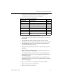
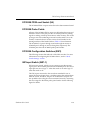
Manual Contents
This manual covers the following topics.
•
Chapter 1, “Cable Hardware”provides specific information about
using the MultiLINX™ Cable, Parallel Cable III and XChecker™
cables to configure CPLDs and FPGAs.
•
Chapter 2, “MutliLINX™ Cable”provides detailed information
about the MultiLINX Cable, Flying Wires and Operation Modes.
•
Chapter 3, “FPGA Design Demonstration Board”describes the
function and operation of the FPGA Demonstration Board.
Hardware User Guide — 3.1i
i
Hardware User Guide
•
Chapter 4, “CPLD Design Demonstration Board”describes the
function and operation of this board, which is used for demonstrating the In-system Programming (ISP) capabilities of the
XC9500 CPLD family.
•
“Glossary”defines all the terms you should understand to use
Xilinx Hardware.
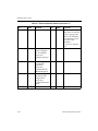
Additional Resources
For additional information, go to http://support.xilinx.com.
The following table lists some of the resources you can access from
this Web site. You can also directly access these resources using the
provided URLs.
Resource
Description/URL
Tutorials
Tutorials covering Xilinx design flows, from design entry to verification
and debugging
http://support.xilinx.com/support/techsup/tutorials/
index.htm
Answers
Database
Current listing of solution records for the Xilinx software tools
Search this database using the search function at
http://support.xilinx.com/support/searchtd.htm
Application
Notes
Descriptions of device-specific design techniques and approaches
http://support.xilinx.com/apps/appsweb.htm
Data Book
Pages from The Programmable Logic Data Book, which contain devicespecific information on Xilinx device characteristics, including readback,
boundary scan, configuration, length count, and debugging
http://support.xilinx.com/partinfo/databook.htm
Xcell Journals
Quarterly journals for Xilinx programmable logic users
http://support.xilinx.com/xcell/xcell.htm
Technical Tips Latest news, design tips, and patch information for the Xilinx design
environment
http://support.xilinx.com/support/techsup/journals/
index.htm
ii
Xilinx Development System
Conventions
This manual uses the following conventions. An example illustrates
each convention.
Typographical
The following conventions are used for all documents.
•
Courier font indicates messages, prompts, and program files
that the system displays.
speed grade: - 100
•
Courier bold indicates literal commands that you enter in a
syntactical statement. However, braces “{ }” in Courier bold are
not literal and square brackets “[ ]” in Courier bold are literal
only in the case of bus specifications, such as bus [7:0].
rpt_del_net=
Courier bold also indicates commands that you select from a
menu.
File → Open
•
Italic font denotes the following items.
♦
Variables in a syntax statement for which you must supply
values
edif2ngd design_name
♦
Hardware User Guide — 3.1i
References to other manuals
iii
Hardware User Guide
See the Development System Reference Guide for more information.
♦
Emphasis in text
If a wire is drawn so that it overlaps the pin of a symbol, the
two nets are not connected.
•
Square brackets “[ ]” indicate an optional entry or parameter.
However, in bus specifications, such as bus [7:0], they are
required.
edif2ngd [option_name] design_name
•
Braces “{ }” enclose a list of items from which you must choose
one or more.
lowpwr ={on|off}
•
A vertical bar “|” separates items in a list of choices.
lowpwr ={on|off}
•
A vertical ellipsis indicates repetitive material that has been
omitted.
IOB #1: Name = QOUT’
IOB #2: Name = CLKIN’
.
.
.
•
A horizontal ellipsis “….” indicates that an item can be repeated
one or more times.
allow block block_name loc1 loc2locn;
Online Document
The following conventions are used for online documents.
•
iv
Red-underlined text indicates an interbook link, which is a crossreference to another book. Click the red-underlined text to open
the specified cross-reference.
Xilinx Development System
•
Hardware User Guide
Blue-underlined text indicates an intrabook link, which is a crossreference within a book. Click the blue-underlined text to open
the specified cross-reference.
v
Hardware User Guide
vi
Xilinx Development System
Contents
About This Manual
Manual Contents ............................................................................ i
Additional Resources ..................................................................... ii
Conventions
Typographical................................................................................. iii
Online Document ........................................................................... iv
Chapter 1
Cable Hardware
Cable Overview.............................................................................. 1-1
Selecting a Cable...................................................................... 1-1
MultiLINX Cable................................................................... 1-1
Parallel Cable ...................................................................... 1-2
XChecker Cable................................................................... 1-2
Software Support ...................................................................... 1-2
Cable Limitations ...................................................................... 1-3
XChecker Hardware Drawbacks.......................................... 1-3
MultiLINX Hardware Advantages......................................... 1-3
Previous Cable Versions ..................................................... 1-4
Cable Baud Rates .......................................................................... 1-5
MultiLINX Cable and Flying Leads ................................................. 1-5
External Power for the MultiLINX Cable......................................... 1-7
Parallel Cable III............................................................................. 1-8
Flying Leads.............................................................................. 1-9
Configuring CPLDs With the Parallel Cable III.......................... 1-11
Configuring FPGAs With the Parallel Cable III ......................... 1-13
XChecker Cable ............................................................................. 1-15
Flying Leads.............................................................................. 1-15
XChecker Baud Rates .............................................................. 1-18
Configuring CPLDs With the XChecker Cable.......................... 1-18
Configuring FPGAs With the XChecker Cable.......................... 1-19
Hardware User Guide — 3.1i
vii
Hardware User Guide
Chapter 2
Pin Connection Considerations................................................. 1-20
Cable Connection Procedure.................................................... 1-21
Setting Up The Cable................................................................ 1-22
Download Cable Schematic ........................................................... 1-22
MutliLINX™ Cable
Additional MultiLINX Documentation.............................................. 2-1
MultiLINX Platform Support............................................................ 2-2
MultiLINX Flying Wires................................................................... 2-2
MultiLINX Baud Rates............................................................... 2-8
MultiLINX Power Requirements................................................ 2-8
External Power for the MultiLINX Cable ................................... 2-8
Device Configuration Modes .......................................................... 2-10
Downloading Configuration Data .............................................. 2-10
Slave Serial Mode (XC3000) ............................................... 2-10
Downloading Configuration Data or Verification of Data........... 2-12
SelectMAP Mode (Virtex).......................................................... 2-12
Downloading Configuration Data .............................................. 2-13
JTAG Mode (XC9000, Virtex, Spartan, XC5200, XC4000) . 2-13
Downloading/Verification of Configuration Data ....................... 2-14
Slave Serial Mode (XC3000) ............................................... 2-14
Slave Serial Mode (Spartan, XC5200, XC4000).................. 2-15
SelectMAP Mode (Virtex) .................................................... 2-16
SelectMAP Mode (Virtex with Asynchronous Probing)........ 2-17
JTAG Mode (XC9000, Virtex, Spartan, XC5200, XC4000) . 2-18
Verification of Configuration Data Only..................................... 2-19
Verification of Configuration Data Only (Spartan, XC5200, XC4000)
2-19
Synchronous Probing................................................................ 2-21
Slave Serial Mode (XC3000) ............................................... 2-21
Chapter 3
FPGA Design Demonstration Board
Demonstration Board Overview ..................................................... 3-1
Device Support ......................................................................... 3-1
Download Cable Support .......................................................... 3-2
Software Support ...................................................................... 3-2
Board Features ......................................................................... 3-2
General Components ..................................................................... 3-4
+5 V Power Connector (J9) ...................................................... 3-5
Unregulated Power Input (J12) ................................................. 3-6
+5 V Regulator Option (U3) ...................................................... 3-6
viii
Xilinx Development System
Contents
RESET Pushbutton (SW4)........................................................ 3-7
SPARE Pushbutton (SW5) ....................................................... 3-7
PROG Pushbutton (SW6) ......................................................... 3-7
Eight General-Purpose Input Switches (SW3).......................... 3-7
Seven-Segment Displays (U6, U7, U8) .................................... 3-9
LED Indicators (D1-D8, D9-D16) .............................................. 3-10
I/O Line Connections ................................................................ 3-11
Optional Crystal Oscillator (Y1)................................................. 3-11
Prototype Area .......................................................................... 3-11
XC4003E Components .................................................................. 3-12
XC4003E FPGA and Socket (U5)............................................. 3-13
XC4003E Probe Points ............................................................. 3-14
XC4003E Configuration Switches (SW2).................................. 3-14
PWR-Power (SW2–1) ............................................................... 3-14
MPE-Multiple Program Enable (SW2-2) ................................... 3-14
SPE-Single Program Enable (SW2-3) ...................................... 3-14
M0, M1, M2-Mode Pins (SW2-4,5,6) ........................................ 3-15
RST-Reset (SW2-7).................................................................. 3-15
INIT-Initialize (SW2-8)............................................................... 3-15
XChecker/Parallel Cable III Connector J2 ................................ 3-15
Jumper J7 and Tiepoints J10 (1-3) ........................................... 3-17
Serial PROM Socket (U2) ......................................................... 3-17
XC3020A Components .................................................................. 3-18
XC3020A FPGA and Socket (U4)............................................. 3-19
XC3020A Probe Points ............................................................. 3-19
XC3020A Configuration Switches (SW1).................................. 3-19
INP-Input Switch (SW1-1)......................................................... 3-19
MPE-Multiple Program Enable (SW1-2) ................................... 3-20
SPE-Single Program Enable (SW1-3) ...................................... 3-20
M0, M1, M2-Mode Pins (SW1-4,5,6) ........................................ 3-20
MCLK-Master Clock (SW1-7) ................................................... 3-21
DOUT-Data Out (SW1–8) ......................................................... 3-21
XChecker/Parallel Cable III Connector J1 ................................ 3-21
Serial PROM Socket (U1) ......................................................... 3-23
Relaxation Oscillator Components (R1 C5, R2 C6).................. 3-23
Mode Switch Settings..................................................................... 3-25
Demonstration Board Operation ................................................... 3-30
Demonstration Designs............................................................. 3-30
Design Downloading Checklist ................................................. 3-31
Loading with a Configuration PROM......................................... 3-32
Starting Hardware Debugger .................................................... 3-33
Tutorials .................................................................................... 3-34
Hardware User Guide
ix
Hardware User Guide
Chapter 4
CPLD Design Demonstration Board
Demonstration Board Overview ..................................................... 4-1
Software and Download Cable Support.................................... 4-1
Printed Circuit Board (PCB) ...................................................... 4-2
Prototyping Area ....................................................................... 4-2
Power Supply............................................................................ 4-2
Demonstration Board Schematics.................................................. 4-3
Foundation Design Tutorial ............................................................ 4-5
Example I: Schematic Design Entry.......................................... 4-5
Schematic With VHDL Macro Design .................................. 4-6
Example 2: VHDL Design Entry................................................ 4-7
x
Xilinx Development System
Chapter 1
Cable Hardware
This chapter gives specific information about connecting and using
the In System Programming (ISP) Download Cables. These cables can
be used to configure FPGAs and CPLDs. The following sections are in
this chapter.
•
“Cable Overview”
•
“Cable Baud Rates”
•
“MultiLINX Cable and Flying Leads”
•
“External Power for the MultiLINX Cable”
•
“Parallel Cable III”
•
“XChecker Cable”
•
“Download Cable Schematic”
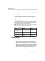
Cable Overview
There are three cables available for use with Xilinx Alliance and
Foundation software. The MultiLINX Cable supports USB and RS232 serial port connections, the Parallel Cable III supports parallel
port, and the XChecker Cable supports RS-232 serial ports.
Selecting a Cable
Determine the most suitable cable to use, depending upon the tasks
you wish to perform.
MultiLINX Cable
You can use the MultiLINX Cable to download and readback your
Xilinx programmable logic device. The MultiLINX cable hardware
Hardware User Guide — 3.1i
1-1
Hardware User Guide
communicates with the host through the Universal Serial Bus (USB)
port or an RS-232 interface. The additional flying wires support the
various configuration modes available on Xilinx configuration cables.
Parallel Cable
The Parallel Cable III connects to the parallel printer port of a PC.
This cable can be used to download and readback configuration data
via JTAG.
XChecker Cable
The XChecker Cable connects to the serial port of both workstations
and PCs. This cable can be used for design verification and debugging in addition to data download and readback.
Note Always set the configuration mode of the device being configured to slave serial, no matter which cable you use.
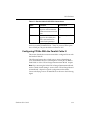
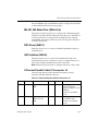
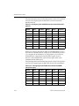
Table 1-1 Cable Support
Name
Function
Platform
MultiLINX Cable
(Model: DLC6)
Download, Readback
PC,
Workstation
Parallel Cable III
(Model: DLC5)
Download
Only
PC
XChecker Cable
(Model: DLC4)
Download, Readback,
and Debug
PC,
Workstation
Software Support
Make sure that you use the appropriate configuration software for
your device type.
1-2
•
JTAG Programmer Software is used to configure FPGAs and
CPLDs, and supports both the XChecker and the Parallel Cable
III. This is a GUI based program.
•
Hardware Debugger Software supports the MultiLINX, Parallel,
and XChecker download cables and is used for FPGA configuration. This is a GUI based program with a waveform viewer.
Xilinx Development System
Cable Hardware
Note All Hardware Debugger Software versions prior to 2.1i do
not support the MultiLINX Cable. The Hardware Debugger Software only supports the MultiLINX Cable in the 2.1i release.
For specific information on using the download cables with the Hardware Debugger Software, see the Hardware Debugger Guide. Consult
the JTAG Programmer Guide for more information about using this
software.
Cable Limitations
The MultiLINX Cable is compatible in supporting Readback for all
the FPGAs supported by the XChecker Cable. In addition to the
supporting legacy devices, the MultiLINX Cable supports the devices
that were not supported by the XChecker Cable. Supported devices
include those devices in the 4000E, 4000XL, and SPARTAN families
whose bitfile size is more than 256K bits. The MultiLINX Cable will
also support readback for the new Virtex family.
Note Debug is not available with the MultiLINX Cable when using
the Hardware Debugger Software in the 2.1i Xilinx release version.
XChecker Hardware Drawbacks
Following are the limitations of the XChecker cable.
•
Cannot support readback for devices whose bitfile size is more
than 256K bits.
•
Only supports RS-232.
•
Has less user control (only 2 sets of 8 flying wires each).
MultiLINX Hardware Advantages
Following are the advantages of the MultiLINX cable.
Hardware User Guide
•
Fast download, readback & verify using the USB port.
•
More configuration modes are supported.
•
Supports both RS-232 ports and USB ports.
•
Compatible with the currently supported devices for Readback &
Verify.
•
Supports new devices that are not supported by XChecker due to
RAM size limitation.
1-3
Hardware User Guide
•
Works at multiple supply voltages (5 V, 3.3 V, and 2.5 V).
•
Supports JTAG configuration for all Xilinx devices.
•
Supports SelectMAP configuration mode for Virtex.
Previous Cable Versions
This section details considerations for using previous download
cables with the Hardware Debugger Software.
You can use Hardware Debugger software with all previous parallel
and serial download cables. However, these previous cables can only
be used to download a configuration bitstream, they cannot be used
for readback.
If you do use Hardware Debugger with a previous parallel or serial
download cable version, keep the following points in mind.
•
Previous versions of the download cable were made to download
XC3000 and XC2000 designs, not XC4000 designs. The basic limitation of the previous cables is that they do not have a PROG pin
to initiate a re-program in XC4000 devices. They also do not have
an INIT pin to check for Cyclical Redundancy Check (CRC)
errors during configuration.
Note To use a parallel download cable prior to the Parallel Cable
III to download designs to the XC4000 family devices, you must
manually toggle the PROG pin to low. PROG is active when it is
low. (The Parallel Cable III has a wire for the PROG pin.)
•
Previous download cables do not support readback or verification.
•
For the PC, the download cable is a parallel cable, requiring
connection to the parallel port. (The XChecker cable is serial.)
There are only two situations when you might prefer using previous
download cables instead of the XChecker Cable or MultiLINX Cable.
1-4
•
You have circuit boards with header connectors keyed to match
the previous cable headers. However, you could use the
XChecker Cable with its flying lead connectors. Simply match the
labeled flying leads to the equivalent signals on your system.
•
You have circuit boards where power consumption is a critical
factor. (The XChecker Cable requires about 100 mA at 5 V and the
MultiLINX Cable requires about 300mA at 5 V, 500mA at 3.3 V,
Xilinx Development System
Cable Hardware
and 750mA at 2.5 V; the Parallel Cable used with PCs draws less
power from the target LCA board.) In such cases, you may use
the Hardware Debugger software to download the bitstream.
Cable Baud Rates
The supported Baud Rates for the MultiLINX, Parallel and XChecker
Cables are shown in the following table.
Table 1-2 Cable Baud Rates
Cable
PC
Workstation
MultiLINX Cable
(USB)
USB is currently not
1M-12M (Currently
USB is supported only supported on WorkStations.
on Win98.)
MultiLINX Cable
(RS-232)
9600, 19200, 38400,
and 57600
9600, 19200, and 38400
Parallel Cable
9600
Not supported on
WorkStations.
XChecker Cable
9600, 19200, 38400,
and 115200
9600, 19200, and 38400
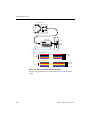
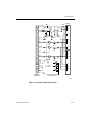
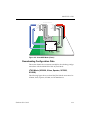
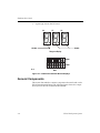
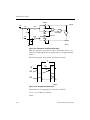
MultiLINX Cable and Flying Leads
The MultiLINX Cable is a device for configuring and verifying Xilinx
FPGAs and CPLDs.
The MultiLINX Cable is shipped with four sets of flying lead wires. A
USB Cable and RS-232 Cable (with adapter) are also supplied.
For detailed information on the MultiLINX Flying Wires supported
modes, refer to the “MutliLINX™ Cable” chapter.
The following figure shows the MultiLINX Cable hardware and
flying lead connection wires.
Hardware User Guide
1-5
Hardware User Guide
RT
RT(TDO)
TRIG
R
TDI
TCK
TMS
CLK1-IN
CLK2-OUT
TM
CS0(CS)
CS1
CS2
CLK2-IN
CLK2-OUT
WS
RS(RDWR)
RDY/BUSY
MultiLINX
TM
PWR
GND
CCLK
DONE
DIN
PROG
INIT
RST
2 1 STATUS
43
D0
D1
D2
D3
D4
D5
D6
D7
Flying Lead Connector Set #1
PWR
GND
CCLK
DONE(D/P)
DIN
PROG
INIT
RST
1
MultiLINX
TM
Flying Lead Connector Set #2
RT
RD(TDO)
TRIG
TDI
TCK
TMS
CLK1-IN
CLK1-OUT
2
MultiLINX
TM
Flying Lead Connector Set #3
D0
D1
D2
D3
D4
D5
D6
D7
3
MultiLINX
4
TM
Flying Lead Connector Set #4
CS0(CS)
CS1
CS2
CLK2-IN
CLK2-OUT
WS
RS(RDWR)
RDY/BUSY
X8926
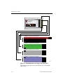
Figure 1-1 MultiLINX Cable and Flying Lead Connectors
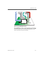
The following figure shows the top and bottom view of the MultiLINX Cable.
1-6
Xilinx Development System
Cable Hardware
Top View
RT
RT(TDO)
TRIG
R
TDI
TCK
TMS
CLK1-IN
CLK2-OUT
TM
CS0(CS)
CS1
CS2
CLK2-IN
CLK2-OUT
WS
RS(RDWR)
RDY/BUSY
PWR
GND
CCLK
DONE
DIN
PROG
INIT
RST
2 1 STATUS
43
D0
D1
D2
D3
D4
D5
D6
D7
Bottom View
CAUTION
R
RS-232
SENSITIVE
ELECTRONIC
DEVICE
TM
CE
Model: DLC6
Power: 2.5V
0.8A to 5V
Serial: UC-000074
Made in U.S.A
0.4A Typ.
USB
UNIVERSAL SERIAL BUS
X8927
Figure 1-2 MultiLINX Cable
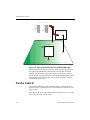
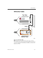
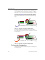
External Power for the MultiLINX Cable
The MultiLINX Cable gets its power from the User’s circuit board an
extended power supply. The cable power does not come from the
USB port (nor the RS-232 port). The red (PWR) and black (GND)
wires from Flying Wire Set #1 are connected to the VCC (red wire)
and Ground (black wire) lines of the circuit board that is powering
the Xilinx device. The external power for the MultiLINX Cable is
shown in the following figure.
Hardware User Guide
1-7
Hardware User Guide
MultiLINX Connectors
43
CS0 (CS)
CS1
CS2
CLK2-IN
CLK2-OUT
WS
RS (RDWR)
D0
D1
D2
D3
D4
D5
D6
D7
RDY/BUSY
RT
RD (TDO)
TRIG
PWR
GND
CCLK
DONE (D / P)
DIN
PROG
INIT
RST
TDI
TCK
TMS
CLK1-IN
CLK1-OUT
External DC Power
Supply
21
Circuit Board
XILINX device
VCC
GND
VCC
NOTE: Ground of Circuit Board, Power Supply and MultiLINX Cable must be tied together.
X8928
Figure 1-3 Optional External Power for the MultiLINX Cable
When using an external power supply, make sure that the ground of
the supply, the MultiLINX Cable and the circuit board are all tied
together. An advantage of the external DC power supply is that no
power is taken away from the circuit board and the MultiLINX Cable
can remain powered up and does not get powered down when the
circuit board power is off.
Parallel Cable III
The Parallel Cable III is a cable assembly which contains a buffer to
protect your PC’s parallel port and a set of headers to connect to your
target system.
The cable can be used with a single CPLD or FPGA device, or several
devices connected in a daisy chain.
1-8
Xilinx Development System
Cable Hardware
The transmission speed of the this cable is determined solely by the
speed at which the host PC can transmit data through its parallel port
interface.
Using the Parallel Cable III requires a PC equipped with an AT
compatible parallel port interface and a DB25 standard printer
connector.
Flying Leads
This cable is shipped with two sets of flying leads, one for FPGAs and
one for CPLDs. The CPLD leads are labelled “JTAG” and the FPGA
leads are labelled “FPGA”.
Each flying lead has a 9-pin (6 signals, 3 keys) header connector on
one end. This connector fits onto one of the two cable headers. These
header connectors are keyed to assure proper orientation to the cable
assembly.
On the other end of each flying lead are six individual wires with
female connectors. The female connectors fit onto standard 0.025 inch
square male pins.
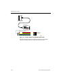
As an example, the following figure shows the Parallel Cable III and
its FPGA flying lead wires.
Hardware User Guide
1-9
Hardware User Guide
DB25 Plug Connector
Parallel Cable III
FPGA Flying Lead Connector
FPGA
VCC
GND
CCLK
Connections to
Target System
D/P
DIN
PROG
X8325
Figure 1-4 Parallel Cable III and FPGA Flying Leads
The following figure shows top and bottom views of the Parallel
Cable III, including the FPGA and JTAG (CPLD) headers.
1-10
Xilinx Development System
Cable Hardware
Parallel Cable III
Top View
JTAG Header
TCK
SENSITIVE
ELECTRONIC
Made in U.S.A
DEVICE
TDO
TDI
TMS
VCC
GND
CCLK
FPGA
VCC
GND
CAUTION
JTAG
Parallel Cable III
Model DLC5
Power 5V 10mA Typ.
Serial JT - 1 2 3 4 5
D/P
DIN
PROG
Bottom View
X7252
Figure 1-5 Parallel Cable III
Note The plastic cover of the Parallel Cable III is grey, while the
XChecker Cable is beige.
Configuring CPLDs With the Parallel Cable III
When connecting the CPLD flying leads for configuration, make sure
to use the “JTAG” header. The following figure shows the connections between the Parallel Cable III CPLD flying leads and a target
system.
Hardware User Guide
1-11
Hardware User Guide
VCC
GND
TDO
TCK
JTAG
VCC
GND
TCK
TDO
TDI
TMS
TCK
TCK
TDI TDO
TDI
TMS
TDI TDO
TCK
TDI TDO
TMS
TMS
TMS
JTAG Flying Lead Connector
Target System
X83
Figure 1-6 Parallel Cable III Connections to CPLD Device
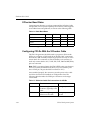
The following table describes the pin functions and connections for
configuring CPLDs with the Parallel Cable III.
Table 1-3 Parallel Cable III CPLD Pin Connections
1-12
Name
Function
Connections
VCC
Power – Supplies VCC (5
V, 10 mA, typically) to the
cable.
To target system VCC
GND
Ground – Supplies ground To target system
reference to the cable.
ground
TCK
Test Clock – Drives the test Connect to system TCK
logic for all devices on a
pin.
JTAG chain.
TDO
Test Data Output – data
from the target system is
read at this pin.
Connect to system
TDO pin.
Xilinx Development System
Cable Hardware
Table 1-3 Parallel Cable III CPLD Pin Connections
Name
Function
Connections
TDI
Connect to system TDI
Test Data Input – this
signal is used to transmit
pin.
serial test instructions and
data.
TMS
Test Mode Select – this
signal is decoded by the
JTAG state machine to
control test operations.
Connect to system TMS
pin.
Note TRST is an optional pin in the JTAG (IEEE 1149.1) specification,
and is not used by XC9500 CPLDs. If any of your non-Xilinx parts
have a TRST pin, the pin should be connected to VCC
Configuring FPGAs With the Parallel Cable III
This section details the connections needed to configure FPGAs with
the Parallel Cable III.
The following figures show which pins to connect, depending on
your chosen FPGA device. For descriptions of each pin, see Table 36and Table 3-7 of the “FPGA Design Demonstration Board” chapter.
Note If you are using the Xilinx FPGA Design Demonstration Board,
see the “Mode Switch Settings” section of the “FPGA Design Demonstration Board” chapter for specific configuration information.
Connect the flying wires to XC4000 FPGAs as shown in the following
figure.
Hardware User Guide
1-13
Hardware User Guide
VCC
GND
FPGA
VCC
GND
CCLK
D/P
DIN
PROG
CCLK
DONE
DIN
PROG
XC4000 FPGA in Slave Serial Mode
Parallel Cable III with FPGA Flying Leads
Target System
X8326
Figure 1-7 Parallel Cable III Connections to XC4000 Device
To configure XC3000 FPGAs, the PROG wire is not used as shown in
the following figure. In both cases the FPGA must be in the Serial
Slave Mode.
VCC
GND
FPGA
VCC
GND
CCLK
D/P
DIN
CCLK
D/P
DIN
XC3000 FPGA in Slave Serial Mode
PR
O
G
Not Used
Parallel Cable III with FPGA Flying Leads
Target System
X8327
Figure 1-8 Parallel Cable III Connections to XC3000 Device
Note If you are using the Xilinx FPGA Demonstration Board, see the
“Mode Switch Settings” section of the “FPGA Design Demonstration
Board” chapter for specific configuration information.
1-14
Xilinx Development System
Cable Hardware
XChecker Cable
The XChecker hardware consists of a cable assembly with internal
logic, a test fixture, and a set of headers to connect the cable to your
target system. The cable can be used with a single FPGA or CPLD, or
several devices connected in a daisy chain.
Using the XChecker hardware requires either a standard DB-9 or DB25 RS-232 serial port. If you have a different serial port connection,
you need to provide a DB-9/DB-25 adapter.
Flying Leads
The XChecker Cable is shipped with two sets of flying lead wires. The
flying lead connectors have a nine position header connector on one
end. The other end has eight individual wires with female connectors
that fit onto standard 0.025 inch square male pins.
You need appropriate pins on the target system for connecting to the
download cable. The “XChecker Baud Rates” section details the
necessary pins.
The following figure shows the XChecker Cable hardware and flying
lead connection wires.
Hardware User Guide
1-15
Hardware User Guide
Connection to Host Computer
DB25 Adapter
DB9 Socket Connector
GND
+5V
XChecker Cable
Test Fixture
(Enlarged to
show plugs)
Header 2
Header 1
Flying Lead Connector 1
VCC
GND
Connections to
Target System
CCLK
D/P
DIN
PROG
INIT
RST
Flying Lead Connector 2
RT
RD
TRIG
Connections to
Target System
TDI
TCK
TMS
CLK1
CLK0
X8322
Figure 1-9 XChecker Cable and Flying Leads
The following figure shows top and bottom views of the XChecker
Cable.
1-16
Xilinx Development System
Cable Hardware
XChecker Cable
Top View
Header 2
Model : DLC4
CAUTION
Power : 5V 100mA Typ.
Serial: DL - 1 2 3 4 5
Made in U.S.A
RT
RD
TRIG
TDI
TCK
SENSITIVE TMS
ELECTRONIC CLKI
DEVICE CLKO
Header 1
VCC
GND
CCLK
D/P
DIN
PROG
INIT
RST
Bottom View
X7249
Figure 1-10 XChecker Cable
Note The plastic cover of the XChecker Cable is beige, while the
cover for the Parallel Cable III is grey. The flying lead wires are keyed
to fit into the appropriate cable header. Use Header 1 for FPGAs and
Header 2 for CPLDs.
Hardware User Guide
1-17
Hardware User Guide
XChecker Baud Rates
Communication between your host system and the XChecker Cable
is dependent on host system capability. The XChecker Cable supports
several Baud rates and platforms, as shown in the following table.
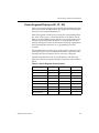
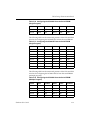
Table 1-4 Valid Baud Rates
Platform
9600
19200
38400
115.2K
IBM® PC
X
X
X
X
NEC PC
X
SUN®
X
X
X
HP 700
X
X
X
X
X indicates applicable baud rate
Configuring CPLDs With the XChecker Cable
The JTAG Programmer should be used to program in JTAG mode.
When you configure a CPLD with the XChecker Cable, connections
between the cable assembly and the target system use only six of the
sixteen leads. For connection to JTAG boundary-scan systems you
need only ensure that the VCC, GND, TDI, TCK, TMS and RD (TDO)
pins are connected.
Note TRST is an optional pin in the JTAG (IEEE 1149.1) specification,
and is not used by XC9500 CPLDs (If any of your non-Xilinx parts
have a TRST pin, the pin should be connected to VCC).
Once installed properly, the connectors provide power to the cable
and allow download and readback of configuration data. The
following table describes the CPLD pin connections to the target
circuit board.
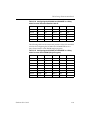
Table 1-5 XChecker Cable Pin Connections for CPLDs
1-18
Name
Function
Connections
VCC
Power – Supplies VCC (5 To target system VCC
V, 100 mA, typically) to the
cable
GND
Ground – Supplies ground To target system
reference to the cable
ground
Xilinx Development System
Cable Hardware
Table 1-5 XChecker Cable Pin Connections for CPLDs
Name
Function
Connections
RD (TDO)
Read Data – Reads back
data from the target
system is read at this pin.
Connect to system
TDO pin.
TDI
Test Data In – this signal is Connect to system TDI
used to transmit serial test pin.
instructions and data.
TCK
Test Clock – this clock
drives the test logic for all
devices on boundary-scan
chain.
Connect to system TCK
pin.
TMS
Test Mode Select – this
signal is decoded by the
TAP controller to control
test operations.
Connect to system TMS
pin.
CLKI
Not used.
Unconnected.
CLKO
Not used.
Unconnected.
CCLK
Not used.
Unconnected.
D/P
Not used.
Unconnected.
DIN
Not used.
Unconnected.
PROG
Not used.
Unconnected.
INIT
Not used.
Unconnected.
RST
Not used.
Unconnected.
RT
Not used.
Unconnected.
TRIG
Not used.
Unconnected.
Configuring FPGAs With the XChecker Cable
This section details the connections needed to configure FPGAs with
the XChecker Cable.
Note If you are using the Xilinx FPGA Design Demonstration Board,
see the “Demonstration Board Operation” section of the “FPGA
Design Demonstration Board” chapter for specific configuration
information.
Hardware User Guide
1-19
Hardware User Guide
The following figures show which pins to connect, depending on
your chosen FPGA device. For descriptions of each pin, see Table 36and Table 3-7 of the “FPGA Design Demonstration Board” chapter.
Use Header 1 (see Figure 1-9) to connect the XChecker Cable to the
target system for configuring FPGAs. When configuring XC4000
FPGAs, the RST (Reset) wire is not used as shown in the following
figure.
VCC
GND
VCC
GND
CCLK
D/P
DIN
PROG
INIT
CCLK
DONE
DIN
PROG
INIT
XC4000 FPGA in Slave Serial Mode
R
ST
Not Used
XChecker with Header 1
Target System
X8323
Figure 1-11 XChecker Connections to XC4000 Device
To configure XC3000 FPGAs, the PROG wire is not used. This is
shown in the following figure. In both cases, the FPGA must be in the
Serial Slave Mode.
VCC
GND
VCC
GND
CCLK
D/P
DIN
INIT
RST
CCLK
D/P
DIN
INIT
RESET
PR
O
G
XC3000 FPGA in Slave Serial Mode
Not Used
XChecker with Header 1
Target System
X8324
Figure 1-12 XChecker Connections to XC3000 Device
Pin Connection Considerations
The following adjustments will make the process of connecting and
downloading easier.
1-20
Xilinx Development System
Cable Hardware
•
Provide appropriate pins on your printed circuit board for your
device type.
•
Place pins on board so that flying leads can reach them. The
flying leads that are shipped with the cable are six inches long.
While pins may be a couple inches apart, do not have any two
pins more than six inches apart.
•
Keep header pins on your board a minimum of 0.10 inches apart.
Cable Connection Procedure
The following steps are required for download cable operation.
1.
Connect the cable to your host system. Make sure to use the
appropriate port and adapter, if necessary.
2.
Connect the cable to your target system or demonstration board.
Always power up the host system before the target system. The
power for the drivers is derived from the target system.
3.
Connect the cable’s GND wire to the corresponding signal on the
target board. Next, connect VCC to the +5 V on the target board.
4.
Connect the appropriate pins for device configuration.
5.
Power up the target system.
Cable protection ensures that the host system port cannot be
damaged through normal cable operation. For increased safety,
please check that the power to the host computer is on before the
target system is powered up.
6.
Start the appropriate Xilinx software package and configure your
device. The JTAG Programmer Software and Hardware
Debugger Software will automatically identify the download
cables when correctly connected. If you need to set up the cable
manually, see the following section.
Note The download cables will not operate if the target system‘s
power is turned off before or during software operations. Make
certain that this power connection is on and stable. Your system’s
power should be on during ISP operations. When powering
down, turn off the target demonstration board first, and then the
host machine.
Hardware User Guide
1-21
Hardware User Guide
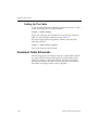
Setting Up The Cable
If you are using the Hardware Debugger Software and a PC as a host
system, manually select your cable as follows.
Output > Cable Setup
Select your cable type, then click OK. If you are using the XChecker
cable, you may also select a BAUD rate. See Table 1-4.
If you are using the JTAG Programmer software, select the cable
manually as follows.
Output > Cable Auto Connect
Select your cable type, then click OK.
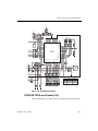
Download Cable Schematic
The following figure is an internal schematic of the Parallel Cable III.
You must use the recommended lengths for parallel cables. Xilinx
cables are typically six feet (approximately two meters) in length
between the connector and active circuitry. Keep the wires between
the headers and target system as short as possible.
1-22
Xilinx Development System
Cable Hardware
JTAG Header
1N5817
15
1N5817
VCC SENSE
100
100
13
3
DONE
100
2
U2
5.1K
1
2
14
U2
7
14
U1
7
GND
3
TCK
100
5
100pF
PROG
DIN
5
6
U1
4
300
TMS_IN
12
TDO
7
TDI
8
11
U1
13
300
6
100
100pF
4
2
4
3
300
2
VCC
U1
1
6
1
.01uF
1K
9
TMS
1
VCC
2
GND
3
CCLK
100
100pF
5
CTRL
300
3
9
CLK
300
8
U1
10
100
100pF
20
25
8
11
12
4
GND
6
GND
U2
5
4
D6
BUSY
PE
SHIELD
DB25 MALE
CONNECTOR
U1 = 74HC125
U2 = 74HC125
8
U2
U2
6
D/P
7
DIN
8
PROG
9
10
11
5
12
13
9
Serial JT -05000 and above
for EPP parallel ports.
FPGA Header
X7557
Figure 1-13 Parallel Cable III Schematic
Hardware User Guide
1-23
Hardware User Guide
1-24
Xilinx Development System
Chapter 2
MutliLINX™ Cable
The MultiLINX™ Cable is the next generation configuration and
readback tool for FPGA’s and CPLD’s. During the integration of
Xilinx programmable logic into your design, the MultiLINX Cable
can be used to troubleshoot your configuration setup, and diagnose
configuration problems associated with Xilinx programmable logic.
The MultiLINX Cable uses either a serial or USB port on a host
computer. Maximum throughput is available by using the USB interface.
This chapter contains the following sections.
•
“Additional MultiLINX Documentation”
•
“MultiLINX Platform Support”
•
“MultiLINX Flying Wires”
•
“Device Configuration Modes”
Additional MultiLINX Documentation
You can access the following mentioned application note with
descriptions of device-specific design techniques and approaches
from the support page at http://support.xilinx.com/
support/searchtd.htm.
The “Getting Started with the MultiLINX Guide” application note is a
quick reference to everything you need to know to use the MultiLINX
Cable.
•
Describes using a USB port, Mixed Voltage environments,
connections for all the supported Modes.
•
Describes how to setup a Prototype application for use with the
MultiLINX Cable.
Hardware User Guide— 3.1i
2-1
Hardware User Guide
•
Describes all the cables, their capabilities, and associated software tools.
MultiLINX Platform Support
The MultiLINX Cable supports the following platforms.
•
Win 95
•
Win 98
•
Win NT 4.0
•
Solaris 2.6
•
HP 10.2
Table 2-1 MultiLINX Support
Supported
Platforms
USB
Win 95
Win 98
RS-232
X
X
X
Win NT 4.0
X
Solaris 2.6
X
HP 10.2
X
X indicates applicable ports that can be used with the MultiLINX Cable on specified platforms.
MultiLINX Flying Wires
The MultiLINX Cable is shipped with four sets of flying lead wires.
The following figure shows these four sets of MultiLINX flying lead
connectors.
2-2
Xilinx Development System
MutliLINX™ Cable
MultiLINX
TM
Flying Lead Connector Set #1
PWR
GND
CCLK
DONE(D/P)
DIN
PROG
INIT
RST
1
MultiLINX
TM
Flying Lead Connector Set #2
RT
RD(TDO)
TRIG
TDI
TCK
TMS
CLK1-IN
CLK1-OUT
2
MultiLINX
TM
Flying Lead Connector Set #3
D0
D1
D2
D3
D4
D5
D6
D7
3
MultiLINX
TM
Flying Lead Connector Set #4
CS0(CS)
CS1
CS2
CLK2-IN
CLK2-OUT
WS
RS(RDWR)
4
RDY/BUSY
X8919
Figure 2-1 MultiLINX Flying Wires
The MultiLINX Flying wires are described in the following table.
Table 2-2 MultiLINX Pin Descriptions
Hardware User Guide
Signal Name
Function
PWR
Power — Supplies VCC to cable
(Works at multiple voltages 5V,
3.3V, and 2.5V).
GND
Ground — Supplies ground reference to cable.
2-3
Hardware User Guide
Table 2-2 MultiLINX Pin Descriptions
2-4
Signal Name
Function
CCLK
Configuration Clock — is the
configuration clock pin, and the
default clock for readback operation.
DONE (D/P)
Done/Program — represents the
D/~P pin for XC3000A/L and
XC3100A devices, and DONE for
XC4000, XC5200 and Spartan
devices. This pin indicates that
the configuration process is
complete for XC4000, XC5200,
and Spartan devices. This same
pin initiates a reconfiguration,
and indicates that the configuration process is complete on
XC3000 FPGAs.
DIN
Data In — Provides configuration
data to target system during
configuration and is tristated at
all other times.
PROG
Program — A Low indicates the
device is clearing its configuration memory.
Active Low signal to initiate the
configuration process.
INIT
Initialize — Initialization
sequencing pin during configuration (Indicates start of configuration).
A logical zero on this pin during
configuration indicates a data
error.
Xilinx Development System
MutliLINX™ Cable
Table 2-2 MultiLINX Pin Descriptions
Hardware User Guide
Signal Name
Function
RST
Reset —Pin used to reset internal
FPGA logic. Connection to this
pin is optional during configuration.
During configuration, a Low
pulse causes XC3000A devices to
restart configuration.
After configuration, this pin can
drive Low to reset target FPGA
internal latches and flip-flops.
RST is the active high for
XC4000/XC5200 devices.
RT
Read Trigger — Pin used to
initiate a readback of target
FPGA.
MultiLINX output. Hardware
Debugger provides
Low-to-High transition on RT to
initiate readback.
RD (TDO)
Read Data — MultiLINX input.
Hardware Debugger receives the
readback data through the RD
pin after readback is initiated.
Pin used to initiate a readback of
target FPGA.
TDO is for JTAG.
TRIG
System Trigger — MultiLINX
input
High on this pin signals the
MultiLINX electronics to initiate
a readback and causes the RT pin
to go High.
2-5
Hardware User Guide
Table 2-2 MultiLINX Pin Descriptions
2-6
Signal Name
Function
RD (TDO)
TDI
TCK
TMS
These pins are used for JTAG
Programmer device configuration.
The JTAG/boundary scan pins
function for FPGA and CPLD
JTAG operations.
CLKI-IN
Clock Input — Transmits your
system clock to the MultiLINX
electronic.
Clock must be between 120 kHz
and 10 MHz.
Connect this pin to target system
clock to synchronize the readback trigger with target system
clock.
CLK1-OUT
Clock Output — Drives target
system clock.
Clock can come from either the
CLKI-IN pin, or it can be internally generated by the MultiLINX Cable when CLKI-IN is
unconnected.
D0-D7
Data Bus — This pin is used for
Virtex SelectMAP Mode.
An 8 bit data bus supporting the
SelectMAP, and Express configuration modes.
CS0 (CS)
Chip Select — CS on the Virtex;
and CS0 on the XC4000 and
XC5200 FPGAs.
The CS0/CS pin represents a
chip select to the
CS1
Chip Select — The CS1 pin represents Chip Select to the XC4000
and XC5200 FPGAs during
configuration.
Xilinx Development System
MutliLINX™ Cable
Table 2-2 MultiLINX Pin Descriptions
Hardware User Guide
Signal Name
Function
CS2
Chip Select — The CS2 pin represents Chip Select to the XC3000
FPGA while using the Peripheral
configuration mode.
CLK2-IN
Clock Input — Transmits your
system clock to the MultiLINX
electronics.
Clock must be between 120 kHz
and 10 MHz.
Connect this pin to target system
clock to synchronize the readback trigger with target system
clock.
CLK2-OUT
Clock Output — Drives target
system clock.
Clock can come from either the
CLK2-IN pin, or it can be internally generated by the MultiLINX Cable when CLK2-IN is
unconnected
WS
Write Select — The WS pin represents Write Select control for the
Asynchronous Peripheral configuration mode on XC4000 and
XC5200 FPGAs.
2-7
Hardware User Guide
Table 2-2 MultiLINX Pin Descriptions
Signal Name
Function
RS (RDWR)
Read Select — The RS pin represents Read Select control for the
Asynchronous Peripheral configuration mode on XC4000 and
XC5200 FPGAs.
Read/Write — The RDWR pin is
used as an active high READ and
an active low WRITE control
signal to the Virtex FPGA.
RDY/BUSY
Busy Pin — Busy pin on the
Virtex; and RDY/Busy pin on the
XC3000, XC4000, and XC5200
FPGAs.
MultiLINX Baud Rates
Communication between your host system and the MultiLINX Cable
is dependent on host system capability. The MultiLINX Cable
supports several Baud rates.
With the USB interface, the MultiLINX Cable can run at 12 M bits/
sec. With the PC RS-232 interface, the MultiLINX Cable can run from
a 9600 baud rate to a 57.6 K baud rate.
MultiLINX Power Requirements
The MultiLINX Cable gets its power from the User’s circuit board.
The cable power does not come from the USB port (nor the RS-232
port). The red (PWR) and black (GND) wires from Flying Wire Set #1
are connected to the VCC (red wire) and Ground (black wire) lines of
the circuit board that is powering the Xilinx device.
The minimum input voltage to the cable is 2.5 V (.8 A). The maximum
input voltage is 5 V (.4 A).
External Power for the MultiLINX Cable
An optional method of powering the MultiLINX Cable is to use an
external DC power supply (not supplied) as shown in the following
2-8
Xilinx Development System
MutliLINX™ Cable
“Optional External Power for the MultiLINX Cable” figure.Typical
current requirements are: 300 mA at 2.5 V.
Note The voltage supplied to the MultiLINX Cable does not need to
be the same voltage powering the Xilinx device. The cable generates
its own voltages from the power supplied to it.
MultiLINX Connectors
43
CS0 (CS)
CS1
CS2
CLK2-IN
CLK2-OUT
WS
RS (RDWR)
D0
D1
D2
D3
D4
D5
D6
D7
RDY/BUSY
RT
RD (TDO)
TRIG
PWR
GND
CCLK
DONE (D / P)
DIN
PROG
INIT
RST
TDI
TCK
TMS
CLK1-IN
CLK1-OUT
External DC Power
Supply
21
Circuit Board
XILINX device
VCC
GND
VCC
NOTE: Ground of Circuit Board, Power Supply and MultiLINX Cable must be tied together.
X8928
Figure 2-2 Optional External Power for the MultiLINX Cable
When using an external power supply, make sure that the ground of
the supply, the MultiLINX Cable and the circuit board are all tied
together. An advantage of the external DC power supply is that no
power is taken away from the circuit board and the MultiLINX Cable
Hardware User Guide
2-9
Hardware User Guide
can remain powered up and does not get powered down when the
circuit board power is off.
Device Configuration Modes
The various MultiLINX device configuration modes supported for
each device are shown in the following table.
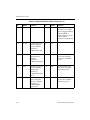
Table 2-3 MultiLINX Device Configuration Modes
Configuration Device
Mode
Virtex
Spartan
SelectMAP
X
Slave Serial
X
X
JTAG
X
X
XC9500
XC5200
XC4000
X
X
X
XC3000
X
X
Downloading Configuration Data
This section details the connections needed to download configuration data with the MultiLINX Cable.
Slave Serial Mode (XC3000)
The following figure shows in detail the Slave Serial Mode connections to a XC3000 device for Downloading Configuration Data.
2-10
Xilinx Development System
MutliLINX™ Cable
MultiLINX Connectors
43
CS0 (CS)
CS1
CS2
CLK2-IN
CLK2-OUT
WS
RS (RDWR)
RDY/BUSY
D0
D1
D2
D3
D4
D5
D6
D7
PWR
GND
RT
RD (TDO)
TRIG
CCLK
DONE (D / P)
DIN
PROG
INIT
RST
TDI
TCK
TMS
CLK1-IN
CLK1-OUT
21
Circuit Board
VCC
VCC
VCC
XILINX device
VCC
PWRDN
RESET
INIT
DIN
D/P
M0
M1
M2
CCLK
VCC
VCC VCC VCC
NOTE: Pull-up resistors are 4.7k ohm.
X8942
Figure 2-3 Slave Serial Mode (XC3000)
Slave Serial Mode (Virtex, Spartan, XC5200, XC4000)
The following figure shows in detail the Slave Serial Mode connections for Virtex, Spartan, XC5200, and XC4000 devices.
Hardware User Guide
2-11
Hardware User Guide
MultiLINX Connectors
43
CS0 (CS)
CS1
CS2
CLK2-IN
CLK2-OUT
WS
RS (RDWR)
D0
D1
D2
D3
D4
D5
D6
D7
RT
RD (TDO)
TRIG
PWR
GND
CCLK
DONE (D / P)
DIN
PROG
INIT
RST
TDI
TCK
TMS
CLK1-IN
CLK1-OUT
RDY/BUSY
(optional)
21
Circuit Board
VCC
VCC
XILINX device
User I/O: RESET
INIT
PROG
DIN
DONE
CCLK
M0
TMS
M1
TCK
VCC
M2
VCC
VCC VCC VCC
VCC
VCC
VCC
NOTE: Pull-up resistors are 4.7k ohm.
X8941
Figure 2-4 Slave Serial Mode (Virtex, Spartan, XC5200, XC4000)
Downloading Configuration Data or Verification of
Data
This section details the connections needed for downloading configuration data or the verification of data with the MultiLINX Cable.
SelectMAP Mode (Virtex)
The following figure shows in detail the SelectMAP Mode connections for Virtex devices.
2-12
Xilinx Development System
MutliLINX™ Cable
MultiLINX Connectors
43
CS0 (CS)
CS1
CS2
CLK2-IN
CLK2-OUT
WS
RS (RDWR)
D0
D1
D2
D3
D4
D5
D6
D7
PWR
GND
RT
RD (TDO)
TRIG
CCLK
DONE (D / P)
DIN
PROG
INIT
RST
TDI
TCK
TMS
CLK1-IN
CLK1-OUT
RDY/BUSY
21
Circuit Board
D7
D6
D5
D4
D3
D2
D1
D0
Vcco
BUSY/DOUT
INIT
PROG
WRITE
DONE
M0
M1
M2
CCLK
CS
XILINX device
VCC VCC
Vcco Vcco
NOTE: Pull-up resistors are 4.7k ohm.
X8940
Figure 2-5 SelectMAP Mode (Virtex)
Downloading Configuration Data
This section details the connections needed for downloading configuration data with the MultiLINX Cable in JTAG Mode.
JTAG Mode (XC9000, Virtex, Spartan, XC5200,
XC4000)
The following figure shows in detail the JTAG Mode connections for
XC9000, Virtex, Spartan, XC5200, and XC4000 devices.
Hardware User Guide
2-13
Hardware User Guide
MultiLINX Connectors
43
CS0 (CS)
CS1
CS2
CLK2-IN
CLK2-OUT
WS
RS (RDWR)
D0
D1
D2
D3
D4
D5
D6
D7
RT
RD (TDO)
TRIG
PWR
GND
CCLK
DONE (D / P)
DIN
PROG
INIT
RST
TDI
TCK
TMS
CLK1-IN
CLK1-OUT
RDY/BUSY
Circuit Board
XILINX device
(only XC4000 and SPARTAN)
(only XC4000 and SPARTAN)
21
VCC
TMS
TCK
INIT
TDI
PROG
M0
M1
M2
TDO
see data sheet of the device (if applicable)
NOTE: Pull-up resistors are 4.7k ohm.
X8939
Figure 2-6 JTAG Mode (XC9000, Virtex, Spartan, XC5200,
XC4000)
Downloading/Verification of Configuration Data
This section details the connections needed for downloading/verification of configuration data with the MultiLINX Cable in Slave Serial
Mode.
Slave Serial Mode (XC3000)
The following figure shows in detail the Slave Serial Mode connections for the XC3000 device.
2-14
Xilinx Development System
MutliLINX™ Cable
MultiLINX Connectors
System Clock (x)
System Clock (y)
(optional)
PWRDN
GCK (x)
GCK (y)
VCC
VCC
VCC
XILINX device
RESET
INIT
DIN
M0\RTRIG
VCC
21
M1/RDATA
Circuit Board
CCLK
DONE (D / P)
DIN
PROG
INIT
RST
TDI
TCK
TMS
CLK1-IN
CLK1-OUT
User I/O: TRIGGER
RDY/BUSY
PWR
GND
RT
RD (TDO)
TRIG
(optional- only used for probing)
D0
D1
D2
D3
D4
D5
D6
D7
M2
43
CS0 (CS)
CS1
CS2
CLK2-IN
CLK2-OUT
WS
RS (RDWR)
VCC
D/P
CCLK
VCC
VCC
VCC
NOTE: Pull-up resistors are 4.7k ohm.
X8938
Figure 2-7 Slave Serial Mode (XC3000)
Slave Serial Mode (Spartan, XC5200, XC4000)
The following figure shows in detail the Slave Serial Mode connections for Spartan, XC5200, and XC4000 devices.
Hardware User Guide
2-15
Hardware User Guide
MultiLINX Connectors
VCC
TCK
VCC
TMS
System Clock (x)
GCK (x)
System Clock (y)
(optional)
GCK (y)
NOTE: Pull-up resistors are 4.7k ohm.
PWR
GND
CCLK
DONE (D / P)
DIN
PROG
INIT
RST
TDI
TCK
TMS
CLK1-IN
CLK1-OUT
21
VCC
VCC
XILINX device
User I/O:
RESET
INIT
PROG
DIN
DONE
CCLK
M0
User I/O: RT
User I/O: RD
User I/O: TRIGGER
Circuit Board
(optional- only used for probing)
RDY/BUSY
RT
RD (TDO)
TRIG
M1
D0
D1
D2
D3
D4
D5
D6
D7
M2
43
CS0 (CS)
CS1
CS2
CLK2-IN
CLK2-OUT
WS
RS (RDWR)
VCC VCC VCC
VCC VCC VCC
X8937
Figure 2-8 Slave Serial Mode (Spartan, XC5200, XC4000)
SelectMAP Mode (Virtex)
The following figure shows in detail the SelectMAP Mode connections for downloading/verification of configuration data with Virtex
devices.
2-16
Xilinx Development System
MutliLINX™ Cable
MultiLINX Connectors
43
CS0 (CS)
CS1
CS2
CLK2-IN
CLK2-OUT
WS
RS (RDWR)
D0
D1
D2
D3
D4
D5
D6
D7
PWR
GND
RT
RD (TDO)
TRIG
CCLK
DONE (D / P)
DIN
PROG
INIT
RST
TDI
TCK
TMS
CLK1-IN
CLK1-OUT
RDY/BUSY
21
User I/O: TRIGGER
(optional)
Circuit Board
D7
D6
D5
D4
D3
D2
D1
D0
XILINX device
Vcco
INIT
BUSY/DOUT
PROG
WRITE
CS
System Clock (x)
GCK (x)
System Clock (y)
(optional)
GCK (y)
DONE
M0
M1
M2
CCLK
Vcco
VCC VCC
Vcco
NOTE: Pull-up resistors are 4.7k ohm.
X8936
Figure 2-9 SelectMAP Mode (Virtex)
SelectMAP Mode (Virtex with Asynchronous Probing)
The following figure shows in detail the SelectMAP Mode connections for Virtex with Asynchronous Probing.
Hardware User Guide
2-17
Hardware User Guide
MultiLINX Connectors
43
CS0 (CS)
CS1
CS2
CLK2-IN
CLK2-OUT
WS
RS (RDWR)
D0
D1
D2
D3
D4
D5
D6
D7
PWR
GND
RT
RD (TDO)
TRIG
CCLK
DONE (D / P)
DIN
PROG
INIT
RST
TDI
TCK
TMS
CLK1-IN
CLK1-OUT
RDY/BUSY
21
D7
D6
D5
D4
D3
D2
D1
D0
XILINX device
BUSY/DOUT
WRITE
CS
(optional)
Circuit Board
User I/O: RESET
User I/O
User I/O: TRIGGER
(optional)
Vcco
User Logic
flip-flops & latches,
LUTRAMS,
& block RAMS
INIT
PROGRAM
CAPTURE
GCK (y)
CAPCLK
M0
System Clock (y)
(optional)
DONE
Capture Control
CCLK
Logic
M1
GCK (x)
M2
System Clock (x)
Vcco
NOTE: Pull-up resistors are 4.7k ohm.
VCC VCC
Vcco
X8935
Figure 2-10 SelectMAP Mode (Virtex with Asynchronous
Probing)
JTAG Mode (XC9000, Virtex, Spartan, XC5200,
XC4000)
The following figure shows in detail the JTAG Mode connections for
XC9000, Virtex, Spartan, XC5200, and XC4000 devices.
2-18
Xilinx Development System
MutliLINX™ Cable
MultiLINX Connectors
43
CS0 (CS)
CS1
CS2
CLK2-IN
CLK2-OUT
WS
RS (RDWR)
D0
D1
D2
D3
D4
D5
D6
D7
RT
RD (TDO)
TRIG
PWR
GND
CCLK
DONE (D / P)
DIN
PROG
INIT
RST
TDI
TCK
TMS
CLK1-IN
CLK1-OUT
RDY/BUSY
System Clock (x)
XILINX device
TMS
(only XC4000 and SPARTAN)
Circuit Board
(only XC4000 and SPARTAN)
21
VCC
GCK (x)
TCK
TDI
(optional)
User I/O: TRIGGER
INIT
PROG
TDO
M0
M1
M2
GCK (y)
(optional)
System Clock (y)
see data sheet of the device (if applicable)
NOTE: Pull-up resistors are 4.7k ohm.
X8934
Figure 2-11 JTAG Mode (XC9000, Virtex, Spartan, XC5200,
XC4000
Verification of Configuration Data Only
This section details the connections needed for verification of configuration data only using the MultiLINX Cable.
Verification of Configuration Data Only (Spartan,
XC5200, XC4000)
The following figure shows in detail the connections for verification
of configuration data only with Spartan, XC5200, and XC4000
devices.
Hardware User Guide
2-19
Hardware User Guide
D0
D1
D2
D3
D4
D5
D6
D7
RDY/BUSY
User I/O: RT
User I/O: RD
User I/O: TRIGGER
Circuit Board
(optional- only used for probing)
MultiLINX Connectors
43
CS0 (CS)
CS1
CS2
CLK2-IN
CLK2-OUT
WS
RS (RDWR)
RT
RD (TDO)
TRIG
PWR
GND
CCLK
DONE (D / P)
DIN
PROG
INIT
RST
TDI
TCK
TMS
CLK1-IN
CLK1-OUT
21
VCC
XILINX device
CCLK
X8933
Figure 2-12 Verification of Configuration Data Only (Spartan,
XC5200, XC4000)
Verification of Configuration Data Only (XC3000)
The following figure shows in detail the connections for verification
of configuration data only with the XC3000 device.
2-20
Xilinx Development System
MutliLINX™ Cable
MultiLINX Connectors
21
VCC
User I/O: TRIGGER
Circuit Board
CCLK
DONE (D / P)
DIN
PROG
INIT
RST
TDI
TCK
TMS
CLK1-IN
CLK1-OUT
XILINX device
M0\RTRIG
RDY/BUSY
PWR
GND
RT
RD (TDO)
TRIG
M1/RDATA
D0
D1
D2
D3
D4
D5
D6
D7
(optional- only used for probing)
43
CS0 (CS)
CS1
CS2
CLK2-IN
CLK2-OUT
WS
RS (RDWR)
CCLK
X8932
Figure 2-13 Verification of Configuration Data Only (XC3000)
Synchronous Probing
This section details the connections needed for synchronous probing
using the MultiLINX Cable.
Slave Serial Mode (XC3000)
The following figure shows in detail the Slave Serial Mode connections for synchronous probing using the XC3000 device.
Hardware User Guide
2-21
Hardware User Guide
MultiLINX Connectors
CCLK
DONE (D / P)
DIN
PROG
INIT
RST
21
VCC
User I/O: TRIGGER
Circuit Board
PWR
GND
TDI
TCK
TMS
CLK1-IN
CLK1-OUT
XILINX device
M0\RTRIG
RDY/BUSY
RT
RD (TDO)
TRIG
M1/RDATA
D0
D1
D2
D3
D4
D5
D6
D7
(optional- only used for probing)
43
CS0 (CS)
CS1
CS2
CLK2-IN
CLK2-OUT
WS
RS (RDWR)
CCLK
X8932
Figure 2-14 Slave Serial Mode (XC3000)
Slave Serial Mode (Spartan, XC5200, XC4000)
The following figure shows in detail the Slave Serial Mode connections for synchronous probing using Spartan, XC5200, and XC4000
devices.
2-22
Xilinx Development System
MutliLINX™ Cable
MultiLINX Connectors
43
CS0 (CS)
CS1
CS2
CLK2-IN
CLK2-OUT
WS
RS (RDWR)
D0
D1
D2
D3
D4
D5
D6
D7
PWR
GND
RT
RD (TDO)
TRIG
CCLK
DONE (D / P)
DIN
PROG
INIT
RST
TDI
TCK
TMS
CLK1-IN
CLK1-OUT
RDY/BUSY
(optional)
21
Circuit Board
VCC
GCK (x)
User I/O: RT
User I/O: RD
User I/O: TRIGGER
System Clock (x)
XILINX device
RESET
User I/O:
INIT
PROG
DIN
CCLK
GCK (y)
VCC
VCC
VCC
M0
DONE
TMS
M1
TCK
M2
VCC
VCC
(optional)
VCC
System Clock (y)
VCC VCC VCC
NOTE: Pull-up resistors are 4.7k ohm.
X8929
Figure 2-15 Slave Serial Mode (Spartan, XC5200, XC4000)
SelectMAP Mode (Virtex)
The following figure shows in detail the SelectMAP Mode connections for synchronous probing using Virtex devices.
Hardware User Guide
2-23
Hardware User Guide
MultiLINX Connectors
43
CS0 (CS)
CS1
CS2
CLK2-IN
CLK2-OUT
WS
RS (RDWR)
D0
D1
D2
D3
D4
D5
D6
D7
RT
RD (TDO)
TRIG
PWR
GND
CCLK
DONE (D / P)
DIN
PROG
INIT
RST
(optional)
TDI
TCK
TMS
CLK1-IN
CLK1-OUT
RDY/BUSY
Circuit Board
D7
D6
D5
D4
D3
D2
D1
D0
XILINX device
BUSY/DOUT
GCK (x)
WRITE
User I/O
CS
(optional)
System Clock (x)
User I/O
User I/O: TRIGGER
21
Vcco
User Logic
flip-flops & latches,
LUTRAMS,
& block RAMS
INIT
PROGRAM
CAPTURE
CAPCLK
DONE
Capture Control
CCLK
Logic
M0
M1
GCK (y)
M2
(optional)
Vcco
System Clock (y)
VCC VCC
Vcco
NOTE: Pull-up resistors are 4.7k ohm.
X8930
Figure 2-16 SelectMAP Mode (Virtex)
JTAG Mode
In JTAG mode Synchronous Probing is not available.
2-24
Xilinx Development System
Chapter 3
FPGA Design Demonstration Board
The FPGA Demonstration Board (Part Number: HW-FPGABOARD)
is a stand-alone board for experimenting and developing prototypes
using the Xilinx FPGA architecture. The FPGA Demonstration Board
allows you to become familiar with some of the Xilinx FPGA device
families and the Xilinx software development system. This chapter
contains the following sections.
•
“Demonstration Board Overview”
•
“General Components”
•
“XC4003E Components”
•
“XC3020A Components”
•
“Mode Switch Settings”
•
“Demonstration Board Operation”
Demonstration Board Overview
The following sections detail the device and software support for the
FPGA Demonstration Board, as well as describing the board’s general
features.
Device Support
The FPGA Demonstration Board supports the following Xilinx FPGA
families.
•
XC3000A, XC3000L
•
XC3100A
•
XC4000E
Hardware User Guide— 3.1i
3-1
Hardware User Guide
•
Spartan™ Product Families
Note: The Spartan series is a low-cost FPGA family, based on the
XC4000 devices. See the Xilinx web site or the 1998 Xilinx Databook for
more information about Spartan.
Download Cable Support
The FPGA Demonstration Board is shipped with two short "ribbon"
cables which can be used to configure FPGAs. You can also configure
designs with the XChecker Cable (slave serial mode), the onboard
XC1700PD8 PROM (master serial mode), or the Parallel Cable III, a
JTAG Cable. For more information on connecting XChecker Cable or
the Parallel Cable III, see the “Cable Hardware” chapter.
Software Support
Two Xilinx software packages can be used with this demonstration
board.
•
XChecker is a command line text-only program, available for
both PC and Workstation platforms. The XChecker Software
supports the XChecker Cable only.
•
Hardware Debugger, a GUI-type program, is the recommended
software for use with this demonstration board. For more information on using Hardware Debugger with the demonstration
board, see the “Demonstration Board Operation” section.
Board Features
The FPGA Demonstration Board is shipped with two devices, the
XC3020APC68 and XC4003EPC84. The board has the following
features.
3-2
•
One socket for an XC3000 PC68 device
•
One socket for an XC4000 PC84 device
•
One XC1700PD8 socket for each FPGA
•
An XChecker/Parallel Cable III header for each FPGA
•
Daisy-chain configuration with the XC4000 device at the head of
the chain
Xilinx Development System
FPGA Design Demonstration Board
•
Total of three 8-pin DIP switches to set up the XC4000 and
XC3000 FPGAs, as shown in the following table.
Table 3-1 DIP Switch Configuration
Hardware User Guide
XC3000 SW1
XC4000 SW2
Switch
INP
1
PWR
MPE
MPE (multiple configurations)
2
SPE
SPE (single configuration)
3
M0
M0
4
M1
M1
5
M2
M2
6
MCLK
RST
7
DOUT
INIT
8
•
16 I/O lines that connect the two FPGAs
•
An external relaxation oscillator circuit available to the user for
the XC3000
•
The XC4000 OSC4 library symbol, which uses pin 19 of the
XC4003E to drive the XC3000 TCLKIN on pin 11 of the XC3020A
•
The XC4000 OSC4, uses pin 13 to drive the XC3000 alternate
clock buffer (BCLKIN) on pin 43
•
Eight general purpose input switches to provide logic inputs to
the FPGAs
•
Program, Reset, and Spare Active Low push-button switches,
which are common to both FPGAs
•
An XC3000A display for the XC3000 device. The display uses
eight LED bars in one row and one 7-segment LED, as shown in
the following figure.
•
An XC4000A display for the XC4000 device. The display uses
eight LED bars in one row and two 7-segment LEDs, as shown in
the following figure.
•
Space for an optional +5 V regulator for battery operation
•
Space for an optional crystal oscillator
•
Headers for FPGA probe points
3-3
Hardware User Guide
•
A prototype area on the PC board
U6
U7
U8
XC4000
XC3000
7-Segment Display
XC3000
XC4000
X4710
Bars
Figure 3-1 FPGA Demonstration Board Displays
General Components
This section describes the common components that are found on the
FPGA Demonstration Board. The following figure shows the component layout of the FPGA Demonstration Board.
3-4
Xilinx Development System
26
27
28
SW1
Y1
SPARE
SW5
43
PROG
SW6
XC3020A
PC68
U4
INP
MPE
SPE
M0
M1
M2
MCLK
DOUT
ASSY 0430822
R7
RESET
SW4
D17
C7
C4
11 10
J3
J5
RN10
RN11
RN12
U6
C8
44
59 60
R1
R2
U1
C1
R6
R
U7
LO
HI
SW3 C6
1
2
3
4
5
6
7
8
R5
R4
R3
RN3
RN4
U8
11
10
MPE
SPE
M0
M1
M2
RST
INIT
D9
RN17 D1
RN18
RN19
XC4003E
PC84
PWR
SW2
C3 RN2
ON
32
C9
RN13 33
34
RN14
RN15 RN16
U5
1312
U2
J9 5V
U3 C2 GND
FPGA DEMO BOARD
C5
RN5
RN6
RN7
RN1
RN8
Hardware User Guide
RN9
J1
53
J7
J2
54
D16
D8
73 74
J10
J12
FPGA Design Demonstration Board
X4689
Figure 3-2 FPGA Demonstration Board
+5 V Power Connector (J9)
A regulated +5 volts and ground connected to the FPGA Demonstration Board through connector J9. Pin 1 (square pad) is +5 V and pin 2
3-5
Hardware User Guide
is ground. The power supply should provide at least 250 mA of
current to drive the LED displays.
Unregulated Power Input (J12)
This input provides a way to power the FPGA Demonstration Board
from an unregulated source, such as a 9 V battery or an AC adapter.
Typically, the input should be 7VDC - 12VDC at 250 mA. You must
consider the power dissipation requirements of the U3 voltage regulator if the voltage input is greater than 9 V.
The J12 unregulated power input provides two holes to connect the
unregulated power source. The hole with the square pad, marked
with a "+" is the positive input. The other hole, marked with a "-" is
circuit ground. The positive input is connected through the power
on-off switch SW2–1 to U3–1, which is the optional +5 V regulator. U3
must be installed to use this input.
+5 V Regulator Option (U3)
You can install a three terminal +5 V regulator, such as the LM2940CT
shown in the following figure. This regulator powers the demonstration board from an unregulated power supply, such as a +9 V battery.
Pin 1 (square pad) is Vin, pin 2 is ground, and pin 3 is +5 V out.
Note Insulate the metal heat sink tab of the regulator from traces and
vias on the PCB.
LM2940CT
Pin1
X4692
Figure 3-3 LM2940CT +5 V Regulator
3-6
Xilinx Development System
FPGA Design Demonstration Board
RESET Pushbutton (SW4)
Depending on how the Reset signal routing is configured the RESET
pushbutton switch can apply an active-Low Reset signal to the
FPGAs and configuration PROMs. Reset is normally pulled High
through a 27 kilohm resistor.
SPARE Pushbutton (SW5)
The SPARE pushbutton applies an active-Low signal to the XC3020A
on pin 16, and to the XC4003E on pin 18. You can isolate these pins
from the switch by using the trace-cut options on the solder side of
the board. The trace-cut options appear as point-to-point triangles;
the trace-cut option for the XC3020A is under its socket and the tracecut option for the XC4003E is under R3. The SPARE signal is pulled
High through a 27 kilohm resistor.
PROG Pushbutton (SW6)
The PROG pushbutton applies an active-Low signal to the DONE/
PROGRAM input on the XC3020A FPGA socket at pin 45 and to the
PROGRAM input on the XC4003E FPGA socket at pin 55. The PROG
signal is normally pulled High through a 13.5 kilohm resistor.
Eight General-Purpose Input Switches (SW3)
Eight switches connect to eight general-purpose inputs on both the
XC3020A and the XC4003E FPGAs. These switches provide logic
input to the FPGAs. An FPGA input pin is set to a logic "1" when a
switch is on, and a logic "0" when a switch is off. See the following
figure for a diagram.
Hardware User Guide
3-7
Hardware User Guide
+5V
SW3-n
1K
1K
XC3020A
XC4003E
4.7K
X4744
Figure 3-4 FPGA Demonstration Board General-Purpose Switch
The FPGA pins connected to this switch are intended for use as
inputs. However, each FPGA pin has a 1 kilohm resistor that isolates
it from the switch, so it is possible to define the pins as outputs. You
can also drive the pins from an external source by connecting that
signal to the FPGA probe point header. The following table lists the
FPGA pin connections.
Table 3-2 Input Switch Pin Connections
3-8
Switch
XC3020A
XC4003E
SW3–1
11
19
SW3–2
13
20
SW3–3
15
23
SW3–4
17
24
SW3–5
19
25
SW3–6
21
26
SW3–7
23
27
SW3–8
24
28
Xilinx Development System
FPGA Design Demonstration Board
Seven-Segment Displays (U6, U7, U8)
Three seven-segment displays are included with the leftmost display
(U6) connect to the XC3020A FPGA. The rightmost two displays (U7
and U8) connect to the XC4003E device.
Each LED segment is turned on by driving the corresponding FPGA
pin ‘LOW’ with a logic ‘0.’ The decimal point on U8 connects to the
INIT pin of the XC4003E (pin 41) and serves as a programming error
indicator. The decimal point should be on while the FPGA is in its
internal clearing state, then it should remain off during configuration.
If the decimal point comes back on, a programming error has
occurred.
The decimal points on U6 and U7 are tied to the Low During Configuration (LDC) pins of the XC3020A and XC4003E, respectively. The
decimal points are on while the FPGAs wait to be configured.
The following table shows the I/O pin definitions. The following
figure shows the seven-segment display of the FPGA demonstration
board.
Table 3-3 Seven-Segment I/O Connections
Display Segment
Hardware User Guide
XC3020A
XC4003E
XC4003E
U6
U7
U8
a
38
39
49
b
39
38
48
c
40
36
47
d
56
35
46
e
49
29
45
f
53
40
50
g
55
44
51
decimal point
30
37
41
3-9
Hardware User Guide
a
f
b
g
e
c
d
Decimal point
X4709
Figure 3-5 Seven-Segment Display
LED Indicators (D1-D8, D9-D16)
Eight LEDs are connected to the I/O pins of each FPGA. Pins D1
through D8 connect to the XC3020A, and D9 through D16 connect to
the XC4003E. You can turn on an LED by driving its corresponding
FPGA pin Low with a logic "0." The following table shows the pin
connections for the LED indicators.
Table 3-4 LED Indicators for XC3020A and XC4003E
3-10
LED
XC3020A Pin
LED
XC4003E Pin
D1
37
D9
61
D2
36
D10
62
D3
41
D11
65
D4
33
D12
66
D5
32
D13
57
D6
31
D14
58
D7
28
D15
59
D8
29
D16
60
Xilinx Development System
FPGA Design Demonstration Board
I/O Line Connections
There are 16 I/O lines that connect the XC3020A and XC4003E
FPGAs. These are shown in the following table.
Table 3-5 I/O Line Connections for XC3020A and XC4003E
Devices
I/O Line
XC3020A Pin
XC4003E Pin
0
61
10
1
62
9
2
63
8
3
64
7
4
65
6
5
66
5
6
67
4
7
68
3
8
2
84
9
3
83
10
4
82
11
5
81
12
6
80
13
7
79
14
8
78
15
9
77
Optional Crystal Oscillator (Y1)
You can add a standard 4-pin crystal oscillator to the FPGA Demonstration Board. The oscillator output drives the XC3020A XTL2 input
at pin 43 and the XC4003E PGCK1 input at pin 13.
Prototype Area
The Prototype area is a 0.1-inch grid of holes where you can add
additional circuitry to the demonstration board. A +5 V bus (compo-
Hardware User Guide
3-11
Hardware User Guide
nent side) and a ground bus (solder side) are available on the perimeter of this area. There are also locations for filter capacitors.
XC4003E Components
This section describes the components on the FPGA Demonstration
Board which are used with the XC4003E device. The following schematic shows this device.
3-12
Xilinx Development System
FPGA Design Demonstration Board
+5
SW2
RN2
1K
J2B
1
3
5
10
12
14
16
18
1
2
3
4
RN4
4.7K
6
2
9
7
2
4
6
1
1
1
J10
+5
8I/O
9I/O
10I/O
11I/O
12I/O
13I/O
14I/O
15I/O
TDI
TCK
TMS
CLKI
CLKO
2
4
6
0I/O
1I/O
2I/O
3I/O
4I/O
5I/O
6I/O
7I/O
RT
RD
TRIG
1 1 1
3 2 1
D9
2 2 2 2
2 2 2 2
1 1 1 1
1 1 1 1
1 3 5 7
1 3 5 7
2 4 6 8
2 4 6 8
D16
13
14
15
16
17
18
19
20
3
5
2
6
5
8
7
7
RN8
1K
6
8
RN9
1K
I/O
I/O
I/O
I/O
I/O
I/O
SGCK2
M1
32
TDO
I/O
I/O
I/O
I/O
I/O
PGCK3
I/O
PROG
73
72
71
70
69
68
67
66
65
RN18
560
1
6
SW1
INP
1
INP3
R4
1K
R5
1K
8
RN4
4.7K
62
61
60
59
58
57
56
55
1
M0
34
35
36
37
38
39
40
41
+5
RN3
27K
75
84
83
82
81
80
79
78
77
U5
XC4003E
4
23
24
25
26
27
28
29
30
CLK
DOUT
DIN
I/O
I/O
I/O
I/O
I/O
I/O
DONE
2
1
4
3
M2
PGCK2
I/O
I/O
I/O
I/O
I/O
I/O
1
PGCK1
I/O
TDI-I/O
TCK-I/O
TMS-I/O
I/O
I/O
I/O
RN19
560
1
0
SW2
53
Y1
I/O
I/O
I/O
I/O
I/O
I/O
I/O
SGCK3
O
U
T
I/O
I/O
I/O
I/O
I/O
I/O
PGCK4
I/O
8
N
C
44
45
46
47
48
49
50
51
1
SGCK1
I/O
I/O
I/O
I/O
I/O
I/O
I/O
10
9
8
7
6
5
4
3
LD101VR
1 1 1 1 1 1 1
RST
7
U2
1
3
VCC
GND
7
9
11
13
15
17
CCLK
DONE
DIN
PROG
INIT
RST
5 6 7 8 4 9 2
1
2
CUT
OPTION
SW2
2
15
DATA
CLK
CEO
3
4
SW2
3
6
OE/R
CE
MPE
1765
14
1
2
SPE
2 4 6 8
J7
J2A
2 4 6 8
2 8 6 4
8 6 4 2
RN13
560
RN14
560
1 3 5 7
1 3 5 7
1 7 5 3
R3
RN15
560
RN12
560
7 5 3 1
100K
D17
+5
MBR030
8
SW2
INIT
9
7 6 4 2
SW6
SW4
SW5
PROG
RESET
SPARE
1
1 9 0 5
7 6 4 2
1
1 9 0 5
U8
HPSP5551
+5
8
3
8
GND
U1, U2
7, 8
5
U3
3
2
U4
18, 52
1, 35
U5
2, 11, 33, 42, 54,
63, 74
1, 12, 21, 31, 43, 52,
43, 52, 64, 76
3
U7
HPSP5551
X4728
Figure 3-6 XC4003E Schematic
XC4003E FPGA and Socket (U5)
The XC4003E FPGA occupies socket U5 on the demonstration board.
Hardware User Guide
3-13
Hardware User Guide
XC4003E Probe Points
All pins of the XC4003E connect to the headers that surround the
FPGA socket. These pins provide convenient points for probing
signals or making wirewrap connections to other circuitry, including
the prototype area. Pin numbering increases from the inside row to
the outside, counterclockwise. See the corners of each header for the
starting number of that header.
XC4003E Configuration Switches (SW2)
The following sections describe each of the SW2 switches. For more
information on configuring the XC40003E device, see the “Mode
Switch Settings” section.
PWR-Power (SW2–1)
This switch turns the unregulated power input on or off to the +5 V
regulator U3.
MPE-Multiple Program Enable (SW2-2)
With MPE turned on and SPE turned off, the configuration PROM
(U2) is reset by the RESET pushbutton (SW4). Configuration mode
must be set to master-serial. After a Reset or powerup, the first
bitstream stored in the serial PROM is loaded into the XC4003E.
Pressing RESET resets the serial PROM address pointer. Pressing
PROG (SW6) loads the XC4003E with the first bitstream again. If you
press PROG without pressing RESET, the XC4003E is loaded with the
next bitstream that is stored in the serial PROM. The size of the serial
PROM limits the number of bitstreams that can be sequentially
loaded.
SPE-Single Program Enable (SW2-3)
With SPE turned on and MPE turned off, the configuration PROM
(U2) is reset by the XC4003E’s INIT output, which is driven Low
whenever you press PROG (SW6). The first bitstream stored in the
serial PROM is loaded into the XC4003E.
Note MPE and SPE must not be on at the same time, one must be off
when the other is on. MPE and SPE are only used in conjunction with
3-14
Xilinx Development System
FPGA Design Demonstration Board
the serial PROMs. The serial PROMs must be configured as OE/Reset
to allow MPE and SPE to function properly.
M0, M1, M2-Mode Pins (SW2-4,5,6)
These three switches must be on to configure the XC4003E using the
XChecker/Parallel Cable III. When these switches are on, the FPGA is
in slave serial mode. To configure the XC4003E from the onboard
serial PROM, these three switches must be off. This places the FPGA
in master serial mode.
RST-Reset (SW2-7)
When this switch is on, it connects the RESET pushbutton (SW4) to
XC4003E pin 56.
INIT-Initialize (SW2-8)
When this switch is on, it connects the XC3020A INIT pin to the
XC4003E INIT pin. This connection is used to configure FPGAs in a
daisy chain with the XC4003E at the head of the chain.
Note INIT should only be used to configure FPGAs in a daisy chain.
XChecker/Parallel Cable III Connector J2
The following table provides a detailed description of the J2
XChecker/Parallel Cable III connector.
Table 3-6 XChecker/Parallel Cable III Connector J2
Pin
Name
Function
J2-1a
VCC
J2-3a
GND
Supplies ground
reference to the
cable.
Hardware User Guide
Pin
Name
Function
Supplies +5 V to the J2-2
cable.
RT
Read Trigger allows
XChecker Cable to
trigger a readback of the
XC4003E.
Connects to XC4003E
pin 32.
J2-4
RD
Used by XChecker Cable
for readback data.
Connects to XC4003E
pin 30.
3-15
Hardware User Guide
Table 3-6 XChecker/Parallel Cable III Connector J2
Pin
Name
J2-5
b
N.C.
J2-7a
CCLK
Provides the clock
during configuration or readback.
Connects to
XC4003E input pin
73.
J2-9a
DONE
J2-10
Indicates when
configuration is
complete.
Connects to
XC4003E output pin
53.
TDI
Inputs boundary-scan
data to the XC4003E.
Connects to XC4003E
pin 15.
J2-11a
DIN
Provides configura- J2-12
tion data during
configuration.
Connects to
XC4003E DIN input
pin 71.
TCK
Input boundary scan
clock to the XC4003E.
Connects to pin 16.
J2-13a
PROG
Provides program
pulse causing the
FPGA to configure.
Connects to
XC4003E PROG
input pin 55.
J2-14
TMS
Boundary scan mode
input to the XC4003E.
Connects to pin 17.
3-16
Function
Pin
Name
Function
J2-6
TRIG
XChecker Cable input
that allows an external
event to trigger readback
of the XC4003E or
output a burst of clocks
to the XC4003E.
Connects to tiepoint J10–
1.
J2-8
N.C.b
Xilinx Development System
FPGA Design Demonstration Board
Table 3-6 XChecker/Parallel Cable III Connector J2
Pin
Name
Function
Pin
Name
Function
J2-15
INIT
Goes Low if CRC
error occurs during
configuration.
Connects to
XC4003E INIT pin
41.
J2-16
CLK1
A system clock input to
XChecker Cable to be
controlled and output on
CLK0.
Connects to tiepoint J102.
J2-17
RST
Connects to jumper J2-18
J7. If connected,
allows XChecker
Cable to provide a
Reset input (same as
pressing the Reset
button).
CLK0
A system clock output
controlled by XChecker
Cable. Used to singlestep or burst clocks to
the XC4003E.
Connects to tiepoint J103.
a.
Denotes pins supported by the Parallel Cable III
b.
No pin connection
The D/P wire from the FPGA header on the Parallel Cable III is
connected to J2-9 DONE pin.
Jumper J7 and Tiepoints J10 (1-3)
Jumper J7 allows the XChecker signal RST on J2-17 to drive the reset
line on the demonstration board. Tiepoint pins jumper the following
XChecker signals into the circuit. Tiepoint J10-1 connects to TRIG on
J2-6; Tiepoint J10-2 connects to CLK1 on J2-16; and, Tiepoint J10-3
connects to CLK0 on J2-18. See the preceding table for more details on
the cable and pin connections.
Serial PROM Socket (U2)
This serial PROM configures the XC4003E or the XC4003E and
XC3020A connected in a daisy chain. The configuration mode must
be in the master serial mode to configure from the serial PROM.
Hardware User Guide
3-17
Hardware User Guide
XC3020A Components
This section describes the components on the FPGA Demonstration
Board which are for the XC3020A device. The following figure is a
schematic of the FPGA Demonstration Board utilizing this device.
+5
+5
+5
D1
3
1 1 1 1
1 1 1 1
SW1
8
U6
HPSP5551
RN10
560
2 2 2 2
D8
2 2 2 2 LD101VR
5 1 9 1
0
2 4 6 8
2 4 6 7
1 3 5 7
1 3 5 7
8 6
2 4 6 8
4
RN16
560
3 4 2 1
RN17
5
2
4
6
6 5 4
10
12
14
16
18
TDI
TCK
TMS
CLKI
CLKO
3 1
4 5 6
1
3
5
2
4
6
RT
RD
TRIG
560
7
1K
J1B
2
RN11
560
8 7 5 6
1 1 1
3 2 1
RN1
J3
1
2
3
RN4
4.7K
1 1 1
INP3
34
33
32
31
30
29
28
27
U4
XC3020A
I/O
I/O
I/O
I/O
I/O
DIN
DOUT
CCLK
7
9
11
13
15
17
R7
27K
I/O
I/O
I/O
I/O
I/O
I/O
I/O
PWRDN
26
25
24
23
22
21
20
19
7
17
16
15
14
13
12
11
10
SPE
MPE
MCLK
DOUT
1
2
J5
14
15
10
9
3
2
7
8
DATA
CLK
CEO
3
4
SW1
1 1 1
2 1 0 9
1 2 3 4
5 6 7 8
2 3 4 5
6 7 8 9
1 1 1 1
1 1 1 1
RN6
1K
7
8
5
6
5
6
3
4
3
2
4
1
2
1
3
1
R1
100K
CUT
OPTION
U1
1
2
1 1 1 1
6 5 4 3
8
RN7
4.7K
RN3
27K
8I/O
9I/O
10I/O
11I/O
12I/O
13I/O
14I/O
15I/O
61
62
63
64
65
66
67
68
CCLK
DONE
DIN
PROG
INIT
RST
+5
1
3
0I/O
1I/O
2I/O
3I/O
4I/O
5I/O
6I/O
7I/O
J1A
VCC
GND
RN5
1K
M0/RT
M1/RD
I/O
I/O
I/O
I/O
I/O
I/O
2
3
4
5
6
7
8
9
I/O
I/O
I/O
I/O
I/O
I/O
I/O
I/O
53
54
55
56
57
58
59
60
RESET
D/P
I/O
XTL1
I/O
I/O
I/O
I/O
I/O
I/O
I/O
I/O
I/O
I/O
I/O
I/O
44
45
46
47
48
49
50
51
INIT
I/O
I/O
I/O
LDC
I/O
HDC
M2
XTL2
I/O
I/O
I/O
I/O
I/O
I/O
I/O
43
42
41
40
39
38
37
36
+5
SW3
+5
R2
100K
C6
C5
0.1uF
0.1uF
6
OE/R
CE
1765
R6
100K
+5
U3
SW2
J12
1
2
J9
1
2
1
16
1
VOUT
VIN
3
C2
C1
C3
C4
C7
C8
C9
10uF
25V
0.1uF
0.1uF
0.1uF
0.1uF
0.1uF
0.1uF
PWR
5VREG
X9242
Figure 3-7 XC3020A Schematic
3-18
Xilinx Development System
FPGA Design Demonstration Board
XC3020A FPGA and Socket (U4)
The XC3020A FPGA occupies socket U4 on the demonstration board.
XC3020A Probe Points
All pins of the XC3020A FPGA connect to the headers that surround
the FPGA socket. These pins provide convenient points for probing
signals or making wirewrap connections to other circuitry, such as the
prototype area. Pin numbering increases from the inside row to the
outside, counterclockwise. See the corners of each header for the
starting number of that header. Refer to Table 3-5 for information.
The XC3020A I/O pins 2 through 9 and 61 through 68 connect to
XC4003E pins 3 through 10 and 77 through 84, respectively. The
XC3020A pins share the XC4003E probe points header.
XC3020A Configuration Switches (SW1)
The following sections describe each of the SW1 switches. For more
information on configuring the XC3020A device, see the “Mode
Switch Settings” section.
INP-Input Switch (SW1-1)
INP is an extra switch, which you can connect to provide an extra
logic input to the XC3020A pin 46 and the XC4003E pin 69. The FPGA
input pins are set to a logic "1" when the switch is on and a logic "0"
when the switch is off.
The FPGA pins connected to this switch are intended for use as
inputs. However, the pins have a 1 kilohm resistor that isolates them
from the switch. Therefore, the pins can be defined as outputs. It is
also possible to drive the pins from an external source by connecting
the source signal to the FPGA probe point header. See the following
figure for details.
Hardware User Guide
3-19
Hardware User Guide
+5V
SW1-1
1K
1K
XC3020A
XC4003E
4.7K
X4691
Figure 3-8 Configuration Switch SW1
MPE-Multiple Program Enable (SW1-2)
When MPE is on and SPE is off, the configuration PROM (U1) is reset
by the RESET pushbutton (SW4). Configuration must be set to the
master serial mode. After a Reset or powerup, the first bitstream
stored in the serial PROM is loaded into the XC3020A FPGA. IF you
press RESET, the serial PROM address pointer is reset. If you press
PROG (SW6), the XC3020A is loaded with the first bitstream again. If
you press PROG, and do not press RESET, the XC3020A is loaded
with the next bitstream stored in the serial PROM. The number of
bitstreams that can be sequentially loaded is limited by the size of the
serial PROM.
SPE-Single Program Enable (SW1-3)
When SPE is on and MPE is off, the configuration PROM (U1) is reset
by the XC3020A’s INIT output, which is driven Low whenever you
press PROG (SW6). The first bitstream stored in the serial PROM is
loaded into the XC3020A FPGA.
Note MPE and SPE must not be on at the same time. MPE and SPE
are only used in conjunction with the serial PROMs. The serial
PROMs must be configured as OE/RESET to allow MPE and SPE to
function properly.
M0, M1, M2-Mode Pins (SW1-4,5,6)
To configure the XC3020A using the XChecker/Parallel Cable III
these switches must be on. This places the FPGA in slave serial mode.
3-20
Xilinx Development System
FPGA Design Demonstration Board
To configure from the onboard serial PROM, these switches must be
off. This places the FPGA in master serial mode.
MCLK-Master Clock (SW1-7)
When this switch is on, it connects the XC4003E configuration clock
(pin 73) to the configuration clock on the XC3020A (pin 60). This
connection is used to configure FPGAs in a daisy chain with the
XC4003E at the head.
DOUT-Data Out (SW1–8)
When this switch is on, it connects the XC4003E data out line (pin 72)
to the data in line of the XC3020A. This connection configures FPGAs
in a daisy chain with the XC4003E at the head.
Note MCLK and DOUT should only be used to configure the FPGAs
in a daisy chain.
XChecker/Parallel Cable III Connector J1
The following table describes the pins and functions of the
XChecker/Parallel Cable III J1 connector.
Table 3-7 XChecker/Parallel Cable III Connector J1
Pin
Name
Function
a
J1–1
VCC
J1–3a
GND
Supplies ground
reference to
XChecker Cable.
Hardware User Guide
Pin
Name
Function
Supplies +5 V to the J1–2
XChecker Cable.
RT
Allows XChecker
Cable to trigger a readback of the XC3020A.
Connects to XC3020A
pin 26.
J1–4
RD
Used by XChecker
Cable for readback
data. Connects to
XC3020A pin 25.
3-21
Hardware User Guide
Table 3-7 XChecker/Parallel Cable III Connector J1
Pin
Name
Function
b
Pin
Name
Function
J1–6
TRIG
XChecker Cable input
that allows an external
event to trigger readback of the XC3020A
or outputting a burst
of clocks to the
XC3020A.
Connects to tiepoint
J3–1.
J1–8
N.C.b
J1–5
N.C.
J1–7a
CCLK
Provides clock
during configuration or readback.
Connects to
XC3020A input pin
50.
J1–9a
D/P
Starts configuration J1–10
and indicates
completion.
Connects to
XC3020A DONE/
PROGRAM pin 45.
N.C.b
J1–11a
DIN
Provides configura- J1–12
tion data during
configuration.
Connects to
XC3020A DIN input
pin 58.
N.C.b
J1–13
N.C.b
J1–14
N.C.b
3-22
Xilinx Development System
FPGA Design Demonstration Board
Table 3-7 XChecker/Parallel Cable III Connector J1
Pin
Name
J1–15
N.C.b
J1–17
RST
Function
b
Pin
Name
Function
J1–16
CLKI
System clock input to
XChecker Cable to be
controlled and output
on CLKO. Connects to
tiepoint J3–2.
CLKO
System clock output
controlled by
XChecker Cable; used
to single-step or burst
clocks to the XC3020A.
Connects to tiepoint
J3–3.
Connects to jumper J1–18
J5. If connected,
allows XChecker
Cable to provide a
Reset input (same as
pressing Reset
button).
a.
Denotes pins supported by the Parallel Cable III
b.
No pin connection
Jumper J5 allows the XChecker Cable signal RST on J1-17 to drive the
reset line on the demonstration board. Tiepoint pins jumper the
following XChecker Cable signals into your circuit. Tiepoint J3-1
connects to TRIG on J1-6; Tiepoint J3-2 connects to CLK1 on J1-16;
and, Tiepoint J3-3 connects to CLK0 on J1-18. See the preceding table
for more information on cable connections.
Serial PROM Socket (U1)
This serial PROM configures the XC3020A. You must use the master
serial mode to configure from the serial PROM.
Relaxation Oscillator Components (R1 C5, R2 C6)
R1, C5 and R2, C6 are two RC networks that connect to the XC3020A
at pins 12 and 14. These RC networks are for use in a relaxation oscillator such as the circuit is shown in the following figure.
Hardware User Guide
3-23
Hardware User Guide
OBUFT
nameQ
Vcc
R1
CQ
IBUF
C5
name reset
IBUF
name set
CQL
R2
OBUFT
C6
nameQL
X6127
Figure 3-9 Relaxation Oscillator Schematic
With the components provided, R1 = R2 = 100 kilohms and C5 = C6 =
0.1uF, the oscillator generates an output frequency of approximately
100 Hz.
The following figure shows the RC Network waveforms.
T
Q
T2
T1
VT
C5
C6
VT
X4715
Figure 3-10 RC Network Waveforms
The formula for calculating the RC network is as follows.
T = T1 + T2 = N ((R1C5) + (R2C6))
where:
3-24
Xilinx Development System
FPGA Design Demonstration Board
N = approximately 0.35 for TTl threshold
= approximately 0.75 for CMOS threshold
when the FPGA allows each capacitor to discharge during the opposite timing phase.
Mode Switch Settings
This section describes the SW1 and SW2 switch settings for configuring the XC3020A and XC4003E devices.
•
From the XChecker/Parallel Cable III
•
From the serial PROM (single program)
•
From the serial PROM (multiple program)
•
In a daisy chain
The following table lists the names and positions of the SW1 and SW2
switches for configuring the XC3020A FPGA from the XChecker or
Parallel Cable III.
Table 3-8 Configuring the XC3020A from the XChecker/Parallel
Cable III
Switch
Name
Position
Switch
Name
Position
SW1–1
INP
X
SW2–1
PWR
X
SW1–2
MPE
OFF
SW2–2
MPE
X
SW1–3
SPE
OFF
SW2–3
SPE
X
SW1–4
M0
ON
SW2–4
M0
X
SW1–5
M1
ON
SW2–5
M1
X
SW1–6
M2
ON
SW2–6
M2
X
SW1–7
MCLK
OFF
SW2–7
RST
SW1–8
DOUT
OFF
SW2–8
INIT
OFF
X indicates don‘t care
Hardware User Guide
3-25
Hardware User Guide
The following table lists the names and positions of the SW1 and SW2
switches for configuring the XC4003E FPGA from the XChecker/
Parallel Cable III.
Table 3-9 Configuring the XC4003E from the XChecker/Parallel
Cable III
Switch
Name
Position
Switch
Name
Position
SW1–1
INP
X
SW2–1
PWR
X
SW1–2
MPE
X
SW2–2
MPE
OFF
SW1–3
SPE
X
SW2–3
SPE
OFF
SW1–4
M0
X
SW2–4
M0
ON
SW1–5
M1
X
SW2–5
M1
ON
SW1–6
M2
X
SW2–6
M2
ON
SW1–7
MCLK
OFF
SW2–7
RST
X
SW1–8
DOUT
OFF
SW2–8
INIT
OFF
X indicates don’t care
When you configure both the XC3020A and XC4003E devices using
the XChecker/Parallel Cable III, configure the XC4003E FPGA first. If
you configure the XC3020A first, its configuration is lost when the
XC4003E FPGA configures because the PROG signal connects
directly to the XC4003E PROG input and through a diode to the
XC3020A DONE/PROG input.
The following table lists the names and positions of the SW1 and SW2
switches for configuring the XC3020A FPGA from the serial PROM.
Table 3-10 Configuring the XC3020A from the Serial PROM
(Single Program)
3-26
Switch
Name
Position
Switch
Name
Position
SW1–1
INP
X
SW2–1
PWR
X
SW1–2
MPE
OFF
SW2–2
MPE
X
SW1–3
SPE
ON
SW2–3
SPE
X
SW1–4
M0
OFF
SW2–4
M0
X
SW1–5
M1
OFF
SW2–5
M1
X
SW1–6
M2
OFF
SW2–6
M2
X
Xilinx Development System
FPGA Design Demonstration Board
Table 3-10 Configuring the XC3020A from the Serial PROM
(Single Program)
Switch
Name
Position
Switch
Name
Position
SW1–7
MCLK
OFF
SW2–7
RST
X
SW1–8
DOUT
OFF
SW2–8
INIT
OFF
X indicates don’t care
The following table lists the names and positions of the SW1 and SW2
switches for configuring the XC4003E FPGA from the serial PROM.
Table 3-11 Configuring the XC4003E from the Serial PROM
(Single Program)
Switch
Name
Position
Switch
Name
Position
SW1–1
INP
X
SW2–1
PWR
X
SW1–2
MPE
X
SW2–2
MPE
OFF
SW1–3
SPE
X
SW2–3
SPE
ON
SW1–4
M0
X
SW2–4
M0
OFF
SW1–5
M1
X
SW2–5
M1
OFF
SW1–6
M2
X
SW2–6
M2
OFF
SW1–7
MCLK
OFF
SW2–7
RST
X
SW1–8
DOUT
OFF
SW2–8
INIT
OFF
X indicates don‘t care
The following table lists the names and positions of the SW1 and SW2
switches for configuring the XC3020A FPGA from the serial PROM
(multiple program).
Table 3-12 Configuring the XC3020A from the Serial PROM
(Multiple Program)
Hardware User Guide
Switch
Name
Position
Switch
Name
Position
SW1–1
INP
X
SW2–1
PWR
X
SW1–2
MPE
ON
SW2–2
MPE
X
SW1–3
SPE
OFF
SW2–3
SPE
X
SW1–4
M0
OFF
SW2–4
M0
X
SW1–5
M1
OFF
SW2–5
M1
X
3-27
Hardware User Guide
Table 3-12 Configuring the XC3020A from the Serial PROM
(Multiple Program)
Switch
Name
Position
Switch
Name
Position
SW1–6
M2
OFF
SW2–6
M2
X
SW1–7
MCLK
OFF
SW2–7
RST
X
SW1–8
DOUT
OFF
SW2–8
INIT
OFF
X indicates don‘t care
The following table lists the names and positions of the SW1 and SW2
switches for configuring the XC4003E FPGA from the serial PROM
(multiple program).
Table 3-13 Configuring the XC4003E from the Serial PROM
(Multiple Program)
Switch
Name
Position
Switch
Name
Position
SW1–1
INP
X
SW2–1
PWR
X
SW1–2
MPE
X
SW2–2
MPE
ON
SW1–3
SPE
X
SW2–3
SPE
OFF
SW1–4
M0
X
SW2–4
M0
OFF
SW1–5
M1
X
SW2–5
M1
OFF
SW1–6
M2
X
SW2–6
M2
OFF
SW1–7
MCLK
OFF
SW2–7
RST
X
SW1–8
DOUT
OFF
SW2–8
INIT
OFF
X indicates don’t care
The following table lists the names and positions of the SW1 and SW2
switches for configuring the XC3020A and XC4003E FPGAs in a
daisy-chain from the XChecker/Parallel Cable III.
Table 3-14 Configuring the XC3020A and XC4003E in a Daisy
Chain from the XChecker/Parallel Cable III
3-28
Switch
Name
Position
Switch
Name
Position
SW1–1
INP
X
SW2–1
PWR
X
SW1–2
MPE
OFF
SW2–2
MPE
OFF
SW1–3
SPE
OFF
SW2–3
SPE
OFF
Xilinx Development System
FPGA Design Demonstration Board
Table 3-14 Configuring the XC3020A and XC4003E in a Daisy
Chain from the XChecker/Parallel Cable III
Switch
Name
Position
Switch
Name
Position
SW1–4
M0
ON
SW2–4
M0
ON
SW1–5
M1
ON
SW2–5
M1
ON
SW1–6
M2
ON
SW2–6
M2
ON
SW1–7
MCLK
ON
SW2–7
RST
X
SW1–8
DOUT
ON
SW2–8
INIT
ON
X indicates don‘t care
The following table lists the names and positions of the SW1 and SW2
switches for configuring the XC3020A and XC4003E FPGAs in a
daisy-chain from the serial PROM (single program).
Table 3-15 Configuring the XC3020A and XC4003E in a Daisy
Chain from the Serial PROM (Single Program)
Switch
Name
Position
Switch
Name
Position
SW1–1
INP
X
SW2–1
PWR
X
SW1–2
MPE
OFF
SW2–2
MPE
OFF
SW1–3
SPE
OFF
SW2–3
SPE
ON
SW1–4
M0
ON
SW2–4
M0
OFF
SW1–5
M1
ON
SW2–5
M1
OFF
SW1–6
M2
ON
SW2–6
M2
OFF
SW1–7
MCLK
ON
SW2–7
RST
X
SW1–8
DOUT
ON
SW2–8
INIT
ON
X indicates don‘t care
Hardware User Guide
3-29
Hardware User Guide
The following table lists the names and positions of the SW1 and SW2
switches for configuring the XC3020A and XC4003E FPGAs in a
daisy-chain from the serial PROM (multiple program).
Table 3-16 Configuring the XC3020A and XC4003E in a Daisy
Chain from the Serial PROM (Multiple Program)
Switch
Name
Position
Switch
Name
Position
SW1–1
INP
X
SW2–1
PWR
X
SW1–2
MPE
OFF
SW2–2
MPE
ON
SW1–3
SPE
OFF
SW2–3
SPE
OFF
SW1–4
M0
ON
SW2–4
M0
OFF
SW1–5
M1
ON
SW2–5
M1
OFF
SW1–6
M2
ON
SW2–6
M2
OFF
SW1–7
MCLK
ON
SW2–7
RST
X
SW1–8
DOUT
ON
SW2–8
INIT
ON
X indicates don‘t care
Demonstration Board Operation
This section describes how to use the XChecker download cable with
the FPGA Demonstration Board and Hardware Debugger software
for device configuration. Explicit cable connection information is
included in the “Cable Hardware” chapter.
The information in this section applies to both the XC3020A and the
XC4003E devices. However, for clarity references are only made to
the XC4003E FPGA.
Note The Parallel Cable III can also be used for FPGA configuration.
For Parallel Cable III connection information, refer to the “External
Power for the MultiLINX Cable” section of the “Cable Hardware”
chapter.
Demonstration Designs
Demonstration designs are supplied with Xilinx Foundation™ and
Alliance™ Series software. You can view or edit the demonstration
designs. Before editing, you must compile the input files with your
design implementation software.
3-30
Xilinx Development System
FPGA Design Demonstration Board
These example designs incorporate the ability of the XC4003E to
build ROM out of function generators. The ROM macros store a
sequence of patterns that are displayed on the 7-segment displays
and the LED bar graphs of the FPGA Demonstration board.
Please read the text files that accompany these designs. Design schematics are available by calling the Xilinx Technical Support Hotline.
You can also access schematics through the Xilinx web site, located at
http://www.xilinx.com.
Design Downloading Checklist
You must follow the recommended design flow to assure proper
operation. Make backups before making changes to any demonstration design files.
1.
Produce a routed design, design_name using a design entry tool
and the appropriate place and route tool.
If you want a global Reset signal in your XC4000 designs, you
must include the Startup symbol in your design and select the
location of the RESET pin. Attach pin 56 to an inverter and the
GSR pin on the Startup symbol. GSR is active-High so you must
include an inverter between the pad and the Startup symbol.
2.
Generate a bitstream for the design, design_name.bit with the
appropriate configuration options using the BitGen program.
3.
Optionally, create a PROM File.
4.
Generate a PROM file (design_name.mcs, design_name.tek, or
design_name.exo) using the PROMGen program. This step is
optional since the XChecker and Hardware Debugger software
can use the design.bit file as input.
5.
Connect the XChecker Cable to your host system.
6.
Connect the XChecker Cable to your target system.
The XChecker Cable draws its power from the target system
through the VCC and GND wires. Therefore, power to the
XChecker Cable and the target FPGA must be stable. Do not
connect the XChecker Cable pins to any signals before connecting
VCC and ground to the FPGA Demonstration Board.
When you use the XChecker Cable to download, only one of the
two-keyed connectors are needed.
Hardware User Guide
3-31
Hardware User Guide
7.
Connect XChecker to J1 (for the XC3020A) and J2 (for the
XC4003E) on the FPGA Demonstration Board.
8.
Set the mode switches.
When you use the XChecker Cable, the M0, M1, and M2 switches
must be on. This setting causes the device to be in the serial slave
mode. Refer to the Table 3-14 for the switch settings necessary to
configure a daisy chain.
9.
Power up the target system.
10. Start your software package.
For information on starting the Hardware Debugger software, see
the“Starting Hardware Debugger” section.
Loading with a Configuration PROM
If you already have a design programmed in a PROM, skip to step 5.
You can also view or edit the demonstration designs supplied with
the Xilinx software tools.
Note Make backups before making changes to any demonstration
design files.
1.
Place and route the design.
Produce a routed design, design_name using a design entry tool
and the appropriate place and route tool.
2.
Generate a configuration bitstream for the design,
design_name.bit with the appropriate configuration options
using the BitGen program.
3.
Create a PROM file.
Generate a PROM file (design_name) using the PROMGen
program. See the PROMGen documentation in the Development
System Reference Guide to create a PROM file.
Note The XC1700 series of configuration serial PROMs must be
programmed with the reset polarity set for active-Low.
4.
Place the PROM on the FPGA Demonstration Board.
After you have a PROM that has a configuration bitstream
programmed into it, place it into the FPGA Demonstration Board
3-32
Xilinx Development System
FPGA Design Demonstration Board
with power off. Use the appropriate demonstration board socket
for your device.
5.
♦
U2 socket: XC4003E devices
♦
U2 socket: XC4003E and XC3020A devices in a daisy chain
with the XC4003E at the head of the chain
♦
U1 socket: XC3020A devices
Set the mode switches.
When you use the serial PROMs, the M0, M1, and M2 switches
must be off. This setting causes the device to be in the active
master serial mode. Set the MPE, SPE, and RST switches to the
desired positions. Refer to theTable 3-15 and the Table 3-16 for
switch settings required to configure a daisy chain.
6.
Load the FPGA.
7.
After you insert the PROM into the socket and set the configuration switches, apply power to the FPGA Demonstration Board.
This step configures the FPGA; when the DONE pin goes High, it
indicates that the design logic is active.
8.
Start your configuration software.
For information on starting the Hardware Debugger software, see the
following section.
Starting Hardware Debugger
The following section includes a checklist for opening the Hardware
Debugger software. For further information, consult the Hardware
Debugger Guide.
1.
Open your Alliance or Foundation software.
2.
From within Xilinx Design Manager (version M1.0 or later), select
Hardware Debugger from the tools menu. You can also start the
Hardware Debugger from the operating system prompt by
entering the following command.
hwdebugr design_name
When you start the Hardware Debugger, the port where the cable
is plugged in is located, and the baud rate is set to the maximum
allowed by the platform.
Hardware User Guide
3-33
Hardware User Guide
3.
A message window indicates that the FPGA design is loading.
When loading is complete, the Hardware Debugger indicates that
the DONE pin went High. At this point, the loaded bit file functions as designed.
Tutorials
Tutorials are available from the Xilinx Web site and on the AppLINX
CD. (The Web site location is http://support.xilinx.com/support/
techsup/tutorials/index.htm). Please contact your local Sales Representative for a copy of the AppLINX CD.
Calculator tutorial designs for Mentor® and Cadence are available on
the Xilinx CAE Interface CD-ROM at the following locations.
•
Mentor Tutorial on a Workstation
<CD DRIVE or server>
/mentor/tutorial/calc_4ke/calc.bit
•
Cadence Tutorial on a Workstation
<CD DRIVE or server>
/cadence/tutorial/calc_4ke/xilinx.run/calc.bit
3-34
Xilinx Development System
Chapter 4
CPLD Design Demonstration Board
The CPLD Design Demonstration Board (Part Number : HW-CPLDDEMOBD) is a tool used for demonstrating the In-System Programming (ISP) capabilities of the XC9500 CPLD family. Using this board,
you can easily program, erase, verify, and functionally test any
XC9500 device.
This chapter contains the following sections:
•
“Demonstration Board Overview”
•
“Demonstration Board Schematics”
•
“Foundation Design Tutorial”
Demonstration Board Overview
The following section details the features and support for the CPLD
Demonstration Board.
The demonstration board uses a surface-mounted 555 timer, with
resistor and capacitor values set for 14 Hz operation. This oscillator
clocks a simple test design (a Johnson counter) implemented in the
XC9536; this counter drives LEDs used to verify operation.
Software and Download Cable Support
The CPLD Demonstration Board is shipped with two short "ribbon"
style cables for device configuration. The board also supports the
Parallel Cable III and the XChecker (serial) cables.
Make sure to connect the cables properly to your host and target
system. For information on connecting cables and powering up the
demonstration board, refer to the “Cable Hardware” chapter.
Hardware User Guide— 3.1i
4-1
Hardware User Guide
This demonstration board is supported by the JTAG Programmer
Software. For more information about using this software, refer to the
JTAG Programmer Guide.
Printed Circuit Board (PCB)
The Printed Circuit Board is shipped with a 44-pin VQFP XC9536
device with two bypass capacitors, 8 LEDs with current limiting
resistors, and a header for attaching the download cable.
The PCB will accept a DPDT switch or a permanent jumper at location SW1. The switch is used to connect or disconnect an external DC
voltage from the +5V regulator.
Prototyping Area
A prototyping area is included on the PCB. This area has 299 holes (13
columns x 23 rows) for attaching additional circuitry. The holes are
0.038 inch diameter on 0.10 inch centers. Two pairs of these holes are
connected to + 5V and GND along the left side of the prototyping
area.
Power Supply
The Demonstration Board allows the attachment of an external regulated +5V power supply via the pads at J2. If a +5V regulator is
installed at location U2 with a 22uF (or larger) filter capacitor at C4,
an external DC voltage of 7V to 12V can be applied at location J3.
You can also install an outer case, battery, 5V regulator, filter capacitor, and on-off switch on the demonstration board. These power
supply components can be purchased from Digi-Key, as shown in the
following table.
Table 4-1 Digi-Key Parts List
4-2
Quantity
Descriptions
References
Digi-Key Part
Number
1
DPDT Switch,
right angle.
SW1
EG1909
Xilinx Development System
CPLD Design Demonstration Board
Table 4-1 Digi-Key Parts List
Quantity
Descriptions
References
Digi-Key Part
Number
1
5V, 1A, low
dropout reg.
U2
LM2940CT-5.0
1
22uf, 16V,
Tantalum cap.
C4
P2040
•
Digi-Key Corporation is located at 701 Brooks Ave. South, Thief
River Falls, MN 56701-0677, Tel: 800-344-4539, Fax: 218-681-3380,
(http://www.digikey.com).
•
The PCB is designed to fit into a SERPAC plastic case, Model H65 AC. This case can be purchased from SERPAC, 619 Commercial Ave., Covina, CA 91723, Tel: 818-331-0517, Fax: 818-331-8584
(http://www.serpac.com).
Demonstration Board Schematics
A schematic of this demonstration board is shown in the following
figure.
Hardware User Guide
4-3
Hardware User Guide
SW1
60mA
ON
9V BATTERY
J3
+9V
OFF
U2
LM2940
J2
C2
+5V
0.1uF
C4
35
0.1uF
36
38
I/O
TDO
I/O
GND
I/O
23
22
I/O
21
VCC
I/O
20
U1
I/O
19
I/O
I/O
I/O
I/O
18
I/O
GND
17
I/O
16
39
GND
40
TCK
41
TDO
42
GCK1
I/O
14
TDI
43
GCK2
I/O
13
TMS
44
8
TCK
7
TDI
6
I/O
I/O
5
I/O
9
10 11
D1
R2470
D2
R3470
D3
R4470
D4
R5470
D5
R6
D6
470
VCC
TMS
4
GND
I/O
3
I/O
2
I/O
1
GCK3
I/O
I/O
XC9536
I/O
R1
470
VCC
I/O
+
22uF
GTS2
GTS1
37
VCC
I/O
I/O
I/O
34
C1
I/O
32 31 30 29 28 27 26 25 24
GSR
33
15
R7
D7
R8470
D8
470
12
R9
1M
U3
8
1
VCC
GND
7
2
TRIG
DISCH
OUT
THRES
6
3
C3
.047uF
5
4
RESET CONT
X8087
TLC555
Figure 4-1 XC9536 Device Schematic
The following figure shows the pin layout and components of the ISP
Demonstration Board.
4-4
Xilinx Development System
CPLD Design Demonstration Board
J3
J2
R
+5V
+9V
C2
33 32 31 30 29 28 27 26 25 24 23
SW1
C1
ON
OFF
J1
VCC
GND
TCK
TDO
TDI
34
35
36
37
38
39
40
41
42
43
44
R
XC9536
U1
TMS
R9
C3
22 R1
21
20
19
18
17
16
15
14
13
12
R8
U2
D1
IN
C4
OUT
+5V
GND
D8
1 2 3 4 5 6 7 8 9 10 11
ISP DEMO BOARD
U3
+5V
GND
X8163
Figure 4-2 CPLD ISP Demonstration Board
All pins of the XC9536 device are connected to through-hole pads on
the PCB, numbered 1 to 44. Header Rows of 0.025 inch square posts
(on 0.10 inch centers) can be installed at these locations to provide
connection points for application circuitry.
Foundation Design Tutorial
The Xilinx Foundation Software Series contains the CPLD Jcounter
tutorial, which includes the following five design entry methods.
•
JCT_SCH (schematic only)
•
JCT_ABL (ABEL only)
•
JCT_SABL (schematic with ABEL macro)
•
JCT_VHD (VHDL only)
•
JCT_SVHD (schematic with VHDL macro)
Example I: Schematic Design Entry
Example 1 shows the readme.txt file that is located in the project
directories of the Jcounter tutorial designs in the Xilinx Foundation
Hardware User Guide
4-5
Hardware User Guide
Series™ software. Use these tutorial designs to learn the ISP design
flow.
Schematic With VHDL Macro Design
JCT_SVHD is a simple 8-bit Johnson counter
DESIGN FLOW: Schematic (JCT_SVH1.SCH) with XVHDL
macro (JCOUNTER.VHD)
TARGET DEVICE: XC9536-VQ44 (any speed)
I/O Pins:
CLK
: input free-running clock
Q0-Q7 : counter outputs
OPERATION:
The counter is triggered on rising edge of the
clock(CLK).
The following is the sequence of states on outputs
Q Q7-Q0:
00000000
00000001
00000011
00000111
00001111
00011111
00111111
01111111
11111110
11111110
11111100
11111000
11110000
11100000
11000000
10000000
00000000 (repeats)
SIMULATION WAVEFORMS:
4-6
Xilinx Development System
CPLD Design Demonstration Board
JCT_FUNC : functional simulation of design before
implementation.
JCT_TIME : timing simulation results after
implementation.
TUTORIAL:
This project is used as one of the example designs
described in the CPLD Design Flow tutorial in the
Foundation Series On-Line Help System.
DEMO BOARD:
The JEDEC programming file produced by this
project
can be downloaded into the CPLD Demo Board
(HW-CPLD-DEMOBD).
Example 2: VHDL Design Entry
Example 2 shows the same design, done in VHDL while using Xilinx
Foundation software.
library IEEE;
use IEEE.std_logic_1164.all
library metamor;
use metamor.attributes.all;
entity jcounter is
port (
clk:in STD_LOGIC;
Dout: buffer STD_LOGIC_VECTOR (7 downto 0)
);
Hardware User Guide
4-7
Hardware User Guide
-- Can use attributes to assign pin locations in
-- Foundation VHDL
attribute pinnum of Dout:signal is
"p13,14,16,18,19,20,21,22";
end jcounter;
architecture jcounter_arch of jcounter is
begin
if CLK’ event and CLK=’1’ then--CLK rising edge
Dout (7 downto 1) <= Dout (6 downto 0);--shift Dout (7 downto 1) <= Dout (6 downto 0);--shift Dout (0) <= not Dout (7);--Last bit inverted --- back into first bit
end if;
end process;
end jcounter_arch;
4-8
Xilinx Development System
Glossary
Baud Rates
Baud rates refer to your host system communication capabilities.
Configuration Modes
Configuration Modes are the modes available on the Xilinx
configuration cables. They include JTAG, SelectMAP and Slave
Serial.
CPLD
Complex Programmable Logic Device (CPLD) is an erasable
programmable logic device that can be programmed with a
schematic or a behavioral design.
Daisy Chain
A daisy chain is a series of bitstream files concatenated in one
file. It can be used to program several FPGAs connected in a
daisy chain board configuration.
Download
Dowloading is the process of configuring or programming a
device by sending bitstream data to the device.
FPGA Flying Lead Connector
FPGA flying lead connectors connect your target FPGA to the
FPGA demonstration board.
Hardware User Guide — 3.1i
Glossary-1
Hardware User Guide
FPGA Lead Wires
FPGA lead wires connnect to the Parallel Cable III.
GUI Based Program
A graphical program used for accessing the implementation
tools.
In System Programming (ISP)
A programmable logic device that can be programmed after it
has been connected to the system pc-board.
JTAG Mode
JTAG Mode is a MultiLINX configuration mode supported by
the following MultiLINX devices: Virtex, Spartan, XC9500,
XC5200, and XC4000.
MultiLINX Cable
The MultiLINX cable is a device for configuring and verifying
Xilinx FPGAs and CPLDs.
MultiLINX Flying Wires
The MultiLINX flying wires consist of four sets that are
included with the MultiLINX Cable.
Parallel Cable III
Parallel Cable III is a cable assembly which contains a buffer to
protect your PCs parallel port and a set of headers to connect to
your target system.
Readback
Readback is the process of reading the logic downloaded to an
FPGA device.
Glossary-2
Xilinx Development System
RS-232 Port
The RS-232 Port is where the MultiLINX cable connects to on
the host computer. This is how the MultiLINX cable hardware
communicates with the host.
SelectMAP Mode
SelectMAP mode is a MultiLINX configuration mode supported
by the MultiLINX device, Virtex.
Slave Serial Mode
Slave Serial Mode is a MultiLINX configuration mode
supported by the following MultiLINX devices: Virtex, Spartan,
XCS5200, and XC3000.
Universal Serial Buss (USB) Port
The USB Port is where the MultiLINX cable connects to on the
host computer.
XChecker Cable
The XChecker hardware consists of a cable assembly with
internal logic, a test fixture, and a set of headers to connect the
cable to your target system.
Hardware User Guide
Glossary-3
Hardware User Guide
Glossary-4
Xilinx Development System