1
Model 935
Quad Constant-Fraction 200-MHz Discriminator
Operating and Service Manual
U.S. Patent No. 4,179,644
Printed in U.S.A.
ORTEC® Part No. 753770
Manual Revision H
0503
ii
$GYDQFHG0HDVXUHPHQW7HFKQRORJ\,QF
a/k/a/ ORTEC®, a subsidiary of AMETEK®, Inc.
WARRANTY
ORTEC* warrants that the items will be delivered free from defects in material or workmanship. ORTEC makes
no other warranties, express or implied, and specifically NO WARRANTY OF MERCHANTABILITY OR
FITNESS FOR A PARTICULAR PURPOSE.
ORTEC’s exclusive liability is limited to repairing or replacing at ORTEC’s option, items found by ORTEC to be
defective in workmanship or materials within one year from the date of delivery. ORTEC’s liability on any claim
of any kind, including negligence, loss, or damages arising out of, connected with, or from the performance or
breach thereof, or from the manufacture, sale, delivery, resale, repair, or use of any item or services covered
by this agreement or purchase order, shall in no case exceed the price allocable to the item or service furnished
or any part thereof that gives rise to the claim. In the event ORTEC fails to manufacture or deliver items called
for in this agreement or purchase order, ORTEC’s exclusive liability and buyer’s exclusive remedy shall be
release of the buyer from the obligation to pay the purchase price. In no event shall ORTEC be liable for special
or consequential damages.
Quality Control
Before being approved for shipment, each ORTEC instrument must pass a stringent set of quality control tests
designed to expose any flaws in materials or workmanship. Permanent records of these tests are maintained
for use in warranty repair and as a source of statistical information for design improvements.
Repair Service
If it becomes necessary to return this instrument for repair, it is essential that Customer Services be contacted
in advance of its return so that a Return Authorization Number can be assigned to the unit. Also, ORTEC must
be informed, either in writing, by telephone [(865) 482-4411] or by facsimile transmission [(865) 483-2133], of
the nature of the fault of the instrument being returned and of the model, serial, and revision ("Rev" on rear
panel) numbers. Failure to do so may cause unnecessary delays in getting the unit repaired. The ORTEC
standard procedure requires that instruments returned for repair pass the same quality control tests that are
used for new-production instruments. Instruments that are returned should be packed so that they will withstand
normal transit handling and must be shipped PREPAID via Air Parcel Post or United Parcel Service to the
designated ORTEC repair center. The address label and the package should include the Return Authorization
Number assigned. Instruments being returned that are damaged in transit due to inadequate packing will be
repaired at the sender's expense, and it will be the sender's responsibility to make claim with the shipper.
Instruments not in warranty should follow the same procedure and ORTEC will provide a quotation.
Damage in Transit
Shipments should be examined immediately upon receipt for evidence of external or concealed damage. The
carrier making delivery should be notified immediately of any such damage, since the carrier is normally liable
for damage in shipment. Packing materials, waybills, and other such documentation should be preserved in
order to establish claims. After such notification to the carrier, please notify ORTEC of the circumstances so
that assistance can be provided in making damage claims and in providing replacement equipment, if
necessary.
Copyright © 2003, Advanced Measurement Technology, Inc. All rights reserved.
*ORTEC® is a registered trademark of Advanced Measurement Technology, Inc. All other trademarks used herein are
the property of their respective owners.
iii
CONTENTS
SAFETY INSTRUCTIONS AND SYMBOLS . . . . . . . . . . . . . . . . . . . . . . . . . . . . . . . . . . . . . . . . . . . . . . . . . . iv
SAFETY WARNINGS AND CLEANING INSTRUCTIONS . . . . . . . . . . . . . . . . . . . . . . . . . . . . . . . . . . . . . . . v
1. DESCRIPTION . . . . . . . . . . . . . . . . . . . . . . . . . . . . . . . . . . . . . . . . . . . . . . . . . . . . . . . . . . . . . . . . . . . . . . 1
2. SPECIFICATIONS . . . . . . . . . . . . . . . . . . . . . . . . . . . . . . . . . . . . . . . . . . . . . . . . . . . . . . . . . . . . . . . . . . .
2.1. PERFORMANCE . . . . . . . . . . . . . . . . . . . . . . . . . . . . . . . . . . . . . . . . . . . . . . . . . . . . . . . . . . . . . . . .
2.2. CONTROLS . . . . . . . . . . . . . . . . . . . . . . . . . . . . . . . . . . . . . . . . . . . . . . . . . . . . . . . . . . . . . . . . . . . .
2.3. INPUTS . . . . . . . . . . . . . . . . . . . . . . . . . . . . . . . . . . . . . . . . . . . . . . . . . . . . . . . . . . . . . . . . . . . . . . .
2.4. OUTPUTS . . . . . . . . . . . . . . . . . . . . . . . . . . . . . . . . . . . . . . . . . . . . . . . . . . . . . . . . . . . . . . . . . . . . .
2.5. ELECTRICAL AND MECHANICAL . . . . . . . . . . . . . . . . . . . . . . . . . . . . . . . . . . . . . . . . . . . . . . . . . .
2
2
2
3
3
4
3. INSTALLATION . . . . . . . . . . . . . . . . . . . . . . . . . . . . . . . . . . . . . . . . . . . . . . . . . . . . . . . . . . . . . . . . . . . . .
3.1. GENERAL . . . . . . . . . . . . . . . . . . . . . . . . . . . . . . . . . . . . . . . . . . . . . . . . . . . . . . . . . . . . . . . . . . . . .
3.2. CONNECTION TO POWER . . . . . . . . . . . . . . . . . . . . . . . . . . . . . . . . . . . . . . . . . . . . . . . . . . . . . . .
3.3. INPUT CONNECTIONS . . . . . . . . . . . . . . . . . . . . . . . . . . . . . . . . . . . . . . . . . . . . . . . . . . . . . . . . . . .
3.4. OUTPUT CONNECTIONS . . . . . . . . . . . . . . . . . . . . . . . . . . . . . . . . . . . . . . . . . . . . . . . . . . . . . . . . .
3.5. GATING . . . . . . . . . . . . . . . . . . . . . . . . . . . . . . . . . . . . . . . . . . . . . . . . . . . . . . . . . . . . . . . . . . . . . . .
3.6. CF SHAPING DELAY CABLE SELECTION . . . . . . . . . . . . . . . . . . . . . . . . . . . . . . . . . . . . . . . . . . .
3.7. WALK SETTING . . . . . . . . . . . . . . . . . . . . . . . . . . . . . . . . . . . . . . . . . . . . . . . . . . . . . . . . . . . . . . . . .
4
4
4
4
4
5
5
6
4. OPERATING INSTRUCTIONS . . . . . . . . . . . . . . . . . . . . . . . . . . . . . . . . . . . . . . . . . . . . . . . . . . . . . . . . .
4.1. GENERAL . . . . . . . . . . . . . . . . . . . . . . . . . . . . . . . . . . . . . . . . . . . . . . . . . . . . . . . . . . . . . . . . . . . . .
4.2. THRESHOLD ADJUSTMENT . . . . . . . . . . . . . . . . . . . . . . . . . . . . . . . . . . . . . . . . . . . . . . . . . . . . . .
4.3. OUTPUT WIDTH ADJUSTMENT . . . . . . . . . . . . . . . . . . . . . . . . . . . . . . . . . . . . . . . . . . . . . . . . . . .
4.4. CONSTANT-FRACTION SHAPING DELAY ADJUSTMENT . . . . . . . . . . . . . . . . . . . . . . . . . . . . . .
4.5. WALK ADJUSTMENT . . . . . . . . . . . . . . . . . . . . . . . . . . . . . . . . . . . . . . . . . . . . . . . . . . . . . . . . . . . .
4.6. GATING ADJUSTMENTS . . . . . . . . . . . . . . . . . . . . . . . . . . . . . . . . . . . . . . . . . . . . . . . . . . . . . . . . .
6
6
6
8
8
8
9
5. THEORY OF OPERATION . . . . . . . . . . . . . . . . . . . . . . . . . . . . . . . . . . . . . . . . . . . . . . . . . . . . . . . . . . . . . 9
6. MAINTENANCE . . . . . . . . . . . . . . . . . . . . . . . . . . . . . . . . . . . . . . . . . . . . . . . . . . . . . . . . . . . . . . . . . . . .
6.1. CALIBRATION . . . . . . . . . . . . . . . . . . . . . . . . . . . . . . . . . . . . . . . . . . . . . . . . . . . . . . . . . . . . . . . . .
6.2. TYPICAL DC VOLTAGES . . . . . . . . . . . . . . . . . . . . . . . . . . . . . . . . . . . . . . . . . . . . . . . . . . . . . . . .
6.3. FACTORY SERVICE . . . . . . . . . . . . . . . . . . . . . . . . . . . . . . . . . . . . . . . . . . . . . . . . . . . . . . . . . . . .
10
10
10
10
iv
SAFETY INSTRUCTIONS AND SYMBOLS
This manual contains up to three levels of safety instructions that must be observed in order to avoid
personal injury and/or damage to equipment or other property. These are:
DANGER
Indicates a hazard that could result in death or serious bodily harm if the safety instruction is
not observed.
WARNING
Indicates a hazard that could result in bodily harm if the safety instruction is not observed.
CAUTION
Indicates a hazard that could result in property damage if the safety instruction is not
observed.
Please read all safety instructions carefully and make sure you understand them fully before attempting to
use this product.
In addition, the following symbol may appear on the product:
ATTENTION – Refer to Manual
DANGER – High Voltage
Please read all safety instructions carefully and make sure you understand them fully before attempting to
use this product.
v
SAFETY WARNINGS AND CLEANING INSTRUCTIONS
DANGER
Opening the cover of this instrument is likely to expose dangerous voltages. Disconnect the
instrument from all voltage sources while it is being opened.
WARNING Using this instrument in a manner not specified by the manufacturer may impair the
protection provided by the instrument.
Cleaning Instructions
To clean the instrument exterior:
Unplug the instrument from the ac power supply.
Remove loose dust on the outside of the instrument with a lint-free cloth.
Remove remaining dirt with a lint-free cloth dampened in a general-purpose detergent and water
solution. Do not use abrasive cleaners.
CAUTION To prevent moisture inside of the instrument during external cleaning, use only enough liquid
to dampen the cloth or applicator.
Allow the instrument to dry completely before reconnecting it to the power source.
vi
1
ORTEC MODEL 935
QUAD 200-MHz CONSTANT-FRACTION DISCRIMINATOR
1. DESCRIPTION
The Model 935 Quad 200-MHz Constant-Fraction
Discriminator incorporates four separate and
independently adjustable timing discriminators in a
single-width NIM module. Except where indicated
otherwise, the descriptions and specifications apply
to each of the four channels in the module.
The ability of the Model 935 to provide constantfraction timing on fast, negative-polarity signals as
narrow as 1 ns (FWHM) makes it ideal for use with
microchannel plates, fast photomultiplier tubes, fast
scintillators, and fast silicon detectors. The
exceptionally low walk delivered by the Model 935
is vital in achieving the excellent time resolution
inherent in these fast detectors over a wide
dynamic range of pulse amplitudes. The Model 935
can also be used with scintillators such as Nal(TI)
which have long decay times. To prevent multiple
triggering on the long decay times, the width of the
blocking output can be adjusted up to 1 µs in
duration.
The Model 935 uses the constant-fraction timing
technique to select a timing point on each input
pulse that is independent of pulse amplitude. When
properly adjusted, the generation of the output logic
pulse corresponds to the point on the leading edge
of the input pulse where the input pulse has risen to
20% of its maximum amplitude. To achieve this
constant-fraction triggering, the input pulse is
inverted and delayed. The delay time is selected by
an external delay cable (DLY) to be equal to the
time taken for the input pulse to rise from 20% of
maximum amplitude to maximum amplitude.
Simultaneously, the prompt input signal is
attenuated to 20% of its original amplitude. This
attenuated signal is added to the delayed and
inverted signal to form a bipolar signal with a zero
crossing. The zero crossing occurs at the time
when the inverted and delayed input signal has
risen to 20% of its maximum amplitude. The zerocrossing discriminator in the Model 935 detects this
point and generates the corresponding timing
output pulse.
"Walk" is the systematic error in detecting the time
for the 20% fraction as a function of input pulse
amplitude. Minimizing walk is important when a
wide range of pulse amplitudes must be used,
because walk contributes to the time resolution.
The Model 935 uses a patented transformer
technique for constant-fraction shaping to achieve
the exceptionally wide bandwidth essential for
processing input signals with sub-nanosecond rise
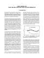
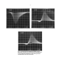
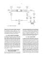
times. As shown in Fig. 1, this results in a walk
guaranteed < ±50 ps and typically < ±25 ps over a
I 00: 1 dynamic range of input pulse amplitudes.
The patented shaping technique also provides a
zero-crossing monitor output that facilitates quick
and accurate walk adjustment, because it displays
the full input signal amplitude range.
Fig. 1. Actual Walk Measured on Four Different Units. See
Walk Specifications for Measurement Conditions.
The extremely short pulses from microchannel
plate multipliers and ultra-fast photomultiplier tubes
require very short constant-fraction shaping delays.
To accommodate these detectors, the Model 935
incorporates a selectable compensation for the
inherent internal delay.
The Model 935 includes a number of controls which
considerably broaden its utility. The threshold
discriminator is useful for rejecting low-level noise.
A front-panel test point permits precise
measurement of its setting in the range from -20 to
-1 000 mV. Each channel provides three bridged,
timing outputs. These are standard, fast negative
NIM outputs. The outputs can be selected to have
either updating or blocking characteristics. The
2
updating mode is useful for reducing dead time in
overlap coincidence experiments. The blocking
mode simultaneously minimizes multiple triggering
and dead time on scintillators with long decay
times. The output pulse width is adjustable from <4
ns to >200 ns in the updating mode, and from <5 ns
to > 1 µs in the blocking mode. The pulse-pair
resolution is <5 ns at minimum pulse width in the
updating mode.
Switches on the printed circuit board allow selection
of which channels will respond to the front-panel
fast-veto input. Additional fast gating capability is
provided by individual gate inputs for each channel
on the rear panel. The mode of these separate gate
inputs can be individually selected to be either
coincidence or anti-coincidence via DIP switches
on the printed circuit board. Each channel ran also
be programmed, for NIM bins incorporating that
signal, to ignore or respond to the slow bin gate
signal on pin 36 of the power connector.
2. SPECIFICATIONS
The Model 935 contains four independent and
identical constant-fraction discriminators. Except
where stated otherwise, the descriptions and
specifications are given for an individual channel,
and apply to each of the four channels.
2.1. PERFORMANCE
WALK Guaranteed < ±50 ps (typically < ±25 ps)
over a 100:1 dynamic range. Measured under the
following conditions: input pulse amplitude range
from -50 mV to -5 V, rise time <1 ns, pulse width 10
ns, external shaping delay approximately 1.6 ns (33
cm or 13 in.), internal offset delay enabled,
threshold approximately 20 mV.
CONSTANT FRACTION 20%.
PULSE-PAIR RESOLUTION <5 ns in the updating
mode, <7 ns in the blocking mode.
INPUT/OUTPUT RATE Operates at burst rates
>200 MHZ in the updating mode, and >150 MHZ in
the blocking mode.
2.2. CONTROLS
THRESHOLD (T) A front-panel, 20-turn screwdriver
adjustment for each discriminator channel sets the
minimum pulse amplitude that will produce a timing
output. Variable from -20 to -1000 mV. A frontpanel test point located to the left of the threshold
adjustment monitors the discriminator threshold
setting. The test point voltage is 10× the actual
threshold setting. Output impedance: 2 k.
WALK ADJUSTMENT (Z) A front-panel, 20-turn
screwdriver adjustment for fine-tuning the zerocrossing discriminator threshold to achieve
minimum walk. Adjustable over a ±15 mV range. A
front-panel test point located to left of the walk
adjustment monitors the actual setting of the zerocrossing discriminator. Output impedance, 1 k.
OUTPUT WIDTH (W) A front-panel, 20-turn
screwdriver adjustment for each discriminator
channel sets the width of the three output logic
pulses. The range of width adjustment depends on
the positions of jumpers W2 and W3.
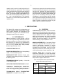
Table 1. The Dependence of the Output Pulse Width
Range on W2 and W3 Jumper Positions.
TRANSMISSION DELAY Typically < 13 ns with
1.6-ns external delay.
OPERATING TEMPERATURE RANGE 0 to 50(C.
THRESHOLD TEMPERATURE SENSITIVITY
<0.01%/(C, from 0 to 50(C. Threshold referenced
to the -12 V supply level supplied by the NIM bin.
TRANSMISSION DELAY TEMPERATURE
SENSITIVITY <±10 ps/(C from 0 to 50(C.
W3
Jumper
Position
Output Pulse Width Adjustment
Range
W2 = U
Updating
W2 = B
Blocking
open
<4 to >100 ns
<5 to >100 ns
S
<4 to >200 ns
<5 to >200 ns
S+L
Not functional
<30 ns to >400 ns
3
B GATE ON/OFF Rear-panel switch turns the Bin
Gate on or off for all channels programmed to
accept the Bin Gate.
GATE COIN/ANTI A printed wiring board DIP
switch selects either the coincidence or
anticoincidence mode for the individual channel's
response to the rear-panel gate input.
VETO YES/NO A printed wiring board DIP switch
selects whether or not an individual channel will
respond to the front-panel VETO input.
BIN GATE YES/NO A printed wiring board DIP
switch selects whether or not an individual channel
will respond to the bin gate signal.
INTERNAL OFFSET DELAY (WI) Printed wiring
board jumper W1 is normally omitted to enable the
1.7-ns internal offset delay. This delay
compensates for internal delays and makes it
possible to implement the very short shaping
delays required with 1-ns input pulse widths. With
jumper W1 installed, the minimum shaping delay is
limited by a +0.7-ns internal contribution. With W1
omitted, the internal delay contribution is effectively
-1.0 ns. The Model 935 is shipped from the factory
with the W1 jumper omitted. Spare jumpers for this
position are located in the storage area towards the
rear of the module.
UPDATING/BLOCKING MODE (W2) The printed
wiring board jumper W2 selects either the updating
mode (U ), or the blocking mode (B) for the output
pulse widths. In the blocking mode, a second input
pulse will generate no output pulse if it arrives
within the output pulse width W caused by a
previous input pulse. In the updating mode, a
second input pulse arriving within the output pulse
width W from a previous pulse will extend the
output pulse, from the time of arrival, by a length W.
The Model 935 is shipped from the factory in the
updating mode.
OUTPUT PULSE WIDTH RANGE (W3) The printed
wiring board jumper W3 selects the range of output
width adjustment as listed in Table 1. The Model
935 is shipped from the factory with the W3 jumper
omitted. Spare jumpers for this position are located
in the storage area toward the rear of the module.
2.3. INPUTS
IN1, IN2, IN3, or IN4 A front-panel LEMO
connector input on each channel accepts the fast
linear signal from a detector for constant-fraction
timing. Linear range from 0 to -10 V. Signal input
impedance, 50, dc-coupled; input protected with
diode clamps at ±10 V. Input reflections <10% for
input rise times > 2 ns.
GATE INPUTS 1, 2, 3, or 4 A rear-panel BNC
connector for each channel accepts a negative, fast
NIM logic signal to gate the respective constantfraction timing output. Coincidence or
anticoincidence gating is selected by a printed
wiring board DIP switch (See GATE COIN/ANTI).
Input impedance, 50. For proper gating operation,
the leading edge of the GATE INPUT should
precede the IN1 (IN2, IN3, or IN4) signal by 1 ns
and have a width equal to the CF Shaping Delay
plus 5 ns.
VETO A single, front-panel LEMO connector
accepts NIM negative fast logic pulses to inhibit the
timing outputs on all the channels chosen with the
VETO YES/NO switch. Input impedance, 50. For
proper FAST VETO operation, the leading edge of
the VETO signal must precede the IN1 (IN2, IN3, or
IN4) signal by 3 ns and have a width equal to the
CF Shaping Delay plus 5 ns.
BIN GATE A slow master gate signal enabled by
the rear-panel B GATE ON/OFF switch permits
gating off the timing outputs when the Model 935 is
installed in a bin that provides a bin gate signal on
pin 36 of the NIM power connector. Clamping pin
36 to ground from +5 V inhibits operation of all
channels selected by the BIN GATE YES/NO
switch.
2.4. OUTPUTS
CF SHAPING DELAY (DLY) A front-panel pair of
LEMO connectors for selecting the required
constant-fraction shaping delay. A 50- cable is
required. For triggering at a 20% fraction, the length
of the shaping delay is approximately equal to the
time taken for the input pulse to rise from 20% of its
full amplitude to full amplitude.
CF MONITOR (M)
Permits observation of the
constant-fraction shaped signal through a LEMO
connector on the front panel. Output impedance,
4
50 , ac-coupled. The monitor output is attenuated
by a factor of approximately 5 with respect to the
input when driving a terminated 50- cable.
OUT Three bridged, updating or blocking, fast
negative NIM output signals, furnished through
front-panel LEMO connectors, mark the CF zerocrossing time. Amplitude -800 mV on 50- load.
Each output connector has its own 50- resistor in
series with the common output driver.
GND Front-panel test point provides a convenient
ground connection for test probes.
EVENT-OCCURRED LED Front-panel LED for
each channel indicates that an output signal has
occurred.
2.5. ELECTRICAL AND MECHANICAL
POWER REQUIREMENTS The Model 935 derives
its power from a NIM bin power supply. Required dc
voltages and currents are: +12 V at 33 mA, + 6 V at
225 mA, -6V at 1400 mA, -12V at 169 mA, -24 V at
55 mA.
WEIGHT
Net 1.1 kg (2.6 lb).
Shipping 2.0 kg (4.4 lb)
DIMENSIONS NIM-standard single-width module
3.43 x 22.13 cm (1.35 x 8.714 in.) per TID-20893
(Rev).
3. INSTALLATION
3.1. GENERAL
3.3. INPUT CONNECTIONS
The Model 935 power requirements must be
furnished from a NIM-standard bin and power
supply that includes ±6 V power distribution such as
the ORTEC 4001C/4002E, 4001C/4002D, or
4001A/4002D NIM Bins/Power Supplies.
Each discriminator channel includes an input
connector on the front panel that is terminated
internally in 50. Connect the source of negative
input signals to this connector through a 50
coaxial cable and a mating LEMO connector. Any
of the four channels can be provided with an input
signal and will operate independently from all other
channels.
The bin and power supply in which the Model 935
will normally be operated is designed for relay rack
mounting. If the equipment is rack mounted, be
sure that there is adequate ventilation to prevent
any localized heating in the Model 935. The
temperature of equipment mounted in racks can
easily exceed the maximum limit of 50(C (323 K)
unless precautions are taken.
3.2. CONNECTION TO POWER
Due to the very high speed electronic components
used in the Model 935 to achieve its excellent
performance, the Model 935 exceeds the normal
fair share of power per slot of normal NIM power
supplies. As many as eight Model 935s, a total of
32 channels, can be operated in a ORTEC
4002C/4002E NIM Bin/Power Supply. To be sure of
proper operation, check the de voltage levels of the
power supply after all modules have been installed
in the bin. ORTEC bins and power supplies include
convenient test points on the power supply control
panel to permit monitoring these levels.
3.4. OUTPUT CONNECTIONS
There are three output connectors for each
channel. These connectors furnish three identical,
simultaneous, negative NIM logic signals for each
input pulse that exceeds the adjusted threshold
level. The output pulse width can be adjusted by
the front-panel W control associated with that
channel. When operating in the updating mode, the
range of width adjustment can be increased by
adding a PWB jumper to the "S" pins at W3. When
operating in the blocking mode, the range of width
adjustment can be increased by adding jumpers to
either or both the "S" and "L" pins at W3.
Each output connection should be furnished
through a mating LEMO connector and a 50-
coaxial cable to a 50- load impedance. For best
results, terminate all unused output connectors in
each active channel with a 50- terminator on the
front panel. Termination is not necessary for
unused channels.
5
3.5. GATING
Each channel of the Model 935 can be externally
gated by one of three conditions. A front-panel
Veto input can block the output. Each channel can
be separately gated by rear-panel Gate inputs. A
NIM bin signal, the B (bin) Gate operating through
pin 36 of the power connector in the NIM bin, can
inhibit an output, providing that the rear-panel B
Gate switch is set to On. The gating conditions for
each channel of the Model 935 are controlled by
PWB DIP switches. The Veto input can be selected
as either Yes or No, the Gate input can be selected
as either Coincidence or Anticoincidence, and the
B Gate can be selected as either Yes or No.
For proper gating operation, certain timing
conditions must be satisfied between the leading
edge of the input signal and the gating signal.
When using the front-panel fast Veto input, its
leading edge should precede the input signal by 3
ns, and its width should be equal to the CF shaping
delay plus 5 ns. When using the rear-panel Gate
input, its leading edge should precede the input
signal by 1 ns, and its width should be equal to the
CF shaping delay plus 5 ns. The B (bin) Gate signal
is a slow logic signal, and it must overlap the input
signal to be effective.
3.6. CF SHAPING DELAY CABLE
SELECTION
The CF shaping delay for each channel is adjusted
by selecting an appropriate length of 50- coaxial
cable and adding it between the two Delay (DLY)
LEMO connectors on the front panel. The length of
cable determines the amount of external signal
delay that is added to the internal delay to
constitute the total constant-fraction shaping delay.
Since the Model 935 is equipped with a jumperselectable internal offset delay, the external CF
shaping delay will depend on the position of internal
jumper W1. With jumper W1 removed (placed in
the storage area at the rear of the PWB), the total
constant-fraction shaping delay, td(Total), is
approximated by
td(Total) td(External) - 1.0 ns, W1 removed. (3.1)
td(Total) td(External) + 0.7 ns, W1 in place.
(3.2)
The primary usage of the Model 935 is expected to
be in fast timing or counting experiments with
scintillators and photomultiplier tubes (PMTs) and
Silicon Surface Barrier Detectors. In these
applications, the CF Shaping Delay td(Total) is
selected so that the zero-crossing of the bipolar
timing signal occurs just as the peak of the
attenuated, undelayed portion of the CF signal has
reached its maximum amplitude. Thus, the zerocrossing occurs at the same fraction of the input
pulse height, regardless of the amplitude of the
input signal.
Selection of the CF Shaping Delay for best timing
performance with a given scintillator and PMT is
usually accomplished experimentally. The randomly
generated signals from the anode of the PMT are
applied to the input of one channel of the
discriminator. Each of the two CF Delay connectors
should be terminated with a 50- terminator. The
CF Monitor signal can be observed on a fast
oscilloscope (bandwidth > 300 MHZ), which is
terminated in 50- and triggered internally. The
Monitor signal represents the attenuated,
undelayed portion of the constant-fraction signal
with no delayed signal subtracted from it. The
addition of the appropriate external CF Shaping
Delay td(External) causes the resulting bipolar signal at
the CF Monitor to cross the baseline at the peak of
the attenuated, undelayed signal. When using the
internal offset delay (i.e., jumper W1 removed), a
useful formula for the initial trial selection of the CF
Shaping Delay is
td(External) = T + 1.0 ns, W1 removed,
(3.3)
where T is the time for the leading edge of the
pulse to rise from 20% of maximum amplitude to
maximum amplitude. The 20% number
corresponds to the 20% triggering fraction designed
into the Model 935. With jumper W1 in place (i.e.,
when not using the internal offset delay), a useful
formula for the initial trial selection of the CF
Shaping Delay is
td(External) = T - 0.7 ns, W1 in place.
(3.4)
In normal operation, jumper W1 is removed and
placed in the storage area at the rear of the PWB.
This setting will work properly for all input signals.
The Model 935 is shipped with jumper W1 in the
storage area. For input signals having rise times
greater than 2 ns, jumper W1 can be used to short
the internal offset delay, allowing for shorter
external CF Shaping Delays.
6
3.7. WALK SETTING
The Walk adjustment is a front-panel, 20-turn
screwdriver adjusted potentiometer for each
channel. A Walk Monitor front-panel test point is
used to monitor the actual setting of the dc zerocrossing adjustment. A nominal value for this dc
level is +1.5 mV, but the optimal value is best
determined experimentally.
Walk adjustment can be accomplished while
observing the delayed CF Monitor signal on a fast
oscilloscope (bandwidth >300 MHZ), which is
triggered externally by the output signal of the
Model 935. The Walk potentiometer (Z) should be
adjusted so that the bipolar constant-fraction
signals for all amplitudes cross through the
baseline at approximately the same time.
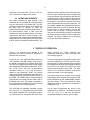
Figure 3(a) shows the anode signals from a
Hamamatsu 1332 PMT with a 12.9-cc BC418
truncated cone scintillator exposed to a 60Co
source. Figure 3(b) shows the delayed CF Monitor
signal triggered by the Model 935 output signal with
the walk properly adjusted. Adjusting the Walk
potentiometer counterclockwise results in the
waveform shown in Figure 3(c), where the extra
line near the baseline indicates leading-edge
timing. Proper Walk adjustment can be achieved by
adjusting the Walk potentiometer counter-clockwise
to obtain the waveform shown in Figure 3(c), then
turning the Walk adjustment clockwise to just
eliminate the leading-edge timing line. An additional
1 to 2 turns clockwise should give the waveform in
Figure 3(b) and optimum walk adjustment. The final
optimization of the Walk adjustment is best
accomplished by optimizing the symmetry and
minimizing the width of the coincidence peak in the
time spectrum (see Section 4).
4. OPERATING INSTRUCTIONS
4.1. GENERAL
The actual timing performance of a timing system
depends on many variables. The type of detector
and the energy range of interest are two important
system variables that are independent of the
electronics. In general, detectors having fast rise
time signals and higher energies give the best
timing performance.
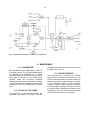
A simple timing system is shown in Figure 4. This
system consists of two detectors each with their
own high voltage supply, two Model 935 CFDs, a
Delay unit for timing calibration and signal offset, a
Time-to-Amplitude Converter (TAC) and a
multichannel analyzer (MCA). Also shown is a
Preamplifier (PA), a spectroscopy amplifier (Amp),
and a Gate and Delay Generator (GDG) used for
energy calibration.
The detectors shown in Figure 4 consist of fast
scintillators mounted on fast photomultiplier tubes
(PMTs). Each PMT is connected to a PMT Base for
distribution of the high voltage. Care must be taken
in preparing and mounting the scintillator to ensure
very efficient coupling between the scintillator and
the PMT.
The high voltage setting for the PMT depends on
the type of PMT, and the manufacturer of the PMT
should be consulted. The gain of the PMT depends
directly on the value of the high voltage and
provides a convenient method for adjusting the
output signal amplitude from the PMT. In general,
the high voltage should be set sufficiently high to
ensure a large signal input to the CFD. However,
the high voltage should not be set so high as to
cause the onset of saturation in the PMT. The final
adjustment of the high voltage is a compromise that
can best be determined experimentally.
4.2. THRESHOLD ADJUSTMENT
The Model 935 will produce an output signal each
time the input signal crosses the threshold. Setting
the threshold is equivalent to setting the lowest
energy of interest. While it is possible to set the
threshold using an oscilloscope, a far more
accurate method is to use the actual detector, a
radioactive source, and an MCA gated by the
Model 935. A Gate and Delay Generator is used to
convert the Model 935 output to a signal suitable
for gating the MCA.
To adjust the threshold level, measure the dc
voltage from the front-panel Threshold monitor test
point to ground for the active channel. The
Threshold monitor test point is located to the left of
the threshold potentiometer on the front panel. A
convenient ground test point is located at the
7
Fig. 3. (a) Anode signal from PMT and scintillator, (b) the
Model 935 CF Monitor signal showing proper walk adjustment,
and (c) the Model 935 CF Monitor signal showing improper
walk adjustment. See text for discussion.
8
Fig. 4. A Simple Timing System.
bottom of the front panel to the right of the Veto
Input connector. The nominal range of voltages at
the Threshold test point is -200 mV to -10 V,
corresponding to the actual threshold which is 10%
of the test point voltage. Use a screwdriver to set
the threshold level with the control marked T.
4.3. OUTPUT WIDTH ADJUSTMENT
To adjust the output width, provide an input pulse
that exceeds the adjusted threshold at a rate less
than 0.5 MHZ and observe the width of an output
pulse from any of the three output connectors.
Terminate the other output connectors in 50 . Use
a screwdriver to set the control marked W for the
output width in the active channel. When operating
in the Updating mode, the output width can be
adjusted from <4 ns to >100 ns. Adding a PWB
jumper to the S position of W3 changes the range
of adjustment to >200 ns. When operating in the
blocking mode, an additional jumper can be added
to the L position of W3, increasing the Blocking
output width to > 1000 ns.
4.4. CONSTANT-FRACTION SHAPING
DELAY ADJUSTMENT
Selection of the initial value for the CF Shaping
Delay is described in Section 3.6. For input signals
having widths approaching 1 ns, it is necessary to
fine tune the CF Shaping Delay to achieve optimum
performance. The optimum value is determined for
a given detector using the timing system shown in
Figure 4. Repeated measurements of timing
resolution FWHM and FWHM are made as a
function of CF Shaping Delay length to determine
the optimum value of the CF Shaping Delay.
4.5. WALK ADJUSTMENT
To adjust the Walk characteristics, connect the
signal source to be used to the Input connector in
the active channel and connect the signal from the
constant-fraction Monitor connector to a fast
oscilloscope (bandwidth greater than 300 MHZ)
through a 50- delay. Select the CF Shaping Delay
according to the information in Section 3.6. The
constant-fraction shaped signal can be observed on
the oscilloscope, triggered by an undelayed output
signal from the active discriminator. Adjust the
Walk (Z) control, which sets the zero-crossing
reference, so that the bipolar constant-fraction
signals for all input amplitudes cross through the
baseline at approximately the same time. The
adjacent test point can be used for resettability of
the zero-crossing reference. Under most operating
conditions, the dc voltage level at the test point
9
should be in the range from -1.0 mV to +2.0 mV.
Use a screwdriver to adjust the Z control.
4.6. GATING ADJUSTMENTS
The gating conditions for each channel of the
Model 935 are set by PWB DIP switches located
near the rear panel of the Model 935. The DIP
switches located nearest the top of the module set
the Gate input to operate in either the
Anticoincidence mode or the Coincidence mode. In
the Anticoincidence mode, a Gate input that
satisfies the timing conditions relative to the Input
signal blocks the output of that channel. In the
Coincidence mode, a Gate input enables the output
of that channel. If no Gate input is to be used, place
the DIP switch in the Anticoincidence position. The
middle set of DIP switches controls the front-panel
fast Veto input. With the DIP switch corresponding
to a given channel in the On position, the fast Veto
signal can block or veto the output of that channel,
providing that the timing conditions of the fast Veto
input relative to the Input are satisfied. The lowest
set of DIP switches controls the bin gate input. The
bin gate DIP switches are effective only K the rearpanel B Gate switch is in the On position. With the
B Gate switch in the On position, and the DIP
switch in the On position, a bin gate blocks the
output of the corresponding channel, provided that
the timing conditions relative to the input signal are
satisfied. The timing conditions for all the gating
inputs are described in Section 3.5.
5. THEORY OF OPERATION
Figure 5 is a simplified block diagram of the
instrument that can be used as a reference to
describe how it operates.
signal exceeds the LEAD threshold, that
comparator produces an output pulse that arms
zero-crossing gate G1.
An input of 0 to -10 V amplitude starts at time zero
and is applied to the 50- Splitter. One output of
the Splitter is delayed by the internal offset delay
DL1 before it is applied to the leading-edge arming
discriminator (LEAD) and the CF attenuator, ATTN.
The ATTN circuit sets the constant-fraction
attenuation factor of f = 0.2, and its output is
applied to the transformer, XFMR. The second
output of the Splitter is delayed by the external CF
Shaping Delay and applied to the second input to
the XFMR. The XFMR output is a bipolar-shaped
signal whose zero-crossing time is used to derive
the Model 935 output. This signal is amplified by
the constant-fraction amplifier (CFA) prior to being
connected to the zero-crossing gate Gl.
The timing logic signal from gate G1 triggers a fast
one-shot, comprised of an ECL type D masterslave flip-flop FF1 and a stretcher circuit. All gating
input signals are ORed by G2 and applied to the D
input of FF1. One output of FF1 drives A2, which
controls the front-panel event LED. The other
output of FF1 drives the stretcher circuit, which
controls the width of the output signals.
The output driver circuit provides a fast voltage
output signal that is capable of driving three 50-
loads simultaneously with NIM-standard negative
fast logic pulses. The output signals are either
updating or blocking, depending on the setting of
PWB jumper W2.
The LEAD has an adjustable threshold, ranging
from -20 mV to -1 V, that determines the minimum
input signal amplitude that is required to produce
an output pulse from the Model 935. If the input
The dc power requirements are shown in the
specifications in Section 2. The power levels are
+6 V, -6 V, +12 V, -1 2 V, and -24 V, and they are
all obtained directly from the bin power supply.
10
Fig. 5. Simplified Block Diagram of One Section of the Model 935.
6. MAINTENANCE
6.1. CALIBRATION
Most adjustments to the Model 935 are made via
front-panel controls. The only internal adjustment is
the Threshold Cal potentiometer, R. Should
recalibration be required, connect a 50-mV, 20-nswide signal to the input of the section being
adjusted. Adjust the front-panel Threshold
potentiometer such that the front-panel Threshold
Test Point reads 500 mV. Adjust the Threshold Cal
potentiometer so that the Model 935 output halffires.
6.2. TYPICAL DC VOLTAGES
All voltages listed on the schematic drawing are
measured with respect to ground, with the
Threshold and Width controls set at minimum, and
the Walk set at + 1.5 mV.
6.3. FACTORY SERVICE
This instrument can be returned to the ORTEC
factory for service and repair at a nominal cost. The
ORTEC standard procedure for repair ensures the
same quality control and checkout that are used for
a new instrument. Always contact Customer
Services at ORTEC before sending an instrument
for repair to obtain shipping instructions and so that
the required Return Authorization Number can be
assigned to the unit. This number should be written
on the address label and on the package.
11
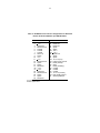
Table 2. Bin/Module Connector Pin Assignments For Standard
Nuclear Instrument Modules per DOE/ER-0457T.
Pin
1
2
3
4
5
6
7
8
9
10
11
12
13
14
15
*16
*17
18
19
20
21
22
Function
+3 V
3 V
Spare bus
Reserved bus
Coaxial
Coaxial
Coaxial
200 V dc
Spare
+6 V
6 V
Reserved bus
Spare
Spare
Reserved
+12 V
12 V
Spare bus
Reserved bus
Spare
Spare
Reserved
Pin
23
24
25
26
27
*28
*29
30
31
32
*33
*34
35
36
37
38
39
40
*41
*42
G
Function
Reserved
Reserved
Reserved
Spare
Spare
+24 V
24 V
Spare bus
Spare
Spare
117 V ac (hot)
Power return ground
Reset (Scaler)
Gate
Reset (Auxiliary)
Coaxial
Coaxial
Coaxial
117 V ac (neutral)
High-quality ground
Ground guide pin
Pins marked (*) are installed and wired in ORTEC’s 4001A and 4001C
Modular System Bins.
12