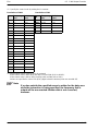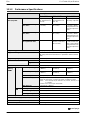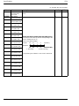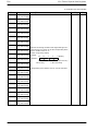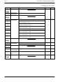
1
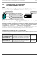
PROGRAMMABLE CONTROLLER
FP Σ
User’s Manual
[Applicable PLC]
FPΣ Control units
• FPG - C32T
• FPG - C32T2
• FPG - C24R2
This manual was created using Adobe Acrobat.
Adobe, the Adobe logo, and Acrobat are trademarks
of Adobe Systems Incorporated.
http://www.naisplc.com
FPΣ
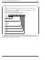
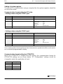
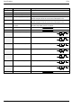
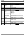
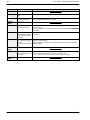
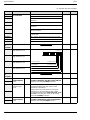
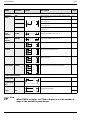
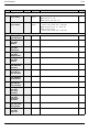
Table of Contents
Table of Contents
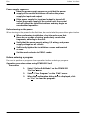
Before You Start . . . . . . . . . . . . . . . . . . . . . . . . . . . . . . . . . . . . . . . . . . . . . . . . . . . . viii
Programming Tool Restrictions . . . . . . . . . . . . . . . . . . . . . . . . . . . . . . . . . . . . . . . . xi
Compatibility with the FP0 . . . . . . . . . . . . . . . . . . . . . . . . . . . . . . . . . . . . . . . . . . . . xii
Chapter 1
Functions and Restrictions of the Unit
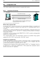
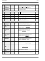
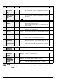
1.1
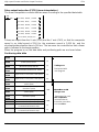
Features and Functions of the Unit . . . . . . . . . . . . . . . . . . . . . . . . . . . . . . . 1 - 3
1.2
Unit Types . . . . . . . . . . . . . . . . . . . . . . . . . . . . . . . . . . . . . . . . . . . . . . . . . . . .
1.2.1
FPΣ Control Unit . . . . . . . . . . . . . . . . . . . . . . . . . . . . . . . . . . . . . . .
1.2.2
FPΣ Expansion Unit . . . . . . . . . . . . . . . . . . . . . . . . . . . . . . . . . . . . .
1.2.3
Units for FP0 and FPΣ . . . . . . . . . . . . . . . . . . . . . . . . . . . . . . . . . .
1.2.4
Communication Cassette . . . . . . . . . . . . . . . . . . . . . . . . . . . . . . . .
1.3
Restrictions on Unit Combinations . . . . . . . . . . . . . . . . . . . . . . . . . . . . . . . . 1 - 7
1.3.1
Restrictions on the Number of Expansion Units
(for FP0 expansion unit) . . . . . . . . . . . . . . . . . . . . . . . . . . . . . . . . . 1 - 7
1.3.2
Restrictions on the Number of Units for Expansion
(for FPΣ expansion unit) . . . . . . . . . . . . . . . . . . . . . . . . . . . . . . . . . 1 - 8
1.4
Programming Tools . . . . . . . . . . . . . . . . . . . . . . . . . . . . . . . . . . . . . . . . . . . . . 1 - 9
1.4.1
Tools Needed for Programming . . . . . . . . . . . . . . . . . . . . . . . . . . 1 - 9
1.4.2
Software Environment and Suitable Cable . . . . . . . . . . . . . . . . . 1 - 9
Chapter 2
1-6
1-6
1-6
1-6
1-6
Specifications and Functions of Control Unit
2-3
2-3
2-6
2-6
2.1
Parts and Functions . . . . . . . . . . . . . . . . . . . . . . . . . . . . . . . . . . . . . . . . . . . .
2.1.1
Parts and Functions . . . . . . . . . . . . . . . . . . . . . . . . . . . . . . . . . . . .
2.1.2
Tool Port Specification . . . . . . . . . . . . . . . . . . . . . . . . . . . . . . . . . .
2.1.3
Communication Cassette . . . . . . . . . . . . . . . . . . . . . . . . . . . . . . . .
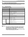
2.2
Input and Output Specifications . . . . . . . . . . . . . . . . . . . . . . . . . . . . . . . . . . 2 - 7
2.2.1
Input Specifications . . . . . . . . . . . . . . . . . . . . . . . . . . . . . . . . . . . . . 2 - 7
2.2.2
Output Specifications . . . . . . . . . . . . . . . . . . . . . . . . . . . . . . . . . . . 2 - 9
2.3
Terminal Layout Diagram . . . . . . . . . . . . . . . . . . . . . . . . . . . . . . . . . . . . . . . . 2 - 12
2.3.1
Control Unit (for C32T and C32T2) . . . . . . . . . . . . . . . . . . . . . . . 2 - 12
2.3.2
Control Unit (for C24R2) . . . . . . . . . . . . . . . . . . . . . . . . . . . . . . . . . 2 - 12
Chapter 3
3.1
Expansion
Type of Expansion Unit . . . . . . . . . . . . . . . . . . . . . . . . . . . . . . . . . . . . . . . . . 3 - 3
i
Table of Contents
FPΣ
3.2
Expansion Method of Units for FP0 and FPΣ . . . . . . . . . . . . . . . . . . . . . . . 3 - 4
3.3
Expansion Method of FPΣ Expansion Unit . . . . . . . . . . . . . . . . . . . . . . . . . 3 - 5
3.4
Specifications of FPΣ Expansion Unit . . . . . . . . . . . . . . . . . . . . . . . . . . . . . 3 - 6
3.4.1
FPΣ Expansion I/O Unit . . . . . . . . . . . . . . . . . . . . . . . . . . . . . . . . . 3 - 6
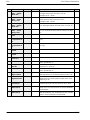
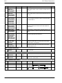
Chapter 4
4.1
I/O Allocation
I/O Allocation . . . . . . . . . . . . . . . . . . . . . . . . . . . . . . . . . . . . . . . . . . . . . . . . . .
4.1.1
I/O Number of FPΣ Control Unit . . . . . . . . . . . . . . . . . . . . . . . . . .
4.1.2
I/O Number of FPΣ Expansion Unit (for left side expansion) . .
4.1.3
I/O Number of FP0 Expansion Unit (for right side expansion) .
4.1.4
I/O Number of FP0 Analog I/O Unit (for right side expansion) .
4.1.5
I/O Number of FP0 A/D Conversion Unit
(for right side expansion) . . . . . . . . . . . . . . . . . . . . . . . . . . . . . . . .
4.1.6
I/O Number of FP0 I/O Link Unit (for right side expansion) . . .
Chapter 5
4-3
4-3
4-4
4-5
4-5
4-5
4-6
Installation and Wiring
5.1
Installation . . . . . . . . . . . . . . . . . . . . . . . . . . . . . . . . . . . . . . . . . . . . . . . . . . . . 5 - 3
5.1.1
Installation Environment and Space . . . . . . . . . . . . . . . . . . . . . . . 5 - 3
5.1.2
Installation and Removal . . . . . . . . . . . . . . . . . . . . . . . . . . . . . . . . 5 - 6
5.2
Wiring of Power Supply . . . . . . . . . . . . . . . . . . . . . . . . . . . . . . . . . . . . . . . . . 5 - 9
5.2.1
Wiring of Power Supply . . . . . . . . . . . . . . . . . . . . . . . . . . . . . . . . . 5 - 9
5.2.2
Grounding . . . . . . . . . . . . . . . . . . . . . . . . . . . . . . . . . . . . . . . . . . . . . 5 - 11
5.3
Wiring of Input and Output . . . . . . . . . . . . . . . . . . . . . . . . . . . . . . . . . . . . . .
5.3.1
Input Wiring . . . . . . . . . . . . . . . . . . . . . . . . . . . . . . . . . . . . . . . . . . .
5.3.2
Output Wiring . . . . . . . . . . . . . . . . . . . . . . . . . . . . . . . . . . . . . . . . . .
5.3.3
Precautions Regarding Input and Output Wirings . . . . . . . . . . .
5.4
Wiring of MIL Connector Type . . . . . . . . . . . . . . . . . . . . . . . . . . . . . . . . . . . 5 - 17
5.5
Wiring of Terminal Block Type . . . . . . . . . . . . . . . . . . . . . . . . . . . . . . . . . . . . 5 - 20
5.6
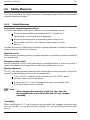
Safety Measures . . . . . . . . . . . . . . . . . . . . . . . . . . . . . . . . . . . . . . . . . . . . . . .
5.6.1
Safety Measures . . . . . . . . . . . . . . . . . . . . . . . . . . . . . . . . . . . . . . .
5.6.2
Momentary Power Failures . . . . . . . . . . . . . . . . . . . . . . . . . . . . . .
5.6.3
Protection of Power Supply and Output Sections . . . . . . . . . . .
5 - 22
5 - 22
5 - 23
5 - 23
5.7
Backup Battery . . . . . . . . . . . . . . . . . . . . . . . . . . . . . . . . . . . . . . . . . . . . . . . .
5.7.1
Installation of Backup Battery . . . . . . . . . . . . . . . . . . . . . . . . . . . .
5.7.2
System Register Setting . . . . . . . . . . . . . . . . . . . . . . . . . . . . . . . . .
5.7.3
Lifetime of Backup Battery . . . . . . . . . . . . . . . . . . . . . . . . . . . . . . .
5 - 24
5 - 24
5 - 25
5 - 26
ii
5 - 12
5 - 12
5 - 15
5 - 16
FPΣ
Table of Contents
Chapter 6
High - speed Counter and Pulse Output Functions
6.1
Overview of Each Functions . . . . . . . . . . . . . . . . . . . . . . . . . . . . . . . . . . . . . 6 - 3
6.1.1
Three Functions that Use Built- in High - speed Counter . . . . . . 6 - 3
6.1.2
Performance of Built- in High - speed Counter . . . . . . . . . . . . . . . 6 - 4
6.2
Function Specifications and Restricted Items . . . . . . . . . . . . . . . . . . . . . .
6.2.1
Table of Specifications . . . . . . . . . . . . . . . . . . . . . . . . . . . . . . . . . .
6.2.2
Function being Used and Restrictions . . . . . . . . . . . . . . . . . . . . .
6.2.3
Booting Time . . . . . . . . . . . . . . . . . . . . . . . . . . . . . . . . . . . . . . . . . .
6-5
6-5
6-7
6-9
6.3
High - speed Counter Function . . . . . . . . . . . . . . . . . . . . . . . . . . . . . . . . . . .
6.3.1
Overview of High - speed Counter Function . . . . . . . . . . . . . . . . .
6.3.2
Types of Input Modes . . . . . . . . . . . . . . . . . . . . . . . . . . . . . . . . . . .
6.3.3
Min. Input Pulse Width . . . . . . . . . . . . . . . . . . . . . . . . . . . . . . . . . .
6.3.4
I/O Allocation . . . . . . . . . . . . . . . . . . . . . . . . . . . . . . . . . . . . . . . . . .
6.3.5
Instructions Used with High - speed Counter Function . . . . . . . .
6.3.6
Sample Program . . . . . . . . . . . . . . . . . . . . . . . . . . . . . . . . . . . . . . .
6 - 10
6 - 10
6 - 10
6 - 12
6 - 12
6 - 13
6 - 16
6.4
Pulse Output Function . . . . . . . . . . . . . . . . . . . . . . . . . . . . . . . . . . . . . . . . . .
6.4.1
Overview of Pulse Output Function . . . . . . . . . . . . . . . . . . . . . . .
6.4.2
Types of Pulse Output Method . . . . . . . . . . . . . . . . . . . . . . . . . . .
6.4.3
I/O Allocation . . . . . . . . . . . . . . . . . . . . . . . . . . . . . . . . . . . . . . . . . .
6.4.4
Control Mode . . . . . . . . . . . . . . . . . . . . . . . . . . . . . . . . . . . . . . . . . .
6.4.5
Instructions Used with Pulse Output Function . . . . . . . . . . . . . .
6.4.6
Sample Program for Positioning Control . . . . . . . . . . . . . . . . . . .
6 - 20
6 - 20
6 - 21
6 - 22
6 - 23
6 - 24
6 - 43
6.5
PWM Output Function . . . . . . . . . . . . . . . . . . . . . . . . . . . . . . . . . . . . . . . . . . 6 - 56
6.5.1
Overview of PWM Output Function . . . . . . . . . . . . . . . . . . . . . . . 6 - 56
6.5.2
Instruction Used with PWM Output Function . . . . . . . . . . . . . . . 6 - 56
Chapter 7
Communication Cassette
7.1
Communication Functions of FPΣ . . . . . . . . . . . . . . . . . . . . . . . . . . . . . . . . 7 - 3
7.1.1
Functions of Communication Cassette . . . . . . . . . . . . . . . . . . . . 7 - 3
7.2
Communication Cassette . . . . . . . . . . . . . . . . . . . . . . . . . . . . . . . . . . . . . . . .
7.2.1
Type of Communication Cassette . . . . . . . . . . . . . . . . . . . . . . . . .
7.2.2
Names and Principle Applications of the Ports . . . . . . . . . . . . . .
7.2.3
Communication Specifications of Communication Cassette . .
7.3
Attachment of Communication Cassette . . . . . . . . . . . . . . . . . . . . . . . . . . . 7 - 10
7.3.1
Attachment Procedure . . . . . . . . . . . . . . . . . . . . . . . . . . . . . . . . . . 7 - 10
7-6
7-6
7-7
7-8
iii
Table of Contents
7.4
Wiring of Communication Cassette . . . . . . . . . . . . . . . . . . . . . . . . . . . . . . .
7.4.1
Wiring the Connector with the Communication Cassette . . . . .
7.4.2
Tool for Tightening Communication Connector Terminal Block
7.4.3
Wiring Method . . . . . . . . . . . . . . . . . . . . . . . . . . . . . . . . . . . . . . . . .
7.4.4
Cautions Regarding Wiring . . . . . . . . . . . . . . . . . . . . . . . . . . . . . .
Chapter 8
8.1
FPΣ
7 - 11
7 - 11
7 - 12
7 - 12
7 - 12
Communication Function 1 Computer Link
Computer Link . . . . . . . . . . . . . . . . . . . . . . . . . . . . . . . . . . . . . . . . . . . . . . . . .
8.1.1
Overview of Function . . . . . . . . . . . . . . . . . . . . . . . . . . . . . . . . . . .
8.1.2
Explanation of Operation when Using a Computer Link . . . . . .
8.1.3
Format of Command and Response . . . . . . . . . . . . . . . . . . . . . .
8.1.4
Types of Commands that Can Be Used . . . . . . . . . . . . . . . . . . .
8.1.5
Setting the Communication Parameters when
Using a Computer Link . . . . . . . . . . . . . . . . . . . . . . . . . . . . . . . . . . . . . . . . . .
8.1.6
Restriction . . . . . . . . . . . . . . . . . . . . . . . . . . . . . . . . . . . . . . . . . . . . .
8-3
8-3
8-4
8-5
8-8
8 - 10
8 - 10
8.2
Connection Example with External Device . . . . . . . . . . . . . . . . . . . . . . . . . 8 - 11
8.2.1
Connection Example with External Device
(1:1 communication with computer) . . . . . . . . . . . . . . . . . . . . . . 8 - 11
8.2.2
Connection Example with External Device
(1:1 communication with programmable display “GT10/GT30”) 8 - 14
8.3
Computer Link (1:N communication) . . . . . . . . . . . . . . . . . . . . . . . . . . . . . .
8.3.1
Overview of 1:N Communication . . . . . . . . . . . . . . . . . . . . . . . . .
8.3.2
Communication Cassette Used for 1:N Communication . . . . . .
8.3.3
Settings of System Register and Unit No. . . . . . . . . . . . . . . . . . .
8.3.4
Connection with External Device . . . . . . . . . . . . . . . . . . . . . . . . .
Chapter 9
9.1
9.2
iv
8 - 18
8 - 18
8 - 18
8 - 19
8 - 22
Communication Function 2 General - purpose
Serial Communication
General - purpose Serial Communication . . . . . . . . . . . . . . . . . . . . . . . . . .
9.1.1
Overview of Function . . . . . . . . . . . . . . . . . . . . . . . . . . . . . . . . . . .
9.1.2
Program of General - purpose Serial Communication . . . . . . . .
9.1.3
Communication Parameter Settings when Using
General - purpose Serial Communications . . . . . . . . . . . . . . . . . .
9-3
9-3
9-5
9-6
Overview of Communication with External Devices . . . . . . . . . . . . . . . . . 9 - 8
9.2.1
Data Transmission to External Device . . . . . . . . . . . . . . . . . . . . . 9 - 8
9.2.2
Receiving Data from External Device . . . . . . . . . . . . . . . . . . . . . . 9 - 12
FPΣ
Table of Contents
9.3
Connection Example with External Devices . . . . . . . . . . . . . . . . . . . . . . . . 9 - 16
9.3.1
Connection Example with External Device
(1:1 communication with Micro - Imagechecker) . . . . . . . . . . . . . 9 - 16
9.3.2
Connection Example with External Device
(1:1 communication with FP series PLC) . . . . . . . . . . . . . . . . . . 9 - 22
9.4
Data Transmitted and Received with the FPΣ . . . . . . . . . . . . . . . . . . . . . . 9 - 29
9.5
1:N Communication . . . . . . . . . . . . . . . . . . . . . . . . . . . . . . . . . . . . . . . . . . . .
9.5.1
Overview of 1:N Communication . . . . . . . . . . . . . . . . . . . . . . . . .
9.5.2
Communication Cassette Used with 1 : N Communication . . .
9.5.3
Setting of System Register . . . . . . . . . . . . . . . . . . . . . . . . . . . . . .
9.6
Flag Operations When Using Serial Communication . . . . . . . . . . . . . . . . 9 - 33
9.6.1
When “STX not exist” is Set for Start Code and “CR” is
Set for End Code . . . . . . . . . . . . . . . . . . . . . . . . . . . . . . . . . . . . . . . 9 - 33
9.6.2
When “STX” is Set for Start Code and “ETX” is Set for
End Code . . . . . . . . . . . . . . . . . . . . . . . . . . . . . . . . . . . . . . . . . . . . . 9 - 35
9.7
Changing the Communication Mode of COM. Port . . . . . . . . . . . . . . . . . . 9 - 37
9 - 31
9 - 31
9 - 31
9 - 32
Chapter 10 Communication Function 3 PLC Link Function
10.1 PLC Link . . . . . . . . . . . . . . . . . . . . . . . . . . . . . . . . . . . . . . . . . . . . . . . . . . . . . .
10.1.1 Overview of Function . . . . . . . . . . . . . . . . . . . . . . . . . . . . . . . . . . .
10 - 3
10 - 3
10.2 Communication Parameter Settings . . . . . . . . . . . . . . . . . . . . . . . . . . . . . . 10 - 5
10.2.1 Setting of Communication Mode . . . . . . . . . . . . . . . . . . . . . . . . . . 10 - 5
10.2.2 Setting of Unit No. . . . . . . . . . . . . . . . . . . . . . . . . . . . . . . . . . . . . . . 10 - 6
10.2.3 Allocation of Link Relay and Link Register . . . . . . . . . . . . . . . . . 10 - 10
10.2.4 Setting the Largest Station Number for a PLC Link . . . . . . . . . . 10 - 16
10.3 Monitoring When a PLC Link is Being Used . . . . . . . . . . . . . . . . . . . . . . . . 10 - 17
10.3.1 Monitoring Using Relays . . . . . . . . . . . . . . . . . . . . . . . . . . . . . . . . . 10 - 17
10.4 Connection Example of PLC Link . . . . . . . . . . . . . . . . . . . . . . . . . . . . . . . . . 10 - 18
10.4.1 Using a PLC Link with Three FPΣ Units . . . . . . . . . . . . . . . . . . . . 10 - 18
10.4.2 Sample Programs . . . . . . . . . . . . . . . . . . . . . . . . . . . . . . . . . . . . . . 10 - 21
10.5 PLC Link Response Time . . . . . . . . . . . . . . . . . . . . . . . . . . . . . . . . . . . . . . .
10.5.1 PLC Link Response Time . . . . . . . . . . . . . . . . . . . . . . . . . . . . . . . .
10.5.2 Shortening the Transmission Cycle Time When There are
Stations That Have not been Added to the Link . . . . . . . . . . . . .
10.5.3 Error Detection Time for Transmission Assurance Relays . . . .
10 - 22
10 - 22
10 - 25
10 - 26
v
Table of Contents
FPΣ
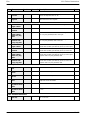
Chapter 11 Other Functions
11.1 Analog Potentiometer . . . . . . . . . . . . . . . . . . . . . . . . . . . . . . . . . . . . . . . . . . . 11 - 3
11.1.1 Overview of Analog Potentiometer . . . . . . . . . . . . . . . . . . . . . . . . 11 - 3
11.1.2 Example Showing How the Analog Potentiometers are Used . 11 - 3
11.2 Clock/Calendar Function . . . . . . . . . . . . . . . . . . . . . . . . . . . . . . . . . . . . . . . .
11.2.1 Area for Clock/Calendar Function . . . . . . . . . . . . . . . . . . . . . . . . .
11.2.2 Setting of Clock/Calendar Function . . . . . . . . . . . . . . . . . . . . . . .
11.2.3 Precautions Concerning Backup of Clock/Calendar Data . . . .
11.2.4 Example Showing the Clock/Calendar being Used . . . . . . . . . .
11 - 4
11 - 4
11 - 4
11 - 5
11 - 6
Chapter 12 Self - Diagnostic and Troubleshooting
12.1 Self - Diagnostic Function . . . . . . . . . . . . . . . . . . . . . . . . . . . . . . . . . . . . . . . . 12 - 3
12.1.1 LED Display for Status Condition . . . . . . . . . . . . . . . . . . . . . . . . . 12 - 3
12.1.2 Operation on Error . . . . . . . . . . . . . . . . . . . . . . . . . . . . . . . . . . . . . . 12 - 4
12.2 Troubleshooting . . . . . . . . . . . . . . . . . . . . . . . . . . . . . . . . . . . . . . . . . . . . . . . .
12.2.1 If the ERROR/ALARM LED Flashes . . . . . . . . . . . . . . . . . . . . . . .
12.2.2 If the ERROR/ALARM LED Lights . . . . . . . . . . . . . . . . . . . . . . . .
12.2.3 If None of the LEDs Light . . . . . . . . . . . . . . . . . . . . . . . . . . . . . . . .
12.2.4 If Outputting does not Occur as Desired . . . . . . . . . . . . . . . . . . .
12.2.5 If a Protect Error Message Appears . . . . . . . . . . . . . . . . . . . . . . .
12.2.6 If the Program Mode does not Change to RUN . . . . . . . . . . . . .
12.2.7 If a Transmission Error has Occurred . . . . . . . . . . . . . . . . . . . . .
12 - 5
12 - 5
12 - 7
12 - 7
12 - 8
12 - 10
12 - 10
12 - 11
Chapter 13 Specifications
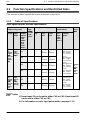
13.1 Table of Specifications . . . . . . . . . . . . . . . . . . . . . . . . . . . . . . . . . . . . . . . . . . 13 - 3
13.1.1 General Specifications . . . . . . . . . . . . . . . . . . . . . . . . . . . . . . . . . . 13 - 3
13.1.2 Performance Specifications . . . . . . . . . . . . . . . . . . . . . . . . . . . . . . 13 - 5
13.2 I/O No. Allocation . . . . . . . . . . . . . . . . . . . . . . . . . . . . . . . . . . . . . . . . . . . . . . 13 - 10
13.3 Relays, Memory Areas and Constants . . . . . . . . . . . . . . . . . . . . . . . . . . . . 13 - 12
13.4 Table of System Registers . . . . . . . . . . . . . . . . . . . . . . . . . . . . . . . . . . . . . . . 13 - 14
13.4.1 System Registers . . . . . . . . . . . . . . . . . . . . . . . . . . . . . . . . . . . . . . 13 - 14
13.4.2 Table of System Registers . . . . . . . . . . . . . . . . . . . . . . . . . . . . . . . 13 - 16
13.5 Table of Special Internal Relays . . . . . . . . . . . . . . . . . . . . . . . . . . . . . . . . . . 13 - 21
13.6 Table of Special Data Registers . . . . . . . . . . . . . . . . . . . . . . . . . . . . . . . . . . 13 - 28
vi
FPΣ
Table of Contents
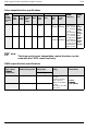
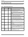
13.7 Table of Error Cords . . . . . . . . . . . . . . . . . . . . . . . . . . . . . . . . . . . . . . . . . . . . 13 - 42
13.7.1 Table of Syntax Check Error . . . . . . . . . . . . . . . . . . . . . . . . . . . . . 13 - 42
13.7.2 Table of Self - Diagnostic Error . . . . . . . . . . . . . . . . . . . . . . . . . . . . 13 - 43
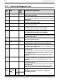
13.8 Table of Instructions . . . . . . . . . . . . . . . . . . . . . . . . . . . . . . . . . . . . . . . . . . . . 13 - 44
13.9 MEWTOCOL - COM Communication Commands . . . . . . . . . . . . . . . . . . . 13 - 66
13.10 Hexadecimal/Binary/BCD . . . . . . . . . . . . . . . . . . . . . . . . . . . . . . . . . . . . . . . 13 - 67
13.11 ASCII Codes . . . . . . . . . . . . . . . . . . . . . . . . . . . . . . . . . . . . . . . . . . . . . . . . . . 13 - 68
13.12Dimensions . . . . . . . . . . . . . . . . . . . . . . . . . . . . . . . . . . . . . . . . . . . . . . . . . . . 13 - 69
13.12.1 Control Unit . . . . . . . . . . . . . . . . . . . . . . . . . . . . . . . . . . . . . . . . . . . . 13 - 69
13.12.2 Expansion Unit . . . . . . . . . . . . . . . . . . . . . . . . . . . . . . . . . . . . . . . . . 13 - 70
Index
.............................................................. I-1
Record of changes
..............................................R-1
vii
Before You Start
Before You Start
Installation environment
Do not use the FPΣ unit where it will be exposed to the following:
Direct sunlight and ambient temperatures outside the
range of 0_C to 55_C/32_F to 131_F.
Ambient humidity outside the range of 30% to 85% RH
and sudden temperature changes causing condensation.
Inflammable or corresive gas.
Excessive vibration or shock.
Excessive airborne dust, metal particles or salts.
Water or oil in any from including spray or mist.
Benzine, paint thinner, alcohol or other organic solvents
or strong alkaline solutions such as ammonia or caustic
soda.
Influence from power transmission lines, high voltage
equipment, power cables, power equipment, radio
transmitters, or any other equipment that would generate
high switching surges.
Static electricity
Before touching the unit, always touch a grounded piece
of metal in order to discharge static electricity.
In dry locations, excessive static electricity can cause
problems.
Cleaning
Do not use thinner based cleaners because they deform
the unit case and fade the colors.
Power supplies
An insulated power supply with an internal protective
circuit should be used. The power supply for the control
unit operation is a non-insulated circuit, so if an
incorrect voltage is directly applied, the internal circuit
may be damaged or destroyed.
If using a power supply without a protective circuit,
power should be supplied through a protective element
such as a fuse.
viii
FPΣ
FPΣ
Before You Start
Power supply sequence
Have the power supply sequence such that the power
supply of the control unit turns off before the power
supply for input and output.
If the power supply for input and output is turned off
before the power supply of the control unit, the control
unit will detect the input fluctuations and may begin an
unscheduled operation.
Before turning on the power
When turning on the power for the first time, be sure to take the precautions given below.
When performing installation, check to make sure that
there are no scraps of wiring, particularly conductive
fragments, adhering to the unit.
Verify that the power supply wiring, I/O wiring, and power
supply voltage are all correct.
Sufficiently tighten the installation screws and terminal
screws.
Set the mode selector to PROG. mode.
Before entering a program
Be sure to perform a program clear operation before entering a program.
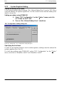
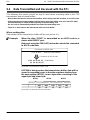
Operation procedure when using FPWIN GR Ver.2
Procedure:
1.
Select “Online Edit Mode” on the FPWIN GR
“On line” menu.
2.
Select “Clear Program” on the “Edit” menu.
3.
When the confirmation dialog box is displayed, click
on “Yes” to clear the program.
ix
Before You Start
FPΣ
Request concerning program storage
To prevent the accidental loss of programs, the user should consider the following
measures.
Drafting of documents
To avoid accidentally losing programs, destroying files, or
overwriting the contents of a file, documents should be
printed out and then saved.
Specifying the password carefully
The password setting is designed to avoid programs being
accidentally overwritten. If the password is forgotten,
however, it will be impossible to overwrite the program even if
you want to. Also, if a password is forcibly bypassed, the
program is deleted. When specifying the password, note it in
the specifications manual or in another safe location in case
it is forgotten at some point.
x
FPΣ
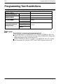
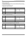
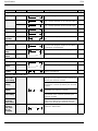
Programming Tool Restrictions
Programming Tool Restrictions
Type of programming tool
Windows software
Conforms to IEC61131- 3
Windows software
MS - DOS software
Instruction used/function restrictions
FPWIN Pro Ver.4
All instructions and functions can be used.
FPWIN GR Ver.2
All instructions and functions can be used.
FPWIN GR Ver.1
Not used
NPST - GR Ver.4
NPST - GR Ver.3
Not used
AFP1114V2
Handy
yp
programming
g
g unit
(FP programmer))
Notes
AFP1114
AFP1112A
AFP1112
Not used
Precautions concerning programming tools
Programming tools used with the FPΣ require FPWIN Pro Ver. 4 or
later or Ver. 2 or a subsequent version of the FPWIN GR. Please be
aware that other tools cannot be used.
Either “FPWIN Pro Ver.4.1 or later” or “FPWIN GR Ver. 2.1 or later”
are necessary for use the C32T2 and C24R2 types control unit.
xi
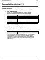
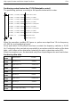
Compatibility with the FP0
FPΣ
Compatibility with the FP0
Program compatibility
The following points require attention if using FP0 programs on the FPΣ.
Pulse output function
With the FPΣ, please be aware that the following changes
have been made to instructions concerning pulse output.
Instruction
For the FP0
For the FPΣ
Trapezoidal control
F168 (SPD1)
F171 (SPDH)
Jog feed
F169 (PLS)
F172 (PLSH)
Data table control
None
F174 (SP0H)
Linear interpolation control
None
F175 (SPSH)
Circular interpolation control
None
F176 (SPCH)
PWM output
F170 (PWM)
F173 (PWMH)
* Linear and circular interpolation control can be used only with the
FPΣ Control Unit C32T2.
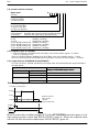
Serial data communication function
With the FPΣ, please be aware that the following changes
have been made to instructions concerning serial data
communication.
Instruction
For the FP0
For the FPΣ
Serial data communication
F144 (TRNS)
F159 (MTRN)
* The F159 (MTRN) instruction is used only with an FPΣ in which
the conventional F144 (TRNS) instruction has been set up to
correspond to multiple communication ports. Please be aware
that the conventional F144 (TRNS) instruction cannot be used
with the FPΣ.
xii
Chapter 1
Functions and Restrictions of the Unit
1.1
Features and Functions of the Unit . . . . . . . . . . . . . . . . 1 - 3
1.2
Unit Types . . . . . . . . . . . . . . . . . . . . . . . . . . . . . . . . . . . . . . 1 - 6
1.3
Restrictions on Unit Combinations . . . . . . . . . . . . . . . . . 1 - 7
1.4
Programming Tools . . . . . . . . . . . . . . . . . . . . . . . . . . . . . . 1 - 9
Functions and Restrictions of the Unit
1-2
FPΣ
FPΣ
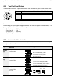
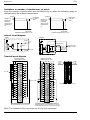
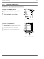
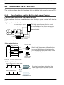
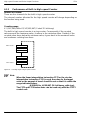
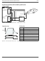
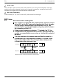
1.1 Features and Functions of the Unit
1.1
Features and Functions of the Unit
Powerful control capabilities
All of the functions of a mid - scale PLC are packed into the compact body size of the
32 - point type FP0. A program capacity of 12 k steps is provided as a standard feature,
so you never have to worry about how much memory is left as you’re programming. In
addition, 32 k words are reserved for data registers, so large volumes of data can be
compiled and multiple operations can be processed without running out of memory.
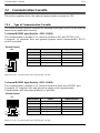
A full range of communication functions
Using the Tool port (RS232C) provided as a standard feature on the main unit,
communication can be carried out with a display panel or computer. Additionally,
communication cassettes with RS232C and RS485 interfaces are available as an
option. Installing a 2 - channel RS232C type communication cassette in the FPΣ makes
it possible to connect two devices with RS232C port. A full lineup of communication
functions means you can also work with 1:N communication and PLC link function (up
to 16 units).
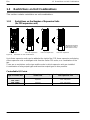
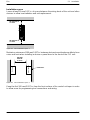
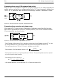
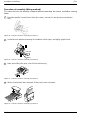
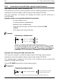
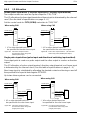
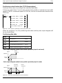
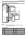
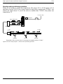
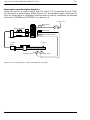
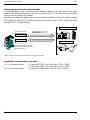
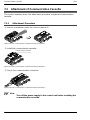
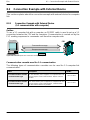
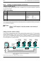
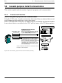
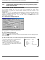
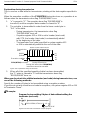
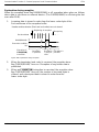
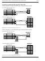
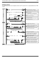
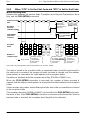
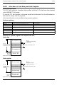
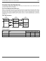
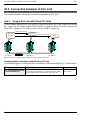
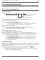
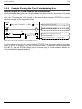
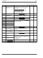
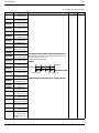
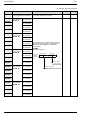
Controlling two devices with RS232C port with one FPΣ
When using the 2 - channel RS232C type communication cassette
Display panel
Two devices with RS232C port can be connected.
FPΣ
Device with RS232C port
The Tool port can be used
to connect a display panel
or other device.
Figure 1:
Device with RS232C port
Features- communication (RS232C)
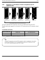
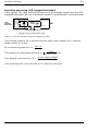
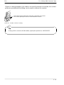
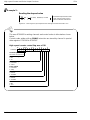
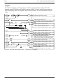
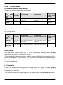
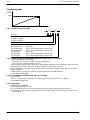
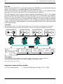
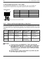
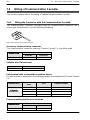
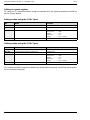
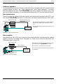
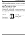
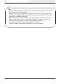
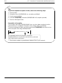
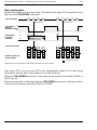
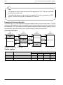
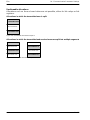
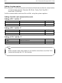
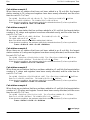
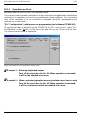
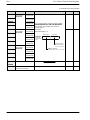
1:N communication possible with up to 99 stations (units)
When using the 1 - channel RS485 type communication cassette
Computer
Communication is possible with up to 99 units.
FPΣ
No.1
Commercial adapter
Figure 2:
FPΣ
No.2
FPΣ
No.3
FPΣ
No.99
RS485
Features- communication (C- NET)
next page
1-3
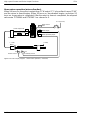
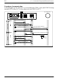
Functions and Restrictions of the Unit
FPΣ
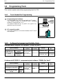
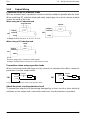
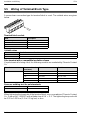
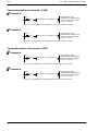
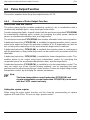
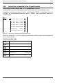
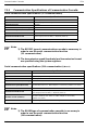
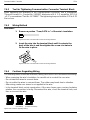
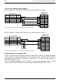
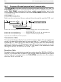
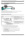
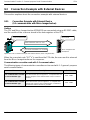
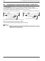
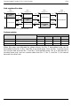
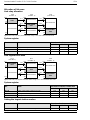
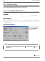
Data can be shared among the various PLCs using the PLC link function.
When using the 1 - channel RS485 type communication cassette
Data can be shared among up to 16 FPΣ units using
the PLC link function.
FPΣ
No.1
FPΣ
No.3
FPΣ
No.2
FPΣ
No.16
RS485
Figure 3:
Features- communication (PLC link)
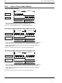
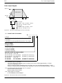
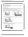
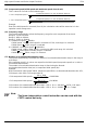
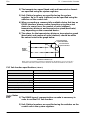
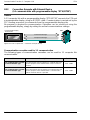
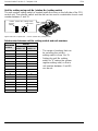
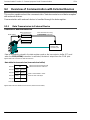
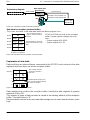
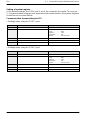
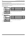
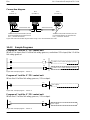
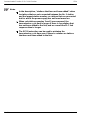
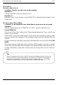
Positioning control supported through high - speed counter and pulse output
A high- speed counter and pulse output functions are provided as standard features.
The pulse output function supports frequencies of up to 100 kHz, enabling positioning
control using a stepping motor or servo motor.
Measurement using high - speed counter supported
Increment input mode, decrement input mode, 2- phase input mode, individual input mode, and
direction discrimination mode are supported.
Single phase: Max. 50 kHz, Two- phase: Max. 20 kHz
Encoder
Pulse input
Encoder
Pulse input
Figure 4:
FPΣ
Features- High- speed counter
Positioning control based on pulse output supported
CW/CCW and Pulse/sign outputs are supported.
1 - channel: Max. 100 kHz, 2 - channel: Max. 60 kHz
FPΣ
Mortor
Pulse output
Mortor
driver
Mortor
Pulse output
Mortor
driver
Figure 5:
1-4
Features- Pulse output
FPΣ
1.1 Features and Functions of the Unit
Analog control supported
An analog potentiometer (volume dial) is provided as a standard feature. This can be
used in applications such as analog timers, without using the programming tools. An
analog unit is also available as the intelligent unit.
1-5
Functions and Restrictions of the Unit
1.2
FPΣ
Unit Types
This section explains the type of unit used with the FPΣ and about the optional
communication cassette.
1.2.1
FPΣ Control Unit
Name
FPΣ Control unit
1.2.2
Number of I/O points
Part No.
Product No.
Input: 16 points/Transistor output: 16 points
FPG - C32T
AFPG2543
Input: 16 points/Transistor output: 16 points
FPG - C32T2
AFPG2643
Input: 16 points/Relay output: 8 points
FPG - C24R2
AFPG2423
FPΣ Expansion Unit
Name
Number of I/O points
Part No.
Product No.
FPΣ expansion I/O unit
Input: 32 points/Transistor output: 32 points
FPG - XY64D2T
AFPG3467
* The FPΣ expansion I/O unit can be used for “FPG - C32T2 and FPG - C24R2” FPΣ
control units.
1.2.3
Units for FP0 and FPΣ
The FPΣ can be used the FP0 series expansion I/O unit, power supply unit, and
intelligent unit.
1.2.4
Communication Cassette
A detachable communication cassette (optional) should be used when using the
various functions such as the computer link, serial data communication, and PLC link
functions.
Name
Description
Part No.
Product No.
FPΣ Communication
cassette 1 - channel
RS232C type
This communication cassette is a 1 - channel unit with
a five - wire RS232C port. It supports 1 : 1 computer
links and general - purpose serial communication. RS/
CS control is possible.
FPG - COM1
AFPG801
FPΣ Communication
cassette 2 - channel
RS232C type
This communication cassette is a 2 - channel unit with
a three- wire RS232C port. It supports 1 : 1 computer
links and general - purpose serial communication.
Communication with two external devices is possible.
FPG - COM2
AFPG802
FPΣ Communication
cassette 1 - channel
RS485 type
This communication cassette is a 1 - channel unit with
a two - wire RS485 port. It supports 1 : N computer
links (C- NET), general - purpose serial communication,
and a PLC link.
FPG - COM3
AFPG803
1-6
1.3 Restrictions on Unit Combinations
FPΣ
1.3
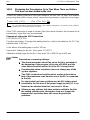
Restrictions on Unit Combinations
This section contains restrictions on unit combinations.
1.3.1
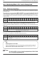
Restrictions on the Number of Expansion Units
(for FP0 expansion unit)
(Maximum possible
expansion is with a
total of three units)
Control unit
Figure 6:
Unit 1 for expansion
Unit 2 for expansion
Unit 3 for expansion
Restriction on unit combinations
Up to three expansion units can be added at the right of the FPΣ, these expansion units being
either expansion units or intelligent units from the earlier FP0 series, or a combination of the
two.
There are no restrictions on the type and the order in which expansion units are installed.
A combination of relay output types and transistor output types is also possible.
Controllable I/O Points
Type of control unit
FPG - C32T
FPG - C32T2
FPG - C24R2
Number of I/O points when using
control unit
Number of I/O points when using
FP0 expansion unit
32 points
Max. 128 points
24 points
Max. 120 points
1-7
Functions and Restrictions of the Unit
1.3.2
FPΣ
Restrictions on the Number of Units for Expansion (for FPΣ
expansion unit)
Expansion unit 4
Expansion unit 3
Expansion unit 2
Expansion unit 1
Control unit
Max. possible expansion is with a total of four units.
Up to four dedicated FPΣ expansion units can be added at the left of the FPΣ.
The 64 points type expansion unit consist of 32 input points and 32 transistor output
points.
Controllable I/O Points
Type of control unit
Number of I/O points when using
control unit
Number of I/O points when using
FPΣ expansion unit
FPG - C32T2
32 points
Max. 288 points
FPG - C24R2
24 points
Max. 280 points
The FPΣ expansion unit cannot be used for FPG - C32T.
Tip
If using FP0 expansion units and FPΣ expansion units in combination, the number
of input and output points can be expanded to a maximum of 384 points for the
FPG - C32T2 and 376 points for the FPG - C24R2.
1-8
1.4
FPΣ
1.4
Programming Tools
Programming Tools
This section explains about the programming tools for FPΣ.
1.4.1
1
Tools Needed for Programming
Programming
tool software
Programming tool software
The tool software can also be used with the FP series.
The “FPWIN Pro Ver. 4” or “FPWIN GR Ver. 2” Windows
software is used with the FPΣ.
The earlier FPWIN GR Ver. 1x, NPST - GR, and FP Programmer cannot be used.
Computer
PC connection cable
2
PC connection cable
This cable needed for connection between the FPΣ and
the computer.
FPΣ
FPΣ
Figure 7:
1.4.2
Programming tools
Software Environment and Suitable Cable
Standard ladder diagram tool software “FPWIN - GR Ver.2”
Type of software
FPWIN - GR Ver. 2
English - language
menu
English -language
software
Upgrade (to
upgrade from
Ver.1.1)
OS (Operating
system)
Windows 95/98/
Me/2000/NT
(Ver. 4.0 or later)
Hard disk
capacity
Part No.
Product
No.
FPWINGRF - EN2
AFPS10520
FPWINGRR- EN2
AFPS10520R
30MB or more
Conforms to IEC61131 - 3 programming tool software “FPWIN - Pro Ver.4”
Type of software
OS (Operating
system)
English language
Windows 95/98/
menu
Me/2000/NT
FPWIN Pro Ver. 4 Small type English - (Ver. 4.0 or later)
(for FP0, FPΣ, FP1, and
language
FP - M)
menu
FPWIN Pro Ver. 4 Full type
(for all type FP series PLC)
Hard disk
capacity
Part No.
Product
No.
FPWINPROF - EN4
AFPS50540
FPWINPROS - EN4
AFPS51540
100MB or
more
1-9
Functions and Restrictions of the Unit
FPΣ
Type of computer and suitable cable
Type of computer
Cable
IBM PC/AT or
its compatible machine
Part No.: AFC8503
D- Sub 9 - pin female - Mini DIN 5 - pin male
Part No.: AFC8513
D- Sub 25- pin male - Mini DIN 5 - pin male
1 - 10
Cable specification
Chapter 2
Specifications and Functions of Control
Unit
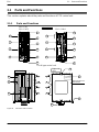
2.1
Parts and Functions . . . . . . . . . . . . . . . . . . . . . . . . . . . . . 2 - 3
2.2
Input and Output Specifications . . . . . . . . . . . . . . . . . . . 2 - 7
2.3
Terminal Layout Diagram . . . . . . . . . . . . . . . . . . . . . . . . 2 - 12
Specifications and Functions of Control Unit
2-2
FPΣ
FPΣ
2.1
2.1
Parts and Functions
Parts and Functions
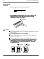
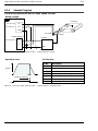
This section explains about the parts and functions of FPΣ control unit.
2.1.1
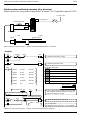
Parts and Functions
FPG - C32T
FPG - C32T2
Front view
FPG - C24R2
5
1
6
2
7
5
1
6
2
7
3
8
3
8
4
9
4
9
10
10
For all type control unit
Left side view
Right side
view
11
14
EXPANSION
CONNECTOR
15
DIN standard rail
attachment
12
13
16
14
Figure 8:
FPΣ Parts and Functions
2-3
Specifications and Functions of Control Unit
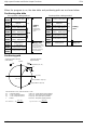
1
FPΣ
Status indicator LEDs
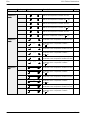
These LEDs display the current mode of operation or the occurrence of an error.
LED
LED and operation status
RUN (green)
Lights when in the RUN mode and indicates that the program is being executed.
It flashes during forced input/output.
(The RUN and PROG LEDs flash alternately.)
Lights when in the PROG. mode and indicates that operation has stopped.
PROG. (green)
It flashes during forced input/output.
(The RUN and PROG LEDs flash alternately.)
ERROR/ALARM (red)
Flashes when an error is detected during the self-diagnostic function.
Lights if a hardware error occurs, or if operation slows because of the program, and
the watchdog timer is activated.
2
RUN/PROG. mode switch
This switch is used to change the operation mode of the PLC.
Switch position
Operation mode
RUN (upward)
This sets the RUN mode. The program is executed and operation begins.
PROG. (downward)
This sets the PROG. mode. The operation stops. In this mode, programming can be
done using tools.
When performing remote switching from the programming tool, the position of the mode
switch and the actual mode of operation may differ. Verify the mode with the status indicator
LED. Otherwise, restart the FPΣ and change the mode of operation with the RUN/PROG.
mode switch.
3
Communication status LEDs
These display the communication status of the COM.1 and COM.2 ports.
LED
COM.1
LED and communication status
S
R
COM.2
S
R
4
Transmitted data
monitor
Flashes while data is being transmitted
Received data
monitor
Flashes while data is being received
Transmitted data monitor
Flashes while data is being transmitted
Received data
monitor
Flashes while data is being received
Goes out when no data is being transmitted
Goes out when no data is being received
Goes out when no data is being transmitted
Goes out when no data is being received
Tool port (RS232C)
This port is used to connect a programming tool.
5
Input connector (10 pins × 2)
6
Input indicator LEDs
2-4
2.1
FPΣ
7
Output connector (10 pins × 2)
8
Output indicator LEDs
9
Analog potentiometer (analog dial)
Parts and Functions
Turning this dial changes the values of special data registers DT90040 and DT90041 within
the range of K0 to K1000. It can be used for analog timers and other applications.
10
Power supply connector (24 V DC)
Supply 24 V DC. It is connected using the power supply cable (AFP0581) that comes with the
unit.
11
Left - side connector for FPΣ expansion
This is used to connect dedicated FPΣ expansion units on the left side of the control unit with
the internal circuits.
*The FPG - C32T2 and FPG - C24R2 control units are equipped with this connector, but the
FPG - C32T is not.
12
Unit No. (Station No.) setting switch
This unit No. (station No.) is specified when using the communication functions provided on
the optional communication cassettes.
The unit No. (station No.) setting switch is located under the cover on the back of the
unit. Specify the unit (station) number using the selector switch and the dial.
Figure 9:
13
FPΣ Parts and Functions (Unit No. setting switch)
Communication cassette (option)
This is the optional cassette type adapter used when communication is carried out.
Any one of the following the cassette types may be installed.
- 1 - channel RS232C type
- 2 - channel RS232C type
- 1 - channel RS485 type
14
Expansion hook
This hook is used to secure expansion units. The hook is also used for installation on flat type
mounting plate (AFP0804).
15
Right - side connector for FP0 expansion
Connects an expansion unit to the internal circuit of the control unit.
16
DIN rail attachment lever
The FPΣ unit enables attachment at a touch to a DIN rail. The lever is also used for
installation on slim 30 type mounting plate (AFP0811).
2-5
Specifications and Functions of Control Unit
2.1.2
FPΣ
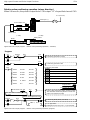
Tool Port Specification
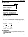
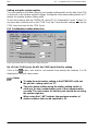
A commercial mini - DIN 5 - pin connector is used for the Tool port on the control unit.
2
4
1
5
3
Pin no.
Signal name
Abbreviation
Signal direction
1
Signal Ground
SG
—
2
Transmitted Data
SD
Unit → External device
3
Received Data
RD
Unit ← External device
4
(Not used)
—
—
5
+5V
+5V
Unit → External device
Figure 10: FPΣ Parts and Functions (Tool port)
The following are the default settings set when the unit is shipped from the factory. The
system registers should be used to change these.
-
Baud rate . . . . . .
Character bit . . .
Parity check . . . .
Stop bit length . .
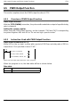
2.1.3
9600 bps
8 bit
Odd parity
1 bit
Communication Cassette
The detachable communication cassette (optional) can be selected from among the
three types shown below.
Type
Applicable communication
function
1 - channel
RS232C
type
Computer link
2 - channel
RS232C
type
Computer link
General - purpose serial
communication
General - purpose serial
communication
1 - channel Computer link
RS485 type General - purpose serial
communication
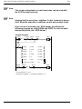
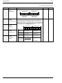
Terminal layout diagram
SD: Transmitted Data (Output)
RD: Received Data (Input)
RS: Request to Send (Output)
CS: Clear to Send (Input)
SG: Signal Ground
S1: Transmitted Data (Output) (COM.1)
R1: Received Data (Input) (COM.1)
S2: Transmitted Data (Output) (COM.2)
R2: Received Data (Input) (COM.2)
SG: Signal Ground (COM.1 and 2)
General Terminal
station station
PLC link
Short
2-6
2.2 Input and Output Specifications
FPΣ
2.2
Input and Output Specifications
This section contains input and output specifications of FPΣ control unit.
2.2.1
Input Specifications
Input specifications (for all type)
Item
Description
Insulation method
Optical coupler
Rated input voltage
24 V DC
Operating voltage range
21.6 to 26.4 V DC
Rated input current
For X0, X1, X3, X4: approx. 8 mA
For X2, X5 to X7: approx. 4.3 mA
For X8 to XF:
approx. 3.5 mA
Input points per common
For C32T, C32T2: 16 points/common
For C24R2: 8 points/common
(Either the positive or negative of the input power supply can be connected to
common terminal.)
Min. on voltage/Min. on current
For X0, X1, X3, X4: 19.2 V DC/6 mA
For X2, X5 to XF: 19.2 V DC/3 mA
Max. off voltage/Max. off current
2.4 V DC/1.3 mA
Input impedance
For X0, X1, X3, X4: 3 kΩ
For X2, X5 to X7: 5.6 kΩ
For X8 to XF:
6.8 kΩ
Response time
off → on
For input X0, X1, X3, X4:
1 ms or less:
normal input
5 µs or less:
high- speed counter, pulse catch, interrupt input settings
For input X2, X5 to X7:
1 ms or less:
normal input
100 µs or less: high- speed counter, pulse catch, interrupt input settings
For input X8 to XF:
1 ms or less:
normal input only
on → off
Operating mode indicator
Note
Same as above
LED display
X0 through X7 are inputs for the high-speed counter and have a
fast response time. If used as normal inputs, we recommend
inserting a timer in the ladder program as chattering and noise
may be interpreted as an input signal.
Also, the above specifications apply when the rated input voltage
is 24 VDC and the temperature is 25°C/70°F.
2-7
Specifications and Functions of Control Unit
FPΣ
Limitations on number of simultaneous input on points
Keep the number of input points per common which are simultaneously on within the
following range as determined by the temperature.
[C32T]
[C24R]
at 24 V DC
16
Number of
points per 12
common
which are si- 8
multaneous
on
16
at 26.4 V DC Number of
points per 12
common
which are si- 9
multaneous 7
on
46/ 52/ 55/
107.8 118.6 124
Ambient temperature (°C/°F)
Figure 11: FPΣ Limitations on number of simultaneous input on points
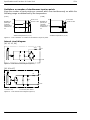
Internal circuit diagram
[X0, X1, X3, X4]
3 kΩ
Internal circuit
Xn
510 Ω
COM
Figure 12: FPΣ Internal circuit diagram (Input- 1)
[X2, X5 to XF]
Internal circuit
R1
Xn
R2
COM
R1: 5.6 kΩ, R2: 1 kΩ
R1: 6.8 kΩ, R2: 820 Ω
Figure 13: FPΣ Internal circuit diagram (Input- 2)
2-8
at 26.4 V DC
46/ 48/ 55/
107.8 118.4 124
Ambient temperature (°C/°F)
For X2 and X5 to X7,
For X8 to XF,
at 24 V DC
2.2 Input and Output Specifications
FPΣ
2.2.2
Output Specifications
Transistor output specifications (for C32T and C32T2)
Item
Description
Insulation method
Optical coupler
Output type
Open collector (NPN)
Rated load voltage
5 to 24 V DC
Operating load voltage range
4.75 to 26.4 V DC
Max. load current
For Y0, Y1, Y3, Y4: 0.3 A
For Y2, Y5 to YF: 0.1 A
Max. surge current
For Y0, Y1, Y3, Y4: 0.9 A
For Y2, Y5 to YF: 0.5 A
Output points per common
16 points/common
Off state leakage current
100 µA or less
On state voltage drop
0.5 V or less
Response time
off → on
For Y0, Y1, Y3, Y4 (at 15 mA or more): 2 µs or less
For Y2, Y5 to YF: 0.2 ms or less
on → off
For Y0, Y1, Y3, Y4 (at 15 mA or more): 8 µs or less
For Y2, Y5 to YF: 0.5 ms or less
Voltage
21.6 to 26.4 V DC
Current
70 mA or less
External power
supply for
di i
driving
iinternall
circuit
Surge absorber
Zener diode
Operating mode indicator
LED display
Phase fault protection
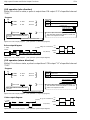
Thermal protection for Y2, Y5 to YF
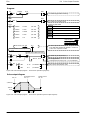
Limitations on number of simultaneous output on points
Keep the number of output points per common which are simultaneously on within the
following range as determined by the ambient temperature.
[C32T]
Number of 16
points per
12
common
which are simultaneous 8
on
at 24 V DC
at 26.4 V DC
46/ 52/ 55/
107.8 118.6 124
Ambient temperature (°C/°F)
Figure 14: FPΣ Limitations on number of simultaneous output on points
2-9
Specifications and Functions of Control Unit
FPΣ
Internal circuit diagram
[Y0, Y1, Y3, Y4]
Output indicator LED
+
Output circuit
Internal circuit
Output
Load
Load
power supply
5 to 24 V DC
External power supply
24 V DC
0V
Figure 15: FPΣ Internal circuit diagram (output- 1)
[Y2, Y5 to YF]
Output indicator LED
+
Output circuit
Internal circuit
Output
Load
Load
power supply
5 to 24 V DC
0V
Phase fault
protection circuit
Figure 16: FPΣ Internal circuit diagram (output- 2)
2 - 10
External power supply
24 V DC
2.2 Input and Output Specifications
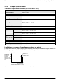
FPΣ
Relay output specifications (for C24R2)
Item
Description
Output type
1a (1 Form A, Normally open)
Rated control capacity
2 A 250 V AC, 2 A 20 V DC (4.5 A per common or later)
Output points per common
8 points/common
Response time
off → on
Approx. 10 ms
on → off
Approx. 8 ms
Mechanical lifetime
Min. 20,000,000 operations
Electrical lifetime
Min. 100,000 operations
Surge absorber
-
Operating mode indicator
LED display
Limitations on number of simultaneous output on points
Keep the number of output points which are simultaneously on within the following
range as determined by the ambient temperature.
[C24R]
Number of
points per
common
which are
simultaneous
on
8
at 24 V DC
at 26.4 V DC
4
46/ 48/ 55/
107.8 118.4 124
Ambient temperature (°C/°F)
Internal circuit diagram
Internal circuit
[C24R]
Yn
COM
2 - 11
Specifications and Functions of Control Unit
2.3
FPΣ
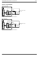
Terminal Layout Diagram
2.3.1
Control Unit (for C32T and C32T2)
Input
X0- 7
X0 X1
X2 X3
X4 X5
X6 X7
COM COM
Note
X0 X1
X8- F
X8 X9
XA XB
XC XD
XE XF
COM COM
X8 X9
The four COM terminals of input circuit are connected internally.
Output
Y0
L
L
L
L
Y0- 7
Y0 Y1
Y2 Y3
Y4 Y5
Y6 Y7
(+) (–)
L
L
L
L
L
L
L
L
Y8- F
Y8 Y9
YA YB
YC YD
YE YF
(+) (–)
Y1
Y8 Y9
L
L
L
L
(Connector front view)
Figure 17: FPΣ Terminal layout diagram (I/O connector)
Notes
The two (+) terminals of output circuit are connected
internally.
The two (–) terminals of output circuit are connected internally.
2.3.2
Control Unit (for C24R2)
Input
X0
X0 X8
X1 X9
X2 XA
X3 XB
X4 XC
X5 XD
X6 XE
X7 XF
COM COM
Note
X8
The two COM terminals of input circuit are not connected
internally.
Output
Y0
Y1
Y2
Y3
Y4
Y5
Y6
Y7
COM
2 - 12
L
L
L
L
L
L
L
L
Power
Y0
(Connector front view)
Chapter 3
Expansion
3.1
Type of Expansion Unit . . . . . . . . . . . . . . . . . . . . . . . . . . 3 - 3
3.2
Expansion Method of Units for FP0 and FPΣ . . . . . . . . 3 - 4
3.3
Expansion Method of FPΣ Expansion Unit . . . . . . . . . . 3 - 5
3.4
Specifications of FPΣ Expansion Unit . . . . . . . . . . . . . . 3 - 6
Expansion
3-2
FPΣ
FPΣ
3.1
3.1 Type of Expansion Unit
Type of Expansion Unit
Expansion I/O units, power supply units, and intelligent units from the earlier FP0 series
can be used with the FPΣ, in addition to the dedicated expansion units designed
expressly for the FPΣ.
Expansion units used for the earlier FP0 series are connected on the right side of the
control unit, just as they were with the FP0. Dedicated expansion units for the FPΣ are
connected to the left side of the control unit.
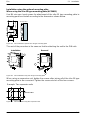
Expansion on left side of control unit
Expansion on right side of control unit
FPΣ dedicated
expansion unit
FP0 expansion unit
Expansion possible up to 4 units
Expansion possible up to 3 units
Control unit
3-3
Expansion
3.2
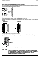
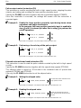
FPΣ
Expansion Method of Units for FP0 and FPΣ
The previously available expansion I/O unit or intelligent unit for FP0 is expanded by
connecting to the right side of control unit.
Because unit expansion is done using the right - side connector for FP0 expansion and
expansion hook on the side of the unit, no expansion cable is needed.
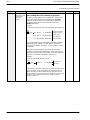
1
Peel the seal on the side of the unit so that the internal right - side connector for FP0
expansion is exposed.
Peel the seal.
Figure 18: Expansion method procedure - 1
2
Raise the expansion hooks on the top and bottom sides of the unit with a screwdriver.
Figure 19: Expansion method procedure - 2
3
Align the pins and holes in the four corners of the control unit and expansion unit, and
insert the pins into the holes so that there is no gap between the units.
Figure 20: Expansion method procedure - 3
4
Press down the expansion hooks raised in step 2 to secure the unit.
Figure 21: Expansion method procedure - 4
3-4
3.3 Expansion Method of FPΣ Expansion Unit
FPΣ
3.3
Expansion Method of FPΣ Expansion Unit
The dedicated expansion unit for FPΣ is expanded by connecting to the left side of the
control unit. Because unit expansion is done using the left - side connector for FPΣ
expansion and expansion hook on the side of the unit, no expansion cable is needed.
1
Remove the cover on the left side of the unit so that the internal left- side connector for
FPΣ expansion is exposed.
2
Raise the expansion hooks on the top and bottom sides of the unit with a screwdriver.
3
Align the pins and holes in the four corners of the control unit and expansion unit, and
insert the pins into the holes so that there is no gap between the units.
4
Press down the expansion hooks raised in step 2 to secure the unit.
3-5
Expansion
3.4
FPΣ
Specifications of FPΣ Expansion Unit
3.4.1
FPΣ Expansion I/O Unit
Parts and Functions
FPG - XY64D2T
(Input: 32 points / Transistor output: 32 points)
Front view
1
4
2
3
Left side view
Right side view
5
6
5
DIN standard
rail attachment
7
6
1
LED display selection switch
Switches between the input (32 points) and output (32 points) of the LED display.
2
Input connector (40 pins)
3
Output connector (40 pins)
4
Input and Output indicator LEDs
5
FPΣ expansion connector
This expansion connector is used to connect the dedicated unit for FPΣ.
6
Expansion hook
This hook is used to secure expansion unit. The hook is also used for installation on FP0
mounting plate (flat type)(Part No.: AFP0804).
7
DIN rail attachment lever
The expansion unit enables attachment at a touch to a DIN rail. The lever is also used for
installation on FP0 mounting plate (slim 30 type)(Part No.: AFP0811).
3-6
3.4 Specifications of FPΣ Expansion Unit
FPΣ
Input specifications
Item
Description
Insulation method
Optical coupler
Rated input voltage
24 V DC
Operating voltage range
21.6 to 26.4 V DC
Rated input current
Approx. 3.5 mA
Input points per common
32 points/common
(Either the positive or negative of input power supply can be connected to
common terminal.)
Min. on voltage/Min. on current
19.2 V DC/3 mA
Max. off voltage/Max. off current
2.4 V DC/1.3 mA
Input impedance
Approx. 6.8 kΩ
Response time
off → on
0.2 ms or less
on → off
0.3 ms or less
Operating mode indicator
LED display
Transistor output specifications
Item
Description
Insulation method
Optical coupler
Output type
Open collector
Rated load voltage
5 to 24 V DC
Operating load voltage range
4.75 to 26.4 V DC
Max. load current
0.1 A
Max. surge current
0.5 A
Output points per common
32 points/common
Off state leakage current
100 µA or less
On state voltage drop
0.5 V or less
Response time
off → on
0.2 ms or less
on → off
0.5 ms or less
Voltage
21.6 to 26.4 V DC
Current
15 mA or less
External power
supp
y for
o
supply
di i
driving
iinternall
circuit
Surge absorber
Zener diode
Operating mode indicator
LED display
Phase fault protection
Thermal protection
3-7
Expansion
FPΣ
Limitations on number of simultaneous on points
Keep the number of points which are simultaneously on within the following range as
determined by the ambient temperature.
[Input]
Number of 32
points per 29
common
which are simultaneous
on
at 24 VDC
and 26.4
VDC
[Output]
Number of 32
points per 29
at 24 VDC
and 26.4
VDC
common
which are simultaneous
on
52/ 55/
118.6 124
Ambient temperature (°C/°F)
52/ 55/
118.6 124
Ambient temperature (°C/°F)
Internal circuit diagram
[Input]
[Output]
Output display LED
Xn
Inside COM
Output circuit
820 Ω
+
Output terminal
Internal circuit
Internal circuit
6.8 kΩ
Load
Power
supply for
load 5 to
24 VDC
0V
External power
supply 24 VDC
Phase fault protection
Terminal layout diagram
Input connector
(Left side on unit)
A
Output connector
(Right side on unit)
A
B
L 1 100 108 1 L
L 2 101 109 2 L
L 3 102 10A 3 L
L 4 103 10B 4 L
B
1 100 108 1
2 101 109 2
3 102 10A 3
4 103 10B 4
24 V DC
7 106 10E 7
8 107 10F 8
COM
COM
9
10 N.C. N.C. 10
11 110 118 11
12 111 119 12
13 112 11A 13
14 113 11B 14
15 114 11C 15
16 115 11D 16
17 116 11E 17
18 117 11F 18
19
20
COM
COM
N.C.
N.C.
19
20
The COM terminals are connected
internally with the same connector.
5 to 24 V DC
L 8 107 10F 8 L
9 — — 9
10
10
+
+
L 11 110 118 11 L
L 12 111 119 12 L
L 13 112 11A 13 L
(Front view of connector)
L 14 113 11B 14 L
L 15 114 11C 15 L
L 16 115 11D 16 L
L 17 116 11E 17 L
L 18 117 11F 18 L
19 — — 19
20
20
+
+
Although “+” and “- ” terminals are connected
internally with the same connector, it is recommended that they also be connected externally.
Note: The number in the connector are for the first expansion.
3-8
Y100
Y108
L 5 104 10C 5 L
L 6 105 10D 6 L
L 7 106 10E 7 L
5 104 10C 5
6 105 10D 6
9
X108
X100
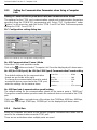
Chapter 4
I/O Allocation
4.1
I/O Allocation . . . . . . . . . . . . . . . . . . . . . . . . . . . . . . . . . . . 4 - 3
I/O Allocation
4-2
FPΣ
FPΣ
4.1
4.1
I/O Allocation
I/O Allocation
This section explains about the I/O allocation of FPΣ.
FPΣ expansion unit side
Fourth
expansion
Third
expansion
Second
expansion
Control unit
First
expansion
Max. possible expansion is
with a total of four units.
FP0 expansion unit side
First
Second
Third
expansion expansion expansion
Max. possible expansion is
with a total of three units.
Figure 22: FPΣ I/O allocation
4.1.1
I/O Number of FPΣ Control Unit
The I/O allocation of FPΣ control unit is fixed.
Type of control unit
I/O number
FPG - C32T
Input (16 points)
X0 to XF
FPG - C32T2
Output (16 points)
Y0 to YF
Input (16 points)
X0 to XF
Output (8 points)
Y0 to Y7
FPG - C24R2
4-3
I/O Allocation
4.1.2
FPΣ
I/O Number of FPΣ Expansion Unit (for left side expansion)
I/O do not need to be set as I/O allocation is performed automatically when an
expansion unit is added.
The I/O allocation of expansion unit is determined by the installation location.
First
expansion
Second
expansion
Third
expansion
Fourth
expansion
Input (32 points)
X100 to X11F
X180 to X19F
X260 to X27F
X340 to X35F
Output (32 points)
Y100 to Y11F
Y180 to Y19F
Y260 to Y27F
Y340 to Y35F
Type of expansion unit
XY64D2T
Note
The FPΣ expansion unit nearest the control unit has the lowest
I/O number, so that the unit closest to the control unit is the first
unit, the one next to that the second, and so on. Consequently,
the I/O numbers in the illustration below start with the lowest
number at the right and proceed in sequential order.
The I/O numbers indicated below
would be used if the FPG - C32T or
FPG - C32T2 was used as the control
unit, and the XY64D2T was used as
the FPΣ expansion unit.
FPΣ control unit
X0 to XF
Y0 to YF
FPΣ expansion unit
Y100 to Y11F First expansion
X100 to X11F
Y180 to Y19F Second expansion
X180 to X19F
Y260 to Y27F Third expansion
X260 to X27F
Y340 to Y35F Fourth expansion
X340 to X35F
4-4
4.1
FPΣ
4.1.3
I/O Allocation
I/O Number of FP0 Expansion Unit (for right side expansion)
I/O do not need to be set as I/O allocation is performed automatically when an
expansion unit is added. The I/O allocation of expansion unit is determined by the
installation location.
Type of expansion unit
E8X
First expansion
Second expansion
Third expansion
Input (8 points)
X20 to X27
X40 to X47
X60 to X67
Input (4 points)
X20 to X23
X40 to X43
X60 to X63
Output (4 points)
Y20 to Y23
Y40 to Y43
Y60 to Y63
E8YR/E8YT/E8YP
Output (8 points)
Y20 to Y27
Y40 to Y47
Y60 to Y67
E16X
Input (16 points)
X20 to X2F
X40 to X4F
X60 to X6F
Input (8 points)
X20 to X27
X40 to X47
X60 to X67
E8R
E16R/E16T/E16P
E16YT/E16YP
E32T/E32P
4.1.4
Output (8 points)
Y20 to Y27
Y40 to Y47
Y60 to Y67
Output (16 points)
Y20 to Y2F
Y40 to Y4F
Y60 to Y6F
Input (16 points)
X20 to X2F
X40 to X4F
X60 to X6F
Output (16 points)
Y20 to Y2F
Y40 to Y4F
Y60 to Y6F
I/O Number of FP0 Analog I/O Unit (for right side expansion)
The I/O allocation of FP0 analog I/O unit “FP0 - A21” is determined by the installation
location.
Unit
Input
First expansion
Second expansion
Third expansion
CH0 (16 points)
WX2 (X20 to X2F)
WX4 (X40 to X4F)
WX6 (X60 to X6F)
CH1 (16 points)
WX3 (X30 to X3F)
WX5 (X50 to X5F)
WX7 (X70 to X7F)
WY2 (Y20 to Y2F)
WY4 (Y40 to Y4F)
WY6 (Y60 to Y6F)
Output (16 points)
4.1.5
I/O Number of FP0 A/D Conversion Unit (for right side expansion)
The I/O allocation of FP0 A/D conversion unit “FP0 - A80” is determined by the
installation location.
The data for the various channels is converted and loaded with a user program that
includes a switching flag to convert the data.
Unit
First expansion
Second expansion
Third expansion
WX2 (X20 to X2F)
WX4 (X40 to X4F)
WX6 (X60 to X6F)
WX3 (X30 to X3F)
WX5 (X50 to X5F)
WX7 (X70 to X7F)
CH0 (16 points)
CH2 (16 points)
CH4 (16 points)
Input
CH6 (16 points)
CH1 (16 points)
CH3 (16 points)
CH5 (16 points)
CH7 (16 points)
4-5
I/O Allocation
4.1.6
FPΣ
I/O Number of FP0 I/O Link Unit (for right side expansion)
The I/O allocation of FP0 I/O link unit “FP0 - IOL” is determined by the installation
location.
Unit
First expansion
Second expansion
Third expansion
Input (32 points)
X20 to X3F
X40 to X5F
X60 to X7F
Output (32 points)
Y20 to Y3F
Y40 to Y5F
Y60 to Y7F
Tip
I/O number of FPΣ and FP0
Specifying X and Y numbers
On the FPΣ and the FP0, the same numbers are used for input and output.
Example: The same number “X20 and Y20” can be used for input and output
Expression of numbers for input/output relays
Since input relay “X” and output relay “Y” are handled in units of 16 points,
they are expressed as a combination of decimal and hexadecimal numbers as
shown below.
Decimal
1, 2, 3 ......
Hexadecimal
1, 2, 3 ...... 9, A, B ... F
4-6
X
Chapter 5
Installation and Wiring
5.1
Installation . . . . . . . . . . . . . . . . . . . . . . . . . . . . . . . . . . . . . 5 - 3
5.2
Wiring of Power Supply . . . . . . . . . . . . . . . . . . . . . . . . . . 5 - 9
5.3
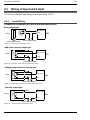
Wiring of Input and Output . . . . . . . . . . . . . . . . . . . . . . . 5 - 12
5.4
Wiring of MIL Connector Type . . . . . . . . . . . . . . . . . . . 5 - 17
5.5
Wiring of Terminal Block Type . . . . . . . . . . . . . . . . . . . . 5 - 20
5.6
Safety Measures . . . . . . . . . . . . . . . . . . . . . . . . . . . . . . . 5 - 22
5.7
Backup Battery . . . . . . . . . . . . . . . . . . . . . . . . . . . . . . . . 5 - 24
Installation and Wiring
5-2
FPΣ
FPΣ
5.1
5.1
Installation
Installation
This section explains installation environment and installation method of FPΣ.
5.1.1
Installation Environment and Space
Avoid installing the unit in the following locations:
- Ambient temperatures outside the range of 0°C to
55°C/32°F to 131°F
- Ambient humidity outside the range of 30% to 85% RH
- Sudden temperature changes causing condensation
- Inflammable or corrosive gases
- Excessive airborne dust, metal particles or salts
- Benzine, paint thinner, alcohol or other organic solvents or
strong alkaline solutions such as ammonia or caustic soda
- Excessive vibration or shock
- Direct sunlight
- Water or oil in any form including spray or mist
Measures regarding noise:
- Influence from power transmission lines, high voltage
equipment, power cables, power equipment, radio
transmitters, or any other equipment that would generate
high switching surges
- If noise occurs in the power supply line even after the
above countermeasures are taken, it is recommended to
supply power through an insulation transformer, noise
filter, or like.
5-3
Installation and Wiring
FPΣ
Measures regarding heat discharge
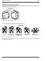
Always install the unit orientated with the tool port facing outward on the bottom in order
to prevent the generation of heat.
CORRECT
Figure 23: FPΣ Installation - heat discharge
Do not install the FPΣ control unit as shown below.
INCORRECT
Upside- down
Installation which
blocks the air duct
Installations such that
the input and output
connectors face down
Input and output
connectors on top
Horizontal
installation of the unit
Figure 24: FPΣ Installation direction
Do not install the unit above devices which generate heat such as heaters, transformers
or large scale resistors.
5-4
5.1
FPΣ
Installation
Installation space
Leave at least 50 mm/1.97 in. of space between the wiring ducts of the unit and other
devices to allow heat radiation and unit replacement.
50 mm/1.97 in.
or more
50 mm/1.97 in.
or more
Figure 25: FPΣ Installation space - 1
Maintain a minimum of 100 mm/3.937 in. between devices to avoid adverse affects from
noise and heat when installing a device or panel door to the front of the PLC unit.
Other device
PLC unit
100 mm/
3.937 in.
or more
Panel door
Figure 26: FPΣ Installation space - 2
Keep the first 100 mm/3.937 in. from the front surface of the control unit open in order
to allow room for programming tool connections and wiring.
5-5
Installation and Wiring
5.1.2
FPΣ
Installation and Removal
Attachment to DIN rail and removal from DIN rail
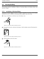
The FPΣ unit enables simple attachment to DIN rails.
Procedure of installation method
1
Fit the upper hook of the unit onto the DIN
rail.
2
Without moving the upper hook, press on the
lower hook to fit the unit into position.
1
2
Figure 27: Installation method
Procedure of removal method
1
Insert a slotted screwdriver into the DIN rail
attachment lever.
2
Pull the attachment lever downwards.
3
Lift up the unit and remove it from the rail.
3
1
2
Figure 28: Removal method
5-6
5.1
FPΣ
Installation
10 mm/0.39 in.
30 mm/
1.18 in.
90 mm/3.54 in.
Installation using the optional mounting plate
When using the slim 30 type mounting plate (AFP0811)
Use M4 size pan - head screws for attachment of the slim 30 type mounting plate to
mounting panel and install according to the dimensions shown below.
30 mm/
1.18 in.
6 mm/0.24 in.
Figure 29: FPΣ Installation - optional slim 30 type mounting plate
The rest of the procedure is the same as that for attaching the unit to the DIN rails.
Installation
Removal
1
3
4
1
2
Figure 30: FPΣ Installation using slim 30 type mounting plate
When using an expansion unit, tighten the screws after joining all of the slim 30 type
mounting plate to be connected. Tighten the screws at each of the four corners.
Example: Two expansion units
30.0 mm/1.18 in.
60.0 mm/2.36 in
Figure 31: FPΣ Installation using two expansion units
5-7
Installation and Wiring
FPΣ
When using the flat type mounting plate (AFP0804)
Use M4 size pan - head screws for attachment of the flat type mounting plate and install
according to the dimensions shown below.
60.0 mm/
2.36 in.
Figure 32: FPΣ Installation - optional flat type mounting plate
Raise the expansion hooks on the top and bottom of the unit.
Align the expansion hooks with the mounting plate and press the hooks on the top and
bottom.
Installation
Removal
Figure 33: FPΣ Installation using flat type mounting plate
An unit with an attached flat type mounting plate can also be installed sideways on a
DIN rail.
DIN rail
Figure 34: FPΣ Installation on DIN rail using flat type mounting plate
Note
5-8
The flat type mounting plate (AFP0804) should be used only with
the control unit as a stand - alone unit. It should not be used when
the control unit is being used in combination with an FP0
expansion unit or FPΣ expansion unit.
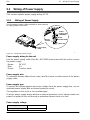
5.2
FPΣ
5.2
Wiring of Power Supply
Wiring of Power Supply
This section explains power supply wiring of FPΣ.
5.2.1
Wiring of Power Supply
Use the power supply cable provided as an accessory
to supply power to the unit.
Power
supply cable
(AFP0581)
Brown:
24 V DC
Green:
Function earth
Blue: 0 V
Power supply
cable
Figure 35: FPΣ Wiring of power supply
Power supply wiring for the unit
Use the power supply cable (Part No.: AFP0581) that comes with the unit to connect
the power supply.
- Brown:
- Blue:
- Green:
24 V DC
0V
Function earth
Power supply wire
To minimize adverse effects from noise, twist the brown and blue wires of the power
supply cable.
Power supply type
To protect the system against erroneous voltage from the power supply line, use an
insulated power supply with an internal protective circuit.
The regulator on the unit is a non-insulated type.
If using a power supply device without an internal protective circuit, always make sure
power is supplied to the unit through a protective element such as a fuse.
Power supply voltage
Rated voltage
Operating voltage range
24 V DC
21.6 to 26.4 V DC
5-9
Installation and Wiring
FPΣ
Wiring system
Isolate the wiring systems to the control unit, input/output devices, and mechanical
power apparatus.
Circuit breaker
Mechanical
power
apparatus
Input/Output
devices
Control unit
Insulated DC
power supply
Figure 36: FPΣ Power supply wiring system
Measures regarding power supply sequence (start up sequence)
The power supply sequence should be set up so that power to the control unit is turned
off before the input/output power supplies.
If the input/output power supplies are turned off before the power to the control unit, the
control unit will detect the input fluctuations and may begin an unscheduled operation.
Be sure to supply power to a control unit and an expansion unit from the same power
supply, and turn the power on and off simultaneously for both.
5 - 10
5.2
FPΣ
5.2.2
Wiring of Power Supply
Grounding
Under normal conditions, the inherent noise resistance is sufficient. However, in
situations of excess noise, ground the instrument to increase noise suppression.
For grounding purposes, use wiring with a minimum of 2 mm2. The grounding
connection should have a resistance of less than 100 Ω.
The point of grounding should be as close to the PLC unit as possible. The ground wire
should be as short as possible.
If two devices share a single ground point, it may produce an adverse effect. Always
use an exclusive ground for each device.
CORRECT
INCORRECT
Other device
(Inverter etc.)
Other device
(Inverter etc.)
Figure 37: FPΣ Grounding
Note
Depending on the surroundings in which the equipment is used,
grounding may cause problems.
Example:
Since the power supply line of the FPΣ power supply connector
is connected to the function earth through a varistor, if there is
an irregular potential between the power supply line and earth,
the varistor may be shorted.
24 V DC
0V
Function
earth
24 V DC
0V
Varistor
82 V: for C32T, C32T2
56 V: for C24R2
FPΣ power supply line
Function
earth
Varistor
(39 V)
FP0 exponsion unit
power supply line
Figure 38: Power supply line of FPΣ and FP0 expansion unit
5 - 11
Installation and Wiring
5.3
FPΣ
Wiring of Input and Output
This section explains input wiring and output wiring of FPΣ.
5.3.1
Input Wiring
Connection of photoelectric sensor and proximity sensor
Sensor
Internal
circuit
Relay output type
Input terminal
COM
Relay
Power supply for sensor
FPΣ
Power supply for input
Figure 39: FPΣ Relay output type sensor
Sensor
Internal
circuit
NPN open collector output type
Vcc
Output
0V
Input terminal
FPΣ
COM
Power supply for input
Figure 40: FPΣ NPN open collector output type sensor
Sensor
Internal
circuit
Voltage output (Universal output) type
Vcc
Output
0V
Input terminal
FPΣ
COM
Power supply for input
Figure 41: FPΣ Voltage output (universal output) type sensor
Two-wire output type
Sensor
Internal
circuit
Output
Input terminal
FPΣ
COM
Power supply for input
Figure 42:
5 - 12
FPΣ Two- wire output type sensor
5.3
FPΣ
Wiring of Input and Output
Precaution when using LED - equipped lead switch
When a LED is connected in series to an input contact such as LED-equipped lead
switch, make sure that the on voltage applied to the PLC input terminal is greater than
19.2 V DC. In particular, take care when connecting a number of switches in series.
LED equipped
lead
switch
LED
contact
Input terminal
19.2 V
or more
FPΣ
COM
24 V
Figure 43: FPΣ Precaution when using LED- equipped lead switch
Precaution when using two - wire type sensor
If the input of PLC does not turn off because of leakage current from the two-wire
type sensor “photoelectric sensor or proximity sensor”, the use of a bleeder resistor
is recommended, as shown below.
Two- wire
type sensor
Internal
circuit
Input terminal
Bleeder
resistor
FPΣ
R
COM
Figure 44: FPΣ Precaution when using two - wire type sensor
The off voltage of the input is 2.4 V, therefore, select the value of bleeder resistor “R” so that
the voltage between the COM terminal and the input terminal will be less than 2.4 V.
The input impedance is 5.6 kΩ. (I: Sensor’s leakage current (mA))
The resistance R of the bleeder resistor is: R
13.44
5.6 x I –2.4
(kΩ)
The formula is based on an input impedance of 5.6 kΩ. The input impedance varies depending on the input terminal number.
The wattage W of the resistor is:
(Power supply voltage)2
W=
R
In the actual selection, use a value that is 3 to 5 times the value of W.
5 - 13
Installation and Wiring
FPΣ
Precaution when using LED - equipped limit switch
If the input of PLC does not turn off because of the leakage current from the LEDequipped limit switch, the use of a bleeder resistor is recommended, as shown below.
Internal
circuit
Input terminal
LED equipped
limit switch
r
Bleeder
resistor
FPΣ
R
COM
Power supply for input
r: Internal resistor of limit switch (kΩ)
Figure 45: FPΣ Precaution when using LED- equipped limit switch
The off voltage of input is 2.4 V, therefore when the power supply voltage is 24 V, select the
bleeder resistor “R” so that
the current will be greater than I =
24 - 2.4
r
The resistance R of the bleeder resistor is: R
The wattage W of the resistor is: W =
13.44
(kΩ)
5.6 x I - 2.4
(Power supply voltage)2
R
In the actual selection, use a value that is 3 to 5 times the value of W.
5 - 14
5.3
FPΣ
5.3.2
Wiring of Input and Output
Output Wiring
Protective circuit for inductive loads
With an inductive load, a protective circuit should be installed in parallel with the load.
When switching DC inductive loads with relay output type, be sure to connect a diode
across the ends of the load.
When using an AC inductive load
Surge absorver
FPΣ
Output
terminal
Varistor
Output
terminal
Load
Load
FPΣ
COM
COM
Example of surge absorber: R: 50 Ω, C: 0.47 μF
When using a DC inductive load
Diode
FPΣ
Output
terminal
Load
COM
Diode:
Reverse voltage (VR): 3 times the load voltage
Average rectified forward current (I0): Load current or more
Precautions when using capacitive loads
When connecting loads with large in-rush currents, to minimize their effect, connect a
protection circuit as shown below.
FPΣ
Output
terminal
Resistor
Load
COM
FPΣ
Output
terminal
Inductor
Load
COM
Figure 46: FPΣ Precautions when using capacitive loads
About the short - circuit protective circuit
To prevent the output circuit from being damaged by a short - circuit or other electrical
problems on the output side, a transistor with short - circuit protection is provided.
5 - 15
Installation and Wiring
5.3.3
FPΣ
Precautions Regarding Input and Output Wirings
Be sure to select the thickness (dia.) of the input and output wires while taking into
consideration the required current capacity.
Arrange the wiring so that the input and output wiring are separated, and these wirings
are separated from the power wiring, as much as possible. Do not route them through
the same duct or wrap them up together.
Separate the input/output wires from the power and high voltage wires by at least
100 mm/3.937 in.
5 - 16
5.4
FPΣ
5.4
Wiring of MIL Connector Type
Wiring of MIL Connector Type
Supplied connector and Suitable wires
The connector “housings, semi-cover and welders” listed below come supplied with the
FPΣ control unit. Use the suitable wires given below. Also, use the required pressure
connection tools for connecting the wires.
Figure 47: FPΣ Supplied MIL connector
Supplied connector (AFP0807)
Type and Product No.
Housing
10- pin type only
Semi - cover
AXW61001
Welder (contact)
AXW7221
Suitable wires
Size
AWG#22
AWG#24
Conductor cross - sectional area
0.3
mm2
0.2
mm2
Insulation thickness
dia. 1.5 to dia. 1.1
Pressure connection tool
Product No.
AXY52000
Figure 48: FPΣ Pressure connection tool
5 - 17
Installation and Wiring
FPΣ
Procedure of assembly (Wiring method)
The wire end can be directly crimped without removing the wire’s insulation, saving
labor.
1
Bend the welder (contact) back from the carrier, and set it in the pressure connection
tool.
Figure 49: FPΣ MIL connector assembly procedure - 1
2
Insert the wire without removing its insulation until it stops, and lightly grip the tool.
Figure 50: FPΣ MIL connector assembly procedure - 2
3
After press-fitting the wire, insert it into the housing.
Figure 51: FPΣ MIL connector assembly procedure - 3
4
When all wires has been inserted, fit the semi-cover into place.
Figure 52: FPΣ MIL connector assembly procedure - 4
5 - 18
5.4
FPΣ
Wiring of MIL Connector Type
If there is a wiring mistake or the cable is incorrectly pressure-connected, the contact
puller pin provided with the fitting can be used to remove the contact.
Press the housing against the pressure connection tool so that
the contact puller pin comes in contact with this section.
Figure 53: FPΣ MIL connector - rewiring
Tip
If using a MIL connector for flat cables, specify the product no. AXM110915.
5 - 19
Installation and Wiring
5.5
FPΣ
Wiring of Terminal Block Type
A screw-down connection type for terminal block is used. The suitable wires are given
below.
Terminal block socket
Item
Description
Number of pin
9 pins
Manufacturer
Phoenix Contact Co.
Model
MC1,5/9-ST-3,5
Product number
1840434
Suitable wires
Size
Nominal cross - sectional area
AWG #22
0.3 mm2
AWG #24 to 16
0.2 to 1.25 mm2
Pole terminal with a compatible insulation sleeve
If a pole terminal is being used, the following models are marketed by Phoenix Contact
Co.
Manufacturer
Cross-sectional
area (mm2)
Size
Part No.
Phoenix Contact Co.
0.25
AWG #24
AI 0,25 - 6YE
0.50
AWG #20
AI 0,5 - 6WH
0.75
AWG #18
AI 0,75 - 6GY
1.00
AWG #18
AI 1 - 6RD
0.5 x 2
AWG #20 (for 2 pcs.)
AI - TWIN 2 x 0.5 - 8WH
Pressure welding tool for pole terminals
Manufacturer
Phoenix Contact Co.
Part No.
CRIMPFOX UD6
Product number
12 04 43 6
When tightening the terminals of the terminal block, use a screwdriver (Phoenix Contact
Co., Product No. 1205037) with a blade size of 0.4 × 2.5. The tightening torque should
be 0.22 to 0.25 N⋅m (2.3 to 2.5 kgf⋅cm) or less.
5 - 20
5.5 Wiring of Terminal Block Type
FPΣ
Wiring method
Procedure:
1.
Remove a portion of the wire’s insulation.
Suitable wire
7 mm/0.276 in.
2.
Insert the wire into the terminal block until it contacts the
back of the block socket, and then tighten the screw
clockwise to fix the wire in place.
Clockwise
Wire
Notes
When removing the wire’s insulation, be careful not to scratch
the core wire.
Do not twist the wires to connect them.
Do not solder the wires to connect them. The solder may
break due to vibration.
After wiring, make sure stress is not applied to the wire.
In the terminal block socket construction, if the wire closes
upon counter-clockwise rotation, the connection is faulty.
Disconnect the wire, check the terminal hole, and then
re-connect the wire.
Clockwise
Wire
Wire
CORRECT
Counter
clockwise
INCORRECT
5 - 21
Installation and Wiring
5.6
FPΣ
Safety Measures
This section explains the safety measures, momentary power failures and protection
of power supply and output.
5.6.1
Safety Measures
Precautions regarding system design
In certain applications, malfunction may occur for the following reasons:
Power on timing differences between the PLC system and
input/output or mechanical power apparatus
Responce time lag when a momentary power drop occurs
Abnormality in the PLC unit, external power supply, or other
devices
In order to prevent a malfunction resulting in system shutdown choose the adequates
safety measures listed in the following:
Interlock circuit
When a motor clockwise/counter-clockwise operation is controlled, provide an interlock
circuit externally.
Emergency stop circuit
Add an emergency stop circuit externally to controlled devices in order to prevent a
system shutdown or an irreparable accident when malfunction occurs.
Start up sequence
The PLC should be operated after all of the outside devices are energized. To keep this
sequence, the following measures are recommended:
Turn on the PLC with the mode selector set to the PROG. mode,
and then switch to the RUN mode.
Program the PLC so as to disregard the inputs and outputs until
the outside devices are energized
Note
When stopping the operation of the PLC also, have the
input/output devices turned off after the PLC has stopped
operating.
Grounding
When installing the PLC next to devices that generate high voltages from switching,
such as inverters, do not ground them together. Use an exclusive ground for each
device.
5 - 22
5.6
FPΣ
5.6.2
Safety Measures
Momentary Power Failures
Operation of momentary power failures
If the duration of the power failure is less than 4 ms, the FPΣ continues to operate. If
the power is off for 4 ms or longer, operation changes depending on the combination
of units, the power supply voltage, and other factors. (In some cases, operation may
be the same as that for a power supply reset.)
5.6.3
Protection of Power Supply and Output Sections
Power supply
An insulated power supply with an internal protective circuit should be used. The power
supply for the control unit operation is a non-insulated circuit, so if an incorrect voltage
is directly applied, the internal circuit may be damaged or destroyed. If using a power
supply without a protective circuit, power should be supplied through a protective
element such as a fuse.
Protection of output
If current exceeding the rated control capacity is being supplied in the form of a motor
lock current or a coil shorting in an electromagnetic device, a protective element such
as a fuse should be attached externally.
5 - 23
Installation and Wiring
5.7
FPΣ
Backup Battery
This section explains installation, lifetime of backup battery and battery alarm error
function setting.
5.7.1
Installation of Backup Battery
Installing a backup battery in the FPΣ makes it possible to access clock/calendar
functions for use, in addition to backing up data registers and other data.
1
Using a screwdriver or similar tool, open the battery cover.
Figure 54: FPΣ Backup battery installation procedure - 1
2
Connect the connector, and place the battery so that the battery terminal fits between the
two tabs.
Figure 55: FPΣ Backup battery installation procedure - 2
3
Insert the battery cover from above.
Figure 56: FPΣ Backup battery installation procedure - 3
5 - 24
5.7
FPΣ
5.7.2
Backup Battery
System Register Setting
Setting the battery error alarm
In the system register default settings, “No. 4 Alarm Battery Error” is set to “Off”. When
using the battery, set system register No. 4 of the control unit so that the battery error
alarm is turned on.
Setting procedure using FPWIN GR
1. Select “PLC Configuration” on the “Option” menu, and click
on “Action on Error” tab.
2.
Turn on “No. 4 Alarm Battery Error” check box.
PLC Configuration setting dialog box
Figure 57: FPWIN GR - PLC Configuration setting dialog box
Specifying the hold area
In order to use backup functions such as data registers, settings must be entered for
system registers Nos. 6 to 12.
For hold area setting using FPWIN GR, select “PLC Configuration” on the “Option”
menu, and click on “Hold/Non - hold 1” and “Hold/Non - hold 2”.
5 - 25
Installation and Wiring
5.7.3
FPΣ
Lifetime of Backup Battery
The life of the backup battery will eventually expire and therefore it is important to
replace it with a new battery periodically. Refer to the table below for a guide as to when
to replace the battery.
Item
Description
Battery lifetime
220 days or more (typical lifetime in actual use: approx. 840 days
at 25 °C/70 °F) (Suggested replacement interval: 1 year)
(Value when no power at all is supplied)
Maintenance battery
Name
Part No.
Battery for FPΣ
AFPG804
Notes
If system register “No. 4 Alarm Battery Error” is set to “ON”,
special internal relays R9005 and R9006 will go on if the
battery voltage drops, and the ERROR/ALARM LED will flash.
The battery remains effective for about a week after the alarm
is issued, but in some cases the problem is not detected
immediately. The battery should be replaced as soon as
possible, without turning off the power supply.
When replacing the battery, connect the new battery within 20
seconds of removing the old one.
5 - 26
Chapter 6
High - speed Counter and Pulse Output
Functions
6.1
Overview of Each Functions . . . . . . . . . . . . . . . . . . . . . . 6 - 3
6.2
Function Specifications and Restricted Items . . . . . . . 6 - 5
6.3
High - speed Counter Function . . . . . . . . . . . . . . . . . . . 6 - 10
6.4
Pulse Output Function . . . . . . . . . . . . . . . . . . . . . . . . . . 6 - 20
6.5
PWM Output Function . . . . . . . . . . . . . . . . . . . . . . . . . . 6 - 56
High - speed Counter and Pulse Output Functions
6-2
FPΣ
FPΣ
6.1 Overview of Each Functions
6.1
Overview of Each Functions
This section explains about the functions that use built - in high- speed counter of FPΣ.
6.1.1
Three Functions that Use Built - in High - speed Counter
Functions that use built - in high - speed counter
There are three functions available when using the high- speed counter built into the
FPΣ.
High - speed counter function
Encoder output is input to
the high- speed counter
Roller
Motor
Encoder
The high- speed counter function counts
external inputs such as those from sensors
or encoders. When the count reaches the
target value, this function turns on/off the
desired output.
Inverter
START STOP
signal
Cutter
Cutter blade control signal
Tape, lead wire
Figure 58: FPΣ High- speed counter function
Pulse output function
Stepping motor
Servo motor
Pulse output CW
Y0
Y1
Combined with a commercially available
motor driver, the function enables positioning control. With the exclusive instruction,
you can perform trapezoidal control, home
return, and JOG operation.
Pulse output CCW Motor
driver 1
Pulse output CW
Y3
Y4
Pulse output CCW Motor
driver 2
Stepping motor
Servo motor
Figure 59: FPΣ Pulse output function
PWM output function
When you increase the pulse width...
Heating increases.
By using the exclusive instruction, the
PWM output function enables a pulse
output of the desired duty ratio.
When you decrease it...
Heating decreases.
Figure 60: FPΣ PWM output function
6-3
High - speed Counter and Pulse Output Functions
6.1.2
FPΣ
Performance of Built - in High - speed Counter
Number of channel
There are four channels for the built - in high- speed counter.
The channel number allocated for the high- speed counter will change depending on
the function being used.
Counting range
K - 2,147,483,648 to K2,147,483,647 (Coded 32 - bit binary)
The built - in high- speed counter is a ring counter. Consequently, if the counted
value exceeds the maximum value, it returns to the minimum value. Similarly, if the
counted value drops below the minimum value, it goes back to the maximum value
and continues counting from there.
Max. value =
+ 2,147,483,647
+ 2,147,483,646
+ 2,147,483,645
- 2,147,483,646
- 2,147,483,647
Min. value =
- 2,147,483,648
Figure 61: Counting range of high- speed counter
Note
6-4
When the linear interpolation instruction F175 or the circular
interpolation instruction F176 is used, the value for the target
value or the amount of travel should be set so that it is within the
range indicated below.
- 8,388,608 to +8,388,607 (24 - bit binary, with sign)
The F175 and F176 instructions can be used only with the C32T2
control unit.
6.2 Function Specifications and Restricted Items
FPΣ
6.2
Function Specifications and Restricted Items
This section contains specifications and restriction of functions.
6.2.1
Table of Specifications
High - speed counter function specifications
Input/output contact
number being used
On/off Count
output input
mode
Input
contact
number
(value
in parenthesis is
reset
input)
Built-in Memory area being used
high speed
counter Control Elapsed Target
flag
value
value
chanarea
area
nel no.
Performance
specifications
Minimum
input
pulse
width
Maximum
counting
speed
10 µs
· Using
one channel:
Max. 50 kHz
((×1 - channel))
Related
instructions
*Note 2
*Note 1
Specify
the
desired
p
output
from
Y0 to Y7
using
instruction
Specify
the
desired
output
from
Y0 to Y7
using
instruction
Addition X0
input,
(X2)
Subtraction
inp t
input
X1
(X2)
CH0
R903A
DT90044
to
DT90045
DT90046
to
DT90047
CH1
R903B
DT90048
to
DT90049
DT90050
to
DT90051
· Using
two channels:
Max. 30 kHz
(×2 - channel)
X3
(X5)
CH2
R903C
DT90200
to
DT90201
DT90202
to
DT90203
X4
(X5)
CH3
R903D
DT90204
to
DT90205
DT90206
to
DT90207
· Using
three channels: F0 (MV),
Max. 20 kHz
F1
(×3 - channel)
((DMV),
)
F166
· Using
four channels: (HC1S),
F167
Max. 20 kHz
(HC1R)
(×4 - channel)
X0
X1
(X2)
CH0
R903A
DT90044
to
DT90045
DT90046
to
DT90047
X3
X4
(X5)
CH2
R903C
DT90200
to
DT90201
DT90202
to
DT90203
2-phase
input,
One input,
Direction distinction
Notes
25 µs
· Using
one channel:
Max. 20 kHz
(×1 - channel)
· Using
two channels:
Max. 15 kHz
(×2 - channel)
1) Reset input X2 can be set to either CH0 or CH1. Reset input X5
can be set to either CH2 or CH3.
2) For information on min. input pulse width, see page 6 - 12.
6-5
High - speed Counter and Pulse Output Functions
FPΣ
Pulse output function specifications
Built - in
high speed
counter
channel
no.
Input/output contact number being used
Memory area being used
CW or
Pulse
output
CCW
Deviation Home Near
or sign counter input home
input
output clear
output
Control Elapsed
flag
value
area
CH0
Y0
Y1
Y2
X2
DT90052 R903A
<bit4>
CH2
Y3
Y4
Y5
X5
DT90052 R903C
<bit4>
DT90044
to
DT90045
Target
value
area
Maximum
output
frequency
Related
instructions
DT90046 · Using
to
one channel:
DT90047 Max. 100 kHz
(×1-channel)
F0 (MV),
F1
(DMV),
F171
(SPDH),
· Using
two channels: F172
Max. 60 kHz (PLSH)
DT90200 DT90202 (×2 - channel) F174
to
to
· Using linear (SP0H)
DT90201 DT90203 interpolation: F175
Max. 100 kHz (SPSH)
· Using circular F176
interpolation: (SPCH)
Max. 20 kHz
Note
The linear and circular interpolation control functions can be
used with the C32T2 control unit only.
PWM output function specifications
Built - in
high - speed
counter
channel no.
Output contact
number being used
CH0
Y0
CH2
6-6
Memory area
being used
Output frequency Related
(duty)
instructions
Control flag
Y3
R903A
· When the resolution
is 1000,
1.5 Hz to 12.5 kHz
((0.0 to 99.9 %))
R903C
· When the resolution
is 100,
15.6 kHz to 41.7 kHz
(0 to 99 %)
F0 (MV),
F1 (DMV),
(DMV)
F173 (PWMH)
6.2 Function Specifications and Restricted Items
FPΣ
6.2.2
Function being Used and Restrictions
Channel
The same channel cannot be used by more than one function.
Function
being used
Pulse output
function
Channel
High - speed counter function
(Addition input and Subtraction input)
High - speed counter
function
(Two - phase input,
One input, and Direction distinction)
CH0
CH1
CH2
CH3
CH0
CH2
CH0
N/A
A
A
A
N/A
A
CH2
A
A
N/A
A
A
N/A
A: Available
N/A: Not Available
Restrictions on I/O allocations
The inputs and outputs allocated to the various functions listed in the table in the
previous section “6.2.1” cannot be allocated to more than one function.
Except for the examples noted below, inputs and outputs that have been allocated to
the various functions cannot be allocated as normal inputs and outputs.
Cases in which inputs and outputs can be used as exceptions
Example 1:
If no reset input is used in the high - speed counter function,
X2 and X5 are allocated as normal inputs.
Example 2:
If no output is used to clear the differential counter in the
pulse output function, Y2 and Y5 are allocated as normal
outputs.
Restrictions on the execution of related instructions (F166 to F176)
When any of the instructions related to the high- speed counter “F166 to F176” are
executed, the control flag (special internal relay: R903A to R903D) corresponding to the
used channel turns on.
Please be aware that the control flag is in progress may change while a scan is being
carried out. To prevent this, an internal relay should be substituted at the beginning of
the program.
When the flag for a channel turns on, another instruction cannot be executed using that
same channel.
6-7
High - speed Counter and Pulse Output Functions
FPΣ
Restrictions for maximum counting speed and pulse output frequency
The counting speed when using the high- speed counter function will differ depending
on the counting mode as shown in the table on page 6 - 5.
Example 1:
While in the decremental input mode and using the two
channels CH0 and CH1, CH0 and CH1 can be used up to 30 kHz.
Example 2:
While in the two- phase input mode and using the two channels
CH0 and CH2, CH0 and CH2 can be used up to 15 kHz.
The maximum output frequency when using the pulse output function will differ
depending on the number of channel being used as shown in the table on page 6 - 6.
Example 1:
When using only one channel, CH0, up to 100 kHz can be used.
Example 2:
When using two channels, CH0 and CH2, up to 60 kHz may be
used for each channel.
Example 3:
When linear interpolation control is being carried out on CH0
and CH2, a composite speed of up to 100 kHz may be used for
the pulse output function. When circular interpolation control is
being carried out, the maximum composite speed that may be
used is 20 kHz.
If using both the pulse output function and the high- speed counter function, the
following combinations result.
Example 1:
When using one pulse output channel with a maximum output of
60 kHz, the maximum counting speed of the high- speed counter
is 20 kHz in the single- phase and three channels mode.
Example 2:
When using one pulse output channel with a maximum output of
60 kHz, the maximum counting speed of the high- speed counter
is 15 kHz in the two- phase and one channel mode.
Note
6-8
The linear and circular interpolation control functions can be
used with the C32T2 control unit only.
6.2 Function Specifications and Restricted Items
FPΣ
6.2.3
Booting Time
The booting time is the time from when the instruction is executed, to the time that the
pulse is actually output.
Type of instruction
Booting time
Pulse output instruction F171 (SPDH)
trapezoidal control/home return
If CW/CCW is set
Pulse output instruction F172 (PLSH)
JOG operation
If CW/CCW is set: approx. 20 µs
If Pulse/Sign is set: approx. 320 µs (*)
: approx.200µs (with 30 steps setting)
: approx.400µs (with 60 steps setting)
If Pulse/Sign is set : approx.500µs (with 30 steps setting) (*)
: approx.700µs (with 60 steps setting) (*)
Pulse output instruction F174 (SP0H) Data If CW/CCW is set: approx. 30 µs
If Pulse/Sign is set: approx. 330 µs (*)
table control
PWM output instruction F173 (PWMH)
Approx. 30 µs
(*) If Pulse/Sign is set, a waiting time (approx. 300 µs) is included from the time that the
Sign output goes on until the pulse output instruction can be executed.
6-9
High - speed Counter and Pulse Output Functions
6.3
FPΣ
High - speed Counter Function
This section explains about the high- speed counter function of FPΣ.
6.3.1
Overview of High - speed Counter Function
High - speed counter function
The high- speed counter function counts the input signals, and when the count reaches
the target value, turns on and off the desired output.
To turn on an output when the target value is matched, use the target value match on
instruction F166 (HC1S). To turn off an output, use the target value match off instruction
F167 (HC1R).
Preset the output to be turned on and off with the SET/RET instruction.
Setting the system register
In order to use the high- speed counter function, it is necessary to set system register
Nos. 400 and 401.
6.3.2
Types of Input Modes
Addition input mode
on
off
X0
Count 0
1
2
3
4
n-3
n-2
n-1
n
Figure 62: FPΣ High- speed counter function - addition input mode
Subtraction input mode
on
off
X0
Count n
n-1
n-2
n-3
n-4
3
2
1
Figure 63: FPΣ High- speed counter function - subtraction input mode
6 - 10
0
6.3 High - speed Counter Function
FPΣ
Two - phase input mode (Phase difference input mode)
(Incremental input: CW)
X0
on
off
X1
on
off
Count
0
1
n-1
2
n
(Decremental input: CCW)
X0
on
off
X1
on
off
Count
n
n-1
n-2
2
n-3
1
Figure 64: FPΣ High- speed counter function - two - phase input mode
One input mode (Addition and subtraction input mode)
X0
on
off
X1
on
off
Count 0
1
2
3
4
Increasing
3
2
1
2
Decreasing
3
4
Increasing
3
Decreasing
Figure 65: FPΣ High- speed counter function - One input mode
Direction distinction mode
on
off
X0
on
off
X1
Count 0
1
2
3
Increasing
4
3
2
1
0
Decreasing
Figure 66: FPΣ High- speed counter function - direction distinction mode
6 - 11
High - speed Counter and Pulse Output Functions
6.3.3
FPΣ
Min. Input Pulse Width
The minimum input pulse width indicated below is necessary for the period
T (1/frequency).
Single phase
Two - phase
T
T
2
T
T
2
T T T T
4 4 4 4
Figure 67: FPΣ High- speed counter function
- min. input pulse width (single phase)
6.3.4
Figure 68: FPΣ High- speed counter function
- min. input pulse width (two- phase)
I/O Allocation
The inputting and outputting, as shown in the table on page 6 - 5, will differ depending
on the channel number being used.
The output turned on and off can be specified from Y0 to Y7 as desired with instructions
F166 (HC1S) and F167 (HC1R).
When using CH0 with incremental input and reset input
Count input
Reset input
X0
X2
Yn
* On and off output
* The output turned on and off when the target values match can be specified from Y0
to Y7 as desired.
Figure 69: FPΣ High- speed counter function - I/O allocation - 1
When using CH0 with two - phase input and reset input
A phase input
B phase input
Reset input
X0
X1
X2
Yn
* On and off output
* The output turned on and off when the target values match can be specified from Y0 to Y7
as desired.
Figure 70: FPΣ High- speed counter function - I/O allocation - 2
6 - 12
6.3 High - speed Counter Function
FPΣ
6.3.5
Instructions Used with High - speed Counter Function
High - speed counter control instruction (F0)
This instruction is used for counter operations such as software reset and count disable.
Specify this instruction together with the special data register DT90052.
Once this instruction is executed, the settings will remain until this instruction is
executed again.
Operations that can be performed with this instruction
- Counter software reset
- Counting operation enable/disable
- Hardware reset enable/disable
- Clear controls from high- speed counter instructions F166
to F176
- Clear target value match interrupt
Example:
Performing a software reset
X7
DF
F0 MV, H 1 , DT90052
⋅⋅⋅⋅⋅⋅⋅
F0 MV, H 0 , DT90052
⋅⋅⋅⋅⋅⋅⋅ 2
1
Figure 71: FPΣ Program of high- speed counter control instruction “F0”
In the above program, the reset is performed in step 1 and 0
is entered just after that in step 2 . The count is now ready for
operation. If it is only reset, counting will not be performed.
Elapsed value change and read instruction (F1)
This instruction changes or reads the elapsed value of the high- speed counter.
Specify this instruction together with the special data register DT90044.
The elapsed value is stored as 32 - bit data in the combined area of special data
registers DT90044 and DT90045.
Use this F1 (DMV) instruction to set the elapsed value.
Example 1:
Changing the elapsed value.
X7
DF
F1 DMV, K3000, DT90044
Set the initial value of K3000
in the high- speed counter
Figure 72: FPΣ Program (1) of elapsed value change and read instruction “F1”
6 - 13
High - speed Counter and Pulse Output Functions
FPΣ
Example 2:
Reading the elapsed value
X7
DF
F1 DMV, DT90044, DT100
Read the elapsed value of the
high- speed counter and copies it to DT100 and DT101
Figure 73: FPΣ Program (2) of elapsed value change and read instruction “F1”
Tip
The area DT90052 for writing channels and control codes is allocated as shown
below.
Control codes written with an F0(MV) instruction are stored by channel in special
data registers DT90190 to DT90193.
High - speed counter control flag area of FPΣ
15
12 11
8 7
DT90052:
Channel specification
H0 to H3: CH0 to CH3
Near home input
0: off
1: on
Clear high - speed counter instruction
0: Continue
1: Clear
Pulse output
0: Continue
1: Stop
Hardware reset
0: Permit
1: Prohibit
Count
0: Permit
1: Prohibit
Software reset
0: No
1: Yes
6 - 14
4 3
0
6.3 High - speed Counter Function
FPΣ
Target value match on instruction (F166)
Example 1:
XA
DF
F166 HC1S, K0, K10000, Y7
If the elapsed value
(DT90044 and DT90045) for
channel 0 matches K10000,
output Y7 turns on.
Figure 74: FPΣ Program (1) of target value match on instruction “F166”
Example 2:
XB
DF
F166 HC1S, K2, K20000, Y6
If the elapsed value
(DT90200 and DT90201) for
channel 2 matches K20000,
output Y6 turns on.
Figure 75: FPΣ Program (2) of target value match on instruction “F166”
Target value match off instruction (F167)
Example 1:
XC
DF
F167 HC1R, K1, K30000, Y4
If the elapsed value
(DT90048 and DT90049) for
channel 1 matches K30000,
output Y4 turns off.
Figure 76: FPΣ Program (1) of target value match off instruction “F167”
Example 2:
XD
DF
F167 HC1R, K3, K40000, Y5
If the elapsed value
(DT90204 and DT90205) for
channel 3 matches K40000,
output Y5 turns off.
Figure 77: FPΣ Program (2) of target value match off instruction “F167”
6 - 15
High - speed Counter and Pulse Output Functions
6.3.6
FPΣ
Sample Program
Positioning operations with a single speed inverter
Wiring example
Input terminal
Conveyor
Encoder input
X0
Operation start
X5
COM
Encoder
Output terminal
Inverter operation
Motor
Inverter
Y0
Operation/Stop
+
–
COM
Figure 78: FPΣ High- speed counter function - sample program 1 (wiring)
Operation chart
Speed
0
Y0
5000
Number of pulse
I/O allocation
I/O No.
Description
X0
Encoder input
X5
Operation start signal
Y0
Inverter operation signal
R100
Positioning operation running
R101
Positioning operation start
R102
Positioning done pulse
R903A
High- speed counter CH0 control flag
Figure 79: FPΣ High- speed counter function - sample program 1 (operation chart)
6 - 16
6.3 High - speed Counter Function
FPΣ
Program
When X5 is turned on, Y0 turns on and the conveyor begins moving. When the elapsed
value (DT90044 and DT90045) reaches K5000, Y0 turns off and the conveyor stops.
X5
R903A
R102
R100
Positioning operations running
DF
R100
R101
R100
DF
R101
F1 DMV
K0
Resets elapsed value of high- speed counter
CH0
,DT 90044
F167 HC1R K 0
,K 5000
,Y 0
Target value match off instruction
Y0 goes off when elapsed value of high- speed
counter CH0 reaches 5,000 pulses
Sets high- speed counter CH0
When elapsed value reaches 5,000
Y0 goes off
Y0
S
R101
R903A
R102
DF/
R100
T0
Positioning operations start
R102
TMX 0, K 5
Set the inverter operation signal “Y0”
Posotioning done pulse (0.5 s)
0.1 s type timer
Setting K5 and using it as a 0.5 s timer
Figure 80: FPΣ High- speed counter function - sample program 1 (program)
6 - 17
High - speed Counter and Pulse Output Functions
FPΣ
Positioning operations with a double speed inverter
Wiring example
Input terminal
Encoder input
X0
Operation start
X5
Conveyor
COM
Encoder
Output terminal
Inverter operation
Inverter
high- speed
Motor
Inverter
Y0
Y1
Operation/Stop
Fast/Slow
+
-
COM
Figure 81: FPΣ High- speed counter function - sample program 2 (wiring)
Operation chart
I/O allocation
Speed
0
Y0
Y1
4500
Number of pulse
5000
I/O No.
Description
X0
Encoder input
X5
Operation start signal
Y0
Inverter operation signal
Y1
Inverter high- speed signal
R100
Positioning operation running
R101
Positioning operation start
R102
Arrival at deceleration point
R103
Positioning done pulse
R900C
Comparison instruction “<” flag
R903A
High- speed counter CH0 control flag
Figure 82: FPΣ High- speed counter function - sample program 2 (operation chart)
6 - 18
6.3 High - speed Counter Function
FPΣ
Program
When X5 is turned on, Y0 and Y1 turn on and the conveyor begins moving. When the
elapsed value (DT90044 and DT90045) reaches K4500, Y1 turns off and the conveyor begins decelerating. When the elapsed value reaches K5000, Y0 turns off and the conveyor
stops.
R903A
X5
R103
R100
DF
Positioning operations running
R100
R101
R100
DF
R101
F1 DMV
K0
Resets elapsed value of high- speed counter
CH0
,DT 90044
F167 HC1R K 0
,K 5000
Positioning operations start
,Y 0
Target value match off instruction
Y0 goes off when elapsed value of high- speed
counter CH0 reaches 5,000 pulses
Sets high- speed counter CH0
When elapsed value reaches 5,000
Y0 goes off
R101
Y0
S
Y1
S
R100
F61 DCMP
R100
K 4500
R900C
Set the inverter operation signal “Y0”.
Set the inverter high- speed signal “Y1”.
32- bit data comparison instruction
DT 90044
R102
R900C turns on when the CH0 high-speed counter
elapsed value becomes greater than 4500 pulses.
Speed reduction point reached
R102
R903A
R103
DF
DF/
R100
T0
Y1
R
R103
Reset the inverter high- speed signal “Y1”.
Positioning done pulse (0.5 s)
TMX 0, K 5
0.1 s type timer
Setting K5 and using it as a 0.5 s timer
Figure 83: FPΣ High- speed counter function - sample program 2 (program)
6 - 19
High - speed Counter and Pulse Output Functions
6.4
FPΣ
Pulse Output Function
This section explains about the pulse output function of FPΣ.
6.4.1
Overview of Pulse Output Function
Instructions used and controls
The pulse output function enables positioning control by use in combination with a
commercially available pulse- string input type motor driver.
Provides trapezoidal (table - shaped) control with the exclusive instruction F171 (SPDH)
for automatically obtaining pulse outputs by specifying the initial speed, maximum
speed, acceleration/deceleration time, and target value.
The exclusive instruction F171 (SPDH) also enables automatic home return operation.
A dedicated instruction, F172 (PLSH), is available for jogging operation, which causes
pulses to be output as long as the execution condition is on. A target value can also be
set, so that pulse output stops at the point when the target value is matched.
A dedicated instruction, F174 (PL0H), is available that outputs pulses in conformance
with the data table, so that positioning control can be carried out in accordance with the
data table.
A dedicated instruction, F175 (SPSH), is available for linear interpolation control. This
enables pulses to be output using linear interpolation control, by specifying the
composite speed, the acceleration/deceleration time, and the target value.
A dedicated instruction, F176 (SPCH), is available for circular interpolation control. The
user can select one of two circular forming methods, one by specifying the pass
positions and the other by specifying a center position. Pulses are output using circular
interpolation control, by specifying the various parameters.
Note
The linear interpolation control instruction F175(SPSH) and
circular interpolation control instruction F176(SPCH) can be used
with the C32T2 control unit only.
Setting the system register
When using the pulse output function, set the channels corresponding to system
registers 400 and 401 to “Do not use high- speed counter.”
6 - 20
6.4
FPΣ
6.4.2
Pulse Output Function
Types of Pulse Output Method
CW/CCW output method
CW pulse
Y0
CCW pulse
Y1
Forward
Reverse
Direction of increasing elapsed value
Direction of decreasing elapsed value
This is a method in which control is carried out using two pulses,
a forward rotation pulse and a reverse rotation pulse.
Figure 84: FPΣ Pulse output function - CW/CCW output method
Pulse/Sign output method (Forward: off/Reverse: on)
Forward
Reverse
OFF
ON
Pulse [Pulse] Y0
Y1
Rotation
direction [Sign]
Direction of increasing elapsed value
Direction of decreasing elapsed value
This is a method in which control is carried out using one pulse output to
specify the speed, and on/off signals to specify the direction of rotatin.
In this mode, forward rotation is carried out when the rotation direction
(Sign) signal is off.
Figure 85: FPΣ Pulse output function - Pulse/sign output method 1
Pulse/Sign output method (Forward: on/Reverse: off)
Forward
Reverse
ON
OFF
Pulse [Pulse] Y0
Rotation
Y1
direction [Sign]
Direction of increasing elapsed value
Direction of decreasing elapsed value
This is a method in which control is carried out using one pulse output to
specify the speed, and on/off signals to specify the direction of rotatin.
In this mode, forward rotation is carried out when the rotation direction
(Sign) signal is on.
Figure 86: FPΣ Pulse output function - Pulse/sign output method 2
6 - 21
High - speed Counter and Pulse Output Functions
6.4.3
FPΣ
I/O Allocation
Double pulse input driver (CW pulse input and CCW pulse input method)
Two output contact are used as a pulse output for “CW, CCW”.
The I/O allocation of pulse output terminal and home input is determined by the channel
used. (See the table of specifications on page 6 - 6.)
Set the control code for F171 (SPDH) instruction to “CW/CCW”.
When using CH0
When using CH2
Home input
Home input
Near home
input
X2
*
X3
Driver
Y0
Y1
Near home
input
CW output
X5
*
X6
Driver
Y3
Y4
CCW output
* X3 or other desired input can
be specified for the near home input.
Figure 87: FPΣ Pulse output function I/O allocation when using CH0
(double pulse input)
CW output
CCW output
* X6 or other desired input can
be specified for the near home input.
Figure 88: FPΣ Pulse output function - I/O allocation
when using CH2 (double pulse input)
Single pulse input driver (pulse input and directional switching input method)
One output point is used as a pulse output and the other output is used as a direction
output.
The I/O allocation of pulse output terminal, direction output terminal, and home input
is determined by the channel used. (See the table of specifications on page 6 - 6.)
Near home input is substituted by allocating the desired contact and turning on and off
the specified bit of special data register DT90052.
Up to two driver systems can be connected.
When using CH2
When using CH0
Home input
Near home
input
Home input
X2
*
X3
Driver
Y0
Y1
Pulse output
Directional
switching
output
* X3 or other desired input can
be specified for the near home input.
Figure 89: FPΣ Pulse output function I/O allocation when using CH0
(single pulse input)
6 - 22
Near home
input
X5
*
X6
Driver
Y3
Y4
Pulse output
Directional
switching
output
* X6 or other desired input can
be specified for the near home input.
Figure 90: FPΣ Pulse output function I/O allocation when using CH2
(single pulse input)
6.4
FPΣ
6.4.4
Pulse Output Function
Control Mode
Incremental <relative value control>
Outputs the pulses set with the target value.
Selected
mode
CW/CCW
Elapsed value
PLS and SIGN
PLS and SIGN
of high - speed
Forward off/Reverse on Forward on/Reverse off
counter
Positive
Pulse output
from CW
Pulse output when direction
output is off
Pulse output when direction
output is on
Addition
Negative
Pulse output
from CCW
Pulse output when direction
output is on
Pulse output when direction
output is off
Subtraction
Target
value
Absolute <absolute value control>
Outputs a number of pulses equal to the difference between the set target value and
the current value.
Selected
mode
CW/CCW
Elapsed value
PLS and SIGN
PLS and SIGN
of high - speed
Forward off/Reverse on Forward on/Reverse off
counter
Target value
greater than
current value
Pulse output
from CW
Pulse output when direction
output is off
Pulse output when direction
output is on
Addition
Target value
less than
current value
Pulse output
from CCW
Pulse output when direction
output is on
Pulse output when direction
output is off
Subtraction
Target
value
Home return
Until the home position input (X2 or X5) is entered by executing F171 (SPDH)
instruction, the pulse is continuously output.
To decelerate the movement when near the home, set the bit corresponding to the
special data register DT90052 to off → on → off with the home position proximity input.
The differential counter clear output can be output when the return to the home position
has been completed.
JOG operation
Pulses are output from the specified channel while the trigger for F172 (PLSH)
instruction is in the on state. Also, the pulse output can be stopped when the specified
target value is matched.
The direction output and output frequency are specified by F172 (PLSH) instruction.
6 - 23
High - speed Counter and Pulse Output Functions
6.4.5
FPΣ
Instructions Used with Pulse Output Function
Positioning control instruction (F171) (trapezoidal control)
Automatically performs trapezoidal control according to the specified data table.
Generates a pulse from output Y0 at an initial speed of 500Hz, a maximum speed of
5,000Hz, an acceleration/deceleration time of 300ms, and a movement amount of
10,000 pulses.
X8
DF
F1 DMV, H1100,
DT100
F1 DMV, K500,
DT102
F1 DMV, K5000,
DT104
F1 DMV, K300,
DT106
F1 DMV, K10000, DT108
F1 DMV, K0,
DT110
F171 SPDH, DT100, K0
Figure 91: FPΣ Program of positioning control instruction “F171”
When the program is run, the positioning data table and the pulse output diagram will
be as shown below.
Positioning data table
DT100
DT101
Control code *1
:H 1100
DT102
DT103
Initial speed *2
:500 Hz
DT104
DT105
Maximum speed *2
:5,000 Hz
DT106
DT107
Acceleration/deceleration time *3
:300 ms
DT108
DT109
Target value *4
:10,000 pulses
DT110
DT111
Pulse stop
:K0
6 - 24
6.4
FPΣ
Pulse Output Function
Pulse output diagram
5000 Hz
10000 pulses
500 Hz
0 Hz
300 ms
300 ms
With 30 steps:
f = (5000 - 500) ÷ 30 steps = 150 Hz
t = 300 ms ÷ 30 steps = 10 ms
f
t
With 60 steps
f = (5000 - 500) ÷ 60 steps = 75 Hz
t = 300 ms ÷ 60 steps = 5 ms
Figure 92: FPΣ Pulse output diagram of “F171” instruction
(*1): Control code <H constant>
Hjjjjjjjj
0: Fixed
Number of acceleration/deceleration steps
0: 30 steps
1: 60 steps (Can be specified for only Ver. 2.0 or later.)
Duty (on width)
0: Duty 1/2 (50%)
1: Duty 1/4 (25%)
Frequency range
0: 1.5 Hz to 9.8 kHz
1: 48 Hz to 100 kHz
2: 191 Hz to 100 kHz
Operation mode and output method
00: Incremental
02: Incremental
03: Incremental
10: Absolute
12: Absolute
13: Absolute
CW/CCW
PLS and SIGN
PLS and SIGN
CW/CCW
PLS and SIGN
PLS and SIGN
(forward off / reverse on)
(forward on / reverse off)
(forward off / reverse on)
(forward on / reverse off)
(*2): Frequency (Hz) “K constant”
1.5 Hz to 9.8 KHz [K1 to K9800 (units: Hz)] (Max. error near 9.8 kHz approximately - 0.9 kHz)
* Set “K1” to specify 1.5 Hz.
48 Hz to 100 KHz [K48 to K100000 (units: Hz)] (Max. error near 100 kHz approximately - 3 kHz)
191 Hz to 100 KHz [K191 to K100000 (units: Hz)] (Max. error near 100 kHz approximately - 0.8 kHz)
(*3): Acceleration/deceleration time (ms) “K constant”
With 30 steps: K30 to K32767
With 60 steps: K36 to K32767
(*4): Target value “K constant”
K - 2147483648 to K2147483647
Figure 93: FPΣ Control code of “F171” instruction
6 - 25
High - speed Counter and Pulse Output Functions
FPΣ
Positioning control instruction (F171) (home return)
Performs home return according to the specified data table.
Pulses are output from Y1 and a return to the home position is carried out at an initial
speed of 100 Hz, a maximum speed of 2,000 Hz, and an acceleration/deceleration time
of 150 ms.
XA
DF
F1 DMV, H1121,
DT200
F1 DMV, K100,
DT202
F1 DMV, K2000,
DT204
F1 DMV, K150,
DT206
F1 DMV, K0,
DT208
F171 SPDH, DT200, K0
Figure 94: FPΣ Program of positioning control instruction “F171”
When the program is run, the positioning data table and the pulse output diagram will
be as shown below.
Positioning data table
DT200
DT201
Control code *1
:H 1121
DT202
DT203
Initial speed *2
:100 Hz
DT204
DT205
Maximum speed *2
:2000 Hz
DT206
DT207
Acceleration/deceleration time *3
:150 ms
DT208
DT209
Deviation counter clear signal *4
:Not used
Pulse output diagram (when home position proximity input is not used)
XA:on
Home
sensor:on
2000 Hz
100 Hz
0 Hz
150 ms
Pulse output diagram (when home position proximity input is used)
XA:on
Proximity
sensor:on
Home
sensor:on
2000 Hz
100 Hz
0 Hz
150 ms
150 ms
Figure 95: FPΣ Pulse output diagram of “F171” instruction
6 - 26
6.4
FPΣ
(*1): Control code <H constant>
Pulse Output Function
Hjjjjjjjj
0: Fixed
Number of acceleration/deceleration steps
0: 30 steps
1: 60 steps (Can be specified for only Ver. 2.0 or later.)
Duty (on width)
0: Duty 1/2 (50%)
1: Duty 1/4 (25%)
Frequency range
0: 1.5 Hz to 9.8 kHz
1: 48 Hz to 100 kHz
2: 191 Hz to 100 kHz
Operation mode and output type
20: Type I home return
CW
21: Type I home return
CCW
22: Type I home return
Direction output off
23: Type I home return
Direction output on
24: Type I home return
CW and deviation counter reset
25: Type I home return
CCW and deviation counter reset
26: Type I home return
Direction output off and deviation counter reset
27: Type I home return
Direction output on and deviation counter reset
30: Type II home return
CW
31: Type II home return
CCW
32: Type II home return
Direction output off
33: Type II home return
Direction output on
34: Type II home return
CW and deviation counter reset
35: Type II home return
CCW and deviation counter reset
36: Type II home return
Direction output off and deviation counter reset
37: Type II home return
Direction output on and deviation counter reset
(*2): Frequency (Hz) “K constant”
1.5 Hz to 9.8 KHz [K1 to K9800 (units: Hz)] (Max. error near 9.8 kHz approximately - 0.9 kHz)
* Set “K1” to specify 1.5 Hz.
48 Hz to 100 KHz [K48 to K100000 (units: Hz)] (Max. error near 100 kHz approximately - 3 kHz)
191 Hz to 100 KHz [K191 to K100000 (units: Hz)] (Max. error near 100 kHz approximately - 0.8 kHz)
(*3): Acceleration/deceleration time (ms) “K constant”
With 30 steps: K30 to K32767
With 60 steps: K36 to K32767
(*4): Deviation counter clear signal (ms) “K constant”
0.5 ms to 100 ms [K0 to K100] Set value and error (0.5 ms or less)
Specify “K0” when not using or when specifying 0.5 ms.
If a value is written that exceeds the specified range of the deviation
counter clear signal, it will be revised to a value within the range.
Figure 96: FPΣ Control code of “F171” instruction
6 - 27
High - speed Counter and Pulse Output Functions
FPΣ
Tip
Home return operation modes
There are two operation modes for a home return with the FPΣ, a Type I home return and a Type II home return.
Type I home return
The home return input is effective regardless of whether or not there is near home
input, whether deceleration is taking place, or whether deceleration has been completed. In this mode, home position proximity input is not used.
When home position proximity input
is not used
Speed
Home
input: on
When home position proximity input
is used
Speed
Max. speed
Max. speed
Initial speed
0Hz
Initial speed
0Hz
Home position
proximity input: on
Home
input: on
Home input is effective at
any timing.
When home input is input while the home position proximity input is decelerating
Speed
Max. speed
Home position
proximity input: on
Home
input: on
Initial speed
0Hz
Type II home return
In this mode, the home return input is effective only after deceleration based on the
home position proximity input has been completed.
Speed
Home position
proximity input: on
Home
input: on
Max. speed
Initial speed
0Hz
Home return input effective
only during deceleration.
Figure 97: FPΣ Home return operation modes
6 - 28
6.4
FPΣ
Pulse Output Function
Pulse output instruction (F172) (JOG operation, target value setting)
This instruction is for JOG operation by obtaining a pulse from the desired output when
the execution condition (trigger) turns on.
While XB is in the on state, a pulse of 300Hz is output from Y0.
XB
F1 DMV, H1110,
DT300
F1 DMV, K300,
DT302
F172 PLSH, DT300, K0
Figure 98: FPΣ Program of pulse output instruction “F172”
When the program is run, the data table and the pulse output diagram will be as shown
below.
Data table
DT300
DT301
Control code *1
:H 1110
DT302
DT303
Frequency *2
:300 Hz
Pulse output diagram
XB (JOG command)
on
off
300 Hz
Y0 (Pulse)
0 Hz
Figure 99: FPΣ Pulse output diagram of “F172” instruction
6 - 29
High - speed Counter and Pulse Output Functions
FPΣ
(*1): Control code <H constant>
Hjjjjjjjj
0: Fixed
Target value setting
0: Mode with no target value
1: Target value match stop mode
(Can be specified for only Ver. 2.0 or later.)
Duty (on width)
0: Duty 1/2 (50%)
1: Duty 1/4 (25%)
Frequency range
0: 1.5 Hz to 9.8 kHz
1: 48 Hz to 100 kHz
2: 191 Hz to 100 kHz
Output method
00: No counting
01: No counting
10: Addition counting
12: Addition counting
13: Addition counting
21: Subtraction counting
22: Subtraction counting
23: Subtraction counting
CW
CCW
CW
Directional output off
Directional output on
CCW
Directional output off
Directional output on
(*2): Frequency (Hz) “K constant”
1.5 Hz to 9.8 KHz [K1 to K9800 (units: Hz)] (Max. error near 9.8 kHz approximately - 0.9 kHz)
* Set “K1” to specify 1.5 Hz.
48 Hz to 100 KHz [K48 to K100000 (units: Hz)] (Max. error near 100 kHz approximately - 3 kHz)
191 Hz to 100 KHz [K191 to K100000 (units: Hz)] (Max. error near 100 kHz approximately - 0.8 kHz)
(*3): Target value (Absolute value) (Can be specified for only Ver. 2.0 or later.)
This is used when setting the target value match stop mode. (Absolute only)
Designate the target value setting in the range indicated below. If an out of range value is
designated, the number of pulses output will be different than the desinated value. The target
value setting is ignored in the no count mode.
Output method
Range of target values which can be designated
Addition counting
Designate a value larger than the current value.
Subtraction counting
Designate a value smaller than the current value.
Figure 100: FPΣ Control code of “F172” instruction
6 - 30
6.4
FPΣ
Pulse Output Function
Tip
There are two operation modes in which jogging feed can be carried out with the
FPΣ, one in which no target value is specified, and one in which feed stops when
the target value is reached.
Normal jogging feed (mode in which no target value is specified)
Pulses are output in accordance with the condition set for the data table, as long as
the condition is on.
Data table
DT300
DT301
DT302
DT303
Control code *1
: H1110
Frequency *2
: 300 Hz
Pulse output diagram
ON
XB
OFF
(JOG command)
300Hz
Y0 (Pulse)
0Hz
Mode in which output stops when the target value is reached (supported in
Ver. 2.0 and subsequent versions)
With Ver. 2.0 and subsequent versions of the FPΣ (control unit C32T2), a mode
can be used in which a target value is specified for jogging operation, and pulses
are stopped when that target value is reached. As shown below, the control code is
used to select this mode, and the target value (an absolute value) is then specified
in the data table.
Data table
DT300
DT301
DT302
DT303
DT304
DT305
Control code *1
: H11110
Frequency *2
: 300 Hz
Target value *3
: K1000
Pulse output diagram
ON
XB
(JOG command) OFF
Y0 (Pulse)
300Hz
0Hz
Target value matching
Pulse stopping
6 - 31
High - speed Counter and Pulse Output Functions
FPΣ
Positioning control instruction (F174) (Data table control)
The positioning performs according to the specified data table in order.
R0
R10
F1 DMV , H 1200, DT400
Control code: “H1200”
F1 DMV , K 1000, DT402
Frequency 1: 1,000Hz
F1 DMV , K 1000, DT404
Target value 1: 1,000 pulses
F1 DMV , K 2500, DT406
Frequency 2: 2,500Hz
F1 DMV , K 2000, DT408
Target value 2: 2,000 pulses
F1 DMV , K 5000, DT410
Frequency 3: 5,000Hz
F1 DMV , K 5000, DT412
Target value 3: 5,000 pulses
F1 DMV , K 1000, DT414
Frequency 4: 1,000Hz
F1 DMV , K 2000, DT416
Target value 4: 2,000 pulses
F1 DMV , K
Output pulse stops
DF
0, DT418
F174 SP0H,DT400,K0
Pulse output control
When the execution condition R10 goes on, pulses are output from Y0 at a frequency
of 1,000 Hz, and positioning begins.
At the point when 1,000 pulses have been counted, the frequency switches to 2,500
Hz. Positioning is then carried out sequentially in accordance with the values of the data
table, until it stops at the data table containing the pulse output stop value (K0).
When the program is run, the data table and pulse output diagram are as shown below.
Positioning data table
DT400
DT401
Control code *1
:H 1200
DT402
DT403
Frequency 1 *2
:1000 Hz
DT404
DT405
Target value 1 *3
:1000 pulses
DT406
DT407
Frequency 2
:2500 Hz
DT408
DT409
Target value 2
:2500 pulses
DT410
DT411
Frequency 3
:500 Hz
DT412
DT413
Target value 3
:5000 pulses
DT414
DT415
Frequency 4
:1000 Hz
DT416
DT417
Target value 4
:2000 pulses
DT418
DT419
Pulse output stop setting
:K0
6 - 32
6.4
FPΣ
Pulse Output Function
(*1): Control code (H constant)
Hjjj jjj
Upper word
0: Fixed
Duty (on width)
0: Duty 1/2 (50%)
1: Duty 1/4 (25%)
jj
Frequency range
0: 1.5 Hz to 9.8 kHz
1: 48 Hz to 100 kHz
2: 191 Hz to 100 kHz
Operation mode
0: Incremental
Specifies the amount of travel (number of pulses)
1: Absolute
Specifies the target value (absolute value)
Output method
0: CW
(addition counting)
1: CCW
(subtraction counting)
2: PLS+SIGN (forward off) (addition counting)
3: PLS+SIGN (reverse on) (subtraction counting)
4: PLS+SIGN (forward on) (addition counting)
5: PLS+SIGN (reverse off) (subtraction counting)
(*2): Frequency (Hz) “K constant”
1.5 Hz to 9.8 kHz [K1 to K9800 (units: Hz)] (Max. error near 9.8 kHz: approx. - 0.9 kHz)
* Set “1” to specify 1.5 Hz.
48 Hz to 100 kHz [K48 to K100000 (units: Hz)] (Max. error near 100 kHz: approx. - 3 kHz)
191 Hz to 100 kHz [K191 to K100000 (units: Hz)] (Max. error near 100 kHz: approx. - 0.8 kHz)
(*3): Target value (K - 2147483648 to K2147483647)
The value of the 32 - bit data specified for the target value should be within the range indicated in
the table below.
Specification of control code
Range of allowable target values
Operation mode
Output method
Incremental
Addition counting
Specifies a positive value.
Subtraction counting
Specifies a negative value.
Addition counting
Specifies a value larger than the current value
Subtraction counting
Specifies a value smaller than the current value
Absolute
Pulse output diagram
Frequency (speed) [Hz]
5,000
2,500
1,000
01000 3000
8000 10000
Elapsed value of
high- speed
counter
(Amount of travel)
Trigger
R10
R903A
(R903C)
When the execution condition (trigger) R10 of the F174 (SP0H) instruction goes on, the
high- speed counter control flag R903A (R903C) goes on. When the elapsed value
reaches 10,000 and pulse output stops, R903A (R903C) goes off.
6 - 33
High - speed Counter and Pulse Output Functions
FPΣ
Pulse output instruction (F175) (Linear interpolation)
The linear interpolation controls with two axes according to the specified data table.
R11
DF
F1 DMV, H1000,
DT500
F1 DMV, K500,
DT502
F1 DMV, K5000,
DT504
F1 DMV, K300,
DT506
F1 DMV, K5000,
DT508
F1 DMV, K2000,
DT510
F175 SPSH, DT500, K0
Pulses are output from the X axis (CH0) and the Y axis (CH2), so that the composite
speed is an initial speed of 500 Hz, the maximum speed is 5,000 Hz, and the
acceleration/deceleration time is 300 ms. The two axes are controlled so that a linear
path is followed to the target position.
When the program is run, the data table and positioning path are as shown below.
Positioning data table
DT500
DT501
Control code: H1000
(*1)
DT502
DT503
Composite speed
(Initial speed): 500 Hz
(*2)
DT504
DT505
Composite speed
(Maximum speed): 5000 Hz
(*2)
DT506
DT507
Acceleration/Deceleration time: 300ms
(*3)
DT508
DT509
Target value (X - axis) (CH0): 5000 pulses
(*4)
DT510
DT511
Target value (Y - axis) (CH2): 2000 pulses
(*4)
DT512
DT513
X - axis (CH0) component speed
(Initial speed)
DT514
DT515
X - axis (CH0) component speed
(Maximum speed)
DT516
DT517
Y - axis (CH2) component speed
(Initial speed)
DT518
DT519
Y - axis (CH2) component speed
(Maximum speed)
DT520
X - axis (CH0) frequency range
DT521
Y - axis (CH2) frequency range
DT522
X - axis (CH0) number of
acceleration/deceleration steps
(*7)
DT523
Y - axis (CH2) number of
acceleration/deceleration steps
(*7)
6 - 34
(*5)
(*6)
Setting area
Designated with
g
user program
Operation
O
ti
result
lt
storage area
Parameters for each
axis component,
component
calculated due to
instruction execution,,
are stored
d here.
h
6.4
FPΣ
Pulse Output Function
Positioning path
Y - axis
(CH2)
2000
5000 X - axis (CH0)
(*1): Control code (H constant)
S+1
S
Hjjjjjjjj
0: Fixed
Duty (on width)
0: Duty 1/2 (50%)
1: Duty 1/4 (25%)
0: Fixed
Operation mode and output method
00: Incremental
CW/CCW
02: Incremental
PLS + SIGN (forward off / reverse on)
03: Incremental
PLS + SIGN (forward on / reverse off)
10: Absolute
CW/CCW
12: Absolute
PLS + SIGN (forward off / reverse on)
13: Absolute
PLS + SIGN (forward on / reverse off)
(*2): Composite speed (Initial speed, Maximum speed) (Hz) <K constant>
1.5Hz to 100kHz [K1 to K100000]
However, 1.5Hz is for an angle of 0deg or 90deg only.
Also, specify K1 when specifying 1.5 Hz.
If the component speed drops lower than the minimum speed for each frequency range, then the
speed will become the corrected component speed, so be careful. (See *6)
When simultaneously using a high - speed counter, periodical interrupt or PLC link, do not set to
60kHz or higher.
If initial speed is set equal to maximum speed, pulses will be output with no
acceleration/deceleration.
(*3): Acceleration/deceleration time (ms) “K constant”
K0 to K32767
If this is 0, pulses will be output for the initial speed (composite speed) as is, with no
acceleration/deceleration.
(*4): Target value
K - 8388608 to K8388607
When operating only one axis,
a) In incremental mode, set the target value for the axis which will not be operated to 0.
b) In absolute mode, set the target value for the axis which will not be operated the same as the
current value.
6 - 35
High - speed Counter and Pulse Output Functions
FPΣ
(*5): Component speed (Initial speed and maximum speed of each axis)
This is stored as 2 words in real numbers type.
X - axis component speed =
Y - axis component speed =
(Composite speed) x (X - axis movement distance)
(( X - axis movement distance)2 + ( Y - axis movement distance)2)
(Composite speed) x (Y - axis movement distance)
(( X - axis movement distance)2 + ( Y - axis movement distance)2)
Example:
Even if the initial speed is corrected (See *6), the calculation value will be stored as is in the
operation result storage area.
(*6): Frequency range
The system automatically selects the frequency range for each component of each axis.
Range 0: 1.5Hz to 9.8kHz
Range 1: 48Hz to 100kHz
Range 2: 191Hz to 100kHz
9800Hz
a) If maximum speed
If initial speed < 1.5Hz, initial speed is corrected to 1.5Hz, and range 0 is selected.
If initial speed
1.5Hz, range 0 is selected.
b) If 9800Hz < maximum speed
100000Hz,
If initial speed < 48Hz, initial speed is corrected to 48Hz, and range 0 is selected.
initial speed < 191Hz, range 1 is selected.
If 48Hz
If initial speed
191Hz, range 2 is selected.
(*7): Number of acceleration/deceleration steps
The system automatically calculates the number of acceleration/deceleration steps in the range 0
to 60 steps.
If the operation result is 0, pulses are output for the initial speed (composite speed) as is, with no
acceleration/deceleration.
The number of acceleration/deceleration steps is found using the formula:
acceleration/deceleration time (ms) x component initial speed (Hz).
Example:
With incremental, initial speed 300Hz, maximum speed 5kHz, acceleration/deceleration time 0.5s,
CH0 target value 1000, CH2 target value 50
300 × 1000
= 299.626Hz
CH0 component initial speed =
(10002 + 502)
CH2 component initial speed =
300 × 50
(10002 + 502)
= 14.981Hz
CH0 number of acceleration/deceleration steps = 500 × 10 - 3 × 299.626
CH2 number of acceleration/deceleration steps = 500 × 10 - 3 × 14.981
Note
6 - 36
147.8 ⇒ 60 steps
7.4 ⇒ 7 steps
The linear interpolation control instruction can be used with the
C32T2 control unit only.
6.4
FPΣ
Pulse Output Function
Pulse output instruction (F176) (Circular interpolation)
The circular interpolation controls with two axes according to the specified data table.
This instruction calculates the component speed at each scan, and corrects it while
moving along the circular. If the scan time is shorter than the specified frequency timing
by more than 10 times, the constant scan function should be used, and if the scan time
is longer than the specified frequency timing, the instruction should be written in an
interrupt program and used in period interrupts.
R12
F1 DMV, H10,
DT600
F1 DMV, K500,
DT602
F1 DMV, K8660,
DT604
F1 DMV, K - 5000, DT606
F1 DMV, K9396,
DT608
F1 DMV, K - 3420, DT610
F176 SPCH, DT600, K0
Assume that the execution conditions for this instruction always hold.
When the execution conditions are off, pulse output stops.
Pulses are output from the X axis (CH0) and the Y axis (CH2) at a composite speed of
2,000 Hz, and the two axes are controlled so that a circular path is followed to the target
position.
In the program, operation is being carried out in the mode in which absolute and pass
positions are specified. Pulses are output from the current position (θ 60°, Xs = 5000,
Ys = 8660) using circular interpolation control, and when the pass position (θ - 20°, Xp
= 9396, Yp = - 3420) has been passed, pulse output stops at the target position (θ - 30°,
Xe = 8660, Ye = - 5000).
Note
Assume that the execution conditions for this instruction always
hold. When the execution conditions are off, pulse output stops.
6 - 37
High - speed Counter and Pulse Output Functions
FPΣ
When the program is run, the data table and positioning path are as shown below.
Positioning data table
Pass position setting method
DT600
DT601
Control code: H10
DT602
DT603
Composite speed:
500 Hz
DT604
DT605
Target value (X - axis)
(CH0): 8660 pulses
DT606
DT607
Target value (Y - axis)
(CH2): - 5000 pulses
DT608
DT609
Pass value (X - axis)
(CH0): 9396 pulses
DT610
DT611
Pass value (Y - axis)
(CH2): - 3420 pulses
DT612
DT613
Radius:
10000 pulses
DT614
DT615
X - axis (CH0)
Center position: 0 pulse
DT616
DT617
Y - axis (CH2)
Center position: 0 pulse
Center position setting method
(*1)
DT600
DT601
Control code: H110
(*1)
(*2)
DT602
DT603
Composite speed:
2000 Hz
(*2)
Setting
area
Designated
with user program
(*3)
Operation result
storage area
Parameters for each
axis component, calculated due to instruction execution,
are stored here.
DT604
DT605
Target value (X - axis)
(*3)
(CH0): 8660 pulses
DT606
DT607
Target value (Y - axis)
(*3)
(CH2): - 5000 pulses
DT608
DT609
X - axis (CH0)
Center position: 0 pulse
DT610
DT611
Y - axis (CH2)
Center position: 0 pulse
DT612
DT613
Radius:
10000 pulses
Positioning path
Counterclockwise direction
(Left rotation)
Y (CH2)
Clockwise direction
(Right rotation)
Current position S (Xs, Ys)
Fx
r
θ
Fy
Fv
θ
X (CH0)
Center position O
(Xo, Yo)
Pass position P (Xp, Yp)
Target position E (Xe, Ye)
Let CH0 be the X - axis, and CH2 be the Y - axis.
Fv:
Fx:
Fy:
r:
Composite speed
X - axis component speed
Y - axis component speed
Radius
Fx= Fv sin θ = Fv
6 - 38
|Ye - Yo|
r
O (Xo, Yo):
S (Xs, Ys):
P (Xp, Yp):
E (Xe, Ye):
Center point (Center position)
Start point (Current position)
Pass point (Pass position)
End point (Target position)
Fy= Fv cos θ = Fv
|Xe - Xo|
r
Setting
area
Operation result
storage area
6.4
FPΣ
Pulse Output Function
(*1): Control code (H constant)
S+1
S
Hjjjjjjjj
0: Fixed
Operation connection mode(*4)
0: Stop
1: Continue
Rotation direction (*5)
0: Clockwise direction (Right rotation)
1: Counterclockwise direction (Left rotation)
Circular shape method (*6)
0: Pass position setting method
1: Center position setting method
Operation mode and output method
00: Incremental CW/CCW
02: Incremental PLS + SIGN (forward off / reverse on)
03: Incremental PLS + SIGN (forward on / reverse off)
10: Absolute
CW/CCW
12: Absolute
PLS + SIGN (forward off / reverse on)
13: Absolute
PLS + SIGN (forward on / reverse off)
(*2): Composite speed (Frequency) “K constant”
100 Hz to 20 kHz [K100 to K20000]
(*3): Target position and pass position
K - 8388608 to K8388607
(*4): Operation connection mode
Stop:
When stop (0) is specified, it will stop when the target position is reached.
Continue:
When the following circular interpolation data table is overwritten when continue (1) is specified
after circular interpolation action begins, the following circular interpolation begins when the first
circular interpolation that was started up finishes (target position reached). To finish, specify stop (0)
for this flag (operation connection mode) after the last circular interpolation action has started.
(*5): Rotation direction
Pulses are output according to the designated direction. Operation differs, as indicated below,
depending on the pass position and rotation direction setting.
Counterclockwise direction
(Left rotation)
Clockwise direction
(Right rotation)
S
S
P
P
E
E
S: Current position
P: Pass position E: Target position
Operation due to calculation result
(*6): Circular shape method
Pass position setting method:
The center position and the radius of the circular are calculated by specifying the pass and target
positions for the current position.
Center position setting method:
The radius of the circular is calculated by specifying the center and target positions for the current
position.
6 - 39
High - speed Counter and Pulse Output Functions
Note
Note
FPΣ
The circular interpolation control instruction can be used with
the C32T2 control unit only.
Assume that the execution conditions for this instruction always
hold. When the execution conditions are off, pulse output stops.
If you use one - shot relay (ex.: R101 below), pls refer to the
following program by using R903A and R903C in order to make
internal relay hold. (ex.: R102 below.)
Sample Program
R101
DF
R903A R903C
R103
R102
R102
R102
F1 DMV ,
H 1100
, DT 600
F1 DMV ,
K 1000
, DT 602
F1 DMV ,
K0
, DT 604
F1 DMV ,
K 1000
, DT 606
F1 DMV ,
K0
, DT 608
F1 DMV ,
K 500
, DT 610
F176 SPCH , DT 600
R903A
R903C
, K0
R102
DF
* Current position S = (0.0)
(DT90044, DT90045) = 0, (DT90200, DT90201) = 0
6 - 40
R103
6.4
FPΣ
Pulse Output Function
Pulse output control instruction (F0)
This instruction is used for resetting the built - in high- speed counter, stopping the pulse
outputs, and setting and resetting the home position proximity input.
Specify this F0 (MV) instruction together with the special data register DT90052.
Once this instruction is executed, the settings will remain until this instruction is
executed again.
Example 1: Enable the home position proximity input during home return
operations and begin deceleration.
In the program, the home position proximity input is enabled in
step 1 and 0 is entered just after that in step 2 to perform the
preset operations.
X3
DF
F0 MV, H 10 , DT90052
.....
F0 MV, H 0 , DT90052
..... 2
1
Figure 101: FPΣ Program 1 of pulse output control instruction “F0”
Example 2: Performing a forced stop of the pulse output.
X7
DF
F0 MV, H 8 , DT90052
F0 MV, H 0 , DT90052
Figure 102: FPΣ Program 2 of pulse output control instruction “F0”
Elapsed value write and read instruction (F1)
This instruction is used to read the pulse number counted by the built - in high- speed
counter.
Specify this F1 (DMV) instruction together with the special data register DT90044.
The elapsed value is stored as 32 - bit data in the combined area of special data
registers DT90044 and DT90045.
Use only this F1 (DMV) instruction to set the elapsed value.
Example 1: Writing the elasped value
X7
DF
F1 DMV, K3000, DT90044
Set the initial value of K3000 in the
high- speed counter.
Figure 103: FPΣ Program 1 of elapsed value write and read instruction “F1”
Example 2: Reading the elapsed value
X8
DF
F1 DMV, DT90044, DT100
Reads the elapsed value of the
high- speed counter to DT100 and
DT101.
Figure 104: FPΣ Program 2 of elapsed value write and read instruction “F1”
6 - 41
High - speed Counter and Pulse Output Functions
FPΣ
Tip
The area DT90052 for writing channels and control codes is allocated as shown
below.
Control codes written with an F0(MV) instruction are stored by channel in special
data registers DT90190 to DT90193.
High - speed counter control flag area of FPΣ
15
12 11
8 7
4 3
0
DT90052:
Channel specification
H0 to H3: CH0 to CH3
Near home input
0: off
1: on
High - speed counter instruction
0: Continue
1: Clear
Pulse output
0: Continue
1: Stop
Hardware reset
0: Permit
1: Prohibit
Count
0: Permit
1: Prohibit
Software reset
0: No
1: Yes
For information on the special data register for high- speed counter function and pulse
output function, see pages 6 - 5 and 6 - 6.
6 - 42
6.4
FPΣ
6.4.6
Pulse Output Function
Sample Program for Positioning Control
Wiring example
Input terminal
Home sensor
X2
Near home sensor
X3
Positioning start (+)
X8
Positioning start (- )
X9
Home return start
XA
JOG start (+)
XB
JOG start (- )
XC
Overrun
XD
COM
a contact
b contact
a contact
Stepping motor
(- side)
Moving table
b contact
(+ side)
Stepping motor driver
Output terminal
Pulse output CW
COM
CW input
Y0
COM
Pulse output CCW Y1
CCW input
+
–
24 V (Note)
DC
Power supply
Figure 105: FPΣ Pulse output function - sample program (wiring)
Note
When the stepping motor input is a 5 V optical coupler type,
connect a 2 kΩ 1/4 W resister.
Table of I/O allocation
I/O No.
Description
I/O No.
Description
X2
Home sensor input
XD
Overrnning signal
X3
Near home sensor input
Y0
Pulse output CW
X8
Positioning start signal (+)
Y1
Pulse output CCW
X9
Positioning start signal (- )
R10
Positioning in progress
XA
Home return start signal
R11
Positioning operation start
XB
JOG start signal (+)
R12
Positioning done pulse
XC
JOG start signal (- )
R903A
High- speed counter control flag for CH0
6 - 43
High - speed Counter and Pulse Output Functions
FPΣ
Relative value positioning operation (plus direction)
When X8 turns on, the pulse is output from CW output “Y0” of specified channel “CH0”.
0 V (24 V DC)
Start input (+)
X8
Pulse output CW
Y0
Pulse output CCW
Y1
Motor driver
(- side)
(+ side)
10000 pulses
Motor
Figure 106: FPΣ Sample program - relative value positioning operation (+ direction)
Program
X8
R903A
R12
R10
DF
Positioning operation running
R10
R10
R11
DF
Positioning operation start
Positioning data table
R11
F1 DMV
H 1100
,DT 100
F1 DMV
K 500
,DT 102
F1 DMV
K 5000
,DT 104
F1 DMV
K 200
,DT 106
F1 DMV
K 10000
,DT 108
F1 DMV
K0
,DT 110
F171 SPDH DT 100
,K 0
The data table headed by DT100
is used.
R903A
R10
Control code *:
Initial speed:
500 Hz
Maximum speed:
5,000 Hz
Acceleration time:
200 msec
Target value (Movement amount) :10,000 pulses
Pulse stop
* Control code
H11 00
Duty 1/4 (25%)
48 Hz to 100 kHz
Incremental CW and CCW
Pulse output instruction (table- shaped control)
The data table headed by DT100 is used and
pulses are output from CH0.
Positioning done pulse (1 second)
TMX 0, K 10
0.1 s type timer
Setting K10 and using it as a 1 - second timer
Figure 107: FPΣ Sample program - relative value positioning operation (program)
6 - 44
H 1100
Pulses are output from CH0.
T0
R12
DF/
R12
DT100
DT101
DT102
DT103
DT104
DT105
DT106
DT107
DT108
DT109
DT110
DT111
6.4
FPΣ
Pulse Output Function
Pulse output diagram
5,000 Hz
10,000 pulses
500 Hz
0 Hz
200 ms
200 ms
Figure 108: FPΣ Sample program - pulse output diagram
6 - 45
High - speed Counter and Pulse Output Functions
FPΣ
Relative value positioning operation (minus direction)
When X9 turns on, the pulse is output from CCW output “Y1” of specified channel CH0.
0 V (24 V DC)
Start input (- )
X9
Pulse output CW
Y0
Pulse output CCW
Y1
Motor driver
(- side)
(+ side)
8000 pulses
Motor
Figure 109: FPΣ Sample program - relative value positioning operation (– direction)
Program
X9
R903A
R22
R20
DF
Positioning operation running
R20
R20
R21
DF
Positioning operation start
Positioning data table
R21
F1 DMV
H 1100
,DT 100
F1 DMV
K 1000
,DT 102
F1 DMV
K 6000
,DT 104
F1 DMV
K 300
,DT 106
F1 DMV
K - 8000
,DT 108
F1 DMV
K0
,DT 110
F171 SPDH DT 100
,K 0
The data table headed by DT100
is used.
R903A
R20
Control code *:
H 1100
Initial speed:
1,000 Hz
Maximum speed:
6,000 Hz
Acceleration time:
300 msec
Target value (Movement amount) : - 8,000 pulses
Pulse stop
* Control code
H11 00
Duty 1/4 (25%)
48 Hz to 100 kHz
Incremental CW and CCW
Pulse output instruction (table- shaped control)
The data table headed by DT100 is used and
pulses are output from CH0.
Pulses are output from CH0.
T0
R22
DF/
R22
DT100
DT101
DT102
DT103
DT104
DT105
DT106
DT107
DT108
DT109
DT110
DT111
Positioning done pulse (1 second)
TMX 0, K 10
0.1 s type timer
Setting K10 and using it as a 1 - second timer
Figure 110: FPΣ Sample program - relative value positioning operation (program)
6 - 46
6.4
FPΣ
Pulse Output Function
Pulse output diagram
6,000 Hz
8,000 pulses
1,000 Hz
0 Hz
300 ms
300 ms
Figure 111: FPΣ Sample program - pulse output diagram
6 - 47
High - speed Counter and Pulse Output Functions
FPΣ
Absolute value positioning operation
When X1 is turned on, pulses are output from CW output “Y0” or CCW output “Y1” of
specified channel CH0. If the current value at that point is larger than “22,000”, the
pulses are output from Y1, and if the value is smaller than “22,000”, the pulses are
output from Y2.
0 V (24 V DC)
X8
Start input
Pulse output CW
Y0
Pulse output CCW
Y1
Motor driver
(- side)
Motor
(+ side)
(10,000)
22,000
(30,000)
Regardless of the current value, its movement is towards position “22,000.”
Figure 112: FPΣ Sample program - absolute value positioning operation
6 - 48
6.4
FPΣ
Pulse Output Function
Program
X8
R903A
R32
R30
DF
Positioning operation running
R30
R30
R31
DF
Positioning operation start
Positioning data table
R31
F1 DMV
H 1110
F1 DMV
K 200
,DT 102
F1 DMV
K 4000
,DT 104
F1 DMV
K 250
,DT 106
F1 DMV
K 22000
,DT 108
F1 DMV
K0
,DT 110
F171 SPDH DT 100
DT100
DT101
DT102
DT103
DT104
DT105
DT106
DT107
DT108
DT109
DT110
DT111
,DT 100
R30
,K 0
T0
200 Hz
Maximum speed:
4,000 Hz
Acceleration time:
250 msec
Target value (Movement amount) :22,000 pulses
Pulse stop
Pulse output instruction (table- shaped control)
The data table headed by DT100 is used and
pulses are output from CH0.
R32
DF/
R32
H 1110
Initial speed:
* Control code
H11 10
Duty 1/4 (25%)
48 Hz to 100 kHz
Absolute CW and CCW
The data table headed by DT100
is used.
Pulses are output from CH0.
R903A
Control code *:
Positioning done pulse (1 second)
TMX 0,
K 10
0.1 s type timer
Setting K10 and using it as a 1 - second timer
Figure 113: FPΣ Sample program - absolute value positioning operation (program)
Pulse output diagram
4,000 Hz
200 Hz
0 Hz
250 ms
250 ms
Figure 114: FPΣ Sample program - pulse output diagram
6 - 49
High - speed Counter and Pulse Output Functions
FPΣ
Home return operation (minus direction)
When XA turns on, the pulse is output from CCW output “Y1” of specified channel “CH0”
and the return to home begins. When X3 turns on, deceleration begins, and when X2
turns on, home return is completed. After the return to home is completed, the elapsed
value area “DT90044 and DT90045” are cleared to 0.
0 V (24 V DC)
Home return
XA start
Pulse output CW
Y0
Pulse output CCW
Y1
X2 Home input
X3 Home proximity input
Motor driver
(- side)
Motor
X2
Home sensor
(+ side)
X3
Proximity sensor
Figure 115: FPΣ Sample program - home return operation (– direction)
6 - 50
6.4
FPΣ
Pulse Output Function
Program
XA
DF
R903A
R42
R40
Positioning operation running
R40
R40
R41
DF
Positioning operation start
Positioning data table
R41
F1 DMV
H 1121
,DT 200
F1 DMV
K 100
,DT 202
F1 DMV
K 2000
,DT 204
F1 DMV
K 150
,DT 206
F1 DMV
K0
,DT 208
F171 SPDH DT 200
DT200
DT201
DT202
DT203
DT204
DT205
DT206
DT207
DT208
DT209
DF/
,K 0
DF
Initial speed:
100 Hz
Maximum speed:
2,000 Hz
Acceleration time:
150 msec
Deviation counter clear output:
Not used
Pulse output instruction (table- shaped control)
The data table headed by DT200 is used and
pulses are output from CH0.
Pulses are output from CH0.
T0
R42
R40
Positioning done pulse (1 s)
R42
X3
H 1121
* Control code
H11 21
Duty 1/4 (25%)
48 Hz to 100 kHz
Home return CCW
The data table headed by DT200
is used.
R903A
Control code *:
TMX 0, K 10
0.1 s type timer
Setting K10 and using it as a 1 - second timer
Near home deceleration start
F0 MV
H 10
,DT 90052
F0 MV
H0
,DT 90052
Figure 116: FPΣ Sample program - home return operation (program)
Pulse output diagram
XA: on
Proximity sensor
X3: on
Home sensor
X2: on
2,000 Hz
100 Hz
0 Hz
150 ms
150 ms
Figure 117: FPΣ Sample program - home return operation (pulse output diagram)
6 - 51
High - speed Counter and Pulse Output Functions
FPΣ
Home return operation (plus direction)
When XA turns on, a pulse is output from CW output “Y0” of specified channel “CH0”
and the return to home begins. When X3 turns on, deceleration begins, and when X2
turns on, home return is completed. After the return to home is completed, the elapsed
value area “DT90044 and DT90045” are cleared to 0.
0 V (24 V DC)
Home return
XA start
Pulse output CW
Y0
Pulse output CCW
Y1
X2 Home input
X3 Home proximity input
Motor driver
(- side)
Motor
(+ side)
X3
Proximity sensor
X2
Home sensor
Figure 118: FPΣ Sample program - home return operation (+ direction)
6 - 52
6.4
FPΣ
Pulse Output Function
Program
XA
DF
R903A
R52
R50
Positioning operation running
R50
R50
R51
DF
Positioning operation start
Positioning data table
R51
F1 DMV
H 1120
,DT 200
F1 DMV
K 120
,DT 202
F1 DMV
K 1000
,DT 204
F1 DMV
K 100
,DT 206
F1 DMV
K0
,DT 208
F171 SPDH DT 200
DT200
DT201
DT202
DT203
DT204
DT205
DT206
DT207
DT208
DT209
DF/
R50
,K 0
T0
DF
Initial speed:
120 Hz
Maximum speed:
1,000 Hz
Acceleration time:
100 msec
Deviation counter clear output:
Not used
Pulse output instruction (table- shaped control)
The data table headed by DT200 is used and
pulses are output from CH0.
R52
Positioning done pulse (1 s)
R52
X3
H 1120
* Control code
H11 20
Duty 1/4 (25%)
48 Hz to 100 kHz
Home return CW
The data table headed by DT200
is used.
Pulses are output from CH0.
R903A
Control code *:
TMX 0, K 10
0.1 s type timer
Setting K10 and using it as a 1 - second timer
Near home deceleration start
F0 MV
H 10
,DT 90052
F0 MV
H0
,DT 90052
Figure 119: FPΣ Sample program - home return operation (program)
Pulse output diagram
XA: on
Proximity sensor
X3: on
Home sensor
X2: on
1,000 Hz
120 Hz
0 Hz
100 ms
100 ms
Figure 120: FPΣ Sample program - home return operation (pulse output diagram)
6 - 53
High - speed Counter and Pulse Output Functions
FPΣ
JOG operation (plus direction)
While X8 is in the on state, a pulse is output from CW output “Y0” of specified channel
“CH0”.
Program
Data table
XB
F1 DMV
H 1110
,DT 300
F1 DMV
K 300
,DT 302
F172 PLSH DT 300
DT300
Control code *:
H 1110
DT301
DT302 Frequency (speed):
300 Hz
DT303
* Control code
H11 10
Duty 1/4 (25%)
48 Hz to 100 kHz
Addition counting CW
,K 0
Pulse output instruction (JOG operation)
The data table headed by DT300 is used and
pulses are output from CH0.
The data table headed by DT300
is used.
Pulses are output from CH0.
Figure 121: FPΣ Sample program - JOG operation (+ direction) (program)
Pulse output diagram
(- side)
Motor
(+ side)
XB (JOG command)
Y0 (Pulse)
on
off
300Hz
0Hz
Figure 122: FPΣ Sample program - JOG operation (pulse output diagram)
JOG operation (minus direction)
While XC is in the on state, a pulse is output from CCW output “Y1” of specified channel
“CH0”.
Program
Data table
XC
F1 DMV
H 1121
,DT 310
F1 DMV
K 300
,DT 312
F172 PLSH DT 310
DT310 Control code *:
H 1121
DT311
DT312 Frequency (speed):
300 Hz
DT313
* Control code
H11 21
Duty 1/4 (25%)
48 Hz to 100 kHz
Subtraction counting CCW
,K 0
Pulse output instruction (JOG operation)
The data table headed by DT310 is used and
pulses are output from CH0.
The data table headed by DT310
is used
Pulses are output from CH0.
Figure 123: FPΣ Sample program - JOG operation (– diagram) (program)
Pulse output diagram
(- side)
Motor
(+ side)
XC (JOG command)
Y1 (Pulse)
Figure 124: FPΣ Sample program - JOG operation (pulse output diagram)
6 - 54
on
off
300Hz
0Hz
6.4
FPΣ
Pulse Output Function
Emergency stop (over limit)
If XD turns off while a pulse is being output from Y0, the output of the pulse is stopped.
Program
XD
DF/
F0 MV
H8
,DT 90052
F0 MV
H0
,DT 90052
Pulse output control clear
Figure 125: FPΣ Sample program - emergency stop (program)
6 - 55
High - speed Counter and Pulse Output Functions
6.5
FPΣ
PWM Output Function
This section explains about the PWM output function of FPΣ.
6.5.1
Overview of PWM Output Function
PWM output function
With the F173 (PWMH) instruction, the pulse width modulation output of specified duty
ratio is obtained.
Setting the system register
When using the PWM output function, set the channels “CH0 and CH2” corresponding
to system registers 400 and 401 to “Do not use high- speed counter.”
6.5.2
Instruction Used with PWM Output Function
PWM output instruction (F173)
While X6 is in the on state, a pulse with a period of 502.5ms and duty ratio of 50% is
output from Y0 of specified channel “CH2”.
X6
F0 MV, K1, DT100
F0 MV, K500, DT101
F173 PWMH, DT100, K0
Figure 126: FPΣ PWM output instruction “F173” (program)
When the program is run, the data table will be as shown below.
Data table
DT100
Control code *1
:K 1
DT101
Duty *2
:50%
6 - 56
6.5
FPΣ
PWM Output Function
*1: Specify the control code by setting the K constant.
Resolution of 1000
Resolution of 100
K
Frequency
(Hz)
Period
(ms)
K
Frequency
(Hz)
Period
(ms)
K0
1.5
666.7
K20
15.6 k
0.06
K1
2.0
502.5
K21
20.8 k
0.05
K2
4.1
245.7
K22
25.0 k
0.04
K3
6.1
163.9
K23
31.3 k
0.03
K4
8.1
122.9
K24
41.7 k
0.02
K5
9.8
102.4
K6
19.5
51.2
K7
48.8
20.5
K8
97.7
10.2
K9
201.6
5.0
K10
403.2
2.5
K11
500.0
2.0
K12
694.4
1.4
K13
1.0 k
1.0
K14
1.3 k
0.8
K15
1.6 k
0.6
K16
2.1 k
0.5
K17
3.1 k
0.3
K18
6.3 k
0.2
K19
12.5 k
0.1
*2: Specification of duty (specify using K constant)
If the control code is K0 to K19, the duty is K0 to K999 (0.0% to 99.9%).
If the control code is K20 to K24, the duty is K0 to K990 (0% to 99%).
Values are specified in units of 1% (K10) (digits below the decimal point are rounded off).
Note
If a value outside the specified range is written for the duty area
while the instruction is being executed, the frequency that is
output will be uncorrected. Written data is not corrected,
however.
6 - 57
High - speed Counter and Pulse Output Functions
6 - 58
FPΣ
Chapter 7
Communication Cassette
7.1
Communication Functions of FPΣ . . . . . . . . . . . . . . . . . 7 - 3
7.2
Communication Cassette . . . . . . . . . . . . . . . . . . . . . . . . . 7 - 6
7.3
Attachment of Communication Cassette . . . . . . . . . . . 7 - 10
7.4
Wiring of Communication Cassette . . . . . . . . . . . . . . . 7 - 11
Communication Cassette
7-2
FPΣ
FPΣ
7.1
7.1
Communication Functions of FPΣ
Communication Functions of FPΣ
This section explains about the communication functions of the optional communication
cassette.
7.1.1
Functions of Communication Cassette
There are three types of communication functions made possible by the FPΣ
communication cassette, as described below.
Computer link
The computer link is used to carry out communication with a computer connected to the
PLC that has a transmission right. Instructions (command messages) are output to the
PLC, and the PLC responds (sends response messages) based on the received
instructions.
A MEWNET exclusive protocol called “MEWTOCOL - COM” is used to exchange data
between the computer and PLC. Two communication methods are available, 1:1 and
1:N. A network using the 1:N connection is called a C - NET.
The PLC sends back responses automatically in reply to commands from the computer,
so no program is necessary on the PLC side in order to carry out communication.
Computer
FPΣ
Command message
Response message
Figure 127: FPΣ Computer link function
Applicable communication cassette
For 1:1 communication . . . . 1 - channel RS232C type (Part No. FPG - COM1)
2 - channel RS232C type (Part No. FPG - COM2)
For 1:N communication . . . 1 - channel RS485 type (Part No. FPG - COM3)
7-3
Communication Cassette
FPΣ
General - purpose serial communication
General - purpose serial communication enables data to be sent back and forth
between an image processing device connected to the COM. port and an external
device such as a bar code reader.
Reading and writing of data is done using a ladder program in the FPΣ, while reading
and writing of data from an external device connected to the COM. port is handled
through the FPΣ data registers.
Image processing device
Data register (DT)
Data transmission using
F159(MTRN) instruction
Transmitted data
Received data
Data received in reception buffer
FPΣ
Bar code reader
Data is sent to and received
from external devices through
the data registers.
Figure 128: FPΣ General - purpose serial communication function
Applicable communication cassette
For 1:1 communication . . . . 1 - channel RS232C type (Part No. FPG - COM1)
2 - channel RS232C type (Part No. FPG - COM2)
For 1:N communication . . . 1 - channel RS485 type (Part No. FPG - COM3)
7-4
FPΣ
7.1
Communication Functions of FPΣ
PLC link
Data is shared with PLCs connected through the MEWNET, using dedicated internal
relays “Link relays (L)” and data registers “Link registers (LD)”.
When using link relays, if the link relay contact for one PLC goes on, the same link relay
also goes on in each of the other PLCs connected to the network.
With link registers, if the contents of a link register are rewritten in one PLC, the change
is made in the same link register of each of the other PLCs connected to the network.
With a PLC link, the status of the link relays and link registers in any one PLC are fed
back to all of the other PLCs connected to the network, so control of data that needs
to be consistent throughout the network, such as target production values and type
codes, can easily be implemented to coordinate the data, and all of the units are booted
at the same timing.
Link relay
When the link relay “L0” of the master station (No. 1) is turned on, that signal is converted
by the ladder programs of the other stations, and the Y0 of the other stations are output.
R0
L0
L0
No. 1
Y0
L0
No. 2
FPΣ
Y0
L0
No. 3
FPΣ
Y0
No. 4
FPΣ
FPΣ
RS485
No. 2 Link register
R0
F0, MV, K100, LD0
LD 0
No. 3 Link register
100
LD 0
No. 4 Link register
100
LD 0
100
No. 1 Link register
LD 0
100
Link register
If a constant of 100 is written to LD0 of the master station (No. 1), the contents of
LD0 in the other station (No. 2) are also changed to a constant of 100.
Figure 129: FPΣ PLC link function
Applicable communication cassette
For 1:N communication . . . 1 - channel RS485 type (Part No. FPG - COM3)
7-5
Communication Cassette
7.2
FPΣ
Communication Cassette
This section explains about the optional communication cassette for FPΣ.
7.2.1
Type of Communication Cassette
The communication cassette contains the following three types, which can be selected
based on the application involved.
1 - channel RS232C type (Part No. : FPG - COM1)
This communication cassette is a 1 - channel unit with a five - wire RS232C port.
It supports 1:1 computer links and general- purpose serial communication. RS/CS
control is possible.
Terminal layout
FPΣ
SD
RD
RS
CS
SG
Abbreviation
Name
Signal direction
SD
Transmitted data
Unit → External device
RD
Received data
Unit ← External device
RS
Request to Send
Unit → External device
CS
Clear to Send
Unit ← External device
SG
Signal Ground
—
Figure 130: FPΣ 1 - channel RS232C type communication cassette
2 - channel RS232C type (Part No. : FPG - COM2)
This communication cassette is a 2 - channel unit with a three - wire RS232C port.
It supports 1:1 computer links and general- purpose serial communication.
Communication with two external devices is possible.
Terminal layout
FPΣ
S1
R1
SG
S2
R2
SG
Abbreviation
Name
Signal direction
S1
Transmitted data 1
Unit → External device
R1
Received data 1
Unit ← External device
S2
Transmitted data 2
Unit → External device
R2
Received data 2
Unit ← External device
SG
Signal Ground
—
Figure 131: FPΣ 2 - channel RS232C type communication cassette
7-6
FPΣ
7.2
Communication Cassette
1 - channel RS485 type (Part No. : FPG - COM3)
This communication cassette is a 1 - channel unit with a two - wire RS485 port.
It supports 1:N computer links and general- purpose serial communication.
Terminal layout
FPΣ
Abbreviation
Name
Signal direction
+
Transmission line (+)
—
–
Transmission line (–)
—
+
Transmission line (+)
—
–
Transmission line (–)
—
E
Terminal station setting
—
E
+
+
–
–
Figure 132: FPΣ 1 - channel RS485 type communication cassette
7.2.2
Names and Principle Applications of the Ports
The tool port provided as a standard feature of the FPΣ is treated as the COM. 0 port.
The ports in which the communication cassettes are installed are treated as the COM.
1 port and COM. 2 port. The principle applications of the various ports are as described
below.
When using
Port name only the FPΣ
contorl unit
COM. 0 port
Tool port
Computer link
COM. 1 port
—
COM. 2 port
—
When the 1 - channel
RS232C type has
been added
When the 2 - channel
RS232C type has
been added
When the 1 - channel
RS485 type has
been added
Tool port
Computer link
Tool port
Computer link
Tool port
Computer link
Computer link
General - purpose
serial communication
Computer link
General - purpose
serial communication
Computer link
General - purpose
serial communication
PLC link
—
Computer link
General - purpose
serial communication
—
Notes
Communication using MEWTOCOL - COM is possible with
ports and tool ports for which “Computer link” is noted above.
With MEWTOCOL - COM, the same commands are supported
on all three channels, and frames of up to 2,048 bytes (header
<) are supported.
General - purpose serial communication is possible only with
the COM. 1 port and COM. 2 port.
7-7
Communication Cassette
7.2.3
FPΣ
Communication Specifications of Communication Cassette
Serial communication specifications (1:1 communication) (*Note 1)
Item
Specification
Communication method
Half - duplex communication
Synchronous method
Start - stop synchronous system
Transmission line
RS232C
Transmission distance (Total length)
15m/49.21 ft.
Transmission speed (Baud rate)
2,400 bits/s to 115.2 k bits/s (*Note 2)
Transmission code
ASCII
Transmission data format
Stop bit: 1 - bit/2 - bit, Parity: None/Even/Odd
Data length (Character bits): 7 - bit/8 - bit (*Note 2)
Interface
Conforming to RS232C (Connection using terminal block)
Notes
1) The RS232C type of communication cassette is necessary in
order to use the serial communication function
(1:1 communication).
2) The transmission speed (baud rate) and transmission format
are specified using the system registers.
Serial communication specifications (1:N communication) (*Note 1)
Item
Specification
Communication method
Two- wire half - duplex communication
Synchronous method
Start - stop synchronous system
Transmission line
Twisted pair cable or VCTF
Transmission distance (Total length) Max. 1,200 m/3,937 ft. (*Notes 4 and 5)
Transmission speed (Baud rate)
2,400 bits/s to 115.2 k bits/s
(19,200 bits/s when a C- NET adapter is connected.) (*Notes 2, 4 and 5)
Transmission code
ASCII
Transmission data format
Stop bit: 1 - bit/2 - bit, Parity: None/Even/Odd
Data length (Character bits): 7 - bit/8 - bit (*Note 2)
Number of units (stations)
Max. 99 units (stations)
(32 units (stations) max. when a C- NET adapter is connected.)
(*Notes 3, 4 and 5)
Interface
Conforming to RS485 (Connection using terminal block)
Notes
7-8
1) The RS485 type of communication cassette is necessary in
order to use the serial communication function
(1:N communication).
FPΣ
7.2
Communication Cassette
2) The transmission speed (baud rate) and transmission format
are specified using the system registers.
3) Unit (Station) numbers are specified using the system
registers. Up to 31 units (stations) can be specified using the
switches on the control unit.
4) When connecting a commercially available device that has an
RS485 interface, please confirm operation using the actual
device. In some cases, the number of units (stations),
transmission distance, and transmission speed (baud rate)
vary depending on the connected device.
5) The values for the transmission distance, transmission speed
(baud rate), and number of units (stations) should be within
the values noted in the graph below.
For transmission
speed 115.2k bits/s
99
For transmission
speed 57.6k bits/s
70
Number
of units
(stations) 40
0
700
1000
1200
Transmission distance (m)
When using a transmission speed of 2,400 bits/s to 38.4k bits/s, you can set up to a
maximum of 99 units (stations) and a maximum transmission distance of 1,200 m.
PLC link function specifications (*Note 1)
Item
Specification
Communication method
Token bus
Transmission method
Floating master
Transmission line
Twisted pair cable or VCTF
Transmission distance (Total length)
1,200 m/3,937 ft.
Transmission speed (Baud rate)
115.2 kbps
Number of units (stations)
Max. 16 units (stations) (*Note 2)
PLC link capacity
Link relay: 1,024 points, Link register: 128 words
Interface
Conforming to RS485 (Connection using terminal block)
Notes
1) The RS485 type of communication cassette is necessary in
order to use the PLC link function.
2) Unit (Station) numbers are specified using the switches on the
control unit or the system registers.
7-9
Communication Cassette
7.3
FPΣ
Attachment of Communication Cassette
This section explains about the attachment procedure of optional communication
cassette.
7.3.1
Attachment Procedure
1. Insert a screwdriver under the cover to remove it.
Figure 133: FPΣ Communication cassette attachment procedure 1
2. Install the communication cassette.
Communication cassette
Figure 134: FPΣ Communication cassette attachment procedure 2
3. Plug in the communication connector.
Figure 135: FPΣ Communication cassette attachment procedure 3
Note
7 - 10
Turn off the power supply to the control unit before installing the
communication cassette.
FPΣ
7.4
7.4
Wiring of Communication Cassette
Wiring of Communication Cassette
This section explains about the wiring of optional communication cassette.
7.4.1
Wiring the Connector with the Communication Cassette
The communication connector (provided with the communication cassette) has a
screw - type terminal block. Use the following for wiring.
Figure 136: FPΣ Communication connector
Accessory communication connector
The communication connector made by Phoenix Contact Co. should be used.
Number of pin
5 pins
Model No. of Phoenix Contact Co.
Model No.
Product No.
MC1,5/5 - ST - 3,5
1840396
Suitable wire (Twisted wire)
Size
Cross - sectional area
AWG#28 to 16
0.08 mm2 to 1.25 mm2
Pole terminal with a compatible insulation sleeve
If a pole terminal is being used, the following models are marketed by Phoenix Contact
Co.
Manufacturer
Phoenix
Contact Co.
Cross-sectional
area
Size
Product number
0.25 mm2
AWG#24
AI 0,25- 6 YE
0.50
mm2
AWG#20
AI 0,50- 6 WH
0.75
mm2
AWG#18
AI 0,75- 6 GY
1.00 mm2
AWG#18
AI 1 - 6 RD
Pressure welding tool for pole terminals
Manufacturer
Phoenix Contact Co.
Model No. of Phoenix Contact Co.
Model No.
Product No.
CRIMPFOX UD6
12 04 43 6
7 - 11
Communication Cassette
7.4.2
FPΣ
Tool for Tightening Communication Connector Terminal Block
When tightening the terminals of the communication connector, use a screwdriver
“Phoenix Contact Co., Product No. 1205037, blade size of 0.4 2.5, model No. SZS 0,4
x 2,5” or screwdriver “Part No. AFP0806”. The tightening torque should be 0.22 to 0.25
N⋅m or less.
7.4.3
Wiring Method
Procedure:
1.
Remove a portion “7 mm/0.276 in.” of the wire’s insulation.
7 mm
Figure 137: FPΣ Communication connector wiring method 1
2.
Insert the wire into the terminal block until it contacts the
back of the block, and then tighten the screw clockwise to
fix the wire in place.
Figure 138: FPΣ Communication connector wiring method 2
7.4.4
Cautions Regarding Wiring
The following items should be observed, taking care not to cut or disconnect the wiring.
-
When removing the wire’s insulation, be careful not to scratch the core wire.
Do not twist the wires to connect them.
Do not solder the wires to connect them. The solder may break due to vibration.
After wiring, make sure stress is not applied to the wire.
In the terminal block socket construction, if the wire closes upon counter-clockwise
rotation, the connection is faulty. Disconnect the wire, check the terminal hole, and
then re-connect the wire.
CORRECT
(Clockwise)
INCORRECT
(Counter clockwise)
Figure 139: Cautions regarding wiring
7 - 12
Chapter 8
Communication Function 1
Computer Link
8.1
Computer Link . . . . . . . . . . . . . . . . . . . . . . . . . . . . . . . . . . 8 - 3
8.2
Connection Example with External Device . . . . . . . . . 8 - 11
8.3
Computer Link (1:N communication) . . . . . . . . . . . . . . 8 - 18
Communication Function 1 Computer Link
8-2
FPΣ
FPΣ
8.1
8.1
Computer Link
Computer Link
This section explains about overview of computer link function.
8.1.1
Overview of Function
Computer
FPΣ
Command message
Response message
With a computer link, first an instruction (command) is sent
from the computer to the PLC, and then the PLC sends a
reply (response) back to the computer.
Figure 140: FPΣ Overview of computer link function
What is the computer link?
A computer link is a function that carries out communication between a computer and
PLC, making it possible to monitor and control the PLC operating status from a
computer.
Conversation is carried out between the two by instructions (commands) being sent
from the computer to the PLC, and the PLC replying (sending response messages)
back to the computer.
A MEWNET exclusive protocol called “MEWTOCOL - COM” is used to exchange data
between the computer and PLC.
The communication speed and transmission format are specified using system
registers No. 413 (COM. 1 port) and No. 414 (COM. 2 port).
Program for computer link
To use a computer link, a program should be created that enables command messages
to be sent and response messages to be received on the computer side. No
communication program is required on the PLC side.
Programs for the computer side should be written in BASIC or C language, based on
the MEWTOCOL - COM format. MEWTOCOL - COM contains the commands used to
monitor and control PLC operation.
8-3
Communication Function 1 Computer Link
8.1.2
FPΣ
Explanation of Operation when Using a Computer Link
Command and Response
Instructions pertaining to the PLC are called “commands”. These should be issued by
the computer, to the PLC.
Messages sent back to the computer from the PLC are called “responses”. When the
PLC receives a command, it processes the command regardless of the sequence
program, and sends a response back to the computer. The computer uses the response
to confirm the results of the command being executed.
MEWTOCOL - COM sketch
Communication is carried out in a conversational format, based on the MEWTOCOL COM communication procedures.
Data is sent in ASCII format.
The computer has the first right of transmission.
The right of transmission shifts back and forth between the computer and PLC each
time a message is sent.
Computer
Transmission program
Reception processing program
Command messages sent from
the PLC should contain the following content:
Command message
Start
code
Destination 1
Text
2 3
Check
code
End
code
Command messages should
contain the following content
when sent:
1
The unit number of the PLC
to which the command is
being sent
2
The type of command
3
Any settings and data required in order to execute
the command
4
The unit number of the PLC that
sent the response
5
Confirmation of whether or not the
processing was carried out successfully
6
The type of command processed
7
If the command was used to read
data, the data that was read
8
If an error occurred and the command could not be processed successfully, the content of the error
A response is returned, and processing is carried out based on the
content of the response, such as
retrieving any data that was sent.
The command and data are
sent to the PLC with the
specified unit number.
Response message
Start
code
FPΣ
Figure 141: FPΣ MEWTOCOL- COM
8-4
Source
Text
4
5 6 7 8
Check
code
End
code
8.1
FPΣ
8.1.3
Computer Link
Format of Command and Response
Command message
Items necessary for commands should be noted in the text segment, and the unit
number specified before sending the command.
1
Start code
2 Unit No. of destination (01 to 32, Decimal)
3
%
or
<
0
1
#
R
C
S
R
0
0
0
1
Text (Content is specified based on type of
command)
4 Check code (BCC, Hexadecimal)
5 End code
C
R
(Two - (One digit) digit)
Target that reads the value (internal relay R1)
Specified item (specifies that only 1 point should be read)
Command name (e.g. Read contact area)
Command code (Indicates that this is a command)
Figure 142: FPΣ Command message (format)
1
Start code (Header)
Commands must always have a “%” (ASCII code: H25) or a “<” (ASCII code: H3C) at the
beginning of a message.
2
Unit No.
The unit number of the PLC to which you want to send the command should be specified.
When using 1:1 communication, “01” should be specified.
3
Text
The content differs depending on the command. The content should be noted in all
upper - case characters, following the fixed formula for that particular command.
%
0
1
#
R
C
S
X
0
0
0
1
1 D CR
Command name
Command code [#]
(ASCII code: H23)
Specification and
data to be written
Figure 143: FPΣ Command message (text)
4
Check code
This is the BCC (block check code) used to detect errors using horizontal parity. It should be
created so that it targets all of the text data from the start code to the last text character.
The BCC starts from the start code and checks each character in sequence, using the
exclusive OR operation, and replaces the final result with character text. It is normally part of
the calculation program, and is created automatically.
The parity check can be skipped by entering “
” (ASCII code: H2A2A) instead of the BCC.
5
End code (Terminator)
Messages must always end with a “CR” (ASCII code: H0D).
next page
8-5
Communication Function 1 Computer Link
Notes
FPΣ
Precautions when writing messages
The method for writing text segments in the message varies
depending on the type of command.
If there is a large number of characters to be written, they may
be divided and sent as several commands. If there is a large
number of characters in the value that was loaded, they may
be divided and several responses sent.
Response message
The PLC that received the command in the previous page sends the results of the
processing to the computer.
1
%
or
<
0
Start code
2 Unit No. of source (PLC that processed the command, in decimal)
3 Text (Processing results and communication error codes are stored here)
4 Check code (BCC, Hexadecimal)
5 End code
1
$
R
C
C
R
0
(Two - (One digit) digit)
Read value (specified contact is off)
Command name (Processing results for contact area read)
Response code ($ indicates a normal processing result; ! indicates that an error occurred)
Figure 144: FPΣ Response message (format)
Start code (Header)
A “%” (ASCII code: H25) or “<” (ASCII code: H3C) must be at the beginning of a message.
The response must start with the same start code that was at the beginning of the command.
1
Unit No.
The unit number of the PLC that processed the command is stored here. If 1:1
communication is being used, “01” will be stored here.
2
Text
The content of this varies depending on the type of command. The value should be read
based on the content. If the processing is not completed successfully, an error code will be
stored here, so that the content of the error can be checked.
3
%
0
1
$
R
C
1
2
1
C
R
If the read command was used, the data that was read is stored here.
If normal: Command name
If error occurs: Error code
Response code
If normal: “#” (ASCII code: H23)
If error occurs: “!” (ASCII code: H21)
Figure 145: FPΣ Response message (text)
8-6
8.1
FPΣ
4
Computer Link
Check code
This is the BCC (block check code) used to detect errors using horizontal parity. The BCC
starts from the start code and checks each character in sequence, using the exclusive OR
operation, and replaces the final result with character text.
5
End code (Terminator)
There is always a “CR” (ASCII code: H0D) at the end of the message.
Notes
Precautions when reading data
If no response is returned, the command may not have arrived
at the PLC, or the PLC may not be functioning. Check to make
sure all of the communication specifications, such as the
communication speed, data length, and parity, match between
the computer and the PLC.
If the received response contains a “!” instead of a “$”, the
command was not processed successfully. The response will
contain a communication error code, so confirm the content of
the error.
The unit number and command name will be the same for a
command and its corresponding response, as shown in the
figure below. This makes the correspondence between the
command and the response clear.
Command
%
0
1
#
R
Same
Response
%
C
C
R
Same
0
1
$
R
C
C
R
Figure 146: FPΣ Command & response message (note)
8-7
Communication Function 1 Computer Link
8.1.4
FPΣ
Types of Commands that Can Be Used
Command name
Code
Description
Read contact area
RC
(RCS)
(RCP)
(RCC)
Reads the on and off status of contacts.
- Specifies only one point.
- Specifies multiple contacts.
- Specifies a range in word units.
Write contact area
WC
(WCS)
(WCP)
(WCC)
Turns contacts on and off.
- Specifies only one point.
- Specifies multiple contacts.
- Specifies a range in word units.
Read data area
RD
Reads the contents of a data area.
Write data area
WD
Writes data to a data area.
Read timer/counter set value area
RS
Reads the value set for a timer/counter.
Write timer/counter set value area
WS
Writes a timer/counter setting value.
Read timer/counter elapsed value area
RK
Reads the timer/counter elapsed value.
Write timer/counter elapsed value area
WK
Writes the timer/counter elapsed value.
Register or Reset contacts monitored
MC
Registers the contact to be monitored.
Register or Reset data monitored
MD
Registers the data to be monitored.
Monitoring start
MG
Monitors a registered contact or data using the code “MD or
MC”.
Preset contact area
(fill command)
SC
Embeds the area of a specified range in a 16- point on and
off pattern.
Preset data area
(fill command)
SD
Writes the same contents to the data area of a specified
range.
Read system register
RR
Reads the contents of a system register.
Write system register
WR
Specifies the contents of a system register.
Read the status of PLC
RT
Reads the specifications of the programmable controller and
error codes if an error occurs.
Remote control
RM
Switches the operation mode of the programmable controller.
Abort
AB
Aborts communication.
8-8
8.1
FPΣ
Computer Link
Tip
- Commands and responses used with the FPΣ have a dedicated
header (start code) added to the “MEWTOCOL - COM” communication protocol of the FP series PLC.
- The contents of the specified header vary depending on the communication conditions.
- With the FPΣ, in addition to ordinary MEWTOCOL - COM, an expansion header is also supported that enables single frames of up to
2,048 characters to be sent.
Type of header
No. of characters that can be sent in 1 frame
%
Max. 118 characters
<
Max. 2048 characters
- The number of characters that can be sent is restricted by the type
of header and the command.
8-9
Communication Function 1 Computer Link
8.1.5
FPΣ
Setting the Communication Parameters when Using a Computer
Link
Setting of communication speed (baud rate) and communication format
The settings for the COM. port communication speed and communication format are
specified using the FPWIN GR programming tool. Select “PLC Configuration” under
“Options” on the menu bar, and click on the “COM.1 and 2 Port” tab. There are separate
settings for COM. 1 and COM. 2.
PLC Configuration setting dialog box
Figure 147: FPWIN GR PLC Configuration setting dialog box
No. 412 Communication (Comm.) Mode
Select the COM. port operation mode.
Click on the
button and select “Computer Link” from the displayed pull - down menu.
No. 413 (for COM.1 port), No. 414 (for COM.2 port) Communication Format setting
The default settings for the communication
format are as shown at the right.
To change the communication format to match
an external device connected to the COM. port,
enter the settings for the various items.
Char. Bit . . . . . . . . . . . . . . 8 Bits
Parity . . . . . . . . . . . . . . . . . Odd
Stop Bit . . . . . . . . . . . . . . . 1 Bit
Terminator . . . . . . . . . . . . . CR
Header . . . . . . . . . . . . . . . . STX not exist
No. 415 Baud rate (communication speed) setting
The default setting for the communication speed for the various ports is “9600 bps”.
Change the communication speed to match the external device connected to the COM.
port.
Click on the
button, and select one of the values from “2400 bps, 4800 bps, 9600 bps,
19200 bps, 38400 bps, 57600 bps, 115200 bps” on the displayed pull- down menu.
8.1.6
Restriction
Either the computer link mode or the general- purpose communication mode can be
used for the communication cassette COM. port.
There are no restrictions when multiple ports are used.
8 - 10
8.2 Connection Example with External Device
FPΣ
8.2
Connection Example with External Device
This section explains about the connection example with external device for computer
link.
8.2.1
Connection Example with External Device
(1:1 communication with computer)
Outline
To use a 1:1 computer link with a computer, an RS232C cable is used to set up a 1:1
connection between the FPΣ and the computer. Communication is carried out by the
PLC sending responses to commands sent from the computer side.
Computer
FPΣ
Command message
Response message
RS232C
Figure 148: FPΣ Computer link - connection example (computer)
Communication cassette used for 1:1 communication
The following types of communication cassettes can be used for 1:1 computer link
communication.
Name
Description
Part No.
This communication cassette is a 1 - channel unit with a
FPΣ Communication cassette five - wire RS232C port. It supports 1:1 computer links and
1 - channel RS232C type
general - purpose serial communication. RS/CS control is
possible.
FPG - COM1
This communication cassette is a 2 - channel unit with a
FPΣ Communication cassette three- wire RS232C port. It supports 1:1 computer links and
2 - channel RS232C type
general - purpose serial communication. Communication
with two external devices is possible.
FPG - COM2
8 - 11
Communication Function 1 Computer Link
FPΣ
Setting of system register
To carry out 1:1 communication using a computer link, the system registers should be
set as shown below.
Settings when using the COM. 1 port
No.
Name
Set value
No. 410
Unit No. for COM.1 port
1
No. 412
Communication mode for COM.1 port
Computer link
No. 413
Communication format for COM.1 port
Character bit: . . . .
Parity check: . . . . .
Stop bit: . . . . . . . . .
Terminator: . . . . . .
Header: . . . . . . . . .
No. 415
Baud rate setting for COM.1 port
9600 bps to 115200 bps
8 bits
Odd
1 bit
CR
STX not exist
Settings when using the COM. 2 port
No.
Name
Set value
No. 411
Unit No. for COM.2 port
1
No. 412
Communication mode for COM.2 port
Computer link
No. 414
Communication format for COM.2 port
Character bit: . . . .
Parity check: . . . . .
Stop bit: . . . . . . . . .
Terminator: . . . . . .
Header: . . . . . . . . .
No. 415
Baud rate setting for COM.2 port
9600 bps to 115200 bps
8 bits
Odd
1 bit
CR
STX not exist
The communication format and baud rate (transmission speed) should be set to match
the connected computer.
8 - 12
8.2 Connection Example with External Device
FPΣ
Connection example with computer
When using the 1 - channel RS232C type of communication cassette
Computer side
(D- SUB 9 - pin)
FPΣ side (5- pin)
Pin name
Signal name
Abbre.
Symbol
Pin No.
SD
Transmitted Data
SD
CD
1
RD
Received Data
RD
RD
2
RS
Request to Send
RS
SD
3
CS
Clear to Send
CS
ER
4
SG
Signal Ground
SG
SG
5
DR
6
RS
7
CS
8
RI
9
Figure 149: FPΣ Computer link - connection example 1 (computer)
When using the 2 - channel RS232C type of communication cassette
Computer side
(D- SUB 9 - pin)
FPΣ side (5- pin)
Pin name
Signal name
Abbre.
Symbol
Pin No.
S1
Transmitted Data 1
SD
CD
1
R1
Received Data 1
RD
RD
2
S2
Transmitted Data 2
SD
SD
3
R2
Received Data 2
RD
ER
4
SG
Signal Ground
SG
SG
5
DR
6
RS
7
CS
8
RI
9
(To other device)
Figure 150: FPΣ Computer link - connection example 2 (computer)
Programming for a computer link
To use a computer link, a program should be created that enables command messages
to be sent and response messages to be received on the computer side. The PLC
automatically sends back a response to commands. No communication program is
required on the PLC side.
Also, if a software program such as PCWAY is used on the computer side, PLC data
can be easily compiled, without having to think about the MEWTOCOL - COM.
8 - 13
Communication Function 1 Computer Link
8.2.2
FPΣ
Connection Example with External Device
(1:1 communication with programmable display “GT10/GT30”)
Outline
A 1:1 computer link with a programmable display “GT10/GT30” connects the FPΣ and
a programmable display, using an RS232C cable. Communication is carried out by the
PLC sending responses to commands from the programmable display side.
No program is required for communication. Operation can be carried out using the
programmable display, simply by setting the mutual communications settings.
Programmable display
“GT10/GT30”
FPΣ
Command message
Response message
RS232C
Figure 151: FPΣ Computer link - connection example (GT10)
Communication cassette used for 1:1 communication
The following types of communication cassettes can be used for 1:1 computer link
communication.
Name
Description
Part No.
This communication cassette is a 1 - channel unit with a
FPΣ Communication cassette five - wire RS232C port. It supports 1:1 computer links and
1 - channel RS232C type
general - purpose serial communication. RS/CS control is
possible.
FPG - COM1
This communication cassette is a 2 - channel unit with a
FPΣ Communication cassette three- wire RS232C port. It supports 1:1 computer links and
2 - channel RS232C type
general - purpose serial communication. Communication
with two external devices is possible.
FPG - COM2
8 - 14
8.2 Connection Example with External Device
FPΣ
Setting of system register
To carry out 1:1 communication using a computer link, the system registers should be
set as shown below.
Communication format setting for FPΣ side
• Settings when using the COM. 1 port
No.
Name
Set value
No. 410
Unit No. for COM.1 port
1
No. 412
Communication mode for COM.1 port
Computer link
No. 413
Communication format for COM.1 port
Character bit: . . . .
Parity check: . . . . .
Stop bit: . . . . . . . . .
Terminator: . . . . . .
Header: . . . . . . . . .
No. 415
Baud rate setting for COM.1 port
19200 bps
8 bits
Odd
1 bit
CR
STX not exist
• Settings when using the COM. 2 port
No.
Name
Set value
No. 411
Unit No. for COM.2 port
1
No. 412
Communication mode for COM.2 port
Computer link
No. 414
Communication format for COM.2 port
Character bit: . . . .
Parity check: . . . . .
Stop bit: . . . . . . . . .
Terminator: . . . . . .
Header: . . . . . . . . .
No. 415
Baud rate setting for COM.2 port
19200 bps
8 bits
Odd
1 bit
CR
STX not exist
The communication format and baud rate (transmission speed) should be set to match
the connected programmable display.
Communication format setting for GT10/GT30
When the GT10/GT30 is shipped from the factory, the communication format for
GT10/GT30 settings are as shown below. “GT Configuration” settings should be
changed to match the application at hand.
Item
Description
Baud rate
19200 bps
Data length
8 bits
Stop bit
1 bit (fixed)
Parity bit
Odd
next page
8 - 15
Communication Function 1 Computer Link
FPΣ
Communication condition settings are specified using the parameter settings for the
programmable display and the “GT Configuration” item in the GTWIN screen creation
tool. For detailed information, please see the technical manual for the GT10/GT30.
GTWIN GT Configuration settings “Communication Parameters” screen
Figure 152: GTWIN GT Configuration setting screen (communication prameters)
Connection example with programmable display “GT10/GT30”
When using the 1 - channel RS232C type of communication cassette
GT10/GT30 side (5- pin)
FPΣ side (5- pin)
Pin name
Signal name
Abbre.
Symbol
Pin No.
SD
Transmitted Data
SD
SD
1
RD
Received Data
RD
RD
2
RS
Request to Send
RS
RS
3
CS
Clear to Send
CS
SG
Signal Ground
SG
CS
SG
4
5
Figure 153: FPΣ Computer link - connection example 1 (GT10)
When using the 2 - channel RS232C type of communication cassette
GT10/GT30 side (5- pin)
FPΣ side (5- pin)
Pin name
Signal name
Abbre.
Symbol
Pin No.
S1
R1
Transmitted Data 1
Received Data 1
SD
SD
1
RD
RD
2
S2
Transmitted Data 2
SD
RS
3
R2
Received Data 2
RD
CS
4
SG
Signal Ground
SG
SG
5
(To other device)
Figure 154: FPΣ Computer link - connection example 2 (GT10)
8 - 16
8.2 Connection Example with External Device
FPΣ
Basic communication area setting for GT10/GT30
To carry out communication with a PLC, the “Basic Communication Area” setting for the
internal device area in the PLC reserved by the programmable display in advance
should be specified in the configuration settings.
When the GT10/GT30 is shipped from the factory, the basic communication area for
GT10/GT30 is set as shown below. “GT Configuration” settings should be changed to
match the application at hand.
Item
Description
Word area
DT0 to DT2
Bit area
WR0 to WR2
The basic communication area is changed using the configuration parameter settings
for the programmable display and the “GT Configuration” item in the GTWIN screen
creation tool.
GTWIN GT Configuration settings “Basic Setup” screen
Figure 155: GTWIN GT Configuration setting screen (basic setup)
8 - 17
Communication Function 1 Computer Link
8.3
FPΣ
Computer Link (1:N communication)
This section explains about the 1:N communication of computer link.
8.3.1
Overview of 1:N Communication
For a 1:N computer link, the computer and the FPΣ are connected through a
commercially available RS232C - RS485 conversion adapter, and the respective PLCs
are wired using an RS485 cable.
Communication is carried out by the command specifying the unit number being sent
from the computer side, and the PLC with that unit number sending a response back
to the computer.
Unit No.1
Unit No.2
Unit No.3
Unit No.4
Computer
Commercially
available
conversion
adapter
RS232C
RS485
The unit number for the PLC to which the command
is being sent is included in the command message.
The unit number of the PLC sending a response is
included in the response message.
Figure 156: FPΣ Overview of compute link function (1:N communication)
Tip
If the FPΣ is used in combination with a communication cassette (the 1 - channel
RS485 type), no C - NET adapter is necessary on the PLC side.
8.3.2
Communication Cassette Used for 1:N Communication
The following types of communication cassettes can be used for 1:N communication
with a computer link.
Name
Description
This communication cassette is a 1 - channel unit with a
FPΣ Communication cassette two - wire RS485 port. It supports 1:N computer links (C1 - channel RS485 type
NET), general - purpose serial communication, and a PLC
link.
8 - 18
Part No.
FPG - COM3
8.3 Computer Link (1:N communication)
FPΣ
8.3.3
Settings of System Register and Unit No.
Setting of system register
To carry out 1:N communication with a computer link, the system registers should be
set as shown below.
COM. 1 port settings
No.
Name
Set value
No.410
Unit No. for COM.1 port
1 to 99 (Set the desired unit No.)
No.412
Communication mode for COM.1 port
Computer Link
No.413
Communication format for COM.1 port
Character bit: . . . .
Parity check: . . . . .
Stop bit: . . . . . . . . .
Terminator: . . . . . .
Header: . . . . . . . . .
No.415
Baud rate setting for COM.1 port
9600 bps
8 bits
Odd
1 bit
CR
STX not exist
The communication format and baud rate (transmission speed) should be set to match
the connected computer.
Note
When a C - NET adapter is used, the number of unit (station) is
max.32.
Setting of unit No. (station number)
The “Unit No.” parameter for each of the communication ports is set to “1” in the system
register default settings. There is no need to change this if 1:1 communication is being
used, but if 1:N communication is being used to connect multiple PLCs to transmission
line, such as in a C - NET, the “Unit No.” must be specified so that the system can identify
the unit targeted for communication.
Unit No.
1
2
3
4
Computer
Commercially
available
conversion
adapter
RS232C
RS485
A unit number is used to identify the destination to
which a command is being sent.
The PLC that sends a response can be identified by
the unit number.
Figure 157: FPΣ Computer link - setting of unit No. (station No.)
8 - 19
Communication Function 1 Computer Link
FPΣ
Unit No. setting using unit No. (station No.) setting switch
The unit number setting switch is located inside the cover on the left side of the FPΣ
control unit. The selector switch and the dial can be used in combination to set a unit
number between 1 and 31.
Unit No. (station No.) setting switch
Selector
switch
Dial switch
Figure 158: FPΣ Computer link - unit No. (station No.) setting switch
Relationship between unit No. setting switch and unit numbers
Dial switch
position
8 - 20
Unit No.
Selector
switch: off
Selector
switch: on
0
—
16
1
1
17
2
2
18
3
3
19
4
4
20
5
5
21
6
6
22
7
7
23
8
8
24
9
9
25
A
10
26
B
11
27
C
12
28
D
13
29
E
14
30
F
15
31
- The range of numbers that can
be set using the unit No.
setting switch is from 1 to 31.
- Setting the unit No. setting
switch to “0” makes the system
register setting valid, so that a
unit number between 1 and 99
can be set.
8.3 Computer Link (1:N communication)
FPΣ
Setting using the system register
The unit number is specified using the unit number setting switch on the side of the FPΣ
control unit, or the system register settings. Setting the unit number setting switch to “0”
makes the system register setting valid
To set unit numbers with the FPWIN GR, select “PLC Configuration” under “Option” on
the menu bar, and then click on the “COM. Port” tab. There are two settings, one for the
COM.1 port and one for the COM.2 port.
PLC Configuration setting dialog box
Figure 159: FPWIN GR PLC Configuration setting dialog box
No. 410 (for COM.1 port), No.411 (for COM.2 port) Unit No. setting
Click on the
button, and select a unit number from among the numbers 1 to 99
displayed on the pull - down menu.
Notes
To make the unit number setting in the FPWIN GR valid, set
the unit No. setting switch to “0”.
The unit number setting using the station setting switch is
valid only for the communication port of the communication
cassette. The unit number for the tool port should be set using
the system registers.
When using the C - NET adapter, the maximum number of
station numbers that can be specified is 32.
8 - 21
Communication Function 1 Computer Link
8.3.4
FPΣ
Connection with External Device
Connection diagram
Pin name
FPΣ side (5- pin)
Signal name
E
Transmission line 1 (+)
Transmission line 1 (–)
Transmission line 2 (+)
Transmission line 2 (–)
Terminal station setting
Abbre.
Wiring should extend from one unit to the next.
Never run two wires from the same unit to two
other units.
Correct
wiring
E
Incorrect
wiring
To external device
with RS485 port
To external device
with RS485 port
Figure 160: FPΣ Computer link - connection diagram
With 1 : N communication, the various RS485 devices are connected using twisted pair
cables. The (+) and (–) signals of transmission line 1 and transmission line 2 are
connected inside the communication cassette, and either port may be used as COM.1
port.
Setting of terminal station
In the PLC that serves as the final unit (terminal station), the transmission line (–) and
the E terminal should be shorted.
To C- NET adapter of
computer connection
Transmission line
Transmission line
Transmission line
Short the transmission line (–) and the E
terminal in the final unit (terminal station).
Figure 161: FPΣ Computer link - terminal station setting
8 - 22
Chapter 9
Communication Function 2
General - purpose Serial Communication
9.1
General - purpose Serial Communication . . . . . . . . . . . 9 - 3
9.2
Overview of Communication with External Devices . . 9 - 8
9.3
Connection Example with External Devices . . . . . . . . 9 - 16
9.4
Data Transmitted and Received with the FPΣ . . . . . . 9 - 29
9.5
1:N Communication . . . . . . . . . . . . . . . . . . . . . . . . . . . . 9 - 31
9.6
Flag Operations When Using Serial Communication 9 - 33
9.7
Changing the Communication Mode of COM. Port . . 9 - 37
Communication Function 2 General - purpose Serial Communication
9-2
FPΣ
FPΣ
9.1
9.1 General - purpose Serial Communication
General - purpose Serial Communication
This section explains about overview of general- purpose serial communication.
9.1.1
Overview of Function
What is the general - purpose serial communication?
Using the COM. ports, it sends and receives data to and from an external device such
as an image processing device or a bar code reader.
Data is read and written using the FPΣ ladder program, and data is read from and written
to an external device connected to the COM. port by means of the FPΣ data registers.
Image processing device
Data register (DT)
Transmitted data
Sending data using the F159
(MTRN) instruction
Data is sent by transferring the data to
a data register and then sending it using the F159 (MTRN) instruction.
Bar code reader
Received data
FPΣ
Receiving data to the data register(s)
designated as the received buffer
Data is received by data being sent from
the RS232C port to the data register
specified by the system register as the
received buffer, and then being stored
there automatically.
Printer
Data is read from and written to an external device
through the data registers.
Figure 162: FPΣ General - purpose Serial Communication (overview)
9-3
Communication Function 2 General - purpose Serial Communication
FPΣ
Outline of operation
To send data to and receive it from an external device using the general- purpose serial
communication function, the “Data transmission” and “Data reception” functions
described below are used. The F159 (MTRN) instruction and the “Reception done” flag
are used in these operations, to transfer data between the FPΣ and an external device.
Data transmission
Data to be output is stored in the data register used as the transmission buffer (DT), and
when the F159 (MTRN) instruction is executed, the data is output from the COM. port.
Data writing
Data transmission using
F159(MTRN) instruction
Data register (DT)
Device with
RS232C port
The end code specified by the system register is
automatically added to the data that has been
sent.
The maximum volume of data that can be sent is
2,048 bytes.
FPΣ
Figure 163: FPΣ Data transmission
Data reception
Input data from the COM. port is stored in the received buffer specified by the system
register, and the “Reception done” flag goes on. Data can be received whenever the
“Reception done” flag is off.
Data register (DT)
When data is received, the “Reception done” flag
is controlled by the F159 (MTRN) instruction.
Data receiving
Device with
RS232C port
FPΣ
Reception done
flag: on
Figure 164: FPΣ Data reception
9-4
No end code is included in the stored data.
The maximum volume of data that can be received
is 4,096 bytes.
9.1 General - purpose Serial Communication
FPΣ
9.1.2
Program of General - purpose Serial Communication
The F159 (MTRN) instruction is used to send and receive data using the COM. port. The
F159 (MTRN) instruction is used only with the FPΣ, and is an updated version of the
earlier F144 (TRNS) instruction that allows multiple communication ports to be
accommodated. Please be aware that the earlier F144 (TRNS) instruction cannot be
used with the FPΣ.
F159 (MTRN) instruction
Data is sent to and received from an external device through the specified COM. port.
R0
S
F159 MTRN , DT 100
n
D
, K8
, K1
Serial data communication
Starting from DT100
the contents of 8 bytes
are sent from the COM.1 (K1) port.
Devices that can be specified for S . . . . . . . Only data registers (DT) can be specified as the
transmission buffer.
Devices that can be specified by n . . . . . . . . WX, WY, WR, WL, SV, EV, DT, LD, I (I0 to ID), K, H
Devices that can be specified by D . . . . . . . Only the K constants (only K1 and K2)
Figure 165: FPΣ F159 (MTRN) instruction (program)
Transmission of data
The amount of data specified by “n” is sent to the external device from among the data
stored in the data table starting with the area specified by “S”, through the COM. port
specified by “D”. Data can be sent with the start code and end code automatically
attached. A maximum of 2,048 bytes can be sent. When the above program is run, the
eight bytes of data contained in DT101 to DT104, stored in the transmission buffer
starting from DT100, are sent from the COM. 1 port.
Reception of data
Reception of data is controlled by turning the reception done flag “R9038 or R9048” on
and off. The received data is stored in the received buffer specified by the system
register. Data can be received when the F159 (MTRN) instruction turns the reception
done flag “R9038 or R9048” off.
9-5
Communication Function 2 General - purpose Serial Communication
9.1.3
FPΣ
Communication Parameter Settings when Using General-purpose
Serial Communications
Setting of baud rate and communication format
In the default settings, the COM. port is set to the computer link mode. When
communication is carried out, system register settings should be entered for the
following items.
Settings for the COM. port baud rate and transmission format are entered using the
FPWIN GR programming tool. Select “PLC Configuration” under “Option (O)” on the
menu bar, and click on the “COM. 1 & 2 Port” tab. There are separate settings for the
COM.1 and COM.2 ports.
PLC Configuration setting dialog box
Figure 166: FPWIN GR PLC Configuration setting dialog box
No. 412 Communication mode
Select the COM. port operation mode.
button, and select “General Communication” from the displayed pull Click on the
down menu.
No. 413 (for COM.1 port), No. 414 (for COM.2 port) Communication format setting
The default settings for the communication
format are as shown at the right.
To change the communication format to
match the external device connected to the
COM. port, enter the appropriate settings for
the various items.
9-6
Character Bit . . 8 Bits
Parity . . . . . . . . . Odd
Stop bit . . . . . . . 1
Terminator . . . . . CR
Header . . . . . . . . STX not exist
9.1 General - purpose Serial Communication
FPΣ
No. 415 Baud rate setting
The default setting for the baud rates for the ports is “9600 bps”. Set the baud rate to
match the external device connected to the COM. port.
Click on the
button, and select one of the values from “2400 bps, 4800 bps, 9600
bps, 19200 bps, 38400 bps, 57600 bps, 115200 bps” on the displayed pull - down menu.
No. 416 (for COM.1 port), No. 418 (for COM.2 port)
Starting address for data received
No. 417 (for COM.1 port), No. 419 (for COM.2 port)
Buffer capacity setting for data received
To use general- purpose serial communication, the received buffer must be specified.
In the default setting, the entire data register area is specified for use as the received
buffer. To change the data register area used as the received buffer, specify the starting
area using system register No. 416 (No. 418 for the COM. 2 port) and the volume
(number of words) using No. 417 (No. 419 for the COM. 2 port). The received buffer
layout is as shown below.
Starting area specified by
No. 416 (No. 418)
* The system register number in
parentheses indicates the
number for the COM. 2 port.
Reception buffer
The number of
received bytes is
stored here.
Received data
storage area
The number of words is
specified using No. 417
(No. 419).
Figure 167: FPΣ Reception buffer
9-7
Communication Function 2 General - purpose Serial Communication
9.2
FPΣ
Overview of Communication with External Devices
This section explains about the communication “data transmission and data reception”
with external devices.
Communication with external device is handled through the data register.
9.2.1
Data Transmission to External Device
Overview of data transmission
Data register (DT)
Data writing
Transmitted data
Data transmission using
F159 (MTRN) instruction
Received data
Device with
RS232C port
FPΣ
Data to be output is stored in the data register used as the transmission buffer (DT), and
when the F159 (MTRN) instruction is executed, the data is output from the COM. port.
Figure 168: FPΣ Overview of data transmission
Data table for transmission (transmission buffer)
DT100
When transmission begins: K8
When transmission ends: K0
K8
DT101 H42(B)
H41(A)
DT102 H44(D)
H43(C)
DT103 H46(F)
H45(E)
DT104 H48(H)
H47(G)
Data is transmitted in order
from the low order byte.
Data table before transmission
Figure 169: FPΣ Data table for transmission (transmission buffer)
9-8
9.2 Overview of Communication with External Devices
FPΣ
Sample program for data transmission
This program transmits the character “ABCDEFGH” to external device using COM.1
port.
R10
R0
Data transmission command
The internal relay “R10” is turned on at the timing of the transmission condition “R0”.
DF
R10
R10
F95 ASC , M ABCDEFGH
F159MTRN ,DT 100
, K8
, DT101
,K1
Starting from DT100
Data conversion
The character “ABCDEFGH” is converted to an
ASCII code, and written to DT101 to DT104.
Data transmission
The data in the transmission buffer is sent from
the COM. 1 port.
the contents of 8 bytes
are sent from the COM.1 (K1) port.
Figure 170: FPΣ Sample program for data transmission
The program described above is executed in the following sequence.
(1) “ABCDEFGH” is converted to an ASCII code and stored in a data register.
(2) That data is sent from the COM. 1 port using the F159 (MTRN) instruction.
Explanatory diagram
Data register (DT)
The character is converted to ASCII code
and the data is stored in transmission buffer.
Data transmission using
F159 (MTRN) instruction
Transmission
buffer
“H4142434445464748”
FPΣ
“ABCDEFGH”
Device with
RS232C port
Figure 171: FPΣ Data transmission explanatory diagram
Explanation of data table
This is used as a data table for transmission, starting at the data register specified in
“S”.
At the beginning of transmission,
the number of bytes to be transmitted is set.
At the end of transmission, “0” is set.
S
S+1
2
1
S+2
4
3
Transmission data
storage area
The circled numbers indicate the order of
transmission.
S+n
Figure 172: FPΣ Data table for transmission
Use an F0(MV) or F95(ASC) instruction to write the data to be transmitted to the
transmission data storage area specified in “S”.
9-9
Communication Function 2 General - purpose Serial Communication
FPΣ
Explanation during transmission
This is used as a data table for transmission, starting at the data register specified in
“S”.
When the execution condition of the F159(MTRN) instruction turns on, operation is as
follows when the transmission done flag “R9039/R9049” is on:
1.
“n” is preset in “S”. The reception done flag “R9038/R9048” is
turned off, and the reception data number is cleared to “0”.
2.
The set data is transmitted in order from the lower- order byte in
“S+1” of the table.
- During transmission, the transmission done flag
“R9039/R9049” turns off.
- If system register 413 or 414 is set to header (start code)
with STX, the header (start code) is automatically added
to the beginning of the data.
- The terminator (end code) specified in system register 413
or 414 is automatically added to the end of the data.
DT101 DT102 DT103 DT104
Transmission
data
A B C D E
F G H
(CR)
R9039
(R9049)
on
off
Execution condition
R0
F159 (MTRN) execution
on
off
During transmission
During this interval the F159(MTRN)
instruction cannot be executed.
Figure 173: Explanation during transmission
3.
When all of the specified quantity of data has been transmitted,
the “S” value is cleared to “0” and the transmission done flag
“R9039/R9049” turns on.
When you do not wish to add the terminator (end code) during transmissions, use
one of the following methods:
Specify the number of bytes to be transmitted using a negative number.
If you also do not wish to add an end code to receptions, set system register 413 or 414
to Terminator “None”.
Example:
Program for transmitting 8 bytes of data without adding the
terminator (end code)
R0
1
DF
1
F159 MTRN, DT100, K - 8, K1
Specify “K - 8”
Figure 174: FPΣ Data transmission sample program
9 - 10
9.2 Overview of Communication with External Devices
FPΣ
Tip
- Do not include the terminator (end code) in the transmission data. The terminator
(end code) is added automatically.
- When “STX exist” is specified for the header (start code) in system register 413
or 414, do not add the header (start code) to the transmission data. The header
(start code) is added automatically.
- When using the 1 - channel RS232C type communication cassette, transmission
does not take place until CS (Clear to Send) turns on. If you are not going to
connect to the other device, connect to RS (Request to Send).
- The maximum number of transmission bytes “n” is 2048.
- Contact numbers in parentheses indicate COM. 2 port contacts.
9 - 11
Communication Function 2 General - purpose Serial Communication
9.2.2
FPΣ
Receiving Data from External Device
Overview of data reception
Data register (DT)
Data receiving
Device with
RS232C port
Reception done flag: on
FPΣ
Figure 175: FPΣ Data reception
Data input from the COM. port is stored in the received buffer specified by the system
register, and the “Reception done” flag goes on.
If the “Reception done” flag is off, data can be received at any time.
Sample program for data reception
Data “10 byte” received in the received buffer through the COM.1 port is read to DT0.
R9038
R10
DF
R10
F10 BKMV ,DT201 , DT204
,DT0
The contents of the four words
from DT201 to DT204
Reception done detection
The internal relay (R10) is turned on at the
reception done contact “R9038” timing.
Retrieving received data
The received data in the received buffer is read
from the area in which it is stored (from DT201 )
and sent to DT0.
are written to data registers DT0 to DT4.
R10
F159 MTRN ,DT100
,K0
, K1
Starting from DT100
the contents of 0 bytes
are sent from the COM.1 (K1) port.
Preparing to receive the next data
To prepare to receive the next data, the F159
instruction resets the buffer writing point and
turns off the reception done contact “R9038”,
based on the empty data.
Figure 176: FPΣ Sample program for data reception
The program described above is executed in the following sequence.
1. Data is received from the RS232C device to the received buffer.
2.
The reception done contact “R9038 (R9048)” is turned on.
3.
The received data is sent from the received buffer to the area starting
with the data register DT0.
4.
The F159 (MTRN) instruction based on the empty data is executed,
which resets the buffer writing point and turns off the reception done
contact “R9038 (R9048)”.
The system is then ready to receive the next data.
9 - 12
9.2 Overview of Communication with External Devices
FPΣ
Data register (DT)
Explanatory diagram
Data reading
“H4142434445464748”
Data receiving
Received
buffer
Reception done (R9038: on)
Reception ready (R9038: off)
FPΣ
Device with
RS232 port
Figure 177: FPΣ Data reception explanatory diagram
Data table for reception (received buffer)
This shows the status of the data table when the above program is run.
DT200
The received number of
bytes is stored as data is
stored.
K8
DT201 H42(B)
H41(A)
DT202 H44(D)
H43(C)
DT203 H46(F)
H45(E)
DT204 H48(H)
H47(G)
Received data is stored in
order from the lower - order
byte.
DT200 to DT204 are used as the reception
buffer. System register settings are as follows:
- System register 416: K200
- System register 417: K5
Reception buffer when
reception is completed.
Figure 178: FPΣ Data table for reception (received buffer)
Explanation of data table
Data sent from an external device connected to the RS232C port is stored in the data
registers that have been set as the reception buffer.
The number of bytes
received is stored in
this area.
(Word) 0
1
2
1
2
4
3
Reception data storage area
(The circled numbers indicate
the order of storage.)
n
Figure 179: FPΣ Data table for reception
Data registers are used for the reception buffer. Specify the data registers in system
registers 416 to 419.
The number of bytes of data received is stored in the starting address of the reception
buffer. The initial value is “0”.
Received data is stored in the received data storage area in order from the lower- order
byte.
9 - 13
Communication Function 2 General - purpose Serial Communication
FPΣ
Explanation during reception
When the reception done flag R9038(R9048) is off, operation takes place as follows
when data is sent from an external device. (The R9038(R9048) is off during the first
scan after RUN).
1.
Incoming data is stored in order from the lower- order byte of the
2nd - word area of the reception buffer.
Header and terminator (Start and end codes) are not stored.
Beginning of reception
Received data
R9038(R9048)
Execution condition
R0
Execution of
F159(MTRN)
instruction
A
B
… T
(CR)
Reopening
U
V
…
on
off
on
off
Reception
is possible
Reception Reception is
is not pos- possible
sible
Figure 180: Explanation during reception
2.
When the terminator (end code) is received, the reception done
flag “R9038(R9048)” turns on. Reception of any further data is
prohibited.
3.
When an F159(MTRN) instruction is executed, the reception done
flag “R9038(R9048)” turns off, the number of received bytes is
cleared, and subsequent data is stored in order from the
lower- order byte.
9 - 14
9.2 Overview of Communication with External Devices
FPΣ
Tip
To perform repeated reception of data, refer to the following steps.
1. Receive data
2. Reception done (R9038/R9048: on, reception prohibited)
3. Process received data
4. Execute F159(MTRN) instruction (R9038/R9048: off, reception possible)
5. Receive subsequent data
Preparation of reception
The reception done flag “R9038(R9048)” turns on when data reception from the
external device is completed. Reception of any further data is prohibited.
To receive subsequent data, you must execute an F159(MTRN) instruction to turn
off the reception done flag “R9038(R9048)”.
R0
F159 MTRN, DT100, K 0, K 1
To repeatedly perform only reception, specify K0.
R9038(R9048) also turns off when transmission is performed
with a byte number specification.
* The contact numbers in parentheses indicate COM. 2 port contacts.
9 - 15
Communication Function 2 General - purpose Serial Communication
9.3
FPΣ
Connection Example with External Devices
This section explains about the connection example with external devices.
9.3.1
Connection Example with External Device
(1:1 communication with Micro-Imagechecker)
Outline
The FPΣ and Micro - Imagechecker A200/A100 are connected using an RS232C cable,
and the results of the scan are stored in the data registers of the FPΣ.
Communication mode:
General Communication
Communication mode:
Normal mode
Start command “%SCR” is sent
Scan result “1012345CR” is received
Micro - Imagechecker
A200/A100
Figure 181: FPΣ Connection example with external device (micro - imagechecker)
When the scan start code “%SCR” is sent from the FPΣ side, the scan result is returned
from the Micro - Imagechecker as the response.
Communication cassette used with 1:1 communication
The following types of communication cassettes can be used with 1 : 1 general- purpose
serial communication.
Name
Description
Part No.
This communication cassette is a 1 - channel unit with a
FPΣ Communication cassette five - wire RS232C port. It supports 1 : 1 computer links and
1 - channel RS232C type
general - purpose serial communication. RS/CS control is
possible.
FPG - COM1
This communication cassette is a 2 - channel unit with a
FPΣ Communication cassette three- wire RS232C port. It supports 1 : 1 computer links
2 - channel RS232C type
and general - purpose serial communication. Communication with two external devices is possible.
FPG - COM2
9 - 16
9.3 Connection Example with External Devices
FPΣ
Setting of system register
In the default settings, the COM. port is set to the computer link mode. To carry out
1 :1 communication using general- purpose serial communication, the system registers
should be set as shown below.
Communication format setting for FPΣ
• Settings when using the COM. 1 port
No.
Name
Set value
No. 412
Communication mode
General communication
No. 413
Communication format
Character bit: . . . .
Parity: . . . . . . . . . .
Stop bit: . . . . . . . . .
Terminator: . . . . . .
Header: . . . . . . . . .
No. 415
Baud rate
9600 bps
No. 416
Starting address for data received
DT200
No. 417
Buffer capacity setting for data received
100 byte
8 bits
Odd
1 bit
CR
STX not exist
• Settings when using the COM. 2 port
No.
Name
Set value
No. 412
Communication mode
General communication
No. 414
Communication format
Character bit: . . . .
Parity: . . . . . . . . . .
Stop bit: . . . . . . . . .
Terminator: . . . . . .
Header: . . . . . . . . .
No. 415
Baud rate
9600 bps
No. 418
Starting address for data received
DT200
No. 419
Buffer capacity setting for data received
100 byte
8 bits
Odd
1 bit
CR
STX not exist
9 - 17
Communication Function 2 General - purpose Serial Communication
FPΣ
Communication format setting for Micro - Imagechecker
To set the communication mode and transmission format settings for the Micro Imagechecker, select “5: Communication” under “5: ENVIRONMENT” on the main
menu, and set the following items.
No.
Name
Set value
No. 51
Communication mode
Normal Mode
No. 52
RS232C
Baud rate . . . . . . . . . . .
Length . . . . . . . . . . . . .
Stop bit . . . . . . . . . . . .
Parity . . . . . . . . . . . . . .
Flow Control . . . . . . . .
9600 bps
8
1
Odd
None
Serial communication setting for Micro - Imagechecker
To enter settings relating to serial communication for the Micro - Imagechecker, select
“53: Serial Output” under “5: Communication” on “5: ENVIRONMENT” of the main
menu, and set the following items.
No.
Name
Set value
No. 53
Serial Output
Output . . . . . . . . . . . . . .
Invalid Digit . . . . . . . . . .
Read End . . . . . . . . . . .
Process End . . . . . . . . .
Numerical Calculation .
Judgment . . . . . . . . . . .
5 Column
Repl. 0
None
None
Output
Output
Tip
- If “Del” is specified for the invalid processing parameter, zero suppression
processing will be carried out on the output data, and the output format will be
changed. Always make sure “Repl. 0” is specified.
- When outputting data to an external device, numerical calculation is required, so
“Out” should be specified for the “Numerical calculation” parameter.
- When the above settings are specified, data with the contents shown below will
be output from the Micro - Imagechecker.
1 0 1 2 3 4 5 CR
Terminator (End code)
Results of numerical calculation No.1
Judgment output No.2 0=NG
Judgment output No.1 1=OK
9 - 18
9.3 Connection Example with External Devices
FPΣ
Connection example with Micro - Imagechecker “A200/A100”
• When using the 1 - channel RS232C type of communication cassette
Micro - Imagechecker side
FPΣ side (5 - pin)
Symbol
Pin No.
Pin name
Signal name
Abbr.
FG
1
SD
Transmitted Data
SD
SD
2
RD
Received Data
RD
RD
3
RS
Request to Send
RS
RS
4
CS
Clear to Send
CS
CS
5
SG
Signal Ground
SG
(Not used)
6
SG
7
CD
8
ER
9
Figure 182: FPΣ Connection example with micro - imagechecker 1
• When using the 2 - channel RS232C type of communication cassette
Micro - Imagechecker side
FPΣ side (5 - pin)
Symbol
Pin No.
Pin name
Signal name
Abbr.
FG
1
S1
Transmitted Data 1
SD
SD
2
R1
Received Data 1
RD
RD
3
S2
Transmitted Data 2
SD
RS
4
R2
Received Data 2
Signal Ground
RD
CS
(Not used)
5
SG
7
CD
8
ER
9
SG
SG
(To other device)
6
Figure 183: FPΣ Connection example with micro - imagechecker 2
9 - 19
Communication Function 2 General - purpose Serial Communication
FPΣ
Procedure of communication
In the following example, the Micro - Imagechecker is connected to the COM. 1 port.
Micro-Imagechecker
Ladder program
Data register
RS232C port
Transmission
Start command “%SCR” is
set in transmission buffer.
Data transmission with F159 (MTRN)
R9039: off and R9038: off
Reception buffer writing point reset
Start command “%S CR” transmission
Transmission done flag (R9039: on)
Scan result “1012345CR” is received.
Reception
Reception done flag (R9038: on)
Data read “1012345CR”
Empty data transmission with F159
(MTRN)
R9039: off and R9038: off
Reception buffer writing point reset
Figure 184: FPΣ Procedure of communication (micro - imagechecker)
9 - 20
9.3 Connection Example with External Devices
FPΣ
Sample program
In the following example, the Micro - Imagechecker is connected to the COM. 1 port.
R0
R10
Data transmission command
DF
The internal relay “R10” is turned on at the
timing of the transmission condition “R0”.
R10
Transmission
F95 ASC , M %S
Data conversion
, DT101
The start command “%S” character is converted to ASCII code, and written to DT101 to
DT106.
Ten spaces inserted
F159 MTRN , DT 100
, K2
Data transmission
, K1
The data in the transmission buffer is sent
from the COM. 1 port
With DT100 as the transmission buffer
the contents consisting of two bytes of it
are sent from COM. 1 (K1) port.
R9038
R11
Reception done detection
DF
The internal relay “R11” is turned on at the
reception done contact “R9038” timing.
R11
Reception
F10 BKMV , D201 , DT204
Retrieving received data
, DT0
The received data in the received buffer is
read from the area in which it is stored (from
DT201) and sent to DT0.
The 4- word contents from DT201 to DT204
are written to data registers DT0 to DT3.
R11
F159 MTRN , DT 100
, K0
Preparing to receive the next data
, K1
To prepare to receive the next data, the F159
instruction resets the buffer writing point and
turns off the reception done contact “R9038”,
based on the empty data.
Starting from DT100
the contents of 0 bytes
are sent from the COM. 1 (K1) port.
Figure 185: FPΣ Sample program (for micro - imagechecker)
The various buffer statuses
The following shows the statuses of the send and received buffers when the sample
program is run.
Reception buffer
Transmission buffer
DT100
DT101
K2
H53 (S)
H25 (%)
(Statuses before
transmission)
Number of
bytes to be
transmitted
K7
DT200
DT201
H30 (0)
H31 (1)
DT202
H32 (2)
H31 (1)
DT203
H34 (4)
H33 (3)
DT204
H35 (5)
Received
number of
bytes
Received data is
stored in order from
the lower - order byte.
(Statuses when
reception is completed)
Figure 186: FPΣ Various buffer statuses
9 - 21
Communication Function 2 General - purpose Serial Communication
9.3.2
FPΣ
Connection Example with External Device
(1:1 communication with FP series PLC)
Outline
Connect the FPΣ and the other FP series PLC using the RS232C interface, and carry
out communication using the MEWTOCOL- COM communication protocol.
Communication mode:
General Communication
Communication
mode: Computer link
Data area read command
“%01#RDD00000 00001** CR” transmission
FP series PLC
Value of specified data register
Figure 187: FPΣ Connection example with external device (FP series PLC)
When the data area read command “%01#RDD00000 00001** CR” is sent from the FPΣ
side, the values of the data register of the PLC connected to the system are sent as a
response. For example, if the value K100 is stored in DT0 and the value K200 is stored
in DT1 of the PLC, “%01$RD6400C8006FCR” is sent as a response to the command.
If there is an error, “%01! OO ** CR” is returned (OO is the error code).
In addition to data area read and write commands, the MEWTOCOL - COM is also
provided with contact area reading and writing, and many other commands.
Communication cassette used with 1:1 communication
The following types of communication cassettes can be used with 1 : 1 general- purpose
serial communication.
Name
Description
Part No.
This communication cassette is a 1 - channel unit with a
FPΣ Communication cassette five - wire RS232C port. It supports 1 : 1 computer links and
1 - channel RS232C type
general - purpose serial communication. RS/CS control is
possible.
FPG - COM1
This communication cassette is a 2 - channel unit with a
FPΣ Communication cassette three- wire RS232C port. It supports 1 : 1 computer links
2 - channel RS232C type
and general - purpose serial communication. Communication with two external devices is possible.
FPG - COM2
9 - 22
9.3 Connection Example with External Devices
FPΣ
Setting of system register
In the default settings, the COM. port is set to the computer link mode. To carry out
1 :1 communication using general- purpose serial communication, the system registers
should be set as shown below.
Communication format setting for FPΣ
• Settings when using the COM. 1 port
No.
Name
Set value
No. 412
Communication mode
General communication
No. 413
Communication format
Character bit: . . . .
Parity: . . . . . . . . . .
Stop bit: . . . . . . . . .
Terminator: . . . . . .
Header: . . . . . . . . .
No. 415
Baud rate setting
19200 bps
No. 416
Starting address for data received
DT200
No. 417
Buffer capacity setting for data received
100 byte
8 bits
Odd
1 bit
CR
STX not exist
• Settings when using the COM. 2 port
No.
Name
Set value
No. 412
Communication mode
General communication
No. 414
Communication format
Character bit: . . . .
Parity: . . . . . . . . . .
Stop bit: . . . . . . . . .
Terminator: . . . . . .
Header: . . . . . . . . .
No. 415
Baud rate setting
19200 bps
No. 418
Starting address for data received
DT200
No. 419
Buffer capacity setting for data received
100 byte
8 bits
Odd
1 bit
CR
STX not exist
Communication format setting for FP series PLC (FP0, FP1)
No.
Name
Set value
No. 412
Communication mode for COM. port
Computer link
No. 413
Communication format for COM. port
Character bit: . . . .
Parity: . . . . . . . . . .
Stop bit: . . . . . . . . .
Terminator: . . . . . .
Header: . . . . . . . . .
No. 414
Baud rate for COM. port
19200 bps
8 bits
Odd
1 bit
CR
STX not exist
9 - 23
Communication Function 2 General - purpose Serial Communication
FPΣ
Connection example with FP series PLC (FP0, FP1)
• When using the 1 - channel RS232C type of communication cassette
Connection with FP0 COM. port
FPΣ side (5- pin)
FP0 COM. port
side (3- pin)
Pin name
Signal name
Abbr.
Symbol
SD
Transmitted Data
SD
S
RD
Received Data
RD
R
RS
CS
Request to Send
Clear to Send
RS
CS
G
SG
Signal Ground
SG
Connection with FP1 COM. port
FPΣ side (5- pin)
FP1 COM. port
side (9- pin)
Symbol
Pin No.
Pin name
Signal name
Abbr.
FG
1
SD
Transmitted Data
SD
SD
2
RD
Received Data
RD
RD
3
RS
Request to Send
RS
RS
4
CS
SG
Clear to Send
Signal Ground
CS
SG
CS
—
5
6
SG
7
—
—
8
9
Figure 188: FPΣ Connection example with FP series PLC- 1
• When using the 2 - channel RS232C type of communication cassette
Connection with FP0 COM. port
FPΣ side (5- pin)
FP0 COM. port
side (3- pin)
Pin name
Signal name
Abbr.
Symbol
S1
Transmitted Data 1
SD
R1
S2
Received Data 1
RD
S
R
Transmitted Data 2
SD
G
R2
Received Data 2
Signal Ground
RD
SG
SG
(To other device)
Connection with FP1 COM. port
FPΣ side (5- pin)
Pin name
Signal name
Symbol
Pin No.
Abbr.
FG
1
S1
Transmitted Data 1
SD
SD
2
R1
Received Data 1
RD
RD
3
S2
Transmitted Data 2
SD
RS
4
R2
Received Data 2
Signal Ground
RD
CS
5
SG
—
6
SG
7
—
—
8
SG
(To other device)
Figure 189: FPΣ Connection example with FP series PLC- 2
9 - 24
FP1 COM. port
side (9- pin)
9
9.3 Connection Example with External Devices
FPΣ
Procedure of communication
In this example, an FP series PLC is connected to the COM. 1 port, and “K100” is being
stored to DT0 of the PLC on the other end, and “K200” to DT1.
FP series PLC
Ladder program
Data register
RS232C port
Transmission
Data area read command is
set in transmission buffer
Data transmission with F159 (MTRN)
R9039: off and R9038: off
Data area reading command
“%01#RDD00000 00001 * * CR” transmission
Reception buffer writing point reset
Transmission done flag (R9039: on)
Data register value of PLC on other end is received
Reception
Reception done flag (R9038: on)
Data read
If normal: “%01$RD6400C8006FCR”
C ”
If error occurs: “%01!
R
BCC
Error code
Empty data transmission with F159 (MTRN)
R9039: off and R9038: off
Reception buffer writing point reset
Figure 190: FPΣ Procedure of communication (FP series PLC)
9 - 25
Communication Function 2 General - purpose Serial Communication
FPΣ
Sample program
The following shows an example in which an FP series PLC is connected to the COM.
1 port.
R0
R10
Data transmission command
DF
The internal relay “R10” is turned on at the
timing of the transmission condition “R0”.
R10
Data conversion
F95 ASC , M %01#RDD00000, DT101
Transmission
“%01#RDD00000” is converted to ASCII
code, and written to DT101 to DT106.
F95 ASC , M 00001**
, DT107
“00001**” is converted to ASCII code, and
written to DT107 to DT112.
Five spaces inserted
F159 MTRN , DT 100
, K19
Data transmission
, K1
The data in the transmission buffer is sent
from the COM. 1 port
With DT100 as the transmission buffer
the contents consisting of 19 bytes of it
are sent from COM. 1 (K1) port.
R9038
R11
DF
Reception done detection
The internal relay “R11” is turned on at the
reception done contact “R9038” timing.
R11
F10 BKMV , D201 , DT208
, DT0
Retrieving received data
The received data in the received buffer is
read from the area in which it is stored
(DT201 to ) and sent to DT0.
The contents of 8 words from DT201 to DT208
are written to data registers DT0 to DT7.
Reception
R11
R12
=, DT1, H2431
DF
Check of received data
To determine whether the received data is
a normal response, the comparison instruction is used to check whether the
character string “1$” is stored in DT1.
R12
F72 AHEX , DT3
, K8
, DT50
The eight- character ASCII code beginning
with DT3 is converted to a hexadecimal
value and stored in DT50 and DT51.
R11
F159 MTRN , DT 100
, K0
, K1
Starting from DT100
the contents consisting of 0 bytes
are sent from the COM. 1 (K1) port.
Figure 191: FPΣ Sample program (for FP series PLC)
9 - 26
Check of received data
Preparing to receive the next data
To prepare to receive the next data, the
F159 instruction resets the buffer writing
point and turns off the reception done contact “R9038”, based on the empty data.
9.3 Connection Example with External Devices
FPΣ
The various buffer statuses
The following shows the statuses of the send and received buffers when the sample
program is run.
Transmission buffer
DT100
K19
Reception buffer
Number of
bytes to be
transmitted
DT200
K16
DT201
H30 (0)
H31 (%)
H31 (1)
DT202
H32 ($)
H31 (1)
H44 (D)
H52 (R)
DT203
H34 (D)
H33 (R)
DT104
H30 (0)
H44 (D)
DT204
H34 (4)
H36 (6)
DT105
H30 (0)
H30 (0)
DT205
H30 (0)
H30 (0)
DT106
H30 (0)
H30 (0)
DT206
H38 (8)
H43 (C)
DT107
H30 (0)
H30 (0)
DT207
H30 (0)
H30 (0)
DT108
H30 (0)
H30 (0)
DT208
H46 (F)
H36 (6)
DT109
H2A (*)
H31 (1)
DT101
H30 (0)
H25 (%)
DT102
H23 (#)
DT103
DT110
H2A (*)
Received number
of bytes
Received data is
stored in order from
the lower - order byte.
(Statuses when
reception is completed)
(Statuses before transmission)
Figure 192: FPΣ Various buffer statuses
9 - 27
Communication Function 2 General - purpose Serial Communication
FPΣ
Tip
Contents of the response:
If K100 is stored in DT0 and K200 is stored in DT1 of the FP series PLC on
the other side, “%01$RD6400C8006FCR” is returned from the FP series PLC
on the other side as the response when the program is executed. The received data is stored in the data registers as shown below.
DT4
DT3
DT2
DT1
DT0
Upper Lower Upper Lower Upper Lower Upper Lower Upper Lower
byte byte byte
byte byte
byte
byte byte byte byte
H30
H30
H34
H36
H44
H52
H24
H31
H30
H25
(0)
(0)
(4)
(6)
(D)
(R)
($)
(1)
(0)
(%)
Value of DT0 in the PLC on the other side
DT7
DT6
DT5
Upper Lower Upper Lower Upper Lower
byte
byte byte
byte byte byte
H46 H36 H30
H30
H38
H43
(0)
(0)
(8)
(C)
(F)
(6)
BCC
Value of DT1 in the PLC on
the other side
Extracting the data register values from the PLC on the other side
In the program, the data segment of the response from the PLC on the other
side is converted to hexadecimal data using the F72 (AHEX) (hexadecimal
ASCII → hexadecimal data conversion) instruction and stored in DT50 and
DT51, only if the character string “$1” stored in DT1 detected as a comparison
instruction.
DT6
Upper
byte
H30
(0)
DT4
DT5
Lower
byte
H30
(0)
Upper
byte
Lower
byte
Upper
byte
H38
(8)
H43
(C)
H30
(0)
DT3
Lower
byte
Upper
byte
Lower
byte
H30
(0)
H34
(4)
H36
(6)
Value of DT0 in the PLC
on the other side
Value of DT1 in the PLC on
the other side
Hexadecimal ASCII → HEX conversion instruction (F72)
DT51
Upper
byte
Lower
byte
H00
HC8
(K200)
DT50
Upper
byte
Lower
byte
H00
H64
(K100)
Value of DT1 in the
Value of DT0 in the PLC
PLC on the other side on the other side
If an error occurs, “%01!
jj CR” is returned as the response. (
error code and jj is the BCC.)
9 - 28
is the
9.4 Data Transmitted and Received with the FPΣ
FPΣ
9.4
Data Transmitted and Received with the FPΣ
The following four points should be kept in mind when accessing data in the FPΣ
transmission and received buffers.
- Data in the transmission and received buffers, that is being sent and received, is in ASCII code.
- If the transmission format settings indicate that a start code will be used, the code STX (H02)
will automatically be added at the beginning of the data being sent.
- An end code is automatically added to the end of the data being sent.
- There is no end code on the data stored in the received buffer.
When sending data:
Data written to the transmission buffer will be sent just as it is.
Example:
When the data “12345” is transmitted as an ASCII code to a
device with RS232C port.
Data sent using the F95 (ASC) instruction should be converted
to ASCII code data.
Conversion of ASCII code
“1 2 3 4 5”
(Data to be transmitted)
Conversion of ASCII code
H 31 32 33 34 35
(Coded data)
(1) (2) (3) (4) (5)
Figure 193: FPΣ Conversion of ASCII code
If DT100 is being used as the transmission buffer, data will be
stored in sequential order in the data registers starting from
the next register (DT101), in two - byte units consisting of the
upper byte and lower byte.
DT103
DT102
Upper byte Lower byte Upper byte
DT101
Lower byte Upper byte
Lower byte
H35
H34
H33
H32
H31
(5)
(4)
(3)
(2)
(1)
Figure 194: FPΣ Example (transmission buffer)
9 - 29
Communication Function 2 General - purpose Serial Communication
FPΣ
When receiving data:
The data of received area being read is ASCII code data.
Example:
When the data “12345CR” is transmitted from a device with
RS232C port
If DT200 is being used as the received buffer, received data
will be stored in the registers starting from DT201, in
sequential order of first the lower byte and then the upper
byte.
DT203
DT202
DT201
Upper byte Lower byte Upper byte Lower byte Upper byte Lower byte
H35
H34
H33
H32
H31
(5)
(4)
(3)
(2)
(1)
Figure 195: FPΣ Example (received buffer)
9 - 30
9.5
FPΣ
9.5
1:N Communication
1:N Communication
This section explains about the 1:N communication of general- purpose serial
communication.
9.5.1
Overview of 1:N Communication
The FPΣ and the external unit with the unit number are connected using an RS485
cable. Using the protocol that matches the external unit, the F159 (MTRN) instruction
is used to send and receive data.
FPΣ
Data register (DT)
Transmitted data
Data transmission using F159 (MTRN) instruction
Received data
RS485
Data is received into received buffer.
Data is sent and received
through the data registers.
Figure 196: FPΣ General - purpose serial communication (1:N communication)
9.5.2
Communication Cassette Used with 1 : N Communication
The following types of communication cassettes can be used with 1: N general- purpose
serial communication.
Name
Description
This communication cassette is a 1 - channel unit with a
FPΣ Communication cassette two - wire RS485 port. It supports 1 : N computer links (C1 - channel RS485 type
NET), general - purpose serial communication, and a PLC
link.
Part No.
FPG - COM3
9 - 31
Communication Function 2 General - purpose Serial Communication
9.5.3
FPΣ
Setting of System Register
The following types of communication cassettes can be used with 1: N general- purpose
serial communication.
Settings when using the COM. 1 port
No.
Name
Set value
No. 410
Unit No.
1 to 32 (Set the desired unit No.)
No. 412
Communication mode for COM.1 port
General communication
No. 413
Communication format for COM.1 port
Character bit: . . . .
Parity check: . . . . .
Stop bit: . . . . . . . . .
Terminator: . . . . . .
Header: . . . . . . . . .
No. 415
Baud rate setting
9600 bps
No. 416
Starting address for data received
Set the desired address.
No. 417
Buffer capacity setting for data received
Set the desired capacity. (Max. 2,048 byte)
8 bits
Odd
1 bit
CR
STX not exist
Settings when using the COM. 2 port
No.
Name
Set value
No. 411
Unit No.
1 to 32 (Set the desired unit No.)
No. 412
Communication mode
General communication
No. 414
Communication format
Character bit: . . . .
Parity check: . . . . .
Stop bit: . . . . . . . . .
Terminator: . . . . . .
Header: . . . . . . . . .
No. 415
Baud rate setting
9600 bps
No. 418
Starting address for data received
Set the desired address.
No. 419
Buffer capacity setting for data received
Set the desired capacity. (Max. 2,048 byte)
8 bits
Odd
1 bit
CR
STX not exist
The communication format and baud rate (transmission speed) should be set to match
the connected device.
9 - 32
9.6 Flag Operations When Using Serial Communication
FPΣ
9.6
Flag Operations When Using Serial Communication
This section explains about the operation of “reception done flag” and “transmission
done flag” when using serial communication.
9.6.1
When “STX not exist” is Set for Start Code and “CR” is Set for End
Code
When receiving data:
Relationship between the various flags “Reception done flag and Transmission done
flag” and the F159 (MTRN) instruction
A
External received
data
B
C
CR
D
E
F
G
E
B
C
E
F
C
E
B
G
<1>
<2>
<3>
Cannot be stored when
reception done flag is on.
on
Reception
done flag
“R9038 or R9048” off
on
F159 (MTRN)
instruction
execution
Duplex transmission
disabled while F159 (MTRN)
instruction is being executed
off
on
Transmission
done flag
“R9039 or R9049”
off
Transmitted data
1
2
3
CR
Stored
A
A
B
A
B
C
A
B
C
<1>
<2>
<3>
<0>
Reception
buffer
Number of reception bytes
*
: Write pointer
Write pointer
Number of bytes received is
cleared when F159 (MTRN)
instruction is executed
*
: Write pointer
Figure 197: FPΣ Flag operation when receiving data (STX not exit and CR setting)
Half - duplex transmission method should be used for general- purpose serial
communication.
Reception is disabled when the reception done flag “R9038 or R9048” is on.
next page
9 - 33
Communication Function 2 General - purpose Serial Communication
FPΣ
When the F159 (MTRN) instruction is executed, the number of bytes received is
cleared, and the address (write pointer) returns to the initial address in the reception
buffer.
When the F159 (MTRN) instruction is executed, the error flag “R9037 or R9047”,
reception done flag “R9038 or R9048” and transmission done flag “R9039 or R9049”
go off.
Duplex transmission is disabled while the F159 (MTRN) instruction is being executed.
Check the transmission done flag “R9039 or R9049”.
Reception stops if the error flag “R9037 or R9047” goes on. To resume reception,
execute the F159 (MTRN) instruction and turns off the error flag.
Note
Be aware that the reception done flag “R9038 or R9048” changes
even while a scan is in progress.
Example: If the reception completed flag is used multiple times
as an input condition, there is a possibility of different statuses
existing within the same scan. To avoid this, an internal relay
should be substituted at the beginning of the program.
9 - 34
9.6 Flag Operations When Using Serial Communication
FPΣ
9.6.2
When “STX” is Set for Start Code and “ETX” is Set for End Code
When receiving data:
Relationship between the various flags “Reception done flag and Transmission done
flag” and the F159 (MTRN) instruction
External received
data
A
B
C
STX
D
E
ETX
F
G
Cannot be
stored when
reception done
flag is on
Reception
on
done flag
“R9038 or R9048”
H
STX
ETX
Reception code is
deleted by F159
(MTRN) instruction.
off
Reception done flag is
turned off by executing the F159 (MTRN)
instruction.
on
F159 (MTRN)
instruction
execution
D
off
Stored
Reception
buffer
A
Number of
reception bytes
*
<1>
A
B
<2>
A
B
C
<3>
: Write pointer
A
B
C
D
D
B
E
C
C
<0> <1> <2>
Number of bytes
received is
cleared when
start code is
received.
D
E
D
E
C
C
<2>
G
E
C
G
E
C
H
E
C
H
E
C
<1>
<0>
<1> <0> <1>
Number of bytes
Number of bytes
received is cleared
received is
when F159 (MTRN)
cleared when
instruction is
start code is
executed.
received.
Figure 198: FPΣ Flag operation when receiving data (STX and ETX setting)
The data is stored in the reception buffer in sequential order, but at the point at which
the start code is received, the number of bytes received is cleared, and the address
(write pointer) is returned to the initial address in the reception buffer.
Reception is disabled while the reception done flag “R9038 or R9048” is on.
When the F159 (MTRN) instruction is executed, the number of bytes received is
cleared, and the address (write pointer) is returned to the initial address in the reception
buffer.
If there are two start codes, data following the later start code is overwritten and stored
in the reception buffer.
The reception done flag “R9038 or R9049” is turned off by the F159 (MTRN) instruction.
Because of this, if the F159 (MTRN) instruction is executed at the same time that the
terminal code is received, the reception done flag will not be detected.
9 - 35
Communication Function 2 General - purpose Serial Communication
FPΣ
When sending data:
Relationship between the various flags “Reception done flag and Transmission done
flag” and the F159 (MTRN) instruction
Transmitted data
STX
a
b
ETX
c
STX
Transmission
d
e
ETX
Transmission
Transmission on
done flag
“R9039 or R9049”
off
F159 (MTRN)
instruction
execution
Transmission buffer
on
Duplex transmission
disabled while F159
(MTRN) instruction
is being executed
off
a
b
Number of bytes not
yet transmitted
<2>
a
a
a
c
c
c
c
c
b
b
b
d
d
e
d
e
e
d
e
d
e
<3>
<2>
<1>
<0>
<0>
<1>
<0>
<0>
*
: Transmission point
Figure 199: FPΣ Flag operation when sending data (STX and ETX setting)
Start code (STX) and end code (ETX) are automatically added to the data being
transmitted, and the data is transmitted to an external device.
When the F159 (MTRN) instruction is executed, the transmission done flag “R9039 or
R9049” go off.
Duplex transmission is disabled while the F159 (MTRN) instruction is being executed.
Check the transmission done flag “R9039 or R9049”.
9 - 36
9.7 Changing the Communication Mode of COM. Port
FPΣ
9.7
Changing the Communication Mode of COM. Port
An F159 (MTRN) instruction can be executed to change between “general
communication mode” and “computer link mode”. To do so, specify “H8000” in “n”
(the number of transmission bytes) and execute the instruction.
Changing from “general port” to “computer link”
R0
1
DF
Changing from “computer link” to “general port”
R9032
R0
1
F159 MTRN, DT100, H8000 K1
Set to H8000
Specify the port to be changed
1
DF
R9032
1
F159 MTRN, DT100, H8000 K1
Set to H8000
Specify the port to be changed
Figure 200: FPΣ Changing the communication mode of COM. port
RS232C port selection flag in R9032 or R9042.
Turns on when “general communication mode” is selected.
Note
When the power is turned on, the mode of use selected in system
register No. 412 takes effect.
9 - 37
Communication Function 2 General - purpose Serial Communication
9 - 38
FPΣ
Chapter 10
Communication Function 3
PLC Link Function
10.1 PLC Link . . . . . . . . . . . . . . . . . . . . . . . . . . . . . . . . . . . . . . 10 - 3
10.2 Communication Parameter Settings . . . . . . . . . . . . . . 10 - 5
10.3 Monitoring When a PLC Link is Being Used . . . . . . . 10 - 17
10.4 Connection Example of PLC Link . . . . . . . . . . . . . . . . 10 - 18
10.5 PLC Link Response Time . . . . . . . . . . . . . . . . . . . . . . 10 - 22
Communication Function 3 PLC Link Function
10 - 2
FPΣ
FPΣ
10.1 PLC Link
10.1 PLC Link
This section explains about the overview of PLC link function.
10.1.1
Overview of Function
What is the PLC Link?
The PLC link is an economic way of linking two PLCs, using a twisted - pair cable.
Data is shared between the PLCs using a link relay (L) and a link register (LD).
With a PLC link, the statuses of the link relays and link registers for one PLC are
automatically fed back to other PLCs on the same network.
The PLC link is not set to be used in the default settings, so the setting of system register
No. 412 should be changed to “PLC Link” in order to use the function.
The various PLC units and link areas are allocated using the system registers. For more
detailed information, please see page 10 - 5, “Communication Parameter Settings”.
FPΣ
(Unit No. 1)
Transmitted
area
Received
area
No.1
FPΣ
(Unit No. 2)
Received
area
No.1
No.2
Transmitted
area
No.2
No.3
Received
area
No.3
FPΣ
(Unit No. 3)
Received
area
Transmitted
area
No.1
No.2
FPΣ
(Unit No. 4)
Received
area
No.3
RS485
The link relays and link registers of the various PLCs contain areas where data is sent and areas
where data is received, and these are used to share data among the PLCs.
Figure 201: FPΣ PLC link function (overview)
10 - 3
Communication Function 3 PLC Link Function
FPΣ
Overview of PLC link operation
Link relay: Turning on a link relay contact in one PLC turns on the same link relay
in all of the other PLCs on the same network.
Link register:If the contents of a link register in one PLC are changed, the values of
the same link register are changed in all of the PLCs on the same
network.
Link relay
If the link relay L0 for the unit (No. 1) is turned on, the status change is fed back to the ladder programs of other
units, and the Y0 of the other units is output.
R0
L0
L0
FPΣ
Y0
L0
FPΣ
Y0
L0
FPΣ
Y0
FPΣ
RS485
No. 3 Link register
No. 2 Link register
R0
F0, MV, K100, LD0
LD 0
100
LD 0
No. 4 Link register
100
LD 0
100
No. 1 Link register
LD 0
100
Link register
If a constant of 100 is written to the LD0 of unit No. 1, the contents of LD0 in unit No. 2 are also changed to a
constant of 100.
Figure 202: FPΣ Overview of PLC link operation
10 - 4
10.2 Communication Parameter Settings
FPΣ
10.2 Communication Parameter Settings
This section explains about communication parameter settings when using PLC link
function.
10.2.1
Setting of Communication Mode
In the default settings, the COM. ports are not set so that communication is enabled.
Communication mode settings are entered using the FPWIN GR programming tool.
Select “PLC Configuration” under “Option (O)” on the menu bar, and click on the “COM.
1 Port” tab.
PLC Configuration setting dialog box
Figure 203: FPWIN GR - PLC Configuration setting dialog box
No. 412 Communication Mode (Comm. Mode)
Select the communication mode of COM. port.
button, and select “PC Link” from the displayed pull - down menu.
Click on the
Tip
When using a PLC link, the communication format and baud rate are fixed as
shown below.
- Communication format; Character Bit: 8 bits, Parity: Odd, Stop Bit: 1
- Baud rate: 115200 bps
10 - 5
Communication Function 3 PLC Link Function
10.2.2
FPΣ
Setting of Unit No.
Unit No.
In the default settings in the system registers, the “Unit No.” parameter for the
communication port is set to “1”.
In a PLC link that connects multiple PLCs on the same transmission line, the “Unit No.”
parameter must be set in order to identify the various PLCs.
Unit No.
1
2
3
4
16
Max. 16 units
RS485
Figure 204: FPΣ Unit No. for PLC link
The unit number is a number assigned to a given PLC in order to identify that particular
PLC. Unit numbers should be specified in such a way that the same number is not used
for more than one PLC on the same network.
Setting method
The unit number is specified using the system registers settings in the FPWIN GR
programming tool, and the unit No. setting switch on the side of the FPΣ control unit.
Setting the unit No. setting switch to “0” makes the system register settings valid.
10 - 6
FPΣ
10.2 Communication Parameter Settings
To set unit numbers with the FPWIN GR, select “PLC Configuration” under “Option” on
the menu bar, and then click on the “COM. 1 Port” tab.
PLC Configuration setting dialog box
Figure 205: FPWIN GR - PLC Configuration setting dialog box
No. 410 Unit No. setting (for COM.1 port)
Click on the
button, and select a unit number from among the numbers 1 to 16
displayed on the pull - down menu.
10 - 7
Communication Function 3 PLC Link Function
FPΣ
Unit number setting using unit No. setting switch
The unit No. setting switch is located inside the cover on the left side of the FPΣ control
unit. The selector switch and the dial can be used in combination to set a unit number
between 1 and 16.
Unit No. setting switch
Selector switch
Dial switch
ON
Figure 206: FPΣ Unit No. setting switch
Relationship between unit number setting switch and unit numbers
Dial switch
position
10 - 8
Unit No.
Selector
switch: off
Selector
switch: on
0
16
1
1
2
2
3
3
4
4
5
5
6
6
7
7
8
8
9
9
A
10
B
11
C
12
D
13
E
14
F
15
Not available
• The range of numbers that can be set using
the unit No. setting switch is from 1 to 16.
• Setting the unit No. setting switch to “0” makes
the system register settings valid.
10.2 Communication Parameter Settings
FPΣ
Notes
To make the unit number setting in the FPWIN GR valid, set
the unit No. setting switch to “0”.
If the station number setting switch has been set to 0, the
system register settings and SYS1 instruction setting become
valid.
When using the PLC link function, set the range of unit
numbers as 1 to 16.
Station numbers should be set sequentially and consecutively,
starting from 1, with no breaks between them. If there is a
missing station number, the transmission time will be that
much longer.
If fewer than 16 units are linked, the transmission time can be
shortened by setting the largest station number in system
register no. 47.
Station numbers can also be set using the SYS1 instruction.
The priority order for station number settings is the station
number setting switch > system registers > SYS1 instruction.
10 - 9
Communication Function 3 PLC Link Function
10.2.3
FPΣ
Allocation of Link Relay and Link Register
Link area allocation
The PLC link function is a function that involves all of the PLCs that have been booted
in the MEWNET- W0 mode.
To use the PLC link function, a link area needs to be allocated. Set the allocations for
both the link relays and link registers.
Link area allocations are specified using system registers.
System registers
No.
Name
Set value
No. 40
Range of link relay used for PLC link
0 to 64 words
No. 41
Range of link register used for PLC link
0 to 128 words
No. 42
Starting no. for link relay transmission
0 to 63
No. 43
Link relay transmission size
0 to 64 words
No. 44
Starting no. for link register transmission
0 to 127
No. 45
Link register transmission size
0 to 127 words
Relation of system register set value to link area
Link relay
0
No. 40
Range of link relay
used for PLC link
Received area
Transmitted area
No. 42
Starting no. for link relay
transmission
No. 43 Link relay transmission size
Received area
Max. 64
(word)
Not used area
for PLC link
Figure 207: FPΣ Link relay allocation
Link register
Received area
No. 41
Range of link
register used for
PLC link
Transmitted area
Received area
Max. 128
(word)
Not used area
for PLC link
Figure 208: FPΣ Link register allocation
10 - 10
No. 44
Starting no. for link
register transmission
No. 45 Link register transmission size
10.2 Communication Parameter Settings
FPΣ
Tip
Link areas consist of link relays and link registers for PLC link and used with
respective control units.
The link relay which can be used in an area for PLC link is maximum 1,024
points, and the link register is maximum 128 words.
Example of link area allocation
The areas for PLC link is divided into transmitted areas and received areas. The link
relays and link registers are transmitted from the transmitted area to the received area
of a different FPΣ. Link relays and link registers with the same numbers as those on the
transmission side must exist in the received area on the receiving side.
Link relay allocation
FPΣ
(Unit No. 2)
FPΣ
(Unit No. 1)
WL0
19
20
No.1
Transmitted
area
No.2
Received area
No.3
WL0
Received area
19
20
39
40
Transmitted
area
No.1
WL0
Received area
No.2
No.3
No.1
63
WL0
No.2
Received area
39
40
Transmitted
area
Received area
63
FPΣ
(Unit No. 4)
FPΣ
(Unit No. 3)
63
No.3
63
Figure 209: Example of link area allocation
System register
No.
Name
Set value of various control unit
No. 1
No. 2
No. 3
No. 4
No. 40
Range of link relay used for PLC link
64
64
64
64
No. 42
Starting no. for link relay transmission
0
20
40
0
No. 43
Link relay transmission size
20
20
24
0
10 - 11
Communication Function 3 PLC Link Function
FPΣ
Link register allocation
FPΣ
(Unit No. 2)
FPΣ
(Unit No. 1)
LD0
39
40
No.1
Transmitted
area
No.2
Received area
No.3
LD0
Received area
39
40
79
80
Transmitted
area
No.1
LD0
Received area
No.2
No.3
No.1
127
LD0
No.2
Received area
79
80
No.3
Transmitted
area
Received area
127
FPΣ
(Unit No. 4)
FPΣ
(Unit No. 3)
127
127
Figure 210: Example of link register allocation
System register
No.
Name
No. 41
Range of link register used for PLC link
No. 44
No. 45
Set value of various control unit
No. 1
No. 2
No. 3
No. 4
128
128
128
128
Starting no. for link register transmission
0
40
80
0
Link register transmission size
40
40
48
0
When link areas are allocated as shown above, the No. 1 transmitted area can be
transmitted to the No. 2, No. 3 and No. 4 received areas. Also, the No. 1 received area
can receive data from the No. 2 and No. 3 transmitted areas. No. 4 is allocated as a
received area only, and can receive data from No. 1, No. 2, and No. 3, but cannot
transmit it to other unit.
10 - 12
10.2 Communication Parameter Settings
FPΣ
Using only a part of the link area
Link areas are available for PLC link, and link relay 1,024 points (64 words) and link
register 128 words can be used. This does not mean, however, that it is necessary to
reserve the entire area. Parts of the area which have not been reserved can be used
as internal relays and internal registers.
Link relay allocation
WL0
Received area
Used
19
20
Transmitted area
39
40
49
50
Not used
63
Received area
No.
Name
No. 1
No. 40
Range of link relay used for PLC link
50
No. 42
Starting no. for link relay transmission
20
No. 43
Link relay transmission size
20
With the above setting, the 14 words (224 points) consisting
of WL50 to WL63 can be used as internal relays.
Internal relay
Figure 211: Using only a part of the link relay area
Link register allocation
LD0
Received area
Used
39
40
Transmitted area
79
80
99
100
Not used
127
Received area
No.
Name
No. 1
No. 41
Range of link register used for PLC link
100
No. 44
Starting no. for link register transmission
40
No. 45
Link register transmission size
40
With the above setting, the 28 words consisting of LD100
to LD127 can be used as internal registers.
Internal register
Figure 212: Using only a part of the link register area
10 - 13
Communication Function 3 PLC Link Function
FPΣ
Precautions when allocating link areas
If a mistake is made when allocating a link area, be aware that an error will result, and
communication will be disabled.
Avoid overlapping transmitted areas
When sending data from the transmitted area to the received area of another FPΣ, there
must be a link relay and link register with the same number in the received area on the
receiving side. In the example shown below, there is an area between No. 2 and No.
3 which is overlapped, and this will cause an error, so that communication cannot be
carried out.
Link relay allocation
FPΣ
(Unit No. 1)
WL0
19
20
FPΣ
(Unit No. 2)
No.1
Transmitted
area
No.2
WL0
19
20
39
40
Received area
No.3
63
FPΣ
(Unit No. 3)
No.1
Received area
Transmitted
area
WL0
Received area
39
40
Overlap
No.3
Transmitted
area
Received area
63
63
Figure 213: Precautions when allocating link relay area
System register
No.
Name
No. 40
Range of link relay used for PLC link
No. 42
No. 43
10 - 14
Set value of various control unit
No. 1
No. 2
No. 3
64
64
64
Starting no. for link relay transmission
0
20
30
Link relay transmission size
20
20
34
10.2 Communication Parameter Settings
FPΣ
Unallowable allocations
Allocations such as those shown below are not possible, either for link relays or link
registers.
Allocations in which the transmitted area is split
Transmitted area
Received area
Transmitted area
Figure 214: Unallowable allocation example 1
Allocations in which the transmitted and received areas are split into multiple segments
Transmitted area
Received area
Received area
Transmitted area
Transmitted area
Received area
Received area
Transmitted area
Figure 215: Unallowable allocation example 2
10 - 15
Communication Function 3 PLC Link Function
10.2.4
FPΣ
Setting the Largest Station Number for a PLC Link
The largest station number can be set using system register no. 47.
Sample settings
No. of units linked
Setting contents
When linked with 2 units
1st unit: station no. 1 is set
2nd unit: station no. 2 is set
A largest station no. of 2 is set for each.
When linked with 4 units
1st unit: station no. 1 is set
2nd unit: station no. 2 is set
3rd unit: station no. 3 is set
4th unit: station no. 4 is set
A largest station no. of 4 is set for each.
When linked with n units
Nth unit: station no. n is set
A largest station no. of N is set for each.
Notes
Station numbers should be set sequentially and consecutively,
starting from 1, with no breaks between them. If there is a
missing station number, the transmission time will be that
much longer.
If fewer than 16 units are linked, the transmission time can be
shortened by setting the largest station number in system
register no. 47.
The same value should be set for the largest station numbers
of all of the PLCs that are linked.
If there are fewer than 16 units linked and the largest station
number has not been set (default = 16), or the largest station
number has been set but the station number settings are not
consecutive, or the station number settings are consecutive
but there is a station for which the power supply has not been
turned on, the response time for the PLC Link (the link
transmission cycle) will be longer. For further information,
please refer to page 10 - 22, “PLC Link Response Time”.
10 - 16
10.3 Monitoring When a PLC Link is Being Used
FPΣ
10.3 Monitoring When a PLC Link is Being Used
10.3.1
Monitoring Using Relays
When using a PLC link, the operation status of the links can be monitored using the
following relays.
Transmission assurance relay R9060 to R906F (correspond to station No.1 to 16)
If the transmission data from a different station is being used with the various PLCs,
check to make sure the transmission assurance relay for the target station is on before
using the data.
Relay No.
R9060 R9061 R9062 R9063 R9064 R9065 R9066 R9067 R9068 R9069 R906A R906B R906C R906D R906E R906F
1
Station No.
2
3
4
5
6
7
8
9
10
11
12
13
14
15
16
ON: When the PLC link is normal
OFF: If transmission is stopped, a problem has occurred, or a PLC link is not being used
Conditions
for on/off
Operation mode relay R9070 to R907F (correspond to station No.1 to 16)
The PLC operation modes (RUN/PROG.) of other stations can be ascertained for any
given PLC.
Relay No.
R9070 R9071 R9072 R9073 R9074 R9075 R9076 R9077 R9078 R9079 R907A R907B R907C R907D R907E R907F
Station No.
1
2
3
4
5
6
7
8
9
10
11
12
13
14
15
16
12
13
14
15
16
ON: When the unit is in the RUN mode
OFF: When the unit is in the PROG. mode
Conditions
for on/off
PLC link transmission error relay R9050
This goes on if a problem is detected during transmission.
Relay No.
Station No.
R9050
1
2
3
4
5
6
7
8
9
10
11
Conditions ON: When a transmission error has occurred in the PLC link, or when there is an error in the setting for
for on/off the PLC link area
OFF: When there are no transmission errors
Tip
Monitoring the PLC link status
The PLC link status items, such as the transmission cycle time and the number of
times that errors have occurred, can be monitored by pressing down the PLC link
switch on the FPWIN GR Status Monitor screen.
Note
It is not possible to carry out remote programming of other linked
PLCs using the programming tool.
10 - 17
Communication Function 3 PLC Link Function
FPΣ
10.4 Connection Example of PLC Link
This section explains about the connection example of PLC link.
10.4.1
Using a PLC Link with Three FPΣ Units
In the example shown here, link relays are used, and when X1 of the control unit of unit
No. 1 goes on, Y0 of the control unit of unit No. 2 goes on. When X2 of the control unit
of unit No. 1 goes on, Y0 of the control unit of unit No. 3 goes on.
Link relay L0 turns on
X1: on
Y0: on
X2: on
FPΣ
(Unit No. 1)
RS485
FPΣ
(Unit No. 2)
Link relay L1 turns on
Y0: on
FPΣ
(Unit No. 3)
Figure 216: FPΣ Connection when using a PLC link with three FPΣ units
Communication cassettes used with the PLC link
The following types of communication cassettes can be used with the PLC link function.
Name
Description
This communication cassette is a 1-channel unit with a twoFPΣ Communication cassette
wire RS485 port. It supports 1 : N computer links (C-NET),
1 - channel RS485 type
general-purpose serial communication, and a PLC link.
10 - 18
Part No.
FPG - COM3
10.4 Connection Example of PLC Link
FPΣ
Setting of system register
When using a PLC link, the transmission format and baud rate are fixed as shown below.
- Communication format; Character Bit: 8 bits, Parity: Odd, Stop Bit: 1
- Baud rate: 115200 bps
Set the communication mode and the unit No. using the system registers.
Setting of unit No. and communication mode
Setting of FPΣ “unit No. 1”
No.
Name
Set value
No. 410
Unit No. for COM.1 port
1
No. 412
Communication mode for COM.1 port
PC link
Setting of FPΣ “unit No. 2”
No.
Name
Set value
No. 410
Unit No. for COM.1 port
2
No. 412
Communication mode for COM.1 port
PC link
Setting of FPΣ “unit No. 3”
No.
Name
Set value
No. 410
Unit No. for COM.1 port
3
No. 412
Communication mode for COM.1 port
PC link
Tip
Make sure the same unit number is not used for more than one of the PLCs
connected through the PLC link function.
10 - 19
Communication Function 3 PLC Link Function
FPΣ
Allocation of link area
Link relay allocation
FPΣ
(Unit No. 1)
WL0
19
20
FPΣ
(Unit No. 3)
FPΣ
(Unit No. 2)
No.1
Transmitted
area
No.2
Received area
No.3
WL0
Received area
19
20
39
40
Transmitted
area
No.1
WL0
Received area
No.2
No.3
39
40
Transmitted
area
Received area
63
63
63
Figure 217: FPΣ Link relay allocation when using a PLC link with three FPΣ units
System register
No.
Name
Set value of various control unit
No. 1
No. 2
No. 3
No. 40
Range of link relay used for PLC link
64
64
64
No. 42
Starting no. for link relay transmission
0
20
40
No. 43
Link relay transmission size
20
20
24
Link register allocation
FPΣ
(Unit No. 1)
LD0
39
40
FPΣ
(Unit No. 3)
FPΣ
(Unit No. 2)
No.1
Transmitted
area
No.2
Received area
No.3
LD0
Received area
39
40
79
80
Transmitted
area
No.1
LD0
Received area
No.2
79
80
No.3
Transmitted
area
Received area
127
127
127
Figure 218: FPΣ Link register allocation when using a PLC link with three FPΣ units
System register
No.
Name
No. 41
Range of link register used for PLC link
No. 44
No. 45
Set value of various control unit
No. 1
No. 2
No. 3
128
128
128
Starting no. for link register transmission
0
40
80
Link register transmission size
40
40
48
Setting the largest station number
No.
Name
No. 47
Largest station number setting for PLC link
10 - 20
Set value of various control unit
No. 1
No. 2
No. 3
3
3
3
10.4 Connection Example of PLC Link
FPΣ
Connection diagram
FPΣ
(Unit No. 1)
FPΣ
(Unit No. 2)
Transmission line
FPΣ
(Unit No. 3)
Transmission line
The final unit (terminal station) should
be shorted between the transmission
line (–) and the E terminal.
The final unit (terminal station) should
be shorted between the transmission
line (–) and the E terminal.
Figure 219: FPΣ Connection diagram when using a PLC link with three FPΣ units
10.4.2
Sample Programs
Program of “unit No. 1” FPΣ contorl unit
When X1 is input, the L0 of the link relay goes on, and when X2 is input, the L1 of the
link relay goes on.
X1
L0
“Unit No. 2” FPΣ control unit begins operation
X2
L1
“Unit No. 3” FPΣ control unit begins operation
Figure 220: Sample program - unit No. 1
Program of “unit No. 2” FPΣ contorl unit
When the L0 of the link relay goes on, Y0 is output.
L0
Y0
Y0: output
Figure 221: Sample program - unit No. 2
Program of “unit No. 3” FPΣ contorl unit
When the L1 of the link relay goes on, Y0 is output.
L1
Y0
Y0: output
Figure 222: Sample program - unit No. 3
10 - 21
Communication Function 3 PLC Link Function
FPΣ
10.5 PLC Link Response Time
10.5.1
PLC Link Response Time
The maximum value for the transmission time (T) of one cycle can be calculated using
the following formula.
T max. = Ts1 + Ts2 + - - - - + Tsn + Tlt + Tso + Tlk
1
4
Ts (transmission time per station)
3
2
Tlk (link addition processing time)
Tso (master station scan time)
Tlt (link table sending time)
The various items in the formula are calculated as described below.
1
Ts (transmission time per station)
Ts = scan time + Tpc (PLC link sending time)
Tpc = Ttx (sending time per byte) x Pcm (PLC link sending size)
Ttx = 1 / transmission speed x 1000 x 11 ms - - - approx. 0.096 ms at 115.2 kbps
Pcm = 23 + (number of relay words + number of register words) x 4
2
Tlt (link table sending time)
Tlt = Ttx (sending time per byte) x Ltm (link table sending size)
Ttx = 1 / transmission speed x 1000 x 11 ms - - - approx. 0.096 ms at 115.2 kbps
Ltm = 13 + 2 x n (n = number of stations being added)
3
Tso (master station scan time)
This should be confirmed using the programming tool.
4
Tlk (link addition processing time) - - - If no stations are being added, Tlk = 0.
Tlk = Tlc (link addition command sending time) + Twt (addition waiting time) + Tls (sending time for
command to stop transmission if link error occurs) + Tso (master station scan time)
Tlc = 10 x Ttx (sending time per byte)
Ttx = 1 / transmission speed x 1000 x 11 ms - - - approx. 0.096 ms at 115.2 kbps
Twt = Initial value 400 ms (can be changed using SYS2 system register instruction)
Tls = 7 x Ttx (sending time per byte)
Ttx = 1 / transmission speed x 1000 x 11 ms - - - approx. 0.096 ms at 115.2 kbps
Tso = Master station scan time
Calculation example 1
When there are no stations that have not been added to a 16 - unit link, the largest
station number is 16, relays and registers have been evenly allocated, and the scan
time for each PLC is 1 ms
Ttx = 0.096 Each Pcm = 23 + (4 + 8) x 4 = 71 Tpc = Ttx x Pcm = 0.096 x 71
6.82 ms
Each Ts = 1 + 6.82 = 7.82 ms Tlt = 0.096 x (13 + 2 x 16) = 4.32 ms
Given the above conditions, the maximum value for the transmission time (T) of one cycle will be:
T max. = 7.82 x 16 + 4.32 + 1 = 130.44 ms
10 - 22
FPΣ
10.5 PLC Link Response Time
Calculation example 2
When there are no stations that have not been added to a 16 - unit link, the largest
station number is 16, relays and registers have been evenly allocated, and the scan
time for each PLC is 5 ms
Ttx = 0.096 Each Pcm = 23 + (4 + 8) x 4 = 71 Tpc = Ttx x Pcm = 0.096 x 71
6.82 ms
Each Ts = 5 + 6.82 = 11.82 ms Tlt = 0.096 x (13 + 2 x 16) = 4.32 ms
Given the above conditions, the maximum value for the transmission time (T) of one cycle will be:
T max. = 11.82 x 16 + 4.32 + 5 = 198.44 ms
Calculation example 3
When there is one station that has not been added to a 16 - unit link, the largest station
number is 16, relays and registers have been allocated evenly, and the scan time for
each PLC is 5 ms
Ttx = 0.096 Each Ts = 5 + 6.82 = 11.82 ms Tlt = 0.096 x (13 + 2 x 15)
4.31 ms
407 ms
Tlk = 0.96 + 400 + 0.67 + 5
Note: The default value for the addition waiting time is 400 ms.
Given the above conditions, the maximum value for the transmission time (T) of one cycle will be:
T max. = 11.82 x 15 + 4.13 + 5 + 407 = 593.43 ms
Calculation example 4
When there are no stations that have not been added to an 8 - unit link, the largest
station number is 9, relays and registers have been evenly allocated, and the scan time
for each PLC is 5 ms
Ttx = 0.096 Each Pcm = 23 + (8 + 16) x 4 = 119 Tpc = Ttx x Pcm = 0.096 x 119
11.43 ms
Each Ts = 5 + 11.43 = 16.43 ms Tlt = 0.096 x (13 + 2 x 8)
2.79 ms
Given the above conditions, the maximum value for the transmission time (T) of one cycle will be:
T max. = 16.43 x 8 + 2.79 + 5 = 139.23 ms
Calculation example 5
When there are no stations that have not been added to a 2 - unit link, the largest station
number is 2, relays and registers have been evenly allocated, and the scan time for
each PLC is 5 ms
Ttx = 0.096 Each Pcm = 23 + (32 + 64) x 4 = 407 Tpc = Ttx x Pcm = 0.096 x 407
39.072 ms
Each Ts = 5 + 39.072 = 44.072 ms Tlt = 0.096 x (13 + 2 x 2)
1.632 ms
Given the above conditions, the maximum value for the transmission time (T) of one cycle will be:
T max. = 44.072 x 2 + 1.632 + 5 = 94.776 ms
Calculation example 6
When there are no stations that have not been added to a 2 - unit link, the largest station
number is 2, 32 relays and register 2 words have been evenly allocated, and the scan
time for each PLC is 1 ms
Ttx = 0.096 Each Pcm = 23 + (1 + 1) x 4 = 31 Tpc = Ttx x Pcm = 0.096 x 31 ≒ 2.976 ms
1.632 ms
Each Ts = 1 + 2.976 = 3.976 ms Tlt = 0.096 x (13 + 2 x 2)
Given the above conditions, the maximum value for the transmission time (T) of one cycle will be:
T max. = 3.976 x 2 + 1.632 + 1 = 10.584 ms
next page
10 - 23
Communication Function 3 PLC Link Function
FPΣ
Notes
In the description, “stations that have not been added” refers
to stations that are not connected between the No. 1 station
and the largest station number, or stations that are connected
but for which the power supply has not been turned on.
When calculation examples 2 and 3 are compared, the
transmission cycle time is longer if there is one station that
has not been added to the link, and as a result the PLC link
response time is longer.
The SYS1 instruction can be used to minimize the
transmission cycle time even if there is a station or stations
that have not been added to the link.
10 - 24
10.5 PLC Link Response Time
FPΣ
10.5.2
Shortening the Transmission Cycle Time When There are Stations
That Have not been Added to the Link
If there are stations that have not been added to the link, the Tlk time (link addition
processing time) will be longer, which causes the transmission cycle time to be longer.
T max. = Ts1 + Ts2 + - - - - + Tsn + Tlt + Tso + Tlk
Tlk = Tlc (link addition command sending time) + Twt (addition waiting time) + Tls (link error stop command
sending time) + Tso (master station scan time)
If the SYS1 instruction is used to shorten Twt in the above formula, the increase in the
transmission cycle time can be minimized.
Example of setting the SYS1 instruction
SYS1 MPCLK1T0, 100
Function description: Changes the waiting time for a link to be added to the PLC link
(default value = 400 ms)
In the above, the waiting time is set to 100 ms.
Key words: Setting for the No. 1 key word: PCLK1T0
Allowable setting range for the No. 2 key word: 10 to 400 (10 ms to 400 ms)
Notes
Precautions concerning settings:
The above instruction should be set so that it is executed at
the beginning of the program, at the rise of R9014, and the
same value should be set for all of the PLCs being linked.
Executing the above instruction does not change any of the
system registers.
The SYS1 instruction should be set to a value at least twice
that of the maximum scan time for any of the PLCs connected
to the link.
If a short value has been set, there may be PLCs that cannot
be added to the link even if the power supply to that PLC is on.
However, the shortest time that can be set is 10 ms.
If there are any stations that have not been added to the link,
the setting should not be changed as long as a longer link
transmission cycle time does not cause any particular
problems.
10 - 25
Communication Function 3 PLC Link Function
10.5.3
FPΣ
Error Detection Time for Transmission Assurance Relays
If the power supply for the PLC of any given station fails or is turned off, it takes (as a
default value) 6.4 seconds for the transmission assurance relay of that PLC to be turned
off at the other stations. This time period can be shortened using the SYS1 instruction.
Example of SYS1 instruction setting
SYS1 MPCLK1T1, 100
Function description: This changes the time that the PLC link transmission assurance
relay is off (default value = 6400 ms).
The above example shows the time being set to 100 ms.
Key words: Specification of No. 1 key word: PCLK1T1
Allowable setting range for No. 2 key word: 100 to 6400 (100 ms to 6400 ms)
Notes
Precautions concerning settings
The above instruction should be set up at the beginning of the
program, so that it is executed at the rise of R9014, and the
same value should be set for all of the PLCs in the link.
Executing the above instruction does not change any of the
system registers.
The SYS1 instruction should be set to a value at least twice
that of the maximum transmission cycle time when all of the
PLCs are connected to the link.
If a short value has been set, there is a possibility of the
transmission assurance relay malfunctioning. However, the
shortest time that can be set is 100 ms.
The setting should not be changed as long as a longer
transmission assurance relay detection time does not cause
any particular problems.
10 - 26
Chapter 11
Other Functions
11.1 Analog Potentiometer . . . . . . . . . . . . . . . . . . . . . . . . . . . 11 - 3
11.2 Clock/Calendar Function . . . . . . . . . . . . . . . . . . . . . . . . 11 - 4
Other Functions
11 - 2
FPΣ
FPΣ
11.1 Analog Potentiometer
11.1 Analog Potentiometer
This section explains about the analog potentiometer.
11.1.1
Overview of Analog Potentiometer
The FPΣ is equipped with two analog potentiometers as a standard feature. Turning the
potentiometers changes the values of the special data registers DT90040 and
DT90041 within a range of K0 to K1000.
Using this function makes it possible to change the internal set values in the PLC without
using the programming tool, so this can be used, for example, with analog clocks, to
change the set value externally by turning the potentiometer.
Analog potentiometer
V0 (potentiometer 0) . Changes the value of DT90040 within a range of K0 to K1000.
V1 (potentiometer 1) . Changes the value of DT90041 within a range of K0 to K1000.
Figure 223: FPΣ Analog potentiometer
Applicable special data register
Symbol
Potentiometer No.
Special data register
V0
Volume 0
DT90040
V1
Volume 1
DT90041
11.1.2
Range of change
K0 to K1000
Example Showing How the Analog Potentiometers are Used
The FPΣ is provided with special data registers, in which the values in the registers
change in response to the analog potentiometers being moved. If the values of these
registers are sent to the clock setting value area, a clock can be created that allows the
time to be set using the potentiometer.
Writing example of the clock setting value
The value of the special data register (DT90040) that corresponds to the analog
potentiometer V0 is sent to the setting value area (SV0) of TMX0 to set the time for the
clock.
R9010
R0
F0 MV
DT 90040
, SV 0
TMX 0, K 999
Data transmission instruction
The value of special data register DT90040 is
sent to the setting value area.
0.1 - second type timer
K999 is set as a dummy value.
Figure 224: Program example of analog potentiometer
11 - 3
Other Functions
FPΣ
11.2 Clock/Calendar Function
This section explains about the clock/calendar function.
11.2.1
Area for Clock/Calendar Function
If a backup battery is installed in the FPΣ, the clock/calendar function can be used.
With the clock/calendar function, data indicating the hour, minute, second, day, year
and other information stored in the special data registers DT90053 to DT90057 can be
read using the transmission instruction and used in sequence programs.
Special data
register No.
Upper byte
Lower byte
Reading
Writing
DT90053
Hour data
H00 to H23
Minute data
H00 to H59
Available
Not available
DT90054
Minute data
H00 to H59
Second data
H00 to H59
Available
Available
DT90055
Day data
H01 to H31
Hour data
H00 to H23
Available
Available
DT90056
Year data
H00 to H99
Month data
H01 to H12
Available
Available
DT90057
—
Day - of - the - weekdata
H00 to H06
Available
Available
11.2.2
Setting of Clock/Calendar Function
There are two ways to set the clock/calendar function, as described below.
Setting using FPWIN GR
1. Press the [CTRL] and [F2] keys at the same time, to switch to the [Online] screen.
2. Select “Set PLC Date and Time” under “Tool” on the menu bar.
Set PLC Date and Time dialog box
The above steps display the “Set PLC Date and
Time dialog box” shown at the left. Input the date
and time, and click on the “OK” button.
Figure 225: FPWIN GR - Set PLC Date and Time dialog box
11 - 4
11.2 Clock/Calendar Function
FPΣ
Setting and changing using program
1. The values written to the special data registers DT90054 to DT90057, which are
allocated as the clock/calendar setting area, are sent.
2. A value of H8000 is written to DT90058.
Note
The value can be sent using the differential instruction “DF”, or
by changing H8000 to H0000.
Example showing the date and time being written
Set the time to 12:00:00 on the 5th day when the X0 turns on.
X0
DF
, DT 90054
Inputs 0 minutes and 0 seconds.
F0 MV
H0
F0 MV
H 512 , DT 90055
Inputs 12th hour 5th day.
F0 MV
H 8000 , DT 90058
Set the time.
Figure 226: FPΣ Sample program of clock/calendar function
11.2.3
Precautions Concerning Backup of Clock/Calendar Data
The clock/calendar values are backed up using a battery. Please be aware that these
values cannot be used unless a battery has been installed in the FPΣ.
No values have been set in the default settings, so the programming tool or another
means must be used to specify the values.
11 - 5
Other Functions
11.2.4
FPΣ
Example Showing the Clock/Calendar being Used
Sample program for Fixed schedule and automatic start
In the example shown here, the clock/calendar function is used to output the (Y0) signal
for one second, at 8:30 a.m. every day.
Here, the “Hour/minute” data stored in the special data register DT90053 is used to
output the signal at the appointed time.
R9010
F60 CMP DT 90053
R900B
, H 830
R0
Data comparison instruction
The value of the special data register DT90053 (Hour/
minute data) is compared with the value of H830 (8:30).
Comparison match is output.
R0
Y0
DF
T0
Y0
TMX 0, K 10
Appointed time output pulse (1 second)
0.1- second type timer
K10 is set and used as a 1- second type timer.
Figure 227: FPΣ Sample program of clock/calendar function
The hour data is stored in the upper 8 bits of DT90053 and the minute data in the lower
8 bits, in the BCD format. This hour and minute data is compared with the appointed
time (BCD), and the R900B (=flag) special internal relay is used to detect whether or
not it matches the appointed time.
11 - 6
Chapter 12
Self - Diagnostic and Troubleshooting
12.1 Self - Diagnostic Function . . . . . . . . . . . . . . . . . . . . . . . . 12 - 3
12.2 Troubleshooting . . . . . . . . . . . . . . . . . . . . . . . . . . . . . . . . 12 - 5
Self - Diagnostic and Troubleshooting
12 - 2
FPΣ
FPΣ
12.1 Self - Diagnostic Function
12.1 Self - Diagnostic Function
This section explains about the self - diagnostic function of FPΣ.
12.1.1
LED Display for Status Condition
Status indicator LEDs on control unit
LED status
Normal
condition
Abnormal
condition
Description
Operation status
RUN
PROG.
ERROR/
ALARM
Light (on)
Off
Off
Normal operation
Operation
Off
Light (on)
Off
PROG. mode
Stop
Flashes
Flashes
Off
Forcing on/off in Run
mode
Operation
Off
Off
Flashes
When a self - diagnostic
error occurs
Operation
Off
Light (on)
Flashes
When a self - diagnostic
error occurs
Stop
Varies
Varies
Light (on)
System watchdog timer
has been activated
Stop
The control unit has a self-diagnostic function which
identifies errors and stops operation if necessary.
When an error occurs, the status of the status indicator
LEDs on the control unit vary, as shown in the table
above.
Status
indicator
LED
Figure 228: FPΣ Status indicator LED
12 - 3
Self - Diagnostic and Troubleshooting
12.1.2
FPΣ
Operation on Error
Normally, when an error occurs, the operation stops.
The user may select whether operation is to be continued or stopped when a duplicated
output error or operation error occurs, by setting the system registers. You can set the
error which operation is to be continued or stopped using the programming tool
software as shown below.
“PLC Configuration” setting menu on programming tool software (FPWIN GR)
To specify the steps to be taken by the FPWIN GR if a PLC error occurs, select “PLC
Configuration” under “Option” on the menu bar, and click on the “Action on Error” tab.
The screen shown below is displayed.
Figure 229: FPWIN GR PLC Configuration setting screen
Example 1: Allowing duplicated output
Turn off the check box for No. 20. When operation is resumed,
it will not be handled as an error.
Example 2: When continuing operation even a calculation error has occured
Turn off the check box for No. 26. When operation is resumed,
it will be continued, but will be handled as an error.
12 - 4
12.2 Troubleshooting
FPΣ
12.2 Troubleshooting
This section explains about what to do if an error occurs.
12.2.1
If the ERROR/ALARM LED Flashes
Condition: The self-diagnostic error occurs.
Procedure 1
Check the error contents (error code) using the programming tool “FPWIN GR”.
Using FPWIN GR
With the FPWIN GR Ver. 2, if a PLC error occurs during programming or debugging, the
following status display dialog box is displayed automatically. Check the contents of the
self - diagnosed error.
Status display dialog box
If the error is an operation error,
the error address can be confirmed in this dialog box.
Click on the “Clear Error” button to clear the error.
Figure 230: FPWIN GR - Status display dialog box
Tip
To display the status display dialog box, select “Status Display” under “Online” on
the menu bar.
next page
12 - 5
Self - Diagnostic and Troubleshooting
FPΣ
Procedure 2:
For error code is 1 to 9
Condition: There is a syntax error in the program.
Operation 1
Change to PROG. mode and clear the error.
Operation 2
Execute a total - check function using FPWIN GR to determine the location of the
syntax error.
For error code is 20 or higher
Condition: A self-diagnostic error other than a syntax error has occurred.
Operation
Use the programming tool “FPWIN GR” in PROG. mode to clear the error.
Using FPWIN GR
Click on the “Clear Error” button in the “Status display dialog box”. Error code 43 and
higher can be cleared.
In the PROG. mode, the power supply can be turned off and then on again to clear
the error, but all of the contents of the operation memory except hold type data are
cleared.
An error can also be cleared by executing a self-diagnostic error set instruction F148
(ERR).
If the mode selector switch has been set to the ”RUN” position, the error is cleared
and at the same time operation is enabled. If the problem that caused the error has
not been eliminated, it may look in some cases as though the error has not been
cleared.
Tip
When an operation error (error code 45) occurs, the address at which the error occurred is stored in special data registers DT90017 and DT90018. If this happens,
click on the “Operation Err” button in the “Status display dialog box” and confirm
the address at which the error occurred before cancelling the error.
12 - 6
12.2 Troubleshooting
FPΣ
12.2.2
If the ERROR/ALARM LED Lights
Condition: The system watchdog timer has been activated and the operation of
PLC has been stopped.
Procedure 1
Set the mode selector of PLC from RUN to PROG. mode and turn the power off and then
on.
- If the ERROR/ALARM LED is turned on again, there is probably an abnormality in
the FPΣ control unit. Please contact your dealer.
- If the ERROR/ALARM LED is flashed, go to page 12 - 5.
Procedure 2
Set the mode selector from PROG. to RUN mode.
- If the ERROR/ALARM LED is turned on, the program execution time is too long.
Check the program, referring the following:
Check if instructions such as “Jump” or “LOOP” are programmed in such a way
that a scan can never finish.
Check that interrupt instructions are executed in succession.
12.2.3
If None of the LEDs Light
Procedure 1
Check wiring of power supply.
Procedure 2
Check if the power supplied to the FPΣ control unit is in the range of the rating.
- Be sure to check the fluctuation in the power supply.
Procedure 3
Disconnect the power supply wiring to the other devices if the power supplied to the FPΣ
control unit is shared with them.
- If the LED on the control unit turn on at this moment, increase the capacity of the
power supply or prepare another power supply for other devices.
12 - 7
Self - Diagnostic and Troubleshooting
12.2.4
FPΣ
If Outputting does not Occur as Desired
Proceed from the check of the output side to the check of the input side.
Check of output condition 1: Output indicator LEDs are on
Procedure 1
Check the wiring of the loads.
Procedure 2
Check if the power is properly supplied to the loads.
- If the power is properly supplied to the load, there is probably an abnormality in the
load. Check the load again.
- If the power is not supplied to the load, there is probably an abnormality in the output
section. Please contact your dealer.
Check of output condition 2: Output indicator LEDs are off
Procedure 1
Monitor the output condition using a programming tool.
- If the output monitored is turned on, there is probably a duplicated output error.
Procedure 2
Forcing on the output using forcing input/output function.
- If the output indicator LED is turned on, go to input condition check.
- If the output indicator LED remains off, there is probably an abnormality in the
output unit. Please contact your dealer.
Check of input condition 3: Input indicator LEDs are off
Procedure 1
Check the wiring of the input devices.
Procedure 2
Check that the power is properly supplied to the input terminals.
- If the power is properly supplied to the input terminal, there is probably an
abnormality in the input unit. Please contact your dealer.
- If the power is not supplied to the input terminal, there is probably an abnormality
in the input device or input power supply. Check the input device and input power
supply.
12 - 8
FPΣ
12.2 Troubleshooting
Check of input condition 4: Input indicator LEDs are on
Procedure
Monitor the input condition using a programming tool.
- If the input monitored is off, there is probably an abnormality with the input unit.
Please contact your dealer.
- If the input monitored is on, check the leakage current at the input devices (e.g.,
two-wire type sensor) and check the program again, referring the following:
Check for the duplicated use of output and for the output using the high- level
instruction.
Check the program flow when a control instruction such as Master control relay
or Jump is used.
12 - 9
Self - Diagnostic and Troubleshooting
12.2.5
FPΣ
If a Protect Error Message Appears
When a Password Function is Used
Procedure
Enter a password in the “Set PLC Password” menu in FPWIN GR and turn on the
“Access” radio button.
Using FPWIN GR
1. Select “Set PLC Password” under “Tool” on the menu bar.
2. The PLC password setting dialog box shown below is displayed. Turn on the radio
button next to “Access”, enter a password, and click on the “Settings” button.
Set PLC Password dialog box
Figure 231: FPWIN GR - Set PLC Password dialog box
12.2.6
If the Program Mode does not Change to RUN
Condition: A syntax error or a self - diagnosed error that caused operation to stop
has occurred.
Procedure 1
Check to see if the ERROR/ALARM LED is flashing.
If the ERROR/ALARM LED is flashing, check the contents noted on page 12 - 5.
Procedure 2
Execute a total - check function to determine the location of the syntax error.
12 - 10
12.2 Troubleshooting
FPΣ
12.2.7
If a Transmission Error has Occurred
Procedure 1
Check to make sure the transmission cables have been securely connected between
the two (+) terminals and the two (–) terminals of the units, and that the final unit has
been correctly connected.
Procedure 2
Check to see if the transmission cables are within the specifications range, referring to
page 7 - 11.
At this point, make sure all of the cables in the link are of the same type, and that multiple
types of cables are not being used.
Do not designate any unit other than those at both ends of the network as a terminal
station.
Procedure 3
Check that link areas do not overlap.
12 - 11
Self - Diagnostic and Troubleshooting
12 - 12
FPΣ
Chapter 13
Specifications
13.1 Table of Specifications . . . . . . . . . . . . . . . . . . . . . . . . . . 13 - 3
13.2 I/O No. Allocation . . . . . . . . . . . . . . . . . . . . . . . . . . . . . 13 - 10
13.3 Relays, Memory Areas and Constants . . . . . . . . . . . 13 - 12
13.4 Table of System Registers . . . . . . . . . . . . . . . . . . . . . . 13 - 14
13.5 Table of Special Internal Relays . . . . . . . . . . . . . . . . . 13 - 21
13.6 Table of Special Data Registers . . . . . . . . . . . . . . . . . 13 - 28
13.7 Table of Error Cords . . . . . . . . . . . . . . . . . . . . . . . . . . . 13 - 42
13.8 Table of Instructions . . . . . . . . . . . . . . . . . . . . . . . . . . . 13 - 44
13.9 MEWTOCOL - COM Communication Commands . . 13 - 66
13.10 Hexadecimal/Binary/BCD . . . . . . . . . . . . . . . . . . . . . . 13 - 67
13.11 ASCII Codes . . . . . . . . . . . . . . . . . . . . . . . . . . . . . . . . . 13 - 68
13.12 Dimensions . . . . . . . . . . . . . . . . . . . . . . . . . . . . . . . . . . 13 - 69
Specifications
13 - 2
FPΣ
FPΣ
13.1 Table of Specifications
13.1 Table of Specifications
This section contains the general and performance specifications for the FPΣ.
13.1.1
General Specifications
Item
Description
Rated operating voltage
24 V DC
Operating voltage range
21.6 to 26.4 V DC
Allowed momentary power off time
C32
4 ms at 21.6 V, 7 ms at 24 V, 10 ms at 26.4 V
C24
3 ms at 21.6 V, 5 ms at 24 V, 8 ms at 26.4 V
Ambient temperature
0 to +55 °C/32 to +131 °F
Storage temperature
–20 to +70 °C/–4 to +158 °F
Ambient humidity
30 to 85 % RH (non-condensing)
Storage humidity
30 to 85 % RH (non-condensing)
Breakdown
voltage
C32
Between input/output terminals and power supply terminal/
function earth
500 VAC for 1 minute
Between input terminal and output terminal
C24
Insulation
resistance
C32
Between input terminals (X0 to X7)/input terminals (X8 to
XF) and power supply terminal/function earth
500 VAC for 1 minute
Between output terminals and power supply terminal/function earth
1500 VAC for 1 minute
Between input terminals (X0 to X7) and input terminals (X8
to XF)
500 VAC for 1 minute
Between input terminals (X0 to X7)/input terminals (X8 to
XF) and output terminals
1500 VAC for 1 minute
Between input/output terminals and power supply terminal/
function earth
Min. 100Ω (measured
with a 500 V DC megger)
Between input terminal and output terminal
C24
Between input terminals (X0 to X7)/input terminals (X8 to
XF) and power supply terminal/function earth
Between output terminals and power supply terminal/function earth
Between input terminals (X0 to X7) and input terminals (X8
to XF)
Between input terminals (X0 to X7)/input terminals (X8 to
XF) and output terminals
Vibration resistance
10 to 55 Hz, 1 cycle/min: double amplitude of 0.75 mm/ 0.030 in., 10 min on 3 axes
Shock resistance
Shock of 98 m/s2 or more, 4 times on 3 axes
Noise immunity
1,000 Vp-p with pulse widths 50 ns and 1 µs (based on in-house measurements)
Operating condition
Free from corrosive gases and excessive dust
13 - 3
Specifications
FPΣ
Weight
Unit type
Part No.
Weight
FPΣ control unit
FPG - C32T/C32T2
Approx. 120 g/4.24 oz
FPG - C24R2
Approx. 140 g/4.94 oz
FPΣ expansion unit
FPG - XY64D2T
Approx. 100 g/3.53 oz
FP0 expansion unit
FPG - E8X
Approx. 65 g/2.29 oz
FPG - E8R/E8YR
Approx. 90 g/3.17 oz
FPG - E8YT/E8YP
Approx. 65 g/2.29 oz
FPG - E16R
Approx. 105 g/3.70 oz
FPG - E16T/E16P/E16X/E16YT/E16YP
Approx. 70 g/2.47 oz
FPG - E32T/E32P
Approx. 85 g/3.00 oz
Unit’s current consumption table
Type of unit
FPΣ cont l unit
trol
it
Control unit
current
consumption
Expansion unit
current
consumption
Input circuit
current
consumption
Output circuit
current
consumption
This is the current consumed
from the control
unit power supply
connector. If expansion units or
intelligent units
are added, the
current is increased by the
value indicated
below.
This is the current consumed
from the expansion unit power
supplyconnector.
If a unit is not
listed below, it
means that it has
no power supply
connector.
This is the current consumed
by the input circuits of the various units. This
value indicates
the current that
flows into the input circuit. “n” indicates the number of points that
are on.
This is the current consumed
by the output circuits of the various units. This
value indicates
the current used
to drive the output circuits. “n”
indicates the
number of points
that are on. This
value does not include the load
current value.
FPG - C32T
90 mA or less
—
77.2 mA or less
70 mA or less
FPG - C32T2
90 mA or less
—
77.2 mA or less
70 mA or less
FPG - C24R2
160 mA or less
—
77.2 mA or less
—
35 mA or less
—
3.5 x n mA or less
15 mA or less
FP0 - E8X
10 mA or less
—
4.3 x n mA or less
—
FP0 - E8R
15 mA or less
50 mA or less
4.3 x n mA or less
—
FP0 - E8YR
10 mA or less
100 mA or less
—
—
FP0 - E8YT
15 mA or less
—
—
3 x n mA or less
FP0 - E16X
20 mA or less
—
4.3 x n mA or less
—
FP0 - E16R
20 mA or less
100 mA or less
4.3 x n mA or less
—
FP0 - E16T
25 mA or less
—
4.3 x n mA or less
3 x n mA or less
FP0 - E16YT
25 mA or less
—
—
3 x n mA or less
FP0 - E32T
40 mA or less
—
4.3 x n mA or less
3 x n mA or less
FP0 - A21
20 mA or less
100 mA or less
—
—
FP0 - A80
20 mA or less
60 mA or less
—
—
FP0 - IOL
30 mA or less
40 mA or less
—
—
20 mA or less
—
—
—
25 mA or less
—
—
—
FPΣ expan- FPG - XY64D2T
sion unit
FP0 expanp
sion
i
unit
it
FP0 intelligentt unit
it
Communication
cassette
13 - 4
FPG - COM1
FPG - COM2
FPG - COM3
13.1 Table of Specifications
FPΣ
13.1.2
Performance Specifications
Item
Descriptions
Number of controllable I/O points
FPG - C32T
FPG - C32T2
FPG - C24R2
Control unit
32 points (DC input:
16, Transistor output: 16)
32 points (DC input:
16, Transistor output: 16)
24 points (DC input:
16, Relay output: 8)
When using FP0 expansion units
Max. 128 points (up
to 3 units)
Max. 128 points (up
to 3 units)
Max. 120 points (up
to 3 units) *When
using transistor output type expansion
units
Max. 288 points (up
to 4 units)
Max. 280 points (up
to 4 units) *When
using transistor output type expansion
units
Max. 384 points (up
to FP0 3 units and
FPΣ 4 units)
Max. 376 points (up
to FP0 3 units and
FPΣ 4 units) *When
using transistor output type expansion
units
When using FPΣ expan- Not possible
sion units
When using FP0 and
FPΣ expansion units
—
Programming method/Control method
Relay symbol/Cyclic operation
Program memory
Built - in Flash ROM (without backup battery)
(By using exclusive instructions it is possible to write and read
data.)
Program capacity
12,000 steps
Number of instruction
Basic
85
High - level
220
0.4 µs/step (by basic instruction)
Operation speed
Operation Relay
memory
points
Memory
area
512 points
(* Note 7)
1,184 points
(* Note 7)
1,184 points
(* Note 7)
External output relay (Y) 512 points
(* Note 7)
1,184 points
(* Note 7)
1,184 points
(* Note 7)
External input relay (X)
Internal relay (R)
1,568 points (R0 to R97F) (* Note 1)
Timer/Counter (T/C)
1,024 points (* Note 1 and 2) (for initial setting, Timer: 1,008
points (T0 to T1007), Counter: 16 points (C1008 to C1023)
Timer: Can count up to (in units of 1 ms, 10 ms, 100 ms, or 1
s) x 32767.
Counter: Can count up to 1 to 32767.
Link relays (L)
1,024 points (* Note 1)
Data register (DT)
32,765 words (DT0 to DT32764) (* Note 1)
Link data register (LD)
128 words (* Note 1)
Index register (I)
14 words (I0 to ID)
Differential points
Unlimited of points
Master control relay points (MCR)
256 points
Number of labels (JP and LOOP)
256 labels
Number of step ladders
1,000 stages
next page
13 - 5
Specifications
FPΣ
Item
Descriptions
Number of subroutines
100 subroutines
Pulse catch input
8 points (X0 to X7)
Number of interrupt programs
9 programs (external input 8 points “X0 to X7”, periodical interrupt 1 point “0.5 ms to 30s”)
Self - diagnosis function
Such as watchdog timer, program syntax check
Clock/calendar function
Available (year, month, day, hour, minute, second and day of
week) (However, this can only be used when a battery has been
installed.) (* Note 3)
Potentiometer (Volume) input
2 points, Resolution: 10 bits (K0 to K1000)
Battery life
220 days or more (actual usage value: approx. 840 days (25°C)
(Periodic replacement interval: 1 year) (value applies when no
power is supplied at all)
Comment storage
All kinds of comments, including I/O comments, remarks, and
block comments, can be stored. (Without backup battery)
Link function
Computer link (1:1, 1:N) (* Note 4)
General-purpose communication (1:1, 1:N) (* Note 4) (* Note 5)
PLC link (* Note 6)
Other functions
Program edition during RUN, constant scan, forced on/off, password, floating-point operation, and PID processing
Notes
13 - 6
1) If no battery is used, only the fixed area is backed up
(counters 16 points: C1008 to C1023, internal relays 128
points: R900 to R97F, data registers 55 words: DT32710 to
DT32764). When the optional battery is used, all area can be
backed up. Areas to be held and not held can be specified
using the system registers.
2) The number of points can be increased by using an auxiliary
timer.
3) Precision of calender timer:
- At 0_C/32_F, less than 119 second error per month.
- At 25_C/77_F, less than 51 seconds error per month.
- At 55_C/131_F, less than 148 seconds error per month.
4) An optional communication cassette (RS232C type) is
required in order to use 1 : 1 communication.
5) An optional communication cassette (RS485 type) is required
in order to use 1 : N communication.
6) An optional communication cassette (RS485 type) is required.
If a communication cassette is installed and communication is
being carried out, re - send processing is recommended.
7) The number of points actually available for use is determined
by the hardware configuration.
13.1 Table of Specifications
FPΣ
High - speed counter, pulse output and PWM output specifications
Item
Descriptions
High Input point
speed
number
counter
Maximum
counting
speed
When using single - phase: Four channels
maximum
Input mode
When using single-phase:
When using 2 - phase:
for 1 channel: 50 kHz max. (x1 ch)
for 1 channel: 20 kHz max. (x1 ch)
for 2 channels: 30 kHz max. (x2 ch)
for 2 channels: 15 kHz max. (x2 ch)
for 3 or 4 channels: 20 kHz max. (x3 to 4ch)
When using single - phase:
Addition input,
Subtraction input
Input
When using single - phase:
contact used
X0: count input (ch0)
(* Note1)
X1: count input (ch1)
X2: reset input (ch0, ch1)
X3: count input (ch2)
X4: count input (ch3)
X5: reset input (ch2, ch3)
Pulse
output
Output point
number
When using 2 - phase: Two channels
maximum
When using 2 - phase:
Two- phase input, One input,
Direction distinction input
When using 2 - phase:
X0, X1: count input (ch0)
X2: reset input (ch0)
X3, X4: count input (ch2)
X5: reset input (ch2)
Two independent points (simultaneous output possible)
Output mode CW and CCW mode, Pulse and Sign mode
Maximum
output
frequency
When using 1 channel: 100 kHz max. (x1 ch)
When using 2 channels: 60 kHz max. (x2 ch)
When using linear interpolation function:
Max. 100 kHz
When using circular interpolation function:
Max. 20 kHz
High - speed Two- phase ch0 or ch2
counter used
(* Note 2)
Input/Output X2 or X5: Home input
contact used Y0 or Y3: CW output or Pulse output
(* Note 1)
Y1 or Y4: CCW output or Sigh output
Y2 or Y5: Deviation counter reset output
PWM
output
Output point
number
Two points (Y0, Y3)
Output
frequency
1.5 to 12.5k Hz (at resolution of 1000), 15.6k to 41.7k Hz (at resolution of 100)
Output duty
0.0 to 99.9% (at resolution of 1000), 1 to 99% (at resolution of 100)
High - speed Two- phase ch0 or ch 2
counter used
(* Note 2)
Output
Y0 or Y3
contact used
(* Note 1)
Notes
1) The contacts noted above cannot be allocated for more than
one function. Also, contacts that are not assigned to the
various functions can be used as general inputs/outputs.
Inputs X0 to X5 are pulse catch inputs, and can also be used
for interrupt input.
2) If using pulse output or PWM output, one channel of the
two - phase high - speed counter is used for each output point,
in each case. If only one pulse output point is being used,
either one point of the two - phase high - speed counter or three
points of the single - phase high - speed counter may be used.
13 - 7
Specifications
FPΣ
Serial communication specifications (1:1 communication) (* Note 1)
Item
Description
Communication method
Half duplex transmission
Synchronous method
Start stop synchronous system
Transmission line
RS232C
Transmission distance
15 m/49.21 ft.
Transmission speed
(Baud rate)
2,400 bits/s to 115.2k bits/s (* Note 2)
Transmission code
ASCII
Transmission format
Stop bit: 1 bit/2 bits, Parity: none/even/odd, Data length: 7 bits/8 bits (* Note 2)
Interface
Conforming to RS232C (connected via the terminal block)
Notes
1) In order to use the serial communication function (1:1
communication), RS232C type communication cassette is
required.
2) The transmission speed (baud rate) and transmission format
are specified using the system registers.
Serial communication specifications (1:N communication) (* Note 1)
Item
Description
Communication method
Two- wire, half duplex transmission
Synchronous method
Start stop synchronous system
Transmission line
Twisted - pair cable or VCTF
Transmission distance
(Total distance)
Maximum 1,200 m/3,937 ft. (* Notes 4 and 5)
Transmission speed
(Baud rate)
2,400 bits/s to 115.2k bits/s
(19,200 bits/s when a C- NET adapter is connected) (* Notes 2, 4 and 5)
Transmission code
ASCII
Transmission format
Stop bit: 1 bit/2 bits, Parity: none/even/odd, Data length: 7 bits/8 bits (* Notes 2)
Number of units (stations) Maximum 99 units (stations)
(32 units (stations) max. when a C- NET adapter is connected) (* Notes 3, 4 and 5)
Interface
Notes
13 - 8
Conforming to RS485 (connected via the terminal block)
1) In order to use the serial communication function (1:N
communication), RS485 type communication cassette is
required.
13.1 Table of Specifications
FPΣ
2) The transmission speed (baud rate) and transmission format
are specified using the system registers.
3) Unit (Station) numbers are specified using the system
registers. Up to 31 units (stations) can be set, using the
switches on the control unit.
4) When connecting a commercially available device that has an
RS485 interface, please confirm operation using the actual
device. In some cases, the number of units (stations),
transmission distance, and transmission speed (baud rate)
vary depending on the connected device.
5) The values for the transmission distance, transmission speed
(baud rate), and number of units (stations) should be within
the values noted in the graph below.
For transmission
speed 115.2k bits/s
99
For transmission
speed 57.6k bits/s
70
Number
of units
(stations) 40
0
700
1000
1200
Transmission distance (m)
When using a transmission speed of 2,400 bits/s to 38.4k bits/s, you can set up to a
maximum of 99 units (stations) and a maximum transmission distance of 1,200 m.
PLC link function specification (* Note 1)
Item
Description
Communication method
Token bus
Transmission method
Floating master method
Transmission line
Twisted - pair cable or VCTF
Transmission distance
(Total distance)
1,200 m/3,937 ft.
Transmission speed
(Baud rate)
115.2k bits/s
Number of units (stations) Maximum 16 units (* Note 2)
PLC link capacity
Link relay: 1,024 points, Link register: 128 words
Interface
Conforming to RS485 (connected via the terminal block)
Notes
1) RS485 type communication cassette is required in order to
use the PLC link function.
2) Unit (Station) numbers are specified using the switches on the
control unit or the system registers.
13 - 9
Specifications
FPΣ
13.2 I/O No. Allocation
FPΣ Control unit
The allocation of the FPΣ control unit is fixed.
Control unit
I/O No.
FPG - C32T
Input: 16 points
X0 to XF
FPG - C32T2
Output: 16 points
Y0 to YF
FPG - C24R2
Input: 16 points
X0 to XF
Output: 8 points
Y0 to Y7
I/O No. of expansion unit
I/O numbers do not need to be set as I/O allocation is performed automatically by the
PLC when an expansion I/O unit is added.The I/O allocation of expansion unit is
determined by the installation location.
FPΣ expansion unit
(for left side expansion)
First
expansion
Second
expansion
Third
expansion
Fourth
expansion
FPG - XY64D2T
Input: 32 points
X100 to X11F
X180 to X19F
X260 to X27F
X340 to X35F
Output: 32 points
Y100 to Y11F
Y180 to Y19F
Y260 to Y27F
Y340 to Y35F
FP0 expansion unit
(for right side expansion)
First
expansion
Second
expansion
Third
expansion
FP0 - E8X
Input: 8 points
X20 to X27
X40 to X47
X60 to X67
FP0 - E8R
Input: 4 points
X20 to X23
X40 to X43
X60 to X63
Output: 4 points
Y20 to Y23
Y40 to Y43
Y60 to Y63
FP0 - E8YT/E8YR/E8YP
Output: 8 points
Y20 to Y27
Y40 to Y47
Y60 to Y67
FP0 - E16X
Input: 16 points
X20 to X2F
X40 to X4F
X60 to X6F
FP0 - E16R/E16T/E16P
Input: 8 points
X20 to X27
X40 to X47
X60 to X67
Output: 8 points
Y20 to Y27
Y40 to Y47
Y60 to Y67
FP0 - E16YT/E16YP
Output: 16 points
Y20 to Y2F
Y40 to Y4F
Y60 to Y6F
FP0 - E32T/E32P
Input: 16 points
X20 to X2F
X40 to X4F
X60 to X6F
Output: 16 points
Y20 to Y2F
Y40 to Y4F
Y60 to Y6F
I/O No. of FP0 analog I/O unit (for right side expansion)
The I/O allocation of FP0 analog I/O unit (FP0 - A21) is determined by the installation
location.
Unit
Input
Output: 16 points
13 - 10
First
expansion
Second
expansion
Third
expansion
CH0: 16 points
WX2
(X20 to X2F)
WX4
(X40 to X4F)
WX6
(X60 to X6F)
CH1: 16 points
WX3
(X30 to X3F)
WX5
(X50 to X5F)
WX7
(X70 to X7F)
WY2
(Y20 to Y2F)
WY4
(Y40 to Y4F)
WY6
(Y60 to Y6F)
13.2 I/O No. Allocation
FPΣ
I/O No. of FP0 A/D converter unit (for right side expansion)
The I/O allocation of FP0 A/D converter unit (FP0 - A80) is determined by the installation
location.
The data of the various channels is switched and read using a program that includes
the flag for switching converted data.
Unit
Input
First
expansion
Second
expansion
Third
expansion
CH0, CH2, CH4, and
CH6: each 16 points
WX2
(X20 to X2F)
WX4
(X40 to X4F)
WX6
(X60 to X6F)
CH1, CH3, CH5, and
CH7: each 16 points
WX3
(X30 to X3F)
WX5
(X50 to X5F)
WX7
(X70 to X7F)
I/O No. of FP0 I/O link unit (for right side expansion)
The I/O allocation of FP0 I/O link unit (FP0 - IOL) is determined by the installation
location.
Unit
First
expansion
Second
expansion
Third
expansion
Input: 32 points
X20 to X3F
X40 to X5F
X60 to X7F
Output: 32 points
Y20 to Y3F
Y40 to Y5F
Y60 to Y7F
13 - 11
Specifications
FPΣ
13.3 Relays, Memory Areas and Constants
Item
Number of points and
Function
range of memory area available for use
FPG - C32T
FPG - C24R2
FPG - C32T2
Relay
Memory
area
13 - 12
External input relay (X)
(* Note 1)
512 points
(X0 to X31F)
1,184 points
(X0 to X73F)
Turn on or off based on external input.
External output
relay (* Note 1)
(Y)
512 points
(Y0 to Y31F)
1,184 points
(Y0 to Y73F)
Externally outputs on or off state.
Internal relay
(* Note 2)
(R)
1,568 points (R0 to R97F)
Relay which turns on or off only within
program.
Link relay
(* Note 2)
(L)
1,024 points (L0 to L63F)
This relay is a shared relay used for
PLC link.
Timer (* Note 2)
(T)
1,024 points
(T0 to T1007/C1008 to C1023)
(* Note 3)
This goes on when the timer reaches
the specified time.
It corresponds to the timer number.
Counter (* Note 2)
(C)
Special internal
relay
(R)
This goes on when the timer
increments.
It corresponds to the timer number.
176 points (R9000 to R910F)
External input relay (WX) 32 words
74 words
(* Note 1)
(WX0 to WX31) (WX0 to WX73)
Relay which turns on or off based on
specific conditions and is used as a
flag.
Code for specifying 16 external input
points as one word (16 bits) of data.
External output
relay (* Note 1)
(WY) 32 words
74 words
(WY0 to WY31) (WY0 to WY73)
Code for specifying 16 external output
points as one word (16 bits) of data.
Internal relay
(* Note 2)
(WR) 98 words (WR0 to WR97)
Code for specifying 16 internal relay
points as one word (16 bits) of data.
Link relay
(WL) 64 words (WL0 to WL63)
Code for specifying 16 link relay points
as one word (16 bits) of data.
Data register
(* Note 2)
(DT)
32,765 words (DT0 to DT32764)
Data memory used in program. Data is
handled in 16-bit units (one word).
Link data register
(* Note 2)
(LD)
128 words (LD0 to LD127)
This is a shared data memory which is
used within the PLC link. Data is handled in 16-bit units (one word).
Timer/Counter set
value area
(* Note 2)
(SV)
1,024 words (SV0 to SV1023)
Data memory for storing a target value
of a timer and an initial value of a counter. Stores by timer/counter number.
Timer/Counter set
value area
(* Note 2)
(EV)
1,024 words (EV0 to EV1023)
Data memory for storing the elapsed
value during operation of a timer/counter. Stores by timer/ counter number.
Special data
register
(DT)
260 words (DT90000 to DT90259)
Data memory for storing specific data.
Various settings and error codes are
stored.
Index register
(I)
14 words (I0 to ID)
Register can be used as an address of
memory area and constants modifier.
13.3 Relays, Memory Areas and Constants
FPΣ
Item
Range available for use
Constant Decimal constants
(integer type)
(K)
K - 2147483648 to K2147483647 (for 32-bit operation)
Hexadecimal
constants
(H)
Decimal constants
(monorefined real
number)
(F)
Notes
K - 32768 to K32767 (for 16-bit operation)
H0 to HFFFF (for 16-bit operation)
H0 to HFFFFFFFF (for 32-bit operation)
F - 1.175494 × 10 - 38 to F - 3.402823 × 1038
F1.175494 × 10 - 38 to F3.402823 × 1038
1) The number of points noted above is the number reserved as
the calculation memory. The actual number of points available
for use is determined by the hardware configuration.
2) If no battery is used, only the fixed area is backed up
(counters 16 points: C1008 to C1023, internal relays 128
points: R900 to R97F, data registers 55 words: DT32710 to
DT32764). When the optional battery is used, all area can be
backed up. Areas to be held and not held can be specified
using the system registers.
3) The points for the timer and counter can be changed by the
setting of system register 5. The number given in the table are
the numbers when system register 5 is at its default setting.
13 - 13
Specifications
FPΣ
13.4 Table of System Registers
This section explains about system registers for FPΣ.
13.4.1
System Registers
What is the system register area
System registers are used to set values (parameters) which determine operation
ranges and functions used. Set values based on the use and specifications of your
program. There is no need to set system registers for functions which will not be used.
Type of system registers
Hold/non - hold type setting (System registers 5 to 8, 10, 12 and 14)
The values for the timer and counter can be specified by using system register no. 5
to specify the first number of the counter. System registers no. 6 to no. 8, no. 10, no.
12, and no. 14 are used to specify the area to be held when a battery is used.
Operation mode setting on error (System registers 4, 20,23 and 26)
Set the operation mode when errors such as battery error, duplicated use of output, I/O
verification error and operation error occur.
Time settings (System registers 31 to 34)
Set time-out error detection time and the constant scan time.
MEWNET- W0 PLC link settings (System registers 40 to 45, and 47)
These settings are for using link relays and link registers for MEWNET- W0 PLC link
communication.
Note that the default value setting is “no PLC link communication”
Input settings (System register 400 to 403)
When using the high- speed counter function, pulse catch function or interrupt function,
set the operation mode and the input number to be used as a exclusive input.
Tool and COM. ports communication settings (System registers 410 to 419)
Set these registers when the tool port, COM.1 and COM.2 ports are to be used for
computer link, general communication, PLC link and modem communication.
Note that the default value setting is “Computer link” mode.
Checking and changing the set value of system register
1. Set the control unit in the “PROG” mode.
2.
Select “PLC Configuration” under “Option” on the menu bar.
3.
When the function for which settings are to be entered is selected in the PLC
Configuration dialog box, the value and setting status for the selected system
register are displayed. To change the value and setting status, write in the
new value and/or select the setting status.
4.
To register these settings, click on the “OK” button.
13 - 14
FPΣ
13.4 Table of System Registers
Precautions for system register setting
Sytem register settings are effective from the time they are set.
However, MEWNET- W0 PLC link settings, input settings, tool and COM. ports
communication settings become effective when the mode is changed from PROG. to
RUN. With regard to the modem connection setting, when the power is turned off and
on or when the mode is changed from PROG. to RUN, the controller sends a command
to the modem which enables it for reception.
When the initialized operation is performed, all set system register values (parameters)
will be initialized.
13 - 15
Specifications
13.4.2
FPΣ
Table of System Registers
Item
No.
Name
Default
value
Descriptions
Hold/
Non hold 1
5
Starting number setting for counter
1008
0 to 1024
6
Hold type area starting number setting
for timer and counter
1008
0 to 1024
7
Hold type area starting number setting
for internal relays
90
0 to 98
8
Hold type area starting number setting
for data registers
32710
0 to 32765
14
Hold or non- hold setting for step
ladder process
Non- hold
Hold/Non - hold
10
Hold type area starting number for
PLC link relays
64
0 to 64
12
Hold type area starting number for
PLC link registers
128
0 to 128
Action 20
on
error
23
Disable or enable setting for duplicated output
Disabled
Disabled/Enabled
Operation setting when an I/O
verification error occurs
Stop
Stop/Continuation of operation
26
Operation setting when an operation
error occurs
Stop
Stop/Continuation of operation
4
Alarm Battery Error
(Operating setting when battery error
occurs)
Disabled
Disabled: When a battery error occurs, a
self-diagnostic error is not issued and the ERROR/ALARM
LED does not flash.
Hold/
Non hold 2
S In case of using
back - up battery
(option), the setting
value will be effective.
S In case of not using
back - up battery
(option) please keep
(option),
the default value.
Otherwise we can’t
can t
guarantee the function
of hold/non - hold value.
Enabled: When a battery error occurs, a
self-diagnostic error is issued
and the ERROR/ALARM LED
flashes.
Time
setting
31
Wait time setting for multi-frame communication
6500.0 ms
10 to 81900 ms
34
Constant value settings for scan time
Normal scan
0: Normal scan
0 to 350 ms: Scans once each specified
time interval.
0: Normal scan
0 to 350 ms: Scans once each specified
time interval.
PLC
link
setting
13 - 16
40
Range of link relays used for PLC link
0
0 to 64 words
41
Range of link data registers used for
PLC link
0
0 to 128 words
42
Starting number for link relay
transmission
0
0 to 63
43
Link relay transmission size
0
0 to 64 words
44
Starting number for link data register
transmission
0
0 to 127
45
Link data register transmission size
0
0 to 127 words
47
Maximum unit number setting for
MEWNET - W0 PLC link
16
1 to 16
13.4 Table of System Registers
FPΣ
Item
No.
High - 400
speed
counter
401
Name
Default
value
Descriptions
High-speed counter operation mode
settings (X0 to X2)
CH0:
Do not set input X0 as
high- speed
counter
CH0
Do not set input X0 as high-speed
counter.
2-phase input (X0, X1)
2-phase input (X0, X1), Reset
input (X2)
Addition input (X0)
Addition input (X0), Reset
input (X2)
Subtraction input (X0)
Subtraction input (X0), Reset
input (X2)
One input (X0, X1)
One input (X0, X1), Reset input
(X2)
Direction decision (X0, X1)
Direction decision (X0, X1), Reset
input (X2)
CH1:
Do not set input X1 as
high- speed
counter
CH1
Do not set input X1 as highspeed counter.
Addition input (X1)
Addition input (X1), Reset
input (X2)
Subtraction input (X1)
Subtraction input (X1), Reset input (X2)
CH2:
Do not set input X3 as
high- speed
counter
CH2
Do not set input X3 as high-speed
counter.
2-phase input (X3, X4)
2-phase input (X3, X4), Reset
input (X5)
Addition input (X3)
Addition input (X3), Reset
input (X5)
Subtraction input (X3)
Subtraction input (X3), Reset
input (X5)
One input (X3, X4)
One input (X3, X4), Reset input
(X5)
Direction decision (X3, X4)
Direction decision (X3, X4), Reset
input (X5)
CH3:
Do not set input X4 as
high- speed
counter
CH3
Do not set input X4 as highspeed counter.
Addition input (X4)
Addition input (X4), Reset
input (X5)
Subtraction input (X4)
Subtraction input (X4), Reset input (X5)
High-speed counter operation mode
settings (X3 to X5)
13 - 17
Specifications
FPΣ
Item
No.
Name
Default
value
Descriptions
Interrupt
input
402
Pulse catch input settings
Not set
X0 X1 X2 X3 X4 X5 X6 X7
Specify the input contacts used as pulse
catch input.
403
Interrupt input settings
Not set
X0 X1 X2 X3 X4 X5 X6 X7
Specify the input contacts used as
interrupt input.
X0 X1 X2 X3 X4 X5 X6 X7
Specify the effective interrupt edge.
(When set: on → off is valid)
Notes
13 - 18
If the operation mode is set to 2 - phase, individual, or direction
decision, the setting for CH1 is invalid in system register 400
and the setting for CH3 is invalid in system register 401.
If reset input settings overlap, the setting of CH1 takes
precedence in system register 400 and the setting of CH3
takes precedence in system register 401.
The settings for system register 402 and 403 are specified on
the screen, for each contact.
If system register 400 to 403 have been set simultaneously for
the same input relay, the following precedence order is
effective: [High - speed counter] ' [Pulse catch] ' [Interrupt
input].
Example:
When the high - speed counter is being used in the incremental
input mode, even if input X0 is specified as an interrupt input
and as pulse catch input, those settings are invalid, and input
X0 functions as counter input for the high - speed counter.
13.4 Table of System Registers
FPΣ
Item
No.
Name
Default
value
Descriptions
Tool
port
set
setting
410
Unit No. setting
1
1 to 99
412
Selection of modem connection
Disabled
Enabled/Disabled
413
Communication format setting
Character bit:
8 bits,
Parity check:
“with, odd”
Stop bit: 1 bit
Enter the settings for the various items.
Character bit: 7bits/8bits
Parity chk: none/with odd/with even
Stop bit: 1bit/2bits
415
Communication speed (Baud rate)
setting
9600 bps
2400 bps
4800 bps
9600 bps
19200 bps
38400 bps
57600 bps
115200 bps
410
Unit No. setting
1
0 to 99
412
Communication mode setting
Computer link Computer link
General communication
PLC link
Selection of modem connection
Disabled
Enabled/Disabled
413
Communication format setting
Character bit:
8 bits,
Parity check:
“with, odd”
Stop bit: 1 bit
Enter the settings for the various items.
Character bit: 7bits/8bits
Parity chk: none/with odd/with even
Stop bit: 1bit/2bits
The following setting is valid only when the
communication mode specified by system
register 412 has been set to “General communication”.
End code (Terminator): CR/CR+LF/None
Start code (Header): STX not exist/STX
exist
415
Communication speed (Baud rate)
setting
9600 bps
2400 bps
4800 bps
9600 bps
19200 bps
38400 bps
57600 bps
115200 bps
416
Starting address for received buffer of
general (serial data) communication
mode
0
0 to 32764
417
Buffer capacity setting for data
received of general (serial data)
communication mode
2048
0 to 2048
COM.
1 port
setting
Note
The communication format when using the PLC link is fixed at
the following settings:
the data length is 8 bits, odd parity, stop bit is 1.
The communication speed (baud rate) is fixed at 115,200 bps.
13 - 19
Specifications
FPΣ
Item
No.
Name
Default
value
Descriptions
COM.
2 port
setting
411
Unit No. setting
1
1 to 99
412
Communication mode setting
Computer link Computer link
General communication
Selection of modem connection
Disabled
Enabled/Disabled
414
Communication format setting
Character bit:
8 bits,
Parity check:
“with, odd”
Stop bit: 1 bit
Enter the settings for the various items.
Character bit: 7bits/8bits
Parity chk: none/with odd/with even
Stop bit: 1bit/2bits
The following setting is valid only when the
communication mode specified by system
register 412 has been set to “General communication”.
End code (Terminator): CR/CR+LF/None
Start code (Header): STX not exist/STX
exist
415
Communication speed (Baud rate)
setting
9600 bps
2400 bps
4800 bps
9600 bps
19200 bps
38400 bps
57600 bps
115200 bps
418
Starting address for received buffer of
general (serial data) communication
mode
2048
0 to 32764
419
Buffer capacity setting for data received of general (serial data) communication mode
2048
0 to 2048
Note
13 - 20
The communication format when using the PLC link is fixed at
the following settings:
the data length is 8 bits, odd parity, stop bit is 1.
The communication speed (baud rate) is fixed at 115,200 bps.
13.5 Table of Special Internal Relays
FPΣ
13.5 Table of Special Internal Relays
The special internal relays turn on and off under special conditions. The on and off
states are not output externally. Writing is not possible with a programming tool or an
instruction.
Relay No.
Name
Description
R9000
Self-diagnostic error flag
Turns on when a self-diagnostic error occurs.
The content of self-diagnostic error is stored in DT90000.
R9001
Not used
R9002
Not used
R9003
Not used
R9004
I/O verification error flag
Turns on when an I/O verification error occurs.
R9005
Backup battery error flag
(non-hold)
Turns on for an instant when a backup battery error occurs.
R9006
Backup battery error flag
(hold)
Turns on and keeps the on state when a backup battery
error occurs.
Once a battery error has been detected, this is held even after
recovery has been made.
It goes off if the power supply is turned off, or if the system is
initialized.
R9007
Operation error flag
(hold)
Turns on and keeps the on state when an operation error occurs.
The address where the error occurred is stored in DT90017.
(indicates the first operation error which occurred).
R9008
Operation error flag
(non-hold)
Turns on for an instant when an operation error occurs. The address
where the operation error occurred is stored in DT90018.
The contents change each time a new error occurs.
R9009
Carry flag
This is set if an overflow or underflow occurs in the
calculation results, and as a result of a shift system instruction being
executed.
R900A
> flag
Turns on for an instant when the compared results become larger in
the comparison instructions.
R900B
= flag
Turns on for an instant,
- when the compared results are equal in the comparison instructions.
- when the calculated results become 0 in the arithmetic instructions.
R900C
< flag
Turns on for an instant when the compared results become smaller in
the comparison instructions”.
R900D
Auxiliary timer instruction flag
Turns on when the set time elapses (set value reaches 0) in the timing
operation of the F137 (STMR)/F183 (DSTM) auxiliary timer instruction.
The this flag turns off when the trigger for auxiliary timer instruction
turns off.
R900E
Tool port communication error Turns on when communication error at tool port is occurred.
R900F
Constant scan error flag
Turns on when scan time exceeds the time specified in system
register 34 during constant scan execution.
This goes on if 0 has been set using system register 34.
13 - 21
Specifications
FPΣ
Relay No.
Name
Description
R9010
Always on relay
Always on.
R9011
Always off relay
Always off.
R9012
Scan pulse relay
Turns on and off alternately at each scan
R9013
Initial (on type) pulse relay
This goes on for only the first scan after operation (RUN) has been
started, and goes off for the second and subsequent scans.
R9014
Initial (off type) pulse relay
This goes off for only the first scan after operation (RUN) has been
started, and goes on for the second and subsequent scans.
R9015
Step ladder initial pulse relay
(on type)
Turns on for an instant only in the first scan of the process the moment the step ladder process is opened.
R9016
Not used
R9017
Not used
R9018
0.01 s clock pulse relay
R9019
0.02 s clock pulse relay
Repeats on/off operations in 0.01 s cycles.
0.01 s
Repeats on/off operations in 0.02 s cycles.
0.02 s
R901A
0.1 s clock pulse relay
Repeats on/off operations in 0.1 s cycles.
0.1 s
R901B
0.2 s clock pulse relay
Repeats on/off operations in 0.2 s cycles.
0.2 s
R901C
1 s clock pulse relay
Repeats on/off operations in 1 s cycles.
1s
R901D
2 s clock pulse relay
Repeats on/off operations in 2 s cycles.
R901E
1 min clock pulse relay
Repeats on/off operations in 1 min cycles.
2s
1 min
R901F
13 - 22
Not used
13.5 Table of Special Internal Relays
FPΣ
Relay No.
Name
Description
R9020
RUN mode flag
Turns off while the mode selector is set to PROG.
Turns on while the mode selector is set to RUN.
R9021
Not used
R9022
Not used
R9023
Not used
R9024
Not used
R9025
Not used
R9026
Message flag
R9027
Not used
R9028
Not used
R9029
Forcing flag
Turns on during forced on/off operation for input/output relay and
timer/counter contacts.
R902A
Interrupt enable flag
Turns on while the external interrupt trigger is enabled by the ICTL
instruction.
R902B
Interrupt error flag
Turns on when an interrupt error occurs.
R902C
Not used
R902D
Not used
R902E
Not used
R902F
Not used
Turns on while the F149 (MSG) instruction is executed.
13 - 23
Specifications
FPΣ
Relay No.
Name
R9030
Not used
R9031
Not used
R9032
COM. 1 port communication
mode flag
R9033
Print instruction execution flag Off: Printing is not executed.
On: Execution is in progress.
R9034
Run overwrite complete flag
R9035
Not used
R9036
Not used
R9037
COM.1 port communication
error flag
This goes on if a transmission error occurs during data
communication.
This goes off when a request is made to send data, using the F159
(MTRN) instruction.
R9038
COM.1 port reception done
flag during general purpose
communicating
Turns on when the end code is received during the general purpose
communicating.
R9039
COM.1 port transmission
done flag during general
purpose communicating
This goes on when transmission has been completed when using
general - purpose communication.
It goes off when transmission is requested when using general purpose communication.
R903A
High- speed counter
control flag
ch0
Turns on while the high- speed counter instructions F166 (HC15),
F167 (HC1R) and the pulse output instructions “F171 (SPDH) to
F176 (SPCH)” are executed.
R903B
High- speed counter
control flag
ch1
Turns on while the high- speed counter instructions F166 (HC15),
F167 (HC1R) and the pulse output instructions “F171 (SPDH) to
F176 (SPCH)” are executed.
R903C
High- speed counter
control flag
ch2
Turns on while the high- speed counter instructions F166 (HC15),
F167 (HC1R) and the pulse output instructions “F171 (SPDH) to
F176 (SPCH)” are executed.
R903D
High- speed counter
control flag
ch3
Turns on while the high- speed counter instructions F166 (HC15),
F167 (HC1R) and the pulse output instructions “F171 (SPDH) to
F176 (SPCH)” are executed.
R903E
Not used
R903F
Not used
13 - 24
Description
This is on when the general - purpose communication function is
being used.
It goes off when the MEWTOCOL- COM or the PLC link function is
being used.
This is the special internal relay that goes on for only the first scan
following completion of a rewrite during the RUN operation.
13.5 Table of Special Internal Relays
FPΣ
Relay No.
Name
Description
R9040
Not used
R9041
COM. 1 port PLC link
flag
Turns on while PLC link function is used.
R9042
COM. 2 port communication mode flag
This goes on when the general - purpose communication function is used.
It goes off when MEWTOCOL is used.
R9043 to
R9046
Not used
R9047
COM.2 port communication error flag
This goes on if a transmission error occurs during data
communication.
This goes off when a request is made to send data, using the F159 (MTRN)
instruction.
R9048
COM.2 port reception
done flag during general purpose communicating
Turns on when the end code is received during the general - purpose communication.
R9049
COM.2 port transmission done flag during
general
purpose communicating
This goes on when transmission has been completed when using general purpose communication.
It goes off when transmission is requested when using general - purpose
communication.
R904A to
R904F
Not used
R9050
MEWNET - W0
PLC link transmission
error flag
R9051 to
R905F
Not used
When using MEWNET-W0
- turns on when transmission error occurs at PLC link.
- turns on when there is an error in the PLC link area settings.
13 - 25
Specifications
FPΣ
Relay No.
Name
R9060
MEWNET - W0
PLC link
transmission
assurance relay
Description
Unit No. 1
Turns on when Unit No. 1 is communicating properly in the
PLC link mode. Turns off when operation is stopped, when
an error is occurring, or when not in the PLC link mode.
Unit No. 2
Turns on when Unit No. 2 is communicating properly in the
PLC link mode. Turns off when operation is stopped, when
an error is occurring, or when not in the PLC link mode.
R9062
Unit No. 3
Turns on when Unit No. 3 is communicating properly in the
PLC link mode. Turns off when operation is stopped, when
an error is occurring, or when not in the PLC link mode.
R9063
Unit No. 4
Turns on when Unit No. 4 is communicating properly in the
PLC link mode. Turns off when operation is stopped, when
an error is occurring, or when not in the PLC link mode.
R9064
Unit No. 5
Turns on when Unit No. 5 is communicating properly in the
PLC link mode. Turns off when operation is stopped, when
an error is occurring, or when not in the PLC link mode.
R9065
Unit No. 6
Turns on when Unit No. 6 is communicating properly in the
PLC link mode. Turns off when operation is stopped, when
an error is occurring, or when not in the PLC link mode.
R9066
Unit No. 7
Turns on when Unit No. 7 is communicating properly in the
PLC link mode. Turns off when operation is stopped, when
an error is occurring, or when not in the PLC link mode.
R9067
Unit No. 8
Turns on when Unit No. 8 is communicating properly in the
PLC link mode. Turns off when operation is stopped, when
an error is occurring, or when not in the PLC link mode.
R9068
Unit No. 9
Turns on when Unit No. 9 is communicating properly in the
PLC link mode. Turns off when operation is stopped, when
an error is occurring, or when not in the PLC link mode.
R9069
Unit No. 10
Turns on when Unit No. 10 is communicating properly in the
PLC link mode. Turns off when operation is stopped, when
an error is occurring, or when not in the PLC link mode.
R906A
Unit No. 11
Turns on when Unit No. 11 is communicating properly in the
PLC link mode. Turns off when operation is stopped, when
an error is occurring, or when not in the PLC link mode.
R906B
Unit No. 12
Turns on when Unit No. 12 is communicating properly in the
PLC link mode. Turns off when operation is stopped, when
an error is occurring, or when not in the PLC link mode.
R906C
Unit No. 13
Turns on when Unit No. 13 is communicating properly in the
PLC link mode. Turns off when operation is stopped, when
an error is occurring, or when not in the PLC link mode.
R906D
Unit No. 14
Turns on when Unit No. 14 is communicating properly in the
PLC link mode. Turns off when operation is stopped, when
an error is occurring, or when not in the PLC link mode.
R906E
Unit No. 15
Turns on when Unit No. 15 is communicating properly in the
PLC link mode. Turns off when operation is stopped, when
an error is occurring, or when not in the PLC link mode.
R906F
Unit No. 16
Turns on when Unit No. 16 is communicating properly in the
PLC link mode. Turns off when operation is stopped, when
an error is occurring, or when not in the PLC link mode.
R9061
13 - 26
13.5 Table of Special Internal Relays
FPΣ
Relay No.
Name
R9070
MEWNET - W0
PLC link operation
mode relay
Description
Unit No. 1
Turns on when unit No. 1 is in the RUN mode.
Turns off when unit No. 1 is in the PROG. mode.
Unit No. 2
Turns on when unit No. 2 is in the RUN mode.
Turns off when unit No. 2 is in the PROG. mode.
R9072
Unit No. 3
Turns on when unit No. 3 is in the RUN mode.
Turns off when unit No. 3 is in the PROG. mode.
R9073
Unit No. 4
Turns on when unit No. 4 is in the RUN mode.
Turns off when unit No. 4 is in the PROG. mode.
R9074
Unit No. 5
Turns on when unit No. 5 is in the RUN mode.
Turns off when unit No. 5 is in the PROG. mode.
R9075
Unit No. 6
Turns on when unit No. 6 is in the RUN mode.
Turns off when unit No. 6 is in the PROG. mode.
R9076
Unit No. 7
Turns on when unit No. 7 is in the RUN mode.
Turns off when unit No. 7 is in the PROG. mode.
R9077
Unit No. 8
Turns on when unit No. 8 is in the RUN mode.
Turns off when unit No. 8 is in the PROG. mode.
R9078
Unit No. 9
Turns on when unit No. 9 is in the RUN mode.
Turns off when unit No. 9 is in the PROG. mode.
R9079
Unit No. 10
Turns on when unit No. 10 is in the RUN mode.
Turns off when unit No. 10 is in the PROG. mode.
R907A
Unit No. 11
Turns on when unit No. 11 is in the RUN mode.
Turns off when unit No. 11 is in the PROG. mode.
R907B
Unit No. 12
Turns on when unit No. 12 is in the RUN mode.
Turns off when unit No. 12 is in the PROG. mode.
R907C
Unit No. 13
Turns on when unit No. 13 is in the RUN mode.
Turns off when unit No. 13 is in the PROG. mode.
R907D
Unit No. 14
Turns on when unit No. 14 is in the RUN mode.
Turns off when unit No. 14 is in the PROG. mode.
R907E
Unit No. 15
Turns on when unit No. 15 is in the RUN mode.
Turns off when unit No. 15 is in the PROG. mode.
R907F
Unit No. 16
Turns on when unit No. 16 is in the RUN mode.
Turns off when unit No. 16 is in the PROG. mode.
R9071
13 - 27
Specifications
FPΣ
13.6 Table of Special Data Registers
The special data registers are one word (16-bit) memory areas which store specific
information.
(A: Available, N/A: Not available)
Address
Name
Description
Reading
Writing
DT90000
Self - diagnostic error code
The self-diagnostic error code is stored
here when a self-diagnostic error occurs.
A
N/A
DT90001
Not used
N/A
N/A
DT90002
Position of abnormal I/O unit
for FPΣ left side expansion
When an error occurs at FPΣ expansion
A
I/O unit, the bit corresponding to the unit
No. will be set on “1”. Monitor using binary
display.
15
11
7
N/A
3 2 1 0 (Bit No.)
3 2 1 0 (Unit No.)
on “1”: error, off “0”: normal
DT90003
Not used
N/A
N/A
DT90004
Not used
N/A
N/A
DT90005
Not used
N/A
N/A
DT90006
Position of abnormal intelligent unit for FPΣ left side expansion
When an error condition is detected in an
A
intelligent unit, the bit corresponding to the
unit No. will be set on “1”. Monitor using
binary display.
15
11
7
N/A
3 2 1 0 (Bit No.)
3 2 1 0 (Unit No.)
on “1”: error, off “0”: normal
DT90007
Not used
DT90008
Not used
DT90009
Communication error flag for
COM2
DT90010
N/A
N/A
A
N/A
Position of I/O verify error unit When the state of installation of FP0 expan- A
for FP0 right side expansion
sion I/O unit has changed since the power
was turned on, the bit corresponding to the
unit No. will be set on ”1”. Monitor using
binary display.
N/A
Stores the error contents when using
COM.2 port.
15
11
7
3 2 1 0 (Bit No.)
2 1 0 (Unit No.)
on “1”: error, off “0”: normal
DT90011
Position of I/O verify error unit When the state of installation of FPΣ exA
pansion I/O unit has changed since the
for FPΣ left side expansion
power was turned on, the bit corresponding
to the unit No. will be set on ”1”. Monitor
using binary display.
15
11
7
N/A
3 2 1 0 (Bit No.)
3 2 1 0 (Unit No.)
on “1”: error, off “0”: normal
DT90012
13 - 28
Not used
N/A
N/A
13.6 Table of Special Data Registers
FPΣ
(A: Available, N/A: Not available)
Address
Name
DT90013
Not used
DT90014
Operation auxiliary register for data shift instruction
One shift-out hexadecimal digit is stored in bit A
positions 0 to 3 when the data shift instruction,
F105 (BSR) or F106 (BSL) is executed.
The value can be read and written by executing
F0 (MV) instruction.
A
DT90015
Operation auxiliary register for division instruction
The divided remainder (16-bit) is stored in
A
DT90015 when the division instruction F32 (%)
or F52 (B%) instruction is executed.
The divided remainder (32
bit) is stored in
(32-bit)
DT90015 and DT90016 when the division inA
struction F33 (D%) or F53 (DB%) is executed.
The value can be read and written by executing
F0 (MV) instruction.
A
DT90016
Description
Reading
Writing
N/A
N/A
A
DT90017
Operation error address
(hold type)
After commencing operation, the address
where the first operation error occurred is
stored. Monitor the address using decimal display.
A
N/A
DT90018
Operation error address
(non-hold type)
The address where a operation error occurred A
is stored. Each time an error occurs, the new
address overwrites the previous address. At
the beginning of scan, the address is 0. Monitor
the address using decimal display.
N/A
DT90019
2.5ms ring counter
The data stored here is increased by one every A
2.5ms. (H0 to HFFFF)
Difference between the values of the two points
(absolute value) × 2.5ms = Elapsed time between the two points.
N/A
DT90020
Not used
DT90021
Not used
DT90022
Scan time (current value)
(* Note)
The current scan time is stored here. Scan time A
is calculated using the formula:
Scan time (ms) = stored data (decimal) × 0.1ms
Example: K50 indicates 5ms.
N/A
DT90023
Scan time (minimum
value) (* Note)
The minimum scan time is stored here. Scan
A
time is calculated using the formula:
Scan time (ms) = stored data (decimal) × 0.1ms
Example: K50 indicates 5ms.
N/A
DT90024
Scan time (maximum
value) (* Note)
The maximum scan time is stored here. Scan A
time is calculated using the formula:
Scan time (ms) = stored data (decimal) × 0.1ms
Example: K125 indicates 12.5ms.
N/A
Note
N/A
N/A
Scan time display is only possible in RUN mode, and shows the
operation cycle time. (In the PROG. mode, the scan time for the
operation is not displayed.) The maximum and minimum values
are cleared when each the mode is switched between RUN mode
and PROG. mode.
13 - 29
Specifications
FPΣ
(A: Available, N/A: Not available)
Address
Name
Description
DT90025
Mask condition monitoring The mask conditions of interrupts using ICTL
register for interrupts
instruction can be stored here. Monitor using
binary display.
(INT 0 to 7)
15
11
7
3
0 (Bit No.)
23
19
16 (INT No.)
Reading
Writing
A
N/A
N/A
N/A
A
N/A
N/A
N/A
A
N/A
N/A
N/A
0: interrupt disabled (masked)
1: interrupt enabled (unmasked)
DT90026
Not used
DT90027
Periodical interrupt
interval (INT 24)
DT90028
Not used
DT90029
Not used
DT90030
Message 0
DT90031
Message 1
DT90032
Message 2
DT90033
Message 3
DT90034
Message 4
DT90035
Message 5
DT90036
Not used
DT90037
Operation auxiliary
register for search
instruction “F96 (SRC)”
The number of data that match the searched data
is stored here when F96 (SRC) instruction is
executed.
A
N/A
DT90038
Operation auxiliary
register for search
instruction “F96 (SRC)”
The position of the first matching data is stored
here when an F96 (SRC) instruction is executed.
A
N/A
DT90039
Not used
N/A
N/A
DT90040
Potentiometer (volume)
input V0
A
N/A
DT90041
Potentiometer (volume)
input V1
The potentiometer value (K0 to K1000) is stored
here. This value can be used in analog timers and
other applications by using the program to read this
value to a data register.
V0→DT90040
V1→DT90041
DT90042
Used by the system.
N/A
N/A
DT90043
Used by the system.
N/A
N/A
13 - 30
The value set by ICTL instruction is stored.
- K0: periodical interrupt is not used
- K1 to K3000: 0.5ms to 1.5s or 10ms to 30s
The contents of the specified message are stored
in these special data registers when F149 (MSG)
instruction is executed.
13.6 Table of Special Data Registers
FPΣ
(A: Available, N/A: Not available)
Address
Name
DT90044
Highspeed
counter
elapsed
value
DT90045
DT90046
DT90047
DT90048
DT90049
DT90050
DT90051
DT90052
Description
Reading
Writing
For
ch0
The elapsed value (32- bit data) for the high- speed counter is
stored here. The value can be read and written by executing
F1 (DMV) instruction.
instruction
A
A
Highspeed
counter
target
value
For
ch0
The target value (32- bit data) of the high- speed counter
specified by the high- speed counter instruction is stored
here.
Target values have been preset for the various instructions,
instructions
to be used when the high- speed counter related instruction
“F166, F167, F171, F175 or F176” is executed.The value can
be read by executing F1 (DMV) instruction.
A
N/A
Highspeed
counter
elapsed
value
area
For
ch1
The elapsed value (32- bit data) for the high- speed counter is
stored here.The value can be read and written by executing
F1 (DMV)instruction.
A
A
Highspeed
counter
target
value
area
For
ch1
The target value (32- bit data) of the high- speed counter
A
specified by the high- speed counter instruction is stored
here.
Target values have been preset for the various
instructions, to be used when the high- speed counter related
instruction “F166 or F167” is executed.The value can be read
by executing F1 (DMV) instruction.
N/A
A value can be written with F0 (MV) instruction to reset the
high-speed counter, disable counting, continue or clear
high-speed counter instruction.
A
High- speed
counter and
pulse output
control flag
N/A
Control code setting
15
4 3 2 1 0
Channel setting
0 to 3: CH0 to CH3
Home near input
0: Invalid/1: Valid
High - speed counter
instruction
Pulse output
Hardware reset
0: Continue/1: Clear
0: Continue/1: Stop
0: Enable/1: Disable
Count
0: Enable/1: Disable
Software reset
0: No/1: Yes
13 - 31
Specifications
FPΣ
(A: Available, N/A: Not available)
Address
Name
Description
Reading
Writing
DT90053
Clock/calendar
monitor
(hour/minute)
Hour and minute data of the clock/calendar are stored here.
This data is read-only data; it cannot be overwritten.
Higher byte
Lower byte
A
N/A
Hour data
H00 to H23
DT90054
Clock/calendar
setting
(minute/second)
DT90055
Clock/calendar
setting
(day/hour)
DT90056
DT90057
13 - 32
Minute data
H00 to H59
The year, month, day, hour, minute, second, and day-of-the- A
week data for the calendar timer is stored. The built-in calendar timer will operate correctly through the year 2099 and
supports leap years. The calendar timer can be set (the time
set) by writing a value using a programming tool software or a
program that uses the F0 (MV) instruction.
Higher byte
Lower byte
Clock/calendar
setting
(year/month)
DT90054
Minute data
H00 to H59
Second data
H00 to H59
DT90055
Day data
H01 to H31
Hour data
H00 to H23
Clock/calendar
setting
(day-of-theweek)
DT
DT90056
Year
Y
data
d
H00 to H99
M
Month
h data
d
H01 to H12
DT90057
Day-of-the-week
data
H00 to H06
A
13.6 Table of Special Data Registers
FPΣ
(A: Available, N/A: Not available)
Address
Name
Description
Reading
Writing
DT90058
Clock/calendar
time setting and
30 seconds
correction
register
The clock/calendar is adjusted as follows.
A
A
When setting the clock/calendar by program
By setting the the highest bit of DT90058 to 1, the time becomes that written to DT90054 to DT90057 by F0 (MV)
instruction. After the time is set, DT90058 is cleared to 0.
(Cannot be performed with any instruction other than
F0 (MV) instruction.)
Example:
Set the time to 12:00:00 on the 5th day when the X0 turns on.
X0
( DF ) [ F0 MV, H
Inputs 0 minutes
0, DT90054 ] and 0 seconds
[ F0 MV, H 512, DT90055 ] Inputs 12th
hour 5th day
[ F0 MV, H8000, DT90058 ] Sets the time
If you changed the values of DT90054 to DT90057 with the
programming tool software, the time will be set when the
new values are written. Therefore, it is unnecessary to write
to DT90058.
When the correcting times less than 30 seconds
By setting the lowest bit of DT90058 to 1, the value will be
moved up or down and become exactly 0 seconds. After the
correction is completed, DT90058 is cleared to 0.
Example:
Correct to 0 seconds with X0 turns on
X0
( DF )
F0 MV, H
1, DT90058
Correct to 0
second
At the time of correction, if between 0 and 29 seconds, it will
be moved down, and if the between 30 and 59 seconds, it
will be moved up. In the example above, if the time was 5
minutes 29 seconds, it will become 5 minutes 0 second; and,
if the time was 5 minutes 35 seconds, it will become 6
minutes 0 second.
13 - 33
Specifications
FPΣ
(A: Available, N/A: Not available)
Address
Name
Description
Reading
Writing
DT90059
Serial
communication
error code
Error code is stored here when a communication error
occurs.
N/A
N/A
DT90060
Step ladder
process (0 to 15)
A
A
DT90061
Step ladder
process (16 to 31)
DT90062
Step ladder process (32 to 47)
DT90063
Step ladder process (48 to 63)
DT90064
Step ladder process (64 to 79)
DT90065
Step ladder process (80 to 95)
DT90066
Step ladder process (96 to 111)
DT90067
Step ladder process (112 to 127)
DT90068
Step ladder process (128 to 143)
DT90069
Step ladder process (144 to 159)
DT90070
Step ladder process (160 to 175)
DT90071
Step ladder process (176 to 191)
DT90072
Step ladder process (192 to 207)
DT90073
Step ladder process (208 to 223)
DT90074
Step ladder process (224 to 239)
DT90075
Step ladder process (240 to 255)
DT90076
Step ladder process (256 to 271)
13 - 34
Indicates the startup condition of the step ladder process.
When the proccess starts up, the bit corresponding to the
process number turns on “1”.
Monitor using binary display.
Example:
15
11
7
15
11
1: Executing
7
3
0 (Bit No.)
DT90060
3
0 (Process No.)
No )
0: Not - executing
A programming tool software can be used to write data.
13.6 Table of Special Data Registers
FPΣ
(A: Available, N/A: Not available)
Address
Name
DT90077
Step ladder process (272 to 287)
DT90078
Step ladder process (288 to 303)
DT90079
Step ladder process (304 to 319)
DT90080
Step ladder process (320 to 335)
DT90081
Step ladder process (336 to 351)
DT90082
Step ladder process (352 to 367)
DT90083
Step ladder process (368 to 383)
DT90084
Step ladder process (384 to 399)
DT90085
Step ladder process (400 to 415)
DT90086
Step ladder process (416 to 431)
DT90087
Step ladder process (432 to 447)
DT90088
Step ladder process (448 to 463)
DT90089
Step ladder process (464 to 479)
DT90090
Step ladder process (480 to 495)
DT90091
Step ladder process (496 to 511)
DT90092
Step ladder process (512 to 527)
DT90093
Step ladder process (528 to 543)
DT90094
Step ladder process (544 to 559)
DT90095
Step ladder process (560 to 575)
DT90096
Step ladder process (576 to 591)
DT90097
Step ladder process (592 to 607)
Description
Reading
Writing
A
A
Indicates the startup condition of the step ladder process.
When the proccess starts up, the bit corresponding to the
process number turns on “1”.
Monitor using binary display.
Example:
15
11
7
3
0 (Bit No.)
No )
15
11
7
3
0 (Process No.)
DT90060
1: Executing
0: Not - executing
A programming tool software can be used to write data.
13 - 35
Specifications
FPΣ
(A: Available, N/A: Not available)
Address
DT90098
Name
Description
Step ladder process (608 to 623)
DT90099
Step ladder process (624 to 639)
DT90100
Step ladder process (640 to 655)
DT90101
Step ladder process (656 to 671)
DT90102
Step ladder process (672 to 687)
DT90103
Step ladder process (688 to 703)
DT90104
Step ladder process (704 to 719)
DT90105
Step ladder process (720 to 735)
DT90106
Step ladder process (736 to 751)
DT90107
Step ladder process (752 to 767)
DT90108
Step ladder process (768 to 783)
Indicates the startup condition of the step ladder process.
process
When the proccess starts up, the bit corresponding to the
process number turns on “1”.
1.
DT90109
Step ladder process (784 to 799)
Monitor using binary display.
DT90110
Step ladder process (800 to 815)
DT90111
Step ladder process (816 to 831)
DT90112
Step ladder process (832 to 847)
DT90113
Step ladder process (848 to 863)
DT90114
Step ladder process (864 to 879)
DT90115
Step ladder process (880 to 895)
DT90116
Step ladder process (896 to 911)
DT90117
Step ladder process (912 to 927)
DT90118
Step ladder process (928 to 943)
DT90119
Step ladder process (944 to 959)
DT90120
Step ladder process (960 to 975)
DT90121
Step ladder process (976 to 991)
DT90122
Step ladder process (992 to 999)
(Higher byte: not
used)
13 - 36
Example:
15
11
7
3
0 (Bit No.)
DT90100
655
1: Executing
651
647
643
640 (Process No.)
No )
0: Not - executing
A programming tool software can be used to write data.
Reading
Writing
A
A
13.6 Table of Special Data Registers
FPΣ
(A: Available, N/A: Not available)
Address
Name
DT90123
to
DT90125
Not used
DT90126
Forced Input/
Output unit No.
DT90127
to
DT90139
Not used
DT90140
MEWNET - W0
PLC link status
DT90141
Description
The number of times the receiving operation is performed.
DT90143
The maximum interval between two receiving operations:
value in the register × 2.5ms
DT90144
The number of times the sending operation is performed.
DT90145
The current interval between two sending operations:
value in the register × 2.5ms
DT90146
The minimum interval between two sending operations:
value in the register × 2.5ms
DT90147
The maximum interval between two sending operations:
value in the register × 2.5ms
DT90156
MEWNET - W0
PLC link status
DT90157
DT90158
N/A
N/A
A
N/A
N/A
N/A
A
N/A
N/A
N/A
The current interval between two receiving operations: value in the register × 2.5ms
The minimum interval between two receiving operations:
value in the register × 2.5ms
Not used
Writing
Used by the system.
DT90142
DT90148
to
DT90155
Reading
Area used for measurement of receiving interval.
Area used for measurement of sending interval.
Not used
DT90159
DT90160
MEWNET - W0
PLC link unit No.
Stores the unit No. of PLC link
A
N/A
DT90161
MEWNET - W0
PLC link error
flag
Stores the error contents of PLC link
A
N/A
DT90162
to
DT90169
Not used
N/A
N/A
13 - 37
Specifications
FPΣ
(A: Available, N/A: Not available)
Address
Name
Description
Reading
Writing
DT90170
MEWNET - W0
PLC link status
Duplicated destination for PLC inter- link address
A
N/A
DT90171
Counts how many times a token is lost.
DT90172
Counts how many times two or more tokens are
detected.
DT90173
Counts how many times a signal is lost.
DT90174
No. of times undefined commands have been
received
DT90175
No. of times sum check errors have occurred
during reception
DT90176
No. of times format errors have occurred in received data
DT90177
No. of times transmission errors have occurred
DT90178
No. of times procedural errors have occurred
DT90179
No. of times overlapping parent units have occurred
DT90180
to
DT90189
Not used
N/A
N/A
DT90190
High- speed counter control This monitors the data specified in DT90052.
4 3 21 0
flag monitor for ch0
A
N/A
DT90191
High- speed counter control
flag monitor for ch1
DT90192
High- speed counter control
flag monitor for ch2
Home near input
0: Invalid/1: Valid
High - speed counter instruction
Pulse output
0: Continue/1: Clear
0: Continue/1: Stop
High- speed counter control
flag monitor for ch3
H d
Hardware
reset
0: Enable/1:
E bl / Disable
Di bl
Count
0: Enable/1: Disable
Software reset
0: No/1: Yes
N/A
N/A
DT90193
DT90194
to
DT90199
Not used
DT90200
High- speed
counter elapsed
value
For ch2
The elapsed value (32-bit data) for the high-speed
counter is stored here. The value can be read and
written by executing F1 (DMV) instruction.
A
A
High- speed
counter target
value
For ch2
The target value (32-bit data) of the high-speed
counter specified by the high-speed counter
instruction is stored here.
A
N/A
A
A
DT90201
DT90202
Target values have been preset for the various
instructions, to be used when the high-speed
counter related instruction “F166, F167, F171 , F175
or F176” is executed. The value can be read by
executing F1 (DMV) instruction.
DT90203
DT90204
DT90205
13 - 38
High- speed
counter elapsed
value
For ch3
The elapsed value (32-bit data) for the high-speed
counter is stored here.The
here The value can be read and
written by executing F1 (DMV)instruction.
13.6 Table of Special Data Registers
FPΣ
(A: Available, N/A: Not available)
Address
Name
DT90206
High- speed
counter target
value
Description
Reading
Writing
The target value (32- bit data) of the high- speed
counter specified by the high- speed counter
instruction is stored here.
A
N/A
N/A
N/A
Target values have been preset for the various
instructions, to be used when the high- speed
counter related instruction “F166 or F167” is
executed. The value can be read by executing F1
(DMV) instruction.
DT90207
DT90208
to
DT90218
For ch3
Not used
13 - 39
Specifications
FPΣ
(A: Available, N/A: Not available)
Address
Name
Description
Reading
Writing
DT90219
Unit No. (Station No.) selection for DT90220 to DT90251
0: Unit No. (Station No.) 1 to 8,
1: Unit No. (Station No.) 9 to 16
A
N/A
DT90220
PLC link
unit (station)
No 1 or 9
No.1
A
N/A
DT90221
System register 40 and 41
System register 42 and 43
DT90222
System register 44 and 45
DT90223
System register 46 and 47
DT90224
DT90225
PLC link
unit (station)
No 2 or 10
No.2
DT90226
DT90227
DT90228
DT90229
PLC link
unit (station)
No 3 or 11
No.3
System register 42 and 43
System regis- The contents of the system register settings
ter 44 and 45 p
g to the PLC inter- link function for
pertaining
th various
the
i
unitit numbers
b
are stored
t d as
System regisshown below.
ter 46 and 47
Example:
System regis- When DT90219 is 0
ter 40 and 41
System register 42 and 43
System register 44 and 45
DT90230
System register 46 and 47
DT90231
DT90232
System register 40 and 41
PLC link
unit (station)
No 4 or 12
No.4
System register 40 and 41
DT90233
System register 42 and 43
DT90234
System register 44 and 45
DT90235
System register 46 and 47
DT90236
PLC link
unit (station)
No 5 or 13
No.5
System register 40 and 41
DT90237
System register 42 and 43
DT90238
System register 44 and 45
DT90239
System register 46 and 47
13 - 40
DT90220 to
DT90223
Unit (Station)
No.1
Higher byte
Lower byte
Setting contents
of system register
40 42,
40,
42 44,
44 and 46
Setting contents of
system register 41,
41 43,
43 45,
45 and 47
13.6 Table of Special Data Registers
FPΣ
(A: Available, N/A: Not available)
Address
Name
Name
DT90240
PLC link
unit (station)
No 6 or 14
No.6
System register 40 and 41
DT90241
Description
System register 44 and 45
DT90243
System register 46 and 47
The contents of the system register settings
pertaining to the PLC inter
inter- link function for
the various unit numbers are stored as
shown below.
System register 40 and 41
Example:
When DT90219 is 0
DT90245
PLC link
unit (station)
No 7 or 15
No.7
System register 42 and 43
DT90246
System register 44 and 45
DT90247
System register 46 and 47
DT90248
DT90249
PLC link
unit (station)
No 8 or 16
No.8
Writing
A
N/A
A
N/A
N/A
N/A
N/A
N/A
System register 42 and 43
DT90242
DT90244
Reading
DT90240 to
DT90243
Unit (Station)
No.6
Higher byte
Setting
g contents
off system register
i
40, 42, 44, and 46
System register 40 and 41
Setting
S
tti contents
t t off
system register 41, 43, 45, and 47
System register 42 and 43
DT90250
System register 44 and 45
DT90251
System register 46 and 47
DT90252
to
DT90255
Not used
DT90256
Unit No. (Station No.) switch
monitor for COM port
Lower byte
Used by the system.
13 - 41
Specifications
FPΣ
13.7 Table of Error Cords
This section contains the syntax check error and self - diagnostic error for the FPΣ.
13.7.1
Table of Syntax Check Error
Error code Name
E1
Syntax error
Operation
status
Description and steps to take
Stops
A program with a syntax error has been written.
Change to PROG. mode and correct the error.
E2
Duplicated
output error
Stops
Two or more OT(Out) instructions and KP(Keep) instructions are
programmed using the same relay. (This also occurs if the same
timer/counter number is being used.)
Change to PROG. mode and correct the program so that one
relay is not used for two or more OT instructions and KP instructions. Or, set the duplicated output to enable in system
register 20.
E3
Not paired error
Stops
For instructions which must be used in a pair such as jump (JP and
LBL), one instruction is either missing or in an incorrect position.
Change to PROG. mode and enter the two instructions which
must be used in a pair in the correct positions.
E4
Parameter
mismatch error
Stops
An instruction has been written which does not agree with system
register settings. For example, the number setting in a program
does not agree with the timer/counter range setting.
Change to PROG. mode, check the system register settings, and
change so that the settings and the instruction agree.
E5
Program area
error
Stops
An instruction which must be written to a specific area (main program area or subprogram area) has been written to a different area
(for example, a subroutine SUB to RET is placed before an ED
instruction).
Change to PROG. mode and enter the instruction into the correct area.
E6
Compile memory
full error
Stops
The program stored in the FPΣ is too large to compile in the program memory.
Change to PROG. mode and reduce the total number of steps
for the program.
E7
High- level
instruction type
error
Stops
In the program, high- level instructions, which execute in every
scan and at the leading edge of the trigger, are programmed to be
triggered by one contact. (e.g., F0 (MV) and P0 (PMV) are programmed using the same trigger continuously.)
Correct the program so that the high - level instructions executed in every scan and at the leading edge are triggered separately.
E8
13 - 42
High-level
instruction
operand combination error
Stops
There is an incorrect operand in an instruction which requires a
specific combination operands (for example, the operands must all
be of a certain type).
Enter the correct combination of operands.
13.7 Table of Error Cords
FPΣ
13.7.2
Table of Self - Diagnostic Error
Error
code
Name
Operation
status
Description and steps to take
E26
User’s ROM error
Stops
Probably a hardware abnormality.
Please contact your dealer.
E27
Unit installation error
Stops
The number of installed units exceed the limitations.
Turn off the power supply and check the restrictions on unit
combinations.
E28
System register error
Stops
Probably an abnormality in the system register.
Check the system register setting.
E30
Interrupt error 0
Stops
Probably a hardware abnormality.
Please contact your dealer.
E31
Interrupt error 1
Stops
An interrupt occurred without an interrupt request.
A hardware problem or error due to noise is possible.
Turn off the power and check the noise conditions.
E32
Interrupt error 2
Stops
An interrupt occurred without an interrupt request.
A hardware problem or error due to noise is possible.
Turn off the power and check the noise conditions.
There is no interrupt program for an interrupt which occurred.
Check the number of the interrupt program and change it to agree
with the interrupt request.
E34
I/O status error
Stops
An abnormal unit is installed.
Replace the unit with a new one.
E40
Position of abnormal
I/O unit
Stops
An abnormality in an I/O unit is occurred.
Check the contents of special data register “DT90002” and locate
the abnormal FPΣ expansion I/O unit. Then check the unit.
E41
Intelligent unit error
Stops
An abnormality in an intelligent unit.
Check the contents of special data register “DT90006” and locate
the abnormal FPΣ intelligent unit.
E42
I/O unit verify error
Selectable The connection condition of I/O unit has changed compared to that at
time of power - up.
Check the contents of special data register (FP0 expansion I/O
unit: “DT90010”, FPΣ expansion I/O unit: “DT90011”) and locate
the erroneous I/O unit.
Set the operation status using system register 23 to continue
operation.
E45
Operation error
Selectable Operation became impossible when a high-level instruction was executed.
The causes of calculation errors vary depending on the instruction.
Set the operation status using system register 26 to continue
operation.
E50
Battery error
Selectable The voltage of the backup battery lowered or the battery is not connected to the control unit.
Check the connection of the backup battery and then replace battery if necessary.
By setting the system register 4, you can issued this self- diagnostic error. (In that case, the ERROR/ALARM LED flashes.)
E100
to
E299
Self - diagnostic error
set byy F148
(ERR)
instruction
E100
to
E199
Stops
E200
to
E299
Continues
The self-diagnostic error specified by the F148 (ERR) instruction is
occurred.
Take steps to clear the error condition according to the
specification you chose.
13 - 43
Specifications
FPΣ
13.8 Table of Instructions
Table of Basic Instructions
Name
Boolean
Symbol
Description
Steps
(* Note)
Sequence basic instructions
Start
ST
X,Y,R,L,T,C
Start Not
ST/
X,Y,R,L,T,C
Out
OT
Not
/
AND
AN
AND Not
AN/
OR
OR
OR Not
OR/
Alternative
out
ALT
AND stack
Y,R,L
X,Y,R,L,T,C
Begins a logic operation with a Form A (normally
open) contact.
1 (2)
Begins a logic operation with a Form B (normally
closed) contact.
1 (2)
Outputs the operated result to the specified output.
1
Inverts the operated result up to this instruction.
1
Connects a Form A (normally open) contact serially. 1 (2)
Connects a Form B (normally closed) contact serially.
1 (2)
X,Y,R,L,T,C
Connects a Form A (normally open) contact in
parallel.
1 (2)
X,Y,R,L,T,C
Connects a Form B (normally closed) contact in
parallel.
1 (2)
Inverts the output condition (on/off) each time the
leading edge of the trigger is detected.
3
ANS
Connects the multiple instruction blocks serially.
1
OR stack
ORS
Connects the multiple instruction blocks in parallel.
1
Push stack
PSHS
Stores the operated result up to this instruction.
1
Read stack
RDS
Reads the operated result stored by the PSHS
instruction.
1
Pop stack
POPS
Reads and clears the operated result stored by the
PSHS instruction.
1
Leading
edge
differential
DF
Turns on the contact for only one scan when the
leading edge of the trigger is detected.
1
(DF )
Trailing
edge
differential
DF/
Turns on the contact for only one scan when the
trailing edge of the trigger is detected.
1
(DF/ )
Note
13 - 44
X,Y,R,L,T,C
Y,R,L
A
When T256/C256 or higher, R9000 or higher is used, the number
of steps is the number in parentheses.
13.8 Table of Instructions
FPΣ
Name
Boolean
Symbol
Leading
DFI
edge differential (initial
execution
type)
Set
SET
Reset
RST
Keep
KP
(DFI )
Y,R,L
<S>
Y,R,L
<R>
Set
Reset
No operation
NOP
Description
KP
Steps
(* Note)
Turns on the contact for only one scan when the
leading edge of the trigger is detected. The leading
edge detection is possible on the first scan.
1
Output is set to and held at on.
3
Output is set to and held at off.
3
Outputs at set trigger and holds until reset trigger
turns on.
1
No operation.
1
13 - 45
Specifications
Name
FPΣ
Boolean
Symbol
Description
Steps
(* Note)
Basic function instructions
On-delay
timer
After set value “n” × 0.001 seconds, timer contact 3 (4)
“a” is set to on.
TML
TMR
TMa
After set value “n” × 0.01 seconds, timer contact 3 (4)
“a” is set to on.
n
TMX
After set value “n” × 0.1 seconds, timer contact
“a” is set to on.
3 (4)
TMY
After set value “n” × 1 second, timer contact “a”
is set to on.
4 (5)
Auxiliary
timer
(16- bit)
F137
(STMR)
F137 STMR, S, D
Auxiliary
timer
(32- bit)
F183
(DSTM)
F183 DSTM, S, D
Counter
CT
Count
CT
Y,R,L
After set value “S” × 0.01 seconds, the specified 5
output and R900D are set to on.
Y,R,L
After set value “S” × 0.01 seconds, the specified 7
output and R900D are set to on.
Decrements from the preset value “n”.
n
3 (4)
Reset
UP/DOWN
counter
F118 (UDC)
UP/DOWN
F118 UDC
Count
Increments or decrements from the preset value 5
“S” based on up/down input.
S
Reset
D
Shift register SR
Data
SR WR n
Shifts one bit of 16-bit [word internal relay (WR)] 1
data to the left.
F119 LRSR
Shifts one bit of 16-bit data range specified by
“D1” and “D2” to the left or to the right.
5
Starts the master control program.
2
Ends the master control program.
2
The program jumps to the label instruction and
continues from there.
2
Shift
Reset
Left/right
F119
shift register (LRSR)
L/R
Data
Shift
D1
D2
Reset
Control instructions
Master
control relay
MC
Master
control relay
end
MCE
Jump
JP
Label
LBL
Note
13 - 46
(MC n)
Master control area
(MCE n)
(JP
n)
(LBL n)
1
When TM256 or higher or CT256 or higher is set, the number of
steps is the number in parentheses.
13.8 Table of Instructions
FPΣ
Name
Boolean
Loop
LOOP
Label
LBL
End
ED
Conditional
end
CNDE
Eject
EJECT
Symbol
Description
(LBL n)
LOOP n, S
Steps
(* Note)
The program jumps to the label instruction and
4
continues from there (the number of jumps is set
in “S”).
1
)
The operation of program is ended. Indicates the 1
end of a main program.
(CNDE )
The operation of program is ended when the trig- 1
ger turns on.
(ED
(EJECT)
Adds page break for use when printing.
1
13 - 47
Specifications
Name
FPΣ
Boolean
Symbol
Description
Steps
The start of program “n” for process control
3
Step ladder instructions
Start step
SSTP
Next step
NSTL
(SSTP n)
NSTP
Clear step
CSTP
Step end
STPE
Clear multiple steps
SCLR
(NSTL n)
Start the specified process “n” and clear the pro- 3
cess currently operated. (Scan execution type)
(NSTP n)
Start the specified process “n” and clear the pro- 3
cess currently operated. (Pulse execution type)
(CSTP n)
(STPE )
SCLR n1, n2
Resets the currently operated process “n”.
3
End of step ladder area
1
Resets the currently operated processes “n1” to
“n2”.
5
Subroutine instructions
Subroutine
call
CALL
Subroutine
entry
SUB
Subroutine
return
RET
(CALL n)
(SUB
n)
(RET
)
Executes the specified subroutine. When return- 2
ing to the main program, outputs in the subroutine program are maintained.
Indicates the start of the subroutine program “n”. 1
Ends the subroutine program.
1
Indicates the start of the interrupt program “n”.
1
Ends the interrupt program.
1
Select interrupt enable/disable or clear in “S1”
and “S2” and execute.
5
Interrupt instructions
Interrupt
INT
Interrupt
return
IRET
Interrupt
control
ICTL
(INT n)
(IRET
(DF)
ICTL S1, S2
)
Special setting instructions
Communica- SYS1
tion conditions setting
Change the communication conditions for the
13
COM port or tool port based on the contents specified by the character constant.
Password
setting
Change the password specified by the PLC
based on the contents specified by the character
constant.
Interrupt
setting
(DF)
SYS1, M
Set the interrupt input based on the contents
specified by the character constant.
PLC link
time setting
Set the system setting time when a PLC link is
used, based on the contents specified by the
character constant.
RS485
response
time control
Change the communication conditions of the
COM. port or tool port for RS485 based on the
contents specified by the character constant.
System
registers
“No. 40 to
No. 47”
changing
13 - 48
Change the setting value of the system register
for the PLC link function.
SYS2
SYS2, S, D1, D2
7
13.8 Table of Instructions
FPΣ
Name
Boolean
Symbol
Description
Steps
Data comparison instructions
16-bit data
comparison
(Start)
16-bit data
comparison
(AND)
ST=
=
ST<>
< >
S1, S2
ST>
>
S1, S2
ST>=
> =
S1, S2
ST<
<
S1, S2
ST<=
< =
S1, S2
AN=
AN<>
AN>
AN>=
AN<
AN<=
16-bit data
comparison
(OR)
OR=
=
S1, S2
S1, S2
Begins a logic operation by comparing two 16-bit 5
data in the comparative condition “S1>S2”.
Begins a logic operation by comparing two 16-bit 5
data in the comparative condition “S1 S2”.
Begins a logic operation by comparing two 16-bit 5
data in the comparative condition “S1<S2”.
Begins a logic operation by comparing two 16-bit
data in the comparative condition “S1 S2”.
5
Connects a contact serially by comparing two
5
16-bit data in the comparative condition “S1=S2”.
Connects a contact serially by comparing two
16-bit data in the comparative condition
“S1 S2”.
>
Connects a contact serially by comparing two
5
16-bit data in the comparative condition “S1>S2”.
> =
<
< =
S1, S2
S1, S2
S1, S2
S1, S2
Connects a contact serially by comparing two
16-bit data in the comparative condition
“S1 S2”.
5
5
Connects a contact serially by comparing two
5
16-bit data in the comparative condition “S1<S2”.
Connects a contact serially by comparing two
16-bit data in the comparative condition
“S1 S2”.
5
S1, S2
Connects a contact in parallel by comparing two 5
16-bit data in the comparative condition “S1=S2”.
< > S1, S2
Connects a contact in parallel by comparing two 5
16-bit data in the comparative condition
“S1 S2”.
>
Connects a contact in parallel by comparing two 5
16-bit data in the comparative condition “S1>S2”.
=
S1, S2
OR>=
> =
OR<
Begins a logic operation by comparing two 16-bit 5
data in the comparative condition “S1 S2”.
< > S1, S2
OR<>
OR>
Begins a logic operation by comparing two 16-bit 5
data in the comparative condition “S1=S2”.
<
S1, S2
S1, S2
OR<=
< =
S1, S2
Connects a contact in parallel by comparing two 5
16-bit data in the comparative condition
“S1 S2”.
Connects a contact in parallel by comparing two 5
16-bit data in the comparative condition “S1<S2”.
Connects a contact in parallel by comparing two 5
16-bit data in the comparative condition
“S1 S2”.
13 - 49
Specifications
FPΣ
Name
Boolean
32-bit data
comparison
(Start)
STD=
STD<>
STD>
STD>=
STD<
STD<=
32-bit data
comparison
(AND)
AND=
Symbol
D=
D< >
D>
D> =
D<
D< =
Description
S1, S2
S1, S2
S1, S2
S1, S2
S1, S2
S1, S2
Begins a logic operation by comparing two 32-bit 9
data in the comparative condition “(S1+1, S1)
(S2+1, S2)”.
Begins a logic operation by comparing two 32-bit 9
data in the comparative condition “(S1+1, S1) <
(S2+1, S2)”.
Begins a logic operation by comparing two 32-bit 9
data in the comparative condition “(S1+1, S1)
(S2+1, S2)”.
Connects a contact serially by comparing two
32-bit data in the comparative condition “(S1+1,
S1) (S2+1, S2)”.
9
D< > S1, S2
D>
Connects a contact serially by comparing two
32-bit data in the comparative condition “(S1+1,
S1)>(S2+1, S2)”.
9
Connects a contact serially by comparing two
32-bit data in the comparative condition “(S1+1,
S1) (S2+1, S2)”.
9
Connects a contact serially by comparing two
32-bit data in the comparative condition “(S1+1,
S1)<(S2+1, S2)”.
9
Connects a contact serially by comparing two
32-bit data in the comparative condition “(S1+1,
S1) (S2+1, S2)”.
9
S1, S2
D<
S1, S2
S1, S2
AND<=
D< =
S1, S2
S1, S2
Connects a contact in parallel by comparing two 9
32-bit data in the comparative condition “(S1+1,
S1)=(S2+1, S2)”.
D< > S1, S2
Connects a contact in parallel by comparing two 9
32-bit data in the comparative condition “(S1+1,
S1) (S2+1, S2)”.
D>
Connects a contact in parallel by comparing two 9
32-bit data in the comparative condition “(S1+1,
S1)>(S2+1, S2)”.
ORD=
D=
ORD<>
ORD>
S1, S2
ORD>=
D> =
S1, S2
ORD<
D<
S1, S2
ORD<=
D< =
13 - 50
Begins a logic operation by comparing two 32-bit 9
data in the comparative condition “(S1+1, S1) >
(S2+1, S2)”.
9
D> =
32-bit data
comparison
(OR)
Begins a logic operation by comparing two 32-bit 9
data in the comparative condition “(S1+1, S1)
(S2+1, S2)”.
Connects a contact serially by comparing two
32-bit data in the comparative condition “(S1+1,
S1)=(S2+1, S2)”.
AND>=
AND<
Begins a logic operation by comparing two 32-bit 9
data in the comparative condition “(S1+1, S1) =
(S2+1, S2)”.
S1, S2
D=
AND<>
AND>
Steps
S1, S2
Connects a contact in parallel by comparing two 9
32-bit data in the comparative condition “(S1+1,
S1) (S2+1, S2)”.
Connects a contact in parallel by comparing two 9
32-bit data in the comparative condition “(S1+1,
S1)<(S2+1, S2)”.
Connects a contact in parallel by comparing two 9
32-bit data in the comparative condition “(S1+1,
S1) (S2+1, S2)”.
13.8 Table of Instructions
FPΣ
Table of High - level Instructions
No.
Name
Boolean
Operand Description
Steps
Data transfer instructions
F0
16-bit data
move
MV
S, D
(S) → (D)
5
F1
32-bit data
move
DMV
S, D
(S+1, S) → (D+1, D)
7
F2
16-bit data invert and move
MV/
S, D
(S) → (D)
5
F3
32-bit data invert and move
DMV/
S, D
(S+1, S) → (D+1, D)
7
F5
Bit data move
BTM
S, n, D
The specified one bit in “S” is transferred to the specified one bit in “D”. The bit is specified by “n”.
7
F6
Hexadecimal
digit (4-bit)
data move
DGT
S, n, D
The specified one digit in “S” is transferred to the speci- 7
fied one digit in “D”. The digit is specified by “n”.
F7
Two 16-bit data
move
MV2
S1, S2, D
(S1) → (D),
(S2) → (D+1)
7
F8
Two 32-bit data
move
DMV2
S1, S2, D
(S1+1, S1) → (D+1, D),
(S2+1, S2) → (D+3, D+2)
11
F10
Block move
BKMV
S1, S2, D
The data between “S1” and “S2” is transferred to the area 7
starting at “D”.
F11
Block copy
COPY
S, D1, D2
The data of “S” is transferred to the all area between
“D1” and “D2”.
7
F12
Data read from
F - ROM
ICRD
S1, S2, D
The data stored in the F - ROM specified by “S1” and
“S2” are transferred to the area starting at “D”.
11
P13
Data write to
F - ROM
PICWT
S1, S2, D
The data specified by “S1” and “S2” are transferred to
the F - ROM starting at “D”.
11
F15
16-bit data
exchange
XCH
D1, D2
(D1) → (D2), (D2) → (D1)
5
F16
32-bit data
exchange
DXCH
D1, D2
(D1+1, D1) → (D2+1, D2)
(D2+1, D2) → (D1+1, D1)
5
F17
Higher/ lower
byte in 16-bit
data exchange
SWAP
D
The higher byte and lower byte of “D” are exchanged.
3
F18
16-bit data
block
exchange
BXCH
D1, D2,
D3
Exchange the data between “D1” and “D2” with the
data specified by “D3”.
7
13 - 51
Specifications
No.
Name
FPΣ
Boolean
Operand Description
Steps
Binary arithmetic instructions
F20
16-bit data
addition
+
S, D
(D) + (S) → (D)
5
F21
32-bit data
addition
D+
S, D
(D +1, D) + (S+1, S) → (D+1, D)
7
F22
16-bit data
addition
(Destination
setting)
+
S1, S2, D
(S1) + (S2) → (D)
7
F23
32-bit data
addition
(Destination
setting)
D+
S1, S2, D
(S1+1, S1) + (S2+1, S2) → (D+1, D)
11
F25
16-bit data
subtraction
-
S, D
(D) - (S) → (D)
5
F26
32-bit data
subtraction
D-
S, D
(D+1, D) - (S+1, S) → (D+1, D)
7
F27
16-bit data
subtraction
(Destination
setting)
-
S1, S2, D
(S1) - (S2) → (D)
7
F28
32-bit data
subtraction
(Destination
setting)
D-
S1, S2, D
(S1+1, S1) - (S2+1, S2) → (D+1, D)
11
F30
16-bit data
multiplication
*
S1, S2, D
(S1) × (S2) → (D+1, D)
7
F31
32-bit data
multiplication
D*
S1, S2, D
(S1+1, S1) × (S2+1, S2) → (D+3, D+2, D+1, D)
11
F32
16-bit data
division
%
S1, S2, D
(S1) ÷ (S2) → quotient (D) remainder (DT90015)
7
F33
32-bit data
division
D%
S1, S2, D
(S1+1, S1) ÷ (S2+1, S2) → quotient (D+1, D)
remainder (DT90016, DT90015)
11
F34
16-bit data
multiplication
(result in one
word)
*W
S1, S2, D
(S1) × (S2) → (D)
7
F35
16-bit data
increment
+1
D
(D) + 1 → (D)
3
F36
32-bit data
increment
D+1
D
(D+1, D) + 1 → (D+1, D)
3
F37
16-bit data
decrement
-1
D
(D) - 1 → (D)
3
F38
32-bit data
decrement
D- 1
D
(D+1, D) - 1 → (D+1, D)
3
F39
32-bit data
multiplication
(result in two
words)
D*D
S1, S2, D
(S1+1, S1) × (S2+1, S2) → (D+1, D)
11
13 - 52
13.8 Table of Instructions
FPΣ
No.
Name
Boolean
Operand Description
Steps
BCD arithmetic instructions
F40
4-digit BCD
data addition
B+
S, D
(D) + (S) → (D)
5
F41
8-digit BCD
data addition
DB+
S, D
(D+1, D) + (S+1, S) → (D+1, D)
7
F42
4-digit BCD
data addition
(Destination
setting)
B+
S1, S2, D
(S1) + (S2) → (D)
7
F43
8-digit BCD
data addition
(Destination
setting)
DB+
S1, S2, D
(S1+1, S1) + (S2+1, S2) → (D+1, D)
11
F45
4-digit BCD data Bsubtraction
S, D
(D) - (S) → (D)
5
F46
8-digit BCD data DBsubtraction
S, D
(D+1, D) - (S+1, S) → (D+1, D)
7
F47
4-digit BCD data Bsubtraction
(Destination
setting)
S1, S2, D
(S1) - (S2) → (D)
7
F48
8-digit BCD data DBsubtraction
(Destination
setting)
S1, S2, D
(S1+1, S1) - (S2+1, S2) → (D+1, D)
11
F50
4-digit BCD data B*
multiplication
S1, S2, D
(S1) × (S2) → (D+1, D)
7
F51
8-digit BCD data DB*
multiplication
S1, S2, D
(S1+1, S1) × (S2+1, S2) → (D+3, D+2, D+1, D)
11
F52
4-digit BCD
data division
B%
S1, S2, D
(S1) ÷ (S2) → quotient (D) remainder (DT90015)
7
F53
8-digit BCD
data division
DB%
S1, S2, D
(S1+1, S1) ÷ (S2+1, S2) → quotient (D+1, D)
remainder (DT90016, DT90015)
11
F55
4-digit BCD
data increment
B+1
D
(D) + 1 → (D)
3
F56
8-digit BCD
data increment
DB+1
D
(D+1, D) + 1 → (D+1, D)
3
F57
4-digit BCD
data decrement
B- 1
D
(D) - 1 → (D)
3
F58
8-digit BCD
data decrement
DB- 1
D
(D+1, D) - 1 → (D+1, D)
3
Data comparison instructions
F60
16-bit data
comparison
CMP
S1, S2
(S1) > (S2) → R900A: on
(S1) = (S2) → R900B: on
(S1) < (S2) → R900C: on
5
F61
32-bit data
comparison
DCMP
S1, S2
(S1+1, S1) > (S2+1, S2) → R900A: on
(S1+1, S1) = (S2+1, S2) → R900B: on
(S1+1, S1) < (S2+1, S2) → R900C: on
9
F62
16-bit data band WIN
comparison
S1, S2, S3 (S1) > (S3) → R900A: on
(S2) (S1) (S3) → R900B: on
(S1) < (S2) → R900C: on
7
13 - 53
Specifications
FPΣ
No.
Name
Boolean
Operand Description
Steps
F63
32-bit data
band
comparison
DWIN
S1, S2, S3 (S1+1, S1) > (S3+1, S3) → R900A: on
(S2+1, S2) (S1+1, S1) (S3+1, S3) → R900B: on
(S1+1, S1) < (S2+1, S2) → R900C: on
13
F64
Block data
comparison
BCMP
S1, S2, S3 Compares the two blocks beginning with “S2” and “S3” 7
to see if they are equal.
Logic operation instructions
F65
16-bit data AND
WAN
S1, S2, D
(S1)
(S2) → (D)
7
F66
16-bit data OR
WOR
S1, S2, D
(S1)
(S2) → (D)
7
F67
16-bit data
exclusive OR
XOR
S1, S2, D
{(S1)
(S2)}
{(S1)
(S2)} → (D)
7
F68
16-bit data
exclusive NOR
XNR
S1, S2, D
{(S1)
(S2)}
{(S1)
(S2)} → (D)
7
F69
Word (16-bit)
data unite
WUNI
S1, S2,
S3, D
([S1] [S3]) ([S2] [S3]) → (D)
When (S3) is H0, (S2) → (D)
When (S3) is HFFFF, (S1) → (D)
9
Data conversion instructions
F70
Block
check code
calculation
BCC
S1, S2,
S3, D
Creates the code for checking the data specified by
“S2” and “S3” and stores it in “D”.
The calculation method is specified by “S1”.
9
F71
Hexadecimal
data → ASCII
code
HEXA
S1, S2, D
Converts the hexadecimal data specified by “S1” and
“S2” to ASCII code and stores it in “D”.
7
ASCII code →
Hexadecimal
data
AHEX
4-digit BCD
data → ASCII
code
BCDA
ASCII code →
4-digit BCD
data
ABCD
16-bit binary
data → ASCII
code
BINA
ASCII code →
16-bit binary
data
ABIN
F77
32-bit binary
data → ASCII
code
DBIA
S1, S2, D
Converts the 32 bits of binary data (S1+1, S1) to ASCII 11
code and stores it in (D+1, D).
F78
ASCII code →
32-bit binary
data
DABI
S1, S2, D
Converts the ASCII code specified by “S1” and “S2” to 11
32 bits of binary data and stores it in (D+1, D).
F72
F73
F74
F75
F76
13 - 54
Example: HABCD → H 42 41 44 43
B A D C
S1, S2, D
Converts the ASCII code specified by “S1” and “S2” to 7
hexadecimal data and stores it in “D”.
Example: H 44 43 42 41 → HCDAB
D C B A
S1, S2, D
Converts the four digits of BCD data specified by “S1”
and “S2” to ASCII code and stores it in “D”.
7
Example: H1234 → H 32 31 34 33
2 1 4 3
S1, S2, D
Converts the ASCII code specified by “S1” and “S2” to 9
four digits of BCD data and stores it in “D”.
Example: H 34 33 32 31 → H3412
4 3 2 1
S1, S2, D
Converts the 16 bits of binary data specified by “S1” to 7
ASCII code and stores it in “D” (area of “S2” bytes).
Example: K - 100 → H 30 30 31 2D 20 20
0 0 1 -
S1, S2, D
Converts the ASCII code specified by “S1” and “S2” to 7
16 bits of binary data and stores it in “D”.
Example: H 30 30 31 2D 20 20 → K - 100
0 0 1 -
13.8 Table of Instructions
FPΣ
No.
Name
Boolean
Operand Description
Steps
F80
16-bit binary
data → 4-digit
BCD data
BCD
S, D
5
4-digit BCD
data → 16-bit
binary data
BIN
F82
32-bit binary
data → 8-digit
BCD data
DBCD
S, D
Converts the 32 bits of binary data specified by (S+1, 7
S) to eight digits of BCD data and stores it in (D+1, D).
F83
8-digit BCD
data → 32-bit
binary data
DBIN
S, D
Converts the eight digits of BCD data specified by
7
(S+1, S) to 32 bits of binary data and stores it in (D+1,
D).
F84
16-bit data invert
INV
D
Inverts each bit of data of “D”.
3
F85
16-bit data
complement of
2
NEG
D
Inverts each bit of data of “D” and adds 1 (inverts the
sign).
3
F86
32-bit data
complement of
2
DNEG
D
Inverts each bit of data of (D+1, D) and adds 1 (inverts 3
the sign).
F87
16-bit data absolute
ABS
D
Gives the absolute value of the data of “D”.
3
F88
32-bit data absolute
DABS
D
Gives the absolute value of the data of (D+1, D).
3
F89
16-bit data sign
extension
EXT
D
Extends the 16 bits of data in “D” to 32 bits in (D+1, D). 3
F90
Decode
DECO
S, n, D
Decodes part of the data of “S” and stores it in “D”. The 7
part is specified by “n”.
F91
7-segment
decode
SEGT
S, D
Converts the data of “S” for use in a 7-segment display 5
and stores it in (D+1, D).
F92
Encode
ENCO
S, n, D
Encodes part of the data of “S” and stores it in “D”. The 7
part is specified by “n”.
F93
16-bit data
digit combine
UNIT
S, n, D
The least significant digit of each of the “n” words of
7
data beginning at “S” are stored (united) in order in “D”.
F94
16-bit data
digit distribute
DIST
S, n, D
Each of the digits of the data of “S” are stored in
(distributed to) the least significant digits of the areas
beginning at “D”.
F95
ASCII code
conversion
ASC
S, D
Twelve characters of the character constants of “S” are 15
converted to ASCII code and stored in “D” to “D+5”.
F96
16-bit table
data search
SRC
S1, S2, S3 The data of “S1” is searched for in the areas in the
range “S2” to “S3” and the result is stored in DT90037
and DT90038.
7
F97
32-bit table
data search
DSRC
S1, S2, S3 The data of (S1+1, S1) is searched for in the 32-bit
data designated by “S3”, beginning from “S2”, and the
result is stored in DT90037 and DT90038.
9
F81
Converts the 16 bits of binary data specified by “S” to
four digits of BCD data and stores it in “D”.
Example: K100 → H100
S, D
Converts the four digits of BCD data specified by “S” to 5
16 bits of binary data and stores it in “D”.
Example: H100 → K100
7
13 - 55
Specifications
No.
Name
FPΣ
Boolean
Operand Description
Steps
Data shift instructions
F98
Data table
shift-out and
compress
CMPR
D1, D2,
D3
Transfer “D2” to “D3”. Any parts of the data between “D1” 7
and “D2” that are 0 are compressed, and shifted in order
toward “D2”.
F99
Data table
shift-in and
compress
CMPW
S, D1, D2
Transfer “S” to “D1”. Any parts of the data between “D1” 7
and “D2” that are 0 are compressed, and shifted in order
toward “D2”.
F100
Right shift of n
bits in a 16-bit
data
SHR
D, n
Shifts the “n” bits of “D” to the right.
5
F101
Left shift of n
bits in a 16-bit
data
SHL
D, n
Shifts the “n” bits of “D” to the left.
5
F102
Right shift of n
bits in a 32-bit
data
DSHR
D, n
Shifts the “n” bits of the 32-bit data area specified by
(D+1, D) to the right.
5
F103
Left shift of n
bits in a 32-bit
data
DSHL
D, n
Shifts the “n” bits of the 32-bit data area specified by
(D+1, D) to the left.
5
F105
Right shift of
one hexadecimal digit (4-bit)
BSR
D
Shifts the one digit of data of “D” to the right.
3
F106
Left shift of
one hexadecimal digit (4-bit)
BSL
D
Shifts the one digit of data of “D” to the left.
3
F108
Right shift of
multiple bits (n
bits)
BITR
D1, D2, n
Shifts the “n” bits of data range by “D1” and “D2” to the 7
right.
F109
Left shift of
multiple bits (n
bits)
BITL
D1, D2, n
Shifts the “n” bits of data range by “D1” and “D2” to the 7
left.
F110
Right shift of
one word
(16-bit)
WSHR
D1, D2
Shifts the one word of the areas by “D1” and “D2” to
the right.
5
F111
Left shift of
one word
(16-bit)
WSHL
D1, D2
Shifts the one word of the areas by “D1” and “D2” to
the left.
5
F112
Right shift of
one hexadecimal digit (4-bit)
WBSR
D1, D2
Shifts the one digit of the areas by “D1” and “D2” to the 5
right.
F113
Left shift of
one hexadecimal digit (4-bit)
WBSL
D1, D2
Shifts the one digit of the areas by “D1” and “D2” to the 5
left.
Data buffer instructions
F115
FIFO buffer
define
FIFT
n, D
The “n” words beginning from “D” are defined in the
buffer.
F116
Data read from
FIFO buffer
FIFR
S, D
The oldest data beginning from “S” that was written to the 5
buffer is read and stored in “D”.
F117
Data write into
FIFO buffer
FIFW
S, D
The data of “S” is written to the buffer starting from “D”. 5
13 - 56
5
13.8 Table of Instructions
FPΣ
No.
Name
Boolean
Operand Description
Steps
Basic function instructions
F118
UP/DOWN
counter
UDC
S, D
Counts up or down from the value preset in “S” and
stores the elapsed value in “D”.
5
F119
Left/right shift
register
LRSR
D1, D2
Shifts one bit to the left or right with the area between
“D1” and “D2” as the register.
5
Data rotation instructions
F120
16-bit data
right rotation
ROR
D, n
Rotate the “n” bits in data of “D” to the right.
5
F121
16-bit data left
rotation
ROL
D, n
Rotate the “n” bits in data of “D” to the left.
5
F122
16-bit data
right rotation
with carry flag
data
RCR
D, n
Rotate the “n” bits in 17-bit area consisting of “D” plus
the carry flag (R9009) data to the right.
5
F123
16-bit data left
rotation with
carry flag data
RCL
D, n
Rotate the “n” bits in 17-bit area consisting of “D” plus
the carry flag (R9009) data to the left.
5
F125
32-bit data
right rotation
DROR
D, n
Rotate the number of bits specified by “n” of the double 5
words data (32 bits) specified by (D+1, D) to the right.
F126
32-bit data left
rotation
DROL
D, n
Rotate the number of bits specified by “n” of the double 5
words data (32 bits) specified by (D+1, D) to the left.
F127
32-bit data
right rotation
with carry flag
data
DRCR
D, n
Rotate the number of bits specified by “n” of the double 5
words data (32 bits) specified by (D+1, D) to the right
together with carry flag (R9009) data.
F128
32-bit data left
rotation with
carry flag data
DRCL
D, n
Rotate the number of bits specified by “n” of the double 5
words data (32 bits) specified by (D+1, D) to the left
together with carry flag (R9009) data.
Bit manipulation instructions
F130
16-bit data bit
set
BTS
D, n
Set the value of bit position “n” of the data of “D” to 1.
5
F131
16-bit data bit
reset
BTR
D, n
Set the value of bit position “n” of the data of “D” to 0.
5
F132
16-bit data bit
invert
BTI
D, n
Invert the value of bit position “n” of the data of “D”.
5
F133
16-bit data bit
test
BTT
D, n
Test the value of bit position “n” of the data of “D” and
output the result to R900B.
5
F135
Number of on
(1) bits in 16-bit
data
BCU
S, D
Store the number of on (1) bits in the data of “S” in “D”. 5
F136
Number of on
(1) bits in 32-bit
data
DBCU
S, D
Store the number of on (1) bits in the data of (S+1, S)
in “D”.
S, D
Turn on the specified output and R900D after set value 5
“S” × 0.01 sec..
7
Basic function instruction
F137
Auxiliary timer
(16- bit)
STMR
13 - 57
Specifications
No.
FPΣ
Name
Boolean
Operand Description
Steps
Special instructions
F138
Hours, minutes HMSS
and seconds
data to seconds
data
S, D
Converts the hour, minute and second data of (S+1, S) 5
to seconds data, and the converted data is stored in
(D+1, D).
F139
Seconds data to SHMS
hours, minutes
and seconds
data
S, D
Converts the seconds data of (S+1, S) to hour, minute 5
and second data, and the converted data is stored in
(D+1, D).
F140
Carry flag set
STC
Turns on the carry flag (R9009).
1
F141
Carry flag reset CLC
Turns off the carry flag (R9009).
1
F143
Partial I/O
update
Updates the I/O from the number specified by “D1” to
the number specified by “D2”.
5
IORF
D1, D2
Only possible for I/O numbers in a range of X0 to XF
and Y0 to YF.
F147
Printout
PR
S, D
Converts the ASCII code data in the area starting with 5
“S” for printing, and outputs it to the word external output relay WY specified by “D”.
F148
Self-diagnostic
error set
ERR
n
(n: K100
to K299)
Stores the self-diagnostic error number “n” in DT90000 3
turns R9000 on, and turns on the ERROR/ALARM LED.
F149
Message
display
MSG
S
Displays the character constant of “S” in the connected 13
programming tool.
F157
Time addition
CADD
S1, S2, D
The time after (S2+1, S2) elapses from the time of
(S1+2, S1+1, S1) is stored in (D+2, D+1, D).
F158
Time
substruction
CSUB
S1, S2, D
The time that results from subtracting (S2+1, S2) from 9
the time (S1+2, S1+1, S1) is stored in (D+2, D+1, D).
F159
Serial data
communication
MTRN
S, n, D
This is used to send data to or receive data from an
external device through the specified COM., RS232C
or RS485 port.
7
S, D
√(S) → (D)
7
9
BIN arithmetic instruction
F160
Double word
(32-bit) data
square root
DSQR
High - speed counter and pulse output control instructions
F0
High - speed
counter and
pulse output
control
MV
S,
DT90052
Performs high- speed counter control according to the
control code specified by “S”.
F1
Change and
read of the
elapsed value
of high - speed
counter
DMV
S,
DT90044
Transfers (S+1, S) to high- speed counter elapsed val- 7
ue area (DT90045, DT90044). (* Note)
DT90044,
D
Transfers value in high- speed counter elapsed value
area (DT90045, DT90044) to (D+1, D). (* Note)
Note
13 - 58
5
7
The elapsed value area varies depending on the channel being
used.
13.8 Table of Instructions
FPΣ
No.
Name
Boolean
Operand Description
Steps
F166
Target value
much on
(with channel
specification)
HC1S
n, S, D
Turns output Yn on when the elapsed value of the
built-in high-speed counter reaches the target value of
(S+1,S).
11
F167
Target value
much off
(with channel
specification)
HC1R
n, S, D
Turns output Yn off when the elapsed value of the
11
built - in high- speed counter reaches the target value of
(S+1,S).
F171
Pulse output
(with channel
specification)
SPDH
S, n
Positioning pulses are output from the specified channel, in accordance with the contents of the data table
that starts with S.
5
PLSH
S, n
Pulse strings are output from the specified output, in
accordance with the contents of the data table that
starts with S.
5
(Trapezoidal
control and
home return)
F172
Pulse output
(with channel
specification)
(JOG operation)
F173
PWM output
(with channel
specification)
PWMH
S, n
PWM output is output from the specified output, in ac- 5
cordance with the contents of the data table that starts
with S.
F174
Pulse output
(with channel
specification)
(Selectable
data table control operation)
SP0H
S, n
Outputs the pulses from the specified channel accord- 5
ing to the data table specified by S.
F175
Pulse output
(Linear interpolation)
SPSH
S, n
Pulses are output from channel, in accordance with the 5
designated data table, so that the path to the target
position forms a straight line.
F176
Pulse output
(Circular
interpolation)
SPCH
S, n
Pulses are output from channel, in accordance with the 5
designated data table, so that the path to the target
position forms an arc.
S, D
Turn on the specified output and R900D after set value 7
“S” × 0.01 sec..
Basic function instruction
F183
Auxiliary timer
(32-bit)
DSTM
Data transfer instructions
F190
Three 16-bit
data move
MV3
S1, S2,
S3, D
(S1) → (D), (S2) → (D+1), (S3) → (D+2)
10
F191
Three 32-bit
data move
DMV3
S1, S2,
S3, D
(S1+1, S1) → (D+1, D), (S2+1, S2) → (D+3, D+2),
(S3+1, S3) → (D+5, D+4)
16
Logic operation instructions
F215
32-bit data AND
DAND
S1, S2, D
(S1+1, S1)
(S2+1, S2) → (D+1, D)
12
F216
32-bit data OR
DOR
S1, S2, D
(S1+1, S1)
(S2+1, S2) → (D+1, D)
12
F217
32-bit data XOR
DXOR
S1, S2, D
{(S1+1, S1)
→ (D+1, D)
(S2+1, S2)}
{(S1+1, S1)
(S2+1, S2)} 12
F218
32-bit data XNR
DXNR
S1, S2, D
{(S1+1, S1) (S2+1, S2)}
S2)} → (D+1, D)
{(S1+1, S1)
(S2+1,
12
13 - 59
Specifications
FPΣ
No.
Name
Boolean
Operand Description
F219
Double word
(32-bit) data
unites
DUNI
S1, S2,
S3, D
{(S1+1, S1)
→ (D+1, D)
(S3+1, S3)}
Steps
{(S2+1, S2)
(S3+1, S3)}
16
Data conversion instructions
F235
16- bit binary
data →
Gray code
conversion
GRY
S, D
Converts the 16-bit binary data of “S” to gray codes,
and the converted result is stored in the “D”.
6
F236
32- bit binary
data →
Gray code
conversion
DGRY
S, D
Converts the 32-bit binary data of (S+1, S) to gray
code, and the converted result is stored in the (D+1,
D).
8
F237
16- bit gray
code →
binary data
conversion
GBIN
S, D
Converts the gray codes of “S” to binary data, and the
converted result is stored in the “D”.
6
F238
32- bit gray
code →
binary data
conversion
DGBIN
S, D
Converts the gray code of (S+1, S) to binary data,and
the converted result is stored in the (D+1, D).
8
F240
Bit line to bit
column
conversion
COLM
S, n, D
The values of bits line 0 to 15 of “S” are stored in bit
column “n” of (D to D+15).
8
F241
Bit column to
bit line
conversion
LINE
S, n, D
The values of bit column “n” of (S to S+15) are stored
in bits line 0 to 15 of “D”.
8
Character strings instructions
F257
Comparing
character
strings
SCMP
S1, S2
These instructions compare two specified character
strings and output the judgment results to a special
internal relay.
10
F258
Character
string coupling
SADD
S1, S2, D
These instructions couple one character string with
another.
12
F259
Number of char- LEN
acters in a character string
S, D
These instructions determine the number of characters 6
in a character string.
F260
Search for char- SSRC
acter string
S1, S2, D
The specified character is searched in a character
string.
F261
Retrieving data
from character
strings
(right side)
S1, S2, D
These instructions retrieve a specified number of char- 8
acters from the right side of the character string.
F262
Retrieving data LEFT
from character
strings (left side)
S1, S2, D
These instructions retrieve a specified number of char- 8
acters from the left side of the character string.
F263
Retrieving a
MIDR
character string
from a character string
S1, S2,
S3, D
These instructions retrieve a character string consist- 10
ing of a specified number of characters from the specified position in the character string.
F264
Writing a character string to
a character
string
MIDW
S1, S2, D,
n
These instructions write a specified number of charac- 12
ters from a character string to a specified position in
the character string.
F265
Replacing
character
strings
SREP
S, D, p, n
A specified number of characters in a character string
are rewritten, starting from a specified position in the
character string.
13 - 60
RIGHT
10
12
13.8 Table of Instructions
FPΣ
No.
Name
Boolean
Operand Description
Steps
Integer type data processing instructions
F270
Maximum value
(word data
(16-bit))
MAX
S1, S2, D
Searches the maximum value in the word data table
8
between the “S1” and “S2”, and stores it in the “D”. The
address relative to “S1” is stored in “D+1”.
F271
Maximum value
(double word
data (32-bit))
DMAX
S1, S2, D
Searches for the maximum value in the double word
data table between the area selected with “S1” and
“S2”, and stores it in the “D”. The address relative to
“S1” is stored in “D+2”.
F272
Minimum value
(word data
(16-bit))
MIN
S1, S2, D
Searches for the minimum value in the word data table 8
between the area selected with “S1” and “S2”, and
stores it in the “D”. The address relative to “S1” is
stored in “D+1”.
F273
Minimum value
(double word
data (32-bit))
DMIN
S1, S2, D
Searches for the minimum value in the double word data 8
table between the area selected with “S1” and “S2”, and
stores it in the “D”. The address relative to “S1” is stored
in “D+2”.
F275
Total and mean
values (word
data (16-bit))
MEAN
S1, S2, D
The total value and the mean value of the word data
with sign from the area selected with “S1” to the “S2”
are stored in the “D”.
F276
Total and mean
values (double
word data
(32-bit))
DMEAN
S1, S2, D
The total value and the mean value of the double word 8
data with sign from the area selected with “S1” to “S2”
are stored in the “D”.
F277
Sort (word data
(16-bit))
SORT
S1, S2, S3 The word data with sign from the area specified by “S1” to 8
“S2” are sorted in ascending order (the smallest word is
first) or descending order (the largest word is first).
F278
Sort (double
word data
(32-bit))
DSORT
S1, S2, S3 The double word data with sign from the area specified 8
by “S1” to “S2” are sorted in ascending order (the
smallest word is first) or descending order (the largest
word is first).
F282
Scaling of
16- bit data
SCAL
S1, S2, D
The output value “Y” is found for the input value “X” by 8
performing scaling for the given data table.
F283
Scaling of
32- bit data
DSCAL
S1, S2, D
The output value “Y” is found for the input value “X” by 10
performing scaling for the given data table.
F285
16-bit data
upper and
lower limit
control
LIMT
S1, S2,
S3, D
When S1
S3, S1 → D
When S2
S3, S2 → D
When S1
S3
32-bit data
upper and
lower limit
control
DLIMT
16-bit data
deadband
control
BAND
32-bit data
deadband
control
DBAND
F286
F287
F288
S1, S2,
S3, D
8
8
10
S2, S3 → D
When (S1+1, S1)
(S3+1, S3), (S1+1, S1) → (D+1, D) 16
When (S2+1, S2)
(S3+1, S3), (S2+1, S2) → (D+1, D)
When (S1+1, S1) (S3+1, S3) (S2+1, S2), (S3+1, S3)
→ (D+1, D)
S1, S2,
S3, D
S1, S2,
S3, D
When S1
S3, S3 - S1 → D
When S2
S3, S3 - S2 → D
When S1
S3
10
S2, 0 → D
When (S1+1, S1) (S3+1, S3),
(S3+1, S3) - (S1+1, S1) → (D+1, D)
16
When (S2+1, S2) (S3+1, S3),
(S3+1, S3) - (S2+1, S2) → (D+1, D)
When (S1+1, S1)
0 → (D+1, D)
(S3+1, S3)
(S2+1, S2),
13 - 61
Specifications
No.
Name
FPΣ
Boolean
Operand Description
Steps
Integer type data processing instructions
F289
16-bit data
zone control
ZONE
S1, S2,
S3, D
When S3 < 0, S3 + S1 → D
10
When S3 = 0, 0 → D
When S3 > 0, S3 + S2 → D
F290
32-bit data
zone control
DZONE
S1, S2,
S3, D
When (S3+1, S3) < 0,
(S3+1, S3) + (S1+1, S1) → (D+1, D)
16
When (S3+1, S3) = 0, 0 → (D+1, D)
When (S3+1, S3) > 0,
(S3+1, S3) + (S2+1, S2) → (D+1, D)
Floating-point type real number operation instructions
F309
Floating-point
type data move
FMV
S, D
(S+1, S) → (D+1, D)
8
F310
Floating-point
type data
addition
F+
S1, S2, D
( S1+1, S1) + (S2+1, S2) →(D+1, D)
14
F311
Floating-point
type data
subtraction
F-
S1, S2, D
( S1+1, S1) - (S2+1, S2) → (D+1, D)
14
F312
Floating-point
type data
multiplication
F*
S1, S2, D
( S1+1, S1) × (S2+1, S2) → (D+1, D)
14
F313
Floating-point
type data
division
F%
S1, S2, D
( S1+1, S1) ÷ (S2+1, S2) → (D+1, D)
14
F314
Floating-point
type data sine
operation
SIN
S, D
SIN (S+1, S) → (D+1, D)
10
F315
Floating-point
type data cosine operation
COS
S, D
COS (S+1, S) → (D+1, D)
10
F316
Floating-point
type datatangent operation
TAN
S, D
TAN (S+1, S) → (D+1, D)
10
F317
Floating-point
type data arcsine operation
ASIN
S, D
SIN - 1 (S+1, S) → (D+1, D)
10
F318
Floating-point
type data
arccosine
operation
ACOS
S, D
COS - 1 (S+1, S) → (D+1, D)
10
F319
Floating-point
type data
arctangent
operation
ATAN
S, D
TAN - 1 (S+1, S) → (D+1, D)
10
F320
Floating-point
type data natural logarithm
LN
S, D
LN (S+1, S) → (D+1, D)
10
F321
Floating-point
type data
exponent
EXP
S, D
EXP (S+1, S) → (D+1, D)
10
13 - 62
13.8 Table of Instructions
FPΣ
No.
Name
Boolean
Operand Description
Steps
F322
Floating-point
type data
logarithm
LOG
S, D
LOG (S+1, S) → (D+1, D)
10
F323
Floating-point
type data
power
PWR
S1, S2, D
(S1+1, S1)
14
F324
Floating-point
type data
square root
FSQR
S, D
F325
16-bit integer
data to
floating-point
type data
conversion
FLT
S, D
Converts the 16-bit integer data with sign specified by
“S” to real number data, and the converted data is
stored in “D”.
F326
32-bit integer
data to
floating-point
type data
conversion
DFLT
S, D
Converts the 32-bit integer data with sign specified by 8
(S+1, S) to real number data, and the converted data is
stored in (D+1, D).
F327
Floating-point
type data to
16-bit integer
conversion (the
largest integer
not exceeding
the floatingpoint type data)
INT
S, D
Converts real number data specified by (S+1, S) to the 8
16-bit integer data with sign (the largest integer not
exceeding the floating-point data), and the converted
data is stored in “D”.
F328
Floatingpoint type data
to 32-bit
integer conversion (the
largest integer
not exceeding
the floatingpoint type data)
DINT
S, D
Converts real number data specified by (S+1, S) to the 8
32-bit integer data with sign (the largest integer not
exceeding the floating-point data), and the converted
data is stored in (D+1, D).
F329
Floatingpoint type data
to 16-bit integer conversion
(rounding the
first decimal
point down to
integer)
FIX
S, D
Converts real number data specified by (S+1, S) to the 8
16-bit integer data with sign (rounding the first decimal
point down), and the converted data is stored in “D”.
F330
Floatingpoint type data
to 32-bit integer conversion
(rounding the
first decimal
point down to
integer)
DFIX
S, D
Converts real number data specified by (S+1, S) to the 8
32-bit integer data with sign (rounding the first decimal
point down), and the converted data is stored in (D+1,
D).
(S2+1, S2) → (D+1, D)
(S+1, S) → (D+1, D)
10
6
13 - 63
Specifications
FPΣ
No.
Name
Boolean
Operand Description
F331
Floating-point
type data to
16-bit integer
conversion
(rounding the
first decimal
point off to
integer)
ROFF
S, D
Converts real number data specified by (S+1, S) to the 8
16-bit integer data with sign (rounding the first decimal
point off), and the converted data is stored in “D”.
F332
Floating-point
type data to
32-bit integer
conversion
(rounding the
first decimal
point off to
integer)
DROFF
S, D
Converts real number data specified by (S+1, S) to the 8
32-bit integer data with sign(rounding the first decimal
point off), and the converted data is stored in (D+1, D).
F333
Floating-point
type data
rounding the
first decimal
point down
FINT
S, D
The decimal part of the real number data specified in
(S+1, S) is rounded down, and the result is stored in
(D+1, D).
F334
Floating-point
type data
rounding the
first decimal
point off
FRINT
S, D
The decimal part of the real number data stored in
8
(S+1, S) is rounded off, and the result is stored in (D+1,
D).
F335
Floating-point
type data sign
changes
F+/ -
S, D
The real number data stored in (S+1, S) is changed the 8
sign, and the result is stored in (D+1, D).
F336
Floating-point
type data
absolute
FABS
S, D
Takes the absolute value of real number data specified 8
by (S+1, S), and the result (absolute value) is stored in
(D+1, D).
F337
Floating-point
type data
degree →
radian
RAD
S, D
The data in degrees of an angle specified in (S+1, S) is 8
converted to radians (real number data), and the result
is stored in (D+1, D).
F338
Floating-point
type data
radian →
degree
DEG
S, D
The angle data in radians (real number data) specified 8
in (S+1, S) is converted to angle data in degrees, and
the result is stored in (D+1, D).
13 - 64
Steps
8
13.8 Table of Instructions
FPΣ
No.
Name
Boolean
Operand Description
Steps
Floating-point type real number data processing instructions
F345
Floating-point
type data
compare
FCMP
S1, S2
(S1+1, S1) > (S2+1, S2) → R900A: on
(S1+1, S1) = (S2+1, S2) → R900B: on
(S1+1, S1) < (S2+1, S2) → R900C: on
10
F346
Floating-point
type data band
compare
FWIN
S1, S2, S3 (S1+1, S1) > (S3+1, S3) → R900A: on
(S2+1, S2) (S1+1, S1) (S3+1,S3) → R900B: on
(S1+1, S1) < (S2+1, S2) → R900C: on
14
F347
Floating-point
type data upper
and lower limit
control
FLIMT
S1, S2,
S3, D
Floating-point
type data deadband control
FBAND
F348
When (S1+1, S1) > (S3+1, S3), (S1+1, S1) → (D+1, D) 18
When (S2+1, S2) < (S3+1, S3), (S2+1, S2) → (D+1, D)
When (S1+1, S1) (S3+1, S3)
(S3+1, S3) → (D+1, D)
S1, S2,
S3, D
When (S1+1, S1) > (S3+1, S3),
(S3+1, S3) - (S1+1, S1) → (D+1, D)
Floatingpoint type data
zone control
18
When (S2+1, S2) < (S3+1, S3),
(S3+1, S3) - (S2+1, S2) → (D+1, D)
When (S1+1, S1)
0.0 → (D+1, D)
F349
(S2+1, S2),
FZONE
S1, S2,
S3, D
(S3+1, S3)
(S2+1, S2),
When (S3+1, S3) < 0.0,
(S3+1, S3) + (S1+1, S1) → (D+1, D)
18
When (S3+1, S3) = 0.0, 0.0 → (D+1, D)
When (S3+1, S3) > 0.0,
(S3+1, S3) + (S2+1, S2) → (D+1, D)
Process control instruction
F355
PID processing
PID
S
PID processing is performed depending on the control 4
value (mode and parameter) specified by (S to S+2)
and (S+4 to S+10), and the result is stored in the
(S+3).
Data compare instructions
F373
16-bit data
revision
detection
DTR
S, D
If the data in the 16-bit area specified by “S” has
changed since the previous execution, internal relay
R9009 (carry flag) will turn on. “D” is used to store the
data of the previous execution.
6
F374
32-bit data
revision
detection
DDTR
S, D
If the data in the 32-bit area specified by (S+1, S) has
changed since the previous execution, internal relay
R9009 (carry flag) will turn on.
(D+1, D) is used to store the data of the previous execution.
6
13 - 65
Specifications
FPΣ
13.9 MEWTOCOL - COM Communication Commands
Table of MEWTOCOL - COM commands
Command name
Code
Description
Read contact area
RC
(RCS)
(RCP)
(RCC)
Reads the on and off status of contacts.
- Specifies only one point.
- Specifies multiple contacts.
- Specifies a range in word units.
Write contact area
WC
(WCS)
(WCP)
(WCC)
Turns contacts on and off.
- Specifies only one point.
- Specifies multiple contacts.
- Specifies a range in word units.
Read data area
RD
Reads the contents of a data area.
Write data area
WD
Writes data to a data area.
Read timer/counter set value area
RS
Reads the value set for a timer/counter.
Write timer/counter set value area
WS
Writes a timer/counter setting value.
Read timer/counter elapsed value area
RK
Reads the timer/counter elapsed value.
Write timer/counter elapsed value area
WK
Writes the timer/counter elapsed value.
Register or Reset contacts monitored
MC
Registers the contact to be monitored.
Register or Reset data monitored
MD
Registers the data to be monitored.
Monitoring start
MG
Monitors a registered contact or data using the code “MC or
MD”.
Preset contact area
(fill command)
SC
Embeds the area of a specified range in a 16- point on and off
pattern.
Preset data area
(fill command)
SD
Writes the same contents to the data area of a specified
range.
Read system register
RR
Reads the contents of a system register.
Write system register
WR
Specifies the contents of a system register.
Read the status of PLC
RT
Reads the specifications of the programmable controller and
error codes if an error occurs.
Remote control
RM
Switches the operation mode of the programmable controller.
Abort
AB
Aborts communication.
13 - 66
13.10 Hexadecimal/Binary/BCD
FPΣ
13.10 Hexadecimal/Binary/BCD
Decimal
Hexadecimal
Binary data
BCD data
(Binary Coded Decimal)
0
1
2
3
4
5
6
7
0000
0001
0002
0003
0004
0005
0006
0007
0000 0000 0000 0000
0000 0000 0000 0001
0000 0000 0000 0010
0000 0000 0000 0011
0000 0000 0000 0100
0000 0000 0000 0101
0000 0000 0000 0110
0000 0000 0000 0111
0000 0000 0000 0000
0000 0000 0000 0001
0000 0000 0000 0010
0000 0000 0000 0011
0000 0000 0000 0100
0000 0000 0000 0101
0000 0000 0000 0110
0000 0000 0000 0111
8
9
10
11
12
13
14
15
0008
0009
000A
000B
000C
000D
000E
000F
0000 0000 0000 1000
0000 0000 0000 1001
0000 0000 0000 1010
0000 0000 0000 1011
0000 0000 0000 1100
0000 0000 0000 1101
0000 0000 0000 1110
0000 0000 0000 1111
0000 0000 0000 1000
0000 0000 0000 1001
0000 0000 0001 0000
0000 0000 0001 0001
0000 0000 0001 0010
0000 0000 0001 0011
0000 0000 0001 0100
0000 0000 0001 0101
16
17
18
19
20
21
22
23
0010
0011
0012
0013
0014
0015
0016
0017
0000 0000 0001 0000
0000 0000 0001 0001
0000 0000 0001 0010
0000 0000 0001 0011
0000 0000 0001 0100
0000 0000 0001 0101
0000 0000 0001 0110
0000 0000 0001 0111
0000 0000 0001 0110
0000 0000 0001 0111
0000 0000 0001 1000
0000 0000 0001 1001
0000 0000 0010 0000
0000 0000 0010 0001
0000 0000 0010 0010
0000 0000 0010 0011
24
25
26
27
28
29
30
31
0018
0019
001A
001B
001C
001D
001E
001F
0000 0000 0001 1000
0000 0000 0001 1001
0000 0000 0001 1010
0000 0000 0001 1011
0000 0000 0001 1100
0000 0000 0001 1101
0000 0000 0001 1110
0000 0000 0001 1111
0000 0000 0010 0100
0000 0000 0010 0101
0000 0000 0010 0110
0000 0000 0010 0111
0000 0000 0010 1000
0000 0000 0010 1001
0000 0000 0011 0000
0000 0000 0011 0001
D
D
D
D
D
D
D
D
D
D
D
D
63
003F
0000 0000 0011 1111
0000 0000 0110 0011
D
D
D
D
D
D
D
D
D
D
D
D
255
00FF
0000 0000 1111 1111
0000 0010 0101 0101
D
D
D
D
D
D
D
D
D
D
D
D
9999
270F
0010 0111 0000 1111
1001 1001 1001 1001
13 - 67
Specifications
FPΣ
13.11 ASCII Codes
b7
13 - 68
b6
b5
b4
0
0
0
0
1
1
1
1
b5
0
0
1
1
0
0
1
1
b4
0
1
0
1
0
1
0
1
ASCII HEX
code
b3
b2
b1
b0
0
0
0
0
0
0
0
0
1
0
0
1
0
0
0
Most significant digit
2
3
4
5
6
7
NUL DEL
SPA
CE
0
@
P
‘
p
1
SOH DC1
!
1
A
Q
a
q
0
2
STX DC2
”
2
B
R
b
r
1
1
3
ETX DC3
#
3
C
S
c
s
1
0
0
4
EOT DC4
$
4
D
T
d
t
0
1
0
1
5
ENQ NAK
%
5
E
U
e
u
0
1
1
0
6
ACK SYN
&
6
F
V
f
v
0
1
1
1
7
BEL ETB
’
7
G
W
g
w
1
0
0
0
8
BS
CAN
(
8
H
X
h
x
1
0
0
1
9
HT
EM
)
9
I
Y
i
y
1
0
1
0
A
LF
SUB
*
:
J
Z
j
z
1
0
1
1
B
VT
ESC
+
;
K
[
k
{
1
1
0
0
C
FF
FS
,
<
L
¥
l
|
1
1
0
1
D
CR
GS
-
=
M
]
m
}
1
1
1
0
E
SO
RS
.
>
N
^
n
~
1
1
1
1
F
SI
US
/
?
O
_
o
DEL
Leas
ast signi
nificantt d
digit
b7
b6
0
1
13.12 Dimensions
FPΣ
13.12 Dimensions
13.12.1 Control Unit
FPG - C32T, FPG - C32T2
(18/0.709)
60.0/2.362
3.5/0.138
(unit: mm/in.)
4.5/0.177
90.0/3.543
30.0/1.181
FPG - C24R2
60.0/2.362
90.0/3.543
10/0.394
3.5/0.138
(unit: mm/in.)
4.5/0.177
30.0/1.181
13 - 69
Specifications
FPΣ
13.12.2 Expansion Unit
FPG - XY64D2T
(18/0.709)
60.0/2.362
3.5/0.138
(unit: mm/in.)
13 - 70
4.5/0.177
90.0/3.543
30.0/1.181
FPΣ
Index
Index
Numbers
1:N communication, 9 - 31
A
Absolute <absolute value control>, 6 - 23
Computer link (1 : N communication),
8 - 18
Connection example of PLC link, 10 - 18
Connection example with external device,
9 - 22
Connection example with external devices, 9 - 16
Absolute value positioning operation,
6 - 48
Constants, 13 - 12
Addition and subtraction input mode,
6 - 11
Controllable I/O points, 1 - 7, 1 - 8
Addition input mode, 6 - 10
Analog potentiometer, 11 - 3
Attachment of communication cassette,
7 - 10
B
Backup battery, 5 - 24
Basic instructions, 13 - 44
Battery error alarm, 5 - 25
BCD data, 13 - 67
Booting time, 6 - 9
C
Capacitive loads, 5 - 15
Changing the communication mode of
COM. Port, 9 - 37
Clock/calendar Function, 11 - 4
Control mode, 6 - 23
CW/CCW output method, 6 - 21
D
Data transmission, 9 - 4
Data transmission to external device,
9-8
Direction distinction mode, 6 - 11
E
Elapsed value change and read instruction (F1), 6 - 13
Elapsed value write and read instruction
(F1), 6 - 41
Emergency stop circuit, 5 - 22
Error cords, 13 - 42
F
Command, 8 - 5
F159 (MTRN) instruction, 9 - 5
Command message, 8 - 5
Features, 1 - 3
Commands, 8 - 8
Flat type mounting plate, 5 - 8
Communication Cassette, 7 - 3
FPsigma control unit, 1 - 6
Communication cassette, 1 - 6, 2 - 6,
7-6
Communication specifications of communication cassette, 7 - 8
Communication status LEDs, 2 - 4
Computer link, 7 - 3, 8 - 3
I- 1
FPΣ
Index
G
General specifications, 13 - 3
General - purpose serial communication,
7 - 4, 9 - 3
Grounding, 5 - 11, 5 - 22
J
JOG operation, 6 - 23, 6 - 54
L
LED - equipped lead switch, 5 - 13
H
High - level instructions, 13 - 51
High - speed counter, 13 - 7
High - speed counter control instruction
(F0), 6 - 13
High - speed counter function, 6 - 3, 6 - 10
High - speed counter function specifications, 6 - 5
Home return, 6 - 23
Home return operation, 6 - 50
Home return operation modes, 6 - 28
I
I/O allocation, 4 - 3, 6 - 12, 6 - 22
I/O no. allocation, 13 - 10
Incremental <relative value control>,
6 - 23
LED - equipped limit switch, 5 - 14
Lifetime of backup battery, 5 - 26
link area, 10 - 13
Link area allocation, 10 - 10
M
Memory areas, 13 - 12
Min. input pulse width, 6 - 12
Momentary power failures, 5 - 23
O
One input mode, 6 - 11
Operation on error, 12 - 4
Optional mounting plate, 5 - 7
Output specifications, 2 - 9
Output wiring, 5 - 15
Inductive loads, 5 - 15
Input modes, 6 - 10
Input specifications, 2 - 7
Input wiring, 5 - 12
Installation, 5 - 3
Installation environment, 5 - 3
Installation method, 5 - 6
Installation space, 5 - 5
Instructions, 13 - 44
P
Password function, 12 - 10
Performance specifications, 13 - 5
Photoelectric sensor, 5 - 12
PLC link, 7 - 5, 10 - 3
PLC link function specification, 13 - 9
PLC link function specifications, 7 - 9
Interlock circuit, 5 - 22
Positioning control instruction (F171),
6 - 24, 6 - 26
Internal circuit diagram, 2 - 8, 2 - 10,
2 - 11
Programming tools, 1 - 9
Protect error, 12 - 10
Proximity sensor, 5 - 12
Pulse output, 13 - 7
I- 2
FPΣ
Index
Pulse output control instruction (F0),
6 - 41
Pulse output function, 6 - 3, 6 - 20
Pulse output function specifications, 6 - 6
Pulse output instruction (F172), 6 - 29
Pulse output method, 6 - 21
Pulse/Sign output method, 6 - 21
PWM output function, 6 - 3, 6 - 56
PWM output instruction, 6 - 56
PWM output specifications, 13 - 7
R
Receiving data from external device,
9 - 12
Relative value positioning operation,
6 - 44, 6 - 46
Relays, 13 - 12
Removal method, 5 - 6
Response, 8 - 5
Response message, 8 - 6
Restrictions on unit combinations, 1 - 7
RUN/PROG. mode switch, 2 - 4
S
Safety measures, 5 - 22
Self - diagnostic error, 12 - 5, 13 - 43
Self - diagnostic function, 12 - 3
Serial communication specifications (1:1
communication), 7 - 8, 13 - 8
Serial communication specifications (1:N
communication), 7 - 8, 13 - 8
Short - circuit protective circuit, 5 - 15
Slim 30 type mounting plate, 5 - 7
Software environment, 1 - 9
Subtraction input mode, 6 - 10
Suitable cable, 1 - 9
Suitable wire, 7 - 11
Syntax check error, 13 - 42
System registers, 13 - 14
System watchdog timer, 12 - 7
T
Target value match off instruction (F167),
6 - 15
Target value match on instruction (F166),
6 - 15
Terminal layout diagram, 2 - 12
Terminal station, 8 - 22
Tool port, 2 - 6
Transmission error, 12 - 11
Troubleshooting, 12 - 5
Two - phase input mode, 6 - 11
Two - wire type sensor, 5 - 13
Type I home return, 6 - 28
Type II home return, 6 - 28
U
Unit (station) number setting switch, 2 - 5
Unit no., 10 - 6
Unit types, 1 - 6
W
Weight, 13 - 4
Wiring of communication cassette, 7 - 11
Wiring of MIL connector type, 5 - 17
Wiring of power supply, 5 - 9
Special internal relays, 13 - 21
Specifications, 13 - 3
Start up sequence, 5 - 22
Status indicator LEDs, 2 - 4, 12 - 3
I- 3
Index
I- 4
FPΣ
Record of changes
FPΣ
Record of changes
Manual No.
Date
Description of changes
ARCT1F333E/
ACG - M333E
Sept. 2001
First edition
ARCT1F333E - 1/
ACG - M333E - 1
Feb. 2002
2nd edition
S Additions:
Control units
- FPG - C32T2
- FPG - C24R2
Expansion unit
- FPG - XY64D2T
Tool software
- FPWIN Pro Ver. 4
R- 1
Record of changes
R- 2
FPΣ
GLOBAL NETWORK
http://www.mew - europe.com/
Europe
Germany
North & South America
USA
http://www.aromat.com/
Aromat Corporation
629 Central Ave., New Providence, N.J. 07974 U.S.A.
Tel: 1- 908- 464- 3550 (Headquarters)
S New Jersey
S Georgia
S Massachusetts
S Illinois
S Texas
S California
Los Angeles
San Jose
S Michigan
Canada
Germany
United Kingdom
S Ireland
Austria
Switzerland
France
Italy
Benelux
Spain
S Portugal
Czech
Scandinavia
Matsushita Electric Works (Europe) AG
Rudolf- Diesel- Ring 2, D- 83607 Holzkirchen, Germany
Tel: 49- 8024- 648- 0
Matsushita Electric Works Deutschland G.m.b.H.
Matsushita Electric Works UK Ltd.
Matsushita Electric Works UK Ltd. Irish Branch Office
Matsushita Electric Works Austria G.m.b.H.
Matsushita Electric Works Schweiz AG
Matsushita Electric Works France S.A.R.L.
Matsushita Electric Works Italia s.r.l.
Matsushita Electric Works Benelux B.V.
Matsushita Electric Works España S.A.
Matsushita Electric Works España S.A. Portuguese Branch Office
Matsushita Electric Works (CZ) s.r.o.
Matsushita Electric Works Scandinavia AB
Aromat Canada, Inc.
Asia
Singapore
Representative Office
S Indonesia
S Vietnam
S Philippines
S India
S Turkey
S Brazil
Malaysia
Thailand
U.A.E.
China
Beijing
Shanghai
Guangzhou
Dalian
Shenzhen
Chengdu
Hong Kong
Japan
Matsushita Electric Works (Asia Pacific) Pte. Ltd.
101 Thomson Road, #25- 03/05, United Square, Singapore 307591
Tel: 65- 255- 5473
Matsushita Electric Works (Malaysia) Sdn. Bhd.
Matsushita Electric Works Sales (Thailand) Co., Ltd.
Matsushita Electric Works (Middle East) FZE.
Matsushita Electric Works (China) Co., Ltd.
Suite 201 Level 2 Tower W3, The Toners, Oriental Plaza, No.1,
East Chang An Ave., Dong Cheng District, Beijing, 100005 China
Tel: 86- 10- 8518- 1302, 1303
Matsushita Electric Works (China) Co., Ltd.
Matsushita Electric Works (China) Co., Ltd. Shanghai Branch Office
Matsushita Electric Works (China) Co., Ltd. Guangzhou Branch Office
Matsushita Electric Works (China) Co., Ltd. Dalian Branch Office
Matsushita Electric Works (China) Co., Ltd. Shenzhen Branch Office
Matsushita Electric Works (China) Co., Ltd. Chengdu Branch Office
Matsushita Electric Works (Hong Kong), Ltd.
Rm1601, 16/F, Tower 2,
The Gateway, 25 Canton Road,
Tsimshatsui, Kowloon, Hong Kong
Tel: 852- 2529- 3956
Matsushita Electric Works, Ltd.
Automation Controls Company
1048, Kadoma, Kadoma- shi, Osaka 571- 8686, Japan
Tel: 81- 06- 6908- 1050
Please contact .........
Matsushita Electric Works, Ltd.
Automation Controls Company
H Head Office: 1048, Kadoma, Kadoma-shi, Osaka 571- 8686, Japan
H Telephone: Japan (81) Osaka (06) 6908 - 1050
H Facsimile: Japan (81) Osaka (06) 6908 - 5781
http://www.nais- e.com/
COPYRIGHT
ARCT1F333E - 1 200202 - 1YT
ACG-M333E - 1
Specifications are subject to change without notice.
2002 All Rights Reserved
Printed in Japan.