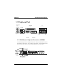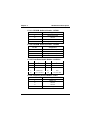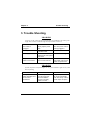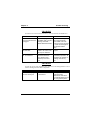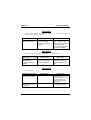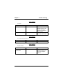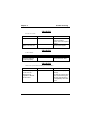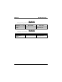
1
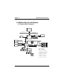
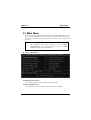
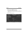
M7VIB Ver:2.5&2.6 Federal Communications Commission (F.C.C) Statement This device complies with Part 15 of the FCC Rules. Operation of this device is subject to the following two conditions: (1) this device may not cause harmful interference, and (2) this device must accept any interference received, including interference that may cause undesired operation. Accessories: This device has been tested and found to comply with the limits of a Class B digital device; the accessories associated with this equipment are as follows: 1. Shielded serial cable. (Can be obtained from multiple retail outlets) 2. Shielded printer cable. (Can be obtained from multiple retail outlets) 3. Shielded video cable. (Can be obtained from multiple retail outlets) 4. Shielded power cord. (Provided by manufacturer) These accessories are required to ensure compliance with FCC Rules. It is the responsibility of the user to provide and use these accessories properly. This equipment has been tested and found to comply with the limits of a Class B digital device, pursuant of Part 15 of the FCC Rules. These limits are designed to provide reasonable protection against harmful interference in a residential installation. This equipment generates, uses and radiates radio frequency energy and, if you did not installed and used in accordance with the instructions, may cause harmful interference in the radio communications. There is no guarantee that interference will not occur in a particular installation. If this equipment does cause harmful interference in the radio or television reception, which can be determined by turning the equipment off and on, you are encouraged to try to correct the interference by one or more of the following measures: 1. Reorient / relocate the receiving antenna. 2. Increase the separation between the equipment and the receiver. 3. Connect the equipment into an outlet from a different circuit where the receiver is connected. 4. Consult the dealer or an experienced radio/TV technician for help. Caution: Changes or modifications that is not expressly approved by the manufacturer could void the user’s authority to operate the equipment. Disclaimer The vendor makes no representations or warranties with respect to the contents here of and specially the vendor disclaims any implied warranties of merchantability or fitness for any purpose. Further, the vendor reserves the right to revise this publication and to make changes of the contents here of without obligation to notify any party beforehand. Duplication of this publication, in part or in whole, is not allowed without first obtaining the vendor’s approval in writing. Trademarks and Remarks MS-DOS, Windows, Windows NT, Windows 9X, Windows ME, Windows XP and Windows 2000 are products of Microsoft Corp, with its ownership of trademark, and are distributed by the vendor under a license agreement. All trademarks used in this manual are property of their respective owners. Copyright© 2001 All Rights Reserved Canadian D.O.C. Statement This digital apparatus does not exceed the Class B limits for radio noise emissions from digital apparatus to set out of the radio interference regulations of the Canadian Department of Communications. Cet appareil numérique n‘émet pas de bruits radioélectriques dépassant les limites appliquées aux appareils numériques de Class B préscrits dans le réglement du brouillage radioélectrique edict par le minister Des Communications du Canada. Contents Introduction .................................................................................. 1-1 1. Motherboard Description ........................................................ 1-2 1.1 Features ....................................................................................................1-2 1.1.1 Hardware....................................................................................................................1-2 1.1.2 BIOS ...........................................................................................................................1-5 1.1.3 Software......................................................................................................................1-5 1.1.4 Accessories ................................................................................................................1-5 1.2 Motherboard Installation..........................................................................1-6 1.2.1 System Block Diagram ...........................................................................................1-6 1.2.2 Layout of Motherboard ...........................................................................................1-7 1.2.3 Quick Reference .......................................................................................................1-8 1.3 CPU Installation.......................................................................................1-9 1.3.1 CPU Installation Procedure: Socket A .................................................................1-9 1.3.2 Frequency Selection: JCLK1 ...............................................................................1-10 1.3.3 CPU Fan Header: JCFAN1..................................................................................1-10 1.3.4 System Fan Header: JSFAN1 ..............................................................................1-11 1.3.5 North Bridge Chipset Fan Header: JNFAN1....................................................1-11 1.4 RAM Module Installation ......................................................................1-12 1.4.1 DIMM.......................................................................................................................1-12 1.4.2 How to install a DIMM Module..........................................................................1-13 1.5 Slots........................................................................................................1-14 1.5.1 ACR (Advanced Communication Riser) Slot..................................................1-15 1.5.2 AGP (Accelerated Graphics Port) Slot...............................................................1-15 i Contents 1.5.3 CNR (Communication Network Riser) Slot.....................................................1-15 1.5.4 PCI (Peripheral Component Interconnect) Slots ..............................................1-15 1.6 Connectors, Headers & Jumpers............................................................1-16 1.6.1 Front Panel Connector: JPANEL1......................................................................1-17 1.6.2 ATX 20-pin Power Connector: JATXPWR1..................................................1-19 1.6.3 Hard Disk Connectors: IDE1/IDE2....................................................................1-19 1.6.4 Floppy Disk Connector: FDD1 ...........................................................................1-20 1.6.5 Wake On LAN Header: JWOL1 ........................................................................1-20 1.6.6 Clear CMOS Jumper: JCMOS1..........................................................................1-20 1.6.7 Front USB Header: JUSB2 ..................................................................................1-21 1.6.8 CNR Codec Primary/Secondary Selection: J2.................................................1-21 1.6.9 DDR DIMM Voltage: J9......................................................................................1-21 1.6.10 5V/ 5VSB Selection for USB: JUSBV1 .........................................................1-22 1.6.11 5V/ 5VSB Selection for KB: JKBV1 ..............................................................1-22 1.7 Peripheral Port .......................................................................................1-23 1.7.1 PS/2 Mouse / Keyboard Connector: JKBMS1.................................................1-23 1.7.2 USB Connector: JUSB1 .......................................................................................1-24 1.7.3 Serial and Parallel Interface Ports........................................................................1-25 1.7.3.1 The Serial Interface: JCOM1/ JCOM2 .............................................1-25 1.7.3.2 Parallel Interface Port: JPRNT1 ......................................................1-27 1.7.4 Game (Joystick/MIDI) Port Connector: J8 .......................................................1-28 1.7.5 Audio Port Connectors: J8....................................................................................1-28 1.7.6 Audio Subsystem....................................................................................................1-29 1.7.6.1 CD-ROM Audio-In Header: JCDIN1...............................................1-30 ii Contents 1.7.6.2 CD-ROM Audio-In Header: JCDIN2...............................................1-30 1.7.6.3 Front Panel Audio Header: JAUDIO1..............................................1-30 1.7.6.4 Telephony Audio Header: JTAD1 ...................................................1-30 2. BIOS Setup................................................................................ 2-1 2.1 Main Menu ...............................................................................................2-3 2.2 Standard CMOS Features ........................................................................2-6 2.3 Advanced BIOS Features.........................................................................2-9 2.4 Advanced Chipset Features....................................................................2-13 2.5 Integrated Peripherals ............................................................................2-17 2.6 Power Management Setup .....................................................................2-22 2.7 PnP/PCI Configurations .........................................................................2-27 2.8 PC Health Status ....................................................................................2-30 2.9 Frequency/Voltage Control....................................................................2-31 3. Trouble Shooting ...................................................................... 3-1 iii Chapter 1 Motherboard Description Introduction System Overview Congratulations on the purchase of your new system! This motherboard is designed to take advantage of the latest industry technology to provide you with the ultimate solution in data processing. In the tradition of its predecessors, this motherboard continues the commitment of reliability, performance and strives for full compliance and compatibility with industry software and hardware standards. M7VIB Highlights: 8 Contains on board I/O facilities, which include two serial ports, a parallel port, a PS/2 mouse port, a PS/2 keyboard port, audio ports, USB ports and a game port. 8 Contains on board IDE facilities for IDE devices such as hard disks and CD-ROM Drives. 8 Supports the AMD-AthlonTM processor, a leading edge processor which brings to you the latest technology in microarchitecture design, graphics performance, system bus design, cache architecture and much more. 8 Complies with PC ATX form factor specifications. 8 Supports popular operating systems such as Windows 95/98, Windows NT, Windows 2000, Windows ME, Windows XP, Novell, UNIX, LINUX and SCO UNIX. 1-1 Chapter 1 Motherboard Description 1. Motherboard Description 1.1 Features 1.1.1 Hardware CPU − − − Single Socket-A for an AMD Athlon Family processor. Runing at 100 or 133 MHz Front Side Bus frequency. The AMD Athlon system bus supports the 200/266 MHz high-speed, split-transaction AMD Athlon system bus interface. Speed − − − − − − Supports up to AMD AthlonTM XP 2000+ CPU core speeds. Supports up to AMD AthlonTM 1.4 GHz CPU core speeds. Supports up to AMD DuronTM 1.2 GHz CPU core speeds. The 33MHz 32 bit PCI 2.2 compliant. The 66MHz AGP 2.0 compliant interface supports 1x, 2x and 4x data transfer mode. High-speed memory --The VT8366/A system controller is designed to support 200/266 MHz DDR SDRAM DIMMs. Chipset − − Chipset – VIA VT8366/A and VT8233A. Chipset – Winbond W83697HF. DRAM Memory − − − − − Supports 64MB/128MB/256MB/512MB/1GB DIMM modules (4). Supports DDR (Double Data Rate) Synchronous DRAM (2.5 V). Supports 8 banks up to 4Gb DRAMs for registered DDR SDRAM module. (DIMM x 4pcs) Supports 6 banks up to 3Gb DRAMs for unbuffered DDR SDRAM module. (DIMM x 3pcs) 200/266 MHz Bus Frequency. 1-2 Chapter 1 Motherboard Description Shadow RAM − Motherboard is equipped with a memory controller providing shadow RAM and support for 8 bit ROM BIOS. Green Functionality − − − Supports Award BIOS™ power management functionality. Has a power down timer from 1 to 15 minutes. Wakes from power saving sleep mode with any keyboard or mouse activity. BUS Slots − − − − (1) AGP slot. (1) CNR slot (Support Type B CNR only). (1) ACR slot (5) 32-bit PCI bus slots Flash Memory − − Supports flash memory functionality. Supports ESCD functionality. Built in IDE Facilities − − − − − − − Supports four IDE hard disk drives. Supports PIO Mode 4, Master Mode, and high performance hard disk drives. Supports disk transfer rates up to 100 MB/second. Supports Ultra DMA 33, Ultra DMA 66, Ultra DMA 100, Ultra DMA 133 Bus Master Modes. Supports IDE interface with CD-ROM. Supports high capacity hard disk drives. Supports LBA mode. Stereo AC 97 Digital Audio Codec − − − − − Single chip audio CODEC with high S/N ratio (>90dB). 18-bit ADC and DAC resolution. Compliant with AC’97 2.2 specification. Meet performance requirements for audio on PC2001 systems. 18-bit stereo full-duplex CODEC with independent and variable sampling rate. 1-3 Chapter 1 Motherboard Description − 3D Stereo Enhancement. I/O facilities − − − − − One multi-mode Parallel Port capable of supporting the following specifications: Standard & Bidirection Parallel Port. Enhanced Parallel Port (EPP). Extended Capabilities Port (ECP). Normal Supports two serial ports, 16550 UART. Supports Infrared Data Transmission using IrDA. Supports PS/2 mouse and PS/2 keyboard. Supports 360KB, 720KB, 1.2MB, 1.44MB, and 2.88MB floppy disk drives. Universal Serial Bus − − Supports two back panel Universal Serial Bus Ports and two front panel Universal Serial Bus Ports (optional). Supports 48 MHz USB. Hardware Monitor Function − − Monitors CPU Fan Speed. Monitors System Voltage. Dimensions (ATX form-factor) − 24.4cm x 30.5cm (WxL) 1-4 Chapter 1 Motherboard Description 1.1.2 BIOS − − − − AWARD legal BIOS. Supports APM1.2. Supports USB Function. Supports ACPI. 1.1.3 Software Operating System − Offers the highest performance for MS-DOS, Windows NT, Windows 2000, Windows 95/98, Windows ME, Windows XP, Novell, LINUX, UNIX, SCO UNIX etc. 1.1.4 Accessories − − − − − − HDD Cable. FDD Cable. Flash Memory Writer for BIOS Update. USB2 Cable (Optional). Rear I/O Panel for ATX Case (Optional). Fully Setup Driver CD. 1-5 Chapter 1 Motherboard Description 1.2 Motherboard Installation 1.2.1 System Block Diagram AMD K 7 P ROC ESS OR H OST BUS H OS T BU S C NTL VIA VT8366/ A V LI NK A GP C NR S LOT ADDR MEM ORY 4 DDR DIM M DATA PCI BUS USB USB AC R SLOT 4 USB CONN. LPC PCI CON N PCI CON N PCI CON N PCI CON N I DE I DE C NTL PCI CON N VT823 3A AC' 97 CODEC C LOCK W255 100/ 133M HZ MOUS E K EYBOAR D M7VIB WINB OND W83697HF FLOPPY C ON N. FLA SH BIOS SER . C ONN. SER. C ONN. 1-6 ATX(F SB: 133/100MH z) SUP PORTS 4 DDR D IMMS SUP PORT 1 AG P SLOT SUP PORTS 5 PCI SLOTS SUP PORT 1 ACR SLOT SUP PORT 1 CNR SLOT SUP PORT TELEPH ONY Chapter 1 Motherboard Description 1.2.2 Layout of Motherboard Model No.M7VIB 1 CPU 1 Socket A JK BV 1 1 JCO M1 JU SBV 1 J8 DIMM3 DIMM4 DIMM1 U2 JPRN T 1 JCO M2 DIMM2 CP U VT 8366/A JAT XP WR 1 BAT 1 1 AGP SLOT 10 9 2 1 PCI2 1 JCMO S1 PCI SL OT 1 1 4 2 PCI3 PCI SL OT 1 PCI4 JTA D 1 BIO S 8 7 2 1 U3 3 1 JU SB 2 VT8233A 10 9 S ECO NDARY I DE C ONN. J9 PCI1 PCI SL OT P R IM ARY I DE C ONN. 2 1 I DE 1 ID E2 PCI SL OT PCI5 U26 PCI SL OT Winbond W83697 ACR 1 ACR SL OT J2 CNR SLOT 1 CN R1 2 JW O L1 1 JPAN E L1 JSFA N1 24 23 1 1 1-7 FD D 1 FL O PPY D ISK CON N . Chapter 1 Motherboard Description 1.2.3 Quick Reference G F E D C B A W inbon d W 83697 Y BI OS X W V H So ck et A I CPU J V T8366/A K U T S L M D IMM1 D IMM2 VT8233A D IMM3 D IMM4 N O P R Q A. Back Panel I/O Connectors O. Clear CMOS (JCMOS1) B. ATX Power Connector (JATXPWR1) P. DDR DIMM Voltage (J9) C. AGP Slot (AGP1) Q. IDE Connectors (IDE1-2) D. Front Audio Header (JAUDIO1) R. DIMMs (DIMM1-4) E. CD Audio-In Header (JCDIN1) S. CPU Clock Selection (JCLK1) F. CD Audio-In Header (JCDIN2) T. ACR Slot (ACR1) G. Telephony Header (JTAD1) U. PCI BUS Slots (PCI1-5) H. CNR Slot (CNR1) V. North Bridge Chipset (U2) FAN I. Codec Selection (J2) Header (JNFAN1) J. Wake-On-LAN Header (JWOL1) W. CPU FAN Header (JCFAN1) K. Front Panel Connector (JPANEL1) X. 5V / 5VSB Selection for USB L. Front USB Header (JUSB2) M. System FAN Header (JSFAN1) (JUSBV1) Y. 5V / 5VSB Selection for KB (JKBV1) N. Floppy Disk Connector (FDD1) 1-8 Chapter 1 Motherboard Description 1.3 CPU Installation 1.3.1 CPU Installation Procedure: Socket A CPU 1. Pull the lever sideways away from the socket then raise the lever up to 90-degree angle. 2. Locate Pin A in the socket and look for the white dot or cut edge in the CPU. Match Pin A with the white dot/cut edge then insert the CPU. 3. Press the lever down. 4. Put the fan on the CPU by buckling it and then put the fan’s powerport into the JCFAN1, then the installation will be completed. 1-9 Chapter 1 Motherboard Description So cket A DIM M4 DIMM3 DIM M2 DIMM1 C PU VT83 66 /A B AT1 VT8233A BIOS Winbond W83697 JSFAN 1 1.3.2 Frequency Selection: JCLK1 CPU Clock 100.0MHz 133.3MHz PIN 1-2 OFF ON 1.3.3 CPU Fan Header: JCFAN1 Pin No. Assignment 1 Ground 2 +12V 3 Sense 1-10 PIN 3-4 OFF ON Chapter 1 Motherboard Description 1.3.4 System Fan Header: JSFAN1 Pin No. Assignment 1 Ground 2 +12V 3 Sense 1.3.5 North Bridge Chipset Fan Header: JNFAN1 Pin No. Assignment 1 Ground 2 +12V 1-11 Chapter 1 Motherboard Description 1.4 RAM Module Installation 1.4.1 DIMM DRAM Access Time: 2.5V Unbuffered/ Registered DDR SDRAM PC1600/ PC2100 Type required. DRAM Type : 64MB/ 128MB/ 256MB/ 512MB/ 1GB DIMM Module (184 pin) Total Memory Size Devices used on DIMM 1 DIMM 2 DIMM 3 DIMM 4 DIMM (2 Rows) (2 Rows) (2 Rows) (2 Rows) x64 256 M 128 M 64 M 512 M 256 M 128 M 1G 512 M 256 M 1G 512 M x64 256 M 128 M 64 M 512 M 256 M 128 M 1G 512 M 256 M 1G 512 M x64 256 M 128 M 64 M 512 M 256 M 128 M 1G 512 M 256 M 1G 512 M 64M (4Mx4x4banks) 64M (2Mx8x4banks) 64M (1Mx16x4banks) 128M (8Mx4x4banks 128M (4Mx8x4banks) 128M (2Mx16x4banks) 256M (16Mx4x4banks) 256M (8Mx8x4banks) 256M (4Mx16x4banks) 512M (16Mx8x4banks) 512M (8Mx16x4banks) x64 256 M 128 M 64 M 512 M 256 M 128 M 1G 512 M 256 M 1G 512 M * This M7VIB motherboard does not support with parity DIMM. *The list shown above for DRAM configuration is only for reference. 1-12 Chapter 1 Motherboard Description 1.4.2 How to install a DIMM Module Single Sided DIMM Double Sided DIMM 1. The DIMM socket has a “ Plastic Safety Tab”, and the DIMM memory module has an “Asymmetrical notch”, so the DIMM memory module can only fit into the slot in one direction. 2. Push the tabs out. Insert the DIMM memory modules into the socket at a 90-degree angle, and then push down vertically so that it will fit into the place. 3. The Mounting Holes and plastic tabs should fit over the edge and hold the DIMM memory modules in place. 1-13 Chapter 1 Motherboard Description 1.5 Slots The slots in this motherboard are designed to hold expansion cards and connect them to the system bus. Expansion slots are a mean of adding or enhancing the motherboard's features and capabilities. With these efficient facilities, you can increase the motherboard's capabilities by adding hardware that performs tasks that are not part of the basic system. Socke t A DI MM 4 DIM M3 DI MM 2 DIM M1 C PU VT83 66/A AGP S LOT P CI S LOT VT82 33 A BIOS Win bon d W8 36 97 ACR SLOT CNR SLOT 1-14 Chapter 1 Motherboard Description 1.5.1 ACR (Advanced Communication Riser) Slot The ACR specification is an open Industry Standard Architecture, and it defines a hardware scalable riser card interface, which supports audio and modem only. 1.5.2 AGP (Accelerated Graphics Port) Slot Unlike the mouse ports, keyboard ports and printer ports, this motherboard does not have built in video facilities; and therefore, requires a video card for one of the expansion slots. Your monitor will attach directly to that video card. This motherboard supports video cards for PCI and ISA slots, but it is also equipped with an Accelerated Graphics Port (AGP). An AGP card will take advantage of AGP technology for improved video efficiency and performance, especially with 3D graphics. 1.5.3 CNR (Communication Network Riser) Slot The CNR specification is an open Industry Standard Architecture, and it defines a hardware scalable riser card interface, which supports audio and modem only. 1.5.4 PCI (Peripheral Component Interconnect) Slots This motherboard is equipped with 5 standard PCI slots. PCI stands for Peripheral Component Interconnect, and it is a bus standard for expansion cards, which has supplanted the older ISA bus standard in most parts. This PCI slot is designated as 32 bits. 1-15 Chapter 1 Motherboard Description 1.6 Connectors, Headers & Jumpers The connectors, headers and jumpers introduced below provide you lots of capabilities such as power supply, front panel signal revelation, IDE hard disk connection, floppy disk connection, Wake On LAN function and USB connection. Noticeably, a jumper has two or more pins that can be covered by a plastic jumper cap, allowing you to select a different system options. JKBV1 Socket A 1 JUSBV1 1 DIMM4 DIMM3 DIMM2 DIMM1 C PU VT8366/A JAT XPWR1 J9 2 1 8 7 IDE 1-2 VT8233A JCMOS1 BIOS 1 Winbon d 2 1 W 83697 J2 1 JWOL1 1 1-16 JPANEL 1 FDD1 JUSB 2 10 9 Chapter 1 Motherboard Description 1.6.1 Front Panel Connector: JPANEL1 SLP NA POW-LED (+) (+) (-) K ON/OFF E Y IR 24 2 23 1 SPK (+) (-) HLED RST NA Function Pin No. Assignment Function Sleep Control Sleep Ground Button NA Pin No. Assignment 1 3 +5V NA Speaker 2 4 5 NA Connector 6 NA 7 Speaker 8 Power LED (+) 9 HDD LED (+) Hard Drive 10 Power LED (+) POWER 11 HDD LED (-) LED 12 Power LED (-) LED 13 Ground Reset 14 Power Button Power-on 15 Reset Control Button 16 Ground Button 17 NA 18 KEY 19 NA IrDA 21 23 VCC5 Connector IRTX 20 KEY IrDA 22 24 Ground Connector IRRX SPK (Speaker Connector) An offboard speaker can be installed on the motherboard as a manufacturing option. It can be connected to the motherboard at the front panel connector. The speaker (onboard or offboard) provides error beep code information during the Power On Self-Test when the computer cannot use the video interface. The speaker is not connected to the audio subsystem and does not receive output from the audio subsystem. 1-17 Chapter 1 Motherboard Description RST (Reset Button) This connector can be attached to a momentary SPST switch. This switch is usually open, and when it is closed, it will cause the motherboard to reset and run the POST (Power On Self Test). POW-LED (Power LED Connector) This connector can be attached to an LED on the front panel of a computer case. The LED will illuminate while the computer is powered on. HLED (Hard Drive LED Connector) This connector can be attached to an LED on the front panel of a computer case. The LED will flicker during disk activity where it is only applied to those IDE drives directly attached to the system board. IR (Infrared Connector) This connector is used to attach to an infrared sensing device. After the IrDA interface is configured, connectionless data transfer to and from portable devices such as laptops making PDAs is possible. SLP (Sleep/Green Button) This connector is used to conserve energy by powering down the monitor and the hard disk when is not in use. To configure this option, you need to connect a button from the front panel to this sleep button. Depressing the button will power down the monitor and the hard drives until the system is invoked by any keyboard activity, mouse activity, modem activity or when the sleep button is depressed again. APM (Advanced Power Management) must be enabled in the system BIOS and the APM driver must be loaded. ON/OFF (Power Button) This connector can be attached to a front panel power switch. The switch must pulled the Power Button pin to ground for at least 50 ms to signal the power supply to switch on or off. (The time required is due to internal debounce circuitry on the system board). At least two seconds must pass before the power supply will recognize another on/off signal. 1-18 Chapter 1 Motherboard Description 1.6.2 ATX 20-pin Power Connector: JATXPWR1 This connector supports the power button on-board. Using the ATX power supply, function such as Soft Power Off, is supported on this motherboard. This power connector supports instant power-on functionality, which means that the system will boot up instantly when the power connector is inserted on the board. PIN Assignment PIN 1 3.3V 11 Assignment 3.3V 2 3.3V 12 -12V 3 Ground 13 Ground 4 5 5V Ground 14 15 PS_ON Ground 6 5V 16 Ground 7 8 Ground PW_OK 17 18 Ground -5V 9 5V_SB 19 5V 10 12V 20 5V 1.6.3 Hard Disk Connectors: IDE1/IDE2 The motherboard has a 32-bit Enhanced PCI IDE Controller that provides PIO Mode 0~4, Bus Master, and Ultra DMA 33, Ultra DMA 66,Ultra DMA 100, Ultra DMA 133 functionality. It has two HDD connectors: IDE1 (primary) and IDE2 (secondary). You can connect up to four hard disk drives, a CD-ROM, a 120MB Floppy (reserved for future BIOS) and other devices to IDE1 and IDE2. These connectors support the IDE hard disk cable provided. • IDE1 (Primary IDE Connector) The first hard drive should always be connected to IDE1. IDE1 can connect a Master and a Slave drive. You must configure the second hard drive on IDE1 to Slave mode by setting the jumper accordingly. • IDE2 (Secondary IDE Connector) The IDE2 controller can also support a Master and a Slave drive. Its configuration is similar to IDE1. The second drive on this controller must be set to slave mode. 1-19 Chapter 1 Motherboard Description 1.6.4 Floppy Disk Connector: FDD1 The motherboard provides a standard floppy disk connector (FDC) that supports 360K, 720K, 1.2M, 1.44M and 2.88M floppy disk types. This connector supports the provided floppy drive ribbon cables. 1.6.5 Wake On LAN Header: JWOL1 Pin No. Assignment 1 5V SB 2 Ground 3 Wake up 1.6.6 Clear CMOS Jumper: JCMOS1 JCMOS1 1 Assignment 3 1-2 Closed 1 3 2-3 Closed Normal Operation (default) Clear CMOS Data The following procedures are for resetting the BIOS password. It is important to follow these instructions closely. Remove AC power line JCMOS1 (2-3) closed Wait five seconds JCMOS1 (1-2) closed Reset your desired password AC power on or clear CMOS data 1-20 Chapter 1 Motherboard Description 1.6.7 Front USB Header: JUSB2 Note: Before you install this header, make sure the pin assignments are corresponded to the table below; otherwise, it may cause great damage to your USB device. (JUSB2) Pin 1 3 5 7 9 Assignment +5V(fused) USBP2USBP2+ Ground KEY Pin 2 4 6 8 10 Assignment +5V(fused) USBP3USBP3+ Ground NC 1.6.8 CNR Codec Primary/Secondary Selection: J2 Pin No. Assignment 1-2 On-board Primary Codec 2-3 CNR Primary Codec 1.6.9 DDR DIMM Voltage: J9 z Pin DDR DIMM Voltage 1-2 2.55V 3-4 2.65V (Default) 5-6 2.75V 7-8 2.85V If you meet the DDR DIMM compatible program, try to adjust the DDR Voltage to fix the compatible program. 1-21 Chapter 1 Motherboard Description 1.6.10 5V/ 5VSB Selection for USB: JUSBV1 JUSBV1 1 Assignment 3 5V 1-2 Closed 1 3 5V_SB 2-3 Closed 1.6.11 5V/ 5VSB Selection for KB: JKBV1 JKBV1 1 Assignment 3 5V 1-2 Closed 1 3 5V_SB 2-3 Closed 1-22 Chapter 1 Motherboard Description 1.7 Peripheral Port JKBMS1 JPRNT1 PS/2 Mouse JUSB1 PS/2 Keyboard USB J8 Parallel Game Port COM1 COM2 JCOM1 JCOM2 Speaker Out Line In Mic In 1.7.1 PS/2 Mouse / Keyboard Connector: JKBMS1 The motherboard provides a standard PS/2 mouse / Keyboard mini DIN connector for attaching a PS/2 mouse. You can plug a PS/2 mouse / Keyboard directly into this connector. The connector location and pin definition are shown below: 1-23 Chapter 1 Motherboard Description PS/2 Mouse / Keyboard Connectors Pin Assignment 1 Data 2 No connect 3 Ground 4 +5 V (fused) 5 Clock 6 No connect 1.7.2 USB Connector: JUSB1 The motherboard provides a OHCI (Open Host Controller Interface) Universal Serial Bus Roots for attaching USB devices such as: keyboard, mouse and other USB devices. You can plug the USB devices directly into this connector. Stacked USB Connectors Pin Assignment 1 +5 V (fused) 2 USBP0- [USBP1-] 3 USBP0+ [USBP1+] 4 Ground Signal names in brackets ([]) are for USB Port 1. 1-24 Chapter 1 Motherboard Description 1.7.3 Serial and Parallel Interface Ports This system is equipped with two serial ports and one parallel port. Both types of interface ports will be explained in this chapter. 1.7.3.1 The Serial Interface: JCOM1/ JCOM2 The serial interface port is sometimes referred to as an RS-232 port or an asynchronous communication port. Mice, printers, modems and other peripheral devices can be connected to a serial port, where it can also be used to connect your computer with another computer system. If you wish to transfer the contents of your hard disk to another system, it can be accomplished by using each machine’s serial port. The serial port on this system has two 9-pin connectors. Some older computer systems and peripherals used to be equipped with only one 25-pin connector. If you need to connect a 9-pin serial port to an older 25-pin serial port, you can purchase a 9-to-25 pin adapter. 1-25 Chapter 1 Motherboard Description Connectivity The serial ports can be used in many ways, and it may be necessary to become familiar with the pinout diagram. The following chart gives you the function of each pin on the 9-pin connector and some of the 25-pin connector. This information can be used when configuring certain software programs to work with the serial ports. Signal Name DB9 PIN DB25 PIN DCD Data Carrier Detect 1 8 RX Receive Data 2 3 TX Transmit Data 3 2 DTR Data Terminal Ready 4 20 GND Signal Ground 5 7 DSR Data Set Ready 6 6 RTS Request to Send 7 4 CTS Clear to Send 8 5 RI Ring Indicator 9 22 1-26 Chapter 1 Motherboard Description 1.7.3.2 Parallel Interface Port: JPRNT1 Unlike the serial ports, parallel interface port has been standardized, and it should not present any difficulty interfacing peripherals of your system. Sometimes called centronics port, the parallel port is almost exclusively used with printers. The parallel port on your system has a 25-pin, DB25 connector (see picture below). The pinout for the parallel port are shown in the table below. Signal -Strobe Data 0 Data 1 Data 2 Data 3 Data 4 Data 5 Data 6 Data 7 -Ack Busy Paper Empty +Select -Auto FDXT -Error -Init -SLCTN Ground Ground Ground Ground Ground Ground Ground Ground 1-27 Pin 1 2 3 4 5 6 7 8 9 10 11 12 13 14 15 16 17 18 19 20 21 22 23 24 25 Chapter 1 Motherboard Description 1.7.4 Game (Joystick/MIDI) Port Connector: J8 This connector allows you to connect a joystick or game pad for playing computer games. Also, you may play or edit professional music by connecting MIDI devices. Game/Joystick/MIDI 1.7.5 Audio Port Connectors: J8 Speaker Out is used to connect speakers or headphones for audio output. Line In can be connected to the external CD player, Tape player or other audio devices for audio input. Mic In is used to connect a microphone that allows you to input sounds and voices. Speaker Out 1-28 Line In Mic In Chapter 1 Motherboard Description 1.7.6 Audio Subsystem Socket A DIMM4 DIMM3 DIMM1 DIMM2 C PU VT8366/A 10 9 2 1 1 1 VT8 233A BIOS 1 Winbond W83697 1-29 Chapter 1 Motherboard Description 1.7.6.1 CD-ROM Audio-In Header: JCDIN1 Pin No. Assignment 1 Left Channel Input 2 Ground 3 Ground 4 Right Channel Input 1.7.6.2 CD-ROM Audio-In Header: JCDIN2 Pin No. Assignment 1 Left Channel Input 2 Ground 3 Right Channel Input 4 Ground 1.7.6.3 Front Panel Audio Header: JAUDIO1 Pin No. Assignment Pin No. Assignment 1 Mic In 2 Ground 3 Mic Power 4 Audio Power 5 RT Line Out 6 RT Line Out 7 Reserved 8 Key 9 LFT Line Out 10 LFT Line Out 1.7.6.4 Telephony Audio Header: JTAD1 Pin No. Assignment 1 MONO_IN 2 Ground 3 Ground 4 MONO_OUT 1-30 Chapter 2 BIOS Setup 2. BIOS Setup Introduction This manual discussed Award™ Setup program built into the ROM BIOS. The Setup program allows users to modify the basic system configuration. This special information is then stored in battery-backed RAM so that it retains the Setup information when the power is turned off. The Award BIOS™ installed in your computer system’s ROM (Read Only Memory) is a custom version of an industry standard BIOS. This means that it supports AMD-AthlonTM / Duron TM processors input/output system. The BIOS provides critical low-level support for standard devices such as disk drives and serial/ parallel ports. Adding important has customized the Award BIOS™, but nonstandard features such as virus and password protection as well as special support for detailed fine-tuning of the chipset controls the entire system. The rest of this manual is intended to guide you through the process of configuring your system by using Setup. Plug and Play Support These AWARD BIOS supports the Plug and Play Version 1.0A specification. ESCD (Extended System Configuration Data) write is supported. EPA Green PC Support This AWARD BIOS supports Version 1.03 of the EPA Green PC specification. APM Support These AWARD BIOS supports Version 1.1&1.2 of the Advanced Power Management (APM) specification. Power management features are implemented via the System Management Interrupt (SMI). Sleep and Suspend power management modes are supported. This AWARD BIOS can manage power to the hard disk drives and video monitors. 2-1 Chapter 2 BIOS Setup PCI Bus Support This AWARD BIOS also supports Version 2.1 of the Intel PCI (Peripheral Component Interconnect) local bus specification. DRAM Support DDR SDRAM (Double Data Rate Synchronous DRAM) is supported. Supported CPUs This AWARD BIOS supports the AMD AthlonTM / Duron TM / Athlon XP TM CPU. Using Setup In general, you use the arrow keys to highlight items, press <Enter> to select, use the <PgUp> and <PgDn> keys to change entries, press <F1> for help and press <Esc> to quit. The following table provides more detail about how to navigate in the Setup program by using the keyboard. Keystroke Up arrow Down arrow Left arrow Right arrow Esc Move Enter PgUp key PgDn key + Key - Key Esc key F1 key F5 key F6 key F7 key F10 key Function Move to previous item Move to next item Move to the item on the left (menu bar) Move to the item on the right (menu bar) Main Menu: Quit without saving changes Submenus: E xit C urrent page to the next higher level menu Move to the item you desired Increase the numeric value or make changes Decrease the numeric value or make changes Increase the numeric value or make changes Decrease the numeric value or make changes Main Menu – Quit and not save changes into CMOS Status Page Setup Menu and Option Page Setup Menu – E xit Current page and return to Main Menu General help on Setup navigation keys Load previous values from CMOS Load the fail-safe defaults from B IOS default table Load the optimized defaults Save all the CMOS changes and exit 2-2 Chapter 2 BIOS Setup 2.1 Main Menu Once you enter Award BIOS™ CMOS Setup Utility, the Main Menu will appear on the screen. The Main Menu allows you to select from several setup functions. Use the arrow keys to select among the items and press <Enter> to accept and enter the sub-menu. !! WARNING !! The information about BIOS defaults on manual (Figure 1,2,3,4,5,6,7,8) is just for reference; please refer to the BIOS installed on board, for update information. Figure 1. Main Menu Standard CMOS Features This submenu contains industry standard configurable options. Advanced BIOS Features This submenu allows you to configure enhanced features of the BIOS. 2-3 Chapter 2 BIOS Setup Advanced Chipset Features This submenu allows you to configure special chipset features. Integrated Peripherals This submenu allows you to configure certain IDE hard drive options and Programmed Input/ Output features. Power Management Setup This submenu allows you to configure the power management features. PnP/PCI Configurations This submenu allows you to configure certain “Plug and Play” and PCI options. PC Health Status This submenu allows you to monitor the hardware of your system. Frequency/Voltage Control This submenu allows you to change CPU Vcore Voltage and CPU/PCI clock. (However, this function is strongly recommended not to use. Not properly change the voltage and clock may cause CPU or M/B damage!) Load Optimized Defaults This selection allows you to reload the BIOS when the system is having problems particularly with the boot sequence. These configurations are factory settings optimized for this system. A confirmation message will be displayed before defaults are set. Set Supervisor Password Setting the supervisor password will prohibit everyone except the supervisor from making changes using the CMOS Setup Utility. You will be prompted with to enter a password. 2-4 Chapter 2 BIOS Setup Set User Password If the Supervisor Password is not set, then the User Password will function in the same way as the Supervisor Password. If the Supervisor Password is set and the User Password is set, the “User” will only be able to view configurations but will not be able to change them. Save & Exit Setup Save all configuration changes to CMOS(memory) and exit setup. message will be displayed before proceeding. Confirmation Exit Without Saving Abandon all changes made during the current session and exit setup. Confirmation message will be displayed before proceeding. Update BIOS This submenu allows you to update bios. 2-5 Chapter 2 BIOS Setup 2.2 Standard CMOS Features The items in Standard CMOS Setup Menu are divided into 10 categories. Each category includes no, one or more than one setup items. Use the arrow keys to highlight the item and then use the<PgUp> or <PgDn> keys to select the value you want in each item. Figure 2. Standard CMOS Setup 2-6 Chapter 2 BIOS Setup Main Menu Selections This table shows the selections that you can make on the Main Menu. Item Options Description Date MM DD YYYY Set the system date. Note that the ‘Day’ automatically changes when you set the date. Time HH MM SS Set the clock. system internal IDE Primary Master Options are in its sub menu. Press <Enter> to enter the sub menu of detailed options IDE Primary Slave Options are in its sub menu. Press <Enter> to enter the sub menu of detailed options. IDE Secondary Master Options are in its sub menu. Press <Enter> to enter the sub menu of detailed options. IDE Secondary Slave Options are in its sub menu. Press <Enter> to enter the sub menu of detailed options. 360K, 5.25 in Select the type of floppy disk drive installed in your system. Drive A 1.2M, 5.25 in 720K, 3.5 in 1.44M, 3.5 in 2.88M, 3.5 in Drive B None Video EGA/VGA CGA 40 CGA 80 MONO 2-7 Select the device. default video Chapter 2 BIOS Setup Item Options Description Halt On All Errors Select the situation in which No Errors you want the BIOS to stop All, but Keyboard the POST process and All, but Diskette notify you. All, but Disk/ Key Base Memory N/A Displays the amount of conventional memory detected during boot up. Extended Memory N/A Displays the amount of extended memory detected during boot up. Total Memory N/A Displays the total memory available in the system. 2-8 Chapter 2 BIOS Setup 2.3 Advanced BIOS Features Figure 3. Advanced BIOS Setup Virus Warning This option allows you to choose the VIRUS Warning feature that is used to protect the IDE Hard Disk boot sector. If this function is enabled and an attempt is made to write to the boot sector, BIOS will display a warning message on the screen and sound an alarm beep. Disabled (default) Enabled Virus protection is disabled. Virus protection is activated. CPU Internal Cache Depending on the CPU/chipset in use, you may be able to increase memory access time with this option. Enabled (default) Enable cache. Disabled Disable cache. 2-9 Chapter 2 BIOS Setup Extermal Cache This option enables or disables “Level 2” secondary cache on the CPU, which may improve performance. Enabled (default) Enable cache. Disabled Disable cache. CPU L2 Cache ECC Checking This item allows you to enable/disable CPU L2 Cache ECC Checking. The Choices: Enabled (default), Disabled. Quick Power On Self Test Enabling this option will cause an abridged version of the Power On Self-Test (POST) to execute after you power up the computer. Enabled (default) Enable quick POST. Disabled Normal POST. First /Second/Third/ Boot Other Device These BIOS attempts to load the operating system from the devices in the sequence selected in these items. The Choices: Floppy, LS120, HDD-0, SCSI, CDROM, HDD-1, HDD-2, HDD-3, ZIP100, LAN, Disabled, Enabled. Swap Floppy Drive For systems with two floppy drives, this option allows you to swap logical drive assignments. The Choices: Enabled, Disabled (default). Boot Up Floppy Seek Enabling this option will test the floppy drives to determine if they have 40 or 80 tracks. Disabling this option reduces the time it takes to boot-up. The Choices: Enabled (default), Disabled. 2-10 Chapter 2 BIOS Setup Boot Up NumLock Status Selects the NumLock. State after power on. On (default) Numpad is number keys. Off Numpad is arrow keys. Gate A20 Option Select if chipset or keyboard controller should control Gate A20. Normal A pin in the keyboard controller controls Gate A20. Fast (default) Lets chipset control Gate A20. Typematic Rate Setting When a key is held down, the keystroke will repeat at a rate determined by the keyboard controller. When enabled, the typematic rate and typematic delay can be configured. Disabled (default) Enabled Typematic Rate (Chars/Sec) Sets the rate at which a keystroke is repeated when you hold the key down. The Choices: 6 (default), 8,10,12,15,20,24,30. Typematic Delay (Msec) Sets the delay time after the key is held down before it begins to repeat the keystroke. The Choices: 250 (default), 500,750,1000. Security Option This option will enable only individuals with passwords to bring the system online and/or to use the CMOS Setup Utility. System A password is required for the system to boot and is also required to access the Setup Utility. Setup (default) A password is required to access the Setup Utility only. This will only apply if passwords are set from the Setup main menu. 2-11 Chapter 2 BIOS Setup APIC Mode Selecting Enabled enables APIC device mode reporting from the BIOS to the operating system. The Choices: Enabled, Disabled (default). MPS Version Control For OS The BIOS supports versions 1.1 and 1.4 of the Intel multiprocessor specification. Select the version supported by the operation system running on this computer. The Choices: 1.4 (default), 1.1. OS Select For DRAM > 64MB A choice other than Non-OS2 is only used for OS2 systems with memory exceeding 64MB. The Choices: Non-OS2 (default), OS2. Video BIOS Shadow Determines whether video BIOS will be copied to RAM for faster execution. Enabled (default) Optional ROM is enabled. Disabled Optional ROM is disabled. 2-12 Chapter 2 BIOS Setup 2.4 Advanced Chipset Features This submenu allows you to configure the specific features of the chipset installed on your system. This chipset manages bus speeds and access to system memory resources, such as DRAM and external cache. It also coordinates communications with the PCI bus. The default settings that came with your system have been optimized and therefore should not be changed unless you are suspicious that the settings have been changed incorrectly. Figure 4. Advanced Chipset Setup DRAM Clock/Drive Control To control the Clock/Drive. If you highlight the literal “Press Enter” next to the “DRAM Clock/Drive Control” label and then press the enter key, it will take you a submenu with the following options: DRAM Clock This item determines DRAM clock following 100MHz, 133MHz or By SPD. The Choices: 100MHz, 133MHz, By SPD (default). 2-13 Chapter 2 BIOS Setup DRAM Timing This item determines DRAM clock/ timing follow SPD or not. The Choices: By SPD (default), Manual. SDRAM Cycle Length When synchronous DRAM is installed, the number of clock cycles of CAS latency depends on the DRAM timing. Do not reset this field from the default value specified by the system designer. The Choices: 3(default), 2.5, 2. Bank Interleave This item allows you to enable or disable the bank interleave feature. The Choices: Disabled (default), 2 bank, 4 bank. DRAM Queue Depth This item permits to place the depths of the memory. depth is, the better is this function. The Choices: 4 level (default), 2 level, 3 level. The deeper the DRAM Command Rate This item controls clock cycle that must occur between the last valid write operation and the next command. The Choices: 1T Command, 2T Command (default). AGP & P2P Bridge Control If you highlight the literal “Press Enter” next to the “AGP & P2P Bridge Control” label and then press the enter key, it will take you a submenu with the following options: AGP Aperture Size Select the size of the Accelerated Graphics Port (AGP) aperture. The aperture is a portion of the PCI memory address range dedicated for graphics memory address space. Host cycles that hit the aperture range are forwarded to the AGP without any translation. The Choices: 64M (default), 256M, 128M, 32M, 16M, 8M, 4M. AGP Mode This item allows you to select the AGP Mode. The Choices: 4X (default), 2X, 1X. 2-14 Chapter 2 BIOS Setup AGP Driving Control By choosing “Auto” the system BIOS will the AGP output Buffer Drive strength P Ctrl by AGP Card. By choosing “Manual”, it allows user to set AGP output Buffer Drive strength P Ctrl by manual. The Choices: Auto (default), Manual. AGP Driving Value While AGP driving control item set to “Manual”, it allows user to set AGP driving. The Choices: DA (default). AGP Fast Write The Choices: Enabled, Disabled (default). AGP Master 1 WS Write When Enabled, writes to the AGP (Accelerated Graphics Port) are executed with one-wait states. The Choices: Disabled (default), Enabled. AGP Master 1 WS Read When Enabled, read to the AGP (Accelerated Graphics Port) are executed with one wait states. The Choices: Disabled (default), Enabled. CPU & PCI Bus Control If you highlight the literal “Press Enter” next to the “CPU & PCI Bus Control” label and then press the enter key, it will take you a submenu with the following options: PCI1 Master 0 WS Write When enabled, writes to the PCI bus are executed with zero-wait states. The Choices: Enabled (default), Disabled. PCI2 Master 0 WS Write When enabled, writes to the AGP bus are executed with zero-wait states. The Choices: Enabled (default), Disabled. PCI1 Post Write When Enabled, CPU writes are allowed to post on the PCI bus. The Choices: Enabled (default), Disabled. 2-15 Chapter 2 BIOS Setup PCI2 Post Write When Enabled, CPU writes are allowed to post on the AGP bus. The Choices: Enabled (default), Disabled. PCI Delay Transaction The chipset has an embedded 32-bit posted write buffer to support delay transactions cycles. Select Enabled to support compliance with PCI specification. The Choices: Enabled (default), Disabled. Memory Hole When enabled, you can reserve an area of system memory for ISA adapter ROM. When this area is reserved, it cannot be cached. Refer to the user documentation of the peripheral you are installing for more information. The Choices: Disabled (default), 15M – 16M. System BIOS Cacheable Selecting the “Enabled” option allows caching of the system BIOS ROM at F0000h-FFFFFh, which can improve system performance. However, any programs writing to this area of memory will cause conflicts and result in system errors. The Choices: Enabled, Disabled (default). Video RAM Cacheable Enabling this option allows caching of the video RAM, resulting in better system performance. However, if any program writes to this memory area, a system error may result. The Choices: Enabled, Disabled (default). 2-16 Chapter 2 BIOS Setup 2.5 Integrated Peripherals Figure 5. Integrated Peripherals VIA OnChip IDE Device If you highlight the literal “Press Enter” next to the “VIA OnChip IDE Device” label and then press the enter key, it will take you a submenu with the following options: OnChip IDE Channel 0/1 The motherboard chipset contains a PCI IDE interface with support for two IDE channels. Select “Enabled” to activate the first and/or second IDE interface. Select “Disabled” to deactivate an interface if you are going to install a primary and/or secondary add-in IDE interface. The Choices: Enabled (default), Disabled. IDE Prefetch Mode The “onboard” IDE drive interfaces supports IDE prefetching for faster drive access. If the interface does not support prefetching. If you install a primary and/or secondary add-in IDE interface, set this option to “Disabled”. The Choices: Enabled (default), Disabled. 2-17 Chapter 2 BIOS Setup Primary / Secondary /Master / Slave PIO The IDE PIO (Programmed Input / Output) fields let you set a PIO mode (0-5) for each of the IDE devices that the onboard IDE interface supports. Modes 0 to 5 will increase performance progressively. In Auto mode, the system automatically determines the best mode for each device. The Choices: Auto (default), Mode0, Mode1, Mode2, Mode3, Mode4, Mode5. Primary / Secondary /Master / Slave UDMA Ultra DMA/133 functionality can be implemented if it is supported by the IDE hard drives in your system. As well, your operating environment requires a DMA driver (Windows 95 OSR2 or a third party IDE bus master driver). If your hard drive and your system software both support Ultra DMA/133, select Auto to enable BIOS support. The Choices: Auto (default), Disabled. VIA OnChip PCI Device If you highlight the literal “Press Enter” next to the “VIA OnChip PCI Device” label and then press the enter key, it will take you a submenu with the following options: VIA-3058 AC97 Audio This option allows you to control the onboard AC97 audio. The Choices: Auto (default), Disabled. VIA-3068 MC97 Modem This option allows you to control the onboard MC97 modem. The Choices: Auto (default), Disabled. VIA-3043 OnChip LAN (optional) This option allows you to control the onboard LAN. The Choices: Enabled, Disabled (default). Note: For the chip VT8233A this option is hidden. For the chip VT8233 this option is shown on screen. 2-18 Chapter 2 BIOS Setup Super IO Device If you highlight the literal “Press Enter” next to the “Super IO Device” label and then press the enter key, it will take you a submenu with the following options: Onboard FDC Controller Select Enabled if your system has a floppy disk controller (FDC) installed on the system board and you wish to use it. If install and FDC or the system has no floppy drive, select Disabled in this field. The Choices: Enabled (default), Disabled. Onboard Serial Port 1 Select an address and corresponding interrupt for the first and second serial ports. The Choices: Disabled, 3F8/IRQ4 (default), 2F8/IRQ3, 3E8/IRQ4, 2E8/IRQ3, Auto. Onboard Serial Port 2 Select an address and corresponding interrupt for the first and second serial ports. The Choices: Disabled, 2F8/IRQ3 (default), 3F8/IRQ4, 3E8/IRQ4, 2E8/IRQ3, Auto. UART Mode Select This item allows you to determine which Infra Red (IR) function of onboard I/O chip. The Choices: Normal (default), AS KIR, IrDA. RxD, TxD Active This item allows you to determine which Infrared (IR) function of onboard I/O chip. The Choices: Hi / Lo (default), Hi / Hi, Lo / Hi, Lo / Lo. IR Transmission Delay This item allows you to enable/disable IR transmission delay. The Choices: Enabled (default), Disabled. 2-19 Chapter 2 BIOS Setup UR2 Duplex Mode Select the value required by the IR device connected to the IR port. Full-duplex mode permits simultaneous two-direction transmission. Half-duplex mode permits transmission in one direction only at a time. The Choices: Half (default), Full. Use IR Pins Consult your IR peripheral documentation to select the correct setting of the TxD and RxD signals. The Choices: IR-Rx2Tx2 (default), RxD2, TxD2. Onboard Parallel Port This item allows you to determine access onboard parallel port controller with which I/O Address. The Choices: 378/IRQ7 (default), 278/IRQ5, 3BC/IRQ7, Disabled. Parallel Port Mode The default value is EPP. The Choices: SPP EPP(default) ECP ECP+EPP Using Parallel port as Standard Printer Port. Using Parallel Port as Enhanced Parallel Port. Using Parallel port as Extended Capabilities Port. Using Parallel port as ECP & EPP mode. EPP Mode Select Select EPP port type 1.7 or 1.9. The Choices: EPP 1.7(default), EPP1.9. ECP Mode Use DMA Select a DMA Channel for the port. The Choices: 3 (default), 1. Game Port Address Game Port I/O Address. The Choices: 201 (default), 209, Disabled. Midi Port Address Midi Port Base I/O Address. The Choices: 330 (default), 300, 290, Disabled. 2-20 Chapter 2 BIOS Setup Midi Port IRQ This determines the IRQ in which the Midi Port can use. The Choices: 5, 10 (default). Init Display First With systems that have multiple video cards, this option determines whether the primary display uses a PCI Slot or an AGP Slot. The Choices: PCI Slot (default), AGP. OnChip USB Controller This option should be enabled if your system has a USB installed on the system board. You will need to disable this feature if you add a higher performance controller. The Choices: All Enabled (default), All Disabled, 1& 2 USB Port, 2 & 3 USB Port, 1& 3 USB Port, 1 USB Port, 2 USB Port, 3 USB Port. Note: For the chip VT8233A, the choices are All Enabled, All Disabled, 1 USB Port and 2 USB Port. For the chip VT8233, the choices are 1&2 USB Port, 2&3 USB Port, 1&3 USB Port, 3 USB Port. USB Keyboard Support Enables support for USB attached keyboards. The Choices: Disabled (default), Enabled. IDE HDD Block Mode Block mode is otherwise known as block transfer, multiple commands, or multiple sector read/write. Select the “Enabled” option if your IDE hard drive supports block mode (most new drives do). The system will automatically determine the optimal number of blocks to read and write per sector. The Choices: Enabled (default), Disabled. 2-21 Chapter 2 BIOS Setup 2.6 Power Management Setup The Power Management Setup Menu allows you to configure your system to utilize energy conservation and power up/power down features. Figure 6. Power Management Setup ACPI function This item displays the status of the Advanced Configuration and Power Management (ACPI). The Choices: Enabled (default), Disabled. ACPI Suspend Type The item allows you to select the suspend type under the ACPI operating system. The Choices: S1 (POS) (default) Power on Suspend S3 (STR) Suspend to RAM 2-22 Chapter 2 BIOS Setup Power Management Option This category allows you to select the type (or degree) of power saving and is directly related to the following modes: 1. HDD Power Down. 2. Suspend Mode. There are four options of Power Management, three of which have fixed mode settings Min. Power Saving Minimum power management. Suspend Mode = 1 hr. HDD Power Down = 15 min Max. Power Saving Maximum power management only available for sl CPU’s. Suspend Mode = 1 min. HDD Power Down = 1 min. User Defined (default) Allow you to set each mode individually. When not disabled, each of the ranges is from 1 min. to 1 hr. except for HDD Power Down which ranges from 1 min. to 15 min. and disable. HDD Power Down When enabled, the hard disk drive will power down and after a set time of system inactivity. All other devices remain active. The Choices: Disabled (default), 1 Min, 2 Min, 3 Min, 4 Min, 5 Min, 6 Min, 7 Min, 8 Min, 9 Min, 10 Min, 11 Min, 12 Min, 13 Min, 14 Min, 15Min. . 2-23 Chapter 2 BIOS Setup Suspend Mode The item allows you to select the suspend type under ACPI operating system. The Choices: Disabled (default), 1 Min, 2 Min, 4 Min, 6 Min, 8 Min, 10 Min, 20 Min, 30 Min, 40 Min, 1 Hour. Video Off Option This field determines when to activate the video off feature for monitor power management. The Choices: Suspend→Off (default), Always on. Video Off Method This option determines the manner in which the monitor is goes blank. V/H SYNC+Blank (default) This selection will cause the system to turn off the vertical and horizontal synchronization ports and write blanks to the video buffer. Blank Screen This option only writes blanks to the video buffer. DPMS Support Initial display power management signaling. Modem Use IRQ This determines the IRQ, which can be applied in MODEM use. 3 (default) 4 / 5 / 7 / 9 / 10 / 11 / NA Soft-Off by PWRBTN Pressing the power button for more than 4 seconds forces the system to enter the Soft-Off state when the system has “hung.” The Choices: Delay 4 Sec, Instant-Off (default). 2-24 Chapter 2 BIOS Setup IRQ/Event Activity Detect If you highlight the literal “Press Enter” next to the “IRQ/Event Activity Detect” label and then press the enter key, it will take you a submenu with the following options: VGA When set to On, any event occurring at a VGA Port will awaken a system which has been powered down. The Choices: Off (default), On. LPT & COM When this option is set to On, any event occurring at a COM(serial)/LPT (printer) port will awaken a system which has been powered down. The Choices: LPT/COM (default), COM, LPT, NONE. HDD & FDD When this option is set to On, any event occurring on a hard drive or a floppy drive will awaken a system which has been powered down. The Choices: On (default), Off. PCI Master When set to On, you need a LAN add-on card which supports the power function. It should also support the wake-up on LAN jump. The Choices: Off (default), On. PowerOn by PCI Card When you select Enabled, a PME signal from PCI card returns the system to Full ON state. The Choices: Disabled (default), Enabled. Wake Up On LAN/Ring To use this function, you need a LAN add-on card which support power on function. It should also support the wake-up on LAN jump. Disabled (default) Wake up on LAN/Ring not supported. Enabled Wake up on LAN/Ring supported. RTC Alarm Resume When “Enabled”, you can set the date and time at which the RTC (real-time clock) alarm awakens the system from Suspend mode. The Choices: Enabled, Disabled (default). 2-25 Chapter 2 BIOS Setup Date (of Month) You can choose which month the system will boot up. This field is only configurable when “RTC Resume” is set to “Enabled”. Resume Time (hh:mm:ss) You can choose the hour, minute and second the system will boot up. This field is only configurable when “RTC Resume” is set to “Enabled”. IRQs Activity Monitoring Press Enter to access another sub menu used to configure the different wake up events (i.e. wake on LPT & COMM activity). Primary INTR IRQ3 (COM2) IRQ4 (COM1) IRQ5 (LPT2) IRQ6 (Floppy Disk) IRQ7 (LPT1) IRQ8 (RTC Alarm) IRQ9 (IRQ2 Redir) IRQ10 (Reserved) IRQ11 (Reserved) IRQ12 (PS/2 Mouse) IRQ13 (Coprocessor) IRQ14 (Hard Disk) IRQ15 (Reserved) 2-26 On Enabled Enabled Enabled Enabled Enabled Disabled Disabled Disabled Disabled Enabled Enabled Enabled Disabled Chapter 2 BIOS Setup 2.7 PnP/PCI Configurations This section describes configuring the PCI bus system. PCI, or Personal Computer Interconnect, is a system, which allows I/O devices to operate at speeds nearing the speed of the CPU itself uses when communicating with its own special components. This section covers some very technical items and it is strongly recommended that only experienced users should make any changes to the default settings. Figure 7. PnP/PCI Configurations PNP OS Installed When set to YES, BIOS will only initialize the PnP cards used for the boot sequence (VGA, IDE, SCSI). The rest of the cards will be initialized by the PnP operating system like Window™ 95. When set to NO, BIOS will initialize all the PnP cards. For non-PnP operating systems (DOS, Netware™), this option must set to NO. The Choices: No (default), Yes. 2-27 Chapter 2 BIOS Setup Reset Configuration Data The system BIOS supports the PnP feature, which requires the system to record which resources are assigned and protects resources from conflict. Every peripheral device has a node, which is called ESCD. This node records which resources are assigned to it. The system needs to record and update ESCD to the memory locations. These locations (4K) are reserved in the system BIOS. If the Disabled (default) option is chosen, the system‘s ESCD will update only when the new configuration varies from the last one. If the Enabled option is chosen, the system is forced to update ESCDs and then is automatically set to the “Disabled” mode. IRQ-3 assigned to: PCI / ISA PnP IRQ-4 assigned to: PCI / ISA PnP IRQ-5 assigned to: PCI / ISA PnP IRQ-7 assigned to: PCI / ISA PnP IRQ-9 assigned to: PCI / ISA PnP IRQ-10 assigned to: PCI / ISA PnP IRQ-11 assigned to: PCI / ISA PnP IRQ-12 assigned to: PCI / ISA PnP IRQ-14 assigned to: PCI / ISA PnP IRQ-15 assigned to: PCI / ISA PnP DMA-0 assigned to: PCI / ISA PnP DMA-1 assigned to: PCI / ISA PnP DMA-3 assigned to: PCI / ISA PnP DMA-5 assigned to: PCI / ISA PnP DMA-6 assigned to: PCI / ISA PnP DMA-7 assigned to: PCI / ISA PnP The above settings will be shown on the screen only if “Manual” is chosen for the resources controlled by function. Legacy is the term, which signifies that a resource is assigned to the ISA Bus and provides non-PnP ISA add-on cards. PCI / ISA PnP signifies that a resource is assigned to the PCI Bus or provides for ISA PnP add-on cards and peripherals. The Choices: Disabled (default), Enabled. Resources Controlled By By Choosing “Auto” (default), the system BIOS will detect the system resources and automatically assign the relative IRQ and DMA channel for each peripheral. By Choosing “Manual”, the user will need to assign IRQ & DMA for add-on cards. Be sure that there are no IRQ/DMA and I/O port conflicts. 2-28 Chapter 2 BIOS Setup IRQ Resources This submenu will allow you to assign each system interrupt a type, depending on the type of device using the interrupt. When you press the “Press Enter” tag, you will be directed to a submenu that will allow you to configure the system interrupts. This is only configurable when “Resources Controlled By” is set to “Manual”. PCI / VGA Palette Snoop Choose Disabled or Enabled. Some graphic controllers that are not VGA compatible take the output from a VGA controller and map it to their display as a way to provide boot information and VGA compatibility. However, the color information coming from the VGA controller is drawn from the palette table inside the VGA controller to generate the proper colors, and the graphic controller needs to know what is in the palette of the VGA controller. To do this, the non-VGA graphic controller watches for the Write access to the VGA palette and registers the snoop data. In PCI based systems, where the VGA controller is on the PCI bus and a non-VGA graphic controller is on an ISA bus, the Write Access to the palette will not show up on the ISA bus if the PCI VGA controller responds to the Write. In this case, the PCI VGA controller should not respond to the Write, it should only snoop the data and permit the access to be forwarded to the ISA bus. The non-VGA ISA graphic controller can then snoop the data on the ISA bus. Unless you have the above situation, you should disable this option. The Choices: Disabled (default) Disables the function. Enabled Enables the function. Assign IRQ For VGA This item allows the users to choose which IRQ to assign for the VGA. The Choices: Enabled (default), Disabled. Assign IRQ For USB This item allows the users to choose which IRQ to assign for the USB. The Choices: Enabled (default), Disabled. 2-29 Chapter 2 BIOS Setup 2.8 PC Health Status Figure 8. PC Health Status Show H/W Monitor in POST If your computer contains a monitoring system, it will show PC health status during POST stage. The item offers several delay time for you to choose. The Choices: None, 1sec, 2sec, 3 sec (default). Current CPU Temperature This field displays the current temperature of the CPU. Current CPUFAN Speed This field displays the current speed of CPU fan. Current SYSFAN Speed This field displays the current speed SYSTEM fan. CPU Voltage 3.3V, 5V, 12V Detect the system’s voltage status automatically. 2-30 Chapter 2 BIOS Setup 2.9 Frequency/Voltage Control z Frequency/Voltage Control CPU Vcore Select This item allows you slight the CPU Vcore. The Choices: Default (default), +0.025V, +0.050V, +0.075V, +0.100V, +0.125V, +0.150V, +0.175V, +0.200V, +0.225V, +0.250V, +0.275V, -0.025V, -0.050V, -0.075V, -0.100V. CPU Host / PCI Clock This item allows you to select CPU Host Clock (CPU / PCI). If unfortunately, the system’s frequency that you are selected is not functioning, there are two methods of booting-up the system. Method 1: Clear the COMS data by setting the JCOMS1 ((2-3) closed)) as “ON” status. All the CMOS data will be loaded as defaults setting. Method 2: Press the <Insert> key and Power button simultaneously, after that keep-on pressing the <Insert> key until the power-on screen showed. This action will boot-up the system according to FSB of the processor. ※ It’s strongly recommended to set CPU Vcore and clock in default setting. If the CPU Vcore and clock are not in default setting, it may cause CPU or M/B damage. 2-31 Chapter 3 Trouble Shooting 3. Trouble Shooting PROBLEM No power to the system at all. Power light does not illuminate, fan inside power supply does not turn on. Indicator light on keyboard does not turn on. PROBABLE CAUSE DIAGNOSIS SOLUTION Power cable is unplugged. Visually inspect power cable. Defective power cable. Visually inspect the cable; Replace cable. try another cable. Power supply failure. Power cable and wall Contact technical support. socket are OK, but system is still dead. Faulty wall outlet; circuit Plug in device known to breaker or fuse blown. work in socket and test Make sure power cable is securely plugged in. Use different socket, repair outlet, reset circuit breaker or replace fuse. PROBLEM System inoperative. Keyboard lights are on, power indicator lights are lit, hard drive is spinning. PROBABLE CAUSE Memory DIMM is partially dislodged from the slot on the motherboard. DIAGNOSIS SOLUTION Turn off computer. Take cover off system unit. Check the DIMM to ensure it is securely seated in the slot. Using even pressure on both ends of the DIMM, press down firmly until the module snaps into place. 3-1 Chapter 3 Trouble Shooting PROBLEM System does not boot from hard disk drive, can be booted from CD-ROM drive. PROBABLE CAUSE DIAGNOSIS SOLUTION Connector between hard When attempting to run drive and system board the FDISK utility you get a unplugged. message, INVALID DRIVE SPECIFICATION. Check cable running from disk to disk controller board. Make sure both ends are securely plugged in; check the drive type in the standard CMOS setup. Damaged hard disk or disk controller. Format hard disk; if unable to do so the hard disk may be defective. Contact technical support. Hard disk directory or FAT is scrambled. Run the FDISK program, format the hard drive. Copy data that was backed up onto hard drive. Backing up the hard drive is extremely important. All hard disks are capable of breaking down at any time. PROBLEM System only boots from CD-ROM. Hard disk can be read and applications can be used but booting from hard disk is impossible. PROBABLE CAUSE DIAGNOSIS SOLUTION Hard Disk boot program A number of causes could Back up data and has been destroyed. be behind this. applications files. Reformat the hard drive. Re-install applications and data using backup disks. 3-2 Chapter 3 Trouble Shooting PROBLEM Error message reading “SECTOR NOT FOUND” or other error messages not allowing certain data to be retrieved. PROBABLE CAUSE A number of causes could be behind this. DIAGNOSIS Use a file by file backup instead of an image backup to backup the hard disk. SOLUTION Back up any salvageable data. Then low level format, partition, and high level format the hard drive. Re-install all saved data when completed. PROBLEM Screen message says “Invalid Configuration” or “CMOS Failure.” PROBABLE CAUSE Incorrect information entered into the configuration (setup) program. DIAGNOSIS Check the configuration program. Replace any incorrect information. SOLUTION Review system’s equipment . Make sure correct information is in setup. PROBLEM Screen is blank. PROBABLE CAUSE DIAGNOSIS SOLUTION No power to monitor. Check the power connectors to monitor and to system. Make sure monitor is connected to display card. Monitor not connected to computer. See instructions above. 3-3 Chapter 3 Trouble Shooting PROBLEM No screen. PROBABLE CAUSE DIAGNOSIS SOLUTION Memory problem. Reboot computer. Reinstall memory, make sure that all memory modules are installed in correct sockets. Computer virus. Use anti-virus programs to detect and clean viruses. PROBLEM Screen goes blank periodically. PROBABLE CAUSE DIAGNOSIS Screen saver is enabled. SOLUTION Disable screen saver. PROBLEM Keyboard failure. PROBABLE CAUSE DIAGNOSIS Keyboard is disconnected. SOLUTION Reconnect keyboard. Check keys again, if no improvement replace keyboard. 3-4 Chapter 3 Trouble Shooting PROBLEM No color on screen. PROBABLE CAUSE DIAGNOSIS SOLUTION Faulty Monitor. If possible, connect monitor to another system. If no color replace monitor. CMOS incorrectly set up. Call technical support. PROBLEM C: drive failure. PROBABLE CAUSE DIAGNOSIS Hard drive cable not connected properly. SOLUTION Check hard drive cable. PROBLEM Cannot boot system after installing second hard drive. PROBABLE CAUSE DIAGNOSIS SOLUTION Master/slave jumpers not set correctly. Set master/slave jumpers correctly. Hard drives not compatible / different manufacturers. Run SETUP program and select correct drive types. Call drive manufacturers for compatibility with other drives. 3-5 Chapter 3 Trouble Shooting PROBLEM Missing operating system on hard drive. PROBABLE CAUSE DIAGNOSIS CMOS setup has been changed. SOLUTION Run setup and select correct drive type. PROBLEM Certain keys do not function. PROBABLE CAUSE DIAGNOSIS Keys jammed or defective. SOLUTION Replace keyboard. 3-6 1/31/2002