1
4. Connection with Programmable controller
6. Allocation of buffer memory (BFM)
6.1 Buffer memory
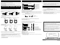
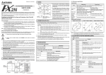
1) The FX2N-2AD and main unit are connected by a cable on the right of the main unit.
FX 2N-2AD
FX2N-2AD SPECIAL FUNCTIONBLOCK
FX0N
FX1N,
units can connect to the
series PLC, up to 5 for
up to 8 for
or, up
2) Up to 4
to 4 for the FX2NC series PLC, all with powered extension units.
However the following limitation exists when the undermentioned special function blocks are connected.
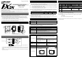
USER’S GUIDE
FX2N:
Main unit and powered extension units of 32 points I/O or less. Consumption current available for
undermentioned special function blocks ≤ 190mA
JY992D74701D
FX2N:
Main unit and powered extension units of I/O 48 points or more. Consumption current available
for undermentioned special function blocks ≤ 300mA
This manual contains text, diagrams and explanations which will guide the reader in the correct installation
and operation of the FX 2N -2AD special function block and should be read and understood before
attempting to install or use the unit.
Further information can be found in the FX SERIES PROGRAMMING MANUAL(ΙΙ), FX 0N/FX1N /FX2N/
FX2NC SERIES HARDWARE MANUAL of each PLC.
FX2NC: Up to 4 undermentioned special function blocks can be connected regardless of the system I/O.
FX0N/1N: Main unit and powered extension units. Up to 2 undermentioned special function blocks can be
connected regardless of the system I/O.
FX2N-2AD
FX2N-2DA
FX0N-3A
50mA
85mA
90mA
Consumption current of 24V DC for one unit
1. Introduction
The FX2N -2AD type analog input block (hereafter referred to as the FX 2N-2AD) is used to convert the
analog input of two points (voltage and current input) into a digital value of 12 bits, and to forward the
values to the Programmable Controller (hereafter referred to as a PLC).
FX2N-2AD can connected to the FX0N, FX1N, FX2N, and the FX2NC series Programmable Controllers.
1) The analog input is selected from the voltage or current input by the method of connecting wires.
At this time, assume the setting to be two channels common analog input (voltage or current input).
The consumption current of the above units is to be subtracted from the service power supply of the
host PLC.
3) The blocks occupies 8 points. (The 8 points can be allocated from either inputs or outputs).
4) FX 2N-2AD consumes 5V DC by 20mA.
The total 5V consumption of all special function blocks connected to an FX 2N, FX2NC main unit or
FX 2N extension unit must not exceed the 5V source capacity of the system.
2) The analog to digital conversion characteristics can be adjusted.
5. Specifications
3) The block occupies 8 I/O points which can be allocated from either inputs or outputs.
5.1 Environmental specification
4) The data transfer with the PLC uses the FROM/TO instructions.
Dielectric withstand
voltage
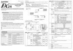
Dimensions: mm (inches)
M3(0.12)
terminal screws
GAIN
43(1.69)
A/D
OFFSET
volume
A/D
GAIN
volume
Mass (Weight):0.2kg (0.44lbs)
Accessories: Special Function block number label
Analog circuits
24V DC ±10% 50mA (Internal power supplied from the main unit)
Digital circuits
5V DC 20mA (Internal power supplied from the main unit)
Isolation
Photo-coupler isolation between analog and digital circuits.
No isolation between analog channels.
Number of occupied
I/O points
The blocks occupies either 8 input or output points
(can be either inputs or outputs)
5.3 Defining gain and offset
Item
*2
VIN{
IIN{
37.3KΩ
Range of analog input
250Ω
COM{
Current input 4~20mA
*1
VIN{
IIN{
165KΩ
AG
37.3KΩ
250Ω
Channel number enter {
Extension cable
*1
The FX2N-2AD cannot have 1 channel as an analog voltage input and one channel as current input because both
channels use the same offset and gain values. For current input please short circuit VIN and IIN as shown in the
diagram.
*2
Connect a 0.1 to 0.47 µF 25V DC capacitor with the position of *2 when there is voltage ripple in the voltage input or
there will be a lot of noise.
0 to 10V DC, 0 to 5V DC
(input resistance 200KΩ)
Warning-this unit may be damaged
by an input voltage in excess of
-0.5V, +15V DC
4 to 20mA (input resistance 250Ω)
Warning-this unit may be damaged by
an input current in excess of
-2mA, +60mA
12bit
Resolution
2.5mV:10V/4000(At shipment)
Change depending on the input
characteristic.
4µA: (20-4)A/4000
Change depending on the input
characteristic.
Integrated accuracy
±0.1V
±0.16mA
Processing time
2.5ms/1 channel (synchronized to the sequence program)
165KΩ
FX2N-2AD
Current input
Digital output
COM{
PLC
Voltage input
At shipping, the unit is adjusted to a digital range of 0 to 4000 for an analog
voltage input of 0 to 10V DC. When using an FX2N-2AD for current or
differing voltage inputs except 0 to 10V DC, it is necessary to adjust the
offset and gain.
3. Wiring
Voltage input 0~10V DC
Content
Analog value :0 to 20mA
Digital value :0 to 4000
Analog value :0 to 10V
Digital value :0 to 4000
(At shipment)
4095
4095
4000
4000
Input characteristics
0
10V
Analog value
20.380mA
OFFSET
4(0.16)
87(3.43)
Item
Digital value
GAIN
Environmental specifications other than the above-mentioned are the same as the main unit of the
Programmable controller. (Refer to the Hardware manual of the Programmable controller)
5.2 Power supply specification and others
OFFSET
Mounting
holes
2 holes 4.5
(0.18) dia
500V AC 1min(Between all terminals and case)
10.238V
POWER
Content
Digital value
80(3.15)
POWER
90(3.54)
FX2N -2AD
9(0.35)
VIN2 IIN2
COM2
VIN1
IIN1
COM1
VIN2 IIN2
COM
VIN1 IIN1
COM
Extension
cable
BFM
number
b15 to b8
#0
Reserved
#1
b7 to b4
#18 or
more
b2
b1
b0
Current value of input data (lower 8bit data)
Reserved
#2 to 16
#17
b3
Current value of input data (higher 4bit data)
Reserved
Reserved
Analog to digital
conversion beginning
Analog to digital
conversion channel
Reserved
BFM#0 :The current value of the input data for the channel specified with BFM#17 (lower 8bit data) is
stored.The current value data is stored by binary.
BFM#1:The current value of the input data (higher 4bit data) is stored. The current value data is stored
by binary.
BFM#17:b0⋅⋅⋅Channel (CH1,CH2) which does the analog to digital conversion is specified.
b0=0⋅⋅⋅CH1
b0=1⋅⋅⋅CH2
b1⋅⋅⋅0→1 The A/D conversion process is started.
Write/read data to the above-mentioned buffer memory according to the programming example of
"8.Program example".
Item
2. External Dimensions and Parts
DIN rail
mounting
slot
35mm(1.38)
FX2N
0 4mA
20mA
Analog value
The input characteristic is the same for each channel.
7. Adjustment of offset and gain
8. Program example
9. Notes in drive
7.1 Change in input characteristic
The following program examples (8.1 and 8.3) are formula circuits.
The device numbers that have been underlined can be assigned by the user during programming.
1) Confirm whether the input wiring of FX2N-2AD and the connection of the extension cable is correctly
done.
8.1 Example of programming analog input
2) Confirm whether the "4. Connection with programmable controller" condition is satisfied.
At shipment, 0 to 4000 range is selected for 0 to 10V DC input.
When using an FX 2N-2AD for current or differing voltage inputs except 0 to 10V DC, it is necessary to
adjust the offset and gain.
The module does not allow different input characteristics for two channels.
Set analog values within the range specified in the table below when changing the input characteristic.
X000
0
Range of input characteristic
Voltage input
Current input
0 to 1V
0 to 4mA
Analog value when digital value is 4000
5 to 10V
20mA
K0
[T0
K0
[FROM K0
*1
Analog value when digital value is 0
[T0
K17
H0000
K1
] a) Selecting A/D input channel 1.
K17
H0002
K1
] b) A/D conversion beginning of CH1.
K0
] c) Reading of digital value of CH1.
K4M100 D100 ] d) The higher 4 bits of CH1 are
moved to the lower 8 bits, and it is
stored in D100.
H0001 K1
] e) Selecting A/D input channel 2.
[MOV
X001
33
K0
[T0
K0
[FROM K0
*1
Resolution changes depending on the set value when the input characteristic changes accordingly.
Example: Resolution becomes (5 - 0V)/4000=1.25mV at voltage input 0 to 5V/0 to 4000.
Integrated accuracy does not change. (Voltage input: ±0.1V, Current input: ±0.16mA)
[T0
K17
K2M100 K2
K1
3) When shipped from the factory, the input characteristic is adjusted to 0 to 10V DC.
If a different input characteristic is desired, please adjust as required.
When the input characteristic is adjusted, the input characteristics of CH1 and CH2 are changed.
4) The coexistence use for the current and voltage input cannot be done with two channels.
10. Error check
] f) A/D conversion beginning of CH2.
Confirm the following items when it seems that the FX2N-2AD does not operate normally.
] g) Reading of digital value of CH2.
1) Confirm the state of POWER LED.
Lit
:The extension cable is correctly connected.
Turn off or blinks :Confirm the proper connection of the extension cable.
K17
H0003
K0
K2M100 K2
[MOV
K4M100 D101 ] h) The higher 4 bits of CH2 are
moved to the lower 8 bits, and it is
stored in D101.
2) Confirm the external wiring per section “3. Wiring”.
The adjustment of the offset and gain values sets a digital equivalent to the analogue data.
(The “POT” requires 18 revolutions to move between MIN and MAX setting.)
Voltage
generator
+
-
Current input
V
VIN{
+
Current
generator
IIN{
-
+
FX2N-2AD
+
-
VIN{
A
Volume
FX2N-2AD *1
VIN2 IIN2 COM
VIN1 IIN1 COM
Voltage input
POWER
OFFSET
IIN{
GAIN
OFFSET
GAIN
COM{
A/D
OFFSET
volume
AD GAIN
volume
COM{
Analog to digital conversion execution input of CH1:X000
Analog to digital conversion execution input of CH2:X001
At the same time X000 and X001 can be turned ON.
A/D input data CH1 :D100 (Replace with auxiliary relay M100 to M115. Assign these numbers only once)
A/D input data CH2 :D101 (Replace with auxiliary relay M100 to M115. Assign these numbers only once)
4) Confirm the Voltage and Current input values with a voltage and current generator. Confirm the
analog to digital conversion from the input characteristic.
Processing time: 2.5ms / 1 channel
(Time from turning on X000 and X001 to storage of analog to digital conversion value in
data register of main unit.)
5) Readjust the offset and gain by "7. Adjustment of offset and gain" when the analog to digital
conversion is not suitable for the input characteristic.
The input characteristic when shipped from the factory is 0 to 10V DC.
3) Confirm whether the load resistance of the connected equipment corresponds to the specification of
the FX 2N-2AD.
*1 Change the circuit of “*1” as follows when using an FX0N PLC
*1 The digital value increases if the volume is turned clockwise.
(FX2N-4DA and FX2N-2DA can be used instead of the voltage and current generator)
[FROM K0 K0
K4M100 K2
] yReading of digital value
[MOV K2M116 K2M108] yThe higher 4 bits are synthesized
to the lower 8 bits.
7.1.1 Adjustment of gain
The gain value can be set to an arbitrary digital value.
However, using the maximum 12bit resolution provides the user with a digital range of 0 to 4000.
Voltage input
characteristic(0 to 10V)
At shipment
Voltage input
characteristic(0 to 5V)
4000
Digital value
Digital value
Digital value
10V
0
Analog value
8.2 Connection to FX2N (V3.00 or later) or FX2NC (V3.00 or later) Series PLC
Please use FNC 176 (RD3A).
Refer to FX Series Programming Manual ΙΙ.
4000
4000
0
Current input
characteristic(4 to 20mA)
8.3 Example of programming making average value data
0 4mA
5V
20mA
Add the undermentioned program after "8.1 Example of programming analog input" and use the average
value data when you can not read a stable digital value.
Analog value
Analog value
0
7.1.2 Adjustment of offset
M8002
M133
The offset value can be set to an arbitrary digital value. However, it is advisable to set the analog value
when the digital value is set as following.
100mV
Analog value
80
0
39
Digital value
40
0
Voltage input
characteristic(0 to 5V)
Digital value
Digital value
Voltage input
characteristic(0 to 10V)
At shipment
Current input
characteristic(4 to 20mA)
100mV
Analog value
25
0 4mA 4.1mA
K0
D114
]
[DM0V
K0
D116
]
[DM0V
K0
D118
]
[MOV
K0
D101
]
[MOV
K0
D103
]
M8000
M133
84
[DM0V
Guidelines for the safety of the user and protection of the FX2N-2AD SPECIAL
FUNCTION BLOCK
•
This manual has been written to be used by trained and competent personnel. This is defined
by the European directives for machinery, low voltage and EMC.
•
If in doubt at any stage during the installation of the FX2N-2AD always consult a professional
electrical engineer who is qualified and trained to the local and national standards. If in doubt
about the operation or use of the FX2N-2AD please consult the nearest Mitsubishi Electric
distributor.
•
Under no circumstances will Mitsubishi Electric be liable or responsible for any consequential
damage that may arise as a result of the installation or use of this equipment.
a a) Initialization of data
[DINC
D118
] b
b) Count of sampling frequency
[DADD
D114
D100
D114
] c
c) Total of input data of CH1
[DADD
D116
] d
d) Total of input data of CH2
•
D118
D102
K20 *1
D116
[DCMP
M132
] e
[DDIV
D114
D118
D110
] f
All examples and diagrams shown in this manual are intended only as an aid to
understanding the text, not to guarantee operation. Mitsubishi Electric will accept no
responsibility for actual use of the product based on these illustrative examples.
[DDIV
D116
D118
D112
] g
e) Comparison of sampling frequencies
K20 is an average frequency
f) The average value of CH1 is calcurated,
and the result is stored in D111, D110
g) The average value of CH2 is calcurated,
and the result is stored in D113, D112
•
Owing to the very great variety in possible application of this equipment, you must satisfy
yourself as to its suitability for your specific application.
Analog value
For instance, when a digital range of 0 to 4000 is used with the analog range of 0 to 10V, a digital value of
40 is equal to an analog input of 100mV. (40 × 10V/4000 digital points)
1) The offset and gain adjustments for CH1 and CH2 are accomplished at the same time. When the
offset and gain values of one channel are adjusted, the other channel is automatically adjusted.
2) Repeat the offset and gain adjustment alternately until a stable value is reached.
A/D input data of CH1 :D100
A/D input data of CH2 :D102
Sampling frequency
:D118
Agreement flag of sampling frequency and average frequency :M133
Average value of CH1 :D111, D110
Average value of CH2 :D113, D112
Manual number : JY992D74701
*1 The above program example has an average sampling frequency of 20. Make the average frequency
within the range of 2 to 262143.
Manual revision : D
Date
3) Each channel is common to the analog input circuit. However, check each channel individually for
maximum accuracy.
: SEPTEMBER 2002
4) Adjust offset / gain by using subsection 8-3 "Example of programming making average value data"
when a digital value is not steady.
5) Adjust the gain before the offset.
HEAD OFFICE : MITSUBISHI DENKI BLDG MARUNOUTI TOKYO 100-8310
HIMEJI WORKS : 840, CHIYODA CHO, HIMEJI, JAPAN
JY992D74701D
TELEX : J24532 CABLE MELCO TOKYO
Effective Sep. 2002
Specifications are subject to
change without notice