1
Electric User's Manual, version 8.07
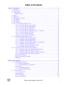
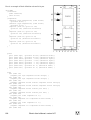
Table of Contents
Chapter 1: Introduction.....................................................................................................................................1
1−1: Welcome..........................................................................................................................................1
1−2: About Electric..................................................................................................................................2
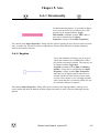
1−3: Requirements...................................................................................................................................3
Memory Control.........................................................................................................................3
1−4: Setup................................................................................................................................................4
1−5: Plug−Ins...........................................................................................................................................5
1−6: Fundamental Concepts....................................................................................................................6
1−7: The Display.....................................................................................................................................9
1−8: The Mouse.....................................................................................................................................11
1−9: The Keyboard................................................................................................................................12
1−10−1: IC Layout Tutorial: Make a Cell.............................................................................................15
1−10−2: IC Layout Tutorial: Create a Node.............................................................................15
1−10−3: IC Layout Tutorial: Highlighting...............................................................................16
1−10−4: IC Layout Tutorial: Make an Arc...............................................................................17
1−10−5: IC Layout Tutorial: Constraints.................................................................................17
1−10−6: IC Layout Tutorial: Adding Contacts to a Transistor................................................18
1−10−7: IC Layout Tutorial: Hierarchy...................................................................................21
1−10−8: IC Layout Tutorial: Exports.......................................................................................22
1−10−9: IC Layout Tutorial: Final Points................................................................................22
1−11−1: Schematics Tutorial: Make a Cell...........................................................................................23
1−11−2: Schematics Tutorial: Make a Node............................................................................24
1−11−3: Schematics Tutorial: Highlighting.............................................................................24
1−11−4: Schematics Tutorial: Make an Arc.............................................................................25
1−11−5: Schematics Tutorial: Multi−Input gates and Negation..............................................25
1−11−6: Schematics Tutorial: Constraints...............................................................................25
1−11−7: Schematics Tutorial: Hierarchy and Icons.................................................................26
1−11−8: Schematics Tutorial: Final Points..............................................................................27
1−12−1: Schematics and Layout Tutorial: Introduction........................................................................28
1−12−2: Schematics and Layout Tutorial: Schematic Entry....................................................28
1−12−3: Schematics and Layout Tutorial: Layout...................................................................29
1−12−4: Schematics and Layout Tutorial: Hierarchical Design..............................................33
1−12−5: Schematics and Layout Tutorial: Analysis................................................................35
Design Rule Checking..............................................................................................................35
Network Consistency Checking................................................................................................35
Simulation.................................................................................................................................36
Chapter 2: Basic Editing..................................................................................................................................37
2−1−1: Selecting Nodes and Arcs.........................................................................................................37
2−1−2: Selection Appearance...................................................................................................38
2−1−3: Unusual Selection: Areas and Text..............................................................................39
Selecting Text...........................................................................................................................39
2−1−4: Controlling Selection...................................................................................................40
2−1−5: Easy and Hard Selection..............................................................................................41
2−2−1: Node Creation...........................................................................................................................42
2−2−2: Arc Creation.................................................................................................................43
Segment Wiring........................................................................................................................43
Two−Point Wiring....................................................................................................................44
Special Considerations..............................................................................................................44
Electric User's Manual, version 8.07
i
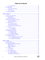
Table of Contents
2−2−3: Special Cases................................................................................................................45
2−3: Circuit Deletion.............................................................................................................................46
2−4−1: Movement..................................................................................................................................48
2−4−2: Other Modification.......................................................................................................49
2−5−1: Node Sizing...............................................................................................................................51
2−5−2: Arc Sizing.....................................................................................................................52
2−6: Changing Orientation....................................................................................................................53
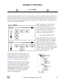
Chapter 3: Hierarchy.......................................................................................................................................55
3−1: Cells...............................................................................................................................................55
3−2: Cell Creation and Deletion............................................................................................................56
3−3: Creating Instances.........................................................................................................................58
Schematic Instances..................................................................................................................59
3−4: Examining Cell Instances..............................................................................................................60
3−5: Moving Up and Down the Hierarchy............................................................................................61
Layout Considerations..............................................................................................................61
Schematic Considerations.........................................................................................................62
3−6−1: Export Creation.........................................................................................................................63
3−6−2: Export Information.......................................................................................................65
Displaying Ports and Exports...................................................................................................66
3−6−3: Export Deletion and Movement...................................................................................66
3−7−1: Cell Lists...................................................................................................................................68
3−7−2: Cell Graphing...............................................................................................................70
3−7−3: Cell Properties..............................................................................................................71
3−8: Rearranging Cell Hierarchy...........................................................................................................73
3−9−1: Introduction to Libraries............................................................................................................74
3−9−2: Reading Libraries.........................................................................................................75
3−9−3: Writing Libraries..........................................................................................................76
3−9−4: Standard Cell Libraries................................................................................................79
3−10: Copying Cells Between Libraries................................................................................................80
3−11−1: Setting a Cell's View...............................................................................................................82
3−11−2: Switching between Views of a Cell...........................................................................82
3−11−3: Creating and Deleting Views.....................................................................................83
3−11−4: Automatic Icon Generation........................................................................................83
Chapter 4: Display............................................................................................................................................87
4−1: The Tool Bar..................................................................................................................................87
4−2: The Messages Window..................................................................................................................89
4−3: Creating and Deleting Editing Windows.......................................................................................90
Window Frames........................................................................................................................90
Display Considerations.............................................................................................................91
Display Algorithms...................................................................................................................92
4−4−1: Zooming....................................................................................................................................93
4−4−2: Panning.........................................................................................................................94
4−4−3: Focus............................................................................................................................95
4−5−1: The Component Menu...............................................................................................................96
4−5−2: The Cell Explorer.........................................................................................................98
Context Menus for Libraries.....................................................................................................99
Context Menus for Errors and Jobs........................................................................................100
ii
Electric User's Manual, version 8.07
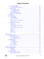
Table of Contents
4−5−3: Layer Visibility..........................................................................................................101
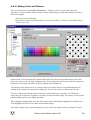
4−6−1: Electric's Color Model.............................................................................................................102
4−6−2: Editing Colors and Patterns........................................................................................103
4−7−1: Drawing a Grid........................................................................................................................106
4−7−2: Aligning to a Grid......................................................................................................107
4−7−3: Aligning to Objects....................................................................................................107
4−7−4: Measuring...................................................................................................................108
Measuring in an Edit Window................................................................................................108
Measuring in a Waveform Window........................................................................................108
4−8: Printing........................................................................................................................................109
4−9: Text Windows.............................................................................................................................111
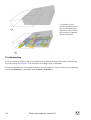
4−10−1: 3D Introduction.....................................................................................................................113
Troubleshooting......................................................................................................................114
4−10−2: 3D Preferences.........................................................................................................115
Lights......................................................................................................................................116
4−10−3: 3D Behaviors and Animation...................................................................................117
Animation...............................................................................................................................118
4−11−1: Digital Waveform Windows.................................................................................................119
Wave Panels............................................................................................................................119
Time Control...........................................................................................................................120
Stimuli (for Built−in Simulators only)...................................................................................121
Other Controls.........................................................................................................................122
4−11−2: Analog Waveform Windows....................................................................................123
Wave Panels............................................................................................................................124
Sweeps....................................................................................................................................124
Time Control...........................................................................................................................125
Eye Plots.................................................................................................................................126
Other Controls.........................................................................................................................126
Chapter 5: Arcs...............................................................................................................................................127
5−1: Introduction to Arcs.....................................................................................................................127
5−2−1: Rigid and Fixed−Angle Arcs...................................................................................................128
5−2−2: Slidable Arcs..............................................................................................................128
5−2−3: Constraint Propagation...............................................................................................129
5−3: Setting Constraints.......................................................................................................................130
5−4−1: Directionality...........................................................................................................................131
5−4−2: Negation.....................................................................................................................131
5−4−3: End Extension............................................................................................................132
5−4−4: Naming.......................................................................................................................132
5−4−5: Curvature....................................................................................................................132
5−5: Default Arc Properties.................................................................................................................133
Chapter 6: Advanced Editing........................................................................................................................135
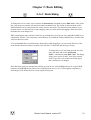
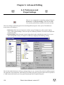
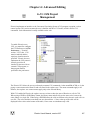
6−1: Making Copies.............................................................................................................................135
Duplication..............................................................................................................................135
Cut−and−Paste........................................................................................................................135
6−2: Creation Defaults.........................................................................................................................136
6−3: Preferences and Project Settings.................................................................................................138
Where Preferences Are Stored................................................................................................139
Electric User's Manual, version 8.07
iii
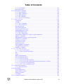
Table of Contents
Where Project Settings Are Stored.........................................................................................139
6−4: Making Arrays.............................................................................................................................140
6−5: Spreading Circuitry.....................................................................................................................142
6−6: Replacing Circuitry.....................................................................................................................143
6−7: Undo Control...............................................................................................................................145
6−8−1: Understanding Text.................................................................................................................146
6−8−2: Selecting Text.............................................................................................................146
6−8−3: Modifying Text..........................................................................................................147
Changing a Single Piece of Text.............................................................................................147
Changing Multiple Pieces of Text..........................................................................................148
6−8−4: Text Defaults..............................................................................................................150
6−8−5: Cell Parameters..........................................................................................................152
Special Considerations............................................................................................................153
6−9−1: Introduction to Networks........................................................................................................155
6−9−2: Naming Networks......................................................................................................156
6−9−3: Bus Naming................................................................................................................156
Arrayed Nodes........................................................................................................................157
Parameterized Bus Names......................................................................................................158
6−9−4: Power and Ground......................................................................................................158
6−9−5: Global Networks........................................................................................................159
Global Partitioning..................................................................................................................159
6−10−1: Introduction to Outlines........................................................................................................161
6−10−2: Manipulating Outlines..............................................................................................161
6−10−3: Special Outline Generation......................................................................................162
6−11: Interpretive Languages..............................................................................................................163
6−12: Project Management..................................................................................................................164
Checking Cells In and Out......................................................................................................165
Advanced Commands.............................................................................................................166
Under the Hood.......................................................................................................................166
6−13: CVS Project Management.........................................................................................................167
6−14: Emergencies..............................................................................................................................169
Chapter 7: Technologies.................................................................................................................................171
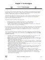
7−1−1: Technologies...........................................................................................................................171
7−1−2: Controlling Technologies...........................................................................................172
7−2−1: Scale........................................................................................................................................174
7−2−2: Units...........................................................................................................................175
7−3−1: I/O Specifications....................................................................................................................176
7−3−2: CIF Control................................................................................................................176
7−3−3: GDS Control...............................................................................................................178
7−3−4: EDIF Control..............................................................................................................181
7−3−5: DEF Control...............................................................................................................183
7−3−6: CDL Control...............................................................................................................184
7−3−7: DXF Control...............................................................................................................184
7−3−8: SUE Control...............................................................................................................185
7−4−1: The MOS Technologies..........................................................................................................186
7−4−2: The MOSIS CMOS Technology................................................................................187
Scalable Transistors................................................................................................................188
7−5−1: The Schematics Technology...................................................................................................189
iv
Electric User's Manual, version 8.07
Table of Contents
Digital Schematics..................................................................................................................190
Analog Schematics.................................................................................................................190
7−5−2: Multipage Schematics and Frames.............................................................................191
7−6−1: The Artwork Technology........................................................................................................193
7−6−2: The FPGA Technology..............................................................................................195
Primitive Definition Section...................................................................................................195
Block Definition and Architecture Sections...........................................................................196
Commands..............................................................................................................................199
7−6−3: The Generic Technology............................................................................................199
Special Arcs............................................................................................................................199
Special Nodes.........................................................................................................................199
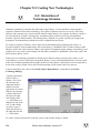
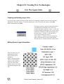
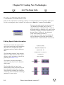
Chapter 8: Creating New Technologies........................................................................................................201
8−1: Designing New Technologies......................................................................................................201
8−2: Converting between Technologies and Libraries........................................................................202
Converting Technologies to Libraries....................................................................................202
Technology−Editing Mode.....................................................................................................202
Converting Libraries to Technologies....................................................................................202
Cleaning Up............................................................................................................................203
Using Technology Libraries...................................................................................................203
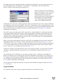
8−3: Hierarchies of Technology Libraries...........................................................................................204
8−4: The Layers Cells..........................................................................................................................205
Creating and Deleting Layer Cells..........................................................................................205
Editing Special Layer Information.........................................................................................205
Layer Function........................................................................................................................206
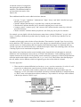
8−5: The Arc Cells...............................................................................................................................208
Creating and Deleting Arc Cells.............................................................................................208
Editing Special Arc Information.............................................................................................208
Editing Arc Geometry.............................................................................................................209
8−6: The Node Cells............................................................................................................................210
Creating and Deleting Node Cells..........................................................................................210
Editing Special Node Information..........................................................................................210
Editing Node Geometry..........................................................................................................211
Special Node Considerations..................................................................................................212
8−7: Miscellaneous Information..........................................................................................................214
The Support Cell.....................................................................................................................214
Transparent Colors..................................................................................................................215
Design Rules...........................................................................................................................215
The Component Menu............................................................................................................216
8−8: How Technology Changes Affect Existing Libraries.................................................................217
Adding layers, adding arcs, adding nodes, adding miscellaneous information......................217
Deleting layers........................................................................................................................217
Deleting nodes, deleting arcs..................................................................................................217
Deleting miscellaneous information.......................................................................................217
Modifying layers.....................................................................................................................217
Modifying arcs, modifying nodes...........................................................................................218
Modifying miscellaneous information....................................................................................218
8−9: Examples of Use..........................................................................................................................219
Example: Modifying a Layer's Appearance...........................................................................219
Electric User's Manual, version 8.07
v
Table of Contents
Example: Creating a New Node.............................................................................................220
8−10: Technology XML File Format..................................................................................................222
Introduction.............................................................................................................................222
Overall Structure.....................................................................................................................223
Layers......................................................................................................................................224
Arcs.........................................................................................................................................226
Nodes......................................................................................................................................227
Node Layers............................................................................................................................230
8−11: The Technology Creation Wizard.............................................................................................233
Chapter 9: Tools..............................................................................................................................................239
9−1: Introduction to Tools...................................................................................................................239
9−2−1: Introduction to DRC................................................................................................................241
9−2−2: DRC Preferences........................................................................................................242
9−2−3: Design Rules..............................................................................................................243
9−2−4: Coverage Rules..........................................................................................................245
9−2−5: Assura and Calibre DRC............................................................................................246
9−3−1: Well and Substrate Checking..................................................................................................247
9−3−2: Antenna Rule Checking.............................................................................................248
9−4−1: Introduction to Simulation......................................................................................................249
9−4−2: Verilog........................................................................................................................250
9−4−3: Spice...........................................................................................................................251
Special Spice Nodes................................................................................................................251
Spice Text...............................................................................................................................253
Spice Preferences....................................................................................................................254
9−4−4: Special Spice and Verilog Nodes...............................................................................257
9−4−5: FastHenry...................................................................................................................258
9−5−1: IRSIM......................................................................................................................................260
9−5−2: ALS............................................................................................................................262
Preferences..............................................................................................................................262
9−5−3: ALS Concepts............................................................................................................262
Behavioral Models..................................................................................................................263
Simulator Internals..................................................................................................................264
9−5−4: ALS Gates..................................................................................................................265
The i: and o: Statements (Input and Output)...........................................................................265
Signal References in the i: Statement.....................................................................................265
Signal References in the o: Statement....................................................................................266
The t: Statement (Time Delay)...............................................................................................266
The Delta Timing Distribution of the t: Statement.................................................................267
The Linear Timing Distribution of the t: Statement...............................................................267
The Random Probability Function of the t: Statement...........................................................267
The Fanout Statement.............................................................................................................268
The Load Statement................................................................................................................269
The Priority Statement............................................................................................................269
The Set Statement...................................................................................................................269
9−5−5: ALS Functions...........................................................................................................270
Declaring Input and Output Ports...........................................................................................270
Other Specifications................................................................................................................270
Example of Function Use.......................................................................................................271
vi
Electric User's Manual, version 8.07
Table of Contents
9−5−6: ALS Models...............................................................................................................271
The Set Statement...................................................................................................................272
9−6−1: Introduction to Routing...........................................................................................................273
9−6−2: Auto Stitching............................................................................................................274
9−6−3: Mimic Stitching..........................................................................................................274
9−6−4: Maze Routing.............................................................................................................276
9−6−5: River Routing.............................................................................................................276
9−6−6: Sea−of−Gates Routing...............................................................................................277
9−7−1: NCC Overview........................................................................................................................278
Limitations ............................................................................................................................278
Example ................................................................................................................................278
9−7−2: NCC Commands........................................................................................................278
9−7−3: NCC Preferences........................................................................................................280
Operation Section .................................................................................................................280
Size Checking Section ..........................................................................................................280
Checking All Cells Section ...................................................................................................281
Reporting Progress Section....................................................................................................281
Error Reporting Section.........................................................................................................281
9−7−4: NCC Annotations.......................................................................................................281
exportsConnectedByParent <string or regular expression>...................................................282
skipNCC <comment>.............................................................................................................282
flattenInstances <string or regular expression> ... .................................................................283
notSubcircuit <comment>......................................................................................................283
joinGroup <cell name>...........................................................................................................283
transistorType<type>..............................................................................................................284
resistorType<type>.................................................................................................................284
forceWireMatch <wireName>................................................................................................284
forcePartMatch <partName>..................................................................................................284
blackBox <comment>.............................................................................................................284
9−7−5−1: NCC GUI: Overview..........................................................................................................285
9−7−5−2: NCC GUI: Exports.................................................................................................286
9−7−5−3: NCC GUI: Parts and Wires....................................................................................287
Parts........................................................................................................................................288
Wires......................................................................................................................................289
Hash Code Partitioning...........................................................................................................290
Selecting Multiple Classes......................................................................................................290
9−7−5−4: NCC GUI: Sizes.....................................................................................................291
9−7−5−5: NCC GUI: Export Assertions................................................................................292
9−7−5−6: NCC GUI: Export/Global Network and Characteristics Conflicts........................293
9−7−5−7: NCC GUI: Unrecognized Parts..............................................................................293
9−7−5−8: NCC GUI: Advanced Features..............................................................................294
9−8−1: Pad Frame Generation.............................................................................................................295
9−8−2: Other Generators........................................................................................................298
9−9: Logical Effort..............................................................................................................................301
Logical Effort Gates................................................................................................................301
Logical Effort Libraries..........................................................................................................302
Advanced Features..................................................................................................................303
Commands..............................................................................................................................303
9−10−1: Parasitic Extraction...............................................................................................................304
Electric User's Manual, version 8.07
vii
Table of Contents
Project Settings.......................................................................................................................304
Preferences..............................................................................................................................305
9−10−2: Node Extraction.......................................................................................................306
9−11: Compaction................................................................................................................................309
9−12: Silicon Compiler........................................................................................................................310
Chapter 10: The JELIB File Format............................................................................................................313
10−1: JELIB and DELIB File Format.................................................................................................313
10−2−1: Header, View, and Tool........................................................................................................315
Headers...................................................................................................................................315
Views......................................................................................................................................315
Tools.......................................................................................................................................316
10−2−2: External References.................................................................................................316
10−2−3: Technologies............................................................................................................317
Technologies...........................................................................................................................317
10−3−1: Cells.......................................................................................................................................318
Groups.....................................................................................................................................318
10−3−2: Node Instances.........................................................................................................319
10−3−3: Arc Instances............................................................................................................320
10−3−4: Exports.....................................................................................................................321
10−4−1: Variables................................................................................................................................323
10−4−2: Text Descriptors.......................................................................................................324
10−4−3: Example....................................................................................................................325
viii
Electric User's Manual, version 8.07
Chapter 1: Introduction
1−1: Welcome
Now you have it!
A state−of−the−art computer−aided design system for VLSI circuit design.
Electric designs MOS and bipolar integrated circuits, printed−circuit−boards, or any type of circuit you
choose. It has many editing styles including layout, schematics, artwork, and architectural specifications.
A large set of tools is available including design−rule checkers, simulators, routers, layout generators, and
more.
Electric interfaces to most popular CAD specifications including EDIF, LEF/DEF, VHDL, CIF and GDS.
The most valuable aspect of Electric is its layout−constraint system, which enables top−down design by
enforcing consistency of connections.
This manual explains the concepts and commands necessary to use Electric. It begins with essential features
and builds on them to explain all aspects of the system. As with any computer system manual, the reader is
encouraged to have a machine handy and to try out each operation.
Electric User's Manual, version 8.07
1
Chapter 1: Introduction
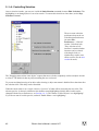
1−2: About Electric
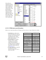
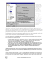
The About Electric... command (in menu Help) shows you the names of the Electric development team. It
also outlines you legal rights with respect to Electric.
This manual is available while running Electric. Use the User's Manual... command (in menu Help) to see
this manual (you may already be doing that).
While inside of the manual, click "Menu Help" to get help with Electric's pulldown menus. It displays a
pulldown menu inside of the manual page which mimics the real pulldown menu. Select any command from
this new menu to get help for the real pulldown menu entry.
2
Electric User's Manual, version 8.07
Chapter 1: Introduction
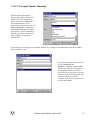
1−3: Requirements
Electric is written in the Java programming language and is distributed as a single ".jar" file, typically called
"electric.jar". There are two variations on the ".jar" file: with or without source code. Either of these files can
run Electric, but the one with source code is larger because it also has all of the Java code.
Electric requires Java version 1.5 or later from Sun Microsystems. It can also run with Apache Harmony.
However, it does not run properly on some open−source implementations of Java, including the version
shipped on Fedora Core systems. You will have to reinstall Java from Sun or Apache in such cases.
If you extract the source code from the ".jar" file and wish to build Electric, note that there are some
Macintosh vs. non−Macintosh issues to consider.
• Build on a Macintosh The easiest thing to do is to remove references to "AppleJavaExtensions.jar"
from the Ant script (build.xml). This package is a collection of "stubs" to replace Macintosh
functions that are unavailable elsewhere. You can also build a native "App" by running the
"mac−app" Ant script. This script makes use of files in the "packaging" folder. Macintosh computers
must be running OS 10.3 or later.
• Build on non−Macintosh If you are building Electric on and for a non−Macintosh platform, remove
references to "AppleJavaExtensions.jar" from the Ant script (build.xml). Also, remove the module
"com.sun.electric.MacOSXInterface.java". It is sufficient to delete this module, because Electric
automatically detects its presence and is able to run without it.
• Build on non−Macintosh, to run on all platforms To build Electric so that it can run on all
platforms, Macintosh and other, you will need to keep the module
"com.sun.electric.MacOSXInterface.java". However, in order to build it, you will need the stub
package "AppleJavaExtensions.jar". The package can be downloaded from Apple at
http://developer.apple.com/samplecode/AppleJavaExtensions/index.html.
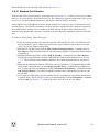
Memory Control
One problem with Java is that the Java Virtual Machine has a memory limit. This limit prevents programs
from growing too large. However, it prevents large circuits from being edited.
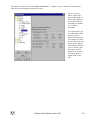
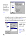
If Electric runs out of memory, you can request more. To do this, use General Preferences (in menu File /
Preferences..., "General" section, "General" tab). At the bottom of the dialog are two memory limit fields,
for heap space and permanent space. Changes to these values take effect when you next run Electric.
The heap space limit is the most important because increasing it will offer much more circuitry capacity.
Note that 32−bit JVMs can only grow so far. On 32−bit Windows systems you should not set it above 1500
(1.5 Gigabytes). On 32−bit Linux or Macintosh system, you should not set it above 3600 (3.6 Gigabytes).
Permanent space is an additional section of memory that can be insufficiently small. For very large chips, a
value of 200 or larger may enhance performance.
Electric User's Manual, version 8.07
3
Chapter 1: Introduction
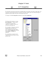
1−4: Setup
Running Electric varies with the different platforms. Most systems also allow you to double−click on the .jar
file.
If double−clicking doesn't work, try running it from the command−line by typing:
java −jar electric.jar
An alternate command−line is:
java −classpath electric.jar com.sun.electric.Launcher
There are a number of options that can be given at the end of the command line:
• −mdi force a multiple document interface style (where Electric is one big window with smaller edit
windows in it).
• −sdi force a single document interface style (where each Electric window is separate). Note that the
MDI/SDI settings can also be made from the Display Control Preferences (see Section 4−3).
• −s <script> run the <script> file through the Bean shell.
• −batch run in batch mode (no windows or other user interface are shown).
• −version provides full version information including build date.
• −v provides brief version information.
• −NOMINMEM ignore minimum memory requirements and start JVM.
• −help prints a list of available command options.
4
Electric User's Manual, version 8.07
Chapter 1: Introduction
1−5: Plug−Ins
Electric plug−ins are additional pieces of code that can be downloaded separately to enhance the system's
functionality. Currently, these plug−ins are available:
• IRSIM The IRSIM simulator is a gate−level simulator from Stanford University. Although originally
written in C, it was translated to Java so that it could plug into Electric. The Electric version is
available from Static Free Software at www.staticfreesoft.com/electricIRSIM−8.07.jar.
• PIE Port Interchange Experiment (PIE) is an experimental version of NCC (see Section 9−7−1).
Because it is ever−evolving, it is left as a plug−in so that frequent updates can be made. The latest
version is available from Static Free Software at www.staticfreesoft.com/electricPIE−8.07.jar.
• Bean Shell The Bean Shell is used to do parameter evaluation in Electric. Advanced operations that
make use of cell parameters will need this plug−in. The Bean Shell is available from
www.beanshell.org.
• 3D The 3D facility lets you view an integrated circuit in three−dimensions. It requires the Java3D
package, which is available from the Java Community Site, www.j3d.org. This is not a plugin, but
rather an enhancement to your Java installation.
• 3D Axis Controller Once the 3D facility is installed, there is one extra part that can be added to
enhance the display: a 3D axis controller. The 3D axis controller is available from Static Free
Software at www.staticfreesoft.com/electricJava3D−8.07.jar
• Animation Another extra that can be added to the 3D facility is 3D animation. This requires the Java
Media Framework (JMF) and extra animation code. The Java Media Framework is available from
Sun Microsystems at java.sun.com/products/java−media/jmf (this is not a plugin: it is an
enhancement to your Java installation). The animation code is available from Static Free Software at
www.staticfreesoft.com/electricJMF−8.07.jar.
• Russian User's Manual An earlier version of the user's manual (8.02) has been translated into
Russian. This manual is available from Static Free Software at
www.staticfreesoft.com/electricRussianManual−8.07.jar.
To attach a plugin, it must be in the CLASSPATH. The simplest way to do that is to invoked Electric from
the command line, and specify the classpath. For example, to add the beanshell (a file named
"bsh−2.0b1.jar"), type:
java −classpath electric.jar:bsh−2.0b1.jar com.sun.electric.Launcher
On Windows, you must use the ";" to separate jar files, and you might also have to quote the collection since
";" separates commands:
java −classpath "electric.jar;bsh−2.0b1.jar" com.sun.electric.Launcher
Note that you must explicitly mention the main Electric class (com.sun.electric.Launcher) when using
plug−ins since all of the jar files are grouped together as the "classpath".
Electric User's Manual, version 8.07
5
Chapter 1: Introduction
1−6: Fundamental
Concepts
MOST CAD SYSTEMS use two methods to do circuit design: connectivity and geometry.
• The connectivity approach is used by every Schematic design system: you place components and
draw connecting wires. The components remain connected, even when they move.
• The geometry approach is used by most Integrated Circuit (IC) layout systems: rectangles of "paint"
are laid down on different layers to form the masks for chip fabrication.
ELECTRIC IS DIFFERENT because it uses connectivity for all design, even IC layout. This means that you
place components (MOS transistors, contacts, etc.) and draw wires (metal−2, polysilicon, etc.) to connect
them. The screen shows the true geometry, but it knows the connectivity too.
The advantages of connectivity−based IC layout are many:
• No node extraction. Node extraction is not a separate, error−prone step. Instead, the connectivity is
part of the layout description and is instantly available. This speeds up all network−oriented
operations, including simulation, layout−versus−schematic (LVS), and electrical rules checkers.
• No geometry errors. Complex components are no longer composed of unrelated pieces of geometry
that can be moved independently. In paint systems, you can accidentally move the gate geometry
away from a transistor, thus deleting the transistor. In Electric, the transistor is a single component,
and cannot be accidentally destroyed.
• More powerful editing. Browsing the circuit is more powerful because the editor can show the
entire network whenever part of it is selected. Also, Electric combines the connectivity with a layout
constraint system to give the editor powerful manipulation tools. These tools keep the design
well−connected, even as the circuit is modified on different levels of hierarchy.
• Tools are smarter when they can use connectivity information. For example, the Design Rule
checker knows when the layout is connected and uses different spacing rules.
• Simpler design process. When doing schematics and layout at the same time, getting a correct LVS
typically involves many steps of design rule cleaning. This is because node extraction must be done
to obtain the connectivity of the IC layout, and node extractors cannot work when the design rules are
bad. So, each time LVS problems are found, the layout must be fixed and made DRC clean again.
Since Electric can extract connectivity for LVS without having perfect design rules, the first step is to
get the layout and schematics to match. Then the design rules can be cleaned−up without fear of
losing the LVS match.
• Common user interface. One CAD system, with a single user interface, can be used to do both IC
layout and schematics. Electric tightly integrates the process of drawing separate schematics and has
an LVS tool to compare them.
6
Electric User's Manual, version 8.07
The disadvantages of connectivity−based IC layout are also known:
• It is different from all the rest and requires retraining. This is true, but many have converted and
found it worthwhile. Users who are familiar with paint−based IC layout systems typically have a
harder time learning Electric than those with no previous IC design experience.
• Requires extra work on the user's part to enter the connectivity as well as the geometry. While this
may be true in the initial phases of design, it is not true overall. This is because the use of
connectivity, early in the design, helps the system to find problems later on. In addition, Electric has
many power tools for automatically handling connectivity.
• Design is not WYSIWYG (what−you−see−is−what−you−get) because objects that touch on the
screen may or may not be truly connected. Electric has many tools to ensure that the connectivity has
been properly constructed.
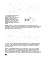
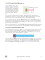
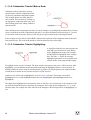
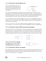
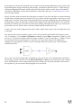
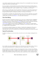
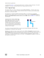
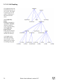
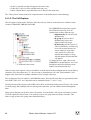
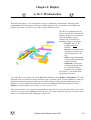
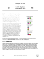
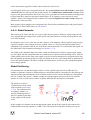
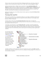
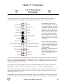
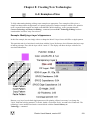
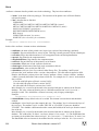
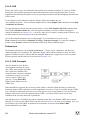
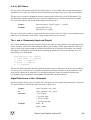
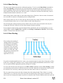
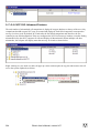
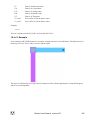
The way that Electric handles all types of
circuit design is by viewing it as a
collection of nodes and arcs, woven into a
network. The nodes are electrical
components such as transistors, contacts,
and logic gates. Arcs are simply wires that
connect two components. Ports are the
connection sites on nodes where the wires
connect.
In the above example, the transistor node on the left has three pieces of geometry on different layers:
polysilicon, active, and well. This node can be scaled, rotated, and otherwise manipulated without concern for
specific layer sizes. This is because rules for drawing the node have been coded in a technology , which
describes nodes and arcs in terms of specific layers.
Because Electric uses nodes and arcs for design, it is important that they be used to make all of the relevant
connections. Although layout may appear to be connected when two components touch, a wire must still be
used to indicate the connectivity to Electric. This requires a bit more effort when designing a circuit, but that
effort is paid back in the many ways that Electric understands your circuit.
Besides creating meaningful electrical networks, arcs which form wires in Electric can also hold constraints.
A constraint helps to control geometric changes, for example, the rigid constraint holds two components in a
fixed configuration while the rest of the circuit stretches. These constraints propagate through the circuit,
even across hierarchical levels of design, so that very complex circuits can be intelligently manipulated.
A cell is a collection of these nodes and arcs, forming a circuit description. There can be different views of a
cell, such as the schematic, layout, icon, etc. Also, each view of a cell can have different versions, forming a
history of design. Multiple views and versions of a cell are organized into Cell groups.
For example, a clock cell may consist of a schematic view and a layout view. The schematic view may have
two versions: 1 (older) and 2 (newer). In such a situation, the clock cell group contains 3 cells: the layout
view called "clock{lay}", the current schematic view called "clock{sch}", and the older schematic view
called "clock;1{sch}".
Hierarchy is implemented by placing instances of one cell into another. When this is done, the cell that is
placed is considered to be lower in the hierarchy, and the cell where it is placed is higher. Therefore, the
notion of going down the hierarchy implies moving into a cell instance, and the notion of going up the
hierarchy implies popping out to where the cell is placed. Note that cell instances are actually nodes, just like
the primitive transistors and gates. By defining exports inside of a cell, these become the connection sites, or
Electric User's Manual, version 8.07
7
ports, on instances of that cell.
A collection of cells forms a library, and is treated on disk as a single file. Because the entire library is
handled as a single entity, it can contain a complete hierarchy of cells. Any cell in the library can contain
instances of other cells. A complete circuit can be stored in a single library, or it can be broken up into
multiple libraries.
8
Electric User's Manual, version 8.07
Chapter 1: Introduction
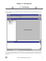
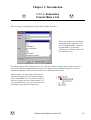
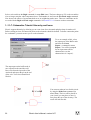
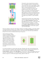
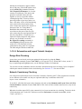
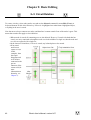
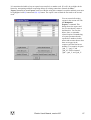
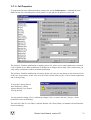
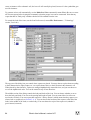
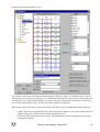
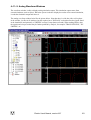
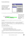
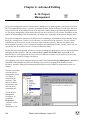
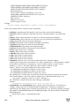
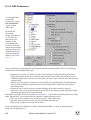
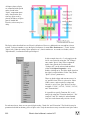
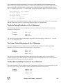
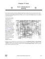
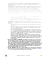
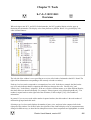
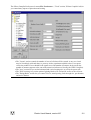
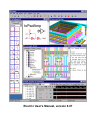
1−7: The Display
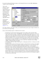
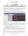
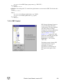
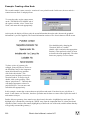
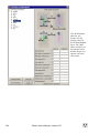
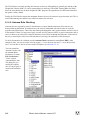
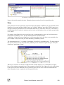
The Electric display varies from platform to platform. The image below shows a typical display with some
essential features.
The editing window is the largest window that initially says "No cell in this window" (this indicates that no
circuit is being displayed in that window). You can create multiple editing windows to see different parts of
the design.
Electric User's Manual, version 8.07
9
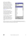
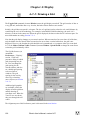
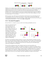
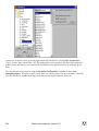
The left side of the edit window is the side
bar that has 3 tabbed sections, the components
menu, the cell explorer, and the layers. You can
move it to the right side with the On
Right command (of menu Windows / Side Bar)
and move it back with the On Left command.
You can also request that the side bar always be
on the right by checking "Side bar defaults to the
right side" in the Display Control Preferences (in
menu File / Preferences..., "Display" section,
"Display Control" tab).
The cell explorer lets you examine the hierarchy,
system activity, and error messages (see Section
4−5−2 for more).
The components menu shows a list of nodes (blue
border) and arcs (red border) that can be used in
design. The arrangement of the entries in the
components menu varies with the different
technologies. For MOS technologies, see Section
7−4−2; for schematics, see Section 7−5−1; and
for artwork, see Section 7−6−1.
The top three entries in the components menu let
you place pure−layer nodes (see Section
6−10−1), miscellaneous objects (see Section
7−6−3) and instances of cells (see Section 3−3).
The layers tab lets you control which parts of the
display are visible. See Section 4−5−3 for more
on layer visibility.
Below the edit window is the messages window,
which is used for all textual communication.
Above the edit windows is a pulldown menu along the top with command options. On some operating
systems, the pulldown menu is part of the edit window, and on others it is separate. Below the pulldown
menu is a tool bar which has buttons for common functions.
Finally, the status area gives useful information about the design state. It appears along the bottom of the
editing window or (in this example) at the bottom of the screen. The status area shows cursor coordinates,
and can show global coordinates when traversing the hierarchy (see Section 4−3).
10
Electric User's Manual, version 8.07
Chapter 1: Introduction
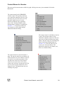
1−8: The Mouse
Electric makes use of only two mouse buttons: left and right. On systems with three−button mice, the middle
button is not used. On Macintosh systems with only one button, the right button is obtained by holding the
Command key when clicking.
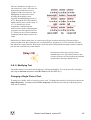
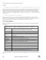
Modifier
Button
Action
Left Click
Select
Left Drag
Move selected objects
Left Double Click
Get Info
CTRL
Left Click
Cycle through
selected objects
SHIFT
Left Mouse Click
Invert selection
CTRL + SHIFT
Left Mouse Click
Cycle through objects
to Invert
Right Click
Draw or Connect Wire
SHIFT
Right Click
Zoom Out
SHIFT
Right Drag
Zoom In
CTRL + SHIFT
Right Drag
Draw Box
Wheel Up/Down
Scroll Up/Down
Wheel Up/Down
Scroll Right/Left
SHIFT
By combining special keystrokes with the mouse functions, advanced layout operations can be done:
• Switch Wiring Targets Hit Space while holding the Right mouse button to switch between possible
wiring targets under the mouse.
• Switch Layers Hit a number between 1−6 to switch layout layers. Additionally, if you have a port
highlighted that can connect to the new layer, a contact cut will be created at that point and connected
to the port.
• Abort Type ESCAPE to abort the current operation.
Electric User's Manual, version 8.07
11
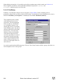
Chapter 1: Introduction
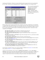
1−9: The Keyboard
Many common
commands can be
invoked by typing
"quick keys" for them.
These quick keys are
shown in the pulldown
menus next to the
item. For example, the
New Cell... command
(in menu Cell) has the
quick key
"Control−N". On the
Macintosh, the menu
shows " N",
indicating that you
must hold the
command key while
typing the "N"; on
Windows and UNIX
systems, the menu
shows "Ctrl−N",
indicating that you
must hold the Control
key while typing "N".
There are also
unshifted quick keys
(for example, the letter
"n" runs the Place
Cell
Instance command).
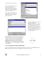
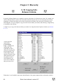
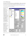
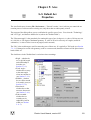
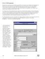
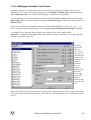
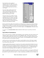
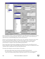
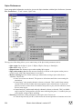
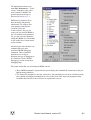
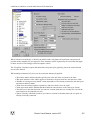
To change the bindings of quick keys, use the Key Bindings Preferences (in menu File / Preferences...,
"General" section, "Key Bindings" tab). The dialog shows the hierarchical structure of the pulldown menus
on the top, and lets you add or remove key bindings in the bottom area.
You can remove a quick key binding with the "Remove" button, and you can add a quick key binding with
the "Add" button. The "Reset" button restores default quick key bindings. Change key bindings with caution,
because it customizes your user interface, making it more difficult for other users to work at your computer.
You can get to EVERY menu command with key sequences. The keys to use are underlined in the menus.
For example, the File menu has the "F" underlined, and the Print... command of that menu has the "P"
underlined. This means that you can hold the Alt key and type "FP" to issue the print command.
12
Electric User's Manual, version 8.07
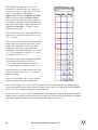
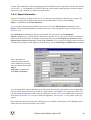
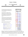
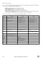
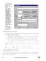
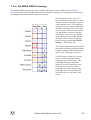
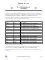
The default key bindings are shown here (use the Show Key Bindings command in menu Help to see the
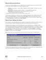
current set). For information about alternate key binding sets that mimic Cadence, see Section 4−6−2.
Letter
Control
Plain
Add Signal to Waveform
Window (4−11−1)
A
Select All (see 2−1−1)
B
Size Interactively (2−5−1)
C
Copy (6−1)
Change (6−6)
D
Down Hierarchy (3−5)
Down Hierarchy In−place (3−5)
E
Create Export (3−6−1)
F
Focus on Highlighted (4−4−1)
Full Unit Movement (2−4−1)
G
Toggle Grid (4−7−1)
Set Signal Low (4−11−1)
H
Other
Shift: Down Hierarchy In−place
to Object (3−5)
Half Unit Movement (2−4−1)
I
Object Properties (2−4−2)
J
Rotate 90 Counterclockwise
(2−6)
K
Show Network (6−9−1)
L
Find Text (4−9)
M
Duplicate (6−1)
Measure Mode (4−7−4)
N
New Cell (3−2)
Place Cell Instance (3−3)
O
Open Library (3−9−2)
Overlay Signal in Waveform
Window (4−11−2)
P
Peek (3−4)
Pan Mode (4−4−2)
Q
Quit (1−10−9)
Cycle through windows (4−3)
Remove Signal from Waveform
Window (4−11−2)
R
S
Save All Libraries (3−9−3)
Select Mode (2−1−1)
T
Toggle Negation (5−4−2)
Place Annotation Text (2−2−1)
U
Up Hierarchy (3−5)
V
Paste (6−1)
W
Close Window (4−3)
X
Cut (6−1)
Set Signal undefined (4−11−1)
Y
Redo (6−7)
Outline Edit Mode (6−10−2)
Z
Undo (6−7)
Zoom Mode (4−4−1)
Set Signal High (4−11−1)
Electric User's Manual, version 8.07
13
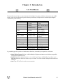
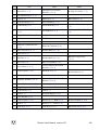
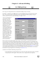
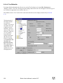
Key
0
Control
Zoom Out (4−4−1)
1
2
Pan Down (4−4−2)
3
Plain
Wire to Poly (1−8)
Other
See All Layers (4−5−3)
Wire to Metal−1 (1−8) See Metal−1 (4−5−3)
F1: Mimic Stitch
(9−6−3)
Wire to Metal−2 (1−8) See Metal−2/1 (4−5−3)
F2: Auto Stitch
(9−6−2)
Wire to Metal−3 (1−8) See Metal−3/2 (4−5−3)
4
Pan Left (4−4−2)
Wire to Metal−4 (1−8) See Metal−4/3 (4−5−3)
5
Center cursor (4−4−2)
Wire to Metal−5 (1−8) See Metal−5/4 (4−5−3) F5: Run DRC (9−2−1)
6
Pan Right (4−4−2)
Wire to Metal−6 (1−8) See Metal−6/5 (4−5−3) F6: Array (6−4)
7
Zoom In (4−4−1)
Wire to Metal−7 (1−8) See Metal−7/6 (4−5−3)
8
Pan Up (4−4−2)
Wire to Metal−8 (1−8) See Metal−8/7 (4−5−3)
9
Fill Window (4−4−1)
Wire to Metal−9 (1−8) See Metal−9/8 (4−5−3)
=
Increase all Text Size
(6−8−4)
−
Decrease all Text Size
(6−8−4)
DEL
Erase (2−3)
&
Repeat Last Action
(6−7)
>
Show Next Error (9−1)
<
Show Previous Error
(9−1)
SPACE
Switch Wiring Target
(1−8)
14
Shift
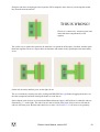
Electric User's Manual, version 8.07
F9: Tile Windows
Vertically (4−3)
Chapter 1: Introduction
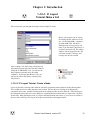
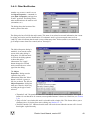
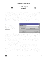
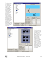
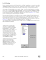
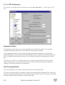
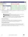
1−10−1: IC Layout
Tutorial: Make a Cell
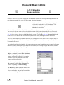
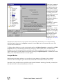
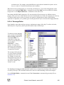
This section takes you through the design of some simple IC layout.
Before you can place any IC layout,
the editing window must have a cell
in it. Use the New Cell... command
(in menu Cell). This will show a
dialog that lets you type a new cell
name. Type the name ("MyCircuit" is
used here) and click OK. The editing
window will no longer have the "No
cell in this window" message, and
circuitry may now be created.
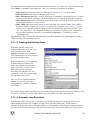
After creating a cell, look at the cell explorer (in
the status bar on the left side of the edit window).
Under the "LIBRARIES" icon, you will see the
list of libraries (currently only one called
"noname"). If you open that library's icon, you
will see the cells in the library (currently only
"MyCircuit").
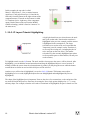
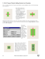
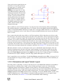
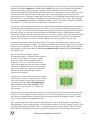
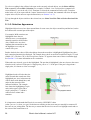
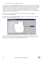
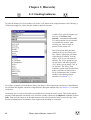
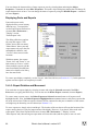
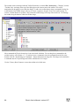
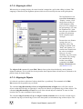
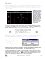
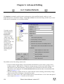
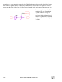
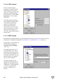
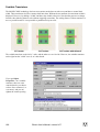
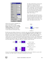
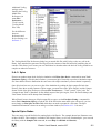
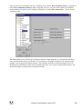
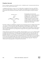
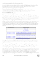
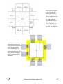
1−10−2: IC Layout Tutorial: Create a Node
Layout is placed by selecting nodes from the side bar's components menu, and then wiring them together.
This example shows two nodes that have been created. This was done by clicking on the appropriate
component menu entry, and then clicking again in the editing window to place that node. After clicking on
the component menu entry, the cursor changes to a pointing hand to indicate that you must select a location
for the node. When placing the node, if you press the button and do not release it, you will see an outline of
the new node, which you can drag to its proper location before releasing the button.
Electric User's Manual, version 8.07
15
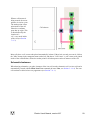
In this example, the top node is called
Metal−1−Polysilicon−1−Con (a contact between
metal layer 1 and polysilicon layer 1, found in the
fifth entry from the bottom in the right column of the
component menu). The node on the bottom is called
N−Transistor (lower−right entry of the component
menu). Both of these nodes are from the MOSIS
CMOS technology (which is listed as "mocmos" in
the status area).
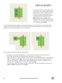
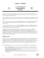
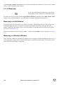
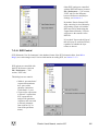
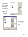
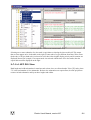
1−10−3: IC Layout Tutorial: Highlighting
A highlighted node has two selected areas: the node
and a port on that node. Note that the transistor is
highlighted in the previous example, and the contact
is highlighted in the example here. The larger
selected area covers the node, and it surrounds the
"important" part (for example, on the Transistor, it
covers only the overlap area, excluding the tabs of
active and gate on the four sides). The smaller
selected area is the currently highlighted port (there
are four possible ports on the transistor, but only one
on the contact).
To highlight a node, use the left button. The node, and the closest port to the cursor, will be selected. After
highlighting, you can hold the mouse button down and drag the highlighted object to a new location. If
nothing is under the cursor when the selection button is pushed, you may drag the cursor while the button
remains down to define an area in which all objects will be selected.
Another way to affect what is highlighted is to use the shift−left button. This button causes object
highlighting to be reversed (highlighted objects become unhighlighted and unhighlighted objects are
highlighted).
The shape of the highlighted port is important. Ports are the sites of arc connections, so the end point of the
arc must fall inside this port area. Ports may be rectangles, lines, single points (displayed as a "+"), or any
arbitrary shape. For example, when the active tabs of a transistor are highlighted, the port is shown as a line.
16
Electric User's Manual, version 8.07
1−10−4: IC Layout Tutorial: Make an Arc
To wire a component, select it, move
the cursor away from the component,
and use the right button. A wire will be
created that runs from the component to
the location of the cursor. Note that the
wire is a fixed−angle wire which means
that it will be drawn along a horizontal
or vertical path from the originating
node.
To see where the wire will end, click but do not release the button and drag the outline of the wire's
terminating node (a pin) until it is in the proper location. It is highly recommended that you do all wiring
operations this way, because wiring is quite complex and can follow many different paths.
Once a wire has been created, the other end is highlighted (see above). This is the highlighting of a pin node
that was created to hold the other end of the arc. Because it is a node, the right button can be used again to
continue the wire to a new location. If, during wiring, the cursor is dragged on top of an existing component,
the wire will attach to that component.
To remove wires or components, you can issue the Undo command (in menu Edit) to remove the last created
object. Alternatively, you can select the component and use the Selected command (in menu Edit / Erase).
1−10−5: IC Layout Tutorial: Constraints
Once components are wired, moving them will also move their connecting wires. Notice that the wires stretch
and move to maintain the connections. What actually happens is that the programmable constraint system
follows instructions stored on the wires, and reacts to node changes. The default wire is fixed−angle and
slidable, so the letters "FS" are shown when the wire is highlighted.
Select a wire and issue the Rigid command (in menu Edit / Arc). The letters change to "R" on the arc and the
wire no longer stretches when nodes move. Find another arc and issue the Not Fixed−angle command. Now
observe the effects of an unconstrained arc as its neighboring nodes move. These arc constraints can be
reversed with the Rigid and Fixed−angle commands. See Section 5−2−1 for more on these constraints.
Electric User's Manual, version 8.07
17
1−10−6: IC Layout Tutorial: Adding Contacts to a Transistor
One very common structure in IC layout is the transistor−contact combination. Here you will see the proper
way to construct it.
• Start with a transistor (in
this example on the left, an
n−transistor).
• Rotate the transistor so that
the gate is vertical. To do
this, use the 90 Degree
Counterclockwise command
(in menu Edit / Rotate), or
just type Control−J.
• Note that the active gate on
the left is highlighted (it is
just a line).
Although the default transistor is 2x3 in size, most people want them to be wider. For the purposes of this
example, make the transistor be 12 wide. To do this, select the node and use the Object Properties command
(in menu Edit / Properties).
Two easier
ways to see the
objects
properties are to
double−click on
the node, or
select it and
type Control−I.
When the "node
Properties"
dialog appears,
make the width
12 and click
OK.
Next we need a contact. Choose a
"Metal−1−N−Active−Con" to
connect the N−Active to Metal−1.
Make its size be 5x12 instead of the
default 5x5. Notice that contacts
are "smart" about the cuts, and add
them to fill the node. Note also that
the port (the inner rectangle) grows
with the node.
18
Electric User's Manual, version 8.07
Designers who have used polygon−based systems will be tempted to move these two nodes together so that
they form the desired structure:
THIS IS WRONG!
Electric is a connectivity−oriented system, and
insists that these components be wired
together.
The easiest way to connect the contact to the transistor is to spread the nodes apart, wire them, and then push
them back together. These two figures show the transistor and contact nodes, spread apart, and connected by
an arc.
On the left, the nodes and their ports; on the right, the arc.
The arc was made by selecting one node, clicking and HOLDING the right button, dragging the mouse over
the other component, and then releasing the button to create the arc.
Notice that the ends of an arc are centered and indented from the edge by half of the arc's width (the ends are
illustrated by "+" on the right). The ends of an arc must sit inside of the ports. If an arc moves such that its
ends are still in the ports, then the nodes don't have to move. See Section 5−4−3 for more on arc geometry.
Electric User's Manual, version 8.07
19
THIS IS RIGHT!
Now that the nodes are wired together, bring
the contact in close. Notice that the arc has
shrunk down to a square, with the endpoints
very close together. If you make the arc
rigid, the two nodes will be held together in
this configuration. To do this, use the
Rigid command (in menu Edit / Arc). As
shown here, the "R" on the selected arc tells
you that it has been made rigid. See Section
5−2−1 for more arc constraints.
Another common situation in making contacts meet transistors is when the sizes are not the same. In this
example, the contact is the default size. The arc runs from the center of the contact's port to the top of the
transistor's port. The finished layout is shown on the right.
Here are some points about connecting nodes with arcs:
• By doing it, the system understands your circuit connectivity and uses it in many other places.
• The design−rule checker will flag objects that touch but are not connected.
• After you create one of these structures, it can be copied−and−pasted many times. Use the Copy and
Paste commands (in menu Edit). Note that when pasting, you must not have anything selected, or
else it tries to replace the selected objects with the copied objects. Therefore, to duplicate some
circuitry, select it, Copy, click away to deselect, and then Paste.
• If you want to rotate or mirror these structures, select all of it (both nodes and the arc) and use the
Rotate or Mirror commands (in menu Edit).
20
Electric User's Manual, version 8.07
1−10−7: IC Layout Tutorial: Hierarchy
Electric supports hierarchy by
allowing you to place instances of
another cell. These instances are
nodes, just like the simpler ones in
the component menu. To see
hierarchy in action, create a new cell
with the New Cell... command (in
menu Cell). Make sure the "Make
new window" option is checked in
the dialog. Then type the new cell
name ("Higher" is used in the
example here).
A new (empty) cell will appear in a separate window. Try creating a few simple nodes in this new window
(place a contact or two).
Now place an instance of the other cell
by using the Place Cell
Instance... command (in menu Cell).
You can also click the "Cell" entry in
the component menu. You will be
given a list of cells to create: select the
one that is in the OTHER window (the
one called "MyCircuit" in this
example). Then click in the newer cell
to create the instance.
Electric User's Manual, version 8.07
21
The box that appears is a node in the same sense
as the contacts and transistors: it can be moved,
wired, and so on. In addition, because the node
contains subcomponents, you can see its
contents by selecting it and using the One Level
Down command (in menu Cell / Expand Cell
Instances, or click on the opened−eye button in
the tool bar). Note that if the objects in a cell no
longer fit in the display window, use the Fill
Display command (in menu Window).
1−10−8: IC Layout Tutorial: Exports
Before you can attach wires to the instance node, there must be connection sites, or ports on that node.
Primitive nodes such as contacts and transistors already have their ports established, but you must explicitly
create ports for cell instances. This is done by creating exports inside the cell definition.
Move the cursor to the window
with the lower−level cell
("MyCircuit") and select the
contact node. Then issue the
Create Export... command (in
menu Export). You will be
prompted for an export name and
its characteristic (the
characteristics can be ignored for
now).
This takes the port on
the contact node and
exports it to the outside
world. Its name will be
visible on the
unexpanded instance
node in the higher−level
cell.
You can now connect
wires to that node in
just the same way as
you wired the contact.
1−10−9: IC Layout Tutorial: Final Points
Some final commands that should be mentioned in this introductory example are the Save Library and the
Quit commands which can be found in the File menu. They do the obvious things.
22
Electric User's Manual, version 8.07
Chapter 1: Introduction
1−11−1: Schematics
Tutorial: Make a Cell
This section takes you through the design of some simple schematics.
Before you can place any schematics,
the editing window must have a cell
in it. Use the New Cell... command
(in menu Cell). Type the name
("MyCircuit" is used here) and select
the "schematic" view.
The editing window will no longer have the "No cell in this window" message, and circuitry may now be
created. Note that the component menu on the left will change to show schematics primitives. Also, the
Schematic technology is now listed in the status area at the bottom of the screen.
After creating a cell, look at the cell explorer (in
the status bar on the left side of the edit window).
In the "LIBRARIES" icon, you will see the list of
libraries (currently only one called "noname"). If
you open that library's icon, you will see the cells
in the library (currently only "MyCircuit").
Electric User's Manual, version 8.07
23
1−11−2: Schematics Tutorial: Make a Node
Schematic nodes are placed by selecting
them from the side bar's components menu
(on the left), and then wiring them together.
This example shows two nodes that have
been created. This was done by clicking on
the appropriate component menu entry, and
then clicking again in the editing window to
place that node.
After clicking on the component menu entry, the cursor changes to a pointing hand to indicate that you must
select a location for the node. When placing the node, if you press the button and do not release it, you will
see an outline of the new node, which you can drag to its proper location before releasing the button.
In this example, the top node is called a Buffer (found on the right side of the component menu in the third
entry from the top). The node on the bottom is called an And (top entry on the right).
1−11−3: Schematics Tutorial: Highlighting
A highlighted node has two selected parts: the
node and a port on that node. Note that the
And is highlighted in the previous example,
and the Buffer is highlighted in the example
here. The little "+" sign is the currently
highlighted port (there are two possible ports
on these nodes, on the input and the output).
To highlight a node, use the left button. The node, and the closest port to the cursor, will be selected. After
highlighting, you can hold the mouse button down and drag the highlighted object to a new location. If
nothing is under the cursor when the selection button is pushed, you may drag the cursor while the button
remains down to define an area in which all objects will be selected.
Another way to affect what is highlighted is to use the shift−left button. This button causes object
highlighting to be reversed (highlighted objects become unhighlighted and unhighlighted objects are
highlighted).
The shape of the highlighted port is important. Ports are the sites of arc connections, so the end point of the
arc must fall inside this port area. Ports may be rectangles, lines, single points (displayed as a "+"), or any
arbitrary shape. For example, the entire left side of the And gate is the input port and so its highlighting is a
line.
24
Electric User's Manual, version 8.07
1−11−4: Schematics Tutorial: Make an Arc
To wire a component, select it, move the
cursor away from the component, and use the
right button. If you click the right button and
hold it without releasing, then you can move
around and see where the wire will go when
you do release.
A wire will be created that runs from the component to the location of the cursor. Note that the wire is a
fixed−angle wire which means that it will be drawn along a horizontal, vertical, or 45−degree path from the
originating node. To see where the wire will end, click but do not release the button and drag the outline of
the wire's terminating node (a pin) until it is in the proper location. It is highly recommended that you do all
wiring operations this way, because wiring is quite complex and can follow many different paths.
Once a wire has been created, the other end is highlighted (see above). This is the highlighting of a pin node
that was created to hold the other end of the arc. Because it is a node, the right button can be used again to
continue the wire to a new location. If, while wiring, the dragged location is over an existing component, the
wire will attach to that component.
To remove wires or nodes, you can issue the Undo command (in menu Edit) to remove the last created
object. Alternatively, you can select the component and use the Selected command (in menu Edit / Erase).
1−11−5: Schematics Tutorial: Multi−Input gates and Negation
One aspect of the And, Or, and Xor gates that you will notice is that their left side (the input side) can accept
any number of wires. To see this in action, place one of these components in the cell. Then repeatedly select
its left side and use the right button to draw wires out of it. Each wire will connect at a different location in
the input port, and once the side fills with arcs, it will automatically grow to fit more. Note that the vertical
cursor location along the input side is used to select the position that will be used when a new wire is added.
To negate an input or output of a digital gate,
select the port or the arc and use the Toggle
Port Negation command (in menu Edit /
Technology Specific). With this facility, you
can construct arbitrary gate configurations.
1−11−6: Schematics Tutorial: Constraints
Once components are wired, moving them will also move their connecting wires. Notice that the wires stretch
and move to maintain the connections. What actually happens is that the programmable constraint system
follows instructions stored on the wires, and reacts to component changes. The default wire is fixed−angle, so
the letter "F" is shown when the wire is highlighted.
Electric User's Manual, version 8.07
25
Select a wire and issue the Rigid command (in menu Edit / Arc). The letter changes to "R" on the arc and the
wire no longer stretches when components move. Find another arc and issue the Not Fixed−angle command.
Now observe the effects of an unconstrained arc as its neighboring nodes move. These arc constraints can be
reversed with the Rigid and Fixed−angle commands. See Section 5−2−1 for more on these constraints.
1−11−7: Schematics Tutorial: Hierarchy and Icons
Electric supports hierarchy by allowing you to create icons for a schematic and place them in another cell.
Before creating an icon, all connection points to the schematic should be defined. To define connection points
for a schematic, you must create exports on the schematic.
To see an example of this, select
the output port of the Buffer node
and issue the Create
Export... command (in menu
Export). You will be prompted
for an export name and its
characteristics (set the
characteristics to "output").
The output port on the buffer node is
now exported to the outside world.
Run a wire from the input side of the
And node and export the pin at the end
of the wire. Your circuit should look
like this.
You can now make an icon for this circuit
by using the Make Icon command (in
menu View). The icon will be placed in
your circuit (you may have to move it
away from the rest of the circuitry). The
result will look like this.
26
Electric User's Manual, version 8.07
To test this icon in a circuit, create a
new cell in which to place instances
of the icon. Use the New
Cell... command (in menu Cell).
Type the new cell name ("Higher" is
used in the example here) and make
sure its view is "schematic".
A new (empty) cell will appear in a
separate window. Try creating a few
simple nodes in this new window
(place a gate or two).
Now place an instance of the other cell
by using the Place Cell
Instance... command (in menu Cell).
You can also click the "Cell" entry in
the component menu. You will be
given a list of cells to create: select the
one that is in the OTHER window (the
one called "MyCircuit{ic}" in this
example). Then click in the newer cell
to create the instance.
The icon that appears is a node in the same sense as the
Buffer and And gate: it can be moved, wired, and so on.
In addition, because the node contains subcomponents,
you can see its contents by selecting it and using the
Down Hierarchy command (in menu Cell / Down
Hierarchy). Note that if the objects in a cell no longer fit
in the display window, use the Fill Window command (in
menu Window).
1−11−8: Schematics Tutorial: Final Points
Some final commands that should be mentioned in this introductory example are the Save Library and the
Quit commands which can be found in the File menu. They do the obvious things.
Electric User's Manual, version 8.07
27
Chapter 1: Introduction
1−12−1: Schematics and
Layout Tutorial:
Introduction
This tutorial was originally written by David Harris at Harvey Mudd College as the first in a set of lab
instructions for an undergraduate−level CMOS VLSI design class. It provides very basic instructions to
acclimatize first−time users with Electric. As such, it is not a full introduction to using Electric, nor does it
cover many commonly used commands.
What this tutorial does cover is:
• Basic schematic editing. You will create a simple "nand" gate.
• Layout drawing. You will create the IC layout of the "nand" gate.
• Hierarchy. You will assemble the "nand" with an "inverter" to build an "and" gate.
• Analysis. You will run the design rule checker on the layout, and will compare the layout with the
schematic.
To begin, load the "mipscells" library with the MIPS Cells command (in menu Help / Load Built−in
Libraries). This library contains many parts of the MIPS processor that are provided to you. You will add
your new design to the library as you work through the tutorial.
1−12−2: Schematics and Layout Tutorial: Schematic Entry
Your first task is to create a schematic for a 2−input NAND gate. Each design is kept in a cell; for example,
your schematic will be in the "nand2{sch}" cell, while your layout will eventually go in the "nand2{lay}" cell
and your AND gate will go in the "and2{sch}" cell. Use the New Cell command (in menu Cell), or just type
Ctrl−N. Enter "nand2" as the cell name and select "schematic" as the view. The editing window will now
have the title "mipscells:nand2{sch}" indicating the library, cell name, and view. It is useful to put a label
inside a cell, in addition to assigning its given name. To label your cell, select the "Components" tab of the
sidebar (on the left), click on "Misc.", and select "Annotation text". Move the cursor to the location where
you want the label to appear, and click to create the text. Change the text by double−clicking on it and typing
"nand2". When done typing, click away from the text to exit the in−place editing (the text is now selected
with an "X" through it). Then bring up the full properties dialog for this text with the Object
Properties command (in menu Edit / Properties), or just type Ctrl−I. Set the "Text Size" to 5 units and click
OK. When your cell is finished, you can move this label to a sensible location.
Electric defines various technologies for schematics and layout. To draw transistor−level schematics, you can
use the symbols in the Components tab of the side bar.
28
Electric User's Manual, version 8.07
Your goal is to draw a gate like the one
shown here. Turn on the grid to help
you align objects. To do this, use the
Toggle Grid command (in menu
Window), or just type Ctrl−G. Click
on an nMOS transistor symbol in the
Components tab on the left side of the
screen. Then click in your schematic
window to place the transistor in the
circuit (perform this as two separate
clicks, not drag−and−drop). Repeat
until you have two nMOS transistors,
two pMOS transistors, the Power
symbol, and the Ground symbol
arranged on the page.
These symbols are nodes in Electric parlance. You may move the nodes around by clicking and dragging.
The transistors default to a width/length value of 2/2. Double−click on the pMOS transistor and change its
width to 12. Recall that nMOS transistors are roughly twice as strong as pMOS transistors. So a single nMOS
transistor would only have to be 6 wide. However, because the nMOS transistors are in series, they should
also be 12 wide.
Now, connect the nodes with wires (called arcs in Electric parlance). Notice that when you click on a node,
the closest port is also selected. These ports are the sides of arc connections. Click on a port such as the gate,
source, or drain of a transistor. Right−click, hold the mouse, and drag away from the node. When you release
the mouse, an arc will be created from the original node to the location of the cursor. A new "pin" node will
also be created at the cursor to hold the other end of the arc. If you right−click and drag over an existing
node, then you will connect to it. If two objects to be connected are not lined up, Electric will create two arcs
to join them. The location of the cursor determines the angle of the bend, so wiggle it to see how the two arcs
will run before releasing the button and creating the connection. See Section 2−2−2 for more on arc creation.
When the schematic is wired, you will need to create exports which define inputs and outputs of the cell.
From the Components tab, select the "Off−Page" symbol and place it in the circuit. Connect the tip of the
arrow the proper place in the circuit. To make an export on the other side of the Off−Page, select that port
and use the Create Export command (in menu Export), or just type Ctrl−E. Name the export "a" and define
its characteristic as "input". Similarly, create Off−Page symbols and exports for "b" and "y".
Now is a good time to save your library. Use the Save Library command (in menu File), or just type Ctrl−S.
Get into the habit of saving your library regularly. Also, learn the keyboard shortcuts for the commands you
use frequently.
1−12−3: Schematics and Layout Tutorial: Layout
Now that you have a schematic, it is time to draw the layout. Use the New Cell command (in menu Cell) to
bring up the new cell dialog. Enter "nand2" as the cell name and "layout" as the view. Notice that the
Components change from schematic symbols to layout primitives. The default technology is "mocmos"
(MOSIS CMOS) but can be changed with the pop−up menu at the top of the Components tab. The "mocmos"
technology has many options, such as the number of metal layers. To see these options, use the Project
Settings command (in menu File), and choose the "Technology" tab. In the "MOSIS CMOS" section, set the
number of Metal layers to 6. (This settings is remembered, and you will not have to set it again in future
sessions with Electric.) See Section 7−4−2 for more on the MOSIS CMOS technology.
Electric User's Manual, version 8.07
29
Your goal is to draw a layout like the one shown
here. It is important to choose a consistent layout
style so that various cells can "snap together." In this
project's style, power and ground run horizontally in
Metal−2 at the top and bottom of the cell,
respectively. The spacing between power and
ground is 80 units, center to center. No other
Metal−2 is used in the cell, allowing the designer to
connect cells with Metal−2 over the top later on.
nMOS transistors occupy the bottom half of the cell
and pMOS transistors occupy the top half. Each cell
has at least one well and substrate contact. Inputs
and outputs are given Metal−1 exports within the
cell.
You may find it convenient to have another sample
of layout visible on the screen while you draw your
gate. Use the Place Cell Instance command (in
menu Cell) and select "inv{lay}". Then click to drop
this inverter in the layout window. To view the
contents of the inverter, highlight the inverter and
use the One Level Down command (in menu Cell /
Expand Cell Instances), or click on the "opened
eye" icon in the toolbar.
The inverter instance is really just a node, and its contents are unavailable for editing. To extract the contents,
so that the individual nodes and arcs are available for editing, use the Extract Cell Instance command (in
menu Cell). Note that this command flattens makes a copy of the inverter cell inside of your NAND cell.
Study the inverter until you understand what each piece represents.
Start by drawing your nMOS
transistors. Recall that an nMOS
transistor is formed when polysilicon
crosses N−diffusion. N−diffusion is
represented in Electric as green
diffusion, surrounded by a dotted
yellow N−select layer all within a
hashed brown P−well background.
This set of layers is conveniently
provided as a 3−terminal transistor
node in Electric. Move the mouse to
the Components tab on the left side of
the screen.
As you move the mouse over various nodes, their name will appear in the status area at the bottom of the
screen. Click on the N−Transistor, and click again in the layout window to drop the transistor in place. To
rotate the transistor so that the red polysilicon gate is oriented vertically, use the 90 Degrees
Counterclockwise command (in menu Edit / Rotate), or just type Ctrl−J. There are two nMOS transistors in
series in a 2−input NAND gate, so we would like to make each wider to compensate. Double−click on the
transistor (or type Ctrl−I). In the node properties dialog, adjust the width to 12.
30
Electric User's Manual, version 8.07
We need two transistors in series, so copy and paste the transistor you have drawn. You can also duplicate the
selected object with the Duplicate command (in menu Edit) or just type Ctrl−M. Drag the two transistors
along side each other so they are not quite touching. Click the diffusion (source/drain) of one of the
transistors and right click on the diffusion of the other transistor to connect the two. Notice that Electric uses
nodes and arcs in IC layout as well as in schematics. Once connected, drag the two transistors until the
polysilicon gates are 3 units apart, looking like they do below. You will probably find it helpful to turn on the
grid (type Ctrl−G). The grid defaults to small dots every unit and large dots every 10 units. You can change
this with the Preferences command (in menu File), "Display" section, "Grid" panel. Change the "Frequency
of bold dots" to 7, because the cells in this library have a wire pitch of seven.
You can move objects around with the arrow keys on the keyboard. The distance that they move defaults to 1
unit, but this can be changed by using the "Full", "Half", or "Qtr" icons in the toolbar (or by pressing the "f",
"h", or "q" keys). You will avoid messy problems by keeping your layout on a unit grid as much as possible.
Inevitably, though, you will create structures that are an odd number of units in width and thus will have
either centers or edges on a half−unit boundary. (To move an object 7 units per click, or the equivalent of one
bold−spaced unit, press Control and then press the appropriate arrow key. If you first hit "h" and then the
control−arrow key will move an item one−half the distance of a bold−spaced unit, 3.5 in this case.)
Electric has an interactive design rule checker (DRC). If you place elements too closely together, it will
report errors in the "Messages" window. Try dragging one of the transistors until its gate is only 2 units from
the other. Observe the DRC error. Then drag the transistors back to proper spacing. When you are in doubt
about spacing, you can recheck the cell with the Check Hierarchically command (in menu Tool / DRC), or
just type the F5 key.
Next we will create the contacts from the
N−diffusion to Metal−1. Diffusion is also referred to
as "active". Drop a Metal−1−N−Active−Contact
node in the layout window and double−click to
change its Y size to 12. You will need a second
contact for the other end of the series stack of nMOS
transistors, so duplicate the contact you have drawn
(type Ctrl−M). Move the contacts near each end of
the transistor stack and draw diffusion lines to
connect to the transistors.
A quick way to connect many items that are touching
is to use the "auto router". To do this, select all of the
objects to be routed (click and drag a selection box
over them) and use the Auto−Stitch Highlighted
Now command (in menu Tool / Routing), or just
type the F2 key. See Section 9−6−2 for more on
auto−stitching.
Once the contacts are connected to the transistors; you will need a gap of only 1 unit between the metal and
polysilicon. Use the design rule checker to ensure you are as close as possible but no closer. Using similar
steps, draw two pMOS transistors in parallel and create contacts from the P−diffusion to Metal−1. At this
point, your layout should look something like this.
Draw wires to connect the polysilicon gates, forming inputs "a" and "b", and the Metal−1 output node "y".
Then add Metal−2 power and ground lines. You can create these Metal−2 wires by creating a "Metal−2−Pin"
node and right−clicking on it to draw a wire. Use the grid to make sure that the Metal−2 wires are 80 units
apart. This is the same spacing as the power/ground lines of the inverter. Note that when two objects are
Electric User's Manual, version 8.07
31
selected, the Properties dialog box (Ctrl−I), also tells the distance between them.
A via, called "Metal−1−Metal−2−Con", is required to connect the Metal−1 to the Metal−2 lines. Select an
active contact and right−click to connect it to the ground line. Electric will automatically create the necessary
via for you while making the connection. Complete the other connections to power and ground. Let power
and ground extend 2 units beyond the contents of the cell (excluding wells) on either side so that cells may
"snap together" with their contents separated by 4 units (so design rules are satisfied).
Recall that well contacts are required to keep the diodes between the cells and source/drain diffusion reverse
biased. We will place an N−well contact and a P−well contact in each cell. It is often easiest to drop the
"Metal−1−N−Well−Con" near the desired destination (near VDD), then right click on the power line to create
the via. Then drag the contact until it overlaps the via to form a stack of N+ diffusion, the diffusion to
Metal−1 contact, Metal−1, the Metal−1−Metal−2−Con, and Metal−2. Repeat with the P−well.
In our datapath design style, we will be connecting gates, with horizontal and Metal−2 lines. Metal−2 cannot
connect directly to the polysilicon gates. Therefore, we will add contacts from the polysilicon gate inputs to
Metal−1 to facilitate connections later in our design. Place a "Metal−1−Polysilicon−1−Con" node near the
left polysilicon gate. Connect it to the polysilicon gate and drag it near the gate. You will find a 3 unit
separation requirement from the Metal−1 in the contact to the metal forming the output "y". Add a short strip
of Metal−1 near the contact to give yourself a landing pad for a via later in the design. You may find Electric
wants to draw your strip from the contact in polysilicon rather than Metal−1. To tell Electric explicitly which
layer you want, click over the Metal−1 arc in the Component tab (arcs have red borders). Then draw your
wire.
Electric is agnostic about the polarity of well and substrate; it generates both n− and p−well layers. In our
process that has a p−substrate already, the p−well, indicated by brown slanting lines, will be ignored. The
n−well, indicated by small brown dots, will define the well on the chip. Electric only generates enough well
to surround the n and p diffusion regions of the chip. (Electric creates well contacts that are only 11 units
wide! This will generate a DRC error, but this behavior is intentional. Wells should be 12 units wide to meet
DRC's expectations.) It is a good idea to create rectangles of well to entirely cover each cell so that when you
abut multiple cells you don't end up with awkward gaps between wells that cause design rule errors. To do
this, click on the "Pure" entry of the Components tab and select "N−Well−Node" or "P−Well−Node". To
change its size so that it entirely covers the existing well, resize it with the Interactively command (in menu
Edit / Size) or just type Ctrl−B. You will find the pure layer nodes are annoying because you will tend to
select them when you really want to select a transistor or wire. To avoid this problem, select them and use the
Make Selected Hard command (in menu Edit / Selection) to make the node hard−to−select. Once an item is
defined as hard−to−select, you must use "special select" mode to be able to select it (click on the arrow with
the letters "SP" in the toolbar). You can use the Make Selected Easy command if you want to restore a node
or arc to be easily selected. Electric also provides the Coverage Implants Generator command (in menu
Tool / Generation) that automatically creates hard−to−select pure layer nodes for N and P wells. This
command is convenient for simple geometries inside of a cell.
Create exports for the cell. When you use the cell in another design, the exports define the locations that you
can connect to the cell. Click near the end of the short Metal−1 input line that you just drew on the left gate,
and select the Metal−1−Pin node. If you accidentally select the Metal−1 arc instead, click elsewhere in space
to deselect the arc, then try again to find the pin. You may also try holding the Control key while clicking to
cycle through everything that is under the cursor. Add an input export called "a" (type Ctrl−E to get the
export dialog). Repeat for input "b". Export output "y" from the metal line connecting the nMOS and pMOS
transistors. You may have to place an extra pin and connect it to the output line to give yourself a pin to
export as "y". Also export "vdd" and "gnd" from the Metal−2 arcs; these should be of type power and ground,
respectively. Electric recognizes "vdd" and "gnd" as special names, so be sure to use them.
32
Electric User's Manual, version 8.07
1−12−4: Schematics and Layout Tutorial: Hierarchical Design
Now that you have a 2−input NAND gate, you can use it, and an inverter, to construct a 2−input AND gate.
Such hierarchical design is very important in the creation of complex systems. You have found that the layout
of an individual cell can be quite time consuming. It is very helpful to reuse cells wherever possible to avoid
unnecessary drawing. Moreover, hierarchical design makes fixing errors much easier. For example, if you
had a chip with a thousand NAND gates and made an error in the NAND design, you would prefer to have to
fix only one NAND cell so that all thousand instances of it inherit the correction.
Each schematic has a corresponding symbol, called an icon, used to represent the cell in a higher−level
schematic. For example, open the "inv{sch}" and "inv{ic}" cells to see the inverter schematic and icon. You
will need to create an icon for your 2−input NAND gate. When creating your icon, it is a good idea to keep
everything aligned to the 1 unit grid; this will make connecting icons simpler and cleaner when you use it in
another cell.
Edit your "nand2{sch}" cell and use the Make
Icon View command (in menu View). Electric
will create a generic icon based on the exports as
shown here. It will drop the icon in the schematic
for handy reference; drag the icon away from the
transistors so it leaves the schematic readable.
A schematic is easier to read when
familiar icons are used instead of generic
boxes. Modify the icon to look like this.
Pay attention to the dimensions of the
icon; the overall design will look more
readable if icons are of consistent sizes.
To edit the icon, click on it and use the Down Hierarchy command (in menu Cell / Down Hierarchy) or just
type Ctrl−D. The Component tab will now show with various shapes (this is the "Artwork" technology).
Delete the generic black box but leave the input and output wires. Turn on the grid.
The body of the NAND is formed from an open C−shaped polygon, a semicircle, and a small negating circle.
To form the semicircle, create an unfilled circle node. Double−click to change its size to 6x6 and to span only
180 degrees of the circle. Use the rotate commands under the Edit menu to rotate the semicircle into place.
Place another circle, adjust its size to 1x1, and move it into place. Alternatively, you can type "h" and use the
arrow keys to move objects by 1/2 grid increments, then press "f" to return to full grid movement.
The Opened−Polygon node can be used to form the
C−shaped body. When first created, it appears as a
zigzag, shown here. To manipulate its shape, select it and
enter "outline edit mode" by using the Toggle Outline
Edit command (in menu Edit / Modes / Edit), or just
type "y", or click on the icon in the toolbar.
Electric User's Manual, version 8.07
33
In this mode, you can use the left button to select and move points and the right button to create points. Since
the default Opened−Polygon node has 4 points already, you should be able to form the "C" shape simply by
clicking and dragging these points. Outline edit mode is not entirely intuitive at first, but you will master it
with practice. When done, use the same command to exit the mode (just type "y"). See Section 6−10−1 for
more on outline editing.
Electric is finicky about moving the lines with inputs or outputs. If you click and drag to select the line along
with the input, everything moves as expected. If you try to move only the export name, it won’t move as you
might expect. Therefore, make a habit of moving both the line and export simultaneously when editing icons.
For appearance, remove the thin export connector lines. Replace these with bold black lines. You can easily
do this by left clicking on a wire of the icon, then right−clicking, placing the cursor where you want the end
point of the wire to be. Electric draws a wire that extends from the artwork of the icon.
Use the "Text" item in the Component tab to place a label "nand2" in the center of the icon. Make the text be
2 units high.
Now that you have an icon with three exports, create a new schematic called "and2" (don't forget to set the
view to "schematic"). Use the Place Cell Instance command (in menu Edit) to instantiate a "nand2{ic}" and
an "inv{ic}". Wire the two together and create exports on inputs "a" and "b" and output "y". Double−click on
the wire between the two gates and give it a name like "yb" so you know what you are looking at in
simulation. It is good practice to label every net in a design. When you are done, your "and2" schematic
should look like this.
Next, create a new layout called "and2" (remember to select the "layout" view). Instantiate the "nand2{lay}"
and "inv{lay}" layouts. ALWAYS use the Place Cell Instance command to create layout from pre−existing
facets. NEVER build a cell by cutting and pasting entire existing cells. If you do, then make a correction to
the original cell, your correction will not propagate to the new layout.
34
Electric User's Manual, version 8.07
Initially the cell instances appear as black
boxes with ports. Select both instances and
use the All the Way command (in menu
Cell / Expand Cell Instances) to view the
contents of each layout. Wire power and
ground to each other. Move the cells
together as closely as possible without
violating design rules. You may need to
place large blobs of pure layer nodes over
the n−well and p−well to avoid introducing
well−related errors from notches in the
wells. Connect the output of the "nand2" to
the input of the "inv" using Metal−1.
Remember that connections may only
occur between the ports of the two cells.
Also connect the power and ground lines of
the cells using Metal−2. Export the two
inputs, the output, and power and ground.
An easy way to do this is to use the
Re−Export Everything command (in
menu Exports) to bring exports to the
surface level. The Messages window
confirms how many ports were exported.
The final and gate should resemble this.
1−12−5: Schematics and Layout Tutorial: Analysis
Design Rule Checking
At any time, you can check your layout against the design rules by using the Check
Hierarchically command (in menu Tool / DRC), or just type the F5 key. When DRC is done, use the ">"
key to step through and highlight errors; see the Messages window for comments.
You can also use this command to check a schematic. Schematic design rules are simply "rules of etiquette"
which report unusual situations in the circuit drawing. See Section 9−2−1 for more on DRC.
Network Consistency Checking
One of the most useful analysis tools is Network Consistency Checking (NCC). This compares the networks
in two different cells to make sure they are equivalent (this step is sometimes called LVS:
layout−versus−schematic).
To run NCC, edit either the layout or the schematic cell, and use the Schematic and Layout Views of Cell in
Current Window command (in menu Tool / NCC). This check will not consider transistor sizes, only circuit
connectivity.
When the circuit has passed NCC at the connectivity level, turn on transistor size checking. To do this, check
"Check transistor sizes" in the NCC Preferences (use the Preferences command in menu File, section
"Tools", tab "NCC").
Electric User's Manual, version 8.07
35
Electric ideally likes layout, schematic and icons of the same items to be named identically (i.e. "nand2{sch}"
and "nand2{lay}" have identical names). Having the same name places cells in the same cell group. (Much of
this naming happens automatically in Electric when new views of a current cell are made.) If the two cells to
be compared are not in the same group, additional work is needed to tell NCC what to compare. See Section
9−7−1 for more on NCC.
Simulation
Electric has two built−in simulators, and can interface to many more. The built−in simulators are ALS and
IRSIM. ALS is a logic−level simulator, and is not useful for transistor−level design. IRSIM is a gate−level
simulator, and can handle the transistors in this example. Unfortunately, IRSIM is not packaged with the
basic Electric system (it is a free, but separate, "plugin"). See Section 1−5 for details on adding the IRSIM
simulator to Electric.
To simulate a circuit with IRSIM, use the IRSIM: Simulate Current Cell command (in menu Tool /
Simulation (Built−in)). A waveform window appears to show the simulation status. To get the waveform
window and your schematic/layout to appear side−by−side, use the Tile Vertically command (in menu
Window / Adjust Position).
The exported signals of your design will automatically appear in the waveform window. To add an internal
signal to the waveform display, select it and use the Add to Waveform in New Panel (in menu Edit /
Selection), or just type "a". To set a "1" value on a signal, select it (in either the waveform or the
schematic/layout) and use Set Signal High at Main Time (in menu Tool / Simulation (Built−in)), or just
type "V". You can drag the "main" time cursor (the dashed line) to any point in the waveform window.
Notice that as you drag it, level information is displayed in the schematic/layout. See Section 9−5−1 for more
on the IRSIM simulator.
Besides built−in simulation, Electric can generate input decks for many popular external simulators (see
Section 9−4−1). For example, to simulate with Spice, follow these steps:
• Use the Spice Preferences to select the Spice engine that you have (Spice 3, HSpice, PSpice,
SmartSpice, etc.)
• Use the Write Spice Deck... command (in menu Tool / Simulation (Spice)) to generate an input
deck for Spice.
• Run the simulation externally
• Use the Plot Spice Listing... command (in menu Tool / Simulation (Spice)) to read the output of
Spice and display it in a waveform window.
See Section 9−4−3 for more on Spice.
36
Electric User's Manual, version 8.07
Chapter 2: Basic Editing
2−1−1: Selecting
Nodes and Arcs
Electric is a noun/verb system, meaning that all commands work by first selecting something (the noun) and
then doing an operation (the verb). For this reason, selection is important.
Selection (and movement, wiring, and zooming) are done
in "selection" mode, which is the default mode. This
mode is indicated by having the "selection" icon
highlighted in the tool bar.
Selection is done with clicks of the left button. Individual nodes and arcs are selected by clicking over them.
You can tell in advance what will be selected by the button click, because the next object to be selected is
shown in blue. This advance selection is called "mouse−over highlighting" and can be disabled (see Section
2−1−4). Once selected, objects are highlighted on the screen. If you use the shift−left button, unhighlighted
nodes and arcs are added to the selection, but objects that are already highlighted become deselected.
There are often multiple objects under the cursor (for example, in the area where an arc overlaps a node). To
get the object you want, hold the control key while clicking. The control−left button cycles through all
objects under the cursor.
The notion of toggling selection (shift−left) and cycling through what is under the cursor (control−left) can be
combined. If there are multiple objects under the cursor, and you are trying to toggle the selection, use the
control−shift−left button to cycle through them .
To select an object by its name, use the Select
Object... command (in menu Edit / Selection).
The resulting dialog lets you select nodes, arcs,
exports, or networks in the cell. You can also
search for objects by name (the search field
supports regular expressions).
To select everything in the cell, use the Select
All command (in menu Edit / Selection). To
deselect everything, use Select Nothing.
The Deselect All Arcs command deselects all
selected arcs. This is useful when you wish to
select a set of nodes, but you have selected the
entire area, including nodes and arcs.
Electric User's Manual, version 8.07
37
To select everything in the cell that is the same as the currently selected objects, use the Select All Like
This command (in menu Edit / Selection). For example, if a Metal−1 arc is selected, the command will
select all Metal−1 arcs in the cell; if a P−Transistor is selected, the command will select all P−Transistor
nodes in the cell; if an export with the "output" characteristic is selected, the command will select all output
exports in the cell (for more on export characteristics, see Section 3−6−1).
To loop through the objects similar to the selected one, use Select Next Like This and Select Previous Like
This.
2−1−2: Selection Appearance
Highlighted objects have a box drawn around them. In some cases, the object extends beyond the box, but the
box encloses the essential part of the object.
For example, MOS transistors are
highlighted where the two
materials cross, even though the
materials extend on all four sides.
Also, CMOS active arcs have
implants that surround them, but
the highlight covers only the
central active part.
Besides the basic box, there will be other things drawn when an object is highlighted. Highlighted arcs have
their constraint characteristics displayed. The example above shows an arc that is both fixed−angle ("F") and
slidable ("S"). The letter "R" is used for rigid arcs, and an "X" appears when none of these constraints apply.
See Section 5−1 for more information on arc constraints.
When nodes are selected, a port is also highlighted. The port that is highlighted is the one closest to the cursor
when the node is selected. If the port is a single point, you see a "+" at the port. If the port is larger than a
single point, it is shown as a line or rectangle.
Highlighted nodes will also show the
entire network that extends out of the
highlighted port. Arcs in that network
will be drawn with dashed lines, and
nodes in that network will be
indicated with dots. The example
here shows the highlighting of a pin
node (in the upper−right) with a
single−point port ("+") which is
connected to a contact and a
transistor.
It is important to understand that Electric is not exactly a WYSIWYG editor
(what−you−see−is−what−you−get). Nodes that are touching on the screen may not actually be connected if
there are no arcs joining them. The best way to ensure that the circuit is correct is to highlight a node and see
the extent of the connections on it.
38
Electric User's Manual, version 8.07
2−1−3: Unusual Selection: Areas and Text
Besides highlighting nodes and arcs, Electric can also highlight an arbitrary rectangular area. The notion of a
highlighted area, as opposed to a highlighted object, is used in some commands, and it generally implies
highlighting of everything in the area.
There are two ways to highlight an area. If you click the left button where there is no object, and hold it down
while dragging over objects, all of those objects will be highlighted.
To more precisely define a highlighted area,
switch to area selection (as opposed to object
selection) with the Select Area command (in
menu Edit / Modes / Select, or click on the
"Area Selection" icon in the tool bar). Use
Select Objects to revert back to object selection.
Once in area selection mode, each click and drag of the left button leaves the highlight rectangle on the screen
exactly as it was drawn. You can convert this selection to a set of actual nodes and arcs with the Enclosed
Objects command (in menu Edit / Selection).
Selecting Text
Highlighted text appears as an "X" over the letters. However, text is a special case, so it will not be covered
until later (Section 6−8−2). For now, if you highlight some text, it is best to click again and select something
else.
Electric User's Manual, version 8.07
39
2−1−4: Controlling Selection
Once a selection is made, you can save it with the Push Selection command (in menu Edit / Selection). The
highlighting is not changed, but it is saved on a stack. To restore this selection at a later time, use the Pop
Selection command.
There are some selection
preferences that can be set
with Selection Preferences
(in menu File /
Preferences..., "General"
section, "Selection" tab).
"Easy selection of cell
instances" controls whether
instances can be selected
with simple clicks, or
whether they require extra
effort to select (see the next
section for more).
The "Dragging must enclose entire object" requests that area−selection completely enclose an object in order
to select it. The default is that any object touching the area is selected.
To prevent accidental moving of an object after selecting it, object movement is disabled for a short time after
the selection click. This delay can be controlled.
When the cursor roams over a circuit, it shows a "preview" of what will be selected by the next click. The
advance preview is shown in a different color than the actual highlighting (initially blue, but this can be
changed with the Layers Preferences, see Section 4−6−2). This feature is called "mouse−over highlighting".
If you do not want to see this preview, uncheck "Enable Mouse−over highlighting".
40
Electric User's Manual, version 8.07
2−1−5: Easy and Hard Selection
In a busy circuit, many objects may overlap, causing confusion when selecting. To simplify selection, objects
can be marked so that they are no longer easy−to−select, which means that standard selection does not work
on them.
To select hard−to−select objects, use the Toggle
Special Select command (in menu Edit / Modes /
Select). You can also click on the "Special Select"
tool bar button to enable "special selection". Once in
this mode, all objects are selectable.
Ease of selection extends to more than just nodes and arcs. There are four "classes" of objects that can be
selected:
• Basic objects (all arcs, primitive nodes, and port names)
• Cell instances
• Node and arc text (names and other text placed on nodes and arcs)
• Instance names (an unexpanded cell instance's name)
By default, the first three classes are easy−to−select, and instance names are hard−to−select. If you uncheck
"Easy selection of cell instances" in the Selection Preferences dialog, then cell instances become
hard−to−select.
Although all nodes and arcs are typically easy−to−select, you can control them individually by unchecking
the "Easy to Select" field in their properties dialog (use the Object Properties... command in menu Edit /
Properties). If multiple objects are selected, the Object Properties... dialog has a popup on the right for
changing their selection difficulty.
Special commands exist in the Selection menu for dealing with easy−to−select nodes and arcs. You can
select all of the easy−to−select objects in the current cell with the Select All Easy command. Similarly, you
can select those that are not easy−to−select with the Select All Hard command. To change the ease of
selection for a set of objects, highlight them and use either Make Selected Easy or Make Selected Hard.
Electric User's Manual, version 8.07
41
Chapter 2: Basic Editing
2−2−1: Node Creation
Node creation is done by selecting a node from the component menu in the side bar (on the left). Nodes in the
component menu are outlined in blue. After clicking on one of these nodes, click in the edit window to place
the node.
The location of the cursor is aligned to the nearest grid unit. This adjustment can be controlled with the Grid
Preferences (in menu File / Preferences..., "Display" section, "Grid" tab, see Section 4−7−2).
When placing a node, the cursor points to the anchor point of the newly created node. This is the center (for
primitives) or the location of the cell−center (for cell instances). Cell instances can change their anchor point
by moving the Cell−Center node inside of their layout (see Section 3−3).
When placing a node, but before you click to actually create the node, it is possible to temporarily switch
from node−placement to zoom/pan mode. This allows you to better select the location of the newly−created
node. To temporarily zoom, type "z", zoom the display, and then type "z" again to finish placing the node. To
temporarily pan, type "p", pan the display, and then type "p" again to finish placing the node. For more on
zooming and panning, see Sections 4−4−1 and Sections 4−4−2.
Besides basic components, there are special entries in the component menu for creation of additional nodes:
• The "Cell" button displays a list of cell instances that can be created (see Section 3−3).
• The "Pure" button (only available in layout technologies) lets you place pure−layer nodes (see
Section 6−10−1).
• The "Spice" button (only available in schematics) lets you place Spice primitives (see Section 9−4−3).
42
Electric User's Manual, version 8.07
• The "Misc" button has a collection of special objects that can be created.
• "Cell Instance..." brings up a dialog to
select a cell instance to place (see Section
3−3).
• "Annotation Text" places a node that
contains only text (see Section 6−8−1).
This can also be accomplished with the
Add Text Annotation command (in
menu Edit / Text)
• "Layout Text..." brings up a dialog to
create text from layout nodes (see Section
6−10−3).
• "Annular Ring..." brings up a dialog to
create circular shapes (see Section
6−10−3).
• "Cell Center" places a node that defines
the origin of the cell (see Section 3−3).
• "Essential Bounds" places a node that
defines the corners of the cell's essential
bounds (see Section 7−6−3).
• "Spice Code" places a text−only node that will be inserted into Spice decks (see Section 9−4−3).
• "Spice Declaration" places a text−only node that will be inserted into Spice decks near the top (see
Section 9−4−3).
• "Verilog Code" places a text−only node that will be inserted into the code area of Verilog decks (see
Section 9−4−2).
• "Verilog Declaration" places a text−only node that will be inserted into the declaration area of
Verilog decks (see Section 9−4−2).
• "Simulation Probe" places a node that can be used to display simulation results (see Section 4−11−1).
• "DRC Exclusion" places a node that covers DRC errors and causes them to be ignored (see Section
9−2−3).
• "AFG Exclusion" places a node that tells Auto−Fill Generation to ignore the area (not currently used,
but see Section 9−8−2 for more on Auto−Fill Generation).
• "Invisible Pin" places an invisible−pin node (see Section 7−6−3).
• "Universal Pin" places an universal−pin node (see Section 7−6−3).
• "Unrouted Pin" places an unrouted−pin node (see Section 7−6−3).
2−2−2: Arc Creation
As the introductory example showed, arcs are created by clicking the right button. This can actually function
in two different ways, depending on what is highlighted.
Segment Wiring
If one node is highlighted, segment wiring is done, in which an arc is drawn from the highlighted node to the
location of the cursor. If there is nothing at that location, a pin is created, and it is left highlighted. Using the
right button again runs an arc from that pin to another location. By clicking and holding the right button, you
can see the path that the new arc will follow.
In general, all wiring operations should be done by clicking and holding the right button, then moving the
Electric User's Manual, version 8.07
43
cursor until the intended wiring is shown, and finally releasing. This is recommended because wiring is quite
complex and can follow many different paths.
If you type a digit key while the right button is pressed, it changes the wiring layer by inserting contacts to
that layer of metal. For example, if you are running a metal−1 wire, and type "3" during the wiring, then two
contacts will be added (metal−1−metal−2 and metal−2−metal−3) to make the wire run in metal−3.
If the cursor is over another object when the right button is released, the new wire attaches to that object. If
there are multiple objects under the cursor, press the space bar (while the right button is pressed) to cycle
through the possible endpoints (including the possibility of connecting to none of them).
If an Unrouted arc is attached to the original node, that arc moves to the new pin. This allows you to replace
Unrouted arcs incrementally, one segment at a time. When both ends of the Unrouted arc are replaced by a
segment, that arc is removed. See Section 9−6−1 for more about Unrouted Arcs.
Two−Point Wiring
The other way that the creation button can operate is two−point wiring, in which two nodes are highlighted
and one or more arcs are created to connect them. Highlighting of these two nodes is done by clicking the
left button over the first one, and then using the shift−left button on the second. Note that if the second node
is obscured by other objects, you can cycle through the objects under the cursor with the
control−shift−left button. Once the two nodes are highlighted, use the right button to wire them together.
Note that the highlighted ports on the selected nodes are important: arcs will run between them, so they must
be compatible in their wiring capabilities.
Two−point wire creation first attempts to run a single arc. Generally, this can happen only if the ports are
lined up accurately. Failing single arc placement, an attempt is made to connect with two arcs and an
intermediate node. These two arcs can bend in one of two directions, determined by the location of the cursor.
Special Considerations
In addition to running an arc between two nodes, you can also use arcs as the starting or ending point of arc
creation.
If it is sensible, the creation command actually uses one of the nodes on an end of the selected arc. However,
if the connection falls inside the arc, it is split and a new node is created to make a "T" connection.
Electric will allow you to connect two nodes or arcs as long as there is some way in the current technology
for those objects to be connected. For example, if connecting between metal−1−pin and a metal−3−pin in the
MOSIS CMOS technology, Electric will place metal−1−metal−2 and metal−2−metal−3 contact cuts down,
and wire between all four nodes. When vias are inserted, they are placed closest to the "destination" node (or
44
Electric User's Manual, version 8.07
farthest from the original node).
As mentioned in Section 1−8, pressing the number keys for a valid layer switches to that layer. If a node is
highlighted, it will route to that layer from the node, creating contacts as necessary.
2−2−3: Special Cases
The default width is set by the Arcs Preferences (in menu File / Preferences..., "General" section, "Arcs"
tab). If there are other arcs of this type already connected to the new one, and they are wider than normal,
then the new arc will use that width.
Note that all arcs overlap their endpoint by half of their width, so very wide arcs may overlap their
destination with too much geometry. You can turn off this overlap by using the Toggle End Extension of
Head and Toggle End Extension of Tail commands (in menu Edit / Arc). See Section 5−4−3 for more on
end extension.
An unusual circuit creation command is the
Insert Jog In Arc command (in menu Edit /
Arc). This command inserts a jog in the
highlighted arc by replacing it with three new
arcs. Two of the new arcs run to the location of
the cursor, and the third arc is perpendicular to
them, connecting the ends at the cursor location
(initially it has zero length).
Once the jog is inserted, either half of the arc may be moved without affecting the other half, and the
perpendicular arc will keep the circuit connected.
Beginning users often leave many extra pins in their circuits. With the Cleanup Pins command (in menu
Edit / Cleanup Cell), these pins are automatically removed from your circuit, leaving a cleaner network. The
command does other pin organizations, such as making sure that text on these pins is located correctly,
identifying zero−sized pins, and identifying oversized pins. The Cleanup Pins Everywhere command does
this function for all cells at once.
Electric User's Manual, version 8.07
45
Chapter 2: Basic Editing
2−3: Circuit Deletion
To remove circuitry, select nodes and/or arcs and use the Selected command (in menu Edit / Erase). A
keyboard shortcut for this is the Delete key. If there is a highlighted area rather than a highlighted object,
everything in the area is erased.
Note that an arc always connects two nodes, and therefore it cannot remain if one of the nodes is gone. This
means that certain rules apply to circuit deletion:
• When a node is erased, all connecting arcs are also deleted. However, if a node is deleted that has
exactly two arcs, connected as though the node were in the middle of a single arc, then the node and
two arcs are replaced with a single arc.
• In the interest of cleanliness, if an arc is erased, any isolated pins are also erased.
• If an erased
node has an
export on it (as
in this
example), then
the export
disappears and
so do all arcs
connected to the
port on
instances of the
current cell (for
more
information on
hierarchy, see
Chapter 3).
46
Electric User's Manual, version 8.07
When an area is selected instead of objects
(see Section 4−7−2) the Edit / Erase /
Selected command erases all geometry in
the highlighted area. All arcs that cross into
that area will be truncated. Thus, this
command erases precise geometry,
independent of the structure of nodes and
arcs. Note that the area to be erased is
adjusted by the current alignment values
(see Section 4−7−2).
Two special arc deletion commands are Arcs Connected to Selected Nodes and Arcs Connected Between
Selected Nodes (in menu Edit / Erase). The first command removes all arcs that have either end on a
selected node. The second command removes all arcs that have both ends on selected nodes.
Electric User's Manual, version 8.07
47
Chapter 2: Basic Editing
2−4−1: Movement
Components can be moved by clicking on them with the left button and then dragging them around while
keeping the button pressed. During the drag, the new location of the components will be shown (as well as
the amount of motion), and once the button is released the circuitry will be moved.
While moving, simple design−rules are
applied and a warning is shown if the object
is in violation. In the example here, the
Metal−1−Metal−2 contact is moved down
toward the Metal−1 arc and is too close. Use
DRC Preferences to control these error
messages (see Section 9−2−2).
Another way to move objects is to use the arrow keys. When a node or arc is selected, each press of an arrow
key moves that object by one grid unit. If the shift key or the control key is held, then the arrow keys move
the object by a block of grid units. A block of grid units is defined in the Grid Preferences (in menu File /
Preferences..., "Display" section, "Grid" tab) to be the frequency of bold dots in the grid, initially 10. If you
hold both the shift key and the control key, then the distance moved will be a block squared (i.e. initially
100).
The distance that the arrow keys move is also
affected by the Movement commands (in menu
Edit / Modes). These commands are also available
in the tool bar.
The Quarter motion command causes the amount to be quartered (so unshifted arrow keys will move by a
quarter unit). The Half motion command causes the amount to be halved (so unshifted arrow keys will move
by a half unit). The Full motion command causes the amount to be full (so unshifted arrow keys will move
by one unit). Note that the Half and Full menu items are attached to the "h" and "f" keys.
To move objects along only one line (just horizontally or vertically but not both), hold the Control key down
during motion. Note that holding the Control key down before clicking will change the nature of the mouse
action, so you must click first, and then press Control. When editing schematics, this will constrain objects to
movement along 45 degree angles.
When arcs are moved by a large amount, they cause the connecting nodes to move with them. However, for
small arc motion, the arc may shift within its ports. This can only happen if the port has nonzero area and if
the arc has the slidable constraint (shown with the letter "S" when highlighted). These constraints are
discussed in greater detail in Section 5−2−2.
48
Electric User's Manual, version 8.07
2−4−2: Other Modification
Another way to move a node is to use
the Object Properties... command (in
menu Edit / Properties), and type new
X and Y positions. This dialog allows
other modifications to be made as well
(orientation, etc.)
The dialog shows the location of the
anchor−point of the node.
The dialog also has a field for the node's name. This name is not related to network information, but it must
be unique, and can be used for identification. If a schematic node is given an arrayed name (such as
"and[0:3]") then it indicates that the node is arrayed that many times. Nodes (and arcs) are automatically
given unique names when first created (such as "nmos@0").
The Object Properties dialog is
modeless: it can remain on the
screen while other editing is
being done. If a different node
is selected, the dialog updates
to show that node's
information. The "Apply"
button changes the selected
node to match the new values
typed into the dialog.
The Object
Properties... dialog can also
expand to show more
information. When the "More"
button is clicked, it grows to
full size as shown. The full size
Object Properties... dialog has
many new controls, which vary
according to the type of node
selected:
• "Expanded" and "Unexpanded" control how the node is drawn (if it is a cell instance). An expanded
instance is one that shows its contents; an unexpanded instance is drawn as a black box (see Section
3−4).
• "Easy to Select" sets whether this node is selectable with a simple click. This feature allows you to
eliminate pieces of circuitry from active editing (see Section 2−1−5).
• "Invisible Outside Cell" indicates that this node will not be drawn when the current cell is viewed
from higher−up the hierarchy.
Electric User's Manual, version 8.07
49
• "Locked" nodes may not be changed (moved, deleted).
The bottom of the expanded Object Properties... dialog has a scroll area that can view "Ports", "Parameters",
or "Bus Members on Port". By default, a list of the node's ports is shown, including any exports, connections,
and highlight details. If the "Parameters" button is selected, the list shows the parameters on the node. When
"Parameters" is selected, the entries in the list let you modify individual values. Note that there is also an
"Edit Parameters" button, which brings up a full dialog for editing them. See Section 6−8−5 for more on
Parameters. The last button, "Bus Members on Port" lists all of the signals found on the currently selected bus
port (see Section 6−9−3 for more on busses).
If many objects are selected, you can move them by a specific distance with the Move Objects
By... command (in menu Edit / Move).
If many nodes are selected, the Object Properties... command will list all of them, and allow appropriate
changes to be made (depending on what is selected).
Changes are only made in the fields where you type a value. To remove an item from the list of selected
objects, use the "Remove" button. To remove all but the selected item, use "Remove Others". If only two
objects are selected, this dialog shows the distance between their centers.
50
Electric User's Manual, version 8.07
Chapter 2: Basic Editing
2−5−1: Node Sizing
To change the size of a node, select it and use the Interactively command (in menu Edit / Size). After you do
that, your mouse movements will stretch an outline around the node. The outline is anchored at the corner
farthest from the cursor, and stretches the corner closest to the cursor. The anchored corner changes as you
roam the cursor over the node, but it stops changing when you click (and keep dragging). When you release
the button, the node changes size.
While stretching the node, hold the Control key to constrain the size to just one axis, and hold the Shift key to
constrain the X and Y sizes so that they scale uniformly. If you hold the Control and Shift keys, then the node
will resize about its center.
It is recommended that you hold the mouse button down while dragging so you can see the final size of the
node. Release the mouse button to actually resize the node. To abort this operation, type Escape.
To change the size of more than one node at a time,
select the nodes and use the All Selected
Nodes... command (in menu Edit / Size). The dialog
allows you to set the X and Y sizes of the selected
nodes. If you leave one of these size fields empty,
that coordinate is not changed.
Note that when typing size amounts into a dialog, specify the size of the highlighted area. In a typical MOS
transistor, the highlighted area (where active and polysilicon cross) is 2x3, even though the component is
much larger if you include the four overlap regions sticking out.
Electric User's Manual, version 8.07
51
2−5−2: Arc Sizing
To change the width of an arc, issue the Interactively command (in menu Edit / Size ). Note that the arc
stretches about its center so that an edge is at the cursor location. Click a button to make the change. To
change the size of more than one arc at a time, select the arcs and use the All Selected Arcs... command.
Another way to change an arc's width is
to select it and use the Object
Properties... command (in menu Edit /
Properties).
Note that when typing size amounts into
a dialog, specify the size of the
highlighted area. A CMOS active arc
shows highlighting only on its active
area, even though the complete arc has
implant regions that are much larger.
The "Name" field lets you name an arc
(see Section 6−8−1). Arc names are only
displayed on the arc if they have been
explicitly typed into this dialog. You can
also use the "Props." button to show a
dialog that controls all aspects of a
displayed arc name.
The "Easy to Select" checkbox enables
selection of the arc with a simple click
(see Section 2−1−5).
Many pieces of state can be changed here, including Rigid and Fixed−angle (see Section 5−2−1), Slidable
(see Section 5−2−2), Directionality (see Section 5−4−1), Ends extension (see Section 5−4−3), and Negation
(see Section 5−4−2).
When an Artwork arc has been selected (see Section 7−6−1), the "Color and Pattern..." button is available for
setting its color.
52
Electric User's Manual, version 8.07
Chapter 2: Basic Editing
2−6: Changing
Orientation
There are two commands that can be used to change the orientation of circuitry. The Rotate command (in
menu Edit) has a submenu that allows the currently highlighted objects to rotate in any of three Manhattan
directions or by an arbitrary amount.
The Mirror command (in menu Edit) has a submenu that allows you to flip the currently highlighted objects
about their vertical centerline (left/right mirroring) or their horizontal centerline (up/down mirroring).
For individual nodes, the Object Properties... dialog (in menu Edit / Properties) lets you control its rotation
and mirroring.
Be aware that mirroring is not the same as rotating, even though both may produce the same visual results.
Mirroring causes the node to be flipped about its horizontal or vertical centerline, and thus appear backwards.
Electric User's Manual, version 8.07
53
54
Electric User's Manual, version 8.07
Chapter 3: Hierarchy
3−1: Cells
A collection of nodes and arcs is called a cell, and instances of cells can be placed in other cells. When a cell
instance is placed, that instance is also a node, and is treated just like the simpler transistor and contact nodes.
Thus, nodes come in two forms: primitive and complex. Primitive nodes are found in the component menu
and are pre−defined by the technologies (transistors, contacts, pins). Complex nodes are actually instances of
other cells, and are found in libraries.
Besides organizing cells into a hierarchy,
Electric also organizes cells into cell
groups and gives each cell a view and a
version. A cell's view describes its contents
(for example "layout", "schematics",
"netlist", etc.) A cell's version defines its
design age. The full name of a cell is:
CELLNAME;VERSION{VIEW}
where CELLNAME is the name of the cell,
VIEW is the abbreviated name of this cell's
view, and VERSION is the version number
of this view of the cell. When no version
number is displayed, it implies that this cell
is the most recent version (has the largest
number). Thus, the cell "gate;2{lay}" is more
recent than "gate;1{lay}" but less recent than
"gate{lay}" (which must have a higher
version number, probably 3).
In this example, there is a library with two cell
groups. One group has a set of cells called "gate"
and the other has a set of cells called "latch". On
the right is the explorer view of these cells. See
Section 4−5−2 for more on the cell explorer.
Although it is not necessary for cells in a group
to all have the same name, the system presumes
that common names will be grouped together.
Once in a group, you can rename a cell to give it
a different name than the others in its group. Use
the Rename Cell... command (in menu Cell).
You can also use context menus in the cell
explorer to rearrange groups.
Electric User's Manual, version 8.07
55
Chapter 3: Hierarchy
3−2: Cell Creation and
Deletion
Cells are created with the New
Cell... command (in menu Cell).
The New Cell... command requests a
new cell name as well as its view and
technology. You can choose to show
the cell in the current window, or
create a new one.
Cell names may not contain spaces,
tabs, unprintable characters, or a
colon.
Another way to create a new cell is to make a copy of an existing one. The Duplicate Current Cell and
Duplicate Cell... commands (in menu Cell) copy a cell to a different one with a new name (you will be
prompted for the new name). The New Version of Current Cell command makes a copy of the cell in the
current window, but since it is a "new version", it has the same cell name. The newly created cell is displayed
in the window.
Once cells are created you can edit them with the Edit Cell... command (in menu Cell). Cells can also be
edited by using the cell explorer (see Section 4−5−2 for more).
56
Electric User's Manual, version 8.07
To delete a cell, use the Delete
Cell... command (in menu Cell). When
deleting a cell, there cannot be any
instances of this cell, or the deletion fails.
As a side effect of failure, you are shown a
list of all other cells that have instances of
this, so you can see the extent of its use. To
find out whether a cell is being used
elsewhere in the hierarchy, use the List
Cell Usage command (in menu Cell / Cell
Info). For an explanation of the "Evaluate
Numbers when Sorting Names" checkbox,
see Section 3−7−1.
Because Electric is able to keep old
versions of cells, deleting the latest version
will cause an older version to become the
"most recent". Old versions are those
whose cell names include the ";VERSION"
clause indicating that there is a newer
version of this view of the cell.
For example, if you have cell "Adder" and
an older version "Adder;1", then deleting
"Adder" will cause "Adder;1" to be
renamed to "Adder". This might make you
think that the deletion failed, because there
is still a cell called "Adder", but this cell is
actually the older (but now most recent)
version.
To clean−up old and unused versions of cells, use the Delete Unused Old Versions command (in menu
Cell). Any such cells that are no longer used as instances in other cells will be deleted from the library. You
will get a list of deleted cells, and it is possible to undo this command.
Electric User's Manual, version 8.07
57
Chapter 3: Hierarchy
3−3: Creating Instances
To place an instance of a cell in another cell, use the "Cell" button in the component menu. After choosing a
cell from the popup list, click in the edit window to place the instance.
Another way to place an instance of a
cell is to use the Place Cell
Instance... command (in menu Cell).
You will be shown a list of cells that
are available for creation. After
selecting one, click to create an
instance in the current cell.
The cell selection dialog has three
controls at the top for viewing cells.
The "Library" popup lets you choose
which library to examine. You can
choose "ALL" to see cells from all
libraries. The "View" popup lets you
see only those cells in the specified
view. Again, you can choose "All" to
see all views. The "Filter" field
contains a regular expression that must
match a cell name in order to list it.
For an explanation of the "Evaluate
Numbers when Sorting Names"
checkbox, see Section 3−7−1.
If you place an instance from a different library, that library will be linked to the current one. Linked libraries
are read from disk together, and form a single hierarchy that spans multiple files. See Section 3−9−1 for more
on libraries.
An alternate way to create a cell instance is to duplicate an existing one on the screen. This requires that an
instance of that particular cell already exist. Select the existing cell and use the Duplicate command (in menu
Edit). Then move the cursor to the intended location of the new instance and click to create the copy. Note
that this command copies all attributes of the original node including its orientation.
58
Electric User's Manual, version 8.07
When a cell instance is
being created, the cursor
points to its anchor point.
The anchor point is that
point inside of the cell
where the coordinate
space has its origin. This
is often defined by the
location of a
cell−center node inside
of the cell (see Section
7−6−3).
Most cells have a cell−center node placed automatically in them. If there isn't one and you want it, click on
the "Misc" button in the component menu on the left, and choose "Cell Center". A cell−center node, placed
inside of the cell definition, affects the anchor point for all subsequent creation of instances of the cell.
Schematic Instances
When drawing schematics, you place instances of the icon cell, not the schematics cell. An icon cell can be
automatically created with the Make Icon View command (in menu View, see Section 3−11−4). The icon
cell can then be edited to have any appearance (see Section 7−6−1).
Electric User's Manual, version 8.07
59
Chapter 3: Hierarchy
3−4: Examining Cell
Instances
When instances are initially created, they are drawn as black boxes with nothing inside. This form of instance
display is called unexpanded. When the instances show the actual layout inside of them, they are expanded.
This distinction applies only in layout; schematic icons never show their actual contents.
To expand a cell instance, select it and use the commands of the Cell / Expand Cell Instances menu. The
One Level Down command opens up the next closed level; the All the Way command opens up all levels to
the bottom; and the Specified Amount... lets you type a number of levels of hierarchy to expand. These
commands expand all highlighted cells. If a highlighted cell is already expanded, this command expands any
subcells inside of the instance, repeatedly down the hierarchy.
Once expanded, a cell instance will continue to be drawn with its contents shown until the commands of the
Cell / Unexpand Cell Instances command are used. These commands return cell instances to their
black−box form, starting with the deepest subcells that are expanded at the bottom of the hierarchy. The One
Level Up command closes up the bottommost expanded level; the All the Way command closes all levels
from the bottom; and the Specified Amount... lets you type a number of levels of hierarchy to close.
You can also use the expansion (opened eye) and
unexpansion (closed eye) icons from the tool bar to
expand and unexpand by one level.
The expansion information can also be controlled by using the Object Properties... command (in menu Edit
/ Properties) and clicking on the "Expanded" or "Unexpanded" buttons.
There are times when you want to see the layout inside of a cell instance, but only temporarily. The Look
Inside Highlighted command (in menu Cell) displays everything in the highlighted area, down through all
hierarchical levels. This is a one−shot display that reverts to unexpanded form if the window is shifted,
scaled, or redrawn.
There is a slight difference in specification between the Expand Cell Instances commands and the Look
Inside Highlighted command. The Expand Cell Instances commands affect cell instances only, and thus
any instances that are highlighted or in the highlighted area will be completely expanded. The Look Inside
Highlighted command affects layout display in an area, so only those parts of instances that are inside of the
highlighted area will be shown. Thus, the command Look Inside Highlighted is more precise in what it
expands and can be used, in conjunction with Area selection, to show only a specific part of the circuit (see
Section 2−1−3 for more on area selection).
60
Electric User's Manual, version 8.07
Chapter 3: Hierarchy
3−5: Moving Up and
Down the Hierarchy
Each editing window in Electric displays a single cell. Editing changes can be made only to that cell, and not
to any subcells that appear as instances. Thus, you may be able to see the contents of a cell instance, but you
cannot edit it.
To edit a cell instance, use one of these commands in the Cell / Down Hierarchy menu:
• Down Hierarchy descends into the definition of the currently selected cell instance. You will now be
able to edit that cell.
• Down Hierarchy, Keep Focus descends while keeping the same window zoom and pan.
• Down Hierarchy, New Window creates a new window in which to show the lower−level cell.
• Down Hierarchy, Keep Focus, New Window creates a new window in which to show the
lower−level cell, while maintaining the zoom and pan factor.
The opposite of going down the hierarchy is the Up Hierarchy command (in menu Cell), which pops you to
the next higher cell in the hierarchy. If there was an associated Down Hierarchy command, then this returns
you to the place where you started, up the hierarchy. If the Down Hierarchy commands were not used,
Electric attempts to figure out the next higher cell in the hierarchy, switching icons for schematics where
appropriate. If there are multiple possibilities (because the current cell is used in many locations) then you
will be prompted for a specific location.
Besides traversing the hierarchy, you can also traverse the sequence of cells that has been edited. To edit the
cell that was previously displayed, use the Go Back a Cell command (in the Cell / Cell Viewing
History menu) and to go forward in the list, use the Go Forward a Cell.
These commands are also accessible from the tool bar
"back" and "forward" buttons. If you right−click on
these buttons, you are given a list of cells and can jump
directly to one of them.
When going down or up the hierarchy, if an export or port is selected, then the equivalent port or export is
shown after the level of hierarchy has changed.
Layout Considerations
If a layout cell is selected, you can use the Down Hierarchy In Place command to edit the cell while
showing the upper level of the hierarchy. A red border is drawn around the cell now being edited and the
surrounding geometry at the upper level, which is not editable, is grayed−out. To change the border color, use
the Layers Preferences (in menu File / Preferences..., "Display" section, "Layers" tab) and set the colors for
the layer "SPECIAL: DOWN−IN−PLACE BORDER". To disable the graying−out of upper levels of
hierarchy, use the Display Control Preferences and uncheck "Dim upper levels of hierarchy when editing
Down−In−Place".
Electric User's Manual, version 8.07
61
The Down Hierarchy In Place To Object command finds the object under the cursor (at any level of the
hierarchy) and descends to that level. This may go down the hierarchy many times. It descends "in place" so
that the original geometry is visible, but higher−levels are grayed−out. It is useful when trying to quickly find
the hierarchy that exists at that point, and see which instances were used to construct it.
Schematic Considerations
If an icon is selected, the Down Hierarchy commands will take you to the associated schematic. If the icon
that is selected is already in its own schematic (you can place an icon inside its own schematic for
documentation purposes), then the Down Hierarchy command takes you to the actual icon so that you can
edit it. The Down Hierarchy In Place command takes you directly to the icon, showing it in the context of
the upper−level schematic.
Schematic nodes can be arrayed by giving them array names (see Section 6−9−3). When you descend into an
arrayed node, the system does not know which element of the array you are entering. Most of the time, the
specific element is irrelevant, but if the circuit is being simulated, the specific instance may be necessary for
cross−probing. Therefore, if the cell is being simulated and you descend into an arrayed node, you will be
prompted for the specific element that you wish to visit.
There are other situations that cannot be detected, where the specific element needs to be known. To solve
this problem, you can request that Electric prompt for the specific element in all situations where an arrayed
node is visited. To do this, check "Always prompt for index when descending into array nodes" in the Nodes
Preferences (in menu File / Preferences..., "General" section, "Nodes" tab)
62
Electric User's Manual, version 8.07
Chapter 3: Hierarchy
3−6−1: Export
Creation
All nodes in Electric have connection sites, called ports, which indicate where wires may be attached. The
primitive nodes have predefined ports, but ports on cell instances must be defined by the user. To do this,
simply select a port on a node inside the cell, and turn it into an export, which makes it available on all
instances of the current cell. Although most ports are on nodes along the edge of the cell, Electric makes no
port location restrictions, so they may appear anywhere.
To see the location of all ports on the selected nodes, use the Show Ports on Node command (in menu
Export). This command highlights the ports on the screen, using the global text scale to affect size (see
Section 6−8−4).
To create an export, select a port
on a node and use the Create
Export... command (in menu
Export). The resulting dialog
requests an export name and some
characteristics.
All export names on a cell must be unique; if a nonunique name is given, it is modified to be unique. This
modification involves adding "_1", "_2", etc. to the end of scalar export names, or changing the index (from
[1] to [2], etc.) for arrayed export names. Like cell names, export names may not contain spaces, tabs, or
unprintable characters.
Behavioral characteristics can be associated with an export by selecting the appropriate field in the export
creation dialog. These behavior characteristics are stored with the export and used primarily by simulators.
The characteristics include the following:
• Directional: "input", "output", and "bidirectional".
• Supply: "power" and "ground".
• Clocking: "clock" (a generic clock export) and "clock phase 1" through "clock phase 6".
• Reference: "reference input", "reference output", and "reference base". In addition, reference exports
carry an associated export name that is used by the CIF netlister.
The "Always drawn" check box requests that the export label should always appear, regardless of the
connection or expansion of its cell. Typically, an export label on an instance of a cell is not displayed when
that port is connected to an arc or when the instance is expanded. This check box overrides the suppression.
Electric User's Manual, version 8.07
63
Another special check box, "Body only," requests that this export not appear when an icon is generated for
the cell. This is useful for power and ground exports or duplicate connection sites on a single network.
You can control exporting of all
of the ports on the currently
highlighted node with the
Manipulate Ports on
Node... command (in menu
Export). This dialog shows all
ports, and lets you select sets of
them for reexport.
There are many special exporting commands that are primarily used in array−based layout. If a cell instance
is replicated many times and the instances are wired together, then ports on the edge of the array are the only
ones that are not wired. These ports define the connections for the next level of hierarchy. What you want to
do is to create exports for all unwired ports, automatically generating unique names. To do this, use these
commands in menu Export:
• Re−Export Everything reexports all ports on all nodes in the current cell.
• Re−Export Selected reexports only ports on currently highlighted nodes.
• Re−Export Selected, With Wired Ports reexports current nodes, but allows wired ports to be
reexported.
• Re−Export Selected Port on All Nodes reexports the selected port on the every node in the cell that
is the same as the current one.
• Re−Export Power and Ground reexports only Power and Ground exports.
• Re−Export Highlighted Area reexports only ports inside the currently highlighted area (for precise
area selection, see Section 2−1−3).
• Re−Export Highlighted Area, With Wired Ports reexports highlighted ports, but allows wired
ports to be reexported.
• Re−Export Deep Highlighted Area reexports only ports inside the currently highlighted area, but
goes all the way down the hierarchy, reexporting from the lowest level. This causes unconnected
exports deep down the hierarchy to become available for connection.
• Re−Export Deep Highlighted Area, With Wired Ports reexports highlighted ports all the way
down the hierarchy, and allows wired ports to be reexported.
Note that ports on primitive nodes are not exported with these commands. See Section 6−4 for more about
arrays, and see Section 9−6−1 for more on automatic wiring.
Another special command for export creation is Add Exports from Library... (in menu Cell / Merge
Libraries), which copies exports from another library into the current one. The other library is examined for
cells whose names match ones in the current library. When a cell is found in the other library, all of its
exports are copied to the cell in the current library (if they don't already exist) and placed in the same
64
Electric User's Manual, version 8.07
location. This command is useful in managing standard cell libraries that are imported from other file formats
(see Section 3−9−4 on Standard Cell Libraries). Because some formats contain geometry and others contain
connectivity, this command is needed to put them together.
3−6−2: Export Information
Exports are selected by clicking on their text, or by clicking on the node from which they are exported. If a
very dense design makes export selection hard, you can choose from a list by using the Select
Object... command (in menu Edit / Selection).
To see all exports that have been defined in the current cell, use the Show Exports command (in menu
Export). This command highlights the exports on the screen, using the global text scale to affect size (see
Section 6−8−4).
The List Exports command gives the same information, but in text form, and the Summarize
Exports command gives a text list that is reduced where sensible. To see a list of exports that are electrically
connected to the current object, at multiple levels of hierarchy, use the List Exports on Network and List
Exports below Network commands (in menu Tool / Network). To see a list of cells and networks where the
currently selected export is used, higher up in the hierarchy, use the Follow Export Up Hierarchy command.
Once a port has been
exported, its characteristics
can be modified by selecting
the export name and using the
Object
Properties... command (in
menu Edit / Properties).
You can change basic export information such as the name, characteristic, and reference name (if applicable).
You can control export state such as whether it is always drawn, and whether or not it appears on icons. You
can also change the appearance of the export by editing the size, font, color, style, anchor point, and rotation
of the name. See Section 6−8−1 for more about text appearance. See Section 6−8−4 for "smart" export text
control.
Special buttons in the Export Properties dialog allow you to examine related objects. The "Highlight Owner"
button shows the node on which this export resides.
Electric User's Manual, version 8.07
65
You can change the characteristics of many exports at once by selecting them and using the Object
Properties... command (in menu Edit / Properties). This multi−object dialog has popups that will change all
export characteristics at once. You can change the name of exports by using the Rename Export... command
(in menu Export).
Displaying Ports and Exports
Ports and exports can be
displayed on the screen in many
different ways. To control this,
use the Ports/Exports Preferences
(in menu File / Preferences...,
"Display" section,
"Ports/Exports" tab).
The dialog offers three options
for ports and exports: "Full
Names" shows full text names,
"Short Names" shows port and
export names only up to the first
nonalphabetic character, and
"Crosses" shows crosses at the
locations.
With short names, the exports
"Power−left" and "Power−1" are
both written as "Power," which
allows multiple exports with the
same functionality but different
names to be displayed as if they
have the same name.
To remove port display completely, use the "Layers" tab of the side bar (see Section 4−5−3). In this panel are
options to make exports text completely invisible.
3−6−3: Export Deletion and Movement
You can delete an export simply by selecting its name and using the Selected command of the Edit /
Erase menu (or typing the Delete key). You can also use the Delete Export command (in menu Export).
To remove many exports at once, the Delete Exports on Selected command removes all exports on all
highlighted nodes. Also, the Delete Exports in Highlighted Area command removes only those exports that
are in the selected area. When an export is deleted, all arcs connected to that port on instances of the current
cell (higher up the hierarchy) are also deleted (see Section 2−3).
To move export text, simply select it and drag it. The location of the text has no effect on the location of the
export: moving the text is only for improvement of the display. However, if you check "Move node with
export name" in the Ports/Exports Preferences (in menu File / Preferences..., "Display" section,
"Ports/Exports" tab), then moving an export name will cause the node (and the export) to move as well.
66
Electric User's Manual, version 8.07
It is sometimes desirable to keep an export but to transfer it to another node. If a cell is in use higher in the
hierarchy, unexporting and then reexporting deletes all existing connections. Instead, the Move
Export command (in menu Export) can be used. Before using this command, two nodes and their ports must
be highlighted with left button and shift−left button. The export is moved from the first node to the second
node.
You can control all existing
exports in the current cell with
the Manipulate
Exports... command. This
dialog shows the exports and
lets you sort them by name or
characteristic. You can also
delete, show, or renumber
selected exports. Renumbering
of exports presumes that the
exports have numbers in their
names and renames them so that
there are no gaps in the
sequence (and the first has no
number). For example, the ports
"gnd_7", "gnd_9", and
"gnd_10" will be renamed
"gnd", "gnd_1", and "gnd_2".
Electric User's Manual, version 8.07
67
Chapter 3: Hierarchy
3−7−1: Cell Lists
To get some basic information about the
current cell (size, dates, etc) use the
Describe this Cell command (in menu
Cell / Cell Info).
To get information about more than one
cell, use the General Cell
Lists... command. The dialog selects a
subset of the cells in the current library.
The section labeled "Which cells:" selects
the cells to be listed (all, only those used in
other cells, only those NOT used in the
current cell, only those in the current cell,
or only "placeholder" cells: those created
because of cross−library dependency
failures, see Section 3−9−1).
The section labeled "View filter:" allows
only certain views to be displayed.
The section labeled "Version filter:" allows
removal of older or newer versions of
cells.
The section labeled "Display ordering:"
controls the order in which the selected
cells will be listed.
The section labeled "Destination:" allows
you to dump this listing to a disk file,
formatted for spreadsheets (tab−separated).
The "Evaluate Numbers when Sorting Names" checkbox controls how cells are sorted (only relevant when
cells are to be ordered by name). When checked, numbers inside of cell names are evaluated and sorted
numerically. Thus, a set of cells called "A8", "A9", "A10", and "A11" will appear in that order. When not
checked, cells are sorted lexically, causing the cells to appear in this order: "A10", "A11", "A8", "A9".
68
Electric User's Manual, version 8.07
The result of cell information listing looks like this:
−Cell−−−−−−−−−−−−Version−−−−Creation
tech−Artwork{}
1 Dec 31, 1969
tech−Bipolar{ic}
1 Dec 15, 2004
tech−Bipolar{lay}
1 Jul 23, 1990
tech−Bipolar{sch}
1 Jul 26, 1990
tech−DigitalFilter{} 1 Dec 31, 1969
tech−MOSISCMOS{lay} 1 Jul 24, 1998
tech−PCB7404{}
1 Dec 31, 1969
tool_NCC{sch}
1 Mar 27, 2001
date−−−−−−−−−−Revision
16:00:00 Dec 15, 2004
11:34:25 Dec 15, 2004
23:25:49 Dec 15, 2004
23:58:58 Dec 15, 2004
16:00:00 Dec 01, 2000
16:10:55 Dec 09, 2001
16:00:00 Dec 15, 2004
06:35:49 Jan 25, 2002
Date−−−−−−−−−Size−−−−Usage−−L−I−C−D
11:34:15 131.0x83.0
0
L
11:34:25
10.0x12.0
1
12:38:11
37.0x73.5
0
11:34:27 58.75x59.5
0
L I
13:56:47
48.0x45.5
0
12:35:29
85.5x83.0
0
D
11:45:03
12.5x28.5
1
15:57:57
44.0x41.5
0
L I
The last five columns show the usage and four state bits. The usage is the number of times that this cell
appears as an instance in other cells. The state bits are:
• "L" if the cell contents are locked
• "I" if instances in the cell are locked
• "C" if the cell is part of a cell library
• "D" if the cell has passed design−rule checking
For more cell information, use the commands of menu Cell / Cell Info:
• List Nodes in this Cell counts the number of nodes in current cell and below. This is a hierarchical
count: if two cell instances each have two transistors inside of them, the total is 4 transistors.
However, it counts only actual nodes, ignoring arrayed nodes (see Section 6−9−3).
• List Cell Instances shows all cell instances below the current cell.
• List Cell Usage looks up the hierarchy and finds cells that contain the current cell as an instance.
• List Cell Usage, Hierarchically looks up the hierarchy and finds cells that contain the current cell as
an instance or as a subinstance. For example, if cell A contains cell B, and cell B contains cell C, then
using this command on cell C will mention both cells A and B, whereas the nonhierarchical version
of this command will mention only cell B.
• Number of Transistors counts the number of transistors in the current cell and below (considering
arrayed instances, see Section 2−4−2).
Electric User's Manual, version 8.07
69
3−7−2: Cell Graphing
Cell graphing shows the
hierarchical structure of
your circuit. The graph
is stored in a new cell
called "CellStructure",
built from Artwork
nodes.
The Graphically,
Entire
Library command (in
menu Edit / Cell Info)
displays a graph of
every cell in the library.
The Graphically,
From Current
Cell command displays
a graph that places the
current cell at the top.
A cell graph can be
edited like anything
else in Electric. Click
and drag the cell names
to rearrange the graph.
70
Electric User's Manual, version 8.07
3−7−3: Cell Properties
To examine and set more information about existing cells, use the Cell Properties... command (in menu
Cell): The left side of the dialog lists cells by library. On the right are the properties of the cells.
The checkbox "Disallow modification of anything in this cell", allows you to control whether the contents of
a cell is editable or not. When modification is disallowed, no changes may be made. This is useful when you
want to allow examination without accidental modification.
The checkbox "Disallow modification of instances in this cell", also prevents changes to the selected cell, but
in this case, only instances of sub−cells are locked. This is useful when you have a correct instance placement
and are doing wiring.
If you make a change that has
been disallowed, a dialog
appears that asks if you want to
override the lock.
You may make the change ("Yes"), disallow the change ("No"), or remove the lock ("Always", which
unchecks the locks in this dialog).
The check box "Part of a cell−library" indicates that this cell is from a library of standard cells and should be
treated accordingly.
Electric User's Manual, version 8.07
71
The check box "Part of technology editor library" indicates that this cell helps to define a technology. For
more on the technology editor, see Section 8−1.
The check box "Expand new instances of this cell" indicates whether newly created instances of this cell are
expanded (contents visible) or unexpanded (drawn with a black outline) See Section 3−4 for more on
expansion.
For the first 5 checkboxes in this dialog, there are buttons on the right which allow you to set or clear these
flags for all cells in the library.
Each cell is tied to a specific technology. The cell's technology is set when the cell is created. You can change
the technology that is associated with a cell by using the "Technology" popup.
The section labeled "For Textual Cells" lets you set the font and size of the text in that cell (see Section 4−9).
At the bottom is the cell frame control. The frame is a border that is usually drawn around schematics. You
can set the frame size, whether it is wider (Landscape mode) or taller (Portrait mode), and whether a title box
is drawn in the corner. Additionally, you can set the designer name to be drawn for each cell. Other
information in the title box (company name, project name) are set on a per−user or per−library basis with the
Frame Preferences (in menu File / Preferences..., "Display" section, "Frame" tab). See Section 7−5−2 for
more on frames.
72
Electric User's Manual, version 8.07
Chapter 3: Hierarchy
3−8: Rearranging Cell
Hierarchy
In order to manipulate hierarchical circuits, it is useful to create and delete levels of the hierarchy. The
Package Into Cell... command (in menu Cell) collects all of the highlighted objects into a new cell. You will
be prompted for the cell name. To package everything in an area, use the Area Selection commands (see
Section 2−1−3). When packaging an area, every node touching the area and all arcs between nodes in the area
are included in the new cell.
Packaging does not affect the highlighted circuitry. However, after packaging circuitry into a new cell, that
circuitry can be deleted and replaced with an instance of the cell.
The opposite function is the removal of levels of hierarchy. This is done with the Extract Cell
Instance subcommands (in menu Cell), which takes the currently highlighted cell instances and replaces
them with their contents. The One Level Down subcommand just replaces the selected instances with their
contents. The All the Way subcommand continues to extract instances inside of instances until there are no
more instances, just primitives. The Specified Amount... prompts for a number of levels of hierarchy and
extracts that many levels deep. All arcs that were connected to the cell instances are reconnected to the
correct parts of the instantiated circuitry.
Electric User's Manual, version 8.07
73
Chapter 3: Hierarchy
3−9−1: Introduction to
Libraries
A library is a collection of cells that forms a consistent hierarchy. To enforce this consistency, Electric stores
an entire library in one disk file that is read or written at one time. It is possible, however, to have multiple
libraries in Electric. Only one library is the current one, and this sometimes affects commands that work at
the library level. When there are multiple libraries, you can switch between them with the Change Current
Library... command (in menu File) or by using the library's context menu in the cell explorer (see Section
4−5−2). To see which libraries are read in, use the List Libraries command.
To create a new, empty library, use the New Library... command (in menu File). To change the name of the
current library, use the Rename Library... command. To delete a library, use the Close Library command.
This removes only the memory representation, not the disk file.
It is possible to link two libraries by placing an instance of a cell from one library into another (this is done
with the Place Cell Instance... command in menu Cell). When this happens, the library with the instance (the
main library) is linked to the library with the actual cell (this is the reference library). Because the reference
library is needed to complete the main library, it will be read whenever the main library is read.
If referenced libraries are edited independently, it is possible that a reference to a cell in another library will
not match the actual cell in that library. When this happens, Electric creates a "placeholder" cell that matches
the original specification. Thus, the link to the referenced library is broken because the cell there does not fit
where the instance should be. To see a list of all placeholder cells that were created because of such
problems, use the General Cell Lists... command (in menu Cell / Cell Info) and select "Only placeholder
cells".
Electric comes with some built−in libraries:
• There are two Spice primitive libraries (see Section 9−4−3).
• A library of examples can be loaded with the Sample Cells command (in menu Help / Load
Built−in Libraries). Another simple library can be found in the Load Library command (in menu
Help / 3D Showcase).
• A set of MOSIS CMOS pads can be loaded with the MOSIS CMOS Pads command (in menu Help
/ Load Built−in Libraries).
• A set of cells used in the design of a MIPS processor (and used by the tutorial, see Section 1−12−1)
is available with the MIPS Cells command (in menu Help / Load Built−in Libraries).
• A set of gates, useful for Logical Effort (see Section 9−9), can be loaded with the Load Logical
Effort Libraries (Purple, Red, and Orange) command (in menu Tool / Logical Effort).
Additional libraries are available at the Static Free Software website (www.staticfreesoft.com).
74
Electric User's Manual, version 8.07
3−9−2: Reading Libraries
The Open Library... command (in menu File) brings a new library into Electric from disk. These libraries
may have the extension ".elib", ".jelib", or ".delib" (the jelib format is the default, see Section 10−1).
You can also use the open−library
icon from the tool bar.
Electric users with very old ".elib" files may have difficulty reading them into Electric. If you have been
using versions of Electric prior to 7.00, it may help to upgrade to that version and read the libraries. Saving
".elib" files from version 7.00 will work properly in the current system.
By default Electric searches for libraries in the working directory, absolute file path references, and Electric's
internal library directory. Users can specify additional directories to search by using a file called "LIBDIRS"
placed in the working directory. This file specifies additional paths to search for library files. The file has the
following syntax:
* <comments>
include <another_LIBDIRS_file>
<library_directory>
Paths may be absolute or relative.
Besides Electric libraries, it is possible to read circuit descriptions that are in other formats with these
commands in the File / Import menu:
• CIF (Caltech Intermediate Format) is used to describe integrated circuit layout. It contains no
connectivity, so after the library is read, it does not know about transistors and contacts: just layers.
You can use the node extractor to convert CIF to real Electric components (see Section 9−10−2). To
affect how CIF is read, use the CIF Preferences (in menu File / Preferences..., "I/O" section, "CIF"
tab). See Section 7−3−2 for more on CIF.
• GDS II (Stream) is also used to describe integrated circuit layout. It contains no connectivity, so
after the library is read, it does not know about transistors and contacts: just layers. You can use the
node extractor to convert GDS to real Electric components (see Section 9−10−2). To affect how GDS
is read, use the GDS Preferences (in menu File / Preferences..., "I/O" section, "GDS" tab). See
Section 7−3−3 for more on GDS.
• EDIF (Electronic Design Interchange Format) is used to describe both schematics and layout.
Electric reads EDIF version 2 0 0. Use the EDIF Preferences (in menu File / Preferences..., "I/O"
section, "EDIF" tab) to affect how EDIF is read (see Section 7−3−4).
• LEF (Library Exchange Format) is an interchange format that describes the cells in a library. The
cells that are read in contain ports, but very little contents.
• DEF (Design Exchange Format) is an interchange format that describes the contents of a library.
DEF input often makes use of associated LEF files which must already have been read. Two
commands exist for reading DEF (both in menu File / Import): DEF (Design Exchange
Format)... and DEF (Design Exchange Format) to current cell... (the former creates a new library
and the later reads DEF into the current cell/library). Use the DEF Preferences (in menu File /
Preferences..., "I/O" section, "DEF" tab) to affect how DEF is read (see Section 7−3−5).
• DXF (AutoCAD) is a solid−modeling interchange format, and so it may contain 3D objects that
cannot be read into Electric. Nevertheless, Electric creates a library of artwork primitives as well as it
can. Use the DXF Preferences (in menu File / Preferences..., "I/O" section, "DXF" tab) to affect how
DXF is read (see Section 7−3−7).
Electric User's Manual, version 8.07
75
• SUE (Schematic User Environment) is a schematic editor that captures a single cell in each file.
The circuitry in SUE files is added to the current library instead of being placed in its own library
(because many SUE files may have to be read to build up a single Electric library). When reading a
SUE file, any subdirectories that start with "suelib_" will also be examined for dependent SUE cells.
Use the SUE Preferences (in menu File / Preferences..., "I/O" section, "SUE" tab) to affect how SUE
is read (see Section 7−3−8).
• Verilog is a hardware description language used for simulation and fabrication. Electric reads the
Verilog file and constructs a schematic representation. Because there is no placement in Verilog files,
the schematic is topologically correct, but visually messy.
• ELIB is an older Electric library format that is in an undocumented binary format.
• Readable Dump is an older Electric library format that captures the entire database in a
text−readable format. These files were used when the ".elib" file was the main way of saving
libraries, because a way was needed of reading library files. Now that the newer ".jelib" format is
also text−readable, there is no need to use Readable Dumps anymore.
• Text Cell Contents is used to read a text file into a text cell. The current window must be a textual
view (such as VHDL, Verilog, documentation, etc.) See Section 4−9 for more on text windows.
3−9−3: Writing Libraries
Writing libraries to disk is done with the Save Library command (in menu File).
The Save All Libraries command writes all libraries that
have changed. You can also use the save−libraries icon from
the tool bar. To force all libraries to be saved, use the Mark
All Libraries for Saving command, or use Save All
Libraries in Format... to specify how they are to be saved.
If a library was read from disk, it is written back to the same file. If, however, you wish to write the library to
a new file (thus preserving the original) then use the Save Library As... command.
76
Electric User's Manual, version 8.07
The Library Preferences (in menu
File / Preferences..., "I/O" section,
"Library" tab) offers options for
writing libraries to disk. By
default, saved libraries overwrite
the previous files and no backup is
created. If you choose "Backup of
last library file", then the former
library is renamed so that it has a
"~" at the end. If you choose
"Backup history of library files",
then the former library is renamed
so that it has its creation date as
part of its name.
Electric can also write external format files with these commands in the File / Export menu:
• CIF (Caltech Intermediate Format) is used to describe integrated circuit layout. The output file
contains only the current cell and any circuitry below that in the hierarchy. Use the CIF Preferences
(in menu File / Preferences..., "I/O" section, "CIF" tab) to affect how CIF is written. See Section
7−3−2 for more on CIF.
• GDS II (Stream) is also used to describe integrated circuit layout. The output file contains only the
current cell and any circuitry below that in the hierarchy. Use the GDS Preferences (in menu File /
Preferences..., "I/O" section, "GDS" tab) to affect how GDS is written. See Section 7−3−3 for more
on GDS.
• EDIF (Electronic Design Interchange Format) can write either the Netlist or the Schematic view
of the circuit. Electric writes EDIF version 2 0 0. Use the EDIF Preferences (in menu File /
Preferences..., "I/O" section, "EDIF" tab) to affect how EDIF is written. See Section 7−3−4 for more
on EDIF.
• LEF (Library Exchange Format) is an interchange format that describes the exports on cells in a
library.
• L is the GDT language, still appearing in some commercial systems. The output file contains only the
current cell and any circuitry below that in the hierarchy.
• Eagle is an interface to the Eagle schematics design system (its netlist format). Before writing Eagle
files, you must give every node the "ref_des" attribute, and every port on these nodes the "pin"
attribute. If you also place the "pkg_type" attribute on the node, it overrides the cell name.
• ECAD is an interface to the ECAD schematics design system (its netlist format). Before writing
ECAD files, you must give every node the "ref_des" attribute, and every port on these nodes the
"pin" attribute. If you also place the "pkg_type" attribute on the node, it overrides the cell name.
• Pads is an interface to the Pads schematics design system (its netlist format). Before writing Pads
files, you must give every node the "ref_des" attribute, and every port on these nodes the "pin"
attribute. If you also place the "pkg_type" attribute on the node, it overrides the cell name.
Electric User's Manual, version 8.07
77
• Text Cell Contents is used to write a text file from a text cell. The current window must be a textual
view (such as VHDL, Verilog, documentation, etc.) See Section 4−9 for more on text windows.
• PostScript is the Adobe printing language. The output file contains only a visual representation of
the current cell (or part of that cell). PostScript options can be controlled with the Printing
Preferences (in menu File / Preferences..., "General" section, "Printing" tab).
• HPGL is the Hewlett−Packard printing language. The output file contains only a visual
representation of the current cell (or part of that cell).
• PNG (Portable Network Graphics) is an image format that captures the current window.
• DXF (AutoCAD) is a solid−modeling interchange format. Use the DXF Preferences (in menu File /
Preferences..., "I/O" section, "DXF" tab) to affect how DXF is written. See Section 7−3−7 for more
on DXF.
• ELIB (Version 6) writes old−format binary files. These files can be read by version 6 of Electric.
• JELIB (Version 8.03) writes old−format JELIB files. These files are useful for versions 8.03 and
earlier.
The exported files from Electric are often considered to be proprietary information, and must be marked
appropriately. Copyright information can be inserted into exported files with the Netlists Project Settings (in
menu File / Project Settings..., "Netlists" tab).
Since each export file has a different format for comments, the copyright text should not contain any such
characters. Instead, the system will insert the proper comment characters for the particular export format.
The copyright information will be inserted into decks exported for CIF, LEF, and PostScript, as well as in
simulation netlists for Verilog, Spice, Silos, ESIM/RSIM/RNL/COSMOS, FastHenry, Maxwell, and IRSIM.
Most netlisters insert date and version information in the comments at the head of the generated file. You can
request that this information be omitted by unchecking "Include date and version in output files".
78
Electric User's Manual, version 8.07
Information about resistor ignoring can be found in Section 7−5−1.
3−9−4: Standard Cell Libraries
Electric comes with few useful libraries for doing design (see Section 3−9−1). However, the system is able to
make use of Artisan libraries. These libraries are free, provided that you sign an Artisan license. Once you are
licensed, you will have standard cell libraries, pad libraries, memory libraries, and more.
Artisan libraries are not distributed in Electric format. Instead, they come in a variety of formats that can be
read into Electric. The GDS files contain the necessary geometry, and the LEF files contain the connectivity.
By combining them, Electric creates a standard cell library that can be placed−and−routed and can be
fabricated. Note that the data is not node−extracted, so not all of Electric's capabilities can be used with this
data.
To create an Artisan library, follow these steps:
• Select the Artisan data that you want, and extract the GDS and LEF files for it. The GDS files will
have the extension ".gds2", which is not what Electric expects (Electric expects them to end with
".gds"), so you may want to rename them.
• Read the LEF file into Electric with the LEF (Library Exchange Format)... command (in menu
File / Import). Keep in mind that the LEF data may come in multiple versions for different numbers
of metal layers.
• Read the GDS data into Electric with the GDS II (Stream)... command (in menu File / Import).
Note that the proper GDS layers must be established first (with the GDS Preferences, see Section
7−3−3). There will now be two libraries in memory: one with the GDS data and one with the LEF
data.
• Merge the port information from the LEF library into the GDS library. It is important that the GDS
library be the "current library" (use the Change Current Library... command in menu File if it is
not). To merge the LEF port information, use the Add Exports from Library... command (of menu
Cell / Merge Libraries). You will be prompted for another library, and should select the one with
the LEF data.
• At this point, the GDS library now has standard cells in it, including the export information that was
in the LEF library. Before saving it to disk, you should probably use the Cell Properties... command
(of menu Cells, see Section 3−7−3) and set all of the cells to be "Part of a cell−library".
Electric User's Manual, version 8.07
79
Chapter 3: Hierarchy
3−10: Copying Cells
Between Libraries
In general, different libraries are completely separate collections of cells that do not relate. For example, two
cells in different libraries can have the same name without being the same size or having the same content.
Although a cell from one library can be used as an instance in another, this causes the two libraries to be
linked together. It may be simpler to copy the cells from one library to another, thus allowing a single library
to contain the entire design.
A simple way to copy cells from one library to another is to drag them in the Explorer window (see Section
4−5−2).
A more powerful
method is the
Cross−Library
Copy... command (in
menu Cell). This
command provides a
dialog for copying cells
between libraries. The
left and right columns
show the contents of two
different libraries (and
the pulldowns above
each column let you
select the two libraries
that you want to see).
When there is a cell with the same name in both libraries, the system compares them to determine which is
80
Electric User's Manual, version 8.07
newer. If you check "Date and content" (and then "Compare" to do comparison again) Electric will compare
the actual contents of cells when determining their equality. Unchecking "Examine quietly" will cause the
system to describe differences found during comparison.
By choosing one or more cells in the right−hand library and clicking "<< Copy", those cells are copied into
the left−hand library. The "Copy >>" button does the reverse. If "Delete after copy" is checked, the buttons
change to "<< Move" and "Move >>".
The system can be requested to copy additional cells that relate to the selected one. By checking "Copy
subcells", all subcells of the copied cell are also transferred. By checking "Copy all related views", all related
views (icon, schematic, layout, etc.) are also transferred. Note that if "Copy all related views" is off but you
want to "Copy subcells", it still copies related views in a limited fashion (i.e. schematics and icons are copied
together).
When there is a reference to an instance inside of a copied cell, and that instance already exists in the
destination library, there are many ways to handle the transfer. For example, library "Frank" has cell "A"
which has, inside of it, an instance of cell "B" ("B" is also in library "Frank"). You want to copy cell "A" to
library "Tom", but there is already a cell called "B" in library "Tom". These things may happen:
• If "Copy subcells" is checked, then a new version of "Tom:B" is created from "Frank:B", and this cell
is instantiated in the copied "Tom:A".
• If "Copy subcells" is not checked, the instance in the new "Tom:A" points to the old "Frank:B".
• If "Copy subcells" is not checked and "Use existing subcells" is checked, the instance in the new
"Tom:A" points to the existing cell "Tom:B". In order for this to work, however, the size and exports
of "Tom:B" must match the original in "Frank:B".
Therefore, if "Copy subcells" is checked, "Use existing subcells" is implied.
Electric User's Manual, version 8.07
81
Chapter 3: Hierarchy
3−11−1: Setting a
Cell's View
Each cell has a view, which provides a description of its contents. A view consists of a full name and an
abbreviation to be used in cell naming. For example, the "layout" view is abbreviated "lay" and so the layout
view of cell "adder" is called "adder{lay}." When no view name appears, the cell has the "unknown" view.
Possible views are:
• "layout" (for IC layout)
• "schematic" (for logic designs)
• "icon" (to describe a cell symbolically)
• "layout.skeleton" (a minimal view)
• "documentation" (a text−only view)
• "VHDL" or "Verilog" (text−only views for hardware−description languages)
• a number of "netlist" views (text−only views that list connectivity for various tools such as "netlisp",
"als", "quisc", "rsim", and "silos")
• "unknown" (no specified view)
When creating a cell with the New
Cell... command, you can specify its
view. After creation, you can change the
current cell's view with the Change Cell's
View... command (in menu View). You
can also use context menus in the cell
explorer to change a cell's view.
3−11−2: Switching between Views of a Cell
When editing one view of a cell, there are commands in the View menu that will switch to an alternate view
of the same cell.
• Use Edit Layout View to switch to the layout view.
• Use Edit Schematic View to switch to the schematic view.
• Use Edit Icon View to switch to the Icon view.
• Use Edit VHDL View to switch to the VHDL view.
• Use Edit Documentation View to switch to the text−only documentation view.
• Use Edit Skeleton View to switch to the Skeleton view.
For all other view types, use Edit Other View... and select the desired view. Note that these commands are
equivalent to the Edit Cell... command (in menu Cell) with an appropriate selection.
When editing cells with text−only views (VHDL, Documentation, etc.), the window becomes a text editor.
You may then use the Text Cell Contents... commands (in menu File / Export and File / Import) to save
and restore this text to disk. See Section 4−9 for more on text editing.
82
Electric User's Manual, version 8.07
The commands to edit another view work only when that cell exists. To create a new cell of a particular type,
use the Make... commands of the View menu. These view conversion commands are available:
• Make Icon View creates an icon from a schematic (see Section 3−11−4 for more on this).
• Make Schematic View creates a schematic from a layout.
• Make Alternate Layout View... converts from layout or schematic to an alternate layout. You must
choose a specific layout technology, and the new layout will use components from that technology.
• Make Skeleton View makes a skeletonized layout from a layout (the only thing in the skeleton is the
exports and the frame; it is a "layout icon").
• Make VHDL View converts the current layout or schematic into structural VHDL. This VHDL is
used by the Silicon Compiler (see Section 9−12) and the ALS simulator (see Section 9−5−2). Note
that there are 5 schematic primitives which can exist in a normal and negated form ("buffer", "and",
"or", "xor", and "mux"). You can choose the names to use for these two forms in the "Schematics"
section of the Technology Preferences (in menu File / Preferences..., "Technology" section,
"Technology" tab).
Note that Electric does not have any commands that convert from hardware description languages (such as
VHDL or Verilog) into schematic or layout.
3−11−3: Creating and Deleting Views
If the list of possible views is not
sufficient to describe a cell, new views
can be created with the View
Control... command (in menu View).
This command shows all views and lets
you create and delete them.
When creating a new view, a name and
an abbreviation are required. The
abbreviation should be the first few
letters of the full view name. This
abbreviation will be used when
describing cells with that view. For
example, the view "fast−layout" might
have the abbreviation "fast".
The "Text View" checkbox indicates
that this is a text−only view, like
"Documentation", "Netlist", "Verilog",
and "VHDL".
The "Delete" button deletes views that you have created (it cannot delete the views that exist on startup , such
as "layout", "schematic", etc). Also, there must be no cells with the view that is being deleted.
3−11−4: Automatic Icon Generation
A particularly useful view type is icon. The icon cell is used for instances of an associated contents cell,
which contains schematics. For example, you may have a cell called "adder{sch}" which contains a
schematic. You may then create a cell called "adder{ic}" that contains a circle with a plus sign inside (these
are nodes in the Artwork technology). This is then the icon for the contents cell "adder{sch}". Now, if you
Electric User's Manual, version 8.07
83
create an instance of the schematic cell, the icon cell will actually be placed, because it is the symbol that gets
used for instances.
To generate an icon cell automatically, use the Make Icon View command (in menu View). Be sure to create
all relevant exports before issuing this command, so that the proper icon can be constructed. Note that any
export that has its "Body only" attribute checked will be omitted from the icon.
To control the look of the icons, use the Icon Preferences (in menu File / Preferences..., "Technology"
section, "Icon" tab).
The top part of the dialog lets you control where exports are placed. You may choose to place them according
to their characteristics (input, output, etc.) or to place them relative to their location in the schematic cell.
When placed by characteristics, exports are arranged alphabetically around the icon, and you can choose to
reverse the alphabetical order. Text can be rotated in any of four directions.
The middle section of the dialog controls the body and leads of the icon. You can choose whether or not to
draw the body and leads. You can set the spacing and length of leads. You can control the size of the text
used on the cell body. You can request that exports be "Always Drawn" (which means that they appear even
when wired or reexported, see Section 3−6−1). You can choose the location of the exports (at the end of the
leads, in the middle of the leads, or on the body). You can choose the style of the export text (whether it
grows inward, outward).
84
Electric User's Manual, version 8.07
The bottom part of the dialog has miscellaneous controls. You can choose the technology of the exports
("Schematic" uses nodes from the Schematic technology and can connect only to other Schematic arcs;
"Universal" uses nodes from the Generic technology which can connect to any arc). You can choose the
location of the icon instance in the original schematic (when you use the Make Icon View command, it
generates the icon and places an instance of that icon in the schematic). A button at the bottom requests that
an icon be made now, and takes the place of the Make Icon View command.
The icon cell is correctly tied to its contents in most respects. If you descend into it (with the commands in
the Cell / Down Hierarchy menu), then you actually find yourself editing the associated contents cell. The
Up Hierarchy command properly returns you to the location of the icon instance. Also, the network
consistency checker and the simulators correctly substitute the contents whenever an icon appears. In order
for this to work, however, all exports in the contents cell must exist with the same name in the icon cell (with
the exception of those that are marked "Body Only").
Electric User's Manual, version 8.07
85
86
Electric User's Manual, version 8.07
Chapter 4: Display
4−1: The Tool Bar
The tool bar sits near the top of the screen, below the menu bar. It provides shortcuts for many common
commands.
The tool bar has these sections:
• Library Control Icons to read a library (Section 3−9−2) and to save libraries (Section 3−9−3).
• Editing Modes Icons for selection (Section 2−1−1), panning (Section 4−4−2), zooming (Section
4−4−1), outline edit (Section 6−10−2), and measuring (Section 4−7−4).
• Arrow Distance Icons set the distance that arrow keys will move, to full, half, and quarter units
(Section 2−4−1).
• Object or Area Icons switch between object selection and area definition (Section 2−1−3).
• Hard Select Icon to toggle the selection of hard−to−select objects (Section 2−1−5).
• Preferences Icon to show the preferences dialog (Section 6−3).
• Undo Icons to undo and redo (Section 6−7).
• Hierarchy Icons to go back and forward while traversing the hierarchy (Section 3−5).
• Expansion Icons to expand and unexpand cell instances (Section 3−4).
Electric User's Manual, version 8.07
87
The toolbar can be rearranged with the Toolbar Preferences (in menu File / Preferences..., "Display" section,
"Toolbar" tab). An image at the top of the dialog shows the current state of the toolbar. This can be
manipulated by dragging icons within the dialog. To add a new toolbar button, drag a command from the list
at the bottom to the toolbar image at the top. To insert a separator, drag the "Sep" to the toolbar image. To
remove a toolbar button or separator, drag it from the toolbar image at the top to the trash icon. To rearrange
the toolbar, drag the buttons within the toolbar image.
Most commands in Electric do not have icons associated with them. You can drag these commands to the
toolbar, but they will all show a "?". To add an icon to a command, select the command from the list at the
bottom, click the "Attach Image to Command..." button and choose an image file. The image to be attached to
a command must be 16 pixels high and will be scaled down if it is larger.
Use the "Factory Reset" button to restore the toolbar to its initial state.
88
Electric User's Manual, version 8.07
Chapter 4: Display
4−2: The Messages
Window
The messages window is a text window near the bottom of the screen. Many commands list their results in
the messages window, and minor error messages are reported there.
The text in the messages window can be selected with the cursor and edited with the Cut, Copy, and
Paste commands (in menu Edit). You can remove all text with the Clear command (in menu Window /
Messages Window). In addition, you can right−click in the messages window to Cut, Copy, Clear, or Paste
text.
The text in the messages window can be saved to disk by using the Save Messages... command (in menu
Window / Messages Window). You will be prompted for the place to save the text.
You can select the messages window font with the Set Font... command.
The command Tile with Edit Window adjusts the messages window so that it abuts the edit window cleanly.
Electric User's Manual, version 8.07
89
Chapter 4: Display
4−3: Creating and
Deleting Editing
Windows
Initially, there is only one editing window on the screen. Electric allows you to create multiple editing
windows, each of which can show a different cell. You can also have the same cell in more than one window
to see it at different scales and locations.
New windows are created by checking the appropriate checkbox in the New Cell... or Edit Cell... commands
(in menu Cell). New windows can also be created from the cell explorer by using the context menu on a cell
name.
All of the windows are listed at the bottom of the Window pulldown menu, including the Messages Window.
To bring a window to the top for editing, select its name from this list. To cycle through the different
windows, type "q".
To delete a window, click its close box, or use the Close Window command (in menu Window). Note that
you cannot delete the last window on systems where the pulldown menu is inside of each window, because
then the pulldown menus would become unavailable.
When there are many editing windows on the display, you can arrange them neatly with the Window /
Adjust Position commands. The Tile Horizontally command adjusts the windows so that they are
full−width, but just tall enough to fill the screen, one above the other. The Tile Vertically command adjusts
the windows so that they are full−height, but just wide enough to fill the screen, one next to the other. The
Cascade command adjusts the windows so that they are all the same size and overlap each other uniformly
from the upper−left to the lower−right.
Window Frames
When Electric runs on the Windows operating systems, each editing window lives inside of a larger frame on
the display. This is called an MDI (Multiple Document Interface) interaction. On non−Windows systems
(UNIX/Linux, Macintosh, etc.) each editing window is a separate frame on the display. This is called an SDI
(Single Document Interface) interaction. Note that Windows users can request an SDI interaction, and
non−Windows users can request MDI interaction. This is done with command−line switches (see Section
1−4).
When running in SDI mode, there are two extra commands (in menu Windows) for controlling the frames:
• Move to Other Display requests that the current window frame be moved to a different display.
Some systems (Macintosh) let you drag the frames between displays, but others keep each display
distinct, requiring this command to make the move.
• Remember Location of Display requests that the current editing window's frame location be used as
the initial location when Electric runs again. This command can also be used to start the system on a
different display.
90
Electric User's Manual, version 8.07
Display Considerations
Electric offers many settings for controlling the display, available in the Display Control Preferences (in
menu File / Preferences..., "Display" section, "Display Control" tab).
The status area at the bottom of the screen shows current selection, cursor coordinates, etc. If "Show
hierarchical cursor coordinates in status bar" is checked, it will also show global coordinates when traversing
the hierarchy.
The side bar can be set to always show on the right by checking "Side Bar defaults to the right side". See
Section 1−7 for more on the side bar.
When editing "down−in−place", the upper levels of hierarchy are dimmed. Some displays find this difficult to
do and draw slowly in down−in−place mode. This is particularly noticeable on X Window systems that use
Xorg and Xinerama. To disable the dimming and speed the display, uncheck "Dim upper levels of hierarchy
when editing Down−In−Place". See Section 3−5 for more on down−in−place editing.
When panning the window using menu commands, the distance to pan can be controlled with the "Panning
distance" selection (see Section 4−4−2 for more on panning).
The "Display style" controls whether Electric uses the MDI (Multiple Document Interface) or the SDI (Single
Document Interface) style of interaction. MDI (used typically on Windows systems) uses a single large
window that has all of the editing windows inside of it. SDI (used typically on Linux and Macintosh systems)
creates a window for every editing window in Electric. You can leave the default style for your operating
system, or you can override that and force a style.
Electric User's Manual, version 8.07
91
Display Algorithms
Electric has three different display algorithms:
• The "Pixel Display Algorithm" is the older. It was the only display algorithm prior to version 8.04 of
Electric.
• The "Vector Display Algorithm" is newer, and is faster for panning and zooming. This algorithm
optimizes the display of circuitry by simplifying the display of objects when they get to be very
small. For example, when zoomed−out very far, a transistor may be only 1 screen pixel in size, and it
does not make sense to carefully compute and draw all of its parts. In such cases, the algorithm
"simplifies" display of the object, usually drawing it as a single dot.
Besides simplifying individual nodes and arcs, Electric also simplifies the display of entire cells if
their contents are all too small to draw. Such simplification can consist of rendering the cell with a
single "approximating" color, or keeping a small image of the cell and using it in the proper place.
There are some controls for the Vector Display Algorithm. The first control selects whether cell
simplification uses an image of the cell or just an approximating color. The next control determines
the size at which objects are simplified. The default is to "Simplify objects smaller than 3 pixels".
Making this value smaller will cause more detailed drawing, but take longer. The last control
determines the threshold for simplifying entire cells. Although a cell's contents may be small, the cell
may be quite large on the screen, and so should not be simplified (this happens to top−level cells in a
deep hierarchy). The default limit is to "Do not simplify cells greater than 10 percent of the screen".
Making this number smaller causes more cells to be drawn fully. Making this number zero turns off
cell simplification.
• The "Layer Display Algorithm" is the newest, but still experimental. It has controls for the use of
pattern displays, and has controls for Alpha blending (used in layer composition). When zoomed out
below the "Alpha blending overcolor limit", standard alpha blending composition rule is used. When
zoomed in above this limit, alphablending with overcolor composition rule is used.
92
Electric User's Manual, version 8.07
Chapter 4: Display
4−4−1: Zooming
The scale of a window's contents can be controlled in a number of ways. The Zoom In command (in menu
Window) zooms in, magnifying the contents of the display. The Zoom Out command does the opposite − it
shrinks the display. Both zoom by a factor of two.
During normal editing, you can zoom the display with the shift−right button (see Section 1−8). Holding
shift−right while dragging a rectangular area causes the display to zoom into that area, making it fill the
screen. Clicking shift−right in a single location causes the display to zoom out, centered at that point.
You can also use the Zoom tool from the tool bar to zoom in
and out. This has the same zoom in and out functions, but
they are now attached to the left button (no shift needed). To
zoom into an area, click and drag out that area. To zoom
out, hold the shift key and click in the center of the desired
area. The Zoom tool can also scale continuously by clicking
the right button and dragging up and down. This mode can
also be invoked with the Toggle Zoom command (in menu
Edit / Modes / Edit).
The most useful scale change command is Fill Window (in menu Window), which makes the current cell fill
the window.
There are four special zooming commands in the Window / Special Zoom menu:
• Focus on Highlighted makes the highlighted objects fill the display. This is useful for examining a
specific area of the display. To examine a specific area of the display that is not necessarily aligned
with nodes and arcs, use the area select commands (see Section 2−1−3).
• Zoom Box allows you to drag−out a rectangle, and then zooms to that area.
• Make Grid Just Visible zooms in or out until the grid is minimally visible. Any further zoom−out
from this point will make the grid invisible. If the grid is not being displayed, it is turned on. See
Section 4−7−1 for more on the grid.
• Match Other Window redraws the current window at the same scale as the other. If there are more
than two windows, you will be asked to select the window to match.
Electric User's Manual, version 8.07
93
4−4−2: Panning
Besides scaling, you can also pan the window contents, shifting it about on the display. This is typically done
with the sliders on the right and bottom of the window. On systems that have a mouse wheel, you can use it
to pan vertically (and hold the shift key while rolling the mouse wheel to pan horizontally).
You can also use the Pan tool from the tool bar to move the
window contents. Once in this mode, clicking and dragging
slides the circuitry smoothly. This mode can also be
invoked with the Toggle Pan command (in menu Edit /
Modes / Edit).
Yet another way to control screen panning is to use menu commands. The Pan Left, Pan Right, Pan Up,
and Pan Down commands (in menu Window) all shift the window contents appropriately (and because they
are bound to quick keys, these operations can even be done from the keyboard). By default, these commands
shift the screen by about 30% of its size. You can use the Display Control Preferences (in menu File /
Preferences..., "Display" section, "Display Control" tab), to change that amount. The Small panning distance
causes subsequent shifts to be about 15% of the screen size. The Medium panning distance causes
subsequent shifts to be about 30% of the screen size. The Large panning distance causes subsequent shifts to
be about 60% of the screen size.
There are five special panning commands in the Window / Special Pan menu:
Center Selection makes the window shift so that the highlighted objects are in the center of the
window.
• Center Cursor makes the window shift so that the current cursor location is in the center of the
window. Note that this command is useful only when bound to a keystroke, because you cannot issue
the command and have a valid cursor location at the same time.
• Match Other Window in X redraws the current window so that it has the same horizontal pan as the
other. If there are more than two windows, you will be asked to select the window to match.
• Match Other Window in Y redraws the current window so that it has the same vertical pan as the
other. If there are more than two windows, you will be asked to select the window to match.
• Match Other Window in X, Y and Scale redraws the current window so that it has the same zoom
and pan as the other. If there are more than two windows, you will be asked to select the window to
match.
One final command is useful if the display appears incorrect. If this happens, redraw the screen with the
Redisplay Window command (in menu Window).
94
Electric User's Manual, version 8.07
4−4−3: Focus
A particular scale and pan in a window is called a focus. Each time you zoom in or out, the focus is saved in a
list.
You can move back through the list and show the last focus with the Go To Previous Focus command (in
menu Windows). You can move forward in the list with the Go To Next Focus command.
The Set Focus... command (in menu Window)
lets you type specific pan and zoom factors. The
"X Center" and "Y Center" fields are the
database coordinates of the center of the screen.
The "Horizontal Grid Units" field is the number
of database grid units across the screen.
Electric User's Manual, version 8.07
95
Chapter 4: Display
4−5−1: The Component
Menu
The component menu shows the nodes and arcs
of the current technology. The popup menu at the
top lets you change the current technology and
see its nodes and arcs.
In the component menu, nodes have a blue
outline and arcs have a red outline. To place a
node in the current cell, click on its entry and
then click again in the cell to place the node. To
select a default arc for wiring, click on its entry
(note that the default arc has a heavier red
outline).
Some node entries in the component menu have
multiple nodes in them, as indicated by a black
arrow in the lower−right corner. Clicking on the
arrow shows a menu of possible nodes to create.
Once selected, that node becomes the default for
the menu entry.
Special component menu entries with text in
them are provided for special functions:
• "Pure" places pure−layer nodes (see
Section 6−10−1).
• "Misc" places unusual nodes (see Section
2−2−1).
• "Cell" places cell instances (see Section
3−3).
• "Spice" places special Spice nodes (see
Section 9−4−3).
• "Export" places export nodes when
editing icon artwork (see Section 7−6−1).
The layout of the component menu is controlled by the Component Menu Preferences (in menu File /
Preferences..., "Display" section, "Component Menu" tab). The menu is shown on the left, and the possible
entries (Nodes, Arcs, Cells, and Special) are on the right. To change a menu entry, select it (the selected entry
is highlighted in green), and choose either "Remove" to empty that entry or "<< Add" to add the selected
Node, Arc, Cell, or Special to the entry. Adding multiple nodes to a menu entry allows that entry to have a
96
Electric User's Manual, version 8.07
popup menu to select among the nodes.
The structure of the menu can be altered with the buttons in the lower−right. Use "Add Row Below Current"
to add a new row below the selected entry. Use "Delete Row With Current" to delete the row that includes the
selected entry. Use "Add Column to Right of Current" to add a new column to the right of the selected entry.
Use "Delete Column With Current" to delete the column with the selected entry.
When a menu entry with a node is selected, the fields in the lower−left let you add information to that node.
• "Angle" indicates the angle that the node will be placed. For example, if you want a transistor node to
appear and be placed with 90−degree rotation, set this field to 90.
• "Function" indicates the function of the node. This information is used for grouping like−nodes and
scaling them together.
Electric User's Manual, version 8.07
97
• "Label" is optional text that will appear in the menu entry.
• "Label Size" is the size of the optional menu entry text.
• "Show Label in Menu" requests that the text be drawn in the menu entry.
The "Factory Reset" button restores the component menu to the default state for the technology.
4−5−2: The Cell Explorer
The cell explorer resides in the "Explorer" tab of the side bar. It shows a hierarchical tree with three main
sections: LIBRARIES, ERRORS, and JOBS.
The LIBRARIES section of the explorer
lists all libraries and cells. You can
examine them in three different ways:
• Alphabetically all cells are listed
alphabetically.
• By group all cells are listed
alphabetically, but are also
organized into cell groups.
• By hierarchy only the "top level"
cells of each library are listed (top
level cells are those that are not
used as instances in any other
cells). Inside of a cell are the
subcells that comprise it, along
with the number of times that that
cell appears.
To change the view, right−click on the
LIBRARIES icon and choose a view. Note
that libraries and cells which have been
modified are listed in bold−face.
When an entry in the explorer is shown in boldface, it means that it has been changed and not saved. When a
schematic cell in the explorer has "**" after its name, it means that the cell is the "main schematic" (this
happens only when there are multiple schematic cells in a single cell group).
The second part of the cell explorer is the ERRORS section. This lists all errors that were generated by other
tools (DRC, ERC, NCC, etc.) and which can be examined with the "<" and ">" keys.
The third section of the explorer is the JOBS section. Here are listed all running tasks in Electric. The section
is usually empty, but if multiple jobs are running at the same time, you can examine them and manipulate
them.
Many special functions can be done in the cell explorer. You can double−click on any cell name to see that
cell in the right half of the window. You can drag a cell or cell−group from one library to another. This
makes a copy of that cell or group in the destination library.
98
Electric User's Manual, version 8.07
Context Menus for Libraries
There are special context menus available by right−clicking on an entry (use command−click on the
Macintosh).
The context menu for the LIBRARIES
icon has 5 parts. The top three entries let
you control the expansion of the tree. The
next entry lets you create a new cell. The
next three entries lets you view the
libraries in different ways (explained
above). The "Evaluate Numbers when
Sorting Names" checkbox is explained in
Section 3−7−1. The bottom entries lets
you search for a cell by name and get
information about the library.
The context menu for each library icon has
5 parts. The top three entries let you
control the expansion of the tree. The next
entry lets you make the library the current
library. The next entry lets you manage the
library with Project Management (see
Section 6−12). The next entry lets you
create a new cell in the library. The
bottom four entries let you rename, save,
delete, or reload the library.
The context menu for each cell icon has 5
parts. The top two entries let you edit the cell
(in the current or in a new window). The next
two entries let you place an instance of the
cell and create a new cell. The next three
entries let you create a new cell version,
create a new cell copy, or delete the cell. The
next two entries let you rename the cell or
change its view. The bottom entry lets you
rearrange cell groups.
Electric User's Manual, version 8.07
99
The context menu for each cell group has 3
parts. The top three entries let you control the
expansion of the tree. The middle entries let
you create a new cell in the group or to delete
all cells in the group. The bottom two entries
let you rename or duplicate every cell in the
group.
The context menu for a multi−page schematic
cell has two parts (see Section 7−5−2 for more
on multi−page schematics). The top two entries
let you edit the cell (in the current or in a new
window). The bottom entries let you add a new
page to the current multi−page schematic, or
delete the current page of the multi−page
schematic.
Context Menus for Errors and Jobs
The ERRORS section contains collections of errors.
Three commands may be given to the ERRORS header:
"Delete All" removes all error collections; "Import
Logger" reads a saved set of errors and creates a new
collection (this function is also available with the XML
Error Logger... command in the File / Import menu);
and "Get Info" describes this collection of errors.
Each collection of errors in the ERRORS section has a
context menu with 5 entries: "Delete" removes this
collection of errors; "Show All" highlights all of the
errors in this collection (this is also accomplished with
the Show Current Collection of Errors command in
the Edit / Selection menu); "Export" saves is collection
of errors to a disk file for later import; "Set Current"
makes this the current collection of errors (which can
be examined with the "<" and ">" keys); and "Get Info"
describes this collection of errors.
The context menu for individual jobs under the JOBS
icon has 3 entries: "Get Info" requests any additional
information about the job; "Abort" requests that the
Job stop itself (not always possible); and "Delete"
removes a job from the queue.
100
Electric User's Manual, version 8.07
4−5−3: Layer Visibility
The nodes and arcs on the display are composed
of more basic layers. By using the "Layers" tab of
the Side Bar, you can control which layers are
actually drawn.
The layers tab shows the layers in the current
technology. Changing the technology popup at the
top of this tab will change the current technology.
When a layer is checked, it is visible. You can
turn the check on and off by double−clicking on a
line. You can also use the "Make Visible" and
"Make Invisible" buttons. The "Select All" button
selects every layer so that the "Make..." buttons
will work on the entire set.
As a convenient shortcut to layer visibility, you
can type SHIFT−number to make metal layer
number (and the layer below it, if applicable)
visible. Typing SHIFT−1 makes Metal−1 visible
and all other metal layers invisible. Typing
SHIFT−2 makes Metal−1 and Metal−2 visible,
with all others invisible. To restore full visibility,
type SHIFT−0, which makes all metal layers
visible.
Note that the layers are listed in order of height,
and that you can select multiple entries in the list
by using the Shift key. This means that you can
easily control visibility by depth in the chip. If a
different order of layers is desired, simply drag
them around to rearrange them.
Two buttons in the middle control the
highlighting of layers. By selecting a layer and
clicking "Toggle", it makes that layer stand out on
the display. Use "Clear" to return to normal layer
display.
The bottom of the tab lets you choose which of
the different types of text will be visible. These
different types of text are described more fully in
Section 6−8−1.
Electric User's Manual, version 8.07
101
Chapter 4: Display
4−6−1: Electric's Color
Model
The Layers Preferences (in menu File / Preferences..., "Display" section, "Layers" tab) controls the
appearance of individual layers in the editing window.
Before explaining this panel, it is useful to understand the distinction between transparent and opaque layers
in Electric.
Every layer in a technology is either transparent or opaque. Transparent layers are able to overlap each other,
and it is possible to see all of them. Typically, the most commonly used layers are transparent because it is
clearer to distinguish.
The remaining layers in a technology are opaque, meaning that when drawn, they completely obscure
anything underneath. These layers typically have stipple patterns so that they do not cover all of the bits. In
this way, the opaque layers can combine without obscuring the display. Because opaque color does obscure
everything under it, the less common layers are drawn in this style.
When editing colors, the opaque layers have only one color, whereas the transparent layers have many
different colors, considering their interaction with other transparent layers.
102
Electric User's Manual, version 8.07
4−6−2: Editing Colors and Patterns
The Layers Preferences (in menu File / Preferences..., "Display" section, "Layers" tab) controls the
appearance of layers and other display elements. The top of the dialog lists all possible things that can have
their color changed:
• The layers in each technology.
• Special colors such as the background, text, waveform windows, etc. (these are found at the bottom
of the "Layer" list).
Each layer has a color on the left and a pattern on the right. The color can be specified directly in the color
picker, or it can be set to one of the transparent layers. If you change the color of a layer that has transparency
assigned to it, the change will affects all layers assigned to that transparency.
You can draw in the pattern area to set a pattern, and you can choose from a set of predefined patterns by
clicking on their image below the pattern−editing area. You can also choose an outline texture to draw.
The lower−right controls the appearance of the layer on the printed page. A separate "Use Fill Pattern"
control lets you use patterns on a printer, even if they are not used on the display. The Opacity is also used for
printer blending, and for some display algorithms.
When changing the background color, note that it must contrast with both the highlight color and the inverse
of the highlight color (the inverse is black in the default settings).
After many changes to layer colors and patterns, you can restore the original state by pressing the "Factory
Electric User's Manual, version 8.07
103
Reset All Layers" button.
To save the trouble of hand−editing all of the colors, there are some predefined color schemes, available with
the commands of the Window / Color Schemes menu:.
• Black Background Colors sets the background to black.
• White Background Colors sets the background to white.
• Restore Default Colors sets the background to gray (the default).
• Cadence Colors and Keystrokes loads a set of colors that mimic Cadence systems. This command
also changes the key bindings to be closer to Cadence systems, as shown below:
Here are the key bindings set by the Cadence Colors and Keystrokes command above:
Key
0
Control
Plain
Zoom Out (4−4−1)
Wire to Poly (1−8)
1
2
Pan Down (4−4−2)
3
Wire to Metal−1 (1−8)
F1: Mimic Stitch (9−6−3)
Wire to Metal−2 (1−8)
F2: Auto Stitch (9−6−2)
Wire to Metal−3 (1−8)
F3: Cleanup Pins (2−2−3)
4
Pan Left (4−4−2)
Wire to Metal−4 (1−8)
5
Center cursor (4−4−2)
Wire to Metal−5 (1−8)
F5: Run DRC (9−2−1)
6
Pan Right (4−4−2)
Wire to Metal−6 (1−8)
F6: Array (6−4)
7
Zoom In (4−4−1)
Wire to Metal−7 (1−8)
8
Pan Up (4−4−2)
Wire to Metal−8 (1−8)
F8: NCC Cells in Windows
(9−7−2)
9
Fill Window (4−4−1)
Wire to Metal−9 (1−8)
F9: Tile Windows Vertically
(4−3)
=
Increase all Text Size (6−8−4)
−
Decrease all Text Size (6−8−4)
DEL
Erase (2−3)
&
Repeat Last Action (6−7)
>
Show Next Error (9−1)
<
Show Previous Error (9−1)
SPACE
Switch Wiring Target (1−8)
104
Other
Electric User's Manual, version 8.07
Letter
Ctrl
Plain
Other
Add Signal to Waveform
Window (4−11−1)
Alt: Align To Grid (4−7−2)
Copy (6−1)
Duplicate (6−1)
Shift: Change (6−6)
D
Down Hierarchy (3−5)
Select Nothing (2−1−1)
E
Up Hierarchy (3−5)
Down Hierarchy (3−5)
Shift: Down Hierarchy In−place
(3−5)
F
Unexpand Cell All The Way
(3−4)
Fill Window (4−4−1)
Shift: Expand Cell All The Way
(3−4)
G
Toggle Grid (4−7−1)
Set Signal Low (4−11−1)
A
Select All (2−1−1)
B
Size Interactively (2−5−1)
C
H
Half Unit Movement (2−4−1)
I
Object Properties (2−4−2)
Shift: Place Instance (3−3)
J
Rotate 90 Counterclockwise
(2−6)
Rotate 90 Clockwise (2−6)
K
Show Network (6−9−1)
Measure Mode (4−7−4)
L
Find Text (4−9)
M
Duplicate (6−1)
Measure Mode (4−7−4)
N
New Cell (3−2)
Place Cell Instance (3−3)
O
Open Library (3−9−2)
Overlay Signal in Waveform
Window (4−11−2)
P
Create Export (3−6−1)
Pan Mode (4−4−2)
Q
Quit (1−10−9)
Object Properties (2−4−2)
R
Redisplay Window (4−4−2)
Remove Signal from Waveform
Window (4−11−2)
S
Save All Libraries (3−9−3)
Select Object... (2−1−1)
T
Toggle Negation (5−4−2)
Place Annotation Text (2−2−1)
U
Up Hierarchy (3−5)
Undo (6−7)
V
Paste (6−1)
Set Signal High (4−11−1)
W
Close Window (4−3)
X
Create Export (3−6−1)
Mirror Left <−> Right (2−6)
Y
Redo (6−7)
Mirror Up <−> Down (2−6)
Z
Zoom In (4−4−1)
Zoom Box (4−4−1)
Electric User's Manual, version 8.07
Shift: Move Objects By...
(2−4−2)
Shift: Peek (3−4)
Alt: Preferences (6−3)
Alt: Show Exports (3−6−2)
Shift: Zoom Out (4−4−1)
105
Chapter 4: Display
4−7−1: Drawing a Grid
The Toggle Grid command (in menu Window) turns the grid display on and off. The grid consists of dots at
every grid unit, and bolder dots every 10 units, but both of these distances are settable.
Initially, the grid dots are spaced 1 unit apart. The size of a grid unit can be related to real−world distance by
considering the scale of the technology. For example, in the MOSIS CMOS technology, the scale is 0.2
microns, as shown in the status area. When the grid is displayed, the dots are therefore 0.2 microns apart. For
more information on scaling, Section 7−2−1.
Note that the grid display changes as you zoom in and out. When zoomed too far out to show all of the dots,
only the bolder dots are shown. When zoomed too far out to show even the bolder dots, the grid is not
displayed. However, the fact that the grid should be on is remembered, so it reappears when you zoom back
in. Use the Make Grid Just Visible command (in menu Window / Special Zoom to change the zoom factor
so that the grid is minimally visible.
The Grid Preferences (in
menu File /
Preferences..., "Display"
section, "Grid" tab)
presents a dialog in which
grid dot spacing may be
set. You can change the
grid spacing for the
current window, and also
set a default grid spacing
to be used in new
windows. The grid
spacing is also used by
arrow keys when they
move objects (see Section
2−4−1).
Additional grid graphics
are available, such as the
display of bolder grid dots
and the drawing of
coordinate axes. When the
X and Y axes are shown,
they pass through the cell
center.
The Alignment part of this Preferences panel is discussed in the next Section
106
Electric User's Manual, version 8.07
4−7−2: Aligning to a Grid
When moving or creating circuitry, the cursor location is snapped to a grid so that editing is cleaner. This
snapping is controlled by the alignment options (which are not necessarily the same as the grid options).
The Grid Preferences (in
menu File / Preferences...,
"Display" section, "Grid"
tab) presents a dialog in
which alignment values
may be set. For example, if
the grid spacing is 2x3, and
the alignment is 0.5, then
there are up to six different
positions for placement
inside a displayed grid
rectangle.
Because there are distance
settings, there are 3
alignment values. The
settings are labeled "Full",
"Half", and "Quarter", so
sensible users should scale
the values accordingly.
However, for more
flexibility, any value can be
entered here. The settings
are controlled by the
toolbar icons and the
commands in the Edit /
Modes / Movement menu
(see Section 2−4−1).
The Align to Grid command (in menu Edit / Move) cleans up the selected objects by moving them to
aligned coordinates. This is useful for circuitry that has been imported from external sources, and needs to be
placed cleanly for further editing.
4−7−3: Aligning to Objects
It is often the case that a collection of objects should line−up uniformly. The commands of the Edit /
Move menu offer six possible ways to do this.
The command Align Horizontally to Left (and Align Horizontally to Right) moves all of the selected
objects so that their left edge (or right edge) is moved to the leftmost (or rightmost) edge of those objects. The
command Align Horizontally to Center moves all of the selected objects so that their X center is at the
location of the X center coordinate of those objects.
The command Align Vertically to Top (and Align Vertically to Bottom) moves all of the selected objects
so that their top edge (or bottom edge) is moved to the topmost (or bottommost) edge of those objects. The
Electric User's Manual, version 8.07
107
command Align Vertically to Center moves all of the selected objects so that their Y center is at the location
of the Y center coordinate of those objects.
4−7−4: Measuring
If you wish to find the distance between any two points
on the display, use the "Measure" tool from the tool bar.
This mode can also be invoked with the Toggle Measure Distance command (in menu Edit / Modes / Edit).
Another way to measure distances is to use the cursor coordinates, displayed in the status area.
Measuring in an Edit Window
In measure mode, each click places a new point on the display, and shows the distance to the previous point.
Clicking the right button lets you start a new measure point without connecting it to the previous one.
Double−clicking the right button removes the measurements. The measurement text is scaled by the global
text scale (see Section 6−8−4).
The measured distance can be used by the Array... command (in menu Edit) to specify spacing (see Section
6−4).
Measuring in a Waveform Window
When waveform windows are measured, the display shows a rectangle, with low and high time values as well
as low and high waveform values. Each new click drags−out a different measurement. Use the right−click to
clear all measurement displays in the panel.
108
Electric User's Manual, version 8.07
Chapter 4: Display
4−8: Printing
To make a paper copy of the contents of the current window, use the Print... command (in menu File). You
can use the Page Setup... command for general print settings.
As an alternative to printing, you can request the system to write a PostScript, HPGL, or PNG file. To do this,
use the PostScript..., HPGL, and PNG (Portable Network Graphics)... commands (in menu File /
Export).
Finally, it is always possible to do a screen−capture in order to get a copy of the image. The following table
shows the tradeoffs between the different ways of obtaining hardcopy from the screen:
METHOD
TEXT QUALITY
LAYOUT
QUALITY
Print command
High
May be dithered
Screen capture
Low
High
PostScript export
High but different
fonts
Dithered
HPGL export
High but different
fonts
Dithered
PNG export
Low
High
Electric User's Manual, version 8.07
109
For specific printing and PostScript settings, use the Printing Preferences (in menu File / Preferences...,
"General" section, "Printing" tab).
The "For all
printing" section at
the top has some
general options. The
default is to include
the entire cell, but
you can choose to
print only what is
highlighted or only
what is displayed by
selecting the
appropriate buttons.
Note that when
printing the
highlighted area, a
precise selection can
be made with Area
selection (see
Section 2−1−3).
The "Print resolution" is the number of dots−per−inch (DPI) that the printer expects. Higher resolutions use
more memory for the print image.
There are many PostScript options, available in the lower section.
• "Encapsulated" requests that the PostScript output to be insertable in other documents (EPS).
• "Color" offers four color choices: "Black&White", uses stipple patterns for the layers; "Color" uses
solid colors, but does not handle overlap (because PostScript does not handle transparency); "Color
Stippled" uses color stipple patterns for better overlap; and "Color Merged" computes layer overlap
and generates blended colors to recreate the appearance on the screen (this takes time and memory).
• "Printer" and "Plotter" let you specify the size of the page (choose "Printer" for devices that print
onto single pieces of paper, and "Plotter" for devices that print onto continuous rolls of paper). The
"Margin" field is the amount of white space to leave on the sides. All distances in the "Height",
"Width", and "Margin" fields are in inches.
• "Line Width" controls the width of PostScript lines. Although they default to 1, this may be too thin
on some printers.
• "Rotation" controls rotation of the image by 90 degrees so that it fits better on the page. The default
is "No Rotation", but the popup can switch to "Rotate plot 90 degrees" or "Auto−rotate plot to fit".
• "Plot Date In Corner" requests that additional information appear in the corner of the plot.
• "EPS Scale" sets the scale factor of the specified cell when it is written as encapsulated PostScript.
• "Synchronize to file" requests that PostScript files be synchronized with the current cell. Clicking the
"Set" button prompts you for a file name, which is stored with the current cell. Whenever you write
any PostScript, Electric checks all synchronized cells to see if they are newer than their associated
disk file. If they are newer, the files are regenerated. Thus, you can specify PostScript files for many
different cells in a library, and when PostScript is generated, all of the files will be properly updated
to reflect the state of the design.
110
Electric User's Manual, version 8.07
Chapter 4: Display
4−9: Text Windows
Some cells are textual in nature
(VHDL, Verilog, Netlists, or
Documentation), and cause text to
appear in the edit window. When
editing a textual cell, a standard
point−and−click editor appears.
You can use the Cut, Copy, and
Paste commands (in menu Edit).
You can specify the font and size to
use in textual editing windows with
Text Preferences (in menu File /
Preferences..., "Display" section,
"Text" tab).
Instead of using the built−in text
editor, you can request an external
text editor be used (for example,
EMACS). Do this with the Edit
Text Cell Externally... command
(in menu Edit / Text). Specify the
external editor to use with the Text
Preferences.
The contents of a text window can be saved to disk with the Text Cell Contents... command (in menu File /
Export) and restored from disk with the Text Cell Contents... command (in menu File / Import).
Note that there is no "saving" of text windows because they are editing internal data structures. Therefore
every change updates the information in Electric (but the library must be saved to truly preserve changes).
Electric User's Manual, version 8.07
111
Text searching is done with the
Find Text... command (in
menu Edit / Text). You can
find and/or replace text with the
appropriate buttons. Check
boxes allow the search to be
case sensitive, have regular
expressions, and to go in the
reverse direction. In addition,
you can jump directly to a
specified line number.
Interestingly, the Find Text... command can also be used outside of the text edit window. If you are editing a
layout or schematic, this dialog will search all of the node, arc, export, and other names. The checkboxes in
the "Objects to Search" area control which of these pieces of text will be considered. "Automatically
Generated" names are those created for you by the system. They can be included in the search but normally
are not. The checkbox "Limit Search to the Highlighted Area" causes only objects that are selected or in the
highlighted area to be considered in the text search. See Section 2−1−3 for more on area selection.
112
Electric User's Manual, version 8.07
Chapter 4: Display
4−10−1: 3D Introduction
Electric has the ability to view an integrated circuit in 3−dimensions as shown below, allowing a fuller
understanding of the interaction between layers. When displaying 3D, you can rotate, zoom, and pan the
image to get a better view, however you can no longer change the circuit.
The 3D View is based on Java3D,
the Java interface for interactive 3D
graphics. Because not everyone has
a full 3D capability on their
computer, the 3D facilities are
dependent on these extra plugins:
• Java3D is the core 3D
package and must be
installed.
• 3D axes is an optional extra
download from Static Free
Software that shows a 3D
axis.
• JMF is an optional package
from Sun Microsystems that
enables animation.
• Animation is an optional
extra download from Static
Free Software that does
animation (it needs JMF).
See Section 1−5 for details about
getting these extensions.
To see the 3D view of a layout cell, use the 3D View command (in menu Window / 3D Window). The cell is
displayed in 3D, and mouse movements will rotate, pan, or zoom the circuit. Use the left button to rotate, the
right button for panning, and the middle one for zooming. When zooming, drag the middle button in one
direction to zoom in, and the other direction to zoom out. Standard pan and zoom operations (in menu
Window) are also available (see Section 4−4−1 and Section 4−4−2).
Each layer of a node or arc is drawn as a separate object in the 3D view. If you click on a node or arc in a 2D
view, all of its layers will be highlighted in the 3D view. Conversely, clicking on any layer of a node or arc in
the 3D view will show the entire component in the 2D view.
Electric User's Manual, version 8.07
113
Cell instances will be
drawn as bounding boxes if
they are unexpanded (top
illustration), and will show
their contents if expanded
(bottom illustration).
Troubleshooting
If you are running on Windows and are using MDI mode (multiple document interface) the 3D display may
not work properly. See Section 1−4 for instructions on running Electric in SDI mode.
Because Java3D makes use of the graphics hardware on your computer, it may be useful to test that hardware
with the Test Hardware command (in menu Window / 3D Window).
114
Electric User's Manual, version 8.07
4−10−2: 3D Preferences
To control the 3D view, use the 3D Preferences (in menu File / Preferences..., "Display" section, "3D" tab).
This provides access to most of the parameters that control 3D viewing. The only other controls available are
the colors used to draw 3D features, which are available in the Layers Preferences (see Section 4−6−2).
In the 3D Preferences, the thickness and Z distance (height) of each layer can be controlled as well as the
view mode, the Z−axis scale, and use of antialiasing.
On the left side of this
dialog is a list of layers
in the current
technology. On the
right side is a cross
sectional view of the
chip, showing the
relative position of
each layer. You can
select a layer by
clicking on either side
of the dialog. The
currently selected layer
is highlighted in the list
on the left and shown
in red in the right−hand
view. Change the "3D
HIGHLIGHTED
INSTANCES" entry in
the Layers Preferences
to change the color
used for highlighting
layers in the 3D view
and in the preferences.
The distance of the
layer from the wafer
bottom and its
thickness are the most
important values. These
values are not only
used for the 3D view;
they are also used
whenever layers are
presented in "height"
order. Once selected,
you can type new
values into the
"Thickness" and
"Distance" fields.
By default, a perspective view is shown. Uncheck "Use Perspective" to see a parallel display. Antialiasing
Electric User's Manual, version 8.07
115
can be turned on by checking "Use Antialiasing". Due to performance issues, antialiasing is not on by default.
You can also control the display of cell bounds and axes. The limit on the number of nodes prevents
massively large circuits from swamping the 3D system.
The transparency option controls whether you can see through layers, allowing finer control of the display.
The transparency factor ranges from 0 (fully opaque: not transparent at all) to 1 (completely transparent: an
invisible shape). The transparency mode sets the rasterization technique to use during rendering. Possible
values are NONE, BLENDED, FASTEST, NICEST or SCREEN DOOR. The default setting of "NONE"
indicates that all objects are opaque. Due to rendering issues while setting more than 1 layer with the
transparency mode "NICEST", the select layers are set with "SCREEN_DOOR" so they can be seen from any
angle. Refer to www.j3d.org for technical details.
Other controls are available in this dialog, for example the initial zoom factor and rotation. If the displayed
layers are too thin along the Z axis (compared to their X and Y values), use the "Z Scale" field to make
everything thicker.
Lights
The 3D view uses one the ambient (background) light and two directional lights. The ambient light is always
on, but the directional light can be enabled or disabled with the checkboxes.
The directional lights sit outside of the circuit and point in the given direction. The default directions of (−1,
1, −1) and (1, −1, −1) illuminate the 3D view from the front. Although the lights have a default color of
white, this can be changed by editing the "SPECIAL: 3D DIRECTIONAL LIGHT" entry in the Layers
Preferences.
Ambient light is the background light that fills a space. It is used to illuminate those areas that are not directly
hit by the directional lights. The default color of the ambient light is gray, but this can be changed by editing
the "SPECIAL: 3D AMBIENT LIGHT" entry in the Layers Preferences.
116
Electric User's Manual, version 8.07
If Java3D is not
installed, the distance
and the thickness can
still be controlled. In
such a situation, the
3D Preferences dialog
has much more
limited information.
The cross−section
information on the
right shows layers and
their range of depth.
You can choose either
the layer name or its
cross−section name.
4−10−3: 3D Behaviors and Animation
Behaviors are controls that affect the 3D display. In Electric, there are 3 types of behaviors available.
1. Orbit Behavior combines three
basic mouse behaviors: zoom, pan
and rotate. The left button rotates,
the right button pans, and the
middle button zooms. Click and
drag to alter the display.
2. 3D Axis Behavior is available
when the 3D axis is shown.
Clicking on the axis affects
rotation (but not panning or
zooming). This axis is not part of
the standard Electric distribution
and must be installed separately
(see Section 1−5).
3. Navigator Behavior is controlled
by special keys. Use the
up/down/left/right arrow keys as
shown in the table.
Key Press
Effect
DOWN Arrow
Move along −Z axis
UP Arrow
Move along +Z axis
CTRL + DOWN Arrow Move along −Y axis
CTRL + UP Arrow
Move along +Y axis
ALT + LEFT Arrow
Move along −X axis
ALT + RIGHT Arrow
Move along +X axis
RIGHT Arrow
Rotate along −Y axis
LEFT Arrow
Rotate along +Y axis
CTRL + RIGHT Arrow Rotate along −Z axis
CTRL + LEFT Arrow
Rotate along +Z axis
ALT + DOWN Arrow
Rotate along −X axis
ALT + UP Arrow
Rotate along +X axis
Electric User's Manual, version 8.07
117
Animation
A 3D display can be animated by creating "key frames" along a time line. Interpolators examine the key
frames and smoothly animate the 3D view. There are two types of interpolators: simple and path. Simple
interpolators have a start and end frame, varying the view between them linearly. Path interpolators allow
multiple key frames to combine into a single smooth animation.
Spline interpolators can be created and
controlled with the Capture
Frame/Animate command (in menu
Window / 3D Window). To animate, you
must create a sequence of key frames that
define the view changes. Each key frame
represents a different 3D view of the scene.
To control the animation, make changes to the display and click "Enter Frame". You can enter as many
frames as you want and animate them later. The animated sequence is a "demo" that can be saved to disk and
restored later for playback. A QuickTime movie can be created by using the "Create Movie" button. For this
option, the JMF plugin must be available (see Section 1−5).
There is a built−in demo of animation, available in the Help / 3D Showcase menu. First, use the Load
Library command to load the demo library. Next, use the 3D View of Cage Cell command to start the 3D
viewer on the cage cell (used on the cover page of this manual). Finally, use the Animate Cage
Cell command to start an animation demo on the 3D view of the cage cell.
118
Electric User's Manual, version 8.07
Chapter 4: Display
4−11−1: Digital
Waveform Windows
The waveform window is able to display digital simulation output. This simulation output can come from
external simulators (such as Verilog and ArchSim) or built−in simulators (such as ALS and IRSIM). When
displaying the results of external simulators, the system reads the simulation output and shows it. When
internal simulators are displayed, you have the additional capability of changing the stimuli.
The digital waveform window looks like the picture below. Note also that there is a side bar with a cell
explorer in the window, just like in all windows, but the explorer has a "SIGNALS" section that lists the
signals found in the simulation.
Wave Panels
The waveform window contains a set of panels, each with a signal name and signal waveform. In each panel,
signal names are shown on the left, and their waveform on the right. Signals can be high (line at the top), low
(line at the bottom), "X" (solid bar from top to bottom), or "Z" (solid bar in the middle). Between the name
and the waveform are two control buttons:
• Close (an "X") to remove that panel from the waveform window.
• Hide to stop displaying the panel, but keep it available (it can be restored by selecting its name from
the popup at the top of the waveform window).
The waveforms can be single signals or busses. Busses are collections of single signals that display integer
values (for example, "himb[1:10]"). To expand a bus, and show its individual signals in separate panels,
double−click on its name. To contract the bus (removing its individual signals), double−click on the bus
name again.
Although the color of the waveforms is usually the same, it can vary with the strength of the signal. To enable
such a display, check "Multistate display" in the Simulators Preferences (in menu File / Preferences...,
"Tools" section, "Simulators" tab). To control the actual colors used in multistate display, use the Layers
Electric User's Manual, version 8.07
119
Preferences (in menu File / Preferences..., "Display" section, "Layers" tab) and set the colors for
"WAVEFORM: OFF STRENGTH", "WAVEFORM: NODE (WEAK) STRENGTH", "WAVEFORM:
GATE STRENGTH", and "WAVEFORM: POWER STRENGTH".
You can select a signal by selecting either its name or the actual waveform. A selected signal is highlighted,
and the selected panel is marked with a bold white line (see the "out" signal above). Note that when you click
on a signal, the equivalent network in the associated schematic or layout window is also highlighted (more on
this below).
You can rearrange the order of the signals by dragging their names to a new location.
You can add a new panel to the waveform window by double−clicking on its name in the "SIGNALS" area
(or by dragging that name to the waveform part on the right). If the layout or schematics cell that produced
the simulation is being displayed in another window, and the currently selected network in that window is
found in the simulation output, then that output can be added to the waveform window with the Add to
Waveform in New Panel command (in menu Edit / Selection). You can also use the Remove from
Waveform command to remove the currently selected network from the waveform display.
The order of signals in the waveform window is saved in the original cell so that subsequent simulations will
show the same signals. You can also save the configuration of the waveform window with the Save
Waveform Window Configuration to Disk... command (in menu Window / Waveform Window) and you
can restore the configuration with the Restore Waveform Window Configuration from Disk... command.
Time Control
Two vertical cursors appear in the window, called "main" and "extension" (the extension cursor is dotted).
Their time values and their difference are shown at the top of the window. You can click over the cursors and
drag them to different time locations. You can also use the "Center" buttons to bring these cursors to the
center of the display.
The time axis of the simulation window can be controlled with the appropriate Window menu commands.
Use Zoom Out and Zoom In to scale the time axis by a factor of two. Use Focus on Highlighted (in menu
Window / Special Zoom) to display the range between the main and extension cursors.
Besides controlling time with menu commands,
you can also use the Pan and Zoom tools of the
toolbar to change the view. You can also adjust
time by clicking−and−dragging in the time axis
at the top.
The pan tool lets you smoothly shift time when you click and drag. In the zoom tool, you zoom into an area
by clicking and dragging out that area. To zoom out, hold the shift key and click in the center of the desired
area.
The time axis is drawn linearly, but it can be changed to a logarithmic scale by right−clicking on the ruler and
choosing "Logarithmic" (use "Linear" to restore the scale).
The different panels in the waveform window are locked in time: they all show the same range of time, as
shown at the top of the waveform window. If you click on the "time lock" button at the top of the waveform
window (looks like a lock with the time on it:
) then time is unlocked, and each panel has its own
time scale. Now individual panels can show a different range of time than the rest.
120
Electric User's Manual, version 8.07
Electric does crossprobing between the waveform window and an edit window with the original circuit. If the
original circuit is being displayed, selection in the waveform window is mirrored in that cell. Also, whenever
the main time cursor changes, the electrical state of the circuit is shown in that cell. Wires are colored
differently according to their high/low/X/Z value in the simulation at that time. If you connect Simulation
Probe nodes to any part of the circuit, those nodes light up with the appropriate color instead, which allows
better visualization of activity patterns (see Section 7−6−3). You can control the colors used in crossprobing
by using the Layers Preferences (in menu File / Preferences..., "Display" section, "Layers" tab) and setting
the colors for "WAVEFORM: CROSSPROBE LOW", "WAVEFORM: CROSSPROBE HIGH",
"WAVEFORM: CROSSPROBE UNDEFINED", and "WAVEFORM: CROSSPROBE FLOATING".
For best visualization of the simulation activity, there is a set of VCR buttons to control an animation of the
main time cursor. The play rate can be controlled by the up−arrow and down−arrow buttons, to the right of
the VCR controls. These make the playback run faster or slower. As the time cursor sweeps across the
waveform window, the original circuit can be seen to change levels.
These window functions apply to the digital simulation windows:
• Window / Fill Window make all data fit in window. If you wish to fill only in X, use the Fill Only
in X command (in the Window / Waveform Window menu). To fill only in Y, use Fill Only in Y.
• Window / Zoom Out show twice as much time.
• Window / Zoom In show half as much time.
• Window / Special Zoom / Focus on Highlighted show from main to extension cursors.
• Window / Pan Left show earlier time.
• Window / Pan Right show later time.
• Window / Special Pan / Center Cursor shifts the time so that the location of the cursor is in the
center (this command is only sensibly executed by using its quick−key binding).
• "Pan" tool in tool bar freehand drag of time.
• "Zoom" tool in tool bar drag area to zoom in, hold shift to zoom out.
• "Measure" tool in tool bar for measuring time (see Section 4−7−4).
Stimuli (for Built−in Simulators only)
When the waveform window displays the output of built−in simulators, you can set stimuli on the signals to
affect the simulation. Each stimulus that you set is marked with a large red box at the time of the stimulus
(see signals "cc" and "in"). You can select the stimuli by clicking on the red box. A selected stimulus has a
green box in it (see the rightmost stimulus on signal "in").
To set stimuli, select either a waveform or the equivalent network in the original schematic or layout. Once
selected, use the Set Signal High at Main Time (in menu Tool / Simulation (Built−in)) to make that signal
go to "high" at the time indicated by the Main cursor. Use Set Signal Low at Main Time to set the selected
signal "low", and use Set Signal Undefined at Main Time to set the selected signal "undefined" (X). Use the
Get Information about Selected Signals command to show stimuli and other information on the selected
signals.
To remove the selected stimulus, use the Clear Selected Stimuli command. To remove all stimuli on a the
selected waveforms, use Clear All Stimuli on Selected Signals. To remove all stimuli in the simulation, use
Clear All Stimuli.
Electric User's Manual, version 8.07
121
Besides simple test vectors, the ALS simulator
can also set clock patterns on the currently
selected signal by using the Set Clock on
Selected Signal... command. There are two
ways to specify a clock: by frequency (in cycles
per second) or period (in seconds).
Note that the clock cycles infinitely, but Electric generates simulation events to fill only the current waveform
window. If you want more clock events generated, zoom−out the waveform window before issuing the clock
command.
Once a set of stimuli has been established, you can save it to disk with the Save Stimuli to Disk... command.
These stimuli can be restored later with the Restore Stimuli from Disk... command. Each built−in simulator
has its own format for saving stimuli.
The Simulators Preferences (in menu File / Preferences..., "Tools" section, "Simulators" tab), offers some
controls for built−in simulators.
• "Auto advance time" requests that the main time cursor advance after each stimulus is added. This
allows each stimulus added to occur at a new time.
• "Resimulate each change" requests that the simulator rerun the simulation after any change to the
stimuli. Because the process of simulating a circuit can be costly, you might want to delay
resimulation until all stimuli have been set. If you uncheck this item, you must issue the Update
Simulation Window command to re−run the simulation.
Other Controls
At the top of the waveform window, above the signal names, are many useful controls. Those relating to time
have already been discussed. Here are the remaining buttons:
• "Refresh"
Refreshing the simulation causes it to reload from the original source. In the case of
external simulation, it is assumed that the simulation was re−run and the output file is different, so
the simulation output file is re−read. In the case of built−in simulators, it is assumed that the original
circuit has changed, so it is re−evaluated and reloaded into the simulator. This function is also
available with the Refresh Simulation Data command (in menu Window / Waveform Window).
• The Panel popup This is a list of all panels, including the hidden ones. Selecting a panel from this
list toggles its "hidden" state, making a visible one disappear, and making a hidden one reappear.
• "Grow" and "Shrink"
These buttons, which show a waveform being stretched or
squeezed, cause the minimum panel size to change. By shrinking the panel size, more of them can fit
in the window without having to use a slider to access them. Also, the panels can be resized
individually by dragging any of the dividers.
122
Electric User's Manual, version 8.07
4−11−2: Analog Waveform Windows
The waveform window is able to display analog simulation output. This simulation output comes from
external simulators (such as Spice). When the system is asked to display the results of an external simulation,
it reads the simulation output and shows it.
The analog waveform window looks like the picture below. Note that there is a side bar with a cell explorer
in the window, just like in all windows, but the explorer has a "SIGNALS" section that lists the signals found
in the simulation (and optionally a "SWEEPS" section if swept data was found). When reading HSpice data,
the signals and sweeps sections may be further qualified by analysis, for example "TRANS SIGNALS", "DC
SWEEPS", etc.
Electric User's Manual, version 8.07
123
Wave Panels
The waveform window contains a set of panels, each with one or more signals and waveforms. In a panel,
signal names are shown on the left, and their waveform on the right. Above the signal names in each panel
are 5 names and controls:
• Panel number each panel is numbered so that it can be hidden and retrieved.
• Close (an "X") to remove the panel from the waveform window.
• Hide to stop displaying the panel, but keep it available (it can be restored by selecting its name from
the popup at the top of the waveform window).
• Remove Signal remove the selected signal from the panel (the DELETE key works for this, too).
• Remove All Signals remove all signals from the panel.
You can select a signal by selecting either its name or the actual waveform. Note that when you click on a
signal, the equivalent network in the associated schematic or layout window is also highlighted. If a Spice
deck was generated from the schematic, then crossprobing its simulation results to layout may not work
properly. This can be fixed with the Run NCC for Schematic Cross−Probing command (in menu Tool /
NCC, see Section 9−7−2).
You can change the color of a signal by right−clicking on its name and choosing a different color.
You can rearrange the order of the waveform panels by clicking on their panel−number and dragging the
panel to a new location. You can move signals from one panel to another by dragging their names to their
desired panel. If you use shift−click to drag signals, they are copied to the new panel.
You can add signals to the list by double−clicking on their name in the "SIGNALS" area (or by dragging
those names to the waveform part on the right). The signals will be added to the highlighted panel (the one
with the bold vertical axis). You can create a new panel, with no signals in it, by clicking on the button in the
upper−left of the waveform window ( ).
If the layout or schematics cell that produced the simulation is being displayed in another window, and the
currently selected network in that window is found in the simulation output, then that output can be added to
the waveform window with the Add to Waveform in New Panel command (in menu Edit / Selection). The
command Add to Waveform in Current Panel overlays the signal on top of others in the currently selected
waveform panel.
The order of signals in the waveform window is saved in the original cell so that subsequent simulations will
show the same signals. You can also save the configuration of the waveform window with the Save
Waveform Window Configuration to Disk... command (in menu Window / Waveform Window) and you
can restore the configuration with the Restore Waveform Window Configuration from Disk... command.
The Export Simulation Data... command (in menu Window / Waveform Window) writes a tab−separated
file with all simulation data (names and values). This is useful for doing spreadsheet analysis of the data.
Sweeps
If the simulation had sweeps, those values are shown in the cell explorer in the "SWEEPS" area. You can
right−click on a sweep and choose to include or exclude it from the display (double−clicking on the sweep
toggles its inclusion). Right−clicking on the "SWEEPS" icon lets you include or exclude all of them.
A single sweep can be highlighted to distinguish it on the display. Right−click on that sweep and choose
"Highlight". To remove all highlighting, right−click on the "SWEEPS" icon and choose "Remove
Highlighting".
124
Electric User's Manual, version 8.07
Time Control
Two vertical cursors appear in the window, called "main" and "extension" (the extension cursor is dotted).
Their time values and their difference are shown at the top of the window. You can click over the cursors and
drag them to different time locations. You can also use the "Center" buttons to bring these cursors to the
center of the display.
Another way to measure
in the waveform window
is to use the "measure"
tool (see Section 4−7−4).
This tool lets you drag a
rectangle, and it shows
the left/right time with
difference as well as the
top/bottom values with
difference. The tool
snaps to data points so it
is easy to get precise
measurements.
The time axis of the simulation window can be controlled with the appropriate Window menu commands.
Use Zoom Out and Zoom In to scale the time axis by a factor of two. Use Focus on Highlighted (in menu
Window / Special Zoom) to display the range between the main and extension cursors.
Besides controlling time with menu commands,
you can also use the Pan and Zoom tools of the
toolbar. You can also adjust time by
clicking−and−dragging in the time axis at the
top.
The pan tool lets you smoothly shift time when you click and drag. In the zoom tool, you zoom into an area
by clicking and dragging out that area. To zoom out, shift−click in the center of the desired area.
You can control the horizontal and
vertical range precisely by
double−clicking in the vertical scale
area. The dialog lets you type exact
values into the ranges.
Both the horizontal and vertical axis are drawn linearly. Either axis can be changed to a logarithmic scale by
right−clicking on the ruler and choosing "Logarithmic" (use "Linear" to restore the scale).
The different panels in the waveform window are locked in time: they all show the same range of time, as
shown at the top of the waveform window. If you click on the "time lock" button at the top of the waveform
window (looks like a lock with the time on it:
) then time is unlocked, and each panel has its own
time scale. Now individual panels can show a different range of time than the rest.
Electric User's Manual, version 8.07
125
A set of VCR buttons is available to animate the main time cursor. The play rate can be controlled by the
up−arrow and down−arrow buttons to the right of the VCR controls. These buttons make the playback run
faster or slower. As the time cursor sweeps across the waveform window, the original circuit can be seen to
change levels.
These window functions apply to the analog simulation windows:
• Window / Fill Window make all data fit in window. If you wish to fill only in X, use the Fill Only
in X command (in the Window / Waveform Window menu). To fill only in Y, use Fill Only in Y.
• Window / Zoom Out show twice as much time.
• Window / Zoom In show half as much time.
• Window / Special Zoom / Focus on Highlighted show from main to extension cursors.
• Window / Pan Left show earlier time.
• Window / Pan Right show later time.
• Window / Special Pan / Center Cursor shifts the time so that the location of the cursor is in the
center (this command is only sensibly executed by using its quick−key binding).
• "Pan" tool in tool bar freehand drag of time.
• "Zoom" tool in tool bar drag area to zoom in, hold shift to zoom out.
• "Measure" tool in tool bar for measuring time.
Eye Plots
The horizontal axis does not have to represent time. Any signal can be used in the horizontal axis, simply by
dragging that signal onto the horizontal ruler. To restore the horizontal axis to show time, right−click on it
and choose "Make the X axis show Time".
Other Controls
At the top of the waveform window, above the signal names, are many useful controls. Those relating to time
have already been discussed. Here are the remaining buttons:
• "Refresh"
Rereads the simulation output file and updates the display. If the simulation has
been re−run, and the output file is different, then this button shows the new data. This function is also
available with the Refresh Simulation Data command (in menu Window / Waveform Window).
• "Show Vertices"
Controls the display of dots on the vertices of the waveforms. The
button toggles between three states: (1) showing lines only, (2) showing lines and dots, and (3)
showing dots only.
• "Show Grid"
Displays a grid in the waveform panels. The button toggles between showing
and not−showing the grid.
• The Panel popup This is a list of all panels, including the hidden ones. Selecting a panel from this
list toggles its "hidden" state, making a visible one disappear, and making a hidden one reappear.
• "Grow" and "Shrink"
These buttons, which show a waveform being stretched or
squeezed, cause the minimum panel size to change. By shrinking the panel size, more of them can fit
in the window without having to use a slider to access them. Also, the panels can be resized
individually by dragging any of the dividers.
126
Electric User's Manual, version 8.07
Chapter 5: Arcs
5−1: Introduction to Arcs
The arcs in a circuit are much more than
simple connecting wires. They can take many
different forms according to the needs of the
design environment. In schematics, arcs can
be negated, directional, zigzag, and more. In
layout, they can be directional and extended
by half of their width.
The most important property of an arc is its ability to remain connected when physical changes are made to
the circuit. Constraining properties provide for intelligent circuit layout.
Electric allows you to control how layout changes when the circuit is modified. This is done by placing
constraints on the arcs that react to node changes. Electric has a set of four constraints that, although not
complete, have been found to be useful in circuit design.
Electric User's Manual, version 8.07
127
Chapter 5: Arcs
5−2−1: Rigid and
Fixed−Angle Arcs
The first constraint in Electric is the rigid constraint.
When an arc is made rigid, it cannot change length. If a
node on either end is moved, the other node and the arc
move by the same amount. Besides keeping a constant
length, rigid arcs attach in a fixed way to their nodes.
This means that if the node rotates or mirrors, the arc
spins about so that the overall configuration does not
change. Without this rigidity constraint, arcs simply
stretch and rotate to keep their connectivity.
The second constraint, which is used only if an arc is not
rigid, is the fixed−angle constraint. This constraint
forces a wire to remain at a constant angle (usually used
to keep horizontal and vertical wires in their Manhattan
orientations). For example, if a vertical fixed−angle arc
connects two nodes, and the bottom node moves left,
then the arc and the top node also move left by the same
amount. If that bottom node moves down, the arc simply
stretches without affecting the other node. If the bottom
node moves down and to the left, the arc both moves
and stretches. Rotation of nodes causes no change to
fixed−angle arcs unless the arc is connected to an
off−center port, in which case a slight translation and
stretch may occur.
Most IC layout is done with Manhattan geometry. If you suspect that some of your wires have become
skewed, use the Show Nonmanhattan command (in menu Edit / Cleanup Cell).
5−2−2: Slidable Arcs
Another constraint, available only for nonrigid arcs, is slidability. When an arc is slidable, it may move about
within its port. To understand this fully, you should know exactly where the arc endpoint is located. Most
arcs are defined to extend past the endpoint by one−half of their width. This means that the arc endpoint is
centered in the end of the arc rectangle. If the arc is 2 wide, then the endpoint is indented 1 from the edge of
its rectangle. All arc endpoints must be inside of the port to which they connect. If the port is a single point,
then there is no question of where the arc may attach. If, however, the port has a larger area, as in the case of
contacts, then the arc can actually connect in any number of locations.
128
Electric User's Manual, version 8.07
Slidable arcs may adjust themselves within the port area rather than move. For example, if a node's motion is
such that the arc can slide without moving, then no change occurs to the arc or to the other node. Without the
slidable constraint, the arc moves to stay connected at the same location within the port. Slidability
propagation works both ways, because if an arc moves but can slide within the other node's port, then that
node does not move. Note that slidability occurs only for complete motions and not for parts of a motion. If
the node moves by 10 and can slide by 1, then it pushes the arc by the full 10 and no sliding occurs. In this
case, only motions of 1 or less will slide.
Because ports have area, and because arcs end somewhere inside of that area, the actual ending point can
vary considerably. If the arc is at the far side of the port, it may protrude out of the far side of the node,
causing unwanted extra geometry. You can shorten an arc so that its endpoint is at the closest side of the port
with the Shorten Selected Arcs command (in menu Edit / Cleanup Cell).
5−2−3: Constraint Propagation
The last of Electric's constraints is the only one that is not actually programmable by the user.
This is the constraint that all arcs
must stay in their ports, even
across hierarchical levels of
design. When a node in a cell
moves, and has an export on it, all
the ports on instances of that cell
also change. The constraint
system therefore adjusts all arcs
connected to those instances, and
follows their constraints. If those
constraints change nodes with
exports in the higher−level cell,
then the changes propagate up
another level of hierarchy.
This bottom−up propagation of changes guarantees a correctly connected hierarchy, and allows top−down
design. Users can create skeleton cells that are mostly empty and contain only exports on unconnected nodes.
They can then do high−level design with these skeleton cell instances. Later, when circuitry is placed in the
cells, or when layout views are substituted for the skeletons, the constraint system will maintain proper
connectivity in all higher levels of hierarchy.
The hierarchical−propagation aspect of the constraint system leaves open the possibility of an
overconstrained situation. For example, if two different cell instances are connected to each other with two
rigid wires, and one connection point moves, then it is not possible to keep both wires rigid. Electric jogs an
arc, converting it into three arcs that zigzag, to retain the connection. Although connectivity is retained, the
geometry may be in the wrong place, causing unexpected changes to the circuit. Users are encouraged to
examine the hierarchy to make sure that arbitrary hierarchical changes do not cause undetected damage to the
layout. Electric will warn you of any changes which affect undisplayed cells farther up the hierarchy.
Electric User's Manual, version 8.07
129
Chapter 5: Arcs
5−3: Setting Constraints
The two most common constraints, rigid and fixed−angle (see Section 5−2−1), can be controlled from the
Edit / Arc menu. When the Rigid, Non Rigid, Fixed Angle, and Not Fixed Angle commands are issued, all
of the currently highlighted arcs have those constraints set.
In order to set slidability (see Section 5−2−2), select a single arc and issue the Object Properties... command
(in menu Edit / Properties).
At the bottom of the arc properties
dialog, when the "More" button
has been pressed, are check boxes
that control constraints. This is the
only way to affect the slidable
constraint (which is not very
commonly used).
130
Electric User's Manual, version 8.07
Chapter 5: Arcs
5−4−1: Directionality
For documentation purposes, it is possible to display
a directional arrow on arcs to indicates flow. This
property can be changed with the Toggle
Directionality command (in menu Edit / Arc). It
may also be controlled by the Object
Properties... dialog (in menu Edit / Properties).
The controls in the Object Properties... dialog offer the option of placing the arrow head on either end, both
ends, or neither end. This allows arbitrary combinations of arrow heads and bodies to display arbitrarily
intricate directionality schemes.
5−4−2: Negation
Arcs in the Schematic technology may be negated,
which causes them to have a bubble drawn where
they attach to schematic elements. This property can
be changed with the Toggle Port
Negation command (in menu Edit / Technology
Specific). It may also be controlled by the Object
Properties... dialog (in menu Edit / Properties).
Note that you can toggle negation when an arc is
selected (which leaves the system to guess which
end you want to negate) or you can toggle negation
when a node and port is selected (in which case, the
arc attached to that port is negated).
Note that the Object Properties... dialog offers precise control of the negating bubbles, allowing you to
specify which ends have the bubbles on them. Negated arcs make no sense in layout technologies and are
ignored.
Electric User's Manual, version 8.07
131
5−4−3: End Extension
All arcs are drawn so that their geometry
extends beyond their endpoints by
one−half of their width. This property
can be set or reset with the Toggle End
Extension of Head, Toggle End
Extension of Tail and Toggle End
Extension of Both
Head/Tail commands (in menu Edit /
Arc). It may also be controlled by the
Object Properties... dialog (in menu
Edit / Properties).
5−4−4: Naming
Another property of an arc is its name. This is a character string that is displayed on the arc and used to name
the electrical network connected to that arc. The "Name" field in the Object Properties... dialog allows you
to specify this property, which is then displayed on the arc. See Section 6−8−4 for "smart" arc name control.
All arcs are named in Electric, so if you don't give it a name, one will be assigned. These names, which
typically take the form "object@number" are temporary names, and are distinguished from the names given
by the user. Temporary names are not displayed on the arcs, but user−defined names are.
Note that creating exports is another way of naming a network. See Section 6−9−2 for more on network
naming.
Arc names can be quite complex when applied to busses. The names can be indexed, aggregated, and
otherwise be used to describe multiple signals. See Section 6−9−3 for more on bus naming.
5−4−5: Curvature
An unusual arc property, used only in circular geometry, is curvature. Although most arcs cannot handle
curvature, those in the Artwork and Round CMOS ("rcmos") technologies can.
The Curve through Cursor command (in menu
Edit / Arc) requests that the currently highlighted
arc curve in such a way that it passes through the
location of the cursor. The Curve about
Cursor command requests that the currently
highlighted arc curve between its endpoints such
that the center of curvature is at the location of
the cursor. After issuing these commands, click
and drag to see how the arc will curve.
The Remove Curvature command makes the arc straight.
132
Electric User's Manual, version 8.07
Chapter 5: Arcs
5−5: Default Arc
Properties
The Arcs Preferences (in menu File / Preferences..., "General" section, "Arcs" tab) lets you control the arc
creation process. It does not affect existing arcs, only those that are subsequently created.
The top part of the dialog allows you to set defaults for specific types of arcs . You select the "Technology"
and "Arc Type", and then set defaults for it (such as the "Default width").
The "Placement angle" is the granularity for running this type of arc (in degrees). A value of 90 lets arcs run
at 0, 90, 180, or 270 degrees: manhattan geometry. A value of 45 lets it run at any of 8 angles (useful for
schematics). A value of 0 lets it run at any angle (used in artwork).
The "Pin" is the node that gets used for connecting two of these arcs. It is typically a "Pin" node (see Section
7−1−1). If changed to a node with geometry (such as a contact node) then these contacts will be placed at the
bends of this arc.
The checkboxes in the "Default State" section have these meanings:
• Rigid − whether the
arc is rigid in length
and relationship to
its nodes (see
Section 5−2−1).
• Fixed−angle −
whether the arc stays
at the same angle
when one end moves
(see Section 5−2−1).
• Slidable − whether
the arc slides around
in its node's port (see
Section 5−2−2).
• Directional −
whether the arc has
an arrow drawn on it
(see Section 5−4−1).
• Ends extended −
whether the arc
extends past its
endpoint by half its
width (see Section
5−4−3).
Electric User's Manual, version 8.07
133
The bottom portion of the dialog has controls for all arcs.
• "Play 'click' sounds when arcs are created" − plays a sound to confirm arc creation. The sound is a
single click for one arc, a double−click for two arcs, and a triple−click for three or more arcs.
• "Duplicate/Array/Paste increments arc names" − sets whether the name on an arc should be kept
unique by auto−incrementing after this arc has been duplicated, arrayed, or pasted.
134
Electric User's Manual, version 8.07
Chapter 6: Advanced Editing
6−1: Making Copies
Once you have created a collection of objects, it may be desirable to have other identical copies. There are
two ways to do this: by duplication, and by cut−and−paste.
Duplication
The Duplicate command (in menu Edit) makes a copy of the selected nodes and arcs. After issuing this
command, you can move the cursor to any location and click to place the copy. While moving the cursor, an
outline of the duplicated objects is shown (as well as the amount of motion).
If you have disabled "Move after Duplicate" (in the Nodes Preferences, in menu File / Preferences...,
"General" section, "Nodes" tab) then the duplicated objects are placed immediately without dragging.
Initially, they are moved by a predefined amount. However, Electric remembers motion that is made after a
duplication and uses that offset in subsequent duplications.
If any of the nodes have exports on them, they are not duplicated (unless "Duplicate/Array/Paste copies
exports" is set in the Nodes Preferences).
The Duplicate command forces newly created nodes and arcs to have unique names. This means that if any
nodes or arcs are named (using the Object Properties... command, in menu Edit / Properties) and then
duplicated, the new ones will have different names (specifically, the old names with numbers appended or
modified).
Cut−and−Paste
Another way to make copies of nodes and arcs is with the cut−and−paste commands. The Copy and
Cut commands (in menu Edit) copy the currently selected nodes and arcs to a special buffer. Cut also
removes the objects after copying them. The Paste command then copies the objects from the special buffer
to the display. After issuing this command, an outline of the pasted objects attaches to the cursor. When you
click, the objects are placed at that location. You can right−click during the paste drag to affect the location,
and to abort the paste.
Note that if you copy a node or arc and then select another before pasting, then the copied object will replace
the selected object (changing its type and other properties, similar to the Change... command, see Section
6−6). If you want the Paste command to make a second copy, be sure that nothing is selected when you issue
the command. Thus, duplicating an object cannot be done by issuing a Copy and then a Paste. You must do a
Copy, then deselect the object, then do a Paste.
Electric User's Manual, version 8.07
135
Chapter 6: Advanced Editing
6−2: Creation Defaults
The Duplicate command is useful because a node may have been modified (rotated, scaled, etc.) and
duplication preserves all of those changes. Using Copy and Paste does the same thing. Another way to create
nodes that are nonstandard is to set creation defaults.
To do this, use the
Nodes Preferences
(in menu File /
Preferences...,
"General" section,
"Nodes" tab). The
top part of the dialog
controls new
primitive nodes. You
can change the
default size of any
primitive node by
choosing the node
and changing the
values.
The middle section of the dialog controls cells:
• "Check cell dates during editing" requests that date information be used to ensure a proper circuit
building sequence. When this box is checked, warning messages will be issued when editing a cell
that has more recent subcell instances. Electric tracks cell creation and revision dates, and this
information can be displayed with the Describe this Cell command and others in menu Cell / Cell
Info (see Section 3−7−1).
• "Switch technology to match current cell" requests that the current technology automatically change
whenever the current cell changes, so that the two match.
• "Place Cell−Center in new cells" requests that all newly created cells have a Cell−Center node placed
at the origin (see Section 3−3 for more on Cell centers).
136
Electric User's Manual, version 8.07
• "Reconstruct arcs and exports when deleting instances" requests that arcs connected to cell instances
be reconstructed when the cell instances are deleted. These reconstructed arcs appear to be the same
as before, but they now connect to pins that end where the instance ports used to be. In addition,
exports that were on deleted cell instances are moved to pins in the same location. When this box is
not checked, arcs and exports connected to deleted instances are also deleted.
• "Always prompt for index when descending into array nodes" controls whether nodes with array
specifications should be precisely tracked when descending the hierarchy (see Section 3−5 for more).
The bottom part of the dialog applies to all nodes:
• "Disallow modification of complex nodes" requests that all cell instances, transistors, and other
complex nodes be anchored. Pins and contacts are not considered to be complex.
• "Disallow modification of locked primitives" requests that all lockable primitive node instances be
anchored. Once locked, these nodes cannot be created, deleted, or modified in any way. Typically,
only primitives in "array" technologies are lockable (such as the FPGA technology, see Section
7−6−2), presuming that these components will be used to define the fixed circuitry that is then
customized. Design of the fixed circuitry is done with this lock off, and then the customization phase
is done with this lock on.
• "Move after Duplicate" allows duplicated objects to be positioned interactively. This is the default
condition. However, if this is unchecked, then the Duplicate command (in menu Edit) will place a
copy automatically, without allowing the new location to be specified by the cursor.
• "Duplicate/Array/Paste copies exports" requests that these node−copying operations also copy their
exports. This includes the Duplicate, Array, and Paste commands (in menu Edit) . See Section
6−4 for more on arrays.
• "Extract copies exports" requests that extraction of cell instances also copy the exports. Extraction is
done with the Extract Cell Instance command (in menu Cell). See Section 3−8 for more on
extraction.
Electric User's Manual, version 8.07
137
Chapter 6: Advanced Editing
6−3: Preferences and
Project Settings
There are two commands for controlling settings in Electric:
Preferences... and Project Settings... (both in menu File.
You can also get Preferences with this icon on the tool bar.
These two dialogs contain many panels for controlling different aspects of the system. The differences
between these two dialogs is:
• Preferences affect the user's interaction with the system. Examples are printer control, display
colors, and keyboard bindings. Each user may have different preferences, and it does not impact the
design being done.
• Project Settings affect the actual circuitry being edited (and so should be the same for every user
who is editing that circuitry). Examples are GDS layer mappings and technology scaling.
The left side of the Preferences or Project Settings dialog is a tree−structured list of all of its different panels.
The right side is the actual panel, which changes according to the panel requested. Below the list of panels is
a "Help" button which takes you to the proper manual page which explains that panel.
138
Electric User's Manual, version 8.07
Where Preferences Are Stored
Preferences are stored permanently on your computer and are remembered each time you run Electric. The
actual location of this information varies with each operating system.
• Windows: In the registry. Look in: HKEY_CURRENT_USER / Software / JavaSoft / Prefs / com /
sun / electric.
• UNIX/Linux: In your home directory. Look in: ~/.java/.userPrefs/com/sun/electric
• Macintosh: In your home directory, under Library/Preferences. Look at:
~/Library/Preferences/com.sun.electric.plist
You can delete the appropriate data to reset Electric to its "factory" state.
You can export your preferences to disk for ease of saving and transporting. Use the "Export" button in the
dialog, or with the Preferences... command (in menu File / Export). These will write an XML file with
preference information. This XML file can be read back into Electric's preferences with the "Import" button,
or with the Preferences... command (in menu File / Import).
Where Project Settings Are Stored
Project settings are stored permanently on your computer in the same place as Preferences. However, they are
also saved with your circuitry so that the values will be correct when the circuits are read back in.
By default, project settings are saved in each library that is saved to disk. However, for multiple−library
projects, this can be troublesome if some libraries have different settings than others. The solution is to create
a file, in the same directory as the libraries, called "projsettings.xml". If this file exists, then settings are taken
from it (and ignored if found in the libraries). To write this file, use the Project Settings... command (in
menu File / Export). To override current settings and explicitly read a project settings file, use the Project
Settings... command (in menu File / Import).
When Electric finds Project Settings that are inconsistent with the current values, this dialog appears:
You must choose whether you want to use the new setting values (recommended) or the current setting. This
can be done on an individual−setting basis, or for all settings that conflict.
Electric User's Manual, version 8.07
139
Chapter 6: Advanced Editing
6−4: Making Arrays
If one copy is not enough, Electric has a command for building an array of circuitry.
The Array... command (in menu Edit) takes the currently highlighted objects and replicates them many
times. You specify the number of replications in the X and Y directions and the geometry is arrayed.
Arbitrary expressions can be used in this dialog, for example "3*4+1".
Arrays are generated by X
(row) with Y (column),
following a raster scan
order. If you request that
alternate rows or columns
be flipped, then they are
mirrored in the direction of
repetition. If you request
that alternate rows or
columns be staggered, then
each element is offset by an
alternating amount. If you
request that the rows or
columns be centered, then
the original circuitry will be
placed in the middle of the
array instead of the corner.
If the X or Y values are
negative, then the array is
laid out backwards
(replications are placed in
the reverse direction).
There are four ways to specify spacing: edge overlap, centerline distance, essential bounds spacing, or
measured distance. The edge overlap amounts indicate the amount by which the rows and columns will be
squeezed together (zero overlap causes the each arrayed copy to touch the next one, negative overlap can be
specified to spread the objects apart). Centerline distance is the distance between object centers, and defaults
to the size of the selected objects (which causes the copies to touch). Essential bounds is a size that is set for
set for specific cells by placing two or more Essential Bounds nodes in the cell (see Section 7−6−3). If a cell
with essential bounds is arrayed, that value can be used. Finally, the last measured distance can be used to
determine the array spacing (for more on measuring, see Section 4−7−4).
Checkboxes at the bottom of the dialog are special cases:
• "Linear diagonal array" indicates that the array is linear (one of the repeat factors must be 1) but that
both spacing rules will be applied. This therefore creates a single line that runs diagonally.
140
Electric User's Manual, version 8.07
• "Generate array indices" requests that the array entries be drawn with index information. When this is
checked, array entries are labeled with the index of each entry. The original copy is labeled "0−0"
and the copy to its right is labeled "1−0". These names are simply visual tags that have no bearing on
the contents (use the Object Properties... command, in menu Edit / Properties, to set or remove
these names).
• "Only place entries that are DRC correct" requests that array entries only be placed where they do not
create design−rule violations. This option is only available if a single node is being arrayed. After the
array is created, the design−rule checker is run on each entry, and if it causes an error, it is removed.
• "Transpose placement ordering" requests that array placement go by column instead of by row. This
is useful if the arraying includes names which are being auto−incremented in the array. By
transposing the order of arraying, the names will run in the orthogonal direction.
Electric User's Manual, version 8.07
141
Chapter 6: Advanced Editing
6−5: Spreading Circuitry
When a large amount of circuitry has been placed too close together or too far apart, Electric's constraint
system can help. All that is necessary is to make all arcs in an area rigid and then move one node. Of course,
you may have to move more than one node if the one you pick is not connected to everything else you want
to move. Also, you must make sure that arcs connecting across the area boundary are nonrigid. Finally,
setting arc rigidity should be done temporarily so that it does not spoil an existing constraint setup. All these
operations are handled for you by the Spread... command (in menu Edit / Move).
With the Spread... command, the highlighted
node is a focal point about which objects
move. A dialog is presented in which an
amount and a direction (up, down, left, or
right) are specified. An infinite line is passed
through the highlighted node's center and
everything above, below, to the left of, or to
the right of the line is moved by the specified
amount.
Negative spread distances compact the circuit.
142
Electric User's Manual, version 8.07
Chapter 6: Advanced Editing
6−6: Replacing Circuitry
The Change... command (in menu Edit) removes the currently highlighted node or arc and replaces it with a
new one of a different type.
This same effect can be had by
copying one object and then
pasting it onto another (see
Section 6−1). A dialog is
presented in which the possible
replacements are shown. For node
changing, you can choose to show
primitives from the current
technology, cells from the current
library, or both.
When replacing an arc, the
existing nodes on either end must
be able to reconnect to the new
type of arc. If "Change nodes with
arcs" is checked, nodes will be
changed to allow the new type of
arc to remain connected.
When replacing a node, the existing arcs on it must be able to reconnect properly to the new node. However,
the sizes of the replaced object can be different, and the layout will be adjusted. Electric determines which
ports on the replaced node to use by examining the port names and locations. If the ports are aligned correctly
but not named the same, this matching will fail. Check "Ignore port names" to disable name matching and use
only position information. If the new node is missing essential ports, such that existing wires cannot be
reconnected, then the change will fail (unless "Allow missing ports" is checked).
Besides replacing the currently highlighted node or arc ("Change selected ones only"), it is also possible to
specify replacement of many other objects.
• "Change all connected to this" requests that other objects of the same type which are connected to the
highlighted ones will be changed.
• "Change all in this cell" requests that all other objects of the same type in this cell will be changed.
• "Change all in this library" requests that all other objects of the same type in the current library will
be changed.
• "Change all in all libraries" requests that all other objects of the same type in every library will be
changed.
Electric User's Manual, version 8.07
143
This is a modeless dialog: it can remain up while other editing is being done. Click "Done" to dismiss it, and
"Apply" to make a change.
Note that some Schematic nodes use parameters to further describe them. For example, an electrolytic
capacitor is really just a capacitor with the "electrolytic" parameter on it. Therefore, you can change a node
into a capacitor, but not an electrolytic capacitor, because it is not in the list. To change a capacitor into an
electrolytic capacitor, paste an electrolytic capacitor onto it. Besides capacitors, parameters can be found on
diodes, transistors, sources, and two−ports (the four−connection primitives such as VCCS).
Another command for changing circuitry is Replace Cells from Library... (in menu Cell / Merge
Libraries). This command replaces instances in the current cell with like−names ones from another library. It
is useful when a new standard−cell library is replacing an old one, and all instances must be switched.
144
Electric User's Manual, version 8.07
Chapter 6: Advanced Editing
6−7: Undo Control
Electric has an undo mechanism that tracks all changes made during a session. When a command is issued, it
and its side effects are stored.
The Undo command (in menu Edit) reverses the last change made (this includes any changes that may have
been made by other tools). Multiple uses of the Undo command continue to undo further back. The
Redo command redoes changes, up to the most recent change made.
You can also use the undo (counterclockwise) and redo
(clockwise) icons from the tool bar.
Electric stores only the last 40 changes, so anything older than that cannot be undone. To increase the number
of changes that are saved, use the General Preferences (in menu File / Preferences..., "General" section,
"General" tab), and change the "Maximum undo history" field. To see a history of changes that were made,
use the Show Undo List command (in menu Edit).
In Electric, almost every command is undoable, but there are some exceptions. Commands that write disk
files are not undoable, because Electric would not be so presumptuous as to delete a disk file.
Another useful command in for controlling changes being made is Repeat Last Action (in menu Edit). This
repeats the last command, but only works for commands that can sensibly be repeated.
Electric User's Manual, version 8.07
145
Chapter 6: Advanced Editing
6−8−1: Understanding Text
There are a number of ways to place text in a circuit.
• Each unexpanded instance of a cell has text that describes it, and its ports.
• Each export has a text label.
• Nodes and arcs can be named (with Object Properties...) so that they have text on them. They can
also have additional attributes that appear as text (for example, NCC annotations, Spice multipliers,
Verilog transistor strength, etc.)
• Certain primitive nodes (such as the Flip−Flop component of the Schematic technology) have text as
an integral part of their image.
• It is even possible to create a special node that is only text (with some of the commands under the
"Misc" entry of the component menu: "Annotation Text", "Spice Code", "Spice Declaration",
"Verilog Code", and "Verilog Declaration").
• Schematic and icon cells can have parameter definitions, and the instances of those cells can have
parameter values (see Section 6−8−5).
Essentially, every piece of text on the display is tied to some node or arc (or occasionally a cell). By
understanding the relationship between text and its attached object, it becomes easy to manipulate that text.
The visibility of text can be controlled with the "Layers" tab of the sidebar (see Section 4−5−3). This allows
you to reduce the clutter of text on the display.
6−8−2: Selecting Text
The only category of text that is not selectable is the text that is integral to a node's graphics (i.e. the
Flip−Flop). For the rest, you can select and manipulate the text just as you would the object on which the text
resides. (Note that port names on cell instances are not selectable: instead, select their export name inside of
the cell definition.)
Note that the name of an unexpanded cell instance is not easily selectable. This is a feature that prevents
accidental selection of unimportant text. For these hard−to−select pieces of text, the only way to select them
is to use special select mode (see section 2−1−5).
146
Electric User's Manual, version 8.07
All text is attached to its node, arc, or
cell at an anchor−point. This is the one
point on the text that never moves,
regardless of the size of the text. The
highlighting of selected text varies
according to the anchor−point.
Typically, the highlighting consists of
an "X" through the text. This indicates
that the anchor−point is in the center. If
a "U" is drawn in any of four
orientations, it indicates that the
anchor−point is on the side and that the
text grows out of the opened end. If an
"L" is drawn in any of four orientations,
it indicates that the anchor−point is in a
corner.
Besides these 9 anchor points, there is one more special type of anchor called boxed. Boxed text has a
centered anchor point, but is limited in size to a particular box. It appears as an "X" but also has four lines
that indicate the edge of the box. Boxed text is typically used on unexpanded cell instance names so that the
text does not exceed the size of the instance.
Note that text can be moved away from its
attached node or arc. If this has been done, then
selection of the text will also indicate the attached
component by drawing a dashed line to it.
6−8−3: Modifying Text
Like nodes and arcs, text can be moved simply by clicking and dragging. Text can be erased by selecting it
and using the Selected command of the Edit / Erase menu (the Delete key).
Changing a Single Piece of Text
To change text, double−click on it and type a new value. To change other aspects of selected text, and use the
Object Properties... command (in menu Edit / Properties). Besides the text at the top of the dialog, these
fields can be modified:
Electric User's Manual, version 8.07
147
• "Text Size" can be
absolute (given in
"points") or
relative (given in
units).
• "X/Y offset" is
relative to the
center of the
attached object.
• "Rotation" is in
90−degree
increments only.
• "Anchor" is the
point in the text
that remains
unchanged (see
Section 6−8−2).
• "Font" can be the
default font or any
font installed on
your system.
• "Color" can be any
color.
• "Bold", "Italic",
and "Underline"
can be set in any
combination.
These additional factors can be controlled:
• "Code" allows the text to be code in an interpretive language, in which case, the evaluation of that
code is displayed. The code choices are:
♦ "Not Code" the text is taken as−is.
♦ "Java" the text is handed to a Java interpreter for evaluation. For example, the expression
"Math.abs(−4*5)" will be converted to "20".
♦ "Spice" the text is handled as a Spice expression. Spice allows simple expressions and
Electric is able to evaluate them. These expressions are not as powerful as Java. One
advantage of Spice code is that the Spice deck writer can send them unevaluated to the Spice
deck.
• "Units" can be any electrical type (capacitance, resistance, etc.) See Section 7−2−2 for more on units.
• "Show" allows you to show the text value, the name of the piece of text, or both.
• "Multi−Line Text" allows the text to have more than one line. After checking this box, it may be
useful to stretch the dialog in order to have a larger field for editing the text.
• "Highlight Owner" highlights the node or arc on which the text is attached.
• "Invisible outside cell" requests that the text not be drawn when an instance of the cell is examined.
Changing Multiple Pieces of Text
The above dialog changes information on a single piece of text. There are two ways to change information on
multiple pieces of text: (1) select all of the text and use Object Properties... or (2) use the Change Text
Size... command (in menu Edit / Text).
148
Electric User's Manual, version 8.07
The Change Text
Size... command allows you to
change the size, font, and style
of any text object. Instead of
selecting the text, you have a
choice of 6 classes of text that
can be changed, and you can
choose whether to make the
changes only on selected
objects, in the current cell, in
all cells of a particular view, or
everywhere.
Electric User's Manual, version 8.07
149
6−8−4: Text Defaults
To change default information for all new text, use the Text Preferences (in menu File / Preferences...,
"Display" section, "Text" tab). The top part of the dialog controls how new text will appear. Select the type of
text, and then its appearance (size, anchor, font, etc.)
The middle section is "For Textual Cells" and controls the fonts used to display textual cells (see Section
4−9).
The bottom part of
the dialog controls
text drawn in
circuitry. You can set
the default font, and
a global text scale.
Normally, all text is
drawn at 100% of its
stated size. However,
you can globally
scale all text by
typing a value other
than 100 into this
field. You can also
use the Increase All
Text Size and
Decrease All Text
Size commands (in
menu Edit / Text) to
change this value,
and alter the size of
all displayed text.
150
Electric User's Manual, version 8.07
The Smart Text Preferences (in menu File / Preferences..., "Display" section, "Smart Text" tab) controls
where new text will appear on Exports and Arcs.
For arcs, you can
choose to place the
name on the inside of
the arc (the default), or
on one side of the arc,
depending on whether
it is vertical or
horizontal.
For export names, you
can control their offset
relative to the arc
attached to that export.
For example, if a node
on the left end of a wire
has an export, and the
"Horizontal" placement
is set to "Inside", then
the export text will
attach on the left side,
causing the label to
appear inside of the
wire.
Electric User's Manual, version 8.07
151
6−8−5: Cell Parameters
Parameters are special pieces of text that are passed from icon instances to the schematic cells. Parameters are
defined in the icon or schematic cell, and then they appear on the icon instances. Users can set different
values on each icon instance, and these values will be passed down into the schematic and applied as
necessary. The computer−programming equivalent of this is that the cell's parameter is the "formal" value
and the instance parameters are the "actual" values.
For example, an inverter schematic may have transistor sizes defined with a parameter. The actual transistors
inside of the inverter schematic will use the parameter values, and each inverter instance will have a different
parameter value, causing that particular inverter to have a different transistor ratio. Another example of the
use of cell parameters is in the Spice primitives, where user−defined values (such as voltage) are
communicated into the icon for generation in the Spice deck (see Section 9−4−4).
To define parameters on a cell, it is necessary to be editing either the schematic or one of its icons (it does not
matter which, because the set of parameters is the same inside of the cell group). Use the Cell
Parameters... command (in menu Edit / Properties).
A list of parameters is
shown at the top. You
can create a new
parameter by typing its
name in the "Name"
field, its default value in
the "Value" field and
then clicking the "Create
New" button. If "Show
new parameter on
instances" is checked,
this new parameter will
be seen on all instances
with its default value.
The "Edit" button next to
the "Value" field lets you
change the value in a
separate dialog (useful
for major changes). You
can delete a parameter
with the "Delete" button
and change its name with
the "Rename..." button.
152
Electric User's Manual, version 8.07
The bottom part of the dialog has controls for the appearance and nature of the selected parameter.
• "Code" determines whether the parameter is code or pure data. This can be changed to one of the
interpretive languages in Electric. When this happens, the parameter value is treated as code that is
sent to that interpreter. Then, the true value of the parameter is the evaluation of that code. For
example, if the value of a parameter is "3+5" and the parameter is set to be Java code, then the Java
interpreter will be invoked, and the parameter will actually be "8".
• "Units" determines the type of unit (choices are capacitance, resistance, inductance, current, voltage,
or distance). See Section 7−2−2 for more on these units.
• "Show" controls the way that a parameter is displayed in the circuit. You can request that various
combinations of the parameter's name and value be displayed.
• "Text Size" gives the size of the parameter text, which can be in relative or absolute units.
• "X/Y offset" is the distance of the text's anchor point from the center of the cell.
• "Rotation" is the text orientation (in 90−degree increments).
• "Anchor" controls the anchor−point of the parameter text. When the anchor style is "Boxed", the
"Boxed width" and "height" fields give the size limits. See Section 6−8−2 for more on text anchors.
• "Font" is the text font.
• "Color" is the text color.
• "Bold", "Italic", and "Underline" control the style of the text.
• "Invisible outside cell" requests that the parameter not be drawn when viewed farther up the
hierarchy.
The "Done" button terminates this dialog. Note that there is no "Cancel" button: this dialog makes changes as
they are entered.
Special Considerations
To use a parameter inside of a cell, create text that has the code set to "Java" and has a "@" in front of the
parameter name. For example, if a cell has the parameter "size" defined and you want a transistor in the cell
to be size*2 in width, then edit the transistor and set its width to "@size*2" and its code to "Java".
To display the current value of a parameter from up the hierarchy, create a piece of "Annotation Text" (found
in the "Misc" entry of the component menu) and set its "code" to Java and its value to "@PNAME" (where
PNAME is the parameter name). Note that when a parameter is used in a cell but there is no value from up
the hierarchy, the text appears as "not found".
Parameters on cells are not tied to any node or arc. Instead, they float freely inside of the cell. You can select
the text and drag it to any location in the cell.
Parameters get inherited when the cell is instantiated. This means that each new icon, when created, will have
all of the parameters shown on it, with default values. You can select any of these pieces of text and edit their
text or other information (with the exception of the "Units" field which must match the defined parameter's
units). If you delete a parameter's text, the parameter remains, but with its default value.
Parameters on instances of cells are placed at the same location as they appear inside of the icon cell. To
change the location on all subsequently created icon instances, move the location in the icon.
If a parameter is added to a cell without checking "Show new parameter on instances", existing instances of
that cell will not show the parameter. To see the parameter at a later time, use the Update Parameters on
Node command (in menu Edit / Properties). To do this everywhere, use the Update Parameters all
Libraries command.
Electric User's Manual, version 8.07
153
It is sometimes desirable for each instance parameter to have a unique value. When the default value of a
parameter inside the schematic or icon cell has "++" in it, then the number before that will be incremented
after each new icon instance is created. Similarly, a "−−" indicates that the number be decremented after
instance is created. This allows all instance parameters to be given unique values.
154
Electric User's Manual, version 8.07
Chapter 6: Advanced Editing
6−9−1: Introduction to
Networks
A collection of electrically connected components defines a network. Networks may span many arcs, or they
may reside on only a single export on a single node. Because networks are stored in the Electric database,
they can be immediately accessed when needed.
Whenever a port on a node is selected, the highlighting indicates the entire network that is connected to that
port. Another way to see an entire network is to use the Show Network command (in menu Tool / Network).
This will highlight all arcs on the currently selected networks. Repeated use of this command causes the
network to be highlighted at successively lower levels of the hierarchy.
If the design is very dense, you can select one or more networks by name with the Select Object... command
(in menu Edit / Selection). The Show All Networks command (in menu Tool / Network) highlights every
network in a different color (useful if there are not too many nets).
There are many commands in menu Tool / Network that can be used to get information about the networks
in a cell:
• List Networks shows a list of the networks in the current cell.
• List Exports on Network lists all export names on the currently highlighted network. This list
contains the names of exports at all levels of the hierarchy, above and below the current cell. The
facility is useful if, for example, you have propagated clock lines throughout the circuit and wish to
make sure that all of the export names on this network have some variant of the name "phi". By
quickly examining this list, you can see all of the names that have been used on the network,
throughout the hierarchy.
• List Exports below Network lists all export names on the currently highlighted network. This list is
similar to the one generated by List Exports on Network except that it works only on cells below
the current one.
• List Connections on Network lists all nodes in the current cell that are connected to the current
network. This list includes only those nodes at the ends of the net, not the pin or contact nodes used
inside of the network. The command is useful if you are at one end of a wire and want to check to see
what is at the other end.
• List Geometry on Network lists all geometry in the current cell that is connected to the current
network. This reports the area and perimeter of all attached layers.
• List Total Wire Lengths on All Networks lists the lengths of all networks in the current cell.
Electric User's Manual, version 8.07
155
6−9−2: Naming Networks
Network names are derived from export names and arcs that are named in a cell. The name given to an export
becomes the network name for all arcs connected to that export. Similarly, the name given to an arc (by
setting the name field in the Object Properties... dialog) becomes the name of the network for all connected
arcs. You can rename a network by changing the name of a connected export or arc.
Two phenomena can occur in network naming: a network can be multiply named, and it can span disjoint
circuitry. A network has multiple names when two or more connected arcs or exports are named with
different names. For example, if you make an export on a contact node and call it "clock", then you select an
arc connected to that contact node and name it "sig", the circuitry will be on the network "clock/sig." Thus,
both names now apply to the same network.
The other phenomenon of network naming is that a single network can include unconnected parts of the
circuit. This happens when arcs in unconnected parts of the circuit are given the same name. This causes the
two arcs to be implicitly joined into one network. Because this network naming phenomena is most
commonly used in schematics, the unification of like−named networks only happens in cells with the
"schematic" view.
6−9−3: Bus Naming
The Bus arc of the Schematics technology is a special arc that can carry multiple signals (see Section 7−5−1).
When giving a network name to Bus arcs, it is possible to specify complex bus names.
• Simple arrays Bus names can be arrays (for example, "A[0:7]" which defines an 8−wide bus). The
indices can ascend or descend.
• Lists Bus names can be lists (for example, "clock,in1,out" which aggregates 3 signals into a 3−wide
bus).
• Array index lists and ranges Arrayed bus names can have lists of values (separated by commas) or
ranges of values (using the colon). For example, the bus "b[0],c[3,5],d[1:2],e[8:6]" is an 8−wide bus
with signals in this order: b[0], c[3], c[5], d[1], d[2], e[8], e[7], e[6].
• Multidimensional array indices Arrays can be multiply indexed (for example "b[1:2][100,102]"
defines a bus with 4 entries: b[1][100], b[1][102], b[2][100], and b[2][102]). You can have any
number of dimensions in an array.
• Symbolic array indices It is possible to use symbolic indices in bus naming (for example, the bus
"r[x,y]" defines a 2−wide bus with the signals r[x] and r[y]).
156
Electric User's Manual, version 8.07
When a bus is unnamed,
the system determines
its width from the ports
that it connects. Some
tools (such as simulation
netlisters) need to name
everything, and so use
automatically−generated
names. When this
happens, the system
must choose whether to
number the bus
ascending or
descending. To resolve
this issue, use the
Network Preferences (in
menu File /
Preferences..., "Tools"
section, "Network" tab),
and choose "Ascending"
or "Descending". (For
information about the
"Node Extraction"
portion of the Network
Preferences, see Section
9−10−2.)
Individual wires that connect to a bus must be named with names from that bus. As an aid in obtaining
individual signals from a bus, the Rip Bus command (in menu Edit / Arc) will automatically create such
wires for the selected bus arc.
To find out what signals are on a bus, select that bus and use the Object Properties... command (in the Edit /
Properties menu). In the full dialog (obtained by clicking the "More" button), select "List Shows Bus
Members" to see a list of networks on the selected bus arc. When a node's port is a bus, you can see the
signals on that bus by selecting that port of the node and using the Object Properties... command. In the full
dialog, select "Bus Members on Port" to see the signals.
Arrayed Nodes
Besides using array names on busses, you can also give array names to cell instances in a schematic.
Netlisters will create multiple copies of that node, named with the individual elements of the array.
Note that it is not possible to array a primitive node from the Schematic technology. Instead, you must place
that node inside of a cell, and array instances of the cell.
Electric User's Manual, version 8.07
157
Parameterized Bus Names
It is possible to have variable−width
busses by parameterizing their names.
Electric maintains a list of global
parameters, and these can be
manipulated with the Edit Bus
Parameters... command (in menu Edit /
Properties). You can create and delete
parameters, and can set values for each.
To use these parameters, you must add a template to an arc, node, or export name.
This figure shows an export
called "in", and an arc called
"internal". Both the export
name and the arc name were
selected, and the command
Parameterize Bus
Name issued (in menu Edit
/ Properties).
The templates are then shown near the original names. Arrayed nodes can also have their names
parameterized.
You may type any text into the template. Wherever the string $(par) appears, it will be replaced with the
parameter par. In this example, the parameter x has the value 7. You can also use simple arithmetic
operators (just "+", "−", "*", and "/"), for example in[0:$(x)−1] defines a bus that runs from 0 to one
minus the value of "x". When parameter values change, click the "Update All Templates" button to reevaluate
all node, arc, and export names.
6−9−4: Power and Ground
Identification of a power network is done by finding:
• a Power node from the Schematic technology;
• an export in the current cell that has the "power" characteristic;
• an export in the current cell that begins with the letters "vdd", "vcc", "pwr", or "power";
• a port on a component in the current cell that has either of the above two properties.
Ground networks use the same rules, except that the acceptable port names begin with "vss", "gnd", or
"ground".
All supply networks defined with the Power and Ground nodes of the Schematic technology are combined
into one network. This means, for example, that two arcs, each connected to a separate Ground node, appear
158
Electric User's Manual, version 8.07
on the same network regardless of their actual connectivity in the circuit.
As a debugging aid for power and ground networks, the command Show Power and Ground (in menu Tool
/ Network) shows the entire power and ground network. The Validate Power and Ground command checks
all power and ground networks in the circuit. Any power or ground networks that are named according to the
prefixes listed above must have the proper characteristics. If, for example, a power network is called
"gnd007", then it will be flagged by this command. The command Repair Power and Ground changes the
characteristics where necessary.
Many designs require multiple power and ground rails. Electric allows additional power and ground signals
through the use of the Global node (see next Section).
6−9−5: Global Networks
When wiring an IC layout, the only way to get a signal from one point to another is to physically place the
wires. Signals that span a large circuit, such as power and ground, must be carefully wired together at each
level of the hierarchy.
In schematics, however, it is often the case that a signal is used commonly without explicitly being wired or
exported. Examples of such signals are power, ground, clocks, etc. The power and ground signals can be
established in any schematic with the use of the Power and Ground nodes. To create another such signal, use
the Global node of the schematics technology (see Section 7−5−1).
The Global node is diamond−shaped, and it has a name and characteristic similar to exports (input, output,
etc.) All signals with the same global name are considered to be connected when netlisting occurs. Thus, the
Global symbol can be used to route clock signals, as well as to define multiple power and ground rails. Note
that with multiple power and ground rails, only one of them is the true "power and ground" as defined by the
Power and Ground symbols. All others, declared with Global nodes, are not true power and ground signals,
but are simply globals.
Global Partitioning
It is sometimes the case that the designer wishes to isolate a global signal and wire it differently. For
example, a schematic cell may be defined with power and ground symbols, connecting it to the global power
and ground. But a particular instance of the schematic may need to be wired to alternate power and ground
rails, for example "dirty power". Another example of rewiring happens when you want to test a specific
instance of a cell, and you need to connect its globals differently for the purposes of simulation.
The solution is to place a
"Global Partition" node inside
of the schematic (see Section
7−5−1). This symbol acts like
an "offpage" symbol: it is
wired to something inside of
the cell (a global signal) and it
is also exported to the outside
world.
In this example, the schematic has power and ground signals, but the power signal is also connected to a
Global Partition node and exported (as "vddR"). The icon has an extra connection for this power tap. In
Electric User's Manual, version 8.07
159
normal use, the extra connections created by the Global Partition nodes do not need to be wired up, because
they connect to globals, and their connectivity is understood. If, however, the extra exports are wired, it
means that the signal inside of the cell is disconnected from the global, and connected instead to that wire.
In the example here, two "invR" icons
are placed, but one of them has its
"vddR" connection wired (to a
different power source). The
subcircuit for the rightmost icon will
not use the global power signal, but
will instead use the attached signal,
"vddInv".
160
Electric User's Manual, version 8.07
Chapter 6: Advanced Editing
6−10−1: Introduction to
Outlines
For some primitive nodes, it is not enough to rotate,
mirror, and scale. These primitives can to be
augmented with an outline, which is a polygonal
description.
There are quite a few primitive nodes that make use of
outline information. The MOS transistors use the
outline to define the gate path in serpentine
configurations (see Section 7−4−1). The Artwork
technology has nodes that use outline information:
Opened−Solid−Polygon, Opened−Dotted−Polygon,
Opened−Dashed−Polygon,
Opened−Thicker−Polygon, Closed−Polygon,
Filled−Polygon, and Spline (see Section 7−6−1).
For arbitrary shapes on arbitrary layers, use the
pure−layer nodes in the IC layout technologies. The
pure−layer nodes are found under the "Pure" entry in
the component menu. For example, the node called
"Metal−1−Node" in the CMOS technologies looks
like a rectangle of the Metal−1, until you add outline
information. With an outline, this node can take any
shape.
Because pure−layer nodes are unusual, it is useful to be able to identify them. Use the Show Pure Layer
Nodes command (in menu Edit / Cleanup Cell) to highlight all of them in the current cell. If pure−layer
nodes overlap each other, use Show Redundant Pure Layer Nodes to identify those that are enclosed by
others and, therefore, are redundant.
6−10−2: Manipulating Outlines
To manipulate outline information on the currently
highlighted node, use "Outline Edit" mode (click on the
icon in the tool bar or use the Toggle Outline
Edit command, in menu Edit / Modes / Edit).
In this mode, there is always a "current point", identified with an "X" over it. To further identify this point,
the lines coming into and out of the point have arrows on them indicating the direction of the outline.
Electric User's Manual, version 8.07
161
In outline edit mode, the left button is used to select and move a point on the outline, and the right button
adds a new point after the selected one.
Besides selecting points with the mouse, you can also step through the points of the outline with the "." key
(next outline point) and "," key (previous outline point). These keys are under the ">" and "keys, so you can
think of them as the "next point" (>) and "previous point" (<) commands.
The Selected command (in menu Edit / Erase) deletes the current outline point (this is the Delete key).
When done editing the outline, switch to standard selection mode (the Click/Zoom/Wire command, in menu
Edit / Modes / Edit).
6−10−3: Special Outline Generation
To generate a doughnut shaped outline, use the
"Annular Ring..." command under the "Misc"
entry in the component menu. This dialog
prompts for a layer to use and an inner and outer
radius for the annulus. By default, it is made as
a full circle (360 degrees), but this can also be
changed. Also, the number of line segments
used in the construction can be set, allowing for
smoother or coarser shapes.
To generate text−shaped outlines, use the "Layout
Text..." command under the "Misc" entry in the
component menu. This dialog prompts for text and a
layer to use as well as the size, scale, font, and style. A
nonzero dot separation causes each pixel of the text to
be placed separately (some design rules need this).
162
Electric User's Manual, version 8.07
Chapter 6: Advanced Editing
6−11: Interpretive
Languages
Electric has the Bean Shell built into it. This enables you to load Java scripts that access the Electric database.
The Bean Shell is not part of the default Electric distribution. You must add it as a "plug in" (see Section
1−5 for more on plug−ins).
To run a script, use the Run Java Bean Shell Script command (in menu Tool / Languages). Here is an
example script that searches the current cell for exports starting with "a".
import
import
import
import
import
com.sun.electric.database.hierarchy.Cell;
com.sun.electric.tool.user.ui.WindowFrame;
java.util.List;
java.util.ArrayList;
java.util.Iterator;
// read library with test setup
Cell lay = WindowFrame.getCurrentCell();
// find all exports
com.sun.electric.database.hierarchy.Export e;
List aList = new ArrayList();
for(Iterator it = lay.getPorts(); it.hasNext(); )
{
e = (com.sun.electric.database.hierarchy.Export)it.next();
if (e.getName().startsWith("a")) aList.add(e);
}
String aOut = "Exports that start with 'a':";
for(Iterator it = aList.iterator(); it.hasNext(); )
{
e = (com.sun.electric.database.hierarchy.Export)it.next();
aOut += " " + e.getName();
}
System.out.println(aOut);
Notice that Electric's "Export" object must be a fully−qualified name, because the name "Export" is used for
other reasons in the Bean Shell. This also applies to Electric's "EPoint" class.
For more information about accessing the internals of Electric, read the Javadoc in the source code.
Electric User's Manual, version 8.07
163
Chapter 6: Advanced Editing
6−12: Project
Management
The project management system in Electric allows multiple users to work together on the design of a circuit.
This is accomplished by having a repository in a shared location, and local libraries in each user's disk area.
Users work on cells by checking them out of the repository, making changes, and then checking them back
in. The project management system ensures that only one user can access a cell at a time. In addition, it also
applies its understanding of the circuit hierarchy to inform users of potential inconsistencies that may arise.
The project management system uses the full power of cell naming to accomplish its task. It handles design
history by creating a new version of a cell each time it is checked out of the repository. The user's library
contains only the most recent version of each cell, taken from the repository. When a user updates their
library from the repository, newer versions are brought in and substituted for older versions. Unless the user
specifically asks for an older version, it is removed from their library.
Because the project management system uses versions to manage design progress, users are discouraged from
managing versions explicitly. Thus, the command New Version of Current Cell (in menu Cell) is not
allowed. Also, it is not appropriate for a user to use two different versions of a cell explicitly, because they
are considered to be part of a single cell's history.
All commands to the project management system can be found under the Project Management command (in
menu File). Subcommands exist there for checking cells in and out, updating local libraries from the
repository, and more. Many project management functions are also available in context menus in the cell
explorer.
The first step needed
to use the project
management system
is to choose a
location for the
repository. This
must be a shared
location that each
user can access
(read and write).
Use the Project
Management
Preferences, in
menu File /
Preferences...,
"General" section,
"Project
Management" tab.
164
Electric User's Manual, version 8.07
Each user must set the same location in their Project Management Preferences so that they can share the
repository. Also, be sure that your user name is correct, as this will be used when tagging file changes.
After the repository has been set, libraries can be entered into it. Use the Add Current Library To
Repository command to place your library in the repository. Use Add All Libraries To Repository to add
all libraries in the system. Note that a library that has been entered into the repository is also tagged with
information about the repository location, as well as the state of the cells (checked−in or checked−out).
Therefore, you should save your library after entering it into the repository.
Other users can obtain a copy of your library directly from the repository by using the Get Library From
Repository... command.
Checking Cells In and Out
When a cell is not checked out, you cannot make changes to it. Any change is immediately undone by the
project management system. This means that a change which affects unchecked−out cells, higher up the
hierarchy, will also be disallowed.
To check−out the current cell, use the Check Out This Cell command. If there are related cells
(hierarchically above or below this) that are already checked−out to other users, you will be given warnings
about potential conflicts that may arise.
To check the current cell back in, use the Check In This Cell... command. You will be prompted for a
documentation message about the change. No further changes will be allowed to the cell. Note that when
checking−in a cell, other cells above and below this in the hierarchy will also be checked−in. This is because
changes affect other cells in the hierarchy, and so consistent pieces of the hierarchy must be updated at the
same time.
The cell explorer shows
the state of cells that are
under project management
control (see Section
4−5−2). Locks are drawn
over cells to indicate their
state (checked−in,
checked−out to you, or
checked−out to others).
You can also access many
of the project management
commands by selecting
cells in the explorer and
using context menu
commands.
To update your library so that it contains the most recent version of every cell, use the Update command.
This will retrieve the newest version of every cell in every library that is being managed. You will be given a
list of cells that were replaced.
Electric User's Manual, version 8.07
165
Advanced Commands
If, after a cell has been checked−out, you change your mind and do not wish to make changes, use the
Rollback and Release Check−Out command (or use the "Rollback and Release Check−Out" context menu
when clicking on a cell name in the cell explorer). This will destroy any changes made to the cell since it was
checked−out and revert the cell to its state when it was checked−in.
If, in the course of design, a new cell is created, it must be added to the repository so that others can share it.
Use the Add This Cell command to include the cell in the repository. Similarly, if a cell is to be deleted, use
the Remove This Cell command to delete it from the repository.
To examine the history of changes to a cell, use the Show History of This Cell... command (or use the
"Show History of This Cell..." context menu when clicking on a cell name in the cell explorer). Besides
showing the history of changes, you can use this dialog to retrieve an earlier version of the cell.
Under the Hood
The project management system makes use of version information on all cells to control cell changes. When
a cell is checked−out, a new version is made in your local library, and the old version is deleted. All instances
of the old version are switched to the new version. The old version remains in the repository. When the cell is
checked−in, that new version also goes into the repository. When updates are done, newer versions are
obtained from the repository, and appropriate substitutions are performed.
166
Electric User's Manual, version 8.07
Chapter 6: Advanced Editing
6−13: CVS Project
Management
Electric implements an interface to the Concurrent Versioning System (CVS) program, a popular version
control system. This section assumes the user is familiar with how CVS works, and the various CVS
commands. Such information is readily available on the web.
To enable Electric to use
CVS, you must first configure
the CVS Preferences (in File /
Preferences..., "General"
section, "CVS" tab). CVS
must be enabled, and the
repository location must be
specified. Electric does not
implement the CVS protocol,
it merely provides an
interface to interact with an
external CVS program, so
that program must be
specified in the preferences.
The Electric GUI allows the user to perform the common CVS commands via the menu File / CVS, or via the
popup−context menu on the libraries and cells listed in the explorer tree. The menu commands apply to all
libraries; the explorer−tree context menus apply only to the selected library.
With CVS enabled in Electric, the explorer tree uses colors to show the state of libraries or cells in CVS.
When using a JELIB or ELIB library format, the library name and all cells are the same color, because the
entire library is a single file. When using a DELIB format, the cells are different color, because each cell is its
own file. The colors and their associated state are shown below. Colors at the top of the table will be
displayed before colors at the bottom of the table, if two states are simultaneously valid.
Electric User's Manual, version 8.07
167
State
Color
Conflicts with CVS version
Red
Locally Modified
Blue
Needs Update
Magenta
Added/Removed
Green
Unknown (not in CVS)
Orange
Up−to−date
Black
These are the commands implemented by Electric:
• Update Retrieves latest version from CVS repository.
• Commit Commit a locally modified version to CVS.
• Get Status Check the status with respect to the CVS version.
• List Editors List other users who have a locally modified version of the file.
• Show Log Display a dialog of all versions of the file in CVS (allows checkout of specific version).
• Rollback Revert to latest CVS version.
• Add Add the file to CVS (requires a commit to actually add it).
• Remove Remove the file from CVS (requires a commit to actually remove it).
168
Electric User's Manual, version 8.07
Chapter 6: Advanced Editing
6−14: Emergencies
Electric uses separate Java threads for all activities. Because of this, if the system encounters an error, it
aborts the thread but the main program continues to run.
If a thread crashes and leaves a Job running, then you will not be able to issue other commands, because their
Jobs will be queued behind the stuck one (see Section 4−5−2 for more viewing Jobs). Even the
Quit command is a job, and so it cannot run. To solve this problem, use the Force Quit (and
Save) command (in menu File).
If you suspect that the database is corrupt, use the subcommands of the Check Libraries command (in menu
File). The Check command examines the database but does not fix errors. The Repair command checks and
repairs the database (if it can).
The networks may also need to be renumbered. Do this with Redo Network Numbering command (in menu
Tool / Network).
Electric User's Manual, version 8.07
169
170
Electric User's Manual, version 8.07
Chapter 7: Technologies
7−1−1: Technologies
A technology is an environment in which design is done. Technologies can be layout specific, for example
MOSIS CMOS, or they can be abstract, for example Schematics and Artwork. There are multiple CMOS
variations to handle popular design rules such as MOSIS, submicron, etc.
Each technology consists of a set of primitive nodes and arcs. These, in turn, are constructed from one or
more layers. Each technology also includes information necessary to do design, such as design rules,
connectivity rules, simulation information, etc.
The primitive nodes in a technology come in three styles:
• PINS are used to join arcs, so there is one pin for every arc in the technology.
• COMPONENTS are the basic nodes used in design: contacts, transistors, etc.
• PURE−LAYER NODES are used for geometric manipulation (see Section 6−10−1). There is one
pure−layer node for every layer in the technology.
The component menu in the side bar (on the left side of the editing window) shows arcs on the left (the menu
entries with red border), pin nodes in the center column (these appear as boxes with a cross inside), and
components on the right (the more complex layer combinations). See Section 4−5−1 for more on the
component menu.
These are the technologies that come with Electric. Some of these technologies are illustrated with sample
cells in the built−in "sample" library. To access this library, use the Sample Cells command (in menu Help /
Load Built−in Libraries).
• artwork is used for drawing graphics, for example when designing icons. See Section 7−6−1 for
more. The cell tech−Artwork in the sample library illustrates this technology.
• bicmos a hybrid bipolar/CMOS technology, as specified by MOSIS using older N−Well SCE rules.
• bipolar a bipolar technology (self−aligned, single−poly). The cell tech−Bipolar{lay} in the
sample library illustrates this technology.
• cmos a generic CMOS technology described in a old paper (Griswold, Thomas W., "Portable Design
Rules for Bulk CMOS," VLSI Design, III:5, 62−67, September/October 1982). It was never aligned
with an actual process and exists only for illustration.
• efido a high−level digital−filter architecture technology. The cell tech−DigitalFilter in the
sample library illustrates this technology.
• fpga a customizable technology that can describe field−programmable gate array architectures. The
basic technology does not have any FPGA capabilities: it must be customized with a special
architecture file (see Section 7−6−2 for more).
• gem a temporal−logic technology that illustrates Electric's capability to do graph editing in
nonelectrical environments. Based on the paper: Lansky, A. L. and Owicki, S. S., "GEM: A Tool for
Concurrency Specification and Verification," Proceedings 2nd Annual ACM Symposium on
Principles of Distributed Computing, 198−212, August 1983. The cell tech−Gem in the sample
library illustrates this technology.
Electric User's Manual, version 8.07
171
• generic a technology used for special features such as inter−technology connections, routing
specifications, cell definitions, etc. This technology is never used for actual design, but its nodes and
arcs appear in many places. See Section 7−6−3 for more.
• mocmos a CMOS technology that conforms to MOSIS design rules. This is the most used CMOS
technology in Electric, because it is kept current with MOSIS rules. See Section 7−4−2 for more. The
cell tech−MOSISCMOS{lay} in the sample library illustrates this technology.
• mocmosold an older version of the "mocmos" technology, kept for compatibility with older designs.
The technology should not be used for any new designs.
• mocmossub an older version of the "mocmos" technology that focuses on submicron facilities. The
technology should not be used for any new designs because the "mocmos" technology incorporates
these submicron features.
• nmos an old nMOS technology, based on the book: Mead, C. and Conway, L., Introduction to VLSI
Systems, Addison−Wesley, Reading, Massachusetts, 1980. The cell tech−nMOS{lay} in the
sample library illustrates this technology.
• pcb a printed−circuit board technology with 8 layers. The cell tech−PCB{sch} in the sample
library illustrates this technology.
• rcmos a round CMOS technology, based on work at CalTech. The cell
tech−RoundCMOS{lay} in the sample library illustrates this technology.
• schematic a schematic capture facility. See Section 7−5−1 for more. The cells
tech−SchematicsDigital{sch} and tech−SchematicsAnalog{sch} in the sample
library illustrates the digital and analog capabilities of this technology.
• tft an organic thin−film technology. Thin film transistors are p−type depletion devices formed with
an aluminum gate, gold source/drain electrodes, and a pentacene active area. Two layers of metal are
available for routing signals, Metal−1 (the aluminum gate metal) and Metal−2 (the source/drain
metal). A capacitor is also available in the process and is formed between the gate electrode and a
source/drain electrode. The cell tech−TFTInverter{lay} in the sample library illustrates this
technology.
7−1−2: Controlling Technologies
Electric has the concept of a current technology which is shown in the status bar. This technology affects
many things, including the selection of nodes and arcs in the component menu. There are a number of ways
to affect the current technology, both manual and automatic.
You can change the current technology by selecting it from the popup at the top of the side bar (either the
"Components" or "Layers" tab). Electric automatically switches the current technology to match the cell
being edited. If there are multiple cells being edited from different technologies, this switching can become
annoying. To disable automatic technology switching, use the Nodes Preferences (in menu File /
Preferences..., "General" section, "Nodes" tab), and uncheck "Switch technology to match current cell".
To see a list of primitive nodes and arcs in the current technology, use the Describe this
Technology command (in menu Edit / Technology Specific). To see a detailed description of the current
technology, use the Document Current Technology command.
172
Electric User's Manual, version 8.07
Some technologies have
settings that further
customize them. The
Technology Project
Settings command (in
menu File / Project
Settings..., "Technology"
tab) lets you control many
general and specific
technology settings. The
bottom part of the dialog
is specific to the MOSIS
CMOS technology. More
information about this
can be found in Section
7−4−2.
The Defaults section at the top of the dialog has these controls:
• "Startup technology" controls the technology that is used when Electric first begins. It is also used
when reading old libraries that are missing some technology information.
• "Layout technology to use for Schematics" sets the technology to use for real geometry (an integrated
circuit technology, not a schematics or artwork technology). The default layout technology is used to
give further information about schematics components (see, for example, Section 9−4−3).
• "PWell process in Layout Technology" declares that the layout technologies are PWell, and therefore
the PWell spacing and minimum width rules should be ignored by the design−rule checker. Since
Electric displays both wells, users might be concerned with filling in notches in the PWell, but in
these processes it is not necessary.
Other settings are found in the
Technology Preferences
dialog (in menu File /
Preferences..., "Technology"
section, "Technology" tab) For
the difference between
Preferences and Project
Settings, see Section 6−3.
Layout Technology
preferences are discussed in
Section 7−4−2. Artwork
controls are discussed in
Section 7−6−1). Schematics
controls are discussed in
Section 7−5−1 and Section
3−11−2.
Electric User's Manual, version 8.07
173
Chapter 7: Technologies
7−2−1: Scale
Electric represents all distances in dimensionless units. A transistor that is 2 x 3 in size is actually stored in
memory as 2 x 3. To convert these units to real distances, each technology has a scale, measured in
nanometers (billionths of a meter). The scale of a technology is shown in the status area after the technology's
name.
For example, if the scale for the MOSIS CMOS ("mocmos") technology is 200 nanometers, then a 2 x 3
transistor is actually 400 x 600 nanometers (or 0.4 x 0.6 microns).
To set the scale, use the
Scale Project Settings (in
menu File / Project
Settings..., "Scale" tab).
Scale only applies to
integrated−circuit layout
technologies. There is no
scale for Schematics,
Artwork, and other
nonlayout technologies.
174
Electric User's Manual, version 8.07
7−2−2: Units
Although distances are described
in dimensionless units, they must
be expressed with real units when
converted to the real world. You
can choose which unit should be
used with the Units Preferences (in
menu File / Preferences...,
"Technology" section, "Units"
tab).
Much of this dialog is currently unavailable, because the system does not use this information.
Electric User's Manual, version 8.07
175
Chapter 7: Technologies
7−3−1: I/O Specifications
Electric is able to read and write circuits in a number of different formats. This is done with the Import and
the Export commands (in menu File). See Section 3−9−2 for more on Import; see Section 3−9−3 for more on
Export.
To properly control translation, use the many settings dialogs for the different file types, both Preferences (in
menu File / Preferences..., "I/O" section) and Project Settings (in menu File / Project Settings...).
Unfortunately, many of these formats are pure geometry with no information about the circuit connections.
When read, they appear as pure−layer nodes. This means that transistors, contacts, and other multi−layer
nodes are not constructed properly. Although the cell appears visually correct, and can be used to export the
same type of file, it cannot be analyzed at a circuit level. The node extractor can be used to convert these
pure−layer nodes to true Electric components (see Section 9−10−2).
The next few sections describe control of different I/O formats.
7−3−2: CIF Control
CIF (Caltech
Intermediate
Format) is used as
an interchange
between design
systems and
fabrication
facilities. Most
CIF settings are
found in the CIF
Project Settings
(in menu File /
Project
Settings..., "CIF"
tab). Here you can
assign CIF names
to each layer in
the technology.
You can also
control how CIF
output is
produced.
176
Electric User's Manual, version 8.07
By default, CIF output writes the entire hierarchy below the current cell. If you check "Output Mimics
Display", cell instances that are unexpanded will be represented as an outline in the CIF file. This is useful
when the CIF output is intended for hardcopy display, and only the screen contents is desired.
Another option is whether or not to merge adjoining geometry. This is an issue because of the duplication and
overlap that occurs wherever arcs and nodes meet. The default action is to write each node and arc
individually. This makes the file larger because of redundant box information, however it is faster to generate
and uses simpler constructs. If you check "Output Merges Boxes", all connecting regions on the same layer
are merged into one complex polygon. This requires more processing, produces a smaller file, and generates
more complex constructs.
Another option is whether or not to instantiate the circuit in the CIF. By default, the currently displayed cell
becomes the top level of the CIF file, and is instantiated at the end of the file. This causes the CIF file to
display the current cell. If the CIF file is to be used as a library, with no current cell, then uncheck "Output
Instantiates Top Level", and there will be no invocation of the current cell.
Be advised that the CIF format has a minimum resolution of 10 nanometers. Since nothing smaller can be
accurately represented in the file, the CIF output of smaller geometries will generate errors.
Only one setting is unrelated to
circuitry and found in the CIF
Preferences (in menu File /
Preferences..., "I/O" section, "CIF"
tab). This controls how CIF is read.
When reading CIF files, the CIF
"wire" statements are assumed to have
rounded geometry at the ends and
corners. If you check "Input Squares
Wires", CIF input assumes that wire
ends are square and extend by half of
their width.
For the difference between
Preferences and Project Settings, see
Section 6−3.
Electric User's Manual, version 8.07
177
7−3−3: GDS Control
GDS II (also called "Stream" format) is
used as an interchange between design
systems and fabrication facilities. For
information on reading and writing
GDS, see Section 3−9−2 and Section
3−9−3, respectively. In GDS files, there
are no names for each layer, just a pair
of numbers (the layer number and
type). It is important that Electric know
how these values correspond with
layers so that it can properly read and
write GDS files. You can set the
correspondences by using the GDS
Map File... command (in menu File /
Import) to read a GDS map file. You
can also use the GDS Project Settings
(in menu File / Project Settings...,
"GDS" tab) to edit the GDS numbers
and control other aspects of GDS input
and output.
In the GDS Project Settings dialog, the list on the left shows all of the Electric layers in the current
technology. By clicking on a layer name, its GDS numbers are shown in the top−right and can be edited. In
addition to GDS numbers to use for layout, there are also two other types of GDS numbers: pin (for exports)
and text (for export names).
178
Electric User's Manual, version 8.07
These dialog elements apply to writing GDS:
• "Output merges Boxes". This controls the merging of adjoining geometry. It is an issue because of
the duplication and overlap that occurs wherever arcs and nodes meet. The default action is to write
each node and arc individually. This makes the file larger because of redundant box information,
however it is faster to generate and uses simpler constructs. If you check this item, all connecting
regions on the same layer are merged into one complex polygon. This requires more processing,
produces a smaller file, and generates more complex constructs.
• "Output writes export Pins". This controls whether pins are written to the GDS file for each export. If
checked, and there is a valid pin layer, then it is written.
• "Output all upper case". This controls whether the GDS file uses all upper case. The default is to mix
upper and lower case, but some systems insist on upper−case GDS.
• "Output converts brackets in exports". This controls whether the square brackets used in array
specifications should be converted (to underscores). Some GDS readers cannot handle the square
bracket characters.
• "Max chars in output cell name". This limits the number of characters in a cell name. Names longer
than this are truncated, and adjusted to ensure uniqueness.
• "Output default text layer". This is the layer number to use when writing text. When exports are
being written, and there is a text layer number associated with the appropriate Electric layer, then that
layer number is used instead of this default number.
You can also use the GDS
Preferences (in menu File /
Preferences..., "I/O" section,
"GDS" tab) to control GDS input
and output. For the difference
between Preferences and Project
Settings, see Section 6−3.
These dialog elements are available in the GDS Preferences:
• "Input merges boxes (slow)". This requests GDS input to combine overlapping boxes into complex
polygons. It takes more time, but produces a more compact database.
Electric User's Manual, version 8.07
179
• "Input includes text". Text annotations in the GDS file can often clutter the display, so they are
ignored during input. If you check this item, annotation text will be read and displayed.
• "Input expands cells". This controls whether cell instances are expanded or not in the Electric circuit.
By default, cell instances are not expanded (they appear as a simple box). If you check this item, cells
are expanded so that their contents are displayed. Expansion of cells can always be changed after
reading GDS by using the subcommands of the Expand Cell Instances and Unexpand Cell
Instances commands of the Cells menu.
• "Input instantiates arrays". This controls whether or not arrays in the GDS file are instantiated. By
default, arrays are instantiated fully, but this can consume excessive amounts of memory if there are
large arrays. If you uncheck this item, only the upper−left and lower−right instance are actually
placed.
• "Input ignores unknown layers". This controls whether unknown layers in the GDS file will be
ignored, or placed in the circuit. By default, unknown layers appear as DRC−Nodes (special nodes
used to indicate DRC errors, which appear as orange squares). By checking this item, the unknown
layers are simply ignored.
• "Input simplifies contact vias". This requests GDS input to find combinations of metal and via cuts
and replace them with Electric contacts. It takes time, and may simplify some GDS.
• "Use NCC annotations for exports". The network consistency checker (NCC) allows special circuit
annotations to join two networks (see Section 9−7−4). For example, two separate power networks
may be joined higher in the circuit hierarchy, and the NCC needs to know this at the current level of
design. This checkbox requests that the NCC annotations be used when exporting GDS. It enables
external circuit analysis programs (such as Assura) to properly understand the circuit connectivity.
• "Collapse VDD/GND pin names". Requests that all names starting with "VDD" or "GND" be merged
into a single power or ground signal.
180
Electric User's Manual, version 8.07
7−3−4: EDIF Control
EDIF (Electronic Design Interchange Format) is used to exchange design information between different CAD
systems. Although EDIF is currently at version "4 0 0", Electric reads and writes version "2 0 0".
For more information on reading and writing EDIF, see Section 3−9−2 and Section 3−9−3, respectively.
EDIF options are controlled with the EDIF Preferences (in menu File / Preferences..., "I/O" section, "EDIF"
tab).
This dialog controls
whether EDIF output writes
schematic or netlist views
(the default is netlist). It
also lets you set a scale
factor for EDIF input. The
"Cadence compatibility"
check affects both EDIF
input and output. When
checked, output of
multidimensional and
symbolic busses is
converted to simpler,
all−numeric busses, and
input of properties starting
with "def" are added to
cells as parameters. Finally,
the "Accepted Parameters"
area lets you list those
EDIF parameters that will
be read (all others are
ignored).
The bottom section of the panel lets you specify a configuration file that will control EDIF I/O. This file has
conversions between coordinates and names inside of Electric and the EDIF file. The file has these lines of
text that control different aspects of conversion:
• Primitives A line starting with "P" controls how primitives are converted to EDIF. The line has this
format:
P ElTech ElPrim ElFunc ElRot ElPortOff EdTech EdPrim EdFunc EdPortOff
Where:
♦ ElTech is the Electric technology name (e.g. "schematic").
♦ ElPrim is the Electric primitive name (e.g. "Transistor").
♦ ElFunc is the Electric function (e.g. "CONPOWER").
♦ ElRot is the Electric rotation (e.g. "90").
♦ ElPortOff is the Electric port offsets, enclosed in braces (e.g. "{ g(−1,0) }"). The offsets
are the values required to move the port to the origin, so if a port is at (2, −5), the offset
should be (−2, 5). Each port on the primitive must be listed, and an offset given. To ignore a
port, use "NA" instead of "port(x,y)". You can also specify an ignored port as "NA(x,y)" if
you want to affect how an attached wire's endpoint is modified. "NA" by itself is the same as
Electric User's Manual, version 8.07
181
"NA(0,0)". If the port's name is "NA", use "\NA(x,y)" to specify the name as NA, and not be
ignored.
♦ EdTech is the EDIF technology name (e.g. "tsmc18").
♦ EdPrim is the EDIF primitive name (e.g. "pmos2v").
♦ EdFunc is the EDIF function (e.g. "symbol").
♦ EdPortOff is the EDIF port offsets, enclosed in braces (e.g. "{ G(0,0) }"). Each port on the
primitive must be listed, and an offset given. The offsets are the values required to move the
port to the origin, so if a port is at (2, −5), the offset should be (−2, 5).
For example:
P schematic Ground CONGROUND 0 { gnd(0,2) } basic gnd symbol { gnd!(0,0) }
• Cells A line starting with "C" controls how cells are converted to EDIF. The line has this format:
C ElLib ElCell ElView ElRot ElPortOff EdTech EdPrim EdFunc EdPortOff
Where:
♦ ElLib is the Electric library name (e.g. "MyCells").
♦ ElCell is the cell name in that library (e.g. "Inverter").
♦ ElView is the view name of the cell (e.g. "ic" for Icon).
All other fields are the same as in the "Primitive" line.
• Exports A line starting with "E" controls how exports are converted to EDIF. The line has this
format:
E ElTech ElPrim ElFunc ElRot ElPortOff EdTech EdPrim EdFunc EdPortOff
Where:
♦ ElTech is the Electric technology name (e.g. "schematic").
♦ ElPrim is the Electric primitive name (e.g. "Transistor").
♦ ElFunc is the Electric function (e.g. "CONNECT").
♦ ElRot is the Electric rotation (e.g. "90").
♦ ElPortOff is the Electric port offsets, enclosed in braces (e.g. "{ g(−1,0) }"). The offsets
are the values required to move the export to the origin, so if an export is at (2, −5), the offset
should be (−2, 5). Each port on the primitive must be listed, and an offset given.
♦ EdTech is the EDIF technology name (e.g. "tsmc18").
♦ EdPrim is the EDIF primitive name (e.g. "pmos2v").
♦ EdFunc is the EDIF function (e.g. "symbol").
♦ EdPortOff is the EDIF port offsets, enclosed in braces (e.g. "{ G(0,0) }"). The offsets are
the values required to move the export to the origin, so if an export is at (2, −5), the offset
should be (−2, 5). Each port on the primitive must be listed, and an offset given.
For example:
E schematic Off−Page CONNECT 0 input { a(−2,0), y(2,0) } basic ipin symbol {
NA, NA }
• Variables A line starting with "V" controls how variables are converted to EDIF. The line has this
format:
V ElVarName EdVarName Scale [Append]
Where:
♦ ElVarName is the Electric variable name (e.g. "ATTR_M").
♦ EdVarName is the EDIF primitive name (e.g. "m").
♦ Scale is a scale from Electric to EDIF (e.g. "1").
♦ Append is an optional string to append to EDIF (e.g. "u").
For example:
V ATTR_length l 0.9 u
• FigureGroups A line starting with "F" controls how figure groups are converted to EDIF. The line
has this format:
F ElName EdName
Where:
♦ ElName is the Electric technology name (e.g. "ARTWORK").
182
Electric User's Manual, version 8.07
♦ EdName is the EDIF figure group name (e.g. "DEVICE").
For example:
F ARTWORK DEVICE
• Globals A line starting with "G" controls how global names are converted to EDIF. The line has this
format:
G ElName EdName
Where:
♦ ElName is the Electric global name (e.g. "GND").
♦ EdName is the EDIF global name (e.g. "gnd!").
For example:
G GND gnd!
7−3−5: DEF Control
DEF (Design Exchange Format) is
a recent interchange format for
CAD systems. It is often combined
with LEF (Library Exchange
Format) files. For more information
on reading and writing DEF or
LEF, see Section 3−9−2 and
Section 3−9−3, respectively. DEF
options are controlled with the DEF
Preferences (in menu File /
Preferences..., "I/O" section,
"DEF" tab).
This dialog controls whether DEF
reads physical and/or logical
information. If a type of
interconnect is not checked, the
DEF input reader ignores those
arcs.
Electric User's Manual, version 8.07
183
7−3−6: CDL Control
CDL (Circuit Description
Language) is almost identical to
Spice format, and is used as a
netlist interchange method. CDL
options are controlled with the
CDL Preferences (in menu File /
Preferences..., "I/O" section,
"CDL" tab).
This dialog controls the library
name and path information that
is written when generating a
netlist. You can specify an
Include file which will be
inserted at the top of the netlist.
Also, you can choose to convert
square−bracket characters (if
your CDL cannot handle indexed
signal names).
7−3−7: DXF Control
DXF (Drawing eXchange Format) is a solid modeling format used by AutoCAD systems. For more
information on reading and writing DXF, see Section 3−9−2 and Section 3−9−3, respectively.
DXF settings are controlled with
the DXF Project Settings (in
menu File / Project Settings...,
"DXF" tab).
This dialog controls the list of
acceptable DXF layers. These
layers can be typed into the edit
field, separated by commas. If a
layer name in the DXF file is not
found in the list of acceptable
layers, it will be ignored.
To control scaling, you can
change the meaning of units in
the DXF file. The default unit is
"Millimeters", which means that
a value of 5 in the DXF file
becomes 5 millimeters in
Electric.
184
Electric User's Manual, version 8.07
Other DXF settings are controlled
with the DXF Preferences (in menu
File / Preferences..., "I/O" section,
"DXF" tab). For the difference
between Preferences and Project
Settings, see Section 6−3.
By default, Electric flattens DXF
input, removing levels of hierarchy
and creating a single cell with the
DXF artwork. By unchecking the
"Input flattens hierarchy", Electric
will preserve the structure of the
DXF file.
If you check "Input reads all layers",
then all layers are read into Electric,
regardless of whether the layer
names are known.
7−3−8: SUE Control
SUE (Schematic User Environment) is the database format of the SUE schematic editor, from Micro
Magic (www.micromagic.com). For more information on reading SUE, see Section 3−9−2.
SUE options are controlled with
the SUE Preferences (in menu
File / Preferences..., "I/O"
section, "SUE" tab).
This dialog has two controls:
• "Make 4−port transistors"
requests that transistors
be 4−port (with a
substrate connection).
The default is 3−port.
• "Convert Sue expressions
to Electric" requests that
SUE expressions be
analyzed for parameter
references and converted
to Electric parameter
form (with an "@" in
front of the parameter
name).
Electric User's Manual, version 8.07
185
Chapter 7: Technologies
7−4−1: The MOS
Technologies
There are both nMOS and CMOS technologies available in Electric, with many different design rules. Use
the popup at the top of the component menu to select a different MOS technology.
There is one nMOS technology: "nmos" (the specifications used in the Mead and Conway textbook).
There are a few CMOS technologies available. The most basic is "cmos", which uses an idealized set of
design−rules from a paper by Griswold. The most popular CMOS technology is "mocmos" (MOSIS design
rules) which has two layers of polysilicon and up to 6 layers of metal with standard, submicron, or deep rules
(this is described more fully in the next Section). There is even "rcmos", which uses round geometry!
Each MOS technology has two transistors
(enhancement and depletion in nMOS
technologies, n and p in CMOS). These nodes
can have serpentine paths by highlighting
them and using "Outline Edit" mode (see
Section 6−10−1).
The contact nodes in the MOS
technologies automatically
increase the number of cut
layers when the contact grows in
size. For very large contacts,
however, the display of these
cuts can waste time. Therefore,
when very large contacts are
displayed at small scale, the
interior cuts may not be drawn
(as shown on the right). Be
assured, however, that the cuts
are actually there, and will
appear in all appropriate output.
Although individual MOS nodes and arcs have the proper amount of implant around them, a collection of
such objects may result in an irregular implant boundary. To clean this up, you can place pure−layer nodes of
implant that neatly cover the implant area. Also, you can do this automatically with the Coverage Implants
Generator command (in menu Tool / Generation, see Section 9−8−2).
186
Electric User's Manual, version 8.07
7−4−2: The MOSIS CMOS Technology
The MOSIS CMOS technology describes a scalable CMOS process that is fabricated by the MOSIS
project of the University of Southern California. To obtain this technology, use the popup menu at the top of
the component tab (in the side bar) and select "mocmos".
This technology can have from 2 to 6
layers of metal (4 are shown here, 6 is the
default). It also has 1 polysilicon layer but
can be changed to use 2. The technology
can also be set to use either standard rules
(SCMOS), submicron rules, or deep rules.
You can choose whether to allow stacked
vias and whether or not to use alternate
contact rules. You can also set "Analog"
mode, which provides an NPN transistor.
All of this is done with the Technology
Project Settings (in menu File / Project
Settings..., "Technology" tab).
The default orientation of transistors (both
in the menu, and when first placed) can be
rotated by checking "Rotate transistors in
menu" in the Technology Preferences.
Users of Electric version 6.02 or earlier
will have a different MOSIS CMOS
technology called "mocmossub". This
technology attempted to match the
submicron rule set, but did not do so as
accurately as the current "mocmos"
technology. If you have designs in that
technology, they will be automatically
converted to the new "mocmos" when
read in.
Electric User's Manual, version 8.07
187
Scalable Transistors
The MOSIS CMOS technology also has two transistor nodes that can take a text attribute to control their
width. These transistors also have contacts built into them. Without the text attribute, the maximum width is
displayed. However, by adding a "width" attribute, they shrink to that size. Note that the ports never change
location, thus allowing them to scale without triggering constraints. The scaling feature of these transistors is
not very useful because it is not possible to parameterize layout cells.
The scalable transistor on the left is 3 wide, and the other two are 10 wide. However, the scalable transistor
on the right has the "width" set to 8, so it has shrunk.
If you get Object
Properties... on a scalable
transistor, there are extra
controls that let you choose
to have fewer contacts (1 or
even none), and you can
tighten the contact spacing.
188
Electric User's Manual, version 8.07
Chapter 7: Technologies
7−5−1: The Schematics
Technology
The Schematic technology allows you to design using digital and analog schematic components. To obtain
this technology, use the popup menu at the top of the component menu and select "schematics".
There are two arcs in the
Schematic technology: the wire
(blue) and the bus (green). These
arcs can be drawn at 45 degree
angles. One typically names
busses with array names (for
example "insig[0:7]"), and then
names wires with scalar names
(for example "insig[1]"). See
Section 6−9−3 for more on bus
naming.
To make a physical connection
from a wire to a bus, the bus pin
can connect to either, so it acts as
a tap. In addition, the Wire Con
node connects wires to busses, or
connects busses of different
width, replicating the narrower
side to make it as wide as the
wider side. Use the Rip
Bus command (in menu Edit /
Arc) to automatically add taps to
a bus.
There are four transistor entries in the menu. The two on the right are the n and p transistors. The two images
on the left are actually popup menus that let you select any style of transistor. The difference between the two
on the left is that the top one is for 3−port transistors, and the bottom one is for 4−port transistors.
The "Spice" entry presents a popup menu of Spice parts. More information about the use of these parts can be
found in the Section 9−4−3.
The "Cell" entry presents a popup menu of all cell instances.
Electric User's Manual, version 8.07
189
The "Global" entry provides two nodes: a "Global Signal" node defines a signal name that spans levels of
hierarchy, and a "Global Partition" node allows globals to be treated locally. See Section 6−9−5 for more on
global networks.
Some commands that analyze a schematic circuit need to know which layout technology will be used to
fabricate the design. For example, when generating a Spice deck from a schematic, it is necessary to know the
sizes and parasitics that are associated with the actual circuit. To set the layout technology to use for
schematic circuits, use the Technology Preferences (in menu File / Preferences..., "Technology" section,
"Technology" tab), and set the "Use scale values from this technology" popup.
Digital Schematics
Digital schematics are built with the And, Or, Xor, Buffer, Multiplexor, and Flip−Flop nodes that appear in
the component menu. By attaching arcs to these components and negating them (with the Toggle Port
Negation command, in menu Edit / Technology Specific), these turn into NAND, NOR, Inverter, and many
other specialized components (see Section 5−4−2). Note that the size of the negating bubble can be controlled
by using the Technology Preferences (in menu File / Preferences..., "Technology" section, "Technology"
tab), and setting the "Negating Bubble Size" value in the "Schematics" area.
The And, Or, Xor, and Multiplexor nodes can accept any number of input connections on the left, so they
require some care in wiring (see Section 1−11−5). The left side has one large input port that allows an
arbitrary number of connections. Initially, wires may attach at only three input locations, spaced evenly along
the left side. However, when all three locations are connected, the node automatically expands, adding
additional space along the side for new arcs.
To properly wire inputs to an And, Or, Xor, or Multiplexor node, cursor placement is very important, for it
determines which of the locations to use on the left side. If an arc gets connected in the wrong location, try
connecting more arcs until one appears in the right place, and then delete the unwanted ones.
The Switch node can also take an arbitrary number of poles on its left side. Simply stretch it along the line of
the poles and their number will grow.
Analog Schematics
The analog nodes (Resistor, Inductor, Capacitor, and Diode) have values on them which can be selected and
edited. Double−clicking on them brings up a special dialog for editing their value.
The Resistor can be treated as a connecting or nonconnecting node. By default, it does not connect the
networks on its two ends, and this is the correct way to treat it when doing low−level simulation such as
Spice. However, for higher−level simulations (such as Verilog) the resistor should be ignored and treated as
if it connects its two networks. To make this happen, use the Networks Project Settings (in menu File /
Project Settings..., "Networks" tab), and check "Ignore Resistors when building netlists". Note that if
resistors are being ignored, Spice deck generation will temporarily include them while the netlist is being
created.
190
Electric User's Manual, version 8.07
7−5−2: Multipage Schematics and Frames
Multipage schematics are implemented in Electric by having each page map to a different area of a vast
schematic cell. To create one of these multipage cells, use the Make Cell Multi−Page command (in menu
Cell / Multi−Page Cells). You will then be editing page 1 of the multi−page schematic.
You can add pages to the current multipage schematic with the Create New Page command (in menu Cell /
Multi−Page Cells). You can delete the current page with Delete This Page. To advance to the next page, use
Edit Next Page.
Older versions of Electric implemented multipage schematics with different view types ("p1", "p2", ...). If
these views appear instead of proper pages, use the Convert old−style Multi−Page Schematics command.
As a graphical aid to schematic design, frames can be displayed in a cell by using the Cell
Properties... command (in menu Cell). Multi−page schematics require a cell frame on every page, but their
presence is optional in other cells.
The frame
size can be
"Half−A",
"A", "B", "C",
"D", and "E".
The frame can
be horizontal
(landscape) or
vertical
(portrait).
You can
choose to
display a title
box in the
lower−right
corner. The
designer
name can also
be set for each
cell.
Besides the designer name, cell frames have a company name and a project name. These values are not set for
each cell, but instead are preferences that are set for each user. Individual libraries can override these defaults
as well.
Electric User's Manual, version 8.07
191
The Frame
Preferences (in menu
File / Preferences...,
"Display" section,
"Frame" tab) lets you
set all of these
defaults. Note that
the designer name is
taken first from the
cell, then from the
library if the cell
does not set a value,
and finally from the
general default if the
library and cell do
not set a value.
192
Electric User's Manual, version 8.07
Chapter 7: Technologies
7−6−1: The Artwork
Technology
The Artwork technology is an unusual technology that provides general−purpose sketching facilities. To
obtain this technology, use the popup menu at the top of the component menu and select "artwork".
This technology has nodes for
many typical graphic objects such
as rectangles, triangles, circles, and
arrowheads. Polygonal and Spline
nodes allow arbitrary shapes to be
defined. Of course, nodes from all
other technologies can be used as
special electronic symbols when
artwork is generated. Conversely,
these artwork nodes can be used to
embellish designs done in all other
technologies.
Circles can be outlines (normal or
thick) or filled. The default shape is
round, but elongation of the node
produces an ellipse. In addition, by
using the Object
Properties... command (in menu
Edit / Properties), the outline
circles can be reduced to a portion
of the circle (from 1 to 360
degrees).
Arrow heads can be drawn in two different styles: simple or filled. The simple arrow head is the default and
consists of two lines. The filled arrow head looks better because it is made of polygons. Use the Technology
Preferences (in menu File / Preferences..., "Technology" section, "Technology" tab), and set the "Arrows
filled" checkbox in the "Artwork" area.
The "Export" entry creates an export for use in icons. After clicking on the entry, you have the choice of
selecting "Wire", "Bus", or "Universal" exports (see Section 3−11−4 for more on icon generation).
There are four different polygon styles: opened, closed, filled, and spline. The opened polygon can be drawn
with solid lines, dotted lines, dashed lines, or thicker lines. These nodes require that you use the "Outline
Edit" mode (see Section 6−10−1).
The illustration below shows how outline information, applied to Artwork nodes, results in different shapes.
In each of the shapes, the outline has the same 5 points, as illustrated in the upper−left. The nodes interpret
Electric User's Manual, version 8.07
193
this outline information to produce their shape. Note that the spline curve does not run through the outline
points, only near them.
The final feature of the Artwork technology is its ability to set the appearance of any of its nodes or arcs. Use
the Artwork Color and Pattern... command (in menu Edit / Technology Specific) to set the color and
pattern of any Artwork node or arc. You can also invoke this dialog by clicking on the "Color and Pattern..."
button in the node or arc "Properties" dialogs. You can set the color, pattern, and outline texture of any
Artwork node and arc. Predefined patterns are available below the pattern−editing area. If transparent colors
are selected, they are taken from the current color map, which in turn is taken from the most recently selected
technology (other than the Artwork technology).
194
Electric User's Manual, version 8.07
7−6−2: The FPGA Technology
The FPGA technology is a "soft" technology that creates primitives according to an FPGA Architecture file.
Special commands in the Edit / Technology Specific / FPGA menu let you create the FPGA primitives,
build FPGA structures, and program them.
The FPGA Architecture file contains all of the information needed to define a specific FPGA chip. It has
three sections: the Primitive Definition section, the Block Definition section, and the Architecture section.
The Primitive Definition section describes the basic blocks for a family of FPGA chips (these are primitives
in the FPGA technology). The Block Definition section builds upon the primitives to create higher−level
blocks. Finally, the Architecture section defines the top−level block that is the FPGA.
An FPGA Architecture file must have the Primitive Definition section, but it need not have the Block
Definition or Architecture Sections. This is because the placement of the primitives can be saved in an
Electric library, rather than the architecture file. Thus, after reading the Primitive Definition section (which
creates the primitives), and reading the Block Definition and Architecture Sections (which places the
primitives to create a chip library) the library can be saved to disk. Subsequent design activity can proceed by
reading only the Primitive Definition section and then reading the library with the chip definition. This avoids
large FPGA Architecture files (the Primitive Definition section will be smaller than the Block Definition and
Architecture sections).
Primitive Definition Section
The Primitive Definition section defines the lowest−level blocks, which become primitive nodes in the FPGA
technology. A primitive definition looks like this:
(primdef
(attributes
(name PRIMNAME)
(size X Y)
)
(ports
(port
(name PORTNAME)
(position X Y)
(direction input | output | bidir)
)
)
(components
(pip
(name PIPNAME)
(position X Y)
(connectivity NET1 NET2)
)
)
(nets
(net
(name INTNAME)
(segment FROMPART TOPART)
)
)
)
The attributes section defines general information about the block. The ports section defines external
connections. The components section defines logic in the block (currently only PIPs). The nets section
defines internal networks. There can be multiple segment entries in a net, each defining a straight wire that
Electric User's Manual, version 8.07
195
runs from the FROMPART to the TOPART. These parts can be either port PORTNAME or coord X Y,
depending on whether the net ends at a port or at an arbitrary position inside of the primitive.
For example, this block has two vertical nets and two horizontal nets. Four pips are placed at the
intersections. Six ports are defined (two on the left, two on the top, and two on the bottom). Here is the code:
(primdef
(attributes
(name sampleblock)
(size 40 60)
)
(ports
(port (name inleft1) (position
(direction input) )
(port (name inleft2) (position
(direction input) )
(port (name outtop1) (position
(direction output) )
(port (name outtop2) (position
(direction output) )
(port (name outbot1) (position
(direction output) )
(port (name outbot2) (position
(direction output) )
)
(components
(pip (name
(pip (name
(pip (name
(pip (name
)
pip1)
pip2)
pip3)
pip4)
(nets
(net
(net
(net
(net
)
intv1)
intv2)
inth1)
inth2)
(name
(name
(name
(name
(position
(position
(position
(position
(segment
(segment
(segment
(segment
10
30
10
30
0 40)
0 20)
10 60)
30 60)
10
0)
30
0)
20)
20)
40)
40)
port
port
port
port
(connectivity
(connectivity
(connectivity
(connectivity
outbot1
outbot2
inleft2
inleft1
intv1
intv2
intv1
intv2
inth1)
inth1)
inth2)
inth2)
)
)
)
)
port outtop1 ) )
port outtop2 ) )
coord 30 20 ) )
coord 30 40 ) )
)
Block Definition and Architecture Sections
The Block Definition and Architecture sections define higher−level blocks composed of primitives. They
looks like this:
(blockdef
(attributes
(name CHIPNAME)
(size X Y)
(wirecolor COLOR)
(repeatercolor COLOR)
)
(ports
(port
(name PORTNAME)
(position X Y)
(direction input | output | bidir)
)
196
Electric User's Manual, version 8.07
)
(components
(instance
(attributes ATTPAIRS)
(type BLOCKTYPE)
(name BLOCKNAME)
(position X Y)
(rotation ROT)
)
(repeater
(name BLOCKNAME)
(porta X Y)
(portb X Y)
(direction vertical | horizontal)
)
)
(nets
(net
(name INTNAME)
(segment FROMPART TOPART)
)
)
)
The only difference between the Architecture section and the Block Definition section is that the Architecture
section has the keyword architecture instead of blockdef. There can be only one
architecture section, but there can be many blockdefs, defining a complete hierarchy.
The attributes section defines general information about the block.
The ports section defines external connections.
The components section defines logic in the block (currently instances of other blocks or repeaters). The
rotation of an instance is the number of degrees counterclockwise, rotated about the center. The
attributes section of the instance assigns name/value pairs (this can be used to program the FPGA).
The nets section defines internal networks. There can be multiple segment entries in a net, each defining
a straight wire that runs from the FROMPART to the TOPART. These parts can be either component
INSTNAME PORTNAME, port PORTNAME, or coord X Y, depending on whether the net ends at a
component, port or at an arbitrary position inside of the block.
Electric User's Manual, version 8.07
197
Here is an example of block definition code and its layout.
(blockdef
(attributes
(name testblock)
(size 80 150)
)
(components
(instance (type sampleblock) (name block0)
(position 30 80) )
(instance (type sampleblock) (name block1)
(position 30 10) )
(repeater (name r0) (porta 10 120)
(portb 20 120) (direction horizontal)
)
(repeater (name r1) (porta 10 100)
(portb 20 100) (direction horizontal)
)
(repeater (name r2) (porta 10 50)
(portb 20 50) (direction horizontal)
)
(repeater (name r3) (porta 10 30)
(portb 20 30) (direction horizontal)
)
)
(ports
(port
(port
(port
(port
(port
(port
(port
(port
)
(name
(name
(name
(name
(name
(name
(name
(name
(nets
(net (name
(segment
(net (name
(segment
(net (name
(segment
(net (name
(segment
(net (name
(segment
(net (name
(segment
(net (name
(segment
(net (name
(segment
(net (name
(segment
(net (name
(segment
(net (name
198
top0)
top1)
left0)
left1)
left2)
left3)
bot0)
bot1)
(position
(position
(position
(position
(position
(position
(position
(position
40
60
0
0
0
0
40
60
150) (direction bidir) )
150) (direction bidir) )
120) (direction input) )
100) (direction input) )
50) (direction input) )
30) (direction input) )
0) (direction bidir) )
0) (direction bidir) )
iv0)
port top0 component block0 outtop1) )
iv1)
port top1 component block0 outtop2) )
iv2)
component block0 outbot1 component block1 outtop1))
iv3)
component block0 outbot2 component block1 outtop2))
iv4)
component block1 outbot1 port bot0) )
iv5)
component block1 outbot2 port bot1) )
ih0)
port left0 component r0 a) )
ih1)
component r0 b component block0 inleft1) )
ih2)
port left1 component r1 a) )
ih3)
component r1 b component block0 inleft2) )
ih4)
Electric User's Manual, version 8.07
(segment
(net (name
(segment
(net (name
(segment
(net (name
(segment
port left2 component r2 a) )
ih5)
component r2 b component block1 inleft1) )
ih6)
port left3 component r3 a) )
ih7)
component r3 b component block1 inleft2) )
)
)
Commands
To read an architecture file, use the Read Architecture And Primitives... command (in menu Edit /
Technology Specific / FPGA). You will be prompted for an architecture file. To read only the primitives
from an architecture file, use the Read Primitives... command.
Once an FPGA is on the screen, two aspects of its display can be controlled: the wires and the text. Three
commands control the display of wires: Show All Wires displays every wire, Show No Wires hides every
wire, and Show Active Wires shows only the wires that have been connected to PIPs that have been
programmed. Two commands control the display of text: Show Text displays text and Hide Text turns text
display off.
Once an FPGA has been created, you can program the PIPs by selecting a component and using the Edit
Pips... command. This will display a list of active PIPs on the component. For example, after clicking on one
of the "SampleBlock" instances, you can type the string "pip1 pip4" to program two of the pips in that
instance.
7−6−3: The Generic Technology
One particularly interesting technology is the Generic technology, which is a grab bag of miscellaneous
facilities. It is not necessary to actually switch into this technology, for all of its nodes and arcs are available
through other means.
Special Arcs
The Universal arc in the Generic technology is able to make a connection between any two components,
even if they are in different technologies. This is useful when mixing technologies while still maintaining
proper connectivity, for example when simulating.
The Invisible arc attaches any two components, but makes no electrical connection. It is useful for
constraining otherwise unrelated components.
The Unrouted arc makes arbitrary electrical connections, like the universal arc, but routers know to replace
them with real geometry.
None of these arcs produce any actual geometry in IC descriptions, but they make important conceptual
connections. Any existing arc in a normal technology can be converted to one of these three special arcs by
using the Change... command (in menu Edit).
Special Nodes
There are also special nodes in the Generic technology. They are all available from the "Misc." entry of the
Electric User's Manual, version 8.07
199
component menu.
A special primitive, called Cell Center, defines
the origin of any cell. Once the node is placed,
its location is at (0,0) for the cell. Since
instances of the current cell use the origin as
the anchor point for cursor−based references,
the location of this node defines the anchor. For
example, if you place this node in the
upper−right corner of a cell, then creation
commands place instances such that their
upper−right corner is at the cursor. See Section
3−3 for more information on cell centers.
A special primitive, called Essential Bounds,
defines an alternate boundary of any cell. At
least two of them must be placed in opposite
corners, although 4 can be place to make it
look better.
Note that the Cell Center and Essential Bounds
nodes are made "hard−to−select" by default,
which means that they can be selected only by
using "Special Select" mode (see Section
2−1−5 for more).
The Spice Code and Spice Declaration entries create text for Spice decks (see Section 9−4−3). The Verilog
Code and Verilog Declaration entries create text for Verilog decks (see Section 9−4−2). These entries
actually create Universal Pin nodes with appropriate text on them.
A special primitive, called Simulation Probe is recognized by simulators and visually modified to reflect
whatever it is connected to. The simulators that reflect the state of the circuit by drawing lines along arcs also
fill−in these probe nodes. It provides a visual display of simulation activity, and works especially well with
the VCR controls in the waveform window. See Section 4−11−1 for more.
The DRC Exclusion node is used by the design−rule checker (see Section 9−2−3). The AFG Exclusion node
is used by the auto−fill generator (see Section 9−8−2).
The Invisible Pin is used for holding text, and it does not appear in hardcopy output (this is what is created
when you use place Annotation Text). This pin can connect to any arc.
The Universal Pin is a node that can connect to any arc. This is useful as an intermediate component when
replacing (first you replace the unwanted node with a Universal−Pin to allow it to fit with the existing arcs;
then you replace the arcs; finally you put the desired new node in place).
The Unrouted Pin is used when joining unrouted arcs. It can also connect to anything.
200
Electric User's Manual, version 8.07
Chapter 8: Creating New Technologies
8−1: Designing New
Technologies
Although there are many technology descriptions in Electric, there are many more in the world. To
accommodate this, there are two technology creation tools:
• The technology editor allows you to modify existing technologies and create new ones. The
technology editor is describe here and in Sections 8−2 through 8−9.
• The technology creation wizard constructs technologies from simple process parameters. The
technology creation wizard is described in Sections 8−11.
The editor works by converting a technology into a library of cells. You then edit the cells, using familiar
Electric commands, and make changes to the technology. Finally, the technology editor translates the library
back into a new technology.
Libraries which describe a technology are
called technology libraries. They use
elements from the Artwork technology to
describe their information. Special
commands from the Edit / Technology
Editing menu aid in the manipulation of
these libraries.
There are four types of cells in a
technology library which describe the
layers, arcs, nodes, and support. They are
separated into these groups in the cell
explorer. The layer cells all begin with the
name "layer−" and each one defines a
layer in the technology. For example, the
cell called "layer−Metal" defines the metal
layer. The node and arc cells correspond to
the primitives in the technology. Their
names always begin with "node−" and
"arc−". The support cell is always called
"factors". Any other cell in the library is
ignored.
Electric User's Manual, version 8.07
201
Chapter 8: Creating New Technologies
8−2: Converting between
Technologies and
Libraries
Converting Technologies to Libraries
The best way to create a new technology is to change an existing one. Use the Convert Technology to
Library for Editing... command (in menu Edit / Technology Editing) and select a similar technology.
Unfortunately, the Schematic and Artwork technologies are too complex to edit and cannot be converted.
Conversion of a technology to a library creates a library with the same name as the technology. Note that
technologies with settings (such as MOSIS CMOS) will be converted with their current settings only, and the
options will no longer be available.
Technology−Editing Mode
Once a technology−library has been created, editing of its cells is done in a special technology−editing mode.
The system knows to use technology−editing mode because the cells are marked as being "Part of a
technology editor library" (see the Cell Properties... command of the Cells menu, see Section 3−7−3).
Converting Libraries to Technologies
To convert a technology−library into a technology, use the Convert Library to Technology... command.
You are given the opportunity of
naming the technology, and can also
request that XML code be produced
(this code can be used to install the
technology permanently). If a
technology already exists with the
name you want, you can request that
it be renamed, or you can choose a
different name for the new
technology.
If there is an error in the library, conversion is aborted and you are given a chance to fix the library.
Generally, the offending part of the library is highlighted. If no errors have occurred in the translation, there
will be a new technology in Electric and it will be the current one.
Before creating any circuitry with the new technology, it is advisable to create a new library (use the New
Library... command of menu File) so that the test circuitry is not stored with the library that describes it.
202
Electric User's Manual, version 8.07
Once a technology has
been created, you can
make it a permanent part
of Electric by adding its
XML code to the
system. This is done
with the Added
Technologies Project
Setting (in menu File /
Project Settings...,
"Added Technologies"
tab). Use the "Add"
button and browse to the
XML file that was
produced by the
technology editor. If you
no longer want to have a
technology installed in
Electric, select it and use
the "Remove" button.
Note that changes to
installed technologies do
not take effect until
Electric is next started.
Since XML files describe technologies, you can also edit technologies manually by editing these files (see
Section 8−10 for the XML file format). To generate the XML file for a given technology, use the Write
XML of Current Technology... command (in menu Edit / Technology Specific). It is also possible to
extract an XML file for a technology from an older version of Electric. To do this, you need the JAR file for
that release. Use the command Write XML of Technology from Old Electric Build... and specify both the
Electric JAR file and the desired technology from that build.
Cleaning Up
After a few rounds of technology editing, there may be many libraries and technologies. You can delete the
current library with the Close Library command of the File menu (to make another library current, use the
Change Current Library... command of the File menu).
Using Technology Libraries
Once a library has been successfully built that describes a technology, it can be saved to disk with the Save
Library command of the File menu. Then, in another session of Electric, it can be read from disk and
converted to a technology. Alternatively, the XML for the technology can be installed into Electric with the
Added Technologies Project Settings.
Electric User's Manual, version 8.07
203
Chapter 8: Creating New Technologies
8−3: Hierarchies of
Technology Libraries
Although a technology is normally described with a single library, it is also possible to string together a
sequence of libraries to describe a technology. The sequence forms an inheritance hierarchy, where later
libraries in the sequence can override elements found in earlier libraries. For example, one library could be a
base description for a family of technologies, and another library could be a tailoring description that
describes a specific family member. The tailoring library might be very small, consisting of a single node
description. That information would then override or augment the base library.
To connect a sequence of libraries, a list is placed in the bottommost library pointing to the earlier, or
dependent libraries. In the example below, the current library is "smallPads" and it is tailored with two other
libraries: "pads" and "cmos" (the base library). Note that the list implicitly begins with the current library, and
continues in reverse order. In this example, the first library examined is "padsSmall", followed by "pads" and
finally the base library "cmos".
When a piece of technology information is found in more than one library, the latest one is used (i.e. the
current library's version is used before a dependent library's version, and a dependent library's version is used
before that of another dependent library higher up the list). Note that the version which is used is expected to
be the most recently created version, and a warning message will be issued if this is not the case.
Control of the library list is done with the Edit Library Dependencies... command (in menu Edit /
Technology Editing).
A dialog is presented
with two lists of
libraries. The list on
the left shows the
dependent libraries
and the list on the
right shows all current
libraries. By selecting
a library name from
the list on the right
and clicking on the
"<< Add" button, it is
added to the list on the
left. To add a library
not shown, type its
name into the box on
the right and click the
"<< Add" button.
To remove a library from the list on the left, select it and click the "Remove" button.
204
Electric User's Manual, version 8.07
Chapter 8: Creating New Technologies
8−4: The Layers Cells
Creating and Deleting Layer Cells
Layers are used to construct primitive nodes and arcs in a technology. Because of this, the layers must be
edited before the nodes and arcs. To edit an existing layer, select it from the cell explorer or the Edit
Cell... command (in menu Edit).
To create a new layer, use the context menu on the
"TECHNOLOGY LAYERS" entry of the cell
explorer and choose "Add New Layer". A layer can
be deleted simply by deleting its cell. A layer can be
renamed by renaming its cell, but remember to use
the name "layer−" in front (i.e. the old name is
"layer−metal" and the new name is
"layer−metal−1"). Finally, you can rearrange the
order in which the layers will be listed with the
"Reorder Layers" command from the context menu.
Editing Special Layer Information
There are many pieces of
information in a layer,
most of which can be
updated by
double−clicking on them.
There is a 16x16 stipple
pattern, a large square of
color above that, and a
number of pieces of textual
information along the right
side.
Electric User's Manual, version 8.07
205
The stipple pattern can be changed by double−clicking on any grid squares. You can also do operations on
the entire stipple pattern ("Clear Pattern", "Invert Pattern", "Copy Pattern", and "Paste Pattern") by
double−clicking on their name below the pattern area.
The color of the layer can be changed by
double−clicking on the "Color" entry. The
dialog lets you choose a color, opacity,
and foreground factor for the layer.
Opacity ranges from 1.0 (fully opaque) to
0 (transparent). The foreground flag is
"on" to indicate that the non−opaque
colors can be combined with others.
Transparency lets a layer have a unique appearance where it overlaps other layers. The overlap is defined in
the technology's color map. You can double−click on the "Transparency" entry to assign this factor to a layer.
Non−transparent layers (with "Transparency: none") are opaque, so they obscure anything under them when
drawn. In general, the most commonly used layers should be transparent. See Section 4−6−1 for more
information on transparency.
The "Style" entry on the right can be "solid", "patterned", or "patterned/outline" to indicate how that layer
will be appear. When using "solid" styles, the 16x16 stipple pattern is ignored (except for hardcopy). The
"patterned/outline" option draws a solid line around all patterned polygons. Transparent layers should be
solid because they distinguish themselves in the color map. Layers with opaque colors should probably be
patterned so that their combination is visible.
Many of the entries on the right side of the layer cell provide correspondences between a layer and various
interchange standards. The "CIF Layer" entry is the string to use for CIF I/O (see Section 7−3−2). The
"GDS−II layer" entry can be as simple as a single layer number, but it can also be two numbers separated by
a "/" (the layer number and its type). You can also add a comma and then another layer/type pair with the
letter "t" (for text) or "p" (for pin) at the end (see Section 7−3−3).
Another set of options on the right side of the layer cell is for Spice parasitics. You may assign a resistance,
capacitance, and edge capacitance to the layer for use in creating Spice simulation decks (see Section
9−10−1).
The "3D Height" and "3D Thickness" are used when viewing a chip in 3−dimensions. The height and
thickness are arbitrary values which describe the location and thickness in the third axis (out of the screen).
For example, to show how poly and diffusion interact, the poly layer can be at height 21 and the diffusion
layer at height 20, both with 0 thickness. This will appear as two ribbons, one over the other. See Section
4−10−2 for more information on 3D display.
The last option on the right side of the layer cell specifies the minimum coverage percentage (see Section
9−2−4 for more).
Layer Function
The "Function" entry allows a general−purpose description to be attached to the layer.
206
Electric User's Manual, version 8.07
A function consists of a single base
description plus optional additional
modifiers. The additional modifiers
are found in the last entries of the
function list.
These additional modifiers can be added to the base function:
• "p−type," "n−type," "depletion," "enhancement," "light," "heavy", and "thick" describe layer types
that are process−specific.
• "pseudo" indicates that this layer is a pseudo−layer, used for pin construction.
• "nonelectrical" indicates that this layer is decorative and not part of a real circuit.
• "connects−metal," "connects−poly," and "connects−diff" indicate that this contact layer joins the
specified real layers.
• "inside−transistor" indicates that the polysilicon is not field−poly, but is part of a transistor.
For example, you can double−click the function entry many times, selecting "Diffusion", "p−type", and
"heavy" to indicate a Diffusion layer that is heavily−doped p−type. To clear the layer function, set it to
"unknown."
A number of rules apply to the selection of layer functions. There must be a "pseudo" layer for every layer
used to build arcs. This is because every arc needs a pin, and pins are constructed from "pseudo" layers. The
"pseudo" layers are virtual geometry that do not appear in the fabrication output. It is important that every
"pseudo" layer have an associated real layer, with similar descriptive fields. The technology editor will issue
a warning if pins are not constructed from pseudo−layers.
Note that the layer functions must be treated carefully as they form the basis of subsequent arc and node
definitions. One consideration to note is the use of "Wells" and "Substrates". If the technology requires a
separate contact to the well, then it will typically contain a metal layer, and a piece of heavily doped material
under the metal to make ohmic contact to the well; i.e. p++ in a P−well. This will have the same doping as
the well, unlike a device diffusion, which is of opposite type to the well in which it is located.
Two rules apply here:
1. There must be a separate diffusion layer for the p++ or n++ used as a contact in a P−well or N−well,
respectively; it cannot be the same layer that is used for diffusions in active devices.
2. A p++ or n++ layer that is used to make a contact in a well of the same semiconductor type (for
example p++ in a P−well) must not be defined with the layer function Diffusion; it must be declared
as "Well". In the well contact shown below, both the p++ layer and the P−well layer will be defined
with the layer function "Well, P−type".
Electric User's Manual, version 8.07
207
Chapter 8: Creating New Technologies
8−5: The Arc Cells
Creating and Deleting Arc Cells
Arcs are the wires in a technology, and they are constructed from pieces of geometry on the layers. To edit an
existing arc, select it from the cell explorer or the Edit Cell... command (in menu Edit).
To create a new arc, use the context menu on the
"TECHNOLOGY ARCS" entry of the cell explorer
and choose "Add New Arc".
An arc can be deleted simply by deleting its cell. An arc can be renamed by renaming its cell, but remember
to use the name "arc−" in front (i.e. the old name is "arc−metal" and the new name is "arc−metal−1"). Finally,
you can rearrange the order in which the arcs will be listed with the "Reorder Arcs" command from the
context menu.
Editing Special Arc Information
Arc cells show a sample arc on the bottom and a few pieces of textual information above it. The textual
information can be updated by double−clicking on it.
• "Function" describes the arc's function, which
is a different set than the layer functions. As
with layer functions, the arc functions should
be carefully considered.
• "Fixed−angle" lets you choose whether or not
default arcs of this type are drawn at fixed
angles (see Section 5−2−1). In many layout
technologies, the correct state is "yes". The
particular fixed angle is specified by the
"Angle increment" field below.
• "Wipes pins" lets you choose whether or not these arcs completely erase connecting pins (the
sensible state is "yes" because pins are drawn in the same layer and would not be visible anyway).
• "Extend arcs" lets you choose whether or not these arcs extend beyond their endpoints by half of their
width (see Section 5−4−3). The typical state is "yes".
• "Angle increment" is the preferred angle granularity of this type of arc (see Section 5−5).
The typical state is "90" which requests Manhattan arcs.
• "Antenna Ratio" is used in antenna rules calculations (see Section 9−3−2).
A well arc that contains a well layer and does not contain device diffusion (i.e. opposite doping to the well)
must not be defined as "diffusion"; it must be defined as "well−diffusion". This prevents the Spice extractor
from incorrectly adding any p or n doped area found in the well arc to the source or drain area of a transistor
208
Electric User's Manual, version 8.07
on the same network. This does not mean that a device arc cannot contain a well layer. Device arcs will be
declared as "p−diffusion" or "n−diffusion", and their well layer will be handled correctly; the arc connectivity
is really defined by the device diffusion layer. For example, a p−device arc will have an N−well, or N
substrate under it, and a p−type diffusion will end up as part of the drain or source of the P transistor to which
it is connected.
Editing Arc Geometry
In addition to the above information, the arc must also be described with pieces of geometry on the various
layers. Thus, a prototypical arc must be drawn in this cell. The length of the arc is not important, but the
smaller dimension is presumed to be the width and defines the default for this arc type.
Use the entries from the component menu of the side bar to create new layers. The typical layer in an IC
technology is a Filled box (third from the top).
After the geometry is created, it can be moved
and resized with standard Electric commands.
Remember to keep all arc geometry separate
from the information messages in the cell so
that the technology editor can distinguish
them. Once a piece of geometry is created, its
layer can be set by double−clicking on it. A
menu is then presented with possible layers
(ignore the last entries,
"SET−MINIMUM−SIZE", and
"CLEAR−MINIMUM−SIZE" which are used
only for nodes).
Besides geometric layers, the graphical arc
description must have a highlight layer to
show where the arc will be outlined when
used in a circuit. Although the highlighting is
typically drawn around the outside of all
geometry, implant layers may extend beyond
the highlight (see the CMOS diffusion arcs
for an example of this). Select the "HIGH"
entry in the component menu to create this
special type of layer.
After geometry has been created, there may be some confusion as to what is there. To find out, use the
Identify Primitive Layers command (in menu Edit / Technology Editing), which temporarily labels each
piece of geometry in the arc cell.
Electric User's Manual, version 8.07
209
Chapter 8: Creating New Technologies
8−6: The Node Cells
Creating and Deleting Node Cells
Nodes are the components in a technology, and they are constructed from pieces of geometry on the layers.
To edit an existing node, select it from the cell explorer or the Edit Cell... command (in menu Edit).
To create a new node, use the context menu on the
"TECHNOLOGY NODES" entry of the cell
explorer and choose "Add New Node". A node can
be deleted simply by deleting its cell. A node can be
renamed by renaming its cell, but remember to use
the name "node−" in front (i.e. the old name is
"node−metal" and the new name is
"node−metal−1"). Finally, you can rearrange the
order in which the nodes will be listed with the
"Reorder Nodes" command from the context menu.
Editing Special Node Information
The node cell contains four pictures of the
node on the bottom and textual information
above that. You can update the textual
information entries by double−clicking on
them.
The "Serpentine transistor" entry indicates
that this is a MOS transistor and it can take
arbitrary outline information to describe its
geometry (see Section 7−4−1).
The "Square" entry forces the node to
always have the same X and Y dimension
when scaled.
The "Invisible with 1 or 2 arcs" entry
indicates that the node will not be drawn if
it is connected to exactly one or two arcs.
This is useful in schematic pins, which are
visible only when unconnected or forming a
junction of 3 or more wires.
210
Electric User's Manual, version 8.07
The "Lockable" entry indicates that this node can be made unchangeable along with other lockable
primitives, when the lock is turned on during editing (see Section 6−2 for more on locking these primitives).
This is typically used in array technologies such as FPGA (see Section 7−6−2).
The "Spice template" entry is an overriding line of Spice code to be emitted for this primitive. See Section
9−4−4 for more on Spice templates.
The "Function" entry describes
the node's function, which is a
different set than the arc and layer
functions. A dialog offers a list of
possible node functions.
Editing Node Geometry
For nodes, it is common to sketch four different examples of the node in varying scales, so that X and Y
scaling rules can be derived (square nodes need only two examples). If only one example is specified, linear
scaling rules will be presumed.
The smallest example, called the main example, is used as the default size and also contains all of the special
port information. Needless to say, it is important to keep the geometry of each example well apart from the
others so that the technology editor can distinguish them.
Each example must contain the same geometric layers (only stretched). As in the Arc cells, pieces of
geometry can be created by selecting from the component menu of the side bar, creating the geometry, and
then double−clicking to assign a layer. If any polygonal geometry is used (for example, the Filled polygon
entry, sixth from the top), they require outline information to be assigned (see Section 6−10−1). If the
Opened circle arc entry is selected (second from the bottom), you can specify the number of degrees of the
circle with the Object Properties... command (in menu Edit / Properties).
Each example must also contain a highlight layer to indicate the correct highlighting on the display. Select
the "HIGH" entry from the component menu to create this special type of layer.
Electric User's Manual, version 8.07
211
Each example must also contain port
information. Select the "PORT" entry in the
component menu to create this special type of
layer. You will have to provide a name for
each port, and the name must be the same on
each example.
Ports on the main example must also have
connectivity information (which arcs can
connect to them) and range information (the
permissible angle of connected arcs).
Double−click on the port to set this.
The range consists of two numbers: an angle
(in degrees counterclockwise from 3 O'clock)
and an angle range. For example, a port angle
of 90 with a port angle range of 45 describes a
port that points upward and can connect at
angles up to 45 degrees off from this direction.
The range will be graphically depicted.
The ports on the main example must also indicate any internal electrical connectivity by actually connecting
them together. For example, the two polysilicon ports on a MOS transistor should be connected in the main
example. Join the ports with a universal arc. Do not put this internal connection on any example other than
the main one. To see the location of all ports on the main example, use the Identify Ports command (in menu
Edit / Technology Editing).
As with arcs, use the Identify Primitive Layers command to label each piece of geometry in the main
example.
Special Node Considerations
There are some special cases available in node descriptions. A piece of geometry in the main example may be
changed (by double−clicking on its function) to "SET−MINIMUM−SIZE". This indicates that the current
size is the smallest possible, and it cannot scale any smaller (this is used by the "mocmos" technology for the
metal layer in contacts). The restriction can be removed with the "CLEAR−MINIMUM−SIZE" description.
This option cannot be used in serpentine transistors.
Another special case in node description is the ability to specify multiple cut layers. If the larger examples
have more cut layers, rules are derived for cut spacing and indentation so that an arbitrary numbers of cuts
can be inserted as the contact scales.
Although serpentine MOS transistors are a special case, they cannot be automatically identified, but must be
explicitly indicated with a textual indicator. Besides this explicit indication, the transistor node must contain
four ports: two on the gate layer (polysilicon) and two on the gated layer (active). A standard geometry must
be used that shows polysilicon and diffusion crossing in a central transistor area. Any deviation from this
format may cause the technology editor to be unable to derive serpentine rules for the node.
Besides the standard nodes for transistors, contacts, and other circuit elements, it is necessary to build pin and
pure−layer nodes. There should be one pin for every arc, so that the arc can connect to others of its type. The
pin should be constructed of pseudo−layers (i.e. it has no real geometry), should have the "pin" function, and
212
Electric User's Manual, version 8.07
should have one port in the center that connects to one arc. The technology editor will issue a warning if there
is no pin node associated with an arc.
The pure−layer nodes should also be built, one for each layer. They should have only one piece of geometry
and have the "pure−layer" function. The technology editor will issue a warning if there is no pure−layer node
associated with a layer.
Electric User's Manual, version 8.07
213
Chapter 8: Creating New Technologies
8−7: Miscellaneous
Information
The Support Cell
Each cell in a technology library describes a different aspect of the technology. The support cell contains
technology−wide information. To see this, edit the cell "factors" under the "TECHNOLOGY SUPPORT"
section of the cell explorer.
The support cell contains many items, any of which can be changed by double−clicking on it.
• "Scale" is the scaling factor between grid units and nanometers.
• "Description" is the full description of the technology.
• "Minimum Resistance" is the minimum resistance for the technology (see Section 9−10−1 for this
and other parasitics).
• "Minimum Capacitance" is the minimum capacitance for the technology.
• "Gate Shrinkage" is the gate shrinkage for the technology.
• "Gates Included in Resistance" tells whether to include a transistor's gate in resistance computations.
• "Parasitics Includes Ground" tells whether to include ground networks in parasitics computations.
214
Electric User's Manual, version 8.07
Transparent Colors
Double−clicking on the
"Transparent Colors" entry shows
a dialog for selecting the
transparent colors. You must
define as many colors as you have
used in the layers.
Design Rules
Unfortunately, it is not possible to edit design rules associated with the technology. However, you can add
design rules to the XML files produced by the technology editor. To do this, examine the XML files for some
existing technologies (for example, CMOS) and copy these lines to the new XML file, editing where
appropriate for layer names and spacings.
Electric User's Manual, version 8.07
215
The Component Menu
To customize the layout
of the component
menu, use the Edit
Component
Menu... command (in
menu Edit /
Technology Editing).
This dialog works
exactly the same as the
Component Menu
Preferences (see
Section 4−5−1).
216
Electric User's Manual, version 8.07
Chapter 8: Creating New Technologies
8−8: How Technology
Changes Affect Existing
Libraries
Once a technology is created, the components are available for design. Soon there will be many libraries of
circuitry that makes use of this new technology. What happens to these libraries when the technology
description changes? In most cases, the change correctly affects the existing libraries. However, some
changes are more difficult and might invalidate the existing libraries. This section discusses the possible
changes and shows workarounds for the difficult situations.
Technology information appears in four different places: the layers, the arcs, the nodes, and miscellaneous
information on the technology (the support cell and color tables). Information in these areas can be added,
deleted, or modified. The rest of this section outlines all of these situations.
Adding layers, adding arcs, adding nodes, adding miscellaneous information
Adding information has no effect on the existing circuitry. All subsequent circuit design may make use of the
new technology elements.
Deleting layers
All references to a deleted layer, in any nodes or arcs of the technology, will become meaningless. This does
not invalidate libraries that use the layers, but it does invalidate the node and arc descriptions in the
technology. The geometry in these nodes and arcs will have to be moved to another layer.
Deleting nodes, deleting arcs
This will cause error messages when libraries are read that make use of the deleted elements. When the
library is read, you can substitute another node or arc to use in place of the now−unknown component.
Deleting miscellaneous information
This depends entirely on where that information is used. For example, an analysis tool may fail to find the
information that it requires.
Modifying layers
This is a totally transparent operation. Any change to the color, style, or stipple information (including
changes to the color map) will appear in all libraries that use the technology. Changes to I/O equivalences or
Spice parasitics will be available to all existing libraries. A change of the layer function may affect the
technology editor's ability to decode the nodes and arcs that use this layer (for example, if you change the
function of the "polysilicon" or "diffusion" layers that form a transistor, the editor will be unable to identify
this transistor). Renaming a layer has no effect.
Electric User's Manual, version 8.07
217
Modifying arcs, modifying nodes
This is not as simple as layer modification because the arcs and nodes appear in the circuit libraries, whereas
the layers do not. If you rename a node or arc, it will cause errors when libraries are read that make use of
nodes with the old name. Therefore, you must create a new node or arc first, convert all existing ones to the
new type, and then delete the old node or arc.
Many of the pieces of special information on the top of the node and arc cells apply to newly created circuitry
only, and do NOT affect existing components already in libraries. The arc factors "Fixed−angle", "Wipes
pins", "Extend arcs", and "Angle increment" have no effect on existing libraries. The node factor "Square
node" also has no effect on existing circuitry and gets applied only in subsequent designs.
Other factors do affect existing circuitry. Changes to the "Function" field, in both arcs and nodes, pass to all
existing components, thus affecting how analysis tools treat the old circuits. If the "Serpentine Transistor"
field in nodes is turned off, any existing transistors that have serpentine descriptions will turn into large
rectangular nodes with incorrect connections (i.e. get trashed). Unfortunately, it may become impossible to
keep the "Serpentine Transistor" field on if the geometry does not conform to standards set by the technology
editor for recognizing the parts. If a node is not serpentine, turning the factor on has no effect. Finally, the
node factors "Invisible with 1 or 2 arcs" and "Lockable" correctly affect all existing circuitry.
A more common modification of arcs and nodes is to change their graphical descriptions. A simple rule
applies to all such changes: the size of existing nodes and arcs is the amount that their highlighted area is
larger than the default highlighted area. Thus, an arc or node that is at its default size will be saved with a
zero size increase. If you change the default size, it will make all default−sized nodes and arcs change as
well. If the node is larger than the default size, it will grow accordingly.
For example, assume that an
arc has a default size of 2, and
there are two of these arcs, one
that is 2 wide (an increase of 0
beyond the default) and one
that is 3 wide (an increase of 1
beyond the default). If you
redefine the technology such
that these arcs are now 4 wide
by default, then the 2−wide arc
becomes 4 wide and the old
3−wide arc becomes 5 wide.
Because of these changes, it may be preferable to keep the old technology and give the new technology a
different name. Then the old libraries can be read into the old technology, and the Make Alternate Layout
View... command (in menu View) can be used to translate into the new technology. This command uses node
and arc functionality to associate components, scaling them appropriately relative to their default sizes. The
change is completed by deleting the old technology, renaming the new technology to the old name, and then
saving the library.
Modifying miscellaneous information
This last situation is typically transparent: changed information appears in all existing libraries, and affects
those subsystems that make use of the information. For example, a change to the Spice resistance will be seen
when a Spice deck is next generated.
218
Electric User's Manual, version 8.07
Chapter 8: Creating New Technologies
8−9: Examples of Use
To fully understand technology editing, some examples are appropriate. Two examples will be given: a
simple one that modifies the appearance of a pattern, and a more complex example in which a new primitive
node is created. Both examples are based on the MOSIS CMOS technology, so they presume that the
Convert Technology to Library for Editing... command (in menu Edit / Technology Editing) has been
issued and the "mocmos" entry was selected.
Example: Modifying a Layer's Appearance
In this first example, the user simply wishes to change the Metal−2 layer from a solid fill to a stipple pattern.
This particular task is so basic that it can be done with the Layers Preferences, but it illustrates the basic steps
of making a change. First, edit the layer cell for "metal−2". The display will show the layer with all of its
associated information.
Because every layer has a default stipple pattern used for printing, all that is necessary is to change the
"Style" field from solid to patterned. To do this, double−click on the "Style" text and select "Patterned". The
technology is now modified and can be converted back with the Convert Library to
Technology... command.
Electric User's Manual, version 8.07
219
Example: Creating a New Node
The second example is more extensive: creation of a new primitive node. In this case, the new node is a
contact between metal−2 and polysilicon.
To create the node, use the context menu
on the "TECHNOLOGY NODES" tab of
the explorer window, select "Create New
Node", and name the node appropriately.
At this point, the display will show only the textual information about the node (because the graphical
information is yet to be supplied). The textual information consists of five factors that now fill the screen.
You should begin by changing the
"Function" factor to "contact"
(double−click it and select the appropriate
function). Then pan back so there is room
to describe the node graphically. The other
factors are properly set for a contact.
To place a piece of geometry (for
example, some polysilicon), click over
the Filled Box entry in the component
menu (third from the top) and then
click in the edit window. This
geometry now has shape, but no layer
associated with it. To assign a layer,
double−click on the geometry. Then
choose "polysilicon−1". The black box
will change appearance to that of a
polysilicon layer. You can move and
stretch this box appropriately.
In this example, assume that a contact between polysilicon and metal−2 has three layers: polysilicon−1,
metal−2, and contact cut. Therefore, the above operation must be done two more times to place the metal−2
and contact cut layers.
Besides this pure geometry, there must be two other items in the node: a highlight layer and a port. The
highlight layer is obtained by selecting the "HIGH" entry from the component menu. It is then placed and
stretched so that it encloses the contact (highlight layers define the size of the node, and this means that they
will typically surround the geometry).
220
Electric User's Manual, version 8.07
The other item that must be created is a port
(more than one can be created, but for
contacts, one is sufficient). Select the
"PORT" entry from the menu on the left and
place it in the display. You will be prompted
for a port name, after which you can further
move or stretch the port. Besides a location
and a name, ports must specify which arcs
may connect to them. To do this,
double−click on the port.
The resulting menu lists all of the arcs and
indicates possible connectivity. Note that the
last two entries define the permissible range
of angles to which arcs may connect. For a
contact such as this, arcs may connect at any
angle, so the default values are correct.
When all of the geometry, highlighting, and
ports have been placed, you can
double−check your work with the Identify
Primitive Layers command (in menu Edit /
Technology Editing), which will display
this information (note that the port name
"Center" has been moved away for clarity):
The final step in the definition of this node is to create three more copies that illustrate scaling in both axes.
This is done simply by selecting all five objects and using the Duplicate command (in menu Edit). Once
duplicated in a new location, each piece must be stretched appropriately. In this example, the contact cut is
designed so that the number of cut elements grows with the node. Thus, when stretched horizontally or
vertically, there are two cuts, and when stretched in both directions there are four cuts. The technology editor
will determine precise multicut rules from the cut spacing and the amount of stretch, so that even more cuts
will appear as the node grows larger. The finished node definition is shown below. All that is necessary is to
convert this library back to a technology, and the new technology will have this node.
Of course, the newly created technology is valid only during the current session. Therefore, to preserve this
technology, write XML and add it to the Added Technologies Project Settings.
Electric User's Manual, version 8.07
221
Chapter 8: Creating New Technologies
8−10: Technology XML
File Format
Introduction
Layout technologies in Electric are described by Xml technology files. These files can be edited graphically
by the technology editor, but some users may prefer to edit these files as text. For these users, the following is
a descriptor of the technology XML file format.
Electric currently has Xml technology files that are unparameterized (all values are explicitly entered and
there is no symbolic information). Technology distances are specified as double−precision numbers in
display units. Future versions of Electric may implement a symbolic style of Xml technology files.
Currently technology files contain two kinds of information:
1. Electric−independent information. This includes physical and electrical details of the foundry
process. Most of these details are attached to Layers and includes design rules, simulation
information, etc.
2. Electric−specific information. This includes the primitive nodes and arcs that Electric uses for
design. It also has connectivity rules, display and print styles, component menus for the technology,
etc.
Primitive nodes and arcs can be considered to be layout macros. Node description consists of a set of
two−dimensional shapes. Arcs description consists of a set of one−dimensional intervals, which are stretched
in the other dimension. The technology file describes primitive nodes and arcs of a standard size (usually the
DRC minimum) and also includes information about how they can grow larger. Instances of these nodes and
arcs in Libraries can be larger than standard.
A primitive node or arc can consists of many shapes in different technology Layers. Each shape in a primitive
node is called a NodeLayer. Each interval in a primitive arc is called an ArcLayer.
The minimum bounding box of all NodeLayers of a primitive node is called its FullRectangle. Description
of a primitive node can also define the FullRectangle explicitly. The largest of all ArcLayers in a primitive
arc defines its FullWidth.
Primitive nodes and arcs also have the notion of a BaseRectangle and a BaseWidth. They relate to the shape
of the most important layer in this node or arc. The BaseRectangle of a primitive node is described
explicitely. The BaseWidth of primitive arc is the width of the first 'ArcLayer' in the arc description. The
BaseRectangle and BaseWidth are highlighed in the Edit Window and they appear in Properties dialogs.
Instances of nodes and arcs in a library can have sizes larger than standard. Electric writes size information of
each instance in the library files. Since release 8.05 of Electric (or more precisely since the 8.05o
development version) library files contain the extent of the node/arc over its standard size described in the
technology file. When you switch a design library from one technology to another compatable technology,
222
Electric User's Manual, version 8.07
the standard size node/arc in old technology is converted to the standard size node/arc in the new technology.
The node/arc which extends by 1 unit beyond the standard node/arc in old technology is converted to a
node/arc which extends by 1 unit beyond the standard node/arc in new technology.
Older Electric releases wrote sizes of node/arc instances in another way. Jelib format before Electric 8.05
(actually, the 8.05g developement version) and all Elib files saved the size of the FullRectangle and
FullWidth. Jelib format between 8.05g and 8.05n wrote sizes of BaseRectangle and BaseWidth. The Full and
Base sizes can be redefined in future versions of technology file. To be able to read older Jelib formats
correctly after redefinition of Full and Base, Technology file can containe explicit sizes of standard nodes and
arcs in older library files.
All sizes in technology files are in display units. There is a scale declaration which relates this unit to
nanometers.
Overall Structure
Here is a description of Xml technology file in Electric relreases 8.05 and 8.06.
<technology> is the main element of the Xml technology file. It has many Xml−specific attributes:
• "name" contains the name of this technology inside Electric.
• "class" (optional) contains the name of a Java class which is a subclass of
"com.sun.electric.technology.Technology". It can be used to describe things which are not described
by the Xml technology class yet. The interface with this class is not specified and can be changed. If
you need a non−standard technology feature, the better way is to contact Electric developers about
this.
Example:
<technology name="mocmos"
class="com.sun.electric.technology.technologies.MoCMOS"
xmlns="http://electric.sun.com/Technology"
xmlns:xsi="http://www.w3.org/2001/XMLSchema−instance"
xsi:schemaLocation="http://electric.sun.com/Technology
../../technology/Technology.xsd">
Inside of the <technology> element are these subelements:
• <shortName> a more descriptive name for the technology (optional)
• <description> the most descriptive name for the technology.
• <version> describes Electric versions when Jelib changed and how it affects sizes. The "tech"
attribute contains an identifier of this version used in subsequent <diskOffset> subelements of
<arcProto> and <primitiveNode> descriptions. The "electric" attribute is a corresponding Electric
version. These elements are usually fixed in all technology files.
Examples:
<version tech="1" electric="8.05g"/>
<version tech="2" electric="8.05o"/>
• <numMetals> describes a possible range for the number of metall layers in the technology. There is
no good support for Xml technology files with a variable number of metal layers. Therefore, this
element should contains the same value for all three attributes.
Example:
<numMetals min="6" max="6" default="6"/>
• <scale> defines how many nanometers are in a display unit. Electric uses dimensionless "units" in its
interface, where a transistor may be "2x3" without specifying actual distances. This scale converts
Electric User's Manual, version 8.07
223
the units to real spacings. The "relevant" attribute should be true for layout technologies.
Example:
<scale value="200.0" relevant="true"/>
• <defaultFoundry> is a name of the default foundry for this technology. The name references one of
the <foundry> elements found later in the Xml file.
Example:
<defaultFoundry value="MOSIS"/>
• <minResistance> global minimum resistance (for parasitics).
Example:
<minResistance value="4.0"/>
• <minCapacitance> global minimum capacitance (for parasitics).
Example:
<minCapacitance value="0.1"/>
• <transparentLayer> defines the transparent layers in the technology. All layers can be drawn in
either a "transparent" or "opaque" style. Transparent layers can overlap other transparent layers
without obscuring each other (they blend where they overlap). Opaque layers cover all other layers
without blending. Because the system needs to store all combination of transparent layers, it is not
possible to make every layer transparent. Instead, less−used layers should be opaque and use a
stipple−pattern so that they do not cover everything. The exception is the Layer−Display
Algorithm which does not use the transparent/opaque distinction (see Section 4−3 for more on the
display algorithms). This element lists the number of transparent layers, and provides the color of
each. The system automatically determines the blending colors where multiple transparent layers
overlap.
Example:
<transparentLayer transparent="1">
<r>96</r>
<g>209</g>
<b>255</b>
</transparentLayer>
• <layer> a list of layer descriptions (see below).
• <arcProto> a list of primitive arc descriptions (see below).
• <primitiveNode> a list of primitive node descriptions (see below).
• <spiceHeader> default spice models.
• <menuPalette> description of the default component menu (optional).
• <foundry> information for the Foundry. Each has default DRC rules and default GDS mapping.
Layers
The <layer> elements define layers in the technology. They contains these attributes:
• "name" the name of this layer. Layer names are not referenced in Library files. They are used only
in the description of primtive nodes and arcs and in DRC rules.
• "fun" the function of this layer, taken from this list:
UNKNOWN
METAL1 METAL2 METAL3 METAL4 METAL5 METAL6 (metal)
METAL7 METAL8 METAL9 METAL10 METAL11 METAL12 (metal)
POLY1 POLY2 POLY3 (polysilicon)
GATE (gate polysilicon)
DIFF DIFFP DIFFN (active)
IMPLANT IMPLANTP IMPLANTN SUBSTRATE WELL WELLP WELLN (implants)
CONTACT1 CONTACT2 CONTACT3 CONTACT4 CONTACT5 CONTACT6 (cuts)
CONTACT7 CONTACT8 CONTACT9 CONTACT10 CONTACT11 CONTACT12 (cuts)
224
Electric User's Manual, version 8.07
RESISTOR CAP (resistor/capacitor)
TRANSISTOR (transistor)
EMITTER BASE COLLECTOR (bipolar parts)
BUS ART (schematics and artwork)
PLUG OVERGLASS GUARD ISOLATION (specialty)
TILENOT CONTROL (specialty)
• "extraFun" optional functions for this layer, taken from this list:
nonelectrical
connects−metal connects−poly connects−diff
heavy light depletion_heavy depletion_light enhancement_heavy enhancement_light
vt thick native
n−type deprecated: use fun=IMPLANTN
p−type deprecated: use fun=IMPLANTP
Example:
<layer name="Poly−Cut" fun="CONTACT1" extraFun="connects−poly">
Inside of the <layer> element are these subelements:
• <transparentColor> the transparent color to use (if omitted, this is an opaque layer).
• <opaqueColor> the opaque color to use.
• <patternedOnDisplay> true to use the <pattern> when drawing on the screen.
• <patternedOnPrinter> true to use the <pattern> when printing.
• <pattern> the stipple pattern to use (if requested on either the screen or printed page).
• <outlined> true to outline the layer (sensible only for patterned layers).
• <opacity> intensity of this layer (from 0 to 1).
• <foreground> true to place this layer in the foreground.
• <display3D> defines thickness and height above the substrate for 3D display and parasitics. The
element has these attributes:
♦ "thick" 3D thickness of the layer in display units
♦ "height" 3D height of the bottom of the layer in display units
♦ "mode" 3D display style
♦ "factor" 3D display style
Example:
<display3D thick="0.75" height="15.75" mode="NONE" factor="0.2"/>
• <cifLayer> CIF layer name.
• <skillLayer> Skill layer name.
• <parasitic> parasitic extractor subelements.
• <pureLayerNode> description of the pure−layer node for this layer. This node is used to represent
arbitrary polygons of this Layer. It is also used when importing from external formats like GDS. The
standard pure−layer node has zero FullRectangle and BaseRectangle. So library files contain exact
geometric information for instances of pure−layer node. All the shape of pure−layer node is
considered a port shape of the single port of the node. There are these optional subelements:
♦ <oldName> if the pure−layer node has another name in older versions of the technology.
♦ <lambda> the default width of this pure−layer−node when it is placed manually.
♦ <portArc> the list of arc names which can connect to this pure−layer node.
Example:
<pureLayerNode name="Transistor−Poly−Node" port="trans−poly−1">
<lambda>2.0</lambda>
<portArc>Polysilicon−1</portArc>
</pureLayerNode>
Electric User's Manual, version 8.07
225
Arcs
<arcProto> elements describe primitive arcs in the technology. They have these attributes:
• "name" is the name of the arc prototype. The instances of the primtive arc in Electric libraries
reference this name.
• "fun" describes the arc function:
UNKNOWN
METAL1 METAL2 METAL3 METAL4 METAL5 METAL6 (metal)
METAL7 METAL8 METAL9 METAL10 METAL11 METAL12 (metal)
POLY1 POLY2 POLY3 (polysilicon)
DIFF DIFFP DIFFN DIFFS DIFFW (active)
BUS (busses)
UNROUTED (unrouted, for routers)
NONELEC (non−electrical, for constraints)
Example:
<arcProto name="P−Active" fun="DIFFP">
Inside of the <arcProto> element are these subelements:
• <oldName> the name of this primitive arc in previous versions of the technology (optional).
• <wipable> flag to mark that the arc erases its pins. This flag is usually present in layout technologies.
• <curvable> flag to described round arcs. It is not supported in the current implementation.
• <special> flag related to the component menu.
• <skipSizeInPalette> flag related to the component menu.
• <notUsed> flag to forbid use of this primtive arc in libraries.
• <extended> default state of end−extension for this arc.
• <fixedAngle> default state of the fixed−angle constraint on this arc.
• <antennaRatio> value used by the ERC tool.
• <diskOffset> tells how sizes were written in older library files. The attribute "untilVersion"
references the "tech" attribute of the <version> element above. This disk offset is applied to Jelib
libraries with Electric versions prior to the "electric" attribute of that <version> element. Attribute
<width> is actually half of the value written to Jelib file. For example, the "P−Active" arc described
above will be:
15.0 wide with Jelib prior to Electric version "8.05g";
3.0 wide with Jelib prior to Electric version "8.05o";
0.0 wide with Jelib in Electric versions since "8.05o".
More formally, let a.extend be the internal value associated with the arc instance in the Electric
database. The value written to libraries prior to "diskOffset.untilVersion" was 2*(a.extend +
diskOffset.width). The <diskOffset> element is necessary only in legacy technologies.
Example:
<diskOffset untilVersion="1" width="7.5"/>
• <defaultWidth> factory default value of arc width. This element is not used now and should be
omitted.
• <arcLayer> a list of ArcLayers that comprise this Arc. The attribute "layer" references the layer of
the ArcLayer. The attribute "style" is either "FILLED" or "CLOSED". Layout arcs should be
"FILLED". The <lambda> subelement describes extent (half width) of the ArcLayer from the central
line of the arc.
More formally, let a.extend be the internal value associated with the arc instance in the Electric
database. The width of the "P−Select" <arcLayer> below is 2*(a.extend + 3.5) The FullWidth of the
arc instance is the width of the widest ArcLayer. It is 2*(a.extend + 7.5) in the above "P−Active" arc.
The BaseWidth of the arc instance is the width of the first ArcLayer in the list. It is 2*(a.extennd +
226
Electric User's Manual, version 8.07
1.5) in the above "P−Active" arc.
Example:
<arcLayer layer="P−Select" style="FILLED">
<lambda>3.5</lambda>
</arcLayer>
Example:
<arcProto name="P−Active" fun="DIFFP">
<wipable/>
<extended>true</extended>
<fixedAngle>true</fixedAngle>
<angleIncrement>90</angleIncrement>
<antennaRatio>200.0</antennaRatio>
<diskOffset untilVersion="1" width="7.5"/>
<diskOffset untilVersion="2" width="1.5"/>
<arcLayer layer="P−Active" style="FILLED">
<lambda>1.5</lambda>
</arcLayer>
<arcLayer layer="N−Well" style="FILLED">
<lambda>7.5</lambda>
</arcLayer>
<arcLayer layer="P−Select" style="FILLED">
<lambda>3.5</lambda>
</arcLayer>
</arcProto>
Nodes
<primitiveNode> elements describe primitive node in the technology. They have these attributes:
• "name" is the name of the node prototype. Instances of this primtive node in Electric libraries
reference this name.
• "fun" describes the node function:
UNKNOWN
PIN (pins connect arcs)
NODE (pure layer nodes)
CONTACT CONNECT (nodes that connect all arcs)
TRANMOS TRADMOS TRAPMOS TRA4NMOS TRA4DMOS TRA4PMOS (MOS
transistors)
TRANPN TRAPNP TRA4NPN TRA4PNP (Bipolar transistors)
TRANJFET TRAPJFET TRA4NJFET TRA4PJFET (JFET transistors)
TRADMES TRAEMES TRA4DMES TRA4EMES (MESFET transistors)
TRANS TRANS4 (generic transistors)
TRANSREF (reference transistors)
RESIST PRESIST WRESIST ESDDEVICE (resistors)
CAPAC ECAPAC (capacitors)
DIODE DIODEZ (diodes)
INDUCT (inductors)
METER (meters)
BASE EMIT COLLECT (Bipolar transistor parts)
BUFFER GATEAND GATEOR GATEXOR (logic gates)
FLIPFLOPRSMS FLIPFLOPRSP FLIPFLOPRSN (RS flipflops)
Electric User's Manual, version 8.07
227
FLIPFLOPJKMS FLIPFLOPJKP FLIPFLOPJKN (JK flipflops)
FLIPFLOPDMS FLIPFLOPDP FLIPFLOPDN (D flipflops)
FLIPFLOPTMS FLIPFLOPTP FLIPFLOPTN (T flipflops)
MUX (multiplexors)
CCVS CCCS VCVS VCCS TLINE (two−port gates)
CONPOWER CONGROUND SOURCE (power/ground)
SUBSTRATE WELL (implants)
ART (artwork)
ARRAY (array nodes)
ALIGN (alignment nodes)
Example:
<primitiveNode name="Metal−1−Metal−2−Con" fun="CONTACT">
Inside of the <primitiveNode> element are these subelements:
• <oldName> optional name of this primitive node in previous versions of the technology.
• <shrinkArcs> flag to shrink arcs connected to the node. This flag should be "on" only for PIN
nodes.
• <square> flag to restrict the node to be square. It is used in round layout technologies.
• <canBeZeroSize> flag to allow the size to become zero (not used in layout technologies).
• <wipes> flag which is not used in layout technologies.
• <lockable> flag which is used in arrayed technologies (like FPGA).
• <edgeSelect> flag which is not used in layout technologies.
• <skipSizeInPalette> flag related to the component menu.
• <notUsed> flag to forbid use of this primtive node in libraries.
• <lowVt> flag to mark a low vt transistor.
• <highVt> flag to mark a high vt transistor.
• <nativeBit> flag to mark a native transistor.
• <od18> flag to mark an od18 transistor.
• <od25> flag to mark an od25 transistor.
• <od33> flag to mark an od33 transistor.
• <diskOffset> tells how sizes were written in older library files. It has this attribute:
"untilVersion" references the "tech" attribute of <version> elements above. This disk offset is applied
to Jelib libraries with Electric version prior to "electric" attribute of that <version> element.
Attributes <x> and <y> are actually half of the values written to Jelib file. So the
"Metal−1−Metal−2−Con" node example shown below will be written:
5.0 width/height with Jelib prior to Electric version "8.05g";
4.0 width/height with Jelib prior to Electric version "8.05o";
0.0 width/height with Jelib in Electric versions since "8.05o".
More formally, let n.extendX and n.extendY be the internal values associated with the node instance
in the Electric database. The values written to library prior to "diskOffset.untilVersion" were
2*(n.extendX + diskOffset.x) and 2*(n.extendY + diskOffset.y).
The <diskOffset> element is necessary only with legacy technologies.
Example:
<diskOffset untilVersion="1" x="2.5" y="2.5"/>
• <defaultWidth> and <defaultHeight> factory default values of the node size. The subelement
<lambda> contains the value of extendX/extendY in display units. Usually these elements are
omitted because the default values of extendX and extendY are 0. So, the factory defaults of extendX
and extendY are defaultWidth.lambda and defaultHeight.lambda The factory defaults of BaseWidth
and BaseHeight are
BaseRectangle.width + 2*defaultWidth.lambda
and
228
Electric User's Manual, version 8.07
BaseRectangle.height + 2*defaultHeight.lambda .
The factory defaults of FullWidth and FullHeight are
FullRectangle.width + 2*defaultWidth.lambda
and
FullRectangle.height + 2*defaultHeight.lambda .
• <sizeOffset> defines the BaseRectangle of the node The attributes "lx", "hx", "ly", and "hy" are
offsets from the FullRectangle to the BaseRectangle The BaseRectangle is
[x = FullRectangle.minX + sizeOffset.lx, y = FullRectangle.minY + sizeOffset.ly]
and
[x = FullRectangle.maxX − sizeOffset.hx, y = FullRectangle.maxY − sizeOffset.hy]
If the <sizeOffset> element is omitted then the BaseRectangle is the same as the FullRectangle. For
more on the FullRectangle, see the <minSizeRule> description below.
• <nodeLayer> a list of NodeLayers (described below).
• <primitivePort> a list of primitive ports on the node. The "name" attribute describes the port name.
To make a library conversion from one technology to another it would help to unify port names in
some manner. Port names of single−port nodes are not very important because the library reader can
unambiguously connect arcs to the renamed port. However, port names of transistors could have
compatable names like "poly−top", "poly−bottom", "diff−left", "diff−right". <primtivePort> has
these subelements:
♦ <portAngle> can restrict direction of arcs which can connect to this port
♦ <portTopology> is a small integer that is unique among PrimitivePorts on the
PrimitiveNode. When two PrimitivePorts have the same topology number, it indicates that
these ports are connected.
♦ <box> a rectangle which constraints the position of end point of connected arc
♦ <portArc> a list of primitive arcs from this technology which can connect to this port
Example:
<primitivePort name="metal−1−metal−2">
<portAngle primary="0" range="180"/>
<portTopology>0</portTopology>
<box>
<lambdaBox klx="−1.0" khx="1.0" kly="−1.0" khy="1.0"/>
</box>
<portArc>Metal−1</portArc>
<portArc>Metal−2</portArc>
</primitivePort>
• <serpTrans> marks this node as serpentine transistor. It supplies 6 special values.
• <polygonal> marks that this node can be an arbitrary polygon. Usually is not used in layout
technologies.
• <minSizeRule> overrides the FullRectangle of the node and supplies the name of a minimal size rule
The attributes "width" and "height" describe the size of the FullRectangle. The attribute "rule" is the
name of minimal size rule. By default the FullRectangle is calculated as the minimum bounding box
of all points found in the NodeLayers of a standard primitive node. For the "Metal−1−Metal−2−Con"
node example shown below, the FullRectangle is calculated as a box with endpoints
[x = −2.0, y = −2.0] and [x = 2.0, y = 2.0].
The FullBox of a node instance with n.extendX and n.extendY is:
[x = FullRectangle.minX − n.extendX, y = FullRectangle.minY − n.extendY]
and
[x = FullRectangle.maxX + n.extendX, y = FullRectangle.maxY + n.extendY]
This may be not accurate if shapes which made the minimum bounding box of the standard−size
node grows more slowly than other shapes when extents are increased. The <minSizeRule> element
defines the FullRectangle manually as a rectangle with its center at the origin. The FullRectangle in
the presence of <minSizeRule> is
Electric User's Manual, version 8.07
229
[x = −0.5*minSizeRule.width, y = −0.5*minSizeRule.height]
and
[x = +0.5*minSizeRule.width, y = +0.5*minSizeRule.height]
This element defines FullRectangle of the "Metal−1−Metal−2−Con" as
[x = −2.5, y = −2.5] and [x = 2.5, y = 2.5]
Example:
<minSizeRule width="5.0" height="5.0" rule="8.3, 9.3"/>
• <spiceTemplate> optional spice template of this node.
Example:
<primitiveNode name="Metal−1−Metal−2−Con" fun="CONTACT">
<diskOffset untilVersion="1" x="2.5" y="2.5"/>
<diskOffset untilVersion="2" x="2.0" y="2.0"/>
<sizeOffset lx="0.5" hx="0.5" ly="0.5" hy="0.5"/>
<nodeLayer layer="Metal−1" style="FILLED">
<box>
<lambdaBox klx="−2.0" khx="2.0" kly="−2.0" khy="2.0"/>
</box>
</nodeLayer>
<nodeLayer layer="Metal−2" style="FILLED">
<box>
<lambdaBox klx="−2.0" khx="2.0" kly="−2.0" khy="2.0"/>
</box>
</nodeLayer>
<nodeLayer layer="Via1" style="FILLED">
<multicutbox sizex="2.0" sizey="2.0" sep1d="3.0" sep2d="3.0">
<lambdaBox klx="0.0" khx="0.0" kly="0.0" khy="0.0"/>
</multicutbox>
</nodeLayer>
<primitivePort name="metal−1−metal−2">
<portAngle primary="0" range="180"/>
<portTopology>0</portTopology>
<box>
<lambdaBox klx="−1.0" khx="1.0" kly="−1.0" khy="1.0"/>
</box>
<portArc>Metal−1</portArc>
<portArc>Metal−2</portArc>
</primitivePort>
<minSizeRule width="5.0" height="5.0" rule="8.3, 9.3"/>
</primitiveNode>
Node Layers
<nodeLayer> elements describe NodeLayers in the primitive nodes. They have these attributes:
• "layer" references the layer of the NodeLayer.
• "style" is either "FILLED", "CLOSED" or "CROSSED". Layout nodes should be "FILLED".
"CROSSED" is used only with pins.
• "portNum" relates a primitive port to this NodeLayer. It is the 0−based index of the <primitivePort>
subelement of <primitiveNodeElement>. Negative values mean that this NodeLayer is not related to
any port. If this attribute is omitted, the first primitive port in the list is chosen.
• "electrical" marks this NodeLayer be used only in either electrical or non−electrical node layers. For
example a transistor's Polysilicon is defined with electrical layers as a gate−poly and two poly−ends.
230
Electric User's Manual, version 8.07
The same transistor's Polysilicon is defined with one long stripe in non−electrical layers. If this
attribute is omitted, the NodeLayer appears in both electrical and non−electrical lists. This feature
may be removed in future Electric versions. So the recommended style is to define NodeLayers of a
transistor in electrical style and to omit "electrical" attribute in NodeLayers.
Example:
<nodeLayer layer="Metal−2" style="FILLED">
Inside of the <nodeLayer> element are these subelements:
• <box> defines a rectangular shape. It has attributes "klx", "khx", "kly", and "khy". If these attributes
are omitted, their default values are "klx=−1", "khx=1" "kly=−1" "khy=1". There is also a subelement
<lambdaBox> which has attributes "klx", "khx", "kly", and "khy". Attributes of a <lambdaBox>
describe the shape of the NodeLayer on a standard size node. Attributes of a <box> describe how this
shape grows when the node instance is larger than standard. More formally, let n.extendX and
n.extendY be the internal values associated with the node instance in the Electric database. The shape
of the <nodeLayer> with <box> shape is a rectangle with endPoints:
[x = lambdaBox.klx + n.extendX*box.klx, y = lambdaBox.kly + n.extendY*box.kly]
and
[x = lambdaBox.khx + n.extendX*box.khx, y = lambdaBox.khy + n.extendY*box.khy]
For example, the shape of the "Metal−2" NodeLayer below is a rectangle with endPoints:
[x = −2 − n.extendX, y = −2 − n.extendY] and [x = 2 + n.extendX, y = 2 + n.extendY]
Example:
<nodeLayer layer="Metal−2" style="FILLED">
<box>
<lambdaBox klx="−2.0" khx="2.0" kly="−2.0" khy="2.0"/>
</box>
</nodeLayer>
• <points> is followed by <techPoint> elements which describe vertices of a polygon. <techPoint>
elements have attributes "xm", "xa", "ym", and "ya" which define a point:
[x = techPoint.xa + 2*n.extendX*techPoint.xm, y = techPoint.ya + 2*n.extendY*techPoint.ym]
Notice that meaning of techPoint.xm and techPoint.ym is inconsistent with meanding of box.klx,
box.khx, box.kly, box.khy .
• <multicutbox> a rectangular region where centers of contact−cuts are placed in a uniformly spaced
array. This is similar to <box>, but it has additional attributes:
♦ "sizex" and "sizey" describe the size of a contact cut.
♦ "sep1d" describes the separation between contact cuts in a one−dimensional array.
♦ "sep2d" describes the separation between contact cuts in a two−dimensional array.
The centers of contact cuts are constrained to be in the box defined by the <lambdaBox> subelement
and multicutbox's attributes "klx", "khx", "kly", and "khy". The NodeLayer of a "Via1" layer on a
standard size node will generate a single contact cut of size 2x2 with the center in origin. When the
n.extendX 2.5 [(2.0 + 3.0)/2] or n.extendY 2.5 then the NodeLayer will generate more contact cuts.
Example:
<nodeLayer layer="Via1" style="FILLED">
<multicutbox sizex="2.0" sizey="2.0" sep1d="3.0" sep2d="3.0">
<lambdaBox klx="0.0" khx="0.0" kly="0.0" khy="0.0"/>
</multicutbox>
</nodeLayer>
• <serpbox> a box used in serpentine transistors. A serpentine transistor consists of many segments of
the transistor gate. Each segment is described when viewed from one end of the segment to the other
end. Thus, going to the left or right indicates how far from the centerline of the segment the geometry
extends. Going top or bottom indicates how far past the end of the segment the geometry extends. So,
in addition to the attributes found in the <box> element, it has these additional attributes:
Electric User's Manual, version 8.07
231
♦ "lWidth" the distance from the centerline to the "left" edge.
♦ "rWidth" the distance from the centerline to the "right" edge.
♦ "tExtent" the extension beyond the "top" point of the centerline.
♦ "bExtent" the extension beyond the "bottom" point of the centerline.
232
Electric User's Manual, version 8.07
Chapter 8: Creating New Technologies
8−11: The Technology
Creation Wizard
The technology creation
wizard generates a new
technology from a few
simple parameters. To start
it, use the Technology
Creation
Wizard... command (in
menu Edit / Technology
Editing). The wizard has a
set of panels that describe
various aspects of the
technology. The first panel
that appears, "General"
describes the wizard and
requests some basic
information.
The values in these panels can be saved to disk with the "Save Parameters" button and restored from disk
with the "Load Parameters" button. When all parameters have been filled−in, use the "Write XML" button to
generate an XML file for the technology. This file can then be installed into Electric with the Added
Technologies project settings panel (see Section 8−2 for more).
Electric User's Manual, version 8.07
233
The "Active" panel
lets you specify size
and spacing values
for the Active layer.
Note that all sizes are
in nanometers. For
example, if the
Active Width (A) is
set to 200, and the
Unit size (in the
General panel) is set
to 100, then Active
arcs will be 2 units
wide. The "Rule
Name" fields let you
describe the rule so
that the design−rule
checker can report
error names.
The "Poly" panel
lets you specify
size and spacing
values for the
Polysilicon
layer. The "Rule
Name" fields let
you describe the
rule so that the
design−rule
checker can
report error
names.
234
Electric User's Manual, version 8.07
The "Gate" panel lets
you specify size and
spacing values for
the Polysilicon layer
in transistors. The
"Rule Name" fields
let you describe the
rule so that the
design−rule checker
can report error
names.
The "Contact"
panel lets you
specify size and
spacing values for
the Contact layer.
The "Rule Name"
fields let you
describe the rule so
that the design−rule
checker can report
error names. Note
that "inline"
spacing is for
one−dimensional
arrays of contacts
and "array" spacing
is for
two−dimensional
arrays.
Electric User's Manual, version 8.07
235
The "Well/Implant"
panel lets you
specify size and
spacing values for
the Well and Implant
layers. The "Rule
Name" fields let you
describe the rule so
that the design−rule
checker can report
error names.
236
Electric User's Manual, version 8.07
The "Metal" panel
lets you specify
size and spacing
values for the
Metal layer. You
can change the
number of Metal
layers with the
"Add Metal" and
"Remove Metal"
buttons. The
number of metal
layers should be
established in this
panel before using
subsequent panels
that depend on this.
The "Rule Name"
fields let you
describe the rule so
that the design−rule
checker can report
error names.
The "Via" panel lets
you specify size and
spacing values for
the Via layer. A
popup lets you select
the desired via. Note
that the "Metal"
panel should be
completed before
filling−in this panel
so that the proper
number of via layers
is shown. The "Rule
Name" fields let you
describe the rule so
that the design−rule
checker can report
error names.
Electric User's Manual, version 8.07
237
The "Antenna" panel lets you
specify antenna ratios for all
layers. Note that the "Metal"
panel should be completed
before filling−in this panel so
that the proper number of
metal layers is shown. The
values here are the maximum
ratio of polysilicon and metal
layers to the area of connected
transistors. For example, if the
Metal−1 ratio is 200, then it is
an error to have Metal−1
connected to transistors if the
area of the Metal−1 is more
than 200 times the area of the
transistors. See Section
9−3−2 for more on antenna
ratio checking.
The "GDS" panel lets you
specify GDS layer numbers
for all layers. Note that the
"Metal" panel should be
completed before filling−in
this panel so that the proper
number of metal layers is
shown.
238
Electric User's Manual, version 8.07
Chapter 9: Tools
9−1: Introduction to
Tools
There are many different tools available in Electric for doing both synthesis and analysis of circuitry.
Synthesis tools include routers, compactors, circuit generators, and so on. Analysis tools include design−rule
checkers, network comparison, and many simulators. To see a list of tools, including which ones are active,
use the List Tools command (in menu Tool). This chapter covers many of the tools available in Electric.
When a tool is running, it may take a long time. You can see it under the "JOBS" entry of the cell explorer
(see Section 4−5−2). After a tool has run, it may reports errors in the ERRORS section of the cell explorer.
To browse these errors, use the Show Next Error and Show Previous Error commands (in menu Edit /
Selection) or type the ">" and "<" keys. Use Show Current Collection of Errors to highlight all errors.
A number of common tool controls are available from the General Preferences (in menu File / Preferences...,
"General" section, "General" tab), especially in the "I/O" and "Jobs" section.
Most of the commands
to generate an input deck
for a simulator (a netlist)
prompt the user for the
desired file. If "Show
file−selection dialog
before writing netlists" is
unchecked, however, the
file is written (or
overwritten) without
prompt. This is useful in
repetitive iterations of
design/simulate, and
saves the cumbersome
file−selection dialog.
However, it can be
dangerous because it
overwrites files without
asking.
When reading and
writing files, Electric
remembers the last
directory and uses it in
subsequent file selection
dialogs.
Electric User's Manual, version 8.07
239
Since different types of files are often stored in different locations, the system remembers many different
directories, organized by type. Thus, there may be a current directory for "Database" work (library files), for
Spice simulation, etc. Choose the type of file to examine and change the directory associated with it.
In the "Jobs" section, "Beep after long jobs" requests that any job which runs longer than a minute make a
beep sound when done. The "Verbose mode" requests that all changes made by a job be described in the
messages window.
You can set the maximum number of errors that will be reported at once. By default, there is no limit to the
number of errors.
For more information about "Maximum undo history", see Section 6−7.
For more information about the "Memory" section, see Section 1−3.
The "Database" section controls aspects of the Electric database that do not affect most users. Electric can run
as two processes: a client that manages the display and a server that manages the database. By checking "Use
Client / Server interactions", Electric will use this experimental configuration. Checking "Snapshot Logging"
requests debugging information on the client/server interactions.
240
Electric User's Manual, version 8.07
Chapter 9: Tools
9−2−1: Introduction to
DRC
There are three built−in design−rule checkers: incremental, hierarchical, and schematic.
The incremental design−rule checker is always running, examining your layout, and issuing error messages
when an error is detected. It checks only the current cell, and does not consider the contents of cell instances,
lower in the hierarchy. It therefore offers an instant analysis, but not a complete one.
The hierarchical design−rule checker uses the same rules and techniques as the incremental checker, but it
checks all levels of hierarchy below the current cell. To run it, use the Check Hierarchically command (in
menu Tool / DRC). To check only a selected subset of the current cell, use Check Selection Area
Hierarchically.
The schematic design−rule checker looks for issues that make drawing or editing of the cell difficult. These
are the errors that is finds:
1. Nodes:
♦ Nodes whose parameters don't match the cell definition (check export names, units, and
visibility).
♦ "Stranded" pins: with no connections, exports, or attached text.
♦ "Inline" pins: those that sit in a line between two arcs (both of which could be replaced by a
single straight arc).
♦ Nodes whose ports touch but are not connected.
♦ Invisible pins with text that is offset from the node center (this is an internal consistency
check).
2. Arcs:
♦ Unnamed arcs that "dangle": one end is unconnected and unexported (does not apply to
busses).
♦ Bus arcs whose width is inconsistent with its two nodes.
♦ Bus pins that "float": do not connect to bus arcs and are not exported.
♦ Bus pins that connect to more than 1 wire.
After analysis of the circuit, you can review the errors by typing ">" and "<" to step to the next and previous
error that was found. You can also see a list of errors in the cell explorer (see Section 4−5−2).
Electric User's Manual, version 8.07
241
9−2−2: DRC Preferences
To control the DRC,
use the DRC
Preferences (in menu
File / Preferences...,
"Tools" section,
"DRC" tab).
By default, the
incremental
design−rule checker is
on. To turn it off,
uncheck the "On"
checkbox in the
"Incremental DRC"
section. You can also
control the incremental
display of design−rule
violations that occurs
when moving nodes
and arcs (see Section
2−4−1).
There are three levels of checking that can be requested for the Hierarchical DRC. Each level of checking
consumes more time and finds more errors.
• "Report just 1 error per cell" tells the system to stop checking a cell after the first error has been
found. By using this option, you can more quickly determine which cells in the design are correct,
without knowing exactly where the errors lie. Then, you can go to the cells with errors and do a more
complete check.
• "Report just 1 error per pair of geometries" is the default. The algorithm works by checking design
rules per each possible pair of geometries and it stops when the first violation for a given pair is
found in this mode.
• "Report all errors" tells the system to continue checking all possible violations in a pair of
geometries, even if an error has already been found. This is the exhaustive mode and therefore time
consuming that will report all violations found.
Hierarchical errors appear in the cell explorer (see Section 4−5−2). Since there can be many errors involving
many different rules, you can control how they appear by setting "Report Errors" to:
• "By Cell" creates a separate error section for each cell. This is the default.
• "By Rule" creates a separate error section for each different design rule.
• "Flat" creates a single error section with all errors.
Users with multiprocessor computers can check "Multi−threaded DRC" to speed−up the hierarchical
design−rule checking process.
242
Electric User's Manual, version 8.07
The design−rule checker remembers the date of the last clean check. If a cell has not changed since then, it
does not need to be rechecked. This date information can be stored in the libraries (requiring them to be
saved) or can be held only in Electric's memory (requiring them to be rechecked if Electric is restarted). You
can also request that all date information be removed so that a full recheck is done. To see which cells have
passed DRC, use the General Cell Lists... command (in menu Cell / Cell Info) A "D" is shown in on the
right for cells that are DRC current (see Section 3−7−1).
MOS contact nodes automatically increase the number of cuts when they grow larger (see Section 7−4−1).
Because of this, very large contact nodes can create excessive work for the design−rule checker as it
examines each of the cuts. To save time, check the "Ignore center cuts in large contacts" check box, which
will examine only the cut layers around the edges of contact nodes.
DRC rules for new technologies might require special rules, which can be time consuming. To ignore these
errors, check "Ignore area checking" (for minimum area rules) and "Ignore extension rules" (for special
overlap rules).
After DRC is complete, errors are available in the the cell explorer. If you wish to see errors while DRC is
running, check "Interactive logging", and the errors will appear incrementally.
The final DRC control is how minimum area detection is done. Setting "MinArea Algorithm" to "Simple"
uses an algorithm that is slower. Setting "MinArea Algorithm" to "Local" uses an algorithm that is faster but
consumes more memory.
9−2−3: Design Rules
Four types of errors are detected by the incremental and hierarchical design−rule checkers. Spacing errors are
caused by geometry that is too close, but not connected. Notch errors are caused by geometry that is too
close, but connected. Minimum size errors are caused by geometry that is too small. Resolution errors are
caused by geometries that are smaller than a specified limit.
In addition to examining geometry, the design−rule checkers use connectivity information to help find
violations. This use of network information helps the designer to debug circuit connectivity. For example, if
two overlapping nodes are not joined by an arc, they may be considered to be in violation, even if their
geometry looks right. This is because the checkers know what is connected and have a separate set of rules
for such situations.
To help guide the design−rule checker, an "exclusion" layer can be placed over areas that are not to be
examined. This exclusion layer is created by clicking the "Misc." entry of the component menu and selecting
"DRC Exclusion" (see Section 7−6−3). Any errors that fall inside of this node's area are ignored.
To edit the design rules, use the Design Rules Preferences (in menu File / Preferences..., "Technology"
section, ""Design Rules" tab). The dialog allows you to examine and modify the spacing limits for the current
technology. Each rule has a numeric value (size or distance) as well as a textual description of the rule. The
dialog is divided into two parts: "Node Rules" and "Layer Rules".
In the "Node Rules" section, you may set the minimum size of each node in the current technology.
Electric User's Manual, version 8.07
243
In the "Layer Rules" section, you may set the minimum size, area, and enclosure area of each layer. You may
also set the inter−layer spacing (between the "From Layer" and the "To Layer"). Use the "Show only 'to'
entries with rules" to restrict the displayed rules to those with valid values.
The layer−to−layer spacing rules appear in 3 forms: normal, wide, and multicut. Normal rules come in three
flavors: connected, unconnected, and edge. The connected rules apply to pieces of geometry that are
electrically connected; the unconnected rules apply to unconnected geometry; edge rules apply to
unconnected layers and ignore overlap when considering spacing distance.
The wide rules apply to large geometry. Although some technologies may have many different rules for
different definitions of "large", the MOSIS CMOS technology has only one such rule. Additional rules can be
controlled with the "Add Wide Rule" and "Delete Wide Rule" buttons.
The bottom of the dialog has some special features of design rules:
• The "Factory Reset" button restores all rules to the original set built into Electric.
• The "Min resolution" is the minimum resolution that can be manufactured. If zero, no resolution
check is done. When checking resolution, all geometry of that size or less will be flagged as
244
Electric User's Manual, version 8.07
resolution errors. For example, current MOSIS rules require that no boundaries be quarter−unit or
less, so a value of .25 in this field will detect such violations.
When rules have been changed, they are saved with your Preferences. To save them independently of the
Preferences, use the Export DRC Deck... command (in menu Tool / DRC) to write an XML file with the
design rules. Use the Import DRC Deck... command to restore these rules.
Note that the MOSIS CMOS design rule 6.7b is not checked by Electric because it is difficult to detect
properly. This error is never fatal, and the worst case of missing this error is that active and poly are closer by
1/2 lambda, which merely results in an increase in capacitive coupling between them. If this fringing
capacitance is important, you've probably got so much polysilicon in your circuit that it has bigger problems.
9−2−4: Coverage Rules
Some foundries request that each layer occupy a minimum percentage of the chip. To enforce such rules,
additional pieces of geometry must be placed around the chip to fill that layer.
To check for proper minimum
layer coverage, use the Check
Area Coverage command (in
menu Tool / DRC). To
control the coverage rules,
use the Coverage Preferences
(in menu File /
Preferences..., "Tools"
section, "Coverage" tab).
Each layer in the technology
has a minimum percentage of
coverage that is needed.
The coverage check proceeds
in a "tiled" manner, checking
rectangular areas of the cell.
For example, to check each
100x100 unit area of the cell,
set "Width" and "Height" to
100, and set "DeltaX" and
"DeltaY" to 100.
The List Layer Coverage on Cell command is another way to compute the percentage of the cell that is
covered by each layer. This command examines the entire cell without breaking it into tiled rectangles.
Use the Fill (MoCMOS)... command (in menu Tool / Generation) to automatically generating fill (see
Section 9−8−2).
Electric User's Manual, version 8.07
245
9−2−5: Assura and Calibre DRC
Electric is able to read the output of Cadence's Assura and Mentor's Calibre design−rule checkers.
Assura error files (with the extension ".err") can be read with the Import Assura DRC Errors for Current
Cell... command (in menu Tool / DRC).
Calibre error files (with the extension ".db") can be read with the Import Calibre DRC Errors for Current
Cell... command.
After reading the error file, you can review the errors by typing ">" and "<" to step to the next and previous
error that was found. You can also see a list of errors in the cell explorer (see Section 4−5−2).
246
Electric User's Manual, version 8.07
Chapter 9: Tools
9−3−1: Well and
Substrate Checking
To check the well and substrate layers, use the Check Wells command (in menu Tool / ERC). This does a
more thorough job of checking the layers than the design−rule checker.
After analysis is done, you can review the errors by typing ">" to see the next error and "<" to see the
previous error. You can also see the list of errors in the cell explorer (see Section 4−5−2).
You can control the Well Checker with the Well Check Preferences (in menu File / Preferences..., "Tools"
section, "Well Check" tab).
The Well Checker makes sure that there are well contacts in every area of well. The dialog allows you to
relax that restriction and demand only 1 well contact in each cell, or not to check for contacts at all.
The Well Checker also checks that there is a connection to power and ground in the appropriate places. You
can disable these checks in the "Well Check" dialog.
An additional well check is to find the farthest distance from a substrate contact to the edge of that area. This
check takes more time to do, and so it can be disabled.
Electric User's Manual, version 8.07
247
The Well Checker can check spacing rules between well areas. Although this is generally the domain of the
Design Rule Checker (DRC), it can be requested here by checking "Check DRC Spacing Rules for Wells".
Since the well checker has not been designed for DRC purposes, the algorithm is not efficient and therefore
the option is off by default.
Finally, the Well Checker reports the maximum distance from a well contact to any point on the well. This is
useful when making sure that there are sufficient contacts for each area.
9−3−2: Antenna Rule Checking
Antenna rules are required by some IC manufacturers to ensure that the transistors of the chip are not
destroyed during fabrication. In such processes, the wafer is bombarded with ions in order to create the
polysilicon and metal layers. These ions must find a path through the wafer (to the substrate and active layers
at the bottom). If there is a large area of poly or metal, and if it connects ONLY to gates of transistors (not to
source or drain or any other active material) then these ions will travel through the transistors. If the ratio of
the poly or metal layers to the area of the transistors is too large, the transistors will be destroyed.
To check for antenna rule violations, use the Antenna Check command (in menu Tool / ERC). After
analysis is done, you can review the errors by typing ">" to see the next error and "<" to see the previous
error. You can also see the list of errors in the cell explorer (see Section 4−5−2).
You can control the
Antenna Checker with
the Antenna Rules
Preferences (in menu
File / Preferences...,
"Tools" section,
"Antenna Rules" tab).
The dialog lets you
modify the required
ratio of a layer (poly or
metal) to the transistor
area.
248
Electric User's Manual, version 8.07
Chapter 9: Tools
9−4−1: Introduction to
Simulation
Electric has two built−in simulators: IRSIM (see Section 9−5−1) and ALS (see Section 9−5−2). It also can
generate decks for many other simulators. The ability to interface to external simulators is controlled with the
Tool / Simulation (Spice), Tool / Simulation (Verilog), and Tool / Simulation (Others) menus.
Be aware that the Electric distribution does not come packaged with these external simulators. You must get
your own copy of Spice, Verilog, or any other simulator mentioned here.
Electric can write netlists for these simulators:
Simulator
Level
Netlist Command
ArchSim
functional
Tool / Simulation (Others) / Write ArchSim Deck...
CDL
circuit
Tool / Simulation (Spice) / Write CDL Deck...
COSMOS
switch
Tool / Simulation (Others) / Write COSMOS Deck...
ESIM/RNL
switch
Tool / Simulation (Others) / Write ESIM/RNL Deck...
FastHenry
inductance
Tool / Simulation (Others) / Write FastHenry Deck...
IRSIM
switch
Tool / Simulation (Others) / Write IRSIM Deck...
Maxwell
circuit
Tool / Simulation (Others) / Write Maxwell Deck...
MOSSIM
switch
Tool / Simulation (Others) / Write MOSSIM Deck...
PAL
gate
Tool / Simulation (Others) / Write PAL Deck...
RSIM
switch
Tool / Simulation (Others) / Write RSIM Deck...
SILOS
functional
Tool / Simulation (Others) / Write SILOS Deck...
Spice
circuit
Tool / Simulation (Spice) / Write Spice Deck...
Tegas
functional
Tool / Simulation (Others) / Write Tegas Deck...
Verilog
functional
Tool / Simulation (Verilog) / Write Verilog Deck...
For more control of netlist generation, see Section 3−9−3.
The ArchSim simulator is a special−purpose experimental simulator. Output from it can be displayed in a
waveform window by using Display ArchSim Journal... (in menu Tool / Simulation (Others)).
For more information on Spice, see Section 9−4−3; for Verilog, see Section 9−4−2; and for FastHenry, see
Section 9−4−5.
Electric User's Manual, version 8.07
249
9−4−2: Verilog
Electric can produce input decks for Verilog simulation with Write Verilog Deck... command (in menu Tool
/ Simulation (Verilog)). After this has been done, you must run Verilog externally to produce a ".dump" file.
Note that the Electric distribution does not come with a Verilog simulator: you must obtain it separately.
After running a Verilog simulation, you can read the ".dump" file into Electric and display it in a waveform
window. This is done with the Plot Verilog VCD Dump... command (in menu Tool / Simulation (Verilog)).
You can also use the Plot Verilog for This Cell command if the cell name and file name are the same. The
Verilog simulation information is then shown in a digital waveform window (see Section 4−11−1 for more).
Electric also understands the output of Modelsim and can plot it.
Before generating Verilog decks, it is possible to annotate circuits with additional Verilog declarations and
code that will be included in the deck. To add Verilog code, select "Verilog Code" under the "Misc." entry in
the component menu of the side bar. To add a Verilog declaration, select "Verilog Declaration" under the
"Misc." entry in the component menu. These pieces of text can be manipulated like any other text object (see
Section 6−8−1 on text). For an example of Verilog layout and code, look at the cell
"tool−SimulateVERILOG" in the Samples library (get this library with the Sample Cells command, in menu
Help / Load Built−in Libraries).
Additional control of Verilog deck
generation is accomplished with the
Verilog Project Settings (in menu File /
Project Settings..., "Verilog" tab). A
checkbox lets you choose whether or not
to use the Verilog "assign" construct.
You can control the type of Verilog
declaration that will be used for wires
("wire" by default, "trireg" if checked).
Note that this can be overridden with the
Set Verilog Wire command (in menu
Tool / Simulation (Verilog)).
Another property that can be assigned to
transistors is their strength. The
Weak command (in menu Tool /
Simulation (Verilog) / Transistor
Strength) sets the transistor to be weak.
The Normal command restores the
transistor to be normal strength.
250
Electric User's Manual, version 8.07
Additional Verilog
settings can be
found in the Verilog
Model Files
Preferences (in
menu File /
Preferences...,
"Tools" section,
"Verilog Model
Files" tab).
For the difference
between
Preferences and
Project Settings, see
Section 6−3.
The Verilog Model Files Preferences dialog lets you attach disk files with Verilog code to any cell in the
library. Once attached, the generated Verilog will use the contents of that file instead of examining the cell
contents. This allows you to create your own definitions in situations where the derived Verilog would be too
complex or otherwise incorrect.
9−4−3: Spice
Electric can produce input decks for Spice simulation with Write Spice Deck... command (in menu Tool /
Simulation (Spice)). After this has been done, you must run Spice externally to produce a simulation output
file. Note that the Electric distribution does not come with a Spice simulator: you must obtain it separately.
Once Spice has been run, you can see a plot of the simulation by reading the Spice output file back into
Electric. Since there are may formats of Spice output, you must first set the "Spice Engine" and the "Output
format" fields of the Spice Preferences (in menu File / Preferences..., "Tools" section, "Spice" tab). The
"Output format" field is "Standard" for the default output of the Spice engine; "Raw" for rawfile dumps; and
"Raw/Smart" for the rawfile dumps from SmartSpice.
When Electric knows what type of Spice output file to expect, use the Plot Spice Listing... command (in
menu Tool / Simulation (Spice)) to read the file. If the file has the same name as the current cell, you can
more simply use Plot Spice for This Cell, which does not need to prompt for a file name. The Spice
simulation information is shown in an analog waveform window (see Section 4−11−2 for more).
Special Spice Nodes
There are many powerful facilities for running Spice with Electric. The example shown here illustrates some
of these facilities. This example is available in the Samples library as cell "tool−SimulateSpice" (you can read
the library with the Sample Cells command, in menu Help / Load Built−in Libraries).
Electric User's Manual, version 8.07
251
All input values to Spice
are controlled with special
nodes, found in the
"Spice" component menu
entry. Note that the first
time any Spice node is
placed, the library of Spice
parts is loaded into
Electric, so there may be a
delay.
The Spice nodes described here are Electric's default set. However, additional sets can (and have) been
written. To choose another set, use the Spice Preferences (in menu File / Preferences..., "Tools" section,
"Spice" tab). Under the setting "Spice primitive set", choose another set. A second set of nodes, called
"SpicePartsS3", is tailored towards special Spice3.
In this example, there is a 5−volt supply on the
left. It was created by using the "DC Voltage"
entry under "Spice" entry of the component
menu. Once placed, the text that reads
"Voltage=0V" can be selected and modified
(either with Object Properties... or by
double−clicking on it). The Pulse input signal on
the right is created with the "Pulse" entry under
"Spice" (it has 7 parameters).
There are both voltage and current sources, in
AC and DC form. There is a piecewise−linear
(PWL) source, and two pulses (voltage and
current). A set of "two−gate" devices are also
available: "CCCS", "CCVS", "VCCS", "VCVS",
and "Transmission".
It is possible to specify Transient, DC, or AC
analysis by using the "Transient Analysis", "DC
Analysis", and "AC Analysis" subcommands.
Only one such element may exist in a circuit.
For advanced users, there are two special Spice nodes: "Node Set" and "Extension". The Node Set may be
parameterized with an arbitrary piece of Spice code. Truly advanced users may create their own Spice nodes
252
Electric User's Manual, version 8.07
by modifying the cells in the Spice library (see next Section).
Spice Text
This example also shows the ability to add arbitrary text to the Spice deck, as shown in the lower−right. To
create this text, use the "Spice Code" or "Spice Declaration" entries under the "Misc." button in the
component menu. These command create text that can be modified arbitrarily. Whatever the text says will be
added to the Spice deck (declarations go near the top).
Another option that can be used when modeling transistors and other component is to set a specific Spice
model to use for that component. To set a node's model, select it and use the Set Spice Model... command (in
menu Tool / Simulation (Spice)).
The Add Multiplier subcommand places a multiplier on the currently selected node. Multipliers (also called
"M" factors) scale the size of transistors inside of them.
Another piece of text that can be added to a circuit is for separate flattened analysis files. This is useful for
Nanosim timing assertions, hierarchical measurements, etc. The Add Flat Code subcommand places a piece
of text in the circuit that will be flattened and written to a separate file with the "flatcode" extension.
Flattening adds global scope to these statements. For example, if you place a Nanosim timing assertion in a
cell with the flat code
tv_node_setuphold $(clk) rf $(in) rf 100p 100p
and there are 3 instances of the cell, then there will be 3 flattened assertions in the flatcode file:
tv_node_setuphold xtop.xflop1.clk rf xtop.flop1.in rf 100p 100p
tv_node_setuphold xtop.xflop2.clk rf xtop.flop2.in rf 100p 100p
tv_node_setuphold xtop.xflop3.clk rf xtop.flop3.in rf 100p 100p
If clk is actually a single signal that comes from the top level, it is smart enough to recognize this:
tv_node_setuphold clk rf xtop.flop1.in rf 100p 100p
tv_node_setuphold clk rf xtop.flop2.in rf 100p 100p
tv_node_setuphold clk rf xtop.flop3.in rf 100p 100p
Electric User's Manual, version 8.07
253
Spice Preferences
Some nongraphical information can also be given to the Spice simulator with the Spice Preferences (in menu
File / Preferences..., "Tools" section, "Spice" tab).
The top part of this dialog allows you to control many of the Spice deck parameters such as:
• Spice engine Can be Spice 2, Spice 3, HSpice, PSpice, Gnucap, or SmartSpice.
• Spice level Can be 1, 2, or 3.
• Output format The format to expect when reading Spice output.
• Epic reader memory size Sets the amount of memory to allocate to the separate reader process
(which is only valid if the Output format is set to Epic).
• Resistor shorting Specifies which resistors get shorted when writing a Spice netlist from a
schematic. Choices are:
♦ "none" no resistors are shorted. This preserves all resistors and is the correct setting for
simulations.
♦ "normal only" only normal schematic resistors are shorted. This is useful when running
external LVS tools like Calibre and Assura against a Spice netlist because it shorts out
parasitic resistors (such as from wire models) but preserves poly resistors which are actual
devices in the layout.
♦ "normal and poly" both normal and poly schematic resistors are shorted. This is available
only because the Verilog netlister uses the same netlisting subsystem; it is unlikely that you
will want this setting for Spice netlisting.
• Parasitics Controls the writing of parasitics in the Spice deck. Choices are:
♦ "Trans area/perim only (no RC)" which writes the area and perimeter of transistor active but
254
Electric User's Manual, version 8.07
does not write any Resistor/Capacitor information.
♦ "Conservative RC" writes Resistor/Capacitor information (in addition to the area/perimeter).
♦ "Proximity RC" is an experimental parasitics option that is not yet working.
• Spice primitive set Switches between Spice primitive sets. Currently there are only two: "spiceparts"
and "spicepartsG3".
• Use node names Whether to use actual node names in the deck (Spice 2 can only handle numbers).
• Force global VDD/GND Whether to force power and ground to be global signal names.
• Use cell parameters When set, any parameters defined on the cell will appear in the Spice deck.
When not checked, each parameterized cell appears multiple times in the deck, once for each
different parameter combination. See Section 6−8−5 for more on parameters.
• Write trans sizes in units Requests that the Spice deck contain scalable size information instead of
absolute size information.
• Write .subckt for top cell Requests that a the top−level cell be written as a subcircuit, and a call
made to it. The default is to write the top−level cell without a subcircuit wrapper.
• Write .end statement Requests that an .end statement be written at the end of the deck. This can be
disabled in situations where the deck is part of a larger Spice deck.
Running Spice: Electric can create an external process as specified by the user to run Spice on the generated
netlist. If the pull−down box is set to "Don't Run", nothing is done. If the pull−down box is set to "Run,
Ignore Output", the external process is run, and the user is notified when it is finished. If set to "Run, Report
Output", a dialog box is opened to show the user the output produced by the process. Please note that this is a
*process*, and not a command line command.
There are several options for the process:
• Run program Identifies the Spice program to run.
• With args the arguments passed to the program.
• Use dir if specified, this is the working directory of the program.
• Overwrite existing file (no prompts) this will overwrite the existing netlist without prompting the
user.
• Run probe this will run the waveform viewer on the output of the Spice run.
• Help tells which environment variables are exported to be used by the process.
The lower section controls header and trailer cards (placed at the start and end of the Spice deck). This dialog
allows you to specify a disk file with cards to be used instead of the built−in set. You can specify a particular
file or request that the system search for files with the cell's name and a given extension.
Note that the header and trailer information is specific to a particular technology. If you set this information
for one technology, but then use another technology when generating the Spice deck, the information that you
set will not be used. Note also that schematics, although a technology in Electric, are not considered to be
Spice technology. You can set the proper layout technology that you want to use when dealing with
schematics by using the "Layout technology to use for schematics" popup. This popup can be found in the
Technology Project Settings (in menu File / Project Settings..., "Technology" tab, see Section 7−1−2).
Electric User's Manual, version 8.07
255
Another set of controls can be used is the Spice Model Files Preferences (in menu File / Preferences...,
"Tools" section, "Spice Model Files" tab). This dialog allows you to specify a disk file of Spice cards that
will be used to describe any cell. Instead of the cell subcircuit, the specified disk file is "included" in the
deck.
The same function can be done by using the Set Netlist Cell From File command (in menu Tool /
Simulation (Spice)). This places a piece of text in the cell, which you must edit to be the path to a disk file.
That file will then be included in the Spice deck instead of the actual subcircuit of the cell.
256
Electric User's Manual, version 8.07
9−4−4: Special Spice and Verilog Nodes
For both Spice and Verilog, you can place special nodes in your circuit that augment the generated deck.
Spice even has a predefined set of these nodes, available from the "Spice" entry in the component menu. A
second set, called "SpicePartsS3", is tailored towards Spice3 (use the Spice Preferences in menu File /
Preferences..., "Tools" section, "Spice" tab, to switch to this set). There are no Verilog nodes in the current
release of Electric. Users who define new nodes for Spice or Verilog are encouraged to share these with the
entire community by contacting Static Free Software.
Users can define their own Spice or Verilog nodes by creating new icon cells. The icon cell should have:
• Graphics. This is an icon cell, so it typically will have nodes from the Artwork technology to describe
its appearance. See Section 7−6−1 for more on the Artwork technology.
• Exports (optional). This allows the icon cell to be connected to the circuitry.
• Parameters (optional). This allows custom values to be specified on each node. Parameters are
created with the Cell Parameters... command (in menu Edit / Properties). See Section 6−8−5 for
more on parameters.
• At least one template. The template is the essential part of the Node because it describes exactly what
Spice or Verilog will be emitted. The Spice template is created with the Set Generic Spice
Template command (in menu Tool / Simulation (Spice)). If the template is specific to a particular
version of Spice, use the appropriate template command (Set Spice 2 Template, Set Spice 3
Template, Set HSpice Template, Set PSpice Template, Set GnuCap Template, Set SmartSpice
Template, Set Assura CDL Template, or Set Calibre Spice Template). You can also create a
Verilog template by using the Set Verilog Template command (in menu Tool / Simulation
(Verilog)). Note that a single cell can contain both Verilog and multiple Spice templates. Once a
template has been created, double−click on the text to edit it.
To explain the format of a
template, a DC Voltage
Source primitive is used as
an example. Graphics is
placed to describe the look
of the symbol (a "battery"
look). Exports are created
at the top and bottom of
the battery with the names
"plus" and "minus". A
single parameter is defined
called "Voltage" with a
default value of "0V".
Finally, a Spice template is
created that has the string:
V$(node_name) $(plus) $(minus) DC $(Voltage)
This string contains substitution expressions of the form $(SOMETHING) where SOMETHING can be an
export, a parameter, or "node_name". In this example, $(node_name) will be replaced with the name of
the voltage node; $(plus) will be replaced with the net name attached to the positive export;
$(minus) will be replaced with the net name attached to the negative export; and $(Voltage) will be
replaced with the voltage value specified by the user.
Electric User's Manual, version 8.07
257
When defining technologies, it is possible to place Spice templates onto primitive nodes (see Section 8−6).
These templates can make use of two additional substitution expressions: $(width) and
$(length) which access the size of the node.
9−4−5: FastHenry
FastHenry is an inductance analysis tool (see the papers of Jacob White). When a FastHenry deck is
generated, a subset of the arcs in the current cell are written. To include an arc in the FastHenry deck, select it
and use the FastHenry Arc Properties... command (in menu Tools / Simulation (Others)).
This command presents a dialog
with FastHenry factors for the
selected arc. The most important
factor is at the top: "Include this
arc in FastHenry analysis". By
checking this, the arc is described
in the FastHenry deck. Once this is
checked, other fields in the dialog
become active. You can set the
thickness of this arc (the default
value shown will be used if no
override is specified). You can set
the number of subdivisions that
will be used in height and width
(again, defaults are shown). You
can even set the height of the two
ends of the arc.
Arcs can be partitioned into different groups. Click the "New Group" button to define a group. After that, arcs
can be assigned to one or more groups.
258
Electric User's Manual, version 8.07
After all arcs have been marked, generate a FastHenry deck with the Write FastHenry Deck... command (in
menu Tools / Simulation (Others)). Before doing that, however, you can set other options for FastHenry
deck generation. To do this, use the FastHenry Preferences (in menu File / Preferences..., "Tools" section,
"FastHenry" tab).
This dialog allows you to set the type of frequency analysis (single frequency or a sequence specified by a
start, end, and number of runs per decade). You can choose to use single or multiple−pole analysis (and if
multiple, you can specify the number of poles). The FastHenry Preferences dialog also allows you to set
defaults for the individual arcs that will be included in the deck. You can specify the default thickness, and
the default number of subdivisions (in height and width).
Electric User's Manual, version 8.07
259
Chapter 9: Tools
9−5−1: IRSIM
Electric has a built−in simulator, Stanford's IRSIM, which uses RC models to accurately simulate transistors
at a gate−level. IRSIM is not packaged with the standard Electric distribution. To obtain it, you must get the
additional "plugin" JAR file from Static Free Software (see Section 1−5 for instructions on installing
plugins).
To simulate the current cell with IRSIM, use the IRSIM: Simulate Current Cell command (in menu Tool /
Simulation (Built−in)). After issuing this command, a waveform window will appear to control the
simulation (see Section 4−11−1 for more). To generate an input deck for IRSIM without running the
simulator, use the IRSIM: Write Deck... command. To simulate an IRSIM deck (that is, simulate the file,
not the circuit), use the IRSIM: Simulate Deck... command. Note: if these commands do not appear in the
menu, then IRSIM has not been installed.
Since the IRSIM engine is running inside of Electric, you can place stimuli on the circuit and see the results
immediately (also described in Section 4−11−1). Note that the command to save stimuli (Save Stimuli to
Disk... of menu Tool / Simulation (Built−in)) writes an IRSIM "command file" which can be edited by
hand.
260
Electric User's Manual, version 8.07
The Simulators Preferences (in
menu File / Preferences..., "Tools"
section, "Simulators" tab), offers
some controls for IRSIM. The
general controls at the top are
discussed in Section 4−11−1.
IRSIM uses a parameter file to
describe timing and parasitic
information. Two of these files
come packaged with Electric
("scmos0.3.prm" and
"scmos1.0.prm"), but you can
create your own and tell IRSIM to
use it. In addition to the parameter
file, you can select the simulation
model that IRSIM uses. The default
is a RC model, but a Linear model
is also available.
Advanced users who edit their own
command files may enter
specialized IRSIM debugging
commands. These commands
depend on a set of flags to
determine the type of debugging to
do. Checkboxes in the "IRSIM
Debugging" section control these
debugging flags.
The bottom section has two miscellaneous IRSIM controls.
• "Show IRSIM commands" requests that the system display the command file instructions as they are
applied during simulation.
• "Use Delayed X propagation" does less conservative, but potentially more accurate calculation of the
time required to propagate an undefined (X) value in the circuit. This improved propagation delay
calculation has been shown to be effective in asynchronous circuits.
Electric User's Manual, version 8.07
261
9−5−2: ALS
Electric has a built−in gate−level simulator called ALS that can simulate schematics, IC layout, or VHDL
descriptions. The simulator already knows about MOS transistors and some digital logic gates. It can be
augmented with functional descriptions of any circuit using the hardware description language described later
in this section.
For an example of ALS simulation, load the "samples" library and simulate the cell
"tool−SimulateALS{sch}". You can load the samples library with the Sample Cells command (in menu Help
/ Load Built−in Libraries).
To begin simulation of the circuit in the current window, use the ALS: Simulate This Cell command (from
menu Tools / Simulation (Built−in)). After issuing this command, a waveform window will appear to
control the simulation (see Section 4−11−1 for more). Since the ALS engine is running inside of Electric, you
can place stimuli on the circuit and see the results immediately.
ALS is able to handle transistors with varying strength. To set a transistor to be weak, use the
Weak command (in menu Tool / Simulation (Verilog) / Transistor Strength). To restore the strength to
normal, use the Normal command. Note that this must be done before simulation begins.
Preferences
The Simulators Preferences (in menu File / Preferences..., "Tools" section, "Simulators" tab) has some
controls that affect ALS simulation. The "Multistate display" check tells the simulator to show waveform
signals with different colors to indicate different strengths. Without this, a single color is used everywhere.
The other general controls at the top are discussed in Section 4−11−1.
9−5−3: ALS Concepts
The user should be aware that the
ALS simulator translates the circuit
into VHDL, then compiles the VHDL
into a netlist for simulation. This
means that when a layout or schematic
is simulated, two new views of that
cell are created: {VHDL} and
{net.als}. Use the Edit VHDL
View (in menu View) to see the
VHDL code.
When simulation is requested, the cell in the current window is simulated. Date checking is performed to
determine whether VHDL translation or netlist compilation is necessary. If you are currently editing a VHDL
cell, it will not be regenerated from layout, even if the layout is more recent. Similarly, if you are currently
editing a netlist cell, it will not be regenerated from VHDL, even if that VHDL is more recent. Thus,
simulation of the currently edited cell is guaranteed.
Note that the presence of VHDL in the path to simulation means that it can simulate VHDL that is entered
manually. You can type this VHDL directly into the cell (see Section 4−9 for more on text editing). Also, you
can explicitly request that VHDL be produced from schematics or layout with the Make VHDL
View command (in menu View).
262
Electric User's Manual, version 8.07
This complete VHDL capability, combined with the Silicon Compiler which places and routes from VHDL
descriptions, gives Electric a powerful facility for creating, testing, and constructing complex circuits from
high−level specifications. See Section 9−12 for more on the Silicon Compiler.
Behavioral Models
When the VHDL for a circuit is compiled into a netlist, both connectivity and behavior are included. This is
because the netlist format is hierarchical, and at the bottom of the hierarchy are behavioral primitives.
Electric knows the behavioral primitives for MOS transistors, AND, OR, NAND, NOR, Inverter, and XOR
gates. Other primitives can be defined by the user, and all of the existing primitives can be redefined.
To create (or redefine) a primitive's behavior, simply create the {net.als} view of the cell with that primitive's
name. Use the New Cell... command (in menu Cell) and select the "netlist.als" view. For example, to define
the behavior of an ALU cell, edit "alu{net.als}", and to redefine the behavior of a two−input And gate, edit
"and2{net.als}". The compiler copies these textual cells into the netlist description whenever that node is
referenced in the VHDL.
The netlist format provides three different types of entities: model, gate, and function. The model entity
describes interconnectivity between other entities. It describes the hierarchy and the topology. The gate and
function entities are at the primitive level. The gate uses a truth−table and the function makes reference to
Java−coded behavior (which must be compiled into Electric, see the module
"com.sun.electric.tool.simulation.als.UserCom.java"). Both primitive entities also allow the specification of
operational parameters such as switching speed, capacitive loading and propagation delay. (The simulator
determines the capacitive load, and thus the event switching delay, of each node of the system by considering
the capacitive load of each primitive connected to a node as well as taking into account feedback paths to the
node.)
A sample netlist describing an RS latch model is shown below. Note that the "#" character starts a comment.
# model declaration for the figure
model main(set, reset, q, q_bar)
inst1: nor2(reset, q_bar, q)
inst2: nor2(q, set, q_bar)
# gate description of nor2
gate nor2(in1, in2, out)
t: delta=4.5e−9 + linear=5.0e−10
i: in1=L in2=L o: out=H@2
i: in1=H o: out=L@2
i: in2=H o: out=L@2
i: o: out=X@2
When combined, these entities represent a complete description of the circuit. Note that when a gate,
function, or other model is referenced within a model description, there is a one−to−one correspondence
between the signal names listed at the calling site and the signal names contained in the header of the called
entity.
Electric User's Manual, version 8.07
263
Simulator Internals
The ALS simulator simulates a set of simulation nodes. A simulation node is a connection point which may
have one or more signals associated with it.
A simulation node can have 3 values (L, H, or X) and can have 4 strengths (off, node, gate, and VDD, in
order of increasing strength). It is thus a 12−state simulator. In deciding the state of a simulation node at a
particular time of the simulation, the simulator considers the states and strengths of all inputs driving the
node.
Driving inputs may be from other
simulation nodes, in which case the driving
strength is "gate" (i.e. H(gate) indicates a
logic HIGH state with gate driving
strength), from a power or ground supply
("VDD" strength) or from the user (any
strength). If no user vector has been input at
the current simulation time, then the input
defaults to the "off" strength.
In the above example, the combination of a high and a low driving input at the same strength from the signals
"out" and "in2" result in the simulation algorithm assigning the X (undefined) state to the output signal
represented by "q". This example also shows the behavior of part of the simulation engine's arbitration
algorithm, which dictates that an undefined state exists if a simulator node is being driven by signals with the
same strength but different states, providing that the strength of the driving signals in conflict is the highest
state driving the node.
Another important concept for the user to remember is that the simulator is an event−driven simulator. When
a simulation node changes state, the simulation engine looks through the netlist for other nodes that could
potentially change state. Obviously, only simulation nodes joined by model, gate or function entities can
potentially change state. If a state change, or event, is required (based on the definition of the inter−nodal
behavior as given by the model, gate or function definition), the event is added to the list of events scheduled
to occur later in the simulation. When the event time is reached and the event is fired, the simulator must
again search the database for other simulation nodes which may potentially change state. This process
continues until it has propagated across all possible nodes and events.
264
Electric User's Manual, version 8.07
9−5−4: ALS Gates
The gate entity is the primary method of specifying behavior. It uses a truth−table to define the operational
characteristics of a logic gate. Many behavioral descriptions need contain only a gate entity to be complete.
The gate entity is headed by the gate declaration statement and is followed by a body of information. The
gate declaration contains a name and a list of exported simulation nodes (which are referenced in a higher
level model description). The format of this statement is shown below:
Format:
Example:
gate name(signal1, signal2, signal3, ... signalN)
gate nor2(in1, in2, out)
gate and3(a, b, c, output)
There is no limit on the number of signal names that can be placed in the list. If there is not enough room on a
single line to accommodate all the names, simply continue the list on the next line.
The i: and o: Statements (Input and Output)
The i: and o: statements are used to construct a logical truth table for a gate primitive. The signal names and
logical assertions which follow the i: statement represent one of many possible input conditions. If the logic
states of all the input signals match the conditions specified in the i: statement, the simulator will schedule
the outputs for updating (as specified in the corresponding o: statement). The logical truth table for a two
input AND gate is shown below:
gate and2(in1, in2, output)
i: in1=H in2=H o: output=H
i: in1=L o: output=L
i: in2=L o: output=L
i: o: output=X
The last line of the truth table represents a default condition in the event that none of the previous conditions
are valid (e.g. in1=H and in2=X). It should be noted that the simulator examines the input conditions in the
order that they appear in the truth table. If a valid input condition is found, the simulator schedules the
corresponding output assignments and terminates the truth table search immediately.
Signal References in the i: Statement
Besides testing the logical values of a signal, the i: statement can also compare them numerically. The format
of a signal references, which follow the i: statement, is show below:
Format:
or:
Operators:
Example:
signal <operator> state_value
signal <operator> other_signal
= Test if equal
! Test if not equal
< Test if less than
> Test if greater than
node1 = H
input1 ! input2
Electric User's Manual, version 8.07
265
There is no limit on the number of signal tests that can follow an i: statement. If there is not enough room on
a single line to accommodate all the test conditions, the user can continue the list on the next line of the
netlist.
Signal References in the o: Statement
The signal references which follow the o: statement are used as registers for mathematical operations. It is
possible to set a signal to a logic state and it is possible to perform mathematical operations on its contents.
The format for signal references which follow the o: statement is shown below:
Format:
Operators:
Strengths:
Example:
signal [ <operator> operand [ @ <strength> ] ]
= equate signal to value of operand
+ increment signal by value of operand
− decrement signal by value of operand
* multiply signal by value of operand
/ divide signal by value of operand
% modulo signal by value of operand
0 off
1 node
2 gate
3 VDD
qbar = H@3
out1 + 3
out + out1@4
It should be noted that the logic state of the operand can be directly specified (such as H, 3) or it can be
indirectly addressed through a signal name (such as out1, modulus_node). In the indirect addressing case, the
value of the signal specified as the operand is used in the mathematical calculations. The strength declaration
is optional and if it is omitted, a default strength of 2 (gate) is assigned to the output signal.
The t: Statement (Time Delay)
The propagation delay time (switching speed) of a gate can be set with the t: statement. The format of this
statement is shown below:
Format:
Mode:
Example:
t: <mode> = value { + <mode> = value ... }
delta: fixed time delay in seconds
linear: random time delay with uniform distribution
random: probability function with values between 0 and 1.0
t: delta=5.0e−9
t: delta=1.0e−9 + random=0.2
It is possible to combine multiple timing distributions by using the + operator between timing mode
declarations. The timing values quoted in the statement should represent the situation where the gate is
driving a single unit load (e.g. a minimum size inverter input).
266
Electric User's Manual, version 8.07
The t: statement sets the timing parameters for each row in the truth table (i: and o: statement pair) that
follows in the gate description. It is possible to set different rise and fall times for a gate by using more than
one t: statement in the gate description. Assuming that a 2 input NAND gate had timing characteristics of
t(lh) = 1.0 nanoseconds and t(hl) = 3.0 nanoseconds, the gate description for the device would be as follows:
gate nand2(in1, in2, output)
t: delta=3.0e−9
i: in1=H in2=H o: output=L
t: delta=1.0e−9
i: in1=L o: output=H
i: in2=L o: output=H
This example shows that when both inputs are high, the output will go low after a delay of 3.0 nanoseconds
and that if either input is low, the output will go high after a delay of 1.0 nanosecond.
The Delta Timing Distribution of the t: Statement
The Delta timing distribution is used to specify a fixed, non−random delay. The format of a delta timing
declaration is shown below:
Format:
Example:
delta = value
delta = 1.0
delta = 2.5e−9
The value associated with the delta declaration represents the fixed time delay in seconds (1.0 = 1 second,
2.5e−9 = 2.5 nanoseconds, etc.)
The Linear Timing Distribution of the t: Statement
The Linear timing distribution is used to specify a random delay period that has a uniform probability
distribution. The format of a linear timing declaration is shown below:
Format:
Example:
linear = value
linear = 1.0
linear = 2.0e−9
The value associated with the linear declaration represents the average delay time (in seconds) for the
uniform distribution. This means that there is an equally likely chance that the delay time will lie anywhere
between the bounds of 0 and 2 times the value specified.
The Random Probability Function of the t: Statement
The random probability function enables the user to model things which occur on a percentage basis (e.g. bit
error rate, packet routing). The format for random probability declaration is shown below:
Format:
Example:
random = value
random = 0.75
random = 0.25
Electric User's Manual, version 8.07
267
The value associated with random declaration must be in the range 0.0 <= value <= 1.0. This value represents
the percentage of the time that the event is intended to occur.
A gate which uses the random probability feature must be operated in parallel with another gate which has a
common event driving input. Both these gates should have the same timing distributions associated with
them. When the common input changes state, a probability trial is performed. If the probability value is less
than or equal to the value specified in the random declaration, the gate containing the random declaration will
have its priority temporarily upgraded and its outputs will change state before the outputs of the other gate.
This feature gives the user some level of control (on a percentage basis) over which gate will process the
input data first.
As an example, a system which models a communication channel that corrupts 1% of the data bytes that pass
through it is shown below:
model main(in, out)
trans1: good(in, out)
trans2: bad(in, out)
gate good(in, out)
t: delta=1.0e−6
i: in>0x00 o: out=in
in=0x00
gate bad(in, out)
t: delta=1.0e−6 + random=0.01
i: in>0x00 o: out=0xFF in=0x00
The netlist describes a system where ASCII characters are represented by 0x01−0x7F. The value 0x00
indicates there is no data in the channel and the value 0xFF indicates a corrupted character. It is assumed that
there is an external data source which supplies characters to the channel input. It should be noted that the
random declaration is placed on only one of the two gate descriptions rather than both of them. Unpredictable
events occur if the random declaration is placed on both gate descriptions.
The Fanout Statement
The fanout statement is used to selectively enable/disable fanout calculations for a gate when the database is
being compiled. The format for a fanout statement is shown below:
Format:
or:
fanout = on
fanout = off
When fanout calculation is enabled (the default setting for all gates), the simulator scans the database and
determines the total load that the gate is driving. It then multiplies the gate timing parameters by an amount
proportional to the load. If an inverter gate was found to have a propagation delay time of 1 nanosecond when
driving a single inverter input, an instance of that gate would have a propagation delay time of 3 nanoseconds
if it was driving a load equivalent to 3 inverter inputs.
If fanout calculation is turned off for a gate primitive, fanout calculations for all instances of that gate will be
ignored. This feature allows the user to force switching times to a particular value and not have them
modified by the simulator at run time.
268
Electric User's Manual, version 8.07
The Load Statement
The load statement is used to set the relative loading (capacitance) for an input or output signal. The format
of a load statement is shown below:
Format:
Example:
load signal1 = value { signal2 = value ... }
load in1=2.0 in2=1.5 in3=1.95
load sa=2.5
The value associated with the signal represents the relative capacitance of the simulation node. When the
timing parameters are specified for a gate description, it is assumed that they are chosen for the situation
where the gate is driving a single (1.0) unit load such as a minimum size inverter input. The load command
tells the simulator that some input structures are smaller or larger (more capacitive) than the reference
standard. The simulator, by default, assumes that all signals associated with gate primitives have a load rating
of 1.0 (unit load) unless they are overridden by a load statement.
The Priority Statement
The priority statement is used to establish the scheduling priority for a gate primitive. The format for a
priority statement is shown below:
Format:
Example:
priority = level
priority = 1
priority = 7
In the event that two gates are scheduled to update their outputs at exactly the same time, the gate with lowest
priority level will be processed first. All gate primitives are assigned a default priority of 1 unless they
contain random timing declarations in the gate description. In this case the primitive is assigned a default
priority of 2. This base priority can be temporarily upgraded to a value of −1 if a random trial is successful
during the course of a simulation run. The user is advised to leave the priority settings at their default values
unless there is a specific requirement which demands priority readjustment.
The Set Statement
The set statement is used to initialize signals to specific logic states before the simulation run takes place. The
format for the set statement is shown below:
Format:
Example:
set signal1 = <state> @ { <strength> }
signal2 = <state> @ { <strength> }
set input1=H@2 input2=L input3=X@0
set count=4 multiplier=5 divisor=7@2
If the user does not specify a strength value, the signal will be assigned a default logic strength of 3 (VDD).
This default setting will override any gate output (because the default strength of 2 is used for gate outputs).
The user will find this feature useful in situations where some of the inputs to a logic gate need to be set to a
fixed state for the entire duration of the simulation run. For example, the set and reset inputs of a flip flop
should be tied low if these inputs are not being driven by any logic circuitry. All instances of a gate entity
which contains a set statement will have their corresponding simulation nodes set to the desired state.
Electric User's Manual, version 8.07
269
9−5−5: ALS Functions
The function entity is an alternate method of specifying behavior. It makes reference to a Java method that
has been compiled into Electric. Because there are only a limited number of these methods, and because the
source code isn't always easy to update, the function entity is of limited use. However, the facility is very
powerful and can be used to efficiently model complex circuits. It permits the designer to work at higher
levels of abstraction so that the overall system can be conceived before the low level circuitry is designed.
Examples of this include arithmetic logic units, RAM, ROM, and other circuitry which is easier to describe in
terms of a software algorithm than a gate level hardware description. To add a function to the simulator, edit
the module "com.sun.electric.tool.simulation.als.UserCom.java".
The function entity is headed by a function declaration statement that gives a name and a list of exports
(which are referenced in a higher level model description). The format of this statement is shown below:
Format:
Example:
function name(signal1, signal2, signal3, ... signalN)
function JK_FF(ck, j, k, out)
function DFFLOP(data_in, clk, data_out)
function BUS_TO_STATE(b7,b6,b5,b4,b3,b2,b1,b0, output)
function STATE_TO_BUS(input, b7,b6,b5,b4,b3,b2,b1,b0)
The name refers to a Java method, which will find the signal parameters in the same order that they appear in
the argument list. The only four functions currently available are listed above. There are two flip−flops (JK
and D) and two numeric converters that translate between a bus of 8 signals and a composite hexadecimal
digit.
Declaring Input and Output Ports
The i: and o: statements which follow the function declaration are used to tell the simulator which signals are
responsible for driving the function and which drive other events. If any signal in the event driving list
changes state, the function is called and the output values are recalculated. The format of an i: statement,
which contains a list of event driving inputs, is shown below:
Format:
Example:
i: signal1 signal2 signal3 ... signalN
i: b7 b6 b5 b4 b3 b2 b1 b0
i: input phi phi_bar set reset
The format of an o: statement which contains a list of output ports is shown below:
Format:
Example:
o: signal1 signal2 signal3 ... signalN
o: out1 out2 out3
o: q q_bar
Other Specifications
Just as there are special statements that affect the operating characteristics of a gate entity, so are these
statements available to direct the function entity. The t: statement is used to set the time delay between input
and output changes. The load statement is used to set the relative loading (capacitance) for the input and
output ports. The priority statement is used to establish the scheduling priority. The set statement is used to
initialize signals to specific logic states before the simulation run takes place. The format of these statement is
270
Electric User's Manual, version 8.07
identical to that of the gate entity. Note that the Java method does not have to use the values specified in these
statements and can schedule events with values that are specified directly inside the code.
Example of Function Use
The specification for a 3 bit shift register (edge triggered) is shown below. This circuit uses a function
primitive to model the operation of a D flip−flop:
model main(input, ck, q2, q1, q0)
stage0: DFFLOP(input, ck, q0)
stage1: DFFLOP(q0, ck, q1)
stage2: DFFLOP(q1, ck, q2)
function DFFLOP(data_in, clock, output)
i: clock
o: output
t: delta=10e−9
load clock=2.0
It should be noted that the clock is the only event driving input for the flip−flop function. There is no need to
call the function if the signal "data_in" will be sampled only when the event driving signal ("clock") changes
state. The designer can write the function so that it samples the data only when the function is called and the
clock input is asserted high (rising edge triggered). If the clock signal is low when the function is called
(falling clock edge) the procedure can ignore the data and return control back to the simulation program.
The calling arguments to the Java method are set up as a linked list of signal pointers. The simulator places
the arguments into this list in the same order that they appear in the declaration of the function entity. The
programmer requires some knowledge of the internals of the simulator to extract the correct information from
this list and to schedule new events. A complete discussion of function entity programming is beyond the
scope of this document.
9−5−6: ALS Models
As previous examples have shown, the model entity provides connectivity between other entities, including
other model entities. The model may be used in conjunction with gate and function entities to describe the
behavior of any circuit.
The model entity is headed by a model declaration statement and followed by a body which references
instances of other entities, lower in the hierarchy. The model name and a list of exports (which are referenced
in a higher level model description) are included in this statement. The format of the model declaration
statement is:
Format:
Example:
model name(signal1, signal2, signal3, ... signalN)
model dff(d, ck, set, reset, q, q_bar)
References to instances of primitive objects (gates and functions) and lower level models are used to describe
the topology of the model to the simulator. The format of an instance reference statement is:
Format:
Example:
instance : model ( signal1, signal2, signal3, ... signalN )
gate1: subgate(input, en, mix)
Electric User's Manual, version 8.07
271
It should be noted each instance reference in a model entity must have a unique instance name. The following
is an example of the use of a model entity:
model latch(input, en, en_bar, out)
gate1: xgate(input, en, mix)
gate2: xgate(out, en_bar, mix)
gate3: inverter(mix, out_bar)
gate4: inverter(out_bar, out)
gate xgate(in, ctl, out)
t: delta=8.0e−9
t: delta=8.0e−9
i: ctl=L o: out=X@0
i: ctl=H in=L o: out=L
i: ctl=H in=H o: out=H
i: o: out=X@2
gate inverter(in, out)
t: delta=5.0e−9
i: in=L o: out=H
i: in=H o: out=L
i: o: out=X@2
This example contains the description of a simple latch. When the enable signal is asserted high (en=H,
en_bar=L) the input data passes through the transmission gate (gate1) and then through two inverters where it
eventually reaches the output. When enable is asserted low (en=L, en_bar=H) the input connection is broken
and the feedback transmission gate (gate2) is turned on.
The Set Statement
The set statement is used to initialize signals within the model description to specific logic states before the
simulation run takes place. This feature is useful for tying unused inputs to power(H) or ground(L).
272
Electric User's Manual, version 8.07
Chapter 9: Tools
9−6−1: Introduction to
Routing
The routing tool contains a number of different subsystems for creating wires. Two stitching routers can be
used in array−based design to connect adjoining cells. A maze−router runs individual wires. A river−router is
available for running multiple parallel wires. Finally, the sea−of−gates router handles many wires in arbitrary
connection situations.
All of the non−stitching
routers make use of the
"Unrouted Arc", a
thin−line arc that can
connect any two
components. Creating "rats
nests" of these arcs forms a
graphical specification that
the router can use. The
unrouted arc is from the
Generic Technology (see
Section 7−6−3). To create
one, use the Get Unrouted
Wire command (in menu
Tool / Routing). Then use
standard wiring commands
to run the unrouted arc.
Another way to get
unrouted wires is to select
all or part of an existing
route (made with any arc)
and use the
Unroute command.
Another way to get Unrouted arcs for router input is to use the Copy Routing Topology and Paste Routing
Topology commands. These copy the network topology from one cell (the "copied" cell) to another cell (the
"pasted" cell). The copied cell should be properly routed. The Paste Routing Topology command uses node
and arc names to associate the two cells.
Electric User's Manual, version 8.07
273
9−6−2: Auto Stitching
The auto−stitching router looks for adjoining nodes that make implicit connections, and places wires at those
connections to make them explicit. For example, if a cell has power and ground rails at the top and bottom,
and there are ports on the left and right of each rail, then the auto−stitching router can be used to connect all
of these rails in a horizontal string of these cell instances.
The auto−stitcher places a wire when all of these conditions are met:
• The design is layout (auto stitching does not work in schematics).
• Ports exist on both nodes. Because wires must run between two ports, you must make exports at
every location where wiring may occur. If "Create exports where necessary" is checked in the
Routing Preferences (in menu File / Preferences..., "Tools" section, "Routing" tab), then it is not
necessary to have ports at all connection sites: the router will create them for you.
• The nodes inside of the cells (the ones with the exports) must touch or overlap, thus creating an
implicit connection. When a pin node has an export, it should be the same size as any wires
connected to it inside of the cell. This is because a small pin which is deep inside of a wide arc will
not make an implicit connection when the arc touches something.
• The ports must not already be connected to each other.
To run the auto−stitcher, use the Enable Auto−Stitching command (in menu Tool / Routing). The router
will make all necessary connections, and incrementally add wires as further changes are made to the circuit.
To stop stitching, select the menu entry again to disable it. To run the auto−stitcher only once for the current
cell, use Auto−Stitch Now To run it once, and in the highlighted area only, use the Auto−Stitch
Highlighted Now command. Note that this auto−stitches all cell instances that intersect the highlighted area,
so even if only a portion of a cell falls into the highlighted area, the entire cell is stitched.
The auto−stitcher allows you to specify a particular type of wire to use in routing. By default, the router
figures out which wire to use. However, in the Routing Preferences a specified wire can be given (or
automatic selection can be resumed by selecting the "DEFAULT ARC" entry). First check "Use this arc in
stitching routers" and then select the arc.
9−6−3: Mimic Stitching
One problem with the auto−stitcher is that it may take a different view of the circuit than originally intended.
In an area where more than two cells meet, the auto−stitcher may place many wires in an attempt to connect
all touching ports. Another problem with the auto−stitcher is that it makes explicit only what is already
implicit, and so does not always add all necessary wires.
To control the wiring of arrays of cells more directly, there is the mimic−stitcher. This tool lets the designer
place a wire, and then it adds other wires between all other similar situations in the circuit. Thus, it mimics
your actions. The router also mimics your wire removals, removing arcs similar to the ones that you delete.
To turn on the mimic−stitcher, use the Enable Mimic−Stitching command (in menu Tool / Routing). To
disable the stitcher, use the command to uncheck it. You can also request that the mimic−stitcher run just
once (mimicking the very last wire that was created or deleted) by using the Mimic−Stitch Now command.
Finally, you can request that the mimic−stitcher run just once, mimicking the currently selected arc, by using
the Mimic Selected command.
A set of restrictions applies to the mimic stitcher. These restrictions prevent mimicking from happening. Use
Routing Preferences (in menu File / Preferences..., "Tools" section, "Routing" tab) to control these exact
274
Electric User's Manual, version 8.07
conditions in which arc creation and deletion will be mimicked.
When "Interactive mimicking" is checked, the mimic stitcher will ignore the restrictions, and present all
possible mimic situations for your approval. These situations will be organized by the restrictions that apply
to them, in order of increasingly relaxed acceptance criteria.
The "Keep Pins" checkbox requests that deleted arcs keep their pins (typically, pins at the ends of deleted
arcs are also deleted).
When running noninteractively, these are the restrictions that may be applied:
• "Ports must match" indicates that the specific ports at the end of the arcs must be the same.
• "Bus ports must have same width" applies to schematics: the ports must have the same bus−width.
• "Number of existing arcs must match" counts the number of arcs already connected to the other ports
and ensures that they match.
• "Node sizes must match" applies to primitives, and forces their sizes to be equal.
• "Node types must match" demands that the mimicked connections be on the same type of node.
• "No other arcs in the same direction" prevents arc creation when there are existing arcs wired in the
same location as the proposed new arcs.
• "Ignore if already connected elsewhere" prevents arc creation in situations where the two ports are
already electrically connected.
Electric User's Manual, version 8.07
275
9−6−4: Maze Routing
The maze router replaces unrouted arcs with actual geometry. To run it, use the Maze Route command (in
menu Tool / Routing). If unrouted arcs are selected when the command is issued, those connections are
routed. If nothing is selected, the all unrouted arcs in the current cell are routed. Note that the router is not
able to handle routes that connect more than two points, so collections of unrouted arcs that daisy−chain to
multiple locations must be routed one−at−a−time.
Maze routing is done with a single arc, and cannot change layers. Therefore, if the two ends of an unrouted
arc are not able to connect to a common layout arc, routing will fail.
Maze routing is done one wire at a time, and may fail if no path can be found. Therefore it may be preferable
to route the unrouted wires one−at−a−time in order to better control the process.
Note also that maze routing constructs an array which is the size of the route, and searches the array for a
routing path. Therefore, long wires will use large amounts of memory and time.
For an example of maze routing, open the Samples library and edit the cell "tool−RoutingMaze" (you can
read the library with the Sample Cells command, in menu Help / Load Built−in Libraries). This cell has a
number of unrouted wires that can be routed.
9−6−5: River Routing
River routing is the running of
multiple parallel wires between
two facing rows (presumably
two cell instances or two rows
of instances). The wires must
remain in sequential order and
cannot cross each other. Thus,
they appear as a flowing stream
of lines, and have the
appearance of a river.
To specify an intended path for the river−router, every connection must be made with an Unrouted arc. Thus,
before river−routing, there should be a series of direct (and presumably nonmanhattan) unrouted arcs. These
arcs are replaced with the appropriate geometry during river−routing.
To convert the unrouted wires into layout, use the River−Route command (in menu Tool / Routing). If there
are unrouted arcs selected, these will be the only ones converted. Otherwise, all unrouted arcs in the cell will
be converted. If it is necessary, nodes may be moved to make room for the river−routed wires.
The river router always routes to the left or bottom side of the routing channel. Thus, if there is a vertical
channel that is very wide, the wires will run to the left side and then jog to their proper location there. The
only way to force routing to the right or top side is to rotate the entire circuit so that these sides are on the left
276
Electric User's Manual, version 8.07
and bottom.
For an example of river routing, open the Samples library and edit the cell "tool−RoutingRiver" (you can read
the library with the Sample Cells command, in menu Help / Load Built−in Libraries).
9−6−6: Sea−of−Gates Routing
The sea−of−gates router is able to take an arbitrary set of unrouted arcs and convert them to layout.
To do this, use the Sea−Of−Gates Route command (in menu Tool / Routing). If there are unrouted arcs
selected, these will be the only ones converted. Otherwise, all unrouted arcs in the cell will be converted.
The Sea−of−Gates router uses metal layers in the current technology. You can disable the use of any layer, or
favor it above others to guide the routing. To do this, use the Routing Preferences (in menu File /
Preferences..., "Tools" section, "Routing" tab).
Another control found in the Routing Preferences sets the maximum width of a route segment. By default,
each segment is made as wide as the widest arc already connected to that segment. However, in some
situations, very wide arcs exist, and the connecting routes should not be that wide. By setting the maximum
width, this limits the size of generated layout.
Yet another control in the Routing Preferences sets the maximum number of steps that the router will take to
find a route. The larger the value, the longer the router will run until giving up.
The final Routing Preferences control the use of multiple processors when doing a Sea−Of−Gates route. If
your computer has only one processor, these controls are ignored. The "Use two processors per route"
preference is the best use of two processors because it uses two processors for each segment that is to be
routed. The "Do multiple routes in parallel" preference attempts to use as many processors as possible to run
multiple routes at once. If your computer has two processors, it is recommended that you use "Use two
processors per route" to get the best performance. If your computer has four processors, it is recommended
that you check both options so that two different segments can be routed at once and each can have two
processors working on it (as opposed to checking only the second preference and having four different
segments routed more slowly but in parallel).
Electric User's Manual, version 8.07
277
Chapter 9: Tools
9−7−1: NCC Overview
Electric can compare two different cells and determine whether their networks have the same topology. This
operation is sometimes called Layout vs. Schematic (LVS), but because Electric can compare any two
circuits (including two layouts or two schematics) we use the term Network Consistency Checking (NCC).
The Java Electric NCC differs from the C Electric NCC in two significant ways.
• The Java Electric NCC firsts attempts to discover circuit mismatches using a new algorithm called
"Local Partitioning". We do this because Local Partitioning provides much more precise and
intelligible mismatch diagnostics. We fall back upon the Gemini algorithm (Ebeling, Carl, "GeminiII:
A Second Generation Layout Validation Program", Proceedings of ICCAD 1988, p322−325.) only as
a last resort. In practice upwards of 95% of all errors are found by Local Partitioning.
• The Java Electric NCC has a "hierarchical" mode. When comparing a cell hierarchically, NCC first
tries to compare the cell's descendents. We strongly recommend this mode to the user because it
allows the Local Partitioning algorithm to provide even more precise and intelligible mismatch
diagnostics.
The Java Electric NCC is also significantly faster than the C Electric NCC. For example, for one of our chips,
C−NCC flat took 48 minutes, Java−NCC flat took 3.5 minutes, and Java−NCC hierarchical took 9 seconds.
Limitations
NCC has a number of limitations
• NCC does not check the substrate connection of transistors. This is because Electric does not keep
track of the connectivity of the substrate connection of layout transistors. In fact, layout transistors
don't have substrate ports. We plan to remedy this.
Example
For an example of network consistency checking, open the Samples library with the Sample Cells command
(in menu Help / Load Built−in Libraries) and compare the cells "tool−NCC{lay}" and "tool−NCC{sch}".
These two cells are equivalent and the checker will find them to be so.
9−7−2: NCC Commands
To compare two cells, use these commands (in menu Tool / NCC):
• Schematic and Layout Views of Cell in Current Window Use a heuristic to figure out what to
compare against the cell in the current window. If the current cell is a schematic then compare it
against some layout cell in the same cell group. If the current cell is a layout then compare it against
some schematic cell in the same cell group. Since most cell groups have one layout cell and one
schematic cell, this form of the NCC command is usually the most convenient.
• Cells from Two Windows Compare the two cells that are displayed in the two opened windows
(there must be exactly two windows). This is useful when the schematic and layout are not in the
278
Electric User's Manual, version 8.07
same cell group. The command can also be used to compare schematics with schematics or layout
with layout. However, the command refuses to compare icon cells since icons cells don't have
defined connectivity.
• Copy Schematic User Names to Layout and Copy All Schematic Names to Layout For each pair
of matching schematic and layout cells, rename networks and nodes in the layout cell to have the
same name as the equivalent networks in the schematic cell. The first command copies only
user−assigned names from the schematic to the layout; the second command copies all names.
Furthermore, it only changes the names of layout networks and nodes that have no user−assigned
names. If a layout network or node has a user−assigned name that does not match the schematic then
this command prints a warning. This command also warns when non−equivalent networks or nodes
have the same user−assigned name.
Notes:
♦ These commands use the result generated by the most recent run of NCC. That NCC run
should be hierarchical without size checking.
♦ These commands clear the saved result from the last run of NCC. If you need to run a
command that needs the last result, for example "Highlight Equivalent", then you must rerun
NCC.
• Highlight Equivalent Highlight the network or node that is equivalent to the currently selected
network or node, using the result of the most recent NCC run. The user should be aware of a number
of limitations:
1. This command works best for networks in the top level cells compared by the most recent
NCC run.
2. This command also works for nodes in the top level cells compared by the most recent NCC
run as long as those nodes are primitive transistors or were treated as primitives because
NCC compared them hierarchically.
3. Because NCC combines MOS transistors that are in series into a single NMOS_*STACK,
NCC can't find equivalents for certain networks and nodes. For example, when NCC merges
two series MOS transistors into a single NMOS_2STACK it removes the network between
them from NCC's database. Therefore if you click on that network and ask to highlight the
equivalent, NCC won't be able to find an equivalent.
4. Because NCC combines MOS transistors that are in parallel, it can't find equivalents for
certain networks and nodes. For example when NCC detects two parallel MOS transistors, it
removes one from NCC's database but adds it's width to the other. Therefore if you click on
the transistor that was discarded and ask to highlight the equivalent, NCC won't be able to
find an equivalent.
• Run NCC for Schematic Cross−Probing This command runs NCC and saves the net associations
between schematic and layout. The user can generate a Spice netlist (for example) from an Electric
layout cell. Simulating this netlist will result in a waveform file that uses layout hierarchy and net
names. If this waveform file is loaded into Electric, it cannot be cross−probed from the schematic. It
can be cross−probed from the layout, but that is often difficult to do. In this case, the user can run this
NCC command, which will save net associations between schematic and layout. Then, the user can
cross−probe from the schematic, and Electric will automatically translate the schematic net to the
appropriate layout net contained in the waveform file.
• Add NCC Annotation to Cell This is a submenu that allows user to select which NCC annotation to
add to a cell. Note that the designer should replace text surrounded by angle brackets: "<See Section
9−7−4 on "NCC Annotations" for a description of each NCC annotation.
Electric User's Manual, version 8.07
279
9−7−3: NCC Preferences
NCC options are available in the NCC Preferences (in menu File / Preferences... , "Tools" section, "NCC"
tab).
Operation Section
The "Operation" section allows you to select what kind of NCC operation to perform. You can either
compare hierarchically, compare flat, or list all the NCC annotations in the design.
We recommend hierarchical over flat comparison because hierarchical comparisons are faster and the
mismatch diagnostics are much more precise and intelligible. However, transistor size checking limits what
NCC can compare hierarchically because the size of a schematic transistor may depend upon the instance
path.
The best way to use NCC is to initially perform all your comparisons hierarchically. This will typically
require many iterations. Once you have gotten your cell to pass a hierarchical comparison, turn on size
checking. This will report transistor size mismatches.
Size Checking Section
The "Size Checking" section controls the checking of transistor widths and lengths.
NCC does the following when size checking is enabled. After each topological comparison, NCC checks if it
found any topological mismatches. If NCC found no mismatches then NCC checks, for each pair of matching
transistors, that the widths and lengths are approximately equal.
280
Electric User's Manual, version 8.07
The two tolerance values allow the user to specify how much more the larger of the two matched transistors
may be than the smaller before NCC reports a size mismatch. The "Relative size tolerance" is the difference
in percentage. The "Absolute size tolerance" is the difference in units. NCC reports a size mismatch when
both tolerances are exceeded.
If you choose "Check transistor sizes" and "Hierarchical Comparison" simultaneously then NCC restricts
which cells it treats hierarchically to ensure a correct answer in the presence of automatically sized
transistors. For this case it compares a pair of cells hierarchically if and only if each cell is instantiated
exactly once.
Checking All Cells Section
In hierarchical mode, NCC attempts to compare all cells in the design starting with those at the leaves and
working it's way toward the root. For that mode it is often best if NCC stops as soon as it finds an export or
topology mismatch. To get this behavior the user should check "Halt after finding the first mismatched cell".
Note that size mismatches never cause NCC to stop.
It is occasionally useful to continue checking even after mismatches have been detected. For example, the
designer might find that although a cell mismatches, it cannot be fixed because someone else designed it.
When asked to continue, NCC will do the following when comparing cells that use the mismatched one:
• If NCC found no export mismatches when comparing the mismatched cell then NCC will use the
export names to identify corresponding ports in the layout and schematic.
• If NCC found export mismatches when comparing the mismatched cell then NCC will flatten that
one level of hierarchy before performing the comparison.
The check box "Don't recheck cells that have passed in this Electric run" skips the checking of a pair of cells
if they have ever passed in this run of Electric. Because this command is not smart enough to recheck the
cells after either have changed, this command is of very limited utility. At the moment NCC has run
sufficiently fast that it doesn't seem worth the effort to implement anything more sophisticated.
Reporting Progress Section
This panel controls how verbose NCC is in reporting its progress. Most users should leave this at 0.
Error Reporting Section
The error reporting section controls how many error messages are printed when the Local Partitioning
algorithm has failed to find a mismatch but the Gemini algorithm has. Most users will want to leave these at
the default setting of 10.
9−7−4: NCC Annotations
For certain situations, NCC cannot figure out that two cells are equivalent unless the designer supplies extra
information. The designer supplies this extra information by adding NCC annotations to layout and/or
schematic cells. This is done with the subcommands of the Tool / NCC / Add NCC Annotations to
Cell menu.
NCC annotations are represented by attributes placed on cells. The attribute's name is NCC. The attribute's
value is one or more lines. Each line contains a separate NCC annotation. Thus, although a cell can have at
most one attribute named NCC, that attribute can contain any number of NCC annotations.
Electric User's Manual, version 8.07
281
exportsConnectedByParent <string or regular expression>
Layout cells sometimes contain multiple exports that are supposed to be connected by the parent cell. For
example, a layout cell, A{lay}, might export vdd, vdd_1, vdd_2, and vdd3. The designer expects the cell that
instantiates A{lay} will connect all the vdd exports to a single net: vdd. However, because the corresponding
schematic cell usually only contains a single export, vdd, the NCC of the schematic and layout cells fails.
This situation is most common for the power and ground networks, although it occasionally arises for signal
networks such as clock or precharge.
NCC allows the designer to add the annotation: exportsConnectedByParent to the cell to inform NCC which
exports will be connected by the parent. The keyword is followed by a list of strings and/or regular
expressions. A string matches an export name exactly, for example: vdd. Thus A{lay} can contain the NCC
annotation:
exportsConnectedByParent vdd vdd_1 vdd_2
Alternatively, the designer can use regular expressions. Regular expressions begin and end with the character:
'/'. Thus A{lay} can contain the NCC annotation:
exportsConnectedByParent vdd /vdd_[0−9]+/
When NCC compares a cell with an exportsConnectedByParent annotation it performs the comparison as if
those exports were connected. It is safe for NCC to believe this annotation because NCC also checks the
assertion. When NCC encounters an instance of a cell with an exportsConnectedByParent annotation NCC
reports an error whenever that assertion isn't satisfied.
skipNCC <comment>
The skipNCC annotation should be added to a cell, say B, when:
• B{sch} and B{lay} won't pass either flat or hierarchical NCC and
• you want any hierarchical NCC of the parents of B to flatten the one level of hierarchy: cell B.
If cell B has a skipNCC annotation, then a hierarchical comparison won't check B and will simply flatten
through the one level of hierarchy: B.
All the characters following the keyword to the end of the line serve as a comment. This is useful for
documenting why this annotation was necessary. When you ask NCC to compare every cell in the design,
NCC will tell you which cells it is skipping and why. For example, if cell B includes the NCC annotation:
skipNCC layout is missing ground connection
then NCC will print:
Skipping NCC of A because layout is missing ground connection.
A common reason for needing this annotation is an unfortunate situation: the exports of B{sch} and B{lay}
don't match. A skipNCC on B prevents NCC from reporting export mismatches because 1) cell B is not
checked by itself and 2) when a parent of cell B is checked, B's exports are discarded when NCC flattens
through cell B. Although not always possible, it's better to fix export mismatches, because fixing them will
yield clearer mismatch diagnostics when there is a problem.
282
Electric User's Manual, version 8.07
The skipNCC annotation may be placed on any schematic or layout cell in the cell group. We prefer a
schematic cell because it's more visible to the designer.
flattenInstances <string or regular expression> ...
Hierarchical NCCs do not require a perfect match between the schematic and layout hierarchies. Instead,
hierarchical NCC uses heuristics to determine which cell instances must be flattened and which can be
compared hierarchically. The heuristic sometimes make mistakes. When that happens, the flattenInstances
annotation can guide the heuristic.
The list of strings and/or regular expressions are used to match instance names within the cell. Those cell
instances that match are always flattened.
notSubcircuit <comment>
The designer should add the notSubcircuit annotation to a cell, say B, if:
• B{sch} and B{lay} will pass NCC when compared separately but
• hierarchical NCC of a parent of B should not treat B as a hierarchical element but should, instead,
flatten through B.
One reason for using this annotation is to correct errors made by the heuristic that determines which cells to
flatten and which to compare hierarchically. For example, suppose that the schematics instantiate cell B{sch}
1000 times and the layout instantiates cell B{lay} 500 times. In principle one could use the
flattenInstances annotation to inform NCC which instances to keep and which to flatten. However sometimes
that's more work than it's worth and it's better to add a single notSubcircuit annotation to cell B{sch} or
B{lay} to tell NCC to never treat B as a hierarchical entity.
When hierarchical NCC encounters a notSubcircuit annotation it prints a message that includes the comment
in a manner similar to skipNCC.
The notSubcircuit annotation only affects hierarchical NCC; it is ignored by flat NCC.
The notSubcircuit annotation may be placed on any schematic or layout cell in the cell group. We prefer a
schematic cell because it's more visible to the designer.
joinGroup <cell name>
The designer should add a joinGroup annotation to, say, cell B if NCC should behave as if cell B belonged to
a different cell group and that cell group is in a different library. The cell group to move B to is that cell
group that contains <cell name>. That specification should be fully qualified: library:cell{view}.
Memberships in cell groups is important when NCC performs hierarchical comparisons because NCC
assumes that cells in the same cell group are supposed to be topologically identical. Membership of two cells
in the same cell group is one criteria NCC uses to decide that it should treat them as hierarchical entities and
it should compare them separately.
Occasionally it is impractical to place the layout and schematic views of a cell in the same cell group. For
example when layout is automatically generated from hand drawn schematics it may be better to place the
layout in a different library than the schematics.
Electric User's Manual, version 8.07
283
transistorType<type>
All schematic transistors in this cell are of type: type. The type field may be one of the following:
N−Transistor, VTH−N−Transistor, VTL−N−Transistor, OD18−N−Transistor, OD25−N−Transistor,
OD33−N−Transistor, NT−N−Transistor, NT−OD18−N−Transistor, NT−OD25−N−Transistor,
NT−OD33−N−Transistor, P−Transistor, VTH−P−Transistor, VTL−P−Transistor, OD18−P−Transistor,
OD25−P−Transistor, or OD33−P−Transistor.
Warning: This annotation is used very infrequently. Typically it is used only inside special libraries such as
the "red" library (see Section 9−9). Most designers simply instantiate transistors from those special libraries.
resistorType<type>
All schematic polysilicon resistors in this cell are of type: type. The type field may be one of the following:
N−Poly−RPO−Resistor, N−Poly−RPO−Resistor, P−Poly−RPO−Resistor, or P−Poly−RPO−Resistor. Unlike
all other resistors, polysilicon resistors are not treated as short circuits by NCC. Instead, NCC tries to match
these schematic polysilicon resistors with layout polysilicon resistors.
Warning: This annotation is used very infrequently. Typically it is used only inside special libraries such as
the "red" library (see Section 9−9). Most designers simply instantiate resistors from those special libraries.
forceWireMatch <wireName>
Force the wire in the schematic named wireName to match the wire in the layout named wireName .
The forceWireMatch annotation is useful when local partitioning fails to detect a mismatch but hash code
partitioning does. In that case forceWireMatch can be used to tell NCC that certain wires were intended to
match. With luck, a strategically placed forceWireMatch can cause NCC to display fewer hash code
mismatches and help the user narrow in on the actual error.
After fixing the problem, you should try to remove all forceWireMatch annotations.
forcePartMatch <partName>
Same as forceWireMatch except that this command works on parts rather than wires.
blackBox <comment>
Don't compare the cells in this cell group; just assume they are topologically equivalent.
The blackBox annotation is useful when a particular arrangement of layout geometry implements a construct
that Electric doesn't understand. For example, to handle resistors and parasitic bipolar transistors in the
layout.
The blackBox annotation should be used with care because unlike the other annotations; NCC has no way of
double checking this assertion should the user make a mistake.
The blackBox annotation may be placed on any schematic or layout cell in the cell group. We prefer a
schematic cell because it's more visible to the designer.
284
Electric User's Manual, version 8.07
Chapter 9: Tools
9−7−5−1: NCC GUI:
Overview
When a designer runs NCC, and NCC finds mismatches, the NCC graphical display window pops up
displaying the mismatches. The display varies from platform to platform. Below is a typical display with
some essential features.
The left side of the window is a tree providing an overview of the kinds of mismatches that NCC found. The
right side has information corresponding to the currently selected tree node(s).
Each top−level tree node corresponds to a comparison of two cells. In the above example, the label on the
top−level node indicates that the comparison that failed was between the cells: "bitslice{sch}" and
"bitslice{lay}" in the library: "mipscells". If the two cells have different names or are from different libraries,
then their names are shown individually. For example, "libraryA:gateA{sch} & libraryB:gateB{sch}". The
number in square brackets at the right end of the cell names, in this example "[34]", is the number of
mismatches.
In general, if you see a tree node with a number in square brackets, then this number is the total number of
mismatches grouped under this node.
Selecting a top−level tree node displays the number of parts, wires, and ports in the compared cells in the
right part of the window. For all other nodes, the right side of the window displays a list of component names
arranged in different ways, as described in subsequent sections. Some components are highlightable, in which
Electric User's Manual, version 8.07
285
case their names are printed as blue, red, or green hyperlinks.
A top−level node has one or more subnodes. Subnodes can have the following types: Exports, Parts, Wires,
Parts (hash code), Wires (hash code), Sizes, Export Assertions, Export/Global Network Conflicts,
Export/Global Characteristics Conflicts, and Unrecognized Parts.
For more information on the NCC graphical user interface, see:
Kao, Russell, Ivan Minevskiy, and Jon Lexau, "Design Notes for Electric's Network Consistency
Check", Sun Microsystems Laboratories Technical Report 2006−152, January 2006.
9−7−5−2: NCC GUI: Exports
The exports node is always a leaf node with the name "Exports [X]", where "X" is the number of export
mismatches in this comparison. Selecting an exports node displays a table on the right side of the NCC
graphical window (see below). The table has two columns − one per compared cell. The header contains cell
names. Each row corresponds to a mismatch. A table cell has zero or more export lists. An export list is a list
of all the exports found on a network and is displayed as a list of export names surrounded by curly brackets
"{ }". Each export list is a single hyperlink which highlights all the exports in the list.
Multiple export lists in a table cell occur when a single network in one design (e.g. the schematic) has one or
more exports that match multiple exports attached to more than one network in the other design (e.g. the
layout). For example, the mismatch on the third row from the top in the figure below has layout exports (the
second column) attached to a single network matching schematic exports (the first column) attached to two
networks.
An empty table cell means one design has exports that match no exports with the same names in the other
design. For example, the mismatch in the top row above has the layout export "E_core_sclk" matching no
exports in the schematic.
Some exports are implied. For example, if a schematic cell uses a global ground, but does not contain an
export for that ground, then NCC will automatically insert an implied export for ground. This is done because
most often the corresponding layout cell has a ground export, and we want the schematic and layout cells to
match. Implied exports are not hyperlinked and have ": implied" added to their names (see below).
When NCC does not find any topological mismatches, it attempts to suggest possible matches for exports that
failed to match by name. Such suggestions are printed in green. The first row of the table below indicates that
the "outO[1][T]" export in the layout topologically matches the "outO[T]" export in the schematic, even
though they have different names. The second row indicates that the "outE[1][F]" export in the layout
topologically matches the "net@4[1]" wire in the schematic, even though the "net@4[1]" wire has no exports.
286
Electric User's Manual, version 8.07
Note that a wire name is not an export list and is not surrounded by curly brackets.
Implied exports are marked by "implied". Suggestions are printed in green.
Exports that match by name, but are not on equivalent networks, have red hyperlinks. Such exports might
have suggested matches as well, which are printed in green. In the first row of the table below, the "jtag[1]"
export in the schematic does not topologically match the "jtag[1]" export in the layout, but does match the
"jtag[8]" export in the layout.
Exports that match by name, but are not on equivalent networks have red hyperlinks
9−7−5−3: NCC GUI: Parts and Wires
NCC finds mismatches by applying two partitioning techniques in sequence. First it uses local
partitioning and then it uses hash code partitioning. If local partitioning finds mismatches, then NCC reports
only those. The mismatches in local partitioning of parts and wires are grouped under nodes with names
"Parts [X]" and "Wires [X]", where "X" is the number of mismatched local partitioning classes (see figure
below). Each class node represents a class of parts or wires sharing the same local characteristics.
Electric User's Manual, version 8.07
287
Parts
Parts are partitioned into equivalence classes based upon their type and the number of wires attached to them.
The figure below shows a list of two part classes.
The tree node corresponding to the first class is selected and has the name
#3 [4]: mipscells:mux2
which has the following meaning:
• #3 The sequence number of this class
• [4] The number of mismatched parts in one of the two cells, whichever is bigger. In our example,
the schematic cell has 4 mismatched part in this class and the layout has 3 mismatched parts in this
class. The maximum of 4 and 3 is 4 and, therefore, the tree node has "[4]" in its name.
• mipscells Part library
• mux2 Part type
In the example above, part types were enough to partition parts into classes. In many other cases, like the one
in the figure below, types are not enough and the number of different wires attached to a part is employed as
an additional partitioning criterion.
When a part class node is selected, the right half of the window displays a two−column table. Each column
corresponds to one of the compared cells and has a list of that cell's parts which belong to the selected part
class. Matched parts are printed in green.
288
Electric User's Manual, version 8.07
The number of attached Wires as a Part class characteristic
Parts on the same line match each other. Mismatched parts are printed in red in no particular order.
Wires
NCC partitions wires into equivalence classes based upon the number of different port types attached to them.
Examples of port types include an NMOS "gate" port, a PMOS "diffusion" port, and a NAND "output" port.
Port type counts are represented as a list of leaf nodes under the wire class node. Since zero−value counts at
the beginning of the list tend to be numerous and are rarely used by designers, they are further grouped under
a "0's"; node.
For example, in the figure below, the second wire class is expanded and we can see its four characteristics,
the first three of which are "zero". The first characteristic has a leaf node called
"pads180nm_150um:PAD_raw welltapL ports", which means that wires in this class are not attached to the
port "welltapL" of the part "PAD_raw" from the library "pads180nm_150um".
The fourth characteristic is "1 = number of pads180nm_150um:PAD_raw padRaw ports". The name suggests
that all wires in this class are connected to the "padRaw" ports of 3 instances of parts with type "PAD_raw"
from library "pads180nm_150um".
When a wire class node is selected, the right half of the window displays a two−column table (see figure
below). Each column corresponds to one of the compared cells and has a list of that cell's wires which belong
to the selected wire class. Matched wires are printed in green, the two wires on the same line match each
other. Mismatched wires are printed in red in no particular order.
Electric User's Manual, version 8.07
289
The tree node names contain the first mismatched wires from both lists. For example, in the above figure, the
first wire class has the node name
#1 : {alucontrol[2],...} { } [3]
which has the following meaning:
• #1 The sequence number of this class.
• {alucontrol[2],...} The first mismatched wire in the first cell's list is called "alucontrol[2]"
The ellipsis after the name suggest that there is more than one wire in the list.
• { } The name of the mismatched wire in the second cell's list (nothing is found).
• [3] The number of mismatched wires in one of the two cells, whichever is bigger. In our example,
the schematic cell has 3 mismatched wires in this class, and the layout has 0 mismatched wires in this
class. The maximum of 3 and 0 is 3, and therefore, the tree node has "[3]" in its name.
Hash Code Partitioning
If local partitioning fails to find a mismatch, then NCC reports mismatches found by hash code
partitioning under the nodes labeled "Parts (hash code)" and "Wires (hash code)". Unlike their local
partitioning counterparts, hash code partitioning classes do not have any characteristics.
Selecting Multiple Classes
It is possible to select more than one class by holding the Control (Command on Macintosh) or the Shift key
during selection. In this case, the right side will have multiple rows, one row per class. The figure below
shows what is displayed when the three wire classes in the figure above are selected. Up to five classes can be
displayed at once. Rows are arranged in the order in which the classes are selected.
290
Electric User's Manual, version 8.07
Up to five equivalence classes can be selected simultaneously
Selecting one or more subnodes of a class node is equivalent to selecting the class node itself. This means
that no class appears twice in the table on the right. If some node of a type different from Parts, Wires, Parts
(hash code), or Wires (hash code) is selected as well, then it has a higher display priority and its contents are
displayed instead. For example, if an exports node was selected with the three wire class nodes, then the
export table would be displayed on the right.
9−7−5−4: NCC GUI: Sizes
Both length and width mismatches in transistor and resistor sizes are collected under "Sizes [X]" node, where
"X" is the total number of size mismatches. Resistor size mismatches are reported here, because polysilicon
resistors in both schematics and layout have lengths and widths.
Electric User's Manual, version 8.07
291
The size mismatches table is sorted in the descending order of the relative error
On the right side of the window, mismatches are arranged into a table sorted in the descending order of the
relative error (see example above). Each mismatch occupies one row and has four columns. The first column
contains the relative error of the mismatch. The second and third columns have widths and lengths of the
corresponding parts in two cells. The mismatched value is printed in red. The last column has hyperlinked
part names.
If a transistor has both a length and a width mismatch, then these mismatches are displayed in separate rows
(e.g. the first and the second rows above).
9−7−5−5: NCC GUI: Export Assertions
It is very common for a layout cell, A, to have multiple ground wires that are connected by it's parent cell, B.
For example, cell A may have a wire with the export "gnd" and a different wire with the export "gnd_1".
When cell B instantiates A, cell B connects A's exports "gnd" and "gnd_1". However, A's schematic typically
has only one combined "gnd" wire. When NCC compares A's schematic and layout, it finds that the ground
wires mismatch. As a solution, the designer adds the following NCC annotation into A's layout cell:
exportsConnectedByParent gnd gnd_1
This annotation constitutes a promise that whenever A is instantiated, its exports "gnd" and "gnd_1" will be
connected. Then, when NCC compares A's schematic and layout, it assumes that the promise has been kept
and the comparison passes. However, when NCC compares B's schematic and layout, it checks to see if the
designer is keeping the promise. If the promise is not kept, and no new promise to connect exports in the next
parent is given, then NCC reports an export assertion error in the "Export Assertions" leaf node.
When an "Export Assertions" node is selected, it displays a table with two columns and one or more rows
(see below). Each row corresponds to a broken promise. The first column has cell names. The second column
lists exports that the designer promised would be connected, but which remained disconnected. The exports
are organized into two or more export lists. Each export list is a comma−separated list of exports enclosed in
curly brackets "{ }". Exports in the same list are connected. Exports in different lists are disconnected. The
designer promised that all exports in all lists would be connected.
292
Electric User's Manual, version 8.07
All exports are individually highlightable. For example, if the designer clicks on the "vdd" export then NCC
will open up a window for cell "rectifier{lay}" and highlight the net connected to the export "vdd".
Tip: If it the design includes multiple instances of cell "rectifier{lay}" then the designer can find out which
particular instance failed to keep the promise by typing control−U which will pop up a level in the hierarchy.
9−7−5−6: NCC GUI: Export/Global Network and Characteristics Conflicts
In an export/global network conflict, a cell has both an export and a global signal with the same name, but
their networks are topologically different (see below). Both the global network export and the cell export are
highlightable.
In an export/global characteristics conflict, one cell also has both an export and a global signal with the same
name, but their characteristics differ (see below). The cell export can be highlighted by clicking on its
characteristics.
9−7−5−7: NCC GUI: Unrecognized Parts
This node has a list of parts (transistors and resistors) with unrecognized types (see below). Each part can be
highlighted by clicking on its type.
Electric User's Manual, version 8.07
293
9−7−5−8: NCC GUI: Advanced Features
The total number of mismatched cell comparisons is displayed in square brackets on the top of the tree. Only
comparisons that did not pass NCC tests are counted and displayed. Each failed comparison corresponds to
one top−level tree node. By default, NCC halts after the first failed comparison and, therefore, the tree
contains just one failed comparison. If the user configures the NCC Preferences to continue even after finding
mismatched cells, then NCC compares all cells and displays all that mismatch. When multiple cells have
mismatches, the left pane will display more than one top−level node as shown below.
Right−clicking on a tree node or a table cell pops up a menu with an option to copy the node name or the cell
text to the system clipboard (see below).
294
Electric User's Manual, version 8.07
Chapter 9: Tools
9−8−1: Pad Frame
Generation
The Pad Frame generator reads a disk file and places a ring of pads around your chip. The pads are contained
in a separate library, and are copied into the current library to construct the pad frame. The format of the pad
frame disk file is as follows:
celllibrary LIBRARYFILE [copy]
cell PADFRAMECELL
views VIEWS
core CORECELL
align PADCELL INPUTPORT OUTPUTPORT
export PADCELL IOPORT [COREPORT]
place PADCELL [GAP] [PORTASSOCIATION]
rotate DIRECTION
; Identifies the file with the pads
; Creates a cell to hold the pad frame
; A list of views to generate
; Places cell in center of pad frame
; Defines input and output ports on pads
; Defines exports on the pads
; Places a pad into the pad frame
; Turns the corner in pad placement
The file must have exactly one celllibrary and cell statement, as they identify the pad library and the
pad frame cell. If the celllibrary line ends with the keyword copy, then cells from that library are
copied into the library with the pad ring (by default, they are merely instantiated, creating a cross−library
reference to the pads library). If there is a views statement, it identifies a list of views to generate (such as
sch or lay). Requesting multiple views will produce multiple pad frame cells.
The file may have only one core statement to place your top−level circuit inside of the pad frame. If there is
no core statement, then pads are placed without any circuit in the middle.
The align statement is used to identify connection points on the pads that will be used for placement. Each
pad should have an input and an output port that define the edges of the pad. These ports are typically the on
the power or ground rails that run through the pad. When placing pads, the output port of one pad is aligned
with the input port of the next pad.
Each pad that is placed with a place statement is aligned with the previous pad according to the alignment
factor. A gap can be given in the placement that spreads the two pads by the specified distance. For example,
the statement:
place padIn gap=100
requests that pad "padIn" be placed so that its input port is 100 units from the previous pad's output port.
If a core cell has been given, you can also indicate wiring between the pads and the core ports. This is done
by having one or more port associations in the place statements. The format of a port association is simply
PADPORT = COREPORT. For example, the statement:
place padOut tap=y
Electric User's Manual, version 8.07
295
indicates that the "tap" port on the placed pad will connect to the "y" port on the core cell.
The port association can also create an export on the pad. The statement:
place padOut export io=o7 export tap=core_o7
creates two exports on the pad, "o7" on its "io" port, and "core_o7" on its "tap" port. For many instances of
this pad type, this notation can be condensed with the use of the name keyword in conjunction with exports
defined for the pad at the start of the file. For example, defining the IO ports as
export padOut io tap
and then changing the place statement to
place padOut name=o7
results in the same ports being exported with the same names. This shorted notation always prepends name
with "core_" on the core port export.
The rotate statement rotates subsequent pads by the specified amount. The statement has only two forms:
rotate c to rotate clockwise, and rotate cc to rotate counterclockwise.
Here is an example of a pad frame disk file, with the finished layout. There is a cell in the Samples library
called "tool−PadFrame" (get it with the Sample Cells command, in menu Help / Load Built−in Libraries).
The text below makes use of that cell, so save it to disk and read it with the Pad Frame
Generator... command (in menu Tool / Generation).
; specify library with pads
; place the top edge of pads
celllibrary pads4u.txt
place PAD_corner{lay}
place PAD_gnd{lay} gnd_in=gnd
; create cell "padframe"
place PAD_vdd{lay} m1m2=vdd
cell padframe
; place the right edge of pads
; place this cell as the "core"
rotate c
core tool−PadFrame
place PAD_corner{lay}
place PAD_in{lay} out=pulse
; set the alignment of the pads
place PAD_spacer{lay}
; (with input and output
export)
align PAD_in{lay}
dvddL dvddR
; place the bottom edge of pads
align PAD_out{lay}
dvddL dvddR
rotate c
align PAD_vdd{lay}
dvddL dvddR
place PAD_corner{lay}
align PAD_gnd{lay}
dvddL dvddR
place PAD_out{lay} in=out1
align PAD_corner{lay} dvddL dvddR
place PAD_out{lay} in=out2
align PAD_spacer{lay} dvddL dvddR
; place the left edge of pads
rotate c
place PAD_corner{lay}
place PAD_in{lay} out=in1
place PAD_in{lay} out=in2
296
Electric User's Manual, version 8.07
This file places 8 pads in
a ring (2 on each side)
and also places corner
"pads" for making bends.
The input pads connect to
the 2 input ports "a1" and
"a2". The output pads
connect to the 3 output
ports "out1", "out2", and
"out3" The power and
ground pads connect to
the "vdd" and "gnd" ports.
Connections between pads
and ports of the core cell use
Unrouted arcs (from the
Generic technology, see
Section 7−6−3). After these
connections are routed with
real geometry, the finished
layout is shown here, fully
instantiated.
Electric User's Manual, version 8.07
297
9−8−2: Other Generators
There are other generators built into Electric. These commands (in menu Tool / Generation) may be used:
• Coverage Implants Generator Although individual MOS nodes and arcs have the proper amount of
implant around them, a collection of such objects may result in an irregular implant boundary. To
clean this up, you can place pure−layer nodes of implant that neatly cover the implant area (see
Section 7−1−1). This command does it automatically. It removes previous pieces of coverage implant
before running, so that the result is a clean cover.
• ROM Generator... The ROM generator constructs many cells to describe a ROM from a personality
file. You will be prompted for the personality file. The first line of the ROM personality file lists the
degree of folding. For example, a 256−word x 10−bit ROM with a folding degree of 4 will be
implemented as a 64 x 40 array with 4:1 column multiplexors to return 10 bits of data while
occupying more of a square form factor. The number of words and degree of folding should be a
power of 2. The remaining lines of the file list the contents of each word. The parser is pretty picky.
There should be a carriage return after the list word, but no other blank lines in the file. Here is a
sample ROM file:
1
010101
011001
100101
101010
4
00000000
10000000
01000000
11000000
• MOSIS CMOS PLA Generator... The MOSIS CMOS PLA generator reads two personality files
(AND and OR) and generates a PLA array. Each file has only two numbers on the first line to define
the size of the array, and the values of the array on subsequent lines. Both the AND file and the OR
file are similar. Here is some sample PLA logic:
f = (a and b and (not c)) or ((not b) and (not a))
g = (a and c) or ((not a) and (not c))
Here is the AND file for the above logic:
4 3
1 1 0
0 0 X
1 X 1
0 X 0
• Fill (MoCMOS)... Fill cells are used to meet metal density rules in modern fabrication processes by
filling spaces with certain metal layers. Fill cells are also created to improve chip power distribution
and to avoid voltage drops by inserting cap transistors. Electric has a coverage facility to evaluate the
amount of fill (see Section 9−2−4). This command generates fill cells.
Unlike other fill generators, Electric's fill generator creates cells containing power and ground grids
of specified layers, usually starting at Metal−2. These cells can also be arrayed into tile cells to cover
larger areas. When Metal−1 is filled, the generator will cover the area with cap transistors whose
functionality is to prevent voltage drops in the power grid.
298
Electric User's Manual, version 8.07
The Fill dialog has two tabs: "Floorplan" and "Tiling". The Floorplan section specifies what is inside
of a single fill cell. The Tiling section specifies how those cells are arrayed.
The Floorplan section offers two fill techniques: Template Fill and Fill Cell (not yet available).
Template Fill generates fill cells of a given width and height. The default values reflect the minimum
spacing rules given by the technology. The "Reserved Space" section lets you specify which layers of
metal will be in the fill cells. These metal layers alternate running horizontally and vertically (the
"Even layer orientation" controls which layer runs horizontally first).
The fill cell will have four
metal wires running in each
direction: the outer two are
Ground and the inner two
are Power. The spacing
between the inner two is
given in the "Vdd Space"
section next to the selected
metal layer. The spacing
between the ground wires
and the edge is half of the
"Gnd Space" value. The
spacing between the power
and ground wires is the
minimal design−rule
spacing for that layer of
metal. The width of the
wires is then adjusted to fill
the remaining space in the
cell.
Electric User's Manual, version 8.07
299
The Tiling section lets you
request arrays of fill cells to be
generated. Check the desired
sizes and they will be generated.
Each generated array cell will
contain the specified−size array,
and it will be internally wired.
• Generate gate layouts (MoCMOS) Generates the layout for schematic cells in the Purple and Red
libraries (see Section 9−9). To use this command you must have a schematic in the current window.
The command then hierarchically scans the schematic looking for instances of the Purple and Red
library cells. When it finds such instances it generates layout for them and places the layout in a
library called "autoGenLibMOCMOS". If the cell already exists, it is not regenerated.
The gate layout generator recognizes these gates from the Purple and Red libraries:
inv
inv2i
inv2iKn
inv2iKp
invCLK
invCTLn
invHT
invK
invLT
inv_passgate
300
mullerC_sy
nand2
nand2HLT_sy
nand2LT
nand2LT_sy
nand2PH
nand2_sy
nand2en
nand2k
nand2LTen
nand2HTen
nand3
nand3LT
nand3LT_sy3
nand3LTen
nand3MLT
nand3en
nms1
nms1K
nms2
Electric User's Manual, version 8.07
nms2K
nms2_sy
nms3_sy3
nor2
nor2kresetV
pms1
pms1K
pms2
pms2_sy
Chapter 9: Tools
9−9: Logical Effort
The Logical Effort tool examines a digital schematic and determines the optimal transistor size to use in order
to get maximum speed. The tool is based on the book Logical Effort, by Ivan Sutherland, Bob Sproull, and
David Harris (Morgan Kaufmann, San Francisco, 1999). It is highly recommended that the user be familiar
with the concepts of this book before using the Logical Effort Tool.
To control Logical
Effort, use the Logical
Effort Project Settings
(in menu File /
Project Settings...,
"Logical Effort" tab).
This lets you control a
number of settings for
Logical Effort
analysis.
Logical Effort Gates
A design that is intended to be analyzed with Logical Effort must be composed of special Logical Effort
gates. A Logical Effort gate is simply a schematic or layout cell that conforms to the following specifications:
• The cell has an attribute "LEGATE" which is set to "1".
• The cell has only one output, which may have a logical effort attribute (explained below).
• The cell has zero or more inputs/bidirectional ports. Each of these must have a logical effort attribute
(explained below).
• The cell has an attribute whose name does not matter, but whose value is "LE.getdrive()", and whose
code is set to "Java".
Electric User's Manual, version 8.07
301
On the input and output exports of the cell, we can define an attribute named "le" (use the Add LE Attribute
to Selected Export command in menu Tool / Logical Effort to add this attribute). The value of this attribute
is the logical effort of that port. For example, a NAND gate typically has a logical effort on each input of 4/3,
and an output logical effort of 2. An inverter is defined to have an input logical effort of 1, and an output
logical effort of 1.
The size assigned to the logical effort gate is retrieved via the "LE.getdrive()" call. This value can then be
used to size transistors within the gate. The size retrieved is scaled with respect to a minimum sized inverter
(as are all other logical effort parameters). So a size of "1" denotes a minimum sized inverter.
While these attributes are defined on the layout or schematic cell definition, they must also be present on the
instantiated icon or instance of that definition. By default this will be so.
Finally, there must be at least one load that is driven by the gates in order for them to be sized. A load is
either a transistor or a capacitor. Gates that do not drive loads, or that do not drive gates that drive loads, will
not be assigned sizes.
Logical Effort Libraries
Electric comes with a set of libraries that are specially designed for Logical Effort. Use the Load Logical
Effort Libraries (Purple, Red, and Orange) command (in menu Tool / Logical Effort) to read these
libraries.
• The Purple library is a set of logic gates that have been tailored for Logical Effort, as described
above.
• The Red library is a similar set of gates, but they are not setup for Logical Effort. The Red gates can
be used in places where Logical Effort is not to be done.
• The Orange library is a low−level set of gates that is parameterized for a specific fabrication process.
Orange gates are used in the Purple and Red libraries, but should not be used elsewhere. The Orange
library that comes with Electric is tailored for a generic 180 nanometer process.
302
Electric User's Manual, version 8.07
Advanced Features
There are several advanced features that may be added to the cell definition:
• Attribute "LEKEEPER=1". This cell is defined as a keeper, whose size will be the size of the
smallest Logical Effort gate driving against it, multiplied by the Keeper Ratio.
• Attribute "LEPARALLGRP=0". If set to 0, this gate drives by itself. If an integer greater than zero,
all gates with that value whose outputs drive the same network are assumed to drive in parallel. The
size needed to drive the load on the network will be equally divided among those gates.
• Attribute "su=−1". This specifies the step−up (fanout) of the gate, and overrides the global fanout
specified in the project settings. If set to −1, this attribute is ignored, and the global value is used.
Commands
These commands may be given to the Logical Effort tool (in menu Tool / Logical Effort):
• Optimize for Equal Gate Delays Optimizes all logical effort gates (cells) to have the same delay.
The delay is specified by the Global fan−out (step−up) project setting. This is NOT a path
optimization algorithm.
• Optimize for Equal Gate Delays (no caching) It is intended that both the caching and non−caching
algorithms obtain exactly the same result, however due to the difficulty in obtaining and maintaining
correctness when it comes to caching, the non−caching algorithm is also available.
• List Info for Selected Node After running sizing, information about a specific logical effort gate can
be found by selecting the gate instance and running this command.
• Back Annotate Wire Lengths for Current Cell Runs NCC on the current cell against it's matching
layout or schematic cell. Assuming they match, for each LEWIRE in the schematic cell, it finds the
half−perimeter of the matching wire in the layout cell (as if the layout was flattened), and then
changes the "L" parameter on the LEWIRE to the value. Note, back−annotation is only performed on
top level LEWIREs, and it takes into account the wire's length throughout the layout hierarchy.
• Clear Sizes on Selected Node(s) Logical effort sizes are stored as parameters on the LEGATE.
Sometimes the sheer number of sizes can overwhelm the allocated process memory, and can also
bloat file sizes when they are no longer needed. This command deletes saved sizes on a per−node
basis.
• Clear Sizes in all Libraries This command deletes saved sizes everywhere.
• Estimate Delays This command computes load factors for every network in the cell.
Electric User's Manual, version 8.07
303
Chapter 9: Tools
9−10−1: Parasitic
Extraction
Parasitic Extraction is used by netlisters and other parts of the system that need to know about geometric
factors. Control of parasitic extraction is done with the Parasitic Preferences (in menu File / Preferences...,
"Tools" section, "Parasitic" tab) and the Parasitic Project Settings (in menu File / Project Settings...,
"Parasitic" tab). For the difference between Preferences and Project Settings, see Section 6−3.
Project Settings
Each layer of every technology is listed, and you can set its unit resistance, area capacitance, and edge
capacitance. The "Factory Reset" buttons reverts values to the default shipped with Electric.
The bottom section controls values for every layer in a technology. You can set the minimum resistance and
capacitance, as well as the maximum series resistance. The maximum series resistance breaks long single PI
models into series of distributed PI models. "Include Gate In Resistance" requests that a transistor's gate area
be included in overall area calculations for resistance determination. "Include Ground Network" requests that
ground networks be analyzed. The "Gate Length Shrink" is a compensation factor for gate lengths. Some
process technologies shrink the gate length by a fixed amount.
304
Electric User's Manual, version 8.07
Preferences
This dialog offers more controls:
• "Use Verbose Naming" The parasitic extractor inserts resistors, and thus makes multiple networks
out of a single network. The new networks are automatically named by the netlister. Normally, the
names are simple, such as "oldnetworkname#1". When verbose naming is requested, the network
names include the nodes to which they connect, for example
"oldnetworkname#m1m2conn−conn@0". This makes it possible for the user to cross−probe back to
the layout from the expanded Spice file, but it makes the file larger.
• "Back Annotate Layout" transfers schematic net names to layout net names after NCC completes and
matches. This allows one to probe networks in layout with the same name as in the schematics,
making it easier to compare schematic simulations against layout simulations.
• "Use exemptedNets.txt file" looks for the file 'exemptedNets.txt' in your library directory. This file
specifies nets that are exempted from simple parasitic extraction. There are two ways these nets are
treated, depending on subsequent setting: if "Extract everything except exempted nets" is selected, all
networks are extracted except the ones in the exempted nets file. If "Extract only exempted nets",
only the nets in the exempted nets file are extracted. All nets connected to this net in subcircuits are
also treated the same way.
Electric User's Manual, version 8.07
305
Exempted Nets file format. One line per network. A network is specified by a library name, cell name, and
net name. When nets are not extracted, a lumped capacitance value may be specified to use on the network.
This last argument is optional (0 if not specified) and ignored when the exempted nets are the only nets
extracted.
libraryName cellName netName [replacementCapValue]
Example:
myLib myCell{lay} net@0
myLib myCell{lay} in_a
9−10−2: Node Extraction
Because Electric captures connectivity information during design, there is no need for "node extraction", the
process of extracting connectivity from layout. However, there are situations where a circuit has only layout
and no connectivity, specifically when a circuit has been read into Electric from CIF, GDS, or other formats
that have no connectivity information in them (see Section 3−9−2).
When CIF, GDS, and other foreign file formats are read into Electric, the cells they create are composed
entirely of pure−layer nodes (see Section 7−1−1). These nodes appear to represent the circuit correctly, and
can even be written back out to CIF or GDS correctly. But the missing connectivity information means that
Electric cannot properly analyze these circuits (cannot do DRC, simulation, etc.)
The solution is to convert this geometry into properly connected components. To convert the current cell into
connected geometry, use the Extract Current Cell command (from menu Tool / Network). To convert the
current cell and all subcells, use the Extract Current Hierarchy command. Electric creates new versions of
the layout cells that have higher−level nodes and arcs in them.
Although the process of converting layout into connectivity information is difficult, it can usually be done
correctly. In Electric, this process is complicated by the fact that the resulting connectivity information must
be expressed as a set of "high−level" primitives (transistors and contacts) which have their own ways of
appearing in the layout. Therefore, it is not always possible to extract layout precisely. For example, the
design rules for a transistor typically require that polysilicon extend beyond the gate area by 2 units, so
transistor primitives typically have this extra geometry built into them. But what would happen if the
geometry to be extracted extends by 3 units? Electric adds an extra 1−unit arc to fill−out the geometry that it
finds. Worse yet, what would happen if the geometry extends by only 1 unit? Electric simply cannot represent
this with its primitives. It will create the transistor, but it will no longer match the original geometry. In
general, the system attempts to create high−level primitives that mimic the original geometry. It often leaves
small pure−layer nodes behind to complete the extraction. As an aid in debugging the extraction process,
these extra pure−layer nodes are highlighted in the resulting cell.
306
Electric User's Manual, version 8.07
Control of node
extraction is done
with the Network
Preferences (in
menu File /
Preferences...,
"Tools" section,
"Network" tab).
"Grid−align
geometry before
extraction" causes
all coordinates to
be adjusted so that
they are on grid
units (see Section
4−7−2). This is
useful for data that
has precision
problems.
"Approximate cut placement" relaxes the requirement that the cut (or via) locations appear exactly in the
same place, once extracted. When this preference is checked, Electric will find contact areas and replace them
with contact nodes regardless of where those nodes place the cuts. Without this preference, Electric will place
contact nodes in such a way that the cut layers land in the correct original locations.
The disadvantage of forcing exact cut placement is that Electric will create many contact nodes, one for each
cut layer. In multi−cut situations, this may be many more nodes than are necessary.
Active and implant regions can be handled in a number of different ways, depending on the way that these
layers are defined in the original CIF/GDS.
• "Require separate N and P active; require proper select/well" assumes that there are distinct N and P
active layers being extracted and that they are surrounded by the proper select and well layers.
Extraction is easiest when all of this information is guaranteed to be correct.
• "Ignore N vs. P active; require proper select/well" assumes that there is only one active layer for N
and P regions and so the correct select and well implants will be used to determine the type of active.
• "Require separate N and P active; ignore select/well" assumes that the N and P active layers are
correct, but that the implant regions are not N/P distinct and must be derived from the active
information.
"Smallest extracted polygon" limits the size of extracted polygons. When unusual geometries are extracted,
there can be many tiny polygons needed to fill in gaps. By default, any polygon smaller than 1/4 unit in area
is ignored.
"Flatten cells whose names match this" is a way to automatically flatten the hierarchy when extracting. This
is useful in situations where parts of a node are encapsulated in subcells. For example, some designers place
all via layers into a subcell, and construct all contacts with instances of these cells. The node extractor does
Electric User's Manual, version 8.07
307
not examine subcells when extracting, and so it will not detect the contacts. By placing the subcell names into
this field, the extractor will extract those cells and find the contacts. Note that wildcards can be used here.
308
Electric User's Manual, version 8.07
Chapter 9: Tools
9−11: Compaction
The compaction tool squeezes layout down to minimal design−rule spacing. It does this by doing single−axis
compaction, alternating horizontal and vertical directions until no further space can be found. Each pass of
compaction squeezes either to the left or to the bottom of the circuit.
To compact, use the Do Compaction command (in menu Tool / Compaction).
The Compaction Preferences (in menu
File / Preferences..., "Tools" section,
"Compaction" tab) can tell the
compactor to expand the circuit if it is
too close for the design rules.
For an example of compaction, open the
Samples library and edit the cell
"tool−Compaction" (you can read the
library with the Sample Cells command,
in menu Help / Load Built−in
Libraries).
Be warned that the compaction tool is
experimental and doesn't always achieve
optimal results.
Electric User's Manual, version 8.07
309
Chapter 9: Tools
9−12: Silicon Compiler
Electric has a silicon compiler called QUISC (the Queen's University Interactive Silicon Compiler). It is a
powerful tool that can do placement and routing of standard cells from a schematic or a structural VHDL
description. The VHDL is compiled into a netlist which is then used to drive placement and routing.
Schematics are first converted into VHDL, then compiled to a netlist and laid−out. Thus, a byproduct of
silicon compilation will be a {net.quisc} view of a cell, and potentially a {vhdl} view.
Be warned that the silicon compiler is rather old, and so it produces layout that alternates standard cell rows
and routing rows. Modern silicon compilers use multiple metal processes to route over the standard cells, but
this system does not. This system uses two layers: a vertical routing arc to run in and out of cells, and a
horizontal routing arc to run between the cells in the routing channel. It also uses power arcs to bring power
and ground to the cell rows, and main power arcs to connect the rails on the left and right.
The VHDL description is normally placed in the "vhdl" view of a cell (see Section 4−9 for more on text
editing). There is a VHDL example in cell "tool−SiliconCompiler{vhdl}" of the "samples" library. To access
it, use the Sample Cells command (in menu Help / Load Built−in Libraries).
To convert a schematic or VHDL cell into layout, use the Convert Current Cell to Layout command (in
menu Tools / Silicon Compiler). To compile VHDL to the {net.quisc} view, use the Compile VHDL to
Netlist View command (this is typically not needed, since the previous command does it automatically).
When creating a schematic or VHDL cell to be compiled, it is important to know what primitives are
available in the standard cell library. Electric comes with a CMOS cell library in the MOSIS CMOS
("mocmos") technology. This library is not correct, and exists only to illustrate the Silicon Compiler. These
component declarations are available:
component and2 port(a1, a2 : in bit; y : out bit); end component;
component and3 port(a1, a2, a3 : in bit; y : out bit); end component;
component and4 port(a1, a2, a3, a4 : in bit; y : out bit); end component;
component inverter port(a : in bit; y : out bit); end component;
component nand2 port(a1, a2 : in bit; y : out bit); end component;
component nand3 port(a1, a2, a3 : in bit; y : out bit); end component;
component nand4 port(a1, a2, a3, a4 : in bit; y : out bit); end component;
component nor2 port(a1, a2 : in bit; y : out bit); end component;
component nor3 port(a1, a2, a3 : in bit; y : out bit); end component;
component nor4 port(a1, a2, a3, a4 : in bit; y : out bit); end component;
component or2 port(a1, a2 : in bit; y : out bit); end component;
component or3 port(a1, a2, a3 : in bit; y : out bit); end component;
component or4 port(a1, a2, a3, a4 : in bit; y : out bit); end component;
component rdff port(d, ck, cb, reset : in bit; q, qb : out bit); end component;
component xor2 port(a1, a2 : in bit; y : out bit); end component;
310
Electric User's Manual, version 8.07
The Silicon Compiler Preferences (in menu File / Preferences..., "Tools" section, "Silicon Compiler" tab) let
you control many aspects of placement and routing.
• The "Layout" section controls the number of rows of cells that will be created. A one−row circuit
may be exceedingly wide and short, so you may wish to experiment with this value. For a square
circuit, the number of rows should be the square root of the number of instances in the circuit (the
number of instances appears as the sum of the unresolved references, listed by the VHDL Compiler).
• The "Arcs" section lets you set the horizontal and vertical routing arcs, as well as the power rails.
• The "Well" section gives you the option of placing blocks of P−well and N−well over the cell rows.
• The "Design Rules" section lets you control Via size, metal spacing, feed−through size, port distance,
and active distance.
Electric User's Manual, version 8.07
311
312
Electric User's Manual, version 8.07
Chapter 10: The JELIB File Format
10−1: JELIB and
DELIB File Format
This chapter describes Electric's native file format, which ends in "jelib". These files contain an entire library
of cells. The "delib" variation is used when each cell is stored in its own file (useful when using CVS version
control on a project, see Section 6−13). The earlier file format, which ends in "elib", remains undocumented
and is no longer recommended.
JELIB files are text−readable files. Each line of a JELIB file starts with an identifying character that
distinguishes the line. Blank lines, and those that start with the comment identifying character (#) are ignored.
There is no limit to the length of a line of text.
After the identifying character at the start of a line, there are a set of fields. All of the fields are separated by
the separator character (|) except for the first field, which begins immediately after the identifying character.
No blank spaces are allowed on a line (that is, any blank spaces are treated as valid characters). Control
characters (such as the identifying characters) must be upper case. In order to insert a '|' or '\n' or '\r' into a
field, it must be enclosed in the quotation mark characters ("). Backslash character can be used inside
enclosed strings to denote special characters:
Characters
Meaning
\n
line feed character (\n)
\r
carriage return character (\r)
\"
quotation mark character (")
\\
backslash character (\)
Each of the different types of lines in the file has a fixed set of fields that must appear. Some line types also
allow additional fields at the end to add variables (attribute/value pairs, see Section 10−4−1).
The JELIB file has 3 parts: the header, cells, and trailer.
The header has these elements:
H
Header information; variable fields are allowed
V
View information
L
External library information
R
External cell in the above external library
F
External export in the above external cell
T
Technology information; variable fields are allowed
O
Tool information; variable fields are allowed
Electric User's Manual, version 8.07
313
The cells have these elements:
C
Cell header; variable fields are allowed
N
Primitive node information in the current cell; variable fields are allowed
I
Cell instance information in the current cell; variable fields are allowed
A
Arc information in the current cell; variable fields are allowed
E
Export information in the current cell; variable fields are allowed
X
Cell termination
The trailer has this optional element:
G
Group information
Everything in the file is completely ordered. There is an ordering to the external libraries, cells in those
libraries, technologies, tools, cells, nodes/arcs/exports in a cell, etc. Even the extra variables on a line are
ordered. The ordering is usually a name sort. By ordering everything in the file, the exact same file is
generated every time, and text comparison operations will accurately find differences between two files.
Note, however, that the JELIB reader does not require any sorting, and can handle the data in any order.
314
Electric User's Manual, version 8.07
Chapter 10: The JELIB File Format
10−2−1: Header, View,
and Tool
Headers
The first line in the JELIB file should be the "H" header line. The syntax is:
H<name> | <version> [ | <variable> ]*
<name>
the name of the library.
<version>
the version of Electric that wrote the library.
<variable>
a list of variables on the library (see Section 10−4−1).
The name of the library is used in the JELIB file to identify references to this library. The actual name of this
library is obtained from the file path of this JELIB file.
Example:
Hlatches|8.01
Declares that library "latches" was written from Electric version 8.01.
Views
All views used in the library must be declared.
V<full name> | <name>
<full name>
the full name of the view.
<name>
the abbreviation name of the view.
Example:
Vlayout|lay
Declares view with abbreviation name "lay" and full name "layout".
Electric User's Manual, version 8.07
315
Tools
There is no need to declare all tools in the header. The only reason for a tool declaration to exist is if the tool
has project setting variables stored on it. If there are multiple tool lines, they are sorted by the tool name. The
syntax is:
O<name> [ | <variable> ]*
<name>
the name of the tool.
<variable>
a list of project settings on the tool (stored as variables, see Section 10−4−1).
Example:
Ologeffort|GlobalFanout()D12.0
Declares a project setting on the "Logical Effort" tool object. The "GlobalFanout" is set to the floating point
value 12.
10−2−2: External References
After the header line, all external libraries cells and exports must be declared. This allows the file reader to
quickly find all libraries that will be needed for the design, and to reconstruct any missing cells and exports.
The cells are listed under their libraries. The exports are listed under their cells. If there are multiple external
library lines, they are sorted by library name; where there are multiple external cells in a library, they are
sorted by their name; and where there are multiple external exports in a cell, they are sorted by their name.
The syntax of an external library reference is:
L<name> | <path>
<name>
the name of the external library.
<path>
the full path to the disk file with the library.
The name of the library is used in JELIB file to references to this library. The actual name of this library is
obtained from the path.
The syntax of an external cell reference is:
R<name> | <lowX> | <highX> | <lowY> | <highY>
316
<name>
the name of the external cell.
<lowX>
reserved for the low X bounds of the cell contents.
<highX>
reserved for the high X bounds of the cell contents.
<lowY>
reserved for the low Y bounds of the cell contents.
<highY>
reserved for the high Y bounds of the cell contents.
Electric User's Manual, version 8.07
The syntax of an external export reference is:
F<name> | <centerX> | <centerY>
<name>
the name of the external export.
<centerX>
reserved for the X coordinate of the center of export polygon.
<centerY>
reserved for the Y coordinate of the center of export polygon.
Examples:
Lspiceparts|/home/strubin/electric/spiceparts.jelib
Rgate;1{sch}|−4|4|0|2
Fout|0|2
Declares that an external library called "spiceparts" will be used by the current library, and that it can be
found at "/home/strubin/electric/spiceparts.jelib". In that library is a cell called "gate;1{sch}" whose contents
run from −4 to 4 in X and 0 to 2 in Y. In that cell is an export called "out" with center at (0,2).
10−2−3: Technologies
Technologies
All technologies used in the library must be in the header. The other reason for a technology declaration to
exist is if the technology has project settings stored on it. If there are multiple technology lines, they are
sorted by technology name. The syntax is:
T<name> [ | <variable> ]*
<name>
the name of the technology.
<variable>
a list of project settings on the technology (stored as variables, see Section
10−4−1).
Examples:
Tmocmos
Declares that there should be a technology called "mocmos".
Tmocmos|ScaleFORmocmos()D200
Declares the technology "mocmos" and also creates a project setting on that technology object called
"ScaleFORmocmos" which is a double−precision value equal to 200.
Electric User's Manual, version 8.07
317
Chapter 10: The JELIB File Format
10−3−1: Cells
After the header information, each cell is described. A cell consists of a cell declaration ("C") followed by a
number of node ("N"), instance ("I"), arc ("A"), and export ("E") lines. The cell is terminated with a cell−end
line ("X"). Inside of a cell, all nodes come first and are sorted by the node name; arcs come next and are
sorted by the arc name; finally come exports, sorted by the export name. Also, when there are multiple cells,
their appearance in the file is sorted by the cell name. The syntax is:
C<name> | <group> | <tech> | <creation> | <revision> | <flags> [ | <variable> ]*
<name>
the name of the cell in the form "NAME;VERSION{VIEW}".
<group>
the name of this cell's group (if different than expected). This field may be
omitted in earlier−format libraries.
<tech>
the technology of the cell.
<creation>
the creation date of the cell (Java format).
<revision>
the revision date of the cell (Java format).
<flags>
flags for the cell.
<variable>
a list of variables on the cell (see Section 10−4−1).
The Java format for dates (the creation and revision dates) is in milliseconds since the "epoch" (Midnight on
January 1, 1970, GMT).
The <flags> field consists of any of the following letters, (sorted alphabetically):
"C" if this cell is part of a cell−library.
"E" if the cell should be created "expanded".
"I" if instances in the cell are locked.
"L" if everything in the cell is locked.
"T" if this cell is part of a technology−library.
Example:
CrxArray;1{lay}||mocmos|1092185029000|1092185060000|I
Declares cell "rxArray{lay}", version 1, associated with the "mocmos" technology. The cell was created at
date 1092185029000 and last modified at date 1092185060000. All instances in the cell are locked.
Groups
In older JELIB files, the group information appears in special group lines. Each group line consists simply of
a list of cells in that group. The first cell listed is the "main schematics" of the group. If there is no such cell,
the first field is empty. After that, the cells appear in alphabetical order. When multiple groups are declared,
318
Electric User's Manual, version 8.07
they appear sorted by the group name (which is derived from the cell names in it). The syntax is:
G<cell> | <cell> | ... | <cell>
<cell>
the name of the cells in the group. <cell> may consists only of proto name,
because all cells with the same base name are put into the same group.
10−3−2: Node Instances
Inside of a cell definition, node instances are declared with the "N" and "I" lines. "N" is for primitive nodes
and "I" is for cell instances. All nodes are sorted by the node name. The syntax is:
N<type> | <name> | <nameTD> | <x> | <y> | <width> | <height> | <orientation> | <flags> [ |
<variable> ]*
I<type> | <name> | <nameTD> | <x> | <y> | <orientation> | <flags> | <TD> [ | <variable> ]*
<type>
the type of the node instance. For primitive node instances, this has the form:
[<technology>:]<primitive−node>. If <technology> is omitted, the
technology of the cell is assumed. For cell instances, it has the form:
[<library>:]<cell>;<version>{<view>}. If <library> is omitted, the library
defined by this JELIB file is assumed.
<name>
the name of the node instance.
<nameTD>
a text descriptor for the name (when displayed).
<x>
the X coordinate of the anchor point of the node instance.
<y>
the Y coordinate of the anchor point of the node instance.
<width>
the difference between width of the primitive node and the standard width of
this primitive
<height>
the difference between height of the primitive node and the standard height
of this primitive
<orientation>
the orientation of the node (see below).
<flags>
flags for the node instance (see below).
<TD>
a text descriptor for the cell instance name (does not apply to primitives).
<variable>
a list of variables on the node instance (see Section 10−4−1).
The <orientation> field consists of any of the following letters, with an optional numeric part at the end:
"X" if the node instance is X−mirrored (mirrored about Y axis).
"Y" if the node instance is Y−mirrored (mirrored about X axis).
"R" each letter rotates the node instance at 90 degrees counter−clockwise.
Num Any digits at the end are additional rotation in tenths of a degree.
The <flags> field consists of any of the following letters, sorted alphabetically, with the numeric part at the
end:
"A" if the node instance is hard−to−select.
"L" if the node instance is locked.
"V" if the node instance is visible only inside the cell.
Electric User's Manual, version 8.07
319
Num Any digits at the end are the technology−specific bits.
Examples:
Nschematic:Transistor|mos@0||2|0|||R|2|ATTR_length(D5G0.5;X−0.5;Y−1;)S2
Places a schematic Transistor called "mos@0" at (2,0), standard size, rotated 90 degrees. The flag field "2" is
numeric, and therefore is technology−specific information (in this case, it makes the transistor be pMOS).
There is one attribute on the node, called "length", with the value "2" (a string). This attribute is displayed,
anchored at its center ("D5"), is 1 half grid unit in size ("G0.5;"), and is offset (−0.5, −1) from the node center
("X−0.5;Y−1;").
Ilow;1{lay}|HAPPY||14|12|Y|A|D5G4;
Places an instance of cell "low{lay}" from the library defined in this JELIB file. The instance is named
"HAPPY". It is at (14,12),mirrored in Y, and is rotated 0. The "A" means that the node is hard−to−select. Its
name is described by D5G4; (D5 means a centered anchor point, G4; means size 4 units).
10−3−3: Arc Instances
Inside of a cell definition, arc instances are declared with the "A" line. All arcs are sorted by the arc name.
The syntax is:
A<type> | <name> | <nameTD> | <width> | <flags> | <headNode> | <headPortID> |
<headX> | <headY> | <tailNode> | <tailPortID> | <tailX> | <tailY> [ | <variable> ]*
<type>
the type of the arc instance. It has the form: [<technology>:]<arc>. If
technology is omitted, the technology of the cell is assumed.
<name>
the name of the arc instance.
<nameTD>
a text descriptor for the name (when displayed).
<width>
the difference between width of the arc instance and standard width of this
arc's prototype.
<flags>
flags for the arc instance (see below).
<headNode>
the name of the node at the head of the arc instance.
<headPortID>
the ID of the port on the head node (may be blank if there are no choices).
<headX>
the X coordinate of the head of the arc instance.
<headY>
the Y coordinate of the head of the arc instance.
<tailNode>
the name of the node at the tail of the arc instance.
<tailPortID>
the ID of the port on the tail node (may be blank if there are no choices).
<tailX>
the X coordinate of the tail of the arc instance.
<tailY>
the Y coordinate of the tail of the arc instance.
<variable>
a list of variables on the arc instance (see Section 10−4−1).
The <flags> field consists of any of the following letters, sorted alphabetically, with the numeric part at the
end:
320
Electric User's Manual, version 8.07
"A" if the arc instance is hard−to−select.
"B" if the arc instance has an arrow line on the body (use "X" and "Y" for arrow heads).
"F" if the arc instance is NOT fixed−angle (fixed−angle is more common).
"G" if the arc instance has its head connection negated.
"I" if the arc instance has its head NOT extended.
"J" if the arc instance has its tail NOT extended.
"N" if the arc instance has its tail connection negated.
"R" if the arc instance is rigid.
"S" if the arc instance is slidable.
"X" if the arc instance has an arrow on the head (use "B" for an arrow body).
"Y" if the arc instance has an arrow on the tail (use "B" for an arrow body).
Num Any digits at the end are the angle of the arc (in tenths of a degree).
Examples:
AMetal−1|net@0||1|S1800|contact@0||10|10|pin@0||20|10
Places a metal−1 arc (from the technology of the cell). The arc is named "net@0", is 1 wider than standard,
slidable, and at a 180 degree angle. The arc runs from (10,10) on node "contact@0", to (20,10) on node
"pin@0".
Aschematic:bus|net@161|||IJ2700|busHat@4|s[1:8]|42|14|conn@15|y|42|25
Places a bus arc (from schematic) named "net@161", standard width, not end−extended on either end, at 270
degrees angle. The bus runs from (42,14) on node busHat@4 (port "s[1:8]") to (42,25) on node "conn@15"
(port "y").
10−3−4: Exports
Inside of a cell definition, exports are declared with the "E" line. All exports are sorted by their name. The
syntax is:
E<portID> | <name> | <TD> | <originalNode> | <originalPort> | <flags> [ | <variable> ]*
<portID>
the export ID of the export.
<name>
the name of the export. If empty, the <portID> field is used.
<TD>
the text descriptor for writing the port (described later).
<originalNode>
the name of the node instance in this cell that the export resides on.
<originalPortID>
the ID of the port on the exported node instance (may be blank if there are no
choices).
<flags>
flags for the export (see below).
<variable>
a list of variables on the export (see Section 10−4−1).
The <flags> field has the format:
<characteristics> [ /A ] [ /B ]
<characteristics> the nature of the export. Choose from the following:
Electric User's Manual, version 8.07
321
"U" unknown.
"I" input.
"O" output.
"B" bi−directional.
"P" power.
"G" ground.
"C" clock.
"C1" clock phase 1.
"C2" clock phase 2.
"C3" clock phase 3.
"C4" clock phase 4.
"C5" clock phase 5.
"C6" clock phase 6.
"RO" reference output.
"RI" reference input.
"RB" reference base.
/A indicates that the export is always drawn
/B indicates that the export is body−only (no equivalent on the icon)
Example:
Es[18]||conn@14|a|D5G2;|I/B
Exports port "a" of node instance "conn@14" and calls it "s[18]". The text of the export is attached at the
center of the port ("D5") and is 2 units high ("G2;"). It is of type input, and only appears in the contents (not
the icon).
322
Electric User's Manual, version 8.07
Chapter 10: The JELIB File Format
10−4−1: Variables
Variables may be attached to any object in the Electric database. They appear at the end of many of the lines
in the file. When more than 1 variable is listed on an object, they are sorted by the variable name. The syntax
is:
<name> ( <TD> ) <type> <value>
<name>
the name of the variable.
<TD>
the text descriptor (when the variable is visible).
<type>
the type of data attached.
<value>
the data. If it starts with "[", it is an array of the form [ , , ... ]
<name> and <value> fields may be enclosed in quotation marks. Backslash character can be used inside
enclosed strings to denote special characters.
The <type> field can be one of these:
"B" Boolean ("T" or "F")
"C" Cell (of the form <library> : <cell>)
"D" Double
"E" Export (of the form <library> : <cell> : <exportID>)
"F" Float
"G" Long
"H" Short
"I" Integer
"L" Library name
"O" Tool name
"P" Primitive Node prototype (of the form <technology> : <node name>)
"R" Arc prototype (of the form <technology> : <arc name>)
"S" String
"T" Technology name
"V" Point2D (of the form <x> / <y>)
"Y" Byte (0−255)
Examples:
ART_message(D5G8;)StxArray4x4B
Adds a variable called "ART_message" with the string "txArray4x4B". The text descriptor indicates centered
text ("D5") that is 8 units tall ("G8;").
ART_degrees()F[0.0,3.1415927]
Adds a variable called "ART_degrees" with an array of 2 floating point values: 0.0 and 3.1415927.
Electric User's Manual, version 8.07
323
EXPORTS()E[ccc:gate;1{sch}:a,"ccc:hate;1{sch}:b[0:4]"]
Adds a variable called "EXPORTS" with an array of 2 exports: export "a" of cell "ccc:gate{sch}" and export
"b[0:4]" from the cell "ccc:hate{sch}".
ATTR_z0(D5G0.5;NPY1;)I50
Adds an attribute called "z0" with the integer value 50. It is displayed anchored at the center ("D5"), 0.5 unit
tall ("G0.5;"), written as "name=value" ("N"), is a parameter ("P"), and is offset by 1 in Y ("Y1;").
10−4−2: Text Descriptors
Text descriptors appear in every Variable, and also in other places (cell instances and exports). All text
descriptors have an anchor factor ("D0" through "D9"). If the anchor starts with a lower−case "d", the text is
hidden (but the descriptor information is remembered). Here are the fields of a text descriptor:
A <size> ;
B
C <color> ;
D0 / d0
D1 / d1
D2 / d2
D3 / d3
D4 / d4
D5 / d5
D6 / d6
D7 / d7
D8 / d8
D9 / d9
F <font> ;
G <size> ;
H
I
L
N
OJ
OL
OT
P
R
RR
RRR
T
UR
UC
324
Text is absolute size (in points).
Text is bold.
Text is drawn in the color index given.
Text is anchored at its center, limited to the size of its owner.
Text is anchored at its lower−left.
Text is anchored at its bottom.
Text is anchored at its lower−right.
Text is anchored at its left.
Text is anchored at its center.
Text is anchored at its right.
Text is anchored at its upper−left.
Text is anchored at its top.
Text is anchored at its upper−right.
Text is shown in the named font.
Text has relative size (in grid units).
Variable is inheritable (only for variables on Cells or Exports).
Text is italic.
Text is underlined.
Variable is written in the form "NAME=VALUE".
Text is Java code.
Text is Spice code.
Text is TCL code.
Variable is a parameter.
Text is rotated 90 degrees.
Text is rotated 180 degrees.
Text is rotated 270 degrees.
Text is interior (seen only when inside the cell).
Value is in Resistance units.
Value is in Capacitance units.
Electric User's Manual, version 8.07
UI
UA
UV
UD
UT
X <xoff> ;
Y <yoff> ;
Value is in Inductance units.
Value is in Current units.
Value is in Voltage units.
Value is in Distance units.
Value is in Time units.
Text is offset in X from object center.
Text is offset in Y from object center.
Example:
D4G8;
The text is anchored on the left ("D4") and is 8 units tall ("G8;").
10−4−3: Example
As an example of the JELIB format, let us assume a design with two levels of hierarchy. The bottom level of
hierarchy (cell "low") has 3 nodes, two arcs, and an export:
The top level of hierarchy (cell "high") has two instances of the cell (the right instance is rotated 90 degrees)
and an arc connecting them:
Electric User's Manual, version 8.07
325
Here is the JELIB file for the above layout.
# header information:
HExample|8.07
# Views:
Vlayout|lay
# Technologies:
Tmocmos|mocmosSecondPolysilicon()BF
# Cell high;1{lay}
Chigh;1{lay}||mocmos|1093555876000|1094258888640|
Ngeneric:Facet−Center|art@0||0|0||||AV
Ilow;1{lay}|low@0||−14|12|||D5G4;
Ilow;1{lay}|low@1||15|12|R||D5G4;
AMetal−1|net@0|||S0|low@1|a|5|22|low@0|a|−4|22
X
# Cell low;1{lay}
Clow;1{lay}||mocmos|1093555232000|1094258870406|
Ngeneric:Facet−Center|art@0||0|0||||AV
NMetal−1−Metal−2−Con|contact@0||−10|10||||
NMetal−1−Pin|pin@0||10|10||||
NMetal−2−Pin|pin@1||−10|−10||||
AMetal−1|net@0|||S1800|contact@0||−10|10|pin@0||10|10
AMetal−2|net@1|||S900|contact@0||−10|10|pin@1||−10|−10
Ea||D5G2;|pin@0||U
X
326
Electric User's Manual, version 8.07