1
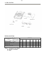
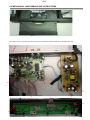
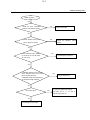
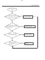
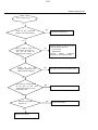
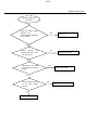
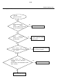
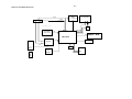
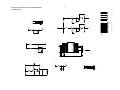
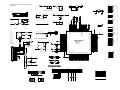
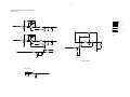
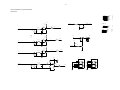
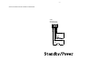
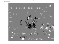
DVD PLAYER
DVP3320/94 & DVP3320X/94
Service Manual
TABLE OF CONTENTS
Chapter
Technical Specification, PCBs Location………………….. 1
Safety Instruction ……………………………………………… 2
Instruction for Use……………………………………………… 3
Mechanical and Dismantling Instructions…………………. 4
Service Modes, Troubleshooting……………………………. 5
Overall Block Diagram, Wiring Diagram……………………. 6
Electrical Diagram……………………………………………… 7
Exploded View Diagram & Service Part List………………..8
Revision List……………………………………………………. 9
©Copyright 2009 Philips Consumer Electronics B.V. Eindhoven, The Netherlands
All rights reserved. No part of this publication may by reproduced, stored in a retrieval system or
transmitted, in any form or by any means, electronics, mechanical, photocopying, or otherwise
without the prior permission of Philips.
Published by BU AVM CY-BL
Version 1.1
Printed in the Netherlands
Subject to modification
3141 785 34261
1-1
1.0 TECHNICAL SPECIFICATION
VIDEO PERFORMANCE
COMPONENT VIDEO RGB
Test equipment:Tektronics VM700T
Test discs:DVD test disc:Philips LVP 10。01
(PAL)/Abex TDV-540(NTSC)
Load Impedance:75Ω
Luminance amplitude output: 700mV ± 10%
RGB unbalance:5%
Sync. Amplitude: 300mV ± 100mV
S/N on RGB outputs: ≥52 dB
DC Level: ≤ 1V
VIDEO FORMAT
COMPONENT VIDEO YPbPr
DVD,VCD,MP3,JPEG
USB:2.0 HS,support MSC,MTP,sector size 4K
PbPr output unbalance:3%
Sync. Amplitude: 286mV ± 100mV
Video Bandwidth 4.2 MHz:-5db
S/N on outputs: YUV: ≥52 dB
AUDIO PERFORMANCE
POWER CONSUMPTION
Line outputs
Test equipment:Audio Precision System2
Test discs:CDDA:Philips audio signal test disc 1
Load Impedance:100KΩ for Audio
Power-Supply:100-280V ac,50/60Hz,standby:310V
Supply voltage:AC 100~280V
Supply Power consumption(AC 100/240V):12W/+10%
Standby Power,230VAC: <1W
AUDIO FORMAT
GENERAL DESCRIPTION
CD/MP3,DVD audio
Optical Pickup:IM S76RFVP
Chip set/Solution:Mediatek MTK1389QE-LA
Disc Size:8cm/12cm
CVBS
Amplitude output:1Vpp± 0.1V/
White bar: 714mV ± 10%/700mVpp ± 10%
Sync. Amplitude: 286mV ±100mV/300mVpp ± 100mV
Burst/chroma ratio: ± 10%
S/N luminance: ≥52 dB
1-2
1.1 PCBs LOCATION
MAIN BOARD
8W/2P POWER BOARD
DECK AMI
POWER SW BOARD
LED BOARD
USB BOARD
VERSION VARIATIONS
Type/Versions:
Service policy
Board in used:
MAIN BOARD
8W/2P POWER BOARD
LED BOARD
USB BOARD
POWER SW BOARD
*TIPS: C -- Component Lever Repair.
M -- Module Lever Repair
X – Used
DVP3320
94
M/C
M/C
C
C
C
1-3
1.2 System, Region Code, etc. Setting Procedure
Procedure to change region code of your DVD
Portable
1. Power ON the DVD player and do not insert
DISC inside player
2. Setup
Prefer
Press IR in the sequence as
9 6 5
3
The LCD display showed the existing region
Code
3. Press▲(navigation up)or▼(navigation down)
repeatedly to select the number from 0 to 6.
4. Then press OK to confirm your region code.
5. Refer below table for your region code setting
Select “0” setting = Region Free (confidential)
Procedure for SW upgrade
1. The upgrade will provide a document
re-named: PHILIPS.BIN
2. “PHILIPS.BIN” copy to USB or CD-ROM into
the data;
3. Reading the USB or CD-ROM,in accordance
with prompt,press ”OK” key to upgrade.
Warning: Do not unplug the AC adapter during
firmware upgrade to prevent flash corrupt of
the set!!
Procedure to check SW version of your DVD
Portable
1.
2.
3.
4.
5.
OPEN
Press SETUP MENU
Select Preferences
Select Version Info
Press “OK” key
2-1
2.0 Safety instruction
1. General safety
2. Laser safety
Safety regulations require that during a repair:
This unit employs a laser. Only qualified service
. Connect the unit to the mains via an isolation
personnel
transformer.
May remove the cover, or attempt to service this
. Replace safety components indicated by the
device
symbol
(due to possible eye injury).
Only by components identical to the original ones.
Laser device unit
Any
Type
Other component substitution (other than original
Wavelength
type)
:Semiconductor laser GaAIAs
:650nm (DVD)
:780nm (VCD/CD)
May increase risk of fire or electrical shock hazard.
Output power :7mW(DVD)
:10mW(DVD/CD)
Safety regulations require that after a repair, you
Beam divergence:60 degree
must
Note: Use of controls or adjustments or
Return the unit in its original condition. Pay, in
performance of procedure other than those
particular,
specified herein, may result in hazardous
Attention to the following points:
radiation exposure. Avoid direct exposure to
. Route the wires/cables correctly, and fix them with
beam.
the
mounted cable clamps
. Check the insulation of the mains lead for external
Damage
. Check the electrical DC resistance between the
mains
Plug and the secondary side:
1) Unplug the mains cord, and connect a wire
between
The two pins of the mains plug.
2) Set the mains switch the “on” position (keep
the
Mains cord unplug).
3) Measure the resistance value between the
mains
plug and the front panel, controls, and chassis
bottom.
4) Repair or correct unit when the resistance
measurement is less than 1M Ω
5) Verify this, before you return the unit to the
customer/user (ref. UL-standard no. 1492).
6) Switch the unit “off”, and remove the wire
between
the two pins of the mains plug.
3-1
3.0 INSTRUCTION FOR USE
You can download this information from the following websites:
http://www.philips.com/support
http://www.p4c.philips.com
4-1
4.0 MECHANICAL AND DISMANTLING INSTRUCTIONS
The following guidelines show how to dismantle the player.
Step1: Remove 5 screws around the Top Cover, and then remove the Top Cover(Figure1)
Figure 1
Step2:If the tray can’t open in normal way, you can make it through the instruction as below (Figure2)
Figure 2
Step2: If it is necessary to dismantle Loader or Front Panel, the Front door should be removed first(Figure3)
4-2
4.0 MECHANICAL AND DISMANTLING INSTRUCTIONS
Figure3
Step4: Remove the 10 screws on board to dismantle the DVD BOARD & POWER BOARD & LED BOARD (Figure 4&5)
Figure4
Power Board repair (swap IC and
transformer)
DVP3336和
DVP3320/3326共
用此IC
IC1: placement of
SD4842P on
DVP3336
board
插IC1位置:
CYT431
location
插IC3位置:
(IC3)
DVP3336用
SD4842P.
CYT431
location IC1:
DVP3336 uses
插IC1位置:
SD4842P
DVP3336用
DVP3320/3326 uses
SD4842P.
SD4841P
DVP3320/3326用
SD4841P.
IC1: placement of SD4841P
on DVP3320/3326 board
插IC1位置:
DVP3320/3326
用SD4841P.
Common power board of
DVP3336/DVP3320/3326
DVP3336和
DVP3320/3326共
用此PCB板
5-1
Trouble shooting chart
Spindle motor does not move
Motor not move
Go
Check the FFC connection
No
Correct connection
between 24P and the loader.
Yes
Check whether “MO_VCC”
No
Check
(VCC) voltage is normal.
the
MOVCC
power
supply
Yes
Check whether laser voltage
No
Check/Replace Q10
ǃQ11.
(1.9V for CD & 2.3V for DVD)
on L21 & L22
Yes
1. Whether voltage on pin 23 of U2
varies between 0 and 3.3V (3.3V
for CD and 0V for DVD),
2. Whether peripheral components
are eroded or badly soldered.
No
Check/ Replace U1.
Yes
Check opu focus
No
1. Check U2 25pin FOO signals
2.If there are F+, F-, T+ and Tsignals output from U1.
Yes
Check/Replace the loader
5-2
Trouble shooting chart
The power can not be on or off
The power can’t be
on or off
Go
Check the power supply
on the power board
No
and the connection to
Replace the power board
or correct the connection
to decoder board is normal.
Yes
Check if the CON2 on the front
Yes board
board to J 6(7PIN) on the decoder
No
Check/Correct connection
is in good contact.
Yes
Whether the connection
No
to Standby Board is broken.
Correct the connection
Yes
Whether there is 0V or
3.3V voltage difference on
Pin41 of U2
Yes
No
Replace U1.
5-3
Trouble shooting chart
Disc cannot be read.
Disc cannot be read.
Yes
Check the FFC connection
No
Check the loaded circuit
between 24P and the loader.
Yes
Check whether there is
laser voltage (1.9V for CD
and 2.3V for DVD) on
Collector of Q11 &Q10
No
1.Check voltage on pin 23 of U2
varies between 0 and 3.3V:
Æ3.3V for CD
Æ0V for DVD
2.Check
whether
peripheral
components are eroded or defect
Yes
Check
U1,
U2,
and
peripheral components are
eroded or badly soldered.
No
Re-solder or replace the defective parts
Yes
Check if there is RFO signal
on the pin8 of HA1. (The
normal RFO signal is a clear
reticulated wave)
No
Check U2 and peripheral components
Yes
Check the connection
between U2
Yes
Replace U2 or loader.
No
Correct connection
5-4
Trouble shooting chart
Only DVD disc or only disc except DVD can be played
Only DVD disc, or only disc
except DVD can be Played.
Go
Check
the
FFC
connection between
24pin and the loader.
No
Check the loaded circuit
Yes
Check laser voltage (1.9V)
output on Collector of Q11, if
No
Check the solder status on U2 and
pin 17 of U2 is at low level.
peripheral components
Yes
Check whether there
is voltage variance on
pin 18 of U2.
No
check if bad solder exist on U2 and
peripheral components
Yes
pin
Check whether pin 1 - 26 and
125-128 of U2 and peripheral
components
are
badly
soldered, defected
No
Replace the bad spare parts
Yes
Check Q5, Q6, Q7
in
good
whether
condition
Yes
Change U2 or the loader.
No
Correct connection
5-5
Trouble shooting chart
Distorted audio and loud noise
Distorted audio and
loud noise
Yes
Check he power supply
voltages +12V
to the operation amplifying
L2 are normal
No
Replace L2
Yes
the
Check
whether
muting transistors Q12,
Q14, are normal
No
Replace Q12, Q14
Yes
No
Checking the U2 leads
the feet has no to break
to open
No
Correct connection
Yes
Check whether the U5
or U2 power supply
normal
Yes
Replace U2, U5
No
Check U2, U5
5-6
Trouble shooting chart
Abnormal color of video picture
Abnormal color of
video picture
Yes
Check whether the 27MHz
No
Check Y1, R17, C21 and C22
output signal is normal.
Yes
Check whether the 3.3V
and 1.8V power supply
voltages on the decoder
board are normal.
No
Check other of power supply electric
circuit
Yes
Check whether the
video filter network
circuit is normal.
Yes
Change U2
No
Correct the connection
5-7
Trouble shooting chart
Remote reception is insensitive or fails.
Remote reception is
insensitive or fails.
Go
Check if the remote
control works properly.
No
Check battery
Yes
Check if the power
supply voltage to the
remote censor is normal
No
Check R1 R2 on front board
Yes
Use an oscilloscope to check
if there is output waveform
from the first pin IR of the
remote censor after pressing
button on the remote control.
No
IR1(PIN 3 - RCwaveform)
Yes
Check if there is IR
signal on pin 44 of
U2
Yes
Change U2
IR waveform
No
Correct connection
5-8
Trouble shooting chart
No video picture, no sound.
No video picture,
no sound.
Go
Check whether all the
voltages from the power
board to the decoder board
are normal.
No
Check the loaded circuit
CVBS(L27 point) waveform
Yes
Check if the reset circuit consisting
of C13, Q4, Q3,R11,R12,R13,R15,R16 is normal
(at a high level for tens of milliseconds,
then constantly at 0V).
No
Change C13,Q4,Q3
27M waveform
Yes
Check whether there is
27MHz signal output.
No
Crystal oscillator Y1 and
peripheral components
are defected or eroded.
Yes
Check if there is 128MHz
signal output on R49.
No
Check whether
short-circuit or bad
solder on U3, U4
SDRAM(R49 SDCLK) waveform
Yes
Yes
Reconnect the component in
short-circuit
Check U3.
No
5-9
Trouble shooting chart
No display on LED, and buttons do not work
LED and
buttons do not work
Yes
Check whether there is
correct
contact
between CON1 of front board
and J 6 of decoder board
No
Correct connection
Yes
Check
DV33(+3.3V)
voltage on the power
and front board
Fix power supply board top
a power supply for should
electric circuit
No
Yes
Check whether there is 0V
or 3.3V on the signals of VPLAY,STB
CLK, DATA
No
Check the U2’s pin 33,34,40,41 arrive
the J 6 connect condition
Yes
Check whether the circuit
connected to LED & BUTTONS
is broken,
Check wether Q1,Q2,Q3,Q4 for 3904
&LED is broken,
Yes
Replace LED or Q1,Q2,Q3,Q4
No
Correct connection
6-1
CIRCUIT DIAGRAM DVP3100
SDRAM
1*16&4*16
3.3V
AV-OUT RCA
1.8V
3.3V
1.8V
ASA 8829B+Sanyo DV38
ASA 8829B+
Sanyo DV38
OP
4558
DVD-CVBS
DVD-AU-R
DVD-AU-L
RF
Y&U&V RCA
MT1389L
COAX
AM5888S
IR
5V
Switch
Power
5V
12V
IR
SENSOR
SPI
Flash
8M&16M
KEY
7-1
CIRCUIT DIAGRAM DVP3100 MAIN BOARD
POWER PART
+12V
VCC
DV33
R1
Q1
+ CE1
VCC
+P12V
2
1
2
3
4
GND
+P12V
R3
L2
0.1uF 2.2dip
C3
FB
V33
FB33
1
+ CE3
C4
R7
6.8K/1%
2
220uF/6.3v 0.1uF
2
R8
CE2
47uF/25v
TROUT
TRIN
TROUT
TROPEN
TRCLOSE
FOSO
DMSO
FMSO
TRSO
SL+
SLSP+
SPT+
TF+
FV1P4
STBY
11K/1%/12K
L4
3 8550 1
+12V
10
C2
0.1uF
OUT33
SERVO I/F
U1
V33
L6
TT+
SL+
SL-
89L_3V3
FB
MO_VCC
+ CE5
10uF/10v
L7
DV33
FB
+
CE6
100uF/10v
DV33
FMSO
OUT18
TRSO
V1P4
STBY
C7
0.1uF
C8
15
16
17
18
19
20
21
VOTK+
VOTKVOLD+
VOLDVCC2
NC
VCTL
30
G2
22
23
24
25
26
27
28
GND
VINLD
NC
TRB2
VINTK
BIAS
MUTE
0.1uF
AM5888
R10
C9
10k
0.1uF
VOFC+
VOFCVOSLVOSL+
VOTR+
VOTRVCC
14
13
12
11
10
9
8
G1
29
REV
FWD
REGO1
VINSL+
REGO2
TRB1
VINFC
7
6
5
4
3
2
1
F+
FSPSP+
LOAD+
LOAD-
TROPEN
TRCLOSE
FB33
MO_VCC
R9
10k DMSO
FB18
OUT33
FOSO
CE7
47uF/10v
+
DV33
VCC
MO_VCC
L8
R11
15k
R12
3.3k
1
Q4
2N3904
1
+
2
3
3
3.9k
R16
4.7k
2
2
Q3
2N3904
1
C13
22uF/6.3v
C14
1uF/NC
DV33
C10
R13
22k
URST#
R15
FB
C11
C12
0.1uF
0.1uF
DV33
[2,3,4,5]
89L_3V3
[2]
V18
[2]
URST#
[2]
TROUT
TRIN
TROUT
TROPEN
TRCLOSE
FOSO
DMSO
FMSO
TRSO
SL+
SLSP+
SPT+
TF+
FV1P4
STBY
[2]
[2]
[2]
[2]
[2]
[2]
[2]
[2]
[2]
[2]
[2]
[2]
[2]
[2]
[2]
[2]
[2]
[2]
[2]
POWER I/F
R5
Q2
R6
+
URST#
OUT18
+12V
[2,4]
10
VCC
FB
V18
10K/1%
4x1 W/HOUSING
+P12V
[2,4]
VCC
FB18
C1
R4
5.6dip
89L_3V3
R2
FB
220uF/6.3v 0.1uF
2
J1
V18
1
3 8550 1
VCC
4.3K/1%/5.1K
L1
+12V
R14
0.1uF LOADLOAD+
TROUT
10k TRIN
1
2
3
4
5
J2
5x1 W/HOUSING
7-2
V18
CIRCUIT DIAGRAM DVP3100 MAIN BOARD
MCU PART
89L_3V3
V18
RFV18-1 C15
FB
C16
L11
0.1uF
89L_3V3
0.1uF
L12 FB600R
RFVDD3
+
0.1uF
CE8
89L_3V3
0R
DACVDD3
C17
100uF/10v
L9
ADACVDD
DQ[0..15]
C18
C20
0.1uF
0.1uF
MA[0..11]
FB
L13
DQM[0..1]
+ CE9
10uF/10v
C26
4.7uF
C35
1uF
C
S
1
2SK3018
B
USB5V
IOA
10k
L16
4.7uH
USB_DP
USB_DM
CE15
100uF/10V
1
2
3
4
PWR2
2
+
C38
C
B
A
D
F
E
RFV18-1
RFVDD3
XI
XO
4x1 W/HOUSING
0.1uF
3
Q6
2SK3018
100k
R27
Only for MT1389L
Q7
2SK3018
R29
R30
0
0
L17
FB
AVCC
CE16
100uF/10v
VCC
VCC
USB5V
C39
+
0.1uF
AVDD33
FB
Q8
R33
USB_EN
470R
1
2
4.7K
89L_3V3
Q9
C41
0.1uF
C44
0.1uF
L19
FB
L20
FB
C46
3
3904
V20
V1P4
REXT
MDI1
MDI2
LDO1
LDO2
DMO
FMO
TRAY-OPEN
TRAY-CLOSE
TRO
FOO
TRIN
USB_DP
C45
USB_DM
USB_V33
10uF/10v
R34
5.1k
C40
4.7uF
V18
close to USB connector
0.1uF
C49
NC
Q10
REXT
LDO2
2
R35
NC
TRAY-OPENR36
0R
R37
NC
R38
NC
CE17
8550
HEADER 24 SMD0.5 TOP
C29
RFA
RFB
RFC
RFD
RFE
RFF
AVDD18
AVDD33
XTALI
XTALO
AGND
V20
V14
REXT
MDI1
MDI2
LDO1
LDO2
AVDD33
DMO
FMO
TRAY_OPEN
TRAY_CLOSE
TRO
FOO
FG / GPIO2
USB_DP
USB_DM
USB_V33
USB_GND
PAD_VRT
USB_V18
RX
R39
4.7
R41
4.7
VREF
47uF/6.3v
TRAY-CLOSE
DV33
R40
R42
CVBS_OUT
V_R
V_B
V_G
MT1389L/K
LQFP 128
Desktop
V1.0
VIDEO I/F
96
95
94
93
92
91
90
89
88
87
86
85
84
83
82
81
80
79
78
77
76
75
74
73
72
71
70
69
68
67
66
65
VREF
C37
DACVDD3
STBY
TROPEN
TRCLOSE
TRIN
TROUT
+12V
0.1uF
GPIO12
RX
GPIO8
USB_EN
MA3
MA2
V18
TT+
FF+
SLSL+
SPSP+
FOSO
TRSO
FMSO
DMSO
MA1
MA0
MA10
BA1
BA0
RAS#
CAS#
WE#
MA4
MA5
MA6
MA7
MA8
MA9
V1P4
MA11
DCLK
DQM1
URST#
AVCC
DV33
VCC
MT1389L/K/SMD
1389L
89L_3V3
V18
MIX
89L_3V3 V18
VR-DVD
3
+ CE18
Q11
47uF/6.3v
2
LDO1
MT1389L&MT1389LA
1
8550
27k
27k
15k
10k
R43
R44
R45
R46
FOSO
TRSO
FMSO
DMSO
C50
C51
C52
330pF 330pF 0.1uF
89L_3V3
FOO
TRO
FMO
DMO
V1P4
V18
C58
C59
C60
C61
C62
C63
0.1uF
0.1uF
0.1uF
0.1uF
0.1uF
0.1uF
Chip Decap.
VPLAY
VSCK
UP1_7
VSDA
GPIO20
GPIO4
VSTB
GPIO12
VCC
DV33
IR
VSDA
VSCK
VSTB
GND
VPLAY
C53
0.015uF
GPIO3
UP1_6
1
2
3
4
5
6
7
8
6x1 W/HOUSING
8P2.0
ADVCM
ASPDIF
VIDEO_EN
ALS
J5
ALF
GPO_B
AUDIO_MUTE
IOA
GPIO6
C54
100pF
C55
100pF
C56
100pF
[3]
[3]
[3]
[3]
SF_CK
SF_CS
SF_DI
SF_DO
[3]
[3]
[3]
[3]
AUDIO_MUTE
[4]
ASPDIF
[4]
AR
AL
[4]
[4]
AKIN
[4]
VIDEO_EN
[5]
CVBS_OUT
V_R
V_B
V_G
[5]
[5]
[5]
[5]
STBY
TROPEN
TRCLOSE
TRIN
TROUT
+12V
[1]
[1]
[1]
[1]
[1]
[1]
TT+
FF+
SLSL+
SPSP+
FOSO
TRSO
FMSO
DMSO
[1]
[1]
[1]
[1]
[1]
[1]
[1]
[1]
[1]
[1]
[1]
[1]
V1P4
[1]
SERVO I/F
STBY
GPO_B
[3]
DCLK
RAS#
CAS#
WE#
TX
VR-CD
0R
NC
[3]
BA[0..1]
AUDIO I/F
VIDEO_EN
560
VREF
DACVDDC
GPIO13
SPDIF / GPIO12
GPIO11
GPIO10
DVDD18
GPIO9
GPIO8
GPIO7 / CKE
RA3
RA2
DVDD33
RA1
RA0
RA10
BA1
DVSS18
BA0
RAS#
CAS#
RWE#
RA4
RA5
RA6
RA7
RA8
RA9
DVDD33
RA11
RCLK
DQM1
33
34
35
36
37
38
39
40
41
42
43
44
45
46
47
48
49
50
51
52
53
54
55
56
57
58
59
60
61
62
63
64
L22
10uH
0.1uF
USB_V18
1
2
3
4
5
6
7
8
9
10
11
12
13
14
15
16
17
18
19
20
21
22
23
24
25
26
27
28
29
30
31
32
GPIO3
GPIO4
GPIO6
SF_CS
SF_DO
SF_DI
SF_CK
UP1_6
UP1_7
L21
10uH
1
C48
C47
10uF/10v
3
F
B
A
RFO
IOA
D
C
TT+
F+
F-
L18
R32
AVCC
MDI1
LD-CD
VR-DVD
VR-CD
E
AVCC
V20
89L_3V3
2302
R31
Very Important to
reduce Noise
15k
R28
DV33
LD-DVD
RX
DQ11
DQ10
DQ9
DQ8
1 _4
10K
3
3
_1 1
+
TOP
1
2N3904
HA1
1
500mA
DQM0
DQ15
DQ14
DQ13
DQ12
R26
1
F1
140
DQ5
DQ6
DQ7
Q5
AVCC
10k
U2
URST#
IR
DQ0
DQ1
DQ2
DQ3
DQ4
R25
100k
2
R24
TX
89L_3V3
SONY KHM313
24
23
22
21
20
19
18
17
16
15
14
13
12
11
10
9
8
7
6
5
4
3
2
1
R23
2N3904
_2 2
_3 2
FF+
T+
TC/c
D/d
CD/DVD SW
RF
A/a
B/b
F
GND-PD
Vc(Vref)
Vcc
E
NC
VR-CD
VR-DVD
CD-LD
MD
HFM
NC
DVD-LD
GND-LD
AKIN
TX
E3
J4
1
2
3
4
5
6
7
8
9
10
11
12
13
14
15
16
17
18
19
20
21
22
23
24
C36
220pF
128
127
126
125
124
123
122
121
120
119
118
117
116
115
114
113
112
111
110
109
108
107
106
105
104
103
102
101
100
99
98
97
3
AR
AL
C33
0.1uF
C34
MDI2
ASPDIF
C43
RFH / OPINN
RFG / OPINP
RFIN / OPOUT
RFIP
AGND18
AVDD18
ADACVDD2
ADACVDD1
ALF / GPIO
ALS / GPIO
AL / GPIO1
AVCM
AR / GPIO0
ARS / GPIO
ARF / GPIO
ADACVSS1
ADACVSS2
APLLCAP
APLLVDD
AADVDD
AKIN1 / GPIO21 / Audio_Mute
ADVCM / GPIO20
AKIN2 / GPIO19 / Audio_Mute
AADVSS
R
B
G
DACVDDA
DACVDDB
CVBS
DACVSSC
FS
1
10uF/10v
2
2
G
MDI1
C31
OPOP+
D
ADVCM
OP+
10k
R22
2
RFO
D1
BAT54C
3
AUDIO_MUTE
ADACVDD
ALF
ALS
AL
AVCM
AR
0.1uF
0
R21
C32
DV33
[3]
DQM[0..1]
S-FLASH
GPIO3 / INT#
GPIO4
GPIO6
SF_CS_
SF_DO
SF_DI
SF_CK
UP1_6 / SCL
UP1_7 / SDA
ICE
PRST#
IR
RD0
RD1
RD2
RD3
RD4
DVDD33
RD5
RD6
RD7
DVDD18
DQM0
RD15
RD14
RD13
RD12
DVSS33
RD11
RD10
RD9
RD8
SP-A
RF Reference
1
0.1uF
1
470uF/6.3v
[3]
DRAM I/F
+ CE12
OP-
C28
R20
DCLK
RAS#
CAS#
WE#
SF_CK
SF_CS
SF_DI
SF_DO
FS
10k
C22
22pF
APLLVDD3
V_R
V_B
V_G
DACVDD3
DACVDD3
CVBS_OUT
C25
27MHz
0.1uF
FB600R
6800pF
R19
SP-
XO
1500pF
C27
0.1uF
AADVDD
CE11
10uF
APLLVDD3
AADVDD
AKIN
GPIO20
+
NC/0.1uF
0.1uF
C24
CE10
10uF
0R
CE14
6x1 W/HOUSING
+
L10
10uF/10v
C23
L15
470uF/10v
SLSL+
V1P4
V20
C21
22pF
89L_3V3
C30
LIMIT
XI
0.1uF
10k
1
2
3
4
5
6
RFV18-1
SP-A
SP+
R18
Y1
J3
+
DV33
100k
R17
SERVO RF DeCAP.
BA[0..1]
DQ[0..15]
MA[0..11]
TROPEN
TRCLOSE
C57
100pF
GPIO8
LIMIT
TROUT
URST#
[1]
AVCC
[1,4,5]
DV33
[1,3,4,5]
VCC
[1,4]
89L_3V3
[1]
V18
[1]
7-3
CIRCUIT DIAGRAM DVP3100 MAIN BOARD
SDRAM & FLASH PART
DQ[0..15]
MA[0..11]
DQM[0..1]
BA[0..1]
U3
MA0
MA1
MA2
MA3
MA4
MA5
MA6
MA7
MA8
MA9
MA10
MA11
DBA0
DBA1
SD33
DCLK
BA0
BA1
RAS#
CAS#
WE#
R47
10k
SDCKE
R48
10k
DCS#
R49
33
SDCLK
DBA0
DBA1
DRAS#
DCAS#
DWE#
23
24
25
26
29
30
31
32
33
34
22
35
20
21
DQ0
DQ1
DQ2
DQ3
DQ4
DQ5
DQ6
DQ7
DQ8
DQ9
DQ10
DQ11
DQ12
DQ13
DQ14
DQ15
2
4
5
7
8
10
11
13
42
44
45
47
48
50
51
53
VCC
VCC
VCC
1
14
27
VCCQ
VCCQ
VCCQ
VCCQ
3
9
43
49
VSSQ
VSSQ
VSSQ
VSSQ
6
12
46
52
A0
A1
A2
A3
A4
A5
A6
A7
A8
A9
A10/AP
A11
BA0/A13
BA1/A12
SDCLK
SDCKE
38
37
DCS#
DRAS#
DCAS#
DWE#
19
18
17
16
CS
RAS
CAS
WE
DQM0
DQM1
15
39
DQML
DQMH
36
40
NC
NC
54
41
28
VSS
VSS
VSS
CLK
CKE
DQ0
DQ1
DQ2
DQ3
DQ4
DQ5
DQ6
DQ7
DQ8
DQ9
DQ10
DQ11
DQ12
DQ13
DQ14
DQ15
V33
L23
DV33
1
2
3
4
U4
100uF/10v
CE# VDD
SO HOLD#
WP# SCK
VSS
SI
AT25FS040/EN25B80
8M/16M bit
R55
10k
SF_CS
SF_CK
SF_DI
MA[0..11]
[2]
DQM[0..1]
[2]
BA[0..1]
[2]
DCLK
RAS#
CAS#
WE#
[2]
[2]
[2]
[2]
C64
C65
C66
0.1uF
0.1uF
0.1uF
DRAM I/F
SF_CK
SF_CS
SF_DI
SF_DO
SF_CK
SF_CS
SF_DI
SF_DO
[2]
[2]
[2]
[2]
S-FLASH
SD33
DV33
SD33
SD33
DV33
8
7
6
5
[2]
FB
+ CE19
ESMT M12L64164A
SF_CS
SF_DO
SD33
DCLK
RAS#
CAS#
WE#
DQ[0..15]
DV33
C72
0.1uF
C67
C68
C69
C70
C71
0.1uF
0.1uF
0.1uF
0.1uF
0.1uF
POWER
DV33
[1,2,4,5]
7-4
CIRCUIT DIAGRAM DVP3100 MAIN BOARD
AUDIO PART
AUDIO I/F
R56
C73
30k
10k
C76
4
3
1
1
NJM4558
+12V
AUDIO_MUTE
R59
2
10uF/25V
A_MUTE
8
3300pF
EC21
100
R61
R60
Q12
2N3904
1
+12V
4700pF
DV33
3
560
C75
100k
AVCC
Q15
AVCC
3 2N3906/NC
2
1
R63
C77
100pF
POWER
1
30k
RCH
560
2
+
R76
AC
+EC1
22uF/25V
100K
R75
100K
C81
3
5
2
4.7K
J7
3P/2.0MM
+12V
R77
1N4148
1
R64
22K
0.1uF
MIC INPUT
100
C82
C83
3300pF
0.1uF
AKIN
R96
D2
2
Q22
2N3904
1
Audio Mute
1
2
3
CE20
220uF/16v
2
1
2
56K
R73
R65
1
51K
1
R74
3.3K
10K
A_MUTE
AUDIO_MUTE
+12V
R70
3
0.1uF
R62
4.7K
Q14
2N3904
1
2
A_MUTE
C6
4700pF
100k
3 2N3906/NC
2
1
R71
Q13
1
1
10uF/25V
+12V
R54
2
C79
1
R69
100
2
2
1
1
8
3300pF
7
NJM4558
1
5
22
6
3
4
5
C80
R68
2
10k
R72
4.7K
EC13
2
+
10uF/16V
U5B
+
1
R67
5.1k
+
2
R66
-
C78
AR
AR
AL
RCH
LCH
2
2
[5]
[5]
AKIN
2
AUDIO_MUTE
2
LCH
2
+
10uF/16V
3
2
U5A
+
1
AKIN
R58
5.1k
+
2
R57
-
AL
C74
AR
AL
RCH
LCH
100pF
0R/NC
+12V
1
DV33
1,2,3,4,5
AVCC
1,2,4,5
7-5
CIRCUIT DIAGRAM DVP3100 MAIN BOARD
VIDEO PART
CVBS_OUT
V_R
V_B
V_G
ASPDIF
VIDEO_EN
VB_5V
ASPDIF
R78
75,1%/NC
L24 1.8uH
R81
75,1%
R82
100
R51
0
R/V
COAXIAL
Q16
2N3906/NC
1
C85
C86
100P
100P
RCH
LCH
C87
R/V_OUT
330pF
AVCC
Q17
2N3906/NC
1
C89
100P
100P
Q18
0
+ CE22
10uF/10v
2
C90
0.1uF
DV33
2
C88
2302
R86
B/U_OUT
B/U
3
L25 1.8uH
1
10K
R52
0
VB_5V
VB_5V
75,1%/NC
R84
R88
R90
2
4.7K
VIDEO_EN
Q20
1
VB_5V
3
3904
470R
R87
75,1%/NC
L26 1.8uH
G/Y_OUT
G/Y
C91
C92
100P
100P
0
Q19
2N3906/NC
1
2
R91
75,1%
R53
0
3
R89
V_G
JK1
VB_5V
R93
3.3k
C100
0.1uF
1
Q21
2N3904
1
C93
C94
100P
100P
3
R95
75,1%
22uF/10v
R92
3.3k
CVBS
R50
75 1%
CE4
1
+
2
+
R94
75,1%
2
220uF/10v
JK2
CVBS_A
6
2
CE25
L27 1.8uH/0R
CVBS_OUT
RCH
LCH
[4]
[4]
AUDIO I/F
DV33
AVCC
+12V
VCC
R83
E
R85
75,1%
[2]
0
VB_5V
3906
C
V_B
[2]
VIDEO_EN
VIDEO I/F
POWER
B
ASPDIF
0.1uF
2
V_R
C84
100
[2]
[2]
[2]
[2]
3
R79
R80
CVBS_OUT
V_R
V_B
V_G
6
4
4
COAXIAL
5
G/Y_OUT 5
LCH
3
B/U_OUT
CVBS_A
1
RCH
3
1
R/V_OUT
2
RCA-AV6
2
RCA-AV6
DV33
AVCC
+12V
VCC
[1,2,3,4]
[1,2,4,5]
[1,5]
[1,2,5]
7-6
CIRCUIT DIAGRAM DVP3100 DISPLAY BOARD
IR1
VCC
J2
VCC
3.3V
IR
DATA
CLK
STB
GND
+
R16 R17
10K 10K
C4
100pF
2
100uF/6.3v
1
CE2
R18
10K
R19
51K
1
2
3
4
5
6
7
8
DATA
CLK
STB
R20 100R
R21 100R
R22 100R
D_DATA
D_CLK
D_STB
GND
Grid1
Grid2
GND
Grid3
Grid4
GND
28
27
26
25
24
23
22
Seg1/KS1
VDD
Seg2/Ks2 Seg14/Grid5
Seg3/Ks3 Seg13/Grid6
Seg4/Ks4 Seg12/Grid7
Seg5/Ks5 Seg10/Ks10
Seg9/Ks9
Seg6/Ks6
Seg7/Ks7
Seg8/Ks8
21
20
19
18
17
16
15
INT
DI/O
CLK
STB
KEY1
KEY2
Vdd
100R
IR
C1
100pF
100R
IRVCC
CE1 4.7UF/6.3V
LED-
C5
8
9
10
11
12
13
14
R3
IR
R2
6x1 W/HOUSING
DIP6/W/H/P2.0
U1
1
2
3
4
5
6
7
3.3V
1
2
3
VCC
IR/VFD
VCC
100pF
R23
LED+
51K
SM1628
KS3 OPEN/CLOSE
KS4
Play/Pause
6x1 W/HOUSING
DIP6/W/H/P2.0
CON3
LEDLED+
STB+
STB-
1
2
3
4
d1
1
2
3
4
5
6
7
8
9
10
11
12
13
4x1 W/HOUSING
DIP4/W/H/P2.54
DIS PLAY
7-7
CIRCUIT DIAGRAM DVP3100 STANDBY POWER BOARD
D_DATA1
D_CLK 2
LED++
3
LED-- 4
CON4
DIP4/W/H/P2.54
4x1 W/HOUSING
LED3
POWER OFF
KS5
Standby/Power
Standby/Power
7-8
CIRCUIT DIAGRAM DVP3100 USB BOARD
5
J1
4x1 W/HOUSING
DIP6/W/H/P2.54
GND
GND
USB_DP
USB_DM
VCC
1
2
3
4
1:GND
2:D+
1
2
3:D4:VCC
3
4
6
4
3
2
1
P1
USB TYPEA
7-9
MAIN BOARD TOP
7-10
MAIN BOARD BOTTOM
7-11
LED PCB BOARD-TOP
7-12
LED PCB BOARD-BOTTOM
USB PCB BOARD-TOP
7-13
USB PCB BOARD-BOTTOM
7-14
POWER SW PCB BOARD-TOP
7-15
POWER SW PCB BOARD-BOTTOM
7-16
8.0 Mechanical Exploded View Diagram
8-1
8-2
8.1 SERVICE PART LIST
MAIN PCB PARTS LIST
12NC No.
No
Part Name
Qty
5
996510029467
MAIN PCB ASS'Y DVD3320
1
U2
996510029222
SMD IC MT1389QE-LA LQFP-128
1
U1
996510028064
SMD IC SW5888 HSOP-28 5-CHA BTL DRIVE SW
1
U5
996510028051
SMD IC YD4558 SOP-8PIN XY
1
U3
996510028043
SMD IC W9864G6XH-6 TSOP54 64M SDRAM WINBOND
1
U4
996510028054
SMD IC EN25F16-100HIP SOP-8 16M FLASH EON
1
Q1,Q2,Q10,Q11
996510029221
DIP TR STS8550D TO-92 PNP PHILIPS
4
Y1
996510028074
DIP X'TAL 27.00MHZ +/-10PPM HC-49/US
1
Q6,Q7
996510028056
SMD TR 2SK3018 SOT-23 ROHM
2
Q3,Q4,Q5,Q9,Q12
,Q14,Q20,Q21,Q2
996510028078
SMD TR PMBT3904 SOT23 NPN PHILIPS
9
Q13,Q15,Q16,Q17
,Q19
996510028086
SMD TR PMBT3906 SOT23 PNP PHILIPS
1
Q8,Q18
996510028041
SMD MOS CES2307 SOT-23 CET
2
D1
996510028055
SMD DIODE BAT54C SOT-23 RECTRON
JK2
996510029227
DIP AV JACK AV4-8.4-7D2 JIXIN
1
JK1
996510028076
DIP AV JACK AV3-8.4-7D JIXIN
1
F1
996510028048
CHIP RESET FUSE 0.5A/6V LP-NSM050 GP
1
USB PCB PARTS LIST
12NC No.
No
Part Name
1
Qtyy
12
996510029468
USB PCB ASS'Y DVD3320
1
CON2
996510028079
DIP USB AF180°USB-015 ZIYOUDA
1
STANDBY PCB PARTS LIST
No
12NC No.
10
996510028049
Part Name
STANDBY PCB ASS'Y DVD3320
Qty
1
KS5
996510028072
TACT SWITCH 6x6x5mm 180g JIXIN
1
LED3
996510028067
LED RED 1.8V D3 MASON
1
LED PCB PARTS LIST
12NC No.
No
Part Name
QtyG
G
996510028068
U1
996510028075
SMD IC SM1628C SOP-28 DRIVER SUNMOON
1
D1
996510028044
DISPLAY LED DT-25801BG DL
1
R1
996510028082
DIP IR SENSOR 36KHZ IRM36C AAD
1
KS3,KS4
996510028072
TACT SWITCH 6x6x5mm 250g JIXIN
2
Part Name
Qty
POWER PCB PART LIST
No
12NC No.
4
996510029466
DECK PARTS LIST
12NC No.
No
30
6
996510029224
996510028053
LED DISPLAY PCB ASS'Y DVD3320
8W/2P OPEN 94VERSION PCBA DVP3320
Part Name
DVD LOADER WXD-8829B ASA
DVD DECK CMS-S76R IM
1
1
Qty
1
1
8-3
8.1 SERVICE PART LIST
OTHER PARTS LIST
No
12NC No.
Part Name
Qty
31
996510028063
FFC 24P/0.5MM 220MM(3/5-4/8) +/+OUKE
1
RC
996510029469
R/C CD31A0003 BLACK C&D DVP3320-3326
1
CAR ADT
996510029036
AC CORD VDE 94FIXES 1.3M HO3VVH2-F A
1
AVCABLE
996510028065
AV CORD RCA/M*3 BOTH E
1
19
996510028083
BUTTON POWER
1
20
996510028061
BUTTON POWER LENS
1
18
996510028014
DVD DOOR BLACK
1
16
996510028071
OPEN BUTTON BLACK
1
15
996510028112
FRONT PANEL BLACK
1
17
996510028042
LENS DISPLAY PPMA BLACK
1
9.0 REVISION LIST
Version 1.0
• Initial release