1
POS-PHY Level 4 MegaCore Function User Guide
POS-PHY Level 4 MegaCore Function
User Guide
101 Innovation Drive
San Jose, CA 95134
www.altera.com
UG-IPPOSPHY4-12.0
Document last updated for Altera Complete Design Suite version:
Document publication date:
13.0
May 2013
Subscribe
Copyright © 2013 Altera Corporation. All rights reserved. Altera, The Programmable Solutions Company, the stylized Altera logo, and specific device designations
are trademarks and/or service marks of Altera Corporation in the U.S. and other countries. All other words and logos identified as trademarks and/or service marks
are the property of Altera Corporation or their respective owners. Altera products are protected under numerous U.S. and foreign patents and pending applications,
maskwork rights, and copyrights. Altera warrants performance of its semiconductor products to current specifications in accordance with Altera's standard
warranty, but reserves the right to make changes to any products and services at any time without notice. Altera assumes no responsibility or liability arising out of
the application or use of any information, product, or service described herein except as expressly agreed to in writing by Altera. Altera customers are advised to
obtain the latest version of device specifications before relying on any published information and before placing orders for products or services.
POS-PHY Level 4 MegaCore Function User Guide
May 2013 Altera Corporation
Contents
Chapter 1. About This MegaCore Function
Release Information . . . . . . . . . . . . . . . . . . . . . . . . . . . . . . . . . . . . . . . . . . . . . . . . . . . . . . . . . . . . . . . . . . . . . 1–1
Device Family Support . . . . . . . . . . . . . . . . . . . . . . . . . . . . . . . . . . . . . . . . . . . . . . . . . . . . . . . . . . . . . . . . . . . 1–1
Features . . . . . . . . . . . . . . . . . . . . . . . . . . . . . . . . . . . . . . . . . . . . . . . . . . . . . . . . . . . . . . . . . . . . . . . . . . . . . . . . 1–2
General Description . . . . . . . . . . . . . . . . . . . . . . . . . . . . . . . . . . . . . . . . . . . . . . . . . . . . . . . . . . . . . . . . . . . . . 1–3
Interfaces & Protocols . . . . . . . . . . . . . . . . . . . . . . . . . . . . . . . . . . . . . . . . . . . . . . . . . . . . . . . . . . . . . . . . . 1–4
SPI-4.2 Interface . . . . . . . . . . . . . . . . . . . . . . . . . . . . . . . . . . . . . . . . . . . . . . . . . . . . . . . . . . . . . . . . . . . . 1–4
Atlantic Interface . . . . . . . . . . . . . . . . . . . . . . . . . . . . . . . . . . . . . . . . . . . . . . . . . . . . . . . . . . . . . . . . . . . 1–5
Avalon-MM Interface . . . . . . . . . . . . . . . . . . . . . . . . . . . . . . . . . . . . . . . . . . . . . . . . . . . . . . . . . . . . . . . 1–5
MegaCore Verification . . . . . . . . . . . . . . . . . . . . . . . . . . . . . . . . . . . . . . . . . . . . . . . . . . . . . . . . . . . . . . . . . . . 1–5
Performance and Resource Utilization . . . . . . . . . . . . . . . . . . . . . . . . . . . . . . . . . . . . . . . . . . . . . . . . . . . . . . 1–6
Installation and Licensing . . . . . . . . . . . . . . . . . . . . . . . . . . . . . . . . . . . . . . . . . . . . . . . . . . . . . . . . . . . . . . . . 1–9
OpenCore Plus Evaluation . . . . . . . . . . . . . . . . . . . . . . . . . . . . . . . . . . . . . . . . . . . . . . . . . . . . . . . . . . . . 1–10
OpenCore Plus Time-Out Behavior . . . . . . . . . . . . . . . . . . . . . . . . . . . . . . . . . . . . . . . . . . . . . . . . . . . . . 1–10
Chapter 2. Getting Started
Design Flow . . . . . . . . . . . . . . . . . . . . . . . . . . . . . . . . . . . . . . . . . . . . . . . . . . . . . . . . . . . . . . . . . . . . . . . . . . . . 2–1
Specify Parameters . . . . . . . . . . . . . . . . . . . . . . . . . . . . . . . . . . . . . . . . . . . . . . . . . . . . . . . . . . . . . . . . . . . . . . 2–1
Simulate the Design . . . . . . . . . . . . . . . . . . . . . . . . . . . . . . . . . . . . . . . . . . . . . . . . . . . . . . . . . . . . . . . . . . . . . 2–3
Use the Testbench with the ModelSim Simulator . . . . . . . . . . . . . . . . . . . . . . . . . . . . . . . . . . . . . . . . . . 2–4
Use the Testbench with NativeLink . . . . . . . . . . . . . . . . . . . . . . . . . . . . . . . . . . . . . . . . . . . . . . . . . . . . . . 2–4
Compile the Design and Program a Device . . . . . . . . . . . . . . . . . . . . . . . . . . . . . . . . . . . . . . . . . . . . . . . . . 2–6
Chapter 3. Parameter Settings
Basic Parameters . . . . . . . . . . . . . . . . . . . . . . . . . . . . . . . . . . . . . . . . . . . . . . . . . . . . . . . . . . . . . . . . . . . . . . . . 3–1
Device Family . . . . . . . . . . . . . . . . . . . . . . . . . . . . . . . . . . . . . . . . . . . . . . . . . . . . . . . . . . . . . . . . . . . . . . . . 3–1
LVDS Data Rate . . . . . . . . . . . . . . . . . . . . . . . . . . . . . . . . . . . . . . . . . . . . . . . . . . . . . . . . . . . . . . . . . . . . . . 3–3
PLL Input Frequency . . . . . . . . . . . . . . . . . . . . . . . . . . . . . . . . . . . . . . . . . . . . . . . . . . . . . . . . . . . . . . . . . . 3–3
Data Path Width . . . . . . . . . . . . . . . . . . . . . . . . . . . . . . . . . . . . . . . . . . . . . . . . . . . . . . . . . . . . . . . . . . . . . . 3–3
Buffer Mode . . . . . . . . . . . . . . . . . . . . . . . . . . . . . . . . . . . . . . . . . . . . . . . . . . . . . . . . . . . . . . . . . . . . . . . . . . 3–3
Atlantic FIFO Buffer Clock . . . . . . . . . . . . . . . . . . . . . . . . . . . . . . . . . . . . . . . . . . . . . . . . . . . . . . . . . . . . . 3–5
Atlantic Interface Width . . . . . . . . . . . . . . . . . . . . . . . . . . . . . . . . . . . . . . . . . . . . . . . . . . . . . . . . . . . . . . . 3–5
Optional Features . . . . . . . . . . . . . . . . . . . . . . . . . . . . . . . . . . . . . . . . . . . . . . . . . . . . . . . . . . . . . . . . . . . . . . . 3–6
Transmitter Options . . . . . . . . . . . . . . . . . . . . . . . . . . . . . . . . . . . . . . . . . . . . . . . . . . . . . . . . . . . . . . . . . . . 3–7
Receiver Options . . . . . . . . . . . . . . . . . . . . . . . . . . . . . . . . . . . . . . . . . . . . . . . . . . . . . . . . . . . . . . . . . . . . . . 3–8
FIFO RAM Blocks . . . . . . . . . . . . . . . . . . . . . . . . . . . . . . . . . . . . . . . . . . . . . . . . . . . . . . . . . . . . . . . . . . . . 3–10
Protocol Parameters . . . . . . . . . . . . . . . . . . . . . . . . . . . . . . . . . . . . . . . . . . . . . . . . . . . . . . . . . . . . . . . . . . . . 3–12
Calendar Options . . . . . . . . . . . . . . . . . . . . . . . . . . . . . . . . . . . . . . . . . . . . . . . . . . . . . . . . . . . . . . . . . . . . 3–12
Transmitter Options . . . . . . . . . . . . . . . . . . . . . . . . . . . . . . . . . . . . . . . . . . . . . . . . . . . . . . . . . . . . . . . . . . 3–14
Receiver Options . . . . . . . . . . . . . . . . . . . . . . . . . . . . . . . . . . . . . . . . . . . . . . . . . . . . . . . . . . . . . . . . . . . . . 3–16
Chapter 4. Functional Description—Receiver
Features . . . . . . . . . . . . . . . . . . . . . . . . . . . . . . . . . . . . . . . . . . . . . . . . . . . . . . . . . . . . . . . . . . . . . . . . . . . . . . . . 4–1
Block Description . . . . . . . . . . . . . . . . . . . . . . . . . . . . . . . . . . . . . . . . . . . . . . . . . . . . . . . . . . . . . . . . . . . . . . . 4–2
Data Receiver and Serial-to-Parallel Converter (rx_data_phy_altlvds) . . . . . . . . . . . . . . . . . . . . . . . . 4–2
DPA Channel Aligner (rx_data_phy_dpa) . . . . . . . . . . . . . . . . . . . . . . . . . . . . . . . . . . . . . . . . . . . . . . . . 4–3
ALTLVDS_RX Megafunction . . . . . . . . . . . . . . . . . . . . . . . . . . . . . . . . . . . . . . . . . . . . . . . . . . . . . . . . . 4–4
Channel Aligner . . . . . . . . . . . . . . . . . . . . . . . . . . . . . . . . . . . . . . . . . . . . . . . . . . . . . . . . . . . . . . . . . . . . 4–4
May 2013
Altera Corporation
POS-PHY Level 4 MegaCore Function User Guide
iv
Contents
8:4 Serializer . . . . . . . . . . . . . . . . . . . . . . . . . . . . . . . . . . . . . . . . . . . . . . . . . . . . . . . . . . . . . . . . . . . . . . . 4–5
Data Processor (rx_data_proc) . . . . . . . . . . . . . . . . . . . . . . . . . . . . . . . . . . . . . . . . . . . . . . . . . . . . . . . . . . 4–5
Control Word Processing & DIP-4 . . . . . . . . . . . . . . . . . . . . . . . . . . . . . . . . . . . . . . . . . . . . . . . . . . . . 4–5
Clock-Domain Crossing Buffer . . . . . . . . . . . . . . . . . . . . . . . . . . . . . . . . . . . . . . . . . . . . . . . . . . . . . . . 4–6
SOP Alignment & Atlantic Conversion . . . . . . . . . . . . . . . . . . . . . . . . . . . . . . . . . . . . . . . . . . . . . . . . 4–6
Atlantic Buffers . . . . . . . . . . . . . . . . . . . . . . . . . . . . . . . . . . . . . . . . . . . . . . . . . . . . . . . . . . . . . . . . . . . . . . . 4–6
Shared Buffer with Embedded Addressing . . . . . . . . . . . . . . . . . . . . . . . . . . . . . . . . . . . . . . . . . . . . . 4–6
Individual Buffers . . . . . . . . . . . . . . . . . . . . . . . . . . . . . . . . . . . . . . . . . . . . . . . . . . . . . . . . . . . . . . . . . . 4–7
Status Processor . . . . . . . . . . . . . . . . . . . . . . . . . . . . . . . . . . . . . . . . . . . . . . . . . . . . . . . . . . . . . . . . . . . . . . 4–7
Clock Structure . . . . . . . . . . . . . . . . . . . . . . . . . . . . . . . . . . . . . . . . . . . . . . . . . . . . . . . . . . . . . . . . . . . . . . . . 4–10
Single Clock Mode . . . . . . . . . . . . . . . . . . . . . . . . . . . . . . . . . . . . . . . . . . . . . . . . . . . . . . . . . . . . . . . . . . . 4–10
Multiple Clock Mode . . . . . . . . . . . . . . . . . . . . . . . . . . . . . . . . . . . . . . . . . . . . . . . . . . . . . . . . . . . . . . . . . 4–10
Requirements for rxsys_clk . . . . . . . . . . . . . . . . . . . . . . . . . . . . . . . . . . . . . . . . . . . . . . . . . . . . . . . . . . . . 4–12
Reset Structure . . . . . . . . . . . . . . . . . . . . . . . . . . . . . . . . . . . . . . . . . . . . . . . . . . . . . . . . . . . . . . . . . . . . . . . . . 4–12
Error Flagging and Handling . . . . . . . . . . . . . . . . . . . . . . . . . . . . . . . . . . . . . . . . . . . . . . . . . . . . . . . . . . . . 4–13
SPI-4.2 Protocol Errors . . . . . . . . . . . . . . . . . . . . . . . . . . . . . . . . . . . . . . . . . . . . . . . . . . . . . . . . . . . . . . . . 4–14
DIP-4 Marking . . . . . . . . . . . . . . . . . . . . . . . . . . . . . . . . . . . . . . . . . . . . . . . . . . . . . . . . . . . . . . . . . . . . . . . 4–17
Optimistic Mode . . . . . . . . . . . . . . . . . . . . . . . . . . . . . . . . . . . . . . . . . . . . . . . . . . . . . . . . . . . . . . . . . . 4–17
Pessimistic Mode . . . . . . . . . . . . . . . . . . . . . . . . . . . . . . . . . . . . . . . . . . . . . . . . . . . . . . . . . . . . . . . . . . 4–17
DIP-4 Out of Service Indication . . . . . . . . . . . . . . . . . . . . . . . . . . . . . . . . . . . . . . . . . . . . . . . . . . . . . . . . 4–18
Atlantic Interface Error Detection and Handling . . . . . . . . . . . . . . . . . . . . . . . . . . . . . . . . . . . . . . . . . 4–19
Missing SOP . . . . . . . . . . . . . . . . . . . . . . . . . . . . . . . . . . . . . . . . . . . . . . . . . . . . . . . . . . . . . . . . . . . . . . 4–22
Missing EOP . . . . . . . . . . . . . . . . . . . . . . . . . . . . . . . . . . . . . . . . . . . . . . . . . . . . . . . . . . . . . . . . . . . . . . 4–23
Signals . . . . . . . . . . . . . . . . . . . . . . . . . . . . . . . . . . . . . . . . . . . . . . . . . . . . . . . . . . . . . . . . . . . . . . . . . . . . . . . . 4–24
Avalon-MM Interface Register Map . . . . . . . . . . . . . . . . . . . . . . . . . . . . . . . . . . . . . . . . . . . . . . . . . . . . . . . 4–29
Latency Information . . . . . . . . . . . . . . . . . . . . . . . . . . . . . . . . . . . . . . . . . . . . . . . . . . . . . . . . . . . . . . . . . . . . 4–31
Chapter 5. Functional Description—Transmitter
Features . . . . . . . . . . . . . . . . . . . . . . . . . . . . . . . . . . . . . . . . . . . . . . . . . . . . . . . . . . . . . . . . . . . . . . . . . . . . . . . . 5–1
Block Description . . . . . . . . . . . . . . . . . . . . . . . . . . . . . . . . . . . . . . . . . . . . . . . . . . . . . . . . . . . . . . . . . . . . . . . 5–1
Atlantic Buffers . . . . . . . . . . . . . . . . . . . . . . . . . . . . . . . . . . . . . . . . . . . . . . . . . . . . . . . . . . . . . . . . . . . . . . . 5–2
Shared Buffer with Embedded Addressing . . . . . . . . . . . . . . . . . . . . . . . . . . . . . . . . . . . . . . . . . . . . . 5–2
Individual Buffers . . . . . . . . . . . . . . . . . . . . . . . . . . . . . . . . . . . . . . . . . . . . . . . . . . . . . . . . . . . . . . . . . . 5–3
Individual Buffers Transmit Scheduler (tx_sched) . . . . . . . . . . . . . . . . . . . . . . . . . . . . . . . . . . . . . . . . . 5–3
Data Processor (tx_data_proc) . . . . . . . . . . . . . . . . . . . . . . . . . . . . . . . . . . . . . . . . . . . . . . . . . . . . . . . . . . 5–4
Atlantic Conversion . . . . . . . . . . . . . . . . . . . . . . . . . . . . . . . . . . . . . . . . . . . . . . . . . . . . . . . . . . . . . . . . . 5–4
Control Word Insertion, DIP-4, and Training Pattern Insertion . . . . . . . . . . . . . . . . . . . . . . . . . . . . 5–4
Parallel to Serial Converter (tx_data_phy_altlvds) . . . . . . . . . . . . . . . . . . . . . . . . . . . . . . . . . . . . . . . . . 5–5
Status Processor . . . . . . . . . . . . . . . . . . . . . . . . . . . . . . . . . . . . . . . . . . . . . . . . . . . . . . . . . . . . . . . . . . . . . . 5–6
Status Channel Interpretation Modes . . . . . . . . . . . . . . . . . . . . . . . . . . . . . . . . . . . . . . . . . . . . . . . . . . 5–7
Status Bypass Port . . . . . . . . . . . . . . . . . . . . . . . . . . . . . . . . . . . . . . . . . . . . . . . . . . . . . . . . . . . . . . . . . . 5–7
Clock Structure . . . . . . . . . . . . . . . . . . . . . . . . . . . . . . . . . . . . . . . . . . . . . . . . . . . . . . . . . . . . . . . . . . . . . . . . . 5–8
Single Clock Domain . . . . . . . . . . . . . . . . . . . . . . . . . . . . . . . . . . . . . . . . . . . . . . . . . . . . . . . . . . . . . . . . . . 5–8
Multiple Clock Domain . . . . . . . . . . . . . . . . . . . . . . . . . . . . . . . . . . . . . . . . . . . . . . . . . . . . . . . . . . . . . . . . 5–9
Reset Structure . . . . . . . . . . . . . . . . . . . . . . . . . . . . . . . . . . . . . . . . . . . . . . . . . . . . . . . . . . . . . . . . . . . . . . . . . 5–11
Error Flagging and Handling . . . . . . . . . . . . . . . . . . . . . . . . . . . . . . . . . . . . . . . . . . . . . . . . . . . . . . . . . . . . 5–11
SPI-4.2 Error Detection and Handling . . . . . . . . . . . . . . . . . . . . . . . . . . . . . . . . . . . . . . . . . . . . . . . . . . . 5–11
Atlantic Interface Error Detection and Handling . . . . . . . . . . . . . . . . . . . . . . . . . . . . . . . . . . . . . . . . . 5–14
Missing SOP . . . . . . . . . . . . . . . . . . . . . . . . . . . . . . . . . . . . . . . . . . . . . . . . . . . . . . . . . . . . . . . . . . . . . . 5–15
Missing EOP . . . . . . . . . . . . . . . . . . . . . . . . . . . . . . . . . . . . . . . . . . . . . . . . . . . . . . . . . . . . . . . . . . . . . . 5–16
Signals . . . . . . . . . . . . . . . . . . . . . . . . . . . . . . . . . . . . . . . . . . . . . . . . . . . . . . . . . . . . . . . . . . . . . . . . . . . . . . . . 5–16
Avalon-MM Interface Register Map . . . . . . . . . . . . . . . . . . . . . . . . . . . . . . . . . . . . . . . . . . . . . . . . . . . . . . . 5–24
Latency Information . . . . . . . . . . . . . . . . . . . . . . . . . . . . . . . . . . . . . . . . . . . . . . . . . . . . . . . . . . . . . . . . . . . . 5–26
POS-PHY Level 4 MegaCore Function User Guide
May 2013 Altera Corporation
Contents
v
Chapter 6. Testbench
Receiver Testbench Description . . . . . . . . . . . . . . . . . . . . . . . . . . . . . . . . . . . . . . . . . . . . . . . . . . . . . . . . . . . 6–1
Receiver Testbench Examples . . . . . . . . . . . . . . . . . . . . . . . . . . . . . . . . . . . . . . . . . . . . . . . . . . . . . . . . . . . . . 6–3
Transmitter Testbench Description . . . . . . . . . . . . . . . . . . . . . . . . . . . . . . . . . . . . . . . . . . . . . . . . . . . . . . . . 6–6
Appendix A. Start-Up Sequence
Troubleshooting . . . . . . . . . . . . . . . . . . . . . . . . . . . . . . . . . . . . . . . . . . . . . . . . . . . . . . . . . . . . . . . . . . . . . . . .
Issues and Tips—Transmitter . . . . . . . . . . . . . . . . . . . . . . . . . . . . . . . . . . . . . . . . . . . . . . . . . . . . . . . . . .
Issues and Tips—Receiver . . . . . . . . . . . . . . . . . . . . . . . . . . . . . . . . . . . . . . . . . . . . . . . . . . . . . . . . . . . . .
Issues and Tips—Miscellaneous . . . . . . . . . . . . . . . . . . . . . . . . . . . . . . . . . . . . . . . . . . . . . . . . . . . . . . . .
A–3
A–3
A–3
A–5
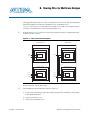
Appendix B. Sharing PLLs for Multicore Designs
Appendix C. Optimum Frequency for rxsys_clk
Appendix D. Board Design
Pin Constraints . . . . . . . . . . . . . . . . . . . . . . . . . . . . . . . . . . . . . . . . . . . . . . . . . . . . . . . . . . . . . . . . . . . . . . . . .
Board Design Configuration . . . . . . . . . . . . . . . . . . . . . . . . . . . . . . . . . . . . . . . . . . . . . . . . . . . . . . . . . . . . .
Design for Testability . . . . . . . . . . . . . . . . . . . . . . . . . . . . . . . . . . . . . . . . . . . . . . . . . . . . . . . . . . . . . . . . . . .
Probe Points . . . . . . . . . . . . . . . . . . . . . . . . . . . . . . . . . . . . . . . . . . . . . . . . . . . . . . . . . . . . . . . . . . . . . . . . .
Receiver MegaCore Functions . . . . . . . . . . . . . . . . . . . . . . . . . . . . . . . . . . . . . . . . . . . . . . . . . . . . . . .
Transmitter MegaCore Functions . . . . . . . . . . . . . . . . . . . . . . . . . . . . . . . . . . . . . . . . . . . . . . . . . . . .
Spare Pins . . . . . . . . . . . . . . . . . . . . . . . . . . . . . . . . . . . . . . . . . . . . . . . . . . . . . . . . . . . . . . . . . . . . . . . . . .
JTAG Scan Chain . . . . . . . . . . . . . . . . . . . . . . . . . . . . . . . . . . . . . . . . . . . . . . . . . . . . . . . . . . . . . . . . . . . .
D–1
D–1
D–1
D–2
D–2
D–2
D–3
D–3
Appendix E. Programming the SPI-4.2 Calendar via the Avalon Memory-Mapped Interface
Introduction . . . . . . . . . . . . . . . . . . . . . . . . . . . . . . . . . . . . . . . . . . . . . . . . . . . . . . . . . . . . . . . . . . . . . . . . . . . E–1
Programming the SPI-4.2 Calendar . . . . . . . . . . . . . . . . . . . . . . . . . . . . . . . . . . . . . . . . . . . . . . . . . . . . . . . E–1
Appendix F. Static and Dynamic Phase Alignment
Static Alignment . . . . . . . . . . . . . . . . . . . . . . . . . . . . . . . . . . . . . . . . . . . . . . . . . . . . . . . . . . . . . . . . . . . . . . .
Dynamic Alignment . . . . . . . . . . . . . . . . . . . . . . . . . . . . . . . . . . . . . . . . . . . . . . . . . . . . . . . . . . . . . . . . . . . .
Altera Solutions . . . . . . . . . . . . . . . . . . . . . . . . . . . . . . . . . . . . . . . . . . . . . . . . . . . . . . . . . . . . . . . . . . . . . . . .
Static Alignment . . . . . . . . . . . . . . . . . . . . . . . . . . . . . . . . . . . . . . . . . . . . . . . . . . . . . . . . . . . . . . . . . . . . .
Dynamic Phase Alignment (DPA) . . . . . . . . . . . . . . . . . . . . . . . . . . . . . . . . . . . . . . . . . . . . . . . . . . . . . .
AC Timing Analysis . . . . . . . . . . . . . . . . . . . . . . . . . . . . . . . . . . . . . . . . . . . . . . . . . . . . . . . . . . . . . . . . . . . .
F–1
F–2
F–2
F–3
F–3
F–4
Appendix G. Conversion from v2.2.x
Introduction . . . . . . . . . . . . . . . . . . . . . . . . . . . . . . . . . . . . . . . . . . . . . . . . . . . . . . . . . . . . . . . . . . . . . . . . . . . G–1
Receiver Signals . . . . . . . . . . . . . . . . . . . . . . . . . . . . . . . . . . . . . . . . . . . . . . . . . . . . . . . . . . . . . . . . . . . . . . . . G–1
Transmitter Signals . . . . . . . . . . . . . . . . . . . . . . . . . . . . . . . . . . . . . . . . . . . . . . . . . . . . . . . . . . . . . . . . . . . . . G–4
Additional Information
Document Revision History . . . . . . . . . . . . . . . . . . . . . . . . . . . . . . . . . . . . . . . . . . . . . . . . . . . . . . . . . . . Info–1
How to Contact Altera . . . . . . . . . . . . . . . . . . . . . . . . . . . . . . . . . . . . . . . . . . . . . . . . . . . . . . . . . . . . . . . . Info–1
Typographic Conventions . . . . . . . . . . . . . . . . . . . . . . . . . . . . . . . . . . . . . . . . . . . . . . . . . . . . . . . . . . . . . Info–2
May 2013
Altera Corporation
POS-PHY Level 4 MegaCore Function User Guide
vi
POS-PHY Level 4 MegaCore Function User Guide
Contents
May 2013 Altera Corporation
1. About This MegaCore Function
The POS-PHY Level 4 MegaCore function performs high-speed cell and packet
transfers between physical and link-layer devices.
Release Information
Table 1–1 provides information about this release of the Altera® POS-PHY Level 4
MegaCore® function.
Table 1–1. POS-PHY Level 4 MegaCore Function Release Information
Item
Version
Release Date
Ordering Code
Description
13.0
May 2013
IP-POSPHY4
Product ID
0088
Vendor ID
6AF7
f For more information about this release, refer to the MegaCore IP Library Release Notes
and Errata.
Altera verifies that the current version of the Quartus® II software compiles the
previous version of each MegaCore function. The MegaCore IP Library Release Notes
and Errata report any exceptions to this verification. Altera does not verify
compilation with MegaCore function versions older than one release.
Device Family Support
MegaCore functions can provide the types of support for target Altera device families
described in Table 1–2.
Table 1–2. Altera IP Core Device Support Levels
FPGA Device Families
HardCopy Device Families
Preliminary—The core is verified with preliminary timing
models for this device family. The core meets all
functional requirements, but might still be undergoing
timing analysis for the device family. It can be used in
production designs with caution.
HardCopy Companion—The core is verified with preliminary
timing models for the HardCopy companion device. The core
meets all functional requirements, but might still be undergoing
timing analysis for HardCopy device family. It can be used in
production designs with caution.
Final—The core is verified with final timing models for
this device family. The core meets all functional and
timing requirements for the device family and can be used
in production designs.
HardCopy Compilation—The core is verified with final timing
models for the HardCopy device family. The core meets all
functional and timing requirements for the device family and
can be used in production designs.
May 2013
Altera Corporation
POS-PHY Level 4 MegaCore Function User Guide
1–2
Chapter 1: About This MegaCore Function
Features
Table 1–3 shows the level of support offered by the POS-PHY Level 4 MegaCore
function to each Altera device family.
Table 1–3. Device Family Support
Device Family
Support
Arria® GX
Final
Arria II GX
Preliminary
Arria II GZ
Preliminary
Cyclone®
Final
Cyclone II
Final
Cyclone III
Final
Cyclone III LS
Preliminary
Cyclone IV
Preliminary
HardCopy II
HardCopy Compilation
HardCopy III
HardCopy Companion
HardCopy IV E
HardCopy Companion
HardCopy IV GX
HardCopy Companion
Stratix®
Final
Stratix GX
Final
Stratix II
Final
Stratix II GX
Final
Stratix III
Final
Stratix IV
Full
Stratix V
Preliminary
Other device families
No support
Features
■
Compliant with all applicable standards, including:
■
Optical Internetworking Forum (OIF), System Packet Interface Level 4 (SPI-4)
Phase 2 Revision 1: OC-192 System Interface for Physical and Link Layer Devices,
OIF-SPI4-02.1, October 2003.
■
PMC-Sierra Inc., POS-PHYTM Level 4 A Saturn Packet and Cell Interface
Specification for OC-192 SONET/SDH and 10 GB/s Ethernet Applications, Issue 5
(Draft): June 2000.
■
Stratix III, Stratix IV, and Stratix V device support up to 1,250 Mbps and Stratix II
device support up to 1,040 Mbps, including integrated dynamic phase alignment
(DPA) hardware module
■
Stratix GX device family support at up to 1,000 Mbps, including integrated DPA
hardware module
■
Stratix device family support at up to 840 Mbps
■
Cyclone III, Cyclone II, and Cyclone device support up to 622 Mbps for 64 bit data
path; support up to 250 Mbps for 32-bit data path width
POS-PHY Level 4 MegaCore Function User Guide
May 2013 Altera Corporation
Chapter 1: About This MegaCore Function
General Description
■
1–3
Configurable data path width—affecting the MegaCore function size and speed—
for various performance requirements and applications:
■
128 bits
■
64 bits
■
32 bits (quarter rate)
■
Supports up to 256 ports
■
Fixed start of packet (SOP) alignment to the most significant byte lane eases
subsequent packet processing
■
First-in first-out (FIFO) buffer status management and indications
■
Configurable FIFO buffer modes
■
■
Shared buffer with embedded addressing
■
Individual buffers
Error detection and handling
■
Protocol checking—SPI-4.2 datapath state machine check and repair
■
Atlantic FIFO buffer overflow handling
■
Status framing hysteresis (good and bad thresholds)
■
DIP-4 hysteresis (good and bad thresholds)
■
IP functional simulation models for use in Altera-supported VHDL and Verilog
HDL simulators
■
I-Tested certification
General Description
The packet over SONET/SDH physical layer (POS-PHY) Level 4 interface, first
developed by the SATURN® Development Group, was adopted by the Optical
Internetworking Forum (OIF) as the System Packet Interface Level 4—Phase 2 (SPI4.2). Therefore, POS-PHY Level 4 and SPI-4.2 are synonymous.
The POS-PHY Level 4 MegaCore function uses the SPI-4.2 interface for high-speed
cell and packet transfers between physical (PHY) and link-layer devices. The SPI-4.2
interface supports a data width of 16 bits (LVDS solution) and can be a PHY-link, linklink, link-PHY, or PHY-PHY connection in multi-gigabit applications, including:
asynchronous transfer mode (ATM) and packet over SONET/SDH (STS-192/STM64), 10 Gigabit Ethernet, and multi-channel Gigabit and Fast Ethernet.
In compliance with the SPI-4.2 interface specification, the POS-PHY Level 4 MegaCore
function allows you to implement transmit and receive functions.
May 2013
Altera Corporation
POS-PHY Level 4 MegaCore Function User Guide
1–4
Chapter 1: About This MegaCore Function
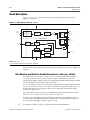
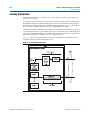
General Description
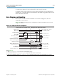
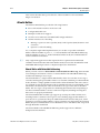
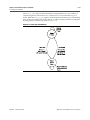
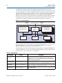
Figure 1–1 shows a full-duplex POS-PHY Level 4 MegaCore function configured for
the link layer in an Altera FPGA device.
Figure 1–1. POS-PHY Level 4 MegaCore Function as Link Layer Configuration
Atlantic Interface
SPI-4.2 Interface
OC-192
POS Framer
or
10 GbitE MAC
POS-PHY Level 4
Receiver
User Packet
Processing
Switch
Interface
Switch
Fabric
POS-PHY Level 4
Transmitter
FPGA
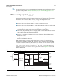
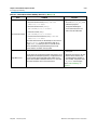
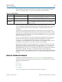
Figure 1–2 shows a full-duplex POS-PHY Level 4 MegaCore function configured for
the PHY layer in an Altera FPGA device.
Figure 1–2. POS-PHY Level 4 MegaCore Function as PHY Layer Configuration
Atlantic Interface
OC-192 or
10 GbitE
SPI-4.2 Interface
POS-PHY Level 4
Transmitter
Framer or MAC
Logic
Packet
Classifier
POS-PHY Level 4
Receiver
FPGA
Interfaces & Protocols
The following three interfaces support the POS-PHY Level 4 MegaCore function:
■
SPI-4.2 interface
■
Atlantic™ interface
■
Avalon® Memory-Mapped (Avalon-MM) interface.
You can use multiple Atlantic interfaces, but the SPI-4.2 interface only supports a
single transmitter and a single receiver.
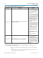
SPI-4.2 Interface
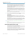
The SPI-4.2 interface is an external interface protocol developed by the Optical
Internetworking Forum (OIF). The SPI-4.2 interface features a high-speed data
portion and a FIFO buffer status portion. The high-speed portion comprises a 16-bit
data bus, a 1-bit control line, and a double data rate (DDR) clock. The FIFO buffer
status portion comprises a 2-bit status channel and a clock.
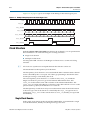
Figure 1–3 shows a full-duplex SPI-4.2 configuration.
Figure 1–3. SPI-4.2 Top-Level View
Transmitter
Source
tdclk
tctl
tdat[15:0]
tsclk
tstat[1:0]
POS-PHY Level 4 MegaCore Function User Guide
rdclk
Receiver
Sink
rctl
rdat[15:0]
rsclk
rstat[1:0]
May 2013 Altera Corporation
Chapter 1: About This MegaCore Function
MegaCore Verification
1–5
f For further information on this interface, refer to the System Packet Interface Level 4
(SPI-4) Phase 2 Revision 1: OC-192 System Interface for Physical and Link Layer Devices,
available at www.oiforum.com.
Atlantic Interface
The Atlantic interface is an Altera-developed synchronous protocol supporting both
packets and cells. The POS-PHY Level 4 MegaCore function is an Atlantic interface
slave that transfers packets to or from the user-side logic. The Atlantic interface
provides a connection between the FIFO buffer and user logic.
f For further information on this interface, refer to the Atlantic Interface Functional
Specification.
Avalon-MM Interface
The Altera Avalon-MM interface is a simple bus architecture that connects on-chip
processors (or external processor interfaces) and peripherals. The Avalon-MM
interface specifies the port connections between master and slave components, and
specifies the timing by which these components communicate.
All Avalon-MM signals are synchronized to the Avalon-MM clock (rav_clk/tav_clk).
This synchronization simplifies the relevant timing behavior of the Avalon-MM
interface and facilitates integration with high-speed peripherals.
In this version of the POS-PHY Level 4 MegaCore function, the Avalon-MM module is
a discrete unit that is instantiated by the MegaWizard® Plug-In, when Asymmetric
Port Support is turned on.
f For further information on this interface, refer to the Avalon Interface Specifications.
MegaCore Verification
The POS-PHY Level 4 MegaCore function has been rigorously tested and verified in
hardware for different platforms and environments. Each environment has individual
test suites that are designed to cover the following five categories of testability:
■
Sanity
■
Flow Control
■
Error Management
■
Performance
■
Stress
These test suites contain several testbenches that are grouped and focused on testing
specific features of the POS-PHY Level 4 MegaCore function. These individual
testbenches set unique parameters for each specific feature test.
Results of the hardware verification tests are gathered in I-tested reports available for
different ASSP devices. For example, SPI-4.2 Interoperability with PMC-Sierra’s S/UNI
9953 and SPI-4.2 Interoperability with PMC-Sierra’s S/UNI 10×GE (PM3388).
f For these reports, contact your local Altera sales representative or FAE.
May 2013
Altera Corporation
POS-PHY Level 4 MegaCore Function User Guide
1–6
Chapter 1: About This MegaCore Function
Performance and Resource Utilization
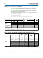
Performance and Resource Utilization
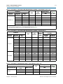
Table 1–4 and Table 1–6 list the resources and internal speeds for a selection of
variations using the shared buffer with embedded addressing mode.
Table 1–7 and Table 1–9 list the resources and internal speeds for a selection of
variations using the individual buffers mode.
All of the results use the Quartus II software version 8.1 for the following devices:
■
Cyclone III (EP3C40F780C6)
■
Stratix III (EP3SE50F780C3)
■
Stratix IV GX (EP4SGX70DF29C3 and EP4SGX230DF29C3ES)
Table 1–4. Performance—Shared Buffer With Embedded Addressing Mode—Cyclone III Device
Parameters
Data Flow Direction
Memory Blocks
M9K
clk (1)
fMAX (MHz)
1,598
10
179
4
1,603
10
175
32
10
1,690
11
162
32
4
1,405
9
140
32
10
1,489
10
146
LEs
Data Path Width
(bits)
Number of Ports
32
1
32
Receiver
Transmitter (2)
Notes to Table 1–4:
(1) Receiver variations mostly use rxsys_clk; transmitter variations use tdint_clk.
(2) These values are for variations that use the lite transmitter feature (refer to page 5–5).
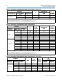
Table 1–5. Performance—Shared Buffer With Embedded Addressing Mode—Stratix III Device (Part 1 of 2)
Parameters
Data Flow
Direction
Receiver
Memory Blocks
Logic
Registers
M9K
clk (1)
fMAX (MHz)
Data Path
Width (bits)
Number of
Ports
ALUTs
32
1
855
1,089
10
193
64
1
1,287
1,809
17
266
128
1
2,176
3,017
23
138
32
4
864
1,085
10
172
64
4
1,301
1,846
17
275
128
4
2,186
3,032
23
158
32
10
857
1,186
11
203
64
10
1,319
2,082
14
260
128
10
2,760
4,521
8
151
POS-PHY Level 4 MegaCore Function User Guide
May 2013 Altera Corporation
Chapter 1: About This MegaCore Function
Performance and Resource Utilization
1–7
Table 1–5. Performance—Shared Buffer With Embedded Addressing Mode—Stratix III Device (Part 2 of 2)
Parameters
Data Flow
Direction
Memory Blocks
Logic
Registers
clk (1)
fMAX (MHz)
Data Path
Width (bits)
Number of
Ports
ALUTs
32
4
875
850
9
162
64
4
944
1,326
13
186
128
4
1,177
1,456
17
151
32
10
901
939
10
155
64
10
1,042
1,579
10
231
128
10
1,896
2,931
2
148
Transmitter (2)
M9K
Notes to Table 1–5:
(1) Receiver variations mostly use rxsys_clk; transmitter variations use tdint_clk.
(2) These values are for variations that use the lite transmitter feature (refer to page 5–5).
Table 1–6. Performance—Shared Buffer With Embedded Addressing Mode—Stratix IV Devices
Parameters
ALUTs
Data Flow
Direction
Receiver
Transmitter
Logic
Registers
Memory
Blocks
(M9K)
Data Path
Width (bits)
Number of
Ports
32
1
1,190
1,294
64
1
1,387
128
1
32
4
64
clk
fMAX (MHz)
EP4SGX70
DF29C3
EP4SGX230
DF29C3ES
6
204
195
1,820
16
261
284
2,215
2,741
30
186
207
1,198
1,300
6
199
156
4
1,398
1,826
16
273
273
128
4
2,221
2,742
30
195
195
32
10
1,138
1,249
7
213
163
64
10
1,396
1,782
18
281
270
128
10
2,273
2,709
33
187
160
32
4
1,049
1,085
5
192
185
64
4
1,032
1,454
9
262
232
128
4
1,178
1,464
17
175
181
32
10
1,023
1,119
5
178
163
64
10
1,057
1,601
9
260
225
128
10
1,331
1,770
17
190
166
Table 1–7. Performance—Individual Buffers Mode—Cyclone III Device (Part 1 of 2)
Parameters
Data Flow Direction
Receiver
May 2013
Altera Corporation
Memory Blocks
M9K
clk (1)
fMAX (MHz)
3,082
36
145
4
5,725
84
130
10
1,786
10
129
LEs
Data Path Width
(bits)
Number of Ports
32
1
32
32
POS-PHY Level 4 MegaCore Function User Guide
1–8
Chapter 1: About This MegaCore Function
Performance and Resource Utilization
Table 1–7. Performance—Individual Buffers Mode—Cyclone III Device (Part 2 of 2)
Parameters
Data Flow Direction
Memory Blocks
Data Path Width
(bits)
Transmitter (2)
clk (1)
fMAX (MHz)
LEs
Number of Ports
M9K
32
4
3,561
34
110
32
10
7,035
82
118
Notes to Table 1–7:
(1) Receiver variations mostly use rxsys_clk; transmitter variations use tdint_clk.
(2) These values are for variations that use the lite transmitter feature (refer to page 5–5).
Table 1–8. Performance—Individual Buffers Mode—Stratix III Device
Parameters
Data Flow
Direction
Data Path
Width (bits)
Number of
Ports
ALUTs
Logic
Registers
Memory Blocks
(M9K)
clk (1)
fMAX (MHz)
32
4
1,915
2,042
36
139
64
4
2,384
2,827
37
253
128
4
3,555
4,242
71
149
32
10
3,865
3,726
84
126
64
10
4,575
4,626
85
230
32
1
1,126
1,131
10
130
64
1
1,312
1,775
10
193
128
1
1,701
2,238
18
146
32
4
2,452
2,201
34
134
64
4
2,709
2,951
34
179
128
4
3,462
3,738
66
125
32
10
5,071
4,189
82
128
64
10
5,678
5,213
82
156
Receiver
Transmitter (2)
Notes to Table 1–8:
(1) Receiver variations mostly use rxsys_clk; transmitter variations use tdint_clk.
(2) These values are for variations that use the lite transmitter feature (refer to page 5–5).
Table 1–9. Performance—Individual Buffers Mode—Stratix IV Devices (Part 1 of 2)
Parameters
Logic
Registers
Memory
Blocks
(M9K)
2,245
2,427
4
2,514
128
4
32
64
ALUTs
Data Flow
Direction
Receiver
Data Path
Width (bits)
Number of
Ports
32
4
64
clk
fMAX (MHz)
EP4SGX70
DF29C3
EP4SGX230
DF29C3ES
21
182
159
2,800
40
270
268
3,833
4,160
78
165
149
10
4,070
4,529
45
140
144
10
4,823
4,830
88
255
254
POS-PHY Level 4 MegaCore Function User Guide
May 2013 Altera Corporation
Chapter 1: About This MegaCore Function
Installation and Licensing
1–9
Table 1–9. Performance—Individual Buffers Mode—Stratix IV Devices (Part 2 of 2)
Transmitter
32
1
1,155
1,213
6
165
176
64
1
1,309
1,784
10
245
182
128
1
1,710
2,245
18
177
171
32
4
2,563
2,524
18
130
151
64
4
2,726
2,997
34
183
212
128
4
3,430
3,778
66
166
153
32
10
5,210
4,789
42
120
118
64
10
5,733
5,188
82
153
213
Installation and Licensing
The POS-PHY Level 4 MegaCore function is part of the MegaCore IP Library, which is
distributed with the Quartus II software and downloadable from the Altera website
(www.altera.com).
f For system requirements and installation instructions, refer to Altera Software
Installation and Licensing.
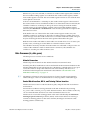
Figure 1–4 shows the directory structure after you install the POS-PHY Level 4
MegaCore function, where <path> is the installation directory. The default installation
directory on Windows is c:\altera\<version>; on Linux it is /opt/altera<version>
Figure 1–4. Directory Structure
<path>
Installation directory.
ip
Contains the Altera MegaCore IP Library and third-party IP cores.
altera
Contains the Altera MegaCore IP Library.
common
Contains shared components.
posphy_l4
Contains the POS-PHY Level 4 MegaCore function files and documentation.
doc
Contains the documentation for the MegaCore function.
lib
Contains encrypted lower-level design files.
You need to purchase a license for the MegaCore function only when you are
completely satisfied with its functionality and performance and want to take your
design to production.
After you purchase a license for POS-PHY Level 4 MegaCore function, you can
request a license file from the Altera Licensing page of the Altera website and install it
on your computer. When you request a license file, Altera emails you a license.dat
file. If you do not have Internet access, contact your local Altera representative.
May 2013
Altera Corporation
POS-PHY Level 4 MegaCore Function User Guide
1–10
Chapter 1: About This MegaCore Function
Installation and Licensing
OpenCore Plus Evaluation
With Altera’s free OpenCore Plus evaluation feature, you can perform the following
actions:
■
Simulate the behavior of a megafunction (Altera MegaCore function or AMPPSM
megafunction) within your system
■
Verify the functionality of your design, as well as evaluate its size and speed
quickly and easily
■
Generate time-limited device programming files for designs that include
megafunctions
■
Program a device and verify your design in hardware
You only need to purchase a license for the megafunction when you are completely
satisfied with its functionality and performance and want to take your design to
production.
f For more information on OpenCore Plus hardware evaluation, refer to AN 320:
OpenCore Plus Evaluation of Megafunctions.
OpenCore Plus Time-Out Behavior
OpenCore Plus hardware evaluation supports the following two operation modes:
■
Untethered—the design runs for a limited time.
■
Tethered—requires a connection between your board and the host computer. If
tethered mode is supported by all megafunctions in a design, the device can
operate for a longer time or indefinitely.
All megafunctions in a device time out simultaneously when the most restrictive
evaluation time is reached. If there is more than one megafunction in a design, a
specific megafunction’s time-out behavior may be masked by the time-out behavior of
the other megafunctions.
1
For MegaCore functions, the untethered timeout is 1 hour; the tethered timeout value
is indefinite.
Your design stops working after the hardware evaluation time expires, at which time
the receiver MegaCore function stops processing incoming data. The status channel
and Atlantic FIFO buffers continue to operate normally.
POS-PHY Level 4 MegaCore Function User Guide
May 2013 Altera Corporation
2. Getting Started
Design Flow
Figure 2–1 shows the stages for creating a system with the POS-PHY Level 4
MegaCore® function and the Quartus® II software. The sections in this chapter
describe each stage.
Figure 2–1. Design Flow
Specify Parameters
Simulate with
Testbench
Apply Timing
Constraints
Compile Design
Program Device
Specify Parameters
To specify the parameters, follow these steps:
1. In the Quartus II software, create a new Quartus II project with the New Project
Wizard.
2. On the Tools menu click MegaWizard Plug-In Manager and follow the steps to
start IP Toolbench.
1
The POS-PHY Level 4 MegaCore function is in the Communications >
POS-PHY directory.
3. Click Step 1: Parameterize in IP Toolbench.
4. Determine your design’s constraints and performance requirements and then
parameterize the POS-PHY Level 4 MegaCore function in IP Toolbench.
1
May 2013
Not all parameters are supported by, or are relevant for, every MegaCore function
variation.
Altera Corporation
POS-PHY Level 4 MegaCore Function User Guide
2–2
Chapter 2: Getting Started
Specify Parameters
f For more information about the parameters, refer to Chapter 3, Parameter Settings.
5. Click Step 2: Set Up Simulation in IP Toolbench.
An IP functional simulation model is a cycle-accurate VHDL or Verilog HDL
model produced by the Quartus II software.
c You may only use these simulation model output files for simulation purposes and
expressly not for synthesis or any other purposes. Using these models for synthesis
creates a nonfunctional design.
6. Turn on Generate Simulation Model.
7. Choose the language in the Language list.
8. Some third-party synthesis tools can use a netlist that contains only the structure
of the MegaCore function, but not detailed logic, to optimize performance of the
design that contains the MegaCore function. If your synthesis tool supports this
feature, turn on Generate netlist.
9. Click OK.
10. Click Step 3: Generate in IP Toolbench.
Table 2–1 describes the generated files and other files that may be in your project
directory. The names and types of files specified in the IP Toolbench report vary
based on whether you created your design with VHDL or Verilog HDL
1
If you want to change your project from a receiver to a transmitter, delete all
the HDL files before you regenerate the MegaCore function.
Table 2–1. Generated Files (Part 1 of 2)
File
Description
<variation name>_atlfifo_concat.v
An encrypted HDL file for Quartus II synthesis. This file is automatically added
to your Quartus II project. You should not modify this file.
<variation name>_dpa_concat.v
A generated HDL file for Quartus II synthesis. This file is automatically added to
your Quartus II project. You should not modify this file.
<variation
name>_pl4_rx_core_constraints.tcl
Constraint settings file for Quartus II synthesis. Use this file to specify
constraints required to achieve performance requirements.
<variation name>_refresh_model.tcl
A Tcl script that regenerates the IP functional simulation model, in both Verilog
HDL (.vo) and VHDL (.vho) formats.
<variation name>_run_modelsim.tcl
A Tcl script that automates the process of running the testbench with the IP
functional simulation model.
<variation name>_rx_data_proc.ocp
An OpenCore Plus file, for time limited or tethered hardware evaluation.
<variation name>_rx_modules.v
An encrypted HDL file for Quartus II synthesis. This file is automatically added
to your Quartus II project. You should not modify this file.
<variation
name>_rx_data_phy_altlvds.v
A generated HDL file for Quartus II synthesis. This file is automatically added to
your Quartus II project. You should not modify this file.
<variation name>_rx_core.v
A generated HDL file for Quartus II synthesis. This file is automatically added to
your Quartus II project. You should not modify this file.
<variation name>_syn.v or
<variation name>_syn.vhd
A timing and resource netlist for use in some third-party synthesis tools.
POS-PHY Level 4 MegaCore Function User Guide
May 2013 Altera Corporation
Chapter 2: Getting Started
Simulate the Design
2–3
Table 2–1. Generated Files (Part 2 of 2)
File
Description
<variation name>_tb.v
A Verilog HDL testbench for the requested parameterization.
<variation name>.bsf
Quartus II symbol file for the MegaCore function variation. You can use this file
in the Quartus II block diagram editor.
<variation name>.html
The MegaCore function report file.
<variation name>.ppf
XML file that describes the MegaCore pin attributes to the Quartus II Pin
Planner. MegaCore pin attributes include pin direction, location, I/O standard
assignments, and drive strength.
<variation name>.sdc
TimeQuest SDC constraint settings file for timing analysis. Use this file to
specify constraints required for TimeQuest analysis.
<variation name>.v or .vhd
A MegaCore function variation file, which defines a Verilog HDL top-level
description of the custom MegaCore function. Instantiate the entity defined by
this file inside of your design. Include this file when compiling your design in the
Quartus II software.
<variation_name>.vo or .vho
Verilog HDL IP functional simulation model.
11. After you review the generation report, click Exit to close IP Toolbench and click
Yes on the Quartus II IP Files message.
1
The Quartus II IP File (.qip) is a file generated by the MegaWizard interface
or SOPC Builder that contains information about a generated MegaCore
function. You are prompted to add this .qip file to the current Quartus II
project at the time of file generation. In most cases, the .qip file contains all
of the necessary assignments and information required to process the
MegaCore function or system in the Quartus II compiler. Generally, a single
.qip file is generated for each MegaCore function and for each SOPC
Builder system. However, some more complex SOPC Builder components
generate a separate .qip file, so the system .qip file references the
component .qip file.
You can now integrate your custom MegaCore function variation into your design
and simulate and compile.
1
Constraints are automatically set by the MegaWizard Plug-In Manager.
Simulate the Design
You can simulate your design using the IP Toolbench-generated VHDL and Verilog
HDL IP functional simulation models.
f For more information on IP functional simulation models, including NativeLink, refer
to “Simulate the Design” on page 2–3 and the Simulating Altera IP in Third-Party
Simulation Tools chapter in volume 3 of the Quartus II Handbook.
May 2013
Altera Corporation
POS-PHY Level 4 MegaCore Function User Guide
2–4
Chapter 2: Getting Started
Simulate the Design
Altera provides models you can use for functional verification of the POS-PHY Level
4 MegaCore function within your design. A Verilog HDL testbench, including scripts
to run it, is also provided. This testbench, for use with the ModelSim-Altera simulator
or other simulator tools via NativeLink, demonstrates how to instantiate a model in a
design.
This section tells you how to use the testbench with the ModelSim simulator or with
other simulators via NativeLink.
f For a list of the simulators that you can use with NativeLink, refer to the Simulating
Altera IP in Third-Party Simulation Tools chapter in volume 3 of the Quartus II Handbook.
c The testbench is in Verilog HDL, so you require a license to run mixed language
simulations to run the testbench with the VHDL model. If you edit any of your
variation’s clear-text Verilog HDL files, you must update the IP functional simulation
model before running the simulator. To update the model, run the quartus_sh -t
<variation_name>_refresh_model.tcl script in the Quartus II software.
Use the Testbench with the ModelSim Simulator
To use the testbench with IP functional simulation models in the ModelSim simulator,
follow these steps:
1. Start the ModelSim simulator.
2. In the simulator, change the working directory to the location of the
<variation_name>_run_modelsim.tcl file.
3. To run the script type the following command at the simulator command prompt:
source <variation_name>_run_modelsim.tcl
Use the Testbench with NativeLink
To use the testbench with third-party IP functional simulation models using
NativeLink, follow these steps:
1. Create a new custom variation in your Quartus II project. Generate your
MegaCore function for this variation using the IP Toolbench.
2. Check that the absolute path to your third-party simulation tool is set. Set the path
from EDA Tool Options in the Options dialog box (Tools menu).
3. On the Processing menu, point to Start and click Start Analysis & Elaboration.
1
If the analysis and elaboration is not successful, fix the error before moving
to the next step.
4. On the Assignments menu, click Settings. The Settings dialog box appears.
Expand EDA Tool Settings and select Simulation.
POS-PHY Level 4 MegaCore Function User Guide
May 2013 Altera Corporation
Chapter 2: Getting Started
Simulate the Design
2–5
5. In Tool name, select a simulator tool from the list.
In EDA Netlist Writer options, select VHDL from the list for Format for output
netlist.
In NativeLink settings, select the Compile test bench option and then click Test
Benches. The Test Benches dialog box appears.
6. In the Test Benches dialog box, click New. The New Test Bench Settings dialog
box appears.
7. In the New Test Bench Settings dialog box, enter the information described in
Table 2–2 on page 2–5 (refer also to Figure 2–2 on page 2–5). To enter the files
described in the table, browse to the files in your project.
Table 2–2. NativeLink Test Bench Settings
Parameter
Setting and File Name
Test bench name
<any name>
Top-level module in test bench
tb
Design instance name in test bench
<variation name>
Run for
100 ns
Test bench files
<variation name>_tb.v
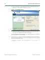
Figure 2–2 on page 2–5 shows an example of the testbench settings when the
<variation_name> is example.
Figure 2–2. Example of New Test Bench Settings for NativeLink
8. When you have entered the required information for your new testbench, click OK
in the New Test Bench Settings dialog box.
9. Click OK in the Test Benches dialog box and then click OK in the Settings dialog
box.
May 2013
Altera Corporation
POS-PHY Level 4 MegaCore Function User Guide
2–6
Chapter 2: Getting Started
Compile the Design and Program a Device
10. On the Tools menu, point to EDA Simulation Tool and click Run EDA RTL
Simulation Tool. The simulation now begins with your chosen simulation tool.
Compile the Design and Program a Device
You can use the Quartus II software to compile your design. Refer to Quartus II Help
for instructions on compiling your design.
After you have compiled your design, program your targeted Altera device and
verify your design in hardware.
POS-PHY Level 4 MegaCore Function User Guide
May 2013 Altera Corporation
3. Parameter Settings
You customize the POS-PHY Level 4 MegaCore® function by specifying parameters
using IP Toolbench launched from the MegaWizard® Plug-in Manager in the
Quartus® II software.
This chapter describes the parameters and how they affect the behavior of the
MegaCore function. Each section corresponds to a tab when you click Parameterize in
IP Toolbench.
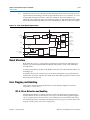
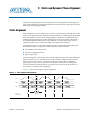
Basic Parameters
Figure 3–1 shows the basic parameters tab.
Figure 3–1. Basic Parameters
Device Family
Select the device family. Table 1–3 on page 1–2 shows the device families that the POSPHY Level 4 MegaCore function supports.
May 2013
Altera Corporation
POS-PHY Level 4 MegaCore Function User Guide
3–2
Chapter 3: Parameter Settings
Basic Parameters
Table 3–1 shows the maximum LVDS data rates supported by the POS-PHY Level 4
MegaCore function for each device family.
Table 3–1. Supported LVDS Data Rates
Device Family
Arria GX
Arria II GX and Arria II GZ
LVDS Rate (Mbps)
840
1,000
Cyclone
622
Cyclone II
622
Cyclone III
622
Cyclone IV
622
HardCopy II
1,040
Stratix
840
Stratix II
1,040
Stratix II GX
1,040
Stratix III
1,250
Stratix IV
1,250
Stratix V
1,250
Stratix GX
1,000
The POS-PHY Level 4 MegaCore function operates either as a receiver where data
flows from the SPI-4.2 interface to the Atlantic™ interface, or as a transmitter where
data flows from the Atlantic interface to the SPI-4.2 interface.
1
The receiver and transmitter variations are separate building blocks in a design, with
no dependency on each other, so you select the parameters independently. For the
MegaCore function to act as a full-duplex, bidirectional transceiver, instantiate one for
each direction. Typical designs may include one or more receivers and one or more
transmitters per FPGA.
1
After you have generated a custom variation, you can re-open the MegaWizard
Plug-In Manager and change the parameters. However, do not change a receiver
variation to a transmitter variation, or a transmitter variation to a receiver variation,
otherwise the Quartus II software generates errors during compilation.
If your receiver design requires dynamic phase alignment (DPA), turn on Dynamic
Phase Alignment.
DPA is recommended for data rates exceeding 622 Mbps, and considered essential for
high-quality signaling above 800 Mbps, or across connectors at 700 Mbps.
DPA is only available in Stratix III, Stratix II, and Stratix GX devices.
f For further information about DPA, refer to “DPA Channel Aligner
(rx_data_phy_dpa)” on page 4–3.
POS-PHY Level 4 MegaCore Function User Guide
May 2013 Altera Corporation
Chapter 3: Parameter Settings
Basic Parameters
3–3
LVDS Data Rate
For a transmitter, the LVDS data rate specifies the data rate out of the FPGA, on each
LVDS pair.
IP Toolbench uses this parameter to instantiate and configure the ALTLVDS
megafunction that includes the fast PLL. For example, to configure a transmitter with
a data rate of 700 Mbps on the tdat line, enter 700 in the LVDS Data Rate field of IP
Toolbench. This rate corresponds to a 350 MHz DDR clock on tdclk.
For a receiver, the LVDS data rate specifies the data rate into the FPGA, on each LVDS
pair, and sets the phase-locked loop (PLL) clock rate.
IP Toolbench uses the LVDS data rate to instantiate and parameterize the ALTLVDS
megafunction that includes the fast PLL. For example, for a receiver with a data rate
of 700 Mbps on each rdat line, enter 700 in LVDS data rate. This value corresponds to
a 350 MHz double-data rate (DDR) clock on rdclk.
PLL Input Frequency
For a transmitter only, you can enter the PLL input frequency. To enter the PLL
frequency, you must click Import PLL Frequency, to open the ALTLVDS wizard and
view the available input PLL frequencies.
1
When you change the data path width, the PLL input frequency changes.
1
Do not type the PLL frequency into the box.
Data Path Width
The Data path width affects two important aspects of the MegaCore function: size
and performance. The MegaCore function offers the following options:
■
128 bits running at a frequency of 1/8 the LVDS data rate
■
64 bits running at 1/4 the LVDS data rate
■
32 bits (quarter rate) running at 1/2 the LVDS data rate (for non-standard
applications at a maximum of 250 Mbps)
f For approximate resource usage and performance of example POS-PHY Level 4
variations, refer to “Performance and Resource Utilization” on page 1–6.
Buffer Mode
The POS-PHY Level 4 MegaCore function supports the following two buffer modes:
■
Shared buffer with embedded addressing
■
Individual buffers
With Shared buffer with embedded addressing, all ports share a single Atlantic
buffer with an 8-bit address field that supports up to 256 ports. The data is read from
the Atlantic buffer in the same order as it is received. The shared buffer with
embedded addressing mode is smaller than the individual buffers mode, and allows
you to develop your own buffering and status generation implementation.
May 2013
Altera Corporation
POS-PHY Level 4 MegaCore Function User Guide
3–4
Chapter 3: Parameter Settings
Basic Parameters
With Individual buffers, the POS-PHY Level 4 MegaCore function provides an
Atlantic first-in first-out (FIFO) buffer for each port. Therefore, there are as many
Atlantic FIFO buffers of the same depth and width—each with a unique Atlantic
interface on the user end—as the number of ports that you select. The individual
buffers supports up to 16 ports.
1
Timing and routing difficulties may occur when using 16 ports for 128 bit variations;
thus a maximum of 10 ports is recommended for 128-bit variations.
For transmitters for individual buffers variations, a credit-based scheduler is
provided. This scheduler decodes the incoming status channel and decides from
which FIFO buffer (port) to transmit.
The individual buffers for transmitters offer the following advantages:
■
A simple user interface
■
Full scheduler
■
No head-of-line blocking
■
Per-port backpressure
f For further information on individual buffers for transmitters, refer to “Individual
Buffers” on page 5–3.
For receivers, the individual buffers offer the following advantages:
■
A simple user interface
■
No head-of-line blocking
■
The POS-PHY Level 4 MegaCore function handles all of the backpressure
automatically
f For further information on individual buffers for receivers, refer to “Individual
Buffers” on page 4–7.
The SPI-4.2 protocol supports from 1 to 256 ports. When you select the number of
ports, you determine the mode of operation. Single-PHY operation for one port; or
multi-PHY for two to 256 ports. For example, when interfacing to a 10-channel Gbit
Ethernet MAC device the number of ports is 10.
When you use the shared buffer with embedded addressing, the Number of ports
determines the number of port addresses supported by the POS-PHY Level 4 protocol
portion of the MegaCore function, such as the status generator and error checker. Port
addresses 0 to 255 can always be sent and received when using Shared buffer with
embedded addressing.
For the shared buffer with embedded addressing, the Buffer size defines the size of
the shared embedded address buffer. For the individual buffers, the Buffer size
defines the size of each buffer. The POS-PHY Level 4 MegaCore function supports the
following sizes (per buffer):
■
512 bytes
■
1,024 bytes
POS-PHY Level 4 MegaCore Function User Guide
May 2013 Altera Corporation
Chapter 3: Parameter Settings
Basic Parameters
3–5
■
2,048 bytes
■
4,096 bytes
■
8,192 bytes
■
16,384 bytes
■
32,768 bytes
Atlantic FIFO Buffer Clock
The Atlantic FIFO buffer clock sets the clock mode for the Atlantic FIFO buffers. Two
choices are available: Single or Multiple.
With a single Atlantic FIFO buffer clock, the Atlantic FIFO buffers are instantiated as
single clock domain buffers that do not include any clock crossing logic and therefore
consume fewer logic resources.
With a multiple Atlantic FIFO buffer clocks, the Atlantic FIFO buffers are instantiated
as multiple clock domain buffers. Each buffer has two independently operated clock
inputs, thus each Atlantic interface has a separate clock input. Multiple Atlantic FIFO
buffer clocks consume more logic resources.
Atlantic Interface Width
The Atlantic interface width includes 32, 64, or 128 bits, and depends on the internal
data path width. Table 3–2 shows the Atlantic data widths supported for each internal
data path width.
1
For the individual buffers mode, all buffers have the same data path width.
Table 3–2. Atlantic Interface Data Width Limitations
Internal Data Path Width (Bits)
Supported Atlantic Data Width (Bits)
128
128
64
64 and 128
32
32 and 64
The Status channel clock edge determines on which clock edge—positive (rising),
negative (falling), or programmable—the 2-bit status channel is transmitted (by the
receiver MegaCore function) in reference to the tsclk (for the transmitter) or rsclk
(for the receiver) pin. When you turn on Programmable Edge, an input pin,
(ctl_ts_statedge for the transmitter; ctl_rs_statedge for the receiver), controls the
status channel clocking edge statically at reset.
1
To ensure proper sampling of the status information, you should typically set this
parameter to be the opposite of the sampling clock edge on the adjacent device.
For the Status channel I/O standard, either LVTTL or LVDS, select LVDS to
implement the optional lower bandwidth LVDS status operation (refer to the OIFSPI4-02.1 specification).
May 2013
Altera Corporation
POS-PHY Level 4 MegaCore Function User Guide
3–6
Chapter 3: Parameter Settings
Optional Features
Optional Features
Figure 3–2 on page 3–6 shows the Optional Features tab.
Figure 3–2. Receiver Optional Features
These parameters allow you to enable additional features that the MegaCore function
provides. Each parameter may increase or decrease the number of logic resources.
Turn on Atlantic error checking to add a packet filtering module to the write side of
every Atlantic FIFO buffer. The packet filtering module ensures that only properly
formatted packets are passed through the Atlantic FIFO buffer. When you turn off
Atlantic error checking, the packet filtering module is not added.
The packet filtering module corrects start-of-packet (SOP) and end-of-packet (EOP)
errors before writing packets into the FIFO buffer. For a missing SOP (where data or
an EOP is received for a port without first having received a SOP), an error output is
asserted, and data is not written to the buffer until a SOP is received. For a missing
EOP (where a SOP is received before the previous packet’s EOP), the current packet is
terminated by an EOP, and ERR is asserted. The next packet is stored normally.
For individual buffers variations with a large number of ports, the Atlantic error
checking increases the amount of logic.
Atlantic error checking is often desirable for receivers, but less applicable for
transmitters because the incoming user-Atlantic data may be presumed correct.
POS-PHY Level 4 MegaCore Function User Guide
May 2013 Altera Corporation
Chapter 3: Parameter Settings
Optional Features
3–7
The missing SOP and missing EOP error indicators are always zero if you turn off
Atlantic error checking.
Turn on Parity protected memory to protect all Atlantic FIFO buffers in the MegaCore
function by byte-lane parity. The parity is calculated across every byte of data that is
written to memory in the buffers, and is checked for correctness when it is read. If a
parity error is detected, an error signal is raised. Turn off Parity protected memory, to
deactivate the parity protection.
1
In the receive direction, the parity error signal is 2 clock cycles delayed (compared to
Atlantic FIFO read data). In the transmit direction, the parity error signal is 1 or 2
clock cycles delayed (compared to Atlantic FIFO read data) depending on the
parameters selected.
Transmitter Options
When you turn on Lite transmitter, the transmitter pads packets with IDLE characters
to a multiple of 16 bytes for 128-bit variations, or 8 bytes for 64-bit variations.
Although using the lite transmitter feature lowers the effective bandwidth rate on the
SPI-4.2 data bus, it greatly reduces the logic consumption.
When you turn off Lite transmitter, the transmitter packs the packets more tightly
together and pads them with IDLE characters to a multiple of 4 bytes. SOP,
continuation of packet (COP) and EOP may be combined into a single control word,
or may be in adjacent control words. Turning off the lite transmitter feature increases
the effective bandwidth rate on the SPI-4.2 data bus, but increases the logic
consumption.
1
COP means no SOP. COP can be pure continuation (control word bits [15:12] =
4'b1000, so no SOP and no EOP, but payload follows) or EOP + continuation (control
word bits [15:12] = 4'b1xx0, so end current packet, but continue other packets).
For the transmitter MegaCore function you can select Pessimistic or Optimistic for
the Status interpretation mode.
In the Pessimistic mode, the latest status information is captured and is stored inside
the status processor block until a DIP-2 status is received. If the DIP-2 is valid, the
buffered status is passed on to the scheduler or user logic. If the DIP-2 is invalid, the
scheduler and user logic do not receive an update, and the next incoming status
overwrites the errored buffered status.
In the Optimistic mode, the status information is provided to the user logic and
scheduler through a clock-crossing buffer as it arrives on the status channel. DIP-2
errors cause the err_ts_dip2 flag to be asserted, but do not affect the status reception.
1
May 2013
The Pessimistic mode causes the latency in receiving a valid status message to be
calendar multiplier × calendar length tsclk cycles longer than the optimistic mode. This
length is significant for systems with large calendar length or large calendar
multiplier values.
Altera Corporation
POS-PHY Level 4 MegaCore Function User Guide
3–8
Chapter 3: Parameter Settings
Optional Features
If you turn on Ignore backpressure (only available when you turn on Shared buffer
with embedded addressing), the MegaCore function ignores the backpressure from
the receiver and simply sends data whenever the buffer is not empty. The MegaCore
function stops reading from the buffer only when the status framer is out of
synchronization, when a training pattern is inserted, or when there is not enough data
to complete a burst. The user logic is responsible for using the status outputs from the
MegaCore function to schedule data writes into the buffer appropriately.
If you turn off Ignore backpressure, a simple scheduling algorithm is employed. If
the status received for any port is satisfied, the transmitter stops reading from the
buffer on the next EOP or burst unit size boundary. If all ports are hungry or starving,
the transmitter sends the data in the buffer. So a satisfied status received for one port
prevents transmission for any port, leading to head-of-line blocking.
If you turn on Switch on end-of-packet, the scheduler stops sending from the current
port, and switches ports at the end of burst (that is, when the credits have all been
consumed), as well as when an EOP is sent. If you turn off Switch on end-of-packet,
the scheduler switches ports at the end of the burst (also includes switching when the
buffer is empty).
1
This option applies only to the individual buffers mode, and allows you to
parameterize the port switching capabilities of the transmit scheduler.
f For more information, refer to “Individual Buffers Transmit Scheduler (tx_sched)” on
page 5–3.
Turn on Burst Limit Enable, if you want the transmitter to limit the maximum size of
bursts it sends. Set the maximum burst value with the Burst Limit option (on the
Protocol Parameters tab). At the end of a burst limit a control word is inserted.
Receiver Options
If you turn off Ignore LVDS DPA locked after training, which is only available for
Stratix II devices, a loss of dpa_lvds_locked causes the MegaCore function to stop
processing data, sends framing, and there is data loss and the possibility of
MSOP/EOP errors. If you turn on Ignore LVDS DPA locked after training, a loss of
dpa_lvds_locked does not trigger stop and framing, and data continues to process
normally. You must monitor the DIP4 error signal to assess if the data is correct or not
and trigger a retrain or not.
1
For Stratix III and Stratix IV devices, the dpa_lvds_locked signal never goes low, so
the MegaCore function behaves as if you turned on Ignore LVDS DPA locked after
training.
If the signal stat_rd_lvds_lock goes low during operation (after training), the
MegaCore function assumes that the lock is lost due to external conditions such as
jitter. This signal goes low if the capture phase of the hardware DPA block changes by
two or more phases. The two phases correspond to a amount that is lower than the
accepted threshold for the SPI4.2 Specification. When the signal goes low, the
MegaCore function states it is out of synchronization and requests a new training
sequence.
POS-PHY Level 4 MegaCore Function User Guide
May 2013 Altera Corporation
Chapter 3: Parameter Settings
Optional Features
3–9
In some cases, it is better to ignore this signal and rely on the error checking
mechanisms or SPI4.2, by checking the DIP4 calculation. You then have to externally
request the retraining and unlock the DPA block.
It is normal during the normal data transfer in SPI-4.2 that dpa_locked signal can
become de-asserted due to some jitter that is still within 0.44 UI of LVDS data. The
DPA has a low pass filter that filters out very high frequency jitter from affecting the
lock signal and phase of rx_clk. If the jitter is detected to be 0.25 UI (two phases out of
8 jump in one direction), dpa_locked is de-asserted and it is still within 0.44 UI.
The DIP-4 error marking determines how the receiver handles DIP-4 errors. The
receiver uses the following three modes to mark received DIP-4 errors:
■
None—no error marking is performed.
■
Optimistic mode—the receiver MegaCore function marks the preceding and
succeeding burst as errored. If these bursts are payload (that is, if a DIP-4 occurs
followed by IDLEs), then only the preceding control word payload is marked as
errored. Bursts going into the Atlantic FIFO buffer are marked with the Atlantic
error signal. If a burst is not an EOP, it is up to the user logic to detect it.
■
Pessimistic mode—the receiver MegaCore function marks all open packets as
errored. Packets going into the Atlantic FIFO buffer are marked with the Atlantic
error signal. This feature increases in resource utilization as the number of ports
increases.
End-of-packet-based data available controls the aN_arxdav signal on the Atlantic
FIFO buffer. Turn on so the aN_arxdav signal is asserted (high) when at least one EOP
is in the buffer, or the fill level is above FIFO threshold low (ctl_ax_ftl). Turn off so
the aN_arxdav signal is asserted (high) only if the fill level of the FIFO buffer is above
the FIFO threshold low value.
The Status source option applies only to variations using the shared buffer with
embedded addressing mode and provides the following two status channel control
options:
■
Buffer Fill Level—the status for each channel is controlled by the single buffer’s
status. Every calendar time slot contains the result of the almost empty (AE) and
almost full (AF) comparison to the buffer level.
■
User Controlled—to add extra pins, which allows you to directly control the
transmitted buffer status and allows you to send a status irrespective of the fill
level of the internal FIFO buffers, which avoids the situation where the FIFO
buffer is not emptied quickly enough, and if you still request data, the FIFO buffer
overfills.
Turn on Safe External (User Controlled) Status, to ensure the sent status avoids FIFO
buffer overflow (refer to Table 3–3). Turn off Safe External (User Controlled) Status,
to ensure the sent status is always the user status (refer to Table 3–3), irrespective of
buffer fill level.
May 2013
Altera Corporation
POS-PHY Level 4 MegaCore Function User Guide
3–10
Chapter 3: Parameter Settings
Optional Features
1
If you turn off Safe External (User Controlled) Status, you can overflow the internal
FIFO buffer.
Table 3–3. User-Controlled Option
User Status Value
FIFO Buffer Status Value
Sent Status Value
Starving
Starving
Starving
Starving
Hungry
Hungry
Starving
Satisfied
Satisfied
Hungry
Starving or Hungry
Hungry
Hungry
Satisfied
Satisfied
Satisfied
Any
Satisfied
f For more information, refer to “Status Processor” on page 4–7.
FIFO RAM Blocks
The option to select 2 FIFO RAM blocks depends on the parameters you select on the
Basic Parameters tab. These parameters affect the FIFO buffer size and FIFO buffer
width, both of which play a role in memory utilization.
When you select 2 FIFO RAM blocks, the timing performance of the MegaCore
function may decrease (because the memory rdata bus is unregistered, as opposed to
registered for 4 FIFO RAM blocks). Altera recommends that you do full compilations
for both configurations before deciding which one to choose.
1
Use 2 FIFO RAM block only if it gives an improvement in memory utilization and if
your timing requirements are still met.
Table 3–3 shows the support for the 2 FIFO RAM block. 4 FIFO RAM block supports
all configuration.
Table 3–4. 2 RAM Block Support
Data Flow
Direction
Receiver
Buffer Mode
Data Path Width
Atlantic Interface
Width
Lite Transmitter
2 RAM Block Support
Any
Any
Any
—
Yes
32
—
No
64
—
Yes
64
Any
No
Yes
Yes
No
No
32
Transmitter
Shared Buffer
with Embedded
Addressing
Individual
Buffers
POS-PHY Level 4 MegaCore Function User Guide
64
128
128
128
Any
No
Any
Any
Any
Yes
May 2013 Altera Corporation
Chapter 3: Parameter Settings
Optional Features
3–11
Each FIFO RAM block is implemented independently in the available device memory
(for example, with M512, M4K, or M9K blocks) and each device memory has a fixed
number of available configurations. The FIFO RAM block depth for small buffer
configurations (such as 128 × 36 of M4K memory) can be smaller than the minimum
configurable depth of the memory element, meaning that the remainder of the
memory is wasted. By using 2 FIFO RAM blocks instead of 4 you may get better
memory utilization. Figure 3–3 shows the comparison of FIFO RAM blocks.
Figure 3–3. Comparison of FIFO RAM Blocks
4 FIFO RAM Blocks
FIFO Block 0
(size = fifo_size/4)
FIFO Block 1
(size = fifo_size/4)
Write Side
Read Side
FIFO Block 2
(size = fifo_size/4)
FIFO Block 3
(size = fifo_size/4)
2 FIFO RAM Blocks
FIFO Block 0
(size = fifo_size/2)
Write Side
Read Side
FIFO Block 1
(size = fifo_size/2)
Both FIFO buffer width and FIFO buffer size affect memory utilization. The
improvement for a two block FIFO buffer configuration versus a four block FIFO
buffer configuration ranges from half the memory consumption for small buffers, to
the same memory consumption for large buffers.
Table 3–5 gives a comparison of the memory utilization for a Stratix II device with 4
FIFO RAM blocks versus 2 FIFO RAM blocks.
Table 3–5. Memory Utilization Comparison
Buffer
Size
(bytes)
(Note 1)
Atlantic Interface Width 32
Atlantic Interface Width 64
2 FIFO RAM Blocks 4 FIFO RAM Blocks
2 FIFO RAM Blocks
4 FIFO RAM Blocks
512
4 M4K
4 M4K + 4 M512
4 M4K + 2 M512
8 M4K + 4 M512
1,024
4 M4K
8 M4K
6 M4K
8 M4K + 4 M512
2,048
6 M4K
8 M4K
6 M4K
12 M4K
4,096
12 M4K
12 M4K
10 M4K
12 M4K
8,192
24 M4K
24 M4K
20 M4K
20 M4K
Note to Table 3–5:
(1) Stratix II device, receive (Rx), shared buffer, data path width 32, parity enabled.
May 2013
Altera Corporation
POS-PHY Level 4 MegaCore Function User Guide
3–12
Chapter 3: Parameter Settings
Protocol Parameters
Protocol Parameters
Figure 3–4 on page 3–12 shows the Protocol Parameters tab.
Figure 3–4. Receiver Protocol Parameters
Select Real-Time Programmable, so most of the protocol parameters on this tab
become input pins to the MegaCore function. These input pins allow each parameter
to be connected to a user-implemented register, and controlled at run-time.
Select Fixed Value, to enter values for the protocol parameters on this tab.
IP Toolbench then fixes these values in the MegaCore function, making the
parameters static and the input pins unavailable.
Calendar Options
Turn on Asymmetric Port Support (only available if you select the Real-time
programmable) for the calendar to allow asymmetric weighting of calendar entries to
control the allocation of bandwidth to a given SPI-4.2 port. You must program the
calendar for the MegaCore function to produce the status channel (refer to
Appendix E, Programming the SPI-4.2 Calendar via the Avalon Memory-Mapped
Interface).
A port with twice the calendar entries of all other ports nominally uses twice as much
bandwidth on the SPI-4.2 interface depending on the data characteristics. Ports can be
disabled by removing them from the calendar.
POS-PHY Level 4 MegaCore Function User Guide
May 2013 Altera Corporation
Chapter 3: Parameter Settings
Protocol Parameters
3–13
To be effective, the far-end scheduler must handle received status optimistically. As
status is received, credits for each port are topped up to MaxBurst1/MaxBurst2
levels.
Turn on Asymmetric Port Support to instantiate an Avalon® Memory-Mapped
(Avalon-MM) interface in the MegaCore function. The Avalon-MM interface
programs the values of calendar length, calendar multiplier, and the port numbers for
each of the calendar slots.
If you turn on Asymmetric Port Support, the calendar length is programmed from
the Avalon-MM interface (refer to Appendix E).
If you turn on Programmable calendar length, a calendar length input pin is added to
the MegaCore function. This pin allows you to vary the calendar length value from
one to the number of ports without having to recompile. If the programmable
calendar length support parameter is turned off, the calendar length is equal to the
number of ports.
The calendar length value cannot be greater than the number of ports (except when
you turn on Asymmetrical Port Support).
The Calendar multiplier determines the number of times the calendar sequence is
repeated before the DIP-2 parity and framing is inserted. Choose a value from 1 to
256.
If the Asymmetric Port Support is turned on, the calendar multiplier value is
programmed via the Avalon-MM interface.
1
The calendar multiplier × calendar length value must be set according to the
instructions in Table C–1 on page C–1 of the “Clock Structure” section, otherwise the
status channel does not operate correctly.
The Maximum calendar length (only available when you turn on Asymmetric Port
Support) defines the maximum number of calendar entries available in the
configurable calendar. Choose a value from 32 to 2,048.
When you turn on Hitless B/W Reprovisioning (only available when you turn on
Asymmetric Port Support), the receiver can transmit a calendar-select word in the
status frame. Active and inactive calendars are tied to the current calendar-select
word in the receiver. When the current calendar-select word changes, the active and
inactive calendars are swapped at the appropriate time, in the following order:
May 2013
■
The CALSEL_REQ register bit is toggled at the receiver (refer to page 4–30).
■
At the beginning of the next status frame, the calendar-select word is toggled.
■
The receiver toggles the used calendar multiplier, calendar length, and calendar to
transmit the next status frame.
■
The transmitter receives the first calendar-select word of the new frame and
detects the toggle.
■
The transmitter toggles the used calendar multiplier, calendar length, and
calendar to interpret the next status frame.
Altera Corporation
POS-PHY Level 4 MegaCore Function User Guide
3–14
Chapter 3: Parameter Settings
Protocol Parameters
For individual buffers far-end transmitter variations, changing calendars does not
cause the credit table to be flushed, thus a port may not immediately be disabled if it
still has credits. It is up to the user logic to flush the receiver and transmitter buffers
prior to changing the calendar-select word. Otherwise, data may become stranded.
Each calendar can have independent values for calendar length and calendar
multiplier.
Transmitter Options
The Burst unit size sets the unit size in bytes for burst transfers and controls the
smallest burst transmitted. The valid range for this parameter is from 16 to 1,024
bytes, in 16-byte granularity.
1
The burst unit size multiplier does not limit the maximum burst length, and does not
force control word insertion. Instead, use the Burst limit parameter.
When the data path width is equal to 128 bits and the lite transmitter feature is turned
off, the unit size is 32 bytes, up to 1,024 bytes in 32-byte granularity.
The MaxBurst1 parameter allows you to select the maximum number of credits—
burst unit size to 2,032 bytes—that can be transmitted when the adjacent device’s
FIFO buffer is starving.
The MaxBurst2 parameter allows you to select the maximum number of credits—
burst unit size to 2,032 bytes—that can be transmitted when the adjacent device’s
FIFO buffer is hungry.
The MaxBurst1 and MaxBurst2 parameters do not limit the maximum burst length,
and do not force control word insertion.
The MaxBurst1 and MaxBurst2 parameters are used by the transmit scheduler, thus
they apply only to the individual buffers mode.
1
MaxBurst2 must be less than or equal to MaxBurst1; MaxBurst1 and MaxBurst2 must
be greater than or equal to burst unit size.
f Refer to Figure 3–5 on page 3–16 for the relation of AE and AF.
You can enter the Burst limit only when you turn on Burst Limit Enable. The Burst
limit sets the maximum burst size, in bytes, to be sent by the transmitter, and
guarantees that the transmitter does not send bursts longer than the burst limit (a
control word is inserted at the end of the burst limit). Burst limit values are restricted
to multiples of burst unit size. Depending on other transmitter parameters, the values
may be limited to a minimum value. IP Toolbench only allows valid burst limit
values.
The Maximum training sequence interval (MaxT) allows you to select the interval at
which the training sequence occurs—16 to 65,535 bytes. The training sequence is
scheduled to be inserted after the MaxT counter expires, but is not actually inserted
until the burst that is sent is complete. Therefore, the time between training pattern
insertions is no less than the value of the MaxT parameter, and no more than the value
of the MaxT parameter plus the burst unit size.
POS-PHY Level 4 MegaCore Function User Guide
May 2013 Altera Corporation
Chapter 3: Parameter Settings
Protocol Parameters
3–15
If MaxT = 0, periodic training patterns are disabled. If the transmitter status framer is
out of synchronization, the transmitter sends continuous training patterns regardless
of the MaxT parameter. Training patterns always begin on the rising edge of the clock
(tdclk).
For the Training pattern repetition value, the training sequence includes one IDLE
word, plus ALPHA(a) × 20 training words. ALPHA is a user-selectable option (0 to 255).
Zero (0) is equal to 256 training pattern repetitions.
The training sequence includes one IDLE control word, plus a × 20 words. The twenty
words are separated into ten consecutive tdat words of 16’h0FFF with tctl of 1’b1,
followed by ten consecutive tdat words of 16’hF000 with tctl of 1’b0.
For the Status sync good and Status sync bad threshold values, two 4-bit inputs,
good_level (ctl_ts_sync_good_theshold) and bad_level
(ctl_ts_sync_bad_theshold), are associated with the stat_ts_sync signal.
The stat_ts_sync signal is asserted high when a good_level number of consecutive
status frames are received without frame or DIP-2 errors. The stat_ts_sync signal is
deasserted when a bad_level number of DIP-2 errors or frame errors have been
received since the last error-free frame.
The FIFO buffer threshold high (FTH) for transmitter variations controls when the
aN_atxdav signal is asserted and deasserted for the write side of the FIFO buffer. The
aN_atxdav signal indicates when there is room available to write new data into the
FIFO buffer, and is asserted whenever the remaining space in the buffer is greater than
the FTH value.
This threshold is defined in terms of bytes, with a valid range from N to buffer size
bytes, in N-byte increments, where:
■
N = 4 or 8 bytes for 32-bit data path variations
■
N = 8 or 16 bytes for 64-bit data path variations
■
N = 16 or 32 bytes for 128-bit data path variations
The N-byte values depend on the Atlantic interface width and on the Lite transmitter
setting. Table 3–6 shows the N-byte values, based on the transmitter's settings.
Table 3–6. N-Byte Values
Datapath Width
32
64
Atlantic Interface
Width
Lite Transmitter
N Bytes (FTH
Increment)
32
—
4
64
—
8
On
8
Off
16
On or off
16
On
16
Off
32
64
128
128
May 2013
Altera Corporation
128
POS-PHY Level 4 MegaCore Function User Guide
3–16
Chapter 3: Parameter Settings
Protocol Parameters
1
Although the MegaWizard interface allows you to set FTH values as low as one FIFO
buffer element (translated to bytes), a minimum FTH value is used internally. And,
depending on the core's configuration, up to four FIFO buffer locations are unusable.
For the exact minimum FTH value and number of unusable locations, refer to the
MegaWizard interface message that appears while configuring the core.
Receiver Options
The Almost empty (AE) and Almost full (AF) thresholds segregate the receiver FIFO
buffer into three states, depending on the fill levels: starving, hungry, and satisfied.
The SPI-4 Phase 2 specification defines two-bit status values for starving, hungry, and
satisfied. These two-bit values are based on the available space in the FIFO buffer and
on the AE and AF parameter settings:
■
Starving—when the number of elements in the FIFO buffer is less than, or equal to,
the AE threshold
■
Hungry—when the number of elements in the FIFO buffer is between the AE
threshold and the AF threshold
■
Satisfied—when the number of elements in the FIFO buffer is greater than the AF
threshold
The starving, hungry, and satisfied conditions are reported to the adjacent transmitter
on the rstat bus, which operates at up to ¼ of the rdclk frequency.
These thresholds are defined in terms of bytes, with a valid range from zero to buffer
size.
1
AE must be lower than or equal to AF.
Figure 3–5 illustrates the relationship between the AE and AF thresholds and the
MaxBurst1 and MaxBurst2 values.
Figure 3–5. FIFO Buffer Thresholds
AE
(Empty)
Starving
Lmax + ε
AF
Hungry
(Full)
Satisfied
Lmax + MaxBurst2+ ε
Lmax + MaxBurst1+ ε
Notes to Figure 3–5:
(1) LMAX corresponds to the worst-case response time from sending a status update over the FIFO status channel until
observing the reaction to that update on the corresponding data path.
(2)
corresponds to the difference between the granted credit and the actual data transfer length. This difference arises
from various protocol overheads.
(3) The MaxBurst1 and MaxBurst2 values are defined by the adjacent device’s transmitter. Determining the optimal
MaxBurst1 and MaxBurst2 values is application-specific, and requires an analysis of the data flows, beyond the
scope of this user guide.
POS-PHY Level 4 MegaCore Function User Guide
May 2013 Altera Corporation
Chapter 3: Parameter Settings
Protocol Parameters
3–17
The FIFO buffer threshold low (FTL) value for receiver variations controls when the
aN_arxdav signal is asserted for the read side of the FIFO buffer. If the fill level of the
buffer is higher than the FTL value, the aN_arxdav signal is asserted indicating that
there is a burst of data available.
1
There is no requirement to wait for the aN_arxdav signal to be asserted, you can read
from the buffer at any time.
1
FTL must be greater than zero.
This threshold is defined in terms of bytes, with a valid range from: N to buffer size,
in increments of N bytes, where:
■
N = 4 or 8 bytes for 32-bit data path variations
■
N = 8 or 16 bytes for 64-bit data path variations
■
N = 16 bytes for 128-bit data path variations
The N-byte values for the 32-bit and 64-bit variations depend on the Atlantic interface
width. If the Atlantic interface width is greater than the data path width, the larger
value for N is used.
For the DIP-4 good and DIP-4 bad threshold values, two 4-bit inputs are associated
with the DIP-4 OOS state machine: good_level (ctl_rd_dip4_good_threshold) and
bad_level (ctl_rd_dip4_bad_threshold).
If the stat_rd_dip4_oos signal is high, and all of the DIP-4s in the control words
received in the current clock cycle (up to 8 in 128-bit mode) are good, the good counter
is incremented by 1; otherwise it is reset to 0. If the good counter reaches the
good_level threshold, the stat_rd_dip4_oos flag is cleared. A good_level of 0 is
invalid.
If the stat_rd_dip4_oos signal is low, and all of the DIP-4s in the control words
received in the current clock cycle (up to 8 in 128-bit mode) are errored, the bad
counter is incremented by 1; otherwise it is reset to 0. If the bad counter reaches the
bad_level threshold, the stat_rd_dip4_oos flag is asserted. A bad_level of 0 is
invalid.
1
The receiver may need to receive more control word DIP-4 errors than the DIP-4 bad
threshold parameter set in the wizard, for stat_rd_dip4_oos to go high.
f For more information, refer to “DIP-4 Marking” on page 4–17 and “DIP-4 Out of
Service Indication” on page 4–18.
May 2013
Altera Corporation
POS-PHY Level 4 MegaCore Function User Guide
3–18
POS-PHY Level 4 MegaCore Function User Guide
Chapter 3: Parameter Settings
Protocol Parameters
May 2013 Altera Corporation
4. Functional Description—Receiver
The POS-PHY Level 4 MegaCore® function consists of the main SPI-4.2 processing
logic, and configurable Atlantic™ first-in first-out (FIFO) buffers. When the POS-PHY
Level 4 MegaCore function is configured as a receiver, data flows from the SPI-4
interface to the Atlantic interface.
Features
May 2013
■
Accepts packets from a SPI-4.2 transmitter
■
Processes control words
■
Detects diagonal interleaved parity (DIP-4) errors
■
Detects SPI-4.2 protocol errors
■
Performs start-of-packet (SOP) alignment and Atlantic conversion
■
Buffers packets on a per-port or per-interface basis
■
Detects buffer fill levels and generates the status channel
Altera Corporation
POS-PHY Level 4 MegaCore Function User Guide
4–2
Chapter 4: Functional Description—Receiver
Block Description
Block Description
Figure 4–1 on page 4–2 shows the blocks and clocks that comprise the receiver
MegaCore function.
Figure 4–1. Block Diagram—Receiver
(Note 1)
rdint_clk
SPI4.2
Interface
rdclk
Data Receiver
And
Serial-to-Parallel
Converter
DPA Channel
Aligner
Data
Processor
Atlantic
Buffer 0
Atlantic
Buffer N
rsclk
Status PHY
Atlantic
Interface 0
Atlantic
Interface N
Status FSM
Status
Register
Status Hold
rxsys_clk
Status
Calculator
rav_clk
Note to Figure 4–1:
(1) The dotted lines illustrate the clock domain separations.
This section describes the top-level blocks of the POS-PHY Level 4 receiver MegaCore
function.
Data Receiver and Serial-to-Parallel Converter (rx_data_phy_altlvds)
Data and control words arrive on the rdat bus, and are sampled on both edges of
rdclk. Payload and control words contain two bytes, where bit 15 is the most
significant bit (MSB) and bit 8 is the least significant bit (LSB) of the first byte, and bit
7 is the MSB and bit 0 is the LSB of the second byte.
For 128- and 64-bit variations, an ALTLVDS_RX megafunction deserializes the SPI-4.2
rdat/rctl lines into words at or the rdat data rate, respectively. The rdint_clk
is derived from the rdclk input pin, and is the clock that drives the internal logic
elements for the receiver.
For 32-bit (quarter-rate) variations, an ALTDDIO_IN megafunction deserializes the
SPI-4.2 rdat/rctl lines into words at the rdat data rate.
For rates above 311 Mbps, the Stratix® III, Stratix II, Stratix GX, and Stratix devices
include a dedicated SERDES (ALTLVDS megafunction) implemented in LVDS I/Os.
For rates below 250 Mbps, LVDS I/O pins are used.
1
A fast phase-locked loop (PLL) is required for the ALTLVDS SERDES.
POS-PHY Level 4 MegaCore Function User Guide
May 2013 Altera Corporation
Chapter 4: Functional Description—Receiver
Block Description
4–3
f For more information on the ALTLVDS_RX and ALTDDIO_IN megafunctions, refer to
Quartus® II Help, to the SERDES Transmitter/Receiver ALTLVDS Megafunction User
Guide, or to the ALTDDIO Megafunction User Guide.
DPA Channel Aligner (rx_data_phy_dpa)
In the Stratix III, Stratix II, and Stratix GX device families, the ALTLVDS_RX
megafunctions support an optional DPA feature that can compensate for trace length
mismatches and variations due to process, voltage, and temperature (PVT).
The DPA feature includes the following functions:
■
Supports data rates from 415 Mbps to 1 Gbps in Stratix GX devices
■
Supports data rates from 415 Mbps to 1,250 Gbps in Stratix III devices and to 1,050
Gbps in Stratix II devices
■
At reset, it performs channel alignment using SPI-4.2 training patterns
compensating for static clock-channel and channel-to-channel skew
■
After reset, it dynamically follows changing clock-channel and channel-to-channel
skew without using SPI-4.2 training patterns
■
Supports a total skew of 4.5 bits, with 0.5 bits of the total allowed after reset in
Stratix GX devices
■
Supports a total skew of 4.4 bits, with 0.4 bits of the total allowed after reset in
Stratix III and Stratix II devices
If the DPA parameter is turned on, the DPA feature consists of an ALTLVDS_RX
megafunction with DPA enabled, and a channel aligner. For 64-bit data path width
variations in Stratix GX devices, this feature also consists of an 8:4 serializer (needed
to achieve an overall deserialization factor of 4). Three status signals:
stat_rd_dpa_locked, err_rd_dpa and stat_rd_dpa_lvds_locked, and one control
signal: ctl_rd_dpa_force_unlock are also part of this feature. Figure 4–2 shows the
DPA block diagram.
Figure 4–2. DPA and Channel Aligner Block Diagram
rdclk
x2
PLL
rdint_clk
lvds_reset
Serial
Data
rdat/rctl
16+1
ALTLVDS_RX
Megafunction
(with DPA)
16+1
data_out
128+/64+
Channel
Aligner
data_out_algn
128+/64+
16+1
16+1
rx_data_phy_dpa
Altera Corporation
8:4
Serializer
(2)
Parallel
Data
data : 2
128+/64+
err_rd_dpa
stat_rd_dpa_locked
ctl_rd_dpa_force_unlock
stat_rd_dpa_lvds_locked (3)
align
May 2013
clk x 2
Status/
Control
Signals
rxreset_n
POS-PHY Level 4 MegaCore Function User Guide
4–4
Chapter 4: Functional Description—Receiver
Block Description
Figure 4–2. DPA and Channel Aligner Block Diagram
Notes to Figure 4–2:
(1) The width of the data path for the data_out, data_out_algn, and data:2 signals depends on the deserialization factor.
(2) Exists only for Stratix GX devices, if the internal data path width is 64 bits.
(3) The stat_rd_dpa_lvds_locked signal does not exist in the altlvds block for Stratix GX devices. It is tied to a logic 1 inside the receiver
MegaCore function.
ALTLVDS_RX Megafunction
The ALTLVDS_RX megafunction always performs deserialization on the input rdat
and rctl high-speed LVDS signals, and divides the DDR rdclk to produce a slower
rdint_clk.
When DPA is enabled in the POS-PHY Level 4 MegaCore function, the ALTLVDS_RX
megafunction has two other features enabled: DPA and bit slip. DPA with respect to
ALTLVDS has a different meaning than DPA with respect to the POS-PHY Level 4
MegaCore function. After DPA resets, the ALTLVDS DPA feature tolerates only a
small amount of change to the channel-to-channel skew, which compensates for the
very small amounts of change in channel-to-channel skew that may occur due to
voltage and temperature shifts during system operation. A change in channel-channel
skew that is greater than the bit-time tolerance causes one or more of the internal
deskew FIFO buffers to underflow or overflow, which the POS-PHY Level 4
MegaCore function detects only as DIP-4 errors. You must use the DIP-4 thresholds
and stat_rd_dip4_oos to trigger the DPA reset by asserting
ctl_rd_dpa_force_unlock.
The stat_rd_dpa_lvds_locked signal indicates when the DPA cannot stay locked
either because of a lack of transitions on the channel, or because of rapid changes in
skew. The DPA run length is 6,400 UI for Stratix III, Stratix II, and Stratix GX devices.
If the traffic on the SPI-4.2 interface is very sparse, periodic training patterns may be
required.
To compensate for large amounts of static channel-to-channel skew, the POS-PHY
Level 4 MegaCore function channel aligner state machine uses the bit slip feature (the
channel align or data realignment) of the ALTLVDS_RX megafunction.
The POS-PHY Level 4 MegaCore function automatically configures and includes the
ALTLVDS_RX megafunction.
Channel Aligner
The DPA feature of the ALTLVDS_RX megafunction provides parallel data sampled
correctly and aligned to a single clock. As it does not use a data pattern, it cannot
compensate for more than one bit time of channel-to-channel skew which may exist
due to trace length mismatches.
The channel aligner sub-block uses the SPI-4.2 training pattern to align the parallel
data. Alignment is done once at start-up, and then only when requested by asserting
the ctl_rd_dpa_force_unlock signal. The channel aligner state machine begins the
alignment process once the ctl_rd_dpa_force_unlock signal is deasserted and the
altlvds_rx megafunction asserts the stat_rd_dpa_lvds_locked signal (high). It then
pulses the bits of the align[16:0] signal channel by channel until all channels are
POS-PHY Level 4 MegaCore Function User Guide
May 2013 Altera Corporation
Chapter 4: Functional Description—Receiver
Block Description
4–5
aligned, which can be detected by looking for the repeating training pattern. For every
align pulse, the ALTLVDS_RX megafunction sub-block shifts the data on the
corresponding channel by one bit, effectively in the serial domain. The actual shift
occurs in the serial domain for Stratix III and Stratix II devices, and in the parallel
domain for Stratix GX devices.
In Stratix III and Stratix II devices, the MegaCore function requires less than 220
training patterns (lock time) before it asserts the stat_rd_dpa_lvds_locked signal.
The err_rd_dpa signal is tied low.
In Stratix GX devices, the MegaCore function requires less than 700 training patterns
(lock time) before it asserts the stat_rd_dpa_locked signal. If alignment cannot be
achieved because of a large skew between data channels, or because the
stat_rd_dpa_lvds_locked signal becomes deasserted during training, the channel
aligner asserts the err_rd_dpa signal.
8:4 Serializer
The 8:4 serializer block supports an overall deserialization factor of 4 for 64-bit
Stratix GX variations only. It consists of a PLL and a 2:1 multiplexer for each channel.
f For more information on using dynamic phase alignment, refer to Appendix F, Static
and Dynamic Phase Alignment.
Data Processor (rx_data_proc)
The data processor consists of three sub-blocks.
Control Word Processing & DIP-4
The control word processing and DIP-4 block analyses the control words from the
data stream, and calculates the running DIP-4 value. It detects the following errors:
■
SOP8 violations. If SOPs occur less than 8 cycles apart, the err_rd_sop8 signal is
asserted but there is no impact on the received data. In 128- and 64-bit variations,
the clock-domain crossing buffer may fill faster when SOP8 violations occur.
■
Odd size packet violations. If an odd size packet does not end with the LSB cleared
to zero, the aN_arxerr signal is asserted on EOP. The err_rd_pad_byte_non_zero
signal is also asserted.
■
EOP aborts. If an EOP abort is received, the aN_arxerr signal is asserted on EOP.
The err_rd_eop_abort signal is also asserted.
■
DIP-4 errors (refer to “DIP-4 Marking” on page 4–17 and “DIP-4 Out of Service
Indication” on page 4–18).
■
Reserved control words—data is dropped.
■
Proper training patterns. The channel aligner block requires proper training
patterns to lock, so if the transmitting device is sending bad training patterns, the
err_rd_tp signal is asserted and the MegaCore function does not lock.
1
May 2013
Altera Corporation
Whenever the MegaCore function aborts a packet by asserting the
aN_arxerr signal (as in the odd size packet with LSB not cleared), the
resulting packet is even sized, except in the DIP-4 optimistic mode.
POS-PHY Level 4 MegaCore Function User Guide
4–6
Chapter 4: Functional Description—Receiver
Block Description
f For a more complete list of errors detected by the MegaCore function, refer to “Error
Flagging and Handling” on page 4–13.
Clock-Domain Crossing Buffer
This block instantiates a clock-domain crossing buffer called alignment buffer (ABUF)
to transfer data from the rdint_clk clock domain to the rxsys_clk clock domain. The
depth of the alignment buffer is fixed at 128; the width is equal to the MegaCore
function data path width.
f For a description of the relationship between rdint_clk and rxsys_clk, refer to
“Clock Structure” on page 4–10.
SOP Alignment & Atlantic Conversion
This block moves the SOP for each packet to the first-byte position on the Atlantic
interface, and aligns the data to ensure that valid data is contiguous (no IDLEs) before
sending it to the Atlantic buffer.
Atlantic Buffers
The Atlantic FIFO buffers provide the following features:
■
Single receive slave-source Atlantic interface on the user end
■
Configurable buffer size
■
Support for crossing clock domains
■
Buffer status interface
■
■
Overflow error indication
■
Underflow warning indication
■
Configurable FIFO buffer threshold low (FTL)
■
Optional end-of-packet-based data available (aN_arxdav) signal assertion
Atlantic interface error checking
■
Missing or spurious SOP/EOP detection and correction
■
Optional overflow handling
Shared Buffer with Embedded Addressing
When the shared buffer with embedded addressing mode is selected, the POS-PHY
Level 4 MegaCore function consists of the receiver processor logic and a shared FIFO
buffer with embedded addressing.
The shared buffer is a single Atlantic FIFO buffer, where for each data word a tag is
carried containing the port number. This means that the Atlantic-side logic cannot
selectively pick a port to access. Instead, data bursts from all ports are stored
collectively into this one shared physical buffer, and the ordering of the data bursts is
maintained in the order in which they were received on the SPI-4.2 bus.
POS-PHY Level 4 MegaCore Function User Guide
May 2013 Altera Corporation
Chapter 4: Functional Description—Receiver
Block Description
4–7
The shared buffer and the logic support up to 256 ports. If Atlantic error checking is
enabled, 256 ports are still supported by the MegaCore function, but the logic for error
checking uses only the minimum amount of logic required to support the number of
ports chosen as a parameter. The port width field remains fixed for 256 ports and
unused address bits are passed through unaffected. For example, if a variation has 4
ports, only the lower 2 address bits are used for error checking—data received for port
6 is checked as though it is for port 2. This allows unused upper address bits to be
used for packet classification.
The single FIFO buffer with embedded addressing supports interleaved packets. An
interleaved packet occurs when, for example, a packet from port 2 is sent, and then a
packet from port 3 is sent before port 2 has received the EOP indication. This
interleaving is achieved by changing the aN_arxadr in the middle of the packet.
The shared buffer with embedded addressing mode is useful if you intend to handle
buffering outside of the MegaCore function. To support user-defined external
buffering, a fully exposed status interface is provided, but requires that the status
channel override (status source parameter) be enabled. Normally, the shared buffer
with embedded addressing fill level is compared against the global almost empty
(AE) and almost full (AF) values to produce the status information for all ports on the
status channel. With the override feature, you can set the FIFO buffer status
information values on a per-port basis.
Individual Buffers
When the individual buffers mode is selected, the POS-PHY Level 4 MegaCore
function consists of the receiver processor logic, and a separate Atlantic FIFO buffer
for each port.
The advantage of the individual buffers mode is that each Atlantic interface can be
accessed in parallel and independently, and the MegaCore function handles the status
generation automatically. The disadvantage is that because the number of ports
directly increases the logic utilization, the individual buffers mode is not well suited
for applications with a large number of ports.
Status Processor
A major component of a SPI-4.2 system is flow control. Flow control is achieved by
periodically sending near-end FIFO buffer status to the far-end device’s scheduler
over the status channel.
Collectively, the status processor blocks calculate, format, and transmit the status
channel.
Starting at the physical interface and working back to the FIFO buffers, the flow
control has the following operation.
The status PHY block (rx_stat_phy) generates rsclk given some reference clock:
May 2013
■
In 128-bit variations, the rsclk runs at the rdint_clk rate.
■
In 64-bit variations, the rsclk runs at 1/2 the rdint_clk rate.
■
In 32-bit variations, the rsclk runs at 1/4 of the rdint_clk rate.
Altera Corporation
POS-PHY Level 4 MegaCore Function User Guide
4–8
Chapter 4: Functional Description—Receiver
Block Description
The status PHY block aligns rstat to either the positive or negative edge of rsclk
depending on the input value of the ctl_rs_statedge signal. This block also
implements a clock-crossing FIFO buffer between the rsclk and rxsys_clk domains.
The status FSM block (rx_stat_proc_fsm) is enabled when the clock-crossing FIFO
buffer of the status PHY block has available space. When enabled, this block generates
the next words in the status frame.
If the clock-crossing FIFO buffer underflows or overflows because of an incorrect
configuration, if the ctl_ry_rsfrm signal is set, or if the rsfrm bit in the Avalon®
Memory-Mapped (Avalon-MM) interface is set, the finite state machine outputs ‘11’
continuously and the stat_ry_disabled signal is asserted.
Framing, calendar select word, and DIP are generated locally, but the actual status for
each calendar slot is provided on request by the status register (rx_stat_proc_reg)
block, and either the status calculator (rx_stat_calc) or status hold (rx_stat_hold)
blocks.
Given a calendar slot number, the status register block determines which port's status
belongs in the slot according to the calendar that it stores. When the asymmetric port
support parameter is turned off, the port number corresponds with the slot number,
(that is, slot one is port one, and so on). When the asymmetric port support parameter
is turned on, a programmable calendar is stored in memory, and the port
corresponding to the slot is looked up.
1
If the asymmetric port support parameter is turned on, the Avalon-MM registers must
be programmed prior to releasing the rsfrm bit (refer to Appendix E and the “AvalonMM Interface Register Map” on page 4–29).
The port number is provided with a request signal to both the status calculator and
status hold blocks, but only the output of one block, according to the value of the
ctl_ry_fifostatoverride input, is sent to the status FSM block to be inserted into the
outgoing status frame. In the individual buffers mode, the ctl_ry_fifostatoverride
input is forced low to always select the calculated value. In the shared buffer with
embedded addressing mode, the ctl_ry_fifostatoverride input is set according to
the option selected in IP Toolbench for the status source parameter. If the usercontrolled option is selected, you must write buffer status per-port into the status hold
block via the external status interface. Otherwise, the interface is ignored and the
calculated value is used. This external control interface features an 8-bit address bus, a
2-bit status port value, and a valid signal (refer to Figure 4–3).
POS-PHY Level 4 MegaCore Function User Guide
May 2013 Altera Corporation
Chapter 4: Functional Description—Receiver
Block Description
1
4–9
Due to the round trip latency of the status channel, especially at high calendar
lengths, the hysteresis between the AE and AF values (in addition to the possibility of
the override capabilities listed above) may be such that a transition from starving to
satisfied (and vice versa) can occur. In the event that a transmitting device does not
allow these types of transitions (require hungry state to be observed between starving
and satisfied), you should ensure that the difference between AE and AF values is
greater than the hysteresis between the thresholds.
Figure 4–3. Receiver External Status Timing Diagram
rxsys_clk
ctl_ry_extstat
2'b00
2'b00
2'b00
2'b00
2'b01
2'bxx
2'bxx
2'bxx
2'b01
2'b00
2'b10
8'd0
8'd0
8'd0
8'd1
8'd1
8'd0
8'd0
8'd0
8'd2
8'd3
8'd1
ctl_ry_extstat_val
ctl_ry_extstat_adr
Notes to Figure 4–3:
(1) The external status address does not have to be incrementing. Any value within calendar length can be provided at any time.
(2) The calendar status after the last clock cycle shown has: port 0 = 2’b00, port 1 = 2’b10, port 2 = 2’b01, and port 3 = 2’b00.
The external status address you provide does not have to be incrementing or have any
set sequence. You can provide any address value, at any time. If the external address
provided is for an unprovisioned port, the value is written into the internal RAM at
that address, but the internal status block never reads from that location.
The status hold block reads the contents of the memory where you have stored the
status of the external FIFO buffer(s).
The status calculator block compares the Atlantic FIFO buffer fill levels to the AE and
AF values for the requested port. In the shared buffer with embedded addressing
mode, because there is a single Atlantic FIFO buffer, the status for any port is
calculated according to the single level as opposed to a per-port basis.
The outgoing status of all ports is forced to satisfied ,if the datapath clock-crossing
buffer or Atlantic buffer overflows.
The FIFO buffer status of each port is encoded in 2 bits (refer to Table 4–1) and is
transmitted synchronous to the rsclk.
Table 4–1. Status Channel Field Descriptions (Part 1 of 2)
May 2013
MSB
LSB
1
1
Reserved for framing
1
0
SATISFIED—FIFO buffer is almost full. No new credits should be granted in the far
end scheduler.
0
1
HUNGRY—FIFO buffer is at a midpoint. MaxBurst2 credits should be granted in the
far end scheduler.
Altera Corporation
Description
POS-PHY Level 4 MegaCore Function User Guide
4–10
Chapter 4: Functional Description—Receiver
Clock Structure
Table 4–1. Status Channel Field Descriptions (Part 2 of 2)
MSB
LSB
0
0
Description
STARVING—FIFO buffer is almost empty. MaxBurst1 credits should be granted in
the far end scheduler. (1)
Note to Table 4–1:
(1) Worst case, up to MaxBurst1 16-byte units—plus the amount of data in transit due to data and status latency—
may still be received, regardless of the current status transmitted.
Clock Structure
With the Atlantic FIFO buffer clock mode parameter in IP Toolbench, you can
parameterize the receiver in one of the following two clocking structures:
■
Single clock mode
■
Multiple clock mode
The MegaCore function uses a common clocking structure for all data path width
variations.
1
All clocks are asynchronous and paths between the domains can be cut.
The receiver has two primary clock domains. The first clock domain is associated with
the SERDES and logic directly connected to the SPI-4.2 interface; the second clock
domain is associated with the Atlantic interface and the bulk of the receiver logic. The
clock for the first domain is derived from the rdclk of the SPI-4.2 interface. This clock,
rdint_clk, is available as an output from the MegaCore function, and is the output of
the PLL for the ALTLVDS block. For Stratix GX devices, an extra PLL generates the
rdint_clk clock.
f For advanced information on the requirements of rxsys_clk, refer to Appendix C,
Optimum Frequency for rxsys_clk.
Single Clock Mode
In the single clock mode, the Atlantic FIFO buffers are instantiated as single clock
domain buffers, thereby consuming fewer logic resources.
Multiple Clock Mode
If you select the multiple clock domain mode, the rxsys_clk clock clocks the protocol
logic of the MegaCore function, and the write side of the Atlantic FIFO buffers.
In multiple clock domain mode, an input clock is instantiated for each Atlantic FIFO
buffer in the MegaCore function, which is used for the read side of the buffers. The
naming convention for these input clocks is aN_arxclk. These clocks are inputs to the
MegaCore function and can either be tied together or controlled individually. No
specific frequency requirement is specified for the aN_arxclk clocks, but they should
be fast enough to ensure that the FIFO buffers do not fill, otherwise backpressure is
asserted via the SPI-4.2 status channel.
POS-PHY Level 4 MegaCore Function User Guide
May 2013 Altera Corporation
Chapter 4: Functional Description—Receiver
Clock Structure
4–11
Figure 4–4 on page 4–11 shows the multiple clock domain clocking structure for the
receiver MegaCore function, for 128- and 64-bit individual buffers variations. For
shared buffer with embedded addressing variations, only Atlantic buffer port 0 is
instantiated.
Figure 4–4. Clock Layout Diagram (Full Rate)
rdint_clk
a0_arxclk
altlvds Megafunction
DPA/
SERDES
rdat[15:0]
rctl
LVDS
PLL
rdclk
Channel
Aligner
Data
Processor
Atlantic
Buffer 0
Atlantic
Interface 0
aN_arxclk
(Note 2, 3)
EPLL
(Note 1)
Atlantic
Buffer N
Atlantic
Interface N
LVTTL
rsclk (Note 4)
Status
Processor
rstat[1:0]
LVTTL
rxsys_clk
2
Notes to Figure 4–4:
(1) Stratix GX 64-bit DPA only.
(2) The single clock mode removes the separate Atlantic clocks.
(3) The embedded address mode has only one buffer; the individual buffers mode can have more than one buffer.
(4) The rsclk in 128-bit data path source is rdint_clk. 64-bit is internally generated (status processor).
In 32-bit (quarter-rate) SPI-4.2 mode, all the above clocks exist. The maximum
frequency of the clocks depends on ALTDDIO_IN limitations. To minimize clock
skews, the rdclk goes into a PLL where it generates rdint_clk (×1). The PLL is
required to provide 90 phase shift, so the ALTDDIO_IN megafunction samples in the
centre of the data eye. A typical system may have a rdint_clk of 100 MHz, of which
May 2013
Altera Corporation
POS-PHY Level 4 MegaCore Function User Guide
4–12
Chapter 4: Functional Description—Receiver
Reset Structure
the SPI-4.2 data rate is 200 Mbps. Most of the quarter-rate receiver MegaCore function
runs off rdint_clk, including all data path processors and the write side of the FIFO
buffer. Figure 4–5 shows the clocking structure used by the receiver MegaCore
function, for 32-bit (quarter-rate mode) variations that use the ALTDDIO_IN
megafunction.
Figure 4–5. Clock Layout Diagram (Quarter Rate)
rdint_clk
a0_arxclk
rdat[15:0]
rctl
Data
Processor
ALTDDIO_IN
rdclk
Atlantic
Buffer 0
EPLL
(Note 4)
ctl_rx_pll_areset
aN_arxclk
(Note 2, 3)
stat_rx_pll_locked
Atlantic
Buffer N
rsclk
Status
Processor
ALTDDIO_OUT
rstat[1:0]
Atlantic
Interface 0
Atlantic
Interface N
rxsys_clk
(Note 1)
2
Notes to Figure 4–5:
(1) rxsys_clk is internally connected to rdint_clk in 32-bit shared buffer with embedded addressing mode variations.
(2) The single clock mode removes the separate Atlantic clocks.
(3) The embedded address mode has only one buffer; the individual buffers mode can have more than one buffer.
(4) In 32-bit (quarter-rate) SPI-4.2 mode, this PLL only provides a phase shift for the incoming rdclk.
Requirements for rxsys_clk
The MegaCore function’s protocol logic and all Atlantic FIFO buffers share a common
clock called rxsys_clk that clocks both the write and optionally the read side of the
Atlantic FIFO buffers.
Table 4–2 shows guidelines for the frequency of rxsys_clk.
Table 4–2. Frequency Guidelines—rxsys_clk
Data Path Width
(Bits)
Worst Case Frequency Requirement
32
1.0 × rdint_clk
64
1.25 × rdint_clk
128
1.6 × rdint_clk
f For detail on the optimum setting of rxsys_clk, refer to Chapter C, Optimum
Frequency for rxsys_clk.
Reset Structure
By default, the rxreset_n signal is the asynchronous global reset for the MegaCore
function. It is internally metastable hardened and passed to each of the individual
clock domains.
POS-PHY Level 4 MegaCore Function User Guide
May 2013 Altera Corporation
Chapter 4: Functional Description—Receiver
Error Flagging and Handling
4–13
Asserting reset deletes all data in the buffers, and resets all state bits.
In addition to the reset, asynchronous reset and locked signals are provided for the
internal PLL, if present. The PLL should be reset and stable along with all other clocks
before the reset is released.
Error Flagging and Handling
This section describes how the POS-PHY Level 4 receiver MegaCore function
responds to various errors.
Figure 4–6 shows an example user configuration for the POS-PHY Level 4 receiver
MegaCore function.
Figure 4–6. Example User Receiver Configuration
Internal SPI-4.2 Receiver Core
LVDS Locked
DPA Locked
Example User Side Connections
17
stat_rd_dpa_lvds_locked
stat_rd_dpa_locked
Delay
Receiver Trained
stat_rd_rdat_sync
DIP-4 OOS
Atlantic Buffer Ready
Send Framing
RSFRM Control Bit from
Avalon Control Register
DPA Force Unlock
stat_rd_rx_dip4_oos
Counter
ctl_ry_rsfrm
User Force Frame
ctl_rd_dpa_
force_
unlock
Atlantic Buffer Overview
Atlantic Buffer Reset
Alignment
Buffer Overflow
Alignment Buffer Flush
err_ry_fifo_oflwN
aN_arxreset_n
User Atlantic Reset
err_rd_abuf_oflw
err_rd_abuf_oflw
ctl_rd_abuf_flush
User Buffer Flush
Note to Figure 4–6:
(1) The ctl_rd_dpa_force_unlock signal is not asserted until after start up.
(2) The delay is to ensure the ctl_rd_dpa_force_unlock signal is asserted for at least one clock cycle.
(3) The counter is intended to pulse the ctl_rd_dpa_force_unlock signal after the frame has been out of synchronization for some time.
May 2013
Altera Corporation
POS-PHY Level 4 MegaCore Function User Guide
4–14
Chapter 4: Functional Description—Receiver
Error Flagging and Handling
SPI-4.2 Protocol Errors
The receiver MegaCore function decodes the control words from the incoming SPI-4.2
interface and ensures that they follow the state machine shown in Fig. 6.2. Data Path
State Diagram of the SPI-4.2 Specification, and ensures that there are no other errors.
Table 4–3 summarizes the SPI-4.2 protocol errors.
Table 4–3. SPI-4.2 Protocol Error Handling (Part 1 of 3) (Note 1), (2)
Error
Condition
Protocol error
A transition on the receiver data path that does not follow
Fig. 6.2. Data Path State Diagram of the SPI-4.2
Specification.
Start-of-packet spacing
violation (SOP8)
The SPI-4.2 specification states that SOP control words
should not be less than 8 cycles apart.
Start of burst error
(SOB)
Data or training data is received without a payload control
word.
Training pattern errors (err_rd_tp) occur when one of the
following conditions occur:
Training pattern error
8N boundary error
(8N_ERR)
Response
■
Assert err_rd_pr for one clock
cycle.
■
Asserts err_rd_sop8 for one
clock cycle. When this happens,
the data is not affected.
■
Assert err_rd_sob for one
cycle.
■
Data is dropped until a proper
payload control word is received.
■
Assert err_rd_tp at the end of
the training pattern.
■
Training control portion is too short.
■
Channel aligner may not lock.
■
Training control portion is too long.
■
■
Training data portion is too short.
■
Training data portion is too long.
■
Training control word is followed by something other
than another training control word or training data
word.
Some training pattern errors may
result in successive assertions of
the err_rd_tp interrupt (for
example, Training Control portion
> 10 cycles).
■
Malformed data bus during a data or control word.
■
Missing IDLE before training pattern begins. (The IDLE
can be an EOP).
■
Assert err_rd_eightn for one
clock cycle.
■
Packet is marked as errored.
■
Consider error as a missing EOP.
■
Cleanly terminate packet
internally as an EOP-Abort. (3)
■
Process subsequent bursts as
per missing SOP.
A burst that is neither a multiple of 16 bytes, nor an EOP.
POS-PHY Level 4 MegaCore Function User Guide
May 2013 Altera Corporation
Chapter 4: Functional Description—Receiver
Error Flagging and Handling
4–15
Table 4–3. SPI-4.2 Protocol Error Handling (Part 2 of 3) (Note 1), (2)
Error
Condition
Response
Reserved control words:
■
Ignore reserved control words.
■
Reserved control word 0 (RSV0) = CTL and
DAT[15:12] == 4’b0101
■
Assert the stat_rd_rsv_cw for
notification purposes.
■
Reserved control word 1 (RSV1) =
■
The payload following the
reserved control word is not
written into the FIFO buffer.
■
Assert err_rd_dip4 for one
clock cycle.
■
Optionally mark some or all open
packets with an Atlantic error.
(Including packets with DIP-4
error at SOP). The packets have
aN_arxerr asserted (high).
CTL and DAT[15:12] == 4’b0011
■
Reserved control word
Extension control (EXT) =
CTL and DAT[15:12] == 4’b0001
■
End of control word extension (EOE) = CTL and
DAT[15:12] == 4’b0111
Reserved control words are identified by the assertion of
the stat_rd_rsv_cw signal, which pulses high for a
single rdint_clk clock cycle when a reserved control
word is detected.The payload following the reserved
control word is not written into any buffer.
Single DIP-4 error
As part of the SPI-4.2 protocol control word content, the 4bit diagonal interleaved parity (DIP-4) is computed over the
current control word and preceding data. A DIP-4 error
occurs when the DIP-4 calculated over the rdat line does
not match the DIP-4 value in the control word.
Refer to “DIP-4 Marking” on
page 4–17.
May 2013
Altera Corporation
POS-PHY Level 4 MegaCore Function User Guide
4–16
Chapter 4: Functional Description—Receiver
Error Flagging and Handling
Table 4–3. SPI-4.2 Protocol Error Handling (Part 3 of 3) (Note 1), (2)
Error
Burst of DIP-4 errors
Condition
Data bus out of alignment (consecutive DIP-4 errors over a
programmable threshold)
Response
■
MegaCore function asserts
stat_rd_dip4_oos when a
bad_level of consecutive DIP-4
errors are detected (Refer to
“DIP-4 Out of Service Indication”
on page 4–18).
■
Control input signal is provided
(ctl_ry_rsfrm) for you to force
the receiver status channel logic
to cease proper calendar framing
and send continuous 2’b11
framing pattern. The transition
from proper calendar frame to
continuous framing occurs after
the current calendar frame is
completed.
■
The ctl_ry_rsfrm signal is
controlled externally by user logic
or software-controlled registers
to initiate automatic retraining.
■
Asserting the ctl_ry_rsfrm
signal does not affect the receiver
operation as a SPI-4.2 sink.
■
Any incoming SPI-4.2 traffic
continues to be processed as
usual.
■
Atlantic error checking is also
unaffected by the ctl_ry_rsfrm
signal.
Refer to “DIP-4 Marking” on
page 4–17.
Packet address error
A packet address error (err_ry_paddr) occurs when a
packet is received with an out-of-range port address.
■
Assert err_ry_paddr.
■
In the shared buffer with
embedded addressing mode, the
burst/packet is sent to the user
logic, and it is up to the user logic
to define and determine the
course of action. In the individual
buffers mode, the packet/burst is
discarded.
Notes to Table 4–3:
(1) More than one error of the same type may occur per internal clock. In such a case, the error is only asserted once.
(2) DIP-4 errors and protocol errors are independent.
(3) Injection of the EOP-Abort may cause a missing SOP error to occur in the Atlantic FIFO buffer (if error checking is turned on).
When you use DPA, the protocol checker block does not function until the DPA is
locked.
The latency from an error occurring on the SPI-4.2 interface to the assertion of the
corresponding error signal is unspecified.
POS-PHY Level 4 MegaCore Function User Guide
May 2013 Altera Corporation
Chapter 4: Functional Description—Receiver
Error Flagging and Handling
4–17
After the optional channel aligner, the training pattern is treated as IDLEs and
discarded. The training pattern has no internal function because the data entering the
MegaCore function is already byte aligned.
A status flag, stat_rd_tp_flag, is also provided. This flag pulses high for one clock
cycle at the end of the training pattern to indicate that a correct training pattern has
been detected. This flag pulses once for every occurrence of 10 (repeated) training
control words followed by 10 (repeated) training data words. This flag does not
indicate that the data path has been deskewed.
DIP-4 Marking
The receiver MegaCore function supports three different ways of handling DIP-4
errors. In the first mode, the none mode, the err_rd_dip4 signal is asserted but no
packets are marked as errored. You should use a higher level CRC or FCS to detect
packets with errors. In the second mode, the optimistic mode, the MegaCore function
only marks packets that have a high probability of having errors. In the third mode,
the pessimistic mode, the MegaCore function assumes the worst case and marks any
packet that may have errors. In all modes, if the MegaCore function detects a DIP-4
error, it asserts the err_rd_dip4 signal.
The optimistic and pessimistic modes are discussed further in these sub-sections,
where an open packet is a packet for which a SOP but not an EOP has been received
when the error was detected.
Optimistic Mode
This mode attempts to error individual bursts as opposed to entire packets. Any data
burst incoming on the SPI-4.2 interface is marked with an Atlantic error if its starting
payload control word contains a DIP-4 error, or its terminating control word contains
a DIP-4 error.
If the starting payload control word contains a DIP-4 error, the aN_arxerr signal is
asserted for as long as the burst is present on the Atlantic interface. If the terminating
control word contains a DIP-4 error, the aN_arxerr signal is asserted on the last
Atlantic data cycle of the burst.
The MegaCore function does not keep track of open packets containing errors that
have not been terminated with an EOP. The Atlantic error signal is not held until EOP
and it is up to the user logic to ensure that errors are carried across continued packets
if required.
1
In cases where the terminating control word contains an EOP, the associated
aN_arxmty value is not rounded down to the nearest even value.
Pessimistic Mode
In the event of a DIP-4 error, all open packets are marked. All subsequent data for
each port is marked until a new SOP for that port is received.
1
May 2013
Because of the logic required to track open packets per ports, this feature uses a large
amount of logic for systems with many ports.
Altera Corporation
POS-PHY Level 4 MegaCore Function User Guide
4–18
Chapter 4: Functional Description—Receiver
Error Flagging and Handling
DIP-4 Out of Service Indication
A DIP-4 out-of-service (stat_rd_dip4_oos) status signal provides an in-service or outof-service indication based on recent DIP-4 errors. Two 4-bit inputs are associated
with this signal: good_level (ctl_rd_dip4_good_threshold) and bad_level
(ctl_rd_dip4_bad_threshold).
Figure 4–7. DIP-4 OOS State Machine
If the receiver is in service (the stat_rd_dip4_oos is low) and one or more DIP-4
errors are detected (up to 8 in 128-bit mode) in the current rdint_clk cycle, the bad
counter is incremented. If the bad counter reaches the bad_level threshold, the
receiver goes out of service by asserting the stat_rd_dip4_oos signal. If any of the
DIP-4s received in the current cycle are good, the bad counter is cleared. So if both
good and bad DIP-4s are received in the current cycle the bad counter is also cleared.
If no control words are received, nothing happens.
If the receiver is in service and the bad threshold is set to 0 or 1, the receiver goes out
of service as soon as a single DIP-4 error is detected.
If the receiver is out of service and there are no DIP-4 errors in the current rdint_clk
clock cycle, the good counter is incremented. If the good counter reaches the
good_level threshold, the receiver goes in service and asserts. If any DIP-4 errors are
received in the current cycle, the counter is cleared. If no control words are received,
nothing happens.
POS-PHY Level 4 MegaCore Function User Guide
May 2013 Altera Corporation
Chapter 4: Functional Description—Receiver
Error Flagging and Handling
4–19
The DIP-4 out-of-service status signal does not affect the data portion of the receiver.
However, it does affect the status channel portion, causing framing to be sent to the
adjacent device.
When reset, the stat_rd_dip4_oos flag is asserted (high). It remains asserted until the
reset is deasserted and a good_level number of consecutive control words that do not
contain DIP-4 errors are received.
Figure 4–8 shows an example of the DIP-4 counter, where the receiver is in service
state and bad threshold is 3.
Figure 4–8. DIP-4 Counter
(Note 1)
SPI-4.2 Bus
Internal Parallel
Bus (Four-Lane)
Bad DIP-4 Counter
1
0
2
Increments by 1
Resets
Counter
Increments by 1
0
2
Resets
Counter (1)
Unchanged
0
0
Resets
Counter
Resets
Counter
Non-control word (payload)
Control word witih good DIP-4
Control word with bad DIP-4
Notes to Figure 4–8:
(1) Receiving a good and a bad DIP-4 in the same parallel cycle resets the counter (does not increment it), so that OOS
does not trigger.
f For further information on the DIP-4, refer to the System Packet Interface Level 4 (SPI-4)
Phase 2 Revision 1: OC-192 System Interface for Physical and Link Layer Devices, available
at www.oiforum.com.
Atlantic Interface Error Detection and Handling
When the Atlantic error checking parameter is turned on, a filtering block—the
Atlantic FIFO buffer error checker—is instantiated at the write side of the FIFO buffer
to ensure that the MegaCore function does not pass errored packets.
May 2013
Altera Corporation
POS-PHY Level 4 MegaCore Function User Guide
4–20
Chapter 4: Functional Description—Receiver
Error Flagging and Handling
Table 4–4 summarizes the errors.
Table 4–4. Atlantic Error Handling (Part 1 of 2)
Error
Missing SOP
Condition
■
Packet is not open.
■
End of packet (EOP) without
preceding SOP.
■
Data belonging to unopened
packet is discarded.
Response
■
When it detects a missing SOP error, the Atlantic
FIFO buffer error checker block asserts the
err_ry_msopN flag.
■
Data following a missing SOP is ignored for that
port until an EOP is detected.
■
Drops data not preceded by a SOP (data is not
readable via the Atlantic interface).
Refer to “Missing SOP” on page 4–22.
■
Multiple packets are open.
■
SOP without a preceding EOP.
■
Data subsequent to the
detection of multiple open
packets is discarded until an
EOP is detected.
Missing EOP
■
■
Empty non-zero
The aN_arxmty inputs must
be zero whenever the
aN_arxeop signal is not
asserted.
If a new packet with a nonzero value for MTY is received
without an EOP, all
subsequent data associated
with that address is ignored
until an EOP associated with
that address is received.
POS-PHY Level 4 MegaCore Function User Guide
■
Assert err_ry_meopN for one clock cycle. When
it detects a missing EOP error, the open packet is
closed by forcing an EOP into the buffer and
marking it with an error. When it is received on
the user Atlantic interface side, the aN_arxerr
and aN_arxeop signals are asserted.
■
The stat_ry_mp_erradr signal contains the
address of the failing packet.
■
Subsequent data that is rejected until the EOP is
detected is not signaled by the err_ry_meopN
signal.
■
When it detects the error, the open packet is
closed.
■
Assert err_ry_meopN for one clock cycle by
forcing an EOP into the buffer and marking it with
an error. When it is received on the transmit side,
the aN_atxerr and aN_atxeop signals are
asserted.
■
The signal stat_ry_mp_erradr contains the
address of the failing packet.
■
Subsequent data that is rejected until the EOP is
detected is not signaled by the err_ry_meopN
signal.
■
If an EOP is forced, the aN_atxerr output signal
is asserted. Generally this signal can be ignored,
unless the aN_atxeop signal is also asserted.
May 2013 Altera Corporation
Chapter 4: Functional Description—Receiver
Error Flagging and Handling
4–21
Table 4–4. Atlantic Error Handling (Part 2 of 2)
Error
Condition
■
■
Atlantic buffer overflow
Atlantic buffer underflow
The Atlantic FIFO buffer error
checker block also handles
overflows
(err_ry_fifo_oflwN is
asserted).
If a packet is open when an
overflow occurs, the open
packet is closed and all
subsequent data associated
with that address is ignored
until an EOP associated with
that address is received.
Response
■
Assert the err_ry_fifo_oflwN flag until the
FIFO buffer is flushed.
■
Any open packets are truncated with EOP and
ERR signal. If the last successful write
immediately before the overflow was an EOP, then
truncation is not necessary.
■
All further writes to the FIFO buffer are discarded
and ignored.
■
The FIFO buffer is drained (due to the assurance
that an EOP is in the FIFO buffer). Draining is
accomplished by the Atlantic sink logic (user
logic) as it continues to read data from the FIFO
buffer. Complete packets already written to the
FIFO buffer before the overflow occurred are not
corrupted and can be safely read.
■
Once the FIFO buffer is empty, the
err_ry_fifo_oflwN is deasserted (low). Writes
to the FIFO buffer are ignored until a SOP is
received on that port.
■
Assert stat_aN_fifo_emptyN for each Atlantic
FIFO buffer.
■
No loss of data if Atlantic compliant.
—
The Atlantic FIFO buffer error checker block checks for missing SOP and EOP
markers, for each port. If these markers are found to be missing, their respective
err_ry_msopN and err_ry_meopN signals are asserted (high). These signals remain
high for one rxsys_clk cycle. These error conditions do not correlate directly—in
terms of latency—to the data going into, or coming out of, the FIFO buffer.
1
May 2013
Altera recommends that you assert the ctl_ax_fifo_eopdav signal with the error
checker to ensure the buffer is emptied in the event of an overflow.
Altera Corporation
POS-PHY Level 4 MegaCore Function User Guide
4–22
Chapter 4: Functional Description—Receiver
Error Flagging and Handling
Missing SOP
If incoming data contains one or more EOPs without corresponding SOPs (refer to
Figure 4–9), the block deasserts the enable after the last EOP (refer to Figure 4–10).
This deassertion indicates that the current data between the SOP to EOP transition is a
valid packet, and that everything following the EOP is discarded until the next SOP is
received. None of the packets are marked as errored, so it is up to the user logic to
determine which cells or packets have been dropped.
Figure 4–9. Missing SOP Input Timing Diagram
aN_arxtclk
aN_arxena
Missing SOP
aN_arxsop
aN_arxeop
aN_arxerr
Figure 4–10. Missing SOP Output Timing Diagram
aN_arxtclk
aN_arxena
aN_arxsop
aN_arxeop
aN_arxerr
err_ry_msopN
POS-PHY Level 4 MegaCore Function User Guide
May 2013 Altera Corporation
Chapter 4: Functional Description—Receiver
Error Flagging and Handling
4–23
Missing EOP
Figure 4–11 and 4–23 show that if a SOP is detected during an open packet, the
err_ry_meop signal is asserted, an EOP is forced, the err signal is asserted, and data is
ignored for that port until an EOP is received.
Figure 4–11. Missing EOP Input Timing Diagram
Packet A
Packet B
aN_atxtclk
aN_atxena
aN_atxsop
aN_atxeop
aN_atxerr
Figure 4–12. Missing EOP Output Timing Diagram
aN_arxtclk
aN_arxena
aN_arxsop
aN_arxeop
aN_arxerr
err_ry_meop
Figure 4–13. Overflow
SS
aN_rxclk
SS
aN_arxena
aN_arxsop
SS
aN_arxeop
SS
err_ry_fifo_oflwN
aN_arxdav
SS
Good Packet
May 2013
Altera Corporation
Interrupted Packet(s)
Good Packet
POS-PHY Level 4 MegaCore Function User Guide
4–24
Chapter 4: Functional Description—Receiver
Signals
Signals
Table 4–5 through Table 4–11 list the I/O signals used in the receiver MegaCore
function. The active low signals are suffixed by _n.
Table 4–5. SPI-4.2 Receive Interface
Signal
Direction
Clock Domain
LVDS Clock
Input
rdclk
Description
SPI-4.2 differential receive clock. Double-data rate clock
synchronous to rctl and rdat.
SPI-4.2 differential receive control.
rctl
LVDS Input
rdat[15:0]
LVDS Input
SPI-4.2 differential receive data bus. Bus carries packets/cells or
in-band control words.
rsclk
LVTTL Output
SPI-4.2 receive status clock. This signal uses a regular LVTTL
data pin instead of a dedicated output clock pin. Derived from
rdclk. Active if rdclk is active.
rstat[1:0]
rdclk
When set to a logic 1, the word on rdat is a control word. When
set to a logic 0, the word on rdat is a payload word.
rsclk
(rdint_clk)
LVTTL Output
SPI-4.2 receive status channel. Indicates the downstream
device’s FIFO buffers’ fill level to the upstream device’s scheduler.
Table 4–6. Global
Signal
Direction
Clock Domain
Description
rdint_clk
Output
rdint_clk
Derived from rdclk. Signals infixed with _rd_ are
synchronous to this clock. Active if rdclk is active.
rxsys_clk
Input
rxsys_clk
System clock. Signals infixed with _ry_ are synchronous to
this clock.
rxreset_n
Input
Active low asynchronous reset to all internal logic, including
Asynchronous Atlantic FIFO buffers. Refer to “Reset Structure” on
page 4–12.
rxinfo_aot[12:0]
Output
Static
Fixed output information signal that contains the current
AOT number for the release.
stat_rx_pll_locked
Output
Asynchronous
Locked signal directly from fast PLL in ALTVDS for full rate
variations, or enhanced PLL in quarter-rate variations.
ctl_rx_pll_areset
Input
Asynchronous reset signal directly to fast PLL in ALTVDS for
Asynchronous full rate variations, or enhanced PLL in quarter-rate
variations.
POS-PHY Level 4 MegaCore Function User Guide
May 2013 Altera Corporation
Chapter 4: Functional Description—Receiver
Signals
4–25
Table 4–7. Atlantic Receive Interface (Slave Source) (Note 1)
Signal
Direction
Clock Domain
Description
aN_arxclk
Input
Atlantic clock (one for each Atlantic interface). This input is absent
and internally connected to rxsys_clk if a single clock domain is
selected. Signals prefixed with aN_ are synchronous to this clock.
aN_arxdav
Output
Atlantic data available (one for each Atlantic interface). Asserted when
the Atlantic FIFO buffer has at least ctl_ax_ftl bytes available to
read.
aN_arxena
Input
Atlantic enable (one for each Atlantic interface).
aN_arxdat[n:0]
Output
Atlantic data bus (one for each Atlantic interface). The width is set by
the Atlantic interface width parameter.
aN_arxval
Output
aN_arxsop
Output
Atlantic start of packet (one for each Atlantic interface).
aN_arxeop
Output
Atlantic end of packet (one for each Atlantic interface).
aN_arxmty[n:0]
Output
Atlantic empty signal (one for each Atlantic interface). Number of
invalid octets on the upper bits of the Atlantic data bus (aN_arxdat).
Valid only when aN_arxeop is asserted. The width is log2(Atlantic
width/8).
aN_arxerr
Output
Atlantic error (one for each Atlantic interface).
Output
Atlantic port address (one for each Atlantic interface). Only present
for the shared buffer with embedded addressing mode.
aN_arxadr[7:0]
aN_arxclk
Atlantic data valid (one for each Atlantic interface).
Note to Table 4–7:
(1) N is equal to the number of ports for the individual buffers mode; N is equal to zero for the shared buffer with embedded addressing mode.
Table 4–8. Atlantic FIFO Buffer Control and Status (Part 1 of 2)
Signal
Direction Clock Domain
Description
ctl_ax_ftl[n:0] (1)
Input
FIFO buffer threshold low determines when to inform the
user logic that data is available via the aN_arxdav signal.
This threshold applies to all buffers. Units are in bytes.
Only change at reset.
ctl_ax_fifo_eopdav
Input –
Static
reset
Assert to turn on dav when there is an end of packet
below the FTL threshold. Value applies to all Atlantic
buffers. Only change at reset.
aN_arxclk
err_aN_fifo_parityN
Output
Indicates that the FIFO buffer has detected a parity error
(one for each Atlantic buffer).
stat_aN_fifo_emptyN
Output
Indicates that the FIFO buffer has underflowed. Asserted
for one cycle if a buffer read fails because the buffer is
empty (one for each Atlantic interface).
May 2013
Altera Corporation
POS-PHY Level 4 MegaCore Function User Guide
4–26
Chapter 4: Functional Description—Receiver
Signals
Table 4–8. Atlantic FIFO Buffer Control and Status (Part 2 of 2)
Signal
Direction Clock Domain
Description
err_ry_fifo_oflwN
Output
Indicates that the FIFO buffer has overflowed, and data has
been lost (one for each Atlantic interface).
ctl_ry_errchk_chkpkt
Input –
Static
reset
Atlantic FIFO error checking enable. Disable to ignore
missing SOP and missing EOP detection and correction.
Value applies to all Atlantic buffer levels. Only change at
reset.
err_ry_msopN
Output
err_ry_meopN
Output
Indicates a packet was received on the SPI-4.2 bus with a
missing end of packet (one for each Atlantic buffer).
stat_ry_mp_erradr[7:0]
Output
Address qualifier for err_ry_meop and err_ry_msop
flags. Only present for the shared buffer with embedded
addressing mode.
rxsys_clk
Indicates a packet was received on the SPI-4.2 bus with a
missing start of packet (one for each Atlantic buffer).
Note to Table 4–8:
(1) For 128-and 64-bit variations, N is equal to log2(buffer size /(data path width × 16). For 32-bit variations, N is equal to log2(buffer size/data
path width×8).
Table 4–9. SPI-4.2 Channel Control and Status (Part 1 of 3)
Signal
Direction Clock Domain
Description
ctl_ry_ae[n:0]
Input
Almost empty defines starving to hungry threshold.
Units are in bytes. Value applies to all Atlantic buffers.
Only change at reset.
ctl_ry_af[n:0]
Input
Almost full defines hungry to satisfied threshold. Units
are in bytes. Value applies to all Atlantic buffers. Only
change at reset.
ctl_ry_fifostatoverride
Input Static
Asserting this signal allows external logic to control the
outgoing status of each port. Only change at reset.
rxsys_clk
ctl_ry_extstat_val (1)
Input
Valid qualifier for the external status input. This value is
ignored if ctl_ry_fifostatoverride is deasserted.
ctl_ry_extstat_adr[7:0] (1)
Input
Port number for the external status value. This value is
ignored if ctl_ry_fifostatoverride is deasserted.
ctl_ry_extstat[1:0] (1)
Input
Status for port indicated by ctl_ry_extstat_adr.
This value is ignored if ctl_ry_fifostatoverride is
deasserted.
ctl_rs_statedge
Input Static
constant
rsclk
Controls the edge of rsclk on which transitions of
rstat occur. (1 = positive edge, 0 = negative edge).
Only change at reset.
Note to Table 4–9:
(1) The external status address you provide does not have to be incrementing or have any set sequence. You can provide any address value, at any
time. If the external address provided is for an unprovisioned port, the value is written into the internal RAM at that address, but the internal
status block never reads from that location.
POS-PHY Level 4 MegaCore Function User Guide
May 2013 Altera Corporation
Chapter 4: Functional Description—Receiver
Signals
4–27
Table 4–9. SPI-4.2 Channel Control and Status (Part 2 of 3)
Signal
Direction Clock Domain
Description
Input
When asserted, the ctl_ry_rsfrm signal forces the
receiver status channel into framing mode beginning at
the end of the next frame. You can use ctl_ry_rsfrm
to indicate that the receiver requires retraining.
ctl_ry_dip2err_ins
Input
If you assert ctl_ry_dip2err_ins while it is
calculating the DIP2, it inverts it. It does not invert the
statuses on the way and does not wait for the end of the
calendar to do the inversion. Also, if the error is set for
the calendar length (plus 2 cycles, 1 for DIP2 one for
FRM), it is only active on one DIP2 calculation.
Therefore you should not see two consecutive DIP2
errors.
stat_ry_disabled
Output
Indicates that the calendar state machine is disabled,
and is transmitting continuous framing.
stat_ry_dip2state
Output
Indicates that the calendar state machine is in DIP-2
state.
Output
Indicates that the status FIFO buffer has underflowed or
overflowed causing the status finite state machine to go
into continuous framing state (refer to “Single Clock
Mode” on page 4–10). If the status FIFO buffer regularly
underflows or overflows, ensure the clock relationships
meet Altera guidelines.
ctl_ry_rsfrm
err_ry_stat_fifo
ctl_ry_callen[7:0]
ctl_ry_calm[7:0]
stat_ry_calsel
May 2013
Altera Corporation
rxsys_clk
Input
Sets the length of the calendar in the outgoing status
frame. Zero is interpreted as 256. This port is absent if
asymmetric port support is turned on. Only change at
reset, or when ctl_ry_rsfrm and
stat_ry_disabled are both asserted.
Input
Sets the number of status calendar repetitions between
framing and DIP-2 in the outgoing status frame. If
err_ry_stat_fifo is asserted, you need to increase
the number of repetitions. Refer to “Single Clock Mode”
on page 4–10. Zero is interpreted as 256. This port is
absent if asymmetric port support is turned on. Only
change at reset, or when ctl_ry_rsfrm and
stat_ry_disabled are both asserted.
Output
Indicates the currently selected calendar when hitless
bandwidth reprovisioning is enabled. It is set to zero
otherwise. This port is absent if asymmetric port
support is turned off.
POS-PHY Level 4 MegaCore Function User Guide
4–28
Chapter 4: Functional Description—Receiver
Signals
Table 4–9. SPI-4.2 Channel Control and Status (Part 3 of 3)
Signal
Direction Clock Domain
Description
rav_clk
Input
Avalon-MM clock. Signals prefixed with rav_ are
synchronous to this clock. This port is absent if
asymmetric port support is turned off.
rav_address[3:0]
Input
Avalon-MM address. This port is absent if asymmetric
port support is turned off.
rav_chipselect
Input
Avalon-MM chip select. This port is absent if
asymmetric port support is turned off.
rav_write
Input
Avalon-MM write enable. This port is absent if
asymmetric port support is turned off.
rav_clk
rav_read
Input
Avalon-MM read enable. This port is absent if
asymmetric port support is turned off.
rav_writedata[15:0]
Input
Avalon-MM write data. This port is absent if asymmetric
port support is turned off.
rav_readdata[15:0]
Output
Avalon-MM write data. This port is absent if asymmetric
port support is turned off.
rav_waitrequest
Output
Avalon-MM wait request. This port is absent if
asymmetric port support is turned off.
Note to Table 4–9:
(1) The nominal phase offset between the clock and data is 180, you may want to put some timing constraints between the clock and status block.
You must take into account the trace delay difference between the clock and status block, to compensate for any difference.
Table 4–10. DPA Control and Status
Signal
err_rd_dpa
stat_rd_dpa_locked
Direction
Clock Domain
Description
Output
Error flag to indicate that the DPA circuitry
could not find byte alignment. This port is
absent if DPA is turned off.
Output
When this signal is high, it indicates that
the DPA aligner has aligned to the training
pattern. This port is absent if DPA is turned
off.
rdint_clk
stat_rd_dpa_lvds_locked[16:0]
Output
When this signal is high, it indicates that
the DPA PLL has locked. This port is absent
if DPA is turned off.
ctl_rd_dpa_force_unlock
Input
Forces the DPA circuitry and PLL to unlock
and retrain. This port is absent if DPA is
turned off.
POS-PHY Level 4 MegaCore Function User Guide
May 2013 Altera Corporation
Chapter 4: Functional Description—Receiver
Avalon-MM Interface Register Map
4–29
Table 4–11. Data Path Control and Status
Signal
Direction
Clock Domain
Description
stat_rd_rdat_sync
Output
Main receiver data path sync output signal. Combination of
DPA, channel aligner sync, and DIP-4 status.
stat_rd_tp_flag
Output
Indicates that the receiver has detected a training pattern.
This signal is for debug purposes only. It does not indicate
that the data path is deskewed.
stat_rd_rsv_cw
Output
Indicates that the receiver has detected a reserved control
word. This signal is provided for information purposes only.
ctl_rd_dip4_good_
threshold[3:0]
Input
Number of consecutive correct DIP-4s to clear
stat_rd_dip4_oos. Only change at reset.
ctl_rd_dip4_bad_
threshold[3:0]
Input
Number of consecutive DIP-4 errors to set
stat_rd_dip4_oos. Only change at reset.
stat_rd_dip4_oos
Output
Receiver’s out-of-service flag. When asserted, the MegaCore
function is still passing data, but is receiving DIP-4 errors
above a threshold.
err_rd_dip4
Output
Each clock cycle asserted indicates that one or more
(depending on the data path width parameter) calculated
DIP-4 values did not match the received DIP-4 values.
rdint_clk
err_rd_pr
Output
Indicates that the receiver has detected a miscellaneous
protocol error. These errors correspond to invalid state
transitions in the data path state machine.
err_rd_tp
Output
Indicates that the receiver has detected an error in the
training pattern.
err_rd_sob
Output
Indicates that the receiver has detected a data burst that
does not start on a payload control word.
err_rd_sop8
Output
SOP violation. Two SOPs occurred less than eight rdat
cycles apart.
err_rd_abuf_oflw
Output
Indicates that an internal buffer has overflowed and data has
been lost.
ctl_rd_abuf_flush
Input
Flushes an internal buffer. While asserted, no data is written
to the Atlantic buffer(s). Data continues to be lost until
deasserted. The ctl_rd_abuf_flush signal must be
asserted for one rdint_clk cycle only, and any subsequent
assertion has to be done after minimum of approximately 20
cycles, because some ABUF internal signals are sent from
one clock domain to another.
err_rd_eightn
Output
Indicates that the receiver has detected a burst that was not
a multiple of 16 bytes.
err_ry_paddr
Output
err_rd_eop_abort
Output
err_rd_pad_byte_
non_zero
Output
rdint_clk
Invalid address received.
Indicates that the receiver has detected an EOP Abort.
Indicates that the receiver has detected an odd-sized burst
(in bytes), and the invalid pad byte was not zero.
Avalon-MM Interface Register Map
Table 4–12 lists the Avalon-MM interface registers.
May 2013
Altera Corporation
POS-PHY Level 4 MegaCore Function User Guide
4–30
Chapter 4: Functional Description—Receiver
Avalon-MM Interface Register Map
1
If the hitless bandwidth repositioning (HBWR) register is not enabled, the CALM1,
CALLEN1, and CALMEM_DAT1 registers become reserved.
1
Only change the CALM0, CALLEN0, and CALMEM_DAT0 registers when the DISABLED
register is equal to 1, or when the CALSEL_ACT register is equal to 1. Only change the
CALM1, CALLEN1, and CALMEM_DAT1 registers when the DISABLED register is equal to 1, or
when the CALSEL_ACT register is equal to 0.
Table 4–12. Avalon-MM Interface Register Map
Address
0
Bits
Name
Type
Description
12:0
AOT_ID
Read only status
AOT code
15:13
BLOCK_ID
Read only status
Block ID
0
HBWR_EN
Read write control
HBWR_EN enables the calendar select word in the status
frame.
1
RSFRM
Read write control
RSFRM disables the status finite state machine. The
framing word 'b11 is sent continuously starting at the
next frame boundary. Regular behavior resumes when
this bit is cleared. The value of the register is ORed with
the ctl_ry_rsfrm input.
This bit resets to one. Therefore, you must reprogram
the calendar and clear this bit whenever the MegaCore
function is reset.
1
2
CALSEL_REQ
Read write control
CALSEL_REQ sets the value of the calendar select word
at the next frame boundary. 0='b01, 1='b10
3
CALSEL_ACT
Read only status
CALSEL_ACT is the active calendar select word.
0='b01, 1='b10
4
RSERVED
Reserved
Reserved.
5
DISABLED
Read only status
Mirror of stat_ry_disabled.
2
7:0
CALM0
Read write control
CALM when CALSEL_ACT=0.
3
7:0
CALM1
Read write control
CALM when CALSEL_ACT=1.
4
9:0
CALLEN0
Read write control
CALLEN when CALSEL_ACT=0.
5
9:0
CALLEN1
Read write control
CALLEN when CALSEL_ACT=1.
6
9:0
CALMEM_ADR
Read write indirect
control
Refer to CALMEM_DAT0 and CALMEM_DAT1.
If write, CALMEM_ADR is applied to the write address of
RAM and CALMEM_DAT0 is applied to the write data.
7
7:0
CALMEM_DAT0
Read write indirect data
If read, CALMEM_ADR is applied to read address of
RAM, and resulting read data is captured in
CALMEM_DAT0.
If write, CALMEM_ADR is applied to the write address of
RAM and CALMEM_DAT1 is applied to the write data.
8
7:0
CALMEM_DAT1
Read write indirect data
If read, CALMEM_ADR is applied to read address of
RAM, and resulting read data is captured in
CALMEM_DAT1.
9..15
—
RESERVED
Reserved
Reserved.
POS-PHY Level 4 MegaCore Function User Guide
May 2013 Altera Corporation
Chapter 4: Functional Description—Receiver
Latency Information
4–31
Latency Information
The receiver MegaCore functions involve two kinds of latency: data latency and
status transmit latency.
Data latency is defined as the latency from the SPI-4.2 LVDS receive pins to the
internal Atlantic interface that is writing into the buffer(s). For the shared buffer with
embedded addressing mode, it does not include the time the data spends in the
buffer.
Status transmit latency is the number of clock cycles from when the status is provided
from the user logic or the Atlantic buffer until it is transmitted to the adjacent device,
assuming that the status channel is not disabled. It does not include the latency
involved in waiting for the previous transmit message to complete, or in waiting for
the status for other ports to be sent.
Figure 4–14 on page 4–31 shows a picture of the LMAX contributions (receiver start to
receiver finish gives the receiver LMAX) for a receiver using the individual buffers
mode.
Figure 4–14. LMAX Individual Buffers Mode Overview
FPGA
Receiver MegaCore Function
Status Latency
SPI-4.2
Status
3
Status
Generator
Status
Transmit
& Port
Processor
Table
Buffer 1
Buffer 2
Receiver Processor
18
(ALTLVDS, DPA,
Atlantic Buffer,
CTL Word Processor)
Buffer N
Data Latency
May 2013
Altera Corporation
POS-PHY Level 4 MegaCore Function User Guide
4–32
Chapter 4: Functional Description—Receiver
Latency Information
Table 4–13 lists the latency numbers for receiver MegaCore functions.
Table 4–13. Receiver Latency
MegaCore Function
Data Latency
(Bytes on SPI-4.2 Interface)
Status Transmit Latency
(Bytes on SPI-4.2 Interface)
128-bit shared buffer with embedded addressing
272
320
128-bit individual buffers
288
320
64-bit shared buffer with embedded addressing
152
320
64-bit individual buffers
160
320
32-bit shared buffer with embedded addressing
36
320
32-bit individual buffers
72
320
1
1
Data latency:
■
The values in Table 4–13 do not include the latency through the user-side buffers.
■
For 64- and 128-bit data path width variations, the values assume that the clockcrossing buffer is empty. Additional latency should be added if multiple continue
traffic is expected.
■
The DPA adds 32 bytes for a 128-bit data path, and 16 bytes for a 64-bit data path.
For 64-bit variations using Stratix GX devices, the DPA adds an additional 24 bytes
due to the extra clocking stage with the PLL.
■
The external support in the shared buffer with embedded addressing mode adds
8, 4, or 2 bytes for 128-, 64-, and 32-bit data path widths, respectively.
For status latency, the values do not include waiting for the appropriate time slot in
the status channel for the status to be transmitted.
POS-PHY Level 4 MegaCore Function User Guide
May 2013 Altera Corporation
5. Functional Description—Transmitter
The POS-PHY Level 4 MegaCore® function consists of the main SPI-4.2 processing
logic, and one of two first-in first-out (FIFO) buffer options: a single shared buffer
with embedded addressing and support for external scheduling, or an individual
buffer for each port including a full scheduler.
When the POS-PHY Level 4 MegaCore function is configured as a transmitter, data
flows from the Atlantic™ interface to the SPI-4.2 interface.
Features
■
Sends data packets on the SPI-4.2 interface
■
Inserts control words
■
Generates DIP-4
■
Inserts training sequence
■
Manages the FIFO buffer status
Block Description
Figure 5–1 on page 5–1 shows the blocks and clocks that comprise the transmitter
MegaCore function.
Figure 5–1. Block Diagram—Transmitter (Note 1) and (2)
tdint_clk
tdclk
SPI4.2
Interface
trefclk
Parallel-to-Serial
Converter
tsclk
Status PHY
Data
Processor
Scheduler
(Note 2)
Status FSM
Scheduler
FIFO Buffer
Status
Register
Atlantic
Buffer 0
Atlantic
Interface 0
Atlantic
Buffer N
(Note 2)
Atlantic
Interface N
User FIFO
Buffer
txsys_clk
rav_clk
Notes to Figure 5–1:
(1) The dotted lines illustrate the clock domain separations.
(2) These blocks and signals are only present when the individual buffers mode is selected.
May 2013
Altera Corporation
POS-PHY Level 4 MegaCore Function User Guide
5–2
Chapter 5: Functional Description—Transmitter
Block Description
This section describes the top-level blocks of the POS-PHY Level 4 transmitter
MegaCore function.
Atlantic Buffers
The Atlantic FIFO buffers provide the following features:
■
Slave-sink Atlantic interface on the user side
■
Configurable buffer size
■
Multiple clock domain support
■
Overflow error indication and FIFO buffer empty indication
■
Atlantic interface error checking
■
Missing or spurious start-of-packet (SOP)/end-of-packet (EOP) detection and
correction
■
Optional overflow handling
For a complete single-PHY implementation, two modes are possible: individual
buffers with the number of ports = 1, or a shared buffer with embedded addressing
with the number of ports = 1. In the individual buffers mode, the credit-based flowcontrol scheduler is included.
1
Only single-PHY applications that require the more sophisticated credit-based
scheduler should select the individual buffers mode, because the shared buffer with
embedded addressing mode has a simpler backpressure mechanism.
Shared Buffer with Embedded Addressing
When you turn on turn on Shared Buffer with Embedded Addressing, the POS-PHY
Level 4 MegaCore function consists of a shared buffer with embedded addressing,
and the transmitter processor logic.
The shared buffer is a single Atlantic FIFO buffer, where for each data word a tag is
carried containing the port number. There is no transmit scheduler provided with this
mode; the data is simply pulled from the buffer and transmitted in the same order it
was pushed in. This means that the order in which data bursts are transmitted on the
SPI-4.2 bus is dictated by the order in which the user logic writes data to the FIFO
buffer. The user logic is responsible for scheduling the transmit data and pushing it
into the transmitter buffers so that it is SPI-4.2 compliant (including ensuring that
burst sizes are properly maintained).
The shared FIFO buffer and the logic support up to 256 ports. If the Atlantic error
checking feature is turned on, the logic for error checking supports the number of
ports chosen as a parameter. The port width field remains fixed for 256 ports, and if
packets for ports beyond the number of ports parameter are pushed into the transmit
buffer, they are transmitted but are not checked for errors. All address bits are passed
through the buffer unaffected
The shared buffer with embedded addressing mode supports two different
backpressure mechanisms.
POS-PHY Level 4 MegaCore Function User Guide
May 2013 Altera Corporation
Chapter 5: Functional Description—Transmitter
Block Description
5–3
When the ignore backpressure feature is turned on, the transmitter sends packets
whenever possible regardless of the incoming status channel. This mode assumes that
external logic is properly controlling the scheduling of ports, managing credits
(topping up to MaxBurst1 and MaxBurst2 as appropriate), and performing any other
related functions. Packets are sent whenever there are at least burst unit size bytes in
the Atlantic FIFO buffer, or an EOP.
When the ignore backpressure feature is turned off, the transmitter uses the status
channel to decide whether or not to transmit. Packets are only sent when none of the
ports in the incoming status channel are found to be satisfied, and there are at least
burst unit size bytes in the Atlantic FIFO buffer, or an EOP. With this mode, there is a
head-of-line blocking limitation, where if one port is satisfied it blocks all ports from
transmitting.
Regardless of the mode you select, the scheduling and insertion of the SPI-4.2 training
pattern is handled automatically by the MegaCore function.
1
In the shared buffer with embedded addressing mode, the MaxBurst1 and MaxBurst2
parameters are unused because the user logic does the scheduling.
Individual Buffers
When you turn on Individual Buffers, the POS-PHY Level 4 MegaCore function
consists of the transmitter processor logic, a credit-based round-robin scheduler, and a
separate Atlantic FIFO buffer for each port. Each buffer supports an optional Atlantic
error checking block.
The advantages of the individual buffers mode are the included scheduler, and that
each Atlantic interface can be accessed in parallel and independently. For individual
buffers transmitter variations, scheduling logic decodes the incoming status channel
and decides which buffer (port) to serve, and then reads from that buffer.
f For more information, refer to “Individual Buffers Transmit Scheduler (tx_sched)” on
page 5–3.
1
Because the number of ports directly increases the logic usage, the individual buffers
mode is not well suited for applications with a large number of ports.
Individual Buffers Transmit Scheduler (tx_sched)
For individual buffers variations, the transmit scheduler manages the SPI-4.2 per-port
credits, and transmits data from the appropriate FIFO buffer.
The scheduler includes a next-credit table that is updated when status is received, and
a second credit table that maintains the number of credits left. Each table has n port
entries, where each entry is henceforth referred to as a register.
The next-credits register contains the number of credits corresponding to the latest
status update. A starving status update loads the next-credit register with MaxBurst1.
A hungry status update loads the next-credit register with MaxBurst2. A satisfied
status update has no effect on the next-credits register.
May 2013
Altera Corporation
POS-PHY Level 4 MegaCore Function User Guide
5–4
Chapter 5: Functional Description—Transmitter
Block Description
Whenever a port is not selected, or exhausts its credit-counter register, the contents of
the next-credits holding register are loaded into the credit-counter register, and the
next-credits register is cleared. The next-credits register remains at zero until the next
status update is received.
As data is transmitted for a selected port, the credit-counter register is decreased. If
the credit counter ever has insufficient credits for an entire burst unit size transfer, the
scheduler switches to another port. This port cannot send again until the creditscounter register is reloaded with the contents of the next-credits holding register.
Therefore, the MaxBurst1 and MaxBurst2 values must be greater than or equal to the
burst unit size value.
If the buffer runs out of data before the credit-counter register reaches zero, the
scheduler switches to another port. The leftover credits remain available until a new
status message causes the credit counter to be overwritten with fresh credits. The port
may be selected again before the next status update if the buffers fill again.
Both the next-credits and credits-counter tables are cleared when a loss of status sync
(LOSS) occurs, resuming to normal behavior when the LOSS is cleared.
The scheduler normally switches when the credits are exhausted or the port runs out
of data. If the scheduler switch on EOP feature is turned on, the scheduler also
switches to another port when an EOP is sent.
Data Processor (tx_data_proc)
The data processor consists of two sub-blocks.
Atlantic Conversion
This block packs the data from the Atlantic interface into SPI-4.2 format.
Normally, this block enables data to be transferred from the transmit scheduler to the
Atlantic FIFO buffer. If ignore backpressure is disabled, a satisfied status for any port
causes the enable to drop at the next burst unit size boundary and data is not
transferred. This backpressure mechanism is described in “Shared Buffer with
Embedded Addressing” on page 5–2.
1
The MegaCore function cannot force insertion of control words except when the
address changes or there is insufficient data to send, regardless of the buffer type.
Control Word Insertion, DIP-4, and Training Pattern Insertion
This block inserts control words into the data path, and performs DIP-4 calculation
and insertion.
An EOP-abort condition can be generated on the SPI-4.2 interface by asserting
aN_atxerr with a valid aN_atxeop on the Atlantic interface. This condition is the only
one for which the EOP-abort bit is set in the transmitted control word.
This block also inserts the training pattern at the interval defined by the Maximum
Training Sequence Interval parameter (MaxT). If the status channel is receiving a
continuous framing pattern on the status channel, the MegaCore function sends
training patterns continuously.
POS-PHY Level 4 MegaCore Function User Guide
May 2013 Altera Corporation
Chapter 5: Functional Description—Transmitter
Block Description
5–5
The training sequence includes one IDLE control word, plus ALPHA × 20 words. The
twenty words are separated into ten consecutive tdat words of 16’h0FFF with tctl of
1’b1, followed by ten consecutive tdat words of 16’hF000 with tctl of 1’b0. MaxT is
defined in terms of bytes. In other words, a MaxT=16 value covers one SPI-4.2 cycle.
The range for MaxT is from 0 to 65,535. If MaxT=0, the training pattern is sent only
when in LOSS state (when stat_ts_sync is deasserted) and is not sent periodically.
Training patterns always begin on the rising edge of the clock (tdclk).
If you change the ALPHA and MaxT values at run-time, the values update internally
after the upcoming training pattern is sent. The only exception is when you change
from MaxT=0 to MaxT!= 0. In this case, a training pattern with the new ALPHA and
MaxT values is immediately sent out. Thus, you should change the ALPHA value before
the MaxT value if both values are to be altered during run time.
For control word insertion, two modes are possible: full transmitter or lite transmitter.
The lite transmitter mode is chosen by turning on Lite Transmitter in IP Toolbench.
The lite transmitter uses a smaller, less efficient version of the Atlantic converter that
allows packets to be padded with IDLE characters to a multiple of 16 bytes for 128-bit
variations, or of 8 bytes for 64-bit variations. Although turning on Lite Transmitter
lowers the effective bandwidth rate on the SPI-4.2 data bus, it greatly reduces the logic
consumption.
In IP Toolbench turn off Lite Transmitter for the full transmitter mode. The full
transmitter packs packets more tightly, padding with IDLE characters to multiples of 4
bytes. Thus SOP, COP, and EOP may be combined into a single control word, or may
be in adjacent control words. Turning off Lite Transmitter increases the effective
bandwidth rate on the SPI-4.2 data bus, but also increases the logic consumption.
IDLE control words may be inserted for the following conditions:
■
One or two IDLEs occur before a training pattern is inserted
■
To meet the SOP8 rule
■
The buffer runs empty or near empty in the shared buffer with embedded address
mode
■
If no buffer or only one buffer has enough data to start a burst in the individual
buffers mode
Parallel to Serial Converter (tx_data_phy_altlvds)
The parallel to serial converter converts the parallel bus and control signals inside the
FPGA into the high-speed SPI-4.2 clock, data, and control signals operating at twice,
four times, or eight times the internal frequency.
Data words are sent on the tdat data bus with the rising and falling edges of tdclk.
Payload data words contain two bytes: bits [15:8] form the first byte, and bits [7:0]
form the second byte. Bit 15 is the most significant bit (MSB), and bit 8 is the least
significant bit (LSB) of the first byte. Bit 7 is the MSB, and bit 0 is the LSB of the second
byte.
For 128- and 64-bit variations, an ALTLVDS megafunction serializes the words into
input high-speed tdat, tctl, and tdclk signals.
The tdclk pin uses an output data pin, using the SERDES to send a repeating binary
10 pattern, guaranteeing minimal skew between the clock and data.
May 2013
Altera Corporation
POS-PHY Level 4 MegaCore Function User Guide
5–6
Chapter 5: Functional Description—Transmitter
Block Description
For 32-bit (quarter-rate) variations, an ALTDDIO megafunction serializes the tdclk,
tdat, and tctl lines.
Status Processor
The transmitter MegaCore function monitors and decodes the tstat status channel
from the receiver. It handles framing, checking for DIP-2 errors, and extracting status.
The status is provided to the transmit scheduler if present, and is always available to
the user logic. The clock edge on which the transmitter samples the status channel is
programmable.
The re-timed optimistic/pessimistic filtered status appears on the following signals:
■
ctl_ty_extstat_val: asserted when the following two signals are valid
■
ctl_ty_extstat_adr: port
■
ctl_ty_extstat: status
These signals are synchronous with the positive edge of txsys_clk. The txsys_clk
must be faster than the status clock, tsclk.
Based on the received status channel, these signals are updated when the finite state
machine is not in disable state. It is up to the user logic to ensure these signals are
used when stat_ts_sync is asserted.
In the individual buffers mode, if these signals are not connected to the user logic, the
Quartus II software removes the status FIFO buffer (tx_stat_fifo_user).
Figure 5–2. Transmitter Timing Diagram
txsys_clk
stat_ty_extstat
2'b00 2'b00 2'b00 2'b00 2'b01 2'bxx 2'bxx 2'bxx 2'b01 2'b00 2'b10 2'b10
stat_ty_extstat_val
stat_ty_extstat_adr
8'd0
8'd1
8'd2
8'd3
8'd4
8'dx
8'dx
8'dx
8'd5
8'd6
8'd7
8'd0
Note to Figure 5–2:
(1) val is negated when the internal status FIFO buffer empties.
Given a calendar slot number, the status processor determines which port's status
belongs in the slot according to the calendar that it stores. When Asymmetric Port
Support is turned off, the port number corresponds with the slot number (that is, slot
one is port one, and so on). When Asymmetric Port Support is turned on, a
programmable calendar is stored in memory, and the port corresponding to the slot is
looked up.
1
If the Asymmetric Port Support parameter is turned on, the Avalon® MemoryMapped (Avalon-MM) registers must be programmed prior to releasing the rsfrm bit
(refer to Appendix E and the “Avalon-MM Interface Register Map” on page 5–24).
POS-PHY Level 4 MegaCore Function User Guide
May 2013 Altera Corporation
Chapter 5: Functional Description—Transmitter
Block Description
5–7
When the ignore backpressure feature is turned off (always off for the individual
buffers mode), and the status channel informs the Atlantic converter that one port is
satisfied, all ports stop sending.
Status Channel Interpretation Modes
The status FIFO buffers of the transmitter MegaCore function support two status
channel interpretation modes: pessimistic and optimistic. The mode is applied to the
status sent to the scheduler (individual buffers mode) and to the user logic.
Pessimistic Mode
The last calendar length of the incoming status frame is stored in a FIFO buffer until a
DIP-2 is received. If a DIP-2 containing errors is received, the status from that frame is
dropped, and the transmit scheduler does not get any new credits. If the DIP-2 is
errorless, the status is sent to the user logic and scheduler.
1
The pessimistic mode causes the latency in receiving a valid status message to be
calendar multiplier × calendar length tsclk cycles longer than the optimistic mode. This
is significant for systems with large calendar length or large calendar multiplier
values.
Optimistic Mode
The status information is provided to the user and transmit scheduler as soon as it can
pass through the clock-crossing FIFO buffers, before the DIP-2 cycle is even received.
DIP-2 errors are flagged, but have no effect on the status provided to the user, or to the
scheduler.
1
In either mode, the stat_ts_dip2state signal indicates when a DIP-2 has been
received at the finite state machine.
Status Bypass Port
The status bypass port copies the values of the status signals going to the MegaCore
function. DIP-2 errors are not calculated on this port. The port is output only and can
therefore be left unconnected or undeclared. This interface provides the following
signals on the tsclk:
■
stat_ts_sync
■
stat_ts_disabled
■
stat_ts_dip2state
■
stat_ts_frmstate
■
stat_ts_extstat_adr
■
stat_ts_extstat
f For more information on the signals, refer to Table 5–7 on page 5–19.
May 2013
Altera Corporation
POS-PHY Level 4 MegaCore Function User Guide
5–8
Chapter 5: Functional Description—Transmitter
Clock Structure
Figure 5–3 on page 5–8 gives an example of the timing for the status bypass port.
Figure 5–3. Example Timing Diagram for the Status Bypass Port
tsclk
stat_ts_sync
stat_ts_disabled
stat_ts_extstat
stat_ts_extstat_adr
3
3
2'b00 2'b00
0
0
0
0
3
3
0
0
0
0
3
2'b00
2'b01
2'b02
2'b03
2'b00
2'b00
2'b00
2'b01
2'b02
2'b03
2'b00
stat_ts_dip2state
stat_ts_frmstate
Clock Structure
With the Atlantic FIFO clock mode parameter in IP Toolbench, you can parameterize
the transmitter in one of the following two clocking structures:
■
Single clock domain
■
Multiple clock domain
All data path width variations of the MegaCore function use a common clocking
structure.
1
All clocks are asynchronous and paths between the domains can be cut.
The transmitter has three primary clock domains.
The first primary clock domain is associated with the SPI-4.2 transmit status channel
and is controlled by the tsclk input. All of the logic pertaining to the SPI-4.2 status
channel processing is controlled by this clock.
The second primary clock domain is a a common clock, tdint_clk, which the
MegaCore function’s protocol logic and all Atlantic FIFO buffers share. This
tdint_clk clocks both the write and read sides of the Atlantic FIFO buffers. The
tdint_clk is an output of the MegaCore function, and is derived from trefclk via the
phase-locked loop (PLL) in the transmit altlvds block.
The third primary clock domain relays received transmit status channel information
to the user logic. This clock domain is controlled by the txsys_clk signal. In most
applications, txsys_clk is on the same domain as tdint_clk, but they are separated
for flexibility.
Single Clock Domain
In the single clock domain mode, the Atlantic FIFO buffers are instantiated as single
clock domain buffers, thereby consuming fewer logic resources.
POS-PHY Level 4 MegaCore Function User Guide
May 2013 Altera Corporation
Chapter 5: Functional Description—Transmitter
Clock Structure
5–9
Multiple Clock Domain
In multiple clock domain mode, the tdint_clk clocks the protocol logic of the
MegaCore function, and the read side of the Atlantic FIFO buffers.
In multiple clock mode, an extra input clock is instantiated for each Atlantic FIFO
buffer in the MegaCore function, which is used for the write side of the buffers. The
naming convention for these input clocks is aN_atxclk. These clocks are inputs to the
MegaCore function and can either be tied together or controlled individually.
Table 5–1 shows the clock frequency values for a data rate of 800 Mbps on the SPI-4.2
bus.
Table 5–1. Clock Domains
Clock Domain
Description
The trefclk clock is the input to the MegaCore function. The tdint_clk clock is an output
wire, and is the output of a fast PLL. The trefclk can be generated from multiple possible
Transmit MegaCore function
sources, for various frequencies. For example, a SPI-4.2 bus rate of 800 Mbps requires a
clock (trefclk/tdint_clk)
100 MHz clock for a data path width of 128 bits, a 400 MHz clock for a data path width of 32
bits, and a 200 MHz clock for a data path width of 64 bits.
Transmit status channel
clock (tsclk)
The SPI-4.2 specification specifies a maximum status clock of ¼ of the tdclk frequency.
This clock may be independent of tdclk. For example, it is possible to have a frequency of
100 MHz or less for a data path width of 128 or 64 bits, and of 25 MHz or less for a data path
width of 32 bits.
System clock (txsys_clk)
The txsys_clk frequency must be faster than, or equal to, the tsclk frequency. This clock
transfers status to the external status interface.
Transmit Atlantic clock
(aN_atxclk)
This clock is typically asynchronous to trefclk, but this is not a restriction. In the
individual buffers mode, there may be as many clock domains as there are ports, and they
are all allowed to be of different phase and frequency.
May 2013
Altera Corporation
POS-PHY Level 4 MegaCore Function User Guide
5–10
Chapter 5: Functional Description—Transmitter
Clock Structure
Figure 5–4 on page 5–10 shows the multiple clock domain clocking structure for the
transmitter MegaCore function in full-rate mode.
Figure 5–4. Clock Layout Diagram (Full Rate)
tdint_clk
a0_atxclk
altlvds Megafunction
tdat[15:0]
tctl
tdclk
SERDES
Data
Processor
Atlantic
Buffer 0
Atlantic
Interface 0
LVDS
PLL
trefclk
LVTTL
tsclk
Status
Processor
txsys_clk
ctl_ts_statedge
tstat[1:0]
LVTTL
2
Notes to Figure 5–4:
(1) Stratix and Stratix GX devices use trefclk for tdint_clk. All other device families use the PLL output clock.
(2) The single clock mode removes the separate Atlantic clocks.
(3) The embedded address mode has only one buffer; the individual buffers mode can have more than one buffer.
Figure 5–5 on page 5–11 shows the clocking structure for the transmitter MegaCore
function, for 32-bit (quarter rate) SPI-4.2 mode variations. For 32-bit variations, the
ALTLVDS_TX block is replaced by an ALTDDIO_OUT block and there is no LVDS
PLL function that is clocked by trefclk.
POS-PHY Level 4 MegaCore Function User Guide
May 2013 Altera Corporation
Chapter 5: Functional Description—Transmitter
Reset Structure
1
5–11
The SPI-4.2 tdclk is not a separate clock domain because it is not on an FPGA clock
signal. Instead, alternating 1s and 0s are preloaded into the tdclk serializer. As tdclk
is generated using the same PLL as the rest of the data, the clock and data are
launched at the same time. The same technique applies to the 32-bit data path width,
where the ALTLVDS megafunction is set to alternating 1s and 0s for the tdclk signal.
Figure 5–5. Clock Layout Diagram (Quarter Rate)
tdint_clk
a0_atxclk
tdat[15:0]
tctl
tdclk
altddio_out
Data
Processor
Scheduler
Atlantic
Buffer 0
Atlantic
Interface 0
aN_atxclk
(Note 2, 3)
trefclk
Atlantic
Buffer N
Atlantic
Interface N
LVTTL
tsclk
Status
Processor
txsys_clk
ctl_ts_statedge
tstat[1:0]
LVTTL
2
Reset Structure
By default, the txreset_n signal is the asynchronous global reset for the MegaCore
function. It is internally metastable hardened and passed to each of the individual
clock domains.
Asserting reset deletes all data in the buffers and resets all of the state bits in the error
checking logic.
In addition to the reset, asynchronous reset and locked signals are provided for the
internal PLL, if present. The PLL should be reset and stable along with all other clocks
before the reset is released.
Error Flagging and Handling
This section outlines how the POS-PHY Level 4 transmitter MegaCore function
responds to various errors.
SPI-4.2 Error Detection and Handling
The transmitter MegaCore function monitors and decodes the SPI-4.2 input status
channel. When an error is detected, an error flag is asserted. The flag pulses high for
one tsclk period for each error. Errors occur when the received status channel does
not match expectations set by the state machine shown in Figure 6.11 FIFO Status State
Diagram (Sending Side) of the SPI-4.2 Specification.
May 2013
Altera Corporation
POS-PHY Level 4 MegaCore Function User Guide
5–12
Chapter 5: Functional Description—Transmitter
Error Flagging and Handling
A DIP-2 error occurs when the DIP-2 code locally calculated on the received status
message does not match the DIP-2 received in the status message. If a DIP-2 error
occurs, the err_ts_dip2 signal is asserted at the end of the calendar sequence for a
single clock cycle.
A framing status error occurs for three regions:
■
When something other than framing is received when the framing pattern is
expected.
■
When an unexpected reserved (‘b11) is received.
■
When Hitless B/W reprovisioning is turned on, and a calendar select word is not
‘b01 or ‘b10.
If a framing status error occurs, the err_ts_frm signal is asserted for one cycle.
The stat_ts_sync signal indicates that the status channel is synchronized. It is
deasserted under the following conditions:
■
At start up, reset, or user rsfrm
■
Continuous framing is received
■
The MAximum Calendar Length or Calendar Multiplier parameters of the status
channel are improperly configured
■
Continuous DIP-2 errors are received (more than DIP-2 bad threshold)
Two 4-bit inputs, ctl_ts_sync_good_theshold and ctl_ts_sync_bad_theshold
control the stat_ts_sync signal.
The stat_ts_sync signal is asserted when a programmed good_level number of
consecutive, non-errored calendar sequences is received. When stat_ts_sync is
asserted, the MegaCore function sends status normally, based on the received status.
The transmitter’s credit and scheduling logic can send normal traffic (refer to
Figure 5–6).
POS-PHY Level 4 MegaCore Function User Guide
May 2013 Altera Corporation
Chapter 5: Functional Description—Transmitter
Error Flagging and Handling
5–13
The stat_ts_sync signal is deasserted when a programmed bad_level number of
calendar sequences with frame errors or DIP-2 errors is received without a good
frame. When the stat_ts_sync signal is deasserted, the transmitter stops transmitting
data on the nearest burst unit size boundary or at the next EOP, and starts sending the
training patterns continuously (refer to Figure 5–6).
Figure 5–6. Status Sync State Machine
May 2013
Altera Corporation
POS-PHY Level 4 MegaCore Function User Guide
5–14
Chapter 5: Functional Description—Transmitter
Error Flagging and Handling
Table 5–2 summarizes the SPI-4.2 protocol errors.
Table 5–2. SPI-4.2 Protocol Error Handling
Error
Condition
Single DIP-2 or frame error has been
detected
Bit error on bus
Response
■
When stat_ts_sync is asserted,
assert err_ts_dip2.
■
stat_ts_sync remains asserted
(high).
■
Transmit output data (TDAT) is
unaffected.
■
For pessimistic mode, the received
calendar status is ignored, the status
is not forwarded to the user logic, and
the transmit scheduler is not updated
with new credits.
■
For optimistic mode, no action is
taken. An incorrect status value may
be extracted and passed on to the
scheduler.
■
When stat_ts_sync is asserted, the
scheduler ignores a value of 11.
Assuming the bad_level input is greater
than 1 (ctl_ts_sync_bad_theshold)
Multiple consecutive DIP-2 or frame
errors when sync is detected
Causes the bad_level counter to go over
the bad level threshold
(ctl_ts_sync_bad_theshold)
■
Bit errors on bus
■
Incorrect status edge
■
Calendar multiplier and
Maximum calendar length
values do not match the far-end
values
■
When stat_ts_sync is not asserted,
the state machine returns to the
disabled state and waits for the next
framing pattern.
■
Receiver is sending incorrect
calendar multiplier or calendar
length values
■
All credits are revoked.
■
Data stops transmitting on the nearest
burst unit size boundary or EOP.
Receiver sending corrupted
status frames
■
Training patterns are sent
continuously.
■
The data in the buffer is untouched.
■
Once the status channel regains sync,
the transmitter restarts, and packet
transfers resume from where they left
off (that is, continue open packets).
■
Atlantic Interface Error Detection and Handling
When the Atlantic error checking parameter is turned on, a filtering block—the
Atlantic FIFO buffer error checker—is instantiated at the write side of the FIFO buffer
to ensure that only valid packets are written into memory.
The Atlantic FIFO buffer error checker block checks for missing SOP and EOP
markers, for each port. If these markers are found to be missing, their respective
err_aN_msopN and err_aN_meopN signals are asserted and the packet is corrected.
These signals remain high for one aN_atxclk cycle. These error conditions do not
correlate directly—in terms of latency—to the data coming out of the FIFO buffer.
When a missing SOP error is detected, the Atlantic FIFO error checker block asserts
the err_aN_msopN flag and filters the burst. Data following a missing SOP is ignored
for that port until a SOP is detected.
POS-PHY Level 4 MegaCore Function User Guide
May 2013 Altera Corporation
Chapter 5: Functional Description—Transmitter
Error Flagging and Handling
5–15
If a SOP is detected during an open packet, then err_aN_meopN is asserted. The packet
is terminated with an EOP-Abort, and data is ignored for that port until an EOP is
received.
If a MTY is non-zero when a missing EOP is not asserted, then err_aN_meopN is
asserted. The packet is terminated with an EOP-Abort, and data is ignored for that
port until a SOP is received.
The Atlantic FIFO buffer error checker block also handles overflows. If an overflow
occurs, the error checker block rejects all inputs until the buffer is drained of all of its
data (err_aN_fifo_oflwN is asserted), however existing internal calendar values are
left untouched. Any open packets are truncated with the EOP and ERR signals (this
leads to EOP abort on the SPI-4.2 bus). If the last successful write immediately before
the overflow was an EOP, then truncation is unnecessary. All writes to the buffer are
discarded and ignored. The Atlantic write aN_atxdav signal is forced low (to indicate
to the user logic to stop writing) during the flushing operation. The buffer is fully
flushed out (due to the assurance that no EOP is present in the buffer). Flushing is
accomplished by the transmitter MegaCore function as it continues to read data from
the buffer. Complete packets already written to the buffer before the overflow
occurred are not corrupted and are safely transmitted. Once the buffer is empty, the
aN_atxdav signal is released and the err_aN_fifo_oflwN flag is deasserted low. Writes
to the buffer are ignored until a SOP is received, for each port that had an open packet
during the overflow. Refer to Figure 5–11 on page 5–16.
Missing SOP
Figure 5–7 and Figure 5–8 show missing SOP.
Figure 5–7. Atlantic Interface with Missing SOP
aN_atxtclk
aN_atxena
Missing SOP
aN_atxsop
aN_atxeop
aN_atxerr
Figure 5–8. Output from Atlantic Error Checker Block (Corrected MSOP)
aN_atxtclk
aN_atxena
aN_atxsop
aN_atxeop
aN_atxerr
err_ry_msopN
May 2013
Altera Corporation
POS-PHY Level 4 MegaCore Function User Guide
5–16
Chapter 5: Functional Description—Transmitter
Signals
Missing EOP
Figure 5–9 and Figure 5–10 show missing EOP.
Figure 5–9. Atlantic Interface with Missing EOP
Packet A
Packet B
aN_atxtclk
aN_atxena
aN_atxsop
aN_atxeop
aN_atxerr
Figure 5–10. Output from Atlantic Error Checking Block (Corrected MEOP)
aN_atxtclk
aN_atxena
aN_atxsop
aN_atxeop
aN_atxerr
err_ry_meopN
Figure 5–11 shows overflow.
Figure 5–11. Overflow
SS
aN_atxtclk
aN_atxena
SS
aN_atxsop
SS
aN_atxeop
SS
aN_atxerr
SS
err_aN_
fifo_oflwN
SS
SS
aN_atxdav
Good Packet
Terminated Packet
Good Packet
Signals
Table 5–3 through 5–24 list the transmitter MegaCore function I/O signals. The active
low signals are suffixed by _n.
POS-PHY Level 4 MegaCore Function User Guide
May 2013 Altera Corporation
Chapter 5: Functional Description—Transmitter
Signals
5–17
.
Table 5–3. SPI-4.2 Transmit Interface
Signal
Clock
Domain
Direction
tdclk
Output
tctl
Output
tdat[15:0]
Output
tsclk
Input
tstat[1:0]
Input
Description
SPI-4.2 differential transmit clock. Double-data rate clock
synchronous to tctl and tdat.
tdclk
SPI-4.2 differential transmit control. When set to logic 1, the word
on tdat is a control word. When set to logic 0, the word on tdat
is a payload word.
SPI-4.2 differential transmit data bus. Bus carries packet/cell
payload or in-band control words.
tsclk
tsclk
(either edge)
SPI-4.2 transmit status clock. All signals infixed by _ts_ are
synchronous to this clock.
SPI-4.2 transmit status channel. Indicate the downstream device’s
FIFO buffers fill levels to the upstream device’s scheduler.
Table 5–4. Global
Signal
Direction
Clock Domain
Description
trefclk
Input
trefclk
Transmitter reference clock. Typically route to LVDS PLL.
Signals infixed by _tr_ are synchronous to this clock.
tdint_clk
Output
tdint_clk
Derived from trefclk. Signals infixed by _td_ are
synchronous to this clock.
txsys_clk
Input
txsys_clk
System clock. Signals infixed by _ty_ are synchronous to
this clock.
txreset_n
Input
Active low asynchronous reset to all internal logic, including
Asynchronous Atlantic FIFO buffers. Refer to “Reset Structure” on
page 5–11.
txinfo_aot[12:0]
Output
Static
Fixed output information signal that contains the value for the
current AOT number for the release.
stat_tx_pll_locked
Output
Asynchronous
Locked signal directly from fast PLL in ALTLVDS for full rate
variations. Absent in quarter-rate variations.
ctl_tx_pll_areset
Input
May 2013
Altera Corporation
Asynchronous reset signal directly to fast PLL in ALTLVDS for
full-rate variations. Absent in quarter-rate variations.
POS-PHY Level 4 MegaCore Function User Guide
5–18
Chapter 5: Functional Description—Transmitter
Signals
Table 5–5. Atlantic Transmit Interface (Slave Sink)
Signal
Direction
Clock
Domain
(Note 1)
Description
aN_atxclk
Input
Atlantic Clock (one for each Atlantic interface). This input is absent
and internally connected to tdint_clk if a single clock domain is
selected. Signals prefixed with aN_ are synchronous to this clock.
aN_atxdav
Output
Atlantic data available (one for each Atlantic interface). Asserted when
the Atlantic FIFO buffer has at least ctl_atx_fth bytes of free space
available.
aN_atxena
Input
Atlantic enable (one for each Atlantic interface).
aN_atxdat[?:0]
Input
Atlantic data bus (one for each Atlantic interface). The width is set by
the Atlantic interface width parameter.
aN_atxsop
Input
aN_atxeop
Input
Atlantic end of packet (one for each Atlantic interface).
aN_atxmty[?:0]
Input
Atlantic empty signal (one for each Atlantic interface). Number of
invalid octets on the lower bits of aN_atxdat. Valid only when
aN_atxeop is asserted, must be zero otherwise. The width is
log2(Atlantic interface width/8).
aN_atxerr
Input
Atlantic Error (one for each Atlantic interface). Translates to an EOPAbort on the transmit data bus.
aN_atxadr[7:0]
Input
Atlantic port address. Only present when you turn on turn on Shared
Buffer with Embedded Addressing.
aN_atxclk
Atlantic start of packet (one for each Atlantic interface).
Note to Table 5–5:
(1) N is equal to the number of ports for the individual buffers mode; N is equal to zero when you turn on Shared Buffer with Embedded
Addressing.
POS-PHY Level 4 MegaCore Function User Guide
May 2013 Altera Corporation
Chapter 5: Functional Description—Transmitter
Signals
5–19
Table 5–6. Atlantic Buffer Control and Status
Signal
Direction Clock Domain
Description
ctl_ax_fth[?:0]
Input Static
reset
FIFO buffer threshold high determines when to
inform the user logic that space is available via the
aN_atxdav signals. Units are in bytes. Value applies
to all Atlantic buffers. Only change at reset.
ctl_ax_errchk_chkpkt
Input Static
reset
Atlantic buffer error checking enable. Disable to
bypass missing SOP and missing EOP detection and
correction. Value applies to all Atlantic buffer levels.
Only change at reset.
err_td_fifo_parityN
Output
Indicates that the FIFO buffer has detected a parity
error (one for each Atlantic buffer).
stat_td_fifo_emptyN
Output
err_aN_fifo_oflwN
Output
Indicates that the FIFO buffer has overflowed, and
data has been lost (one for each Atlantic interface).
err_aN_msopN
Output
Indicates a missing start of packet error was detected
on the incoming Atlantic interface.
err_aN_meopN
Output
Indicates a missing end of packet error was detected
on the incoming Atlantic interface.
stat_aN_mp_erradrN[7:0]
Output
Address qualifier for err_aN_meopN and
err_aN_msopN flags. (Shared Buffer with
Embedded Addressing only.)
aN_atxclk
Indicates that the FIFO buffer has underflowed.
Asserted for one cycle if a buffer read fails because
the buffer is empty (one for each Atlantic interface).
.
Table 5–7. SPI-4.2 Status Channel Control and Status (Part 1 of 3)
Signal
Direction
ctl_ts_status_mode
Input Static reset
stat_ty_extstat_val
Output
stat_ty_exstat_adr[7:0]
Output
stat_ty_exstat[1:0]
Output
May 2013
Altera Corporation
Clock Domain
tsclk
Description
Controls the filtering of framed status. Set to one to
select optimistic processing of status, otherwise set
to zero for pessimistic processing of status.
Pessimistic behavior only passes status from the last
calendar multiplier in error free frames to the user
and scheduler. Optimistic behavior has the least
latency, passing all status to the user and scheduler
before determining if the status frame is error free.
Only change at reset.
Valid qualifier for the received status value, after
optimistic/pessimistic filtering.
txsys_clk
Port number for the received status value.
Received status value.
POS-PHY Level 4 MegaCore Function User Guide
5–20
Chapter 5: Functional Description—Transmitter
Signals
Table 5–7. SPI-4.2 Status Channel Control and Status (Part 2 of 3)
Signal
ctl_ts_statedge
ctl_ts_sync_good_
Direction
Clock Domain
Input Static
constant
Controls the edge of tsclk on which tstat is
sampled (1= positive edge; 0= negative edge). Only
change at reset.
Input
Number of status frames which must be error free
(err_ts_frm=0 and err_ts_dip2=0) to assert
stat_ts_sync. Zero is interpreted as one. Only
change at reset.
Input
Number of status frames which must be errored
(err_ts_frm=1 and err_ts_dip2=1) to deassert
stat_ts_sync. Zero is interpreted as one. Only
change at reset.
threshold[3:0]
ctl_ts_sync_bad_
threshold[3:0]
Description
tsclk
Output
Indicates status frames are well formed, according to
hysteresis with ctl_ts_synch_good_threshold
and ctl_ts_bad_threshold.
Input
Forces the status state machine into the disabled
state, beginning at the next frame, at which time
stat_ts_sync is forced low and
stat_ts_disabled is asserted.
stat_ts_disabled
Output
Indicates that the status state machine is in the
disabled state. Asserted at startup, after the negative
edge of stat_ts_sync, or at a frame boundary if
ctl_ts_rsfrm is asserted. Deasserted when a
potentially valid framing pattern is detected. A
potentially valid framing word is ‘b11 followed by
anything other than ‘b11.
stat_ts_dip2state
Output
Indicates that the status state machine is in DIP-2
state.
stat_ts_frmstate
Output
Indicates that the status state machine is in framing
state.
stat_ts_exstat_adr[7:0]
Output
Port number for the received status value.
stat_ts_exstat[1:0]
Output
Received status value.
stat_ts_sync
ctl_ts_rsfrm
tsclk
POS-PHY Level 4 MegaCore Function User Guide
May 2013 Altera Corporation
Chapter 5: Functional Description—Transmitter
Signals
5–21
Table 5–7. SPI-4.2 Status Channel Control and Status (Part 3 of 3)
Signal
Direction
Clock Domain
Description
Indicates the frame was malformed. Possible causes
are:
err_ts_frm
Output
■
Calendar did not begin with a framing word.
■
Hitless bandwidth repositioning is turned on, and
calendar select word was not ‘b01 or ‘b10.
■
Unexpected framing word was in the calendar
portion of the frame.
Asserted synchronous to stat_ts_dip2state.
err_ts_dip2
ctl_ts_callen[7:0]
Output
Indicates the calculated DIP-2 did not match the DIP2 word in the status frame. Asserted synchronous to
stat_ts_dip2state.
Input
Sets the expected length of the calendar in the status
frame. This port is absent if Asymmetric Port
Support is turned on. Only change at reset, or when
ctl_ts_rsfrm and stat_ts_disabled are both
asserted.
tsclk
Input
Sets the expected number of status calendar
repetitions between framing and DIP-2 in the status
frame. This port is absent if Asymmetric Port
Support is turned on. Only change at reset, or when
ctl_ts_rsfrm and stat_ts_disabled are both
asserted.
stat_ts_calsel
Output
Indicates the currently selected calendar when
Hitless B/W reprovisioning is turned on. Zero
indicates ‘b01, and one indicates ‘b10. It is set to
zero when Hitless B/W reprovisioning is turned off.
This port is absent if Asymmetric Port Support is
turned off.
tav_clk
Input
Avalon-MM clock. Signals prefixed by tav_ are
synchronous to this clock. This port is absent if
Asymmetric Port Support is turned off.
tav_address[3:0]
Input
tav_chipselect
Input
Avalon-MM chip select. This port is absent if
Asymmetric Port Support is turned off.
tav_write
Input
Avalon-MM write enable. This port is absent if
Asymmetric Port Support is turned off.
tav_read
Input
Avalon-MM read enable. This port is absent if
Asymmetric Port Support is turned off.
tav_writedata[15:0]
Input
tav_readdata[15:0]
Output
Avalon-MM read data. This port is absent if
Asymmetric Port Support is turned off.
tav_waitrequest
Output
Avalon-MM wait request. This port is absent if
Asymmetric Port Support is turned off.
ctl_ts_calm[7:0]
May 2013
Altera Corporation
tav_clk
tav_clk
Avalon-MM address. This port is absent if
Asymmetric Port Support is turned off.
Avalon-MM write data. This port is absent if
Asymmetric Port Support is turned off.
POS-PHY Level 4 MegaCore Function User Guide
5–22
Chapter 5: Functional Description—Transmitter
Signals
Table 5–8. Data Path and Control Status (Part 1 of 2)
Signal
Direction
ctl_td_holb_disable
Input- Static
reset
stat_td_holb
Output
ctl_td_maxt[15:0]
Input
POS-PHY Level 4 MegaCore Function User Guide
Clock Domain
Description
Head-of-line blocking disable. When set to logic 1,
the data path requests data from the scheduler or
Atlantic buffer(s) whenever possible. When set to
logic 0, status (after error checking) is monitored for
all ports, and while any port is satisfied, the
transmitter stops requesting data from the scheduler
or Atlantic buffer(s), and sends idle control words or
training patterns. This input is tied to one in the IP
Toolbench top-level file, if you use the individual
buffers mode. Only change at reset.
tdint_clk
Indicates if the MegaCore function is currently headof-line blocked. It is never asserted if
ctl_td_holb_disable is set to logic 1.
Training sequence interval, measured from the end of
the last training sequence to the beginning of the next
training sequence. The actual interval may be slightly
longer to maintain valid bursts according to
ctl_td_burstlen. Setting to zero disables interval
training insertion. Training is always inserted if
stat_ts_sync is deasserted. Training patterns
always begin on the positive edge of tdclk. Only
change at reset.
May 2013 Altera Corporation
Chapter 5: Functional Description—Transmitter
Signals
5–23
Table 5–8. Data Path and Control Status (Part 2 of 2)
Signal
ctl_td_alpha[7:0]
Direction
Clock Domain
Number of training pattern sequence repetitions. This
value only applies to interval training patterns. If a
training pattern is inserted due to stat_ts_sync
deasserted, the training pattern lasts until
stat_ts_sync is asserted, and the current 20-cycle
training pattern completes. Setting to zero results in
an ALPHA of 256. Only change at reset.
Input
tdint_clk
ctl_td_burstlen[9:0]
ctl_td_burstlimit[10:0]
May 2013
Altera Corporation
Description
■
For the individual buffers mode, this input sets the
legal burst unit size, formerly known as burst
length. A burst must end on either a non-zero
multiple of ctl_td_burstlen, or on an EOP.
■
For the shared buffer with embedded addressing
mode, this input only limits when the MegaCore
function may read data from the buffer. This input
enables delineating bursts, as in the individual
buffers case, only if the user logic pushes bursts
into the buffer with the desired delineation.
■
In either mode, this input also delays insertion of
training patterns after MaxT so that bursts are not
interrupted.
■
Units are in bytes. Supports M to 1,024 bytes in
increments of M, where M equals 16 or 32 bytes
depending on the Atlantic buffer width.
Input
Input
Sets the maximum burst size to be sent by the
transmitter. A control word is inserted at the end of
the burst limit. Burst limit values are restricted to
multiples of burst unit size (set via
ctl_td_burstlen[9:0]), and depending on other
transmitter parameters, the values may be limited to
a minimum value. You can use IP Toolbench to
determine the valid values (set Parameter Type to
Fixed Value to determine the valid values, and then
set back to Real Time Programmable). The units are
in bytes.
POS-PHY Level 4 MegaCore Function User Guide
5–24
Chapter 5: Functional Description—Transmitter
Avalon-MM Interface Register Map
Table 5–9. Scheduler Control and Status
Signal
ctl_td_mb1[10:0]
ctl_td_mb2[10:0]
Direction
Clock Domain
Description
Input
Maximum number of bytes that can be transmitted when the
downstream FIFO buffer is starving. This number does not
imply that a control word is inserted. Units are in bytes.
Supports 0 to 2,032 bytes in 16-byte increments. This port is
absent if you turn on Shared Buffer with Embedded
Addressing.
Input
Maximum number of bytes that can be transmitted when the
downstream FIFO buffer is hungry. This number does not
imply that a control word is inserted. Units are in bytes.
Supports 0 to 2,032 bytes in 16-byte increments. This port is
absent if you turn on Shared Buffer with Embedded
Addressing.
This input determines the port switching behavior of the
scheduler.
■
The scheduler always makes a port switch decision when
ctl_td_burstlen data is sent, or when an EOP is sent.
■
Next credits are held in a table for all ports, and are
incremented by status updates.
■
Current credits are stored in a separate register for a single
port while it is serviced, and become stale because status
updates do not increment the value.
■
A port is only eligible for scheduling if there are greater
than or equal to ctl_td_burstlen next credits available,
and greater than or equal to ctl_td_burstlen data
available in the corresponding Atlantic FIFO buffer.
■
When ‘00’ (switch on EOP is turned off) the scheduler
switches when less than ctl_td_burstlen current
credits are available, or less than ctl_td_burstlen data
is available in the Atlantic buffer.
■
When ‘01’ (switch on EOP is turned on), the scheduler
switches when less than ctl_td_burstlen current
credits are available, or less than ctl_td_burstlen data
is available in the Atlantic buffer, or an EOP is sent.
■
When ‘10’ or ‘11’, the scheduler switches when
ctl_td_burstlen data is sent, or an EOP is sent.
■
In the IP Toolbench top-level file, the upper bit is always
tied to zero, and the lower bit is tied depending on the value
of the switch on end of packet feature. This port is absent if
you turn on Shared Buffer with Embedded Addressing.
Only change at reset.
tdint_clk
ctl_td_
switchmode[1:0]
Input Static reset
Avalon-MM Interface Register Map
Table 5–10 lists the Avalon-MM interface registers.
POS-PHY Level 4 MegaCore Function User Guide
May 2013 Altera Corporation
Chapter 5: Functional Description—Transmitter
Avalon-MM Interface Register Map
5–25
1
If the hitless bandwidth repositioning (HBWR) register is not enabled, the CALM1,
CALLEN1, CALMEM_DAT registers become reserved.
1
Only change the CALM0, CALLEN0, CALMEM_DAT0 registers when the DISABLED register is
equal to 1, or when the CALSEL_ACT register is equal to 1. Only change the CALM1,
CALLEN1, CALMEM_DAT1 registers when the DISABLED register is equal to 1, or when the
CALSEL_ACT register is equal to 0.
Table 5–10. Avalon-MM Interface Register Map
Address
0
Bits
Name
Type
Description
12:0
AOT_ID
Read only status
AOT code
15:13
BLOCK_ID
Read only status
Block ID
0
HBWR_EN
Read write control
HBWR_EN enables the calendar select word in the status
frame.
1
RSFRM
Read write control
1
RSFRM disables the status finite state machine. This forces
stat_ts_sync low and stat_ts_disabled high at the end
of the current status frame. Regular behavior eventually
resumes after this bit is cleared. The value of the register is
ORed with the ctl_ts_rsfrm input.
This bit resets to one. Therefore, you must reprogram the
calendar and clear this bit whenever the MegaCore function is
reset.
2
RESERVED
Reserved
Reserved.
3
CALSEL_ACT
Read only status
CALSEL_ACT is the active calendar select word. 0='b01,
1='b10
4
SYNC
Read only status
Mirror of stat_ts_sync.
5
DISABLED
Read only status
Mirror of stat_ts_disabled.
2
7:0
CALM0
Read write control
CALM when CALSEL_ACT=0.
3
7:0
CALM1
Read write control
CALM when CALSEL_ACT=1.
4
9:0
CALLEN0
Read write control
CALLEN when CALSEL_ACT=0.
5
9:0
CALLEN1
Read write control
CALLEN when CALSEL_ACT=1.
6
9:0
CALMEM_ADR
Read write indirect
control
Refer to CALMEM_DAT0 and CALMEM_DAT1.
CALMEM_DAT0
Read write indirect
data
7
7:0
8
7:0
CALMEM_DAT1
Read write indirect
data
9..15
—
RESERVED
Reserved
May 2013
Altera Corporation
If write, then CALMEM_ADR is applied to the write address of
RAM with CALMEM_DAT0 applied to the write data.
If read, then CALMEM_ADR is applied to the read address of
RAM, and resulting read data is captured in CALMEM_DAT0.
If write, then CALMEM_ADR is applied to the write address of
RAM with CALMEM_DAT1 applied to the write data.
If read, then CALMEM_ADR is applied to the read address of
RAM, and resulting read data is captured in CALMEM_DAT1.
Reserved.
POS-PHY Level 4 MegaCore Function User Guide
5–26
Chapter 5: Functional Description—Transmitter
Latency Information
Latency Information
The transmitter MegaCore functions involve two kinds of latency: data latency and
status receive latency.
Data latency is defined as the latency from the Atlantic interface that is reading from
the buffer to the SPI-4.2 LVDS transmit pins. It does not include the latency through
the buffer. For external status, the numbers assume that the aN_atxclk is faster than
the tsclk thus ensuring that the clock-crossing FIFO buffer is empty.
Status receive latency is defined as the latency from the point at which the last cycle of
a valid status message is received (the DIP-2 error code) to the point at which the user
logic or the transmit scheduler can use the status information. It does not include the
time spent waiting for a complete, error-free status message.
Figure 5–12 shows a generic picture of the LMAX contributions (transmitter start to
transmitter finish gives the transmitter LMAX).
Figure 5–12. LMAX Top Level Overview
POS-PHY Level 4 MegaCore Function User Guide
May 2013 Altera Corporation
Chapter 5: Functional Description—Transmitter
Latency Information
5–27
Table 5–11 lists the latency numbers for transmitter variations.
Table 5–11. Transmitter Latency
Data Latency
(Bytes on SPI-4.2 Interface)
Status Receive Latency
(Bytes on SPI-4.2 Interface)
128-bit shared buffer with embedded addressing
160
256
128-bit individual buffers
160
256
64-bit shared buffer with embedded addressing
128
256
64-bit individual buffers
128
256
32-bit shared buffer with embedded addressing
64
256
32-bit individual buffers
64
256
MegaCore Function
Data latency:
■
The values in Table 5–11 do not include the latency through the user-side buffers.
■
The external support in the shared buffer with embedded addressing mode adds
8, 4, or 2 bytes for 128-, 64-, and 32-bit data path widths, respectively.
Status latency:
May 2013
■
The values do not include the time spent waiting for a complete error-free status
message. The resultant value also reflects the status channel mode—either
optimistic or pessimistic.
■
Turning on Lite Transmitter adds up to 32 bytes for 128-bit data path widths, or
up to 16 bytes for 64-bit data path widths.
Altera Corporation
POS-PHY Level 4 MegaCore Function User Guide
5–28
POS-PHY Level 4 MegaCore Function User Guide
Chapter 5: Functional Description—Transmitter
Latency Information
May 2013 Altera Corporation
6. Testbench
The testbench stimulates the inputs and checks the outputs of the interfaces of the
POS-PHY Level 4 MegaCore function, demonstrating basic functionality.
The remainder of this section contains the following information about the testbench:
■
Receiver Testbench Description
■
Receiver Testbench Examples
■
Transmitter Testbench Description
Receiver Testbench Description
The testbench provided with the receiver variations of the POS-PHY Level 4
MegaCore function tests the following functions:
May 2013
■
Using the Avalon-MM interface, program the calendar if Asymmetric Port
Support is turned on (refer to Appendix E)
■
Synchronization of the MegaCore function with the SPI-4.2 training pattern
■
Data integrity from the SPI-4.2 interface through the MegaCore function variation
to the Atlantic back-end interface
■
Ability to send data to multiple ports
■
Verifies that the MegaCore function correctly drives backpressure on the SPI-4.2
interface (this test can be turned on and off)
Altera Corporation
POS-PHY Level 4 MegaCore Function User Guide
6–2
Chapter 6: Testbench
Receiver Testbench Description
The testbench consists of three basic modules: packet generation, user receiver
variation, and a data analyzer. All testbench modules are in the <variation name>_tb.v
file. The testbench also consists of multiple support modules for pin monitoring, clock
generation, and reset generation (refer to Figure 6–1). The packet generation module
generates SPI-4.2 packets. These packets are received by the receiver MegaCore
function, which processes the packets and converts them to Atlantic interface format.
Finally, the data analyzer module receives the data from the Atlantic interface and
verifies the correctness of the data with an individual monitor for each port.
Figure 6–1. Receiver Testbench
SPI-4.2
Interface
Device Under Test
Atlantic
Interface
POS-PHY Level 4
Packet Generation
POS-PHY
Level 4
Receiver
Variation
Atlantic Interface
Data Analyser
(one per port)
Reset
Clock
Generator
Pin Monitor
The packet generation module begins by sending the idle pattern (16'h000f) and then
the training pattern (16'h0fff,16'hf000) until the POS-PHY Level 4 receiver
MegaCore function is synchronized to the data source.
The packet generation module then begins sending packets of lengths defined by the
top-level testbench. To allow for automated packet checking, a special packet format
is used. Table 6–1 shows the format of each packet.
Table 6–1. Packet Format
Packet Byte
Format
Description
Header byte
{0,0,len[5:1],ext}
Contains information about the packet. len represents the length of
the packet if the length can be encoded in six bits. If the length is
beyond 32 bits, ext is set to indicate that the next byte in the packet
contains the length information.
Extra length byte
{size[16:0]}
If ext is 1, the extended expected packet size shows the length of the
packet including the header (size > 16 bytes) (optional).
Number byte
{N[7:0] ^ port_num}
Packet number (packet number begins at 'h01 and is incremented by
one for each packet) XORed with the port number.
Payload bytes
{N++^ port_num}
The following bytes in the packet are incremented by one and XORed
with the port number.
POS-PHY Level 4 MegaCore Function User Guide
May 2013 Altera Corporation
Chapter 6: Testbench
Receiver Testbench Examples
6–3
There are three pattern generation functions capable of generating idles, training
patterns, and data packets. Table 6–2 shows the format of each function.
Table 6–2. Function Format
Command
Format
Description
Training
pattern
spi_gen.tp (width, number)
width is the number of clock cycles the training pattern takes;
number is the number of training pattern sequences.
Idle
spi_gen.idles (number)
number is the number of sequential idles
Data packet
spi_gen.pkt (port_number,
err, size, num)
port_number is the target port for the packet. err is set to zero;
size is the packet size in bytes (2-216 bytes); num is the packet
sequence number.
All of the packets are sent in sequence with no breaks between them. However, idles
can be inserted by adding the idle command in the testbench data generation section.
After all packets have been sent, the idle pattern is repeated until the end of the
simulation.
The testbench concludes by checking that all of the packets have been received. In
addition, it checks that the Atlantic packet receivers (data analyzer modules, one for
each port) have not detected any errors in the received packets. If no errors have been
detected, and all packets have been received, the testbench issues a message stating
that the simulation is successful.
If errors have been detected, a message states that the testbench has failed. If not all
packets have been detected, a message states that the testbench is incomplete. The
tb.exp_chk_cnt variable determines the number of checks done to ensure
completeness of the testbench. For each port tested, one completeness check is done.
In addition, a final check is done for the conclusion of the testbench.
Optionally, the testbench can create backpressure on the SPI-4.2 interface. When the
backpressure variable is defined, backpressure is generated on one or more ports by
first turning off the data analyzer receiver for the appropriate port. As the receive
FIFO buffer begins to fill, it goes from the hungry state to the satisfied state. When the
FIFO buffer is satisfied, the status on the SPI-4.2 interface notifies the packet
generation module to stop sending data. There is a break in packet generation during
which idles are sent. After the status returns to the hungry state, the packet generation
resumes.
Receiver Testbench Examples
In addition to the tasks described in Table 6–2 on page 6–3, the packet generation
module also has the following four tasks, which you can use to generate error signals
when running the testbench:
■
pkt2
■
task_cw
■
task_cw2
■
task_pay
Table 6–3 describes the four error generation tasks in more detail.
May 2013
Altera Corporation
POS-PHY Level 4 MegaCore Function User Guide
6–4
Chapter 6: Testbench
Receiver Testbench Examples
1
To simulate errors using these tasks, you must turn on dynamic phase alignment
(DPA) and Atlantic error checking when parameterizing your MegaCore function.
Table 6–3. Error Generation Tasks in the Packet Generation Module
Task Format
General Description
Input Parameters Description
port[7:0] sets the port address (ADR bits [11:4] of SOP
control word).
err sets the error code for inserting various protocol
errors into the SPI-4 stream. The error codes are:
spi_gen.pkt2
(port,err,size,pkt_num)
Sends a single packet
and can optionally
insert various
protocol errors.
■
0 = no error
■
1 = invert DIP4 and set error bit
■
2 = omit start of packet (SOP)
■
3 = omit end of packet (EOP)
■
4 = insert a payload control word mid-packet (not really
an error)
■
5 = insert an idle followed by a payload control word
mid-packet (not really an error)
■
6 = set SOP in idle EOP (odd or even) control word
following packet
■
7 = set SOP in idle EOP (abort) control word following
packet
■
8 = set EOP (abort) for packet and insert error bit in
header
■
9 = invert dip4 but do not set error bit
All other values are undefined.
size sets the length field of the packet header.
pkt_num[7:0]sets the value of the first byte after the
header. This byte is then incremented for the rest of the
packet.
spi_gen.cw
(word[15:0],dip4err)
POS-PHY Level 4 MegaCore Function User Guide
Sends a control word
for one clock cycle.
The DIP4 is auto
calculated and
inserted into word
[3:0]. The DIP4
calculation can be
inverted.
word[15:0]is the control word to be inserted.
When the dip4err bit is set, the DIP4 calculation is
inverted.
May 2013 Altera Corporation
Chapter 6: Testbench
Receiver Testbench Examples
6–5
Table 6–3. Error Generation Tasks in the Packet Generation Module
Task Format
General Description
spi_gen.cw2
(cw_type,eops[1:0],sop,
port[7:0],dip4err)
spi_gen.pay (data[15:0])
Similar to the cw task,
but has separate
arguments for each
control word field.
DIP4 is auto
calculated and
inserted, and it can be
inverted.
Sends a payload data
burst for one cycle.
Input Parameters Description
cw_type sets the control word type, in accordance with
the POS-PHY4 specification.
eops[1:0] sets the EOP status, in accordance with the
POS-PHY4 specification.
sop sets the SOP status, in accordance with the POSPHY4 specification.
port[7:0] sets the port address.
When the dip4_err bit is set, the DIP4 calculation is
inverted.
dat[15:0] sets the payload data bytes.
Table 6–4 gives examples of how to simulate the 12 error conditions in the MegaCore
function by running the packet generation tasks in the testbench module. When
simulating errors on the SPI-4.2 interface, you must turn off error checking on the
testbench interface by using the following tasks:
■
To disable the missing EOP check on the POS-PHY Level 4 interface:
spi_gen.check_meop = 1’b0;
■
To disable the missing SOP check on the POS-PHY Level 4 interface:
spi_gen.check_msop = 1’b0;
■
To disable error checking on the data analyzer interface:
sapmon.checking(1’b0);
Table 6–4. Error Simulation Using the Testbench Module (Part 1 of 2)
Error Signal
Testbench Simulation
err_ry_meop
Using the pkt2 task, send in packets with error code 3:
spi_gen.pkt2(<port>,/*err*/3,<size>,<pkt_num>);
err_ry_msop
Using the pkt2 task, send in packets with error code 2:
spi_gen.pkt2(<port>,/*err*/2,<size>,<pkt_num>);
err_ry_paddr
Using the pkt2 task, send in a packet with an address greater than the setting for number of
ports.
Turn off the data analyzer interface:
sapmon.port0.stop;
err_ry_fifo_oflw
spi_gen.idles(10);
Send in a large packet:
spi_gen.next_pkt2(<port>,/*err*/0,/*size*/5000);
err_rd_dpa
This error signal can only be asserted on a Stratix GX device. Delay one of the bits of the Rx SPI4.2 bus by more than the tolerable amount of 4.5,:
delay.bit_delay(/*rctl*/0, /*rdat*/9, 0, 0, 0, 0, 0, 0, 0, 0, 0, 0, 0, 0,
0, 0, 0);
err_rd_abuf_oflw
This error signal cannot be simulated with this version of the testbench.
err_rd_eightn
Using the pkt2 task, send in a packet with a missing EOP and a non 16-byte multiple length:
spi_gen.pkt2(<port>,/*err*/3,65,<pkt_num>);
May 2013
Altera Corporation
POS-PHY Level 4 MegaCore Function User Guide
6–6
Chapter 6: Testbench
Transmitter Testbench Description
Table 6–4. Error Simulation Using the Testbench Module (Part 2 of 2)
Error Signal
Testbench Simulation
Using the pkt2 task, send in packets with error code 9:
spi_gen.pkt2(<port>,/*err*/9,<size>,<pkt_num>);
err_rd_dip4
This is a catch all error for miscellaneous protocol errors. For example, a payload control word
followed by a payload control word:
spi_gen.cw2(1'b1,1'b00,1'b1,8'h05,1'b0); // Payload control word with SOP
for port 5
err_rd_pr
spi_gen.cw2(1'b1,1'b00,1'b0,8'h02,1'b0); // Payload control word with
Continue for port 2
Send in a data burst that is not properly started, with a payload control word:
spi_gen.cw2(1'b0,1'b00,1'b0,8'h03,1'b0); // Control word without payload
cw bit
err_rd_sob
set spi_gen.pay(16'h1234);
spi_gen.pay(16'h4567);
Send in packets with SOPs less than 8 cycles apart:
spi_gen.cw2(/*cw_type*/1'b1,/*eop*/2'b00,/*sop*/1'b1,<port>,/*dip4err*/1'b0
);
spi_gen.pay(16'h1234);
spi_gen.pay(16'h4567);
err_rd_sop8
spi_gen.cw2(/*cw_type*/1'b1,/*eop*/2'b00,/*sop*/1'b1,<port>,/*dip4err*/1'b0
);
spi_gen.pay(16'h89ab);
spi_gen.pay(16'hcdef);
Send in a corrupted training pattern:
repeat (10) spi_gen.cw(16'h0FFF,1'b0); // Send 10 training control word
err_rd_tp
repeat (99) spi_gen.pay(16'h000F); // Create a tp error with 99 training
data words
Only works after the MegaCore function is aligned with DPA.
Transmitter Testbench Description
The testbench provided with the transmitter variations of the POS-PHY Level 4
MegaCore function tests the following functions:
■
Using the Avalon-MM interface, programs the calendar if Asymmetric Port
Support is turned on (refer to Appendix E.)
■
Synchronization of the MegaCore function with a training pattern
■
Data integrity from the Atlantic back-end interface through the user’s
configuration to the SPI-4.2 interface
■
Sends data from multiple ports to the SPI-4.2 interface
■
Verifies that the MegaCore function responds to backpressure on the SPI-4.2
interface (this test can be turned on and off)
POS-PHY Level 4 MegaCore Function User Guide
May 2013 Altera Corporation
Chapter 6: Testbench
Transmitter Testbench Description
6–7
The testbench consists of three basic modules: data generator, user transmitter
variation, and packet analyzer. All testbench modules are in the <variation name>_tb.v
file. The testbench also consists of multiple support modules for pin monitoring, clock
generation, SPI-4.2 state machine tracking, and reset generation (refer to Figure 6–2 on
page 6–7). The data generator module consists of one Atlantic generator per port.
Each generator creates packets for a single port, via Verilog HDL tasks. These packets
are received by the user’s transmitter variation, which processes the packets and
converts them to SPI-4.2 bus format. Finally, the packet analyzer module receives the
data from the SPI-4.2 interface and verifies the data is correct.
Figure 6–2. Transmitter Testbench
SPI-4.2
Interface
Device Under Test
POS-PHY Level 4
Packet Analyzer
POS-PHY
Level 4
Transmitter
Variation
Reset
Clock
Generator
Atlantic
Interface
Atlantic Interface
Data Generator
(one per port)
Pin Monitor
Framing is asserted from the packet analyzer module’s status channel going to the
POS-PHY Level 4 transmitter MegaCore function, which asserts the training pattern
(16'h0fff,16'hf000) until the receiver is synchronized. When the synchronization is
complete, the data generator module begins sending data.
During the main test the data generator module sends data to each port using Verilog
HDL tasks. Table 6–5 summarizes the tasks that send data.
Table 6–5. Training Pattern Commands
Command
Pause
Format
sapgen.portN.pause;
Description
This command pauses a given port. No data is sent to a paused port. N is
the port number to pause.
N is the port to which the data packet is sent.
length is the number in bytes of the data pattern.
packet number is a user-supplied number that identifies the packet.
Data Packet
sapgen.portN.pkt (length,
packet number, error);
error generates an error on the Atlantic interface.
The error value can be:
May 2013
Altera Corporation
■
0: No error.
■
1: Assert Atlantic error, set header error bit.
POS-PHY Level 4 MegaCore Function User Guide
6–8
Chapter 6: Testbench
Transmitter Testbench Description
When an error is asserted on the Atlantic interface with a valid EOP, and an end of
packet abort message is sent to the SPI-4.2 interface, it is not counted as an error in the
data and does not cause the testbench to fail.
The packet tasks for each port are called in parallel via a fork or join statement.
Arbitration is handled in the data generator module and varies for each buffer mode.
■
For individual buffers variations, the packets can be written in parallel.
■
For shared buffer with embedded addressing variations, the arbiter selects each
port in a round-robin fashion, switching to the next port at a fixed interval.
The packets have lengths defined in the top-level testbench and follow the format in
Table 6–6.
Table 6–6. Packet Format
Packet Byte
Header byte
Format
{0,0,len[5:1],ext}
Description
Contains info about the packet. len is the length of the packet if the
length can be encoded in six bits. If the length is beyond 32 bits, ext is
set to indicate that the next byte in the packet contains the length
information.
Extra length byte {size[16:0]}
If ext is 1, the extended expected packet size shows the length of the
packet including the header (size > 16 bytes) (optional).
Number byte
{N[7:0] ^ port_num}
Packet number (packet number begins at 'h01 and is incremented by
one for each packet) XORed with the port number.
Payload bytes
{N++^ port_num}
The following bytes in the packet are incremented by one and XORed with
the port number.
The testbench concludes by checking that all of the packets have been received. In
addition, it checks that the POS-PHY Level 4 packet receiver (packet analyzer
module) has not detected any errors in the received packets. If no error has been
detected, and all packets have been received, the testbench issues a message stating
that the simulation was successful.
If an error has been detected, a message states that the testbench has failed. If not all
packets have been detected, a message states that the testbench is incomplete. The
tb.exp_chk_cnt variable determines the number of checks done to ensure
completeness of the testbench. For each port tested, one completeness check is done.
In addition, a preliminary check is done to make sure synchronization is complete,
and a final check is done for the conclusion of the testbench.
Optionally, the testbench can test backpressure on the SPI-4.2 interface. When the
backpressure variable is defined, backpressure is generated on one or more ports, by
first setting the status for the appropriate ports to satisfied. This action informs the
POS-PHY Level 4 transmitter MegaCore function to not send data to those ports
(specific reaction to backpressure depends on the variation selected). The data
generator continues to write to the buffers until the Atlantic aN_arxdav or aN_atxdav
signal goes high, indicating that the buffer is nearly full. The testbench then turns the
status for the satisfied ports back to starving or hungry. The POS-PHY Level 4
POS-PHY Level 4 MegaCore Function User Guide
May 2013 Altera Corporation
Chapter 6: Testbench
Transmitter Testbench Description
6–9
transmitter MegaCore function then resumes sending packets to those ports. When
the FIFO buffer is satisfied, the status on the SPI-4.2 interface notifies the data
generator module to stop sending data. There is a break in packet generation during
which idles are sent. After the status returns to the hungry state, the packet generation
resumes.
May 2013
Altera Corporation
POS-PHY Level 4 MegaCore Function User Guide
6–10
POS-PHY Level 4 MegaCore Function User Guide
Chapter 6: Testbench
Transmitter Testbench Description
May 2013 Altera Corporation
A. Start-Up Sequence
This appendix applies to any SPI-4.2 transmitter and receiver pair, where at least one
is an Altera® POS-PHY Level 4 MegaCore® function.
Figure A–1. Start-Up Sequence Flowchart
Power up
Assert all resets
RX sends 'b11 status
(1)
TX system clocks
stabilize
(2a)
TX PL4 clocks
stabilize
(2b)
RX system clocks
stabilize
(2a)
RX PL4 clocks
stabilize
(2b)
Release TX core reset
and
disable status FSM
(3)
Release RX core reset
and
disable status FSM
(3)
TX sends training
(3)
Configure TX function
and
enable status FSM
(4)
RX DPA
stabilized and trained
(5a)
Configure RX function
and
enable status FSM
(4)
RX ready
Sends status frames
(6)
TX frames on status
TX ready
(6)
The startup sequence combines clock stabilization, reset, and configuration with the
training and framing aspects of the SPI-4.2 protocol as shown in Figure A–1 on
page A–1. Details of each event as they happen in the POS-PHY Level 4 MegaCore
function are listed in Table A–1, but similar events should happen in other SPI-4.2
implementations.
May 2013
Altera Corporation
POS-PHY Level 4 MegaCore Function User Guide
A–2
Appendix A: Start-Up Sequence
1
For a 32-bit transmitter MegaCore function, no PLLs are used so the
ctl_tx_pll_areset and stat_rx_pll_locked signals do not exist.
Table A–1. Start-Up Sequence (Part 1 of 2)
Event
1
Description
Power Up
Receiver MegaCore Function
Assert ctl_rx_pll_areset and
rxreset_n.
Assert ctl_tx_pll_areset and
txreset_n.
The receiver MegaCore function sends
framing pattern('b11) on rstat[1:0].
—
2a
Release PLL
areset
Release receiver PLL reset
(ctl_rx_pll_areset) after rdclk
stabilizes (timed). Wait for the receiver PLL to
lock (stat_rx_pll_locked).
2b
Wait for other clock
to stabilize.
Wait for all the other clocks (aN_arxclk,
rxsys_clk and rav_clk) to be stable.
3
3
4
After trefclk stabilizes, deassert the
transmitter PLL reset
(ctl_tx_pll_areset).
Wait for the transmitter PLL to lock
(stat_tx_pll_locked). Depending on the
source of trefclk, you can deassert the PLL
reset by observing a PLL locked signal,
waiting for a fixed amount of time, or both.
Wait for all the clocks (aN_atxclk,
txsys_clk and tav_clk) to be stable.
Wait for at least 4 clock cycles of the
transmitter’s slowest clock, then release the
transmitter reset (txreset_n).
Release MegaCore
function reset
Wait for at least 4 clock cycles of the
receiver’s slowest clock, then release the
receiver reset (rxreset_n).
MegaCore function
Configuration
(Optional)
If MegaCore function configuration needs to
be performed, assert ctl_ry_rsfrm to
disable the status finite state machine (FSM)
from transmitting valid status information.
If MegaCore function configuration needs to
be performed, assert ctl_ts_rsfrm to
prevent the MegaCore function from
attempting to frame, and force it to send a
continuous training pattern.
If Asymmetric Port Support and/or Hitless
B/W Reprovisioning is turned on, set up the
calendar parameters using the Avalon®
Memory-Mapped (Avalon-MM) interface
(refer to Appendix E, Programming the SPI4.2 Calendar via the Avalon Memory-Mapped
Interface for details). Once the MegaCore
function configuration is complete deassert
ctl_ry_rsfrm. All the MegaCore function
parameters (signals that start with ctl_)
must be stable before releasing
ctl_ry_rsfrm.
If Asymmetric Port Support and/or Hitless
B/W Reprovisioning is turned on, set up the
calendar parameters using the Avalon-MM
interface (refer to Appendix E, Programming
the SPI-4.2 Calendar via the Avalon MemoryMapped Interface for details). Once the
MegaCore function configuration is complete
deassert ctl_ts_rsfrm. All the MegaCore
function parameters (signal that start with
ctl_) must be stable before releasing
ctl_ts_rsfrm.
—
The MegaCore function may transmit a valid
status frame if the training is complete.
5a
Transmitter MegaCore Function
Trained—DPA
variations of
receiver MegaCore
functions
DPA circuitry locks onto the training pattern
(1 to approximately 1,000 training repetitions
are required). Stratix IV, Stratix III, Stratix II,
and Stratix GX devices indicate altlvds DPA
has locked by asserting
stat_rd_dpa_lvds_locked. DPA channel
aligner lock is indicated by
stat_rd_dpa_locked.
POS-PHY Level 4 MegaCore Function User Guide
As soon as reset is released, the MegaCore
function sends a continuous training pattern.
The status framer searches for a valid status
frame.
—
May 2013 Altera Corporation
Appendix A: Start-Up Sequence
Troubleshooting
A–3
Table A–1. Start-Up Sequence (Part 2 of 2)
Event
5b
6
Description
Receiver MegaCore Function
Trained —Non-DPA
variations of
receiver MegaCore
functions
A single training pattern is required to obtain
lock.
Ready
The data path is deskewed and error signals
are valid. stat_rd_rdat_sync is asserted
once the Atlantic buffers are ready and the
DIP-4 out-of-service clears. The receiver is
ready to receive data and transmits valid
status frames.
Transmitter MegaCore Function
—
Device correctly receives a good_level
(ctl_ts_sync_good_threshold) of status
frames and asserts stat_ts_sync.
The transmitter is ready to transmit data. It
transmits idles or data.
Troubleshooting
This section provides some troubleshooting issues and tips.
Issues and Tips—Transmitter
Transmitter tips:
1. The PLL locked signal is not asserted or toggles. Ensure that the input clock jitter is
within the PLL jitter requirements. In some cases, if the PLL locked signal toggles
the PLL must be reset. If so, perform the appropriate steps listed in Table A–1 on
page A–2. Refer to your PLL’s documentation for further information.
2. Status channel does not sync. This problem can occur when stat_ts_sync remains
low, and/or stat_ts_disabled toggles or remains high and/or err_ts_frm
and/or err_ts_dip2 toggles. The following tips may prove useful:
■
For 128-bit receiver variations, ensure that the rxsys_clk to rdint_clk ratio is
set according to the receive clock setting in Table C–1 on page C–1.
■
Ensure that the calendar length and calendar multiplier are set to the same
values in both devices.
■
Verify timing requirements for the status channel.
■
Select the clock edge that drives or samples the clock with ctl_ts_statedge
and ctl_rs_statedge.
■
Verify tco for the rsclk and rstat pins in the receiver MegaCore function. The
ALTDDIO megafunction keeps on-chip skew to a minimum.
■
Verify board skew for rsclk/rstat.
■
Verify the setup and hold times for tstat on tsclk in the transmit MegaCore
function. The ALTDDIO megafunction keeps on-chip skew to a minimum.
■
Verify that tsclk is operating at the correct frequency.
Issues and Tips—Receiver
Receiver tips:
May 2013
Altera Corporation
POS-PHY Level 4 MegaCore Function User Guide
A–4
Appendix A: Start-Up Sequence
Troubleshooting
1. The PLL locked signal is not asserted or toggles. Ensure that the input clock jitter is
within the PLL jitter requirements. In some cases, if the PLL locked signal toggles,
the PLL must be reset. If so, perform the appropriate steps listed in Table A–1 on
page A–2. Refer to your PLL’s documentation for further information.
2. Data channel does not sync. This problem can be detected when
stat_rd_rdat_sync remains low or toggles. The following tips may prove useful:
■
Ensure all resets are released.
■
Ensure all clocks are up, and measure clock frequencies.
■
Ensure training patterns are received.
3. Data channel syncs but only training patterns are received. This problem can be
detected when stat_rd_rdat_sync goes high, but no data is received, and
stat_rd_tp_flag toggles. The following tips may prove useful:
■
For 128-bit receiver variations, ensure that the rxsys_clk to rdint_clk ratio is
set according to the receive clock setting in Table C–1 on page C–1.
■
Ensure that the calendar length and calendar multiplier are set to the same
values in both devices.
■
Verify timing requirements for the status channel
■
Select the clock edge that drives or samples the clock with ctl_ts_statedge
and ctl_rs_statedge.
■
Verify tco for the rsclk and rstat pins in the receiver MegaCore function. The
ALTDDIO megafunction keeps on-chip skew to a minimum.
■
Verify board skew for rsclk/rstat
■
Verify the setup and hold times for tstat on tsclk in the transmit MegaCore
function. The ALTDDIO megafunction keeps on-chip skew to a minimum.
■
Verify that tsclk is operating at the correct frequency.
4. Data channel syncs but stat_ry_disabled goes high or toggles. The rx_stat_phy
FIFO buffer may be underflowing or overflowing, due to incorrect configuration.
For guidance, refer to the relevant comments in <variation name>_rx_core.v HDL
file (rx_stat_phy section, setting the thresholds).
5. Receive MegaCore function detects DIP-4 errors during normal transmission. The
following tips may prove useful:
■
The receiver MegaCore function (non-DPA variations) assume that the data is
edge aligned. The alignment can be changed at the receiver and transmitter. It
is easier to change the receiver by specifying a different alignment using the
INCLOCK_DATA_ALIGNMENT parameter of the ALTLVDS megafunction. In the
transmitter, the tdclk can be driven by a PLL clock output instead of a SERDES
POS-PHY Level 4 MegaCore Function User Guide
May 2013 Altera Corporation
Appendix A: Start-Up Sequence
Troubleshooting
A–5
data output, and the phase relation can be selected. There are notes on how to
do this in the top-level file. In either case the functional simulation models
need to be refreshed using the tool command language (Tcl) script provided.
Refer to the SERDES Transmitter/Receiver (ALTLVDS) Megafunction User Guide
for details.
■
This issue could be jitter related. Try adjusting the bandwidth of the PLLs. In
the fast PLLs, embedded in the ALTLVDS megafunction, this is done by adding
a pll_bandwidth_type parameter to the ALTLVDS instance. This parameter
can be low, medium, high, and defaults to auto, which should be high. The
following code is a Verilog HDL code example:
altlvds_rx_component.pll_bandwidth_type = "low"
6. Receiver (particularly third-party receivers) detects protocol errors related to burst
length. The following tips may prove useful:
■
If the transmitter is an embedded address variation, ensure that bursts are
written into the FIFO buffer in multiples of ctl_td_burstlen, or eop
terminated.
■
Ensure that ctl_td_burstlen is less than the buffer size.
7. Throughput is lower than expected. The following tips may prove useful:
■
Understand quantization effects and choose transmitter mode (lite or non-lite),
data path width, and clock frequencies appropriate for your packet size and
throughput needs.
■
Ensure all clocks are operating at their specified frequencies.
■
Ensure transmitter queue(s) always has data, otherwise factor into expectation.
■
Ensure receiver queue(s) always has space, otherwise factor into expectation.
■
Ensure status is sent or received as expected, which includes checking
stat_ts_sync, stat_td_holb, ctl_ts_status_mode, ctl_ry_fifostatoverride,
ctl_ry_ae and ctl_ty_af.
■
Ensure credits (ctl_td_mb1 and ctl_td_mb2) are large enough that they do not
run out between status updates.
Issues and Tips—Miscellaneous
Miscellaneous unexpected behavior:
May 2013
■
Ensure all clocks are up and operating at their specified frequencies.
■
Ensure all resets have been asserted, and released only after clock stabilization.
■
Ensure all signals connected to the MegaCore function are driven or sampled with
the appropriate clock.
■
Ensure all parameters are set as specified.
Altera Corporation
POS-PHY Level 4 MegaCore Function User Guide
A–6
POS-PHY Level 4 MegaCore Function User Guide
Appendix A: Start-Up Sequence
Troubleshooting
May 2013 Altera Corporation
B. Sharing PLLs for Multicore Designs
This appendix explains how to share a PLL between one receiver and one transmitter
POS-PHY 4 MegaCore functions and between two transmitter cores.
Figure B–1 shows how to connect the reset and the rdclk and trefclk signals when
you share a PLL between a receiver and transmitter core.
1
Even though Figure B–1 shows two PLLs, the Quartus II software optimizes the PLL
instance as if it is one PLL.
Figure B–1. Connect rdclk and trefclk Signals
Separate PLLs
Shared PLL
Top-Level Entity
Top-Level Entity
<variation name>.v
<variation name>.v
<variation name>_rx_core.v
<variation name>_rx_core.v
altlvds Megafunction
rdclk
reset
altlvds Megafunction
rdclk
PLL
PLL
reset
<variation name>.v
<variation name>.v
<variation name>_tx_core.v
<variation name>_tx_core.v
altlvds Megafunction
reset
trefclk
altlvds Megafunction
reset
PLL
tdclk
PLL
trefclk
tdclk
To share the PLL, follow these steps:
1
The LVDS data rates must be the same for each core.
1. Create a new Quartus II project, but call the project name and the top-level entity
names different names.
2. Create your receiver core.
3. Create your transmitter core.
May 2013
Altera Corporation
POS-PHY Level 4 MegaCore Function User Guide
B–2
Appendix B: Sharing PLLs for Multicore Designs
4. Open the transmitter’s LVDS MegaWizard Plug-In and change the input clock
frequency to <number of Mbps>/2 (refer to Figure B–2).
Figure B–2. Specify ALTLVDS Parameters
5. In the top-level design, connect the PLL reset signals (cH_rx_pll_areset and
cH_tx_pll_areset) and the rdclk to the trefclk signal.
To share a PLL between two transmitters, ensure the input frequencies are matched
and connect the trefclk signals together.
1
If the receiver PLL is configured as real-time configurable, it does not automatically
merge with the transmitter PLL. Use the following assignment to force the merging of
the receiver and transmitter PLLs:
set_instance_assignment -name FORCE_MERGE_PLL ON -from "<tx_pll>" -to
"<rx_pll>"
POS-PHY Level 4 MegaCore Function User Guide
May 2013 Altera Corporation
C. Optimum Frequency for rxsys_clk
The MegaCore function’s protocol logic and all Atlantic FIFO buffers share a common
clock called rxsys_clk that clocks both the write and read sides of the Atlantic FIFO
buffers. Table C–1 shows the rxsys_clk clock frequency restrictions.
Table C–1. rxsys_clk Frequency Restrictions
Data Path
Width (Bits)
Restriction
Label
32
a
64
a
a
128
b
Restriction
rxsys_clk frequency rdint_clk frequency
rxsys_clk frequency [Ceiling (C1) / C1] × rdint_clk frequency
where C1 = (Packet Length +2)/8 (1)
rxsys_clk frequency (Ceiling (C1, 1) / C1) × rdint_clk frequency
where C1 = (Packet Length +2)/16 (1)
rxsys_clk frequency rsclk × (Status Frame Length + 1)/(Status Frame Length)
Note to Table C–1:
(1) For packet lengths 16 bytes, C1 = 1.
Restriction (a) is imposed by the SOP alignment block, which moves the SOP for each
packet into the first-byte position. This move slows the pipeline and temporarily fills
up the alignment buffer. If the higher frequency requirement is not met, the alignment
buffer may overflow. To guarantee correct system operation, the smallest expected
packet size should be used, and the assumption that the MegaCore function is
receiving a constant stream of packets is made.
Restriction (b) comes from the status generation. The MegaCore function requires one
clock cycle more than the length of the status frame to generate a status frame. This
cycle is added on the rxsys_clk domain, thus it must be faster than rsclk. If this
requirement is not met, the MegaCore function does not operate correctly,
err_ry_stat_fifo is asserted periodically, and the status generated is invalid. The
worst case is the minimum length status frame which is three cycles long, giving a
ratio of 4/3.
For example, consider a 128-bit MegaCore function with an LVDS data rate of
800 Mbps, using a single port, a calendar length of 1, and a calendar multiple of 1. For
this example, rdint_clk = rsclk = 100 MHz.
For a minimum packet size of 48 bytes, the required frequency for rxsys_clk from
restriction (a) is:
C1 = (48 +2) /16 = 3.125
Required rxsys_clk frequency [Ceiling (3.1251) / 3.125] × 100 = (4/3.125) × 100
= 128 MHz
May 2013
Altera Corporation
POS-PHY Level 4 MegaCore Function User Guide
C–2
Appendix C: Optimum Frequency for rxsys_clk
The required frequency from restriction (b) is:
Status Frame Length = 3
rxsys_clk frequency 100 × (3+1) /3 = 100 × 4/3 = 133.34 MHz
For this example, rxsys_clk 133.34 MHz
If you increase the LVDS data rate to 820 Mbps (rdint_clk = rsclk = 102.5 MHz), the
new minimum required rxsys_clk frequency from restriction (a) is:
(4/3.125) × 102.5 = 131.2 MHz
and from restriction (b) is:
102.5 × 4/3 = 136.667 MHz
If you do not want to increase the rxsys_clk frequency, you can increase the status
frame length. By setting the calendar multiple to 2, the required frequency from
restriction (b) is
Status frame length = 4
rxsys_clk frequency 102.5 × 5/4 = 128.125 MHz
By changing the calendar multiple to 2, the required minimum rxsys_clk frequency
is 131.2 MHz (from restriction (a)).
Figure C–1. Minimum Frequency Ratio versus Packet Size
Ratio
1.6
1.5
1.4
1.3
1.2
1.1
1.0
0.9
0.8
20
30
40
50
60
70
80
90
100 110
Packet Size
(Bytes)
MegaCore Width = 64
MegaCore Width = 128
POS-PHY Level 4 MegaCore Function User Guide
May 2013 Altera Corporation
D. Board Design
Pin Constraints
The pinouts for the Stratix® GX, and Stratix device families include dedicated LVDS
clock input pins located on either the RXCLK_IN1n/p bank, or the RXCLK_IN2n/p bank.
For the Stratix IV, Stratix III and Stratix II device families, the dedicated LVDS clock
input pins are located on a minimum of two banks. You should try to keep all pins for
the receiver on the same bank. However, for Stratix III devices, if you cannot keep all
receiver pins in one I/O bank, use two adjacent banks. These LVDS banks require a
clean, filtered, power supply.
Board Design Configuration
f For detailed board layout guidelines, refer to AN 224: High-Speed Board Layout
Guidelines.
f For detailed board layout guidelines in Stratix III and Stratix II devices, refer to the
High-Speed Board Layout Guidelines and High-Speed Differential I/O Interfaces with DPA in
Stratix II Devices chapters of the Stratix II Device Handbook.
f For detailed board layout guidelines in Stratix devices, refer to the High-Speed
Differential I/O Interfaces in Stratix Devices chapter of the Stratix Device Handbook.
You should use a parallel combination of 0.1, 0.01, and 0.001 F capacitors to decouple
the high-speed phase-locked loop (PLL) power and ground planes.
If the status lines are not shifted by 180 degrees as per the SPI-4 Phase 2 specification,
the sampling window can be shifted internally. For tstat lines, this shift is
accomplished by sampling on the negative edge of tsclk instead of the positive edge.
The rstat lines can also be flopped out on the negative edge to phase shift the data for
the adjacent device.
For the output clock (tdclk), you should not use the LVDS output clock pins, but
should use an appropriate LVDS data pair instead. Clock pins can be treated as data
pins, because the serializer/deserializer (SERDES) is preloaded with a binary 1010
pattern that guarantees an appropriate skew between the clock and data.
As for LVDS traces running at 500 Mbps or higher, the standard board layout
guidelines for laying out high-speed LVDS traces should apply.
1
Give special attention to status channel lines, to ensure setup and hold time
requirements are met. Trace lengths should match.
Design for Testability
High speed designs involving SPI-4.2 interfaces can be very complex. Altera
recommends that you design the circuit board with debug testability in mind. This
section describes recommended practices to follow while designing the board.
May 2013
Altera Corporation
POS-PHY Level 4 MegaCore Function User Guide
D–2
Appendix D: Board Design
Design for Testability
Probe Points
Altera recommends that you make some of the POS-PHY Level 4 MegaCore® function
pins and status signals available for probing using test points or connectors for logic
analyzers. Good debug connectors take little space on a PCB and have a minimal
effect on signal integrity (for example, Samtec ASP65067-01 connectors).
Receiver MegaCore Functions
The following signals connected to the POS-PHY Level 4 receiver MegaCore functions
should be made available for debugging:
■
■
■
1
SPI-4.2 data interface signals:
■
rdat[15:0]
■
rctl
■
rdclk
SPI-4.2 status interface signals:
■
rstat[1:0]
■
rsclk
Other useful debug signals:
■
FPGA reset
■
stat_rd_dpa_locked
■
stat_rd_dpa_lvds_locked
■
err_rd_dip4
■
err_ry_msopN
■
err_ry_meopN
■
rdint_clk
■
aN_arxerr
■
aN_arxeop
■
aN_arxclk
In addition to these receiver signals, it may be useful to provide test points for similar
debug and status signals from the adjacent device.
Transmitter MegaCore Functions
The following signals connected to the POS-PHY Level 4 transmitter MegaCore
functions should be made available for debugging:
SPI-4.2 Data Interface
■
tdat[15:0]
■
tctl
■
tdclk
POS-PHY Level 4 MegaCore Function User Guide
May 2013 Altera Corporation
Appendix D: Board Design
Design for Testability
D–3
SPI-4.2 Status Interface
■
tstat[1:0]
■
tsclk
Other Useful Debug Signals
1
■
FPGA reset
■
stat_ts_sync
■
err_ts_dip2
■
err_ts_frm
■
trefclk
In addition to these transmitter signals, it may be useful to provide test points for
similar debug and status signals from the adjacent device.
Spare Pins
The SignalProbe feature in the Quartus II software allows you to route signals inside
the device to output pins so you can view the signals on an oscilloscope or logic
analyzer, without recompiling the design.
Altera recommends that you have a set of unused FPGA pins connected to test points
or connectors for an oscilloscope or logic analyzer. If you find problems in the design,
you can easily route internal signals to these connectors or test points to accelerate
debugging.
The following are SignalProbe feature requirements:
■
Pins for analysis must not already be assigned for use in the design, cannot be a
group or bus, and cannot have a carry or cascade fan out.
■
Nodes for analysis must be post-compilation, and cannot be carry-out or cascadeout signals or groups.
f For more information on using the SignalProbe feature, refer to “Performing a
SignalProbe Compilation on a Design” in Quartus II Help.
JTAG Scan Chain
Altera recommends that you make the JTAG scan chain available for the Altera
SignalTap II logic analyzer. The SignalTap II application implements a small logic
analyzer inside the FPGA, and uses memory blocks to store waveforms. The
waveforms are sent via the JTAG interface to the SignalTap waveform viewer
application, allowing you to see what is happening inside the device.
f For further information, refer to AN 280: Design Verification Using the SignalTap II
Embedded Logic Analyzer.
May 2013
Altera Corporation
POS-PHY Level 4 MegaCore Function User Guide
D–4
POS-PHY Level 4 MegaCore Function User Guide
Appendix D: Board Design
Design for Testability
May 2013 Altera Corporation
E. Programming the SPI-4.2 Calendar via
the Avalon Memory-Mapped Interface
Introduction
An Avalon® Memory-Mapped (Avalon-MM) interface is included with some POSPHY Level 4 MegaCore® function variations for easy configurability of some
parameters, provided the required features have been turned on in IP Toolbench.
Specifically, if the Asymmetrical Port Support is turned on, the Avalon-MM interface
allows you to program the SPI-4.2 calendar. It also allows you to control the associated
Hitless B/W reprovisioning feature, provided that option is turned on. You can
thereby allocate more bandwidth to a certain port by repeating it any number of times
in the calendar sequence.
The Asymmetrical Port Support allows the SPI-4.2 status channel to have a calendar
length of up to 1,024 slots, where each slot can be associated with any valid portaddress number. The range of valid port numbers is zero to the number of ports - 1.
You can set the maximum calendar length and number of ports for your variation of
the POS-PHY Level 4 MegaCore function using IP Toolbench within the Quartus II
software (refer to Chapter 2, Getting Started for detailed instructions).
This approach requires that the receiver and transmitter MegaCore functions
maintain identical tables that map each calendar slot number to a port address
number. When the hitless bandwidth reprovisioning feature is turned on, two
calendars are supported thereby requiring two tables. Internally, the POS-PHY Level 4
MegaCore function stores the mappings in a memory which must be configured after
reset. Access to the table memory is provided via the Avalon-MM register fields:
CALMEM_ADR, CALMEM_DAT0, and CALMEM_DAT1.
f For details, refer to the “Avalon-MM Interface Register Map” on page 4–29, and
“Avalon-MM Interface Register Map” on page 5–24.
Programming the SPI-4.2 Calendar
This section provides a step-by-step example, using a 4-port receiver variation with
hitless bandwidth reprovisioning, and the following calendar length and port address
number values:
■
Calendar 0 (CAL0) has 5 slots, and port 3 is allocated two calendar slots. The
desired calendar sequence may be: 0,3,2,3,1.
■
Calendar 1 (CAL1) has 3 slots, and only 3 ports are enabled. The desired calendar
sequence may be: 1,2,3.
To program the calendar, follow these steps:
1
These instructions assume that you are familiar with the Avalon-MM interface and the
Avalon Interface Specifications, and that you have read the previous chapters of this user
guide.
1. Disable the status channel by writing a 1 to the RSFRM bit.
May 2013
Altera Corporation
POS-PHY Level 4 MegaCore Function User Guide
E–2
Appendix E: Programming the SPI-4.2 Calendar via the Avalon Memory-Mapped Interface
Programming the SPI-4.2 Calendar
1
This step is typically only required after reset or power up and prevents
accessing the calendar memories before they are configured.
2. Write a value into the CALM0 field, to set the calendar multiplier for calendar 0.
3. Write a 5 into the CALLEN0 field, to set the calendar length to 5 slots for calendar 0.
4. Map the calendar 0 slot numbers to the desired port numbers. The slots are
addressed indirectly via the CALMEM_ADR register. Write to the CALMEM_ADR register
first, to set the slot number, and then you can write the port number to the
CALMEM_DAT0 register.
a. Assign port 0 to slot 0:
■
Write 0 to CALMEM_ADR.
■
Write 0 to CALMEM_DAT0.
b. Assign port 3 to slot 1:
■
Write 1 to CALMEM_ADR.
■
Write 3 to CALMEM_DAT0.
c. Assign port 2 to slot 2:
■
Write 2 to CALMEM_ADR.
■
Write 2 to CALMEM_DAT0.
d. Assign port 3 to slot 3:
■
Write 3 to CALMEM_ADR.
■
Write 3 to CALMEM_DAT0.
e. Assign port 0 to slot 4:
■
Write 4 to CALMEM_ADR.
■
Write 0 to CALMEM_DAT0.
5. Write a value into the CALM1 field, to set the calendar multiplier for calendar 1.
6. Write a 3 into the CALLEN1 field, to set the calendar length to 3 slots for calendar 1.
7. Map the calendar 1 slot numbers to the desired port numbers:
a. Assign port 1 to slot 0:
■
Write 0 to CALMEM_ADR.
■
Write 1 to CALMEM_DAT1.
b. Assign port 2 to slot 1:
■
Write 1 to CALMEM_ADR.
■
Write 2 to CALMEM_DAT1.
c. Assign port 3 to slot 2:
■
Write 2 to CALMEM_ADR.
■
Write 3 to CALMEM_DAT1.
8. Enable the status channel by writing a 0 to the RSFRM bit, if required.
POS-PHY Level 4 MegaCore Function User Guide
May 2013 Altera Corporation
Appendix E: Programming the SPI-4.2 Calendar via the Avalon Memory-Mapped Interface
Programming the SPI-4.2 Calendar
E–3
The SPI-4.2 calendar is now programmed.
May 2013
1
You can select the active calendar at runtime via the receiver’s CALSEL_REQ field (the
transmitter switches calendars based on the value of the calendar select word in the
incoming status channel).
1
Calendar tables may be updated whenever the status channel is inactive, or when the
calendar to be modified is not the active calendar (calendar 1 can be adjusted while
calendar 0 is active; calendar 0 can be adjusted while calendar 1 is active).
Altera Corporation
POS-PHY Level 4 MegaCore Function User Guide
E–4
POS-PHY Level 4 MegaCore Function User Guide
Appendix E: Programming the SPI-4.2 Calendar via the Avalon Memory-Mapped Interface
Programming the SPI-4.2 Calendar
May 2013 Altera Corporation
F. Static and Dynamic Phase Alignment
The SPI-4.2 standard specifies two mechanisms for receiving data from the physical
layer: static and dynamic alignment. Both follow the same electrical specifications, but
differ in their timing requirements.
Static Alignment
Static alignment is more traditional as it calls for a specific setup and hold time at the
receiver. The implementation in the SPI-4.2 specification is complicated by the double
data rate (DDR) clock. The actual sampling edge is implied by a synthesized clock
related to the input reference. In the specification, the receiver timing is bound by a
maximum differential between the clock and data, or frame signals. The receiver
sampling window has a fixed relationship to the input clock reference.
The timing margin for a statically-aligned system is calculated by subtracting all of
the delays from the overall period of the clock. These delays include:
■
Transmitter clock-to-data skews
■
Receiver sampling windows
■
Jitter components
The remaining time is allocated to the connection between parts. All of the differential
delays between traces—caused by factors such as board routing, transmission line
effects, and connector skews—consume this margin of time. Static alignment is
appropriate for areas where such factors can be well controlled. For example, the
connection between adjacent devices is generally short, and can be controlled—at
layout time—to within a few millimetres.
Figure F–1 shows an example of static alignment.
Figure F–1. Static Alignment Timing Diagram
Clock
Data 1
Data 2
Inferred
Sample Clock
May 2013
Altera Corporation
Receiver Sampling
Window
POS-PHY Level 4 MegaCore Function User Guide
F–2
Appendix F: Static and Dynamic Phase Alignment
Dynamic Alignment
Dynamic Alignment
Dynamic alignment allows for greater skew between the inputs. At the receiver, the
frequency (hence sampling rate) is known, but the actual phase of the data is not. Each
receiver channel looks onto the incoming data and samples at the center of the data
eye. Additional logic is required to account for the skews in sampling the data. These
skews arise when the data is realigned in time to reconstitute the data as it was
originally sent.
The timing margin for a dynamically-aligned system generally excludes the
differential skews between data signals. In this case, the timing margin is calculated
from the clock frequency by subtracting the receiver sampling window, jitter
components, and any sampling errors introduced into the receiver. Transmitter output
delays or skews, or interconnection skews can be ignored because the receiver’s
dynamic phase aligner compensates for them.
Dynamic alignment is appropriate where the skews between signals cannot be
controlled, which is common where signals pass through multiple connectors, or
where devices can be interchanged. It typically provides a much larger timing margin
than static alignment.
Figure F–2 shows an example of dynamic alignment.
Figure F–2. Dynamic Alignment Timing Diagram
Clock
Data 1
Inferred
Sample Clock
Phase Aligned
Sample for
Data 1
Phase Delay
Data 2
Phase Aligned
Sample for
Data 2
Phase Delay
Altera Solutions
Altera supports both static and dynamic alignment as a system solution.
POS-PHY Level 4 MegaCore Function User Guide
May 2013 Altera Corporation
Appendix F: Static and Dynamic Phase Alignment
Altera Solutions
F–3
Static Alignment
The Stratix IV, Stratix III, Stratix II, Stratix GX, and Stratix devices have built-in highspeed interface macros. Using DDR clocking, these macros allow the devices to
receive data at rates exceeding 800 Mbps. Built-in logic within the macros present this
data to the MegaCore® function logic—at lower frequencies—for subsequent protocol
processing. A reference sampling clock recovers the data. This sampling clock is
selected at design time, and cannot be changed when the device is operating.
Dynamic Phase Alignment (DPA)
As high-speed interfaces with source-synchronous clocking schemes approach 700
Mbps and beyond, the margin for clock-to-channel and channel-to-channel skew
contracts significantly. To stay within the permitted budget, designers must use
precise printed circuit board (PCB) design techniques because the slightest mismatch
in trace lengths or the use of connectors could result in erroneous data transfer.
Additionally, skew inducing effects such as process, voltage, and temperature
variations compound the problem, making static phase alignment techniques
ineffective.
DPA technology has been developed to address the inadequacies of static alignment
methods. The goal of DPA is to allow devices to actively respond to changes in the
operational board skew. Devices equipped with DPA continuously check the
incoming data and adjust the phase of the clock to align with it. Several industry
standards responsible for defining chip-to-chip interfaces, including System Packet
Interface (SPI) 4.2, have recognized the value of DPA, and have included or
recommended it in their specifications.
Every Stratix III, Stratix II, and Stratix GX receiver channel features an embedded
DPA block. For Stratix GX devices, the DPA blocks are located in I/O banks 1 and 2;
for Stratix III and Stratix II devices, the DPA blocks are located in banks 1, 2, 5 and 6. A
complete, FPGA-integrated hard-silicon DPA solution offers several benefits to
system designers. It is implemented for each data channel, such that each channel
receives its own phase-adjusted clock. This individual alignment for each channel
minimizes the chance for errors introduced by mismatches in signal propagation
paths. Also, it does not require a training mode; rather, it continuously realigns the
clock to the data during device operation.
The POS-PHY Level 4 MegaCore function utilizes an integrated DPA block on its
receiving path, between the high-speed serial bus and the parallel bus. The functions
of this DPA block include: data deserialization and clock division, dynamic phase
alignment, and byte alignment.
The Stratix GX device family has embedded dynamic phase alignment (DPA) macros
that can support two POS-PHY Level 4 receiver variations in the 1SGX25 and 1SGX40
devices. The 1SGX10 device has a single DPA macro. The Stratix II device family has
embedded DPA macros that can support at least two POS-PHY Level 4 receiver
variations in 2S15, 2S30, and 2S60 devices; or at least four receiver variations in 2S90,
2S130, and 2S180 devices.
The POS-PHY Level 4 DPA block makes use of the DPA capability of Stratix GX
devices, supporting data rates of up to 1 Gbps. The DPA block can be configured to
support 17 hi-speed channels, and internal data widths in excess of 64 or 128 bits.
May 2013
Altera Corporation
POS-PHY Level 4 MegaCore Function User Guide
F–4
Appendix F: Static and Dynamic Phase Alignment
AC Timing Analysis
f For more information on the use of DPA in the POS-PHY Level 4 MegaCore function,
refer to “DPA Channel Aligner (rx_data_phy_dpa)” on page 4–3.
f For more information on using dynamic phase alignment, refer to the following
documents:
■
High-Speed Differential I/O Interfaces with DPA in Stratix II Devices chapter of the
Stratix II Device Handbook
■
AN 236: Using Source-Synchronous Signaling with DPA in Stratix GX Devices
■
The Need for Dynamic Phase Alignment in High-Speed FPGAs White Paper
AC Timing Analysis
Specifications for this interface allow two sets of timing relationships between the
sender and receiver: static and dynamic mode. In the static alignment mode, all data
obeys a common set of timing parameters (for example, set up and hold times with
respect to a sampling clock). In the dynamic alignment mode, a per-bit timing
relationship applies.
This section describes the timing analysis for various configurations and components.
These timing components are referenced to Figure F–3 on page F–5, which shows the
timing path as related to the paths followed by the clock and data signals through the
user’s system. Figure F–4 on page F–5 references the timing values to the clock and
data edges.
POS-PHY Level 4 MegaCore Function User Guide
May 2013 Altera Corporation
Appendix F: Static and Dynamic Phase Alignment
AC Timing Analysis
1
F–5
The calculations follow those in OIF2000.088.4, Appendix D Sample LVDS Timing
Budgets.
Figure F–3. Timing Analysis Model
Buffer Distortion
(Duty Cycle)
Channel Distortion
Data Dependent Jitter
(Deterministic)
Board Effects
Data Sampling Window
Serializer
for
Deserializer
Data
Channel
Buffer Distortion
(Duty Cycle)
Channel-to-Channel
Skew Relative to Clock
Serializer
for
Source
Synchronous
Clock
PLL
Random (Intrinsic)
Jitter
Jitter Attenuation/Pass-Through
plus Intrinsic Jitter
Fast
PLL
Reference Point B
Reference Point A
Clock Source
Jitter
Clock
Source
Figure F–4. Timing Diagram
Clock Placement
Internal Clock
Synchronization
Transmitter
Output Data
TCCS
TCCS/2
Receiver
Input Data
SW
f For timing information on the SPI-4 Phase 2 interface, refer to the Optical
Internetworking Forum (OFI), System Packet Interface Level 4 (SPI-4) Phase 2 Revision 1:
OC-192 System Interface for Physical and Link Layer Devices, OIF-SPI4-02.1, October 2003.
May 2013
Altera Corporation
POS-PHY Level 4 MegaCore Function User Guide
F–6
POS-PHY Level 4 MegaCore Function User Guide
Appendix F: Static and Dynamic Phase Alignment
AC Timing Analysis
May 2013 Altera Corporation
G. Conversion from v2.2.x
Introduction
The POS-PHY Level 4 MegaCore® function version 2.4.x and 2.3.x are not drop-in
replaceable functions for earlier versions. The clocking structure of version 2.4.x and
2.3.x have been modified to allow the Atlantic™ first-in first-out (FIFO) buffers to use
either a single clock domain, or multiple clock domains. As a result, the clock signal
names and the signals naming conventions have changed. Some of the control and
status signals are now synchronous to a different clock domain.
1
The restrictions outlined in Table C–1 on page C–1 must be followed for the clocking
structure to operate properly.
The POS-PHY Level 4 MegaCore function version 2.4.x and 2.3.x also provide support
for asymmetric ports and hitless bandwidth reprovisioning. When Asymmetric ports
support is turned on, an Avalon® Memory-Mapped (Avalon-MM) interface is
instantiated in the MegaCore function. The signals associated with the Avalon-MM
interface were not available in previous versions of the MegaCore function.
Receiver Signals
In the 2.2.x versions of the MegaCore function, the logic was located in the reference
clock (rrefclk) domain. Writing to the Atlantic FIFO buffer also occurred in the
rrefclk domain. The rrefclk was derived from rdclk (SPI-4.2 receive clock). Signals
synchronous to rrefclk were infixed by _rr_. Reading from the Atlantic FIFO buffer
was done using the Atlantic clock (aN_arxclk).
In the 2.4.x and 2.3.x versions of the MegaCore function, rrefclk has been renamed
rdint_clk. Signals synchronous to rdint_clk are infixed by _rd_. Only part of the
function is synchronous to rdint_clk; the bulk of the function is synchronous to
rxsys_clk. The rxsys_clk clock is an input to the MegaCore function, and signals
synchronous to this clock are infixed by _ry_. In 32-bit data path, and shared buffer
with embedded addressing variations, the rxsys_clk is not input and is internally
assigned rdint_clk. The signals remain infixed by _ry_, and the clock domain is still
referred to as rxsys_clk.
In the single clock domain mode, rxsys_clk writes to the Atlantic FIFO buffer. In the
multiple clock domain mode, reading from the Atlantic FIFO buffer is done using the
Atlantic clock (aN_arxclk). For more information, refer to the “Clock Structure”
section of the “Functional Description—Receiver” chapter.
May 2013
Altera Corporation
POS-PHY Level 4 MegaCore Function User Guide
G–2
Appendix G: Conversion from v2.2.x
Receiver Signals
Table G–1 shows the new v2.4.x and 2.3.x receiver signal names as they exist in the
MegaWizard® Plug-In top-level file, their equivalent v2.2.x signal names (if
applicable), and notes explaining the changes.
Table G–1. Receiver Signal Changes (Part 1 of 3)
Version 2.4.x and 2.3.x Signal
Name
Version 2.2.x Signal Name
Notes
rdclk
rdclk
rctl
rctl
rdat[15:0]
rdat[15:0]
rsclk
rsclk
rstat[1:0]
rstat[1:0]
rdint_clk
rrefclk
Clock derived from rdclk. Signals infixed by
_rd_ are synchronous to this domain.
rdint_reset_n
–
New. Tied high in the IP Toolbench top-level file.
Refer to “Clock Structure” on page 4–10 for
usage.
rxsys_clk
a0_arxclk
System clock. Signals infixed by _ry_ are
synchronous to this clock. Refer to “Clock
Structure” on page 4–10 for usage.
rxsys_reset_n
–
New. Tied high in the IP Toolbench top-level file.
Refer to “Clock Structure” on page 4–10 for
usage.
rxreset_n
rxreset_n
No change. Resets all domains.
rxinfo_aot[12:0]
rxinfo_aot[15:0]
Change in port width.
aN_arxclk
aN_arxclk
No change.
aN_arxreset_n
aN_arxreset_n
Tied high in the IP Toolbench top-level file.
aN_arxdav
aN_arxdav
aN_arxena
aN_arxena
aN_arxdat
aN_arxdat
aN_arxval
aN_arxval
aN_arxsop
aN_arxsop
aN_arxeop
aN_arxeop
aN_arxmty
aN_arxmty
aN_arxerr
aN_arxerr
aN_arxadr
aN_arxadr
ctl_ax_ftl
ctl_a0_rxftl
ctl_ax_fifo_eopdav
ctl_xx_fifo_eopdav
err_aN_fifo_parityN
–
New.
stat_aN_fifo_emptyN
stat_a0_rxfifo_empty
No change.
err_ry_fifo_oflwN
err_xx_rxfifo_oflw
In version 2.2.x, this signal is in the rrefclk
domain; in version 2.3.0, this signal is in the
rxsys_clk domain.
ctl_ry_errchk_chkpkt
ctl_xx_errchk_chpkt
No change.
POS-PHY Level 4 MegaCore Function User Guide
No change.
No change.
May 2013 Altera Corporation
Appendix G: Conversion from v2.2.x
Receiver Signals
G–3
Table G–1. Receiver Signal Changes (Part 2 of 3)
Version 2.4.x and 2.3.x Signal
Name
Version 2.2.x Signal Name
Notes
err_ry_msopN
err_xx_msop
err_ry_meopN
err_xx_meop
stat_ry_mp_erradr
stat_xx_mp_erradr
ctl_ry_ae
ctl_xx_rxae
ctl_ry_af
ctl_xx_rxaf
ctl_ry_fifostatoverride
ctl_rr_fifostatoverride
ctl_ry_extstat_val
ctl_a0_extstat_val
ctl_ry_extstat_adr
ctl_a0_extstat_adr
ctl_ry_extstat
ctl_a0_extstat
ctl_rs_statedge
ctl_rr_statedge
ctl_ry_rsfrm
ctl_rr_rsfrm
In version 2.2.x, these signals are in the
rrefclk domain; in version 2.3.0, these
signals are in the rxsys_clk domain.
stat_ry_disabled
–
New.
stat_ry_dip2state
stat_rr_dip2state
In version 2.2.x, these signals are in the
rrefclk domain; in version 2.3.0, these
signals are in the rxsys_clk domain.
ctl_ry_callen
ctl_rr_rxcallen
ctl_ry_calm
ctl_rr_rxcalm
stat_ry_calsel
–
rav_clk
–
rav_reset_n
–
rav_address
–
rav_chipselect
–
rav_write
–
rav_read
–
rav_writedata
–
rav_readdata
–
rav_waitrequest
–
err_rd_dpa
err_rr_dpa
stat_rd_dpa_locked
stat_rr_dpa_locked
stat_rd_dpa_lvds_locked
stat_rr_dpa_lvds_locked
ctl_rd_dpa_force_unlock
ctl_rr_dpa_force_unlock
stat_rd_rdat_sync
stat_rr_rdat_sync
stat_rd_tp_flag
stat_rr_tp_flag
stat_rd_rsv_cw
stat_rr_rsv_cw
ctl_rd_dip4_bad_threshold
ctl_rr_dip4_bad_threshold
ctl_rd_dip4_good_threshold
ctl_rr_dip4_good_threshold
May 2013
Altera Corporation
In version 2.2.x, these signals are in the
rrefclk domain; in version 2.3.0, these
signals are in the rxsys_clk domain.
No change.
New restrictions. The system does not function
properly if these signals are set incorrectly.
Refer to Table C–1 on page C–1 for further
details.
New.
New Avalon-MM interface signals. These
signals are present only when Asymmetric Port
Support is turned on. rav_reset_n tied high in
the IP Toolbench top-level file.
No change.
No change.
Reduced to 4-bit only.
POS-PHY Level 4 MegaCore Function User Guide
G–4
Appendix G: Conversion from v2.2.x
Transmitter Signals
Table G–1. Receiver Signal Changes (Part 3 of 3)
Version 2.4.x and 2.3.x Signal
Name
Version 2.2.x Signal Name
stat_rd_dip4_oos
stat_rr_rx_dip4_oos
err_rd_dip4
err_rr_dip4
err_rd_pr
err_rr_pr
err_rd_tp
err_rr_tp
err_rd_sob
err_rr_sob
err_rd_sop8
err_rr_sop8
err_rd_eightn
err_rr_eightn
err_rd_abuf_oflw
err_rr_prbuf_oflw
ctl_rd_abuf_flush
ctl_rr_pbuf_flush
err_ry_paddr
err_rr_paddr
–
err_rr_rxintfifo_oflw
–
ctl_rr_pbuf_threshold_high
–
ctl_rr_pbuf_threshold_low
–
stat_rr_pbuf_level
–
stat_a0_rxintfifo_empty
Notes
No change.
In version 2.2.x, this signal is in the rrefclk
domain; in version 2.3.0, this signal is in the
rxsys_clk domain.
Removed from Signals table.
Transmitter Signals
In the 2.2.x versions of the MegaCore function, data is written to the Atlantic FIFO
buffers using the Atlantic clock (aN_atxclk). The logic, and reading from the Atlantic
FIFO buffer, is synchronous to trefclk/tx_coreclock (transmit clock). The SPI-4.2
transmit clock, tdclk, is generated from trefclk. Signals synchronous to trefclk are
infixed by _tc_. The status processor is synchronous to tsclk. Signals synchronous to
tsclk are infixed by _ts_. The external status signals in the shared buffer with
embedded addressing mode are synchronous to the Atlantic clock, a0_txclk.
In the 2.4.x and 2.3.x versions, the logic is synchronous to tdint_clk. The tdint_clk
clock is derived from trefclk. Signals synchronous to tdint_clk are infixed by _td_.
Reading from the Atlantic FIFO buffer is always done using tdint_clk. In the single
clock domain mode, writing to the Atlantic FIFO buffer is synchronous to tdint_clk.
In the multiple clock domain mode, writing to the Atlantic FIFO buffer uses
aN_atxclk. For more information, refer to the “Clock Structure” section of the
“Functional Description—Transmitter” chapter.
In 2.4.x and 2.3.x versions of the MegaCore function, the status processor is
synchronous to tsclk; however, the external status signals are in the txsys_clk
domain. The txsys_clk clock is an input to the MegaCore function, and may be set to
tsclk. Signals synchronous to tsclk are infixed by _ts_, and signals synchronous to
txsys_clk are infixed by _ty_.
POS-PHY Level 4 MegaCore Function User Guide
May 2013 Altera Corporation
Appendix G: Conversion from v2.2.x
Transmitter Signals
G–5
Table G–2 shows the new 2.4.x and v2.3.x transmitter signal names as they exist in the
MegaWizard Plug-In top-level file, their equivalent v2.2.x signal names (if applicable),
and notes explaining the changes.
Table G–2. Transmitter Signal Changes (Part 1 of 3)
Version 2.4.x and 2.3.x Signal
Name
Version 2.2.x Signal Name
Notes
tdclk
tdclk
tctl
tctl
tdat[15:0]
tdat[15:0]
tsclk
tsclk
tstat[1:0]
tstat[1:0]
tsreset_n
–
New. Tied high in the IP Toolbench top-level
file. Refer to “Clock Structure” on page 5–8
for usage.
trefclk
trefclk
No change.
stat_tx_pll_locked
–
New signal indicating PLL lock.
tdint_clk
tx_coreclock
Derived from trefclk. Signals synchronous
to this clock are infixed by _td_.
tdint_reset_n
–
New. Tied high in the IP Toolbench top-level
file. Refer to “Clock Structure” on page 5–8
for usage.
txsys_clk
–
Signals synchronous to this clock are infixed
by _ty_.
txsys_reset_n
–
New. Tied high in the IP Toolbench top-level
file. Refer to “Clock Structure” on page 5–8
for usage.
txreset_n
txreset_n
No change. Resets all domains.
txinfo_aot[12:0]
txinfo_aot[15:0]
Change in port width.
aN_atxclk
aN_atxclk
aN_atxreset_n
aN_atxreset_n
aN_atxdav
aN_atxdav
aN_atxena
aN_atxena
aN_atxdat
aN_atxdat
aN_atxsop
aN_atxsop
aN_atxeop
aN_atxeop
aN_atxmty
aN_atxmty
aN_atxerr
aN_atxerr
aN_atxadr
aN_atxadr
May 2013
Altera Corporation
No change.
No change
POS-PHY Level 4 MegaCore Function User Guide
G–6
Appendix G: Conversion from v2.2.x
Transmitter Signals
Table G–2. Transmitter Signal Changes (Part 2 of 3)
Version 2.4.x and 2.3.x Signal
Name
Version 2.2.x Signal Name
Notes
ctl_ax_fth
ctl_a0_txfth
ctl_ax_errchk_chkpkt
ctl_a0_errchk_chpkt
stat_td_fifo_emptyN
stat_tc_txfifo_empty
err_aN_fifo_oflwN
err_a0_txfifo_oflw
err_aN_meopN
err_a0_meopN
err_aN_msopN
err_a0_msopN
stat_aN_mp_erradrN
stat_a0_mp_erradr
ctl_ts_status_mode
—
stat_ty_extstat
stat_a0_extstat
stat_ty_extstat_adr
stat_a0_extstat_adr
stat_ty_extstat_val
stat_a0_extstat_val
ctl_ts_statedge
ctl_ts_statedge
ctl_ts_sync_good_threshold
ctl_ts_dip2_good_threshold
ctl_ts_sync_bad_threshold
ctl_ts_dip2_bad_threshold
stat_ts_sync
stat_ts_tstat_sync
ctl_ts_rsfrm
—
stat_ts_disabled
—
stat_ts_dip2state
stat_ts_dip2state
err_ts_frm
err_ts_tstat_frm
err_ts_dip2
err_ts_dip2
ctl_ts_callen
ctl_ts_txcallen
ctl_ts_calm
ctl_ts_txcalm
stat_ts_calsel
–
tav_clk
–
tav_reset_n
–
tav_address
–
tav_chipselect
–
tav_write
–
tav_read
–
tav_writedata
–
tav_readdata
–
tav_waitrequest
–
ctl_td_holb_disable
–
New. Replaces the ignore backpressure
wizard-selectable feature.
stat_td_holb
–
New.
ctl_td_maxt
ctl_tc_txmaxt
ctl_td_alpha
ctl_tc_txalpha
ctl_td_burstlen
ctl_tc_burstlen
POS-PHY Level 4 MegaCore Function User Guide
No change.
Determines the pessimistic/optimistic
behavior.
No change.
Reduced to 4-bit only.
Slight behavior change.
New.
No change.
New.
New Avalon-MM interface signals. These
signals are present only when Asymmetric
Port Feature is turned on. tav_reset_n tied
high in the IP Toolbench top-level file.
No change.
May 2013 Altera Corporation
Appendix G: Conversion from v2.2.x
Transmitter Signals
G–7
Table G–2. Transmitter Signal Changes (Part 3 of 3)
Version 2.4.x and 2.3.x Signal
Name
Version 2.2.x Signal Name
ctl_td_mb1
ctl_tc_txmb1
ctl_td_mb2
ctl_tc_txmb2
ctl_tc_eopswitch
Notes
No change.
ctl_td_switchmode
ctl_tc_burstswitch
May 2013
Altera Corporation
POS-PHY Level 4 MegaCore Function User Guide
G–8
POS-PHY Level 4 MegaCore Function User Guide
Appendix G: Conversion from v2.2.x
Transmitter Signals
May 2013 Altera Corporation
Additional Information
This chapter provides additional information about the document and Altera.
Document Revision History
The following table shows the revision history for this document
Date
Version
Changes Made
May 2013
13.0
Added HardCopy IV GX device support.
November 2011
11.1
Updated receiver tips and tricks in the startup sequence.
December 2010
10.1
July 2010
November 2009
March 2009
10.0
9.1
9.0
■
Updated device support
■
Added PLL sharing note
■
Added Stratix V device support
■
Updated FIFO buffer threshold high description
■
Updated figure “Example User Receiver Configuration” on page 4–13
■
Expanded Atlantic FIFO read data description
■
Added Cyclone III LS device support
■
Added Cyclone IV device support
■
Corrected figure “Minimum Frequency Ratio versus Packet Size” on page C–2
■
Added Arria II GX device support
■
Added “Sharing PLL” appendix
■
Updated Basic Features tab screen shot and description
How to Contact Altera
To locate the most up-to-date information about Altera products, refer to the
following table.
Contact (1)
Technical support
Technical training
Product literature
Contact Method
Address
Website
www.altera.com/support
Website
www.altera.com/training
Email
Website
[email protected]
www.altera.com/literature
Non-technical support (General)
Email
[email protected]
(Software Licensing)
Email
[email protected]
Note to Table:
(1) You can also contact your local Altera sales office or sales representative.
May 2013
Altera Corporation
POS-PHY Level 4 MegaCore Function User Guide
Info–2
Additional Information
Typographic Conventions
Typographic Conventions
The following table shows the typographic conventions this document uses.
Visual Cue
Meaning
Bold Type with Initial Capital
Letters
Indicate command names, dialog box titles, dialog box options, and other GUI
labels. For example, Save As dialog box. For GUI elements, capitalization matches
the GUI.
bold type
Indicates directory names, project names, disk drive names, file names, file name
extensions, software utility names, and GUI labels. For example, \qdesigns
directory, d: drive, and chiptrip.gdf file.
Italic Type with Initial Capital Letters
Indicate document titles. For example, AN 519: Stratix IV Design Guidelines.
Indicates variables. For example, n + 1.
italic type
Variable names are enclosed in angle brackets (< >). For example, <file name> and
<project name>.pof file.
Initial Capital Letters
Indicate keyboard keys and menu names. For example, the Delete key and the
Options menu.
“Subheading Title”
Quotation marks indicate references to sections within a document and titles of
Quartus II Help topics. For example, “Typographic Conventions.”
Indicates signal, port, register, bit, block, and primitive names. For example, data1,
tdi, and input. The suffix n denotes an active-low signal. For example, resetn.
Courier type
Indicates command line commands and anything that must be typed exactly as it
appears. For example, c:\qdesigns\tutorial\chiptrip.gdf.
Also indicates sections of an actual file, such as a Report File, references to parts of
files (for example, the AHDL keyword SUBDESIGN), and logic function names (for
example, TRI).
r
An angled arrow instructs you to press the Enter key.
1., 2., 3., and
a., b., c., and so on
Numbered steps indicate a list of items when the sequence of the items is important,
such as the steps listed in a procedure.
■ ■
Bullets indicate a list of items when the sequence of the items is not important.
■
1
The hand points to information that requires special attention.
h
A question mark directs you to a software help system with related information.
f
The feet direct you to another document or website with related information.
c
A caution calls attention to a condition or possible situation that can damage or
destroy the product or your work.
w
A warning calls attention to a condition or possible situation that can cause you
injury.
The envelope links to the Email Subscription Management Center page on the Altera
website, where you can sign up to receive update notifications for Altera documents.
POS-PHY Level 4 MegaCore Function User Guide
May 2013 Altera Corporation