1
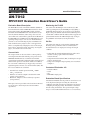
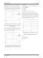
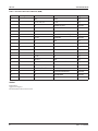
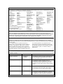
www.fairchildsemi.com
AN-7012
FPF2100/7 Evaluation Board User’s Guide
Contents
Evaluation Board Description.........................................................................................................................2
Contents of Evaluation Kit.........................................................................................................................2
Evaluation Board Specifications.................................................................................................................2
Photo of Evaluation Board.........................................................................................................................3
Evaluation Board Schematic......................................................................................................................3
Setup and Test Procedure..............................................................................................................................4
Test Results................................................................................................................................................4-5
Evaluation Board Bill of Materials (BOM).........................................................................................................6
© 2005 Fairchild Semiconductor
REV. 1.0.0 6/30/05
www.fairchildsemi.com
AN-7012
FPF2100/7 Evaluation Board User’s Guide
Evaluation Board Description
Monitoring the FLAGB
The FPF2100/7 board is an Evaluation Module (EVM) for
the Fairchild Semiconductor FPF2100/1/2/3/4/5/6/7 smart
load switches family. The FPF2100/7 family contains a
0.125Ω P-channel MOSFET with controlled turn-on, fast
turn-off, thermal shutdown, under voltage lock out, and
current limit. The current limit is guaranteed for 200 mA for
the FPF2100/1/2/3 and 400 mA for the FPF2104/5/6/7. The
operating voltage range is 1.8V to 5.5V. The EVM board
provides access for monitoring all pins, and simulates the
fault conditions as they might occur in a real application.
This is accomplished by changing the states of the ON pin,
input voltage, and output current and voltage. See Figure 1
page 2, for a detailed view of the board.
The status of the FLAGB pin can be monitored via TP1
either by probing directly the FLAGB pin or by lighting a
small LED. For this purpose J3 needs to be set as shown in
Figure1. For parts without Auto-Restart the LED stays lit in
current limit conditions until the SW2 switch is toggled. For
parts with Auto-Restart the LED will light only as long as
the pushbutton switch (SW1) is being held down.
Current-Limit
• Using SW2 for manual ON/OFF switching. This can be
used for resetting a part without Auto-Restart
in latch off mode.
• Using External ON terminal (TP4) for driving the ON pin
with an external signal.
• Using J2 for setting the ON pin polarity. Set J2 as shown
in Figure 1.
The output current can be sensed with a current probe by
removing the R3 shunt and soldering a loop across it. The
FPF2100/7 EVM board has a nominal load in normal
operation. By momentarily pushing the SW1 switch the load
switch will be put in an overcurrent condition. In addition,
the overcurrent condition may be triggered by an external
signal through the external. over-current terminal (TP3). The
three load conditions are as follows:
• Nominal load: Normal operation with R1 = 500Ω
and C1 = 0.1µF load.
• Moderate overcurrent: Output is loaded with a 2.2Ω
resistor (J2 in position 2).
• Hard short: Output is connected directly to ground
(J2 in position 1).
Extra space has been provided on the board next to R1 and
C1 for the user to mount any desired load for further
experiments.
2
ON Pin
The status of the ON pin can be monitored through TP2.
Referring to the part number and test conditions, three
mechanisms have been employed to change the ON pin
condition:
Contents of Evaluation Kit
•
•
•
•
Evaluation Board
Cable
CD
FPF2100/7 sample parts
Evaluation Board Specifications
The Evaluation Module has test points for convenient access
to the all pins and jumpers for setting the various load
conditions along with switches for toggling the ON pin and
configuring the ON pin polarity. The board is a stand alone
unit for testing all functions. The operation input voltage
range is 1.8V-5.5V. Board dimensions are 1.75 x 2.35 inches.
REV. 1.0.0 6/30/05
APPLICATION NOTE
AN-7012
Evaluation Board
J1: Current Limit Conditions
1. Hard short (VOUT = 0V)
2. Moderate over current (VOUT = 2 x IOUT)
SW1: Internal OverCurrent Condition
Set J1 for selecting conditions
Sensing Output Current
Remove the R3 = 0Ω and
sense the output current by
soldering a loop across it
TP3: External OverCurrent
Using a function generator, vary
the pulse width to test the TBLANK
and TRESTART functions through
test point TP3
J2: Configuring the ON Pin Polarity
1. Active LO FPF2101 and FPF2105
2. Active HI FPF2100, 02, 03, 04, 06, 07
J3: FLAGB Position
A: Using LED
B: Activating TP1
TP4: External ON
Control the ON/OFF
state of switch by using
a Function Generator
TP1: FLAGB Pin
(First put J3 in position 1 )
SW2: ON/OFF Switch
Toggling SW2 will releases the
Load switch from latch-off mode
TP2: On Pin
Figure 1. FPF2100/7 EVM Board
Evaluation Board Schematic
VIN
VCC
VOUT
1
1
ON/OFF Switch
D1
BZX84C10/SOT
CIN1
10UF
SW2
R9
10K
5
U2B
U3A
5
TP4
3
1
TP2
1
7
6
2
NC7WZ86
R8
50
R10
10K
VCC
J2
GND
3
ON
Vout
4
FLAGB
TP1
R5
2.2
C1
0.1UF
R1
499
FPF210X
NC7WZ32K8
Ext. ON
2
1
C3
0.1UF
Vin
J1
R3
0
U1
1
1
VCC
C4
0.1UF
Q2
FDC645N
J3
VCC
QTLP600CR
D2
Q1
FDC645N
R4
150
R2
ON Pin Polarity
100K
VCC
1
Over-Current
Condition
4
0.1UF
C2
U2A
1
7
SW1
2
3
2
R6
100K
NC7WZ32K8
1
TP3
Ext. OverCurrent
R7
50
Figure 2. FPF2100/7 EVM Board Schematic
REV. 1.0.0 6/30/05
3
AN-7012
APPLICATION NOTE
Evaluation Board Block Diagram
Battery
VIN
VOUT
GND
ON
SW2: ON/OFF switch
TP4: ext. signal
1. Hard
short
FLAGB
2. Moderate
short
ON Pin
SW1
J2: ON pin polarity
TP2 ON pin
test point
LED or TP1
Overcurrent Cond.
Indecator
Ext. signal
TP3
Short Circuit
System
RC Load
(Overcurrent cond.)
Figure 3. FPF2100/7 EVM Board Block Diagram
Setup and Test Procedure
Test Results
The following equipment is recommended for testing:
1. Measuring tBLANK and tRESTART of FPF2100 (Figures 4 to 6)
•
•
•
•
•
This test has been designed to demonstrate the FPF2100
behavior while the output is in a moderate short for 40ms,
170ms, and 180ms. The board setup is described in part 2.0
of this document.
A four-channel oscilloscope
Current probe
One adjustable power supply, 0V-6V@6A
Voltmeter
Function generator with burst function single pulse
The EVM board is a suitable platform for testing the main
electrical characteristics of the FPF2100/7 products. Various
tests such as under voltage lock out, ON input logic voltage,
Current Limit value and all dynamic characteristics of the load
switch can be performed by using two methods for changing
the output, and ON pin condition. The first method is by
changing the SW1 or SW2 switches manually on the board,
and the second by applying an external signal pulse through
TP3 or TP4 for more detailed observation. Here are two
examples of test setup:
Figure 4 shows the FPF2100 is in an overcurrent condition for
40ms. In this case the load switch limits theoutput current to
the Overcurrent Limit value for tBLANK time. Since the short
stays longer than blanking time, the load switch turns off for
tRESTART time and the FLAGB pin activates.
1. Measuring tBLANK and tRESTART value (Figures 4 to 6)
• Power up the board with VIN = 3.3V.
• Remove the current sense resistor (R3) and solder a small
wire across R3 in order to use oscilloscope current probe.
• Put the shunt of J3 in position 2, this will connect the
FLAGB pin to TP1.
• Put the shunt of J1 to position 2 for moderate overcurrent.
• Connect an external pulse from a function generator to
TP3. For better triggering the events on the oscilloscope, a
single burst pulse is recommended.
2. Current Limit Response Time at moderate short (Figure 7)
Power up the board with VIN = 3.3V
Put the shunt of J2 in position 1
Put the SW2 in position LO
Put the shunt of J1 in position 2
Connect an external pulse from a function generator to
TP4. For better triggering the events on the oscilloscope,
a single burst pulse is recommended
• Push down the pushbutton switch (SW1) while pulsing the TP4
•
•
•
•
•
4
Figure 4. tBLANK < Overcurrent = 40ms < tBLANK + tRESTART
Figure 4
Ch1 = External overcurrent signal has been applied to gate
of a NMOS
Ch2 = IOUT (200mA/div)
Ch3 = VOUT
Ch4 = FLAGB
REV. 1.0.0 6/30/05
APPLICATION NOTE
Figure 5 shows the overcurrent condition stays longer than
the tRESTART time. The load switch turns on after tRESTART
time has expired and senses the overcurrent condition again.
The constant current limit will be supplied to the output for
tBLANK. At the end of the second tBLANK, the short was removed
from the line and the load switch is in normal operation.
AN-7012
Figures 5 and 6
Ch1 = External overcurrent signal has been applied to gate
of a NMOS
Ch2 = IOUT (200mA/div)
Ch3 = VOUT
Ch4 = FLAGB
2. Current Limit Response Time Test (Figure 7)
This test has been designed to measure the load switch’s
response time while the output is loaded by a small resistor,
2.2Ω to GND (moderate short). Figure 7 shows response when
the input voltage is connected to 3.3V and a moderate short is
applied to the output while the ON pin is triggered HI. From
the waveforms, it can be seen that the delay between ON pin
triggering and output current is about 27µs.
Figure 5. tBLANK + tRESTART < Overcurrent = 160ms < 2x
tBLANK + tRESTART
Figure 6 shows that the overcurrent condition stays longer than
one cycle of tBLANK + tRESTART. The values of tBLANK and
tRESTART can be measured from channel 2 of this figure, where
tBLANK =10ms and tRESTART =150ms.
Figure 7. Current Limit Response Time Test
Figure 7
Ch1 = VIN=3.3V
Ch2 = IOUT (200mA/div)
Ch3 = VON
Figure 6. 2x tBLANK + tRESTART < Overcurrent = 80ms
REV. 1.0.0 6/30/05
5
AN-7012
APPLICATION NOTE
Table 1. Evaluation Board Bill of Materials (BOM)
Item
Quantity
Reference
Part
Mfg
1
1
CIN1
10UF
Any
2
4
C1, C2, C3, C4
0.1UF
Any
3
1
D1
BZX84C10 SOT
Fairchild
4
1
D2
QTLP600CR
Fairchild
5
1
J1
Dual Jumper 2mm
Any
6
2
J2, J3
Conn Header 2mm Single
Any
7
2
Q1, Q2
FDC645N
Fairchild
8
1
R1
499
Any
9
2
R2, R6
100K
Any
10
1
R3
0
Any
11
1
R4
150
Any
12
1
R5
2.2
Any
13
2
R7, R8
50
Any
14
2
R9, R10
10K
Any
15
1
SW1
Pushbutton-SPST
Any
16
1
SW2
SPDT
Any
17
4
TP1, TP2, TP3, TP4
Test Point
Any
18
1
U1
FPF2100/1/2/3/4/5/6/7
Fairchild
19
1
U2
NC7WZ32K8
Fairchild
20
1
U3
NC7WZ86
Fairchild
Author
Kamil Madoo
Application Engineer
Fairchild Semiconductor International
6
REV. 1.0.0 6/30/05
TRADEMARKS
The following are registered and unregistered trademarks Fairchild Semiconductor owns or is authorized to use and is
not intended to be an exhaustive list of all such trademarks.
ACEx™
FAST®
ActiveArray™
FASTr™
Bottomless™
FPS™
Build it Now™
FRFET™
CoolFET™
GlobalOptoisolator™
CROSSVOLT™ GTO™
DOME™
HiSeC™
EcoSPARK™
I2C™
E2CMOS™
i-Lo™
EnSigna™
ImpliedDisconnect™
FACT™
IntelliMAX™
FACT Quiet Series™
Across the board. Around the world.™
The Power Franchise®
Programmable Active Droop™
ISOPLANAR™
LittleFET™
MICROCOUPLER™
MicroFET™
MicroPak™
MICROWIRE™
MSX™
MSXPro™
OCX™
OCXPro™
OPTOLOGIC®
OPTOPLANAR™
PACMAN™
POP™
Power247™
PowerEdge™
PowerSaver™
PowerTrench®
QFET®
QS™
QT Optoelectronics™
Quiet Series™
RapidConfigure™
RapidConnect™
μSerDes™
SILENT SWITCHER®
SMART START™
SPM™
Stealth™
SuperFET™
SuperSOT™-3
SuperSOT™-6
SuperSOT™-8
SyncFET™
TinyLogic®
TINYOPTO™
TruTranslation™
UHC™
UltraFET®
UniFET™
VCX™
Wire™
DISCLAIMER
FAIRCHILD SEMICONDUCTOR RESERVES THE RIGHT TO MAKE CHANGES WITHOUT FURTHER NOTICE TO ANY
PRODUCTS HEREIN TO IMPROVE RELIABILITY, FUNCTION OR DESIGN. FAIRCHILD DOES NOT ASSUME ANY LIABILITY
ARISING OUT OF THE APPLICATION OR USE OF ANY PRODUCT OR CIRCUIT DESCRIBED HEREIN; NEITHER DOES IT
CONVEY ANY LICENSE UNDER ITS PATENT RIGHTS, NOR THE RIGHTS OF OTHERS.
LIFE SUPPORT POLICY
FAIRCHILD’S PRODUCTS ARE NOT AUTHORIZED FOR USE AS CRITICAL COMPONENTS IN LIFE SUPPORT
DEVICES OR SYSTEMS WITHOUT THE EXPRESS WRITTEN APPROVAL OF FAIRCHILD SEMICONDUCTOR CORPORATION.
As used herein:
2. A critical component is any component of a life
1. Life support devices or systems are devices or
support device or system whose failure to perform can
systems which, (a) are intended for surgical implant into
be reasonably expected to cause the failure of the life
the body, or (b) support or sustain life, or (c) whose
support device or system, or to affect its safety or
failure to perform when properly used in accordance
with instructions for use provided in the labeling, can be
effectiveness.
reasonably expected to result in significant injury to the
user.
PRODUCT STATUS DEFINITIONS
Definition of Terms
Datasheet Identification
Product Status
Definition
Advance Information
Formative or
In Design
This datasheet contains the design specifications for
product development. Specifications may change in
any manner without notice.
Preliminary
First Production
This datasheet contains preliminary data, and
supplementary data will be published at a later date.
Fairchild Semiconductor reserves the right to make
changes at any time without notice in order to improve
design.
No Identification Needed
Full Production
This datasheet contains final specifications. Fairchild
Semiconductor reserves the right to make changes at
any time without notice in order to improve design.
Obsolete
Not In Production
This datasheet contains specifications on a product
that has been discontinued by Fairchild semiconductor.
The datasheet is printed for reference information only.
Rev. I16