1
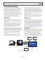
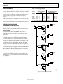
Evaluation Board User Guide
UG-073
One Technology Way • P.O. Box 9106 • Norwood, MA 02062-9106, U.S.A. • Tel: 781.329.4700 • Fax: 781.461.3113 • www.analog.com
Evaluating the AD9114/AD9115/AD9116/AD9117 and
AD9714/AD9715/AD9716/AD9717 DACs
FEATURES
RELATED DOCUMENTS
Full featured evaluation board for the
AD9114/AD9115/AD9116/AD9117 (AD911x) and
AD9714/AD9715/AD9716/AD9717 (AD971x)
Includes options to evaluate
DAC only
DAC and ADL5375 quadrature modulator
DAC and op amp performance
USB interface for configuration
Internal or external power supply regulation
On-board or external clock distribution
Data pattern generator and SPI software interfaces
Data sheets are available for both the AD911x and AD971x
products for product-specific details, including register definitions. The DPG2 user guide is also available for assistance with
vector generation and loading.
EQUIPMENT NEEDED
The AD9114/AD9115/AD9116/AD9117 and AD9714/AD9715/
AD9716/AD9717 data sheets, available at www.analog.com,
should be consulted when using the evaluation board. The
AD971x/AD911x Rev. A evaluation board operates together
with the Data Pattern Generator 2 (DPG2) and the DAC
software suite, including the AD971x/AD911x update.
GENERAL DESCRIPTION
This user guide describes the AD911x and AD971x evaluation
boards, which provide all of the support circuitry required to
operate the AD911x and AD971x in their various modes and
configurations. The application software used to interface with
the devices is also described.
USB 2.0 port, recommended (USB 1.1 compatible)
HSC-DAC-DPG-BZ (DPG2) board
AD9114/AD9115/AD9116/AD9117 or
AD9714/AD9715/AD9716/AD9717 evaluation board
Spectrum analyzer
The CD-ROM provided with the evaluation board includes
the installation program for all necessary software. The install
program can also be downloaded. Both methods install the
DPGDownloader program for loading vectors as well as the
AD971x/AD911x update necessary for SPI communication.
SOFTWARE NEEDED
DAC software suite
AD9717 software update
All documents and software tools are available online at
www.analog.com/dpg.
Please see the last page for an important warning and disclaimers.
Rev. 0 | Page 1 of 12
UG-073
Evaluation Board User Guide
TABLE OF CONTENTS
Features .............................................................................................. 1 Clock Signals ..................................................................................3 Equipment Needed ........................................................................... 1 Input Signals...................................................................................3 Software Needed ............................................................................... 1 Output Signals ...............................................................................4 Related Documents ...................................................................... 1 Default Operation and Jumper Selection Settings ....................4 General Description ......................................................................... 1 Evaluation Board Software: Quick Start Procedures ....................7 Revision History ............................................................................... 2 Configuring the Board .................................................................7 Evaluation Board Hardware ............................................................ 3 Using the Software for Testing.....................................................7 Power Supplies .............................................................................. 3 ESD Caution................................................................................ 12 REVISION HISTORY
3/10—Revision 0: Initial Version
Rev. 0 | Page 2 of 12
Evaluation Board User Guide
UG-073
EVALUATION BOARD HARDWARE
The AD911x and AD971x evaluation boards provide all of the
support circuitry required to operate the AD911x and AD971x
in their various modes and configurations. Figure 1 shows the
typical bench characterization setup used to evaluate the ac
performance of the AD911x and AD971x. It is critical that
the signal source used for the clock have very low phase noise
(<1 ps rms jitter) to realize the optimum performance of the signal
chain. A low noise and low distortion spectrum analyzer is also
necessary to evaluate the analog output correctly.
TP13/TP8 (DVDD), with grounds at TP6, TP14, TP23, TP4,
and TP9. All voltages should show a reading of around 3.3 V
with the factory default jumper settings as mentioned. These
voltages can be changed to 1.8 V by switching JP22, JP26, JP29,
JP88, and JP89 to shunt Pin 2 and Pin 3. Alternatively, external
power supplies can be used to supply the AD911x or AD971x
and its supporting circuitry.
See the Evaluation Board Software: Quick Start Procedures
section to get started.
When using the ADL5375 modulator on board for testing
combined performance, a 5 V power supply must be connected
to the ADL5375 POWER (TP16) with a ground at TP21 for
that part.
POWER SUPPLIES
CLOCK SIGNALS
This evaluation board can be powered via the USB interface or
with an external 5 V power supply. By default, the USB powered
option is selected.
When connecting the clock source, use clean signal generators
with low phase noise, such as Rohde & Schwarz SMA or HP8644B
signal generators or the equivalent. Use a 1 m, shielded, RG-58,
50 Ω coaxial cable for making connections to the evaluation
board. Enter the desired frequency and amplitude (refer to the
specifications in the AD9114/AD9115/AD9116/AD9117 or
AD9714/AD9715/AD9716/AD9717 data sheets). The evaluation
board is set up to be clocked from an external source and the
internal clock distribution IC AD9512.
By default, on-board voltage regulators are selected to supply
power to the AD911x and AD971x as well as its supporting
circuitry. These regulators can be configured to supply 1.8 V
or 3.3 V to the different power supply pins of the AD911x or
AD971x, with 3.3 V selected by default.
The current from each of the power pins can be tested by using
JP54 (AVDD), JP6/JP78 (CVDD), and JP10/JP15 (DVDD). The
nominal values of the AVDD, CVDD, and DVDD currents for
the AD971x board are 9.5 mA, 2.8 mA, and 13.1 mA, respectively. For the AD911x board, the nominal AVDD, CVDD,
and DVDD currents are 50.3 mA, 2.8 mA, and 12.1 mA,
respectively.
Voltages can be checked at each pin at the corresponding
test points listed; TP5 (AVDD), TP12/TP24 (CVDD), and
INPUT SIGNALS
The 14-bit wide data bus is intended to be driven by the DPG2
evaluation platform directly. The DPG2 is capable of driving a
16-bit wide bus. Because the AD911x and AD971x are 14-bit
devices, the DPGDownloader software compensates for the
different resolution parts by automatically bit shifting the
patterns generated to align properly with the DAC. The resolution for patterns needed is controllable through the software.
DAC CLOCK
SOURCE
DPG2
2 × DATA CLOCK
I AND Q DATA 14
DATA CLOCK
AD911x/AD971x
EVALUATION BOARD
USB
SPECTRUM
ANALYZER
Figure 1. Evaluation Board Connection
Rev. 0 | Page 3 of 12
08698-001
USB
AQM LO CLOCK
SOURCE
(OPTIONAL)
UG-073
Evaluation Board User Guide
OUTPUT SIGNALS
Table 1. Power Supply Jumpers
The evaluation board provides the option to evaluate the analog
outputs directly from the DAC (default) or the output of the RF
quadrature modulator ADL5375, driven by the DAC. The DAC
output can also be evaluated as a single-ended buffered output
with an op amp for applications requiring low frequency
signals.
The evaluation board also provides access on a connector to the
auxiliary DAC outputs. Finally, the evaluation board provides a
data clock output intended to synchronize the DPG2 evaluation
board with the AD911x or AD971x internal clock.
DEFAULT OPERATION AND
JUMPER SELECTION SETTINGS
Power
Supply
Output
CVDD
DVDD
AVDD
DVDDX
CVDDX
Jumper Position for
Voltage Regulation
Level1
3.3 V Default
JP22 1−2
JP26 1−2
JP29 1−2
JP88 1−2
JP89 1−2
1.8 V
JP22 2−3
JP26 2−3
JP29 2−3
JP88 2−3
JP89 2−3
Jumper Position for
Internally or Externally
Regulated Voltage1
Internal Default
JP6 2−3
JP10 2−3
JP54 2−3
JP15 2−3
JP78 2−3
External
JP6 1−2
JP10 1−2
JP54 1−2
JP15 1−2
JP78 1−2
1
1–2 means to place the jumper between Pin 1 and Pin 2; 2−3 means to place
the jumper between Pin 2 and Pin 3.
This section explains the default and optional settings or modes
allowed on the AD911x and AD971x Rev. A evaluation boards.
FILTER
CVDD
FILTER
DVDD
FILTER
AVDD
FILTER
DVDD
FILTER
CVDD
CVDD_IN
USB
2
ADP3334A
1.8V
3
2
Power Circuitry
JP22
Connect the USB cable to the USB Mini-B P1 connector.
The USB connections provide the power supply to the evaluation board.
1
JP6
1
3.3V
DVDD_IN
By default, the evaluation board provides on-board regulators to
supply the AD911x or AD971x (DVDD, CVDD, and AVDD)
as well as auxiliary circuits, such as the level translator (DVDDX)
and the clock distribution chip (CVDDX). These regulators can be
set up to regulate the primary voltage to 3.3 V or 1.8 V, depending
on the setting of the 2-position jumpers: JP22, JP26, JP29, JP88,
and JP89 (see Figure 2). Alternatively, external power supplies can
supply all the on-board components. The choice between internally
or externally regulated power supplies can be done individually per
power supply by two-position jumpers: JP6, JP10, JP54, JP15, and
JP78 (see Figure 2). These regulated voltages are then connected to
on-board filters to be used by the components on board.
Note that, for simplicity, it is recommended to use the USBpowered option combined with the on-board regulation. The
choice of 3.3 V or 1.8 V regulation is left to the user depending
on application.
2
ADP3334A
1.8V
3
2
JP26
1
JP10
1
3.3V
AVDD_IN
2
ADP3334A
1.8V
3
2
JP29
1
JP54
1
3.3V
DVDDX_IN
2
ADP3334A
1.8V
3
2
JP88
1
JP15
1
3.3V
CVDDX_IN
2
1.8V
3
2
JP89
1
JP78
1
3.3V
Figure 2. Power Supply Jumpers Schematic
Rev. 0 | Page 4 of 12
08698-002
ADP3334A
Evaluation Board User Guide
UG-073
Clock Circuitry
By default, the evaluation board is set up to have a clock
input on J10 that is distributed on the evaluation board via the
clock distribution IC AD9512. One output of the AD9512 is
configured to be used as a DAC clock input and a data clock
input for the AD911x or AD971x while another one is intended
to the data generation synchronization of the DPG2. For proper
operation, the clock sent to the DPG2 evaluation board should
be configured to be twice the frequency of the clock sent to the
DUT (see Figure 4).
The evaluation board can also be set up to use an on-board
oscillator or a clock without using the clock distribution IC by
changing jumper settings. This set up cannot be used with the
DPG2 as it requires a data pattern generation board capable of
synchronizing to both edges of the clock input.
Table 2. Clock Jumpers
Clock Source
DAC Clock Input
DAC Data Clock Input
DPG2 Clock Output
S5
J10
R64
R65
R66
R67
R34
R110
R122
External Clock and
AD9512 Default
OUT0 from AD9512
OUT0 from AD9512
OUT2 from AD9512
–
Clock input
On
On
Off
On
On
Off
On1
On the evaluation board, three jumpers for each DAC select the
configuration and maximum DAC current as shown in Table 3.
Table 3. DAC Current Full-Scale Jumpers
DACI
Jumper
Setting
JP9 On
JP8 Off
JP7 Off
JP9 Off
JP8 On
JP7 Off
JP9 Off
JP8 Off
JP7 On
JP9 Off
JP8 Off
JP7 Off
DACQ
Full-Scale Current
AD971x : 4 mA
AD911x: 20 mA
AD971x : 2 mA
AD911x: 16 mA
AD971x : 1 mA
AD911x: 8 mA
AD971x:1 to 4 mA
AD911x: 8 to 20 mA
depending on IRSET
register value
Jumper
Setting
JP20 On
JP16 Off
JP21 Off
JP20 Off
JP16 On
JP21 Off
JP20 Off
JP16 Off
JP21 On
JP20 Off
JP16 Off
JP21 Off
Full-Scale Current
AD971x : 4 mA
AD911x: 20 mA
AD971x : 2 mA
AD911x: 16mA
AD971x : 1 mA
AD911x: 8 mA
AD971x:1 to 4 mA
AD911x: 8 to 2 mA
depending on
QRSET register value
Auxiliary DAC Outputs
External Clock
External clock
External clock
External clock
Clock input
–
On
Off
On
On
On
On
On
1
Required for the AD9512.
DAC Full-Scale Adjust/Auxiliary DAC Output
The AD911x and AD971x full-scale current output can be
adjusted by changing the I and Q RSET resistor values. These
resistors can be either external or internal to the AD911x or
AD971x (see the AD9114/AD9115/AD9116/AD9117 or
AD9714/ AD9715/AD9716/AD9717 data sheets.)
If the AD911x or AD971x is configured to use the internal xRSET
resistors, the evaluation board can be configured to output the
auxiliary DACs voltages on SMA connectors (see Table 4).
Table 4. Auxiliary DAC Configuration Jumpers
Jumper Setting
JP9 Off; JP8 Off
JP7 Off; JP12 On
JP90 On
JP20 Off; JP16 Off
JP21 Off; JP77 On
JP91 On
Additional Setting
R97 < 2 kΩ
S9 voltage = AUXI current × R97
R100 < 2 kΩ
S10 voltage = AUXQ current × R100
The main use of the AUX DACs is to provide a simple way to
perform LO suppression so that it does not interfere with the
performance of the part, especially at lower IF frequencies. A
more detailed description and instructions on how to calibrate
the AUX DACs appropriately are found in the SPI section.
Evaluation Board Hardware Setup for Auxiliary DACs
Follow these steps to set up the evaluation board hardware for
auxiliary DACs:
By default, the AD911x and AD971x are configured to use
external resistors to set the DAC full-scale current. By default,
the AD971x jumpers are populated to have both DACs set for
a 2 mA output current while the AD911x DACs are set for a
20 mA output. Alternatively, the on-chip IRSET and QRSET
resistors can be used by setting the corresponding enable bit
and xRSET register value in the SPI software (see Section VI in
the SPI section).
1.
2.
3.
Enable internal bias resistors and remove external jumpers.
Leave JP3, JP25, JP27, and JP28 unsoldered.
Connect the AUX DACs with a fly wire as follows:
• TP1 and TP44 (AUX1 DAC)
• TP17 and TP45 (AUX2 DAC)
Analog Outputs
The evaluation board provides the option to evaluate the DAC
analog output in a variety of ways: direct DAC output (default),
buffered single-ended output, or high frequency output via
quadrature modulator. Changing the setting of a few jumpers
allows choosing among these options.
Rev. 0 | Page 5 of 12
UG-073
Evaluation Board User Guide
Output Loads
Table 5. Output Configuration
DAC Output
Default1
On
On
On
S3 = S8 = GND
0Ω
Single-Ended
Buffered1
On
On
On
S3 = S8 = GND
Off
Quadrature
Modulator
On
On
On
S3 = S8 = GND
Off
The AD911x and AD971x provide output current. These
currents are converted to voltages with loading resistors. By
default, the output loads are provided by on-board resistors.
Alternatively, on-chip resistors can be used. Jumper setting
should be implemented for the option chosen.
453 Ω
Off
453 Ω
Off
R111, R112
Off
JP55, JP56,
JP76, JP82
J6
Off
On-Off or
Off-On
Off
Off
500 Ω
(AD971x)/
50 Ω (AD911x)
Clock input
Resistors
R57, R50
JP32, JP33, JP34,
JP35
RLOAD: Load
Resistor
NC
NC
J7
NC
NC
TP16
NC
NC
TP21
NC
NC
Clock
Source
R15, R16
R11, R38
R9, R1242
R95, R96,
R155, R156
R57, R50
R13, R14,
R52, R53
On
Modulator LO
input
Modulator
output
5 V power
(modulator)
GND
(modulator)
1
NC = no connect.
Board default setup allows single-ended views of IOUTB (S4) and QOUTB (S6).
2
Common-Mode Output Setting
Table 7. DAC Output Load Configuration
On-Board Load
Resistor Default
On
Off
On-Chip Load
Resistors
Off
On
R57 for IDAC
R50 for QDAC
62.5 Ω for AD911x
500 Ω for AD971x
In the load mode configuration proposed, the output voltage for
each DAC can be calculated using the formula:
VOUTPUT = RLOAD × IOUT
Pin Mode
The AD971x and AD911x evaluation boards have the capability
to function in pin mode. This bypasses the USB SPI control and
allows users who operate with less intricate systems to control
the board in a much simpler fashion. This mode is only useful
when a versatile and full-featured SPI is not needed or is
unavailable.
The common mode of the DAC analog outputs is set by default
to be 0 V (R15 and R16 = 0 Ω). It can be changed to use internal
or external common-mode resistors. The AD911x and AD971x
operate safely only within a certain common-mode voltage
range. Refer to the product data sheet to understand these limits.
Change the following hardware settings to operate in pin mode:
Table 6. DAC Common-Mode Configuration
When the system is set into this control mode, all SPI bits
remain in their default states and certain pins are redefined as
controls. Due to the minimum control provided by this setup,
the internal resistances cannot be set and, therefore, only
external resistor options are available to change the output
current. These are set by the JP7, JP8, JP9, JP16, JP17, and JP20
pin shunt jumpers, as shown in Table 3.
Resistors
R15, R16
R22, R154
R20, R26
R19, R21
RC: CommonMode Resistor
=0V
On
Off
On
Off
0Ω
Common Mode
With External
With Internal
Resistors
Resistors
Off
Off
On
Off
Off
Off
On
On
R22 for IDAC
IRCM for IDAC
R154 for QDAC
QRCM for QDAC
In the common-mode configuration proposed, the commonmode voltage for each DAC can be calculated using the formula
VCM = RC × Full-scale current
1.
2.
Populate JP11 (RESET HIGH). Note that R44, R45, and
R103 remain unpopulated
Pull the TP18, TP19, TP20 test points to high or low states
to control the mode selections.
The TP18, TP19, and TP20 test points control the SPI data
input (SDIO), the SPI clock (SCLK), and the SPI chip select
(CSB), respectively. The SDIO control changes the state of
the FORMAT bit (Register 0x02, Bit[7] to either binary (LO)
or twos complement (HI). The SCLK control overrides the
CLKMODE bits (Register 0x14, Bits[1:0]) to be either the
clock in Delay2 of 180° (LO) or the clock in Delay1 of 90°
(HI). The CSB control alters the power-down (PWRDN) bit
(Register 0x01, Bit [5]) to be either powered-up (LO) or
powered-down (HI). All other controls are not implemented
or altered from the default settings, as listed in the SPI Register
Descriptions section of the product data sheets.
Rev. 0 | Page 6 of 12
Evaluation Board User Guide
UG-073
EVALUATION BOARD SOFTWARE: QUICK START PROCEDURES
This section provides quick start procedures for using the AD911x
or AD971x. Both the default and optional settings are described.
CONFIGURING THE BOARD
Before using the software for testing, configure the evaluation
board as follows:
2.
3.
Connect the evaluation board to the DPG2 evaluation
board.
Connect the AD911x or AD971x evaluation board to the
PC with a USB cable (ConnectorXP2 USB/BRD PWR).
The LED XD1 should turn on. If it does not turn on, refer
to the Power Circuitry section and configure the board
with the default setting.
Connect a clean signal generator with low phase noise to
provide an input signal to the clock distribution source
input, J10. Use a 1 m, shielded, RG-58, 50 Ω coaxial cable
to connect the signal generator.
08698-004
1.
Figure 4. AD9512 Clock Divider Setting
5.
USING THE SOFTWARE FOR TESTING
Set Up the DPG2 Software
After configuring the board, set up the DPG2 by following
these steps:
1.
Open DPGDownloader (Start > Programs > Analog
Devices > DPG > DPGDownloader).
The program should automatically recognize and display
the evaluation board, such as the AD9717 used in this
example, in the drop-down menu for the Evaluation
Board, as shown in Figure 3
Select LVCMOS-3.3V (DCO) for the Port Configuration
as the DPG2 data clock input, also shown in Figure 3.
08698-003
2.
6.
See Figure 5 for the appropriate settings.
4.
Open the AD911x or AD971x SPI software (Start >
Programs > Analog Devices > AD9717 > AD971x SPI).
Select the clock dividers for the data clock going to the
DPG2, and for the clock going to the DAC. The divider
ratio for the DAC clock should be double the ratio for the
data clock as shown in Figure 4.
08698-005
Figure 3. DPG2 Board Configuration
3.
The clock going to the DAC should be no greater than
125 MHz. When the AD9512 configuration is complete,
verify the clock frequency output to the DPG2 in
Figure 3. The frequency displayed represents the frequency
of the clock sent to the DPG2. It should be no greater than
250 MHz.
In the DPG2 window (see Figure 5), select Add Generated
Waveform, and then select Single Tone. A single tone
panel is added to the vector list. Enter a clock frequency of
125 MHz for Data Clock Frequency.
Note that this frequency is half of the frequency in Figure 3
for Data Clock Frequency as the data clock sent to the
DPG2 is twice the rate of the DAC. However, the vector
generation is done using the DAC clock (data clock/2) (see
Figure 4).
Make the following entries:
• Enter 10 MHz as the Desired Frequency of the tone.
• The DAC Resolution should be set at the resolution
of the IC selected (14 bits for the AD9717 and
AD9117, 12 bits for the AD9716 and AD9116, and
so on).
• Keep Record Length at 16384
• The digital scaling back of the tone can be done by
changing the Amplitude (defaults to 0 dB).
• Ensure that Unsigned Data and Generate Complex
Data (I & Q) are selected.
Figure 5. Single Tone Generation
7.
Rev. 0 | Page 7 of 12
In the lower portion of the screen, select 1I / 1Q: Single
Tone as the Data Vector, choosing the appropriate inphase and quadrature data for the I and Q vectors, shown
in Figure 6. The other options can be left at their default.
UG-073
Evaluation Board User Guide
08698-006
Once the setting of the part is selected, press the run button,
at the top left side of the SPI software window.
Figure 6. Loading DPG2 Vectors
8.
After the DPG2 is correctly setup, click the Download
button ( ) in the lower right, then the Play button ( )
to begin vector playback into the AD911x or AD971x.
Section I
Evaluation Board Signal Chains
This evaluation board allows for performance to be assessed at
both the DAC output as well as the DAC and modulator signal
chain output. To include the modulator into the path, certain
jumper settings and component values must be changed. The
necessary changes are listed below as a quick reference for using
the modulator and the default settings of the DAC that will
change. Table 5 can also be referred to for further help.
Default Board Setup for Measuring DAC
The DAC settings listed are the factory defaults, however they
can be referenced when changing the board back from using the
modulator to assessing the DAC only. These values are based on
using an output current of 2 mA for the AD971x and 20 mA for
the AD911x boards.
•
•
•
•
•
J55, J56, J76, and J82 are unsoldered.
R95, R96, R155, and R156 are populated with 0 Ω.
R50 and R57 are populated with 453 Ω.
R111 and R112 are unpopulated.
R13, R14, R22, R35, R52, R53, R55, and R154 (found on
back) are unpopulated.
Evaluation Board Setup for Testing DAC and Modulator
Connect a 5 V power supply to TP16 (PWR) and TP21 (GND)
to run the modulator.
•
•
•
•
•
For complete descriptions of each SPI register, see the AD9114/
AD9115/AD9116/AD9117 or AD9714/AD9715/AD9716/
AD9717 data sheet. Note that the software graphics shown
within this user guide may not be an exact match to your
software.
J55, J56, J76, and J82 are soldered.
R50, R57, R95, R96, R155, and R156 are unpopulated.
R13, R14, R52, and R53 (found on back) are populated
with 500 Ω (AD971x) or 50 Ω (AD911x).
R35 and R55 are populated with 100 kΩ (AD971x) or
10 kΩ (AD911x).
R22 and R154 are populated with 0 Ω.
This section of the SPI configures various settings for the
AD9512 clock distribution chip as follow:
•
•
•
DAC clock divide ratio and phase offset
Data clock divide ratio and phase offset
Data clock full scale delay and fine delay
Section II
This section of the SPI software configures SPI communication
and provides the following options:
•
•
•
LSB or MSB first
1 byte or 2 byte transmission
Software reset
Section III
This section of the SPI provides the following power configuration
and status information on the AD911x or AD971x:
•
•
•
•
•
•
Enable/disable digital LDO
LDO status
AD911x or AD971x power down
I or Q DAC sleep
Internal or external voltage reference
Clock to I or Q on/off
Section IV
This section of the SPI software defines the data interface to the
DUT as follows:
•
•
•
•
Data is twos-complement or binary
Data on bus is I first or Q first
Rising edge of data clock is used to sample I or Q data
Allows DCLKIO to be input and output simultaneously
Section V
Note that to set the DAC output current when using the modulator, either the external shunt jumpers may be populated for
the desired setting, or the internal bias resistors may be set by
enabling and setting the appropriate codes in the SPI. Settings
for the external shunts are listed in the Analog Outputs section.
To use the internal bias resistors, see the SPI section for
information on the settings that must be changed to fully enable
and set these resistors.
SPI Software
The SPI software consists of various small sections, which are
described here as they relate to the evaluation board.
This section of the SPI configures the DCLKIO pin of the DUT
as follows:
•
•
DCLKIO input or output
DCLKIO output is regular or double strength
Section VI
This section of the SPI software configures xRSET options and
internal VREF voltage as follows:
•
•
•
Rev. 0 | Page 8 of 12
Enable/disable IRSET and QRSET
Set internal IRSET and QRSET values
Set internal voltage reference value
,
Evaluation Board User Guide
UG-073
Section VII
Section IX
•
This section of the SPI software configures the I and Q auxiliary
DACs as follows:
•
•
•
This section of the SPI configures common-mode options
and xDAC analog gains as follows:
Enable/disable IRCM and QRCM
Set internal IRCM and QRCM values
Set internal IGAIN and QGAIN values
Section VIII
Enable/disable I/Q auxiliary DAC
Set I/Q auxiliary DAC code
Section X
This section of the SPI configures the INL/DNL calibration of
the main DAC.
This section of the SPI configures the retimer of the DUT as
follows:
Automatic or manual retimer selection
Readback or setting of retimer phase
SECTION II
SECTION VI
SECTION III
SECTION IX
SECTION VII
SECTION IV
SECTION VIII
SECTION X
SECTION V
SECTION I
08698-007
•
•
•
•
Figure 7. Default SPI Front Panel Settings
Rev. 0 | Page 9 of 12
UG-073
Evaluation Board User Guide
AD9512 Clock Chip Setup
Using the AUX DACs For LO Suppression
To use the clock distribution chip provided on the evaluation
board, access the control settings found on the front panel
of the SPI front panel shown in Figure 7 and described in
Section I. This allows the single clock source used to be divided
down and to feed separate clocks to the data and DAC, which
helps minimize the number of sources necessary to run the
evaluation board.
To completely suppress the LO when using the modulator in the
signal chain, automatic VIs can be used to sweep the codes for
all of the range and offset settings of the DAC. Section IX of
Figure 7 contains all of the controls for the AUX DACs, which
must be enabled through the SPI before use. The AX1RNG/
AX2RNG controls determine the swing voltage of the DAC to
provide a greater or lesser sweep range. Similarly, the AX1ZE/
AX2ZE settings control the maximum voltage (offset) attainable
in the swing. The code settings (AX1D/AX2D) determine
where along the swing the DAC is set. Depending on the range
and offset settings, this determines what the output voltage for
the AUX DAC will be to calibrate and suppress the LO properly.
For testing purposes in this user guide, a clock source of
250 MHz was used with an fDAC of 125 MHz. In order to
interleave the data, the data clock ratio needs to be twice the
frequency of the DAC to allow for proper I and Q lineup.
To achieve this, the DACCLK divide ratio is set to 2 and the
DATACLK divide ratio is 1. With these settings, the clock chip
should work properly and the data clock can be checked by
probing at S11 SMA with an oscilloscope. For better phase noise
performance, increase the clock signal source frequency and
choose higher divide ratios for the data and DAC clocks to
achieve the desired clock rates.
Using Internal Bias Resistors
When using the internal bias resistors, the RSET resistors must be
enabled and the on-board jumpers removed from the output
current jumpers (see Table 3). To enable the resistors through
the VI, press the buttons labeled IRS_EN and QRS_EN (see
Section VI) of the VI front panel in Figure 7. The default IRSET
and QRSET code is set to 0, which corresponds to a 2 mA
output current for the AD971x.
When testing the AD911x, change the values for the IRSET
and QRSET codes to 32, which correspond to a 20 mA output
current appropriate for this board. Changing this code as
detailed in the SPI Register section of the data sheet allows the
user to change the output current being set with these internal
resistors, much like manually changing the jumpers
on the board.
Using the DAC Fine Gain Adjustment
To obtain finer adjustments in the DAC gain than those provided through the full-scale adjustment resistors, the I and Q
DAC gain registers can be implemented. The gain adjustment
must be enabled and set in Figure 7 (see Section VII). In addition, the common-mode level of the channel output stages
can be changed in this section by setting the IRCML/QRCML
controls that alter the value of the on-chip IRSET/QRSET. The four
different internal resistor options and the corresponding SPI
codes, which can be found in the data sheet, are shown in
Table 8.
Table 8. Internal Resistor Options and SPI Code
IRSET/QRSET Value
16 kΩ
32 kΩ
8 kΩ
16 kΩ
Better resolution for the DAC is attainable by decreasing the
voltage swing, or range, of the part. The offset determines what
the maximum voltage of that range will be set to when the DAC
code is set to maximum (1023). The minimum voltage of that
range can be determined by taking the corresponding offset
voltage value and subtracting the range voltage value from it;
this is the voltage that is output when the DAC code is set to the
minimum (0).
If the DAC code vs. LO amplitude values of a sweep for a
specific range and offset are plotted, there should be a visible
notch trend. The DAC code at the minimum of the graph shows
the optimal setting for the DAC to suppress the LO. The output
voltage for those settings is shown on the VI and is helpful in
determining if the range and offset settings are optimum for the
AUX DAC’s maximum resolution at that voltage. If the code
falls on a voltage that can be achieved using a smaller range, and
sometimes needing a change in offset to achieve the proper
range placement, this provides an even better performance and
further suppression of the LO for performance benefits.
Sweep one DAC at a time while the other is held constant,
normally around 0.5 V as a starting value. Once the optimized
settings are found for the first sweep, hold that AUX DAC at
the determined settings and repeat the sweep technique for the
second AUX DAC to find its optimal setting. Sometimes a
second round of sweeps are necessary to get better LO suppression once the DACs have been initially optimized and even
better performance can be attained.
Table 9. AUX DAC Range Configuration
Code
0
1
2
3
Code
000000 (default)
011111
100000
111111
Rev. 0 | Page 10 of 12
AXIRNG/AX2RNG
Voltage
2.0 V
1.5 V
1.0 V
.5 V
Code
0
1
2
3
4
AXIZE/AX2ZE
Voltage
1.0 V
1.5 V
2.0 V
2.5 V
2.9 V
Evaluation Board User Guide
UG-073
above. If not, try resoldering the jumpers and test again to make
sure there was not a problem with the previous connection.
Troubleshooting
This section lists items to check and practices to use when
debugging any unexpected performance of a board. It also
provides information on how to check for proper operation
when using the modulator in the signal chain.
Single Tone Test
If unexpected results occur
•
•
•
•
•
•
Reset the part (SW1) and rerun the SPI software.
Sync/reset the clock (SW2) when using the clock chip.
Check the voltage at TP30 (COREVDD), which should be
1.75 V.
Check the voltage at TP3 (VREF), which should be 1.0 V.
Probe S11 (DATACLK) to be sure that the DAC is properly
receiving data and that a clock signal is present. This signal
can also be probed at R64 near the part on-board (should
be unsoldered from initial setup instructions).
When using the modulator, check to make sure the commonmode voltage is 0.5 V at the input of the modulator by probing
at R24 or R61 for the I or Q channels, respectively.
To create a single tone signal in the program
1.
2.
3.
4.
5.
Select Add Generated Waveform and choose Single Tone
from the drop-down menu. An item then appears in the
downloader window.
Input the fDAC as the Sample Rate and enter 20 MHz for
Desired Frequency. The DAC Resolution value is 14 bits,
Amplitude of 0dB and Record Length is 16384, as shown
in Figure 8.
Check the boxes next to Unsigned Data and Generate
Complex Data (I&Q).
In the I Data Vector and Q Data Vector drop-down
menus, choose the corresponding vectors from the list.
Press the download button ( ) and once completed, press
the run button (
) to complete the load.
08698-008
If the common-mode voltage is not as expected, unplug the
board and check the resistances at R13, R14, R52, and R53 for
the correct values of the particular board. If a proper reading is
not present, unsolder J13, J14, J19, and J23, which removes the
resistors from the parallel connection with 1 kΩ/100 Ω at the
input of the modulator to measure the individual resistances of
those components. Check if the resistance values are still
incorrect and if so, change out for the appropriate values listed
In this example, a clock signal is sent to the board through the
clock distribution chip while data is input from the DPG2 and
observed at the DAC output. A 20 MHz single tone is created
and loaded through the DPGDownloader program and sent to
the board.
Figure 8. DPGDownloader
Rev. 0 | Page 11 of 12
UG-073
Evaluation Board User Guide
when debugging. After the DPG2 and SPI software setups are
completed and run, Figure 9 shows the spectrum that should be
observed on the analyzer.
With a clock signal source of 250 MHz, the SPI DATACLK
divide ratio is set to 2 (fDAC = 125 MHz) and the DATACLK
divide ratio is set to 1 (fDATA = 250 MHz). These settings, which
are due to the interleaved data input format, allow the data to be
properly allocated to each DAC.
The fundamental is present at about 20 MHz and the folded
image (fDAC – fOUT) is also visible, however it is easily filtered
with a low-pass filter before modulation.
Set these settings in the SPI software front panel and then select
Run. The readback for the SPI software is shown along the
right-hand side of the window and can be checked for accuracy
REF –8dBm
#PEAK
LOG
10
dB/
#ATTEN 24dB
1
2
EXT REF
DC COUPLED
MARKER
1
2
VBW 30kHz
TRACE
(1)
(1)
TYPE
FREQ
FREQ
STOP 130.00MHz
SWEEP 174.2ms (601 PTS)
X AXIS
19.93MHz
105.08MHz
AMPLITUDE
–16.25dBm
–33.15dBm
08698-009
LG AV
20
W1 S2
START 0Hz
#RES BW 30kHz
Figure 9. DAC Output Spectrum
ESD CAUTION
Evaluation boards are only intended for device evaluation and not for production purposes. Evaluation boards are supplied “as is” and without warranties of any kind, express,
implied, or statutory including, but not limited to, any implied warranty of merchantability or fitness for a particular purpose. No license is granted by implication or otherwise under
any patents or other intellectual property by application or use of evaluation boards. Information furnished by Analog Devices is believed to be accurate and reliable. However, no
responsibility is assumed by Analog Devices for its use, nor for any infringements of patents or other rights of third parties that may result from its use. Analog Devices reserves the
right to change devices or specifications at any time without notice. Trademarks and registered trademarks are the property of their respective owners. Evaluation boards are not
authorized to be used in life support devices or systems.
©2010 Analog Devices, Inc. All rights reserved. Trademarks and
registered trademarks are the property of their respective owners.
UG08698-0-3/10(0)
Rev. 0 | Page 12 of 12