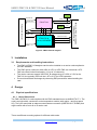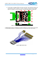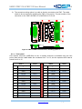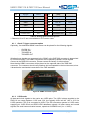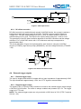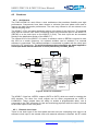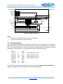
1
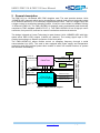
UM012 FMC116 & FMC112 User Manual r1.7 FMC116/FMC112 User Manual 4DSP LLC. USA Email: [email protected] This document is the property of 4DSP LLC and may not be copied or communicated to a third party without the written permission of 4DSP LLC UM012 www.4dsp.com © 4DSP LLC 2015 page 1 of 29 UM012 FMC116 & FMC112 User Manual r1.7 Revision History Date Revision Revision 2012-03-05 Draft 0.1 2012-03-16 Review 0.2 2012-03-23 Release 1.0 2012-08-31 Mentioned that the analog inputs are inverted by the input circuit. 1.1 2013-03-01 VADJ range revised 1.2 2013-06-03 Added a cable label in 4.1.2 1.3 2014-03-06 Changed external clock and reference input power level 1.4 2014-04-11 Revised some descriptions and fixed typos 1.5 2014-12-03 Clarified the op amp used in the front-end circuit. 1.6 2015-02-25 Revised some descriptions and fixed typos 1.7 UM012 www.4dsp.com page 2 of 29 UM012 FMC116 & FMC112 User Manual r1.7 Table of Contents 1 2 3 4 5 6 Acronyms and related documents ............................................................................. 5 1.1 Acronyms ................................................................................................................ 5 1.2 Related Documents ................................................................................................. 5 General description ..................................................................................................... 6 Installation ................................................................................................................... 7 3.1 Requirements and handling instructions .................................................................. 7 Design .......................................................................................................................... 7 4.1 Physical specifications ............................................................................................ 7 4.1.1 Board Dimensions ............................................................................................ 7 4.1.2 Front panel ....................................................................................................... 9 4.1.1 Clock / Trigger connector option ......................................................................10 4.1.2 LVDS mode.....................................................................................................10 4.1.1 EEPROM ........................................................................................................11 4.1.1 Stacked FMC ..................................................................................................11 4.1.2 JTAG...............................................................................................................11 4.2 Main characteristics................................................................................................11 4.3 Analog input channels ............................................................................................12 4.3.1 ADC driver ......................................................................................................12 4.3.2 DC offset correction ........................................................................................13 4.4 External trigger signals ...........................................................................................13 4.4.1 External trigger input .......................................................................................13 4.4.2 External trigger output .....................................................................................13 4.5 Clock tree ...............................................................................................................14 4.5.1 Architecture .....................................................................................................14 4.5.1 External clock input .........................................................................................14 4.5.2 External clock output .......................................................................................15 4.5.3 PLL design ......................................................................................................15 4.6 Power supply..........................................................................................................15 Controlling the FMC116/FMC112 ...............................................................................16 5.1 Control Architecture................................................................................................16 5.2 SPI Programming ...................................................................................................17 5.3 Guidelines for controlling the clock tree ..................................................................19 5.4 Guidelines for controlling the ADCs ........................................................................19 5.5 Guidelines for ADC offset control ...........................................................................19 5.6 Guidelines for controlling onboard monitoring.........................................................20 Environment................................................................................................................21 6.1 Temperature ..........................................................................................................21 6.2 Cooling ...................................................................................................................21 6.2.1 Convection cooling ..........................................................................................21 6.2.1 Conduction cooling ..........................................................................................21 UM012 www.4dsp.com page 3 of 29 UM012 FMC116 & FMC112 User Manual r1.7 7 Safety...........................................................................................................................22 8 EMC .............................................................................................................................22 9 Warranty ......................................................................................................................22 Appendix A Pin-out FMC116/FMC112 ...............................................................................23 Appendix B CPLD Register map .......................................................................................28 UM012 www.4dsp.com page 4 of 29 UM012 FMC116 & FMC112 User Manual r1.7 1 Acronyms and related documents 1.1 Acronyms ADC DDR DSP EPROM FBGA FMC FPGA JTAG LED LVTTL LSB LVDS MGT MSB PCB PCI PCIe PLL PMC PSSR QDR SDRAM SRAM TTL XMC Analog-to-Digital Converter Double Data Rate Digital Signal Processing Erasable Programmable Read-Only Memory Fineline Ball Grid Array FPGA Mezzanine Card Field Programmable Gate Array Join Test Action Group Light Emitting Diode Low Voltage Transistor Logic level Least Significant Bit(s) Low Voltage Differential Signaling Multi-Gigabit Transceiver Most Significant Bit(s) Printed Circuit Board Peripheral Component Interconnect PCI Express Phase-Locked Loop PCI Mezzanine Card Power Supply Rejection Ratio Quadruple Data rate Synchronous Dynamic Random Access memory Synchronous Random Access memory Transistor Logic level PCIe Mezzanine card Table 1: Glossary 1.2 Related Documents FPGA Mezzanine Card (FMC) standard ANSI/VITA 57.1-2010 Datasheet AD9517 Rev A, Analog Devices Datasheet LTC2175-14 Linear Technology Datasheet ADT7411 Rev B, Analog Devices UM012 www.4dsp.com page 5 of 29 UM012 FMC116 & FMC112 User Manual r1.7 2 General description The FMC116 is a 16-channel ADC FMC daughter card. The card provides sixteen 14-bit 125MSPS ADC channels which can be clocked by an internal clock source (optionally locked to an external reference) or an externally supplied sample clock. There is a trigger input and a trigger output for customized sampling control. A low-pin count variant is available offering 12 channels (FMC112). The FMC116/FMC112 daughter card is mechanically and electrically compliant to FMC standard (ANSI/VITA 57.1). The FMC116/FMC112 has a high-pin count connector, front panel I/O, and can be used in conduction-cooled environments. The design is based on Linear Technology’s quad channel 14-bit 125MSPS ADC with highspeed serial DDR LVDS outputs (2-lanes per channel). The analog signal input is DCcoupled connecting to a Samtec connector on the front panel. The FMC116/FMC112 allows flexible control on sampling frequency through a serial communication bus (SPI). The card is also equipped with power supply and temperature monitoring and offers several power-down modes to switch off unused functions or protect the card from overheating. Monitoring Clock/Ref IN Clock Clock/Ref OUT Status & Control I2C Trigger OUT Trigger IN ADC 00 ………. LVDS Clock (4x) ………. Font panel Connector EEPROM LTC2175-14 14-bit, 125 MSPS LVDS Data (32x) LVDS Frame (4x) ADC 15 FMC High-PIn-Count 400-pins LVDS and LVCMOS Clock Tree Figure 1: FMC116 block diagram UM012 www.4dsp.com page 6 of 29 UM012 FMC116 & FMC112 User Manual r1.7 Monitoring Clock/Ref IN Clock Clock/Ref OUT Status & Control I2C Trigger OUT Trigger IN ADC 00 ………. LVDS Clock (3x) ………. Font panel Connector EEPROM LTC2175-14 14-bit, 125 MSPS LVDS Data (24x) LVDS Frame (3x) ADC 11 FMC Low-Pin-Count 160-pins LVDS and LVCMOS Clock Tree Figure 2: FMC112 block diagram 3 Installation 3.1 Requirements and handling instructions The FMC116/FMC112 daughter card must be installed on a carrier card compliant to the FMC standard. The FMC carrier card must either offer an LPC or HPC FMC site. Note that a LPC FMC site offers limited functionality (12 out of 16 channels). The carrier card can support VADJ/VIO_B voltage range of 1.65V to 3.3V for the FMC116, but typically VADJ will be 1.8V or 2.5V for LVDS operation. Prevent electrostatic discharges by observing ESD precautions when handling the card. 4 Design 4.1 Physical specifications 4.1.1 Board Dimensions The FMC116/FMC112 card complies with the FMC standard known as ANSI/VITA 57.1. The card is a single-width, conduction-cooled mezzanine module (with region 1 and front panel I/O). The front area holds an edge-mounted Samtec connector (QSE-020-01-F-D-EM2) that might conflict with a front rib on a carrier card. There are different mounting options for different cable ends: UM012 www.4dsp.com page 7 of 29 UM012 FMC116 & FMC112 User Manual r1.7 1) For this option, an adapter PCB is mounted on the FMC. This enables the cable to be mated while the FMC is installed on a carrier. All signals, including clock and trigger signal, are mapped on a single connector. This is the default factory configuration. REF D/A PS AMP AMP AMP AMP AMP AMP AMP AMP PS PS 12V To +3.8V PS A/D CPLD A/D AMP AMP AMP AMP AMP AMP MON 12V To -3.8V PS PS A/D RF A/D AMP AMP AD 9517 RF RF D/A PS PS XTAL Figure 3 : FMC116/FMC112 dimensions, mounting option 1 A SMA breakout solution is available for the FMC116/FMC112. It gives access to the signals on female SMA connectors. The breakout option can be specified in the order number. Figure 4. SMA breakout cable UM012 www.4dsp.com page 8 of 29 UM012 FMC116 & FMC112 User Manual r1.7 2) The second mounting option is a cable is directly mounted on the FMC. The cable needs to be mounted prior installing the FMC on the carrier. The part number of the connector on the FMC116/FMC112 is QSE-020-01-F-D-A-K. REF D/A PS AMP AMP AMP AMP AMP AMP AMP AMP AMP AMP PS PS 12V To +3.8V PS A/D CPLD MON 12V To -3.8V A/D PS PS A/D AMP AMP AMP AMP RF A/D AMP AMP RF D/A PS PS AD 9517 RF XTAL 9.35mm max. Figure 5: FMC116/FMC112 dimensions, mounting option 2 4.1.2 Front panel One Samtec connector (QSE-020) for the 16 analog channels is available from the front panel. Note that the cable labels are numbered from 1 to 16, but the captured ADC data is saved from 0 to 15. Side 1 Cable Side 2 Pin Signal Label Pin Signal 1 CH 08 CH09 2 GND 3 GND 4 CH 09 5 CH 10 6 GND 7 GND 8 CH 11 9 CH 04 10 GND 11 GND 12 CH 05 13 CH 06 14 GND 15 GND 16 CH 07 17 CH 00 18 GND 19 GND 20 CH 01 21 CH 02 22 GND 23 GND 24 CH 03 UM012 CH11 CH05 CH07 CH01 CH03 www.4dsp.com Cable Label CH10 CH12 CH06 CH08 CH02 CH04 page 9 of 29 UM012 FMC116 & FMC112 User Manual 25 CH 12* 27 GND 29 CH 14* 31 CH13 r1.7 26 GND 28 CH 13* 30 GND GND 32 CH 15* 33 GND 34 GND 35 CLOCK IN 36 GND 37 GND 38 TRIGGER IN TI 39 CLOCK OUT 40 TRIGGER OUT TO CH15 CI CO CH14 CH16 Table 2: Analog input connector pin-out * Channels 12 to 15 are not available on LPC carrier cards. 4.1.1 Clock / Trigger connector option Optionally, four dedicated SSMC connectors can be placed for the following signals: - CLOCK IN CLOCK OUT TRIGGER IN TRIGGER OUT Whether those signals are connected to the SSMC or the QSE-020 connector is determined by a 0R build option. The SSMC connectors are not placed by default, and all signals connect to the QSE-020 connector. Please contact the factory for other options. Note that the SSMC connectors will be placed on the opposite side of the QSE-020 connector. The customer should verify whether this is acceptable in their environment, since it breaches the mechanical constraints of the FMC standard. Figure 6: SSMC connector option 4.1.2 LVDS mode All data and clock signals to the carrier are LVDS pairs. The VADJ voltage supplied to the FMC116 can range between 1.65V and 3.3V, but typically VADJ will be 1.8V or 2.5V for LVDS operation. VIO_B is connected to VADJ. The A/D converters operate in LVDS mode, supplying an LVDS clock and DDR LVDS data/frame signals. All other status and control signals, like serial communication busses, operate at LVCMOS level (VOH = VADJ). UM012 www.4dsp.com page 10 of 29 UM012 FMC116 & FMC112 User Manual r1.7 4.1.1 EEPROM The FMC116/FMC112 card carries a small serial EEPROM which is accessible from the carrier card through the I2C bus. The EEPROM is powered by 3P3VAUX. The standby current is only 0.01µA when SCL and SDA are kept at 3P3VAUX level. These signals may also be left floating since pull-up resistors are present on the FMC116/FMC112. The EEPROM is factory programmed with information recommended in the FMC standard. The EEPROM is therefore available as read-only memory on the FMC116/FMC112 (write protected). 4.1.1 Stacked FMC The FMC connector as defined in ANSI/VITA 57.1 is referred as the top FMC connector. The FMC116/FMC112 can be used in a stacked environment when the bottom FMC connector is mounted. The following connections are available between the top and bottom FMC connector: All gigabit data signals (DP[0..9]_M2C_P/N, DP[0..9]_C2M_P/N). All gigabit reference clocks (GBTCLK[0..1]_M2C_P/N). RES0 3P3VAUX, 3P3V, 12P0V, VADJ The bottom FMC connector is not mounted on factory default boards. 4.1.2 JTAG The FMC116/FMC112 has a CPLD device in the JTAG chain. 4.2 Main characteristics Analog inputs Number of channels 16 on FMC116 12 on FMC112 Channel resolution 14-bit Input voltage range 2Vp-p (10 dBm, inverted) Input impedance Analog input bandwidth SNR Crosstalk 50Ω DC to 62.5MHz 68 dBFS typ. 55dB @ 32MHz typ. External sampling clock input Input Level Input impedance UM012 -10dBm to +7dBm 50Ω www.4dsp.com page 11 of 29 UM012 FMC116 & FMC112 User Manual Input bandwidth r1.7 Input RF transformer: 3 MHz to 800 MHz. (AC-coupled) External reference clock input Input Level -10dBm to +7dBm Input impedance 50Ω Input bandwidth Input RF transformer: 3 MHz to 800 MHz. (AC-coupled) External reference clock output Output Level 800mVp-p into 50Ω typical External Trigger input Format Threshold Frequency range LVTLL/LVCMOS Logic ‘0’ (input low) max 1.25V Logic ‘1’ (input high) min 1.25V Up to 125 MHz ADC Output Output data width Data Format Sampling Frequency Range FMC connector type 2-pair DDR LVDS per channel Frequency 3.5 times the sample frequency Offset binary or 2’s complement 5 MHz to 125 MHz. HPC (ASP-134488-01) Internal sampling clock Format Frequency Range LVPECL up to 125MHz (Software programmable) Table 3 : FMC116/FMC112 daughter card main characteristics 4.3 Analog input channels The analog input signals are connected to the FMC116/FMC112 via the Samtec connector on the front panel. The Samtec connector alternates channels and ground pins to minimize crosstalk between channels. 4.3.1 ADC driver The input circuit is DC-coupled using Analog Devices ADA4938 ADC driver. The gain (G) is set to one giving maximum input bandwidth (BW). As a build option, larger gain can be realized, but the bandwidth will be reduced accordingly (consult factory for more details). Note that that a polarity twist between the op amp and the ADC results in an inverted input signal. UM012 www.4dsp.com page 12 of 29 UM012 FMC116 & FMC112 User Manual r1.7 Vcm + IN - + ADA 4938 + - DC Offset Correction ADC - Figure 7: ADC input circuit 4.3.2 DC offset correction DC offset correction is enabled through a small 16-bit DAC device. An op amp is used as a buffer and to make a bi-polar output on the DAC. The DAC uses an external reference voltage Vref. The DAC output swings from 0V to 2*Vref. A resistor divider is used for a reduced swing of 0V to Vref. The output of the op amp has a swing from –Vref to +Vref. The granularity of the DC offset correction depends on the DAC resolution and the voltage reference. For a 16-bit DAC device with 1.25V reference each step corresponds to approximately 40µV. The circuit depicted in Figure 8 is implemented for each channel, using two octal DAC devices (LTC2656), eight dual op amps (ADA4932-2), and one voltage reference (LTC66551.25). LTC6655 1.25V +3V3 +3V3 Vref ADA 4932 SPI from FMC DAC LTC2656 -3V3 GND Figure 8: DC offset correction circuit. 4.4 External trigger signals 4.4.1 External trigger input The input is single-ended and DC-coupled with an input impedance of approximately 2.5kΩ. The input threshold is approximately 1.25V. An LVTTL signal is recommended. 4.4.2 External trigger output The signal CTRL<7> from the FMC connector is routed to the external trigger output through a SN74LVC1G126 buffer. The buffer is always enabled and powered by 3.3V. The trigger output is LVTTL level. NOTE: The external trigger output can only work with a VADJ level of 2.5V (CTRL7 requires Vih min = 2V). UM012 www.4dsp.com page 13 of 29 UM012 FMC116 & FMC112 User Manual 4.5 r1.7 Clock tree 4.5.1 Architecture The FMC116/FMC112 card offers a clock architecture that combines flexibility and high performance. Components have been chosen to minimize jitter and phase noise and to improve the data conversion performance. The user may choose to use an external or an internal sampling clock. The AD9517-3 PLL and clock distribution device is the base of the clock tree. The external clock input is routed to a RF switch, connecting either to the reference input on the AD9517-3 (REFIN) or to the clock input on the AD9517-3 (CLK). The clock input can be connected directly to the distribution section of the AD9517-3. The internal VCO of the AD9717-3 is used. A reference clock on REFIN is required to tune the VCO to a certain frequency. An onboard oscillator can be enabled if no external reference is connected. The onboard oscillator is connected in parallel with the clock input behind the RF transformer. To avoid interference there should be no signal applied to clock input when internal reference is used (selected by CLKSRC_SEL1). Loop Filter CLKSRC_SEL1 Clock XTAL 100MHz RF Switch CLKSRC_SEL0 ADC 1 ADC 2 ADC 3 ADC 0 Clock out To FMC Figure 9: Clock tree architecture The AD9517-3 has four LVPECL outputs (OUT0 to OUT3) which are used for clocking the ADC devices. The other four clock outputs can be either programmed as LVDS or LVCMOS33. These outputs have the ability to enable a programmable delay: one is connected to the FMC connector for test and monitoring purposes while the other connects to the clock output on the front panel. 4.5.1 External clock input There is one clock input on the front panel that can serve as a sampling clock input or as reference clock input if the internal clock with external reference is desired. An RF switch UM012 www.4dsp.com page 14 of 29 UM012 FMC116 & FMC112 User Manual r1.7 (ADG918) connects the external clock input to either the reference input (REFIN) or the clock input (CLK) of the AD9517. Note: When the internal clock is enabled and there is no need for an external reference, it is highly recommended to leave the clock input unconnected to prevent interference with the internal clock. 4.5.2 External clock output The external clock output is connected through a RF transformer (TC2-1T). Setting up the AD9517 for LVDS outputs is recommended. The RF transformer is used for differential to single-ended conversion and impedance matching. A 50Ω load on the clock output is expected. 4.5.3 PLL design The PLL functionality of the AD9517-3 is used to operate from an internal sampling clock. To 14 10 CLK1 enable flexibilityCLK2 in frequency selection while maintaining high performance, the internal VCO 11 is 15 used. /CLK1The default /CLK2 loop filter is designed for a phase detector frequency of 10MHz, loop bandwidth of 10 kHz, phase margin of 45 degrees, and a charge pump of 4.8mA. AD9510 V Supply CP 6 C1 V+ F out 1 2 Gnd 39nF 68.0nF /REFIN STATUS /OUT0 OUT1 5.10k R2 180R 100 C3 18nF 33.0nF REFIN OUT0 Reference CCLD-033 R1 47.0 82R CPRset CPRset 5.1k Lower /OUT1 OUT2 Ct 50.0pF C2 17 680nF 1.00uF 58 VCO CLV1225A-LF 57 54 53 Figure 10: VCO loop filter design 35 34 frequencies might be required to achieve the required output clock phase detector /OUT2 frequency (phase detector frequency equals the VCO tuning step size). Whether the loop 29 OUT3 filter design still works for other configurations should be investigated case-by-case. 28 61 Rset4.6 /OUT3 Rset OUT4 47 Power supply 46 /OUT4 4.12kPower is supplied to43 the FMC116/FMC112 card through the FMC connector. The power OUT5 provided by the carrier card can be noisy. Special care is taken with the power supply 42 /OUT5 generation on the FMC116 card to minimize the effect of power supply noise on clock Notes AD9510: 39 OUT6 1. Consult manufacturer's data generation and data conversion. 38 sheet for full details /OUT6 The analog and digital +1.8V for the ADC devices are derived directly from the +3.3V plane 25 in a linear way.OUT7 Each analog supply uses its own low-noise, high-PSRR, linear regulator to 24 /OUT7 noise between ADCs. isolate power supply Analog (clock) and bipolar 3.3V power is derived from +12V in two steps for maximum efficiency. The first step uses switched regulators to generate a -3.8V and +3.8V power rail. From this power rail, each analog supply is derived with separate low-dropout, low-noise, high-PSRR, and linear regulators. The regulators have sufficient copper area and thermal vias to dissipate the heat in combination with proper airflow (see section 6.2 Cooling). Worst case power consumption: Typical power consumption: UM012 15.4 W 12.0 W www.4dsp.com page 15 of 29 UM012 FMC116 & FMC112 User Manual Power plane VADJ 3P3V 12P0V 3P3VAUX (Operating) 3P3VAUX (Standby) Typical DC – High DC – Low Performance Power 300mA + IVIO_B 300mA + IVIO_B 1328mA 1328mA 289mA 630mA 0.1 mA 0.1 mA 0.01 µA 0.01 µA r1.7 Maximum Maximum 500mA + IVIO_B 1436mA 885mA 3 mA 1 µA Table 4: Typical/Maximum current drawn from FMC carrier card 5 Controlling the FMC116/FMC112 A small CPLD is implemented on the board to control the FMC116/FMC112 through a minimal amount of connections on the FMC connector. This allows for a maximum amount of A/D channels mapped to the LPC connections. The FMC116/FMC112 maps control signals and 12 A/D channels to the LPC connections. The remaining four A/D channels are mapped to HPC connections. If the FMC is used on a LPC carrier, 12 of the 16 A/D channels will be available (FMC112). 5.1 Control Architecture The FMC needs to be controlled from the carrier hardware through a single SPI communication bus. The SPI communication bus is connected to a CPLD which has the following tasks: Distribute SPI access from the carrier hardware to the local devices: - 4x LTC2175 (A/D converters) - 1x AD9517 (Clock Tree) - 2x LTC2656 (D/A converters) Select clock source based on a SPI command from the carrier hardware (CLKSRC_SEL). Generate SPI reset for AD9517 (CLK_N_RESET) Collect local status signals and store them in a register which can be accessed from the carrier hardware. Drive a LED according to the level of the status signals. UM012 www.4dsp.com page 16 of 29 UM012 FMC116 & FMC112 User Manual Local Side r1.7 CPLD FMC Side ADC0_N_CS ADC1_N_CS ADC2_N_CS ADC3_N_CS CLK_N_CS DAC0_N_CS DAC1_N_CS SCLK CTRL(0) SCLK CTRL(1) N_CS CTRL(2) SDIO SDI SDO Shift register CLKSRC_SEL[0:1] SRC_SEL CLK_N_RESET CLK_N_SYNC Ctrl REG0 REG1 (not used) REG2 DAC_N_CLR DAC_N_LDAC REFMON LD STATUS CTRL(3) N_INT AND VM_N_INT “ZZZZ” LED CTRL(7..4) Figure 11: CPLD architecture Notes: SDO from the LTC2656 devices are not connected. N_PD on the AD9517 is not connected. 5.2 SPI Programming The SPI programmable devices on the FMC116/FMC112 can be accessed as described in their datasheet, but each SPI communication cycle needs to be preceded with a preselection byte. The preselection byte is used by the CPLD to forward the SPI command to the right destination (trough CS# pins). The preselection bytes are defined as follows: - CPLD LTC2175 LTC2175 LTC2175 LTC2175 AD9517 LTC2656 LTC2656 #1 #2 #3 #4 #1 #2 0x00 0x80 0x81 0x82 0x83 0x84 0x85 0x86 (A/D channels 00 to 03) (A/D channels 04 to 07) (A/D channels 08 to 11) (A/D channels 12 to 15) The CLPD has three internal registers which are described in Appendix B CPLD Register map. The registers of the other devices are transparently mapped. UM012 www.4dsp.com page 17 of 29 UM012 FMC116 & FMC112 User Manual r1.7 N_CS SCLK SDIO P7 P6 P5 P4 P3 P2 P1 P0 R/W A6 8-bit pre-selection A5 A4 A3 A2 A1 A0 D7 D6 8-bit instruction D5 D4 D3 D3 D1 D0 D1 D0 D1 D0 D1 D0 8-bit register data Figure 12: Write instruction to CPLD registers A1:A0 N_CS SCLK SDIO P7 P6 P5 P4 P3 P2 P1 P0 R/W A6 8-bit pre-selection A5 A4 A3 A2 A1 A0 D7 D6 8-bit instruction D5 D4 D3 D3 8-bit register data Figure 13: Read instruction to CPLD registers A1:A0 N_CS SCLK SDIO P7 P6 P5 P4 P3 P2 P1 P0 R/W A6 8-bit pre-selection A5 A4 A3 A2 A1 A0 D7 D6 8-bit instruction D5 D4 D3 D3 8-bit register data Figure 14: Write instruction to LTC2175 registers A4:A0 N_CS SCLK SDIO P7 P6 P5 P4 P3 P2 P1 8-bit pre-selection P0 R/W A6 A5 A4 A3 A2 A1 A0 D7 D6 8-bit instruction D5 D4 D3 D3 8-bit register data Figure 15. Read instruction to LTC2175 registers A4:A0 N_CS SCLK SDIO P7 P6 P5 P4 P3 P2 P1 8-bit pre-selection P0 R/W W1 W0 A12 A11 A10 A9 A8 A7 A6 A5 16-bit instruction A4 A3 A2 A1 A0 D7 D6 D5 D4 D3 D3 D1 D0 8-bit register data Figure 16: Write instruction to AD9517 registers A12:A0 UM012 www.4dsp.com page 18 of 29 UM012 FMC116 & FMC112 User Manual r1.7 N_CS SCLK SDIO P7 P6 P5 P4 P3 P2 P1 P0 R/W W1 W0 A12 A11 A10 A9 8-bit pre-selection A8 A7 A6 A5 16-bit instruction A4 A3 A2 A1 A0 D7 D6 D5 D4 D3 D3 D1 D0 8-bit register data Figure 17: Read instruction to AD9517 registers A12:A0 Good knowledge of the internal structure and communication protocol of relevant onboard devices is required for controlling the FMC116/FMC112. This document only gives guidelines for programming the devices. Please refer to the datasheets mentioned in the Related Documents section of this user manual for detailed information. 4DSP may also be contacted for programming support. 5.3 Guidelines for controlling the clock tree Apart from enabling the internal reference the whole clock tree is controlled by programming the AD9517 device through a serial communication bus. The following guidelines should be taken into account: 1) The internal reference is enabled by CLKSRC_SEL1 driven from the CPLD. The internal reference should only be enabled if the internal clock is used and no external reference is applied. 2) The communication bus should be used in bidirectional mode; thus, using SDIO as serial data input and output. 3) It is recommended to disable the unused clock outputs. 4) It is recommended to disable PLL functions on the AD9517 when an external sampling clock is applied. 5) Although the AD9517 provides separate dividers on each clock output, it is not recommended to use different divider settings. 6) Lower phase detector frequencies may be used to increase flexibility on the output frequency. The stability of the PLL is not guaranteed in all cases. 7) If multiple cards are cascaded by means of connecting the clock output to the clock input of the next card, the programmable delay on the clock output may be used to compensate for the propagation delay between cards. 5.4 Guidelines for controlling the ADCs Controlling the ADCs enables advanced control of the digitizing process. The ADC devices allows for serial and parallel programming. On the FMC116/FMC112 the PAR/SER# pins of the ADC are tied together and driven low by the CPLD, forcing the devices in serial programming mode. 5.5 Guidelines for ADC offset control Offset control is available per individual ADC channel. The following table shows the ADC channel controlled by each DAC output. UM012 www.4dsp.com page 19 of 29 UM012 FMC116 & FMC112 User Manual LTC2656 Channel r1.7 LTC2656 Device #1 LTC2656 Device #2 VOUT_A A/D 08 A/D 00 VOUT_B A/D 09 A/D 01 VOUT_C A/D 10 A/D 02 VOUT_D A/D 11 A/D 03 VOUT_E A/D 04 A/D 12 VOUT_F A/D 05 A/D 13 VOUT_G A/D 06 A/D 14 VOUT_H A/D 07 A/D 15 Table 5: Offset control 5.6 Guidelines for controlling onboard monitoring The FMC116/FMC112 has one ADT7411 device for monitoring several power supply voltages on the board as well as temperature. The devices can be programmed and read out through the I2C interface. 1) The measured value on +3.3V and rails must be multiplied by two to get the actual level. 2) The negative supply (-3.3V Analog) is connected with a resistive divider to Vdd. Therefore the formula from the Table 6 should be used. 3) Continuously operating the I2C bus might interfere with the conversion process and result in signal distortion. It is recommended to program the minimum and maximum limits in the monitoring devices, and only read from the device when the interrupt line is asserted. UM012 www.4dsp.com page 20 of 29 UM012 FMC116 & FMC112 User Manual Parameter: r1.7 Device 1 address 1001 000 Formula +3.3V VDD External AIN1 +1.8V #2 AIN1 External AIN2 +1.8V #3 AIN2 External AIN3 1.8V Digital AIN3 External AIN4 -3.3V Analog 5.7 AIN4 – 4.7 * VDD External AIN5 +1.8V #1 AIN5 External AIN6 +1.8V #0 AIN6 External AIN7 +3.3V Clock AIN7 * 2 External AIN8 +3.3V Analog AIN8 * 2 On-chip temperature On-chip AIN0 (VDD) Table 6: Temperature and voltage parameters 6 Environment 6.1 Temperature Operating temperature -40°C to +85°C (Industrial) Storage temperature: -40°C to +120°C 6.2 Cooling Two different types of cooling will be available for the FMC116/FMC112. 6.2.1 Convection cooling The air flow provided by the chassis fans the FMC116/FMC112 is enclosed in will dissipate the heat generated by the onboard components. A minimum airflow of 300 LFM is recommended. For standalone operations (such as on a Xilinx development kit), it is highly recommended to blow air across the FMC to ensure that the temperature of the devices is within the allowed range. 4DSP’s warranty does not cover boards on which the maximum allowed temperature has been exceeded. 6.2.1 Conduction cooling In demanding environments, the ambient temperature inside a chassis could be close to the operating temperature defined in this document. It is very likely that in these conditions the UM012 www.4dsp.com page 21 of 29 UM012 FMC116 & FMC112 User Manual r1.7 junction temperature of power consuming devices will exceed the operating conditions recommended by the devices manufacturers (mostly +85°C). The FMC116/FMC112 is designed for maximum heat transfer to conduction-cooled ribs. A customized cooling frame that connects directly to the surface of the A/D devices is allowed. This conduction-cooling mechanism should be applied in combination with proper chassis cooling. Contact 4DSP for detailed mechanical information. 7 Safety This module presents no hazard to the user. 8 EMC This module is designed to operate within an enclosed host system built to provide EMC shielding. Operation within the EU EMC guidelines is not guaranteed unless it is installed within an adequate host system. This module is protected from damage by fast voltage transients originating from outside the host system which may be introduced through the system. 9 Warranty Hardware Software/Firmware Basic Warranty (included) 1 Year from Date of Shipment 90 Days from Date of Shipment Extended Warranty (optional) 2 Years from Date of Shipment 1 Year from Date of Shipment UM012 www.4dsp.com page 22 of 29 UM012 FMC116 & FMC112 User Manual r1.7 Appendix A Pin-out FMC116/FMC112 Table 7: FMC116 pin-out AV57.1 FMC116 Signal AV57.1 CLK0_M2C_N HPC Pin H5 CLK_TO_FPGA_N HA00_N_CC CLK0_M2C_P H4 CLK_TO_FPGA_P CLK1_M2C_N G3 EXT_TRIGGER_N CLK1_M2C_P G2 CLK2_BIDIR_N K5 CLK2_BIDIR_P CLK3_BIDIR_N FMC116 Signal AV57.1 F5 DCO_N<3> HB00_N_CC K26 N.C. HA00_P_CC F4 DCO_P<3> HB00_P_CC K25 N.C. HA01_N_CC E3 OUTA_N<15> HB01_N J25 N.C. EXT_TRIGGER_P HA01_P_CC E2 OUTA_P<15> HB01_P J24 N.C. N.C. HA02_N K8 OUTB_N<15> HB02_N F23 N.C. K4 N.C. HA02_P K7 OUTB_P<15> HB02_P F22 N.C. J3 N.C. HA03_N J7 OUTA_N<14> HB03_N E22 N.C. CLK3_BIDIR_P J2 N.C. HA03_P J6 OUTA_P<14> HB03_P E21 N.C. LA00_N_CC G7 DCO_N<0> HA04_N F8 OUTB_N<14> HB04_N F26 N.C. LA00_P_CC G6 DCO_P<0> HA04_P F7 OUTB_P<14> HB04_P F25 N.C. LA01_N_CC D9 DCO_N<1> HA05_N E7 FRAME_N<3> HB05_N E25 N.C. LA01_P_CC D8 DCO_P<1> HA05_P E6 FRAME_P<3> HB05_P E24 N.C. LA02_N H8 OUTA_N<3> HA06_N K11 OUTA_N<13> HB06_N_CC K29 N.C. LA02_P H7 OUTA_P<3> HA06_P K10 OUTA_P<13> HB06_P_CC K28 N.C. LA03_N G10 OUTB_N<3> HA07_N J10 OUTB_N<13> HB07_N J28 N.C. LA03_P G9 OUTB_P<3> HA07_P J9 OUTB_P<13> HB07_P J27 N.C. LA04_N H11 OUTA_N<2> HA08_N F11 OUTA_N<12> HB08_N F29 N.C. LA04_P H10 OUTA_P<2> HA08_P F10 OUTA_P<12> HB08_P F28 N.C. LA05_N D12 OUTB_N<2> HA09_N E10 OUTB_N<12> HB09_N E28 N.C. LA05_P D11 OUTB_P<2> HA09_P E9 OUTB_P<12> HB09_P E27 N.C. LA06_N C11 FRAME_N<0> HA10_N K14 N.C. HB10_N K32 N.C. LA06_P C10 FRAME_P<0> HA10_P K13 N.C. HB10_P K31 N.C. LA07_N H14 OUTA_N<1> HA11_N J13 N.C. HB11_N J31 N.C. LA07_P H13 OUTA_P<1> HA11_P J12 N.C. HB11_P J30 N.C. LA08_N G13 OUTB_N<1> HA12_N F14 N.C. HB12_N F32 N.C. LA08_P G12 OUTB_P<1> HA12_P F13 N.C. HB12_P F31 N.C. LA09_N D15 OUTA_N<0> HA13_N E13 N.C. HB13_N E31 N.C. LA09_P D14 OUTA_P<0> HA13_P E12 N.C. HB13_P E30 N.C. LA10_N C15 OUTB_N<0> HA14_N J16 N.C. HB14_N K35 N.C. LA10_P C14 OUTB_P<0> HA14_P J15 N.C. HB14_P K34 N.C. LA11_N H17 OUTA_N<7> HA15_N F17 N.C. HB15_N J34 N.C. LA11_P H16 OUTA_P<7> HA15_P F16 N.C. HB15_P J33 N.C. LA12_N G16 OUTB_N<7> HA16_N E16 N.C. HB16_N F35 N.C. LA12_P G15 OUTB_P<7> HA16_P E15 N.C. HB16_P F34 N.C. LA13_N D18 OUTA_N<6> HA17_N_CC K17 N.C. HB17_N_CC K38 N.C. LA13_P D17 OUTA_P<6> HA17_P_CC K16 N.C. HB17_P_CC K37 N.C. LA14_N C19 OUTB_N<6> HA18_N J19 N.C. HB18_N J37 N.C. LA14_P C18 OUTB_P<6> HA18_P J18 N.C. HB18_P J36 N.C. LA15_N H20 OUTA_N<5> HA19_N F20 N.C. HB19_N E34 N.C. LA15_P H19 OUTA_P<5> HA19_P F19 N.C. HB19_P E33 N.C. LA16_N G19 OUTB_N<5> HA20_N E19 N.C. HB20_N F38 N.C. LA16_P G18 OUTB_P<5> HA20_P E18 N.C. HB20_P F37 N.C. UM012 HPC Pin www.4dsp.com HPC Pin FMC116 Signal page 23 of 29 UM012 FMC116 & FMC112 User Manual r1.7 LA17_N_CC D21 DCO_N<2> HA21_N K20 N.C. HB21_N E37 N.C. LA17_P_CC D20 DCO_P<2> HA21_P K19 N.C. HB21_P E36 N.C. LA18_N_CC C23 FRAME_N<1> HA22_N J22 N.C. LA18_P_CC C22 FRAME_P<1> HA22_P J21 N.C. LA19_N H23 OUTA_N<4> HA23_N K23 N.C. LA19_P H22 OUTA_P<4> HA23_P K22 N.C. LA20_N G22 OUTB_N<4> LA20_P G21 OUTB_P<4> LA21_N H26 OUTA_N<11> LA21_P H25 OUTA_P<11> LA22_N G25 OUTB_N<11> LA22_P G24 OUTB_P<11> LA23_N D24 OUTA_N<10> LA23_P D23 OUTA_P<10> LA24_N H29 OUTB_N<10> LA24_P H28 OUTB_P<10> LA25_N G28 FRAME_N<2> LA25_P G27 FRAME_P<2> LA26_N D27 OUTA_N<9> LA26_P D26 OUTA_P<9> LA27_N C27 OUTB_N<9> LA27_P C26 OUTB_P<9> LA28_N H32 OUTA_N<8> LA28_P H31 OUTA_P<8> LA29_N G31 OUTB_N<8> LA29_P G30 OUTB_P<8> LA30_N H35 CTRL<1> LA30_P H34 CTRL<0> LA31_N G34 CTRL<3> LA31_P G33 CTRL<2> LA32_N H38 CTRL<5> PG_C2M D1 PG_C2M LA32_P H37 CTRL<4> PG_M2C F1 PG_M2C LA33_N G37 CTRL<7> I2C_SCL C30 I2C_SCL LA33_P G36 CTRL<6> I2C_SDA C31 I2C_SDA FMC112 Signal AV57.1 LPC Pin Table 8: FMC112 pin-out AV57.1 LPC Pin FMC112 Signal AV57.1 LPC Pin FMC112 Signal CLK0_M2C_N H5 CLK_TO_FPGA_N HA00_N_CC F5 N.C. HB00_N_CC K26 N.C. CLK0_M2C_P H4 CLK_TO_FPGA_P HA00_P_CC F4 N.C. HB00_P_CC K25 N.C. CLK1_M2C_N G3 EXT_TRIGGER_N HA01_N_CC E3 N.C. HB01_N J25 N.C. CLK1_M2C_P G2 EXT_TRIGGER_P HA01_P_CC E2 N.C. HB01_P J24 N.C. CLK2_BIDIR_N K5 N.C. HA02_N K8 N.C. HB02_N F23 N.C. CLK2_BIDIR_P K4 N.C. HA02_P K7 N.C. HB02_P F22 N.C. CLK3_BIDIR_N J3 N.C. HA03_N J7 N.C. HB03_N E22 N.C. CLK3_BIDIR_P J2 N.C. HA03_P J6 N.C. HB03_P E21 N.C. LA00_N_CC G7 DCO_N<0> HA04_N F8 N.C. HB04_N F26 N.C. LA00_P_CC G6 DCO_P<0> HA04_P F7 N.C. HB04_P F25 N.C. UM012 www.4dsp.com page 24 of 29 UM012 FMC116 & FMC112 User Manual r1.7 LA01_N_CC D9 DCO_N<1> HA05_N E7 N.C. HB05_N E25 N.C. LA01_P_CC D8 DCO_P<1> HA05_P E6 N.C. HB05_P E24 N.C. LA02_N H8 OUTA_N<3> HA06_N K11 N.C. HB06_N_CC K29 N.C. LA02_P H7 OUTA_P<3> HA06_P K10 N.C. HB06_P_CC K28 N.C. LA03_N G10 OUTB_N<3> HA07_N J10 N.C. HB07_N J28 N.C. LA03_P G9 OUTB_P<3> HA07_P J9 N.C. HB07_P J27 N.C. LA04_N H11 OUTA_N<2> HA08_N F11 N.C. HB08_N F29 N.C. LA04_P H10 OUTA_P<2> HA08_P F10 N.C. HB08_P F28 N.C. LA05_N D12 OUTB_N<2> HA09_N E10 N.C. HB09_N E28 N.C. LA05_P D11 OUTB_P<2> HA09_P E9 N.C. HB09_P E27 N.C. LA06_N C11 FRAME_N<0> HA10_N K14 N.C. HB10_N K32 N.C. LA06_P C10 FRAME_P<0> HA10_P K13 N.C. HB10_P K31 N.C. LA07_N H14 OUTA_N<1> HA11_N J13 N.C. HB11_N J31 N.C. LA07_P H13 OUTA_P<1> HA11_P J12 N.C. HB11_P J30 N.C. LA08_N G13 OUTB_N<1> HA12_N F14 N.C. HB12_N F32 N.C. LA08_P G12 OUTB_P<1> HA12_P F13 N.C. HB12_P F31 N.C. LA09_N D15 OUTA_N<0> HA13_N E13 N.C. HB13_N E31 N.C. LA09_P D14 OUTA_P<0> HA13_P E12 N.C. HB13_P E30 N.C. LA10_N C15 OUTB_N<0> HA14_N J16 N.C. HB14_N K35 N.C. LA10_P C14 OUTB_P<0> HA14_P J15 N.C. HB14_P K34 N.C. LA11_N H17 OUTA_N<7> HA15_N F17 N.C. HB15_N J34 N.C. LA11_P H16 OUTA_P<7> HA15_P F16 N.C. HB15_P J33 N.C. LA12_N G16 OUTB_N<7> HA16_N E16 N.C. HB16_N F35 N.C. LA12_P G15 OUTB_P<7> HA16_P E15 N.C. HB16_P F34 N.C. LA13_N D18 OUTA_N<6> HA17_N_CC K17 N.C. HB17_N_CC K38 N.C. LA13_P D17 OUTA_P<6> HA17_P_CC K16 N.C. HB17_P_CC K37 N.C. LA14_N C19 OUTB_N<6> HA18_N J19 N.C. HB18_N J37 N.C. LA14_P C18 OUTB_P<6> HA18_P J18 N.C. HB18_P J36 N.C. LA15_N H20 OUTA_N<5> HA19_N F20 N.C. HB19_N E34 N.C. LA15_P H19 OUTA_P<5> HA19_P F19 N.C. HB19_P E33 N.C. LA16_N G19 OUTB_N<5> HA20_N E19 N.C. HB20_N F38 N.C. LA16_P G18 OUTB_P<5> HA20_P E18 N.C. HB20_P F37 N.C. LA17_N_CC D21 DCO_N<2> HA21_N K20 N.C. HB21_N E37 N.C. LA17_P_CC D20 DCO_P<2> HA21_P K19 N.C. HB21_P E36 N.C. LA18_N_CC C23 FRAME_N<1> HA22_N J22 N.C. LA18_P_CC C22 FRAME_P<1> HA22_P J21 N.C. LA19_N H23 OUTA_N<4> HA23_N K23 N.C. LA19_P H22 OUTA_P<4> HA23_P K22 N.C. LA20_N G22 OUTB_N<4> LA20_P G21 OUTB_P<4> LA21_N H26 OUTA_N<11> LA21_P H25 OUTA_P<11> LA22_N G25 OUTB_N<11> LA22_P G24 OUTB_P<11> LA23_N D24 OUTA_N<10> LA23_P D23 OUTA_P<10> LA24_N H29 OUTB_N<10> LA24_P H28 OUTB_P<10> UM012 www.4dsp.com page 25 of 29 UM012 FMC116 & FMC112 User Manual r1.7 LA25_N G28 FRAME_N<2> LA25_P G27 FRAME_P<2> LA26_N D27 OUTA_N<9> LA26_P D26 OUTA_P<9> LA27_N C27 OUTB_N<9> LA27_P C26 OUTB_P<9> LA28_N H32 OUTA_N<8> LA28_P H31 OUTA_P<8> LA29_N G31 OUTB_N<8> LA29_P G30 OUTB_P<8> LA30_N H35 CTRL<1> LA30_P H34 CTRL<0> LA31_N G34 CTRL<3> LA31_P G33 CTRL<2> LA32_N H38 CTRL<5> PG_C2M LA32_P H37 CTRL<4> LA33_N G37 CTRL<7> LA33_P G36 CTRL<6> UM012 D1 PG_C2M PG_M2C F1 PG_M2C I2C_SCL C30 I2C_SCL I2C_SDA C31 I2C_SDA www.4dsp.com page 26 of 29 UM012 FMC116 & FMC112 User Manual r1.6 Table 9: Signal description (FMC116/FMC112) Signal Group Direction I/O Standard Description DCO_N<3..0> DCO_P<3..0> A/D Output LVDS Digital clock output from the LTC2175. One pair per device. OUTA_N<15..0> OUTA_P<15..0> A/D Output LVDS Output port A from the LTC2175. Four pairs per device. OUTB_N<15..0> OUTB_P<15..0> A/D Output LVDS Output port B from the LTC2175. Four pairs per device. FRAME_N<3..0> FRAME_P<3..0> A/D Output LVDS Frame output from the LTC2175. One pair per device. CLK_TO_FPGA_N CLK_TO_FPGA_P CLOCK Output LVDS Spare clock output from the AD9517. May be used for debugging / monitoring purposes. EXT_TRIGGER_N EXT_TRIGGER_P TRIGGER Output LVDS Representation of the signal connected to the external trigger input. CTRL<0> CONTROL Input CMOS VADJ SPI clock connected to the CPLD CTRL<1> CONTROL Input CMOS VADJ SPI chip select connected to the CPLD CTRL<2> CONTROL Bidir CMOS VADJ SPI data in/out connected to the CPLD CTRL<3> CONTROL Output CMOS VADJ Interrupt connected the CPLD (reserved for future use) CTRL<6..4> CONTROL Bidir CMOS VADJ Reserved for future use CTRL<7> CONTROL Input CMOS VADJ Connected to CPLD and external trigger output buffer PG_C2M STATUS Input LVTTL Power good indicator from carrier to module PG_M2C STATUS Output LVTTL Power good indicator from module to carrier I2C_SCL I2C Input LVTTL I2C clock line I2C_SDA I2C Bidir LVTTL I2C data line UM012 FMC116 & FMC112 User Manual r1.6 Appendix B CPLD Register map Bit nr. Bit 7 Bit 6 Bit 5 Bit 4 Bit 3 Bit 2 Name ‘0’ SYNC CLKR LDAC DACR Reserved Bit 1 Bit 0 CLKSRC Table 10: Register CPLD_REG0 definition Field Description CLKSRC Selection of clock source ‘00’ External clock ‘01’ Internal clock, External Reference ‘10’ Reserved, do not use ‘11’ Internal clock, Internal Reference DACR Asynchronous DAC Clear ‘0‘ Normal operation, DAC output level can be set trough SPI. ‘1‘ All DAC output levels set to mid-scale. This bit is not self-clearing. LDAC Asynchronous DAC Update ‘0‘ Normal operation ‘1‘ Reserved for future use. CLKR Clock tree RESET ‘0‘ Normal operation ‘1‘ Resetting the clock tree is normally not required. This bit is not selfclearing. SYNC Clock tree SYNC ‘0‘ Normal operation ‘1‘ Synchronizing the clock tree is normally not required. This bit is not self-clearing. Table 11 Register CPLD_REG0 description Bit nr. Name Bit 7 Bit 6 Reserved Bit 5 Bit 4 Bit 3 Bit 2 Bit 1 Bit 0 IRQ VM STATUS LD REFMON Table 12: Register CPLD_REG2 definition (read) UM012 FMC116 & FMC112 User Manual Field r1.7 Description REFMON LD Reflect the status of the REFMON output of the AD9517 Reflect the status of the LD output of the AD9517 STATUS VM Reflect the status of the STATUS output of the AD9517 Reflect the status of the INT# output of the ADT7411 (inverted) ‘0‘ INT# is not asserted ‘1‘ INT# is asserted, access to the ADT7411 trough the I2C bus is required to determine the source of the interrupt IRQ Logic function: NOT (REFMON AND LD AND STATUS AND INT#) ‘0‘ All status signals indicate OK ‘1‘ One or more status signals indicate ERROR Table 13 Register CPLD_REG2 description (read) Bit nr. Bit 7 Name Bit 6 Bit 5 Bit 4 Bit 3 Bit 2 Bit 1 Bit 0 LED_SEL Reserved Table 14: Register CPLD_REG2 definition (write) Field Description LED_SEL Writing to this register determines which status signal is reflected on the LED. ‘XXXX1‘ REFMON ‘XXX10‘ LD ‘XX100‘ STATUS ‘X1000‘ VM ‘10000‘ IRQ Table 15 Register CPLD_REG2 description (write) UM012 www.4dsp.com page 29 of 29