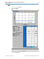
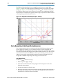
1
Device-Specific Power Delivery Network (PDN) Tool User Guide Device-Specific Power Delivery Network (PDN) Tool User Guide 101 Innovation Drive San Jose, CA 95134 www.altera.com UG-01064-1.1 Subscribe © 2012 Altera Corporation. All rights reserved. ALTERA, ARRIA, CYCLONE, HARDCOPY, MAX, MEGACORE, NIOS, QUARTUS and STRATIX are Reg. U.S. Pat. & Tm. Off. and/or trademarks of Altera Corporation in the U.S. and other countries. All other trademarks and service marks are the property of their respective holders as described at www.altera.com/common/legal.html. Altera warrants performance of its semiconductor products to current specifications in accordance with Altera’s standard warranty, but reserves the right to make changes to any products and services at any time without notice. Altera assumes no responsibility or liability arising out of the application or use of any information, product, or service described herein except as expressly agreed to in writing by Altera. Altera customers are advised to obtain the latest version of device specifications before relying on any published information and before placing orders for products or services. Device-Specific Power Delivery Network (PDN) Tool User Guide September 2012 Altera Corporation Contents Chapter 1. User Guide for the Device-Specific Power Delivery Network (PDN) Tool Overview . . . . . . . . . . . . . . . . . . . . . . . . . . . . . . . . . . . . . . . . . . . . . . . . . . . . . . . . . . . . . . . . . . . . . . . . . . . . . . 1–1 Application of the Tool . . . . . . . . . . . . . . . . . . . . . . . . . . . . . . . . . . . . . . . . . . . . . . . . . . . . . . . . . . . . . . . . . . . 1–1 PDN Decoupling Methodology Review . . . . . . . . . . . . . . . . . . . . . . . . . . . . . . . . . . . . . . . . . . . . . . . . . . . . 1–1 PDN Circuit Topology . . . . . . . . . . . . . . . . . . . . . . . . . . . . . . . . . . . . . . . . . . . . . . . . . . . . . . . . . . . . . . . . . 1–2 ZTARGET . . . . . . . . . . . . . . . . . . . . . . . . . . . . . . . . . . . . . . . . . . . . . . . . . . . . . . . . . . . . . . . . . . . . . . . . . . . . . . . . . . . . . . . . . . . . . . 1–2 FEFFECTIVE . . . . . . . . . . . . . . . . . . . . . . . . . . . . . . . . . . . . . . . . . . . . . . . . . . . . . . . . . . . . . . . . . . . . . . . . . . . . . . . . . . . . . . . . . . . . 1–4 Major Tabs of the PDN Tool . . . . . . . . . . . . . . . . . . . . . . . . . . . . . . . . . . . . . . . . . . . . . . . . . . . . . . . . . . . . . . 1–5 BGA Via . . . . . . . . . . . . . . . . . . . . . . . . . . . . . . . . . . . . . . . . . . . . . . . . . . . . . . . . . . . . . . . . . . . . . . . . . . . . . 1–6 Plane Cap . . . . . . . . . . . . . . . . . . . . . . . . . . . . . . . . . . . . . . . . . . . . . . . . . . . . . . . . . . . . . . . . . . . . . . . . . . . . 1–7 Cap Mount . . . . . . . . . . . . . . . . . . . . . . . . . . . . . . . . . . . . . . . . . . . . . . . . . . . . . . . . . . . . . . . . . . . . . . . . . . . 1–8 X2Y Mount . . . . . . . . . . . . . . . . . . . . . . . . . . . . . . . . . . . . . . . . . . . . . . . . . . . . . . . . . . . . . . . . . . . . . . . . . . . 1–9 Library . . . . . . . . . . . . . . . . . . . . . . . . . . . . . . . . . . . . . . . . . . . . . . . . . . . . . . . . . . . . . . . . . . . . . . . . . . . . . 1–10 Two-Terminal Decoupling Capacitors . . . . . . . . . . . . . . . . . . . . . . . . . . . . . . . . . . . . . . . . . . . . . . . . 1–11 Bulk Capacitors . . . . . . . . . . . . . . . . . . . . . . . . . . . . . . . . . . . . . . . . . . . . . . . . . . . . . . . . . . . . . . . . . . . 1–11 X2Y Decoupling Capacitors . . . . . . . . . . . . . . . . . . . . . . . . . . . . . . . . . . . . . . . . . . . . . . . . . . . . . . . . . 1–11 BGA Via and Plane Capacitance . . . . . . . . . . . . . . . . . . . . . . . . . . . . . . . . . . . . . . . . . . . . . . . . . . . . . 1–11 VRM Library . . . . . . . . . . . . . . . . . . . . . . . . . . . . . . . . . . . . . . . . . . . . . . . . . . . . . . . . . . . . . . . . . . . . . . 1–11 Spreading R, L Parasitics . . . . . . . . . . . . . . . . . . . . . . . . . . . . . . . . . . . . . . . . . . . . . . . . . . . . . . . . . . . 1–11 Dielectric Material Library . . . . . . . . . . . . . . . . . . . . . . . . . . . . . . . . . . . . . . . . . . . . . . . . . . . . . . . . . . 1–12 Decap Selection . . . . . . . . . . . . . . . . . . . . . . . . . . . . . . . . . . . . . . . . . . . . . . . . . . . . . . . . . . . . . . . . . . . . . . 1–13 Device/Power Rail Information . . . . . . . . . . . . . . . . . . . . . . . . . . . . . . . . . . . . . . . . . . . . . . . . . . . . . 1–14 Component Parameters Setting . . . . . . . . . . . . . . . . . . . . . . . . . . . . . . . . . . . . . . . . . . . . . . . . . . . . . . 1–14 Electric Parameters and Design Guidelines . . . . . . . . . . . . . . . . . . . . . . . . . . . . . . . . . . . . . . . . . . . . 1–15 Decoupling Capacitor (High/Mid Frequency) . . . . . . . . . . . . . . . . . . . . . . . . . . . . . . . . . . . . . . . . . 1–15 Decoupling Capacitor (Bulk) . . . . . . . . . . . . . . . . . . . . . . . . . . . . . . . . . . . . . . . . . . . . . . . . . . . . . . . . 1–15 ZEFF Plot . . . . . . . . . . . . . . . . . . . . . . . . . . . . . . . . . . . . . . . . . . . . . . . . . . . . . . . . . . . . . . . . . . . . . . . . . 1–16 BOM . . . . . . . . . . . . . . . . . . . . . . . . . . . . . . . . . . . . . . . . . . . . . . . . . . . . . . . . . . . . . . . . . . . . . . . . . . . . . . . 1–17 Design PCB Decoupling Using the PDN Tool . . . . . . . . . . . . . . . . . . . . . . . . . . . . . . . . . . . . . . . . . . . . . . 1–18 Pre-Layout Instructions . . . . . . . . . . . . . . . . . . . . . . . . . . . . . . . . . . . . . . . . . . . . . . . . . . . . . . . . . . . . . . . 1–18 Derive Decoupling in a Single-Rail Scenario . . . . . . . . . . . . . . . . . . . . . . . . . . . . . . . . . . . . . . . . . . . . . 1–19 Derive Decoupling in the Power-Sharing Scenarios . . . . . . . . . . . . . . . . . . . . . . . . . . . . . . . . . . . . . . . 1–22 Additional Information Document Revision History . . . . . . . . . . . . . . . . . . . . . . . . . . . . . . . . . . . . . . . . . . . . . . . . . . . . . . . . . . . Info–1 How to Contact Altera . . . . . . . . . . . . . . . . . . . . . . . . . . . . . . . . . . . . . . . . . . . . . . . . . . . . . . . . . . . . . . . . Info–1 Typographic Conventions . . . . . . . . . . . . . . . . . . . . . . . . . . . . . . . . . . . . . . . . . . . . . . . . . . . . . . . . . . . . . Info–1 September 2012 Altera Corporation Device-Specific Power Delivery Network (PDN) Tool User Guide iv Device-Specific Power Delivery Network (PDN) Tool User Guide Contents September 2012 Altera Corporation 1. User Guide for the Device-Specific Power Delivery Network (PDN) Tool This user guide provides a brief overview of the various tabs in the device-specific PDN tool. You can quickly and accurately design a robust power delivery network by calculating an optimum number of capacitors that meet the target impedance requirements for a given power supply. Overview PCB designers must estimate the number, value, and type of decoupling capacitors needed to develop an efficient PCB decoupling strategy during the early design phase, without going through extensive pre-layout simulations. Altera’s Power Delivery Network (PDN) tool provides these critical pieces of information. Because all device-specific PDN tools have a similar user interface, this document serves as the user guide to all Altera® device-specific PDN tools. The device family being supported by the tool is shown on the top-right corner of the major tabs of the tool. f For more information about Altera’s general purpose PDN tool with no device support, refer to the Power Delivery Network (PDN) Tool User Guide. The PDN tool is a Microsoft Excel-based spreadsheet tool used to calculate an impedance profile based on user inputs. For a given power supply, the spreadsheet requires only basic design information, such as the board stackup, transient current information, and ripple specifications to calculate the impedance profile and the optimum number of capacitors to meet the desired impedance target (ZTARGET). The tool also provides device- and power rail-specific PCB decoupling cut-off frequency (FEFFECTIVE). The results obtained through the spreadsheet tool are intended only as a preliminary estimate and not as a specification. For an accurate impedance profile, Altera recommends a post-layout simulation approach using any of the available EDA tools, such as Sigrity PowerSI, Ansoft SIWave, Cadence Allegro PCB PI, etc. Application of the Tool The purpose of the PDN tool is to help the design of a robust power delivery network for the device in the targeted device family by determining an optimum number, type, and value of decoupling capacitors needed for selected device/power rail to meet the desired ZTARGET up to FEFFECTIVE. This spreadsheet tool is useful for exploring the various what-if scenarios during the early design phase, without extensive and time consuming pre-layout analysis. PDN Decoupling Methodology Review This section describes general PCB decoupling methodology and explains in detail the two parameters (ZTARGET and FEFFECTIVE) provided by the PDN tool for guiding PCB decoupling design. September 2012 Altera Corporation Device-Specific Power Delivery Network (PDN) Tool User Guide 1–2 Chapter 1: User Guide for the Device-Specific Power Delivery Network (PDN) Tool PDN Decoupling Methodology Review PDN Circuit Topology The PDN tool is based on a lumped equivalent model representation of the power delivery network topology. Figure 1–1 shows a schematic representation of the circuit topology, modeled as part of the tool. The PDN impedance profile is the impedance-over-frequency looking from the device side. Figure 1–1. PDN Topology For first order analysis, the voltage regulator module (VRM) can be simply modeled as a series connected resistor and inductor, as shown in Figure 1–1. At low frequencies, up to approximately 50 KHz, the VRM has a very low impedance and is capable of responding to the instantaneous current requirements of the FPGA. The equivalent series resistance (ESR) and equivalent series inductance (ESL) values can be obtained from the VRM manufacturer. At higher frequency, the VRM impedance is primarily inductive, making it incapable of meeting the transient current requirement. PCB decoupling capacitors are used for reducing the PDN impedance up to tens of MHz. The on-board discrete decoupling capacitors provides the required low impedance depending on the capacitor intrinsic parasitics (RcN, CcN, LcN) and the capacitor mounting inductance (LmntN). The inter-planar capacitance between the power-ground planes typically has lower inductance than the discrete decoupling capacitor network, making it more effective at higher frequencies (tens of MHz). As frequency increases (tens of MHz and above), the PCB decoupling capacitors become less effective. The limitation comes from the parasitic inductance seen with respect to the FPGA, which consists of capacitor mounting inductance, PCB spreading inductance, ball grid array (BGA) via inductance, and packaging parasitic inductance. All these parasitics are modeled in this PDN tool to capture the effect of the PCB decoupling capacitors accurately. To simplify the circuit topology, all parasitics are represented with lumped inductors and resistors despite the distributed nature of PCB spreading inductance. ZTARGET According to Ohm’s law, voltage drop across a circuit is proportional to the current flow through the circuit and impedance of the circuit. The transient component of PDN current gives rise to voltage fluctuation within the PDN, which may lead to logic and timing issues. You can reduce excessive voltage fluctuation by reducing PDN impedance. One design guide line is target impedance ZTARGET. Device-Specific Power Delivery Network (PDN) Tool User Guide September 2012 Altera Corporation Chapter 1: User Guide for the Device-Specific Power Delivery Network (PDN) Tool PDN Decoupling Methodology Review 1–3 Ztarget is defined using the maximum allowable voltage ripple and transient current and is calculated as follows: Equation 1–1. %Ripple- Z TARGET = VoltageRail ------------------100 ---------------------------------------------------------MaxTransientCurrent For example, to reliably decouple a 3.3-volt power rail that allows 5% of AC ripple and a maximum 2 A current draw, 50% of which is transient current, the desired target impedance is: Equation 1–2. 3.3 0.05 Z TARGET = ---------------------------- = 0.165 2 x 0.5 To accurately calculate the Ztarget for any power rail, the following information must be known: ■ September 2012 The maximum transient current requirements for all devices in the system that are powered by the power rail under consideration. You can obtain this information from manufacturers of the respective devices. You can calculate the maximum transient current of a device using the maximum total current and the transient current percentage. 1 The percentage of transient current is signal-pattern dependent. It changes as the output signal pattern varies for drivers using the power rail. You need to choose the value that represents the worst-case scenario of the power rail. For information about recommended settings, refer to the table in the Introduction tab of the PDN tool. Table 1–1 on page 1–4 is from the PDN tool for a Stratix IV GX device. It lists the Stratix IV GX default power supply voltage, the recommended settings of the transient current percentage, and the allowable voltage ripple for power rails. 1 You can obtain accurate estimations on the maximum total current for Altera devices using the Altera PowerPlay Early Power Estimator (EPE) tool or the Quartus II PowerPlay Power Analyzer tools. You can download the EPE tool for your target Altera device from the PowerPlay Early Power Estimator (EPE) and Power Analyzer. Altera Corporation Device-Specific Power Delivery Network (PDN) Tool User Guide 1–4 Chapter 1: User Guide for the Device-Specific Power Delivery Network (PDN) Tool PDN Decoupling Methodology Review ■ The maximum allowable AC ripple on the power rail as a percentage of the supply voltage. The maximum allowable AC ripple varies for different power rails. For information about the recommended maximum allowable AC ripple for power rails, refer to the table in the Introduction tab of the PDN tool. Table 1–1 on page 1–4 shows ripple information for the power rails of Stratix IV GX device. Table 1–1. Settings for the Stratix IV GX Device Power Rails (Note 1) Allowable Ripple Percentage (±) Transient Current Percentage (%) Rail Name Voltage (V) Notes VCC 0.9 V 5% 50% Core VCCIO 1.2 V - 3.0 V 5% 50% I/O Bank VCCPD 2.5 V 5% 50% I/O Pre-Drivers VCCA_PLL 2.5 V 3% 20% PLL (Analog) VCCD_PLL 0.9 V 3% 20% PLL (Digital) VCC_CLKIN 2.5 V 5% 50% Diff Clock Input VCCR 1.1 V 3% 30% XCVR RX (Analog) VCCT 1.1 V 3% 30% XCVR TX (Analog) VCCA 3.0 V 5% 10% XCVR High Voltage Power VCCH_GXB 1.5 V 3% 10% XCVR I/O Buffer Block VCCL_GXB 1.1 V 3% 20% XCVR Clock Block VCCHIP 0.9 V 5% 50% PCIE Hard IP (Digital) VCCPT 1.5 V 3% 20% Programmable Power Tech VCCAUX 2.5 V 3% 20% Programmable Power Tech Aux Note to Table 1–1: (1) For more information about power rail functions, refer to the pin connection guidelines for the selected device family. FEFFECTIVE As shown in Figure 1–1 on page 1–2, a capacitor reduces PDN impedance by providing a least-impedance route between power and ground. Impedance of a capacitor at high frequency is determined by its parasitics (ESL and ESR). For a PCB-mount capacitor, the parasitics include not only the parasitic from the capacitors themselves but also the parasitics associated with mounting, PCB spreading, and packaging. Therefore, PCB capacitor parasitics are generally higher than those of on-package decoupling capacitor and on-die-capacitance. Decoupling using PCB capacitors becomes ineffective at high frequency. Using PCB capacitors for PDN decoupling beyond their effective frequency range brings little improvement to PDN performance and raises the bill of materials (BOM) cost. To help reduce over-design of PCB decoupling, this release of the PDN tool provides a suggested PCB decoupling design cut-off frequency (FEFFECTIVE) as another guideline. It is calculated using the PCB, package, and die parasitics. You only need to design PCB decoupling that keeps ZEFF under ZTARGET up to FEFFECTIVE. Device-Specific Power Delivery Network (PDN) Tool User Guide September 2012 Altera Corporation Chapter 1: User Guide for the Device-Specific Power Delivery Network (PDN) Tool Major Tabs of the PDN Tool 1–5 Major Tabs of the PDN Tool Figure 1–2 shows the tabs of the PDN tool spreadsheet. Table 1–2 describes the PDN tool tabs. Figure 1–2. Tabs in the PDN Tool Table 1–2. Tabs in the PDN Tool Tab Description Release Notes This tab provides the legal disclaimers, the revision history of the tool, and the user agreement. Introduction This tab shows the schematic representation of the circuit that is modeled as part of the PDN tool. The tab also provides related information, such as a quick start instruction, recommended settings for some power rails and a brief description of decoupling design procedures under different power supply connection schemes. Decap Selection This tab provides an interface to input the various parameters and observe the resultant impedance profile. This is the main user interface to the tool. Library This tab points to various libraries (capacitor, dielectric materials, and so on) that are called by other tabs. You can change the default values listed as part of these libraries. BGA Via This tab provides an interface to calculate the BGA mounting inductance based on design-specific via parameters and the number of vias. Plane Cap This tab provides an interface to calculate the plane capacitance based on design-specific parameters. Cap Mount This tab provides an interface to input design-specific parameters for calculating the capacitor mounting inductance for two different capacitor orientations (Via on Side [VOS] and Via on End [VOE]). X2Y Mount This tab provides an interface to input design-specific parameters for calculating the capacitor mounting inductance for X2Y type capacitors. BOM This tab provides a summary of the final capacitor count needed to meet the target impedance. You can input design-specific information in the various tabs to arrive at a very accurate PDN profile for a given power supply. The following sections describe the major tabs for the tool. September 2012 Altera Corporation Device-Specific Power Delivery Network (PDN) Tool User Guide 1–6 Chapter 1: User Guide for the Device-Specific Power Delivery Network (PDN) Tool Major Tabs of the PDN Tool BGA Via The BGA Via tab calculates the vertical via loop inductance under the BGA pin field. Figure 1–3 is a snapshot taken from the tool. Figure 1–3. BGA Via Tab You enter the layout-specific information, such as the via drill diameters, via length, via pitch, and the number of power/ground via pairs under the BGA. The tool calculates the effective via loop inductance and resistance value. You can save the change made to the tab, restore the changes, and restore the tab back to the default settings. Device-Specific Power Delivery Network (PDN) Tool User Guide September 2012 Altera Corporation Chapter 1: User Guide for the Device-Specific Power Delivery Network (PDN) Tool Major Tabs of the PDN Tool 1–7 Plane Cap The Plane Cap tab calculates the distributed plane capacitance in microfarads (µF) that is developed between the power/ground planes based on the parallel plate capacitor equation. Figure 1–4 shows the Plane Cap tab. Figure 1–4. Plane Cap Tab You enter the design specific information, such as plane dimensions, plane configuration, and dielectric material used. The tool calculates a plane capacitance value. You can save custom values, restore custom values, and restore the default settings. September 2012 Altera Corporation Device-Specific Power Delivery Network (PDN) Tool User Guide 1–8 Chapter 1: User Guide for the Device-Specific Power Delivery Network (PDN) Tool Major Tabs of the PDN Tool Cap Mount The Cap Mount tab, shown in Figure 1–5, calculates the capacitor mounting inductance seen by the decoupling capacitor. Figure 1–5. Cap Mount Tab The capacitor mounting calculation is based on the assumption that the decoupling capacitor is a two-terminal device. The capacitor mounting calculation is applicable to any two-terminal capacitor with the following footprints: 0201, 0402, 0603, 0805, and 1206. You enter all the information relevant to your layout and the tool provides a mounting inductance for a capacitor mounted on either the top or bottom layer of the board. Depending on the layout, you can choose between VOE (Via on End) or VOS (Via on Side) to achieve an accurate capacitor mounting inductance value. If you plan to use a footprint capacitor other than a regular two-terminal capacitor or X2Y capacitor for decoupling, you can skip the Cap Mount tab and directly enter the capacitor parasitics and capacitor mounting inductance in the Library tab (under the Custom field in the Decoupling Cap section of the library). As with the other tabs, you can save the changes made to the tab, restore the changes, and restore the tab back to the default settings. Device-Specific Power Delivery Network (PDN) Tool User Guide September 2012 Altera Corporation Chapter 1: User Guide for the Device-Specific Power Delivery Network (PDN) Tool Major Tabs of the PDN Tool 1–9 X2Y Mount The X2Y Mount tab, shown in Figure 1–6, calculates the capacitor mounting inductance seen by the X2Y decoupling capacitor. Figure 1–6. X2Y Mount Tab You enter all the information relevant to your layout and the tool provides a mounting inductance for a X2Y capacitor mounted on either the top or bottom layer of the board. As with the other tabs, you can save the changes made to the tab, restore the changes, and restore the tab back to the default settings. September 2012 Altera Corporation Device-Specific Power Delivery Network (PDN) Tool User Guide 1–10 Chapter 1: User Guide for the Device-Specific Power Delivery Network (PDN) Tool Major Tabs of the PDN Tool Library The Library tab stores all the device parameters that are referred to in the other tabs. Figure 1–7shows the Library tab. Figure 1–7. Library Tab This tab is divided into the following sections: ■ Two-Terminal Decoupling Capacitors (High/Mid Frequency) ■ X2Y Decoupling Capacitors (High/Mid frequency) ■ Bulk Capacitors (Mid/Low Frequency) ■ BGA Via and Plane Capacitance ■ VRM Library ■ Spreading R, L Parasitics ■ Dielectric Material Library You can change each of the default values listed in the respective sections to meet the specific needs of your design. Device-Specific Power Delivery Network (PDN) Tool User Guide September 2012 Altera Corporation Chapter 1: User Guide for the Device-Specific Power Delivery Network (PDN) Tool Major Tabs of the PDN Tool 1–11 Two-Terminal Decoupling Capacitors The decoupling capacitors section contains the default ESR and ESL values for the various two-terminal capacitors in different footprints (0201, 0402, 0603, 0805, and 1206). You also have the option of either modifying the default values or entering your own commonly used custom values in the Custom field. If you are using a capacitor with a footprint that is not available in the tool, you must use the Custom field to enter the capacitor parasitics and the corresponding mounting inductance. The decoupling capacitors section also provides the option for the user defined capacitors (such as User1,...,User4). You can define the ESR and ESL parasitics for the various footprints and enter the corresponding capacitor value in the Decap Selection tab. Choose the corresponding footprint when defining the capacitor values. Bulk Capacitors The bulk capacitors section contains the commonly used capacitor values for decoupling the power supply at mid/low frequencies. You can change the default values to reflect the parameters specific to the design. X2Y Decoupling Capacitors The X2Y decoupling capacitors section contains the default ESR and ESL values for the various X2Y capacitors in different footprints (0603, 0805, 1206, and 1210). You also can replace the default ESR and ESL values with your own commonly used custom values. BGA Via and Plane Capacitance The BGA via and plane capacitance section provides an option to directly enter the values for effective via loop inductance under the BGA and plane capacitance during the pre-layout phase when no design-specific information is available. If you have access to design-specific information, you can ignore this section and enter the design-specific information in the Plane Cap and BGA Via tabs that calculate the plane capacitance and the BGA via parasitics, respectively. VRM Library The VRM section lists the default values for both the linear and switcher regulators. You can change the VRM parasitics listed under the linear/switcher rows or add the custom parasitics for the VRM relevant to the design in the Custom field. Spreading R, L Parasitics The spreading R, L library provides various options for the default effective spreading inductance values that the decoupling capacitors see with respect to the FPGA based on the quality of the PDN design. You can choose a Low value of effective spreading inductance if you have optimally designed your PDN Network. Optimum PDN design involves implementing the following design rules: ■ September 2012 PCB stackup that provides a wide solid power/ground sandwich for a given supply with a thin dielectric between the planes. This minimizes the current loop, which reduces the spreading inductance. The thickness of the dielectric material between the power/ground pair directly influences the amount of spreading/loop inductance that a decoupling cap can see with respect to the FPGA. Altera Corporation Device-Specific Power Delivery Network (PDN) Tool User Guide 1–12 Chapter 1: User Guide for the Device-Specific Power Delivery Network (PDN) Tool Major Tabs of the PDN Tool ■ Placing the capacitors closer to the FPGA from an electrical standpoint. ■ Minimizing via perforations in the power/ground sandwich in the current path from the decoupling caps to the FPGA device. Due to layout and design constraints, the PDN design may not be optimal. In this case, you can choose either a Medium or High value of spreading R and L. You also have the option of changing the default values or using the Custom field listed in the library specific to the design. Dielectric Material Library The dielectric materials section lists the dielectric constant values for the various commonly used dielectric materials. These values are used in the plane capacitance calculations listed under the Plane Cap tab. You can change the values listed in this section. If you change the default values listed in the various sections in the Library tab, you can save the changes by clicking Save Custom. You can restore the default library by clicking Restore Default located at the top right-hand corner of the Library page. You can also restore the saved custom library by clicking Restore Custom. Device-Specific Power Delivery Network (PDN) Tool User Guide September 2012 Altera Corporation Chapter 1: User Guide for the Device-Specific Power Delivery Network (PDN) Tool Major Tabs of the PDN Tool 1–13 Decap Selection The Decap Selection tab, shown in Figure 1–8, is where you perform the analysis for the PCB decoupling design. The user interface shown here is from the PDN tool for the Stratix IV device family. Figure 1–8. Decap Selection Tab This tab is divided into the following sections: September 2012 ■ Device/Power Rail Information ■ Component Parameters Setting ■ Electric Parameters and Design Guidelines ■ Decoupling Capacitor (High/Mid Frequency) ■ Decoupling Capacitor (Bulk) ■ ZEFF Plot Altera Corporation Device-Specific Power Delivery Network (PDN) Tool User Guide 1–14 Chapter 1: User Guide for the Device-Specific Power Delivery Network (PDN) Tool Major Tabs of the PDN Tool Device/Power Rail Information You select the device/power rail to work in this field. A pull-down menu with the names of the available devices and power rails in the Altera device family supported by the tool is shown when you click the corresponding cell. The tool validates the selected device/power rail combination. A warning is shown beneath the field if an invalid combination is chosen (Figure 1–9). Figure 1–9. Device/Power Rail Information Component Parameters Setting You can either enable or disable the following components of the PDN network shown in Figure 1–10. Figure 1–10. Parameter Settings for PDN Components Table 1–3 describes the PDN components. Table 1–3. Parameters of PDN Components Parameter Description VRM to disable this component, select Ignore. To enable the VRM parasitics, select Linear, Switcher, or Custom. Spreading Based on the design, you can select either Low, Medium, High, or a Custom value for the effective spreading R, L values that the decoupling capacitors see with respect to the FPGA. You can also ignore the spreading inductance by selecting Ignore. Ignoring the spreading inductance leads to an optimistic result and is not an accurate representation of the impedance profile that the FPGA sees. The Ignore option helps you understand that the spreading inductance in combination with the BGA via inductance is the limiting factor from a PCB perspective to decouple the FPGA at high frequencies. Be careful when choosing the Ignore option while coming up with a final capacitor count. BGA Via Based on the design, you can choose to Ignore the BGA via component or to Calculate the effective via inductance based on the layout. If you are in the middle of layout, you can directly enter the effective loop R, L via parasitics in the Library tab and choose the Custom setting under BGA Via to include the via parasitics. Plane Capacitance Based on the design, you can either choose to Ignore the inter-planar capacitance between the power and ground plane, or Calculate the plane capacitance based on the layout. If you are in the middle of layout, you can directly enter the plane capacitance in the Library tab and choose the Custom setting under the Plane Cap to include the plane capacitance parasitics. Device-Specific Power Delivery Network (PDN) Tool User Guide September 2012 Altera Corporation Chapter 1: User Guide for the Device-Specific Power Delivery Network (PDN) Tool Major Tabs of the PDN Tool 1–15 Electric Parameters and Design Guidelines The PDN tool calculates ZTARGET based on the user inputs in this field. The PDN tool also displays FEFFECTIVE that is derived based on the PCB stack-up and power rail information (Figure 1–11). The details regarding the calculation procedure are described in “ZTARGET” on page 1–2 and “FEFFECTIVE” on page 1–4. Figure 1–11. Electric Parameters and Design Guidelines You need to enter information for: ■ Power Supply Voltage (min) ■ IMAX ■ Transient Current (%) ■ Allowable Voltage Ripple Percentage (±) The tool then calculates ZTARGET based on the user input from related fields and displays the results in the column below. Decoupling Capacitor (High/Mid Frequency) You can select the various decoupling capacitors, both two-terminal and X2Y types, based on footprint, layer, and orientation to meet the target impedance for the mid to high frequency. The capacitance value for the X2Y capacitor may be different from that of the two-terminal capacitor. A warning message of "Wrong Footprint" is displayed if you choose a wrong combination of capacitance and footprint. The VOE and VOS option do not affect the mounting inductance for X2Y type capacitors because their via locations are symmetric. You also have the option of defining custom capacitor values (User1, ..., User4) needed for high/mid frequency decoupling specific to the design. You cannot change the capacitor parasitics (ESR and ESL) in this tab. This can only be done in the Library tab. Decoupling Capacitor (Bulk) You can select the desired bulk capacitors based on the footprint for the low to mid frequency decoupling need. You can only change the parasitics of the bulk decoupling capacitors and define the mounting inductance specific to the design in the Library tab. You also have the option of defining custom capacitor values (User5 and User6) for low/mid frequency decoupling specific to the design. September 2012 Altera Corporation Device-Specific Power Delivery Network (PDN) Tool User Guide 1–16 Chapter 1: User Guide for the Device-Specific Power Delivery Network (PDN) Tool Major Tabs of the PDN Tool ZEFF Plot The effective impedance that the Altera device encounters is shown in (Figure 1–12). Other information, such as ZTARGET and FEFFECTIVE are also shown in the plot, along with the impedance profile of components such as capacitors, VRM, and BGA via, within the PDN system. The plot is updated automatically when related parameters are changed. Figure 1–12. Zeff Plot As provided in other tabs, you can save and restore the final capacitor count and other settings for a specific set of assumptions. There is also flexibility to revert back to default settings. Device-Specific Power Delivery Network (PDN) Tool User Guide September 2012 Altera Corporation Chapter 1: User Guide for the Device-Specific Power Delivery Network (PDN) Tool Major Tabs of the PDN Tool 1–17 BOM Figure 1–13 shows the BOM tab. Figure 1–13. BOM Tab When the analysis is done, you can print out the final ZEFF profile and capacitor count to achieve the profile by clicking Print BOM on the top right corner. It defaults to the default printer assigned in the File/Print menu. You can also export the data as an .xls file by clicking Export Data. September 2012 Altera Corporation Device-Specific Power Delivery Network (PDN) Tool User Guide 1–18 Chapter 1: User Guide for the Device-Specific Power Delivery Network (PDN) Tool Design PCB Decoupling Using the PDN Tool Design PCB Decoupling Using the PDN Tool PCB decoupling keeps PDN ZEFF smaller than ZTARGET with the properly chosen PCB capacitor combination up to the frequency where the capacitor on the package and die take over the PDN decoupling. This section describes the procedure of designing PCB decoupling using the PDN tool in different power rail configurations. This section also provides design examples using the Stratix IV device PDN tool. Pre-Layout Instructions The PDN tool provides an accurate estimate of the number and types of capacitors needed to design a robust power delivery network, regardless of where you are in the design phase. However, the accuracy of the results depends highly on the user inputs for the various parameters. If you have finalized the board stack-up and have access to board database and layout information, you can step through the tabs and enter the required information to arrive at an accurate decoupling scheme. In the pre-layout phase of the design cycle, when no specific information about the board stack-up and board layout is known, you can follow the instructions in the following sections to explore the solution space when finalizing key design parameters such as stack-up, plane size, capacitor count, capacitor orientation, and so on. Device-Specific Power Delivery Network (PDN) Tool User Guide September 2012 Altera Corporation Chapter 1: User Guide for the Device-Specific Power Delivery Network (PDN) Tool Design PCB Decoupling Using the PDN Tool 1–19 In the pre-layout phase, you can ignore the Plane Cap and Cap Mount tabs and go directly to the Library tab when you do not have the layout information. Figure 1–14 shows the fields in the Library tab that you will use to enter the various parameters. If available, enter the values shown in Figure 1–14 in the Library tab. To use the default values, go directly to the Decap Selection tab to begin the analysis. Figure 1–14. Library Tab Fields Notes to Figure 1–14: The numbers correspond to the following steps 1, 2, 3, 4, 5. (1) Enter the ESR, ESL, and Lmnt values for the capacitors under the Custom field. (2) Enter the effective BGA via (loop) parasitics for the power supply being decoupled. (3) Enter the plane capacitance seen by the power/ground plane pair on the board for the power supply under Plane Cap. (4) Enter the VRM parasitics, if available, under the Custom row. (5) Enter the effective spreading inductance seen by the decoupling capacitors in Custom row. Derive Decoupling in a Single-Rail Scenario A power supply connects to only one power rail on the FPGA device in a single-rail scenario. The PDN noise is created by the transient current of the single rail. You determine ZTARGET and FEFFECTIVE based on the parameters related to the selected rail only. You must follow the steps below to derive the desired capacitor combination: 1. Select the device/power rail to work with. September 2012 Altera Corporation Device-Specific Power Delivery Network (PDN) Tool User Guide 1–20 Chapter 1: User Guide for the Device-Specific Power Delivery Network (PDN) Tool Design PCB Decoupling Using the PDN Tool 2. Select the parameter setting for the PDN components. 3. Enter the electric parameters to set ZTARGET and FEFFECTIVE. 4. Derive the PCB decoupling scheme. The red numbers in Figure 1–15 show the field to work with in each of these steps. For more information on these fields, refer to “Decap Selection” on page 1–13. Figure 1–15. Decap Selection Tab in a Single-Rail Design In Step 2, the PDN tool uses the inductance and resistance value calculated in the BGA Via tab if you choose the Calculate option for the BGA via. Incorrect parameters may negatively affect the derived decoupling design. These values are calculated using the parameters you entered in the BGA Via tab. You must check the BGA Via tab to ensure the numbers you entered—especially the number and length of the BGA power via pair—matches the settings of the power rail selected in Step 1. Device-Specific Power Delivery Network (PDN) Tool User Guide September 2012 Altera Corporation Chapter 1: User Guide for the Device-Specific Power Delivery Network (PDN) Tool Design PCB Decoupling Using the PDN Tool 1–21 In Step 3, you need to have a good estimate of the parameters entered to derive the proper decoupling guidelines (ZTARGET and FEFFECTIVE). Although you need to determine those guidelines based on the worst-case scenario, pessimistic settings result in hard-to-achieve guidelines and over design of your PCB decoupling. For the recommended settings of the percentage of transient current and maximum allowable voltage ripple for selected power rail, refer to Table 1–1 on page 1–4. In Step 4, you must adjust the number and value of the PCB capacitors in the Decoupling Capacitor (Mid/High Frequency) and Decoupling Capacitor (Bulk) fields to keep the plotted ZEFF below ZTARGET until FEFFECTIVE. If you are not able to find a capacitor combination that meets your design goal, you can try to change the parameters at Step 2; for example, reducing the BGA via inductance used in the Calculate option by reducing the BGA via length in the BGA_VIA tab and using the low option for plane spreading. These changes reduce parasitic inductance and make it easier to achieve your decoupling goal. To achieve the low spreading setting, you must place the mid to high frequency PCB capacitors close to the FPGA device. You also must minimize the dielectric thickness between the power and ground plane. If you are not able to meet the ZTARGET requirement with the above changes, the PDN in your design may have reached its physical limitation under the parameters entered in Step 3. You need to go back to Step 3 and re-examine these parameters to check if they are over pessimistic. The design shown in Figure 1–16 is a decoupling example for S4GX230KF40 VCC power rail. Assume that the minimum voltage supply is 0.9 V, IMAX is 7 A, transient current is 50% of IMAX, and the maximum allowable ripple is 3% of supply voltage. The VCC rail has 50 power BGA vias. The length of BGA via is assumed to be 60 mil. September 2012 Altera Corporation Device-Specific Power Delivery Network (PDN) Tool User Guide 1–22 Chapter 1: User Guide for the Device-Specific Power Delivery Network (PDN) Tool Design PCB Decoupling Using the PDN Tool The PDN tool calculated that ZTARGET is 0.0077 and FEFFECTIVE is 24.91 MHz. Figure 1–16 shows one of the capacitor combinations that you can select to meet the design goal. Figure 1–16 is the enlarged view of the ZEFF plot. As shown in the plot, ZEFF remains under ZTARGET up to FEFFECTIVE. There are many combinations, but the ideal solution is to minimize the quantity and the type of capacitors needed to achieve a flat impedance profile below the ZTARGET. Figure 1–16. Enlarged Plot of Zeff Using the Figure 1-16 Design Derive Decoupling in the Power-Sharing Scenarios It is a common practice that several power rails in the FPGA device share the same power supply. For example, you can connect VCCIO, VCCPD, VCCPGM, and VCC_CLKIN rails that require the same supply voltage to the same PCB power plane. This can be required by the design, such as in the memory interface case. This can also come from the needs to reduce BOM cost. In the power sharing scenario, the noise within a power supply is generated by transient current from multiple rails. The design flow is different comparing to the single power rail scenario. Step 1: Derive ZTARGET To derive ZTARGET, follow these steps: 1. Enter the power supply voltage. 2. Choose the smallest allowable voltage ripple of all shared power rails as the allowable voltage ripple. 3. Use the total current of all rails as IMAX. 4. Derive the percentage of transient current by dividing the total transient current of all rails by the total current of all rails. Select the setting in the Transient current column that is the closest to derived number. Device-Specific Power Delivery Network (PDN) Tool User Guide September 2012 Altera Corporation Chapter 1: User Guide for the Device-Specific Power Delivery Network (PDN) Tool Design PCB Decoupling Using the PDN Tool 1–23 Step 2: Determine the Device/Power Rail to Work With Choose the power rail with the highest FEFFECTIVE as the rail to work with in this power-sharing scenario. FEFFECTIVE is power-rail related and can be different for power rails that connect to the same PCB power supply. You must review all power rails that share the PCB power rail and find the one with the highest FEFFECTIVE. Step 3: Select the Parameter Setting for PDN Components In this power-sharing scenario, considerations for selecting the PDN parameter settings for BGA via, VRM, plane spreading, and plane capacitance are the same as the single-rail scenario (refer to “Derive Decoupling in a Single-Rail Scenario” on page 1–19). You must ensure the number and length of the BGA power via pairs entered in BGA Via tab correspond to the power rail selected in Step 2. Step 4: Derive the PCB Decoupling Scheme The considerations and procedure for deriving the desired PCB decoupling scheme are the same as those in Step 4 of the single-rail scenario (refer to “Derive Decoupling in a Single-Rail Scenario” on page 1–19). In this PCB power plane sharing design example, three I/O banks, VCCIO 7A/7B/7C of a S4GX230KF40 device are used in a DDR2 interface. They share the PCB power plane. The power supply voltage is 1.8 V. The maximum allowable voltage ripple is 3%. The total current draw from the three banks adds up to 0.7 A. The percentage of transient current is set at 50% for all three rails. ZTARGET is calculated to be 0.154 with these parameters. After examining the FEFFECTIVE of three power rails. VCCIO 7A is identified as the power rail with the highest FEFFECTIVE. VCCIO 7A has four power via. The length of BGA via is assumed to be 25 mil. The PDN tool calculates that the FEFFECTIVE is approximately 70 MHz. September 2012 Altera Corporation Device-Specific Power Delivery Network (PDN) Tool User Guide 1–24 Chapter 1: User Guide for the Device-Specific Power Delivery Network (PDN) Tool Design PCB Decoupling Using the PDN Tool Figure 1–17 shows one of the capacitor combinations that you can select to meet your design goal. Figure 1–18 is the enlarged view of the ZEFF plot. As shown in the plot, ZEFF remains under ZTARGET up to FEFFECTIVE. There are many combinations, but the ideal solution is to minimize the quantity and the type of capacitors needed to achieve a flat impedance profile below ZTARGET. Figure 1–17. Decap Selection Tab in a Power-Sharing Design Device-Specific Power Delivery Network (PDN) Tool User Guide September 2012 Altera Corporation Chapter 1: User Guide for the Device-Specific Power Delivery Network (PDN) Tool Design PCB Decoupling Using the PDN Tool 1–25 Figure 1–18. Enlarged Plot of Zeff Using the Figure 1-18 Design 1 Some power rails are sensitive to noise, such as PLL-related power supplies. They are isolated from other rails by a power filter (usually ferrite bead) although they connect to the same VRM module. These isolated rails usually have their own PCB power plane. In this scenario, you must treat each group of isolated power rails as an individual power supply and decouple each power supply individually following the procedures described in this User Guide. When deriving decoupling capacitors for multiple FPGAs sharing the same power plane, each FPGA should be analyzed separately using the PDN tool. For each FPGA design, combine the required power rails as described above and analyze the decoupling scheme as if the FPGA was the only device on the power rail. Then repeat for each of the remaining FPGAs on the board. High frequency decoupling capacitors are meant to provide the current needed for AC transitions and must be placed in a close proximity to the FPGA power pins. Thus, the PDN tool should be used to derive the required decoupling capacitors for the unique power requirements for each FPGA on the board. The power regulators must be able to supply the total combined current requirements for each load on the supply, but the decoupling capacitor selections should be analyzed on a single FPGA basis. September 2012 Altera Corporation Device-Specific Power Delivery Network (PDN) Tool User Guide 1–26 Device-Specific Power Delivery Network (PDN) Tool User Guide Chapter 1: User Guide for the Device-Specific Power Delivery Network (PDN) Tool Design PCB Decoupling Using the PDN Tool September 2012 Altera Corporation Additional Information This chapter provides additional information about the document and Altera. Document Revision History The following table shows the revision history for this document. Date Version Changes September 2012 1.1 Updated the“Derive Decoupling in the Power-Sharing Scenarios” section. July 2009 1.0 Initial release. How to Contact Altera To locate the most up-to-date information about Altera products, refer to the following table. Contact (1) Technical support Technical training Product literature Contact Method Address Website www.altera.com/support Website www.altera.com/training Email [email protected] Website www.altera.com/literature Non-technical support (General) Email [email protected] (Software Licensing) Email [email protected] Note to Table: (1) You can also contact your local Altera sales office or sales representative. Typographic Conventions The following table shows the typographic conventions this document uses. Visual Cue Meaning Bold Type with Initial Capital Letters Indicate command names, dialog box titles, dialog box options, and other GUI labels. For example, Save As dialog box. For GUI elements, capitalization matches the GUI. bold type Indicates directory names, project names, disk drive names, file names, file name extensions, software utility names, and GUI labels. For example, \qdesigns directory, D: drive, and chiptrip.gdf file. Italic Type with Initial Capital Letters Indicate document titles. For example, Stratix IV Design Guidelines. Indicates variables. For example, n + 1. italic type September 2012 Variable names are enclosed in angle brackets (< >). For example, <file name> and <project name>.pof file. Altera Corporation Device-Specific Power Delivery Network (PDN) Tool User Guide Info–2 Additional Information Typographic Conventions Visual Cue Meaning Initial Capital Letters Indicate keyboard keys and menu names. For example, the Delete key and the Options menu. “Subheading Title” Quotation marks indicate references to sections within a document and titles of Quartus II Help topics. For example, “Typographic Conventions.” Indicates signal, port, register, bit, block, and primitive names. For example, data1, tdi, and input. The suffix n denotes an active-low signal. For example, resetn. Courier type Indicates command line commands and anything that must be typed exactly as it appears. For example, c:\qdesigns\tutorial\chiptrip.gdf. Also indicates sections of an actual file, such as a Report File, references to parts of files (for example, the AHDL keyword SUBDESIGN), and logic function names (for example, TRI). r An angled arrow instructs you to press the Enter key. 1., 2., 3., and a., b., c., and so on Numbered steps indicate a list of items when the sequence of the items is important, such as the steps listed in a procedure. ■ ■ Bullets indicate a list of items when the sequence of the items is not important. ■ 1 The hand points to information that requires special attention. h A question mark directs you to a software help system with related information. f The feet direct you to another document or website with related information. c A caution calls attention to a condition or possible situation that can damage or destroy the product or your work. w A warning calls attention to a condition or possible situation that can cause you injury. The envelope links to the Email Subscription Management Center page of the Altera website, where you can sign up to receive update notifications for Altera documents. Device-Specific Power Delivery Network (PDN) Tool User Guide September 2012 Altera Corporation