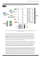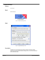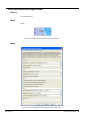
1
Opal-RT RT-XSG toolbox
User Guide
RTXSG-UG-11-01
OPAL-RT Technologies Inc.
TABLE of CONTENTS
CHAPTER 1: INTRODUCTION
About the Opal-RT RT-XSG toolbox . . . . . . . . . . . . . . . . . . . . . . . . . . . . . . . . 1
Key Features . . . . . . . . . . . . . . . . . . . . . . . . . . . . . . . . . . . . . . . . . . . . . . . . 1
Hardware description language (HDL) and fixed-point numbering . . . 2
Simulink . . . . . . . . . . . . . . . . . . . . . . . . . . . . . . . . . . . . . . . . . . . 2
Organization of this Guide . . . . . . . . . . . . . . . . . . . . . . . . . . . . . . . . . . . . . . . 2
Conventions . . . . . . . . . . . . . . . . . . . . . . . . . . . . . . . . . . . . . . . . . . . . . . . . 3
CHAPTER 2: REQUIREMENTS
Software requirements . . . . . . . . . . . . . . . . . . . . . . . . . . . . . . . . . . . . . . . . . 5
CHAPTER 3: HARDWARE DESIGN USING THE RT-XSG TOOLBOX
Field-Programmable Gate Arrays (FPGAs) . . . . . . . . . . . . . . . . . . . . . . . . . . . . 7
RT-XSG-compatible softwares . . . . . . . . . . . . . . . . . . . . . . . . . . . . . . . . . . . . 7
Matlab/Simulink® . . . . . . . . . . . . . . . . . . . . . . . . . . . . . . . . . . . . 7
Xilinx Integrated Software Environment (ISE®) Design Suite . . . . . . 7
Opal-RT Real-Time LABoratory (RT-LAB®) . . . . . . . . . . . . . . . . . . . 7
Introduction to the RT-XSG hardware I/O interfaces. . . . . . . . . . . . . . . . . . . . . 8
RT-XSG FPGA model creation paradigm . . . . . . . . . . . . . . . . . . . . . . . . . . . . . 8
CHAPTER 4: BUILDING MODELS WITH RT-XSG
System generator for DSP toolbox . . . . . . . . . . . . . . . . . . . . . . . . . . . . . . . . 11
Gateways . . . . . . . . . . . . . . . . . . . . . . . . . . . . . . . . . . . . . . . . . . . . . . . . . 11
Target platform and configuration file version selection. . . . . . . . . . . . . . . . . . 12
Building a RT-LAB-compatible RT-XSG model . . . . . . . . . . . . . . . . . . . . . . . . 14
Augmented Dword 33-bit data vectors . . . . . . . . . . . . . . . . . . . . . . . . . . . . . 19
Creating a CONF file for an RT-XSG design . . . . . . . . . . . . . . . . . . . . . . . . . . 19
Supported reconfigurable hardware . . . . . . . . . . . . . . . . . . . . . . . 20
Analog and digital signal types supported in the CONF file . . . . . . . 20
Slots, sections and subsections . . . . . . . . . . . . . . . . . . . . . . . . . . 21
Automated generation procedure. . . . . . . . . . . . . . . . . . . . . . . . . 21
Manual generation . . . . . . . . . . . . . . . . . . . . . . . . . . . . . . . . . . . 21
Inserting custom VHDL files into a model . . . . . . . . . . . . . . . . . . . . . . . . . . . 22
Offline simulation of a design. . . . . . . . . . . . . . . . . . . . . . . . . . . . . . . . . . . . 23
Configuration file generation . . . . . . . . . . . . . . . . . . . . . . . . . . . . . . . . . . . . 23
Target platform configuration . . . . . . . . . . . . . . . . . . . . . . . . . . . . . . . . . . . 24
RT-XSG models invoked from within an RT-LAB model . . . . . . . . . . 24
Standalone RT-XSG models . . . . . . . . . . . . . . . . . . . . . . . . . . . . 25
CHAPTER 5: TROUBLESHOOTING
Test example models and demos . . . . . . . . . . . . . . . . . . . . . . . . . . . . . . . . . 27
Physical resource shortage . . . . . . . . . . . . . . . . . . . . . . . . . . . . . . . . . . . . . 27
© 2009 Opal-RT Technologies Inc.
i
OPAL-RT Technologies Inc.
TABLE of CONTENTS
APPENDIX A: RT-XSG SIMULINK LIBRARY REFERENCE MANUAL
Opal-RT FPGA Synthesis Manager . . . . . . . . . . . . . . . . . . . . . . . . 30
Rescale to Fixed-Point format . . . . . . . . . . . . . . . . . . . . . . . . . . . 32
Rescale to Double format . . . . . . . . . . . . . . . . . . . . . . . . . . . . . . 34
Version. . . . . . . . . . . . . . . . . . . . . . . . . . . . . . . . . . . . . . . . . . . 36
Synchronization pulse train generator . . . . . . . . . . . . . . . . . . . . . 38
op_cosin . . . . . . . . . . . . . . . . . . . . . . . . . . . . . . . . . . . . . . . . . . 40
op_trisin . . . . . . . . . . . . . . . . . . . . . . . . . . . . . . . . . . . . . . . . . . 42
Simulation State . . . . . . . . . . . . . . . . . . . . . . . . . . . . . . . . . . . . 44
Digital Filter . . . . . . . . . . . . . . . . . . . . . . . . . . . . . . . . . . . . . . . 46
OpXsgManager . . . . . . . . . . . . . . . . . . . . . . . . . . . . . . . . . . . . . 48
OpSGxPCManager . . . . . . . . . . . . . . . . . . . . . . . . . . . . . . . . . . . 51
OpXSGscope . . . . . . . . . . . . . . . . . . . . . . . . . . . . . . . . . . . . . . . 54
XSGscopeCmd. . . . . . . . . . . . . . . . . . . . . . . . . . . . . . . . . . . . . . 57
Time-Stamped Digital Inputs. . . . . . . . . . . . . . . . . . . . . . . . . . . . 60
Time-Stamped Digital Outputs . . . . . . . . . . . . . . . . . . . . . . . . . . 63
Averaged Time-On Digital Input . . . . . . . . . . . . . . . . . . . . . . . . . 66
Pulse-Width Modulated Digital Output . . . . . . . . . . . . . . . . . . . . . 69
Pulse-Width Modulated Digital Input . . . . . . . . . . . . . . . . . . . . . . 74
Quadrature Encoder . . . . . . . . . . . . . . . . . . . . . . . . . . . . . . . . . . 77
Quadrature Decoder. . . . . . . . . . . . . . . . . . . . . . . . . . . . . . . . . . 80
Resolver Out . . . . . . . . . . . . . . . . . . . . . . . . . . . . . . . . . . . . . . . 83
Resolver In . . . . . . . . . . . . . . . . . . . . . . . . . . . . . . . . . . . . . . . . 86
Frequency Measurement. . . . . . . . . . . . . . . . . . . . . . . . . . . . . . . 90
Mean-square and Average Measurement - 2 channels . . . . . . . . . . 92
Inverter Module. . . . . . . . . . . . . . . . . . . . . . . . . . . . . . . . . . . . . 94
Permanent-Magnet Machine . . . . . . . . . . . . . . . . . . . . . . . . . . . . 97
Park Transform (alpha, beta, 0 to d, q, 0) . . . . . . . . . . . . . . . . . 100
Inverse Park Transform (d, q, 0 to alpha, beta, 0) . . . . . . . . . . . . 102
Concordia Transform (a, b, c to alpha, beta, 0) . . . . . . . . . . . . . . 104
Inverse Concordia Transform (alpha, beta, 0 to a, b, c) . . . . . . . . 106
Clarke Transform (a, b, c to alpha, beta, 0) . . . . . . . . . . . . . . . . 108
Inverse Clarke Transform (alpha, beta, 0 to a, b, c). . . . . . . . . . . 110
© 2009 Opal-RT Technologies Inc.
ii
© 2007 Opal-RT Technologies Inc. All rights reserved for all countries.
Information in this document is subject to change without notice, and does not represent a commitment on the part
of OPAL-RT Technologies. The software and associated files described in this document are furnished under a license
agreement, and can only be used or copied in accordance with the terms of the agreement. No part of this document
may be reproduced or transmitted in any form or by any means, electronic or mechanical, including photocopying,
recording, or information and retrieval systems, for any purpose other than the purchaser's personal use, without
express written permission of OPAL-RT Technologies Incorporated.
Documents and information relating to or associated with OPAL-RT products, business, or activities, including but
not limited to financial information; data or statements; trade secrets; product research and development; existing
and future product designs and performance specifications; marketing plans or techniques, client lists, computer
programs, processes, and know-how that have been clearly identified and properly marked by OPAL-RT as
“proprietary information,” trade secrets, or company confidential information. The information must have been
developed by OPAL-RT and is not made available to the public without the express consent of OPAL-RT or its legal
counsel.
ARTEMIS, RT-EVENTS, RT-LAB and DINAMO are trademarks of Opal-RT Technologies, Inc. MATLAB, Simulink, RealTime Workshop and SimPowerSystem are trademarks of The Mathworks, Inc. LabVIEW is a trademark of National
Instruments, Inc. QNX is a trademark of QNX Software Systems Ltd. All other brand and product names are
trademarks or service marks of their respective holders and are hereby acknowledged.
We have done our best to ensure that the material found in this publication is both useful and accurate. However,
please be aware that errors may exist in this publication, and that neither the authors nor OPAL-RT Technologies
make any guarantees concerning the accuracy of the information found here or in the use to which it may be put.
Published in Canada
Contact Us
For additional information you may contact the Customer Support team at Opal-RT at the following coordinates:
Tool-Free (US and Canada)
1-877-935-2323 (08:30-17:30 EST)
Phone
1-514-935-2323
Fax
1-514-935-4994
E-mail
[email protected]
[email protected]
[email protected]
Mail
1751 Richardson Street
Suite 2525
Montreal, Quebec
H3K 1G6
Web
www.opal-rt.com
Introduction
1.1
1
About the Opal-RT RT-XSG toolbox
RT-XSG is a toolbox developed by Opal-RT Technologies inc. It can be invoked from within the
Matlab/Simulink or Xilinx Integrated Software Environment (ISE®) Design Suite environments. It can
be used in standalone mode in order to provide the configuration data for one of the supported
reconfigurable platforms. The tool can also be invoked from within the RT-LAB® environment to provide
the user with state-of-the-art solutions for advanced FPGA-accelerated real-time and/or hardware-inthe-loop system simulation.
The user has the freedom to generate a custom, application specific model to be implemented onto the
FPGA device. Opal-RT provides signal conditioning and conversion modules that can be attached to the
custom model for real-time, hardware-in-the-loop data processing. RT-XSG provides a convenient,
Simulink-based way to build the user model. Nevertheless, a user with appropriate knowledge has the
possibility to configure the system with an all-VHDL user model. The RT-XSG toolbox brings FPGAbased cosimulation more straightforward by managing automatically the configuration file generation
according to the specific processing algorithm to be iplemented on the target platform. It also manages
the configuration of the platform, along with the transfer of high-bandwidth data between RT-LAB
simulation models and the user-defined custom system running on the FPGA, designed using the RTXSG Blockset.
1.2
Key Features
Reconfigurability
The supported platform FPGA devices can be configured exactly as required by the user, not just with
the board manufacturer default configuration. Integration with Simulink and the System Generator for
DSP toolbox from Xilinx allows the transfer of Simulink submodels to the FPGA processor for distributed
processing.
In addition, standard and user-developed functions can be stored on the on-board Flash memory for
instant start-up. RT-LAB-compatible platforms can be remotely configured using a network-based
utility. Additionally, all RT-XSG supported standalone products are configurable on-the-fly using a JTAG
connection and the device vendor programming software.
Performance
All of our supported products enable update rates of 100 MHz, providing the capability to perform timestamped capture and generation of digital events for high precision switching of items such as PWM I/O
signaling up to very high frequencies, as I/O scheduling is performed directly on the board. OP5300
family of conversion and conditioning modules provides real-time access to interface I/O signals.
Channel Density
Our supported products let the user configure the I/O interfaces to the FPGA computational node
according to its needs. The channel density for each of the supported platform is indicated in the user
guide of each specific board (refer to Section 1.3 below).
RTXSG-UG-11-01
1
Hardware description language (HDL) and fixed-point numbering
Introduction
,Intended Audience and Required Skills and Knowledge
The intended user of the Opal-RT RT-XSG Toolbox is a R&D, algorithm or Test Engineer that needs a
reconfigurable, very-high-speed, portable and low-cost processing unit with good analog and/or digital
I/O capabilities.
1.2.1 Hardware description language (HDL) and fixed-point numbering
With the help of Xilinx’s System Generator for DSP Blockset, only minimal programmable logic technical
knowledge is needed to use the RT-XSG-supported platforms. This blockset is used to translate a
Simulink design built using particular library blocks into HDL. This translated design is used by Opal-RT
tools to give access to I/O interfaces and debugging facilities.
However, the user should be familiar with the fixed-point numerical format and fixed-point data
processing. The use of floating point numbers is very heavily resource consuming into FPGA processing
devices and is not suitable in RT-XSG devices as the interface to the conversion modules is in a fixedpoint format. A minimal training on FPGA architecture is also recommended.
1.2.2 Simulink
Simulink is a software package developed by the Mathworks that enables modeling, simulation and
analysis of dynamic systems. Models are described graphically, following a precise format based on a
library of blocks. RT-XSG uses Simulink to define models that will be executed by the reconfigurable
platform. It is expected that the user has a clear understanding of Simulink operation, particularly
regarding the model definition and simulation parameters.
1.3
Organization of this Guide
This document is the user guide. The topics covered are:
• Introduction on page 1- Provides an introduction to simulation
and the principles behind the use of the RT-XSG toolbox for
Matlab/Simulink.
• Requirements on page 5 - Software requirements for the use of
the RT-XSG toolbox .
• Hardware Design using the RT-XSG toolbox on page 7 Desciption of the paradigms behind the RT-XSG environment.
• Building models with RT-XSG on page 11 - Describes the
procedure to develop a RT-XSG-compatible model.
• Troubleshooting on page 27 - Useful topics to resolve RT-XSG
problems.
In addition to this guide, the user is invited to each supported board User Guide for information on
platform-specific features:
• Opal-RT OP5130 reconfigurable platform;
• Opal-RT OP5142 reconfigurable platform;
• Xilinx ML50x family of Virtex-5-based platforms.
2
RTXSG-UG-11-01
Conventions
1.4
Conventions
Opal-RT guides use the following conventions:
Table 1: General and Typographical Conventions
THIS CONVENTION
Bold
Note:
INDICATES
User interface elements, text that must be typed exactly as shown.
Emphasizes or supplements parts of the text. You can disregard the information in
a note and still complete a task.
Warning:
Describes an action that must be avoided or followed to obtain desired results.
Recommendation:
Describes an action that you may or may not follow and still complete a task.
Code
Sampel code.
Italics
Reference work titles.
Blue Text
Cross-references (internal or external) or hypertext links.
RTXSG-UG-11-01
3
Introduction
4
Conventions
RTXSG-UG-11-01
2
Requirements
2.1
Software requirements
The RT-XSG toolbox needs the following softwares in order to be able to generate a programming file
for the reconfigurable device and to program the platform:
Minimal configuration (all-VHDL projects):
• Operating system:
•
Microsoft Windows XP (32/64-bit versions) or
•
Linux Red Hat Enterprise Linux 4 WS (32/64-bit) or
•
Linux Red Hat Enterprise Linux Desktop 5 (32/64-bit) or
•
Linux SUSE Linux Enterprise 10 (SLED) or Server (SLES)
(32 and 64 bit);
• Xilinx ISE design suite v10.1.03 with IP Update 3 or later1.
Recommended configuration (with Matlab/Simulink RT-XSG support, OP5142 platform):
• Microsoft Windows XP (32-bit version);
• Xilinx ISE design suite v12.1;
• Xilinx System Generator for DSP v12.1 or later (See footnote 1.);
• Matlab R2009b.
Complete compatibility chart:
RT-XSGcompatible board
Matlab R2007b or
R2008a, Xilinx ISE
Webpack v10.1,
System Generator for
DSP v10.1
Matlab R2007b or
R2008a, Xilinx ISE
Foundation v10.1,
System Generator for
DSP v10.1
Matlab R2008a,
R2008b or R2009b,
Xilinx ISE DSP
Edition v11.
Opal-RT OP5142
(Spartan3)
N/A
X
X
Opal-RT OP5130
(VirtexIIPro)
X
X
N/A
X
Xilinx ML50x
(Virtex5)
Matlab R2008a,
R2008b or R2009b,
Xilinx ISE Webpack
Edition v11 (with
System Generator).
Matlab
R2009b, Xilinx
ISE DSP
Edition v12.
Matlab R2009b,
Xilinx ISE Webpack
Edition v12 (with
System Generator).
N/A
X
N/A
N/A
N/A
N/A
N/A
X
ML505 only
X
ML505 only
1.Xilinx ISE Design Suite, IP and System Generator for DSP should always correspond to the latest available update. In particular,
compatibility issues require the installed release of each component to match (e.g. ISE Design Suite 10.1.03 with IP Update 3 and
System Generator 10.1.03, or any later matching release of all the subcomponents). Updating one of the Xilinx subcomponents is
likely to require an update of all other Xilinx tools and libraries to ensure full software compatibility.
RTXSG-UG-11-01
5
Requirements
6
Software requirements
RTXSG-UG-11-01
Hardware Design using the RT-XSG toolbox
3.1
3
Field-Programmable Gate Arrays (FPGAs)
An FPGA is a programmable logic semiconductor device. Depending on the device model, it includes a
certain number of programmable logic blocks and built-in functions. Many devices, including all OpalRT-supported devices, are fully reconfigurable, enabling the user to sequentially perform any number of
custom processing on the target platform.
3.2
RT-XSG-compatible softwares
3.2.1 Matlab/Simulink®
MATLAB is a technical computing software package that integrates programming, calculation and
visualization. MATLAB also includes Simulink; this software package is discussed below. As RT-LAB and
RT-XSG work in conjunction with this environment to define models, the user must be familiar with
aspects of MATLAB as related to Simulink.
Simulink is a software package that enables modeling, simulation and analysis of dynamic systems.
Models are described graphically, following a precise format based on a library of blocks. RT-XSG uses
Simulink to define models that will be converted into configuration data for the targeted platform. It is
expected that you have a clear understanding of Simulink operation, particularly regarding model
definition and the model various simulation parameters.
3.2.2 Xilinx Integrated Software Environment (ISE®) Design Suite
Xilinx is one of the world major FPGA vendor. The ISE Design Suite is a complete set of tools designed
by Xilinx, inc. to access, manage and generate the configuration data for their FPGAs. From within
Matlab/Simulink, the System Generator for DSP toolbox, also designed by Xilinx inc., gives access to a
block set suited for implementation on an FPGA. It is assumed that the reader is familiar with the Xilinx
System Generator for DSP toolbox. Please refer to the Xilinx System Generator for DSP User Guide and
introductory tutorials for more information on this toolbox.
Although the user does not have to access them manually, many other components from the ISE
Design suite are indirectly called from both the System Generator for DSP and RT-XSG toolboxes.
Please refer to the ISE Design Suite documentation for information on each specific component.
Some of the supported platforms enable the creation of VHDL-only model descriptions. This
configuration does not require Matlab/Simulink, as the configuration data generation is performed from
within the ISE Design Suite Project Navigator. Detailed information on the use of this feature can be
found in the specific platform RT-XSG documentation (see section 1.3).
3.2.3 Opal-RT Real-Time LABoratory (RT-LAB®)
RT-LAB™ is a distributed real-time platform that facilitates the design process for engineering systems
by taking engineers from Simulink or SystemBuild dynamic models to real-time with hardware-in-theloop simulations, in a very short time, at a low cost. Its scalability allows the developer to add
compute-power where and when needed. It is flexible enough to be applied to the most complex
simulation and control problem, whether it is for real-time hardware-in-the-loop applications or for
speeding up model execution, control and test.
RTXSG-UG-11-01
7
Introduction to the RT-XSG hardware I/O interfaces
Hardware Design using the RT-XSG toolbox
RT-LAB provides tools for running simulations of highly complex models on a network of distributed
run-time targets, communicating via ultra low-latency technologies, in order to achieve the required
performance. In addition, RT-LAB's modular design enables the delivery of economical systems by
supplying only the modules needed by the application in order to minimize computational requirements
and meet customers price targets. This is essential for high-volume embedded applications.
Formerly an integrated component of RT-LAB, the RT-XSG toolbox incorporates features to
communicate at very high speed with a RT-LAB model running in real-time.
3.3
Introduction to the RT-XSG hardware I/O interfaces
A general data processing block diagram is illustrated in Figure 1. The role of the RT-XSG toolbox is to
provide the user with all the facilities necessary to feed the custom processing block with appropriate
data, and to send the generated outputs to an appropriate target. In Figure 1, these roles are
symbolized by the two bold arrows.
Inputs
Signal generators;
System inputs.
Custom
processing
Outputs
Oscilloscope;
System outputs;
Data logging.
Figure 1:General data processing block diagram.
The ‘Input’ and ‘Output’ can be implemented as needed by the application. As examples, consider the
four following cases:
•
Direct input and monitoring devices, as external signal generators and
oscilloscopes, respectively;
•
In a hardware-in-the-loop simulation, outputs are used outside the box to
generate the inputs directly by the hardware under test;
•
In a FPGA-accelerated simulation, as when RT-XSG is used in conjunction with
RT-LAB, the ‘Custom processing’ block is used to offload part of the processing
from the software processor onto the FPGA board. In this case, inputs come
from the processor, and the outputs loop back to the same software model;
•
Any combination of the above.
The type of input/output channel configuration is application specific. Nevertheless, the maximum
channels count is platform-dependent, and is indicated in the specific platform RT-XSG documentation
(see section 1.3).
3.4
RT-XSG FPGA model creation paradigm
In Figure 1, the ‘Custom Processing’ block is designed by the user. It is often refered to as the “User
model”. For simplicity purposes, some structural and technical features are transparent from the user
when working with the RT-XSG toolbox. Specifically, the User model signals are attached to a “base
configuration”, which is the top-level hierarchical entity of the reprogrammable device and is invisible to
the user. The base configuration serves as an interface from the user model to the outside world (i.e.
the components and ports on the target platform outside the programmable device). It manages signal
routing and I/O configuration compatibility with the user model, high-speed bidirectional
8
RTXSG-UG-11-01
RT-XSG FPGA model creation paradigm
communication with any RT-LAB model, along with the LCD user interface for platforms that incorporate
such feature.
The RT-XSG toolbox provides a series of block libraries that give access to a variety of analog and digital
I/O interfaces, along with blocks that enable the transfer of digital signals to and from a RT-LAB
simulation model in real-time. The toolbox facilitates the interface management so that the user can
concentrate on the algorithmic processing part of the design.
Note: A RT-XSG model is usually designed from within the Matlab/Simulink environment. Blocks fron the RT-XSG libraries incorporate System
Generator blocks under their mask. Moreover, the FPGA User description model must be built using ONLY blocks from the System Generator for
DSP Blockset. It is advised to pass through the System Generator for DSP tutorials before starting to use the RT-XSG toolbox.
RTXSG-UG-11-01
9
Hardware Design using the RT-XSG toolbox
10
RT-XSG FPGA model creation paradigm
RTXSG-UG-11-01
4
Building models with RT-XSG
This chapter covers important topics related to the creation of a RT-XSG Simulink model. It is assumed
that the user is already familiar with the System Generator for DSP toolbox.
4.1
System generator for DSP toolbox
Xilinx System Generator for DSP is a toolbox provided by Xilinx that consists in two Simulink simulation
libraries1. Using the blocks in these libraries and blocks from the RT-XSG library, a user can construct
and simulate his own FPGA design, download it to the FPGA chip of the reconfigurable I/O card
supported by Opal-RT Technologies, and integrate it in a real-time simulation. Moreover, the System
Generator for DSP toolbox allows a user to create and simulate his own FPGA design without the need
for knowing traditional HDL languages, all in a Matlab/Simulink environment.
The design can implement DSP algorithms like filters, CORDIC algorithms, PWM generators, waveform
generators and much more, and can interface with the I/O cards supported by Opal-RT Technologies.
Note: Simulink designs made using the System Generator for DSP Blockset use intrinsically fixed-point data processing algorithms. Good
knowledge of this numbering format is strongly recommended for the designers of Opal-RT RT-XSG models and, more generally, of any design
including blocks from the System Generator for DSP Blockset.
4.2
Gateways
The System Generator for DSP toolbox is able to convert a model-based Simulink design into an
Hardware Description Language (HDL) file. A programmable device configuration file is then generated
from this HDL description. Input and output ports of the model to be implemented on such device are
inserted in the Simulink model as “Gateway In” and “Gateway Out” blocks, from the Xilinx Blockset
(See Figure 2).
In
Gateway In
Out
Gateway Out
Figure 2:Gateway In and Gateway Out blocks
In an RT-XSG model, the target board is selected by the user in the first designing steps. As the board
layout is fixed, the user does not have control on the input and output port definition. The RT-XSG
library block sets provide the user with all necessary interface blocks. Although the “Gateway In” and
“Gateway Out” blocks are not directly visible by the user on the top hierarchical level of the model, they
are still present under the mask of each of these blocks. In general, interface blocks between the User
model and the external world show a “blue \ yellow” background pattern, while interface blocks
1.Refer to the System Generator for DSP User Guide for further information and tutorials on how to use the toolbox.
RTXSG-UG-11-01
11
Target platform and configuration file version selection
Building models with RT-XSG
between the user model and a RT-LAB CPU model have a “blue \ turquoise” background pattern. As an
example, Figure 3 gives the interface blocks available for a design targeted for the OP5130 board.
DataIN 1
Data _OUT 1
DataIN 2
Data _OUT 2
DataIN 3
Data _OUT 3
DataIN 4
Data _OUT 4
DataIN 5
Data _OUT 5
DataIN 6
Data _OUT 6
DataIN 7
Data _OUT 7
DataIN 8
Data _OUT 8
DataIN 9
Data _OUT 9
NC_i1
DIn 0_15
Carrier : OP 5210
Mezzanines : A:OP 5311 B :OP 5312
Adaptor : DIN /DOUT
NC_o2
DOut 0_15
DataIN 10
Data _OUT 10
DataIN 11
Data _OUT 11
DataIN 12
Data _OUT 12
DataIN 13
Data _OUT 13
DataIN 14
Data _OUT 14
DataIN 15
Data _OUT 15
DataIN 16
Data _OUT 16
DataIN
OUT
FP_A_DIO
FP_B _DIO
MezA _IO _OUT MezA _IO_IN
BP _B_IO
Data _Out
Data _IN
OUT
MezA _CtrlOUT
MezA _CtrlIN
MezA _IO
DIn 0_15
NC_i1
Carrier : OP 5210
Mezzanines : A:OP 5311 B :OP 5312
Adaptor : DIN /DOUT
DOut 0_15
NC_o2
MezB _IO _OUT MezB _IO_IN
MezB _CtrlOUT
BP _A_IO
MezB _CtrlIN
MezB _IO
DataOUT
(a)
(b)
Figure 3:OP5130 interface blocks (a) to the RT-LAB model and (b) to the external world.
As the user does not have control on the physical board layout, no additional gateway should be added
by the user other than the ones located inside the RT-XSG library blocks.
4.3
Target platform and configuration file version selection
The target platform is selected from the “Opal-RT FPGA Synthesis Manager” block, located in the RTXSG/Tools Blockset. The target platform is selected by the “FPGA development board” drop-down list
(See Figure 4). Many configuration settings are automatically set upon the selection of the target
platform.
Note: As the different target platforms have different I/O capabilities, the choice of the interface blocks is strongly dependent on the selected
board. Refer to each board documentation for information on the interface blocks compatibility.
12
RTXSG-UG-11-01
Target platform and configuration file version selection
OPAL-RT FPGA
Synthesis manager
SynthesisManager
Figure 4:Opal-RT FPGA Synthesis Manager icon and mask. The target platform is selected by the “FPGA
development board” drop-down list.
The configuration file version is used to identify the function of any FPGA configuration. From RT-LAB, it
is possible to retrieve the configuration file version used to configure any RT-XSG-compatible
programmable device. For target platforms with an integrated LCD interface, the version is displayed on
the display. The configuration file version is the combination of the release identification number
(“Version”) and the minor identification number (“Minor ID”). Generally, a single minor identification
number is assigned to a specific intended behavior of the FPGA configuration, while the release
identification number identify subsequent versions of the same design. Figure 5 shows the icon and
mask of the “Version” block, used to set those two identification numbers, located in the RTXSG/Common Blockset.
Version
1
Version
Figure 5:“Version” block icon and mask, used to set the configuration file version identification numbers.
RTXSG-UG-11-01
13
Building models with RT-XSG
4.4
Building a RT-LAB-compatible RT-XSG model
Building a RT-LAB-compatible RT-XSG model
When designing and RT-XSG-based RT-LAB application, two Simulink models must be created. The first
one, hereafter called the “FPGA model”, contains the RT-XSG blocks required to build the configuration
file to be downloaded in the reconfigurable chip of the target platform.
The second model, the “CPU model”, runs on the target node and must contain one interface block, the
“OpCtrlReconfigurableIO” block from the ‘RT-LAB I/O/Opal-RT/Reconfigurable IOs’ Blockset, in order to
manage the communication between the CPU model and the reconfigurable board. This block can be
interpreted as a bridge between software and hardware. It communicates and receives in real-time the
data samples to and from the OP5130 reconfigurable IO card through the Opal-RT SignalWire
communication link.
Example CPU and FPGA models are provided with RT-LAB under folder <RTXSG_ROOT
Folder>\Examples\Rt-Lab\ and can be used as a start point for building your specific FPGA design. In
this section the “Basic\xsg_demo1” demo model will be studied to demonstrate various characteristics
of such models, particularly concerning the fixed-point numbering format, typical to programmable
logic devices.
The OpCtrlReconfigurableIO block block can be seen in the example CPU model presented in Figure 6.
The Figure 7 shows the mask parameters of this block. In this example, the OpCtrl ReconfigurableIO
block is set up with 6 input and 11 output communication ports, thus allowing transfer of six 32-bit
words of data to and eleven words from the reconfigurable card at each calculation step. The number of
input and output ports of the OpCtrlReconfigurableIO block is configurable between 0 and 16. Note that
the width of each inport and outport can also be increased up to 250 words if required by the
application using configuration parameters from the DataIN and DataOUT blocks in the FPGA model.
The data lines are accessible in the CPU model by multiplexing multiple 32-bit signals on the same
Simulink net connected on a single input to the ‘Op Ctrl Reconfigurable IO’ block, or by demultiplexing
multi-dimensional data coming from an output port of the same block.
The “XSG model name” parameter indicates the name of the .mdl file containing the FPGA model.
Opening the corresponding model file lets the user design the part of the computation that is to be
performed by the reconfigurable board, as illustrated in Figure 8. The model is a mixture of System
Generator for DSP library blocks and blocks from the RT-XSG toolbox libraries, which is also built using
blocks from the System Generator library. The RT-XSG ‘DataIN’ and ‘DataOUT’ library blocks control
data transfers to and from the CPU model, through the SignalWire link.
14
RTXSG-UG-11-01
Building a RT-LAB-compatible RT-XSG model
Sample model for accessing a Reconfigurable Active Carrier board
freqCH 01
[freq]
D:1
In 1
Out 1
D:1
In 2
Out 2
D:1
In 3
Out 3
D:1
In 4
Out 4
D:1
In 5
Out 5
D:1
In 6
Out 6
D:1
In 7
Out 7
D:1
In 8
Out 8
D:1
In 9
Out 9
D:1
In 15
Out 15
In 16
Out 16
freqCh 01 _out
[AmplSaw]
saw
[AmplSine ]
sawout
0
sin_out
sin
0
Demo 1 FPGA model
[AmplSquare ]
square
inherit
square _out
Signal Specification 5
FP_DIO
FrontPanelDIO
[freq]
[AmplSine ]
D:1
[DIO_BP]
backplane _DIO
BP_DIO
Error
1
to_carrier
Com
=
m
OpComm
1
from _carrier_s
data reformating
from uint 32 to double
[AmplSquare ]
double to unit 32
convert
[AmplSaw]
Nb Overruns
Op Ctrl ReconfigurableIO
Added Nb Overruns
Nb Overruns
[DIO_BP]
0
Model calculation time
Rst Overrun (s)
Effective step size
Total step size
Calc. Time
Eff . Step Size
2
siminfo _s
Total Step Size
OpSimulationInfo
Figure 6:An example of RT-LAB master subsystem controlling a reconfigurable I/O board with the ‘Op Ctrl
Reconfigurable IO’ block.
The DataIN and DataOUT blocks each provide 16 ports of 33 bits (see Section 4.5) in the Xilinx UFix
format. Data coming from the DataIN block is updated at the rate of the CPU model simulation time
step. A synchronization pulse train whose period is equal to the specific CPU application time step is
available as a signal named “ModelSync” (available by using a Simulink “From” block). This rate is
adjusted to the actual CPU model step size at the start of the CPU model execution. This rate is typically
ranges from tens to hundreds of microseconds, which is much larger than the FPGA clock period
(usually 10ns). On the DataOUT side, again, the sample period is 10ns on the input ports of the block
but data samples are sent to the CPU model at the CPU model rate.
The yellow RT-XSG blocks represent the different I/O channels available on the reconfigurable board. In
this example, the design gives access, via the MezA_IO and MezB_IO blocks, to two 52-pin mezzanine
connectors of the OP5130 card (for connecting one 16-channel D/A and one 16-channel A/D mezzanine
boards, the OP5330 and OP5340 respectively). It also gives access to the front panel digital lines
(FP_A_DIO and FP_B_DIO) and to the board backplane connectors (BP_A_DIO and BP_B_DIO), to
which digital signal conditioning interface cards or analog conversion modules can be connected.
In this particular example, the input ports of the OpCtrlReconfigurableIO block placed in the CPU model
are connected to signal generators that generate samples to be transmitted to the OP5130 at a rate of
Ts=200µs. These signal generators create a saw-toothed, a sine and a square waveform. Notice that
these signals pass through a subsystem named "double to uint32 convert" that converts the generated
double type signals into the uint32 type, as shown in Figure 9(a). This is the only type supported by the
OpCtrl ReconfigurableIO for all its inputs or outputs. Along with doing signal type conversion, this
subsystem does signal scaling and concatenation. Scaling is necessary before the type conversion so
that decimal values are not truncated. In this particular case, the waveform signals are routed to a DAC
RTXSG-UG-11-01
15
Building a RT-LAB-compatible RT-XSG model
Building models with RT-XSG
interface in the FPGA XSG model which expects the Xilinx Fix16_11 format (refer to the library blocks
help files for details on the signaling details), so a "Shift Arithmetic" block shifts the three waveform
signals by 11 bits to the left (i.e multiply them by 211).
Inside the three ‘Concatenation’ subsystems you will find the type conversion blocks as well as the
concatenation logic, as can be seen in Figure 9(b). Concatenation is necessary in this case because the
waveform generators are connected to a DAC I/F with 16 bit channels.
Input port In1 represents the lower 16 bits (lowest significant bits, or LSBs) and input port In2 the
upper 16 bits (most significant bits, or MSBs) of the concatenated 32-bit word. In this example, both
ports are connected to the same source and come out of output port 1, ‘saw_out’, of the example
subsystem of Figure 9(a). This output can be connected to any of the input ports of the OpCtrl
ReconfigurableIO block. The i-th input port of the OpCtrl ReconfigurableIO block in the CPU model
correspond to the DataINi port of the DataIN block in the RT-XSG FPGA model. In this example, the
saw_out signal could be connected directly to the OP5330 (bank of digital-to-analog converters)
controller, after passing through the Signal Wire link (between the OpCtrl ReconfigurableIO and DataIN
blocks). Each of the DAC input port of this block represents two 16 bit concatenated channels, exactly
as it was formatted in the RT-LAB model, so no further signal transformation is needed.
Signal concatenation is not required, but it is nonetheless advantageous because it uses the available
bandwidth more efficiently.
Figure 7:Op Ctrl Reconfigurable IO block mask parameters.
16
RTXSG-UG-11-01
Building a RT-LAB-compatible RT-XSG model
OP5130 Active Carrier FPGA model
1e-006
Sync generator
[a:b]
Slice 2
[saw]
DataIN 3
[cosin]
DataIN 4
[square ]
DataIN 5
[FP_DO]
DataIN 6
[BP _DO]
hi
Convert
[a:b]
cos
z-19
sync
sin
Reinterpret
DataIN 1
DataIN 2
Slice 1
step
einterpret
DAC_ch1-0
lo
[a:b]
Concat 2
Slice 10
Modified Xilinx
CORDIC example
[saw]
DAC_ch3-2
[cosin]
DAC_ch5-4
[square ]
DAC_ch7-6
DAC_ch9-8
FPGA -based Sine and
Cosine Wave Generator
CPU-based
signal Generators
DAC_ch11-10
DAC_ch13 -12
reinterpret
-16
reinterpret
-4
reinterpret
Data _IN
Analog output channels
set to constant values
-8
reinterpret
MezA _IO
MezIN
hi
DataIN 9
MezA _CtrlOUTMezA _CtrlIN
MezCtrlOut
DAC_ch15 -14
lo
DataIN 7
1
Data _IN
MezA _IO_IN
MezA _IO _OUT
hi
-12
DataIN 8
MezOut
MezCtrlIN
OP 5330 DAC IF
lo
DataIN 10
hi
DataIN 11
8
reinterpret
4
reinterpret
DataIN 12
DataIN 13
lo
DataIN 14
hi
15 .99951171875
DataIN 15
reinterpret
lo
DataIN 16
12
reinterpret
Concat
DataIN
[ ModelSync ]
DEMO _ FPGA _ MOD EL
- InitFcn . . . . . period = 10e- 9;
MezB _IO_IN
MezB _IO _OUT
0
constant 6
[a:b]
Slice 5
Data _OUT 2
ADC_ch5-4
Data _OUT 3
ADC_ch7-6
Data _OUT 4
ADC_ch9-8
Data _OUT 5
ADC_ch11-10
Data _OUT 6
ADC_ch13 -12
Data _OUT 7
ADC_ch15 -14
hi
From
Data _OUT 1
ADC_ch3-2
MezIN
Model Initialization
[FP_DO]
ADC_ch1-0
Convert
OUT
0
IN
MezB _IO
lo
Concat 3
constant 5
FP_B_DIO
MezB _CtrlOUTMezB _CtrlIN
MezCtrlIN
MezOut
7177350093
Cst_ABCDABCD
MezCtrlOut
OP 5340 ADC IF
FP_A_DIO
Data _OUT 8
Data _Out
Data _OUT 9
1
Data _OUT
Data _OUT 10
Data _OUT 11
Data _OUT 12
[ ModelSync ]
Data _OUT 13
hi
Data _OUT 14
0
[BP _DO]
From 1
NC_i1
DIn 0_15
Carrier : OP 5210
Mezzanines : A:OP 5311 B :OP 5312
NC_o2
DOut 0_15Adaptor : DIN /DOUT
[a:b]
Slice 7
BP_B_IO
Data _OUT 15
0
DIn 0_15
Carrier : OP5210
Mezzanines : A:OP 5311 B:OP 5312
Adaptor : DIN /DOUT
DOut 0_15
NC_o2
NC_i1
[a:b]
lo
Data _OUT 16
Concat 1
DataOUT
BP_A_IO1
0
Figure 8:Example OP5130 subsystem of an FPGA model.
Concatenation
1
saw
2
sin
3
square
Vy = Vu * 2^11
Qy = Qu << 11
Ey = Eu
Vy = Vu * 2^11
Qy = Qu << 11
Ey = Eu
1
saw_out
Vy = Vu * 2^11
Qy = Qu << 11
Ey = Eu
2
sin_out
3
square _out
Scaling to Fix 16 _10
for the FPGA
(a)
1
Bitwise
AND
0xFFFF
uint 32
In 1
2
In 2
uint 32
Vy = Vu * 2^16
Qy = Qu << 16
Ey = Eu
Bitwise
AND
0xFFFF0000
1
Out 1
(b)
Figure 9:(a)Conversion subsystem connected to the inports of the OpCtrlReconfigurableIO block. (b)
Concatenation of two 16-bit data samples into one single 32-bit word to be transmitted to the OP5130.
In the example, the OpCtrl ReconfigurableIO block also receives frequency information on its first input
port, which corresponds to the DataIN1 port in the FPGA model. The numerical format of this
RTXSG-UG-11-01
17
Building a RT-LAB-compatible RT-XSG model
Building models with RT-XSG
information is set to Fix_20_17 in the FPGA model, and thus needs to be transformed in the CPU model
as in the case of the waveform signals described above. This data is first scaled by multiplying it by 217
and then converted to a uint32 format. No concatenation is done in this case as the 12 MSBs are
unused. Once received by the FPGA model on port DataIN1, the 20 LSBs are extracted from the 32 bit
data by a System Generator “Slice” block. Then, a System Generator “Reinterpret” block converts the
UFix_20_0 vector output by the slice block into a Fix_20_17 format as expected by the “Modified Xilinx
CORDIC example” block. The purpose of this subsystem is to implement a sine and cosine waveform
generator using a CORDIC algorithm1. The frequency of the sine and cosine waveform is modifiable by
the target node via the CPU model. The sample rate is controlled by a synchronization pulse train
generator block (“Sync Generator”) that controls both the rate at which the data samples come out of
the “Modified Xilinx CORDIC example” block and the conversion rate of the OP5330 DAC controller
block. The pulse train period is set to ‘1e-006’ or 1µs, which is the maximum conversion rate of the
OP5330 module.
Note: Implementing the waveform algorithm in the FPGA allowed for much faster sample rates (1 MHz instead of 5 kHz).
Since the output of the CORDIC SINCOS generator is of Fix_20_17 format and the OP5330 DAC
controller expects two concatenated Fix_16_10 vectors, it is necessary to extract the 16 MSBs out of
the SIN and COS outputs of the CORDIC generator using “Slice” blocks. These two 16-bit signals are
then concatenated with the help of a System Generator “Concat” block. The resulting 32-bit vector is
now ready to be used by the DAC interface.
The data vectors do be sent by the FPGA model to the CPU model are connected to the “DataOUT”
block. Eight of these signals come from an analog-to-digital conversion interface block called “OP5340
ADC IF”. This represents the Opal-RT OP5340 16 bit/16 channel analog input card. Each of the outputs
of this block represents the concatenation of the 16-bit acquisition data values of two consecutive
channels of the card. The Convert port of the ADC I/F is connected to a "From" block with a tag to a
ModelSync signal. The ModelSync a reserved signal name which corresponds to a pulse train of 10ns
pulse width and a pulse period equal to the sample rate of the CPU target node. By connecting the
“ModelSync” pulse train to the Convert port, the ADC I/F will sample at the same rate as the target
node. This is different from using a SyncGenerator block as was done in the model for the DAC
interface, since using the ModelSync ensures that the sampling is performed in synchronization with
the model calculation step, preventing data loss.
The samples available at the DataOUT ports are transmitted to the target node via the SignalWire link
once per calculation step. Once the data reaches the target and is placed at the outputs of the “OpCtrl
ReconfigurableIO” block, some transformation may be needed in order to extract the samples. The
Figure 10 below shows the type of transformation performed in the "data reformatting from uint32 to
double" subsystem in the CPU model master subsystem to extract the 16-bit ADC samples and convert
them from the uint32 format output from the “OpCtrl ReconfigurableIO” block to the double format.
Note that shift arithmetic blocks is used to scale the information properly. Since ADC samples are in the
Fix_16_10 format in the FPGA, a shift by 10 bit to the right is necessary in the CPU model.
In 1
1
Bitwise
AND
0xFFFF
int 16
double
Vy = Vu * 2^-10
Qy = Qu >> 10
Ey = Eu
1
Out 1
Vy = Vu * 2^-16
Qy = Qu >> 16
Ey = Eu
Bitwise
AND
0xFFFF
int 16
double
Vy = Vu * 2^-10
Qy = Qu >> 10
Ey = Eu
Figure 10:Conversion subsystem connected to one of the output ports of the OpCtrlReconfigurableIO block.
1.Jack E. Volder, The CORDIC Trigonometric Computing Technique, IRE Transactions on Electronic Computers, September 1959.
18
RTXSG-UG-11-01
Augmented Dword 33-bit data vectors
4.5
Augmented Dword 33-bit data vectors
Many RT-XSG blocks communicating 32-bit data vectors (“double words”, or dwords) have input and/or
output ports 33-bit wide. This format is refered to as an “Augmented Dword”. The 33rd bit (the MSB) is
a “valid” bit, used to sample the 32 LSBs by a register or a buffer. Thus, the data output from the
DataIN and from the ADC interface blocks can be sampled when the MSB is found to be active.
Parallely, the DataOUT and the DAC interface blocks sample the input data when the MSB of the 33-bit
inputs is active. A typical application of the 33rd bit of the Augmented Dword to register the data is
illustrated by Figure 11.
In consequence, outputs from the first blocks can be fed directly to the inputs of the latter blocks, and
the data sampling will be performed correctly. Note that even if the “valid” (33rd) bit is activated only
once for each sample period of each signal of the DataIN and ADC interface blocks, the output data
remains unchanged until the next valid data is available, indicated by a new pulse on the 33rd bit of
each output vector.
DataIN
block
DataINi
Slice MSB
Enable
Register
Slice 32
LSBs
Data
Figure 11:Use of the 33rd bit of the Augmented Dword to register the 32-bit data vector.
4.6
Creating a CONF file for an RT-XSG design
An RT-XSG model can be accessed with application-specific RT-LAB blocks from the Opal-RT I/O library. These
blocks perform all the required data scaling and packaging to control the different analog and digital interface
blocks in the RT-XSG model. The CONF file is a text-based file giving the I/O type, count and location related to
each DataIn and DataOut port accessed by the RT-LAB blocks (see Figure 12 for a sample file). The CONF file
must be supplied to the RT-LAB model along with the FPGA configuration file (BIN file), with the same file name
except for the extension.
When is a CONF file required?
The CONF file is required only if the developer wants to access the signals using the application-specific blocks
from the Opal-RT I/O library. It is not required if the signals are interfaced through the lower-level DataIN Send
and DataOUT Recv blocks, for which data scaling and packaging are designed manually by the developer.
Figure 12:Example of a CONF file.
RTXSG-UG-11-01
19
Supported reconfigurable hardware
Building models with RT-XSG
4.6.1
Supported reconfigurable hardware
The use of application-specific Opal-RT I/O blocks through a CONF file is supported by the following hardware:
• Opal-RT OP5142 PCIe Mezzanine (Spartan 3 XC3S5000 device).
4.6.2
Analog and digital signal types supported in the CONF file
The signal types described in Table 2, below, can be referenced by the CONF file so that the Opal-RT I/O blocks
are able to scale and package the communication signals correctly. It is also possible to design custom I/O blocks
that would use additional custom reserved signal names referenced by the CONF file.
Table 2: CONF file supported signal types
I/O type
Direction
Reserved name
Description
AnalogIn
Input
AI
Standard static analog input, inside the range
[-16V, 16V], one value per channel, per time
step.
AnalogOut
Output
AO
Standard static analog input, inside the range
[-16V, 16V], one value per channel, per time
step.
DigitalIn
Input
DI
Standard static digital input (0 or 1). One
value per channel, per time step.
DigitalOut
Output
DO
Standard static digital output (0 or 1). One
value per channel, per time step.
EventDetector
Input
TSDI
A vector of states and times, giving precise
information on all events that occured on each
channel during the last time step (in the RTEvents format).
EventGenerator
Output
TSDO
A vector of states and times, giving precise
information on all events that are requested
on each channel during the next time step (in
the RT-Events format).
EncoderIn
Input
QEI
Angle and speed (frequency) of a quadratureencoded digital input triplet (A, B, Z).
EncoderOut
Output
QEO
Requested speed (frequency) of a quadratureencoded digital output triplet (A, B, Z).
TSB In
Input
TOM
Time-stamped bridge input signal, giving
equivalent RT-Events signals used by the TSB
block.
Input/Output
Any other name
Any other type name is permitted but can only
be used with the low-level DataIN Send or
DataOut Recv blocks.
DataIn Send
DataOut Recv
20
RTXSG-UG-11-01
Slots, sections and subsections
4.6.3
Slots, sections and subsections
Opal-RT hardware is organized in a certain number of slots, sections and subsections. A slot corresponds to a
specific position of a digital or analog hardware interface inside the Opal-RT chassis. Each slot corresponds to a
board that includes two equally sized sections, called A and B, each managing either input or output signals. Each
section is broken downinto subsections of eight channels each.
The number of available slots depends on the chassis type, and the number of subsections composing each slot
depends on the hardware that is located in this slot. For instance, a 64-channel board will have 4 subsections for
both A and B sections.
As a standard, blocks from the Opal-RT I/O Blockset that are compatible with the CONF file are able to manage a
maximum of eight (8) channels each, to which are associated up to eight I/O pins on the external connector of a
hardware interface board. A subsection can be used by only one block from the Opal-RT I/O library.
The different subsections referenced by a CONF file can be accessed independently from any number of
subsystems, provided that each subsystem contains the corresponding OpCtrl or OpLnk block (refer to the help of
these blocks for more information). However, each DataIn or DataOut port can be used only by one block in the
RT-LAB design.
Note: Each line of the CONF file corresponds to one DataIN or DataOUT port number, and manages the signals of only one signal subsection. In
the case of FPGA configurations that implement multiplexing of more signal types on the same subsections, more than one DataIN channel can
provide packaged data that relates to the same subsection, the signal type selection being managed by a dedicated port from the DataIn or
LoadIn block.
4.6.4
Automated generation procedure
An automated procedure to generate the CONF file will be provided in future versions of RT-XSG.
4.6.5
Manual generation
Manual description of the CONF file is needed if the automated procedure cannot be invoked, or if the developer
wants to add custom signal types to the file.
The following template can be used, adding one row per DataIn and DataOut channel, as required. It is not
mandatory to include all ports in the CONF file: only the ports that will used by application-specific blocks from
the Opal-RT I/O library are required.
PortName
Description
Slot
Section
Subsection
Count
Size
DataIn1
AO
1
A
1
8
16
DataIn2
DO
2
A
1
8
1
DataIn3
TSDO
2
A
2
-1
32
(...)
(...)
(...)
(...)
(...)
(...)
(...)
DataOut1
DI
2
B
1
8
1
DataOut2
TSDI
2
B
2
-1
32
(...)
(...)
(...)
(...)
(...)
(...)
(...)
RTXSG-UG-11-01
21
Inserting custom VHDL files into a model
Building models with RT-XSG
Column description
PortName: The port number from either the DataIn or DataOut block.
Description: Signal type (either one of the reserved names from Table 2 or any other name if the signal is to be
used with the DataIn Send or DataOut Recv block)
Slot: Location of the I/O interface hardware in the chassis.
Section: Section of the I/O interface hardware (A or B).
Subsection: 8-channel signal subsection of the corresponding slot/section pair.
Count: Number of items to send per time step. A value of “-1” is written for signal types for which the data count
is not known a priori in RT-XSG (e.g. TSDI and TSDO signal types, as the number of events per time step is set in
the Opal-RT I/O block itself).
Size: Size in bits of each item to be sent. If Size < 17 bits and Count > 1, many items are concatenated into 32bit packets for optimal communication between the RT-LAB and RT-XSG models.
Note: The typical count and size of the different Opal-RT I/O blocks are indicated in Table 3.
Table 3: Typical count and size for the blocks from the Opal-RT I/O library
Signal reserved
name
Typical Count
Typical Size
AI
8
16
8 analog channels, each with one 16-bit data to receive per time step.
AO
8
16
8 analog channels, each with one 16-bit data to send per time step.
DI
8
1
8 digital channels, each with one 1-bit data to receive per time step.
DO
8
1
8 digital channels, each with one 1-bit data to send per time step.
TSDI
-1
32
The length of the RT-Events signal (32-bit) depends on the event count set
in RT-LAB.
TSDO
-1
32
The length of the RT-Events signal (32-bit) depends on the event count set
in RT-LAB.
QEI
2
16
The signal exchanged between RT-XSG and RT-LAB is the angle, expressed
in a 16-bit turn ratio. 6 digital channels are used in the subsection (two A,
B, Z triplets).
QEO
2
16
The signal exchanged between RT-XSG and RT-LAB is the angle, expressed
in a 16-bit turn ratio. 6 digital channels are used in the subsection (two A,
B, Z triplets).
TOM
8
16
8 digital channels, each with one 16-bit data to receive per time step.
4.7
Description
Inserting custom VHDL files into a model
The easiest way to include custom VHDL into an RT-XSH model is to use the System Generator for DSP
‘Blackbox‘block. Refer to the System Generator for DSP documentation for details on how to use this
block.
22
RTXSG-UG-11-01
Offline simulation of a design
Note 1: During compilation, the RT-XSG toolbox uses a copy of the RT-XSG model to generate the configuration file. This compilation is run in
a temporary folder to prevent any file corruption. As a result, the VHDL file location in the M configuration file of the blackbox bust be specified
as an absolute path, instead of the default relative path.
Note2: Any non-VHDL generation (for instance NGC, UCF or EDIF files) that must be available during compilation are to be placed in the Matlab
current directory prior to the configuration file generation.
4.8
Offline simulation of a design
Offline simulation of a RT-XSG design in conjunction with a RT-LAB model is not yet possible. Offline
simulation of a standalone RT-XSG model is possible by following the procedure described in the
System Generator for DSP toolbox documentation.
4.9
Configuration file generation
The configuration file generation is performed automatically from the “Opal-RT FPGA Synthesis
Manager” block. This block is located in the RT-XSG/Tools Blockset, and must always be present in a
RT-XSG model, along with the “Version” block, found in the RT-XSG/Common Blockset.
The generation is launched by clicking the “Generate programming file” button in the block graphical
user interface (GUI) (See Figure 13). The file creation may require a lot of time to complete, depending
on the host computer performance, the model complexity1 and the resources available in the target
platform FPGA. Typical configuration file generation time ranges from ten minutes to several hours.
In order to generate the programming file, the following steps must be performed:
• Verify the correctness of the design using the “Update diagram”
button from the Simulink toolbar and correct the errors, if any;
• Insert a ‘Opal-RT FPGA Synthesis Manager’ block into your design.
In this block GUI, select the appropriate reprogrammable platform
from the list and click the “Generate programming file” button.
The following steps are performed during the configuration file generation:
1.
The configuration options associated to the specific target platform chosen in
the Opal-RT Synthesis Manager block are set. A “System Generator” block from
the System Generator for DSP toolbox library is added to the design with the
appropriate options. Thus, any manual setting done by the user in this block is
not used for the configuration file generation;
2.
The RT-XSG model is completed by adding dummy elements to unused inputs
and output ports of the model (for example, if any interface block is not
present in the original RT-XSG model);
3.
All required hardware cores are generated using the Coregen tool from the ISE
Design Suite;
4.
The “System Generator” block is invoked and the Configuration file generation
is performed. A new window is displayed, logging the ongoing process. During
this step, several tools from the Xilinx ISE design suite are called successively.
If any error occurs during this step, the following files contain the log of the
processes until the error occurs:
• <model folder>\RT-XSG Reports\Synthesis.result:
1.The model complexity in this case is a multidimensional term. One side of a complexity problem is related to the number of basic
logical blocks required to perform the processing described by the model. However, the more complex issue of timing constraints is
of major influence on the time required to generate an FPGA configuration file. In particular, long combinational paths in the desing
may induce routing delays in the FPGA nets in the order of the chip clock period. If the propagation of a signal in any combination path
in the design exceds the FPGA clock period, the configuration file generation will fail. Routing the desing according to timing constraints
specific to each board is an iterative operation, and may require much time to complete.
RTXSG-UG-11-01
23
Target platform configuration
Building models with RT-XSG
Log of the synthesis process, doring which the generated HDL code is
compiled and translated into logical equations;
• <model folder>\RT-XSG Reports\Xflow.result:
Log of the following processes, during which the synthesized design is
converted into elements specific to the targeted FPGA device. Those
elements are then placed into the device and routed together according to
the specific timing constraints of the target platform. Generation errors,
including resource shortage or routing errors, can be found by parsing this
file.
The result of this step is the FPGA confiruration file itself (*.bit);
5.
The target platform Flash memory configuration file is generated from the
FPGA configuration. The Flash memory enables the device to reconfigure itself
automatically after the system power-on. The format of this file is platformdependent (*.bin or *.mcs);
6.
Configuration files are copied into the model folder.
Note: For a programming file to be generated, the user must set the “Rebuild option” parameter to ‘Always’ or ‘Only if changes needed’. This
requirement is included to prevent unwanted compilations, as this operation can take from several minutes to several hours to complete,
depending on the system characteristics.
4.10 Target platform configuration
4.10.1 RT-XSG models invoked from within an RT-LAB model
For RT-XSG models invoked from within an RT-LAB model using an “Op Ctrl Reconfigurable IO” block, the target board is
automatically configured when the RT-LAB model is loaded onto the target computer using the “Load” button in the RT-LAB
GUI (See Figure 14). Any configuration problem is displayed in the RT-LAB log window. The configuration files are transfered
to the target along with the RT-LAB CPU model.
Figure 13:The FPGA configuration file is created by clicking the “Generate programming file” button in the OpalRT FPGA Synthesis Manager block GUI.
24
RTXSG-UG-11-01
Standalone RT-XSG models
Figure 14:For RT-LAB models, any FPGA board is configured using the Load button in the RT-LAB model.
4.10.2 Standalone RT-XSG models
For standalone RT-XSG models, the FPGA board configuration files are transfered to the target via a
JTAG download cable. The configuration is performed using the iMPACT tool from the ISE Design Suite.
iMPACT is invoked automatically from the Opal-RT Synthesis Manager block in the Simulink RT-XSG
model using the “Program (JTAG)” button (see Figure 15). This button is enabled only is a standalonemode-compatible board is selected in the GUI.
Before the configuration is performed, the opportunity to save a back-up copy of the current board
configuration is given to the user.
Specifically, after the generation of a valid programming file, the target platform is configured by
performing the following steps:
• Connect a JTAG platform cable from the host computer to the
target platform;
• Power-up the target platform;
• Click the “Program (JTAG)” button from the ‘Opal-RT FPGA
Synthesis Manager’ block GUI (see Figure 15);
RTXSG-UG-11-01
25
Building models with RT-XSG
Standalone RT-XSG models
Figure 15:For Standalone-mode models, the configuration is performed using a JTAG download cable by clicking
the “Program (JTAG)” button in the Opal-RT FPGA Synthesis Manager GUI.
26
RTXSG-UG-11-01
Troubleshooting
5.1
5
Test example models and demos
Numerous example models can be accessed from Matlab demo browser. To open the example models,
type >> demos on the Matlab prompt, and run one of the “Opal-RT RT-XSG” demo models. The example
models are located in the following folder: <RT_XSG root folder>\Examples.
5.2
Physical resource shortage
Resource management in an FPGA design is a complex science. Even if the target platform includes a
dense reconfigurable device, resource may come to an end. In this case, design optimization for
resource usage must be performed. The first step to this optimization is to look at the map (or
XFlow.results) report.
This file gives informations on which type of resource is insufficient in the device. The designer must
find which of the blocks in the design can be optimized to free these resources. In particular, a small
decrease applied to memory or DSP block port widths can improve significantly the resource usage
efficiency of the entire system.
Parallely, routing problems may occur if long combinational paths are found between sequential
elements in the system. Routing fails if the optimizer is not able to ensure that the signal coming out
from any sequential element has the time to reach all its target sequential elements between two
successive sampling steps. This problem can be resolved by either inserting sequential elements
(registers or delay blocks) into the path to resample the data or by decreasing the sampling rate of the
signal.
RTXSG-UG-11-01
27
Troubleshooting
28
Physical resource shortage
RTXSG-UG-11-01
Appendices
RTXSG-UG-11-01
RT-XSG Simulink library reference manual
A
Opal-RT FPGA Synthesis Manager
Library
RT-XSG/Tools
Block
Synthesis Manager
OPAL-RT FPGA
Synthesis manager
SynthesisManager
Figure 16:Synthesis Manager block
Mask
Figure 17:Synthesis Manager graphical user interface.
Description
The FPGA Synthesis Manager is a convenient utility to manage model translation into FPGAinterpretable VDHL code and to integrate this model into the framework of the Opal-RT
communication and I/O interfaces base configuration. It enables the user to generate a
programming file for the reconfigurable chip of various boards. It also enables the automatic
configuration of the board using a JTAG connection.
Appendix A
30
Refer to the Opal-RT RT-XSG overview1 and to the Xilinx System Generator for DSP User
Guide2 for more info.
Parameters
FPGA development board: This parameter presents the list of the supported boards for
programming file generation.
Generate programming file: Use this button to generate the FPGA programming file
corresponding to the current RT-XSG Model.
Program (JTAG): Use this button to program the target FPGA reconfigurable development
board. If requested, a new programming file will be generated according to the current
model. You will be prompted whether to save a back-up copy of the current FPGA
configuration of the reconfiguration board to skip this step.
Rebuild Options: This parameter gives the user three choices:
•
Always: This choice allows a user to force the compilation of an FPGA
configuration file no matter if changes where made or not to the FPGA
RT-XSG model.
•
If any changes detected: Compile the FPGA configuration file only if
changes to the FPGA RT-XSG model are detected.
•
Never: Never generates the FPGA configuration file, no matter changes
to the model. This avoids accidental FPGA compilations (such
compilations may take several minutes to complete).
Last compiled configuration file name: This non editable field indicates the name of the
last succesfully compiled configuration file. Use the "Copy to clipboard" button to copy the
file name to the clipboard for easy "paste" in the CPU model controller parameter panel.
Inputs
This block has no inputs.
Outputs
This block has no outputs
Characteristics and Limitations
In the current version of RT-XSG, only standalone target reconfigurable FPGA boards are
supported.
Direct Feedthrough
N/A
Discrete sample time
N/A
XHP support
N/A
Work offline
N/A
1.Opal-RT RT-XSG overview: http://www.opal-rt.com/productsservices/hardwarecomponents/xsg/index.html
2.Available from Xilinx Website: http://www.xilinx.com/products/software/sysgen/app_docs/user_guide.htm
Appendix A
Opal-RT XSG BLOCKS
31
Rescale to Fixed-Point format
Library
RT-XSG/Tools
Block
Rescale to Fixed-Point format
DBL
INT
Rescale to
Fixed -Pt format
Figure 18:Rescale to Fixed-Point format block
Mask
Figure 19:Rescale to Fixed-Point format mask.
Description
This block performs the signal conversion and rescaling to an integer signal containing all
bits representing the data in the FPGA, in an Unsigned or Signed fixed-point numerical
format.
Parameters
Type of numerical format: This parameter is used to specify signal shall be interpreted as
Signed or Unsigned.
Appendix A
Opal-RT XSG BLOCKS
32
Total number of bits: This parameter is used to specify the total number of bits of the
fixed-point format.
Number of fractional bits: This parameter is used to specify the number of fractional bits
of the fixed-point format (the number of bits on the right-hand side of the binary point). This
parameter sets the resolution of the signal.
Inputs
DBL: This signal is the floating-point signal, in the double format.
Outputs
INT: This signal is the output signal, in the fixed-point numerical format. This signal is in
the Simulink uint32 format, and the effective signal corresponds to the LSBs of the integer,
with the width specified in the appropriate block parameter.
Characteristics and Limitations
The total number of bits of the output signal is limited to 32 bits.
Appendix A
Direct Feedthrough
N/A
Discrete sample time
N/A
XHP support
N/A
Work offline
YES
Opal-RT XSG BLOCKS
33
Rescale to Double format
Library
RT-XSG/Tools
Block
Rescale to Double format
INT
DBL
Rescale to
double format
Figure 20:Rescale to Double format block
Mask
Figure 21:Rescale to Double format mask.
Description
This block performs the signal conversion and rescaling from an integer signal containing all
bits representing the data in the FPGA, in an Unsigned or Signed fixed-point numerical
format, to the Double format used by RT-Lab.
Parameters
Type of numerical format: This parameter is used to specify signal shall be interpreted as
Signed or Unsigned.
Appendix A
Opal-RT XSG BLOCKS
34
Total number of bits: This parameter is used to specify the total number of bits of the
fixed-point format.
Number of fractional bits: This parameter is used to specify the number of fractional bits
of the fixed-point format (the number of bits on the right-hand side of the binary point). This
parameter sets the resolution of the signal.
Inputs
INT: This signal is the input signal, in the fixed-point numerical format. It is assumed that
this signal is in the Simulink uint32 format, and the effective signal corresponds to the LSBs
of the integer, with the width specified in the appropriate block parameter.
Outputs
DBL: This signal is the floating-point signal, in the double format.
Characteristics and Limitations
The total number of bits of the input signal is limited to 32 bits.
Appendix A
Direct Feedthrough
N/A
Discrete sample time
N/A
XHP support
N/A
Work offline
YES
Opal-RT XSG BLOCKS
35
Version
Library
RT-XSG/Common
Block
Version
Version
1
Version
Figure 22:Version block
Mask
Figure 23:Version mask.
Description
This block allows a user to set the version of the configuration file that will be generated
when the RT-XSG model is compiled.
Parameters
Version: This parameter will appear in the last portion of the configuration file name right
before the “.mcs”. For example, a value of 16 (0x10) will give a configuration file with the
following format: S17-0101-XRS-XXX-YY-10.mcs. The maximum value is 255 (or 0xFF).
Appendix A
Opal-RT XSG BLOCKS
36
Show advanced functions: When set, this allows a user to set the Minor ID parameter in
the configuration file filename. For example, a value of 31 will give a configuration file with
the following name S17-0101-XRS-XXX-1F-ZZ.bin. Again, the value is formatted in decimal
in the block mask and in hexadecimal in the configuration file filename. Minor ID range for
RT-XSG models is from 1 to 31, or from 0x01 to 0x1F. It also enables the user to set the
synchronization signal period. This value is only used for offline simulation purpose.
Inputs
This block has no inputs.
Outputs
This block has no outputs
Characteristics and Limitations
The MinorID parameter should be set to 1 or higher. 0 is usually reserved for standard
configuration files.
Appendix A
Direct Feedthrough
N/A
Discrete sample time
N/A
XHP support
N/A
Work offline
N/A
Opal-RT XSG BLOCKS
37
Synchronization pulse train generator
Library
RT-XSG/Common
Block
Sync Generator
1e-006
Sync generator
Figure 24:Sync Generator block
Mask
Figure 25:Sync Generator mask.
Description
This block generates a synchronization pulse train with the specified period. The width of the
pulse equals the FPGA board clock period, during which its output value is set to the
unsigned integer ‘1’. Otherwise it is set to the unsigned integer ‘0’.
Parameters
Period: The period of the pulse train, in seconds.
Inputs
None.
Outputs
This block has one output, corresponding to the pulse train signal. Its format is Ufix1_0.
Appendix A
Opal-RT XSG BLOCKS
38
Characteristics and Limitations
This block has no special characteristics.
Direct Feedthrough
Appendix A
NO
Discrete sample time
NO
XHP support
N/A
Work offline
YES
Opal-RT XSG BLOCKS
39
op_cosin
Library
RT-XSG/Common
Block
op_cosin
step
scale
cosin
en
op _cosin
Figure 26:op_cosin block
Mask
Figure 27:op_cosin mask.
Description
This block is used to generate a sine wave. The frequency and amplitude of the sine wave is
set from an input to the block. The angle progression of the wave can be halted and
resumed by using another input to the block.
Parameters
None.
Inputs
Step: Angular frequency of the sine wave. This input is of a normalized UFix10_10 format,
so that Step is the fraction of turns per FPGA clock cycle, included in the interval [0,1[.
Scale: Peak-to-peak amplitude of the sine wave. The format of this input is Ufix6_0.
Appendix A
Opal-RT XSG BLOCKS
40
En: This boolean input enables the angle incrementation of the sine wave generator. The
output corresponds to a sine wave if the En signal is true and remains constant if En is false.
Outputs
Cosin: The generated sine wave.
Characteristics and Limitations
This block has no special characteristics.
Direct Feedthrough
Appendix A
NO
Discrete sample time
NO
XHP support
N/A
Work offline
YES
Opal-RT XSG BLOCKS
41
op_trisin
Library
RT-XSG/Common
Block
op_trisin
A
theta
1.600000 e+000
B
offset
C
op _trisin
Figure 28:op_trisin block
Mask
Figure 29:op_trisin mask.
Description
This block is used to generate a three-phase sine wave into an FPGA model. The angle of the
leading wave is set by an input to the block, while its amplitude is set by a block parameter.
Parameters
Appendix A
Opal-RT XSG BLOCKS
42
Maximum amplitude: Peak amplitude of the sine waves. The dynamic range of the wave is
thus [-Maximum amplitude, +Maximum amplitude].
Post right shift: This parameter is used to pre-process the output waves to shift right the
bits with the indicated integer number of positions. This is equivalent to multiplying the data
by 2-Post right shift.
ABC sequence: This parameter is used to determine the order of the three phases
(A=>B=>C or C=>B=>A).
Inputs
Theta: The angle of the leading sine wave, in radiants. The recommended format is
Ufix10_6.
Offset: Offset of the leading sine wave. The format should be Fix10_0, and, when
normalized, represents the proportion of a turn of the offset.
Outputs
A, B and C: These three outputs are the three phases of the generator.
Characteristics and Limitations
This block has no special characteristics.
Direct Feedthrough
Appendix A
NO
Discrete sample time
NO
XHP support
N/A
Work offline
YES
Opal-RT XSG BLOCKS
43
Simulation State
Library
RT-XSG/Common
Block
DigitalFilter
Stopped
Pause
Execute
Reset
Load
Simulation State
Figure 30:The Simulation State block
Mask
Figure 31:The Simulation State block mask.
Description
This block outputs the state of the RT-Lab simulation. Output ‘Stopped’ is '1' if the
simulation appears to be in reset mode (if the Sync pulse is not received after a delay longer
than the timeout time). The value of the other outputs are set by RT-LAB when the
developer clicks on the ‘Load’, ‘Execute’ or ‘Pause’ buttons. This block can be used to output
default values to digital or analog outputs when the simulation is not running.
Parameters
This bloc has no parameter.
Inputs
This block has no input.
Appendix A
Opal-RT XSG BLOCKS
44
Outputs
Stopped: This output goes to '0' while the simulation is running. It is set to '1' when the RTLAB simulation synchronization signal timed out.
Pause: This outputis active when the RT-LAB simulation is in the PAUSE state.
Execute: This outputis active when the RT-LAB simulation is in the EXECUTE state.
Reset: This outputis active when the RT-LAB simulation is in the RESET state.
Load: This outputis active when the RT-LAB simulation is in the LOAD state.
Characteristics and Limitations
This block is only compatible with simulation time steps shorter than 40 milliseconds. All
outputs except 'Stopped' are not compatible with the OP5130 and ML50x boards.
Appendix A
Direct Feedthrough
N/A
Discrete sample time
N/A
XHP support
N/A
Work offline
N/A, except the Stopped output
Opal-RT XSG BLOCKS
45
Digital Filter
Library
RT-XSG/Common
Block
DigitalFilter
Dout _filt
DIn
DigitalFilter
Figure 32:The Digital filter block
Mask
Figure 33:The Digital filter block mask.
Description
This block filters a digital input signal. Pulses shorter than the input PulseMinWidth [number
of clock cycles) are filtered from the DIn input signal. This block induces a delay equal to
PulseMinWidth clock cycles.
Parameters
Pulse minimum width is set...: This parameter determines the mean by which the pulse
minimum width is provided to the digital filters. It can be furnished either from a block input
port of by a block parameter.
Appendix A
Opal-RT XSG BLOCKS
46
Pulse minimum width, in seconds: This parameter is available only if the pulse minimum
width is provided by a block parameter. The value corresponds to the pulse minimum width,
in seconds (e.g. ‘100e-9’ = 100 nanoseconds, i.e. 10 clock cycles), between 0 and 10.23e-6
seconds.
Inputs
DIn: This signal is the input lines. If the port width is larger than one, the signal MSBs are
disregarded.
PulseMinWidth: This port is available only if the digital filtering of the pulses is enabled and
if the developer has chosen to provide the pulse minimum width from a block input port. The
number should be set as an integer number of 10-ns clock periods, between 0 and 1023).
Outputs
DOut_filt: This signal is the filtered output.
Characteristics and Limitations
This block has no special characteristics.
Appendix A
Direct Feedthrough
N/A
Discrete sample time
N/A
XHP support
N/A
Work offline
YES
Opal-RT XSG BLOCKS
47
OpXsgManager
Library
RT-XSG/Tools
Block
OpXsgManager
XSG Manager
OpXsgManager
Figure 34:OpXsgManager block
Mask
Figure 35:OpXsgManager mask.
Description
This block is in an end-of-life cycle. In future versions of RT-XSG, it will be
replaced by the Opal-RT FPGA Synthesis Manager block, to be inserted directly in
the RT-XSG FPGA model.
This block is the basis of the RT-XSG feature for RT-LAB. This block allows a user to create
and simulate an FPGA design in a Matlab/Simulink environment through the use of the Xilinx
Appendix A
Opal-RT XSG BLOCKS
48
System Generator for DSP toolbox. The XsgManager block works in conjunction with RT-LAB
Op Ctrl ReconfigurableIO blocks.
Parameters
Model Reference: This parameter shows the FPGA models associated with each of the
OpCtrlReconfigurableIO blocks. This parameter corresponds to the “Xsg Model Name”
parameter set in the OpCtrlReconfigurableIO blocks.
Block Path: This is the location of the OpCtrlReconfigurableIO associated with the Model
reference parameter. This parameter is not editable by the user.
Edit: This button opens the RT-XSG FPGA model that is presently selected in the Model
reference parameter. A user may then modify the FPGA I/O capabilities and processing
functions.
Compile: Use this button to generate the FPGA configuration file corresponding to the RTXSG model found in the reference parameter.
Rebuild Options: This parameters, used when compiling a model with RT-XSG, gives the
user three choices:
•
Always: This choice is taken into account by RT-LAB and allows a user
to force the compilation of an FPGA configuration file no matter if
changes where made or not to the RT-XSG FPGA model. The compile
button of the XsgManager will not recompile an FPGA bitstream if there
are no changes detected even though this option is set.
•
If any changes detected: Compile the FPGA configuration file only if
changes to the RT-XSG FPGA model are detected.
•
Never: Never generate the FPGA configuration file. This avoids
accidental FPGA compilations (such compilations may take tens of
minutes or more).
Insert: This button will insert an xsgModel_temp subsystem underneath the
OpCtrlReconfigurableIO block selected in the Model reference. This added subsystem is used
for offline simulations and its contents correspond to the FPGA model associated with the
OpCtrlReconfigurableIO set in its Xsg Model Name parameter. Once the FPGA model is
inserted, a complete offline simulation can be performed by pressing the start simulation
button in Simulink. This enables you to simulate both systems, the target node and the
FPGA, exchanging data.
Insert All: Same as the “insert” button but adds an xsgModel_temp subsystem to all of the
OpCtrlReconfigurableIO blocks in the model.
Remove: This button removes the xsgModel_temp subsystem selected in the Model
reference parameter. Offline simulations, after the removal of the xsgModel_temp
subsystem, only simulate Simulink blocks that will run on the target nodes. The
OpCtrlReconfigurableIO, which represents the IO cards with the FPGA, can not be simulated.
Use the Insert button for complete reconfigurable IO card and target node simulation.
Remove All: Same as Remove but removes all of the xsgModel_temp subsystems.
Update XSG: It is possible that the inserted xsgModel_temp subsystem be different of the
original XSG model due to model modifications during validation an simulation. This
Appendix A
Opal-RT XSG BLOCKS
49
parameter brings the RT-XSG FPGA model up to date with the corresponding xsgModel_temp
subsystem if the two are different.
Update Model: This parameter brings the xsgModel_temp subsystem up to date with the
corresponding RT-XSG FPGA model if the two are different.
Allow model to be saved with XSG model references: When this option is set, it allows
an RT-LAB model to be saved with "xsgModel_temp" subsystems (used for offline
simulation) inserted in it. Otherwise, these subsystems must be removed before saving the
model.
Inputs
None.
Outputs
None.
Characteristics and Limitations
This block has no special characteristics.
Appendix A
Direct Feedthrough
N/A
Discrete sample time
N/A
XHP support
N/A
Work offline
N/A
Opal-RT XSG BLOCKS
50
OpSGxPCManager
Library
RT-XSG/Tools
Block
OpSGxPCManager
xPC
XSG Manager
Block
xPCXSGManager
Figure 36:OpSGxPCManager block
Mask
Figure 37:OpSGxPCManager mask.
Description
This block is in an end-of-life cycle. In future versions of RT-XSG, it will be
replaced by the Opal-RT FPGA Synthesis Manager block, to be inserted directly in
the RT-XSG FPGA model.
Appendix A
Opal-RT XSG BLOCKS
51
This block is the basis of the RT-XSG feature for xPC. This block allows a user to create and
simulate an FPGA design in a Matlab/Simulink environment through the use of the Xilinx
System Generator for DSP toolbox. The XsgManager block works in conjunction with a RTLAB xPC Op Ctrl ReconfigurableIO block.
Parameters
Model Reference: This parameter shows the FPGA models associated with each of the
OpCtrlReconfigurableIO blocks. This parameter corresponds to the Xsg Model Name
parameter set in the OpCtrlReconfigurableIO blocks. Note that only one
OpCtrlReconfigurableIO block per model is presently supported.
Block Path: This is the location of the OpCtrlReconfigurableIO associated with the Model
reference parameter.
Edit: This button opens the RT-XSG FPGA model that is presently selected in the Model
reference parameter. Editing the FPGA model allows the user to modify the FPGA I/O
capabilities and processing functions.
Compile: Use this button to generate the FPGA configuration file corresponding to the RTXSG model found in the reference parameter.
Rebuild Options: This parameters, used when compiling a model with RT-XSG, gives the
user three choices:
•
Always: The generation of the FPGA configuration file is started no
matter if changes where made or not to the FPGA model.
•
If any changes detected: Compile the FPGA configuration file only if
changes to the FPGA model were made since the last bitstream
generation.
•
Never: FPGA configuration file generation is disabled. This avoids
accidental FPGA compilations (such compilations may take tens of
minutes or more) during the preparation of the CPU model.
Force flash even if bitstream version is unchanged: This option is used to force the
configuration of the FPGA device on the reconfigurable board. By default programmation is
disabled if the bitstream already programmed on the reconfigurable IO card has the same
version identification numbers (retrieved from the Version block at the top-level of the FPGA
model) as the latest bitstream generated.
Allow model to be saved with XSG model references: When this option is set, it allows
an RT-LAB model to be saved with "xsgModel_temp" subsystems (used for offline
simulation) inserted in it. Otherwise, these subsystems must be removed before saving the
model.
Inputs
None.
Outputs
None.
Characteristics and Limitations
Appendix A
Opal-RT XSG BLOCKS
52
This block has no special characteristics.
Appendix A
Direct Feedthrough
N/A
Discrete sample time
N/A
XHP support
N/A
Work offline
N/A
Opal-RT XSG BLOCKS
53
OpXSGscope
Library
RT-XSG/Tools
Block
OpXSGscope
MSync
controls
Scope
trigger data
Acq_Data
Data in
OpXSGscope
Figure 38:OpXSGscope block
Mask
Figure 39:OpXSGscope mask.
Description
Appendix A
Opal-RT XSG BLOCKS
54
The OpXSGScope feature is not available in the current version of RT-XSG. OpalRT Technologies is now working hard to make it available soon. In the meantime,
it is proposed to use the "Chipscope" block, available from the System Generator
for DSP block set. Thank you for your patience.
The OpXSGscope is a tool that enables the capture of large windows of data on an FPGA with
high sampling rates of up to 100 million 32 bit data samples per second (100Msps). This
data can be sent back to the console for analysis at a must slower rate. This block is to be
instantiated in the FPGA and used with the OpXSGscopeCmd block that will be instantiated
in the real time target.
Parameters
Memory type: Selectable type of memory for sample storage. Internal Block RAM uses the
FPGA’s resources for buffering. External uses the onboard SRAM memory and allows up to
219 32 bit samples to be stored.
Maximum memory depth: This parameter determines the amount of resources taken for
the storage of the data samples. Memory depth is shown only if internal block RAM is chosen
in the previous parameter. The maximum depth, if internal memory is chosen, is
implementation dependent with a maximum of 33 block RAM in the case of an OP5130 card
or 16k of 32 bit data. If external memory is chosen, the maximum depth is by default 512k
x 32 samples.
Trigger width: Width of the input trigger port. Maximum of 32 bits.
Data width: Width of the input port Data in. This value as an incidence on the maximum
sample rate. The maximum sample rate is of 100MHz if data width is set to 32 bits or less.
Higher values diminish by a factor x the maximum sample rate, where x is calculated as
follows: x = ceil(Data width/32). For example, if the maximum width of 128 bits is set, the
maximum sampling rate will fall to 25Msps. The sampling rate is set in the OpXsgScopeCmd
block found in the real time target.
Inputs
Model Sync: Calculation step. Connect to ModelSync “From” block for synchronicity with
the real time target computer.
Controls: This port is to be connected to the DataIN block in order for the XsgScope to
receive its controls from the OpXSGscopeCmd block found in the real time target.
Trigger data: This is the data that will be compared with the trigger value set by the
OpXSGscopeCmd block found in the real time target. Only 32 bits wide for this version.
Data in: Data to be stored in the memory on trigger condition. Up to 128 bits wide.
Outputs
Acq data: Data sent to the real time target for analysis. This port is connected to the
DataOUT block. The corresponding port on the DataOUT block must be set in buffer mode.
Since the information coming out of this ports is in bursts (more than one sample per
calculation step) it must be connected to a mux block in the real time target in order to
extract the samples in vector form where the first vector contains the status of the buffer on
the FPGA and the succeding vectors are the data samples.
Appendix A
Opal-RT XSG BLOCKS
55
The Status vector is composed of an acquisition buffer full indicator (first bit) and buffer
empty (second bit).
Characteristics and Limitations
The trigger width is limited to 32 bits in this version.
Appendix A
Direct Feedthrough
N/A
Discrete sample time
N/A
XHP support
N/A
Work offline
NO
Opal-RT XSG BLOCKS
56
XSGscopeCmd
Library
RT-XSG/Tools
Block
XSGScopeCmd
Start/Stop/Trig
Transfer
Cmd _out
Trig_Value
Status
OpTrigger
XSGscopeCmd
Figure 40:XSGScopeCmd block
Mask
Figure 41:XSGScopeCmd mask.
Appendix A
Opal-RT XSG BLOCKS
57
Description
The OpXSGscopeCmd block must be instantiated in the real time target and is used to
control the hardware OpXsgScope block found in the FPGA.
Parameters
Sample rate : Enter the number of FPGA clock cycles (or the number of 10 ns cycles)
between the capture of two data samples. The minimum is one clock cycle and the
maximum is 228 cycles between two samples.
Buffer depth: This is the amount of 32 bit data samples that will be stored in the memory
buffers on the FPGA once the trigger condition is encountered. Once this depth is reached in
the memory, it is ready to be sent back to the computer target by setting the transfer input
port to 1. The maximum depth is determined by the type of memory chosen on the FPGA. In
the case of the external SRAM memory, the maximum is 219 or 524288 32-bit data samples.
Trigger type: This is the type of condition that will trigger the sampling. Once this condition
is encountered, the memory is filled up to the buffer depth set above.
Transfer quantity per calculation step: The OpXsgScope found on the FPGA is a store
and forward engine. It can aquire information at a much higher rate the calculation step of
the real time target. When the memory buffers on the FPGA card are full, they are
transfered back to the target at a rate that is configurable by this parameter from one 32 bit
data sample per calculation step up to 253. The higher this number the more the computer
target will require bandwidth to process this information but the faster it will be to transfer
the information. For example, when using the external SRAM memory on the FPGA and
setting the buffer depth at 500000 and the transfer rate at 1, it can take almost one minute
to transfer all these samples if the calculation step of the model is set at 100µs.
Inputs
Start/Stop/Trig: This command starts the acquisiton. Applying a value of 1 to this port
starts the acquisition on the FPGA immediatly regardless of the trigger value. Applying a
value of 2 stop the acquisition and a value of 3 sets the scope in trigger mode where data
samples will be written in the memory buffer only when the trigger conditions are
encountered.
Transfer: This port is given to allow control on the transfer of the acquired data. Apply a
value of 1 to this port to start transfer.
Trig_value: This is the value that will be compared with the data presented on the
OpXSGscope Trigger data port in the FPGA.
Status: The acquired data coming from the FPGA is in vector form where the first vector is
the status of the buffer in the FPGA and this vector must be connected to the status port.
The information is available at every calculation step. The number of vectors coming out of
the ReconfigIO port containing the acquired data depends on the Transfer quantity per
calculation step parameter. If this last parameter is set to 0, there will be only one vector
available per calculation step, the status. If the transfer quantity parameter is set to one,
there will then be two vectors where the first one is again the status and the second vector
is the 32 bit data sample and so on.
See the OpXsgScope block documentation for the signification of the status bits.
Appendix A
Opal-RT XSG BLOCKS
58
Outputs
Cmd out : The parameters set in the mask and the input ports of the OpXsgScopeCmd
block are sent to the harware version of the scope in the FPGA through this port. The output
is already in uint32 format and can be directly connected to the ReconfigIO block that will
send these command to the FPGA.
OpTrigger: This port toggles from low to high when the requested data samples arrive from
the FPGA. It can be directly connected to an RT-LAB OpTrigger block whose Condition
parameter is set to TRIGGER SIGNAL >= TRIGGER LEVEL with the signal the Trig_level ties
to a constant equals to 1. The OpTrigger block can in turn be connected to an RT-LAB
OpWriteFile block for storing large amounts of data.
Characteristics and Limitations
Appendix A
Direct Feedthrough
N/A
Discrete sample time
N/A
XHP support
N/A
Work offline
NO
Opal-RT XSG BLOCKS
59
Time-Stamped Digital Inputs
Library
RT-XSG/Applications
Block
TSDI
HSIn
Time -Stamped
Digital Inputs
TSDIn
TSDI
Figure 42:The Time-Stamped Digital Inputs block
Mask
Figure 43:The Time-Stamped Digital Inputs block mask.
Appendix A
Opal-RT XSG BLOCKS
60
Description
The 8-bit Time-Stamped Digital Inputs block enables the monitoring of events occurring on
the digital input pins. The block is able to detect edges on the input signal and to transmit
the timestamp of the occurence of these events to a processing unit. This feature is used to
lower the bandwidth needed to transmit high-resolution digital data between computation
nodes, comparing to the transmission of the integral raw data.
Parameters
Number of clannels (1..8): This parameter sets the number of channels to monitor. The
monitored channel numbers are in the range 1 to the number specified by this parameter.
The remaining channels, if any, are disregarded.
Signal polarity is set...: This parameter determines the mean by which the signal polarity
is set. It can be either set by a block input port or by a block parameter.
Signal polarity: If the developer chose to specify the polarity as a block parameter, this
entry is made available. The value entered should be a string of 0’s and 1’s that correspond
to the polarity of each of the input lines, in a little-endian fashion (i.e., from the highestnumbered channel to the lowest-numbered). A ‘0’ for this parameter means that the signal
is active-low, which means that a ‘Low’ input voltage is interpreted as a ‘1’ and a ‘High’ input
voltage is interpreted as a ‘0’. A ‘1’ for this parameter means that the signal is active-high
(default), which means that a ‘Low’ input voltage is interpreted as a ‘0’ and a ‘High’ input
voltage is interpreted as a ‘1’.
Enable digital filtering of pulses: This parameter is used by the developer to enable
(default) or disable a digital filtering of narrow pulses on the input lines. The digital filter
annihilates the effect of glitches on the line but induces a delay equal to the pulse minimum
width.
Pulse minimum width is set...: This parameter is available only if the digital filtering of
narrow pulses is activated. It determines the mean by which the pulse minimum width is
provided to the digital filters. It can be furnished either from a block input port of by a block
parameter.
Pulse minimum width, in seconds: This parameter is available only if the digital filtering
of narrow pulses is activated and the developer has chosen to provide the pulse minimum
width by a block parameter. The value corresponds to the pulse minimum width, in seconds
(e.g. ‘100e-9’ = 100 nanoseconds, i.e. 10 clock cycles), between 0 and 10.23e-6 seconds.
Detect events on inputs rising edges: This parameter is used to enable the detection of
events associated to a low-to-high transition on any input line.
Detect events on inputs falling edges: This parameter is used to enable the detection of
events associated to a high-to-low transition on any input line.
Generate error on data loss: The developer can use this checkbox to add an output to the
block giving an error status related to a loss of data. Data will be lost and this flag activated
if more than 512 events are detected between two synchronization (ModelSync) pulses.
Appendix A
Opal-RT XSG BLOCKS
61
Inputs
HSIn: This signal is a concatenation of all input lines. If the port width is larger than the
channel number parameter, the signal MSBs are disregarded. If its width is lower than the
channel number parameter, MSBs are padded with zeros.
PulseMinWidth: This port is available only if the digital filtering of the pulses is enabled and
if the developer has chosen to provide the pulse minimum width from a block input port. The
number should be set as an integer number of 10-ns clock periods, between 0 and 1023).
Polarity: This port is available only if the developer has chosen to provide the signal polarity
from a block input port. The vector entered should be a concatenation of 0’s and 1’s that
correspond to the polarity of each of the input lines, in a little-endian fashion (i.e., from the
highest-numbered channel to the lowest-numbered). A ‘0’ for this parameter means that the
signal is active-low, which means that a ‘Low’ input voltage is interpreted as a ‘1’ and a
‘High’ input voltage is interpreted as a ‘0’. A ‘1’ for this parameter means that the signal is
active-high (default), which means that a ‘Low’ input voltage is interpreted as a ‘0’ and a
‘High’ input voltage is interpreted as a ‘1’.
Outputs
TSDIn: TSDIn packet, intended to be interpreted by the corresponding block in the RT-Lab
model. The format of the data is the following, in addition to a 33rd bit set active when a
new event is detected and available in the packet (a ‘valid’ bit).
Bit 31
Reserved
Bit 30
LoadToggle
Bits 8-29
Timestamp
Bits 0-7
Status
The ‘LoadToggle’ bit indicates the meaning of the ‘Status’ field. If LoadToggle is equal to ‘1’,
the Status field is in the ‘load’ mode and equal to the state of the input lines after the event.
If LoadToggle is equal to ‘0’, the Status field is in the ‘toggle’ mode and indicated which input
line(s) has(ve) toggled during the current event. The ‘Timestamp’ field is the delay of the
occurence of the event relatively to the preceding synchronization pulse, in number of clock
ticks.
DataLossError: This output port is the ‘Data loss error’ flag, and is available only upon
request fron the corresponding mask parameter.
Characteristics and Limitations
Appendix A
Direct Feedthrough
N/A
Discrete sample time
N/A
XHP support
N/A
Work offline
YES
Opal-RT XSG BLOCKS
62
Time-Stamped Digital Outputs
Library
RT-XSG/Applications
Block
TSDO
TSDOut
Time -Stamped
Digital Outputs
HSOut
TSDO
Figure 44:The Time-Stamped Digital Outputs block
Mask
Figure 45:The Time-Stamped Digital Inputs block mask.
Description
The 8-bit Time-Stamped Digital Outputs block provides individual control over the state of
each digital output pin. The block is able to generate edges on the output signals according
to a timestamp corresponding to the delay of the occurence of these events relatively to the
synchronization pulse train. This feature is used to lower the bandwidth needed to transmit
Appendix A
Opal-RT XSG BLOCKS
63
high-resolution digital data between computation nodes, comparing to the transmission of
the integral raw data.
Parameters
Number of clannels (1..8): This parameter sets the number of channels to control. The
controlled channel numbers are in the range 1 to the number specified by this parameter.
The remaining channels, if any, are disregarded.
Signal polarity is set...: This parameter determines the mean by which the signal polarity
is set. It can be either set by a block input port or by a block parameter.
Signal polarity: If the developer chose to specify the polarity as a block parameter, this
entry is made available. The value entered should be a string of 0’s and 1’s that correspond
to the polarity of each of the input lines, in a little-endian fashion (i.e., from the highestnumbered channel to the lowest-numbered). A ‘0’ for this parameter means that the signal
is active-low, which means that a ‘Low’ output voltage is generated for a ‘1’ and a ‘High’
input voltage is igenerated for ‘0’. A ‘1’ for this parameter means that the signal is activehigh (default), which means that a ‘Low’ input voltage is generated for a ‘0’ and a ‘High’
input voltage is generated for a ‘1’.
Generate error on invalid timestamp: The developer can use this checkbox to add an
output to the block giving an error status related to an invalid timestamp. Invalid
timestamps occur when the events requested during a calculation step are not in
chronological (ascending delay) order. An error is also generated if the calculation step is too
short to generate the signals for each of the requested events (i.e. the last timestamp
overflows the calculation step duration).
Generate error on event data loss: The developer can use this checkbox to add an output
to the block giving an error status related to a loss of data. Data may be lost and this flag
activated if more than 512 events are requested between two synchronization (ModelSync)
pulses.
Inputs
TSDOut: TSDOut packet, normally generated by the corresponding block in the RT-Lab
model. The format of the data is the following, in addition to a 33rd bit set active when a
new event is requested and available in the packet (a ‘valid’ bit).
Bit 31
Last data
Bit 30
LoadToggle
Bits 8-29
Timestamp
Bits 0-7
Status
The ‘LoadToggle’ bit indicates the meaning of the ‘Status’ field. If LoadToggle is equal to ‘1’,
the Status field is in the ‘load’ mode and equal to the state of the output lines after the
event. If LoadToggle is equal to ‘0’, the Status field is in the ‘toggle’ mode and indicated
which input line(s) has(ve) toggled during the current event. The ‘Timestamp’ field is the
delay of the occurence of the event relatively to the preceding synchronization pulse, in
number of clock ticks. Finally, the ‘LastData’ field is used to indicate that the currently sent
data is the last event information to be received during the current timestep.
Note that all data received during a timestep are to be applied during the following
timestep. Data are stored in an internal buffer that is read only upon the reception
of the synchronization signal indicating the beginning of the next step. It is
Appendix A
Opal-RT XSG BLOCKS
64
strongly recommended to connect the TSDO block to the corresponding generator
block in a RT-LAB subsystem, via a DataIN block in the RT-XSG model. This block
will generate accurately all the fields of the TSDOut input port according to its
inputs.
Polarity: This port is available only if the developer has chosen to provide the signal polarity
from a block input port. The vector entered should be a concatenation of 0’s and 1’s that
correspond to the polarity of each of the output lines, in a little-endian fashion (i.e., from the
highest-numbered channel to the lowest-numbered). A ‘0’ for this parameter means that the
signal is active-low, which means that a ‘Low’ input voltage is interpreted as a ‘1’ and a
‘High’ input voltage is interpreted as a ‘0’. A ‘1’ for this parameter means that the signal is
active-high (default), which means that a ‘Low’ input voltage is interpreted as a ‘0’ and a
‘High’ input voltage is interpreted as a ‘1’.
Outputs
HSOut: This signal is a concatenation of all the output lines. Is the port width is equal to the
requested number of channels.
TimestampError: This output port is the ‘Timestamp error’ flag, and is available only upon
request fron the corresponding mask parameter.
DataLossError: This output port is the ‘Data loss error’ flag, and is available only upon
request fron the corresponding mask parameter.
Characteristics and Limitations
Appendix A
Direct Feedthrough
N/A
Discrete sample time
N/A
XHP support
N/A
Work offline
YES
Opal-RT XSG BLOCKS
65
Averaged Time-On Digital Input
Library
RT-XSG/Applications
Block
TOM
HSDIn
Sync
Averaged -Time -On
Digital Inputs
Ton
Enable
TOM 1
Figure 46:The Averaged Time-On Digital Input block
Mask
Figure 47:The Averaged Time-On Digital Input block mask.
Description
The Averaged time-on digital input block computes the total ‘on’ time of a digital signal
between two synchronization pulses. The user can specify the polarity of the signal and can
add a filter to disregard pulses narrower than a specific treshold.
Appendix A
Opal-RT XSG BLOCKS
66
Parameters
Signal polarity: This parameter is used to specify the input signal polarity. The polarity can
be either Active-High (default) or Active-Low. Alternatively, the polarity can be set via an
input port. ‘Active-Low’ for this parameter means that the signal is active-low, which means
that a ‘Low’ output voltage is interpreted as a ‘1’ and a ‘High’ input voltage is interpreted as
a ‘0’. ‘Active-High’ for this parameter means that the signal is active-high (default), which
means that a ‘Low’ input voltage is interpreted as a ‘0’ and a ‘High’ input voltage is
interpreted as a ‘1’.
Enable digital filtering of pulses: This parameter is used by the developer to enable
(default) or disable a digital filtering of narrow pulses on the input lines. The digital filter
annihilates the effect of glitches on the line but induces a delay equal to the pulse minimum
width.
Pulse minimum width is set...: This parameter is available only if the digital filtering of
narrow pulses is activated. It determines the mean by which the pulse minimum width is
provided to the digital filters. It can be furnished either from a block input port of by a block
parameter.
Pulse minimum width, in seconds: This parameter is available only if the digital filtering
of narrow pulses is activated and the developer has chosen to provide the pulse minimum
width by a block parameter. The value corresponds to the pulse minimum width, in seconds
(e.g. ‘100e-9’ = 100 nanoseconds, i.e. 10 clock cycles), between 0 and 10.23e-6 seconds.
Generate error on time-on overflow: A time-on overflow occurs if the on time exceeds
the capacity of a counter under the mask of this block. This capacity has been set to
160 microseconds.
Add the digital input logic level as a ‘Status’ output: This option, when selected, adds
an output port to the block that gives the logic level of the input at the end of the preceding
timestep.
Inputs
HSIn: This signal is the input lines. If the port width is larger than one, the signal MSBs are
disregarded.
Sync: This signal is the synchronization pulse train. It is generally connected to the
ModelSync signal.
Enable: This enable signal allows the developer to enable/disable the on time
incrementation.
PulseMinWidth: This port is available only if the digital filtering of the pulses is enabled and
if the developer has chosen to provide the pulse minimum width from a block input port. The
number should be set as an integer number of 10-ns clock periods, between 0 and 1023).
Polarity: This port is available only if the developer has chosen to provide the signal polarity
from a block input port. The value corresponds to the polarity of the input lines. A ‘0’ for this
parameter means that the signal is active-low, which means that a ‘Low’ input voltage is
interpreted as a ‘1’ and a ‘High’ input voltage is interpreted as a ‘0’. A ‘1’ for this parameter
means that the signal is active-high (default), which means that a ‘Low’ input voltage is
interpreted as a ‘0’ and a ‘High’ input voltage is interpreted as a ‘1’.
Appendix A
Opal-RT XSG BLOCKS
67
Outputs
TOn: This signal is the 14-bit wide Time-On value, corresponding to the total ‘on’ time, in
clock ticks.
Status: This output port gives the logic level of the input at the end of the preceding
timestep, and is available only if the corresponding option is selected in the mask parameter
window.
Error: This output port is the ‘error’ flag, and is available only upon request fron the
corresponding mask parameter.
ErrorCode: This output port igives the error code associated with any error signalated by
the ‘Error’ output port. The codes are the following:
Error code
Description
1
Time-on overflow
Characteristics and Limitations
Appendix A
Direct Feedthrough
N/A
Discrete sample time
N/A
XHP support
N/A
Work offline
YES
Opal-RT XSG BLOCKS
68
Pulse-Width Modulated Digital Output
Library
RT-XSG/Applications
Block
PWMO
Sync
Pulse -Width -Modulated
Digital Output
HSOut
RCO
PWMO
Figure 48:The Pulse-Width Modulated Digital Output block
Mask
Figure 49:The Pulse-Width Modulated Digital Output block mask.
Appendix A
Opal-RT XSG BLOCKS
69
Description
The Pulse-Width Modulated Digital Output block is used to generate PWM signals according
to specific or variable duty cycle or carrier frequency. The user can specify the polarity of the
signal and generate a complementary waveform. When a complementary waveform is
requested, a dead time between the phases can be applied. Either symmetric or asymmetric
generation patterns can be selected by the user, and phase synchronization can be managed
by an external signal.
Parameters
Signal polarity: This parameter is used to specify the input signal polarity. The polarity can
be either Active-High (default) or Active-Low. Alternatively, the polarity can be set via an
input port. ‘Active-Low’ for this parameter means that the signal is active-low, which means
that a ‘Low’ output voltage is interpreted as a ‘1’ and a ‘High’ input voltage is interpreted as
a ‘0’. ‘Active-High’ for this parameter means that the signal is active-high (default), which
means that a ‘Low’ input voltage is interpreted as a ‘0’ and a ‘High’ input voltage is
interpreted as a ‘1’.
Apply carrier frequency: This parameter determines how the PWM carrier frequency is
specified. It can be specified either by a block parameter or by a block input port.
Carrier frequency: If the PWM carrier frequency is specified via a block parameter, this
entry is made available. It is used to set a constant carrier frequency. The frequency is
calculated at the FPGA model compilation.
Generate a complementary waveform: When selected, this option adds an output to the
block that corresponds to the complementary PWM waveform.
Figure 50:Complementary waveform.
Apply dead time: This parameter is available only if a complementary waveform is
requested. It is used to specify if a dead time between the active phase of the two
waveforms should be included. The duration of this dead time may be specified either by a
block parameter or by a block input port.
Figure 51:Complementary waveform with dead time.
Appendix A
Opal-RT XSG BLOCKS
70
Dead time interval duration, in seconds: This parameter is available only if a dead time
is requested, and if this dead time should be specified as a block parameter. It corresponds
of the duration of this dead time, in seconds. Note that the inclusion of a dead time will
reduce the length of the active phase of the two complementary waveforms, thus reducing
the duty cycle.
Add a 'On/Off' input to deactivate outputs temporarily: This option, if selected, adds a
‘On/Off’ input port. If this input is inactive, the outputs are forced to the inactive state. This
input is synchronized with the ‘Sync’ input signal. Output return to their normal behavior if
the synchronized ‘On/Off’ input returns to its active state.
Add a 'Fault' input to deactivate outputs permanently: This option, if selected, adds a
‘Fault’ input port. If this input is active, the block enters in a fault state outputs are forced to
their inactive state. The system may go out of a fault state only if the synchronized ‘On/Off’
input is reactivated (‘0’ - ‘1’ sequence). The ‘Fault’ input is not synchronized.
Sync
On/Off
Fault
HSOut
HSOut_C
HSOut and HSOut_C
inactive due to On/Off
HSOut and HSOut_C
inactive due to a fault
Figure 52:PWM output deactivation according to the On/Off and Fault signals.
Create an output port for registered Fault signal: This option, if selected, adds a
‘Fault_logged’ output port. This port registers the ‘Fault’ signal. It is active if the block is in
its fault state. This parameter is available only if the ‘Fault’ input port is requested.
Fault signal minimal duration, in seconds: This parameter is available only if the ‘Fault’
input port is requested. It sets a minimum duration to the Fault signal. Pulses shorter that
this duration are not considered.
PWM generation mode: This parameter sets the PWM generation pattern. If the
generation mode is set to ‘Symmetric’, the PWM carrier is a triangular waveform. An
‘Asymmetric’ generation mode corresponds to a sawthooted carrier waveform. As a result,
the symmetric PWM active phase is symmetric to the beginning of the PWM period while the
asymmetric PWM active phase is asymmetric to the beginning of the PWM period. The PWM
generation mode can also be specified via an block input port, by setting this parameter to
‘Block input (0: Asymmetric; 1: Symmetric)’.
Appendix A
Opal-RT XSG BLOCKS
71
Figure 53:Symmetric vs. Asymmetric PWM generation modes.
Update the Duty cycle: This parameter is used to specify if the frequency at which the
duty cycle should be updated. By default, the duty cycle is updated only at the beginning of
the PWM period, but for a symmetric generation pattern, it can also be updated in the
middle of the PWM period (in the middle of the PWM inactive phase in addition to the middle
of the active phase). It is used only if the generation mode is symmetric.
PWM Carrier initial phase definition: This option enables the selection of the way used
to specify the initial angle of the PWM carrier. The initial angle can be specified either by a
block parameter or by an input port.
Initial phase [0..1]: This parameter is available only if the initial phase is to be provided as
a block parameter. The initial phase of the carrier is expressed as a cycle ration, between 0
and 1. It is quantized to the nearest 1/1000.
Inputs
Sync: This signal is the synchronization signal. It is used to reset the carrier waveform
generator phase to zero and to synchronize the Polarity, On/Off, Symm_mode and DeadTime
inputs. The Sync input is generally managed by a PWMO Sync Manager block, which
generates the Frequency and Sync inputs of all channels of a multiple-phase PWM generator
array. This signal should be 1-bit wide
RCO: This signal is the duty cycle. Its should be inside the [0,1] range, although no
limitation is set for this signal format. As an example, a UFixX_X format suits well the RCO
signal (X=10 gives a 0.1% duty cycle precision).
Polarity: This port is available only if the developer has chosen to provide the signal polarity
from a block input port. The value entered should be a either a ‘0’ or a ‘1’. A ‘0’ for this input
means that the signal is active-low, which means that a ‘Low’ output voltage is generated for
a ‘1’ and a ‘High’ output voltage is igenerated for a ‘0’. A ‘1’ for this parameter means that
the signal is active-high (default), which means that a ‘Low’ output voltage is generated for
a ‘0’ and a ‘High’ output voltage is generated for a ‘1’.
Frequency: This signal sets the PWM carrier frequency, and is available only upon request
from the block parameter panel. The value should correspond to the proportion pf the carrier
period that equals one FPGA clock cycle. It is normal for this signal to be very small, and
thus to use a very large bit-count numerical format. The recommended format is UFix42_42.
The Sync input is generally managed by a PWMO Sync Manager block, which generates the
Frequency and Sync inputs of all channels of a multiple-phase PWM generator array.
Appendix A
Opal-RT XSG BLOCKS
72
On/Off: This signal is used to deactivate temporarily the PWM outputs and to reset the
block Fault state. If this input is inactive, the outputs are forced to the inactive state. This
input is synchronized with the ‘Sync’ input signal. Output return to their normal behavior if
the synchronized ‘On/Off’ input returns to its active state. If the block is in its Fault state, a
rising edge on this signal brings back the block to its normal state.
Fault: If this input is active, the block enters in a fault state outputs are forced to their
inactive state. The system may go out of a fault state only if the synchronized ‘On/Off’ input
is reactivated (‘0’ - ‘1’ sequence). The ‘Fault’ input is not synchronized.
Symm_mode: This input sets the PWM generation pattern, if it is not set by the block
paramenter panel. This signal is 1-bit wide (‘0’ corresponding to the Asymmetric mode and
‘1’ to the Symmetric mode). If the generation mode is symmetric, the PWM carrier is a
triangular waveform. An asymmetric generation mode corresponds to a sawthooted carrier
waveform. As a result, the symmetric PWM active phase is symmetric to the beginning of the
PWM period while the asymmetric PWM active phase is asymmetric to the beginning of the
PWM period.
DeadTime: This signal sets the dead time between the two complementary phases of the
PWM signal, if those phases are requested, and if the dead time set by an input port is
requested from the block parameter panel. It corresponds to an integer number of 10-ns
clock cycles in the [0, 1023] range.
InitPhase: This parameter is available only if the initial phase is to be provided as an input
port. The initial phase of the carrier is expressed as a cycle ration, between 0 and 1. It is
quantized to the nearest 1/1000. Thus, numerical format UFix10_10 is recommended.
Outputs
HSOut: This signal is the 1-bit wide PWM signal.
HSOut_C: This signal is the 1-bit wide PWM complementary phase, and is available only
upon request from the block parameter panel.
Fault_logged: This port registers the ‘Fault’ signal. It is active if the block is in its fault
state, and is available only upon request from the block parameter panel.
Characteristics and Limitations
The Sync signal fed to this block should be sent synchronously with the beginning of a new
PWM carrier period, as it resets the carrier generator to its initial phase. As a result, the
most convenient way to generate the Sync input is via a Synchronization manager that sets
bith the Sync and Frequency signals. Note that if no Sync signal is received, the PWM
generation will continue perpetually, unless a Fault flag is received, and RCO will continue to
be updated at each PWM period and#or mid-period.
One-shot PWM generation can be achieved by an appropriate use of the On/Off signal.
Appendix A
Direct Feedthrough
N/A
Discrete sample time
N/A
XHP support
N/A
Work offline
YES
Opal-RT XSG BLOCKS
73
Pulse-Width Modulated Digital Input
Library
RT-XSG/Applications
Block
PWMI
TimeOn
HSDIn
Pulse -Width Modulated
Digital Input
Enable
Period
PWMI
Figure 54:The Pulse-Width Modulated Digital Input block
Mask
Figure 55:The Pulse-Width Modulated Digital Input block mask.
Description
The Pulse-Width Modulated Digital Input block computes the ‘on’ time ant total time of one
PWM period. Outputs are updated at every digital signal period. The two values can be used
to compute the duty cycle og the input signal by the division Ton/Period. A digital filter can
be applied to reduce the digital noise on the input signal.
Appendix A
Opal-RT XSG BLOCKS
74
Parameters
Signal polarity: This parameter is used to specify the input signal polarity. The polarity can
be either Active-High (default) or Active-Low. Alternatively, the polarity can be set via an
input port. ‘Active-Low’ for this parameter means that the signal is active-low, which means
that a ‘Low’ output voltage is interpreted as a ‘1’ and a ‘High’ input voltage is interpreted as
a ‘0’. ‘Active-High’ for this parameter means that the signal is active-high (default), which
means that a ‘Low’ input voltage is interpreted as a ‘0’ and a ‘High’ input voltage is
interpreted as a ‘1’.
Enable digital filtering of pulses: This parameter is used by the developer to enable
(default) or disable a digital filtering of narrow pulses on the input lines. The digital filter
annihilates the effect of glitches on the line but induces a delay equal to the pulse minimum
width.
Pulse minimum width is set...: This parameter is available only if the digital filtering of
narrow pulses is activated. It determines the mean by which the pulse minimum width is
provided to the digital filters. It can be furnished either from a block input port of by a block
parameter.
Pulse minimum width, in seconds: This parameter is available only if the digital filtering
of narrow pulses is activated and the developer has chosen to provide the pulse minimum
width by a block parameter. The value corresponds to the pulse minimum width, in seconds
(e.g. ‘100e-9’ = 100 nanoseconds, i.e. 10 clock cycles), between 0 and 10.23e-6 seconds.
Add the digital input logic level as a ‘Status’ output: This option, when selected, adds
an output port to the block that gives the logic level of the input at the end of the preceding
timestep.
Generate error on duration overflow: An overflow occurs if the on time and/or period
exceeds the capacity of a counter under the mask of this block. This capacity has been set to
20 milliseconds.
Inputs
HSDIn: This signal is the input line. If the port width is larger than one, the signal MSBs are
disregarded.
Enable: This enable signal allows the developer to enable/disable the update of the output
registers. This input is also used to reset any error flag output.
PulseMinWidth: This port is available only if the digital filtering of the pulses is enabled and
if the developer has chosen to provide the pulse minimum width from a block input port. The
number should be set as an integer number of 10-ns clock periods, between 0 and 1023).
Polarity: This port is available only if the developer has chosen to provide the signal polarity
from a block input port. The value corresponds to the polarity of the input lines. A ‘0’ for this
parameter means that the signal is active-low, which means that a ‘Low’ input voltage is
interpreted as a ‘1’ and a ‘High’ input voltage is interpreted as a ‘0’. A ‘1’ for this parameter
means that the signal is active-high (default), which means that a ‘Low’ input voltage is
interpreted as a ‘0’ and a ‘High’ input voltage is interpreted as a ‘1’.
Appendix A
Opal-RT XSG BLOCKS
75
Outputs
TimeOn: This signal is the 20-bit wide Time-On value, corresponding to the total ‘on’ time,
in clock ticks, of the last PWM period. This output is updated at the beginning of any PWM
period with the last period data (Rising edge of HSDin for active-high signals or falling edge
for active-low signals).
Period: This signal is the 20-bit wide PWM period total duration value, in clock ticks, of the
last period. This output is updated at the beginning of any PWM period with the last period
data (Rising edge of HSDin for active-high signals or falling edge for active-low signals).
Status: This output port gives the logic level of the input after the application of the digital
filter, and is available only if the corresponding option is selected in the mask parameter
window.
Error: This output port is the ‘error’ flag, and is available only upon request fron the
corresponding mask parameter.
ErrorCode: This output port igives the error code associated with any error signalated by
the ‘Error’ output port. The codes are the following:
Error code
Description
1
Period duration overflow
Characteristics and Limitations
This block has no special characteristics. Figure 56 presents an example of its behavior for
an active-high input signal.
HSDin
TimeOn
Period
Time
100
75
100
75
25
75
100
200
100
400
100
200
300
400
500
600
700
800
900
[clock cycles]
Figure 56:PWMI Block typical behavior for an active-high input signal.
Appendix A
Direct Feedthrough
N/A
Discrete sample time
N/A
XHP support
N/A
Work offline
YES
Opal-RT XSG BLOCKS
76
Quadrature Encoder
Library
RT-XSG/Applications
Block
Quad Encoder
A
Angle
Quadrature Encoder
B
Z
Quad Encoder
Figure 57:The Quadrature Encoder block
Mask
Figure 58:The Quadrature Encoder block mask.
Description
The Quadrature Encoder block generate the A, B and Z signals of a quadrature encoder
module with a specific number of pulses per turn according to an input angle or speed.
Outputs A and B have a specific phase difference that enable a decoder to retrieve the
modulated signal angle and speed at any time.
Appendix A
Opal-RT XSG BLOCKS
77
Parameters
Encoding configuration: This parameter is used to specify the encoding pattern
(according to the encoder specification, the A pulse may come before or after the B pulse,
for a positive speed). The user chooses between “A leads B” or “B leads A”, which applies to
a positive speed (the leading channel is interchanged for a negative speed).
Number of pulses per turn: The number of A/B pulses per turn (i.e. between two
consecutive Z pulses if the rotation direction does not change).
Provide input as:This parameter enables the designer to select the input type of the block.
The input can provide the encoder angle, given as a turn ratio between 0 and 1. The input
can also be given as a step, proportional to the machine speed, expressed as a turn ratio per
FPGA clock cycle. Note that this step is likely to be very small, and thus to require many bits
after the binary point. The recommended format is Fix42_42, giving a wide range for the
device speed. Feeding the block with the speed instead of the angle facilitates the use of the
block when it is connected to RT-LAB signals, as the angle is generated directly inside the
block, and is updated at every FPGA clock cycle.
Inputs
Angle: The angle modulating the quadrature encoder. The angle must be provided as a turn
ratio, in the range [0,1[.
Step: The speed of the angle generator located inside the block. The speed must be
provided as a turn ratio per FPGA clock cycle, in the range [-0.5,0.5[. This value is likely to
be very small. Thus, the recommended format is Fix42_42, which provides a convenient
range for the Step value. The presence of this input and of the Angle input are mutually
exclusive, according to the mask parameters.
rst: If the block uses the "Step" input to generate its output, this input is used to reset the
angle of the device to 0.
Outputs
A: The “A” channel. The number of “A” pulses per turn is specified as a block parameter.
B: The “B” channel. The number of “B” pulses per turn is specified as a block parameter and
is equal to the number of “A” pulses.
Z: The “Z” channel. One “Z” pulse occurs per turn, when the angle is close to zero. The
width of the “Z” pulse is equal to the A/B pulses width.
Appendix A
Opal-RT XSG BLOCKS
78
Characteristics and Limitations
This block has no special characteristics. Figure 59 presents an example of its behavior for a
positive speed.
Angle
A
B
Z
Figure 59:Quadrature Encoder block typical behavior for a positive speed.
Appendix A
Direct Feedthrough
N/A
Discrete sample time
N/A
XHP support
N/A
Work offline
YES
Opal-RT XSG BLOCKS
79
Quadrature Decoder
Library
RT-XSG/Applications
Block
Quad Decoder
A
B
Angle
Quadrature Decoder
Error
Z
Quad Decoder
Figure 60:The Quadrature Decoder block
Mask
Figure 61:The Quadrature Decoder block mask.
Description
The Quadrature Decoder block retrieve the angle of a rotating device according to a
quadrature-encoded A, B and Z channel triplet. Inputs A and B have a specific phase
difference that enable the decoder to retrieve the modulated signal angle and speed at any
time.
Parameters
Encoding configuration: This parameter is used to specify the encoding pattern
(according to the encoder specification, the A pulse may come before or after the B pulse,
Appendix A
Opal-RT XSG BLOCKS
80
for a positive speed). The user chooses between “A leads B” or “B leads A”, which applies to
a positive speed (the leading channel is interchanged for a negative speed).
Number of pulses per turn: The number of A/B pulses per turn (i.e. between two
consecutive Z pulses if the rotation direction does not change).
Provide Timestamp and DataReady outputs: If this checkbox is selected, the
"Timestamp" and "DataReady" outputs are available.
Inputs
A: The “A” channel. The number of “A” pulses per turn is specified as a block parameter.
B: The “B” channel. The number of “B” pulses per turn is specified as a block parameter and
is equal to the number of “A” pulses.
Z: The “Z” channel. One “Z” pulse occurs per turn, when the angle is close to zero. In
practice, the output angle is reset upon the reception of the “Z” pulse. For optimal behavior,
the width of the “Z” pulse should be inferior or equal to the width of an A/B pulse.
Outputs
Angle: The angle modulating the quadrature-encoded rotating device. The angle is provided
as a turn ratio, in the range [0,1[ and in the UFix16_16 format.
Timestamp: This output is available only if the "Provide Timestamp and DataReady
outputs" option is selected. It outputs the timestamp of the last update of the angle,
detected as an event on A, B or Z. It is expressed as an integer number of clock ticks. This
output can be used along with the angle output to compute precisely the speed of the
encoder.
DataReady: This output is available only if the "Provide Timestamp and DataReady
outputs" option is selected. It is active high, and is activated only if the angle has been
updated since the last synchronization pulse (ModelSync).
Appendix A
Opal-RT XSG BLOCKS
81
Characteristics and Limitations
This block has no special characteristics. Figure 62 presents an example of a quadratureencoded A/B/Z triplet behavior for a positive speed.
Angle
A
B
Z
Figure 62:Quadrature-encoded A/B/Z triplet typical behavior for a positive speed.
Appendix A
Direct Feedthrough
N/A
Discrete sample time
N/A
XHP support
N/A
Work offline
YES
Opal-RT XSG BLOCKS
82
Resolver Out
Library
RT-XSG/Applications
Block
Resolver Out
Carrier
CarrierFreq
CarrierAmp
SinRES
Speed
SinAmp
CosRES
SinBias
CosAmp
Resolver Out
Theta
CosBias
CarrierSelect
Sin
ExtCarrier
Alpha
Cos
Beta
Resolver Out
Figure 63:The Resolver Out block
Mask
Figure 64:The Resolver Out block mask.
Appendix A
Opal-RT XSG BLOCKS
83
Description
This block generates output resolver signals : modulated sine and cosine, sine and cosine
envelops and motor angle.
These signals can then be send to an analog output module (see OP5330 DAC IF block) and
be send to a external device with fast-sampling precision.
Figure 65:Generated output signals.
Parameters
Internal carrier frequency (Hz): This parameter sets the maximum value of the carrier
frequency. Used for computing equivalent carrier angle in pu.
Rated electrical frequency (Hz): This parameter sets the maximum value of the rotor
speed. Used for computing equivalent speed angle in pu.
Reset Angle (rad): This parameter is used to reset angle when one complete round is done
by rotor. It also detrmines the initial angle of the rotor. This parameter must be between 0
and 2π.
Sin-Cos table width (power of 2): This parameter determines the width of Sin table used
for internal carrier signal build.
Inputs
CarrierFreq: This input is the internal carrier frequency coming from CPU model. Its format
is Fix18_15.
CarrierAmp: This input is the internal carrier amplitude coming from CPU model. Its format
is Fix16_11.
Speed: This input is the rotor speed coming from CPU model. Its format is Fix18_15.
Appendix A
Opal-RT XSG BLOCKS
84
SinAmp: This input is the amplitude (coming from CPU model) of the generated modulated
sine signal. Its format is Fix16_11.
SinBias: This input is the bias (coming from CPU model) of the generated modulated sine
signal. Its format is Fix16_11.
CosAmp: This input is the amplitude (coming from CPU model) of the generated modulated
cosine signal. Its format is Fix16_11.
CosBias: This input is the bias (coming from CPU model) of the generated modulated cosine
signal. Its format is Fix16_11.
CarrierSelect: This input allows to choose between internal carrier and external carrier
coming from Analog In module. Its format is UFix1_0.
ExtCarrier: This input is the external carrier coming from Analog In module. Its format is
Fix16_10.
Alpha: This input is the cosine of the phasing between modulated sine signal and modulated
cosine signal. This input comes from CPU model. Its format is Fix18_16.
Beta: This input is the sine of the phasing between modulated sine signal and modulated
cosine signal. This input comes from CPU model. Its format is Fix18_16.
Outputs
Carrier: This output is the carrier (either internal or external) used for modulated signals
generation is the internal carrier frequency coming from CPU model. Its format is Fix16_11.
SinRES: This output is the resolver modulated sine. Its format is Fix16_11.
CosRES: This output is the resolver modulated cosine. Its format is Fix16_11.
Theta: This output is the equivalent normalized speed angle. Its format is UFix18_18.
Sin: This output is the resolver sine envelope. Its format is Fix16_11.
Cos: This output is the resolver cosine envelope. Its format is Fix16_11.
Characteristics and Limitations
This block cannot be used in Virtex5-based platforms, such as the ML50x series.
Appendix A
Direct Feedthrough
N/A
Discrete sample time
N/A
XHP support
N/A
Work offline
YES
Opal-RT XSG BLOCKS
85
Resolver In
Library
RT-XSG/Applications
Block
Resolver In
CarFreqOUT
CarOUT
CarAmpOUT
RESCar
InvRESCarAmp
Resolver In
Theta
RESSin
InvRESSinAmp
RESCos
Error
InvRESCosAmp
Resolver In
Figure 66:The Resolver In block
Mask
Figure 67:The Resolver In block mask.
Appendix A
Opal-RT XSG BLOCKS
86
Description
This block outputs the per unit (p.u.) angle calculated by demodulating the modulated sine
and cosine with the carrier. It requires all input signals amplitudes in order to perform the
angle in the per unit scale.
Input signals (carrier, modulated sine and cosine) can be directly read from an analog input
module (see OP5340 ADC block) and computed with fast-sampling precision.
Figure 68:Input Signals.
Parameters
Carrier Frequency Base (Hz): This parameter sets the maximum value of the carrier
frequency. Used for computing carrier in pu.
Rotor Frequency Base (Hz): This parameter sets the maximum value of the rotor speed.
Used for computing equivalent speed angle in pu.
Provide controls for phase tracker algorithm: This parameter, when enabled, gives
access to the Kp and Ki parameters of the speed tracking algorithm of the phase-lock loop
implemented into the block. These parameter determine the convergence behavior of the
algorithm, and should be selected carefully.
Inputs
CarFreqOUT: This input is the carrier frequency coming from CPU model in per unit (with
regards to the carrier frequency base of the block mask). It is used to generate an output
sine carrier to be send to the hardware resolver through a DAC board if no other carrier is
available. Its format is UFix18_18.
CarAmpOUT: This input is the carrier amplitude in Volts coming from CPU model. It is used
to step up the carrier amplitude to the voltage level required by the resolver "exciter". Its
format is Fix16_10.
Appendix A
Opal-RT XSG BLOCKS
87
RESCar: This input is the resolver carrier signal coming from Analog Input (entire voltage
range). This signal also called "exciter" should be the same (in phase, frequency and
amplitude) as the one send to the resolver and used to modulate sine and cosine. Its format
is Fix16_10.
InvRESCarAmp: This input coming from the CPU Model is the INVERSE of the resolver
carrier amplitude in Volts. It is used internally for per-unit scaling. Its format is Fix16_10.
RESSin: This input is the resolver modulated sine coming from Analog Input (entire voltage
range). Its format is Fix16_10.
InvRESSinAmp: This input coming from the CPU Model is the INVERSE of the resolver sine
amplitude in Volts. It is used internally for per-unit scaling. Its format is Fix16_10.
RESCos: This input is the resolver modulated cosine coming from Analog Input (entire
voltage range). Its format is Fix16_10.
InvRESCosAmp: This input coming from the CPU Model is the INVERSE of the resolver
cosine amplitude in Volts. It is used internally for per-unit scaling. Its format is Fix16_10.
Kp: This input is accessible only if the "Provide controls for phase tracker algorithm" option
is selected in the block mask. It gives access to the Kp parameter of the speed tracking
algorithm of the phase-lock loop implemented into the block. This parameter determine the
convergence behavior of the algorithm, and should be selected carefully.
Ki: This input is accessible only if the "Provide controls for phase tracker algorithm" option is
selected in the block mask. It gives access to the Ki parameter of the speed tracking
algorithm of the phase-lock loop implemented into the block. This parameter determine the
convergence behavior of the algorithm, and should be selected carefully.
Outputs
CarOUT: This output is the external carrier to be send to the the resolver exciter through
analog output interface. Voltage and current specifications of the analog output board should
match the resolver specifications in order to prevent any destruction of the materials. Low
power amplifier can be used to adapt the voltage and current levels to the resolver needs.
Its format is Fix16_11.
Theta: This output is the resolver calculated angle in per unit. It varies from 0 to 1 for angle
positions from 0 to 2p with angle steps as accurate as 2.4e-5 radian. Its format is
UFix18_18.
Error: This output represents the product between the carrier and the sine of the actual
angle of the resolver minus the calculated angle. A value lower than 5% on this output
usually feedbacks the actual resolver angle with an accuracy lower than 0.5%. Its format is
Fix18_15.
Characteristics and Limitations
This block cannot be used in Virtex5-based platforms, such as the ML50x series.
Appendix A
Direct Feedthrough
N/A
Discrete sample time
N/A
XHP support
YES
Opal-RT XSG BLOCKS
88
Work offline
Appendix A
YES
Opal-RT XSG BLOCKS
89
Frequency Measurement
Library
RT-XSG/Applications
Block
Quad Decoder
Signal
Frequency
Measurement
RMS
Period
Average
Frequency Measurement
Figure 69:The Frequency Measurement block
Mask
Figure 70:The Frequency Measurement block mask.
Description
This block measure the duration of one period of a periodic signal. The input signal can be
provided using any fixed-point numerical format.
Parameters
This block has no parameter.
Inputs
Signal: This port shoult be fed with the input signal, on which the frequency measurement
shall be applied.
RMS: This port should be connected to the input signal RMS value. It is used to positionate
the trigger for the frequency measurement.
Average: This port should be connected to the input signal average value. It is used to
positionate the trigger for the frequency measurement.
Appendix A
Opal-RT XSG BLOCKS
90
Outputs
Period: The period of the input periodic signal, expressed in number of 10-ns clock cycles.
Characteristics and Limitations
This block calculates the the period of most periodic signals. To compute the frequency, it
measures the number of clock cycles between two consecutive treshold crossing, after a
hysteresis loop. Periodic signals with many local extrema, such as the hysteresis loop cycles
more than once in a period, may mot give correct period values. Good input waveforms
include sinusoidal, square, triangular and saw-toothed waveforms. A modulated sine wave is
not an appropriate waveform.
The tresholds of the hysteresis loop corresponds to (s(t) - Average > RMS - Average) and
(s(t) - Average < -(RMS - Average)).
Appendix A
Direct Feedthrough
N/A
Discrete sample time
N/A
XHP support
N/A
Work offline
YES
Opal-RT XSG BLOCKS
91
Mean-square and Average Measurement - 2 channels
Library
RT-XSG/Applications
Block
Quad Decoder
Ain _0
RmsOut ChOdd -ChEven
Mean -square & Average
Measurement
RmsAvgGain
AvgOut ChOdd -ChEven
Sync
Ain _1
Mean -square & Average - 2 channels
Figure 71:The Mean-square and Average Measurement - 2 channels block
Mask
Figure 72:The Mean-square and Average Measurement - 2 channels block mask.
Description
This block computes the average of a normalized input signal, along with the average of its
square. The input signal must be within the range -1 to 1. This block shares FPGA resources
to apply the computation to two input channels.
Parameters
This block has no parameter.
Inputs
Ain_0: This port should be fed with the first input signal, on which the mean-square and
average measurement shall be applied.
Ain_1: This port should be fed with the second input signal, on which the mean-square and
average measurement shall be applied.
Appendix A
Opal-RT XSG BLOCKS
92
RMSAvgGain: This can be used to provide a gain to apply to both input signals to enhance
their dynamic range / resolution to fill optimally the [-1, +1] range.
Sync: This synchronization signal triggers the measurement of new values for the meansquare and average outputs. Seven clock cycles are necessary to output the new values. The
new values arrival is notified by the 33rd bit of the outputs being active for a one-cycle
pulse.
Outputs
MeanSquare_Ch1_Ch0: The output gives the average square value of both input signals.
RMS value can be obtained by applying the square-root of these values. Bit assignations are
the following:
Positions
Description
Bit 32
Data ready flag
Bits 16-31
Mean-square of input Ain_1, in the
Bits 0-15
Mean-square of input Ain_0, in the
Fix16_15 format
Fix16_15 format
Average_Ch1_Ch0: The output gives the average value of both input signals. Bit
assignations are the following:
Positions
Description
Bit 32
Data ready flag
Bits 16-31
Average of input Ain_1, in the
Bits 0-15
Average of input Ain_0, in the
Fix16_15 format
Fix16_15 format
Characteristics and Limitations
This block has no special characteristics.
Appendix A
Direct Feedthrough
N/A
Discrete sample time
N/A
XHP support
N/A
Work offline
YES
Opal-RT XSG BLOCKS
93
Inverter Module
Library
RT-XSG/Applications/RT-XSG Drive Library
Block
Inverter Module
Va
Vdc
Ia
Ib
Vb
Ic
gates
Inverter
Module
VbemfA
Vc
VbemfB
Idc
VbemfC
noIGBTpulse
model _sync
Rmach
Inverter Module
Figure 73:The Inverter Module block
Mask
Figure 74:The Inverter Module block mask.
Appendix A
Opal-RT XSG BLOCKS
94
Description
This block implements a 3-phase inverter model on the RT-XSG-compatible card. The
inverter has a high-impedance mode to simulate the rectifying mode of this type of
converter when all IGBT pulse are OFF.
The model has a minimum latency of 8 FPGA clock cycles (18 cycles if Ron > 0 and Vf > 0).
Parameters
Inverter base voltage (in V) and base current (in A): Rated voltage (in volts) and current
(in amperes) of the devices.
Voltage offset (V): Voltage offset of the IGBT or diodes when in conduction (in volts). A
null offset voltage minimizes FPGA ressource usage as well as latency.
Switches ON Resistance (Ohms): Conduction resistance (in Ohms), equal to the
conduction resistance in Ohms divided by the impedance base. A null ON Resistance
minimizes FPGA ressources usage as well as latency.
Implement DC link current module: When positive, implements the DC-link current
calculation module. Set to ‘no’ if working with a fixed voltage DC link and/or if DC-link
current is not used to optimize FPGA ressources usage.
Inputs
Vdc: DC link voltage in pu and in Fix18_15 format.
Ia: Machine current for phase A in Fix18_15 format.
Ib: Machine current for phase B in Fix18_15 format.
Ic: Machine current for phase C in Fix18_15 format.
gates: Concatenated IGBT gate signals in (6-bit format). The MSB bit correspond to phase A
top IGBT, while the MSB-1 bit correspond to phase A bottom IGBT. Phase B and C are
controlled similarly (down to the LSB controlling the phase C bottom IGBT).
Vbemf_A: Back-EMF induced voltage for phase A in F18_15 format.
Vbemf_B: Back-EMF induced voltage for phase B in F18_15 format.
Vbemf_C: Back-EMF induced voltage for phase C in F18_15 format.
noIGBTpulse: This 1-bit signal disables all IGBT pulses.
model_sync: CPU synchronisation signal. Used to sum up the DC-link current.
Appendix A
Opal-RT XSG BLOCKS
95
Outputs
Va: Phase A inverter voltage, in Fix18_15 format
Vb: Phase B inverter voltage, in Fix18_15 format
Vc: Phase C inverter voltage, in Fix18_15 format
Rmach: High impedance phase signal (UFix3_0) to be connected to the phase domain
machine model.
Characteristics and Limitations
This block requires a specific license for FPGA configuration file generation and during
runtime. This block is not compatible with Virtex5-based cards, such as the ML50x
development board family.
Appendix A
Direct Feedthrough
N/A
Discrete sample time
N/A
XHP support
N/A
Work offline
NO
Opal-RT XSG BLOCKS
96
Permanent-Magnet Machine
Library
RT-XSG/Applications/RT-XSG Drive Library
Block
Permanent-Magnet Machine
Vabc
Iabc
L
High _Impedance
Vind _ABC
Permanent -Magnet
Parameters
Machine Core
V_neutral
theta
we_pu
RAMData
lambdaABC
Permanent -Magnet Machine
Figure 75:The Permanent-Magnet Machine block
Mask
Figure 76:The Permanent-Magnet Machine block mask.
Description
This block implements a phase-domain permanent-magnet machine model with full fault
capability (including open-terminal faults) in a RT-XSG model. The model is equivalent to a
Park model.
The models are implemented using per-unit scaling on most quantities using a phasedomain model with open-stator fault capability. The model has a latency of 20 FPGA clock
cycles.
Appendix A
Opal-RT XSG BLOCKS
97
Parameters
This block has no parameter.
Inputs
Vabc: This port must be connected to a bus containing the Phase A, B and C terminal
voltages (named 'Va', 'Vb' and 'Vc', recpectively), in PU, and in the Fix18_15 format.
L: This port must be connected to a bus containing the (1,1), (2,1), (1,2) and (2,2)
componants of the inversed of the reduced 2x2 inductance matrix (named L1, L2, L3 and L4,
respectively), in PU and in the Fix18_15 format.
High_Impedance: Logical signals to set individual stator phase in open state (high
impendance). When this signal is set to 1, the stator impedance is set to the value provided
in the 'Resistances' input.
Parameters: This port contains various parameters used to configure the motor model.
This port must be connected to a bus containing the following signals:
•
Ra: Normal phase A resistance, in PU and in the Fix24_18 format.
•
Rb: Normal phase B resistance, in PU and in the Fix24_18 format.
•
Rc: Normal phase C resistance, in PU and in the Fix24_18 format.
•
Hi_Imp: High-impedance value of the permanent-magnet machine,
used when High_Impedance is active on any of the three phases, in
PUs and in the UFix24_18 format.
•
IntCTE: This signal provides the model integration constant. It must be
in the UFix47_47 format.
Theta: electrical angle of the rotor in [0 1] format. The rotor direct axis is located under
phase A for an angle of 0. Equivalently, the maximum BackEMF (for positive speed) is
reached at a rotor angle of 0.75 (3*pi/4), i.e. a quarter of an electrical period before the
rotor reach the A phase position.
we_pu: Rotor electrical speed, in PUs and in the F18_15 format.
RAMData: This port is used to initialize the Back-EMF table from the EMF.mat block located
in the CPU. This table is modified according to the motor type and parameters. This port
shout receive data from the RT-LAB subsystem via a DataIN block port.
Outputs
Iabc: Machine current for phase A, B and C, in the Fix18_15 format (a bus with signals
named Ia, Ib and Ic, respectively).
Vind_ABC: Back-EMF induced voltage for phase A, B and C, in the Fix18_15 format (a bus
with signals named Va, Vb and Vc, respectively).
V_neutral: Stator neutral point voltage, in the Fix18_15 format.
LambdaABC: Flux induced by the motor magnet, for phase A, B and C, in PUs and in the
Fix18_15 format (a bus with signals named LambdaA, LambdaB and LambdaC,
respectively).
Appendix A
Opal-RT XSG BLOCKS
98
Characteristics and Limitations
This block requires a specific license for FPGA configuration file generation and during
runtime.
Appendix A
Direct Feedthrough
N/A
Discrete sample time
N/A
XHP support
N/A
Work offline
NO
Opal-RT XSG BLOCKS
99
Park Transform (alpha, beta, 0 to d, q, 0)
Library
RT-XSG/Applications/RT-XSG Drive Library
Block
Park Transform
Xalpha
Xbeta
X0
Theta
Xd
-6
z
Xq
X0
Park Transform
alpha,beta,0 -> d,q,0
Figure 77:The Park Transform block
Mask
Figure 78:The Park Transform block mask.
Description
This blocks performs the Park transformation from a two-phase reference frame to a direct
and quadrature (D, Q) rotating reference frame.
All the calculations performed by this block are made in the per-unit scale. Therefore, the
user should ensure that inputs are correctly scaled before entering the block.
Appendix A
Opal-RT XSG BLOCKS
100
It is based on the following equations:
Parameters
These parameters have been optimized to provide an accuracy better than 0.01% for an
angle resolution of 16 bits, and has been disabled. If a better resolution is needed, the
expert developer can change the parameters by disabling the link between this block and
the library.
Output number of bits: This parameter sets the number of bits used to format the
outputs.
Output binary point: This parameter sets the outputs binary point location.
Sine and Cosine number of bits: This parameter sets the number of bits used for the
generation of the sine and cosine intermediate signals.
Inputs
xalpha ,xbeta ,x0: These inputs are signals (currents, voltages etc...) expressed in the two
phases reference frame (Clarke or Concordia) in the per unit scale. “x0” corresponds to the
homopolar quantity and is equal to zero for balanced systems (xa + xb + xc = 0). Their
format is Fix18_16.
Theta: This input is the angle expressed per-unit on which the direct and quadrature axis of
the DC reference frame should be attached with regards to the initial three-phase reference
frame. A value of 0 on this input corresponds to 0 radian and a value of 1 corresponds to
2*pi radians. Its format is UFixX_X. (A format of UFix16_16 on this input reduce the output
error lower than 0.01% where a format of UFix15_15 induces an error on the output higher
than 0.03%.)
Outputs
xd ,xq ,x0 : These outputs are per unit signals (currents, voltages etc...) expressed in the
d,q,0 reference frame. “x0” corresponds to the homopolar quantity and is equal to zero for
balanced systems (xa + xb + xc = 0). Their default format is Fix18_16 but can be specified
by user through the mask parameters.
Characteristics and Limitations
This block cannot be used in Virtex5-based platforms, such as the ML50x series.
Appendix A
Direct Feedthrough
N/A
Discrete sample time
N/A
XHP support
YES
Work offline
YES
Opal-RT XSG BLOCKS
101
Inverse Park Transform (d, q, 0 to alpha, beta, 0)
Library
RT-XSG/Applications/RT-XSG Drive Library
Block
Inverse Park Transform
Xd
Xalpha
Xq
X0
Theta
z
-6
Xbeta
X0
Inverse Park Transform
d,q,0 -> alpha,beta,0
Figure 79:The Inverse Park Transform block
Mask
Figure 80:The Inverse Park Transform block mask.
Description
This blocks performs the inverse of the Park transformation from a direct and quadrature
rotating reference frame to a two-phases reference frame.
All the calculations performed by this block are made in the per-unit scale. Therefore, the
user should ensure that inputs are correctly scaled before entering the block.
Appendix A
Opal-RT XSG BLOCKS
102
It is based on the following equations:
Parameters
These parameters have been optimized to provide an accuracy better than 0.01% for an
angle resolution of 16 bits, and has been disabled. If a better resolution is needed, the
expert developer can change the parameters by disabling the link between this block and
the library.
Output number of bits: This parameter sets the number of bits used to format the
outputs.
Output binary point: This parameter sets the outputs binary point location.
Sine and Cosine number of bits: This parameter sets the number of bits used for the
generation of the sine and cosine intermediate signals.
Inputs
xd ,xq ,x0 : These inputs are signals (currents, voltages etc...) expressed in the d,q,0
reference frame in the per unit scale. “x0” corresponds to the homopolar quantity and is
equal to zero for balanced systems (xa + xb + xc = 0). Their format is Fix18_16.
Theta: This input is the angle expressed in per unit on which the direct and quadrature axis
of the DC reference frame should be attached with regards to the initial three phase
reference frame. A value of 0 on this input corresponds to 0 radian and a value of 1
corresponds to 2*pi radians. Its format is UFixX_X. (A format of UFix16_16 on this input
reduce the output error lower than 0.01% where a format of UFix15_15 induces an error on
the output higher than 0.03%.)
Outputs
xalpha ,xbeta ,x0 : These outputs are per-unit signals (currents, voltages etc...) expressed in
the two phases reference frame (Clarke or Concordia) in the per unit scale. “x0” corresponds
to the homopolar quantity and is equal to zero for balanced systems (xa + xb + xc = 0).
Their default format is Fix18_16 but can be specified by user through the mask parameters.
Characteristics and Limitations
This block cannot be used in Virtex5-based platforms, such as the ML50x series.
Appendix A
Direct Feedthrough
N/A
Discrete sample time
N/A
XHP support
YES
Work offline
YES
Opal-RT XSG BLOCKS
103
Concordia Transform (a, b, c to alpha, beta, 0)
Library
RT-XSG/Applications/RT-XSG Drive Library
Block
Concordia Transform
Xalpha
Xa
Xb
Xc
-5
z
Xbeta
X0
Concordia Transform
a,b,c -> alpha,beta,0
Figure 81:The Concordia Transform block
Mask
Figure 82:The Concordia Transform block mask.
Description
This blocks performs the Concordia transformation of an electrical three-phases system.
All the calculations performed by this block are made in the per-unit scale. Therefore, the
user should ensure that inputs are correctly scaled before entering the block.
Appendix A
Opal-RT XSG BLOCKS
104
It is based on the following equations:
Parameters
These parameters have been optimized to provide an accuracy better than 0.01% for an
angle resolution of 16 bits, and has been disabled. If a better resolution is needed, the
expert developer can change the parameters by disabling the link between this block and
the library.
Output number of bits: This parameter sets the number of bits used to format the
outputs.
Output binary point: This parameter sets the outputs binary point location.
Inputs
xa, xb, xc: These inputs are signals (currents, voltages etc...) expressed in the three-phase
reference frame in the per unit scale. Their format is Fix18_16.
Outputs
xalpha ,xbeta ,x0 : These outputs are per unit signals (currents, voltages etc...) expressed in
the Concordia two phases reference frame. “x0” corresponds to the homopolar quantity and
is equal to zero for balanced systems (xa + xb + xc = 0). Their default format is Fix18_16
but can be specified by user through the mask parameters.
Characteristics and Limitations
This block cannot be used in Virtex5-based platforms, such as the ML50x series.
Appendix A
Direct Feedthrough
N/A
Discrete sample time
N/A
XHP support
YES
Work offline
YES
Opal-RT XSG BLOCKS
105
Inverse Concordia Transform (alpha, beta, 0 to a, b, c)
Library
RT-XSG/Applications/RT-XSG Drive Library
Block
Inverse Concordia Transform
Xalpha
Xa
Xbeta z- 5
Xb
X0
Xc
Inverse Concordia Transform
alpha,beta,0 -> a,b,c
Figure 83:The Inverse Concordia Transform block
Mask
Figure 84:The Inverse Concordia Transform block mask.
Description
This blocks performs the inverse of the Concordia transformation of an electrical two-phases
system.
All the calculations performed by this block are made in the per-unit scale. Therefore, the
user should ensure that inputs are correctly scaled before entering the block.
Appendix A
Opal-RT XSG BLOCKS
106
It is based on the following equations:
Parameters
These parameters have been optimized to provide an accuracy better than 0.01% for an
angle resolution of 16 bits, and has been disabled. If a better resolution is needed, the
expert developer can change the parameters by disabling the link between this block and
the library.
Output number of bits: This parameter sets the number of bits used to format the
outputs.
Output binary point: This parameter sets the outputs binary point location.
Inputs
xalpha ,xbeta ,x0: These inputs are signals (currents, voltages etc...) expressed in the
Concordia two phases reference frame in the per unit scale. “x0” corresponds to the
homopolar quantity and is equal to zero for balanced systems (xa + xb + xc = 0). Their
format is Fix18_16.
Outputs
xa, xb, xc: These outputs are per unit signals (currents, voltages etc...) expressed in the
three phases reference frame. Their default format is Fix18_16 but can be specified by user
through the mask parameters.
Characteristics and Limitations
This block cannot be used in Virtex5-based platforms, such as the ML50x series.
Appendix A
Direct Feedthrough
N/A
Discrete sample time
N/A
XHP support
YES
Work offline
YES
Opal-RT XSG BLOCKS
107
Clarke Transform (a, b, c to alpha, beta, 0)
Library
RT-XSG/Applications/RT-XSG Drive Library
Block
Clarke Transform
Xalpha
Xa
Xb
Xc
- 5 Xbeta
z
X0
Clarke Transform
a,b,c -> alpha,beta,0
Figure 85:The Clarke Transform block
Mask
Figure 86:The Clarke Transform block mask.
Description
This blocks performs the Clarke transformation of an electrical three-phases system.
All the calculations performed by this block are made in the per unit scale. Therefore, the
user should ensure that inputs are correctly scaled before entering the block.
Appendix A
Opal-RT XSG BLOCKS
108
It is based on the following equations:
Parameters
These parameters have been optimized to provide an accuracy better than 0.01% for an
angle resolution of 16 bits, and has been disabled. If a better resolution is needed, the
expert developer can change the parameters by disabling the link between this block and
the library.
Output number of bits: This parameter sets the number of bits used to format the
outputs.
Output binary point: This parameter sets the outputs binary point location.
Inputs
xa, xb, xc: These inputs are signals (currents, voltages etc...) expressed in the three-phase
reference frame in the per unit scale. Their format is Fix18_16.
Outputs
xalpha ,xbeta ,x0 : These outputs are per unit signals (currents, voltages etc...) expressed in
the Clarke two phases reference frame. “x0” corresponds to the homopolar quantity and is
equal to zero for balanced systems (xa + xb + xc = 0). Their default format is Fix18_16 but
can be specified by user through the mask parameters.
Characteristics and Limitations
This block cannot be used in Virtex5-based platforms, such as the ML50x series.
Appendix A
Direct Feedthrough
N/A
Discrete sample time
N/A
XHP support
YES
Work offline
YES
Opal-RT XSG BLOCKS
109
Inverse Clarke Transform (alpha, beta, 0 to a, b, c)
Library
RT-XSG/Applications/RT-XSG Drive Library
Block
Inverse Clarke Transform
Xalpha
Xa
Xbeta z -4
Xb
X0
Xc
Inverse Clarke Transform
alpha,beta,0 -> a,b,c
Figure 87:The Inverse Clarke Transform block
Mask
Figure 88:The Inverse Clarke Transform block mask.
Description
This blocks performs the inverse of the Clarke transformation of an electrical three-phases
system.
All the calculations performed by this block are made in the per-unit scale. Therefore, the
user should ensure that inputs are correctly scaled before entering the block.
Appendix A
Opal-RT XSG BLOCKS
110
It is based on the following equations:
Parameters
These parameters have been optimized to provide an accuracy better than 0.01% for an
angle resolution of 16 bits, and has been disabled. If a better resolution is needed, the
expert developer can change the parameters by disabling the link between this block and
the library.
Output number of bits: This parameter sets the number of bits used to format the
outputs.
Output binary point: This parameter sets the outputs binary point location.
Inputs
xalpha ,xbeta ,x0: These inputs are signals (currents, voltages etc...) expressed in the Clarke
two phases reference frame in the per-unit scale. “x0” corresponds to the homopolar
quantity and is equal to zero for balanced systems (xa + xb + xc = 0). Their format is
Fix18_16.
Outputs
xa, xb, xc: These outputs are per unit signals (currents, voltages etc...) expressed in the
three phases reference frame. Their default format is Fix18_16 but can be specified by user
through the mask parameters.
Characteristics and Limitations
This block cannot be used in Virtex5-based platforms, such as the ML50x series.
Appendix A
Direct Feedthrough
N/A
Discrete sample time
N/A
XHP support
YES
Work offline
YES
Opal-RT XSG BLOCKS
111