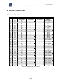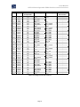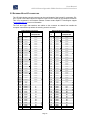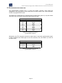
1
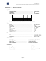
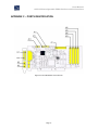
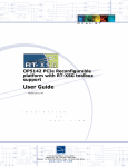
OP5000 Signal Conditioning & I/O Products
for RT-LAB Engineering Simulators
OP5110 Reconfigurable FPGA Platform and I/O Interface
User Manual
Published by
Opal-RT Technologies, Inc.
1751 Richardson, suite 2525
Montréal (Québec) Canada
H3K 1G6
www.opal-rt.com
© 2009 Opal-RT Technologies, Inc.
All rights reserved
Printed in Canada
OP5110_user_manual-C.doc
Rev. B
User Manual
OP5110 Reconfigurable FPGA Platform and I/O Interface
1 TABLE OF CONTENTS
1
Table of Contents ..................................................................................................................... 1
2
Introduction............................................................................................................................... 2
3
4
2.1
About the OP5110 Devices............................................................................................... 2
2.2
Unpacking ......................................................................................................................... 2
2.3
Optional Equipment........................................................................................................... 3
Installation and Configuration................................................................................................... 3
3.1
Hardware Installation ........................................................................................................ 3
3.2
Device Configuration......................................................................................................... 3
Device Overview ...................................................................................................................... 4
4.1
Device Description ............................................................................................................ 4
4.2
Functionality ...................................................................................................................... 4
4.2.1
Static digital input/output (SDIO) ............................................................................... 4
4.2.2
Time-stamped digital input/output (TDIO).................................................................. 4
4.2.3
Parallel interface to D/A and A/D modules ................................................................ 5
4.2.4
Reference pulse generation module (RPG) .............................................................. 5
4.2.5
SignalWire interface................................................................................................... 5
4.3
Functionality Matrix ........................................................................................................... 6
4.3.1
5
Verifying the firmware version on your card .............................................................. 6
Signal Connections .................................................................................................................. 8
5.1
Internal 40-pin I/O connectors........................................................................................... 8
5.2
External 68-pin I/O connectors ....................................................................................... 12
5.3
Internal SignalWire connectors ....................................................................................... 13
5.4
External SignalWire connectors...................................................................................... 13
5.5
Synchronization connectors ............................................................................................ 14
Appendix A – Specifications .......................................................................................................... 15
Appendix B – Example Wiring: RT-LAB WANDA.......................................................................... 16
Appendix C – Ports identification................................................................................................... 17
Appendix D – Block Diagram......................................................................................................... 18
Appendix E – OP5110 PCI Installation Guide ............................................................................... 19
Page 1
User Manual
OP5110 Reconfigurable FPGA Platform and I/O Interface
2 INTRODUCTION
2.1 ABOUT THE OP5110 DEVICES
The OP5110-series devices are multifunction digital input/output cards that feature a
programmable FPGA chip. Currently, this includes the OP5110-1 and OP5110-2 cards. For most
applications, the FPGA chip will have been programmed with dedicated code enabling the
features needed for your application. Should these requirements ever change, please contact
Opal-RT to see if a programming change could better suit your redefined application.
Figure 1: OP5110 Reconfigurable FPGA Platform and I/O Interface
2.2 UNPACKING
The OP5110 Reconfigurable FPGA Platform and I/O Interface card is usually not installed in your
Engineering Simulator. As the card is usually shipped separately, your OP5110 device should be
in an antistatic package to prevent an electrostatic discharge to the device.
An electrostatic discharge can damage several components on the device. To avoid such
damage, be sure to follow these important guidelines:
•
Ground yourself via a grounding strap or by holding a grounded, metallic object.
•
Touch the antistatic package to a metal part of your computer chassis before removing
the device from the package.
•
Remove the device from the package and inspect the device for loose components or
any sign of damage. If the device appears damaged in any way, please notify Opal-RT
Technologies. DO NOT install a damaged device in your computer.
•
Never touch the exposed pins of connectors.
Page 2
User Manual
OP5110 Reconfigurable FPGA Platform and I/O Interface
•
When not in use, store your OP5110 device in the antistatic envelope.
2.3 OPTIONAL EQUIPMENT
The OP5100-series cards are designed for use with other OP5000 signal conditioning and
interfacing modules. Although stand-alone use is supported, in this manual we assume that the
card will be used in an RT-LAB Engineering Simulator.
Typically, this card is used in conjunction with either some OP592x backplane adaptor modules
or a SignalWire connection to the OP5912 OPXI Backplane for Type A and B Carriers. For more
information on these components, please refer to their respective manuals.
3 INSTALLATION AND CONFIGURATION
3.1 HARDWARE INSTALLATION
If you need to install the OP5110 card yourself you will need a Phillips #2 screwdriver. After
disconnecting all power cables from the computer chassis and opening the case of your system
(referred to as the target), you will need to find a free PCI slot. These are usually located at the
back or bottom of the PC chassis and feature a slot of multiple connectors in a rectangular
connector of about 1cm by 15 cm.
Make sure that there is enough clearance on each side of the OP5110 card once inserted in
order for the cable connections to be free of sharp bends and clear of sharp metal parts which
could damage the connections.
Insert the card by first removing the blank faceplate aligned with the PCI slot on the computer's
chassis. Secure the card in its slot by re-using the mounting screw of the faceplate. This should
require firm, but not excessive pressure. See appendix E for detailed instructions.
3.2 DEVICE CONFIGURATION
If your system has multiple OP5110-series cards, each of these must possess a unique board
index. Possible board indices range from 12 to 15, with the default board index of 15 being the
master card for all other cards in the system most of the time. It is not always the case as the
board with index 15 can also be in slave mode. Refer to your system configuration and to your
bitstream selection.
The board index is set using the JP8 jumper terminal. By default, the jumpers should be installed
on the card so that its board index is set to 15. This is the required setting when there is only one
card in the target computer. Other JP8 configurations are used when several cards are installed
in the same target and when a master/slave configuration is needed.
Index 15
Index 14
Index 13
Index 12
Page 3
User Manual
OP5110 Reconfigurable FPGA Platform and I/O Interface
For the clock signal to be propagated from the master card to the other cards, you must connect
the clock synchronization cable, as specified in section 5.5.
4 DEVICE OVERVIEW
4.1 DEVICE DESCRIPTION
The OP5110 card is based around a Xilinx FPGA chip that performs the computational and
input/output functionalities. This chip controls 128 digital lines, which can be used, depending on
the firmware used, in various configurations.
The card's firmware is a special piece of software that resides onboard and is typically not directly
available to the user. This program controls the low-level hardware in order to perform specific
task. Each firmware branch supports a different set of input/output configurations. Each
configuration is, in turn, a set of base functions using one or more of the FPGA's digital lines.
The next section (4.2) defines the base functionalities, or functional building blocks available. The
upcoming Functionality Matrix section shows the configurations (combinations of base
functionalities) supported by each firmware branch.
4.2 FUNCTIONALITY
The functionalities described below are the basic interactions that the card hardware can have
with the systems connected to it. In many cases, higher-level applications can be built on top of
these low-level functionalities. For each low-level functionality described below, we give a few of
the applications that are supported through the RT-LAB software.
4.2.1
STATIC DIGITAL INPUT/OUTPUT (SDIO)
The static digital input or output functionality allows you to set or get the state of one of the digital
signal lines to one of two discrete values. These values are either a logical "off" level of 0 volts or
a logical "on" level of 3.3 volts relative to the card's ground.
These signal lines are named "static" because their state can only be set or read once for every
cycle (or computation step) of the simulation. Typical applications of static digital input/output are:
•
Switch monitoring/simulation
•
Relay driver
•
Logical control signals
Note that for the static digital input/outputs, the signals are in groups of 8 lines. A letter ranging
from A to P identifies each group. This is the notation used in the RT-LAB blocks that use this
functionality.
4.2.2
TIME-STAMPED DIGITAL INPUT/OUTPUT (TDIO)
Time-stamped digital inputs and outputs offer the same functionality as the static digital inputs
and outputs but, with the added possibility that the signal lines can be toggled or read multiple
times and with precise timing during one of the simulation's cycle. This enables you to detect or
generate discrete events with precise timing (down to 10ns resolution).
Page 4
User Manual
OP5110 Reconfigurable FPGA Platform and I/O Interface
Furthermore, with a higher-level algorithm such as the ones implemented in the RT-LAB and RTEVENTS block sets, it is possible to use the time-stamped ports for:
•
Frequency (square-wave) signal generation/detection
•
PWM signal generation/detection
•
Quadrature encoder simulation/detection
•
Arbitrary digital pulse-train generation and detection
As for the static signals, the time-stamped digital signals are in groups of 8 lines. A letter ranging
from A to P identifies each group. This is the notation used in the RT-LAB blocks that use this
functionality.
4.2.3
PARALLEL INTERFACE TO D/A AND A/D MODULES
In conjunction with an OP5220 Type B I/O Module Carrier (passive), it is possible to use a group
of 32 digital signal lines to control and access 16 analog outputs (OP5330 A/D Converter and
Signal Conditioning Module) or 16 analog inputs (OP5340 D/A Converter and Signal Conditioning
Module).
The access to these analog inputs or outputs is controlled through the corresponding blocks in
the RT-LAB block set and allow the following:
4.2.4
•
Sensor simulation/reading (temperature, pressure, force, displacement, and much more)
•
Actuator control
•
Arbitrary waveform playback/detection
REFERENCE PULSE GENERATION MODULE (RPG)
The reference pulse generation module allows for the generation of digital events synchronized
on a position (angular) reference. The typical use of this module is to generate engine events,
such as spark and fuel injection based on an engine's angular position. Note that this is much like
the time-stamped digital output functionality, with the generation of events being position-based
rather than time-based.
The engine can be simulated in the RPG module. The simulated engine RPM must be given
periodically to the RPG core, using its Simulink block. This RPM is used to generate the position
pulse train (with 0.1 or 0.01 degrees of precision) and the synchronous events will be generated
according to the event specifications given at initialization time.
The RPG module can also be used to generate synchronous events for a real engine. For this,
the engine position, CAM and index pulse trains are fed to the RPG module as 0-5 volts signals.
Synchronous events will be generated from this external position reference according to the event
specifications given at initialization time. The RPG module can perform up sampling of the
reference signal, which allows the generation of events within 0.1 or 0.01 degrees of precision
with a 1-degree period for the position signal given as input.
4.2.5
SIGNALWIRE INTERFACE
SignalWire is a high-speed (625 Mbps) serial data link developed by Opal-RT as a means to link
multiple I/O devices together.
Page 5
User Manual
OP5110 Reconfigurable FPGA Platform and I/O Interface
When used in conjunction with an OP5130 Type B I/O Module Carrier (active), it is possible to
use a group of 32 digital signal lines to control and access 16 analog outputs (OP5330 A/D
Converter and Signal Conditioning Module) or 16 analog inputs (OP5340 D/A Converter and
Signal Conditioning Module).
Moreover, many application-specific I/O devices are being developed by Opal-RT Technologies
which use a SignalWire link to interface with RT-LAB Engineering Simulators.
The access to all these field I/O devices is controlled through the corresponding blocks in the RTLAB block set and use of the SignalWire serial link is transparent to the user.
4.3 FUNCTIONALITY MATRIX
The table that follows shows the various possible configurations for each firmware program
available for the OP5110-series cards. Each card shipped is identified with the firmware branch
and revision used for its programming. Please use the table to understand the possible
combinations of features available to you.
Firmware
JP3
(IJKL)
JP4
(MNOP)
JP5 (ABCD)
JP6 (EFGH)
SignalWire
1C-2
-
-
ESPG
ESPG
-
0x26
0026-27
16 D/A
16 A/D
16 D/A
16 A/D
Internal
0x30
30-29
16 A/D
16 A/D
32 TSDIN
32 TSDOUT
Internal
0x35
35-21
16 D/A
16 A/D
16 TSDIN /
16 TSDOUT
16 TSDIN /
16 TSDOUT
Internal
0x36
36-35
SPI
-
16 TSDIN /
16 TSDOUT
-
Internal
0x39
39-20
16 D/A
16 D/A
16 TSDIN
16 TSDOUT
16 TSDIN /
16 TSDOUT
Internal
Device ID
(S17-0016PCI prefix)
0x1C
Table 1: Firmware configuration matrix for OP5110-series cards
Note that the last digit of the firmware name is the revision and might be more recent on the card
you received. The configurations should nonetheless be identical if the other numbers match
those of your card. Note also that the firmware list provided in Table 1 is not exhaustive. Only the
most commonly-used and most up-to-date versions are listed.
4.3.1
VERIFYING THE FIRMWARE VERSION ON YOUR CARD
The PCI vendor ID for the OP5110 is EDDD. When listing all of the PCI devices in your system,
look for this vendor identification to locate the information referring to the OP5110 card. The PCI
device ID will refer to the firmware branch (in this case 1A) and the revision displayed will be the
revision of the firmware (8 here). All numbers are in hexadecimal representation.
From the QNX command line, using the "pci -v | less" will give a listing of all the PCI
devices found in you computer system. For Linux, the equivalent command is "lspci –n –v |
less".
Under QNX (partial listing shown):
Page 6
User Manual
OP5110 Reconfigurable FPGA Platform and I/O Interface
# pci –v | less
Class
Vendor ID
Device ID
PCI index
Revision ID
Interrupt line
=
=
=
=
=
=
System Peripherals (Unknown)
edddh, Unknown
1ah, Unknown Unknown
0h
8h
11
Under Linux (partial listing shown):
# lspci –v –n | less
02:06.0 Class 0880: eddd:001A (rev 08)
Flags: bus master, medium devsel, latency 0, IRQ 17
Memory at d0240000 (32-bit, non-prefetchable) [size=256K]
Page 7
User Manual
OP5110 Reconfigurable FPGA Platform and I/O Interface
5 SIGNAL CONNECTIONS
5.1 INTERNAL 40-PIN I/O CONNECTORS
Hardware
Pin#
Name
1
2
3
4
5
6
7
8
9
10
11
12
13
14
15
16
17
18
19
20
21
22
23
24
25
26
27
28
29
30
31
32
33
34
35
36
37
38
39
40
IO0
GND
IO1
IO2
IO3
IO4
IO5
IO6
IO7
IO8
IO9
IO10
IO11
IO12
IO13
IO14
IO15
IO16
GND
IO17
GND
IO18
GND
IO19
GND
IO20
IO21
IO22
GND
IO23
IO24
IO25
IO26
IO27
IO28
IO29
IO30
IO31
GND
Static and TimeStamped DIO
A0
GND
A1
A2
A3
A4
A5
A6
A7
B0
B1
B2
B3
B4
B5
B6
B7
C0
GND
C1
GND
C2
GND
C3
GND
C4
C5
C6
GND
C7
D0
D1
D2
D3
D4
D5
D6
D7
GND
Functionality Mapping
DAC
ADC
Not Available
Not Available
-
Table 2: Pin Assignment for JP5 Connector
Page 8
RPG
(IN / OUT)
A0 / Position IN
GND
A1 / A2 / Index IN
A3 / A4 / CAM IN
A5 / A6 / A7 / B0 / B0
B1 / B1
B2 / B2
B3 / B3
B4 / B4
B5 / B5
B6 / B6
B7 / B7
C0 / RPG_00
GND
C1 / RPG_01
GND
C2 / RPG_02
GND
C3 / RPG_03
GND
C4 / RPG_04
C5 / RPG_05
C6 / RPG_06
GND
C7 / RPG_07
D0 / RPG_08
D1 / RPG_09
D2 / RPG_10
D3 / RPG_11
D4 / RPG_12
D5 / RPG_13
D6 / RPG_14
D7 / RPG_15
GND
User Manual
OP5110 Reconfigurable FPGA Platform and I/O Interface
Hardware
Pin#
Name
1
2
3
4
5
6
7
8
9
10
11
12
13
14
15
16
17
18
19
20
21
22
23
24
25
26
27
28
29
30
31
32
33
34
35
36
37
38
39
40
IO32
GND
IO33
IO34
IO35
IO36
IO37
IO38
IO39
IO40
IO41
IO42
IO43
IO44
IO45
IO46
IO47
IO48
GND
IO49
GND
IO50
GND
IO51
GND
IO52
IO53
IO54
GND
IO55
IO56
IO57
IO58
IO59
IO60
IO61
IO62
IO63
GND
Static and TimeStamped DIO
E0
GND
E1
E2
E3
E4
E5
E6
E7
F0
F1
F2
F3
F4
F5
F6
F7
G0
GND
G1
GND
G2
GND
G3
GND
G4
G5
G6
GND
G7
H0
H1
H2
H3
H4
H5
H6
H7
GND
Functionality Mapping
DAC
ADC
Not Available
Not Available
-
Table 3: Pin Assignment for JP6 Connector
Page 9
RPG
E0 / E0
GND
E1 / E1
E2 / E2
E3 / E3
E4 / E4
E5 / E5
E6 / E6
E7 / E7
F0 / C0
F1 / C1
F2 / C2
F3 / C3
F4 / C4
F5 / C5
F6 / C6
F7 / C7
G0 / D0
GND
G1 / D1
GND
G2 / D2
GND
G3 / D3
GND
G4 / D4
G5 / D5
G6 / D6
GND
G7 / D7
- / CAM OUT
- / Index OUT
- / Position OUT
GND
User Manual
OP5110 Reconfigurable FPGA Platform and I/O Interface
Hardware
Pin#
Name
1
2
3
4
5
6
7
8
9
10
11
12
13
14
15
16
17
18
19
20
21
22
23
24
25
26
27
28
29
30
31
32
33
34
35
36
37
38
39
40
IO64
GND
IO65
IO66
IO67
IO68
IO69
IO70
IO71
IO72
IO73
IO74
IO75
IO76
IO77
IO78
IO79
IO80
GND
IO81
GND
IO82
GND
IO83
GND
IO84
IO85
IO86
GND
IO87
IO88
IO89
IO90
IO91
IO92
IO93
IO94
IO95
GND
Static and TimeStamped DIO
I0
GND
I1
I2
I3
I4
I5
I6
I7
J0
J1
J2
J3
J4
J5
J6
J7
K0
GND
K1
GND
K2
GND
K3
GND
K4
K5
K6
GND
K7
L0
L1
L2
L3
L4
L5
L6
L7
GND
Functionality Mapping
DAC (A)
ADC (A)
dac_LDAC0
GND
dac_SDI0
dac_SDI1
SCL
dac_SDI2
dac_LDAC1
SDA
dac_LDAC2
dac_LDAC3
dac_SDI3
adj_SDI1
adj_SDI0
adj_SDI3
adj_SDI2
adj_CLK
adj_nCS
dac_MSB
GND
dac_nRST
GND
GND
dac_nCS
GND
dac_CLK
dac_LDAC4
GND
dac_SDI4
dac_SDI5
dac_SDI6
dac_LDAC5
dac_LDAC6
dac_LDAC7
dac_SDI7
GND
adc_CONV0
GND
SCL
adc_CONV2
adc_CONV1
SDA
adc_CONV3
adc_SDA0
adc_SDB0
adc_SDB1
adc_SDA1
adc_SDA2
adc_SDB2
adc_SDB3
adc_SDA3
adc_A0
GND
adc_CONV4
GND
adc_CONV5
GND
adc_nCS
GND
adc_CLK
adc_CONV6
adc_CONV7
GND
adc_SDA4
adc_SDB4
adc_SDB5
adc_SDA5
adc_SDA6
adc_SDB6
adc_SDB7
adc_SDA7
GND
Table 4: Pin Assignment for JP3 Connector
Page 10
RPG
Not Available
-
User Manual
OP5110 Reconfigurable FPGA Platform and I/O Interface
Hardware
Pin#
Name
1
2
3
4
5
6
7
8
9
10
11
12
13
14
15
16
17
18
19
20
21
22
23
24
25
26
27
28
29
30
31
32
33
34
35
36
37
38
39
40
IO96
GND
IO97
IO98
IO99
IO100
IO101
IO102
IO103
IO104
IO105
IO106
IO107
IO108
IO109
IO110
IO111
IO112
GND
IO113
GND
IO114
GND
IO115
GND
IO116
IO117
IO118
GND
IO119
IO120
IO121
IO122
IO123
IO124
IO125
IO126
IO127
GND
Static and TimeStamped DIO
M0
GND
M1
M2
M3
M4
M5
M6
M7
N0
N1
N2
N3
N4
N5
N6
N7
O0
GND
O1
GND
O2
GND
O3
GND
O4
O5
O6
GND
O7
P0
P1
P2
P3
P4
P5
P6
P7
GND
Functionality Mapping
DAC (B)
ADC (B)
dac_LDAC0
GND
dac_SDI0
dac_SDI1
SCL
dac_SDI2
dac_LDAC1
SDA
dac_LDAC2
dac_LDAC3
dac_SDI3
adj_SDI1
adj_SDI0
adj_SDI3
adj_SDI2
adj_CLK
adj_nCS
dac_MSB
GND
dac_nRST
GND
GND
dac_nCS
GND
dac_CLK
dac_LDAC4
GND
dac_SDI4
dac_SDI5
dac_SDI6
dac_LDAC5
dac_LDAC6
dac_LDAC7
dac_SDI7
GND
adc_CONV0
GND
SCL
adc_CONV2
adc_CONV1
SDA
adc_CONV3
adc_SDA0
adc_SDB0
adc_SDB1
adc_SDA1
adc_SDA2
adc_SDB2
adc_SDB3
adc_SDA3
adc_A0
GND
adc_CONV4
GND
adc_CONV5
GND
adc_nCS
GND
adc_CLK
adc_CONV6
adc_CONV7
GND
adc_SDA4
adc_SDB4
adc_SDB5
adc_SDA5
adc_SDA6
adc_SDB6
adc_SDB7
adc_SDA7
GND
Table 5: Pin Assignment for JP4 Connector
Page 11
RPG
Not Available
-
User Manual
OP5110 Reconfigurable FPGA Platform and I/O Interface
5.2 EXTERNAL 68-PIN I/O CONNECTORS
The JP2 high-density external connector can be used instead of the internal IO connectors JP3JP6; It gives a more direct access to digital IO lines from the outside of the computer enclosure.
This is not supported in all firmware releases. Please contact Opal-RT Technologies support
([email protected]) for more information.
The "left" and "right" side notations are relative to the connector as viewed from outside the
computer case with the top where the securing screw is mounted.
Pin
#
1
2
3
4
5
6
7
8
9
10
11
12
13
14
15
16
17
18
19
20
21
22
23
24
25
26
27
28
29
30
31
32
33
34
35
36
37
38
39
40
41
42
Left-side 68-pin connector
Name
Static and TimeStamped DIO
GND
GND
GND
GND
GND
GND
GND
GND
GND
GND
GND
GND
GND
GND
GND
GND
GND
GND
GND
GND
GND
GND
GND
GND
GND
GND
GND
GND
GND
GND
GND
GND
GND
GND
GND
GND
GND
GND
GND
GND
GND
GND
GND
GND
GND
GND
GND
GND
GND
GND
GND
GND
+5V
+5V
IO68
I4
IO70
I6
IO72
J0
IO74
J2
IO76
J4
IO78
J6
IO40
F0
IO41
F1
IO42
F2
IO43
F3
IO44
F4
IO45
F5
IO46
F6
IO47
F7
Right-side 68-pin connector
Pin
Name
Static and Time#
Stamped DIO
1
GND
GND
2
GND
GND
3
GND
GND
4
GND
GND
5
GND
GND
6
GND
GND
7
GND
GND
8
GND
GND
9
GND
GND
10
GND
GND
11
GND
GND
12
GND
GND
13
GND
GND
14
GND
GND
15
GND
GND
16
GND
GND
17
GND
GND
18
GND
GND
19
GND
GND
20
GND
GND
21
GND
GND
22
GND
GND
23
GND
GND
24
GND
GND
25
GND
GND
26
GND
GND
27
+5V
28
+5V
29
IO28
D4
30
IO30
D6
31
IO32
E0
32
IO34
E2
33
IO36
E4
34
IO38
E6
35
IO00
A0
36
IO01
A1
37
IO02
A2
38
IO03
A3
39
IO04
A4
40
IO05
A5
41
IO06
A6
42
IO07
A7
Page 12
User Manual
OP5110 Reconfigurable FPGA Platform and I/O Interface
43
44
45
46
47
48
49
50
51
52
53
54
55
56
57
58
59
60
61
62
63
64
65
66
67
68
IO48
IO49
IO50
IO51
IO52
IO53
IO54
IO55
IO56
IO57
IO58
IO59
IO60
IO61
IO62
IO63
IO64
IO65
IO66
IO67
IO69
IO71
IO73
IO75
IO77
IO79
G0
G1
G2
G3
G4
G5
G6
G7
H0
H1
H2
H3
H4
H5
H6
H7
I0
I1
I2
I3
I5
I7
J1
J3
J5
J7
43
44
45
46
47
48
49
50
51
52
53
54
55
56
57
58
59
60
61
62
63
64
65
66
67
68
IO08
IO09
IO10
IO11
IO12
IO13
IO14
IO15
IO16
IO17
IO18
IO19
IO20
IO21
IO22
IO23
IO24
IO25
IO26
IO27
IO29
IO31
IO33
IO35
IO37
IO39
B0
B1
B2
B3
B4
B5
B6
B7
C0
C1
C2
C3
C4
C5
C6
C7
D0
D1
D2
D3
D5
D7
E1
E3
E5
E7
Table 6: Pin assignment for the JP2 external dual 68-pin connector
5.3 INTERNAL SIGNALWIRE CONNECTORS
The internal SignalWire connections are typically used to communicate with an OP5130 FPGAbased Type B I/O Module Carrier. The recommended connection is through shielded twisted-pair
cables.
Pin#
1
2
3
4
5
6
7
8
JP13 SignalWire Connector
Name
GND
RX RX +
RX Shield
TX Shield
TX TX +
GND
Table 7: Pin assignment for the JP13 SignalWire
connector
5.4 EXTERNAL SIGNALWIRE CONNECTORS
The external SignalWire connectors are not currently supported in any of the available firmware
branches.
Page 13
User Manual
OP5110 Reconfigurable FPGA Platform and I/O Interface
5.5 SYNCHRONIZATION CONNECTORS
The synchronization connector JP7 is a 34-pin IDC header connector, which allows the
propagation of the clock signal from the master card to the slave cards. In the current generation
of cards, only signal RTSI0 is used.
The RTSI0 line is configured as an output for cards in master mode (index 15). Any other board
index will put the card in slave mode and RTSI0 becomes an input.
JP7 Synchronization Connector
Pin#
Name
19
GND
20
RTSI0
21
GND
22
RTSI1
23
GND
24
RTSI2
25
GND
26
RTSI3
27
GND
Table 9: Pin assignment for the JP7
synchronization connector
Alternatively, the JP12 connector can also be used to input or output the synchronization signal.
In order to activate the RTSI0 signal on the JP12 connector, the "Auto Detect" pin must be
shorted to GND.
JP12 Synchronization Connector
Pin#
Name
3
Auto Detect
4
RTSI0
5
+5V
6
GND
Table 10: Pin assignment for the JP12
synchronization connector
Page 14
User Manual
OP5110 Reconfigurable FPGA Platform and I/O Interface
APPENDIX A – SPECIFICATIONS
Digital I/O
Number of channels …………………………………………………………
Compatibility …………………………………………………………………
Power-on state ………………………………………………………………
Levels
Level
Minimum
Maximum
Input low
0.0v
0.8v
Input high
2.0v
5.5v
Output low – 12mA (sink)
0.0v
0.4v
Output high – 12mA (source)
2.4v
3.3v
128 input/output
TTL
High impedance
For additional signal conditioning and protection, see OP531x specifications.
FPGA
Device ………………………………………………………………………
I/O package …………………………………………………………………
Available RAM ………………………………………………………………
Clock …………………………………………………………………………
Platform options ……………………………………………………………
Logic slices …………………………………………………………………
Equivalent logic cells ………………………………………………………
Available I/O lines …………………………………………………………
Xilinx Virtex II Pro
625FF
16 KB (ext. to 2MB)
62.5, 100MHz
XC2V1000
5,120
11,500
396
PCI ……………………………………………………………………………
32-bit, 33MHz, 1Gbps
64-bit, 66MHz, 4Gbps
Interrupt or DMA
Bus
Data transfers ………………………………………………………………
I/O connectors
Internal DIO ……………………………………………
Internal SignalWire ……………………………………
External DIO ……………………………………………
External SignalWire ……………………………………
4 x 40-way header AMP 120613-1
2 x Molex 35362-0810
1 x Molex 74337-0011
2 x Lumberg 2301F90V203
Environmental
Operating temperature ……………………………………………
Storage temperature ………………………………………………
Relative humidity ……………………………………………………
Maximum altitude …………………………………………………
Page 15
0 - 70°C
-55 - 105°C
10 - 90%, non-condensing
2,000 meters
User Manual
OP5110 Reconfigurable FPGA Platform and I/O Interface
APPENDIX B – EXAMPLE WIRING: RT-LAB WANDA
Below is an example of the OP5110 card being used in an RT-LAB Engineering Simulator. In this
configuration, it allows for 16 digital inputs, 16 digital outputs, all time-stamped (JP5) as well as
16 DAC (JP3) and 16 ADC (JP4) channels connected in parallel.
The SignalWire port is also used to retrieve another set of 16 DAC channels from another FPGAbased card: the OP5130. The RTSI port allows synchronization between both FPGA cards
(OP5110 and OP5130).
Figure 2: Example wiring of an OP5110 using an RT-LAB Wanda
Page 16
User Manual
OP5110 Reconfigurable FPGA Platform and I/O Interface
APPENDIX C – PORTS IDENTIFICATION
Figure 3: Ports identification of the OP5110.
Page 17
User Manual
OP5110 Reconfigurable FPGA Platform and I/O Interface
APPENDIX D – BLOCK DIAGRAM
Figure 4: OP5110 Block diagram
Page 18
User Manual
OP5110 Reconfigurable FPGA Platform and I/O Interface
APPENDIX E – OP5110 PCI INSTALLATION GUIDE
HOW TO INSTALL YOUR FPGA PCI
(OP5110 : 126-0158 OR 126-0107)
Caution: this product is sensitive to static electricity.
Before you start, be sure the system is not connected to power line.
Test Drive :
HIL:
Installation:
•
Remove the panel (TestDrive : back panel,
HIL : top panel)
TestDrive :
•
Connect the gray cable to the JP13
connector of the OP5110.
•
Secure the bracket, by using the available screw.
•
HIL :
•
You can now put back the back panel.
If necessary:
-
Connect the flat cable to JP3, JP4, JP5, JP6
-
Installed the signal wire cable to JP13 connectors
of the OP5110.
Install the Synchronisation cable to JP12
connectors of the OP5110.
Note: The cable are already inside your system.
-
•
Secure the bracket, by using the available screw.
•
You can now put back the top panel.
Page 19
JP6
Push the PCI card into the empty slot, so that
it is fully seated in the slot.
JP5
•
JP4
Carrefully insert the PCI card into the empty
slot (the one without a bracket) of the target.
JP13
JP3
•
JP12