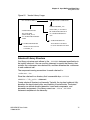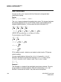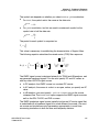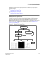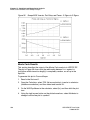
1
HSPICE® RF User Guide
Version Y-2006.03-SP1, June 2006
Copyright Notice and Proprietary Information
Copyright © 2006 Synopsys, Inc. All rights reserved. This software and documentation contain confidential and proprietary
information that is the property of Synopsys, Inc. The software and documentation are furnished under a license agreement and
may be used or copied only in accordance with the terms of the license agreement. No part of the software and documentation may
be reproduced, transmitted, or translated, in any form or by any means, electronic, mechanical, manual, optical, or otherwise, without
prior written permission of Synopsys, Inc., or as expressly provided by the license agreement.
Right to Copy Documentation
The license agreement with Synopsys permits licensee to make copies of the documentation for its internal use only.
Each copy shall include all copyrights, trademarks, service marks, and proprietary rights notices, if any. Licensee must
assign sequential numbers to all copies. These copies shall contain the following legend on the cover page:
“This document is duplicated with the permission of Synopsys, Inc., for the exclusive use of
__________________________________________ and its employees. This is copy number __________.”
Destination Control Statement
All technical data contained in this publication is subject to the export control laws of the United States of America.
Disclosure to nationals of other countries contrary to United States law is prohibited. It is the reader’s responsibility to
determine the applicable regulations and to comply with them.
Disclaimer
SYNOPSYS, INC., AND ITS LICENSORS MAKE NO WARRANTY OF ANY KIND, EXPRESS OR IMPLIED, WITH
REGARD TO THIS MATERIAL, INCLUDING, BUT NOT LIMITED TO, THE IMPLIED WARRANTIES OF
MERCHANTABILITY AND FITNESS FOR A PARTICULAR PURPOSE.
Registered Trademarks (®)
Synopsys, AMPS, Arcadia, C Level Design, C2HDL, C2V, C2VHDL, Cadabra, Calaveras Algorithm, CATS, CRITIC,
CSim, Design Compiler, DesignPower, DesignWare, EPIC, Formality, HSIM, HSPICE, Hypermodel, iN-Phase, in-Sync,
Leda, MAST, Meta, Meta-Software, ModelTools, NanoSim, OpenVera, PathMill, Photolynx, Physical Compiler, PowerMill,
PrimeTime, RailMill, RapidScript, Saber, SiVL, SNUG, SolvNet, Superlog, System Compiler, TetraMAX, TimeMill, TMA,
VCS, Vera, and Virtual Stepper are registered trademarks of Synopsys, Inc.
Trademarks (™)
Active Parasitics, AFGen, Apollo, Apollo II, Apollo-DPII, Apollo-GA, ApolloGAII, Astro, Astro-Rail, Astro-Xtalk, Aurora,
AvanTestchip, AvanWaves, BCView, Behavioral Compiler, BOA, BRT, Cedar, ChipPlanner, Circuit Analysis, Columbia,
Columbia-CE, Comet 3D, Cosmos, CosmosEnterprise, CosmosLE, CosmosScope, CosmosSE, Cyclelink, Davinci, DC
Expert, DC Professional, DC Ultra, DC Ultra Plus, Design Advisor, Design Analyzer, Design Vision, DesignerHDL,
DesignTime, DFM-Workbench, Direct RTL, Direct Silicon Access, Discovery, DW8051, DWPCI,
Dynamic-Macromodeling, Dynamic Model Switcher, ECL Compiler, ECO Compiler, EDAnavigator, Encore, Encore PQ,
Evaccess, ExpressModel, Floorplan Manager, Formal Model Checker, FoundryModel, FPGA Compiler II, FPGA Express,
Frame Compiler, Galaxy, Gatran, HANEX, HDL Advisor, HDL Compiler, Hercules, Hercules-Explorer, Hercules-II,
Hierarchical Optimization Technology, High Performance Option, HotPlace, HSIMplus, HSPICE-Link, iN-Tandem,
Integrator, Interactive Waveform Viewer, i-Virtual Stepper, Jupiter, Jupiter-DP, JupiterXT, JupiterXT-ASIC, JVXtreme,
Liberty, Libra-Passport, Library Compiler, Libra-Visa, Magellan, Mars, Mars-Rail, Mars-Xtalk, Medici, Metacapture,
Metacircuit, Metamanager, Metamixsim, Milkyway, ModelSource, Module Compiler, MS-3200, MS-3400, Nova Product
Family, Nova-ExploreRTL, Nova-Trans, Nova-VeriLint, Nova-VHDLlint, Optimum Silicon, Orion_ec, Parasitic View,
Passport, Planet, Planet-PL, Planet-RTL, Polaris, Polaris-CBS, Polaris-MT, Power Compiler, PowerCODE, PowerGate,
ProFPGA, ProGen, Prospector, Protocol Compiler, PSMGen, Raphael, Raphael-NES, RoadRunner, RTL Analyzer,
Saturn, ScanBand, Schematic Compiler, Scirocco, Scirocco-i, Shadow Debugger, Silicon Blueprint, Silicon Early Access,
SinglePass-SoC, Smart Extraction, SmartLicense, SmartModel Library, Softwire, Source-Level Design, Star, Star-DC,
Star-MS, Star-MTB, Star-Power, Star-Rail, Star-RC, Star-RCXT, Star-Sim, Star-SimXT, Star-Time, Star-XP, SWIFT,
Taurus, TimeSlice, TimeTracker, Timing Annotator, TopoPlace, TopoRoute, Trace-On-Demand, True-Hspice,
TSUPREM-4, TymeWare, VCS Express, VCSi, Venus, Verification Portal, VFormal, VHDL Compiler, VHDL System
Simulator, VirSim, and VMC are trademarks of Synopsys, Inc.
Service Marks (SM)
MAP-in, SVP Café, and TAP-in are service marks of Synopsys, Inc.
SystemC is a trademark of the Open SystemC Initiative and is used under license.
ARM and AMBA are registered trademarks of ARM Limited.
All other product or company names may be trademarks of their respective owners.
Printed in the U.S.A.
HSPICE® RF User Guide, Y-2006.03-SP1
ii
HSPICE® RF User Guide
Y-2006.03-SP1
Contents
1.
2.
3.
Inside This Manual. . . . . . . . . . . . . . . . . . . . . . . . . . . . . . . . . . . . . . . . . . . . . .
xiii
The HSPICE Documentation Set. . . . . . . . . . . . . . . . . . . . . . . . . . . . . . . . . . .
xiv
Other Related Publications . . . . . . . . . . . . . . . . . . . . . . . . . . . . . . . . . . . . . . .
xvi
Conventions . . . . . . . . . . . . . . . . . . . . . . . . . . . . . . . . . . . . . . . . . . . . . . . . . . .
xvii
Customer Support . . . . . . . . . . . . . . . . . . . . . . . . . . . . . . . . . . . . . . . . . . . . . .
xvii
HSPICE RF Features and Functionality . . . . . . . . . . . . . . . . . . . . . . . . . . . .
1
HSPICE RF Overview . . . . . . . . . . . . . . . . . . . . . . . . . . . . . . . . . . . . . . . . . . .
1
HSPICE RF Features. . . . . . . . . . . . . . . . . . . . . . . . . . . . . . . . . . . . . . . .
2
HSPICE and HSPICE RF Differences . . . . . . . . . . . . . . . . . . . . . . . . . . . . . . .
5
Getting Started. . . . . . . . . . . . . . . . . . . . . . . . . . . . . . . . . . . . . . . . . . . . . . . .
9
Running HSPICE RF Simulations . . . . . . . . . . . . . . . . . . . . . . . . . . . . . . . . . .
9
Netlist Overview . . . . . . . . . . . . . . . . . . . . . . . . . . . . . . . . . . . . . . . . . . . . . . . .
9
Parametric Analysis Extensions. . . . . . . . . . . . . . . . . . . . . . . . . . . . . . . . . . . .
10
Generating Output Files. . . . . . . . . . . . . . . . . . . . . . . . . . . . . . . . . . . . . . . . . .
10
HSPICE RF Output File Types . . . . . . . . . . . . . . . . . . . . . . . . . . . . . . . . .
11
Using the CosmosScope Waveform Display . . . . . . . . . . . . . . . . . . . . . . . . . .
12
HSPICE RF Tutorial . . . . . . . . . . . . . . . . . . . . . . . . . . . . . . . . . . . . . . . . . . . .
15
Example 1: Low Noise Amplifier . . . . . . . . . . . . . . . . . . . . . . . . . . . . . . . . . . .
15
Example 2: Power Amplifier . . . . . . . . . . . . . . . . . . . . . . . . . . . . . . . . . . . . . . .
19
Example 3: Amplifier IP3 . . . . . . . . . . . . . . . . . . . . . . . . . . . . . . . . . . . . . . . . .
22
Example 4: Colpitts Oscillator . . . . . . . . . . . . . . . . . . . . . . . . . . . . . . . . . . . . .
27
Example 5: CMOS GPS VCO . . . . . . . . . . . . . . . . . . . . . . . . . . . . . . . . . . . . .
29
Example 6: Mixer . . . . . . . . . . . . . . . . . . . . . . . . . . . . . . . . . . . . . . . . . . . . . . .
37
Two-tone HB Approach . . . . . . . . . . . . . . . . . . . . . . . . . . . . . . . . . . . . . .
38
HBAC Approach . . . . . . . . . . . . . . . . . . . . . . . . . . . . . . . . . . . . . . . . . . . .
39
iii
Contents
4.
iv
Comparing Results . . . . . . . . . . . . . . . . . . . . . . . . . . . . . . . . . . . . . . . . .
40
Device Model Cards. . . . . . . . . . . . . . . . . . . . . . . . . . . . . . . . . . . . . . . . . . . . .
41
Input Netlist and Data Entry . . . . . . . . . . . . . . . . . . . . . . . . . . . . . . . . . . . . .
43
Input Netlist File Guidelines . . . . . . . . . . . . . . . . . . . . . . . . . . . . . . . . . . . . . . .
43
Input Line Format . . . . . . . . . . . . . . . . . . . . . . . . . . . . . . . . . . . . . . . . . . .
44
Delimiters . . . . . . . . . . . . . . . . . . . . . . . . . . . . . . . . . . . . . . . . . . . . . . . . .
46
Node Identifiers . . . . . . . . . . . . . . . . . . . . . . . . . . . . . . . . . . . . . . . . . . . .
46
Instance Names . . . . . . . . . . . . . . . . . . . . . . . . . . . . . . . . . . . . . . . . . . . .
46
Hierarchy Paths . . . . . . . . . . . . . . . . . . . . . . . . . . . . . . . . . . . . . . . . . . . .
48
Numbers. . . . . . . . . . . . . . . . . . . . . . . . . . . . . . . . . . . . . . . . . . . . . . . . . .
48
Parameters and Expressions . . . . . . . . . . . . . . . . . . . . . . . . . . . . . . . . .
49
Input Netlist File Structure . . . . . . . . . . . . . . . . . . . . . . . . . . . . . . . . . . . .
50
Schematic Netlists . . . . . . . . . . . . . . . . . . . . . . . . . . . . . . . . . . . . . . . . . .
51
Input Netlist File Composition . . . . . . . . . . . . . . . . . . . . . . . . . . . . . . . . . . . . .
52
Title of Simulation. . . . . . . . . . . . . . . . . . . . . . . . . . . . . . . . . . . . . . . . . . .
53
Comments and Line Continuation . . . . . . . . . . . . . . . . . . . . . . . . . . . . . .
54
Element and Source Statements . . . . . . . . . . . . . . . . . . . . . . . . . . . . . . .
55
Defining Subcircuits . . . . . . . . . . . . . . . . . . . . . . . . . . . . . . . . . . . . . . . . .
58
Node Naming Conventions . . . . . . . . . . . . . . . . . . . . . . . . . . . . . . . . . . .
58
Element, Instance, and Subcircuit Naming Conventions . . . . . . . . . . . . .
61
Subcircuit Node Names . . . . . . . . . . . . . . . . . . . . . . . . . . . . . . . . . . . . .
61
Path Names of Subcircuit Nodes . . . . . . . . . . . . . . . . . . . . . . . . . . . . . . .
62
Abbreviated Subcircuit Node Names . . . . . . . . . . . . . . . . . . . . . . . . . . . .
62
Automatic Node Name Generation . . . . . . . . . . . . . . . . . . . . . . . . . . . . .
63
Global Node Names. . . . . . . . . . . . . . . . . . . . . . . . . . . . . . . . . . . . . . . . .
63
Circuit Temperature . . . . . . . . . . . . . . . . . . . . . . . . . . . . . . . . . . . . . . . . .
64
Data-Driven Analysis . . . . . . . . . . . . . . . . . . . . . . . . . . . . . . . . . . . . . . . .
64
Library Calls and Definitions . . . . . . . . . . . . . . . . . . . . . . . . . . . . . . . . . .
65
Defining Parameters. . . . . . . . . . . . . . . . . . . . . . . . . . . . . . . . . . . . . . . . .
65
Deleting a Library . . . . . . . . . . . . . . . . . . . . . . . . . . . . . . . . . . . . . . . . . . .
69
Ending a Netlist . . . . . . . . . . . . . . . . . . . . . . . . . . . . . . . . . . . . . . . . . . . .
70
Condition-Controlled Netlists (IF-ELSE). . . . . . . . . . . . . . . . . . . . . . . . . .
70
Using Subcircuits . . . . . . . . . . . . . . . . . . . . . . . . . . . . . . . . . . . . . . . . . . . . . . .
71
Hierarchical Parameters. . . . . . . . . . . . . . . . . . . . . . . . . . . . . . . . . . . . . .
72
DDL Library Access . . . . . . . . . . . . . . . . . . . . . . . . . . . . . . . . . . . . . . . . .
75
Vendor Libraries . . . . . . . . . . . . . . . . . . . . . . . . . . . . . . . . . . . . . . . . . . . .
76
Contents
5.
6.
Subcircuit Library Structure . . . . . . . . . . . . . . . . . . . . . . . . . . . . . . . . . . .
77
Elements . . . . . . . . . . . . . . . . . . . . . . . . . . . . . . . . . . . . . . . . . . . . . . . . . . . . .
79
Passive Elements. . . . . . . . . . . . . . . . . . . . . . . . . . . . . . . . . . . . . . . . . . . . . . .
79
Values for Elements . . . . . . . . . . . . . . . . . . . . . . . . . . . . . . . . . . . . . . . . .
79
Resistor Elements in a HSPICE or HSPICE RF Netlist . . . . . . . . . . . . . .
80
Capacitors . . . . . . . . . . . . . . . . . . . . . . . . . . . . . . . . . . . . . . . . . . . . . . . .
85
Inductors . . . . . . . . . . . . . . . . . . . . . . . . . . . . . . . . . . . . . . . . . . . . . . . . .
92
Active Elements . . . . . . . . . . . . . . . . . . . . . . . . . . . . . . . . . . . . . . . . . . . . . . . .
105
Diode Element . . . . . . . . . . . . . . . . . . . . . . . . . . . . . . . . . . . . . . . . . . . . .
105
Bipolar Junction Transistor (BJT) Element . . . . . . . . . . . . . . . . . . . . . . . .
107
JFETs and MESFETs . . . . . . . . . . . . . . . . . . . . . . . . . . . . . . . . . . . . . . .
109
MOSFETs . . . . . . . . . . . . . . . . . . . . . . . . . . . . . . . . . . . . . . . . . . . . . . . .
111
Transmission Lines . . . . . . . . . . . . . . . . . . . . . . . . . . . . . . . . . . . . . . . . . . . . .
114
W Element . . . . . . . . . . . . . . . . . . . . . . . . . . . . . . . . . . . . . . . . . . . . . . . .
114
Lossless (T Element) . . . . . . . . . . . . . . . . . . . . . . . . . . . . . . . . . . . . . . . .
119
Lossy (U Element) . . . . . . . . . . . . . . . . . . . . . . . . . . . . . . . . . . . . . . . . . .
123
Frequency-Dependent Multi-Terminal S Element . . . . . . . . . . . . . . . . . .
124
Frequency Table Model . . . . . . . . . . . . . . . . . . . . . . . . . . . . . . . . . . . . . .
130
Group Delay Handler in Time Domain Analysis . . . . . . . . . . . . . . . . . . . .
130
Preconditioning S Parameters . . . . . . . . . . . . . . . . . . . . . . . . . . . . . . . . .
131
Parameters and Functions . . . . . . . . . . . . . . . . . . . . . . . . . . . . . . . . . . . . . .
133
Using Parameters in Simulation (.PARAM) . . . . . . . . . . . . . . . . . . . . . . . . . . .
133
Defining Parameters . . . . . . . . . . . . . . . . . . . . . . . . . . . . . . . . . . . . . . . .
133
Assigning Parameters . . . . . . . . . . . . . . . . . . . . . . . . . . . . . . . . . . . . . . .
135
User-Defined Function Parameters . . . . . . . . . . . . . . . . . . . . . . . . . . . . .
136
Predefined Analysis Function. . . . . . . . . . . . . . . . . . . . . . . . . . . . . . . . . .
137
Measurement Parameters . . . . . . . . . . . . . . . . . . . . . . . . . . . . . . . . . . . .
137
.PRINT and .PROBE Parameters . . . . . . . . . . . . . . . . . . . . . . . . . . . . . .
137
Multiply Parameter . . . . . . . . . . . . . . . . . . . . . . . . . . . . . . . . . . . . . . . . . .
137
Using Algebraic Expressions . . . . . . . . . . . . . . . . . . . . . . . . . . . . . . . . . . . . . .
138
Built-In Functions and Variables . . . . . . . . . . . . . . . . . . . . . . . . . . . . . . . . . . .
139
Parameter Scoping and Passing . . . . . . . . . . . . . . . . . . . . . . . . . . . . . . . . . . .
143
Library Integrity . . . . . . . . . . . . . . . . . . . . . . . . . . . . . . . . . . . . . . . . . . . .
144
Reusing Cells . . . . . . . . . . . . . . . . . . . . . . . . . . . . . . . . . . . . . . . . . . . . . .
144
v
Contents
7.
vi
Creating Parameters in a Library . . . . . . . . . . . . . . . . . . . . . . . . . . . . . . .
144
String Parameter (HSPICE Only) . . . . . . . . . . . . . . . . . . . . . . . . . . . . . . .
147
Parameter Defaults and Inheritance. . . . . . . . . . . . . . . . . . . . . . . . . . . . .
147
Parameter Passing Solutions . . . . . . . . . . . . . . . . . . . . . . . . . . . . . . . . . .
150
Testbench Elements . . . . . . . . . . . . . . . . . . . . . . . . . . . . . . . . . . . . . . . . . . .
151
Behavioral Passive Elements. . . . . . . . . . . . . . . . . . . . . . . . . . . . . . . . . . . . . .
151
Resistors . . . . . . . . . . . . . . . . . . . . . . . . . . . . . . . . . . . . . . . . . . . . . . . . .
151
Capacitors . . . . . . . . . . . . . . . . . . . . . . . . . . . . . . . . . . . . . . . . . . . . . . . .
154
Frequency-Dependent Inductors . . . . . . . . . . . . . . . . . . . . . . . . . . . . . . .
158
DC Block and Choke Elements . . . . . . . . . . . . . . . . . . . . . . . . . . . . . . . .
159
Ideal Transformers . . . . . . . . . . . . . . . . . . . . . . . . . . . . . . . . . . . . . . . . . .
160
Coupled Inductor Element . . . . . . . . . . . . . . . . . . . . . . . . . . . . . . . . . . . .
162
Scattering Parameter Data Element . . . . . . . . . . . . . . . . . . . . . . . . . . . . . . . .
164
Frequency-Dependent Multi-Terminal (S) Element . . . . . . . . . . . . . . . . .
165
Frequency Table Model . . . . . . . . . . . . . . . . . . . . . . . . . . . . . . . . . . . . . .
174
Group Delay Handler in Time Domain Analysis . . . . . . . . . . . . . . . . . . . .
175
Pre-Conditioning S Parameters . . . . . . . . . . . . . . . . . . . . . . . . . . . . . . . .
175
Port Element . . . . . . . . . . . . . . . . . . . . . . . . . . . . . . . . . . . . . . . . . . . . . . . . . .
176
Port Element Syntax . . . . . . . . . . . . . . . . . . . . . . . . . . . . . . . . . . . . . . . .
177
Using the Port Element for Mixed-Mode Measurement . . . . . . . . . . . . . .
180
Steady-State Voltage and Current Sources . . . . . . . . . . . . . . . . . . . . . . . . . . .
180
I and V Element Syntax . . . . . . . . . . . . . . . . . . . . . . . . . . . . . . . . . . . . . .
181
Steady-State HB Sources . . . . . . . . . . . . . . . . . . . . . . . . . . . . . . . . . . . . . . . .
184
Phase Differences Between HB and SIN Sources . . . . . . . . . . . . . . . . . . . . .
186
Behavioral Noise Sources . . . . . . . . . . . . . . . . . . . . . . . . . . . . . . . . . . . . . . . .
187
Power Supply Current and Voltage Noise Sources . . . . . . . . . . . . . . . . .
188
Function Approximations for Distributed Devices . . . . . . . . . . . . . . . . . . . . . .
189
Foster Pole-Residue Form for Transconductance or Gain . . . . . . . . . . . .
190
Advantages of Foster Form Modeling . . . . . . . . . . . . . . . . . . . . . . . . . . .
190
G and E Element Syntax . . . . . . . . . . . . . . . . . . . . . . . . . . . . . . . . . . . . .
190
Complex Signal Sources and Stimuli . . . . . . . . . . . . . . . . . . . . . . . . . . . . . . . .
191
Vector-Modulated RF Source. . . . . . . . . . . . . . . . . . . . . . . . . . . . . . . . . .
192
Voltage and Current Source Elements. . . . . . . . . . . . . . . . . . . . . . . . . . .
194
SWEEPBLOCK in Sweep Analyses . . . . . . . . . . . . . . . . . . . . . . . . . . . . . . . .
200
Input Syntax . . . . . . . . . . . . . . . . . . . . . . . . . . . . . . . . . . . . . . . . . . . . . . .
201
Contents
8.
9.
Using SWEEPBLOCK in a DC Parameter Sweep . . . . . . . . . . . . . . . . . .
202
Using in Parameter Sweeps in TRAN, AC, and HB Analyses . . . . . . . . .
202
Limitations . . . . . . . . . . . . . . . . . . . . . . . . . . . . . . . . . . . . . . . . . . . . . . . .
203
References. . . . . . . . . . . . . . . . . . . . . . . . . . . . . . . . . . . . . . . . . . . . . . . . . . . .
203
Steady-State Harmonic Balance Analysis . . . . . . . . . . . . . . . . . . . . . . . . . .
205
Harmonic Balance Analysis . . . . . . . . . . . . . . . . . . . . . . . . . . . . . . . . . . . . . . .
206
Harmonic Balance Equations. . . . . . . . . . . . . . . . . . . . . . . . . . . . . . . . . .
206
Features Supported . . . . . . . . . . . . . . . . . . . . . . . . . . . . . . . . . . . . . . . . .
207
Input Syntax . . . . . . . . . . . . . . . . . . . . . . . . . . . . . . . . . . . . . . . . . . . . . . .
208
HB Analysis Spectrum . . . . . . . . . . . . . . . . . . . . . . . . . . . . . . . . . . . . . . .
209
HB Analysis Options . . . . . . . . . . . . . . . . . . . . . . . . . . . . . . . . . . . . . . . .
210
Harmonic Balance Output Measurements . . . . . . . . . . . . . . . . . . . . . . . .
212
Output Syntax . . . . . . . . . . . . . . . . . . . . . . . . . . . . . . . . . . . . . . . . . . . . .
214
Calculating Power Measurements After HB Analyses . . . . . . . . . . . . . . .
215
Calculating for a Time-Domain Output . . . . . . . . . . . . . . . . . . . . . . . . . . .
218
Output Examples . . . . . . . . . . . . . . . . . . . . . . . . . . . . . . . . . . . . . . . . . . .
219
Using .MEASURE with .HB Analyses . . . . . . . . . . . . . . . . . . . . . . . . . . .
219
HB Output Data Files . . . . . . . . . . . . . . . . . . . . . . . . . . . . . . . . . . . . . . . . . . . .
221
Errors and Warnings . . . . . . . . . . . . . . . . . . . . . . . . . . . . . . . . . . . . . . . .
222
References. . . . . . . . . . . . . . . . . . . . . . . . . . . . . . . . . . . . . . . . . . . . . . . . . . . .
224
Oscillator and Phase Noise Analysis. . . . . . . . . . . . . . . . . . . . . . . . . . . . . .
227
Harmonic Balance for Oscillator Analysis . . . . . . . . . . . . . . . . . . . . . . . . . . . .
227
Input Syntax . . . . . . . . . . . . . . . . . . . . . . . . . . . . . . . . . . . . . . . . . . . . . . .
228
HB Simulation of Ring Oscillators . . . . . . . . . . . . . . . . . . . . . . . . . . . . . .
230
HBOSC Analysis Options. . . . . . . . . . . . . . . . . . . . . . . . . . . . . . . . . . . . .
231
Additional .HBOSC Analysis Options. . . . . . . . . . . . . . . . . . . . . . . . . . . .
232
.HBOSC Output Syntax . . . . . . . . . . . . . . . . . . . . . . . . . . . . . . . . . . . . . .
233
Phase Noise Analysis . . . . . . . . . . . . . . . . . . . . . . . . . . . . . . . . . . . . . . . . . . .
233
Input Syntax . . . . . . . . . . . . . . . . . . . . . . . . . . . . . . . . . . . . . . . . . . . . . . .
235
Phase Noise Algorithms. . . . . . . . . . . . . . . . . . . . . . . . . . . . . . . . . . . . . .
237
Measuring PHASENOISE Analyses with .MEASURE . . . . . . . . . . . . . . .
239
Output Syntax . . . . . . . . . . . . . . . . . . . . . . . . . . . . . . . . . . . . . . . . . . . . .
240
Phase Noise Analysis Options . . . . . . . . . . . . . . . . . . . . . . . . . . . . . . . . .
241
Timing Jitter Analysis . . . . . . . . . . . . . . . . . . . . . . . . . . . . . . . . . . . . . . . . . . . .
242
vii
Contents
viii
Timing Jitter Syntax . . . . . . . . . . . . . . . . . . . . . . . . . . . . . . . . . . . . . . . . .
244
RMS JITTER Measurement . . . . . . . . . . . . . . . . . . . . . . . . . . . . . . . . . . .
245
References. . . . . . . . . . . . . . . . . . . . . . . . . . . . . . . . . . . . . . . . . . . . . . . . . . . .
246
10. Power-Dependent S Parameter Extraction . . . . . . . . . . . . . . . . . . . . . . . . .
247
HBLSP Analysis. . . . . . . . . . . . . . . . . . . . . . . . . . . . . . . . . . . . . . . . . . . . . . . .
247
Limitations . . . . . . . . . . . . . . . . . . . . . . . . . . . . . . . . . . . . . . . . . . . . . . . . . . . .
248
Input Syntax . . . . . . . . . . . . . . . . . . . . . . . . . . . . . . . . . . . . . . . . . . . . . . . . . . .
248
Output Syntax . . . . . . . . . . . . . . . . . . . . . . . . . . . . . . . . . . . . . . . . . . . . . . . . .
250
.PRINT and .PROBE Statements. . . . . . . . . . . . . . . . . . . . . . . . . . . . . . .
250
Output Data Files . . . . . . . . . . . . . . . . . . . . . . . . . . . . . . . . . . . . . . . . . . . . . . .
251
11. Harmonic Balance-Based AC and Noise Analyses. . . . . . . . . . . . . . . . . . .
253
Multitone Harmonic Balance AC Analysis (.HBAC) . . . . . . . . . . . . . . . . . . . . .
253
Prerequisites and Limitations . . . . . . . . . . . . . . . . . . . . . . . . . . . . . . . . . .
253
Input Syntax . . . . . . . . . . . . . . . . . . . . . . . . . . . . . . . . . . . . . . . . . . . . . . .
254
Output Syntax . . . . . . . . . . . . . . . . . . . . . . . . . . . . . . . . . . . . . . . . . . . . .
255
Output Data Files . . . . . . . . . . . . . . . . . . . . . . . . . . . . . . . . . . . . . . . . . . .
256
Errors and Warnings . . . . . . . . . . . . . . . . . . . . . . . . . . . . . . . . . . . . . . . .
257
Multitone Nonlinear Steady-State Analysis (.HBNOISE) . . . . . . . . . . . . . . . . .
258
Supported Features . . . . . . . . . . . . . . . . . . . . . . . . . . . . . . . . . . . . . . . . .
258
Input Syntax . . . . . . . . . . . . . . . . . . . . . . . . . . . . . . . . . . . . . . . . . . . . . . .
259
Output Syntax . . . . . . . . . . . . . . . . . . . . . . . . . . . . . . . . . . . . . . . . . . . . .
261
Output Data Files . . . . . . . . . . . . . . . . . . . . . . . . . . . . . . . . . . . . . . . . . . .
262
Measuring HBNOISE Analyses with .MEASURE . . . . . . . . . . . . . . . . . .
263
Errors and Warnings . . . . . . . . . . . . . . . . . . . . . . . . . . . . . . . . . . . . . . . .
264
Frequency Translation S-Parameter (HBLIN) Extraction . . . . . . . . . . . . . . . . .
265
HB Analysis . . . . . . . . . . . . . . . . . . . . . . . . . . . . . . . . . . . . . . . . . . . . . . .
267
Port Element . . . . . . . . . . . . . . . . . . . . . . . . . . . . . . . . . . . . . . . . . . . . . .
267
HBLIN Analysis . . . . . . . . . . . . . . . . . . . . . . . . . . . . . . . . . . . . . . . . . . . .
268
Output Syntax . . . . . . . . . . . . . . . . . . . . . . . . . . . . . . . . . . . . . . . . . . . . .
270
Output Data Files . . . . . . . . . . . . . . . . . . . . . . . . . . . . . . . . . . . . . . . . . . .
271
Computing Transfer Functions (.HBXF) . . . . . . . . . . . . . . . . . . . . . . . . . . . . . .
271
Supported Features . . . . . . . . . . . . . . . . . . . . . . . . . . . . . . . . . . . . . . . . .
272
Input Syntax . . . . . . . . . . . . . . . . . . . . . . . . . . . . . . . . . . . . . . . . . . . . . . .
273
Contents
Output Syntax . . . . . . . . . . . . . . . . . . . . . . . . . . . . . . . . . . . . . . . . . . . . .
274
Output Data Files . . . . . . . . . . . . . . . . . . . . . . . . . . . . . . . . . . . . . . . . . . .
274
References. . . . . . . . . . . . . . . . . . . . . . . . . . . . . . . . . . . . . . . . . . . . . . . . . . . .
275
12. Envelope Analysis . . . . . . . . . . . . . . . . . . . . . . . . . . . . . . . . . . . . . . . . . . . . .
277
Envelope Simulation . . . . . . . . . . . . . . . . . . . . . . . . . . . . . . . . . . . . . . . . . . . .
277
Envelope Analysis Commands. . . . . . . . . . . . . . . . . . . . . . . . . . . . . . . . .
278
Output Syntax . . . . . . . . . . . . . . . . . . . . . . . . . . . . . . . . . . . . . . . . . . . . .
281
Envelope Output Data File Format. . . . . . . . . . . . . . . . . . . . . . . . . . . . . .
281
13. Post-Layout Analysis. . . . . . . . . . . . . . . . . . . . . . . . . . . . . . . . . . . . . . . . . . .
283
Post-Layout Back-Annotation. . . . . . . . . . . . . . . . . . . . . . . . . . . . . . . . . . . . . .
283
Standard Post-Layout Flow . . . . . . . . . . . . . . . . . . . . . . . . . . . . . . . . . . .
285
Selective Post-Layout Flow . . . . . . . . . . . . . . . . . . . . . . . . . . . . . . . . . . .
288
Additional Post-Layout Options . . . . . . . . . . . . . . . . . . . . . . . . . . . . . . . .
290
Selective Extraction Flow . . . . . . . . . . . . . . . . . . . . . . . . . . . . . . . . . . . . .
292
Overview of DSPF Files . . . . . . . . . . . . . . . . . . . . . . . . . . . . . . . . . . . . . .
293
Overview of SPEF Files . . . . . . . . . . . . . . . . . . . . . . . . . . . . . . . . . . . . . .
298
Linear Acceleration . . . . . . . . . . . . . . . . . . . . . . . . . . . . . . . . . . . . . . . . . . . . .
309
PACT Algorithm . . . . . . . . . . . . . . . . . . . . . . . . . . . . . . . . . . . . . . . . . . . .
310
PI Algorithm . . . . . . . . . . . . . . . . . . . . . . . . . . . . . . . . . . . . . . . . . . . . . . .
311
Linear Acceleration Control Options Summary . . . . . . . . . . . . . . . . . . . .
311
14. Using HSPICE with HSPICE RF . . . . . . . . . . . . . . . . . . . . . . . . . . . . . . . . . .
315
RF Numerical Integration Algorithm Control . . . . . . . . . . . . . . . . . . . . . . . . . .
315
RF Transient Analysis Accuracy Control . . . . . . . . . . . . . . . . . . . . . . . . . . . . .
316
.OPTION SIM_ACCURACY . . . . . . . . . . . . . . . . . . . . . . . . . . . . . . . . . . .
316
Algorithm Control . . . . . . . . . . . . . . . . . . . . . . . . . . . . . . . . . . . . . . . . . . .
316
RF Transient Analysis Output File Formats . . . . . . . . . . . . . . . . . . . . . . . . . . .
318
Tabulated Data Output . . . . . . . . . . . . . . . . . . . . . . . . . . . . . . . . . . . . . . .
319
WDB Output Format. . . . . . . . . . . . . . . . . . . . . . . . . . . . . . . . . . . . . . . . .
319
TR Output Format . . . . . . . . . . . . . . . . . . . . . . . . . . . . . . . . . . . . . . . . . .
320
XP Output Format . . . . . . . . . . . . . . . . . . . . . . . . . . . . . . . . . . . . . . . . . .
320
NW Output Format . . . . . . . . . . . . . . . . . . . . . . . . . . . . . . . . . . . . . . . . . .
320
VCD Output Format . . . . . . . . . . . . . . . . . . . . . . . . . . . . . . . . . . . . . . . . .
321
turboWave Output Format . . . . . . . . . . . . . . . . . . . . . . . . . . . . . . . . . . . .
321
ix
Contents
x
Undertow Output Format . . . . . . . . . . . . . . . . . . . . . . . . . . . . . . . . . . . . .
321
CSDF Output Format . . . . . . . . . . . . . . . . . . . . . . . . . . . . . . . . . . . . . . . .
322
Compressing Analog Files . . . . . . . . . . . . . . . . . . . . . . . . . . . . . . . . . . . . . . . .
322
Eliminating Voltage Datapoints . . . . . . . . . . . . . . . . . . . . . . . . . . . . . . . .
322
Eliminating Current Datapoints . . . . . . . . . . . . . . . . . . . . . . . . . . . . . . . .
323
15. Statistical and Monte Carlo Analysis . . . . . . . . . . . . . . . . . . . . . . . . . . . . . .
325
Overview . . . . . . . . . . . . . . . . . . . . . . . . . . . . . . . . . . . . . . . . . . . . . . . . . . . . .
325
Application of Statistical Analysis. . . . . . . . . . . . . . . . . . . . . . . . . . . . . . . . . . .
325
Analytical Model Types . . . . . . . . . . . . . . . . . . . . . . . . . . . . . . . . . . . . . . . . . .
326
Simulating Circuit and Model Temperatures . . . . . . . . . . . . . . . . . . . . . . . . . .
327
Temperature Analysis. . . . . . . . . . . . . . . . . . . . . . . . . . . . . . . . . . . . . . . .
328
.TEMP Statement. . . . . . . . . . . . . . . . . . . . . . . . . . . . . . . . . . . . . . . . . . .
330
Worst Case Analysis . . . . . . . . . . . . . . . . . . . . . . . . . . . . . . . . . . . . . . . . . . . .
330
Model Skew Parameters . . . . . . . . . . . . . . . . . . . . . . . . . . . . . . . . . . . . .
330
Monte Carlo Analysis . . . . . . . . . . . . . . . . . . . . . . . . . . . . . . . . . . . . . . . . . . . .
335
Monte Carlo Setup . . . . . . . . . . . . . . . . . . . . . . . . . . . . . . . . . . . . . . . . . .
336
Monte Carlo Output . . . . . . . . . . . . . . . . . . . . . . . . . . . . . . . . . . . . . . . . .
338
.PARAM Distribution Function . . . . . . . . . . . . . . . . . . . . . . . . . . . . . . . . .
338
Monte Carlo Parameter Distribution . . . . . . . . . . . . . . . . . . . . . . . . . . . . .
340
Monte Carlo Examples. . . . . . . . . . . . . . . . . . . . . . . . . . . . . . . . . . . . . . .
341
Worst Case and Monte Carlo Sweep Example . . . . . . . . . . . . . . . . . . . . . . . .
347
Transient Sigma Sweep Results . . . . . . . . . . . . . . . . . . . . . . . . . . . . . . .
348
Monte Carlo Results . . . . . . . . . . . . . . . . . . . . . . . . . . . . . . . . . . . . . . . .
350
Simulating the Effects of Global and Local Variations with Monte Carlo . . . . .
357
Variations Specified on Geometrical Instance Parameters . . . . . . . . . . .
357
Variations Specified in the Context of Subcircuits . . . . . . . . . . . . . . . . . .
359
Variations on a Model Parameter Using a Local Model in Subcircuit. . . .
360
Indirect Variations on a Model Parameter . . . . . . . . . . . . . . . . . . . . . . . .
360
Variations Specified on Model Parameters . . . . . . . . . . . . . . . . . . . . . . .
361
Variations Specified Using DEV and LOT . . . . . . . . . . . . . . . . . . . . . . . .
362
Combinations of Variation Specifications . . . . . . . . . . . . . . . . . . . . . . . . .
362
Variation on Model Parameters as a Function of Device Geometry. . . . .
363
Contents
16. Advanced Features . . . . . . . . . . . . . . . . . . . . . . . . . . . . . . . . . . . . . . . . . . . .
365
Creating a Configuration File . . . . . . . . . . . . . . . . . . . . . . . . . . . . . . . . . . . . . .
365
Inserting Comments in a .hspice File. . . . . . . . . . . . . . . . . . . . . . . . . . . .
368
Using Wildcards in HSPICE RF . . . . . . . . . . . . . . . . . . . . . . . . . . . . . . . . . . . .
369
Limiting Output Data Size . . . . . . . . . . . . . . . . . . . . . . . . . . . . . . . . . . . . . . . .
369
SIM_POSTTOP Option . . . . . . . . . . . . . . . . . . . . . . . . . . . . . . . . . . . . . .
370
SIM_POSTSKIP Option . . . . . . . . . . . . . . . . . . . . . . . . . . . . . . . . . . . . . .
370
SIM_POSTAT Option . . . . . . . . . . . . . . . . . . . . . . . . . . . . . . . . . . . . . . . .
370
SIM_POSTDOWN Option . . . . . . . . . . . . . . . . . . . . . . . . . . . . . . . . . . . .
371
SIM_POSTSCOPE Option. . . . . . . . . . . . . . . . . . . . . . . . . . . . . . . . . . . .
371
Probing Subcircuit Currents . . . . . . . . . . . . . . . . . . . . . . . . . . . . . . . . . . . . . . .
371
Generating Measurement Output Files . . . . . . . . . . . . . . . . . . . . . . . . . . . . . .
373
Optimization . . . . . . . . . . . . . . . . . . . . . . . . . . . . . . . . . . . . . . . . . . . . . . . . . . .
373
Optimizing AC, DC. and TRAN Analyses . . . . . . . . . . . . . . . . . . . . . . . . .
375
Optimizing HB Analysis . . . . . . . . . . . . . . . . . . . . . . . . . . . . . . . . . . . . . .
375
Optimizing HBOSC Analysis . . . . . . . . . . . . . . . . . . . . . . . . . . . . . . . . . .
376
Using CHECK Statements . . . . . . . . . . . . . . . . . . . . . . . . . . . . . . . . . . . . . . . .
377
Setting Global Hi/Lo Levels . . . . . . . . . . . . . . . . . . . . . . . . . . . . . . . . . . .
378
Slew, Rise, and Fall Conditions . . . . . . . . . . . . . . . . . . . . . . . . . . . . . . . .
378
Edge Timing Verification . . . . . . . . . . . . . . . . . . . . . . . . . . . . . . . . . . . . .
379
Setup and Hold Verification . . . . . . . . . . . . . . . . . . . . . . . . . . . . . . . . . . .
380
IR Drop Detection. . . . . . . . . . . . . . . . . . . . . . . . . . . . . . . . . . . . . . . . . . .
381
POWER DC Analysis. . . . . . . . . . . . . . . . . . . . . . . . . . . . . . . . . . . . . . . . . . . .
381
Power DC Analysis Output Format . . . . . . . . . . . . . . . . . . . . . . . . . . . . .
382
POWER Analysis . . . . . . . . . . . . . . . . . . . . . . . . . . . . . . . . . . . . . . . . . . . . . . .
383
Setting Default Start and Stop Times. . . . . . . . . . . . . . . . . . . . . . . . . . . .
384
Controlling Power Analysis Waveform Dumps . . . . . . . . . . . . . . . . . . . . .
384
Controlling Hierarchy Levels . . . . . . . . . . . . . . . . . . . . . . . . . . . . . . . . . .
384
SIM_POWER_ANALYSIS Option. . . . . . . . . . . . . . . . . . . . . . . . . . . . . . .
384
Detecting and Reporting Surge Currents. . . . . . . . . . . . . . . . . . . . . . . . . . . . .
388
Index . . . . . . . . . . . . . . . . . . . . . . . . . . . . . . . . . . . . . . . . . . . . . . . . . . . . . . . . . . . .
389
xi
Contents
xii
About This Manual
This manual contains detailed reference information, application examples, and
design flow descriptions that show how HSPICE RF features can be used for
RF circuit characterization. The manual supplements the HSPICE user
documentation by describing the additional features, built on top of the
standard HSPICE feature set, that support the design of RF and high-speed
circuits. Where necessary, the manual describes differences that might exist
between HSPICE RF and HSPICE.
Note:
This manual discusses only HSPICE RF features. For information on other
HSPICE applications, see the other HSPICE manuals, listed in The HSPICE
Documentation Set on page xiv.
Inside This Manual
This manual contains the chapters described below. For descriptions of the
other manuals in the HSPICE documentation set, see the next section, The
HSPICE Documentation Set.
Chapter
Description
Chapter 1, HSPICE RF
Features and Functionality
Introduces HSPICE RF features and
functionality.
Chapter 2, Getting Started
Describes how to set up your environment,
invoke HSPICE RF, customize your simulation,
and redirect input and output.
Chapter 3, HSPICE RF
Tutorial
Provides a quick-start tutorial for users new to
HSPICE RF.
Chapter 7, Testbench
Elements
Describes the specialized elements supported
by HSPICE RF for high-frequency analysis and
characterization.
Chapter 8, Steady-State
Harmonic Balance Analysis
Describes how to use harmonic balance analysis
for frequency-driven, steady-state analysis.
HSPICE® RF User Guide
Y-2006.03-SP1
xiii
About This Manual
The HSPICE Documentation Set
Chapter
Description
Chapter 9, Oscillator and
Phase Noise Analysis
Describes how to use HSPICE RF to perform
oscillator and phase noise analysis on
autonomous (oscillator) circuits.
Chapter 10, PowerDependent S Parameter
Extraction
Describes how to use periodically driven
nonlinear circuit analyses as well as noise
parameter calculation.
Chapter 11, Harmonic
Balance-Based AC and
Noise Analyses
Describes how to use harmonic balance-based
AC analysis as well as nonlinear, steady-state
noise analysis.
Chapter 12, Envelope
Analysis
Describes how to use envelope simulation.
Chapter 13, Post-Layout
Analysis
Describes the post-layout flow, including postlayout back-annotation, DSPF and SPEF files,
linear acceleration, check statements, and power
analysis.
Chapter 14, Using HSPICE
with HSPICE RF
Describes how various analysis features differ in
HSPICE RF as compared to standard HSPICE.
Chapter 16, Advanced
Features
Describes how to invoke HSPICE RF and how to
perform advanced tasks, including redirecting
input and output.
The HSPICE Documentation Set
This manual is a part of the HSPICE documentation set, which includes the
following manuals:
xiv
Manual
Description
HSPICE Simulation and
Analysis User Guide
Describes how to use HSPICE to simulate and
analyze your circuit designs. This is the main HSPICE
user guide.
HSPICE Signal Integrity
Guide
Describes how to use HSPICE to maintain signal
integrity in your chip design.
HSPICE® RF User Guide
Y-2006.03-SP1
About This Manual
The HSPICE Documentation Set
Manual
Description
HSPICE Applications
Manual
Provides application examples and additional HSPICE
user information.
HSPICE and HSPICE RF
Command Reference
Provides reference information for HSPICE
commands.
HPSPICE Elements and
Device Models Manual
Describes standard models you can use when
simulating your circuit designs in HSPICE, including
passive devices, diodes, JFET and MESFET devices,
and BJT devices.
HPSPICE MOSFET
Models Manual
Describes standard MOSFET models you can use
when simulating your circuit designs in HSPICE.
HSPICE RF Manual
Describes a special set of analysis and design
capabilities added to HSPICE to support RF and highspeed circuit design.
AvanWaves User Guide
Describes the AvanWaves tool, which you can use to
display waveforms generated during HSPICE circuit
design simulation.
HSPICE Quick
Reference Guide
Provides key reference information for using HSPICE,
including syntax and descriptions for commands,
options, parameters, elements, and more.
HSPICE Device Models
Quick Reference Guide
Provides key reference information for using HSPICE
device models, including passive devices, diodes,
JFET and MESFET devices, and BJT devices.
Searching Across the HSPICE Documentation Set
Synopsys includes an index with your HSPICE documentation that lets you
search the entire HSPICE documentation set for a particular topic or keyword.
In a single operation, you can instantly generate a list of hits that are
hyperlinked to the occurrences of your search term. For information on how to
perform searches across multiple PDF documents, see the HSPICE release
notes (available on SolvNet at http://solvnet.synopsys.com/ReleaseNotes) or
the Adobe Reader online help.
HSPICE® RF User Guide
Y-2006.03-SP1
xv
About This Manual
Other Related Publications
Note:
To use this feature, the HSPICE documentation files, the Index directory,
and the index.pdx file must reside in the same directory. (This is the default
installation for Synopsys documentation.) Also, Adobe Acrobat must be
invoked as a standalone application rather than as a plug-in to your web
browser.
Other Related Publications
For additional information about HSPICE, see:
■
The HSPICE release notes, available on SolvNet (see Known Limitations
and Resolved STARs, below)
■
Documentation on the Web, which provides PDF documents and is
available through SolvNet at http://solvnet.synopsys.com/DocsOnWeb
■
The Synopsys MediaDocs Shop, from which you can order printed copies
of Synopsys documents, at http://mediadocs.synopsys.com
You might also want to refer to the documentation for the following related
Synopsys products:
■
CosmosScope
■
Aurora
■
Raphael
■
VCS
Known Limitations and Resolved STARs
You can find information about known problems and limitations and resolved
Synopsys Technical Action Requests (STARs) in the HSPICE Release Notes in
SolvNet.
To see the HSPICE Release Notes:
1. Go to https://solvnet.synopsys.com/ReleaseNotes. (If prompted, enter your
user name and password. If you do not have a Synopsys user name and
password, follow the instructions to register with SolvNet.)
2. Click HSPICE, then click the release you want in the list that appears at the
bottom.
xvi
HSPICE® RF User Guide
Y-2006.03-SP1
About This Manual
Conventions
Conventions
The following conventions are used in Synopsys documentation.
Convention
Description
Courier
Indicates command syntax.
Italic
Indicates a user-defined value, such as object_name.
Bold
Indicates user input—text you type verbatim—in syntax and
examples.
[ ]
Denotes optional parameters, such as:
write_file [-f filename]
...
Indicates that parameters can be repeated as many times as
necessary:
pin1 pin2 ... pinN
|
Indicates a choice among alternatives, such as
low | medium | high
\
Indicates a continuation of a command line.
/
Indicates levels of directory structure.
Edit > Copy
Indicates a path to a menu command, such as opening the
Edit menu and choosing Copy.
Control-c
Indicates a keyboard combination, such as holding down the
Control key and pressing c.
Customer Support
Customer support is available through SolvNet online customer support and
through contacting the Synopsys Technical Support Center.
HSPICE® RF User Guide
Y-2006.03-SP1
xvii
About This Manual
Customer Support
Accessing SolvNet
SolvNet includes an electronic knowledge base of technical articles and
answers to frequently asked questions about Synopsys tools. SolvNet also
gives you access to a wide range of Synopsys online services, which include
downloading software, viewing Documentation on the Web, and entering a call
to the Support Center.
To access SolvNet:
1. Go to the SolvNet Web page at http://solvnet.synopsys.com.
2. If prompted, enter your user name and password. (If you do not have a
Synopsys user name and password, follow the instructions to register with
SolvNet.)
If you need help using SolvNet, click Help on the SolvNet menu bar.
Contacting the Synopsys Technical Support Center
If you have problems, questions, or suggestions, you can contact the Synopsys
Technical Support Center in the following ways:
■
Open a call to your local support center from the Web by going to
http://solvnet.synopsys.com/EnterACall (Synopsys user name and
password required).
■
Send an e-mail message to your local support center.
■
xviii
•
E-mail [email protected] from within North America.
•
Find other local support center e-mail addresses at
http://www.synopsys.com/support/support_ctr.
Telephone your local support center.
•
Call (800) 245-8005 from within the continental United States.
•
Call (650) 584-4200 from Canada.
•
Find other local support center telephone numbers at
http://www.synopsys.com/support/support_ctr.
HSPICE® RF User Guide
Y-2006.03-SP1
1
HSPICE RF Features and Functionality
1
Introduces HSPICE RF features and functionality.
HSPICE RF is a special set of analysis and design capabilities that support the
design of RF and high-speed circuits. This functionality, built on top of the
standard HSPICE feature set, is also useful for analog and signal integrity
applications. Although the HSPICE and HSPICE RF simulators share a
common set of device models and simulation capabilities, HSPICE RF includes
several modeling, simulation, and measurement additions that augment the
ultimate-accuracy analog circuit simulation capabilities of HSPICE.
Note:
This manual describes the additional features and capabilities of HSPICE
RF. Where necessary, the manual describes differences between HSPICE
RF and HSPICE. For information about standard HSPICE device models,
syntax, and simulation control, you can refer to one of the other HSPICE
manuals in the HSPICE documentation set, listed in The HSPICE
Documentation Set on page xiv.
HSPICE RF Overview
HSPICE RF consists of:
■
The hspicerf simulation engine
■
The CosmosScope (cscope) waveform display tool
The hspicerf simulation engine contains extensions to HSPICE for RF design.
These extensions are in the form of new analysis commands and new
elements. The hspicerf simulation engine processes command and element
syntax for new RF simulation features but also accepts standard HSPICE
netlist files as input.
HSPICE® RF User Guide
Y-2006.03-SP1
1
Chapter 1: HSPICE RF Features and Functionality
HSPICE RF Overview
The CosmosScope waveform display tool has been enhanced with special
features for reading and analyzing data created by the HSPICE RF simulation
engine. For a basic overview on how to use CosmosScope to view HSPICE RF
output, see Using the CosmosScope Waveform Display on page 12.
HSPICE RF Features
This section briefly introduces the features of both the simulation engine and
the waveform display tool.
HSPICE RF supports most HSPICE capabilities, and also includes:
■
Steady-state frequency-domain analyses for linear and nonlinear circuits.
■
High-performance transient analysis for faster simulation of high-speed
digital and analog circuits.
■
Port-wise automated .AC analyses for S (scattering) parameters. The.LIN
command invokes extraction of noise and linear transfer parameters of a
multi-port linear network. Extracts the S parameter and generates the Nport model.
This command is used in conjunction with the .AC command to measure
multiport S, Y, and Z parameters, noise parameters, stability and gain
factors, and matching coefficients. Additionally, it is used with the Port
element, which identifies the network ports and their impedances. You can
also use mixed mode with .LIN.
2
■
The Port (P) element identifies ports used in LIN analysis (multiport S, Y, or
Z parameter and noise parameter extraction). A port element behaves as a
noiseless impedance or a voltage source in series with an impedance,
depending on the simulation being performed. Different impedances can be
specified for DC, transient, AC, HB, and HBAC analyses.
■
The S element describes a linear network using multi-port S, Y, or Z
parameters in the form of a frequency table. These parameters can come
from a .LIN simulation or from physical measurement. The standard
Touchstone and CITIfile formats are supported in addition to a proprietary
HSPICE format.
■
The syntax of voltage and current sources as well as Port elements supports
the syntax for specifying power sources. In this case, the source value is
interpreted as a power value in Watts or dBm units, and the Port element is
HSPICE® RF User Guide
Y-2006.03-SP1
Chapter 1: HSPICE RF Features and Functionality
HSPICE RF Overview
implemented as a voltage source with a series impedance. The.HBLSP
command invokes periodically driven nonlinear circuit analyses for powerdependent S parameters.
■
Harmonic Balance (.HB) analysis using Direct and Krylov solvers. The.HB
command invokes the single and multitone Harmonic Balance algorithm for
periodic steady state analysis.
■
TRANFORHB element parameter to recognize V/I sources that include SIN
and PULSE transient descriptions as well as PWL and VMRF sources.
■
Harmonic balance-based periodic AC analysis. The .HBAC command
invokes periodic AC analysis for analyzing small-signal perturbations on
circuits operating in a large-signal periodic steady state.
■
Harmonic Balance-based Periodic Noise analysis (.HBNOISE) for noise
analysis of periodically modulated circuits, includes stationary,
cyclostationary, and frequency-dependent noise effects.
■
Autonomous Harmonic Balance analysis. The.HBOSC command invokes
the multitone, oscillator-capable Harmonic Balance algorithm for periodic
steady state analysis.
■
Perturbation analysis for Oscillator Phase Noise. The .HBAC command
invokes phase periodic AC noise for oscillators circuits operating in a largesignal steady-state.
■
Oscillator phase noise analysis, including both a nonlinear perturbation
method and a PAC method, and includes stationary, cyclostationary,
frequency-dependent, and correlated noise effects.
■
Frequency translation S parameter and noise figure extraction with the
.HBLIN command.
■
Envelope analysis. The.ENV command: invokes standard envelope
simulation. The .ENVOSC command invokes envelope startup simulation.
The.ENVFFT command invokes envelope Fast Fourier Transform
simulation.
■
.OPTION HBTRANINIT, HBTRANPTS, and HBTRANSTEP for transient
analysis of ring oscillators.
■
Convolution for transient analysis of S parameter data models (S element).
■
Calculation of the transfer function from an arbitrary source and harmonic in
the circuit to a designated output with the .HBXF command.
■
Reading encrypted netlists.
HSPICE® RF User Guide
Y-2006.03-SP1
3
Chapter 1: HSPICE RF Features and Functionality
HSPICE RF Overview
■
.OPTION SIM_ACCURACY provides simplified accuracy control for all
simulations while .OPTION SIM_ORDER and SIM_TRAP improve transient
analysis simulation controls.
■
DSPF Flow for fast analysis using parasitic data from layout.
■
.OPTION SIM_LA provides linear acceleration for RC network reduction for
faster simulation.
■
Saving .PRINT simulation output to a separate file.
■
HERTZ variable for frequency-dependent equations.
■
IC=OFF in element statements, IC parameter (initial conditions).
HSPICE RF also adds the following measurement capabilities to HSPICE:
■
Small-signal scattering parameters.
■
Small-signal two-port noise parameters.
■
1 dB compression point.
■
Intercept points (for example, IP2, IP3).
■
Mixer conversion gain and noise figure.
■
VCO output spectrum.
■
Oscillator phase noise.
Options simplify specifying levels of accuracy. As a result, HSPICE RF provides
effective simulation solutions for RF, high-speed, and PCB signal integrity
circuit challenges.
4
HSPICE® RF User Guide
Y-2006.03-SP1
Chapter 1: HSPICE RF Features and Functionality
HSPICE and HSPICE RF Differences
HSPICE and HSPICE RF Differences
The following tables give an overview of which features (Table 1) and device
models (Table 2 on page 7) in HSPICE are not supported in HSPICE RF.
Table 1
HSPICE Features Not in HSPICE RF
Feature
See
Read hspice.ini file.
HSPICE Simulation and Analysis User Guide
Short names for internal sub-circuits, such as
10:M1.
HSPICE Simulation and Analysis User Guide
.MODEL types: AMP and PLOT for graphs
HSPICE and HSPICE RF Command Reference
Parameter definition (.PARAM) for Monte Carlo
statistical functions
HSPICE and HSPICE RF Command Reference
.PLOT simulation output
HSPICE and HSPICE RF Command Reference
.GRAPH simulation output (uses PLOT model
type)
HSPICE Simulation and Analysis User Guide
HSPICE and HSPICE RF Command Reference
.WIDTH, and .OPTION CO
HSPICE Simulation and Analysis User Guide
HSPICE and HSPICE RF Command Reference
.OPTION ACCT
HSPICE Simulation and Analysis User Guide
HSPICE and HSPICE RF Command Reference
Element template output
HSPICE Simulation and Analysis User Guide
Group time delay parameters in AC analysis
output
HSPICE Simulation and Analysis User Guide
.DISTO distortion analysis and associated
output commands
HSPICE Simulation and Analysis User Guide
.SAVE and .LOAD
HSPICE and HSPICE RF Command Reference
HSPICE® RF User Guide
Y-2006.03-SP1
5
Chapter 1: HSPICE RF Features and Functionality
HSPICE and HSPICE RF Differences
Table 1
HSPICE Features Not in HSPICE RF (Continued)
Feature
See
Options that activate unsupported features in
HSPICE RF:
FAST GSHDC GSHUNT
LIMPTS OFF RESMIN
TIMERES
All version options
HSPICE and HSPICE RF Command Reference
Options ignored by HSPICE RF, because they
are not needed since they are replaced by
automated algorithms:
ABSH
ABSV ABSVAR
BELV
BKPSIZ CHGTOL
CONVERGE CSHDC CVTOL
DCFOR DCHOLD DCON
DCSTEP DI
DV
DVDT
FAST FS
FT
GMAX GRAMP
GSHDC GSHUNT ICSWEEP
IMAX
IMIN ITL3
ITL5
ITLPZ LIMPTS
LVLTIM MAXAMP MBYPASS
NEWTOL RELH RELI
RELQ
RELV RELVAR
TRTOL
All matrix options
All error options
HSPICE and HSPICE RF Command Reference
Some Transient/AC input/output
(I/O) options. HSPICE RF does support POST
and PROBE options.
Sub-circuit cross-listing in a .pa file
HSPICE Simulation and Analysis User Guide,
Chapter 3
-r command-line argument for a remote host
HSPICE Simulation and Analysis User Guide
.OP supports node voltage for any time, but
supports element values only for t=0.
HSPICE and HSPICE RF Command Reference
Sensitivity analysis (.SENS)
HSPICE Simulation and Analysis User Guide
HSPICE and HSPICE RF Command Reference
6
HSPICE® RF User Guide
Y-2006.03-SP1
Chapter 1: HSPICE RF Features and Functionality
HSPICE and HSPICE RF Differences
Table 1
HSPICE Features Not in HSPICE RF (Continued)
Feature
See
DC mismatch analysis (.DCMATCH)
HSPICE Simulation and Analysis User Guide
HSPICE and HSPICE RF Command Reference
Table 2
Device Models Not in HSPICE RF
Model
See
B element: IBIS buffer—
HSPICE Signal Integrity Guide
Bname n1 n2 [...] parameters
data-driven I element (current source)
HSPICE Elements and Device Models Manual
data-driven V element (voltage source)
HSPICE Elements and Device Models Manual
BJT LEVEL=10 (MODELLA)
HSPICE Elements and Device Models Manual,
Chapter 5
MOSFET Levels 4-8.
HSPICE MOSFET Models Manual
Common Model Interface (CMI)
HSPICE MOSFET Models Manual
HSPICE® RF User Guide
Y-2006.03-SP1
7
Chapter 1: HSPICE RF Features and Functionality
HSPICE and HSPICE RF Differences
8
HSPICE® RF User Guide
Y-2006.03-SP1
2
Getting Started
2
Describes how to set up your environment, invoke HSPICE RF, customize your
simulation, redirect input and output, and use the CosmosScope waveform
display tool.
Before you run HSPICE RF, you need to set up several environment variables.
You can also create a configuration file to customize your simulation run.
HSPICE RF accepts a netlist file from standard input and delivers the ASCII
text simulation results to HTML or to standard output. Error and warning
messages are forwarded to standard error output.
Running HSPICE RF Simulations
Use the following syntax to invoke HSPICE RF:
hspicerf [-a] inputfile [outputfile] [-h] [-v]
For a description of the hspicerf command syntax and arguments, see
section HSPICE RF Command Syntax in the HSPICE and HSPICE RF
Command Reference.
Netlist Overview
The circuit description syntax for HSPICE RF is compatible with the SPICE and
HSPICE input netlist format. For a description of an input netlist file and
methods of entering data, see chapter Input Netlist and Data Entry in the
HSPICE Simulation and Analysis User Guide.
HSPICE® RF User Guide
Y-2006.03-SP1
9
Chapter 2: Getting Started
Parametric Analysis Extensions
Parametric Analysis Extensions
All major HSPICE RF analyses (.TRAN, .AC, .DC, and .HB) support the
following parameter sweeps with the same syntax as standard HSPICE:
■
LIN
■
DEC
■
OCT
■
DATA
■
POI
You can also use the MONTE keyword for a Monte Carlo analysis or the
OPTIMIZE keyword for optimization.
Generating Output Files
HSPICE RF generates a table of simulation outputs.
■
If the output is text (the default), the text is put into a .lis file.
■
If you specify .OPTION POST, then HSPICE RF generates simulation
output in a format suitable for a waveform display tool.
■
The default output format for transient analysis in HSPICE RF is the same
as in HSPICE: the .tr0 file format. For additional information, see Standard
Output Files in the HSPICE Simulation and Analysis User Guide.
The Synopsys interactive waveform display tool, CosmosScope, can display
both the text simulation results and binary output within the X-window
environment.
All output functions (.PRINT, .PROBE, .MEASURE, and so on) can use power
output variables in the form p(devicename), just as in HSPICE. You can also
use the “power” keyword.
Larger output files from multi-million transistor simulations might not be
readable by some waveform viewers. Options are available that enable you to
limit the output file size. See Limiting Output Data Size on page 369 for more
information.
10
HSPICE® RF User Guide
Y-2006.03-SP1
Chapter 2: Getting Started
Generating Output Files
HSPICE RF Output File Types
Table 3 shows the output file extensions that HSPICE RF analyses produce.
The base file name of each output file is the same as the input netlist file’s base
name. The # at the end of each file extension represents the .ALTER run from
which the file came.
In general, text output from .PRINT commands is intended to be read by
humans, while binary output from .PROBE or .OPTION POST is intended to be
read by the CosmosScope waveform display tool.
Table 3
HSPICE RF Output File Types
Command
Text Output
Output for CosmosScope
AC analysis (.AC)
.printac#
.ac#
AC noise analysis (.NOISE) .printac#
.ac#
DC sweep (.DC)
.printsw#
.sw#
Envelope analysis (.ENV)
.printev#
.ev#
Envelope FFT (.ENVFFT)
.printev#
.ev#
Harmonic Balance (.HB)
.printhb#
.hb#
Harmonic Balance AC
(.HBAC)
.printhb#
.hb#
.HBLIN analysis
.PRINT output: .printhl#
S-param output: .SnP
.PROBE output: .hl#
S-paramr output: .SnP
.HBLSP large-signal
.PRINT output: .printls#
S-param output: .p2d#
.PROBE output: .ls#
S-param output: .p2d#
.HBLSP small-signal
.PRINT output: .printss#
S/noise output: .S2P#
.PROBE output: .ss#
S/noise output: .S2P#
HBAC noise (.HBNOISE)
.printpn#
.pn#
Harmonic Balance OSC
(.HBOSC)
.printhb#
.hb#
HSPICE® RF User Guide
Y-2006.03-SP1
11
Chapter 2: Getting Started
Using the CosmosScope Waveform Display
Table 3
HSPICE RF Output File Types
Command
Text Output
Output for CosmosScope
Harmonic Balance TRAN
(.HBTRAN)
.printhr#
.hr#
Transfer Functions (.HBXF)
.printxf#
.xf#
Oscillator startup
(.ENVOSC)
.printev#
.ev#
.LIN analysis
.PRINT output: .printac#;
S/noise output: .sc#, .SnP,
.citi#
.PROBE output: .ac#;
S/noise output: .sc#,
.SnP, .citi#
Phase Noise
(.PHASENOISE)
.printpn#
.pn#
.SN analysis
.printsn#
.sn#
Transient analysis (.TRAN)
.printtr#
.tr#
Using the CosmosScope Waveform Display
CosmosScope has been enhanced to support viewing and processing of
HSPICE RF output files. This section presents a basic overview of how to use
CosmosScope to view HSPICE RF output.
12
■
Type cscope on the UNIX command line to start the CosmosScope tool.
■
Choose File > Open > Plotfiles (or just press CTRL-O) to open the Open
Plotfiles dialog. Use the Files of Type filter to find the HSPICE RF output file
that you want to open. Table 3 on page 11 lists the HSPICE RF file types.
When you open a file, its contents appear in the Signal Manager window.
■
The Signal Manager lists all open plot files. If you double-click a plot file
name, a new window appears, showing the contents of that plot file. To plot
one of the signals listed here in the active chart, double click on the signal
label.
■
To create a new chart, use the File > New menu. Select either XY Graph,
Smith Chart, or Polar Chart. You can also use the first three icons in the
toolbar to create new chart windows.
HSPICE® RF User Guide
Y-2006.03-SP1
Chapter 2: Getting Started
Using the CosmosScope Waveform Display
■
■
To display the Signal Menu, right-click a signal label in a chart. Using this
menu, you can change how signals look, delete signals, or move signals
from one chart panel to another.
•
Use the Attributes menu item to control how the signal looks.
•
Use the Stack Region menu to move signals. You can move a signal to
a new panel or an existing panel. The existing panels are named
“Analog 0”, “Analog 1”, and so on; “Analog 0” is the bottom panel on a
chart.
•
Use the To Time Domain command to convert a histogram plot (for
example, from a .hb0 file) to a time domain signal.
Right-click a horizontal or vertical axis to control an axis. Using the Axis
Attributes dialog, you can use the Axis Menu to configure the axis precisely.
•
Use the Range submenu to zoom in or out.
•
Use the Scale submenu to switch between linear and logarithmic
scales.
•
Lock Out New Signals creates an independent axis when you create a
new panel.
•
Display Range Slider displays a region next to the axis. Click in that
region to pan the display right, left, up, or down.
■
To zoom in and out, use the Axis Attributes dialog, the zoom buttons on the
tool bar, or the mouse directly on the chart window.
■
To attach a marker to a signal, click on a signal label, then click the Vertical
Marker or Horizontal Marker icons in the tool bar. You can use the mouse to
drag the marker along the signal to see the signal’s precise value at different
points.
■
Choose Tools > Calculator to open the Waveform Calculator tool. This tool
can be used to generate new waveforms from existing ones. It is described
in detail in the CosmosScope User Guide. The waveform calculator has no
RF-specific features.
■
Tools>Measurement opens the Measurement Tool. Three RF
measurements have been added, under the RF submenu of the
measurement selection menu:
•
1db compression point (1DB CP).
•
IIP3/OIP3.
HSPICE® RF User Guide
Y-2006.03-SP1
13
Chapter 2: Getting Started
Using the CosmosScope Waveform Display
•
■
14
Spurious free dynamic range (SFDR).
Tools>RF Tool opens the RF Tool, which generates contour plots on Smith
or Polar charts. In HSPICE RF, the plotfile must be a file with a .sc#
extension that a .LIN command generates. HSPICE RF automatically finds
the S parameter and noise parameter data in the .sc# file, and uses it to
generate noise, gain, and stability circles.
HSPICE® RF User Guide
Y-2006.03-SP1
3
HSPICE RF Tutorial
3
Provides a quick-start tutorial for users new to HSPICE RF.
This tutorial assumes you are familiar with HSPICE and general HSPICE
syntax, but new to RF analysis features. The most basic RF analysis features
are presented here, using simple examples.
Example 1: Low Noise Amplifier
The .LIN command simplifies the calculation of linear multi-port transfer
parameters and noise parameters. In the LIN analysis, Port (P) elements are
used to specify port numbers and their characteristic impedances. The analysis
automatically computes the frequency-dependent complex transfer coefficients
between ports. The result is a convenient means to get scattering parameters,
noise parameters, stability parameters, and gain coefficients. The .LIN
command essentially obsoletes the .NET command. The output from the .LIN
command is saved in the *.sc0 file format that can, in turn, be referenced as a
model file for the new S parameter element.
HSPICE® RF User Guide
Y-2006.03-SP1
15
Chapter 3: HSPICE RF Tutorial
Example 1: Low Noise Amplifier
To set up a linear transfer parameter analysis, the HSPICE input netlist must
contain:
■
Use the .AC command to activate small-signal AC analysis, and to specify
a frequency sweep. Also, use the .AC command to specify any other
parameter sweeps of interest.
■
Use the .LIN command with the .AC command to activate small-signal
linear transfer analysis. The .AC command specifies the base frequency
sweep for the LIN analysis. The LIN analysis automatically performs multiple
AC and NOISE analyses, as needed to compute all complex signal transfer
parameters.
■
The necessary number of port (P) elements, numbered sequentially
beginning with one to define the terminals of the multi-port network. For
example, a two-port circuit must contain two port elements with one listed
as port=1 and the other as port=2. The port elements define the ordering for
the output quantities from the .LIN command (for example, the terminals
for port=1 are used for S11, Y11, and Z11 measurements).
Much of the LIN analysis is automated so the HSPICE input netlist often does
not require the following:
■
AC signal sources. The .LIN command computes transfer parameters
between the ports with no additional AC sources needed.
■
DC sources. You can analyze a purely passive circuit without adding
sources of any kind.
The following tutorial example shows how to set up a LIN analysis for an NMOS
low noise amplifier circuit. This netlist is shipped with the HSPICE RF
distribution as gsmlna.sp and is available in directory $<installdir>/demo/
hspicerf/examples.
** NMOS 0.25um Cascode LNA for GSM applications
** setup for s-parameter and noise parameter measurements
.temp 27
.options post=2
.param
Vdd=2.3
.global gnd
**
** Cascode LNA tuned for operation near 1 GHz
**
M1 _n4 _n3 _n5 _n5 CMOSN l=0.25u w=7.5u as=15p ad=15p
+ ps=19u pd=19u m=80
M2 _n6 _n1 _n4 _n4 CMOSN l=0.25u w=7.5u as=15p ad=15p
+ ps=19u pd=19u m=80
16
HSPICE® RF User Guide
Y-2006.03-SP1
Chapter 3: HSPICE RF Tutorial
Example 1: Low Noise Amplifier
M3 rfo _n6 gnd gnd CMOSN l=0.25u w=7.5u as=15p ad=15p
+ s=19u pd=19u m=40
r1 _vdd _n6 400
l1 _n5 gnd l=0.9nH
l2 rfin _n3 l=13nH
vvb _n1 gnd
dc=1.19 $ bias for common base device
vvdd _vdd gnd dc=Vdd
rfb rfo _n6 120 $ feedback
**
** 50 Ohm input port (incl. bias), 255 Ohm output port.
**
P1 rfin gnd port=1 z0=50 dc = 0.595 $ input port includes DC bias
P2 rfo _vdd port=2 z0=255 $ port doubles as pull-up resistor
**
** Measure s-parameters and noise parameters
**
.AC DEC 50 100MEG 5G
.LIN noisecalc=1 sparcalc=1
.PRINT S11(DB) S21(DB) S12(DB) S22(DB) NFMIN
**
** Approximate parameters for TSMC 0.25 Process (MOSIS run T17B)
**
.MODEL CMOSN NMOS
LEVEL
= 49
+VERSION
= 3.1
TNOM
= 27
TOX
= 5.8E-9
+XJ
= 1E-7
NCH
= 2.3549E17
VTH0
= 0.3819327
+K1
= 0.477867
K2
= 2.422759E-3
K3
= 1E-3
+K3B
= 2.1606637
W0
= 1E-7
NLX
= 1.57986E-7
+DVT0W
= 0
DVT1W
= 0
DVT2W
= 0
+DVT0
= 0.5334651
DVT1
= 0.7186877
DVT2
= -0.5
+U0
= 289.1720829
UA
= -1.300598E-9
UB
= 2.3082E-18
+UC
= 2.841618E-11
VSAT
= 1.482651E5
A0
= 1.6856991
+AGS
= 0.2874763
B0
= -1.833193E-8
B1
= -1E-7
+KETA
= -2.395348E-3
A1
= 0
A2
= 0.4177975
+RDSW
= 178.7751373
PRWG
= 0.3774172
PRWB
= -0.2
+WR
= 1
WINT
= 0
LINT
= 1.88839E-8
+XL
= 3E-8
XW
= -4E-8
DWG
= -1.2139E-8
+DWB
= 4.613042E-9
VOFF
= -0.0981658
NFACTOR
= 1.2032376
+CIT
= 0
CDSC
= 2.4E-4
CDSCD
= 0
+CDSCB
= 0
ETA0
= 5.128492E-3
ETAB
= 6.18609E-4
+DSUB
= 0.0463218
PCLM
= 1.91946
PDIBLC1
= 1
+PDIBLC2
= 4.422611E-3
PDIBLCB
= -0.1
DROUT
= 0.9817908
+PSCBE1
= 7.982649E10
PSCBE2
= 5.200359E-10
PVAG
= 9.31443E-3
+DELTA
= 0.01
RSH
= 3.7
MOBMOD
= 1
+PRT
= 0
UTE
= -1.5
KT1
= -0.11
+KT1L
= 0
KT2
= 0.022
UA1
= 4.31E-9
HSPICE® RF User Guide
Y-2006.03-SP1
17
Chapter 3: HSPICE RF Tutorial
Example 1: Low Noise Amplifier
+UB1
= -7.61E-18
UC1
= -5.6E-11
AT
= 3.3E4
+WL
= 0
WLN
= 1
WW
= 0
+WWN
= 1
WWL
= 0
LL
= 0
+LLN
= 1
LW
= 0
LWN
= 1
+LWL
= 0
CAPMOD
= 2
XPART
= 0.5
+CGDO
= 5.62E-10
CGSO
= 5.62E-10
CGBO
= 1E-12
+CJ
= 1.641005E-3
PB
= 0.99
MJ
= 0.4453094
+CJSW
= 4.179682E-10
PBSW
= 0.99
MJSW
= 0.3413857
+CJSWG
= 3.29E-10
PBSWG
= 0.99
MJSWG
= 0.3413857
+CF
= 0
PVTH0
= -8.385037E-3
PRDSW
= -10
+PK2
= 2.650965E-3
WKETA
= 7.293869E-3
LKETA
= -6.070E-3)
*
.END
A LIN analysis also includes the following:
■
.LIN command:
.LIN noisecalc=1 sparcalc=1
This invokes a LIN analysis and activates noise calculations and S
parameter output files.
■
Two port elements:
P1 rfin gnd port=1 z0=50 dc=0.595
Specifies that an input port is assumed between terminals rfin and
ground, that it is has a 50 ohm termination, and it has a built-in DC bias of
0.595 V. The output (second) port is:
P2 rfo _vdd port=2 z0=255
This syntax specifies that the output port is between terminals rfo and
_vdd, and is being used as a pull up resistor with impedance of 255 ohms.
■
A .PRINT command for plotting the output S parameters in dB and the
noise figure minimum.
To run this netlist, type the following command:
hspicerf gsmlna.sp
This produces two output files, named gsmlna.sc0 and gsmlna.printac0,
containing the S parameter and noise parameter results, and the requested
PRINT data.
18
HSPICE® RF User Guide
Y-2006.03-SP1
Chapter 3: HSPICE RF Tutorial
Example 2: Power Amplifier
To view the output:
1. Type cscope to invoke CosmosScope.
2. Open gsmlna.sc0 in the File>Open>Plotfiles dialog. (Be sure to change the
“Files of Type…” filter to find the sc0 file.)
3. To open a blank Smith chart, click the Smith chart icon, on the left side of
the upper toolbar.
4. Using the signal manager, select the S(1,1) and S(2,2) signals under the
S-Par heading from the gsmlna.sc0 file. You should see them plotted on the
Smith chart.
5. To open a blank Polar chart, click the Polar chart icon on the left side of the
upper toolbar. Now use the signal manager to select the S(2,1) signal under
the S-Par heading to plot the complex gain of the LNA.
6. Open a blank X-Y plot. Use the signal manager to plot K (the Rollett stability
factor) and Gas (the associated gain) under the Gain-Par heading, and
NFMIN (the noise figure minimum) under the Noise-Par heading.
Example 2: Power Amplifier
The .HB command computes periodic steady-state solutions of circuits. This
analysis uses the Harmonic Balance (HB) technique for computing such
solutions in the frequency domain. The circuit can be driven by a voltage,
power, or current source, or it may be an autonomous oscillator. The HB
algorithm represents the circuit’s voltage and current waveforms as a Fourier
series, that is, a series of sinusoidal waveforms.
To set up a periodic steady-state analysis, the HSPICE input netlist must
contain:
■
A .HB command to activate the analysis. The .HB command specifies the
base frequency (or frequencies, also called tones) for the analysis, and the
number of harmonics to use for each tone. The .HB command can specify
base tones so that the circuit solution is represented as a multi-dimensional
Fourier series. The number of terms in the series are determined by the
number of harmonics; more harmonics result in higher accuracy, but also
longer simulation times and higher memory usage.
■
One or more signal sources for driving the circuit in HB analysis, if the circuit
is driven. In the case of autonomous oscillator analysis, no signal source is
required. Signal sources are specified using the HB keyword on the voltage
HSPICE® RF User Guide
Y-2006.03-SP1
19
Chapter 3: HSPICE RF Tutorial
Example 2: Power Amplifier
or current source syntax. Power sources are specified by setting the power
switch on voltage/current sources to 1; in this case, the source value is
treated as a power value in Watts instead of a voltage or current.
Optionally, the netlist can also contain a set of control option for optimizing HB
analysis performance.
The following example shows how to set up a Harmonic Balance analysis on an
NMOS Class C Power Amplifier. The example compares transient analysis
results to Harmonic Balance results.
The following netlist performs both a transient and a Harmonic Balance
analysis of the amplifier driven by a sinusoidal input waveform. The accurate
option is set to ensure sufficient number of time points for comparison with HB.
This example is included with the HSPICE RF distribution as pa.sp and is
available in directory $<installdir>/demo/hspicerf/examples.
.options POST accurate
.param f0=950e6 PI=3.1415926 Ld=2e-9 Rload=5 Vin=3.0
.param Lin=0.1n Vdd=2 Cd='1.0/(4*PI*PI*f0*f0*Ld)'
M1 drain gt 0 0 CMOSN L=0.35u W=50u AS=100p AD=100p
PS=104u PD=104u M=80
Ls in gt
Lin $ gate tuning
Ld drain vdd Ld $ drain tuning
Cd drain 0
Cd
Cb drain out
INFINITY $ DC block
Rload out
0
Rload
Vdd vdd 0
DC
Vdd
Vrf1 in
0
DC 'Vin/2.0'
+ SIN ('Vin/2' 'Vin/2' 'f0' 0 0 90)
+ HB 'Vin/2' 0.0 1 1
.hb tones=f0 nharms=10
.tran 10p 10n
.probe hb p(Rload)
.probe tran p(Rload)
.include cmos49_model.inc
.end
An HB analysis uses the following:
■
An .HB command:
.hb tones=f0 nharms=10
This invokes a single tone HB analysis with base frequency 950 mHz and
10 harmonics.
20
HSPICE® RF User Guide
Y-2006.03-SP1
Chapter 3: HSPICE RF Tutorial
Example 2: Power Amplifier
■
The HB source in Vrf1:
HB ‘Vin/2’ 0.0 1 1.
This creates a sinusoidal waveform matching the transient analysis one.
The amplitude is Vin/2=1.5 V, and it applies to the first harmonic of the first
tone, 950 MHz.
■
A .PROBE command for plotting the output power:
.probe hb p(Rload)
To run this netlist, type the following command:
hspicerf pa.sp
This produces two output files named pa.tr0 and pa.hb0, containing the
transient and HB output, respectively. To view and compare the output:
1. Type cscope to invoke CosmosScope.
2. To open both files, use the File > Open > Plotfiles dialog. (Be sure to change
the “Files of Type…” filter to find the hb0 file.)
3. Using the signal manager, view the v(out) signals from the pa.tr0 file.
A time domain waveform appears.
4. View the v(out) signal from the pa.hb0 file.
This should be a histogram with lines at 950MHz, and multiples thereof, up
to 9.5GHz.
5. Right-click on the waveform label for v(out) from the pa.hb0 file, and choose
To Time-Domain.
6. Change the X-End(sec) value to 10n.
7. Click OK to accept the default interval value.
You should now see a new waveform called timedomain(v(out)).
8. Left-click on the timedomain(v(out)) label, hold, and drag the signal to the
plot containing v(out).
This should overlay the v(out) and timedomain(v(out)) signals on the same
panel. Zoom into the transitions to see the slight differences between the
waveforms.
HSPICE® RF User Guide
Y-2006.03-SP1
21
Chapter 3: HSPICE RF Tutorial
Example 3: Amplifier IP3
Example 3: Amplifier IP3
This example takes the LNA circuit of Example 1 and performs a simulation
using two closely spaced steady-state tones to study the compression and third
order distortion properties of the amplifier. The example file is located at:
/<install_dir>/demo/hspicerf/examples/gsmlnaIP3.sp
**
** NMOS 0.25um Cascode LNA for GSM applications
** Test bench setup for two-tone power sweep in dBm
** to extract IP3.
**
.temp 27
.options post=2
.param
Vdd=2.3
.global gnd
.param Pin:dBm=-30.0
.param Pin=Pin:dBm
.param Pin:W='1.0e-3*pwr(10.0,Pin/10.0)'
$ Change to Watts for sources
**
** Cascode LNA tuned for operation near 1 GHz
**
M1 _n4 _n3 _n5 _n5 CMOSN l=0.25u w=7.5u as=15p ad=15p ps=19u pd=19u m=80
M2 _n6 _n1 _n4 _n4 CMOSN l=0.25u w=7.5u as=15p ad=15p ps=19u pd=19u m=80
M3 rfo _n6 gnd gnd CMOSN l=0.25u w=7.5u as=15p ad=15p ps=19u pd=19u m=40
r1 _vdd _n6 400
l1 _n5 gnd l=0.9nH
l2 rfin _n3 l=13nH $ 0.65n
vvb _n1 gnd
dc=1.19 $ bias for common base device
vinb rfinb gnd dc=0.595
lchk rfin rfinb INFINITY $ Choke
cblk rfin rfind INFINITY $ DC block
vvdd _vdd gnd dc=Vdd
rfb rfo _n6 120
$ feedback
**
**
** Two-tone input source (DC blocked at this point)
**
Vin rfind gnd dc=0 power=1 z0=50 $ 50 Ohm src
+ HB Pin:W 0 1 1 $ tone 1
+ HB Pin:W 0 1 2 $ tone 2
Rload rfo _vdd R=255
**
** HB test bench to measure IP3 and IP2
22
HSPICE® RF User Guide
Y-2006.03-SP1
Chapter 3: HSPICE RF Tutorial
Example 3: Amplifier IP3
**
.HB tones=900MEG,910MEG nharms=11 11 intmodmax=7
+ SWEEP Pin:dBm -50.0 0.0 2.0
.print HB P(Rload) P(Rload)[1,0] P(Rload)[2,0] P(Rload)[2,-1]
.probe HB P(Rload) P(Rload)[1,0] P(Rload)[2,0] P(Rload)[2,-1]
**
** Approximate parameters for MOSIS 0.25um process (run T17B)
**
.MODEL CMOSN NMOS(
LEVEL
= 49
+VERSION
= 3.1
TNOM
= 27
TOX
= 5.8E-9
+XJ
= 1E-7
NCH
= 2.3549E17
VTH0
= 0.3819327
+K1
= 0.477867
K2
= 2.422759E-3
K3
= 1E-3
+K3B
= 2.1606637
W0
= 1E-7
NLX
= 1.579864E-7
+DVT0W
= 0
DVT1W
= 0
DVT2W
= 0
+DVT0
= 0.5334651
DVT1
= 0.7186877
DVT2
= -0.5
+U0
= 289.1720829
UA
= -1.300598E-9
UB
= 2.308197E-18
+UC
= 2.841618E-11
VSAT
= 1.482651E5
A0
= 1.6856991
+AGS
= 0.2874763
B0
= -1.833193E-8
B1
= -1E-7
+KETA
= -2.395348E-3
A1
= 0
A2
= 0.4177975
+RDSW
= 178.7751373
PRWG
= 0.3774172
PRWB
= -0.2
+WR
= 1
WINT
= 0
LINT
= 1.888394E-8
+XL
= 3E-8
XW
= -4E-8
DWG
= -1.213938E-8
+DWB
= 4.613042E-9
VOFF
= -0.0981658
NFACTOR
= 1.2032376
+CIT
= 0
CDSC
= 2.4E-4
CDSCD
= 0
+CDSCB
= 0
ETA0
= 5.128492E-3
ETAB
= 6.18609E-4
+DSUB
= 0.0463218
PCLM
= 1.91946
PDIBLC1
= 1
+PDIBLC2
= 4.422611E-3
PDIBLCB
= -0.1
DROUT
= 0.9817908
+PSCBE1
= 7.982649E10
PSCBE2
= 5.200359E-10
PVAG
= 9.314435E-3
+DELTA
= 0.01
RSH
= 3.7
MOBMOD
= 1
+PRT
= 0
UTE
= -1.5
KT1
= -0.11
+KT1L
= 0
KT2
= 0.022
UA1
= 4.31E-9
+UB1
= -7.61E-18
UC1
= -5.6E-11
AT
= 3.3E4
+WL
= 0
WLN
= 1
WW
= 0
+WWN
= 1
WWL
= 0
LL
= 0
+LLN
= 1
LW
= 0
LWN
= 1
+LWL
= 0
CAPMOD
= 2
XPART
= 0.5
+CGDO
= 5.62E-10
CGSO
= 5.62E-10
CGBO
= 1E-12
+CJ
= 1.641005E-3
PB
= 0.99
MJ
= 0.4453094
+CJSW
= 4.179682E-10
PBSW
= 0.99
MJSW
= 0.3413857
+CJSWG
= 3.29E-10
PBSWG
= 0.99
MJSWG
= 0.3413857
+CF
= 0
PVTH0
= -8.385037E-3
PRDSW
= -10
+PK2
= 2.650965E-3
WKETA
= 7.293869E-3
LKETA
= -6.070221E-3 )
*
.END
HSPICE® RF User Guide
Y-2006.03-SP1
23
Chapter 3: HSPICE RF Tutorial
Example 3: Amplifier IP3
First, notice that we have defined variables that allow power to be swept in dBm
units.
.param Pin:dBm=-30.0
.param Pin=Pin:dBm
.param Pin:W='1.0e-3*pwr(10.0,Pin/10.0)'
References to sources must use SI units in conjunction with the previous
equation to convert from dBm to Watts. The colon (:) is used as a labeling
convenience.
Second, a voltage source element is used as a two-tone power source by
setting the power flag and a source impedance of 50 ohms is specified. The HB
keyword is used to identify the amplitude (interpreted in Watts with the power
flag set), phase, harmonic index, and tone index for each tone.
Vin rfind gnd dc=0 power=1 z0=50 $ 50 Ohm src
+ HB Pin:W 0 1 1
$ tone 1
+ HB Pin:W 0 1 2
$ tone 2
Third, the .HB command designates the frequencies of the two tones and
establishes the power sweep using the dBm power variable. The intmodmax
parameter has been set to 7 to include intermodulation harmonic content up to
7th order effects.
.HB tones=900MEG,910MEG nharms=11 intmodmax=7
+ SWEEP Pin:dBm -50.0 0.0 2.0
Last, the HSPICE RF ability to specify specific harmonic terms is used in
the .PRINT and .PROBE statements to pull out the signals of particular
interest. Notice the three different formats:
.PRINT HB P(Rload)
This reference dumps a complete spectrum in RMS Watts for the power across
resistor Rload.
.PRINT HB P(Rload)[1,0]
This reference selectively dumps the power in resistor Rload at the first
harmonic of the 1st tone.
.PRINT HB P(Rload)[2,-1]
This reference selectively dumps the power in resistor Rload at the 3rd
intermodulation product frequency (890 MHz).
24
HSPICE® RF User Guide
Y-2006.03-SP1
Chapter 3: HSPICE RF Tutorial
Example 3: Amplifier IP3
To run this simulation, type the following line at the command line:
hspicerf gsmlnaIP3.sp
Viewing Results using CosmoScope
For this analysis, the .print statement will generate a<design_name>.printhb0
file. Assume you want to find out the output power through the load resistor at
the first tone when the input power is 0.1mW
To view the file:
1. Click the 4. Analysis button and then click on the Print tab.
2. Click the 3. Simulation button.
3. Invoke CosmosScope by clicking on the Waveform button.
4. Choose File > Open > Plotfiles to open the <design_name>.hb0 file. (Be
sure to select HSPICERF (*.hb*, *.pn*, *.hr*, *.jt*) from the Files of type
pulldown to find the <design_name>.hb0 file.)
5. Plot the signals Pr(rload) [1,0], Pr(rload) [2,0] and Pr(rload) [2 -1] on top of
each other. The X-axis will be the input power and the Y-axis will be the
output power.
Result: CosmosScope will display the input and output power in dBm. But,
there will be a (W) or (Watt) after the dBm label, this is incorrect.
6. To measure the 1dB compression point of the amplifier, open the
measurement tool by clicking on the caliper icon at the bottom tool bar. Use
the down arrow at the end of the Measurement field and select RF and
P1dB. The PowerOut field should contain the Pr(rload):(1,0) trace.
7. Select a PowerIn value from the list.(The power value should be as large as
possible, but still well within the linear range of the amplifier.) Try -25dbm.
8. Click the Apply button.
Result: CosmoScope will show the linear gain of the amplifier and the
1dBcompression point.
9. The 3rd order intercept point is also measured by using the measurement
tool. Use the down arrow at the end of the Measurement field and select RF
and IP3/SFDR. The PowerOut1 field should contain the Pr(rload):(1,0) trace
and the PowerOut3 field should contain the Pr(rload):(2, -1) trace.
10. Select a PowerIn value from the list. (The power value should be a value that
is as large as possible but, still well within the linear range of the amplifier.)
Try -25dbm.
HSPICE® RF User Guide
Y-2006.03-SP1
25
Chapter 3: HSPICE RF Tutorial
Example 3: Amplifier IP3
11. Click Apply.
Result: CosmosScope will show the 3rd order intercept point of the
amplifier.
26
HSPICE® RF User Guide
Y-2006.03-SP1
Chapter 3: HSPICE RF Tutorial
Example 4: Colpitts Oscillator
Example 4: Colpitts Oscillator
This section demonstrates HSPICE RF oscillator analysis using a single
transistor oscillator circuit. Oscillator analysis is an extension of Harmonic
Balance in which the base frequency itself is an unknown to be solved for. In
oscillator analysis, the user supplies a guess at the base frequency, and no
voltage or current source stimulus is needed.
To activate oscillator analysis, include a .HBOSC command with:
■
The TONE parameter set to a guess of the oscillation frequency.
■
The PROBENODE parameter set to identify an oscillating node or pair of
nodes. Always specify a pair of nodes; if only one node oscillates, specify
ground as the second node. To speed up the simulation, also supply a guess
at the magnitude of the oscillating voltage across these nodes.
■
The FSPTS parameter set to a frequency range and number of search
points. When you set FSPTS, HSPICE RF precedes the HBOSC analysis
with a frequency search in the specified range to obtain an optimal initial
guess for the oscillation frequency. This can accelerate the HB oscillator
convergence.
In conjunction with oscillator analysis, HSPICE RF can perform phase noise
analysis. Phase noise analysis measures the effect of transistor noise on the
oscillator frequency. Phase noise analysis is activated using the .HBNOISE
command; this command sets a set of frequency points for phase noise
analysis. The .PRINT and .PROBE commands can be used to output phase
noise values.
The following netlist, osc.sp, simulates an oscillator, and performs phase noise
analysis. This example is included with the HSPICE RF distribution as pa.sp
and is available in directory $<installdir>/demo/hspicerf/examples.
Use the .HBOSC command with the PROBENODE and FSPTS parameters set.
PROBENODE=emitter,0,4.27
Identifies the emitter node as an oscillating node, and provides a guess value
of 4.27 volts for the oscillation amplitude at the emitter node.
FSPTS=40,9e6,1.1e7
Causes an initial frequency search using 40 equally-spaced points between 9
and 11 MHz.
In the .PHASENOISE, .PRINT, and .PROBE commands:
HSPICE® RF User Guide
Y-2006.03-SP1
27
Chapter 3: HSPICE RF Tutorial
Example 4: Colpitts Oscillator
.PHASENOISE V(emitter) dec 10 10k 1meg
Runs phase noise analysis at the specified offset frequencies, measured from
the oscillation carrier frequency. The frequency points specified here are on a
logarithmic scale, 10 points per decade, 10 kHz to 1 MHz.
■
.PROBE PHASENOISE PHNOISE and the similar .PRINT command
instruct HSPICE RF to output phase noise results to the osc.pn0 and
osc.printpn0 files.
**
** Uses emitter resistor limiting to keep output sinusoidal.
** Output can be taken at the emitter (eml node).
**
*--------------------------------------------------------* Options for Oscillator Harmonic Balance Analysis...
*
.OPTIONS post sim_accuracy=100 hbsolver=0
*--------------------------------------------------------* Bias NPN transistor for 5V Vce, 10mA Ic
* Emitter follower Colpitts design
Vcc collector 0
9V
Q1 collector base emitter emitter RF_WB_NPN
Re1
emitter
eml
100
RLoad eml
0
300
Rb1
collector base 4300
Rb2
base
0
5600
*
*--------------------------------------------------------* Capacitive feedback network
Ce
0
eml
100pF
Cfb base eml
100pF
Cbb base bb
470pF
Lb bb
0
6uH
*--------------------------------------------------------* Simulation control for automated oscillator analysis
*
.HBOSC tones=1.0e7 nharms=15
+PROBENODE=emitter,0,4.27
+FSPTS=40,9.e6,1.1e7
*
.PHASENOISE V(emitter) DEC 10 10K 1MEG
+METHOD=0 CARRIERINDEX=1
*
.print hbosc vm(eml) vp(eml) vr(emitter) vi(emitter)
.print hbosc vm(emitter) vp(emitter) P(Rload)
.print phasenoise phnoise
.probe phasenoise phnoise
28
HSPICE® RF User Guide
Y-2006.03-SP1
Chapter 3: HSPICE RF Tutorial
Example 5: CMOS GPS VCO
.probe hbosc v(emitter) v(eml)
.include bjt.inc
.END
After you run this netlist, examine the osc.printhb0 file.
■
At the top is the oscillator frequency (about 10.14 MHz) and the .PRINT
HBOSC output.
■
The first 2 lines show that the eml node oscillates around 3V with an
amplitude of about 2.85V.
■
The emitter node oscillates around 4V with an amplitude of about 4.27V.
Also examine the osc.printpn0 file, which contains the phase noise results in
text form.
You can view the osc.hb0 and osc.pn0 files in CosmosScope.
1. To start CosmosScope, type cscope.
2. Use the File>Open>Plotfiles dialog to open osc.hb0.
Remember to set the file type filter to HSPICE RF HB (*.hb*).
3. From the signal manager, double click on v(emitter) to see that node’s
spectrum.
4. Right-click on the v(emitter) label in the chart, and choose “To Time Domain”
to create a time domain waveform.
5. To accept the defaults for range and interval, click OK.
You should see an oscillating time domain waveform.
To run a transient simulation for comparison:
1. Use the .TRAN 1n 10u command.
2. Add ic=10n to the Lb inductor.
The resulting waveforms should be the same as those from HB oscillator
analysis.
Example 5: CMOS GPS VCO
This second oscillator analysis example involves two negative resistance
oscillators coupled at 90 degrees. MOS capacitors are used as varactors. This
VCO topology is common for GPS applications and produces quadrature LO
outputs near 1550 MHz. The purpose of this example is to generate the VCO
HSPICE® RF User Guide
Y-2006.03-SP1
29
Chapter 3: HSPICE RF Tutorial
Example 5: CMOS GPS VCO
tuning curve (output level and frequency as a function of tuning voltage) as well
as its phase noise characteristics as a function of tuning voltage.
As in previous examples, the oscillator analysis is activated using the .HBOSC
command:
■
The TONE parameter sets an approximate oscillation frequency (near 1550
MHz).
■
The NHARMS parameter sets the harmonic content to 11th order.
■
The PROBENODE parameters identify the drain pins across the first oscillator
section as the pair of oscillating nodes. This is a differential oscillator, and
the approximate value for this differential amplitude is 6.1 V.
■
The FSPTS parameters set the search frequency range between 1500 and
1600 MHz.
■
The SWEEP parameters set a tuning voltage sweep from 2.0 to 3.2 V.
The following example is based on demonstration netlist gpsvco.sp, which is
available in directory $<installdir>/demo/hspicerf/examples. This netlist
simulates the oscillator schematic shown in Figure 1 and performs phase noise
analysis.
**
** NMOS IC Quadrature VCO circuit for GPS local oscillator
**
** Twin differential negative resistance VCOs using NMOS
** transistors for varactors, coupled to produce quadrature
** resonances.
** Design based on 0.35um CMOS process.
**
** References:
** >P. Vancorenland and M.S.J. Steyaert, "A 1.57-GHz fully
**
integrated very low-phase-noise quadrature VCO,"
**
IEEE Trans. Solid-State Circuits, May 2002, pp.653-656.
** >J. van der Tang, P. van de Ven, D. Kasperkovitz, and A.
Roermund,
** "Analysis and design of an optimally coupled 5-GHz quadrature
**
LC oscillator," IEEE Trans. Solid-State Circuits, May 2002,
**
pp.657-661.
** >F. Behbahani, H. Firouzkouhi, R. Chokkalingam, S. Delshadpour,
**
A. Kheirkhani, M. Nariman, M. Conta, and S. Bhatia,
** "A fully integrated low-IF CMOS GPS radio with on-chip analog
** image rejection," IEEE Trans. Solid-State Circuits, Dec. 2002,
**
pp. 1721-1727.
**
** Setup for Harmonic Balance Analysis
**
30
HSPICE® RF User Guide
Y-2006.03-SP1
Chapter 3: HSPICE RF Tutorial
Example 5: CMOS GPS VCO
** Oscillation Frequency: ~ 1575 MHz (GPS L1 frequency)
** Amplitude: ~5 Volts peak-to-peak (zero to 5V)
** Vdd: 2.5 V
**
** HSPICE Simulation Options:
*.option delmax=1n ACCURATE LIST NODE
**
** HSPICE RF Simulation Options :
.option sim_accuracy=10
**
*.option savehb=’a.hbs’ loadhb=’a.hbs’
.option POST
.param Vtune=2.0 $ Failures: vtune=1
.param Cval=0.2p
*--------------------------------Vtune vc gnd DC Vtune
Vdd vdd gnd 2.5
*--------------------------------* First oscillator section
** Low-Q resonator with Vdd at center tap of inductors
R1a IP ri 100k $ These R’s set the Q
R1b ri IN 100k
L1 IP vdd 16.5nH
L2 vdd IN 16.5nH
Cc1 IP gnd Cval $ I to Q
Cc2 IN gnd Cval $ -I to Q
** Differential fets
M1 IP IN cs gnd NMOS l=0.35u w=15u
M2 IN IP cs gnd NMOS l=0.35u w=15u
** Bias fet - bias at Vdd -- too high?
Mb cs vdd gnd gnd NMOS l=0.35u w=15u
** fets used as varactors
Mt1 vc IP vc gnd NMOS l=0.35u w=2u M=50
Mt2 vc IN vc gnd NMOS l=0.35u w=2u M=50
*--------------------------------** Second oscillator section
** Low-Q resonator with Vdd at center tap of inductors
R1a_b QP ri_b 100k $ These R’s set the Q
R1b_b ri_b QN 100k
L1_b QP vdd 16.5nH
L2_b vdd QN 16.5nH
Cc1_b QP gnd Cval $ -Q to -I
Cc2_b QN gnd Cval $ -Q to I
** Differential fets
M1_b QP QN cs_b gnd NMOS l=0.35u w=15u
M2_b QN QP cs_b gnd NMOS l=0.35u w=15u
** Bias fet - bias at Vdd -- too high? 2nd in parallel
Mb_b cs_b vdd gnd gnd NMOS l=0.35u w=15u
HSPICE® RF User Guide
Y-2006.03-SP1
31
Chapter 3: HSPICE RF Tutorial
Example 5: CMOS GPS VCO
** fets used as varactors
Mt1_b vc QP vc gnd NMOS l=0.35u w=2u M=50
Mt2_b vc QN vc gnd NMOS l=0.35u w=2u M=50
*
*------------------------------* Differentiators Coupling transistors for quadrature
*
.param Cdiff=0.14p difMsize=50u
vidiff dbias gnd 1.25
viqdiff vdcdif gnd 1.75
Midiff1 dQP dbias gnd gnd NMOS l=0.35u w=difMsize
Midiff2 dQN dbias gnd gnd NMOS l=0.35u w=difMsize
Midiff3 dIN dbias gnd gnd NMOS l=0.35u w=difMsize
Midiff4 dIP dbias gnd gnd NMOS l=0.35u w=difMsize
Cdiff1 dQP QP Cdiff
Cdiff2 dQN QN Cdiff
Cdiff3 dIN IN
Cdiff
Cdiff4 dIP IP
Cdiff
Mc_QP1 IP vdcdif dQP gnd NMOS l=0.35u w=difMsize
Mc_QN2 IN vdcdif dQN gnd NMOS l=0.35u w=difMsize
Mc_QN3 QP vdcdif dIN gnd NMOS l=0.35u w=difMsize
Mc_QP4 QN vdcdif dIP gnd NMOS l=0.35u w=difMsize
*------------------------------* Transient Analysis Test Bench
*
* stimulate oscillation with 2mA pulse
*iosc IP IN PULSE ( 0 2m .01n .01n .01n 10n 1u )
*.probe tran v(IP) v(IN)
*.print tran v(IP) v(IN)
*.TRAN .01n 10n
*-----------------------------* Harmonic Balance Test Bench
*
.sweepblock vtune_sweep
+ 0 5 0.2
+ 2 3 0.1
.HBOSC tones=1550e6 nharms=12
+ PROBENODE=IP,QN,4
+ sweep Vtune sweepblock=vtune_sweep
**
.phasenoise dec 10 100 1e7
.print phasenoise phnz
.probe phasenoise phnz
.print hb v(IP,IN) v(IP,IN)[1] v(QP,QN) v(QP,QN)[1]
.probe hb v(IP,IN) v(IP,IN)[1] v(QP,QN) v(QP,QN)[1]
.probe hb hertz[1][1]
*
* NMOS Device from MOSIS 0.35um Process
32
HSPICE® RF User Guide
Y-2006.03-SP1
Chapter 3: HSPICE RF Tutorial
Example 5: CMOS GPS VCO
*
* BSIM3 VERSION 3.1 PARAMETERS
*
* DATE: Mar 8/00
* LOT: n9co
WAF: 07
* Temperature_parameters=Default
*
.MODEL NMOS NMOS (
LEVEL
= 49
+VERSION = 3.1
TNOM
= 27
TOX
= 7.9E-9
+XJ
= 1.5E-7
NCH
= 1.7E17
VTH0
= 0.5047781
+K1
= 0.5719698
K2
= 0.0197928
K3
= 33.4446099
+K3B
= -3.1667861
W0
= 1E-5
NLX
= 2.455237E-7
+DVT0W
= 0
DVT1W
= 0
DVT2W
= 0
+DVT0
= 2.8937881
DVT1
= 0.6610934
DVT2
= -0.0446083
+U0
= 421.8714618
UA
= -1.18967E-10 UB
= 1.621684E-18
+UC
= 3.422111E-11 VSAT
= 1.145012E5
A0
= 1.119634
+AGS
= 0.1918651
B0
= 1.800933E-6
B1
= 5E-6
+KETA
= 3.313177E-3
A1
= 0
A2
= 1
+RDSW = 984.149934
PRWG = -1.133763E-3 PRWB = -7.19717E-3
+WR
= 1
WINT
= 9.590106E-8
LINT
= 1.719803E-8
+XL
= -5E-8
XW
= 0
DWG
= -2.019736E-9
+DWB
= 6.217095E-9
VOFF
= -0.1076921
NFACTOR = 0
+CIT
= 0
CDSC
= 2.4E-4
CDSCD
= 0
+CDSCB = 0
ETA0
= 0.0147171
ETAB
= -7.256296E-3
+DSUB
= 0.3377074
PCLM
= 1.1535622
PDIBLC1 = 2.946624E-4
+PDIBLC2 = 4.171891E-3
PDIBLCB = 0.0497942
DROUT = 0.0799917
+PSCBE1 = 3.380501E9
PSCBE2 = 1.69587E-9
PVAG
= 0.4105571
+DELTA
= 0.01
MOBMOD = 1
PRT
= 0
+UTE
= -1.5
KT1
= -0.11
KT1L
= 0
+KT2
= 0.022
UA1
= 4.31E-9
UB1
= -7.61E-18
+UC1
= -5.6E-11
AT
= 3.3E4
WL
= 0
+WLN
= 1
WW
= -1.22182E-15
WWN
= 1.1657
+WWL
= 0
LL
= 0
LLN
= 1
+LW
= 0
LWN
= 1
LWL
= 0
+CAPMOD = 2
XPART
= 0.4
CGDO
= 3.73E-10
+CGSO
= 3.73E-10
CGBO
= 1E-11
CJ
= 8.988141E-4
+PB
= 0.8616985
MJ
= 0.3906381
CJSW
= 2.463277E-10
+PBSW
= 0.5072799
MJSW
= 0.1331717
PVTH0 = -0.0143809
+PRDSW = -81.683425
WRDSW = -107.8071189 PK2
= 1.210197E-3
+WKETA = -1.00008E-3
LKETA = -6.1699E-3
PAGS
= 0.24968
+AF
= 1.0
KF
= 1.0E-30
)
*
.END
HSPICE® RF User Guide
Y-2006.03-SP1
33
Chapter 3: HSPICE RF Tutorial
Example 5: CMOS GPS VCO
Figure 1
VCO Schematic
The results of the analysis are displayed in Figure 2 on page 35, Figure 3 on
page 36, and Figure 4 on page 37 using CosmosScope for VCO waveforms,
tuning curves, and phase noise response.
34
HSPICE® RF User Guide
Y-2006.03-SP1
Chapter 3: HSPICE RF Tutorial
Example 5: CMOS GPS VCO
Figure 2
HSPICE® RF User Guide
Y-2006.03-SP1
VCO Waveforms Output in CosmosScope
35
Chapter 3: HSPICE RF Tutorial
Example 5: CMOS GPS VCO
Figure 3
36
VCO Tuning Curves Output in CosmosScope
HSPICE® RF User Guide
Y-2006.03-SP1
Chapter 3: HSPICE RF Tutorial
Example 6: Mixer
Figure 4
VCO Phase Noise Response in CosmosScope
Example 6: Mixer
The example in this section shows how to use HSPICE RF to analyze a circuit
driven by multiple input stimuli with different frequencies. Mixer circuits provide
a typical example of this scenario: in this case, there might be two input signals
(LO and RF), which are mixed to produce an IF output signal. In this case,
HSPICE RF offers two options:
■
Multi-tone HB analysis: specify the LO and RF base frequencies as two
separate tones on the .HB command.
■
Periodic AC analysis (HBAC): if one of the inputs is a small-signal, you can
use a faster linear analysis to analyze its effect. For example, if a mixer’s LO
is a large signal, but RF is a small signal, a single-tone HB analysis using
the LO frequency can be combined with HBAC in place of a 2-tone HB
analysis.
HSPICE® RF User Guide
Y-2006.03-SP1
37
Chapter 3: HSPICE RF Tutorial
Example 6: Mixer
To demonstrate both techniques, this example analyzes an ideal mixer built
using behavioral elements. It is based on demonstration netlist mix_tran.sp,
which is available in directory $<installdir>/demo/hspicerf/examples.
* Ideal mixer example: transient analysis
.OPTIONS POST
vlo lo 0 1.0 sin (1.0 0.5 1.0g 0 0 90)
rrf1 rf1 rf 1.0
g1 0 if cur='1.0*v(lo)*v(rf)' $ mixer element
c1 0 if q='1.0e-9*v(lo)*v(rf)' $ mixer element
rout if ifg 1.0
vctrl ifg 0 0.0
h1 out 0 vctrl 1.0 $ convert I to V
rh1 out 0 1.0
vrf rf1 0 sin (0 0.001 0.8GHz 0 0 114)
.tran 10p 10n
.opt sim_accuracy=100
.end
This example uses behavioral controlled current and charge sources to
simulate a mixer. The LO signal is driven by a 0.5 Volt sinusoid at 1 GHz, and
RF is driven by a 10mV signal at 800 MHz. The mixer output is the voltage at
node out, v(out).
Two-tone HB Approach
To analyze this circuit using 2-tone HB, add:
■
HB source for LO: add HB 0.5 0 1 1 to the LO voltage source; this sets
the amplitude to 0.5, no phase shift for the first harmonic of the first tone,
which is 1 GHz.
■
HB source for RF: add HB 0.001 24 1 2 to the RF voltage source; this
sets the amplitude to 0.001, 24 degrees phase shift for the first harmonic of
the second tone (0.8 GHz).
■
An .HB command specifying both tones: .hb tones=1g 0.8g nharms=6 3;
only a small number of harmonics is required to resolve the signals.
The complete mix_hb.sp netlist for 2-tone HB analysis is then:
* Ideal mixer example: 2-tone HB analysis
.OPTIONS POST
vlo lo 0 1.0 sin (1.0 0.5 1.0g 0 0 90) HB 0.5 0 1 1
rrf1 rf1 rf 1.0
g1 0 if cur='1.0*v(lo)*v(rf)' $ mixer element
c1 0 if q='1.0e-9*v(lo)*v(rf)' $ mixer element
38
HSPICE® RF User Guide
Y-2006.03-SP1
Chapter 3: HSPICE RF Tutorial
Example 6: Mixer
rout if ifg 1.0
vctrl ifg 0 0.0
h1 out 0 vctrl 1.0 $ convert I to V
rh1 out 0 1.0
vrf rf1 0 sin (0 0.001 0.8GHz 0 0 114) HB 0.001 24 1 2
.opt sim_accuracy=100
.hb tones=1g 0.8g nharms=6 3
.end
This example is available in directory $<installdir>/demo/hspicerf/examples.
HBAC Approach
To analyze this circuit using HBAC, start with the 2-tone HB analysis setup, and
modify it as follows:
■
Replace the RF HB signal with an HBAC signal: change HB 0.001 24 1
2 to HBAC 0.001 24; this deactivates the source for HB and activates it for
HBAC with the same magnitude and phase.
■
Specify the frequency in the .HBAC command.
■
Change the .HB command to single tone:
.HB tones=1g nharms=6
HBAC takes care of the second tone.
■
Add a .HBAC command
.HBAC lin 1 0.8g 0.8g
This command runs an analysis at a single frequency point, 0.8 GHz. In
general, HBAC analysis can sweep the RF frequency over a range of values.
The following is the complete mix_hbac.sp netlist for HBAC analysis of this
simple mixer. This netlist also contains commands for performing periodic noise
analysis. It is available in directory $<installdir>/demo/hspicerf/examples.
* Ideal mixer example: HBAC analysis
.OPTIONS POST
vlo lo 0 1.0 sin (1.0 0.5 1.0g 0 0 90)
+ HB 0.5 0 1 1
rrf1 rf1 rf 1.0
g1 0 if cur='1.0*v(lo)*v(rf)' $ mixer element
c1 0 if q='1.0e-9*v(lo)*v(rf)' $ mixer element
rout if ifg 1.0
vctrl ifg 0 0.0
h1 out 0 vctrl 1.0 $ convert I to V
HSPICE® RF User Guide
Y-2006.03-SP1
39
Chapter 3: HSPICE RF Tutorial
Example 6: Mixer
rh1 out 0 1.0
vrf rf1 0 sin (0 0.001 0.8GHz 0 0 114)
+ HBAC 0.001 24
.opt sim_accuracy=100
.hb tones=1g nharms=6
.hbac lin 1 0.8g 0.8g
* Noise analysis
.hbnoise v(out) rrf1 lin 40 0.1g 4g
.print hbnoise onoise nf
.probe hbnoise onoise nf
.end
Comparing Results
After running all three netlists above, you will have generated 3 output files:
■
mix_tran.tr0
■
mix_hb.hb0
■
mix_hbac.hb0
You can compare the results of the 3 analyses in CosmosScope.
1. To run the netlists and start CosmosScope, type:
hspicerf mix_tran.sp
hspicerf mix_hb.sp
hspicerf mix_hbac.sp
cscope &
2. Open the mix_tran.tr0 file: choose File>Open>Plotfiles and select
mix_tran.tr0.
3. To plot v(out), double-click v(out) in the signal manager.
4. Open the mix_hb.hb0 file: choose File>Open>Plotfiles and select
mix_hb.hb0.
You might need to change the “Files of Type…” filter to “HSPICERF HB
(*.hb*)”.
5. Plot v(out) by double clicking v(out) in the signal manager.
A histogram displays.
6. Open the mix_hbac.hb0 file: choose File>Open>Plotfiles and select
mix_hbac.hb0.
You might need to change the “Files of Type…” filter to “HSPICERF HBAC
(*.hb*)”.
40
HSPICE® RF User Guide
Y-2006.03-SP1
Chapter 3: HSPICE RF Tutorial
Device Model Cards
7. Plot v(out) by double clicking v(out) in the signal manager.
You should see a histogram similar to the one from mix_hb.hb0.
8. Convert the HB and HBAC histograms to time domain. For each of the two
v(out) histogram signals, right-click on the v(out) label and choose To Time
Domain. Accept the default range and interval settings.
Two new time domain waveforms should appear.
9. Overlay the three time domain plots. Right click on each
“timedomain(v(out))” label, and choose Stack Region/Analog 0.
The bottom panel should now display all three time domain signals. All three
are almost indistinguishable from each other.
You can also use HBAC to perform noise analysis on RF circuits by using
the .HBNOISE command, which is included in the mix_hbac.sp netlist.
■
The .HBNOISE command invokes noise analysis, identifying an output
node where the noise is measured, an input noise source (in this case, rrf1)
which serves as a reference for noise figure computation, and a frequency
sweep for the noise analysis.
■
The .PRINT and .PROBE hbnoise commands instruct HSPICE RF to
save the output noise and noise figure at each frequency in the
mix_hbac.printpn0 and mix_hbac.pn0 output files.
This ideal mixer is noiseless, except for the resistors at the input and output.
The mix_hbac.lis file contains detailed data on the individual noise source
contributions of the resistors. You can view mix_hbac.printpn0 to see the output
noise and noise figure at each frequency. In CosmosScope, you can view
mix_hbac.pn0 to plot the output noise and noise figure data as a function of
frequency.
Device Model Cards
The following is an NMOS model in cmos49_model.inc file used in the power
amplifier example. It is available in directory $<installdir>/demo/hspicerf/
examples.
.MODEL CMOSN NMOS (LEVEL
= 49
+VERSION = 3.1
TNOM
= 27
TOX
= 7.9E-9
+XJ
= 1.5E-7
NCH
= 1.7E17
VTH0
= 0.5047781
+K1
= 0.5719698
K2
= 0.0197928
K3
= 33.4446099
+K3B
= -3.1667861
W0
= 1E-5
NLX
= 2.455237E-7
HSPICE® RF User Guide
Y-2006.03-SP1
41
Chapter 3: HSPICE RF Tutorial
Device Model Cards
+DVT0W =
+DVT0
=
+U0
=
+UC
=
+AGS
=
+KETA
=
+RDSW
=
+WR
=
+XL
=
+DWB
=
+CIT
=
+CDSCB =
+DSUB
=
+PDIBLC2=
+PSCBE1 =
+DELTA =
+UTE
=
+KT2
=
+UC1
=
+WLN
=
+WWL
=
+LW
=
+CAPMOD =
+CGSO
=
+PB
=
+PBSW
=
+PRDSW =
+WKETA =
0
DVT1W
= 0
DVT2W
= 0
2.8937881
DVT1
= 0.6610934
DVT2
= -0.0446083
421.8714618
UA
= -1.18967E-10
UB = 1.621684E-18
3.422111E-11
VSAT
= 1.145012E5
A0
= 1.119634
0.1918651
B0
= 1.800933E-6
B1
= 5E-6
3.313177E-3
A1
= 0
A2
= 1
984.149934
PRWG = -1.133763E-3 PRWB = -7.19717E-3
1
WINT
= 9.590106E-8
LINT
= 1.719803E-8
-5E-8
XW
= 0
DWG
= -2.019736E-9
6.217095E-9
VOFF
= -0.1076921
NFACTOR
= 0
0
CDSC
= 2.4E-4
CDSCD
= 0
0
ETA0
= 0.0147171
ETAB
= -7.256296E-3
0.3377074
PCLM = 1.1535622
PDIBLC1 = 2.946624E-4
4.171891E-3 PDIBLCB = 0.0497942
DROUT = 0.0799917
3.380501E9
PSCBE2
= 1.69587E-9
PVAG = 0.4105571
0.01
MOBMOD
= 1
PRT
= 0
-1.5
KT1
= -0.11
KT1L
= 0
0.022
UA1
= 4.31E-9
UB1
= -7.61E-18
-5.6E-11
AT
= 3.3E4
WL
= 0
1
WW
= -1.22182E-15
WWN
= 1.1657
0
LL
= 0
LLN
= 1
0
LWN
= 1
LWL
= 0
2
XPART
= 0.4
CGDO
= 3.73E-10
3.73E-10
CGBO
= 1E-11
CJ
= 8.988141E-4
0.8616985
MJ
= 0.3906381
CJSW
= 2.463277E-10
0.5072799
MJSW
= 0.1331717
PVTH0
= -0.0143809
-81.683425
WRDSW = -107.8071189
PK2 = 1.210197E-3
-1.00008E-3
LKETA
= -6.1699E-3
PAGS
= 0.24968)
The following is the BJT model file, bjt.inc used in oscillator example. It is
available in directory $<installdir>/demo/hspicerf/examples.
* RF Wideband NPN Transistor die SPICE MODEL
.MODEL RF_WB_NPN
NPN
+ IS
= 1.32873E-015
BF
= 1.02000E+002
+ NF
= 1.00025E+000
VAF
= 5.19033E+001
+ EG
= 1.11000E+000
XTI
= 3.00000E+000
+ CJE
= 2.03216E-012
VJE
= 6.00000E-001
+ MJE
= 2.90076E-001
TF
= 6.55790E-012
+ XTF
= 3.89752E+001
VTF
= 1.09308E+001
+ ITF
= 5.21078E-001
CJC
= 1.00353E-012
+ VJC
= 3.40808E-001
MJC
= 1.94223E-001
42
HSPICE® RF User Guide
Y-2006.03-SP1
4
4
Input Netlist and Data Entry
Describes the input netlist file and methods of entering data.
For descriptions of individual HSPICE commands referenced in this chapter,
see Chapter 3, RF Netlist Commands, in the HSPICE and HSPICE RF
Command Reference.
Input Netlist File Guidelines
HSPICE RF operates on an input netlist file, and store results in either an
output listing file or a graph data file. An input file, with the name <design>.sp,
contains the following:
■
Design netlist (subcircuits, macros, power supplies, and so on).
■
Statement naming the library to use (optional).
■
Specifies the type of analysis to run (optional).
■
Specifies the type of output desired (optional).
An input filename can be up to 1024 characters long. The input netlist file
cannot be in a packed or compressed format.
To generate input netlist and library input files, HSPICE or HSPICE RF uses
either a schematic netlister or a text editor.
Statements in the input netlist file can be in any order, except that the first line is
a title line, and the last .ALTER submodule must appear at the end of the file
and before the .END statement.
Note:
If you do not place an .END statement at the end of the input netlist file,
HSPICE RF issues an error message.
HSPICE® RF User Guide
Y-2006.03-SP1
43
Chapter 4: Input Netlist and Data Entry
Input Netlist File Guidelines
Netlist input processing is case insensitive, except for file names and their
paths. HSPICE RF does not limit the identifier length, line length, or file size.
Input Line Format
■
The input reader can accept an input token, such as:
•
a statement name.
•
a node name.
•
a parameter name or value.
Any valid string of characters between two token delimiters is a token.
You can not use a character string as a parameter value in HSPICE RF.
See Delimiters on page 46.
■
An input statement, or equation can be up to 1024 characters long.
■
HSPICE RF ignores differences between upper and lower case in input
lines, except in quoted filenames.
■
To continue a statement on the next line, enter a plus (+) sign as the first
non-numeric, non-blank character in the next line.
■
To indicate “to the power of” in your netlist, use two asterisks (**). For
example, 2**5 represents two to the fifth power (25)
■
To continue all HSPICE RF statements, including quoted strings (such as
paths and algebraics), use a backslash (\) or a double backslash (\\) at the
end of the line that you want to continue.
•
■
A single backslash preserves white space.
Names must begin with an alphabetic character, but thereafter can contain
numbers and the following characters:
! # $ % * + / < > [ ] _ { } : ; ? | .
44
•
When you use an asterisk (*) or a question mark (?) with
a .PRINT, .PROBE, .LPRINT (HSPICE RF), or .CHECK (HSPICE RF)
statement, HSPICE or HSPICE RF uses the character as a wildcard.
For additional information, see Using Wildcards on Node Names on
page 59.
•
When you use curly brackets ( { } ), HSPICE converts them to square
brackets ( [ ] ) automatically.
HSPICE® RF User Guide
Y-2006.03-SP1
Chapter 4: Input Netlist and Data Entry
Input Netlist File Guidelines
•
Names are input tokens. Token delimiters must precede and follow
names. See “Delimiters” below.
•
Names can be up to 1024 characters long and are not case-sensitive.
•
Do not use any of the time keywords as a parameter name or node
name in your netlist.
•
The following symbols are reserved operator keywords: , () = “ ‘
Do not use these symbols as part of any parameter or node name that
you define. Using any of these reserved operator keywords as names
causes a syntax error, and HSPICE RF stops immediately.
First Character
The first character in every line specifies how HSPICE RF interprets the
remaining line. Table 4 lists and describes the valid characters.
Table 4
First Character Descriptions
Line
If the First Character is...
Indicates
First line of a netlist
Any character
Title or comment line. The first
line of an included file is a
normal line and not a
comment.
Subsequent lines of
netlist, and all lines of
included files
. (period)
Netlist keyword. For example,
HSPICE® RF User Guide
Y-2006.03-SP1
.TRAN 0.5ns 20ns
c, C, d, D, e, E, f, F, g, G, h,
H, i, I, j, J, k, K, l, L, m, M,
q, Q, r, R, s, S, v, V,w,W
Element instantiation
* (asterisk)
# (number)
Comment line (HSPICE)
Comment line (HSPICE RF)
+ (plus)
Continues previous line
45
Chapter 4: Input Netlist and Data Entry
Input Netlist File Guidelines
Delimiters
■
An input token is any item in the input file that HSPICE RF recognizes. Input
token delimiters are: tab, blank, comma (,), equal sign (=), and parentheses
( ).
■
Single (‘) or double quotes (“) delimit expressions and filenames.
■
Colons (:) delimit element attributes (for example, M1:VGS).
■
Periods (.) indicate hierarchy. For example, X1.X2.n1 is the n1 node on the
X2 subcircuit of the X1 circuit.
Node Identifiers
Node identifiers can be up to 1024 characters long, including periods and
extensions. Node identifiers are used for node numbers and node names.
■
Node numbers are valid in the range of 0 through 9999999999999999
(1-1e16).
■
Leading zeros in node numbers are ignored.
■
Trailing characters in node numbers are ignored. For example, node 1A is
the same as node 1.
■
A node name can begin with any of these characters:
! # % * / < > _ ? | . &
For additional information, see Node Naming Conventions on page 58.
■
To make node names global across all subcircuits, use a .GLOBAL
statement.
■
The 0, GND, GND!, and GROUND node names all refer to the global HSPICE
RF ground. Simulation treats nodes with any of these names as a ground
node, and produces v(0) into the output files.
Instance Names
The names of element instances begin with the element key letter (see
Table 5), except in subcircuits where instance names begin with X. (Subcircuits
46
HSPICE® RF User Guide
Y-2006.03-SP1
Chapter 4: Input Netlist and Data Entry
Input Netlist File Guidelines
are sometimes called macros or modules.) Instance names can be up to 1024
characters long.
Table 5
Element Identifiers
Letter
(First
Char)
Element
Example Line
B
IBIS buffer
b_io_0 nd_pu0 nd_pd0
nd_out nd_in0 nd_en0
nd_outofin0 nd_pc0 nd_gc0
C
Capacitor
Cbypass 1 0 10pf
D
Diode
D7 3 9 D1
E
Voltage-controlled voltage source
Ea 1 2 3 4 K
F
Current-controlled current source
Fsub n1 n2 vin 2.0
G
Voltage-controlled current source
G12 4 0 3 0 10
H
Current-controlled voltage source
H3 4 5 Vout 2.0
I
Current source
I A 2 6 1e-6
J
JFET or MESFET
J1 7 2 3 GAASFET
K
Linear mutual inductor (general form) K1 L1 L2 1
L
Linear inductor
LX a b 1e-9
M
MOS transistor
M834 1 2 3 4 N1
P
Port
P1 in gnd port=1 z0=50
Q
Bipolar transistor
Q5 3 6 7 8 pnp1
R
Resistor
R10 21 10 1000
S
S parameter element
S1 nd1 nd2 s_model2
V
Voltage source
V1 8 0 5
HSPICE® RF User Guide
Y-2006.03-SP1
47
Chapter 4: Input Netlist and Data Entry
Input Netlist File Guidelines
Table 5
Letter
(First
Char)
Element Identifiers (Continued)
Element
Example Line
W, T,
U
Transmission Line
W1 in1 0 out1 0 N=1 L=1
X
Subcircuit call
X1 2 4 17 31 MULTI WN=100
LN=5
Hierarchy Paths
■
A period (.) indicates path hierarchy.
■
Paths can be up to 1024 characters long.
■
Path numbers compress the hierarchy for post-processing and listing files.
■
The .OPTION PATHNUM controls whether the list files show full path names
or path numbers.
Numbers
You can enter numbers as integer, floating point, floating point with an integer
exponent, or integer or floating point with one of the scale factors listed in
Table 6.
Table 6
48
Scale Factors
Scale Factor
Prefix
Symbol
Multiplying Factor
T
tera
T
1e+12
G
giga
G
1e+9
MEG or X
mega
M
1e+6
K
kilo
k
1e+3
M
milli
m
1e-3
U
micro
μ
1e-6
HSPICE® RF User Guide
Y-2006.03-SP1
Chapter 4: Input Netlist and Data Entry
Input Netlist File Guidelines
Table 6
Scale Factors (Continued)
Scale Factor
Prefix
Symbol
Multiplying Factor
N
nano
n
1e-9
P
pico
p
1e-12
F
femto
f
1e-15
A
atto
a
1e-18
Note:
Scale factor A is not a scale factor in a character string that contains amps.
For example, HSPICE interprets the 20amps string as 20e-18mps
(20-18amps), but it correctly interprets 20amps as 20 amperes of current,
not as 20e-18mps (20-18amps).
■
Numbers can use exponential format or engineering key letter format, but
not both (1e-12 or 1p, but not 1e-6u).
■
To designate exponents, use D or E.
■
The .OPTION EXPMAX limits the exponent size.
■
Trailing alphabetic characters are interpreted as units comments.
■
Units comments are not checked.
■
The .OPTION INGOLD controls the format of numbers in printouts.
■
The .OPTION NUMDGT=x controls the listing printout accuracy.
■
The .OPTION MEASDGT=x controls the measure file printout accuracy.
■
The .OPTION VFLOOR=x specifies the smallest voltage for which HSPICE
or HSPICE RF prints the value. Smaller voltages print as 0.
Parameters and Expressions
■
Parameter names in HSPICE RF use HSPICE name syntax rules, except
that names must begin with an alphabetic character. The other characters
must be either a number, or one of these characters:
! # $ % [ ] _
HSPICE® RF User Guide
Y-2006.03-SP1
49
Chapter 4: Input Netlist and Data Entry
Input Netlist File Guidelines
■
To define parameter hierarchy overrides and defaults, use the .OPTION
PARHIER=global | local statement.
■
If you create multiple definitions for the same parameter or option, HSPICE
RF uses the last parameter definition or .OPTION statement, even if that
definition occurs later in the input than a reference to the parameter or
option. HSPICE RF does not warn you when you redefine a parameter.
■
You must define a parameter before you use that parameter to define
another parameter.
■
When you select design parameter names, be careful to avoid conflicts with
parameterized libraries.
■
To delimit expressions, use single or double quotes.
■
Expressions cannot exceed 1024 characters.
■
For improved readability, use a double slash (\\) at end of a line, to continue
the line.
■
You can nest functions up to three levels.
■
Any function that you define can contain up to two arguments.
■
Use the PAR (expression or parameter) function to evaluate expressions in
output statements.
Input Netlist File Structure
An input netlist file should consist of one main program and can contain one or
more optional submodules. HSPICE RF uses a submodule (preceded by
an .ALTER statement) to automatically change an input netlist file; then rerun
the simulation with different options, netlist, analysis statements, and test
vectors.
You can use several high-level call statements (.INCLUDE,and .LIB) to
structure the input netlist file modules. These statements can call netlists,
model parameters, test vectors, analysis, and option macros into a file, from
library files or other files. The input netlist file also can call an external data file,
which contains parameterized data for element sources and models. You must
enclose the names of included or internally-specified files in single or double
quotation when they begin with a number (0-9).
50
HSPICE® RF User Guide
Y-2006.03-SP1
Chapter 4: Input Netlist and Data Entry
Input Netlist File Guidelines
Schematic Netlists
HSPICE RF typically use netlisters to generate circuits from schematics, and
accept either hierarchical or flat netlists.
The process of creating a schematic involves:
■
Symbol creation with a symbol editor.
■
Circuit encapsulation.
■
Property creation.
■
Symbol placement.
■
Symbol property definition.
■
Wire routing and definition
Table 7
Input Netlist File Sections
Sections
Examples
Definition
Title
.TITLE
The first line in the netlist is the title of the
input netlist file (optional in HSPICE RF).
Set-up
.OPTION .IC or .NODESET,
.PARAM, .GLOBAL
Sets conditions for simulation.
Initial values in circuit and subcircuit.
Set parameter values in the netlist.
Set node name globally in netlist.
Sources
Sources and digital inputs
Sets input stimuli (I or V element).
Netlist
Circuit elements
.SUBKCT, .ENDS, or
.MACRO, .EOM
Circuit for simulation.
Subcircuit definitions.
Analysis
.DC, .TRAN, .AC, and so on.
.SAVE and .LOAD
.DATA,
.TEMP
Statements to perform analyses.
Save and load operating point information.
Create table for data-driven analysis.
Set temperature analysis.
Output
.PRINT, .PROBE,
.MEASURE
Statements to output variables.
Statement to evaluate and report userdefined functions of a circuit.
HSPICE® RF User Guide
Y-2006.03-SP1
51
Chapter 4: Input Netlist and Data Entry
Input Netlist File Composition
Table 7
Input Netlist File Sections (Continued)
Sections
Examples
Definition
Library,
Model and
File
Inclusion
.INCLUDE
General include files.
.MODEL
Element model descriptions.
.LIB
Library.
.END
Required statement; end of netlist.
End of
netlist
Input Netlist File Composition
The HSPICE RF circuit description syntax is compatible with the SPICE input
netlist format. Figure 5 shows the basic structure of an input netlist.
Figure 5
Basic Netlist Structure
Title line: First line is automatically a comment
* Comments (all lines beginning with an asterisk)
*
Input control statements
Netlist body: description of circuit topology.
.MODEL statements
*
.OPTION statements
.OPTION with option statements
.PRINT and other output statements.
Analysis statement (such as .POWER, .TRAN)
.END
Element and input
control statements
Analysis/output
control statements
The following is an example of a simple netlist file, called inv_ckt.in. It shows a
small inverter test case that measures the timing behavior of the inverter.
To create the circuit:
1. Define the MOSFET models for the PMOS and NMOS transistors of the
inverter.
2. Insert the power supplies for both VDD and GND power rails.
52
HSPICE® RF User Guide
Y-2006.03-SP1
Chapter 4: Input Netlist and Data Entry
Input Netlist File Composition
Insert the pulse source to the inverter input.
This circuit uses transient analysis and produces output graphical waveform
data for the input and output ports of the inverter circuit.
* Sample inverter circuit
* **** MOS models *****
.MODEL n1 NMOS LEVEL=3 THETA=0.4 ...
.MODEL p1 PMOS LEVEL=3 ...
* ***** Define power supplies and sources *****
VDD VDD 0 5
VPULSE VIN 0 PULSE 0 5 2N 2N 2N 98N 200N
VGND GND 0 0
* ***** Actual circuit topology *****
M1 VOUT VIN VDD VDD p1
M2 VOUT VIN GND GND n1
* ***** Analysis statement *****
.TRAN 1n 300n
* ***** Output control statements *****
.OPTION POST PROBE
.PROBE V(VIN) V(VOUT)
.END
For a description of individual commands used in HSPICE RF netlists, see
Chapter 3, RF Netlist Commands, in the HSPICE and HSPICE RF Command
Reference.
Title of Simulation
You set the simulation title in the first line of the input file. HSPICE or HSPICE
RF always reads this line, and uses it as the title of the simulation, regardless of
the line’s contents. The simulation prints the title verbatim, in each section
heading of the output listing file.
To set the title, you can place a .TITLE statement on the first line of the netlist.
However, HSPICE or HSPICE RF does not require the .TITLE syntax.
The first line of the input file is always the implicit title. If any statement appears
as the first line in a file, simulation interprets it as a title, and does not execute it.
An .ALTER statement does not support use the .TITLE statement. To change
a title for a .ALTER statement, place the title content in the .ALTER statement
itself.
HSPICE® RF User Guide
Y-2006.03-SP1
53
Chapter 4: Input Netlist and Data Entry
Input Netlist File Composition
Comments and Line Continuation
The first line of a netlist is always a comment, regardless of its first character;
comments that are not the first line of the netlist require an asterisk (*) as the
first character in a line or a dollar sign ($) directly in front of the comment
anywhere on the line. For example,
* <comment_on_a_line_by_itself>
-or<HSPICE_statement> $ <comment_following_HSPICE_input>
You can place comment statements anywhere in the circuit description.
54
HSPICE® RF User Guide
Y-2006.03-SP1
Chapter 4: Input Netlist and Data Entry
Input Netlist File Composition
The dollar sign must be used for comments that do not begin in the first
character position on a line (for example, for comments that follow simulator
input on the same line). If it is not the first nonblank character, then the dollar
sign must be preceded by either:
■
Whitespace
■
Comma (,)
■
Valid numeric expression.
You can also place the dollar sign within node or element names. For example,
* RF=1K GAIN SHOULD BE 100
$ MAY THE FORCE BE WITH MY CIRCUIT
VIN 1 0 PL 0 0 5V 5NS $ 10v 50ns
R12 1 0 1MEG $ FEED BACK
.PARAM a=1w$comment a=1, w treated as a space and ignored
.PARAM a=1k$comment a=1e3, k is a scale factor
A dollar sign is the preferred way to indicate comments, because of the
flexibility of its placement within the code.
Line continuations require a plus sign (+) as the first character in the line that
follows. Here is an example of comments and line continuation in a netlist file:
.ABC Title Line (HSPICE or HSPICE RF ignores the netlist keyword
* on this line, because the first line is always a comment)
* This is a comment line
.MODEL n1 NMOS $ this is an example of an inline comment
* This is a comment line and the following line is a continuation
+ LEVEL=3
Element and Source Statements
Element statements describe the netlists of devices and sources. Use nodes to
connect elements to one another. Nodes can be either numbers or names.
Element statements specify:
■
Type of device.
■
Nodes to which the device is connected.
■
Operating electrical characteristics of the device.
Element statements can also reference model statements that define the
electrical parameters of the element.
HSPICE® RF User Guide
Y-2006.03-SP1
55
Chapter 4: Input Netlist and Data Entry
Input Netlist File Composition
Table 8 lists the parameters of an element statements.
Table 8
Element Parameters
Parameter
Description
elname
Element name that cannot exceed 1023 characters, and must begin with a
specific letter for each element type:
C Capacitor
D Diode
E,F,G,H Dependent current and voltage sources
I
Current (inductance) source
J JFET or MESFET
K Mutual inductor
L Inductor model or magnetic core mutual inductor model
M MOSFET
Q BJT
P Port
R Resistor
S S-parameter model
T, U, W Transmission line
V Voltage source
X Subcircuit call
node1 ...
Node names identify the nodes that connect to the element. The node name
begins with a letter and can contain a maximum of 1023 characters. You cannot
use the following characters in node names:=( ),’ <space>
mname
HSPICE or HSPICE RF requires a model reference name for all elements, except
passive devices.
pname1 ...
An element parameter name identifies the parameter value that follows this
name.
expression
Any mathematical expression containing values or parameters, such as
param1 * val2
val1 ...
Value of the pname1 parameter, or of the corresponding model node. The value
can be a number or an algebraic expression.
M=val
Element multiplier. Replicates val element times, in parallel. Do not assign a
negative value or zero as the M value.
56
HSPICE® RF User Guide
Y-2006.03-SP1
Chapter 4: Input Netlist and Data Entry
Input Netlist File Composition
For descriptions of element statements for the various types of supported
elements, see the chapters about individual types of elements in this user
guide.
Example 1
Q1234567
4000
5000 6000 SUBSTRATE BJTMODEL AREA=1.0
The preceding example specifies a bipolar junction transistor, with its collector
connected to node 4000, its base connected to node 5000, its emitter
connected to node 6000, and its substrate connected to the SUBSTRATE node.
The BJTMODEL name references the model statement, which describes the
transistor parameters.
M1 ADDR SIG1 GND SBS N1 10U 100U
The preceding example specifies a MOSFET named M1, where:
■
drain node=ADDR
■
gate node=SIG1
■
source node=GND
■
substrate nodes=SBS
The preceding element statement calls an associated model statement, N1.
The MOSFET dimensions are width=100 microns and length=10 microns.
Example 2
M1 ADDR SIG1 GND SBS N1 w1+w l1+l
The preceding example specifies a MOSFET named M1, where:
■
drain node=ADDR
■
gate node=SIG1
■
source node=GND
■
substrate nodes=SBS
The preceding element statement calls an associated model statement, N1.
MOSFET dimensions are algebraic expressions (width=w1+w, and
length=l1+l).
HSPICE® RF User Guide
Y-2006.03-SP1
57
Chapter 4: Input Netlist and Data Entry
Input Netlist File Composition
Defining Subcircuits
You can create a subcircuit description for a commonly-used circuit, and
include one or more references to the subcircuit in your netlist.
■
Use .SUBCKT and .MACRO statements to define subcircuits within your
HSPICE netlist or HSPICE RF.
■
Use the .ENDS statement to terminate a .SUBCKT statement.
■
Use the .EOM statement to terminate a .MACRO statement.
■
Use X<subcircuit_name> (the subcircuit call statement) to call a
subcircuit that you previously defined in a .MACRO or .SUBCKT command in
your netlist, where <subcircuit_name> is the element name of the subcircuit
that you are calling. This subcircuit element name can be up to 15
characters long.
■
Use the .INCLUDE statement to include another netlist as a subcircuit in the
current netlist.
Node Naming Conventions
Nodes are the points of connection between elements in the input netlist. You
can use either names or numbers to designate nodes. Node numbers can be
from 1 to 999999999999999; node number 0 is always ground. HSPICE or
HSPICE RF ignores letters that follow numbers in node names. When the node
name begins with a letter or a valid special character, the node name can
contain a maximum of 1024 characters.
In addition to letters and digits, node names can include the following
characters:
+, -, *, /, $, #, [], !, <>, _, %
Node names that begin with one or more numerical digits cannot contain
brackets; for example, 123[r55]. Whereas, node names that begin with
alphabetic character may contain brackets; for example, n123[r55].
If you use braces { } in node names, HSPICE or HSPICE RF changes them to
brackets [ ].
You cannot use the following characters in node names: () ,=‘ <blank>
You should avoid using the dollar sign ($) after a numerical digit in a node
name, because HSPICE assumes whatever follows the “$” symbol is an in-line
comment (see Comments and Line Continuation on page 54 for additional
58
HSPICE® RF User Guide
Y-2006.03-SP1
Chapter 4: Input Netlist and Data Entry
Input Netlist File Composition
information). It can cause error and warning messages depending on where
the node containing the “$” is located. For example, HSPICE generates an
error indicating that a resistor node is missing:
R1 1$ 2 1k
Also, in this example, HSPICE issues a warning indicating that the value of
resistor R1 is limited to 1e-5 and interprets the line as “R1 2 1“ without a
defined value:
R1 2 1$ 1k
The period (.) is reserved for use as a separator between a subcircuit name
and a node name: subcircuitName.nodeName. If a node name contains a
period, the node will be considered a top level node unless there is a valid
match to a subcircuit name and node name in the hierarchy.
The sorting order for operating point nodes is:
a-z, !, #, $, %, *, +, -, /
Using Wildcards on Node Names
You can use wildcards to match node names.
■
? wildcard matches any single character. For example, 9? matches 92, 9a,
9A, and 9%.
■
* wildcard matches any string of zero or more characters. For example:
■
•
If your netlist includes a resistor named r1 and a voltage source named
vin, then .PRINT i(*) prints the current for both of these elements:
i(r1) and i(vin).
•
And .PRINT v(o*) prints the voltages for all nodes whose names start
with o; if your netlist contains nodes named in and out, this example
prints only the v(out) voltage.
[ ] matches any character tht appears within the brackets. For example,
[123] matches 1, 2, or 3. A hyphen inside the brackets indicates a
character range. For example, [0-9] is the same as [0123456789], and
matches any digit.
For example, the following prints the results of a transient analysis for the
voltage at the matched node name.
.PRINT TRAN V(9?t*u)
HSPICE® RF User Guide
Y-2006.03-SP1
59
Chapter 4: Input Netlist and Data Entry
Input Netlist File Composition
Wildcards must begin with a letter or a number; for example,
.PROBE v(*)
.PROBE *
.PROBE x*
$ correct format
$ incorrect format
$ correct format
Here are some practical applications for these wildcards:
■
If your netlist includes a resistor named r1 and a voltage source named
vin, then .PRINT i(*) prints the current for both elements i(r1) and
i(vin).
■
The statement .PRINT v(o*) prints the voltages for all nodes whose
names start with o; if your netlist contains nodes named in and out, this
example prints only the v(out) voltage.
■
If your netlist contains nodes named 0, 1, 2, and 3, then .PRINT v(0,*)
or .PRINT v(0 *) prints the voltage between node 0 and each of the other
nodes: v(0,1), v(0,2), and v(0,3).
Examples
The following examples use wildcards with .PRINT, .PROBE, and .LPRINT
statements.
■
Probe node voltages for nodes at all levels.
.PROBE v(*)
■
Probe all nodes whose names start with “a”. For example: a1, a2, a3, a00,
ayz.
.PROBE v(a*)
■
Print node voltages for nodes at the first level and all levels below the first
level, where zero-level are top-level nodes. For example: X1.A, X4.554,
Xab.abc123.
.PRINT v(*.*)
■
Probe node voltages for all nodes whose name start with “x” at the first level
and all levels below the first level, where zero-level are top-level nodes. For
example: x1.A, x4.554, xab.abc123.
.PROBE v(x*.*)
■
Print node voltages for nodes whose names start with “x” at the second-level
and all levels below the second level. For example: x1.x2.a,
xab.xdff.in.
.PRINT v(x*.*.*)
60
HSPICE® RF User Guide
Y-2006.03-SP1
Chapter 4: Input Netlist and Data Entry
Input Netlist File Composition
■
Match all first-level nodes with names that are exactly two characters long.
For example: x1.in, x4.12.
.PRINT v(x*.*.*)
■
In HSPICE RF, print the logic state of all top-level nodes, whose names start
with b. For example: b1, b2, b3, b56, bac.
.LPRINT (1,4) b*
Element, Instance, and Subcircuit Naming Conventions
Instances and subcircuits are elements and as such, follow the naming
conventions for elements.
Element names in HSPICE or HSPICE RF begin with a letter designating the
element type, followed by up to 1023 alphanumeric characters. Element type
letters are R for resistor, C for capacitor, M for a MOSFET device, and so on
(see Element and Source Statements on page 55).
Subcircuit Node Names
HSPICE assigns two subcircuit node names.
■
To assign the first name, HSPICE or HSPICE RF uses the (.) extension to
concatenate the circuit path name with the node name—for example,
X1.XBIAS.M5.
Node designations that start with the same number, followed by any letter,
are the same node. For example, 1c and 1d are the same node.
■
The second subcircuit node name is a unique number that HSPICE
automatically assigns to an input netlist subcircuit. The ( : ) extension
concatenates this number with the internal node name, to form the entire
subcircuit’s node name (for example, 10:M5). The output listing file crossreferences the node name.
Note:
HSPICE RF does not support short names for internal subcircuits, such
as 10:M5.
To indicate the ground node, use either the number 0, the name GND, or !GND.
Every node should have at least two connections, except for transmission line
nodes (unterminated transmission lines are permitted) and MOSFET substrate
HSPICE® RF User Guide
Y-2006.03-SP1
61
Chapter 4: Input Netlist and Data Entry
Input Netlist File Composition
nodes (which have two internal connections). Floating power supply nodes are
terminated with a 1Megohm resistor and a warning message.
Path Names of Subcircuit Nodes
A path name consists of a sequence of subcircuit names, starting at the
highest-level subcircuit call, and ending at an element or bottom-level node.
Periods separate the subcircuit names in the path name. The maximum length
of the path name, including the node name, is 1024 characters.
You can use path names in .PRINT, .PLOT, .NODESET, and .IC
statements, as another way to reference internal nodes (nodes not appearing
on the parameter list). You can use the path name to reference any node,
including any internal node. Subcircuit node and element names follow the
rules shown in Figure 6 on page 62.
Figure 6
Subcircuit Calling Tree, with Circuit Numbers and Instance Names
0 (CKT)
1 (X1)
3 (X3)
sig24
2 (X2)
n (abc) is
circuit number (instance name)
4 (X4)
sig25
sig26
In Figure 6, the path name of the sig25 node in the X4 subcircuit is
X1.X4.sig25. You can use this path in HSPICE or HSPICE RF statements,
such as:
.PRINT v(X1.X4.sig25)
Abbreviated Subcircuit Node Names
In HSPICE, you can use circuit numbers as an alternative to path names, to
reference nodes or elements in .PRINT, .NODESET, or .IC statements.
62
HSPICE® RF User Guide
Y-2006.03-SP1
Chapter 4: Input Netlist and Data Entry
Input Netlist File Composition
Compiling the circuit assigns a circuit number to all subcircuits, creating an
abbreviated path name:
<subckt-num>:<name>
Note:
HSPICE RF does not recognize this type of abbreviated subcircuit name.
The subcircuit name and a colon precede every occurrence of a node or
element in the output listing file. For example, 4:INTNODE1 is a node named
INTNODE1, in a subcircuit assigned the number 4.
Any node not in a subcircuit has a 0: prefix (0 references the main circuit). To
identify nodes and subcircuits in the output listing file, HSPICE uses a circuit
number that references the subcircuit where the node or element appears.
Abbreviated path names let you use DC operating point node voltage output, as
input in a .NODESET statement for a later run.
You can copy the part of the output listing titled Operating Point Information or
you can type it directly into the input file, preceded by a .NODESET statement.
This eliminates recomputing the DC operating point in the second simulation.
Automatic Node Name Generation
HSPICE or HSPICE RF can automatically assign internal node names. To
check both nodal voltages and branch currents, you can use the assigned node
name when you print or plot. HSPICE or HSPICE RF supports several special
cases for node assignment—for example, simulation automatically assigns
node 0 as a ground node.
For CSOS (CMOS Silicon on Sapphire), if you assign a value of -1 to the bulk
node, the name of the bulk node is B#. Use this name to print the voltage at the
bulk node. When printing or plotting current—for example .PLOT I(R1)—
HSPICE inserts a zero-valued voltage source. This source inserts an extra
node in the circuit named Vnn, where nn is a number that HSPICE (or HSPICE
RF) automatically generates; this number appears in the output listing file.
Global Node Names
The .GLOBAL statement globally assigns a node name, in HSPICE or HSPICE
RF. This means that all references to a global node name, used at any level of
the hierarchy in the circuit, connect to the same node.
HSPICE® RF User Guide
Y-2006.03-SP1
63
Chapter 4: Input Netlist and Data Entry
Input Netlist File Composition
The most common use of a .GLOBAL statement is if your netlist file includes
subcircuits. This statement assigns a common node name to subcircuit nodes.
Another common use of .GLOBAL statements is to assign power supply
connections of all subcircuits. For example, .GLOBAL VCC connects all
subcircuits with the internal node name VCC.
Ordinarily, in a subcircuit, the node name consists of the circuit number,
concatenated to the node name. When you use a .GLOBAL statement,
HSPICE or HSPICE RF does not concatenate the node name with the circuit
number, and assigns only the global name. You can then exclude the power
node name in the subcircuit or macro call.
Circuit Temperature
To specify the circuit temperature for a HSPICE or HSPICE RF simulation, use
the .TEMP statement, or the TEMP parameter in the .DC, .AC, and .TRAN
statements. HSPICE compares the circuit simulation temperature against the
reference temperature in the TNOM control option. HSPICE or HSPICE RF uses
the difference between the circuit simulation temperature and the TNOM
reference temperature to define derating factors for component values.
In HSPICE RF, you can use multiple .TEMP statements to specify multiple
temperatures for different portions of the circuit. HSPICE permits only one
temperature for the entire circuit. Multiple .TEMP statements in a circuit behave
as a sweep function.
Data-Driven Analysis
In data-driven analysis, you can modify any number of parameters, then use
the new parameter values to perform an operating point, DC, AC, or transient
analysis. An array of parameter values can be either inline (in the simulation
input file) or stored as an external ASCII file. The .DATA statement associates
a list of parameter names with corresponding values in the array.
HSPICE supports the entire functionality of the .DATA statement. However,
HSPICE RF supports .DATA only for:
64
■
Data-driven analysis.
■
Inline or external data files.
HSPICE® RF User Guide
Y-2006.03-SP1
Chapter 4: Input Netlist and Data Entry
Input Netlist File Composition
Library Calls and Definitions
To create and read from libraries of commonly-used commands, device
models, subcircuit analysis, and statements in library files, use the .LIB call
statement. As HSPICE RF encounters each .LIB call name in the main data
file, it reads the corresponding entry from the designated library file, until it finds
an .ENDL statement.
You can also place a .LIB call statement in an .ALTER block.
Library Building Rules
■
A library cannot contain .ALTER statements.
■
A library can contain nested .LIB calls to itself or to other libraries. If you
use a relative path in a nested .LIB call, the path starts from the directory
of the parent library, not from the work directory. If the path starts from the
work directory, HSPICE can also find the library, but it prints a warning. The
depth of nested calls is limited only by the constraints of your system
configuration.
■
A library cannot contain a call to a library of its own entry name, within the
same library file.
■
A HSPICE RF library cannot contain the .END statement.
■
.ALTER processing cannot change .LIB statements, within a file that
an .INCLUDE statement calls.
Defining Parameters
The .PARAM statement defines parameters. Parameters in HSPICE or HSPICE
RF are names that have associated numeric values. You can also use either of
the following specialized methods to define parameters:
■
Predefined Analysis
■
Measurement Parameters
Predefined Analysis
HSPICE RF provides several specialized analysis types, which require a way to
control the analysis. For the syntax used in these .PARAM commands, see the
description of the .PARAM command in the HSPICE and HSPICE RF
Command Reference.
HSPICE® RF User Guide
Y-2006.03-SP1
65
Chapter 4: Input Netlist and Data Entry
Input Netlist File Composition
HSPICE RF supports the following predefined analysis parameters:
■
Temperature functions (fn)
■
Optimization guess/range
■
Monte Carlo functions
HSPICE RF does not support:
■
frequency
■
time
Measurement Parameters
A .MEASURE statement produces a measurement parameter. In general, the
rules for measurement parameters are the same as those for standard
parameters. However, measurement parameters are not defined in a .PARAM
statement, but directly in the .MEASURE statement.
Altering Design Variables and Subcircuits
The following rules apply when you use an .ALTER block to alter design
variables and subcircuits in HSPICE. This section does not apply to HSPICE
RF.
66
■
If the name of a new element, .MODEL statement, or subcircuit definition is
identical to the name of an original statement of the same type, then the new
statement replaces the old. Add new statements in the input netlist file.
■
You can alter element and .MODEL statements within a subcircuit definition.
You can also add a new element or .MODEL statement to a subcircuit
definition. To modify the topology in subcircuit definitions, put the element
into libraries. To add a library, use .LIB; to delete, use .DEL LIB.
■
If a parameter name in a new .PARAM statement in the .ALTER module is
identical to a previous parameter name, then the new assigned value
replaces the old value.
■
If you used parameter (variable) values for elements (or model parameter
values) when you used .ALTER, use the .PARAM statement to change
these parameter values. Do not use numerical values to redescribe
elements or model parameters.
■
If you used an .OPTION statement (in an original input file or a .ALTER
block) to turn on an option, you can turn that option off.
HSPICE® RF User Guide
Y-2006.03-SP1
Chapter 4: Input Netlist and Data Entry
Input Netlist File Composition
■
Each .ALTER simulation run prints only the actual altered input. A
special .ALTER title identifies the run.
■
.ALTER processing cannot revise .LIB statements within a file that
an .INCLUDE statement calls. However, .ALTER processing can
accept .INCLUDE statements, within a file that a .LIB statement calls.
Using Multiple .ALTER Blocks
■
For the first simulation run, HSPICE reads the input file, up to the
first .ALTER statement, and performs the analyses up to that .ALTER
statement.
■
After it completes the first simulation, HSPICE reads the input between the
first .ALTER statement, and either the next .ALTER statement or the .END
statement.
■
HSPICE RF then uses these statements to modify the input netlist file.
■
HSPICE RF then resimulates the circuit.
■
For each additional .ALTER statement, HSPICE RF performs the simulation
that precedes the first .ALTER statement.
■
HSPICE RF then performs another simulation, using the input between the
current .ALTER statement, and either the next .ALTER statement or
the .END statement.
If you do not want to rerun the simulation that precedes the first .ALTER
statement, every time you run an .ALTER simulation, then do the following:
1. Put the statements that precede the first .ALTER statement, into a library.
2. Use the .LIB statement in the main input file.
3. Put a .DEL LIB statement in the .ALTER section, to delete that library for
the .ALTER simulation run.
Altering Design Variables and Subcircuits
The following rules apply when you use an .ALTER block to alter design
variables and subcircuits in HSPICE. This section does not apply to HSPICE
RF.
HSPICE® RF User Guide
Y-2006.03-SP1
67
Chapter 4: Input Netlist and Data Entry
Input Netlist File Composition
68
■
If the name of a new element, .MODEL statement, or subcircuit definition is
identical to the name of an original statement of the same type, then the new
statement replaces the old. Add new statements in the input netlist file.
■
You can alter element and .MODEL statements within a subcircuit definition.
You can also add a new element or .MODEL statement to a subcircuit
definition. To modify the topology in subcircuit definitions, put the element
into libraries. To add a library, use .LIB; to delete, use .DEL LIB.
■
If a parameter name in a new .PARAM statement in the .ALTER module is
identical to a previous parameter name, then the new assigned value
replaces the old value.
■
If you used parameter (variable) values for elements (or model parameter
values) when you used .ALTER, use the .PARAM statement to change
these parameter values. Do not use numerical values to redescribe
elements or model parameters.
■
If you used an .OPTION statement (in an original input file or a .ALTER
block) to turn on an option, you can turn that option off.
■
Each .ALTER simulation run prints only the actual altered input. A
special .ALTER title identifies the run.
■
.ALTER processing cannot revise .LIB statements within a file that
an .INCLUDE statement calls. However, .ALTER processing can
accept .INCLUDE statements, within a file that a .LIB statement calls.
HSPICE® RF User Guide
Y-2006.03-SP1
Chapter 4: Input Netlist and Data Entry
Input Netlist File Composition
Using Multiple .ALTER Blocks
This section does not apply to HSPICE RF.
■
For the first simulation run, HSPICE reads the input file, up to the
first .ALTER statement, and performs the analyses up to that .ALTER
statement.
■
After it completes the first simulation, HSPICE reads the input between the
first .ALTER statement, and either the next .ALTER statement or the .END
statement.
■
HSPICE then uses these statements to modify the input netlist file.
■
HSPICE then resimulates the circuit.
■
For each additional .ALTER statement, HSPICE performs the simulation
that precedes the first .ALTER statement.
■
HSPICE then performs another simulation, using the input between the
current .ALTER statement, and either the next .ALTER statement or
the .END statement.
If you do not want to rerun the simulation that precedes the first .ALTER
statement, every time you run an .ALTER simulation, then do the following:
1. Put the statements that precede the first .ALTER statement, into a library.
2. Use the .LIB statement in the main input file.
3. Put a .DEL LIB statement in the .ALTER section, to delete that library for
the .ALTER simulation run.
Connecting Nodes
Use a .CONNECT statement to connect two nodes in your HSPICE netlist, so
that simulation evaluates two nodes as only one node. Both nodes must be at
the same level in the circuit design that you are simulating: you cannot connect
nodes that belong to different subcircuits. You also cannot use this statement in
HSPICE RF.
Deleting a Library
Use a .DEL LIB statement to remove library data from memory. The next time
you run a simulation, the .DEL LIB statement removes the .LIB call
statement, with the same library number and entry name, from memory. You
can then use a .LIB statement to replace the deleted library.
HSPICE® RF User Guide
Y-2006.03-SP1
69
Chapter 4: Input Netlist and Data Entry
Input Netlist File Composition
You can use a .DEL LIB statement with a .ALTER statement. HSPICE RF
does not support the .ALTER statement.
Ending a Netlist
An .END statement must be the last statement in the input netlist file. Text that
follows the .END statement is a comment, and has no effect on the simulation.
An input file that contains more than one simulation run must include an .END
statement for each simulation run. You can concatenate several simulations
into a single file.
Condition-Controlled Netlists (IF-ELSE)
You can use the IF-ELSE structure to change the circuit topology, expand the
circuit, set parameter values for each device instance, select different model
cards, reference subcircuits, or define subcircuits in each IF-ELSE block.
.if (condition1)
<statement_block1>
# The following statement block in {braces} is
# optional, and you can repeat it multiple times:
{ .elseif (condition2)
<statement_block2>
}
# The following statement block in [brackets]
# is optional, and you cannot repeat it:
[ .else
<statement_block3>
]
.endif
■
In an .IF, .ELSEIF, or .ELSE condition statement, complex Boolean
expressions must not be ambiguous. For example, change (a==b &&
c>=d) to ( (a==b) && (c>=d) ).
■
In an IF, ELSEIF, or ELSE statement block, you can include most valid
HSPICE or HSPICE RF analysis and output statements. The exceptions
are:
•
70
.END, .ALTER, .GLOBAL, .DEL LIB, .MALIAS, .ALIAS, .LIST,
.NOLIST, and .CONNECT statements.
HSPICE® RF User Guide
Y-2006.03-SP1
Chapter 4: Input Netlist and Data Entry
Using Subcircuits
•
search, d_ibis, d_imic, d_lv56, biasfi, modsrh, cmiflag,
nxx, and brief options.
■
You can include IF-ELSEIF-ELSE statements in subcircuits and subcircuits
in IF-ELSEIF-ELSE statements.
■
You can use IF-ELSEIF-ELSE blocks to select different submodules to
structure the netlist (using .INC, .LIB, and .VEC statements).
■
If two or more models in an IF-ELSE block have the same model name and
model type, they must also be the same revision level.
■
Parameters in an IF-ELSE block do not affect the parameter value within the
condition expression. HSPICE or HSPICE RF updates the parameter value
only after it selects the IF-ELSE block.
■
You can nest IF-ELSE blocks.
■
You can include .SUBCKT and .MACRO statements within an IF-ELSE block.
■
You can include an unlimited number of ELSEIF statements within an
IF-ELSE block.
■
You cannot include sweep parameters or simulation results within an
IF-ELSE block.
■
You cannot use an IF-ELSE block within another statement. In the following
example, HSPICE or HSPICE RF does not recognize the IF-ELSE block as
part of the resistor definition:
r 1 0
.if (r_val>10k)
+ 10k
.else
+ r_val
.endif
Using Subcircuits
Reusable cells are the key to saving labor in any CAD system. This also applies
to circuit simulation, in HSPICE or HSPICE RF.
■
To create and simulate a reusable circuit, construct it as a subcircuit.
■
Use parameters to expand the utility of a subcircuit.
Traditional SPICE includes the basic subcircuit, but does not provide a way to
consistently name nodes. However, HSPICE or HSPICE RF provides a simple
HSPICE® RF User Guide
Y-2006.03-SP1
71
Chapter 4: Input Netlist and Data Entry
Using Subcircuits
method for naming subcircuit nodes and elements: use the subcircuit call name
as a prefix to the node or element name.
In HSPICE RF, you cannot replicate output commands within subcircuit
(subckt) definitions.
Figure 7
Subcircuit Representation
MP
MN
INV
The following input creates an instance named X1 of the INV cell macro, which
consists of two MOSFETs, named MN and MP:
X1 IN OUT VD_LOCAL VS_LOCAL inv W=20
.MACRO INV IN OUT VDD VSS W=10 L=1 DJUNC=0
MP OUT IN VDD VDD PCH W=W L=L DTEMP=DJUNC
MN OUT IN VSS VSS NCH W=’W/2’ L=L DTEMP=DJUNC
.EOM
Note:
To access the name of the MOSFET, inside of the INV subcircuit that X1
calls, the names are X1.MP and X1.MN. So to print the current that flows
through the MOSFETs, use .PRINT I (X1.MP).
Hierarchical Parameters
You can use two hierarchical parameters, the M (multiply) parameter and the S
(scale) parameter.
M (Multiply) Parameter
The most basic HSPICE RF subcircuit parameter is the M (multiply) parameter.
This keyword is common to all elements, including subcircuits, except for
voltage sources. The M parameter multiplies the internal component values,
72
HSPICE® RF User Guide
Y-2006.03-SP1
Chapter 4: Input Netlist and Data Entry
Using Subcircuits
which, in effect, creates parallel copies of the element. To simulate 32 output
buffers switching simultaneously, you need to place only one subcircuit; for
example,
X1 in out buffer M=32
Figure 8
How Hierarchical Multiply Works
X1 in out inv M=2
M=8
mp out in vdd pch W=10 L=1 M=4
M=6
mn out in vss nch W=5 L=1 M=3
UNEXPANDED
EXPANDED
Multiply works hierarchically. For a subcircuit within a subcircuit, HSPICE RF
multiplies the product of both levels. Do not assign a negative value or zero as
the M value.
HSPICE® RF User Guide
Y-2006.03-SP1
73
Chapter 4: Input Netlist and Data Entry
Using Subcircuits
S (Scale) Parameter
To scale a subcircuit, use the S (local scale) parameter. This parameter
behaves in much the same way as the M parameter in the preceding section.
.OPTION hier_scale=value
.OPTION scale=value
X1 node1 node2 subname S=valueM parameter
The OPTION HIER_SCALE statement defines how HSPICE RF interprets the
S parameter, where value is either:
■
0 (the default), indicating a user-defined parameter, or
■
1, indicating a scale parameter.
The .OPTION SCALE statement defines the original (default) scale of the
subcircuit. The specified S scale is relative to this default scale of the subcircuit.
The scale in the subname subcircuit is value*scale. Subcircuits can originate
from multiple sources, so scaling is multiplicative (cumulative) throughout your
design hierarchy.
x1 a y inv S=1u
subckt inv in out
x2 a b kk S=1m
.ends
In this example:
■
HSPICE RF scales the X1 subcircuit by the first S scaling value, 1u*scale.
■
Because scaling is cumulative, X2 (a subcircuit of X1) is then scaled, in
effect, by the S scaling values of both X1 and X2: 1m*1u*scale.
Using Hierarchical Parameters to Simplify Simulation
You can use the hierarchical parameter to simplify simulations. An example is
shown in the following listing and Figure 9 on page 75.
X1 D Q Qbar CL CLBAR dlatch flip=0
.macro dlatch
+ D Q Qbar CL CLBAR flip=vcc
.nodeset v(din)=flip
xinv1 din qbar inv
xinv2 Qbar Q inv
m1 q CLBAR din nch w=5 l=1
m2 D CL din nch w=5 l=1
.eom
74
HSPICE® RF User Guide
Y-2006.03-SP1
Chapter 4: Input Netlist and Data Entry
Using Subcircuits
Figure 9
D Latch with Nodeset
Q
clbar
cl
Q
D
din
.Nodeset
HSPICE does not limit the size or complexity of subcircuits; they can contain
subcircuit references, and any model or element statement. However, in
HSPICE RF, you cannot replicate output commands within subcircuit
definitions. To specify subcircuit nodes in .PRINT statements, specify the full
subcircuit path and node name.
DDL Library Access
To include a DDL library component in a data file, use the X subcircuit call
statement with the DDL element call. The DDL element statement includes the
model name, which the actual DDL library file uses.
For example, the following element statement creates an instance of the
1N4004 diode model:
X1 2 1 D1N4004
Where D1N4004 is the model name.
See Element and Source Statements on page 55 and the HSPICE Elements
and Device Models Manual for descriptions of element statements.
Optional parameter fields in the element statement can override the internal
specification of the model. For example, for op-amp devices, you can override
the offset voltage, and the gain and offset current. Because the DDL library
devices are based on HSPICE circuit-level models, simulation automatically
compensates for the effects of supply voltage, loading, and temperature.
HSPICE or HSPICE RF accesses DDL models in several ways:
HSPICE® RF User Guide
Y-2006.03-SP1
75
Chapter 4: Input Netlist and Data Entry
Using Subcircuits
■
The installation script creates an hspice.ini initialization file.
■
HSPICE or HSPICE RF writes the search path for the DDL and vendor
libraries into a .OPTION SEARCH=‘<lib_path>’ statement.
This provides immediate access to all libraries for all users. It also
automatically includes the models in the input netlist. If the input netlist
references a model or subcircuit, HSPICE or HSPICE RF searches the
directory to which the DDLPATH environment variable points for a file with
the same name as the reference name. This file is an include file so its
filename suffix is .inc. HSPICE installation sets the DDLPATH variable in the
meta.cfg configuration file.
■
Set .OPTION SEARCH=‘<lib_path>’ in the input netlist.
Use this method to list the personal libraries to search. HSPICE first
searches the default libraries referenced in the hspice.ini file, then searches
libraries in the order listed in the input file.
■
Directly include a specific model, using the .INCLUDE statement. For
example, to use a model named T2N2211, store the model in a file named
T2N2211.inc, and put the following statement in the input file:
.INCLUDE <path>/T2N2211.inc
This method requires you to store each model in its own .inc file, so it is not
generally useful. However, you can use it to debug new models, when you
test only a small number of models.
Vendor Libraries
The vendor library is the interface between commercial parts and circuit or
system simulation.
■
ASIC vendors provide comprehensive cells, corresponding to inverters,
gates, latches, and output buffers.
■
Memory and microprocessor vendors supply input and output buffers.
■
Interface vendors supply complete cells for simple functions and output
buffers, to use in generic family output.
■
Analog vendors supply behavioral models.
To avoid name and parameter conflicts, models in vendor cell libraries should
be within the subcircuit definitions.
76
HSPICE® RF User Guide
Y-2006.03-SP1
Chapter 4: Input Netlist and Data Entry
Using Subcircuits
Figure 10
Vendor Library Usage
x1 in out vdd vss buffer_f
.OPTION search=‘/usr/lib/vendor’
/usr/lib/vendor/buffer_f.inc
/usr/lib/vendor/skew.dat
.macro buffer_f in out vdd vss
.lib ‘/usr/lib/vendor/skew.dat’ ff
.lib ff $ fast model
.param vendor_xl=-.1u
.inc ‘/usr/lib/vendor/model.dat’
.endl ff
.inc ‘/usr/lib/vendor/buffer.inc’
.eom
/usr/lib/vendor/buffer.inc
/usr/lib/vendor/model.dat
.model nch nmos level=28
+ xl=vendor_xl ...
.macro buffer in out vdd vss
m1 out in vdd vdd nch w=10 l=1
...
Subcircuit Library Structure
Your library structure must adhere to the .INCLUDE statement specification in
the implicit subcircuit. You can use this statement to specify the directory that
contains the <subname>.inc subcircuit file, and then reference the <subname>
in each subcircuit call.
The component naming conventions for each subcircuit is:
<subname>.inc
Store the subcircuit in a directory that is accessible by a.OPTION
SEARCH=‘<lib_path>’ statement.
Create subcircuit libraries in a hierarchy. Typically, the top-level subcircuit fully
describes the input/output buffer; any hierarchy is buried inside. The buried
hierarchy can include model statements, lower-level components, and
parameter assignments. Your library cannot use .LIB or .INCLUDE
statements anywhere in the hierarchy.
HSPICE® RF User Guide
Y-2006.03-SP1
77
Chapter 4: Input Netlist and Data Entry
Using Subcircuits
78
HSPICE® RF User Guide
Y-2006.03-SP1
5
Elements
5
Describes the syntax for the basic elements of a circuit netlist in HSPICE or
HSPICE RF.
Elements are local and sometimes customized instances of a device model
specified in your design netlist.
For descriptions of the standard device models on which elements (instances)
are based, see the HSPICE Elements and Device Models Manual and the
HSPICE MOSFET Models Manual.
Passive Elements
This section describes the passive elements: resistors, capacitors, and
inductors.
Values for Elements
HSPICE RF accepts equation-based resistors and capacitors. You can specify
the value of a resistor or capacitor as an arbitrary equation, involving node
voltages or variable parameters. Unlike HSPICE, you cannot use parameters to
indirectly reference node voltages in HSPICE RF.
HSPICE® RF User Guide
Y-2006.03-SP1
79
Chapter 5: Elements
Passive Elements
Resistor Elements in a HSPICE or HSPICE RF Netlist
Rxxx n1 n2 <mname> Rval <TC1 <TC2><TC>> <SCALE=val> <M=val>
+ <AC=val> <DTEMP=val> <L=val> <W=val> <C=val>
+ <NOISE=val>
Rxxx n1 n2 <mname> <R=>resistance <<TC1=>val>
+ <<TC2=>val> <<TC=>val> <SCALE=val> <M=val>
+ <AC=val> <DTEMP=val> <L=val> <W=val>
+ <C=val> <NOISE=val>
Rxxx n1 n2 R=‘equation’ ...
Parameter
Description
Rxxx
Resistor element name. Must begin with R, followed by up to 1023
alphanumeric characters.
n1
Positive terminal node name.
n2
Negative terminal node name.
mname
Resistor model name. Use this name in elements, to reference a
resistor model.
TC
TC1 alias. The current definition overrides the previous definition.
TC1
First-order temperature coefficient for the resistor. See the “Passive
Device Models” chapter in the HSPICE Elements and Device Models
Manual for temperature-dependent relations.
TC2
Second-order temperature coefficient for the resistor.
SCALE
Element scale factor; scales resistance and capacitance by its value.
Default=1.0.
R=
resistance
Resistance value at room temperature. This can be:
■
■
■
■
■
80
a numeric value in ohms
a parameter in ohms
a function of any node voltages
a function of branch currents
any independent variables such as time, hertz, and temper
HSPICE® RF User Guide
Y-2006.03-SP1
Chapter 5: Elements
Passive Elements
Parameter
Description
M
Multiplier to simulate parallel resistors. For example, for two parallel
instances of a resistor, set M=2, to multiply the number of resistors by
2. Default=1.0.
AC
Resistance for AC analysis. Default=Reff.
DTEMP
Temperature difference between the element and the circuit, in degrees
Celsius. Default=0.0.
L
Resistor length in meters. Default=0.0, if you did not specify L in a
resistor model.
W
Resistor width. Default=0.0, if you did not specify W in the model.
C
Capacitance connected from node n2 to bulk. Default=0.0, if you did
not specify C in a resistor model.
user-defined Can be a function of any node voltages, element currents, temperature,
equation
frequency, or time
NOISE
■
■
NOISE=0, do not evaluate resistor noise.
NOISE=1, evaluate resistor noise (default).
Resistance can be a value (in units of ohms) or an equation. Required
parameters are the two nodes, and the resistance or model name. If you
specify other parameters, the node and model name must precede those
parameters. Other parameters can follow in any order. If you specify a resistor
model (see the “Passive Device Models” chapter in the HSPICE Elements and
Device Models Manual), the resistance value is optional.
HSPICE RF Examples
Some basic examples for HSPICE RF include:
■
R1 is a resistor whose resistance follows the voltage at node c.
R1 1 0 ‘v(c)’
■
R2 is a resistor whose resistance is the sum of the absolute values of nodes
c and d.
R2 1 0 ‘abs(v(c)) + abs(v(d))’
■
R3 is a resistor whose resistance is the sum of the rconst parameter, and
100 times tx1 for a total of 1100 ohms.
HSPICE® RF User Guide
Y-2006.03-SP1
81
Chapter 5: Elements
Passive Elements
.PARAM rconst=100 tx1=10
R3 4 5 ‘rconst + tx1 * 100’
Linear Resistors
Rxxx node1 node2 < modelname > < R = > value < TC1=val >
+ < TC2=val > < W=val > < L=val > < M=val >
+ < C=val > < DTEMP=val > < SCALE=val >
Parameter
Description
Rxxx
Name of a resistor.
node1 and node2
Names or numbers of the connecting nodes.
modelname
Name of the resistor model.
value
Nominal resistance value, in ohms.
R
Resistance, in ohms, at room temperature.
TC1, TC2
Temperature coefficient.
W
Resistor width.
L
Resistor length.
M
Parallel multiplier.
C
Parasitic capacitance between node2 and the substrate.
DTEMP
Temperature difference between element and circuit.
SCALE
Scaling factor.
Example
R1 1 2 10.0
Rload 1 GND RVAL
.param rx=100
R3 2 3 RX TC1=0.001 TC2=0
RP X1.A X2.X5.B .5
.MODEL RVAL R
82
HSPICE® RF User Guide
Y-2006.03-SP1
Chapter 5: Elements
Passive Elements
In the example above, R1 is a simple 10Ω linear resistor and Rload calls a
resistor model named RVAL, which is defined later in the netlist.
Note:
If a resistor calls a model, then you do not need to specify a constant
resistance, as you do with R1.
■
R3 takes its value from the RX parameter, and uses the TC1 and TC2
temperature coefficients, which become 0.001 and 0, respectively.
■
RP spans across different circuit hierarchies, and is 0.5Ω.
Behavioral Resistors in HSPICE or HSPICE RF
Rxxx n1 n2 . . . <R=> ‘equation’ . . .
Note:
The equation can be a function of any node voltage or branch current, and
any independent variables such as time, hertz, or temper.
HSPICE® RF User Guide
Y-2006.03-SP1
83
Chapter 5: Elements
Passive Elements
Example
R1 A B R=‘V(A) + I(VDD)’
Frequency-Dependent Resistors
Rxxx n1 n2 R=equation <CONVOLUTION=[0|1|2] <FBASE=value>
+ <FMAX=value>>
Parameter
CONVOLUTION
Description
Indicates which method is used.
■
■
■
FBASE
0 : Acts the same as the conventional method. This is the
default.
1 : Applies recursive convolution, and if the rational function
is not accurate enough, it switches to linear convolution.
2 : Applies linear convolution.
Specifies the lower bound of the transient analysis frequency.
For CONVOLUTION=1 mode, HSPICE starts sampling at this
frequency. For CONVOLUTION=2 mode, HSPICE uses this
value as the base frequency point for Inverse Fourier
Transformation.
For recursive convolution, the default value is 0Hz, and for
linear convolution, HSPICE uses the reciprocal of the transient
period.
FMAX
Specifies the possible maximum frequency of interest. The
default value is the frequency point where the function reaches
close enough to infinity value, assuming that the monotonous
function is approaching the infinity value and that it is taken at
10THz.
The equation should be a function of HERTZ. If
CONVOLUTION is turned on when a HERTZ keyword is not
used in the equation, it is automatically be turned off to let the
resistor behave as conventional.The equation can be a function
of temperature, but it cannot be node voltage or branch current
and time.
The equation can only be a function of time-independent variables such as
hertz, and temperature.
Example
R1 1 2 r='1.0 + 1e-5*sqrt(HERTZ)' CONVOLUTION=1
84
HSPICE® RF User Guide
Y-2006.03-SP1
Chapter 5: Elements
Passive Elements
Skin Effect Resistors
Rxxx n1 n2 R=value Rs=value
The Rs indicates the skin effect coefficient of the resistor.
The complex impedance of the resistor can be expressed as the following
equation:
R(f)=Ro + (1+j)*Rs*sqrt(f)
The Ro, j, and f are DC resistance, imaginably unit (j^2=-1) and frequency,
respectively.
Capacitors
Cxxx n1 n2 <mname> <C=>capacitance <<TC1=>val>
+ <<TC2=>val> <SCALE=val> <IC=val> <M=val>
+ <W=val> <L=val> <DTEMP=val>
Cxxx n1 n2 <C=>’equation’ <CTYPE=0|1>
+ <above_options...>
Polynomial form:
Cxxx n1 n2 POLY c0 c1... <above_options...>
Parameter
Description
Cxxx
Capacitor element name. Must begin with C, followed by up to 1023
alphanumeric characters.
n1
Positive terminal node name.
n2
Negative terminal node name.
mname
Capacitance model name. Elements use this name to reference a
capacitor.
C=capacitance
Capacitance at room temperature—a numeric value or a parameter
in farads.
TC1
First-order temperature coefficient for the capacitor. See the
“Passive Device Models” chapter in the HSPICE Elements and
Device Models Manual for temperature-dependent relations.
TC2
Second-order temperature coefficient for the capacitor.
HSPICE® RF User Guide
Y-2006.03-SP1
85
Chapter 5: Elements
Passive Elements
Parameter
Description
SCALE
Element scale parameter, scales capacitance by its value.
Default=1.0.
IC
Initial voltage across the capacitor, in volts. If you specify UIC in
the .TRAN statement, HSPICE or HSPICE RF uses this value as
the DC operating point voltage. The .IC statement overrides it.
M
Multiplier, used to simulate multiple parallel capacitors. Default=1.0
W
Capacitor width, in meters. Default=0.0, if you did not specify W in
a capacitor model.
L
Capacitor length, in meters. Default=0.0, if you did not specify L in
a capacitor model.
DTEMP
Element temperature difference from the circuit temperature, in
degrees Celsius. Default=0.0.
C=’equation’
Capacitance at room temperature, specified as a function of:
■
■
■
any node voltages
any branch currents
any independent variables such as time, hertz, and temper
CTYPE
Determines capacitance charge calculation for elements with
capacitance equations. If the C capacitance is a function of
V(n1<,n2>), set CTYPE=0. Use this setting correctly, to ensure
proper capacitance calculations, and correct simulation results.
Default=0.
POLY
Keyword, to specify capacitance as a non-linear polynomial.
c0 c1...
Coefficients of a polynomial, described as a function of the voltage
across the capacitor. c0 represents the magnitude of the 0th order
term, c1 represents the magnitude of the 1st order term, and so on.
You cannot use parameters as coefficient values.
You can specify capacitance as a numeric value, in units of farads, as an
equation, or as a polynomial of the voltage. The only required fields are the two
nodes, and the capacitance or model name.
86
HSPICE® RF User Guide
Y-2006.03-SP1
Chapter 5: Elements
Passive Elements
■
If you use the parameter labels, the nodes and model name must precede
the labels. Other arguments can follow in any order.
■
If you specify a capacitor model (see the “Passive Device Models” chapter
in the HSPICE Elements and Device Models Manual), the capacitance
value is optional.
If you use an equation to specify capacitance, the CTYPE parameter
determines how HSPICE calculates the capacitance charge. The calculation is
different, depending on whether the equation uses a self-referential voltage
(that is, the voltage across the capacitor, whose capacitance is determined by
the equation).
To avoid syntax conflicts, if a capacitor model has the same name as a
capacitance parameter, HSPICE or HSPICE RF uses the model name.
Example 1
In the following example, C1 assumes its capacitance value from the model,
not the parameter.
.PARAMETER CAPXX=1
C1 1 2 CAPXX
.MODEL CAPXX C CAP=1
Example 2
In the following example, the C1 capacitors connect from node 1 to node 2, with
a capacitance of 20 picofarads:
C1 1 2 20p
In this next example, Cshunt refers to three capacitors in parallel, connected
from the node output to ground, each with a capacitance of 100 femtofarads.
Cshunt output gnd C=100f M=3
The Cload capacitor connects from the driver node to the output node. The
capacitance is determined by the voltage on the capcontrol node, times 1E-6.
The initial voltage across the capacitor is 0 volts.
Cload driver output C=’1u*v(capcontrol)’ CTYPE=1 IC=0v
The C99 capacitor connects from the in node to the out node. The capacitance
is determined by the polynomial C=c0 + c1*v + c2*v*v, where v is the voltage
across the capacitor.
C99 in out POLY 2.0 0.5 0.01
HSPICE® RF User Guide
Y-2006.03-SP1
87
Chapter 5: Elements
Passive Elements
Linear Capacitors
Cxxx node1 node2 < modelname > < C=> value < TC1=val >
+ < TC2=val > <W=val > < L=val > < DTEMP=val >
+ < M=val > < SCALE=val > < IC=val >
Parameter
Description
Cxxx
Name of a capacitor. Must begin with C, followed by up to 1023
alphanumeric characters.
node1 and node2
Names or numbers of connecting nodes.
value
Nominal capacitance value, in Farads.
modelname
Name of the capacitor model.
C
Capacitance, in Farads, at room temperature.
TC1, TC2
Specifies the temperature coefficient.
W
Capacitor width.
L
Capacitor length.
M
Multiplier to simulate multiple parallel capacitors.
DTEMP
Temperature difference between element and circuit.
SCALE
Scaling factor.
IC
Initial capacitor voltage.
Example
Cbypass 1 0 10PF
C1 2 3 CBX
.MODEL CBX C
CB B 0 10P IC=4V
CP X1.XA.1 0 0.1P
In this example:
88
■
Cbypass is a straightforward, 10-picofarad (PF) capacitor.
■
C1, which calls the CBX model, does not have a constant capacitance.
HSPICE® RF User Guide
Y-2006.03-SP1
Chapter 5: Elements
Passive Elements
■
CB is a 10 PF capacitor, with an initial voltage of 4V across it.
■
CP is a 0.1 PF capacitor.
Frequency-Dependent Capacitors
You can specify frequency-dependent capacitors using the C=’equation’
with the HERTZ keyword. The HERTZ keyword represents the operating
frequency. In time domain analyses, an expression with the HERTZ keyword
behaves differently according to the value assigned to the CONVOLUTION
keyword.
Syntax
Cxxx n1 n2 C=’equation’ <CONVOLUTION=[0|1|2]
+ <FBASE=val> <FMAX=val>>
Parameter
Description
n1 n2
Names or numbers of connecting nodes.
equation
Expressed as a function of HERTZ. If CONVOLUTION=1 or 2
and HERTZ is not used in the equation, CONVOLUTION is
turned off and the capacitor behaves conventionally.
The equation can be a function of temperature, but it does not
support variables of node voltage, branch current, or time. If
these variables exist in the expression and CONVOLUTION=1 or
2, then only their values at the operating point are considered in
calculation.
CONVOLUTION
Specifies the method used.
■
■
0 (default): HERTZ=0 in time domain analysis.
1 or 2: performs Inverse Fast Fourier Transformation (IFFT)
linear convolution.
FBASE
Base frequency to use for transient analysis. This value becomes
the base frequency point for Inverse Fast Fourier Transformation
(IFFT) when CONVOLUTION=1 or 2. If you do not set this value,
the base frequency is a reciprocal value of the transient period.
FMAX
Maximum frequency to use for transient analysis. Used as the
maximum frequency point for Inverse Fourier Transformation. If
you do not set this value, the reciprocal value of RISETIME is
taken.
HSPICE® RF User Guide
Y-2006.03-SP1
89
Chapter 5: Elements
Passive Elements
Example
C1 1 2 C='1e-6 - HERTZ/1e16' CONVOLUTION=1 fbase=10
+ fmax=30meg
Behavioral Capacitors in HSPICE or HSPICE RF
Cxxx n1 n2 . . . C=‘equation’ CTYPE=0 or 1
Parameter
Description
CTYPE
Determines the calculation mode for elements that use capacitance
equations. Set this parameter carefully, to ensure correct simulation
results. HSPICE RF extends the definition and values of CTYPE,
relative to HSPICE:
■
■
■
CTYPE=0, if C depends only on its own terminal voltages—that is,
a function of V(n1<, n2>).
CTYPE=1, if C depends only on outside voltages or currents.
CTYPE=2, if C depends on both its own terminal and outside
voltages. This is the default for HSPICE RF. HSPICE does not
support CTYPE=2.
You can specify the capacitor value as a function of any node voltage or branch
current, and any independent variables such as time, hertz, and temper.
Example
C1 1 0 C=’1e-9*V(10)’ CTYPE=1
V10 10 0 PWL(0,1v t1,1v t2,4v)
DC Block Capacitors
Cxxx node1 node2 <C=> INFINITY
<IC=val>
When the capacitance of a capacitor is infinity, this element is called a “DC
block.” In HSPICE, you specify an INFINITY value for such capacitors.
HPSICE does not support any other capacitor parameters for DC block
elements, because HSPICE assumes that an infinite capacitor value is
independent of any scaling factors.
The DC block acts as an open circuit for all DC analyses. HSPICE calculates
the DC voltage across the nodes of the circuit. In all other (non-DC) analyses, a
DC voltage source of this value represents the DC block—HSPICE does not
allow dv/dt variations.
90
HSPICE® RF User Guide
Y-2006.03-SP1
Chapter 5: Elements
Passive Elements
Charge-Conserved Capacitors
Cxxx node1 node2 q=’expression’
HSPICE supports AC, DC, TRAN, and PZ analyses for charge-conserved
capacitors.
The expression supports the following parameters and variables:
■
■
Parameters
•
node voltages
•
branch currents
Variables
•
time
•
temper
•
hertz
Note:
The hertz variable is not supported in transient analyses.
Parameters must be used directly in an equation. HSPICE does not support
parameters that represent an equation containing variables.
Error Handling If you use an unsupported parameter in an expression,
HSPICE issues an error message and aborts the simulation. HSPICE ignores
unsupported analysis types and then issues warning a message.
Limitations
capacitors:
The following syntax does not support charge-conserving
Cxx node1 node2 C=’expression’
Capacitor equations are not implicitly converted to charge equations.
Example 1: Capacitance-based Capacitor
C1 a b C=‘Co*(1+alpha*V(a,b)’ ctype=0
You can obtain Q by integrating ‘C’ w.r.t V(a,b)
Example 2: Charge-based Capacitor
C1 a b Q=‘Co*V(a,b)(1+0.5*alpha*V(a,b))
HSPICE® RF User Guide
Y-2006.03-SP1
91
Chapter 5: Elements
Passive Elements
Example 3: Capacitance-based Capacitor
.option list node post
r1 1 2 100
r2 3 0 200
Vin 1 0 pulse(0 5v 1ns 2ns 2ns 10ns 20ns)
C1 2 3 c='cos(v(2,3)) + v(1,2)’ ctype=2
.tran 1ns 100ns
.print tran i(c1)
.end
Example 4: Charge-based Capacitor
.option list node post
r1 1 2 100
r2 3 0 200
Vin 1 0 pulse(0 5v 1ns 2ns 2ns 10ns 20ns)
C1 2 3 q='sin(v(2,3)) + v(2,3)*v(1,2)'
.tran 1ns 100ns
.print tran i(c1)
.end
Inductors
General form:
Lxxx n1 n2 <L=>inductance <mname> <<TC1=>val>
+ <<TC2=>val> <SCALE=val> <IC=val> <M=val>
+ <DTEMP=val> <R=val>
Lxxx n1 n2 L=‘equation’ <LTYPE=val> <above_options...>
Polynomial form:
Lxxx n1 n2 POLY c0 c1... <above_options...>
Magnetic winding form:
Lxxx n1 n2 NT=turns <above_options...>
92
Parameter
Description
Lxxx
Inductor element name. Must begin with L, followed by up to
1023 alphanumeric characters.
n1
Positive terminal node name.
n2
Negative terminal node name.
HSPICE® RF User Guide
Y-2006.03-SP1
Chapter 5: Elements
Passive Elements
Parameter
Description
TC1
First-order temperature coefficient for the inductor. See the
“Passive Device Models” chapter in the HSPICE Elements and
Device Models Manual for temperature-dependent relations.
TC2
Second-order temperature coefficient for the inductor.
SCALE
Element scale parameter; scales inductance by its value.
Default=1.0.
IC
Initial current through the inductor, in amperes. HSPICE or
HSPICE RF uses this value as the DC operating point voltage,
when you specify UIC in the .TRAN statement. The .IC
statement overrides it.
L=inductance
Inductance value. This can be:
■
■
■
■
■
a numeric value, in henries
a parameter in henries
a function of any node voltages
a function of branch currents
any independent variables such as time, hertz, and
temper
M
Multiplier, used to simulate parallel inductors. Default=1.0.
DTEMP
Temperature difference between the element and the circuit, in
degrees Celsius. Default=0.0.
R
Resistance of the inductor, in ohms. Default=0.0.
L=‘equation’
Inductance at room temperature, specified as:
■
■
■
LTYPE
HSPICE® RF User Guide
Y-2006.03-SP1
a function of any node voltages
a function of branch currents
any independent variables such as time, hertz, and
temper
Calculates inductance flux for elements, using inductance
equations. If the L inductance is a function of I(Lxxx), then set
LTYPE=0. Otherwise, set LTYPE=1. Use this setting correctly, to
ensure proper inductance calculations, and correct simulation
results. Default=0.
93
Chapter 5: Elements
Passive Elements
Parameter
Description
POLY
Keyword that specifies the inductance, calculated by a
polynomial.
c0 c1...
Coefficients of a polynomial in the current, describing the
inductor value. c0 is the magnitude of the 0th order term, c1 is
the magnitude of the 1st order term, and so on.
NT=turns
Number of turns of an inductive magnetic winding.
mname
Saturable core model name. See the “Passive Device Models”
chapter in the HSPICE Elements and Device Models Manual for
model information.
In this syntax, the inductance can be either a value (in units of henries), an
equation, a polynomial of the current, or a magnetic winding. Required fields
are the two nodes, and the inductance or model name.
■
If you specify parameters, the nodes and model name must be first. Other
parameters can be in any order.
■
If you specify an inductor model (see the “Passive Device Models” chapter
in the HSPICE Elements and Device Models Manual), the inductance value
is optional.
Example 1
In the following example, the L1 inductor connects from the coilin node to the
coilout node, with an inductance of 100 nanohenries.
L1 coilin coilout 100n
Example 2
The Lloop inductor connects from node 12 to node 17. Its inductance is 1
microhenry, and its temperature coefficients are 0.001 and 0.
Lloop 12 17 L=1u TC1=0.001 TC2=0
Example 3
The Lcoil inductor connects from the input node to ground. Its inductance is
determined by the product of the current through the inductor, and 1E-6.
Lcoil input gnd L=’1u*i(input)’ LTYPE=0
94
HSPICE® RF User Guide
Y-2006.03-SP1
Chapter 5: Elements
Passive Elements
Example 4
The L99 inductor connects from the in node to the out node. Its inductance is
determined by the polynomial L=c0 + c1*i + c2*i*i, where i is the current
through the inductor. The inductor also has a specified DC resistance of 10
ohms.
L99 in out POLY 4.0 0.35 0.01 R=10
Example 5
The L inductor connects from node 1 to node, as a magnetic winding element,
with 10 turns of wire.
L 1 2 NT=10
Mutual Inductors
General form:
Kxxx Lyyy Lzzz <K=coupling | coupling>
Mutual core form:
Kaaa Lbbb <Lccc ... <Lddd>> mname <MAG=magnetization>
Parameter
Description
Kxxx
Mutual inductor element name. Must begin with K, followed by up
to 1023 alphanumeric characters.
Lyyy
Name of the first of two coupled inductors.
Lzzz
Name of the second of two coupled inductors.
K=coupling
Coefficient of mutual coupling. K is a unitless number, with
magnitude > 0 and < 1. If K is negative, the direction of coupling
reverses. This is equivalent to reversing the polarity of either of
the coupled inductors. Use the K=coupling syntax when using a
parameter value or an equation, and the keyword “k=” can be
omitted.
Kaaa
Saturable core element name. Must begin with K, followed by up
to 1023 alphanumeric characters.
HSPICE® RF User Guide
Y-2006.03-SP1
95
Chapter 5: Elements
Passive Elements
Parameter
Description
Lbbb, Lccc, Lddd
Names of the windings about the Kaaa core. One winding
element is required, and each winding element must use the
magnetic winding syntax. All winding elements with the same
magnetic core model should be written in one mutual inductor
statement in the netlist.
mname
Saturable core model name. (See the “Passive Device Models”
chapter in the HSPICE Elements and Device Models Manual for
more information.)
MAG=
Initial magnetization of the saturable core. You can set this to +1,
0, or -1, where +/- 1 refer to positive and negative values of the
BS model parameter. (See the “Passive Device Models” chapter
in the HSPICE Elements and Device Models Manual for more
information.)
magnetization
In this syntax, coupling is a unitless value, from zero to one, representing the
coupling strength. If you use parameter labels, the nodes and model name
must be first. Other arguments can be in any order. If you specify an inductor
model (see the “Passive Device Models” chapter in the HSPICE Elements and
Device Models Manual), the inductance value is optional.
You can determine the coupling coefficient, based on geometric and spatial
information. To determine the final coupling inductance, HSPICE or HSPICE
RF divides the coupling coefficient by the square-root of the product of the selfinductances.
When using the mutual inductor element to calculate the coupling between
more than two inductors, HSPICE or HSPICE RF can automatically calculate
an approximate second-order coupling. See the third example below for a
specific situation.
Note:
The automatic inductance calculation is an estimation, and is accurate for a
subset of geometries. The second-order coupling coefficient is the product
of the two first-order coefficients, which is not correct for many geometries.
Example 1
The Lin and Lout inductors are coupled, with a coefficient of 0.9.
K1 Lin Lout 0.9
96
HSPICE® RF User Guide
Y-2006.03-SP1
Chapter 5: Elements
Passive Elements
Example 2
The Lhigh and Llow inductors are coupled, with a coefficient equal to the value
of the COUPLE parameter.
Kxfmr Lhigh Llow K=COUPLE
■
The K1 mutual inductor couples L1 and L2.
■
The K2 mutual inductor couples L2 and L3.
Example 3
The coupling coefficients are 0.98 and 0.87. HSPICE or HSPICE RF
automatically calculates the mutual inductance between L1 and L3, with a
coefficient of 0.98*0.87=0.853.
K1 L1 L2 0.98
K2 L2 L3 0.87
Ideal Transformer
Kxxx Li Lj <k=IDEAL | IDEAL>
Ideal transformers use the IDEAL keyword with the K element to designate
ideal K transformer coupling.
This keyword activates the following equation set for non-DC values, which is
presented here with multiple coupled inductors. Ij is the current into the first
terminal of Lj.
V1/sqrt(L1)=V2/sqrt(L2)=V3/sqrt(L3)=V4/sqrt(L4)=...
(I1*sqrt(L1) + (I2*sqrt(L2) + (I3*sqrt(L3) + (I4*sqrt(L4) +
...=0
HSPICE can solve any I or V in terms of L ratios. DC is treated as expected—
inductors are treated as short circuits. Mutual coupling is ignored for DC.
Inductors that use the INFINITY keyword can be coupled with IDEAL K
elements. In this situation, all inductors involved must have the INFINITY
value, and for K=IDEAL, the ratio of all L values is unity. Then, for two L values:
v2= v1
i2 + i1=0
HSPICE® RF User Guide
Y-2006.03-SP1
97
Chapter 5: Elements
Passive Elements
Example 1
This example is a standard 5-pin ideal balun transformer subcircuit. Two pins
are grounded for standard operation. With all K values being IDEAL, the
absolute L values are not crucial—only their ratios are important.
**
**
all K's ideal
**
**
o----in**
Lin=1
** 0 o------**
.subckt BALUN1 in
Lin
in
gnd
Lo1
out1 gnd
Lo2
gnd
out2
K12
Lin Lo1
K13
Lin Lo2
K23
Lo1 Lo2
.ends
-----o out1
Lo1=.25
-----o 0
Lo2=.25
-----o out2
out1 out2
L=1
L=0.25
L=0.25
IDEAL
IDEAL
IDEAL
Example 2
This example is a 2-pin ideal 4:1 step-up balun transformer subcircuit with
shared DC path (no DC isolation). Input and output have a common pin, and
both inductors have the same value. Note that Rload=4*Rin.
**
**
all K's ideal
**in o-------------------o out=in
**
L1=1
**
-----o 0
**
L2=1
**
-----o out2
**
** With all K's ideal, the actual L's values are
** not important -- only their ratio to each other.
.subckt BALUN2 in out2
L1
in
gnd
L=1
L2
gnd out2 L=1
K12
L1
L2
IDEAL
.ends
98
HSPICE® RF User Guide
Y-2006.03-SP1
Chapter 5: Elements
Passive Elements
Example 3
This example is a 3-pin ideal balun transformer with shared DC path (no DC
isolation). All inductors have the same value (here set to unity).
**
**
all K's ideal -----o out1
**
Lo2=1
**
-----o 0
**
Lo1=1
**
-----o out2
**
in
Lin=1
**
o-------------------o in
**
.subckt BALUN3 in out1 out2
Lo2
gnd out1 L=1
Lo1
out2 gnd
L=1
Lin
in
out2 L=1
K12
Lin Lo1 IDEAL
K13
Lin Lo2 IDEAL
K23
Lo1 Lo2 IDEAL
.ends
Linear Inductors
Lxxx node1 node2 <L => inductance <TC1=val> <TC2=val>
+ <M=val> <DTEMP=val> <IC=val>
Parameter
Description
Lxxx
Name of an inductor.
node1 and node2
Names or numbers of the connecting nodes.
inductance
Nominal inductance value, in Henries.
L
Inductance, in Henries, at room temperature.
TC1, TC2
Temperature coefficient.
M
Multiplier for parallel inductors.
DTEMP
Temperature difference between the element and the circuit.
IC
Initial inductor current.
HSPICE® RF User Guide
Y-2006.03-SP1
99
Chapter 5: Elements
Passive Elements
Example:
LX A B 1E-9
LR 1 0 1u IC=10mA
■
LX is a 1 nH inductor.
■
LR is a 1 uH inductor, with an initial current of 10 mA.
Frequency-Dependent Inductors
You can specify frequency-dependent inductors using the L=’equation’ with
the HERTZ keyword. The HERTZ keyword represents the operating frequency.
In time domain analyses, an expression with the HERTZ keyword behaves
differently according to the value assigned to the CONVOLUTION keyword.
Syntax
Lxxx n1 n2 L=’equation’ <CONVOLUTION=[0|1|2] <FBASE=value>
+ <FMAX=value>>
Parameter
Description
Lxxx
Inductor element name. Must begin with L, followed by up to
1023 alphanumeric characters
n1 n2
Positive and negative terminal node names.
equation
The equation should be a function of HERTZ. If
CONVOLUTION is turned on when a HERTZ keyword is not
used in the equation, CONVOLUTION is automatically be
turned off and the inductor behaves conventionally.The
equation can be a function of temperature, but it does not
support variables of node voltage, branch current, or time. If
these variables exist in the equation with CONVOLUTION
turned on, only their values at the operating point are
considered in the calculation.
CONVOLUTION
Indicates which method is used.
■
■
■
100
0 (default): Acts the same as the conventional method.
1 : Applies recursive convolution, and if the rational function
is not accurate enough, it switches to linear convolution.
2 : Applies linear convolution.
HSPICE® RF User Guide
Y-2006.03-SP1
Chapter 5: Elements
Passive Elements
Parameter
Description
FBASE
Specifies the lower bound of the transient analysis frequency.
■
■
■
■
FMAX
For CONVOLUTION=1 mode, HSPICE starts sampling at
this frequency.
For CONVOLUTION=2 mode, HSPICE uses this value as
the base frequency point for Inverse Fourier Transformation.
For recursive convolution, the default value is 0Hz.
For linear convolution, HSPICE uses the reciprocal of the
transient period.
Specifies the possible maximum frequency of interest. The
default value is the frequency point where the function reaches
close enough to infinity value, assuming that the monotonous
function is approaching the infinity value and that it is taken at
10THz.
Example
L1 1 2 L='0.5n + 0.5n/(1 + HERTZ/1e8)' CONVOLUTION=1 fbase=10
+ fmax=30meg
AC Choke Inductors
Syntax
Lxxx node1 node2
<L=> INFINITY
<IC=val>
When the inductance of an inductor is infinity, this element is called an “AC
choke.” In HSPICE, you specify an INFINITY value for inductors.
HSPICE does not support any other inductor parameters, because it assumes
that the infinite inductance value is independent of temperature and scaling
factors. The AC choke acts as a short circuit for all DC analyses and HSPICE
calculates the DC current through the inductor. In all other (non-DC) analyses,
a DC current source of this value represents the choke—HSPICE does not
allow di/dt variations.
To properly simulate power-line inductors with HSPICE RF, either set them to
analog mode or invoke the SIM_RAIL option:
.OPTION SIM_ANALOG=“L1”
-or.OPTION SIM_RAIL=ON
HSPICE® RF User Guide
Y-2006.03-SP1
101
Chapter 5: Elements
Passive Elements
Reluctors
Syntax
Reluctance Inline Form
Lxxx n1p n1n ... nNp nNn
+ RELUCTANCE=(r1, c1, val1, r2, c2, val2, ... , rm, cm, valm)
+ <SHORTALL=yes | no> <IGNORE_COUPLING=yes | no>
Reluctance External File Form
Lxxx n1p n1n ... nNp nNn RELUCTANCE
+ FILE=“<filename1>” [FILE="<filename2>" [...]]
+ <SHORTALL=yes | no> <IGNORE_COUPLING=yes | no>
102
Parameter
Description
Lxxx
Name of a reluctor. Must begin with L, followed by up to 1023
alphanumeric characters
n1p n1n ...
nNp nNn
Names of the connecting terminal nodes. The number of
terminals must be even. Each pair of ports represents the
location of an inductor.
RELUCTANCE
Keyword to specify reluctance (inverse inductance).
r1, c1, val1,
r2, c2, val2, ...
rm, cm, valm
Reluctance matrix data. In general, K will be sparse and only
non-zero values in the matrix need be given. Each matrix entry
is represented by a triplet (r,c,val). The value r and c are
integers referring to a pair of inductors from the list of terminal
nodes. If there are 2*N terminal nodes, there will be N
inductors, and the r and c values must be in the range [1,N].
The val value is a reluctance value for the (r,c) matrix location,
and the unit for reluctance is the inverse Henry (H-1).
Only terms along and above the diagonal are specified for the
reluctance_matrix.
The simulator fills in the lower triangle to ensure symmetry. If
you specify lower diagonal terms, the simulator converts that
entry to the appropriate upper diagonal term.
If multiple entries are supplied for the same (r,c) location, then
only the first one is used, and a warning will be issued
indicating that some entries are ignored.
All diagonal entries of the reluctance matrix must be assigned
a positive value.
The reluctance matrix should be positive definite.
HSPICE® RF User Guide
Y-2006.03-SP1
Chapter 5: Elements
Passive Elements
Parameter
Description
FILE=”<filename1>”
For the external file format, the data files should contain three
columns of data. Each row should contain an (r,c,val) triplet
separated by white space. The r, c, and val values may be
expressions surrounded by single quotes. Multiple files may be
specified to allow the reluctance data to be spread over several
files if necessary.
SHORTALL
■
■
IGNORE_COUPLIN
G
■
■
SHORTALL=yes, all inductors in this model are converted
to short circuits, and all reluctance matrix values are
ignored.
SHORTALL=no (default), inductors are not converted to
short circuits, and reluctance matrix values are not ignored.
IGNORE_COUPLING=yes, all off-diagonal terms are
ignored (that is, set to zero).
IGNORE_COUPLING=no (default), off-diagonal terms are
not ignored.
Example
This example has 9 segments (or ports) with 12 nodes, and can potentially
generate a 9x9 reluctance matrix with 81 elements.
L_ThreeNets a 1 1 2 2 a_1 b 4 4 5 5 b_1 c 7 7 8 8 c_1
+ RELUCTANCE=(
+ 1 1
103e9
+ 1 4
-34.7e9
+ 1 7
-9.95e9
+ 4 4
114e9
+ 4 7
-34.7e9
+ 7 7
103e9
+ 2 2
103e9
+ 2 5
-34.7e9
+ 2 8
-9.95e9
+ 5 5
114e9
+ 5 8
-34.7e9
+ 8 8
103e9
+ 3 3
103e9
+ 3 6
-34.7e9
+ 3 9
-9.95e9
+ 6 6
114e9
+ 6 9
-34.7e9
+ 9 9
103e9 )
+ SHORTALL = no IGNORE_COUPLING = no
HSPICE® RF User Guide
Y-2006.03-SP1
103
Chapter 5: Elements
Passive Elements
Alternatively, the same element could be specified by using:
L_ThreeNets a 1 1 2 2 a_1 b 4 4 5 5 b_1 c 7 7 8 8 c_1 RELUCTANCE
+ FILE="reluctance.dat" SHORTALL = no IGNORE_COUPLING = no
Where reluctance.dat contains:
+
+
+
+
+
+
+
+
+
+
+
+
+
+
+
+
+
+
1
1
1
4
4
7
2
2
2
5
5
8
3
3
3
6
6
9
1
4
7
4
7
7
2
5
8
5
8
8
3
6
9
6
9
9
103e9
-34.7e9
-9.95e9
114e9
-34.7e9
103e9
103e9
-34.7e9
-9.95e9
114e9
-34.7e9
103e9
103e9
-34.7e9
-9.95e9
114e9
-34.7e9
103e9
The following shows the mapping between the port numbers and node pairs:
------------------------------------------------------------------------------------|Ports
|
1
|
2
|
3
|
4
|
5
|
6
|
7
|
8
|
9
|
|Node pairs | (a,1) | (1,2) |(2,a_1)| (b,4) | (4,5) |(5,b_1)| (c,7) | (7,8) |(8,c_1)|
-------------------------------------------------------------------------------------
104
HSPICE® RF User Guide
Y-2006.03-SP1
Chapter 5: Elements
Active Elements
Active Elements
This section describes the active elements: diodes and transistors.
Diode Element
Geometric (LEVEL=1) or Non-Geometric (LEVEL=3) form:
Dxxx nplus nminus mname <<AREA=>area> <<PJ=>val>
+ <WP=val> <LP=val> <WM=val> <LM=val> <OFF>
+ <IC=vd> <M=val> <DTEMP=val>
Dxxx nplus nminus mname <W=width> <L=length> <WP=val>
+ <LP=val> <WM=val> <LM=val> <OFF> <IC=vd> <M=val>
+ <DTEMP=val>
Fowler-Nordheim (LEVEL=2) form:
Dxxx nplus nminus mname <W=val <L=val>> <WP=val>
+ <OFF> <IC=vd> <M=val>
Parameter
Description
Dxxx
Diode element name. Must begin with D, followed by up to 1023
alphanumeric characters.
nplus
Positive terminal (anode) node name. The series resistor for the
equivalent circuit is attached to this terminal.
nminus
Negative terminal (cathode) node name.
mname
Diode model name reference.
AREA
Area of the diode (unitless for LEVEL=1 diode, and square meters for
LEVEL=3 diode). This affects saturation currents, capacitances, and
resistances (diode model parameters are IK, IKR, JS, CJO, and RS).
The SCALE option does not affect the area factor for the LEVEL=1
diode. Default=1.0. Overrides AREA from the diode model. If you do not
specify the AREA, HSPICE or HSPICE RF calculates it from the width
and length.
HSPICE® RF User Guide
Y-2006.03-SP1
105
Chapter 5: Elements
Active Elements
Parameter
Description
PJ
Periphery of junction (unitless for LEVEL=1 diode, and meters for
LEVEL=3 diode). Overrides PJ from the diode model. If you do not
specify PJ, HSPICE or HSPICE RF calculates it from the width and
length specifications.
WP
Width of polysilicon capacitor, in meters (for LEVEL=3 diode only).
Overrides WP in the diode model. Default=0.0.
LP
Length of polysilicon capacitor, in meters (for LEVEL=3 diode only).
Overrides LP in the diode model. Default=0.0.
WM
Width of metal capacitor, in meters (for LEVEL=3 diode only). Overrides
WM in the diode model. Default=0.0.
LM
Length of metal capacitor, in meters (for LEVEL=3 diode only).
Overrides LM in the diode model. Default=0.0.
OFF
Sets the initial condition for this element to OFF, in DC analysis.
Default=ON.
IC=vd
Initial voltage, across the diode element. Use this value when you
specify the UIC option in the .TRAN statement. The .IC statement
overrides this value.
M
Multiplier, to simulate multiple diodes in parallel. The M setting affects
all currents, capacitances, and resistances. Default=1.
DTEMP
The difference between the element temperature and the circuit
temperature, in degrees Celsius. Default=0.0.
W
Width of the diode, in meters (LEVEL=3 diode model only)
L
Length of the diode, in meters (LEVEL=3 diode model only)
You must specify two nodes and a model name. If you specify other
parameters, the nodes and model name must be first and the other parameters
can appear in any order.
Example 1
The D1 diode, with anode and cathode, connects to nodes 1 and 2. Diode1
specifies the diode model.
D1 1 2 diode1
106
HSPICE® RF User Guide
Y-2006.03-SP1
Chapter 5: Elements
Active Elements
Example 2
The Dprot diode, with anode and cathode, connects to both the output node
and ground, references the firstd diode model, and specifies an area of 10
(unitless for LEVEL=1 model). The initial condition has the diode OFF.
Dprot output gnd firstd 10 OFF
Example 3
The Ddrive diode, with anode and cathode, connects to the driver and output
nodes. The width and length are 500 microns. This diode references the
model_d diode model.
Ddrive driver output model_d W=5e-4 L=5e-4 IC=0.2
Bipolar Junction Transistor (BJT) Element
Qxxx nc nb ne <ns> mname <area> <OFF>
+ <IC=vbeval,vceval> <M=val> <DTEMP=val>
Qxxx nc nb ne <ns> mname <AREA=area> <AREAB=val>
+ <AREAC=val> <OFF> <VBE=vbeval> <VCE=vceval>
+ <M=val> <DTEMP=val>
Parameter
Description
Qxxx
BJT element name. Must begin with Q, then up to 1023 alphanumeric
characters.
nc
Collector terminal node name.
nb
Base terminal node name.
ne
Emitter terminal node name.
ns
Substrate terminal node name, which is optional. You can also use the
BULK parameter to set this name in the BJT model.
mname
BJT model name reference.
area,
AREA=area
Emitter area multiplying factor, which affects currents, resistances, and
capacitances. Default=1.0.
OFF
Sets initial condition for this element to OFF, in DC analysis.
Default=ON.
HSPICE® RF User Guide
Y-2006.03-SP1
107
Chapter 5: Elements
Active Elements
Parameter
Description
IC=vbeval,
Initial internal base-emitter voltage (vbeval) and collector-emitter
vceval, VBE, voltage (vceval). HSPICE or HSPICE RF uses this value when
VCE
the .TRAN statement includes UIC. The .IC statement overrides it.
M
Multiplier, to simulate multiple BJTs in parallel. The M setting affects all
currents, capacitances, and resistances. Default=1.
DTEMP
The difference between the element temperature and the circuit
temperature, in degrees Celsius. Default=0.0.
AREAB
Base area multiplying factor, which affects currents, resistances, and
capacitances. Default=AREA.
AREAC
Collector area multiplying factor, which affects currents, resistances,
and capacitances. Default=AREA.
The only required fields are the collector, base, and emitter nodes, and the
model name. The nodes and model name must precede other fields in the
netlist.
Example 1
In the Q1 BJT element below:
Q1 1 2 3 model_1
■
The collector connects to node 1.
■
The base connects to node 2.
■
The emitter connects to node 3.
■
model_1 references the BJT model.
Example 2
In the following Qopamp1 BJT element:
Qopamp1 c1 b3 e2 s 1stagepnp AREA=1.5 AREAB=2.5
AREAC=3.0
108
■
The collector connects to the c1 node.
■
The base connects to the b3 node.
■
The emitter connects to the e2 node.
■
The substrate connects to the s node.
■
1stagepnp references the BJT model.
HSPICE® RF User Guide
Y-2006.03-SP1
Chapter 5: Elements
Active Elements
■
The AREA area factor is 1.5.
■
The AREAB area factor is 2.5.
■
The AREAC area factor is 3.0.
Example 3
In the Qdrive BJT element below:
Qdrive driver in output model_npn 0.1
■
The collector connects to the driver node.
■
The base connects to the in node.
■
The emitter connects to the output node.
■
model_npn references the BJT model.
■
The area factor is 0.1.
JFETs and MESFETs
Jxxx nd ng ns <nb> mname <<<AREA>=area | <W=val>
+ <L=val>> <OFF> <IC=vdsval,vgsval> <M=val>
+ <DTEMP=val>
Jxxx nd ng ns <nb> mname <<<AREA>=area> | <W=val>
+ <L=val>> <OFF> <VDS=vdsval> <VGS=vgsval>
+ <M=val> <DTEMP=val>
Parameter
Description
Jxxx
JFET or MESFET element name. Must begin with J, followed by up
to 1023 alphanumeric characters.
nd
Drain terminal node name
ng
Gate terminal node name
ns
Source terminal node name
nb
Bulk terminal node name, which is optional.
mname
JFET or MESFET model name reference
HSPICE® RF User Guide
Y-2006.03-SP1
109
Chapter 5: Elements
Active Elements
Parameter
Description
area,
AREA=area
Area multiplying factor that affects the BETA, RD, RS, IS, CGS, and
CGD model parameters. Default=1.0, in units of square meters.
W
FET gate width in meters
L
FET gate length in meters
OFF
Sets initial condition to OFF for this element, in DC analysis.
Default=ON.
IC=vdsval,
vgsval, VDS,
VGS
Initial internal drain-source voltage (vdsval) and gate-source voltage
(vgsval). Use this argument when the .TRAN statement contains
UIC. The .IC statement overrides it.
M
Multiplier to simulate multiple JFETs or MESFETs in parallel. The M
setting affects all currents, capacitances, and resistances.
Default=1.
DTEMP
The difference between the element temperature and the circuit
temperature, in degrees Celsius. Default=0.0.
Only drain, gate, and source nodes, and model name fields are required. Node
and model names must precede other fields.
Example 1
In the J1 JFET element below:
J1 1 2 3 model_1
■
The drain connects to node 1.
■
The source connects to node 2.
■
The gate connects to node 3.
■
model_1 references the JFET model.
Example 2
In the following Jopamp1 JFET element:
Jopamp1 d1 g3 s2 b 1stage AREA=100u
110
■
The drain connects to the d1 node.
■
The source connects to the g3 node.
■
The gate connects to the s2 node.
HSPICE® RF User Guide
Y-2006.03-SP1
Chapter 5: Elements
Active Elements
■
1stage references the JFET model.
■
The area is 100 microns.
Example 3
In the Jdrive JFET element below:
Jdrive driver in output model_jfet W=10u L=10u
■
The drain connects to the driver node.
■
The source connects to the in node.
■
The gate connects to the output node.
■
model_jfet references the JFET model.
■
The width is 10 microns.
■
The length is 10 microns.
MOSFETs
Mxxx nd ng ns <nb> mname <<L=>length> <<W=>width>
+ <AD=val> AS=val> <PD=val> <PS=val>
+ <NRD=val> <NRS=val> <RDC=val> <RSC=val> <OFF>
+ <IC=vds,vgs,vbs> <M=val> <DTEMP=val>
+ <GEO=val> <DELVTO=val>
.OPTION WL
Mxxx nd ng ns <nb> mname <width> <length> <other_options...>
Parameter
Description
Mxxx
MOSFET element name. Must begin with M, followed by up to 1023
alphanumeric characters.
nd
Drain terminal node name.
ng
Gate terminal node name.
ns
Source terminal node name.
nb
Bulk terminal node name, which is optional. To set this argument in the
MOSFET model, use the BULK parameter.
mname
MOSFET model name reference
HSPICE® RF User Guide
Y-2006.03-SP1
111
Chapter 5: Elements
Active Elements
112
Parameter
Description
L
MOSFET channel length, in meters. This parameter overrides
.OPTION DEFL, with a maximum value of 0.1m. Default=DEFL.
W
MOSFET channel width, in meters. This parameter overrides .OPTION
DEFW. Default=DEFW.
AD
Drain diffusion area. Overrides .OPTION DEFAD. Default=DEFAD, if
you set the ACM=0 model parameter.
AS
Source diffusion area. Overrides .OPTION DEFAS. Default=DEFAS, if
you set the ACM=0 model parameter.
PD
Perimeter of drain junction, including channel edge. Overrides
.OPTION DEFPD. Default=DEFAD, if you set the ACM=0 or 1 model
parameter. Default=0.0, if you set ACM=2 or 3.
PS
Perimeter of source junction, including channel edge. Overrides
.OPTION DEFPS. Default=DEFAS, if you set the ACM=0 or 1 model
parameter. Default=0.0, if you set ACM=2 or 3.
NRD
Number of squares of drain diffusion for resistance calculations.
Overrides .OPTION DEFNRD. Default=DEFNRD, if you set ACM=0 or
1 model parameter. Default=0.0, if you set ACM=2 or 3.
NRS
Number of squares of source diffusion for resistance calculations.
Overrides .OPTION DEFNRS. Default=DEFNRS when you set the
MOSFET model parameter ACM=0 or 1. Default=0.0, when you set
ACM=2 or 3.
RDC
Additional drain resistance due to contact resistance, in units of ohms.
This value overrides the RDC setting in the MOSFET model
specification. Default=0.0.
RSC
Additional source resistance due to contact resistance, in units of
ohms. This value overrides the RSC setting in the MOSFET model
specification. Default=0.0.
OFF
Sets initial condition for this element to OFF, in DC analysis.
Default=ON. This command does not work for depletion devices.
IC=vds, vgs,
vbs
Initial voltage across external drain and source (vds), gate and source
(vgs), and bulk and source terminals (vbs). Use these arguments
with .TRAN UIC. .IC statements override these values.
HSPICE® RF User Guide
Y-2006.03-SP1
Chapter 5: Elements
Active Elements
Parameter
Description
M
Multiplier, to simulate multiple MOSFETs in parallel. Affects all channel
widths, diode leakages, capacitances, and resistances. Default=1.
DTEMP
The difference between the element temperature and the circuit
temperature, in degrees Celsius. Default=0.0.
GEO
Source/drain sharing selector for a MOSFET model parameter value of
ACM=3. Default=0.0.
DELVTO
Zero-bias threshold voltage shift. Default=0.0.
The only required fields are the drain, gate and source nodes, and the model
name. The nodes and model name must precede other fields in the netlist. If
you did not specify a label, use the second syntax with the .OPTION WL
statement, to exchange the width and length options.
Example
In the following M1 MOSFET element:
M1 1 2 3 model_1
■
The drain connects to node 1.
■
The gate connects to node 2.
■
The source connects to node 3.
■
model_1 references the MOSFET model.
In the following Mopamp1 MOSFET element:
Mopamp1 d1 g3 s2 b 1stage L=2u W=10u
■
The drain connects to the d1 node.
■
The gate connects to the g3 node.
■
The source connects to the s2 node.
■
1stage references the MOSFET model.
■
The length of the gate is 2 microns.
■
The width of the gate is 10 microns.
In the following Mdrive MOSFET element:
Mdrive driver in output bsim3v3 W=3u L=0.25u DTEMP=4.0
HSPICE® RF User Guide
Y-2006.03-SP1
113
Chapter 5: Elements
Transmission Lines
■
The drain connects to the driver node.
■
The gate connects to the in node.
■
The source connects to the output node.
■
bsim3v3 references the MOSFET model.
■
The length of the gate is 3 microns.
■
The width of the gate is 0.25 microns.
■
The device temperature is 4 degrees Celsius higher than the circuit
temperature.
Transmission Lines
A transmission line is a passive element that connects any two conductors, at
any distance apart. One conductor sends the input signal through the
transmission line, and the other conductor receives the output signal from the
transmission line. The signal that is transmitted from one end of the pair to the
other end, is voltage between the conductors.
Examples of transmission lines include:
■
Power transmission lines
■
Telephone lines
■
Waveguides
■
Traces on printed circuit boards and multi-chip modules (MCMs)
■
Bonding wires in semiconductor IC packages
■
On-chip interconnections
W Element
The W element supports five different formats to specify the transmission line
properties:
■
114
Model 1: RLGC-Model specification.
•
Internally specified in a .model statement.
•
Externally specified in a different file.
HSPICE® RF User Guide
Y-2006.03-SP1
Chapter 5: Elements
Transmission Lines
■
Model 2: U-Model specification.
•
RLGC input for up to five coupled conductors.
•
Geometric input (planer, coax, twin-lead).
•
Measured-parameter input.
•
Skin effect.
■
Model 3: Built-in field solver model.
■
Model 4: Frequency-dependent tabular model.
■
Model 5: S Parameter Model
W Element Statement
The general syntax for a lossy (W Element) transmission line element is:
RLGC file form:
Wxxx in1 <in2 <...inx>> refin out1 <out2 <...outx>>
+ refout <RLGCfile=filename> N=val L=val
U Model form:
Wxxx in1 <in2 <...inx>> refin out1 <out2 <...outx>>
+ refout <Umodel=modelname> N=val L=val
Field solver form:
Wxxx in1 <in2 <...inx>> refin out1 <out2 <...outx>>
+ refout <FSmodel=modelname> N=val L=val
The number of ports on a single transmission line are not limited. You must
provide one input and output port, the ground references, a model or file
reference, a number of conductors, and a length. HSPICE RF does not support
the Field Solver form of the W element.
S Model form:
Wxxx in1 <in2 <...inx>> refin out1 <out2 <...outx>>
+ refout <Smodel=modelname> <NODEMAP=XiYj...> N=val L=val
HSPICE® RF User Guide
Y-2006.03-SP1
115
Chapter 5: Elements
Transmission Lines
Table Model form:
Wxxx in1 in2 <...inx>> refin out1 <out2 <...outx>>
+ refout N=val L=val TABLEMODEL=name
Parameter
Description
Wxxx
Lossy (W Element) transmission line element name. Must start
with W, followed by up to 1023 alphanumeric characters.
inx
Signal input node for xth transmission line (in1 is required).
refin
Ground reference for input signal
outx
Signal output node for the xth transmission line (each input port
must have a corresponding output port).
refout
Ground reference for output signal.
N
Number of conductors (excluding the reference conductor).
L
Physical length of the transmission line, in units of meters.
RLGCfile=filename
File name reference for the file containing the RLGC
information for the transmission lines (for syntax, see “Using
the W Element” in the HSPICE Signal Integrity Guide).
Umodel=modelname U-model lossy transmission-line model reference name. A
lossy transmission line model, used to represent the
characteristics of the W-element transmission line.
FSmodel=
modelname
116
Internal field solver model name. References the PETL internal
field solver as the source of the transmission-line
characteristics (for syntax, see “Using the Field Solver Model”
chapter in the HSPICE Signal Integrity Guide).
HSPICE® RF User Guide
Y-2006.03-SP1
Chapter 5: Elements
Transmission Lines
Parameter
Description
NODEMAP
String that assigns each index of the S parameter matrix to one
of the W Element terminals. This string must be an array of
pairs that consists of a letter and a number, (for example, Xn),
where
■
X= I, i, N, or n to indicate near end (input side) terminal of
the W element
■
X= O, i, F, or f to indicate far end (output side) terminal of the
W element.
The default value for NODEMAP is “I1I2I3...InO1O2O3...On”
Smodel
S Model name reference, which contains the S parameters of
the transmission lines (for the S Model syntax, see the HSPICE
Signal Integrity Guide).
TABLEMODEL
Name of the frequency-dependent tabular model.
Example 1
The W1 lossy transmission line connects the in node to the out node:
W1 in gnd out gnd RLGCfile=cable.rlgc N=1 L=5
Where,
■
Both signal references are grounded
■
The RLGC file is named cable.rlgc
■
The transmission line is 5 meters long.
Example 2
The Wcable element is a two-conductor lossy transmission line:
Wcable in1 in2 gnd out1 out2 gnd Umodel=umod_1 N=2
+ L=10
Where,
■
in1 and in2 input nodes connect to the out1 and out2 output node
■
Both signal references are grounded.
■
umod_1 references the U-model.
■
The transmission line is 10 meters long.
HSPICE® RF User Guide
Y-2006.03-SP1
117
Chapter 5: Elements
Transmission Lines
Example 3
The Wnet1 element is a five-conductor lossy transmission line:
Wnet1 i1 i2 i3 i4 i5 gnd o1 gnd o3 gnd o5 gnd
+ FSmodel=board1 N=5 L=1m
Where,
■
The i1, i2, i3, i4 and i5 input nodes connect to the o1, o3, and o5 output
nodes.
■
The i5 input and three outputs (o1, o3, and o5) are all grounded.
■
board1 references the Field Solver model.
■
The transmission line is 1 millimeter long.
Example 4: S Model Example
Wnet1 i1 i2 gnd o1 o2 gnd
+ Smodel=smod_1 nodemap=i1i2o1o2
+ N=2 L=10m
Where,
■
in1 and in2 input nodes connect to the out1 and out2 output node.
■
Both signal references are grounded.
■
smod_1 references the S Model.
■
The transmission line is 10 meters long.
You can specify parameters in the W Element card in any order. You can
specify the number of signal conductors, N, after the node list. You can also mix
nodes and parameters in the W Element card.
You can specify only one of the RLGCfile, FSmodel, Umodel, or Smodel
models, in a single W Element card.
Figure 11 shows node numbering for the element syntax.
118
HSPICE® RF User Guide
Y-2006.03-SP1
Chapter 5: Elements
Transmission Lines
Figure 11
Terminal Node Numbering for the W Element
N+1 conductor line
[i1]1
1.1 [i ]
12
1.2
[i1]N
1.N
1’
[v1]1
R(f), L(f), G(f), C(f)
[v2]1
[v1]2
Signal Conductors
[v2]2
.
.
.
.
.
.
[v1]N
+
_
Reference conductor
[i2]1
[i2]2
.
.
.
2.2
[i2]N
2.N
[v2]N
+
_
0
2.1
2’
x
For additional information about the W element, see the “Modeling Coupled
Transmission Lines Using the W Element” chapter in the HSPICE Signal
Integrity User Guide.
Lossless (T Element)
General form:
Txxx in refin out refout Z0=val TD=val <L=val>
+ <IC=v1,i1,v2,i2>
Txxx in refin out refout Z0=val F=val <NL=val>
+ <IC=v1,i1,v2,i2>
U Model form:
Txxx in refin out refout mname L=val
Parameter
Description
Txxx
Lossless transmission line element name. Must begin with T,
followed by up to 1023 alphanumeric characters.
in
Signal input node.
refin
Ground reference for the input signal.
out
Signal output node.
HSPICE® RF User Guide
Y-2006.03-SP1
119
Chapter 5: Elements
Transmission Lines
refout
Ground reference for the output signal.
Z0
Characteristic impedance of the transmission line.
TD
Signal delay from a transmission line, in seconds per meter.
L
Physical length of the transmission line, in units of meters.
Default=1.
IC=v1,i1,v2,i2
Initial conditions of the transmission line. Specify the voltage on
the input port (v1), current into the input port (i1), voltage on the
output port (v2), and the current into the output port (i2).
F
Frequency at which the transmission line has the electrical length
specified in NL.
NL
Normalized electrical length of the transmission line (at the
frequency specified in the F parameter), in units of wavelengths
per line length. Default=0.25, which is a quarter-wavelength.
mname
U-model reference name. A lossy transmission line model,
representing the characteristics of the lossless transmission line.
Only one input and output port is allowed.
Example 1
The T1 transmission line connects the in node to the out node:
T1 in gnd out gnd Z0=50 TD=5n L=5
■
Both signal references are grounded.
■
Impedance is 50 ohms.
■
The transmission delay is 5 nanoseconds per meter.
■
The transmission line is 5 meters long.
Example 2
The Tcable transmission line connects the in1 node to the out1 node:
Tcable in1 gnd out1 gnd Z0=100 F=100k NL=1
120
■
Both signal references are grounded.
■
Impedance is 100 ohms.
■
The normalized electrical length is 1 wavelength at 100 kHz.
HSPICE® RF User Guide
Y-2006.03-SP1
Chapter 5: Elements
Transmission Lines
Example 3
The Tnet1 transmission line connects the driver node to the output node:
Tnet1 driver gnd output gnd Umodel1 L=1m
■
Both signal references are grounded.
■
Umodel1 references the U-model.
■
The transmission line is 1 millimeter long.
Ideal Transmission Line
For the ideal transmission line, voltage and current will propagate without loss
along the length of the line (±x direction) with spatial and time-dependence
given according to the following equation:
v ( x, t ) = Re [ Ae
j ( ωt – βx )
+ Be
j ( ϖt + βx )
]
B j ( ωt + βx )
A j ( ωt – βx ) ----v ( x, t ) = Re ----- e
– e
Z0
Z0
The A represents the incident voltage, B represents the reflected voltage, Z0 is
the characteristic impedance, and β is the propagation constant. The latter are
related to the transmission line inductance (L) and capacitance (C) by the
following equation:
Z0 =
L--C
β = ω LC
The L and C terms are in per-unit-length units (Henries/meter, Farads/meter).
The following equation gives the phase velocity:
ω
1
υ ρ = ---- = ----------β
LC
At the end of the transmission line ( x = l ), the propagation term βl becomes
the following equation:
l
βl = ω LC ⋅ l = ω ----vp
HSPICE® RF User Guide
Y-2006.03-SP1
121
Chapter 5: Elements
Transmission Lines
This is equivalent to an ideal delay with the following value:
l- =
T = ----VP
LC ⋅ l
Where,
T : absolute time delay (sec)
l : physical length (L) (meters)
VP : phase velocity (meters/sec)
Using standard distance=velocity*time relationships, the HSPICE T element
parameter values are related to these terms according to:
1V P = f ⋅ λ = --td
Where,
f
: frequency
λ
: wavelength
td
: relative time delay (TD) (sec/meter)
l - = t ⋅ l = -------l - = l-------⁄λ =
T = ----d
Vp
f⋅λ
f
LC ⋅ l
Where,
l
: physical length (L) (meters)
l⁄λ
f
: normalized length (NL)
: frequency at NL (F) (Hz)
T = TD ⋅ L = NL
------- =
L
LC ⋅ L
HSPICE therefore allows you to specify a transmission line in three different
ways:
■
Z0, TD, L
■
Z0, NL, F
■
122
L- and LC values taken from a U model.
L, with --C
HSPICE® RF User Guide
Y-2006.03-SP1
Chapter 5: Elements
Transmission Lines
Lossy (U Element)
Uxxx in1 <in2 <...in5>> refin out1 <out2 <...out5>>
+ refout mname L=val <LUMPS=val>
Parameter
Description
Uxxx
Lossy (U Element) transmission line element name. Must begin with U,
followed by up to 1023 alphanumeric characters.
inx
Signal input node for the xth transmission line (in1 is required).
refin
Ground reference for the input signal.
outx
Signal output node for the xth transmission line (each input port must
have a corresponding output port).
refout
Ground reference for the output signal.
mname
Model reference name for the U-model lossy transmission-line.
L
Physical length of the transmission line, in units of meters.
LUMPS
Number of lumped-parameter sections used to simulate the element.
In this syntax, the number of ports on a single transmission line is limited to five
in and five out. One input and output port, the ground references, a model
reference, and a length are all required.
Example 1
The U1 transmission line connects the in node to the out node:
U1 in gnd out gnd umodel_RG58 L=5
■
Both signal references are grounded.
■
umodel_RG58 references the U-model.
■
The transmission line is 5 meters long.
Example 2
The Ucable transmission line connects the in1 and in2 input nodes to the out1
and out2 output nodes:
Ucable in1 in2 gnd out1 out2 gnd twistpr L=10
HSPICE® RF User Guide
Y-2006.03-SP1
123
Chapter 5: Elements
Transmission Lines
■
Both signal references are grounded.
■
twistpr references the U-model.
■
The transmission line is 10 meters long.
Example 3
The Unet1 element is a five-conductor lossy transmission line:
Unet1 i1 i2 i3 i4 i5 gnd o1 gnd o3 gnd o5 gnd Umodel1 L=1m
■
The i1, i2, i3, i4, and i5 input nodes connect to the o1, o3, and o5 output
nodes.
■
The i5 input, and the three outputs (o1, o3, and o5) are all grounded.
■
Umodel1 references the U-model.
■
The transmission line is 1 millimeter long.
Frequency-Dependent Multi-Terminal S Element
The S element uses the following parameters to define a frequency-dependent,
multi-terminal network:
■
S (scattering)
■
Y (admittance)
■
Z (impedance)
You can use an S element in the following types of analyses:
■
DC
■
AC
■
Transient
■
Small Signal
For a description of the S parameter and SP model analysis, see the
“S Parameter Modeling Using the S Element” chapter in the HSPICE Signal
Integrity Guide.
S Element Syntax (HSPICE):
Sxxx nd1 nd2 ... ndN ndRef
+ <MNAME=Smodel_name> <FQMODEL=sp_model_name>
+ <TYPE=[s|y]> <Zo=[value|vector_value]>
+ <FBASE=base_frequency> <FMAX=maximum_frequency>
+ <PRECFAC=val> <DELAYHANDLE=[1|0|ON|OFF]>
124
HSPICE® RF User Guide
Y-2006.03-SP1
Chapter 5: Elements
Transmission Lines
+
+
+
+
+
+
<DELAYFREQ=val>
<INTERPOLATION=STEP|LINEAR|SPLINE>
<INTDATTYP =[RI|MA|DBA]> <HIGHPASS=value>
<LOWPASS=value> <MIXEDMODE=[0|1]>
<DATATYPE=data_string>
<DTEMP=val> <NOISE=[1|0]>
S Element Syntax (HSPICE RF):
Sxxx nd1 nd2 ... ndN [ndR] s_model_name
S model Syntax (HSPICE):
.MODEL S_model_name S
+ N=dimension
+ [FQMODEL=sp_model_name | TSTONEFILE=filename |
+ CITIFILE=filename] <TYPE=[s | y]>
+ <Zo=[value | vector_value]>
+ <FBASE=base_frequency> <FMAX=maximum_frequency>
+ <PRECFAC=val> <DELAYHANDLE=ON | OFF> <DELAYFREQ=val>
S Model Syntax (HSPICE RF):
.model S_model_name S
+ [FQMODEL=sp_model_name | TSTONEFILE=filename |
+ CITIFILE=filename] <TYPE=[S | Y | Z]>
+ <FBASE=base_frequency> <FMAX=max_frequency>
+ <Zo=[50 | vector_value ] | Zof=ref_model>
+ <HIGHPASS=[0 | 1 | 2]> <LOWPASS=[0 | 1 | 2]>
+ <DELAYHANDLE=[0 | 1]> <DELAYFREQ=val>
Parameter
Description
nd1 nd2 ... ndN
Nodes of an S element (see Figure 12 on page 129). Three
kinds of definitions are present:
■
With no reference node ndRef, the default reference
node in this situation is GND. Each node ndi (i=1~N) and
GND construct one of the N ports of the S element.
■
With one reference node, ndRef is defined. Each node
ndi (i=1~N) and the ndRef construct one of the N ports
of the S element.
With an N reference node, each port has its own reference
node. You can write the node definition in a clearer way as:
nd1+ nd1- nd2+ nd2- ... ndN+ ndNEach pair of the nodes (ndi+ and ndi-, i=1~N) constructs
one of the N ports of the S element.
HSPICE® RF User Guide
Y-2006.03-SP1
125
Chapter 5: Elements
Transmission Lines
Parameter
Description
nd_ref or NdR
Reference node.
MNAME
Name of the S model.
FQMODEL
Frequency behavior of the S,Y, or Z parameters. .MODEL
statement of sp type, which defines the frequency-dependent
matrices array.
TSTONEFILE
Name of a Touchstone file. Data contains frequencydependent array of matrixes. Touchstone files must follow the
.s#p file extension rule, where # represents the dimension of
the network.
For details, see Touchstone® File Format Specification by
the EIA/IBIS Open Forum (http://www.eda.org).
CITIFILE
Name of the CITIfile, which is a data file that contains
frequency-dependent data.
For details, see Using Instruments with ADS by Agilent
Technologies (http://www.agilent.com).
TYPE
Parameter type:
■
■
■
Zo
126
S (scattering), the default
Y (admittance)
Z (impedance)
Characteristic impedance value of the reference line
(frequency-independent). For multi-terminal lines (N>1),
HSPICE assumes that the characteristic impedance matrix
of the reference lines are diagonal, and their diagonal values
are set to Zo. You can also set a vector value for non-uniform
diagonal values. Use Zof to specify more general types of a
reference-line system. The default is 50.
HSPICE® RF User Guide
Y-2006.03-SP1
Chapter 5: Elements
Transmission Lines
Parameter
Description
FBASE
Base frequency used for transient analysis. HSPICE uses
this value as the base frequency point for Inverse Fast
Fourier Transformation (IFFT).
■
■
If FBASE is not set, HSPICE uses a reciprocal of the
transient period as the base frequency.
If FBASE is set smaller than the reciprocal value of
transient period, transient analysis performs circular
convolution by using the reciprocal value of FBASE as a
base period.
FMAX
Maximum frequency for transient analysis. Used as the
maximum frequency point for Inverse Fast Fourier Transform
(IFFT).
PRECFAC
Preconditioning factor to avoid a singularity (infinite
admittance matrix). See Preconditioning S Parameters on
page 131. Default=0.75.
DELAYHANDLE
Delay frequency for transmission line type parameters.
Default=OFF.
■
1 of ON activates the delay handler. See Group Delay
Handler in Time Domain Analysis on page 130
■
0 of OFF (default) deactivates the delay handler.
You must set the delay handler, if the delay of the model is
longer than the base period specified in the FBASE
parameter.
If you set DELAYHANDLE=OFF but DELAYFQ is not zero,
HSPICE simulates the S element in delay mode.
DELAYFREQ
Delay frequency for transmission-line type parameters. The
default is FMAX. If the DELAYHANDLE is set to OFF, but
DELAYFREQ is nonzero, HSPICE still simulates the S
element in delay mode.
INTERPOLATION
The interpolation method:
■
■
■
HSPICE® RF User Guide
Y-2006.03-SP1
STEP: piecewise step
SPLINE: b-spline curve fit
LINEAR: piecewise linear (default)
127
Chapter 5: Elements
Transmission Lines
Parameter
Description
INTDATTYP
Data type for the linear interpolation of the complex data.
■
■
■
HIGHPASS
RI: real-imaginary based interpolation
DBA: dB-angle based interpolation
MA: magnitude-angle based interpolation (default)
Specifies high-frequency extrapolation:
0: Use zero in Y dimension (open circuit).
1: Use highest frequency.
2: Use linear extrapolation, with the highest two points.
3: Apply window function (default).
This option overrides EXTRAPOLATION in ,model SP.
LOWPASS
Specifies low-frequency extrapolation:
0: Use zero in Y dimension (open circuit).
1: Use lowest frequency (default).
2: Use linear extrapolation, with the lowest two points.
This option overrides EXTRAPOLATION in .model SP.
MIXEDMODE
Set to 1 if the parameters are represented in the mixed mode.
DATATYPE
A string used to determine the order of the indices of the
mixed-signal incident or reflected vector. The string must be
an array of a letter and a number (Xn) where:
■
■
128
X=D to indicate a differential term
=C to indicate a common term
=S to indicate a single (grounded) term
n=the port number
HSPICE® RF User Guide
Y-2006.03-SP1
Chapter 5: Elements
Transmission Lines
Parameter
Description
DTEMP
Temperature difference between the element and the circuit.a
Expressed in °C. The default is 0.0.
NOISE
Activates thermal noise.
■
■
1 (default): element generates thermal noise
0: element is considered noiseless
a. Circuit temperature is specified by using the .TEMP statement or by sweeping the global
TEMP variable in .DC, .AC, or .TRAN statements. When neither .TEMP or TEMP is used, circuit
temperature is set by using .OPTION TNOM. The default for TNOM is 25 °C, unless you use
.OPTION SPICE, which has a default of 27 °C. You can use the DTEMP parameter to specify
the temperature of the element.
You can set all optional parameters, except MNAME, in both the S element and
the S model statement. Parameters in element statements have higher
priorities. You must specify either the FQMODEL, TSTONEFILE, or CITIFILE
parameter in either the S model or the S element statement.
When used with the generic frequency-domain model (.MODEL SP), an S
(scattering) element is a convenient way to describe a multi-terminal network.
Figure 12
Terminal Node Notation
.
.
.
.
.
.
.
.
.
N+1 terminal system
[vinc]1
[i]1
[vinc]N
[i]N
[vref]N
[vref]1
ndN
(+) [v]N
nd1
(+) [v]1
(-)
ndR
(reference node)
HSPICE® RF User Guide
Y-2006.03-SP1
129
Chapter 5: Elements
Transmission Lines
Frequency Table Model
The frequency table model (SP model) is a generic model that you can use to
describe frequency-varying behavior. Currently, the S element and .LIN
command use this model. For a description of this model, see “Small-Signal
Parameter Data Frequency Table Model” in the HSPICE Signal Integrity User
Guide.
Group Delay Handler in Time Domain Analysis
The S element accepts a constant group delay matrix in time-domain analysis.
You can also express a weak dependence of the delay matrix on the frequency,
as a combination of the constant delay matrix and the phase shift value at each
frequency point.
To activate or deactivate this delay handler, specify the DELAYHANDLE keyword
in the S model statement.
The delay matrix is a constant matrix, which HSPICE RF extracts using finite
difference calculation at selected target frequency points. HSPICE RF obtains
the ϒ ω ( i, j ) delay matrix component as:
dθ Sij
1 dθ Sij
-----ϒ ω ( i, j ) = -------------- =
⋅ -------------2π
df
dω
■
f is the target frequency, which you can set using DELAYFREQ=val. The
default target frequency is the maximum frequency point.
■
θ Sij is the phase of Sij.
After time domain analysis obtains the group delay matrix, the following
equation eliminates the delay amount from the frequency domain systemtransfer function:
y′ mn ( ω ) = y mn ( ω ) × e
jωΤ mn
The convolution process then uses the following equation to calculate the
delay:
T
i k ( t ) = ( y′ k1 ( t ), y′ k2 ( t ), …, y′ kN ( t ) ) × ⎛ v 1 ( t – T ), v 2 ( t – T ), …, v Nt – T ⎞
⎝
⎠
K1
K2
KN
130
HSPICE® RF User Guide
Y-2006.03-SP1
Chapter 5: Elements
Transmission Lines
Preconditioning S Parameters
Certain S parameters, such as series inductor (2-port), show a singularity when
converting S to Y parameters. To avoid this singularity, the S element
preconditions S matrices by adding kRref series resistance:
S′ = [ kI + ( 2 – k )S ] [ ( 2 + k )I – kS ]
–1
■
Rref is the reference impedance vector.
■
k is the preconditioning factor.
To compensate for this modification, the S element adds a negative resistor
(-kRref) to the modified nodal analysis (NMA) matrix, in actual circuit
compensation. To specify this preconditioning factor, use the <PREFAC=val>
keyword in the S model statement. The default preconditioning factor is 0.75.
Figure 13
Preconditioning S Parameters
preconditioning
S
S
kRref
NMA stamp
kRref
Y’
Y’
Y
HSPICE® RF User Guide
Y-2006.03-SP1
131
Chapter 5: Elements
Transmission Lines
132
HSPICE® RF User Guide
Y-2006.03-SP1
6
6
Parameters and Functions
Describes how to use parameters within HSPICE RF netlists.
Parameters are similar to the variables used in most programming languages.
Parameters hold a value that you assign when you create your circuit design or
that the simulation calculates based on circuit solution values. Parameters can
store static values for a variety of quantities (resistance, source voltage, rise
time, and so on). You can also use them in sweep or statistical analysis.
For descriptions of individual HSPICE and HSPICE RF commands referenced
in this chapter, see Chapter 2, Netlist Commands, and Chapter 3, RF Netlist
Commands in the HSPICE and HSPICE RF Command Reference.
Using Parameters in Simulation (.PARAM)
Defining Parameters
Parameters in HSPICE are names that you associate with numeric values.
(See Assigning Parameters on page 135.) You can use any of the methods
described in Table 9 to define parameters.
HSPICE® RF User Guide
Y-2006.03-SP1
133
Table 9
.PARAM Statement Syntax
Parameter
Description
Simple assignment
.PARAM <SimpleParam>=1e-12
Algebraic definition
.PARAM <AlgebraicParam>=‘SimpleParam*8.2’
SimpleParam excludes the output variable.
You can also use algebraic parameters in .PRINT and .PROBE
statements. For example:
.PRINT AlgebraicParam=par(’algebraic expression’)
You can use the same syntax for .PROBE, statements. See Using
Algebraic Expressions on page 138.
User-defined function
.PARAM <MyFunc( x, y )>=‘Sqrt((x*x)+(y*y))’
Character string
definition
.PARAM <paramname>=str(‘string’)
Subcircuit default
.SUBCKT <SubName> <ParamDefName>=<Value> str(‘string’)
.MACRO <SubName> <ParamDefName>=<Value> str(‘string’)
Predefined analysis
function
.PARAM <mcVar>=Agauss(1.0,0.1)
.MEASURE statement
.MEASURE <DC | AC | TRAN> result TRIG ...
+ TARG ... <GOAL=val> <MINVAL=val>
+ <WEIGHT=val> <MeasType> <MeasParam>
(See Specifying User-Defined Analysis (.MEASURE) on page 252.)
.PRINT | .PROBE |
.PRINT | .PROBE
+ outParam=Par_Expression
A parameter definition in HSPICE always uses the last value found in the input
netlist (subject to local versus global parameter rules). The definitions below
assign a value of 3 to the DupParam parameter.
.PARAM DupParam=1
...
.PARAM DupParam=3
HSPICE® RF User Guide
Y-2006.03-SP1
134
HSPICE assigns 3 as the value for all instances of DupParam, including
instances that are earlier in the input than the .PARAM DupParam=3
statement.
All parameter values in HSPICE are IEEE double floating point numbers. The
parameter resolution order is:
1. Resolve all literal assignments.
2. Resolve all expressions.
3. Resolve all function calls.
Table 10 shows the parameter passing order.
Table 10
Parameter Passing Order
.OPTION PARHIER=GLOBAL
.OPTION PARHIER=LOCAL
Analysis sweep parameters
Analysis sweep parameters
.PARAM statement (library)
.SUBCKT call (instance)
.SUBCKT call (instance)
.SUBCKT definition (symbol)
.SUBCKT definition (symbol)
.PARAM statement (library)
Assigning Parameters
You can assign the following types of values to parameters:
■
Constant real number
■
Algebraic expression of real values
■
Predefined function
■
Function that you define
■
Circuit value
■
Model value
To invoke the algebraic processor, enclose a complex expression in single
quotes. A simple expression consists of one parameter name.
HSPICE® RF User Guide
Y-2006.03-SP1
135
The parameter keeps the assigned value, unless:
■
A later definition changes its value, or
■
An algebraic expression assigns a new value during simulation.
HSPICE does not warn you, if it reassigns a parameter.
Inline Parameter Assignments
To define circuit values, using a direct algebraic evaluation:
r1 n1 0 R=’1k/sqrt(HERTZ)’ $ Resistance for frequency
Parameters in Output
To use an algebraic expression as an output variable in a .PRINT, .PROBE
or .MEASURE statement, use the PAR keyword. (See Chapter 7, Simulation
Output, for more information.)
Example
.PRINT DC v(3) gain=PAR(‘v(3)/v(2)’) PAR(‘v(4)/v(2)’)
User-Defined Function Parameters
You can define a function that is similar to the parameter assignment, but you
cannot nest the functions more than two deep.
■
An expression can contain parameters that you did not define.
■
A function must have at least one argument, and can have up to 20 (and in
many cases, more than 20) arguments.
■
You can redefine functions.
The format of a function is:
funcname1(arg1[,arg2...])=expression1
+ [funcname2(arg1[,arg2...])=expression2] off
Parameter
Description
funcname
Specifies the function name. This parameter must be distinct from
array names and built-in functions. In subsequently defined functions,
all embedded functions must be previously defined.
arg1, arg2
Specifies variables used in the expression.
HSPICE® RF User Guide
Y-2006.03-SP1
136
Parameter
Description
off
Voids all user-defined functions.
Example
.PARAM f(a,b)=POW(a,2)+a*b g(d)=SQRT(d)
+ h(e)=e*f(1,2)-g(3)
Predefined Analysis Function
HSPICE includes specialized analysis types, such as Optimization and Monte
Carlo, that require a way to control the analysis.
Measurement Parameters
.MEASURE statements produce a measurement parameter. The rules for
measurement parameters are the same as for standard parameters, except
that measurement parameters are defined in a .MEASURE statement, not in
a .PARAM statement. For a description of the .MEASURE statement, see
Specifying User-Defined Analysis (.MEASURE) on page 252.
.PRINT and .PROBE Parameters
.PRINT,and.PROBE statements in HSPICE produce a print parameter. The
rules for print parameters are the same as the rules for standard parameters,
except that you define the parameter directly in a.PRINT or.PROBE
statement, not in a .PARAM statement
For more information about the.PRINT or .PROBE statements, see Displaying
Simulation Results on page 231.
Multiply Parameter
The most basic subcircuit parameter in HSPICE is the M (multiply) parameter.
For a description of this parameter, see M (Multiply) Parameter on page 58.
HSPICE® RF User Guide
Y-2006.03-SP1
137
Using Algebraic Expressions
Note:
Synopsys HSPICE uses double-precision numbers (15 digits) for
expressions, user-defined parameters, and sweep variables. For better
precision, use parameters (instead of constants) in algebraic expressions,
because constants are only single-precision numbers (7 digits).
In HSPICE, an algebraic expression, with quoted strings, can replace any
parameter in the netlist.
In HSPICE, you can then use these expressions as output variables
in .PRINT, statements. Algebraic expressions can expand your options in an
input netlist file.
Some uses of algebraic expressions are:
■
Parameters:
.PARAM x=’y+3’
■
Functions:
.PARAM rho(leff,weff)=’2+*leff*weff-2u’
■
Algebra in elements:
R1 1 0 r=’ABS(v(1)/i(m1))+10’
■
Algebra in .MEASURE statements:
.MEAS vmax MAX V(1)
.MEAS imax MAX I(q2)
.MEAS ivmax PARAM=’vmax*imax’
■
Algebra in output statements:
.PRINT conductance=PAR(‘i(m1)/v(22)’)
The basic syntax for using algebraic expressions for output is:
PAR(‘algebraic expression’)
In addition to using quotations, you must define the expression inside the
PAR( ) statement for output.The continuation character for quoted parameter
strings, in HSPICE, is a double backslash (\\). (Outside of quoted strings, the
single backslash (\) is the continuation character.)
HSPICE® RF User Guide
Y-2006.03-SP1
138
Built-In Functions and Variables
In addition to simple arithmetic operations (+, -, *, /), you can use the built-in
functions listed in Table 11 and the variables listed in Table 10 on page 135 in
HSPICE expressions.
Table 11
Synopsys HSPICE Built-in Functions
HSPICE Form
Function
Class
Description
sin(x)
sine
trig
Returns the sine of x (radians)
cos(x)
cosine
trig
Returns the cosine of x (radians)
tan(x)
tangent
trig
Returns the tangent of x (radians)
asin(x)
arc sine
trig
Returns the inverse sine of x (radians)
acos(x)
arc cosine
trig
Returns the inverse cosine of x (radians)
atan(x)
arc tangent
trig
Returns the inverse tangent of x (radians)
sinh(x)
hyperbolic
sine
trig
Returns the hyperbolic sine of x (radians)
cosh(x)
hyperbolic
cosine
trig
Returns the hyperbolic cosine of x (radians)
tanh(x)
hyperbolic
tangent
trig
Returns the hyperbolic tangent of x (radians)
abs(x)
absolute
value
math
Returns the absolute value of x: |x|
sqrt(x)
square root
math
Returns the square root of the absolute value of x:
sqrt(-x)=-sqrt(|x|)
pow(x,y)
absolute
power
math
Returns the value of x raised to the integer part of y:
x(integer part of y)
pwr(x,y)
signed
power
math
Returns the absolute value of x, raised to the y
power, with the sign of x: (sign of x)|x|y
HSPICE® RF User Guide
Y-2006.03-SP1
139
Table 11
Synopsys HSPICE Built-in Functions (Continued)
HSPICE Form
Function
x**y
power
Class
Description
If x<0, returns the value of x raised to the integer part
of y.
If x=0, returns 0.
If x>0, returns the value of x raised to the y power.
log(x)
natural
logarithm
math
Returns the natural logarithm of the absolute value of
x, with the sign of x: (sign of x)log(|x|)
log10(x)
base 10
logarithm
math
Returns the base 10 logarithm of the absolute value
of x, with the sign of x: (sign of x)log10(|x|)
exp(x)
exponential
math
Returns e, raised to the power x: ex
db(x)
decibels
math
Returns the base 10 logarithm of the absolute value
of x, multiplied by 20, with the sign of x: (sign of
x)20log10(|x|)
int(x)
integer
math
Returns the integer portion of x. The fractional
portion of the number is lost.
nint(x)
integer
math
Rounds x up or down, to the nearest integer.
sgn(x)
return sign
math
Returns -1 if x is less than 0.
Returns 0 if x is equal to 0.
Returns 1 if x is greater than 0
sign(x,y)
transfer sign math
Returns the absolute value of x, with the sign of y:
(sign of y)|x|
min(x,y)
smaller of
two args
control
Returns the numeric minimum of x and y
max(x,y)
larger of two control
args
Returns the numeric maximum of x and y
val(element)
get value
Returns a parameter value for a specified element.
For example, val(r1) returns the resistance value of
the r1 resistor.
HSPICE® RF User Guide
Y-2006.03-SP1
various
140
Table 11
Synopsys HSPICE Built-in Functions (Continued)
HSPICE Form
Function
Class
Description
val(element.
parameter)
get value
various
Returns a value for a specified parameter of a
specified element. For example, val(rload.temp)
returns the value of the temp (temperature)
parameter for the rload element.
val(model_type:
model_name.
model_param)
get value
various
Returns a value for a specified parameter of a
specified model of a specific type. For example,
val(nmos:mos1.rs) returns the value of the rs
parameter for the mos1 model, which is an nmos
model type.
lv(<Element>)
or
lx(<Element>)
element
templates
various
Returns various element values during simulation.
See Element Template Output (HSPICE Only) on
page 251 for more information.
v(<Node>),
i(<Element>)...
circuit
output
variables
various
Returns various circuit values during simulation. See
DC and Transient Output Variables on page 236 for
more information.
[cond] ?x : y
ternary
operator
Returns x if cond is not zero. Otherwise, returns y.
relational
operator
(less than)
Returns 1 if the left operand is less than the right
operand. Otherwise, returns 0.
relational
operator
(less than or
equal)
Returns 1 if the left operand is less than or equal to
the right operand. Otherwise, returns 0.
relational
operator
(greater
than)
Returns 1 if the left operand is greater than the right
operand. Otherwise, returns 0.
<
<=
>
HSPICE® RF User Guide
Y-2006.03-SP1
.param z=’condition ? x:y’
.para x=y<z (y less than z)
.para x=y<=z (y less than or equal to z)
.para x=y>z (y greater than z)
141
Table 11
Synopsys HSPICE Built-in Functions (Continued)
HSPICE Form
Function
>=
relational
operator
(greater
than or
equal)
Returns 1 if the left operand is greater than or equal
to the right operand. Otherwise, returns 0.
equality
Returns 1 if the operands are equal. Otherwise,
returns 0.
==
Class
Description
.para x=y>=z (y greater than or equal to z)
.para x=y==z (y equal to z)
!=
inequality
Returns 1 if the operands are not equal. Otherwise,
returns 0.
.para x=y!=z (y not equal to z)
&&
Logical
AND
Returns 1 if neither operand is zero. Otherwise,
returns 0. .para x=y&&z (y AND z)
||
Logical OR
Returns 1 if either or both operands are not zero.
Returns 0 only if both operands are zero.
.para x=y||z (y OR z)
Example
.parameters p1=4 p2=5 p3=6
r1 1 0 value='p1 ? p2+1 : p3'
HSPICE reserves the variable names listed in Table 12 on page 142 for use in
elements, such as E, G, R, C, and L. You can use them in expressions, but you
cannot redefine them; for example, this statement would be illegal:
.param temper=100
Table 12
Synopsys HSPICE Special Variables
HSPICE Form
Function
Class
Description
time
current
simulation
time
control
Uses parameters to define the current simulation
time, during transient analysis.
HSPICE® RF User Guide
Y-2006.03-SP1
142
Table 12
Synopsys HSPICE Special Variables (Continued)
HSPICE Form
Function
Class
Description
temper
current circuit
temperature
control
Uses parameters to define the current simulation
temperature, during transient/temperature
analysis.
hertz
current
simulation
frequency
control
Uses parameters to define the frequency, during
AC analysis.
Parameter Scoping and Passing
If you use parameters to define values in sub-circuits, you need to create fewer
similar cells, to provide enough functionality in your library. You can pass circuit
parameters into hierarchical designs, and assign different values to the same
parameter within individual cells, when you run simulation.
For example, if you use parameters to set the initial state of a latch in its
subcircuit definition, then you can override this initial default in the instance call.
You need to create only one cell, to handle both initial state versions of the
latch.
You can also use parameters to define the cell layout. For example, you can
use parameters in a MOS inverter, to simulate a range of inverter sizes, with
only one cell definition. Local instances of the cell can assign different values to
the size parameter for the inverter.
In HSPICE, you can also perform Monte Carlo analysis or optimization on a cell
that uses parameters.
How you handle hierarchical parameters depends on how you construct and
analyze your cells. You can construct a design in which information flows from
the top of the design, down into the lowest hierarchical levels.
■
To centralize the control at the top of the design hierarchy, set global
parameters.
■
To construct a library of small cells that are individually controlled from
within, set local parameters and build up to the block level.
This section describes the scope of parameter names, and how HSPICE
resolves naming conflicts between levels of hierarchy.
HSPICE® RF User Guide
Y-2006.03-SP1
143
Library Integrity
Integrity is a fundamental requirement for any symbol library. Library integrity
can be as simple as a consistent, intuitive name scheme, or as complex as
libraries with built-in range checking.
Library integrity might be poor if you use libraries from different vendors in a
circuit design. Because names of circuit parameters are not standardized
between vendors, two components can include the same parameter name for
different functions. For example, one vendor might build a library that uses the
name Tau as a parameter to control one or more subcircuits in their library.
Another vendor might use Tau to control a different aspect of their library. If you
set a global parameter named Tau to control one library, you also modify the
behavior of the second library, which might not be the intent.
If the scope of a higher-level parameter is global to all subcircuits at lower levels
of the design hierarchy, higher-level definitions override lower-level parameter
values with the same names. The scope of a lower-level parameter is local to
the subcircuit where you define the parameter (but global to all subcircuits that
are even lower in the design hierarchy). Local scoping rules in HSPICE prevent
higher-level parameters from overriding lower-level parameters of the same
name, when that is not desired.
Reusing Cells
Parameter name problems also occur if different groups collaborate on a
design. Global parameters prevail over local parameters, so all circuit
designers must know the names of all parameters, even those used in sections
of the design for which they are not responsible. This can lead to a large
investment in standard libraries. To avoid this situation, use local parameter
scoping, to encapsulate all information about a section of a design, within that
section.
Creating Parameters in a Library
To ensure that the input netlist includes critical, user-supplied parameters when
you run simulation, you can use “illegal defaults”—that is, defaults that cause
the simulator to abort if you do not supply overrides for the defaults.
If a library cell includes illegal defaults, you must provide a value for each
instance of those cells. If you do not, the simulation aborts.
HSPICE® RF User Guide
Y-2006.03-SP1
144
For example, you might define a default MOSFET width of 0.0. HSPICE aborts,
because MOSFET models require this parameter.
Example 1
* Subcircuit default definition
.SUBCKT Inv A Y Wid=0 $ Inherit illegal values by default
mp1 <NodeList> <Model> L=1u W=’Wid*2’
mn1 <NodeList> <Model> L=1u W=Wid
.ENDS
* Invoke symbols in a design
x1 A Y1 Inv
$ Bad! No widths specified
x2 A Y2 Inv Wid=1u $ Overrides illegal value for Width
This simulation aborts on the x1 subcircuit instance, because you never set the
required Wid parameter on the subcircuit instance line. The x2 subcircuit
simulates correctly. Additionally, the instances of the Inv cell are subject to
accidental interference, because the Wid global parameter is exposed outside
the domain of the library. Anyone can specify an alternative value for the
parameter, in another section of the library or the circuit design. This might
prevent the simulation from catching the condition on x1.
Example 2
In this example, the name of a global parameter conflicts with the internal
library parameter named Wid. Another user might specify such a global
parameter, in a different library. In this example, the user of the library has
specified a different meaning for the Wid parameter, to define an independent
source.
.Param Wid=5u
$ Default Pulse Width for source
v1 Pulsed 0 Pulse ( 0v 5v 0u 0.1u 0.1u Wid 10u )
...
* Subcircuit default definition
.SUBCKT Inv A Y Wid=0
$ Inherit illegals by default
mp1 <NodeList> <Model> L=1u W=’Wid*2’
mn1 <NodeList> <Model> L=1u W=Wid
.Ends
* Invoke symbols in a design
x1 A Y1 Inv
$ Incorrect width!
x2 A Y2 Inv Wid=1u
$ Incorrect! Both x1 and x2
$ simulate with mp1=10u and
$ mn1=5u instead of 2u and 1u.
Under global parameter scoping rules, simulation succeeds, but incorrectly.
HSPICE does not warn you that the x1 inverter has no assigned width,
because the global parameter definition for Wid overrides the subcircuit default.
HSPICE® RF User Guide
Y-2006.03-SP1
145
Note:
Similarly, sweeping with different values of Wid dynamically changes both
the Wid library internal parameter value, and the pulse width value to the
Wid value of the current sweep.
In global scoping, the highest-level name prevails, when resolving name
conflicts. Local scoping uses the lowest-level name.
When you use the parameter inheritance method, you can specify to use local
scoping rules.
When you use local scoping rules, the Example 2 netlist correctly aborts in x1
for W=0 (default Wid=0, in the .SUBCKT definition, has higher precedence,
than the .PARAM statement). This results in the correct device sizes for x2. This
change can affect your simulation results, if you intentionally or accidentally
create a circuit such as the second one shown above.
As an alternative to width testing in the Example 2 netlist, you can
use .OPTION DEFW to achieve a limited version of library integrity. This option
sets the default width for all MOS devices during a simulation. Part of the
definition is still in the top-level circuit, so this method can still make unwanted
changes to library values, without notification from the HSPICE simulator.
Table 13 compares the three primary methods for configuring libraries, to
achieve required parameter checking for default MOS transistor widths.
Table 13
Method
Methods for Configuring Libraries
Parameter
Location
Pros
Cons
Local
On a .SUBCKT
definition line
Protects library from global
circuit parameter definitions,
unless you override it. Single
location for default values.
Global
At the global level
and on .SUBCKT
definition lines
Works with all HSPICE
versions.
An indiscreet user, another
vendor assignment, or the
intervening hierarchy can
change the library. Cannot
override a global value at a
lower level.
Special
.OPTION DEFW
statement
Simple to do.
Third-party libraries, or other
sections of the design, might
depend on .OPTION DEFW.
HSPICE® RF User Guide
Y-2006.03-SP1
146
String Parameter (HSPICE Only)
HSPICE uses a special delimiter to identify string and double parameter types.
The single quotes (‘), double quotes (“), or curly brackets ( {} ) do not work for
these kinds of delimiters. Instead, use the sp1=str('string') keyword for an sp1
parameter definition and use the str(sp1) keyword for a string parameter
instance.
Example
The following sample netlist shows an example of how you can use these
definitions for various commands, keywords, parameters, and elements:
xibis1 vccq vss out in IBIS
+ IBIS_FILE=str('file1.ibs') IBIS_MODEL=str('model1')
xibis2 vccq vss out in IBIS
+ IBIS_FILE=str('file2.ibs') IBIS_MODEL=str('model2')
.subckt IBIS vccq vss out in
+ IBIS_FILE=str('file.ibs')
+ IBIS_MODEL=str('ibis_model')
ven en 0 vcc
BMCH vccq vss out in en v0dq0 vccq vss buffer=3
+ file= str(IBIS_FILE) model=str(IBIS_MODEL)
+ typ=typ ramp_rwf=2 ramp_fwf=2 power=on
.ends
HSPICE can now support these kinds of definitions and instances with the
following netlist components:
■
.PARAM statements
■
.SUBCKT statements
■
FQMODEL keywords
■
S Parameters
■
FILE and MODEL keywords
■
B Elements
■
RLGCFILE, UMODEL, FSMODEL, RLGCMODEL, TABLEMODEL, and SMODEL
keywords in the W Element
Parameter Defaults and Inheritance
Use the .OPTION PARHIER parameter to specify scoping rules.
HSPICE® RF User Guide
Y-2006.03-SP1
147
Syntax:
.OPTION PARHIER=< GLOBAL | LOCAL >
The default setting is GLOBAL.
Example
This example explicitly shows the difference between local and global scoping
for using parameters in subcircuits.
The input netlist includes the following:
.OPTION parhier=<global | local>
.PARAM DefPwid=1u
.SUBCKT Inv a y DefPwid=2u DefNwid=1u
Mp1 <MosPinList> pMosMod L=1.2u W=DefPwid
Mn1 <MosPinList> nMosMod L=1.2u W=DefNwid
.ENDS
Set the .OPTION PARHIER=parameter scoping option to GLOBAL. The
netlist also includes the following input statements:
xInv0 a y0 Inv
$ override DefPwid default,
$ xInv0.Mp1 width=1u
xInv1 a y1 Inv DefPwid=5u $ override DefPwid=5u,
$ xInv1.Mp1 width=1u
.measure tran Wid0 param=’lv2(xInv0.Mp1)’ $ lv2 is the
$ template for
.measure tran Wid1 param=’lv2(xInv1.Mp1)’ $ the channel
$ width
$ ‘lv2(xInv1.Mp1)’
.ENDS
Simulating this netlist produces the following results in the listing file:
wid0=1.0000E-06
wid1=1.0000E-06
If you change the .OPTION PARHIER=parameter scoping option
to LOCAL:
xInv0 a y0 Inv
$ not override .param
$ DefPwid=2u,
$ xInv0.Mp1 width=2u
xInv1 a y1 Inv DefPwid=5u
$ override .param
$ DefPwid=2u,
$ xInv1.Mp1 width=5u:
.measure tran Wid0 param=’lv2(xInv0.Mp1)’$ override the
.measure tran Wid1 param=’lv2(xInv1.Mp1)’$ global .PARAM
HSPICE® RF User Guide
Y-2006.03-SP1
148
...
Simulation produces the following results in the listing file:
wid0=2.0000E-06
wid1=5.0000E-06
Parameter Passing
Figure 14 on page 149 shows a flat representation of a hierarchical circuit,
which contains three resistors.
Each of the three resistors obtains its simulation time resistance from the Val
parameter. The netlist defines the Val parameter in four places, with three
different values.
Figure 14
+
Hierarchical Parameter Passing Problem
Sub1
Sub2
Sub3
r1
r2
r3
1V
-
TEST OF PARHIER
.OPTION list node post=2
+ ingold=2
+ parhier=<Local|Global>
.PARAM Val=1
x1 n0 0 Sub1
.SubCkt Sub1 n1 n2 Val=1
r1 n1 n2 Val
x2 n1 n2 Sub2
.Ends Sub1
.SubCkt Sub2 n1 n2 Val=2
r2 n1 n2 Val
x3 n1 n2 Sub3
.Ends Sub2
.SubCkt Sub3 n1 n2 Val=3
r3 n1 n2 Val
.Ends Sub3
.OP
.END
The total resistance of the chain has two possible solutions: 0.3333Ω and
0.5455Ω.
You can use .OPTION PARHIER to specify which parameter value prevails,
when you define parameters with the same name at different levels of the
design hierarchy.
Under global scoping rules, if names conflict, the top-level assignment .PARAM
Val=1 overrides the subcircuit defaults, and the total is 0.3333Ω. Under local
HSPICE® RF User Guide
Y-2006.03-SP1
149
scoping rules, the lower level assignments prevail, and the total is 0.5455Ω
(one, two, and three ohms in parallel).
The example in Figure 14 produces the results in Table 14, based on how you
set .OPTION PARHIER to local/global:
Table 14
PARHIER=LOCAL vs. PARHIER=GLOBAL Results
Element
PARHIER=Local
PARHIER=Global
r1
1.0
1.0
r2
2.0
1.0
r3
3.0
1.0
Parameter Passing Solutions
The checklist below determines whether you will see simulation differences
when you use the default scoping rules. These checks are especially important
if your netlists contain devices from multiple vendor libraries.
■
Check your sub-circuits for parameter defaults, on the .SUBCKT or .MACRO
line.
■
Check your sub-circuits for a .PARAM statement, within a .SUBCKT
definition.
■
To check your circuits for global parameter definitions, use the .PARAM
statement.
■
If any of the names from the first three checks are identical, set up two
HSPICE simulation jobs: one with .OPTION PARHIER=GLOBAL, and one
with .OPTION PARHIER=LOCAL. Then look for differences in the output.
HSPICE® RF User Guide
Y-2006.03-SP1
150
7
Testbench Elements
7
Describes the specialized elements supported by HSPICE RF for highfrequency analysis and characterization.
In addition to the elements described in the HSPICE Elements and Device
Models Manual, HSPICE RF also supports several specialized elements for
high-frequency analysis and characterization.
Behavioral Passive Elements
HSPICE RF accepts equation-based resistors and capacitors. You can specify
the value of a resistor or capacitor as an arbitrary equation that involves node
voltages or variable parameters. Unlike HSPICE, you cannot use parameters to
indirectly reference node voltages in HSPICE RF.
Resistors
The following general input syntax is for a resistor.
Rxxx node1 node2 < modelname > < R = > resistance
+ < TC1 = val > < TC2 = val > < TC = val > < W = val >
+ < L = val > < M = val > < C = val > < DTEMP = val >
+ < SCALE = val >
Rxxx node1 node2 . . . <R=> ‘equation’ . . .
Parameter
Description
Rxxx
Name of a resistor.
node1 and node2
Names of the connecting nodes.
HSPICE® RF User Guide
Y-2006.03-SP1
151
Chapter 7: Testbench Elements
Behavioral Passive Elements
Parameter
Description
modelname
Name of the resistor model.
value
Minimal resistance value in ohms.
R
Resistance in ohms, at room temperature.
TC1, TC2, TC
First- and second-order temperature coefficients. TC is alias for
TC1. The current definition overrides the previous definition.
W
Resistor width.
L
Resistor length.
M
Parallel multiplier.
C
Parasitic capacitance between node2 and the substrate.
DTEMP
Temperature difference between element and circuit.
SCALE
Scaling factor.
equation
Resistance can be a function of any node voltage, and any
branch current, but not a function of time, frequency, or
temperature.
This support is similar to HSPICE. For additional information, see Resistor
Elements in a HSPICE or HSPICE RF Netlist the HSPICE Simulation and
Analysis User Guide.
The following are some basic examples for HSPICE RF.
Example 1
R1 is a resistor whose resistance follows the voltage at node c.
R1 1 0 ‘v(c)’
Example 2
R2 is a resistor whose resistance is the sum of the absolute values of nodes c
and d.
R2 1 0 ‘abs(v(c)) + abs(v(d))’
152
HSPICE® RF User Guide
Y-2006.03-SP1
Chapter 7: Testbench Elements
Behavioral Passive Elements
Example 3
R3 is a resistor whose resistance is the sum of the rconst parameter, and 100
times tx1 for a total of 1100 ohms.
.PARAM rconst=100 tx1=10
R3 4 5 ‘rconst + tx1 * 100’
R3 takes its value from the RX parameter, and uses the TC1 and TC2
temperature coefficients, which become 0.001 and 0, respectively.
Example 4
You can use the HERTZ keyword to form frequency-dependent resistors.
HSPICE RF accurately analyzes these in all time-domain and frequencydomain simulations. In this example, R4 has resistance with both DC and skineffect contributions:
R4 in out R='100.0 + sqrt(HERTZ)/1000.0'
Frequency-Dependent Resistors
You can specify frequency-dependent resistors using the R=expression with
the HERTZ keyword. The HERTZ keyword represents the operating frequency.
In time domain analyses, an expression with the HERTZ keyword behaves
differently according to the value assigned to the CONVOLUTION keyword.
Syntax
Rxxx n+ n- R=expression(with HERTZ) <CONVOLUTION=0|1|2>
+ <FBASE=value> <FMAX=value>>
Parameter
CONVOLUTION
Description
Indicates which method is used.
■
■
■
HSPICE® RF User Guide
Y-2006.03-SP1
0 : Acts the same as the conventional method. This is the
default.
1 : Applies recursive convolution, and if the rational function
is not accurate enough, it switches to linear convolution.
2 : Applies linear convolution.
153
Chapter 7: Testbench Elements
Behavioral Passive Elements
Parameter
Description
FBASE
Specifies the lower bound of the transient analysis frequency.
For CONVOLUTION=1 mode, HSPICE starts sampling at this
frequency. For CONVOLUTION=2 mode, HSPICE uses this
value as the base frequency point for Inverse Fourier
Transformation.
For recursive convolution, the default value is 0Hz, and for
linear convolution, HSPICE uses the reciprocal of the transient
period.
FMAX
Specifies the possible maximum frequency of interest. The
default value is the frequency point where the function reaches
close enough to infinity value, assuming that the monotonous
function is approaching the infinity value and that it is taken at
10THz.
The equation should be a function of HERTZ. If
CONVOLUTION is turned on when a HERTZ keyword is not
used in the equation, it is automatically be turned off to let the
resistor behave as conventional.The equation can be a function
of temperature, but it cannot be node voltage or branch current
and time.
The equation can only be a function of time-independent variables such as
hertz, and temperature.
Example:
R1 1 2 r='1.0 + 1e-5*sqrt(HERTZ)' CONVOLUTION=1
Capacitors
The following general input syntax is for a capacitor.
Cxxx node1 node2 < modelname > < C = > capacitance
+ < TC1 = val > < TC2 = val > <W = val > < L = val >
+ < DTEMP = val > < M = val > < SCALE = val > < IC = val >
Cxxx n1 n2 . . . C=‘equation’ CTYPE=[0|1|2]
154
Parameter
Description
Cxxx
Capacitor element name. Must begin with C, followed by up to
1023 alphanumeric characters.
HSPICE® RF User Guide
Y-2006.03-SP1
Chapter 7: Testbench Elements
Behavioral Passive Elements
Parameter
Description
node1 and node2
Names or numbers of connecting nodes.
capacitance
Nominal capacitance value in Farads.
modelname
Capacitance model name.
C
Capacitance at room temperature in Farads.
TC1, TC2
First-order and second-order temperature coefficient.
W
Capacitor width in meters.
L
Capacitor length in meters.
M
Multiplier to simulate multiple parallel capacitors.
DTEMP
Temperature difference between element and circuit.
SCALE
Scaling factor.
IC
Initial capacitor voltage.
equation
Capacitance can be a function of any node voltage, and any
branch current, but not a function of time, frequency, or
temperature.
CTYPE
Determines the calculation mode for elements that use
capacitance equations. Set this parameter carefully to ensure
correct simulation results. HSPICE RF extends the definition
and values of CTYPE relative to HSPICE:
■
■
■
0, if C depends only on its own terminal voltages—that is, a
function of V(n1<, n2>). This is consistent with HSPICE.
1, if C depends only on outside voltages or currents. This is
consistent with HSPICE.
2, if C depends on both its own terminal and outside
voltages (default for HSPICE RF). HSPICE does not use
CTYPE=2.
This support is similar to HSPICE. For additional information, see Capacitors
the HSPICE Simulation and Analysis User Guide.
HSPICE® RF User Guide
Y-2006.03-SP1
155
Chapter 7: Testbench Elements
Behavioral Passive Elements
Example 1
Cbypass 1 0 10PF
C1 2 3 CBX
.MODEL CBX C
CB B 0 10P IC = 4V
CP X1.XA.1 0 0.1P
In this example:
■
Cbypass is a straightforward, 10 pF capacitor.
■
C1 calls the CBX model, and its capacitance is not constant.
■
CB is a 10 pF capacitor with an initial voltage of 4V across it.
■
CP is a 0.1 pF capacitor.
Example 2
V1 1 0 pwl(0n 0v 100n 10v)
V2 2 0 pwl(0n 0v 100n 10v)
C1 1 0 C='(V(1) + V(2))*1e-12' CTYPE=2
Example 3 (HSPICE RF Only)
C2 1 0 C='1 + TIME' $ Time-varying capacitor
Charge-Based Capacitors
You can also specify capacitors using behavioral equations for charge.
Syntax
Cxxx n1 n2 Q='equation'
dQ
C = -------, V = V (n1,n2) is equivalent to:
dV
Cxxx a b Q=’f(V(a,b))’
(x) .
In the preceding equations, d ( x ) = df
-----------dx
Example 1
C1 a b Q = ’sin(V(a,b)) + V(c,d)*V(a,b)’
This example is equivalent to:
C1 a b C = ’cos (V(a,b)) + V(c,d)’
Example 2
C3 3 0 Q = ‘TIME+TIME’
156
$ supported in HPICE RF only
HSPICE® RF User Guide
Y-2006.03-SP1
Chapter 7: Testbench Elements
Behavioral Passive Elements
Frequency-Dependent Capacitors
You can specify frequency-dependent capacitors using the C=’equation’
with the HERTZ keyword. The HERTZ keyword represents the operating
frequency. In time domain analyses, an expression with the HERTZ keyword
behaves differently according to the value assigned to the CONVOLUTION
keyword.
Syntax
Cxxx n1 n2 C=’equation’ <CONVOLUTION=[0|1|2]
+ <FBASE=val> <FMAX=val>>
Parameter
Description
n1 n2
Names or numbers of connecting nodes.
equation
Expressed as a function of HERTZ. If CONVOLUTION=1 or 2
and HERTZ is not used in the equation, CONVOLUTION is
turned off and the capacitor behaves conventionally.
The equation can be a function of temperature, but it does not
support variables of node voltage, branch current, or time. If
these variables exist in the expression and CONVOLUTION=1 or
2, then only their values at the operating point are considered in
calculation.
CONVOLUTION
Specifies the method used.
■
■
0 (default): HERTZ=0 in time domain analysis.
1 or 2: performs Inverse Fast Fourier Transformation (IFFT)
linear convolution.
FBASE
Base frequency to use for transient analysis. This value becomes
the base frequency point for Inverse Fast Fourier Transformation
(IFFT) when CONVOLUTION=1 or 2. If you do not set this value,
the base frequency is a reciprocal value of the transient period.
FMAX
Maximum frequency to use for transient analysis. Used as the
maximum frequency point for Inverse Fourier Transformation. If
you do not set this value, the reciprocal value of RISETIME is
taken.
Example
C1 1 2 C='1e-6 - HERTZ/1e16' CONVOLUTION=1 fbase=10 fmax=30meg
HSPICE® RF User Guide
Y-2006.03-SP1
157
Chapter 7: Testbench Elements
Behavioral Passive Elements
Frequency-Dependent Inductors
You can specify frequency-dependent inductors using the L=’equation’ with
the HERTZ keyword. The HERTZ keyword represents the operating frequency.
In time domain analyses, an expression with the HERTZ keyword behaves
differently according to the value assigned to the CONVOLUTION keyword.
Syntax
Lxxx n1 n2 L=equation <CONVOLUTION=[0|1|2] <FBASE=valule>
+ <FMAX=value>>
Parameter
Description
Lxxx
Inductor element name. Must begin with L, followed by up to
1023 alphanumeric characters
n1 n2
Positive and negative terminal node names.
equation
The equation should be a function of HERTZ. If
CONVOLUTION is turned on when a HERTZ keyword is not
used in the equation, CONVOLUTION is automatically be
turned off and the inductor behaves conventionally.The
equation can be a function of temperature, but it does not
support variables of node voltage, branch current, or time. If
these variables exist in the equation with CONVOLUTION
turned on, only their values at the operating point are
considered in the calculation.
CONVOLUTION
Indicates which method is used.
■
■
■
FBASE
Specifies the lower bound of the transient analysis frequency.
■
■
■
■
158
0 (default): Acts the same as the conventional method.
1 : Applies recursive convolution, and if the rational function
is not accurate enough, it switches to linear convolution.
2 : Applies linear convolution.
For CONVOLUTION=1 mode, HSPICE starts sampling at
this frequency.
For CONVOLUTION=2 mode, HSPICE uses this value as
the base frequency point for Inverse Fourier Transformation.
For recursive convolution, the default value is 0Hz.
For linear convolution, HSPICE uses the reciprocal of the
transient period.
HSPICE® RF User Guide
Y-2006.03-SP1
Chapter 7: Testbench Elements
Behavioral Passive Elements
Parameter
Description
FMAX
Specifies the possible maximum frequency of interest. The
default value is the frequency point where the function reaches
close enough to infinity value, assuming that the monotonous
function is approaching the infinity value and that it is taken at
10THz.
Example
L1 1 2 L='0.5n + 0.5n/(1 + HERTZ/1e8)' CONVOLUTION=1 fbase=10
+ fmax=30meg
DC Block and Choke Elements
In HSPICE RF, you can specify an INFINITY value for capacitors and inductors
to model ideal DC block and choke elements. The following input syntax is for
the DC block (ideal infinite capacitor):
Syntax
Cxxx node1 node2 <C=> INFINITY <IC=val>
HSPICE RF does not support any other capacitor parameters for DC block
elements, because HSPICE RF assumes that the infinite capacitor value is
independent of temperature and scaling factors. The DC block acts as an open
circuit for all DC analyses. HSPICE RF calculates the DC voltage across the
circuit’s nodes. In all other (non-DC) analyses, a DC voltage source of this
value represents the DC block (that is, HSPICE RF does not then allow dv/dt
variations).
The following input syntax is for the Choke (ideal infinite inductor):
Syntax
Lxxx node1 node2 <L=> INFINITY <IC=val>
HSPICE RF does not support any other inductor parameters, because HSPICE
RF assumes that the infinite inductance value is independent of temperature
and scaling factors. The choke acts as a short circuit for all DC analyses.
HSPICE RF calculates the DC current through the inductor. In all other (nonDC) analyses, a DC current source of this value represents the choke (that is,
HSPICE RF does not then allow di/dt variations).
HSPICE® RF User Guide
Y-2006.03-SP1
159
Chapter 7: Testbench Elements
Behavioral Passive Elements
Ideal Transformers
You can use the IDEAL keyword with the K element to designate ideal
transformer coupling.
Syntax
Kxxx Ij Lj <k=IDEAL | IDEAL>
The IDEAL keyword replaces the coupling factor value. This keyword activates
the following equation set for non-DC values, which is presented here with
multiple coupled inductors. Ij is the current into the first terminal of Lj.
v1 = ---------v2 = ---------v3 = ---------v4 = ...
---------L1
L2
L3
L4
0 = ( il ⋅ L1 ) + ( i2 ⋅ L2 ) + ( i3 ⋅ L3 ) + ( i4 ⋅ L4 ) + ...
HSPICE RF can solve any i or v in terms of L ratios.
For two inductors (non-DC values):
v1 = ---------v2
---------L1
L2
0 = ( il ⋅ L1 ) + ( i2 ⋅ L2 )
v2 = v1 ⋅ L2
-----L1
i2 = i1 ⋅ L1
-----L2
DC is treated as usual—inductors are treated as short circuits. DC ignores
mutual coupling.
You can couple inductors that use the INFINITY keyword to IDEAL K
elements. All inductors involved must have the INFINITY value, and for
K=IDEAL, the ratios of all L values is unity. Then, for two L values:
v2 = v1
i2 = -i1
Example 1
This example is a standard 5-pin ideal balun transformer subcircuit. Two pins
are grounded for standard operation. With all K values being IDEAL, the
absolute L values are not crucial—only their ratios are important.
160
HSPICE® RF User Guide
Y-2006.03-SP1
Chapter 7: Testbench Elements
Behavioral Passive Elements
**
**
all K's ideal
**
**
o----in**
Lin=1
** 0 o------**
.subckt BALUN1 in
Lin
in
gnd
Lo1
out1 gnd
Lo2
gnd
out2
K12
Lin Lo1
K13
Lin Lo2
K23
Lo1 Lo2
.ends
-----o out1
Lo1=.25
-----o 0
Lo2=.25
-----o out2
out1 out2
L=1
L=0.25
L=0.25
IDEAL
IDEAL
IDEAL
Example 2
This example is a 2-pin ideal 4:1 step-up balun transformer subcircuit with
shared DC path (no DC isolation). Input and output have a common pin, and
both inductors have the same value. Note that Rload = 4*Rin.
**
**
all K's ideal
**in o-------------------o out=in
**
L1=1
**
-----o 0
**
L2=1
**
-----o out2
**
** With all K's ideal, the actual L's values are
** not important -- only their ratio to each other.
.subckt BALUN2 in out2
L1
in
gnd
L=1
L2
gnd out2 L=1
K12
L1
L2
IDEAL
.ends
Example 3
This example is a 3-pin ideal balun transformer with shared DC path (no DC
isolation). All inductors have the same value (here set to unity).
**
**
**
**
**
**
**
all K's ideal
in
HSPICE® RF User Guide
Y-2006.03-SP1
-----o out1
Lo2=1
-----o 0
Lo1=1
-----o out2
Lin=1
161
Chapter 7: Testbench Elements
Behavioral Passive Elements
**
o-------------------o in
**
.subckt BALUN3 in out1 out2
Lo2
gnd out1 L=1
Lo1
out2 gnd
L=1
Lin
in
out2 L=1
K12
Lin Lo1 IDEAL
K13
Lin Lo2 IDEAL
K23
Lo1 Lo2 IDEAL
.ends
Coupled Inductor Element
This section describes the multiport syntax for coupled inductor elements. This
syntax extends the existing linear (Lxxx) and mutual (Kxxx) inductor elements.
Two syntax configurations are available:
■
a reluctance format that is used by Star-RCXT for inductance extraction
■
an ideal transformer format that can be used to create balanced converter
(that is, balun) models in HSPICE RF.
Reluctance Format
The element topology is specified on the L record. Two forms are available: an
inline form and an external file reference form.
Syntax
Lxxx n1p n1n ... nNp nNn RELUCTANCE=(r1, c1, val1, r2, c2,
+ val2, ... , rm, cm, valm) <SHORTALL=yes|no>
+ <IGNORE_COUPLING=yes|no>
Lxxx n1p n1n ... nNp nNn RELUCTANCE FILE=<filename1>”
+ [FILE=”<filename2>” [...]] <SHORTALL=yes|no>
+ <IGNORE_COUPLING=yes|no>
+ <M = val> <DTEMP = val> <R = val>
162
Parameter
Description
Lxxx
Inductor element name. Must begin with L, followed by up to
1023 alphanumeric characters.
HSPICE® RF User Guide
Y-2006.03-SP1
Chapter 7: Testbench Elements
Behavioral Passive Elements
Parameter
Description
n1p n1n ... nNp nNn
Positive and negative terminal node names. The number of
terminals must be even. Each pair of reports represents the
location of an inductor.
RELUCTANCE
Reluctance provided in units of inverse Henry (H-1). When
present, this keyword indicates that tokens between Lxxx and
it are node names.
■
■
■
■
Only terms along and above the diagonal are specified for
the reluctance matrix. The simulator fills in the lower
triangle to ensure symmetry. If you specify a lower diagonal
term, the simulator converts that entry to the appropriate
upper diagonal term.
In general, the reluctance matrix is sparse and only nonzero values in the matrix need be given. Each matrix entry
is represented by a triplet (r,c,val). Here, r and c are
integers referring to a pair of inductors from the list of
terminal nodes. If there are 2*N terminal nodes, there will
be N inductors, and the r and c values must be in the range
[1,N]. The val value is a reluctance value for the (r,c) matrix
location.
If you supply multiple entries for the same (r,c) location,
then only the first one will be used, and a warning issued to
indicate that some entries were ignored.
All diagonal entries of the reluctance matrix must be
assigned a positive value.
RELUCTANCE FILE
The data files should contain three columns of data. Each row
should contain an (r,c,val) triplet separated by white space.
The r, c, and val values may be expressions surrounded by
single quotes. Multiple files may be specified to allow the
reluctance data to be spread over several files if necessary.
The files should not contain a header row.
SHORTALL
Causes all inductors to be converted to short circuits, and all
reluctance matrix values to be ignored.
IGNORE_COUPLING Causes all off-diagonal terms to be ignored (that is, set to 0).
Ideal Transformer Format in HSPICE RF
The ideal transformer format simplifies modeling of baluns. Previously, baluns
were modeled using mutual inductors (K elements) with the IDEAL keyword.
HSPICE® RF User Guide
Y-2006.03-SP1
163
Chapter 7: Testbench Elements
Scattering Parameter Data Element
Multiple L and K elements were needed for a given balun model. The ideal
transformer model allows modeling of a balun using a single L element.
In the ideal transformer format, no absolute inductance or reluctance values
are specified. Instead, the transformer’s coupling characteristics are specified
using inductor number-of-turns values. The behavior of the ideal transformer
depends on ratios of the inductors’ number of turns.
Syntax
Lxxx n1p n1n ... nNp nNn TRANSFORMER_NT=(nt1, ... , ntN)
Parameter
Description
Lxxx
Inductor element name. Must begin with L, followed by up to
1023 alphanumeric characters.
n1p n1n ... nNp nNn
Positive and negative terminal node names. The number of
terminals must be even. Each pair of reports represents the
location of an inductor.
TRANSFORMER_NT Number of turns values. These parameters must match the
number of inductors.
The ideal transformer element obeys the standard ideal transformer equations:
ν
ν
νN
------1- = ------2- = … = ------nt 1
nt 2
nt N
i 1 nt 1 + i 2 nt 2 + … + i N nt N = 0
Example
L1 1 0 0 2 3 0 transformer_nt=(1,2,2)
Scattering Parameter Data Element
A transmission line is a passive element that connects any two conductors at
any distance apart. For more information about transmission lines, see S
Parameter Modeling Using the S Element in the HSPICE Signal Integrity
Guide.
164
HSPICE® RF User Guide
Y-2006.03-SP1
Chapter 7: Testbench Elements
Scattering Parameter Data Element
Frequency-Dependent Multi-Terminal (S) Element
When used with the generic frequency-domain model (.MODEL SP), a S
element is a convenient way to describe the behavior of a multi-terminal
network.
The S element describes a linear time-invariant system, and provides a series
of data that describe the frequency response of the system. The S element is
particularly useful for high-frequency characterization of distributed passive
structures. A common use of the S element is in microwave circuits, because
electronic devices in this frequency domain no longer act as they do in low
frequencies. In this case, distributed system parameters must be considered.
The S element uses the following parameters to define a frequency-dependent,
multi-terminal network:
■
S (scattering) parameter
■
Y (admittance) parameter
Note:
All HSPICE and HSPICE RF analyses can use the S element.
The S parameter is the reflection coefficient of the system, which is measured
through ratios of incident and reflected sinusoidal waves. For passive systems,
the magnitude of an S parameter varies between zero and one. Because the
reflection coefficient is easy to measure in real microwave circuits, the S
parameter can be a very useful tool for microwave engineers.
You can use the S element with a .MODEL SP, or with data files that describe
the frequency response of a network and provide discrete frequency
dependent data (Touchstone and CITIfile). You can measure this data directly
using network analyzers such as Hewlett-Packard's MDS (Microwave Design
System) or HFSS (High Frequency Structure Simulator). HSPICE can also
extract the S element from a real circuit system.
For a description of the S parameter and SP analyses, see S Parameter Model
in the HSPICE Signal Integrity Guide.
S Element Syntax
Sxxx nd1 nd2 ... ndN ndRef
+ <MNAME=Smodel_name> <FQMODEL=sp_model_name>
+ <TYPE=[s|y]> <Zo=[value|vector_value]>
+ <FBASE = base_frequency> <FMAX=maximum_frequency>
+ <PRECFAC=val> <DELAYHANDLE=[1|0|ON|OFF]>
HSPICE® RF User Guide
Y-2006.03-SP1
165
Chapter 7: Testbench Elements
Scattering Parameter Data Element
+
+
+
+
+
+
<DELAYFREQ=val>
<INTERPOLATION=STEP|LINEAR|SPLINE>
<INTDATTYP =[RI|MA|DBA]> <HIGHPASS=value>
<LOWPASS=value> <MIXEDMODE=[0|1]>
<DATATYPE=data_string> <DTEMP=val>
<NOISE=[1|0]>
Parameter
Specifies
nd1 nd2 ... ndN
N signal (terminal) nodes (see Figure 15 on page 170). Three
kinds of definitions are present:
■
■
■
ndR (nd_ref)
Reference node.
MNAME
Name of the S model.
FQMODEL
Frequency behavior of the S,Y, or Z parameters. .MODEL
statement of sp type, which defines the frequency-dependent
matrices array.
TYPE
Parameter type:
■
■
■
Zo
166
With no reference node ndRef, the default reference node
in this situation is GND. Each node ndi (i=1~N) and GND
construct one of the N ports of the S element.
With one reference node, ndRef is defined. Each node ndi
(i=1~N) and the ndRef construct one of the N ports of the
S element.
With an N reference node, each port has its own reference
node. You can write the node definition in a clearer way as:
nd1+ nd1- nd2+ nd2- ... ndN+ ndNEach pair of the nodes (ndi+ and ndi-, i=1~N) constructs
one of the N ports of the S element.
S (scattering) (default)
Y (admittance)
Z (impedance)
Characteristic impedance value for reference line (frequencyindependent). For multiple terminals (N>1), HSPICE or
HSPICE RF assumes that the characteristic impedance
matrix of the reference lines is diagonal, and that you set
diagonal values to Zo. To specify general types of reference
lines, use Zof. Default value is 50.
HSPICE® RF User Guide
Y-2006.03-SP1
Chapter 7: Testbench Elements
Scattering Parameter Data Element
Parameter
Specifies
FBASE
Base frequency to use for transient analysis. This value
becomes the base frequency point for Inverse Fast Fourier
Transformation (IFFT).
■
■
■
If you do not set this value, the base frequency is a
reciprocal value of the transient period.
If you do not set this value, the reciprocal value of
RISETIME is taken. (See .OPTION RISETIME in the
HSPICE and HSPICE RF Command Reference for more
information.)
If you set a frequency that is smaller than the reciprocal
value of the transient, then transient analysis performs
circular convolution, and uses the reciprocal value of
FBASE as its base period.
FMAX
Maximum frequency to use for transient analysis. Used as the
maximum frequency point for Inverse Fourier Transformation.
PRECFAC
In almost all cases, you do not need to specify a value for this
parameter. This parameter specifies the precondition factor
keyword used for the precondition process of the S
parameter. A precondition is used to avoid an infinite
admittance matrix. The default is 0.75, which is good for
most cases.
DELAYHANDLE
Delay handler for transmission-line type parameters. Set
DELAYHANDLE to ON (or 1) to turn on the delay handle; set
DELAYHANDLE to OFF (or 0) to turn off the delay handle
(default).
If you set DELAYHANDLE=OFF but DELAYFQ is not zero,
HSPICE simulates the S element in delay mode.
DELAYFREQ
Delay frequency for transmission-line type parameters. The
default is FMAX. If the DELAYHANDLE is set to OFF, but
DELAYFREQ is nonzero, HSPICE still simulates the S
element in delay mode.
INTERPOLATION
The interpolation method:
■
■
■
HSPICE® RF User Guide
Y-2006.03-SP1
STEP: piecewise step
SPLINE: b-spline curve fit
LINEAR: piecewise linear (default)
167
Chapter 7: Testbench Elements
Scattering Parameter Data Element
Parameter
Specifies
INTDATTYP
Data type for the linear interpolation of the complex data.
■
■
■
HIGHPASS
RI: real-imaginary based interpolation
DBA: dB-angle based interpolation
MA: magnitude-angle based interpolation (default)
Method to extrapolate higher frequency points.
■
0: cut off
1: use highest frequency point
■
2: perform linear extrapolation using the highest 2 points
■
3: apply the window function to gradually approach the
cut-off level (default)
This option overrides EXTRAPOLATION in ,MODEL SP.
■
LOWPASS
Method to extrapolate lower frequency points.
■
0: cut off
1: use the magnitude of the lowest point
■
2: perform linear extrapolation using the magnitude of the
lowest two points
This option overrides EXTRAPOLATION in ,MODEL SP.
■
MIXEDMODE
Set to 1 if the parameters are represented in the mixed mode.
DATATYPE
A string used to determine the order of the indices of the
mixed-signal incident or reflected vector. The string must be
an array of a letter and a number (Xn) where:
■
■
168
X = D to indicate a differential term
= C to indicate a common term
= S to indicate a single (grounded) term
n = the port number
HSPICE® RF User Guide
Y-2006.03-SP1
Chapter 7: Testbench Elements
Scattering Parameter Data Element
Parameter
Specifies
DTEMP
Temperature difference between the element and the circuit.a
Expressed in °C. The default is 0.0.
NOISE
Activates thermal noise.
■
■
1 (default): element generates thermal noise
0: element is considered noiseless
a. Circuit temperature is specified by using the .TEMP statement or by sweeping the global
TEMP variable in .DC, .AC, or .TRAN statements. When neither .TEMP or TEMP is used, circuit
temperature is set by using .OPTION TNOM. The default for TNOM is 25⎦C, unless you use
.OPTION SPICE, which has a default of 27 °C. You can use the DTEMP parameter to specify
the temperature of the element.
The preceding table lists descriptions of the S element parameters. For other
parameters, refer to the S model parameter descriptions.
The nodes of the S element must come first. If MNAME is not declared, you must
specify the FQMODEL. You can specify all the optional parameters in both the S
element and S model statements, except for MNAME argument.
You can enter the optional arguments in any order, and the parameters
specified in the element statement have a higher priority.
If the number of nodes in the element card is smaller than the number specified
in the model card (or external file) by 1, then the reference node is the default.
The default reference node is 0 (gnd).
HSPICE® RF User Guide
Y-2006.03-SP1
169
Chapter 7: Testbench Elements
Scattering Parameter Data Element
Figure 15
Terminal Node Notation
.
.
.
.
.
.
[vinc]1
[i]1
[vref]1
.
.
.
N+1 terminal system
[vinc]N
[i]N
[vref]N
ndN
(+) [v]N
nd1
(+) [v]1
(-) ndR
(reference node)
S Model Syntax
.MODEL Smodel_name S
+ <N=dimension>
+ [FQMODEL=sp_model_name | TSTONEFILE=filename |
+ CITIFILE=filename]
+ <TYPE=[s | y]> <Zo=[value | vector_value]>
+ <FBASE=base_frequency> <FMAX=maximum_frequency>
+ <HIGHPASS=[0|1|2]> <LOWPASS=[0|1|2]>
+ <PRECFAC=val> <DELAYHANDLE=[1|0|ON|OFF]>
+ <DELAYFREQ=val> <MIXEDMODE=[0|1]>
+ <DATATYPE=data_string> <XLINELENGTH=val>
170
Parameter
Specifies
Smodel_name
Name of the S model.
S
Specifies that the model type is an S model.
N
S model dimension, which is the terminal number of the S element,
excluding the reference node.
FQMODEL
Frequency behavior of the S,Y, or Z parameters. .MODEL statement
of SP type, which defines the frequency-dependent matrices array.
HSPICE® RF User Guide
Y-2006.03-SP1
Chapter 7: Testbench Elements
Scattering Parameter Data Element
Parameter
Specifies
TSTONEFILE
Name of a Touchstone file. Data contains frequency-dependent
array of matrixes. Touchstone files must follow the .sp# file
extension rule, where # represents the dimension of the network.
For details, see Touchstone® File Format Specification by the EIA/
IBIS Open Forum (http://www.eda.org).
CITIFILE
Name of the CITIfile, which is a data file that contains frequencydependent data.
For details, see Using Instruments with ADS by Agilent
Technologies (http://www.agilent.com).
TYPE
One of the following parameter types:
■
■
■
S (scattering) (default)
Y (admittance)
Z (impedance)
Zo
Characteristic impedance value of the reference line (frequencyindependent). For multi-terminal lines (N>1), HSPICE assumes
that the characteristic impedance matrix of the reference lines are
diagonal, and their diagonal values are set to Zo. You can also set
a vector value for non-uniform diagonal values. Use Zof to specify
more general types of a reference-line system. The default is 50.
FBASE
Base frequency to use for transient analysis. This value becomes
the base frequency point for Inverse Fast Fourier Transformation
(IFFT).
■
■
If you do not set this value, the base frequency is a reciprocal
value of the transient period.
If you set a frequency that is smaller than the reciprocal value of
the transient, then the transient analysis performs circular
convolution, and uses the reciprocal value of FBASE as its base
period.
FMAX
Maximum frequency for transient analysis. Used as the maximum
frequency point for Inverse Fast Fourier Transform (IFFT).
LOWPASS
Specifies low-frequency extrapolation:
■
0: Use zero in Y dimension (open circuit).
1: Use lowest frequency (default).
■
2: Use linear extrapolation with the lowest two points.
This option overrides EXTRAPOLATION in .MODEL SP.
■
HSPICE® RF User Guide
Y-2006.03-SP1
171
Chapter 7: Testbench Elements
Scattering Parameter Data Element
Parameter
Specifies
HIGHPASS
Specifies high-frequency extrapolation:
■
0: Use zero in Y dimension (open circuit).
1: Use highest frequency.
■
2: Use linear extrapolation with the highest two points.
■
3: Apply window function (default).
This option overrides EXTRAPOLATION in .MODEL SP.
■
PRECFAC
Preconditioning factor to avoid a singularity in the form of an infinite
admittance matrix. See Pre-Conditioning S Parameters on
page 175 for more information. The default=0.75.
DELAYHANDLE Delay handler for transmission line type parameters.
■
1 or ON activates the delay handler. See Group Delay Handler
in Time Domain Analysis on page 175.
■
0 or OFF (default) deactivates the delay handler.
You must set the delay handler, if the delay of the model is longer
than the base period specified in the FBASE parameter.
If you set DELAYHANDLE=OFF but DELAYFQ is not zero, HSPICE
simulates the S element in delay mode.
DELAYFREQ
Delay frequency for transmission line type parameters, which is the
frequency point when HSPICE RF extracts the matrix delay. The
default is the FMAX value, which is the maximum frequency used
in the transient analysis.
If you set DELAYHANDLE to OFF, but DELAYFREQ is not zero,
HSPICE still simulates the S element in delay mode.
MIXEDMODE
Set to 1 if the parameters are represented in the mixed mode.
DATATYPE
A string used to determine the order of the indices of the mixedsignal incident or reflected vector. The string must be an array of a
letter and a number (Xn) where:
■
■
XLINELENGTH
172
X = D to indicate a differential term
= C to indicate a common term
= S to indicate a single (grounded) term
n = the port number
The line length of the transmission line system where the S
parameters are extracted. This keyword is required only when the
S Model is used in a W element.
HSPICE® RF User Guide
Y-2006.03-SP1
Chapter 7: Testbench Elements
Scattering Parameter Data Element
The FQMODEL, TSTONEFILE, and CITIFILE parameters describe the
frequency-varying behavior of a network. Only specify one of the parameters in
an S model card. If more than one method is declared, only the first one is used
and HSPICE issues a warning message.
FQMODEL can be set in S element and S model statements, but both
statements must refer to the same model name.
The S element is capable of reading in two-port noise parameter data from
Touchstone data files and then transform the raw data into a form used for
noise (and .LIN 2PNOISE) analysis.
For example, you can represent a two-port system with an S element and then
perform a noise analysis (or any other analysis). The S element noise model
supports both normal and two-port noise analysis (.NOISE and .LIN
NOISECALC=1).
Example 1
s1 n1 n2 n3 n_ref mname=smodel
.model smodel s n=3 fqmodel=sfqmodel zo=50 fbase=25e6
+ fmax=1e9
Example 2
s1 n1 n2 n3 n_ref fqmodel=sfqmodel zo=50 fbase=25e6 fmax=1e9
Examples 1 and 2 return the same result.
Example 3
s1 n1 n2 n3 n_ref mname=smodel zo=100
.model smodel s n=3 fqmodel=sfqmodel zo=50 fbase=25e6
+ fmax=1e9
In this example, the characteristic impedance of each port is 100 ohms, instead
of 50 ohms as defined in smodel, because parameters defined in the S
element statement have higher priority than those defined in the S model
statement.
Example 4
s1 n1 n2 n3 n_ref mname=smodel
.model smodel s n=3 fqmodel=sfqmodel zo=50 50 100
In this example, the characteristic impedance of port1 and port2 are 50 ohms,
and the characteristic impedance of port3 is 100 ohms.
HSPICE® RF User Guide
Y-2006.03-SP1
173
Chapter 7: Testbench Elements
Scattering Parameter Data Element
Example 5
s1 n1 n2 n3 n_ref mname=smodel
.model smodel s tstonefile=expl.s3p
In this example, the name of the tstone file, expl.s3p, reveals that the network
has three ports.
Example 6
s1 n1 n2 n3 n_ref mname=smodel
.model smodel s fqmodel=sfqmodel tstonefile=expl.s3p
+ citifile=expl.citi0
In this example, fqmodel, tstonefile, and citifile are all declared.
HSPICE uses only the fqmodel, ignores tstonefile and citifile, and
reports warning messages.
Example 7
s1 n1 n2 n3 n_ref mname=smodel fqmodel=sfqmodel_1
.model smodel s n=3 fqmodel=sfqmodel_2
In this example, fqmodel is declared in both the S element statement and the
S model statement, and they have different fqmodel names. This is not
allowed in HSPICE.
Example 8
s1 n1 n2 n3 n_ref mname=smodel fqmodel=sfqmodel
.model smodel s tstonefile=expl.s3p
In this example, fqmodel is already declared in the s1 statement, and
tstonefile is declared in the related smodel card. This is a conflict when
describing the frequency-varying behavior of the network, which is not allowed
in HSPICE.
Frequency Table Model
The frequency table model (SP model) is a generic model that you can use to
describe frequency-varying behavior. Currently, the S element and the .LIN
command use this model. For a description of this model, see section SmallSignal Parameter Data Frequency Table Model in the HSPICE Signal Integrity
Guide.
174
HSPICE® RF User Guide
Y-2006.03-SP1
Chapter 7: Testbench Elements
Scattering Parameter Data Element
Group Delay Handler in Time Domain Analysis
The S element accepts a constant group delay matrix in time-domain analysis.
You can also express a weak dependence of the delay matrix on the frequency
as a combination of the constant delay matrix and the phase shift value at each
frequency point.
To activate or deactivate this delay handler, specify the DELAYHANDLE keyword
in the S model statement.
The delay matrix is a constant matrix, which HSPICE RF extracts using finite
difference calculation at selected target frequency points. HSPICE RF obtains
the T ω ( i, j ) delay matrix component as:
dθ Sij
1 dθ Sij
= ------ ⋅ ----------T ω ( i, j ) = ----------2π df
dω
(1)
■
f is the target frequency, which you can set using DELAYFREQ. The default
target frequency is the maximum frequency point.
■
θ Sij is the phase of Sij.
After time domain analysis obtains the group delay matrix, the following
equation eliminates the delay amount from the frequency domain systemtransfer function:
y′ mn ( ω ) = y mn ( ω ) × e
jωT mn
(2)
The convolution process then uses the following equation to calculate the
delay:
i k ( t ) = ( y′ k1 ( t ), y′ k2 ( t ), …, y′ kN ( t ) ) × ( v 1 ( t – TK1 ), v 2 ( t – TK2 ), …, v Nt – TKN )
T
(3)
Pre-Conditioning S Parameters
Certain S parameters, such as series inductor (2-port), show a singularity when
converting S to Y parameters. To avoid this singularity, the S element adds
kRref series resistance to pre-condition S matrices:
S′ = [ kI + ( 2 – k )S ] [ ( 2 + k )I – kS ]
–1
■
Rref is the reference impedance vector.
■
k is the pre-conditioning factor.
HSPICE® RF User Guide
Y-2006.03-SP1
175
Chapter 7: Testbench Elements
Port Element
To compensate for this modification, the S element adds a negative resistor
(-kRref) to the modified nodal analysis (NMA) matrix in actual circuit
compensation. To specify this pre-conditioning factor, use the PREFAC keyword
in the S model statement. The default pre-conditioning factor is 0.75.
Figure 16
Pre-Conditioning S Parameters
S
S
kRref
Preconditioning
S’
S to Y
Y’
-kRref
NMA stamp
Y’
Y
Port Element
The port element identifies the ports used in LIN analysis. Each port element
requires a unique port number. If your design uses N port elements, your netlist
must contain the sequential set of port numbers, 1 through N. For example, in a
design containing 512 ports, you must number each port sequentially, 1 to 512.
Each port has an associated system impedance, zo. If you do not explicitly
specify the system impedance, the default is 50 ohms.
The port element behaves as either a noiseless impedance or a voltage source
in series with the port impedance for all other analyses (DC, AC, or TRAN).
176
■
You can use this element as a pure terminating resistance or as a voltage or
power source.
■
You can use the RDC, RAC, RHB, RHBAC, and RTRAN values to override the
port impedance value for a particular analysis.
HSPICE® RF User Guide
Y-2006.03-SP1
Chapter 7: Testbench Elements
Port Element
Port Element Syntax
Pxxx p n port=portnumber
+ $ **** Voltage or Power Information ********
+ <DC mag> <AC <mag <phase>>> <HBAC <mag <phase>>>
+ <HB <mag <phase <harm <tone <modharm <modtone>>>>>>>
+ <transient_waveform> <TRANFORHB=[0|1]>
+ <DCOPEN=[0|1]>
+ $ **** Source Impedance Information ********
+ <Z0=val> <RDC=val> <RAC=val>
+ <RHBAC=val> <RHB=val> <RTRAN=val>
+ $ **** Power Switch ********
+ <power=[0|1|2|W|dbm]>
Parameter
Description
port=portnumber
The port number. Numbered sequentially beginning
with 1 with no shared port numbers.
<DC mag>
DC voltage or power source value.
<AC <mag <phase>>>
AC voltage or power source value.
<HBAC <mag <phase>>>
(HSPICE RF) HBAC voltage or power source value.
<HB <mag <phase <harm
<tone <modharm
<modtone>>>>>>>
(HSPICE RF) HB voltage, current, or power source
value. Multiple HB specifications with different harm,
tone, modharm, and modtone values are allowed.
■
■
■
<transient_waveform>
HSPICE® RF User Guide
Y-2006.03-SP1
phase is in degrees
harm and tone are indices corresponding to the
tones specified in the .HB statement. Indexing starts
at 1 (corresponding to the first harmonic of a tone).
modtone and modharm specify sources for multitone simulation. A source specifies a tone and a
harmonic, and up to 1 offset tone and harmonic
(modtone for tones and modharm for harmonics).
The signal is then described as:
V(or I) = mag*cos(2*pi*
(harm*tone+modharm*modtone)*t + phase)
(Transient analysis) Voltage or power source waveform.
Any one of waveforms: AM, EXP, PULSE, PWL, SFFM,
or SIN. Multiple transient descriptions are not allowed.
177
Chapter 7: Testbench Elements
Port Element
Parameter
Description
<TRANFORHB=[0|1]>
■
0 (default): The transient description is ignored if an
HB value is given or a DC value is given. If no DC or
HB value is given and TRANFORHB=0, then HB
analysis treats the source as a DC source, and the
DC source value is the time=0 value.
■
1: HB analysis uses the transient description if its
value is VMRF, SIN, PULSE, PWL, or LFSR. If the
type is a non-repeating PWL source, then the
time=infinity value is used as a DC analysis source
value. For example, the following statement is treated
as a DC source with value=1 for HB analysis:
v1 1 0 PWL (0 0 1n 1 1u 1)
+ TRANFORHB=1
In contrast, the following statement is a 0V DC
source:
v1 1 0 PWL (0 0 1n 1 1u 1)
+ TRANFORHB=0
The following statement is treated as a periodic
source with a 1us period that uses PWL values:
v1 1 0 PWL (0 0 1n 1 0.999u 1 1u 0) R
+ TRANFORHB=1
To override the global TRANFORHB option, explicitly
set TRANFORHB for a voltage or current source.
DCOPEN
Switch for open DC connection when DC mag is not set.
■
■
<z0=val>
0 (default): P element behaves as an impedance
termination.
1 : P element is considered an open circuit in DC
operating point analysis. DCOPEN=1 is mainly used in
.LIN analysis so the P element will not affect the selfbiasing device under test by opening the termination
at the operating point.
(LIN analysis) System impedance used when
converting to a power source, inserted in series with the
voltage source. Currently, this only supports real
impedance.
■
When power=0, z0 defaults to 0.
When power=1, z0 defaults to 50 ohms.
You can also enter zo=val.
■
178
HSPICE® RF User Guide
Y-2006.03-SP1
Chapter 7: Testbench Elements
Port Element
Parameter
Description
<RDC=val>
(DC analysis) Series resistance (overrides z0).
<RAC=val>
(AC analysis) Series resistance (overrides z0).
<RHBAC=val>
(HSPICE RF HBAC analysis) Series resistance
(overrides z0).
<RHB=val>
(HSPICE RF HB analysis) Series resistance (overrides
z0).
<RTRAN=val>
(Transient analysis) Series resistance (overrides z0).
<power=[0 | 1 | 2 | W | dbm]> (HSPICE RF) power switch
■
When 0 (default), element treated as a voltage or
current source.
■
When 1 or W, element treated as a power source,
realized as a voltage source with a series
impedance. In this case, the source value is
interpreted as RMS available power in units of Watts.
■
When 2 or dbm, element treated as a power source
in series with the port impedance. Values are in
dbms.
You can use this parameter for Transient analysis if the
power source is either DC or SIN.
Example
For example, the following port element specifications identify a 2-port network
with 50-ohm reference impedances between the “in” and “out” nodes.
P1 in gnd port=1 z0=50
P2 out gnd port=2 z0=50
Computing scattering parameters requires z0 reference impedance values.
The order of the port parameters (in the P element) determines the order of
the S, Y, and Z parameters. Unlike the .NET command, the .LIN command
does not require you to insert additional sources into the circuit. To calculate
the requested transfer parameters, HSPICE automatically inserts these
sources as needed at the port terminals. You can define an unlimited number of
ports.
HSPICE® RF User Guide
Y-2006.03-SP1
179
Chapter 7: Testbench Elements
Steady-State Voltage and Current Sources
Using the Port Element for Mixed-Mode Measurement
You can use a port element with three terminals as the port element for
measuring the mixed mode S parameters. Except for the number of external
terminals, the syntax of the port element remains the same. The LIN analysis
function internally sets the necessary drive mode (common/differential) of
these mixed mode port elements. For analyses other than the LIN analysis
(such as DC, AC, TRAN, and so on), the mixed-mode P element acts as a
differential driver that drives positive nodes with half of their specified voltage
and the negative nodes with a negated half of the specified voltage. Figure 17
on page 180 shows the block diagram of the mixed mode port element.
Figure 17
Mixed Mode Port Element
P1 (Port element)
n1+
Z0
V+
Z0
Vn2-
n1_ref
Pl nl+ nl- nl_ref Zo=50
Steady-State Voltage and Current Sources
The I (current source) and V (voltage source) elements include extensions that
allow you to use them as sources of steady-state sinusoidal signals for HB and
HBAC analyses. When you use a power parameter to specify the available
power, you can also use these elements as power sources.
For a general description of the I and V elements, see Power Sources in the
HSPICE Simulation and Analysis User Guide.
180
HSPICE® RF User Guide
Y-2006.03-SP1
Chapter 7: Testbench Elements
Steady-State Voltage and Current Sources
I and V Element Syntax
Vxxx p n
+ $ **** Voltage or Power Information ********
+ <<dc> mag> <ac <mag <phase>>> <HBAC <mag <phase>>>
+ <hb <mag <phase <harm <tone <modharm <modtone>>>>>>>
+ <transient waveform> <TRANFORHB=[1|0]>
+ $ **** Power Switch ********
+ <power=[0 | 1 | W | dbm]> <z0=val> <rdc=val> <rac=val>
+ <RHBAC=val> <rhb=val> <rtran=val>
Ixxx p n
+ $ **** Current or Power Information ********
+ <<dc> mag> <ac <mag <phase>>> <HBAC <mag <phase>>>
+ <hb <mag <phase <harm <tone <modharm <modtone>>>>>>>
+ <transient waveform> <TRANFORHB=[1|0]>
+ $ **** Power Switch ********
+ <power=[0 | 1 | W | dbm]> <z0=val> <rdc=val> <rac=val>
+ <RHBAC=val> <rhb=val> <rtran=val>
Parameter
Description
<<dc> mag>
DC voltage or power source value. You don’t need to
specify DC explicitly (default=0).
<ac <mag <phase>>>
AC voltage or power source value.
<HBAC <mag <phase>>> (HSPICE RF) HBAC voltage or power source value.
<hb <mag <phase <harm (HSPICE RF) HB voltage, current, or power source value.
<tone <modharm
Multiple HB specifications with different harm, tone,
<modtone>>>>>>>
modharm, and modtone values are allowed.
■
■
■
HSPICE® RF User Guide
Y-2006.03-SP1
phase is in degrees
harm and tone are indices corresponding to the tones
specified in the .HB statement. Indexing starts at 1
(corresponding to the first harmonic of a tone).
modtone and modharm specify sources for multi-tone
simulation. A source specifies a tone and a harmonic,
and up to 1 offset tone and harmonic (modtone for
tones and modharm for harmonics). The signal is then
described as:
V(or I) = mag*cos(2*pi*
(harm*tone+modharm*modtone)*t + phase)
181
Chapter 7: Testbench Elements
Steady-State Voltage and Current Sources
Parameter
Description
<transient waveform>
(Transient analysis) Any one of waveforms: AM, EXP,
PULSE, PWL, SFFM, or SIN. Multiple transient
descriptions are not allowed.
<power=[0 | 1 | W | dbm]> (HSPICE RF) Power Switch
■
When 0 (default), element treated as a voltage or
current source.
■
When 1 or W, element treated as a power source,
realized as a voltage source with a series impedance.
In this case, the source value is interpreted as RMS
available power in units of Watts.
■
When dbm, element treated as a power source in
series with the port impedance. Values are in dbms.
You can use this parameter for Transient analysis if the
power source is either DC or SIN.
<z0=val>
(LIN analysis) System impedance used when converting
to a power source, inserted in series with the voltage
source. Currently, this only supports real impedance.
■
When power=0, z0 defaults to 0.
When power=1, z0 defaults to 50 ohms.
You can also enter zo=val.
■
182
<rdc=val>
(DC analysis) Series resistance (overrides z0).
<rac=val>
(AC analysis) Series resistance (overrides z0).
<RHBAC=val>
(HSPICE RF HBAC analysis) Series resistance (overrides
z0).
<rhb=val>
(HSPICE RF HB analysis) Series resistance (overrides
z0).
<rtran=val>
(Transient analysis) Series resistance (overrides z0).
HSPICE® RF User Guide
Y-2006.03-SP1
Chapter 7: Testbench Elements
Steady-State Voltage and Current Sources
Parameter
Description
<TRANFORHB=[0|1]>
■
0 (default): The transient description is ignored if an HB
value is given or a DC value is given. If no DC or HB
value is given and TRANFORHB=0, then HB treats the
source as a DC source, and the DC source value is the
time=0 value.
■
1: HB analysis uses the transient description if its value
is VMRF, SIN, PULSE, PWL, or LFSR. If the type is a
non-repeating PWL source, then the time=infinity value
is used as a DC source value. For example, the
following statement is treated as a DC source with
value=1 for HB:
v1 1 0 PWL (0 0 1n 1 1u 1) TRANFORHB=1
In contrast, the following statement is a 0V DC source:
v1 1 0 PWL (0 0 1n 1 1u 1) TRANFORHB=0
The following statement is treated as a periodic source
with a 1us period that uses PWL values:
v1 1 0 PWL (0 0 1n 1 0.999u 1 1u 0) R
TRANFORHB=1
To override the global TRANFORHB option, explicitly set
TRANFORHB for a V/I source.
Example 1
This example shows an HB source for a single tone analysis:
.hb tones=100MHz harms=7
I1 1 2 dc=1mA hb 3mA 0. 1 1
I1 is a current source with a the following time-domain description:
I1=1mA + 3mA*cos(2*pi*1.e8*t)
Example 2
This example shows HB sources used for a two-tone analysis:
.hb tones=1.e9 1.1e9 intmodmax=5
Vin lo 0 dc=0. hb 1.5 90 1 1
Vrf rf 0 dc=0. hb 0.2 0 1 2
These sources have the following time-domain descriptions:
Vin=1.5*cos(2*pi*1.e9*t - 90*pi/180) V
Vrf = 0.2*cos(2*pi*1.1e9*t) V
HSPICE® RF User Guide
Y-2006.03-SP1
183
Chapter 7: Testbench Elements
Steady-State HB Sources
Example 3
The following HB source uses a modtone and modharms:
.hb tones=2.e9 1.9e9 harms=5 5
Vm input gnd dc=0.5 hb 0.2 0. 1 1 -1 2
Vm has the following time-domain description:
Vm = 0.5 + cos(2*pi*1.e8*t)
Example 4
This example uses an HB source specified with a SIN source and
HBTRANINIT.
.hb tone=1.e8 harms=7
Vt 1 2 SIN(0.1 1.0 2.e8 0. 0. 90) tranforhb=1
Vt is converted to the following HB source:
Vt 1 2 dc=0.1 hb 1.0 0.0 2 1
Example 5
This example shows a power source (the units are Watts).
.hb tones=1.1e9 harms=9
Pt Input Gnd power=1 Z0=50. 1m 0. 1 1
Pt delivers 1 mW of power through a 50 ohm impedance.
Steady-State HB Sources
The fundamental frequencies used with harmonic balance analysis are
specified with the .HB TONES command. These frequencies can then be
referenced by their integer indices when specifying steady-state signal sources.
For example, the .HB specification given by the following line:
.HB TONES=1900MEG,1910MEG INTMODMAX=5
This specifies two fundamental frequencies: f [ tone = 1 ] = 1.9GHz and
f [ tone = 2 ] = 1.91GHz . Their mixing product at 10 MHz can then be referenced
using indices as f [ 2 ] – f [ 1 ] , while their 3rd order intermodulation product at 1.89
GHz can be referenced as 2f [ 1 ] – f [ 2 ] .
184
HSPICE® RF User Guide
Y-2006.03-SP1
Chapter 7: Testbench Elements
Steady-State HB Sources
Steady-state voltage and current sources are identified with the HB keyword
according to
<HB <mag <phase <harm <tone <modharm <modtone>>>>>>>
The source is mathematically equivalent to a cosine signal source that follows
the equation
A cos ( ωt + φ )
where
A = mag
ω = 2π harm ⋅ f [ tone ] + modharm ⋅ f [ mo dtone ]
π
φ = --------- ⋅ phase
180
Values for tone and modtone (an optional modulating tone) must be nonnegative integers that specify index values for the frequencies specified with
the .HB TONES command. Values for harm (harmonic) and modharm
(modulating tone harmonic) must be integers (negative values are OK) that
specify harmonic indices.
Example 1
The following example is a 1.0 Volt (peak) steady-state cosine voltage source,
which is at the fundamental HB frequency with zero phase and with a zero volt
DC value:
Vsrc
in
gnd
DC
0
HB
1.0
0
1
1
Example 2
The following example is a steady-state cosine power source with 1.0mW
available power, which is implemented with a Norton equivalent circuit and a 50
ohm input impedance:
Isrc
in
gnd
HB
1.0e-3
0
1
1
power=1 z0=50
Example 3
Five series voltage sources sum to produce a stimulus of five equally spaced
frequencies at and above 2.44 GHz using modharm and modtone parameters.
These are commensurate tones (an integer relation exists); therefore, you only
need to specify two tones when invoking the HB analysis.
.param Vin=1.0
.param f0=2440MEG
.param deltaf=312.5K
HSPICE® RF User Guide
Y-2006.03-SP1
185
Chapter 7: Testbench Elements
Phase Differences Between HB and SIN Sources
.param fcenter='f0 + 2.0*deltaf'
Vrfa
in
ina
HB
'Vin'
0
1
GHz
Vrfb
ina
inb
HB
'Vin'
0
1
2.4403125
GHz
Vrfc
inb
inc
HB
'Vin'
0
1
2.440
GHz
Vrfd
inc
ind
HB
'Vin'
0
1
2.4409375
GHz
Vrfe
ind
gnd
HB
'Vin'
0
1
GHz
.HB tones=fcenter,deltaf intmodmax=5
1
$ 2.440625
1
-1
2
$
1
-2
2
$
1
+1
2
$
1
+2
2
$ 2.44125
Phase Differences Between HB and SIN Sources
The HB steady-state cosine source has a phase variation compared to the
TRAN time-domain SIN source. The SIN source (with no offset, delay or
damping) follows the equation:
A sin ( ωt + φ )
while the HB sources follow
A cos ( ωt + φ )
In order for the two sources to yield identical results it is necessary to align
them by setting their phase values accordingly using:
A cos ( ωt + φ ) = A sin ( ωt + φ + 90° )
A sin ( ωt + φ ) = A cos ( ωt + φ – 90° )
To specify sources with matching phase for HB and TRAN analysis, use a
convention similar to:
** Example #1 with equivalent HB and SIN sources
** SIN source is given +90 phase shift
.param freq1=2400MEG Vin=1.0
Vsrc in gnd DC 0 HB 'Vin' 0 1 1 SIN(0 'Vin' 'freq1' 0 0 90)
.HB tones=freq1 intmodmax=7
** Example #2 with equivalent HB and SIN sources
** HB source is given -90 phase shift to align with SIN
.param freq1=2400MEG Vin=1.0
Vsrc in gnd DC 0 HB 'Vin' -90 1 1 SIN(0 'Vin' 'freq1' 0)
.HB tones=freq1 intmodmax=7
** Example #3 with equivalent .HB and .TRAN sources
** SIN source is activated for HB using "TRANFORHB"
.param freq1=2400MEG Vin=1.0
186
HSPICE® RF User Guide
Y-2006.03-SP1
Chapter 7: Testbench Elements
Behavioral Noise Sources
Vsrc in gnd DC 0 SIN(0 'Vin' 'freq1' 0) TRANFORHB=1
.HB tones=freq1 intmodmax=7
Behavioral Noise Sources
In HSPICE RF, you can use the G element to specify noise sources. Frequency
domain noise analyses (.NOISE, .HBNOISE, and .PHASENOISE) take these
noise sources into account.
You can attach noise sources to behavioral models. For example, you can use
a G element with the VCCAP parameter to model a varactor, which includes a
noise model. You can also simulate effects such as substrate noise, including
its effect on oscillator phase noise. You can also use this G element syntax to
simulate behavioral descriptions of substrate noise during any frequency
domain noise analysis, which includes phase noise analysis. For example,
gname node1 node2 noise=’noise_equation’
gname node1 node2 node3 node4 noise=’noise_equation’
The first line creates a simple two-terminal current noise source, whose value
is described in A2/(Hz). The output noise generated from this noise source is:
noise_equation*H
Where H is the transfer function from the terminal pair (node1,node2) to the
circuit output, where HSPICE RF measures the output noise.
The second line produces a noise source correlation between the
(node1,node2) and (node3,node4) terminal pairs. The resulting output noise is
calculated as noise_equation*sqrt(H1*H2*); where,
■
H1 is the transfer function from (node1,node2) to the output
■
H2 is the transfer function from (node3,node4) to the output.
The noise_equation expression can involve node voltages and currents through
voltage sources.
For the PAC phasenoise simulation to evaluate the frequency-dependent noise,
the frequency-dependent noise factor in the phasenoise must be expressed in
between the parentheses. For example:
gname node1 node2 noise = '(frequency_dependent_noise)*
bias_dependent_noise'
This is only true when the total noise can be expressed in this form and when
the frequency-dependent noise can be evaluated in the PAC phasenoise
HSPICE® RF User Guide
Y-2006.03-SP1
187
Chapter 7: Testbench Elements
Behavioral Noise Sources
simulation. You can also input the behavioral noise source as a noise table with
the help of predefined Table() function. The Table() function takes two formats:
■
Noise table can be input directly through the Table() function. For example:
gname node1 node2 noise = 'Table(arg1,f1,v1,f2,v2,......)'
■
The f1,v1,f2,v2,..... parameters describe the noise table. When arg1 == f1,
the function returns v1. The arg1 can be an expression of either HERTZ,
bias, or both. For example, arg1 = 'HERTZ * 1.0E+3'.
■
The noise table can be input through a .DATA structure:
.DATA d1
+ x y
+ f1 v1
+ f2 v2
.ENDDATA
gname node1 node2 noise = 'TABLE(arg1,d1)'
The x, y parameters in the DATA structure are two placeholder strings that can
be set to whatever you prefer even if they are in conflict with other parameters
in the netlist. The arg1 parameter can be an expression of HERTZ and bias.
When arg1 == f2, the function will return v2.
Power Supply Current and Voltage Noise Sources
You can implement the power supply noise source with G and E elements. The
G element for the current noise source and the E element for the voltage noise
source. As noise elements, they are two-terminal elements that represent a
noise source connected between two specified nodes.
Syntax
Expression form
Gxxx node1 node2 noise=‘expression’
Exxx node1 node2 noise=‘expression’
The G noise element represents a noise current source and the E noise
element represents a noise voltage source. The xxx parameter can be set with
a value up to 1024 characters. The node1 and node2 are the positive and
negative nodes that connect to the noise source. The noise expression can
contain the bias, frequency, or other parameters.
188
HSPICE® RF User Guide
Y-2006.03-SP1
Chapter 7: Testbench Elements
Function Approximations for Distributed Devices
Data form
Gxxx node1 node2 noise data=dataname
Exxx node1 node2 noise data=dataname
.data dataname
+ pname1 pname2
+ freq1 noise1
+ freq2 noise2
+ ...
.enddata
The data form defines a basic frequency-noise table. The .DATA statement
contains two parameters: frequency and noise to specify the noise value at
each frequency point. The unit for frequency is hertz, and the unit for noise is
A2/Hz (for G current noise source) or V2/Hz (for E voltage noise source).
Example
The following netlist shows a 1000 ohm resistor (g1) using a G element. The
g1noise element, placed in parallel with the g1 resistor, delivers the thermal
noise expected from a resistor. The r1 resistor is included for comparison: The
noise due to r1 should be the same as the noise due to g1noise.
* Resistor implemented using g-element
v1 1 0 1
r1 1 2 1k
g1 1 2 cur='v(1,2)*0.001'
g1noise 1 2
+ noise='4*1.3806266e-23*(TEMPER+273.15)*0.001'
rout 2 0 1meg
.ac lin 1 100 100
.noise v(2) v1 1
.end
Function Approximations for Distributed Devices
High-order rational function approximations constructed for distributed devices
used at RF frequencies are obtained in the pole-residue form (also known as
Foster canonical form). The popular method of recursive convolution also uses
this form.
HSPICE supports the pole-residue form for its frequency-dependent controlled
sources (G and E elements). You can enter the pole-residue form directly
without first converting to another form.
HSPICE® RF User Guide
Y-2006.03-SP1
189
Chapter 7: Testbench Elements
Function Approximations for Distributed Devices
Foster Pole-Residue Form for Transconductance or Gain
The Foster pole-residue form for transconductance G(s) or gain E(s) has the
form:
G ( s ) = k0 + k1 s +
N
∑
i=1
⎛ Ai
A i∗ ⎞
⎜ ------------ + ---------------⎟
⎝ s – p i s – p i∗⎠
Where,
■
k0, k1 are real constants
■
residues Ai and poles pi are complex numbers (or real as a special case of
complex
■
asterisk (*) denotes the expression's complex conjugate
Advantages of Foster Form Modeling
The advantages of Foster canonical form modeling are:
■
models high-order systems. It can theoretically model systems having
infinite poles without numerical problems.
■
equivalent to Laplace and Pole-zero models
■
popular method of recursive convolution uses this form.
G and E Element Syntax
Transconductance G(s) form
Gxxx n+ n+ (Re{A1},
+ (Re{A2},
+ (Re{A3},
+ ...
FOSTER in+ in- k0
Im{A1})/ (Re{p1},
Im{A2})/ (Re{p2},
Im{A3})/ (Re{p3},
k1
Im{p1})
Im{p2})
Im{p3})
FOSTER in+ in- k0
Im{A1})/ (Re{p1},
Im{A2})/ (Re{p2},
Im{A3})/ (Re{p3},
k1
Im{p1})
Im{p2})
Im{p3})
Gain E(s) form
Exxx n+ n+ (Re{A1},
+ (Re{A2},
+ (Re{A3},
+ ...
190
HSPICE® RF User Guide
Y-2006.03-SP1
Chapter 7: Testbench Elements
Complex Signal Sources and Stimuli
In the above syntax, parenthesis , commas, and slashes are separators—they
have the same meaning as a space. A pole-residue pair is represented by four
numbers (real and imaginary part of the residue, then real and imaginary part
of the pole).
You must make sure that Re[pi]<0; otherwise, the simulations will certainly
diverge. Also, it is a good idea to assure passivity of the model (for an N-port
admittance matrix Y, Re{Y} should be positive-definite), or the simulation is
likely to diverge).
Example
To represent a G(s) in the form,
G ( s ) = 0.001 + 1 × 10
– 12
( 0.001 – j0.006 )
0.0008 - ------------------------------------------------------------------+
s + --------------------------+
10
8
10
s – ( – 1 × 10 + j1.8 × 10 )
s + 1 × 10
( 0.001 + j0.006 )
-----------------------------------------------------------------8
10
s – ( – 1 × 10 – j1.8 × 10 )
You would input:
G1 1 0 FOSTER 2 0 0.001 1e-12
+(0.0004, 0)/(-1e10, 0) (0.001, -0.006)/(-1e8, 1.8e10)
Note:
In the case of a real poles, half the residue value is entered, because it's
essentially applied twice. In the above example, the first pole-residue pair is
real, but we still write it as “A1/(s-p1)+A1/(s-p1)”; therefore, 0.0004 is
entered rather than 0.0008.
Complex Signal Sources and Stimuli
To predict radio-frequency integrated circuit (RFIC) performance, some
analyses require simulations that use representative RF signal sources. Among
the representative sources available in HSPICE RF is the complex modulated
RF source. Also known as the Vector Modulated source, it allows digital
modulation of an RF carrier using in-phase and quadrature components
created from a binary data stream.
HSPICE® RF User Guide
Y-2006.03-SP1
191
Chapter 7: Testbench Elements
Complex Signal Sources and Stimuli
Vector-Modulated RF Source
Digital RF waveforms are typically constructed by modulating an RF carrier with
in-phase (I) and quadrature (Q) components. In HSPICE RF, this is
accomplished using the Vector Modulated RF (VMRF) signal source.
The VMRF signal source function is supported both for independent voltage
and current sources (V and I elements), and with controlled sources (E, F, G,
and H elements).
■
When used with independent sources, a baseband data stream can be input
in binary or hexadecimal format, and the scheme used to divide the data into
I and Q signals can be specified.
■
With controlled VMRF sources, the modulating I and Q signals can be
separately specified with other signal sources (such as a PWL source) and
then used as control inputs into the VMRF source.
Implementation
The VMRF source is a mathematical implementation of the following block
diagram:
l(t)
cos(wt)
Data in
Serial to
Parallel
S(t)
sin(wt)
Q(t)
The following equation calculates the time and frequency domain stimuli from
the quadrature modulated signal sources:
s ( t ) = I ( t ) cos ( 2πf c t + φ 0 ) – Q ( t ) sin ( 2πfct + φ 0 )
192
HSPICE® RF User Guide
Y-2006.03-SP1
Chapter 7: Testbench Elements
Complex Signal Sources and Stimuli
The discrete ideal I (in-phase) and Q (quadrature) signal components are
digital. Discrete values allow uniform scaling of the overall signal. HSPICE RF
generates data streams for the I and Q signals based on interpreting the data
string, breaking the data string into a binary representation, and then using the
bit pairs to assign values for the I and Q data streams.
For BPSK (binary phase shift keying) modulation, the discrete signals are
scaled so that
2
2
I + Q = 1:
Data In
I Data
Q Data
0
–1
------2
–1
------2
1
1
------2
1
------2
For QPSK (quadrature phase shift keying) modulation, the data stream is
broken into bit pairs to form the correct I and Q values. This function is
represented as the serial to parallel converter:
Data In
I Data
Q Data
00
–1
------2
–1
------2
01
–1
------2
1
------2
10
1
------2
–1
------2
11
1
------2
1
------2
To generate a continuous-time waveform, the VMRF source takes the resulting
digital I and Q data streams and passes them through ideal filters. Rectangular
and Nyquist (raised-cosine) filter options are available. The output waveforms
are therefore band-limited according to the specified data rate.
HSPICE® RF User Guide
Y-2006.03-SP1
193
Chapter 7: Testbench Elements
Complex Signal Sources and Stimuli
Voltage and Current Source Elements
The V and I elements can include VMRF signal sources that you can use to
generate BPSK and QPSK waveforms.
V and I Element Syntax
Vxxx n+ n- VMRF <(> AMP=sa FREQ=fc PHASE=ph MOD=MOD
+ FILTER=FIL FILCOEF=filpar RATE=Rb BITSTREAM=data
+ <TRANFORHB=0/1> <)>
Ixxx n+ n- VMRF <(> AMP=sa FREQ=fc PHASE=ph MOD=MOD
+ FILTER=FIL FILCOEF=filpar RATE=Rb BITSTREAM=data
+ <TRANFORHB=0/1> <)>
Parameter
Description
Vxxx
Independent voltage source.
Ixxx
Independent current source.
n+ n-
Positive and negative controlled source connecting nodes.
VMRF
Keyword that identifies and activates the Vector Modulated RF signal
source.
AMP
Signal amplitude (in volts or amps).
FREQ
Carrier frequency in hertz. Set fc=0.0 to generate baseband I/Q
signals. For harmonic balance analysis, the frequency spacing must
coincide with the .HB TONES settings.
PHASE
Carrier phase (in degrees). If fc=0.0,
■
■
■
MOD
One of the following keywords identifies the modulation method used
to convert a digital stream of information to I(t) and Q(t) variations:
■
■
194
ph=0 and baseband I(t) is generated
ph=-90 and baseband q(t) is generated
Otherwise, s ( t ) = I ( t ) cos ( φ 0 ) – Q ( t ) sin ( φ 0 )
BPSK (binary phase shift keying)
QPSK (quadrature phase shift keying)
HSPICE® RF User Guide
Y-2006.03-SP1
Chapter 7: Testbench Elements
Complex Signal Sources and Stimuli
Parameter
Description
FILTER
One of the following keywords identifies the method used to filter the
I and Q signals before modulating the RF carrier signal:
■
■
COS (raised cosine Nyquist filter)
RECT (rectangular filtering)
FILCOEF
Filter parameter for the COS filter: 0 ≤ filpar ≤ 1
RATE
Bit rate for modulation (bits per second).
■
For BPSK modulation, the data rate and the symbol rate are the
same.
■
For QPSK modulation, the symbol rate is half the data rate.
The Rb value must be greater than zero.
BITSTREAM A binary (b) or hexadecimal (h) string that represents an input data
stream.
Valid data string characters are:
■
0 or 1 for binary (b) mode.
0, 1, 2, 3, 4, 5, 6, 7, 8, 9, A, B, C, D, E, F, a, b, c, d, e, or f for
hexadecimal (h) mode.
For example:
■
■
■
01010011b (binary)
0F647A30E9h (hexadecimal)
You can also use the standard V source and I source options for non-transient
simulations (such as DC=val and AC=mag,ph) a with the VMRF source.
Example
BITSTREAM=01010010011100b
data
1/dr
HSPICE® RF User Guide
Y-2006.03-SP1
195
Chapter 7: Testbench Elements
Complex Signal Sources and Stimuli
BPSK I and Q Signals
.707
1/dr
QPSK I Signal
.707
1/dr
QPSK Q Signal
.707
1/dr
The Rb parameter represents the data rate. The associated symbol rate
represents how fast the I and Q data streams change. The period for each bit of
data is:
1T b = ----Rb
196
HSPICE® RF User Guide
Y-2006.03-SP1
Chapter 7: Testbench Elements
Complex Signal Sources and Stimuli
The symbol rate depends on whether you select BPSK or QPSK modulation:
■
For BPSK, the symbol rate is the same as the data rate:
S
■
R
BPSK
= Rb
For QPSK modulation, two bits are used to create each symbol so the
symbol rate is half the data rate.
S
R
QPSK
R
= -----b2
The period for each symbol is computed as:
1
T s = ----Rs
This value is necessary for establishing the characteristics of Nyquist filters.
The following equation calculates the raised cosine (COS) filter response:
1–α
f ≤ -----------2T s
H rc ( f ) =
Ts
∫0 Ts cos
2
πT s ⎛
1 – α⎞
-------- f – -----------2α ⎝
2T s ⎠
1–α
1+α
------------ ≤ f ≤ ------------2T s
2T s
1+a
f > -----------2T s
The VMRF signal source is designed primarily for TRAN and HB analyses, and
can generate baseband signals. You can also specify DC and AC values as
with any other HSPICE signal source:
■
In DC analysis, the VMRF source is a constant DC source.
■
In AC analysis, the source is a short or an open, unless you specify an AC
value.
■
In HB analysis, you must specify .OPTION TRANFORHB on the source
statement line. The TRANFORHB option supports the VMRF signal source as
well as the SIN, PULSE, and PWL sources.
The VMRF quadrature signal source typically involves an HF carrier signal that
is modulated with a baseband signal on a much different time scale. You must
set source and simulation control parameters appropriately to avoid timeconsuming simulations in both the time and frequency domains.
HSPICE® RF User Guide
Y-2006.03-SP1
197
Chapter 7: Testbench Elements
Complex Signal Sources and Stimuli
E, F, G, and H Element Statements
For E, F, G, and H elements, you can use the VMRF function to modulate I(t)
and Q(t) signals with a RF carrier signal. The I and Q signal are driven by PWL
sources that might be generated by an external tool, such as MATLAB. The
PWL source accepts a text file containing time and voltage (or current) pairs.
When the VMRF function is used with controlled sources, it is anticipated that
the in-phase (I) and quadrature (Q) signals are not digital, but continuous-time
analog signals. The VMRF function therefore includes no filtering, and merely
serves to create the complex modulation on the RF carrier.
Exxx n+ n- <VCVS> VMRF <(> Iin+ Iin- Qin+ Qin- FREQ=fc
+ PHASE=ph <SCALE=A> <)>
Fxxx n+ n- <CCCS> VMRF <(> VI VQ FREQ=fc PHASE=ph
+ <SCALE=A> <)>
Gxxx n+ n- <VCCS> VMRF <(> Iin+ Iin- Qin+ Qin- FREQ=fc
+ PHASE=ph <SCALE=A> <)>
Hxxx n+ n- <CCVS> VMRF <(> VI VQ FREQ=fc PHASE=ph
+ <SCALE=A> <)>
198
Parameter
Description
Exxx
Voltage-controlled voltage source.
Fxxx
Current-controlled current source.
Gxxx
Voltage-controlled current source.
Hxxx
Current-controlled current source.
VCVS
Keyword for voltage-controlled voltage source.
CCCS
Keyword for current-controlled current source.
VCCS
Keyword for voltage-controlled current source.
CCVS
Keyword for current-controlled current source.
n+ n-
Positive and negative controlled source connecting nodes.
HSPICE® RF User Guide
Y-2006.03-SP1
Chapter 7: Testbench Elements
Complex Signal Sources and Stimuli
Parameter
Description
VMRF
Keyword that identifies and activates the vector-modulated RF signal
source.
Iin+ Iin-
Node names for input I(t) signal.
Qin+ Qin-
Node names for input Q(t) signal.
VI VQ
FREQ
Carrier frequency in Hertz. Set fc=0.0 to generate baseband I/Q
signals.
PHASE
Carrier phase (in degrees). If fc=0.0,
■
■
SCALE
ph=0 and baseband I(t) is generated
ph=-90 and baseband Q(t) is generated
Unit-less amplitude scaling parameter.
Example
Emod1 inp1 inn1 VMRF It_plus It_neg Qt_plus Qt_neg
+ freq=1g phase=0 scale=1.5
File-Driven PWL Source
Vxxx n1 n2 PWL PWLFILE='filename' <col1, <col2>> <R=repeat>
+ <TD=delay> <options>
Ixxx n1 n2 PWL PWLFILE='filename' <col1, <col2>> <R=repeat>
+ <TD=delay> <options>
Parameter
Description
Vxxx
Independent voltage source.
Ixxx
Independent current source.
n1 n2
Positive and negative terminal node names.
PWL
Keyword for piecewise linear.
HSPICE® RF User Guide
Y-2006.03-SP1
199
Chapter 7: Testbench Elements
SWEEPBLOCK in Sweep Analyses
Parameter
Description
PWLFILE
Text file containing the PWL data consisting of time and voltage (or
current) pairs. This file should not contain a header row, unless it is a
comment. The PWL source data is obtained by extracting col1 and
col2 from the file.
col1, <col2>
Time values are in col1 and voltage (or current) values are in col2. By
default, col1=1 and col2=2.
R
Repeat function. When an argument is not specified, the source
repeats from the beginning of the function. The argument repeated is
the time, in seconds, which specifies the start point of the waveform
being repeat. The repeat time must be less than the greatest time point
in the file.
TD
Time delay, in seconds, of the PWL function.
options
Any standard V or I source options.
Example
Vit It_plus It_neg PWL PWLFILE=’Imod.dat’
SWEEPBLOCK in Sweep Analyses
You can use the .SWEEPBLOCK statement to specify complicated sweeps.
Sweeps affect:
■
DC sweep analysis
■
Parameter sweeps around TRAN, AC, or HB analyses
■
Frequency values used in AC or HBAC analyses
Currently, HSPICE supports the following types of sweeps:
■
■
200
Linear sweeps: sweeps a variable over an interval with a constant
increment. The syntax is one of the following:
•
variable start stop increment
•
variable lin npoints start stop
Logarithmic sweeps: sweeps a variable over an interval. To obtain each
point, this sweep multiplies the previous point by a constant factor. You can
specify the factor as a number of points per decade or octave as in:
HSPICE® RF User Guide
Y-2006.03-SP1
Chapter 7: Testbench Elements
SWEEPBLOCK in Sweep Analyses
■
•
variable dec npoints start stop
•
variable oct npoints start stop
Point sweeps: a variable takes on specific values that you specify as a list.
The syntax is:
variable poi npoints p1 p2 …
■
Data sweeps: a .DATA statement identifies the swept variables and their
values. The syntax is:
data=dataname
You can use the SWEEPBLOCK feature to combine linear, logarithmic, and point
sweeps, which creates more complicated sets of values over which a variable is
swept.
The .TRAN, .AC, .DC, and .HB commands can specify
SWEEPBLOCK=blockname as a sweep instead of LIN, DEC, OCT, and so forth.
Also, you can use SWEEPBLOCK for frequency sweeps with
the .AC, .HBAC, .PHASENOISE, and .HBNOISE commands.
All commands that can use SWEEPBLOCK must refer to the SWEEPBLOCK
sweep type. In addition, you must specify SWEEPBLOCK as one of the syntax
types allowed for frequency sweeps with the .HBAC, .PHASENOISE,
and .HBNOISE commands.
Input Syntax
The SWEEPBLOCK feature creates a sweep whose set of values is the union of
a set of linear, logarithmic, and point sweeps. To specify the set of values in the
SWEEPBLOCK, use the .SWEEPBLOCK command. This command also assigns
a name to the SWEEPBLOCK. For example,
.SWEEPBLOCK swblockname sweepspec [sweepspec
+ [sweepspec […]]]]
You can use SWEEPBLOCK to specify DC sweeps, parameter sweeps, AC and
HBAC frequency sweeps, or wherever HSPICE accepts sweeps.
You can specify an unlimited number of sweepspec parameters. Each
sweepspec can specify a linear, logarithmic, or point sweep by using one of
the following forms:
start stop increment
lin npoints start stop
dec npoints start stop
HSPICE® RF User Guide
Y-2006.03-SP1
201
Chapter 7: Testbench Elements
SWEEPBLOCK in Sweep Analyses
oct npoints start stop
poi npoints p1 p2 …
Example
The following example specifies a logarithmic sweep from 1 to 1e9 with more
resolution from 1e6 to 1e7:
.sweepblock freqsweep dec 10 1 1g dec 1000 1meg 10meg
Using SWEEPBLOCK in a DC Parameter Sweep
To use the sweepblock in a DC parameter sweep, use the following syntax:
.DC sweepspec [sweepspec [sweepspec]]
Each sweepspec can be a linear, logarithmic, point, or data sweep, or it can be
in the form:
variable SWEEPBLOCK=swblockname
The SWEEPBLOCK syntax sweeps the specified variable over the values
contained in the SWEEPBLOCK.
Example
.dc vin1 0 5 0.1 vin2 sweepblock=vin2vals
Using in Parameter Sweeps in TRAN, AC, and HB Analyses
To use the sweepblock in parameter sweeps on .TRAN, .AC, and .HB
commands, and any other commands that allow parameter sweeps, use the
following syntax:
variable sweepblock=swblockname
Example 1
.tran 1n 100n sweep rout sweepblock=rvals
AC and HBAC analysis frequency sweeps can use
sweepblock=swblockname to specify the frequency values.
Example 2
.ac sweepblock=freqsweep
202
HSPICE® RF User Guide
Y-2006.03-SP1
Chapter 7: Testbench Elements
References
Limitations
■
You cannot use recursive SWEEPBLOCK specifications. That is,
a .SWEEPBLOCK command cannot refer to another SWEEPBLOCK to build its
list of values.
■
You cannot include data sweeps in a .SWEEPBLOCK statement.
References
[1] L.J. Greenstein and M.Shafi, Microwave Digital Radio, IEEE Press, 1988.
[2] N. Sheikholeslami and P. Kabal, “A Family of Nyquist Filters Based on
Generalized Raised-Cosine Spectra,” Proceedings of the 19th Biennial
Symposium on Communications (Kingston, Ontario), pages 131-135, June
1998.
HSPICE® RF User Guide
Y-2006.03-SP1
203
Chapter 7: Testbench Elements
References
204
HSPICE® RF User Guide
Y-2006.03-SP1
8
8
Steady-State Harmonic Balance Analysis
Describes how to use harmonic balance analysis for frequency-driven, steadystate analysis.
HSPICE RF provides several new analyses that support the simulation and
analysis of radio-frequency integrated circuits (RFICs). These analyses provide
simulation capabilities that are either much more difficult to perform, or are not
practically possible by using standard HSPICE analyses. The RF analyses
include:
■
Harmonic Balance (HB) for frequency-domain, steady-state analysis.
■
Harmonic Balance OSC (HBOSC) for oscillator analysis (see Chapter 9,
Oscillator and Phase Noise Analysis).
■
Harmonic Balance AC (HBAC) for periodic AC analysis (see Chapter 11,
Harmonic Balance-Based AC and Noise Analyses).
■
Harmonic Balance Noise (HBNOISE) for periodic, time-varying AC noise
analysis (see Chapter 11, Harmonic Balance-Based AC and Noise
Analyses).
■
Frequency translation S-parameter extraction for describing N-port circuits
that exhibit frequency translation effects (see Chapter 11, Harmonic
Balance-Based AC and Noise Analyses).
■
Envelope Analysis (ENV) (see Chapter 12, Envelope Analysis).
You can use steady-state analysis on a circuit if it contains only DC and
periodic sources. These analyses assume that all “start-up” transients have
completely died out with only the steady-state response remaining. Sources
that are not periodic or DC are treated as zero-valued in these analyses.
HSPICE® RF User Guide
Y-2006.03-SP1
205
Chapter 8: Steady-State Harmonic Balance Analysis
Harmonic Balance Analysis
Harmonic Balance Analysis
Harmonic balance analysis (HB) is a frequency-domain, steady-state analysis
technique. In HSPICE RF, you can use this analysis technique on a circuit that
is excited by DC and periodic sources of one or more fundamental tones. The
solution that HB finds is a set of phasors for each signal in the circuit. You can
think of this set as a set of truncated Fourier series. You must specify the
solution spectrum to use in an analysis. HB then finds a set of phasors at these
frequencies that describes the circuit response.
Linear circuit elements are evaluated in the frequency domain, while nonlinear
elements are evaluated in the time domain. The nonlinear response is then
transformed to the frequency domain where it is added to (or “balanced” with)
the linear response. The resulting composite response satisfies KCL and KVL
(Kirchoff's current and voltage laws) when the circuit solution is found.
Typical applications include performing intermodulation analysis and gain
compression analysis, on amplifiers and mixers. HB analysis also serves as a
starting point for periodic AC and noise analyses.
Harmonic Balance Equations
The condition in this equation must be satisfied in the time domain.
t
f ( v, t ) = i ( v ( t ) ) + d q ( v ( t ) ) +
dt
206
∫ y ( t – τ )v ( τ ) dτ + is ( t )
= 0
–∞
■
i(v(t)) represents the resistive currents from nonlinear devices
■
q represents the charges from nonlinear devices
■
y represents the admittance of the linear devices in the circuit
■
is represents the vector of independent current sources
■
v is a variable that represents the circuit unknowns, both node voltages and
branch currents.
HSPICE® RF User Guide
Y-2006.03-SP1
Chapter 8: Steady-State Harmonic Balance Analysis
Harmonic Balance Analysis
Transforming this equation to the frequency domain results in equation:
F ( V ) = I ( V ) + ΩQ ( V ) + YV + I s = 0
Note:
Time-differentiation is transformed to multiplication by jω terms (which make
up the Ω matrix) in the frequency domain. The convolution integral is
transformed to a simple multiplication. The Y matrix is the circuit’s modified
nodal admittance matrix.
All terms above are vectors, representing the circuit response at each analysis
frequency.
The following equation shows the vector of (complex-valued) unknowns in the
frequency domain for a circuit with K analysis frequencies and N unknowns.
V = V_ ( 1, 0 ) V_ ( 1, 1 ) … V_ ( 1, K – 1 ) V_ ( 2, 0 ) … V_ ( N, K – 1 )
HSPICE RF finds the unknown vector (V), which satisfies the system of
nonlinear equations shown in the equation above. This is done via the NewtonRaphson technique by using either a direct solver to factor the Jacobian matrix,
or an indirect solver. The indirect solver available in HSPICE RF is the
Generalized Minimum Residual (GMRES) Solver, a Krylov technique, and uses
a matrix-implicit algorithm.
Features Supported
HB supports the following features:
■
All existing HSPICE RF models.
■
Unlimited number of independent input tones.
■
Sources with multiple HB specifications.
■
SIN, PULSE, VMRF, and PWL sources with TRANFORHB=1.
Prerequisites and Limitations
The following prerequisites and limitations apply to HB:
■
Requires one .HB statement.
■
Treats sources without a DC, HB, or TRANFORHB description as a zerovalue for HB unless the sources have a transient description, in which case,
the time=0. The value is used as a DC value.
HSPICE® RF User Guide
Y-2006.03-SP1
207
Chapter 8: Steady-State Harmonic Balance Analysis
Harmonic Balance Analysis
Input Syntax
Without SS_TONE
.HB TONES=<F1> [<F2> <...> <FN>]
+ <NHARMS=<H1>, <H2> <...> <HN>> <INTMODMAX=n>
+ [SWEEP parameter_sweep]
With SS_TONE
.HB TONES=<F1> [<F2> <...> <FN>]
+ <NHARMS=<H1>, <H2> <...> <HN>> <INTMODMAX=n>
+ <SS_TONE=n> [SWEEP parameter_sweep]
208
Parameter
Description
TONES
Fundamental frequencies.
NHARMS
Number of harmonics to use for each tone. Must have the
same number of entries as TONES. You must specify
NHARMS, INTMODMAX, or both.
INTMODMAX
INTMODMAX is the maximum intermodulation product
order that you can specify in the analysis spectrum. You
must specify NHARMS, INTMODMAX, or both.
SS_TONE
Small-signal tone number for HBLIN analysis. The value
must be an integer number. The default value is 0,
indicating that no small signal tone is specified. For
additional information, see Frequency Translation SParameter (HBLIN) Extraction on page 265.
HSPICE® RF User Guide
Y-2006.03-SP1
Chapter 8: Steady-State Harmonic Balance Analysis
Harmonic Balance Analysis
Parameter
Description
SWEEP
Type of sweep. You can sweep up to three variables. You
can specify either LIN, DEC, OCT, POI, SWEEPBLOCK,
DATA, OPTIMIZE, or MONTE. Specify the nsteps, start,
and stop frequencies using the following syntax for each
type of sweep:
■
■
■
■
■
■
■
■
LIN nsteps start stop
DEC nsteps start stop
OCT nsteps start stop
POI nsteps freq_values
SWEEPBLOCK nsteps freq1 freq2 ... freqn
DATA=dataname
OPTIMIZE=OPTxxx
MONTE=val
HB Analysis Spectrum
The NHARMS and INTMODMAX input parameters define the spectrum.
■
If INTMODMAX=N, the spectrum consists of all f=a*f1 + b*f2 + ... + n*fn
frequencies so that f>=0 and |a|+|b|+...+|n|<=N. The a,b,...,n coefficients are
integers with absolute value <=N.
■
If you do not specify INTMODMAX, it defaults to the largest value in the
NHARMS list.
■
If entries in the NHARMS list are > INTMODMAX, HSPICE RF adds the m*fk
frequencies to the spectrum, where fk is the corresponding tone, and m is a
value <= the NHARMS entry.
Example 1
.hb tones=f1, f2 intmodmax=1
The resulting HB analysis spectrum={dc, f1, f2}
Example 2
.hb tones=f1, f2 intmodmax=2
The resulting HB analysis spectrum={dc, f1, f2, f1+f2, f1-f2, 2*f1, 2*f2}
HSPICE® RF User Guide
Y-2006.03-SP1
209
Chapter 8: Steady-State Harmonic Balance Analysis
Harmonic Balance Analysis
Example 3
.hb tones=f1, f2 intmodmax=3
The resulting HB analysis spectrum={dc, f1, f2, f1+f2, f1-f2, 2*f1, 2*f2, 2*f1+f2,
2*f1-f2, 2*f2+f1, 2*f2-f1, 3*f1, 3*f2}
Example 4
.hb tones=f1, f2 nharms=2,2
The resulting HB analysis spectrum={dc, f1, f2, f1+f2, f1-f2, 2*f1, 2*f2}
Example 5
hb tones=f1, f2 nharms=2,2 intmodmax=3
The resulting HB analysis spectrum={dc, f1, f2, f1+f2, f1-f2, 2*f1, 2*f2, 2*f1-f2,
2*f1+f2, 2*f2-f1, 2*f2+f1}
Example 6
.hb tones=f1, f2 nharms=5,5 intmodmax=3
The resulting HB analysis spectrum={dc, f1, f2, f1+f2, f1-f2, 2*f1, 2*f2, 2*f1-f2,
2*f1+f2, 2*f2-f1, 2*f2+f1, 3*f1, 3*f2, 4*f1, 4*f2, 5*f1, 5*f2}
HB Analysis Options
The following table lists the .OPTION command options specific to HB
analysis.
Table 15
HB Analysis Options
Option
Description
HBCONTINUE
Specifies whether to use the sweep solution from the
previous simulation as the initial guess for the present
simulation.
■
■
210
HBCONTINUE=1 (default): Use solution from previous
simulation as the initial guess.
HBCONTINUE=0: Start each simulation in a sweep from
the DC solution.
HSPICE® RF User Guide
Y-2006.03-SP1
Chapter 8: Steady-State Harmonic Balance Analysis
Harmonic Balance Analysis
Table 15
HB Analysis Options (Continued)
Option
Description
HBJREUSE
Controls when to recalculate the Jacobian matrix:
■
HBJREUSE=0 recalculates the Jacobian matrix at each
iteration.
■
HBJREUSE=1 reuses the Jacobian matrix for several
iterations, if the error is sufficiently reduced.
The default is 0 if HBSOLVER=1 or 2, or 1 if HBSOLVER=0.
HBJREUSETOL
Determines when to recalculate Jacobian matrix (if
HBJREUSE=1). The percentage by which HSPICE RF must
reduce the error from the last iteration so you can use the
Jacobian matrix for the next iteration. Must be a real number,
between 0 and 1. The default is 0.05.
HBKRYLOVDIM
Dimension of the Krylov subspace that the Krylov solver
uses. Must be an integer, greater than zero. Default is 40.
HBKRYLOVTOL
The error tolerance for the Krylov solver. Must be a real
number, greater than zero. The default is 0.01.
HBLINESEARCHFAC The line search factor. If Newton iteration produces a new
vector of HB unknowns with a higher error than the last
iteration, then scale the update step by
HBLINESEARCHFAC, and try again. Must be a real number,
between 0 and 1. The default is 0.35.
HBMAXITER
Specifies the maximum number of Newton-Raphson
iterations that the HB engine performs. Analysis stops when
the number of iterations reaches this value. The default is
10000.
HBSOLVER
Specifies a preconditioner to solve nonlinear circuits.
■
■
■
HBTOL
HSPICE® RF User Guide
Y-2006.03-SP1
HBSOLVER=0: invokes the direct solver.
HBSOLVER=1 (default): invokes the matrix-free Krylov
solver.
HBSOLVER=2: invokes the two-level hybrid timefrequency domain solver.
The absolute error tolerance for determining convergence.
Must be a real number that is greater than zero. The default
is 1.e-9.
211
Chapter 8: Steady-State Harmonic Balance Analysis
Harmonic Balance Analysis
Table 15
HB Analysis Options (Continued)
Option
Description
LOADHB
LOADHB=’filename’ loads the state variable information
contained in the specified file. These values are used to
initialize the HB simulation.
SAVEHB
SAVEHD=’filename’ saves the final state (that is, the no
sweep point or the steady state of the first sweep point)
variable values from a HB simulation in the specified file. This
file can be loaded as the starting point for another simulation
by using a LOADHB option.
TRANFORHB
■
TRANFORHB=1: forces HB to recognize V/I sources that
include SIN, PULSE, VMRF, and PWL transient
descriptions, and to use them in analysis. However, if the
source also has an HB description, analysis uses the HB
description instead.
■
TRANFORHB=0: forces HB to ignore transient
descriptions of V/I sources, and to use only HB
descriptions.
To override this option, specify TRANFORHB in the source
description.
Harmonic Balance Output Measurements
This section explains the harmonic balance output measurements you receive
after HSPICE runs an HB simulation.
Harmonic Balance Signal Representation
The HB cosine sources can be interpreted in real/imaginary and polar formats
according to:
( t ) = A cos ( αt + φ ) = Re { Ae
j ( αt + φ )
jφ jωt
} = Re { Ae e
jφ
= Re { Ae [ cos ( αt ) + j sin ( αt ) ] }
= Re { [ V R + jV I ] [ cos ( αt ) + j sin ( αt ) ] }
= V R cos ( αt ) – V I sin ( at )
= A cos ( φ ) cos ( αt ) – A sin ( φ ) sin ( αt )
212
HSPICE® RF User Guide
Y-2006.03-SP1
Chapter 8: Steady-State Harmonic Balance Analysis
Harmonic Balance Analysis
Note that real/imaginary and polar formats are related with the standard
convention:
V R + jV I = Ae
jφ
V R = A cos ( φ )
V I = A sin ( φ )
A =
2
2
VR + VI
V
tan φ = -----IVR
The result of HB analysis is a complex voltage (current) spectrum at each
circuit node (or specified branch). Let a[i] be the real part and b[i] be the
imaginary part of the complex voltage at the ith frequency index. Conversion to
a steady-state time-domain waveform is given by the Fourier series expansion:
v(t) = a[0] + a[1]*cos(2πf[1]*t) – b[1]*sin(2πf[1]*t)
+ a[2]*cos(2πf[2]*t) – b[2]*sin(2πf[2]*t)
+ a[3]*cos(2πf[3]*t) – b[3]*sin(2πf[3]*t)
+...
+ a[N]*cos(2πf[N]*t) – b[N]*sin(2πf[N]*t)
Where:
■
v[t] is the resulting time domain waveform.
■
N+1 is the total number of harmonics (including DC) in the frequency
domain spectrum in the *.hb0 file (the zero-th data point represents DC).
■
a[i] is the real value of the ith data point (i.e. the real component at the ith
frequency).
■
b[i] is the imag value of the i'th data point (i.e., the imaginary component at
the ith frequency).
■
f[i] is the ith frequency value, which is the DC term. These frequencies need
not be harmonically related.
The time-domain representation can be accessed and analyzed by using
the .PRINT or .PROBE HBTRAN output option or by invoking the To Time
Domain function on complex spectra within CosmosScope.
HSPICE® RF User Guide
Y-2006.03-SP1
213
Chapter 8: Steady-State Harmonic Balance Analysis
Harmonic Balance Analysis
Output Syntax
This section describes the syntax for the HB .PRINT and .PROBE statements.
.PRINT and .PROBE Statements
.PRINT HB TYPE(NODES or ELEM)[INDICES]
.PROBE HB TYPE(NODES or ELEM)[INDICES]
Parameter
Description
TYPE(NODES or ELEM) Specifies a harmonic type node or element.
TYPE can be one of the following:
■
■
■
■
214
Voltage type –
V = voltage magnitude and phase in degrees
VR = real component
VI = imaginary component
VM = magnitude
VP - Phase in degrees
VPD - Phase in degrees
VPR - Phase in radians
VDB - dB units
VDBM - dB relative to 1 mV
Current type –
I = current magnitude and phase in degrees
IR = real component
II = imaginary component
IM = magnitude
IP - Phase in degrees
IPD - Phase in degrees
IPR - Phase in radians
IDB - dB units
IDBM - dB relative to 1 mV
Power type – P
Frequency type –
‘HERTZ[i]’, ‘HERTZ[i][j]’, ‘HERTZ[i][j][k]’
You must specify the harmonic index for the HERTZ
keyword. The frequency of the specified harmonics is
dumped.
HSPICE® RF User Guide
Y-2006.03-SP1
Chapter 8: Steady-State Harmonic Balance Analysis
Harmonic Balance Analysis
Parameter
Description
NODES or ELEM can be one of the following:
■
■
■
INDICES
Voltage type – a single node name (n1), or a pair of node
names, (n1,n2)
Current type – an element name (elemname)
Power type – a resistor (resistorname) or port
(portname) element name.
Index to tones in the form [n1, n2, ..., nN], where nj is the
index of the HB tone and the HB statement contains N
tones. If INDICES is used, then wildcards are not
supported.
HB data can be transformed into the time domain and output using the
following syntax:
.PRINT hbtran ov1 <ov2 ... >
.PROBE hbtran ov1 <ov2 ... >
Where ov1 ... are the output variables to print or probe.
Calculating Power Measurements After HB Analyses
Two types of power measurements are available: dissipated power in resistors
and delivered power to port elements. The following subtle differences between
these two measurements are described in this section.
Power Dissipated in a Resistor
All power calculations make use of the fundamental phasor power relationship
given as the following equation, where voltage V and current I are complex
phasors given in peak values (not rms, nor peak-to-peak):
1
P rms = --- Re { VI∗ }
2
In the case of a simple resistor, its current and voltage are related according to
Vn=InR. The power dissipated in a resistor of (real) value R at frequency index
n is then given by:
2
Vn
P rms ( resistor ) [ n ] = ---------2R
HSPICE® RF User Guide
Y-2006.03-SP1
215
Chapter 8: Steady-State Harmonic Balance Analysis
Harmonic Balance Analysis
Power Delivered to a Port Element
The port element can be either a source or sink for power. You can use a
special calculation that computes the power flowing into a port element even if
the port element itself is the source of that power. In the following figure is a
port element connected to a circuit (the port element may or may not include a
voltage source).
Figure 18
Port Element
Zo
In
+
+
Vs
Port
Element
Vn
Remainder
Of
Circuit
-
Let Vn be the (peak) voltage across the terminals of the port element (at
frequency index n). Let In be the (peak) current into the (1st) terminal of the port
element (at frequency index n). Let Zo be the impedance value of the z0 port
element. Then, the power wave flowing into the terminals of the port element
(at frequency index n) can be computed according to:
1 Vn + Zo In
P in [ n ] = --- ---------------------2 2 Z
o
2
This power expression remains valid whether or not the port element includes
an internal voltage source at the same frequency. If the port element includes a
voltage source at the same frequency, you can use this power calculation to
compute the magnitude of the related large-signal scattering parameters.
If you expand the preceding formula, the power delivered to a port element with
(real) impedance Zo is given by
2
2
2
⎫
1 ⎧ Vn + Zo In
1
P rms ( port ) [ n ] = --- ⎨ ----------------------------------- + --- Re { V n I∗n } ⎬
2⎩
2
4Z o
⎭
216
HSPICE® RF User Guide
Y-2006.03-SP1
Chapter 8: Steady-State Harmonic Balance Analysis
Harmonic Balance Analysis
This power value represents the power incident upon and delivered to the port
element's load impedance (Zo) due to other power sources in the circuit, and
due to reflections of its own generated power.
If the port element is used as a load resistor (no internal source), the preceding
equation reduces to that for the simple resistor.
If you used the port element as a power source (with non-zero available power,
i.e. a non-zero Vs) and it is terminated in a matched load (Zo), the port power
measurement returns 0 W, because no power is reflected.
You can request power measurements in the form of complete spectra or in the
form of scalar quantities that represent power at a particular element. To
request a complete power spectrum, use the following syntax.
.PRINT HB P(Elem)
.PROBE HB P(Elem)
To request a power value at a particular frequency tone, use the following
syntax:
.PRINT HB P(Elem)[n1<,n2<,n3<,...>>>]
.PROBE HB P(Elem)[n1<,n2<,n3<,...>>>]
The Elem is the name of either a Resistor (R) or Port (P) element, and n1,n2,
and n3 are integer indices used for selecting a particular frequency in the
Harmonic Balance output spectrum.
Example 1
This example prints a table of the RMS power (spectrum) dissipated by resistor
R1.
.PRINT HB P(R1)
Example 2
This example outputs the RMS power dissipated by resistor R1 at the
fundamental HB analysis frequency following a one-tone analysis.
.PROBE HB P(R1)[1] x
Example 3
This example prints the power dissipated by resistor R1 at DC following a onetone analysis.
.PRINT HB P(R1)[0]
HSPICE® RF User Guide
Y-2006.03-SP1
217
Chapter 8: Steady-State Harmonic Balance Analysis
Harmonic Balance Analysis
Example 4
This example outputs the RMS power dissipated by resistor R1 at the (low-side)
3rd order intermodulation product following an HB two-tone analysis.
.PROBE HB P(R1)[2,-1]
Example 5
This example prints the RMS power dissipated by resistor R1 at the (high-side)
3rd order intermodulation product following an HB two-tone analysis.
.PRINT HB P(R1)[-1,2]
Example 6
This example outputs the RMS power (spectrum) delivered to port element
Pload.
.PROBE HB P(Pload)
Example 7
The following example prints the RMS power delivered to port element Pload
at the fundamental HB analysis frequency following a one-tone analysis.
.PRINT HB P(Pload)[1] $
Example 8
The following example outputs the RMS power delivered to port element Pload
at the (low-side) 3rd order intermodulation product following an HB two-tone
analysis.
.PROBE HB P(Pload)[2,-1]
Calculating for a Time-Domain Output
In addition to a frequency-domain output, HB analysis also supports a timedomain output. A frequency-domain signal is Inverse Fast Fourier Transformed
into a time-domain by this formula
V(n1)@time t = SUM_OVER_m (REAL(V(n1)[m]) * COS(OMEGA[m] * t)
– IMAG(V(n1)[m]) * SIN(OMEGA[m] * t)
Where m starts from 0 to the number of frequency points in the HB simulation.
The output syntax is
.PRINT [HBTRAN | HBTR] V(n1)
.PROBE [HBTRAN | HBTR] V(n1)
218
HSPICE® RF User Guide
Y-2006.03-SP1
Chapter 8: Steady-State Harmonic Balance Analysis
Harmonic Balance Analysis
The output time ranges from 0 to twice the period of the smallest frequency in
the HB spectra.
Output Examples
.PRINT HB P(rload)
.PROBE
.PRINT
.PROBE
.PRINT
.PROBE
$ RMS power (spectrum)
$ dissipated at the rload resistor
HB V(n1,v2)
$ Differential voltage (spectrum)
$ between the n1,n2 nodes
HB VP(out)[1]
$ Phase of voltage at the out
$ node, at the fundamental
$ frequency
HB P(Pout)[2,-1] $ RMS power delivered to the Pout
$ port, at third-order intermod
HBTRAN V(n1)
$ Voltage at n1 in time domain
HBTRAN V(n1<,n2>) $ Differential voltages between n1
$ and n2 node in time domain.
Using .MEASURE with .HB Analyses
■
For transient analysis (TRAN), the independent variable for
calculating .MEASURE is time.
■
For AC analysis, the independent variable for calculating .MEASURE is
frequency.
■
However, as with DC analysis, the use of a .MEASURE command is peculiar
for HB analysis, because it has no obvious independent variable.
In HSPICE RF, the independent variable for HB .MEASURE analysis is the first
swept variable specified in the .HB simulation control statement. This variable
can be anything: frequency, power, voltage, current, a component value, and so
on.
Example 1
For the following .HB simulation control statement, the independent variable is
the swept tone frequency, and the .MEASURE command values return results
based on this frequency sweep:
* HARMONIC BALANCE tone-frequency sweep for amplifier
.param freq1=1.91e9 power=1e-3
.HB tones=freq1 nharms=10 sweep freq1 LIN 10 1.91e9 2.0e9
.MEASURE HB Patf0 FIND P(Rload)[1] AT=1.95e9 $ Power at
+ f0=1.95Ghz
.MEASURE HB Frq1W WHEN P(Rload)[1]=1. $ freq1 @ 1 Watt
HSPICE® RF User Guide
Y-2006.03-SP1
219
Chapter 8: Steady-State Harmonic Balance Analysis
Harmonic Balance Analysis
.MEASURE HB BW1W TRIG AT=1.92e9 TARG P(Rload)[1] VAL=1.
+ CROSS=2 $ 1 Watt bandwidth
.MEASURE HB MaxPwr MAX P(Rload)[1] FROM=1.91e9 TO=2.0e9
+ $ Finds max output power
.MEASURE HB MinPwr MIN P(Rload)[1] FROM=1.91e9 TO=2.0e9
+ $ Finds min output power
Example 2
In the following example, the independent variable is the power variable, and
the .MEASURE values return results based on the power sweep. Units are in
Watts.
* HARMONIC BALANCE power sweep for amplifier
.param freq1=1.91e9 power=1e-3
.HB tones=freq1 nharms=10 sweep power DEC 10 1e-6 1e-3
.MEASURE HB Pat1uW FIND P(Rload)[1] AT=1e-6 $ Pout at 1uW
.MEASURE HB Pin1W WHEN P(Rload)[1]=1. $ Pin @ 1 Watt Pout
.MEASURE HB Prange1W TRIG AT=1.92e9 TARG P(Rload)[1] VAL=1.
+ CROSS=2
$ 1W oper. range
.MEASURE HB ssGain DERIV P(Rload)[1] AT=1e-5
+ $ relative power gain at 10uW input
.MEASURE HB Gain3rd DERIV P(Rload)[3] AT=1e-5
+ $ 3rd harmonic gain at 10uW input
.MEASURE HB PAE1W FIND ‘(P(Rload)[1]-power)/P(Vdc)[0]’
+ WHEN P(Rload)[1]=1 $ PAE at 1 Watt output
Example 3
In this example, the independent variable is again the power variable, and
the .MEASURE values return results based on the power sweep. This is a twotone sweep, where both input frequency sources are at the same power level in
Watts.
* HARMONIC BALANCE two-tone sweep for amplifier
* An IP3 calculation is made at 10uW in the sweep
.param freq1=1.91e9 freq2=1.91e9 power=1e-3
.HB tones=freq1,freq2 nharms=6,6 sweep power DEC 10 1e-6 1e-3
.MEASURE HB Pf1dBm FIND ’10.*LOG(P(Rload)[1,0]/1.e-3)’
+ AT=1e-5 $ P(f1) at 10uW input
.MEASURE HB P2f1_f2dBm FIND ’10.*LOG(P(Rload)[2,-1]/1.e-3)’
+ AT=1e-5 $ P(2f1-f2) at 10uW input
.MEASURE HB OIP3dBm PARAM = ‘0.5*(3.*Pf1dBm-P2f1_f2dBm)’
.MEASURE HB IIP3dBm PARAM = ‘OIP3dBm-Pf1dBm+20.0’
.MEASURE HB AM2PM DERIV VP(outp,outn)[1] AT=1e-5
+ $ AM to PM Conversion in Deg/Watt
220
HSPICE® RF User Guide
Y-2006.03-SP1
Chapter 8: Steady-State Harmonic Balance Analysis
HB Output Data Files
If you do not specify an HB sweep, then .MEASURE assumes a single-valued
independent variable sweep.
You can apply the measurements to current, voltage, and power waveforms.
The independent variable for measurements is the swept variable (such as
power), not the frequency axis corresponding to a single HB steady state point.
HSPICE RF also supports the .MEASURE [HBTRAN | HBTR] ... syntax.
Similar to the .PROBE and .PRINT HBTR statements in the section Calculating
for a Time-Domain Output on page 218, a .MEASURE HBTR statement is
applied on the signals obtained in the same way. Moreover, like a .MEASURE
statement in transient analysis, the independent variable in a .MEASURE HBTR
statement is time.
HSPICE RF optimization can read the data from .MEASURE HB and .MEASURE
HBTR statements. The optimization syntax in HSPICE RF is identical to that in
the HSPICE (for details, see Statistical Analysis and Optimization in the
HSPICE Simulation and Analysis User Guide). Due to the difference in the
independent variable between the .MEASURE HB and .MEASURE HBTR
statements, these two types of measurements cannot be mixed in a HSPICE
RF optimization. But a .MEASURE HBTR statement can be combined with a
.MEASURE PHASENOISE statement (see Measuring PHASENOISE Analyses
with .MEASURE on page 239) and a .MEASURE HBNOISE statement (see
Measuring HBNOISE Analyses with .MEASURE on page 263) in a HSPICE RF
optimization flow.
HB Output Data Files
The results of an HB analysis are complex spectral components at each
frequency point. The a[i] is the real part, and b[i] is the imaginary part of the
complex voltage at frequency index i. The conversion to a steady state timedomain is then given by the Fourier series expansion.
An HB analysis produces these output data files:
■
Output from the .PRINT HB statement is written to a .printhb# file.
•
The header contains the large signal fundamental frequencies.
•
The columns of data are labeled as HERTZ, followed by frequency
indices, and then the output variable names.
•
The sum of the frequency indices, multiplied by the corresponding
fundamental frequencies, add up to the frequency in the first column.
HSPICE® RF User Guide
Y-2006.03-SP1
221
Chapter 8: Steady-State Harmonic Balance Analysis
HB Output Data Files
■
Output from the .PROBE HB statement is written to a .hb# file. It is in the
same format as the HSPICE transient analysis .tr# file. Besides the output
waveform, it contains the information of harmonic indices and basic tone
frequencies.
■
Output from the .PRINT HBTRAN statement is written to a .printhr# file. The
format is identical to a .print# file.
■
Output from the .PROBE HBTRAN statement is written to a .hr# file. The
format is identical to a .tr# file.
■
Reported performance log statistics are written to a .lis file:
•
Name of HB data file.
•
Simulation time:
DC operating point (op) time
HB time
Total simulation time
•
Memory used
•
Size of matrix (nodes * harmonics)
•
Final HB residual error
Errors and Warnings
Table 16 lists the errors messages and Table 17 on page 223 lists the warning
messages.
Table 16
222
HB Analysis Error Messages
File
Description
HB_ERR.1
Harmonic numbers must be positive non-zero.
HB_ERR.2
No .hb frequencies given.
HB_ERR.3
Negative frequency given.
HB_ERR.4
Number of harmonics should be greater than zero.
HB_ERR.5
Different number of tones, nharms.
HB_ERR.6
Bad probe node format for oscillator analysis.
HSPICE® RF User Guide
Y-2006.03-SP1
Chapter 8: Steady-State Harmonic Balance Analysis
HB Output Data Files
Table 16
HB Analysis Error Messages (Continued)
File
Description
HB_ERR.7
Bad format for FSPTS.
HB_ERR.8
Bad .hb keyword.
HB_ERR.9
Tones must be specified for .hb analysis.
HB_ERR.10
Nharms or intmodmax must be specified for .hb analysis.
HB_ERR.11
Source harmonic out of range.
HB_ERR.12
Source named in the tones list is not defined.
HB_ERR.13
Source named in the tones list does not have TRANFORHB
specified.
HB_ERR.14
Source named in the tones list has no transient description.
HB_ERR.15
Source named in the tones list must be HB, SIN, PULSE, PWL,
or VMRF.
HB_ERR.16
Tone specification for the source is inconsistent with its
frequency.
HB_ERR.17
HB oscillator analysis has reached the NULL solution.
HB_ERR.18
Bad subharms format.
HB_ERR.19
Modtone may not be set to the same value as tone.
Table 17
HB Analysis Warning Messages
File
Description
HB_WARN.1
.hb multiply defined. Last one will be used.
HB_WARN.2
Tone specified for V/I source not specified in .HB command.
HB_WARN.3
HB convergence not achieved.
HSPICE® RF User Guide
Y-2006.03-SP1
223
Chapter 8: Steady-State Harmonic Balance Analysis
References
Table 17
HB Analysis Warning Messages
File
Description
HB_WARN.4
Source specifies both HB and transient description. HB
description will be used.
HB_WARN.5
Source specifies exponential decay. HB will ignore it.
HB_WARN.6
Source specifies a non-positive frequency.
HB_WARN.7
Source does not fit the HB spectrum.
HB_WARN.8
Source cannot be used with the TRANFORHB option.
HB_WARN.9
Frequency not found from transient analysis
References
[1] S. Maas, Nonlinear Microwave Circuits, Chapter 3, IEEE Press, 1997.
[2] R. Gilmore and M.B. Steer, “Nonlinear Circuit Analysis Using the Method of
Harmonic Balance - A Review of the Art, Part I, Introductory Concepts.”
International Journal of Microwave and Millimeter-wave Computer-Aided
Engineering, Volume 1, No. 1, pages 22-37, 1991.
[3] R. Gilmore and M.B. Steer, “Nonlinear Circuit Analysis Using the Method of
Harmonic Balance - A Review of the Art. Part II. Advanced Concepts.”
International Journal of Microwave and Millimeter-wave Computer-Aided
Engineering, Volume 1, No. 2, pages 159-180, 1991.
[4] V. Rizzoli, F. Mastri, F. Sgallari, G. Spaletta, “Harmonic-Balance Simulation
of Strongly Nonlinear Very Large-Size Microwave Circuits by Inexact
Newton Methods,” MTT-S Digest, pages 1357-1360, 1996.
[5] S. Skaggs, Efficient Harmonic Balance Modeling of Large Microwave
Circuits, Ph.D. thesis, North Carolina State University, 1999.
[6] R.S. Carson, High-Frequency Amplifiers, 2nd Edition, John Wiley & Sons,
1982
[7] S.Y. Liao, Microwave Circuit Analysis and Amplifier Design, Prentice-Hall,
1987.
224
HSPICE® RF User Guide
Y-2006.03-SP1
Chapter 8: Steady-State Harmonic Balance Analysis
References
[8] J. Roychowdhury, D. Long, P. Feldmann, “Cyclostationary Noise Analysis of
Large RF Circuits with Multitone Excitations”, IEEE JSCC, volume 33,
number 3, March 1998.
[9] Y. Saad, Iterative Methods for Sparse Linear Systems, PWS Publishing
Company, 1995.
[10] J. Roychowdhury, D. Long, and P. Feldmann, “Cyclostationary Noise
Analysis of Large RF Circuits with Multitone Excitations,” IEEE Journal of
Solid-State Circuits, volume 33, pages 324–336, March 1998.
[11] K. Kurakawa, “Power waves and the Scattering Matrix,” IEEE Trans.
Microwave Theory Tech., vol. MTT-13, pp. 194-202, March 1965.
HSPICE® RF User Guide
Y-2006.03-SP1
225
Chapter 8: Steady-State Harmonic Balance Analysis
References
226
HSPICE® RF User Guide
Y-2006.03-SP1
9
Oscillator and Phase Noise Analysis
9
Describes how to use HSPICE RF to perform oscillator and phase noise
analysis on autonomous (oscillator) circuits.
Harmonic Balance for Oscillator Analysis
HSPICE RF can analyze oscillator circuits. Because the frequency of oscillation
is not determined by the frequencies of driving sources, these circuits are
called autonomous. Autonomous simulation solves a slightly different set of
nonlinear equations as shown in the following equation:
F ( V, ω 0 ) = I ( V, ω 0 ) + ΩQ ( V, ω 0 ) + Y ( ω 0 )V + I s
HSPICE RF adds the fundamental frequency of oscillation to the list of
unknown circuit quantities. To accommodate the extra unknown, the phase (or
equivalently, the imaginary part) of one unknown variable (generally a node
voltage) is set to zero. The phases of all circuit quantities are relative to the
phase, at this reference node.
Additionally, HSPICE RF tries to avoid the “degenerate solution,” where all nonDC quantities are zero. Although this is a valid solution of the above equation (it
is the correct solution, if the circuit does not oscillate), HB analysis might find
this solution incorrectly, if the algorithm starts from a bad initial solution.
HSPICE RF follows the technique described by Ngoya, et al, which uses an
internally-applied voltage probe to find the oscillation voltage and frequency.
The source resistance of this probe is a short circuit at the oscillation frequency,
and an open circuit otherwise. HSPICE RF uses a two-tier Newton approach to
find a non-zero probe voltage, which results in zero probe current.
HSPICE RF uses the DC solution as a starting point for non-autonomous HB
analysis. In addition to the DC solution, autonomous circuits need an accurate
initial value for both the oscillation frequency and the probe voltage. HSPICE
RF calculates the small-signal admittance that the voltage probe sees over a
HSPICE® RF User Guide
Y-2006.03-SP1
227
Chapter 9: Oscillator and Phase Noise Analysis
Harmonic Balance for Oscillator Analysis
range of frequencies in an attempt to find potential oscillation frequencies.
Oscillation is likely to occur where the real part of the probe current is negative,
and the imaginary part is zero. You can use the FSPTS parameter to specify the
frequency search. You must also supply an initial guess for the large signal
probe voltage. A value of one-half the supply voltage is often a good starting
point.
Input Syntax
.HBOSC TONE=F1,<F2>,...,<Fn>
+ NHARMS=H1,<H2>,...,<Hn> PROBENODE=N1,N2,VP
+ <OSCTONE=N> <FSPTS=NUM, MIN, MAX>
+ <SWEEP PARAMETER_SWEEP> <SUBHARMS=I>
ISRC N1,N2,VP HBOSCVPROBE=VP
.HBOSC TONE=F1 NHARMS=H1
+ PROBENODE=N1,N2,VP <FSPTS=NUM, MIN, MAX>
Parameter
Description
TONE
Approximate value for oscillation frequency (Hz). The search for
an exact oscillation frequency begins from this value, unless you
specify an FSPTS range or transient initialization (see HB
Simulation of Ring Oscillators on page 230 for more information).
NHARMS
Number of harmonics to use for oscillator HB analysis.
PROBENODE
Nodes used to probe for oscillation conditions.
■
N1 and N2 are the positive and negative nodes for a voltage
probe inserted in the circuit for oscillator analysis.
■
VP is the initial probe voltage value (one-half the supply
voltage is a suggested value).
The phase of the probe voltage is forced to zero; all other phases
are relative to the probe phase. HSPICE RF uses this probe to
calculate small-signal admittance for the initial frequency
estimates. It should be connected to a non-linear device.
OSCTONE
228
Specifies what tone to use as the autonomous tone (counted
from 1 up). The default is 1.
HSPICE® RF User Guide
Y-2006.03-SP1
Chapter 9: Oscillator and Phase Noise Analysis
Harmonic Balance for Oscillator Analysis
Parameter
Description
FSPTS
Specifies the frequency search points that HSPICE RF uses in its
initial small-signal frequency search. Optional, but recommended
unless the circuit is a ring oscillator (see HB Simulation of Ring
Oscillators on page 230 for more information).
■
NUM is an integer.
MIN and MAX are in units of Hz.
When present, this parameter causes the TONE parameter to be
ignored.
■
SWEEP
Specifies the type of sweep. You can sweep up to three variables.
You can specify either LIN, DEC, OCT, POI, SWEEPBLOCK,
DATA, OPTIMIZE, or MONTE. Specify the nsteps, start, and stop
frequencies using the following syntax for each type of sweep:
■
■
■
■
■
■
■
■
SUBHARMS
LIN nsteps start stop
DEC nsteps start stop
OCT nsteps start stop
POI nsteps freq_values
SWEEPBLOCK nsteps freq1 freq2 ... freqn
DATA=dataname
OPTIMIZE=OPTxxx
MONTE=val
Allows subharmonics in the analysis spectrum. The minimum
non-DC frequency in the analysis spectrum is f/subharms, where
f is the frequency of oscillation.
Example 1
.HBOSC tone=900MEG nharms=9 probenode=gate,gnd,0.65
Performs an oscillator analysis, searching for frequencies in the vicinity of 900
MHz. This example uses nine harmonics with the probe inserted between the
gate and gnd nodes. The probe voltage estimate is 0.65 V.
Example 2
.HBOSC tone=2400MEG nharms=11
+ probenode=drainP,drainN,1.0 fspts=20,2100MEG,2700MEG
Performs an oscillator analysis, searching for frequencies in the vicinity of 2.4
GHz. This example uses 11 harmonics with the probe inserted between the
drainP and drainN nodes. The probe voltage estimate is 1.0 V.
HSPICE® RF User Guide
Y-2006.03-SP1
229
Chapter 9: Oscillator and Phase Noise Analysis
Harmonic Balance for Oscillator Analysis
Example 3
Another method to define the probenode information is through a zero-current
source. The following two methods define an equivalent .HBOSC command:
■
Method 1:
.HBOSC tone = 2.4G nharms = 10
+ probenode = drainP, drainN, 1.0
+ fspts = 20, 2.1G, 2.7G
■
Method 2:
ISRC drainP drainN 0 HBOSCVPROBE = 1.0
.HBOSC tone = 2.4G nharms = 10
+ fspts = 20, 2.1G, 2.7G
In method 2, the PROBENODE information is defined by a current source in the
circuit. Only one such current source is needed, and its current must be 0.0
with the HBOSC PROBENODE voltage defined through its HBOSCVPROBE
property.
HB Simulation of Ring Oscillators
Ring oscillators require a slightly different simulation approach in HB. Since
their oscillation is due to the inherent delay in the inverters of the ring, they are
best modeled in the time domain and not in the frequency domain.
Also, ring oscillator waveforms frequently approach square waves, which
require a large number of harmonics to be described in the frequency domain.
An accurate initial guess is important if they are going to be simulated
accurately with HB.
HSPICE RF HB oscillator analysis typically starts from the DC solution and
looks for potential resonances in the linear portion of the circuit to determine
the initial guess for the oscillation frequency. However, these resonances
generally do not exist in ring oscillators, which do not contain many linear
elements.
HB analysis provides a second method of obtaining a good initial guess for the
oscillation frequency, which is specifically intended for ring oscillators. Instead
of starting from the results of a DC analysis, this method starts from the result
of a transient analysis. This method also provides a good initial guess for all the
voltages and currents in the circuit.
230
HSPICE® RF User Guide
Y-2006.03-SP1
Chapter 9: Oscillator and Phase Noise Analysis
Harmonic Balance for Oscillator Analysis
HBOSC Analysis Options
To perform an HB analysis of a ring oscillator, set the following options in your
HSPICE RF netlist.
Table 18
HBOSC Analysis Options
Option
Description
HBTRANINIT = <time>
Tells HB to use transient analysis to initialize all
state variables. <time> is when the circuit has
reached (or is near) steady-state. Default = 0.
HBTRANPTS = <npts>
<npts> specifies the number of points per period
for converting the time-domain data results from
transient analysis, into the frequency domain.
<npts> must be an integer greater than 0. The
units are in nharms (nh). Default=4*nh.
This option is relevant only if you set .OPTION
HBTRANINIT.
HBTRANSTEP = <stepsize>
<stepsize> specifies the step size for the
transient analysis.
The default is 1/(4*nh*f0), where nh is the
nharms value and f0 is the oscillation frequency.
This option is relevant only if you set .OPTION
HBTRANINIT.
HBTRANFREQSEARCH = <1|0>
If HBTRANFREQSEARCH=1 (default), then HB
analysis calculates the oscillation frequency
from the transient analysis.
Otherwise, HB analysis assumes that the period
is 1/f, where f is the frequency specified in the
tones description.
Note:
You can specify either .OPTION HBTRANPTS or .OPTION HBTRANSTEP,
but not both.
You must also either specify the initial conditions or add a PWL or PULSE
source to start the oscillator for transient analysis. This source should provide a
HSPICE® RF User Guide
Y-2006.03-SP1
231
Chapter 9: Oscillator and Phase Noise Analysis
Harmonic Balance for Oscillator Analysis
brief stimulus, and then return to zero. HB analysis effectively ignores this type
of source, treating it as zero-valued.
This method does the following:
1. If HBTRANFREQSEARCH=1, transient analysis runs for several periods,
attempting to determine the oscillation frequency from the probe voltage
signal.
2. Transient analysis continues until the time specified in HBTRANINIT.
3. Stores the values of all state variables over the last period of the transient
analysis.
4. Transforms the state variables to the frequency domain by using a Fast
Fourier Transform (FFT) to establish an initial guess for HB oscillator
analysis.
5. Starts the standard HB oscillator analysis.
Additional .HBOSC Analysis Options
Oscillator analysis will make use of all standard HB analysis options as listed in
the following table. In addition, the following options are specifically for
oscillator applications.
Table 19
232
HBOSC Analysis Options for Oscillator Applications
Parameter
Description
HBFREQABSTOL
An additional convergence criterion for oscillator analysis.
HBFREQABSTOL is the maximum absolute change in
frequency between solver iterations for convergence.
Default is 1 Hz.
HBFREQRELTOL
An additional convergence criterion for oscillator analysis.
HBFREQRELTOL is the maximum relative change in
frequency between solver iterations for convergence.
Default is 1.e-9.
HBPROBETOL
HBOSC analysis tries to find a probe voltage at which the
probe current is less than HBPROBETOL. This option
defaults to the value of HBTOL, which defaults to 1.e-9.
HBMAXOSCITER
Maximum number of outer-loop iterations for HBOSC
analysis. It defaults to 10000.
HSPICE® RF User Guide
Y-2006.03-SP1
Chapter 9: Oscillator and Phase Noise Analysis
Phase Noise Analysis
.HBOSC Output Syntax
The output syntax for .HBOSC analysis is identical to that for HB analysis (see
Chapter 8, Steady-State Harmonic Balance Analysis). To output the final
frequency of oscillation, use the HERTZ keyword. For example, hertz[1]
identifies the fundamental frequency of oscillation.
Phase Noise Analysis
Figure 19 shows a simple free-running oscillator, which includes a port with
injected current.
Figure 19
Oscillator with Injected Current
+
in
v(t)
-
An ideal oscillator would be insensitive to perturbations with a fixed amplitude,
frequency, and phase represented by:
v ( t ) = A cos [ ω 0 t + φ 0 ]
A noisy oscillator has amplitude and phase fluctuations:
v ( t ) = A ( t ) cos [ ω 0 t + φ ( t ) ]
In the preceding equation:
■
A(t) is the time varying amplitude for the noisy oscillator.
■
φ ( t ) is the time varying phase for the noisy oscillator.
■
ω 0 is the frequency of oscillation.
In most applications, the phase noise is of particular interest, because it
represents frequency fluctuations about the fundamental, which you cannot
remove. These fluctuations are random processes, and are typically expressed
in terms of their power spectral density. For most oscillators, the phase noise is
HSPICE® RF User Guide
Y-2006.03-SP1
233
Chapter 9: Oscillator and Phase Noise Analysis
Phase Noise Analysis
a low-frequency modulation that creates sidebands in the oscillator’s spectrum,
about ω 0 .
For example, the following equation represents a simple sinusoidal variation in
the phase:
v ( t ) = A cos ω 0 t + θ P sin ω m t
■
θ P is the peak phase deviation, specified as θ P = Δω ⁄ ω m
■
Δω is the peak angular frequency deviation.
For θ P « 1 , the following equation approximates the output:
θP
⎧
⎫
v ( t ) = A ⎨ cos ( ω 0 t ) – ------ [ cos ( ω 0 + ω P )t – cos ( ω 0 – ω m )t ] ⎬
2
⎩
⎭
That is, when the peak phase deviation is small, the result is frequency
components on each side of the fundamental with amplitude θ P ⁄ 2 . Therefore,
an effective treatment of the noisy oscillator is to consider it a frequencymodulated source, operating with a small modulation index β = θ P , under the
conditions of the narrowband FM assumption (modulation results in only two
sidebands about the carrier).
The Single-Sideband Phase Noise L(fm) is then the ratio of noise power to
carrier power in a 1Hz bandwidth, at offset ω m = 2πf m :
2
V sb 2
θ P2
θ rms
⎛
⎞
L ( f m ) = -------- = ------ = ----------⎝ A ⎠
4
2
This model for oscillator noise shows that sidebands about the fundamental,
due to noise, are directly related to the spectrum of the phase fluctuations
θ ( t ) . The power spectral density of phase fluctuations is related to phase
noise:
θ P2
S φ ( ω m ) = ------ = 2L ( f m )
2
Characterizing and measuring low-frequency phase variations of the oscillator,
leads directly to its spectrum about the fundamental.
234
HSPICE® RF User Guide
Y-2006.03-SP1
Chapter 9: Oscillator and Phase Noise Analysis
Phase Noise Analysis
Input Syntax
.PHASENOISE <output> <frequency_sweep> <method=int>
+ <carrierindex=int> <listfreq=(frequencies|none|all)>
+ <listcount=val> <listfloor=val> <listsources=on|off>
Parameter
Description
output
An output node, pair of nodes, or 2-terminal element.
HSPICE RF references phase noise calculations to this
node (or pair of nodes). Specify a pair of nodes as V(n+,n). If you specify only one node, V(n+), then HSPICE RF
assumes that the second node is ground. You can also
specify a 2-terminal element.
frequency_sweep
A sweep of type LIN, OCT, DEC, POI, or SWEEPBLOCK.
Specify the type, nsteps, and start and stop time for each
sweep type, where:
■
type = Frequency sweep type, such as OCT, DEC, or
LIN.
■
nsteps = Number of steps per decade or total number of
steps.
■
start = Starting frequency.
■
stop = Ending frequency.
The four parameters determine the offset frequency sweep
about the carrier used for the phase noise analysis.
LIN type nsteps start stopOCT type nsteps start stopDEC
type nsteps start stopPOI type nsteps start
stopSWEEPBLOCK freq1 freq2 ... freqn
method
HSPICE® RF User Guide
Y-2006.03-SP1
■
METHOD=0 (default) selects the Nonlinear Perturbation
(NLP) algorithm, which is used for low-offset
frequencies.
■
METHOD=1 selects the Periodic AC (PAC) algorithm,
which is used for high-offset frequencies.
■
METHOD=2 selects the Broadband Phase Noise (BPN)
algorithm, which you can use to span low and high offset
frequencies.
You can use METHOD to specify any single method. See
the section on Phasenoise Algorithms below for a more
detailed discussion on using the METHOD parameter.
235
Chapter 9: Oscillator and Phase Noise Analysis
Phase Noise Analysis
Parameter
Description
carrierindex
Optional. Specifies the harmonic index of the carrier at
which HSPICE RF computes the phase noise. The phase
noise output is normalized to this carrier harmonic.
Default=1.
listfreq
Dumps the element phase noise value to the .lis file. You
can specify which frequencies the element phase noise
value dumps. The frequencies must match the
sweep_frequency values defined in the parameter_sweep,
otherwise they are ignored.
In the element phase noise output, the elements that
contribute the largest phase noise are dumped first. The
frequency values can be specified with the NONE or ALL
keyword, which either dumps no frequencies or every
frequency defined in the parameter_sweep. Frequency
values must be enclosed in parentheses. For example:
listfreq=(none)
listfreq=(all)
listfreq=(1.0G)
listfreq=(1.0G, 2.0G)
The default value is the first frequency value.
236
listcount
Dumps the element phase noise value to the .lis file, which
is sorted from the largest to smallest value. You do not need
to dump every noise element; instead, you can define
listcount to dump the number of element phase-noise
frequencies. For example, listcount=5 means that only the
top 5 noise contributors are dumped. The default value is
20.
listfloor
Dumps the element phase noise value to the .lis file and
defines a minimum meaningful noise value (in dBc/Hz
units). Only those elements with phase-noise values larger
than the listfloor value are dumped. For example, listfloor=200 means that all noise values below -200 (dBc/Hz) are
not dumped. The default value is -300 dBc/Hz.
HSPICE® RF User Guide
Y-2006.03-SP1
Chapter 9: Oscillator and Phase Noise Analysis
Phase Noise Analysis
Parameter
Description
listsources
Dumps the element phase-noise value to the .lis file. When
the element has multiple noise sources, such as a level 54
MOSFET, which contains the thermal, shot, and 1/f noise
sources. When dumping the element phase-noise value,
you can decide if you need to dump the contribution from
each noise source. You can specify either ON or OFF: ON
dumps the contribution from each noise source and OFF
does not. The default value is OFF.
Phase Noise Algorithms
HSPICE RF provides three algorithms for oscillator phasenoise: nonlinear
perturbation, periodic AC, and broadband calculations. These algorithms are
selected by setting the METHOD parameter to 1, 2, or 3 respectively.
Each algorithm has their regions of validity and computational efficiency, so
some thought is necessary to obtain meaningful results from a PHASENOISE
simulation. For each algorithm, the region of validity depends on the particular
circuit being simulated. However, there are some general rules that can be
applied to oscillator types (that is, ring or harmonic) so that a valid region can
be identified. And there are techniques that can be used to check validity of
your simulation results.
Nonlinear Perturbation Algorithm
The nonlinear perturbation (NLP) algorithm, which is the default selection, is
typically the fastest computation, but is valid only in a region close to the carrier.
Generally, you will want to use this algorithm if you interested in phasenoise
close to the carrier and do not need to determine a noise floor. NLP
computation time is almost independent of the number of frequency points in
the phasenoise frequency sweep.
Periodic AC Algorithm
The periodic AC (PAC) algorithm is valid in a region away from the carrier and is
slower than the NLP algorithm. The PAC algorithm is used for getting
phasenoise in the far carrier region and when you need to determine a noise
floor.
HSPICE® RF User Guide
Y-2006.03-SP1
237
Chapter 9: Oscillator and Phase Noise Analysis
Phase Noise Analysis
The computation time for the PAC algorithm is approximately linearly
dependent on the number of frequency points in the phasenoise frequency
sweep. If you are using the PAC algorithm, you should try to minimize the
number of points in the sweep.
Another issue is that the PAC algorithm becomes more ill-conditioned as you
approach the carrier. This means that you may have to generate a steady-state
solution with more harmonics to get an accurate simulation as you get closer to
the carrier. So, if you find that the PAC is rolling off at close-in frequencies, you
should rerun HB analysis with a larger number of harmonics. Although,
typically, you will not see improvements in PAC accuracy beyond more than
about 100-200 harmonics.
Early in your testing, the best way to verify that NLP and PAC are giving
accurate results is to run both algorithms over a broad frequency range and
check that the curves have some range in frequency where they overlap.
Typically, you will see the NLP curve rolling off at 20 to 30 dB/decade as
frequency increases, characteristic of white noise or 1/f noise behavior. Also,
the PAC curve will at first be flat or even noisy close to the carrier. At some point
though, you will see this curve match the NLP roll-off.
The lowest frequency at which the curves overlap defines the point, fPAC above
which the PAC algorithm is valid. Sometimes, by increasing the number of HB
harmonics, it is possible to move fPAC to lower frequencies. The highest
frequency at which the curves overlap defines the point, fNLP below which the
NLP algorithm is valid. A rough rule of thumb is that fPAC = fo/Q, where fo is the
carrier frequency and Q is the oscillator Q-value. This implies that for high-Q
oscillators, such as crystal and some harmonic oscillators, that PAC will be
accurate to values quite close to the carrier.
Broadband Phasenoise Algorithm
The broadband phasenoise (BPN) algorithm has been added to HSPICE RF to
allow phasenoise simulation over a broad frequency range. The BPN algorithm
actually runs both the NLP and PAC algorithms and then connects them in the
overlap region to generate a single phasenoise curve. This algorithm is ideal for
verifying the NLP and PAC accuracy regions and when you require a
phasenoise curve over a broad frequency range.
238
HSPICE® RF User Guide
Y-2006.03-SP1
Chapter 9: Oscillator and Phase Noise Analysis
Phase Noise Analysis
Measuring PHASENOISE Analyses with .MEASURE
The .MEASURE PHASENOISE syntax supports five types of measurements:
■
trigger-target
.MEASURE PHASENOISE result TRIG trig_var VAL = trig_val
+ < TD =time_delay > < CROSS = c > < RISE = r >
+ < FALL = f > TARG ...
This measurement yields the result of the frequency difference between the
trigger event and the target event.
■
find-when
.MEASURE PHASENOISE result FIND out_var1
+ WHEN out_var2 = out_val2 <TD = time_delay >
+ < RISE = r > < FALL = f > < CROSS = c>
.MEASURE PHASENOISE result FIND out_var1
+ At = Input_Frequency_Band value
The previous measurement yields the result of a variable value at a specific
input frequency band (IFB) point.
.MEASURE PHASENOISE result FIND out_var1
+ WHEN out_var2 = out_var3
The previous measurement yields the result at the input frequency point
when out_var2 == out_var3.
.MEASURE PHASENOISE result WHEN out_var2 = out_var3
The previous measurement yields the input frequency point when out_var2
== out_var3.
■
average, RMS, min, max, and peak-to-peak
.MEASURE PHASENOISE result <RMS> out_var
+ < FROM = IFB1 > < TO = IFB2 >
This measurement yields the RMS of out_var from frequency IFB1 to
frequency IFB2. You can replace the <RMS> with <AVG> to find the average
value of out_var. Similarly, you can replace <RMS> with <MIN>, <MAX>, or
<PP> to find the result of min, max, or pp.
■
integral evaluation
.MEASURE PHASENOISE result INTEGRAL out_var
+ < FROM = IFB1 > < TO = IFB2 >
HSPICE® RF User Guide
Y-2006.03-SP1
239
Chapter 9: Oscillator and Phase Noise Analysis
Phase Noise Analysis
This measurement integrates the out_var value from the IFB1 frequency to
the IFB2 frequency.
■
derivative evaluation
.MEASURE PHASENOISE result DERIVATIVE out_var AT = IFB1
This measurement finds the derivative of out_var at the IFB1 frequency
point.
Note:
.MEASURE PHASENOISE cannot contain an expression that uses an
phasenoise variable as an argument. You also cannot use .MEASURE
PHASENOISE for error measurement and expression evaluation of
PHASENOISE.
The HSPICE RF optimization flow can read the measured data from a
.MEASURE PHASENOISE analysis. This flow can be combined in the HSPICE
RF optimization routine with a .MEASURE HBTR analysis (see
Using .MEASURE with .HB Analyses on page 219) and a .MEASURE HBNOISE
analysis (see Measuring HBNOISE Analyses with .MEASURE on page 263).
Output Syntax
.PRINT PHASENOISE phnoise phnoise(element_name)
.PROBE PHASENOISE phnoise phnoise(element_name)
In this syntax, phnoise is the phase noise parameter.
The .PHASENOISE statement outputs raw data to the *.pn# and *.printpn#
files. HSPICE RF outputs the phnoise data in decibels, relative to the carrier
signal, per hertz, across the output nodes in the .PHASENOISE statement. The
data plot is a function of the offset frequency. Units are in dBc/Hz.
240
■
If you use the NLP algorithm (default), HSPICE RF calculates only the
phase noise component.
■
If you use the PAC algorithm, HSPICE RF sums both the phase and
amplitude noise components to show the total noise at the output.
■
If you use the BPN algorithm (METHOD=2), HSPICE RF adds both the phase
and amplitude noise components together to show the total noise at the
output. HSPICE RF outputs phnoise to the .pn# file if you set .OPTION
POST.
HSPICE® RF User Guide
Y-2006.03-SP1
Chapter 9: Oscillator and Phase Noise Analysis
Phase Noise Analysis
Element phase noise can also be analyzed through the .PRINT and .PROBE
statements, which the previous syntax shows. A single phnoise keyword
specifies the phase noise for the whole circuit, and the
phnoise(element_name) specifies the phase-noise value of the specified
element.
Example 1
.HBOSC TONE=900MEG NHARMS=9
+ PROBENODE=gate,gnd,0.65
.PHASENOISE V(gate,gnd) DEC 10 100 1.0e7
+ METHOD=0 CARRIERINDEX=1 $use NLP algorithm
This example performs an oscillator analysis, searching for frequencies in the
vicinity of 900 MHz, followed by a phase noise analysis at frequency offsets
from 100 Hz to 10 MHz.
Example 2
.HBOSC TONE=2400MEG NHARMS=11
+ PROBENODE=drainP,drainN,1.0
+ FSPTS=20,2100MEG,2700MEG
+ SWEEP Vtune 0.0 5.0 0.2
.PHASENOISE V(drainP,drainN) DEC 10 100 1.0e7
+ METHOD=1 CARRIERINDEX=1 $use NLP algorithm
This example performs a VCO analysis, searching for frequencies in the vicinity
of 2.4 GHz. This example uses eleven harmonics, and sweeps the VCO tuning
voltage from 0 to 5 V. HSPICE RF uses the nonlinear perturbation (NLP)
algorithm to perform a phase noise analysis about the fundamental frequency
for each tuning voltage value.
Phase Noise Analysis Options
Table x lists the control options specific to PHASENOISE applications.
Table 20
PHASENOISE Analysis Options
Parameter
Description
BPNMATCHTOL=val
Determines the minimum required match between the
NLP and PAC phase noise algorithms. An acceptable
range is 0.05dB to 5dB. The default is 0.5dB.
HSPICE® RF User Guide
Y-2006.03-SP1
241
Chapter 9: Oscillator and Phase Noise Analysis
Timing Jitter Analysis
Table 20
PHASENOISE Analysis Options (Continued)
Parameter
Description
PHASENOISEKRYLOVDIM
Specifies the dimension of the Krylov subspace that
the Krylov solver uses. This must be an integer greater
than zero. The default is 500.
PHASENOISEKRYLOVITER Specifies the maximum number of Krylov iterations
that the phase noise Krylov solver takes. Analysis
stops when the number of iterations reaches this
value. The default is 1000.
PHASENOISETOL
Specifies the error tolerance for the phase noise
solver. This must be a real number greater than zero.
The default is 1e-8.
PHNOISELORENTZ=val
Turns on a Lorentzian model for the phase noise
analysis.
■
■
■
val=0: uses a linear approximation to a lorentzian
model
val=1 (default): applies a lorentzian model to all
noise sources
val=2: applies a lorentzian model to all nonfrequency dependent noise sources
Timing Jitter Analysis
Timing jitter is a measurement of oscillator uncertainty in the time domain. For
clock applications, time domain measurements are preferable, since most
specifications of concern involve time domain values.
Timing jitter is the standard deviation of the timing uncertainty, which is a
function of the auto correlation function in the power spectrum of the phase
variations. The following equation shows this function:
22
σ ( τ ) = -------[ Rφ ( 0 ) – Rφ ( τ ) ]
2
ωo
242
HSPICE® RF User Guide
Y-2006.03-SP1
Chapter 9: Oscillator and Phase Noise Analysis
Timing Jitter Analysis
The Weiner-Khintchine Theorem [1] relates the auto correlation function to the
power spectrum of phase variations as in the following equation:
∞
1
R φ ( τ ) = -----2π
∫ Sφ ( ω )e
jωτ
dω
–∞
The S φ ( ω ) is written as a double-sided power spectrum. Using a single-sided
spectra would result in an additional factor of two.
The following equation shows the relationship between mean-square timing
jitter and the power spectrum of phase variations:
∞
4 2 ωτ
σ ( τ ) = ----------S ( ω )sin ⎛ -------⎞ dω
2 ∫ φ
⎝ 2⎠
πω o
2
0
For reasonably large offset frequencies, such as a narrowband FM assumption
that holds for phase modulation, the assumption is that L ( f ) ≅ S φ ( f ) , which
creates the following equation:
∞
82
σ ( τ ) ≅ -------L ( f )sin ( πfτ )df
2 ∫
ωo
2
0
In the more common notation for timing jitter, the following equation applies:
∞
82
σ τ ≅ -------L ( f )sin ( πfτ )df
2 ∫
ωo
0
This integral assumes a continual roll-off in L ( f ) and is easily evaluated for an
2
L ( f ) with f behavior (the “White FM region”) since the following equation is
true:
∞
2
2
sin ( πfτ -) df = π
-------τ∫ ---------------------2
2
f
0
Given an L ( f ) that is written (in non-dB form) as
L 1HZ
L ( f ) = ----------2
f
HSPICE® RF User Guide
Y-2006.03-SP1
243
Chapter 9: Oscillator and Phase Noise Analysis
Timing Jitter Analysis
The following timing jitter expression becomes apparent with the expected
square root delay dependence:
L 1HZ
σ τ = ---------------- τ
f0
In the general case, you must carefully set the limits of integration for the timing
jitter calculation.
Timing Jitter Syntax
The timing jitter calculations are derived from the results of phase noise
analysis. The phase noise output syntax supports the JITTER keyword as an
output keyword in addition to the PHNOISE keyword.
.PRINT PHASENOISE PHNOISE JITTER
.PROBE PHASENOISE PHNOISE JITTER
If the JITTER keyword is present, the .PHASENOISE statement also outputs
the raw jitter data to *.jt0 and *.printjt0 data files. These data are plotted as a
function of time in units of seconds. Timing jitter data itself is unitless. The
timing jitter calculations make use of some of the parameters given in
the .PHASENOISE syntax. See Input Syntax on page 235 for the syntax and
examples.
The timing jitter calculations make use of the phase noise frequency sweep
specification. The resulting values for type, nsteps, start, and stop result in an
array of frequency points given by:
f0, f1, ...fn
The output of timing jitter information uses a corresponding time sampling
derived via:
1
1
1
τ 0 = -----, τ 1 = -------------, ...,τ N = ---fN
fN – 1
f0
244
HSPICE® RF User Guide
Y-2006.03-SP1
Chapter 9: Oscillator and Phase Noise Analysis
Timing Jitter Analysis
RMS JITTER Measurement
Based on the phase noise data, the syntax of the RMS JITTER measurement
is provided, where word is in units of sec (seconds), rad (radiens), or iu (interval
units). The default is sec.
.MEASURE phasenoise integralOutMag RMSJITTER phnoise
+ <FROM start_frequency> <TO end_frequency> <UNITS=word>
Example
.meas phasenoise rj RMSJITTER phnoise from 1K to 100K
+ units = rad
The RMSJITTER is calculated as
endfrequency
rms1 =
∑
( 2.0 ⋅ 10.0
0.1 ⋅ phasenoise
)
k = startfrequency
With sec units, the RMSJITTER is calculated as
rms1
RMSJITTER = -----------------------2.0 ⋅ π ⋅ f0
in which PI = 3.1415926 and f0 is the tone frequency of the oscillator.
With rad units, the RMSJITTER is calculated as
RMSJITTER =
rms1
With iu units, the RMSJITTER is calculated as
rms1
RMSJITTER = ----------------2.0 ⋅ π
HSPICE® RF User Guide
Y-2006.03-SP1
245
Chapter 9: Oscillator and Phase Noise Analysis
References
References
[1] E. Ngoya, A. Suarez, R. Sommet, R. Quere, “Steady State Analysis of Free
or Forced Oscillators by Harmonic Balance and Stability Investigation of
Periodic and Quasi-Periodic Regimes,” International Journal of Microwave
and Millimeter-Wave Computer-Aided Engineering, Volume 5, Number 3,
pages 210-223 (1995)
[2] C.R. Chang, M.B. Steer, S. Martin, E. Reese, “Computer-Aided Analysis of
Free-Running Microwave Oscillators,” IEEE Trans. on Microwave Theory
and Techniques, Volume 39, No. 10, pages 1735-1745, October 1991.
[3] G.D. Vendelin, Design of Amplifiers and Oscillators by the S-Parameter
Method, John Wiley & Sons, 1982
[4] A. Demir, A. Mehrotra, J. Roychowdhury, “Phase Noise in Oscillators: A
Unifying Theory and Numerical Methods for Characterization” in Proc. IEEE
DAC, pages 26-31, June 1998.
[5] A. Demir, A. Mehrotra, and J. Roychowdhury, “Phase Noise in Oscillators: A
Unifying Theory and Numerical Methods for Characterization,” IEEE Trans.
Circuits System I, Volume 47, pages 655–674, May 2000.
246
HSPICE® RF User Guide
Y-2006.03-SP1
10
Power-Dependent S Parameter Extraction
10
Describes how to use periodically driven nonlinear circuit analyses as well as
noise parameter calculation.
HBLSP Analysis
An HBLSP analysis provides three kinds of analyses for periodically-driven
nonlinear circuits, such as those that employ power amplifiers and filters:
■
Two-port power-dependant (large-signal) S parameter extraction
■
Two-port small-signal S parameter extraction
■
Two-port small-signal noise parameter calculation
Unlike small-signal S parameters, which are based on linear analysis, powerdependent S parameters are based on harmonic balance simulation. Its
solution accounts for nonlinear effects such as compression and variation in
power levels.
The definition for power-dependent S parameters is similar to that for smallsignal parameters. Power-dependent S parameters are defined as the ratio of
reflected and incident waves by using this equation:
b=S*a ;
S[i, j]=b[i,n]/a[j,n]
when a[k,n](k!=j)=0
The incident waves, a[i, n], and reflected waves, b[i, n], are defined by using
these equations:
a[i, n] = (V[i](n*W0) + Zo[i] * I[i](n*W0)) / (2 * sqrt(Zo[i]))
b[i, n] = (V[i](n*W0) - Zo[i] * I[i](n*W0)) / (2 * sqrt(Zo[i]))
Where:
■
W0 is the fundamental frequency (tone).
■
n is a signed integer.
HSPICE® RF User Guide
Y-2006.03-SP1
247
Chapter 10: Power-Dependent S Parameter Extraction
Limitations
■
i is the port number.
■
a[i, n] is the input wave at the frequency n*W0 on the ith port.
■
b[i, n] is the reflected wave at the frequency n*W0 on the ith port.
■
V[i](n*W0) is the Fourier coefficient at the frequency n*W0 of the voltage at
port i.
■
I[i](n*W0) is the Fourier coefficient at the frequency n*W0 of the current at
port i.
■
Zo[i] is the reference impedance at port i.
An HBLSP analysis only extracts the S parameters on the first harmonic (that
is, n=1).
Limitations
The HBLSP analysis has these known limitations:
■
Power-dependent S parameter extraction is a 2-port analysis only. Multiport
power-dependent S parameters are not currently supported.
■
The intermodulation data block (IMTDATA) in the .p2d# file is not supported.
■
The internal impedance of the P (port) Element can only be a real value.
Complex impedance values are not supported.
Input Syntax
.HBLSP NHARMS=nh <POWERUNIT=[dbm | watt]>
+ <SSPCALC=[1|0|YES|NO]> <NOISECALC=[1|0|YES|NO]>
+ <FILENAME=file_name> <DATAFORMAT=[ri | ma | db]>
+ FREQSWEEP freq_sweep POWERSWEEP power_sweep
248
Parameter
Description
NHARMS
Number of harmonics in the HB analysis triggered by the .HBLSP
statement.
POWERUNIT
Power unit. Default is watt.
HSPICE® RF User Guide
Y-2006.03-SP1
Chapter 10: Power-Dependent S Parameter Extraction
Input Syntax
Parameter
Description
SSPCALC
Extract small-signal S parameters. Default is 0 (NO).
NOISECALC
Perform small-signal 2-port noise analysis. Default is 0 (NO).
FILENAME
Output data .p2d# filename. Default is the netlist name or the object
name after the -o command-line option.
DATAFORMAT
Format of the output data file. Default is ma (magnitude, angle).
FREQSWEEP
Frequency sweep specification. A sweep of type LIN, DEC, OCT,
POI, or SWEEPBLOCK. Specify the nsteps, start, and stop times
using the following syntax for each type of sweep:
■
LIN nsteps start stop
DEC nsteps start stop
■
OCT nsteps start stop
■
POI nsteps freq_values
■
SWEEPBLOCK=blockname
This keyword must appear before the POWERSWEEP keyword.
■
POWERSWEEP Power sweep specification. A sweep of type LIN, DEC, OCT,POI, or
SWEEPBLOCK. Specify the nsteps, start, and stop frequencies
using the following syntax for each type of sweep:
■
LIN nsteps start stop
DEC nsteps start stop
■
OCT nsteps start stop
■
POI nsteps power_values
■
SWEEPBLOCK=blockname
This keyword must follow the FREQSWEEP keyword.
■
Note:
The FREQSWEEP and POWERSWEEP keywords must appear at the end of an
.HBLSP statement.
Example
This example does 2-port single-tone, power-dependent S parameter
extraction, without frequency translation:
■
Frequency sweep: The fundamental tone is swept from 0 to 1G
■
Power sweep: The power input at port 1 is swept from 6 to 10 Watts.
■
Five harmonics are required for the HB analysis. Large-signal S parameters
are extracted on the first harmonic.
HSPICE® RF User Guide
Y-2006.03-SP1
249
Chapter 10: Power-Dependent S Parameter Extraction
Output Syntax
■
Five harmonics are required in the HBLSP triggered HB analysis.
■
The DC value in p1 statement is used to set DC bias, which is used to
perform small-signal analyses.
■
Small-signal S parameters are required extracted.
■
Small-signal two-port noise analysis is required.
■
The data will be output to the ex1.p2d file.
p1 1 0 port=1 dc=1v
p2 2 0 port=2
.hblsp nharms=5 powerunit = watt
+ sspcalc=1 noisecalc=1 filename=ex1
+ freqsweep lin 5 0 1G powersweep lin 5 6 10
Output Syntax
This section describes the syntax for the HBLSP .PRINT and .PROBE
statements. These statements only support S and noise parameter outputs.
Node voltage, branch current, and all other parameters are not supported in
HBLSP .PRINT and .PROBE statements.
.PRINT and .PROBE Statements
.PRINT HBLSP Smn | Smn(TYPE) |
+ ...small signal 2-port noise
.PROBE HBLSP Smn | Smn(TYPE) |
+ ...small signal 2-port noise
Parameter
Description
Smn | Smn(TYPE) |
S(m,n) | S(m,n)(TYPE)
Complex 2-port parameters. Where:
■
■
■
250
S(m, n) | S(m, n)(TYPE)
params...
S(m, n) | S(m, n)(TYPE)
params...
m = 1 or 2
n = 1 or 2
TYPE = R, I, M, P, PD, D, DB, or DBM
R = real
I = imaginary
M = magnitude
P = PD = phase in degrees
D = DB = decibels
DBM = decibels per 1.0e-3
HSPICE® RF User Guide
Y-2006.03-SP1
Chapter 10: Power-Dependent S Parameter Extraction
Output Data Files
Parameter
Description
... small signal 2-port noise
parameters ...
G_AS | NF | RN | YOPT | GAMMA_OPT | NFMIN |
VN2 | ZCOR | GN | RHON | YCOR | ZOPT | IN2
For a description of these parameters, see Linear
Network Parameter Analysis in the HSPICE Simulation
and Analysis User Guide.
Output Data Files
An HBLSP analysis produces these output data files:
■
The large-signal S parameters from the .PRINT statement are written to
a .printls# file.
■
The small-signal S parameters from the .PRINT statement are written to
a .printss# file.
■
The large-signal S parameters from the .PROBE statement are written to
a .ls# file.
■
The small-signal S parameters from the .PROBE statement are written to
a .ss# file.
■
The extracted large- and small-signal S and noise parameters are written to
a .p2d# file.
The large- and small-signal S parameters from the .PROBE statement are
viewable in CosmosScope.
HSPICE® RF User Guide
Y-2006.03-SP1
251
Chapter 10: Power-Dependent S Parameter Extraction
Output Data Files
252
HSPICE® RF User Guide
Y-2006.03-SP1
11
Harmonic Balance-Based AC and Noise Analyses
11
Describes how to use harmonic balance-based AC analysis as well as
nonlinear, steady-state noise analysis.
Multitone Harmonic Balance AC Analysis (.HBAC)
You use the .HBAC (Harmonic Balance AC) statement for analyzing linear
behavior in large-signal periodic systems. The .HBAC statement uses a
periodic AC (PAC) algorithm to perform linear analysis of autonomous
(oscillator) or nonautonomous (driven) circuits, where the linear coefficients are
modulated by a periodic, steady-state signal.
Multitone HBAC analysis extends single-tone HBAC to quasi-periodic systems
with more than one periodic, steady-state tone. One application of multitone
HBAC is to more efficiently determine mixer conversion gain under the
influence of a strong interfering signal than is possible by running a swept
three-tone HB simulation.
Prerequisites and Limitations
The following prerequisites and limitations apply to HBAC:
■
Requires one and only one .HBAC statement. If you use multiple .HBAC
statements, HSPICE RF uses only the last .HBAC statement.
■
Requires one and only one .HB statement.
■
Supports arbitrary number of tones.
■
Requires placing the parameter sweep in the .HB statement.
■
Requires at least one HB source.
■
Requires at least one HBAC source.
HSPICE® RF User Guide
Y-2006.03-SP1
253
Chapter 11: Harmonic Balance-Based AC and Noise Analyses
Multitone Harmonic Balance AC Analysis (.HBAC)
■
Supports unlimited number of HB and HBAC sources.
■
The requested maximum harmonic in a .PROBE or .PRINT statement must
be less than or equal to half the number of harmonics specified in harmonic
balance (that is, max_harm <= num_hb_harms / 2).
Input Syntax
.HBAC <frequency_sweep>
Parameter
Description
frequency_sweep
Frequency sweep range for the input signal (also referred to
as the input frequency band (IFB) or fin). You can specify LIN,
DEC, OCT, POI, or SWEEPBLOCK. Specify the nsteps, start,
and stop frequencies using the following syntax for each type
of sweep:
■
■
■
■
■
■
LIN nsteps start stop
DEC nsteps start stop
OCT nsteps start stop
POI nsteps freq_values
SWEEPBLOCK nsteps freq1 freq2 ... freqn
DATA=dataname
HBAC Analysis Options
The following options directly relate to a HBAC analysis and override the
corresponding PAC options if specified in the netlist:
■
.OPTION HBACTOL, default = 1x10⁻⁸, Range = 1x10-14 to Infinity
■
.OPTION HBACKRYLOVDIM, default = 300, Range = 1 to Infinity
■
.OPTION HBACKRYLOVITR, default = 1000, Range = 1 to Infinity
If these parameters are not specified in the netlist, then the following conditions
apply:
254
■
If HBACTOL > HBTOL, then HBACTOL = HBTOL
■
If HBACKRYLOVDIM < HBKRYLOVDIM, then HBACKRYLOVDIM =
HBKRYLOVDIM
HSPICE® RF User Guide
Y-2006.03-SP1
Chapter 11: Harmonic Balance-Based AC and Noise Analyses
Multitone Harmonic Balance AC Analysis (.HBAC)
Output Syntax
This section describes the syntax for the HBAC .PRINT and .PROBE
statements. These statements are similar to those used for HB analysis.
.PRINT and .PROBE Statements
.PRINT HB TYPE(NODES | ELEM)[INDICES]
.PROBE HB TYPE(NODES | ELEM)[INDICES]
Parameter
Description
TYPE
Specifies a harmonic type node or element.
TYPE can be one of the following:
■
■
■
■
HSPICE® RF User Guide
Y-2006.03-SP1
Voltage type –
V = voltage magnitude and phase in degrees
VR = real component
VI = imaginary component
VM = magnitude
VP - Phase in degrees
VPD - Phase in degrees
VPR - Phase in radians
VDB - dB units
VDBM - dB relative to 1 mV
Current type –
I = current magnitude and phase in degrees
IR = real component
II = imaginary component
IM = magnitude
IP - Phase in degrees
IPD - Phase in degrees
IPR - Phase in radians
IDB - dB units
IDBM - dB relative to 1 mV
Power type – P
Frequency type –
hertz[index], hertz[index1, index2, ...]
You must specify the harmonic index for the hertz variable. The
frequency of the specified harmonics is dumped.
255
Chapter 11: Harmonic Balance-Based AC and Noise Analyses
Multitone Harmonic Balance AC Analysis (.HBAC)
Parameter
Description
NODES |
ELEM
NODES or ELEM can be one of the following:
■
■
■
■
INDICES
Voltage type – a single node name (n1), or a pair of node names,
(n1,n2)
Current type – an element name (elemname)
Power type – a resistor (resistorname) or port (portname) element
name
Frequency type – the harmonic index for the hertz variable. The
frequency of the specified harmonics is dumped.
Index to tones in the form [n1, n2, ..., nK, +/-1].
■
nj is the index of the j-th HB tone and the .HB statement contains K
tones
■
+/-1 is the index of the HBAC tone
Wildcards are not supported if this parameter is used.
You can transform HB data into the time domain and output by using
the following syntax:.PRINT HBTRAN ov1 [ov2 ... ovN].PROBE
HBTRAN ov1 [ov2 ... ovN]. See TYPE above for voltage and current
type definitions.
Output Data Files
An HBAC analysis produces these output data files:
■
Output from the .PRINT statement is written to a .printhb# file. This data is
against the IFB points.
•
The header contains the large-signal fundamental and the range of
small-signal frequencies.
•
The columns of data are labeled as F(Hz), followed by the output
variable names. Each variable name has the associated mixing pair
value appended.
All N variable names and all M mixing pair values are printed for each
swept small-signal frequency value (a total of N*M for each frequency
value).
■
256
Output from the .PROBE statement is written to a .hb# file. This data is
against the IFB points.
HSPICE® RF User Guide
Y-2006.03-SP1
Chapter 11: Harmonic Balance-Based AC and Noise Analyses
Multitone Harmonic Balance AC Analysis (.HBAC)
■
Reported performance log statistics are written to a .lis file:
•
Number of nodes
•
Number of FFT points
•
Number of equations
•
Memory in use
•
CPU time
•
Maximum Krylov iterations
•
Maximum Krylov dimension
•
Target GMRES residual
•
GMRES residual
•
Actual Krylov iterations taken
•
Frequency (swept input frequency values).
Errors and Warnings
The following error and warning messages are used when HSPICE encounters
a problem with a HBAC analysis.
Error Messages
HBAC frequency sweep includes negative frequencies. HBAC allows only
frequencies that are greater than or equal to zero.
No HB statement is specified (error at parser). HBAC requires an HB statement
to generate the steady-state solution.
Warning Messages
More than one HBAC statement (warning at parser). HSPICE RF uses only the
last HBAC statement in the netlist.
No HBAC sources are specified (error at parser). HBAC requires at least one
HBAC source.
GMRES Convergence Failure. When GMRES (Generalized Minimum
Residual) reaches the maximum number of iterations and the residual is
greater than the specified tolerance. The HBAC analysis generates a warning
HSPICE® RF User Guide
Y-2006.03-SP1
257
Chapter 11: Harmonic Balance-Based AC and Noise Analyses
Multitone Nonlinear Steady-State Analysis (.HBNOISE)
and then continue as if the data were valid. This warning reports the following
information:
■
Final GMRES Residual
■
Target GMRES Residual
■
Maximum Krylov Iterations
■
Actual Krylov Iterations taken
Multitone Nonlinear Steady-State Analysis (.HBNOISE)
An HBNOISE (Harmonic Balance noise) analysis simulates the noise behavior
in periodic systems. It uses a Periodic AC (PAC) algorithm to perform noise
analysis of nonautonomous (driven) circuits under periodic, steady-state tone
conditions. This can be extended to quasi-periodic systems having more than
one periodic, steady-state tone. One application for a multitone HBNOISE
analysis is determining mixer noise figures under the influence of a strong
interfering signal.
The PAC method simulates noise assuming that the stationary noise sources
and/or the transfer function from the noise source to a specific output are
periodically modulated.
■
The modulated noise source (thermal, shot, or flicker) is modeled as a
cyclostationary noise source.
■
A PAC algorithm solves the modulated transfer function.
■
You can also use the HBNOISE PAC method with correlated noise sources,
including the MOSFET level 9 and level 11 models, and the behavioral noise
source in the G Element (Voltage Dependent Current Source).
You use the .HBNOISE statement to perform a Periodic Noise Analysis.
Supported Features
HBNOISE supports the following features:
258
■
All existing HSPICE RF noise model.
■
Uses more than one single-tone, harmonic balance to generate the steadystate solution.
HSPICE® RF User Guide
Y-2006.03-SP1
Chapter 11: Harmonic Balance-Based AC and Noise Analyses
Multitone Nonlinear Steady-State Analysis (.HBNOISE)
■
Unlimited number of HB sources (using the same tone, possibly multiple
harmonics).
■
Includes stationary, cyclostationary, frequency-dependent, and correlated
noise effects.
■
Swept parameter analysis.
■
Results are independent of the number of HBAC sources in the netlist.
Prerequisites and Limitations
The following prerequisites and limitations apply to HBNOISE:
■
Requires one .HB statement (which determines the steady-state solution).
■
Requires at least one HB source.
■
Requires placing the parameter sweep in the .HB statement.
■
The requested maximum harmonic in .HBNOISE must be less than or equal
to half the number of harmonics used in harmonic balance (that is,
max_harm <= num_hb_harms/2).
Input Syntax
.HBNOISE [output] [insrc] [parameter_sweep]
+ <[n1, n2, ..., nk,+/-1]>
+ <listfreq=(frequencies|none|all)> <listcount=val>
+ <listfloor=val> <listsources=on|off>
Parameter
Description
output
Output node, pair of nodes, or 2-terminal element. HSPICE
RF references equivalent noise output to this node (or pair of
nodes). Specify a pair of nodes as V(n+,n-). If you specify only
one node, V(n+), then HSPICE RF assumes that the second
node is ground. You can also specify a 2-terminal element
name that refers to an existing element in the netlist.
insrc
An input source. If this is a resistor, HSPICE RF uses it as a
reference noise source to determine the noise figure. If the
resistance value is 0, the result is an infinite noise figure.
HSPICE® RF User Guide
Y-2006.03-SP1
259
Chapter 11: Harmonic Balance-Based AC and Noise Analyses
Multitone Nonlinear Steady-State Analysis (.HBNOISE)
Parameter
Description
parameter_sweep
Frequency sweep range for the input signal. Also referred to
as the input frequency band (IFB) or fin). You can specify LIN,
DEC, OCT, POI, SWEEPBLOCK, DATA, MONTE, or
OPTIMIZE sweeps. Specify the nsteps, start, and stop
frequencies using the following syntax for each type of sweep:
■
■
■
■
■
n1,n2,...,nk,
+/-1
LIN nsteps start stop
DEC nsteps start stop
OCT nsteps start stop
POI nsteps freq_values
SWEEPBLOCK nsteps freq1 freq2 ... freqn
Index term defining the output frequency band (OFB or fout)
at which the noise is evaluated. Generally,
fout=ABS(n1*f+n2*f2+...+nk*fk+/-fin)
Where:
■
f1,f2,...,fk are the first through k-th steady-state tones
determined from the harmonic balance solution
■
n1,n2,...,nk are the associated harmonic multipliers
■
fin is the IFB defined by parameter_sweep.
The default index term is [1,1,...1,-1]. For a single tone
analysis, the default mode is consistent with simulating a lowside, down conversion mixer where the RF signal is specified
by the IFB and the noise is measured at a down-converted
frequency that the OFB specifies. In general, you can use the
[n1,n2,...,nk,+/-1] index term to specify an arbitrary offset. The
noise figure measurement is also dependent on this index
term.
listfreq
Prints the element noise value to the .lis file. You can specify
at which frequencies the element noise value is printed. The
frequencies must match the sweep_frequency values defined
in the parameter_sweep, otherwise they are ignored.
In the element noise output, the elements that contribute the
largest noise are printed first. The frequency values can be
specified with the NONE or ALL keyword, which either prints
no frequencies or every frequency defined in
parameter_sweep. Frequency values must be enclosed in
parentheses. For example:listfreq=(none)
listfreq=(all)
listfreq=(1.0G)
listfreq=(1.0G, 2.0G)The default value is NONE.
260
HSPICE® RF User Guide
Y-2006.03-SP1
Chapter 11: Harmonic Balance-Based AC and Noise Analyses
Multitone Nonlinear Steady-State Analysis (.HBNOISE)
Parameter
Description
listcount
Prints the element noise value to the .lis file, which is sorted
from the largest to smallest value. You do not need to print
every noise element; instead, you can define listcount to
print the number of element noise frequencies. For example,
listcount=5 means that only the top 5 noise contributors
are printed. The default value is 1.
listfloor
Prints the element noise value to the .lis file and defines a
minimum meaningful noise value (in V/Hz1/2 units). Only
those elements with noise values larger than listfloor are
printed. The default value is 1.0e-14 V/Hz1/2.
listsources
Prints the element noise value to the .lis file when the element
has multiple noise sources, such as a FET, which contains the
thermal, shot, and 1/f noise sources. You can specify either
ON or OFF: ON Prints the contribution from each noise
source and OFF does not. The default value is OFF.
Output Syntax
This section describes the syntax for the HBNOISE .PRINT and .PROBE
statements.
.PRINT and .PROBE Statements
.PRINT HBNOISE <ONOISE> <NF> <SSNF> <DSNF>
.PROBE HBNOISE <ONOISE> <NF> <SSNF> <DSNF>
Parameter
Description
ONOISE
Outputs the voltage noise at the output frequency band (OFB) across
the output nodes in the .HBNOISE statement. The data is plotted as a
function of the input frequency band (IFB) points. Units are in V/Hz1/2.
Simulation ignores ONOISE when applied to autonomous circuits.
HSPICE® RF User Guide
Y-2006.03-SP1
261
Chapter 11: Harmonic Balance-Based AC and Noise Analyses
Multitone Nonlinear Steady-State Analysis (.HBNOISE)
Parameter
Description
NF
SSNF
NF and SSNF both output a single-side band noise figure as a function
of the IFB points:
NF = SSNF = 10 Log(SSF)
Single side-band noise factor, SSF = {(Total Noise at output, at OFB,
originating from all frequencies) - (Load Noise originating from OFB)} /
(Input Source Noise originating from IFB).
DSNF
DSNF outputs a double side-band noise figure as a function of the IFB
points.
DSNF = 10 Log(DSF)
Double side-band noise factor, DSF = {(Total Noise at output, at the
OFB, originating from all frequencies) - (Load Noise originating from the
OFB)} / (Input Source Noise originating from the IFB and from the
image of IFB).
Output Data Files
An HBNOISE analysis produces these output data files:
■
Output from the .PRINT statement is written to a .printpn# file.
■
Output from the .PROBE statement is written to a .pn# file.
Both the *.printpn# and *.pn# files output data against the input frequency
band points.
■
262
Standard output information is written to a .lis file:
•
simulation time
•
HBNOISE linear solver method
•
HBNOISE simulation time
•
total simulation time
HSPICE® RF User Guide
Y-2006.03-SP1
Chapter 11: Harmonic Balance-Based AC and Noise Analyses
Multitone Nonlinear Steady-State Analysis (.HBNOISE)
Measuring HBNOISE Analyses with .MEASURE
Note:
A .MEASURE HBNOISE statement cannot contain an expression that uses a
HBNOISE variable as an argument. Also, you cannot use a .MEASURE
HBNOISE statement for error measurement and expression evaluation of
HBNOISE.
The .MEASURE HBNOISE syntax supports four types of measurements:
■
Find-when
.MEASURE HBNOISE result FIND out_var1
+ At = Input_Frequency_Band value
The previous measurement yields the result of a variable value at a specific
IFB point.
.MEASURE HBNOISE result FIND out_var1
+ WHEN out_var2 = out_var3
The previous measurement yields the result at the input frequency point
when out_var2 == out_var3.
.MEASURE HBNOISE result WHEN out_var2 = out_var3
The previous measurement yields the input frequency point when out_var2
== out_var3.
■
Average, RMS, min, max, and peak-to-peak
.MEASURE HBNOISE result <RMS> out_var < FROM = IFB1 >
+ < TO = IFB2 >
■
Integral evaluation
.MEASURE HBNOISE result INTEGRAL out_var
+ < FROM = IFB1 > < TO = IFB2 >
This measurement integrates the out_var value from the IFB1 frequency to
the IFB2 frequency.
■
Derivative evaluation
.MEASURE HBNOISE result DERIVATIVE out_var AT = IFB1
This measurement finds the derivative of out_var at the IFB1 frequency
point.
HSPICE® RF User Guide
Y-2006.03-SP1
263
Chapter 11: Harmonic Balance-Based AC and Noise Analyses
Multitone Nonlinear Steady-State Analysis (.HBNOISE)
Note:
.MEASURE HBNOISE cannot contain an expression that uses an
hbnoise variable as an argument. You also cannot use .MEASURE
HBNOISE for error measurement and expression evaluation of
HBNOISE.
The HSPICE RF optimization flow can read the measured data from a
.MEASURE HBNOISE analysis. This flow can be combined in the HSPICE RF
optimization routine with a .MEASURE HBTR analysis (see Using .MEASURE
with .HB Analyses on page 219) and a .MEASURE PHASENOISE analysis (see
Measuring PHASENOISE Analyses with .MEASURE on page 239).
Errors and Warnings
HBNOISE Errors
See the list of HBAC Errors and Warnings on page 257.
Example
This example performs an HB analysis, then runs an HBNOISE analysis over a
range of frequencies, from 9.0e8 to 8.8e8 Hz. Simulation outputs the output
noise at V(out) and the single side-band noise figure versus IFB, from 1e8 to
1.2e8 Hz, to the *.pn0 file. The netlist for this example is shown immediately
following.
.hb tones=1e9 nharms=16
.hbnoise V(out) Rin lin 10 1e8 1.2e8
.probe hbnoise onoise nf
$$*-Ideal mixer + noise source
$ prints total noise at the output (2.47e-20 V^2/Hz),
$ single-sideband noise figure, (3.01 dB)
$ double-sideband noise figure. (0 dB)
.OPTION PROBE
.OPTION POST=2
vlo lo 0 0.0 hb 1.0 0 1 1$ Periodic, HB Input
Ilo lo 0 0
rsrc rfin rf1 1.0$ Noise source
g1 0 if cur=’1.0*v(lo)*v(rfin)’ $ mixer element
rout if 0 1.0
vrf rf1 0 $ hbac 2.0 0.0
.hb tones=1.0g nharms=4 $ sweep mval 1 2 1
.HBNOISE rout rsrc lin 11 0.90g 0.92g
.print HBNOISE onoise ssnf dsnf
.end
264
HSPICE® RF User Guide
Y-2006.03-SP1
Chapter 11: Harmonic Balance-Based AC and Noise Analyses
Frequency Translation S-Parameter (HBLIN) Extraction
Frequency Translation S-Parameter (HBLIN) Extraction
Frequency translation scattering parameter (S-parameter) extraction is used to
describe N-port circuits that exhibit frequency translation effects, such as
mixers. The analysis is similar to the existing LIN analysis, except that the
circuit is first linearized about a periodically varying operating point instead of a
simple DC operating point. After the linearization, the S-parameters between
circuit ports that convert signals from one frequency band to another are
calculated.
You use the .HBLIN statement to extract frequency translation S-parameters
and noise figures.
Frequency translation S-parameter describes the capability of a periodically
linear time varying systems to shift signals in frequency. The S-parameters for
a frequency translation system are similar to the S-parameters of a linear-timevarying system, it is defined as:
b = S⋅a
b i,m ( w )
S i,j;m,n ( w ) = -----------------a j,n ( w )
a k ≠ j, p ≠ n ( w ) = 0
The incident waves, a i ,n ( w ) , and reflected waves, b i ,n ( w ) , are defined by using
these equations:
V i ( w + nw 0 ) + Z 0i I i ( w + nw 0 )
a i ,n ( w ) = -------------------------------------------------------------------------2 Z 0i
V i ( w + nw 0 ) – Z 0i I i ( w + nw 0 )
b i ,n ( w ) = ------------------------------------------------------------------------2 Z 0i
Where,
■
w 0 is the fundamental frequency (tone).
■
n is a signed integer.
■
i is the port number.
■
a i ,n ( w ) is the input wave at the frequency w + nw 0 on the ith port.
■
b i ,n ( w ) is the reflected wave at the frequency w + nw 0 on the ith port.
HSPICE® RF User Guide
Y-2006.03-SP1
265
Chapter 11: Harmonic Balance-Based AC and Noise Analyses
Frequency Translation S-Parameter (HBLIN) Extraction
■
V i ( w + nw 0 ) is the Fourier coefficient at the frequency w + nw 0 of the
voltage at port i.
■
I i ( w + wn 0 ) is the Fourier coefficient at the frequency w + nw 0 of the current
at port i.
■
Z 0i is the reference impedance at port i.
■
V and I definitions are Fourier coefficients rather than phasors.
For a multi-tone analysis, it can be expressed as:
b = S⋅a
Si
b i ,m ,m ...m ( w )
1
2
N
( w ) = -------------------------------------,j;m 1 ...m N ,n 1 ,n 2 ...n N
a j ,n ,n ...n ( w )
1
2
N
N
∑
∑
N
N
∑
∑
N
a k ,p
,p ...p k ≠ j ,∇p ≠ n ( w )
1 2 N
q
q
⎛
⎞
⎛
⎞
⎜
⎟
⎜
Vi w +
n j w j + Z 0i I i w +
n j w j⎟
⎜
⎟
⎜
⎟
⎝
⎠
⎝
⎠
j=1
j=1
a i ,n ,n ...n ( w ) = -------------------------------------------------------------------------------------------------1 2
N
2 Z oi
⎛
⎞
⎛
⎞
⎜
⎟
⎜
n j w j – Z 0i I i w +
n j w j⎟
Vi w +
⎜
⎟
⎜
⎟
⎝
⎠
⎝
⎠
j=1
j=1
b i ,n ,n ...n ( w ) = ----------------------------------------------------------------------------------------------1 2
N
2 Z oi
Where,
■
w j is the ith tone.
The frequency translate S-parameters are calculated by applying different
n j ( j = 1 ∼ N ) to different ports.
Limitations
The HBLIN analysis has these known limitations:
266
■
Noise parameters are not calculated for mixed-mode operation.
■
Only the S-parameters corresponding to the set of frequencies specified at
each port are extracted.
HSPICE® RF User Guide
Y-2006.03-SP1
=0
Chapter 11: Harmonic Balance-Based AC and Noise Analyses
Frequency Translation S-Parameter (HBLIN) Extraction
■
Multiple small-signal tones are not supported.
■
The port (P) element impedance cannot be specified as complex.
HB Analysis
An HB analysis is required prior to an HBLIN analysis. To extract the frequency
translation S-parameters, a sweep of the small-signal tone is necessary. You
can identify the small-signal tone sweep in the .HBLIN command or in the .HB
command together with a SS_TONE specification.
For additional information regarding HB analysis, see Harmonic Balance
Analysis on page 206.
Port Element
You must use a port (P) element as the termination at each port of the system.
To indicate the frequency band that the S-parameters are extracted from, it is
necessary to specify a harmonic index for each P element.
Port Element Syntax
Without SS_TONE
Pxxx p n <n_ref> <PORT=portnumber >
+ <HBLIN = [H1, H2, ... HN, +/-1]> ...
With SS_TONE
Pxxx p n <n_ref> <PORT=portnumber >
+ <HBLIN = [H1, H2, ... +/-1 ... HN]> ...
Parameter
Description
n_ref
Reference node used when a mixed-mode port is specified.
PORT
The port number. Numbered sequentially beginning with 1 with no
shared port numbers.
HBLIN
Integer vector that specifies the harmonic index corresponding to the
tones defined in the .HB command. The +/-1 term corresponds to the
small-signal tone specified by SS_TONE in the .HB command. If there
is no SS_TONE in the .HB command, the +/-1 term must be at the last
entry of HBLIN vector.
HSPICE® RF User Guide
Y-2006.03-SP1
267
Chapter 11: Harmonic Balance-Based AC and Noise Analyses
Frequency Translation S-Parameter (HBLIN) Extraction
HBLIN Analysis
You use the .HBLIN statement to extract frequency translation S-parameters
and noise figures.
Input Syntax
Without SS_TONE
.HBLIN <frequency_sweep>
+ <NOISECALC = [1|0|yes|no]> <FILENAME=file_name>
+ <DATAFORMAT = [ri|ma|db]>
+ <MIXEDMODE2PORT = [dd|cc|cd|dc|sd|sc|cs|ds]>
With SS_TONE
.HBLIN <NOISECALC = [1|0|yes|no]> <FILENAME=file_name>
+ <DATAFORMAT = [ri|ma|db]>
+ <MIXEDMODE2PORT = [dd|cc|cd|dc|sd|sc|cs|ds]>
Parameter
Description
frequency_sweep
Frequency sweep range for the input signal (also referred to as
the input frequency band (IFB) or fin). You can specify LIN,
DEC, OCT, POI, or SWEEPBLOCK. Specify the nsteps, start,
and stop frequencies using the following syntax for each type of
sweep:
■
■
■
■
■
■
268
LIN nsteps start stop
DEC nsteps start stop
OCT nsteps start stop
POI nsteps freq_values
SWEEPBLOCK nsteps freq1 freq2 ... freqn
DATA=dataname
NOISECALC
Enables calculating the noise figure. The default is no (0).
FILENAME
Specifies the output file name for the extracted S-parameters or
the object name after the -o command-line option. The default
is the netlist file name.
HSPICE® RF User Guide
Y-2006.03-SP1
Chapter 11: Harmonic Balance-Based AC and Noise Analyses
Frequency Translation S-Parameter (HBLIN) Extraction
Parameter
Description
DATAFORMAT
Specifies the format of the output data file.
■
■
■
dataformat=RI, real-imaginary.
dataformat=MA, magnitude-phase. This is the default format
for Touchstone files.
dataformat=DB, DB(magnitude)-phase.
MIXEDMODE2PORT Describes the mixed-mode data map of output mixed mode S
parameter matrix. The availability and default value for this
keyword depends on the first two port (P element) configuration
as follows:
■
■
■
■
case 1: p1=p2=single-ended (standard-mode P element)
available: ss
default: ss
case 2: p1=p2=balanced (mixed-mode P element)
available: dd, cd, dc, cc
default: dd
case 3: p1=balanced p2=single-ended
available: ds, cs
default: ds
case 4: p1=single p2=balanced
available: sd, sc
default: sd
Example 1
Single-tone analysis with frequency translation. In this example, the 2-port Sparameters from RF (1G-del_f) to IF (del_f) are extracted. The LO signal is
specified by normal voltage source Vlo. The frequency on port 1 is in the RF
band, 1G-del_f, and the frequency on port 2 is in the IF band, del_f. The IF
band is swept from 0- to 100-MHz. The results are output to file ex1.s2p.
p1 RFin gnd port=1 HBLIN=(1,-1)
p2 IFout gnd port=2 HBLIN=(0,1)
Vlo LOin gnd DC 0 HB 2.5 0 1 1
.HB tones=1G harms=5
.HBLIN lin 5 0 100meg noisecalc=no filename=ex1
+ dataformat=ma
Example 2
Another single-tone analysis with frequency translation example. In this
example, the 3-port S-parameters are extracted. Port 3 provides the periodic
large signal. The frequency on port 1 is del_f, the frequency on port 2 is
1G*2-del_f, and the frequency on port 3 is 1G*1+del_f. The small-signal
HSPICE® RF User Guide
Y-2006.03-SP1
269
Chapter 11: Harmonic Balance-Based AC and Noise Analyses
Frequency Translation S-Parameter (HBLIN) Extraction
frequency is swept from 0 to 100MHz. HBNOISE calculation is required. The
results are output to file ex2.s3p.
p1 1 0 port=1 HBLIN=(0, 1)
p2 2 0 port=2 HBLIN=(2, -1)
p3 3 0 port=3 hb 0.5 0 1 1 HBLIN=(1, 1)
.HB tones=1G harms=5
.HBLIN lin 5 0 100meg noisecalc=yes filename=ex2
Output Syntax
This section describes the syntax for the HBLIN .PRINT and .PROBE
statements.
.PRINT and .PROBE Statements
.PRINT
.PROBE
.PRINT
.PROBE
.PRINT
.PROBE
HBLIN Smn | Smn(TYPE) | S(m,n) | S(m,n)(TYPE)
HBLIN Smn | Smn(TYPE) | S(m, n) | S(m, n)(TYPE)
HBLIN SXYmn | SXYmn(TYPE) | SXY(m,n) | SXY(m,n)(TYPE)
HBLIN SXYmn | SXYmn(TYPE) | SXY(m, n) | SXY(m, n)(TYPE)
HBLIN <NF> <SSNF> <DSNF>
HBLIN <NF> <SSNF> <DSNF>
Parameter
Description
Smn | Smn(TYPE) |
Complex 2-port parameters. Where:
S(m,n) | S(m,n)(TYPE)
■
m = 1 or 2
SXYmn | SXYmn(TYPE) |
■
n = 1 or 2
SXY(m,n) | SXY(m,n)(TYPE) ■ X and Y are used for mixed-mode S-parameter
output. The values for X and Y can be D
(differential), C (common), or S (single-end).
■
TYPE = R, I, M, P, PD, D, DB, or DBM
R = real
I = imaginary
M = magnitude
P = PD = phase in degrees
D = DB = decibels
DBM = decibels per 1.0e-3
270
HSPICE® RF User Guide
Y-2006.03-SP1
Chapter 11: Harmonic Balance-Based AC and Noise Analyses
Computing Transfer Functions (.HBXF)
Parameter
Description
NF
SSNF
NF and SSNF both output a single-side band noise
figure as a function of the IFB points:
NF = SSNF = 10 Log(SSF)
Single side-band noise factor, SSF = {(Total Noise at
output, at OFB, originating from all frequencies) - (Load
Noise originating from OFB)} / (Input Source Noise
originating from IFB).
DSNF
DSNF outputs a double side-band noise figure as a
function of the IFB points.
DSNF = 10 Log(DSF)
Double side-band noise factor, DSF = {(Total Noise at
output, at the OFB, originating from all frequencies) (Load Noise originating from the OFB)} / (Input Source
Noise originating from the IFB and from the image of
IFB).
Output Data Files
An HBLIN analysis produces these output data files:
■
The S-parameters from the .PRINT statement are written to a .printhl# file.
■
The extracted S parameters from the .PROBE statement are written to a .hl#
file.
Computing Transfer Functions (.HBXF)
The .HBXF command calculates the transfer function from a given source in
the circuit to a designated output. Frequency conversion is calculated from the
input frequencies to a single output frequency that is specified with the
command. The relationship between the .HBXF command and the input/output
is expressed in the following equation:
Y m ( jω 0 ) =
∑ HBXFm,n ( jω0 ,j ( ω + Δω ) ) ⋅ Xn ( j ( ω + Δω ) )
ωεW
HSPICE® RF User Guide
Y-2006.03-SP1
271
Chapter 11: Harmonic Balance-Based AC and Noise Analyses
Computing Transfer Functions (.HBXF)
Where:
■
HBXF m ,n ( jω 0 ,j ( ω + Δω ) ) is the transfer function from input port n to the
output port m
■
W is the set of all possible harmonics
■
ω + Δω is the input frequency
■
Δω is the offset frequency
■
m is the output node number
■
n is the input node number
■
ω 0 is the output frequency
■
Y is the output (voltage or current)
■
X is the input (voltage or current)
Supported Features
The .HBXF command supports the following features:
■
All existing HSPICE RF models and elements
■
Sweep parameter analysis
■
Unlimited number of HB sources
Prerequisites and Limitations
The following prerequisites and limitations apply to the .HBXF command:
272
■
Only one .HBXF statement is required. If you use multiple .HBXF
statements, HSPICE RF only uses the last .HBXF statement.
■
At least one .HB statement is required, which determines the steady-state
solution.
■
Parameter sweeps must be placed in .HB statements.
HSPICE® RF User Guide
Y-2006.03-SP1
Chapter 11: Harmonic Balance-Based AC and Noise Analyses
Computing Transfer Functions (.HBXF)
Input Syntax
.HBXF out_var <freq_sweep>
Parameter
Description
out_var
Specify i(2_port_elem) or V(n1<,n2>)
freq_sweep
Frequency sweep range for the input signal (also referred to as the
input frequency band (IFB or fin)). A sweep of type LIN, DEC, OCT,
POI, or SWEEPBLOCK. Specify the nsteps, start, and stop
frequencies using the following syntax for each type of sweep:
■
LIN nsteps start stop
DEC nsteps start stop
■
OCT nsteps start stop
■
POI nsteps freq_values
■
SWEEPBLOCK = BlockName
Specify the frequency sweep range for the output signal. HSPICE
RF determines the offset frequency in the input sidebands; for
example,
■
f1 = abs(fout - k*f0) s.t. f1<=f0/2
The f0 is the steady-state fundamental tone, and f1 is the input
frequency.
HSPICE® RF User Guide
Y-2006.03-SP1
273
Chapter 11: Harmonic Balance-Based AC and Noise Analyses
Computing Transfer Functions (.HBXF)
Output Syntax
This section describes the syntax for the HBXF .PRINT and .PROBE
statements.
.PRINT and .PROBE Statements
.PRINT HBXF TYPE(NODES | ELEM)
.PROBE HBXF TYPE(NODES | ELEM)
Parameter
Description
TYPE
TYPE can be one of the following:
■
TFV = existing source
TFI = placeholder value for the current source
attached to the given node.
The transfer function is computed on the output
variables and input current or voltage.
■
NODES | ELEM
NODES or ELEM can be one of the following:
■
■
■
Voltage type – a single node name (n1), or a pair
of node names, (n1,n2)
Current type – an element name (elemname)
Power type – a resistor (resistorname) or port
(portname) element name.
Output Data Files
An HBXF calculation produces these output data files:
■
Output from the .PRINT statement is written to a .printxf# file.
•
274
The output is in ohms, siemens, or undesignated units, and the header
in the output file is Z(..). Y(..) or GAIN(..).
■
Output from the .PROBE statement is written to a .xf# file.
■
Reported performance log statistics are written to a .lis file:
•
HBXF CPU time
•
HBXF peak memory usage
HSPICE® RF User Guide
Y-2006.03-SP1
Chapter 11: Harmonic Balance-Based AC and Noise Analyses
References
Example
Based on the HB analysis, the following example computes the transimpedance from isrc to v(1).
.hb tones=1e9 nharms=4
.hbxf v(1) lin 10 1e8 1.2e8
.print hbxf tfv(isrc) tfi(n3)
References
[1] S. Maas, Nonlinear Microwave Circuits, Chapter 3, IEEE Press, 1997.
[2] R. Gilmore and M.B. Steer, “Nonlinear Circuit Analysis Using the Method of
Harmonic Balance - A Review of the Art, Part I, Introductory Concepts.”
International Journal of Microwave and Millimeter-wave Computer-Aided
Engineering, Volume 1, No. 1, pages 22-37, 1991.
[3] R. Gilmore and M.B. Steer, “Nonlinear Circuit Analysis Using the Method of
Harmonic Balance - A Review of the Art. Part II. Advanced Concepts.”
International Journal of Microwave and Millimeter-wave Computer-Aided
Engineering, Volume 1, No. 2, pages 159-180, 1991.
[4] V. Rizzoli, F. Mastri, F. Sgallari, G. Spaletta, “Harmonic-Balance Simulation
of Strongly Nonlinear Very Large-Size Microwave Circuits by Inexact
Newton Methods,” MTT-S Digest, pages 1357-1360, 1996.
[5] S. Skaggs, Efficient Harmonic Balance Modeling of Large Microwave
Circuits, Ph.D. thesis, North Carolina State University, 1999.
[6] R.S. Carson, High-Frequency Amplifiers, 2nd Edition, John Wiley & Sons,
1982
[7] S.Y. Liao, Microwave Circuit Analysis and Amplifier Design, Prentice-Hall,
1987.
[8] J. Roychowdhury, D. Long, P. Feldmann, “Cyclostationary Noise Analysis of
Large RF Circuits with Multitone Excitations”, IEEE JSCC, volume 33,
number 3, March 1998.
[9] Y. Saad, Iterative Methods for Sparse Linear Systems, PWS Publishing
Company, 1995.
[10] J. Roychowdhury, D. Long, and P. Feldmann, “Cyclostationary Noise
Analysis of Large RF Circuits with Multitone Excitations,” IEEE Journal of
Solid-State Circuits, volume 33, pages 324–336, March 1998.
HSPICE® RF User Guide
Y-2006.03-SP1
275
Chapter 11: Harmonic Balance-Based AC and Noise Analyses
References
276
HSPICE® RF User Guide
Y-2006.03-SP1
12
12
Envelope Analysis
Describes how to use envelope simulation.
Envelope Simulation
Envelope simulation combines features of time- and frequency-domain
analysis. Harmonic Balance (HB) solves for a static set of phasors for all the
circuit state variables, as shown in this equation:
v ( t ) = a0 +
N
∑ [ ai cos ωi t + bi sin ωi t ]
i=1
In contrast, envelope analysis finds a dynamic, time-dependent set of phasors,
as this equation shows:
v ( t ) = a 0 ( ˆt ) +
N
∑ [ ai (ˆt ) cos ωi t + bi (ˆt ) sin ωi t ]
i=1
Thus, in envelope simulation, each signal is described by the evolving
spectrum. Envelope analysis is generally used on circuits excited by signals
with significantly different timescales. An HB simulation is performed at each
point in time of the slower-moving ( ˆt ) timescale. In this way, for example, a 2tone HB simulation can be converted into a series of related 1-tone simulations
where the transient analysis proceeds on the ( ˆt ) timescale, and 1-tone HB
simulations are performed with the higher frequency tone as the fundamental
frequency.
In HSPICE RF, any voltage or current source identified as a HB source either in
a V or I element statement, or by an .OPTION TRANFORHB command, is used
HSPICE® RF User Guide
Y-2006.03-SP1
277
Chapter 12: Envelope Analysis
Envelope Simulation
for HB simulations at each point in ˆt time. All other sources are associated with
the transient timescale. Also, the input waveforms can be represented in the
frequency domain as RF carriers modulated by an envelope by identifying a
VMRF signal source in a V or I element statement. The amplitude and phase
values of the sampled envelope are used as the input signal for HB analysis.
Some typical applications for envelope simulation are amplifier spectral
regrowth, adjacent channel power ration (ACPR), and oscillator startup and
shutdown analyses.
Envelope Analysis Commands
This section describes those commands specific to envelope analysis. These
commands are:
■
Standard envelope simulation (.ENV)
■
Oscillator simulation, both startup and shutdown (.ENVOSC)
■
Envelope Fast Fourier Transform (.ENVFFT)
Nonautonomous Form
.ENV TONES=f1<f2...fn> NHARMS=h1<h2...hn>
+ ENV_STEP=tstep ENV_STOP=tstop
Parameter
Description
TONES
Carrier frequencies, in hertz.
NHARMS
Number of harmonics.
ENV_STEP
Envelope step size, in seconds.
ENV_STOP
Envelope stop time, in seconds.
Description
You use the .ENV command to do standard envelope simulation. The
simulation proceeds just as it does in standard transient simulation, starting at
time=0 and continuing until time=env_stop. An HB analysis is performed at
each step in time. You can use Backward-Euler (BE), trapezoidal (TRAP), or
level-2 Gear (GEAR) integration.
278
HSPICE® RF User Guide
Y-2006.03-SP1
Chapter 12: Envelope Analysis
Envelope Simulation
Recommended option settings are:
■
For BE integration, set .OPTION SIM_ORDER=1.
■
For TRAP, set .OPTION SIM_ORDER=2 (default) METHOD=TRAP (default).
■
For GEAR, set .OPTION SIM_ORDER=2 (default) METHOD=GEAR.
Example
.env tones=1e9 nharms=6 env_step=10n env_stop=1u
Oscillator Analysis Form
.ENVOSC TONE=f1 NHARMS=h1 ENV_STEP=tstep ENV_STOP=tstop
+ PROBENODE=n1,n2,vosc <FSPTS=num, min, max>
Parameter
Description
TONE
Carrier frequencies, in hertz.
NHARMS
Number of harmonics.
ENV_STEP
Envelope step size, in seconds.
ENV_STOP
Envelope stop time, in seconds.
PROBENODE
Defines the nodes used for oscillator conditions and the initial
probe voltage value.
FSPTS
Specifies the frequency search points used in the initial smallsignal frequency search. Usage depends on oscillator type.
Description
You use the .ENVOSC command to do envelope simulation for oscillator startup
or shutdown.
Oscillator startup or shutdown analysis with this command must be helped
along by converting a bias source from a DC description to a PWL description
that either:
■
Starts at a low value that supports oscillation and ramps up to a final value
(startup simulation)
■
Starts at the DC value and ramps down to zero (shutdown simulation).
In addition to solving for the state variables at each envelope time point, the
.ENVOSC command also solves for the frequency. This command is intended to
HSPICE® RF User Guide
Y-2006.03-SP1
279
Chapter 12: Envelope Analysis
Envelope Simulation
be applied to high-Q oscillators that take a long time to reach steady-state. For
these circuits, standard transient analysis is too costly. Low-Q oscillators, such
as typical ring oscillators, are more efficiently simulated with standard transient
analysis.
Example
.envosc tone=250Meg nharms=10 env_step=20n env_stop=10u
+ probenode=v5,0,1.25
Fast Fourier Transform Form
.ENVFFT <output_var> <NP=value> <FORMAT=keyword>
+ <WINDOW=keyword> <ALFA=value>
Parameter
Description
output_var
Any valid output variable.
NP
The number of points to use in the FFT analysis. NP must be a
power of 2. If not a power of 2, then it is automatically adjusted to
the closest higher number that is a power of 2. The default is 1024.
FORMAT
Specifies the output format:
NORM= normalized magnitude
UNORM=unnormalized magnitude (default)
WINDOW
Specifies the window type to use:
RECT=simple rectangular truncation window (default)
BART=Bartlett (triangular) window
HANN=Hanning window
HAMM=Hamming window
BLACK=Blackman window
HARRIS=Blackman-Harris window
GAUSS=Gaussian window
KAISER=Kaiser-Bessel window
ALFA
Controls the highest side-lobe level and bandwidth for GAUSS and
KAISER windows. The default is 3.0.
Description
You use the .ENVFFT command to perform Fast fourier Transform (FFT) on
envelope output. This command is similar to the .FFT command. The only
difference is that transformation is performed on real data with the .FFT
280
HSPICE® RF User Guide
Y-2006.03-SP1
Chapter 12: Envelope Analysis
Envelope Simulation
command, and with the .ENVFFT command, the data being transformed is
complex. You usually want to do this for a specific harmonic of a voltage,
current, or power signal.
Example
.envfft v(out)[1]
Output Syntax
The results from envelope simulation can be made available through the
.PRINT, .PROBE, and .MEASURE commands. This section describes the basic
syntax you can use for this purpose.
.PRINT or .PROBE
You can print or probe envelope simulation results by using the following
commands:
.PRINT ENV ov1 <ov2... >
.PROBE ENV ov1 <ov2... >
Where ov1... are the output variables to print or probe.
.MEASURE
In HSPICE RF, the independent variable for envelope simulation is the first
tone. Otherwise and except for the analysis type, the .MEASURE statement
syntax is the same as the syntax for HB; for example,
.MEASURE ENV result ...
Envelope Output Data File Format
The results of envelope simulations are written to *.ev# data files by the
.PROBE statement. The format of an *.ev# data file is equivalent to an *.hb#
data file with the addition of one fundamental parameter sweep that represents
the slowly-varying time-envelope variation ˆt of the Fourier coefficients and
frequencies. You can recognize this swept parameter” in the *.ev# file by the
keyword env_time.
Each row in the tabulated data of an *.ev# file includes values for identifying
frequency information, the complex data for the output variables, and
information on the envelope time sweep. For example, the header for a data file
HSPICE® RF User Guide
Y-2006.03-SP1
281
Chapter 12: Envelope Analysis
Envelope Simulation
dump for output variables v(in) and v(out) that follow a 2-tone envelope
analysis, have entries for:
hertz
v(in)
v(out)
n0
f0
n1
f1
sweep
env_time
$&%#
Which result in data blocks with floating point values following:
env_time[0]
f[0] a[0]{v(in)} b[0] {v(in)} a[0] {v(out)} b[0] {v(out)} n0 f0 n1 f1
f[1] a[1]{v(in)} b[1] {v(in)} a[1] {v(out)} b[1] {v(out)} n0 f0 n1 f1
...
f[N] a[N]{v(in)} b[N] {v(in)} a[N] {v(out)} b[N] {v(out)} n0 f0 n1 f1
env_time[1]
f[0] a[0]{v(in)} b[0] {v(in)} a[0] {v(out)} b[0] {v(out)} n0 f0 n1 f1
f[1] a[1]{v(in)} b[1] {v(in)} a[1] {v(out)} b[1] {v(out)} n0 f0 n1 f1
...
f[N] a[N]{v(in)} b[N] {v(in)} a[N] {v(out)} b[N] {v(out)} n0 f0 n1 f1
...
env_time[M-1]
f[0] a[0]{v(in)} b[0] {v(in)} a[0] {v(out)} b[0] {v(out)} n0 f0 n1 f1
f[1] a[1]{v(in)} b[1] {v(in)} a[1] {v(out)} b[1] {v(out)} n0 f0 n1 f1
...
f[N] a[N]{v(in)} b[N] {v(in)} a[N] {v(out)} b[N] {v(out)} n0 f0 n1 f1
Where there are M data blocks corresponding to M envelope time points, with
each block containing N+1 rows for the frequency data. The units for the
env_time sweep are seconds.
282
HSPICE® RF User Guide
Y-2006.03-SP1
13
Post-Layout Analysis
13
Describes the post-layout analysis flow, including post-layout back-annotation,
DSPF and SPEF files, linear acceleration, check statements, and power
analysis.
Post-Layout Back-Annotation
A traditional, straightforward, “brute-force” flow runs an RC extraction tool that
produces a detailed standard parasitic format (DSPF) file. DSPF is the
standard format for transferring RC parasitic information. This traditional flow
then feeds this DSPF file into the circuit simulation tool for post-layout
simulation.
A key problem is that the DSPF file is flat. Accurately simulating a complete
design, such as an SRAM or an on-chip cache, is a waste of workstation
memory, disc space usage, and simulation runtime. Because this DSPF file is
flat, control and analysis are limited.
■
How do you set different options for different blocks for better trade-off
between speed and accuracy?
■
How do you perform a power analysis on a flat netlist to check the power
consumption?
■
This traditional flow flattens all nodes after extraction so it is more difficult to
compare the delay before and after extraction.
■
This traditional flow can also stress the limits of an extraction tool so
reliability also becomes an issue.
HSPICE RF provides a flow that solves all of these problems.
HSPICE® RF User Guide
Y-2006.03-SP1
283
Chapter 13: Post-Layout Analysis
Post-Layout Back-Annotation
■
Star-RCXT generates a hierarchical Layout Versus Schematic (LVS) ideal
netlist, and flat information about RC parasitics in a DSPF or (standard
parasitic exchange format (SPEF) file.
■
HSPICE RF uses the hybrid flat-hierarchical approach to back-annotate the
RC parasitics, from the DSPF or SPEF file, into the hierarchical LVS ideal
netlist.
Using the hierarchical LVS ideal netlist cuts simulation runtime and CPU
memory usage. Because HSPICE RF uses the hierarchical LVS ideal netlist as
the top-level netlist, you can fully control the netlist. For example:
■
You can set different modes to different blocks for better accuracy and speed
trade-off.
■
You can run power analysis, based on the hierarchical LVS ideal netlist, to
determine the power consumption of each block. If you use the hierarchical
LVS ideal netlist, you can reuse all post-processing statements from the prelayout simulation for the post-layout simulation. This saves time, and the
capacity of the verification tool is not stressed so reliability is higher.
HSPICE RF supports only the XREF:COMPLETE flow and the XREF:NO flow
from Star-RCXT. Refer to the Star-RCXT User Guide for more information
about the XREF flow.
To generate a hierarchical LVS ideal netlist with Star-RCXT, include the
following options in the Star-RCXT command file.
*** for XREF:NO flow ***
NETLIST_IDEAL_SPICE_FILE: ideal_spice_netlist.sp
NETLIST_IDEAL_SPICE_TYPE: layout
NETLIST_IDEAL_SPICE_HIER:YES
*** for XREF:COMPLETE flow ***
NETLIST_IDEAL_SPICE_FILE: ideal_spice_netlist.sp
NETLIST_IDEAL_SPICE_TYPE: schematic
NETLIST_IDEAL_SPICE_HIER:YES
Note:
Before version 2002.2, Star-RCXT used
NETLIST_IDEAL_SPICE_SKIP_CELLS to generate the hierarchical ideal
SPICE netlist. HSPICE RF can still simulate post-layout designs using the
brute-force flow, but the post-layout flow is preferable in HSPICE RF.
284
HSPICE® RF User Guide
Y-2006.03-SP1
Chapter 13: Post-Layout Analysis
Post-Layout Back-Annotation
HSPICE RF supports these post-layout flows to address your post-layout
simulation needs.
■
Standard Post-Layout Flow
■
Selective Post-Layout Flow
■
Additional Post-Layout Options
Standard Post-Layout Flow
Use this flow mainly for analog or mixed signal design, and high-coverage
verification runs when you need to back-annotate RC parasitics into the
hierarchical LVS ideal netlist. In this flow, HSPICE RF expands all nets from the
DSPF or SPEF file. To expand only selected nets, use see Selective PostLayout Flow on page 288.
Figure 20
Standard Post-Layout Flow
Extraction Tool
Ideal Netlist
DSPF
SPEF
HSPICE RF
Back-annotation
.html
.lis
HSPICE® RF User Guide
Y-2006.03-SP1
285
Chapter 13: Post-Layout Analysis
Post-Layout Back-Annotation
Standard Post-Layout Flow Control Options
The standard post-layout flow options are SIM_DSPF and SIM_SPEF. Include
one of these options in your netlist. For example,
.OPTION SIM_DSPF=“[scope] dspf_filename”
.OPTION SIM_SPEF=“spec_filename”
In the SIM_DSPF syntax, scope can be a subcircuit definition or an instance. If
you do not specify scope, it defaults to the top-level definition. HSPICE RF
requires both a DSPF file and an ideal netlist. Only flat DSPF files are
supported; hierarchy statements, such as .SUBCKT and .x1, are ignored.
Very large circuits generate very large DSPF files; this is when using either the
SIM_DSPF or the SIM_DSPF_ACTIVE option can really improve performance.
You can specify a DSPF file in the SIM_SPEF option, or a SPEF file in the
SIM_DSPF option. The scope function is not supported in the SPEF format.
For descriptions and usage examples, see .OPTION SIM_DSPF and .OPTION
SIM_SPEF in the HSPICE and HSPICE RF Command Reference.
Example
$ models
.MODEL p pmos
.MODEL n nmos
.INCLUDE add4.dspf
.OPTION SIM_DSPF=“add4.dspf”
.VEC “dspf_adder.vec”
.TRAN 1n 5u
vdd vdd 0 3.3
.OPTION POST
.END
SIM_DSPF With SIM_LA Option
The SIM_DSPF option accelerates the simulation by more than 100%. By using
the SIM_LA option at the same time, you can further reduce the total CPU time:
$ models
.MODEL p pmos
.MODEL n nmos
.INCLUDE add4.dspf
.OPTION SIM_DSPF="add4.dspf"
.OPTION SIM_LA=PACT
.VEC "dspf_adder.vec"
.TRAN 1n 5u
vdd vdd 0 3.3
.OPTION POST
.END
286
HSPICE® RF User Guide
Y-2006.03-SP1
Chapter 13: Post-Layout Analysis
Post-Layout Back-Annotation
To expand only active nodes, such as those that move, include the
SIM_DSPF_ACTIVE option in your netlist. For example:
.OPTION SIM_DSPF_ACTIVE=“active_net_filename”
This option is most effective when used with a large design—for example, over
5K transistors. Smaller designs lose some of the performance gain, due to
internal overhead processing.
For syntax and description of SIM_DSPF_LA option, see .OPTION
SIM_DSPF_LA in the HSPICE and HSPICE RF Command Reference.
When you have included the appropriate control option, run HSPICE RF, using
the ideal netlist.
The structure of a DSPF file is:
*|DSPF 1.0
*|DESIGN “demo”
*|Date “October 6, 1998”
...
.SUBCKT < name > < pins >
* Net Section
C1 ...
R1 ...
...
* Instance Section
...
.ENDS
HSPICE® RF User Guide
Y-2006.03-SP1
287
Chapter 13: Post-Layout Analysis
Post-Layout Back-Annotation
Selective Post-Layout Flow
Figure 21
Selective Post-Layout Flow
Extraction Tool
DSPF
SPEF
Ideal Netlist
HSPICE RF
Active Nodes
Back-annotation
HSPICE RF
.html
.lis
You can use the selective post-layout flow to simulate a post-layout design for a
memory or digital circuit, and for a corner-point verification run. Instead of backannotating all RC parasitics into the ideal netlist, the selective post-layout flow
automatically detects and back-annotates only active parasitics, into the
hierarchical LVS ideal netlist. For a high-latency design, the selective postlayout flow is an order of magnitude faster than the standard post-layout flow.
288
HSPICE® RF User Guide
Y-2006.03-SP1
Chapter 13: Post-Layout Analysis
Post-Layout Back-Annotation
Note:
The selective post-layout flow applies only to RF transient analyses and
cannot be used with other analyses such as DC, AC, or HB.
Selective Post-Layout Flow Control Options
To invoke the selective post-layout flow, include one of the options listed in
Table 21 in your netlist.
Table 21
Selective Post-Layout Flow Options
Syntax
Description
SIM_DSPF_ACTIVE
-orSIM_SPEF_ACTIVE
HSPICE RF performs a preliminary verification run to
determine the activity of the nodes and generates two ASCII
files: active_node.rc and active_node.rcxt. These files save
all active node information in both Star-RC format and StarRCXT format.
By default, a node is considered active if the voltage varies
by more than 0.1V. To change this value, use the
SIM_DSPF_VTOL or SIM_SPEF_VTOL option.
For descriptions and usage examples, see .OPTION
SIM_DSPF_ACTIVE and .OPTION SIM_SPEF_ACTIVE in
the HSPICE and HSPICE RF Command Reference.
SIM_DSPF_VTOL
-orSIM_SPEF_VTOL
HSPICE RF performs a second simulation run by using the
active_node file, the DSPF or SPEF file, and the hierarchical
LVS ideal netlist to back-annotate only active portions of the
circuit. If a net is latent, then HSPICE RF does not expand
the net. This saves simulation runtime and memory.
■
value is the tolerance of the voltage change.
scopen can be a subcircuit definition (which has an @
prefix), or a subcircuit instance.
By default, HSPICE RF performs only one iteration of the
second simulation run. Use the SIM_DSPF_MAX_ITER or
SIM_SPEF_MAX_ITER option to change it.
■
For descriptions and usage examples, see .OPTION
SIM_DSPF_VTOL and .OPTION SIM_SPEF_VTOL in the
HSPICE and HSPICE RF Command Reference.
HSPICE® RF User Guide
Y-2006.03-SP1
289
Chapter 13: Post-Layout Analysis
Post-Layout Back-Annotation
Table 21
Selective Post-Layout Flow Options (Continued)
Syntax
Description
SIM_DSPF_MAX_ITER value is the maximum number of iterations for the second
-orsimulation run.
SIM_SPEF_MAX_ITER Some of the latent nets might turn active after the first
iteration of the second run. In this case:
■
Resimulate the netlist to ensure the accuracy of the postlayout simulation.
■
Use SIM_DSPF_MAX_ITER or SIM_SPEF_MAX_ITER
to set the maximum number of iterations for the second
run. If the active_node remains the same after the second
simulation run, HSPICE RF ignores these options.
For descriptions and usage examples, see .OPTION
SIM_DSPF_MAX_ITER and .OPTION
SIM_SPEF_MAX_ITER in the HSPICE and HSPICE RF
Command Reference.
Additional Post-Layout Options
Other post-layout options are listed in Table 22.
Table 22
Additional Post-Layout Options
Syntax
Description
SIM_DSPF_RAIL
-orSIM_SPEF_RAIL
By default, HSPICE RF does not back-annotate parasitics
of the power-net. To back-annotate power-net parasitics,
include one of these options in the netlist.
Default=OFF. ON expands nets in a power rail as it expands
all nets.
SIM_DSPF_SCALER
SIM_SPEF_SCALER
-orSIM_DSPF_SCALEC
SIM_SPEF_SCALEC
290
Scales the resistance or capacitance values.
■
■
scaleR is the scale factor for resistance
scaleC is the scale factor for capacitance.
HSPICE® RF User Guide
Y-2006.03-SP1
Chapter 13: Post-Layout Analysis
Post-Layout Back-Annotation
Table 22
Additional Post-Layout Options (Continued)
Syntax
Description
SIM_DSPF_LUMPCAPS If HSPICE RF cannot back-annotate an instance in a net
-orbecause one or more instances are missing in the
SIM_SPEF_LUMPCAPS hierarchical LVS ideal netlist, then by default HSPICE RF
does not evaluate the net. Instead of ignoring all parasitic
information for this net, HSPICE RF includes these options
to connect a lumped capacitor with a value equal to the net
capacitance to this net.
Default = ON adds lumped capacitance; ignores other net
contents.
SIM_DSPF_INSERROR HSPICE RF supports options to skip the unmatched
-orinstance, and continue the evaluation of the next instance.
SIM_SPEF_INSERROR The default is OFF. ON skips unmatched instances and
continues the evaluation.
SIM_SPEF_PARVALUE
This option affects only values in a SPEF file that have
triplet format: float:float:float, which this option interprets as
best:average:worst.
In such cases:
■
■
■
If SIM_SPEF_PARVALUE=1, HSPICE RF uses best.
If SIM_SPEF_PARVALUE=2 (default), HSPICE RF uses
average.
If SIM_SPEF_PARVALUE=3, HSPICE RF uses worst.
Unsupported SPEF Options
HSPICE RF does not yet support the following IEEE-481 SPEF options:
■
Hierarchical SPEF definition (multiple SPEF files connected with a
hierarchical definition):
■
*DEFINE and *PDEFINE
■
*R_NET and *R_PNET definition
■
*D_PNET definition.
HSPICE® RF User Guide
Y-2006.03-SP1
291
Chapter 13: Post-Layout Analysis
Post-Layout Back-Annotation
Selective Extraction Flow
Use the selective extraction flow if disk space is limited. Especially use this
option when simulating a full-chip post-layout design, where block latency is
high. HSPICE RF feedbacks the active net information to Star-RCXT to extract
only the active parasitic.
The major advantage of this flow is a smaller DSPF or SPEF file, which saves
disk space.
Figure 22
Selective Extraction Flow
Star-RCXT
DSPF/SPEF
Post-Layout Flow
Ideal Netlist
OR
HSPICE RF
Active Nodes
Star-RCXT
DSPF/SPEF
Post-Layout Flow
Note:
HSPICE RF generates an active node file in both Star-RC and Star-RCXT
format. It then expands the active node file to the Star-RCXT command file
to extract only active parasitics.
292
HSPICE® RF User Guide
Y-2006.03-SP1
Chapter 13: Post-Layout Analysis
Post-Layout Back-Annotation
Overview of DSPF Files
In general, an SPF (Standard Parasitic Format) file describes interconnect
delay and loading, due to parasitic resistance and capacitance. DSPF (Detailed
Standard Parasitic Format) is a specific type of SPF file that describes the
actual parasitic resistance and capacitance components of a net. DSPF is a
standard output format commonly used in many parasitic extraction tools,
including Star-RCXT. The HSPICE RF circuit simulator can read DSPF files.
DSPF File Structure
The DSPF standard is published by Open Verilog International (OVI). For
information about how to obtain the complete DSPF specification, or any other
documents from OVI, see:
http://www.ovi.org/document.html
The OVI DSPF specification requires the following file structure in a DSPF file.
Parameters in {braces} are optional:
DSPF_file : :=
*|DSPF{version}
{*|DESIGN design_name}
{*|DATE date}
{*|VENDOR vendor}
{*|PROGRAM program_name}
{*|VERSION program_version}
{*|DIVIDER divider}
{*|DELIMITER delimiter}
.SUBCKT
*|GROUND_NET
{path divider} net_name
*|NET {path divider} net_name ||
{path divider} instance_name ||
pin_name
net_capacitance
*|P (pin_name pin_type
pinCap
{resistance {unit} {O}
capacitance {unit} {F}}
{x_coordinate y_coordinate})
||
HSPICE® RF User Guide
Y-2006.03-SP1
293
Chapter 13: Post-Layout Analysis
Post-Layout Back-Annotation
*|I {path divider} instance_name
delimiter pin_name
{path divider} instance_name
pin_name pin_type
pinCap
{resistance {unit} {O}
capacitance {unit}{F}}
{x_coordinate y_coordinate}
*|S ({path divider} net_name ||
{path divider} instance_name
delimiter pin_name ||
pin_name
instance_number
{x_coordinate y_coordinate})
capacitor_statements
resistor_statements
subcircuit_call_statements
.ENDS
{.END}
Table 23
294
DSPF Parameters
Parameter
Definition
*|DSPF
Specifies that the file is in DSPF format.
{version}
Version number of the DSPF specification (optional).
*|
Words that start with *| are keywords.
||
Or (use the option either preceding or following ||). For
example, *|P || *I means you can use either the *|P option or
the *|I option.
design_name
Name of your circuit design (optional).
date
Date and time when a parasitic extraction tool (such as StarRCXT) generated the DSPF file (optional).
vendor
Name of the vendor (such as Synopsys) whose tools you
used to generate the DSPF file (optional).
program_name
Name of the program (such as Star-RCXT) that generated
the DSPF file (optional).
HSPICE® RF User Guide
Y-2006.03-SP1
Chapter 13: Post-Layout Analysis
Post-Layout Back-Annotation
Table 23
DSPF Parameters (Continued)
Parameter
Definition
program_version
Version number of the program that generated the DSPF file
(optional).
divider
Character that divides levels of hierarchy in a circuit path
(optional). If you do not define this parameter, the default
hierarchy divider is a slash (/). For example, X1/X2 indicates
that X2 is a subcircuit of the X1 circuit.
delimiter
Character used to separate the name of an instance and a
pin in a concatenated instance pin name, or a net name and
a sub-node number in a concatenated sub-node name. If you
do not define this parameter, the default delimiter is a colon
(:).
path
Hierarchical path to a net, instance, or pin, within a circuit.
net_name
Name of a net in a circuit or subcircuit.
instance_name
Name of an instance of a subcircuit.
pin_name
Name of a pin on an instance of a subcircuit.
pinCap
Capacitance of a pin.
pin_type
■
■
■
■
■
■
HSPICE® RF User Guide
Y-2006.03-SP1
I (input)
O (output)
B (bidirectional)
X (don’t care)
S (switch)
J (jumper)
295
Chapter 13: Post-Layout Analysis
Post-Layout Back-Annotation
Table 23
DSPF Parameters (Continued)
Parameter
Definition
resistance
Resistance on a pin in ohms for input (I), output (O), or
bidirectional (B) pins. You can use resistance-capacitance
(RC) pairs to model pin characteristics by using a higherorder equivalent RC ladder circuit than a single capacitor
model. For example: C0 {R1 C1 R2 C2...}. Attaching RC pairs
increases the order of the equivalent circuit from the first (C0)
order. For X, S, and J pin types, simulation ignores this
generalized capacitance value, but you should insert a 0
value as a place-holder for format integrity.
The resistance value can be a real number or an exponent
(optionally followed by a real number). You can enter an O
(ohms) after the value.
capacitance
Capacitance on a pin in farads for input (I), output (O), or
bidirectional (B) pins. Use as part of a resistancecapacitance (RC) pair. Optionally enter an F (farads) after the
value.
unit
■
■
■
■
■
■
296
K (kilo)
M (milli)
U (micro)
N (nano)
P (pico)
F (femto)
x_coordinate
Location of a pin relative to the x (horizontal) axis.
y_coordinate
Location of a pin relative to the y (vertical) axis.
capacitor_ statements
SPICE-type statements that define capacitors in the
subcircuit.
resistor_ statements
SPICE-type statements that define resistors in the subcircuit.
subcircuit_call_
statements
Statements that call the subcircuit from higher-level circuits.
.END
Marks the end of the file (optional).
HSPICE® RF User Guide
Y-2006.03-SP1
Chapter 13: Post-Layout Analysis
Post-Layout Back-Annotation
DSPF File Example
*|DSPF 1.0
*|DESIGN "my_circuit"
*|DATE June 15, 2002 14:12:43
*|VENDOR "Synopsys"
*|PROGRAM "Star-RC"
*|VERSION "Star-RCXT 2002.2"
*|DIVIDER /
*|DELIMITER :
.SUBCKT BUFFER OUT IN
* Description of Nets
*GROUND_NET VSS
*|NET IN 1.221451PF
*|P(IN 1 0.0 0 10)
*|I(DF1:A DF1 A I 0.0PF 10.0 10.0)
*|I(DF1:B DF1 B I 0.0PF 10 0 20.0)
*|S(IN:1 5.0 10.0)(IN:2 5.0 20.0)
C1 IN VSS 0.117763PF
C2 IN:1 VSS 0.276325PF
C3 IN:2 VSS 0.286325PF
C4 DF1:A VSS 0.270519PF
C5 DF1:B VSS 0.270519PF
R20 IN N:1 1.70333E00
R21 IN:1 DF1:A 1.29167E-01
R22 IN:1 IN:2 1.29167E-01
R23 IN:2 DF1:B 1.70333E-01
*|NET BF 0.287069PF
*|I(DF1:C DF1 C O 0.0PF 12.0 15.0)
*|I(INV1:IN INV1 IN I 0.0PF 30.0 15.0)
C6 DF1:C VSS 0.208719PF
C7 INV1:IN VSS 0.783500PF
R24 DF1:C INV1:IN 1.80833E-01
*|NET OUT 0.148478PF
*|S(OUT:1 45.0 15.0)
*|P(OUT O 0.0PF 50.0 5.0)
*|I(INV1:OUT INV1 OUT O 0.0PF 40.0 15.0)
C8 INV1:OUT VSS 0.147069PF
C9 OUT:1 VSS 0.632813PF
C10 OUT VSS 0.776250PF
R25 INV1:OUT OUT:1 3.11000E00
R26 OUT:1 OUT 3.03333E00
* Description of Instances
XDF1 DF1:A DF1:B DF1:C DFF
XINV1 INV1:IN INV1:OUT INV
.ENDS
.END
HSPICE® RF User Guide
Y-2006.03-SP1
297
Chapter 13: Post-Layout Analysis
Post-Layout Back-Annotation
Overview of SPEF Files
The Standard Parasitics Exchange Format (SPEF) file structure is described in
IEEE standard IEEE-1481. For information about how to obtain the complete
SPEC (IEEE-1481) specification, or any other documents from IEEE, see:
http://www.ieee.org/products/onlinepubs/stand/standards.html
SPEF File Structure
The IEEE-1481 specification requires the following file structure in a SPEF file.
Parameters in [brackets] are optional:
SPEF_file : :=
*SPEF version
*DESIGN design_name
*DATE date
*VENDOR vendor
*PROGRAM program_name
*VERSION program_version
*DESIGN_FLOW flow_type {flow_type}
*DIVIDER divider
*DELIMITER delimiter
*BUS_DELIMITER bus_prefix bus_suffix
*T_UNIT time_unit NS|PS
*C_UNIT capacitance_unit FF|PF
*R_UNIT resistance_unit OHM|KOHM
*L_UNIT inductance_unit HENRY|MH|UH
[*NAME_MAP name_index name_id|bit|path|name|physical_ref]
[*POWER_NETS logical_power_net physical_power_net ...]
[*GROUND_NETS ground_net ...]
[*PORTS logical_port I|B|O
*C coordinate ...
*L par_value
*S rising_slew falling_slew [low_threshold high_threshold]
*D cell_type]
[*PHYSICAL_PORTS [physical_instance delimiter]
physical_port I|B|O
*C coordinate ...
*L par_value
*S rising_slew falling_slew [low_threshold high_threshold]
*D cell_type]
[*DEFINE logical_instance design_name |
*PDEFINE physical_instance design_name]
298
HSPICE® RF User Guide
Y-2006.03-SP1
Chapter 13: Post-Layout Analysis
Post-Layout Back-Annotation
*D_NET net_path total_capacitance
[*V routing_confidence]
[*CONN
*P [logical_instance delimiter] logical_port|physical_port
I|B|O
*C coordinate ...
*L par_value
*S rising_slew falling_slew
[low_threshold high_threshold]
*D cell_type
|
*I [physical_instance delimiter] logical_pin|physical_node
I|B|O
*C coordinate ...
*L par_value
*S rising_slew falling_slew
[low_threshold high_threshold]
*D cell_type
*N net_name delimiter net_number coordinate
[*CAP cap_id node1 [node2] capacitance]
[*RES res_id node1 node2 resistance]
[*INDUC induc_id node1 node2 inductance]
*END
HSPICE® RF User Guide
Y-2006.03-SP1
299
Chapter 13: Post-Layout Analysis
Post-Layout Back-Annotation
Table 24
SPEF Parameters
Parameter
Definition
*SPEF
Specifies that the file is in SPEF format.
{version}
Version number of the SPEF specification, such as “IEEE 14811998”.
*
Words that start with an asterisk (*) are keywords.
|
Or. For example, NS|PS means choose either nanoseconds or
picoseconds as the time units.
design_name
Name of your circuit design.
date
Date and time when a parasitic extraction tool (such as Star-RCXT)
generated the SPEF file.
vendor
Name of the vendor (such as Synopsys) whose tools you used to
generate the SPEF file (optional).
program_name
Name of the program (such as Star-RCXT) that generated the
SPEF file.
program_version
Version number of the program that generated the SPEF file.
300
HSPICE® RF User Guide
Y-2006.03-SP1
Chapter 13: Post-Layout Analysis
Post-Layout Back-Annotation
Table 24
SPEF Parameters (Continued)
Parameter
Definition
flow_type
One or more of the following flow types:
■
■
■
■
■
■
■
HSPICE® RF User Guide
Y-2006.03-SP1
EXTERNAL_LOADS: The SPEF file defines all external loads (if
any). If you do not specify this flow type, then some or all external
loads are not defined in this SPEF file. If HSPICE RF cannot find
external load data outside the SPEF file, it reports an error.
EXTERNAL_SLEWS: The SPEF file defines all external slews (if
any). If you do not specify this flow type, then some or all external
slews are not defined in this SPEF file. If HSPICE RF cannot find
external slew data outside the SPEF file, it reports an error.
FULL_CONNECTIVITY: A SPEF file defines all net connectivity.
If you do not specify this flow type, then some or all net
connectivity is not defined in this SPEF file. If HSPICE RF cannot
find connectivity data outside the SPEF file, it issues an error.
This flow does not look for presence or absence of power and
ground nets, or any other nets that do not correspond to the
logical netlist. If a SPEC file includes FULL_CONNECTIVITY
and MISSING_NETS, HSPICE RF reports an error.
MISSING_NETS: If any logical nets are not defined in the netlist,
HSPICE RF merges missing parasitic data from another source.
If it does not find another source, HSPICE RF rereads the netlist
and estimates the missing parasitics. This flow does not look for
presence or absence of power and ground nets, or any other
nets that do not correspond to the logical netlist. If you use
FULL_CONNECTIVITY and MISSING_NETS in the same SPEF
file, HSPICE RF reports an error.
NETLIST_TYPE_VERILOG, NETLIST_TYPE_VHDL87,
NETLIST_TYPE_VHDL93, or NETLIST_TYPE_EDIF: Specifies
the type of naming conventions used in the SPEF file. If you
specify more than one format in one SPEF file, HSPICE RF
reports an error.
ROUTING_CONFIDENCE positive_integer: Specifies a default
routing confidence value for all nets in the SPEF file.
ROUTING_CONFIDENCE_ENTRY positive_integer
character_string: Specifies one or more characters that
represent additional routing confidence values, which you can
assign to nets in the SPEF file.
301
Chapter 13: Post-Layout Analysis
Post-Layout Back-Annotation
Table 24
SPEF Parameters (Continued)
Parameter
Definition
flow_type
(continued)
■
■
■
divider
NAME_SCOPE LOCAL|FLAT: Specifies whether paths in the
SPEF file are LOCAL (relative to the current SPEF file) or FLAT
(relative to the top level of your circuit design).
SLEW_THRESHOLDS low high: Specifies low and high default
input slew thresholds for your circuit design as a percentage of
the voltage level for the input pin.
PIN_CAP NONE|INPUT_OUTPUT|INPUT_ONLY: Specifies the
type of pin capacitance to include when calculating the total
capacitance for all nets in the SPEF file, either no capacitance,
all input and output capacitances, or only input capacitances.
Character used to divide levels of hierarchy in a circuit path name.
Must be one of the following characters: . / : |
For example, X1/X2 means that X2 is a subcircuit of the X1 circuit.
delimiter
Character used to separate the name of an instance and a pin in a
concatenated instance pin name. Must be one of these characters:
./:|
bus_prefix
bus_suffix
Delimiter characters that precede and follow a bus bit or an arrayed
instance number. If these characters are not matching pairs,
HSPICE RF reports an error. Valid bus delimiter prefix and suffix
character pairs are brackets “[ ]”, braces “{ }”, parentheses “( )”, or
angle brackets “< >”>
time_unit
A positive number. For example, 10 PS means use time units of 10
picoseconds. 5 NS means use time units of 5 nanoseconds.
capacitance_unit
A positive number. For example, 10 PF means capacitance units of
10 picofarads. 5 FF means use capacitance units of 5
femtoseconds.
resistance_unit
Positive number. For example, 10 OHM sets resistance units to 10
ohms. 5 KOHM sets resistance units to 5 kilo ohms.
inductance_unit
A positive number. For example, 10 HENRY means use inductance
units of 10 henries. 5 MH means use inductance units of 5
millihenries. 2 UH means use inductance units of 2 micro-henries.
name_index
Name used throughout a SPEF file. To reduce file space, you can
map other names to this name.
302
HSPICE® RF User Guide
Y-2006.03-SP1
Chapter 13: Post-Layout Analysis
Post-Layout Back-Annotation
Table 24
SPEF Parameters (Continued)
Parameter
Definition
name_id|bit|path|name|
physical_ref
A name identifier, bit, path, name, or physical reference to map to
the name_index.
logical_power_net
Logical path (or logical path index) to a power net.
physical_power_net
Physical path (or physical path index) to a power net. You can
specify multiple logical_power_net physical_power_net pairs.
ground_net
Name of a net to use as a ground net. You can specify multiple
ground net names.
logical_port
Logical name of an input, output, or bidirectional port.
coordinate
Geometric location of a logical or physical port.
par_value
Either a single float value, or a triplet in float:float:float form.
rising_slew
Rising slew of the waveform for the port. T_UNIT defines the time
unit for the waveform.
falling_slew
Rising slew of the waveform for the port. T_UNIT defines the time
unit for the waveform.
low_threshold
Low voltage threshold as a percentage of the port’s input voltage.
Can bed one float value or a triplet in float:float:float form.
high_threshold
High voltage threshold as a percentage of the input voltage for the
port. Either a single float value or a triplet in float:float:float form.
cell_type
Type of cell that drives the port. If you do not know the cell type, use
the reserved word UNKNOWN_DRIVER as the cell type.
physical_port
Physical name of an input, output, or bidirectional port.
logical_instance
Logical name of a subcircuit in your design_name circuit design.
You can specify more than one logical_instance. Whenever you
specify a logical instance name, you must set NAME_SCOPE to
FLAT. If you connect a logical net to a physical port, HSPICE RF
reports an error.
HSPICE® RF User Guide
Y-2006.03-SP1
303
Chapter 13: Post-Layout Analysis
Post-Layout Back-Annotation
Table 24
SPEF Parameters (Continued)
Parameter
Definition
physical_instance
Physical name of a subcircuit in your design_name circuit design.
You can specify more than one physical_instance. Whenever you
specify a physical instance name, you must set NAME_SCOPE to
FLAT. If you connect a physical net to a logical port, HSPICE RF
reports an error.
routing_confidence
One of the following positive integers:
■
■
■
■
■
■
■
■
■
■
10: Statistical wire load model.
20: Physical wire load model.
30: Physical partitions with locations, no cell placement.
40: Estimated cell placement with Steiner tree-based route.
50: Estimated cell placement with global route.
60: Final cell placement with Steiner route.
70: Final cell placement with global route.
80: Final cell placement, final route, 2d extraction.
90: Final cell placement, final route, 2.5d extraction.
100: Final cell placement, final route, 3d extraction.
logical_pin
Logical name of a pin.
physical_node
Physical name of a node.
net_name
Name of a net in a circuit or subcircuit.
cap_id
Unique identifier for capacitance between two specific nodes.
res_id
Unique identifier for resistance between two specific nodes.
induc_id
Unique identifier for inductance between two specific nodes.
node1
First of two nodes, between which you are specifying a capacitance,
resistance, or inductance value.
node2
Second of two nodes, between which you are specifying a
capacitance, resistance, or inductance value. For a capacitance
value, if you do not specify a second node name, HSPICE RF
assumes that the second node is ground.
304
HSPICE® RF User Guide
Y-2006.03-SP1
Chapter 13: Post-Layout Analysis
Post-Layout Back-Annotation
Table 24
SPEF Parameters (Continued)
Parameter
Definition
capacitance
Specifies the capacitance value assigned to a cap_id identifier.
capacitance_unit defines the units of capacitance. For example, if
you set capacitance to 5 and capacitance_unit to 10 PF, then the
actual capacitance value is 50 picoFarads.
resistance
Specifies the resistance value assigned to a res_id identifier.
resistance_unit defines the units of resistance. For example, if you
set resistance to 5 and resistance_unit to 5 KOHM, then the actual
resistance value is 25 kilo ohms.
inductance
Specifies the resistance value assigned to an induc_id identifier.
inductance_unit defines the units of inductance. For example, if you
set inductance to 6 and inductance_unit to 2 UH, then the actual
inductance value is 12 microhenries.
SPEF File Example
*SPEF "IEEE 1481-1998"
*DESIGN
"My_design"
*DATE
"11:26:34 Friday June 28, 2002"
*VENDOR
"Synopsys, Inc."
*PROGRAM
"Star-RCXT"
*VERSION
"2002.2."
*DESIGN_FLOW
"EXTERNAL_LOADS" "EXTERNAL_SLEWS" "MISSING_NETS"
*DIVIDER
/
*DELIMITER
:
*BUS_DELIMITER
[ ]
*T_UNIT
1 NS
*C_UNIT
1 PF
*R_UNIT
1 OHM
*L_UNIT
1 HENRY
*POWER_NETS
VDD
*GND_NETS
VSS
*PORTS
CONTROL O *L 30 *S 0 0
FARLOAD O *L 30 *S 0 0
INVX1FNTC_IN I *L 30 *S 5 5
NEARLOAD O *L 30 *S 0 0
TREE O *L 30 *S 0 0
HSPICE® RF User Guide
Y-2006.03-SP1
305
Chapter 13: Post-Layout Analysis
Post-Layout Back-Annotation
If you use triplet format, the above section would look like this:
*PORTS
CONTROL O *L 30:30:30 *S 0:0:0 0:0:0
FARLOAD O *L 30:30:30 *S 0:0:0 0:0:0
INVX1FNTC_IN I *L 30:30:30 *S 5:5:5 5:5:5
NEARLOAD O *L 30:30:30 *S 0:0:0 0:0:0
TREE O *L 30:30:30 *S 0:0:0 0:0:0
This triplet formatting principle applies to the rest of this example.
*D_NET INVX1FNTC_IN 0.033
*CONN
*P INVX1FNTC_IN I
*I FL_1281:A *L 0.033
*END
*D_NET INVX1FNTC 2.033341
*CONN
*I FL_1281:X
*I I1184:A I
*I FL_1000:A
*I NL_1000:A
*I TR_1000:A
O *L 0.0
*L 0.343
I *L 0.343
I *L 0.343
I *L 0.343
*CAP
216 FL_1000:A 0.346393
217 I1184:A 0.344053
218 INVX1FNTC_IN 0
219 INVX1FNTC_IN:10 0.154198
220 INVX1FNTC_IN:11 0.117827
221 INVX1FNTC_IN:12 0.463063
222 INVX1FNTC_IN:13 0.0384381
223 INVX1FNTC_IN:14 0.00246845
224 INVX1FNTC_IN:15 0.00350198
225 INVX1FNTC_IN:16 0.00226712
226 INVX1FNTC_IN:17 0.0426184
227 INVX1FNTC_IN:18 0.0209701
228 INVX1FNTC_IN:2 0.0699292
229 INVX1FNTC_IN:20 0.019987
230 INVX1FNTC_IN:21 0.0110279
231 INVX1FNTC_IN:24 0.0192603
232 INVX1FNTC_IN:25 0.0141824
233 INVX1FNTC_IN:3 0.0520437
234 INVX1FNTC_IN:4 0.0527105
235 INVX1FNTC_IN:5 0.1184749
236 INVX1FNTC_IN:6 0.0468458
237 INVX1FNTC_IN:7 0.0391578
238 INVX1FNTC_IN:8 0.0113856
306
HSPICE® RF User Guide
Y-2006.03-SP1
Chapter 13: Post-Layout Analysis
Post-Layout Back-Annotation
239 INVX1FNTC_IN:9 0.0142528
240 NL_1000:A 0.344804
241 TR_000:A 0.34506
*RES
152 INVX1FNTC_IN INVX1FNTC_IN:18 8.39117
153 INVX1FNTC_IN INVX1FNTC_IN:5 25.1397
154 INVX1FNTC_IN:11 INVX1FNTC_IN:20 4.59517
155 INVX1FNTC_IN:12 INVX1FNTC_IN:13 3.688
156 INVX1FNTC_IN:13 INVX1FNTC_IN:17 25.102
157 INVX1FNTC_IN:14 INVX1FNTC_IN:16 0.0856444
158 INVX1FNTC_IN:14 NL_1000:A 0.804
159 INVX1FNTC_IN:15 INVX1FNTC_IN:16 1.73764
160 INVX1FNTC_IN:15 INVX1FNTC_IN:24 0.307175
161 INVX1FNTC_IN:17 INVX1FNTC_IN:25 5.65517
162 INVX1FNTC_IN:18 FL_1000:A 1/36317
163 INVX1FNTC_IN:2 INVX1FNTC_IN:4 6.95371
164 INVX1FNTC_IN:2 INVX1FNTC_IN:5 50.9942
165 INVX1FNTC_IN: INVX1FNTC_IN:21 4.71035
166 INVX1FNTC_IN: I1184:A 0.403175
167 INVX1FNTC_IN: TR_1000:A 0.923175
168 INVX1FNTC_IN: INVX1FNTC_IN:12 31.7256
169 INVX1FNTC_IN: INVX1FNTC_IN:4 11.9254
170 INVX1FNTC_IN: INVX1FNTC_IN:7 25.3618
171 INVX1FNTC_IN: INVX1FNTC_IN:6 23.3057
172 INVX1FNTC_IN: INVX1FNTC_IN:24 8.64717
173 INVX1FNTC_IN: INVX1FNTC_IN:8 7.46529
174 INVX1FNTC_IN: INVX1FNTC_IN:10 2.04729
175 INVX1FNTC_IN: INVX1FNTC_IN:10 10.8533
176 INVX1FNTC_IN: INVX1FNTC_IN:11 1.05164
*END
*D_NET NE_794 1.98538
*CONN
*I NL_1039:X O *L 0 *D INVX
*I NL_2039:A I *L 0.343
*I NL_1040:A I *L 0.343
*CAP
3387
3388
3389
3390
3391
3392
3393
NE_794 0
NE_794:1 0.0792492
NE_794:10 0.0789158
NE_794:11 0.0789991
NE_794:12 0.0789991
NE_794:13 0.0792992
NE_794:14 0.00093352
HSPICE® RF User Guide
Y-2006.03-SP1
307
Chapter 13: Post-Layout Analysis
Post-Layout Back-Annotation
308
3394
3395
3396
3397
3398
3399
3400
3401
3402
3403
3404
3405
3406
3407
3408
3409
3410
3411
3412
3413
3414
NE_794:15 0.00063346
NE_794:16 0.0792992
NE_794:17 0.80116
NE_794:18 0.80116
NE_794:19 0.00125452
NE_794:2 0.0789158
NE_794:20 0.00336991
NE_794:21 0.00668512
NE_794:23 0.00294932
NE_794:25 0.00259882
NE_794:26 0.00184653
NE_794:3 0.0789158
NE_794:4 0.0796826
NE_794:5 0.0796826
NE_794:6 0.0789991
NE_794:7 0.0789991
NE_794:8 0.0793992
NE_794:9 0.0789158
NL_1039:X 0.00871972
NL_1040:A 0.344453
NL_2039:A 0.343427
*RES
2879
2880
2881
2882
2883
2884
2885
2886
2887
2888
2889
2890
2891
2892
2893
2894
2895
2896
2897
2898
2899
2900
2901
2902
2903
NE_794:1 NE_794:13 66.1953
NE_794:1 NE_794:2 0.311289
NE_794:11 NE_794:12 0.311289
NE_794:13 NE_794:14 0.353289
NE_794:14 NE_794:19 0.365644
NE_794:15 NE_794:16 0.227289
NE_794:15 NE_794:20 0.239644
NE_794:17 NE_794:18 0.14
NE_794:19 NE_794:21 0.0511746
NE_794:2 NE_794:9 65.9153
NE_794:20 NE_794:23 1.15117
NE_794:21 NL_1039:X 3.01917
NE_794:25 NE_794:26 0.166349
NE_794:26 NL_1040:A 0.651175
NE_794:3 NE_794:10 65.9153
NE_794:3 NE_794:4 0.311289
NE_794:4 NE_794:17 66.5437
NE_794:5 NE_794:18 66.5437
NE_794:5 NE_794:6 0.311289
NE_794:6 NE_794:11 65.98853
NE_794:7 NE_794:12 65.9853
NE_794:7 NE_794:8 0.311289
NE_794:8 NE_794:16 66.3213
NE_794:9 NE_794:10 0.311289
NL_1039:X NE_794:25 1.00317
HSPICE® RF User Guide
Y-2006.03-SP1
Chapter 13: Post-Layout Analysis
Linear Acceleration
2904 NL_2039:A NE_794:23 0.171175
*END
Linear Acceleration
Linear acceleration, by using the SIM_LA option, accelerates the simulation of
circuits that include large linear RC networks. To achieve this acceleration,
HSPICE RF reduces all matrices that represent RC networks. The result is a
smaller matrix that maintains the original port behavior, yet achieves significant
savings in memory and computation. Thus, the SIM_LA option is ideal for
circuits with large numbers of resistors and capacitors, such as clock trees,
power lines, or substrate networks.
In general, the RC elements are separated into their own network. The nodes
shared by both main circuit elements (including .PRINT, .PROBE,
and .MEASURE statements), and RC elements. are the port nodes of the RC
network,. All other RC nodes are internal nodes. The currents flowing into the
port nodes are a frequency-dependent function of the voltages at those nodes.
The multiport admittance of a network represents this relationship.
■
The SIM_LA option formulates matrices to represent multiport admittance.
■
Then, to eliminate as many internal nodes as possible, it reduces the size of
these matrices, while preserving the admittance, otherwise known as port
node behavior.
■
The amount of reduction depends on the f0 upper frequency, the threshold
frequency where SIM_LA preserves the admittance. This is shown
graphically in Figure 23.
Multiport Admittance vs. Frequency
nce
itta
m
d
a
ual
approx
act
admittance
Figure 23
f0
HSPICE® RF User Guide
Y-2006.03-SP1
frequency
309
Chapter 13: Post-Layout Analysis
Linear Acceleration
The SIM_LA option is very effective for post-layout simulation, because of the
volume of parasitics. For frequencies below f0, the approx signal matches that
of the original admittance. Above f0, the two waveforms diverge, but
presumably the higher frequencies are not of interest. The lower the f0
frequency, the greater the amount of reduction.
For the syntax and description of this control option, see .OPTION SIM_LA in
the HSPICE and HSPICE RF Command Reference.
You can choose one of two algorithms, explained in the following sections:
■
PACT Algorithm
■
PI Algorithm
PACT Algorithm
The PACT (Pole Analysis via Congruence Transforms) algorithm reduces the
RC networks in a well-conditioned manner, while preserving network stability.
■
The transform preserves the first two moments of admittance at DC (slope
and offset), so that DC behavior is correct (see Figure 24).
■
The algorithm preserves enough low-frequency poles from the original
network to maintain the circuit behavior up to a specified maximum
frequency f0, within the specified tolerance.
This approach is the most accurate of the two algorithms, and is the default.
PACT Algorithm
ed
erv
s
re
tp
e
s
off
nd
ce
a
tan
e
t
i
p
dm
slo
al a
u
t
ac
admittance
Figure 24
PACT: poles added
f0
310
frequency
HSPICE® RF User Guide
Y-2006.03-SP1
Chapter 13: Post-Layout Analysis
Linear Acceleration
PI Algorithm
This algorithm creates a pi model of the RC network.
■
For a two-port, the pi model reduced network consists of:
•
a resistor connecting the two ports, and
•
a capacitor connecting each port to ground
The result resembles the Greek letter pi.
■
For a general multiport, SIM_LA preserves the DC admittance between the
ports, and the total capacitance that connects the ports to ground. All
floating capacitances are lumped to ground.
Linear Acceleration Control Options Summary
In addition to .OPTION SIM_LA, other options are available to control the
maximum resistance and minimum capacitance values to preserve, and to limit
the operating parameters of the PACT algorithm. Table 25 contains a summary
of these control options. For the syntax and descriptions of these control
options, see the respective section in the HSPICE and HSPICE RF Command
Reference.
Table 25
PACT Options
Syntax
Description
.OPTION SIM_LA=PACT | PI
Activates linear matrix reduction and selects between four
methods. If you set the entire netlist to ANALOG mode,
linear matrix reduction does not occur.
.OPTION SIM_LA_FREQ=<value>
Upper frequency where you need accuracy preserved.
value is the upper frequency for which the PACT algorithm
preserves accuracy. If value is 0, PACT drops all
capacitors, because only DC is of interest. The maximum
frequency required for accurate reduction depends on
both the technology of the circuit and the time scale of
interest. In general, the faster the circuit, the higher the
maximum frequency. The default is 1GHz.
HSPICE® RF User Guide
Y-2006.03-SP1
311
Chapter 13: Post-Layout Analysis
Linear Acceleration
Table 25
PACT Options (Continued)
Syntax
Description
.OPTION SIM_LA_MAXR=<value>
Maximum resistance for linear matrix reduction. value is
the maximum resistance preserved in the reduction.
SIM_LA assumes that any resistor greater than value has
an infinite resistance, and drops the resistor after
reduction finishes. The default is 1e15 ohms.
.OPTION SIM_LA_MINC=<value>
Minimum capacitance for linear matrix reduction. value is
the minimum capacitance preserved in the reduction.
After reduction completes, SIM_LA lumps any capacitor
smaller than value to ground. The default is 1e-16 farads.
.OPTION SIM_LA_MINMODE=
ON|OFF
Reduces the number of nodes instead of the number of
elements.
.OPTION SIM_LA_TIME=<value>
Minimum time for which accuracy must be preserved.
value is the minimum switching time for which the PACT
algorithm preserves accuracy. HSPICE RF does not
accurately represent waveforms that occur more rapidly
than this time. SIM_LA_TIME is simply the dual of
SIM_LA_FREQ. The default is equivalent to setting
LA_FREQ=1 GHz. The default is 1ns.
.OPTION SIM_LA_TOL=<value>
Error tolerance for the PACT algorithm. value is the error
tolerance for the PACT algorithm, is between 0.0 and 1.0.
The default is 0.05.
Example
In this example, the circuit has a typical risetime of 1ns. Set the maximum
frequency to 1 GHz, or set the minimum switching time to 1ns.
.OPTION SIM_LA_FREQ = 1GHz
-or.OPTION SIM_LA_TIME = 1ns
However, if spikes occur in 0.1ns, HSPICE will not accurately simulate them. To
capture the behavior of the spikes, use:
.OPTION SIM_LA_FREQ = 10GHz
-or.OPTION SIM_LA_TIME = 0.1ns
312
HSPICE® RF User Guide
Y-2006.03-SP1
Chapter 13: Post-Layout Analysis
Linear Acceleration
Note:
Higher frequencies (smaller times) increase accuracy, but only up to the
minimum time step used in HSPICE.
HSPICE® RF User Guide
Y-2006.03-SP1
313
Chapter 13: Post-Layout Analysis
Linear Acceleration
314
HSPICE® RF User Guide
Y-2006.03-SP1
14
14
Using HSPICE with HSPICE RF
Describes how various analysis features differ in HSPICE RF as compared to
standard HSPICE.
This first section of this chapter describes topics related to transient analysis
and the other section describe other differences between HSPICE and
HSPICE RF.
RF Numerical Integration Algorithm Control
In HSPICE RF, you can select either the Backward-Euler or Trapezoidal
integration algorithm. Each of these algorithms has its own advantages and
disadvantages for specific circuit types. For pre-charging simulation or timing
critical simulation, the Trapezoidal algorithm usually improves accuracy.
You use the SIM_ORDER option to control the amount of Backward-Euler (BE)
to mix with the Trapezoidal (TRAP) method for hybrid integration. For example,
.OPTION SIM_ORDER=x
Setting SIM_ORDER to its lowest value selects Backward-Euler integration
algorithm, and setting it to its highest value selects Trapezoidal integration.
For the syntax and description of this control option, see .OPTION
SIM_ORDER in the HSPICE and HSPICE RF Command Reference.
HSPICE® RF User Guide
Y-2006.03-SP1
315
Chapter 14: Using HSPICE with HSPICE RF
RF Transient Analysis Accuracy Control
RF Transient Analysis Accuracy Control
The default time step method in HSPICE RF mixes timestep algorithms
Trapezoidal and second-order Gear (Gear-2). This yields a more accurate
scheme than Trapezoidal or Backward-Euler. Also, detection of numerical
oscillations inserts fewer Backward-Euler steps than in previous HSPICE
versions.
.OPTION SIM_ACCURACY
You use the SIM_ACCURACY option to modify the size of timesteps in HSPICE
RF. For example,
.OPTION SIM_ACCURACY=<value>
A timestep is a time interval at which you evaluate a signal. HSPICE RF
discretely expresses the time continuum as a series of points. At each point or
timestep, a circuit simulator evaluates the corresponding voltage or current
value of a signal. Thus, a resulting signal waveform is a series of individual data
points; connecting these points results in a smooth curve.
You can apply different accuracy settings to different blocks or time intervals.
The syntax to set accuracy on a block, instance, or time interval is similar to the
settings used for a power supply.
Note:
An .OPTION SIM_ACCURACY takes precedence over an.OPTION
ACCURATE.
For the syntax and description of this control option, see .OPTION
SIM_ACCURACY in the HSPICE and HSPICE RF Command Reference.
Algorithm Control
In HSPICE RF, you can select the Backward-Euler, Trapezoidal, Gear, or hybrid
method algorithms. Each of these algorithms has its own advantages and
disadvantages for specific circuit types. These methods have tradeoffs related
to accuracy, avoidance of numerical oscillations, and numerical damping of
circuit oscillations. For pre-charging simulation or timing critical simulations, the
Trapezoidal algorithm usually improves accuracy.
316
HSPICE® RF User Guide
Y-2006.03-SP1
Chapter 14: Using HSPICE with HSPICE RF
RF Transient Analysis Accuracy Control
.OPTION METHOD
You use the METHOD option to select a numeric integration method for a
transient analysis.
HSPICE RF supports three basic timestep algorithms: Trapezoidal (TRAP),
second-order Gear (Gear-2), and Backward-Euler (BE). Backward-Euler is the
same as first-order Gear. Also, HSPICE RF supports a hybrid algorithm
(TRAPGEAR), which is a mixture of the three basic algorithms.
HSPICE RF contains an algorithm for auto-detection of numerical oscillations
commonly encountered with trapezoidal integration. If HSPICE RF detects
such oscillations, it inserts BE steps, but not more than one BE step for every
10 time steps. To turn off auto-detection, use the PURETP option.
The TRAPGEAR method, combining 90% trapezoidal with 10% Gear-2. HSPICE
RF inserts BE steps, when the simulator encounters a breakpoint, or when the
auto-detection algorithm finds numerical oscillations.
For the syntax and description of this control option, see .OPTION METHOD in
the HSPICE and HSPICE RF Command Reference.
.OPTION MAXORD
You use the MAXORD option to select the maximum order of integration for the
GEAR method. Either the first-order Gear (Backward-Euler), or the secondorder Gear (Gear-2) integration method.
For the syntax and description of this control option, see .OPTION MAXORD in
the HSPICE and HSPICE RF Command Reference.
.OPTION SIM_ORDER
You use the SIM_ORDER option to control the amount of Backward-Euler (BE)
to mix with the Trapezoidal method for hybrid integration. This option affects
time stepping when you set .OPTION METHOD to TRAP or TRAPGEAR.
For the syntax and description of this control option, see .OPTION
SIM_ORDER in the HSPICE and HSPICE RF Command Reference.
.OPTION SIM_TG_THETA
You use the SIM_TG_THETA option to control the amount of Gear-2 method to
mix with trapezoidal integration for the hybrid TRAPGEAR method.
For the syntax and description of this control option, see .OPTION
SIM_TG_THETA in the HSPICE and HSPICE RF Command Reference.
HSPICE® RF User Guide
Y-2006.03-SP1
317
Chapter 14: Using HSPICE with HSPICE RF
RF Transient Analysis Output File Formats
.OPTION SIM_TRAP
You use the SIM_TRAP option to change the default SIM_TG_THETA to 0, so
that method=trapgear acts like METHOD=TRAP.
For the syntax and description of this control option, see .OPTION SIM_TRAP
in the HSPICE and HSPICE RF Command Reference.
.OPTION PURETP
You use the PURETP option to turn off insertion of Backward-Euler (BE) steps
due to auto-detection of numerical oscillations.
For the syntax and description of this control option, see .OPTION PURETP in
the HSPICE and HSPICE RF Command Reference.
.OPTION SIM_OSC_DETECT_TOL
You use the SIM_OSC_DETECT_TOL option to specify the tolerance for
detecting numerical oscillations. If HSPICE RF detects numerical oscillations, it
inserts Backward-Euler (BE) steps. Smaller values of this tolerance result in
fewer BE steps.
For the syntax and description of this control option, see .OPTION
SIM_OSC_DETECT_TOL in the HSPICE and HSPICE RF Command
Reference.
RF Transient Analysis Output File Formats
The default output format for transient analysis in HSPICE RF is the same as in
HSPICE: the .tr0 file format. See Transient Analysis in the HSPICE Simulation
and Analysis User Guide. HSPICE RF supports these output formats, which
are described in this section:
318
■
Tabulated Data Output
■
WDB Output Format
■
XP Output Format
■
NW Output Format
■
VCD Output Format
■
turboWave Output Format (tw)
HSPICE® RF User Guide
Y-2006.03-SP1
Chapter 14: Using HSPICE with HSPICE RF
RF Transient Analysis Output File Formats
■
Undertow Output Format (ut)
■
CSDF Output Format
If your netlist includes an unsupported output format, HSPICE RF prints a
warning message, indicating that the selected format is unsupported. HSPICE
RF then automatically defaults the output to TR0 format.
You can use the waveform viewer to view certain output formats:
■
wdb: XP/CosmosScope (Recommended)
■
nw: XP/AvanWaves
■
xp: XP/AvanWaves/CosmosScope
Note:
If your waveform file is larger than 2GB, use split waveforms.
Tabulated Data Output
HSPICE RF outputs all analog waveforms specified in a .PRINT statement.
HSPICE RF saves these waveforms as ASCII tabulated data, into a file with
the .PRINT extension.
To display waveforms graphically, CosmosScope can directly read the
tabulated data. For more information about CosmosScope, see the
CosmosScope User’s and Reference.
Note:
Tabulated data excludes waveforms specified in .PROBE statements.
WDB Output Format
You can use the waveform database (WDB) output format in .OPTION POST. It
was developed for maximum efficiency. The output file is *.wdb#. For example,
to output to a *.wdb# file, enter:
.OPTION POST=wdba
Signals across multiple hierarchies, that map to the same node, are named
together. They also share the same waveform data.
You can also set up the database so that CosmosScope extracts one signal at
a time. This means that CosmosScope does not need to read the entire output
file to display a single waveform.
HSPICE® RF User Guide
Y-2006.03-SP1
319
Chapter 14: Using HSPICE with HSPICE RF
RF Transient Analysis Output File Formats
The WDB format was designed to make accessing waveform data faster and
more efficient. It is a true database so the waveform browser does not have to
load the complete waveform file for you to view a single signal. This feature is
especially useful if the size of the waveform file is several gigabytes.
Furthermore, the WDB format is usually more compact than XP and NW
(described later in this section). However, if the NW file is already very small,
then WDB offers little advantage in size or speed.
You can compress WDB files. For additional information, see Compressing
Analog Files on page 322.
TR Output Format
HSPICE RF stores simulation results for analysis by using the AvanWaves
graphical interface method. For example, these commands output a *.tr# file in
TR format:
■
.OPTION POST=1 saves the results in binary format
■
.OPTION POST=2 saves the results in ASCII format.
XP Output Format
HSPICE RF outputs XP binary format to a file with the .xp# extension. This
format is compatible with the HSPICE TR binary format. For example, to output
to a *.xp# file, enter:
.OPTION POST=xp
NW Output Format
HSPICE RF outputs the NW format to a file with the .nw# extension. Synopsys
developed this format; you need a Synopsys waveform display tool to process a
file in NW format. For example, to output to a *.nw# file, enter:
.OPTION POST=nw
You can compress NW files. For additional information, see Compressing
Analog Files on page 322.
320
HSPICE® RF User Guide
Y-2006.03-SP1
Chapter 14: Using HSPICE with HSPICE RF
RF Transient Analysis Output File Formats
VCD Output Format
To output your waveforms from HSPICE RF in VCD (Value Change Dump)
format, set the VCD option in conjunction with the .LPRINT statement. For
example,
.OPTION VCD
.LPRINT (0.5 4.5) v(0) v(2) v(6)
.LPRINT Statement
You use the .LPRINT statement to produce output in VCD file format from
transient analysis. For example,
.LPRINT (v1,v2) output_varable_list
For additional information, see .LPRINT in the HSPICE and HSPICE RF
Command Reference.
turboWave Output Format
To use turboWave output format TW, enter:
.OPTION POST=tw
This format supports analog compression as described in Compressing Analog
Files on page 322.
Undertow Output Format
To use Veritools Undertow output format UT, enter:
.OPTION POST=ut
This format supports analog compression as described in Compressing Analog
Files on page 322.
The waveform list in UT format now displays in a hierarchical structure, rather
than one flat level as in previous versions.
HSPICE® RF User Guide
Y-2006.03-SP1
321
Chapter 14: Using HSPICE with HSPICE RF
Compressing Analog Files
CSDF Output Format
To use CSDF output format CSDF, enter:
.OPTION POST=csdf
.OPTION csdf [overrides .OPTION POST setting]
Compressing Analog Files
Analog compression eliminates unnecessary data points from a HSPICE RF
voltage or current waveform to reduce the size of the waveform file.
Eliminating Voltage Datapoints
You use the SIM_DELTAV option to determine the selection criteria for HSPICE
RF voltage waveforms in WDB or NW format. For example,
.OPTION SIM_DELTAV=<value>
During simulation, HSPICE RF checks whether the value of the X signal at the
n timestep changes by more than the SIM_DELTAV option, from its previous
value at the n-1 timestep.
■
If yes, then HSPICE RF saves the new data point.
■
Otherwise, this new data point is lost.
Typically such an algorithm yields a reduced file size with minimal resolution
loss as long as you set an appropriate SIM_DELTAV value. If a value for the
SIM_DELTAV option is too large, the waveform degrades.
Figure 25
Analog Compression Formats
NW and WDB both eliminate these data points,
which are within DELTAV or DELTAI of the previous
data point, and are not ON the plotted waveform line.
322
NW retains these data
points that are ON the line,
plotting 3 segments. But
WDB eliminates these data
points, plotting only ONE
segment for this line.
HSPICE® RF User Guide
Y-2006.03-SP1
Chapter 14: Using HSPICE with HSPICE RF
Compressing Analog Files
For a additional information, see .OPTION SIM_DELTAV in the HSPICE and
HSPICE RF Command Reference.
Eliminating Current Datapoints
You use the SIM_DELTAI option to determine the selection criteria for HSPICE
RF current waveforms in WDB or NW format. For example,
.OPTION SIM_DELTAI=<value>
For a additional information, see .OPTION SIM_DELTAI in the HSPICE and
HSPICE RF Command Reference.
HSPICE® RF User Guide
Y-2006.03-SP1
323
Chapter 14: Using HSPICE with HSPICE RF
Compressing Analog Files
324
HSPICE® RF User Guide
Y-2006.03-SP1
15
Statistical and Monte Carlo Analysis
15
Describes the features available in HSPICE RF for statistical analysis.
Overview
Described in this chapter are the features available in HSPICE RF for statistical
analysis. These features are supported for HSPICE RF and differ from the
enhanced statistical analysis features available for HSPICE (described in the
HSPICE Simulation and Analysis User Guide in Chapter 13, Simulating
Variability, Chapter 14, Variation Block, and Chapter 15, Monte Carlo Analysis).
The following subjects are described in this chapter:
■
Application of Statistical Analysis
■
Analytical Model Types
■
Simulating Circuit and Model Temperatures
■
Worst Case Analysis
■
Monte Carlo Analysis
■
Worst Case and Monte Carlo Sweep Example
■
Simulating the Effects of Global and Local Variations with Monte Carlo
Application of Statistical Analysis
When you design an electrical circuit, it must meet tolerances for the specific
manufacturing process. The electrical yield is the number of parts that meet the
electrical test specifications. Overall process efficiency requires maximum
yield. To analyze and optimize the yield, HSPICE RF supports statistical
techniques and observes the effects of variations in element and model
parameters.
HSPICE® RF User Guide
Y-2006.03-SP1
325
Chapter 15: Statistical and Monte Carlo Analysis
Analytical Model Types
Analytical Model Types
To model parametric and statistical variation in circuit behavior, use:
■
.PARAM statement to investigate the performance of a circuit as you change
circuit parameters. For details about the .PARAM statement, see the
.PARAM statement in the HSPICE and HSPICE RF Command Reference.
■
Temperature variation analysis to vary the circuit and component
temperatures, and compare the circuit responses. You can study the
temperature-dependent effects of the circuit, in detail.
■
Monte Carlo analysis when you know the statistical standard deviations of
component values to center a design. This provides maximum process
yield, and determines component tolerances.
■
Worst-case corner analysis when you know the component value limit to
automate quality assurance for:
■
•
basic circuit function
•
process extremes
•
quick estimation of speed and power tradeoffs
•
best-case and worst-case model selection
•
parameter corners
•
library files
Data-driven analysis for cell characterization, response surface, or Taguchi
analysis. See “Performing Digital Cell Characterization” in the HSPICE
Applications Manual. Automates characterization of cells and calculates the
coefficient of polynomial delay for timing simulation. You can simultaneously
vary any number of parameters and perform an unlimited number of
analyses. This analysis uses an ASCII file format so HSPICE RF can
automatically generate parameter values. This analysis can replace
hundreds or thousands of HSPICE RF simulation runs.
Use yield analyses to modify:
326
■
DC operating points
■
DC sweeps
■
AC sweeps
■
Transient analysis.
HSPICE® RF User Guide
Y-2006.03-SP1
Chapter 15: Statistical and Monte Carlo Analysis
Simulating Circuit and Model Temperatures
CosmosScope can generate scatter plots from the operating point analysis or a
family of curve plots for DC, AC, and transient analysis.
Use .MEASURE statements to save results for delay times, power, or any other
characteristic extracted in a .MEASURE statement. HSPICE RF generates a
table of results in an .mt# file in ASCII format. You can analyze the numbers
directly or read this file into CosmosScope to view the distributions. Also, if you
use .MEASURE statements in a Monte Carlo or data-driven analysis, then the
HSPICE RF output file includes the following statistical results in the listing:
Mean
x1 + x2 + … + xn
---------------------------------------N
Variance
Sigma
( x 1 – Mean ) 2 + … ( x n – Mean ) 2
------------------------------------------------------------------------------N–1
Variance
Average Deviation
x 1 – Mean + … + x n – Mean
--------------------------------------------------------------------------N–1
Simulating Circuit and Model Temperatures
Temperature affects all electrical circuits. Figure 26 shows the key temperature
parameters associated with circuit simulation:
■
Model reference temperature – you can model different models at different
temperatures. Each model has a TREF (temperature reference) parameter.
■
Element junction temperature – each resistor, transistor, or other element
generates heat so an element is hotter than the ambient temperature.
■
Part temperature – at the system level each part has its own temperature.
■
System temperature – a collection of parts form a system, which has a local
temperature.
■
Ambient temperature – the ambient temperature is the air temperature of
the system.
HSPICE® RF User Guide
Y-2006.03-SP1
327
Chapter 15: Statistical and Monte Carlo Analysis
Simulating Circuit and Model Temperatures
Figure 26
Part Junction Temperature Sets System Performance
Ambient Temperature
System Temperature
source
drain
gate
Model Junction Temperature
Part Temperature
source
drain
gate
Part Junction Temperature
HSPICE RF calculates temperatures as differences from the ambient
temperature:
Tambient + Δsystem + Δpart + Δjunction = Tjunction
Ids = f ( Tjunction, Tmodel )
Every element includes a DTEMP keyword, which defines the difference
between junction and ambient temperature.
Example
The following example uses DTEMP in a MOSFET element statement:
M1 drain gate source bulk Model_name W=10u L=1u DTEMP=+20
Temperature Analysis
You can specify three temperatures:
328
HSPICE® RF User Guide
Y-2006.03-SP1
Chapter 15: Statistical and Monte Carlo Analysis
Simulating Circuit and Model Temperatures
■
Model reference temperature specified in a .MODEL statement. The
temperature parameter is usually TREF, but can be TEMP or TNOM in some
models. This parameter specifies the temperature, in °C, at which
HSPICE RF measures and extracts the model parameters. Set the value of
TNOM in an .OPTION statement. Its default value is 25°C.
■
Circuit temperature that you specify using a .TEMP statement or the TEMP
parameter. This is the temperature, in °C, at which HSPICE RF simulates all
elements. To modify the temperature for a particular element, use the
DTEMP parameter. The default circuit temperature is the value of TNOM.
■
Individual element temperature, which is the circuit temperature, plus an
optional amount that you specify in the DTEMP parameter.
To specify the temperature of a circuit in a simulation run, use either the .TEMP
statement, or the TEMP parameter in the .DC, .AC, or .TRAN statements.
HSPICE RF compares the circuit simulation temperature that one of these
statements sets against the reference temperature that the TNOM option sets.
TNOM defaults to 25°C, unless you use the SPICE option, which defaults to
27°C. To calculate the derating of component values and model parameters,
HSPICE RF uses the difference between the circuit simulation temperature,
and the TNOM reference temperature.
Elements and models within a circuit can operate at different temperatures. For
example, a high-speed input/output buffer that switches at 50 MHz is much
hotter than a low-drive NAND gate that switches at 1 MHz). To simulate this
temperature difference, specify both an element temperature parameter
(DTEMP), and a model reference parameter (TREF). If you specify DTEMP in an
element statement, the element temperature for the simulation is:
element temperature=circuit temperature + DTEMP
Specify the DTEMP value in the element statement (resistor, capacitor, inductor,
diode, BJT, JFET, or MOSFET statement), or in a subcircuit element. Assign a
parameter to DTEMP, then use the .DC statement to sweep the parameter. The
DTEMP value defaults to zero.
If you specify TREF in the model statement, the model reference temperature
changes (TREF overrides TNOM). Derating the model parameters is based on
the difference between circuit simulator temperature and TREF (instead of
TNOM).
HSPICE® RF User Guide
Y-2006.03-SP1
329
Chapter 15: Statistical and Monte Carlo Analysis
Worst Case Analysis
.TEMP Statement
To specify the temperature of a circuit for a HSPICE RF simulation, use
the .TEMP statement.
Worst Case Analysis
Circuit designers often use worst-case analysis when designing and analyzing
MOS and BJT IC circuits. To simulate the worst case, set all variables to their 2or 3-sigma worst-case values. Because several independent variables rarely
attain their worst-case values simultaneously, this technique tends to be overly
pessimistic and can lead to over-designing the circuit. However, this analysis is
useful as a fast check.
Model Skew Parameters
The HSPICE RF device models include physically-measurable model
parameters. The circuit simulator uses parameter variations to predict how an
actual circuit responds to extremes in the manufacturing process. Physicallymeasurable model parameters are called skew parameters, because they skew
from a statistical mean to obtain predicted performance variations.
Examples of skew parameters are the difference between the drawn and
physical dimension of metal, postillion, or active layers, on an integrated circuit.
Generally, you specify skew parameters independently of each other, so you
can use combinations of skew parameters to represent worst cases. Typical
skew parameters for CMOS technology include:
■
XL – polysilicon CD (critical dimension of the poly layer, representing the
difference between drawn and actual size).
■
XWn, XWp – active CD (critical dimension of the active layer, representing the
difference between drawn and actual size).
■
TOX – thickness of the gate oxide.
■
RSHn, RSHp – resistivity of the active layer.
■
DELVTOn, DELVTOp– variation in threshold voltage.
You can use these parameters in any level of MOS model, within the HSPICE
RF device models. The DELVTO parameter shifts the threshold value. HSPICE
330
HSPICE® RF User Guide
Y-2006.03-SP1
Chapter 15: Statistical and Monte Carlo Analysis
Worst Case Analysis
RF adds this value to VTO for the Level 3 model, and adds or subtracts it from
VFB0 for the BSIM model. Table 26 shows whether HSPICE RF adds or
subtracts deviations from the average.
Table 26
Sigma Deviations
Type
Parameter
Slow
Fast
NMOS
XL
+
-
RSH
+
-
DELVTO
+
-
TOX
+
-
XW
-
+
XL
+
-
RSH
+
-
DELVTO
-
+
TOX
+
-
XW
-
+
PMOS
HSPICE RF selects skew parameters based on the available historical data
that it collects either during fabrication or electrical test. For example,
HSPICE RF collects the XL skew parameter for poly CD during fabrication. This
parameter is usually the most important skew parameter for a MOS process.
Figure 27 is an example of data that historical records produce.
HSPICE® RF User Guide
Y-2006.03-SP1
331
Chapter 15: Statistical and Monte Carlo Analysis
Worst Case Analysis
Figure 27
Historical Records for Skew Parameters in a MOS Process
3 sigma
2 sigma
Fab Database
1 sigma
Run# PolyCD
Mean
101 +0.04u
102 -0.06u
pop.#
103 +0.03u
...
XL value
Using Skew Parameters
Figure 28 shows how to create a worst-case corners library file for a CMOS
process model. Specify the physically-measured parameter variations so that
their proper minimum and maximum values are consistent with measured
current (IDS) variations. For example, HSPICE can generate a 3-sigma
variation in IDS from a 2-sigma variation in physically-measured parameters.
Figure 28
SS
Worst Case Corners Library File for a CMOS Process Model
Slow Corner Skew Parameters
EE
Extracted Skew Parameters
TT
Typical Corner Skew Parameters + Gaussian
FF
Fast Corner Skew Parameters
pop.
IDS
The .LIB (library) statement, and the .INCLUDE (include file) statement,
access the models and skew. The library contains parameters that
modify .MODEL statements. The following example of .LIB features both
332
HSPICE® RF User Guide
Y-2006.03-SP1
Chapter 15: Statistical and Monte Carlo Analysis
Worst Case Analysis
worst-case and statistical-distribution data by using model skew parameters. In
statistical distribution, the median value is the default for all non-Monte Carlo
analysis.
Example
.LIB TT
$TYPICAL P-CHANNEL AND N-CHANNEL CMOS LIBRARY DATE:3/4/91
$ PROCESS: 1.0U CMOS, FAB22, STATISTICS COLLECTED 3/90-2/91
$ following distributions are 3 sigma ABSOLUTE GAUSSIAN
.PARAM
$ polysilicon Critical Dimensions
+ polycd=agauss(0,0.06u,1) xl=’polycd-sigma*0.06u’
$ Active layer Critical Dimensions
+ nactcd=agauss(0,0.3u,1) xwn=’nactcd+sigma*0.3u’
+ pactcd=agauss(0,0.3u,1) xwp=’pactcd+sigma*0.3u’
$ Gate Oxide Critical Dimensions (200 angstrom +/- 10a at 1
$ sigma)
+ toxcd=agauss(200,10,1) tox=’toxcd-sigma*10’
$ Threshold voltage variation
+ vtoncd=agauss(0,0.05v,1) delvton=’vtoncd-sigma*0.05’
+ vtopcd=agauss(0,0.05v,1) delvtop=’vtopcd+sigma*0.05’
.INC ‘/usr/meta/lib/cmos1_mod.dat’ $ model include file
.ENDL TT
.LIB FF
$HIGH GAIN P-CH AND N-CH CMOS LIBRARY 3SIGMA VALUES
.PARAM TOX=230 XL=-0.18u DELVTON=-.15V DELVTOP= 0.15V
.INC ‘/usr/meta/lib/cmos1_mod.dat’ $ model include file
.ENDL FF
The /usr/meta/lib/cmos1_mod.dat include file contains the model.
.MODEL NCH NMOS LEVEL=2 XL=XL TOX=TOX DELVTO=DELVTON . .
.MODEL PCH PMOS LEVEL=2 XL=XL TOX=TOX DELVTO=DELVTOP . .
Note:
The model keyname (left) equals the skew parameter (right). Model keys
and skew parameters can use the same names.
HSPICE® RF User Guide
Y-2006.03-SP1
333
Chapter 15: Statistical and Monte Carlo Analysis
Worst Case Analysis
Skew File Interface to Device Models
Skew parameters are model parameters for transistor models or passive
components. A typical device model set includes:
■
MOSFET models for all device sizes by using an automatic model selector.
■
RC wire models for polysilicon, metal1, and metal2 layers in the drawn
dimension. Models include temperature coefficients and fringe capacitance.
■
Single-diode and distributed-diode models for N+, P+, and well (includes
temperature, leakage, and capacitance based on the drawn dimension).
■
BJT models for parasitic bipolar transistors. You can also use these for any
special BJTs, such as a BiCMOS for ECL BJT process (includes current and
capacitance as a function of temperature).
■
Metal1 and metal2 transmission line models for long metal lines.
■
Models must accept elements. Sizes are based on a drawn dimension. If
you draw a cell at 2μ dimension and shrink it to 1μ, the physical size is 0.9μ.
The effective electrical size is 0.8μ. Account for the four dimension levels:
•
drawn size
•
shrunken size
•
physical size
•
electrical size
Most simulator models scale directly from drawn to electrical size. HSPICE
MOS models support all four size levels as in Figure 29.
334
HSPICE® RF User Guide
Y-2006.03-SP1
Chapter 15: Statistical and Monte Carlo Analysis
Monte Carlo Analysis
Figure 29
Device Model from Drawn to Electrical Size
Drawn Size
Shrunken Size
2m
1m
LMLT
WMLT
XL
XW
Electrical Size
source
Physical Size
source
drain
drain
gate
gate
LD
WD
0.8 m
0.9 m
Monte Carlo Analysis
Monte Carlo analysis uses a random number generator to create the following
types of functions.
■
■
■
Gaussian parameter distribution
•
Relative variation—variation is a ratio of the average.
•
Absolute variation—adds variation to the average.
•
Bimodal–multiplies distribution to statistically reduce nominal
parameters.
Uniform parameter distribution
•
Relative variation—variation is a ratio of the average.
•
Absolute variation—adds variation to the average.
•
Bimodal–multiplies distribution to statistically reduce nominal
parameters.
Random limit parameter distribution
•
Absolute variation—adds variation to the average.
•
Monte Carlo analysis randomly selects the min or max variation.
HSPICE® RF User Guide
Y-2006.03-SP1
335
Chapter 15: Statistical and Monte Carlo Analysis
Monte Carlo Analysis
The value of the MONTE analysis keyword determines how many times to
perform operating point, DC sweep, AC sweep, or transient analysis.
Figure 30
Monte Carlo Distribution
Uniform Distribution
Gaussian Distribution
Population
Population
Abs
variation
Abs
variation
3 Sigma
Nom_value
Nom_value
Rel_variation=Abs_variation/Nom_value
Monte Carlo Setup
To set up a Monte Carlo analysis, use the following HSPICE statements:
■
.PARAM statement—sets a model or element parameter to a Gaussian,
Uniform, or Limit function distribution.
■
.DC, .AC, or .TRAN analysis—enables MONTE.
■
.MEASURE statement—calculates the output mean, variance, sigma, and
standard deviation.
■
.MODEL statement—sets model parameters to a Gaussian, Uniform, or
Limit function distribution.
Select the type of analysis to run, such as operating point, DC sweep, AC
sweep, or TRAN sweep.
Operating Point
.DC MONTE=<firstrun=num1>
-or.DC MONTE=list <(> <num1:num2> <num3> <num5:num6> <num7> <)>
DC Sweep
.DC vin 1 5 0.25 sweep MONTE=val <firstrun=num1>
336
HSPICE® RF User Guide
Y-2006.03-SP1
Chapter 15: Statistical and Monte Carlo Analysis
Monte Carlo Analysis
-or.DC vin 1 5 0.25 sweep MONTE=list<(> <num1:num2> <num3>
+ <num5:num6> <num7> <)>
AC Sweep
.AC dec 10 100 1meg sweep MONTE=val <firstrun=num1>
-or.AC dec 10 100 1meg sweep MONTE=list<(> <num1:num2>
+ <num3> <num5:num6> <num7> <)>
TRAN Sweep
.TRAN 1n 10n sweep MONTE=val <firstrun=num1>
-or.TRAN 1n 10n sweep MONTE=list<(> <num1:num2> <num3>
+ <num5:num6> <num7> <)>
The val value specifies the number of Monte Carlo iterations to perform. A
reasonable number is 30. The statistical significance of 30 iterations is quite
high. If the circuit operates correctly for all 30 iterations, there is a 99%
probability that over 80% of all possible component values operate correctly.
The relative error of a quantity, determined through Monte Carlo analysis, is
proportional to val-1/2.
The firstrun values specify the desired number of iterations. HSPICE RF runs
from num1 to num1+val-1. The number after firstrun can be a parameter. You
can write only one number after list. The colon represents “from ... to ...".
Specifying only one number makes HSPICE RF runs only a the one specified
point.
Example 1
In this example, HSPICE RF runs from the 90th to 99th Monte Carlo iterations:
.tran 1n 10 sweep monte=10 firstrun=90
You can write more than one number after list. The colon represents “from ... to
...". Specifying only one number makes HSPICE RF run only at that single
point.
Example 1
In this example, HSPICE RF begins running at the 10th iteration, then
continues from the 20th to the 30th, at the 40th, and finally from the 46th to
72nd Monte Carlo iteration. The numbers after list can not be parameter.
HSPICE® RF User Guide
Y-2006.03-SP1
337
Chapter 15: Statistical and Monte Carlo Analysis
Monte Carlo Analysis
.tran 1n 10n sweep monte=list(10 20:30 40 46:72)
Monte Carlo Output
■
.MEASURE statements are the most convenient way to summarize the
results.
■
.PRINT statements generate tabular results, and print the values of all
Monte Carlo parameters.
■
.MCBRIEF determines the output types of the random parameters during
Monte Carlo analysis to improve output performance.
■
If one iteration is out of specification, you can obtain the component values
from the tabular listing. A detailed resimulation of that iteration might help
identify the problem.
■
AvanWaves superimposes all iterations as a single plot so you can analyze
each iteration individually.
.PARAM Distribution Function
This section describes how to use assign a .PARAM parameter in Monte Carlo
analysis. For a general description of the .PARAM statement, see the .PARAM
command in the HSPICE and HSPICE RF Command Reference.
You can assign a .PARAM parameter to the keywords of elements and models,
and assign a distribution function to each .PARAM parameter. HSPICE RF
recalculates the distribution function each time that and element or model
keyword uses a parameter. When you use this feature, Monte Carlo analysis
can use a parameterized schematic netlist without additional modifications.
Syntax
.PARAM xx=UNIF(nominal_val, rel_variation
+ <, multiplier>)
.PARAM xx=AUNIF(nominal_val, abs_variation <,
+ multiplier>)
.PARAM xx=GAUSS(nominal_val, rel_variation, sigma <,
+ multiplier>)
.PARAM xx=AGAUSS(nominal_val, abs_variation, sigma <,
+ multiplier>)
338
HSPICE® RF User Guide
Y-2006.03-SP1
Chapter 15: Statistical and Monte Carlo Analysis
Monte Carlo Analysis
.PARAM xx=LIMIT(nominal_val, abs_variation)
Argument
Description
xx
Distribution function calculates the value of this parameter.
UNIF
Uniform distribution function by using relative variation.
AUNIF
Uniform distribution function by using absolute variation.
GAUSS
Gaussian distribution function by using relative variation.
AGAUSS
Gaussian distribution function by using absolute variation
LIMIT
Random-limit distribution function by using absolute variation.
Adds +/- abs_variation to nominal_val based on whether the
random outcome of a -1 to 1 distribution is greater than or less
than 0.
nominal_val
Nominal value in Monte Carlo analysis and default value in all
other analyses.
abs_variation
AUNIF and AGAUSS vary the nominal_val by +/- abs_variation.
rel_variation
UNIF and GAUSS vary the nominal_val by +/- (nominal_val ⋅
rel_variation).
sigma
Specifies abs_variation or rel_variation at the sigma level. For
example, if sigma=3, then the standard deviation is abs_variation
divided by 3.
multiplier
If you do not specify a multiplier, the default is 1. HSPICE RF
recalculates many times and saves the largest deviation. The
resulting parameter value might be greater than or less than
nominal_val. The resulting distribution is bimodal.
Example 1
In this example, each R has an unique variation.
.param mc_var=agauss(0,1,3)
.param val='1000*(1+mc_var)'
v_vin vin 0 dc=1 ac=.1
r1 vin 0 '1000*(1+mc_var)'
r2 vin 0 '1000*(1+mc_var)'
HSPICE® RF User Guide
Y-2006.03-SP1
$ +/- 20% swing
339
Chapter 15: Statistical and Monte Carlo Analysis
Monte Carlo Analysis
Example 2
In this example, each R has an identical variation.
.param mc_var=agauss(0,1,3)
.param val='1+mc_var'
v_vin vin 0 dc=1 ac=.1
r1 vin 0 '1000*val'
r2 vin 0 '1000*val'
$ +/- 20% swing
Example 3
In this example, local variations to an instance parameter are applied by
assigning randomly-generated variations directly to each instance parameter.
Each resistor r1 through r3 receives randomly different resistance values
during each Monte Carlo run.
.param
r1 1 2
r2 3 4
r3 5 6
r_local=agauss(...)
r=r_local
r=r_local
r=r_local
Example 4
In this example, global variations to an instance parameter are applied by
assigning the variation to an intermediate parameter before assigning it to each
instance parameter. Each resistor r1 through r3 receives the same random
resistance value during each Monte Carlo run.
.param
.param
r1 1 2
r2 3 4
r3 5 6
r_random=agauss(...)
r_global=r_random
r=r_global
r=r_global
r=r_global
Monte Carlo Parameter Distribution
Each time you use a parameter, Monte Carlo calculates a new random variable.
■
If you do not specify a Monte Carlo distribution, then HSPICE RF assumes
the nominal value.
■
If you specify a Monte Carlo distribution for only one analysis, HSPICE RF
uses the nominal value for all other analyses.
You can assign a Monte Carlo distribution to all elements that share a common
model. The actual element value varies according to the element distribution. If
you assign a Monte Carlo distribution to a model keyword, then all elements
340
HSPICE® RF User Guide
Y-2006.03-SP1
Chapter 15: Statistical and Monte Carlo Analysis
Monte Carlo Analysis
that share the model, use the same keyword value. You can use this feature to
create double element and model distributions.
For example, the MOSFET channel length varies from transistor to transistor by
a small amount that corresponds to the die distribution. The die distribution is
responsible for offset voltages in operational amplifiers, and for the tendency of
flip-flops to settle into random states. However, all transistors on a die site vary
according to the wafer or fabrication run distribution. This value is much larger
than the die distribution, but affects all transistors the same way. You can
specify the wafer distribution in the MOSFET model to set the speed and power
dissipation characteristics.
Monte Carlo Examples
Gaussian, Uniform, and Limit Functions
You can find the sample netlist for this example in the following
directory:$installdir/demo/hspice/apps/mont1.sp
Figure 31
119.182
Uniform Functions
MONT1.SP TEST OF MONTE CARLO, GAUSSIAN, UNIFORM, AND LIMIT FUNCTIONS
May 15 2003 11:41:23
MONT1_SV0
RUNIF_1
110.0
VOLT [LIN]
100.0
90.0
80.1384
120.0
MONT1_SV0
RUNIF_10
110.0
100.0
90.0
80.0402
1.0
10.0
20.0
30.0
40.0
50.0
60.0
MONTE CARLO [LIN]
HSPICE® RF User Guide
Y-2006.03-SP1
341
Chapter 15: Statistical and Monte Carlo Analysis
Monte Carlo Analysis
Figure 32
115.0
Gaussian Functions
MONT1.SP TEST OF MONTE CARLO, GAUSSIAN, UNIFORM, AND LIMIT FUNCTIONS
May 15 2003 11:41:23
MONT1_SV
RGAUSS_1
110.0
VOLT [LIN]
105.0
100.0
95.0
90.0
MONT1_SV
RGAUSS_1
118.375
110.0
100.0
90.0
80.9998
1.0
10.0
20.0
30.0
40.0
50.0
60.0
MONTE CARLO [LIN]
342
HSPICE® RF User Guide
Y-2006.03-SP1
Chapter 15: Statistical and Monte Carlo Analysis
Monte Carlo Analysis
Figure 33
Limit Functions
MONT1.SP TEST OF MONTE CARLO, GAUSSIAN, UNIFORM, AND LIMIT FUNCTIONS
May 15 2003 11:41:23
MONT1.SV0
LIMIT
120.0
115.0
110.0
VOLT [LIN]
105.0
100.0
95.0
90.0
85.0
80.0
1.0
10.0
20.0
30.0
40.0
50.0
60.0
MONTE CARLO [LIN]
Major and Minor Distribution
In MOS IC processes, manufacturing tolerance parameters have both a major
and a minor statistical distribution.
■
The major distribution is the wafer-to-wafer and run-to-run variation. It
determines electrical yield.
■
The minor distribution is the transistor-to-transistor process variation. It is
responsible for critical second-order effects, such as amplifier offset voltage
and flip-flop preference.
HSPICE® RF User Guide
Y-2006.03-SP1
343
Chapter 15: Statistical and Monte Carlo Analysis
Monte Carlo Analysis
Figure 34
Major and Minor Distribution of Manufacturing Variations
major distribution
minor distribution
pop.#
XL
(polysilicon linewidth variation)
The following example is a Monte Carlo analysis of a DC sweep in HSPICE RF.
Monte Carlo sweeps the VDD supply voltage from 4.5 volts to 5.5 volts.
You can find the sample netlist for this example in the following directory:
$installdir/demo/hspice/apps/mondc_a.sp
■
The M1 through M4 transistors form two inverters.
■
The nominal value of the LENGTH parameter sets the channel lengths for the
MOSFETs, which are set to 1u in this example.
■
All transistors are on the same integrated circuit die. The LEFF parameter
specifies the distribution—for example, a ±5% distribution in channel length
variation at the ±3-sigma level.
■
Each MOSFET has an independent random Gaussian value.
The PHOTO parameter controls the difference between the physical gate length
and the drawn gate length. Because both n-channel and p-channel transistors
use the same layer for the gates, Monte Carlo analysis sets XPHOTO
distribution to the PHOTO local parameter.
XPHOTO controls PHOTO lithography for both NMOS and PMOS devices, which
is consistent with the physics of manufacturing.
RC Time Constant
This simple example shows uniform distribution for resistance and capacitance.
It also shows the resulting transient waveforms for 10 different random values.
You can find the sample netlist for this example in the following directory:
$installdir/demo/hspice/apps/rc_monte.sp
344
HSPICE® RF User Guide
Y-2006.03-SP1
Chapter 15: Statistical and Monte Carlo Analysis
Monte Carlo Analysis
Figure 35
Monte Carlo Analysis of RC Time Constant
*FILE: NOM1.SP WITH UNIFORM DISTRIBUTION
May 15 2003 12:38:49
MONT1.SV0
1
992.750N
900.0N
VOLT [LIN]
800.0N
700.0N
600.0N
10
500.0N
9
8
400.0N
7
5
26
3
1
300.0N
0
200.0N
400.0N
600.0N
800.0N
1.0
TIME [LIN]
Switched Capacitor Filter Design
Capacitors used in switched-capacitor filters consist of parallel connections of a
basic cell. Use Monte Carlo techniques in HSPICE RF to estimate the variation
in total capacitance. The capacitance calculation uses two distributions:
■
Minor (element) distribution of cell capacitance from cell-to-cell on a single
die.
■
Major (model) distribution of the capacitance from wafer-to-wafer or from
manufacturing run-to-run.
HSPICE® RF User Guide
Y-2006.03-SP1
345
Chapter 15: Statistical and Monte Carlo Analysis
Monte Carlo Analysis
Figure 36
Monte Carlo Distribution
cap-to-cap
(element)
C1a
C1b
C1a
C1b
C1c
C1d
C1c
C1d
run-to-run
(model)
You can approach this problem from physical or electrical levels.
■
The physical level relies on physical distributions, such as oxide thickness
and polysilicon line width control.
■
The electrical level relies on actual capacitor measurements.
Physical Approach:
1. Since oxide thickness control is excellent for small areas on a single wafer,
you can use a local variation in polysilicon to control the variation in
capacitance for adjacent cells.
2. Next, define a local poly line-width variation and a global (model-level) poly
line-width variation. In this example:
•
The local polysilicon line width control for a line 10 m wide,
manufactured with process A, is ±0.02 m for a 1-sigma distribution.
•
The global (model level) polysilicon line-width control is much wider; use
0.1 m for this example.
3. The global oxide thickness is 200 angstroms with a ±5 angstrom variation at
1 sigma.
4. The cap element is square with local poly variation in both directions.
5. The cap model has two distributions:
•
poly line-width distribution
•
oxide thickness distribution.
The effective length is:
346
HSPICE® RF User Guide
Y-2006.03-SP1
Chapter 15: Statistical and Monte Carlo Analysis
Worst Case and Monte Carlo Sweep Example
Leff=Ldrawn - 2 ⋅ DEL
The model poly distribution is half the physical per-side values:
C1a 1 0 CMOD W=ELPOLY L=ELPOLY
C1b 1 0 CMOD W=ELPOLY L=ELPOLY
C1C 1 0 CMOD W=ELPOLY L=ELPOLY
C1D 1 0 CMOD W=ELPOLY L=ELPOLY
$ 10U POLYWIDTH,0.05U=1SIGMA
$ CAP MODEL USES 2*MODPOLY .05u= 1 sigma
$ 5angstrom oxide thickness AT 1SIGMA
.PARAM ELPOLY=AGAUSS(10U,0.02U,1)
+ MODPOLY=AGAUSS(0,.05U,1)
+ POLYCAP=AGAUSS(200e-10,5e-10,1)
.MODEL CMOD C THICK=POLYCAP DEL=MODPOLY
Electrical Approach:
The electrical approach assumes no physical interpretation, but requires a local
(element) distribution and a global (model) distribution. In this example:
■
You can match the capacitors to ±1% for the 2-sigma population.
■
The process can maintain a ±10% variation from run to run for a 2-sigma
distribution.
C1a 1 0 CMOD SCALE=ELCAP
C1b 1 0 CMOD SCALE=ELCAP
C1C 1 0 CMOD SCALE=ELCAP
C1D 1 0 CMOD SCALE=ELCAP
.PARAM ELCAP=Gauss(1,.01,2) $ 1% at 2 sigma
+ MODCAP=Gauss(.25p,.1,2) $10% at 2 sigma
.MODEL CMOD C CAP=MODCAP
Worst Case and Monte Carlo Sweep Example
The following example measures the delay and the power consumption of two
inverters. Additional inverters buffer the input and load the output.
This netlist contains commands for two sets of transient analysis: parameter
sweep from -3 to +3-sigma, and a Monte Carlo analysis. It creates one set of
output files (mt0 and tr0) for the sigma sweep, and one set (mt1 and tr1) for
Monte Carlo.
$ inv.sp sweep mosfet -3 sigma to +3 sigma, use measure output
.param vref=2.5 sigma=0
.global 1
vcc 1 0 5.0
HSPICE® RF User Guide
Y-2006.03-SP1
347
Chapter 15: Statistical and Monte Carlo Analysis
Worst Case and Monte Carlo Sweep Example
vin in 0 pwl 0,0 0.2n,5
x1 in 2 inv
x2 2 3 inv
x3 3 out inv
x4 out 4 inv
.macro inv in out
mn out in 0 0 nch w=10u l=1u
mp out in 1 1 pch w=10u l=1u
.eom
.param mult1=1
+ polycd=agauss(0,0.06u,1)
xl='polycd-sigma*0.06u'
+ nactcd=agauss(0,0.3u,1) xwn='nactcd+sigma*0.3u'
+ pactcd=agauss(0,0.3u,1) xwp='pactcd+sigma*0.3u'
+ toxcd=agauss(200,10,1)
tox='toxcd-sigma*10'
+ vtoncd=agauss(0,0.05v,1) delvton='vtoncd-sigma*0.05'
+ vtopcd=agauss(0,0.05v,1) delvtop='vtoncd+sigma*0.05'
+ rshncd=agauss(50,8,1)
rshn='rshncd-sigma*8'
+ rshpcd=agauss(150,20,1)
rshp='rshpcd-sigma*20'
* level=28 example model
.model nch nmos
+ level=28 lmlt=mult1 wmlt=mult1 wref=22u lref=4.4u
+ xl=xl xw=xwn tox=tox delvto=delvton rsh=rshn
...
.model pch pmos
+ level=28 lmlt=mult1 wmlt=mult1 wref=22u lref=4.4u
+ xl=xl xw=xwp tox=tox delvto=delvtop rsh=rshp
+ ld=0.08u wd=0.2u acm=2 ldif=0 hdif=2.5u
+ rs=0 rd=0 rdc=0 rsc=0 rsh=rshp js=3e-04 jsw=9e-10
...
* transient with sweep
.tran 20p 1.0n
sweep sigma -3 3 .5
.meas s_delay trig v(2) val=vref fall=1
+
targ v(out) val=vref fall=1
.meas s_power rms power
* transient with Monte Carlo
.tran 20p 1.0n
sweep monte=100
.meas m_delay trig v(2) val=vref fall=1
+
targ v(out) val=vref fall=1
.meas m_power rms power
.probe tran v(in) v(1) v(2) v(3) v(4)
.end
Transient Sigma Sweep Results
The plot in Figure 37 shows the family of transient analysis curves for the
transient sweep of the sigma parameter from -3 to +3 from the file inv.tr0. In the
348
HSPICE® RF User Guide
Y-2006.03-SP1
Chapter 15: Statistical and Monte Carlo Analysis
Worst Case and Monte Carlo Sweep Example
sweep, HSPICE RF uses the values of sigma to update the skew parameters,
which in turn modify the actual NMOS and PMOS models.
Operating-Point Results in Transient Analysis
If you want to get OP results after every Monte Carlo simulation in transient
analysis, you can add the option opfile to the netlist. OP results will all output
to the file *.dp0.
Figure 37
Sweep of Skew Parameters from -3 Sigma to +3 Sigma
To view the measured results, plot the inv.mt0 output file. The plot in Figure 38
shows the measured pair delay and the total dissipative power, as a function of
the parameter sigma.
HSPICE® RF User Guide
Y-2006.03-SP1
349
Chapter 15: Statistical and Monte Carlo Analysis
Worst Case and Monte Carlo Sweep Example
Figure 38
Sweep MOS Inverter, Pair Delay and Power: -3 Sigma to 3 Sigma
Monte Carlo Results
This section describes the output of the Monte Carlo analysis in HSPICE RF.
The plot in Figure 39 shows that the relationship between TOX against XL
(polysilicon width=transistor length)) is completely random, as set up in the
input file.
To generate this plot in CosmosScope:
1. Read in the file inv.mt1.
2. Open the Calculator, select TOX (left mouse button), transfer to calculator
(middle mouse button), and then select and transfer XL.
3. On the WAVE pulldown in the calculator, select f(x), and then click the plot
icon.
4. Using the right mouse button on the plotted waveform, select Attributes to
change from the line plot to symbols.
350
HSPICE® RF User Guide
Y-2006.03-SP1
Chapter 15: Statistical and Monte Carlo Analysis
Worst Case and Monte Carlo Sweep Example
Figure 39
Scatter Plot, XL and TOX
The next graph (see Figure 40) is a standard scatter plot showing the
measured delay for the inverter pair against the Monte Carlo index number.
HSPICE® RF User Guide
Y-2006.03-SP1
351
Chapter 15: Statistical and Monte Carlo Analysis
Worst Case and Monte Carlo Sweep Example
Figure 40
Scatter Plot of Inverter Pair Delay
If a particular result looks interesting; for example, if the simulation 68 (monte
carlo index=68) produces the smallest delay, then you can obtain the Monte
Carlo parameters for that simulation.
*** monte carlo index =
68 ***
MONTE CARLO PARAMETER DEFINITIONS
polycd xl
= -1.6245E-07
nactcd xwn
= 3.4997E-08
pactcd xwp
= 3.6255E-08
toxcd
tox
=
191.0
vtoncd delvton
= -2.2821E-02
delvtop
= 4.1776E-02
vtopcd
rshncd rshn
=
45.16
rshpcd rshp
=
166.2
m_delay= 1.7929E-10 targ= 3.4539E-10
m_power= 6.6384E-03 from= 0.0000E+00
trig=
to=
1.6610E-10
1.0000E-09
In the preceding listing, the m_delay value of 1.79e-10 seconds is the fastest
pair delay. You can also examine the Monte Carlo parameters that produced
this result.
352
HSPICE® RF User Guide
Y-2006.03-SP1
Chapter 15: Statistical and Monte Carlo Analysis
Worst Case and Monte Carlo Sweep Example
The information on shortest delay and so forth is also available from the
statistics section at the end of the output listing. While this information is useful
to determine whether the circuit meets specification, it is often desirable to
understand the relationship of the parameters to circuit performance. Plotting
the results against the Monte Carlo index number does not help for this
purpose. You need to generate plots that display a Monte Carlo result as a
function of a parameter. For example, Figure 41 shows the inverter pair delay to
channel as a function of poly width, which relates directly to device length.
Figure 41
Delay as a function of Poly width (XL)
Figure 42 shows the pair delay against the TOX parameter. The scatter plot
shows no obvious dependence, which means that the effect of TOX is much
smaller than XL. To explore this in more detail, set the XL skew parameter to a
constant and run a simulation.
HSPICE® RF User Guide
Y-2006.03-SP1
353
Chapter 15: Statistical and Monte Carlo Analysis
Worst Case and Monte Carlo Sweep Example
Figure 42
Sensitivity of Delay with TOX
The plot in Figure 43 overlays the skew result with the ones from Monte Carlo.
The skew simulation traverses the design space with all parameters changing
in parallel and then produces a relationship between power and delay, which
shows as a single line. Monte Carlo exercises a variety of independent
parameter combinations, and shows that there is no simple relationship
between the two results. Since the distributions were defined as Gaussian in
the netlist, parameter values close to the nominal are more often exercised
than the ones far away. With the relatively small number of samples, the chance
of hitting a combination at the extremes is very small. In other words, designing
for 3-sigma extreme for every parameter is probably not a good solution from
the point of view of economy.
354
HSPICE® RF User Guide
Y-2006.03-SP1
Chapter 15: Statistical and Monte Carlo Analysis
Worst Case and Monte Carlo Sweep Example
Figure 43
Superimposing Sigma Sweep Over Monte Carlo
Figure 44 superimposes the required part grades for product sales onto the
Monte Carlo plot. This example uses a 250 ps delay and 6.0 mW power
dissipation to determine the four binning grades.
HSPICE® RF User Guide
Y-2006.03-SP1
355
Chapter 15: Statistical and Monte Carlo Analysis
Worst Case and Monte Carlo Sweep Example
Figure 44
Speed/Power Yield Estimation
Sorting the results from inv.mt1 yields:
■
Bin1 - 18%
■
Bin2 - 30%
■
Bin3 - 31%
■
Bin4 - 21%
If this circuit is representative of the entire chip, then the present yield should
be 18% for the premium Bin 1 parts, assuming variations in process
parameters as specified in the netlist. Of course this example only shows the
principle on how to analyze the Monte Carlo results; there is no market for a
device with two of these inverters.
356
HSPICE® RF User Guide
Y-2006.03-SP1
Chapter 15: Statistical and Monte Carlo Analysis
Simulating the Effects of Global and Local Variations with Monte Carlo
Simulating the Effects of Global and Local Variations with Monte Carlo
Monte Carlo analysis is dependent on a method to describe variability. Four
different approaches are available in HSPICE RF:
■
specify distributions on parameters and apply these to instance parameters
■
specify distributions on parameters and apply these to model parameters
■
specify distributions on model parameters using DEV/LOT construct
■
specify distributions on model parameters in a variation block.
While the first three methods are still supported in HSPICE RF, the method
based on the variation block emphasized here for improvements and future
developments. The variation block is described in Chapter 14, Variation Block,
and Monte Carlo analysis controlled by the variation block is described in
Chapter 15, Monte Carlo Analysis.
In the following sections, the first three methods are described. The description
relies on test cases, which can be found in the tar file monte_test.tar in
directory $<installdir>/demo/hspice/apps.
Variations Specified on Geometrical Instance Parameters
This method consists of defining parameters with variation using the
distribution functions UNIF, AUINF, GAUSS, AGAUSS, and LIMIT. These
parameters are then used to generate dependent parameters or in the place of
instance parameters. In a Monte Carlo simulation, at the beginning of each
sample, new random values are calculated for these parameters. For each
reference, a new random value is generated; however, no new value is
generated for a derived parameter. Therefore, it is possible to apply
independent variations to parameters of different devices, as well as the same
variation to parameters of a group of devices. Parameters that describe
distributions can be used in expressions, thus it is possible to create
combinations of variations (correlations).
These concepts are best explained with circuit examples. In the three following
examples, variation is defined on the width of a physical resistor, which has a
model. If this device was a polysilicon resistor for example, then the variations
describe essentially the effects of photoresist exposure and etching on the
width of the poly layer.
HSPICE® RF User Guide
Y-2006.03-SP1
357
Chapter 15: Statistical and Monte Carlo Analysis
Simulating the Effects of Global and Local Variations with Monte Carlo
■
test1.sp has a distribution parameter defined called globw. A parameter
called globwidth is assigned the value of globw. The parameter globwidth is
assigned a different random value for each Monte Carlo sample. The
parameter globwidth is used to define the width of the physical resistors r1,
r2, r3, and r4, with model “resistor”. Since parameter globwidth does not
have its own distribution defined, but rather gets its value from the parameter
globw, the value for globwidth is the same wherever it is used; thus the
resistors have the same width for each Monte Carlo sample, and therefore
the same resistance. When plotting the simulation results v1, v2, v3, and v4
from the .meas file, the waveforms overlay perfectly. This type of setup is
typically used to model global variations, which means variations that affect
all devices the same way.
■
test2.sp has a distribution parameter defined called locwidth. This
parameter is used to define the width of the physical resistors r1, r2, r3, and
r4, with model “resistor”. Since the parameter has its own distribution
defined, its value will be different for each reference, and of course for each
Monte Carlo sample. Therefore, the resistors will always have different
values, and the voltages will be different. This type of setup is typically used
to model local variations, which means variations that affect devices in a
different way.
■
test3.sp has two kinds of distributions defined: globw/globwidth as in the first
example, and locwidth as in the second example. The sum of the two is used
to define the width of the resistors. Therefore, the resistors will always have
different widths: a common variation due to globwidth and a separate
variation due to locwidth. In the example, the distribution for locwidth was
chosen as narrower than for globwidth. When overlaying the measurement
results, the large common variation can easily be seen; however, all
voltages are different.
In summary, each reference to a parameter with a specified distribution causes
a new random variable to be generated for each Monte Carlo sample. When
referencing the parameter on an instance, the effect of a local variation is
created. When referencing the parameter on an expression for a second
parameter and using the second parameter on an instance, then the effect of a
global variation is created.
358
HSPICE® RF User Guide
Y-2006.03-SP1
Chapter 15: Statistical and Monte Carlo Analysis
Simulating the Effects of Global and Local Variations with Monte Carlo
Variations Specified in the Context of Subcircuits
The concept explained in the previous section applies also to subcircuits as
instances, and instances within subcircuits. Here we again use the example of
a physical resistor, with variation of its width.
■
test4.sp uses a subcircuit for each resistor instead of the top-level resistors
in test3.sp. On each subcircuit, a parameter “width” is assigned a value by
an expression, which is the same for all of them. This value is then passed
into the subcircuit and the resistor width gets this value. Because the
expression is the same for all subcircuits, the value of parameter “width” will
be the same for all subcircuits, thus it expresses a global variation.
Therefore all resistors have the same width, and the terminal voltages are
the same.
■
In test5.sp, if a different “width” is used for the subcircuits, then the
expressions are treated separately, get local variation assigned, and
different values are passed into the subcircuit. In test5.sp, the differences
inside of the expressions are kept numerically very small, thus the
differences from the different values of “locwidth” are dominant and the
results look almost identical to the ones from test3.sp.
■
In test6.sp, the resistor width is assigned inside of the subcircuit. The
variations get picked up from the top level. Because each subcircuit is a
separate entity, the parameter “w” is treated as a separate reference, thus
each resistor will have its own value, partly defined through the common
value of “globwidth” and partly through the separate value of “locwidth”.
■
test7.sp has two resistors in the subcircuit. Each device in each subcircuit
has a separate reference to the variation, therefore each device gets its own
value.
■
In test8.sp, the variation definition for “locwidth” has been moved from the
top level into the subcircuit. Each resistor has a common global variation
and its own local variation.
■
test9.sp assigns the top level variation to a local parameter, which in turn is
applied to the width definition of the resistor. This happens independently
within each subcircuit, thus we end up with the same values for the resistor
pair in each subcircuit, but different values for the different pairs. This
technique can be applied to long resistors when a middle terminal is
required for connecting capacitance to the substrate. The resulting two
resistor pieces will have the same resistance, but it will be different from
other resistor pairs.
HSPICE® RF User Guide
Y-2006.03-SP1
359
Chapter 15: Statistical and Monte Carlo Analysis
Simulating the Effects of Global and Local Variations with Monte Carlo
In summary, each subcircuit has its own parameter space, therefore it is
possible to put groups of identical components into a subcircuit, and within
each group all devices have the same parameter values, but between the
groups, parameters are different. When specifying variations on these
parameters, the effects of local variations between the groups are created.
Variations on a Model Parameter Using a Local Model in
Subcircuit
If a model is specified within a subcircuit, then the specified parameter values
apply only to the devices in the same subcircuit. Therefore, it is possible to
calculate the value of a model parameter within the subcircuit; for example, as
a function of geometry information.
When specifying variations on these parameters, the effects of local variations
between subcircuits are created. If this method is used at the extreme with one
device per subcircuit, then each device has its own model. This approach leads
to a substantial overhead in the simulator and is therefore not recommended.
Indirect Variations on a Model Parameter
In sections Variations Specified on Geometrical Instance Parameters and
Variations Specified in the Context of Subcircuits, variations on geometrical
parameters were presented. If we want to specify variations on a model
parameter; for example, the threshold of a MOS device, then the approach
explained in the previous section with one model per device in a subcircuit
could be used. However, this is impractical because the netlist needs to be
created to call each device as a subcircuit, and because of the overhead. Since
variations are of interest only on a few model parameters, an indirect method of
varying model parameters can be used. Some special instance parameters are
available for this purpose. For example, for MOS devices, the parameter delvt0
defines a shift in threshold.
Referencing a parameter with a distribution as value for delvt0 creates the
effect of local threshold variations. A significant number of parameters of this
type are available in HSPICE RF for BSIM3 and BSIM4 models. The variations
can be tailored for each device depending on its size for example. A
disadvantage of this method is that the netlist needs to be parameterized
properly to get the correct variations. The process of preparing a basic netlist
for Monte Carlo simulations with this approach is tedious and error prone,
therefore it is best handled with scripts.
360
HSPICE® RF User Guide
Y-2006.03-SP1
Chapter 15: Statistical and Monte Carlo Analysis
Simulating the Effects of Global and Local Variations with Monte Carlo
Bsim3 supports the following instance parameters:
L, w, ad, as, pd, ps, nrd, nrs, rdc, rsc, off, ic, dtemp, delvto, geo, sa, sb, sd, nf,
stimod, sa1, sa2, sa3, sa4, sa5, sa6, sa7, sa8, sa9, sa10, sb1, sb2, sb3, sb4,
sb5, sb6, sb7, sb8, sb9, sb10, sw1, sw2, sw3, sw4, sw5, sw6, sw7, sw8, sw9,
sw10, mulu0, mulua, mulub, tnodeout, rth0, cth0, deltox, delk1, delnfct, and
acnqsmod.
Bsim4 supports the following instance parameters:
L, w, ad, as, pd, ps, nrd, nrs, rdc, rsc, off, ic, dtemp, delvto, geo, rbsb, rbdb,
rbpb, rbps, rbpd, trnqsmod, acnqsmod, rbodymod, rgatemod, geomod,
rgeomod, nf, min, mulu0, delk1, delnfct, deltox, sa, sb, sd, stimod, sa1, sa2,
sa3, sa4, sa5, sa6, sa7, sa8, sa9, sa10, sb1, sb2, sb3, sb4, sb5, sb6, sb7, sb8,
sb9, sb10, sw1, sw2, sw3, sw4, sw5, sw6, sw7, sw8, sw9, sw10, xgw, ngcon,
sca, scb, scc, sc, delk2, delxj, mulngate, delrsh, delrshg, dellpe0, deldvt0, and
mulvsat.
Variations Specified on Model Parameters
In this section, we investigate the method of specifying distributions on
parameters and using these parameters to define values of model parameters.
With this approach, the netlist does not have to be parameterized. The
modmonte option can be used to distinguish between global variations (all
devices of a particular model have the same parameter set) or local variations
(every device has a unique random value for the specified parameters).
■
test10.sp shows a simple case where the model parameter for sheet
resistivity is assigned a distribution defined on the parameter rsheet. The
results show that all resistors have the same value for each Monte Carlo
sample, but a different one for different samples. This setup is useful for
studying global variations.
■
test11.sp has .option modmonte=1 added. Now every resistor has a
different value.
Note that .option modmonte has no effect on any other approach presented
here.
In summary, assigning parameters with specified distributions to model
parameters allows for investigating the effects of global or local variations, but
not both. The possibility of selecting one or the other with a simple option is
misleading in the sense that the underlying definitions for global and local
variations are not the same for a realistic semiconductor technology.
HSPICE® RF User Guide
Y-2006.03-SP1
361
Chapter 15: Statistical and Monte Carlo Analysis
Simulating the Effects of Global and Local Variations with Monte Carlo
Variations Specified Using DEV and LOT
The two limitations of the approach described in section Variations Specified on
Model Parameters are resolved in this method by specifying global and local
variations directly on a model parameter with the syntax:
parameterName=parameterValue LOT/distribution LotDist
+ DEV/distribution DevDist
Where,
LOT keyword for global distribution
DEV keyword for local distribution
distribution is as explained in section Variations Specified on Geometrical
Instance Parameters
LotDist, DevDist characteristic number for the distribution. 3-sigma
value for Gaussian distributions.
■
test12.sp has large global and small local variation, similar to the setup in
the file test3.sp The result shows four different curves, with a large common
part and small separate parts. The amount of variation defined in the two
files is the same. The curves look different from the test3.sp results,
because different random sequences are used. However the statistical
results (sigma) converge for a large number of samples.
There is no option available to select only local or only global variations. This
can be an obstacle if the file is read-only or encrypted.
Combinations of Variation Specifications
Specifying distributions on parameters and applying them to model parameters
can be used on some models and the DEV/LOT approach on others in the same
simulation.
362
■
test13.sp has DEV/LOT specified for model res1, and the parameter “width”
for model res2. The values for the resistors with model res1 are different,
and the values for resistors with model res2 are the same.
■
test14.sp is similar to test7.sp and has modmonte=1 specified. All four
resistors have different values. However, note that in reality, the sigma for
width would be different when simulating local or global variations.
■
test15.sp has instance parameter variations specified on two resistors and
DEV/LOT on two others. From the waveforms, v3 and v4 form a first pair, and
v1 and v2 a second pair.
HSPICE® RF User Guide
Y-2006.03-SP1
Chapter 15: Statistical and Monte Carlo Analysis
Simulating the Effects of Global and Local Variations with Monte Carlo
It is also possible to mix variations on instance parameters and model
parameters in the same setup.
■
test16.sp has small instance parameter variations specified on width and
relatively large model parameter variations on the sheet resistivity, rsh. The
results show four different waveforms, with a common behavior.
■
test17.sp shows instance and model parameter variations as in the previous
test case, but .option modmonte is set to 1, thus the model variations
affect every device in a different way. The results show completely
independent behavior of all four resistors.
If an instance parameter or instance parameter variations and model parameter
variations are specified on the same parameter, then the instance parameter
always overrides the model parameter. Because only few parameters can be
used in both domains, this case is rather seldom, but it needs to be considered
to avoid unexpected results.
■
test18.sp has model variation specified on width with a parameter. Two
resistors have width also defined on instance. The resistors with instance
parameter do not vary at all. The other two resistors vary independently, as
expected because .option modmonte is set to 1.
■
test19.sp is similar to test18.sp with .option modmonte set to 0. The two
resistors that do not have width defined on the instance line vary together.
■
test20.sp has DEV/LOT specified. Instance parameters override variations
on selected resistors.
Variation on Model Parameters as a Function of Device
Geometry
For local variations (see DC Mismatch Analysis), it is a common requirement to
specify variation on a model parameter as a function of device geometry. For
example, the MOS device threshold was observed to vary with the total device
area.
The approach explained in the section Indirect Variations on a Model
Parameter can be used. While this allows for specifying local variations on each
device, it does not include the capability of using expressions based on
element parameters. Thus, variation cannot be described with an expression
that includes the device’s geometry. Conceptually, a netlist processor could be
written that inserts the appropriate values for the parameters as a function of
device size. (Synopsys does not make such a tool available).
HSPICE® RF User Guide
Y-2006.03-SP1
363
Chapter 15: Statistical and Monte Carlo Analysis
Simulating the Effects of Global and Local Variations with Monte Carlo
The DEV/LOT approach has no mechanism to describe variation as a function
of an element parameter.
364
HSPICE® RF User Guide
Y-2006.03-SP1
16
16
Advanced Features
Describes how to invoke HSPICE RF and how to perform advanced tasks,
including redirecting input and output.
HSPICE RF accepts a netlist file from stdin and delivers the ASCII text
simulation results to an HTML file or to stdout. Error and warning messages are
forwarded to standard error output.
This chapter describes how to do this as well as how to invoke HSPICE RF and
redirect input and output.
Creating a Configuration File
You can create a configuration file, called .hspicerf, to customize your HSPICE
RF simulation. HSPICE RF first searches for .hspicerf in your current working
directory, then in your home directory as defined by $HOME. The configuration
options listed in Table 27 are available for your use.
HSPICE® RF User Guide
Y-2006.03-SP1
365
Chapter 16: Advanced Features
Creating a Configuration File
Table 27
Configuration File Options
Keyword
Description
Example
flush_waveform
Flushes a waveform. If you do not specify a
percentage, then the default value is 20%.
flush_waveform
percent%
ground_floating_
node
Uses .IC statements to set floating nodes in a
ground_floating_
circuit to ground. You can select three options for node 1
grounding floating nodes:
■
■
■
If set to 1, grounds only floating nodes
(gates, bulk, control nodes, non-rail bulk) that
are included in the .IC set.
If set to 2, adds unconnected terminals to this
set.
If set to 3, uses .IC statements to ground all
floating nodes, including dangling terminals.
hier_delimiter
Changes the delimiter for subcircuit hierarchies hier_delimiter /
from “.” to the specified symbol.
html
Stores all HSPICE RF output in HTML format.
htmlhspicerf
test
This example creates
a file named test.html
in the current directory.
integer_node
Removes leading zeros from node names. For
example, HSPICE RF considers 0002 and 2 to
be the same node.
integer_node
Without this keyword, 0002 and 2 are two
separate nodes.
max_waveform_size
Automatically limits the waveform file size.
■
■
■
366
max_waveform_
If the number is less than 5000, HSPICE RF size 2000000000
resets it to 2G.
If you do not set the number, HSPICE RF
uses the default, 2G.
If you do not set the line, the file size has no
limit.
HSPICE® RF User Guide
Y-2006.03-SP1
Chapter 16: Advanced Features
Creating a Configuration File
Table 27
Configuration File Options (Continued)
Keyword
Description
Example
negative_td
Allows negative time delay input in pwl
(piecewise linear with repeat), pl (piecewise
linear), exp (exponential, rising time delay only),
sin (damped sinusoidal), pulse (trapezoidal
pulse), and am (amplitude modulation) formats.
If you do not set
negative_td, a
negative time delay
defaults to zero.
port_element_
voltage_ matchload
Allows the alternate Port element definition. A
Port element consists of a voltage source in
series with a resistor.
port_element_
voltage_
matchload
For the explanation that follows, let the userspecified DC, AC, or transient value of the Port
element be V, and let the voltage across the
overall port element be Vp.
By default, HSPICE RF will set the internal
voltage source value to V. The value of Vp will be
lower than V, depending on the internal
impedance and the network's input impedance.
With the alternate definition, the internal voltage
source value is adjusted to 2*V, so that Vp=V
when the Port element's impedance is matched
with the network input impedance. The actual
value of Vp will still depend on the port and
network impedances.
rcxt_divider
Defines the hierarchy delimiter in the active
nodes file in RCXT format.
skip_nrd_nrs
Directs HSPICE RF to consider transistors with skip_nrd_nrs
matching geometries (except for NRD and NRS)
as identical for pre-characterization purposes.
unit_atto
Activates detection of the “atto.” unit. Otherwise, unit_atto
HSPICE RF assumes that “a” represents
“amperes.”
v_supply
Changes the default voltage supply range for
characterization.
v_supply 3
wildcard_left_range
Begins range expression.
wildcard_left_
range [
HSPICE® RF User Guide
Y-2006.03-SP1
rcxt_divider /
367
Chapter 16: Advanced Features
Creating a Configuration File
Table 27
Configuration File Options (Continued)
Keyword
Description
Example
wildcard_match_all
Matches any group of characters.
wildcard_match_
all *
wildcard_match_one
Matches any single character.
wildcard_match_
one ?
wildcard_right_range Ends range expression.
wildcard_right_
range ]
Note:
For more information about wildcards, see Using Wildcards in HSPICE RF
on page 369.
Inserting Comments in a .hspice File
To insert comments into your .hspicerf file, include a number sign character (#)
as the first character in a line. For example, this configuration file shows how to
use comments in a .hspicerf file:
# sample configuration file
# the next line of code changes the delimiter
# for subcircuit hierarchies from "," to "^"
hier_delimiter ^
# the next line of code matches any groups of "*" characters
wildcard_match_all *
# the next line of code matches one "?" character
wildcard_match_one ?
# the next line of code begins the range expression with
# the "[" character
wildcard_left_range [
# the next line of code ends the range expression with
# the "]" character
wildcard_right_range ]
368
HSPICE® RF User Guide
Y-2006.03-SP1
Chapter 16: Advanced Features
Using Wildcards in HSPICE RF
Using Wildcards in HSPICE RF
You can use wildcards to match node names. HSPICE RF uses wildcards
somewhat differently than standard HSPICE.
Before using wildcards, you must define the wildcard configuration in
a .hspicerf file. For example, you can define the following wildcards in
a .hspicerf file:
file .hspicerf
wildcard_match_one
wildcard_match_all
wildcard_left_range
wildcard_right_range
?
*
[
]
The .PRINT, .PROBE, .LPRINT, and .CHECK statements support wildcards in
HSPICE RF.
For more information about using wildcards in an HSPICE configuration file,
see Using Wildcards in PRINT, PROBE, PLOT, and GRAPH Statements in the
HSPICE Simulation and Analysis User Guide.
Limiting Output Data Size
For multi-million transistor simulations, an unrestricted waveform file can grow
to several gigabytes in size. The file becomes unreadable in some waveform
viewers, and requires excessive space on the hard drive.
This section describes options that limit the number of nodes output to the
waveform file to reduce the file size. HSPICE RF supports the following options
to control the output:
■
SIM_POSTTOP Option
■
SIM_POSTSKIP Option
■
SIM_POSTAT Option
■
SIM_POSTDOWN Option
■
SIM_POSTSCOPE Option
HSPICE® RF User Guide
Y-2006.03-SP1
369
Chapter 16: Advanced Features
Limiting Output Data Size
SIM_POSTTOP Option
You use the SIM_POSTTOP option to limit the data written to your waveform file
to data from only the top n level nodes. This option outputs instances up to n
levels deep. For example,
.OPTION SIM_POSTTOP=<n>
Note:
To enable the waveform display interface, you also need the POST option.
For additional information, see .OPTION SIM_POSTTOP in the HSPICE and
HSPICE RF Command Reference.
SIM_POSTSKIP Option
You use the SIM_POSTSKIP to have the SIM_POSTTOP option skip any
instances and their children that the subckt_definition defines. For example,
.OPTION SIM_POSTSKIP=<subckt_definition>
For additional information, see .OPTION SIM_POSTSKIP in the HSPICE and
HSPICE RF Command Reference.
SIM_POSTAT Option
You use the SIM_POSTAT
option to limit the waveform output to only the nodes in the specified subcircuit
instance. For example,
.OPTION SIM_POSTAT=<instance>
This option can be used in conjunction with the SIM_POSTTOP option and
when present, has precedence over the SIM_POSTSKIP option.
For additional information, see .OPTION SIM_POSTAT in the HSPICE and
HSPICE RF Command Reference.
370
HSPICE® RF User Guide
Y-2006.03-SP1
Chapter 16: Advanced Features
Probing Subcircuit Currents
SIM_POSTDOWN Option
You use the SIM_POSTDOWN option to include an instance and all children of
that instance in the output. For example,
.OPTION SIM_POSTDOWN=<instance>
It can be used in conjunction with the SIM_POSTTOP option and when present,
has precedence over the SIM_POSTSKIP option.
For additional information, see .OPTION SIM_POSTDOWN in the HSPICE and
HSPICE RF Command Reference.
SIM_POSTSCOPE Option
You use the SIM_POSTSCOPE option to specify the signal types to probe from
within a scope. For example,
.OPTION SIM_POSTSCOPE=net|port|all
For additional information, see .OPTION SIM_POSTSCOPE in the HSPICE
and HSPICE RF Command Reference.
Probing Subcircuit Currents
To provide subcircuit power probing utilities, HSPICE RF uses the X() and X0()
extended output variables. You can use these X variables in .PROBE, .PRINT,
or .MEASURE statements.
The following syntax is for the output variable X():
X (subcircuit_node_path)
X0 (subcircuit_node_path)
subcircuit_node_path specifies the subcircuit path and the subcircuit node
name definition. The node must be either an external node in a subcircuit
definition or a global node.
X() returns the total current flowing into a subcircuit branch, including all lower
subcircuit hierarchies. X0() returns only current flowing into a subcircuit branch,
minus any current flowing into lower subcircuit hierarchies. Figure 45 on
page 372 illustrates the difference between the X() and X0 () variables.
The dotted line boxes represent subcircuits, and the black circles are the
external nodes. The X(X1.vc1) path returns the current of the X1subcircuit,
HSPICE® RF User Guide
Y-2006.03-SP1
371
Chapter 16: Advanced Features
Probing Subcircuit Currents
through the vc1 node, including the current to the X1.X1 and X1.X2 subcircuits
as represented by the white (black outlined) arrows. In contrast, X0(X1.vc2)
returns only the current flowing through vc2 to the top level of the X1 subcircuit
as shown by the black arrows.
Figure 45
Probing Subcircuit Currents
VDD1
VDD2
X0(X1.vc2)
X(X1.vc1)
vc1
X(X2.vd2)
vc2
X1
vd1
vd2
X2
X1.X1
X1.X2
Example 1
In this example, the first five lines constitute the definition of the sb1 subcircuit
with external nodes named node1, node2, and clr. The line beginning with
X1 is an instance of sb1 with nodes named;
■
11 (references node1)
■
12 (references node2)
■
0 (references clr)
.subckt sb1 node1 node2 clr
* subckt elements
R1 node1 node2 1K
C1 clr node1 1U
.ends
* subcircuit instance
X1 11 12 0 sb1
.PRINT X(X1.node1) ‘X(X1.clr) + I(X1.R1)’
To find the current flowing into node 11 of the X1 subcircuit instance, this
example uses the X() variable. HSPICE RF maps node 11 to the node1
external node as shown in the first part of the .PRINT statement.
372
HSPICE® RF User Guide
Y-2006.03-SP1
Chapter 16: Advanced Features
Generating Measurement Output Files
The latter half of the .PRINT statement illustrates that you can combine the
X() variable with I() variables.
Example 2
In this example, the X() variable finds the current through the in node of the S1
subcircuit.
.subckt S1 in out
R1 in inp 1K
C1 inp 0 1u
R2 in out 1K
.PROBE X(in)
.ends
Generating Measurement Output Files
You can make all of the same measurements with the .MEASURE statement in
HSPICE RF as you can in HSPICE.
The results of the .MEASURE statements appear in a file with one of the
following filename extensions:
■
.mt# for measurements in transient analysis
■
.ms# for measurements in DC analysis
■
.ma# for measurements in AC analysis
■
.mb# for measurements in HB analysis
■
.mp# for measurements in HBNOISE analysis
For more information about .MEASURE statements, see the HSPICE and
HSPICE RF Command Reference.
Optimization
Like HSPICE, HSPICE RF employs an incremental optimization technique.
This technique solves the DC parameters first, then the AC parameters, and
finally the transient parameters.
To perform optimization, create an input netlist file that specifies:
■
Optimization parameters with upper and lower boundary values along with
an initial guess.
■
An AC, DC, TRAN, HB, or HBOSC optimization statement.
HSPICE® RF User Guide
Y-2006.03-SP1
373
Chapter 16: Advanced Features
Optimization
■
An optimization model statement.
■
Optimization measurement statements for optimization parameters.
If you provide the input netlist file, optimization specifications, limits, and initial
guess, then the optimizer reiterates the simulation until it finds an optimized
solution.
Usage Notes and Examples
■
Optimization works for TRAN, AC, DC, HB, HBOSC, and HBAC analyses.
■
You can add the GOAL options in every meaningful .MEASURE statement,
like FIND-WHEN, FIND-AT, and so forth.
■
A data sweep is not required to be defined in the .HB statement for HB
optimization to use the measured result from .MEASURE HBNOISE,
PHASENOISE, or HBTRAN statements. Therefore, parameter sweep is not
supported for this type of optimization.
■
Optimize multiple parameters with multiple goals by selecting .MODEL OPT
LEVEL=0 (modified Lavenberg-Marquardt method).
■
Optimize single parameters in single measurement situations by selecting
.MODEL OPT LEVEL=1 (bisection method).
■
Examples
•
Setting optimization parameters
.param W=opt1(231u, 100u, 800u)
.param Rs=opt1(10,8,20)
•
Optimization analysis statement
.HB tones=2.25g 2.5g nharms=6,3
+ sweep Pin:dbm -30 0 2
+ sweep optimize = opt1
+ results = gain $measure result to tune the parameters
+ model= optmod1
•
Selecting an optimization model
.model optmod1 opt level=1 $Bisection method
+ itropt=40 relin=1e-4 relout=1e-6 $ accuracy settings
•
Measurement statements to tune the optimization parameters
.measure HB vif find vdb(if+)[-1,1] at 10e-6
.measure HB vrf find vdb(rf+)[0,1] at 10e-6
.measure HB gain=param('vif-vrf') goal=-2
374
HSPICE® RF User Guide
Y-2006.03-SP1
Chapter 16: Advanced Features
Optimization
•
Measurement statement to find the fundamental frequency from HB
analysis
.measure HB frequency_max FIND ‘HERTZ[1]’ at=0
Optimizing AC, DC. and TRAN Analyses
The HSPICE syntax is followed for optimizing AC, DC. and TRAN analyses.
The required statements are:
■
Optimization .PARAM statement
.PARAM <ParamName>=OPTxxx(<Init>,<LoLim>,<HiLim>)
■
Optimizing .TRAN statement
.TRAN tincr1 tstop1 <tincr2 tstop2 ... tincrN tstopN>
+ SWEEP OPTIMIZE=OPTxxx RESTULTS=measname MODEL=optmod
■
Optimizing .MODEL statement
.MODEL mname OPT LEVEL=[0|1]
Where:
•
0 specifies the Modified Levenberg-Marquardt method. You would use
this setting with multiple optimization parameters and goals.
•
1 specifies the Bisection method. You would use this setting with one
optimization parameter.
Optimizing HB Analysis
There are two types of optimizations with HB analyses:
■
Optimization with only HB measurements
■
Optimization with HBNOISE, PHASENOISE, or HBTRAN measurements
HSPICE® RF User Guide
Y-2006.03-SP1
375
Chapter 16: Advanced Features
Optimization
Optimization With HB Measurements
The required statements are:
■
Analysis statement
.HB TONES=<f1>[<f2> ... <fn>] <NHARMS=<h1>,<h2> ... <hn>>
+ SWEEP parameter_sweep OPTIMIZE=OPTxxx RESULT=measname
+ MODEL=mname
■
Measure statement
.MEASURE HB measname FIND out_var1 AT=val GOAL=val
Optimization With HBNOISE, PHASENOISE, or HBTRAN
Measurements
The required statements are:
■
Analysis statement
.HB TONES=<f1>[<f2> ... <fn>] <NHARMS=<h1>,<h2> ... <hn>>
+ SWEEP OPTIMIZE=OPTxxx RESULT=measname MODEL=mname
For example,
.HBOSC tones=1g nharms = 5 optimize = opt1
+ result = y1, y2 model = m1
.model m1 opt level=0
.PHASENOISE dec 1 1k 1g
.meas phasenoise y1 find phnoise at 10k goal = -150dbc
.meas phasenoise y2 RMSJITTER phnoise units = sec goal =
1.0e-12
■
Measure statement
.MEASURE HBNOISE measname FIND out_var1 AT=val GOAL=val
.MEASURE PHASENOISE measname FIND out_var1 AT=val
+ GOAL=val
.MEASURE HBTRAN measname FIND out_var1 AT=val GOAL=val
Optimizing HBOSC Analysis
There are two types of optimizations with .HBOSC analyses:
376
■
Optimization with only HB measurements
■
Optimization with HBNOISE, PHASENOISE, or HBTRAN measurements
HSPICE® RF User Guide
Y-2006.03-SP1
Chapter 16: Advanced Features
Using CHECK Statements
Optimization With HB Measurements
The required statements are:
■
Analysis statement
.HBOSC TONES=<f1>[<f2> ... <fn>] <NHARMS=<h1>,<h2> ... <hn>>
+ SWEEP parameter_sweep OPTIMIZE=OPTxxx RESULT=measname
+ MODEL=mname
■
Measure statement
.MEASURE HB measname FIND out_var1 AT=val GOAL=val
Optimization With HBNOISE, PHASENOISE, or HBTRAN
Measurements
The required statements are:
■
Analysis statement
.HBOSC TONES=<f1>[<f2> ... <fn>] <NHARMS=<h1>,<h2> ... <hn>>
+ SWEEP OPTIMIZE=OPTxxx RESULT=measname MODEL=mname
For example,
.HBOSC tones=1g nharms = 5 sweep x 1 5 1 optimize = opt1
+ result = y1, y2 model = m1
.model m1 opt level=0
.PHASENOISE dec 1 1k 1g
.meas phasenoise y1 find phnoise at 10k goal = -150dbc
.meas phasenoise y2 RMSJITTER phnoise units = sec goal =
1.0e-12
Measure statement—
.MEASURE HBNOISE measname FIND out_var1 AT=val GOAL=val
.MEASURE PHASENOISE measname FIND out_var1 AT=val
+ GOAL=val
.MEASURE HBTRAN measname FIND out_var1 AT=val GOAL=val
Optimization with HBNOISE, PHASENOISE or HBTRAN measurements must
not be used in combination with HB measurement optimization as shown in
Optimization With HB Measurements.
Using CHECK Statements
The CHECK statements in HSPICE RF offer the following instrumentation:
HSPICE® RF User Guide
Y-2006.03-SP1
377
Chapter 16: Advanced Features
Using CHECK Statements
■
Setting Global Hi/Lo Levels
■
Slew, Rise, and Fall Conditions
■
Edge Timing Verification
■
Setup and Hold Verification
■
IR Drop Detection
The results of these statements appear in a file with an .err extension. To
prevent creating unwieldy files, HSPICE RF reports only the first 10 violations
for a particular check in the .err file.
Setting Global Hi/Lo Levels
You use the .CHECK GLOBAL_LEVEL statement to globally set the desired
high and low definitions for all CHECK statements. For example,
.CHECK GLOBAL_LEVEL (hi lo hi_th lo_th)
Values for hi, lo, and the thresholds are defined by using this statement.
For syntax and description of this statement, see .CHECK GLOBAL_LEVEL in
the HSPICE and HSPICE RF Command Reference.
Slew, Rise, and Fall Conditions
You use the .CHECK SLEW statement to verify that a slew rate occurs within
the specified window of time. For example,
.CHECK SLEW (min max) node1 <node2 ...> <(hi lo hi_th lo_th)
Figure 46
SLEW Example
3.3
2.6
0.7
0.0
1ns < t < 3ns
For syntax and description of this statement, see .CHECK SLEW in the
HSPICE and HSPICE RF Command Reference.
378
HSPICE® RF User Guide
Y-2006.03-SP1
Chapter 16: Advanced Features
Using CHECK Statements
You use the .CHECK RISE statement to verify that a rise time occurs within the
specified window of time. For example,
.CHECK RISE (min max) node1 <node2 ...> <(hi lo hi_th lo_th)>
Figure 47
RISE Time Example
HI
HI_thresh
LO_thresh
LO
1.5 ns < t < 2.2 ns
For syntax and description of this statement, see .CHECK RISE in the HSPICE
and HSPICE RF Command Reference.
You use the .CHECK FALL statement to verify that a fall time occurs within the
specified window of time. For example,
.CHECK FALL (min max) node1 <node2 ...> <(hi lo hi_th lo_th)>
For syntax and description of this statement, see .CHECK FALL in the HSPICE
and HSPICE RF Command Reference.
Edge Timing Verification
The edge condition verifies that a triggering event provokes an appropriate
RISE or FALL action, within the specified time window. You use the .CHECK
EDGE statement to verify this condition. For example,
.CHECK EDGE (ref RISE|FALL min max RISE|FALL)
+ node1 < node2 . . . > < (hi lo hi_th low_th) >
HSPICE® RF User Guide
Y-2006.03-SP1
379
Chapter 16: Advanced Features
Using CHECK Statements
Figure 48
EDGE Example
voutA
CLK
HI
HI_thresh
LO_thresh
LO
1ns < t < 3 ns
For syntax and description of this statement, see .CHECK EDGE in the
HSPICE and HSPICE RF Command Reference.
Setup and Hold Verification
You use the .CHECK SETUP and .CHECK HOLD statements to ensure that
specified signals do not switch for a specified period of time. For example,
.CHECK SETUP (ref RISE|FALL duration RISE|FALL) node1
+< node2 . . . > < (hi lo hi_th low_th) >
.CHECK HOLD (ref RISE|FALL duration RISE|FALL) node1
+< node2 . . . > < (hi lo hi_th low_th) >
■
For a SETUP condition, this is the minimum time before the triggering event,
during which the specified nodes cannot rise or fall.
Figure 49
SETUP Example
nodeA
v1
HI
HI_thresh
LO_thresh
LO
t >=2ns
For syntax and description of this statement, see .CHECK SETUP in the
HSPICE and HSPICE RF Command Reference.
■
380
For a HOLD condition, this is minimum time required after the triggering
event, before the specified nodes can rise or fall.
HSPICE® RF User Guide
Y-2006.03-SP1
Chapter 16: Advanced Features
POWER DC Analysis
Figure 50
HOLD Example
vin*
nodeA
HI
HI_thresh
LO_thresh
LO
t >=2ns
For syntax and description of this statement, see .CHECK HOLD in the
HSPICE and HSPICE RF Command Reference.
IR Drop Detection
You use the .CHECK IRDROP statement to verify that the IR drop does not
exceed, or does not fall below, a specified value for a specified duration. For
example,
.CHECK IRDROP ( volt_val time ) node1 < node2 . . . >
+ < ( hi lo hi_th low_th ) >
Figure 51
IR Drop Example
v1
-2 volts
t <=1ns
For syntax and description of this statement, see .CHECK IRDROP in the
HSPICE and HSPICE RF Command Reference.
POWER DC Analysis
You use the .POWERDC (standby current) statement to calculate the DC
leakage current of a design hierarchy. For example,
.POWERDC <keyword> <subckt_name1...>
HSPICE® RF User Guide
Y-2006.03-SP1
381
Chapter 16: Advanced Features
POWER DC Analysis
This statement creates a table that lists the measurements of the AVG, MAX,
and MIN values for the current of every instance in the subcircuit. This table
also lists the sum of the power of each port in the subcircuit.
You use the SIM_POWERDC_HSPICE option to increase the accuracy of
operating point (OP) calculations.
Or for even higher accuracy in operating point calculations, you use the
SIM_POWERDC_ACCURACY option.
For syntax and description of this statement and options, see .POWERDC,
.OPTION SIM_POWERDC_ACCURACY or .OPTION
SIM_POWERDC_HSPICE in the HSPICE and HSPICE RF Command
Reference.
Power DC Analysis Output Format
*** Leakage Current Result ***
Subckt Name=XXX
Instance Name
Port
Max(A)
Min(A)
Avg(A)
.....
Total Power
Max(W)
Min(W)
Avg(W)
NOTE:
Power=Sum{Ii * Vi}
Subckt Name=XXX
Instance Name
Port
Max(A)
Min(A)
Avg(A)
.....
Total Power
Max(W)
Min(W)
Avg(W)
Example
.global vdd vss
.powerdc all
x1 in1 mid1 inv
x2 mid1 out1 inv
.subckt inv in out
mn out in vss vss nch
mp vdd in out vdd pch
.ends
.end
(Output)
*** Leakage Current Result ***
Subckt Name=Top Level
Instance Name
Port
Max(A)
x1
in
.......
x1
out
.......
x2
in
.......
382
Min(A)
Avg(A)
HSPICE® RF User Guide
Y-2006.03-SP1
Chapter 16: Advanced Features
POWER Analysis
x2
out
.......
Total Power
.......
Subckt Name=inv
Instance Name
Port
Max(A)
mn
d
.......
mn
g
.......
mn
s
.......
mn
b
.......
mp
d
.......
mp
g
.......
mp
s
.......
mp
b
.......
Total Power
.......
Min(A)
Avg(A)
POWER Analysis
The .POWER statement in HSPICE RF creates a table, which by default
contains the measurements for AVG, RMS, MAX, and MIN for every signal
specified. For example,
.POWER <signals> <REF=vname FROM=start_time TO=end_time>
By default, the scope of these measurements are set from 0 to the maximum
timepoint specified in the .TRAN statement.
For syntax and description of .POWER statement, see .POWER in the HSPICE
and HSPICE RF Command Reference.
Example 1
In this example, no simulation start and stop time is specified for the x1.in
signal, so the simulation scope for this signal runs from the start (0ps) to the
last .tran time (100ps).
.power x1.in
.tran 4ps 100ps
Example 2
You can use the FROM and TO times to specify a separate measurement start
and stop time for each signal. In this example:
■
The scope for simulating the x2.in signal is from 20ps to 80ps.
■
The scope for simulating the x0.in signal is from 30ps to 70ps.
.param myendtime=80ps
.power x2.in REF=a123 from=20ps to=80ps
.power x0.in REF=abc from=30ps to=’myendtime - 10ps’
HSPICE® RF User Guide
Y-2006.03-SP1
383
Chapter 16: Advanced Features
POWER Analysis
Setting Default Start and Stop Times
In addition to using FROM and TO times in a .POWER statement, you can also
use the SIM_POWERSTART and SIM_POWERSTOP options with .POWER
statements to specify default start and stop times for measuring signals during
simulation. These times apply to all signals that do not have their own defined
FROM and TO measurement times. For example,
.OPTION SIM_POWERSTART=<time>
.OPTION SIM_POWERSTOP=<time>
These options control the power measurement scope; the default is for the
entire run.
For syntax and description of these options, see .OPTION
SIM_POWERSTART or .OPTION SIM_POWERSTOP in the HSPICE and
HSPICE RF Command Reference.
Controlling Power Analysis Waveform Dumps
You use the SIM_POWERPOST option to control power analysis waveform
dumping. For example,
.OPTION SIM_POWERPOST=ON|OFF
Considering the potentially enormous number of signals, there is no waveform
dumping by default for the signals in the .POWER statement. Setting
SIM_POWERPOST=ON turns on power analysis waveform dumping.
Controlling Hierarchy Levels
By default, HSPICE RF performs power analysis on the top three levels of
hierarchy. You use the SIM_POWER_TOP option to control the number of
hierarchy levels for power analysis. For example,
.OPTION SIM_POWER_TOP=<value>
By default, power analysis is performed on the top levels of hierarchy.
SIM_POWER_ANALYSIS Option
You use the SIM_POWER_ANALYSIS option to print a list of signals that match
tolerance and timepoint settings. For example,
384
HSPICE® RF User Guide
Y-2006.03-SP1
Chapter 16: Advanced Features
POWER Analysis
.OPTION SIM_POWER_ANALYSIS=“< time point > < tol >”
-or.OPTION SIM_POWER_ANALYSIS=“bottom < time point > < tol >”
These two options do not give you tabulated data, but they do provide a list of
signals that match the tolerance setting. HSPICE RF traverses down all
hierarchies and prints node(s) specified in the .POWER statement with larger
port current than the threshold current.
■
The first SIM_POWER_ANALYSIS option produces a list of signals that
consume more current than tol at time point.
■
The second SIM_POWER_ANALYSIS option produces the list of lowest-level
signals, known as leaf subcircuits, that consume more than tol at time
point.
For syntax and description of these options, statement, see .OPTION
SIM_POWER_ANALYSIS in the HSPICE and HSPICE RF Command
Reference.
Power Analysis Output Format
Power analysis, using the.POWER statement, creates a table that can be read
by any spreadsheet to post-process the data.
Signal
#
Port_Current_
Name
Definition_
Name
Parent
DepUp
DepDn
Max(A)
Min(A)
Avg(A) RMS(A)
Column
Description
Signal #
Index number assigned to the Port_Current_Name. You can
use this value to find the parent for the port.
Port_Current_Name
Name of the port.
Definition_Name
Definition name of the subcircuit containing this port.
Parent
Identifies the parents of the Port_Current_Name.
Dep-Up
Depth count of Port_Current_Name, from top of hierarchy.
HSPICE® RF User Guide
Y-2006.03-SP1
385
Chapter 16: Advanced Features
POWER Analysis
Column
Description
Dep_Dn
Depth count of Port_Current_Name, from bottom of
hierarchy.
Max(A)
Maximum current flowing through the Port. You can specify
more than one local maximum current value.
Min(A)
Minimum current flowing through the Port. You can specify
more than one local minimum current value.
Avg(A)
Average current flowing through the Port.
RMS(A)
Root Mean Square (RMS) current flowing through the Port.
Tabulated data increases your analysis capability; based on the data generated
in this format, you can analyze:
■
Sub-circuits that consume a maximum amount of power.
■
Leaf-nodes that consume a maximum amount of power.
■
Parent’s power.
Example
REF = NEW FROM = 0.000e+00 TO = 5.000e-7
Signal
#
Port_Current_
Name
Definition_
Name
14
XINV.OUT
STAGE_100 1
21
XINV.XI1.OUT STAGE_10
28
XINV.XI1.XRI
N1.OUT
43
58
386
DepUp
DepDn
2
3
1.580
e-09
-1.615 1.155e 1.569
e-09
-14
e-11
17
3
2
1.667
e-03
-1.524 -1.946
e-03
e-08
2.825
e-05
INVERTER
24
4
1
7.981
e-04
-8.409 1.730
e-04
e-08
2.008
e-05
XINV.XI1.XRI
N2.OUT
INVERTER
25
4
1
1.426
e-03
-1.314 -1.110
e-03
e-08
2.584
e-05
XINV.XI1.XRI
N3.OUT
INVERTER
26
4
1
1.670
e-03
-1.500 1.257
e-03
e-08
2.780
e-05
Parent
Max(A) Min(A) Avg(A)
RMS(A)
HSPICE® RF User Guide
Y-2006.03-SP1
Chapter 16: Advanced Features
POWER Analysis
Signal
#
Port_Current_
Name
Definition_
Name
Parent
DepUp
DepDn
73
XINV.XI1.XRI
N4.OUT
INVERTER
21
4
88
XINV.XI2.OUT STAGE_10
18
95
XINV.XI2.XRI
N1.OUT
INVERTER
110
XINV.XI2.XRI
N2.OUT
125
Max(A) Min(A) Avg(A)
RMS(A)
1
1.667
e-03
-1.524 -1.946
e-03
e-08
2.825
e-05
3
2
1.697
e-03
-1.424 5.399
e-03
e-08
2.840
e-05
91
4
1
1.702
e-03
-1.526 -1.915
e-03
e-08
2.807
e-05
INVERTER
92
4
1
1.724
e-03
-1.459 2.989
e-03
e-08
2.844
e-05
XINV.XI2.XRI
N3.OUT
INVERTER
93
4
1
1.677
e-03
-1.514 -1.321
e-03
e-09
2.823
e-05
140
XINV.X12.XRI
N4.OUT
INVERTER
88
4
1
1.697
e-03
-1.424 5.399
e-03
e-08
2.840
e-05
155
XINV.XI3.OUT STAGE_10
19
3
2
1.738
e-03
-1.442 3.126
e-03
e-08
2.842
e-05
162
XINV.XI3.XRI
N1.OUT
INVERTER
158
4
1
1.700
e-03
-1.514 -2.076
e-03
e-08
2.824
e-05
177
XINV.XI3.XRI
N2.OUT
INVERTER
159
4
1
1.651
e-03
-1.433 -1.307
e-03
e-08
2.872
e-05
192
XINV.XI3.XRI
N3.OUT
INVERTER
160
4
1
1.842
e-03
-1.498 1.608
e-03
e-08
2.845
e-05
207
XINV.XI3.XRI
N4.OUT
INVERTER
155
4
1
1.738
e-03
-1.442 3.126
e-03
e-08
2.842
e-05
222
XINV.XI4.OUT STAGE_10
14
3
2
1.580
e-09
-1.615 1.155
e-09
e-14
1.569
e-11
229
XINV.XI4.XRI
N1.OUT
INVERTER
225
4
1
1.686
e-03
-1.457 4.245
e-03
e-09
2.845
e-05
244
XINV.XI4.XRI
N2.OUT
INVERTER
226
4
1
1.700
e-03
-1.521 -3.056
e-03
e-08
2.827
e-05
HSPICE® RF User Guide
Y-2006.03-SP1
387
Chapter 16: Advanced Features
Detecting and Reporting Surge Currents
Signal
#
Port_Current_
Name
Definition_
Name
Parent
DepUp
DepDn
259
XINV.XI4.XRI
N3.OUT
INVERTER
227
4
274
XINV.XI4.XRI
N4.OUT
INVERTER
222
4
Max(A) Min(A) Avg(A)
RMS(A)
1
1.754
e-03
-1.494 -3.101
e-03
e-09
3.007
e-05
1
1.580
e-09
-1.615 1.155
e-09
e-14
1.569
e-11
Detecting and Reporting Surge Currents
The .SURGE statement in HSPICE RF automatically detects and reports a
current surge that exceeds the specified surge tolerance. For example,
.SURGE surge_threshold surge_width node1 < node2 .... noden >
This statement reports any current surge that is greater than surge_threshold
for a duration of more than surge_width.
For additional information, see .SURGE in the HSPICE and HSPICE RF
Command Reference.
388
HSPICE® RF User Guide
Y-2006.03-SP1
Index
Symbols
!GND node 61
A
abs(x) function 139
absolute
power function 139
value function 139
AC choke inductors 101
.AC statement 329
accuracy control 316
acos(x) function 139
AGAUSS keyword 339
algebraic
expressions 138
algorithm
linear acceleration 310
nonlinear perturbation 237
numerical integration 315, 316
periodic AC 237
.ALTER
blocks 66–67, 67–68
statement 67, 69
amplifier 15, 19
analysis
data driven 326, 327
Monte Carlo 327, 335, 335–356
oscillator 227
phase noise 233
statistical 330–356
Taguchi 326
temperature 326, 328
worst case 326, 330–356
yield 326
arccos(x) function 139
arcsin(x) function 139
arctan(x) function 139
arithmetic operators 139
ASIC libraries 76
asin(x) function 139
atan(x) function 139
AUNIF keyword 339
average deviation 327
B
B# node name in CSOS 63
backslash continuation character 138
Backward-Euler
algorithm 315, 316
integration 315, 316
Behavioral capacitors 90
Behavioral resistors 83
BJTs
elements, names 107
block elements 159
broadband phasenoise 238
broadband phasenoise algorithm 238
buffer 176
C
C Element (capacitor) 88, 154
capacitance
element parameter 85
manufacturing variations 345
capacitor 154
charge-based 156
element 85, 88, 154
frequency-dependent 89, 157
linear 88
models 85
cell characterization 326
charge-based capacitor 156
.CHECK EDGE statement 379
.CHECK FALL statement 379
.CHECK GLOBAL_LEVEL statement 378
.CHECK HOLD statement 380
.CHECK IRDROP statement 381
.CHECK RISE statement 379
.CHECK SETUP statement 380
389
Index
D
.CHECK SLEW statement 378
choke elements 159
circuit description syntax 9
circuits
description syntax 52
reusable 71
subcircuit numbers 62
temperature 329
See also subcircuits
Colpitts oscillator 27
.command
.PRINT ENV 281
command
.PROBE ENV 281
commands
hspicerf 9
comment line
netlist 54
comparing results 40
compression of input files 43
config file
hspicerf 365
configuration file 365
example 368
continuation character, parameter strings 138
continuation of line
netlist 55
cos(x) function 139
cosh(x) function 139
Cosmos-Scope 12
coupled inductor element 162
D
.DATA statement 64
data-driven analysis 64
data-driven analysis 326, 327
db(x) function 140
DC block elements 159
.DC statement 329
DDL 75, 76
DDLPATH environment variable 76
decibel function 140
DEFW option 146
.DEL LIB statement 50
in .ALTER blocks 66, 68
with .ALTER 69
with .LIB 69
390
with multiple .ALTER statements 67, 69
DELVTO model parameter 331
Detailed Standard Parasitic Format See DSPF
deviation, average 327
device model cards 41
diodes
junction 106
models 105
polysilicon capacitor length 106
DSPF
file
structure 287
DSPF expansion 293
DTEMP parameter 328, 329
E
edge condition 379
element
active
BJTs 107
diodes 105
JFETs 109
MESFETs 109
MOSFETs 111
C (capacitor) 88, 154
identifiers 47
L (inductor) 99
markers, mutual inductors 95
names 61
parameters See element parameters 79
passive 151
capacitors 85
inductor 92
mutual inductor 95
resistors 79
R (resistor) 82, 151
statements 55, 75
temperature 329
templates
function 141
transmission line 115, 119, 123
element parameters
.ALTER blocks 66, 68
BJTs 107–108
capacitors 85–86
DTEMP 328
inductors 92–94
JFETs and MESFETs 109–110
Index
F
linear inductors 92, 162, 164
MOSFETs 111–113
mutual inductors, Kxxx 95
resistors 80–81
transmission lines
T Element 120
U Element 123
W Element 115, 116
elements
coupled inductor 162
.END statement
for multiple HSPICE runs 70
in libraries 65
location 70
missing 43
with .ALTER 67, 69
.ENDL statement 65
.ENV statement 278
Envelope Analysis (ENV) 277
envelope simulation 277
.ENVFFT 280
.ENVFFT statement 280
environment variables 76
.ENVOSC 279
.ENVOSC statement 279
errors
missing .END statement 43
example
comment line 55
configuration file 368
Monte Carlo 341, 347
worst case 347
exp(x) function 140
exponential function 140
expressions, algebraic 138
Extended output variables 371
external data files 51
F
fall time
verification 379
files
external data 51, 64
.hl# 271
hspice.ini 76
hspicerf 365
include files 50
.ls# 251
multiple simulation runs 70
.p2d# 251
.printhl# 271
.printls# 251
.printss# 251
.ss# 251
files, output 10
first character descriptions 45
flags 365
flush_waveform configuration option
configuration options
flush_waveform 366
format
output
DSPF 287
format, output
NW 320
WDB 319
Foster pole-residue form
E element 190
G element 190
frequency
variable 143
frequency table model 130, 174
frequency-dependent
capacitor 89, 157
inductor 100, 158
resistor 153
functions
built-in 139–143
table 139
G
GAUSS
functions 342
keyword 339
parameter distribution 335
generating output 10
global parameters 144
GND node 61
ground, node name 61
ground_floating_ node configuration option
configuration options
ground_floating_ node 366
H
Harmonic Balance (HB) 205
391
Index
I
analysis spectrum 209
equations 206
errors 222
options 210
oscillator analysis 227
output 214
syntax 208
warnings 222
.HB
for HBLIN 267
HBAC 39, 253
errors 257
example 39
output 255, 281
output data files 256
syntax 254
warnings 257
.HBLIN 265, 268
limitations 266
output syntax 270
.HBLSP 247
example 249
input syntax 248
limitations 248
output data files 251, 271
output syntax 250
.HBOSC
options 232
.HBOSC statement 227
hertz variable 143
hier_delimiter configuration option
configuration options
hier_delimiter 366
hierarchical designs, flattened 51
.hl# file 271
hold time verification 380
hspice.ini file 76
hspicerf command 9
hspicerf file 365
hspicerf test 366
html configuration option
configuration options
html 366
I
IBIS buffers 176
392
ideal transformer
transformer, ideal 163
.INCLUDE statement 50, 67, 68, 76, 77
individual element temperature 329
inductor
coupled 162
frequency-dependent 100, 158
inductors
AC choke 101
element 92
node names 92, 163, 164
power-line 101
input
data
adding library data 69
for data driven analysis 64
files
character case 44
compression 43
netlist 43
structure 50
table of components 51
netlist 52
netlist file 52–70
int(x) function 140
integer function 140
integer_node configuration option
configuration options
integer_node 366
internal
nodes, referencing 62
invoking
hspicerf 9
IR drop
checking 381
J
JFETs
elements 109
length 110
width 110
K
keywords
DTEMP 328
MONTE 336
PAR 138
Index
L
L
L Element (inductor) 99
large-signal S parameter extraction 247
LENGTH model parameter 344
.LIB
call statement 65
statement 50, 77
in .ALTER blocks 65, 66, 68
with .DEL LIB 69
with multiple .ALTER statements 67, 69
libraries
adding with .LIB 69
ASIC cells 76
building 65
configuring 146
creating parameters 144
DDL 75
duplicated parameter names 144
.END statement 65
integrity 144
search 76
subcircuits 77
vendor 76
LIMIT keyword 339
linear
acceleration 309
capacitor 88
inductor 99
matrix reduction 309
resistor 82
local
parameters 144
log(x) function 140
log10(x) function 140
logarithm function 140
low noise amplifier 15
.LPRINT statement 321
.ls# file 251
M
macros 69
manufacturing tolerances 343
max(x,y) function 140
max_waveform_size configuration option
configuration options
max_waveform_size 366
mean, statistical 327
.measure 281
.MEASURE ENV command 281
.MEASURE statement
parameters 137
MESFETs 109
min(x,y) function 140
mixer 37
model cards 41
model parameters
.ALTER blocks 66, 68
capacitance distribution 345
DELVTO 331
DTEMP 329
LENGTH 344
manufacturing tolerances 343
PHOTO 344
RSH 331
sigma deviations, worst case analysis 331
skew 330
TEMP 64, 329
temperature analysis 329
TOX 331
TREF 327, 329
XPHOTO 344
.MODEL statement 329
models
Monte Carlo analysis 335, 340, 347
reference temperature 329
specifying 76
typical set 334
Monte Carlo
analysis 326, 327, 347–356
distribution options 338–339
Monte Carlo analaysis
operating-point results in transient analysis 349
MONTE keyword 336
MOSFETs
drain diffusion area 112
elements 111
initial conditions 112
node names 111
perimeter 112
source 112, 113
squares 112
temperature differential 113
zero-bias voltage threshold shift 113
multiple .ALTER statements 67, 69
multiply parameter 72, 81
393
Index
N
mutual inductor 95
N
natural
log function 140
negative_td configuration option
configuration options
negative_td 367
netlist 51
file example 52
flat 51
input files 43
schematic 51
structure 52
netlist file
example 52
nodes
connection requirements 61
floating supply 62
internal 62
MOSFET’s substrate 62
names 58, 61, 63
automatic generation 63
ground node 61
period in 59
subcircuits 61, 62
zeros in 63
numbers 58, 61
terminators 62
noise
.HBNOISE 258
noise parameter extraction
small-signal 247
nonlinear perturbation algorithm 237
numerical integration 315, 316
NW output format 320
O
operating point
saving 63
operators 139
optimization 373
syntax 373
.OPTION
.ALTER blocks 66, 68
MAXORD 317
PURETP 318
394
SIM_ACCURACY 316
SIM_ANALOG 101
SIM_DELTAI 323
SIM_DELTAV 322
SIM_DSPF 286
SIM_DSPF_ACTIVE 286, 289
SIM_DSPF_INSERROR 291
SIM_DSPF_LUMPCAPS 291
SIM_DSPF_MAX_ITER 290
SIM_DSPF_RAIL 290
SIM_DSPF_SCALEC 290
SIM_DSPF_SCALER 290
SIM_DSPF_VTOL 289
SIM_LA 286, 287, 309, 311
SIM_LA_FREQ 311
SIM_LA_MAXR 312
SIM_LA_MINC 312
SIM_LA_MINMODE 312
SIM_LA_TIME 312
SIM_LA_TOL 312
SIM_ORDER 315, 317
SIM_OSC_DETECT_TOL 318
SIM_POSTAT 370
SIM_POSTDOWN 371
SIM_POSTSCOPE 371
SIM_POSTSKIP 370
SIM_POWER_ANALYSIS 384
SIM_POWER_TOP 384
SIM_POWERDC_ACCURACY 382
SIM_POWERDC_HSPICE 382
SIM_POWERPOST 384
SIM_POWERSTART 384
SIM_RAIL 101
SIM_SPEF 286
SIM_SPEF_ACTIVE 289
SIM_SPEF_INSERROR 291
SIM_SPEF_LUMPCAPS 291
SIM_SPEF_MAX_ITER 290
SIM_SPEF_PARVALUE 291
SIM_SPEF_RAIL 290
SIM_SPEF_SCALEC 290
SIM_SPEF_SCALER 290
SIM_SPEF_VTOL 289
SIM_TG_THETA 317
SIM_TRAP 318
options
configuration file 366
oscillator 27
Index
P
example 27
HB analysis 227
phase noise 233
oscillator analysis 227
output
files 10
format
DSPF 293
NW 320
tabulated data 319
WDB 319
format, power analysis 385
generating 10
restricting 369
variables
function 141
P
.p2d# file 251
packed input files 43
PAR keyword 138
.PARAM statement 65, 326
in .ALTER blocks 66, 68
parameters
algebraic 138, 139
analysis 137
assignment 135
cell geometry 143
constants 136
data type 135
data-driven analysis 64
defaults 147
defining 133, 144
evaluation order 135
hierarchical 72, 143
inheritance 146, 147
input netlist file 49
libraries 144–146
M 72
measurement 137
modifying 64
multiply 137
optimization 143
overriding 145, 148
PARHIER option 147
passing 143–150
order 135
problems 150
Release 95.1 and earlier 150
scope 143–144, 150
simple 136
subcircuit 72
user-defined 136
PARHIER option 147
passive element 151
path names 62
periodic AC algorithm 237
phase noise 233
PHASENOISE algorithms 237
PHOTO model parameter 344
PI (linear acceleration) algorithm 311
port_element_voltage_matchload configuration
option
configuration options
port_element_ voltage_ matchload 367
pow(x,y) function 139
power
function 139
power amplifier 19
.POWER statement 383
.POWERDC statement 381
power-line inductors 101
.PRINT ENV command 281
.printhl# file 271
.printls# file 251
.printss# file 251
.PROBE command 281
Probing Subcircuit currents 371
pwr(x,y) function 139
Q
quality assurance 326
R
R Element (resistor) 82, 151
rcells, reusing 144
rcxt_divider configuration option
configuration options
rcxt_divider 367
reference temperature 64, 329
reluctors 102
resistor 151
element 80
frequency-dependent 153
395
Index
S
length parameter 81
linear 82
model name 80
node to bulk capacitance 81
width parameter 81
restricting output 369
results 40
reusing simulation output 321, 381, 383
rise time
example 379
verify 379
RSH model parameter 331
S
S parameter extraction
large-signal 247
power-dependent 247
small-signal 247
saturable core
elements 95, 96
models 94, 96
scale factors 48
SCALE parameter 80
schematic
netlists 51
scope of parameters 144
SEARCH option 77
SETUP
time verification 380
sgn(x) function 140
sign function 140
signed power function 139
silicon-on-sapphire devices 63
SIM_ACCURACY option 316
SIM_ACTIVE option 286, 289, 290, 291
SIM_ANALOG option 101
SIM_DELTAI option 323
SIM_DELTAV option 322
SIM_DSPF option 286, 315, 316, 322
SIM_DSPF_ACTIVE option 286, 289
SIM_DSPF_INSERROR option 291
SIM_DSPF_LUMPCAPS option 291
SIM_DSPF_MAX_ITER option 290
SIM_DSPF_RAIL option 290
SIM_DSPF_SCALEC option 290
SIM_DSPF_SCALER option 290
396
SIM_DSPF_VTOL option 289
SIM_LA option 286, 287, 309, 311
SIM_LA_FREQ option 311
SIM_LA_MAXR option 312
SIM_LA_MINC option 312
SIM_LA_MINMODE option 312
SIM_LA_TIME option 312
SIM_LA_TOL option 312
SIM_ORDER option 315
SIM_POSTAT option 370
SIM_POSTDOWN option 371
SIM_POSTSCOPE option 371
SIM_POSTSKIP option 370
SIM_POWER_ANALYSIS option 384
SIM_POWER_TOP option 384
SIM_POWERDC_ACCURACY option 382
SIM_POWERED_HSPICE option 382
SIM_POWERPOST option 384
SIM_POWERSTART option 384
SIM_RAIL option 101
SIM_SPEF option 286
SIM_SPEF_ACTIVE option 289
SIM_SPEF_INSERROR option 291
SIM_SPEF_LUMPCAPS option 291
SIM_SPEF_MAX_ITER option 290
SIM_SPEF_PARVALUE option 291
SIM_SPEF_RAIL option 290
SIM_SPEF_SCALEC option 290
SIM_SPEF_SCALER option 290
SIM_SPEF_VTOL option 289
simulation
multiple runs 70
title 53
simulation engine 1
sin(x) function 139
sinh(x) function 139
skew
file 334
parameters 330
skip_nrd_nrs configuration option
configuration options
skip_nrd_nrs 367
slew rate
example 378
verification 378
small-signal noise parameter extraction 247
Index
T
small-signal S parameter extraction 247
source
statements 55
sqrt(x) function 139
square root function 139
.ss# file 251
starting
hspicerf 9
statement 279, 280
.ENV 278
.HBOSC 227
statements
.AC 329
.CHECK EDGE 379
.CHECK FALL 379
.CHECK GLOBAL_LEVEL 378
.CHECK HOLD 380
.CHECK IRDROP 381
.CHECK RISE 379
.CHECK SETUP 380
.CHECK SLEW 378
.DATA 64
.DC 329
element 55
.ENDL 65
.LIB 65
.LPRINT 321
.MODEL 329
.PARAM 65
.POWER 383
.POWERDC 381
source 55
.SURGE 388
.TEMP 64, 329, 330
.TRAN 329, 383
statistical analysis 330–356
statistics
calculations 327
subcircuit
probing currents 371
subcircuits
calling tree 62
changing in .ALTER blocks 66, 67
creating reusable circuits 71
hierarchical parameters 72
library structure 77
multiplying 73
node names 61, 62
path names 62
.PRINT and .PLOT statements 75
zero prefix 63
.SURGE statement 388
T
tabulated data output 319
Taguchi analysis 326
tan(x) function 139
tanh(x) function 139
TEMP
model parameter 64, 329
.TEMP statement 329, 330
temper variable 143
temperature
circuit 327, 329
coefficients 80
derating 64, 329
element 329
reference 64, 329
variable 143
Temperature Variation Analysis 326
time
variable 142
title for simulation 53
.TITLE statement 53
TNOM option 64, 329
TOX model parameter 331
.TRAN statement 329, 383
transfer sign function 140
transmission lines
U Element 123
Trapezoidal (TRAP) integration algorithm 315, 316
TREF model parameter 329
tutorial 15
overview 1
simulation engine 1
two-tone HB 38
U
UNIF keyword 339
uniform parameter distribution 335
unit_atto configuration option
configuration options
unit_atto 367
397
Index
V
V
v_supply configuration option
configuration options
v_supply 367
variables
changing in .ALTER blocks 66, 67
Hspice-specific 142
variance, statistical 327
VCD format 319
vector-modualted RF 192
vector-modulated RF
E element 198
F element 198
G element 198
H element 198
I element 194
implementation 192
V element 194
vendor libraries 76
VMRF, <em>See vector-modulated RF 192
Vnn node name in CSOS 63
W
W Elements 115
warnings
floating power supply nodes 62
waveform display 12
398
WDB format 319
wildcard uses 59, 369
wildcard_left_range configuration option
configuration options
wildcard_left_range 367
wildcard_match_all configuration option
configuration options
wildcard_match_all 368
wildcard_match_one configuration option
configuration options
wildcard_match_one 368
wildcard_right_range configuration option
configuration options
wildcard_right_range 368
worst case analysis 330, 347, 356
Worst Case Corners Analysis 326
X
X() variable 371
XL model parameter 331
XPHOTO model parameter 344
XW model parameter 331
Y
yield analysis 326