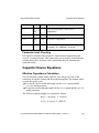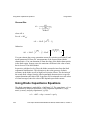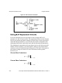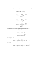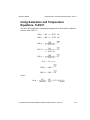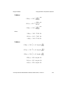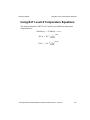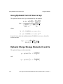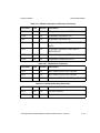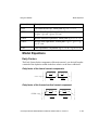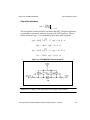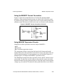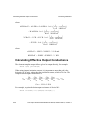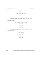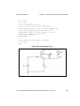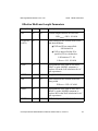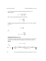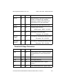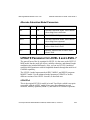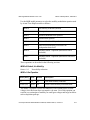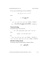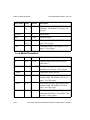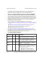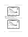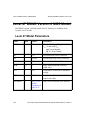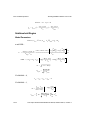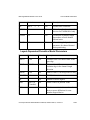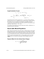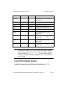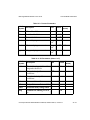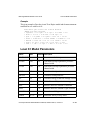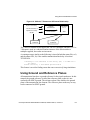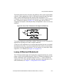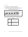
1
True-Hspice Device Models Reference Manual Release 2001.4, revision A December 2001 True-Hspice Device Models Reference Manual, Release 2001.4, revision A, November 2001 Previous Version True-Hspice Device Models Reference Manual, Release 2001.4, November 2001 Copyright © 2001 Avant! Corporation and Avant! subsidiary. All rights reserved. Unpublished--rights reserved under the copyright laws of the United States. Avant! software V2001.4 Copyright © 1985 - 2001 Avant! Corp. All rights reserved. Use of copyright notices is precautionary and does not imply publication or disclosure. Disclaimer AVANT! RESERVES THE RIGHT TO MAKE CHANGES TO ANY PRODUCTS HEREIN WITHOUT FURTHER NOTICE. AVANT! MAKES NO WARRANTY, REPRESENTATION, OR GUARANTEE REGARDING THE FITNESS OF ITS PRODUCTS FOR ANY PARTICULAR PURPOSE AND SPECIFICALLY DISCLAIMS ANY WARRANTY OF MERCHANTABILITY AND ANY WARRANTY OF NON-INFRINGEMENT. AVANT! DOES NOT ASSUME ANY LIABILITY ARISING OUT OF THE APPLICATION OR USE OF ANY PRODUCT, AND SPECIFICALLY DISCLAIMS ANY AND ALL LIABILITY, INCLUDING WITHOUT LIMITATION, SPECIAL, INCIDENTAL OR CONSEQUENTIAL DAMAGES. AVANT!'S LIABILITY ARISING OUT OF THE MANUFACTURE, SALE OR SUPPLYING OF THE PRODUCTS OR THEIR USE OR DISPOSITION, WHETHER BASED UPON WARRANTY, CONTRACT, TORT OR OTHERWISE, SHALL NOT EXCEED THE ACTUAL LICENSE FEE PAID BY CUSTOMER. Proprietary Rights Notice This document contains information of a proprietary nature. No part of this manual may be copied or distributed without the prior written consent of Avant! corporation. This document and the software described herein is only provided under a written license agreement or a type of written non-disclosure agreement with Avant! corporation or its subsidiaries. ALL INFORMATION CONTAINED HEREIN SHALL BE KEPT IN CONFIDENCE AND USED STRICTLY IN ACCORDANCE WITH THE TERMS OF THE WRITTEN NON-DISCLOSURE AGREEMENT OR WRITTEN LICENSE AGREEMENT WITH AVANT! CORPORATION OR ITS SUBSIDIARIES. Trademark/Service-Mark Notice ApolloII, ApolloII-GA, Aurora, ASIC Synthesizer, AvanTestchip, AvanWaves, ChipPlanner, Columbia, Columbia-CE, Cyclelink, Davinci, DFM Workbench, Driveline, Dynamic Model Switcher, Electrically Aware, Enterprise, EnterpriseACE, Evaccess, Hercules, Hercules-Explorer, HotPlace, HSPICE, HSPICE-LINK, LTL, Libra-Passport, Lynx, Lynx-LB, LynxVHDL, Mars, Mars-Rail, Mars-Xtalk, MASTER Toolbox, Medici, Michelangelo, Milkyway, Optimum Silicon, Passport, Pathfinder, Planet, Planet-PL, Planet-RTL, Polaris, Polaris-CBS, Polaris-MT, Progen, Prospector, Raphael, Raphael-NES, Saturn, Sirius, Silicon Blueprint, Smart Extraction, Solar, Solar II, Star, Star-Sim, Star-Hspice, Star-HspiceLink, Star-DC, Star-RC, Star-Power, Star-Sim, Star-Time, Star-MTB, Star-XP, Taurus, Taurus-Device, Taurus-Layout, TaurusLithography, Taurus-OPC, Taurus-Process, Taurus-Topography, Taurus-Visual, Taurus-Workbench, TimeSlice, TrueHspice, and TSUPREM-4 are trademarks of Avant! Corporation. Avant!, Avant! logo, AvanLabs, and avanticorp are trademarks and service-marks of Avant! Corporation. All other trademarks and service-marks are the property of their respective owners. Contacting Avant! Corporation Telephone:...........................(510) 413-8000 Facsimile:............................(510) 413-8080 Toll-Free Telephone: ..........(800) 369-0080 URL: ..................................http://www.avanticorp.com Avant! Corporation 46871 Bayside Parkway Fremont, CA 94538 Using This Manual This manual describes all of the simulation devices models that Avant! Corporation provides for use with its in-circuit simulation products, including Star-Hspice, Star-Hspice XT, Star-Sim, and Star-Sim XT. For information about which simulation device models each product supports, see the User Manual for the specific in-circuit simulator you are using. For example, to determine which of the simulation device models described in this manual are supported in the Avant! Star-Hspice in-circuit simulator, see the Star-Hspice Manual. Audience This manual is intended for design engineers who use Avant! in-circuit simulators to develop, test, analyze, and modify circuit designs. Related Documents The following documents pertain to this guide: ■ Star-Hspice, Star-Time, and AvanWaves Installation Guide ■ Star-Hspice and Star-Hspice XT Manuals ■ Star-Sim, Star-Sim XT, and Star-Time User Guides ■ Star-Hspice, Star-Sim, and AvanWaves Release Notes If you have questions or suggestions about this documentation, send them to: [email protected] True-Hspice Device Models Reference Manual, Release 2001.4, revision A iii Conventions Conventions Avant! documents use the following conventions, unless otherwise specified: Table 6.1: Typographical Conventions Convention Description menuName > commandName Indicates the name of the menu and the command name. For example: Cell > Open refers to the Open command in the Cell menu. Tool: menuName > commandName Indicates that a command is accessible only through an application tool. Tool is the tool through which you access the command, menuName is the name of the menu, and commandName is the name of the command. For example: Data Prep: Pin Solution > Via refers to the Via command on the Pin Solution menu, which you access by selecting Data Prep from the Tools menu in Apollo. courier In text, this font indicates a function or keyword that you must type exactly as shown. In examples, this font indicates system prompts, text from files, and messages printed by the system. courier italic iv Arguments appear in this font when the value of an argument is a string. The string must be enclosed with quotation marks. True-Hspice Device Models Reference Manual, Release 2001.4, revision A Conventions Table 6.1: Typographical Conventions (Continued) Convention Description times italic Indicates commands, functions, arguments, file names, and variables within a line of text. When a variable is included in italicized text, the variable is enclosed by angle brackets (<>). For example, “the name of the technology file is <libraryName>.tf, where <libraryName> is the name of the library.” [] Denotes optional arguments, such as: pin1 [pin2, ...pinN] In this example, you must enter at least one pin name, the other arguments are optional. ({instanceName orientation} ...) Indicates that you can repeat the construction enclosed in braces. . . . Indicates that text was omitted. ’(item1 item2) An apostrophe followed by parentheses indicate that the text within the parentheses enclose a list. When the list contains multiple items, the items are separated by spaces. Type this information exactly as it appears in the syntax. True-Hspice Device Models Reference Manual, Release 2001.4, revision A v Obtaining Customer Support Table 6.1: Typographical Conventions (Continued) Convention Description | Separates items in a list of choices. For example, on | off. \ Indicates the continuation of a command line. Obtaining Customer Support If you have a maintenance contract with Avant!, you can obtain customer support by: ■ Contacting your local Application Engineer (AE) ■ Calling the Avant! Corporate office from 8:00 AM through 5:00 PM Pacific Standard Time (PST) at: 1-800-346-5953 ■ Ask the receptionist for customer support. Emailing a description of the problem to the Hspice Support Center at: [email protected] Other Sources of Information The Avant! external web site provides information for various products. You can access our web site at: http://www.avanticorp.com From our web site, you can register to become a member of the Avant! Users Research Organization for Real Applications (AURORA) user’s group. By participating, you can share and exchange information pertaining to Integrated Circuit Design Automation (ICDA). vi True-Hspice Device Models Reference Manual, Release 2001.4, revision A Table of Contents Audience ............................................................................................. iii Related Documents ............................................................................. iii Conventions ........................................................................................ iv Obtaining Customer Support .............................................................. vi Other Sources of Information ............................................................. vi Chapter 1 - Overview of Models ..................................................................... 1-1 Using Models to Define Netlist Elements .............................................. 1-2 Supported Models for Different Simulator Types ............................ 1-2 Selecting Models .............................................................................. 1-3 Example ............................................................................................ 1-3 Enhancements to This Manual ................................................................ 1-4 Chapter 2 - Using Passive Device Models....................................................... 2-1 Resistor Device Model and Equations .................................................... 2-2 Wire RC Model ................................................................................. 2-2 Resistor Model Equations ................................................................. 2-5 Capacitor Device Model and Equations ............................................... 2-10 Capacitance Model ......................................................................... 2-10 Capacitor Device Equations ........................................................... 2-11 Inductor Device Model and Equations ................................................. 2-14 Inductor Core Models ..................................................................... 2-15 Magnetic Core Element Outputs .................................................... 2-18 True-Hspice Device Models Reference Manual, Release 2001.4, revision A vii Inductor Device Equations .............................................................. 2-19 Jiles-Atherton Ferromagnetic Core Model ..................................... 2-21 Chapter 3 - Using Diodes ................................................................................. 3-1 Understanding the Diode Types .............................................................. 3-2 Using Diode Model Statements .............................................................. 3-3 Setting Control Options .................................................................... 3-3 Specifying Junction Diode Models ......................................................... 3-5 Using the Junction Model Statement ................................................ 3-6 Using Junction Model Parameters .................................................... 3-7 Geometric Scaling for Diode Models ............................................. 3-13 Defining Diode Models ................................................................... 3-15 Determining Temperature Effects on Junction Diodes ................... 3-18 Using Junction Diode Equations ........................................................... 3-21 Using Junction DC Equations ......................................................... 3-22 Using Diode Capacitance Equations ............................................... 3-24 Using Noise Equations .................................................................... 3-27 Temperature Compensation Equations ........................................... 3-27 Using the Junction Cap Model .............................................................. 3-32 Setting Juncap Model Parameters ................................................... 3-34 Theory ............................................................................................. 3-37 JUNCAP Model Equations ............................................................. 3-38 Using the Fowler-Nordheim Diode ...................................................... 3-46 Converting National Semiconductor Models ........................................ 3-48 Chapter 4 - Using BJT Models ........................................................................ 4-1 Using BJT Models .................................................................................. 4-2 Selecting Models ............................................................................... 4-2 BJT Model Statement ............................................................................. 4-4 Using BJT Basic Model Parameters ................................................. 4-5 viii True-Hspice Device Models Reference Manual, Release 2001.4, revision A Handling BJT Model Temperature Effects ..................................... 4-15 BJT Device Equivalent Circuits ............................................................ 4-21 Scaling ............................................................................................. 4-21 Understanding the BJT Current Convention ................................... 4-21 Using BJT Equivalent Circuits ....................................................... 4-22 BJT Model Equations (NPN and PNP) ................................................. 4-29 Understanding Transistor Geometry in Substrate Diodes .............. 4-29 Using DC Model Equations ............................................................ 4-31 Using Substrate Current Equations ................................................. 4-32 Using Base Charge Equations ......................................................... 4-33 Using Variable Base Resistance Equations .................................... 4-34 Using BJT Capacitance Equations ........................................................ 4-35 Using Base-Emitter Capacitance Equations ................................... 4-35 Determining Base Collector Capacitance ....................................... 4-37 Using Substrate Capacitance ........................................................... 4-39 Defining BJT Noise Equations ............................................................. 4-41 BJT Temperature Compensation Equations ......................................... 4-43 Using Energy Gap Temperature Equations .................................... 4-43 Saturation and Beta Temperature Equations, TLEV=0 or 2 ........... 4-43 Using Saturation and Temperature Equations, TLEV=1 ................ 4-45 Using Saturation Temperature Equations, TLEV=3 ....................... 4-46 Using Capacitance Temperature Equations .................................... 4-48 Parasitic Resistor Temperature Equations ...................................... 4-50 Using BJT Level=2 Temperature Equations .................................. 4-51 BJT Quasi-Saturation Model ................................................................ 4-52 Using Epitaxial Current Source Iepi ............................................... 4-54 Epitaxial Charge Storage Elements Ci and Cx ............................... 4-54 Converting National Semiconductor Models ........................................ 4-57 True-Hspice Device Models Reference Manual, Release 2001.4, revision A ix VBIC Bipolar Transistor Model ........................................................... 4-59 Understanding the History of VBIC ............................................... 4-59 VBIC Parameters ............................................................................ 4-60 Noise Analysis ................................................................................ 4-61 Level 6 Philips Bipolar Model (MEXTRAM Level 503) ..................... 4-69 Level 6 Element Syntax .................................................................. 4-69 Level 6 Model Parameters .............................................................. 4-70 Level 6 Philips Bipolar Model (MEXTRAM Level 504) ..................... 4-76 Notes for HSPICE Users ................................................................. 4-77 Level 6 Model Parameters (504) ..................................................... 4-78 Level 8 HiCUM Model ......................................................................... 4-91 What is the HiCUM Model? ........................................................... 4-91 HiCUM Model Advantages ............................................................ 4-91 Avant! HiCUM Model vs. Public HiCUM Model .......................... 4-93 Model Implementation .................................................................... 4-93 Internal Transistors ......................................................................... 4-94 Level 9 VBIC99 Model ...................................................................... 4-107 Element Syntax of BJT Level 9 .................................................... 4-107 Effects of VBIC99 ........................................................................ 4-109 Model Implementation .................................................................. 4-109 Example ........................................................................................ 4-116 VBIC99 Notes for HSPICE Users ................................................ 4-120 Level 10 Phillips MODELLA Bipolar Model .................................... 4-121 Model Parameters ......................................................................... 4-121 Equivalent Circuits ........................................................................ 4-126 DC Operating Point Output .......................................................... 4-128 Model Equations ........................................................................... 4-129 Temperature Dependence of the Parameters ................................ 4-139 x True-Hspice Device Models Reference Manual, Release 2001.4, revision A Level 11 UCSD HBT Model .............................................................. 4-143 Using the UCSD HBT Model ....................................................... 4-143 Description of Parameters ............................................................. 4-144 Model Equations ........................................................................... 4-149 Equivalent Circuit ......................................................................... 4-160 Example Avant! True-Hspice Model Statement ........................... 4-162 Chapter 5 - Using JFET and MESFET Models............................................. 5-1 Understanding JFETs .............................................................................. 5-2 Specifying a Model ................................................................................. 5-3 Understanding the Capacitor Model ....................................................... 5-5 Model Applications ........................................................................... 5-5 Control Options ................................................................................. 5-6 JFET and MESFET Equivalent Circuits ................................................. 5-7 Scaling ............................................................................................... 5-7 Understanding JFET Current Convention ........................................ 5-7 JFET Equivalent Circuits .................................................................. 5-8 JFET and MESFET Model Statements ................................................. 5-13 JFET and MESFET Model Parameters ........................................... 5-13 Gate Diode DC Parameters ............................................................. 5-15 JFET and MESFET Capacitances ................................................... 5-25 Capacitance Comparison (CAPOP=1 and CAPOP=2) ................... 5-29 JFET and MESFET DC Equations ................................................. 5-31 JFET and MESFET Noise Models ....................................................... 5-35 Noise Parameters ........................................................................... 5-35 Noise Equations .............................................................................. 5-35 Noise Summary Printout Definitions .............................................. 5-36 JFET and MESFET Temperature Equations ........................................ 5-37 Temperature Compensation Equations ........................................... 5-40 True-Hspice Device Models Reference Manual, Release 2001.4, revision A xi TriQuint Model (TOM) Extensions to Level=3 ................................... 5-44 TOM Model Parameters ................................................................. 5-46 Level 7 TOM3 (TriQuint’s Own Model III) ......................................... 5-47 Using the TOM3 Model .................................................................. 5-47 Model Description .......................................................................... 5-48 Parameters ....................................................................................... 5-51 Level 8 Materka Model ......................................................................... 5-54 Using the Materka Model ............................................................... 5-54 Description of Parameters ............................................................... 5-55 Example .......................................................................................... 5-59 Chapter 6 - Using Transmission Lines............................................................ 6-1 Equations and Parameters ....................................................................... 6-3 Frequency-Dependent Matrices .............................................................. 6-5 Determining Matrix Properties ......................................................... 6-6 Wave Propagation ................................................................................... 6-8 Propagating a Voltage Step ............................................................. 6-10 Handling Line-to-Line Junctions .................................................... 6-12 Using the W Element ............................................................................ 6-15 Using Time-Step Control ................................................................ 6-16 Input Syntax for the W Element ..................................................... 6-17 Input Model 1: W Element, RLGC Model ..................................... 6-20 Input Model 2: U Element, RLGC Model ...................................... 6-28 Input Model 3: Built-in Field-Solver Model ................................... 6-32 Input Model 4: Frequency-Dependent Tabular Model ................... 6-32 Extracting Transmission Line Parameters (Field Solver) ..................... 6-37 Filament Method ............................................................................. 6-37 Modeling Geometries ...................................................................... 6-38 Solver Limitation ............................................................................ 6-39 Field-Solver Statement Syntax ....................................................... 6-39 xii True-Hspice Device Models Reference Manual, Release 2001.4, revision A Field Solver Examples .................................................................... 6-50 Frequency Table Model ........................................................................ 6-60 Syntax ............................................................................................. 6-60 Frequency Table Model Examples ................................................. 6-64 Chapter 7 - Using IBIS Models........................................................................ 7-1 IBIS Conventions .................................................................................... 7-3 General Form: .................................................................................. 7-3 Terminology ...................................................................................... 7-5 Limitations and Restrictions ............................................................. 7-5 Buffers ..................................................................................................... 7-6 Input Buffer ....................................................................................... 7-6 Output Buffer .................................................................................... 7-8 Tristate Buffer ................................................................................. 7-12 Input/Output Buffer ........................................................................ 7-16 Open Drain, Open Sink, Open Source Buffers ............................... 7-20 I/O Open Drain, I/O Open Sink, I/O Open Source Buffers ............ 7-20 Input ECL Buffer ............................................................................ 7-21 Output ECL Buffer ......................................................................... 7-22 Tristate ECL Buffer ........................................................................ 7-23 Input-Output ECL Buffer ................................................................ 7-25 Specifying Common Keywords ............................................................ 7-27 Required Keywords ........................................................................ 7-27 Optional Keywords ......................................................................... 7-27 Differential Pins .................................................................................... 7-37 Scaling Buffer Strength ......................................................................... 7-39 Buffers in subcircuits ...................................................................... 7-40 Example ................................................................................................ 7-42 Using the IBIS Buffer Component ....................................................... 7-44 Understanding the .ibis Command .................................................. 7-44 True-Hspice Device Models Reference Manual, Release 2001.4, revision A xiii Required Keywords ........................................................................ 7-45 Optional Keywords ......................................................................... 7-46 How .ibis Creates Buffers ............................................................... 7-46 Using the Buffer Component .......................................................... 7-48 Simulating the Component with pkg and ebd ................................. 7-50 Additional Notes ................................................................................... 7-51 Keywords ........................................................................................ 7-51 Voltage Thresholds ......................................................................... 7-51 .OPTION D_IBIS ........................................................................... 7-52 Sub-model ....................................................................................... 7-52 Driver Schedule .............................................................................. 7-52 Warning and Error Messages ................................................................ 7-54 References ............................................................................................. 7-56 Chapter 8 - Introducing MOSFETs ................................................................ 8-1 Understanding MOSFET Models ........................................................... 8-3 Selecting Models ..................................................................................... 8-4 Selecting MOSFET Model LEVELs ................................................ 8-4 Selecting MOSFET Capacitors ......................................................... 8-7 Selecting MOS Diodes ...................................................................... 8-9 Searching Models as Function of W, L ............................................ 8-9 Setting MOSFET Control Options ................................................. 8-11 General MOSFET Model Statement ..................................................... 8-14 Nonplanar and Planar Technologies ..................................................... 8-15 Using Field Effect Transistors ........................................................ 8-16 MOSFET Equivalent Circuits ............................................................... 8-21 MOSFET Diode Models ....................................................................... 8-27 Selecting MOSFET Diode Models ................................................. 8-27 Enhancing Convergence ................................................................. 8-27 xiv True-Hspice Device Models Reference Manual, Release 2001.4, revision A Using MOSFET Diode Model Parameters ..................................... 8-28 Using an ACM=0 MOS Diode ....................................................... 8-33 Using an ACM=1 MOS Diode ....................................................... 8-36 Using an ACM=2 MOS Diode ....................................................... 8-39 Using an ACM=3 MOS Diode ....................................................... 8-43 MOS Diode Equations .......................................................................... 8-47 DC Current ...................................................................................... 8-47 Using MOS Diode Capacitance Equations ..................................... 8-48 Common Threshold Voltage Equations ................................................ 8-52 Common Threshold Voltage Parameters ........................................ 8-52 Calculating PHI, GAMMA, and VTO ............................................ 8-53 MOSFET Impact Ionization ................................................................. 8-55 Using Impact Ionization Model Parameters ................................... 8-55 Calculating the Impact Ionization Equations .................................. 8-55 Calculating Effective Output Conductance .................................... 8-56 Cascoding Example ........................................................................ 8-57 Cascode Circuit ............................................................................... 8-58 MOS Gate Capacitance Models ............................................................ 8-59 Selecting Capacitor Models ............................................................ 8-59 Introducing Transcapacitance ......................................................... 8-61 Operating Point Capacitance Printout ............................................. 8-64 Using the Element Template Printout ............................................. 8-65 Calculating Gate Capacitance ......................................................... 8-66 MOS Gate Capacitance Model Parameters ..................................... 8-72 Specifying XQC and XPART for CAPOP=4, 9, 11, 12 and 13 ..... 8-75 Using Overlap Capacitance Equations ............................................ 8-76 CAPOP=0 — SPICE Meyer Gate Capacitances ............................ 8-77 CAPOP=1 — Modified Meyer Gate Capacitances ........................ 8-81 CAPOP=2—Parameterized Modified Meyer Capacitances ........... 8-85 CAPOP=3 — Gate Capacitances (Simpson Integration) ............... 8-90 True-Hspice Device Models Reference Manual, Release 2001.4, revision A xv CAPOP=4 — Charge Conservation Capacitance Model ............... 8-91 CAPOP=5 — Gate Capacitance ..................................................... 8-98 CAPOP=6 — AMI Gate Capacitance Model ................................. 8-98 CAPOP=13 — BSIM1-based Charge-Conserving Gate Capacitance Model .................................................................... 8-101 CAPOP=39 — BSIM2 Charge-Conserving Gate Capacitance Model ........................................................................................ 8-101 Calculating Effective Length and Width for AC Gate Capacitance ............................................................................... 8-101 Noise Models ...................................................................................... 8-102 Using Noise Parameters ............................................................... 8-102 Using Noise Equations .................................................................. 8-102 Noise Summary Printout Definitions ........................................... 8-104 Temperature Parameters and Equations .............................................. 8-105 Temperature Parameters ............................................................... 8-105 Using Temperature Equations ....................................................... 8-109 Chapter 9 - Selecting MOSFET Models: Level 1-40 ..................................... 9-1 LEVEL 1 IDS: Schichman-Hodges Model ............................................. 9-2 LEVEL 1 Model Parameters ............................................................. 9-2 LEVEL 1 Model Equations .............................................................. 9-5 LEVEL 2 IDS: Grove-Frohman Model .................................................. 9-8 LEVEL 2 Model Parameters ............................................................. 9-8 LEVEL 2 Model Equations ............................................................ 9-13 LEVEL 3 IDS: Empirical Model .......................................................... 9-20 LEVEL 3 Model Parameters ........................................................... 9-20 LEVEL 3 Model Equations ............................................................ 9-24 Compatibility Notes ........................................................................ 9-30 Temperature Compensation ............................................................ 9-31 LEVEL 4 IDS: MOS Model ................................................................. 9-34 xvi True-Hspice Device Models Reference Manual, Release 2001.4, revision A LEVEL 5 IDS Model ............................................................................ 9-35 LEVEL 5 Model Parameters ........................................................... 9-35 IDS Equations ................................................................................. 9-38 Depletion Mode DC Model ZENH=0 ............................................ 9-44 IDS Equations, Depletion Model LEVEL 5 ................................... 9-45 LEVEL 6 and LEVEL 7 IDS: MOSFET Model ................................... 9-53 LEVEL 6 and LEVEL 7 Model Parameters ................................... 9-53 UPDATE Parameter for LEVEL 6 and LEVEL 7 .......................... 9-59 LEVEL 6 Model Equations, UPDATE=0,2 ................................... 9-62 LEVEL 6 IDS Equations, UPDATE=1 .......................................... 9-72 ASPEC Compatibility ..................................................................... 9-86 LEVEL 7 IDS Model ............................................................................ 9-89 LEVEL 8 IDS Model ............................................................................ 9-90 LEVEL 8 Model Parameters ........................................................... 9-90 LEVEL 8 Model Equations ............................................................ 9-95 LEVEL 13 BSIM Model ..................................................................... 9-102 BSIM Model Features ................................................................... 9-102 LEVEL 13 Model Parameters ....................................................... 9-103 Sensitivity Factors of Model Parameters ...................................... 9-111 .MODEL VERSION Changes to BSIM Models .......................... 9-112 LEVEL 13 Equations .................................................................... 9-113 Charge-Based Capacitance Model ................................................ 9-117 Prevention of Negative Output Conductance ............................... 9-121 Calculations Using LEVEL 13 Equations .................................... 9-122 Compatibility Notes ...................................................................... 9-123 LEVEL 27 SOSFET Model ................................................................ 9-136 LEVEL 27 Model Parameters ....................................................... 9-137 Non-Fully Depleted SOI Model .................................................... 9-141 Obtaining Model Parameters ........................................................ 9-143 Fully Depleted SOI Model Considerations ................................... 9-145 True-Hspice Device Models Reference Manual, Release 2001.4, revision A xvii LEVEL 28 Modified BSIM Model ..................................................... 9-146 LEVEL 28 Model Parameters ....................................................... 9-146 LEVEL 28 Model Equations ........................................................ 9-155 LEVEL 38 IDS: Cypress Depletion Model ........................................ 9-161 LEVEL 38 Model Parameters ....................................................... 9-163 LEVEL 38 Model Equations ........................................................ 9-168 Example Model File ...................................................................... 9-175 LEVEL 39 BSIM2 Model ................................................................... 9-177 LEVEL 39 Model Parameters ....................................................... 9-177 LEVEL 39 Model Equations ........................................................ 9-185 Geometry and Bias of Model Parameters ..................................... 9-188 Compatibility Notes ...................................................................... 9-190 Preventing Negative Output Conductance .................................... 9-192 Charge-based Gate Capacitance Model (CAPOP=39) ................. 9-193 True-Hspice Model Enhancements ............................................... 9-195 Modeling Example ........................................................................ 9-198 Typical BSIM2 Model Listing ...................................................... 9-201 LEVEL 40 HP a-Si TFT Model .......................................................... 9-204 Model Parameters ......................................................................... 9-204 Using the HP a-Si TFT Model ...................................................... 9-205 LEVEL 40 Model Equations ........................................................ 9-208 LEVEL 40 Model Topology ......................................................... 9-214 Comparing MOS Models .................................................................... 9-215 History and Motivation ................................................................. 9-215 Future for Model Developments ................................................... 9-217 Model Equation Evaluation Criteria ............................................. 9-217 Potential for Good Fit to Data ....................................................... 9-218 Ease of Fit to Data ......................................................................... 9-219 Robustness and Convergence Properties ...................................... 9-219 Behavior Follows Actual Devices In All Circuit Conditions ....... 9-220 xviii True-Hspice Device Models Reference Manual, Release 2001.4, revision A Ability to Simulate Process Variation ........................................... 9-221 Gate Capacitance Modeling .......................................................... 9-222 Examples of Data Fitting .............................................................. 9-223 Chapter 10 - Selecting MOSFET Models: Level 47-63 ............................... 10-1 Level 47 BSIM3 Version 2 MOS Model .............................................. 10-2 Level 47 Model Parameters ............................................................ 10-2 Leff and Weff Equations for BSIM3 Version 2.0 ......................... 10-10 Level 47 Model Equations ............................................................ 10-11 PMOS Model ................................................................................ 10-18 Levels 49 and 53 BSIM3v3 MOS Models .......................................... 10-19 Selecting Model Versions ............................................................. 10-20 Version 3.2 Features ..................................................................... 10-22 Nonquasi-Static (NQS) Model ...................................................... 10-23 Enhancements ............................................................................... 10-23 Using BSIM3v3 ............................................................................ 10-32 Level 49, 53 Model Parameters .................................................... 10-33 Parameter Range Limits ................................................................ 10-50 Level 49, 53 Equations ................................................................. 10-54 .MODEL CARDS NMOS Model ................................................. 10-55 PMOS Model ................................................................................ 10-56 Level 50 Philips MOS9 Model ........................................................... 10-58 Level 50 Model Parameters .......................................................... 10-58 JUNCAP Model Parameters ......................................................... 10-64 Using the Philips MOS9 Model .................................................... 10-65 Model Statement ........................................................................... 10-66 Level 54 BSIM4.0 Model ................................................................... 10-68 Level 54 Model Parameters .......................................................... 10-69 Level 55 EPFL-EKV MOSFET Model .............................................. 10-90 Single Equation Model ................................................................. 10-90 True-Hspice Device Models Reference Manual, Release 2001.4, revision A xix Effects Modeled ............................................................................ 10-90 Coherence of Static and Dynamic Models .................................... 10-91 Bulk Reference and Symmetry ..................................................... 10-91 Equivalent Circuit ......................................................................... 10-92 Device Input Variables ................................................................. 10-93 EKV Intrinsic Model Parameters .................................................. 10-93 Static Intrinsic Model Equations ................................................... 10-98 Quasi-static Model Equations ..................................................... 10-110 Non-Quasi-Static (NQS) Model Equations ................................ 10-113 Intrinsic Noise Model Equations ................................................ 10-114 Operating Point Information ....................................................... 10-114 Estimation and Limits of Static Intrinsic Model Parameters ...... 10-116 Model Updates Description ........................................................ 10-118 Level 57 UC Berkeley BSIM3-SOI Model ...................................... 10-121 General Form .............................................................................. 10-121 Level 57 Model Parameters ........................................................ 10-124 Level 57 Template Output .......................................................... 10-136 Level 57 Updates to BSIM3-SOI PD versions 2.2, 2.21, and 2.22 ................................................................................... 10-140 Level 58 University of Florida SOI Model ....................................... 10-142 Level 58 FD/SOI MOSFET Model Parameters .......................... 10-143 Level 58 NFD/SOI MOSFET Model Parameters ....................... 10-149 Level 58 Template Output .......................................................... 10-154 Level 59 UC Berkeley BSIM3-SOI FD Model ................................ 10-158 Level 59 Model Parameters ........................................................ 10-160 Level 59 Template Output .......................................................... 10-169 Level 60 UC Berkeley BSIM3-SOI DD Model ................................ 10-173 Model Features ............................................................................ 10-173 Syntax ......................................................................................... 10-174 Level 60 Model Parameters ........................................................ 10-176 xx True-Hspice Device Models Reference Manual, Release 2001.4, revision A Level 61 RPI a-Si TFT Model .......................................................... 10-188 Model Features ............................................................................ 10-188 Using Level 61 ............................................................................ 10-188 Level 61 Model Parameters ........................................................ 10-189 Equivalent Circuit ....................................................................... 10-191 Model Equations ......................................................................... 10-191 Level 62 RPI Poli-Si TFT Model ..................................................... 10-194 Model Features ............................................................................ 10-194 Using Level 62 with Avant! Simulators ..................................... 10-194 Level 62 Model Parameters ........................................................ 10-195 Equivalent Circuit ....................................................................... 10-198 Model Equations ......................................................................... 10-198 Level 63 Phillips MOS11 Model ...................................................... 10-208 Using the Phillips MOS11 Model ............................................... 10-208 Description of Parameters ........................................................... 10-209 Example ...................................................................................... 10-220 Appendix A - Ideal and Lumped Transmission Lines .................................. A-1 Selecting Wire Models ........................................................................... A-2 Using Ground and Reference Planes ............................................... A-5 Selecting Ideal or Lossy Transmission Line Element ...................... A-6 Selecting U Models .......................................................................... A-7 Using Transmission Lines - Example .............................................. A-8 Performing Interconnect Simulation .................................................... A-10 Using the Ideal Transmission Line ................................................ A-10 Lossy U Element Statement ........................................................... A-11 Lossy U Model Statement .............................................................. A-13 Planar Geometric Models Lossy U Model Parameters .................. A-14 Lossy U Model Parameters for Geometric Coax (PLEV=2, ELEV=1) ................................................................................... A-26 True-Hspice Device Models Reference Manual, Release 2001.4, revision A xxi Lossy U Model Parameters Geometric Twinlead (PLEV=3, ELEV=1) ................................................................................... A-27 U Element Examples ...................................................................... A-38 U Model Applications .................................................................... A-55 Solving Ringing Problems with U Elements ................................. A-60 Transmission Line Theory ................................................................... A-69 Lossless Transmission Line Model ................................................ A-69 Lossy Transmission Line Model .................................................... A-70 Impedance ...................................................................................... A-71 Inductance ...................................................................................... A-74 Crosstalk in Transmission Lines .................................................... A-77 Risetime, Bandwidth, and Clock Frequency .................................. A-78 Definitions of Transmission Line Terms ....................................... A-79 Relationships and Rules of Thumb ................................................ A-81 Attenuation in Transmission Lines ................................................ A-87 The Lossy Transmission Line Model ............................................ A-90 References ............................................................................................ A-94 Appendix B - Finding Device Libraries .......................................................... B-1 Selecting Models Automatically ............................................................ B-2 Case 1 ............................................................................................... B-4 Case 2 ............................................................................................... B-4 Examining the Library Listings ............................................................. B-5 Analog Device Models .................................................................... B-5 Behavioral Device Models ............................................................... B-8 Bipolar Transistor Models ............................................................... B-9 Burr-Brown Devices ...................................................................... B-10 Comlinear Device Models ............................................................. B-11 Diode Models ................................................................................. B-11 FET Models ................................................................................... B-14 Linear Technology Device Models ................................................ B-16 xxii True-Hspice Device Models Reference Manual, Release 2001.4, revision A Intel PCI Speedway Models ........................................................... B-16 Signetics Device Models ................................................................ B-17 Texas Instruments Device Models ................................................. B-17 Transmission Line Models ............................................................. B-18 Xilinx Device Models .................................................................... B-18 True-Hspice Device Models Reference Manual, Release 2001.4, revision A xxiii xxiv True-Hspice Device Models Reference Manual, Release 2001.4, revision A Chapter 1 Overview of Models A circuit netlist describes the basic functionality of an electronic circuit that you are designing. In HSPICE format, a netlist consists of a series of elements, which define the individual components of the overall circuit. You can use your Hspice-format netlist to perform an in-circuit simulation of your circuit design, before you turn that design into actual electronic circuitry. An in-circuit simulation verifies and debugs your design. Your netlist can include several types of elements: ■ Passive elements: ❑ Resistors ❑ Capacitors ❑ Inductors ❑ Mutual Inductors ■ Active elements: ❑ Diodes ❑ Bipolar Junction Transistors (BJTs) ❑ Junction Field Effect Transistors (JFETs) ❑ Metal Semiconductor Field Effect Transistors (MESFETs) ❑ Metal Oxide Semiconductor Field Effect Transistors (MOSFETs) ■ Transmission lines: ❑ W element ❑ T element ❑ U element Because there are more variations of the MOSFET model than any other type, and MOSFETs are all very detailed models, MOSFETs have their own separate volume (Volume 2) in this manual. Volume 1 describes all other model types. True-Hspice Device Models Reference Manual, Release 2001.4, revision A 1-1 Using Models to Define Netlist Elements Overview of Models Using Models to Define Netlist Elements Avant! Corporation provides a series of standard models, which define various versions of each of the supported element types in an Hspice-format netlist. The individual elements in your netlist can then refer to these standard models. Using these models helps you to more quickly and efficiently create your netlist and simulate your circuit design. For example, Avant! provides 26 different versions, or levels, of MOSFET models. An individual MOSFET element in your netlist can refer to one of these MOSFET models. That is, you do not need to define all of the characteristics (called parameters) of that MOSFET, within your netlist. Referring to standard models in this way reduces the amount of time required to: ■ Create the netlist. ■ Simulate and debug your circuit design. ■ Turn your circuit design into actual circuit hardware. Within your netlist, each element that refers to a model, is known as an instance of that model. Because your netlist refers to pre-defined device models, you reduce both the time required to create and simulate a netlist, and the risk of errors, compared to fully defining each element within your netlist. Supported Models for Different Simulator Types This manual describes the individual models that Avant! provides. You can use these models with several Avant! in-circuit simulators, including: ■ Star-Hspice ■ Star-Hspice XT ■ Star-Sim ■ Star-Sim XT 1-2 True-Hspice Device Models Reference Manual, Release 2001.4, revision A Overview of Models Selecting Models Each of these Avant! in-circuit simulators supports a specific sub-set of the available models. This manual describes all of the Avant! models that you can use in Hspice-format netlists. Note: See the User Manual for the specific Avant! in-circuit simulator that you are using, for a list of the models that the simulator supports. Selecting Models To specify a device in your netlist, use both an element and a model statement. The element statement uses the name of the simulation device model, to reference the model statement. The following example uses the reference name MOD1, to refer to a BJT model. This example uses an NPN model type to describe an NPN transistor. Example Q3 3 2 5 MOD1 <parameters> .MODEL MOD1 NPN <parameters> You can specify parameters in both element and model statements. If you specify the same parameter in both an element and a model, then the element parameter (local to the specific instance of the model) always overrides the model parameter (global default for all instances of the model, where the parameter is not defined locally). The model statement specifies the type of device—for example, for a BJT, the device type might be NPN or PNP. True-Hspice Device Models Reference Manual, Release 2001.4, revision A 1-3 Enhancements to This Manual Overview of Models Enhancements to This Manual The True-Hspice Device Models Reference Manual, Release 2001.4, revision A, provides the following enhancements compared to the previous release of this manual (Release 2001.2): ■ Descriptions of all supported MOSFET models in the Avant! True-Hspice models. The previous release of this manual described only the MOSFET models that the Avant! Star-Sim XT simulator supports. ■ Addition of the following new Bipolar Junction Transistor (BJT) models (see Chapter 4, “Using BJT Models”): ❑ Level 9 VBIC99 Model ❑ Level 10 Phillips MODELLA Bipolar Model ❑ Level 11 UCSD HBT Model ■ Addition of the following new Junction Field Effect Transistor (JFET) models (see Chapter 5, “Using JFET and MESFET Models”): ❑ Level 7 TOM3 (TriQuint’s Own Model III) ❑ Level 8 Materka Model ■ Addition of the following new Metal-Oxide Semiconductor Field Effect Transistor (JFET) model (see Chapter 10, “Selecting MOSFET Models: Level 47-63”): ❑ Level 63 Phillips MOS11 Model ■ Addition of a new section, Using the IBIS Buffer Component, in Chapter 7, “Using IBIS Models”. ■ Improved online navigation to specific reference information about Avant! True-Hspice device models. 1-4 True-Hspice Device Models Reference Manual, Release 2001.4, revision A Chapter 2 Using Passive Device Models This chapter describes model statements for passive devices. It includes statements for resistors, inductors, and capacitors. Use the set of passive model statements, in conjunction with element definitions, to construct a wide range of board and integrated circuit-level designs. Passive device models let you include the following in any analysis: ■ Transformers. ■ PC board trace interconnects. ■ Coaxial cables. ■ Transmission lines. The wire element model is specifically designed to model the RC delay and RC transmission line effects of interconnects, at both the IC level and the PC board level. To aid in designing power supplies, a mutual-inductor model includes switching regulators and several other magnetic circuits, including a magnetic-core model and element. To specify precision modeling of passive elements, you can use the following types of model parameters: ■ geometric ■ temperature ■ parasitic This chapter describes: ■ Resistor Device Model and Equations ■ Capacitor Device Model and Equations ■ Inductor Device Model and Equations True-Hspice Device Models Reference Manual, Release 2001.4, revision A 2-1 Resistor Device Model and Equations Using Passive Device Models Resistor Device Model and Equations Wire RC Model The wire element RC model is a CRC (pi) model. Use the CRATIO wire model parameter to allocate the parasitic capacitance of the wire element, between the input capacitor and the output capacitor of the model. This allows for symmetric node impedance for bidirectional circuits, such as buses. Syntax .MODEL mname R keyword=value <CRATIO=val> mname Model name. Elements use this name to reference the model. R Specifies a wire model. keyword Any model parameter name. CRATIO Ratio to allocate the total wire element parasitic capacitance, between the capacitor connected to the input node, and the capacitor connected to the output node, of the wire element pi model. You can assign any value between 0 and 1, to CRATIO: 0 — Assigns all of the parasitic capacitance (CAPeff) to the output node. 0.5 — Assigns half of the parasitic capacitance to the input node, and half to the output node. 1 — Assigns all of the parasitic capacitance to the input node. The default is 0.5. 2-2 True-Hspice Device Models Reference Manual, Release 2001.4, revision A Using Passive Device Models Wire RC Model CRATIO values smaller than 0.5 assign more of the capacitance to the output node than to the input node. ■ Values greater than 0.5 assign more of the capacitance to the input node than to the output node. If you specify a CRATIO value outside the range of 0 to 1.0, simulation displays a warning, sets CRATIO to 0.5, and continues the analysis. CRATIO ■ in C=CAPeff CRATIO out C=CAPeff (1-CRATIO) A wire-model resistor behaves like an elementary transmission line (see Chapter 6, “Using Transmission Lines”), if the model statement specifies an optional capacitor from the n2 node to a bulk or ground node. The bulk node functions as a ground plane for the wire capacitance. A wire has a drawn length and a drawn width. The resistance of the wire is the effective length, multiplied by RSH, then divided by the effective width. To avoid syntactic conflicts, if a resistor model uses the same name as a parameter for rval in the element statement, then simulation uses the model name. In the following example, R1 assumes that REXX refers to the model, and not to the parameter. .PARAMETER REXX=1 R1 1 2 REXX .MODEL REXX R RES=1 True-Hspice Device Models Reference Manual, Release 2001.4, revision A 2-3 Wire RC Model Using Passive Device Models Wire Model Parameters Name (Alias) Units Default Description BULK gnd CAP F 0 Default capacitance. CAPSW F/m 0 Sidewall fringing capacitance. COX F/m2 0 Bottomwall capacitance. 0 Relative dielectric constant. Default reference node for capacitance. DI DLR m 0 Difference between drawn length and actual length (for resistance calculation only). Capacitance calculation uses DW. DLReff=DLR ⋅ SCALM DW m 0 Difference between drawn width and actual width. DWeff=DW ⋅ SCALM L m 0 Default length of wire. Lscaled=L ⋅ SHRINK ⋅ SCALM Model selector (not used) LEVEL RAC ohm RES ohm Default AC resistance (RACeff default is Reff). 0 Default resistance. RSH 0 Sheet resistance/square. SHRINK 1 Shrink factor. 0 First-order temperature coefficient for capacitance. TC1C 2-4 1/deg True-Hspice Device Models Reference Manual, Release 2001.4, revision A Using Passive Device Models Resistor Model Equations Name (Alias) Units Default Description TC2C 1/deg2 0 Second-order temperature coefficient for capacitance. TC1R 1/deg 0 First-order temperature coefficient for resistance. TC2R 1/deg2 0 Second-order temperature coefficient for resistance. THICK m 0 Dielectric thickness. TREF deg C TNOM Temperature reference, for model parameters. W m 0 Default width of wire. Wscaled=W ⋅ SHRINK ⋅ SCALM Resistor Model Equations Wire Resistance Calculation You can specify the wire width and length, in both the element and model statements. The element values override the model values. ■ To scale the element width and length, use the SCALE option and the SHRINK model parameter. ■ To scale the model width and length, use the SCALM option and the SHRINK model parameter. The effective width and length are calculated as follows: Weff = Wscaled – 2 ⋅ DWeff Leff = Lscaled – 2 ⋅ DLReff If you specify element resistance: R ⋅ SCALE ( element ) Reff = ------------------------------------------------------M True-Hspice Device Models Reference Manual, Release 2001.4, revision A 2-5 Resistor Model Equations Using Passive Device Models Otherwise, if ( Weff ⋅ Leff ⋅ RSH ) is greater than zero, then: Leff ⋅ RSH ⋅ SCALE ( element ) Reff = ------------------------------------------------------------------------------M ⋅ Weff If ( Weff ⋅ Leff ⋅ RSH ) is zero, then: RES ⋅ SCALE ( element ) Reff = --------------------------------------------------------------M If you specify AC resistance in the element, then: AC ⋅ SCALE ( element ) RACeff = ----------------------------------------------------------M Otherwise, if the model specifies RAC, RAC is used: RAC ⋅ SCALE ( element ) RACeff = ---------------------------------------------------------------M If neither are specified, the equation defaults to: RACeff = Reff If the resistance is less than the RESMIN option, it is reset it to the RESMIN value, and a warning message displays. 1 RESMIN = --------------------------------------------GMAX ⋅ 1000 ⋅ M Wire Capacitance Calculation The effective length is the scaled drawn length, less (2 ⋅ DLeff). ■ Leff represents the effective length of the resistor, from physical edge to physical edge. ■ DWeff is the distance from the drawn edge of the resistor, to the physical edge of the resistor. 2-6 True-Hspice Device Models Reference Manual, Release 2001.4, revision A Using Passive Device Models Resistor Model Equations The effective width is the same as the width used in the resistor calculation. Leff = Lscaled – 2 ⋅ DLeff Weff = Wscaled – 2 ⋅ DWeff If you specify the element capacitance, C: CAPeff = C ⋅ SCALE ( element ) ⋅ M Otherwise, the capacitance is calculated from the Leff, Weff, and COX. CAPeff = M ⋅ SCALE ( element ) ⋅ [ Leff ⋅ Weff ⋅ COX + 2 ⋅ ( Leff + Weff ) ⋅ CAPSW ] Computing the bottom-wall capacitance, COX, is based on a hierarchy of defaults and specified values, involving: ■ dielectric thickness (THICK) ■ relative dielectric constant (DI) ■ two absolute dielectric constants, εo and εox as follows: 1. If you specify COX=value, the value is used. 2. If you do not specify COX, but you do specify a value other than zero for THICK (the dielectric thickness): a) If you specify a non-zero value for DI=value, then: DI ⋅ εo COX = ------------------THICK b) If you do not specify a DI value, or if the value is zero, then: εox COX = ------------------THICK where: εo = 8.8542149e-12 F/meter εox = 3.453148e-11 F/meter True-Hspice Device Models Reference Manual, Release 2001.4, revision A 2-7 Resistor Model Equations 3. Using Passive Device Models If you do not specify COX, and THICK= 0, this is an error. ❑ If you specify only the model capacitance (CAP), then: CAPeff = CAP ⋅ SCALE ( element ) ⋅ M ❑ If you specify the capacitance, but you do not specify the bulk node, then capacitance is not evaluated, and a warning message is issued. Resistor Noise Equation The following equation models the thermal noise of a resistor: 4kT 1 / 2 inr = NOISE ⋅ ------------ Rval where NOISE is a model parameter that defaults to 1. To eliminate the contribution of resistor noise, use the NOISE parameter. To specify the NOISE parameter, use a model for the resistor. Noise Summary Print Out Definitions RX Transfer the function of thermal noise to the output. This is not noise, but is a transfer coefficient, reflecting the contribution of thermal noise to the output. TOT, V2/Hz 2-8 Total output noise:TOT = RX 2 ⋅ inr 2 True-Hspice Device Models Reference Manual, Release 2001.4, revision A Using Passive Device Models Resistor Model Equations Resistor Temperature Equations Temperature values can modify the resistor and capacitor values, as follows: R ( t ) = R ⋅ ( 1.0 + TC1 ⋅ ∆t + TC2 ⋅ ∆t 2 ) RAC ( t ) = RAC ⋅ ( 1.0 + TC1 ⋅ ∆t + TC2 ⋅ ∆t 2 ) C ( t ) = C ⋅ ( 1.0 + TC1 ⋅ ∆t + TC2 ⋅ ∆t 2 ) ∆t t - tnom t Element temperature in °K: t = circuit temp + DTEMP + 273.15 tnom Nominal temperature in °K: tnom = 273.15 + TNOM True-Hspice Device Models Reference Manual, Release 2001.4, revision A 2-9 Capacitor Device Model and Equations Using Passive Device Models Capacitor Device Model and Equations Capacitance Model Syntax .MODEL mname C parameter=value mname Model name. C Specifies a capacitance model. parameter Any model parameter name. Capacitance Parameters Name (Alias) Units Default Description CAP F 0 Default capacitance value. CAPSW F/m 0 Sidewall fringing capacitance. COX F/m2 0 Bottomwall capacitance. DEL m 0 Difference between drawn width and actual width or length. DELeff = DEL ⋅ SCALM 0 Relative dielectric constant. 0 Default length of capacitor. Lscaled = L ⋅ SHRINK ⋅ SCALM 1 Shrink factor. 0 First temperature coefficient for capacitance. DI L m SHRINK TC1 2-10 1/deg True-Hspice Device Models Reference Manual, Release 2001.4, revision A Using Passive Device Models Capacitor Device Equations Name (Alias) Units Default Description TC2 1/ deg2 0 Second temperature coefficient for capacitance. THICK m 0 Insulator thickness. TREF deg C TNOM Reference temperature. W m 0 Default width of capacitor. Wscaled = W ⋅ SHRINK ⋅ SCALM Parameter Limit Checking If a capacitive element value exceeds 0.1 Farad, then the output listing file receives a warning message. This feature helps you to identify elements that are missing units or have incorrect values, particularly those in automaticallyproduced netlists. Capacitor Device Equations Effective Capacitance Calculation You can associate a model with a capacitor. You can specify some of the parameters in both the element and the model descriptions. The element values override the model values. ■ To scale the element width and length, use the SCALE option and the SHRINK model parameter. ■ To scale the model width and length, use the SCALM option and the SHRINK model parameter. The effective width and length are calculated as follows: Weff = Wscaled – 2 ⋅ DELeff Leff = Lscaled – 2 ⋅ DELeff True-Hspice Device Models Reference Manual, Release 2001.4, revision A 2-11 Capacitor Device Equations Using Passive Device Models If you specify the element capacitance: CAPeff = C ⋅ SCALE ( element ) ⋅ M Otherwise, the capacitance is calculated from the Leff, Weff, and COX. CAPeff = M ⋅ SCALE ( element ) ⋅ [ Leff ⋅ Weff ⋅ COX + 2 ⋅ ( Leff + Weff ) ⋅ CAPSW ] If you do not specify COX, but THICK is not zero, then: DI ⋅ εo COX = ------------------- if DI not zero THICK or εox COX = ------------------- if DI=0 THICK where: F εo = 8.8542149e-12 --------------meter F εox = 3.453148e-11 --------------meter If you specify only model capacitance (CAP), then: CAPeff = CAP ⋅ SCALE ( element ) ⋅ M 2-12 True-Hspice Device Models Reference Manual, Release 2001.4, revision A Using Passive Device Models Capacitor Device Equations Capacitance Temperature Equation The capacitance as a function of temperature is calculated as follows: C ( t ) = C ⋅ ( 1.0 + TC1 ⋅ ∆t + TC2 ⋅ ∆t 2 ) ∆t t - tnom t Element temperature, in degrees Kelvin. t=circuit temp + DTEMP + 273.15 tnom Nominal temperature, in degrees Kelvin tnom+273.15 + TNOM True-Hspice Device Models Reference Manual, Release 2001.4, revision A 2-13 Inductor Device Model and Equations Using Passive Device Models Inductor Device Model and Equations You can use several elements and models to analyze: ■ switching regulators, ■ transformers ■ mutual inductive circuits These elements include: ■ magnetic winding elements ■ mutual cores ■ magnetic core models You can use the saturable core model for: ■ chokes ■ saturable transformers ■ linear transformers To use the model, you must: 1. Provide a mutual core statement. 2. Specify the core parameters, using a .MODEL statement. 3. Specify the windings around each core element, using a magnetic winding element statement. 2-14 True-Hspice Device Models Reference Manual, Release 2001.4, revision A Using Passive Device Models Inductor Core Models Inductor Core Models Magnetic Core Syntax .MODEL mname L (<pname1 = val1>…) Jiles-Atherton Ferromagnetic Core Syntax .MODEL mname CORE (LEVEL=1 <pname1 = val1>…) mname Model name. Elements use this name to refer to the model. L Identifies a saturable core model. CORE Identifies a Jiles-Atherton Ferromagnetic Core model. level=x Equation selection for Jiles-Atherton model. pname1=val1 Value of the model parameter. Each core model can include several model parameters. Example 1 .MODEL CHOKE L(BS=12K BR=10K HS=1 HCR=.2 HC=.3 AC=1. LC=3.) To use this example, obtain the core model parameters from the manufacturer’s data. Figure 2-1 on page 2-17 illustrates the required b-h loop parameters for the model. The model includes: ■ core area ■ length ■ gap size ■ core growth time constant True-Hspice Device Models Reference Manual, Release 2001.4, revision A 2-15 Inductor Core Models Using Passive Device Models Example 2 *file: bhloop.sp b-h loop nonlinear magnetic core transformer * plot in avanwaves i(l1 versus 22 to get b-h loop .option acct method=gear post rmax=.05 .tran 1m 25m .probe mu=lx0(k1) h=lx1(k1) b=lx2(k1) L1=lv1(l1) L2=lv1(l2) + i(l1) k1 l1 l2 mag2 l1 1 0 nt=20 l2 2 0 nt=20 r11 1 11 1 v11 11 0 sin (0 5 60 r22 2 22 1 c22 22 0 1 .model mag2 l bs=6k br=3k hs=1 hcr=.1 hc=.8 ac=1 lc=16 .end Magnetic Core Model Parameters 2-16 Name (Alias) Units Default Description AC cm ⋅ 2 1.0 Core area. BS Gauss 13000 Magnetic flux density at saturation. BR Gauss 12000 Residual magnetization. HC Oersted 0.8 Coercive magnetizing force. HCR Oersted 0.6 Critical magnetizing force. HS Oersted 1.5 Magnetizing force at saturation. LC cm 3.0 Core length. LG cm 0.0 Gap length. TC s 0.0 Core growth time constant. True-Hspice Device Models Reference Manual, Release 2001.4, revision A Using Passive Device Models Inductor Core Models Figure 2-1: Magnetic Saturable Core Model BS BR HS HC HCR True-Hspice Device Models Reference Manual, Release 2001.4, revision A 2-17 Magnetic Core Element Outputs Using Passive Device Models Jiles-Atherton Core Model Parameters Name (Alias) Units LEVEL Default Description 2 Model selector. For the Jiles-Atherton model, set LEVEL=1. LEVEL=2, the default, selects the Pheno model, which is the original model. AREA, (AC) cm2 1 Mean of the magnetic core cross section. AC is an alias of AREA. PATH, (LC) cm 3 Mean of the magnetic core path length. LC is an alias of PATH. MS amp/ meter 1e6 Magnetization saturation. A amp/ meter 1e3 Characterizes the shape of the anhysteretic magnetization. ALPHA 1e-3 Represents the coupling between the magnetic domains. C 0.2 Domain flexing parameter. 500 Domain of an isotropy parameter. amp/ meter K Magnetic Core Element Outputs Output Variable Description LX1 magnetic field, h (oersted) LX2 magnetic flux density, b (gauss) LX3 slope of the magnetization curve, 2-18 dm dh True-Hspice Device Models Reference Manual, Release 2001.4, revision A Using Passive Device Models Output Variable Description LX4 bulk magnetization, m (amp/meter) Inductor Device Equations LX5 slope of the anhysteretic magnetization curve, LX6 anhysteretic magnetization, man (amp/meter) LX7 effective magnetic field, he (amp/meter) dm an dh Inductor Device Equations Parameter Limit Checking If an inductive element value exceeds 0.1 Henry, then the output listing file receives a warning message. This feature helps you to identify elements that are missing units or have incorrect values, particularly those in automaticallyproduced netlists. Inductor Temperature Equation The following equation provides the effective inductance, as a function of temperature: 2 L ( t ) = L ⋅ ( 1.0 + TC1 ⋅ ∆t + TC2 ⋅ ∆t ) ∆t t - tnom t Element temperature, in degrees Kelvin. t=circuit temp + DTEMP + 273.15 tnom Nominal temperature, in degrees Kelvin. tnom=273.15 + TNOM True-Hspice Device Models Reference Manual, Release 2001.4, revision A 2-19 Inductor Device Equations Using Passive Device Models 1. To create coupling between inductors, use a separate coupling element. 2. To specify mutual inductance between two inductors, use the coefficient of coupling, kvalue. The following equation defines kvalue: M K = --------------------------( L1 ⋅ L2 ) 1 / 2 L1, L2 Inductances of the two coupled inductors. M Mutual inductance between the inductors. The linear branch relation for transient analysis is: di 1 di 2 v 1 = L 1 ⋅ ------- + M ⋅ ------dt dt di 1 di 2 v 2 = M ⋅ ------- + L 2 ⋅ ------dt dt The linear branch relation for AC analysis is: V1 = ( j ⋅ ω ⋅ L1 ) ⋅ I1 + ( j ⋅ ω ⋅ M ) ⋅ I2 V2 = ( j ⋅ ω ⋅ M ) ⋅ I1 + ( j ⋅ ω ⋅ L2 ) ⋅ I2 Note: You must define an inductor reference, using a mutual inductor statement; otherwise an error message displays, and simulation terminates. 2-20 True-Hspice Device Models Reference Manual, Release 2001.4, revision A Using Passive Device Models Jiles-Atherton Ferromagnetic Core Model Jiles-Atherton Ferromagnetic Core Model The Jiles-Atherton ferromagnetic core model is based on domain wall motion, including both bending and translation. A modified Langevin expression describes the hysteresis-free (anhysteretic) magnetization curve. This leads to: he A m an = MṠ ⋅ coth ----- – ----- A h e h e = h + ALPHA ⋅ m an where is m an Magnetization level, if the domain walls could move freely. he Effective magnetic field. h Magnetic field. MS Model parameter that represents the saturation magnetization. A Model parameter that characterizes the shape of the anhysteretic magnetization. ALPHA Model parameter that represents the coupling between the magnetic domains. The above equation generates anhysteretic curves, when the model parameter ALPHA has a small value. Otherwise, it generates some elementary forms of hysteresis loops, which is not a desirable result. The following equation calculates the slope of the curve at zero (0): dm an 1 = -------------------------------------------A dh 3 ⋅ --------- – ALPHA MS The slope must be positive; therefore, the denominator of the above equation must be positive. If the slope becomes negative, an error message displays. True-Hspice Device Models Reference Manual, Release 2001.4, revision A 2-21 Jiles-Atherton Ferromagnetic Core Model Using Passive Device Models The anhysteretic magnetization represents the global energy state of the material, if the domain walls could move freely. But the walls are displaced and bent, in the material. If you express the bulk magnetization m as the sum of an irreversible component (due to wall displacement), and a reversible component (due to domain wall bending), then: ( m an – m ) dm dm dm = -----------------------+ C ⋅ an – dh dh K dh or dm an ( m an – m ) C dm - + ------------- ⋅ = -------------------------dh (1 + C) ⋅ K 1 + C dh Solving the above differential equation obtains the bulk magnetization m. The flux density b is computed from m: b = µ0 ⋅ ( h + m ) where µ 0 , the permeability of free space, is 4π ⋅ 10 –7 , and the units of h and m are in amp/meter. Then the units of b are in Tesla (Wb/meter2). Jiles-Atherton Model Examples Effects of Varying the ALPHA, A, and K Parameters This example demonstrates the effects of the ALPHA, A, and K model parameters on the b-h curve. Figure 2-2 on page 2-24 shows the b-h curves for three values of ALPHA. Figure 2-3 on page 2-24 shows the b-h curves for three values of A. Figure 2-4 on page 2-25 shows the b-h curves for three values of K. 2-22 True-Hspice Device Models Reference Manual, Release 2001.4, revision A Using Passive Device Models Jiles-Atherton Ferromagnetic Core Model Input File * Test the Jiles-Atherton model .options post * the following analysis studies the effect of parameter ALPHA. *.param palpha=0.0 pk=0.0 pc=0.0 pa=26 *.tran 0.01 1 sweep palpha poi 3 0.0 5.0e-5 1.0e-4 * the following analysis studies the effects of parameter A. *.param palpha=0.0 pk=0.0 pc=0.0 pa=26 *.tran 0.01 1 sweep pa poi 3 10 26 50 * the following analysis studies the effects of parameter K. .param palpha=0.0 pk=5 pc=1.05 pa=26 .tran 0.01 1.25 $ sweep pk poi 2 5 50 rl 1 2 1 l1 2 0 nt=50 k1 l1 ct igen 0 1 sin(0 0.1a 1hz 0 ) .model ct core LEVEL=1 ms=420k k=pk c=pc a=pa + alpha=palpha area=1.17 path=8.49 .probe b=lx2(k1) h=lx1(k1) i(rl) v(1) .probe dmdh=lx3(k1) m=lx4(k1) man=lx6(k1) .probe l=lv1(l1) .alter .param pk=50 .end True-Hspice Device Models Reference Manual, Release 2001.4, revision A 2-23 Jiles-Atherton Ferromagnetic Core Model Using Passive Device Models Plots of the b-h Curve Figure 2-2: Variation of Anhysteretic b-h Curve: the Slope Increases as ALPHA Increases Figure 2-3: Variation of Anhysteretic b-h Curve: the Slope Decreases as A Increases 2-24 True-Hspice Device Models Reference Manual, Release 2001.4, revision A Using Passive Device Models Jiles-Atherton Ferromagnetic Core Model Figure 2-4: Variation of Hysteretic b-h Curve: as K Increases, the Loop Widens and Rotates Clockwise Discontinuities in Inductance Due to Hysteresis This example creates multi-loop hysteresis b-h curves for a magnetic core. Discontinuities in the inductance, which are proportional to the slope of the b-h curve, can cause convergence problems. Figure 2-5 demonstrates the effects of hysteresis on the inductance of the core. Input File *file tj2b.sp Multiloop hysteresis test using Jiles-Atherton model. .options post .tran 0.01 5 rl 1 2 1 l1 2 0 nt=50 k1 l1 ct igen 0 10 sin(0 0.1a 1hz 0 ) ipls 0 20 pwl(0,0 1m,0.5 1s,0.5 + 1.001,1.0 2.000,1.0 + 2.001,1.5 3.000,1.5 + 3.001,2.0 4.000,2.0 + 4.001,2.5 5.000,2.5) gigen 0 1 cur=’v(10)*v(20)’ rpls 0 20 1 rsin 0 10 1 True-Hspice Device Models Reference Manual, Release 2001.4, revision A 2-25 Jiles-Atherton Ferromagnetic Core Model Using Passive Device Models .model ct core LEVEL=1 ms=420k k=18 c=1.05 a=26 + alpha=2e-5 area=1.17 path=8.49 .probe b=lx2(k1) h=lx1(k1) i(rl) v(1) .probe dmdh=lx3(k1) m=lx4(k1) dmandh=lx5(k1) + man=lx6(k1) .probe l=lv1(l1) heff=lx7(k1) .end Plots of the Hysteresis Curve and Inductance Figure 2-5: Hysteresis Curve and Inductance of a Magnetic Core Optimizing the Extraction of Parameters This example demonstrates how to optimize the process of extracting parameters from the Jiles-Atherton model. Figure 2-6 on page 2-29 shows the plots of the core output, both before and after optimization. 2-26 True-Hspice Device Models Reference Manual, Release 2001.4, revision A Using Passive Device Models Jiles-Atherton Ferromagnetic Core Model Input File *file tj_opt.sp for Jiles-Atherton model parameter optimization. .options post + delmax=5m .param palpha=0.0 .param pms= opt1(150k,100k,500k) + pa =opt1(10,5,50) + pk=opt1(5,1,50) + pc= opt1(1,0,3) .tran 0.01 1.0 .tran 0.01 1.0 sweep + optimize=opt1 results=bsat,br,hc model=optmod .model optmod opt itropt=40 + relin=1e-4 relout=1e-6 .meas bsat find par(‘abs(lx2(k1))’) when lx1(k1)=5.0 goal=3.1k .meas br find par(‘abs(lx2(k1))’) when lx1(k1)=0 td=.25 goal=1k .meas hc find par(‘abs(lx1(k1))’) when lx2(k1)=0 td=.25 goal=.4 rl 1 2 0.01 l1 2 0 nt=20 k1 l1 ct igen 0 1 sin(0 2a 1hz 0 ) .model ct core LEVEL=1 ms=pms k=pk c=pc a=pa + alpha=palpha area=1.17 path=8.49 .probe b=lx2(k1) h=lx1(k1) i(rl) v(1) .probe dmdh=lx3(k1) m=lx4(k1) dmandh=lx5(k1) + man=lx6(k1) .probe l=lv1(l1) heff=lx7(k1) .end True-Hspice Device Models Reference Manual, Release 2001.4, revision A 2-27 Jiles-Atherton Ferromagnetic Core Model Using Passive Device Models Analysis Results Listing ****** transient analysis tnom= 25.000 temp= 25.000 optimization results residual sum of squares = 1.043893E-12 norm of the gradient = 1.411088E-06 marquardt scaling parameter = 1.267004E-04 no. of function evaluations = 30 no. of iterations = 11 optimization completed norm of gradient < grad= 1.0000E-06 on last iterations **** optimized parameters opt1 .param pms = 267.5975k .param pa = 27.8196 .param pk = 37.2947 .param pc = 316.4197m *** Measure results bsat = 3.1000E+03 br = 9.9999E+02 hc = 3.9880E-01 2-28 True-Hspice Device Models Reference Manual, Release 2001.4, revision A Using Passive Device Models Jiles-Atherton Ferromagnetic Core Model Figure 2-6: Output Curves Before Optimization (top), and After Optimization (bottom) True-Hspice Device Models Reference Manual, Release 2001.4, revision A 2-29 Jiles-Atherton Ferromagnetic Core Model 2-30 Using Passive Device Models True-Hspice Device Models Reference Manual, Release 2001.4, revision A Chapter 3 Using Diodes Use diode models to describe pn junction diodes within MOS and bipolar integrated circuit environments and discrete devices. You can use four types of models and a wide range of parameters to model standard junction diodes: ■ Zener diodes ■ Silicon diffused junction diodes ■ Schottky barrier diodes ■ Nonvolatile memory diodes (tunneling current) Note: See Chapter 8, “Introducing MOSFETs”; Chapter 9, “Selecting MOSFET Models: Level 1-40”; and Chapter 10, “Selecting MOSFET Models: Level 47-63” for other MOSFET and standard discrete diodes. Diode model types include the junction diode model and the Fowler-Nordheim model. The junction diode model has two variations: geometric and nongeometric. This chapter provides an overview of model parameters and scaling effects for the geometric and nongeometric junction diodes. It describes: ■ Understanding the Diode Types ■ Using Diode Model Statements ■ Specifying Junction Diode Models ■ Determining Temperature Effects on Junction Diodes ■ Using Junction Diode Equations ■ “Using the Junction Cap Model” ■ Using the Fowler-Nordheim Diode ■ Converting National Semiconductor Models True-Hspice Device Models Reference Manual, Release 2001.4, revision A 3-1 Understanding the Diode Types Using Diodes Understanding the Diode Types Use the geometric junction diode to model IC-based standard silicon diffused diodes, Schottky barrier diodes, and Zener diodes. The geometric parameter lets you specify pn junction poly and metal capacitance dimensions for a particular IC process technology. Use the nongeometric junction diode to model discrete diode devices such as standard and Zener diodes. The nongeometric model lets you scale currents, resistances, and capacitances using dimensionless area parameters. The Fowler-Nordheim diode defines tunneling current flow through insulators. Use it to model diode effects in nonvolatile EEPROM memory. 3-2 True-Hspice Device Models Reference Manual, Release 2001.4, revision A Using Diodes Using Diode Model Statements Using Diode Model Statements Use model and element statements to select the diode models. The model statement’s LEVEL parameter selects the type of diode model used: ■ LEVEL=1 selects the nongeometric junction diode model ■ LEVEL=2 selects the Fowler-Nordheim diode model ■ LEVEL=3 selects the geometric junction diode model You can design Zener, Schottky barrier, and silicon diffused diodes by altering model parameters for both LEVEL 1 and LEVEL 3. LEVEL 2 does not permit modeling of these effects. For Zener diodes, the BV parameter is set for an appropriate Zener breakdown voltage. If you do not specify the LEVEL parameter in the .MODEL statement, the model defaults to the nongeometric junction diode model, LEVEL 1. Use control options with the diode model to scale model units, select diffusion capacitance equations, and change model parameters. Setting Control Options Control options related to the analysis of diode circuits, as well as other models, include DCAP, DCCAP, GMIN, GMINDC, SCALE, and SCALM. Specify these models using the .OPTIONS statement. Setting Scaling Options Use the scale element option, SCALE, to scale LEVELs 2 and 3 diode element parameters. Use the scale model option, SCALM, to scale LEVELs 2 and 3 diode model parameters. LEVEL 1 does not use SCALE or SCALM. Include SCALM=<val> in the .MODEL statement to override global scaling that uses the .OPTION SCALM=<val> statement in a diode model. True-Hspice Device Models Reference Manual, Release 2001.4, revision A 3-3 Setting Control Options Using Diodes Using the Capacitor Equation Selector Option — DCAP The DCAP option selects the equations used in calculating the depletion capacitance (LEVEL 1 and LEVEL 3). The option DCCAP invokes calculation of capacitances in DC analysis. Include the DCAP=<val> in the diode’s .MODEL statement to override the global depletion capacitance equation selection with the .OPTIONS DCAP=<val> statement. Using Control Options for Convergence Diode convergence problems often occur at the breakdown voltage region when the diode is overdriven or in the OFF condition. To achieve convergence in such cases, include a nonzero value in the model for the series resistor parameter RS, or increase GMIN (the parallel conductance Star-Hspice automatically places in the circuit). You can specify GMIN and GMINDC in the .OPTIONS statement. The diode control options follow: Table 3-1: Diode Control Options 3-4 Function Control Options Capacitance DCAP, DCCAP Conductance GMIN, GMINDC Geometry SCALM, SCALE True-Hspice Device Models Reference Manual, Release 2001.4, revision A Using Diodes Specifying Junction Diode Models Specifying Junction Diode Models Use the diode element statement to specify the two types of junction diodes, geometric and nongeometric. Use a different element type format for the Fowler-Nordheim model. The diode element statement parameter fields define the connecting nodes, initialization, temperature, geometric junction, and capacitance parameters of the diode model selected in the diode .MODEL statement. Both LEVEL 1 and LEVEL 3 junction diode models share the same element parameter set. Poly and metal capacitor parameters of LM, LP, WM and WP do not share the same element parameter. Element parameters take precedence over model parameters, if repeated in the .MODEL statement as model parameters. Parameters common to both element and model statements are: AREA, PJ, M, LM, LP, WM, WP, W, and L. Table 3-2: Junction Diode Element Parameters Function Parameters Netlist Dxxx, n+, n-, mname Initialization IC, OFF Temperature DTEMP Geometric junction AREA, L, M, PJ, W Geometric capacitance (LEVEL=3 only) LM, LP, WM, WP True-Hspice Device Models Reference Manual, Release 2001.4, revision A 3-5 Using the Junction Model Statement Using Diodes Using the Junction Model Statement This section describes how to use the junction model statement. Syntax The syntax of the junction model statement is: .MODEL mnameD <LEVEL = val> <keyword = val> ... mname Model name. The diode element refers to the model by this name. D Symbol that identifies a diode model LEVEL Symbol that identifies a diode model LEVEL=1 =junction diode LEVEL=2 =Fowler-Nordheim LEVEL=3 =geometric processing for junction diode keyword Model parameter keyword such as CJO or IS Example .MODEL .MODEL .MODEL .MODEL + + + + + + + + + + 3-6 D D (CO=2PF, RS=1, IS=1P) DFOWLER D (LEVEL=2, TOX=100, JF=1E-10, EF=1E8) DGEO D (LEVEL=3, JS=1E-4, JSW=1E-8) d1n750a D LEVEL=1 XOI =0.0 WP =0.0 LM =0.0 PB =0.65 FC =0.95 TT =2.446e-9 IS =1.485e-11 PJ =0.0 IKR =1.100e-2 XP XOM WM AF PHP FCS BV CJO N IBV =0.0 =0.0 =0.0 =1.0 =0.8 =0.4 =4.65 =1.09e-9 =1.615 =2.00e-2 EG =1.1 XM =0.0 LP =0.0 JSW =0.0 M =0.2994 MJSW=0.5 RS =19 CJP =0.0 IK =0.0 True-Hspice Device Models Reference Manual, Release 2001.4, revision A Using Diodes Using Junction Model Parameters Using Junction Model Parameters The .MODEL statement is referenced by the diode element statement. The .MODEL statement contains parameters that specify the type of diode model used (LEVEL 1, 2, or 3), as well as DC, capacitance, temperature, resistance, geometric, and noise parameters. Table 3-3: Junction Diode Model Parameters (LEVEL 1 and LEVEL 3) Function Parameters model type LEVEL DC parameters IBV, IK, IKR, IS, ISW, N, RS, VB, RS geometric junction AREA, M, PJ geometric capacitance (LEVEL=3 only) L, LM, LP, SHRINK, W, WM, WP, XM, XOJ, XOM, XP, XW capacitance CJ, CJP, FC, FCS, M, MJSW, PB, PHP, TT noise AK, KF True-Hspice Device Models Reference Manual, Release 2001.4, revision A 3-7 Using Junction Model Parameters Using Diodes Setting Junction DC Parameters in LEVEL 1 and 3 Table 3-4: Junction DC Parameters Name (Alias) AREA Units Default Description 1.0 Junction area For LEVEL=1 AREAeff = AREA ⋅ M, unitless For LEVEL=3 AREAeff=AREA ⋅ SCALM2 ⋅ SHRINK2 ⋅ M unit = meter2 If you specify W and L: AREAeff = Weff ⋅ Leff ⋅ M unit = meter2 EXPLI amp/ 1e15 AREAeff IB amp/ 1.0e-3 Current at breakdown voltage AREAeff For LEVEL=3 IBVeff = IBV ⋅ AREAeff / SCALM2 IBV amp/ 1.0e-3 Current at breakdown voltage AREAeff For LEVEL=3 IBVeff = IBV ⋅ AREAeff / SCALM2 IK (IKF, JBF) amp/ 0.0 AREAeff 3-8 Current explosion model parameter. The PN junction characteristics above the explosion current are linear, with the slope at the explosion point, which increases simulation speed and improves convergence. EXPLIeff = EXPLI ⋅ AREAeff Forward knee current (intersection of the high- and low-current asymptotes) IKeff = IK ⋅ AREAeff True-Hspice Device Models Reference Manual, Release 2001.4, revision A Using Diodes Using Junction Model Parameters Table 3-4: Junction DC Parameters (Continued) Name (Alias) Units Default IKR (JBR) amp/ 0.0 AREAeff Reverse knee current (intersection of the high- and low-current asymptotes) IKReff = IKR ⋅ AREAeff IS (JS) amp/ LEVEL AREAeff 1= 1.0e14 LEVEL 3= 0.0 If you use an IS value less than EPSMIN, the program resets the value of IS to EPSMIN, and displays a warning message. EPSMIN default=1.0e-28 If the value of IS is too large, the program displays a warning. For LEVEL=1 ISeff = AREAeff ⋅ IS For LEVEL=3 ISeff = AREAeff ⋅ IS/SCALM2 JSW (ISP) amp/ PJeff Sidewall saturation current per unit junction periphery For LEVEL=1 JSWeff = PJeff ⋅ JSW For LEVEL=3 JSWeff = PJeff ⋅ JSW/SCALM 0.0 Description Default length of diode Leff = L ⋅ SHRINK ⋅ SCALM+ XWeff L LEVEL 1 Diode model selector LEVEL=1 or LEVEL=3 selects junction diode model LEVEL=2 selects Fowler-Nordheim model N 1.0 Emission coefficient True-Hspice Device Models Reference Manual, Release 2001.4, revision A 3-9 Using Junction Model Parameters Using Diodes Table 3-4: Junction DC Parameters (Continued) Name (Alias) Units Default Description PJ 0.0 Junction periphery For LEVEL=1 PJeff = PJ ⋅ M, unitless For LEVEL=3 PJeff = PJ ⋅ SCALM ⋅ M ⋅ SHRINK, meter If W and L are specified PJeff = (2 ⋅ Weff + 2 ⋅ Leff) ⋅ M, meter RS 0.0 ohms or ohms/m2 (see note below) SHRINK VB (BV, VAR, VRB) XW V Ohmic series resistance For LEVEL=1 RSeff = RS/AREAeff For LEVEL=3 RSeff= RS SCALM2/AREAeff 1.0 Shrink factor 0.0 Reverse breakdown voltage. 0.0 indicates an infinite breakdown voltage Accounts for masking and etching effects XWeff = XW ⋅ SCALM Note: If you use a diode model for which the AREA is not specified, AREA defaults to 1; then RS has units of ohms. If AREA is specified in the netlist in m2, then the units of RS are ohms/m2. 3-10 True-Hspice Device Models Reference Manual, Release 2001.4, revision A Using Diodes Using Junction Model Parameters Setting Junction Capacitance Parameters Table 3-5: Junction Capacitance Parameters Name (Alias) Units Default Description CJ (CJA, CJO) F/ AREAeff 0.0 Zero-bias junction capacitance per unit junction bottomwall area For LEVEL=1 CJOeff = CJO ⋅ AREAeff For LEVEL=3 CJeff = CJ ⋅ AREAeff/SCALM2 CJP (CJSW) F/PJeff 0.0 Zero-bias junction capacitance per unit junction periphery (PJ) For LEVEL=1 CJPeff = CJP ⋅ PJeff For LEVEL=3 CJPeff = CJP ⋅ PJeff/SCALM FC 0.5 Coefficient for forward-bias depletion area capacitance formula FCS 0.5 Coefficient for the forward-bias depletion periphery capacitance formula M (EXA, MJ) 0.5 Area junction grading coefficient MJSW (EXP) 0.33 Periphery junction grading coefficient PB (PHI, VJ, PHA) V 0.8 Area junction contact potential PHP V PB Periphery junction contact potential TT s 0.0 Transit time True-Hspice Device Models Reference Manual, Release 2001.4, revision A 3-11 Using Junction Model Parameters Using Diodes Setting Metal and Poly Capacitor Parameters for LEVEL=3 Table 3-6: Metal and Poly Capacitor Parameters Name (Alias) Units Default Description LM m 0.0 Use this parameter when LM is not specified in the element statement. LMeff = LM ⋅ SCALM ⋅ SHRINK LP m 0.0 Use this parameter if LP is not specified in the element statement. LPeff = LP ⋅ SCALM ⋅ SHRINK WM m 0.0 Use this parameter if WM is not specified in the element statement. WMeff = WM ⋅ SCALM ⋅ SHRINK WP m 0.0 Use this parameter if WP is not specified in the element statement. WPeff = WP ⋅ SCALM ⋅ SHRINK XM m 0.0 XM accounts for masking and etching effects: XMeff = XM ⋅ SCALM 10k Thickness of the poly to bulk oxide XOI XOM Å 10k Thickness of the metal to bulk oxide XP m 0.0 Accounts for masking and etching effects XPeff = XP ⋅ SCALM Setting Noise Parameters for LEVEL=1 and 3 Table 3-7: Noise Parameters Name (Alias) Default Description AF 1.0 Flicker noise exponent KF 0.0 Flicker noise coefficient 3-12 Units True-Hspice Device Models Reference Manual, Release 2001.4, revision A Using Diodes Geometric Scaling for Diode Models Geometric Scaling for Diode Models LEVEL=1 Scaling Scaling for LEVEL 1 involves the use of the AREA and M Element parameters. The element and model parameters scaled with AREA and M include: IK, IKR, JS, CJO, and RS. For AREA and M, default=1 This element is not a geometric model because both the area (AREA) and periphery (PJ) are measured in dimensionless values. These parameters are not affected by the SCALE and SCALM options. The periphery junction parameter is multiplied by M, the multiplier parameter, to scale the dimensionless periphery junction. PJeff PJ ⋅ M = PJeff is then used to scale CJP, the zero-bias junction capacitance, and the sidewall saturation current, JSW. CJPeff = PJeff ⋅ CJP JSWeff = PJeff ⋅ JSW AREA and M are used to obtain AREAeff. = AREA ⋅ M AREAeff CJO, IK, IKR, IBV, and IS are multiplied by AREAeff to obtain their effective scaled values. RS, however, is divided by AREAeff. IKeff = AREAeff ⋅ IK IKReff = AREAeff ⋅ IKR IBVeff = AREAeff ⋅ IBV ISeff = AREAeff ⋅ IS RSeff = RS/AREAeff CJOeff = CJO ⋅ AREAeff True-Hspice Device Models Reference Manual, Release 2001.4, revision A 3-13 Geometric Scaling for Diode Models Using Diodes LEVEL=3 Scaling LEVEL 3 scaling is affected by SCALM, SCALE, SHRINK, and M. The LEVEL 3 element parameters affected by SCALE include: AREA, LM, LP, PJ, WM, WP, W, L The model parameters affected by SCALM include: AREA, IBV, IK, IKR, IS, PJ, JSW, RS, CJO, CJP, LM, LP, WP, XM, XP, W, L, XW If you include the AREA as either an element parameter or a model parameter, the program uses SCALE or SCALM. The following equations use the AREA element parameter, instead of the AREA model parameter. If the AREA and PJ model parameters are specified and the element is not, use SCALM as the scaling factor instead of SCALE. The scaled effective area and periphery junction element parameters are determined by: AREAeff PJeff = = AREA ⋅ M ⋅ SCALE2 ⋅ SHRINK2 PJ ⋅ SCALE ⋅ M ⋅ SHRINK or, if W and L are specified: AREAeff PJeff = = Weff ⋅ Leff ⋅ M (2 ⋅ Weff + 2 ⋅ Leff) ⋅ M Weff Leff = = W ⋅ SCALE ⋅ SHRINK + XWeff L ⋅ SCALE ⋅ SHRINK + XWeff where To find the value of JSWeff and CJPeff use the formula: JSWeff CJPeff = = PJeff ⋅ (JSW/SCALM) PJeff ⋅ (CJP/SCALM) To determine the polysilicon and metal capacitor dimensions, multiply each by SCALE or by SCALM if specified as model parameters. LMeff WMeff LPeff WPeff XPeff XMeff 3-14 = = = = = = LM ⋅ SCALE ⋅ SHRINK WM ⋅ SCALE ⋅ SHRINK LP ⋅ SCALE ⋅ SHRINK WP ⋅ SCALE ⋅ SHRINK XP ⋅ SCALM XM ⋅ SCALM True-Hspice Device Models Reference Manual, Release 2001.4, revision A Using Diodes Defining Diode Models You can determine the effective scaled model parameters, IBeff, IKeff, IKReff, IBVeff, RSeff, and CJO as follows: IKeff IKReff IBVeff ISeff RSeff CJOeff = = = = = = AREAeff ⋅ IK AREAeff ⋅ IKR (AREAeff ⋅ IBV)/SCALM2 IS ⋅ (AREAeff/SCALM2) RS/(AREAeff ⋅ SCALM2) AREAeff ⋅ (CJO/SCALM2) Defining Diode Models Diode Current Figure 3-1 shows the direction of current flow through the diode. Use either I(D1) or I1(D1) syntax to print the diode current. If the voltage on node1 is 0.6V greater than the voltage on node2, the diode is forward biased or turned on. The anode is the p-doped side of a diode, and the cathode is the n-doped side. Figure 3-1: Diode Current Convention I1 (D1) node1 (anode, P-type, + node) I2 (D2) node2 (cathode, N-type, -node) Using Diode Equivalent Circuits Star-Hspice uses three equivalent circuits in diode analysis: transient, AC, and noise circuits. Components of these circuits form the basis for all element and model equations. True-Hspice Device Models Reference Manual, Release 2001.4, revision A 3-15 Defining Diode Models Using Diodes The fundamental component in the DC equivalent circuit is the DC diode current (id). For noise and AC analyses, the actual id current is not used. The partial derivative of id with respect to the terminal voltage vd is used instead. The name for this partial derivative is: Conductance ∂id gd = --------∂vd The drain current (id) equation accounts for all basic DC effects of the diodes. Star-Hspice assumes capacitance effects to be separate from the id equations. Figure 3-2: Equivalent Circuit, Diode Transient Analysis Anode rs + vd − id cd Cathode 3-16 True-Hspice Device Models Reference Manual, Release 2001.4, revision A Using Diodes Defining Diode Models Figure 3-3: Equivalent Circuit, Diode AC Analysis Anode rs gd cd Cathode Figure 3-4: Equivalent Circuit, Diode AC Noise Analysis Anode rs Inrs id Inrd cd Cathode True-Hspice Device Models Reference Manual, Release 2001.4, revision A 3-17 Determining Temperature Effects on Junction Diodes Using Diodes Determining Temperature Effects on Junction Diodes LEVEL 1 and LEVEL 3 model statements contain parameters for the calculation of temperature effects. TLEV and TLEVC select different temperature equations for the calculation of temperature effects on energy gap, leakage current, breakdown voltage, contact potential, junction capacitance, and grading. Table 3-8: Junction Diode Temperature Parameters (LEVEL 1 and 3) Variable Parameter Resistance coefficient TRS Capacitance coefficient CTA, CTP Energy gap EG, GAP1, GAP2 Transit time coefficient TTT1, TTT2 Reference temperature TREF Temperature selectors TLEV, TLEVC Miscellaneous TM1, TM2, TPB, TPHP Saturation current XT1 Setting Temperature Effect Parameters LEVEL=1 and 3 Table 3-9: Junction Diode Temperature Effect Parameters Name (Alias) Units Default Description CTA (CTC) 1/° 0.0 Temperature coefficient for area junction capacitance (CJ). Set the TLEVC parameter to 1 to let CTAl override the default temperature coefficient. 3-18 True-Hspice Device Models Reference Manual, Release 2001.4, revision A Using Diodes Determining Temperature Effects on Junction Diodes Table 3-9: Junction Diode Temperature Effect Parameters (Continued) Name (Alias) Units Default Description CTP 1/° 0.0 Temperature coefficient for periphery junction capacitance (CJP). Set TLEVC to 1 to let CTP override the default temperature coefficient. EG eV Energy gap for pn junction diode For TLEV=0, 1, default=1.11, for TLEV=2, default=1.16 1.17 - silicon 0.69 - Schottky barrier diode 0.67 - germanium 1.52 - gallium arsenide GAP1 eV/° 7.02 e-4 7.02e-4 - silicon (old value) 4.73e-4 - silicon 4.56e-4 - germanium 5.41e-4 - gallium arsenide GAP2 ° 1108 1108 - silicon (old value) 636 - silicon 210 - germanium 204 - gallium arsenide TCV 1/° 0.0 Breakdown voltage temperature coefficient TLEV 0.0 Temperature equation selector for diode; interacts with TLEVC. TLEVC 0.0 Level selector for diode temperature, junction capacitances and contact potentials; interacts with TLEV. 0.0 First-order temperature coefficient for MJ. TM1 1/° True-Hspice Device Models Reference Manual, Release 2001.4, revision A 3-19 Determining Temperature Effects on Junction Diodes Using Diodes Table 3-9: Junction Diode Temperature Effect Parameters (Continued) Name (Alias) Units Default Description TM2 1/°2 0.0 Second-order temperature coefficient for MJ. TPB (TVJ) V/° 0.0 Temperature coefficient for PB. Set the TLEVC parameter to 1 or 2 to enable TPB to override the default temperature compensation. TPHP V/° 0.0 Temperature coefficient for PHP. Set the TLEVC parameter to 1 or 2 to enable TPHP to override the default temperature compensation. 25.0 Model reference temperature (LEVEL 1 or 3 only) TREF TRS 1/° 0.0 Resistance temperature coefficient. TTT1 1/° 0.0 First order temperature coefficient for TT. TTT2 1/°2 0.0 Second order temperature coefficient for TT. 3.0 Saturation current temperature exponent. ■ Set XTI=3.0 for silicon-diffused junction. ■ Set XTI=2.0 for Schottky barrier diode. XTI 3-20 True-Hspice Device Models Reference Manual, Release 2001.4, revision A Using Diodes Using Junction Diode Equations Using Junction Diode Equations Table 3-10 shows the diode equation variable definition. Table 3-10: Equation Variable Definitions Variable Definition cd total diode capacitance f frequency gd diode conductance id diode DC current id1 current without high level injection ind diode equivalent noise current inrs series resistor equivalent noise current vd voltage across the diode Table 3-11 shows the equation quantity definition. Table 3-11: Equation Quantity Definition Quantity Definition tox 3.453143e-11 F/m k 1.38062e-23 (Boltzmann’s constant) q 1.60212e-19 (electron charge) t temperature in °Kelvin ∆t t - tnom tnom nominal temperature of parameter measurements in °Kelvin True-Hspice Device Models Reference Manual, Release 2001.4, revision A 3-21 Using Junction DC Equations Using Diodes Table 3-11: Equation Quantity Definition (Continued) Quantity Definition vt(t) k ⋅ t/q: thermal voltage vt(tnom) k ⋅ tnom/q: thermal voltage Using Junction DC Equations The basic diode is modeled in three regions: ■ Forward bias ■ Reverse bias ■ Breakdown regions For a forward bias diode, the anode is more positive than the cathode. The diode is turned on and conducts above 0.6 volts. Set the model parameter RS to limit conduction current. As the forward bias voltage increases past 0.6 volts, the limiting resistor prevents the value of the diode current from becoming too high and the solution from converging. Forward Bias: vd > -10 ⋅ vt vd ------------id = ISeff ⋅ e N ⋅ vt – 1 vd = v node1 – v node2 For reverse bias, the anode (node1) is more negative than the cathode. The diode is turned off, and conducts a small leakage current. Reverse Bias: BVeff < vd < -10 ⋅ vt id = – ISeff For breakdown, the parameter BV (VB) is set, inducing reverse breakdown or avalanche. This effect is seen in Zener diodes and occurs when the anodecathode voltage is less than BV. Model this action by measuring the voltage (BV) and the current (IBV) at the reverse knee or onset of avalanche. 3-22 True-Hspice Device Models Reference Manual, Release 2001.4, revision A Using Diodes Using Junction DC Equations Note: BV is always described as a positive number. Breakdown: vd < - BVeff id = – ISeff ⋅ e vd + BVeff – ----------------------------- N ⋅ vt The BV parameter is adjusted as follows to obtain BVeff: – BV ------------ibreak = – ISeff ⋅ e N ⋅ vt – 1 If IBVeff > ibreak, then, IBVeff BVeff = BV – N ⋅vt ⋅ln ------------------- ibreak Otherwise, IBVeff = ibreak Most diodes do not behave as ideal diodes. The parameters IK and IKR are called high-level injection parameters. They tend to limit the exponential current increase. Note: The exponential equation is used in both the forward and reverse regions. Forward Bias id1 id = -----------------------------------id1 1 / 2 1 + -------------- IKeff True-Hspice Device Models Reference Manual, Release 2001.4, revision A 3-23 Using Diode Capacitance Equations Using Diodes Reverse Bias id1 id = ---------------------------------------id1 1 / 2 1 + ------------------ IKReff where id1 is For vd ≥ -BVeff: vd ------------id1 = ISeff ⋅ e N ⋅ vt – 1 Otherwise: vd ------------id1 = ISeff ⋅ e N ⋅ vt – 1 – ISeff ⋅ e vd + BVeff – ----------------------------- N ⋅ vt –1 You can estimate the reverse saturation current IS, emission coefficient N, and model parameter RS from DC measurements of the forward biased diode characteristics. You can determine N from the slope of the diode characteristic in the ideal region. In most cases, the emission coefficient is the value of unit, but is closer to 2 for MOS diodes. In practice, at higher levels of bias, the diode current deviates from the ideal exponential characteristic. This deviation is due to the presence of ohmic resistance in the diode as well as high-level injection effects. The deviation of the actual diode voltage from the ideal exponential characteristic at a specific current determines the value of RS. In practice, RS is estimated at several values of id and averaged, since the value of RS depends upon diode current. Using Diode Capacitance Equations The diode capacitance is modeled by cd in Figure 3-2. The capacitance, cd, is a combination of diffusion capacitance, (cdiff), depletion capacitance, (cdep), metal, (cmetal), and poly capacitances, (cpoly). cd = cdiff + cdep + cmetal + cpoly 3-24 True-Hspice Device Models Reference Manual, Release 2001.4, revision A Using Diodes Using Diode Capacitance Equations Using Diffusion Capacitance Equations The transit time (TT) models the diffusion capacitance, caused by injected minority carriers. In practice, TT is estimated from pulsed time-delay measurements. ∂id cdiff = TT ⋅ --------∂vd Using Depletion Capacitance Equations The depletion capacitance is modeled by junction bottom and junction periphery capacitances. The formula for both bottom area and periphery capacitances is similar, except each has its own model parameters. There are two equations for forward bias junction capacitance that are selected using .OPTIONS DCAP. DCAP=1 The junction bottom area capacitance formula is: vd < FC ⋅ PB vd –MJ cdepa = CJeff ⋅ 1 – ------- PB vd FC⋅ PB vd 1 – FC ⋅ ( 1 + MJ ) + MJ ⋅ ------PB cdepa = CJeff ⋅ -------------------------------------------------------------------( 1 + MJ ) ( 1 – FC ) The junction periphery capacitance formula is: vd < FCS ⋅ PHP vd –MJSW cdepp = CJPeff ⋅ 1 – ----------- PHP vd FCS⋅ PHP True-Hspice Device Models Reference Manual, Release 2001.4, revision A 3-25 Using Diode Capacitance Equations Using Diodes vd 1 – FCS ⋅ ( 1 + MJSW ) + MJSW ⋅ ----------PHP cdepp = CJPeff ⋅ ----------------------------------------------------------------------------------------------( 1 + MJSW ) ( 1 – FCS ) then, cdep = cdepa + cdepp DCAP=2 (default) The total depletion capacitance formula is: vd < 0 vd –MJ vd –MJSW cdep = CJeff ⋅ 1 – ------- + CJPeff ⋅ 1 – ----------- PB PHP vd 0 vd vd cdep = CJeff ⋅ 1 + MJ ⋅ ------- + CJPeff ⋅ 1 + MJSW ⋅ ----------- PHP PB DCAP=3 Limits peak depletion capacitance to FC ⋅ CGDeff or FC ⋅ CGSeff, with proper fall-off when forward bias exceeds PB (FC > 1). Metal and Poly Capacitance Equations (LEVEL=3 Only) To determine the metal and poly capacitances, use the equations: ε ox cmetal = ----------- ⋅ ( WPeff + XPeff ) ⋅ ( LPeff + XPeff ) ⋅ M XOI ε ox cpoly = -------------- ⋅ ( WMeff + XMeff ) ⋅ ( LMeff + XMeff ) ⋅ M XOM 3-26 True-Hspice Device Models Reference Manual, Release 2001.4, revision A Using Diodes Using Noise Equations Using Noise Equations Figure 3-4 shows the noise model for a diode. An independent current source, inrs, in parallel with the resistor, models the thermal noise generated by a resistor. To determine the value of inrs, use the equation: 4 ⋅ k ⋅ t 1/2 inrs = ---------------- RSeff The unit of inrs is Amp/(Hz)1/2. The shot and flicker noise of the diode are modeled by the current source ind, which is defined by: KF ⋅ id AF 1 / 2 ind = 2 ⋅ q ⋅ id + ----------------------- f Temperature Compensation Equations This section describes the temperature compensation equations. Energy Gap Temperature Equations Use the following equations to determine energy gap for temperature compensation. TLEV=0 or 1 tnom 2 egnom = 1.16 – 7.02e-4 ⋅ -----------------------------------tnom + 1108.0 t2 eg ( t ) = 1.16 – 7.02e-4 ⋅ -----------------------t + 1108.0 True-Hspice Device Models Reference Manual, Release 2001.4, revision A 3-27 Temperature Compensation Equations Using Diodes TLEV=2 tnom 2 egnom = EG – GAP1 ⋅ ----------------------------------tnom + GAP2 t2 eg ( t ) = EG – GAP1 ⋅ -----------------------t + GAP2 Leakage Current Temperature Equations JS ( t ) = JS ⋅ e facln ------------N JSW ( t ) = JSW ⋅ facln ------------e N TLEV=0 or 1 t EG EG facln = ----------------------- – ----------- + XTI ⋅ ln ------------- tnom vt ( tnom ) vt ( t ) TLEV=2 t egnom eg ( t ) facln = ----------------------- – ------------ + XTI ⋅ ln ------------- tnom vt ( tnom ) vt ( t ) Breakdown Voltage Temperature Equations TLEV=0 BV ( t ) = BV – TCV ⋅∆t TLEV=1 or 2 BV ( t ) = BV ⋅ ( 1 – TCV ⋅∆t ) Transit Time Temperature Equations TT ( t ) = TT ⋅ ( 1 + TTT1 ⋅ ∆t + TTT2 ⋅ ∆t 2 ) 3-28 True-Hspice Device Models Reference Manual, Release 2001.4, revision A Using Diodes Temperature Compensation Equations Junction Built-in Potential Temperature Equations TLEVC=0 t t egnom eg ( t ) PB ( t ) = PB ⋅ ------------- – vt ( t ) ⋅ 3 ⋅ ln ------------- + ----------------------- – ----------- tnom tnom vt ( tnom ) vt ( t ) t t egnom eg ( t ) PHP ( t ) = PHP ⋅ ------------- – vt ( t ) ⋅ 3 ⋅ ln ------------- + ----------------------- – ----------- tnom vt ( tnom ) vt ( t ) tnom TLEVC=1 or 2 PB ( t ) = PB – TPB ⋅∆t PHP ( t ) = PHP – TPHP ⋅∆t TLEVC=3 PB ( t ) = PB + dpbdt ⋅ ∆t PHP ( t ) = PHP + dphpdt ⋅ ∆t where TLEV=0 or 1 tnom – egnom + 3 ⋅ vt ( tnom ) + ( 1.16 – egnom ) ⋅ 2 – ------------------------------- – PB tnom + 1108 dpbdt = -----------------------------------------------------------------------------------------------------------------------------------------------------------------------------tnom tnom – egnom + 3 ⋅ vt ( tnom ) + ( 1.16 – egnom ) ⋅ 2 – ------------------------------- – PHB tnom + 1108 dphbdt = ---------------------------------------------------------------------------------------------------------------------------------------------------------------------------------tnom and TLEV=2 tnom – egnom + 3 ⋅ vt ( tnom ) + ( EG – egnom ) ⋅ 2 – ----------------------------------- – PB tnom + GAP2 dpbdt = -------------------------------------------------------------------------------------------------------------------------------------------------------------------------------tnom tnom – egnom + 3 ⋅ vt ( tnom ) + ( EG – egnom ) ⋅ 2 – ----------------------------------- – PHP tnom + GAP2 dphpdt = -----------------------------------------------------------------------------------------------------------------------------------------------------------------------------------tnom True-Hspice Device Models Reference Manual, Release 2001.4, revision A 3-29 Temperature Compensation Equations Using Diodes Junction Capacitance Temperature Equations TLEVC=0 PB ( t ) CJ ( t ) = CJ ⋅ 1 + MJ ⋅ 4.0e-4 ⋅∆t – -------------- + 1 PB PHP ( t ) CJSW ( t ) = CJSW ⋅ 1 + MJSW ⋅ 4.0e-4 ⋅∆t – ------------------ + 1 PHP TLEVC=1 CJ ( t ) = CJ ⋅ ( 1 + CTA ⋅ ∆t ) CJSW ( t ) = CJSW ⋅ ( 1 + CTP ⋅ ∆t ) TLEVC=2 PB MJ CJ ( t ) = CJ ⋅ -------------- PB ( t ) Note: In the above equation MJ is not MJ(t). PHP MJSW CJSW ( t ) = CJSW ⋅ ------------------ PHP ( t ) TLEVC=3 ∆t CJ ( t ) = CJ ⋅ 1 – 0.5 ⋅dpbdt ⋅ ------- PB ∆t CJSW ( t ) = CJSW ⋅ 1 – 0.5 ⋅ dphpdt ⋅ ----------- PHP 3-30 True-Hspice Device Models Reference Manual, Release 2001.4, revision A Using Diodes Temperature Compensation Equations Grading Coefficient Temperature Equation MJ ( t ) = MJ ⋅ ( 1 + TM1 ⋅ ∆t + TM2 ⋅ ∆t 2 ) Resistance Temperature Equations RS ( t ) = RS ⋅ ( 1 + TRS ⋅ ∆t ) True-Hspice Device Models Reference Manual, Release 2001.4, revision A 3-31 Using the Junction Cap Model Using Diodes Using the Junction Cap Model This section describes how to use the junction cap model statement. General Syntax The general syntax for including a diode element in a Star-Hspice netlist is: Dxxx nodeplus nodeminus modelname <<area=>val> + <<peri=>val> <<pgate>=val> <<dtemp>=val> + <<off>=val> <<IC=>val> <<m=>val> where: 3-32 Dxxx Diode element name. Must begin with “D” nodeplus Positive terminal (anode) node name. The series resistor of the equivalent circuit is attached to this terminal nminus Negative terminal (cathode) node name mname Diode model name reference area Diode area. In the model card, it can be used by AB peri Length of the side-wall of the diffusion area AB which is not under the gate. In the model card, it is used by LS pgate Length of the side-wall of the diffusion area AB which is under the gate. In the model card, it is used by LG off Sets initial condition to OFF for this element in DC analysis. The default is ON M Multiplier to simulate multiple diodes in parallel. All currents, capacitances and resistances are affected by setting M. Default=1 True-Hspice Device Models Reference Manual, Release 2001.4, revision A Using Diodes Using the Junction Cap Model ic Initial voltage across the diode element. This value is used when the UIC option is present in the .tran statement and is overridden by the .ic statement Dtemp The difference between the element temperature and circuit temperature in celsius. Default=0.0 .option list Prints the updated temperature parameters for juncap diode model Juncap Model Syntax The juncap model statement syntax is: .MODEL modelname D level=4 <keyword=val> where: modelname Model name. The diode element refers to the model by this name D Symbol that identifies a diode model LEVEL Symbol that identifies a diode model keywords Model parameter keywords, listed below in the examples Examples .model MD D level=4 +AB=2E-12 LS=2E-6 LG=1.3E-6 DTA=0 TR=30 VR=0.3 +JSGBR=1.2e-3 JSDBR=1.3e-3 JSGSR=1.1e-3 +JSDSR=1.3e-3 JSGGR=1.4e-3 JSDGR=1.4e-3 NB=1.6 +NS=1.3 +NG=1.3 VB=0.9 CJBR=1.2e-12 CJSR=1.2e-12 +CJGR=1.3e-12 VDBR=1.6 VDSR=1.3 VGDR=1.2 PB=0.5 +PS=0.6 PG=0.4 True-Hspice Device Models Reference Manual, Release 2001.4, revision A 3-33 Setting Juncap Model Parameters Using Diodes Setting Juncap Model Parameters Table 3-12: Juncap Model Parameters Name Units Default Clip Low AB M2 1e-12 0.0 Diffusion area LS M 1.0e-6 0.0 Length of side-wall of diffusion area AB which is not under gate LG M 0.0 0.0 Length of side-wall of diffusion area AB which is under gate DTA C 0.0 TR C 25 VR V 0.0 JSGBR Am-2 1.0E-3 0.0 Bottom saturation-current density due to electronhole gene ration at V=VR JSDBR Am-2 1.0E-3 0.0 Bottom saturation-current density due to diffusion from back contact 3-34 High Description Temperature offset of Juncap element with respect to TA -273.15 Temperature at which parameters have been determined Voltage at which parameters have been determined True-Hspice Device Models Reference Manual, Release 2001.4, revision A Using Diodes Setting Juncap Model Parameters Table 3-12: Juncap Model Parameters (Continued) Name Units Default Clip Low High Description JSGSR Am-2 1.0E-3 0.0 Sidewall saturationcurrent density due to electron-hole generation at V=VR JSDSR Am-2 1.0E-3 0.0 Sidewall saturationcurrent density due to diffusion from back contact JSGGR Am-2 1.0E-3 0.0 Gate edge saturation current density due to electron-hole generation at V=VR JSDGR Am-2 1.0E-3 0.0 Gate edge saturation current density due to diffusion from back contact JSGGR Am-2 1.0E-3 0.0 Gate edge saturation current density due to electron-hole generation at V=VR JSDGR Am-2 1.0E-3 0.0 Gate edge saturation current density due to diffusion from back contact NB 1.0 0.1 Emission coefficient of the bottom forward current NS 1.0 0.1 Emission coefficient of the sidewall forward current True-Hspice Device Models Reference Manual, Release 2001.4, revision A 3-35 Setting Juncap Model Parameters Using Diodes Table 3-12: Juncap Model Parameters (Continued) Name Units NG Default Clip Low 1.0 0.1 High Description Emission coefficient of the gate edge forward current VB V 0.9 CJBR Fm-2 1.0E-12 0.0 Bottom junction capacitance at V=VR CJSR Fm-2 1.0E-12 0.0 Sidewall junction capacitance at V=VR CJGR Fm-2 1.0E-12 0.0 Gate edge junction capacitance at V=VR VDBR V 1.00 0.05 Diffusion voltage of the bottom junction at T=TR VDSR V 1.00 0.05 Diffusion voltage of the sidewall junction at T=TR VDGR V 1.00 0.05 Diffusion voltage of the gate edge junction PB 0.40 0.05 Bottom junction grading coefficient PS 0.40 0.05 Sidewall junction grading coefficient PG 0.40 0.05 Gate edge junction grading coefficient 3-36 Reverse breakdown voltage True-Hspice Device Models Reference Manual, Release 2001.4, revision A Using Diodes Theory Theory This section summarizes the elementary physics of a junction diode. Refer to semiconductor textbooks for additional information. Generally, the current voltage characteristics can be represented as follows: qv 2 J = { J d ( n i + ( J g ( n i, V ) ) } ⋅ exp ------- – 1 kT 3 --2 –Eg ni ~ T ⋅ exp ---------- 2kT Table 3-13: Current Voltage Characteristics Quantity Units Description J Am-2 Total reverse current density Jd Am-2 Diffusion saturation current density Jg Am-2 Generation current density ni m-3 Intrinsic carrier concentration V V Voltage across the diode Eg J Energy gap k JK-1 Boltzmann constant T K Temperature For V<VD, the charge of the junction capacitance is described by: V 1–P Q = Q j 1 – 1 – ------- V D True-Hspice Device Models Reference Manual, Release 2001.4, revision A 3-37 JUNCAP Model Equations Using Diodes Table 3-14: Junction Capacitance Charge Quantity Units Description Q C Total diode junction charge Qj C Junction charge at built-in voltage V V Voltage across the diode Vd V Junction diffusion voltage P Junction grading coefficient JUNCAP Model Equations JUNCAP Model The JUNCAP model is intended to describe formed by the source, drain or wellto-bulk junction devices, limited to the case of reverse biasing of these junctions. Similar to the MOS model, the current equations are formulated and AC effects are modeled via charge equations using the quasi-static approximation. In order to include the effects from differences in the sidewall, bottom, and gateedge junction profiles, these three contributions are calculated separately in the JUNCAP model. Both the diffusion and the generation currents are treated in the model, each with individual temperature and voltage dependence. In the JUNCAP model, a part of the total charge comes from the gate-edge junction very close to the surface. This charge is also included in the MOS model charge equations and is counted twice. However, this results in only a very minor error. In the next section, the model equations are presented. Correct operation of the model in a circuit simulator environment requires some numerical additions, which are described in the section on implementation. Any fixed capacitance that is present on a node (e.g., metal-1-to-substrate capacitance) must appear in a fixed capacitor statement or must be included in INTCAP. They no longer form the JUNCAP model in contrast to the old NODCAP model. 3-38 True-Hspice Device Models Reference Manual, Release 2001.4, revision A Using Diodes JUNCAP Model Equations Nomenclature The following table lists the electrical variable parameters: Table 3-15: Electrical Variable Parameters No Variable Programming Units Name Description 1 Va VA V Potential applied to the anode 2 Vk VK V Potential applied to the cathode 3 Ia IA A DC current into the anode 4 Ik IK A DC current into the cathode 5 Qa QA C Charge in the device attributed to the anode 6 Qk QK C Charge in the device attributed to the cathode Note: The parameters are listed above in the model card. See ‘Setting Juncap Model Parameters” on page 3-34. The following table lists internal variables and parameters: Table 3-16: Internal Variables and Parameters No Parameter Programming Units Name Description 1 Vdb VDB V Diffusion voltage of bottom area AB 2 Vds VDS V Diffusion voltage of Locos-edge L S 3 Vdg VDG V Diffusion voltage of gate-edge L G 4 Cjb CJB F Capacitance of bottom area A B True-Hspice Device Models Reference Manual, Release 2001.4, revision A 3-39 JUNCAP Model Equations Using Diodes Table 3-16: Internal Variables and Parameters (Continued) No Parameter Programming Units Name Description 5 Cjs CJS F Capacitance of Locos-edge L S 6 Cjg CJG F Capacitance of gate-edge L G 7 Isdb ISDB A Diffusion saturation current of bottom area AB 8 Isds ISDS A Diffusion saturation current of Locosedge LS 9 Isdg ISDG A Diffusion saturation current of gateedge LG 10 Isgb ISGB A Generation saturation current of bottom area AB 11 Isgs ISGS A Generation saturation current of Locosedge LS 12 Isgg ISGG A Generation saturation current of gateedge LG 13 Ta TA C Ambient circuit temperature 14 Tkd TKD K Absolute temperature of the junction/ device 15 V V V Diode bias voltage (V=VA - VK) 16 I I A Total DC current from anode to cathode (I = IA = -IK) 17 Q Q C Total junction charge (Q = QA = - QK) 3-40 True-Hspice Device Models Reference Manual, Release 2001.4, revision A Using Diodes JUNCAP Model Equations ON/OFF Condition Circuit solution involves a process of successive calculations. The calculations are started from a set of “initial guesses” for the electrical quantities of the nonlinear elements. The devices start in the default state. Example JUNCAP Default ON OFF VD -0.1 0.7 -0.1 DC Operating Point Output The DC operating point output facility gives information on the state of a device at its operation point. Note: The conductance G min is connected in parallel to the conductance G. This conductance influences the DC operating output. Temperature, Geometry and Voltage Dependence The general scaling rules, which apply to all three components of the JUNCAP model, are: T KR = T 0 + T R T KD = T 0 + T A + DT A T KR V TR = k ⋅ ---------q T KD V TD = K ⋅ ----------q ( 7.02 ⋅ 10e – 4 ⋅ T KR ⋅ T KR ) V gR = 1.16 – ------------------------------------------------------------------( 1108.0 + T KR ) True-Hspice Device Models Reference Manual, Release 2001.4, revision A 3-41 JUNCAP Model Equations Using Diodes ( 7.02 ⋅ 10e – 4 ⋅ T KR ⋅ T KD ) V gD = 1.16 – ------------------------------------------------------------------( 1108.0 + T KD ) V gD T KD 1.5 V gR - – ----------------------- F TD = ----------- ⋅ exp --------------------- ( 2 ⋅ V TR ) ( 2 ⋅ V TD ) T KR Internal Reference The internal reference parameters for the bottom component are specified by: V DBR ⋅ T KD V DB = ------------------------------------------------------T KR – 2 ⋅ V TD ⋅ 1nF TD ( V DBR – V R ) PB C JB = C JBR ⋅ A B ⋅ --------------------------------- V DB PB V DB I SGB = J SGBR ⋅ F TD ⋅ A B ⋅ --------------------------------- ( V DBR – V R ) I SDB = J SDBR ⋅ F TD ⋅ F TD ⋅ A B Similar formulations hold for the locos-edge and the gate-edge components. Replace the index B by S and G, and the area AB by LS and LG. For the locos-edge: V DSR ⋅ T KR V DS = -------------------------------------------------------T KR – 2 ⋅ V TD ⋅ 1nF TD ( V DSR – V R ) PS C JS = C JSR ⋅ L S ⋅ -------------------------------- V DS PS V DS I SGS = J SGSR ⋅ F TD ⋅ L S ⋅ -------------------------------- ( V DSR – V R ) I SDS = J SDSR ⋅ F TD ⋅ F TD ⋅ L S 3-42 True-Hspice Device Models Reference Manual, Release 2001.4, revision A Using Diodes JUNCAP Model Equations For the gate-edge: V DGR ⋅ T KD V DG = ------------------------------------------------------T KR – 2 ⋅ V TD ⋅ 1nF TD ( V DGR – V R ) PG C JG = C JGR ⋅ L G ⋅ --------------------------------- V DG PG V DG I SGS = J SGGR ⋅ F TD ⋅ L G ⋅ --------------------------------- ( V DGR – V R ) I SDS = J SDGR ⋅ F TD ⋅ F TD ⋅ L G Note: Later sections show the equations only for the bottom component. JUNCAP Capacitor and Leakage Current Model In the charge description, the following internal parameter is defined: Q JDB = C JB ⋅ V DB ( 1 – P B ) To prevent an unlimited increase of the voltage derivative of the charge, the charge description is in two parts: the original power function and a supplemented quadratic function. At the cross-over point between these regions, indicated by Vl, the following parameters are defined: 1 F CB ( 1 + P B ) ----P = 1 – -------------------- B 3 V LB = F CB ⋅ V DB C LB = C JB ( 1 – F CB ) –PB Q LB = Q JDB ( 1 – ( 1 – F CB ) ( 1 – PB )) ( 1 – ( 1 – V ) ) ( 1 – PB ) V< V LB Q JBV = Q JCB ⋅ -------------------------------- V DB 1 + ( P B ( V – V LB ) ) Q LB + C LB ( V – V LB ) ⋅ ----------------------------------------------- 2 ⋅ V DB ⋅ ( 1 – F CB ) V >= V LB True-Hspice Device Models Reference Manual, Release 2001.4, revision A ( 12.63 ) 3-43 JUNCAP Model Equations Using Diodes Similar expressions exist for the locos-edge and gate-edge charges, Qjsv and Qjgv. The total charge characteristic can be described by: Q = Q JBV + Q JSV + Q JGV Using elementary mathematics, we can derive from Equation 12.63 (above) simple equations for the capacitance of the bottom area: 1 – v PB C JBV = C JB ⋅ 1 ⁄ ------------ V DB V < V LB ( V – V LB ) C LB + C LB ⋅ P B ⋅ --------------------------------------- V DB ⋅ ( 1 – F CB ) V ≥ V LB Similar expressions exist for Cjsv and Cjgv. Total Capacitance The total capacitance can be described by: C = C JBV + C JSV + C JGV *Bulk to source or bulk to drain diode current. Diffusion and Generation Currents With the scaled parameters of the preceding section, the diffusion and generation current components can be expressed as: V I DB = I SDB ⋅ exp ---------------------------- – 1 ( N B ⋅ V TD ) ( V DB – V ) PB V I GB = I SGB ⋅ -------------------------- ⋅ exp ----------------------- – 1 N B ⋅ V TD V DB 0 3-44 V ≤ V DB V > V DB True-Hspice Device Models Reference Manual, Release 2001.4, revision A Using Diodes JUNCAP Model Equations The first relation concerning the diffusion component is valid over the whole operating range. The second relation, describing the generation current, shows an unlimited increase in the derivative of this function at V=VDB. Therefore, the power function is merged at V=0.0 with a hyperbolic function in the forward bias range. The exponential part is divided by exp ( V ⁄ ( NB ⋅ VTD ) ) . This enables a gradual decrease in the generation current component. The hyperbolic function IHYP = FSB ( V + VAB ) –B is used. The parameter B controls the decrease of the current for voltages V>0.0 for all generation components. The value of B is fixed and set to 2 in the model. The continuity constraints of function and derivative in the merge point lead to the following relations for Fsb and Vab: V DB V AB = B ⋅ ----------PB F SB = I SGB ⋅ V AB B The generation current voltage characteristic in the forward region becomes: I GB = F SB ⁄ ( ( V + V AB ) B ) ⋅ ( 1 – exp ( – v ) ⁄ ( N B ⋅ V TD ) ) Final Model Equations The final model equations for the currents of the bottom area are: I DB = I SDB ⋅ ( exp ( V ⁄ ( N B ⋅ V TD ) ) – 1 ) V DB – V PB V I GB = I SGB ⋅ --------------------- ⋅ exp ---------------------------- – 1 ( N B ⋅ V TD ) V DB B Vab –V Isgb ⋅ -------------------------- ⋅ 1 – exp -------------------------- ( V + Vab ) ( Nb ⋅ Vtd ) V≤0 V > 0.0 Similar expressions exist for the locos-edge and gate-edge components. The total junction current can be expressed as: I = ( I DB + I GB ) + ( I DS + I GS ) + ( I DG + I GG ) True-Hspice Device Models Reference Manual, Release 2001.4, revision A 3-45 Using the Fowler-Nordheim Diode Using Diodes Using the Fowler-Nordheim Diode The diode model parameter LEVEL=2 selects the Fowler-Nordheim model. Fowler- Nordheim diodes are formed as a metal-insulator-semiconductor or as a semiconductor-insulator-semiconductor layer device. The insulator is sufficiently thin (100 Angstroms) to permit tunneling of carriers. It models electrically alterable memory cells, air-gap switches, and other insulation breakdown devices. Fowler-Nordheim Diode Model Parameters LEVEL=2 Table 3-17 shows the Fowler-Nordheim diode model parameters for LEVEL 2. Table 3-17: Fowler-Nordheim Diode Model Parameters Name (alias) Units Default Description EF V/cm 1.0e8 Forward critical electric field ER V/cm EF Reverse critical electric field JF amp/V2 1.0e10 Forward Fowler-Nordheim current coefficient JR amp/V2 JF Reverse Fowler-Nordheim current coefficient L m 0.0 Length of diode for calculation of FowlerNordheim current Leff = L ⋅ SCALM ⋅ SHRINK + XWeff TOX Å 100.0 Thickness of oxide layer W m 0.0 Width of diode for calculation of FowlerNordheim current Weff = W ⋅ SCALM ⋅ SHRINK + XWeff XW 3-46 m 0.0 XWeff = XW ⋅ SCALM True-Hspice Device Models Reference Manual, Release 2001.4, revision A Using Diodes Using the Fowler-Nordheim Diode Using Fowler-Nordheim Diode Equations The DC characteristics of the Fowler-Nordheim diode are modeled by the following forward and reverse nonlinear current source equations. In the following equations: AREAeff = Weff ⋅ Leff ⋅ M Forward Bias: vd 0 – EF ⋅TOX vd 2 --------------------------id = AREAeff ⋅ JF ⋅ ------------- ⋅ e vd TOX Reverse Bias: vd < 0 ER ⋅ TOX vd 2 ------------------------id = – AREAeff ⋅JR ⋅ ------------- ⋅e vd TOX Fowler-Nordheim Diode Capacitances The Fowler-Nordheim diode capacitance is a constant derived from: ε ox cd = AREAeff ⋅ ------------TOX True-Hspice Device Models Reference Manual, Release 2001.4, revision A 3-47 Converting National Semiconductor Models Using Diodes Converting National Semiconductor Models National Semiconductor’s circuit simulator has a scaled diode model that is not the same as that used by Star-Hspice. To use National Semiconductor circuit models, do the following: For a subcircuit that consists of the scaled diode model, the subcircuit name must be the same as the name of the model. The .PARAM statement inside the subcircuit specifies the scaled diode model parameter values. Add a scaled diode model inside the subcircuit, then change the .MODEL mname mtype statement to a .PARAM statement. Ensure that all the scaled diode elements are preceded by the character X. Check that every parameter used in the .MODEL statement inside the subcircuit has a value in the .PARAM statement. Using the Scaled Diode Subcircuit Definition The scaled diode subcircuit definition converts the National Semiconductor scaled diode model to a form a model usable in Star-Hspice. The .PARAM parameter inside the .SUBCKT represents the .MODEL parameter in the National circuit simulator. Replace the .MODEL mname statement by a .PARAM statement. Change the model name to SDIODE. 3-48 True-Hspice Device Models Reference Manual, Release 2001.4, revision A Using Diodes Converting National Semiconductor Models Example An example of scaled diode subcircuit definition is: .SUBCKT SDIODE NP NN SF=1 SCJA=1 SCJP=0 SIS=1 SICS=1 + SRS=1 D NP NN SDIODE .PARAM IS=1.10E-18 N=1.03 EG=0.8 RS=20.7E3 + CJA=0.19E-15 PHI=0.25 CJP=0.318E-15 + EXA=0.5 EXP=0.325 CTC=6E-4 + TRS=2.15M M=2 * .MODEL SDIODE D + IS=’IS*SIS*SF’ CJA=’CJA*SF*SCJA’ CJP=’CJP*SF*SCJP’ + RS=’RS*SRS/SF’ EXA=EXA EXP=EXP + N=N CTA=CTC CTP=CTC + TRS=TRS TLEV=1 TLEVC=1 xti=’m*n’ .ENDS SDIODE Note that all the parameters used in the following model must have a value that comes from either a .PARAM statement or the .SUBCKT call. The diode statements are then replaced by the call to the subcircuit SDIODE: XDS 14 1048 SDIODE SIS=67.32 SCJA=67.32 SRS=1.2285E-2 True-Hspice Device Models Reference Manual, Release 2001.4, revision A 3-49 Converting National Semiconductor Models 3-50 Using Diodes True-Hspice Device Models Reference Manual, Release 2001.4, revision A Chapter 4 Using BJT Models The bipolar-junction transistor (BJT) model is an adaptation of the integral charge control model of Gummel and Poon. The Avant! BJT model extends the original Gummel-Poon model to include several effects at high bias levels. This model automatically simplifies to the Ebers-Moll model when certain parameters (VAF, VAR, IKF, and IKR) are not specified. This chapter covers the following topics: ■ Using BJT Models ■ BJT Model Statement ■ BJT Device Equivalent Circuits ■ BJT Model Equations (NPN and PNP) ■ Using BJT Capacitance Equations ■ Defining BJT Noise Equations ■ BJT Temperature Compensation Equations ■ BJT Quasi-Saturation Model ■ Converting National Semiconductor Models ■ VBIC Bipolar Transistor Model ■ Level 6 Philips Bipolar Model (MEXTRAM Level 503) ■ Level 6 Philips Bipolar Model (MEXTRAM Level 504) ■ Level 8 HiCUM Model ■ Level 9 VBIC99 Model ■ Level 10 Phillips MODELLA Bipolar Model ■ Level 11 UCSD HBT Model True-Hspice Device Models Reference Manual, Release 2001.4, revision A 4-1 Using BJT Models Using BJT Models Using BJT Models The BJT model is used to develop BiCMOS, TTL, and ECL circuits. For BiCMOS devices, use the high-current Beta degradation parameters, IKF and IKR, to modify high injection effects. The model parameter SUBS facilitates the modeling of both vertical and lateral geometrics. Selecting Models To select a BJT device, use a BJT element and model statement. The element statement uses the name of the simulation device model, to reference the model statement. The following example uses the reference name MOD1. This example uses an NPN model type to describe an NPN transistor. Example Q3 3 2 5 MOD1 <parameters> .MODEL MOD1 NPN <parameters> You can specify parameters in both element and model statements. If you specify the same parameter in both an element and a model, then the element parameter (local to the specific instance of the model) always overrides the model parameter (global default for all instances of the model, where the parameter is not defined locally). The model statement specifies the type of device—for example, for a BJT, the device type might be NPN or PNP. 4-2 True-Hspice Device Models Reference Manual, Release 2001.4, revision A Using BJT Models Selecting Models Using Control Options Control options affecting the BJT model are: DCAP, GRAMP, GMIN, and GMINDC. DCAP selects the equation that determines the BJT capacitances. GRAMP, GMIN, and GMINDC place a conductance in parallel with both the base-emitter and base-collector pn junctions. DCCAP invokes capacitance calculations in DC analysis. The BJT control options follow: Function Control Options Capacitance DCAP, DCCAP Conductance GMIN, GMINDC You can override global depletion capacitance equation selection that uses the .OPTION DCAP=<val> statement in a BJT model by including DCAP=<val> in the BJTs .MODEL statement. Convergence Adding a base, collector, and emitter resistance to the BJT model improves its convergence. The resistors limit the current in the device so that the forwardbiased pn junctions are not overdriven. True-Hspice Device Models Reference Manual, Release 2001.4, revision A 4-3 BJT Model Statement Using BJT Models BJT Model Statement Syntax .MODEL mname NPN <(> <pname1 = val1> ... <)> or .MODEL mname PNP <pname1 = val1> ... mname Model name. Elements refer to the model by this name. NPN Identifies an NPN transistor model pname1 Each BJT model can include several model parameters. PNP Identifies a PNP transistor model Example .MODEL + ISS= + CJS= + MJS= + ITF= + BR = + VAR= + NE = + NC = + NR = + RC = + MJC= + TF = + CJC= 4-4 t2n2222a NPN 0. XTF= 1. NS = 1.00000 0. VJS= 0.50000 PTF= 0. 0. EG = 1.10000 AF = 1. 0.50000 VTF= 1.00000 40.00000 IS = 1.6339e-14 VAF= 103.40529 17.77498 IKF= 1.00000 1.31919 IKR= 1.00000 ISC= 3.6856e-13 1.10024 IRB= 4.3646e-05 NF = 1.00531 1.00688 RBM= 1.0000e-02 RB = 71.82988 0.42753 RE = 3.0503e-03 MJE= 0.32339 0.34700 VJE= 0.67373 VJC= 0.47372 9.693e-10 TR = 380.00e-9 CJE= 2.6734e-11 1.4040e-11 FC = 0.95000 XCJC= 0.94518 True-Hspice Device Models Reference Manual, Release 2001.4, revision A Using BJT Models Using BJT Basic Model Parameters Using BJT Basic Model Parameters To permit the use of model parameters from earlier versions of Star-Hspice and Star-Sim, many of the model parameters have aliases, which are included in the model parameter list in ‘Using BJT Basic DC Model Parameters” on page 4-6. The new name is always used on printouts, even if an alias is used in the model statement. BJT model parameters are divided into several groups. The first group of DC model parameters includes the most basic Ebers-Moll parameters. This model is effective for modeling low-frequency large-signal characteristics. Low-current Beta degradation effect parameters ISC, ISE, NC, and NE aid in modeling the drop in the observed Beta, caused by the following mechanisms: ■ Recombination of carriers in the emitter-base space charge layer ■ Recombination of carriers at the surface ■ Formation of emitter-base channels Low base and emitter dopant concentrations, found in some BIMOS type technologies, use the high-current Beta degradation parameters, IKF and IKR. Use the base-width modulation parameters, that is, early effect parameters VAF and VAR, to model high-gain, narrow-base devices. The model calculates the slope of the I-V curve for the model in the active region with VAF and VAR. If VAF and VAR are not specified, the slope in the active region is zero. The parasitic resistor parameters RE, RB, and RC are the most frequently used second-order parameters since they replace external resistors. This simplifies the input netlist file. All of the resistances are functions of the BJT multiplier M value. The resistances are divided by M to simulate parallel resistances. The base resistance is also a function of base current, as is often the case in narrow-base technologies. Transient model parameters for BJTs are composed of two groups: junction capacitor parameters and transit time parameters. The base-emitter junction is modeled by CJE, VJE, and MJE. The base-collector junction capacitance is modeled by CJC, VJC, and MJC. The collector-substrate junction capacitance is modeled by CJS, VJS, and MJS. True-Hspice Device Models Reference Manual, Release 2001.4, revision A 4-5 Using BJT Basic Model Parameters Using BJT Models TF is the forward transit time for base charge storage. TF can be modified to account for bias, current, and phase, by XTF, VTF, ITF, and PTF. The base charge storage reverse transit time is set by TR. There are several sets of temperature equations for the BJT model parameters that you can select by setting TLEV and TLEVC. Table 4-1: BJT Model Parameters DC BF, BR, IBC, IBE, IS, ISS, NF, NR, NS, VAF, VAR beta degradation ISC, ISE, NC, NE, IKF, IKR geometric SUBS, BULK resistor RB, RBM, RE, RC, IRB junction capacitor CJC,CJE,CJS,FC,MJC,MJE,MJS,VJC,VJE,VJS, XCJC parasitic capacitance CBCP, CBEP, CCSP transit time ITF, PTF, TF, VT, VTF, XTF noise KF, AF Using BJT Basic DC Model Parameters Table 4-2: DC Parameters for BJT Models (Sheet 1 of 3) Name (Alias) Default Description BF (BFM) 100.0 Ideal maximum forward Beta BR (BRM) 1.0 Ideal maximum reverse Beta BULK (NSUB) 0.0 Sets the bulk node to a global node name. A substrate terminal node name (ns) in the element statement overrides BULK. 4-6 Unit True-Hspice Device Models Reference Manual, Release 2001.4, revision A Using BJT Models Using BJT Basic Model Parameters Table 4-2: DC Parameters for BJT Models (Sheet 2 of 3) Name (Alias) Unit Default Description IBC amp 0.0 Reverse saturation current between base and collector. If you specify both IBE and IBC, simulation uses them in place of IS to calculate DC current and conductance; otherwise, the simulator uses IS. IBCeff = IBC ⋅ AREAB ⋅ M AREAC replaces AREAB, depending on vertical or lateral geometry. EXPLI amp 1e15 Current explosion model parameter. The PN junction characteristics above the explosion current area linear, with the slope at the explosion point. This speeds up simulation and improves convergence. EXPLIeff = EXPLI ⋅ AREAeff IBE amp 0.0 Reverse saturation current between base and emitter. If you specify both IBE and IBC, simulation uses them in place of IS to calculate DC current and conductance; otherwise, the simulator uses IS. IBEeff = IBE ⋅ AREA ⋅ M IS amp 1.0e16 Transport saturation current. If you specify both IBE and IBC, simulation uses them in place of IS to calculate DC current and conductance; otherwise, the simulator uses IS. ISeff = IS ⋅ AREA ⋅ M True-Hspice Device Models Reference Manual, Release 2001.4, revision A 4-7 Using BJT Basic Model Parameters Using BJT Models Table 4-2: DC Parameters for BJT Models (Sheet 3 of 3) Name (Alias) Unit Default Description ISS amp 0.0 Reverse saturation current bulk-to-collector or bulk-to-base, depending on vertical or lateral geometry selection. SSeff = ISS ⋅ AREA ⋅ M Level 1.0 Model selector NF 1.0 Forward current emission coefficient NR 1.0 Reverse current emission coefficient NS 1.0 Substrate current emission coefficient Substrate connection selector: ■ +1 for vertical geometry ■ -1 for lateral geometry ■ default=1 for NPN ■ default=-1 for PNP SUBS UPDATE 4-8 0 UPDATE = 1 selects alternate base charge equation True-Hspice Device Models Reference Manual, Release 2001.4, revision A Using BJT Models Using BJT Basic Model Parameters Using Low-Current Beta Degradation Effect Parameters Table 4-3: Low-Current Beta Degradation Parameters Name (Alias) Unit Default Description ISC (C4, JLC) amp 0.0 Base-collector leakage saturation current. If ISC is greater than 1e-4, then: ISC = IS ⋅ ISC otherwise: ISCeff = ISC ⋅ AREAB ⋅ M AREAC replaces AREAB, depending on vertical or lateral geometry. ISE (C2, JLE) amp 0.0 Base-emitter leakage saturation current. If ISE is greater than 1e-4, then: ISE = IS ⋅ ISE otherwise: ISEeff = ISE ⋅ AREA ⋅ M NC (NLC) 2.0 Base-collector leakage emission coefficient NE (NLE) 1.5 Base-emitter leakage emission coefficient True-Hspice Device Models Reference Manual, Release 2001.4, revision A 4-9 Using BJT Basic Model Parameters Using BJT Models Using Base Width Modulation Parameters Table 4-4: Base Width Modulation Parameters Name (Alias) Unit Default Description VAF (VA, VBF) V 0.0 Forward early voltage. Use zero to indicate an infinite value. VAR (VB, VRB, BV) V 0.0 Reverse early voltage. Use zero to indicate an infinite value. Using High-Current Beta Degradation Effect Parameters Table 4-5: High-Current Beta Degradation Parameters Name (Alias) Unit Default Description IKF (IK, JBF) amp 0.0 Corner for forward Beta high-current rolloff. Use zero to indicate an infinite value. IKFeff = IKF ⋅ AREA ⋅ M IKR (JBR) amp 0.0 Corner for reverse Beta high-current rolloff. Use zero to indicate an infinite value. IKReff = IKR ⋅ AREA ⋅ M NKF 4-10 0.5 Exponent for high-current Beta roll-off. True-Hspice Device Models Reference Manual, Release 2001.4, revision A Using BJT Models Using BJT Basic Model Parameters Using Parasitic Resistance Parameters Table 4-6: Parasitic Resistance Parameters Name (Alias) Unit Default Description IRB (JRB, IOB) amp 0.0 Base current, where base resistance falls half-way to RBM. Use zero to indicate an infinite value. IRBeff = IRB ⋅ AREA ⋅ M RB ohm 0.0 Base resistance RBeff = RB / (AREA ⋅ M) RBM ohm RB Minimum high-current base resistance RBMeff = RBM / (AREA ⋅ M) RE ohm 0.0 Emitter resistance REeff = RE / (AREA ⋅ M) RC ohm 0.0 Collector resistance RCeff = RC / (AREA ⋅ M) Using Junction Capacitor Parameters Table 4-7: Junction Capacitor Parameters Name (Alias) Unit Default Description CJC F 0.0 Base-collector zero-bias depletion capacitance ■ Vertical: CJCeff = CJC ⋅ AREAB ⋅ M ■ Lateral: CJCeff = CJC ⋅ AREAC ⋅ M if you specify a value other than zero, for ibc and ibe. True-Hspice Device Models Reference Manual, Release 2001.4, revision A 4-11 Using BJT Basic Model Parameters Using BJT Models Table 4-7: Junction Capacitor Parameters (Continued) CJE F 0.0 Base-emitter zero-bias depletion capacitance (vertical and lateral): CJEeff = CJE ⋅ AREA ⋅ M CJS (CCS, CSUB) F 0.0 Zero-bias collector substrate capacitance ■ Vertical: CJSeff = CJS ⋅ AREAC ⋅ M ■ Lateral: CJSeff = CJS ⋅ AREAB ⋅ M If you specify a value other than zero, for ibc and ibe. FC 0.5 Coefficient for forward bias depletion capacitance formula for DCAP=1 DCAP Default=2 and FC are ignored. MJC (MC) 0.33 Base-collector junction exponent (grading factor) MJE (ME) 0.33 Base-emitter junction exponent (grading factor) MJS(ESUB) 0.5 Substrate junction exponent (grading factor) VJC (PC) V 0.75 Base-collector built-in potential VJE (PE) V 0.75 Base-emitter built-in potential VJS (PSUB) V 0.75 Substrate junction built in potential 1.0 Internal base fraction of base-collector depletion capacitance XCJC (CDIS) 4-12 True-Hspice Device Models Reference Manual, Release 2001.4, revision A Using BJT Models Using BJT Basic Model Parameters Using Parasitic Capacitances Parameters Table 4-8: Parasitic Capacitances Parameters Name (Alias) Unit Default Description CBCP F 0.0 External base-collector constant capacitance CBCPeff = CBCP ⋅ AREA ⋅ M CBEP F 0.0 External base-emitter constant capacitance CBEPeff = CBEP ⋅ AREA ⋅ M CCSP F 0.0 External collector substrate constant capacitance (vertical) or base substrate (lateral) CCSPeff = CCSP ⋅ AREA ⋅ M Using Transit Time Parameters Table 4-9: Transit Time Parameters Name (Alias) Unit Default Description ITF (JTF) amp 0.0 TF high-current parameter PTF x 0.0 Frequency multiplier to determine excess phase TF s 0.0 Base forward transit time TR s 0.0 Base reverse transit time VTF V 0.0 TF base-collector voltage dependence coefficient. Zero indicates an infinite value. 0.0 TF bias dependence coefficient XTF ITFeff = ITF ⋅ AREA ⋅ M True-Hspice Device Models Reference Manual, Release 2001.4, revision A 4-13 Using BJT Basic Model Parameters Using BJT Models Using Noise Parameters Table 4-10: Noise Parameters Name (Alias) Unit Default Description AF 1.0 Flicker-noise exponent KF 0.0 Flicker-noise coefficient Using BJT Level=2 Model Parameters Table 4-11: Level=2 Parameters Name (Alias) Unit Default Description BRS 1.0 Reverse beta for substrate BJT. GAMMA 0.0 Epitaxial doping factor, GAMMA = (2 ⋅ ni / n)2 where n is epitaxial impurity concentration NEPI QCO Coul 1.0 Emission coefficient 0.0 Epitaxial charge factor ■ Vertical: QCOeff=QCO ⋅ AREAB ⋅ M ■ Lateral: QCOeff=QCO ⋅ AREAC ⋅ M if you specify a value other than zero, for ibc and ibe. RC ohm 0.0 Resistance of the epitaxial region under equilibrium conditions RCeff=RC/(AREA ⋅ M) VO 4-14 V 0.0 Carrier velocity saturation voltage. Use zero to indicate an infinite value. True-Hspice Device Models Reference Manual, Release 2001.4, revision A Using BJT Models Handling BJT Model Temperature Effects Handling BJT Model Temperature Effects Several temperature parameters control derating of the BJT model parameters. They include temperature parameters for junction capacitance, Beta degradation (DC), and base modulation (Early effect) among others. Table 4-12: BJT Temperature Parameters Function Parameter base modulation TVAF1, TVAF2, TVAR1, TVAR2 capacitor CTC, CTE, CTS capacitor potentials TVJC, TVJE, TVJS DC TBF1, TBF2, TBR1, TBR2, TIKF1, TIKF2, TIKR1, TIKR2, TIRB1, TIRB2, TISC1, TISC2, TIS1, TIS2, TISE1, TISE2, TISS1, TISS2, XTB, XTI emission coefficients TNC1, TNC2, TNE1, TNE2, TNF1, TNF2, TNR1, TNR2, TNS1, TNS2 energy gap EG, GAP1, GAP2 equation selectors TLEV, TLEVC grading MJC, MJE, MJS, TMJC1, TMJC2, TMJE1, TMJE2, TMJS1, TMJS2 resistors TRB1, TRB2, TRC1, TRC2, TRE1, TRE2, TRM1, TRM2 transit time TTF1, TTF2, TTR1, TTR2 True-Hspice Device Models Reference Manual, Release 2001.4, revision A 4-15 Handling BJT Model Temperature Effects Using BJT Models Using Temperature Effect Parameters Table 4-13: Temperature Effect Parameters (Sheet 1 of 5) Name (Alias) Unit Default Description BEX 2.42 VO temperature exponent (Level 2 only). BEXV 1.90 RC temperature exponent (Level 2 only). CTC 1/° 0.0 Temperature coefficient for zero-bias base collector capacitance. TLEVC=1 enables CTC to override the default temperature compensation. CTE 1/° 0.0 Temperature coefficient for zero-bias base emitter capacitance. TLEVC=1 enables CTE to override the default temperature compensation. CTS 1/° 0.0 Temperature coefficient for zero-bias substrate capacitance. TLEVC=1 enables CTS to override the default temperature compensation. EG eV GAP1 eV/ ° 4-16 Energy gap for pn junction for TLEV=0 or 1, default=1.11; for TLEV=2, default=1.16 ■ 1.17 - silicon ■ 0.69 - Schottky barrier diode ■ 0.67 - germanium ■ 1.52 - gallium arsenide 7.02e -4 First bandgap correction factor (from Sze, alpha term) ■ 7.02e-4 - silicon ■ 4.73e-4 - silicon ■ 4.56e-4 - germanium ■ 5.41e-4 - gallium arsenide True-Hspice Device Models Reference Manual, Release 2001.4, revision A Using BJT Models Handling BJT Model Temperature Effects Table 4-13: Temperature Effect Parameters (Sheet 2 of 5) Name (Alias) Unit Default Description GAP2 x 1108 Second bandgap correction factor (Sze, beta term) ■ 1108 - silicon ■ 636 - silicon ■ 210 - germanium ■ 204 - gallium arsenide MJC(MC) 0.33 Base-collector junction exponent (grading factor). MJE(ME) 0.33 Base-emitter junction exponent (grading factor). MJS (ESUB) 0.5 Substrate junction exponent (grading factor). TBF1 1/° 0.0 First-order temperature coefficient for BF. TBF2 1/°2 0.0 Second-order temperature coefficient for BF. TBR1 1/° 0.0 First-order temperature coefficient for BR. TBR2 1/°2 0.0 Second-order temperature coefficient for BR. TIKF1 1/° 0.0 First-order temperature coefficient for IKF. TIKF2 1/°2 0.0 Second-order temperature coefficient for IKF. TIKR1 1/° 0.0 First-order temperature coefficient for IKR. TIKR2 1/°2 TIRB1 1/° 0.0 First-order temperature coefficient for IRB. TIRB2 1/°2 0.0 Second-order temperature coefficient for IRB. TISC1 1/° 0.0 First-order temperature coefficient for ISC TLEV=3 enables TISC1. TISC2 1/°2 0.0 Second-order temperature coefficient for ISC TLEV=3 enables TISC2. Second-order temperature coefficient for IKR. True-Hspice Device Models Reference Manual, Release 2001.4, revision A 4-17 Handling BJT Model Temperature Effects Using BJT Models Table 4-13: Temperature Effect Parameters (Sheet 3 of 5) Name (Alias) Unit Default Description TIS1 1/° 0.0 First-order temperature coefficient for IS or IBE and IBC TLEV=3 enables TIS1. TIS2 1/°2 0.0 Second-order temperature coefficient for IS or IBE and IBC TLEV=3 enables TIS2. TISE1 1/° 0.0 First-order temperature coefficient for ISE TLEV=3 enables TISE1. TISE2 1/°2 0.0 Second-order temperature coefficient for ISE. TLEV=3 enables TISE2. TISS1 1/° 0.0 First-order temperature coefficient for ISS TLEV=3 enables TISS1. TISS2 1/°2 0.0 Second-order temperature coefficient for ISS TLEV=3 enables TISS2. TITF1 First-order temperature coefficient for ITF. TITF2 Second-order temperature coefficient for ITF. TLEV 1 Temperature equation level selector for BJTs (interacts with TLEVC). TLEVC 1 Temperature equation level selector: BJTs, junction capacitances, and potentials (interacts with TLEV). TMJC1 1/° 0.0 First-order temperature coefficient for MJC. TMJC2 1/°2 0.0 Second-order temperature coefficient for MJC. TMJE1 1/° 0.0 First order temperature coefficient for MJE. TMJE2 1/°2 0.0 Second-order temperature coefficient for MJE. TMJS1 1/° 0.0 First-order temperature coefficient for MJS. 4-18 True-Hspice Device Models Reference Manual, Release 2001.4, revision A Using BJT Models Handling BJT Model Temperature Effects Table 4-13: Temperature Effect Parameters (Sheet 4 of 5) Name (Alias) Unit Default Description TMJS2 1/°2 0.0 Second-order temperature coefficient for MJS. TNC1 1/° 0.0 First-order temperature coefficient for NC. 0.0 Second-order temperature coefficient for NC. TNC2 TNE1 1/° 0.0 First-order temperature coefficient for NE. TNE2 1/°2 0.0 Second-order temperature coefficient for NE. TNF1 1/° 0.0 First-order temperature coefficient for NF. TNF2 1/°2 0.0 Second-order temperature coefficient for NF. TNR1 1/° 0.0 First-order temperature coefficient for NR. TNR2 1/°2 0.0 Second-order temperature coefficient for NR. TNS1 1/° 0.0 First-order temperature coefficient for NS. TNS2 1/°2 0.0 Second-order temperature coefficient for NS. TRB1 (TRB) 1/° 0.0 First-order temperature coefficient for RB. TRB2 1/°2 0.0 Second-order temperature coefficient for RB. TRC1 (TRC) 1/° 0.0 First-order temperature coefficient for RC. TRC2 1/°2 0.0 Second-order temperature coefficient for RC. TRE1 (TRE) 1/° 0.0 First-order temperature coefficient for RE. TRE2 1/°2 0.0 Second-order temperature coefficient for RE. TRM1 1/° TRB1 Firs-order temperature coefficient for RBM. TRM2 1/°2 TRB2 Second-order temperature coefficient for RBM. True-Hspice Device Models Reference Manual, Release 2001.4, revision A 4-19 Handling BJT Model Temperature Effects Using BJT Models Table 4-13: Temperature Effect Parameters (Sheet 5 of 5) Name (Alias) Unit Default Description TTF1 1/° 0.0 First-order temperature coefficient for TF. TTF2 1/°2 0.0 Second-order temperature coefficient for TF. TTR1 1/° 0.0 First-order temperature coefficient for TR. TTR2 1/°2 0.0 Second-order temperature coefficient for TR. TVAF1 1/° 0.0 First-order temperature coefficient for VAF. TVAF2 1/°2 0.0 Second-order temperature coefficient for VAF. TVAR1 1/° 0.0 First-order temperature coefficient for VAR. TVAR2 1/°2 0.0 Second-order temperature coefficient for VAR. TVJC V/° 0.0 Temperature coefficient for VJC. TLEVC=1 or 2 enables TVJC to override the default temperature compensation. TVJE V/° 0.0 Temperature coefficient for VJE. TLEVC=1 or 2 enables TVJE to override the default temperature compensation. TVJS V/° 0.0 Temperature coefficient for VJS. TLEVC=1 or 2 enables TVJS to override the default temperature compensation. XTB(TBT CB) 0.0 Forward and reverse Beta temperature exponent (used with TLEV=0, 1, or 2). XTI 3.0 Saturation current temperature exponent. ■ Use XTI=3.0 for silicon diffused junction. ■ Set XTI=2.0 for Schottky barrier diode. 4-20 True-Hspice Device Models Reference Manual, Release 2001.4, revision A Using BJT Models BJT Device Equivalent Circuits BJT Device Equivalent Circuits Scaling Scaling is controlled by the element parameters AREA, AREAB, AREAC, and M. The AREA parameter, the normalized emitter area, divides all resistors and multiplies all currents and capacitors. AREAB and AREAC scale the size of the base area and collector area. Either AREAB or AREAC is used for scaling, depending on whether vertical or lateral geometry is selected (using the SUBS model parameter). For vertical geometry, AREAB is the scaling factor for IBC, ISC, and CJC. For lateral geometry, AREAC is the scaling factor. The scaling factor is AREA for all other parameters. The scaling of the DC model parameters (IBE, IS, ISE, IKF, IKR, and IRB) for both vertical and lateral BJT transistors, is determined by the following formula: Ieff = AREA ⋅ M ⋅ I where I is either IBE, IS, ISE, IKF, IKR, or IRB. For both the vertical and lateral, the resistor model parameters, RB, RBM, RE, and RC are scaled by the following equation. R Reff = --------------------------AREA ⋅ M where R is either RB, RBM, RE, or RC. Understanding the BJT Current Convention The direction of current flow through the BJT is assumed in the example Figure 4-1. Use either I(Q1) or I1(Q1) syntax to print the collector current. I2(Q1) refers to the base current, I3(Q1) refers to the emitter current, and I4(Q1) refers to the substrate current. True-Hspice Device Models Reference Manual, Release 2001.4, revision A 4-21 Using BJT Equivalent Circuits Using BJT Models Figure 4-1: BJT Current Convention Using BJT Equivalent Circuits In-circuit simulation uses four equivalent circuits to analyze BJTs: DC, transient, AC, and AC noise circuits. The components of these circuits form the basis for all element and model equations. Because these circuits represent the entire BJT during simulation, every effort has been made to demonstrate the relationship between the equivalent circuit and the element/model parameters. The fundamental components in the equivalent circuit are the base current (ib) and the collector current (ic). For noise and AC analyses, the actual ib and ic currents are not used. Instead, the partial derivatives of ib and ic with respect to the terminal voltages vbe and vbc are used. The names for these partial derivatives are: Reverse Base Conductance ∂ib gµ = -----------∂vbc vbe = const. Forward Base Conductance ∂ib gπ = -----------∂vbe 4-22 vbc = const. True-Hspice Device Models Reference Manual, Release 2001.4, revision A Using BJT Models Using BJT Equivalent Circuits Collector Conductance ∂ic g o = -----------∂vce vbe = const. ∂ic = – -----------∂vbc vbe = const. Transconductance ∂ic gm = -----------∂vbe vce = con ∂ic ∂ic = ------------ + -----------∂vbe ∂vbc ∂ic = ------------ – g o ∂vbe The ib and ic equations account for all DC effects of the BJT. Figure 4-2: Lateral Transistor, BJT Transient Analysis True-Hspice Device Models Reference Manual, Release 2001.4, revision A 4-23 Using BJT Equivalent Circuits Using BJT Models Figure 4-3: Vertical Transistor, BJT Transient Analysis Figure 4-4: Lateral Transistor, BJT AC Analysis 4-24 True-Hspice Device Models Reference Manual, Release 2001.4, revision A Using BJT Models Using BJT Equivalent Circuits Figure 4-5: Vertical Transistor, BJT AC Analysis Figure 4-6: Lateral Transistor, BJT AC Noise Analysis True-Hspice Device Models Reference Manual, Release 2001.4, revision A 4-25 Using BJT Equivalent Circuits Using BJT Models Figure 4-7: Vertical Transistor, BJT AC Noise Analysis Table 4-14: Equation Variable Names Variable Definitions cbc Internal base to collector capacitance cbcx External base to collector capacitance cbe Internal base to emitter capacitance csc Substrate to collector capacitance (vertical transistor only) cbs Base to substrate capacitance (lateral transistor only) f Frequency gbc Reverse base conductance gbe Forward base conductance gm Transconductance 4-26 True-Hspice Device Models Reference Manual, Release 2001.4, revision A Using BJT Models Using BJT Equivalent Circuits Table 4-14: Equation Variable Names (Continued) Variable Definitions gsc Substrate to collector conductance (vertical transistor only) go Collector conductance gbs Base to substrate conductance (lateral transistor only) ib External base terminal current ibc DC current base to collector ibe DC current base to emitter ic External collector terminal current ice DC current collector to emitter inb Base current equivalent noise inc Collector current equivalent noise inrb Base resistor current equivalent noise inrc Collector resistor equivalent noise inre Emitter resistor current equivalent noise ibs DC current base to substrate (lateral transistor only) isc DC current substrate to collector (vertical transistor only) qb Normalized base charge rb Base resistance rbb Short-circuit base resistance vbs Internal base substrate voltage vsc Internal substrate collector voltage True-Hspice Device Models Reference Manual, Release 2001.4, revision A 4-27 Using BJT Equivalent Circuits Using BJT Models Table 4-15: Equation Constants 4-28 Quantities Definitions k 1.38062e-23 (Boltzmann’s constant) q 1.60212e-19 (electron charge) t temperature in °Kelvin ∆t t - tnom tnom tnom = 273.15 + TNOM in °Kelvin vt(t) k ⋅ t/q vt(tmon) k ⋅ tnom/q True-Hspice Device Models Reference Manual, Release 2001.4, revision A Using BJT Models BJT Model Equations (NPN and PNP) BJT Model Equations (NPN and PNP) This section describes the NPN and PNP BJT models. Understanding Transistor Geometry in Substrate Diodes The substrate diode is connected to either the collector or the base depending on whether the transistor has a lateral or vertical geometry. Lateral geometry is implied when the model parameter SUBS=-1, and vertical geometry when SUBS=+1. The lateral transistor substrate diode is connected to the internal base and the vertical transistor substrate diode is connected to the internal collector. Figure 4-8 and Figure 4-9 show vertical and lateral transistor geometries. Figure 4-8: Vertical Transistor (SUBS = +1) True-Hspice Device Models Reference Manual, Release 2001.4, revision A 4-29 Understanding Transistor Geometry in Substrate Diodes Using BJT Models Figure 4-9: Lateral Transistor (SUBS = -1) In Figure 4-10, the views from the top demonstrate how IBE is multiplied by either base area, AREAB, or collector area, AREAC. Figure 4-10: Base, AREAB, Collector, AREAC substrate C vertical E Area AreaB 4-30 B lateral transistor E Area C AreaC AreaB True-Hspice Device Models Reference Manual, Release 2001.4, revision A Using BJT Models Using DC Model Equations Using DC Model Equations DC model equations are for the DC component of the collector current (ic) and the base current (ib). Current Equations - IS Only If only IS is specified, without IBE and IBC: vbe vbc vbc vbc -------------------------------------------------------------------ISeff ISeff ic = ------------- ⋅ e NF ⋅ vt – e NR ⋅ vt – ------------- ⋅ e NR ⋅ vt – 1 – ISCeff ⋅ e NC ⋅ vt – 1 BR qb vbe vbc vbe -------------------------------------------------ISeff ISeff ib = ------------- ⋅ e NF ⋅ vt – 1 + ------------- ⋅ e NR ⋅ vt – 1 + ISEeff ⋅ e NE ⋅ vt – 1 BF BR vbc -----------------+ ISCeff ⋅ e NC ⋅ vt – 1 Current Equations - IBE and IBC If IBE and IBC are specified, instead of IS: vbe vbc vbc --------------------------------------------------IBEeff IBCeff IBCeff c = ------------------ ⋅ e NF ⋅ vt – 1 – ------------------ ⋅ e NR ⋅ vt – 1 – ------------------ ⋅ e NR ⋅ vt – 1 qb qb BR vbc -----------------– ISCeff ⋅ e NC ⋅ vt – 1 True-Hspice Device Models Reference Manual, Release 2001.4, revision A 4-31 Using Substrate Current Equations Using BJT Models vbe vbc vbe -------------------------------------------------IBCeff IBEeff b = ------------------ ⋅ e NF ⋅ vt – 1 + ------------------ ⋅ e NR ⋅ vt – 1 + ISEeff ⋅ e NE ⋅ vt – 1 BR BF vbc -----------------+ ISCeff ⋅ e NC ⋅ vt – 1 IBCeff = IBC ⋅ AREAB ⋅ M Vertical IBCeff = IBC ⋅ AREAC ⋅ M Lateral IBEeff = IBE ⋅ AREA ⋅ M Vertical or Lateral ISCeff = ISC ⋅ AREAB ⋅ M Vertical ISCeff = ISC ⋅ AREAC ⋅ M Lateral ISEeff = ISE ⋅ AREA ⋅ M Vertical or Lateral The last two terms in the expression of the base current represent the components due to recombination in the base-emitter and base collector space charge regions at low injection. Using Substrate Current Equations The substrate current is substrate to collector for vertical transistors and substrate to base for lateral transistors. Vertical Transistors vsc ----------------isc = ISSeff ⋅ e NS ⋅ vt – 1 vsc > – 10 ⋅ NS ⋅ vt isc = – ISSeff vsc ≤ – 10 ⋅ NS ⋅ vt 4-32 True-Hspice Device Models Reference Manual, Release 2001.4, revision A Using BJT Models Using Base Charge Equations Lateral Transistors vbs ----------------ibs = ISSeff ⋅ e NS ⋅ vt – 1 vbs > – 10 ⋅ NS ⋅ vt ibs = – ISSeff vbs ≤ – 10 ⋅ NS ⋅ vt If both IBE and IBC are not specified: ISSeff = ISS ⋅ AREA ⋅ M If both IBE and IBC are specified: ISSeff = ISS ⋅ AREAC ⋅ M vertical ISSeff = ISS ⋅ AREAB ⋅ M lateral Using Base Charge Equations VAF and VAR are, respectively, forward and reverse early voltages. IKF and IKR determine the high-current Beta roll-off. ISE, ISC, NE, and NC determine the low-current Beta roll-off with ic. vbe vbc If UPDATE=0 or ------------ + ------------- < 0, then VAF VAR 1 q1 = ----------------------------------------------vbc vbe 1 – ----------- – ------------- VAF VAR True-Hspice Device Models Reference Manual, Release 2001.4, revision A 4-33 Using Variable Base Resistance Equations Using BJT Models vbe vbc Otherwise, if UPDATE=1 and ------------ + ------------- ≥ 0, then VAF VAR vbc vbe q1 = 1 + ------------ + ------------VAF VAR vbe vbc ---------------------------------ISEeff ISCeff q2 = ------------------ ⋅ e NF ⋅ vt – 1 + ------------------- ⋅ e NR ⋅ vt – 1 IKReff IKFeff q1 qb = ------ ⋅ [ 1 + ( 1 + 4 ⋅ q2 ) NKF ] 2 Using Variable Base Resistance Equations A variable base resistance BJT model consists of a low-current maximum resistance (set using RB), and a high-current minimum resistance (set using RBM). IRB is the current when the base resistance is halfway to its minimum value. If RBM is not specified, it is set to RB. If IRB is not specified: RBeff – RBMeff rbb = RBMeff + -------------------------------------------qb If IRB is specified: tan ( z ) – z rbb = RBMeff + 3 ⋅ ( RBeff – RBMeff ) ⋅ ------------------------------------------z ⋅ tan ( z ) ⋅ tan ( z ) – 1 + [ 1 + 144 ⋅ ib / ( π 2 ⋅ IRBeff ) ] 1 / 2 z = -----------------------------------------------------------------------------------------24 ib 1 / 2 -----2- ⋅ -----------------π IRBeff 4-34 True-Hspice Device Models Reference Manual, Release 2001.4, revision A Using BJT Models Using BJT Capacitance Equations Using BJT Capacitance Equations This section describes BJT capacitances. Using Base-Emitter Capacitance Equations The base-emitter capacitance contains a complex diffusion term with the standard depletion capacitance formula. The diffusion capacitance is modified by model parameters TF, XTF, ITF, and VTF. Determine the base-emitter capacitance cbe by the following formula: cbe = cbediff + cbedep where cbediff and cbedep are the base-emitter diffusion and depletion capacitances, respectively. Note: When you run a DC sweep on a BJT, use .OPTIONS DCCAP to force the evaluation of the voltage-variable capacitances during the DC sweep. Determining Base-Emitter Diffusion Capacitance Determine diffusion capacitance as follows: ibe ≤ 0 cbediff = ibe ∂ TF ⋅ -------- qb ∂ vbe ibe > 0 cbediff = ibe ∂ TF ⋅ ( 1 + argtf ) ⋅ -------qb ∂ vbe True-Hspice Device Models Reference Manual, Release 2001.4, revision A 4-35 Using Base-Emitter Capacitance Equations Using BJT Models where: 2 vbc --------------------------ibe argtf = XTF ⋅ ------------------------ ⋅ e 1.44 ⋅ VTF ibe + ITF The forward part of the collector-emitter branch current is determined as follows: vbe ----------------ibe = ISeff ⋅ e NF ⋅ vt – 1 Determining Base-Emitter Depletion Capacitance There are two different equations for modeling the depletion capacitance. Select the proper equation by specifying option DCAP in an OPTIONS statement. DCAP=1 The base-emitter depletion capacitance is determined as follows: vbe < FC ⋅ VJE vbe cbedep = CJEeff ⋅ 1 – ----------- VJE – MJE vbe ≥ FC ⋅ VJE vbe 1 – FC ⋅ ( 1 + MJE ) + MJE ⋅ ----------VJE cbedep = CJEeff ⋅ -------------------------------------------------------------------------------( 1 + MJE ) ( 1 – FC ) DCAP=2 The base-emitter depletion capacitance is determined as follows: vbe < 0 vbe –MJE cbedep = CJEeff ⋅ 1 – ----------- VJE 4-36 True-Hspice Device Models Reference Manual, Release 2001.4, revision A Using BJT Models Determining Base Collector Capacitance vbe ≥ 0 vbe cbedep = CJEeff ⋅ 1 + MJE ⋅ ----------- VJE DCAP=3 Limits peak depletion capacitance to FC ⋅ CJCeff or FC ⋅ CJEeff, with proper fall-off when forward bias exceeds PB (FC ≥ 1). Determining Base Collector Capacitance Determine the base collector capacitance cbc as follows: cbc = cbcdiff + cbcdep where cbcdiff and cbcdep are the base-collector diffusion and depletion capacitances, respectively. Determining Base Collector Diffusion Capacitance cbcdiff = ∂ ( TR ⋅ ibc ) ∂ vbc where the internal base-collector current ibc is: vbc -----------------ibc = ISeff ⋅ e NR ⋅ vt – 1 Determining Base Collector Depletion Capacitance There are two different equations for modeling the depletion capacitance. Select the proper equation by specifying option DCAP in an .OPTIONS statement. DCAP=1 Specify DCAP=1 to select one of the following equations: True-Hspice Device Models Reference Manual, Release 2001.4, revision A 4-37 Determining Base Collector Capacitance Using BJT Models vbc < FC ⋅ VJC vbc cbcdep = XCJC ⋅ CJCeff ⋅ 1 – ----------- VJC – MJC vbc ≥ FC ⋅ VJC vbc 1 – FC ⋅ ( 1 + MJC ) + MJC ⋅ ----------VJC cbcdep = XCJC ⋅ CJCeff ⋅ --------------------------------------------------------------------------------( 1 + MJC ) ( 1 – FC ) DCAP=2 Specify DCAP=2 to select one of the following equations: vbc < 0 vbc –MJC cbcdep = XCJC ⋅ CJCeff ⋅ 1 – ----------- VJC vbc ≥ 0 vbc cbcdep = XCJC ⋅ CJCeff ⋅ 1 + MJC ⋅ ----------- VJC External Base — Internal Collector Junction Capacitance The base-collector capacitance is modeled as a distributed capacitance when the model parameter XCJC is set. Since the default setting of XCJC is one, the entire base-collector capacitance is on the internal base node cbc. DCAP=1 Specify DCAP=1 to select one of the following equations: vbcx < FC ⋅ VJC vbcx cbcx = CJCeff ⋅ ( 1 – XCJC ) ⋅ 1 – ------------ VJC 4-38 – MJC True-Hspice Device Models Reference Manual, Release 2001.4, revision A Using BJT Models Using Substrate Capacitance vbcx ≥ FC ⋅ VJC vbcx 1 – FC ⋅ ( 1 + MJC ) + MJC ⋅ -----------VJC cbcx = CJCeff ⋅ ( 1 – XCJC ) ⋅ ---------------------------------------------------------------------------------( 1 + MJC ) ( 1 – FC ) DCAP=2 Specify DCAP=2 to select one of the following equations: vbcx < 0 vbcx –MJC cbcx = CJCeff ⋅ ( 1 – XCJC ) ⋅ 1 – ------------ VJC vbcx ≥ 0 vbcx cbcx = CJCeff ⋅ ( 1 – XCJC ) ⋅ 1 + MJC ⋅ ------------ VJC where vbcx is the voltage between the external base node and the internal collector node. Using Substrate Capacitance The function of substrate capacitance is similar to that of the substrate diode. Switch it from the collector to the base by setting the model parameter, SUBS. Using Substrate Capacitance Equation — Lateral Base to Substrate Diode Reverse Bias vbs < 0 vbs cbs = CJSeff ⋅ 1 – ---------- VJS – MJS True-Hspice Device Models Reference Manual, Release 2001.4, revision A 4-39 Using Substrate Capacitance Using BJT Models Forward Bias vbs ≥ 0 vbs cbs = CJSeff ⋅ 1 + MJS ⋅ ---------- VJS Using Substrate Capacitance Equation — Vertical Substrate to Collector Diode Reverse Bias vsc < 0 vsc –MJS csc = CJSeff ⋅ 1 – ---------- VJS Forward Bias vsc ≥ 0 vsc csc = CJSeff ⋅ 1 + MJS ⋅ ---------- VJS Using Excess Phase Equation The model parameter, PTF, models excess phase. It is defined as extra degrees of phase delay (introduced by the BJT) at any frequency and is determined by the equation: TF excess phase = 2 ⋅ π ⋅ PTF ⋅ --------- ⋅ ( 2 ⋅ π ⋅ f ) 360 where f is in Hertz, and you can set PTF and TF. The excess phase is a delay (linear phase) in the transconductance generator for AC analysis. Use it also in transient analysis. 4-40 True-Hspice Device Models Reference Manual, Release 2001.4, revision A Using BJT Models Defining BJT Noise Equations Defining BJT Noise Equations Equations for modeling BJT thermal, shot, and flicker noise are as follows. Defining Noise Equations The mean square short-circuit base resistance noise current equation is: 4 ⋅ k ⋅ t 1/2 inrb = ---------------- rbb The mean square short-circuit collector resistance noise current equation is: 4 ⋅ k ⋅ t 1/2 inrc = ---------------- RCeff The mean square short-circuit emitter resistance noise current equation is: 4 ⋅ k ⋅ t 1/2 inre = ---------------- REeff The noise associated with the base current is composed of two parts: shot noise and flicker noise. Typical values for the flicker noise coefficient, KF, are 1e-17 to 1e-12. They are calculated as: 2 ⋅ q ⋅ fknee where fknee is noise knee frequency (typically 100 Hz to 10 MHz) and q is electron charge. KF ⋅ ib 2 inb = ( 2 ⋅ q ⋅ ib ) + ----------------------- f AF 2 2 inb = shot noise + flicker noise 2 shot noise = ( 2 ⋅ q ⋅ ib ) 1 / 2 True-Hspice Device Models Reference Manual, Release 2001.4, revision A 4-41 Defining BJT Noise Equations Using BJT Models KF ⋅ ib AF 1 / 2 flicker noise = ----------------------- f The noise associated with the collector current is modeled as shot noise only. inc = ( 2 ⋅ q ⋅ ic ) 1 / 2 Noise Summary Printout Definitions 4-42 RB, V2/Hz output thermal noise due to base resistor RC, V2/Hz output thermal noise due to collector resistor RE, V2/Hz output thermal noise due to emitter resistor IB, V2/Hz output shot noise due to base current FN, V2/Hz output flicker noise due to base current IC, V2/Hz output shot noise due to collector current TOT, V2/Hz total output noise: TOT= RB + RC + RE + IB + IC + FN True-Hspice Device Models Reference Manual, Release 2001.4, revision A Using BJT Models BJT Temperature Compensation Equations BJT Temperature Compensation Equations This section describes how to use temperature compensation equations. Using Energy Gap Temperature Equations To determine energy gap for temperature compensation, use the equations: TLEV = 0, 1 or 3 tnom 2 egnom = 1.16 – 7.02e−4 ⋅ -----------------------------------tnom + 1108.0 t2 eg ( t ) = 1.16 – 7.02e−4 ⋅ -----------------------t + 1108.0 TLEV=2 tnom 2 egnom = EG – GAP1 ⋅ ----------------------------------tnom + GAP2 t2 eg ( t ) = EG – GAP1 ⋅ -----------------------t + GAP2 Saturation and Beta Temperature Equations, TLEV=0 or 2 The basic BJT temperature compensation equations for beta and the saturation currents when TLEV=0 or 2 (default is TLEV=0): XTB t BF ( t ) = BF ⋅ ------------- tnom True-Hspice Device Models Reference Manual, Release 2001.4, revision A 4-43 Saturation and Beta Temperature Equations, TLEV=0 or 2 Using BJT Models t BR ( t ) = BR ⋅ ------------- tnom XTB facln ------------ISE ISE ( t ) = ---------------------------⋅ e NE XTB t ----------- tnom facln ------------ISC NC ISC ( t ) = ---------------------------e ⋅ XTB t ------------- tnom facln ------------ISS NS e ⋅ ISS ( t ) = ---------------------------XTB t ------------- tnom The parameter XTB usually should be set to zero for TLEV=2. IS ( t ) = IS ⋅ e facln IBE ( t ) = IBE ⋅ facln ------------e NF IBC ( t ) = IBC ⋅ facln ------------e NR TLEV=0, 1 or 3 t EG EG facln = ----------------------- – ----------- + XTI ⋅ ln ------------- tnom vt ( tnom ) vt ( t ) TLEV=2 t egnom eg ( t ) facln = ----------------------- – ------------ + XTI ⋅ ln ------------- tnom vt ( tnom ) vt ( t ) 4-44 True-Hspice Device Models Reference Manual, Release 2001.4, revision A Using BJT Models Using Saturation and Temperature Equations, TLEV=1 Using Saturation and Temperature Equations, TLEV=1 The basic BJT temperature compensation equations for beta and the saturation currents when TLEV=1: BF ( t ) = BF ⋅ ( 1 + XTB ⋅ ∆t ) BR ( t ) = BR ⋅ ( 1 + XTB ⋅ ∆t ) facln ------------ISE ISE ( t ) = -------------------------------- ⋅ e NE 1 + XTB ⋅ ∆t facln ------------ISC ISC ( t ) = -------------------------------- ⋅ e NC 1 + XTB ⋅ ∆t facln ------------ISS ISS ( t ) = -------------------------------- ⋅ e NS 1 + XTB ⋅ ∆t IS ( t ) = IS ⋅ e facln IBE ( t ) = IBE ⋅ facln ------------e NF IBC ( t ) = IBC ⋅ facln ------------e NR where: t EG EG facln = ----------------------- – ----------- + XTI ⋅ ln ------------- tnom vt ( tnom ) vt ( t ) True-Hspice Device Models Reference Manual, Release 2001.4, revision A 4-45 Using Saturation Temperature Equations, TLEV=3 Using BJT Models TLEV=0, 1, 2 The parameters IKF, IKR, and IRB are also modified as: IKF ( t ) = IKF ⋅ ( 1 + TIKF1 ⋅ ∆t + TIKF2 ⋅ ∆t 2 ) IKR ( t ) = IKR ⋅ ( 1 + TIKR1 ⋅ ∆t + TIKR2 ⋅ ∆t 2 ) IRB ( t ) = IRB ⋅ ( 1 + TIRB1 ⋅ ∆t + TIRB2 ⋅ ∆t 2 ) Using Saturation Temperature Equations, TLEV=3 The basic BJT temperature compensation equations for the saturation currents when TLEV=3 IS ( t ) = IS ( 1 + TIS1 ⋅ ∆t + TIS2 ⋅ ∆t 2) IBE ( t ) = IBE ( 1 + TIS1 ⋅ ∆t + TIS2 ⋅ ∆t 2) IBC ( t ) = IBC ( 1 + TIS1 ⋅ ∆t + TIS2 ⋅ ∆t 2) ISE ( t ) = ISE ( 1 + TISE1 ⋅ ∆t + TISE2 ⋅ ∆t 2) ISC ( t ) = ISC ( 1 + TISC1 ⋅ ∆t + TISC2 ⋅ ∆t ISS ( t ) = ISS ( 1 + TISS1 ⋅ ∆t + TISS2 ⋅ ∆t 2) 2) The parameters IKF, IKR, and IRB are also modified as: IKF ( t ) = IKF ( 1 + TIKF1 ⋅ ∆t + TIKF2 ⋅ ∆t 2) IKR ( t ) = IKR ( 1 + TIKR1 ⋅ ∆t + TIKR2 ⋅ ∆t IRB ( t ) = IRB ( 1 + TIRB1 ⋅ ∆t + TIRB2 ⋅ ∆t 4-46 2) 2) True-Hspice Device Models Reference Manual, Release 2001.4, revision A Using BJT Models Using Saturation Temperature Equations, TLEV=3 The following parameters are also modified when corresponding temperature coefficients are specified, regardless of the TLEV value. BF ( t ) = BF ⋅ ( 1 + TBF1 ⋅ ∆t + TBF2 ⋅ ∆t 2 ) BR ( t ) = BR ⋅ ( 1 + TBR1 ⋅ ∆t + TBR2 ⋅ ∆t 2 ) VAF ( t ) = VAF ⋅ ( 1 + TVAF1 ⋅ ∆t + TVAF2 ⋅ ∆t 2 ) VAR ( t ) = VAR ⋅ ( 1 + TVAR1 ⋅ ∆t + TVAR2 ⋅ ∆t 2 ITF ( t ) = ITF ⋅ ( 1 + TITF1 ⋅ ∆t + TITF2 ⋅ ∆t 2 ) TF ( t ) = TF ⋅ ( 1 + TTF1 ⋅ ∆t + TTF2 ⋅ ∆t 2 ) TR ( t ) = TR ⋅ ( 1 + TTR1 ⋅ ∆t + TTR2 ⋅ ∆t 2 ) NF ( t ) = NF ⋅ ( 1 + TNF1 ⋅ ∆t + TNF2 ⋅ ∆t 2 ) NR ( t ) = NR ⋅ ( 1 + TNR1 ⋅ ∆t + TNR2 ⋅ ∆t 2 ) NE ( t ) = NE ⋅ ( 1 + TNE1 ⋅ ∆t + TNE2 ⋅ ∆t 2 ) NC ( t ) = NC ⋅ ( 1 + TNC1 ⋅ ∆t + TNC2 ⋅ ∆t 2 ) NS ( t ) = NS ⋅ ( 1 + TNS1 ⋅ ∆t + TNS2 ⋅ ∆t 2 ) MJE ( t ) = MJE ⋅ ( 1 + TMJE1 ⋅ ∆t + TMJE2 ⋅ ∆t 2 ) MJC ( t ) = MJC ⋅ ( 1 + TMJC1 ⋅ ∆t + TMJC2 ⋅ ∆t 2 ) MJS ( t ) = MJS ⋅ ( 1 + TMJS1 ⋅ ∆t + TMJS2 ⋅ ∆t 2 ) True-Hspice Device Models Reference Manual, Release 2001.4, revision A 4-47 Using Capacitance Temperature Equations Using BJT Models Using Capacitance Temperature Equations TLEVC=0 VJE ( t ) CJE ( t ) = CJE ⋅ 1 + MJE ⋅ 4.0e−4 ⋅∆t – ----------------- + 1 VJE VJC ( t ) CJC ( t ) = CJC ⋅ 1 + MJC ⋅ 4.0e−4 ⋅∆t – ------------------ + 1 VJC VJS ( t ) CJS ( t ) = CJS ⋅ 1 + MJS ⋅ 4.0e−4 ⋅∆t – ----------------- + 1 VJS where: t t egnom eg ( t ) VJE ( t ) = VJE ⋅ ------------- – vt ( t ) ⋅ 3 ⋅ ln ------------- + ----------------------- – ----------- tnom tnom vt ( tnom ) vt ( t ) t t egnom eg ( t ) VJC ( t ) = VJC ⋅ ------------- – vt ( t ) ⋅ 3 ⋅ ln ------------- + ----------------------- – ----------- tnom vt ( tnom ) vt ( t ) tnom t t egnom eg ( t ) VJS ( t ) = VJS ⋅ ------------- – vt ( t ) ⋅ 3 ⋅ ln ------------- + ----------------------- – ----------- tnom vt ( tnom ) vt ( t ) tnom TLEVC=1 CJE ( t ) = CJE ⋅ ( 1 + CTE ⋅ ∆t ) CJC ( t ) = CJC ⋅ ( 1 + CTC ⋅ ∆t ) CJS ( t ) = CJS ⋅ ( 1 + CTS ⋅ ∆t ) and built-in potentials determined as: VJE ( t ) = VJE – TVJE ⋅∆t VJC ( t ) = VJC – TVJC ⋅∆t VJS ( t ) = VJS – TVJS ⋅∆t 4-48 True-Hspice Device Models Reference Manual, Release 2001.4, revision A Using BJT Models Using Capacitance Temperature Equations TLEVC=2 VJE MJE CJE ( t ) = CJE ⋅ ----------------- VJE ( t ) VJC MJC CJC ( t ) = CJC ⋅ ------------------ VJC ( t ) VJS CJS ( t ) = CJS ⋅ ----------------- VJS ( t ) MJS where: VJE ( t ) = VJE – TVJE ⋅∆t VJC ( t ) = VJC – TVJC ⋅∆t VJS ( t ) = VJS – TVJS ⋅∆t TLEVC=3 ∆t CJE ( t ) = CJE ⋅ 1 – 0.5 ⋅dvjedt ⋅ ----------- VJE ∆t CJC ( t ) = CJC ⋅ 1 – 0.5 ⋅dvjcdt ⋅ ----------- VJC ∆t CJS ( t ) = CJS ⋅ 1 – 0.5 ⋅dvjsdt ⋅ ---------- VJS VJE ( t ) = VJE + dvjedt ⋅ ∆t VJC ( t ) = VJC + dvjcdt ⋅ ∆t VJS ( t ) = VJS + dvjsdt ⋅ ∆t True-Hspice Device Models Reference Manual, Release 2001.4, revision A 4-49 Parasitic Resistor Temperature Equations Using BJT Models where TLEV= 0, 1, or 3 tnom egnom + 3 ⋅ vt ( tnom ) + ( 1.16 – egnom ) ⋅ 2 – ------------------------------- – VJE tnom + 1108 dvjedt = – -----------------------------------------------------------------------------------------------------------------------------------------------------------------------tnom tnom egnom + 3 ⋅ vt ( tnom ) + ( 1.16 – egnom ) ⋅ 2 – ------------------------------- – VJC tnom + 1108 dvjcdt = – ------------------------------------------------------------------------------------------------------------------------------------------------------------------------tnom tnom egnom + 3 ⋅ vt ( tnom ) + ( 1.16 – egnom ) ⋅ 2 – ------------------------------- – VJS tnom + 1108 dvjsdt = – -----------------------------------------------------------------------------------------------------------------------------------------------------------------------tnom and TLEV=2 tnom egnom + 3 ⋅ vt ( tnom ) + ( EG – egnom ) ⋅ 2 – ----------------------------------- – VJE tnom + GAP2 dvjedt = – -------------------------------------------------------------------------------------------------------------------------------------------------------------------------tnom tnom egnom + 3 ⋅ vt ( tnom ) + ( EG – egnom ) ⋅ 2 – ----------------------------------- – VJC tnom + GAP2 dvjcdt = – --------------------------------------------------------------------------------------------------------------------------------------------------------------------------tnom tnom egnom + 3 ⋅ vt ( tnom ) + ( EG – egnom ) ⋅ 2 – ----------------------------------- – VJS tnom + GAP2 dvjsdt = – -------------------------------------------------------------------------------------------------------------------------------------------------------------------------tnom Parasitic Resistor Temperature Equations The parasitic resistors, as a function of temperature regardless of TLEV value, are determined as: RE ( t ) = RE ⋅ ( 1 + TRE1 ⋅ ∆t + TRE2 ⋅ ∆t 2 ) RB ( t ) = RB ⋅ ( 1 + TRB1 ⋅ ∆t + TRB2 ⋅ ∆t 2 ) RBM ( t ) = RBM ⋅ ( 1 + TRM1 ⋅ ∆t + TRM2 ⋅ ∆t 2 ) RC ( t ) = RC ⋅ ( 1 + TRC1 ⋅ ∆t + TRC2 ⋅ ∆t 2 ) 4-50 True-Hspice Device Models Reference Manual, Release 2001.4, revision A Using BJT Models Using BJT Level=2 Temperature Equations Using BJT Level=2 Temperature Equations The model parameters of BJT Level 2 model are modified for temperature compensation as: GAMMA ( t ) = GAMMA ⋅ e ( facln ) t RC ( t ) = RC ⋅ ------------- tnom BEX BEXV t VO ( t ) = VO ⋅ ------------- tnom True-Hspice Device Models Reference Manual, Release 2001.4, revision A 4-51 BJT Quasi-Saturation Model Using BJT Models BJT Quasi-Saturation Model Use the BJT quasi-saturation model (Level=2), an extension of the GummelPoon model (Level 1 model), to model bipolar junction transistors that exhibit quasi-saturation or base push-out effects. When a device with lightly doped collector regions operates at high injection levels, the internal base-collector junction is forward biased, while the external base-collector junction is reversed biased; DC current gain and the unity gain frequency fT falls sharply. Such an operation regime is referred to as quasi-saturation, and its effects have been included in this model. Figure 4-11 show the additional elements of the Level 2 model. The current source Iepi and charge storage elements Ci and Cx model the quasi-saturation effects. The parasitic substrate bipolar transistor is also included in the vertical transistor by the diode D and current source Ibs. Figure 4-11: Vertical npn Bipolar Transistor (SUBS=+1) 4-52 True-Hspice Device Models Reference Manual, Release 2001.4, revision A Using BJT Models BJT Quasi-Saturation Model Figure 4-12: Lateral npn Bipolar Transistor (SUBS=-1) True-Hspice Device Models Reference Manual, Release 2001.4, revision A 4-53 Using Epitaxial Current Source Iepi Using BJT Models Using Epitaxial Current Source Iepi The epitaxial current value, Iepi, is determined by the equation: 1 + ki vbc – vbcx ki – kx – ln --------------- + --------------------------- 1 + kx NEPI ⋅ vt Iepi = -----------------------------------------------------------------------------------RCeff vbc – vbcx ----------------------⋅ 1 + ------------------------------- NEPI ⋅ vt VO where: ki = [ 1 + GAMMA ⋅ e vbc ⁄ ( NEPI ⋅ vt ) ] 1 / 2 kx = [ 1 + GAMMA ⋅ e vbcx ⁄ ( NEPI ⋅ vt ) ] 1 / 2 In special cases when the model parameter GAMMA is set to zero, ki and kx become one and, vbc – vbcx Iepi = ------------------------------------------------------------------vbc – vbcx RCeff ⋅ 1 + ------------------------------- VO Epitaxial Charge Storage Elements Ci and Cx The epitaxial charges are determined by: GAMMA qi = QCOeff ⋅ ki – 1 – ------------------------- 2 and: GAMMA qx = QCOeff ⋅ kx – 1 – ------------------------- 2 4-54 True-Hspice Device Models Reference Manual, Release 2001.4, revision A Using BJT Models Epitaxial Charge Storage Elements Ci and Cx The corresponding capacitances are calculated as: Ci = GAMMA ⋅ QCOeff ∂ ( qi ) = --------------------------------------------------- ⋅ e vbc / ( NEPI ⋅ vt ) 2 ⋅ NEPI ⋅ vt ⋅ kx ∂ vbc and: Cx = GAMMA ⋅ QCOeff ∂ ( qx ) = --------------------------------------------------- ⋅ e vbcx / ( NEPI ⋅ vt ) 2 ⋅ NEPI ⋅ vt ⋅ kx ∂ vbcx In the special case where GAMMA=0 the Ci and Cx become zero. Example *quasisat.sp comparison of bjt Level1 and Level2 *model .options nomod relv=.001 reli=.001 absv=.1u absi=1p .options post q11 10 11 0 mod1 q12 10 12 0 mod2 q21 10 21 0 mod1 q22 10 22 0 mod2 q31 10 31 0 mod1 q32 10 32 0 mod2 vcc 10 0 .7 i11 0 11 15u i12 0 12 15u i21 0 21 30u i22 0 22 30u i31 0 31 50u i32 0 32 50u .dc vcc 0 3 .1 .print dc vce=par('v(10)') i(q11) i(q12) i(q21) + i(q22) i(q31) i(q32) *.graph dc i(q11) i(q12) i(q21) i(q22) *.graph dc i(q11) i(q12) .MODEL MOD1 NPn IS=4.0E-16 BF=75 VAF=75 + Level=1 rc=500 SUBS=+1 .MODEL MOD2 NPn IS=4.0E-16 BF=75 VAF=75 + Level=2 rc=500 vo=1 qco=1e-10 + gamma=1e-9 SUBS=+1 .end True-Hspice Device Models Reference Manual, Release 2001.4, revision A 4-55 Epitaxial Charge Storage Elements Ci and Cx Using BJT Models Figure 4-13: Comparing BJT Level 1 and Level 2 Models 4-56 True-Hspice Device Models Reference Manual, Release 2001.4, revision A Using BJT Models Converting National Semiconductor Models Converting National Semiconductor Models National Semiconductor’s SNAP circuit simulator has a scaled BJT model that is not the same as the Avant! BJT models. To use this model, make the following changes. For a subcircuit that consists of the scaled BJT model, the subcircuit name must be the same as the name of the model. Inside the subcircuit there is a .PARAM statement that specifies the scaled BJT model parameter values. Put a scaled BJT model inside the subcircuit, then change the “.MODEL mname mtype” statement to a .PARAM statement. Ensure that each parameter in the .MODEL statement within the subcircuit has a value in the .PARAM statement. Defining Scaled BJT Subcircuits The following subcircuit definition converts the National Semiconductor scaled BJT model to a form usable in Avant! in-circuit simulators. The .PARAM parameter inside the .SUBCKT represents the .MODEL parameter in the National circuit simulator. Therefore, replace the “.MODEL mname” statement with a .PARAM statement. Change the model name to SBJT. Note: All parameters used in the following model must have a value that comes either from a .PARAM statement or the subcircuit call. Example .SUBCKT SBJT NC NB NE SF=1 SCBC=1 SCBE=1 SCCS=1 SIES=1 SICS=1 + SRB=1 SRC=1 SRE=1 SIC=0 SVCE=0 SBET=1 Q NC NB NE SBJT IC=SIC VCE=SVCE .PARAM IES=1 10E-18 ICS=5.77E-18 NE=1.02 NC=1.03 + ME=3.61 MC=1.24 EG=1.12 NSUB=0 + CJE=1E-15 CJC=1E-15 CSUB=1E-15 EXE=0.501 + EXC=0.222 ESUB=0.709 PE=1.16 PC=0.37 + PSUB=0.698 RE=75 RC=0.0 RB=1.0 + TRE=2E-3 TRC=6E-3 TRB=1.9E-3 VA=25 + FTF=2.8E9 FTR=40E6 BR=1.5 TCB=5.3E-3 True-Hspice Device Models Reference Manual, Release 2001.4, revision A 4-57 Converting National Semiconductor Models + + + + * TCB2=1.6E-6 BF4=56.5 IBF1=4.8P IBF4=3.13U BF1=9.93 BF5=53.5 IBF2=1.57N IBF5=64.2U Using BJT Models BF2=45.7 BF6=33.8 IBF3=74N IBF6=516U BF3=55.1 .MODEL SBJT NPN + IBE=’IES*SF*SIES’ IBC=’ICS*SF*SICS’ + CJE=’CJE*SF*SCBE’ CJC=’CJC*SF*SCBC’ + CJS=’CSUB*SF*SCCS’ RB=’RB*SRB/SF’ + RC=’RC*SRC/SF’ RE=’RE*SRE/SF’ + TF=’1/(6.28*FTF)’ TR=’1/(6.28*FTR)’ + MJE=EXE MJC=EXC + MJS=ESUB VJE=PE + VJC=PC VJS=PSUB + NF=NE NR=NC + EG=EG BR=BR VAF=VA + TRE1=TRE TRC1=TRC TRB1=TRB + TBF1=TCB TBF2=TCB2 + BF0=BF1 IB0=IBF1 + BF1=BF2 IB1=IBF2 + BF2=BF3 IB2=IBF3 + BF3=BF4 IB3=IBF4 + BF4=BF5 IB4=IBF5 + BF5=BF6 IB5=IBF6 + NSUB=0 sbet=sbet + TLEV=1 TLEVC=1 + XTIR=’MC*NC’ XTI=’ME*NE’ .ENDS SBJT The BJT statement is replaced by: XQ1 1046 1047 8 SBJT SIES=25.5 SICS=25.5 SRC=3.92157E-2 + SRE=3.92157E-2 SBET=3.92157E-2 SRB=4.8823E+2 SCBE=94.5234 + SCBC=41.3745 SCCS=75.1679 SIC=1M SVCE=1 4-58 True-Hspice Device Models Reference Manual, Release 2001.4, revision A Using BJT Models VBIC Bipolar Transistor Model VBIC Bipolar Transistor Model The VBIC (Vertical Bipolar Inter-Company) model is a bipolar transistor model. You can use VBIC by specifying parameter Level=4 for the bipolar transistor model. VBIC addresses many problems of the Gummel-Poon model: ■ More accurate modeling of Early effect ■ Parasitic substrate transistor ■ Modulation of collector resistance ■ Avalanche multiplication in collector junction, parasitic capacitances of base-emitter overlap in double poly BJTs, and self heating. Understanding the History of VBIC VBIC was developed by engineers at several companies. The detailed equations1 for all elements are given in the referenced publication. Recent information and source code can be found on the web site: http://www-sm.rz.fht-esslingen.de/institute/iafgp/neu/VBIC/ index.html The Avant! implementation is compliant to standard VBIC. Self-heating and excess phases have been implemented or enabled in this version 2001.4 The large signal equivalent circuit for VBIC is shown in Figure 4-14. Capacitors CBCO, CBEO and resistors RCX, RBX, RE, and RS are linear elements, all other elements of the equivalent circuit are nonlinear. 1C. McAndrew, J. Seitchik, D. Bowers, M. Dunn, M. Foisy, I. Getreu, M. McSwain, S. Moinian, J. Parker, D. Roulston, M. Schroter, P. van Wijnen, and L. Wagner, “VBIC95: The vertical bipolar intercompany model,” IEEE Journal of Solid State Circuits, vol.31, p.1476-1483, 1996. True-Hspice Device Models Reference Manual, Release 2001.4, revision A 4-59 VBIC Parameters Using BJT Models VBIC Parameters Table 4-16 on page 4-64 lists the parameters for the model that you can set. Table 4-16 also contains the default values for the parameters. The same parameter names are used in the table and the previous referenced publication. Figure 4-14: Transient Analysis Substrate ° Collector CBCO ∪ ° • Rcx Rs •l Q bcp bcp ▼ RBIP / q bp • • • • Base ° • lbep • Qbex Rci Q bep Rbi / q b Rbx • • ▼ lbex • Q bcx • Q bc •Q • CBEO be • l -l • bc gc ▼ ▼ ↓ lccp ↓ • lcc l ▼ be • • Re • ° Emitter If values of parameters given by the user are beyond their ranges, those parameters will be reset to new values and warnings will be printed unless the option NOWARN is set. 4-60 True-Hspice Device Models Reference Manual, Release 2001.4, revision A Using BJT Models Noise Analysis Noise Analysis The following sources of noise are taken into account: ■ The thermal noise of resistors RBX, RCX, RE, RS, RBP, RCI, RBI ■ Shot noise of currents IBE, IBEP, ICC, ICCP ■ Flicker noise due to currents IBE, IBEP The noise due to IBEX and IGC is not included in this preliminary version (nor in the standard VBIC), but will be included in the next release. Accounting for Self-heating and excess phase After self-heating effect is accounted for, the device element syntax becomes: Qxxx nc nb ne <ns> <nT> mname <regular parameters> <tnodeout> where nT is the node for temperature. If this node is given, but ns is not given, the flag “tnodeout” must be specified to indicate the fourth node is temperature node instead of substrate node. To turn on self-heating, in addition to giving the T node, the Rth model parameter must be not zero in the model card. Excess phase has only effects on ac and transient characteristics analysis. To turn on this effect, the model parameter TD must be non-zero. But for transient analysis, to turn on excess phase is not recommended due to model’s convergence very sensitive to TD value. Example Example with no self-heating effect. Usage: Q1 21 22 22 22 VBIC <parameters> .MODEL VBIC NPN <parameters> Complete netlist: *VBIC example, DC analysis .OPTIONS NODE POST NOPAGE .WIDTH OUT=80 .DC QVcolem 0 5 0.1 SWEEP QVbasem 0.7 0.86 0.05 .TEMP -20.0 +25. +100. .PRINT DC I1(Q1) I2(Q1) I3(Q1) I4(Q1) .PRINT DC V(102) V(202) True-Hspice Device Models Reference Manual, Release 2001.4, revision A 4-61 Noise Analysis Using BJT Models Vbas 101 0 QVbasem Vcol 102 0 QVcolem Vsub 104 0 0. Vemi 103 0 0. R1 101 201 10 R2 102 202 10 R4 104 204 10 R3 103 203 10 Q1 202 201 203 204 VBIC_EXAMPLE .model VBIC_EXAMPLE npn Level=4 + afn=1 ajc=-0.5 aje=0.5 ajs=0.5 + avc1=0 avc2=0 bfn=1 cbco=0 cbeo=0 cjc=2e-14 + cjcp=4e-13 cje=le-13 cjep=le-13 cth=0 + ea=1.12 eaic=1.12 eaie=1.12 eais=1.12 eanc=1.12 + eane=1.12 eans=1.12 fc=0.9 gamm=2e-11 hrcf=2 + ibci=2e-17 ibcip=0 ibcn=5e-15 ibcnp=0 + ibei=1e-18 ibeip=0 iben=5e-15 ibenp=0 + ikf=2e-3 ikp=2e-4 ikr=2e-4 is=le-16 isp=le-15 itf=8e-2 + kfn=0 mc=0.33 me=0.33 ms=0.33 + nci=1 ncip=1 ncn=2 ncnp=2 nei=1 nen=2 + nf=1 nfp=1 nr=1 pc=0.75 pe=0.75 ps=0.75 qco=le-12 qtf=0 + rbi=4 rbp=4 rbx=1 rci=6 rcx=1 re=0.2 rs=2 + rth=300 tavc=0 td=2e-11 tf=10e-12 tnf=0 tr=100e-12 + tnom=25 tref=25 vef=10 ver=4 vo=2 + vtf=0 wbe=1 wsp=1 + xii=3 xin=3 xis=3 xrb=0 xrc=0 xre=0 xrs=0 xtf=20 xvo=0 *.END Example with self-heating effects. *# VERSION: 99.4 .option absmos=1e-12 relmos=1e-6 relv=1e-6 absv=1e-9 vc c 0 0 vb b 0 0 ve e 0 0 vs s 0 0 vc1 c1 c 0 vb1 b1 b 0 ve1 e1 e 0 vs1 s1 s 0 *vt t 0 1meg .temp 27 Q1 c1 b1 e1 s1 t mod1 area=1 tnodeout 4-62 True-Hspice Device Models Reference Manual, Release 2001.4, revision A Using BJT Models Noise Analysis .model mod1 npn Level=4 + Tnom=27 RCX=10 RCI=60 VO=2 GAMM=2.e-11 + HRCF=2 RBX=10 RBI=40 RE=2 + RS=20 RBP=40 IS=1e-16 NF=1.00000e+00 + NR=1.00000e+00 FC=9.00000e-01 CBEO=0 + CJE=1.e-13 PE=0.75 ME=0.33 + AJE=-5.00000e-01 CBCO=0 CJC=2e-14 + QCO=1e-12 CJEP=1e-13 PC=7.50000e-01 + MC=3.30000e-01 AJC=-5.00000e-01 CJCP=4e-13 + PS=7.50000e-01 MS=3.30000e-01 AJS=-5.00000e-01 + IBEI=1e-18 WBE=1.0000 NEI=1.00000e+00 + IBEN=5e-15 NEN=2.00000e+00 IBCI=2e-17 + NCI=1.00000e+00 IBCN=5e-15 NCN=2.00000e+00 + AVC1=2 AVC2=15 ISP=1e-15 + WSP=1.000e+00 NFP=1.00000e+00 IBEIP=0 + IBENP=0 IBCIP=0 NCIP=1.00000e+00 + IBCNP=0 NCNP=2.00000e+00 VEF=10 + VER=4 IKF=0.002 IKR=0.0002 IKP=0.0002 + TF=1.e-11 QTF=0 XTF=20 + VTF=0 ITF=0.08 TR=1e-10 + KFN=0 AFN=1.0e+00 + BFN=1.0000e+00 XRE=0 XRB=0 + XRC=0 XRS=0 XVO=0 + EA=1.12000e+00 EAIE=1.12000e+00 + EANE=1.12000e+00 EANC=1.12000e+00 + EANS=1.12000e+00 XIS=3.00000e+00 + XII=3.00000e+00 XIN=3.00000e+00 + TNF=0 TAVC=0 + RTH=300 CTH=0 + TD=0 *+ TD=2.e-11 .dc vc 0.0 5.0001 0.05 vb 0.7 1.0001 0.05 .print i(vc) i(vb) v(t) .end where v(t) prints the device temperature, using the T node. True-Hspice Device Models Reference Manual, Release 2001.4, revision A 4-63 Noise Analysis Using BJT Models Table 4-16: Default Model Parameters for BJT, Level 4 (Sheet 1 of 5) Name (Alias) Unit Default Description AFN 1 Flicker noise exponent for current AJC -0.5 Base-collector capacitance switching parameter AJE -0.5 Base-emitter capacitance switching parameter AJS -0.5 Substrate-collector capacitance switching parameter AVC1 V-1 0 Base-collector weak avalanche parameter 1 AVC2 V-1 0 Base-collector weak avalanche parameter 2 1 Flicker noise exponent for 1/f dependence BFN CBCO (CBC0) F 0 Extrinsic base-collector overlap capacitance CBEO (CBE0) F 0 Extrinsic base-emitter overlap capacitance CJC F 0 Base-collector intrinsic zero bias capacitance CJCP F 0 Substrate-collector zero bias capacitance CJE F 0 Base-emitter zero bias capacitance CJEP F 0 Base-collector extrinsic zero bias capacitance CTH J/K 0 Thermal capacitance EA eV 1.12 Activation energy for IS EAIC eV 1.12 Activation energy for IBCI/IBEIP EAIE eV 1.12 Activation energy for IBEI EAIS eV 1.12 Activation energy for IBCIP EANC eV 1.12 Activation energy for IBCN/IBENP EANE eV 1.12 Activation energy for IBEN 4-64 True-Hspice Device Models Reference Manual, Release 2001.4, revision A Using BJT Models Noise Analysis Table 4-16: Default Model Parameters for BJT, Level 4 (Sheet 2 of 5) Name (Alias) Unit Default Description EANS eV 1.12 Activation energy for IBCNP FC 0.9 Forward bias depletion capacitance limit GAMM 0 Epi doping parameter HRCF 1 High-current RC factor IBCI A 1e-16 Ideal base-collector saturation current IBCIP A 0 Ideal parasitic base-collector saturation current IBCN A 1e-15 Non-ideal base-collector saturation current IBCNP A 0 Non-ideal parasitic base-collector saturation current IBEI A 1e-18 Ideal base-emitter saturation current IBEIP A 0 Ideal parasitic base-emitter saturation current IBEN A 1e-15 Non-ideal base-emitter saturation current IBENP A 0 Non-ideal parasitic base-emitter saturation current IKF A 2e-3 Forward knee current IKP A 2e-4 Parasitic knee current IKR A 2e-4 Reverse knee current IS A 1e-16 Transport saturation current ISP A 1e-16 Parasitic transport saturation current ITF A 1e-3 Coefficient of TF dependence in Ic KFN 0 Base-emitter flicker noise constant MC 0.33 Base-collector grading coefficient True-Hspice Device Models Reference Manual, Release 2001.4, revision A 4-65 Noise Analysis Using BJT Models Table 4-16: Default Model Parameters for BJT, Level 4 (Sheet 3 of 5) Name (Alias) Unit Default Description ME 0.33 Base-emitter grading coefficient MS 0.33 Substrate-collector grading coefficient NCI 1 Ideal base-collector emission coefficient NCIP 1 Ideal parasitic base-collector emission coefficient NCN 2 Non-ideal base-collector emission coefficient NCNP 2 Non-ideal parasitic base-collector emission coefficient NEI 1 Ideal base-emitter emission coefficient NEN 2 Non-ideal base-emitter emission coefficient NF 1 Forward emission coefficient NFP 1 Parasitic forward emission coefficient NR 1 Reverse emission coefficient PC V 0.75 Base-collector built-in potential PE V 0.75 Base-emitter built-in potential PS V 0.75 Substrate-collector built-in potential QCO (QC0) C 0 Epi charge parameter 0 Variation of TF with base-width modulation QTF RBI Ohm 1e-1 Intrinsic base resistance RBP Ohm 1e-1 Parasitic base resistance RBX Ohm 1e-1 Extrinsic base resistance RCI Ohm 1e-1 Intrinsic collector resistance 4-66 True-Hspice Device Models Reference Manual, Release 2001.4, revision A Using BJT Models Noise Analysis Table 4-16: Default Model Parameters for BJT, Level 4 (Sheet 4 of 5) Name (Alias) Unit RCX Ohm 1e-1 Extrinsic collector resistance RE Ohm 1e-1 Emitter resistance RS Ohm 1e-1 Substrate resistance RTH K/W 0 Thermal resistance TAVC 1/K 0 Temperature coefficient of AVC2 TD s 0 Forward excess-phase delay time TF s 1e-11 Forward transit time TNF 1/K 0 Temperature coefficient of NF TR s 1e-11 Reverse transit time 27 Nominal measurement temperature of parameters (do not use TNOM alias) TREF (TNOM) oC Default Description VEF V 0 Forward Early voltage VER V 0 Reverse Early voltage VO (V0) V 0 Epi drift saturation voltage VTF V 0 Coefficient of TF dependence on Vbc WBE 1 Portion of IBEI from Vbei, 1-WBE from Vbex WSP 1 Portion of ICCP from Vbep, 1-WSP from Vbci XII 3 Temperature exponent of IBEI/IBCI/IBEIP/ IBCIP XIN 3 Temperature exponent of IBEN/IBCN/IBENP/ IBCNP XIS 3 Temperature exponent of IS True-Hspice Device Models Reference Manual, Release 2001.4, revision A 4-67 Noise Analysis Using BJT Models Table 4-16: Default Model Parameters for BJT, Level 4 (Sheet 5 of 5) Name (Alias) Unit Default Description XRB 1 Temperature exponent of base resistance XRC 1 Temperature exponent of collector resistance XRE 1 Temperature exponent of emitter resistance XRS 1 Temperature exponent of substrate resistance XTF 0 Coefficient of TF bias dependence XVO (XV0) 0 Temperature exponent of VO Notes on Using VBIC 1. Set Level=4 to identify the model as a VBIC bipolar junction transistor. 2. The Level 4 model does not scale with any area terms, and does not yet scale with M. 3. Setting these parameters to zero infers a value of infinity: HRCF, IKF, IKP, IKR, ITF, VEF, VER, VO, VTF. 4. Parameters CBC0, CBE0, QC0, TNOM, V0, and XV0 are aliases for CBCO, CBEO, QCO, TREF, VO, and XVO, respectively. Avant! discourages use of TNOM as a model parameter name, as it is used as the name of the default room temperature. 5. The default room temperature is 25 degrees in Avant! in-circuit simulation, but is 27 in some other simulators. If the VBIC bipolar junction transistor model parameters are specified at 27 degrees, TREF=27 should be added to the model, so that the model parameters will be interpreted correctly. It is a matter of choice whether you set the nominal simulation temperature to 27, by adding .OPTION TNOM=27 to the netlist. Do this when testing Avant! in-circuit simulators, versus other simulators that use 27 as the default room temperature. 6. Pole-zero simulation of this model is not supported. 7. For this version of implementation, all seven internal resistors should have values greater than or equal to 1.0e-3. Values smaller than this will be reassigned a value of 1.0e-3. 4-68 True-Hspice Device Models Reference Manual, Release 2001.4, revision A Using BJT Models Level 6 Philips Bipolar Model (MEXTRAM Level 503) Level 6 Philips Bipolar Model (MEXTRAM Level 503) The Philips bipolar model (MEXTRAM Level 503) is the BJT Level 6 model. The MEXTRAM covers several effects that are not included in, e.g., the original Gummel-Poon model. These effects include: ■ Temperature ■ Charge storage ■ Substrate ■ Parasitic PNP ■ High-injection ■ Built-in electric field in base region ■ Bias-dependent Early effect ■ Low-level, non-ideal base currents ■ Hard- and quasi-saturation ■ Weak avalanche ■ Hot carrier effects in the collector epilayer ■ Explicit modeling of inactive regions ■ Split base-collector depletion capacitance ■ Current crowding and conductivity modulation for base resistance ■ First order approximation of distributed high frequency effects in the intrinsic base (high frequency current crowding and excess phase shift) The description for this model can be found at “http://wwwus.semiconductors.com/Philips_Models/”. Level 6 Element Syntax General Form Qxxx nc nb ne <ns> mname <AREA=val> + <OFF<VBE=val><VCE=val> <M=val> + <DTEMP=val> where the angle brackets indicate optional parameters. True-Hspice Device Models Reference Manual, Release 2001.4, revision A 4-69 Level 6 Model Parameters Using BJT Models The arguments are as follows: Qxxx BJT element name. Must begin with Q, which can be followed by up to 1023 alphanumeric characters. nc Collector terminal node name or number. nb Base node name or number. ne Emitter terminal node name or number. ns Substrate node name or number. mname BJT model name reference. AREA The normalized emitter area. OFF Sets initial condition to OFF for this element in DC analysis. VBE Initial internal base to emitter voltage. VCE Initial internal collector to emitter voltage. M Multiplier to simulate multiple BJTs in parallel. DTEMP The difference between element and circuit temperature. Level 6 Model Parameters The following tables describe MEXTRAM as Level 6 model parameters including parameters name, descriptions, units, default values and notes. 4-70 True-Hspice Device Models Reference Manual, Release 2001.4, revision A Using BJT Models Level 6 Model Parameters Table 4-17: Flags Parameter Unit Default Description Level - - Level 6 for MEXTRAM EXAVL - 0 Flag for extended modeling of avalanche currents EXMOD - 0 Flag for extended modeling of the reverse current gain EXPHI - 1 Flag for distributed high frequency effects Table 4-18: Basic Parameters (Sheet 1 of 4) Parameter TREF Unit oC Default Description 0.0 Model nominal temperature Collector-emitter saturation current IS A 5.E-17 BF A 140.0 Ideal forward current gain XIBI - 0.0 Fraction of ideal base current that belongs to the sidewall IBF A 2.0E-14 Saturation current of the non-ideal forward base current VLF V 0.5 Cross-over voltage of the non-ideal forward base current IK A 15.E-3 High-injection knee current BRI - 16.0 Ideal reverse current gain IBR A 8.0e-15 Saturation current of the non-ideal reverse base current True-Hspice Device Models Reference Manual, Release 2001.4, revision A 4-71 Level 6 Model Parameters Using BJT Models Table 4-18: Basic Parameters (Sheet 2 of 4) Parameter Unit Default Description VLR V 0.5 Cross-over voltage of the non-ideal reverse base current XEXT - 0.5 Part of I EX,Q EX, Q TEX. and I SUB that depends on the base-collector voltage VBC1 QBO C 1.2e-12 Base charge at zero bias ETA - 4.0 Factor of the built-in field of the base AVL - EFI - 0.7 Electric field intercept (with EXAVL=1) IHC A 3.e-3 Critical current for hot carriers RCC ohm 25. Constant part of the collector resistance RCV ohm 750. Resistance of the unmodulated epilayer SCRCV ohm 1000.0 Space charge resistance of the epilayer SFH - 0.6 Current spreading factor epilayer RBC ohm 50. Constant part of the base resistance RBV ohm RE ohm TAUNE s MTAU - 4-72 50. 100. 2.0 3.e-10 1.18 Weak avalanche parameter Variable part of the base resistance at zero bias Emitter series resistance Minimum delay time of neutral and emitter charge Non-ideality factor of the neutral and emitter charge True-Hspice Device Models Reference Manual, Release 2001.4, revision A Using BJT Models Level 6 Model Parameters Table 4-18: Basic Parameters (Sheet 3 of 4) Parameter Unit Default Description CJE F 2.5e-13 Zero bias collector-base depletion capacitance VDE V 0.9 Emitter-base diffusion voltage PE - XCJE F 0.5 Fraction of the emitter-base depletion capacitance that belongs to the sidewall CJC F 1.3e-13 Zero bias collector-base depletion capacitance VDC V 0.6 Collector-base diffusion voltage PC - 0.4 Collector-base grading coefficient variable part XP F MC - 0.5 Collector current modulation coefficient XCJC - 0.1 Fraction of the collector-base depletion capacitance under the emitter area VGE V 1.01 Band-gap voltage of the emitter VGB V 1.18 Band-gap voltage of the base VGC V 1.205 Band-gap voltage of the collector VGJ V 1.1 Band-gap voltage recombination emitter-base junction VI V 0.040 Ionization voltage base dope NA cm^-3 3.0E17 Maximum base dope concentration 0.33 0.2 Emitter-base grading coefficient Constant part of CJC True-Hspice Device Models Reference Manual, Release 2001.4, revision A 4-73 Level 6 Model Parameters Using BJT Models Table 4-18: Basic Parameters (Sheet 4 of 4) Parameter Unit Default Description ER - 2.E-3 Temperature coefficient of VLF and VLR AB - 1.35 Temperature coefficient resistivity of the base AEPI - 2.15 Temperature coefficient resistivity of the epilayer AEX - 1. Temperature coefficient resistivity of the extrinsic base AC - 0.4 Temperature coefficient resistivity of the buried layer KF - 2.E-16 Flicker noise coefficient ideal base current KFN - 2.E-16 Flicker noise coefficient non-ideal base current AF - 1.0 Flicker noise exponent ISS A 6.E-16 Base-substrate saturation current IKS A 5.E-6 CJS F 1.e-12 Zero bias collector-substrate depletion capacitance VDS V 0.5 Collector-substrate diffusion voltage PS - 0.33 Collector-substrate grading coefficient VGS V 1.15 Band-gap voltage of the substrate AS - 2.15 For a closed buried layer: AS=AC For an open buried layer: AS=AEPI 4-74 Knee current of the substrate True-Hspice Device Models Reference Manual, Release 2001.4, revision A Using BJT Models Level 6 Model Parameters Example *Simulation Input File .options gmin=1e-13 gmindc=1e-13 POST=1 converge=1 QCKT 1 2 3 4 mextram area=1.0 m=1 * START SOURCES VE 3 0 DC 0 VB 2 0 DC 0 VC 1 0 DC 0.1 VS 4 0 DC 0 .DC Vb 0.1 0.90001 0.1 .op .PRINT DC I(VC) I(VB) I(VE) I(VS) .temp 22 .model mextram npn Level=6 + TREF = 2.200000e+01 + EXMOD= 1.000000e+00 EXPHI= 0.000000e+00 + EXAVL= 1.000000e+00 IS = 9.602000e-18 BF = 1.381000e+02 + XIBI = 0.000000e+00 IBF = 2.614800e-15 VLF = 6.164000e-01 + IK = 1.500000e-02 BRI = 5.951000e+00 IBR = 4.606600e-14 + VLR = 5.473000e-01 XEXT = 6.016000e-01 QBO = 9.439600e-14 + ETA = 4.800000e+00 AVL = 6.329000e+01 EFI = 7.306000e-01 + IHC = 4.541900e-04 RCV = 9.819000e+02 RCC=1.91e+01 + SCRCV= 1.899000e+03 SFH = 3.556000e-01 RBC = 1.165000e+02 + RBV = 3.077000e+02 RE = 2.525000e+00 TAUNE= 4.126600e-12 + MTAU = 1.000000e+00 CJE = 4.909400e-14 VDE = 8.764000e-01 + PE = 3.242000e-01 XCJE = 2.600000e-01 CJC = 8.539400e-14 + VDC = 6.390000e-01 PC = 5.237000e-01 XP = 6.561000e-01 + MC = 5.000000e-01 XCJC= 2.759700e-02 VGE = 1.129000e+00 + VGB = 1.206000e+00 VGC = 1.120000e+00 VGJ = 1.129000e+00 + VI = 2.100000e-02 NA = 4.400000e+17 ER = 2.000000e-03 + AB = 1.000000e+00 AEPI =1.900000e+00 AEX= 3.100000e-01 + AC = 2.600000e-01 KF =2.000000e-16 KFN = 2.000000e-16 + AF = 1.000000e+00 ISS = 5.860200e-17 IKS = 6.481200e-06 + CJS = 2.219600e-13 VDS = 5.156000e-01 PS = 3.299000e-01 + VGS = 1.120000e+00 AS = 1.900000e+00 .END True-Hspice Device Models Reference Manual, Release 2001.4, revision A 4-75 Level 6 Philips Bipolar Model (MEXTRAM Level 504) Using BJT Models Level 6 Philips Bipolar Model (MEXTRAM Level 504) Level 504 of the MEXTRAM model is also available as BJT Level 6, as is Level 503 of MEXTRAM. Use the VERS parameter to choose MEXTRAM level 503 or 504. The default value of the VERS parameter is 504. MEXTRAM 504 gives better results for the description of first and higher-order characteristic derivatives than MEXTRAM 503. This effect is noticeable in the output-conductance, the cut-off frequency, and the low-frequency third order distortion. The MEXTRAM Level 504 covers several effects that are not included in the original Gummel-Poon model. These effects include: ■ Temperature ■ Charge storage ■ Substrate ■ Parasitic PNP ■ High-injection ■ Bias-dependent early effect ■ Low-level, non-ideal base currents ■ Hard- and quasi-saturation (including Kirk Effect) ■ Weak avalanche (optionally including snap-back behavior) ■ Explicit modeling of inactive regions ■ Split base-collector and base-emitter depletion capacitance ■ Current crowding and conductivity modulation of the base resistance ■ First order approximation of distributed high frequency effects in the intrinsic base (high frequency current crowding and excess phase shift) ■ Ohmic resistance of epilayer ■ Velocity saturation effects on the resistance of the epilayer ■ Recombination in the base (meant for SiGe transistors) ■ Early effects in the case of a graded bandgap (SiGe) ■ Thermal noise, shot noise, and 1/f-noise ■ Self-heating 4-76 True-Hspice Device Models Reference Manual, Release 2001.4, revision A Using BJT Models Notes for HSPICE Users The description for this model can be found at: http://www.semiconductors.philips.com/Philips_Models/ newsflash/mextram504 Notes for HSPICE Users The following information should be considered when using MEXTRAM 504 with Hspice: ■ Set Level 6 to identify the model as a MEXTRAM bipolar junction transistor model ■ Set VERS parameter to 503 to use MEXTRAM 503 ■ Set VERS parameter to 504 to use MEXTRAM 504 ■ Consider that all internal resistors are limited to greater than or equal to 1.0e6 ■ Reference temperature, TREF, is equal to 25 degrees ■ MEXTRAM does not contain extensive geometrical or process scaling rules (it has a multiplication factor to put transistors in parallel) ■ MEXTRAM does not contain a substrate resistance ■ Constant overlap capacitances are not modelled within MEXTRAM ■ MEXTRAM 504 has better convergence than 503 ■ MEXTRAM is more complex than Gummel-Poon (the computation time will be longer and the convergence will be less) ■ No reverse emitter-base breakdown mechanism ■ Forward current of the parasitic PNP transistor is modelled ■ Output conductance dIc/dVce at the point where hard saturation starts seems to be too abrupt for high current levels, compared to measurements ■ Clarity of extrinsic current model describing Xiex and Xisub could be improved by adding an extra node and an extra contact base resistance. In this case, parameter extraction would be more difficult ■ Self-heating is not enabled for this model, so model parameters RTH and CTH have no influence True-Hspice Device Models Reference Manual, Release 2001.4, revision A 4-77 Level 6 Model Parameters (504) Using BJT Models Level 6 Model Parameters (504) The following tables describe MEXTRAM 504 as Level 6 model parameters including parameter name, unit, default, description and notes. ■ TAUNE in MEXTRAM 503 acts as TAUE in the 504 model. ■ Parameters noted with a ‘*’ are not used in the DC model. The following nine parameters are deleted from MEXTRAM 503: ■ QBO ■ VGE ■ VLF ■ VI ■ AVL ■ NA ■ ETA ■ ER ■ EFI The following 18 parameters have been added to MEXTRAM 504: 4-78 ■ VEF ■ TAUE ■ AE ■ VER ■ TAUB ■ DVGBF ■ MLF ■ TEPI ■ DVGBR ■ WAVL ■ TAUR ■ DVGTE ■ VAVL ■ DEG ■ RTH ■ AXI ■ XREC ■ CTH True-Hspice Device Models Reference Manual, Release 2001.4, revision A Using BJT Models Level 6 Model Parameters (504) Table 4-19: Flags Parameter Unit Default Description Level - 6 Model level VERS - 504 Flag for choosing MEXTRAM model (level 503 or 504) EXMOD - 1 Flag for extended modeling of the reverse current gain EXPHI - 1 *Flag for distributed high frequency effects in transient EXAVL - 0 Flag for extended modeling of avalanche currents TREF oC 25.0 Reference temperature Table 4-20: Basic Parameters Parameter Unit Default Description IS A 2.2e-17 Collector-emitter saturation current VER 2.5 Reverse early voltage VEF 44.0 Forward early voltage BF - 215.0 Ideal forward current gain XIBI - 0.0 Fraction of ideal base current that belongs to the sidewall IBF A 2.7e-15 Saturation current of the non-ideal forward base current True-Hspice Device Models Reference Manual, Release 2001.4, revision A 4-79 Level 6 Model Parameters (504) Using BJT Models Table 4-20: Basic Parameters (Continued) Parameter Unit Default Description MLF V 2.0 Non-ideality factor of the non-ideal forward base current IK A 0.1 Collector-emitter high injection knee current BRI - 7.0 Ideal reverse current gain IBR A 1.0e-15 Saturation current of the non-ideal reverse base current VLR V 0.2 Cross-over voltage of the non-ideal reverse base current XEXT - 0.63 Part of Iex, Qex, Qtex, and Isub that depends on the base-collector voltage Vbc1 Table 4-21: Avalanche Model Parameters Parameter Unit Default Description WAVL m 1.1e-6 Epilayer thickness used in weakavalanche model VAVL V 3.0 Voltage determining the curvature of avalanche current SFH - 0.3 Current spreading factor of avalanche model (when EXAVL=1) 4-80 True-Hspice Device Models Reference Manual, Release 2001.4, revision A Using BJT Models Level 6 Model Parameters (504) Table 4-22: Resistance and Epilayer Parameters Parameter Unit Default Description RE Ohm 5.0 Emitter resistance RBC Ohm 23.0 Constant part of the base resistance RBV Ohm 18.0 Zero-bias value of the variable part of the base resistance RCC Ohm 12.0 Constant part of the collector resistance RCV Ohm 150.0 Resistance of the un-modulated epilayer SCRCV Ohm 1250.0 Space charge resistance of the epilayer IHC A 4.0e-3 Critical current for velocity saturation in the epilayer AXI - 0.3 Smoothness parameter for the onset of quasi-saturation Table 4-23: Base-Emitter Capacitances Parameter Unit Default Description CJE F 7.3e-14 *Zero bias emitter-base depletion capacitance VDE V 0.95 Emitter-base diffusion voltage PE - 0.4 Emitter-base grading coefficient XCJE - 0.4 *Fraction of the emitter-base depletion capacitance that belongs to the sidewall True-Hspice Device Models Reference Manual, Release 2001.4, revision A 4-81 Level 6 Model Parameters (504) Using BJT Models Table 4-24: Base-Collector Capacitances Parameter Unit Default Description CJC F 7.8e-14 *Zero bias collector-base depletion capacitance VDC V 0.68 Collector-base diffusion voltage PC - 0.5 Collector-base grading coefficient XP - 0.35 Constant part of CJC MC - 0.5 Coefficient for the current modulation of the collector-base depletion capacitance XCJC - 3.2e-2 *Fraction of the collector-base depletion capacitance under the emitter Table 4-25: Transit Time Parameters Parameter Unit Default Description MTAU - 1.0 *Non-ideality of the emitter stored charge TAUE S 2.0e-12 *Minimum transit time of stored emitter charge TAUB S 4.2e-12 *Transit time of stored base charge TEPI S 4.1e-11 *Transit time of stored epilayer charge TAUR S 5.2e-10 *Transit time of reverse extrinsic stored base charge DEG EV 0.0 Bandgap difference over the base XREC - 0.0 Pre-factor of the recombination part of Ib1 4-82 True-Hspice Device Models Reference Manual, Release 2001.4, revision A Using BJT Models Level 6 Model Parameters (504) Table 4-26: Temperature Parameters Parameter Unit Default Description AQBO - 0.3 Temperature coefficient of the zerobias base charge AE - 0.0 Temperature coefficient of the resistivity of the emitter AB - 1.0 Temperature coefficient of the resistivity of the base AEPI - 2.5 Temperature coefficient of the resistivity of the epilayer AEX - 0.62 Temperature coefficient of the resistivity of the extrinsic base AC - 2.0 Temperature coefficient of the resistivity of the buried layer DVGBF V 5.0e-2 Bandgap voltage difference of forward current gain CVGBR V 4.5e-2 Bandgap voltage difference of reverse current gain VGB V 1.17 Bandgap voltage of the base VGC V 1.18 Bandgap voltage of the collector VGJ V 1.15 Bandgap voltage recombination emitter-base junction DVGTE V 0.05 *Bandgap voltage difference of emitter stored charge True-Hspice Device Models Reference Manual, Release 2001.4, revision A 4-83 Level 6 Model Parameters (504) Using BJT Models Table 4-27: Noise Parameters Parameter Unit Default Description AF - 2.0 Exponent of the flicker-noise KF - 2.0e-11 Flicker-noise coefficient for ideal base current KFN - 2.0e-11 Flicker-noise coefficient, non-ideal base current Table 4-28: Substrate Parameters Parameter Unit Default Description ISS A 4.8e-17 Base-substrate saturation current IKS A 2.5e-4 Base-substrate high injection knee current CJS F 3.15e13 *Zero bias collector-substrate depletion capacitance VDS V 0.62 *Collector-substrate diffusion voltage PS - 0.34 *Collector-substrate grading coefficient VGS V 1.2 Bandgap voltage of the substrate AS - 1.58 For a closed buried layer: AS=AC For an open buried layer: AS=AEPI Table 4-29: Self-Heating Parameters Parameter Unit Default Description RTH oC/W 300.0 Thermal resistance CTH J/^C 3.0e-9 *Thermal capacitance 4-84 True-Hspice Device Models Reference Manual, Release 2001.4, revision A Using BJT Models Level 6 Model Parameters (504) MEXTRAM Level 504 DC OP Analysis Example **** DC OP analysis of mextram 504 model **** .OPTIONs GMIN=1.0e-13 Q1 1 2 3 4 m504 area=1 m=1 * Start sources VB 2 0 DC 1.2 VC 1 0 DC 2.2 VE 3 0 DC 0.0 VS 4 0 DC 0.0 .DC VB 0.4 1.2 0.1 .DC VC 1.4 2.2 0.1 .op .PRINT DC I(VC) I(VB) I(VE) I(VS) .TEMP 25 .Model m504 npn level=6 + VERS = 504 + TREF = 25.0 + EXMOD = 1.0 + EXPHI = 1.0 + EXAVL = 0.0 + IS = 22.0E-18 + IK = 0.1 + VER = 2.5 + VEF = 44.0 + BF = 215.0 + IBF = 2.7E-15 + MLF = 2.0 + XIBI = 0.0 + BRI = 7.0 + IBR = 1.0e-15 + VLR = 0.2 + XEXT = 0.63 + WAVL = 1.1E-6 + VAVL = 3.0 + SFH = 0.3 + RE = 5.0 + RBC = 23. + RBV = 18. + RCC = 12. + RCV = 150. True-Hspice Device Models Reference Manual, Release 2001.4, revision A 4-85 Level 6 Model Parameters (504) + + + + + + + + + + + + + + + + + + + + + + + + + + + + + + + + + + + + + + + + + SCRCV IHC AXI CJE VDE PE XCJE CJC VDC PC XP MC XCJC MTAU TAUB TEPI TAUR DEG XREC AQBO AE AB AEPI AEX AC DVGBF DVGBR VGB VGC VGJ DVGTE AF KF KFN ISS IKS CJS VDS PS VGS AS Using BJT Models = = = = = = = = = = = = = = = = = = = = = = = = = = = = = = = = = = = = = = = = = 1250.0 4.e-3 0.3 73.0e-15 0.95 0.4 0.4 78.0E-15 0.68 0.5 0.35 0.5 32.E-3 1.0 4.2E-12 41.E-12 520.E-12 0.01 0.1 0.3 0.0 1.0 2.5 0.62 2.0 0.05 0.045 1.17 1.18 1.15 0.05 2.0 2.E-11 2.E-11 48.E-18 250.E-6 315.E-15 0.62 0.34 1.20 1.58 .END 4-86 True-Hspice Device Models Reference Manual, Release 2001.4, revision A Using BJT Models Level 6 Model Parameters (504) MEXTRAM Level 504 Transient Analysis Example *** Transient analysis of Mextram 504 model *** .options gmin=1e-13 dccap POST=1 QCKT 1 2 0 0 m504 area=1.0 m=1 * START SOURCES VC 3 0 DC 2 VB 2 0 DC 0 PULSE (0 0.8 0 1n 1n 10n 25n) R 1 3 0.1 .temp 100 .TRAN 10p 50n .op .PRINT tran I(VC) I(VB) .Model m504 npn level=6 + VERS = 504 + TREF = 25.0 + EXMOD = 1.0 + EXPHI = 1.0 + + + + + + + + + + + + + + + + + + + + + + + EXAVL IS IK VER VEF BF IBF MLF XIBI BRI IBR VLR XEXT WAVL VAVL SFH RE RBC RBV RCC RCV SCRCV IHC = = = = = = = = = = = = = = = = = = = = = = = 0.0 22.0E-18 0.1 2.5 44.0 215.0 2.7E-15 2.0 0.0 7.0 1.0e-15 0.2 0.63 1.1E-6 3.0 0.3 5.0 23. 18. 12. 150. 1250.0 4.e-3 True-Hspice Device Models Reference Manual, Release 2001.4, revision A 4-87 Level 6 Model Parameters (504) + + + + + + + + + + + + + + + + + + + + + + + + + + + + + + + + + + + + + + + + AXI CJE VDE PE XCJE CJC VDC PC XP MC XCJC MTAU TAUE TAUB TEPI TAUR DEG XREC AQBO AE AB AEPI AEX AC DVGBF DVGBR VGB VGC VGJ DVGTE AF KF KFN ISS IKS CJS VDS PS VGS AS Using BJT Models = = = = = = = = = = = = = = = = = = = = = = = = = = = = = = = = = = = = = = = = 0.3 73.0e-15 0.95 0.4 0.4 78.0E-15 0.68 0.5 0.35 0.5 32.E-3 1.0 2.0E-12 4.2E-12 41.E-12 520.E-12 0.01 0.1 0.3 0.0 1.0 2.5 0.62 2.0 0.05 0.045 1.17 1.18 1.15 0.05 2.0 2.E-11 2.E-11 48.E-18 250.E-6 315.E-15 0.62 0.34 1.20 1.58 .END 4-88 True-Hspice Device Models Reference Manual, Release 2001.4, revision A Using BJT Models Level 6 Model Parameters (504) MEXTRAM Level 504 AC Analysis Example *** AC analysis of Mextram 504 model *** .options gmin=1e-13 POST=1 converge=1 relv=1.e-6 absv=1.e-9 QCKT 11 22 33 44 m504 area=1.0 m=1 * START SOURCES VE 3 0 DC 0 VB 2 0 DC 0.7 VC 1 0 DC 1.0 VS 4 0 DC 0 .DC VB 0.7 1.0 0.02 .ac dec 1 1.e4 1.e11 vc1 11 1 0 vb1 22 2 0 ac=0.001 ve1 33 3 0 vs1 44 4 0 .op .print ac ir(vc1) ii(vc1) ir(vb1) ii(vb1) .temp 25 .Model m504 npn level=6 + VERS = 504 + TREF = 25.0 + EXMOD = 1.0 + EXPHI = 1.0 + EXAVL = 0.0 + IS = 22.0E-18 + IK = 0.1 + VER = 2.5 + VEF = 44.0 + BF = 215.0 + IBF = 2.7E-15 + MLF = 2.0 + XIBI = 0.0 + BRI = 7.0 + IBR = 1.0e-15 + VLR = 0.2 + XEXT = 0.63 + WAVL = 1.1E-6 + VAVL = 3.0 + SFH = 0.3 + RE = 5.0 + RBC = 23. + RBV = 18. + RCC = 12. + RCV = 150. + SCRCV = 1250.0 True-Hspice Device Models Reference Manual, Release 2001.4, revision A 4-89 Level 6 Model Parameters (504) + + + + + + + + + + + + + + + + + + + + + + + + + + + + + + + + + + + + + + + + + IHC AXI CJE VDE PE XCJE CJC VDC PC XP MC XCJC MTAU TAUE TAUB TEPI TAUR DEG XREC AQBO AE AB AEPI AEX AC DVGBF DVGBR VGB VGC VGJ DVGTE AF KF KFN ISS IKS CJS VDS PS VGS AS Using BJT Models = = = = = = = = = = = = = = = = = = = = = = = = = = = = = = = = = = = = = = = = = 4.e-3 0.3 73.0e-15 0.95 0.4 0.4 78.0E-15 0.68 0.5 0.35 0.5 32.E-3 1.0 2.0E-12 4.2E-12 41.E-12 520.E-12 0.01 0.1 0.3 0.0 1.0 2.5 0.62 2.0 0.05 0.045 1.17 1.18 1.15 0.05 2.0 2.E-11 2.E-11 48.E-18 250.E-6 315.E-15 0.62 0.34 1.20 1.58 .END 4-90 True-Hspice Device Models Reference Manual, Release 2001.4, revision A Using BJT Models Level 8 HiCUM Model Level 8 HiCUM Model What is the HiCUM Model? HiCUM is an advanced transistor model for bipolar transistors, with a primary emphasis on circuit design for high-speed/high-frequency applications. HiCUM development was spurred by the SPICE Gummel-Poon model’s (SGPM) inadequate level of accuracy for high-speed large-signal transient applications and the required high-collector current densities. Other major disadvantages of the SGPM are: ■ A lack of sufficient physical background ■ Poor descriptions of base resistance and junction capacitances in the regions of interest ■ Inadequate description of both Si- and III-V material-based HBTs. The HiCUM model is implemented as Level 8 in the BJT models. HiCUM Model Advantages Major features of HiCUM are: ■ Accurate description of the high-current operating region (including quasisaturation and saturation). ■ Distributed modelling of external base-collector region. ■ Proper handling of emitter periphery injection and charge storage. ■ Internal base resistance as a function of operating point (conductivity modulation and emitter current crowding), and emitter geometry. ■ Sufficiently physical model equations allowing predictions of temperature and process variations, as well as scalability, even at high current densities. ■ Parasitic capacitances, independent on operating point, are available in the equivalent circuit, representing base-emitter and base-collector oxide overlaps, that become significant for small-size transistors. ■ Weak avalanche breakdown is available. ■ Self-heating effects are included. Non-quasi-static effects, resulting in a delay of collector current AND stored minority charge, are modelled as function of bias. True-Hspice Device Models Reference Manual, Release 2001.4, revision A 4-91 HiCUM Model Advantages ■ ■ ■ ■ ■ ■ ■ Using BJT Models Collector current spreading is included in minority charge and collector current formulation. Extensions for graded-base SiGe HBTs have been derived using the Generalized Integral Charge-Control Relation (GICCR); the GICCR also permits modelling of HBTs with (graded) bandgap differences within the junctions. Base-emitter tunneling model is available (e.g., for simulation of varactor leakage). Simple parasitic substrate transistor is included in the equivalent circuit. Simple parallel RC network taking into account the frequency dependent coupling between buried layer and substrate terminal. Parameter extraction is closely related to the process enabling parametric yield simulation; parameter extraction procedure and list of test structures are available; HiCUM parameters can be determined using standard measurement equipment and mostly simple, decoupled extraction procedures. Simple equivalent circuit and numerical formulation of model equations result in easy implementation and relatively fast execution time. These features together with the choice of easily measurable basic variables such as junction capacitances and transit time provide - compared to the SGPM - high accuracy for digital circuit, small-signal high-frequency and, in particular, highspeed large-signal transient simulation. Also, HiCUM is laterally scaleable over a wide range of emitter widths and lengths up to high collector current densities; the scaling algorithm is generic and has been applied to the SGPM (within its validity limits). In summary, HiCUM’s major advantages over other bipolar compact models are: ■ Scalability ■ Process-based and relatively simple parameter extraction ■ Predictive capability in terms of process and layout variations ■ Fairly simple numerical formulation facilitating easy implementation and resulting in still reasonable simulation time compared to the (too) simple SGPM at high current densities 4-92 True-Hspice Device Models Reference Manual, Release 2001.4, revision A Using BJT Models Avant! HiCUM Model vs. Public HiCUM Model Avant! HiCUM Model vs. Public HiCUM Model Difference Highlights To maintain flexibility, the Level 8 HiCUM model uses FBCS, IS, KRBI, MCF, MSR, and ZETACX as additional model parameters. See ‘Other Parameters” on page 4-102. Model Implementation Table 4-30: Model Parameters Parameter Unit Level TREF C Default Description 8 HiCUM BJT level 26.85 Temperature in simulation True-Hspice Device Models Reference Manual, Release 2001.4, revision A 4-93 Internal Transistors Using BJT Models Internal Transistors Table 4-31: Transfer Current Parameters Parameter Unit Default Factor Description C10 A^2s 3.76e-32 M^2 Constant(IS*QP0) Qp0 As 2.78e-14 Zero-bias hole charge ICH A 2.09e-0Z High-current correction for 2D/3D HFC - 1.0 Weighting factor for Qfc (mainly for HBTs) HFE - 1.0 Weighting factor for Qef in HBTs HJCI - 1.0 Weighting factor for Qjci in HBTs HJEI - 0.0 Weighting factor for Qjei in HBTs ALIT - 0.45 Factor for additional delay time of iT Table 4-32: BE Depletion Capacitance Parameters Parameter Unit Default VDEI V 0.95 Built-in voltage CJEI0 F 8.11e-15 Zero-bias value ZEI - 0.5 Exponent coefficient ALJEI - 1.8 Ratio of max. to zero-bias value 4-94 Factor Description True-Hspice Device Models Reference Manual, Release 2001.4, revision A Using BJT Models Internal Transistors Table 4-33: BC Depletion Capacitance Parameters Parameter Unit Default Factor Description CJCI0 F 1.16e-15 M^2 Zero-bias value VDCI V 0.8 Built-in voltage ZCI - 0.333 Exponent coefficient VPTCI V 416 Punch-through voltage (=q Nci w^2ci /(2epsilion)) Table 4-34: Forward Transit Time Parameters Parameter Unit Default Factor Description T0 s 4.75e-12 Low current transit time at V B’C’=0 DT0H s 2.1e-12 Time constant for base and BC SCR width modulation TBVL s 40e-12 Voltage for modeling carrier jam at low VC'E' TEF0 s 1.8e-12 Storage time in neutral emitter GTFE - 1.4 Exponent factor for current dep. emitter transit time THCS s 3.0e-11 Saturation time constant at high current densities ALHC - 0.75 Smoothing factor for current dep. C and B transit time FTHC - 0.6 Partitioning factor for base and collection portion ALQF - 0.225 Factor for additional delay time of Q_f True-Hspice Device Models Reference Manual, Release 2001.4, revision A 4-95 Internal Transistors Using BJT Models Table 4-35: Critical Current Parameters Parameter Unit Default Factor Description RCI0 Ohm 127.8 1/M Low-field resistance of internal collector region VLIM V 0.7 Voltage separating ohmic and SCR regime VPT V 5.0 Epi punch-through vtg. of BC SCR VCES V 0.1 Internal CE sat. vtg. Table 4-36: Inverse Transit Time Parameter Parameter Unit Default TR s 1.0e-9 Factor Description Time constant for inverse operation Table 4-37: Base Current Components Parameters Parameter Unit Default Factor Description IBEIS A 1.16e-20 M BE saturation current MBEI - 1.015 IREIS A 1.16e-6 MREI - 2.0 IBCIS A 1.16e-20 MBCI - 1.015 4-96 BE saturation current M BE recombination saturation current BE recombination non-ideality factor M BC saturation current BC non-ideality factor True-Hspice Device Models Reference Manual, Release 2001.4, revision A Using BJT Models Internal Transistors Table 4-38: Weak BC Avalanche Breakdown Parameters Parameter Unit Default FAVL 1/V 1.186 QAVL As 1.11e-14 Factor Description Prefactor for CB avalanche effect M Exponent factor for CB avalanche effect Table 4-39: Internal Base Resistance Parameters Parameter Unit Default Factor Description RBI0 Ohm 0 1/M Value at zero-bias FDQR0 - 0.0 Correction factor for modulation by BE abd BC SCR FGEO - 0.73 Geometry factor (value corresponding to long emitter stripe) FQI - 0.9055 Ratio of internal to total minority charge FCRBI - 0.0 Ratio of h.f. shunt to total internal capacitance. Table 4-40: Lateral Scaling Parameter Unit Default Factor Description LATB - 3.765 Scaling factor for Qfc in 1_E LATL - 0.342 Scaling factor for Qfc in l_E direction True-Hspice Device Models Reference Manual, Release 2001.4, revision A 4-97 Internal Transistors Using BJT Models Peripheral Elements Table 4-41: BE Depletion Capacitance Parameter Unit Default Factor Description CJEP0 F 2.07e-15 M Zero-bias value VDEP V 1.05 Built-in voltage ZEP - 0.4 Depletion coeff ALJEP - 2.4 Ratio of max. to zero-bias value Table 4-42: Base Current Parameter Unit Default Factor Description IBEPS A 3.72e-21 M Saturation current MBEP - 1.015 IREPS A 1e-30 MREP - 2.0 Non-ideality factor M Recombination saturation factor Recombination non-ideality factor Table 4-43: BE Tunneling Parameter Unit Default Factor Description IBETS A 0 M Saturation current ABET - 0.0 4-98 Exponent coefficient True-Hspice Device Models Reference Manual, Release 2001.4, revision A Using BJT Models Internal Transistors External Elements Table 4-44: BC Capacitance Parameter Unit Default Factor Description CJCX0 F 5.393e-15 M Zero-bias depletion value VDCX V 0.7 Built-in voltage ZCX - 0.333 Exponent coefficient VPTCX V 100 Punch-through voltage CCOX F 2.97e-15 FBC - 0.1526 M Collector oxide capacitance Partitioning factor for C_BCX =C’_BCx+C”_BCx Table 4-45: BC Base Current Component Parameter Unit Default Factor Description IBCXS A 4.39e-20 M Saturation current MBCX - 1.03 Non-ideality factor Table 4-46: Other External Elements Parameter Unit Default Factor Description CEOX F 1.13e-15 M Emitter-base isolation overlap cap RBX Ohm 0 1/M External base series resistance RE Ohm 0 1/M Emitter series resistance RCX Ohm 0 1/M External collector series resistance True-Hspice Device Models Reference Manual, Release 2001.4, revision A 4-99 Internal Transistors Using BJT Models Table 4-47: Substrate Transistor Parameters Parameter Unit Default Factor Description ITSS A 0.0 M Transfer saturation current MSF - 0.0 Non-ideality factor (forward transfer current) TSF - 0.0 Minority charge storage transit time ISCS A 0.0 MSC - 0.0 M Saturation current of CS diode Non-ideality factor of CS diode Table 4-48: Collector-Substrate Depletion Capacitance Parameter Unit Default Factor Description CJS0 F 3.64e-14 M Zero-bias value of CS depletion cap VDS V 0.6 Built-in voltage ZS - 0.447 Exponent coefficient VPTS V 1000 Punch-through voltage Table 4-49: Substrate Coupling Network Parameter Unit Default Factor Description RSU Ohm 0 1/M Substrate series resistance CSU F 0 4-100 Substrate capacitance from permittivity of bulk material True-Hspice Device Models Reference Manual, Release 2001.4, revision A Using BJT Models Internal Transistors Table 4-50: Noise Parameters Parameter Unit Default Factor Description KF - 1.43e-8 Flicker noise factor (no unit only for AF=2!) AF - 2.0 Flicker noise exponent factor KRBI - 1.17 Factor for internal base resistance Table 4-51: Temperature Dependence Parameters Parameter Unit Default Factor Description VGB V 1.17 Bandgap-voltage ALB 1/K 6.3e-3 Relative temperature coefficient of forward current gain ALT0 1/K 0 First-order relative temperature coefficient of TEF0 KT0 1/K 0 Second-order relative temperature coefficient of TEF0 ZETACI - 1.6 Temperature exponent factor RCI0 ALVS 1/K 1e-3 Relative temperature coefficient of saturation drift velocity ALCES 1/K 0.4e-3 Relative temperature coefficient of VCES ZETARBI - 0.588 Temperature exponent factor of RBI0 ZETARBX - 0.2060 Temperature exponent factor of RBX ZETARCX - 0.2230 Temperature exponent factor of RCX True-Hspice Device Models Reference Manual, Release 2001.4, revision A 4-101 Internal Transistors Using BJT Models Table 4-51: Temperature Dependence Parameters (Continued) Parameter Unit Default Factor Description ZETARE - 0 Temperature exponent factor of RE ALFAV 1/K 8.25e-5 Relative temperature coefficient for avalanche breakdown ALQAV 1/K 1.96e-4 Relative temperature coefficient for avalanche breakdown Table 4-52: Self-Heating Parameters Parameter Unit Default Factor Description RTH K/W 0 1/M Thermal resistance (not supported) CTH Ws/K 0 M Thermal resistance (not supported) Table 4-53: Other Parameters Parameter Unit Default FBCS - -1.0 Determine external BC capacitance partitioning IS -1.0 A Ideal saturation current KRBI - 1.0 Noise analysis of internal resistance MCF - 1.0 Non-ideal factor of reverse current between base and collector. VT=VT*MCF MSR - 1.0 Non-ideal factor of reverse current in substrate transistor. VT=VT*MSR ZETACX - 1.0 Temperature exponent factor (epi-layer) 4-102 Factor Description True-Hspice Device Models Reference Manual, Release 2001.4, revision A Using BJT Models Internal Transistors Netlist Input and Output Formats This section provides the syntax for Level 8 and an example of an input netlist and output format. Syntax Qxxx nc nb ne <ns> mname <area> <M=val> <DTEMP=val> Table 4-54: Netlist Parameters for Level 8 Qxxx BJT element name nc Collector terminal node nb Base terminal node, connected to 1 => 2 ne Emitter terminal node, connected to 1 => 0 ns Substrate terminal node mname BJT model name reference area Emitter area multiplying factor which affects currents, resistances and capacitances(default=1) M Multiplier to simulate multiple BJTs in parallel DTEMP Difference between the element temperature and the circuit temperature in Celsisu. (Default=0.0) Example The following is an example of a BJT Q1 model: Q1 1 2 0 4 QM area=1*0.5*5 dtemp=0.002 where: ■ Collector is connected to node 1. ■ Base is connected to node 1. ■ Emitter is connected to node 1. ■ Substrate is connected to node 4. ■ QM references the name of the BJT model. True-Hspice Device Models Reference Manual, Release 2001.4, revision A 4-103 Internal Transistors Using BJT Models Circuit Diagram Figure 4-15: Large-signal HiCUM/Level2 equivalent circuit rsu B • rBx • CEox • • CjEp ijBEp • iTS dS B* CrBi • • ijBCi iBEt • • CjCi • r*Bi • B’ • CjEi ijBEi E’ S Csu C’ ↓ C’BCx C”BCx ijSC • •i jBCx C ↓ • • • • CjS • • • • CdC • iAVL rCx C ↓ • ↓ CdE iT • rE Tj • E (a) P ↓ • R th C th • (b) (a) The external BC capacitance consists of a depletion and a bias independent (e.g., oxide) capacitance with the ratio C’BCx / C”BCx being adjusted with respect to proper modelling of the h.f. behavior. (b) Thermal network used for self-heating calculation. 4-104 True-Hspice Device Models Reference Manual, Release 2001.4, revision A Using BJT Models Internal Transistors Input Netlist .DATA test_data vbe vce vsub 0.0 0.0 0.0 0.1 0.0 0.0 0.2 0.0 0.0 0.3 0.0 0.0 0.4 0.0 0.0 0.5 0.0 0.0 0.6 0.0 0.0 0.7 0.0 0.0 0.8 0.0 0.0 0.9 0.0 0.0 1.0 0.0 0.0 .ENDDATA .OPTIONS .TEMP 26.85 VIN 2 0 vbe VC 1 0 vce VS 4 0 vsub VE 3 0 0 Q1 1 2 3 4 hicum .DC data= test_data .PRINT DC I(VIN) i2(q1) I(VC) i1(q1) I(VCS) i4(q1) .MODEL hicum NPN Level=8 + tref = 26.85 + c10=.3760000E-31 qp0=.2780000E-13 ich=.2090000E-01 + hfc=.1000000E+01 + hfe=1.0000000E+00 hjei=.000000E+00 + hjci=.100000E+01 tr=1.00000000E-9 + cjei0=.81100E-14 vdei=.950000E+00 zei=.5000000E+00 + aljei=.18000E+01 + cjci0=.11600E-14 vdci=.800000E+00 zci=.3330000E+00 + vptci=.41600E+03 + rci0=.127800E+03 vlim=.700000E+00 vpt=.5000000E+01 + vces=.100000E+00 + t0=.47500000E-11 dt0h=.210000E-11 tbvl=.400000E-11 + tef0=.180000E-11 gtfe=.140000E+01 thcs=.300000E-10 + alhc=.750000E+00 + fthc=.600000E+00 + latb=.376500E+01 latl=.342000E+00 fqi=.9055000E+00 True-Hspice Device Models Reference Manual, Release 2001.4, revision A 4-105 Internal Transistors + + + + + + + + + + + + + + + + + + + + + + + + + + + + + + + + .END 4-106 Using BJT Models alit=.450000E+00 alqf=.225000E+00 favl=.118600E+01 qavl=.111000E-13 alfav=.82500E-04 alqav=.19600E-03 ibeis=.11600E-19 mbei=.101500E+01 ibeps=.10000E-29 mbep=.200000E+01 ireis=.11600E-15 mrei=.200000E+01 ireps=.10000E-29 mrep=.200000E+01 rbi0=.000000E+00 fdqr0=.00000E+00 fgeo=.730000E+00 fcrbi=.00000E+00 cjep0=.00000E+00 vdep=.105000E+01 zep=.4000000E+00 aljep=.24000E+01 ceox=.000000E+00 cjcx0=.00000E+00 vdcx=.700000E+00 zcx=.3330000E+00 vptcx=.10000E+03 ccox=.000000E+00 fbc=.1526000E+00 ibcxs=.10000E-29 mbcx=.200000E+01 ibcis=.11600E-19 mbci=.101500E+01 cjs0=.000000E+00 vds=.6000000E+00 zs=.44700000E+00 vpts=.100000E+04 rcx=.0000000E+00 rbx=.0000000E+00 re=.00000000E+00 kf=.00000000E+00 af=.00000000E+00 vgb=.1170000E+01 alb=.6300000E-02 alt0=.000000E+00 kt0=.0000000E+00 zetaci=.1600E+01 alvs=.100000E-02 alces=.40000E-03 zetarbi=0.5880E+00 zetarcx=0.2230E+00 zetarbx=0.2060E+00 zetare=0.0000E+00 rth=0.0 cth=0.0 ibets=.00000E+00 abet=.000000E+00 itss=.000000E+00 msf=.0000000E+00 tsf=0.000000E+00 iscs=.000000E+00 msc=.0000000E+00 rsu=.0000000E+00 csu=.0000000E+00 True-Hspice Device Models Reference Manual, Release 2001.4, revision A Using BJT Models Level 9 VBIC99 Model Level 9 VBIC99 Model The VBIC 95(Vertical Bipolar Inter-Company Model) for Motorola bipolar transistor device was already installed in the Avant! True-Hspice models as BJT level 4. VBIC99 is a newer version of the VBIC model, and is implemented in the True-Hspice models as BJT level 9. To use the VBIC99 model, set the LEVEL parameter to 9 for the bipolar transistor model. The VBIC99 model includes several effects that are improved compared to the VBIC95 model. ■ In VBIC99, the temperature coefficients of the base and collector resistances are split. ■ The temperature dependence of the built-in potential is also improved. Element Syntax of BJT Level 9 General form Qxxx nc nb ne <ns> mname <AREA=val><OFF><VBE=val><VCE=val> + <M=val><DTEMP=val> where the angle bracket indicate optional parameters. Arguments Qxxx BJT element name. Must begin with Q, followed by up to 1023 alphanumeric characters. Nc Collector terminal node name or number. Nb Base terminal node name and number. Ne Emitter terminal node name or number. Ns Substrate node name or number. True-Hspice Device Models Reference Manual, Release 2001.4, revision A 4-107 Element Syntax of BJT Level 9 4-108 Using BJT Models t Self heating node name or number. Mname BJT model name reference. AREA The normalized emitter area. VBIC99 level 9 model has no area effect. Default value=1. Area is used only as an alias of the multiplication factor (M). OFF Sets the initial condition to OFF, for this element in DC analysis. You cannot use OFF with VBE or VCE. VBE Initial internal base-emitter voltage. VCE Initial internal collector-emitter voltage. M Multiplier to simulate multiple BJTs in parallel. DTEMP The temperature difference between the element and the circuit. True-Hspice Device Models Reference Manual, Release 2001.4, revision A Using BJT Models Effects of VBIC99 Effects of VBIC99 The VBIC99 model includes several effects that are improved compared to the VBIC95 model: ■ The addition of temperature dependency for several parameters. ■ Base-emitter breakdown model. ■ Reach-through model, for base-collector depletion capacitance. ■ High-current beta rolloff effect. ■ Fixed collector-substrate capacitance, ■ Reverse transport saturation current. Model Implementation The following parameters were added to the VBIC99 model, that are not in the VBIC95 model. ISRR IKF VRT ART QBM DEAR EAP VBBE NBBE IBBE TVBBE1 TVBBE2 TNBBE EBBE CCSO XRCX XRBX XRBP XIXF XISR The following tables describe VBIC99 as HSPICE BJT level 9 model parameters, including parameter names, descriptions, units, default values, and notes. Table 4-55: VBIC99 Basic Parameters (Sheet 1 of 5) Parameters Units Defaults Descriptions LEVEL - 9 Model level TREF W 27.0 Nominal measurement temperature of parameters RCX W 0.0 Extrinsic collector Resistance True-Hspice Device Models Reference Manual, Release 2001.4, revision A 4-109 Model Implementation Using BJT Models Table 4-55: VBIC99 Basic Parameters (Sheet 2 of 5) Parameters Units Defaults Descriptions RCI W 0.0 Intrinsic collector Resistance RBI W 0.0 Intrinsic collector Resistance RBX W 0.0 Extrinsic collector Resistance RBP W 0.0 Parasitic base Resistance RE W 0.0 Emitter Resistance RS W 0.0 Substrate Resistance IS A 1.0e-16 Transport saturation current IBEI A 1.0e-18 Ideal base-emitter saturation current IBEN A 0.0 Non-Ideal base-emitter saturation current IBCI A 1.0e-16 Ideal base-collector saturation current IBCN A 0.0 Non-Ideal base-collector saturation current ISP A 0.0 Parasitic transport saturation current IBEIP A 0.0 Ideal parasitic base-emitter saturation current IBENP A 0.0 Non-Ideal parasitic base-emitter saturation current IBCIP A 0.0 Ideal parasitic base-collector saturation current IBCNP A 0.0 Non-Ideal base-collector saturation current ISRR A 1.0 *Reverse transport saturation current NF - 1.0 Forward emission coefficient NR - 1.0 Reverse emission coefficient 4-110 True-Hspice Device Models Reference Manual, Release 2001.4, revision A Using BJT Models Model Implementation Table 4-55: VBIC99 Basic Parameters (Sheet 3 of 5) Parameters Units Defaults Descriptions NEI - 1.0 Ideal base-emitter emission coefficient NEN - 2.0 Non-ideal base-emitter emission coefficient NCI - 1.0 Ideal base-collector emission coefficient NCN - 2.0 Non-ideal base-collector emission coefficient NFP - 1.0 Parasitic forward emission coefficient NCIP - 1.0 Ideal parasitic base-collector emission coefficient NCNP - 2.0 Ideal parasitic base-collector emission coefficient NKF - 0.5 *high current beta roll off parameter ME - 0.33 Base-emitter Grading coefficient MC - 0.33 Base-collector Grading coefficient MS - 0.33 Substrate-collector Grading coefficient PE V 0.75 Base-emitter built-in potential PC V 0.75 Base-collector built-in potential PS V 0.75 Substrate-collector built-in potential WBE - 1.0 Portion of IBEI from Vbei, 1-WBE from Vbex WSP - 1.0 Portion of ICCP from Vbep, 1-WBE from Vbci AVC1 1/V 0.0 Base-collector avalanche parameter 1 AVC2 1/V 0.0 Base-collector avalanche parameter 2 True-Hspice Device Models Reference Manual, Release 2001.4, revision A 4-111 Model Implementation Using BJT Models Table 4-55: VBIC99 Basic Parameters (Sheet 4 of 5) Parameters Units Defaults Descriptions VEF V 0.0 Forward early voltage, zero means infinity VER V 0.0 Reverse early voltage, zero means infinity IKF A 0.0 Forward knee current, zero means infinity IKR A 0.0 Reverse knee current, zero means infinity IKP A 0.0 Parasitic knee current, zero means infinity TF S 0.0 Forward transit time QTF - 0.0 Variation of TF with base-width modulation XTF - 0.0 Coefficient of TF bias dependence VTF V 0.0 Coefficient of TF dependence on Vbc ITF A 0.0 Coefficient of TF dependence on Ic TR S 0.0 Reverse transit time EA EV 1.12 Activation energy for IS EAIE EV 1.12 Activation energy for IBEI EAIC EV 1.12 Activation energy for IBCI/IBEIP EAIS EV 1.12 Activation energy for IBCIP EANE EV 1.12 Activation energy for IBEN EANC EV 1.12 Activation energy for IBCN/IBENP EANS EV 1.12 Activation energy for IBCNP VO V 0.0 Epi drift saturation voltage GAMM - 0.0 Epi doping parameter HRCF - 0.0 High current RC factor 4-112 True-Hspice Device Models Reference Manual, Release 2001.4, revision A Using BJT Models Model Implementation Table 4-55: VBIC99 Basic Parameters (Sheet 5 of 5) Parameters Units Defaults Descriptions VRT V 0.0 *reach-through voltage for Cbc limiting ART - 0.1 *smoothing parameter for reach-through QBM - 0.0 *base charge model selection DEAR - 0.0 *delta activation energy for ISRR EAP - 1.12 *activation energy for ISP VBBE - 0.0 *base-emitter breakdown voltage NBBE - 1.0 * base-emitter breakdown emission coefficient IBBE - 1.0e-6 * base-emitter breakdown current TVBBE1 - 0.0 *linear temperature coefficient of VBBE TVBBE2 - 0.0 *quadratic temperature coefficient of VBBE TNBBE - 0.0 *temperature coefficient of NBBE EBBE - 0.0 exp(-VBBE/(NBBE*Vtv)) Table 4-56: VBIC99 Capacitance and Charge Parameters Parameters Units Defaults Descriptions FC - 0.9 Forward bias depletion cap. Limit CBEO F 0.0 Extrinsic base-emitter overlap cap. CJE F 0.0 Base-emitter zero bias cap. AJE - -0.5 Base-emitter cap. Smoothing factor CBCO F 0.0 Extrinsic base-collector overlap cap. True-Hspice Device Models Reference Manual, Release 2001.4, revision A 4-113 Model Implementation Using BJT Models Table 4-56: VBIC99 Capacitance and Charge Parameters (Continued) Parameters Units Defaults Descriptions CJC F 0.0 Base-collector zero bias cap. QCO Coul 0.0 Epi. charge parameter CJEP F 0.0 Base-collector extrinsic zero bias cap AJC - -0.5 Base-collector cap. Smoothing factor CJCP F 0.0 Substrate-collector zero bias cap. AJS - -0.5 Substrate-collector cap. Smoothing factor CCSO F 0.0 *Fixed collector-substrate capacitance Table 4-57: VBIC99 Temperature Coefficients Parameters Units Defaults Descriptions XRE - 0.0 Temperature exponent of emitter resistance XRBI - 0.0 Temperature exponent of intrinsic base resistance XRCI - 0.0 Temperature exponent of intrinsic collector resistance XRS - 0.0 Temperature exponent of substrate resistance XRCX - 0.0 *Temperature exponent of extrinsic base resistance XRBX - 0.0 *Temperature exponent of extrinsic collector resistance XRBP - 0.0 *Temperature exponent of parasitic base resistance XIKF - 0.0 *Temperature exponent of IKF 4-114 True-Hspice Device Models Reference Manual, Release 2001.4, revision A Using BJT Models Model Implementation Table 4-57: VBIC99 Temperature Coefficients (Continued) Parameters Units Defaults Descriptions XISR - 0.0 *Temperature exponent of ISRR XVO - 0.0 Temperature exponent of VO XIS - 3.0 Temperature exponent of IS XII - 3.0 Temperature exponent of IBEI/IBCI/IBEIP/ IBCIP XIN - 3.0 Temperature exponent of IBEN/IBCN/ IBENP/IBCNP TNF 1/K 0.0 Temperature exponent of NF TAVC 1/K 0.0 Temperature coefficient of AVC2 Table 4-58: VBIC99 Noise Parameters Parameters Units Defaults Descriptions AFN - 1.0 Base-emitter Flicker noise exponent KFN - 0.0 Base-emitter Flicker noise constant BFN - 1.0 Base-emitter Flicker noise 1/f dependence Table 4-59: VBIC99 Self-heating Parameters Parameters Units Defaults Descriptions RTH K/W 0.0 Thermal resistance CTH J/K 0.0 Thermal capacitance True-Hspice Device Models Reference Manual, Release 2001.4, revision A 4-115 Example Using BJT Models Table 4-60: VBIC99 Excess Phase Parameter Parameters Units Defaults Descriptions TD S 0.0 Forward excess-phase delay time Example ***** VBIC99 level 9 AC test ****** .option nopage list post=2 + newtol reli=1e-5 absi=1e-10 relv=1e-5 relvdc=1e-7 + post gmindc=1e-12 *** common emitter *** rt1 t1 0 1meg vce1 c1 0 1.9 vb1 b1 0 dc=0.9 ac=0.01 vee e1 0 0 vss s1 0 0 qe c1 b1 e1 s1 t1 vbic99 .net i(vce1) vb1 rin=50 rout=50 .model vbic99 npn level=9 + + + + + + + + + + + + + + + + + + + 4-116 LEVEL = 9 RCI = 0.001 HRCF = 0 RE = 17.61 IS =4.70047e-25 FC = 0.9 PE = 0.75 CBCO = 0 CJEP = 0 AJC = -0.5 MS = 0.33 WBE = 1 NEN = 2.081 IBCN =3.297e-14 AVC2 = 0 NFP = 1 IBCIP = 0 NCNP = 2 IKF = 0 REF = 300.15 VO = 0 RBX = 122.23 RS = 1 NF = 1.09575 CBEO = 0 ME = 0.33 CJC = 1.1e-14 PC = 0.75 CJCP = 3e-15 AJS = -0.5 NEI = 1.302 IBCI =5.618e-24 NCN = 2 ISP = 0 IBEIP = 0 NCIP = 1 VEF = 800 IKR = 0 RCX = 10.26 GAMM = 0 RBI = 0.001 RBP = 1 NR = 1.02 CJE = 7e-15 AJE = -0.5 QCO = 0 MC = 0.33 PS = 0.75 IBEI =1.484e-23 IBEN =6.096e-18 NCI = 1.11 AVC1 = 0 WSP = 1 IBENP = 0 IBCNP = 0 VER = 700 IKP = 0 True-Hspice Device Models Reference Manual, Release 2001.4, revision A Using BJT Models + + + + + + + + + + + + + + + + + TF = 2.3e-12 VTF = 0 TD = 1e-15 BFN = 1 XRCI = 2 EA = 1.1095 EAIS = 1.12 EANS = 1.12 XIN = 3 RTH = 159.177 ART = 0.1 NKF = 0.5 XRBX = 2 XISR = 0 VBBE = 0 TVBBE1= 0 EBBE = 0 .ac dec 10 100x 20g .print ac y11(r) y11(i) .print ac y12(r) y12(i) .print ac y21(r) y21(i) .print ac y22(r) y22(i) .print v(t1) .end Example QTF = 0 ITF = 0 KFN = 0 XRE = 2 XRS = 2 EAIE =1.489271 EANE =1.489271 XIS = 3 TNF = 0 CTH = 0 CCSO = 0 XIKF = 0 XRBP = 0 DEAR = 0 NBBE = 1 TVBBE2= 0 y11(m) y12(m) y21(m) y22(m) XTF = 0 TR = 0 AFN = 1 XRBI = 2 XVO = 0 EAIC =1.489271 EANC =1.489271 XII = 3 TAVC = 0 VRT = 0 QBM = 0 XRCX = 2 ISRR = 1 EAP = 1.12 IBBE = 1e-06 TNBBE = 0 y11(p) y12(p) y21(p) y22(p) ----------------------------------------------------------***** VBIC99 level9 DC test ***** .options gmin=1.0e-13 vbe bx 0 0 vcb cx bx 0 vib bx b 0 vic cx c 0 rxth dt 0 1e12 ve ex 0 0 vie ex e 0 vs sx 0 0 vis sx s 0 .temp 27 q1 c b e s dt vbic area=1 m=1 .model vbic npn level=9 True-Hspice Device Models Reference Manual, Release 2001.4, revision A 4-117 Example Using BJT Models +tref = 27.0 rcx = 10.0 rci = 60.0 vo = 2.0 +gamm = 2e-11 hrcf = 2.0 rbx = 10.0 rbi = 40.0 +re = 2.0 rs = 20.0 rbp = 40.0 is = 1.0e-16 +nf = 1.0 nr = 1.0 fc = 0.9 cbeo = 0.0 +cje = 1.0e-13 pe = 0.75 me = 0.33 aje = -0.5 +cbco = 0.0 cjc = 2e-14 qco = 1e-12 cjep = 1e-13 +pc = 0.75 mc = 0.33 ajc = -0.5 cjcp = 4e-13 +ps = 0.75 ms = 0.33 ajs = -0.5 ibei = 1.0e-18 +wbe = 1.0 nei = 1.0 iben = 5.0e-15 nen = 2.0 +ibci = 2.0e-17 nci = 1.0 ibcn = 5.0e-15 ncn = 2.0 +avc1 = 2.0 avc2 = 15.0 isp = 1.0e-15 wsp = 1.0 +nfp = 1.0 ibeip = 0.0 ibenp = 0.0 ibcip = 0.0 +ncip = 1.0 ibcnp = 0.0 ncnp = 2.0 vef = 10.0 +ver = 4.0 ikf = 2e-3 ikr = 2e-4 ikp = 2e-4 +tf = 10e-12 qtf = 0.0 xtf = 20.0 vtf = 0.0 +itf = 8e-2 tr = 100e-12 td = 1e-20 +kfn = 0.0 afn = 1.0 bfn = 1.0 xre = 0 +xrbi = 0 xrci = 0 xrs = 0 xvo = 0 +ea = 1.12 eaie = 1.12 eaic = 1.12 eais = 1.12 +eane = 1.12 eanc = 1.12 eans = 1.12 xis = 3.0 +xii = 3.0 xin = 3.0 tnf = 0.0 tavc = 0.0 +rth = 300.0 cth = 0.0 vrt = 0.0 art = 0.1 +ccso = 0.0 qbm = 0.0 nkf = 0.5 +xikf = 0 xrcx = 0 xrbx = 0 xrbp = 0 +isrr = 1.0 xisr = 0.0 dear = 0.0 eap = 1.12 +vbbe = 0.0 nbbe = 1.0 ibbe = 1.0e-6 tvbbe1 = 0.0 +tvbbe2 = 0.0 tnbbe = 0.0 ebbe = 0.0 .dc vbe 0.5 1.0 0.02 .print dc i(vib) i(vic) i(vie) i(vis) v(dt) .end ----------------------------------------------------------***** VBIC99 level 9 Transient test ***** .options numdgt=5 itl1=500 list node post + $ i use this line to invoke mwaves .width out=80 q1 3 2 0 0 t vbic99 tnodeout .op .tran 50p 50n .print tran v(1) v(2) v(3) v(4) v(t) 4-118 True-Hspice Device Models Reference Manual, Release 2001.4, revision A Using BJT Models Example v 4 0 dc 5.0 vin 1 0 dc 2.5 pulse (0 5 0 1n 1n 10n 25n) r1 1 2 100 r2 3 4 10k rxth t 0 1e12 .model vbic99 npn level=9 + + + + + + + + + + + + + + + + + + + + + + + + + + + + + + + + + + + + LEVEL = 9 RCI = 0.001 HRCF = 0 RE = 17.61 IS =4.70047e-25 FC = 0.9 PE = 0.75 CBCO = 0 CJEP = 0 AJC = -0.5 MS = 0.33 WBE = 1 NEN = 2.081 IBCN =3.297e-14 AVC2 = 0 NFP = 1 IBCIP = 0 NCNP = 2 IKF = 0 TF = 2.3e-12 VTF = 0 TD = 1e-15 BFN = 1 XRCI = 2 EA = 1.1095 EAIS = 1.12 EANS = 1.12 XIN = 3 RTH = 159.177 ART = 0.1 NKF = 0.5 XRBX = 2 XISR = 0 VBBE = 0 TVBBE1= 0 EBBE = 0 TREF = 300.15 VO = 0 RBX = 122.23 RS = 1 NF = 1.09575 CBEO = 0 ME = 0.33 CJC = 1.1e-14 PC = 0.75 CJCP = 3e-15 AJS = -0.5 NEI = 1.302 IBCI =5.618e-24 NCN = 2 ISP = 0 IBEIP = 0 NCIP = 1 VEF = 800 IKR = 0 QTF = 0 ITF = 0 KFN = 0 XRE = 2 XRS = 2 EAIE =1.489271 EANE =1.489271 XIS = 3 TNF = 0 CTH = 0 CCSO = 0 XIKF = 0 XRBP = 0 DEAR = 0 NBBE = 1 TVBBE2= 0 RCX = 10.26 GAMM = 0 RBI = 0.001 RBP = 1 NR = 1.02 CJE = 7e-15 AJE = -0.5 QCO = 0 MC = 0.33 PS = 0.75 IBEI =1.484e-23 IBEN =6.096e-18 NCI = 1.11 AVC1 = 0 WSP = 1 IBENP = 0 IBCNP = 0 VER = 700 IKP = 0 XTF = 0 TR = 0 AFN = 1 XRBI = 2 XVO = 0 EAIC =1.489271 EANC =1.489271 XII = 3 TAVC = 0 VRT = 0 QBM = 0 XRCX = 2 ISRR = 1 EAP = 1.12 IBBE = 1e-06 TNBBE = 0 .end True-Hspice Device Models Reference Manual, Release 2001.4, revision A 4-119 VBIC99 Notes for HSPICE Users Using BJT Models VBIC99 Notes for HSPICE Users 1. Set Level to 9, to identify the model as a VBIC99 bipolar junction transistor model. 2. The reference temperature, TREF, equals 27 degrees. 3. The VBIC99 model is not supported with AREA scaling, Multiplication scaling is supported. In HSPICE, the default AREA value is 1.0. 4. Self-heating is enabled for this model. Model parameters are RTH and CTH. 4-120 True-Hspice Device Models Reference Manual, Release 2001.4, revision A Using BJT Models Level 10 Phillips MODELLA Bipolar Model Level 10 Phillips MODELLA Bipolar Model The Philips MODELLA, Level 10 provides a highly-accurate compact model for lateral pnp integrated circuit transistors. This model is based directly on device physics. It uses a physical modelling approach where the main currents and charges are independently related to bias-dependent minority carrier concentrations. It also models current crowding effects, high injection effect, and a bias-dependent output impedance. Model Parameters Table 4-61: BJT Level 10 Transistor Parameters (Sheet 1 of 5) Name (Alias) Units LEVEL IS A BF Default Description 10 Model level 1.80e-16 A Collector-emitter saturation current 131.00 Ideal forward common-emitter current gain IBF A 2.60e-14 A Saturation current of non-ideal forward base current VLF V 0.54 V Cross-over voltage of non-ideal forward base current IK A 1.10e-4 A High injection knee current 0.43 Vertical fraction of forward current XIFV EAFL V 20.50 Early voltage of the lateral forward current component at zero collector-base bias EAFV V 75.00 Early voltage of the vertical forward current component at zero collector-base bias True-Hspice Device Models Reference Manual, Release 2001.4, revision A 4-121 Model Parameters Using BJT Models Table 4-61: BJT Level 10 Transistor Parameters (Sheet 2 of 5) Name (Alias) Units BR Default Description 25.00 Ideal reverse common-emitter current gain IBR A 1.20e-13 Saturation current of non-ideal reverse base current VLR V 0.48 Cross-over voltage of non-ideal reverse base current 0.43 Vertical fraction of reverse current XIRV EARL V 13.10 Early voltage of the lateral reverse current component at zero emitter-base bias EARV V 104.00 Early voltage of the vertical reverse current component at zero emitter-base bias XES 2.70e-3 Ratio between saturation current of e-b-s transistor and e-b-c transistor XHES 0.70 Fraction of substrate current of e-b-s transistor subject to high injection XCS 3.00 Ratio between the saturation current of c-b-s transistor and c-b-e transistor XHCS 1.00 Fraction of substrate current of c-b-s transistor subject to high injection ISS A 4.00e-13 Saturation current of substrate-base diode RCEX W 5.00 External part of the collector resistance RCIN W 47.00 Internal part of the collector resistance RBCC W 10.00 Constant part of the base resistance RBC RBCV W 10.00 Variable part of the base resistance RBC 4-122 True-Hspice Device Models Reference Manual, Release 2001.4, revision A Using BJT Models Model Parameters Table 4-61: BJT Level 10 Transistor Parameters (Sheet 3 of 5) Name (Alias) Units Default Description RBEC W 10.00 Constant part of the base resistance RBE RBEV W 50.00 Variable part of the base resistance RBE REEX W 27.00 External part of the emitter resistance REIN W 66.00 Internal part of the emitter resistance RSB W 1.00e15 Substrate-base leakage resistance TLAT S 2.40e-9 Low injection (forward and reverse) transit time of charge stored in the epilayer between emitter and collector TFVR S 3.00e-8 Low injection forward transit time due to charge stored in the epilayer under the emitter TFN S 2.00e-10 Low injection forward transit time due to charge stored in the emitter and the buried layer under the emitter CJE F 6.10e-14 Zero-bias emitter-base depletion capacitance VDE V 0.52 Emitter-base diffusion voltage 0.30 Emitter-base grading coefficient PE TRVR S 1.00e-9 Low injection reverse transit time due to charge stored in the epilayer under the collector TRN S 3.00e-9 Low injection reverse transit time due to charge stored in the collector and the buried layer under the collector CJC F 3.90e-13 Zero-bias collector-base depletion capacitance VDC V 0.57 Collector-base diffusion voltage True-Hspice Device Models Reference Manual, Release 2001.4, revision A 4-123 Model Parameters Using BJT Models Table 4-61: BJT Level 10 Transistor Parameters (Sheet 4 of 5) Name (Alias) Units PC Default Description 0.36 Collector-base grading coefficient CJS F 1.30e-12 Zero-bias substrate-base depletion capacitance VDS V 0.52 Substrate-base diffusion voltage 0.35 Substrate-base grading coefficient PS TREF oC 25.00 Reference temperature of the parameter set DTA oC 0.00 Difference between the device temperature and the ambient analysis temperature VGEB V 1.206 Bandgap voltage of the emitter-base depletion region VGCB V 1.206 Bandgap voltage of the collector-base depletion region VGSB V 1.206 Bandgap voltage of the substrate-base depletion region VGB V 1.206 Bandgap voltage of the base between emitter and collector VGE V 1.206 Bandgap voltage of the emitter VGJE V 1.123 Bandgap voltage recombination emitter-base junction AE 4.48 Temperature coefficient of BF SPB 2.853 Temperature coefficient of the epitaxial base hole mobility SNB 2.60 Temperature coefficient of the epitaxial base electron mobility 4-124 True-Hspice Device Models Reference Manual, Release 2001.4, revision A Using BJT Models Model Parameters Table 4-61: BJT Level 10 Transistor Parameters (Sheet 5 of 5) Name (Alias) Units Default Description SNBN 0.30 Temperature coefficient of buried layer electron mobility SPE 0.73 Temperature coefficient of emitter hole mobility SPC 0.73 Temperature coefficient of collector hole mobility SX 1.00 Temperature coefficient of combined minority carrier mobilities in emitter and buried layer KF 0.00 Flicker noise coefficient AF 1.00 Flicker noise exponent EXPHI 0.00 rad Excess phase shift True-Hspice Device Models Reference Manual, Release 2001.4, revision A 4-125 Equivalent Circuits Using BJT Models Equivalent Circuits Figure 4-16: Large-signal Equivalent Circuit 4-126 True-Hspice Device Models Reference Manual, Release 2001.4, revision A Using BJT Models Equivalent Circuits Figure 4-17: Small-signal Equivalent Circuit True-Hspice Device Models Reference Manual, Release 2001.4, revision A 4-127 DC Operating Point Output Using BJT Models DC Operating Point Output The DC operating point output facility gives information on the state of a device at its operation point. Figure 1 shows the DC large signal equivalent circuit. The small signal equivalent circuit is given in figure 2. REEX, REIN, RCIN and RCEX are constant resistors. dILAT = g fL dV E1B - g rL dV C1B dIFVER = g 11 dV E2B1 + g 12 dVC1B dIRVER = g 21 dV E1B + g 22 dV C2B2 dI B1B = G IBE dV E2B1 dI B2B =G IBC dV C2B2 dI ΠL= jw C IΠL dV C1B dI µL= jwC IµL dV E1B dISE =G ISE dV E2B1 dISC= G ISC dV C2B2 Name (Alias) Description GFL Forward conductance, lateral path.: ∂I FLAT /∂V E1B1 GRL Reverse conductance, lateral path.: ∂I RLAT / ∂V C1B G11 Forward conductance, vertical path.: ∂I FVER / ∂V E2B1 G12 Collector Early-effect on I FVER: ∂I FVER / ∂V C1B G21 Emitter Early-effect on I RVER: ∂I RVER / ∂V E1B G22 Reverse conductance, vertical path.: ∂I RVER / ∂V C2B2 GPI Conductance e-b junction: ∂ (I RE + I LE)/ ∂V E2B1 GMU Conductance c-b junction: ∂ (I RC + I LC)/ ∂V C2B2 GSB Conductance s-b junction: ∂I SF / ∂V SB + 1/R SB 4-128 True-Hspice Device Models Reference Manual, Release 2001.4, revision A Using BJT Models Model Equations Name (Alias) Description CPIL Forward diffusion cap., lateral path: ∂Q FLAT / ∂V E1B CPIV Forward total capacitance, vertical path: ∂ (Q TE + Q FVER + Q FN) /∂ V E2B1 CMUL Reverse diffusion capacitance, lateral path: ∂Q RLAT / ∂V C1B CMUV Reverse total capacitance, vertical path: ∂ (Q tc + Q rver + Q rn)/ ∂V C2B2 CSB Total capacitance s-b junction: ∂Q TS / ∂V SB + ∂Q SD /∂V SB Model Equations Early Factors The Early factors for the components of the main current I p are derived from the variation of the depletion widths in the base relative to the base width itself. Early factor of the lateral current components 4 FLAT = hyp1 1 − 2 V E1B + δ 4 1 − VDT − EARL 1+ 2VDT 2 VC1B + δ 1 − VDT EAFL 1+ 2VDT ⋅ δ E Early factor of the forward vertical current component 4 FFVER = hyp1 1 − 2 VE 2 B1 1 − +δ 4 VDT − EARV 1+ 2VDT 2 VC1B 1 − + δ VDT EAFV 1+ 2VDT True-Hspice Device Models Reference Manual, Release 2001.4, revision A ⋅ δ E 4-129 Model Equations Using BJT Models Early factor of the reverse vertical current component 4 FRVER = hyp1 1 − 2 V E1B 1 − + δ VDT − EARV 1+ 2VDT 2 4 VC 2 B 2 1 − +δ VDT EAFV 1+ 2VDT ⋅δ E Model parameters: ■ EAFL ■ EAFV ■ EARL ■ EARV Currents Ideal diodes The ideal diode equations are as follows. ( ) ( ) ( ) ( ) If 1 = Is eVe1b / Vt − 1 If 2 = Is eVe 2b1 / Vt − 1 Ir1 = Is eVc1b / Vt − 1 Ir 2 = Is eVc 2b 2 / Vt − 1 model parameter: Is Main current Ip The main current is as follows. Ip = I flat + I fver − I rlat − I rver 4-130 True-Hspice Device Models Reference Manual, Release 2001.4, revision A Using BJT Models Model Equations Forward currents—Iflat and Ifver The main forward current is separated into lateral and vertical components, originating from the emitter-base junction sidewall and bottom, respectively. These formulations include Early and high injection effects. Because the two currents depend on different internal emitter-base junction voltages, emitter current crowding is also modelled. The lateral forward current component (Iflat) is: I flat ( ) 4 1 1 × − × Xifv If ÷ Flat = If 1 3 + 1 + 16 × Ik The vertical forward current component (Ifver) is; I fver 4 × Xifv × If 2 = If 2 3 + 1 + 16 × Ik ÷ Ffver Model parameters: ■ Xifv ■ Ik Reverse currents—Irlat and Irver The main reverse current is separated into lateral and vertical components, originating from the collector-base junction sidewall and bottom, respectively. These formulations include Early and high injection effects. Because the two currents depend on different internal collector-base junction voltages, collector current crowding is also modelled. The lateral reverse current component (Irlat) is: I rlatt ( ) 4 1 1 Xirv Ir × − × ÷ Flat = Ir1 3 + 1 + 16 × Ik True-Hspice Device Models Reference Manual, Release 2001.4, revision A 4-131 Model Equations Using BJT Models The vertical reverse current component (Irver) is: I rver 4 × Xirv × Ir 2 = Ir 2 3 + 1 + 16 × Ik ÷ Frver Model parameter: Xirv Base Current Forward components The total forward base current is composed of an ideal and a non-ideal component. Both components depend on the bottom part of the emitter-base junction. Ideal component: Ire = If 2 Bf Non-ideal component: Ile = ( ) Ibf × eVe 2b1 / Vt − 1 eVe 2b1 / 2Vt + eVlf / 2Vt Model parameters: ■ Bf ■ Ibf ■ Vif Reverse components The total reverse base current is composed of an ideal and a non-ideal component. Both components depend on the bottom part of the collector-base junction. 4-132 True-Hspice Device Models Reference Manual, Release 2001.4, revision A Using BJT Models Model Equations Ideal component: Irc = Ir 2 Br Non-ideal component: Ilc = ( ) Ibr × eVc 2b 2 / Vt − 1 eVc 2b 2 / 2Vt + eVlt / 2Vt Model parameters: ■ Br ■ Ibr ■ Vlr Substrate current Forward components The forward substrate component depends on the bottom part of the emitter-base junction. It consists of an ideal component, and a component subject to high injection effects. The XHES parameter determines the fraction that is subject to high injection. Ise = (1 − Xhes )× Xes × If 2 + 4 × Xhes × Xes × If 2 3 + 1 + 16 × If 2 Ik Model parameters: ■ Xes ■ Xhes Reverse components The reverse substrate component depends on the bottom part of the collectorbase junction. It consists of an ideal component, and a component subject to high injection effects. The XHCS parameter determines the fraction that is subject to high injection. True-Hspice Device Models Reference Manual, Release 2001.4, revision A 4-133 Model Equations Using BJT Models Isc = (1 − Xhcs )× Xcs × Ir 2 + 4 × Xhcs × Xcs × Ir 2 3 + 1 + 16 × Ir 2 Ik Model parameters: ■ Xcs ■ Xhcs Additional Substrate and Base current An ideal diode models the substrate-base junction. You can use the reverse leakage current of this junction to model the zero-crossover phenomena, sometimes observed in the base current at low bias conditions and high temperatures. ( ) Isf = Iss × eVsb / Vt − 1 Model parameter: Iss Charges Depletion Charges The Poon-Gummel formulation is used to model the depletion charges. Emitter-base depletion charge Vde − Ve2b1 − Cje Qte = × Pe 1 − Pe 2 2 Ve b 2 1 1 − +δ Vde Model parameters: ■ Cje ■ Vde ■ Pe 4-134 True-Hspice Device Models Reference Manual, Release 2001.4, revision A Using BJT Models Model Equations Collector-base depletion charge Vdc − Vc 2b 2 − Cjc Qtc = × Pc 1 − Pc 2 2 Vc b 2 2 1 − +δ Vdc Model parameters: ■ Cje ■ Vdc ■ Pc Substrate-base depletion charge Vds − Vsb − Cjs Qts = × Ps 1 − Ps 2 2 Vsb 1 − +δ Vds Model parameters: ■ Cjs ■ Vds ■ Ps Forward Stored Charges Storing forward-active charges consists of three main components. 1. Charge stored in epitaxial base region between emitter and collector: If 1 Flat − 1 × Qflat = Tlat × Ik × 1 + 16 × Ik 8 True-Hspice Device Models Reference Manual, Release 2001.4, revision A 4-135 Model Equations 2. Using BJT Models Charge stored in epitaxial base region under emitter: 1 If 2 Qfver = Tfvr × Ik × 1 + 16 × − 1 × Ik 8 3. Charge stored in emitter and buried layer under emitter: Qfn = Tfn × If 2 Reverse Stored Charges Storing reverse-active charges consists of three main components. 1. Charge stored in epitaxial base region between emitter and collector: Ir1 Flat − 1 × Qrlat = Tlat × Ik × 1 + 16 × Ik 8 2. Charge stored in epitaxial base region under collector: 1 Ir 2 Qrver = Trvr × Ik × 1 + 16 × − 1 × Ik 8 3. Charge stored in collector and buried layer under collector: Qrn = Trn × Ir 2 Substrate-base Stored Charge Charge stored in the substrate and the base, due to the substrate-base junction. This charge storage occurs only when the substrate-base junction is forward biased: Qsd = Tsd × Isf Note: Tsd is a constant. 4-136 True-Hspice Device Models Reference Manual, Release 2001.4, revision A Using BJT Models Model Equations Series Resistances The emitter includes the following series resistance: ■ Reex—constant ■ Rein—constant The collector includes the following series resistance: ■ Rcex—constant ■ Rcin—constant The conductivity modulation of the base resistances is derived from the fact that the voltage drop across the epitaxial layer, is inversely proportional to the electron concentration under the emitter and collector. Base resistance under the emitter: 2 × Rbev Rbe = Rbec + 1 + 16 × If 2 Ik Base resistance under the collector: Rbc = Rbcc + 2 × Rbcv 1 + 16 × Ir 2 Ik The Rb resistance models the ohmic leakage, across the substrate-base junction. Noise Equations For noise analysis current sources are added to the small signal equivalent circuit. In these equations: ■ f represents the operation frequency of the transistor. ■ ∆f is the bandwidth. When measured at 1 Hz, a noise density is obtained. True-Hspice Device Models Reference Manual, Release 2001.4, revision A 4-137 Model Equations Using BJT Models Thermal Noise iN 2 REEX = 4 ⋅ k ⋅ Tk ⋅ ∆f REEX iN 2 REIN = 4 ⋅ k ⋅ Tk ⋅ ∆f REIN iN 2 RCIN = 4 ⋅ k ⋅ Tk ⋅ ∆f RCIN iN 2 RCEX = 4 ⋅ k ⋅ Tk ⋅ ∆f RCEX iN 2 RBE = 4 ⋅ k ⋅ Tk ⋅ ∆f RBE iN 2 RBC = 4 ⋅ k ⋅ Tk ⋅ ∆f RBC iN 2 RSB = 4 ⋅ k ⋅ Tk ⋅ ∆f RSB Lateral Collector Current Shot Noise iN 2 CLAT = 2 ⋅ q ⋅ I FLAT − I RLAT ⋅ ∆f Vertical Collector Current Shot Noise iN 2 CVER = 2 ⋅ q ⋅ I FVER − I RVER ⋅ ∆f 4-138 True-Hspice Device Models Reference Manual, Release 2001.4, revision A Using BJT Models Temperature Dependence of the Parameters Forward-base Current Shot Noise and 1/f Noise iN 2 B = 2 ⋅ q ⋅ I RE + I LE ⋅ ∆f + KF ⋅ MULT 1− AF ⋅ I RE + I LE f AF ⋅ ∆f Temperature Dependence of the Parameters Tk = Tref + 273.16 Tn = Ti = Temp Tref + 273.16 1 1 − Tref + 273.16 Temp Series Resistance RCIN T = RCIN × TN RBCCT = RBCC × TN SPC SNBN RBCVT = RBCV × TN RBECT = RBEC × TN SNB SNBN RBEVT = RBEV × TN SNB REEX and RCEX are assumed to be temperature independent. True-Hspice Device Models Reference Manual, Release 2001.4, revision A 4-139 Temperature Dependence of the Parameters Using BJT Models Depletion Capacitances VDxt = −3k TEMP ⋅ ln(T N ) + VDx ⋅ TN + (1 − TN ) ⋅ Vgap q CJ XT VDx = CJx ⋅ VD XT PX Emitter-base Junction Vgap = VGEB, x = E Collector-base Junction Vgap = VGCB, x = C Substrate-base Junction Vgap = VGSB, x = S 4-140 True-Hspice Device Models Reference Manual, Release 2001.4, revision A Using BJT Models Temperature Dependence of the Parameters Temperature Dependence of the Other Parameters VDT = −3k TEMP ⋅ ln(TN ) + VD ⋅ TN + (1 − TN ) ⋅ VGB q EAFLT = EAFL ⋅ VDT VD EARLT = EARL ⋅ VDT VD EAFVT = EAFV ⋅ VDT VD EARVT = EARV ⋅ VDT VD IS T = IS ⋅ TN BFT = BF ⋅ TN ( 4.0 − SPB ) ( AE − SPB ) T ⋅ exp q ⋅ VGB ⋅ I k T ⋅ expq ⋅ (VGB − VGE )⋅ I k 2 T IBFT = IBF ⋅ TN ⋅ expq ⋅ (VGJE / 2 )⋅ I k IK T = IK ⋅ TN BRT = BR ⋅ IBRT = IBR ⋅ (1− SPB ) BFT BF IBFT IBF True-Hspice Device Models Reference Manual, Release 2001.4, revision A 4-141 Temperature Dependence of the Parameters Using BJT Models 2 T ISS T = ISS ⋅ TN ⋅ expq ⋅ VGSB ⋅ I k TLATT = TLAT ⋅ TN TFVRT = TFVR ⋅ TLATT TLAT TFN T = TFN ⋅ TN TRVRT = TRVR ⋅ TRN T = TRN ⋅ ( SPB −1.0 ) ( SX −1.0 ) TLATT TLAT TFN T TFN All other model parameters are assumed to be temperature-independent. 4-142 True-Hspice Device Models Reference Manual, Release 2001.4, revision A Using BJT Models Level 11 UCSD HBT Model Level 11 UCSD HBT Model The UCSD High Speed Devices Group, in collaboration with the HBT Model Working Group, has been developing better SPICE models for heterojunction bipolar transistors (HBTs). The HSPICE implementation of the UCSD HBT MODEL is based on the web site: http://hbt.ucsd.edu Using the UCSD HBT Model 1. Set BJT Level=11. 2. The default room temperature is 25o C in the Avant! Star-Hspice and StarSim simulators (and their XT versions), but is 27o C in most other simulators. When comparing to other simulators, do one of the following: ❑ set the simulation temperature to 27, or ❑ set TEMP 27, or ❑ set .OPTIONS TNOM=27 3. The set model parameter should always include the model reference temperature, TREF. The default value for TREF is 27. 4. You can use DTEMP with this model, to increase the temperature of individual elements, relative to the circuit temperature. Set its value on the element line. 5. The self-heating calculation and thermal terminals have been added in the UCSD HBT Model, but not in the Avant! True-Hspice model. True-Hspice Device Models Reference Manual, Release 2001.4, revision A 4-143 Description of Parameters Using BJT Models Description of Parameters Parameter Significance Units Default BKDN flag denoting that BC breakdown should be included logic false TREF temperature at which model parameters are given C 27 IS saturation value for forward collector current A 1e-25 NF forward collector current ideality factor - 1 NR reverse current ideality factor - 1 ISA collector current EB barrier limiting current A 1e10 NA collector current EB barrier ideality factor - 2 ISB collector current BC barrier limiting current A 1e10 NB collector current BC barrier ideality factor - 2 VAF forward Early voltage V 1000 VAR reverse Early voltage V 1000 IK knee current for dc high injection effect A 1e10 BF forward ideal current gain - 10000 BR reverse ideal current gain - 10000 ISE saturation value for non-ideal base current A 1e-30 NE ideality factor for non-ideal forward base current - 2 ISEX saturation value for emitter leakage diode A 1e-30 NEX ideality factor for emitter leakage diode - 2 ISC saturation value for intrinsic bc junction current A 1e-30 4-144 True-Hspice Device Models Reference Manual, Release 2001.4, revision A Using BJT Models Description of Parameters Parameter Significance Units Default NC ideality factor for intrinsic bc junction current - 2 ISCX saturation value for extrinsic bc junction current A 1e-30 NCX ideality factor for extrinsic bc junction current - 2 FA Factor for specification of avalanche voltage - 0.9 BVC collector-base breakdown voltage BVcbo V 1000 NBC exponent for BC multiplication factor vs voltage - 8 ICS saturation value for collector-substrate current A 1e-30 NCS ideality factor for collector-substrate current - 2 RE Emitter resistance ohm 0 REX Extrinsic emitter leakage diode series resistance ohm 0 RBX Extrinsic base resistance ohm 0 RBI Intrinsic base resistance ohm 0 RCX Extrinsic collector resistance ohm 0 RCI Intrinsic collector resistance ohm 0 CJE BE depletion capacitance at zero bias F 0 VJE BE diode built-in potential for Cj estimation V 1.6 MJE Exponent for voltage variation of BE Cj - 0.5 CEMIN Minimum BE capacitance F 0 FCE Factor for start of high bias BE Cj approximation - 0.8 CJC Intrinsic BC depletion capacitance at zero bias F 0 True-Hspice Device Models Reference Manual, Release 2001.4, revision A 4-145 Description of Parameters Using BJT Models Parameter Significance Units Default VJC Intrinsic BC diode built-in potential for Cj estimation V 1.4 MJC Exponent for voltage variation of Intrinsic BC Cj - 0.33 CCMIN Minimum value of intrinsic BC Cj F 0 FC Factor for start of high bias BC Cj approximation - 0.8 CJCX Extrinsic BC depletion capacitance at zero bias F 0 VJCX Extrinsic BC diode built-in potential for Cj estimation V 1.4 MJCX Exponent for voltage variation of Extrinsic BC Cj - 0.33 CXMIN Minimum extrinsic Cbc F 0 XCJC Factor for partitioning extrinsic BC Cj - 1 CJS Collector-substrate depletion capacitance (0 bias) F 0 VJS CS diode built-in potential for Cj estimation V 1.4 MJS Exponent for voltage variation of CS Cj - 0.5 TFB Base transit time S 0 TBEXS Excess BE heterojunction transit time S 0 TBCXS Excess BC heterojunction transit time S 0 TFC0 Collector forward transit time S 0 ICRIT0 Critical current for intrinsic Cj variation A 1e3 4-146 True-Hspice Device Models Reference Manual, Release 2001.4, revision A Using BJT Models Description of Parameters Parameter Significance Units Default ITC Characteristic current for TFC A 0 ITC2 Characteristic current for TFC A 0 VTC Characteristic voltage for TFC V 1e3 TKRK Forward transit time for Kirk effect S 0 VKRK Characteristic Voltage for Kirk effect V 1e3 IKRK Characteristic current for Kirk effect A 1e3 TR Reverse charge storage time, intrinsic BC diode S 0 TRX Reverse charge storage time, extrinsic BC diode S 0 FEX Factor to determine excess phase - 0 KFN BE flicker noise constant - 0 AFN BE flicker noise exponent for current - 1 BFN BE flicker noise exponent for frequency - 1 XTI Exponent for IS temperature dependence - 2 XTB Exponent for beta temperature dependence - 2 TNE Coefficient for NE temperature dependence - 0 TNC Coefficient for NC temperature dependence - 0 TNEX Coefficient for NEX temperature dependence - 0 EG Activation energy for IS temperature dependence V 1.5 EAE Activation energy for ISA temperature dependence V 0 True-Hspice Device Models Reference Manual, Release 2001.4, revision A 4-147 Description of Parameters Using BJT Models Parameter Significance Units Default EAC Activation energy for ISB temperature dependence V 0 EAA Added activation energy for ISE temp dependence V 0 EAB Added activation energy for ISC temp dependence V 0 EAX Added activation energy for ISEX temp dependence V 0 XRE Exponent for RE temperature dependence - 0 XREX Exponent for REX temperature dependence - 0 XRB Exponent for RB temperature dependence - 0 XRC Exponent for RC temperature dependence - 0 TVJE Coefficient for VJE temperature dependence V/C 0 TVJCX Coefficient for VJCX temperature dependence V/C 0 TVJC Coefficient for VJC temperature dependence V/C 0 TVJS Coefficient for VJS temperature dependence V/C 0 XTITC Exponent for ITC temperature dependence - 0 XTITC2 Exponent for ITC2 temperature dependence - 0 XTTF Exponent for TF temperature dependence - 0 XTTKRK Exponent for TKRK temperature dependence - 0 XTVKRK Exponent for VKRK temperature dependence - 0 XTIKRK Exponent for IKRK temperature dependence - 0 4-148 True-Hspice Device Models Reference Manual, Release 2001.4, revision A Using BJT Models Model Equations Model Equations Current Flow This section describes seven different current flow calculations for the Avant! True-Hspice Level 11 BJT model. Intrinsic collector current contributions This model computes the electron flow between Ei and Ci nodes, using equations similar to the Gummel-Poon model, with modifications to take into account the potential spike that can appear at the base-emitter or base-collector junctions of HBTs. This model separates the electron current into forward and reverse components, Icf and Icr. Icf = IS * [exp(qVbei/NF/KT) - 1] / D Icr = IS * [exp(qVbci/NR/KT) -1] / D In these equations: D= qb + IS* exp(qVbei/NA/KT) / ISA + IS*exp(qVbci/NB/KT)/ISB ISA, ISB, NA and NB are new parameters. ISA and ISB approximate the transition currents, from base-transport controlled, to potential-barrier controlled, current flow. qb partially retains the form of the standard BJT model (representing a fractional increase in the base charge associated with the bias changes). qb= q1/2 * [1+(1+4*q2)0.5] q1=1/ [1 - Vbci/VAF -Vbei/VAR] q2=IS/IK*[exp(qVbei/NF/KT)-1] qb omits the reverse knee current contribution. As noted below, qb is not used to define the ac model in the fashion of the Gummel-Poon model. The total collector current Icc is: Icc=Icf - Icr True-Hspice Device Models Reference Manual, Release 2001.4, revision A 4-149 Model Equations Using BJT Models This formulation uses the IS, NF, VAF, VAR, and IK parameters, established in the SPICE BJT model, in addition to the ISA, ISB, NA, and NB parameters described above. Intrinsic Base-Emitter Diode Ideal and non-ideal components are included: Ibei= Icf / BF + ISE * [exp (q Vbei/ NE /KT) - 1] Extrinsic Base-Emitter Diode The Level 11 model includes a diode connected between the Ex and E nodes, and an associated series resistance, Rex. You can use the diode and its resistance together, to model contributions from emitter edges. Ibex = ISEX * [exp (q Vbex/ NEX /KT) - 1] Intrinsic Base-Collector Diode Ideal and non-ideal components are included: Ibci = Icr / BR + ISC * [exp (q Vbci/ NC /KT) - 1] Intrinsic Base-Collector Breakdown Current Ibk is current between the collector and base nodes, generated due to avalanche breakdown of the base-collector junction. If you set the BKDN parameter to true, then Ibk is determined according to: Ibk= (Mf -1) * Icf Otherwise, Ibk=0 where: ■ Mf is the multiplication factor associated with the BC junction at the specified voltage. ■ Icf is the forward electron current (as computed above, in the absence of multiplication). Mf is calculated with a physically based expression, modified to avoid the singularity at Vbci=-BVC. 4-150 True-Hspice Device Models Reference Manual, Release 2001.4, revision A Using BJT Models Model Equations Mf depends exclusively on the intrinsic base-intrinsic collector voltage, Vbci. If -Vbci closely approaches or exceeds BVC (-Vbci>FA*BVC, with FA typically chosen to be 0.95), then the multiplication factor is computed according to a constant slope expression. Mf = 1 / [1- (-Vbci/BVC)^NBC] for KTop/q< -Vbci < FA*BVC Mf = 1 for -Vbci > KTop/q Mf = Mfl + gl *(-Vbci-FA*BVC) for -Vbci > FA*BVC where Mfl and gl are the values of Mf and its derivative, with respect to voltage, evaluated at the voltage -Vbci=FA*BVC: Mfl=1 / (1-FA^NBC) gl = Mfl*(Mfl-1)*NBC/(FA*BVC) Extrinsic Base-Collector Diode This diode has customary I-V characteristics, with its own saturation current and ideality factor. Ibcx= ISCX * [exp(q Vbcx/ NCX /KTop) - 1] Substrate-Extrinsic Collector Diode This diode allows for conducting substrates, and is primarily of interest for SiGe HBTs. Ics= ICS * [exp(-q Vcs/ NCS /KTop) - 1] In accordance with the model topology, the external currents through the E,B, and C nodes are: Ib= Ibei + Ibex - Ibk + Ibci + Ibcx Ic= Icc + Ibk -Ibci-Ibcx - Ics Charge Storage This section describes five different charge storage calculations for the Avant! True-Hspice Level 11 BJT model. True-Hspice Device Models Reference Manual, Release 2001.4, revision A 4-151 Model Equations Using BJT Models Base-Emitter Charge The overall charge stored at the base-emitter junction has components associated with the base-emitter depletion layer: ■ Qbej, which is current independent. ■ Qbediff, a collector current-dependent charge. Qbediff corresponds to a portion of the base charge, and the (collector-current dependent) basecollector charge. Qbe= Qbej + Qbediff .Base-Emitter Depletion Charge, Qbej The depletion charge, Qbej, follows equations standard for SPICE, modified to allow specification of a minimum capacitance CEMIN (corresponding to reachthrough to an n+ layer). It should be noted that (as studied by Chris Grossman) there is frequently an extra component of charge storage at the base-emitter heterojunction of HBTs, associated with a minimum in the conduction band energy profile. Qbej is computed using DepletionCapMod. Define Vmin= VJE*[1-(CJE/CEMIN)(1/MJE)] (the critical voltage for attaining the minimum capacitance value) If Vbei<FCE*VJE and Vbei<Vmin: Qbej=CEMIN*(Vbei-VJE)+CEMIN*VJE*MJE/(MJE-1) * (CJE/CEMIN)(1/MJE) Cbej=dQbej/dVbei=CEMIN If Vbei<FCE*VJE and Vbei>Vmin: Qbej= -CJE*VJE*(1-Vbei/VJE)(1-MJE) / (1-MJE) Cbej= CJE*(1-Vbei/VJE)(-MJE) 4-152 True-Hspice Device Models Reference Manual, Release 2001.4, revision A Using BJT Models Model Equations If Vbei>FCE*VJE, and CJE>CEMIN*(1-FCE)MJE: Qbej=-CJE*VJE/(1-FCE)MJE*[(1-FCE)/(1-MJE)+FCE-Vbei/VJE -MJE*(FCE-Vbei/VJE)2/2/(1-FCE)] Cbej=CJE/(1-FCE)MJE*[1+MJE*(Vbei/VJE-FCE)/(1-FCE)] If Vbei>FCE*VJE, and CJE<CEMIN*(1-FCE)MJE, Qbej=CEMIN*(Vbei-VJE)+CEMIN*VJE*MJE/(MJE-1) *(CJE/CEMIN)(1/MJE)+CJE*VJE*(Vbei/VJE-FCE)2*MJE/2/(1-FCE)(MJE+1) Cbej=CEMIN + CJE*VJE*MJE*(Vbei/VJE-FC)/(1-FCE)(MJE+1) .Base-Emitter Diffusion Charge, Qbediff The diffusion charge in HBTs is associated with contributions from minority carriers in the base, and from mobile charge in the collector depletion region. In homojunction transistors, diffusion charge storage in the emitter is also present. The Level 11 model evaluates the base and collector-depletion region contributions separately (if necessary, the emitter charge storage can be associated with the base contribution). The base charge is specified through the base transit time, TFB. This transit time varies with bias through several mechanisms: 1. The Early effect causes a change in transit time with junction voltage. 2. In heterojunction transistors, there is frequently a minimum in the conduction band, on the base side of the base-emitter (and potentially base-collector) heterojunction. Minority carriers tend to accumulate in these potential wells. The stored charge adds to the base charge (to a good approximation). In the lowest order, the charge stored is directly proportional to the collector current, and thus contributes to TFB. For a greater degree of accuracy, the depth of the potential well on the emitter side varies with Vbe. Similarly, the amount of charge stored at the base-collector side varies with Vbc. True-Hspice Device Models Reference Manual, Release 2001.4, revision A 4-153 Model Equations Using BJT Models The equations used to describe the effects are: TFBt=TFB*(1+Vbei/VAR+Vbci/VAF) + TBEXS*exp(-q(Vbei-VJE)/NA/ KTop) + TBCXS*exp(q(Vbci-VJC)/NB/KTop) Note: Different signs are associated with the BE and BC junction effects. The value of the T temperature to describe these effects is assumed to be Top. The collector charge is specified through three separate mechanisms: 1. A part is specified by the TFC0 transit time parameter, modified by the qcc velocity modulation factor to account for voltage and current dependences. 2. A part of the mobile charge is specified in the calculation of base-collector depletion region charge. To calculate this part, Qbcm, an expression for the collector current-dependent base-collector depletion charge is developed. Then the current-independent part is subtracted off (as discussed in the next section). 3. A separate charge term, Qkrk, is associated with the Kirk effect. Qfdiff = Icf*ftt*(TFBt + TFC0/qcc) + Qbcm + Qkrk ftt=rTXTTF qcc is a factor describing bias dependence of electron velocity in the BC depletion region: ■ ■ ■ qcc= [1 + (Icf/ITC)2] / [1 + (Icf/ITC2)3 + (VJCI-Vbci)/VTC] ITC is the threshold current for the velocity profile modulation effect. ITC2 is a higher current at which the velocity profile modulation peaks (and the cutoff frequency begins to roll-off). VTC provides a voltage (or electric field) dependence of the carrier velocity. ITC=ITC@Tnom* rTXTITC ITC2=ITC2@Tnom* rTXTITC2 4-154 True-Hspice Device Models Reference Manual, Release 2001.4, revision A Using BJT Models Model Equations The following expression calculates the charge storage associated with the Kirk effect: Qkrk=TKRK*Icf*exp[Vbci/VKRK+Icf/IKRK] To account for excess phase, a fraction (1-FEX) of the current-dependent forward charge (Qfdiff) is associated with the BE junction, while the remainder is associated with the intrinsic BC junction. Qbediff= (1-FEX)*Qfdiff Note: Qfdiff (and thus Qbediff) depends on Vbci, through the terms involving Icf, qcc, Qkrk and Qbcm. As a result, a trans-capacitance is implied in the ac model. Similarly, Qbcdiff depends on Vbei, implying another trans-capacitance. Intrinsic Base-Collector Charge, Qbci Charge stored at the intrinsic base-collector junction includes: ■ Depletion charge from the junction region. ■ Diffusion charge associated with normal operation of the transistor. ■ Diffusion charge associated with reverse operation of the device. Qbci=Qbcj + TRI* Icr + FEX*Qfdiff Although the charge in the depletion region is dependent on Ic, this section this section describes the portion corresponding to the condition Ic=0. Subsequently, the proper Ic dependent contribution will be considered, and included in Qbcm (a charge that is part of Qfdiff). .Intrinsic base-collector depletion charge, Qbcj When Ic=0, the depletion charge is calculated using the same algorithm as applied to Qbej (which accounts for a minimum of capacitance when the ncollector is depleted). True-Hspice Device Models Reference Manual, Release 2001.4, revision A 4-155 Model Equations Using BJT Models .Intrinsic base-collector diffusion charge For reverse operation, a diffusion capacitance is implied by the TRI term in the Qbci equation. Here TRI is the effective reverse transit time, which is assumed to be bias-independent. The associated reverse diffusion capacitance is: Cbcrdiff= TRI* dIbci/dVbci For forward operation, diffusion capacitance is also included, in a manner similar to base-emitter capacitance, with a partitioning specified by the excess phase factor, FEX. The terms associated with Icf*ftt*(TFB + TFC0/qcc) + Qkrk have already been discussed above for the calculation of Qbediff. The next section considers the Qbcm portion. .Qbcm This charge is the difference between the “proper” Icf-dependent charge in the BCi depletion region (called Qbcf), and the BCi depletion charge computed above (Qbcj) under the assumption that Icf=0. Qbcm=Qbcf - Qbcj To properly compute Qbcf, a formulation of the depletion region charge (similar to that used above) is used, with the modification that the CJ parameter (zero bias capacitance) can depend on the Icf collector current. This corresponds to the physical phenomenon of varying charge density in the depletion region, as a result of the mobile electron charge in that region. The current-dependent CJ parameter is termed CJCH, and has the form: CJCH= CJC*sign(1-Icf/ICRIT)*ABS(1-Icf/ICRIT)MJC In this equation, ICRIT is a critical current, at which the effective charge density in the BC depletion region vanishes (and the capacitance Cbci drops dramatically). ICRIT is dependent on temperature and bias conditions, according to: ICRIT=ICRIT0*qcc/ftt where ftt and qcc are the temperature-dependence, and Icf and Vcb are the dependence parameters described above. 4-156 True-Hspice Device Models Reference Manual, Release 2001.4, revision A Using BJT Models Model Equations Using this formulation, the current dependence of the BC capacitance is included (although it is partially assigned to the BE junction charge, and partially to the BC junction, through the FEX excess-phase parameter). You can extract ICRIT and associated parameters from measurements of Cbc vs Ic. Note: These parameters also control some of the components of the forward transit time. A delay time is associated with specifying ICRIT: TFC1 = CJC*VJC*MJC/(MJC-1)/ICRIT Use the ICRIT parameter carefully, generally in conjunction with selecting TFC0 and CJCI, in such a way that the sum TFB + TFC0 + TFC1 provide a reasonable estimate of charge storage, similar to TF in Gummel-Poon SPICE. Extrinsic Base-Collector Charge, Qbcx The Qbcx stored charge consists of a depletion charge and a diffusion charge. Standard SPICE does not use the diffusion charge component. However, this component can be an important contribution to saturation stored-charge in many HBTs (in addition to the contribution associated with the intrinsic base-collector junction). The corresponding charge storage time, TRX, might be different from the intrinsic time, TRI. This difference occurs because of implant-induced recombination, surfaces, or other structural changes. The depletion charge is corresponds to a standard depletion region expression (without considering charge density modulation due to current), modified to allow for a minimum value of capacitance under a reach-through condition. Furthermore, as indicated below, if you assign a value other than unity to the XCJC variable, then the depletion charge is partitioned between the Bx-Cx capacitance and the B-Cx capacitance. Qbcx= TRX*Ibcx + XCJC*Qbcxo where Qbcxo is the depletion charge. True-Hspice Device Models Reference Manual, Release 2001.4, revision A 4-157 Model Equations Using BJT Models As a result the dependences of Ibcx on Vbcx, a diffusion capacitance results from the formulation: Cbcxdiff= TRX* dIbcx/dVbcx Base-Extrinsic Collector Charge (Qbcxx), and Treatment of XCJC In standard Spice, XCJC indicates the fraction of overall Cbc depletion capacitance that should be associated with the intrinsic base node. The remaining fraction (1-XCJC) is attached to the base terminal. HBT Spice uses a similar assignment: the depletion charge associated with the extrinsic basecollector junction is partitioned between the Bx node and the B node: Qbcx= TRX*Ibcx + XCJC* Qbcxo has been defined above, between the Bx and Cx nodes, and charge Qbcxx= (1-XCJC)*Qbcxxo is assigned between the B and Cx nodes. The Qbcxxo charge is computed with the same algorithm as for Qbcxo, using Vbcxx (rather than Vbcx) as the voltage. Collector-Substrate Charge, Qcs This corresponds to a depletion charge, formulated in the standard SPICE fashion: For Vcs>-FC*VJS, Qcs= - CJS*VJS*(1+Vcs/VJS)(1-MJS) / (1-MJS) Ccs=CJS*(1+Vcs/VJS)(-MJS) For Vcs<-FC*VJS, Qcs= -CJS*VJS/(1-FC)MJS* [(1-FC)/(1-MJS) + FC +Vcs/VJS -MJS/2/(1-FC) *(FC+Vcs/VJS)2] Ccs=CJS*(1-FC)(-MJS)*[1-MJS/(1-FC)*(FC+Vcs/VJS)} 4-158 True-Hspice Device Models Reference Manual, Release 2001.4, revision A Using BJT Models Model Equations Noise The Level 11 model includes noise current generators, similar to those in standard Spice. The noise current generators have magnitudes in units of A2/Hz, and are computed based on 1Hz bandwidth. The noise sources are placed in parallel with corresponding linearized elements, in the small signal model. Sources of 1/f noise have magnitudes that vary with the frequency (f); you can use a BFN exponent, if you do not observe the exact f-1 behavior. inc2 = 2*q*Icc inb2= 2 * q *Ibe + KFN * IbeAFN / fBFN inre2= 4 * K* Td / RE inrbx2= 4 * K * Td / RBX inrbi2= 4 * K * Td / RBI inrcx2= 4 * K * Td / RCX inrci2= 4 * K * Td / RCI inrex2= 4 * K * Td / REX True-Hspice Device Models Reference Manual, Release 2001.4, revision A 4-159 Equivalent Circuit Using BJT Models Equivalent Circuit Figure 4-18: Circuit Diagram for Large-signal HBT Model 4-160 True-Hspice Device Models Reference Manual, Release 2001.4, revision A Using BJT Models Equivalent Circuit Figure 4-19: Circuit Diagram for Small-signal HBT Model True-Hspice Device Models Reference Manual, Release 2001.4, revision A 4-161 Example Avant! True-Hspice Model Statement Using BJT Models Example Avant! True-Hspice Model Statement .model hbt npn level=11 +IS = 1.2E-18 NF +BR = 5 VAF +NE = 1.4 ISEX +NCX = 2 ISC +ISA = 2.18E-10 NB +REX = 20 RBI +FA = 0.995 RCX +VJE = 1.45 CXMIN +ICRIT0 = 0.23 CCMIN +CJCX = 8E-15 MJCX +CJS = 5E-16 MJS +EG = 1.645 XTI +EAB = -0.1 EAE +XTTF = 1.5 ICS +FCE = 0.8 TFB +ITC = 7E-3 ITC2 +VKRK = 10 IKRK +XTITC = 1.5 XTITC2 +VJC = 1.4 MJC 4-162 = = = = = = = = = = = = = = = = = = = 1 60 4E-24 1E-16 10 20 30 1E-16 3E-15 0.35 0.01 0 0.105 1E-30 2E-12 0.014 0.012 1 0.35 NR VAR NEX NC ISB BVC RCI MJE TR XCJC CTH XTB TNE NCS TFC0 VTC TRX TREF = = = = = = = = = = = = = = = = = = 1 20 1.3 2 1E10 28 20 0.5 3.5E-10 1 1E-6 -1.8 0 2 2.5E-11 40 3.5E-10 25 BF ISE ISCX NA RE NBC CJE FC VJCX VJS RTH EAA EAC CEMIN TBEXS TKRK FEX CJC = = = = = = = = = = = = = = = = = = 200 1E-17 1E-14 10 16 6 1.8E-14 0.8 1.4 1.4 0 -0.495 0.34 1E-15 1E-14 5E-13 0 7E-15 True-Hspice Device Models Reference Manual, Release 2001.4, revision A Chapter 5 Using JFET and MESFET Models Avant! provides three JFET/MESFET DC model levels for in-circuit simulation. The same basic equations are used for both gallium arsenide MESFETs and silicon-based JFETs. This is possible because special materials definition parameters are included in these models. These models are also useful in modeling indium phosphide MESFETs. This chapter covers the following topics: ■ Understanding JFETs ■ Specifying a Model ■ Understanding the Capacitor Model ■ JFET and MESFET Equivalent Circuits ■ JFET and MESFET Model Statements ■ JFET and MESFET Noise Models ■ JFET and MESFET Temperature Equations ■ TriQuint Model (TOM) Extensions to Level=3 ■ Level 7 TOM3 (TriQuint’s Own Model III) ■ Level 8 Materka Model True-Hspice Device Models Reference Manual, Release 2001.4, revision A 5-1 Understanding JFETs Using JFET and MESFET Models Understanding JFETs JFETs are formed by diffusing a gate diode between the source and drain, while MESFETs are formed by applying a metal layer over the gate region, and creating a Schottky diode. Both technologies control the flow of carriers by modulating the gate diode depletion region. These field effect devices are called bulk semiconductor devices and are in the same category as bipolar transistors. Compared to surface effect devices such as MOSFETs, bulk semiconductor devices tend to have higher gain because bulk semiconductor mobility is always higher than surface mobility. Enhanced characteristics of JFETs and MESFETs, relative to surface effect devices, include lower noise generation rates and higher immunity to radiation. These advantages have created the need for newer and more advanced models. Features for JFET and MESFET modeling include: ■ Charge-conserving gate capacitors ■ Backgating substrate node ■ Mobility degradation due to gate field ■ Computationally efficient DC model (Curtice and Statz) ■ Subthreshold equation ■ Physically correct width and length (ACM) The GaAs model Level=31 assumes that GaAs device velocity saturates at very low drain voltages. This model includes drain voltage induced threshold modulation and user-selectable materials constants. These features let you use the model for other materials such as silicon, indium phosphide, and gallium aluminum arsenide. The Curtice model2 has been revised, and the TriQuint model (TOM) is implemented as an extension of the earlier Statz model. 1GaAs FET Device and Circuit Simulation in SPICE, IEEE Transactions on Electron Devices, Volume ED-34. 2A MESFET Model for Use in the Design of GaAs Integrated Circuits, IEEE Transactions on Microwave Theory, Vol. MTT-28 No. 5. 5-2 True-Hspice Device Models Reference Manual, Release 2001.4, revision A Using JFET and MESFET Models Specifying a Model Specifying a Model To specify a JFET or MESFET model use a JFET element statement and a JFET model statement. The model parameter Level selects either the JFET or MESFET model. Level=1 and Level=2 select the JFET, and Level=3 selects the MESFET. Different submodels for the MESFET Level=3 equations are selected using the parameter SAT. Level=1 SPICE model Level=2 Modified SPICE model, gate modulation of LAMBDA Level=3 Hyperbolic tangent MESFET model (Curtice, Statz, Meta, TriQuint Models) SAT=0 Curtice model (Default) SAT=1 Curtice model with user defined VGST exponent SAT=2 Cubic approximation of Curtice model with gate field degradation (Statz model) SAT=3 Avant! variable saturation model The CAPOP model parameter selects the type of capacitor model: CAPOP=0 SPICE depletion capacitor model CAPOP=1 Charge conserving, symmetric capacitor model (Statz) CAPOP=2 Avant! improvements to CAPOP=1 True-Hspice Device Models Reference Manual, Release 2001.4, revision A 5-3 Specifying a Model Using JFET and MESFET Models You can use CAPOP=0, 1, 2 for any model level. CAPOP=1 and 2 are most often used for the MESFET Level 3 model. The model parameter ACM selects the area calculation method: ACM=0 SPICE method (default) ACM=1 Physically based method Example 1. The following example selects the n channel MESFET model, Level=3. It uses the SAT, ALPHA, and CAPOP=1 parameter: J1 7 2 3 GAASFET .MODEL GAASFET NJF Level=3 CAPOP=1 SAT=1 VTO=-2.5 + BETA=2.8E-3 LAMBDA=2.2M RS=70 RD=70 IS=1.7E-14 + CGS=14P CGD=5P UCRIT=1.5 ALPHA=2 2. The following example selects an n-channel JFET: J2 7 1 4 JM1 .MODEL JM1 NJF (VTO=-1.5, BETA=5E-3, CGS=5P, CGD=1P, + CAPOP=1 ALPHA=2) 3. The following example selects a p-channel JFET: J3 8 3 5 JX .MODEL JX PJF (VTO=-1.2, BETA=.179M, LAMBDA=2.2M + CGS=100P CGD=20P CAPOP=1 ALPHA=2) 5-4 True-Hspice Device Models Reference Manual, Release 2001.4, revision A Using JFET and MESFET Models Understanding the Capacitor Model Understanding the Capacitor Model The SPICE depletion capacitor model (CAPOP=0) uses a diode-like capacitance between source and gate, where the depletion region thickness (and therefore the capacitance) is determined by the gate-to-source voltage. A similar diode model is often used to describe the normally much smaller gate-to-drain capacitance. These approximations have serious shortcomings such as: 1. Zero source-to-drain voltage: The symmetry of the FET physics gives the conclusion that the gate-to-source and gate-to-drain capacitances should be equal, but in fact they can be very different. 2. Inverse-biased transistor: Where the drain acts like the source and the source acts like the drain. According to the model, the large capacitance should be between the original source and gate; but in this circumstance, the large capacitance is between the original drain and gate. When low source-to-drain voltages inverse biased transistors are involved, large errors can be introduced into simulations. To overcome these limitations, use the Statz charge-conserving model by selecting model parameter CAPOP=1. The model selected by CAPOP=2 contains further improvements. Model Applications MESFETs are used to model GaAs transistors for high speed applications. Using MESFET models, transimpedance amplifiers for fiber optic transmitters up to 50 GHz can be designed and simulated. True-Hspice Device Models Reference Manual, Release 2001.4, revision A 5-5 Control Options Using JFET and MESFET Models Control Options Control options that affect the simulation and design of both JFETs and MESFETs include: DCAP Capacitance equation selector GMIN, GRAMP, GMINDC Conductance options SCALM Model scaling option DCCAP Invokes capacitance calculation in DC analysis Table 5-1: JFET Options Function Control Options capacitance DCAP, DCCAP conductance GMIN, GMINDC, GRAMP scaling SCALM Override a global depletion capacitance equation selection that uses the .OPTION DCAP=<val> statement in a JFET or MESFET model by including DCAP=<val> in the device’s .MODEL statement. Convergence Enhance convergence for JFET and MESFET by using the GEAR method of computation (.OPTIONS METHOD=GEAR), when you include the transit time model parameter. Use the options GMIN, GMINDC, and GRAMP to increase the parasitic conductance value in parallel with pn junctions of the device. Capacitor Equations The DCAP option selects the equation used to calculate the gate-to-source and gate-to-drain capacitance for CAPOP=0. DCAP can be set to 1, 2 or 3. The default is 2. 5-6 True-Hspice Device Models Reference Manual, Release 2001.4, revision A Using JFET and MESFET Models JFET and MESFET Equivalent Circuits JFET and MESFET Equivalent Circuits Scaling The AREA and M Element parameters, together with the SCALE and SCALM control options, control scaling. For all three model levels, the model parameters IS, CGD, CGS, RD, RS, BETA, LDEL, and WDEL, are scaled using the same equations. Scaled parameters A, L, W, LDEL, and WDEL, are affected by the SCALM option. SCALM defaults to 1.0. To enter the W parameter with units in microns, for example, set SCALM to 1e-6, then enter W=5. The default setting is W=5e6 meters, or 5 microns. Override global scaling that uses the .OPTION SCALM=<val> statement in a JFET or MESFET model by including SCALM=<val> in the .MODEL statement. Understanding JFET Current Convention The direction of current flow through the JFET is assumed in Figure 5-1. You can use either I(Jxxx) or I1(Jxxx) syntax when printing the drain current. I2 references the gate current and I3 references the source current. Jxxx is the device name. Figure 5-1 represents the current convention for an n channel JFET. True-Hspice Device Models Reference Manual, Release 2001.4, revision A 5-7 JFET Equivalent Circuits Using JFET and MESFET Models Figure 5-1: JFET Current Convention, N-Channel For a p-channel device, the following must be reversed: ■ Polarities of the terminal voltages vgd, vgs, and vds ■ Direction of the two gate junctions ■ Direction of the nonlinear current source id JFET Equivalent Circuits Avant! in-circuit simulation uses three equivalent circuits to analyze JFETs: transient, AC, and noise circuits. The components of these circuits form the basis for all element and model equation discussion. The fundamental component in the equivalent circuit is the drain to source current (ids). For noise and AC analyses, the actual ids current is not used. Instead, the partial derivatives of ids with respect to the terminal voltages, vgs, and vds are used. The names for these partial derivatives are: Transconductance ∂( ids ) gm = ---------------∂( vgs ) 5-8 vds = const. True-Hspice Device Models Reference Manual, Release 2001.4, revision A Using JFET and MESFET Models JFET Equivalent Circuits Output Conductance ∂( ids ) gds = ---------------∂( vds ) vgs = const. The ids equation accounts for all DC currents of the JFET. The gate capacitances are assumed to account for transient currents of the JFET equations. The two diodes shown in Figure 5-2 are modeled by these ideal diode equations: vgd ------------igd = ISeff ⋅ e N ⋅ vt – 1 igd = – ISeff vgd > – 10 ⋅ N ⋅ vt vgd ≤ – 10 ⋅ N ⋅ vt vgs ------------igs = ISeff ⋅ e N ⋅ vt – 1 igs = – ISeff vgs > – 10 ⋅ N ⋅ vt vgs ≤ – 10 ⋅ N ⋅ vt Figure 5-2: JFET/MESFET Transient Analysis Note: For DC analysis, the capacitances are not part of the model. True-Hspice Device Models Reference Manual, Release 2001.4, revision A 5-9 JFET Equivalent Circuits Using JFET and MESFET Models Figure 5-3: JFET/MESFET AC Analysis Figure 5-4: JFET/MESFET AC Noise Analysis 5-10 True-Hspice Device Models Reference Manual, Release 2001.4, revision A Using JFET and MESFET Models JFET Equivalent Circuits Table 5-2: Equation Variable Names and Constants Variable/ Quantity Definitions cgd Gate to drain capacitance cgs Gate to source capacitance ggd Gate to drain AC conductance ggs Gate to source AC conductance gds Drain to source AC conductance controlled by vds gm Drain to source AC transconductance controlled by vgs igd Gate to drain current igs Gate to source current ids DC drain to source current ind Equivalent noise current drain to source inrd Equivalent noise current drain resistor inrs Equivalent noise current source resistor rd Drain resistance rs Source resistance vgd Internal gate-drain voltage vgs Internal gate-source voltage f Frequency εo Vacuum permittivity = 8.854e-12 F/m k 1.38062e-23 (Boltzmann’s constant) q 1.60212e-19 (electron charge) True-Hspice Device Models Reference Manual, Release 2001.4, revision A 5-11 JFET Equivalent Circuits Using JFET and MESFET Models Table 5-2: Equation Variable Names and Constants (Continued) 5-12 Variable/ Quantity Definitions t Temperature in °K Dt t - tnom tnom Nominal temperature of parameter measurements in °K (user-input in °C). Tnom = 273.15 + TNOM vt(t) k ⋅ t/q vt(tnom) k ⋅ tnom/q True-Hspice Device Models Reference Manual, Release 2001.4, revision A Using JFET and MESFET Models JFET and MESFET Model Statements JFET and MESFET Model Statements Syntax .MODEL mname NJF <Level = val> <pname1 = val1> ... .MODEL mname PJF <Level = val> <pname1 = val1> ... mname Model name. Elements refer to the model by this name. NJF Identifies an N-channel JFET or MESFET model Level The Level parameter selects different DC model equations. pname1=val1 Each JFET or MESFET model can include several model parameters. PJF Identifies a P-channel JFET or MESFET model JFET and MESFET Model Parameters DC characteristics are defined by the model parameters VTO and BETA. These parameters determine the variation of drain current with gate voltage. LAMBDA determines the output conductance, and IS, the saturation current, of the two gate junctions. Two ohmic resistances, RD and RS, are included. The charge storage is modeled by nonlinear depletion-layer capacitances for both gate junctions that vary as the -M power of junction voltage, and are defined by the parameters CGS, CGD, and PB. Use parameters KF and AF to model noise, which is also a function of the series source and drain resistances (RS and RD), in addition to temperature. Use the parameters ALPHA and A to model MESFETs. True-Hspice Device Models Reference Manual, Release 2001.4, revision A 5-13 JFET and MESFET Model Parameters Using JFET and MESFET Models The AREA model parameter is common to both the element and model parameters. The AREA element parameter always overrides the AREA model parameter. Table 5-3: JFET and MESFET Model Parameters Model Parameters Common to All Levels Geometric ACM, ALIGN, AREA, HDIF, L, LDEL, LDIF, RD, RG, RS, RSH, RSHG, RSHL, W, WDEL Capacitance CAPOP, CGD, CGS, FC, M, PB, TT Subthreshol d ND, NG Noise AF, KF Level=1 Model Parameters (JFET) DC BETA, IS, LAMBDA, N, VTO Level=2 Model Parameters (JFET) DC BETA, IS, LAMBDA, LAM1, N, VTO Level=3 Model Parameters (MESFET) DC ALPHA, BETA, D, GAMDS, IS, N, K1, LAMBDA, NCHAN, SAT, SATEXP, UCRIT, VBI, VGEXP, VP, VTO The following subsections provide information about: ■ Gate Diode DC Parameters ■ DC Model Level 1 Parameters ■ DC Model Level 2 Parameters ■ DC Model Level 3 Parameters ■ ACM (Area Calculation Method) Parameter Equations 5-14 True-Hspice Device Models Reference Manual, Release 2001.4, revision A Using JFET and MESFET Models Gate Diode DC Parameters Gate Diode DC Parameters Table 5-4: Gate Diode DC Parameters Name (Alias) Units Default ACM ALIGN Description Area calculation method. Use this parameter to select between traditional SPICE unitless gate area calculations, and the newer style of area calculations (see the ACM section). If W and L are specified, AREA becomes: ACM=0 AREA=Weff/Leff ACM=1 AREA=Weff ⋅ Leff m 0 AREA Misalignment of gate Default area multiplier. This parameter affects the BETA, RD, RS, IS, CGS, and CGD model parameters. AREAeff=M ⋅ AREA Override this parameter using the element effective area. HDIF m 0 Distance of the heavily diffused or low resistance region from source or drain contact to lightly doped region IS amp 1.0e14 Gate junction saturation current ISeff = IS ⋅ AREAeff L m 0.0 Default length of FET. Override this parameter using the element L. Leff = L ⋅ SCALM + LDELeff LDEL m 0.0 Difference between drawn and actual or optical device length LDELeff = LDEL ⋅ SCALM True-Hspice Device Models Reference Manual, Release 2001.4, revision A 5-15 Gate Diode DC Parameters Using JFET and MESFET Models Table 5-4: Gate Diode DC Parameters (Continued) Name (Alias) Units Default Description LDIF m 0 Distance of the lightly doped region from heavily doped region to transistor edge 1.0 Emission coefficient for gate-drain and gate-source diodes N RD ohm 0.0 Drain ohmic resistance (see the ACM section) RDeff = RD /AREAeff, ACM=0 RG ohm 0.0 Gate resistance (see the ACM section) RGeff = RG ⋅ AREAeff, ACM=0 RS ohm 0.0 Source ohmic resistance (see the ACM section) RSeff = RS /AREAeff, ACM=0 RSH ohm/sq 0 Heavily doped region, sheet resistance RSHG ohm/sq 0 Gate sheet resistance RSHL ohm/sq 0 Lightly doped region, sheet resistance W m 0.0 Default width of FET. Override this parameter using the element W. Weff = W ⋅ SCALM + WDELeff WDEL m 0.0 Difference between drawn and actual or optical device width WDELeff = WDEL ⋅ SCALM 5-16 True-Hspice Device Models Reference Manual, Release 2001.4, revision A Using JFET and MESFET Models Gate Diode DC Parameters Gate Capacitance Level 1, 2, and 3 Parameters Table 5-5: Gate Capacitance Parameters Name (Alias) Units CAPOP CALPHA ALPH A CAPDS F Default Description 0.0 Capacitor model selector: ■ CAPOP=0 – default capacitance equation based on diode depletion layer ■ CAPOP=1 – symmetric capacitance equations (Statz) ■ CAPOP=2 – Avant! improvement to CAPOP=1 Saturation factor for capacitance model (CAPOP=2 only) 0 Drain to source capacitance for TriQuint model CAPDSeff=CAPDS ⋅ Weff ------------- ⋅ M Leff CGAMDS GAMD S Threshold lowering factor for capacitance (CAPOP=2 only) CGD F 0.0 Zero-bias gate-drain junction capacitance CGDeff = CGD ⋅ AREAeff Override this parameter by specifying GCAP. CGS F 0.0 Zero-bias gate-source junction capacitance CGSeff = CGS ⋅ AREAeff Override this parameter by specifying GCAP True-Hspice Device Models Reference Manual, Release 2001.4, revision A 5-17 Gate Diode DC Parameters Using JFET and MESFET Models Table 5-5: Gate Capacitance Parameters (Continued) Name (Alias) Units CRAT GCAP Default Description 0.666 Source fraction of gate capacitance (used with GCAP) F Zero-bias gate capacitance. If specified, CGSeff = GCAP ⋅ CRAT ⋅ AREAeff and CGDeff = GCAP ⋅ (1-CRAT) ⋅ AREAeff FC CVTO 0.5 VTO M (MJ) Coefficient for forward-bias depletion capacitance formulas (CAPOP=0 and 2 only) Threshold voltage for capacitance model (CAPOP=2 only) 0.50 Grading coefficient for gate-drain and gate-source diodes (CAPOP=0 and 2 only) 0.50 - step junction 0.33 - linear graded junction PB V 0.8 Gate junction potential TT s 0 Transit time – option METHOD=GEAR is recommended when using transit time for JFET and MESFET Note: Many DC parameters (such as VTO, GAMDS, ALPHA) can also affect capacitance. 5-18 True-Hspice Device Models Reference Manual, Release 2001.4, revision A Using JFET and MESFET Models Gate Diode DC Parameters DC Model Level 1 Parameters Table 5-6: DC Level 1 Parameters Name (Alias) Units Default Description 1.0 Level=1 invokes the SPICE JFET model amp/ V2 1.0e-4 Transconductance parameter, gain LAMBDA 1/V 0.0 Channel length modulation parameter ND 1/V 0.0 Drain subthreshold factor (typical value=1) 0.0 Gate subthreshold factor (typical value=1) -2.0 Threshold voltage. If set, it overrides internal calculation. A negative VTO is a depletion transistor regardless of NJF or PJF. A positive VTO is always an enhancement transistor. Level BETA Weff ⋅ M BETAeff = BETA ⋅ ----------------------Leff NG VTO V DC Model Level 2 Parameters Table 5-7: DC Level 2 Parameters Name (Alias) Units Level BETA amp / V2 Default Description 1.0 Level of FET DC model. Level=2 is based on modifications to the SPICE model for gate modulation of LAMBDA. 1.0e-4 Transconductance parameter, gain Weff ⋅ M BETAeff = BETA ⋅ ----------------------Leff True-Hspice Device Models Reference Manual, Release 2001.4, revision A 5-19 Gate Diode DC Parameters Using JFET and MESFET Models Table 5-7: DC Level 2 Parameters (Continued) Name (Alias) Units Default Description LAMBDA 1/V 0.0 Channel length modulation parameter LAM1 1/V 0.0 Channel length modulation gate voltage parameter ND 1/V 0.0 Drain subthreshold factor (typical value=1) 0.0 Gate subthreshold factor (typical value=1) -2.0 Threshold voltage. When set, VTO overrides internal calculation. A negative VTO is a depletion transistor regardless of NJF or PJF. A positive VTO is always an enhancement transistor. NG VTO 5-20 V True-Hspice Device Models Reference Manual, Release 2001.4, revision A Using JFET and MESFET Models Gate Diode DC Parameters DC Model Level 3 Parameters Table 5-8: DC Level 3 Parameters Name (Alias) Units Level A m Default Description 1.0 Level of FET DC model. Level=3 is the Curtice MESFET model. 0.5µ Active layer thickness Aeff = A ⋅ SCALM ALPHA 1/V 2.0 Saturation factor BETA amp / V2 1.0e-4 Transconductance parameter, gain Weff ⋅ M BETAeff = BETA ⋅ ----------------------Leff D 11.7 Semiconductor dielectric constant: Si=11.7, GaAs=10.9 DELTA 0 Ids feedback parameter of TriQuint model GAMDS (GAMMA) 0 Drain voltage, induced threshold voltage lowering coefficient LAMBDA 1/V 0.0 Channel length modulation parameter K1 V1/2 0.0 Threshold voltage sensitivity to bulk node NCHAN atom/ cm3 1.552e1 6 Effective dopant concentration in the channel ND 1/V 0.0 Drain subthreshold factor 0.0 Gate subthreshold factor (typical value=1) NG True-Hspice Device Models Reference Manual, Release 2001.4, revision A 5-21 Gate Diode DC Parameters Using JFET and MESFET Models Table 5-8: DC Level 3 Parameters (Continued) Name (Alias) Default Description SAT 0.0 Saturation factor ■ SAT=0 (standard Curtice model) ■ SAT= (Curtice model with hyperbolic tangent coefficient) ■ SAT=2 (cubic approximation of Curtice model (Statz)) SATEXP 3 Drain voltage exponent 0 Critical field for mobility degradation VBI 1.0 Gate diode built-in voltage VGEXP (Q) 2.0 Gate voltage exponent UCRIT Units V/cm VP VTO Dinch-off voltage (default is calculated) V -2.0 Threshold voltage. If set, it overrides internal calculation. A negative VTO is a depletion transistor regardless of NJF or PJF. A positive VTO is always an enhancement transistor. ACM (Area Calculation Method) Parameter Equations The JFET model parameter ACM lets you select between traditional SPICE unitless gate area calculations and the newer style of area calculations. The ACM=0 method (SPICE) uses the ratio of W/L to keep AREA unitless. The ACM=1 (Avant!) model requires parameters such as IS, CGS, CGD, and BETA to have proper physics-based units. In the following equations, lower case “m” indicates the element multiplier. 5-22 True-Hspice Device Models Reference Manual, Release 2001.4, revision A Using JFET and MESFET Models Gate Diode DC Parameters ACM=0 Weff AREAeff = ------------- ⋅ m Leff RD RDeff = ------------------------AREAeff RS RSeff = ------------------------AREAeff AREAeff RGeff = RG ⋅ -----------------------m2 ACM=1 AREAeff = Weff ⋅ Leff ⋅ m RD RDeff = -------m Or if RD=0, HDIF LDIF + ALIGN RDeff = RSH ⋅ ---------------------- + RSHL ⋅ ---------------------------------------Weff ⋅ m Weff ⋅ m RG RGeff = -------m or if RG=0, Weff RGeff = RSHG ⋅ -------------------Leff ⋅ m RS RSeff = ------m True-Hspice Device Models Reference Manual, Release 2001.4, revision A 5-23 Gate Diode DC Parameters Using JFET and MESFET Models or if RS=0, HDIF LDIF – ALIGN RSeff = RSH ⋅ ---------------------- + RSHL ⋅ ---------------------------------------Weff ⋅ m Weff ⋅ m Resulting calculations ISeff = IS ⋅ AREAeff CGSeff = CGS ⋅ AREAeff CGDeff = CGD ⋅ AREAeff Weff BETAeff = BETA ⋅ ------------- ⋅ m Leff Note: The model parameter units for IS, CGS, CGD, are unitless in ACM=0 and per square meter for ACM=1. Example j1 10 20 0 40 nj_acm0 w=10u l=1u j2a 10 20 0 41 nj_acm1 w=10u l=1u .model nj_acm0 njf Level=3 capop=1 sat=3 acm=0 + is=1e-14 cgs=1e-15 cgd=.3e-15 $$$note different units for is,cgs,cgd + rs=100 rd=100 rg=5 beta=5e-4 + vto=.3 n=1 ng=1.4 nd=1 + k1=.2 vgexp=2 alpha=4 ucrit=1e-4 lambda=.1 + satexp=2 + eg=1.5 gap1=5e-4 gap2=200 d=13 .model nj_acm1 njf Level=3 capop=1 sat=3 acm=1 + is=1e-2 cgs=1e-3 cgd=.3e-3 $$$note different units for is,cgs,cgd + rs=100 rd=100 rg=5 beta=5e-4 + vto=.3 n=1 ng=1.4 nd=1 + k1=.2 vgexp=2 alpha=4 ucrit=1e-4 lambda=.1 + satexp=2 + eg=1.5 gap1=5e-4 gap2=200 d=13 5-24 True-Hspice Device Models Reference Manual, Release 2001.4, revision A Using JFET and MESFET Models JFET and MESFET Capacitances JFET and MESFET Capacitances Gate Capacitance CAPOP=0 The DCAP option switch selects the diode forward bias capacitance equation: DCAP=1 ■ Reverse Bias: vgd < FC ⋅ PB vgd –M cgd = CGDeff ⋅ 1 – --------- PB vgs < FC ⋅ PB vgs –M cgs = CGSeff ⋅ 1 – --------- PB ■ Forward Bias: vgd FC⋅ PB vgd 1 – FC ⋅ ( 1 + M ) + M ⋅ --------∂igd PB cgd = TT ⋅ ------------ + CGDeff ⋅ ----------------------------------------------------------------M + 1 ∂vgd ( 1 – FC ) vgs FC⋅ PB vgs 1 – FC ⋅ ( 1 + M ) + M ⋅ --------∂igs PB cgs = TT ⋅ ------------ + CGSeff ⋅ ---------------------------------------------------------------M + 1 ∂vgs ( 1 – FC ) DCAP=2 (Default) ■ Reverse Bias: vgd < 0 vgd –M cgd = CGDeff ⋅ 1 – --------- PB True-Hspice Device Models Reference Manual, Release 2001.4, revision A 5-25 JFET and MESFET Capacitances Using JFET and MESFET Models vgs < 0 vgs –M cgs = CGSeff ⋅ 1 – --------- PB ■ Forward Bias: vgd 0 vgd ∂igd cgd = TT ⋅ ------------ + CGDeff ⋅ 1 + M ⋅ --------- ∂vgd PB vgs 0 vgs ∂igs cgs = TT ⋅ ------------ + CGSeff ⋅ 1 + M ⋅ --------- ∂vgs PB DCAP=3 Limits peak depletion capacitance to FC ⋅ CGDeff or FC ⋅ CGSeff, with proper fall-off when forward bias exceeds PB (FC > 1). Gate Capacitance CAPOP=1 Gate capacitance CAPOP=1 is a charge conserving symmetric capacitor model most often used for MESFET model Level 3. CGS veff – vte Cgs = ------------------------------ ⋅ 1 + --------------------------------------------------------- ⋅ 2 vnew ( veff – vte ) 2 + ( 0.2 ) 4 1 – -------------PB CGD vds vds 1 + --------------------------------------------------- + ------------- ⋅ 1 – --------------------------------------------------- 2 2 2 1 1 2 vds + --------------------- vds 2 + --------------------- ALPHA ALPHA 5-26 True-Hspice Device Models Reference Manual, Release 2001.4, revision A Using JFET and MESFET Models JFET and MESFET Capacitances vds CGS veff – vte Cgd = ------------------------------ ⋅ 1 + ---------------------------------------------------------- ⋅ 1 – --------------------------------------------------2 2 2 vnew 1 2 4 1 – -------------( veff – vte ) + ( 0.2 ) vds + --------------------- ALPHA PB vds CGD ------------- ⋅ 1 + -------------------------------------------------- 2 2 1 2 vds + --------------------- ALPHA + where: vte = VTO + GAMDS ⋅ vds + K1 ( vbs ) = effective threshold 2 1 1 2 veff = --- vgs + vgd + vds + --------------------- ALPHA 2 and: 1 2 2 vnew = --- [ veff + vte + ( veff – vte ) + ( 0.2 ) ] 2 CGD CGS CGD CGS = = - High -vds Cgd at vgs = 0 High -vds Cgs at vgs = 0 CGDeff CGSeff Gate Capacitance CAPOP=2 The Statz capacitance equations3 (CAPOP=1) contain mathematical behavior that has been found to be problematic when trying to fit data. ■ For vgs below the threshold voltage and Vds>0 (normal bias condition), Cgd is greater than Cgs and rises with Vds, while Cgs drops with Vds. 3H. Statz, P.Newman, I.W.Smith, R.A. Pucel, and H.A. Haus, GaAs FET Device and Circuit Simulation in Spice. True-Hspice Device Models Reference Manual, Release 2001.4, revision A 5-27 JFET and MESFET Capacitances ■ ■ ■ ■ ■ Using JFET and MESFET Models Although Cgd properly goes to a small constant representing a sidewall capacitance, Cgs drops asymptotically to zero with decreasing Vgs. (For the behavior for Vds<0, interchange Cgs and Cgd and replace Vds with -Vds in the above descriptions.) It can be difficult to simultaneously fit the DC characteristics and the gate capacitances (measured by S-parameters) with the parameters that are shared between the DC model and the capacitance model. The capacitance model in the CAPOP=1 implementation also lacks a junction grading coefficient and an adjustable width for the Vgs transition to the threshold voltage. The width is fixed at 0.2. Finally, an internal parameter for limiting forward gate voltage is set to 0.8 ⋅ PB in the CAPOP=1 implementation. This is not always consistent with a good fit. The CAPOP=2 capacitance equations help to solve the problems described above. 5-28 True-Hspice Device Models Reference Manual, Release 2001.4, revision A Using JFET and MESFET Models Capacitance Comparison (CAPOP=1 and CAPOP=2) CAPOP=2 Parameters Parameter Default Description CALPHA ALPHA Saturation factor for capacitance model CGAMDS GAMDS Threshold lowering factor for capacitance CVTO VTO Threshold voltage for capacitance model FC 0.5 PB multiplier – typical value 0.9 gate diode limiting voltage=FC ⋅ PB. M (MJ) 0.5 Junction grading coefficient VDEL 0.2 Transition width for Vgs Capacitance Comparison (CAPOP=1 and CAPOP=2) Figure 5-5 and Figure 5-6 show comparisons of CAPOP=1 and CAPOP=2. Note in Figure 5-5 that below threshold (-0.6 v) Cgs for CAPOP=2 drops towards the same value as Cgd, while for CAPOP=1, CGS → 0. In Figure 5-6, the Cgs-Cgd characteristic curve “flips over” below the threshold for CAPOP=1, whereas for CAPOP=2, it is well-behaved. True-Hspice Device Models Reference Manual, Release 2001.4, revision A 5-29 Capacitance Comparison (CAPOP=1 and CAPOP=2) Using JFET and MESFET Models Figure 5-5: CAPOP=1 vs. CAPOP=2. Cgs, Cgd vs. Vgs for Vds=0, 1, 2, 3, 4 5-30 True-Hspice Device Models Reference Manual, Release 2001.4, revision A Using JFET and MESFET Models JFET and MESFET DC Equations Figure 5-6: CAPOP=1 vs. CAPOP=2. Cgs, Cgd vs. Vds for Vgs=-1.5, -1.0, -0.5, 0 JFET and MESFET DC Equations DC Model Level 1 JFET DC characteristics are represented by the nonlinear current source, ids. The value of ids is determined by the equations: vgst = vgs – VTO vgst< 0 Channel pinched off ids = 0 0<vgst<vds Saturated region ds = BETAeff ⋅ vgst 2 ⋅ ( 1 + LAMBDA ⋅ vds ) True-Hspice Device Models Reference Manual, Release 2001.4, revision A 5-31 JFET and MESFET DC Equations 0<vds<vgst Using JFET and MESFET Models Linear region ds = BETAeff ⋅ vds ⋅ ( 2 ⋅ vgst – vds ) ⋅ ( 1 + LAMBDA ⋅ vds ) The drain current at zero vgs bias (ids) is related to VTO and BETA by the equation: idss = BETAeff ⋅ VTO 2 At a given vgs, LAMBDA can be determined from a pair of drain current and drain voltage points measured in the saturation region where vgst<vds: ids2 – ids1 LAMBDA = ------------------------------------------------------------- ids1 ⋅ vds2 – ids2 ⋅vds1 DC Model Level 2 The DC characteristics of the JFET Level 2 model are represented by the nonlinear current source (ids). The value of ids is determined by the equations: vgst = vgs – VTO vgst<0 Channel pinched off ids = 0 0<vgst ≤ vds, vgs 0 Saturated region, forward bias ids = BETAeff ⋅ vgst 2 ⋅ [ 1 + LAMBDA ⋅ ( vds – vgst ) ⋅ ( 1 + LAM1 ⋅ vgs ) ] 0<vgst<vds, vgs<0 Saturated region, reverse bias vgst ds = BETAeff ⋅ vgst 2 ⋅ 1 – LAMBDA ⋅ ( vds – vgst ) ⋅ ------------VTO 0<vds<vgst Linear region ids = BETAeff ⋅ vds ( 2 ⋅ vgst – vds ) 5-32 True-Hspice Device Models Reference Manual, Release 2001.4, revision A Using JFET and MESFET Models JFET and MESFET DC Equations DC Model Level 3 The DC characteristics of the MESFET Level 3 model are represented by the nonlinear hyperbolic tangent current source (ids). The value of ids is determined by the equations: vds>0 Forward region If model parameters VP and VTO are not specified they are calculated as: q ⋅ NCHAN ⋅ Aef f 2 VP = – ------------------------------------------------2 ⋅ D ⋅ εo VTO = VP + VBI then, vgst = vgs – [ VTO + GAMDS ⋅ vds + K1 ( vbs ) ] BETAeff beteff = ------------------------------------------------( 1 + UCRIT ⋅ vgst ) vgst<0 Channel pinched off ids = idsubthreshold ( N0, ND, vds, vgs ) vgst>0, SAT=0 On region ids = beteff ⋅ ( vgst VGEXP ) ⋅ ( 1 + LAMBDA ⋅ vds ) ⋅ tanh ( ALPHA ⋅ vds ) + idsubthreshold ( N0, ND, vds, vgs ) vgst>0, SAT=1 On region vds ids = beteff ⋅ ( vgst VGEXP ) ⋅ ( 1 + LAMBDA ⋅ vds ) ⋅ tanh ALPHA ⋅ ----------- vgst + idsubthreshold ( N0, ND, vds, vgs ) True-Hspice Device Models Reference Manual, Release 2001.4, revision A 5-33 JFET and MESFET DC Equations vgst>0, SAT=2, vds<3/ALPHA Using JFET and MESFET Models On region vds ids = beteff ⋅ vgst 2 ⋅ ( 1 + LAMBDA ⋅ vds ) ⋅ 1 – 1 – ALPHA ⋅ --------- 3 3 + idsubthreshold ( N0, ND, vds, vgs ) vgst>0, SAT=2, vds>3/ALPHA On region ids = beteff ⋅ vgst 2 ⋅ ( 1 + LAMBDA ⋅ vds ) + idsubthreshold ( N0, ND, vds, vgs ) If vgst >0, SAT=3 is the same as SAT=2, except exponent 3 and denominator 3 are parameterized as SATEXP, and exponent 2 of vgst is parameterized as VGEXP. Note: idsubthreshold is a special function that calculates the subthreshold currents given the model parameters N0 and ND. 5-34 True-Hspice Device Models Reference Manual, Release 2001.4, revision A Using JFET and MESFET Models JFET and MESFET Noise Models JFET and MESFET Noise Models Noise Parameters Name (Alias) Default Description AF 1.0 Flicker noise exponent KF 0.0 Flicker noise coefficient. Reasonable values for KF are in the range 1e-19 to 1e-25 V2 F. NLEV 2.0 Noise equation selector GDSNOI 1.0 Channel noise coefficient. Use with NLEV=3. Noise Equations The JFET noise model is shown in Figure 5-4. Thermal noise generation in the drain and source regions (RD and RS resistances) is modeled by the two current sources, inrd and inrs. The units of inrd and inrs are: 4 ⋅ k ⋅ t 1⁄2 inrd = ---------------- rd 4 ⋅ k ⋅ t 1⁄2 inrs = ---------------- rs Channel thermal and flicker noise are modeled by the current source ind and defined by the equation: ind = channelthermalnoise + flickernoise If the model parameter NLEV is less than 3, then: 8 ⋅ k ⋅ t ⋅ gm 1 ⁄ 2 channelthermalnoise = ----------------------------- 3 True-Hspice Device Models Reference Manual, Release 2001.4, revision A 5-35 Noise Summary Printout Definitions Using JFET and MESFET Models The previous formula, used in saturation and linear regions, can lead to wrong results in the linear region. For example, at VDS=0, channel thermal noise becomes zero, because gm=0. This is physically impossible. If you set the NLEV model parameter to 3, simulation uses a different equation, which is valid in both linear and saturation regions4. For NLEV=3 2 8kt 1+a+a channelthermalnoise = -------- ⋅ BETAeff ⋅ ( vgs – VTO ) ⋅ ----------------------- ⋅ GDSNOI 3 a where vds α = 1 – ---------------------------- , Linear region vgs – VTO α = 0 Saturation region The flicker noise is calculated as: AF 1 ⁄ 2 KF ⋅ ids flickernoise = -------------------------- f Noise Summary Printout Definitions RD, V2/HZ output thermal noise due to drain resistor RS, V2/HZ output thermal noise due to source resistor RG, V2/HZ output thermal noise due to gate resistor ID, V2/HZ output thermal noise due to channel FN, V2/HZ output flicker noise TOT, V2/HZ total output noise (TOT = RD + RS + RG + ID + FN) ONOISE output noise INOISE input noise 4Tsivids, Yanis P., Operation and Modeling of the MOS Transistor, McGraw-Hill, 1987, p. 340. 5-36 True-Hspice Device Models Reference Manual, Release 2001.4, revision A Using JFET and MESFET Models JFET and MESFET Temperature Equations JFET and MESFET Temperature Equations Table 5-9 lists temperature effect parameters. The temperature effect parameters apply to Levels 1, 2, and 3. They include temperature parameters for the effect of temperature on resistance, capacitance, energy gap, and a number of other model parameters. The temperature equation selectors, TLEV and TLEVC, select different temperature equations for the calculation of energy gap, saturation current, and gate capacitance. TLEV is either 0, 1, or 2 while TLEVC is either 0, 1, 2, or 3. Table 5-9: Temperature Parameters (Levels 1, 2, and 3) Function Parameter capacitance CTD, CTS DC M, TCV, XTI energy gap EG, GAP1, GAP2 equation selections TLEV, TLEVC grading M mobility BEX resistance TRD, TRS True-Hspice Device Models Reference Manual, Release 2001.4, revision A 5-37 JFET and MESFET Temperature Equations Using JFET and MESFET Models Temperature Effect Parameters Table 5-10: Temperature Effect Parameters (Sheet 1 of 3) Name (Alias) Units Default Description BETATCE 1/° 0.0 Beta temperature coefficient for TriQuint model 0.0 Mobility temperature exponent, correction for low field mobility BEX CTD 1/° 0.0 Temperature coefficient for gatedrain junction capacitance. TLEVC=1 enables CTD to override the default temperature compensation. CTS 1/° 0.0 Temperature coefficient for gatesource junction capacitance. TLEVC=1 enables CTS to override the default temperature compensation. EG eV 1.16 Energy gap for the gate to drain and gate to source diodes at 0 °K ■ 1.17 - silicon ■ 0.69 - Schottky barrier diode ■ 0.67 - germanium ■ 1.52 - gallium arsenide GAP1 eV/° 7.02e-4 First bandgap correction factor, from Sze, alpha term ■ 7.02e-4 - silicon ■ 4.73e-4 - silicon ■ 4.56e-4 - germanium ■ 5.41e-4 - gallium arsenide 5-38 True-Hspice Device Models Reference Manual, Release 2001.4, revision A Using JFET and MESFET Models JFET and MESFET Temperature Equations Table 5-10: Temperature Effect Parameters (Sheet 2 of 3) Name (Alias) Units Default Description GAP2 x 1108 Second bandgap correction factor, from Sze, beta term ■ 1108 - silicon ■ 636 - silicon ■ 210 - germanium ■ 204 - gallium arsenide M (MJ) 0.50 Grading coefficient for gate-drain and gate-source diodes ■ 0.50 - step junction ■ 0.33 - linear graded junction N 1.0 Emission coefficient for gate-drain and gate-source diodes 0.0 Temperature compensation coefficient for VTO (threshold voltage) TLEV 0.0 Temperature equation selector for junction diodes. Interacts with the TLEVC parameter. TLEVC 0.0 Temperature equation selector for junction capacitances and potential. Interacts with the TLEV parameter. TCV (VTOTC) 1/° TPB V/° 0.0 Temperature coefficient for PB. TLEVC=1 or 2 overrides the default temperature compensation. TRD (TDR1) 1/° 0.0 Temperature coefficient for drain resistance True-Hspice Device Models Reference Manual, Release 2001.4, revision A 5-39 Temperature Compensation Equations Using JFET and MESFET Models Table 5-10: Temperature Effect Parameters (Sheet 3 of 3) Name (Alias) Units Default Description TRG (TRG1) 1/° 0 Temperature coefficient for gate resistance TRS (TRS1) 1/° 0.0 Temperature coefficient for source resistance 0.0 Saturation current temperature exponent XTI=3 for silicon diffused junction or XTI=2 for Schottky barrier diode XTI Temperature Compensation Equations Energy Gap Temperature Equations To determine energy gap for temperature compensation, use the equation: TLEV = 0 or 1 tnom 2 egnom = 1.16 – 7.02e−4 ⋅ -----------------------------------tnom + 1108.0 t2 eg ( t ) = 1.16 – 7.02e−4 ⋅ -----------------------t + 1108.0 TLEV = 2 tnom 2 egnom = EG – GAP1 ⋅ ----------------------------------tnom + GAP2 t2 eg ( t ) = EG – GAP1 ⋅ -----------------------t + GAP2 5-40 True-Hspice Device Models Reference Manual, Release 2001.4, revision A Using JFET and MESFET Models Temperature Compensation Equations Saturation Current Temperature Equations The saturation current of the gate junctions of the JFET varies with temperature according to the equation: is ( t ) = IS ⋅ facln ------------e N TLEV=0 or 1 t EG EG facln = ----------------------- – ----------- + XTI ⋅ ln ------------- tnom vt ( tnom ) vt ( t ) TLEV=2 t egnom eg ( t ) facln = ----------------------- – ------------ + XTI ⋅ ln ------------- tnom vt ( tnom ) vt ( t ) Gate Capacitance Temperature Equations Temperature equations calculate the gate capacitances. The CTS and CTD parameters are the linear coefficients. If you set TLEVC to zero, simulation uses these equations. To achieve a zero capacitance variation, set the coefficients to a very small value (such as 1e-6), and set TLEVC=1 or 2. TLEVC=0 PB ( t ) CGS ( t ) = CGS ⋅ 1 + M ⋅ 4.0e-4 ⋅ ∆t – -------------- + 1 PB PB ( t ) CGD ( t ) = CGD ⋅ 1 + M ⋅ 4.0e-4 ⋅ ∆t – -------------- + 1 PB where: t t egnom eg ( t ) PB ( t ) = PB ⋅ ------------- – vt ( t ) ⋅ 3ln ------------- + ----------------------- – ----------- tnom tnom vt ( tnom ) vt ( t ) True-Hspice Device Models Reference Manual, Release 2001.4, revision A 5-41 Temperature Compensation Equations Using JFET and MESFET Models TLEVC=1 CGS ( t ) = CGS ⋅ ( 1 + CTS ⋅ ∆t ) CGD ( t ) = CGD ⋅ ( 1 + CTD ⋅ ∆t ) where: PB ( t ) = PB – TPB ⋅∆t TLEVC=2 PB CGS ( t ) = CGS ⋅ -------------- PB ( t ) M PB M CGD ( t ) = CGD ⋅ -------------- PB ( t ) where: PB ( t ) = PB – TPB ⋅∆t TLEVC=3 ∆t CGS ( t ) = CGS ⋅ 1 – 0.5 ⋅dpbdt ⋅ ------- PB ∆t CGD ( t ) = CGD ⋅ 1 – 0.5 ⋅dpbdt ⋅ ------- PB where: PB ( t ) = PB + dpbdt ⋅ ∆t TLEV=0 or 1 tnom – egnom + 3 ⋅ vt ( tnom ) + ( 1.16 – egnom ) ⋅ 2 – ------------------------------- – PB tnom + 1108 dpbdt = -----------------------------------------------------------------------------------------------------------------------------------------------------------------------------tnom 5-42 True-Hspice Device Models Reference Manual, Release 2001.4, revision A Using JFET and MESFET Models Temperature Compensation Equations TLEV=2 tnom – egnom + 3 ⋅ vt ( tnom ) + ( EG – egnom ) ⋅ 2 – ----------------------------------- – PB tnom + GAP2 dpbdt = -------------------------------------------------------------------------------------------------------------------------------------------------------------------------------tnom Threshold Voltage Temperature Equation The threshold voltage of the JFET varies with temperature according to the equation: VTO ( t ) = VTO – TCV ⋅∆t CVTO ( t ) = CVTO – TCV ⋅ ∆t Mobility Temperature Equation The mobility temperature compensation equation is updated as: BEX t BETA ( t ) = BETA ⋅ ------------- If BETATCE=0 tnom Otherwise (TriQuint model): BETA ( T ) = BETA ⋅ 1.01 BETATCE ( t – tnom ) Parasitic Resistor Temperature Equations The RD and RS resistances in JFET vary with temperature according to the equations: RD ( t ) = RD ⋅ ( 1 + TRD ⋅ ∆t ) RS ( t ) = RS ⋅ ( 1 + TRS ⋅ ∆t ) RG ( t ) = RG ⋅ ( 1 + TRG ⋅ ∆t ) True-Hspice Device Models Reference Manual, Release 2001.4, revision A 5-43 TriQuint Model (TOM) Extensions to Level=3 Using JFET and MESFET Models TriQuint Model (TOM) Extensions to Level=3 TOM “TriQuint’s Own Model”5 is implemented as part of the existing GaAs Level 3 model. 6. There are a few differences from the original implementation. The Avant! version of the TOM model takes advantage of existing Level 3 features to provide: ■ Subthreshold model (NG, ND) ■ Channel and source/drain resistances, geometrically derived from width and length (RD, RG, RS, RSH, RSHG, RSHL, HDIF, LDIF) (ACM=1) ■ Photolithographic compensation (LDEL, WDEL, ALIGN) ■ Substrate terminal ■ Geometric model with width and length specified in the element (ACM=1) ■ Automatic model selection as a function of width and length (WMIN, WMAX, LMIN, LMAX) ■ User-defined band-gap coefficients (EG, GAP1, GAP2) Several alias TOM parameters are defined for existing Level 3 parameters to make the conversion easier. An alias allows the original name or the alias name to be used in the .MODEL statement. However, the model parameter printout is in the original name. Please note that in two cases, a sign reversal is needed, even when using the TOM parameter name. 5A.J. McCamant, G.D. Mc Cormack, and D.H.Smith, An Improved GaAs MESFET Model for SPICE, IEEE. 6W.Curtice, A MESFET Model For Use In the Design of GaAs Integrated Circuits, IEEE Tran, Microwave, and H.Statz, P.Newman, I.W.Smith, R.A. Pucel, and H.A. Haus, “GaAs FET Device And Circuit Simulation in SPICE”. 5-44 True-Hspice Device Models Reference Manual, Release 2001.4, revision A Using JFET and MESFET Models TriQuint Model (TOM) Extensions to Level=3 Alias Printout Name Note Q VGEXP GAMMA GAMDS sign opposite of TriQuint’s original VTOTC TCV sign opposite of TriQuint’s original TRG1 TRG TRD1 TRD TRS1 TRS True-Hspice Device Models Reference Manual, Release 2001.4, revision A 5-45 TOM Model Parameters Using JFET and MESFET Models TOM Model Parameters Name (Alias) Description BETATCE Temperature coefficient for BETA If betatce is set to a nonzero value: BETA ( temp ) = BETA ( tnom ) ⋅ 1.01 ( BETATCE ⋅ ( temp – tnom ) ) The more common Beta temperature update is: temp BETA ( temp ) = BETA ( tnom ) ⋅ ------------- tnom DELTA BEX Ids feedback parameter of the TOM model. This parameter is not used if its value is zero. DELTA can be negative or positive. i ds i ds ⇒ -------------------------------------------------------------------------------------------------max [ ( – 1 + v ntol ) ,( DELTA + v ds ⋅ i ds ) ] CAPDS Drain-to-source capacitance Weff CAPDSeff = CAPDS ⋅ ------------- ⋅ M Leff Note: In the original TOM implementation by TriQuint, parameters LAMBDA and UCRIT do not exist. Therefore, they must remain zero (their default value) in Level 3 in order to reproduce the TOM model. Use of nonzero values for these parameters with nonzero BETATCE, DELTA, or CAPDS results in a hybrid model. 5-46 True-Hspice Device Models Reference Manual, Release 2001.4, revision A Using JFET and MESFET Models Level 7 TOM3 (TriQuint’s Own Model III) Level 7 TOM3 (TriQuint’s Own Model III) TOM3 is available as JFET/MESFET Level 7 in the Avant! True-Hspice models. It was developed by TriQuint to improve the accuracy of the capacitance equations, using quasi-static charge conservation in the implanted layer of a MESFET. Using the TOM3 Model 1. Set Level=7, to identify the model as the TOM3 model. 2. The default room temperature is 25 in the Avant! True-Hspice models, but is 27 in most other simulators. When comparing to other simulators, set the simulation temperature to 27, using either .TEMP 27 or .OPTIONS TNOM=27. 3. The set of model parameters should always include the model reference temperature, TNOM, which corresponds to TREF in other levels in the Avant! True-Hspice models. The default for TR is 25. 4. TOM3 has its own charge-based capacitance model. This model ignores the CAPOP parameter, which selects different capacitance models. 5. The model uses the analytical derivatives for the conductances. This model ignores the DERIV parameter, which selects the finite difference method. 6. You can use DTEMP with this model. DTEMP increases the temperature of individual elements, relative to the circuit temperature. Set DTEMP on the element line. 7. The general syntax for the element is the same as the other standard JFET/ MESFET models. 8. The model is defined by a specific sub-circuit, and a set of device equations. The topology uses local feedback, which decreases the DC output conductance to model drain, model dispersion, and self-heating effects. Note: For more informations, refer to “TOM3 Equations, Revised: 2 December 1999” by Robert B. Hallgren and David S. Smith. True-Hspice Device Models Reference Manual, Release 2001.4, revision A 5-47 Model Description Using JFET and MESFET Models Model Description DC Equations Drain to Source Current (IDS) IDS = I0 ⋅ (1 + LAMBDA ⋅ VDS ) I0 = β ⋅ VGQ ⋅ fK fK = α ⋅ VDS [1 + (α ⋅ V DS )K ]1/K 1K VG = Q ⋅ VST ⋅ log[exp(u) + 1] u= VGS − VTO + γ ⋅ VDS Q ⋅ VST VST = VST0 ⋅ (1 + MST0 ⋅ VDS ) Trans-conductance Q ⋅ β ⋅ fK ⋅ VGQ −1 ⋅ (1 + LAMBDA ⋅ VDS ) GM = 1 + exp( −u) Output Conductance ( V − VTO + γ ⋅ VDS ) ⋅ MST 0 GDS = LAMBDA ⋅ I0 + GM ⋅ γ − GS 1 + MST 0 ⋅ VDS Q ⋅ I ⋅ M 0 ST 0 + 1 + MST 0 ⋅ VDS 5-48 α ⋅ β ⋅ VGQ ⋅ (1 + LAMBDA ⋅ V ) + DS +1 / K K 11+1/K 1 + (α ⋅ VDS ) [ ] True-Hspice Device Models Reference Manual, Release 2001.4, revision A Using JFET and MESFET Models Model Description Gate Leakage Diode Current ILK and PLK have no temperature dependence. -V ILS = ILK ⋅ 1 − exp GS PLK -V ILD = ILK ⋅ 1 − exp GD PLK -V ILK GLS = ⋅ exp GS PLK PLK -V ILK GLD = ⋅ exp GD PLK PLK Temperature and Geometry Dependence β = AREA ⋅ BETA ⋅ 1.01BETATCE⋅( T −TNOM ) α = ALPHA ⋅ 1.01ALPHATCE⋅( T −TNOM ) VTO = VTO + VTOTC ⋅ (T − TNOM ) γ = GAMMA + GAMMATC ⋅ (T − TNOM ) VST0 = VST + VSTTC ⋅ (T - TNOM ) VMT0 = MST + MSTTC ⋅ (T - TNOM ) Capacitance Equations Combined Gate Charge Q GG = Q GL ⋅ f T + Q GH ⋅ (1 − f T ) + QGG0 ⋅ ( VGSI + VGDI ) C GS = C GSL ⋅ f T + C GSH ⋅ (1 − f T ) + (Q GL − Q GH ) ⋅ ∂f T + QGG0 ∂VGSI C GD = C GDL ⋅ f T + C GDH ⋅ (1 − f T ) + (Q GL − Q GH ) ⋅ ∂f T + QGG0 ∂VGDI True-Hspice Device Models Reference Manual, Release 2001.4, revision A 5-49 Model Description Using JFET and MESFET Models f T = exp( −QGGB ⋅ IDS ⋅ VDS ) ∂f T = −QGGB ⋅ [IDS + (gm + g ds ) ⋅ VDS ] ⋅ f T ∂VGSI ∂f T = QGGB ⋅ [IDS + g ds ⋅ VDS ] ⋅ f T ∂VGD Lower Power Gate Charge Q GL = qgl + QGCL ⋅ ( VGS + VGD ) qgl = QGQL ⋅ exp[QGAG ⋅ ( VGS + VGD )] ⋅ cosh( QGAD ⋅ VDS ) C GSL = qgl ⋅ [QGAG + QGAD ⋅ tanh( QGAD ⋅ VDS )] + QGCL C GDL = qgl ⋅ [QGAG - QGAD ⋅ tanh( QGAD ⋅ VDS )] + QGCL High Power Gate Charge I Q GH = QGQH ⋅ log1 + DS + QGSH ⋅ VGS + QGDH ⋅ VGD QGI0 QGQH + QGSH C GSH = (GM + GDS ) ⋅ IDS + QGI0 QGQH + QGDH C GDH = −GDS ⋅ IDS + QGI0 5-50 True-Hspice Device Models Reference Manual, Release 2001.4, revision A Using JFET and MESFET Models Parameters Parameters Table 5-11: TOM3 Parameters (Sheet 1 of 3) Name (Alias) Description Units Default LEVEL Model Index (7 for TOM3) - 1 TNOM Reference temperature VTO Threshold voltage V -2 VTOTC Threshold voltage temperature coefficient V/K 0 ALPHA Saturation factor 1/V 2 BETA Transconductance parameter A/V-Q 0.1 LAMBDA Channel length modulation parameter 1/V 0 VBI Gate diode built-in potential V 1 CDS Drain to source capacitance F 1E-12 IS Forward gate diode saturation current A 1E-14 KF Flicker noise coefficient - 0 AF Flicker noise exponent - 1 GAMMA Drain voltage-induced threshold voltage lowering coefficient - 0 Q Parameter Q to model the non-square-law of the drain current - 2 EG Barrier height at 0K(used for capacitance model) V 1.11 XTI Diode saturation current temperature coefficient - 0 True-Hspice Device Models Reference Manual, Release 2001.4, revision A 25 5-51 Parameters Using JFET and MESFET Models Table 5-11: TOM3 Parameters (Sheet 2 of 3) Name (Alias) Description Units Default VST Sub-threshold slope V 1 ALPHATCE ALPHA temperature coefficient (exponential) K-1 0 ILK Leakage diode current parameter A 0 PLK Leakage diode potential parameter V 1 K Knee-function parameter - 2 VSTTC Linear temperature coefficient of VST VK-1 0 QGQL Charge parameter FV 5E-16 QGQH Charge parameter FV -2E-16 QGI0 Charge parameter A 1E-6 QGAG Charge parameter V-1 1 QGAD Charge parameter V-1 1 QGGB Charge parameter A-1V-1 100 QGCL Charge parameter F 2E-16 QGSH Sidewall capacitance F 1E-16 QGDH Sidewall capacitance F 0 QGG0 Charge parameter F 0 MST Sub-threshold slope – drain parameter V-1 0 N Forward gate diode ideality factor - 1 GAMMATC Linear temperature coefficient for GAMMA K-1 0 5-52 True-Hspice Device Models Reference Manual, Release 2001.4, revision A Using JFET and MESFET Models Parameters Table 5-11: TOM3 Parameters (Sheet 3 of 3) Name (Alias) Description Units Default VBITC Linear temperature coefficient for VBI VK-1 0 CGSTCE Linear temperature coefficient for CGS K-1 0 CGDTCE Linear temperature coefficient for CGD K-1 0 MSTTC Linear temperature coefficient for MST V-1K-1 0 BETATCE Linear temperature coefficient for BETA K-1 0 True-Hspice Device Models Reference Manual, Release 2001.4, revision A 5-53 Level 8 Materka Model Using JFET and MESFET Models Level 8 Materka Model This section describes the Avant! True-Hspice JFET&MESFET model Level=8. For more information about this model, see Compact dc Model of GaAs FETs for Large-Signal Computer Calculation, IEEE Journal of Solid-State Circuits, Vol, SC-18, No.2, April 1983, and Computer Calculation of Large-Signal GaAs FET Amplifier Characteristics, IEEE Transactions on Microwave Theory and Techniques, Vol. MTT-33, No. 2, February 1985. Using the Materka Model 1. Set Level=8. 2. The default room temperature is 25 in the Avant! True-Hspice model, but is 27 in most other simulators. When comparing to other simulators, set the simulation temperature to 27, using either .TEMP 27 or .OPTIONS TNOM=27. 3. The model has its own charge-based capacitance model. This model ignores the CAPOP parameter, which selects difference capacitance. 4. The ACM parameter is not supported. 5-54 True-Hspice Device Models Reference Manual, Release 2001.4, revision A Using JFET and MESFET Models Description of Parameters Description of Parameters DC Model 2 gm α1 * V DS V I D = I DSS 1 − GS tanh VP VGS − V P 2 VGS α1 ⋅ V DS ∂I D 1 − ⋅ tanh = = I DSS − ∂VGS VP VGS − V P V P V + 1 − GS VP g DS = 2 α1 ⋅ V DS ⋅ sec h 2 VGS − V P ∂I D = I DSS ∂V DS V + 1 − GS VP V ⋅ 1 − GS VP α1 ⋅ V DS ⋅ sec h 2 VGS − V P − α1 ⋅ V DS ⋅ 2 (VGS − V P ) α1 ⋅ V DS 2γVGS ⋅ − ⋅ tanh 2 V VGS − V P P α1 ⋅ (VGS − V PO ) ⋅ 2 (VGS − V P ) V P = VTO + γV DS Table 5-12: DC Model Parameters Name (Alias) Units LEVEL Default Description 1.0 Level=8 is the Materka MESFET model. ALPHA1 Empirical constant VTO V -2.0 Threshold voltage. If set, it overrides internal calculation. A negative VTO is a depletion transistor regardless of NJF or PJF. A positive VTO is always an enhancement transistor. VP V IDSS A 0.1 Drain saturation current for Vgs=0 GAMMA 1/V 0.0 Voltage slope parameter of pinch-off voltage Pinch-off voltage (default is calculated) True-Hspice Device Models Reference Manual, Release 2001.4, revision A 5-55 Description of Parameters Using JFET and MESFET Models Gate Capacitance Model CGS CGS veff vte vds − 1 + ⋅ 1 + = 2 vnew (veff − vte)2 + (0.2) 2 1 2 4 1− vds + PB ALPHA1 vds eff − vte ⋅ 1 + 2 2 2 − vte ) + (0.2) 1 2 vds + ALPHA1 CGD CGD G vds 1 − + 2 2 1 2 + vds ALPHA1 CGD vds 1 − + 2 2 1 2 vds + ALPHA1 G CGS veff − vte vds vds CGD 1 + ⋅ 1 − + = 1 + 2 2 2 vnew (veff − vte) + (0.2)2 1 1 2 2 2 4 1− vds + vds + PB ALPHA1 ALPHA1 e vds vds CGD ⋅ 1 − + 1 + 2 2 2 + (0.2) 1 1 2 2 2 vds + vds + ALPHA1 ALPHA1 vte = VTO + GAMMA ⋅ vds = effective threshold veff = vnew = 5-56 2 1 1 vgs + vgd + vds 2 + 2 ALPHA1 1 2 veff + vte + (veff − vte) 2 + (0.2 ) 2 True-Hspice Device Models Reference Manual, Release 2001.4, revision A Using JFET and MESFET Models Description of Parameters Table 5-13: Gate Capacitance Model Parameters Name (Alias) Units Default Description CGS F 0.0 Zero-bias gate-source junction capacitance CGD F 0.0 Zero-bias gate-drain junction capacitance PB V 0.8 Gate Junction Potential 1.0 Emission coefficient for gate-drain and gate-source diodes N True-Hspice Device Models Reference Manual, Release 2001.4, revision A 5-57 Description of Parameters Using JFET and MESFET Models Noise Model Two current sources model the thermal noise generation in the drain and source regions (RD and RS resistances): ■ inrd ■ inrs inrd and inrs are modeled by: 4kt inrs = rs 1/ 2 4kt inrd = rd 1/ 2 Channel thermal and flicker noise are modeled by the ind current source, and defined by the equation: ind = channel thermal noise+ flicker noise 8kt ⋅ g m chanel thermal noise = 3 KF ⋅ ids AF flicker noise = f 1/ 2 1/ 2 Table 5-14: Noise Model Parameters Name (Alias) Default Description AF 1.0 Flicker noise exponent KF 0.0 Flicker noise coefficient. Reasonable values for KF are in the range 1e-19 to 1e-25 V2 F. 5-58 Units True-Hspice Device Models Reference Manual, Release 2001.4, revision A Using JFET and MESFET Models Example Example .MODEL + IDSS + ALPHA1 + CGS + IS + FC .END NCH = 69.8e-3 = 1 = 1e-15 = 5e-16 = 0.5 NJF VTO RS CGD AF LEVEL=8 = -2 = 0 = 2e-16 = 1 GAMMA RD PB KF True-Hspice Device Models Reference Manual, Release 2001.4, revision A = = = = 0 0 0.8 0 5-59 Example 5-60 Using JFET and MESFET Models True-Hspice Device Models Reference Manual, Release 2001.4, revision A Chapter 6 Using Transmission Lines A transmission line is a passive element that connects any two conductors, at any distance apart. One conductor sends the input signal through the transmission line, and the other conductor receives the output signal from the transmission line. The signal that is transmitted from one end of the pair to the other end, is voltage between the conductors. Examples of transmission lines include: ■ Power transmission lines. ■ Telephone lines. ■ Waveguides. ■ Traces on printed circuit boards and multi-chip modules (MCMs). ■ Bonding wires in semiconductor IC packages. ■ On-chip interconnections. This chapter describes the basic transmission line simulation equations. It explains how to use these equations as an input to the transmission line model, the W element.1 This chapter also shows you an optional method for computing the parameters of the transmission line equations, using the field solver model. 1For more information about the W element, see Dmitri Kuznetsov, “Optimal Transient Simulation of Transmission Lines,” IEEE Trans., Circuits Syst., vol.43, pp. 110-121, Feb., 1996. True-Hspice Device Models Reference Manual, Release 2001.4, revision A 6-1 Using Transmission Lines The W element is a versatile transmission line model, which you can apply to efficiently and accurately simulate transmission lines, ranging from a simple lossless line, to complex frequency-dependent lossy-coupled lines. Unlike the U Element (see Appendix A, “Ideal and Lumped Transmission Lines”), the W Element can output accurate simulation results, without fine-tuning optional parameters. Transmission line simulation is challenging and time-consuming, because extracting transmission line parameters from physical geometry requires a significant effort. To minimize this effort, you can use a simple (but efficient and accurate) 2-D electromagnetic field solver, which calculates the electrical parameters of a transmission line system, based on its cross-section. This chapter includes the following topics: ■ Equations and Parameters ■ Frequency-Dependent Matrices ■ Wave Propagation ■ Using the W Element ■ Extracting Transmission Line Parameters (Field Solver) ■ Frequency Table Model 6-2 True-Hspice Device Models Reference Manual, Release 2001.4, revision A Using Transmission Lines Equations and Parameters Equations and Parameters Maxwell’s equations, for the transverse electromagnetic (TEM) waves on multiconductor transmission lines, reduce to the telegrapher’s equations. The general form of the telegrapher’s equation in the frequency domain is: – ∂ v(z, ω) = [ R(ω) + jωL(ω) ]i(z, ω) ∂z – ∂ i(z, ω) = [ G(ω) + jωC(ω) ]v(z, ω) ∂z where: ■ Boldface lower-case symbols denote vectors. ■ Boldface upper-case symbols denote matrices. ■ v is the voltage vector across the lines. ■ i is the current vector along the lines. For the TEM mode, the transverse distribution of electromagnetic fields at any instant of time, is identical to that for the static solution. From a static analysis, you can derive the four parameters for multi-conductor TEM transmission lines: ■ resistance matrix R ■ inductance matrix L ■ conductance matrix G ■ capacitance matrix C The telegrapher’s equations, and the four parameter matrices from a static analysis, completely and accurately describe TEM lines. Unfortunately, not all transmission lines support pure TEM waves; some multiconductor systems inherently produce longitudinal field components. In particular, waves propagating in either the presence of conductor losses or the absence of dielectric homogeneity (but not dielectric losses), must have longitudinal components. True-Hspice Device Models Reference Manual, Release 2001.4, revision A 6-3 Equations and Parameters Using Transmission Lines However, if the transverse components of the fields are significantly larger than the longitudinal components, the telegrapher’s equations (and the four parameter matrices obtained from a static analysis) still provide a good approximation. This is known as a quasi-static approximation. Multi-conductor systems, in which this approximation is valid, are called quasiTEM lines. For typical micro-strip systems, the quasi-static approximation holds, up to a few gigahertz. 6-4 True-Hspice Device Models Reference Manual, Release 2001.4, revision A Using Transmission Lines Frequency-Dependent Matrices Frequency-Dependent Matrices The static (constant) L and C matrices are accurate for a wide range of frequencies. In contrast, the static (DC) R matrix applies to only a limited frequency range, mainly due to the skin effect. A good approximate expression of the R resistance matrix, with the skin effect, is: R(f ) ≅ R o + f ( 1 + j )R s where: ■ Ro is the DC resistance matrix. ■ Rs is the skin effect matrix. The imaginary term depicts the correct frequency response at high frequency; however, it might cause significant errors for low-frequency applications. In the W element, you can optionally exclude this imaginary term: Wxxx i1 i2 ... iN iR o1 o2 ... oN oR N=val L=val INCLUDERSIMAG=NO In contrast, the G (loss) conductance matrix is often approximated as: f G(f ) ≅ G o + ---------------------------------- G d 2 1 + ( f ⁄ f gd ) where: ■ Go models the shunt current, due to free electrons in imperfect dielectrics. ■ Gd models the power loss, due to the rotation of dipoles under the alternating field.2 ■ fgd is a cut-off frequency. When you set fgd, G(f) keeps linear dependency on the frequency, where the frequency is higher than fgd. In the W element, the default fgd is zero—that is, G(f) does not use the fgd value. 2C. A. Balanis, Advanced Engineering Electromagnetics, New York: Wiley, 1989. True-Hspice Device Models Reference Manual, Release 2001.4, revision A 6-5 Determining Matrix Properties Using Transmission Lines You can specify an alternate value in the W Element statement: Wxxx i1 i2 ... iN iR o1 o2 ... oN oR N=val L=val fgd=val If you prefer to use the previous linear dependency, set fgd to 0. Determining Matrix Properties All matrices in the previous description are symmetric. ■ The diagonal terms of L and C are positive, non-zero. ■ The diagonal terms of Ro, Rs, Go, and Gd are non-negative (can be zero). 3 ■ Off-diagonal terms of the L, Ro impedance matrices are non-negative . ■ Off-diagonal terms of admittance matrices C, Go, and Gd are non-positive. ■ Off-diagonal terms of all matrices can be zero. The elements of admittance matrices are related to the self/mutual admittances (such as those that the U element generates): N Y ii = ∑ Yij ( self ) ⁄ ( mutual ) j=1 Y ij = – Y ij mutual ,i≠j where Y stands for either C, Go, or Gd. A diagonal term of an admittance matrix is the sum of all self and mutual admittance in this row. This term is larger (in absolute value) than the sum of all off-diagonal terms in its row or column. Admittance matrices are strictly diagonally dominant (except for a zero matrix). 3R o can have negative off-diagonal terms, but a warning appears. Negative off-diagonal terms normally appear when you characterize Ro at a frequency higher than zero. Theoretically, Ro should not contain negative off-diagonal terms, because these might cause errors during analysis. 6-6 True-Hspice Device Models Reference Manual, Release 2001.4, revision A Using Transmission Lines Determining Matrix Properties You can obtain loop impedance matrix terms from the partial impedance matrix: Z ij ( loop ) = Z ij ( partial ) – Z io ( partial ) – Z jo ( partial ) + Z oo ( partial ) where the o index denotes a reference node. True-Hspice Device Models Reference Manual, Release 2001.4, revision A 6-7 Wave Propagation Using Transmission Lines Wave Propagation To illustrate the physical process of wave propagation and reflection in transmission lines4, Figure 6-1 shows lines where simple termination is excited with the voltage step. Figure 6-1: Propagation of a Voltage Step in a Transmission Line Z1 v2 v1 t=t1 t=t2 Z2 v x v x t=t3 v x=l x=0 v1 x v2 0 2τ t1, t2, t3 4τ 6τ 8τ t 0 τ 3τ 5τ 7τ t t1, t2, t3 4A good source for information about transmission lines is: H.B. Bakoglu, Circuits, Interconnections and Packaging for VLSI. Reading, MA: Addison-Wesley, 1990. 6-8 True-Hspice Device Models Reference Manual, Release 2001.4, revision A Using Transmission Lines ■ ■ ■ Wave Propagation At the time t=t1, a voltage step from the e1 source, attenuated by the Z1 impedance, propagates along the transmission line. At t=t2, the voltage wave arrives at the far end of the transmission line, is reflected, and propagates in the backward direction. The voltage at the load end is the sum of the incident and reflected waves. At t=t3, the reflected wave arrives back at the near end, is reflected again, and again propagates in the forward direction. The voltage at the source end is the sum of attenuated voltage from the e1 source, the backward wave, and the reflected forward wave. Figure 6-2: Surface Plot, for the Transmission Line in Figure 6-1 The surface plot in Figure 6-2 shows voltage at each point in the transmission line. The input incident propagates from the left (length = 0) to the right. You can observe both reflection at the end of the line (length = 1), and a reflected wave that goes backward to the near end. True-Hspice Device Models Reference Manual, Release 2001.4, revision A 6-9 Propagating a Voltage Step Using Transmission Lines Propagating a Voltage Step This section is a summary of the process in Figure 6-1 on page 6-8, to propagate a voltage step in a transmission line. ■ Signals from the excitation source spread-out in the termination networks, and propagate along the line. ■ As the forward wave reaches the far-end termination, it does the following: 1. Reflects. 2. Propagates backward. 3. Reflects from the near-end termination. 4. Propagates forward again. ■ 5. Continues in a loop. The voltage at any point along the line, including the terminals, is a superposition of the forward and backward propagating waves. Figure 6-3 shows the system diagram for this process. 6-10 True-Hspice Device Models Reference Manual, Release 2001.4, revision A Using Transmission Lines Propagating a Voltage Step Figure 6-3: System Model for Transmission Lines [e1]2 . . . [e1]M + + - [v1]1 R(f), L(f), G(f), C(f) [v2]1 [v1]2 Signal Conductors [v2]2 . . . . . . . . . [v1]N [v2]N + _ l Wvr [e2]2 . . . [e2]M Γv2 + + + + - v2 v1 Tv1 [e2]1 x vr2 vr1 + - + - + _ Reference conductor 0 e1 Termination network2 [e1]1 + - Termination network1 N+1 conductor line Γv1 e2 vb1 Wvb + vb2 Tv2 This model reproduces the general relationship between the physical phenomena of wave propagation, transmission, reflection, and coupling in a distributed system. It can represent an arbitrarily-distributed system, such as: ■ Transmission lines. ■ Waveguides. ■ Plane-wave propagation. True-Hspice Device Models Reference Manual, Release 2001.4, revision A 6-11 Handling Line-to-Line Junctions Using Transmission Lines You can use this model for: ■ System analysis of distributed systems, or ■ Writing a macro solution for a distributed system, without complicated mathematical derivations. In this model: ■ Wvr and Wvb are forward and backward matrix propagation functions for voltage waves. ■ T1, T2 stand for the near-end matrix transmission and reflection coefficients. ■ Γ 1, Γ 2 (Gamma_1,Gamma_2)stand for the far-end matrix transmission and reflection coefficients. Transmission lines and terminations form a feedback system (as shown in Figure 6-3 on page 6-11). Because the feedback loop contains a delay, both the phase shift, and the sign of the feedback, change periodically, with the frequency. This causes oscillations in the frequency-domain response of the transmission lines, such as those shown in (b) in Figure 6-8 on page 6-23. Handling Line-to-Line Junctions An important special case occurs when the line terminates in another line. Figure 6-4 shows the system diagram for a line-to-line junction. You can use this diagram to: ■ Solve multi-layered plane-wave propagation problems. ■ Analyze common waveguide structures. ■ Derive generalized transmission and reflection coefficient formulas. ■ Derive scattering parameter formulas. 6-12 True-Hspice Device Models Reference Manual, Release 2001.4, revision A Using Transmission Lines Handling Line-to-Line Junctions Figure 6-4: System Model for a Line-to-Line Junction R1, L1, G1, C1 R2, L2, G2, C2 [v]1 [v]2 . . . . . . . . . [v]N + - T1 Wvr1 v + Wvb1 Γ1 + Wvr2 + Γ2 v + T2 Wvb2 The Wvr and Wvb propagation functions describe how propagation (from one termination to another) affects a wave. These functions are equal for the forward (Wvr) and backward (Wvb) directions. The off-diagonal terms of the propagation functions represent the coupling between the conductors of a multi-conductor line. As a wave propagates along the line, it experiences delay, attenuation, and distortion (see Figure 6-5). Lines with frequency-dependent parameters (that is, all real lines) do not contain the frequency-independent attenuation component. True-Hspice Device Models Reference Manual, Release 2001.4, revision A 6-13 Handling Line-to-Line Junctions Using Transmission Lines Figure 6-5: Propagation Function Transient Characteristics (unit-step response) Transient characteristic ww(t) Frequency dependent issues Larger losses Attenuation Distortion 0 6-14 Delay Time, t True-Hspice Device Models Reference Manual, Release 2001.4, revision A Using Transmission Lines Using the W Element Using the W Element The W element is a multi-conductor lossy frequency-dependent transmission line. It provides advanced modeling capabilities for transmission lines. The W element provides: ■ Ability to extract analytical solutions for AC and DC. ■ No limit on the number of coupled conductors. ■ No restriction on the structure of RLGC matrices; all matrices can be full. ■ No spurious ringing, such as the lumped model produces (see Figure 6-6). ■ Accurate modeling of frequency-dependent loss, in the transient analysis. ■ Built-in 2D field solver, which you can use to specify the physical line shape. Figure 6-6: Spurious Ringing in U Element 0.35 0.3 U element (300 segments) W element Transient Waveforms (V) 0.25 0.2 0.15 0.1 0.05 spurious ringing (U element) 0 -0.05 0 10 20 30 40 50 Time (ns) True-Hspice Device Models Reference Manual, Release 2001.4, revision A 6-15 Using Time-Step Control Using Transmission Lines The W element supports the following types of analysis: ■ DC ■ AC ■ Transient ■ RF analyses (HB, HPAC, HPACNOISE, PHASENOISE, LIN) ■ Parameter sweeps ■ Optimization ■ Monte-Carlo Using Time-Step Control The W Element provides accurate results with just 1-2 time steps per excitation transient (0.1 ns in the above example). This element supports iteration count (the LVLTIM=0 option) and DVDT (LVLTIM=1 or 3) time step control algorithms. It does not support the LTE (LVLTIM=2) algorithm yet. The default time-step control algorithm is DVDT. The W Element limits the maximum time step by the smallest transmission line delay in the circuit. The W Element supports the TLINLIMIT option, as the T Element does. The default value of TLINLIMIT=0 enables special breakpoint building. This improves transient accuracy for short lines, but reduces efficiency. To disable this special breakpoint building, set TLINLIMIT=1. Longer transmission lines might experience prolonged time intervals when nothing happens at the terminals, while the wave propagates along the line. if you increase the time step, when the wave finally reaches the terminal, the accuracy of the simulation decreases To prevent this, for longer lines excited with short pulses, set the .option DELMAX to limit the time step to 0.5-1 of the excitation transient. 6-16 True-Hspice Device Models Reference Manual, Release 2001.4, revision A Using Transmission Lines Input Syntax for the W Element .OPTION RISETIME Setting The W element uses the .OPTION RISETIME parameter to compute the maximum frequency range, for the transient analysis of the W Element. Depending on the value of this parameter, analysis uses one of the following methods to determine the maximum frequency: ■ Positive value: The maximum frequency is the inverse of the value that you specify. ■ No setting (recommended): Automatically determines the rise time from source statements. This method works for most cases. However, if the netlist contains the dependent source (which scales or shifts the frequency information), then you must explicitly set the rise time. ■ Zero: The internal W element-bound algorithm computes the maximum frequency for each individual transmission line, and does not use the frequency information contained in source statements. Input Syntax for the W Element The W element supports four different formats, to specify the transmission line properties: ■ Model 1: RLGC-Model specification ❑ Internally specified in a .model statement. ❑ Externally specified in a different file. ■ Model 2: U-Model specification ❑ RLGC input for up to five coupled conductors ❑ Geometric input (planer, coax, twin-lead) ❑ Measured-parameter input ❑ Skin effect ■ Model 3: Built-in field solver model ■ Model 4: Frequency-dependent tabular model. True-Hspice Device Models Reference Manual, Release 2001.4, revision A 6-17 Input Syntax for the W Element Using Transmission Lines Syntax The syntax of the W Element statement is: Wxxx i1 i2 ... iN iR o1 o2 ... oN oR N=val L=val + <RLGCMODEL=name or ROGCFILE=name or UMODEL=name FSMODEL=name + or TABLEMODEL=name> [ INCLUDERSIMAG=YES|NO FGD=val ] where specifies the N Number of signal conductors (excluding the reference conductor). i1...iN Node names for the near-end signal-conductor terminal (see Figure 6-7). iR Node name for the near-end reference-conductor terminal. o1...oN Node names for the far-end signal-conductor terminal (see Figure 6-7). oR Node name for the far-end reference-conductor terminal. L Length of the transmission line. RLGCMODEL Name of the RLGC model. RLGCFILE Name of the external file with RLGC parameters (see Input Model 1: W Element, RLGC Model on page 6-20). UMODEL Name of the U model (see Input Model 2: U Element, RLGC Model on page 6-28). FSMODEL Name of the field solver model. 6-18 True-Hspice Device Models Reference Manual, Release 2001.4, revision A Using Transmission Lines Input Syntax for the W Element where specifies the TABLEMODEL Name of the frequency-dependent tabular model. INCLUDERSIMAG Imaginary term of the skin effect to be considered. The default value is YES. (see Frequency-Dependent Matrices on page 6-5). FGD Specifies the cut-off frequency of dielectric loss (see Handling Dielectrics on page 6-40). Figure 6-7: Terminal Node Numbering N+1 conductor line [i1]1 1.1 [i1]2 1.2 1’ [v1]2 [i2]1 [v2]1 Signal Conductors . . . [i1]N 1.N R(f), L(f), G(f), C(f) [v1]1 [i2]2 [v2]2 . . . . . . [v1]N [v2]N + _ Reference conductor 0 2.2 [i2]N 2.N + _ l 2.1 2’ x Normally, you can specify parameters in the W Element card in any order. Specify the number of signal conductors, N, after the list of nodes. You can intermix the nodes and parameters in the W Element card. You can specify only one RLGCmodel, FSmodel, Umodel, or RLGCfile in a single W Element card. True-Hspice Device Models Reference Manual, Release 2001.4, revision A 6-19 Input Model 1: W Element, RLGC Model Using Transmission Lines Input Model 1: W Element, RLGC Model Equations and Parameters on page 6-3 describes the inputs of the W element per unit length matrices: ■ Ro ■ L ■ G ■ C ■ Rs (skin effect) ■ Gd (dielectric loss) The W element does not limit any of the following parameters: ■ Number of coupled conductors. ■ Shape of the matrices. ■ Line loss. ■ Length or amount of frequency dependence. The RLGC text file contains frequency-dependent RLGC matrices per unit length. The W element also handles frequency-independent RLGC, and lossless (LC) lines. It does not support RC lines. Because RLGC matrices are symmetrical, the RLGC model specifies only the lower triangular parts of the matrices. The syntax of the RLGC model for the W element is: .MODEL name W MODELTYPE=RLGC N=val Lo=matrix_entries + Co=matrix_entries [ Ro=matrix_entries Go=matrix_entries + Rs=matrix_entries Gd=matrix_entries Rognd=val Rsgnd=val + Lgnd=val ] 6-20 True-Hspice Device Models Reference Manual, Release 2001.4, revision A Using Transmission Lines Input Model 1: W Element, RLGC Model where specifies the N Number of conductors (same as in the element card). L H DC inductance matrix, per unit length ---- . m C F DC capacitance matrix, per unit length ---- . m Ro Ω DC resistance matrix, per unit length ---- . m Go S DC shunt conductance matrix, per unit length ---- . m Rs Ω Skin effect resistance matrix, per unit length --------------- . m Hz Gd S Dielectric loss conductance matrix, per unit length --------------- . m ⋅ Hz Lgnd H DC inductance value, per unit length, for grounds ---- (reference m line). Rognd Ω DC resistance value, per unit length, for ground ---- . m Rsgnd Ω Skin effect resistance value, per unit length, for ground --------------- . m Hz True-Hspice Device Models Reference Manual, Release 2001.4, revision A 6-21 Input Model 1: W Element, RLGC Model Using Transmission Lines Example The following in an example of an input netlist file, showing the RLGC input usage for the W element: * W-Element example, four-conductor line W1 N=3 1 3 5 0 2 4 6 0 RLGCMODEL=example_rlc l=0.97 V1 1 0 AC=1v DC=0v pulse(4.82v 0v 5ns 0.1ns 0.1ns 25ns) .AC lin 1000 0Hz 1GHz .DC v1 0v 5v 0.1v .tran 0.1ns 200ns * RLGC matrices for a four-conductor lossy .MODEL example_rlc W MODELTYPE=RLGC N=3 + + + + + + + + Lo= 2.311e-6 4.14e-7 2.988e-6 8.42e-8 5.27e-7 2.813e-6 Co= 2.392e-11 -5.41e-12 2.123e-11 -1.08e-12 -5.72e-12 2.447e-11 + + + + + + Ro= 42.5 0 41.0 + 0 0 33.5 Go= + 0.000609 -0.0001419 0.000599 -0.00002323 -0.00009 0.000502 + + + + Rs= 0.00135 0 0.001303 0 0 0.001064 + + + + Gd= 5.242e-13 -1.221e-13 5.164e-13 -1.999e-14 -7.747e-14 4.321e-13 .end 6-22 True-Hspice Device Models Reference Manual, Release 2001.4, revision A Using Transmission Lines Input Model 1: W Element, RLGC Model Figure 6-8 shows plots of the simulation results: a) DC Sweep. b) AC response. c) Transient waveforms. Figure 6-8 also shows that the transmission line behavior of interconnects has a significant and complicated effect on the integrity of a signal. This is why it is very important to accurately model transmission lines when you verify highspeed designs. Figure 6-8: Simulation Results (a) DC Sweep 1.4 dc Transfer Curves (V) 1.2 V4 1 0.8 0.6 0.4 V5 0.2 0 -0.2 0 1 2 3 4 5 V1 (V) True-Hspice Device Models Reference Manual, Release 2001.4, revision A 6-23 Input Model 1: W Element, RLGC Model Using Transmission Lines (b) AC Response 5 Frequency Responses (V) 4 V4 3 2 V1 1 V5 0 0 200 400 600 800 1000 Frequency (MHz) (c) Transient Waveforms 6 V1 Transient Waveforms (V) 4 2 V4 0 V5 -2 -4 0 50 100 150 200 Time (ns) Specifying the RLGC Model in an External File You can also specify RLGC matrices in an external file (RLGC file). This external file format is more restricted than the RLGC model; for example: ■ You cannot include any parameters. ■ The file does not support ground inductance and resistance. 6-24 True-Hspice Device Models Reference Manual, Release 2001.4, revision A Using Transmission Lines Input Model 1: W Element, RLGC Model Note: This format does not provide any advantage over the RLGC model, so do not use it unless you already have an RLGC file. (It is supported only for backward-compatibility.) The RLGC file specifies only the lower-triangular parts of the matrices. However, in external input, the RLGC file is order-dependent. The parameters in the RLGC file are in the following order: N Number of conductors (same as in the element card). L H DC inductance matrix, per unit length ---- . m C F DC capacitance matrix, per unit length ---- . m Ro (Optional) Ω DC resistance matrix, per unit length ---- . m Go (Optional) S DC shunt conductance matrix, per unit length ---- . m Rs (Optional) Ω Skin effect resistance matrix, per unit length --------------- . m Hz Gd (Optional) S Dielectric loss conductance matrix, per unit length --------------- . m ⋅ Hz Note: You can skip optional parameters (they default to zero). But if you specify one of the optional parameters, then you must specify all of the preceding parameters, even if they are zero. True-Hspice Device Models Reference Manual, Release 2001.4, revision A 6-25 Input Model 1: W Element, RLGC Model Using Transmission Lines Comments and Separators An asterisk * comments out everything until the end of its line. You can use any of the following characters to separate numbers: space tab newline , ; ( ) [ ] { } Example The following example of an RLGC file, is for the same netlist example used for the RLGC model (in the previous section): * W- Element example, four-conductor line W1 N=3 1 3 5 0 2 4 6 0 RLGCfile=example.rlc l=0.97 V1 1 0 AC=1v DC=0v pulse(4.82v 0v 5ns 0.1ns 0.1ns 25ns) .AC lin 1000 0Hz 1GHz .DC v1 0v 5v 0.1v .tran 0.1ns 200ns .end 6-26 True-Hspice Device Models Reference Manual, Release 2001.4, revision A Using Transmission Lines Input Model 1: W Element, RLGC Model This calls the following example.rlc RLGC file: * RLGC parameters for a four-conductor lossy * frequency-dependent line * N (number of signal conductors) 3 * Lo 2.311e-6 4.14e-7 2.988e-6 8.42e-8 5.27e-7 2.813e-6 * Co 2.392e-11 -5.41e-12 2.123e-11 -1.08e-12 -5.72e-12 2.447e-11 * Ro 42.5 0 41.0 0 0 33.5 * Go 0.000609 -0.0001419 0.000599 -0.00002323 -0.00009 0.000502 * Rs 0.00135 0 0.001303 0 0 0.001064 * Gd 5.242e-13 -1.221e-13 5.164e-13 -1.999e-14 -7.747e-14 4.321e-13 The RLGC file does not support scale suffixes, such as: n (10^-9) or p (10^-12) True-Hspice Device Models Reference Manual, Release 2001.4, revision A 6-27 Input Model 2: U Element, RLGC Model Using Transmission Lines Input Model 2: U Element, RLGC Model The W Element accepts the U model as an input, to provide backward compatibility with the U Element. It also uses the geometric and measuredparameter interfaces of the U model. To use the W Element with the U model, on the W Element card, specify: Umodel=U-model_name The W Element supports all U-model modes, including: ■ Geometric, Elev=1 ❑ planar geometry, Plev=1 ❑ coax, Plev=2 ❑ twin-lead, Plev=3 ■ RLGC, Elev=2 ■ Measured parameters, Elev=3 ■ Skin-effect, Nlay=2 The only exception is Llev=1, which adds the second ground plane to the U model. The W Element does not support this. To model the extra ground plane, add an extra conductor to the W Element in Elev=2, or use an external lumped capacitor in Elev=1 or Elev=3. For information about the U model, see Appendix A, “Ideal and Lumped Transmission Lines”. Using RLGC Matrices RLGC matrices, in the RLGC model of the W element, are in the Maxwellian format. In the U model, they are in self/mutual format. For conversion information, see Determining Matrix Properties on page 6-6. When you use the U model, the W element performs the conversion internally. Table 6-1 on page 6-30 shows how the RLGC matrices in the U-model are related to the RLGC matrices in the W element, and how the W element uses these matrices. Handling the Dielectric-loss Matrix Because the U model does not input the Gd dielectric loss matrix, the W element defaults Gd to zero when it uses the U-model input. 6-28 True-Hspice Device Models Reference Manual, Release 2001.4, revision A Using Transmission Lines Input Model 2: U Element, RLGC Model Handling the Skin-effect Matrix The U and W elements use the Rs skin-effect resistance in different ways. ■ In a W Element, the Rs matrix specifies the square-root dependence of the frequency-dependent resistance: R(f ) ≅ R o + f ( 1 + j )R s ■ In a U element, R is the value of skin resistance at the frequency: R ≅ Rc + Rs where the core resistance (Rc) is equivalent to the DC resistance (Ro) in the W element. The frequency at which the U element computes the R matrix is: 1 f skin = ---------------------------------------15 ⋅ RISETIME For U models with W Element RLGC input; Elev=2 Uses the Rs values that you specify in the U model. Geometric input; Elev=1 Divides the Rs (which the U model computes internally), by f skin , to obtain the Rs value. For Elev=1, the value of Rs in the U model printout is not the same as the Rs value that the W element actually uses. Measured-parameter input; Elev=3 Does not support the skin effect. If you do not specify the RISETIME option, the U element uses Tstep from the .tran card. True-Hspice Device Models Reference Manual, Release 2001.4, revision A 6-29 Input Model 2: U Element, RLGC Model Using Transmission Lines Table 6-1: RLGC Matrices in the W Element and the U Model W Element Parameters U Model Parameters L 11 L, C C r1 + C 12 + C 13 L 12 L 22 L 13 L 23 L 33 – C 12 C r2 + C 12 + C 23 – C 13 – C 23 C r3 + C 13 + C 23 G r1 + G 12 + G 13 Go, Gd – G 12 G r2 + G 12 + G 23 – G 13 – G 23 G r3 + G 13 + G 23 Nlay=1 (no skin effect) Nlay=2 (skin effect present) R 11 + R rr Ro R 1c + R rc R rr R 22 + R rr R rr R rr R 33 + R rr Nlay=1 (no skin effect) Rs 6-30 0 00 000 0 00 0 0 0 R rc R 2c + R rc R rc R rc R 3c + R rc Nlay=2 (skin effect present) 1 ----------------f skin R 1s + R rs R rs R 2s + R rs R rs R rs R 3s + R rs True-Hspice Device Models Reference Manual, Release 2001.4, revision A Using Transmission Lines Input Model 2: U Element, RLGC Model Example The following netlist is for a 4-conductor line, shown in Figure 6-9. * W Element example, four-conductor line, U model W1 1 3 5 0 2 4 6 0 Umodel=example N=3 l=0.97 .MODEL example U LEVEL=3 NL=3 Elev=2 Llev=0 Plev=1 Nlay=2 + + L11=2.311uH + L12=0.414uH L22=2.988uH + L13=84.2nH L23=0.527uH L33=2.813uH + + Cr1=17.43pF + C12=5.41pF Cr2=10.1pF + C13=1.08pF C23=5.72pF Cr3=17.67pF + + R1c=42.5 R2c=41.0 R3c=33.5 + + Gr1=0.44387mS + G12=0.1419mS Gr2=0.3671mS + G13=23.23uS G23=90uS Gr3=0.38877mS + + R1s=0.00135 R2s=0.001303 R3s=0.001064 V1 1 0 AC=1v DC=0v pulse(4.82v 0v 5ns 0.1ns 0.1ns 25ns) .AC lin 1000 0Hz 1GHz .DC v1 0v 5v 0.1v .TRAN 0.1ns 200ns .END Figure 6-9: 4-Conductor Line Four-conductor line v1 + - Ro, L, Go, C, Rs, Gd v2 v3 v4 v5 v6 + _ Reference conductor + _ l True-Hspice Device Models Reference Manual, Release 2001.4, revision A 6-31 Input Model 3: Built-in Field-Solver Model Using Transmission Lines Input Model 3: Built-in Field-Solver Model Instead of RLGC matrices, you can directly use geometric data with the W Element, using a built-in field solver. To use the W element with a field solver, specify FSmodel=<model_name> on the W element card. For a description of the built-in field solver, see Extracting Transmission Line Parameters (Field Solver) on page 6-37. Input Model 4: Frequency-Dependent Tabular Model You can use the tabular RLGC model as an extension of the analytical RLGC model, to model any arbitrary, frequency-dependent behavior of transmission lines (this model does not support RC lines). You can use this extension of the W element syntax to specify a table model (use a .MODEL statement of type w). To accomplish this, the .MODEL statement refers to .MODEL statements where the type is SP (described in Frequency Table Model on page 6-60), which contain the actual table data for the RLGC matrices. Notation Used ■ ■ ■ ■ 6-32 Lower-case variable: Scalar quantity Upper-case variable: Matrix quantity All upper-case words: Keyword Parentheses and commas: Optional True-Hspice Device Models Reference Manual, Release 2001.4, revision A Using Transmission Lines Input Model 4: Frequency-Dependent Tabular Model Syntax for Table Model Card .MODEL name W MODELTYPE=TABLE N=val LMODEL=l_freq_model + CMODEL=c_freq_model [ RMODEL=r_freq_model + GMODEL=g_freq_model ] where specifies the N Number of signal conductors (excluding the reference conductor). LMODEL SP model name for the inductance matrix array. CMODEL SP model name for the capacitance matrix array. RLMODEL SP model name for the resistance matrix array. By default, it is zero. GMODEL SP model name for the conductance matrix array. By default, it is zero. Example 1 This is an example of a 2-line system. .MODEL ex1 W MODELTYPE=TABLE N=2 LMODEL=lmod1 + CMODEL=cmod1 RMODEL=rmod1 GMODEL=gmod1 .MODEL lmod1 sp N=2 SPACING=NONUNIFORM VALTYPE=REAL + DATA=( 1, + (0.000000e+00 5.602360e-11 -7.047240e-12) + ) .MODEL lmod1 N=2 SPACING=NONUNIFORM VALTYPE=REAL + INFINITY=(3.93346e-7 4.93701e-8 3.93346e-7) + DATA=( 34, + (0.000000e+00 3.933460e-07 4.937010e-08 3.933460e-07) + (3.746488e+06 4.152139e-07 4.937010e-08 4.151959e-07) ........ + (4.000000e+09 3.940153e-07 4.937010e-08 3.940147e-07) + ) True-Hspice Device Models Reference Manual, Release 2001.4, revision A 6-33 Input Model 4: Frequency-Dependent Tabular Model Using Transmission Lines .MODEL rmod1 N=2 SPACING=NONUNIFORM VALTYPE=REAL + DATA=( 34, + (0.000000e+00 8.779530e-02 6.299210e-03 8.779530e-02) + (3.746488e+06 6.025640e-01 6.299210e-03 6.021382e-01) ........ + (4.000000e+09 1.690795e+01 6.299210e-03 1.689404e+01) + ) .MODEL gmod1 N=2 SPACING=NONUNIFORM VALTYPE=REAL + DATA=( 34, + (0.000000e+00 5.967166e-11 0.000000e+00 5.967166e-11) + (3.746488e+06 1.451137e-05 -1.821096e-06 1.451043e-05) ........ + (4.000000e+09 1.549324e-02 -1.944324e-03 1.549224e-02) + ) SP .MODEL Syntax See Frequency Table Model on page 6-60. Example 2 This is an example of a 4-conductor transmission line system. Header, options and sources Table 6-2: Input File Listing W Element Tabular Model Example .OPTIONS POST V1 7 0 ac=1v dc=0.5v pulse(0.5v 1.5v 0ns 0.1ns) V2 8 0 dc=1v Analysis .DC v1 0.5v 5.5v 0.1v SWEEP length POI 2 1.2 2 .AC lin 200 0Hz 1GHz SWEEP Ro POI 3 400 41.6667 400 .TRAN 0.1ns 50ns Termination R1 R2 R3 R8 R5 R6 R7 6-34 7 4 5 6 4 5 4 1 0 0 0 5 6 6 50 450 450 450 10800 10800 1393.5 True-Hspice Device Models Reference Manual, Release 2001.4, revision A Using Transmission Lines Input Model 4: Frequency-Dependent Tabular Model Analytical RLGC model (W Element) .SUBCKT sub 1 2 3 4 5 6 7 8 W1 n=3 1 2 3 4 5 6 7 8 l=0.1 fgd=5e6 RLGCMODEL=analymod .MODEL analymod W MODELTYPE=RLGC N=3 + Lo=2.41667e-6 + 0.694444e-6 2.36111e-6 + 0.638889e-6 0.694444e-6 2.41667e-6 + Co=20.9877e-12 + -12.3457e-12 29.3210e-12 + -4.01235e-12 -12.3457e-12 20.9877e-12 + Ro=41.6667 + 0 41.6667 + 0 0 41.6667 + Go=0.585937e-3 + 0 0.585937e-3 + 0 0 0.585937e-3 + Rs=0.785e-5 + 0 0.785e-5 + 0 0 0.785e-5 + Gd=0.285e-6 + 0 0.285e-6 + 0 0 0.285e-6 .ENDS sub Tabular RLGC model (W Element) .ALTER Tabular Model .SUBCKT sub 1 2 3 4 5 6 7 8 W1 n=3 1 2 3 4 5 6 7 8 l=0.1 fgd=5e6 tablem odel=trmod .INCLUDE table.txt .ENDS sub True-Hspice Device Models Reference Manual, Release 2001.4, revision A 6-35 Input Model 4: Frequency-Dependent Tabular Model RLGC table model definition Using Transmission Lines Table 6-3: Tabular RLGC Model .MODEL trmod W MODELTYPE=TABLE N=3 + LMODEL=lmod CMODEL=cmod RMODEL=rmod GMODEL=gmod C model .MODEL cmod sp N=3 VALTYPE=REAL INTERPOLATION=LINEAR + DATA=( 1 2.09877e-11 -1.23457e-11 2.9321e-11 + -4.01235e-12 -1.23457e-11 2.09877e-11 ) L model .MODEL lmod sp N=3 VALTYPE=REAL INTERPOLATION=LINEAR + INFINITY= 2.41667e-06 6.94444e-07 2.36111e-06 + 6.38889e-07 6.94444e-07 2.41667e-06 FSTOP=1e+07 + DATA=( 25 + 2.41667e-06 6.94444e-07 2.36111e-06 6.38889e-07 + 6.94444e-07 2.41667e-06 2.41861e-06 6.94444e-07 ... + 2.41707e-06 6.94444e-07 2.36151e-06 6.38889e-07 + 6.94444e-07 2.41707e-06 ) R model .MODEL rmod sp N=3 VALTYPE=REAL INTERPOLATION=LINEAR + FSTOP=1e+10 + DATA=( 200 + 41.6667 0 41.6667 0 0 41.6667 + 41.7223 0 41.7223 0 0 41.7223 ... + 42.4497 0 42.4497 0 0 42.4497 + 42.4517 0 42.4517 0 0 42.4517 ) G model .MODEL gmod sp N=3 VALTYPE=REAL INTERPOLATION=LINEAR + FSTOP=1e+08 + DATA=( 100 + 0.000585937 0 0.000585937 0 0 0.000585937 + 0.282764 0 0.282764 0 0 0.282764 ... + 1.42377 0 1.42377 0 0 1.42377 + 1.42381 0 1.42381 0 0 1.42381 ) 6-36 True-Hspice Device Models Reference Manual, Release 2001.4, revision A Using Transmission Lines Extracting Transmission Line Parameters (Field Solver) Extracting Transmission Line Parameters (Field Solver) The built-in 2-D electromagnetic field solver is highly-optimized for interconnects in stratified media. This field solver uses the W element, and it supports optimization and statistical analysis within transient simulation. The solver is based on: 5 ■ An improved version of the boundary-element method , and 6 ■ The filament method that is also implemented in Raphael . Filament Method This section describes the filament method, for the skin-effect resistance and inductance solver. The 2D filament method uses data about magnetic coupling when it extracts frequency-dependent resistance and inductance. To use this solver, set COMPUTERS=yes in the .fsoption. 1. The filament method divides the original conductor system into thin filaments. 2. From the coupling of these filaments, this method then derives the distributed magnetic coupling of the inside and outside of the conductor. 3. After dividing the conductors into thin filaments, this method creates the impedance matrix of the filament system: Zf (= R f + jω L f ) 5K. S. Oh, D. B. Kuznetsov, and J. E. Schutt-Aine, “Capacitance computations in a multi-layered dielectric medium using closed-form spatial Green s functions,” IEEE Trans. Microwave Theory and Tech., vol. 42, pp. 1443-1453, August 1994. 2. 6Raphael Reference Manual, Avant! Corporation, December 1998. True-Hspice Device Models Reference Manual, Release 2001.4, revision A 6-37 Modeling Geometries 4. Using Transmission Lines This method use the following equation to solve the current matrix (if): vf = Zfif Where vf is an excitation vector for the filament system. 5. The filament method uses the result of this equation to calculate the partial current matrix of the conductor system ip, as a sum of all filament currents: ∑ i p ( j, k ) = if ( @ k-th excitation vector ) filaments in conductor j 6. The filament method use the following equation to solve the partial impedance matrix (Zp): vp 7. = Z pi p From the components of the partial impedance matrix, the filament method uses the following relationship to calculate the components of the loop Z p ( j, k ) [ j, k : 0 ~ n ] impedance matrix: z l ( j, k ) = z p ( j, k ) – z p ( j, 0 ) – z p ( k, 0 ) + z p ( 0, 0 ) Where n is the number of signal (non-reference) conductors in the system. Note: W element analysis uses these loop impedance components. Modeling Geometries In geometry modeling: ■ The number of dielectric layers is arbitrary. ■ You can arbitrarily shape the conductor cross-section, including an infinitely-thin strip. ■ The number of conductors is unlimited. ■ The current dielectric region must be planar. ■ Conductors must not overlap each other. ■ Magnetic materials are not supported. 6-38 True-Hspice Device Models Reference Manual, Release 2001.4, revision A Using Transmission Lines Solver Limitation Geometric modeling outputs the Maxwellian (short-circuit) transmission line matrices: C, L, Ro, Rs, Go, and Gd (see Equations and Parameters on page 6-3). Solver Limitation When the field solver computes the conductance matrices (Go and Gd), if the media are not homogeneous, then the solver uses the arithmetic average values of conductivities and loss tangents. Field-Solver Statement Syntax The netlist input syntax contains five statements that specifically relate to the field solver: Statement Defines .MATERIAL Material properties. .LAYERSTACK Stacking of materials. .SHAPE Material shapes. .FSOPTIONS Field solver options. .MODEL W MODELTYPE=FieldSolver Type of transmission-line model. Defining Material Properties (.MATERIAL) Use the .MATERIAL statement to define the properties of a material. Syntax .MATERIAL mname METAL|DIELECTRIC <ER=val> <UR=val> + <CONDUCTIVITY=val> <LOSSTANGENT=val> True-Hspice Device Models Reference Manual, Release 2001.4, revision A 6-39 Field-Solver Statement Syntax Using Transmission Lines Parameter Specifies mname Material name. METAL|DIELECTRIC Material type: METAL or DIELECTRIC. ER Dielectric constant (relative permittivity). UR Relative permeability. CONDUCTIVITY Static field conductivity of conductor or lossy dielectric (S/m). LOSSTANGENT Alternating field loss tangent of dielectric (tan δ ). Handling Metals The field solver assigns the following default values for metal: ■ CONDUCTIVITY = -1 (perfect conductor) ■ ER = 1 ■ UR = 1 PEC is a pre-defined metal name. You cannot redefine its default values. Handling Dielectrics The field solver assigns the following default values for dielectrics: ■ CONDUCTIVITY = 0 (lossless dielectric) ■ LOSSTANGENT = 0 (lossless dielectric) ■ ER = 1 ■ UR = 1 AIR is a pre-defined dielectric name. You cannot redefine its default values. Note: Because the field solver does not currently support magnetic materials, it ignores UR values. 6-40 True-Hspice Device Models Reference Manual, Release 2001.4, revision A Using Transmission Lines Field-Solver Statement Syntax Creating Layer Stacks (.LAYERSTACK) A layer stack defines a stack of dielectric or/and metal layers. You must associate each transmission line system with one, and only one, layer stack. However, you can associate a single-layer stack with many transmission line systems. Syntax .LAYERSTACK sname <BACKGROUND=mname> + <LAYER=(mname,thickness) ...> Parameter Specifies sname Layer stack name. mname Material name. BACKGROUND Background dielectric material name. By default, the Field Solver assumes AIR for the background. thickness Layer thickness. In the layer stack: ■ Layers are listed from bottom to top. ■ Metal layers (ground planes) are located only at the bottom, only at the top, or both at the top and bottom. ■ Layers are stacked in the y-direction, and the bottom of a layer stack is at y=0. ■ All conductors must be located above y=0. ■ Background material must be dielectric. Limiting Cases ■ Free space without ground: .LAYERSTACK mystack ■ Free space with a (bottom) ground plane: .LAYERSTACK halfSpace PEC 0.1mm True-Hspice Device Models Reference Manual, Release 2001.4, revision A 6-41 Field-Solver Statement Syntax Using Transmission Lines Defining Shapes (.SHAPE) Use the .SHAPE statement to define a shape. The Field Solver uses the shape to describe a cross-section of the conductor. Syntax .SHAPE sname Shape_Descriptor Parameter Specifies sname Shape name. Shape_Descriptor One of the following: ■ Rectangle. ■ Circle. ■ Strip. ■ Polygon. Defining Rectangles Use a shape descriptor that defines a rectangle: RECTANGLE WIDTH=val HEIGHT=val <NW=val> <NH=val> Parameter Specifies WIDTH Width of the rectangle (size in the x-direction). HEIGHT Height of the rectangle (size in the y-direction). NW Number of horizontal (x) segments that define the rectangle, with the specified width. NH Number of vertical (y) segments that define the rectangle, with the specified height. 6-42 True-Hspice Device Models Reference Manual, Release 2001.4, revision A Using Transmission Lines Field-Solver Statement Syntax Figure 6-10: Coordinates of a Rectangle WIDTH y HEIGHT Origin (0,0) x Note: Normally, you do not need to specify the NW and NH values, because the field solver automatically sets these values, depending on the accuracy mode. But you can specify both values, or specify only one of these values and let the solver determine the other. Defining Circles Use a shape descriptor that defines a circle: CIRCLE RADIUS=val <N=val> The Field Solver approximates a circle as an inscribed regular polygon, with N edges. The more edges, the more accurate the circle approximation is. Note: Do not use the CIRCLE descriptor to model actual polygons; instead use the POLYGON descriptor. Parameter Specifies RADIUS Radius of the circle. N Number of segments to use, to approximate the circle, with the specified radius. True-Hspice Device Models Reference Manual, Release 2001.4, revision A 6-43 Field-Solver Statement Syntax Using Transmission Lines Note: Normally, you do not need to specify the N value, because the field solver automatically sets this value, depending on the accuracy mode. But you can specify this value if you need to. Figure 6-11: Coordinates of a Circle y Origin RADIUS Starting vertex of the inscribed polygon (0,0) x Defining Strips This shape descriptor defines an infinitesimally-thin strip: STRIP WIDTH=val <N=val> Note: The field solver (filament method) does not support this shape. Parameter Specifies WIDTH Width of the strip (size in the x-direction). N Number of segments that define the strip shape, with the specified width. Note: Normally, you do not need to specify the N value, because the field solver automatically sets this value, depending on the accuracy mode. But you can specify this value if you need to. 6-44 True-Hspice Device Models Reference Manual, Release 2001.4, revision A Using Transmission Lines Field-Solver Statement Syntax Figure 6-12: Coordinates of a Strip Polygon WIDTH y Origin (0,0) x Defining Polygons Use a shape descriptor that defines a polygon: POLYGON VERTEX=(x1 y1 x2 y2 ...) <N=(n1,n2,...)> The specified coordinates are within the local coordinate, with respect to the origin of a conductor. Parameter Specifies VERTEX (x, y) coordinates of vertices. Listed either in clockwise or counter-clockwise direction. N Number of segments that define the polygon, with the specified X and Y coordinates. You can specify a different N value for each edge. If you specify only one N value, then the Field Solver uses this value for all edges. For example, the first value of N, n1, corresponds to the number of segments for the edge from (x1 y1) to (x2 y2). True-Hspice Device Models Reference Manual, Release 2001.4, revision A 6-45 Field-Solver Statement Syntax Using Transmission Lines Figure 6-13: Coordinates of a Polygon y Origin (0,0) x Examples ■ Rectangular polygon, using the default number of segments: POLYGON VERTEX=(1 10 1 11 5 11 5 10) ■ Rectangular polygon, using five segments for each edge: POLYGON VERTEX=(1 10 1 11 5 11 5 10) N=5 ■ Rectangular polygon, using the different number of segments for each edge: POLYGON VERTEX=(1 10 1 11 5 11 5 10) N=(5 3 5 3) Field-Solver Options (.FSOPTIONS) Use the FSOPTIONS statement to set various options for the field solver. Syntax .FSOPTIONS name <ACCURACY=LOW|MEDIUM|HIGH> + <GRIDFACTOR=val> <PRINTDATA=YES|NO> <COMPUTEG0=YES|NO> + <COMPUTEGD=YES|NO> <COMPUTERO=YES|NO> <COMPUTERS=YES|NO> 6-46 True-Hspice Device Models Reference Manual, Release 2001.4, revision A Using Transmission Lines Field-Solver Statement Syntax Default Value Option Description name Option name. ACCURACY Sets the solver accuracy to one of the following: ■ LOW ■ MEDIUM ■ HIGH HIGH GRIDFACTOR Multiplication factor (integer) to determine the final number of segments used to define the shape. 1 Note: The field solver does not currently use this parameter. PRINTDATA Specifies that the solver prints output matrices. NO COMPUTEGO Specifies that the solver computes the static conductance matrix. YES COMPUTEGD Specifies that the solver computes the dielectric los matrix. NO COMPUTERO Specifies that the solver computes the DC resistance matrix. YES True-Hspice Device Models Reference Manual, Release 2001.4, revision A 6-47 Field-Solver Statement Syntax Using Transmission Lines Option Description COMPUTERS Specifies that the solver computes the skin-effect resistance matrix. Default Value NO Note: This parameter invokes the field solver. ■ ■ ■ The field solver always computes the L and C matrices. If COMPUTERS=YES, then the field solver starts, and calculates Lo, Ro, and Rs. For each accuracy mode, the field solver uses either the pre-defined number of segments, or the number of segments that you specified. It then multiplies this number times the GRIDFACTOR, to obtain the final number of segments. Note: Because a wide range of applications are available, the pre-defined accuracy level might not be accurate enough for certain applications. If you need a higher accuracy than the value that the HIGH option sets, then increase either the GRIDFACTOR value, or the N/NH/NW values, to increase the mesh density. Using the Field Solver Model (.MODEL W MODELTYPE=FieldSolver) Use the field-solver model to specify a geometry model for the W Element transmission line. In the field-solver model: ■ The list of conductors must appear last. ■ Conductors cannot overlap each other. ■ The Field Solver assumes that floating conductors are electrically disconnected, and does not support non-zero fixed charges. Because the field solver is designed as 2D, it ignores displacement current in floating conductors. 6-48 True-Hspice Device Models Reference Manual, Release 2001.4, revision A Using Transmission Lines ■ ■ ■ ■ Field-Solver Statement Syntax The Field Solver treats metal layers in the layer stack, as the reference node. Conductors defined as REFERENCE are all electrically-connected, and correspond to the reference node in the W Element. You must place signal conductors in the same order as the terminal list in the W Element statement. For example, the ith signal conductor (not counting reference and floating conductors), is associated with the ith input and output terminals, specified in the corresponding W Element. Floating and reference conductors can appear in any order. Syntax .MODEL mname W MODELTYPE=FieldSolver LAYERSTACK=name + <FSOPTIONS=name> <RLGCFILE=name> + <OUTPUTFORMAT=RLGC|RLGCFILE> + CONDUCTOR=( SHAPE=name <MATERIAL=name> <ORIGIN=(x,y)> + <TYPE=SIGNAL|REFERENCE|FLOATING> ) ... Parameter Specifies mname Model name. LAYERSTACK Name of the associated layer stack. FSOPTIONS Associated option name. If you do not specify this entry, the field solver uses the default options. RLGCFILE Use the output file for RLGC matrices, instead of the standard error output device. If the specified file already exists, then the Field Solver appends the output. Note: To generate output, you must set PRINTDATA in .FSOPTIONS to YES (which is the default). True-Hspice Device Models Reference Manual, Release 2001.4, revision A 6-49 Field Solver Examples Using Transmission Lines Parameter Specifies OUTPUTFORMAT Model syntax format for RLGC matrices, in the W Element. Specified in the RLGCFILE. The default format is an RLGC model. SHAPE Shape name. x y Coordinates of the local origin. MATERIAL Conductor material name. If you do not specify this entry, the Field Solves uses PEC by default. TYPE One of the following conductor types: ■ SIGNAL: a signal node in the W Element. ■ REFERENCE: the reference node in the W Element. ■ FLOATING: floating conductor, no reference to the W Element. The default value of TYPE is SIGNAL. Field Solver Examples The following examples show you how to use the field solver. All of the examples shown in this section run with the HIGH accuracy mode and GRIDFACTOR = 1. Example 1: Cylindrical Conductor Above a Ground Plane The first example is a copper cylindrical conductor, above an ideal (lossless) ground plane. ■ Figure 6-14 shows the geometry. ■ Table 6-4 on page 6-52 lists the corresponding netlist. 6-50 True-Hspice Device Models Reference Manual, Release 2001.4, revision A Using Transmission Lines Field Solver Examples In this example, you can derive the exact analytical formulas for all of the transmission line parameters7: 1 –1 L = ------ C µε σd G = ------ C = ω ⋅ tan ( δ ) ⋅ C ε 1 2H/d R = ---------------- --------------------------------- = σ c δπd 2 ( 2H/d ) – 1 2H/d πµ 1 f ------- ------ --------------------------------σ c πd 2 ( 2H/d ) – 1 Figure 6-14: Cylindrical Conductor Above a Ground Plane 2πε C = ---------------------------2H acosh ------- d σc = 5.76e7 εr = 4.0 d = 1 mm H = 3 mm tan δ = 1.2e-3 Ideal Ground Plane (PEC) 7S. Ramo, J. R. Whinnery, and T. V. Duzer, Fields and Waves in Communication Electronics, 2nd ed. New York: Wiley, 1984. True-Hspice Device Models Reference Manual, Release 2001.4, revision A 6-51 Field Solver Examples Using Transmission Lines Table 6-4: Input File Listing for Example 1 Header, options and sources *Example 1: cylindrical conductor .OPTION PROBE POST VIMPULSE in1 gnd PULSE 4.82v 0v 5n 0.5n 0.5n 25n W Element W1 in1 gnd out1 gnd FSmodel=cir_trans N=1 l=0.5 Materials .MATERIAL diel_1 DIELECTRIC ER=4, + LOSSTANGENT=1.2e-3 .MATERIAL copper METAL + CONDUCTIVITY=57.6meg Shapes .SHAPE circle_1 CIRCLE RADIUS=0.5mm Defines a halfspace .LAYERSTACK halfSpace BACKGROUND=diel_1, + LAYER=(PEC,1mm) Option settings .FSOPTIONS opt1 PRINTDATA=YES, + COMPUTERS=yes, COMPUTEGD=yes Model definition .MODEL cir_trans W MODELTYPE=FieldSolver + LAYERSTACK=halfSpace, FSOPTIONS=opt1, + RLGCFILE=ex1.rlgc + CONDUCTOR=(SHAPE=circle_1, + ORIGIN=(0,4mm), MATERIAL=copper) Analysis, outputs and end .TRAN 0.5n 100n .PROBE v(out1) .END Compare the computed results with the analytical solutions in Table 6-5. The Field Solver computes the resistance and conductance at the frequency of 200 MHz, but does not include the DC resistance (Ro) and conductance (Go) in the computed values. 6-52 True-Hspice Device Models Reference Manual, Release 2001.4, revision A Using Transmission Lines Field Solver Examples Table 6-5: Comparison Result for Example 1 Value Exact Computed C (pF/m) 89.81 89.66 L (nH/m) 494.9 495.7 G (mS/m) 0.1354 0.1352 R ( Ω /m) 1.194 1.178 Example 2: Stratified Dielectric Media Figure 6-15 shows an example of three traces immersed in stratified dielectric media. Table 6-6 shows the input file. Table 6-7 compares the computed capacitance matrix with the results from two other numerical methods. Figure 6-15: Three Traces Immersed in Stratified Dielectric Media 150 µ 150 µ 2 1 350 µ 70 µ AIR 3 εr = 3.2 100 µ εr = 4.3 200 µ True-Hspice Device Models Reference Manual, Release 2001.4, revision A 6-53 Field Solver Examples Using Transmission Lines Table 6-6: Input File Listing for Example 2 *Example 2, three traces in dielectric Header, options .OPTION PROBE POST and sources + VIMPULSE in1 gnd PULSE 4.82v 0v 5n 0.5n 0.5n + 25n 6-54 W Element W1 in1 in2 in3 gnd out1 out2 out3 gnd + FSmodel=cond3_sys N=3 l=0.5 Materials .MATERIAL diel_1 DIELECTRIC ER=4.3 .MATERIAL diel_2 DIELECTRIC ER=3.2 Shapes .SHAPE rect_1 RECTANGLE WIDTH=0.35mm, + HEIGHT=0.07mm Uses the default AIR background .LAYERSTACK stack_1 + LAYER=(PEC,1um),LAYER=(diel_1,0.2mm), + LAYER=(diel_2,0.1mm) Option settings .FSOPTIONS opt1 PRINTDATA=YES Three conductors share the same shape .MODEL cond3_sys W MODELTYPE=FieldSolver, + LAYERSTACK=stack1, FSOPTIONS=opt1, + RLGCFILE=ex2.rlgc + CONDUCTOR=(SHAPE=rect_1,ORIGIN= + (0,0.201mm)), + CONDUCTOR=(SHAPE=rect_1, + ORIGIN=(0.5mm,0.301mm)), + CONDUCTOR=(SHAPE=rect_1,ORIGIN= + (1mm,0.301mm)) Analysis, outputs and end .TRAN 0.5n 100n .PROBE v(out1) .END True-Hspice Device Models Reference Manual, Release 2001.4, revision A Using Transmission Lines Field Solver Examples Table 6-7: Comparison Result for Example 2 Computed Raphael (Finite-Difference Solver) Referencea 141.1 – 21.36 – 0.90 – 21.36 92.66 – 17.72 (pF/m) – 0.90 – 17.72 87.26 139.5 – 23.46 – 1.89 – 23.69 94.60 – 19.89 (pF/m) – 1.82 – 19.52 85.48 142.1 – 21.76 – 0.89 – 21.73 93.53 – 18.10 (pF/m) – 0.89 – 18.10 87.96 a. W. Delbare and D. D. Zutter, “Space-domain Green’s function approach to the capacitance calculation of multi-conductor lines in multi-layered dielectrics with improved surface charge modeling,” IEEE Trans. Microwave Theory and Tech., vol. 37, pp. 1562-1568, October 1989. Figure 6-16 shows the results of convergence analysis, based on the total capacitance of the first conductor, with respect to the GRIDFACTOR parameter. True-Hspice Device Models Reference Manual, Release 2001.4, revision A 6-55 Field Solver Examples Using Transmission Lines Figure 6-16: -Convergence of Accuracy Modes Example 3: Two Traces Between Two Ground Planes The following example is a coupled strip line, shown in Figure 6-17. Table 6-8 lists the complete input netlist. Table 6-9 shows the comparison between the computed result and the Finite Element (FEM) solver result. Figure 6-17: Two Traces Between Two Ground Planes εr = 2.5 0.2 mm 1 mm 3 mm 0.2 mm εr = 10 6-56 2 mm True-Hspice Device Models Reference Manual, Release 2001.4, revision A Using Transmission Lines Field Solver Examples Table 6-8: Input File Listing for Example 3 Header, options *Example 3: two traces between gnd planes .OPTION PROBE POST and sources + IMPULSE in1 gnd PULSE 4.82v 0v 5n 0.5n 0.5n + 25n W Element W1 in1 in2 gnd out1 out2 gnd FSmodel=cond2_sys +N=2 l=0.5 Materials .MATERIAL diel_1 DIELECTRIC ER=10.0 .MATERIAL diel_2 DIELECTRIC ER=2.5 Shapes .SHAPE rect RECTANGLE WIDTH=1mm, + HEIGHT=0.2mm, Top and bottom ground planes .LAYERSTACK stack_1, + LAYER=(PEC,1mm), LAYER=(diel_1,2mm), + LAYER=(diel_2,3mm), LAYER=(PEC,1mm) Option settings .FSOPTIONS opt1 PRINTDATA=YES Two conductors share the same shape .MODEL cond2_sys W MODELTYPE=FieldSolver, + LAYERSTACK=stack1, FSOPTIONS=opt1 + RLGCFILE=ex3.rlgc + CONDUCTOR=(SHAPE=rect, ORIGIN= + (0,3mm)), + CONDUCTOR=(SHAPE=rect, + ORIGIN=(1.2mm,3mm)) Analysis, outputs and end .TRAN 0.5n 100n .PROBE v(out1) .END Table 6-9: Comparison Result for Example 3 Computed FEM Solver 214.1 – 105.2 (pF/m) – 105.2 214.1 217.7 – 108.2 (pF/m) – 108.2 217.7 True-Hspice Device Models Reference Manual, Release 2001.4, revision A 6-57 Field Solver Examples Using Transmission Lines Example 4: Using Field Solver with Monte Carlo Analysis The following example shows how to use Monte Carlo transient analysis to model variations in the manufacturing of a microstrip. Table 6-10 shows the input listing with the W Element. Figure 6-18 shows the transient output waveforms. Note: In Version 2001.4, only Star-Hspice supports Example 4. You cannot use this example with Star-Hspice XT, Star-Sim, or Star-Sim XT Figure 6-18: Monte Carlo Analysis with a Field Solver and W Element 6-58 True-Hspice Device Models Reference Manual, Release 2001.4, revision A Using Transmission Lines Field Solver Examples Table 6-10: Input File Listing for Example 4 Header, options *PETL Example 4: example 2 with Monte-Carlo .OPTION PROBE POST and sources + VIMPULSE in1 gnd AC=1v PULSE 4.82v 0v 5ns + 0.5ns 0.5ns 25ns Parameter definitions .PARAM x1=Gauss(0,0.02,1) + x2=Gauss(0.5mm,0.02,1) x3=Gauss(1mm,0.02,1) .PARAM dRef=1u dY1=Gauss(2mm,0.02,1) + dY2=Gauss(1mm,0.02,1) W Element W1 in1 in2 in3 0 out1 out2 out3 0 + FSMODEL=cond3_sys N=3 l=0.5 Materials .MATERIAL diel_1 DIELECTRIC ER=4.3 .MATERIAL diel_2 DIELECTRIC ER=3.2 Shapes .SHAPE r1 RECTANGLE WIDTH=0.35mm, + HEIGHT=0.070mm Uses the default .LAYERSTACK stack_1 AIR background + LAYER= (PEC,dRef),LAYER=(diel_1,dY1), + LAYER= (diel_2,dY2) .MODEL cond3_sys W MODELTYPE=FieldSolver, Three conductors share + LAYERSTACK=stack1, + CONDUCTOR=(SHAPE=r1,ORIGIN= the same shape + + + + + Analysis, outputs and end (x1,‘dRef+dY1’)), CONDUCTOR=(SHAPE=r1,ORIGIN= (x2,‘dRef+dY1+dY2’)), CONDUCTOR=(SHAPE=r1,ORIGIN= (x3,‘dRef+dY1+dY2’)) .PROBE TRAN v(in1) v(out1) v(in3) .PROBE AC v(out1) v(out3) .PROBE DC v(in1) v(out1) v(out3) .AC LIN 200 0Hz 0.3GHz .DC v1 0v 5v 0.01v .TRAN 0.5ns 100ns SWEEP MONTE=3 .END True-Hspice Device Models Reference Manual, Release 2001.4, revision A 6-59 Frequency Table Model Using Transmission Lines Frequency Table Model The Frequency Table Model is a generic model that you can use to describe frequency-varying behavior. Currently, the S element and .sp use this model. Syntax The syntax of the .MODEL model card is: .MODEL name sp [N=val FSTART=val FSTOP=val NI=val SPACING=val MATRIX=val VALTYPE=val INFINITY=matrixval INTERPOLATION=val EXTRAPOLATION=val] [DATA=(npts ...)] [DATAFILE=filename] Note: Interpolation and extrapolation occur after the simulator internally converts the Z and S parameter data to the Y parameter. Parameter Specifies name Model name. N Matrix dimension (number of signal terminals). The default value is 1. If you use a value other than the default, then you must specify that value before you set INFINITY and DATA. FSTART Starting frequency point for data. Default=0. FSTOP Final frequency point for data (use this parameter only for the LINEAR and LOG spacing formats). 6-60 True-Hspice Device Models Reference Manual, Release 2001.4, revision A Using Transmission Lines Syntax Parameter Specifies NI Number of frequency points per interval. Use this parameter only for the DEC and OCT spacing formats. Default=10. npts Number of data points. SPACING Data sample spacing format: LIN (LINEAR): uniform spacing, with the frequency step of (FSTOP-FSTART)/(npts-1). This is the default. OCT: octave variation, with FSTART as the starting frequency, and NI points per octave. npts determines the final frequency. DEC: decade variation, with FSTART as the starting frequency, and NI points per decade. npts determines the final frequency. LOG: logarithmic spacing, with FSTART and FSTOP as the starting and final frequencies. POI: non-uniform spacing. Pairs data (NONUNIFORM) points with frequency points. True-Hspice Device Models Reference Manual, Release 2001.4, revision A 6-61 Syntax Using Transmission Lines Parameter Specifies MATRIX Matrix (data point) format: SYMMETRIC: symmetric matrix. Specifies only the lower-half triangle portion of a matrix. This is the default. HERMITIAN: similar to SYMMETRIC, but offdiagonal terms are complexconjugates of each other. NONSYMMETRIC: non-symmetric matrix. Specifies a full matrix. Data type of matrix elements: VALTYPE REAL: real entry. CARTESIAN: complex number in real/imaginary format. This is the default. POLAR: complex number in polar format. Specify angles in radian. INFINITY Data point at infinity. Typically real-valued. This data format must be consistent with MATRIX and VALTYPE specifications. npts does not count this point. DC Data port at DC. Typically real-valued. This data format must be consistent with MATRIX and VALTYPE specifications. npts does not count this point. You must specify either the DC point or the data point at frequency=0. INTERPOLATION Interpolation scheme: 6-62 STEP: piecewise step. This is the default. LINEAR: piecewise linear. SPLINE: b-spline curve fit. True-Hspice Device Models Reference Manual, Release 2001.4, revision A Using Transmission Lines Syntax Parameter Specifies EXTRAPOLATION Extrapolation scheme during simulation: NONE: no extrapolation is allowed. Simulation terminates if a required data point is outside of the specified range. STEP: uses the last boundary point. This is the default. LINEAR: linear extrapolation, using the last two boundary points. If you specify the data point at infinity, then simulation does not extrapolate, and uses the infinity value. DATA Data points. ■ Syntax for LIN spacing: .MODEL name sp SPACING=LIN [N=dim] + FSTART=f0 DF=f1 DATA=npts d1 d2 ... ■ Syntax for OCT or DEC spacing: .MODEL name sp SPACING=DEC or OCT + [N=dim] FSTART=f0 + NI=n_per_intval DATA=npts d1 + d2 ... ■ Syntax for POI spacing: .MODEL name sp SPACING=NONUNIFORM + [N=dim] DATA=npts f1 d1 f2 d2 + ... DATAFILE Data points, using an external file. The content of this file must be only raw numbers, without any suffixes, comments, or continuation letters. The order of data must be the same as in the DATA statement. This data file has no limitation on line length, so you can enter a large number of data points. True-Hspice Device Models Reference Manual, Release 2001.4, revision A 6-63 Frequency Table Model Examples Using Transmission Lines Frequency Table Model Examples Example 1 .MODEL fmod SP N=2 FSTOP=30MegHz + DATA = 2 * * matrix at f=0 * + 0.02 0.0 * Re(Y11) Im(Y11) + -0.02 0.0 0.02 0.0 * Im(Y21) Im(Y21) (= Y21) Re(Y22) Im(Y22) * * matrix at f=30MHz * + 0.02 0.0 * Re(Y11) Im(Y11) + -0.02 0.0 0.02 0.0 * Im(Y21) Im(Y21) (= Y21) Re(Y22) Im(Y22) Example 2 .MODEL fmod SP N=2 FSTOP=30MegHz MATRIX=NONSYMMETRIC + DATA = 2 * * matrix at f=0 * + 0.02 0.0 -0.02 0.0 * Re(Y11) Im(Y11) Re(Y12) Im(Y12) + -0.02 0.0 0.02 0.0 * Im(Y21) Im(Y21) Re(Y22) Im(Y22) * * matrix at f=30MHz * + 0.02 0.0 -0.02 0.0 * Re(Y11) Im(Y11) Re(Y12) Im(Y12) + -0.02 0.0 0.02 0.0 * Im(Y21) Im(Y21) Re(Y22) Im(Y22) 6-64 True-Hspice Device Models Reference Manual, Release 2001.4, revision A Using Transmission Lines Frequency Table Model Examples Example 3 .MODEL fmod SP N=2 SPACING=POI + DATA = 1 + 0.0 * first frequency point * * matrix at f=0 * + 0.02 0.0 * Re(Y11) Im(Y11) + -0.02 0.0 0.02 0.0 * Im(Y21) Im(Y21) (= Y21) Re(Y22) Im(Y22) * + 30e+6 * second frequency point * * matrix at f=30MHz * + 0.02 0.0 * Re(Y11) Im(Y11) + -0.02 0.0 0.02 0.0 * Im(Y21) Im(Y21) (= Y21) Re(Y22) Im(Y22) Example 4 .MODEL fmod SP N=2 FSTOP=30MegHz VALTYPE=REAL + DATA = 2 * * matrix at f=0 * + 0.02 -0.02 * Y11 Y12 + -0.02 0.02 * Y21 Y22 * * matrix at f=30MHz * + 0.02 -0.02 * Y11 Y12 + -0.02 0.02 * Y21 Y22 True-Hspice Device Models Reference Manual, Release 2001.4, revision A 6-65 Frequency Table Model Examples 6-66 Using Transmission Lines True-Hspice Device Models Reference Manual, Release 2001.4, revision A Chapter 7 Using IBIS Models The Input/Output Buffer Information Specification (IBIS) is being developed by the IBIS Open Forum, which is affiliated with the Electronic Industries Alliance (EIA). IBIS specifies a standard form for presentation of information in ASCII format in special files. This information describes behavior of various I/O buffers that send electrical signals outside the silicon chip or receive such signals. The type of information includes output I-V curves for output buffers in LOW and HIGH states, V(t) curves describing the exact form of transitions from LOW to HIGH states and from HIGH to LOW states for a given load, values for die capacitance, electrical parameters of the packages, and so on. The IBIS standard specifies only the “form” of information, and does not specify how the information should be processed or used by the simulator. However, the IBIS standard contains a section devoted to recommendations on how information should be derived through the simulation or from the silicon measurement. In addition, the IBIS Open Forum has sponsored development of a parser for IBIS files—called the golden parser. The golden parser is freely available as an executable and should be used for verification of IBIS files. The golden parser is incorporated into Avant! in-circuit simulators. When the golden parser processes an IBIS file, it produces warnings and/or error messages which by default appear in the Hspice output. The I/O buffer element type is called buffer. The name of this element starts with the letter b. Using buffers is similar to using other simulation elements, such as transistors: give a name to the buffer, specify a list of nodes that are used to connect the buffer to the rest of the circuit, and specify parameters. Only parameters that specify a model for the buffer (file name and model name) are required. True-Hspice Device Models Reference Manual, Release 2001.4, revision A 7-1 Using IBIS Models Two significant differences from the use of other elements are: 1. The number of external nodes is variable depending on the buffer type and can be from 4 to 8; and 2. Nodes that are suppose to connect to power/ground rails must not be connected in the netlist, because simulation does this connection by default. This chapter is not intended to introduce the IBIS standard, because it is a large document; familiarity with the standard is assumed. A significant amount of information is available on the Internet, and appropriate links to other sites are listed in “References” on page 7-56. Three types of analysis are supported for input/output buffers: ■ DC analysis ■ Transient analysis ■ AC analysis This chapter covers the following topics: ■ IBIS Conventions ■ Buffers ■ Specifying Common Keywords ■ Differential Pins ■ Scaling Buffer Strength ■ Example ■ Using the IBIS Buffer Component ■ Additional Notes ■ Warning and Error Messages ■ References 7-2 True-Hspice Device Models Reference Manual, Release 2001.4, revision A Using IBIS Models IBIS Conventions IBIS Conventions The general syntax of an element card for I/O buffers is: General Form: bname node_1 node_2 ... node_N + keyword_1=value_1 ... [keyword_M=value_M] where: bname Buffer element name. Must begin with B, which can be followed by up to 1023 alphanumeric characters. node_1 node_2 ... node_N List of I/O buffer external nodes. The number of nodes and corresponding rules are specific to different buffer types (see later sections in this chapter). keyword_i=value_i Assigns value, value_i, to the keyword, keyword_i. Optional keywords are given in square brackets (see “Specifying Common Keywords” on page 7-27 for more information). Figure 7-1: Circuit Diagram for Package node_p node_o R_p node_p L_p C_p gnd True-Hspice Device Models Reference Manual, Release 2001.4, revision A 7-3 General Form: Using IBIS Models The gnd node on the circuit diagram for buffers denotes the ideal SPICE ground node (the notation node 0 [zero] is also used). This node is always available in the simulation device models. Do not include this node in the node list on the buffer card. If the gnd node appears on a circuit diagram, simulation makes the node connection to the ideal ground. Node gnd is used on circuit diagrams to explain the connection of individual parts inside buffers. In some cases, buffer nodes have different rules than nodes for other elements. Some nodes may already be connected to voltage sources (simulation makes such connections) so it is incorrect to connect a voltage source to such nodes. Conversely, some nodes should be connected to voltage sources and it is incorrect not to connect voltage sources to these nodes. Note: See “Specifying Common Keywords” on page 7-27, and the sections about individual buffer types, for detailed explanations of how to use these nodes. Buffers correspond to models in IBIS files and do not include packages. At this time, corresponding packages should be added manually. For example, if node_out and node_pin are nodes for output of the output buffer and corresponding pin, then add the following lines to the netlist: R_pkg node_out node_pkg R_pkg_value L_pkg node_pkg node_pin L_pkg_value C_pkg node_pin gnd C_pkgvalue where values for R_pkg, L_pkg, and C_pkg are taken from the IBIS file (see Figure 7-1 on page 7-3 for the circuit diagram). 7-4 True-Hspice Device Models Reference Manual, Release 2001.4, revision A Using IBIS Models Terminology Terminology The following are definitions of terms used frequently in this chapter: card, buffer card Used to denote a line(s) from the netlist that specifies the buffer name (should begin with the letter b), a list of external nodes, required keyword, and optional keywords. buffer, I/O buffer, input/output buffer One of 14 IBIS models as specified in the standard, version 3.2, and implemented in the Avant! simulation device models. RWF, FWF Rising waveform, falling waveform I/O Input/Output I/V curve Current-voltage curve PU, PD Pullup, pulldown PC, GC Power clamp, ground clamp Limitations and Restrictions The series, series switch, and terminator buffers are not implemented. You can simulate the terminator by using other existing elements: resistors, capacitors, and voltage dependent current sources. True-Hspice Device Models Reference Manual, Release 2001.4, revision A 7-5 Buffers Using IBIS Models Buffers This section describes the buffers as implemented in Avant! simulation device models. Please refer to “Specifying Common Keywords” on page 7-27 for details on using keywords shown in the syntax examples in the following sections. Input Buffer The syntax of an input buffer element card is: B_INPUT nd_pc nd_gc nd_in nd_out_of_in + file='filename' model='model_name' + [typ={typ|min|max|fast|slow}] [power={on|off}] + [buffer={1|input}] + [interpol={1|2}] + [nowarn] + [c_com_pc=c_com_pc_value] + [c_com_gc=c_com_gc_value] + [pc_scal=pc_scal_value] + [gc_scal=gc_scal_value] where the total number of external nodes is equal to 4. If keyword power=on (default) is specified, nodes nd_pc and nd_gc are connected to voltage sources with values taken from the IBIS file. You should not connect these nodes to voltage sources. However, names for these nodes should be provided, so you can print out the voltage values if required. For example: .PRINT V(nd_pc) V(nd_gc) If you specify the power=off keyword, simulation does not connect these nodes to voltage sources. You should connect the nodes to voltage sources either directly or through an RLC network, or a transmission line. 7-6 True-Hspice Device Models Reference Manual, Release 2001.4, revision A Using IBIS Models Input Buffer There are no special rules for node_in and node_in can connect to I, E, F, G, and H elements. The buffer measures and processes the voltage on this node and sends a response to node nd_out_of_in. The node nd_out_of_in is connected to the voltage source as shown in Figure 7-2. It is an error to connect this node to a voltage source. If power=off, nodes nd_pc, nd_gc can be connected to the ground is the intention is to specify voltage zero on these nodes. Figure 7-2: Input Buffer nd_pc nd_out_of_ PC V_out_of 1M V_in nd_i C_co gn GC gnd nd_gc V_out_of_in is a digital signal that assumes values of either 0 or 1 depending on the voltages V_in, Vinh, Vinl, and Polarity. Simulation processes V_out_of_in according to the following rules. True-Hspice Device Models Reference Manual, Release 2001.4, revision A 7-7 Output Buffer Using IBIS Models If: Polarity=NonInverting Initially V_out_of_in is set to 0 if V_in < (Vinh+Vinl)/2 and to 1 in the opposite case. and if V_out_of_in=1 then it goes to 0 only if V_in < Vinl and if V_out_of_in=0 then it goes to 1 only if V_in>Vinh Polarity=Inverting Initially V_out_of_in is set to 0 if V_in > (Vinh+Vinl)/2 and to 1 in the opposite case and if V_out_of_in=1 then it goes to 0 only if V_in > Vinh and if V_out_of_in=0 then it goes to 1 only if V_in <Vinl Figure 7-2 on page 7-7 shows a single circuit specified on a single element card. V_out_of_in is a voltage source whose value is a function of V_in (as well as of thresholds Vinl, Vinh, and parameter Polarity). It can be used to drive other circuits. If pc_scal or gc_scal arguments exist and pc_scal_value or gc_scal_value do not equal 1.0, then PC or GC iv curve will be adjusted using the pc_scal_value or gc_scal_value. Output Buffer The syntax for an output buffer element card is: B_OUTPUT nd_pu nd_pd nd_out nd_in [nd_pc nd_gc] + file='file_name' model='model_name' + [typ={typ|min|max|fast|slow}] [power={on|off}] + [buffer={2|output}] + [xv_pu=state_pu] [xv_pd=state_pd] + [interpol={1|2}] + [ramp_fwf={0|1|2}] [ramp_rwf={0|1|2}] + [fwf_tune=fwf_tune_value] [rwf_tune=rwf_tune_value] + [nowarn] + [c_com_pu=c_com_pu_value] + [c_com_pd=c_com_pd_value] 7-8 True-Hspice Device Models Reference Manual, Release 2001.4, revision A Using IBIS Models + + + + + + + + + + Output Buffer [c_com_pc=c_com_pc_value] [c_com_gc=c_com_gc_value] [pu_scal=pu_scal_value] [pd_scal=pd_scal_value] [pc_scal=pc_scal_value] [gc_scal=gc_scal_value] [rwf_scal=rwf_scal_value] [fwf_scal=fwf_scal_value] [spu_scal=spu_scal_value] [spd_scal=spd_scal_value] The nd_pc and nd_gc nodes are optional. However, either both or none can be specified. The total number of external nodes is either 4 or 6, any other number is an error. If you do not specify the nd_pc and nd_gc nodes on the element card, but Power_Clamp and/or Ground_Clamp I-V curves are present in the model in question, then the simulator simply connects Power_Clamp and/or Ground_Clamp to the corresponding nd_pu (pullup) and/or nd_pd (pulldown). However, the optional nodes nd_pc and nd_gc are needed if: ■ IBIS keywords POWER Clamp Reference and GND Clamp Reference are present in the IBIS model and have different values than the IBIS keywords Pullup Reference and Pulldown Reference, or ■ IBIS keywords Pullup Reference and Pulldown Reference do not exist and POWER Clamp Reference and GND Clamp Reference have different values than those determined by the Voltage Range IBIS keyword. If optional nodes nd_pc and nd_gc are needed, but omitted from the element card, simulation issues a warning and connects nd_pc to nd_pu and nd_gc to nd_pd. True-Hspice Device Models Reference Manual, Release 2001.4, revision A 7-9 Output Buffer Using IBIS Models Figure 7-3: Output Buffer V_i n nd_pu nd_pc P P I_out nd_ V_out P C_co G gnd nd_pd nd_gc If keyword power=on (default) is specified, nodes nd_pu, nd_pd, and if specified, nd_pc and nd_gc, are connected to voltage sources with values taken from the IBIS file. You should not connect these nodes to voltage sources. However, names for these nodes should be provided, so you can print out the voltage values if required. For example: .PRINT V(nd_pu) V(nd_pd) If you specify the power=off keyword, simulation does not connect these nodes to voltage sources. You should connect the nodes to voltage sources either directly or through an RLC network or a transmission line. There are no special rules for node nd_out. The voltage on this node is controlled by the digital signal on the node nd_in. Now any voltage source, current source, voltage controlled voltage source, voltage controlled current source, current controlled voltage source, or current controlled current source can be connected to the nd_in as shown in the following example: V_in nd_in gnd 0V pulse( 0V 1V 1n 0.1n 0.1n 7.5n 15n )] If power=off, nodes nd_pu, nd_pd, nd_pc, nd_gc can be connected to the ground if the intention is to have zero voltage on these nodes. 7-10 True-Hspice Device Models Reference Manual, Release 2001.4, revision A Using IBIS Models Output Buffer V_in is a controlling signal representing a digital signal with values 0 and 1. However, simulation can use any signal and process, according to the following rules: If: Polarity=NonInverting At t=0 for transient analysis (or for DC analysis), the buffer goes to HIGH state if V_in > 0.5 and to LOW in the opposite case. Next, if the buffer is in HIGH state, it will go to LOW state if V_in < 0.2. If the buffer is in LOW state, it will go to HIGH state if V_in > 0.8. Polarity=Inverting At t=0 for transient analysis (or for DC analysis), the buffer goes to HIGH state if V_in < 0.5 and to LOW in the opposite case. Next, if the buffer is in HIGH state, it will go to LOW state if V_in > 0.8. If the buffer is in LOW state, it will go to HIGH state if V_in < 0.2. If pc_scal (or gc_scal, pu_scal, pd_scal) argument exists and pc_scal_value (or gc_scal_value, pu_scal_value, pd_scal_value) does not equal to 1.0, the PC (or GC, PU, PD) iv curve will be adjusted using the pc_scal_value (or gc_scal_value, pu_scal_value, pd_scal_value). If rwf_scal (or fwf_scal) argument exists and rwf_scal_value (or fwf_scal_value) does not equal to 1.0, rising and falling vt curves will be adjusted using rwf_scal_value (or fwf_scal_value). If spu_scal (or spd_scal) argument exists and spu_scal_value (or spd_scal_value) does not equal to 0.0, but at the same time power is equal to off and (spu_scal_value-spd_scal_value) does not equal to the corresponding value in the .ibs file, then the iv curves of PU (or PD) will be adjusted using spu_scal_value (or spd_scal_value). True-Hspice Device Models Reference Manual, Release 2001.4, revision A 7-11 Tristate Buffer Using IBIS Models Tristate Buffer The syntax for a tristate buffer element card is: B_3STATE nd_pu nd_pd nd_out nd_in nd_en [nd_pc nd_gc] + file='file_name' model='model_name' + [typ={typ|min|max|fast|slow}] [power={on|off}] + [buffer={4|three_state}] + [xv_pu=state_pu] [xv_pd=state_pd] + [interpol={1|2}] + [ramp_fwf={0|1|2}] [ramp_rwf={0|1|2}] + [fwf_tune=fwf_tune_value] [rwf_tune=rwf_tune_value] + [nowarn] + [c_com_pu=c_com_pu_value] + [c_com_pd=c_com_pd_value] + [c_com_pc=c_com_pc_value] + [c_com_gc=c_com_gc_value] + [pu_scal=pu_scal_value] + [pd_scal=pd_scal_value] + [pc_scal=pc_scal_value] + [gc_scal=gc_scal_value] + [rwf_scal=rwf_scal_value] + [fwf_scal=fwf_scal_value] + [spu_scal=spu_scal_value] + [spd_scal=spd_scal_value] The nd_pc and nd_gc nodes are optional. However, either both or none can be specified. The total number of external nodes is either 5 or 7; any other number is an error. If nodes nd_pc and nd_gc are not given on the element card but Power_Clamp and/or Ground_Clamp I-V curves are present in the model in question, then the simulator will simply add Power_Clamp and/or Ground_Clamp I-V curves data to corresponding Pull_Up and/or Pull_Down I-V curves data. However, the optional nodes nd_pc and nd_gc are needed if: ■ IBIS keywords POWER Clamp Reference and GND Clamp Reference are present in the IBIS model and have different values than the IBIS keywords Pullup Reference and Pulldown Reference, or ■ IBIS keywords Pullup Reference and Pulldown Reference do not exist and POWER Clamp Reference and GND Clamp Reference have different values than those determined by the Voltage Range IBIS keyword. 7-12 True-Hspice Device Models Reference Manual, Release 2001.4, revision A Using IBIS Models Tristate Buffer If optional nodes nd_pc and nd_gc are needed, but omitted from the element card, simulation issues a warning and connects nd_pc to nd_pu and nd_gc to nd_pd. Figure 7-4: Tristate Buffer nd_pu nd_pc P P V_i n I_out nd_ V_out P C_co G nd_e n gnd nd_pd nd_gc If you specify the power=on (default) keyword, then the nd_pu, nd_pd nodes, and if specified, nd_pc and nd_gc, are connected to voltage sources with values taken from the IBIS file. You should not connect these nodes to voltage sources. However, names for these nodes should be provided in the netlist, so you can print out the voltage values if required. For example: .PRINT V(nd_pu) V(nd_pd) If you specify the power=off keyword, simulation does not connect these nodes to voltage sources. You should connect the nodes to voltage sources either directly or through an RLC network, or a transmission line. There are no special rules for nd_out. The voltage on this node is controlled by the digital signal on the nodes nd_in, nd_en. Voltage sources must be connected to the nodes nd_in, nd_en as shown in the following example: V_in nd_in gnd 0V pulse( 0V 1V 1n 0.1n 0.1n 7.5n 15n ) V_en nd_en gnd 0V pulse( 0V 1V 3n 0.1n 0.1n 7.5n 15n ) ]. True-Hspice Device Models Reference Manual, Release 2001.4, revision A 7-13 Tristate Buffer Using IBIS Models The nd_pu, nd_pd, nd_pc, and nd_gc nodes can be connected to the ground if the intention is to have zero voltage on these nodes. Nodes nd_in, nd_en can not be connected to the ground. V_in and V_en are controlling signals representing digital signals with values 0 and 1. Simulation can use any signal and process according to the following rules: 7-14 True-Hspice Device Models Reference Manual, Release 2001.4, revision A Using IBIS Models Tristate Buffer The enable signal, V_en, supersedes the input signal, V_in. If: ENABLE = Active-High At t=0 for transient analysis (or for DC analysis), the buffer goes to the ENABLE state if V_en > 0.5 and to DISABLE in the opposite case. ENABLE = Active-Low At t=0 for transient analysis (or for DC analysis), the buffer goes to ENABLE state if V_en < 0.5 and to DISABLE in the opposite case. The buffer is in ENABLE state Begins transition to DISABLE state if V_en < 0.2 (where Enable = Active-High) and if V_en > 0.8 (where Enable = Active-Low). The buffer is in DISABLE state or in the process of transition from ENABLE state to DISABLE state Begins transition to ENABLE state if V_en > 0.8 (where Enable = Active-High) and if V_en < 0.2 (where Enable = Active-Low). The buffer is in ENABLE state Response to the input signal, V_in, is the same as the output buffer. Polarity=Non-Inverting At t=0 for transient analysis (or for DC analysis), the buffer goes to HIGH state if V_in > 0.5 and to LOW in the opposite case. Next, if the buffer is in HIGH state, it will go to LOW state if V_in < 0.2. If the buffer is in LOW state, it will go to HIGH state if V_in > 0.8. Polarity=Inverting At t=0 for transient analysis (or for DC analysis), the buffer goes to HIGH state if V_in < 0.5 and to LOW in the opposite case. Next, if the buffer is in HIGH state, it will go to LOW state if V_in > 0.8. If the buffer is in LOW state, it will go to HIGH state if V_in < 0.2. True-Hspice Device Models Reference Manual, Release 2001.4, revision A 7-15 Input/Output Buffer Using IBIS Models Note: After the buffer begins a transition from ENABLE state to DISABLE state, all memory about previous HIGH/LOW states is lost. If the buffer later goes to the ENABLE state, it compares the controlling signal, V_in, against the threshold 0.5 to decide whether to go to HIGH state or LOW state similar to the time moment t=0, rather than against the thresholds 0.2 and 0.8. Input/Output Buffer The syntax of an input/output buffer element card is: B_IO nd_pu nd_pd nd_out nd_in nd_en V_out_of_in [nd_pc nd_gc] + file='file_name' model='model_name' + [typ={typ|min|max|fast|slow}] [power={on|off}] + [buffer={3|input_output}] + [xv_pu=state_pu] [xv_pd=state_pd] + [interpol={1|2}] + [ramp_fwf={0|1|2}] [ramp_rwf={0|1|2}] + [fwf_tune=fwf_tune_value] [rwf_tune=rwf_tune_value] + [nowarn] + [c_com_pu=c_com_pu_value] + [c_com_pd=c_com_pd_value] + [c_com_pc=c_com_pc_value] + [c_com_gc=c_com_gc_value] + [pu_scal=pu_scal_value] + [pd_scal=pd_scal_value] + [pc_scal=pc_scal_value] + [gc_scal=gc_scal_value] + [rwf_scal=rwf_scal_value] + [fwf_scal=fwf_scal_value] + [spu_scal=spu_scal_value] + [spd_scal=spd_scal_value] 7-16 True-Hspice Device Models Reference Manual, Release 2001.4, revision A Using IBIS Models Input/Output Buffer The nd_pc and nd_gc nodes are optional. However, either both or none can be specified. The total number of external nodes is either 6 or 8; any other number is an error. If nodes nd_pc and nd_gc are not given on the element card but Power_Clamp and/or Ground_Clamp I-V curves are present in the model in question, then the simulator will simply add Power_Clamp and/or Ground_Clamp I-V curves data to corresponding Pull_Up and/or Pull_Down IV curves data. However, the optional nodes nd_pc and nd_gc are needed if: ■ IBIS keywords POWER Clamp Reference and GND Clamp Reference are present in the IBIS model and have different values than the IBIS keywords Pullup Reference and Pulldown Reference, or ■ IBIS keywords Pullup Reference and Pulldown Reference do not exist and POWER Clamp Reference and GND Clamp Reference have different values than those determined by the Voltage Range IBIS keyword. If you need the nd_pc and nd_gc optional nodes, but you omitted them from the element card, simulation issues a warning and connects nd_pc to nd_pu and nd_gc to nd_pd. True-Hspice Device Models Reference Manual, Release 2001.4, revision A 7-17 Input/Output Buffer Using IBIS Models Figure 7-5: Input-Output Buffer nd_pu nd_pc P P V_i n I_out nd_ V_out C_co P G nd_e n gnd nd_pd nd_gc nd_out_of_ V_out_of 1M gn If you specify the power=on (default) keyword, then the nd_pu and nd_pd nodes, and if specified, nd_pc and nd_gc, are connected to voltage sources with values taken from the IBIS file. You should not connect these nodes to voltage sources. However, names for these nodes should be provided in the netlist, so you can print out the voltage values if required. For example: .PRINT V(nd_pu) V(nd_pd) 7-18 True-Hspice Device Models Reference Manual, Release 2001.4, revision A Using IBIS Models Input/Output Buffer If you specify the power=off keyword, simulation does not connect these nodes to voltage sources. You should connect the nodes to voltage sources either directly or through an RLC network or a transmission line. There are no special rules for node nd_out. The voltage on this node is controlled by the digital signal on the nodes nd_in, nd_en. Voltage sources must be connected to the nodes nd_in, nd_en as shown in the following example: V_in nd_in gnd 0V pulse (0V 1V 1n 0.1n 0.1n 7.5n 15n) V_en nd_en gnd 0V pulse (0V 1V 3n 0.1n 0.1n 7.5n 15n). The nd_pu, nd_pd, nd_pc, and nd_gc nodes can be connected to the ground if the intention is to have zero voltage on these nodes. The nd_out_of_in node is connected to a voltage source (see Figure ). It is an error to connect this node to a voltage source or the ground. The input-output buffer is a combination of the tristate buffer and the input buffer. See “Input Buffer” on page 7-6 and “Tristate Buffer” on page 7-12 for more information. The input-output buffer can function as an input buffer. In this case, the resultant digital signal V_out_of_in on the node nd_out_of_in is controlled by the voltage V_out on the node nd_out. For the input buffer, this controlling voltage is called V_in and any corresponding node is nd_in. The input-output buffer uses V_in, nd_in notations to denote the controlling voltage and controlling input node for the output part of the buffer. If the input-output buffer is not in the DISABLE state (this includes ENABLE state and transitions to ENABLE->DISABLE and DISABLE->ENABLE), then it functions as a tristate buffer. If input-output buffer is in the DISABLE state, it functions as an input buffer. However, there is a difference in the digital output of the input part of the buffer (voltage V_out_of_in). Because V_out_of_in is not always defined (e.g. the buffer is in ENABLE state, or Vinl < V_out < Vinh at the time moment, when the transition to DISABLE state is completed) and because we want to preserve logical LEVELs 0 and 1 for LOW and HIGH states, V_out_of_in takes the value 0.5 when it is undefined. True-Hspice Device Models Reference Manual, Release 2001.4, revision A 7-19 Open Drain, Open Sink, Open Source Buffers Using IBIS Models Figure 7-5 on page 7-18 shows a single circuit specified on a single element card. The V_out_of_in is a voltage source whose value is a function of V_out (as well as of thresholds Vinl, Vinh and parameter Polarity). It can be used to drive other circuits. Open Drain, Open Sink, Open Source Buffers Open drain and open sink buffers do not have pullup circuitry. Open source buffers do not have pulldown circuitry. However, the element cards for these three buffers coincide with the element card for the output buffer. Accordingly, you should always specify names for pullup and pulldown nodes, nd_pu and nd_pd, even if the buffer does not have pullup or pulldown circuitry. All rules given in “Output Buffer” on page 7-8 apply to open drain, open sink, and open source buffers with the following exceptions: ■ Because open drain and open sink buffers do not have pullup circuitry, the option xv_pu=nd_state_pu should not be specified. ■ Similarly, because open source buffers do not have pulldown circuitry, the option xv_pd=nd_state_pd should not be specified. I/O Open Drain, I/O Open Sink, I/O Open Source Buffers I/O open drain and I/O open sink buffers do not have pullup circuitry. I/O open source buffers do not have pulldown circuitry. However, the element cards for these three buffers coincide with the element card for the input-output buffer. Accordingly, you should always specify names for pullup and pulldown nodes, nd_pu and nd_pd, even if the buffer does not have pullup or pulldown circuitry. All rules given in “Input/Output Buffer” on page 7-16 are applicable to I/O open drain, I/O open sink, and I/O open source buffers with the following exceptions: ■ Because I/O open drain and I/O open sink buffers do not have pullup circuitry, the option xv_pu=nd_state_pu should not be specified. ■ Similarly, because I/O open source buffers do not have pulldown circuitry, the option xv_pd=nd_state_pd should not be specified. 7-20 True-Hspice Device Models Reference Manual, Release 2001.4, revision A Using IBIS Models Input ECL Buffer Input ECL Buffer The syntax of the input ECL buffer element card is: B_INPUT_ECL nd_pc nd_gc nd_in nd_out_of_in + file='file_name' model='model_name' + [typ={typ|min|max|fast|slow}] [power={on|off}] + [buffer={11|input_ecl}] + [interpol={1|2}] + [nowarn] + [c_com_pc=c_com_pc_value] + [c_com_gc=c_com_gc_value] + [pc_scal=pc_scal_value] + [gc_scal=gc_scal_value] The input ECL buffer is similar to the input buffer. The only difference is in default values for Vinl and Vinh. Figure 7-6: Input ECL Buffer nd_pc nd_out_of_ PC V_out_of 1M V_in nd_i C_co gn GC gnd nd_gc True-Hspice Device Models Reference Manual, Release 2001.4, revision A 7-21 Output ECL Buffer Using IBIS Models Output ECL Buffer The syntax of the output ECL buffer element card is: B_OUTPUT_ECL nd_pu nd_out nd_in [nd_pc nd_gc] + file='file_name' model='model_name' + [typ={typ|min|max|fast|slow}] [power={on|off}] + [buffer={12|output_ecl}] + [xv_pu=state_pu] [xv_pd=state_pd] + [interpol={1|2}] + [ramp_fwf={0|1|2}] [ramp_rwf={0|1|2}] + [fwf_tune=fwf_tune_value] [rwf_tune=rwf_tune_value] + [nowarn] + [c_com_pu=c_com_pu_value] + [c_com_pc=c_com_pc_value] + [c_com_gc=c_com_gc_value] + [pu_scal=pu_scal_value] + [pd_scal=pd_scal_value] + [pc_scal=pc_scal_value] + [gc_scal=gc_scal_value] + [rwf_scal=rwf_scal_value] + [fwf_scal=fwf_scal_value] + [spu_scal=spu_scal_value] + [spd_scal=spd_scal_value] Nodes nd_pc and nd_gc are optional. However, either both or none can be specified. The total number of external nodes is either 3 or 5, any other number is an error. The output ECL buffer does not have a pulldown node. The pulldown table in the IBIS file is referenced in respect to pullup voltage. If nodes nd_pc and nd_gc are not given on the element card but Power_Clamp and/or Ground_Clamp I-V curves are present in the model in question, then the simulator will issue an error message (this simulator behavior is different from that for the output buffer). In other respects, the output ECL buffer is similar to the output buffer. For more information, see “Output Buffer” on page 7-8. 7-22 True-Hspice Device Models Reference Manual, Release 2001.4, revision A Using IBIS Models Tristate ECL Buffer Figure 7-7: Output ECL Buffer V_i n nd_pu nd_pc P P I_out nd_ V_out P C_co G gnd nd_gc Tristate ECL Buffer The syntax for the tristate ECL buffer element card is: B_3STATE_ECL nd_pu nd_out nd_in nd_en [nd_pc nd_gc] + file='file_name' model='model_name' + [typ={typ|min|max|fast|slow}] [power={on|off}] + [buffer={14|three_state_ecl}] + [xv_pu=state_pu] [xv_pd=state_pd] + [interpol={1|2}] + [ramp_fwf={0|1|2}] [ramp_rwf={0|1|2}] + [fwf_tune=fwf_tune_value] [rwf_tune=rwf_tune_value] + [nowarn] + [c_com_pu=c_com_pu_value] + [c_com_pc=c_com_pc_value] + [c_com_gc=c_com_gc_value] + [pu_scal=pu_scal_value] + [pd_scal=pd_scal_value] + [pc_scal=pc_scal_value] + [gc_scal=gc_scal_value] + [rwf_scal=rwf_scal_value] + [fwf_scal=fwf_scal_value] + [spu_scal=spu_scal_value] + [spd_scal=spd_scal_value] True-Hspice Device Models Reference Manual, Release 2001.4, revision A 7-23 Tristate ECL Buffer Using IBIS Models The nd_pc and nd_gc nodes are optional. However, either both or none can be specified. The total number of external nodes is either 4 or 6, any other number is an error. The tristate ECL buffer does not have a pulldown node. The pulldown table in the IBIS file is referenced in respect to pullup voltage. If nodes nd_pc and nd_gc are not given on the element card but Power_Clamp and/or Ground_Clamp I-V curves are present in the model in question, then the simulator will issue an error message (this simulator behavior is different from that for the tristate buffer). In other respects, the tristate ECL buffer is similar to the tristate buffer. See “Tristate Buffer” on page 7-12 for more information. Figure 7-8: Tristate ECL Buffer nd_pu nd_pc P P V_i n I_out nd_ V_out P C_co G nd_e n gnd nd_gc 7-24 True-Hspice Device Models Reference Manual, Release 2001.4, revision A Using IBIS Models Input-Output ECL Buffer Input-Output ECL Buffer The syntax for the input-output ECL buffer element card is: B_IO_ECL nd_pu nd_out nd_in nd_en nd_out_of_in [nd_pc nd_gc] + file='file_name' model='model_name' + [typ={typ|min|max|fast|slow}] [power={on|off}] + [buffer={13|io_ecl}] + [xv_pu=state_pu] [xv_pd=state_pd] + [interpol={1|2}] + [ramp_fwf={0|1|2}] [ramp_rwf={0|1|2}] + [fwf_tune=fwf_tune_value] [rwf_tune=rwf_tune_value] + [nowarn] + [c_com_pu=c_com_pu_value] + [c_com_pc=c_com_pc_value] + [c_com_gc=c_com_gc_value] + [pu_scal=pu_scal_value] + [pd_scal=pd_scal_value] + [pc_scal=pc_scal_value] + [gc_scal=gc_scal_value] + [rwf_scal=rwf_scal_value] + [fwf_scal=fwf_scal_value] + [spu_scal=spu_scal_value] + [spd_scal=spd_scal_value] Nodes nd_pc and nd_gc are optional. However, either both or none can be specified. The total number of external nodes is either 5 or 7, any other number is an error. The tristate ECL buffer does not have a pulldown node. The pulldown table in the IBIS file is referenced in respect to pullup voltage. If nodes nd_pc and nd_gc are not given on the element card but Power_Clamp and/or Ground_Clamp I-V curves are present in the model in question, then the simulator will issue an error message (this simulator behavior is different from that for Input-Output buffer). In other respects, the input-output ECL buffer is similar to the input-output buffer. See “Input/Output Buffer” on page 7-16 for more information. True-Hspice Device Models Reference Manual, Release 2001.4, revision A 7-25 Input-Output ECL Buffer Using IBIS Models Figure 7-9: Input-Output ECL Buffer nd_pu nd_pc P P V_i n I_out nd_ V_out C_co P G nd_e n gnd nd_gc nd_out_of_ V_out_of 1M gn 7-26 True-Hspice Device Models Reference Manual, Release 2001.4, revision A Using IBIS Models Specifying Common Keywords Specifying Common Keywords Required Keywords file='file_name' Identifies the IBIS file. file_name must be lower case and specify either the absolute path for the file or the relative path in respect to the directory from which you run the simulator. Example file = '.ibis/at16245.ibs' file = '/home/oneuser/ibis/models/abc.ibs' model='model_name' Identifies the model for a buffer from the IBIS file, specified with keyword file='...'. The keyword model_name is case sensitive and must match one of the models from the IBIS file. Example model = 'ABC_1234_out' model = 'abc_1234_IN' Optional Keywords All other keywords are optional; if not used, default values will be selected. Optional keywords are enclosed in square brackets [ ] in the buffer cards. The notation keyword={val_1|val_2|...|val_n} is used to denote that the keyword takes a value from the set val_1, val_2, ... , val_n. The order of the keywords is not important. True-Hspice Device Models Reference Manual, Release 2001.4, revision A 7-27 Optional Keywords Using IBIS Models buffer= {Buffer_Number | Buffer_Type} Where buffer_number is an integer from the range 1 ≤ N ≤ 17. Each buffer has an assigned number as follows: 7-28 Buffer Type Buffer Number Number of nodes (nominal or min/max) INPUT 1 4 OUTPUT 2 4/6 INPUT_OUTPUT 3 6/8 THREE_STATE 4 5/7 OPEN_DRAIN 5 4/6 IO_OPEN_DRAIN 6 6/8 OPEN_SINK 7 4/6 IO_OPEN_SINK 8 6/8 OPEN_SOURCE 9 4/6 IO_OPEN_SOUR CE 10 6/8 INPUT_ECL 11 4 OUTPUT_ECL 12 3/5 IO_ECL 13 5/7 THREE_STATE_E CL 14 4/6 SERIES 15 not implemented SERIES_SWITCH 16 not implemented TERMINATOR 17 not implemented Notes was 17 was 14 True-Hspice Device Models Reference Manual, Release 2001.4, revision A Using IBIS Models Optional Keywords The value of buffer_number and buffer_type should match the buffer type specified by keyword model='...'. The keyword buffer= {Buffer_Number | Buffer_Type} provides an extra check for the input netlist. If the keyword is omitted, this checking is not performed. typ={typ|min|max|fast|slow} If the value of the buffer parameter typ is either typ, or min, or max, then this value signifies the column in the IBIS file from which the data are used for the current simulation. The default is typ=typ. If min or max data are not available, typ data are used instead. If the value of the buffer parameter typ is fast or slow, then certain combinations of min and max data are used. The following table specifies the exact type of data used for fast and slow values. Note that the table lists all the parameters and data types for all implemented buffers. Specific buffers use relevant data only. No buffer uses all the data given in the table (for example, the Rgnd, Rpower, Rac, Cac parameters are specified and used only for the terminator). hsp_ver=hspice_version The default is the current version of the Star-Hspice simulator. If you prefer the previous version of the IBIS buffer, then you can use the following statement: hsp_ver = 2001.2 True-Hspice Device Models Reference Manual, Release 2001.4, revision A 7-29 Optional Keywords 7-30 Using IBIS Models Parameter/Data Fast Slow C_comp min max Temp_Range max min Voltage_Range max min Pullup_Ref max min Pulldown_Ref min max POWER_Clamp_Ref max min GND_Clamp_Ref min max Rgnd max min Rpower max min Rac max min Cac min max Pulldown max min Pullup max min GND_ Clamp max min POWER_Clamp max min Ramp max min Rising_waveform max min Falling_waveform max min V_fixture max min True-Hspice Device Models Reference Manual, Release 2001.4, revision A Using IBIS Models Optional Keywords power={on|off} Default is power=on. Connect buffers to power sources that are specified in the IBIS file with keywords Voltage Range, Pullup Reference, Pulldown Reference, POWER Clamp Reference, and GND Clamp Reference. By default, simulation connects required voltage sources for such external nodes as Pullup, Pulldown, Power_Clamp, and Ground_Clamp if applicable. You should not connect these nodes to voltage sources. However, names for these nodes should be provided, so you can print out the voltage values if required. For example: .PRINT V(node_pullup) If power=off is used, then the internal voltage sources are not included in the buffer and you are responsible for adding external voltage sources. Use this option if the voltage source is not connected directly to buffer nodes but through a circuit to account for parasitic RLC, to simulate power/ground bounce, and so on. interpol={1|2} Default is interpol=1 (recommended). The I/V curves and V(t) curves need to be interpolated. Keyword interpol=1 uses linear interpolation and interpol=2 uses quadratic bi-spline interpolation. xv_pu=nd_state_pu xv_pd=nd_state_pd The buffers with output function (output, input-output, tristate, and so on) are controlled by one (input) or two (input and enable) controlling signals. Describe the state of a buffer at any moment with two state variables, St_pu and St_pd, which vary from 0 to 1. For example, if the output buffer is in LOW state, then St_pu=0, St_pd=1. If the output buffer transitions from a LOW state to HIGH state, then St_pu continuously changes from 0 to 1, while St_pd goes from 1 to 0. The actual time dependence for such a transition is derived from either ramp data or waveform(s). True-Hspice Device Models Reference Manual, Release 2001.4, revision A 7-31 Optional Keywords Using IBIS Models You might want to know exactly how the transition takes place. The keywords xv_pu=nd_state_pu, xv_pd=nd_state_pd provide such information. Here nd_state_pu and nd_state_pd are names of additional nodes (which must be unique, and are treated as any other node from the netlist, except for a 16character limitation). If the keyword(s) are included, then simulation adds voltage source(s) (with 1MOhm parallel resistor). The values of the voltages are equal to St_pu and St_pd. They can be printed or displayed as follows: .PRINT V(nd_state_pu) V(nd_state_pd)]. Figure 7-10: Equivalent Circuit for xv_pu=nd_state_pu Keyword nd_state_p St_p 1M gn ramp_fwf={0|1|2} ramp_rwf={0|1|2} Default is ramp_fwf=0, ramp_rwf=0. If ramp and/or waveform(s) data are available, then these options allow you to choose which data to use. The ramp_fwf parameter controls falling waveform(s)/ramp. The ramp_rwf parameter controls rising waveform(s)/ramp. 7-32 True-Hspice Device Models Reference Manual, Release 2001.4, revision A Using IBIS Models ■ ■ ■ Optional Keywords Value 0 denotes use ramp data. Value 1 denotes use one waveform: ❑ For ramp_fwf=1, if more than one falling waveform is available, the first falling waveform found for the model in question will be used. ❑ For ramp_rwf=1, if more than one rising waveform is available, the first rising waveform found for the model in question will be used. Value 2 denotes use two waveforms: ❑ For ramp_fwf=2, if more than two falling waveforms are available, the first two falling waveforms found for the model in question will be used. ❑ For ramp_rwf=2, if more than two rising waveforms are available, the first two rising waveforms found for the model in question will be used. If in-circuit simulation cannot perform a specified type of processing (for example, if ramp_fwf=2 is specified, but only one falling waveform is found), it decrements values of ramp_fwf and/or ramp_rwf by one and attempts to process the new value(s) of ramp_fwf and/or ramp_rwf. In this case, a warning is printed (unless the nowarn option is set). Note: The ramp_fwf and ramp_rwf parameters are independent, and can have different values. fwf_tune=fwf_tune_value rwf_tune=rwf_tune_value The fwf_tune_value and rwf_tune_value keywords are numbers between 0 and 1. The default is fwf_tune=0.1, rwf_tune=0.1. The following two parameters control the algorithm for processing ramp and waveforms: ■ fwf_tune is used only if ramp_fwf is 0 or 1. ■ rwf_tune is used only if ramp_rwf is 0 or 1. The effect of these parameters when switching the output buffer from LOW to is illustrated in Figure 7-11. HIGH True-Hspice Device Models Reference Manual, Release 2001.4, revision A 7-33 Optional Keywords Using IBIS Models Figure 7-11: Change in Values of St_pu(t) and St_pd(t) When a Buffer is Switched from LOW to HIGH St_pu(0) =0 St_pu(∆_T)=1 St_pd(∆_T)=0 0 ∆_T Initially, St_pd=1, St_pu=0. Both ramp data and a single rising waveform provide information about the switching process and, in particular, a time interval, delta_T, during which the transition from LOW -> HIGH occurs. The difference between the two data types (ramp and a single rising waveform) is that the shape of the waveform for ramp is fixed as a linearly growing function from LOW to HIGH, while an actual waveform accounts for an arbitrary time dependence. However, this is not enough information to determine St_pu(t) and St_pd(t) [recall that St_pu(0)=0, St_pd(0)=1, St_pu(delta_T)=1, St_pd(delta_T)=0]. Mathematically, we have one linear equation with two unknowns that have an infinite number of solutions. To resolve this problem, additional conditions on St_pu, St_pd should be imposed (some use St_pu+St_pd=1). Avant! simulation device models use the following approach. Because the circuitry that goes from ON to OFF (for rising waveforms, pulldown circuitry) usually undergoes this transition much faster than the circuitry that goes from OFF to ON (for rising waveforms, pullup circuitry), we specify a fraction of time in units of delta_T during which the circuitry that goes from ON to OFF undergoes the transition. Therefore, if rwf_tune=0.1, then during 0.1*delta_T the pulldown circuitry switches from ON to OFF. The transition is a linear function of time. After imposing this additional condition, we can uniquely find the rate of transition for the circuitry that goes from the OFF state to ON state. This approach is also valid for the fwf_tune parameter. 7-34 True-Hspice Device Models Reference Manual, Release 2001.4, revision A Using IBIS Models Optional Keywords Parameters fwf_tune and rwf_tune should be considered tuning parameters. The significance of these parameters strongly depends on I/V curves for pullup and pulldown circuitries. A change in fwf_tune and rwf_tune can be insignificant or very significant depending on the I/V curves. We recommend that you adjust these parameters slightly to evaluate the accuracy of the model. Note, that in the case of two waveforms, the corresponding system of equations is completely defined mathematically and parameters fwf_tune and rwf_tune are not used (ignored if specified). However, if data given in two waveforms are inaccurate or inconsistent with other data, in-circuit simulation can use single waveform or ramp data instead of two waveforms (giving a warning). If this occurs, fwf_tune and/or rwf_tune are used even if ramp_fwf=2, ramp_rwf=2. If the two-waveform data are inconsistent or inaccurate, the results can be less accurate than ramp or one-waveform results. We recommend that twowaveform results be compared against ramp and one-waveform results. The algorithm used to find the evolution of states in the case of ramp data and single waveform can be augmented by other algorithms if there are such requests from the users. The keywords, xv_pu=nd_state_pu and xv_pd=nd_state_pd, can be used to print and/or view the state evolution functions St_pu(t) and St_pd(t). nowarn The keyword nowarn suppresses warning messages from the IBIS parser. Note that there is no equal sign “=” and value after the nowarn keyword. Do not use nowarn as the first keyword after the nodes list. There should be at least one keyword followed by “=” and a value between the list of nodes and the nowarn keyword. c_com_pu c_com_pd c_com_pc c_com_gc = = = = c_com_pu_value c_com_pd_value c_com_pc_value c_com_gc_value By default (default 1) the die capacitance C_comp is connected between node_out (nd_in for input buffer) and ideal ground. For simulating power bounce and ground bounce it may be desirable to split C_comp into several parts and connect between node_out (nd_in for input buffer) and some (or all) of the node_pu, node_pd, node_pc, node_gc nodes. True-Hspice Device Models Reference Manual, Release 2001.4, revision A 7-35 Optional Keywords Using IBIS Models If you specify at least one of the optional parameters (c_com_pu, c_com_pd, c_com_pc, c_com_gc), then the default 1 does not apply, and unspecified parameters have a value of zero (default 2). The c_com_pu, c_com_pd, c_com_pc, c_com_gc values are dimensionless, and denote fractions of C_comp connected between node_out (nd_in for input buffer) and respective nodes (either node_pu, node_pd, node_pc, or node_gc ). For example, C_comp*c_com_pu is capacitance connected between node_out and node_pu. If given, values of c_com_pu , c_com_pd , c_com_pc , and c_com_gc should be nonnegative. It is expected that c_com_pu + c_com_pd + c_com_pc + c_com_gc = 1, however Hspice-based simulators do not enforce this requirement, and warn you only if the requirement is not satisfied. In this case, the states are derived under the assumption that the die has C_comp specified in the IBIS files while during simulation different value of C_comp used, namely C_comp*(c_com_pu+c_com_pd+c_com_pc+c_com_gc). Effectively it means that some additional capacitance is connected in parallel to C_comp (possibly negative). In the case of buffer types: output, input-output, 3-state, if nodes node_pc and node_gc are not specified in the netlist, c_com_pc is added to c_com_pu and c_com_gc is added to c_com_pd (after that c_com_pc and c_com_gc are not used anymore). In the case of buffer types: open drain, open sink, input-output open drain, inputoutput open sink if nodes node_pc and node_gc are not specified in the netlist, c_com_pc if given is ignored, c_com_gc is added to c_com_pd (after that c_com_gc is not used anymore). In the case of buffer types: open source, input-output open source, if nodes node_pc and node_gc are not specified in the netlist, c_com_gc if given is ignored, c_com_pc is added to c_com_pu (after that c_com_pc is not used anymore). In the case of buffer types: output ECL, input-output ECL, 3-state ECL if nodes node_pc and node_gc are not specified in the netlist, c_com_pc and c_com_gc are ignored (assign zero values). In the case of buffer types: output ECL, input-output ECL, 3-state ECL if c_com_pd is not zero, it is added to c_com_pu (c_com_pd is not used after that). 7-36 True-Hspice Device Models Reference Manual, Release 2001.4, revision A Using IBIS Models Differential Pins Differential Pins Differential pins refer to the relationship between buffers. Differential pins are specified in the “Component Description” section of the IBIS standard. Figure 7-12 and Figure 7-13, and the examples that follow these figures, explain how you can simulate differential pins, using the Avant! implementation of IBIS. Figure 7-12: Output buffers invert (logical) direction of output buffer input for output differenti output buffer transmission line You must use two separate buffers, each of which is specified by a separate card in the netlist. They are related only through their input, which is differential. The only way the inverter can implement in this situation is by specifying two independent voltage sources that have opposite polarity. True-Hspice Device Models Reference Manual, Release 2001.4, revision A 7-37 Differential Pins Using IBIS Models Figure 7-13: Input Buffers out_of_in_ input buffer (logical) direction of transmission line nd_in differenti out_of_in input buffer nd_in transmission line Nodes out_of_in_1, out_of_in_2 must be specified but are not used. In the case of differential input buffers, the voltage will be probed between nd_in_1 and nd_in_2 and processed by a voltage dependent voltage source as described below. V_diff is a differential voltage parameter from the IBIS file (default is 200 mV). Add definition of parameter V_diff, voltage controlled voltage source E_diff_out_of_in, and a resistor R_diff_out_of_in. Example .PARAM V_diff = 0.2 E_diff_out_of_in diff_out_of_in 0 PWL(1) nd_in_1 nd_in_2 + '- V_diff' 0 '+ V_diff' 1 R_diff_out_of_in + diff_out_of_in 0 1x Use the voltage across R_diff_out_of_in as the output of the differential input buffer. If V(nd_in_1) - V(nd_in_2) < V_diff, V(diff_out_of_in) = 0 if V(nd_in_1) - V(nd_in_2) > V_diff, V(diff_out_of_in) = 1 7-38 True-Hspice Device Models Reference Manual, Release 2001.4, revision A Using IBIS Models Scaling Buffer Strength Scaling Buffer Strength Sometimes there is a need to scale buffer strength (that is, increase or decrease current for output type buffers for a given value of the output voltage). This enables the same IBIS file to be used to simulate buffers of different strengths. Let us designate K as a factor for current multiplication. For the original buffer, the value of K=1. This section describes how to accomplish this scaling using the F-element for a single output buffer and differential output buffer. The original circuit for a single output buffer is as follows: Buffer nd_pu nd_pd nd_out nd_pc nd_gc + file=<filename> model=<modelname> + Rload nd_out gnd Rload_val The scaled circuit for a single output buffer is as follows: Buffer nd_pu nd_pd nd_out nd_pc nd_gc + file=<filename> model=<modelname> + Vsenser nd_out nd_out_prime V=0 + Rload nd_out_prime gnd Rload_val + Felement gnd nd_out_prime Vsenser K-1 The original circuit for a differential output buffer is as follows: Buffer1 nd_pu1 nd_pd1 nd_out1 nd_pc1 nd_gc1 + file=<filename1> model=<modelname1> Buffer2 nd_pu2 nd_pd2 nd_out2 nd_pc2 nd_gc2 + file=<filename2> model=<modelname2> + R_load n_out1 n_out2 R_load_value The scaled circuit for a differential output buffer is as follows: Buffer1 nd_pu1 nd_pd1 nd_out1 nd_pc1 nd_gc1 + file=<filename1> model=<modelname1> Buffer2 nd_pu2 nd_pd2 nd_out2 nd_pc2 nd_gc2 + file=<filename2> model=<modelname2> + V_sense n_out1 n_out1_prime 0V + F_element n_out2 n_out1_prime v_sense K-1 + R_load n_out1_prime n_out2 R_load_value True-Hspice Device Models Reference Manual, Release 2001.4, revision A 7-39 Buffers in subcircuits Using IBIS Models Notice the polarity of the F-element. For the K=1 scaling factor, the currentcontrolled current source does not supply any current, so effectively you are still using the original circuit. Buffers in subcircuits ********************************************** * example 1 * buffers in subcircuit, power=on ********************************************** v_in1 nd_in1 0 pulse + ( 0V 1.0V CLK_Q_PRD DLT_TIME DLT_TIME CLK_H_PRD CLK_PRD ) v_en1 nd_en1 0 1V v_in2 nd_in2 0 pulse + ( 1.1V 0V CLK_Q_PRD DLT_TIME DLT_TIME CLK_H_PRD CLK_PRD ) v_en2 nd_en2 0 1V x1 nd_out1 nd_in1 nd_en1 nd_outofin1 buffer11 x2 nd_out2 nd_in2 nd_en2 nd_outofin2 buffer11 R_load nd_out1 nd_out2 50 .subckt buffer11 nd_out0 nd_in0 nd_en0 nd_outofin0 b_io_0 nd_pu0 nd_pd0 nd_out nd_in0 nd_en0 nd_outofin0 nd_pc0 nd_gc0 + file = '92lv090b.ibs' + model = 'DS92LV090A_DOUT' + typ=typ power=on + buffer=3 + interpol=1 + xpin nd_out nd_out0 pin22 .ends .subckt pin22 nd_out nd_out0 R_pin nd_out_c nd_out0 50m C_pin nd_out_c 0 0.3p L_pin nd_out nd_out_c 2n .ends In this example buffers are connected to power sources implicitly, inside the subcircuit. Subcircuit external terminals does not need to include nd_pu, nd_pd, nd_pc, nd_gc. 7-40 True-Hspice Device Models Reference Manual, Release 2001.4, revision A Using IBIS Models Buffers in subcircuits ********************************************** * example 2* buffers in subcircuit, power=off ********************************************** v_in1 nd_in1 0 pulse + ( 0V 1.0V CLK_Q_PRD DLT_TIME DLT_TIME CLK_H_PRD CLK_PRD ) v_en1 nd_en1 0 1V v_in2 nd_in2 0 pulse + ( 1.1V 0V CLK_Q_PRD DLT_TIME DLT_TIME CLK_H_PRD CLK_PRD ) v_en2 nd_en2 0 1V x1 nd_power 0 nd_out1 nd_in1 nd_en1 nd_outofin1 nd_power 0 buffer11 x2 nd_power 0 nd_out2 nd_in2 nd_en2 nd_outofin2 nd_power 0 buffer11 R_load nd_out1 nd_out2 50 .subckt buffer11 nd_pu0 nd_pd0 nd_out0 nd_in0 nd_en0 nd_outofin0 nd_pc0 nd_gc0 r_0 nd_pu0 nd_pd0 1.23456789x b_io_0 nd_pu0 nd_pd0 nd_out nd_in0 nd_en0 nd_outofin0 nd_pc0 nd_gc0 + file = '92lv090b.ibs' + model = 'DS92LV090A_DOUT' + typ=typ power=off + buffer=3 + interpol=1 + xpin nd_out nd_out0 pin22 .ends .subckt pin22 nd_out nd_out0 R_pin nd_out_c nd_out0 50m C_pin nd_out_c 0 0.3p L_pin nd_out nd_out_c 2n .ends V_power nd_power 0 3.3V In this example, only one voltage source, V_power, is used to power all buffers. All power nodes, nd_pu, nd_pd, nd_pc, nd_gc, should be explicitly provided. True-Hspice Device Models Reference Manual, Release 2001.4, revision A 7-41 Example Using IBIS Models Example Below is a complete example of the netlist that contains an output buffer, transmission line, and input buffer. A digital signal is supplied to the node nd_in. It is transmitted by the output buffer to a network, goes through a transmission line, is received by an input buffer, and transformed into digital form and available on node nd_out_of_in_1. IBIS file at16245a.ibs resides in the directory .ibis, which is located in the directory from which you run the simulator. ********************************************************** * test for iob: output buffer—transmission line—input buffer ********************************************************** .option post probe ********************************************************** * Analysis ********************************************************** .tran 0.05n 20n ********************************************************** * Stimuli ********************************************************** V_in nd_in 0 1V pulse ( 0V 1V 1n 1n 1n 4n 10n ) ********************************************************** * Output ********************************************************** .print tran v(nd_pu) v(nd_pd) v(nd_out) v(nd_in) + v(nd_in_1) v(nd_out_of_in_1) ********************************************************** * OUTPUT BUFFER ********************************************************** b2 nd_pu nd_pd nd_out nd_in nd_pc nd_gc + file = '.ibis/at16245a.ibs' + model = 'AT16245_OUT' 7-42 True-Hspice Device Models Reference Manual, Release 2001.4, revision A Using IBIS Models Example ********************************************************** * TRANSMISSION LINE ********************************************************** .PARAM Z_0=50 .PARAM T_delay=10ns .PARAM Length=1mm W1 N=1 nd_out GND nd_in_1 GND Umodel=Uname L=Length .model Uname u nl=1 LEVEL=3 elev=3 llev=0 plev=1 nlay=2 + zk=Z_0 delay=T_delay ********************************************************** * INPUT BUFFER ********************************************************** b1 nd_pc_1 nd_gc_1 nd_in_1 nd_out_of_in_1 + file = '.ibis/at16245a.ibs' + model = 'AT16245_IN' ********************************************************** .end True-Hspice Device Models Reference Manual, Release 2001.4, revision A 7-43 Using the IBIS Buffer Component Using IBIS Models Using the IBIS Buffer Component The Input/Output Buffer Information Specification (IBIS) is being developed by the IBIS Open Forum, which is affiliated with the Electronic Industries Alliance (EIA). IBIS specifies a standard form to present information in ASCII format, using special files. This information describes the behavior of various I/O buffers that send electrical signals outside the silicon chip, or receive such signals. The type of information includes: ■ Output I-V curves for output buffers, in LOWand HIGH states. ■ V(t) curves, describing the exact form of transitions from LOW to HIGH states, and from HIGH to LOW states, for a specified load. ■ Values for die capacitance. ■ Electrical parameters of the packages. The Avant! True-Hspice models implement buffers as a standard b element. But to support simulation of IBIS models using .ebd and .pkg, True-Hspice IBIS models include another component that creates buffers for an integrated circuit. Understanding the .ibis Command The general syntax of the .ibis command for a component is : .ibis cname keyword_1 = value_1 ... [keyword_M=value_M] where: 7-44 cname Instance name of this ibis command keyword_i=value_i Assigns the value_i value, to the keyword_i keyword. Optional keywords are in the square brackets. True-Hspice Device Models Reference Manual, Release 2001.4, revision A Using IBIS Models Required Keywords Required Keywords file=’file_name’ Identifies the IBIS file. file_name must be lower case, and must specify either the absolute path for the file, or the relative path in respect to the directory from which you run simulation. Examples file = ’.ibis/at16245.ibs’ file = ’/home/oneuser/ibis/models/abc.ibs’ component=’component_name’ Identifies the component for a .ibis command from the IBIS file, specified using the file=’...’ keyword. The component_name keyword is case-sensitive, and must match one of the components from the IBIS file. Examples component = ’procfast’ component = ’Virtex_SSTL_3-I_BG432’ subname=’subckt_name’ Identifies the subname to which you add the component buffers. The ’subckt_name’ must be the name of a sub-circuit that you defined in your Hspice netlist. The sub-circuit pins must also match the component in the .ibs file. Note: The component name and file name are defined in the component and file keywords. True-Hspice Device Models Reference Manual, Release 2001.4, revision A 7-45 Optional Keywords Using IBIS Models Optional Keywords The following keywords are the same as for the b-element (I/O buffer). For more information, see Specifying Common Keywords on page 7-27. ■ typ ■ interpo ■ ramp_rwf ■ ramp_fwf ■ rwf_tune ■ fwf_tune ■ pd_scal ■ pu_scal ■ pc_scal ■ gc_scal ■ rwf_scal ■ fwf_scal ■ nowarn ■ hsp_ver ■ c_com_pu ■ c_com_pd ■ c_com_pc ■ c_com_gc How .ibis Creates Buffers The .ibis command adds a buffer to the netlist for every pin, according to the signal_name and model_name defined in the [Pin] keyword in the .ibs file. Note: .ibis does not create a buffer if the pin name is a reserved model name, such as POWER, GND, or NC. buffer_name = ’cname’_’signal_name’ ■ ■ 7-46 cname is defined in the .ibis card in the .sp netlist. signal_name is defined in the [Pin] keyword in the .ibs file True-Hspice Device Models Reference Manual, Release 2001.4, revision A Using IBIS Models How .ibis Creates Buffers The pins, and the elements that connect to these pins in the sub-circuit, are divided. The node name of the elements are changed from subcircuit’s pins to ’bufn_<pin_number>’ ■ ■ <pin_number> is 1 if this pin is the first pin defined in the [Pin] keyword. <pin_number> is 2 if this pin is the second pin. and so on. The buffers are inserted between the ’bufn_<pin_number>’ node and the pin. Example A file named test.ibs contains the following messages: [Component] TEST [Manufacturer] Intel Corporation [Package] | typ min R_pkg 50.000mOhm 40.000mOhm L_pkg 5.00nH 4.00nH C_pkg 2.00pF 1.00pF [PIN] a1 a2 ai ao signal_name Vcc GND Inbuf IO50buf model_name Power GND in_buf5 io50v R_pin max 60.000mOhm 6.00nH 3.00pF L_pin C_pin A netlist named test.sp contains the following commands: .ibis comp component=’TEST’ + file=’test.ibs’ subname= ’test’ + [typ=fast] + [interpol={1}] + [nowarn] + ...... .subckt test vcc1 gnd1 inbuf io50buf ...... .ends xtest vcc gnd in out test ....... For this example, the .ibis command creates two buffers: ptest_inbuf and ptest_io50buf. True-Hspice Device Models Reference Manual, Release 2001.4, revision A 7-47 Using the Buffer Component Using IBIS Models The subcircuit test changes, as shown in Figure 7-14: ■ The bufn_3 node connects to the elements in the sub-circuit test, to which the inbuf node previously connected. ■ The bufn_4 node connects to the elements in the sub-circuit test, to which the io50buf node previously connected. Figure 7-14: Altered Sub-circuuit Test vcc gnd inbuf Old Sub-circuit Test vcc io50buf bufn_3 inbuf bufn_4 io50buf New Sub-circuit Test gnd Using the Buffer Component The component creates buffers that are always connected to the power sources that you specified in the IBIS file. To specify power sources, use the Voltage Range, Pullup Reference, Pulldown Reference, POWER Clamp Reference, and GND Clamp Reference keywords. 7-48 True-Hspice Device Models Reference Manual, Release 2001.4, revision A Using IBIS Models Using the Buffer Component The nodes of buffers expect input and output node names in the following format: ’buffer_name’_<node_name> buffer_name = ’cname’_’signal_name’ where: ■ cname is defined in the .ibis card in the the .sp netlist. ■ signal_name is defined in the [Pin] keyword in the .ibs file ■ <node_name> is different for different types of buffers: INPUT OUTPUT INPUT_OUTPUT THREE_STATE OPEN_DRAIN IO_OPEN_DRAIN OPEN_SINK IO_OPEN_SINK OPEN_SOURCE IO_OPEN_SOURCE INPUT_ECL OUTPUT_ECL IO_ECL THREE_STATE_ECL ’pc’, ’pu’, ’pu’, ’pu’, ’pu’, ’pu’, ’pu’, ’pu’, ’pu’, ’pu’, ’pc’, ’pu’, ’pu’, ’pu’, ’gc’, ’pd’, ’pd’, ’pd’, ’pd’, ’pd’, ’pd’, ’pd’, ’pd’, ’pd’, ’gc’, ’pc’, ’en’, ’en’, ’pc’, ’gc’ ’en’, ’outofin’, ’en’, ’pc’, ’gc’ ’pc’, ’gc’ ’en’, ’outofin’, ’pc’, ’gc’ ’en’, ’outofin’, , ’pc’, ’gc’ ’en’, ’outofin’, ’pc’, ’gc’ ’pc’, ’gc’ ’pc’, ’gc’, ’pc’, ’gc’, ’gc’ ’outofin’, ’pc’, ’gc’ ’pc’, ’gc’ Note: For more information about nodes for different buffers, see Buffers on page 7-6. The names of the input and output nodes for the buffers are: INPUT and INPUT_ECL buffers signal name of pin (’in’) ’ bufn_<pin_number>’ (’outofin’) Other types of buffers ’bufn_<pin_number>’(’in’) signal name of pin (’out’) True-Hspice Device Models Reference Manual, Release 2001.4, revision A 7-49 Simulating the Component with pkg and ebd ■ ■ Using IBIS Models <pin_number> is 1 if this pin is the first pin defined in the [Pin] keyword. <pin_number> is 2 if this pin is the second pin. and so on. Note: If the buffer has an enable terminal, you must create a node named buffer_name_en to enable the buffer. Example The .ibis command creates an input buffer named ptest_inbuf, and an inputoutput buffer named ptest_io50buf. .subckt test vcc1 gnd1 inbuf io50buf ...... ven1 ptest_io50buf_en vcc1 0v .ends xtest vcc gnd in out test rout out gnd 50 ...... .print v(xtest.ptest_inbuf_pc) $ + v(xtest.ptest_inbuf_gc) $ + v(in) $ + v(bufn_3) $ + v(xtest.ptest_io50buf_pu) $ + v(xtest.ptest_io50buf_pd) $ + v(xtest.ptest_io50buf_outofin) $ + v(xtest.ptest_io50buf_pc) $ + v(xtest.ptest_io50buf_gc) $ + v(xtest.ptest_io50buf_en) $ + v(out) $ + v(bufn_4) $ pc node of ptest_inbuf gc node of ptest_inbuf in node of ptest_inbuf outofin node of ptest_inbuf pu node of ptest_io50buf pd node of ptest_io50buf outofin node of ptest_io50buf pc node of ptest_io50buf gc node of ptest_io50buf enable node of ptest_io50buf out node of ptest_io50buf in node of ptest_io50buf Simulating the Component with pkg and ebd If you want to simulate the IBIS buffer component with .pkg and .ebd, add the following option: pkgmap,pkgtyp,ebdmap,ebdtyp For more information, see the "PKG and EBD Simulation" section in Chapter 3, "Specifying Simulation Input and Controls", in the Star-Hspice Manual. 7-50 True-Hspice Device Models Reference Manual, Release 2001.4, revision A Using IBIS Models Additional Notes Additional Notes This section provides some additional notes about IBIS models, to clarify technical issues. Most of this information was developed as a result of customer interaction. Keywords The fwf_tune, rwf_tune parameters specify transition time for circuitry (either pullup or pulldown) that goes from the ON to OFF state as a fraction of time, delta_T, for a transition for the opposite circuitry (either pulldown or pullup) from OFF to ON state. The delta_T value for ramp data transition time is different from the value for single waveform transition time (delta_T depends on parameters ramp_fwf and ramp_rwf). Consequently, the absolute values for transition time from the ON to OFF state are different for ramp data and single waveform data. Voltage Thresholds Voltages applied to the input node and enable node are digital signals. They should be either 0 or 1. It is acceptable to specify input voltage as: V_in nd_in 0 pulse (0 3.3 0 0.5n 0.5n 4n 8n) However, in-circuit simulation currently detects only two thresholds, 20% and 80% of [0,1] swing, i.e., 0.2V and 0.8V. If a buffer is non-inverting and in a LOW state, it will start transition to a HIGH state, if V_in > 0.8V. If the buffer is in HIGH state, it will start the transition to LOW state, if V_in < 0.2V. Specifying input voltage in the range [0, 3.3V] as in the above example does not make LOW -> HIGH transitions better in any way, but can add uncertainty over time interval 0.5ns, when the transition actually occurs. True-Hspice Device Models Reference Manual, Release 2001.4, revision A 7-51 .OPTION D_IBIS Using IBIS Models .OPTION D_IBIS The d_ibis option specifies the directory where IBIS files are located. Example of usage: .OPTION d_ibis='/home/user/ibis/models' If several directories are specified, then simulation looks for IBIS files in the local directory (the directory from which you run the simulation), then in the directories specified through .option d_ibis in the order that .option cards appear in the netlist. At most, four directories can be specified through d_ibis option. Examples of usage: .OPTION d_ibis='/nfs/port/user/hspice/run/subckt/optd' + buffer nd_pu nd_pd nd_out nd_in + file = 'opt.ibs' + model = 'DS92LV090A_DOUT' The d_ibis option is case-sensitive. Sub-model Each buffer can call one Dynamic_clamp or one Bus_hold. ■ Dynamic_clamp is automatically set to the All mode. ■ Bus_hold is automatically set to the Non-driving mode. Note: If you use more than one Bus_hold, combine them to acquire the accurate result. You can define the Off_delay parameter on both the rising edge and the falling edge. You can use this parameter with both the V_trigger_r and the V_trigger_f parameters. Driver Schedule Driver schedule connects the buffers together, to form the more complicated buffer behavior. The scheduled buffer should have the same node list as the top buffer. 7-52 True-Hspice Device Models Reference Manual, Release 2001.4, revision A Using IBIS Models Driver Schedule For example, you can use the output buffer to schedule the open_drain buffer. The delay parameter, such as rise_on_dly, should be consistent with the polarity of the scheduled driver. If the buffer inverts, then the rising edge turns on the pulldown device, and the rise_on_dly parameter means that the pulldown device automatically turns off after the rise_on_dly-rise_off_dly period. True-Hspice Device Models Reference Manual, Release 2001.4, revision A 7-53 Warning and Error Messages Using IBIS Models Warning and Error Messages If certain conditions are met (or not met), simulation prints warnings or error messages. Some examples of these messages are described below. Warnings are issued if the input data is inconsistent. In this case, simulation modifies data to make consistent and runs the simulation with modified data. Static I/V curves take precedence over V(t) curves and ramp data. If simulation modifies your data, it is unlikely the results of simulation with a test load will match V(t) curves specified in the IBIS file. To achieve high accuracy, input data should be consistent. Pay close attention to warnings and understand the causes. Errors are issued if the simulation cannot continue, using the specified data. Example An example of a warning: ** warning** iob_eles2:205: text of the warning, line1 text of the warning, line2 An example of an error: ** error** iob_eles2:205: text of the error, line1 text of the error, line2 Text that follows the comments '** warning**' and '** error**', such as 'iob_eles2:205:' identifies the location where the problem occurs. It is intended to help the developer solve the problem. The following information is intended for users. A list of selected warnings follows. 1. I/V Curves PC and GC I-V curves should be equal to zero at zero voltage, I(V=0)=0. If different values are found, a warning is issued. For example, for a PC I/ V curve the following warning is issued. 7-54 True-Hspice Device Models Reference Manual, Release 2001.4, revision A Using IBIS Models Warning and Error Messages ** warning** ffffffff:NNN: POWER_Clamp curve should be zero at origin found value 1.85800E-01 I/V curve is not modified This warning occurs for Power_Clamp and Ground_Clamp I/V curves. Simulation takes these I/V curves as given, but an error is likely to occur if I(V=0) is not zero. 2. I-V curves and rising/falling waveforms (RWF, FWF) should be consistent. Simulation verifies consistency for the end points of RWF, FWF. If inconsistency is detected, the I/V curves take precedence over V(t) curves, and V(t) curves are modified to make them consistent with I-V curves. ** warning** ffffffff:NNN: Falling WF min estimate and given value differ estimate = 3.3540E-01 given = 6.6000E-01 In this example, I/V curves give a value of 3.3540E-01V for minimum voltage when pullup is OFF (if pullup is available) and pulldown is ON (if pulldown is available) for load specified for FWF. The minimum voltage value of FWF in the IBIS file is 6.6000E-01V. In this case, simulation modifies the FWF to be consistent with I-V curves. 1. I/V curves and ramp data should be consistent (if ramp is used). In-circuit simulation verifies consistency for end points of rising edge and falling edge. The IBIS standard requires that ramp data correspond to 20% to 80% transition of the total voltage change. If inconsistency is detected, the following warning appears: ** warning** ffffffff:NNN: Inconsistency between Ramp and PD/PU data is detected. dV_r=1.5900E+00 V_rwf_max=3.3000E+00 V_rwf_min=3.3540E-01 transition from 20% to 80% is not satisfied FILE = gtl-plus.ibs MODEL = io_buf In this example, voltage changes from 0.3354 V to 3.3 V on the rising edge, as calculated from I/V curves. 60% of this range is 1.78 V. The IBIS file gives 1.59 V. Simulation issues warnings, assumes that the derivative for the ramp is specified in the IBIS file, and the voltage range as calculated from I/V curves. True-Hspice Device Models Reference Manual, Release 2001.4, revision A 7-55 References Using IBIS Models References The official IBIS Open Forum web site is located at: http://www.eia.org/EIG/IBIS/ibis.htm This site contains articles introducing IBIS, text of the IBIS standard, examples of IBIS files, and tools such as the golden parser. The site also links to other web sites devoted to IBIS. Other web and ftp sites that have information about IBIS are: http://www.eda.org/pub/ibis/ http://www.vhdl.org/pub/ibis/ ftp://ftp.eda.org/pub/ibis/ ftp://ftp.vhdl.org/pub/ibis/ 7-56 True-Hspice Device Models Reference Manual, Release 2001.4, revision A Chapter 8 Introducing MOSFETs A MOSFET is defined by the MOSFET model and element parameters, and two submodels selected by the CAPOP and ACM model parameters. ■ The CAPOP model parameter specifies the model for the MOSFET gate capacitances. ■ The ACM (Area Calculation Method) parameter selects the type of diode model to be used for the MOSFET bulk diodes. Each of these submodels has associated parameters that define the characteristics of the gate capacitances and bulk diodes. MOSFET models are either p-channel or n-channel models; they are classified according to level such as LEVEL 1 or LEVEL 50. This chapter covers the design model and simulation aspects of MOSFET models, parameters of each model level, and associated equations. MOSFET diode and MOSFET capacitor model parameters and equations are also described. For information about individual models and their parameters, see Chapter 9, “Selecting MOSFET Models: Level 1-40” and Chapter 10, “Selecting MOSFET Models: Level 47-63”. True-Hspice Device Models Reference Manual, Release 2001.4, revision A 8-1 Introducing MOSFETs This chapter describes: ■ Understanding MOSFET Models ■ Selecting Models ■ General MOSFET Model Statement ■ Nonplanar and Planar Technologies ■ MOSFET Equivalent Circuits ■ MOSFET Diode Models ■ MOS Diode Equations ■ Common Threshold Voltage Equations ■ MOSFET Impact Ionization ■ MOS Gate Capacitance Models ■ Noise Models ■ Temperature Parameters and Equations 8-2 True-Hspice Device Models Reference Manual, Release 2001.4, revision A Introducing MOSFETs Understanding MOSFET Models Understanding MOSFET Models The selection of the MOSFET model type for use in analysis usually depends on the electrical parameters critical to the application. LEVEL 1 models are most often used for simulation of large digital circuits where detailed analog models are not needed. LEVEL 1 models offer low simulation time and a relatively high level of accuracy with regard to timing calculations. When precision is required, as for analog data acquisition circuitry, use the more detailed models, such as the LEVEL 6 IDS model or one of the BSIM models (LEVEL 13, 39, or 49). For precision modeling of integrated circuits, the BSIM models consider the variation of model parameters as a function of sensitivity of the geometric parameters. The BSIM models also reference a MOS charge conservation model for precision modeling of MOS capacitor effects. Use the SOSFET model (LEVEL 27) to model silicon-on-sapphire MOS devices. You can include photocurrent effects at this level. Use LEVELs 5 and LEVEL 38 for depletion MOS devices. LEVEL 2 models consider bulk charge effects on current. LEVEL 3 models require less simulation time and provides as much accuracy as LEVEL 2 and have a greater tendency to converge. LEVEL 6 models are compatible with models originally developed with ASPEC. Use LEVEL 6 models to model ion-implanted devices. True-Hspice Device Models Reference Manual, Release 2001.4, revision A 8-3 Selecting Models Introducing MOSFETs Selecting Models A MOS transistor is described by use of an element statement and a .MODEL statement. The element statement defines the connectivity of the transistor and references the .MODEL statement. The .MODEL statement specifies either an n- or pchannel device, the level of the model, and a number of user-selectable model parameters. Example The following example specifies a PMOS MOSFET with a model reference name, PCH. The transistor is modeled using the LEVEL 13 BSIM model. The parameters are selected from the model parameter lists in this chapter. M3 3 2 1 0 PCH <parameters> .MODEL PCH PMOS LEVEL=13 <parameters> Selecting MOSFET Model LEVELs MOSFET models consist of client private and public models selected by the parameter .MODEL statement LEVEL parameter. Avant! constantly adds new models to the True-Hspice device models. Not all MOSFET models are available in the PC version. The following table shows what is available for PC users. Models listed are either on all platforms, including PC, as indicated in the third column, or they are available on all platforms except the PC, as indicated in the last column. Level MOSFET Model Description All Platforms including PC 1 Schichman-Hodges model X 2 MOS2 Grove-Frohman model (SPICE 2G) X 3 MOS3 empirical model (SPICE 2G) X 4 Grove-Frohman: LEVEL 2 model derived from SPICE 2E.3 X 8-4 All Platforms except PC True-Hspice Device Models Reference Manual, Release 2001.4, revision A Introducing MOSFETs Selecting MOSFET Model LEVELs All Platforms including PC All Platforms except PC Level MOSFET Model Description 5 AMI-ASPEC depletion and enhancement (Taylor-Huang) X 6 Lattin-Jenkins-Grove (ASPEC style parasitics) X 7 Lattin-Jenkins-Grove (SPICE style parasitics) X 8 advanced LEVEL 2 model X 9 ** AMD X 10 ** AMD X 11 Fluke-Mosaid model X 12 ** CASMOS model (GTE style) X 13 BSIM model 14 ** Siemens LEVEL=4 X 15 user-defined model based on LEVEL 3 X 16 not used 17 Cypress model X 18 ** Sierra 1 X 19 *** Dallas Semiconductor model X 20 ** GE-CRD FRANZ X 21 ** STC-ITT X 22 ** CASMOS (GEC style) X 23 Siliconix X 24 ** GE-Intersil advanced X 25 ** CASMOS (Rutherford) X 26 ** Sierra 2 X X – True-Hspice Device Models Reference Manual, Release 2001.4, revision A – 8-5 Selecting MOSFET Model LEVELs Introducing MOSFETs All Platforms including PC All Platforms except PC Level MOSFET Model Description 27 SOSFET 28 BSIM derivative; Avant! proprietary model X 29 *** not used – 30 *** VTI X 31*** Motorola X 32 *** AMD X 33 *** National Semiconductor X 34* (EPFL) not used X 35 ** Siemens X 36 *** Sharp X 37 *** TI X 38 IDS: Cypress depletion model X 39 BSIM2 X 41 TI Analog X 46 *** SGS-Thomson MOS LEVEL 3 X 47 BSIM3 Version 2.0 X 49 BSIM3 Version 3 (Enhanced) X 50 Philips MOS9 X 53 BSIM3 Version 3 (Berkeley) X 54 UC Berkeley BSIM4 Model X 55 EPFL-EKV Model Ver 2.6, R 11 X 57 UC Berkeley BSIM3-SOI MOSFET Model Ver 2.0.1 X 8-6 X – True-Hspice Device Models Reference Manual, Release 2001.4, revision A Introducing MOSFETs Selecting MOSFET Capacitors All Platforms including PC Level MOSFET Model Description 58 University of Florida SOI Model Ver 4.5 (Beta-98.4) X 59 UC Berkeley BSIM3-501 FD Model X 61 RPI a-Si TFT Model X 62 RPI Poli-Si TFT Model X All Platforms except PC * not officially released ** equations are proprietary – documentation not provided *** requires a license and equations are proprietary – documentation not provided Selecting MOSFET Capacitors The MOSFET capacitance model parameter, CAPOP, is associated with the MOS model. Depending on the value of CAPOP, different capacitor models are used to model the MOS gate capacitance, that is, the gate-to-drain capacitance, the gate-to-source capacitance, and the gate-to-bulk capacitance. CAPOP allows for the selection of several versions of the Meyer and charge conservation model. Some of the capacitor models are tied to specific DC models; they are stated as such. Others are for general use by any DC model. CAPOP=0 SPICE original Meyer model (general) CAPOP=1 Modified Meyer model (general) CAPOP=2 Parameterized modified Meyer model (general default) CAPOP=3 Parameterized Modified Meyer model with Simpson integration (general) CAPOP=4 Charge conservation model (analytic), LEVELs 2, 3, 6, 7, 13, 28, and 39 only True-Hspice Device Models Reference Manual, Release 2001.4, revision A 8-7 Selecting MOSFET Capacitors Introducing MOSFETs CAPOP=5 No capacitor model CAPOP=6 AMI capacitor model (LEVEL 5) CAPOP=9 Charge conservation model (LEVEL 3) CAPOP=13 Generic BSIM model (Default for 13, 28, 39) CAPOP=11 Ward-Dutton model specialized (LEVEL 2) CAPOP=12 Ward-Dutton model specialized (LEVEL 3) CAPOP=39 BSIM2 Capacitance Model (LEVEL 39) CAPOP=4 selects the recommended charge-conserving model (from among CAPOP=11, 12, or 13) for the given DC model. Table 8-1: CAPOP=4 Selections MOS Level Default CAPOP CAPOP=4 selects: 2 2 11 3 2 12 13, 28, 39 13 13 others 2 11 LEVELs 49 and 53 use the Berkeley capacitance-model parameter CAPMOD. The proprietary models, as well as LEVELs 5, 17, 21, 22, 25, 27, 31, 33, 49, 53, 55, and 58 have their own built-in capacitance routines. 8-8 True-Hspice Device Models Reference Manual, Release 2001.4, revision A Introducing MOSFETs Selecting MOS Diodes Selecting MOS Diodes The model parameter ACM (Area Calculation Method), which controls the geometry of the source and drain diffusions, selects the modeling of the bulk-tosource and bulk-to-drain diodes of the MOSFET model. The diode model includes the diffusion resistance, capacitance, and DC currents to the substrate. ACM=0 SPICE model, parameters determined by element areas ACM=1 ASPEC model, parameters function of element width ACM=2 Avant! model, combination of ACM=0,1 and provisions for lightly doped drain technology ACM=3 Extension of ACM=2 model that deals with stacked devices (shared source/drains) and source/drain periphery capacitance along gate edge. Searching Models as Function of W, L Model parameters are often the same for MOSFETs having width and length dimensions within specific ranges. To take advantage of this, create a MOSFET model for a specific range of width and length. These MOSFET model parameters help the simulator to select the appropriate model for the given width and length. The automatic model selection program searches a data file for a MOSFET model with the width and length range specified in the MOSFET element statement. This model statement is then used in the simulation. To search a data file for MOSFET models within a given range of width and length, provide a root extension for the model reference name (in the .MODEL statement). Also, use the model geometric range parameters LMIN, LMAX, WMIN, and WMAX. These model parameters give the range of the physical length and width dimensions to which the MOSFET model applies. For example, if the model reference name in the element statement is NCH, the model selection program examines the models with the same root model reference name NCH such as NCH.1, NCH.2 or NCH.A. The model selection program selects the first MOSFET model statement whose geometric range True-Hspice Device Models Reference Manual, Release 2001.4, revision A 8-9 Searching Models as Function of W, L Introducing MOSFETs parameters include the width and length specified in the associated MOSFET element statement. The following example shows how to call the MOSFET model selection program from a data file. The model selector program examines the .MODEL statements that have the model reference names with root extensions NCHAN.2, NCHAN.3, NCHY.20, and NCHY.50. Example *FILE: SELECTOR.SP TEST OF MOS MODEL SELECTOR .OPTION LIST WL SCALE=1U SCALM=1U NOMOD .OP V1 1 0 5 V2 2 0 4 V3 3 0 1 V4 4 0 -1 M1 1 2 3 4 NCHAN 10 2 M2 1 2 3 4 NCHAN 10 3 M3 1 2 3 4 NCH 10 4 M4 1 2 3 4 NCHX 10 5 M5 1 2 3 4 NCHY 20 5 M6 1 2 3 4 NCHY 50 5 $$$$$$$ FOR CHANNEL LENGTH SELECTION .MODEL NCHAN.2 NMOS LEVEL=2 VTO=2.0 UO=800 TOX=500 NSUB=1E15 + RD=10 RS=10 CAPOP=5 + LMIN=1 LMAX=2.5 WMIN=2 WMAX=15 .MODEL NCHAN.3 NMOS LEVEL=2 VTO=2.2 UO=800 TOX=500 NSUB=1E15 + RD=10 RS=10 CAPOP=5 + LMIN=2.5 LMAX=3.5 WMIN=2 WMAX=15 $$$$$$$ NO SELECTION FOR CHANNEL LENGTH AND WIDTH .MODEL NCH NMOS LEVEL=2 VTO=2.3 UO=800 TOX=500 NSUB=1E15 + RD=10 RS=10 CAPOP=5 $+ LMIN=3.5 LMAX=4.5 WMIN=2 WMAX=15 .MODEL NCHX NMOS LEVEL=2 VTO=2.4 UO=800 TOX=500 NSUB=1E15 + RD=10 RS=10 CAPOP=5 $+ LMIN=4.5 LMAX=100 WMIN=2 WMAX=15 $$$$$$$ FOR CHANNEL WIDTH SELECTION .MODEL NCHY.20 NMOS LEVEL=2 VTO=2.5 UO=800 TOX=500 NSUB=1E15 + RD=10 RS=10 CAPOP=5 + LMIN=4.5 LMAX=100 WMIN=15 WMAX=30 .MODEL NCHY.50 NMOS LEVEL=2 VTO=2.5 UO=800 TOX=500 NSUB=1E15 + RD=10 RS=10 CAPOP=5 8-10 True-Hspice Device Models Reference Manual, Release 2001.4, revision A Introducing MOSFETs Setting MOSFET Control Options + LMIN=4.5 LMAX=100 WMIN=30 WMAX=500 .END Setting MOSFET Control Options Specific control options (set in the .OPTIONS statement) used for MOSFET models include the following. For flag-type options, 0 is unset (off) and 1 is set (on). ASPEC This option uses ASPEC MOSFET model defaults and set units. Default=0. BYPASS This option avoids recomputation of nonlinear functions that do not change with iterations. Default=1. MBYPAS BYPASS tolerance multiplier. Default=1. DEFAD Default drain diode area. Default=0. DEFAS Default source diode area. Default=0. DEFL Default channel length. Default=1e-4m. DEFW Default channel width. Default=1e-4m. DEFNRD Default number of squares for drain resistor. Default=0. DEFNRS Default number of squares for source resistor. Default=0. DEFPD Default drain diode periphery. Default=0. DEFPS Default source diode periphery. Default=0. GMIN Pn junction parallel transient conductance. Default=1e-12mho. GMINDC Pn junction parallel DC conductance. Default=1e-12mho. SCALE Element scaling factor. Default=1. SCALM Model scaling factor. Default=1. True-Hspice Device Models Reference Manual, Release 2001.4, revision A 8-11 Setting MOSFET Control Options WL Introducing MOSFETs This option changes the order of specifying MOS element VSIZE from the default order, length-width, to width-length. Default=0. Override the defaults DEFAD, DEFAS, DEFL, DEFNRD, DEFNRS, DEFPD, DEFPS, and DEFW in the MOSFET element statement by specifying AD, AS, L, NRD, NRS, PD, PS, and W, respectively. Scaling Units Units are controlled by the options SCALE and SCALM. SCALE scales element statement parameters, and SCALM scales model statement parameters. SCALM also affects the MOSFET gate capacitance and diode model parameters. In this chapter, scaling applies only to those parameters specified as scaled. If SCALM is specified as a parameter in a .MODEL statement, it overrides the option SCALM. In this way, models using different values of SCALM can be used in the same simulation. MOSFET parameter scaling follows the same rules as for other model parameters, for example: Table 8-2: Model Parameter Scaling Parameter Units Parameter Value meter multiplied by SCALM meter2 multiplied by SCALM2 meter-1 divided by SCALM meter-2 divided by SCALM2 Override global model size scaling for individual MOSFET, diode, and BJT models that uses the .OPTION SCALM=<val> statement by including SCALM=<val> in the .MODEL statement. .OPTION SCALM=<val> applies globally for JFETs, resistors, transmission lines, and all models other than MOSFET, diode, and BJT models, and cannot be overridden in the model. 8-12 True-Hspice Device Models Reference Manual, Release 2001.4, revision A Introducing MOSFETs Setting MOSFET Control Options Scaling for LEVEL 25 and 33 When using the proprietary LEVEL 25 (Rutherford CASMOS) or LEVEL 33 (National) models, the SCALE and SCALM options are automatically set to 1e-6. If you use these models together with other scalable models, however, set the options, SCALE=1e-6 and SCALM=1e-6, explicitly. Bypassing Latent Devices Use the BYPASS (latency) option to decrease simulation time in large designs. It speeds simulation time by not recalculating currents, capacitances, and conductances if the voltages at the terminal device nodes have not changed. The BYPASS option applies to MOSFETs, MESFETs, JFETs, BJTs, and diodes. Use .OPTION BYPASS to set BYPASS. BYPASS can result in a reduction in accuracy of the simulation for tightly coupled circuits such as op-amps, high gain ring oscillators, and so on. Use .OPTION MBYPAS to set MBYPAS to a smaller value to improve the accuracy of the results. True-Hspice Device Models Reference Manual, Release 2001.4, revision A 8-13 General MOSFET Model Statement Introducing MOSFETs General MOSFET Model Statement Following is the syntax for all model specifications. All related parameter levels are covered in their respective sections. Syntax .MODEL mname [PMOS | NMOS] (<LEVEL=val> <keyname1=val1> + <keyname2=val2>…) <VERSION=version_number> or .MODEL mname NMOS(<LEVEL = val> <keyname1 = val1> + <keyname2=val2>…) <VERSION=version_number> …) mname Model name. Elements refer to the model by this name. PMOS Identifies a p-channel MOSFET model NMOS Identifies an n-channel MOSFET model LEVEL The MOSFET model includes several device model types. Use the LEVEL parameter for selection. Default=1.0. VERSION This parameter specifies the version number of the model, for LEVEL=13 BSIM and LEVEL=39 BSIM2 models only. See the .MODEL statement description for information about the effects of the VERSION parameter. Example .MODEL MODP PMOS LEVEL=7 VTO=-3.25 GAMMA=1.0) .MODEL MODN NMOS LEVEL=2 VTO=1.85 TOX=735e-10) .MODEL MODN NMOS LEVEL=39 TOX=2.0e-02 TEMP=2.5e+01 VERSION=95.1 8-14 True-Hspice Device Models Reference Manual, Release 2001.4, revision A Introducing MOSFETs Nonplanar and Planar Technologies Nonplanar and Planar Technologies Two MOSFET fabrication technologies have dominated integrated circuit design: nonplanar and planar technologies. Nonplanar technology uses metal gates. The simplicity of the process generally provides acceptable yields. The primary problem with metal gates is metal breakage across the field oxide steps. Field oxide is grown by oxidizing the silicon surface. When the surface is cut, it forms a sharp edge. Since metal must be affixed to these edges in order to contact the diffusion or make a gate, it is necessary to apply thicker metal to compensate for the sharp edges. This metal tends to gather in the cuts, making etching difficult. The inability to accurately control the metal width necessitates very conservative design rules and results in low transistor gains. In planar technology, the oxide edges are smooth, with a minimal variance in metal thickness. Shifting to nitride was accomplished by using polysilicon gates. Adding a chemical reactor to the MOS fabrication process enables not only the deposition of silicon nitride, but also that of silicon oxide and polysilicon. The ion implanter is the key element in this processing, using implanters with beam currents greater than 10 milliamperes. Because implanters define threshold voltages and “diffusions” as well as field thresholds, processes require a minimum number of high temperature oven steps. This enables low temperature processing and maskless pattern generation. The new wave processes are more similar to the older nonplanar metal gate technologies. True-Hspice Device Models Reference Manual, Release 2001.4, revision A 8-15 Using Field Effect Transistors Introducing MOSFETs Using Field Effect Transistors The metal gate MOSFET is nonisoplanar as shown in Figure 8-1 and Figure 8-2. Figure 8-1: Field Effect Transistor Looking at the actual geometry, from source-to-drain, Figure 8-2 shows a perspective of the nonisoplanar MOSFET. Figure 8-2: Field Effect Transistor Geometry 8-16 True-Hspice Device Models Reference Manual, Release 2001.4, revision A Introducing MOSFETs 1-4 2-3 7-8 6-9 8-9 5 11 Using Field Effect Transistors Drawn metal gate channel length Drawn oxide cut Effective channel length Etched channel length Lateral diffusion Drawn diffusion edge Actual diffusion edge To visualize the construction of the silicon gate MOSFET, observe how a source or drain to field cuts (Figure 8-3.) The cut A-B shows a drain contact (Figure 84). Figure 8-3: Isoplanar Silicon Gate Transistor True-Hspice Device Models Reference Manual, Release 2001.4, revision A 8-17 Using Field Effect Transistors Introducing MOSFETs Figure 8-4: Isoplanar MOSFET Construction, Part A 1-2 4-7 3-1 Diffusion drawn dimension for nitride Nitride layer width after etch Periphery of the diode The cut from the source to the drain is represented by C - D (Figure 8-5), which includes the contacts. Figure 8-5: Isoplanar MOSFET Construction, Part B 8-18 True-Hspice Device Models Reference Manual, Release 2001.4, revision A Introducing MOSFETs 7-8 2-5 3-4 4-5 9 - 10 5-6 Using Field Effect Transistors Drawn channel length L Actual poly width after etching L + XL where XL<0 Effective channel length after diffusion L + XL - LD Lateral diffusion LD Diffusion periphery for diode calculations Gate edge to center contact for ACM=1 and ACM=2 calculations The planar process produces parasitic capacitances at the poly to field edges of the device. The cut along the width of the device demonstrates the importance of these parasitics (Figure 8-6). The encroachment of the field implant into the channel not only narrows the channel width, but also increases the gate to bulk parasitic capacitance. Figure 8-6: Isoplanar MOSFET, Width Cut True-Hspice Device Models Reference Manual, Release 2001.4, revision A 8-19 Using Field Effect Transistors 1-2 3-4 4-5 3-6 8-20 Introducing MOSFETs Drawn width of the gate W Depleted or accumulated channel (parameter WD) Effective channel width W+ XW -2 WD Physical channel width W + XW True-Hspice Device Models Reference Manual, Release 2001.4, revision A Introducing MOSFETs MOSFET Equivalent Circuits MOSFET Equivalent Circuits Equation Variables This section lists the equation variables and constants. Table 8-3: Equation Variables and Constants Variable/ Quantity Definition cbd Bulk-to-drain capacitance cbs Bulk-to-source capacitance cbg Gate-to-bulk capacitance cgd Gate-to-drain capacitance cgs Gate-to-source capacitance f Frequency gbd Bulk-to-drain dynamic conductance gbs Bulk-to source dynamic conductance gds Drain-to-source dynamic conductance controlled by vds gdb Drain-to bulk impact ionization conductance gm Drain-to-source dynamic transconductance controlled by vgs gmbs Drain-to-source dynamic bulk transconductance controlled by vsb ibd Bulk-to-drain DC current ibs Bulk-to-source DC current ids Drain-to-source DC current True-Hspice Device Models Reference Manual, Release 2001.4, revision A 8-21 MOSFET Equivalent Circuits Introducing MOSFETs Table 8-3: Equation Variables and Constants Variable/ Quantity Definition idb Drain-to-bulk impact ionization current ind Drain-to-source equivalent noise circuit inrd Drain resistor equivalent noise circuit inrs Source resistor equivalent noise circuit rd Drain resistance rs Source resistance vsb Source-to-bulk voltage vds Drain-to-source voltage vgs Gate-to-source voltage ∆t t-tnom εsi 1.0359e-10F/m dielectric constant of silicon k 1.38062e-23 (Boltzmann’s constant) q 1.60212e-19 (electron charge) t New temperature of model or element in °K tnom tnom = TNOM + 273.15. This variable represents the nominal temperature of parameter measurements in °K (user input in °C). vt k ⋅ t/q vt(tnom) k ⋅ tnom/q 8-22 True-Hspice Device Models Reference Manual, Release 2001.4, revision A Introducing MOSFETs MOSFET Equivalent Circuits Using the MOSFET Current Convention Figure 8-7 shows the assumed direction of current flow through a MOS transistor. When printing the drain current, use either I(M1) or I1(M1) syntax. I2 produces the gate current, I3 produces the source current, and I4 produces the substrate current. References to bulk are the same as references to the substrate. Figure 8-7: MOSFET Current Convention, N-channel Using MOSFET Equivalent Circuits Simulators use three equivalent circuits to analyze MOSFETs: ■ DC ■ Transient, ■ AC and noise-equivalent circuits. The components of these circuits form the basis for all element and model equation discussion. The equivalent circuit for DC sweep is the same as the one used for transient analysis, except capacitances are not included. Figures 8-8 through Figure 8-10 display the MOSFET equivalent circuits. The fundamental component in the equivalent circuit is the DC drain-to-source current (ids). For the noise and AC analyses, the actual ids current is not used. Instead, the model uses the partial derivatives of ids with respect to the terminal voltages vgs, vds, and vbs. The names for these partial derivatives are as follows. True-Hspice Device Models Reference Manual, Release 2001.4, revision A 8-23 MOSFET Equivalent Circuits Introducing MOSFETs Transconductance ∂( ids ) gm = ---------------∂( vgs ) Conductance ∂( ids ) gds = ---------------∂( vds ) Bulk Transconductance ∂( ids ) gmbs = ---------------∂( vbs ) The ids equation describes the basic DC effects of the MOSFET. The effects of gate capacitance and of source and drain diodes are considered separately from the DC ids equations. In addition, the impact ionization equations are treated separately from the DC ids equation, even though its effects are added to ids. Figure 8-8: Equivalent Circuit, MOSFET Transient Analysis 8-24 True-Hspice Device Models Reference Manual, Release 2001.4, revision A Introducing MOSFETs MOSFET Equivalent Circuits Figure 8-9: Equivalent Circuit, MOSFET AC Analysis True-Hspice Device Models Reference Manual, Release 2001.4, revision A 8-25 MOSFET Equivalent Circuits Introducing MOSFETs Figure 8-10: Equivalent Circuit, MOSFET AC Noise Analysis 8-26 True-Hspice Device Models Reference Manual, Release 2001.4, revision A Introducing MOSFETs MOSFET Diode Models MOSFET Diode Models The Area Calculation Method (ACM) parameter allows for the precise control of modeling bulk-to-source and bulk-to-drain diodes within MOSFET models. The ACM model parameter is used to select one of three different modeling schemes for the MOSFET bulk diodes. This section discusses the model parameters and model equations used for the different MOSFET diode models. Selecting MOSFET Diode Models To select a MOSFET diode model, set the ACM parameter within the MOSFET model statements. If ACM=0, the pn bulk junctions of the MOSFET are modeled in the SPICE-style. The ACM=1 diode model is the original ASPEC model. The ACM=2 model parameter specifies the improved diode model, which is based on a model similar to the ASPEC MOSFET diode model. The ACM=3 diode model is a further improvement that deals with capacitances of shared sources and drains and gate edge source/drain-to-bulk periphery capacitance. If the ACM model parameter is not set, the diode model defaults to the ACM=0 model. ACM=0 and ACM=1 models do not permit the specification of HDIF. ACM=0 does not permit specification of LDIF. Furthermore, the geometric element parameters AD, AS, PD, and PS are not used for the ACM=1 model. Enhancing Convergence The GMIN and GMINDC options parallel a conductance across the bulk diodes and drain-source for transient and DC analysis, respectively. Use these options to enhance the convergence properties of the diode model, especially when the model has a high off resistance. Use the parameters RSH, RS, and RD to keep the diode from being overdriven in either a DC or transient forward bias condition. These parameters also enhance the convergence properties of the diode model. True-Hspice Device Models Reference Manual, Release 2001.4, revision A 8-27 Using MOSFET Diode Model Parameters Introducing MOSFETs Using MOSFET Diode Model Parameters This section describes the diode model parameters for MOSFET. DC Model Parameters Name (Alias) Units ACM Default Description 0 Area calculation method JS amp/m2 0 Bulk junction saturation current JSscaled = JS/SCALM2 – for ACM=1, unit is amp/m and JSscaled = JS/SCALM. JSW amp/m 0 Sidewall bulk junction saturation current JSWscaled = JSW/SCALM. IS amp 1e-14 Bulk junction saturation current. For the option ASPEC=1, default=0. N 1 Emission coefficient NDS 1 Reverse bias slope coefficient -1 Reverse diode current transition point VNDS V Using Capacitance Model Parameters Name (Alias) Units Default Description CBD F 0 Zero bias bulk-drain junction capacitance. Used only when CJ and CJSW are 0. CBS F 0 Zero bias bulk-source junction capacitance. Used only when CJ and CJSW are 0. 8-28 True-Hspice Device Models Reference Manual, Release 2001.4, revision A Introducing MOSFETs Using MOSFET Diode Model Parameters Name (Alias) Units Default Description CJ (CDB, CSB, CJA) F/m2 579.11 µF/m2 Zero-bias bulk junction capacitance: CJscaled = CJ/SCALM2 For ACM=1 the unit is F/m and CJscaled = CJ/SCALM Default for option ASPEC=0 is: εsi ⋅ q ⋅ NSUB 1 / 2 CJ = ------------------------------------ 2 ⋅ PB CJSW (CJP) F/m 0 Zero-bias sidewall bulk junction capacitance CJSWscaled = CJSW/SCALM Default = 0 CJGATE F/m CSJW Zero-bias gate-edge sidewall bulk junction capacitance (ACM=3 only) CJGATEscaled=CJGATE/SCALM Default = CJSW for Hspice releases later than H9007D. Default = 0 for HSPICE releases H9007D and earlier, or if CJSW is not specified. FC 0.5 Forward-bias depletion capacitance coefficient (not used) MJ (EXA, EXJ, EXS, EXD) 0.5 Bulk junction grading coefficient MJSW (EXP) 0.33 Bulk sidewall junction grading coefficient 1.0e15 Substrate doping NSUB (DNB, NB) 1/cm3 True-Hspice Device Models Reference Manual, Release 2001.4, revision A 8-29 Using MOSFET Diode Model Parameters Introducing MOSFETs Name (Alias) Units Default Description PB (PHA, PHS, PHD) V 0.8 Bulk junction contact potential PHP V PB Bulk sidewall junction contact potential TT s 0 Transit time Using Drain and Source Resistance Model Parameters Name (Alias) Units Default Description RD ohm/ sq 0.0 Drain ohmic resistance. This parameter is usually lightly doped regions’ sheet resistance for ACM 1. RDC ohm 0.0 Additional drain resistance due to contact resistance LRD ohm/ m 0 Drain resistance length sensitivity. Use this parameter with automatic model selection in conjunction with WRD and PRD to factor model for device size. WRD ohm/ m 0 Drain resistance length sensitivity (used with LRD) PRD ohm/ m2 0 Drain resistance product (area) sensitivity (used with LRD) RS ohm/ sq 0.0 Source ohmic resistance. This parameter is usually lightly doped regions’ sheet resistance for ACM 1. 8-30 True-Hspice Device Models Reference Manual, Release 2001.4, revision A Introducing MOSFETs Using MOSFET Diode Model Parameters Name (Alias) Units Default Description LRS ohm/ m 0 Source resistance length sensitivity. Use this parameter with automatic model selection in conjunction with WRS and PRS to factor model for device size. WRS ohm/ m 0 Source resistance width sensitivity (used with LRS) PRS ohm/ m2 0 Source resistance product (area) sensitivity (used with LRS) RSC ohm 0.0 Additional source resistance due to contact resistance RSH (RL) ohm/ sq 0.0 Drain and source diffusion sheet resistance Using MOS Geometry Model Parameters Name (Alias) Units Default Description HDIF m 0 Length of heavily doped diffusion, from contact to lightly doped region (ACM=2, 3 only) HDIFwscaled = HDIF ⋅ SCALM True-Hspice Device Models Reference Manual, Release 2001.4, revision A 8-31 Using MOSFET Diode Model Parameters Name (Alias) Units LD (DLAT,LAT D) m LDIF m WMLT Default Introducing MOSFETs Description Lateral diffusion into channel from source and drain diffusion. If LD and XJ are unspecified, LD default=0.0. When LD is unspecified, but XJ is specified, LD is calculated from XJ. LD default=0.75 ⋅ XJ. For LEVEL 4 only, lateral diffusion is derived from LD ⋅ XJ. LDscaled = LD ⋅ SCALM 0 Length of lightly doped diffusion adjacent to gate (ACM=1, 2) LDIFscaled = LDIF ⋅ SCALM 1 Width diffusion layer shrink reduction factor XJ m 0 Metallurgical junction depth XJscaled = XJ ⋅ SCALM XW (WDEL, DW) m 0 Accounts for masking and etching effects XWscaled = XW ⋅ SCALM 8-32 True-Hspice Device Models Reference Manual, Release 2001.4, revision A Introducing MOSFETs Using an ACM=0 MOS Diode Using an ACM=0 MOS Diode Figure 8-11 shows the parameter value settings for a MOSFET diode, designed with a MOSFET that has a channel length of 3 µm and a channel width of 10 µm. Figure 8-11: ACM=0 MOS Diode Example Consider a transistor with: LD=.5µm W=10µm L=3µm AD area of drain (about 80 pm2) AS area of source (about 80 pm2) CJ 4e-4 F/m2 CJSW 1e-10 F/m JS 1e-8 A/m2 JSW 1e-13 A/m NRD number of squares for drain resistance NRS number of squares for source resistance PD sidewall of drain (about 36 µm) PS sidewall of source (about 36 µm) True-Hspice Device Models Reference Manual, Release 2001.4, revision A 8-33 Using an ACM=0 MOS Diode Introducing MOSFETs Calculating Effective Areas and Peripheries For ACM=0, the effective areas and peripheries are calculated as: 2 ADeff = M ⋅ AD ⋅ WMLT ⋅ SCALE 2 ASeff = M ⋅ AS ⋅ WMLT ⋅ SCALE PDeff = M ⋅ PD ⋅ WMLT ⋅ SCALE PSeff = M ⋅ PS ⋅ WMLT ⋅ SCALE 2 2 Calculating Effective Saturation Current For ACM=0, the MOS diode effective saturation currents are calculated as: Source Diode Saturation Current Define: val = JSscaled ⋅ ASeff + JSWscaled ⋅ PSeff If val > 0 then, isbs = val Otherwise, isbd = M ⋅ IS Drain Diode Saturation Current Define: val = JSscaled ⋅ ADeff + JSWscaled ⋅ PDeff If val > 0 then, isbd = val Otherwise, isbd = M ⋅ IS 8-34 True-Hspice Device Models Reference Manual, Release 2001.4, revision A Introducing MOSFETs Using an ACM=0 MOS Diode Calculating Effective Drain and Source Resistances For ACM=0, the effective drain and source resistances are calculated as: Source Resistance Define: val = NRS ⋅ RSH If val > 0 then, val + RSC RSeff = -------------------------M Otherwise: RS + RSC RSeff = -------------------------M Drain Resistance Define: val = NRD ⋅ RSH If val > then, val + RDC RDeff = --------------------------M Otherwise: RD + RDC RDeff = ---------------------------M True-Hspice Device Models Reference Manual, Release 2001.4, revision A 8-35 Using an ACM=1 MOS Diode Introducing MOSFETs Using an ACM=1 MOS Diode Simulation uses ASPEC-style diodes when you specify the ACM=1 model parameter. The AD, PD, AS, and PS parameters are not used, and the JS and CJ units differ from the SPICE style diodes (ACM=0). Figure 8-12: ACM=1 MOS Diode Example The listings below are typical parameter value settings for a transistor with: LD=0.5 µm W=10 µm L=3 µm LDIF=0.5 µm CJ 1e-10 F/m of gate width Note the change from F/m2 (in ACM=0) to F/m. CJSW 2e-10 F/m of gate width JS 1e-14 A/m of gate width Note the change from A/m2 (in ACM=0) to A/m 8-36 JSW 1e-13 A/m of gate width NRD number of squares for drain resistance NRS number of squares for source resistance True-Hspice Device Models Reference Manual, Release 2001.4, revision A Introducing MOSFETs Using an ACM=1 MOS Diode Calculating Effective Areas and Peripheries For ACM=1, the effective areas and peripheries are calculated as follows: ADeff = Weff ⋅ WMLT ASeff = Weff ⋅ WMLT PDff = Weff PSeff = Weff where: Weff = M ⋅ ( Wscaled ⋅ WMLT + XWscaled ) Note: The Weff is not quite the same as the weff given in the models LEVEL 1, 2, 3, 6, and 13 sections. The term 2 ⋅ WDscaled is not subtracted. Calculating Effective Saturation Current For ACM=1, the MOS diode effective saturation currents are calculated as follows: Source Diode Saturation Current Define: val = JSscaled ⋅ ASeff + JSWscaled ⋅ PSeff If val > 0 then, isbs = val Otherwise: isbs = M ⋅ IS True-Hspice Device Models Reference Manual, Release 2001.4, revision A 8-37 Using an ACM=1 MOS Diode Introducing MOSFETs Drain Diode Saturation Current Define: val = JSscaled ⋅ ADeff + JSWscaled ⋅ PDeff If val > 0 then, isbd = val Otherwise, isbd = M ⋅ IS Calculating Effective Drain and Source Resistances For ACM=1, the effective drain and source resistances are calculated as follows: Source Resistance For UPDATE=0, LDscaled + LDIFscaled NRS ⋅ RSH + RSC RSeff = --------------------------------------------------------------- ⋅ RS + ----------------------------------------------Weff M If UPDATE ≥ 1 and LDIF=0 and the ASPEC option is also specified then: 1 RSeff = ----- ⋅ ( RS + NRS ⋅ RSH + RSC ) M Drain Resistance For UPDATE=0: LDscaled + LDIFscaled NRD ⋅ RSH + RDC RDeff = --------------------------------------------------------------- ⋅ RD + ------------------------------------------------Weff M If UPDATE ≥ 1 and LDIF=0 and the ASPEC option is also specified then: 1 RDeff = ----- ⋅ ( RD + NRD ⋅ RSH + RDC ) M Note: See LEVELs 6 and 7 for more possibilities. 8-38 True-Hspice Device Models Reference Manual, Release 2001.4, revision A Introducing MOSFETs Using an ACM=2 MOS Diode Using an ACM=2 MOS Diode Simulation uses HSPICE style MOS diodes when you specify theACM=2 model parameter. This allows a fold-back calculation scheme similar to the ASPEC method, retaining full model-parameter compatibility with the SPICE procedure. This method also supports both lightly and heavily doped diffusions (by setting the LD, LDIF, and HDIF parameters). The JS, JSW, CJ, and CJSW units, used in SPICE are preserved, permitting full compatibility. ACM=2 automatically generates more reasonable diode parameter values than those for ACM=1. The ACM=2 geometry can be generated one of two ways: ■ Element parameters: AD, AS, PD, and PS can be used for parasitic generation when specified in the element statement. Default options values for these parameters are not applicable. ■ If the diode is to be suppressed, set IS=0, AD=0, and AS=0. The source diode is suppressed if AS=0 is set in the element and IS=0 is set in the model. This setting is useful for shared contacts. Figure 8-13: ACM=2 MOS Diode True-Hspice Device Models Reference Manual, Release 2001.4, revision A 8-39 Using an ACM=2 MOS Diode Introducing MOSFETs Example Transistor with LD=0.07µm W=10 µm L=2 µm LDIF=1 µm HDIF= 4 µm, typical MOSFET diode parameter values are: AD Area of drain. Default option value for AD is not applicable. AS Area of source. Default option value for AS is not applicable. CJ 1e-4 F/m2 CJSW 1e-10 F/m JS 1e-4 A/m2 JSW 1e-10 A/m HDIF Length of heavy doped diffusion contact to gate (about 2 µm) HDIFeff=HDIF · WMLT · SCALM LDIF+LD Length of lightly doped diffusion (about 0.4µm) NRD Number of squares drain resistance. Default option value for NRD is not applicable. NRS Number of squares source resistance. Default option value for NRS is not applicable. PD Periphery of drain, including gate width for ACM=2. No default. PS Periphery of source, including gate width for ACM=2. No default. RD Resistance (ohm/square) of lightly doped drain diffusion (about 2000) RS Resistance (ohm/square) of lightly doped source diffusion (about 2000) RSH Diffusion sheet resistance (about 35) 8-40 True-Hspice Device Models Reference Manual, Release 2001.4, revision A Introducing MOSFETs Using an ACM=2 MOS Diode Calculating Effective Areas and Peripheries For ACM=2, the effective areas and peripheries are calculated as: If AD is not specified then, ADeff = 2 ⋅ HDIFeff ⋅ Weff Otherwise, 2 ADeff = M ⋅ AD ⋅ WMLT ⋅ SCALE 2 If AS is not specified then, ASeff = 2 ⋅ HDIFscaled ⋅ Weff Otherwise, 2 ASeff = M ⋅ AS ⋅ WMLT ⋅ SCALE 2 If PD is not specified then, PDeff = 4 ⋅ HDIFeff + 2 ⋅ Weff Otherwise, PDeff = M ⋅ PD ⋅ WMLT ⋅ SCALE If PS is not specified then, PSeff = 4 ⋅ HDIFeff + 2 ⋅ Weff Otherwise: PSeff = M ⋅ PS ⋅ WMLT ⋅ SCALE where: Weff = M ⋅ ( Wscaled ⋅ WMLT + XWscaled ) HDIFeff = HDIFscaled HDIFscaled = HDIF ⋅ SCALM ⋅ WMLT True-Hspice Device Models Reference Manual, Release 2001.4, revision A 8-41 Using an ACM=2 MOS Diode Introducing MOSFETs Note: The Weff is not quite the same as the Weff given in the model LEVEL 1, 2, 3, and 6 sections. The term 2 ⋅ WDscaled is not subtracted. Calculating Effective Saturation Currents For ACM=2, the MOS diode effective saturation currents are calculated as: Source Diode Saturation Current Define: val = JSscaled ⋅ ASeff + JSWscaled ⋅ PSeff If val > 0 then, isbs = val Otherwise: isbs = M ⋅ IS Drain Diode Saturation Current Define: val = JSscaled ⋅ ADeff + JSWscaled ⋅ PDeff If val > 0 then, isbd = val Otherwise: isbd = M ⋅ IS 8-42 True-Hspice Device Models Reference Manual, Release 2001.4, revision A Introducing MOSFETs Using an ACM=3 MOS Diode Calculating Effective Drain and Source Resistances For ACM=2, the effective drain and source resistances are calculated as: Source Resistance If NRS is specified then, NRS ⋅ RSH + RSC LDscaled + LDIFscaled RSeff = --------------------------------------------------------------- ⋅ RS + ----------------------------------------------- M Weff Otherwise: RSC HDIFeff ⋅ RSH + ( LDscaled + LDIFscaled ) ⋅ RS RSeff = ------------ + -----------------------------------------------------------------------------------------------------------------------------M Weff Drain Resistance If NRD is specified then, LDscaled + LDIFscaled NRD ⋅ RSH + RDC RDeff = --------------------------------------------------------------- ⋅ RD + ------------------------------------------------- Weff M Otherwise: RDC HDIFeff ⋅ RSH + ( LDscaled + LDIFscaled ) ⋅ RD RDeff = ------------- + ------------------------------------------------------------------------------------------------------------------------------M Weff Using an ACM=3 MOS Diode Use ACM=3 to model MOS diodes of the stacked devices properly. In addition, the CJGATE model parameter separately models the drain and source periphery capacitances along the gate edge. Therefore, the PD and PS calculations do not include the gate periphery length. CJGATE defaults to CJSW, which, in turn, defaults to 0. True-Hspice Device Models Reference Manual, Release 2001.4, revision A 8-43 Using an ACM=3 MOS Diode Introducing MOSFETs The AD, AS, PD, PS calculations depend on the layout of the device, which is determined by the value of element parameter GEO. The GEO can be specified on the MOS element description. It can have the following values: ■ GEO=0: indicates the drain and source of the device are not shared by other devices (default). ■ GEO=1: indicates the drain is shared with another device. ■ GEO=2: indicates the source is shared with another device. ■ GEO=3: indicates the drain and source are shared with another device. Figure 8-14: Stacked Devices and Corresponding GEO Values GEO=2 GEO=3 GEO=1 LD HDIF HDIF W D S D S D S LDIF Calculating Effective Areas and Peripheries For ACM=3, the effective areas and peripheries are calculated differently, depending on the value of GEO. If AD is not specified, then, For GEO=0 or 2, ADeff = 2 ⋅ HDIFeff ⋅ Weff For GEO=1 or 3, ADeff = HDIFeff ⋅ Weff 8-44 True-Hspice Device Models Reference Manual, Release 2001.4, revision A Introducing MOSFETs Using an ACM=3 MOS Diode Otherwise: ADeff = M ⋅ AD ⋅ WMLT 2 ⋅ SCALE 2 If AS is not specified, then, For GEO=0 or 1, ASeff = 2 ⋅ HDIFeff ⋅ Weff For GEO=2 or 3, ASeff = HDIFeff ⋅ Weff Otherwise: ASeff = M ⋅ AS ⋅ WMLT 2 ⋅ SCALE 2 If PD is not specified, then, For GEO=0 or 2, PDeff = 4 ⋅ HDIFeff + Weff For GEO=1 or 3, PDeff = 2 ⋅ HDIFeff Otherwise: PDeff = M ⋅ PD ⋅ WMLT ⋅ SCALE If PS is not specified, then, For GEO=0 or 1, PSeff = 4 ⋅ HDIFeff + Weff For GEO=2 or 3, PSeff = 2 ⋅ HDIFeff Otherwise: PSeff = M ⋅ PS ⋅ WMLT ⋅ SCALE True-Hspice Device Models Reference Manual, Release 2001.4, revision A 8-45 Using an ACM=3 MOS Diode Introducing MOSFETs The Weff and HDIFeff is calculated as follows: Weff = M ⋅ ( Wscaled ⋅ WMLT + XWscaled ) HDIFeff = HDIFscaled ⋅ WMLT Note: The Weff is not quite the same as the Weff given in the model LEVEL 1, 2, 3, and 6 sections. The term 2 ⋅ WDscaled is not subtracted. Effective Saturation Current Calculations The ACM=3 model calculates the MOS diode effective saturation currents the same as ACM=2. Effective Drain and Source Resistances The ACM=3 model calculates the effective drain and source resistances the same as ACM=2. 8-46 True-Hspice Device Models Reference Manual, Release 2001.4, revision A Introducing MOSFETs MOS Diode Equations MOS Diode Equations This section describes the MOS diode equations. DC Current The drain and source MOS diodes are paralleled with GMINDC conductance in the DC analysis and with GMIN in the transient analysis. The total DC current is the sum of diode current and the conductance current. The diode current is calculated as follows. Drain and Source Diodes Forward Biased vbs > 0, ibs = isbs ⋅ ( e vbs ⁄ ( N ⋅ vt ) – 1 ) vbd > 0, ibd = isbd ⋅ ( e vbd ⁄ ( N ⋅ vt ) – 1 ) Drain and Source Diodes Reverse Biased For 0>vbs>VNDS, ibs = gsbs ⋅ vbs For vbs < VNDS, gsbs bs = gsbs ⋅ VNDS + ------------ ⋅ ( vbs – VNDS ) NDS For 0 > vbd > VNDS, ibd = gsbd ⋅ vbd True-Hspice Device Models Reference Manual, Release 2001.4, revision A 8-47 Using MOS Diode Capacitance Equations Introducing MOSFETs For vbd < VNDS, gsbd ibd = gsbd ⋅ VNDS + ------------ ⋅ ( vbd – VNDS ) NDS where gsbs = isbs , and gdbd = isbd Using MOS Diode Capacitance Equations Each MOS diode capacitance is the sum of diffusion and depletion capacitance. The diffusion capacitance is evaluated in terms of the small signal conductance of the diode and a model parameter TT, representing the transit time of the diode. The depletion capacitance depends on the choice of ACM, and is discussed below. Calculate the bias-dependent depletion capacitance by defining the intermediate quantities: C0BS, C0BD, C0BS_SW, and C0BD_SW, which depend on geometric parameters, such as ASeff and PSeff calculated under various ACM specifications. When ACM=3, the intermediate quantities C0BS_SW, and C0BD_SW include an extra term to account for CJGATE. For ACM=2, the parameter CJGATE has been added in a backward compatible manner. Therefore, the default behavior of CJGATE makes the intermediate quantities C0BS_SW and C0BD_SW the same as for previous versions. The default patterns are: ■ If neither CJSW nor CJGATE is specified, both default to zero. ■ If CJGATE is not specified, it defaults to CJSW, which in turn defaults to zero. ■ If CJGATE is specified, and CJSW is not specified, then CJSW defaults to zero. The intermediate quantities C0BS, C0BS_SW, C0BD, and C0BD_SW are calculated as follows. C0BS = CJscaled*ASeff C0BD = CJscaled*ADeff 8-48 True-Hspice Device Models Reference Manual, Release 2001.4, revision A Introducing MOSFETs Using MOS Diode Capacitance Equations If (ACM= 0 or 1), then: C0BS_SW = CJSWscaled*PSeff C0BD_SW = CJSWscaled*PDeff If (ACM=2): If (PSeff < Weff), then: C0BS_SW = CJGATEscaled*PSeff Otherwise: C0BS_SW = CJSWscaled*(PSeff-Weff) + CJGATEscaled*Weff If (PDeff < Weff), then: C0BD_SW = CJGATEscaled*PDeff Otherwise: C0BD_SW = CJSWscaled*(PDeff-Weff) + CJGATEscaled*Weff If (ACM=3), then: C0BS_SW = CJSWscaled*PSeff + CJGATEscaled*Weff C0BD_SW = CJSWscaled*PDeff + CJGATEscaled*Weff Source Diode Capacitance If (C0BS + C0BS_SW) > 0, then: For vbs < 0, ∂ibs vbs –MJ capbs = TT ⋅ ------------ + C0BS ⋅ 1 – --------- ∂vbs PB vbs + C0BS_SW ⋅ 1 – ----------- PHP – MJSW True-Hspice Device Models Reference Manual, Release 2001.4, revision A 8-49 Using MOS Diode Capacitance Equations Introducing MOSFETs For vbs > 0, ∂ibs vbs capbs = TT ⋅ ------------ + C0BS ⋅ 1 + MJ ⋅ --------- ∂vbs PB vbs + C0BS_SW ⋅ 1 + MJSW ⋅ ----------- PHP Otherwise, if (C0BS + C0BS_SW) ≤ 0, then: For vbs < 0, ∂ibs vbs –MJ capbs = TT ⋅ ------------ + M ⋅ CBS ⋅ 1 – --------- ∂vbs PB For vbs > 0, ∂ibs vbs capbs = TT ⋅ ------------ + M ⋅ CBS ⋅ 1 + MJ ⋅ --------- ∂vbs PB Drain Diode Capacitance If (C0BD + C0BD_SW) > 0, then: For vbd < 0, ∂ibd vbd –MJ capbd = TT ⋅ ------------ + C0BD ⋅ 1 – --------- ∂vbd PB vbd –MJSW + PDeff ⋅ C0BD_SW ⋅ 1 – ----------- PHP For vbd > 0, ∂ibd vbd capbd = TT ⋅ ------------ + C0BD ⋅ 1 + MJ ⋅ --------- ∂vbd PB vbd + C0BD_SW ⋅ 1 + MJSW ⋅ ----------- PHP 8-50 True-Hspice Device Models Reference Manual, Release 2001.4, revision A Introducing MOSFETs Using MOS Diode Capacitance Equations Otherwise, if (ADeff ⋅ CJscaled + PDeff ⋅ CJSWscaled) ≤ 0, then: For vbd < 0, ∂ibd vbd –MJ capbd = TT ⋅ ------------ + M ⋅ CBD ⋅ 1 – --------- ∂vbd PB For vbd > 0, ∂ibd vbd capbd = TT ⋅ ------------ + M ⋅ CBD ⋅ 1 + MJ ⋅ --------- ∂vbd PB True-Hspice Device Models Reference Manual, Release 2001.4, revision A 8-51 Common Threshold Voltage Equations Introducing MOSFETs Common Threshold Voltage Equations This section describes the common threshold voltage equations. Common Threshold Voltage Parameters The parameters described in this section are applicable to all MOSFET models except LEVELs 5 and 13. Name (Alias) Units Default Description DELVTO V 0.0 Zero-bias threshold voltage shift GAMMA V1/2 0.527625 Body effect factor. If GAMMA is not set, it is calculated from NSUB. NGATE 1/ cm3 NSS 1/ cm2 1.0 Surface state density NSUB (DNB, NB) 1/ cm3 1e15 Substrate doping PHI V 0.576036 Surface potential. NSUB default=1e15. 8-52 Polysilicon gate doping, used for analytical model only. Undoped polysilicon is represented by a small value. If NGATE ≤ 0.0, it is set to 1e+18. True-Hspice Device Models Reference Manual, Release 2001.4, revision A Introducing MOSFETs Name (Alias) Units TPG (TPS) VTO (VT) Calculating PHI, GAMMA, and VTO Default Description 1.0 Type of gate material, used for analytical model only LEVEL 4 TPG default=0 where TPG = 0 al-gate TPG = 1 gate type same as source-drain diffusion TPG = -1 fate type opposite to source-drain diffusion V Zero-bias threshold voltage Calculating PHI, GAMMA, and VTO The model parameters PHI, GAMMA, and VTO are used in threshold voltage calculations. If these parameters are not user-specified, they are calculated as follows, except for the LEVEL 5 model. If PHI is not specified, then, NSUB PHI = 2 ⋅ vt ⋅ ln ----------------- ni If GAMMA is not specified, then, ( 2 ⋅ q ⋅ εsi ⋅ NSUB ) 1 ⁄ 2 GAMMA = -------------------------------------------------------COX The energy gap, eg, and intrinsic carrier concentration for the above equations are determined by: tnom 2 eg = 1.16 - 7.02e-4 ⋅ ------------------------------tnom + 1108 tnom ni = 1.45e+10 ⋅ ------------- 300 3⁄2 ⋅e q ⋅ eg 1 1 ------------- ⋅ --------- – ------------- 2 ⋅ k 300 tnom True-Hspice Device Models Reference Manual, Release 2001.4, revision A 3 ( 1/cm ) 8-53 Calculating PHI, GAMMA, and VTO Introducing MOSFETs where, tnom = TNOM + 273.15 If VTO is not specified, then for Al-Gate (TPG=0), the work function Φ ms is determined by: eg PHI Φms = − ------ − type ⋅ ---------- – 0.05 2 2 where type is +1 for n-channel and -1 for p-channel. For Poly-Gate (TPG=±1), the work function is determined by: If the model parameter NGATE is not specified, eg PHI Φms = type ⋅ − TPG ⋅ ------ – ---------- 2 2 Otherwise, NGATE PHI Φms = type ⋅ − TPG ⋅ vt ⋅ ln --------------------- – --------- ni 2 Then VTO voltage is determined by: VTO = vfb + type ⋅ ( GAMMA ⋅ PHI 1 ⁄ 2 + PHI ) where, q ⋅ NSS vfb = Φms – ------------------- + DELVTO COX If VTO is specified, then, VTO = VTO + DELVTO 8-54 True-Hspice Device Models Reference Manual, Release 2001.4, revision A Introducing MOSFETs MOSFET Impact Ionization MOSFET Impact Ionization The impact ionization current for MOSFETs is available for all levels. The controlling parameters are ALPHA, VCR, and IIRAT. The parameter IIRAT sets the fraction of the impact ionization current that goes to the source. Ids = Ids_normal + IIRAT⋅I_impact Idb = Idb_diode + (1-IIRAT)⋅I_impact IIRAT defaults to zero, which sends all impact ionization current to bulk. Leave IIRAT at its default value unless data is available for both drain and bulk current. Using Impact Ionization Model Parameters Name (Alias) Units Default Description ALPHA 1/V 0.0 Impact ionization current coefficient LALPHA µm/V 0.0 ALPHA length sensitivity WALPHA µm/V 0.0 ALPHA width sensitivity VCR V 0.0 Critical voltage LVCR µm V 0.0 VCR length sensitivity WVCR µm V 0.0 VCR width sensitivity 0.0 Portion of impact ionization current that goes to source IIRAT Calculating the Impact Ionization Equations The current I_impact due to impact ionization effect is calculated as follows: I_impact = Ids ⋅ ALPHAeff ⋅ ( vds – vdsat ) ⋅ – VCReff ----------------------------vds e – vdsat True-Hspice Device Models Reference Manual, Release 2001.4, revision A 8-55 Calculating Effective Output Conductance Introducing MOSFETs where: 1 1 ALPHAeff = ALPHA + LALPHA ⋅ 1e-6 ⋅ ----------- – ----------------------- Leff LREFeff 1 1 + WALPHA ⋅ 1e-6 ⋅ ------------- – ------------------------- Weff WREFeff 1 1 VCReff = VCR + LVCR ⋅ 1e-6 ⋅ ----------- – ----------------------- Leff LREFeff 1 1 + WVCR ⋅ 1e-6 ⋅ ------------- – ------------------------- Weff WREFeff where: LREFeff = LREF + XLREF – 2 ⋅ LD and WREFeff = WREF + XWREF – 2 ⋅ WD Calculating Effective Output Conductance The element template output allows gds to be output directly, for example: .PRINT I(M1) gds=LX8(M1) When using impact ionization current, it is important to note that gds is the derivative of Ids only, rather than the total drain current, which is Ids+Idb. The complete drain output conductance is: ∂I d ∂I ds ∂I db ∂I ds ∂I bd g dd = --------- = ----------- + ------------ = ----------- + ------------ = g ds + g bd ∂V d ∂V ds ∂V db ∂V ds ∂V bd G dd = LX8 + LX10 For example, to print the drain output resistance of device M1: .PRINT rout=PAR(’1.0/(LX8(M1)+LX10(M1))’) 8-56 True-Hspice Device Models Reference Manual, Release 2001.4, revision A Introducing MOSFETs Cascoding Example Figure 8-15: Drain, Source, and Bulk Currents for vgs=3, with IIRAT=0.5 Cascoding Example Drain-to-bulk impact ionization current limits the use of cascoding to increase output impedance. The following cascode example shows the effect of changing IIRAT. When IIRAT is less than 1.0, the drain-to-bulk current lowers the output impedance of the cascode stage. Figure 8-16: Low-frequency AC Analysis Measuring Output Impedance in ref True-Hspice Device Models Reference Manual, Release 2001.4, revision A 8-57 Cascode Circuit Introducing MOSFETs Cascode Circuit Example iirat 0.0 0.5 1.0 gout_ac 8.86E-6 4.30E-6 5.31E-8 rout 113 K 233 K 18.8 Meg Input File $ cascode test .param pvds=5.0 pvref=1.4 pvin=3.0 vdd dd 0 pvds ac 1 $ current monitor vd vd dd d 0 vin in 0 pvin vref ref 0 pvref x1 d in ref cascode .macro cascode out in ref m1 out in 1 0 n L=1u W=10u mref 1 ref 0 0 n L=1u W=10u .eom .param xiirat=0 .ac dec 2 100k 1x sweep xiirat poi 3 .print ir(vd) .measure gout_ac avg ir(vd) 0, 0.5, 1.0 .model n nmos level=3 + tox=200 vto=0.8 gamma=0.7 uo=600 kappa=0.05 + alpha=1 vcr=15 iirat=xiirat .end 8-58 True-Hspice Device Models Reference Manual, Release 2001.4, revision A Introducing MOSFETs MOS Gate Capacitance Models MOS Gate Capacitance Models You can use capacitance model parameters with all MOSFET model statements. Model charge storage using fixed and nonlinear gate capacitances and junction capacitances. Gate-to-drain, gate-to-source, and gate-to-bulk overlap capacitances are represented by three fixed-capacitance parameters: CGDO, CGSO, and CGBO. The algorithm used for calculating nonlinear, voltagedependent MOS gate capacitance depends on the value of model parameter CAPOP. Model MOS gate capacitances, as a nonlinear function of terminal voltages, using Meyer’s piecewise linear model for all MOS levels. The charge conservation model is also available for MOSFET model LEVELs 2 through 7, 13, and 27. For LEVEL 1, the model parameter TOX must be specified to invoke the Meyer model. The Meyer, Modified Meyer, and Charge Conservation MOS Gate Capacitance models are described in detail in the following subsections. Some of the charge conserving models (Ward-Dutton or BSIM) can cause “timestep too small” errors when no other nodal capacitances are present. Selecting Capacitor Models Gate capacitance model selection has been expanded to allow various combinations of capacitor models and DC models. Older DC models can now be incrementally updated with the new capacitance equations without having to move to a new DC model. You can select the gate capacitance with the CAPOP model parameter to validate the effects of different capacitance models. The capacitance model selection parameter CAPOP is associated with the MOS models. Depending on the value of CAPOP, different capacitor models are used to model the MOS gate capacitance: the gate-to-drain capacitance, the gate-tosource capacitance, or the gate-to-bulk capacitance. CAPOP allows for the selection of several versions of the Meyer and charge conservation model. Some of the capacitor models are tied to specific DC models (DC model level in parentheses below). Other models are designated as general and can be used by any DC model. True-Hspice Device Models Reference Manual, Release 2001.4, revision A 8-59 Selecting Capacitor Models Introducing MOSFETs CAPOP=0 SPICE original Meyer model (general) CAPOP=1 Modified Meyer model (general) CAPOP=2 Parameterized Modified Meyer model (general default) CAPOP=3 Parameterized Modified Meyer model with Simpson integration (general) CAPOP=4 Charge conservation model (analytic), LEVELs 2, 3, 6, 7, 13, 28, and 39 only CAPOP=5 No capacitor model CAPOP=6 AMI capacitor model (LEVEL 5) CAPOP=9 Charge conservation model (LEVEL 3) CAPOP=13 Generic BSIM model (default for LEVELs 13, 28, 39) CAPOP=11 Ward-Dutton model (specialized, LEVEL 2) CAPOP=12 Ward-Dutton model (specialized, LEVEL 3) CAPOP=39 BSIM2 Capacitance model (LEVEL 39) CAPOP=4 selects the recommended charge-conserving model from among CAPOP=11, 12, or 13 for the given DC model. Table 8-4: CAPOP = 4 Selections 8-60 MOS Level Default CAPOP CAPOP=4 selects 2 2 11 3 2 12 13, 28, 39 13 13 Other levels 2 11 True-Hspice Device Models Reference Manual, Release 2001.4, revision A Introducing MOSFETs Introducing Transcapacitance The proprietary models, LEVEL 5, 17, 21, 22, 25, 31, 33, and the SOS model LEVEL 27 have their own built-in capacitance routines. Introducing Transcapacitance If you have a capacitor with two terminals, 1 and 2 with charges Q1 and Q2 on the two terminals that sum to zero, for example, Q1=-Q2, the charge is a function of the voltage difference between the terminals, V12=V1-V2. The small-signal characteristics of the device are completely described by one quantity, C=dQ1/ dV12. If you have a four-terminal capacitor, the charges on the four terminals must sum to zero (Q1+Q2+Q3+Q4=0), and they can only depend on voltage differences, but they are otherwise arbitrary functions. So there are three independent charges, Q1, Q2, Q3, that are functions of three independent voltages V14, V24, V34. Hence there are nine derivatives needed to describe the small-signal characteristics. It is convenient to consider the four charges separately as functions of the four terminal voltages, Q1(V1,V2,V3,V4), ... Q4(V1,V2,V3,V4). The derivatives form a four by four matrix, dQi/dVj, i=1,.4, j=1,.4. This matrix has a direct interpretation in terms of AC measurements. If an AC voltage signal is applied to terminal j with the other terminals AC grounded, and AC current into terminal i is measured, the current is the imaginary constant times 2*pi*frequency times dQi/dVj. The fact that the charges sum to zero requires each column of this matrix to sum to zero, while the fact that the charges can only depend on voltage differences requires each row to sum to zero. In general, the matrix is not symmetrical: dQi/dVj need not equal dQj/dVi This is not an expected event because it does not occur for the two terminal case. For two terminals, the constraint that rows and columns sum to zero. True-Hspice Device Models Reference Manual, Release 2001.4, revision A 8-61 Introducing Transcapacitance Introducing MOSFETs dQ1 dQ2 ----------- + ----------- = 0 dV1 dV1 dQ1 dQ1 ----------- + ----------- = 0 dV1 dV2 forces dQ1/dV2 = dQ2/dV1. For three or more terminals, this relation does not hold in general. The terminal input capacitances are the diagonal matrix entries Cii = dQi/dVi i=1,.4 and the transcapacitances are the negative of off-diagonal entries Cij = -dQi/dVj i not equal to j All of the Cs are normally positive. Figure 8-17: MOS Capacitances CGG CGS CGD Gate CSG CDG Source Drain CSS CDD CBG CGB CSB CBS CDB CBB CBD In Figure 8-17, Cij determines the current transferred out of node i from a voltage change on node j. The arrows, representing direction of influence, point from node j to node i. 8-62 True-Hspice Device Models Reference Manual, Release 2001.4, revision A Introducing MOSFETs Introducing Transcapacitance A MOS device with terminals D G S B provides: dQg CGG = -----------dVG dQg CGD = – -----------dVD dQD CDG = – -----------dVG CGG represents input capacitance: a change in gate voltage requires a current equal to CGGxdVG/dt into the gate terminal. CGD represents Miller feedback: a change in drain voltage gives a current equal to CGGxdVG/dt out of the gate terminal. CDG represents Miller feedthrough, capacitive current out of the drain due to a change in gate voltage. To see how CGD might not be equal to CDG, the following example presents a simplified model with no bulk charge, with gate charge a function of VGS only, and 50/50 partition of channel charge into QS and QD: QG = Q ( vgs ) QS = – 0.5 ⋅ Q ( vgs ) QD = – 0.5 ⋅ Q ( vgs ) QB = 0 Consequently: dQG CGD = – ------------ = 0 dVD dQ dQD CDG = – ------------ = 0.5 ⋅ -----------dvgs dVG Therefore, in this model there is Miller feedthrough, but no feedback. True-Hspice Device Models Reference Manual, Release 2001.4, revision A 8-63 Operating Point Capacitance Printout Introducing MOSFETs Operating Point Capacitance Printout Six capacitances are reported in the operating point printout: cdtot dQD/dVD cgtot dQG/dVG cstot dQS/dVS cbtot dQB/dVB cgs -dQG/dVS cgd -dQG/dVD These capacitances include gate-drain, gate-source, and gate-bulk overlap capacitance, and drain-bulk and source-bulk diode capacitance. Drain and source refer to node 1 and 3 of the MOS element, that is, physical instead of electrical. For the Meyer models, where the charges like QD are not well defined, the printout quantities are: 8-64 cdtot cgd+cdb cgtot cgs+cgd+cgb cstot cgs+csb cbtot cgb+csb+cdb cgs cgs cgd cgd True-Hspice Device Models Reference Manual, Release 2001.4, revision A Introducing MOSFETs Using the Element Template Printout Using the Element Template Printout The MOS element template printouts for gate capacitance are LX18 – LX23 and LX32 – LX34. From these nine capacitances the complete four-by-four matrix of transcapacitances can be constructed. The nine LX printouts are: LX18(m) LX19(m) LX20(m) LX21(m) LX22(m) LX23(m) LX32(m) LX33(m) LX34(m) = = = = = = = = = dQG/dVGB = CGGBO dQG/dVDB = CGDBO dQG/dVSB = CGSBO dQB/dVGB = CBGBO dQB/dVDB = CBDBO dQB/dVSB = CBSBO dQD/dVG = CDGBO dQD/dVD = CDDBO dQD/dVS = CDSBO These capacitances include gate-drain, gate-source, and gate-bulk overlap capacitance, and drain-bulk and source-bulk diode capacitance. Drain and source refer to node 1 and 3 of the MOS element, that is, physical instead of electrical. For an NMOS device with source and bulk grounded, LX18 represents the input capacitance, LX33 the output capacitance, -LX19 the Miller feedback capacitance (gate current induced by voltage signal on the drain), and -LX32 represents the Miller feedthrough capacitance (drain current induced by voltage signal on the gate). A device operating with node 3 as electrical drain, for example an NMOS device with node 3 at higher voltage than node 1, is said to be in reverse mode. The LXs are physical, but you can translate them into electrical definitions by interchanging D and S: CGG(reverse) = CGG CDD(reverse) = CSS -LX20-LX23-LX34 CGD(reverse) = CGS CDG(reverse) = CSG LX18+LX21+LX32 = LX18 = dQS/dVS = d(-QG-QB-QD)/dVS = = -LX20 = -dQS/dVG = d(QG+QB+QD)/dVG = True-Hspice Device Models Reference Manual, Release 2001.4, revision A 8-65 Calculating Gate Capacitance Introducing MOSFETs For the Meyer models, the charges QD, and so forth, are not well defined. The formulas such as LX18= CGG, LX19= -CGD are still true, but the transcapacitances are symmetrical; for example, CGD=CDG. In terms of the six independent Meyer capacitances, cgd, cgs, cgb, cdb, csb, cds, the LX printouts are: LX18(m) LX19(m) LX20(m) LX21(m) LX22(m) LX23(m) LX33(m) LX34(m) = = = = = = = = CGS+CGD+CGB LX32(m) = -CGD -CGS -CGB -CDB -CSB CGD+CDB+CDS -CDS Calculating Gate Capacitance The following example shows a gate capacitance calculation in detail for a BSIM model. TOX is chosen so that: 2 eox --------- = 1e – 3F ⁄ m tox Vfb0, phi, k1 are chosen so that vth=1v. The AC sweep is chosen so that the last point is: 2 ⋅ π ⋅ freq = 1e6s 8-66 –1 True-Hspice Device Models Reference Manual, Release 2001.4, revision A Introducing MOSFETs Calculating Gate Capacitance Input File $ m d g 0 b nch l=0.8u w=100u ad=200e-12 as=200e-12 vd d 0 5 vg g 0 5 ac 1 vb b 0 0 .ac dec 1 1.59155e4 1.59155e5 .print CGG=lx18(m) CDD=lx33(m) CGD=par(‘-lx19(m)’) + CDG=par(‘-lx32(m)’) .print ig_imag=ii2(m) id_imag=ii1(m) .model nch nmos level=13 update=2 + xqc=0.6 toxm=345.315 vfb0=-1 phi0=1 k1=1.0 muz=600 + mus=650 acm=2 + xl=0 ld=0.1u meto=0.1u cj=0.5e-4 mj=0 cjsw=0 .alter vd d 0 5 ac 1 vg g 0 5 .end Calculations Leff = 0.6u 2 eox --------- = 1e – 3F ⁄ m tox Leff ⋅ Weff ⋅ eox Cap = ------------------------------------------- = 60e – 15F tox BSIM equations for internal capacitance in saturation with xqc=0.4: K1 1 body = 1 + 0.5 ⋅ 1 – ------------------------------------------------------------------------------- ⋅ ------------------------------------- ( 1.744 + 0.8364 ⋅ ( PHI0 + vsb ) ) ( PHI0 + vsb ) 1 1 + 0.5 ⋅ 1 – ----------------------------------------- = 1.3062 ( 1.744 + 0.8364 ) 1 cgg = Cap ⋅ 1 – ------------------------- = Cap ⋅ 0.7448 = 44.69F ( 3 ⋅ body ) True-Hspice Device Models Reference Manual, Release 2001.4, revision A 8-67 Calculating Gate Capacitance Introducing MOSFETs cgd = 0 4 cdg = ------ ⋅ Cap = 16F 15 cdd = 0 eox Gate-drain overlap = ( ld + meto ) ⋅ Weff ⋅ --------- = 20e – 15F tox Adding the overlaps, cgg = 44.69F + 2 ⋅ 20F = 84.69F cgd = 20F cdg = 36F cdd = 20F Drain-bulk diode cap cj ⋅ ad = ( 0.5e – 4 ) ⋅ ( 200e – 12 ) = 1 Adding the diodes, cgg = 84.69F cgd = 20F cdg = 36F cdd = 30F 8-68 True-Hspice Device Models Reference Manual, Release 2001.4, revision A Introducing MOSFETs Calculating Gate Capacitance Results subckt element 0:m model 0:nch cdtot 30.0000f cgtot 84.6886f cstot 74.4684f cbtot 51.8898f cgs 61.2673f cgd 20.0000f freq cgg cdd cgd cdg 15.91550k 84.6886f 30.0000f 20.0000f 35.9999f 159.15500k 84.6886f 30.0000f 20.0000f 35.9999f freq ig_imag id_imag 15.91550k 8.4689n -3.6000n 159.15500k 84.6887n -35.9999n Alter results freq ig_imag id_imag 15.91550k -2.0000n 3.0000n 159.15500k -20.0000n 30.0000n The calculation and the simulation results match. Plotting Gate Capacitances The following input file shows how to plot gate capacitances as a function of bias. Set the .OPTION DCCAP to turn on capacitance calculations for a DC sweep. The model used is the same as for the previous calculations. True-Hspice Device Models Reference Manual, Release 2001.4, revision A 8-69 Calculating Gate Capacitance Introducing MOSFETs Example $ gate capacitance plots .option dccap=1 post m d g 0 b nch l=0.8u w=100u ad=200e-12 as=200e-12 vd d 0 0 vg g 0 5 vb b 0 0 .dc vd 0 5 .1 .print vds=v(d) CGG=lx18(m) + CGD=par(‘-lx19(m)’) CDG=par(‘-lx32(m)’) + CGS=par(‘-lx20(m)’) CSG=par(‘lx18(m)+lx21(m)+lx32(m)’) + CGB=par(‘lx18(m)+lx19(m)+lx20(m)’) CBG=par(‘-lx21(m)’) .model nch nmos + level=13 update=2 xqc=0.6 toxm=345.315 + vfb0=-1 phi0=1 k1=1.0 muz=600 mus=650 + acm=2 xl=0 ld=0.1u meto=0.1u + cj=0.5e-4 mj=0 cjsw=0 .end Figure 8-18: Gate Capacitance 8-70 True-Hspice Device Models Reference Manual, Release 2001.4, revision A Introducing MOSFETs Calculating Gate Capacitance Using Capacitance Control Options The control options affecting the CAPOP models are SCALM, CVTOL, DCSTEP, and DCCAP. SCALM scales the model parameters, CVTOL controls the error tolerance for convergence for the CAPOP=3 model (see ‘CAPOP=3 — Gate Capacitances (Simpson Integration)” on page 8-90). DCSTEP models capacitances with a conductance during DC analysis. DCCAP invokes calculation of capacitances in DC analysis. Scaling The parameters scaled by the option SCALM are CGBO, CGDO, CGSO, COX, LD, and WD. SCALM scales these parameters according to fixed rules that are a function of the parameter’s units. When the model parameter’s units are in meters, the parameter is multiplied by SCALM. For example, the parameter LD has units in meters, its scaled value is obtained by multiplying the value of LD by SCALM. When the units are in meters squared, the parameter is multiplied by SCALM2. If the units are in reciprocal meters, the parameter’s value is divided by SCALM. For example, since CGBO is in farads/meter the value of CGBO is divided by SCALM. When the units are in reciprocal meters squared, then the parameter is divided by SCALM2. The scaling equations specific to each CAPOP level are given in the individual CAPOP subsections. True-Hspice Device Models Reference Manual, Release 2001.4, revision A 8-71 MOS Gate Capacitance Model Parameters Introducing MOSFETs MOS Gate Capacitance Model Parameters Using Basic Gate Capacitance Parameters Name (Alias) Units CAPOP Default Description 2.0 Capacitance model selector COX (CO) F/m2 3.453e4 Oxide capacitance. If COX is not input, it is calculated from TOX. The default value corresponds to the TOX default of 1e-7: COXscaled = COX/SCALM2 TOX m 1e-7 Represents the oxide thickness, calculated from COX when COX is input. The program uses default if COX is not specified. For TOX>1, unit is assumed to be Angstroms. But a leveldependent default can override it. See specific level in Chapter 9, “Selecting MOSFET Models: Level 1-40”. Using Gate Overlap Capacitance Model Parameters Name (Alias) Units Default Description CGBO (CGB) F/m 0.0 Gate-bulk overlap capacitance per meter channel length. If CGBO is not set but WD and TOX are set, then CGBO is calculated. CGBOscaled = CGBO/SCALM 8-72 True-Hspice Device Models Reference Manual, Release 2001.4, revision A Introducing MOSFETs MOS Gate Capacitance Model Parameters Name (Alias) Units Default Description CGDO (CGD, C2) F/m 0.0 Gate-drain overlap capacitance per meter channel width. If CGDO is not set but LD or METO and TOX are set, then CGDO is calculated. CGDOscaled = CGDO/SCALM CGSO (CGS, C1) F/m 0.0 Gate-source overlap capacitance per meter channel width. If CGSO is not set but LD or METO and TOX are set, then CGSO is calculated. CGSOscaled = CGSO/SCALM LD (LATD, DLAT) m METO m 0.0 Fringing field factor for gate-to-source and gate-to-drain overlap capacitance calculation METOscaled = METO ⋅ SCALM WD m 0.0 Lateral diffusion into channel from bulk along width WDscaled = WD ⋅ SCALM Lateral diffusion into channel from source and drain diffusion. When both LD and XJ are unspecified: LD default=0.0. If LD is not set but XJ is specified, then LD is calculated from XJ. LD default=0.75 ⋅ XJ for all levels except LEVEL 4, for which LD default=0.75. LDscaled = LD ⋅ SCALM LEVEL 4: LDscaled = LD ⋅ XJ ⋅ SCALM True-Hspice Device Models Reference Manual, Release 2001.4, revision A 8-73 MOS Gate Capacitance Model Parameters Introducing MOSFETs Using Meyer Capacitance Parameters CAPOP=0, 1, 2 Name (Alias) Units Default Description CF1 V 0.0 Modified MEYER control for transition of cgs from depletion to weak inversion for CGSO (only for CAPOP=2) CF2 V 0.1 Modified MEYER control for transition of cgs from weak to strong inversion region (only for CAPOP=2) CF3 1.0 Modified MEYER control for transition of cgs and cgd from saturation to linear region as a function of vds (only for CAPOP=2) CF4 50.0 Modified MEYER control for contour of cgb and cgs smoothing factors CF5 0.667 Modified MEYER control for capacitance multiplier for cgs in saturation region CF6 500.0 Modified MEYER control for contour of cgd smoothing factor CGBEX 0.5 cgb exponent (only for CAPOP=1) 8-74 True-Hspice Device Models Reference Manual, Release 2001.4, revision A Introducing MOSFETs Specifying XQC and XPART for CAPOP=4, 9, 11, 12 and 13 Using Charge Conservation Parameters (CAPOP=4) Name (Alias) XQC Units Default Description 0.5 Coefficient of channel charge share attributed to drain; its range is 0.0 to 0.5. This parameter applies only to CAPOP=4 and some of its leveldependent aliases. Specifying XQC and XPART for CAPOP=4, 9, 11, 12 and 13 Parameter rules for gate capacitance charge sharing coefficient, XQC & XPART, in the saturation region: ■ If neither XPART or XQC is specified, the 0/100 model is used. ■ If both XPART and XQC are specified, XPART overrides XQC. ■ If XPART is specified: ❑ XPART=0 → 40/60 ❑ XPART=0.4 → 40/60 ❑ XPART=0.5 → 50/50 ❑ XPART=1 → 0/100 ❑ XPART = any other value less than 1 → 40/60 ❑ XPART >1 → 0/100If XQC is specified: ■ XQC=0 → 0/100 ❑ XQC=0.4 → 40/60 ❑ XQC=0.5 → 50/50 ❑ XQC=1 → 0/100 ❑ XQC = any other value less than 1 → 40/60 ❑ XQC>1 → 0/100 The only difference is the treatment of the parameter value 0. True-Hspice Device Models Reference Manual, Release 2001.4, revision A 8-75 Using Overlap Capacitance Equations Introducing MOSFETs After XPART/XQC is specified, the gate capacitance is ramped from 50/50 at Vds=0 volt (linear region) to the value (with Vds sweep) in the saturation region specified by XPART/XQC. This charge sharing coefficient ramping ensures the smoothness of the gate capacitance characteristic. Using Overlap Capacitance Equations The overlap capacitors are common to all models. You can input them explicitly, or the program calculates them. These overlap capacitors are added into the respective voltage-variable capacitors before integration and the DC operating point reports the combined parallel capacitance. Gate-to-Bulk Overlap Capacitance If CGBO is specified, then CGBOeff = M ⋅ Leff ⋅ CGBOscaled Otherwise, CGBOeff = 2 ⋅ WDscaled ⋅ Leff ⋅ COXscaled ⋅ M Gate-to-Source Overlap Capacitance If CGSO is specified, then CGSOeff = Weff ⋅ CGSOscaled Otherwise, CGSOeff = Weff ⋅ ( LDscaled + METOscaled ) ⋅ COXscaled Gate-to-Drain Overlap Capacitance If CGDO is specified, then CGDOeff = Weff ⋅ CGDOscaled Otherwise, CGDOeff = Weff ⋅ ( LDscaled + METOscaled ) ⋅ COXscaled 8-76 True-Hspice Device Models Reference Manual, Release 2001.4, revision A Introducing MOSFETs CAPOP=0 — SPICE Meyer Gate Capacitances The Leff is calculated for each model differently, and it is given in the corresponding model section. The Weff calculation is not quite the same as weff given in the model LEVEL 1, 2, 3, 6, 7 and 13 sections. Weff = M ⋅ ( Wscaled ⋅ WMLT + XWscaled ) The 2⋅WDscaled factor is not subtracted. CAPOP=0 — SPICE Meyer Gate Capacitances Definition: cap = COXscaled ⋅ Weff ⋅ Leff Gate-Bulk Capacitance (cgb) Accumulation, vgs ≤ vth-PH1 cgb = cap Depletion, vgs < vth vth – vgs cgb = cap ⋅ ----------------------PH1 Strong Inversion, vgs ≥ vth cgb = 0 True-Hspice Device Models Reference Manual, Release 2001.4, revision A 8-77 CAPOP=0 — SPICE Meyer Gate Capacitances Introducing MOSFETs Gate-Source Capacitance (cgs) PHI Accumulation, vgs ≤ vth – ---------2 cgs = 0 Depletion, vgs ≤ vth cap ⋅ ( vgs – cth ) cgs = CF5 ⋅ cap + ----------------------------------------0.75 ⋅ PHI Strong Inversion Saturation Region, vgs > vth and vds ≥ vdsat cgs = CF5 ⋅ cap Strong Inversion Linear Region, vgs > vth and vds < vdsat 2 vdsat – vds 1 – ---------------------------------------------------------------------- cgs = CF5 ⋅ cap ⋅ 2 ⋅ ( vdsat + vsb ) – vds – vsb Gate-Drain Capacitance (cgd) The gate-drain capacitance has value only in the linear region. Strong Inversion Linear Region, vgs > vth and vds < vdsat. 2 vdsat + vsb - cgd = CF5 ⋅ cap ⋅ 1 – ----------------------------------------------------------------------2 ⋅ ( vdsat + vsb ) – vds – vsb 8-78 True-Hspice Device Models Reference Manual, Release 2001.4, revision A Introducing MOSFETs CAPOP=0 — SPICE Meyer Gate Capacitances Example *file capop0.sp---capop=0 capacitances * *this file is used to create spice meyer gate c-v plots ** *(capop=0) for low vds and high vds * .options acct=2 post=2 dccap=1 nomod .dc vg1 -1 4 .01 .print dc cgb_vdsp05=par(‘-lx21(m1)’) + cgd_vdsp05=par(‘-lx19(m1)’) cgs_vdsp05=par(‘-lx20(m1)’) .print dc cgb_vdsp8=par(‘-lx21(m2)’) cgd_vdsp8=par(‘-lx19(m2)’) + cgs_vdsp8=par(‘-lx20(m2)’) ******************************************* m1 d1 g1 0 0 mn l=5e-6 w=20e-6 $ create capacitances for + vds=0.05 m2 d2 g1 0 0 mn l=5e-6 w=20e-6 $ create capacitances for + vds=0.80 ******************************************* vd1 d1 0 dc 0.05 vd2 d2 0 dc 0.80 vg1 g1 0 dc 0.0 * ********************************************* * .model mn nmos ( level = 2 + vto = 1.0 gamma = 1.40 nsub = 7.20e15 + uo = 817 ucrit = 3.04e4 phi=.6 + uexp = 0.102 neff = 1.74 vmax = 4.59e5 + tox = 9.77e-8 cj = 0 cjsw = 0 js = 0 + capop=0 ) .end True-Hspice Device Models Reference Manual, Release 2001.4, revision A 8-79 CAPOP=0 — SPICE Meyer Gate Capacitances Introducing MOSFETs Figure 8-19: CAPOP=0 Capacitances 8-80 True-Hspice Device Models Reference Manual, Release 2001.4, revision A Introducing MOSFETs CAPOP=1 — Modified Meyer Gate Capacitances CAPOP=1 — Modified Meyer Gate Capacitances Define cap = COXscaled ⋅ Weff ⋅ Leff In the following equations, G – , G + , D – , and D + are smooth factors. They are not user-defined parameters. Gate-Bulk Capacitance (cgb) Accumulation, vgs ≤ vfb – vsb cgb = cap Depletion, vgs ≤vth cap cgb = ----------------------------------------------------------------------------vgs + vsb – vfb CGBEX 1 + 4 ⋅ -------------------------------------GAMMA 2 Strong Inversion, vgs > vth G + ⋅ cap cgb = ------------------------------------------------------------------------------------------------------------------------------------GAMMA ⋅ ( vsb + PHI ) 2 + vsb + PHI CGBEX 1 + 4 ⋅ ---------------------------------------------------------------------------------------------GAMMA 2 Note: In the above equations, GAMMA is replaced by effective γ for model level higher than 4. True-Hspice Device Models Reference Manual, Release 2001.4, revision A 8-81 CAPOP=1 — Modified Meyer Gate Capacitances Introducing MOSFETs Gate-Source Capacitance (cgs) Low vds (vds < 0.1) Accumulation, vgs ≤ vth cgs = CF5 ⋅ cap ⋅ G – ⋅ D – Weak Inversion, vgs < vth + 0.1 vgs – vth 0.1 – vds 2 cgs = CF5 ⋅ cap ⋅ ----------------------- ⋅ 1 – ---------------------- – D – + D – 0.2 – vds 0.1 Strong Inversion, vgs ≥ vth + 0.1 2 vgs – vth – vds cgs = CF5 ⋅ cap ⋅ 1 – -------------------------------------------------- 2 ⋅ ( vgs – vth ) – vds High vds (vds 0.1) Accumulation, vgs ≤vth cgs = CF5 ⋅ cap ⋅ G – Saturation Region, vgs < vth + vds cgs = CF5 ⋅ cap Linear Region, vgs ≥ vth + vds 2 vgs – vth – vds cgs = CF5 ⋅ cap ⋅ 1 – -------------------------------------------------- 2 ⋅ ( vgs – vth ) – vds 8-82 True-Hspice Device Models Reference Manual, Release 2001.4, revision A Introducing MOSFETs CAPOP=1 — Modified Meyer Gate Capacitances Gate-Drain Capacitance (cgd) Low vds (vds < 0.1) Accumulation, vgs ≤ vth cgd = CF5 ⋅ cap ⋅ G – ⋅ D + Weak Inversion, vgs < vth + 0.1 0.1 2 – vgh D + + vgs --------------------- – D + ----------------------max 0 , 1 ⋅ – cgd = CF5 ⋅ cap ⋅ 0.2 – vds 0.1 Strong Inversion, vgs ≥ vth + 0.1 2 vgs – vth D +, 1 – ------------------------------------------------- cgd = CF5 ⋅ cap ⋅ max 2 ⋅ ( vgs – vth ) – vds High vds (vds 0.1) Accumulation, vgs ≤ vth cgd = CF5 ⋅ cap ⋅ G – ⋅ D + Saturation Region, vgs < vth + vds cgd = CF5 ⋅ cap ⋅ D + Strong Inversion, vgs ≥ vth + vds 2 vgs – vth cgd = CF5 ⋅ cap ⋅ max D +, 1 – -------------------------------------------------- 2 ⋅ ( vgs – vth ) – vds True-Hspice Device Models Reference Manual, Release 2001.4, revision A 8-83 CAPOP=1 — Modified Meyer Gate Capacitances Introducing MOSFETs Example *file capop1.sp---capop1 capacitances * *this file creates the modified meyer gate c-v plots *(capop=1) for low vds and high vds. * .options acct=2 post=2 dccap=1 nomod .dc vg1 -1 4 .01 .print dc cgb_vdsp05=par(‘lx21(m1)’) + cgd_vdsp05=par(‘-lx19(m1)’) + cgs_vdsp05=par(‘-lx20(m1)’) .print dc cgb_vdsp8=par(‘-lx21(m2)’) + cgd_vdsp8=par(‘-lx19(m2)’) + cgs_vdsp8=par(‘-lx20(m2)’) ******************************************* m1 d1 g1 0 0 mn l=5e-6 w=20e-6 $creates capacitances + for vds=0.05 m2 d2 g1 0 0 mn l=5e-6 w=20e-6 $creates capacitances + for vds=0.80 ******************************************* vd1 d1 0 dc 0.05 vd2 d2 0 dc 0.80 vg1 g1 0 dc 0.0 * ********************************************* * .model mn nmos ( level = 2 + vto = 1.0 gamma = 1.40 nsub = 7.20e15 + tox = 9.77e-8 uo = 817 ucrit = 3.04e4 + uexp = 0.102 neff = 1.74 vmax = 4.59e5 + phi = 0.6 cj = 0 cjsw = 0 js = 0 + capop=1 ) .end 8-84 True-Hspice Device Models Reference Manual, Release 2001.4, revision A Introducing MOSFETs CAPOP=2—Parameterized Modified Meyer Capacitances Figure 8-20: CAPOP=1 Capacitances CAPOP=2—Parameterized Modified Meyer Capacitances The CAPOP=2 Meyer capacitance model is the more general form of Meyer capacitance. The CAPOP=1 Meyer capacitance model is the special case of CAPOP=2 when CF1=0, CF2=0.1, and CF3=1. In the following equations, G – , G + , D – , and DD + are smooth factors. They are not user-defined parameters. Definition cap = COXscaled ⋅ Weff ⋅ Leff Gate-Bulk Capacitance (cgb) Accumulation, vgs ≤ vfb - vsb cgb = cap True-Hspice Device Models Reference Manual, Release 2001.4, revision A 8-85 CAPOP=2—Parameterized Modified Meyer Capacitances Introducing MOSFETs Depletion, vgs ≤ vth cap cgs = -------------------------------------------------------------------+ vsb – vfb 1 ⁄ 2 1 + 4 ⋅ vgs ------------------------------------- GAMMA 2 Inversion, vgs > vth G + ⋅ cap cgb = --------------------------------------------------------------------------------------------------------------------------------GAMMA ⋅ ( PHI + vsb ) 1 ⁄ 2 + PHI + vsb 1 ⁄ 2 1 + 4 ⋅ --------------------------------------------------------------------------------------------------GAMMA 2 Note: In the above equations, GAMMA is replaced by effective γ for model level higher than 4. Gate-Source Capacitance (cgs) Low vds (vds < 0.1) Accumulation, vgs < vth – CF1 cgs = CF5 ⋅ cap ⋅ G – ⋅ D – Depletion, vgs ≤ vth + CF2 – CF1 2 vgs – vth + CF1 vds cgs = CF5 ⋅ cap ⋅ ---------------------------------------- ⋅ 1 – CF2 – --------------------------------- – D – + D – CF2 2 ⋅ CF2 – vds Strong Inversion, vgs > vth + max (CF2 – CF1, CF3 ⋅ vds) UPDATE=0 Strong Inversion, vgs > vth + CF2 – CF1, UPDATE=1 vgs – vth + CF1 – vds cgs = CF5 ⋅ cap ⋅ 1 – -------------------------------------------------------------------2 ⋅ ( vgs – vth + CF1 ) – vds 8-86 2 True-Hspice Device Models Reference Manual, Release 2001.4, revision A Introducing MOSFETs CAPOP=2—Parameterized Modified Meyer Capacitances High vds (vds 0.1) Accumulation, vgs < vth – CF1 cgs = CF5 ⋅ cap ⋅ G – ⋅ D +, CF1 ≠ 0 cgs = CF5 ⋅ cap ⋅ G –, CF1 = 0 Weak Inversion, vgs < vth + CF2 – CF1, CF1 ≠ 0 vgs – vth + CF1 cgs = CF5 ⋅ cap ⋅ max ----------------------------------------, D + CF2 Saturation Region, vgs < vth + CF3 ⋅ vds cgs = CF5 ⋅ cap Linear Region, vgs > vth + CF3 ⋅ vds 2 vgs – vth – vds cgs = CF5 ⋅ cap ⋅ 1 – -------------------------------------------------- , UPDATE=0, 2 ⋅ ( vgs – vth ) – vds vgs – vth – CF3 ⋅ vds cgs = CG5 ⋅ cap ⋅ 1 – ------------------------------------------------------------------2 ⋅ ( vgs – vth ) – CF3 ⋅ vds 2 CF1=0 , UPDATE=1 Gate-Drain Capacitance (cgd) Low vds, (vds < 0.1) Accumulation, vgs ≤ vth – CF1 cgd = CF5 ⋅ cap ⋅ G – ⋅ D – Weak Inversion, vgs < vth + CF2 – CF1 2 CF2 – vgs – vth + CF1 ⋅ max 0, 1 – -------------------------------- – D – cgd = CF5 ⋅ cap ⋅ D + --------------------------------------- 2 ⋅ CF2 – vds CF2 True-Hspice Device Models Reference Manual, Release 2001.4, revision A 8-87 CAPOP=2—Parameterized Modified Meyer Capacitances Introducing MOSFETs Strong Inversion, vgs ≥ vth + CF2 – CF1 vgs – vth + CF1 – cgd = CF5 ⋅ cap ⋅ max D , 1 – ------------------------------------------------------------------2 ⋅ ( vgs – vth + CF1 ) – vds 2 High vds (vds > 0.1) Accumulation, vgs ≤ vth – CF1 cgd = CF5 ⋅ cap ⋅ G – ⋅ DD + Saturation Region, vgs ≤ vth + CF3 ⋅ vds cgd = CF5 ⋅ cap ⋅ DD + Note: In the above equation, DD+ is a function of CF3, if UPDATE=1. Linear Region, vgs > vth + CF3 ⋅ vds vgs – vth cgd = CF5 ⋅ cap ⋅ max DD +, 1 – ------------------------------------------------------------------2 ⋅ ( vgs – vth ) – CF3 ⋅ vds 2 Example *file capop2.sp capop=2 capacitances * *this file creates parameterized modified gate capacitances *(capop=2) for low and high vds. * .options acct=2 post=2 dccap=1 nomod .dc vg1 -1 4 .01 .print dc cgb_vdsp05=par(‘-lx21(m1)’) + cgd_vdsp05=par(‘-lx19(m1)’) cgs_vdsp05=par(‘-lx20(m1)’) .print dc cgb_vdsp8=par(‘-lx21(m2)’) cgd_vdsp8=par(‘lx19(m2)’) + cgs_vdsp8=par(‘-lx20(m2)’) 8-88 True-Hspice Device Models Reference Manual, Release 2001.4, revision A Introducing MOSFETs CAPOP=2—Parameterized Modified Meyer Capacitances ******************************************* m1 d1 g1 0 0 mn l=5e-6 w=20e-6 $creates capacitances for + vds=0.05 m2 d2 g1 0 0 mn l=5e-6 w=20e-6 $creates capacitances for + vds=0.80 ******************************************* vd1 d1 0 dc 0.05 vd2 d2 0 dc 0.80 vg1 g1 0 dc 0.0 * ********************************************* * .model mn nmos ( level = 2 + vto = 1.0 gamma = 1.40 nsub = 7.20e15 + tox = 9.77e-8 uo = 817 ucrit = 3.04e4 + uexp = 0.102 neff = 1.74 phi = 0.6 + vmax = 4.59e5 cj = 0 cjsw = 0 js = 0 + capop=2 cf1=0.15 cf2=.2 cf3=.8 cf5=.666) .end Figure 8-21: CAPOP=2 Capacitances True-Hspice Device Models Reference Manual, Release 2001.4, revision A 8-89 CAPOP=3 — Gate Capacitances (Simpson Integration) Introducing MOSFETs CAPOP=3 — Gate Capacitances (Simpson Integration) The CAPOP 3 model is the same set of equations and parameters as the CAPOP 2 model. The charges are obtained by Simpson numeric integration instead of the box integration found in CAPOP models 1, 2, and 6. Gate capacitances are not constant values with respect to voltages. The capacitance values can best be described by the incremental capacitance: dq(v) C(v) = ------------dv where q(v) is the charge on the capacitor and v is the voltage across the capacitor. The formula for calculating the differential is difficult to derive. Furthermore, the voltage is required as the accumulated capacitance over time. The timewise formula is: dv(t) dq(v) i(t) = ------------- = C(v) ⋅ ----------dt dt The charge is: v q(v) = ∫ C(v) dv 0 For the calculation of current: v d dq(v) i(t) = ------------- = ∫ C(v) dv d t dt 0 For small intervals: 1 dq(v) I(n + 1) = ------------- = -------------------------------t(n + 1) – t(n) dt V(n + 1) ∫ C(v) dv V(n) 8-90 True-Hspice Device Models Reference Manual, Release 2001.4, revision A Introducing MOSFETs CAPOP=4 — Charge Conservation Capacitance Model The integral has been approximated in SPICE by: V(n + 1) – V(n) C [ V(n + 1) ] + C [ V(n) ] I(n + 1) = -------------------------------------- ⋅ -------------------------------------------------------- t(n + 1) – t(n) 2 This last formula is the trapezoidal rule for integration over two points. The charge is approximated as the average capacitance times the change in voltage. If the capacitance is nonlinear, this approximation can be in error. To estimate the charge accurately, use Simpson’s numerical integration rule. This method provides charge conservation control. To use this model, set the model parameter CAPOP to 3 and use the existing CAPOP=2 model parameters. Modify the OPTIONS settings RELV (relative voltage tolerance), RELMOS (relative current tolerance for MOSFETs), and CVTOL (capacitor voltage tolerance). The default of 0.5 is a good nominal value for CVTOL. The option CVTOL sets the number of integration steps with the formula: V(n + 1) – V(n) n = ----------------------------------------CVTOL Using a large value for CVTOL decreases the number of integration steps for the time interval n to n+1; this yields slightly less accurate integration results. Using a small CVTOL value increases the computational load, and in some instances, severely. CAPOP=4 — Charge Conservation Capacitance Model The charge conservation method (See Ward, Donald E. and Robert W. Dutton “A Charge-Oriented Model for MOS Transistor”) is not implemented correctly into the SPICE2G.6 program. There are errors in the derivative of charges, especially in LEVEL 3 models. Also, channel charge partition is not continuous going from linear to saturation regions. In the Avant! True-Hspice models, these problems are corrected. By specifying model parameter CAPOP=4, the level-dependent recommended charge conservation model is selected. The ratio of channel charge partitioning between drain and source is selected by the model parameter XQC. True-Hspice Device Models Reference Manual, Release 2001.4, revision A 8-91 CAPOP=4 — Charge Conservation Capacitance Model Introducing MOSFETs For example, if XQC=.4 is set, then the saturation region 40% of the channel charge is associated to drain and the remaining 60% is associated to the source. In the linear region, the ratio is 50/50. An empirical equation is used to make a smooth transition from 50/50 (linear region) to 40/60 (saturation region). Also, the capacitance coefficients, which are the derivative of gate, bulk, drain, and source charges, are continuous. Model LEVELs 2, 3, 4, 6, 7, and 13 have a charge conservation capacitance model that is invoked by setting CAPOP=4. In the following example, only the charge conservation capacitance CAPOP=4 and the improved charge conservation capacitance CAPOP=9 for the model LEVEL 3 are compared. The capacitances CGS and CGD for CAPOP=4 model (SPICE2G.6) show discontinuity at the saturation and linear region boundary while the CAPOP=9 model does not have discontinuity. For the purpose of comparison, the modified Meyer capacitances (CAPOP=2) also is provided. The shape of CGS and CGD capacitances resulting from CAPOP=9 are much closer to those of CAPOP=2. Example FILE MCAP3.SP CHARGE CONSERVATION MOSFET CAPS., CAPOP=4,9 LEVEL=3 * * CGGB = LX18(M) DERIVATIVE OF QG WITH RESPECT TO VGB. * CGDB = LX19(M) DERIVATIVE OF QG WITH RESPECT TO VDB. * CGSB = LX20(M) DERIVATIVE OF QG WITH RESPECT TO VSB. * CBGB = LX21(M) DERIVATIVE OF QB WITH RESPECT TO VGB. * CBDB = LX22(M) DERIVATIVE OF QB WITH RESPECT TO VDB. * CBSB = LX23(M) DERIVATIVE OF QB WITH RESPECT TO VSB. * CDGB = LX32(M) DERIVATIVE OF QD WITH RESPECT TO VGB. * CDDB = LX33(M) DERIVATIVE OF QD WITH RESPECT TO VDB. * CDSB = LX34(M) DERIVATIVE OF QD WITH RESPECT TO VSB. * THE SIX NONRECIPROCAL CAPACITANCES CGB,CBG,CGS,CSG,CGD,AND CDG * ARE DERIVED FROM THE ABOVE CAPACITANCE FACTORS. * .OPTIONS DCCAP=1 POST NOMOD .PARAM XQC=0.4 CAPOP=4 .DC VGG -2 5 .02 .print CGB=PAR(‘LX18(M)+LX19(M)+LX20(M)’) + CBG=PAR(‘-LX21(M)’) + CGS=PAR(‘-LX20(M)’) + CSG=PAR(‘LX18(M)+LX21(M)+LX32(M)’) + CGD=PAR(‘-LX19(M)’) 8-92 True-Hspice Device Models Reference Manual, Release 2001.4, revision A Introducing MOSFETs CAPOP=4 — Charge Conservation Capacitance Model + CDG=PAR(‘-LX32(M)’) .print + CG =par(‘LX14(M)’) VDD D 0 2.5 VGG G 0 0 VBB B 0 -1 M D G 0 B MOS W=10U L=5U .MODEL MOS NMOS LEVEL=3 COX=1E-4 VTO=.3 CAPOP=CAPOP + UO=1000 GAMMA=.5 PHI=.5 XQC=XQC + THETA=0.06 VMAX=1.9E5 ETA=0.3 DELTA=0.05 KAPPA=0.5 XJ=.3U + CGSO=0 CGDO=0 CGBO=0 CJ=0 JS=0 IS=0 * .ALTER .PARAM CAPOP=9 .END Figure 8-22: CAPOP=4, 9 Capacitances for LEVEL 3 Model True-Hspice Device Models Reference Manual, Release 2001.4, revision A 8-93 CAPOP=4 — Charge Conservation Capacitance Model Introducing MOSFETs Figure 8-23: CAPOP=2 Capacitances for LEVEL 3 Model The following example tests the charge conservation capacitance model (Yang, P., B.D. Epler, and P.K. Chaterjee ‘An Investigation of the Charge Conservation Problem) and compares the Meyer model and charge conservation model. As the following graph illustrates, the charge conservation model gives more accurate results. Example *FILE:CHRGPUMP.SP CHARGE CONSERVATION TEST FOR CHARGE PUMP CIRCUIT *TEST CIRCUIT OF A MOSFET CAPACITOR AND A LINEAR CAPACITOR .OPTIONS ACCT LIST NOMOD POST + RELTOL=1E-3 ABSTOL=1E-6 CHGTOL=1E-14 .PARAM CAPOP=2 .OP .TRAN 2NS 470NS SWEEP CAPOP POI 2 2,9 .IC V(S)=1 * VIN G 0 PULSE 0 5 15NS 5NS 5NS 50NS 100NS VBB 0 B PULSE 0 5 0NS 5NS 5NS 50NS 100NS VDD D D- PULSE 0 5 25NS 5NS 5NS 50NS 100NS 8-94 True-Hspice Device Models Reference Manual, Release 2001.4, revision A Introducing MOSFETs CAPOP=4 — Charge Conservation Capacitance Model * RC D- S 10K C2 S 0 10P M1 D G S B MM W=3.5U L=5.5U +AD=100P AS=100P PD=50U PS=50U NRD=1 NRS=1 * .MODEL MM NMOS LEVEL=3 VTO=0.7 KP=50E-6 GAMMA=0.96 +PHI=0.5763 TOX=50E-9 NSUB=1.0E16 LD=0.5E-6 +VMAX=268139 THETA=0.05 ETA=1 KAPPA=0.5 CJ=1E-4 +CJSW=0.05E-9 RSH=20 JS=1E-8 PB=0.7 +CGD=0 CGS=0 IS=0 JS=0 +CAPOP=CAPOP * .PRINT TRAN VOUT=V(S) VIN=V(D) VBB=V(B) + VDD=V(D,D-) .END Figure 8-24: Charge Pump Circuit True-Hspice Device Models Reference Manual, Release 2001.4, revision A 8-95 CAPOP=4 — Charge Conservation Capacitance Model Introducing MOSFETs Figure 8-25: Charge Conservation Test: CAPOP=2 or 9 The following example applies a pulse through a constant capacitance to the gate of MOS transistor. Ideally, if the model conserves charge, the voltage at node 20 should become zero when the input pulse goes to zero. Consequently, the model that provides voltage closer to zero for node 20 conserves the charge better. As results indicate, the CAPOP=4 model is better than the CAPOP=2 model. This example also compares the charge conservation models in SPICE2G.6 and Avant! True-Hspice models. The results indicate that the True-Hspice models are more accurate. 8-96 True-Hspice Device Models Reference Manual, Release 2001.4, revision A Introducing MOSFETs CAPOP=4 — Charge Conservation Capacitance Model Example FILE MCAP2_A.SP .OPTIONS SPICE NOMOD DELMAX=.25N .PARAM CAPOP=4 .TRAN 1NS 40NS SWEEP CAPOP POI 2 4 2 .PRINT TRAN V(1) V(20) VIN 1 0 PULSE (0V, 5V, 0NS, 5NS, 5NS, 5NS, 20NS) CIN 1 20 1PF RLEAK 20 0 1E+12 VDD 10 0 1.3 VBB 30 0 -1 M 10 20 0 30 MOS W=10U L=5U .MODEL MOS NMOS LEVEL=2 TOX=250E-10 VTO=.3 + UO=1000 LAMBDA=1E-3 GAMMA=.5 PHI=.5 XQC=.5 + THETA=0.067 VMAX=1.956E5 XJ=.3U + CGSO=0 CGDO=0 CGBO=0 + CJ=0 JS=0 IS=0 + CAPOP=CAPOP .END Figure 8-26: Charge Conservation Test Circuit True-Hspice Device Models Reference Manual, Release 2001.4, revision A 8-97 CAPOP=5 — Gate Capacitance Introducing MOSFETs CAPOP=5 — Gate Capacitance If you use CAPOP=5 for no capacitors, then simulation does not calculate gate capacitance. CAPOP=6 — AMI Gate Capacitance Model Define: ( vth + vfb ) vgst = vgs – ---------------------------2 εox cox = ------------------------------- ⋅ Weff ⋅ Leff TOX ⋅ 1e-10 The gate capacitance cgs is calculated according to the equations below in the different regions. 0.5 ⋅ (vth + vfb) > vgs cgs = 0 0.5 ⋅ (vth + vfb) <vgs <vth For vgst < vds, 4 cox ⋅ vgst cgs = --- ⋅ -----------------------3 vth – vfb For vgst > vds, 4 cox ⋅ vgst cgs = arg ⋅ --- ⋅ -----------------------3 vth – vfb vgs > vth For vgst < vds, 2 cgs = --- ⋅ cox 3 8-98 True-Hspice Device Models Reference Manual, Release 2001.4, revision A Introducing MOSFETs CAPOP=6 — AMI Gate Capacitance Model For vgst > vds, 2 cgs = arg ⋅ --- ⋅ cox 3 ( 3 ⋅ vgst – 2 ⋅ vds ) arg = vgst ⋅ --------------------------------------------( 2 ⋅ vgst – vds ) 2 The gate capacitance cgd is calculated according to the equations below in the different regions. vgs < vth cgd = 0 vgs > vth and vgst < vds cgd = 0 vgs > vth and vgst > vds 2 cgd = arg ⋅ --- ⋅ cox 3 ( vgst – vds ) arg = ( 3 ⋅ vgst – vds ) ⋅ ----------------------------------------2( 2 ⋅ vgst – vds ) The gate capacitance cgb is combined with the calculation of both oxide capacitance and depletion capacitance as shown below. cgbx ⋅ cd cgb = ------------------------cgbx + cd Oxide capacitance cgbx, is calculated as: cgbx = cox – cgs – cgd True-Hspice Device Models Reference Manual, Release 2001.4, revision A 8-99 CAPOP=6 — AMI Gate Capacitance Model Introducing MOSFETs Depletion capacitance cd is voltage-dependent. εsi cd = ------- ⋅ Weff ⋅ Leff wd 2 ⋅ εsi ⋅ vc 1 ⁄ 2 wd = ------------------------- q ⋅ NSUB vc = The effective voltage from channel to substrate (bulk) The following shows the equations for vc under various conditions: vgs + vsb < vfb vc = 0 vgs + vsb > vfb vc = vgs + vsb – vfb vgst > 0, vgs < vth, vgst < vds 1 3 vc = --- ⋅ ( vth – vfb ) + --- ⋅ vgst + vsb 2 2 vgst > 0, vgs < vth, vgst > vds 1 1 vc = --- ⋅ ( vth – vfb ) + vgst + --- ⋅ vds + vsb 2 2 vgs > vth, vgst < vds 1 vc = vth – vfb + --- ⋅ vgst + vsb 2 vgs > vth, vgst > vds 1 vc = vth – vfb + --- ⋅ vds + vsb 2 8-100 True-Hspice Device Models Reference Manual, Release 2001.4, revision A Introducing MOSFETs CAPOP=13 — BSIM1-based Charge-Conserving Gate Capacitance Model CAPOP=13 — BSIM1-based ChargeConserving Gate Capacitance Model See ‘LEVEL 13 BSIM Model” on page 9-102. CAPOP=39 — BSIM2 Charge-Conserving Gate Capacitance Model See ‘LEVEL 39 BSIM2 Model” on page 9-177. Calculating Effective Length and Width for AC Gate Capacitance For some MOS processes and parameter extraction methods, it is helpful to allow different Leff and Weff values for AC analysis than for DC analysis. For AC gate capacitance calculations, substitute model parameters LDAC and WDAC for LD and WD in Leff and Weff calculations. You can use LD and WD in Leff and Weff calculations for DC current. To use LDAC and WDAC, enter XL, LD, LDAC, XW, WD, WDAC in the .MODEL statement. The model uses the following equations for DC current calculations. Leff = L + XL – 2 ⋅ LD Weff = W + XW – 2 ⋅ WD and uses the following equations for AC gate capacitance calculations Leff = L + XL – 2 ⋅ LDAC Weff = W + XW – 2 ⋅ WDAC The noise calculations use the DC Weff and Leff values. Use LDAC and WDAC with the standard XL, LD, XW, and WD parameters. Do not use LDAC and WDAC with other parameters, such as DL0 and DW0. True-Hspice Device Models Reference Manual, Release 2001.4, revision A 8-101 Noise Models Introducing MOSFETs Noise Models This section describes how to use noise models. Using Noise Parameters Name (Alias) Units Default Description AF 1.0 Flicker noise exponent KF 0.0 Flicker noise coefficient. Reasonable values for KF are in the range 1e-19 to 1e25 V2F. NLEV 2.0 Noise equation selector GDSNOI 1.0 Channel thermal noise coefficient (use with NLEV=3) Using Noise Equations The MOSFET model noise equations have a selector parameter, NLEV, that selects either the original SPICE flicker noise or an equation proposed by Gray and Meyer. Thermal noise generation in the drain and source resistors is modeled by the two sources inrd and inrs (units amp/(Hz)1/2), as shown in Figure 8-10. The values of these sources can be determined by: 4kt 1 / 2 inrs = -------- rs 4kt 1 / 2 inrd = -------- rd 8-102 True-Hspice Device Models Reference Manual, Release 2001.4, revision A Introducing MOSFETs Using Noise Equations Channel thermal noise and flicker noise are modeled by the current source ind and defined by the equation: 2 2 ind = ( channel thermal noise ) + ( flicker noise ) 2 If the model parameter NLEV is less than 3, then 8kT ⋅ gm 1 / 2 channel thermal noise = ---------------------- 3 The above formula is used in both saturation and linear regions, which can lead to wrong results in the linear region. For example, at VDS=0, channel thermal noise becomes zero because gm=0. This calculation is physically impossible. If you set the NLEV model parameter to 3, simulation uses a different equation, which is valid in both linear and saturation regions. See Tsivids, Yanis P., Operation and Modeling of the MOS Transistor, McGraw-Hill, 1987, p. 340. For NLEV=3, 2 8kt 1+a+a channel thermal noise = -------- ⋅ β ⋅ ( vgs – vth ) ⋅ ----------------------- ⋅ GDSNOI 3 1+a 1⁄2 where vds a = 1 – -------------vdsat a = 0 Linear region Saturation region The two parameters AF and KF are used in the small-signal AC noise analysis to determine the equivalent flicker noise current generator connected between drain and source. NLEV=0 (SPICE): KF ⋅ Ids AF 1 / 2 flicker noise = ------------------------------------- COX ⋅ Lef f 2 ⋅ f For NLEV=1 the Leff2 in the above equation is replaced by Weff ⋅ Leff. True-Hspice Device Models Reference Manual, Release 2001.4, revision A 8-103 Noise Summary Printout Definitions Introducing MOSFETs NLEV=2, 3: 1/2 KF ⋅ gm 2 flicker noise = ----------------------------------------------------------- COX ⋅ Weff ⋅ Leff ⋅ f AF Noise Summary Printout Definitions RD, V2/Hz Output thermal noise due to drain resistor RS, V2/Hz Output thermal noise due to source resistor RX Transfer function of channel thermal or flicker noise to the output. This is not a noise, it is a transfer coefficient, reflecting the contribution of channel thermal or flicker noise to the output. ID, V2/Hz Output channel thermal noise: ID = RX2⋅ (channel thermal noise)2 FN, V2/Hz Output flicker noise: FN = RX2⋅ (flicker noise)2 TOT, V2/Hz Total output noise: TOT = RD + RS + ID + FN 8-104 True-Hspice Device Models Reference Manual, Release 2001.4, revision A Introducing MOSFETs Temperature Parameters and Equations Temperature Parameters and Equations Temperature Parameters The following temperature parameters apply to all MOSFET model levels and the associated bulk-to-drain and bulk-to-source MOSFET diode within the MOSFET model. The temperature equations used for the calculation of temperature effects on the model parameters are selected by the TLEV and TLEVC parameters. Temperature Effects Parameters Name (Alias) Units BEX Default Description -1.5 Low field mobility, UO, temperature exponent CTA 1/°K 0.0 Junction capacitance CJ temperature coefficient. Set TLEVC to 1 to enable CTA to override default temperature compensation. CTP 1/°K 0.0 Junction sidewall capacitance CJSW temperature coefficient. Set TLEVC to 1 to enable CTP to override default temperature compensation. True-Hspice Device Models Reference Manual, Release 2001.4, revision A 8-105 Temperature Parameters Name (Alias) Units EG eV Introducing MOSFETs Default Description Energy gap for pn junction diode. Set default=1.11, for TLEV=0 or 1 and default=1.16, for TLEV=2. 1.17 – silicon 0.69 – Schottky barrier diode 0.67 – germanium 1.52 – gallium arsenide F1EX GAP1 eV/ °K 0 Bulk junction bottom grading coefficient 7.02e4 First bandgap correction factor (from Sze, alpha term) 7.02e-4 – silicon 4.73e-4 – silicon 4.56e-4 – germanium 5.41e-4 – gallium arsenide GAP2 °K 1108 Second bandgap correction factor (from Sze, beta term) 1108 – silicon 636 – silicon 210 – germanium 204 – gallium arsenide LAMEX 0 LAMBDA temperature coefficient N 1.0 Emission coefficient MJ 0.5 Bulk junction bottom grading coefficient MJSW 0.33 Bulk junction sidewall grading coefficient 8-106 1/°K True-Hspice Device Models Reference Manual, Release 2001.4, revision A Introducing MOSFETs Temperature Parameters Name (Alias) Units Default Description PTA V/°K 0.0 Junction potential PB temperature coefficient. Set TLEVC to 1 or 2 to enable PTA to override default temperature compensation. PTC V/°K 0.0 Fermi potential PHI temperature coefficient. Set TLEVC to 1 or 2 to enable PTC to override default temperature compensation. PTP V/°K 0.0 Junction potential PHP temperature coefficient. Set TLEVC to 1 or 2 to enable PTP to override default temperature compensation. TCV V/°K 0.0 Threshold voltage temperature coefficient. Typical values are +1mV for n-channel and -1mV for p-channel. TLEV 0.0 Temperature equation level selector. Set TLEV=1 for ASPEC style – default is SPICE style. When you invoke the ASPEC option, the program sets TLEV for ASPEC. TLEVC 0.0 Temperature equation level selector for junction capacitances and potentials, interacts with TLEV. Set TLEVC=1 for ASPEC style. Default is SPICE style. When you invoke the ASPEC option, the program sets TLEVC for ASPEC. TRD 1/°K 0.0 Temperature coefficient for drain resistor TRS 1/°K 0.0 Temperature coefficient for source resistor True-Hspice Device Models Reference Manual, Release 2001.4, revision A 8-107 Temperature Parameters Name (Alias) Units XTI Introducing MOSFETs Default Description 0.0 Saturation current temperature exponent. Use XTI=3 for silicon diffused junction. Set XTI=2 for Schottky barrier diode. Using MOS Temperature Coefficient Sensitivity Parameters Model levels 13 (BSIM1), 39 (BSIM2), and 28 (METAMOS) have length and width sensitivity parameters associated with them as shown in the following table. These parameters are used in conjunction with the Automatic Model Selector capability and enable more accurate modeling for various device sizes. The default value of each sensitivity parameter is zero to ensure backward compatibility. Sensitivity Parameters Parameter Description Length Width Product BEX Low field mobility, UO, temperature exponent LBEX WBEX PBEX FEX Velocity saturation temperature exponent LFEX WFEX PFEX TCV Threshold voltage temperature coefficient LTCV WTCV PTCV TRS Temperature coefficient for source resistor LTRS WTRS PTRS TRD Temperature coefficient for drain resistor LTRD WTRD PTRD 8-108 True-Hspice Device Models Reference Manual, Release 2001.4, revision A Introducing MOSFETs Using Temperature Equations Using Temperature Equations This section describes how to use temperature equations. Calculating Energy Gap Temperature Equations To determine energy gap for temperature compensation use the equations: TLEV = 0 or 1: tnom 2 egnom = 1.16 – 7.02e–4 ⋅ -----------------------------------tnom + 1108.0 t2 eg(t) = 1.16 – 7.02e–4 ⋅ -----------------------t + 1108.0 TLEV = 2: tnom 2 egnom = EG – GAP1 ⋅ ----------------------------------tnom + GAP2 t2 eg(t) = EG – GAP1 ⋅ -----------------------t + GAP2 Calculating Saturation Current Temperature Equations isbd(t) = isbd(tnom) ⋅ e facln / N isbs(t) = isbs(tnom) ⋅ e facln / N where t egnom eg(t) facln = ---------------------- – ----------- + XTI ⋅ ln ------------- tnom vt(tnom) vt(t) These isbd and isbs are defined in ‘MOSFET Diode Models” on page 8-27. Calculating MOS Diode Capacitance Temperature Equations TLEVC selects the temperature equation level for MOS diode capacitance. True-Hspice Device Models Reference Manual, Release 2001.4, revision A 8-109 Using Temperature Equations Introducing MOSFETs TLEVC=0: t t egnom eg(t) PB(t) = PB ⋅ ------------- – vt(t) ⋅ 3 ⋅ ln ------------- + ---------------------- – ---------- tnom tnom vt(tnom) vt(t) t t egnom eg(t) PHP(t) = PHP ⋅ ------------- – vt(t) ⋅ 3 ⋅ ln ------------- + ---------------------- – ---------- tnom tnom vt(tnom) vt(t) PB(t) CBD(t) = CBD ⋅ 1 + MJ ⋅ 400u ⋅ ∆t – ------------- + 1 PB PB(t) CBS(t) = CBS ⋅ 1 + MJ ⋅ 400u ⋅ ∆t – ------------- + 1 PB PB(t) CJ(t) = CJ ⋅ 1 + MJ ⋅ 400u ⋅ ∆t – ------------- + 1 PB PHP(t) CJSW(t) = CJSW ⋅ 1 + MJSW ⋅ 400u ⋅ ∆t – ----------------- + 1 PHP TLEVC=1: PB ( t ) = PB – PTA ⋅∆t PHP ( t ) = PHP – PTP ⋅∆t CBD ( t ) = CBD ⋅ ( 1 + CTA ⋅ ∆t ) CBS ( t ) = CBS ⋅ ( 1 + CTA ⋅ ∆t ) CJ = CJ ⋅ ( 1 + CTA ⋅ ∆t ) CJSW = CJSW ⋅ ( 1 + CTP ⋅ ∆t ) TLEVC=2: PB ( t ) = PB – PTA ⋅∆t PHP ( t ) = PHP – PTP ⋅∆t PB CBD ( t ) = CBD ⋅ -------------- PB ( t ) PB CBS ( t ) = CBS ⋅ -------------- PB ( t ) 8-110 MJ MJ True-Hspice Device Models Reference Manual, Release 2001.4, revision A Introducing MOSFETs Using Temperature Equations PB MJ CJ ( t ) = CJ ⋅ -------------- PB ( t ) PHP MJSW CJSW ( t ) = CJSW ⋅ ------------------ PHP ( t ) TLEVC=3: PB ( t ) = PB + dpbdt ⋅ ∆t PHP ( t ) = PHP + dphpdt ⋅ ∆t ∆t CBD ( t ) = CBD ⋅ 1 – 0.5 ⋅dpbdt ⋅ ------- PB ∆t CBS ( t ) = CBS ⋅ 1 – 0.5 ⋅dpbdt ⋅ ------- PB ∆t CJ ( t ) = CJ ⋅ 1 – 0.5 ⋅dpbdt ⋅ ------- PB ∆t CJSW ( t ) = CJSW ⋅ 1 – 0.5 ⋅dphpdt ⋅ ----------- PHP where for TLEV=0 or 1: tnom egnom + 3 ⋅ vt ( tnom ) + ( 1.16 – egnom ) ⋅ 2 – ------------------------------- – PB tnom + 1108 dpbdt = – -------------------------------------------------------------------------------------------------------------------------------------------------------------------------tnom tnom egnom + 3 ⋅ vt ( tnom ) + ( 1.16 – egnom ) ⋅ 2 – ------------------------------- – PHP tnom + 1108 dphpdt = – ------------------------------------------------------------------------------------------------------------------------------------------------------------------------------tnom TLEV=2: tnom egnom + 3 ⋅ vt ( tnom ) + ( EG – egnom ) ⋅ 2 – ----------------------------------- – PB tnom + GAP2 dpbdt = – ---------------------------------------------------------------------------------------------------------------------------------------------------------------------------tnom True-Hspice Device Models Reference Manual, Release 2001.4, revision A 8-111 Using Temperature Equations Introducing MOSFETs tnom egnom + 3 ⋅ vt ( tnom ) + ( EG – egnom ) ⋅ 2 – ----------------------------------- – PHP tnom + GAP2 dphpdt = – -------------------------------------------------------------------------------------------------------------------------------------------------------------------------------tnom Calculating Surface Potential Temperature Equations TLEVC=0: t t egnom eg ( t ) PHI ( t ) = PHI ⋅ ------------- – vt ( t ) ⋅ 3 ⋅ ln ------------- + ----------------------- – ----------- tnom tnom vt ( tnom ) vt ( t ) TLEVC=1: PHI ( t ) = PHI – PTC ⋅∆t If the PHI parameter is not specified, it is calculated as: NSUB PHI ( t ) = 2 ⋅ vt ( t ) ⋅ ln ----------------- ni The intrinsic carrier concentration, ni, must be temperature updated, and it is calculated from the silicon bandgap at room temperature. 3/2 t 1 t ni = 145e16 ⋅ ------------- ⋅ exp EG ⋅ ------------- – 1 ⋅ ------------------- tnom tnom 2 ⋅ vt ( t ) TLEVC=2: PHI ( t ) = PHI – PTC ⋅∆t TLEVC=3: PHI ( t ) = PHI + dphidt ⋅ ∆t where TLEV=0 or 1: tnom egnom + 3 ⋅ vt ( tnom ) + ( 1.16 – egnom ) ⋅ 2 – ------------------------------- – PHI tnom + 1108 dphidt = – ----------------------------------------------------------------------------------------------------------------------------------------------------------------------------tnom 8-112 True-Hspice Device Models Reference Manual, Release 2001.4, revision A Introducing MOSFETs Using Temperature Equations TLEV=2: tnom egnom + 3 ⋅ vt ( tnom ) + ( EG – egnom ) ⋅ 2 – ----------------------------------- – PHI tnom + GAP2 dphidt = – ------------------------------------------------------------------------------------------------------------------------------------------------------------------------------tnom Calculating Threshold Voltage Temperature Equations The threshold temperature equations are: TLEV=0: PHI ( t ) – PHI egnom – eg ( t ) vbi ( t ) = vbi ( tnom ) + --------------------------------- + -----------------------------------2 2 VTO ( t ) = vbi ( t ) + GAMMA ⋅ ( PHI ( t ) ) 1 / 2 TLEV=1: VTO ( t ) = VTO – TCV ⋅∆t vbi ( t ) = VTO ( t ) – GAMMA ⋅ ( PHI ( t ) ) 1 / 2 TLEV=2: GAMMA - ⋅ dphidt ⋅ ∆t VTO ( t ) = VTO + 1 + ----------------------- 2 ⋅ PHI 1 / 2 vbi ( t ) = VTO ( t ) – GAMMA ⋅ ( PHI ( t ) ) 1 / 2 Calculating Mobility Temperature Equations The MOS mobility temperature equations are: BEX t UO ( t ) = UO ⋅ ------------- tnom BEX t KP ( t ) = KP ⋅ ------------- tnom t F1 ( t ) = F1 ⋅ ------------- tnom F1EX True-Hspice Device Models Reference Manual, Release 2001.4, revision A 8-113 Using Temperature Equations Introducing MOSFETs Calculating Channel Length Modulation Temperature Equation The LAMBDA is modified with temperature if model parameter LAMEX is specified. LAMBDA ( t ) = LAMBDA ⋅ ( 1 + LAMEX ⋅ ∆t Calculating Diode Resistance Temperature Equations The following equation is an example of effective drain and source resistance: RD ( t ) = RS ⋅ ( 1 + TRD ⋅ ∆t ) RS ( t ) = RS ⋅ ( 1 + TRS ⋅ ∆t ) 8-114 True-Hspice Device Models Reference Manual, Release 2001.4, revision A Chapter 9 Selecting MOSFET Models: Level 1-40 Now that you know more about MOSFET models from Chapter 8, “Introducing MOSFETs.”, you can more easily choose which type of models you require for your needs. This chapter lists various MOSFET models, and provides the specifications for each model. This chapter includes the following topics: ■ LEVEL 1 IDS: Schichman-Hodges Model ■ LEVEL 2 IDS: Grove-Frohman Model ■ LEVEL 3 IDS: Empirical Model ■ LEVEL 4 IDS: MOS Model ■ LEVEL 5 IDS Model ■ LEVEL 6 and LEVEL 7 IDS: MOSFET Model ■ LEVEL 7 IDS Model ■ LEVEL 8 IDS Model ■ LEVEL 13 BSIM Model ■ LEVEL 27 SOSFET Model ■ LEVEL 28 Modified BSIM Model ■ LEVEL 38 IDS: Cypress Depletion Model ■ LEVEL 39 BSIM2 Model ■ LEVEL 40 HP a-Si TFT Model The remaining True-Hspice MOSFET models are described in Chapter 10, “Selecting MOSFET Models: Level 47-63.” True-Hspice Device Models Reference Manual, Release 2001.4, revision A 9-1 LEVEL 1 IDS: Schichman-Hodges Model Selecting MOSFET Models: Level 1-40 LEVEL 1 IDS: Schichman-Hodges Model This section describes the parameters and equations for the LEVEL 1 IDS: Schichman-Hodges model. LEVEL 1 Model Parameters The LEVEL 1 model parameters follow. Basic Model Parameters Name (Alias) Units LEVEL COX F/m2 KP (BET, BETA) A/V2 Default Description 1.0 DC model selector. LEVEL 1 is the Schichman-Hodges model. 3.453e-4 Oxide capacitance per unit gate area. If COX is not specified, it is calculated from TOX. Intrinsic transconductance parameter. If KP is not specified and UO and TOX are entered, the parameter is computed from: KP = UO ⋅ COX The default=2.0718e-5 (NMOS), 8.632e-6 (PMOS). LAMBDA (LAM, LA) V-1 0.0 Channel-length modulation TOX m 1e-7 Gate oxide thickness UO cm2/ (V⋅s) 9-2 Carrier mobility True-Hspice Device Models Reference Manual, Release 2001.4, revision A Selecting MOSFET Models: Level 1-40 LEVEL 1 Model Parameters Effective Width and Length Parameters Name (Alias) Units Default Description DEL m 0.0 Channel length reduction on each side. DELscaled = DEL ⋅ SCALM LD (DLAT, LATD) m Lateral diffusion into channel from source and drain diffusion. ■ If LD and XJ are unspecified: ■ LD Default=0.0 If LD is unspecified but XJ is specified, LD is calculated as: LD Default=0.75 ⋅ XJ LDscaled = LD ⋅ SCALM LDAC m LMLT WD m This parameter is the same as LD, but if LDAC is in the .MODEL statement, it replaces LD in the Leff calculation for AC gate capacitance. 1.0 Length shrink factor 0.0 Lateral diffusion into channel from bulk along width WDscaled = WD ⋅ SCALM WDAC WMLT m This parameter is the same as WD, but if WDAC is in the .MODEL statement, it replaces WD in the Weff calculation for AC gate capacitance. 1.0 Diffusion layer and width shrink factor True-Hspice Device Models Reference Manual, Release 2001.4, revision A 9-3 LEVEL 1 Model Parameters Selecting MOSFET Models: Level 1-40 Name (Alias) Units Default Description XJ m 0.0 Metallurgical junction depth: XJscaled = XJ ⋅ SCALM XL (DL, (LDEL) m XW (DW, WDEL) m 0.0 Accounts for masking and etching effects: XLscaled = XL ⋅ SCALM 0.0 Accounts for masking and etching effects: XWscaled = XW ⋅ SCALM Threshold Voltage Parameters Name (Alias) Units Default Description GAMMA V1/2 0.5276 Body effect factor. If GAMMA is not specified, it is calculated from NSUB (See ‘Common Threshold Voltage Equations” on page 8-52). NFS (DFS, NF, DNF) cm⋅V-1 0.0 Fast surface state density 2 NSUB (DNB, NB) cm-3 1e15 Bulk surface doping. NSUB is calculated from GAMMA if not specified. PHI V 0.576 Surface inversion potential –PH is calculated from NSUB if not specified (See ‘Common Threshold Voltage Equations” on page 8-52). VTO (VT) V 9-4 Zero-bias threshold voltage. If not specified, it is calculated. (See ‘Common Threshold Voltage Equations” on page 852). True-Hspice Device Models Reference Manual, Release 2001.4, revision A Selecting MOSFET Models: Level 1-40 LEVEL 1 Model Equations The LEVEL 1 MOSFET model should be used when accuracy is less important than simulation turn-around time. For digital switching circuits, especially when only a “qualitative” simulation of timing and function is needed, LEVEL 1 runtime can be about half that of a simulation using the LEVEL 2 model. The agreement in timing is approximately 10%. The LEVEL 1 model, however, results in severe inaccuracies in DC transfer functions of TTL-compatible input buffers, if these buffers are present in the circuit. The channel-length modulation parameter LAMBDA is equivalent to the inverse of the Early voltage for the bipolar transistor. LAMBDA is a measure of the output conductance in saturation. When this parameter is specified, the MOSFET has a finite but constant output conductance in saturation. If LAMBDA is not input, the LEVEL 1 model assumes zero output conductance. LEVEL 1 Model Equations The LEVEL 1 model equations follow. IDS Equations In the LEVEL 1 model the carrier mobility degradation and the carrier saturation effect and weak inversion model are not included. This model determines the DC current as follows: Cutoff Region, vgs ≤ vth I ds = 0.0 Linear Region, vds < vgs - vth W eff v ds - ⋅v I ds = KP ⋅ ----------- ⋅ ( 1 + LAMBDA ⋅ v ds ) ⋅ v gs – v th – ----- L eff 2 ds Saturation Region, vds ≥ vgs - vth KP W eff I ds = -------- ⋅ ----------- ⋅ ( 1 + LAMBDA ⋅ v ds ) ⋅ ( v gs – v th ) 2 2 L eff True-Hspice Device Models Reference Manual, Release 2001.4, revision A 9-5 LEVEL 1 Model Equations Selecting MOSFET Models: Level 1-40 Effective Channel Length and Width The model calculates the effective channel length and width from the drawn length and width as follows: L eff = L scaled ⋅ LMLT + XL scaled – 2 ⋅ ( LD scaled + DEL scaled ) W eff = M ⋅ ( W scaled WMLT + XW scaled – 2 ⋅WD scaled ) Threshold Voltage, vth vsb ≥ 0 v th = v bi + GAMMA ⋅ ( PHI + v sb ) 1 / 2 vsb < 0 v sb v th = v bi + GAMMA ⋅ PHI 1 / 2 + 0.5 --------------- PHI 1 / 2 Where the built-in voltage vbi is defined as: v bi = v fb + PHI or v bi = VTO – GAMMA ⋅PHI 1 / 2 Note: See ‘Common Threshold Voltage Equations” on page 8-52, for calculation of VTO, GAMMA, and PHI if they are not specified. 9-6 True-Hspice Device Models Reference Manual, Release 2001.4, revision A Selecting MOSFET Models: Level 1-40 LEVEL 1 Model Equations Saturation Voltage, vsat The saturation voltage for the LEVEL 1 model is due to channel pinch off at the drain side and is computed by: v sat = v gs – v th In the LEVEL 1 model, the carrier velocity saturation effect is not included. True-Hspice Device Models Reference Manual, Release 2001.4, revision A 9-7 LEVEL 2 IDS: Grove-Frohman Model Selecting MOSFET Models: Level 1-40 LEVEL 2 IDS: Grove-Frohman Model This section describes the parameters and equations for the LEVEL 2 IDS: Grove-Frohman model. LEVEL 2 Model Parameters The LEVEL 2 model parameters follow. Basic Model Parameters Name (Alias) Units LEVEL Default Description 1.0 DC model selector. LEVEL 2 is the Grove-Frohman model. COX F/m2 3.453e-4 Oxide capacitance per unit gate area. This parameter is calculated from TOX if not specified. ECRIT (ESAT) V/cm 0.0 Critical electric field for carrier velocity saturation. From Grove:electrons 6e4 holes 2.4e4 Use zero to indicate an infinite value. ECRIT is preferred over VMAX because the equation is more stable. ECRIT is estimated as: ECRIT = 100 ⋅ (VMAX / UO) KP (BET, BETA) A/V2 2.0e-5 Intrinsic transconductance. If KP is not specified and UO and TOX are entered, KP is calculated from KP = UO ⋅ COX 9-8 True-Hspice Device Models Reference Manual, Release 2001.4, revision A Selecting MOSFET Models: Level 1-40 LEVEL 2 Model Parameters Name (Alias) Units Default Description LAMBDA (LAM, LA) V-1 0.0 Channel length modulation 1.0 Total channel charge (fixed and mobile) coefficient NEFF TOX m 1e-7 Gate oxide thickness VMAX (VMX, VSAT) m/s 0.0 Maximum drift velocity of carriers. Use zero to indicate an infinite value. Effective Width and Length Parameters Name (Alias) Units Default Description DEL m 0.0 Channel-length reduction on each side: DELscaled = DEL ⋅ SCALM LD (DLAT, LADT) m Lateral diffusion into channel from source and drain diffusion. ■ If LD and XJ are unspecified, ■ LD default=0.0 If LD is unspecified but XJ is specified, LD is calculated from: XJ. Default=0.75 ⋅ XJ LDscaled = LD ⋅ SCALM LDAC m This parameter is the same as LD, but if LDAC is included in the .MODEL statement, it replaces LD in the Leff calculation for AC gate capacitance. True-Hspice Device Models Reference Manual, Release 2001.4, revision A 9-9 LEVEL 2 Model Parameters Name (Alias) Units LMLT LREF m Selecting MOSFET Models: Level 1-40 Default Description 1.0 Length shrink factor 0.0 Channel length reference LREFscaled = LREF ⋅ SCALM WD m 0.0 Lateral diffusion into channel from bulk along width WDscaled = WD ⋅ SCALM WDAC m WMLT WREF m This parameter is the same as WD, but if WDAC is included in the .MODEL statement, it replaces WD in the Weff calculation for AC gate capacitance. 1.0 Diffusion layer and width shrink factor 0.0 Channel width reference WREFscaled = WREF ⋅ SCALM XJ m 0.0 Metallurgical junction depth XJscaled = XJ ⋅ SCALM XL (DL, LDEL) m 0.0 Length bias accounts for masking and etching effects XLscaled = XL ⋅ SCALM XW (DW, WDEL) m 0.0 Width bias accounts for masking and etching effects XWscaled = XW ⋅ SCALM 9-10 True-Hspice Device Models Reference Manual, Release 2001.4, revision A Selecting MOSFET Models: Level 1-40 LEVEL 2 Model Parameters Threshold Voltage Parameters Name (Alias) Units DELTA Default Description 0.0 Narrow width factor for adjusting threshold GAMMA V1/2 0.5276 Body effect factor. This parameter is calculated from NSUB if not specified (see ‘Common Threshold Voltage Equations” on page 8-52). LND µm/V 0.0 ND length sensitivity LN0 µm 0.0 N0 length sensitivity ND V-1 0.0 Drain subthreshold factor 0.0 Gate subthreshold factor. Typical value=1. N0 NFS (DFS, NF, DNF) cm2 -1 ⋅V 0.0 Fast surface state density NSUB (DNB, NB) cm-3 1e15 Bulk surface doping. If NSUB is not specified, it is calculated from GAMMA. PHI V 0.576 Surface inversion potential. If PHI is not specified, it is calculated from NSUB (see ‘Common Threshold Voltage Equations” on page 8-52). VTO(VT) V WIC Zero-bias threshold voltage. If it is not specified, it is calculated (see ‘Common Threshold Voltage Equations” on page 852). 0.0 Subthreshold model selector WND µm/V 0.0 ND width sensitivity. WN0 µm 0.0 N0 width sensitivity True-Hspice Device Models Reference Manual, Release 2001.4, revision A 9-11 LEVEL 2 Model Parameters Selecting MOSFET Models: Level 1-40 Mobility Parameters Name (Alias) Units MOB Default Description 0.0 Mobility equation selector. This parameter can be set to MOB=0 or MOB=7. If MOB=7, the model is changed, which also affects the channel length calculation. Note: MOB=7 operates as a flag. It invokes the channel length modulation and mobility equations of MOSFET LEVEL 3. THETA V-1 0.0 Mobility modulation. THETA is used only when MOB=7. A typical value in this application is THETA=5e-2. UCRIT V/cm 1.0e4 Critical field for mobility degradation, UCRIT. The parameter is the limit at which the surface mobility UO begins to decrease in accordance with the empirical relation given later. 0.0 Critical field exponent in the empirical formula which characterizes surface mobility degradation 600 (N) 250 (P) Low-field bulk mobility. This parameter is calculated from KP if KP is input. UEXP (F2) UO (UB, UBO) 9-12 cm2/ (V·s) True-Hspice Device Models Reference Manual, Release 2001.4, revision A Selecting MOSFET Models: Level 1-40 Name (Alias) Units UTRA LEVEL 2 Model Equations Default Description 0.0 Transverse field coefficient Note: Standard SPICE does not use UTRA. Avant! in-circuit simulators, such as StarHspice and Star-Sim (and their XT versions), can use it if supplied, but simulation issues a warning, because UTRA can hinder convergence. The mobility parameters are best determined by curve fitting. In most cases UTRA should be specified between 0.0 and 0.5. Nonzero values for UTRA can result in negative resistance regions at the onset of saturation. LEVEL 2 Model Equations The LEVEL 2 model equations follow. IDS Equations The following section describes the way the LEVEL 2 MOSFET model calculates the drain current of n-channel and p-channel MOSFETs. Cutoff Region, vgs≤vth I ds = 0 (see subthreshold current) True-Hspice Device Models Reference Manual, Release 2001.4, revision A 9-13 LEVEL 2 Model Equations Selecting MOSFET Models: Level 1-40 On Region, vgs>vth η ⋅ v de 2 - ⋅ v de – --- ⋅γ ⋅ [ ( PHI + v de + v sb ) 3 / 2 – ( PHI + v sb ) 3 / 2 ] I ds = β ⋅ v gs – v bi – -------------- 3 2 where: v de = min ( v ds, v dsat ) π ⋅ εsi η = 1 + DELTA ⋅ ------------------------------------4 ⋅ COX ⋅ W eff W eff β = KP ⋅ ----------L eff Effective Channel Length and Width The model calculates effective channel length and width from the drawn length and width as follows: L eff = L scaled ⋅ LMLT + XL scaled – 2 ⋅ ( LD scaled + DEL scaled ) W eff = M ⋅ ( W scaled ⋅ WMLT + XW scaled – 2 ⋅WD scaled ) LREF eff = LREF scaled ⋅ LMLT + XL scaled – 2 ⋅ ( LD scaled + DEL scaled ) WREF eff = M ⋅ ( WREF scaled ⋅ WMLT + XW scaled – 2 ⋅WD scaled ) Threshold Voltage, vth The model parameter VTO is an extrapolated zero-bias threshold voltage of a large device. The effective threshold voltage, including the device size effects and the terminal voltages, is calculated by: v th = v bi + γ ⋅ ( PHI + v sb ) 1 / 2 9-14 True-Hspice Device Models Reference Manual, Release 2001.4, revision A Selecting MOSFET Models: Level 1-40 LEVEL 2 Model Equations where: v bi = VTO – GAMMA ⋅ ( PHI ) 1 / 2 + ( η – 1 ) ⋅ ( PHI + v sb ) The narrow width effect is included through vbi and η . To include the narrow width effect, specify the model parameter DELTA. The short-channel effect is included through the effective γ . To include short-channel effects, the model parameter XJ must be greater than zero. Then: XJ scaled 2 ⋅ Ws 1 / 2 2 ⋅ Wd 1 / 2 + 1 + ------------------–2 γ = GAMMA ⋅ 1 – ------------------- ⋅ 1 + ------------------- 2 ⋅ L eff XJ scaled XJ scaled The depletion widths, Ws and Wd, are determined by: 2 ⋅ E si W s = ------------------------ ⋅ ( PHI + v sb ) q ⋅ NSUB 1/2 2 ⋅ E si W d = ------------------------ ⋅ ( PHI + v ds + v sb ) q ⋅ NSUB 1/2 Simulation calculates parameters such as VTO, GAMMA, and PHI unless you specify them. The model uses these parameters to calculate threshold voltage. (See ‘Common Threshold Voltage Equations” on page 8-52). True-Hspice Device Models Reference Manual, Release 2001.4, revision A 9-15 LEVEL 2 Model Equations Selecting MOSFET Models: Level 1-40 Saturation Voltage, vdsat If you do not specify the model parameter VMAX, the program computes the saturation voltage due to channel pinch off at the drain side. By including the corrections for small-size effects, vsat is: v gs – v bi 1 γ 2 η 2 v gs – v bi v sat = ------------------- + --- --- ⋅ 1 – 1 + 4 ⋅ --- ⋅ ------------------- + PHI + vsb γ η 2 η η 1/2 v dsat = v sat If you specify ECRIT, the program modifies vsat to include carrier velocity saturation effect. 2 + v 2 )1 / 2 v dsat = v sat + v c – ( v sat c where: v c = ECRIT ⋅ L eff Note: If VMAX is specified, a different vdsat calculation is performed. Refer to the Vladimirescu document1. for details. Mobility Reduction, ueff The mobility of carriers in the channel decreases as the carriers’ speeds approach their scattering limited velocity. The mobility degradation for the LEVEL 2 MOS model uses two different equations, depending on the mobility equation selector value of MOB. If MOB=0, (default): UCRIT ⋅ E si u eff = UO ⋅ ----------------------------------------------------------------------------COX ⋅ ( v gs – v th – UTRA ⋅v ds ) UEXP Because ueff is less than UO, the program uses the above equation if the bracket term is less than one; otherwise the program uses ueff=UO. 9-16 True-Hspice Device Models Reference Manual, Release 2001.4, revision A Selecting MOSFET Models: Level 1-40 LEVEL 2 Model Equations If MOB=7, THETA ≠ 0 UO u eff = -----------------------------------------------------------1 + THETA ⋅ ( v gs – v th ) vgs<vth, ueff = UO If MOB=7, THETA=0 UCRIT ⋅ E si u eff = UO ⋅ ------------------------------------------COX ⋅ ( v gs – v th ) UEXP If MOB=7, VMAX>0 u eff u eff = ------------------------------------------------------vde -------------------------------1 + u eff ⋅ VMAX ⋅ L eff Channel Length Modulation The LEVEL 2 MOS model includes the channel length modulation effect by modifying the Ids current as follows: I ds I ds = ---------------------1 – λ ⋅v ds The model calculates the value of λ if you do not specify the LAMBDA model parameter. LAMBDA>0 λ = LAMBDA VMAX>0, NSUB >0, and LAMBDA ≤0 2 VMAX ⋅ X Xd d ------------------------------------------+ v ds – v dsat ⋅ λ = ------------------------------------------------NEFF 1 / 2 ⋅ L eff ⋅ v ds 2 ⋅ NEFF 1 / 2 ⋅ u eff 1/2 VMAX ⋅ X d – ------------------------------------------2 ⋅ NEFF 1 / 2 ⋅ u eff True-Hspice Device Models Reference Manual, Release 2001.4, revision A 9-17 LEVEL 2 Model Equations Selecting MOSFET Models: Level 1-40 VMAX=0, NSUB>0, and LAMBDA ≤0 If MOB=0 Xd v ds – v dsat 2 v ds – v dsat λ = --------------------- ⋅ ----------------------- + 1 + ------------------------ L eff ⋅ v ds 4 4 1/2 1/2 If MOB=7 v ds – v dsat 2 1 / 2 Xd v ds – v dsat - + 1 + ------------------------ λ = --------------------- ⋅ ---------------------- L eff ⋅ v ds 4 4 1/2 – 1 where Xd is defined by: 2 ⋅ E si 1 / 2 X d = ------------------------ q ⋅ NSUB The above equations do not include the effect of the field between gate and drain and gate and pinch-off point, respectively. They tend to overestimate the output conductance in the saturation region. The modification of Ids by factor (1 - λ ⋅ vds) is equivalent to replacing Leff with: Le = L eff – λ ⋅v ds ⋅ L eff To prevent the channel length (Le) from becoming negative, the value of Le is limited. If Le < xwb, then Le is replaced by: xwb --------------------------------xwb – Le 1 + ----------------------xwb where: xwb = X d ⋅ PB 1 / 2 9-18 True-Hspice Device Models Reference Manual, Release 2001.4, revision A Selecting MOSFET Models: Level 1-40 LEVEL 2 Model Equations Subthreshold Current, Ids This region of operation is characterized by the fast surface states model parameter, NFS. For NFS>0 the model determines the modified threshold voltage (von) as follows: von = v th + fast where: ∂γ γ q ⋅ NFS + ------------------fast = vt ⋅ η + ( PHI + v sb ) 1 / 2 ⋅ ---------- + -----------------------------------------∂v sb 2 ⋅ ( PHI + v sb ) 1 / 2 COX and vt is the thermal voltage. The Ids current for vgs<von is given by: I ds = I ds ( von, vde, v sb ) ⋅ v gs – von ---------------------e fast vgs≥von I ds = I ds ( v gs, vde, v sb ) where: vde = min ( v ds, v dsat ) Note: The modified threshold voltage (von), due to NFS specification, is also used in strong inversion instead of vth, mainly in the mobility equations. If WIC=3, the model calculates the subthreshold current differently. In this case the Ids current is: I ds = I ds ( v gs, vde, v sb ) + isub ( N0 eff , ND eff , v gs, v ds ) The N0eff and NDeff are functions of effective device width and length. True-Hspice Device Models Reference Manual, Release 2001.4, revision A 9-19 LEVEL 3 IDS: Empirical Model Selecting MOSFET Models: Level 1-40 LEVEL 3 IDS: Empirical Model This sections provides the LEVEL 3 IDS: Empirical model parameters and equations. LEVEL 3 Model Parameters The LEVEL 3 model parameters follow. Basic Model Parameters Name (Alias) Units LEVEL COX F/m2 DERIV Default Description 1.0 DC model selector. LEVEL=3 is an empirical model. 3.453e-4 Oxide capacitance per unit gate area. If this parameter is not specified, it is calculated from TOX. 1 Derivative method selector: ■ DERIV=0: analytic ■ DERIV=1: finite difference KAPPA V-1 0.2 Saturation field factor. The channel length modulation equation uses this parameter. KP (BET, BETA) A/V2 2.0e-5 Intrinsic transconductance parameter. If this parameter is not specified and UO and TOX are entered, KP is calculated from KP = UO ⋅ COX TOX m 1e-7 Gate oxide thickness VMAX (VMX) m/s 0.0 Maximum drift velocity of carriers. Use zero to indicate an infinite value. 9-20 True-Hspice Device Models Reference Manual, Release 2001.4, revision A Selecting MOSFET Models: Level 1-40 LEVEL 3 Model Parameters Effective Width and Length Parameters Name (Alias) Units Default Description DEL m 0.0 Channel length reduction on each side DELscaled = DEL ⋅ SCALM LD (DLAT, (LATD) m Lateral diffusion into channel from source and drain diffusion, ■ If LD and XJ are unspecified, ■ LD Default= 0.0 If LD is unspecified but XJ is specified, LD is calculated from XJ as LD = 0.75 ⋅ XJ LDAC m LREF m This parameter is the same as LD, but if LDAC is included in the .MODEL statement, it replaces LD in the Leff calculation for AC gate capacitance. 0.0 Channel length reference LREFscaled = LREF ⋅ SCALM LMLT WD m 1.0 Length shrink factor 0.0 Lateral diffusion into channel width from bulk WDscaled = WD ⋅ SCALM WDAC WMLT m This parameter is the same as WD, but if WDAC is included in the .MODEL statement, it replaces WD in the Weff calculation for AC gate capacitance. 1.0 Diffusion layer and width shrink factor True-Hspice Device Models Reference Manual, Release 2001.4, revision A 9-21 LEVEL 3 Model Parameters Selecting MOSFET Models: Level 1-40 Name (Alias) Units Default Description WREF m 0.0 Channel width reference WREFscaled = WREF ⋅ SCALM XJ m 0.0 Metallurgical junction depth XJscaled = XJ ⋅ SCALM XL (DL, LDEL) m 0.0 Length bias accounts for masking and etching effects XLscaled = XL ⋅ SCALM XW (DW, WDEL) m 0.0 Width bias accounts for masking and etching effects XWscaled = XW ⋅ SCALM Threshold Voltage Parameters Name (Alias) Units Default Description DELTA 0.0 Narrow width factor for adjusting threshold ETA 0.0 Static feedback factor for adjusting threshold GAMMA V1/2 0.5276 Body effect factor. This parameter is calculated from NSUB if not specified (See ‘Common Threshold Voltage Equations” on page 8-52). LND µm/V 0.0 ND length sensitivity LN0 µm 0.0 N0 length sensitivity ND V-1 0.0 Drain subthreshold factor 9-22 True-Hspice Device Models Reference Manual, Release 2001.4, revision A Selecting MOSFET Models: Level 1-40 Name (Alias) Units N0 LEVEL 3 Model Parameters Default Description 0.0 Gate subthreshold factor (typical value=1) NFS (DFS,NF, DNF) cm2 -1 ⋅V 0.0 Fast surface state density NSUB (DNB, NB) cm-3 1e15 Bulk surface doping. This parameter is calculated from GAMMA if not specified. PHI V 0.576 Surface inversion potential. This parameter is calculated from NSUB if not specified (see ‘Common Threshold Voltage Equations” on page 8-52). VTO (VT) V WIC Zero-bias threshold voltage. This parameter is calculated if not specified (see ‘Common Threshold Voltage Equations” on page 8-52). 0.0 Sub-threshold model selector WND µm/V 0.0 ND width sensitivity WN0 µm 0.0 N0 width sensitivity Mobility Parameters Name (Alias) Units Default Description THETA V-1 0.0 Mobility degradation factor UO (UB,UBO) cm2/ (V⋅s) 600(N) 250(P) Low field bulk mobility. This parameter is calculated from KP if KP is specified. True-Hspice Device Models Reference Manual, Release 2001.4, revision A 9-23 LEVEL 3 Model Equations Selecting MOSFET Models: Level 1-40 LEVEL 3 Model Equations The LEVEL 3 model equations follow. IDS Equations The following describes the way the LEVEL 3 MOSFET model calculates the drain current, Ids. Cutoff Region, vgs ≤ vth I ds = 0 (See subthreshold current) On Region, vgs >vth 1 + fb I ds = β ⋅ v gs – v th – -------------- ⋅vde ⋅ vde 2 where: W eff β = KP ⋅ ----------L eff W eff = u eff ⋅ COX ⋅ ----------L eff vde = min ( v ds, v dsat ) and: GAMMA ⋅ f s fb = f n + -----------------------------------------4 ⋅ ( PHI + v sb ) 1 / 2 Note: In the above equation the factor 4 should be 2, but because SPICE uses a factor of 4, this model uses a factor of 4 as well. 9-24 True-Hspice Device Models Reference Manual, Release 2001.4, revision A Selecting MOSFET Models: Level 1-40 LEVEL 3 Model Equations The narrow width effect is included through the fn parameter: DELTA 1 2π ⋅ E si f n = --------------------- ⋅ --- ⋅ -----------------W eff 4 COX The term fs expresses the effect of the short channel and is determined as: 2 Wp XJ scaled LD scaled + W c -------------------------------- ---------------------------------1 ⋅ – f s = 1 – ------------------- ⋅ XJ XJ scaled + W p L eff scaled 1/2 LD scaled – --------------------- XJ scaled W p = X d ⋅ ( PHI + v sb ) 1 / 2 2 ⋅ E si 1 / 2 X d = ------------------------ q ⋅ NSUB Wp W c = XJ scaled ⋅ 0.0631353 + 0.8013292 ⋅ ------------------------ – 0.01110777 XJ scaled Wp 2 ⋅ ------------------------ XJ scaled Effective Channel Length and Width The model determines effective channel length and width in the LEVEL 3 model as follows: L eff = L scaled ⋅ LMLT + XL scaled – 2 ⋅ ( LD scaled + DEL scaled ) W eff = M ⋅ ( W scaled ⋅ WMLT + XW scaled – 2 ⋅WD scaled ) LREFF = LREF scaled ⋅ LMLT + XL scaled – 2 ⋅ ( LD scaled + DEL scaled ) WREF eff = M ⋅ ( WREF scaled ⋅ WMLT + XW scaled – 2 ⋅WD scaled ) True-Hspice Device Models Reference Manual, Release 2001.4, revision A 9-25 LEVEL 3 Model Equations Selecting MOSFET Models: Level 1-40 Threshold Voltage, vth The effective threshold voltage, including the device size and terminal voltage effects, is calculated by: 8.14e-22 ⋅ETA v th = v bi – ------------------------------------⋅v ds + GAMMA ⋅ f s ⋅ ( PHI + v sb ) 1 / 2 + f n ⋅ ( PHI + v sb ) 3 COX ⋅ L eff where: v bi = v fb + PHI or v bi = VTO – GAMMA ⋅PHI 1 / 2 The VTO is the extrapolated zero-bias threshold voltage of a large device. If VTO, GAMMA, and PHI are not specified, simulation computes them (see ‘Common Threshold Voltage Equations” on page 8-52). Saturation Voltage, vdsat The LEVEL 3 model determines saturation voltage due to channel pinch-off at the drain side. The model uses the VMAX parameter to include the reduction of the saturation voltage due to carrier velocity saturation effect. v gs – v th v sat = ------------------1 + fb 2 2 1/2 v dsat = v sat + v c – ( v sat + v c ) where: VMAX ⋅ L eff v c = -------------------------------us The surface mobility parameter “us” is defined in the next section. If the model parameter VMAX is not specified, then: v dsat = v sat 9-26 True-Hspice Device Models Reference Manual, Release 2001.4, revision A Selecting MOSFET Models: Level 1-40 LEVEL 3 Model Equations Effective Mobility, ueff The model defines the carrier mobility reduction due to the normal field as the effective surface mobility (us). vgs>vth UO us = -----------------------------------------------------------1 + THETA ⋅ ( v gs – v th ) The model determines the degradation of mobility due to the lateral field and the carrier velocity saturation if you specify the VMAX model parameter. VMAX>0 us u eff = ------------------vde 1 + --------vc otherwise, u eff = us Channel Length Modulation For vds>vdsat, the channel length modulation factor is computed. The model determines the channel length reduction (∆L) differently, depending on the VMAX model parameter value. VMAX = 0 ∆L = X d ⋅ [ KAPPA ⋅ ( v ds – v dsat ) ] 1 / 2 VMAX>0 2 Xd 2 2 E p ⋅ X d 1/2 Ep ⋅ 2 - + ----------------- + KAPPA ⋅ X d ⋅ ( v ds – v dsat ) ∆L = – ---------------2 2 True-Hspice Device Models Reference Manual, Release 2001.4, revision A 9-27 LEVEL 3 Model Equations Selecting MOSFET Models: Level 1-40 where Ep is the lateral electric field at the pinch off point. Its value is approximated by: v c ⋅ ( v c + v dsat ) E p = -----------------------------------L eff ⋅ v dsat The current Ids in the saturation region is computed as: I ds I ds = -----------------∆L 1 – --------L eff In order to prevent the denominator from going to zero, the ∆L value is limited, as follows: If L eff ∆L > --------2 then 2 L eff ------- 2 ∆L = L eff – ----------------∆L Subthreshold Current, Ids This region of operation is characterized by the model parameter for fast surface state (NFS). The modified threshold voltage (von) is determined as follows: NFS>0 von = v th + fast where: 1/2 q ⋅ NFS GAMMA ⋅ f s ⋅ ( PHI + v sb ) + f n ⋅ ( PHI + v sb ) fast = v tm ⋅ 1 + ------------------- + ---------------------------------------------------------------------------------------------------------------------2 ⋅ ( PHI + v sb ) COX 9-28 True-Hspice Device Models Reference Manual, Release 2001.4, revision A Selecting MOSFET Models: Level 1-40 LEVEL 3 Model Equations The current Ids is given by: vgs<von I ds = I ds ( von, vde, v sb ) ⋅ v gs – von ---------------------e fast vgs von I ds = I ds ( v gs, vde, v sb ) Note: The model does not use the modified threshold voltage in strong inversion. If WIC=3, the model calculates subthreshold current differently. In this case, the Ids current is: I ds = I ds ( v gs, vde, v sb ) + isub ( N0 eff , ND eff , v gs, v ds ) Subthreshold current isub for LEVEL=3 is the same as for LEVEL=13 (see Subthreshold Current ids on page 9-116). N0eff and NDeff are functions of effective device width and length. True-Hspice Device Models Reference Manual, Release 2001.4, revision A 9-29 Compatibility Notes Selecting MOSFET Models: Level 1-40 Compatibility Notes This section describes compatibility issues. Avant! True-Hspice Model versus SPICE3 Differences between the Avant! Level 3 model and Berkeley SPICE3 can arise in the following situations: Small XJ LEVEL 3 and SPICE3 differ for small values of XJ, typically less than 0.05 microns. Such small values for XJ are physically unreasonable and should be avoided. XJ is used to calculate the short-channel reduction of the GAMMA effect, GAMMA → f s ⋅ GAMMA fs is normally less than or equal to 1. For very small values of XJ, fs can be greater than one. The Avant! Level 3 model imposes the limit fs ≤1.0, while SPICE3 allows fs>1.0. ETA This model uses 8.14 as the constant in the ETA equation, which provides the variation in threshold with vds. Berkeley SPICE3 uses 8.15. Solution: To convert a SPICE3 model to Avant! True-Hspice Level 3, multiply ETA by 815/814. NSUB Missing When NSUB is missing in SPICE3, the KAPPA equation becomes inactive. In this model, a default NSUB is generated from GAMMA, and the KAPPA equation is active. Solution: If NSUB is missing in the SPICE3 model, set KAPPA=0 in the Avant! Level 3 model. 9-30 True-Hspice Device Models Reference Manual, Release 2001.4, revision A Selecting MOSFET Models: Level 1-40 Temperature Compensation LD Missing If LD is missing, simulation uses the default 0.75⋅XJ. SPICE3 defaults LD to zero. Solution: If LD is missing in the SPICE3 model, set LD=0 in the Level 3 model. Constants Boltzmann constant k = 1.3806226e-23J⋅ K-1 Electron charge e = 1.6021918e-19C Permittivity of silicon dioxide εox = 3.45314379969e-11F/m Permittivity of silicon εsi = 1.035943139907e-10F/m Temperature Compensation The example below verifies temperature dependence for LEVEL 3. Input File $ test of temp dependence for LEVEL=3 Tlevc=0 Tlev=1 .option ingold=2 numdgt=6 .temp 25 100 vd d 0 5 vg g 0 2 m1 d g 0 0 nch w=10u L=1u .op .print id=lx4(m1) vdsat=lv10(m1) .model nch nmos LEVEL=3 tlev=1 tlevc=0 acm=3 + uo=600 tox=172.6572 + vto=0.8 gamma=0.8 phi=0.64 + kappa=0 xj=0 + nsub=1e16 rsh=0 + tcv=1.5e-3 bex=-1.5 .end True-Hspice Device Models Reference Manual, Release 2001.4, revision A 9-31 Temperature Compensation Selecting MOSFET Models: Level 1-40 This simple model, with XJ=0 and KAPPA=0, has a saturation current: 2 I ds beta ⋅ 0.5 ⋅ ( v gs – v tm ) = ------------------------------------------------------1 + fb W beta = COX ⋅ ----- ⋅ UO ( t ) L GAMMA fb = ------------------------------( 4 ⋅ phi ( t ) ) Using the model parameters in the input file and the equations from the previous page: t BEX beta = ( 1.2e – 3 ) ⋅ --------- tref v tm = 0.8 – TCV ⋅ ( t – tref ) t t phi ( t ) = 0.64 ⋅ --------- – vtherm ⋅ egarg + 3 ⋅ log --------- tref tref At room temperature: beta = ( 1.2e – 3 ) v tm = 0.8 phi ( t ) = 0.64 2 I ds 9-32 ( 2 – 0.8 ) = ( 1.2e – 3 ) ⋅ 0.5 ⋅ ------------------------ = 6.912e – 4 0.2 1 + -------------0.64 True-Hspice Device Models Reference Manual, Release 2001.4, revision A Selecting MOSFET Models: Level 1-40 Temperature Compensation At T=100: beta = 1.2e – 3 ⋅ ( 1.251551 ) – 1.5 = 0.570545e – 4 v tm = 0.8 – ( 1.5e – 3 ) ⋅ 75 = 0.6875 egarg = 9.399920 vtherm = 3.215466e – 2 phi ( t ) = 0.64 ⋅ 1.251551 – 0.3238962 = 0.4770964 ( 2 – vt ) 2 I ds = beta ⋅ 0.5 ⋅ ----------------------------- = 5.724507e – 4 0.2 1 + ------------------phi ( t ) Simulation results: T=25, id=6.91200e-04 T=100, id=5.72451e-04 These results agree with the hand calculations. True-Hspice Device Models Reference Manual, Release 2001.4, revision A 9-33 LEVEL 4 IDS: MOS Model Selecting MOSFET Models: Level 1-40 LEVEL 4 IDS: MOS Model The LEVEL 4 MOS model is the same as the LEVEL 2 model, with the following exceptions: ■ No narrow width effects: η = 1 ■ No short-channel effects: γ = GAMMA ■ For lateral diffusion, LDscaled = LD ⋅ XJ ⋅ SCALM. The LD default = 0.75 if XJ is specified and 0 if XJ is not specified. ■ TPG, the model parameter for type of gate materials, defaults to zero (AL gate). The default is 1 for other levels. This parameter computes VTO if that model parameter is not specified (see ‘Common Threshold Voltage Equations” on page 8-52). 9-34 True-Hspice Device Models Reference Manual, Release 2001.4, revision A Selecting MOSFET Models: Level 1-40 LEVEL 5 IDS Model LEVEL 5 IDS Model This section describes the LEVEL 5 IDS model parameters and equations. Note: This model uses micrometer units rather than the typical meter units. Units and defaults are often unique in LEVEL 5. The option SCALM is ineffective for this level. LEVEL 5 Model Parameters The LEVEL 5 model parameters follow. Basic Model Parameters Name (Alias) Units LEVEL Default Description 1.0 Model level selector DNB (NSUB) cm-3 0.0 Surface doping DP µm 1.0 Implant depth (depletion model only) ECV V/µm 1000 Critical field NI cm-2 2e11 Implant doping (depletion model only) PHI V 0.8 Built-in potential TOX Å 0.0 Oxide thickness TUH 1.5 Implant channel mobility temperature exponent (depletion model only) ZENH 1.0 Mode flag (enhancement). Set ZENH=0.0 for depletion mode. True-Hspice Device Models Reference Manual, Release 2001.4, revision A 9-35 LEVEL 5 Model Parameters Selecting MOSFET Models: Level 1-40 Effective Width and Length Parameters Name (Alias) Units Default Description DEL (WDEL) µm 0.0 Channel length reduction on each side LATD (LD) µm 1.7 ⋅ XJ Lateral diffusion on each side 1.0 Length shrink factor 0.0 Oxide etch 1.0 Diffusion layer and width shrink factor LMLT OXETCH µm WMLT Threshold Voltage Parameters Name (Alias) Units Default Description FSS (NFS) cm2 -1 ⋅V 0.0 Number of fast surface states NWM 0.0 Narrow width modifier SCM 0.0 Short-channel drain source voltage multiplier VT (VTO) V 0.0 Extrapolated threshold voltage XJ µm 1.5 Junction depth Mobility Parameters Name (Alias) Units Default Description FRC Å⋅s/ cm2 0.0 Field reduction coefficient 9-36 True-Hspice Device Models Reference Manual, Release 2001.4, revision A Selecting MOSFET Models: Level 1-40 LEVEL 5 Model Parameters Name (Alias) Units Default Description FSB V1/2⋅s/ cm2 0.0 Lateral mobility coefficient UB (UO) cm2/ (V⋅s) 0.0 Low field bulk mobility UH cm2/ (V⋅s) 900 (N) 300 (P)* Implant - channel mobility * (For depletion model only) VST cm/s 0.0 Saturation velocity Capacitance Parameters Name (Alias) Default Description AFC 1.0 Area factor for MOSFET capacitance CAPOP 6 Gate capacitance selector 0.0 Metal overlap on gate METO Units µm The LEVEL 5 MOSFET model has been expanded to include two modes: enhancement and depletion. These two modes are accessed by the flag mode parameter, ZENH. ZENH=1 This enhancement model (default mode) is a portion of the Avant! True-Hspice MOS5, and is identical to AMI SPICE MOS LEVEL 4. ZENH=0 This depletion model is revised in the Avant! TrueHspice (from previous depletion mode) and is identical to AMI SPICE MOS LEVEL 5. True-Hspice Device Models Reference Manual, Release 2001.4, revision A 9-37 IDS Equations Selecting MOSFET Models: Level 1-40 The Avant! True-Hspice enhancement and depletion models are basically identical to the AMI models. However, certain aspects have been revised to enhance performance. Using the True-Hspice enhancement and depletion models provides access to Star-Hspice features as described below. The Avant! True-Hspice version of the enhancement and depletion models allows the choice of either SPICE-style or ASPEC-style temperature compensation. For LEVEL 5, the default is TLEV=1, invoking ASPEC style temperature compensation. Setting TLEV=0 invokes SPICE-style temperature compensation. CAPOP=6 represents AMI Gate Capacitance in True-Hspice. CAPOP=6 is the default setting for LEVEL 5 only. The LEVEL 5 models can also use CAPOP =1, 2, 3. The parameter ACM defaults to 0 in LEVEL 5, invoking SPICE-style parasitics. ACM also can be set to 1 (ASPEC) or to 2 (Avant! True-Hspice). All MOSFET models follow this convention. The True-Hspice SCALE option can be used with the LEVEL 5 model; however, option SCALM cannot be used due to the difference in units. You must specify the following parameters for MOS LEVEL 5: VTO (VT), TOX, UO (UB), FRC, and NSUB (DNB). IDS Equations The LEVEL 5 IDS equations follow. Cutoff Region, vgs≤vth I ds = 0 (See ‘Subthreshold Current, Ids” on page 9-43) On Region, vgs vth 2 vde - ⋅ vde – --- ⋅γ ⋅ [ ( Φ f + vde + v sb ) 3 / 2 – ( Φ f + v sb ) 3 / 2 ] } I ds = β ⋅ v gs – v bi – -------3 2 9-38 True-Hspice Device Models Reference Manual, Release 2001.4, revision A Selecting MOSFET Models: Level 1-40 IDS Equations where: vde = min ( v ds, v dsat ) W eff β = UB eff ⋅ cox ⋅ ----------L eff DNB Φ f = 2 ⋅ v tm ⋅ ln ------------- ni and gate oxide capacitances per unit area are calculated by: E ox cox = -------------------------------TOX ⋅ 1E-10 F/m True-Hspice Device Models Reference Manual, Release 2001.4, revision A 9-39 IDS Equations Selecting MOSFET Models: Level 1-40 Effective Channel Length and Width The effective channel length and width in the LEVEL 5 model is determined as follows. W eff = W scaled ⋅ WMLT + OXETCH L eff = L scaled ⋅ LMLT – 2 ⋅ ( LATD + DEL ) Threshold Voltage, vth The model parameter VTO is an extrapolated zero-bias threshold voltage of a large device. The effective threshold voltage, including the device size effects and the terminal voltages, is given by: v th = v bi + γ ⋅ ( Φ f + v sb ) 1 / 2 where: v bi = v fb + Φ f = VTO – γ 0 ⋅Φ f1 / 2 ( 2 ⋅ E si ⋅ q ⋅ DNB ) 1 / 2 γ 0 = --------------------------------------------------cox Note: For LEVEL 5 model, you must specify DNB and VTO parameters. The Avant! True-Hspice program computes γ0 using DNB and ignores the GAMMA model parameter. The effective body effect (γ) , including the device size effects, is computed as follows. γ = γ 0 ⋅ ( 1 – scf ) ⋅ ( 1 + ncf ) If SCM ≤ 0, scf = 0 9-40 True-Hspice Device Models Reference Manual, Release 2001.4, revision A Selecting MOSFET Models: Level 1-40 IDS Equations otherwise, XJ 2xd scf = --------- ⋅ 1 + --------- ⋅ ( SCM ⋅ v ds + v sb + Φ f ) 1 / 2 L eff XJ 1/2 – 1 If NWM ≤ 0, ncf = 0 otherwise, NWM ⋅ X d ⋅ ( Φ f ) 1 / 2 ncf = ------------------------------------------------W eff where: 2 ⋅ E si 1 / 2 X d = -------------------- q ⋅ DNB Saturation Voltage, vdsat The saturation voltage due to channel pinch-off at the drain side is computed by: γ2 4 v sat = v gs – v bi + ----- ⋅ 1 – 1 + ---- ⋅ ( v gs – v bi + Φ f + v sb ) 2 2 γ 1/2 v dsat = v sat If ECV is not equal to 1000, then the program modifies vsat to include carrier velocity saturation effect: 2 2 1/2 v dsat = v sat + v c – ( v sat + v c ) where: v c = ECV ⋅ L eff True-Hspice Device Models Reference Manual, Release 2001.4, revision A 9-41 IDS Equations Selecting MOSFET Models: Level 1-40 Mobility Reduction, UBeff The mobility degradation effect in the LEVEL 5 model is computed by: 1 UB eff = ----------------------------------------------------------------------------------------------------------------------FRC ⋅ ( v gs – v th ) 1⁄2 vde 1 + ---------------------- + FSB ⋅ v sb -------- + ----------------------------------------TOX VST ⋅ L e UB where: L e = L eff linear region L e = L eff – ∆L saturation region The channel length modulation effect (∆L) is defined in the following section. Channel Length Modulation The LEVEL 5 model includes the channel length modulation effect by modifying the Ids current as follows: I ds I ds = -----------------∆L 1 – --------L eff where: 1/3 2.73e3 ⋅ XJ ∆L = 1e4 ⋅ -----------------------------------------1e20 DNB ⋅ ln ------------- DNB ⋅ [ ( v ds – v dsat + PHI ) 1 / 3 – PHI 1 / 3 ] The ∆L is in microns, assuming XJ is in microns and DNB is in cm-3. 9-42 True-Hspice Device Models Reference Manual, Release 2001.4, revision A Selecting MOSFET Models: Level 1-40 IDS Equations Subthreshold Current, Ids This region of operation is characterized by the Fast Surface State (FSS) if it is greater than 1e10. Then the effective threshold voltage, separating the strong inversion region from the weak inversion region, is determined as follows: von = v th + fast where: q ⋅ FSS γ fast = v tm ⋅ 1 + ------------------ + --------------------------------------cox 2 ⋅ ( Φ f + v sb ) 1 / 2 and vt is the thermal voltage. The Ids is given by: Weak Inversion Region, vgs <vth I ds = ( von, vde, v sb ) ⋅ v gs – von ---------------------e fast Strong Inversion Region, vgs ≥ vth I ds = I ds ( v gs, vde, v sb ) Note: The modified threshold voltage (von) produced by FSS is also used in strong inversion; that is, in the mobility equations, von is used instead of vth. True-Hspice Device Models Reference Manual, Release 2001.4, revision A 9-43 Depletion Mode DC Model ZENH=0 Selecting MOSFET Models: Level 1-40 Depletion Mode DC Model ZENH=0 The LEVEL 5 MOS model uses depletion mode devices as the load element in contemporary standard n-channel technologies2. . This model was formulated assuming a silicon gate construction with an ion implant used to obtain the depletion characteristics. A special model is required for depletion devices, because the implant used to create the negative threshold also results in a complicated impurity concentration profile in the substrate. The implant profile changes the basis for the traditional calculation of the bulk charge, QB. The additional charge from the implant, QBI, must be calculated. This implanted layer also causes the formation of an additional channel, offering a conductive pathway through the bulk silicon, as well as through the surface channel. This second pathway can cause difficulties when trying to model a depletion device with existing MOS models. The bulk channel is partially shielded from the oxide interface by the surface channel, and the mobility of the bulk silicon can be substantially higher. Yet with all the differences, a depletion model still can share the same theoretical basis as the Ihantola and Moll gradual channel model. The depletion model differs from the Ihantola and Moll model as follows: ■ Implant charge accounted for ■ Finite implant thickness (DP) ■ Two channels are assumed: a surface channel and a bulk channel ■ Bulk channel has a bulk mobility (UH) ■ Bulk gain is assumed to be different from surface gain In the depletion model, the gain is lower at low gate voltages and higher at high gate voltages. This variation in gain is the reason the enhancement models cannot generate an accurate representation for a depletion device. The physical model for a depletion device is basically the same as an enhancement model, except that the depletion implant is approximated by a one-step profile with a depth DP. Due to the implant profile, the drain current equation must be calculated by region. MOSFET device model LEVEL 5 has three regions: depletion, enhancement, and partial enhancement. Depletion Region, vgs - vfb < 0 The low gate voltage region is dominated by the bulk channel. 9-44 True-Hspice Device Models Reference Manual, Release 2001.4, revision A Selecting MOSFET Models: Level 1-40 IDS Equations, Depletion Model LEVEL 5 Enhancement Region, vgs - vfb > 0, vds < vgs - vfb The region is defined by high gate voltage and low drain voltage. In the enhancement region, both channels are fully turned on. Partial enhancement region, vgs - vfb > 0, vds > vgs - vfb The region has high gate and drain voltages, resulting in the surface region being partially turned on and the bulk region being fully turned on. IDS Equations, Depletion Model LEVEL 5 The IDS equations for a LEVEL 5 depletion model follow. Depletion, vgs-vfb <0 vde 2 I ds = β1 ⋅ q ⋅ NI ⋅ vde + cav ⋅ ( v gs – v fb ) ⋅ vde – ----------2 2 --- ⋅ cav ⋅ γ ⋅ [ ( vde + v sb + Φ d ) 3 / 2 – ( v sb + Φ d ) 3 / 2 ] 3 Enhancement, vgs-vfb vde>0 2 I ds = β1 ⋅ q ⋅ NI ⋅ vde – --- ⋅cav ⋅γ ⋅ [ ( vde + v sb + Φ d ) 3 / 2 – ( v sb + Φ d ) 3 / 2 ] 3 vde 2 + β ⋅ ( v gs – v fb ) ⋅ vde – ----------2 Partial Enhancement, vgs-vfb<vde vde 2 I ds = β1 ⋅ q ⋅ NI ⋅ vde + cav ⋅ ( v gs – v fb ) ⋅ vde – ----------2 True-Hspice Device Models Reference Manual, Release 2001.4, revision A 9-45 IDS Equations, Depletion Model LEVEL 5 Selecting MOSFET Models: Level 1-40 2 – --- ⋅ cav ⋅ γ ⋅ [ ( vde + v sb + Φ d ) 3 / 2 – ( v sb + Φ d ) 3 / 2 ] 3 1 + --- β – β1 ⋅cav ⋅ ( v gs – v fb ) 2 2 where: W eff β1 = UH ⋅ ----------L eff W eff β = UBeff ⋅ cox ⋅ ----------L eff cox ⋅ cs cav = --------------------cox + cs 2.77E si cs = ----------------------DP ⋅ 1e-4 DNB ⋅ nd Φ d = v tm ⋅ ln ---------------------- ni 2 NI ⋅ 1e4 nd = -------------------DP and: vde = min ( v ds, v dsat ) The saturation voltage, threshold voltage, and effective γ are described in the following sections. 9-46 True-Hspice Device Models Reference Manual, Release 2001.4, revision A Selecting MOSFET Models: Level 1-40 IDS Equations, Depletion Model LEVEL 5 Threshold Voltage, vth The model parameter VTO is an extrapolated zero-bias threshold voltage for a large device. The effective threshold voltage, including the device size effects and the terminal voltages, is calculated as follows: v th = v fb – βd ⋅ [ vch – γ ⋅ ( Φ d + v sb ) 1 / 2 ] where: 1⁄2 v fb = VTO + βd ⋅ ( vch – γ 0 ⋅Φ d ) UH ⋅ cav βd = ---------------------UB ⋅ cox q ⋅ NI vch = -------------cav ( 2 ⋅ E si ⋅ q ⋅ na1 ) 1 / 2 γ 0 = ----------------------------------------------cav nd ⋅ DNB na1 = -------------------------nd + DNB NI nd = ----------------------DP ⋅ 1e-4 The effective γ , including small device size effects, is computed as follows: γ = γ 0 ⋅ ( 1 – scf ) ⋅ ( 1 + ncf ) True-Hspice Device Models Reference Manual, Release 2001.4, revision A 9-47 IDS Equations, Depletion Model LEVEL 5 Selecting MOSFET Models: Level 1-40 where: If SCM ≤0, scf = 0 otherwise, XJ 2xd scf = --------- ⋅ 1 + --------- ⋅ ( SCM ⋅ v ds + v b + Φ d ) 1 / 2 L eff XJ 1/2 – 1 If NWM ≤0, ncf = 0 otherwise, NWM ⋅ X d ⋅ Φ d1 / 2 ncf = -----------------------------------------W eff where: 2 ⋅ E si 1 / 2 X d = -------------------- q ⋅ DNB Note: When vgs ≤ vth, the surface is inverted and a residual DC current exists.When vsb is large enough to make vth > vinth, then vth is used as the inversion threshold voltage. In order to determine the residual current, vinth is inserted into the Ids, vsat, and mobility equation in place of vgs (except for vgs in the exponential term of the subthreshold current). The inversion threshold voltage at a given vsb is vinth, which is computed as: q ⋅ NI vinth = v fb – -------------- – v sb cox 9-48 True-Hspice Device Models Reference Manual, Release 2001.4, revision A Selecting MOSFET Models: Level 1-40 IDS Equations, Depletion Model LEVEL 5 Saturation Voltage, vdsat The saturation voltage (vsat) is determined as: 4 γ2 v sat = v gs – v fb + vch + ----- ⋅ 1 – 1 + ----2- ⋅ ( v gs – v fb + vch + v sb + Φ d ) 2 γ 1/2 v dsat = v sat IF ECV is not equal to 1000 (V/µm), Avant! True-Hspice modifies vsat to include the carrier velocity saturation effect. 2 1/2 v dsat = v sat + v c – ( v sat + v c ) where: v c = ECV ⋅ L eff Mobility Reduction, UBeff The surface mobility (UB) is dependent upon terminal voltages as follows: 1 UB eff = ---------------------------------------------------------------------------------------------------------------------FRC ⋅ ( v – v ) 1⁄2 1 vde gs th -------- + ----------------------------------------+ --------------------- + FSB ⋅ v sb UB TOX VST ⋅ le where: L e = L eff Linear region L e = L eff – ∆L Saturation region The channel length modulation effect (∆L) is defined next. True-Hspice Device Models Reference Manual, Release 2001.4, revision A 9-49 IDS Equations, Depletion Model LEVEL 5 Selecting MOSFET Models: Level 1-40 Channel Length Modulation The channel length modulation effect is included by modifying the Ids current as: I ds I ds = -----------------∆L 1 – --------L eff where: 1/3 2.73e3 ⋅ XJ ∆L = 1e4 ⋅ ------------------------------------1e20 na1 ⋅ ln ------------ na1 ⋅ [ ( v ds – v dsat + PHI ) 1 / 3 – PHI 1 / 3 ] The ∆L parameter is in microns, assuming XJ is in microns and na1 is in cm-3. Subthreshold Current, Ids When device leakage currents become important for operation near or below the normal threshold voltage, the subthreshold characteristics are considered. The Avant! True-Hspice LEVEL 5 model uses the subthreshold model only if the number of fast surface states (that is, the FSS) is greater than 1e10. An effective threshold voltage (von) is then determined: von = v th + fast where: q ⋅ FSS γ fast = v tm ⋅ 1 + ------------------ + --------------------------------------cox 2 ⋅ ( Φ d + v sb ) 1 / 2 If von < vinth, then vinth is substituted for von. 9-50 True-Hspice Device Models Reference Manual, Release 2001.4, revision A Selecting MOSFET Models: Level 1-40 IDS Equations, Depletion Model LEVEL 5 Note: The Avant! True-Hspice LEVEL 5 model uses the following subthreshold model only if vgs < von and the device is either in partial or full enhancement mode. Otherwise, it use the model in enhancement mode (ZENH=1). The subthreshold current calculated below includes the residual DC current. If vgs <von then, Partial Enhancement, vgs-vfb < vde vde 2 I ds = β1 ⋅ q ⋅ NI ⋅ vde + cav ⋅ ( von – v fb ) ⋅ vde – ----------2 2 – --- ⋅ cav ⋅ γ ⋅ [ ( vde + v sb + Φ d ) 3 / 2 – ( v sb + Φ d ) 3 / 2 ] 3 v – von gs --------------------- 1 + --- ⋅ β ⋅ e fast – β1 ⋅cav ⋅ ( von – v fb ) 2 2 Full Enhancement, vgs-vfb vde > 0 2 I ds = β1 ⋅ q ⋅ NI ⋅ vde – --- ⋅cav ⋅γ [ ( vde + v sb + Φ d ) 3 / 2 – ( v sb + Φ d ) 3 / 2 ] 3 v gs – von ---------------------vde 2 + β ⋅ ( von – v fb ) ⋅ vde – ----------- ⋅ e fast 2 True-Hspice Device Models Reference Manual, Release 2001.4, revision A 9-51 IDS Equations, Depletion Model LEVEL 5 Selecting MOSFET Models: Level 1-40 Example FILE ML5IV.SP HSPICE LEVEL 5 MODEL EXAMPLES *OUTPUT CHARACTERISTICS FOR ENHANCEMENT & DEPLETION MODE .OPT ACCT LIST CO=132 .OP VDS 3 0 .1 VGS 2 0 M1 1 2 0 0 MODEN L=20U W=20U Enhancement Mode .MODEL MODEN NMOS LEVEL=5 + VT=.7 TOX=292 FRC=2.739E-2 DNB=2.423E16 UB=642.8 + OXETCH=-.98 XJ=.29 LATD=.34 ECV=4 VST=5.595E7 + FSB=7.095E-5 SCM=.4 FSS=2.2E11 NWM=.93 PHI=.61 + TCV=1.45E-3 PTC=9E-5 BEX=1.8 * VIDS 3 1 .DC VGS 0 5 0.2 .PRINT DC I(VIDS) V(2) .PLOT DC I(VIDS) $$$$$$ .ALTER $$$$$$ M1 1 2 0 0 MODDP L=20U W=20U Depletion Mode .MODEL MODDP NMOS LEVEL=5 ZENH=0. + VT=-4.0 FRC=.03 TOX=800 DNB=6E14 XJ=0.8 LATD=0.7 + DEL=0.4 CJ=0.1E-3 PHI=0.6 EXA=0.5 EXP=0.5 FSB=3E-5 + ECV=5 VST=4E7 UB=850 SCM=0.5 NI=5.5E11 DP=0.7 UH=1200 * .END 9-52 True-Hspice Device Models Reference Manual, Release 2001.4, revision A Selecting MOSFET Models: Level 1-40 LEVEL 6 and LEVEL 7 IDS: MOSFET Model LEVEL 6 and LEVEL 7 IDS: MOSFET Model These models represent ASPEC, MSINC, and ISPICE MOSFET model equations. The only difference between LEVEL 6 and LEVEL 7 equations is the handling of the parasitic elements and the method of temperature compensation. See ‘Mobility Parameters” on page 9-12 and ‘Channel Length Modulation” on page 9-17 for those model parameters. LEVEL 6 and LEVEL 7 Model Parameters The LEVEL 6 and LEVEL 7 model parameters are listed in this section. Basic Model Parameters Name (Alias) LEVEL Units Default Description 1.0 IDS equation selector LEVEL=6 Lattin-Jenkins-Grove model, using ASPEC-style parasitics Note: ASPEC automatically selects Level 6. However, specifying Level 6 does not automatically invoke ASPEC. (For complete information, see the end of the Level 6 section.) LEVEL=7 Lattin-Jenkins-Grove model, using SPICE-style parasitics True-Hspice Device Models Reference Manual, Release 2001.4, revision A 9-53 LEVEL 6 and LEVEL 7 Model Parameters Name (Alias) Units CLM (GDS) Selecting MOSFET Models: Level 1-40 Default Description 0.0 Channel length modulation equation selector DNB (NSUB) 1/cm3 1.0e15 Substrate doping DNS (NI) 1/cm3 0.0 Surface substrate doping ECRIT (ESAT) V/cm 0.0 Drain-source critical field. Use zero to indicate an infinite value, typically 40,000 V/cm. GAMMA V1/2 LGAMMA V1/2 Body effect factor. ■ If this parameter is not input, GAMMA is calculated from DNB. ■ GAMMA is the body effect when vsb < VB0. ■ If vsb > VB0, LGAMMA is used. Using GAMMA, LGAMMA, and VB0 allows a two-step approximation of a nonhomogeneous substrate. 0.0 This parameter is the body effect factor when vsb > VB0. When the Poon-Yau GAMMA expression is used, LGAMMA is junction depth, in microns. In this case LGAMMA is multiplied by SCALM. MOB 0.0 Mobility equation selector NWM 0.0 Narrow width modulation of GAMMA SCM 0.0 Short-channel modulation of GAMMA 9-54 True-Hspice Device Models Reference Manual, Release 2001.4, revision A Selecting MOSFET Models: Level 1-40 LEVEL 6 and LEVEL 7 Model Parameters Name (Alias) Units Default Description UO (UB, UBO) cm2/ (V⋅s) 600 (N) 250 (P) This parameter is the low field bulk mobility. It is calculated from KP if KP is supplied. 0.0 Selector for different version of LEVEL 6 model. For UPDATE=1 and 2 alternate saturation voltage, mobility equation (MOB=3) and series resistances RS and RD are modified to be compatible with ASPEC. UPDATE UPDATE=1 provides continuous MultiLevel GAMMA model. VB0 (VB) V 0.0 Reference voltage for GAMMA switch. ■ If vsb < VB0, GAMMA is used. ■ If vsb > VB0, LGAMMA is used in the ids equation. VMAX (VMX) cm/s 0.0 Maximum drift velocity of carriers. Whether or not VMAX is set determines which calculation scheme is used for vdsat. Use zero to indicate an infinite value. Typical values: electrons 8.4e6 cm/s holes 4.3e6 cm/s True-Hspice Device Models Reference Manual, Release 2001.4, revision A 9-55 LEVEL 6 and LEVEL 7 Model Parameters Selecting MOSFET Models: Level 1-40 Effective Length and Width Parameters Name (Alias) Units Default Description DEL m 0.0 Channel length reduction on each side. DEL is applicable in most MOSFET models. An exception is the BSIM (LEVEL 13) model, where DEL is not present. DELscaled = DEL ⋅ SCALM LD (DLAT, LATD) m Lateral diffusion into channel from source and drain diffusion. ■ If LD and XJ are unspecified, ■ LD Default=0.0 When LD is unspecified but XJ is specified, LD is calculated from XJ LD Default=0.75 ⋅ XJ LDscaled = LD ⋅ SCALM LDAC m LREF m This parameter is the same as LD, but if LDAC is included in the .MODEL statement, it replaces LD in the Leff calculation for AC gate capacitance. 0.0 Channel length reference LREFscaled = LREF ⋅ SCALM LMLT WD m 1.0 Length shrink factor 0.0 Lateral diffusion into channel from bulk along width WDscaled = WD ⋅ SCALM 9-56 True-Hspice Device Models Reference Manual, Release 2001.4, revision A Selecting MOSFET Models: Level 1-40 Name (Alias) Units WDAC m WMLT WREF m Default LEVEL 6 and LEVEL 7 Model Parameters Description This parameter is the same as WD, but if WDAC is included in the .MODEL statement, it replaces WD in the Weff calculation for AC gate capacitance. 1.0 Diffusion layer and width shrink factor 0.0 Channel width reference WREFscaled = WREF ⋅ SCALM XJ m 0.0 Metallurgical junction depth XJscaled = XJ ⋅ SCALM XL (DL, LDEL) m XW (DW, WDEL) m 0.0 Accounts for masking and etching effects XLscaled = XL ⋅ SCALM 0.0 Accounts for masking and etching effects XWscaled = XW ⋅ SCALM Threshold Voltage Parameters Name (Alias) Units FDS Default Description 0.0 Field, drain to source, controls reduction of threshold due to source-drain electric field LND µm/V 0.0 ND length sensitivity LN0 µm 0.0 N0 length sensitivity ND 1/V 0.0 Drain subthreshold factor. Typical value=1. 0.0 Gate subthreshold factor. Typical value=1. N0 True-Hspice Device Models Reference Manual, Release 2001.4, revision A 9-57 LEVEL 6 and LEVEL 7 Model Parameters Selecting MOSFET Models: Level 1-40 Name (Alias) Units Default Description NFS (DFS, NF) cm2 -1 ⋅V 0.0 Fast surface state density NWE m 0.0 Narrow width effect, direct compensation of VTO NWEscaled = NWE ⋅ SCALM UFDS 0.0 High field FDS VFDS V 0.0 Reference voltage for selection of FDS OR UFDS: ■ FDS used if vds ≤ VFDS ■ UFDS used if vds > VFDS VSH V 0.0 Threshold voltage shifter for zero-bias threshold voltage (VTO) reduction as a function of the ratio of LD to Leff VTO (VT) V Zero-bias threshold voltage. This parameter is calculated if not specified (see ‘Common Threshold Voltage Equations” on page 8-52). WEX Weak inversion exponent WIC 0.0 Subthreshold model selector WND µm/V 0.0 ND width sensitivity WN0 µm 0.0 N0 width sensitivity 9-58 True-Hspice Device Models Reference Manual, Release 2001.4, revision A Selecting MOSFET Models: Level 1-40 UPDATE Parameter for LEVEL 6 and LEVEL 7 Alternate Saturation Model Parameters Name (Alias) Units Default Description KA 1.0 Alternate saturation model: short-channel vds scaling factor coefficient KU 0.0 Lateral field mobility parameter MAL 0.5 Alternate saturation model: short-channel vds scaling factor exponent MBL 1.0 Exponent for mobility reduction due to source-drain electric field NU 1.0 Mobility reduction due to source-drain electric field UPDATE Parameter for LEVEL 6 and LEVEL 7 The general form of the Ids equation for LEVEL 6 is the same as the LEVEL 2 MOS model, but the small size effects, mobility reduction, and channel length modulation are included differently. Also, you can use LEVEL 6 models to model the MOS transistors with ion-implanted channels through the multi-level GAMMA capability. The LEVEL 6 model represents the ASPEC, MSINC, and ISPICE programs MOSFET model. Use the enhanced model parameter UPDATE to invoke different versions of the LEVEL 6 model, as described next. UPDATE=0 This is the original LEVEL 6 model in Avant! True-Hspice which is not quite compatible with the ASPEC model. It has some discontinuities in weak inversion, mobility equations (MOB=3), and multi-level GAMMA equations. True-Hspice Device Models Reference Manual, Release 2001.4, revision A 9-59 UPDATE Parameter for LEVEL 6 and LEVEL 7 Selecting MOSFET Models: Level 1-40 UPDATE=1 This enhanced version of the LEVEL 6 model contains improved multi-level GAMMA equations. The saturation voltage, drain-source current, and conductances are continuous. UPDATE=2 This version of the LEVEL 6 model is compatible with the ASPEC model. The multi-level GAMMA model is not continuous, which is the case in the ASPEC program. See ‘ASPEC Compatibility” on page 9-86. Set UPDATE to 1.0 to implement changes to the device equations. Set UPDATE to 1.0 or 2 to implement the default handling of RS and RD are implemented. These values and changes provide a more accurate ASPEC model. UPDATE=1 or 2 then, TOX = 690 UO (UB) = 750 cm2/(V ⋅ s) (N-ch) UTRA (F3) = 0.0 UPDATE=0 then, TOX = 1000 UO (UB) = 750 cm2/(V ⋅ s) (N-ch) UTRA (F3) = 0.0 Calculation of RD and RS in the MOSFET changes as follows when LDIF is not specified: UPDATE=1 or 2 and LDIF=0, ( RD + NRD ⋅ RL ) RD = --------------------------------------------M ( RS + NRS ⋅ RL ) RS = ------------------------------------------M 9-60 True-Hspice Device Models Reference Manual, Release 2001.4, revision A Selecting MOSFET Models: Level 1-40 UPDATE Parameter for LEVEL 6 and LEVEL 7 Note: The ASPEC program does not use the multiplier M. LDIF ≠ 0, LATDscaled + LDIFscaled RL RD = ------------------------------------------------------------------------ ⋅ RD + NRD ⋅ -------Weff M LATDscaled + LDIFscaled RL RS = ------------------------------------------------------------------------ ⋅ RS + NRS ⋅ -------M Weff The vde in the mobility equations for alternate saturation model changes as follows: vds vde = min ---------, vsat , UPDATE = 1 or 2 vfa vde = min ( vds, vfa ⋅ vsat ) , UPDATE = 0 The saturation voltage in the impact ionization equation is as follows: vdsat = vfa ⋅ vsat , UPDATE= 1 or 2 vdsat = vsat , UPDATE= 0 Mobility equation MOB=3 changes as follows: UPDATE= 1 or 2 and ( vgs – vth ) F 2 > VF1, UB ueff = ------------------------------------------------------------------------------------------------------F4 + ( F1 – F3 ) ⋅ VF1 + F3 ⋅ ( vgs – vth ) F2 UPDATE= 0 and ( vgs – vth ) F 2 > VF1, UB ueff = --------------------------------------------------------F4 + F3 ⋅ ( vgs – vth ) F2 True-Hspice Device Models Reference Manual, Release 2001.4, revision A 9-61 LEVEL 6 Model Equations, UPDATE=0,2 Selecting MOSFET Models: Level 1-40 LEVEL 6 Model Equations, UPDATE=0,2 IDS Equations 2 η ⋅ vde ids = β ⋅ vgs – vbi – ----------------- ⋅ vde – --- ⋅γ ⋅ [ ( PHI + vde + vsb ) 3 / 2 – ( PHI + vsb ) 3 / 2 ] 3 2 where: vde = min ( vds, vdsat ) NWEscaled η = 1 + ------------------------------weff weff β = ueff ⋅ COX ⋅ -----------Leff Include the narrow-width effect through η, vbi, and γ values. For the narrowwidth effect, specify model parameters NWE and/or NWM. Include the shortchannel effect through parameters vbi and γ . Effective Channel Length and Width The model calculates effective channel length and width from the drawn length and width as follows: leff = Lscaled ⋅ LMLT + XLscaled – 2 ⋅ ( LDscaled + DELscaled ) weff = M ⋅ ( Wscaled ⋅ WMLT + XWscaled – 2 ⋅WDscaled ) LREFeff = LREFscaled ⋅ LMLT + XLscaled – 2 ⋅ ( LDscaled + DELscaled ) WREFeff = M ⋅ ( WREFscaled ⋅ WMLT + XWscaled – 2 ⋅WDscaled ) Threshold Voltage, vth The model determines effective threshold voltage as follows: vth = vbi + γ ⋅ ( PHI + vsb ) 1 / 2 9-62 True-Hspice Device Models Reference Manual, Release 2001.4, revision A Selecting MOSFET Models: Level 1-40 LEVEL 6 Model Equations, UPDATE=0,2 The built-in voltage vbi and γ is computed differently depending on the specified model parameters. Single-Gamma, VBO=0 When model parameter VBO is zero, the single-gamma model is used. In this case the model treats the parameter LGAMMA as a junction depth. It then modifies the GAMMA parameter for short-channel effect by the scf factor, which is computed using the Poon and Yau formulation. In this case LGAMMA is multiplied by the SCALM option. 2 ⋅ LAMBDA LGAMMA scf = 1 – ----------------------------- ⋅ 1 + ----------------------------------- ⋅ ( PHI + vsb ) 1 / 2 LGAMMA leff 1/2 – 1 Specify the model parameter XJ to modify the model parameter GAMMA by the short-channel factor (gl). 2 ⋅ LAMBDA XJscaled gl = 1 – ------------------------ ⋅ 1 + ----------------------------------- ⋅ ( PHI + vsb + SCM ⋅ vds ) 1 / 2 XJscaled leff 1/2 – 1 The gl factor generally replaces the scf factor for the multilevel GAMMA model. The model also includes the narrow-width effect by modifying GAMMA with the gw factor, which is computed as: 1 + NWM ⋅ xd gw = -----------------------------------weff where: 2 ⋅ εsi 1 / 2 xd = -------------------- q ⋅ DNB Finally, the effective γ , including short-channel and narrow width effects, is: γ = GAMMA ⋅ gw ⋅ gl ⋅ scf True-Hspice Device Models Reference Manual, Release 2001.4, revision A 9-63 LEVEL 6 Model Equations, UPDATE=0,2 Selecting MOSFET Models: Level 1-40 Effective Built-in Voltage, vbi The model includes the narrow-width effect, which is the increase in threshold voltage due to extra bulk charge at the edge of the channel, by modifying vbi if you specify the model parameter NWE. The short-channel effect, which is the decrease in threshold voltage due to the induced potential barrier- lowering effect, is included through vbi modification. To include this effect, you must specify the model parameter FDS and/or UFDS and VFDS. The expressions for vbi, which sum up the above features, are: vds≤VFDS , or VFDS=0 εsi LDscaled vbi = VTO – γ ⋅PHI 1 / 2 + ( η – 1 ) ⋅ ( PHI + vsb ) – ------------------------- ⋅VSH – ----------------------------- ⋅FDS ⋅vds COX ⋅ Leff Leff vds>VFDS LDscaled esi vbi = VTO – γ ⋅PHI 1 / 2 + ( η – 1 ) ⋅ ( PHI + vsb ) – ------------------------- ⋅VSH – ----------------------------leff COX ⋅ Leff ⋅ [ ( FDS – UFDS ) ⋅ VFDS + UFDS ⋅ vds ] The above equations describe piecewise linear variations of vbi as a function of vds. If you do not specify VFDS, the first equation for vbi is used. Note: The True-Hspice model calculates model parameters such as VTO, PHI, and GAMMA, if they are not user-specified (see ‘Common Threshold Voltage Equations” on page 8-52). Multi-Level Gamma, VBO>0 Use Multi-Level Gamma to model MOS transistors with Ion-Implanted channels. The doping concentration under the gate is approximated as step functions. GAMMA and LGAMMA, respectively, represent the corresponding body effects coefficients for the implant layer and the substrate. Figure 9-1 shows the variation of vth as a function of vsb for Multi-Level Gamma. 9-64 True-Hspice Device Models Reference Manual, Release 2001.4, revision A Selecting MOSFET Models: Level 1-40 LEVEL 6 Model Equations, UPDATE=0,2 Figure 9-1: Threshold Voltage Variation The threshold voltage equations for different regions are as follows: Channel Depletion Region is in the Implant Layer, vsb ≤ VBO γ = γi vth = vbi + γi ⋅ ( vsb + PHI ) 1 / 2 vbi = VTO – γi ⋅ ( PHI ) 1 / 2 Channel Depletion Region is Expanded into the Bulk, vsb> VBO γ = γb vth = vbi + γb ⋅ ( vsb + PHI ) 1 / 2 vbi = vtb – γb ⋅ ( PHI ) 1 / 2 In order for the threshold voltage to be continuous at vsb=VBO, vtb must be: vtb = VTO + ( γi – γb ) ⋅ [ ( VBO + PHI ) 1 / 2 – ( PHI ) 1 / 2 ] True-Hspice Device Models Reference Manual, Release 2001.4, revision A 9-65 LEVEL 6 Model Equations, UPDATE=0,2 Selecting MOSFET Models: Level 1-40 The γi and γb are effective values of GAMMA and LGAMMA, respectively. The model computes them as γ in single-gamma models, except the scf factor is 1.0. γi = GAMMA ⋅ gw ⋅ gl γb = LGAMMA ⋅ gw ⋅ gl Effective Built-in Voltage, vbi for VBO>0 For vds ≤VFDS, if vsb≤VBO, εsi LDscaled vbi = VTO – γi ⋅ ( PHI ) 1 / 2 + ( η – 1 ) ⋅ ( PHI + vsb ) – ------------------------- ⋅VSH – ----------------------------- ⋅FDS ⋅vds COX ⋅ Leff Leff if vsb>VBO, vbi = VTO – γb ⋅ ( PHI ) 1 / 2 + ( γi – γb ) ⋅ [ ( VBO + PHI ) 1 / 2 – ( PHI ) 1 / 2 ] + ( η – 1 ) LDscaled εsi + ( PHI + vsb ) – ------------------------- ⋅VSH – ----------------------------- ⋅FDS ⋅vds Leff COX ⋅ Leff For vds>VFDS, if vsb≤VBO, LDscaled εsi vbi = VTO – γi ⋅ ( PHI ) 1 / 2 + ( η – 1 ) ⋅ ( PHI + vsb ) – ------------------------- ⋅VSH – ----------------------------Leff COX ⋅ Leff ⋅ [ ( FDS – UFDS ) ⋅ VFDS + UFDS ⋅ vds ] if vsb>VBO, vbi = VTO – γb ⋅ ( PHI ) 1 / 2 + ( γi – γb ) ⋅ [ ( VBO + PHI ) 1 / 2 – ( PHI ) 1 / 2 ] + ( η – 1 ) εsi LDscaled ⋅ PHI + vsb – ------------------------- ⋅VSH – ----------------------------- ⋅ [ ( FDS – UFDS ) ⋅ VFDS + UFDS ⋅ vds ] COX ⋅ Leff Leff 9-66 True-Hspice Device Models Reference Manual, Release 2001.4, revision A Selecting MOSFET Models: Level 1-40 LEVEL 6 Model Equations, UPDATE=0,2 Saturation Voltage, vdsat (UPDATE=0,2) The saturation voltage due to channel pinch-off at the drain side is determined by: vgs – vbi 1 γ 2 ⋅ η 2 vgs – vbi vsat = ----------------------- + --- --- ⋅ 1 – 1 + 2---------- ⋅ ----------------------- + PHI + vsb 2 η η γ η 1/2 The reduction of saturation voltage due to the carrier velocity saturation effect is included as follows: vdsat = vsat + vc – ( vsat 2 + vc 2 ) 1 / 2 where vc is determined if model parameter ECRIT >0, or VMAX >0, and KU≤1. If both ECRIT and VMAX are specified, then only the VMAX equation is used. However, the VMAX equation is not used if MOB=4 or MOB=5, since these mobility equations already contain a velocity saturation term. vc = ECRIT ⋅ Leff or VMAX ⋅ Leff vc = ----------------------------------ueff Because vsb>VBO, γ is switched from γi to γb , the ids, vsat, and conductances are not continuous. This problem is demonstrated in the following example. To correct the discontinuity problem, specify model parameter UPDATE=1. The next section discusses this improvement. Example This is an example of a multi-level gamma model, UPDATE=0. $ TGAM2.SP---MULTI-LEVEL GAMMA MODEL, UPDATE=0 * THIS DATA IS FOR THE COMPARISON OF MULTI-LEVEL GAMMA * UPDATE=0 OR 2 AND THE IMPROVED MULTI-LEVEL GAMMA UPDATE=1. * .OPTIONS ASPEC NOMOD POST VNTOL=.1U RELI=.001 RELV=.0001 * .MODEL NCH NMOS BULK=99 UPDATE=0 + FDS=0.9 KU=1.6 MAL=0.5 MOB=1 CLM=1 + LATD=0.2 PHI=0.3 VT=0.9 GAMMA=0.72 LGAMMA=0.14 True-Hspice Device Models Reference Manual, Release 2001.4, revision A 9-67 LEVEL 6 Model Equations, UPDATE=0,2 Selecting MOSFET Models: Level 1-40 + VB0=1.2 F1=0.08 ESAT=8.6E+4 KL=0.05 + LAMBDA=3.2U UB=638 F3=0.22 + KA=0.97 MBL=0.76 NFS=1.0E+12 WIC=0 + LDEL=0.084 WDEL=0.037 TOX=365 VSH=0.7 * VB 0 99 0 VG 2 0 1 MA 1 2 0 99 NCH 26.0 1.4 .DC VB 1.0 1.3 .01 .PRINT IDS=PAR(‘I(MA)’) VTH=PAR(‘LV9(MA)’) VDSAT=PAR(‘LV10(MA)’) .PRINT GM=PAR(‘LX7(MA)’) GDS=PAR(‘LX8(MA)’) GMBS=PAR(‘LX9(MA)’) .END Figure 9-2: Variation of IDS, VTH and VDSAT for UPDATE=0 9-68 True-Hspice Device Models Reference Manual, Release 2001.4, revision A Selecting MOSFET Models: Level 1-40 LEVEL 6 Model Equations, UPDATE=0,2 Figure 9-3: Variation of GM, GDS and GMBS for UPDATE=0 Each plot compares IDS, VTH, VDSAT, GM, GDS and GMBS as a function of vsb for UPDATE=0. Improved Multi-Level Gamma, UPDATE=1 As demonstrated in previous sections, the regular Multi-Level Gamma displays some discontinuities in saturation voltage and drain current. This is because when vsb is less than VBO, γ is set to γi and used in ids and vsat calculation. This is not correct; if (vds + vsb) exceeds VBO, the depletion regions at drain side expands into the substrate region, which means γb must be used instead of γi in vsat computation. Since vsat = vgs - vth (drain), the threshold voltage at drain is computed using γi for vsb<VBO. As a result, the existing model overestimates the threshold voltage, ( γi > γb ), and, in turn, underestimates the saturation voltage and the drain current in the saturation region. This causes a discontinuous increase in the saturation drain current crossing from the region vsb<VBO to the region vsb>VBO. There are two major differences between the improved Multi-Level model and the regular Multi-Level model: the saturation voltage equation and the drain current equations. To use the improved model, set the model parameter to UPDATE=1. True-Hspice Device Models Reference Manual, Release 2001.4, revision A 9-69 LEVEL 6 Model Equations, UPDATE=0,2 Selecting MOSFET Models: Level 1-40 Example This is an example of a multi-level gamma model, UPDATE=2. $ TGAM2.SP---MULTI-LEVEL GAMMA MODEL, UPDATE=2 * THIS DATA IS FOR THE COMPARISON OF MULTI-LEVEL GAMMA * UPDATE=0 OR 2 AND THE IMPROVED MULTI-LEVEL GAMMA UPDATE=1. * .OPTIONS ASPEC NOMOD POST VNTOL=.1U RELI=.001 RELV=.0001 * .MODEL NCH NMOS BULK=99 UPDATE=1 + FDS=0.9 KU=1.6 MAL=0.5 MOB=1 CLM=1 + LATD=0.2 PHI=0.3 VT=0.9 GAMMA=0.72 LGAMMA=0.14 + VB0=1.2 F1=0.08 ESAT=8.6E+4 KL=0.05 + LAMBDA=3.2U UB=638 F3=0.22 + KA=0.97 MBL=0.76 NFS=1.0E+12 WIC=0 + LDEL=0.084 WDEL=0.037 TOX=365 VSH=0.7 * VD 1 0 5 VB 0 99 0 VG 2 0 1 MA 1 2 0 99 NCH 26.0 1.4 .DC VB 1.0 1.3 .01 .PRINT IDS=PAR(‘I(MA)’) VTH=PAR(‘LV9(MA)’) VDSAT=PAR(‘LV10(MA)’) .PRINT GM=PAR(‘LX7(MA)’) GDS=PAR(‘LX8(MA)’) GMBS=PAR(‘LX9(MA)’) .END 9-70 True-Hspice Device Models Reference Manual, Release 2001.4, revision A Selecting MOSFET Models: Level 1-40 LEVEL 6 Model Equations, UPDATE=0,2 Figure 9-4: Variation of IDS, VTH and VDSAT for UPDATE=2 Figure 9-5: Variation of GM, GDS and GMBS for UPDATE=2 Each plot compares IDS, VTH, VDSAT, GM, GDS and GMBS as a function of vsb for UPDATE=1. True-Hspice Device Models Reference Manual, Release 2001.4, revision A 9-71 LEVEL 6 IDS Equations, UPDATE=1 Selecting MOSFET Models: Level 1-40 Saturation Voltage, vsat To get the right value for vsat, two trial values of vsat corresponding to γi and γb are calculated: 2 ⋅ η 2 vgs – vbi1 vgs – vbi1 1 γi 2 vsat1 = -------------------------- + --- ---- ⋅ 1 – 1 + ----------- ⋅ -------------------------- + PHI + vsb 2 η γi η η 1/2 2 ⋅ η 2 vgs – vbi2 vgs – vbi2 1 γb 2 vsat2 = -------------------------- + --- ----- ⋅ 1 – 1 + ----------- ⋅ -------------------------- + PHI + vsb γb 2 η η η 1/2 vbi1 and vbi2 are built in potentials corresponding to γi and γb , respectively. ■ If (vdsat1 + vsb) ≤ VBO, then vdsat = vdsat1 ■ If (vdsat2 + vsb) > VBO, then vdsat = vdsat2 Note: The vsat is modified by vc for carrier velocity saturation effects to obtain vdsat. LEVEL 6 IDS Equations, UPDATE=1 There are three equations for ids depending upon the region of operation. The model derives these equations by integrating the bulk charge (vgs - vth (v) - v) from the source to the drain. For vsb<VBO-vde, the model forms an entire gate depletion region in the implant layer. η ⋅ vde ⋅ vde – 2--- ⋅ γi ⋅ 3/2 3/2 ids = β ⋅ vgs – vbi1 – ---------------3 [ ( PHI + vde + vsb ) – ( PHI + vsb ) ] 2 where vbi1 is the same as vbi for vsb≤VBO. 9-72 True-Hspice Device Models Reference Manual, Release 2001.4, revision A Selecting MOSFET Models: Level 1-40 LEVEL 6 IDS Equations, UPDATE=1 For vsb ≥ VBO, the entire gate depletion region expands into the bulk area. η ⋅ vde ids = β ⋅ vgs – vbi2 – ---------------- ⋅ vde – 2--- ⋅ γb ⋅ [ ( PHI + vde + vsb ) 3 / 2 – ( PHI + vsb ) 3 / 2 ] 2 3 where vbi2 is the same as vbi for vsb>VBO. η ⋅ vde - ) ⋅ vde – 2--- ⋅ yi ⋅ [ ( VBO + PHI ) 3 / 2 – ( vsb + PHI ) 3 / 2 ] ids = β ⋅ ( vgs – vbi2 – ---------------2 3 + ( γi – γb ) ⋅ ( VBO + PHI ) 1 / 2 ⋅ VBO – vsb For VBO-vde<vsb<VBO, the source side gate depletion region is in the implant layer, but the drain side gate depletion region is expanded into the bulk area. Alternate DC Model, (ISPICE model) If model parameter KU>1, this model is invoked. Then, the model computes vfu and vfa scale factors to scale both the vds voltage and the ids current. These scale factors are functions of ECRIT and vgs voltage. The vfa and vfu factors are defined as follows: KU vfu = 1 – -------------------------------------------------------------------1 2 2 ( α + KU ) / 2 + α ( KU – 1 ) vfa = KA ⋅ vf u ( 2 ⋅ MAL ) where: ECRIT ⋅ Leff α = ---------------------------------vgs – vth Note: vfu factor is always less than one. True-Hspice Device Models Reference Manual, Release 2001.4, revision A 9-73 LEVEL 6 IDS Equations, UPDATE=1 Selecting MOSFET Models: Level 1-40 The current ids is modified as follows: NU=1 ids = vf u ( 2 ⋅ MBL ) ⋅ ids For NU=0, the factor vf u ( 2 ⋅ MBL ) is set to one. The current ids is a function of effective drain to source voltage, vde, which is determined as: vde = min ( vds/vfa, vsat ) and: vdsat = vfa ⋅ vsat This alternate model is generally coupled with the mobility normal field equations (MOB=3) and the channel length modulation drain field equation (CLM=3). The vde value used in the mobility equations is: vde = min ( vds, vfa ⋅ vsat ) , UPDATE=0 vds = min ( vds/vfa, vsat ) , UPDATE=1,2 Subthreshold Current, ids This region of operation is characterized by the choice of two different equations, selected through the model parameter WIC (Weak Inversion Choice). WIC can be designated as follows: WIC=0 No weak inversion (default) WIC=1 ASPEC-style weak inversion WIC=2 Enhanced HSPICE-style weak inversion In addition to WIC, set the parameter NFS. NFS represents the number of fast states per centimeter squared. Reasonable values for NFS range from 1e10 to 1e12. 9-74 True-Hspice Device Models Reference Manual, Release 2001.4, revision A Selecting MOSFET Models: Level 1-40 LEVEL 6 IDS Equations, UPDATE=1 WIC=0, no weak inversion WIC=1, the threshold voltage vth is increased by the term fast von = vth + fast where: q ⋅ NFS γ fast = vt ⋅ 1 + ------------------- + -------------------------------------------COX 2 ⋅ ( vsb + PHI ) 1 / 2 and vt is the thermal voltage. The current ids for vgs<von is given by: ids = ids ( von, vde, vsb ) ⋅ e if vgs vgs – von -----------------------fast von, then ids = ids ( vge, vde, vsb ) Note: The modified threshold voltage (von) is not used for strong inversion conditions. WIC=2 The subthreshold region is limited between cutoff and strong inversion regions. Although it appears that, if the gate voltage is less than vth-PHI, there can be no weak inversion conduction, there still can be diffusion conduction from the drain-to-bulk rather than drain-to-source. von = vth + fast where: q ⋅ NFS γ fast = vt ⋅ 1 + ------------------- + -------------------------------------------COX 2 ⋅ ( vsb + PHI ) 1 / 2 True-Hspice Device Models Reference Manual, Release 2001.4, revision A 9-75 LEVEL 6 IDS Equations, UPDATE=1 Selecting MOSFET Models: Level 1-40 Cutoff Region, vgs ≤ vth - PHI ids = 0 Weak Inversion, vth - PHI < vgs ≤ von von – vgs WEX ids = ids ( von, vde, vsb ) ⋅ 1 – -------------------------- fast + PHI Strong Inversion, vgs > von ids = ids ( vgs, vde, vsb ) Note: The modified threshold voltage (von) is not used in strong inversion conditions. If WIC=3, the subthreshold current is calculated differently. In this case, the ids current is: ids = ids ( vgs, vde, vsb ) + isub ( N0eff , NDeff , vgs, vds ) The N0eff and NDeff are functions of effective device width and length. Effective Mobility, ueff All mobility equations have the general form: ueff = UO ⋅ factor 9-76 ueff Effective mobility at analysis temperature. factor Mobility degradation factor, see the following sections. Default=1.0 True-Hspice Device Models Reference Manual, Release 2001.4, revision A Selecting MOSFET Models: Level 1-40 LEVEL 6 IDS Equations, UPDATE=1 Use the MOB model parameter to select the mobility modulation equation used by Avant! True-Hspice models as follows: MOB 0 No mobility reduction (default) MOB 1 Gm equation MOB 2 Frohman-Bentchkowski equation MOB 3 Normal field equation MOB 4 Universal field mobility reduction MOB 5 Universal field mobility reduction with independent drain field MOB 6 Modified MOB 3 equations (lateral field effect included) MOB 7 Modified MOB 3 equations (lateral field effect not included) These equations are described in the following sections. MOB=0 Default, No Mobility factor = 1.0 No mobility reduction MOB=1 Gm Equation Name (Alias) Units Default Description F1 1/V 0.0 Gate field mobility reduction UTRA (F3) factor 0.0 Source-drain mobility reduction factor The MOB=1 equation is useful for transistors with constant source-to-bulk voltage, since the factor does not contain a vsb term. Use of this equation can result in over-estimation of mobility for small gate voltages and large back-bias such as depletion pull-ups. True-Hspice Device Models Reference Manual, Release 2001.4, revision A 9-77 LEVEL 6 IDS Equations, UPDATE=1 Selecting MOSFET Models: Level 1-40 1 factor = ---------------------------------------------------------------------------1 + F1 ⋅ ( vgs – vb1 – F3 ⋅vde ) vde = min ( vds, vdsat ) Note: If the alternate saturation model is used, vde is different for UPDATE=0 and UPDATE=1. See ‘Alternate DC Model, (ISPICE model)” on page 9-73. Also, if VMAX>0, then vde=min (vds, vsat), and if VMAX is not specified, then vde=min (vds, vdsat). MOB=2 Frohman-Bentchkowski Equation Name (Alias) Units Default Description F1 V/cm 0.0 Critical gate-bulk electric field at which mobility reduction becomes significant 0.0 Mobility exponent. Use 0.36 factor for nchannel and 0.15 for p -channel. UEXP (F2) UTRA (F3) factor 0.0 Source-drain mobility reduction factor VMAX (VMX) cm/s 0.0 Maximum drift velocity of carriers. Whether or not VMAX is set determines which calculation scheme is used for vdsat. Use zero to indicate an infinite value. Mobility reduction equation (MOB=23. produces good results for high gate voltages and drain fields with constant back-bias. This equation is typically used for p-channel pull-ups and n-channel pull-downs. Specify a value for VMAX to cause the proper calculation scheme to be used for vdsat. MOB=2 corresponds to MSINC UN=2 and is the SPICE default. F1 ⋅ εsi factor = ----------------------------------------------------------------------COX ⋅ ( vgs – vbi – F3 ⋅vde ) 9-78 F2 True-Hspice Device Models Reference Manual, Release 2001.4, revision A Selecting MOSFET Models: Level 1-40 LEVEL 6 IDS Equations, UPDATE=1 where vde is defined the same as for MOB=1 equation. MOB=3 Normal Field Equation Name (Alias) Units Default Description F1 1/V 0.0 Low-field mobility multiplier F4 1.0 Mobility summing constant UEXP (F2) 0.0 Mobility exponent UTRA (F3) 1/V 0.0 High-field mobility multiplier VF1 V 0.0 Low to high field mobility (voltage switch) This equation is the same as MSINC UN=1. ( vgs – vth ) F2 ≤ VF1, 1 factor = --------------------------------------------------------F4 + F1 ⋅ ( vgs – vth ) F2 If UPDATE=0, and (vgs-vth)F2 > VF1, 1 factor = --------------------------------------------------------F4 + F3 ⋅ ( vgs – vth ) F2 If UPDATE=1, 2 and (vgs-vth)F2 > VF1, 1 factor = ------------------------------------------------------------------------------------------------------F4 + ( F1 – F3 ) ⋅ VF1 + F3 ⋅ ( vgs – vth ) F2 True-Hspice Device Models Reference Manual, Release 2001.4, revision A 9-79 LEVEL 6 IDS Equations, UPDATE=1 Selecting MOSFET Models: Level 1-40 MOB=4 and MOB=5 Universal Field Mobility Reduction Name (Alias) Units Default Description ECRIT V/cm 0.0 Critical electric drain field for mobility reduction. Use zero to indicate an infinite value. F1 V/cm 0.0 Source-drain mobility reduction field (typical value 1e4 to 5e8) 0.0 Mobility equation selector. Set MOB=4 for critical field equation, or set MOB=5 for critical field equation with independent drain field. MOB UEXP (F2) 1/V1/2 0.0 Bulk mobility reduction factor (typical value 0 to 0.5) UTRA (F3) V/cm 0.0 Critical electric drain field for mobility reduction The MOB=4 equation is the same as the MSINC UN=3 equation. The MOB=5 equation is the same as MOB=4 except that F3 substitutes for ECRIT in the expression for vc. The MOB=5 equation provides a better fit for CMOS devices in the saturation region. Do not specify a value for VMAX since velocity saturation is handled in the mobility equation. 1 factor = ------------------------------------------------------------------------------------------------------------------------------------COX vde 1 + -------------------- ⋅ ( vgs – cth ) + --------- + F2 ⋅ ( vsb + PHI ) 1 / 2 F1 ⋅ εox vc If MOB=4, vc = ECRIT ⋅ Leff If MOB=5, vc = F3 ⋅ Leff 9-80 True-Hspice Device Models Reference Manual, Release 2001.4, revision A Selecting MOSFET Models: Level 1-40 LEVEL 6 IDS Equations, UPDATE=1 Note: If you use the alternate saturation model, vde is different for UPDATE=0 and UPDATE=1, 2. MOB=6, 7 Modified MOB=3 This mobility equation is the same as MOB=3, except the equation uses VTO instead of vth. When MOB=6 is used, the current ids also is modified as follows: ids ids = ------------------------------------------------------------------------------------------------------UTRA vde 1 + F1 ⋅ vgs – vth – --------- + ----------------- ⋅ vde Leff 2 Channel Length Modulation The basic MOSFET current equation for ids describes a parabola, where the peak corresponds to the drain-to-source saturation voltage (vdsat). Longchannel MOSFETs generally demonstrate ideal behavior. For vds voltages greater than vdsat, there is no increase in the ids current. As the channel length decreases, the current in the saturation region continues to increase. This increase in current is modeled as a decrease in the effective channel length. Except for CLM=5 and 6, the channel length modulation equations are only calculated when the device is in the saturation region. The Avant! True-Hspice provides several channel length modulation equations; all (except for CLM=5) modify the ids equation as follows: ids ids = -------------------∆L 1 – ----------Leff ∆L is the change in channel length due to MOSFET electric fields. True-Hspice Device Models Reference Manual, Release 2001.4, revision A 9-81 LEVEL 6 IDS Equations, UPDATE=1 Selecting MOSFET Models: Level 1-40 Use the CLM model parameter to designate the channel length modulation equation that the True-Hspice model uses, as follows: CLM = 0 No channel length modulation (default) CLM = 1 one-sided step depletion layer drain field equation CLM = 2 Frohman’s electrostatic fringing field equation CLM = 3 One-sided step depletion layer drain field equation, with carrier velocity saturation CLM = 4 Wang’s equation: linearly graded depletion layer CLM = 5 Avant! channel length modulation CLM = 6 Avant! ∆ L equations These equations and the associated model parameters are discussed in the following sections. CLM=0 No Channel Modulation—Default ∆L = 0 This is the default channel length equation, representing no channel length modulation; it corresponds to MSINC GDS=0.0 CLM=1 Step Depletion Equation Name (Alias) Units KL LAMBDA (LAM, LA) cm/V1/ 2 Default Description 0.0 Empirical constant (saturation voltage) 1.137e-4 Channel length modulation (–s calculated from NSUB unless specified) Default LAMBDA corresponds to default NSUB value 9-82 True-Hspice Device Models Reference Manual, Release 2001.4, revision A Selecting MOSFET Models: Level 1-40 LEVEL 6 IDS Equations, UPDATE=1 vdsat KL ∆L = LAMBDA ⋅ ( vds – vdsat ) 1 / 2 ⋅ -------------- vsat If not user-specified, LAMBDA is calculated as: 2 ⋅ εsi 1 / 2 LAMBDA = -------------------- q ⋅ DNB This is a one-sided step depletion region formulation by Grove: ∆ L varies with the depletion layer width, which is a function of the difference between the effective saturation voltage (vdsat) and the drain-to-source channel voltage (vds). This equation is typically used for long channels and high dopant concentrations. This corresponds to GDS=1 in MSINC. CLM=2 Electrostatic Fringing Field Name (Alias) Units Default Description A1 0.2 First fringing field factor gate-drain A2 0.6 Second fringing field factor gate-vdsat εsi vds – vdsat ∆L = ------------- ⋅ -------------------------------------------------------------------------------------------------------------------------COX A1 ⋅ ( vds – vgs + vbi ) + A2 ⋅ ( vgs – vbi – vdsat ) The fringing field equation, or electrostatic channel length reduction, developed by Frohman-Bentchkowski, is most often used for modeling short-channel enhancement transistors. In MSINC, the equivalent equation is GDS=2. CLM=3 Carrier Velocity Saturation Name (Alias) Units Default Description KA 1.0 vds scaling factor for velocity saturation KCL 1.0 Exponent for vsb scaling factor True-Hspice Device Models Reference Manual, Release 2001.4, revision A 9-83 LEVEL 6 IDS Equations, UPDATE=1 Name (Alias) Units KU LAMBDA (LAM, LA) cm/ V1/2 Selecting MOSFET Models: Level 1-40 Default Description 0.0 Velocity saturation switch. If KU ≤ 1, the standard velocity saturation equation is used. 1.137e-4 Channel length modulation. This parameter is calculated from NSUB if not specified. The default LAMBDA corresponds to the default NSUB value. MAL 0.5 vds exponent for velocity saturation MCL 1.0 Short channel exponent ∆L = vf u ( 2 ⋅ MCL ) ⋅ LAMBDA ⋅ [ ( vds – vfa ⋅vsat + KCL ⋅ vsb + PHI ) 1 / 2 – ( KCL ⋅ vsb + PHI ) 1 / 2 ] This equation is an extension of the first depletion layer equation, CLM=1, and includes the effects of carrier velocity saturation and the source-to-bulk voltage (vsb) depletion layer width. It represents the basic ISPICE equation. See ‘Alternate DC Model, (ISPICE model)” on page 9-73 for definitions of vfa and vfu. CLM=4, Wang’s Equation Name (Alias) Units Default Description A1 m 0.2 Junction depth A1scaled = A1 SCALM DND 9-84 cm-3 1e20 Drain diffusion concentration True-Hspice Device Models Reference Manual, Release 2001.4, revision A Selecting MOSFET Models: Level 1-40 LEVEL 6 IDS Equations, UPDATE=1 Linearly Graded Depletion Layer 1/3 2.73e5 ⋅ A1scaled ∆L = ---------------------------------------------DND DNB ⋅ ln ------------- DNB ⋅ [ ( vds – vdsat + PHI ) 1 / 3 – PHI 1 / 3 ] Wang’s equation allows the inclusion of junction characteristics in the calculation of channel length modulation. The equation assumes that the junction approximated a linearly-graded junction and provides a value of 0.33 for the exponent. This equation is similar to MSINC GDS=3. CLM=5, True-Hspice Model Channel Length Modulation Name (Alias) Units Default Description LAMBDA amp/V2 0 Constant coefficient VGLAM 1/V 0 Constant coefficient When CLM=5, the current ids is increased by idssat, given as: weff idssat = ------------ ⋅ LAMBDA ⋅ vds ⋅ ( vgs – vth ) ⋅ [ 1 + VGLAM ⋅ ( vgs – vth ) Leff ids = ids + idssat Note: The equation adds the idssat term to ids in all regions of operation. Also, LAMBDA is a function of temperature. True-Hspice Device Models Reference Manual, Release 2001.4, revision A 9-85 ASPEC Compatibility Selecting MOSFET Models: Level 1-40 CLM=6, Star-Hspice ∆ L Equation Name (Alias) Units Default Description LAMBDA 1/VKL 0 vds coefficient LAM1 1/m 0 Channel length coefficient 0 vds exponent 0 Gate drive coefficient KL VGLAM 1/V Unlike the other CLMs, this equation calculates the channel length modulation ( ∆ L) in all regions of operations and uses it to modify current ids. Leff ⋅ LAMBDA ⋅ vds KL ⋅ [ 1 + VGLAM ⋅ ( vgs – vth ) ] ∆L = ------------------------------------------------------------------------------------------------------------------------------------------1 + LAM1 ⋅ Leff and: ids ids = -------------------∆L 1 – ----------Leff Note: LAMBDA is a function of temperature. ASPEC Compatibility Make MOSFET models compatible with ASPEC by specifying ASPEC=1 in the .OPTION statement and LEVEL=6 in the associated MOSFET model statement. If you assign the element parameters without keynames, you must use the parameter sequence given in the general format. The Avant! True-Hspice model assigns parameters in the order they are listed in the element statement. Errors occur if parameter names are also element keynames. 9-86 True-Hspice Device Models Reference Manual, Release 2001.4, revision A Selecting MOSFET Models: Level 1-40 ASPEC Compatibility When Option ASPEC is in effect, a number of program variations occur. The MOSFET model parameter LEVEL is set to 6. Note: Setting LEVEL=6 in the model does not invoke ASPEC. ASPEC sets the following options: MOSFET Option WL = 1 General Options SCALE = 1e-6 SCALM = 1e-6 Since the ASPEC option sets the SCALE and SCALM options, it effectively changes the default units of any parameters affected by these options; use parameter values consistent with these scaling factors. ASPEC sets the following model parameter defaults: LEVEL = 6 ACM = 1 CJ = 0.0 IS = 0.0 NSUB = 1e15 Note: NSUB is not be calculated from GAMMA, if UPDATE=1 or 2. PHI = 1 ⋅ Φ f (the Fermi potential) TLEV = 1 TLEVC = 1 True-Hspice Device Models Reference Manual, Release 2001.4, revision A 9-87 ASPEC Compatibility Selecting MOSFET Models: Level 1-40 TLEV (TLEVC in turn, selects the ASPEC method of temperature update for the parameters CJ, CJSW, PB, PHP, VTO, and PHI. Note: If PHI is entered explicitly, however, it is not updated for temperature. SCALM does not effect the scaling of parameters for the ASPEC mode. If SCALM is specified when using ASPEC, the Avant! True-Hspice model generates an error stating that SCALM is ignored. 9-88 True-Hspice Device Models Reference Manual, Release 2001.4, revision A Selecting MOSFET Models: Level 1-40 LEVEL 7 IDS Model LEVEL 7 IDS Model The LEVEL 7 model is the same as the LEVEL 6 model except for the value of PHI. If PHI is specified, then For LEVEL=6, PHI Φ s = ---------- , where Φ s is the surface potential. 2 For LEVEL=7, Φ s = PHI To transform a LEVEL 7 equation to LEVEL 6, make the following substitution: PHI → 2 ⋅ PHI To transform a LEVEL 6 model into a LEVEL 7 model, make the following substitution: PHI ( Level 7 ) = PHI ( Level 6 ) ⁄ 2 True-Hspice Device Models Reference Manual, Release 2001.4, revision A 9-89 LEVEL 8 IDS Model Selecting MOSFET Models: Level 1-40 LEVEL 8 IDS Model The LEVEL 8 model, derived from research at Intersil and General Electric, is an enhanced version of the LEVEL 2 ids equation. LEVEL 2 differs from LEVEL 8 in the following areas: the effective substrate doping, threshold voltage, effective mobility, channel length modulation, and subthreshold current. LEVEL 8 Model Parameters This section lists the LEVEL 8 model parameters. Basic DC Model Parameters Name (Alias) Units LEVEL Default Description 1.0 IDS equation selector. Use LEVEL 8 for the advanced model using finite differences. COX F/m2 3.45314 e-4 Oxide capacitance per unit gate area. This parameter is calculated from TOX if not specified. ECRIT (ESAT) V/cm 0.0 Critical electric field for carrier velocity saturation, from Grove: electrons 6e4 holes 2.4e4 Use zero to indicate an infinite value. SNVB 1/ (V cm3) 0.0 Slope of doping concentration versus vsb (element parameter). (Multiplied by 1e6) TOX m 1e-7 Oxide thickness 9-90 True-Hspice Device Models Reference Manual, Release 2001.4, revision A Selecting MOSFET Models: Level 1-40 LEVEL 8 Model Parameters Name (Alias) Units Default Description VMAX (VMX, VSAT) m/s 0.0 Maximum drift velocity of carriers. Use zero to indicate an infinite value. Effective Channel Width and Length Parameters Name (Alias) Units Default Description DEL m 0.0 Channel length reduction on each side. DEL is applicable in most MOSFET models. An exception is the BSIM (LEVEL 13) model, where DEL is not present. DELscaled = DEL ⋅ SCALM LD (DLAT, LATD) m Lateral diffusion into channel from source and drain diffusion. ■ If LD and XJ are unspecified, ■ LD default=0.0 If LD is unspecified, but XJ is specified, LD default=0.75 ⋅ XJ LDscaled = LD ⋅ SCALM. LDAC m WD m This parameter is the same as LD, but if LDAC is included in the .MODEL statement, it replaces LD in the Leff calculation for AC gate capacitance. 0.0 Lateral diffusion into channel from bulk along width WDscaled = WD ⋅ SCALM True-Hspice Device Models Reference Manual, Release 2001.4, revision A 9-91 LEVEL 8 Model Parameters Name (Alias) Units WDAC m Default Description This parameter is the same as WD, but if WDAC is included in the .MODEL statement, it replaces WD in the Weff calculation for AC gate capacitance. LMLT LREF Selecting MOSFET Models: Level 1-40 m 1.0 Length shrink factor 0.0 Channel length reference LREFscaled = LREF ⋅ SCALM WMLT WREF m 1.0 Diffusion layer and width shrink factor 0.0 Channel width reference WREFscaled = WREF ⋅ SCALM XJ m 0.0 Metallurgical junction depth XJscaled = XJ ⋅ SCALM XL (DL, LDEL) m XW (WDEL, DW) m 0.0 Accounts for masking and etching effects XLscaled = XL · SCALM 0.0 Accounts for masking and etching effects XWscaled = XW ⋅ SCALM Threshold Voltage Parameters Name (Alias) Default Description CAV 0.0 Thermal voltage multiplier for the weak inversion equation DELTA 0.0 Narrow width factor for adjusting threshold 9-92 Units True-Hspice Device Models Reference Manual, Release 2001.4, revision A Selecting MOSFET Models: Level 1-40 Name (Alias) Units ETA LEVEL 8 Model Parameters Default Description 0.0 Drain-induced barrier lowering (DIBL) effect coefficient for threshold voltage GAMMA V1/2 LND µm/V 0.0 ND length sensitivity LN0 µm 0.0 N0 length sensitivity ND 1/V 0.0 Drain subthreshold factor (typical value=1) N0 0.0 Gate subthreshold factor (typical value=1) WIC 0.0 Sub-threshold model selector Body effect factor. This parameter is calculated from NSUB if not specified (see ‘Common Threshold Voltage Equations” on page 8-52). WND µm/V 0.0 ND width sensitivity WN0 µm 0.0 N0 width sensitivity NFS (DFS, NF, DNF) cm-2 V- 0.0 Fast surface state density NSUB (DNB, NB) cm-3 1e15 Bulk surface doping. This parameter is calculated from GAMMA if not specified. PHI V 0.576 Surface inversion potential. This parameter is calculated from NSUB if not specified (see ‘Common Threshold Voltage Equations” on page 8-52). VTO(VT) V 1 Zero-bias threshold voltage. This parameter is calculated if not specified (see ‘Common Threshold Voltage Equations” on page 8-52). True-Hspice Device Models Reference Manual, Release 2001.4, revision A 9-93 LEVEL 8 Model Parameters Selecting MOSFET Models: Level 1-40 Mobility Parameters Name (Alias) Units MOB UCRIT V/cm Default Description 6.0 Mobility equation selector (can be set to 2, 3, 6, or 7 in LEVEL 8) 1e4 MOB=6, UEXP>0 Critical field for mobility degradation, UEXP operates as a switch. MOB=6, UEXP≤0 Critical field for mobility degradation. Typical value is 0.01 V-1. UEXP (F2) 0.0 Critical field exponent in mobility degradation UTRA m/V 0.0 Transverse field coefficient (mobility) UO (UB, UBO) cm2/ (V s) 600 (N) 250 (P) Low field bulk mobility. This parameter is calculated from KP (BETA) if KP (BETA) is input. Channel Length Modulation Parameters Name (Alias) Default Description A1 0.2 Channel length modulation exponent (CLM=8) CLM 7 Channel length modulation equation selector 0.0 Channel length modulation length correction 0.0 Channel length modulation coefficient LAM1 LAMBDA (LAM, LA) 9-94 Units 1/m True-Hspice Device Models Reference Manual, Release 2001.4, revision A Selecting MOSFET Models: Level 1-40 LEVEL 8 Model Equations LEVEL 8 Model Equations This section lists the LEVEL 8 model equations. IDS Equations LEVEL 8 ids equations are the same as the LEVEL 2 model. These equations are repeated here for convenience. Cutoff Region, vgs≤vth ids = 0 (See subthreshold current) On Region, vgs>vth 2 η ⋅ vde ids = β ⋅ vgs – vb1 – ----------------- ⋅ vde – --- ⋅γ ⋅ [ ( Φ + vde + vsb ) 3 / 2 – ( Φ + vsb ) 3 / 2 ] 3 2 where: vde = min ( vds, vdsat ) π ⋅ ε si η = 1 + DELTA ⋅ ------------------------------------4 ⋅ COX ⋅ W eff W eff β = KP ⋅ ----------L eff Effective Channel Length and Width The model calculates effective channel length and width from the drawn length and width as follows: L eff = Lscaled ⋅ LMLT + XLscaled – 2 ⋅ ( LDscaled + DELscaled ) W eff = M ⋅ ( Wscaled ⋅ WMLT + XWscaled – 2 ⋅WDscaled ) LREF eff = LREFscaled ⋅ LMLT + XLscaled – 2 ⋅ ( LDscaled + DELscaled ) WREF eff = M ⋅ ( WREFscaled ⋅ WMLT + XWscaled – 2 ⋅WDscaled ) True-Hspice Device Models Reference Manual, Release 2001.4, revision A 9-95 LEVEL 8 Model Equations Selecting MOSFET Models: Level 1-40 Effective Substrate Doping, nsub Specify the model parameter SNVB to vary substrate doping concentration linearly as a function of vsb. nsub = NSUB + SNVB ⋅ vsb The γ , Φ , and xd parameters are computed using the above equation for nsub. 2 ⋅ ε si ⋅ q ⋅ nsub γ = ----------------------------------------COX nsub Φ = 2 ⋅ vt ⋅ ln ------------ ni xd = 2 ⋅ ε si ------------------q ⋅ nsub If SNVB is zero, then γ = GAMMA. The γ value is adjusted for short-channel effect the same way as the LEVEL 2 model. Also, Φ is calculated using NSUB. Threshold Voltage, vth Specify ETA to include the threshold voltage reduction due to potential barrier lowering effect. 8.14e-22 ⋅ ETA - ⋅vds + ( η – 1 ) ⋅ ( vsb + Φ ) vbi = VTO – γ ⋅ Φ – ------------------------------------3 COX ⋅ L eff vth = vbi + γ ⋅ vsb + Φ The γ is modified for short-channel effect, the same as in the LEVEL 2 model, to get effective γ . Saturation Voltage vdsat The saturation voltage vsat is computed the same as in the LEVEL 2 model. The carrier velocity effect is included only when ECRIT is greater than zero. 9-96 True-Hspice Device Models Reference Manual, Release 2001.4, revision A Selecting MOSFET Models: Level 1-40 LEVEL 8 Model Equations ECRIT > 0, vdsat = vsat + vc – vsat 2 + vc 2 where: vc = ECRIT ⋅ L eff ECRIT ≤ 0 or MOB=7, vdsat = vsat vsat is computed as in the LEVEL=2 model (see Saturation Voltage, vdsat on page 9-16). Effective Mobility, ueff The mobility equation selector MOB controls the mobility reduction equations. In the LEVEL 8 model, set MOB to 2, 3, 6, or 7. Default=6. MOB=2 Mobility Reduction u eff ε se ⋅ UCRIT = UO ⋅ ---------------------------------------------------------------------------------COX ⋅ ( vgs – vth – UTRA ⋅vde ) UEXP MOB=3 Mobility Reduction UO u eff = ----------------------------------------------------------------------------------------2.1e-8 ⋅ ( vgs + vth + egfet – Φ ) 1 + ------------------------------------------------------------------------------6 ⋅ TOX where egfet is the silicon energy gap at the analysis temperature. 7.02e-4 ⋅ t 2 egfet = 1.16 – --------------------------t + 1108 where t is the temperature in degrees Kelvin. True-Hspice Device Models Reference Manual, Release 2001.4, revision A 9-97 LEVEL 8 Model Equations Selecting MOSFET Models: Level 1-40 If VMAX>1, u eff u eff = -------------------------------------------------------u eff 1 + --------------------------------- ⋅ vde VMAX ⋅ L eff MOB=6 Mobility Reduction For UEXP>0, If then u eff ε si ⋅ UCRIT ( vgs – vth ) > -----------------------------COX UEXP ε si ⋅ UCRIT UO ⋅ ---------------------------------------------COX ⋅ ( vgs – vth ) = -----------------------------------------------------------------------------UTRA 1 + ----------------- ⋅ vde L eff otherwise, UO u eff = ---------------------------------------UTRA 1 + ----------------- ⋅ vde L eff For UEXP=0 UO u eff = --------------------------------------------------------------------------------------------------------------------UTRA [ 1 + UCRIT ⋅ ( vgs – vth ) ] ⋅ 1 + ----------------- ⋅ vde L eff UCRIT for UEXP=0 has a dimension of (1/V). MOB=7 Mobility Reduction UO u eff = -----------------------------------------------------------------------------------------------------vde body 1 + UTRA ⋅ vgs – vbi – η ⋅ --------- + ------------- 2 vde 9-98 True-Hspice Device Models Reference Manual, Release 2001.4, revision A Selecting MOSFET Models: Level 1-40 LEVEL 8 Model Equations where: 2 body = --- ⋅ γ ⋅ [ ( vde + vsb + Φ ) 3 / 2 – ( vsb + Φ ) 3 / 2 ] 3 Channel Length Modulation The equation selector CLM controls the channel length modulation equations. In the LEVEL 8 model, set CLM to 6, 7, and 8. Default=7. CLM=6 SPICE Channel Length Modulation If LAMBDA=0, vds – vdsat 2 xd vds – vdsat λ = ----------------------- ⋅ ----------------------------- + 1 + ----------------------------- leff ⋅ vds 4 4 otherwise, λ = LAMBDA then, λ ⋅ L eff ⋅ vds ∆L = ---------------------------------------1 + LAM1 ⋅ L eff Note: The LEVEL 2 model has no LAM1 term. The current is modified for channel length modulation effect in entire regions as: ids ids = -----------------∆L 1 – --------L eff CLM=7 Intersil Channel Length Modulation The ∆ L is only computed for the saturation region. True-Hspice Device Models Reference Manual, Release 2001.4, revision A 9-99 LEVEL 8 Model Equations Selecting MOSFET Models: Level 1-40 vds > vdsat LAMBDA ⋅ L eff ∆L = ----------------------------------------- ⋅ ( vds – vdsat ) 1 + LAM1 ⋅ L eff and: ids ids = ------------------∆L L – --------L eff CLM=8 The ∆L is only computed for the saturation region. vds > vdsat L eff ∆L = ---------------------------------------------------------------------------------------( 1 + LAM1 ⋅ L eff ) ⋅ ( 1 + vde ) A1 1 + -------------------------------------------------------------------------------LAMBDA ⋅ ( vds – vde ) and: ids ids = -----------------∆L 1 – --------L eff Subthreshold Current Ids The LEVEL 8 model has different subthreshold current equations, depending on the value of model parameter CAV. Define: ε si ⋅ q ⋅ SNVB ⋅ vsb + Φ q ⋅ NFS γ - + --------------------------------------------------------------fast = vt ⋅ η + ------------------- + -------------------------------------1 / 2 COX γ ⋅ COX 2 2 ⋅ ( vsb + Φ ) 9-100 True-Hspice Device Models Reference Manual, Release 2001.4, revision A Selecting MOSFET Models: Level 1-40 LEVEL 8 Model Equations CAV ≠ 0 von = vth + CAV ⋅ fast Subthreshold Region, vgs < von If vgs>vth ids = ids ( von, vde, vsb ) ⋅ e – 1 – CAV ------------- 2 ⋅ 1 ( CAV – 2 ) ⋅ ( vgs – vth ) -------- ( vgs – vth ) fast- – ----------------------------------------------------------2 ⋅ CAV 2 ⋅ fast 2 e If vgs≤vth ids = ids ( von, vde, vsb ) ⋅ e – 1 – CAV ------------- 2 ⋅e – vth vgs ----------------------- fast CAV=0 If CLM=8, von = vth + 3 ⋅ fast otherwise, von = vth + 2 ⋅ fast Subthreshold Region, vgs<von ids = ids ( von, vde, vsb ) ⋅ e – von vgs ------------------------ fast If WIC=3, the subthreshold current is calculated differently. In this case the ids current is: ids = ids ( vgs, vde, vsb ) + isub ( N0eff , NDeff , vgs, vds ) N0eff and NDeff are functions of effective device width and length. True-Hspice Device Models Reference Manual, Release 2001.4, revision A 9-101 LEVEL 13 BSIM Model Selecting MOSFET Models: Level 1-40 LEVEL 13 BSIM Model The LEVEL 13 MOSFET model is an adaptation of BSIM (Berkeley Short Channel IGFET) from SPICE 2G.6 (SPICE). The model is formulated on the device physics of small-geometry MOS transistors. To invoke the subthreshold region, set the model parameter N0 (low field weak inversion gate drive coefficient) to less than 200. The Level 13 wire model (from resistor element), which is compatible with SPICE BSIM interconnect model for polysilicon and metal layers, simulates resistors and capacitors generated with interconnect. The capacitor model (from capacitor element) simulates capacitors generated with interconnect. The MOSFET diffusion model is compatible with the SPICE BSIM diffusion model. Two different types of formats are available for specifying the BSIM model parameters. Enter the model parameters as a sequence of numbers similar to SPICE, or set them using model parameter assignments. When converting from SPICE to the Avant! models, the keyletter for the MOSFET device is S for SPICE BSIM and M for the Avant! model. (Refer to the example of the BSIM model circuit file at the end of this section.) Some model parameter names have been modified, due to the SPICE BSIM model installation. BSIM Model Features ■ ■ ■ ■ ■ ■ ■ ■ 9-102 Vertical field dependence of carrier mobility Carrier velocity saturation Drain-induced barrier lowering Depletion charge sharing by source and drain Non-uniform doping profile for ion-implanted devices Channel length modulation Subthreshold conduction Geometric dependence of electrical parameters True-Hspice Device Models Reference Manual, Release 2001.4, revision A Selecting MOSFET Models: Level 1-40 LEVEL 13 Model Parameters LEVEL 13 Model Parameters Note: When reading parameter names, be aware of the difference in appearance between the upper case letter O, the lower case letter o, and the number zero (0). For reference purposes only, the default values below are obtained from a medium size n-channel MOSFET device. All LEVEL 13 parameters should be specified using NMOS conventions, even for PMOS (for example, ETA0=0.02, not ETA0=-0.02). Transistor Process Parameters Name (Alias) Units LEVEL Default Description 1 MOSFET model level selector, set to 13 for the BSIM model CGBOM, (CGBO) F/m 2.0e-10 Gate-to-bulk parasitic capacitance (F/m of length) CGDOM, (CGDO) F/m 1.5e-9 Gate-to-drain parasitic capacitance (F/m of width) CGSOM, (CGSO) F/m 1.5e-9 Gate-to-source parasitic capacitance (F/m of width) DL0 µm 0.0 Difference between drawn poly and electrical DW0 µm 0.0 Difference between drawn diffusion and electrical DUM1 0.0 Dummy (not used) DUM2 0.0 Dummy (not used) True-Hspice Device Models Reference Manual, Release 2001.4, revision A 9-103 LEVEL 13 Model Parameters Name (Alias) Units ETA0 Selecting MOSFET Models: Level 1-40 Default Description 0.0 Linear vds threshold coefficient LETA mm 0.0 Length sensitivity WETA µm 0.0 Width sensitivity K1 V1/2 0.5 Root-vsb threshold coefficient LK1 V1/ 2 ⋅µm 0.0 Length sensitivity WK1 V1/ 2 ⋅µm 0.0 Width sensitivity 0.0 Linear vsb threshold coefficient K2 LK2 µm 0.0 Length sensitivity WK2 µm 0.0 Width sensitivity MUS cm2/ (V⋅s) 600 High drain field mobility LMS (LMUS) µm cm2 /(V s) 0.0 Length sensitivity WMS (WMUS) µm cm2 /(V s) 0.0 Width sensitivity MUZ cm2/ (V⋅s) 600 Low drain field first order mobility LMUZ µm cm2 /(V s) 0.0 Length sensitivity WMUZ µm cm2 /(V s) 0.0 Width sensitivity 9-104 True-Hspice Device Models Reference Manual, Release 2001.4, revision A Selecting MOSFET Models: Level 1-40 Name (Alias) Units LEVEL 13 Model Parameters Default Description N0 0.5 Low field weak inversion gate drive coefficient (a value of 200 for N0 disables weak inversion calculation) LN0 0.0 Length sensitivity WN0 0.0 Width sensitivity NB0 0.0 Vsb reduction to low field weak inversion gate drive coefficient LNB 0.0 Length sensitivity WNB 0.0 Width sensitivity ND0 0.0 Vds reduction to low field weak inversion gate drive coefficient LND 0.0 Length sensitivity WND 0.0 Width sensitivity PHI0 V 0.7 Two times the Fermi potential LPHI V⋅µm 0.0 Length sensitivity WPHI V⋅µm 0.0 Width sensitivity TREF °C 25.0 Reference temperature of model (local override of TNOM) TOXM, (TOX) µm, (m) 0.02 Gate oxide thickness (TOXM or TOX >1 is interpreted as Angstroms) U00 1/V 0.0 Gate field mobility reduction factor LU0 µm/V 0.0 Length sensitivity WU0 µm/V 0.0 Width sensitivity U1 µm/V 0.0 Drain field mobility reduction factor True-Hspice Device Models Reference Manual, Release 2001.4, revision A 9-105 LEVEL 13 Model Parameters Selecting MOSFET Models: Level 1-40 Name (Alias) Units Default Description LU1 µm2/V 0.0 Length sensitivity WU1 µm2/V 0.0 Width sensitivity VDDM V 50 Critical voltage for high drain field mobility reduction VFB0 (VFB) V -0.3 Flatband voltage LVFB V⋅µm 0.0 Length sensitivity WVFB V⋅µm 0.0 Width sensitivity X2E 1/V 0.0 Vsb correction to linear vds threshold coefficient LX2E µm/V 0.0 Length sensitivity WX2E µm/V 0.0 Width sensitivity X2M (X2MZ) cm2/ (V2⋅s) 0.0 Vsb correction to low field first order mobility LX2M (LX2MZ) µm⋅cm 2/(V2⋅s) 0.0 Length sensitivity WX2M (WX2MZ) 2/(V2⋅s) µm⋅cm 0.0 Width sensitivity X2MS cm2/ (V2 s) 0.0 Vbs reduction to high drain field mobility LX2MS µm cm2 /(V2 s) 0.0 Length sensitivity WX2MS µm cm2 /(V2 s) 0.0 Width sensitivity 9-106 True-Hspice Device Models Reference Manual, Release 2001.4, revision A Selecting MOSFET Models: Level 1-40 LEVEL 13 Model Parameters Name (Alias) Units Default Description X2U0 1/V2 0.0 Vsb reduction to GATE field mobility reduction factor LX2U0 µm/V2 0.0 Length sensitivity WX2U0 µm/V2 0.0 Width sensitivity X2U1 µm/V2 0.0 Vsb reduction to DRAIN field mobility reduction factor LX2U1 µm2/ V2 0.0 Length sensitivity WX2U1 µm2 / V2 0.0 Width sensitivity X3E 1/V 0.0 Vds correction to linear vds threshold coefficient LX3E µm/V 0.0 Length sensitivity WX3E µm/V 0.0 Width sensitivity X3MS cm2/ (V2 s) 5.0 Vds reduction to high drain field mobility LX3MS µm cm2 /(V2 s) 0.0 Length sensitivity WX3MS µm cm2 /(V2 s) 0.0 Width sensitivity X3U1 µm/V2 0.0 Vds reduction to drain field mobility reduction factor LX3U1 µm2/V 0.0 Length sensitivity 2 True-Hspice Device Models Reference Manual, Release 2001.4, revision A 9-107 LEVEL 13 Model Parameters Name (Alias) WX3U1 Selecting MOSFET Models: Level 1-40 Units Default Description µm2/V 0.0 Width sensitivity 1.0 Selector for gate capacitance chargesharing coefficient 2 XPART Diffusion Layer Process Parameters Name (Alias) Units Default Description CJW, (CJSW) F/m 0.0 Zero-bias bulk junction sidewall capacitance CJM, (CJ) F/m2 4.5e-5 Zero-bias bulk junction bottom capacitance DS m 0.0 Average variation of size due to side etching or mask compensation (not used) IJS, (JS) A/m2 0 Bulk junction saturation current JSW A/m 0.0 Sidewall bulk junction saturation current MJ0, (MJ) 0.5 Bulk junction bottom grading coefficient MJW, (MJSW) 0.33 Bulk junction sidewall grading coefficient PJ, (PB) V 0.8 Bulk junction bottom potential PJW, (PHP) V 0.8 Bulk junction sidewall potential RSHM, (RSH) ohm/sq 0.0 Sheet resistance/square WDF m 0.0 Default width of the layer (not used) Note: The wire model includes poly and metal layer process parameters. 9-108 True-Hspice Device Models Reference Manual, Release 2001.4, revision A Selecting MOSFET Models: Level 1-40 LEVEL 13 Model Parameters Basic Model Parameters Name (Alias) Units LD (DLAT, LATD) m Default Description Lateral diffusion into channel from source and drain diffusion. ■ If LD and XJ are unspecified, then ■ LD default=0.0 If LD is unspecified but XJ is specified, LD is calculated from XJ. LD Default=0.75 ⋅ XJ LDscaled = LD ⋅ SCALM LDAC m LMLT LREF m This parameter is the same as LD, but if LDAC is included in the .MODEL statement, it replaces LD in the Leff calculation for AC gate capacitance. 1.0 Length shrink factor 0.0 * Channel length reference LREFscaled = LREF ⋅ SCALM WD m 0.0 Lateral diffusion into channel from bulk along width WDscaled = WD ⋅ SCALM WDAC WMLT m This parameter is the same as WD, but if WDAC is included in the .MODEL statement, it replaces WD in the Weff calculation for AC gate capacitance. 1.0 Diffusion layer and width shrink factor True-Hspice Device Models Reference Manual, Release 2001.4, revision A 9-109 LEVEL 13 Model Parameters Selecting MOSFET Models: Level 1-40 Name (Alias) Units Default Description XL (DL, LDEL) m 0.0 Accounts for masking and etching effects XW (DW, WDEL) m WREF m XLscaled = XL ⋅ SCALM 0.0 Accounts for masking and etching effects XWscaled = XW ⋅ SCALM 0.0 * Reference channel width WREFscaled = WREF ⋅ SCALM Note: *If LREF and WREF are not defined in the model, they take a value of infinity. The default of 0.0 is for both Star-Hspice and Star-Sim simulators. Temperature Parameters Name (Alias) Units Default Description BEX -1.5 Temperature exponent for MUZ and MUS mobility parameters FEX 0.0 Temperature exponent for mobility reduction factor U1 TCV V/°K 0.0 Flat-band voltage temperature coefficient TREF °C 25 Temperature at which parameters are extracted. This parameter defaults to the option TNOM, which defaults to 25 °C. 9-110 True-Hspice Device Models Reference Manual, Release 2001.4, revision A Selecting MOSFET Models: Level 1-40 Sensitivity Factors of Model Parameters Sensitivity Factors of Model Parameters For transistors, denote the L (channel length) and W (channel width) sensitivity factors of a basic electrical parameter are denoted by adding the characters ‘L’ and ‘W’ at the start of the name. For example, VFB0 sensitivity factors are LVFB and WVFB. If A0 is a basic parameter, then LA and WA are the corresponding L and W sensitivity factors of this parameter. LA and WA cannot be scaled using the SCALM option. The model uses the general formula below to obtain this parameter value. 1 1 1 1 A = A0 + LA ⋅ ----------- – ----------------------- + WA ⋅ ------------- – ------------------------- Weff WREFeff Leff LREFeff LA and WA are specified in units of microns times the units of A0. The left side of the equation represents the effective model parameter value after device size adjustment. All the effective model parameters are in lower case and start with the character “z”, followed by the parameter name. Example VFB0 = – 0.350v LVFB = – 0.1vµ WVFB = 0.08v ⋅ µ Leff = 1 ⋅ 10 –6 m = 1µ Weff = 2 ⋅ 10 –6 m = 2µ LREFeff = 2 ⋅ 10 –6 m = 2µ WREFeff = 1 ⋅ 10 –5 m = 10µ 1 1 1 1 zvfb = VFB0 + LVFB ⋅ ----------- – ----------------------- + WVFB ⋅ ------------- – ------------------------- Leff LREFeff Weff WREFeff True-Hspice Device Models Reference Manual, Release 2001.4, revision A 9-111 .MODEL VERSION Changes to BSIM Models Selecting MOSFET Models: Level 1-40 1 1 1 1 zvfb = – 0.35v + – 0.1v ⋅ µ ⋅ ------ – ------ + 0.08v ⋅ µ ⋅ ------ – --------- 1µ 2µ 2µ 10µ zvfb = – 0.35v – 0.05v + 0.032v zvfb = – 0.368v .MODEL VERSION Changes to BSIM Models The VERSION parameter to the .MODEL statement allows portability of LEVEL 13 BSIM and LEVEL 39 BSIM2 models between versions. Using the VERSION parameter in a LEVEL 13 .MODEL statement results in the following changes to the BSIM model: Model Version Effect of VERSION on BSIM model 9007B LEVEL 13 BSIM model introduced: no changes 9007D Removes the K2 limit 92A Changes the TOX parameter default from 1000 A to 200 A 92B Adds the K2LIM parameter, which specifies the K2 limit 93A Introduces gds constraints 93A.02 VERSION parameter introduced 95.1 Fixes nonprinting TREF and incorrect GMBS problems 96.1 Flatband voltage temperature adjustment has been changed 9-112 True-Hspice Device Models Reference Manual, Release 2001.4, revision A Selecting MOSFET Models: Level 1-40 LEVEL 13 Equations LEVEL 13 Equations This section lists the LEVEL 13 model equations. Effective Channel Length and Width The effective channel length and width for LEVEL 13 is determined differently, depending on the specified model parameters. If DL0 is specified then, Leff = Lscaled ⋅ LMLT – DL0 ⋅1e-6 LREFeff = LREFscaled ⋅ LMLT – DL0 ⋅1e-6 Otherwise, if XL or LD is specified, Leff = Lscaled ⋅ LMLT + XLscaled – 2 ⋅LDscaled LREFeff = LREFscaled ⋅ LMLT + XLscaled – 2 ⋅LDscaled If DW0 is specified, then Weff = Wscaled ⋅ WMLT – DW0 ⋅1e-6 WREFeff = WREFscaled ⋅ WMLT – DW0 ⋅1e-6 Otherwise, if XW or WD is specified, then Weff = Wscaled ⋅ WMLT + XWscaled – 2 ⋅WDscaled WREFeff = WREFscaled ⋅ WMLT + XWscaled – 2 ⋅WDscaled IDS Equations The device characteristics are modeled by process-oriented model parameters, which are mapped into model parameters at a specific bias voltage. The ids equations are as follows: Cutoff Region, vgs ≤ vth ids = 0 (see subthreshold current) True-Hspice Device Models Reference Manual, Release 2001.4, revision A 9-113 LEVEL 13 Equations Selecting MOSFET Models: Level 1-40 On Region, vgs >vth For vds < vdsat, triode region: β body ids = -------------------------------- ⋅ ( vgs – vth ) ⋅ vds – ------------- ⋅vds 2 1 + xu1 ⋅ vds 2 For vds ≥ vdsat, saturation region: β ids = --------------------------------- ⋅ ( vgs – vth ) 2 2 ⋅ body ⋅ arg where: Weff β = ueff ⋅ COX ⋅ ------------Leff uo ueff = --------------------------------------------------1 + xu0 ⋅ ( vgs – vth ) xu0 = zu0 – zx2u0 ⋅vsb The carrier mobility, uo, is calculated by quadratic interpolation through three data points. uo uo vds = 0 = MUZ – zx2mz ⋅vsb vds = VDDM = zmus – zx2ms ⋅vsb and the sensitivity of uo to vds at vds=VDDM, which is zx3ms. The “body” factor is calculated by: g ⋅ zk1 body = 1 + --------------------------------------------2 ⋅ ( zphi + vsb ) 1 / 2 where: 1 g = 1 – -----------------------------------------------------------------------1.744 + 0.8364 ⋅ ( zphi + vsb ) 9-114 True-Hspice Device Models Reference Manual, Release 2001.4, revision A Selecting MOSFET Models: Level 1-40 LEVEL 13 Equations The “arg” term in saturation region current is calculated by: 1 arg = --- ⋅ [ 1 + vc + ( 1 + 2 ⋅ vc ) 1 / 2 ] 2 where: xu1 ⋅ ( vgs – vth ) vc = -----------------------------------------body and: xu1 = zu1 – zx2u1 ⋅vsb + zx3u1 ⋅ ( vds – VDDM ), zu1 – zx2u1 ⋅vsb + zx3u1 ⋅ ( vds – VDDM ) xu1 = --------------------------------------------------------------------------------------------------------------, Leff UPDATE=2 UPDATE=0, 1 Threshold Voltage The threshold voltage can be expressed as: vth = zvfb + zphi + gamma ⋅ ( zphi + vsb ) 1 / 2 – xeta ⋅vds where gamma = zk1 – zk2 ⋅ ( zphi + vsb ) 1 / 2 and: xeta = zeta – zx2e ⋅vsb + zx3e ⋅ ( vds – VDDM ) , UPDATE=0, 2 xeta = zeta + zx2e ⋅ ( zphi + vsb ) + zx3e ⋅ ( vds – VDDM ) , UPDATE=1 Saturation Voltage (vdsat) The saturation voltage in the BSIM model is calculated as follows: vgs – vth vdsat = -------------------------------body ⋅ arg 1 / 2 True-Hspice Device Models Reference Manual, Release 2001.4, revision A 9-115 LEVEL 13 Equations Selecting MOSFET Models: Level 1-40 Subthreshold Current ids The subthreshold current isub is calculated when zn0 is less than 200 as follows: Ilim ⋅ Iexp isub = ----------------------------Ilim + Iexp where: Iexp = β o ⋅ vt 2 ⋅ e 1.8 ⋅ e vgs – vth ----------------------xn ⋅ vt ⋅ 1 – e vds – --------vt Ilim = 4.5 ⋅ β o ⋅ vt 2 Weff β o = uo ⋅ COX ⋅ ------------Leff and: xn = zn0 – znb ⋅vsb + znd ⋅ vds Note: The current isub also is added to the ids current in the strong inversion. Resistors and Capacitors Generated with Interconnects See the wire model table (resistor element) for the model parameters used. Resistances: Leff r = RSH ⋅ ------------Weff Capacitances: c = COX ⋅ Leff ⋅ Weff + 2 ⋅ CAPSW ⋅ ( Leff + Weff ) 9-116 True-Hspice Device Models Reference Manual, Release 2001.4, revision A Selecting MOSFET Models: Level 1-40 Charge-Based Capacitance Model Temperature Effect t MUZ ( t ) = MUZ ⋅ ------------- tnom BEX UPDATE=0, 1 BEX t zmus ( t ) = zmus ⋅ ------------- UPDATE=0, 1 tnom BEX t UPDATE=2 uo ( t ) = uo ------------- tnom FEX t xu1 ( t ) = xu1 ⋅ ------------- tnom zvfb ( t ) = zvfb – ∆t ⋅TCV where: ∆t = t – tnom Charge-Based Capacitance Model The LEVEL 13 capacitance model conserves charge and has nonreciprocal attributes. Using charge as the state variable guarantees charge conservation. You can get total stored charge in each of the gate, bulk, and channel regions by integrating the distributed charge densities/area of the active region. The channel charge is partitioned into drain and source components in two physically significant methods by using the model parameter XPART: 40/60, or 0/100 in the saturation region, which smoothly changes to 50/50 in the triode region. XPART=0 selects 40/60 drain/source charge-partitioning in the saturation region, while XPART=1 and XPART=0.5 select 0/100 and 50/50 for drain/source charge-partitioning in the saturation region, respectively. True-Hspice Device Models Reference Manual, Release 2001.4, revision A 9-117 Charge-Based Capacitance Model Selecting MOSFET Models: Level 1-40 Define: vtho = zvfb + zphi + zk1 ⋅ ( zphi + vsb ) 1 / 2 cap = COX ⋅ Leff ⋅ Weff vgs – vtho vpof = -------------------------body body ⋅ vds argx = ------------------------------------------------------------------------------------12 ⋅ ( vgs – vtho – 0.5 ⋅body ⋅vds ) If ( vgs – vtho – 0.5 ⋅body ⋅vds ) ≤ 1e-8 then, 1 argx = --6 ( vgs – vtho ) 2 – 0.75 ⋅body ⋅ ( vgs – vtho ) ⋅vds + 0.15 ⋅ body 2 ⋅ vds 2 argy = --------------------------------------------------------------------------------------------------------------------------------------------------------------------------6 ⋅ ( vgs – vtho – 0.5 ⋅body ⋅vds ) 3 If ( vgs – vtho – 0.5 ⋅body ⋅vds ) ≤ 1e-8 then, 4 argy = -----15 Regions Charge Expressions Accumulation Region, vgs ≤ vtho, vgs ≤ zvfb - vsb Qg = cap ⋅ ( vgs – zvfb + vsb ) Qb = – qg Qs = 0 Qd = 0 9-118 True-Hspice Device Models Reference Manual, Release 2001.4, revision A Selecting MOSFET Models: Level 1-40 Charge-Based Capacitance Model Subthreshold Region, vgs ≤ vtho, vgs >zvfb - vsb 1⁄2 cap ⋅ zk1 2 Qg = ---------------------- ⋅ [ ( zk1 ) + 4 ( vgs – zvfb + vsb ) ] – zk1 2 Qb = – qg Qs = 0 50/50 Channel-Charge Partitioning for Drain and Source, XPART=.5 Triode Region, vgs >vtho, vds ≤ vpof Qg = cap ⋅ ( vgs – zvfb – zphi – 0.5 ⋅vds + vds ⋅ argx ) Qb = cap ⋅ [ – vtho + zvfb + zphi + ( 1 – body ) ⋅ ( 0.5 – argx ) ⋅ vds ] Qd = – 0.5 ⋅ ( qg + qb ) Qs = Qd Saturation Region, vgs >vtho, vds >vpof vgs – vtho Qg = cap ⋅ vgs – zvfb – zphi – -------------------------- 3 ⋅ body ( vgs – vtho ) Qb = cap ⋅ zvfb + zphi – vtho + ( 1 – body ) ⋅ ------------------------------3 ⋅ body cap Qd = – --------- ⋅ ( vgs – vtho ) 3 Qs = Qd True-Hspice Device Models Reference Manual, Release 2001.4, revision A 9-119 Charge-Based Capacitance Model Selecting MOSFET Models: Level 1-40 40/60 Channel-Charge Partitioning for Drain and Source, XPART=0 Triode Region, vgs >vtho, vds ≤ vpof Qg = cap ⋅ ( vgs – xvfb – zphi – 0.5 ⋅vds + argx ⋅ vds ) Qb = cap ⋅ [ – vtho + zvfb + zphi + ( 1 – body ) ⋅ ( 0.5 – argx ) ⋅ vds ] Qd = – ( cap ⋅ [ 0.5 ⋅ ( vgs – vtho – body ⋅vds ) + body ⋅ argy ⋅ vds ] ) Qs = – ( Qg + Qb + Qd ) Saturation Region, vgs> vtho, vds >vpof vgs – vtho Qg = cap ⋅ vgs – zvfb – zphi – -------------------------- 3 ⋅ body ( vgs – vtho ) Qb = cap ⋅ zvfb + zphi – vtho + ( 1 – body ) ⋅ ------------------------------3 ⋅ body 4 ⋅ cap Qd = – ---------------- ⋅ ( vgs – vtho ) 15 3 Qs = --- ⋅ Qd 2 0/100 Channel-Charge Partitioning for Drain and Source, XPART=1 Triode Region, vgs >vtho, vds ≤ vpof Qg = cap ⋅ ( vgs – zvfb – zphi – 0.5 ⋅vds + vds ⋅ argx ) Qb = cap ⋅ [ – vtho + zvfb + zphi + ( 1 – body ) ⋅ ( 0.5 – argx ) ⋅ vds ] Qd = – ( cap ⋅ [ 0.5 ⋅ ( vgs – vtho ) – body ⋅vds ⋅ ( 0.75 – 1.5 ⋅argx ) ] ) Qs = – ( Qg + Qb + Qd ) 9-120 True-Hspice Device Models Reference Manual, Release 2001.4, revision A Selecting MOSFET Models: Level 1-40 Prevention of Negative Output Conductance Saturation Region, vgs >vtho, vds >vpof vgs – vtho Qg = cap ⋅ vgs – zvfb – zphi – -------------------------- 3 ⋅ body ( vgs – vtho ) Qb = cap ⋅ zvfb + zphi – vtho + ( 1 – body ) ⋅ ------------------------------3 ⋅ body Qd = 0 Qs = – Qg – Qb Prevention of Negative Output Conductance The LEVEL 13 model internally protects against conditions that might cause convergence problems, due to negative output conductance. The constraints imposed are: ND ≥ 0 MUS ≥ MUZ + X3MS + VDD ( M ⁄ 2 ) These constraints are imposed after length and width adjustment and VBS dependence. This feature is gained at the expense of some accuracy in the saturation region, particularly at high Vgs. Consequently, you might need to qualify BSIM1 models again, if the following occur: 1. Devices exhibit self-heating during characterization, which causes declining Ids at high Vds. This would not occur if the device characterization measurement sweeps Vds. 2. Extraction produces parameters that result in negative conductance. 3. Voltage simulation is attempted outside the characterized range of the device. True-Hspice Device Models Reference Manual, Release 2001.4, revision A 9-121 Calculations Using LEVEL 13 Equations Selecting MOSFET Models: Level 1-40 Calculations Using LEVEL 13 Equations To verify the equations, it is helpful to do very simple simulation and analysis tests, and check the results with a hand calculator. Check threshold, vdsat, and ids for a very simple model, with many parameters set to zero. There is no series resistance, RSH=0. Diode current has been turned off, JS=JSW=IS=0. The LEVEL 13 subthreshold current has been turned off by n0=200. The geometry parameters are set to zero, so Leff=L=1u, Weff=W=1u. A value of TOX has been chosen to give: 2.00000e – 3F cox = ---------------------------------2 m The test is at vbs=-0.35, so that phi-vbs=1.0: $ t1 .option ingold=2 numdgt=6 vd d 0 5 vg g 0 5 vb b 0 -0.35 m1 d g 0 b nch w=10u L=1u .dc vd 4 5 1 .print ids=lx4(m1) vth=lv9(m1) vdsat=lv10(m1) .model nch nmos LEVEL=13 + vfb0=-0.4 lvfb=0 wvfb=0 + phi0=0.65 lphi=0 wphi=0 + k1=0.5 lk1=0 wk1=0 + k2=0 lk2=0 wk2=0 + eta0=1e-3 leta=0 weta=0 + muz=600 mus=700 x3ms=10 + xl=0 ld=0 xw=0 wd=0 + u00=0 lu0=0 wu0=0 + u1=0 lu1=0 wu1=0 + tox=172.657 + acm=2 rsh=0 js=0 jsw=0 is=0 n0=200 .end Simulation Results ids vth vdsat 1.09907e-02 7.45000e-01 3.69000e+00 9-122 True-Hspice Device Models Reference Manual, Release 2001.4, revision A Selecting MOSFET Models: Level 1-40 Compatibility Notes Calculations at vgs=vds=5, vbs=-0.35 phi – vbs = 1 vth = – 0.4 + 0.65 + ( 0.5 ⋅ 1 ) – ( ETA ⋅ vds ) = 0.75 – ( 0.001 ⋅ vds ) = 0.745 1 g = 1 – ------------------------------------------------ = 0.612463 ( 1.744 + 0.8364 ⋅ 1 ) g ⋅ 0.5 body = 1 + --------------- = 1 + 0.25 ⋅ g = 1.153116 (2 ⋅ 1) vc = 0 arg = 1 ( 5 – 0.745 ) ( vgs – vth ) vdsat = ----------------------------------- = --------------------------- = 3.69000 body body ⋅ ( arg ) At vds=VDDM (default VDDM=5), mobility=mus=700 2 Weff ( vgs – vth ) ids = cox ⋅ ------------- ⋅ 700 ⋅ ------------------------------------- Leff ( 2 ⋅ body ⋅ arg ) 2 10 ⋅ 700 ⋅ 4.255 ids = ---------------------------------------- ⋅ cox = 54953.36 ⋅ cox 2 ⋅ 1.15311 ⋅ 1 ids = 1.09907e – 2 These calculations agree with the simulation results above. Compatibility Notes Model Parameter Naming The following names are HSPICE-specific: U00, DL0, DW0, PHI0, ETA0, NB0, ND0. A zero was added to the SPICE names to avoid conflicts with other standard parameter names. For example, U0 cannot be used because it is an alias for UB, the mobility parameter in many other levels. DL cannot be used because it is an alias for XL, a geometry parameter available in all levels. True-Hspice Device Models Reference Manual, Release 2001.4, revision A 9-123 Compatibility Notes Selecting MOSFET Models: Level 1-40 This model supports the use of DL0 and DW0, but the use of XL, LD, XW, WD is recommended instead (noting the difference in units). Watch the units of TOX. It is safest to enter a number greater than one, which is always interpreted as Angstroms. To avoid negative gds: 1. Set X3U1, LX3U1 and WX3U1 to zero. 2. Check that zx3ms>=0, where zx3ms=X3MS, with L, W adjustment 3. Check that zmuz+VDDM ⋅ zx3ms<zmus SPICE/True-Hspice Model Parameter Differences A cross-reference table for UCB’s BSIM1 and the Avant! LEVEL 13 model parameters is provided for comparison. Units are given in brackets. The model parameter name is used only if it differs from the SPICE name. The model specifies parameter units only if they differ from SPICE units. These aliases are in parentheses. Note that some parameter aliases match the SPICE names. An asterisk (*) in front of a UCB SPICE name denotes an incompatibility between the parameter name in the Avant! True-Hspice model and the UCB SPICE name (that is, the parameter alias does not match, or units are different). Even when there is a difference in parameter name between this model and SPICE, the corresponding L and W sensitivity parameter names might not differ. L and W sensitivity parameters are only listed for the few cases for which there is a difference. Table 9-1: Comparing Avant! Model Parameters and UCB SPICE 2/3 (Sheet 1 of 3) 9-124 UC Berkeley SPICE 2, 3 Avant! True-Hspice Model VFB [V] VFB0 (VFB) PHI [V] PHI0 K1 [V1/2] same True-Hspice Device Models Reference Manual, Release 2001.4, revision A Selecting MOSFET Models: Level 1-40 Compatibility Notes Table 9-1: Comparing Avant! Model Parameters and UCB SPICE 2/3 (Sheet 2 of 3) UC Berkeley SPICE 2, 3 Avant! True-Hspice Model K2 same * ETA ETA0 MUZ [cm2/V⋅s] same * DL [µm] DL0 * DW [µm] DW0 * U0 [1/V] U00 * U1 [µ/V] same X2MZ [cm2/V2⋅s] X2M (X2MZ) LX2MZ [µm⋅cm2/ V2⋅s] X2M (LX2MZ) WX2MZ [µm⋅cm2/ V2⋅s] WX2M (WX2MZ) X2E [1/V] same X3E [1/V] same X2U0 [1/V2] same X2U1 [µm/V2] same MUS [cm2/V⋅s] same LMUS [µm⋅cm2/V⋅s] LMS (LMUS) WMUS [µm⋅cm2/V⋅s] WMS (WMUS) X2MS [cm2/V2⋅s] same X3MS [cm2/V2⋅s] same True-Hspice Device Models Reference Manual, Release 2001.4, revision A 9-125 Compatibility Notes Selecting MOSFET Models: Level 1-40 Table 9-1: Comparing Avant! Model Parameters and UCB SPICE 2/3 (Sheet 3 of 3) 9-126 UC Berkeley SPICE 2, 3 Avant! True-Hspice Model X3U1 [µm/V2] same * TOX [µm] TOXM[µ] (TOX[m]) * TEMP [°C] TREF * VDD [V] VDDM CGDO [F/m] CGDOM (CGDO) CGSO [F/m] CGSOM (CGSO) CGBO [F/m] CGBOM (CGBO) XPART same N0 same * NB NB0 * ND ND0 RSH [ohm/sq] RSHM (RSH) JS [A/m2] IJS (JS) PB [V] PJ (PB) MJ MJ0 (MJ) * PBSW [V] PJW (PHP) MJSW MJW (MJSW) CJ [F/m2] CJM (CJ) CJSW [F/m] CCJW (CJSW) * WDF [m] – * DELL [m] – True-Hspice Device Models Reference Manual, Release 2001.4, revision A Selecting MOSFET Models: Level 1-40 Compatibility Notes In UCB SPICE, you must specify all BSIM model parameters. The Avant! model provides defaults for the parameters. Parasitics ACM >0 invokes parasitic diode models. ACM=0 (default) is SPICE style. Temperature Compensation The model reference temperature TNOM’s default is 25˚C, unless you set .OPTION SPICE, causing TNOM to default to 27˚C. This option also sets some other SPICE compatibility parameters. You set TNOM in an .OPTION line in the netlist, and you can always override it locally (that is, for a model) with model parameter TREF. (The model “reference temperature” means that the model parameters were extracted at and are valid at that temperature). In UCB SPICE, TNOM (default 27˚C) is not effective for BSIM, and the model parameter TEMP is used instead (and must be specified) as both the model reference temperature and analysis temperature. The analysis at TEMP only applies to thermally activated exponentials in the model equations. There is no adjustment of model parameter values with TEMP. It is assumed that the model parameters were extracted at TEMP, TEMP being both the reference and the analysis temperature. In contrast to UCB SPICE’s BSIM, the Avant! LEVEL 13 model does provide for temperature analysis. The default analysis temperature is 25˚C (and 27˚C in UCB SPICE for all model levels except for BSIM, as explained in the previous paragraph). Use a .TEMP statement in the netlist to change the analysis temperature. The LEVEL 13 model provides two temperature coefficients: TCV and BEX. Threshold voltage is adjusted by vth ( t ) = vth – TCV ⋅ ( t – tnom ) There are two implementations of the BEX factor, selected by the UPDATE parameter, which is described in the next section. The mobility in BSIM is a combination of five quantities: MUZ, zmus, z3ms, zx2mz, and zx2ms. True-Hspice Device Models Reference Manual, Release 2001.4, revision A 9-127 Compatibility Notes Selecting MOSFET Models: Level 1-40 BEX Usage t BEX MUZ ( t ) = MUZ ⋅ ------------- tnom t BEX zmus ( t ) = zmus ⋅ ------------- tnom t BEX zx3ms ( t ) = zx3ms ⋅ ------------- tnom t zx2mz ( t ) = zx2mz ⋅ ------------- tnom BEX t BEX zx2ms ( t ) = zx2ms ⋅ ------------- tnom This is equivalent to multiplying the final mobility by the factor: t BEX ----------- tnom UPDATE Parameter The UPDATE parameter selects between variations of the BSIM equations. UPDATE=0 is the default, which is consistent with UCB SPICE3. UPDATE=3 also is consistent with UCB SPICE3 and BEX usage. Here is the sequence of UPDATE choices, which were responses to specific customer requests. 9-128 UPDATE=0 UCB compatible, previous BEX usage UPDATE=1 Special X2E equation, previous BEX usage UPDATE=2 Remove 1/Leff in U1 equation, present BEX usage UPDATE=3 UCB compatible, present BEX usage True-Hspice Device Models Reference Manual, Release 2001.4, revision A Selecting MOSFET Models: Level 1-40 Compatibility Notes Explanations The normal X2E equation is xeta = zeta – ( zx2e ⋅ vsb ) + zx3e ⋅ ( vds – VDDM ) The special X2E equation, for UPDATE=1 only, is xeta = zera + zx2e ⋅ ( zphi + vsb ) + zx3e ⋅ ( vds – VDDM ) The special X2E equation was requested to match a parameter extraction program. Whenever you use a parameter extraction program, the equations should be checked carefully. The original U1 equation divides by Leff in microns, ( zu1 – ( zx2u1 ⋅ vsb ) + zx3u1 ⋅ ( vds – VDDM ) ) xu1 = -----------------------------------------------------------------------------------------------------------------------Leff This is one of the few places where Leff enters explicitly into the BSIM equations; usually the Leff variation is handled by the L-adjustment model parameters, such as LU1. Physically xu1 should decrease as 1/Leff at long channels, but when dealing with short-channel devices, you can turn off this variation. Set UPDATE=2 to remove the 1/Leff factor in the xu1 equation. UPDATE=2 introduces the present BEX usage as the 1/Leff removal ability. UPDATE=3 provides the present BEX usage with the previous xu1 equation. IDS and VGS Curves for PMOS and NMOS FILE:ML13IV.SP IDS AND VGS CURVES FOR PMOS AND NMOS Two Different Types Of Model Parameter Formats Used .OPTIONS ACCT LIST NOPAGE .OP .DC VDDN 0 5.0 .1 VBBN 0 -3 -3 *N-CHANNEL I D S CURVES (VD=0 to 5, VG=1,2,3,4,5, VB=0,-3) .PRINT DC I(VN1) I(VN2) I(VN3) I(VN4) I(VN5) V(90) .PLOT DC I(VN1) I(VN2) I(VN3) I(VN4) I(VN5) *P-CHANNEL I D S CURVES (VD=0 to -5,VG=-1,-2,-3,-4,-5,VB=0,3) .PRINT DC I(VP1) I(VP2) I(VP3) I(VP4) I(VP5) V(90) .PLOT DC I(VP1) I(VP2) I(VP3) I(VP4) I(VP5) True-Hspice Device Models Reference Manual, Release 2001.4, revision A 9-129 Compatibility Notes Selecting MOSFET Models: Level 1-40 VGS Curves .PRINT DC I(VN6) I(VP6) .PLOT DC I(VN6) I(VP6) * N-CHANNEL LX7=GM (VD=5, VG=0 to ->5, VS=0, VB=0,-3) * N-CHANNEL LX8=GD (VD=0 to 5,VG=5, VS=0, VB=0,-3) * N-CHANNEL LX9=GB (VD=5, VG=5, VS=0, VB=0 to -5) .PLOT DC LX7(M21) LX8(M5) LX9(M31) * P-CHANNEL LX7=GM (VD=0, VG=0->-5, * P-CHANNEL LX8=GD (VD=0 to -5,VG=-5, * P-CHANNEL LX9=GB (VD=0, VG=0, .PLOT DC LX7(M22) LX8(M15) LX9(M32) * VDDN 99 0 5.0 VBBN 90 0 0 EPD 98 0 99 0 -1 EPB 91 0 90 0 -1 V1 1 0 V2 2 0 V3 3 0 V4 4 0 V5 5 0 V11 11 V12 12 V13 13 V14 14 V15 15 * 1 2 3 4 5 0 0 0 0 0 VN1 VN2 VN3 VN4 VN5 31 32 33 34 35 99 99 99 99 99 -1 -2 -3 -4 -5 M1 31 1 0 M2 32 2 0 M3 33 3 0 M4 34 4 0 M5 35 5 0 * VP1 98 41 9-130 VS=-5VB=0,3) VS=-5,VB=0,3) VS=-5,VB=0- >5) 0 0 0 0 0 90 90 90 90 90 PC_NM1 PC_NM1 PC_NM1 PC_NM1 PC_NM1 8U 8U 8U 8U 8U 8U 8U 8U 8U 8U 0 True-Hspice Device Models Reference Manual, Release 2001.4, revision A Selecting MOSFET Models: Level 1-40 VP2 VP3 VP4 VP5 98 98 98 98 42 43 44 45 0 0 0 0 M11 M12 M13 M14 M15 41 42 43 44 45 11 12 13 14 15 0 0 0 0 0 91 91 91 91 91 PC_PM1 PC_PM1 PC_PM1 PC_PM1 PC_PM1 Compatibility Notes 8U 8U 8U 8U 8U 8U 8U 8U 8U 8U GM Test VN6 VP6 M21 M22 5 36 0 0 46 0 36 99 0 90 PC_NM1 8U 8U 46 98 15 91 PC_PM1 8U 8U GM B CVN7 5 37 0 VP7 0 47 0 M31 37 5 0 98 PC_NM1 8U 8U M32 47 0 15 99 PC_PM1 8U 8U .PROCESS PC Filename=M57R * Preliminary MOSIS BSIM parameters for SPICE3: * The following parameters were extracted from a MOSIS * experimental 1.2 um fabrication run. For N-channel Devices * NM1 PM1 PY1 ML1 ML2 DU1 DU2 *PROCESS=PC1 *RUN=m57r *WAFER=11 *OPERATOR=david & ming *DATE=6/12/87 First Model Parameter Format *nmos model .MODEL PC_NM1 NMOS LEVEL=13 VFB0= +-8.27348E-01, 1.42207E-01, 3.48523E-02 + 7.87811E-01, 0.00000E+00, 0.00000E+00 True-Hspice Device Models Reference Manual, Release 2001.4, revision A 9-131 Compatibility Notes Selecting MOSFET Models: Level 1-40 + 9.01356E-01,-1.96192E-01, 1.89222E-02 + 4.83095E-02,-4.10812E-02,-2.21153E-02 + 2.11768E-03, 3.04656E-04,-1.14155E-03 + 4.93528E+02, 5.39503E-02, 4.54432E-01 + 5.81155E-02, 4.95498E-02,-1.96838E-02 +-5.88405E-02, 6.06713E-01, 4.88790E-03 + 9.22649E+00,-8.66150E+00, 9.55036E+00 +-7.95688E-04, 2.67366E-03, 3.88974E-03 + 2.14262E-03,-7.19261E-04,-3.56119E-03 + 2.05529E-03,-3.66841E-03, 1.86866E-03 +-1.64733E-02,-3.63561E-03, 3.59209E-02 + 4.84793E+02, 3.14763E+02,-3.91874E+01 +-4.21265E+00,-7.97847E+00, 3.50692E+01 +-5.83990E+00, 6.64867E+01,-1.99620E+00 +-1.44106E-02, 8.14508E-02, 7.56591E-04 + 2.30000E-02, 2.30000E+01, 5.00000E+00 + 5.04000E-10, 5.04000E-10, 1.91000E-09 + 1.00000E+00, 0.00000E+00, 0.00000E+00 + 2.00000E+02, 0.00000E+00, 0.00000E+00 + 0.00000E+00, 0.00000E+00, 0.00000E+00 + 0.00000E+00, 0.00000E+00, 0.00000E+00 *n+ diffusion layer +80.0,7.000E-004,4.20E-010,1.00E-008,0.700E000 +0.8000e000,0.5,0.33,0,0 PMOS Model .MODEL PC_PM1 PMOS LEVEL=13 VFB0= +-5.63441E-01,-1.06809E-01, 1.32967E-01 + 7.46390E-01, 0.00000E+00, 0.00000E+00 + 6.57533E-01, 1.94464E-01,-1.60925E-01 +-2.55036E-03, 1.14752E-01,-8.78447E-02 +-5.59772E-03, 2.50199E-02,-5.66587E-04 + 1.73854E+02, 2.72457E-01, 6.57818E-01 + 1.26943E-01, 4.25293E-02,-4.31672E-02 +-1.00718E-02, 1.50900E-01,-1.00228E-02 + 1.03128E+01,-3.94500E+00, 1.87986E+00 + 1.55874E-03, 4.80364E-03,-1.45355E-03 + 4.20214E-04,-2.05447E-03,-7.44369E-04 + 1.00044E-02,-4.43607E-03, 1.05796E-03 +-5.64102E-04, 1.97407E-03, 6.65336E-04 + 1.77550E+02, 1.02937E+02,-2.94207E+01 9-132 True-Hspice Device Models Reference Manual, Release 2001.4, revision A Selecting MOSFET Models: Level 1-40 Compatibility Notes + 8.73183E+00, 1.51499E+00, 9.06178E-01 + 1.11851E+00, 9.75265E+00,-1.88238E+00 +-4.70098E-05, 9.43069E-04,-9.19946E-05 + 2.30000E-02, 2.30000E+01, 5.00000E+00 + 1.00000E-09, 1.00000E-09, 1.91000E-09 + 1.00000E+00, 0.00000E+00, 0.00000E+00 + 2.00000E+02, 0.00000E+00, 0.00000E+00 + 0.00000E+00, 0.00000E+00, 0.00000E+00 + 0.00000E+00, 0.00000E+00, 0.00000E+00 *p+ diffusion layer +140.0,4.0E-004,2.4E-010,1.00E-008,0.700E000 +0.8000e000,0.5,0.33,0,0 Wire Model for Poly and Metal Layers *NOT REFERENCED BY ANY ELEMENTS IN THIS CIRCUIT, *JUST FOR MODEL EXAMPLES. .MODEL PC_PY1 R *poly layer + 65.0 .MODEL PC_ML1 R *metal layer 1 + 0.200 $$$$$$$ .ALTER $$$$$$$ Second Model Parameter Format *nmos model .MODEL PC_NM1 NMOS LEVEL=13 + VFB0=-8.27348E-01 LVFB=1.42207E-01 + PHI0=7.87811E-01 LPHI=0.00000E+00 + K1=9.01356E-01 LK1=-1.96192E-01 + K2=4.83095E-02 LK2=-4.10812E-02 + ETA0=2.11768E-03 LETA=3.04656E-04 + MUZ=4.93528E+02 DL0=5.39503E-02 + U00=5.81155E-02 LU0=4.95498E-02 + U1=-5.88405E-02 LU1=6.06713E-01 + X2M=9.22649E+00 LX2M=-8.66150E+00 + X2E=-7.95688E-04 LX2E=2.67366E-03 + X3E=2.14262E-03 LX3E=-7.19261E-04 + X2U0=2.05529E-03 LX2U0=-3.66841E-03 WVFB=3.48523E-02 WPHI=0.00000E+00 WK1=1.89222E-02 WK2=-2.21153E-02 WETA=-1.14155E-03 DW0=4.54432E-01 WU0=-1.96838E-02 WU1=4.88790E-03 WX2M=9.55036E+00 WX2E=3.88974E-03 WX3E=-3.56119E-03 WX2U0=1.86866E-03 True-Hspice Device Models Reference Manual, Release 2001.4, revision A 9-133 Compatibility Notes + + + + + + + + + + + Selecting MOSFET Models: Level 1-40 X2U1=-1.64733E-02 LX2U1=-3.63561E-03 WX2U1=3.59209E-02 MUS=4.84793E+02 LMS=3.14763E+02 WMS=-3.91874E+01 X2MS=-4.21265E+00 LX2MS=-7.97847E+00 WX2MS=3.50692E+01 X3MS=-5.83990E+00 LX3MS=6.64867E+01 WX3MS=-1.99620E+00 X3U1=-1.44106E-02 LX3U1=8.14508E-02 WX3U1=7.56591E-04 TOXM=2.30000E-02 TEMPM=2.30000E+01 VDDM=5.00000E+00 CGDOM=5.04000E-10 CGSOM=5.04000E-10 CGBOM=1.91000E-09 XPART=1.00000E+00 DUM1=0.00000E+00 DUM2=0.00000E+00 N0=2.00000E+02 LN0=0.00000E+00 WN0=0.00000E+00 NB0=0.00000E+00 LNB=0.00000E+00 WNB=0.00000E+00 ND0=0.00000E+00 LND=0.00000E+00 WND=0.00000E+00 N+ Diffusion Layer + + + + RSHM=80.0 IJS=1.00E-008 PJW=0.8000E000 WDF=0 CJM=7.000E-004 PJ=0.700E000 MJ0=0.5 DS=0 CJW=4.20E-010 MJW=0.33 PMOS Model .MODEL PC_PM1 PMOS LEVEL=13 + VFB0=-5.63441E-01 LVFB=-1.06809E-01 WVFB=1.32967E-01 + PHI0=7.46390E-01 LPHI=0.00000E+00 WPHI=0.00000E+00 + K1=6.57533E-01 LK1=1.94464E-01 WK1=-1.60925E-01 + K2=-2.55036E-03 LK2=1.14752E-01 WK2=-8.78447E-02 + ETA0=-5.59772E-03 LETA=2.50199E-02 WETA=-5.66587E-04 + MUZ=1.73854E+02 DL0=2.72457E-01 DW0=6.57818E-01 + U00=1.26943E-01 LU0=4.25293E-02 WU0=-4.31672E-02 + U1=-1.00718E-02 LU1=1.50900E-01 WU1=-1.00228E-02 + X2M=1.03128E+01 LX2M=-3.94500E+00 WX2M=1.87986E+00 + X2E=1.55874E-03 LX2E=4.80364E-03 WX2E=-1.45355E-03 + X3E=4.20214E-04 LX3E=-2.05447E-03 WX3E=-7.44369E-04 + X2U0=1.00044E-02 LX2U0=-4.43607E-03 WX2U0=1.05796E-03 + X2U1=-5.64102E-04 LX2U1=1.97407E-03 WX2U1=6.65336E-04 + MUS=1.77550E+02 LMS=1.02937E+02 WMS=-2.94207E+01 + X2MS=8.73183E+00 LX2MS=1.51499E+00 WX2MS=9.06178E-01 + X3MS=1.11851E+00 LX3MS=9.75265E+00 WX3MS=-1.88238E+00 + X3U1=-4.70098E-05 LX3U1=9.43069E-04 WX3U1=-9.19946E-05 + TOXM=2.30000E-02 TEMPM=2.30000E+01 VDDM=5.00000E+00 + CGDOM=1.00000E-09 CGSOM=1.00000E-09 CGBOM=1.91000E-09 + XPART=1.00000E+00 DUM1=0.00000E+00 DUM2=0.00000E+00 + N0=2.00000E+02 LN0=0.00000E+00 WN0=0.00000E+00 9-134 True-Hspice Device Models Reference Manual, Release 2001.4, revision A Selecting MOSFET Models: Level 1-40 + NB0=0.00000E+00 + ND0=0.00000E+00 *p+ diffusion layer + RSHM=140.0 + IJS=1.00E-008 + PJW=0.8000E000 + WDF=0 Compatibility Notes LNB=0.00000E+00 LND=0.00000E+00 WNB=0.00000E+00 WND=0.00000E+00 CJM=4.0E-004 PJ=0.700E000 MJ0=0.5 DS=0 CJW=2.4E-010 MJW=0.33 Wire Model for Poly and Metal Layers *NOT REFERENCED BY ANY ELEMENTS IN THIS CIRCUIT, *JUST FOR MODEL EXAMPLES. * .MODEL PC_PY1 R *poly layer + RSH=65.0 .MODEL PC_ML1 R *metal layer 1 + RSH=0.200 * .END True-Hspice Device Models Reference Manual, Release 2001.4, revision A 9-135 LEVEL 27 SOSFET Model Selecting MOSFET Models: Level 1-40 LEVEL 27 SOSFET Model A three-terminal silicon-on-sapphire (SOS) FET transistor model is available in the Avant! True-Hspice model.4. This SOSFET model is based on a sapphire insulator that isolates the substrate and models the behavior of SOS devices more accurately than standard MOSFET models with physically unreal parameter values. The SOSFET model also includes a charge conservation model (Ward and Dutton model based). Because the defaults of the SOSFET model parameters are channel-length dependent, you must specify the model parameter SOSLEV to select either the 5 µm or 3 µm processing model. Setting SOSLEV=1 selects the 5 µm model; otherwise the 3 µm model is automatically set, including the second-order effects (default=3 µm). Note: There is no bulk node specification for this model. If you specify bulk nodes, simulation ignores them. This model does not use the model parameter ACM because the model includes no junction diodes. Also, the model parameter CAPOP only accepts a value of 7. Seven is its own charge conservation model, which cannot be used by the other level MOSFET models. Temperature compensation equations for SOSFET model parameters VTO and UO are the same as those used for the MOSFET model. Note: The model provides a special option for bulk nodes for silicon on sapphire. In the model definition, when you specify -1 for the bulk node, the model generates a special node for each element. This bulk node is named in the form, B#<element name>, where the element name is that of the defined element. Use this name in any statement, such as a .PRINT statement, to refer to the element’s bulk node. 9-136 True-Hspice Device Models Reference Manual, Release 2001.4, revision A Selecting MOSFET Models: Level 1-40 LEVEL 27 Model Parameters Syntax .MODEL mname PMOS <LEVEL=27> <SOSLEV=val> <pname1=val1>… or .MODEL mname NMOS <LEVEL=27> <SOSLEV=val> <pname=val1>… mname The model name PMOS Identifies a p-channel MOSFET model NMOS Identifies an n-channel MOSFET model LEVEL Model level selector SOSLEV Selects the processing model. If you set SOSLEV=1, the default=5µm. The automatic default=3µm. pname Parameter model LEVEL 27 Model Parameters 5-µm Model Parameters Name (Alias) Units Default Description CGDO F/m Gate-drain overlap capacitance per unit channel width. The default=3.1e-10 (ntype), 2.2e-10 (p-type). CGSO F/m Gate-source overlap capacitance per unit channel width. The default=3.1e-10 (ntype), 2.2e-10 (p-type). LD m Lateral diffusion. The default=0.6µ (ntype), 0.3µ (p-type). True-Hspice Device Models Reference Manual, Release 2001.4, revision A 9-137 LEVEL 27 Model Parameters Name (Alias) Units RSH ohm/ sq SOSLEV Selecting MOSFET Models: Level 1-40 Default Description Drain and source diffusion sheet resistance. The default=25 (n -type), 100 (p-type). 1 Model index 7.0e-8 Oxide thickness TOX m UO cm2/ (V s) Surface mobility. The default=350 (ntype), 220 (p-type). VTO V Threshold voltage. The default=1.25 (ntype), -1.25 (p-type). 3-µm Model Parameters Name (Alias) Units Default Description A m/V 0.1µm Channel length shortening coefficient (2nd effect) ALPHA V/m CAPOP Threshold voltage length dependence. The default=0.15µ (n-type), 0.18µ (p-type). 7 Capacitance model selector CGDO F/m Gate-drain overlap capacitance per unit channel width. The default=4.6e-10 (ntype), 3.6e-10 (p-type). CGSO F/m Gate-source overlap capacitance per unit channel width. The default=4.6e-10 (ntype), 3.6e-10 (p-type). EC V/m Critical electric field for velocity saturation (2nd effect). The default=3.0e6 (n-type), 7.5e6 (p-type). 9-138 True-Hspice Device Models Reference Manual, Release 2001.4, revision A Selecting MOSFET Models: Level 1-40 Name (Alias) Units Default FB LEVEL 27 Model Parameters Description Body effect coefficient (2nd effect). The default=0.15 (n-type), 0 (p-type). LD m LEVEL RSH Lateral diffusion. The default=0.3µ (ntype), 0.2µ (p-type). 27 ohm/ sq SOSLEV Model level selector Drain and source diffusion sheet resistance. The default=25 (n-type), 80 (p-type). 2 Model index THETA 1/V Mobility degradation coefficient (2nd effect). The default=0.055 (n-type), 0.075 (p-type). TOX m UO cm2/ (V s) Surface mobility. The default=370 (ntype), 215 (p-type). VTO V Threshold voltage. The default=0.83 (ntype), -0.74 (p-type). 3.4e-8 Oxide thickness Example *FILE ML27IV.SP: IDS AND VGS CURVES FOR NMOS AND PMOS SOSFETS .OPTIONS ACCT LIST NOPAGE NOMOD .OP .DC VDDN 0 5.0 .1 * N-CHANNEL IDS CURVES (VD=0->5, VG=1,2,3,4,5) .PRINT DC I(VN1) I(VN2) I(VN3) I(VN4) I(VN5) .PLOT DC I(VN1) I(VN2) I(VN3) I(VN4) I(VN5) * P-CHANNEL IDS CURVES (VD=0->-5,VG=-1,-2,-3,-4,-5) .PRINT DC I(VP1) I(VP2) I(VP3) I(VP4) I(VP5) .PLOT DC I(VP1) I(VP2) I(VP3) I(VP4) I(VP5) True-Hspice Device Models Reference Manual, Release 2001.4, revision A 9-139 LEVEL 27 Model Parameters Selecting MOSFET Models: Level 1-40 * V G S CURVES .PRINT DC I(VN6) I(VP6) .PLOT DC I(VN6) I(VP6) * N-CHANNEL LX7=GM (VD=5, * N-CHANNEL LX8=GD (VD=0->5, * N-CHANNEL LX9=GB (VD=5, .PLOT DC LX7 (M21) LX8(M5) VG=0->5, VG=5, VG=5, LX9(M31) VS=0) VS=0) VS=0) * P-CHANNEL LX7=GM (VD=0, VG=0->-5, VS=-5) * P-CHANNEL LX8=GD (VD=0->-5, VG=-5, VS=-5) * P-CHANNEL LX9=GB (VD=0, VG=0, VS=-5) .PLOT DC LX7(M22) LX8(M15) LX9(M32) * VDDN 99 0 5.0 EPD 98 0 99 0 -1 V1 1 0 V2 2 0 V3 3 0 V4 4 0 V5 5 0 V11 11 V12 12 V13 13 V14 14 V15 15 * VN1 99 VN2 99 VN3 99 VN4 99 VN5 99 1 2 3 4 5 0 0 0 0 0 31 32 33 34 35 -1 -2 -3 -4 -5 M1 31 1 0 M2 32 2 0 M3 33 3 0 M4 34 4 0 M5 35 5 0 * VP1 98 41 VP2 98 42 VP3 98 43 VP4 98 44 VP5 98 45 9-140 0 0 0 0 0 N1 N1 N1 N1 N1 8U 8U 8U 8U 8U 8U 8U 8U 8U 8U 0 0 0 0 0 True-Hspice Device Models Reference Manual, Release 2001.4, revision A Selecting MOSFET Models: Level 1-40 Non-Fully Depleted SOI Model M11 41 11 0 P1 8U 8U M12 42 12 0 P1 8U 8U M13 43 13 0 P1 8U 8U M14 44 14 0 P1 8U 8U M15 45 15 0 P1 8U 8U * G M Test VN6 5 36 0 VP6 0 46 0 M21 36 99 0 N1 8U 8U M22 46 98 15 P1 8U 8U * G M B Test VN7 5 37 0 VP7 0 47 0 M31 37 5 0 98 N1 8U 8U M32 47 0 15 99 P1 8U 8U * .MODEL N1 NMOS LEVEL=27 SOSLEV=2 + VTO=0.814 TOX=0.34E-7 THETA=0.55E-1 + FB=0.15 EC=0.3E7 A=0.1E-6 + UO=370 CGSO=0.46E-9 CGDO=0.46E-9 + RSH=25 LD=0.3E-6 * .MODEL P1 PMOS LEVEL=27 SOSLEV=2 + VTO=-0.7212 TOX=0.34E-7 THETA=0.75E-1 + FB=0.0 EC=0.75E7 A=0.1E-6 + UO=215 CGSO=0.36E-9 CGDO=0.36E-9 + RSH=80 LD=0.2E-6 * .END Non-Fully Depleted SOI Model When you use Avant! True-Hspice models for SOS/SOI applications, several approaches are currently available. True-Hspice has a 3-terminal SOS model (LEVEL=27) that is stable for circuit design usage, but has some limitations. The model does not have provisions for depleted bulk. Use it only with non-fully depleted applications and where kink effects are not considered. True-Hspice Device Models Reference Manual, Release 2001.4, revision A 9-141 Non-Fully Depleted SOI Model Selecting MOSFET Models: Level 1-40 The following circuit example is a 4-terminal SOI model for incompletely depleted bulk with kink effect. The example uses a sub-circuit to allow a parasitic capacitance to the substrate. In this example, the bulk is considered to be the region under the channel. The substrate is assumed to be the conductive layer under the insulator. For SOI, the insulator is usually silicon dioxide and the substrate is silicon. For SOS, the insulator is sapphire and the substrate is the metal that contacts the back of the integrated circuit die. Model Components The model consists of the following subcomponents: ■ Core IDS model: any level works since the impact ionization and weak inversion models are common to all DC levels. The example uses a LEVEL=3 DC MOS model. ■ Subthreshold model: the model parameter WIC=3 allows the older models to use the more advanced models found in the BSIM (LEVEL=13, LEVEL=28) models. Model parameter N0 should have a typical value around 1.0. ■ Impact ionization model: set the parameters ALPHA and VCR to enable the impact ionization model. Impact ionization is available to all MOS DC equations. Typical values are ALPHA=0.1 and VCR=18. ■ Charge conservation gate cap model (CAPOP=9 XQC=.4) keeps the floating bulk node from obtaining extreme values. ■ The automatic periphery diode area calculation method (ACM) is set to 3 to allow automatic calculation of the source and drain resistances and diode junction leakage and capacitance. (ACM=3 CJ=0 CJSW=0 CJGATE=4e10 JS=0 JSW=1e-9 LD=.1u HDIF=1.5u RS=40 RD=40 N=1). Note: These models assume that the source/drain diffusions extend to the buried oxide; thus, the area part of the diode has no capacitance to bulk. Linear capacitors to the substrate, however, are included in the sub-circuit. 9-142 True-Hspice Device Models Reference Manual, Release 2001.4, revision A Selecting MOSFET Models: Level 1-40 Obtaining Model Parameters Obtaining Model Parameters Use the optimizing capabilities in the Avant! True-Hspice models to obtain the core IDS model parameters. Use the optimizer to get the core model, subthreshold, and impact ionization parameters. The subthreshold model selected is an improved BSIM type of model that was altered for the older models. The impact ionization model is similar to the Intel model. The charge conservation model is more charge conserving than the original Ward-Dutton model in SPICE 2G6. The automatic diode area and resistance calculation estimates the junction capacitance, saturation current, and resistance as a function of the transistor width. The parameters VNDS and NDS allow for a piecewise linear approximation to the reverse junction current characteristics. Figure 9-6: Non-fully Depleted SOI Model source drain gate Isolation Isolation Insulator Silicon/Substrate True-Hspice Device Models Reference Manual, Release 2001.4, revision A 9-143 Obtaining Model Parameters Selecting MOSFET Models: Level 1-40 Example ssoi.sp LEVEL=3 floating bulk model ** non-fully depleted * test 1st order soi model with floating substrate .option nomod post * substrate capacitance 3.45e-11 is for SiO2 .param t_sub_ox=.5u subcap=’3.45e-11/t_sub_ox’ hdif=1.5u .global substrate .dc vd 0 5 0.1 sweep vg 1.5 3.5 0.5 .print id=i(xm1.m) vds=v(d) vgs=v(g) .param vds=0 vgs=0 vbs=0 vd d gnd vds vg g gnd vgs vs s gnd 0 vsub substrate gnd vbs xm1 d g s nch w=50u L=5u .macro nch d g s w=10u l=2u * macro definition for fet+ parasitic cap to substrate * assumes existence of undepleted bulk m d g s b nch w=w L=L cx d substrate c=’w*2*hdif*subcap’ cx s substrate c=’w*2*hdif*subcap’ cx b substrate c=’w*L*subcap’ .eom .model nch nmos LEVEL=3 + lmin=.5u lmax=100u wmin=.5u wmax=500u $model selector + ld=0.1u wd=.15u xl=0 xw=0 $diffusion+photobias + acm=3 hdif=hdif rsh=30 rs=10k rd=10k $resistors + ldif=0.1u $junction cap (ACM=3 (h9007 only) allows diode on gate edge + cj=0 cjsw=0 cgate=0.4e-9 mjsw=0.33 php=0.6 + js=0 jsw=1e-9 n=1 vnds=.5 nds=1 $junction leakage + bex=-1.5 tcv=2m $temperature + tox=200 capop=9 xqc=.4 meto=0.08u $gate cap + alpha=0.1 vcr=18 $impact ionization vto=0.7 phi=1 gamma=1 + eta=10 xj=0.1u + wic=3 n0=0.9 nd=0 + uo=400 theta=1m + vmax=100k kappa=0 .end 9-144 $threshold $threshold $subthreshold $dc mobility $dc saturation True-Hspice Device Models Reference Manual, Release 2001.4, revision A Selecting MOSFET Models: Level 1-40 Fully Depleted SOI Model Considerations Figure 9-7: LEVEL 3 Floating Bulk Model Fully Depleted SOI Model Considerations Fully-depleted transistors require additional modeling equations. The first-order effects are: ■ Threshold sensitivity to the substrate ■ No kink current ■ Depletion capacitance hits a minimum determined by the silicon thickness Lack of these effects is not a serious problem for an inverter circuit because the source-to-substrate voltage does not move. Digital circuits with good gate drive are not seriously affected because a large gate voltage renders the small Vth shift to a small change in IDS current. Analog amplifiers with transistors at back-bias and low gate voltages and similar circuits can be affected by the substrate threshold sensitivity. True-Hspice Device Models Reference Manual, Release 2001.4, revision A 9-145 LEVEL 28 Modified BSIM Model Selecting MOSFET Models: Level 1-40 LEVEL 28 Modified BSIM Model This section lists the LEVEL 28 parameters and equations for the modified BSIM model. LEVEL 28 Features The following are the significant features of the LEVEL 28 model. ■ Vertical field dependence of carrier mobility ■ Carrier velocity saturation ■ Drain-induced barrier lowering ■ Depletion charge sharing by source and drain ■ Nonuniform doping profile for ion-implanted devices ■ Channel length modulation ■ Subthreshold conduction ■ Geometric dependence of electrical parameters LEVEL 28 Model Parameters The LEVEL 28 model parameters follow. Transistor Process Parameters Name (Alias) Units Default Description LEVEL 1 MOSFET model level selector. Set this parameter to 28 for this model. B1 0.0 Lower vdsat transition point LB1 µm 0.0 Length sensitivity WB1 µm 0.0 Width sensitivity 1 Upper vdsat transition point B2 9-146 True-Hspice Device Models Reference Manual, Release 2001.4, revision A Selecting MOSFET Models: Level 1-40 LEVEL 28 Model Parameters Name (Alias) Units Default Description LB2 µm 0.0 Length sensitivity WB2 µm 0.0 Width sensitivity CGBO F/m 2.0e-10 Gate-to-bulk parasitic capacitance (F/m of length) CGDO F/m 1.5e-9 Gate-to-drain parasitic capacitance (F/m of width) CGSO F/m 1.5e-9 Gate-to-source parasitic capacitance (F/m of width) 0.0 Linear vds threshold coefficient ETA0 LETA µm 0.0 Length sensitivity WETA µm 0.0 Width sensitivity 0.0 Minimum linear vds threshold coefficient ETAMN LETAMN µm 0.0 Length sensitivity WETAMN µm 0.0 Width sensitivity GAMMN V1/2 0.0 Minimum root-vsb threshold coefficient LGAMN V1/2⋅µm 0.0 Length sensitivity WGAMN V1/2⋅µm 0.0 Width sensitivity K1 V1/2 0.5 Root-vsb threshold coefficient LK1 V1/2⋅µm 0.0 Length sensitivity WK1 V1/2⋅µm 0.0 Width sensitivity 0.0 Linear vsb threshold coefficient 0.0 Length sensitivity K2 LK2 µm True-Hspice Device Models Reference Manual, Release 2001.4, revision A 9-147 LEVEL 28 Model Parameters Selecting MOSFET Models: Level 1-40 Name (Alias) Units Default Description WK2 µm 0.0 Width sensitivity MUZ cm2/V⋅s 600 Low drain field first order mobility LMUZ µm⋅cm2 /V⋅s 0.0 Length sensitivity µm⋅cm2 V⋅s 0.0 Width sensitivity 200 Low field weak inversion gate drive coefficient (value of 200 for N0 disables weak inversion calculation) WMUZ / N0 LN0 µm 0.0 Length sensitivity WN0 µm 0.0 Width sensitivity 0.0 Vsb reduction to low field weak inversion gate drive coefficient NB0 LNB µm 0.0 Length sensitivity WNB µm 0.0 Width sensitivity 0.0 Vds reduction to low field weak inversion gate drive coefficient ND0 LND µm 0.0 Length sensitivity WND µm 0.0 Width sensitivity PHI0 V 0.7 Two times the Fermi potential LPHI V⋅µm 0.0 Length sensitivity WPHI V⋅µm 0.0 Width sensitivity TOXM (TOX) µm (m) 0.02 Gate oxide thickness (if TOXM or TOX >1, Angstroms is assumed) 9-148 True-Hspice Device Models Reference Manual, Release 2001.4, revision A Selecting MOSFET Models: Level 1-40 LEVEL 28 Model Parameters Name (Alias) Units Default Description U00 1/V 0.0 Gate field mobility reduction factor LU0 µm/V 0.0 Length sensitivity WU0 µm/V 0.0 Width sensitivity U1 1/V 0.0 Drain field mobility reduction factor LU1 µm/V 0.0 Length sensitivity WU1 µm/V 0.0 Width sensitivity VDDM V 5.0 Critical voltage for high drain field mobility reduction VFB0 (VFB) V -0.3 Flatband voltage LVFB V⋅µm 0.0 Length sensitivity WVFB V⋅µm 0.0 Width sensitivity 4 Weak inversion factor WFAC LWFAC µm 0.0 Length sensitivity WWFAC µm 0.0 Width sensitivity 0.0 Second weak inversion factor WFACU LWFACU µm 0.0 Length sensitivity WWFACU µm 0.0 Width sensitivity X2E 1/V 0.0 Vsb correction to linear vds threshold coefficient LX2E µm/V 0.0 Length sensitivity WX2E µm/V 0.0 Width sensitivity True-Hspice Device Models Reference Manual, Release 2001.4, revision A 9-149 LEVEL 28 Model Parameters Selecting MOSFET Models: Level 1-40 Name (Alias) Units Default Description X2M (X2MZ) cm2/ V2⋅s 0.0 Vsb correction to low field first order mobility LX2M (LX2MZ) µm⋅cm2 /V2 ⋅s 0.0 Length sensitivity WX2M (WX2MZ) µm⋅cm2 /V2 ⋅s 0.0 Width sensitivity X2U0 1/V2 0.0 Vsb reduction to GATE field mobility reduction factor LX2U0 µm/V2 0.0 Length sensitivity WX2U0 µm/V2 0.0 Width sensitivity X2U1 µm/V2 0.0 Vsb reduction to DRAIN field mobility reduction factor LX2U1 µm2/V2 0.0 Length sensitivity WX2U1 µm2/V2 0.0 Width sensitivity X33M cm2/ V2⋅s 0.0 Gate field reduction of X3MS LX33M µm⋅cm2 /V2⋅s 0.0 Length sensitivity WX33M µm⋅cm2 /V2⋅s 0.0 Width sensitivity X3E 1/V 0.0 Vds correction to linear vds threshold coefficient LX3E µm/V 0.0 Length sensitivity WX3E µm/V 0.0 Width sensitivity 9-150 True-Hspice Device Models Reference Manual, Release 2001.4, revision A Selecting MOSFET Models: Level 1-40 LEVEL 28 Model Parameters Name (Alias) Units Default Description X3MS cm2/ V2⋅s 5.0 Vds correction for high drain field mobility LX3MS µm⋅cm2 /V2⋅s 0.0 Length sensitivity WX3MS µm⋅cm2 /V2⋅s 0.0 Width sensitivity X3U1 1/V2 0.0 Vds reduction to drain field mobility reduction factor LX3U1 µm/V2 0.0 Length sensitivity WX3U1 µm/V2 0.0 Width sensitivity 1.0 Selector for gate capacitance charge sharing coefficient XPART Notes: 1. When reading parameter names, be aware of the difference in appearance between the capital letter O, and the number zero 0. 2. All LEVEL 28 parameters should be specified using NMOS conventions, even for PMOS—for example, ETA0 = 0.02, not ETA0 = -0.02. 3. The WL-product sensitivity parameter is available for any parameter with an L and W sensitivity. Replace the leading “L” of the L sensitivity parameter name with a “P”. True-Hspice Device Models Reference Manual, Release 2001.4, revision A 9-151 LEVEL 28 Model Parameters Selecting MOSFET Models: Level 1-40 Basic Model Parameters Name (Alias) Units LD (DLAT, LATD) m Default Description Lateral diffusion into channel from source and drain diffusion. ■ If LD and XJ are unspecified ■ LD default=0.0 If LD is unspecified but XJ is specified, LD is calculated from XJ. LD default=0.75 XJ LDscaled = LD ⋅ SCALM LDAC m LMLT LREF m This parameter is the same as LD, but if LDAC is included in the .MODEL statement, it replaces LD in the Leff calculation for AC gate capacitance. 1.0 Length shrink factor 0.0 Reference channel length LREFscaled = LREF ⋅ SCALM XLREF m 0.0 Difference between physical (on wafer) and drawn reference channel length XLREFscaled = XLREF ⋅ SCALM WD m 0.0 Lateral diffusion into channel from bulk along width WDscaled = WD ⋅ SCALM 9-152 True-Hspice Device Models Reference Manual, Release 2001.4, revision A Selecting MOSFET Models: Level 1-40 Name (Alias) Units WDAC m WMLT XL (DL, LDEL) m XW (DW, WDEL) m WREF m Default LEVEL 28 Model Parameters Description This parameter is the same as WD, but if WDAC is in the .MODEL statement, it replaces WD in the Weff calculation for AC gate capacitance. 1.0 Diffusion layer and width shrink factor 0.0 Accounts for masking and etching effects XLscaled = XL ⋅ SCALM 0.0 Accounts for masking and etching effects XWscaled = XW ⋅ SCALM 0.0 Reference channel width WREFscaled = WREF ⋅ SCALM XWREF m 0.0 Difference between physical (on wafer) and drawn reference channel width XWREFscaled = XWREF ⋅ SCALM Temperature Parameters Name (Alias) Default Description BEX -1.5 Temperature exponent for MUZ, X2M, X3MS, X33M mobility parameters FEX 0.0 Temperature exponent for mobility reduction factor U1 0.0 Flat-band voltage temperature coefficient TCV Units V/°K True-Hspice Device Models Reference Manual, Release 2001.4, revision A 9-153 LEVEL 28 Model Parameters Selecting MOSFET Models: Level 1-40 Sensitivity Factors of Model Parameters For transistors, the L (channel length), W (channel width), and WL-product sensitivity factors of a basic electrical parameter are denoted by adding the characters L, W, and P, respectively, at the start of the name, and often dropping any ending “0”. For example, VFB0 sensitivity factors are LVFB, WVFB, and PVFB. If A0 is a basic parameter, LA, WA and PA are the corresponding sensitivity factors of this parameter (note that LA, WA and PA cannot be scaled using the SCALM option). Then the model uses the following general formula to obtain the parameter value. The left side of the equation represents the effective model parameter value after device size adjustment. All the effective model parameters are in lower case and start with the character z, followed by the parameter name. 1 1 1 1 za = A0 + LA ⋅ ----------- – ----------------------- + WA ⋅ ------------- – ------------------------Weff WREFeff Leff LREFeff 1 1 1 1 + PA ⋅ ----------- – ----------------------- ⋅ ------------- – ------------------------Leff LREFeff Weff WREFeff LA and WA are specified in units of microns times the units of A0. PA is specified in units of square microns times the units of A0. If you set LREF or WREF=0, you effectively set the parameter to infinity. This is the default. Example VFB0 = – 0.350v LVFB = – 0.1vµ WVFB = 0.08v ⋅ µ Leff = 1 ⋅ 10 –6 m = 1µ Weff = 2 ⋅ 10 –6 m = 2µ LREFeff = 2 ⋅ 10 –6 m = 2µ 9-154 True-Hspice Device Models Reference Manual, Release 2001.4, revision A Selecting MOSFET Models: Level 1-40 LEVEL 28 Model Equations WREFeff = 1 ⋅ 10 –5 m = 10µ 1 1 1 1 vfb = VFB0 + LVFB ⋅ ----------- – ----------------------- + WVFB ⋅ ------------- – ------------------------- Weff WREFeff Leff LREFeff 1 1 1 1 zvfb = – 0.35v + – 0.1v ⋅ µ ⋅ ------ – ------ + 0.08v ⋅ µ ⋅ ------ – --------- 1µ 2µ 2µ 10µ zvfb = – 0.35v – 0.05v + 0.032v zvfb = – 0.368v LEVEL 28 Model Equations The LEVEL 28 model equations follow. Effective Channel Length and Width The effective channel length and width for LEVEL 28 is determined to be consistent with the LEVEL 3 model. L, W and the multiplier M are from the .MODEL statement in the netlist. SCALE and SCALM are options. When no scaling options or multipliers are used, Leff = L+XL-2⋅LD Weff = W+XW-2⋅WD Note: If LDAC and WDAC are included in the .MODEL statement, Leff=L+XL-2⋅LDAC Weff=W+XW-2⋅WDAC True-Hspice Device Models Reference Manual, Release 2001.4, revision A 9-155 LEVEL 28 Model Equations Selecting MOSFET Models: Level 1-40 Syntax Lscaled = L SCALE Wscaled = W SCALE XLscaled = XL SCALM LDscaled = LD SCALM XWscaled = XW SCALM WDscaled = WD SCALM Leff = Lscaled LMLT+XLscaled-2 LDscaled LREFeff = LREFscaled LMLT+XLREFscaled-2 LDscaled Weff = M (Wscaled WMLT+XWREFscaled-2 WDscaled) WREFeff = M (WREFscaled WMLT+XWscaled-2 WDscaled) Threshold Voltage Effective model parameter values for threshold voltage after device size adjustment are zphi, zvfb, zk1, zk2, zeta, zx2e, zx3e, zgammn, and zetamn. They are calculated from the model parameters PHI0, VFB0, K1, K2, ETA0, X2E, X3E, GAMMN, ETAMN, and their respective length and width sensitivity parameters. xbs=(zphi-vbs)1/2 xeta=zeta+zx2e⋅vbs+zx3e⋅vds vth=zvfb + zphi + zk1⋅xbs - zk2⋅xbs2-xeta⋅vds This equation is quadratic in xbs and vds. It is joined to linear equations at d(vth)/ d(xbs) = zgammn and at d(vth)/d(vds) = -zetamn, which prevents the quadratics from going in the wrong direction. Both gammn and etamn default to zero and typically do not affect behavior in the normal operating region. 9-156 True-Hspice Device Models Reference Manual, Release 2001.4, revision A Selecting MOSFET Models: Level 1-40 LEVEL 28 Model Equations Effective Mobility The effective model parameter values for mobility after device size adjustment are zmuz, zx2m, zx3m, zx33m, zu0, and zx2u0. They are calculated from the model parameters MUZ, X2M, X3m, X33M, U00, X2U0, and their respective length and width sensitivity parameters. v gst = v gs – v th zx3ms cx3ms = ----------------------------------------------------( muz + zx33m ⋅ v gst ) m eff = ( zmuz + zx2m ⋅ v bs ) ⋅ ( 1 + cx3ms ⋅ ( VDDM + v ds – ( VDDM ⋅ VDDM + v ds ⋅ v ds ) 1⁄2 )) xu0 = zu0 + zx2u0 ⋅ v bs m eff u eff = -----------------------------------( 1 + xu0 ⋅ v gst ) W eff beta = u eff ⋅ COX ⋅ ----------L eff True-Hspice Device Models Reference Manual, Release 2001.4, revision A 9-157 LEVEL 28 Model Equations Selecting MOSFET Models: Level 1-40 Saturation Voltage (vdsat) The effective model parameter values for saturation voltage, after device size adjustment, are zu1, zx2u1, and zx3u1. They are calculated from the U1, X2U1, X3U1 model parameters, and their length and width sensitivity parameters. xbs = ( zphi – v bs ) 1⁄2 1 g = 1 – -------------------------------------------------------2 ( 1.744 + 0.8364 ⋅ xbs ) 1 + g ⋅ zk1 body = -------------------------( 2 ⋅ xbs ) xu1 = zu1 + vbs ⋅ zx2u1 2 2 rx = ( body + zu1 ⋅ 2 ⋅ body ⋅ v gst + zx3u1 ⋅ 4 ⋅ v gst ) 1⁄2 2 ⋅ v gst v dsat = ---------------------------( body + rx ) This is the value of vds that makes the partial derivative of v ds f ( v ds, v gst, v bs ) = ( v gst – body ⁄ 2 ⋅ v ds ) ⋅ --------------------------------------------------------------------------( 1 + ( xu1 + zx3u1 ⋅ v ds ) ⋅ v ds ) with respect to vds equal to zero. Transition Points The effective model parameter values for transition points after device size adjustment are zb1 and zb2. They are calculated from the model parameters B1, B2, and their respective length and width sensitivity parameters. v dsat v1 = v dsat – zb1 ⋅ -------------------1 + v dsat v2 = v dsat + zb2 ⋅ v gst 9-158 True-Hspice Device Models Reference Manual, Release 2001.4, revision A Selecting MOSFET Models: Level 1-40 LEVEL 28 Model Equations Strong Inversion Current For vds < v1, v ds I ds = beta ⋅ ( v gst – body ⁄ 2 ⋅ v ds ) ⋅ -------------------------------------------------------------------------( 1 + ( zu1 + zx3u1 ⋅ vds ) ⋅ v ds ) The vds derivative varies approximately linearly between v1 and v2. For vds>v2, ids is a function of beta and vgst only. If zb1 and zb2 are both positive, their main effect is to increase the current in saturation. Weak Inversion Current The effective model parameter values for weak inversion current after device size adjustment are zn0, znb, znd, zwfac and zwfacu. They are calculated from the model parameters N0, ND0, NB0, WFAC, WFACU, and their respective length and width sensitivity parameters. The weak inversion current is calculated when zn0 is less than 200. It is added to the strong inversion current, – v ds Itotal = Istrong + Iweak ⋅ 1 – exp ------------------ vtherm In deep subthreshold, xn = zn0 + znb ⋅ v bs + znd ⋅ v ds KT vtherm = -------Q ( v gs – vt ) xweak = --------------------------------( xn ⋅ vtherm ) Iweak = const ⋅ exp ( xweak ) True-Hspice Device Models Reference Manual, Release 2001.4, revision A 9-159 LEVEL 28 Model Equations Selecting MOSFET Models: Level 1-40 The modification of this formula near threshold is controlled by zwfac and zwfacu. Just above threshold, the device is in saturation: Istrong = const ⋅ xweak 2 so Iweak needs an xweak2 term to cancel the kink in gm at threshold. Then Iweak goes to zero for xweak>A0, which is at a small voltage above threshold. Iweak has four regions: (1) xweak < -zwfac+A0 Iweak = const ⋅ exp ( xweak ) (2) -zwfac+A0 < xweak < 0 Iweak = const ⋅ exp ( xweak – const ⋅ wf ) where wf is the integral with respect to xweak of 2 ( xweak + zwfac – A0 ) dwf = -----------------------------------------------------------------------------------------------------------------------------------------------------------------------[ ( 1 + xweak + zwfac – A0 ) ( 1 + zwfacu ⋅ ( xweak + zwfac – A0 ) ) ] (3) 0 < xweak < A0 Iweak = ( same formula as in region 2 ) – const ⋅ xweak 2 (4) A0 < xweak Iweak = 0 A0 and the constants in the formulas above are not model parameters, but are uniquely determined by continuity conditions at the boundaries between regions. 9-160 True-Hspice Device Models Reference Manual, Release 2001.4, revision A Selecting MOSFET Models: Level 1-40 LEVEL 38 IDS: Cypress Depletion Model LEVEL 38 IDS: Cypress Depletion Model The LEVEL 38 Cypress Depletion MOSFET model (Cypress Semiconductor Corporation) is a further development of the Avant! True-Hspice LEVEL 5 model and features: ■ BSIM-style length and width sensitivities ■ Degraded body effect at high substrate bias (second GAMMA) ■ Empirical fitting parameters for Ids current calculations in the depletion mode of operations ■ A comprehensive surface mobility equation ■ Drain-induced barrier lowering At the default parameter settings, the LEVEL 38 model is basically backwardscompatible with LEVEL 5 /ZENH=0.0, with the exception of the surface mobility degradation equation (see the discussion below). Refer to the documentation for LEVEL 5 for the underlying physics that forms the foundation for the Huang-Taylor construct. In LEVEL 38, the temperature compensation for threshold is ASPEC-style, concurring with the default in LEVEL 5. This section introduces and documents model parameters unique to this depletion model and additional temperature compensation parameters. LEVEL 38 allows the use of all Avant! True-Hspice model capacitance options (CAPOP). CAPOP=2 is the default setting for LEVEL 38. By setting CAPOP=6 (AMI capacitance model), LEVEL 38 capacitance calculations become identical to those of LEVEL 5. The parameter ACM default (ACM=0 in LEVEL 38) invokes SPICE-style parasitics. ACM also can be set to 1 (ASPEC), or to 2 (Avant! True-Hspice). All MOSFET models follow this convention. You can use the SCALE option with the True-Hspice LEVEL 5 model. However, you cannot use the SCALM option, due to the difference in units. You also cannot use the DERIV option. True-Hspice Device Models Reference Manual, Release 2001.4, revision A 9-161 LEVEL 38 IDS: Cypress Depletion Model Selecting MOSFET Models: Level 1-40 The following parameters must be specified for MOS LEVEL 38: VTO (VT), TOX, UO (UB), FRC, ECV, and NSUB (DNB). As with LEVEL 5, the Ids current is calculated according to three gate voltage regions: Depletion Region, vgs - vfb < 0 The low gate voltage region dominated by the bulk channel. Enhancement Region, vgs - vfb > 0, vds < vgs - vfb The region defined by high gate voltage and low drain voltage. In the enhancement region, both channels are fully turned on. Partial enhancement region, vgs - vfb > 0, vds > vgs - vfb The region with high gate and drain voltages, resulting in the surface region being partially turned on and the bulk region being fully turned on. To better model depletion region operations, empirical fitting constants have been added to the original Huang-Taylor mechanism to account for the effects caused by nonuniform channel implants and also to make up for an oversight in the average capacitance construct5. . For the enhancement region, a significantly more elaborate surface mobility model is used. Body effect in LEVEL 38 is calculated in two regions6. : Bulk body effect, vsb-vsbc > 0 With sufficiently high (and negative) substrate bias (exceeding vsbc), the depletion region at the implanted channel-substrate junction reaches the Sioxide interface. Under such circumstances, the free carriers can only accumulate at the interface (like in an enhancement device) and the body effect is determined by the bulk doping level. Implant-dominated body effect, vsb-vsbc < 0 Before reaching vsbc, and as long as the implant dose overwhelms the substrate doping level, the body effect of the depletion mode device is dominated by the deeply “buried” transistor due to the implant. The body effect coefficient γ is proportional to both the substrate doping and, to first order, the implant depth. 9-162 True-Hspice Device Models Reference Manual, Release 2001.4, revision A Selecting MOSFET Models: Level 1-40 LEVEL 38 Model Parameters In this model level, the “amplification” of the body effect due to deep implant is accounted for by an empirical parameter, BetaGam. Model parameters that start with L or W represent geometric sensitivities. In the model equations, a quantity denoted by zX (X being the variable name) is determined by three model parameters: the large-and-wide channel case value X and length and width sensitivities LX and WX, according to zX=X+LX/ Leff+WX/Weff. For example, the zero field surface mobility is given by LUO WUO zUO = UO + ------------- + --------------leff weff Note: This model uses mostly micrometer units rather than the typical meter units. Units and defaults are often unique in LEVEL 38. The Ids derivatives that give small signal gains gm, gds, and gmbs are calculated using the finite difference method. The options SCALM and DERIV are ineffective for this model. LEVEL 38 Model Parameters The LEVEL 38 model parameters follow. Basic Model Parameters Name (Alias) Units LEVEL Default Description 1.0 Model level selector. This parameter is set to 38 for this model. DNB (NSUB) cm-3 0.0 Surface doping density. DP µm 1.0 Implant depth ECV V/µm 1000 Critical field True-Hspice Device Models Reference Manual, Release 2001.4, revision A 9-163 LEVEL 38 Model Parameters Name (Alias) Units KCS Selecting MOSFET Models: Level 1-40 Default Description 2.77 Implant capacitance integration constant NI cm-2 2e11 Implant doping PHI V 0.8 Built-in potential TOX Å 0.0 Oxide thickness Effective Width and Length Parameters Name (Alias) Units Default Description DEL (WDEL) m 0.0 Channel length reduction on each side LATD (LD) m 1.7 ⋅ XJ Lateral diffusion on each side LDAC m This parameter is the same as LD, but if LDAC is included in the .MODEL statement, it replaces LD in the Leff calculation for AC gate capacitance. LMLT OXETCH µm WMLT 1.0 Length shrink factor 0.0 Oxide etch 1.0 Diffusion layer and width shrink factor Threshold Voltage Parameters Name (Alias) FSS (NFS) Units Default Description cm⋅V-1 0.0 Number of fast surface states 0.0 Narrow width modifier 2 NWM 9-164 True-Hspice Device Models Reference Manual, Release 2001.4, revision A Selecting MOSFET Models: Level 1-40 Name (Alias) Units LEVEL 38 Model Parameters Default Description SCM 0.0 Short-channel drain source voltage multiplier BetaGam 1.0 Body effect transition ratio LBetaGam µm 0.0 BetaGam dependence on channel length WBetaGam µm 0.0 BetaGam dependence on channel width DVSBC V 0.0 Empirical body effect transition voltage adjustment LDVSBC V⋅µm 0.0 L-dependent body effect transition voltage adjustment WDVSBC V⋅µm 0.0 W-dependent body effect transition voltage adjustment TDVSBC V/K 0.0 Body effect transition voltage shift due to temperature VT (VTO) V 0.0 Extrapolated threshold voltage LVT (LVTO) V⋅µm 0.0 VT dependence on channel length WVT (WVTO) V⋅µm 0.0 VT dependence on channel width 0.0 Channel-length independent draininduced barrier lowering ETA LETA(DIBL) µm 0.0 Channel-length dependent drain-induced barrier lowering WETA µm 0.0 Channel-width dependent drain-induced barrier lowering DVIN V 0.0 Empirical surface inversion voltage adjustment XJ µm 1.5 Junction depth True-Hspice Device Models Reference Manual, Release 2001.4, revision A 9-165 LEVEL 38 Model Parameters Selecting MOSFET Models: Level 1-40 Mobility Parameters Name (Alias) Units Default Description FRC Å⋅s/ cm2 0.0 Field reduction coefficient LFRC 104 Å⋅s/ cm 0.0 FRC sensitivity to effective channel length WFRC 104 Å⋅s/ cm 0.0 FRC sensitivity to effective channel width VFRC Å⋅s/ (cm2⋅V ) 0.0 Field reduction coefficient variation due to drain bias 10Å⋅s/ (cm⋅V) 0.0 VFRC sensitivity to effective channel length WVFRC 104 Å⋅s/ (cm⋅V) 0.0 VFRC sensitivity to effective channel width BFRC Å⋅s/ (cm2⋅V ) 0.0 Field reduction coefficient variation due to substrate bias. LBFRC 104 Å⋅s/ (cm⋅V) 0.0 BFRC sensitivity to effective channel length WBFRC 104 Å⋅s/ (cm⋅V) 0.0 BFRC sensitivity to effective channel width LVFRC 4 9-166 True-Hspice Device Models Reference Manual, Release 2001.4, revision A Selecting MOSFET Models: Level 1-40 LEVEL 38 Model Parameters Name (Alias) Units Default Description FSB V1/2⋅ s/ cm2 0.0 Substrate bias-induced mobility degradation coefficient LFSB 10-4V1/ 2 ⋅ s/cm 0.0 FSB sensitivity to effective channel length WFSB 10-4V1/ 2 ⋅ s/cm 0.0 FSB sensitivity to effective channel width UO (UB) cm2/ (V⋅s) 600 Low field bulk mobility LUO(LUB) cm2⋅ µm/ (V⋅s) 0.0 UO sensitivity to effective channel length WUO(WUB ) cm2⋅ µm/ (V⋅s) 0.0 UO sensitivity to effective channel width 0.0 Temperature coefficient for FRC 900 Implant-channel mobility 1.0 Effective implant-channel mobility modifier FRCEX(F1 EX) UH cm2/ (V⋅s) KBeta1 LKBeta1 µm 0.0 Length-dependent implant-channel mobility modifier WKBeta1 µm 0.0 Width-dependent implant-channel mobility modifier 1.0 Residue current coefficient 0.0 Length-dependent residue current coefficient KI0(KIO) LKI0(LKIO ) µm True-Hspice Device Models Reference Manual, Release 2001.4, revision A 9-167 LEVEL 38 Model Equations Selecting MOSFET Models: Level 1-40 Name (Alias) Units Default Description WKI0(WKI O) µm 0.0 Width-dependent residue current coefficient HEX(TUH) -1.5 Implant channel mobility temperature exponent BEX -1.5 Surface channel mobility temperature exponent VST cm/s 0.0 Saturation velocity UHSAT µm/V 0.0 Implant-channel mobility saturation factor Capacitance Parameters Name (Alias) Default Description AFC 1.0 Area factor for MOSFET capacitance CAPOP 6 Gate capacitance selector 0.0 Metal overlap on gate METO Units µm LEVEL 38 Model Equations The LEVEL 38 model equations follow. IDS Equations Depletion, vgs-vfb <0 vde 2 ids = β1 ⋅ q ⋅ zKI0 ⋅ NI ⋅ vde + cav ⋅ ( vgs – vfb ) ⋅ vde – ----------2 2 – --- ⋅ cav ⋅ γ ⋅ [ ( vde + vsb + Phid ) 3 / 2 – ( vsb + Phid ) 3 / 2 ] + Icrit 3 9-168 True-Hspice Device Models Reference Manual, Release 2001.4, revision A Selecting MOSFET Models: Level 1-40 LEVEL 38 Model Equations Enhancement, vgs-vfb vde >0 2 ids = β1 ⋅ q ⋅ zKI0 ⋅ NI ⋅ vde – --- ⋅cav ⋅γ ⋅ [ ( vde + vsb + Phid ) 3 / 2 – ( vsb + Phid ) 3 / 2 ] + I crit 3 vde 2 + β ⋅ ( vgs – vfb ) ⋅ vde – ----------2 Partial Enhancement, vgs-vfb<vde vde 2 ids = β1 ⋅ q ⋅ zKI0 ⋅ NI ⋅ vde + cav ⋅ ( vgs – vfb ) ⋅ vde – ----------2 2 – --- ⋅ cav ⋅ γ ⋅ [ ( vde + vsb + Phid ) 3 / 2 – ( vsb + Phid ) 3 / 2 ] + Icrit 3 1 1 + --- β – --- β1 ⋅cav ⋅ ( vgs – vfb ) 2 2 2 where: zKBeta1 Weff β1 = ----------------------------------------------- ⋅ U H ⋅ ------------vde Leff 1 + UHSAT ⋅ ----------Leff Weff β = UBeff ⋅ cox ⋅ ------------Leff cox ⋅ cs cav = --------------------cox + cs KCS ⋅ ε S i cs = ----------------------DP ⋅ 1e-4 DNB ⋅ nd Phid = vt ⋅ ln ---------------------- ni 2 NI ⋅ 1e4 nd = -------------------DP True-Hspice Device Models Reference Manual, Release 2001.4, revision A 9-169 LEVEL 38 Model Equations Selecting MOSFET Models: Level 1-40 and: vde = min ( vds, vdsat ) The temperature dependence of the mobility terms assume the ordinary exponential form: TUH t UH ( t ) = UH ( tnom ) ⋅ ------------- tnom t zUO ( t ) = zUO ( tnom ) ⋅ ------------- tnom TUH The continuity term at the body effect transition point is given by I crit 2 1 = – --- ⋅ cav ⋅ [ ( vde + vsbc + Phid ) 3 / 2 – ( vsbc + Phid ) 3 / 2 ] ⋅ γ ⋅ --------------------------- – 1 zBetaGam 3 for vsb>vsbc; Icrit = 0 otherwise. The saturation voltage, threshold voltage, body effect transition voltage, and body effect coefficient γ are described in the following sections. Threshold Voltage, vth The model parameter VTO, often called the “pinch-off,” is a zero-bias threshold voltage extrapolated from a large device operating in the depletion mode. The effective pinch-off threshold voltage, including the device size effects and the terminal voltages, is given by: vth = vfb – βd ⋅ [ vch – γ ⋅ ( Phid + vsb ) 1 / 2 + vcrit ] where: vfb = zVTO – zETA ⋅ vds + βd ⋅ ( vch – γ 0 ⋅Phid 1 / 2 ) γ vcrit = γ – --------------------------- ⋅ ( Phid + vsbc ) 1 / 2 for vsb > vsbc; 0 otherwise. zBetaGam 9-170 True-Hspice Device Models Reference Manual, Release 2001.4, revision A Selecting MOSFET Models: Level 1-40 LEVEL 38 Model Equations UH ⋅ cav βd = ------------------------zUO ⋅ cox q ⋅ NI vch = -------------cav ( 2 ⋅ εsi ⋅ q ⋅ na1 ) 1 / 2 γ 0 = -----------------------------------------------cav nd ⋅ DNB na1 = -------------------------nd + DNB NI nd = ----------------------DP ⋅ 1e-4 The effective γ , including small device size effects, is computed as follows: γ γ = --------------------------- for vsb>vsbc, and =g otherwise. zBetaGam γ = γ 0 ⋅ ( 1 – scf ) ⋅ ( 1 + ncf ) where: If SCM ≤0, scf = 0 otherwise, 2xd XJ scf = ----------- ⋅ 1 + --------- ⋅ ( SCM ⋅ vds + vsb + Phid ) 1 / 2 XJ Leff True-Hspice Device Models Reference Manual, Release 2001.4, revision A 1/2 – 1 9-171 LEVEL 38 Model Equations Selecting MOSFET Models: Level 1-40 If NWM ≤0, ncf = 0 otherwise, NWM ⋅ xd ⋅ ( Phid ) 1 / 2 ncf = ------------------------------------------------------Weff where: 2 ⋅ εsi 1 / 2 xd = -------------------- q ⋅ DNB The body effect transition point is calculated as follows: qDP 2 NI Vsbc = -------------- --------------------------- – DNB + zDVSBC + TDVSBC ⋅ ( t – tnom ) – Phid 2εsi DP ⋅ 1e – 4 When vgs ≤ vth, the surface is inverted and a residual DC current exists. When vsb is large enough to make vth > vinth, then vth is used as the inversion threshold voltage. In order to determine the residual current, vinth is inserted into the ids, vsat, and mobility equation in place of vgs (except for vgs in the exponential term of the subthreshold current). The inversion threshold voltage at a given vsb is vinth, which is computed as: q ⋅ NI vinth = vfb – -------------- – vsb + DVIN – zETA ⋅ vds cox Saturation Voltage, vdsat The saturation voltage vsat is determined by: 4 γ2 vsat = vgs – vfb + vch + ----- ⋅ 1 – 1 + ----2- ⋅ ( vgs – vfb + vch + vsb + Phid ) γ 2 1/2 vdsat = vsat 9-172 True-Hspice Device Models Reference Manual, Release 2001.4, revision A Selecting MOSFET Models: Level 1-40 LEVEL 38 Model Equations Simulation modifies vsat to include the carrier velocity saturation effect: vdsat = vsat + vc – ( vsat 2 + vc 2 ) 1 / 2 where: vc = ECV ⋅ Leff Mobility Reduction, UBeff The surface mobility UB is dependent upon terminal voltages as follows: 1 UBeff = -----------------------------------------------------------------------------------------------------------------------------------------------------------------------------------------------------------------------------( zFRC + zVFRC ⋅ vde + zBFRC ⋅ vsb ) ⋅ ( vgs – vfb ) vde 1 ------------ + ------------------------------------------------------------------------------------------------------------------------------------ + ----------------------- + zFSB ⋅ vsb 1 / 2 zUO TOX VST ⋅ Le where: Le = Leff Linear region Le = Leff – ∆L Saturation region and at elevated temperatures t zFRC ( t ) = zFRC ( tnom ) ⋅ ------------- tnom FRCEX The ∆ L is the channel length modulation effect, defined in the next section. Note that vfb assumes the role of vth in the LEVEL 5 mobility equation. The degradation parameters are semi-empirical and grouped together according to their (linearized) mathematical dependencies instead of physical origin to better provide parameter extraction.7. Channel Length Modulation The channel length modulation effect is included by modifying the ids current as follows: ids ids = -------------------∆L 1 – ----------Leff True-Hspice Device Models Reference Manual, Release 2001.4, revision A 9-173 LEVEL 38 Model Equations Selecting MOSFET Models: Level 1-40 where: 1/3 2.73e3 ⋅ XJ ∆L = 1e4 ⋅ ------------------------------------1e20 na1 ⋅ ln ------------ na1 ⋅ [ ( vds – vdsat + PHI ) 1 / 3 – PHI 1 / 3 ] The ∆ L is in microns, assuming XJ is in microns and na1 is in cm-3. Subthreshold Current, ids When device leakage currents become important for operation near or below the normal threshold voltage, the model considers the subthreshold characteristics. In the presence of surface states, the effective threshold voltage von is determined by: von = max (vth,vinth) + fast where: q ⋅ FSS γ fast = vt ⋅ 1 + ------------------ + ---------------------------------------------cox 2 ⋅ ( Phid + vsb ) 1 / 2 If vgs <von, then Partial Enhancement, 0< vgs-vfb < vde vde 2 ids = β1 ⋅ q ⋅ zKI0 ⋅ NI ⋅ vde + cav ⋅ ( von – vfb ) ⋅ vde – ----------2 2 – --- ⋅ cav ⋅ γ ⋅ [ ( vde + vsb + Phid ) 3 / 2 – ( vsb + Phid ) 3 / 2 ] + Icrit 3 vgs – von -----------------------1 + --- ⋅ β ⋅ e fast – β1 ⋅cav ⋅ ( von – vfb ) 2 2 9-174 True-Hspice Device Models Reference Manual, Release 2001.4, revision A Selecting MOSFET Models: Level 1-40 Example Model File Full Enhancement, vgs-vfb -vde > 0 2 ids = β1 ⋅ q ⋅ zKI0 ⋅ NI ⋅ vde – --- ⋅cav ⋅γ ⋅ [ ( vde + vsb + Phid ) 3 / 2 – ( vsb + Phid ) 3 / 2 ] + I crit 3 vgs – von -----------------------vde 2 + β ⋅ ( von – vfb ) ⋅ vde – ----------- ⋅ e fast 2 Depletion, vgs-vfb < 0 vde 2 ids = β1 ⋅ q ⋅ zKI0 ⋅ NI ⋅ vde + cav ⋅ ( vgs – vfb ) ⋅ vde – ----------2 vgs – von 2 -----------------------– --- ⋅ cav ⋅ γ ⋅ [ ( vde + vsb + Phid ) 3 / 2 – ( vsb + Phid ) 3 / 2 ] + Icrit ⋅ e fast 3 Example Model File $ file Depstor.mod .MODEL DEPSTOR NMOS LEVEL=38 * PARASITIC ELEMENTS + ACM=1 + LD=0.15u WD=0.2u $ for LEFF AND WEFF + CJ=0.3E-16 MJ=0.4 PB=0.8 JS=2.0E-17 $ INTRINSIC DIODE + CJSW=0 MJSW=0.3 + BULK=98 $ DEFAULT NODE FOR SUBSTRATE * THRESHOLD + VTO=-2.5 LVT=-0.25 WVT=0 + leta=0.02 eta=0.0 weta=0.0 + TCV=0.003 $ TEMPERATURE COEFFICIENT * MISC + DVIN=0.5 PHI=0.75 + NFS=2e10 DNB=3.0E16 True-Hspice Device Models Reference Manual, Release 2001.4, revision A 9-175 Example Model File Selecting MOSFET Models: Level 1-40 Mobility Model + + + + + + + UH= 1300 UO=495 FRC= 0.020 FSB=5e-5 VFRC=-1e-4 BFRC=-0 LUO=-100 LFRC=.03 LFSB=-1e-5 LVFRC=-.002 LBFRC=-1e-3 WUO=-30 WFRC=-0.01 WFSB=5e-5 WVFRC=-0.00 + WBFRC=-0.4e-3 KI0=.9 KBETA1=.5 LKI0=0.16 LKBETA1=-0.15 WKI0=0.0 WKBETA1=-0.0 BEX=-1.3 TUH=-1.0 Frcex=1.0 Body Effect + + + + NWM=0.5 SCM=.1 DVSBC=0.1 LDVSBC=0 WDVSBC=0 TDVSBC=.002 BetaGam=0.9 LBetaGam=-.2 WBetaGam=.1 Saturation + ECV= 2.9 VST=8000 UHSAT=0 * CHANNEL LENGTH MODULATION + XJ= 0.1 * OXIDE THICKNESS AND CAPACITANCE + TOX=165 CGSO=0 CAPOP=2 * CHANNEL IMPLANT + NI=1.5e12 KCS=3 DP=0.25 *.END 9-176 True-Hspice Device Models Reference Manual, Release 2001.4, revision A Selecting MOSFET Models: Level 1-40 LEVEL 39 BSIM2 Model LEVEL 39 BSIM2 Model The BSIM2 (Berkeley Short-Channel IGFET Model 2)8. ,9. is available in the Avant! True-Hspice model as LEVEL 39. The Avant! implementation of this model is based on Berkeley SPICE 3E2. Provide input to the model by assigning model parameters, as for other TrueHspice models. Tabular model entry without model parameter names (as used for BSIM1) is not allowed for BSIM2. LEVEL 39 Model Parameters The following is a list of the BSIM2 parameters, their units, their defaults (if any) in the Avant! True-Hspice model, and their descriptions. The table lists 47 BSIM2-specific parameters. Considering that three of the parameters (TEMP, DELL, DFW) are not used in the Avant! True-Hspice model and, considering the width and length sensitivity parameters associated with all the remaining parameters except the first six (TOX, VDD, VGG, VBB, DL, DW), the total parameter count is 120. (Unlike Berkeley SPICE, True-Hspice has L and W sensitivity for MU0). This count does not include the “generic” MOS parameters listed in a later table or the WL-product sensitivity parameters, which are Avant! enhancements. BSIM2 Model Parameters Name (Alias) Units Default Description TOX m 0.02 Gate oxide thickness. (TOX > 1 is assumed to be in Angstroms) TEMP C - NOT USED IN the Avant! True-Hspice model (see the compatibility notes) VDD V 5 Drain supply voltage (NMOS convention) VGG V 5 Gate supply voltage (NMOS convention) True-Hspice Device Models Reference Manual, Release 2001.4, revision A 9-177 LEVEL 39 Model Parameters Selecting MOSFET Models: Level 1-40 Name (Alias) Units Default Description VBB V -5 Body supply voltage (NMOS convention) DL m 0 Channel length reduction DW m 0 Channel width reduction VGHIGH V 0 Upper bound of the weak-strong inversion transition region VGLOW V 0 Lower bound of same VFB V -0.3 Flat band voltage PHI V 0.8 Surface potential K1 V-1 0.5 Body effect coefficient K2 - 0 Second order body effect coefficient (for nonuniform channel doping) ETA0 - 0 Drain-induced barrier lowering coefficient. ETAB V-1 0 Sensitivity of drain-induced barrier lowering coefficient to Vbs MU0 cm2/ V⋅s 400 Low-field mobility MU0B cm2/ V2⋅s 0 Sensitivity of low-field mobility to Vbs MUS0 cm2/ V⋅s 600 High drain field mobility MUSB cm2/ V2⋅s 0 Sensitivity of high drain field mobility to Vbs MU20 - 0 Empirical parameter for output resistance 9-178 True-Hspice Device Models Reference Manual, Release 2001.4, revision A Selecting MOSFET Models: Level 1-40 LEVEL 39 Model Parameters Name (Alias) Units Default Description MU2B V-1 0 Sensitivity of empirical parameter to Vbs MU2G V-1 0 Sensitivity of empirical parameter to Vgs MU30 cm2/ V2⋅s 0 Empirical parameter for output resistance MU3B cm2/ V3⋅s 0 Sensitivity of empirical parameter to Vbs MU3G cm2/ V3⋅s 0 Sensitivity of empirical parameter to Vgs MU40 cm2/ V3⋅s 0 Empirical parameter for output resistance MU4B cm2/ V4⋅s 0 Sensitivity of empirical parameter to Vbs MU4G cm2/ V4⋅s 0 Sensitivity of empirical parameter to Vgs UA0 V-1 0 First-order vertical-field mobility reduction factor UAB V-2 0 Sensitivity of first-order factor to Vbs UB0 V-2 0 Second-order vertical-field mobility reduction factor UBB V-3 0 Sensitivity of second-order factor to Vbs U10 V-1 0 High drain field (velocity saturation) mobility reduction factor U1B V-2 0 Sensitivity of mobility reduction factor to Vbs True-Hspice Device Models Reference Manual, Release 2001.4, revision A 9-179 LEVEL 39 Model Parameters Selecting MOSFET Models: Level 1-40 Name (Alias) Units Default Description U1D V-2 0 Sensitivity of mobility reduction factor to Vds N0 - 0.5 Subthreshold swing coefficient NB V1/2 0 Sensitivity of subthreshold swing to Vbs ND V-1 0 Sensitivity of subthreshold swing to Vds VOF0 - 0 Threshold offset (normalized to NKT/q) for subthreshold. VOFB V-1 0 Sensitivity of offset to Vbs. VOFD V-1 0 Sensitivity of offset to Vds. AI0 - 0 Impact ionization coefficient. AIB V-1 0 Sensitivity of impact ionization coefficient to Vbs. BI0 V 0 Impact ionization exponent. BIB - 0 Sensitivity of impact ionization exponent to Vbs. DELL m - Length reduction of source drain diffusion. NOT USED IN the Avant! TrueHspice model. WDF m - Default width. NOT USED IN the Avant! True-Hspice model. Use “.OPTION DEFW=#” in the netlist instead. All BSIM2 parameters should be specified according to NMOS convention, even for a PMOS model. Examples: VDD=5, not -5, and VBB=-5, not 5, and ETA0=0.02, not -0.02. Also see the notes following the last table in this section. 9-180 True-Hspice Device Models Reference Manual, Release 2001.4, revision A Selecting MOSFET Models: Level 1-40 LEVEL 39 Model Parameters Other SPICE Parameters The following generic SPICE MOS parameters are used with BSIM2 in Berkeley SPICE 3. All are also Avant! True-Hspice model parameters that you can use with the True-Hspice BSIM2 model. See ‘Gate Capacitance Modeling” on page 9-222 and ‘Selecting MOSFET Model LEVELs” on page 8-4 for more information. Generic SPICE MOS Parameters Name (Alias) Units Default Description CGDO F/m - Gate-drain overlap capacitance. Calculated if not specified and if LD or METO, and TOX are. CGSO F/m - Gate-source overlap capacitance. This parameter is calculated if not specified and if LD or METO, and TOX are. CGBO F/m - Gate-bulk overlap capacitance. This parameter is calculated if not specified and if WD and TOX are. RSH ohm/sq 0 Source/drain sheet resistance. JS A/m2 0 Source/drain bulk diode reverse saturation current density. PB V 0.8 Source/drain bulk junction potential. PBSW V PB Sidewall junction potential CJ F/m2 0 Source/drain bulk zero-bias junction capacitance CJSW F/m 0 Sidewall junction capacitance MJ - 0.5 Source/drain bulk junction grading coefficient 0.33 Sidewall junction grading coefficient MJSW True-Hspice Device Models Reference Manual, Release 2001.4, revision A 9-181 LEVEL 39 Model Parameters Selecting MOSFET Models: Level 1-40 Additionally, source/drain bulk diode sidewall reverse saturation current density, JSW[A/m], is available in the Avant! True-Hspice model. Other True-Hspice Model Parameters Affecting BSIM2 The following Avant! True-Hspice MOS model parameters are needed to use some True-Hspice enhancements, such as LDD-compatible parasitics, model parameter geometry adjustment relative to a reference device, impact ionization modeling with bulk-source current partitioning, and element temperature adjustment of key model parameters. This is a partial list. For complete information, see the following: ■ Calculating Effective Length and Width for AC Gate Capacitance on page 8101 ■ Using Drain and Source Resistance Model Parameters on page 8-30 ■ Using Impact Ionization Model Parameters on page 8-55 ■ Temperature Parameters on page 8-105 See .MODEL VERSION Changes to BSIM2 Models on page 9-192 for information about how the .MODEL statement VERSION parameter changes the BSIM2 model depending on the model version number. True-Hspice Model Parameters Name (Alias) Units Default Description ACM - 0 MOS S/D parasitics selector. ACM=0 is SPICE style. Use ACM=2 or 3 for LDD. SPICE3 - 0 SPICE3 model compatibility selector. For accurate SPICE3 BSIM2, set SPICE3=1. DERIV - 0 Derivative selector: DERIV=0 ⇒ analytic. DERIV=1 ⇒ finite difference CAPOP - * MOS gate cap model selector: CAPOP=39 for BSIM2, CAPOP=13 for BSIM1, CAPOP=4 is a synonym for CAPOP=13. ■ If SPICE3=0, default CAPOP=13. ■ If SPICE3=1, default CAPOP=39. 9-182 True-Hspice Device Models Reference Manual, Release 2001.4, revision A Selecting MOSFET Models: Level 1-40 LEVEL 39 Model Parameters Name (Alias) Units Default Description LMLT - 1.0 Gate length shrink factor XL m 0 Difference between physical (on wafer) and drawn channel length. This parameter is used for Leff calculation only if DL=0. XLscaled = XL ⋅ SCALM LD m 0 Lateral diffusion under gate (per side) of S/D junction. This parameter is used for Leff calculation only if DL=0. LDscaled = LD ⋅ SCALM LDAC m XW m This parameter is the same as LD, but if LDAC is included in the .MODEL statement, it replaces LD in the Leff calculation for AC gate capacitance. 0 Difference between physical (on wafer) and drawn S/D active width. This parameter is used for Weff calculation only if DW=0. XWscaled = XW ⋅ SCALM WMLT - 1.0 Diffusion and gate width shrink factor WD m 0 Channel stop lateral diffusion under gate (per side). This parameter is used for Weff calculation only if DW=0. WD scaled=WD ⋅ SCALM WDAC m This parameter is the same as WD, but if WDAC is included in the .MODEL statement, it replaces WD in the Weff calculation for AC gate capacitance. True-Hspice Device Models Reference Manual, Release 2001.4, revision A 9-183 LEVEL 39 Model Parameters Selecting MOSFET Models: Level 1-40 Name (Alias) Units Default LREF m 0 ( ∞) Description Reference channel length for length adjustment of BSIM model parameters. For Berkeley compatibility (LREF-> ∞ ), use LREF=0. LREFscaled = LREF ⋅ SCALM XLREF m 0.0 WREF m 0 ( ∞) Difference between physical and drawn reference channel length Reference device width for width adjustment of BSIM model parameters. For Berkeley compatibility (WREF-> ∞ ), use WREF=0. WREFscaled = WREF ⋅ SCALM XWREF m 0.0 Difference between physical and drawn reference channel width DELVTO V 0 Threshold voltage shift. This parameter is “type” sensitive. For example, DELVTO>0 increases the magnitude of n-channel threshold and decreases the magnitude of pchannel threshold. It adds to the element-line DELVTO parameter. ALPHA V-1 0 Impact ionization coefficient. This parameter has associated geometry sensitivity parameters. Choose between BSIM2 (A10>0 and HSPICE (ALPHA>0) impact ionization modeling. Do not use both. VCR V 0 Impact ionization critical voltage. This parameter has associated geometry sensitivity parameters. 9-184 True-Hspice Device Models Reference Manual, Release 2001.4, revision A Selecting MOSFET Models: Level 1-40 LEVEL 39 Model Equations Name (Alias) Units Default Description IIRAT - 0 Impact ionization source bulk current partitioning factor. One corresponds to 100% source. Zero corresponds to 100% bulk. TCV V/C 0 Zero-bias threshold voltage temperature coefficient. The sign of TCV is adjusted automatically for NMOS and PMOS to make threshold decrease in magnitude with rising temperature. BEX - -1.5 Temperature exponent for mobility FEX - 0 Temperature exponent for velocity saturation Px [x]⋅µ µ2 0 Px is Avant!’s proprietary WL-product sensitivity parameter for x, where x is a model parameter with length and width sensitivity. LEVEL 39 Model Equations In the following expressions, model parameters are in all upper case Roman. It is assumed that all model parameters have already been adjusted for geometry, and that those without a trailing “0” have already been adjusted for bias, as appropriate. The exceptions are U1 and N, whose bias dependences are given explicitly below. Threshold voltage, Vth: V th = V bi + K1 PHI – V bs – K2 ( PHI – V bs ) – ETA ⋅ V ds where: V bi = VFB + PHI Strong inversion (Vgs > Vth + VGHIGH): True-Hspice Device Models Reference Manual, Release 2001.4, revision A 9-185 LEVEL 39 Model Equations Selecting MOSFET Models: Level 1-40 Linear region (Vds<Vdsat) drain-source current IDS: I DS a β' V gs – V th – --- V ds V ds 2 = -----------------------------------------------------------------------------------------------------------------2 1 + UA ( V gs – V th ) + UB ( V gs – V th ) + U1 ⋅ V ds where: V gs – V th V dsat = ----------------------- , a K 1 + V c + 1 + 2V c K = ---------------------------------------------, 2 U 1S ( V gs – V th ) -, V c = ---------------------------------------------------------------------------------------------2 a [ 1 + UA ( V gs – V th ) + UB ( V gs – V th ) ] U 1S = U10 + U1B ⋅ V bs , U1D ( V ds – V dsat ) 2 U1 = U 1S 1 – Θ ( V dsat – V ds ) ---------------------------------------------2 V dsat where Θ (x) is the usual unit step function, V ds 2 β' = β 0 + β 1 tanh MU2 ------------ + β 3 V ds – β 4 V ds V dsat W eff β 0 = -----------MU ⋅ C ox , L eff β 1 = β S – ( β 0 + β 3 VDD – β 4 VDD 2 ), W eff β i = -----------MUi ⋅ C ox , i = S, 3, 4, L eff 9-186 True-Hspice Device Models Reference Manual, Release 2001.4, revision A Selecting MOSFET Models: Level 1-40 LEVEL 39 Model Equations gK1 a = 1 + --------------------------------, 2 PHI – V bs and: 1 g = 1 – -----------------------------------------------------------------1.744 + 0.8364 ( PHI – V bs ) Saturation (Vds > Vdsat) drain-source current, IDS: β' ( V gs – V th ) 2 ⋅ (1 + f ) I DS = ------------------------------------------------------------------------------------------------------2 2aK [ 1 + UA ( V gs – V th ) + UB ( V gs – V th ) ] where the impact ionization term, f is f = AI ⋅ e – BI -------------------------V ds – V dsat . Weak Inversion (Vgs<Vth+VGLOW; [VGLOW<0]): Subthreshold drain-source current, Ids: V gs – V th V ds 2 ⋅ exp ---------------------I DS = β′ ⋅ V tm - + VOFF ⋅ 1 – exp – -------- ⋅ (1 + f ) N ⋅ V tm V tm kT NB where V tm = ------- and N = N0 + ----------------------------- + ND ⋅ V ds q PHI – V bs Strong inversion-to-weak inversion transition region (Vth +VGLOW≤ Vgs ≤ ς th +VGHIGH): 3 V geff ( V gst ) = ∑ C j Vgst j j=0 replaces Vgst = Vgs - Vth in the linear or saturation drain currents, based on Vdsat (Vgeff). At the lower boundary Vgs-Vth=VGLOW, the saturation equation is assumed to be valid for all Vds (that is, Vdsat (Vgeff(VGLOW)) ≈ 0), to allow a True-Hspice Device Models Reference Manual, Release 2001.4, revision A 9-187 Geometry and Bias of Model Parameters Selecting MOSFET Models: Level 1-40 match to the subthreshold equation given above. The coefficients Cj of the cubic spline Vgeff are internally determined by the conditions that IDS and dIds/dVgs both be continuous at the boundaries Vgs = Vth + VGLOW and Vgs = Vth + VGHIGH. Effective Length and Width If DL is nonzero: L eff = L scaled ⋅ LMLT – DL LREF eff = LREF scaled ⋅ LMLT – DL Otherwise, L eff = L scaled ⋅ LMLT + XL scaled – 2 ⋅ LD scaled LREF eff = LREF scaled ⋅ LMLT + XLREF scaled – 2 ⋅ LD scaled If DW is nonzero: W eff = ( W scaled ⋅ WMLT – DW ) ⋅ M WREF eff = ( WREF scaled ⋅ WMLT – DW ) ⋅ M Otherwise, W eff = ( W scaled ⋅ WMLT + XW – 2 ⋅ WD scaled ) ⋅ M WREF eff = ( WREF scaled ⋅ WMLT + XWREF scaled – 2 ⋅ WD scaled ) ⋅ M Geometry and Bias of Model Parameters Most of the BSIM2 parameters have associated width and length sensitivity parameters. You can also specify Avant!-proprietary WL-product sensitivity parameters. If P is a parameter, then its associated width, length, and WLproduct sensitivity parameters are WP, LP, and PP. 9-188 True-Hspice Device Models Reference Manual, Release 2001.4, revision A Selecting MOSFET Models: Level 1-40 Geometry and Bias of Model Parameters The value of the P’ parameter, adjusted for width, length, and WL-product, is: 1 1 1 1 P' = P + WP ⋅ ----------- – ----------------------- + LP ⋅ --------- – --------------------- W eff WREF eff L eff LREF eff 1 1 1 1 + PP ⋅ ----------- – ----------------------- ⋅ --------- – --------------------- W eff WREF eff L eff LREF eff The WREF and LREF terms do not appear in Berkeley SPICE. They are effectively infinite, which is the default in the Avant! True-Hspice model. The following BSIM2 parameters have no associated geometry sensitivity parameters: ■ TOX ■ TEMP (not used) ■ VDD ■ VGG ■ VBB ■ DL ■ DW The BSIM2 parameters ending in “0” are assumed to be valid at zero bias, and they have associated bias sensitivities, as given in the BSIM2 parameter table. If PB, PD, and PG are the geometry-adjusted vbs-, vds-, and vgs- sensitivity parameters, respectively, associated with the geometry-adjusted zero-bias parameter P0, then in general the bias-dependent parameter P is given by P = P0 + PB ⋅ V bs + PD ⋅ V ds + PG ⋅ V gs The exceptions are the velocity saturation factor U1 and the subthreshold swing coefficient N. Expressions for their bias dependences is given later. True-Hspice Device Models Reference Manual, Release 2001.4, revision A 9-189 Compatibility Notes Selecting MOSFET Models: Level 1-40 Compatibility Notes SPICE3 Flag If model parameter SPICE3=0 (default), certain Avant! corrections to the BSIM2 equations are effective. If SPICE3 is set to 1, the equations used are as faithful as possible to the BSIM2 equations for SPICE3E2. Even in this mode, certain numerical problems have been addressed and should not be noticeable under normal circumstances. Temperature The model reference temperature TNOM’s default is 25˚C in the Avant! TrueHspice model, unless you set .OPTION SPICE. In this case TNOM defaults to 27˚ C. This option also sets some other SPICE compatibility parameters. In the True-Hspice model, you set TNOM in an .OPTION line in the netlist; to override this locally (that is, for a model), use the TREF model parameter. (“Reference temperature” means that the model parameters were extracted at, and are therefore valid at, that temperature.) In UCB SPICE 3, TNOM (default 27˚ C) is not effective for the BSIM models, and model parameter TEMP is used (and must be specified) as both the model reference temperature and analysis temperature. The analysis at TEMP only applies to thermally activated exponentials in the model equations. There is no adjustment of model parameter values with TEMP. It is assumed that the model parameters were extracted at TEMP, TEMP being both the reference and analysis temperature. For model levels other than 4 (BSIM1) and 5 (BSIM2) in UCB SPICE3, key model parameters are adjusted for the difference between TEMP (default 27˚C) and TNOM, and TEMP is specified in the netlist with .TEMP #, just as in the Avant! True-Hspice model. In contrast to UCB SPICE’s BSIM models, the Avant! True-Hspice LEVEL 39 model does provide for temperature analysis. The default analysis temperature is 25˚C in the True-Hspice model. Set .TEMP # in your netlist to change the True-Hspice analysis temperature (TEMP as a model parameter is NOT USED). The True-Hspice model provides temperature adjustment of key model parameters, as explained later. 9-190 True-Hspice Device Models Reference Manual, Release 2001.4, revision A Selecting MOSFET Models: Level 1-40 Compatibility Notes Parasitics ACM > 0 invokes the MOS source-drain parasitics in the Avant! True-Hspice model. ACM=0 (default) is SPICE style. See ‘True-Hspice Model Enhancements” on page 9-195. Gate Capacitance Selection CAPOP=39 selects the BSIM2 charge-conserving capacitance model as shipped with Berkeley SPICE 3E2. This is the default selection if SPICE3=1 is set. Please note that XPART (charge-sharing flag) is currently not a BSIM2 model parameter, despite its specification in the sample BSIM2 input decks shipped with Berkeley SPICE 3E. It appears that its use in SPICE 3E was as a printback debug aid. Saturation charge sharing appears to be fixed at 60/40 (S/D) in the BSIM2 capacitance model. Charge equations are given later under ‘Chargebased Gate Capacitance Model (CAPOP=39)” on page 9-193. See also ‘Modeling Guidelines and Removal of Mathematical Anomalies” on page 9197. Other CAPOPs can be chosen. CAPOP=13 (recommended) selects the Avant! BSIM1-based charge-conserving capacitance model that is in common usage with the Avant! True-Hspice MOS LEVELs 13 (BSIM1) and LEVEL 28 (modified BSIM1) models. This option is the default selection if SPICE3=0. With this capacitance model, charge sharing can be adjusted using model parameters XPART or XQC. See LEVEL 13 BSIM Model on page 9-102 for more information. Unused Parameters The DELL (S/D diode length reduction) and WDF (default device width) SPICE model parameters are not used in the Avant! True-Hspice model. The function of DELL in SPICE 3E cannot be determined. You can specify a default width in the Avant! True-Hspice model, on t .OPTION line, as DEFW (which defaults to 100µ). True-Hspice Device Models Reference Manual, Release 2001.4, revision A 9-191 Preventing Negative Output Conductance Selecting MOSFET Models: Level 1-40 .MODEL VERSION Changes to BSIM2 Models The True-Hspice model provides a VERSION parameter to the .MODEL statement, which allows portability of LEVEL 13 BSIM and LEVEL 39 BSIM2 models between True-Hspice model versions. Use the VERSION parameter in a LEVEL 13 .MODEL statement; the following changes in the BSIM model: Model Version Effect of VERSION on BSIM2 Model 92A LEVEL 39 BSIM2 model introduced: no changes 92B No changes 93A Introduces gds constraints, fixes WMU3B parameter defect, and introduces MU4 parameter defect 93A.02 VERSION parameter introduced, fixes MU4 parameter defect 95.1 Fixes defects that cause PMUSB, LDAC, WDAC parameter problems, fixes GMBS defect when gds constraints are used 96.1 Limited ETA + ETAB ⋅ vb5≥0 Preventing Negative Output Conductance The Avant! True-Hspice model internally protects against conditions in the LEVEL 13 model that cause convergence problems due to negative output conductance. The constraints imposed are: MU2 ≥ 0 ND ≥ 0 AI ≥ 0 These constraints are imposed after length and width adjustment and VBS dependence. This feature is gained at the expense of some accuracy in the saturation region, particularly at high Vgs. 9-192 True-Hspice Device Models Reference Manual, Release 2001.4, revision A Selecting MOSFET Models: Level 1-40 Charge-based Gate Capacitance Model (CAPOP=39) Consequently, BSIM2 models might need to be requalified in the following situations: 1. Devices exhibit self-heating during characterization, which causes declining Ids at high Vds. This would not occur if the device characterization measurement sweeps Vds. 2. The extraction technique produces parameters that result in negative conductance. 3. Voltage simulation is attempted outside the characterized range of the device. Charge-based Gate Capacitance Model (CAPOP=39) The BSIM2 gate capacitance model conserves charge and has non-reciprocal attributes. The use of charges as state variables guarantees charge conservation. Charge partitioning is fixed at 60/40 (S/D) in saturation and is 50/50 in the linear region. Qs = -(Qg+Qd+Qb) in all regions. Accumulation region (Vgs<Vbs+VFB): Q g = C ox W eff ⋅ L eff ( V gs – V bs – VFB ) Qb = –Qg Qd = 0 Subthreshold region (Vbs + VFB<Vgs<Vth + VGLOW): Q g = C ox W eff ⋅ L eff ( V gs – V bs – VFB ) 2 V gs – V bs – VFB 1 V gs – V bs – VFB ⋅ 1 – --------------------------------------------------------- + --- ---------------------------------------------------------- V gs – V bs – VFB – V gst 3 V gs – V bs – VFB – V gst Qb = –Qg Qd = 0 True-Hspice Device Models Reference Manual, Release 2001.4, revision A 9-193 Charge-based Gate Capacitance Model (CAPOP=39) Selecting MOSFET Models: Level 1-40 Saturation region (Vds > Vdsat): 2 Q g = --- C ox W eff ⋅ L eff ⋅ V gst + Q bulk 3 where: 1 Q bulk = --- C ox W eff ⋅ L eff [ V th – V bs – VFB ] 3 Q b = – Q bulk 4 2 4 Q d = – ------ ⋅ --- C ox W eff ⋅ L eff ⋅ V gst = – ------ C ox W eff ⋅ L eff ⋅ V gst 15 10 3 Linear region ( V ds < V dsat ): V ds V ds 2 3 1 – ----------- + ----------- V dsat V dsat 2 Q g = --- C ox W eff ⋅ L eff ⋅ V gst ⋅ --------------------------------------------------------- + Q bulk 3 V ds 2 – ----------V dsat Q b = – Q bulk 1 Q d = – --- C ox W eff ⋅ L eff ⋅ V gst 3 V ds 2 V ds V ds V ds 2 V ds ------------ 1 – ----------- + ------------ + 0.2 ------------ 3 1 – ---------- V dsat V dsat V dsat V dsat V dsat ⋅ --------------------------------------------------------+ -------------------------------------------------------------------------- + Q bulk V ds V ds 2 2 – -----------2 – ----------- V dsat V dsat 9-194 True-Hspice Device Models Reference Manual, Release 2001.4, revision A Selecting MOSFET Models: Level 1-40 True-Hspice Model Enhancements True-Hspice Model Enhancements In the following expressions, model parameters are in all upper case Roman. It is assumed that all model parameters without a trailing “0” have already been adjusted for both geometry and bias, as appropriate. Temperature Effects TLEV=1 is enforced for LEVEL=39. No other TLEV value is currently allowed. Threshold voltage for LEVEL 39 TLEV=1 is adjusted according to: V th ( T ) = V bi ( T ) + K1 ⋅ φ ( T ) – V bs – K2 ⋅ ( φ ( T ) – V bs ) – ETA ⋅ V ds where: V bi ( T ) = V to ( T ) – K1 ⋅ φ ( T ) + K2 ⋅ φ ( T ) , V to ( T ) = V to – TCV ⋅ ( T – T nom ) , and the nominal-temperature, zero-bias threshold voltage is given by V to = V bi + K1 ⋅ PHI – K2 ⋅ PHI = VFB + PHI + K1 ⋅ PHI – K2 ⋅ PHI, and φ (T) is calculated according to the value of TLEVC as specified. Mobility is adjusted according to T BEX β' µ(T) = µ(T nom) ⋅ ------------ where µ = --------------------------------------- . T nom C ox ( W eff ⁄ L eff ) Velocity saturation is adjusted through UIS according to T FEX U1S(T) = U1S ⋅ ------------ T nom In addition, all of the usual Avant! True-Hspice model adjustments to capacitances and parasitic, diodes and resistors are also effective. True-Hspice Device Models Reference Manual, Release 2001.4, revision A 9-195 True-Hspice Model Enhancements Selecting MOSFET Models: Level 1-40 Alternate Gate Capacitance Model Select CAPOP=13 for the Avant! True-Hspice charge-conserving capacitance model, widely used with LEVEL=13 (BSIM1) and LEVEL=28 (improved BSIM1). See LEVEL 13 BSIM Model on page 9-102 for more details. Impact Ionization To select Avant! True-Hspice impact ionization modeling (instead of BSIM2), keep AI0=0, and specify model parameters ALPHA [ALPHA ⋅ (Vds - Vdsat) replaces AI in equation for f in the BSIM2 equations section above], VCR (replaces BI), and IIRAT (multiplies f). Avant! True-Hspice impact ionization modeling differs from BSIM2 modeling in two ways: 1. There is a bias term, Vds - Vdsat, multiplying the exponential, as well as ALPHA. 2. The impact ionization component of the drain current can be partitioned between the source and the bulk with model parameter IIRAT. IIRAT multiplies f in the saturation Ids equation. Thus, the fraction IIRAT of the impact ionization current goes to the source, and the fraction 1-IIRAT goes to the bulk, adding to IDB. IIRAT defaults to zero (that is, 100% of impact ionization current goes to the bulk). BSIM2’s impact ionization assumes that all of the impact ionization current is part of Ids. In other words, it flows to the source. This assumption can lead to inaccuracies in, for example, cascode circuits. See Calculating the Impact Ionization Equations on page 8-55 for more details. Parasitic Diode for Proper LDD Modeling The Avant! True-Hspice model has alternative MOS parasitic diodes to replace SPICE-style MOS parasitic diodes. These alternatives allow for geometric scaling of the parasitics with MOS device dimension, proper modeling of LDD parasitic resistances, allowance for shared sources and drains, and allowance for different diode sidewall capacitances along the gate edge and field edge. The MOS parasitic diode is selected with model parameter ACM. ACM=0 (default) chooses SPICE style. The alternatives likely to be of most interest to the BSIM2 user are ACM=2 and 3. 9-196 True-Hspice Device Models Reference Manual, Release 2001.4, revision A Selecting MOSFET Models: Level 1-40 True-Hspice Model Enhancements ACM=2 allows for diode area calculation based on W, XW, and HDIF (contact to gate spacing). The calculation can be overridden from the element line. It further allows specification of LDIF (spacer dimension) and RS, RD (source and drain sheet resistance under the spacer) for LDD devices, as well as RSH (sheet resistance of heavily doped diffusion). Thus, total parasitic resistance of LDD devices is properly calculated. ACM=3 uses all the features of ACM=2 and, in addition, its calculations of diode parasitics takes into account the sharing of source/drains, and different junction sidewall capacitances along the gate and field edges. Specify source/ drain sharing from the element line with parameter GEO. See Selecting MOSFET Diode Models on page 8-27 for more details. Skewing of Model Parameters The BSIM2 model file, like any other Avant! True-Hspice model, can be set up for skewing to reflect process variation. Worst-case or Monte-Carlo analysis can be performed, based on fab statistics. For more information, see Chapter 13, “Statistical Analysis and Optimization”, in the Star-Hspice Manual. Star-Hspice Optimizer The BSIM2 model, like any other Star-Hspice model, can be tied into the optimizer in an Avant! in-circuit simulator, for fitting to actual device data. For more information, see Chapter 13, “Statistical Analysis and Optimization”, in the Star-Hspice Manual. An example fit appears at the end of this section. Modeling Guidelines and Removal of Mathematical Anomalies Because of the somewhat arbitrary geometric and bias adjustments given to BSIM2 parameters, they can take on non-physical or mathematically unallowed values in Berkeley SPICE 3. This can lead to illegal function arguments, program crashes, and unexpected model behavior (for example, negative conductance). The following guidelines and corrections must be satisfied at all geometries of interest and at biases, up to double the supply voltages (that is, to Vds = 2 ⋅ VDD, Vgs = 2 ⋅ VGG, and Vbs = 2 ⋅ VBB). To avoid drain current discontinuity at Vds = Vdsat, be sure that BI ≠ if AI0 ≠ 0. True-Hspice Device Models Reference Manual, Release 2001.4, revision A 9-197 Modeling Example Selecting MOSFET Models: Level 1-40 To prevent negative gds, be sure that ETA > 0 and that MU3 > 0 and MU4 < MU3 / (4 * VDD). This should ensure positive gds at biases up to double the supply voltages. To simplify matters, set all MU4 parameters to zero. You can obtain reasonably good fits to submicron devices without using MU410. . In the Avant! True-Hspice model, U1S is prevented from becoming negative. A negative U1S is physically meaningless and causes negative arguments in a square root function in one of the BSIM2 equations. It is also recommended that U1D be kept less than unity (between 0 and 1). For reasonable Vth behavior, make sure that K1 – 2K2 ⋅ PHI – V bs ≥ 0 . For the equations to make sense, the following must hold: N > 0, VGLOW ≤ 0, and VGHIGH ≥ 0. The BSIM2 gate capacitance model of SPICE 3E tends to display negative Cgs in subthreshold. This appears to be due to Cgg → 0 as Vgs → Vth by construction of the gate charge equation, so that Cgs = Cgg - Cgd - Cgb → - Cgd - Cgb ≈ - Cgb. Therefore the use of CAPOP=13 (default) is recommend until an improved BSIM2 gate capacitance model is released by Berkeley. Modeling Example The following is the result of fitting data from a submicron channel-length NMOS device to BSIM2. The fitting was performed with the Avant! ATEM characterization software and the Avant! simulation optimizer. 9-198 True-Hspice Device Models Reference Manual, Release 2001.4, revision A Selecting MOSFET Models: Level 1-40 Modeling Example Figure 9-8: IDS vs.Vds for Vgs = 1, 2, 3, 4, 5V; BSIM2 Model vs. Data Figure 9-9: gds vs. Vds for Vgs = 2, 3, 4, 5V; BSIM2 Model vs. Data, LOG scale True-Hspice Device Models Reference Manual, Release 2001.4, revision A 9-199 Modeling Example Selecting MOSFET Models: Level 1-40 Figure 9-10: IDS vs. Vgs for Vds = 0.1V, Vbs = 0, -1, -2, -3, -4V, Showing Subthreshold Region; Model vs. Data Figure 9-11: gm/IDS vs. Vgs for Vds = 0.1V, Vbs = 0, -2V; BSIM2 Model vs. Data 9-200 True-Hspice Device Models Reference Manual, Release 2001.4, revision A Selecting MOSFET Models: Level 1-40 Typical BSIM2 Model Listing Typical BSIM2 Model Listing In this example, geometry sensitivities are set to zero because a fit at only one geometry has been performed. Note the extra HSPICE parameters for LDD, temperature, and geometry. .MODEL NCH NMOS LEVEL = + TOX = 2.000000E-02 + VDD = 5.000000E+00 + DL = 0.000000E+00 + VGHIGH = 1.270000E-01 + WVGHIGH= 0.000000E+00 + VGLOW =-7.820000E-02 + WVGLOW = 0.000000E+00 + VFB =-5.760000E-01 + WVFB = 0.000000E+00 + PHI = 6.500000E-01 + WPHI = 0.000000E+00 + K1 = 9.900000E-01 + K2 = 1.290000E-01 + ETA0 = 4.840000E-03 + WETA0 = 0.000000E+00 + ETAB =-5.560000E-03 + WETAB = 0.000000E+00 + MU0 = 3.000000E+02 + MU0B = 0.000000E+00 + WMU0B = 0.000000E+00 + MUS0 = 7.050000E+02 + WMUS0 = 0.000000E+00 + MUSB = 0.000000E+00 + WMUSB = 0.000000E+00 + MU20 = 1.170000E+00 + WMU20 = 0.000000E+00 + MU2B = 0.000000E+00 + WMU2B = 0.000000E+00 + MU2G = 0.000000E+00 + WMU2G = 0.000000E+00 + MU30 = 3.000000E+01 + WMU30 = 0.000000E+00 + MU3B = 0.000000E+00 + WMU3B = 0.000000E+00 + MU3G =-2.970000E+00 39 TEMP = 2.500000E+01 VGG = 5.000000E+00 VBB =-5.000000E+00 DW = 0.000000E+00 LVGHIGH= 0.000000E+00 LVGLOW = 0.000000E+00 LVFB = 0.000000E+00 LPHI = 0.000000E+00 LK1 = 0.000000E+00 WK1 = 0.000000E+00 LK2 = 0.000000E+00 WK2 = 0.000000E+00 LETA0 = 0.000000E+00 LETAB = 0.000000E+00 LMU0B = 0.000000E+00 LMUS0 = 0.000000E+00 LMUSB = 0.000000E+00 LMU20 = 0.000000E+00 LMU2B = 0.000000E+00 LMU2G = 0.000000E+00 LMU30 = 0.000000E+00 LMU3B = 0.000000E+00 LMU3G = 0.000000E+00 True-Hspice Device Models Reference Manual, Release 2001.4, revision A 9-201 Typical BSIM2 Model Listing + + + + + + + + + + + + + + + + + + + + + + + + + + + + + + + + + + + + + + + 9-202 WMU3G = 0.000000E+00 MU40 = 0.000000E+00 WMU40 = 0.000000E+00 MU4B = 0.000000E+00 WMU4B = 0.000000E+00 MU4G = 0.000000E+00 WMU4G = 0.000000E+00 UA0 = 0.000000E+00 WUA0 = 0.000000E+00 UAB = 0.000000E+00 WUAB = 0.000000E+00 UB0 = 7.450000E-03 WUB0 = 0.000000E+00 UBB = 0.000000E+00 WUBB = 0.000000E+00 U10 = 0.000000E+00 WU10 = 0.000000E+00 U1B = 0.000000E+00 WU1B = 0.000000E+00 U1D = 0.000000E+00 WU1D = 0.000000E+00 N0 = 8.370000E-01 NB = 6.660000E-01 ND = 0.000000E+00 VOF0 = 4.770000E-01 WVOF0 = 0.000000E+00 VOFB =-3.400000E-02 WVOFB = 0.000000E+00 VOFD =-6.900000E-02 WVOFD = 0.000000E+00 AI0 = 1.840000E+00 WAI0 = 0.000000E+00 AIB = 0.000000E+00 WAIB = 0.000000E+00 BI0 = 2.000000E+01 WBI0 = 0.000000E+00 BIB = 0.000000E+00 WBIB = 0.000000E+00 DELL = 0.000000E+00 Selecting MOSFET Models: Level 1-40 LMU40 = 0.000000E+00 LMU4B = 0.000000E+00 LMU4G = 0.000000E+00 LUA0 = 0.000000E+00 LUAB = 0.000000E+00 LUB0 = 0.000000E+00 LUBB = 0.000000E+00 LU10 = 7.900000E-01 LU1B = 0.000000E+00 LU1D = 0.000000E+00 LN0 = LNB = LND = LVOF0 0.000000E+00 WN0 = 0.000000E+00 0.000000E+00 WNB = 0.000000E+00 0.000000E+00 WND = 0.000000E+00 = 0.000000E+00 LVOFB = 0.000000E+00 LVOFD = 0.000000E+00 LAI0 = 0.000000E+00 LAIB = 0.000000E+00 LBI0 = 0.000000E+00 LBIB = 0.000000E+00 WDF = 0.000000E+00 True-Hspice Device Models Reference Manual, Release 2001.4, revision A Selecting MOSFET Models: Level 1-40 Typical BSIM2 Model Listing Common SPICE Parameters + + + + + + CGDO = 1.000000E-09 CGBO = 2.500000E-11 RSH = 3.640000E+01 PB = 8.000000E-01 CJ = 4.310000E-04 MJ = 4.560000E-01 CGSO = 1.000000E-09 JS = PBSW CJSW MJSW 1.380000E-06 = 8.000000E-01 = 3.960000E-10 = 3.020000E-01 Avant! Parameters + + + + + + + + + + ACM = 3 LMLT = 8.500000E-01 WMLT = 8.500000E-01 XL =-5.000000E-08 LD = 5.000000E-08 XW = 3.000000E-07 WD = 5.000000E-07 CJGATE = 2.000000E-10 HDIF = 2.000000E-06 LDIF = 2.000000E-07 RS = 2.000000E+03 TRS = 2.420000E-03 RD = 2.000000E+03 TRD = 2.420000E-03 TCV = 1.420000E-03 BEX =-1.720000E+00 FEX =-2.820000E+00 LMU0 = 0.000000E+00 WMU0 = 0.000000E+00 JSW=2.400000E-12 True-Hspice Device Models Reference Manual, Release 2001.4, revision A 9-203 LEVEL 40 HP a-Si TFT Model Selecting MOSFET Models: Level 1-40 LEVEL 40 HP a-Si TFT Model The Avant! True-Hspice LEVEL 40 model is a Hewlett-Packard amorphous silicon thin-film transistor model. Model Parameters Name Units Default Description UO cm2/V/ s 1.0 Mobility VTO V 0.0 Zero voltage threshold voltage PHI V 0.0 Surface potential NFS cm2 0.0 Fast surface state density NSS cm2 0.0 Surface state density T1 m 280n First thin film thickness T2 m 0.0 Second thin film thickness E1 3.9 Dielectric constant of 1st film E2 0.0 Dielectric constant of 2nd film THETA V-1 0.0 Mobility modulation ETA V-1 0.0 Static feedback on threshold voltage (difficulty of band bending) VMAX m/s 1e6 Maximum drift velocity of carriers GO ohm-1 10e-15 Conductance of TFT leakage current 2.0 Drain voltage effect for TFT leakage current DEFF 9-204 True-Hspice Device Models Reference Manual, Release 2001.4, revision A Selecting MOSFET Models: Level 1-40 Name Units Using the HP a-Si TFT Model Default Description NU 0.0 First order temperature gradient CHI 0.5 Temperature exponential part PSI 1e-20 Temperature exponential part K2 2.0 Temperature exponential part 10m Voltage stress 1.5 Temperature gradient of UO VTIME s TREF RD ohm 1.0K (External) drain resistance RS ohm 1.0K (External) source resistance CGSO F 1.0p TFT gate-to-source overlap capacitance CGDO F 1.0p TFT gate-to-drain overlap capacitance CSC F/m2 10µ Space charge capacitance FREQ Hz 400 Frequency of device 0.5 Frequency effect constant 10n Relaxation time constant FEFF TAU s Using the HP a-Si TFT Model 1. Set LEVEL=40 to identify the model as the HP a-Si TFT model. 2. The default value for L is 10µm, and the default value for W is 40 µm. 3. Use the “M” designation for MOSFET rather than the “A” designation for a-Si TFT in the netlist. 4. Use the “NMOS” or “PMOS” designation for device type rather than the “NAT” or “PAT” designation. Note: Because of the unavailability of p-channel TFTs, PMOS model testing has been very limited. True-Hspice Device Models Reference Manual, Release 2001.4, revision A 9-205 Using the HP a-Si TFT Model Selecting MOSFET Models: Level 1-40 5. The LEVEL 40 model is a three-terminal model. No bulk node exists; therefore, no parasitic drain-bulk or source-bulk diodes are appended to the model. A fourth node can be specified, but does not affect simulation results (except for GMIN terms). 6. Parasitic resistances and overlap capacitances are constant. They are not scaled with width, length, and temperature. 7. The capacitance expressions in this model do not conserve charge. 8. The HP a-Si TFT model has a TREF parameter that is an exponent in an expression for mobility temperature dependence. Other models use the BEX parameter for similar mobility temperature dependence expressions. The HP a-Si TFT TREF model parameter is not the same as the reference temperature TREF used in other models. The reference temperature for the HP a-Si TFT model is 312 K (or 38.85 oC), and cannot be modified. Experimental results from TFT manufacturers indicate that amorphous silicon materials are most stable at this temperature. 9. The default room temperature is 25o C in the Avant! True-Hspice model, but is 27o C in some other simulators. It is a matter of choice whether or not to set the nominal simulation temperature to 27o C, by adding .OPTION TNOM=27 to the netlist. Although the reference temperature of the HP a-Si TFT model is fixed at 312o K (or 38.85 oC), the behavior of the model adjusts to other simulation temperatures that are user specified or provided by Avant! in-circuit simulators as defaults. 10. HP’s SPICE3E2 implementation of this model, on which this implementation is based, is not temperature-dependent. The LEVEL 40 has temperature dependency enabled. 11. The default value of CAPOP is 40, which is the HP a-Si TFT non-chargeconserving capacitance model. CAPOP values of 0, 1, 2, 3, 4, 5, 9, 12, or 13 are allowed, but have not been thoroughly tested. 12. The default of DERIV is zero, the analytical method. DERIV can be set to 1 to select the finite difference method. 9-206 True-Hspice Device Models Reference Manual, Release 2001.4, revision A Selecting MOSFET Models: Level 1-40 Using the HP a-Si TFT Model Effect of SCALE and SCALM The SCALE option has the same effect for LEVEL 40 as for other Avant! TrueHspice models, such as LEVEL 3 or LEVEL 28. If the values of L and W are in microns rather than meters (for example, L=1 rather than L=1µ or 1e-6), set .OPTION SCALE=1e-6. The SCALM option is disabled in the LEVEL 40 model. For standard TrueHspice models (such as LEVEL 3), SCALM affects the scale of model parameters such as XL, XW, LD, WD, CJ, and CJSW. Because the SCALM option is ignored by the LEVEL 40 model, LEVEL 40 models can be mixed in a simulation with other models in which the SCALM is set. In general, netlists for Avant! simulators should be made as standard as possible. Also, it is best to convert L and W to meters scale instead of microns scale, so that the netlist can be used without the OPTION SCALE=1E-6. If these recommendations are followed, then a system-level Avant! simulation user can use I/O sub-circuits from different vendors in one simulation. Noise Model The LEVEL 40 model uses the standard NLEV=0 noise model inherited from the Avant! True-Hspice models. DELVTO Element DELVTO and DTEMP on the element line can be used with LEVEL 40. True-Hspice Model and Element Statement Example .MODEL nch nmos LEVEL=40 UO=0.4229 VTO=1.645 PHI=1.25 NSS=0 + NFS=2.248E+21 VMAX=1231 + THETA=-0.01771 ETA=0.0002703 T1=2.6E-07 T2=0 E1=3.9 E2=0 + GO=9.206E-15 NU=0 K2=2 CHI=0.5 + PSI=1E-20 VTIME=0.01 TREF=1.5 CGSO=5.203E-14 CGDO=4.43E-14 + CSC=0.0001447 RD=5097 + RS=5097 FREQ=1E+06 DEFF=2.15 TAU=1.64E-07 FEFF=0.5 MCKT 1 2 3 nch L=1e-05 W=4e-05 True-Hspice Device Models Reference Manual, Release 2001.4, revision A 9-207 LEVEL 40 Model Equations Selecting MOSFET Models: Level 1-40 LEVEL 40 Model Equations In the following equations, model parameters are shown in all capital letters; working variables are in lower case. Model parameters and bias voltages vgs and vds are inputs. Ids, gm, and gds are the DC outputs, and the gate-to-source capacitance Cgs and the gate-to-drain capacitance Cgd are the AC outputs. Electron charge is q, Boltzmann’s constant is k, and the permittivity of a vacuum is ε0 . Scaling by SCALE has been done prior to evaluation of the equations. Scaling by M is done after evaluation. The variables gm tft and gds tft are intermediate, not final, quantities. A complete description of TFT technology and the device physics underlying these equations can be found in the Hewlett-Packard HP IC-CAP manual. Initially, Cgdi = 0 , Cgsi = 0 , phi = PHI , vto = VTO , uo = UO If then uo = 0 Cfm , uo = 1 the dielectric capacitance per unit area, is computed as follows: If T1 ≠ 0 and T2 ≠ 0 , then ( ε0 ⋅ E1 ⋅ E2 ) Cfm = ---------------------------------------------------------( ( T2 ⋅ E1 ) + ( T1 ⋅ E2 ) ) If T1 = 0 and T2 ≠ 0 , then ( ε0 ⋅ E2 ) Cfm = ---------------------T2 If T2 = 0 and T1 ≠ 0 , then ( ε0 ⋅ E1 ) Cfm = ---------------------T1 kp = uo ⋅ Cfm ⋅ 10 –4 TEMP is the Avant! device simulation temperature, specified in oC, but converted to o K internally to evaluate these equations. ( k ⋅ TEMP ) vt = ----------------------------q 4 eg = ( 2 ⋅ 10 ⋅ ( TEMP – 312 ) ) + 1.4 vto = vto + ( DELVTOmodel ⋅ type ) + ( DELVTOelement ⋅ type ) vbi = vto 9-208 True-Hspice Device Models Reference Manual, Release 2001.4, revision A Selecting MOSFET Models: Level 1-40 LEVEL 40 Model Equations TEMP ratio = ----------------312 If VTIME ≤ 1 , then uo = uo ⋅ ( ratio TREF ) and kp = kp ⋅ ( ratio TREF ) . Note: TREF is the LEVEL 40 model parameter TREF, which is an exponent in temperature adjustment equations. It is not the reference temperature of this device model. vfb = vto – ( 0.5 ⋅ PHI ) + ( 0.5 ⋅ ( 1.4 – eg ) ) vbi = vfb + ( 0.5 + PHI ⋅ ratio ) vto = vbi (printback definition) phi = phi ⋅ ratio (printback definition) vfb = vbi – phi (printback definition) vdsat = 0 beta = kp ⋅ W ⋅ L vth = vbi + ( ETA ⋅ vds ) If NU ≠ 0 and K2 ≠ 0 and PSI ≠ 0 and VTIME > 1 , then: vth = vth + f ( vgs, vds, NU, K2, PSI, CHI, VTIME, TEMP ) von = vth If NFS ≠ 0 , then: 4 ( q ⋅ NFS ⋅ 10 ⋅ W ⋅ L ) xn = 1 + ------------------------------------------------------- Cfm von = f ( vth, ( vt ⋅ xn ) ) True-Hspice Device Models Reference Manual, Release 2001.4, revision A 9-209 LEVEL 40 Model Equations Selecting MOSFET Models: Level 1-40 Cutoff Region (NFS = 0, vgs ≤ von) If NFS = 0 and vgs ≤ von , then: Cgdi = 0 Cgsi = 0 Ids = GO ⋅ f ( vgs, ( DEFF ⋅ vds ) ) gm = GO gds = GO ⋅ DEFF Noncutoff Region (NFS ≠ 0) If vgs > von , then: vgsx = vgs If vgs ≤ von , then: vgsx = von Mobility modulation by vgs: ueff = f ( uo, η, vgs, THETA ) If VMAX > 0 , then: L ⋅ VMAX vdsc = --------------------------ueff 2 2 vdsat = ( vgsx – vth ) + vdsc – ( ( vgsx – vth ) + vdsc ) ( Cfm ⋅ CSC ) Cfmlw = ---------------------------------- ⋅ L ⋅ W ( Cfm + CSC ) Cfmlw is the series combination of the dielectric and space charge capacitance of the MIS structure. 9-210 True-Hspice Device Models Reference Manual, Release 2001.4, revision A Selecting MOSFET Models: Level 1-40 LEVEL 40 Model Equations If vds < vdsat, then: vdsx = vds ( T2 + T1 ) epsfm = Cfm ⋅ ------------------------ε0 epsfm is the effective equivalent dielectric constant of the insulator layers. epsfm – 0.8 fval = 0.8 + -----------------------------------------------------------------2- 1 + ( 2 ⋅ π ⋅ FREQ ⋅ TAU ) Cgdi = f ( Cfmlw ⋅ f ( efm, 0.8 ) ⋅ ( exp ( fval, FEFF, vgs – vth – vds ) ) ) Cgsi = f ( Cfmlw ⋅ f ( efm, 0.8 ) ⋅ ( exp ( fval, FEFF, ( vgs – vth ), vds ) ) ) Otherwise, vds ≥ vdsat : vdsx = vdsat Cgdi = Cfmlw Cfmlw Cgsi = -----------------2 If vdsx ≠ 0 , then: vdsx cdnorm = vdsx ⋅ vgsx – vth – ------------ 2 Normalized drain current: gm tft = vdsx gds tft = vgsx – vth – vdsx cd1 = beta ⋅ cdnorm Drain current without velocity saturation effect: beta = beta ⋅ fgate idrain = beta ⋅ cdnorm gm tft = ( beta ⋅ gm tft ) + ( dfgdvg ⋅ cd1 ) True-Hspice Device Models Reference Manual, Release 2001.4, revision A 9-211 LEVEL 40 Model Equations Selecting MOSFET Models: Level 1-40 Velocity saturation factor—if VMAX ≠ 0 , then: 1 fdrain = ------------------------------- 1 + vdsx ------------ vdsc 2 ( ( fdrain ) ⋅ vdsx ) dfddvg = – dfgdvg ⋅ --------------------------------------------( vdsc ⋅ fgate ) 2 – ( fdrain ) dfddvd = -------------------------vdsc Strong inversion current: gm tft = ( fdrain ⋅ gm tft ) + ( dfddvg ⋅ idrain ) gds tft = ( fdrain ⋅ gds tft ) + ( dfddvd ⋅ idrain ) idrain = fdrain ⋅ idrain beta = beta ⋅ fdrain Ids = idrain ⋅ f ( GO, vgs, DEFF, vds ) gm = f ( gm tft, GO ) gds = f ( gds tft, GO, DEFF ) Weak inversion current—if vgs < von , then: ( vgs – von ) idrain = idrain ⋅ exp ----------------------------- ( vt ⋅ xn ) Ids = idrain + f ( GO, vgs, DEFF, vds ) idrain gm tft = -------------------( vt ⋅ xn ) gm = f ( gm tft, GO ) ( vgs – von ) gds tft = gds tft ⋅ exp ----------------------------- ( vt ⋅ xn ) gds = gds tft + f ( GO, DEFF ) 9-212 True-Hspice Device Models Reference Manual, Release 2001.4, revision A Selecting MOSFET Models: Level 1-40 LEVEL 40 Model Equations vdsx = 0 Ids = f ( GO ⋅ vgs, DEFF, vds ) gm = GO gds tft = beta ⋅ ( vgsx – vth ) If NFS ≠ 0 and vgs < von , then ( vgs – von ) gds tft = gds tft ⋅ exp ----------------------------- ( vt ⋅ xn ) gds = f ( gds tft, GO, DEFF ) Cgd, Cgs Cgd = Cgdi + CGDO Cgs = Cgsi + CGSO True-Hspice Device Models Reference Manual, Release 2001.4, revision A 9-213 LEVEL 40 Model Topology Selecting MOSFET Models: Level 1-40 LEVEL 40 Model Topology Figure 9-12 shows the topology of the LEVEL 40 model. Figure 9-12: LEVEL 40 HP a-Si TFT Topology RD CGDO Drain Cgdi Ids Gate CGSO Cgsi 9-214 Source RS True-Hspice Device Models Reference Manual, Release 2001.4, revision A Selecting MOSFET Models: Level 1-40 Comparing MOS Models Comparing MOS Models This section reviews the history, motivation, strengths and weaknesses of the most commonly used Avant! True-Hspice MOS models: LEVEL 2 SPICE LEVEL 2 LEVEL 3 SPICE LEVEL 3 LEVEL 13 BSIM1 LEVEL 28 Avant! proprietary model, based on BSIM1 LEVEL 39 SIM2 History and Motivation This section describes the history of and motivation for using the Avant! TrueHspice MOS. True-Hspice Model Enhancements Avant! modified the standard SPICE models to satisfy the needs of customers. The modifications are in the areas of: ■ Drawn dimensions with corrections for photolithography and diffusion ■ Corrections for optical shrink ■ Model-independent process variation parameters ■ Uniform subthreshold equations ■ Charge-conserving capacitance equations ■ Impact ionization with selectable source/bulk partitioning of the excess drain current ■ Enhanced temperature relationships True-Hspice Device Models Reference Manual, Release 2001.4, revision A 9-215 History and Motivation Selecting MOSFET Models: Level 1-40 LEVEL 2 The LEVEL 2 model is an enhanced Grove equation. It is the most common of MOS equations in all simulators. The basic current equation with the 3/2-power terms was developed by Ihantola and Moll in 1964. Channel length modulation was added by Reddi and Sah in 1965. The vertical field reduction was added by Crawford in 1967. The ECRIT parameter was added by Klassen in 1978. LEVEL 3 The LEVEL 3 model was developed by Liu in 1981. It is computationally more efficient, replacing the 3/2-power terms with a first-order Taylor expansion. The drain-induced barrier lowering effect (ETA parameter) was added. The LEVEL 3 models is impressively physical, modeling two-dimensional effects based on junction depth and depletion depths. LEVEL 13 - BSIM The BSIM1 model was developed by Sheu, Scharfetter, Poon and Hu at Berkeley in 1984, for higher accuracy modeling of short-channel devices. The approach is empirical rather than physical. It uses polynomials frequently. This makes it easier to write a parameter extraction program, but the polynomials often behave badly. For example, a quadratic function of VDS is used for mobility. Parameters specify the values at VDS=0 and 5 and the slope at VDS=5; unfortunately, values that look reasonable can produce a quadratic that is nonmonotonic, giving a GDS<0 problem. The Avant! True-Hspice implementation of BSIM1 as the LEVEL 13 model removed discontinuities in the current function, added temperature parameters, and added diode and capacitance models consistent with other models. The Berkeley version did not include temperature parameters. LEVEL 28 LEVEL 28 is a proprietary Avant! True-Hspice model for submicron devices, designed to fix the following problems in BSIM1: ■ Negative GDS ■ Bad behavior of some polynomial expressions ■ A kink in GM at threshold 9-216 True-Hspice Device Models Reference Manual, Release 2001.4, revision A Selecting MOSFET Models: Level 1-40 Future for Model Developments LEVEL 28 is based on BSIM1, but some of the parameters are quite different. A BSIM1 parameter set cannot be used as a LEVEL 28 model. The LEVEL 28 model is designed for optimization; there is no simple extraction program. It has proven stable for automated model parameter generation. Optimization of LEVEL 28 models to IDS, GDS, GM data is accomplished routinely by Avant!. LEVEL 39 The BSIM2 model was developed by Duster, Jeng, Ko, and Hu, and released in SPICE3 in 1991. It is designed for deep submicron devices. It uses a cubic spline to give smooth weak inversion transition and has many additional parameters for improved accuracy. The GDS transition at VDSAT is markedly smoother than in BSIM1. Future for Model Developments This sequence of models shows a trend towards empirical rather than physical models, and an ever- increasing number of parameters. It is unfortunate to lose contact with the physics, but it can be unavoidable, because the physics has become less universal. Short-channel devices are much more sensitive to the detail of the process. I-V curves from different manufacturers show qualitative differences in the shape of the curves. Therefore, the models need to be very flexible, requiring a large number of empirical parameters. Model Equation Evaluation Criteria This section describes the following aspects of the model equations: ■ Potential for good fit to data ■ Ease of fitting to data ■ Robustness and convergence properties ■ Behavior follows actual devices in all circuit conditions ■ Ability to simulate process variation ■ Gate capacitance modeling True-Hspice Device Models Reference Manual, Release 2001.4, revision A 9-217 Potential for Good Fit to Data Selecting MOSFET Models: Level 1-40 Some of these aspects depend on general features of the Avant! True-Hspice models that are the same for all levels. Others result in simple objective measures for comparing the levels. These measures are summarized in the ‘Comparing Avant! Model Parameters and UCB SPICE 2/3” on page 9-124. Potential for Good Fit to Data Generally, the model with the largest number of parameters has the potential to give the best fit. For the purpose of comparing the models, the number of parameters are counted in two ways. Measure: Number of Parameters Only the drain current parameters are counted, not the diode or series resistance, nor gate capacitance and impact ionization parameters, since these are almost the same for all levels. LEVEL 2: VTO, PHI, GAMMA, XJ, DELTA, UO, ECRIT, UCRIT, UTRA, UEXP, NSUB, LAMBDA, NFS (total=13). LEVEL 3: VTO, PHI, GAMMA, XJ, DELTA, ETA, UO, THETA, VMAX, NSUB, KAPPA, NFS (total=12). LEVEL 13: VFB0, PHI0, K1, K2, ETA0, X2E, X3E, MUZ, X2M, X3MS, MUS, X2MS, U00, X2U0, U1, X2U1, X3U1, N0, ND0, NB0, plus Land W- variation parameters (total = 20*3 = 60). LEVEL 28: similar to LEVEL 13, minus MUS, X2MS, plus X33M, WFAC, WFACU (total = 21*3 = 63). LEVEL 39: VGHIGH, VGLOW, VFB, K1, K2, ETA0, ETAB, MU0, MU0B, MUS0, MUSB, MU20, MU2B, MU2G, MU30, MU3B, MU40, MU4B, MU4G, UA0, UAB, UB0, UBB, U10, U1B, U1D, N0, NB, ND, plus L- and W- parameters (total = 33*3=99). Measure: Minimal Number of Parameters The minimal number of parameters is a subset of the above parameters, that you use to fit a specific W/L device. LEVEL 2 and 3 drop DELTA, which is a Weffect parameter. LEVEL 13 and 28 drop the L- and W- terms and the X2E, X3E, and ND0 second-order effects. LEVEL 39 drops ETAB, MU40, MU4B, MU4G, and ND. 9-218 True-Hspice Device Models Reference Manual, Release 2001.4, revision A Selecting MOSFET Models: Level 1-40 Ease of Fit to Data The resulting minimal parameter counts for the five models are: ■ LEVEL 2=12 ■ LEVEL 3=11 ■ LEVEL 13=17 ■ LEVEL 28=18 ■ LEVEL 39=28 Ease of Fit to Data Generally, the larger the “minimal number of parameters”, the more time needs to be spent fitting the data. The systematic L and W effect parameters of LEVEL 13, 28, and 39 makes fitting easier because optimization can be done to individual W/L devices. Then the final model parameters, with L and W terms, can be calculated from the individual models. On the other hand, the more physical parameters of LEVEL 2 and 3 are helpful because it is easier to predict the value from a knowledge of the process, before fitting to I-V data. Examples of physical parameters are junction depths and doping concentrations. Measure: Physical Percentage of Parameters Starting with the minimal set of parameters, the percentage that are physical are calculated. For LEVEL 2— PHI, XJ, UO, ECRIT, NSUB, and NFS are physical, while VTO, GAMMA, UCRIT, UTRA, UEXP, LAMBDA are empirical, which gives 50% physical parameters. For LEVEL 3— PHI, XJ, UO, VMAX, NSUB, NFS are physical, which gives 55%. For LEVELs 13, 28, and 39—only PHI0 and MUZ are physical, giving 12%, 11%, and 7% physical parameters, respectively. Robustness and Convergence Properties A discontinuity in the derivatives GM, GDS, GMBS can cause convergence problems. Also, since real devices have continuous derivatives, a discontinuity leads to a large inaccuracy in the derivatives near that region. This can be annoying to an analog designer looking at a plot of gain versus bias, for example. The most common important discontinuities are GDS at vds=vdsat, and GM at vgs=vth. The LEVEL 2 and 3 models have these discontinuities, while the LEVEL 13, 28, and 39 models do not. True-Hspice Device Models Reference Manual, Release 2001.4, revision A 9-219 Behavior Follows Actual Devices In All Circuit Conditions Selecting MOSFET Models: Level 1-40 However, the LEVEL 13 model (BSIM1) often produces a negative GDS, which is obviously inaccurate, and causes oscillation, which can lead to convergence failure or a “timestep too small” error. It is possible for a LEVEL 13 model to avoid negative GDS, but it depends on complex relationships between the parameters MUZ, X2M, MUS, X2MS, X3MS, U1, X2U1, X3U1. Usually, a negative GDS can be removed by setting X3MS=0, but this lowers the accuracy of the model in the linear region. The LEVEL 39 (BSIM2) model also can produce negative GDS, unless you select parameters carefully. The LEVEL 28 model does not give negative GDS. The BSIM1 model has a continuous GM at vgs=vth, but a plot of GM/IDS versus VGS shows a kink, while data from real devices is monotonic. This kink is annoying to analog designers working with devices in the weak and medium inversion region. LEVEL 28 and 39 have solved this problem, at the cost of additional parameters. There are three more important measures, as follows: Measure: Continuous Derivatives LEVELs 2 and 3 fail. LEVELs 13, 28, and 39 pass. Measure: Positive GDS LEVELs 13 and 39 fail. LEVELs 2, 3, and 28 pass. Measure: Monotonic GM/IDS in weak inversion LEVELs 2, 3, and 13 fail. LEVELs 28 and 39 pass. Behavior Follows Actual Devices In All Circuit Conditions A model can be a very good fit to IDS data in the normal operating region, and still fail to be useful for simulating some circuits. The first criterion is that the model should have good temperature dependence. The True-Hspice models provide temperature-dependence parameters for threshold voltage and mobility for all levels. The LEVEL 13, 28 and 39 models also have an FEX parameter that controls VDSAT variation with temperature. 9-220 True-Hspice Device Models Reference Manual, Release 2001.4, revision A Selecting MOSFET Models: Level 1-40 Ability to Simulate Process Variation The next most important criterion is that the model should have subthreshold current to provide accurate analog simulation. Even for digital circuits it aids in convergence. Fortunately, all of these models have subthreshold current. Impact ionization causes a drain-to-bulk current that has a strong effect on cascode circuits. The Avant! True-Hspice models provide ALPHA and VCR parameters for this current, which can be used for all levels. The BSIM2 model has a more complex impact ionization model, with parameters AI0, AIB, BI0, BIB, but in the Berkeley SPICE3 release this current was all assigned to drain-to-source current, IDS. Using the True-Hspice ALPHA and VCR parameters, the impact ionization current is assigned to IDB, which is essential for cascode simulation. The True-Hspice IIRAT parameter allows the model to divide the current between IDS and IDB, if needed. Ability to Simulate Process Variation Usually, full model parameter extraction or optimization is only done on a small number of test wafers. Statistical data on process variation is gathered by infabrication measurements (for example, TOX) and simple electrical measurements (for example, VT), made on a large number of wafers. This statistical data gives variances that are used to simulate process variation, using a worst-case, Monte-Carlo, or Taguchi methodology. In order to do this simulation, models must be modified to take into account variations in TOX, thresholds, line widths, and sheet resistance. In the Avant! True-Hspice models, the different levels use these parameters in similar ways. All of the models discussed here accept the following parameters: TOX, DELVTO, XL, XW, RSH. The DELVTO model parameter shifts the threshold. For the LEVEL 2 and 3 models, setting DELVTO=0.1 is equivalent to adding 0.1 to VTO; for the LEVEL 13, 28, 39 models, it is equivalent to adding 0.1 to VFB0. The parameters XL and XW represent line width variation. The equation for effective channel length is: Leff = L + XL – 2 ⋅ LD True-Hspice Device Models Reference Manual, Release 2001.4, revision A 9-221 Gate Capacitance Modeling Selecting MOSFET Models: Level 1-40 The Berkeley BSIM1 and BSIM2 models use Leff = L - DL. The DL and DW parameters (DL0, DW0 for BSIM1) are supported in the Avant! True-Hspice models for compatibility; using XL, LD, XW, WD is recommended instead. In the True-Hspice models, the geometry parameters (XL, LD, XW, WD) and the parasitic parameters (CJ, MJ, CJSW, MJSW, RSH) are kept simple and levelindependent to use process variation information consistently. Gate Capacitance Modeling LEVEL 2 and 3 were released in Berkeley SPICE with the Meyer model for gate capacitance. This model is non-charge-conserving and sets dQG/dVD = dQD/ dVG, which is not valid in a real device, although provides an adequate response for most digital simulations. The BSIM1 and BSIM2 models were released from Berkeley with charge-conserving, non-symmetric capacitance models. In the Avant! True-Hspice models, several choices of capacitance models are available; the range of choices and the default varies with the model chosen. The default for LEVELs 2 and 3 is still the Meyer model, but you can also select a charge-conserving Ward-Dutton model. LEVEL Comparisons LEVEL 2 3 13 28 39 Number of parameters 13 12 60 63 99 Minimal number of parameters 12 11 17 18 28 Physical parameters 50% 55% 12% 11% 7% Continuous derivatives no no yes yes yes Positive GDS yes yes no yes no Monotonic GM/IDS no no no yes yes 9-222 True-Hspice Device Models Reference Manual, Release 2001.4, revision A Selecting MOSFET Models: Level 1-40 Examples of Data Fitting Outline of Optimization Procedure 1. Extract XL, LD, XW, WD, TOX, RSH, CGSO, CGDO, CGBO, CJ, MJ, CJSW, MJSW from resistor and capacitor data, and plots of Beta vs. W, L. 2. For each W/L device, a) Extract VT versus VBS from IDS vs. VGS data. b) Calculate ETA from log(IDS) vs. VGS plots at VDS=0.1, 5.0. c) Fit VT parameters to the VT vs. VBS data. d) Optimize the rest of the parameters, except L and W sensitivity parameters, to IDS, GDS, GM vs. VGS, VDS, VBS data. 3. For each W/L device, calculate L and W sensitivity parameters from the optimized parameters of nearby devices. 4. Fit the models together into one model using the Avant! True-Hspice Lmin, Lmax, Wmin, Wmax feature. Examples of Data Fitting The following plots show fits of LEVELs 2, 3, 13, 28, 39 to data from a submicron device, fabricated by a modern CMOS process. All of the models were optimized to the same data. Similar optimization files were used, optimizing different parameters. The Avant! True-Hspice impact ionization model, with ALPHA and VCR parameters, was used in all models except LEVEL 39, which has its own impact ionization parameters. The problem of negative GDS in LEVEL 13 was avoided by improved optimization of parameter values, but the GDS discontinuity in LEVEL 3 and the GM discontinuity in LEVEL 2 could not be avoided. Model versus data plots are presented for drain and gate sweeps. These are followed by close-up plots of the models with small step size to show GM and GDS problems with the individual levels. LEVEL 28, 2, 3—Ids Model vs. Data Ids vs. Vds at Vgs=1, 2, 3, 4, 5, Vbs=0 ■ Fits to IDS only (not GDS and GM) would have looked better for these plots, but would not have been acceptable for analog design. ■ True-Hspice Device Models Reference Manual, Release 2001.4, revision A 9-223 Examples of Data Fitting Selecting MOSFET Models: Level 1-40 Figure 9-13: LEVEL 2 Ids Model vs. Data Curves Figure 9-14: LEVEL 28 Ids Model vs. Data Curves 9-224 True-Hspice Device Models Reference Manual, Release 2001.4, revision A Selecting MOSFET Models: Level 1-40 Examples of Data Fitting Figure 9-15: LEVEL 3 Ids Model vs. Data Curves LEVEL 13, 28, 39 - Ids Model vs. Data Ids vs. Vds at Vgs= 1, 2, 3, 4, 5, Vbs=0 Figure 9-16: LEVEL 13 Ids vs. Vds Curves True-Hspice Device Models Reference Manual, Release 2001.4, revision A 9-225 Examples of Data Fitting Selecting MOSFET Models: Level 1-40 Figure 9-17: LEVEL 28 Ids vs. Vds Curves Figure 9-18: LEVEL 39 Ids vs. Vds Curves LEVEL 28, 2, 3—Gds Model vs. Data ■ ■ 9-226 gds -vs.- Vds at Vgs=2, 3, 4, 5, Vbs=0 This plot shows the inability of LEVEL 2 and 3 to model GDS accurately. True-Hspice Device Models Reference Manual, Release 2001.4, revision A Selecting MOSFET Models: Level 1-40 Examples of Data Fitting Figure 9-19: LEVEL 2 gds vs. Vds Curves Figure 9-20: LEVEL 28 gds vs. Vds Curves True-Hspice Device Models Reference Manual, Release 2001.4, revision A 9-227 Examples of Data Fitting Selecting MOSFET Models: Level 1-40 Figure 9-21: LEVEL 3 gds vs. Vds Curves LEVEL 13, 28, 39—Gds Model vs. Data ■ ■ gds = vs. Vds at Vgs=2, 3, 4, 5, Vbs=0 These models still have a small change in slope of Gds at Vdsat, more visible for the LEVEL 13 model than for LEVEL 28 or 39. Figure 9-22: LEVEL 13 gds vs. Vds Curves 9-228 True-Hspice Device Models Reference Manual, Release 2001.4, revision A Selecting MOSFET Models: Level 1-40 Examples of Data Fitting Figure 9-23: LEVEL 28 gds vs. Vds Curves Figure 9-24: LEVEL 39 gds vs. Vds Curves LEVEL 2, 3, 28— Ids Model vs. Data Ids -vs.- Vgs at Vds=0.1, Vgs =0, -1, -2, -3, -4 True-Hspice Device Models Reference Manual, Release 2001.4, revision A 9-229 Examples of Data Fitting Selecting MOSFET Models: Level 1-40 Figure 9-25: LEVEL 2 Ids vs. Vgs Curves Figure 9-26: LEVEL 28 Ids vs. Vgs Curves 9-230 True-Hspice Device Models Reference Manual, Release 2001.4, revision A Selecting MOSFET Models: Level 1-40 Examples of Data Fitting Figure 9-27: LEVEL 3 Ids vs. Vgs Curves LEVEL 13, 28, 39—Ids Model vs. Data Ids -vs.- Vgs at Vds=0.1, Vbs =0, -1, -2, -3, -4 Figure 9-28: LEVEL 13 Ids vs. Vgs Curves True-Hspice Device Models Reference Manual, Release 2001.4, revision A 9-231 Examples of Data Fitting Selecting MOSFET Models: Level 1-40 Figure 9-29: LEVEL 28 Ids vs. Vgs Curves Figure 9-30: LEVEL 39 Ids vs. Vgs Curves LEVEL 2, 3, 28—Gm/Ids Model vs. Data ■ ■ 9-232 gm/Ids -vs.- Vgs at Vds=0.1, Vbs =0, -2 The LEVEL 2 and 3 models have spikes at Vgs=Vth. The data, and the LEVEL 28 model, is monotonic decreasing. True-Hspice Device Models Reference Manual, Release 2001.4, revision A Selecting MOSFET Models: Level 1-40 Examples of Data Fitting Figure 9-31: LEVEL 2 gm/Ids vs. Vgs Curves Figure 9-32: LEVEL 28 gm/Ids vs. Vgs Curves True-Hspice Device Models Reference Manual, Release 2001.4, revision A 9-233 Examples of Data Fitting Selecting MOSFET Models: Level 1-40 Figure 9-33: LEVEL 3 gm/Ids vs. Vgs Curves LEVEL 13, 28, 39—Gm/Ids Model vs. Data ■ ■ gm/Ids -vs.- Vgs at Vds=0.1, Vbs =0, -2 LEVEL 13 has a kink at Vth, which is not visible at this resolution. LEVEL 28 and 39 are monotonic. Figure 9-34: LEVEL 13 gm/Ids vs. Vgs Curves 9-234 True-Hspice Device Models Reference Manual, Release 2001.4, revision A Selecting MOSFET Models: Level 1-40 Examples of Data Fitting Figure 9-35: LEVEL 28 gm/Ids vs. Vgs Curves Figure 9-36: LEVEL 39 gm/Ids vs. Vgs Curves True-Hspice Device Models Reference Manual, Release 2001.4, revision A 9-235 Examples of Data Fitting Selecting MOSFET Models: Level 1-40 Gds vs. Vds at Vgs=4, Vbs=0 This plot shows the behavior of gds at the linear to saturation transition. The LEVEL 3 model has a gds discontinuity. Figure 9-37: LEVELs 2, 3, 28 gds vs. Vds Curves Figure 9-38: LEVELs 13, 28, 39 gds vs. Vds Curves 9-236 True-Hspice Device Models Reference Manual, Release 2001.4, revision A Selecting MOSFET Models: Level 1-40 Examples of Data Fitting Gm/Ids vs. Vgs at Vds=0.1, Vbs=0, 2 This plot shows a gm discontinuity in the LEVEL 2 model, related to parameters UCRIT and UEXP. Figure 9-39: LEVEL 2 gm/Ids vs. Vgs Curves Figure 9-40: LEVEL 28 gm/Ids vs. Vgs Curves True-Hspice Device Models Reference Manual, Release 2001.4, revision A 9-237 Examples of Data Fitting Selecting MOSFET Models: Level 1-40 Gm/Ids vs. Vgs at Vds=0.1, Vbs=0 This plot shows the ratio gm/Ids in the weak inversion transition region. The LEVEL 2, 3, and 13 models have kinks near threshold, while LEVELs 28 and 39 are monotonic. Figure 9-41: LEVELs 2, 3, 28 gm/Ids vs. Vgs Curves Figure 9-42: LEVELs 13, 28, 39 gm/Ids vs. Vgs Curves 9-238 True-Hspice Device Models Reference Manual, Release 2001.4, revision A Selecting MOSFET Models: Level 1-40 Examples of Data Fitting References 1. Vladimirescu, Andrei and Liu, Sally. “Simulation of MOS Integrated Circuits Using SPICE2.” University of California at Berkeley: Memorandum No. UCB/ERL M80/7, February 1980. 2. Huang, J.S., and Taylor, G.W. “Modeling of an Ion-Implanted Silicon Gate Depletion-Mode IGFET.” IEEE Trans. Elec. Dev., Vol. ED-22, pp. 995-1000, Nov. 1975. 3. Frohman-Bentchkowski, D. and Grove, A. S. “On the Effect of Mobility Variation on MOS Device Characteristics,” Proc. IEEE, 56, 1968. 4. Fargher, H. E. and Mole, P. J. The Implementation Of A 3 Terminal SOSFET Model In SPICE For Circuit Simulation. GEC VLSI Research Laboratory, MOS1 Division. 5. Marciniak, W. et. al., “Comments on the Huang and Taylor Model of IonImplanted Silicon-gate Depletion-Mode IGFET,” Solid State Electron., Vol. 28, No.3, pp. 313-315, 1985. 6. Ballay, N. et. al., “Analytic Modeling of Depletion-Mode MOSFET with Short- and Narrow-Channel Effects,” IEEE PROC, Vol. 128, Pt.I, No.6 (1981). 7. Tsividis, Y. Operations and Modeling of the MOS Transistor, McGrawHill, New York, 1987 p. 145; p. 241f. BFRC’s counterpart in BSIM is x2u0. 8. Jeng, M. C. Design and Modeling of Deep Submicrometer MOSFETs, Ph.D. Dissertation, University of California, Berkeley, 1989. 9. Duster, J.S., Jeng,M.C., Ko, P. K. and Hu, C. User’s Guide for the BSIM2 Parameter Extraction Program and the SPICE3 with BSIM Implementation. Industrial Liaison Program, Software Distribution Office, University of California, Berkeley, May 1990. 10. Duster, J.S., Jeng, M.C., Ko, P. K., and Hu, C. User’s Guide for the BSIM2 Parameter Extraction Program and the SPICE3 with BSIM Implementation. Industrial Liaison Program, Software Distribution Office, University of California, Berkeley, May 1990. True-Hspice Device Models Reference Manual, Release 2001.4, revision A 9-239 Examples of Data Fitting 9-240 Selecting MOSFET Models: Level 1-40 True-Hspice Device Models Reference Manual, Release 2001.4, revision A Chapter 10 Selecting MOSFET Models: Level 47-63 The MOSFET models described in this chapter are the most currently developed and widely used models. Avant! True-Hspice models have introduced Levels that are compatible with models developed by Berkeley, The University of Florida, Rensselaer Polytechnic Institute, and others. This chapter lists the various MOSFET models (Level 47 to 62), and provides the specifications for each model. The following topics are covered in this chapter: ■ Level 47 BSIM3 Version 2 MOS Model ■ Levels 49 and 53 BSIM3v3 MOS Models ■ Level 50 Philips MOS9 Model ■ Level 54 BSIM4.0 Model ■ Level 55 EPFL-EKV MOSFET Model ■ Level 57 UC Berkeley BSIM3-SOI Model ■ Level 58 University of Florida SOI Model ■ Level 59 UC Berkeley BSIM3-SOI FD Model ■ Level 60 UC Berkeley BSIM3-SOI DD Model ■ Level 61 RPI a-Si TFT Model ■ Level 62 RPI Poli-Si TFT Model ■ Level 63 Phillips MOS11 Model For information about MOSFET Models Levels 1 to 40, see Chapter 9, “Selecting MOSFET Models: Level 1-40”. True-Hspice Device Models Reference Manual, Release 2001.4, revision A 10-1 Level 47 BSIM3 Version 2 MOS Model Selecting MOSFET Models: Level 47-63 Level 47 BSIM3 Version 2 MOS Model The BSIM3 version 2.0 MOS model from UC Berkeley is available as the Avant! Level 47 model. Level 47 Model Parameters Name Unit Default Description VTH0 V 0.7 Threshold voltage of long channel at Vbs = 0 and small Vds ■ 0.7 for n-channel. ■ - 0.7 for p-channel) K1 V1/2 0.53 First-order body effect coefficient K2 -0.0186 Second-order body effect coefficient K3 80.0 Narrow width effect coefficient K3B 1/V 0 Body width coefficient of narrow width effect KT1 V -0.11 Temperature coefficient for threshold voltage 0.022 Body bias coefficient of threshold temperature effect See Level 47 Model Equations on page 10-11. Body effect coefficient, near interface KT2 GAMMA1 10-2 V1/2 True-Hspice Device Models Reference Manual, Release 2001.4, revision A Selecting MOSFET Models: Level 47-63 Level 47 Model Parameters Name Unit Default Description GAMMA2 V1/2 See Level 47 Model Equations on page 10-11. Body effect coefficient in the bulk W0 m 2.5e-6 Narrow width effect coefficient NLX m 1.74e-7 Lateral nonuniform doping along channel TOX m 150e-10 Gate oxide thickness XJ m 0.15e-6 Junction depth DL m 0.0 Channel length reduction on one side (multiplied by SCALM) DW m 0.0 Channel width reduction on one side (multiplied by SCALM) NPEAK cm-3 (see Note 8) 1.7e17 Peak doping concentration near interface NSUB cm-3 6.0e16 Substrate doping concentration PHI V See Level 47 Model Equations on page 10-11. Surface potential under strong inversion XT m 1.55e-7 Doping depth VBM V -5.0 Maximum substrate bias True-Hspice Device Models Reference Manual, Release 2001.4, revision A 10-3 Level 47 Model Parameters Selecting MOSFET Models: Level 47-63 Name Unit Default Description VBX V See Level 47 Model Equations on page 10-11. Vbs at which the depletion width equals XT DVT0 2.2 Short-channel effect coefficient 0 DVT1 0.53 Short-channel effect coefficient 1 DVT2 1/V -0.032 Short-channel effect coefficient 2 U0 m2/ Vsec (Note 8) 0.067 Low field mobility at T = TREF ■ 0.067 for n-channel. ■ 0.025 for p-channel. UA m/V 2.25e-9 First-order mobility degradation coefficient UA1 m/V 4.31e-9 Temperature coefficient of UA UB m2/V2 5.87e-19 Second-order mobility degradation coefficient UB1 m2/V2 -7.61e-18 Temperature coefficient of UB UC 1/V 0.0465 Body bias sensitivity coefficient of mobility UC1 1/V -0.056 Temperature coefficient of UC VSAT cm/ sec 8e6 Saturation velocity of carrier at T = TREF AT m/sec 3.3e4 Temperature coefficient of VSAT RDSW ohm ⋅ µm 0.0 Source drain resistance per unit width 10-4 True-Hspice Device Models Reference Manual, Release 2001.4, revision A Selecting MOSFET Models: Level 47-63 Level 47 Model Parameters Name Unit Default Description RDS0 ohm 0.0 Source drain contact resistance LDD m 0.0 Total length of LDD region ETA 0.3 Coefficient of drain voltage reduction ETA0 0.08 Subthreshold region DIBL (Drain Induced Barrier Lowering) coefficient ETAB 1/V -0.07 Subthreshold region DIBL coefficient EM V/m 4.1e7 Electrical field in channel above which hot carrier effect dominates 1.0 Subthreshold region swing -0.11 Offset voltage in subthreshold region NFACTOR VOFF V LITL m Characteristic length. The default is: 1⁄2 ε si T ox X j LITL = ---------------------- ε ox VGLOW V -0.12 Lower bound of the weak-strong inversion transition region VGHIGH V 0.12 Upper bound of the weak-strong inversion transition region CDSC F/m2 2.4e-4 Drain/source and channel coupling capacitance CDSCB F/Vm2 0 Body coefficient for CDSC CIT F/m2 0.0 Interface state capacitance 1.3 Coefficient of channel length modulation PCLM True-Hspice Device Models Reference Manual, Release 2001.4, revision A 10-5 Level 47 Model Parameters Name Unit Selecting MOSFET Models: Level 47-63 Default Description PDIBL1 0.39 DIBL (Drain Induced Barrier Lowering) effect coefficient 1 PDIBL2 0.0086 DIBL effect coefficient 2 DROUT 0.56 DIBL effect coefficient 3 DSUB DROUT DIBL coefficient in subthreshold region PSCBE1 V/m 4.24e8 Substrate current induced body effect exponent 1 PSCBE2 m/V 1.0e-5 Substrate current induced body effect coefficient 2 1 Bulk charge effect. The default is 4.4 for PMOS. 25 Temperature at which parameters are extracted. This parameter defaults to the option TNOM, which defaults to 25 °C. See 4 and 5 in “Reminders for this Installation,” below. SUBTHMO D 2 Subthreshold model selector SATMOD 2 Saturation model selector A0 TNOM (TREF) °C KETA 1/V -0.047 Body bias coefficient of the bulk charge effect A1 1/V 0 First nonsaturation factor (0 for NMOS, 0.23 for PMOS) 1.0 Second nonsaturation factor (1.0 for NMOS, 0.08 for PMOS) A2 10-6 True-Hspice Device Models Reference Manual, Release 2001.4, revision A Selecting MOSFET Models: Level 47-63 Name Unit UTE KT1L Vm UC0* (V/m)2 Level 47 Model Parameters Default Description -1.5 Mobility temperature exponent 0 Channel length sensitivity of temperature coefficient for threshold voltage Temperature coefficient BULKMOD 1 Bulk charge model selector XPART 1 Charge partitioning flag VFB PVAG V Flat-band voltage 0 Gate dependence of output resistance * UC0 has no effect on the model Using the BSIM3 Version 2 MOS Model The Level 47 model uses the same model parameters for source/drain diode current, capacitance, and resistance as do the other supported MOS levels. The model parameter ACM controls the choice of source/drain equations. The Level 47 model also uses the same noise equations as the other levels. The parameter NLEV controls the choice of noise equations. This model, like all Avant! simulation device models, can include parameters. This is useful for modeling process skew, either by worst-case corners or by Monte Carlo. For information on worst-case and Monte Carlo analysis, see “Performing Worst Case Analysis” and “Performing Monte Carlo Analysis” in Chapter 13 of the Star-Hspice Manual. True-Hspice Device Models Reference Manual, Release 2001.4, revision A 10-7 Level 47 Model Parameters Selecting MOSFET Models: Level 47-63 Notes: 1. Set Level=47 to identify the model as a BSIM3 model. 2. This model is based on BSIM3 version 2.0 from UC Berkeley. Code was received from UC Berkeley in July 1994, in the form of SPICE3e2. Changes announced in a letter from UCB September 13, 1994, have been included. DC sweeps have been checked against SPICE3e2. 3. The default setting for CAPOP is CAPOP=13, which is the BSIM1 chargeconserving capacitance model. The BSIM3 capacitance model has not been installed. 4. The Level 47 model supports the model parameter name TNOM as an alias for TREF. The conventional terminology is TREF, which is supported as a model parameter in all Avant! MOS levels. The alternative name TNOM is supported for Level 47, for compatibility with SPICE3. 5. The default room temperature is 25°C in this model, but is 27°C in SPICE3. If the BSIM3 model parameters are specified at 27°C, TREF=27 should be added to the model, so that the model parameters is interpreted correctly. It is a matter of choice whether or not to set the nominal simulation temperature to 27, by adding .OPTION TNOM=27 to the netlist. This should be done when testing the Avant! model versus SPICE3. 6. The default of DERIV is zero, the analytical method. You can set DERIV to 1 for the finite difference method. Analytic derivatives in the SPICE3e2 code are not exact in some regions. Setting DERIV=1 gives more accurate derivatives (GM, GDS, GMBS), but consumes more CPU time. 7. There are three ways for the BSIM3 model to calculate Vth: ❑ Using K1 and K2 values that are user specified ❑ Using GAMMA1, GAMMA2, VBM, and VBX values entered in the .MODEL statement ❑ Using NPEAK, NSUB, XT, and VBM values that are user specified 8. You can enter the NPEAK and U0 model parameters in meters or centimeters. NPEAK is converted to cm-3 as follows: if NPEAK is greater than 1e20, it is multiplied by 1e-6. U0 is converted to m2/Vsec as follows: if U0 is greater than 1, it is multiplied by 1e-4. You must enter the parameter NSUB in cm-3 units. 10-8 True-Hspice Device Models Reference Manual, Release 2001.4, revision A Selecting MOSFET Models: Level 47-63 9. Level 47 Model Parameters The specified value of VTH0 for p-channel in the .MODEL statement should be negative. 10. The default value of KT1 is -0.11. The negative sign ensures that the absolute value of threshold decreases with increasing temperature for NMOS and PMOS. 11. Model parameter LITL is not allowed to go below a minimum value of 1.0e-9 m, to avoid a possible divide by zero error. 12. VSAT, after temperature adjustment, is not allowed to go below a minimum value of 1.0e4 m/sec, to assure that it is positive after temperature compensation. 13. There are seven model parameters for accommodating the temperature dependencies of six temperature dependent model variables. They are KT1 and KT2 for VTH, UTE for U0, AT for VSAT, UA1 for UA, UB1 for UB, and UC1 for UC. 14. Set up the conversion of temperature between this model and SPICE3 as follows: SPICE3:.OPTIONS TEMP=125 .MODEL NCH NMOS Level=8 + TNOM =27 ... HSPICE:.TEMP 125 .MODEL NCH NMOS Level=47 + TREF =27 ... 15. The option SCALM does not affect the parameters unique to this model, but it does affect the common MOS parameters, such as XL, LD, XW, WD, CJ, CJSW, JS, and JSW. 16. Level 47 uses the common Avant! MOS parasitic models, specified by ACM. 17. Level 47 uses the common Avant! MOS noise models, specified by NLEV. 18. DELVTO and DTEMP on the element line can be used with Level 47. 19. The impact ionization current determined by the model parameters PSCBE1 and PSCBE2 contributes to the drain-source current; it does not contribute to bulk current. True-Hspice Device Models Reference Manual, Release 2001.4, revision A 10-9 Leff and Weff Equations for BSIM3 Version 2.0 Selecting MOSFET Models: Level 47-63 Leff and Weff Equations for BSIM3 Version 2.0 The standard equations for Leff and Weff in the Avant! model are: L eff = L + XL – ( 2 ⋅ LD ) W eff = W + XW – ( 2 ⋅ WD ) The UCB SPICE3 equations used for BSIM3 are: L eff = L – ( 2 ⋅ DL ) W eff = W – ( 2 ⋅ DW ) The units for these parameters are meters, with defaults of zero. Simulation uses the standard Avant! model equation for both cases, and accepting DL(DW) as the value for LD(WD). If both LD(WD) and DL(DW) are specified in a .MODEL statement, simulation uses the LD(WD) value. If LDAC and WDAC are included in the .MODEL statement, Leff = L+XL-2⋅LDAC, Weff = W+XW-2⋅WDAC The model uses the values of LD(DL) and WD(DW) to generate defaults for CGSO, CGDO, and CGBO. The values are also used with parameters RS and RD for ACM>0. Example The following two models give the same simulation results: * HSPICE style: .MODEL n1 nmos Level=47 XL=0.1e6 LD=0.15e-6 + SatMod=2 SubthMod=2 BulkMod=1 + CGSO=0.3e-9 CGDO=0.3e-9 CGBO=0 * SPICE3 style: .MODEL n2 nmos Level=47 LD=0.1e-6 + SatMod=2 SubthMod=2 BulkMod=1 + CGSO=0.3e-9 CGDO=0.3e-9 CGBO=0 10-10 True-Hspice Device Models Reference Manual, Release 2001.4, revision A Selecting MOSFET Models: Level 47-63 Level 47 Model Equations Level 47 Model Equations The following model equations are based on the source code of BSIM3. Threshold Voltage Model Parameters V th0, K1, K2, φ s, N lx, K3, W 0, T ox, V bi, D vt0, D vt1, D vt2, N , N , ϒ , ϒ , V , V , V , X t, TREF peak sub 1 2 bx bm bi φs N lx V th = V th0 + K1 ( φ s – V bs – φ s ) – K2V bs + K1 1 + ---------- -------------------- – 1 φ s L eff φ s – V bs T ox φ – ∆V + ( K3 + K3 B ⋅ V bs ) ⋅ -------------------------th s W eff + W 0 ( TEMP + DTEMP + 273.15 ) T ratio = -----------------------------------------------------------------------( TREF + 273.15 ) ∆V th = θ th ( L eff ) ⋅ ( V bi – φ s ) θ th ( L eff ) = D vt0 ⋅ lt = –D ⋅L ⋅L –D vt1 eff vt1 eff - + 2 exp ----------------------------- exp --------------------------- 2l t lt 3 ⋅ T ox ⋅ X dep ⋅ ( 1 + D vt2 ⋅ V bs ) X dep = 2 ⋅ ε si ⋅ ( φ s – V bs ) ------------------------------------------q ⋅ N peak If Phis is not specified as a model parameter, then N peak φ s = 2 ⋅ V tm ⋅ ln -------------- ni (Npeak and ni in cm-3) V tm = K ⋅ T ⁄ q True-Hspice Device Models Reference Manual, Release 2001.4, revision A 10-11 Level 47 Model Equations Selecting MOSFET Models: Level 47-63 1.5 T n i = 1.45e10 ⋅ ---------------- ⋅ exp ( 21.5565981 – Eg ⁄ ( 2 ⋅ V tm ) ) 300.15 2˙ Eg = 1.16 – ( 7.02e – 4 ) ⋅ T ⁄ ( T + 1108.0 ) If you do not specify K1, K2 as model parameters, they are calculated as follows: K 1 = ϒ 2 – 2 ⋅ K 2 ⋅ φ s – V bm φ s – V bx – φ s K 2 = ( ϒ 1 – ϒ 2 ) ⋅ ------------------------------------------------------------------------------------2 ⋅ φ s ⋅ ( φ s – V bm – φ s ) + V bm 2 ⋅ q ⋅ ε si ⋅ N peak ϒ 1 = --------------------------------------------C ox 2 ⋅ q ⋅ ε si ⋅ N sub ϒ 2 = -----------------------------------------C ox 2 V bx q ⋅ N peak ⋅ X t = φ s – --------------------------------- 2 ⋅ ε si If Vbi is not specified as a model parameter, then 1.0e 22 ⋅ N peak k⋅T - V bi = ----------- ⋅ ln -----------------------------------2 q ni Mobility of Carrier Model Parameters µ 0, U a, U b, U c µ0 µ eff = -------------------------------------------------------------------------------------------------------------------------------V gs + V th V gs + V th 2 1 + U a ⋅ ------------------------ + U b ⋅ ------------------------ + U c ⋅ V bs T ox T ox 10-12 True-Hspice Device Models Reference Manual, Release 2001.4, revision A Selecting MOSFET Models: Level 47-63 Level 47 Model Equations Drain Saturation Voltage Model Parameters A 0, v sat, X j, A 1, A 2, R ds0, R dsw Rds and Pfactor: R ds = R ds0 + R dsw ⁄ ( 1e6 ⋅ W eff ) Pfactor = A 1 ⋅ V gst + A 2 (if Pfactor >1, it is set to Pfactor = 1) V gst = V gs – V th Vdsat for the case Rds = 0 and Pfactor = 1: E sat ⋅ L eff ⋅ V gst V dsat = ------------------------------------------------------------A bulk ⋅ E sat ⋅ L eff + V gst For BULKMOD = 1, K1 ⋅ A 0 ⋅ L eff A bulk = 1 + -------------------------------------------- ⁄ ( 1 + KETA ⋅ V bs ) ( L eff + T1 ) ⋅ T1s ⋅ 2 For BULKMOD = 2, K1 ⋅ A 0 ⋅ L eff - ⁄ ( 1 + KETA ⋅ V bs ) A bulk = ---------------------------------------------- ( L eff + T1 ) ⋅ φ s ⋅ 2 T1 = 2 ⋅ X j ⋅ X dep For Vbs ≤ 0, T1s = φ s – V bs For Vbs ≥ 0, φs ⋅ φs T1s = --------------------V bs φ s + --------2 True-Hspice Device Models Reference Manual, Release 2001.4, revision A 10-13 Level 47 Model Equations Selecting MOSFET Models: Level 47-63 v sat E sat = 2 ⋅ -------µ eff Vdsat for the general case: Vdsat is the solution of Tmpa * Vdsat * Vdsat - Tmpb * Vdsat + Tmpc = 0 2 V dsat = Tmpb – Tmpb – 4 ⋅ Tmp a ⋅ Tmpc ⁄ ( 2 ⋅ Tmpa ) Tmpa = A bulk ⋅ ( A bulk ⋅ W eff ⋅ v sat ⋅ C ox ⋅ R ds – 1 + 1 ⁄ Pfactor ) Tmpb = V gst ⋅ ( 2 ⁄ Pfactor – 1 ) + ( A bulk ⋅ E sat ⋅ L eff ) + ( 3 ⋅ A bulk ⋅ V gst ⋅ W eff ⋅ v sat ⋅ C ox ⋅ R ds ) Tmpc = ( V gst ⋅ E sat ⋅ L eff ) + ( V gst ⋅ 2 ⋅ W eff ⋅ v sat ⋅ C ox ⋅ R ds ) 2 Linear Region W eff V ds 1 I dslin0 = µ eff ⋅ C ox ⋅ ------------ ⋅ --------------------------------------------- ⋅ V gs – V th – A bulk ⋅ --------- ⋅ V ds L eff 1 + V ⁄ ( E ⋅ L ) 2 ds sat I dslin0 I ds = -------------------------------------R ds ⋅ I dslin0 1 + ----------------------------V ds Saturation Region Model Parameters litl, eta, L dd, E m, D rout, P clm, P dibl1, P dibl2, P scbe1, P scbe2 Vasat and Fvag: V asat 10-14 A bulk ⋅ V dsat E sat ⋅ L eff + V dsat + 2R ds ⋅ v sat ⋅ C ox ⋅ W eff ⋅ V gst – -------------------------------- 2 = ---------------------------------------------------------------------------------------------------------------------------------------------------------------------2 ⁄ Pfactor – 1 + R ds ⋅ v sat ⋅ C ox ⋅ W eff ⋅ A bulk True-Hspice Device Models Reference Manual, Release 2001.4, revision A Selecting MOSFET Models: Level 47-63 Level 47 Model Equations P vag ⋅ V gst F vag = 1 + ----------------------E sat ⋅ L eff Early Voltage, satMod = 1: L dd 1 + eta ⋅ -------- - (A bulk ⋅ E sat ⋅ L eff + V gst – λ ⋅ ( V ds – V dsat ) ) ⋅ ( V ds – V dsat ) litl ⋅ V A = V asat + F vag ⋅ ---------------------------------- -------------------------------------------------------------------------------------------------------------------------------------------------------------------- P E sat ⋅ litl clm ⋅ A bulk A bulk ⋅ E sat ⋅ L eff + ( V gst ) λ = ------------------------------------------------------------------2 ⋅ litl ⋅ E m Early Voltage, satMod = 2: –1 1 1 V A = V asat + F vag ⋅ U vds ⋅ --------------- + --------------- V V aclm adibl L dd U vds = 1 + eta ⋅ --------litl 1 A bulk ⋅ E sat ⋅ L eff + V gst V aclm = ----------- ⋅ ------------------------------------------------------------ ⋅ ( V ds – V dsat ) P clm A bulk ⋅ E sat ⋅ litl 1 1 1 –1 V adibl = ------------ ⋅ ( V gs – V th ) – -------------------------------- + ---------- A θ rout ⋅ V V bulk dsat gst θ rout = P dibl1 ⋅ –D ⋅L ⋅L –D rout eff rout eff exp ------------------------------ + 2 exp ------------------------------- + P dibl2 l V ahce 2 ⋅ lt P scbe2 = ------------------ ⋅ L eff t – P scbe1 ⋅ litl - exp -----------------------------V ds – V dsat –1 Drain Current I dsat = W eff ⋅ v sat ⋅ C ox ⋅ ( V gs – V th – A bulk ⋅ V dsat ) ⋅ Pfactor True-Hspice Device Models Reference Manual, Release 2001.4, revision A 10-15 Level 47 Model Equations Selecting MOSFET Models: Level 47-63 Pfactor = A 1 ⋅ V gst + A 2 V ds – V dsat V ds – V dsat I ds = I dsat ⋅ 1 + ---------------------------- ⋅ 1 + ---------------------------- VA V ahce Subthreshold Region Model Parameters Nfactor, C dsc, C dscb , V off , C it, D sub, eta 0, eta b n and DIBL: – L eff – L eff ( C dsc + C dscb ⋅ V bs ) ⋅ exp -------------- + 2 exp -------------- + C it 2 ⋅ lt lt Nfactor ⋅ 1.034e –10 n = 1 + --------------------------------------------------- + ------------------------------------------------------------------------------------------------------------------------------------------------------X dep ⋅ C ox C ox DIBL = ( eta 0 + eta b ⋅ V bs ) ⋅ ⋅L –D –D ⋅L sub eff sub eff exp ----------------------------+ 2 exp ----------------------------- l t0 = 2 ⋅ l t0 l t0 3 ⋅ T ox ⋅ X dep0 X dep0 = 2 ⋅ ε si ⋅ φ s ----------------------q ⋅ N peak If subthMod = 0, I ds = g m = g ds = g mb = 0 If subthMod = 1, I limit ⋅ I exp I ds = ----------------------------- ⋅ 1 – I limit + I exp 9 I limit = --- ⋅ u0 ⋅ 2 10-16 –V ds exp ---------- V tm qε si ⋅ N peak W eff 2 ----------------------------- ⋅ ------------ ⋅ V tm L eff 2 ⋅ φs True-Hspice Device Models Reference Manual, Release 2001.4, revision A Selecting MOSFET Models: Level 47-63 Level 47 Model Equations q ⋅ ε si ⋅ N peak W eff 2 --------------------------------- ⋅ ------------ ⋅ V tm ⋅ L eff 2 ⋅ φs I exp = u0 ⋅ V gs – V th – V off + DIBL ⋅ V ds n ⋅ V tm exp ---------------------------------------------------------------------------- If subthMod = 2, –V q ⋅ ε si ⋅ N peak W eff V gs – V th – V off + DIBL ⋅ V ds ds- 2 I ds = u0 ⋅ ------------------------------------ ⋅ ------------- ⋅ V tm ⋅ 1 – exp ----------- ⋅ exp -------------------------------------------------------------------------------- V L eff n ⋅ V tm 2 ⋅ φs tm Transition Region (for subthMod = 2 only) Model Parameters V gshigh, V gslow 2 2 I ds = ( 1 – t ) ⋅ I dslow + 2 ⋅ ( 1 – t ) ⋅ t ⋅ I p + t ⋅ I dshigh V p – V gslow t = ---------------------------------------------------------------------- V – 2 ⋅ V + V gslow p gshigh (V )(V – V – V ) gs th gslow gslow – 2 ⋅ V p + V gshigh ----- – 1 ⋅ 1 + ------------------------------------------------------------------------------------------------------------------------------ 2 ( V p – V gslow ) ( g mhigh ⋅ V gshigh – g mlow ⋅ V gslow ) – ( I dshigh – I dslow ) V p = ----------------------------------------------------------------------------------------------------------------------------------------g mhigh – g mlow I p = I dslow + g mlow ⋅ ( V p – V gslow ) Temperature Compensation Model Parameters A t, U a1, U b1, U c1, KT1, KT2 , UTE V th ( temp ) = V th ( tref ) + ( KT1 + KT2 ⋅ V bs ) ⋅ ( T ratio – 1 ) u0 ( temp ) = u0 ( tref ) ⋅ ( T ratio ) UTE V sat ( temp ) = V sat ( tref ) – A t ⋅ ( T ratio – 1 ) True-Hspice Device Models Reference Manual, Release 2001.4, revision A 10-17 PMOS Model Selecting MOSFET Models: Level 47-63 U a ( temp ) = U a ( tref ) + U a1 ⋅ ( T ratio – 1 ) U b ( temp ) = U b ( tref ) + U b1 ⋅ ( T ratio – 1 ) U c ( temp ) = U c ( tref ) + U c1 ⋅ ( T ratio – 1 ) PMOS Model The following is an example of a PMOS model. Note that VTH0 is negative. .model pch PMOS Level=47 + Tnom=27.0 + Npeak= 1.5E+23 Tox=7.0E-09 Xj=1.0E-07 + dl= 0.2E-06 dw=-0.1E-06 + SatMod= 2 SubthMod= 2 BulkMod= 1 + Vth0= -.8 Phi= .7 K1= .5 K2=0.03 K3= 0 + Dvt0= 48 Dvt1= .6 Dvt2=-5e-4 + Nlx=0 W0= 0 + Vsat= 9E6 Ua= 1E-09 Ub= 0 Uc= -3E-02 + Rds0= 180 Rdsw= 0 U0= 7E-03 + A0= .87 + Voff=-.07 NFactor= 1.5 Cit=-3E-05 + Cdsc= 6E-02 Vglow=-.12 Vghigh= .12 + Pclm= 77 Pdibl1= 0 Pdibl2= 2E-011 + Drout= 0 Pscbe1= 0 Pscbe2= 1E-28 + Eta= 0 Litl= 4.5E-08 + Em= 0 Ldd= 0 + kt1=-.3 kt2=-.03 + At= 33000 + Ua1= 4E-09 Ub1= 7E-18 Uc1= 0 10-18 True-Hspice Device Models Reference Manual, Release 2001.4, revision A Selecting MOSFET Models: Level 47-63 Levels 49 and 53 BSIM3v3 MOS Models Levels 49 and 53 BSIM3v3 MOS Models The BSIM3v3 MOS model from UC Berkeley is available as Avant! Level 49 and Level 53 models. Level 49 is an Hspice-enhanced version of BSIM3v3 while Level 53 maintains full compliance with the Berkeley release. This compliance includes numerically identical model equations, identical parameter default values, and identical parameter range limits. Level 49 maintains compliance with the UC Berkeley release of BSIM3v3 with the following three exceptions: 1. Default parameter values. Eliminate differences in default parameter values by explicit assignment of the parameters CAPMOD, XPART and by setting ACM=10. 2. Parameter range limits. Provides parameter range limits that are identical to that of the Berkeley release. Differences occur only in the severity of warning for five parameters. Level 49 issues a warning that the parameter range has been exceeded but continues with simulation, whereas, in the Berkeley release, a fatal error is issued and simulation is aborted. These five parameters include NGATE, DVT1W, DVT1, DSUB, DROUT. (See Parameter Range Limits on page 10-50 for more details.) 3. Improvements in numerical stability. Provides improvements in numerical stability. In most practical situations, these improvements will not affect compliance with the Berkeley release, but will improve convergence and simulation time. Both Levels 49 and 53 support a superset of model parameters that include Hspice-specific parameters. For Level 53, in all cases, Hspice-specific parameters default to OFF. The single exception in Level 49 is that ACM defaults to 0. Level 49 compliance with Berkeley BSIM3v3 can be achieved by setting ACM=10. True-Hspice Device Models Reference Manual, Release 2001.4, revision A 10-19 Selecting Model Versions Selecting MOSFET Models: Level 47-63 Selecting Model Versions Recommended BSIM3v3 Version As of the 2001.4 release (November 2001), the recommended BSIM3v3 model specification is Level=49, VERSION=3.23. This version provides the most stable and up-to-date representation of the UCB BSIM3v3.2.2 model. However, do not change the VERSION specification in existing model cards without consulting the foundry or model extraction group that created the model cards. There are, as of the 99.2 release, five official BSIM3v3 releases from Berkeley and several Level 49 releases. (See the BSIM3 home page at http://wwwdevice.EECS.Berkeley.EDU/~bsim3/ for additional release information from the UCB group.) To minimize confusion and maintain back compatibility, you can select the model parameters VERSION and HSPVER. VERSION selects the Berkeley release version and HSPVER selects the release version. For example, HSPVER=97.2 and VERSION=3.1 reproduce results from Hspice 97.2 using the BSIM3 Version 3.1 model. HSPVER defaults to the current release being executed. The model parameter, VERSION, selects among the various Berkeley releases of BSIM3v3 as follows: ■ Version 3.0 Berkeley release (October 30, 1995) default for HSPICE96.1,96.2,96.3. This version is invoked when VERSION=3.0 and HSPVER= 98.0 are specified. To invoke the Avant! model version that most accurately represents the Berkeley release of October 1995, specify the parameters VERSION=3.0 and HSPVER=98.0 ■ Version 3.1 Berkeley (December 9, 1997) default for HSPICE97.1,97.2. 97.4. This version is invoked when VERSION=3.1 or 3.11 and HSPVER= 98.0 are specified. To invoke the Avant! model version that most accurately represents the Berkeley release of December, 1996 specify the parameters VERSION=3.1 or 3.11 and HSPVER = 98.0. ■ Berkeley Version 3.0, 3.1 bug fixes. Berkeley corrected several Version 3.0 and 3.1 bugs in the June, 1998 release. These bug fixes are incorporated into Hspice98.2 and are represented when VERSION=3.0 and VERSION=3.1 are specified respectively with HSPVER=98.2. As a result of bug fixes, some differences between Version 3.0/3.1 in Hspice98.2 and previous Version 3.0/3.1 releases are expected. Notably, differences occur when perimeter factors PD,PS less than Weff are specified (PD,PS < Weff are no longer clamped to Weff in Version 3.1) and when DLC and LINT are not identical (LeffCV calculation bug in Versions3.0, 3.1). 10-20 True-Hspice Device Models Reference Manual, Release 2001.4, revision A Selecting MOSFET Models: Level 47-63 Selecting Model Versions You can find a complete list of bug fixes at the BSIM3 web site: http://www-device.eecs.berkeley.edu/~bsim3 Note: Version 3.11 was introduced in Hspice97.4. This version represented Berkeley Version 3.1 (Dec., 1996) with Hspice bug fixes. Back compatibility will be maintained for this model. Starting with Hspice98.2, Version 3.1 and 3.11 will be identical and represent Version 3.1 with Berkeley June, 1998 bug fixes. Version 3.2 Berkeley release (June 16, 1998). This version is invoked when VERSION=3.2 and HSPVER=98.2 are specified. ■ Version 3.2.1 Berkeley release (April 20, 1999). This version is invoked when VERSION=3.21 and HSPVER=99.2 are specified. ■ Version 3.2.2 Berkeley release (April 20, 1999). This version is invoked when VERSION=3.22 and HSPVER=99.2 are specified. ■ For the latest HSPICE improvements, use VERSION=3.23 and HSPVER=01.4. ■ Note: Versions 3.2.1 and 3.2.2 are identical except BSIM3v3.2.1 uses a bias-dependent Vfb and BSIM3v3.2.2 uses a bias-independent Vfb for the capacitance models capMod = 1 and 2. Version 3.23 provides various model fixes compared to Version 3.22. The table below summarizes the parameter settings required to match Berkeley releases: Berkeley Release VERSION HSPVER Version 3.0 (October 1995) 3.0 98.0 Version 3.0 with June 1998 bug fixes 3.0 98.2 Version 3.1 (December 1996) 3.1 98.0 Version 3.1 with June 1998 bug fixes 3.1 98.2 Version 3.2 (June 16,1998) 3.2 98.2 True-Hspice Device Models Reference Manual, Release 2001.4, revision A 10-21 Version 3.2 Features Selecting MOSFET Models: Level 47-63 Berkeley Release VERSION HSPVER Version 3.2.1 (April 20, 1999) 3.21 99.2 Version 3.2.2 (April 20, 1999) 3.22 3.23 99.2 01.4 Version 3.2 Features In June, 1998 Berkeley released BSIM3 Version 3.2, which contains many new features. These features are summarized below. ■ A new intrinsic capacitance model, CAPMOD=3, includes finite charge layer thickness effects; CAPMOD now defaults to 3 (new parameters: CAPMOD=3, ACDE, MOIN) ■ Improved modeling of C-V characteristics at the weak-to-strong inversion transition (new parameters: NOFF, VOFFCV) ■ Vth dependence on Tox (new parameter: TOXM) ■ Flatband voltage parameter more accurately models different gate materials (new parameter: VFB) ■ Improved substrate current scaleability with channel length, (new parameter: APLHA1) ■ Restructured nonquasi-static (NQS) model includes pole-zero analysis and bug fixes. Note that NQSMOD is now a BSIM3 element parameter. Hspice supports only the model parameter, not the element parameter. ■ Junction diode model temperature dependence, (new parameters: TCJ, TCJSW, TCJSWG, TPB, TPBSW, TPBSWG) ■ Adjustable current limiting in the junction diode current model (new parameter: IJTH) ■ Option of using C-V inversion charge equations of CAPMOD=0,1,2,3 to calculate the thermal noise when NOIMOD=2 or 4 ■ Elimination of small negative capacitance values (Cgs, Cgd) in the accumulation-depletion regions ■ A separate set of length/width dependence parameters for the CV model (New parameters: LLC, LWC, LWLC, WLC, WWC, WWLC) ■ Additional parameter checking ■ Bug fixes 10-22 True-Hspice Device Models Reference Manual, Release 2001.4, revision A Selecting MOSFET Models: Level 47-63 Nonquasi-Static (NQS) Model Note: If all new Version 3.2 parameters are defaulted, Version 3.2 and Version 3.1 (with June, 1998 bug fixes) will give identical DC results. However, transient and AC results will differ, in general. This discrepancy arises only from differences in flatband voltage calculations used in the intrinsic charge/capacitance models. These differences occur in all CAPMOD models 1-3. ❑ ❑ ❑ HSPVER < 98.0 is reset to 98.0 for Level 53. HSPVER < 98.2 will be reset to 98.2 when VERSION >=3.2 for Levels 49 and 53. Version 3.0, 3.1, and 3.11 in Hspice do not support NQSMOD and CAPMOD=3. These are supported only by Version 3.2. You can obtain additional information about the Berkeley releases from the BSIM3 web site: http://www-device.eecs.berkeley.edu/~bsim3 Nonquasi-Static (NQS) Model The Berkeley NonQuasi-Static (NQS) model is also available (as of the 98.2 release) for Levels 49 and 53. This model provides a first-order correction to the quasi-static charge models. See M.Chan, K.- Y. Hui, C. Hu, and P.-K. Ko, IEEE Trans. Electron Devices, vol. ED-45, pp.834-841, 1998. The Avant! True-Hspice model supports only the model parameter implementation. To invoke the NQS model, specify the parameter NQSMOD=1 in the model card. NQSMOD can be used with any of the CAPMOD Levels (0-3) but is restricted to use with Version 3.2. NQS is not supported in Version 3.0 and 3.1. In future releases, the NQS will be supported in Versions 3.0, 3.1. Enhancements Hspice Junction Diode Model and Area Calculation Method (ACM) There are two junction diode models that can be used with both Levels 49 and 53: the Hspice junction model and the Berkeley junction model. The Hspice True-Hspice Device Models Reference Manual, Release 2001.4, revision A 10-23 Enhancements Selecting MOSFET Models: Level 47-63 junction model is invoked by specifying the model parameter value ACM=0,1,2, or 3. The Berkeley junction model is invoked by specifying ACM=10,11,12, or 13. The default ACM value is 0 and 10 for Levels 49 and 53 respectively. The junction current, junction capacitance, and parasitic resistance equations corresponding to ACM=0,1,2,3 can be found in ‘Selecting MOSFET Diode Models” on page 8-27. The effect of setting ACM=10,11,12, or 13 is to enable the Berkeley junction diodes and to add parasitic resistors to the MOSFET. The parasitic resistor equations for ACM=10-13 correspond to the ACM=0-3 parasitic resistor equations respectively. ACM=10-13 all use the Berkeley junction capacitance model equations: (Bulk-source capacitance) if (Ps >Weff) Cbs = AS * Cjbs + (PS - Weff) * Cjbssw + Weff * Cjbsswg else Cbs = AS * Cjbs + PS * Cjbsswg Area and perimeter factors AS, PS default to 0 if not specified on the element line. if (Vbs < 0) Cjbs = Cj * (1 - (Vbs/Pb))-Mj Cjbssw = Cjsw * (1 - (Vbs/Pbsw))-Mjsw Cjbsswg = Cjswg * (1 - (Vbs/Pbswg))-Mjswg else Cjbs = Cj * (1 + Mj * (Vbs/Pb)) Cjbssw = Cjsw * (1 + Mjsw * (Vbs/Pbsw)) Cjbsswg = Cjswg * (1 + Mjswg * (Vbs/Pbswg)) Bulk-drain equations are analogous. The Hspice equations for AS,PS,AD,PD are not used with ACM=10,11,12,13 and, in accordance with the BSIM3v3 model, the default values for these area and perimeter factors are zero. However, you can invoke the Hspice calculations for AS,PS,AD,PD by specifying the model parameter CALCACM=1. 10-24 True-Hspice Device Models Reference Manual, Release 2001.4, revision A Selecting MOSFET Models: Level 47-63 Enhancements Note: CALCACM is invoked only when used with ACM=12.The calculations used in ACM=10, 11, 13 are not consistent with the Berkeley diode calculations. With CALCACM = 1 and ACM = 12 the following area and perimeter calculations are invoked: if AD is not specified on the element line: AD = 2 * HDIFeff * Weff else: AD = AD * WMLT^2 if AS is not specified on the element line: AS = 2 * HDIFeff * Weff else: AS = AS * WMLT^2 if PS is not specified on the element line: PS = 4 * HDIFeff + 2 * Weff else: PS = PS * WMLT if PD is not specified on the element line: PD = 4 * HDIFeff + 2 * Weff else: PD = PD * WMLT Note: Weff is not the same Weff used in the BSIM3v3, and Levels 49 and 53 I-V, C-V model equations! In the preceding equations the following simple form is used. Weff = W * WMLT + XW True-Hspice Device Models Reference Manual, Release 2001.4, revision A 10-25 Enhancements Selecting MOSFET Models: Level 47-63 where: HDIFeff = HDIF * WMLT W is the width specified on the element line HDIF is a heavy diffusion length specified in the model card WMLT is a shrink factor specified in the model card XW is an etch/mask effect factor specified in the model card Note: SCALM, SCALE, and M factor effects have been ignored in these equations. See MOSFET Diode Models on page 8-27 (ACM=2) for further details. Parameter Differences There are some differences in parameter names between the Avant! model and the Berkeley junction models. The Avant! models (ACM=0-3) do not recognize the following BSIM3v3 parameters: ■ NJ (ignored, instead use N) ■ CJSWG (ignored, instead use CJGATE) ■ MJSWG (ignored, there is no equivalent HSPICE parameter, the gate sidewall grading coefficient will be set = MJSW) ■ PBSW (ignored, instead use PHP) ■ PBSWG (ignored, there is no equivalent HSPICE parameter, the gate sidewall contact potential will be set = PHP) The Berkeley model (ACM=10,11,12,13) will not recognize the following parameters: ■ CJGATE (ignored, instead use CJSWG) ■ PHP (ignored, instead use PBSW) 10-26 True-Hspice Device Models Reference Manual, Release 2001.4, revision A Selecting MOSFET Models: Level 47-63 Enhancements Noise Model The Hspice-specific parameter NLEV overrides the BSIM3v3 parameter NOIMOD. Specifying NLEV will invoke the Hspice noise model. See Noise Models on page 8-102 for further information. If NLEV is not specified, the Berkeley noise equations are invoked. Performance Improvements The performance of Levels 49 and 53 has been improved by reducing model equation complexity, replacing some calculations with spline functions, and compiler optimization. For Level 49, the result is a reduction in simulation time of up to 40% compared to releases prior to 97.4 while maintaining accuracy to 5 digits or better. The use of spline functions can be enabled by setting the model parameter to SFVTFLAG=1 in the model card. SFVTFLAG=0, the default value, disables the spline functions. For Level 53, all BSIM3v3 non-compliant features default to off. There is a significant reduction in simulation time compared to pre-97.4 releases remains. Reduced Parameter Set BSIM3v3 Model (BSIM3-lite) Setting the Level 49 model parameter LITE=1 invokes the BSIM3v3-lite model. This is a BSIM3v3 reduced parameter set model Use it with model binning. Without binning, to account for geometry effects, the full BSIM3v3 model specifies many model parameters. However, it is often difficult to extract a “global” BSIM3v3 model that is accurate over the entire geometry range. To improve accuracy over a range of geometries, you can bin the model parameters. That is, the entire length-width geometry range is divided into rectangular regions or bins. A different set of parameters is extracted for each bin. The Hspice built-in bilinear parameter interpolation scheme maintains continuity (over length-width) at the boundaries between bins. Since many BSIM3 model parameters account for MOSFET geometry effects, these geometry-effect parameters are redundant and can be eliminated when binning is used. The BSIM3-lite model parameter set was created in response to the question: What BSIM3 parameters should be excluded when using a binned model? The BSIM3-lite model is invoked by specifying the model parameter LITE=1 in the model card. Simulation checks the model card to determine if it conforms to the BSIM3-lite parameter set. BSIM3-lite takes advantage of the smaller number of calculations and will reduce simulation times by up to 10% compared to the full parameter set BSIM3 model. LITE=1 is supported only by Level 49. True-Hspice Device Models Reference Manual, Release 2001.4, revision A 10-27 Enhancements Selecting MOSFET Models: Level 47-63 The following table lists model parameters (total 49) that are excluded from the BSIM3-lite model. All parameters in this list should either be excluded from the model card or explicitly set to the default value specified in the list. In some cases, as noted, the BSIM3-lite default value differs from the standard BSIM3v3 default value. Also, exclusion of WR,ALPHA0, CIT is only recommended but not required in the BSIM3-lite model card. Table 10-1: Parameters Excluded from BSIM3-Lite Model (Sheet 1 of 3) Parameter Comments mobmod Recommended default or set = 1 nqsmod Recommended default or set = 0 toxm default = tox ll default = 0 lln default = 1 lw default = 0 lwn default = 1 lwl default = 0 wl default = 0 wln default = 1 ww default = 0 wwn default = 1 wwl default = 0 dwg default = 0 dwb default = 0 llc default = 0 lwc default = 0 10-28 True-Hspice Device Models Reference Manual, Release 2001.4, revision A Selecting MOSFET Models: Level 47-63 Enhancements Table 10-1: Parameters Excluded from BSIM3-Lite Model (Sheet 2 of 3) Parameter Comments lwlc default = 0 wlc default = 0 wwc default = 0 wwlc default = 0 b0 default = 0 b1 default = 0 vbx do not define vbm do not define xt do not define nsub do not define nlx default = 0, std default=1.74e-7 gamma1 do not define gamma2 do not define ngate Recommended default or set = 0 k3 default = 0, std default=80 k3b default = 0 w0 no effect dvt0 default = 0, std default=2.2 dvt1 default = 0, std default=0.53 dvt2 default = 0, std default=-0.032 dvt0w default = 0 True-Hspice Device Models Reference Manual, Release 2001.4, revision A 10-29 Enhancements Selecting MOSFET Models: Level 47-63 Table 10-1: Parameters Excluded from BSIM3-Lite Model (Sheet 3 of 3) Parameter Comments dvt1w default = 0, std default=5.3e6 dvt2w default = 0, std default=-0.032 dsub default = 0 prwg default = 0 prwb default = 0 wr Recommended default or set = 1 drout default = 0, std default=0.56 pdiblc1 default = 0, std default=0.39 cit Recommended default or set = 0 alpha0 Recommended default or set = 0 for Version 3.2 kt1l default = 0 Parameter Binning Parameter binning is supported in the Berkeley BSIM3v3 release through the specification of LWP parameters. That is, a subset of model parameters can be bilinearly interpolated over 1/Leff and 1/Weff by specifying four terms: the parameter Xo, a length term Xl, a width term Xw, and a product term Xp. The parameter value at a given L,W is then interpolated as: X = Xo + Xl/Leff + Xw/Weff + Xp/Leff/Weff See ‘Model Parameter Range Limit” on page 10-51 to determine whether a parameter can be binned. Simulation adds the LMIN, LMAX, WMIN, WMAX and LREF, WREF parameters to allow multiple cell binning. LMIN, LMAX, WMIN, WMAX define the cell boundary. LREF, WREF are offset values that provide a convenient interpolation scheme. LREF,WREF offsets are used when both values are defined and the model parameter BINFLAG >0.9 is specified. 10-30 True-Hspice Device Models Reference Manual, Release 2001.4, revision A Selecting MOSFET Models: Level 47-63 Enhancements The parameter value at a given L,W is then interpolated as: X = Xo + Xl*(1/Leff - 1/LREF) + Xw*(1/Weff - 1/WREF) + Xp/(1/Leff - 1/LREF)/(1/Weff - 1/WREF) The units for the lwp geometry parameters can be selected to be in microns by setting the model parameter BINUNIT = 1. For other choices of BINUNIT, the lengths are in units of meters. The Hspice XL, XLREF, XW, and XWREF parameters are handled in a manner consistent with other Hspice models, and they produce shifts in parameter values without disrupting the continuity across bin boundaries. Charge Models In the December, 1996 release of BSIM3v3, Berkeley offers the BSIM1 capacitance model as CAPMOD=0. This is replaced with a modified BSIM1 capacitance model based on the Hspice CAPOP=13 model in Level 49. Level 53 uses the Berkeley BSIM1 capacitance model for CAPMOD=0. The following table lists CAPMOD defaults for the Berkeley BSIM3v3 model and for Levels 49 and 53. Version BSIM3v3 Level 49 Level 53 3.0 1 1 1 3.1 2 0 2 3.2 3 3 3 Hspice VFBFLAG The capacitance model CAPMOD=0 normally calculates the threshold voltage as Vth = vfbc + phi + k1 * sqrt(phi - vbs), where vfbc is the model parameter VFBCV. This has the effect of eliminating any dependence on the parameter VTH0. To allow capacitance dependence on VTH0, set the model parameter VFBFLAG=1. The capacitance model CAPMOD=0 will calculate the threshold voltage as Vth = vth0 + k1 * sqrt(phi - vbs) - k1 * sqrt(phi). The VFBFLAG default value is 0. True-Hspice Device Models Reference Manual, Release 2001.4, revision A 10-31 Using BSIM3v3 Selecting MOSFET Models: Level 47-63 Printback Printback of all model parameters with units is now enabled. The printback also indicates whether Berkeley or Avant! model junction diodes and noise models are invoked and which parameters are not used (for example, CJGATE is not used when ACM=0-3). Using BSIM3v3 The following are points to note when using BSIM3v3 with one of the Avant! in-circuit simulators: 1. Use either the Level 49 or Level 53 model. Level 53 fully complies with the Berkeley BSIM3v3 release. However, in most cases Level 49, in comparison to Level 53, gives identical results, run as fast or faster, shows better convergence, and allows a wider range of parameter specifications. 2. Explicitly set all Berkeley-specific BSIM3 model parameters in the model card. This will minimize problems resulting from version changes and compatibility with other simulators. Explicitly setting all lwp binning parameters is not necessary. 3. To obtain matching results with simulations from previous Hspice versions use the model parameter HSPVER=YY.N, e.g., HSPVER=97.4. Do not use the full year specification (e.g., do not use 1997.4). Patch version numbers are implemented as HSPVER=YY.NN (for example, HSPVER=98.21 for Hspice release 98.2.1). 4. Levels 49 and 53 support the model parameter name TNOM as an alias for TREF. The conventional terminology in Hspice is TREF, which is supported as a model parameter in all Avant! model MOS levels. The alternative name TNOM is supported in both Levels 49 and 53, for compatibility with SPICE3. The default room temperature is 25oC in this model, but is 27oC in SPICE3. If the BSIM3 model parameters are specified at 27oC, TNOM=27 should be added to the model, so that the model parameters are interpreted correctly. It is a matter of choice whether or not to set the nominal simulation temperature to 27, by adding .OPTION TNOM=27 to the netlist. Add this option when testing the Avant! model versus SPICE3. 10-32 True-Hspice Device Models Reference Manual, Release 2001.4, revision A Selecting MOSFET Models: Level 47-63 Level 49, 53 Model Parameters DELVTO and DTEMP on the element line can be used with Levels 49 and 53. The conversion of temperature setup between the Avant! model and SPICE3 is as follows: SPICE3: .OPTIONS TEMP=125 .MODEL NCH NMOS Level=8 + TNOM =27 ... Avant! True-Hspice:.TEMP 125 .MODEL NCH NMOS Level=49 + TNOM =27 ... 5. To automatically calculate drain, source area, and perimeter factors with the Berkeley junction diode models, use ACM=12 with CALCACM=1. Normally, ACM=10-13 defaults area and perimeter factors to 0. To override this for ACM=12, specify CALCACM=1. Define the Hspicespecific parameter (HDIF) in the model card. If you do not want to have parasitic Rs and Rd in addition to the BSIM3v3 internal Rsd, then make sure that the Hspice-specific parameters (RSH, RSC, RDC,RS, RD) are either not specified (default is 0) or explicitly set to 0. 6. Simulation and analysis will either warn or abort with a fatal error when certain model parameter values are out of a normal range. To view all the warnings, the .OPTION WARNLIMIT value may have to be increased (default=1). To turn full parameter range checking, set the model parameter PARAMCHK=1 (default is 0). With PARAMCHK=0 a smaller set of parameters is checked. (See ‘Model Parameter Range Limit” on page 10-51 for more details regarding parameter limits.) Use the model parameter APWARN=1 (default=0) to turn off PS,PD < Weff warnings. 7. NQSMOD can only be used with Version 3.2 and can only be specified in the model card. Level 49, 53 Model Parameters The following tables describe all Level 49 and Level 53 model parameters including: ■ parameter name ■ units ■ default value ■ whether the parameter can be binned ■ a description True-Hspice Device Models Reference Manual, Release 2001.4, revision A 10-33 Level 49, 53 Model Parameters Selecting MOSFET Models: Level 47-63 These tables are a superset of the BSIM3v3 model parameter set, and include Hspice-specific parameters. These Hspice-specific parameters are noted in the description column, and always default (for Level 53) to maintain compliance with the BSIM3v3 standard. These parameters also apply to Level 49 with the following exceptions: ACM default value = 0, XPART default value = 1, CAPMOD default value = 0. Model Flags Name Unit Default Bin Description VERSION - 3.2 No Selects from BSIM3 Versions 3.0, 3.1, 3.2. Warning is issued if not explicitly set. HSPVER - 98.2 No Selects from Hspice Versions: 98.2, 97.4, 97.2, 96.4, 96.3, 96.1 PARAMC HK - 0 No PARAMCHK=1 will check model parameters for range compliance APWARN - 0 No When >0 turns off warning message for PS,PD < Weff (Hspice specific) BINFLAG - 0 No Uses wref, lref when set >0.9 (Hspice specific) MOBMOD - 1 No Mobility model selector CAPMOD - 3 No Selects from charge models 0,1,2,3 Level 49 CAPMOD defaults to 0. CAPOP - - No Obsolete for Levels 49, 53. Ignored by Hspice (Hspice specific) in all versions. NOIMOD - 1 No Berkeley noise model flag 10-34 True-Hspice Device Models Reference Manual, Release 2001.4, revision A Selecting MOSFET Models: Level 47-63 Level 49, 53 Model Parameters Name Unit Default Bin Description NLEV - -(off) No The noise model flag (non-zero overrides NOIMOD) (Hspice specific). See Noise Models on page 8-102 for more information. NQSMOD - 0 (off) No NQS Model flag SFVTFLAG - 0 (off) No Spline function for Vth (Hspice specific) VFBFLAG - 0 (off) No VFB selector for CAPMOD=0 (Hspice specific) Basic Model Parameters Name Unit Default Bin Description VGSLIM V 0 No Asymptotic Vgs value, Min value is 5V. 0-value indicates an asymptote of infinity. (Hspice and Level 49 specific) TOX m 150e10 No Gate oxide thickness XJ m 0.15e6 Yes Junction depth NGATE cm-3 0 Yes Poly gate doping concentration VTH0 (VTHO) V 0.7 NMOS -0.7 PMOS Yes Threshold voltage of long channel device at 6.0e16 Yes NSUB cm-3 Vbs = 0 and small Vds Substrate doping concentration True-Hspice Device Models Reference Manual, Release 2001.4, revision A 10-35 Level 49, 53 Model Parameters 10-36 Selecting MOSFET Models: Level 47-63 Name Unit Default Bin Description NCH cm-3 See Note6 1.7e17 Yes Peak doping concentration near interface NLX m 1.74e7 Yes Lateral nonuniform doping along channel K1 V1/2 0.50 Yes First-order body effect coefficient K2 - 0.0186 Yes Second-order body effect coefficient K3 - 80.0 Yes Narrow width effect coefficient K3B 1/V 0 Yes Body width coefficient of narrow width effect W0 m 2.5e-6 Yes Narrow width effect coefficient DVT0W 1/m 0 Yes Narrow width coefficient 0, for Vth, at small L DVT1W 1/m 5.3e6 Yes Narrow width coefficient 1, for Vth, at small L DVT2W 1/V -0.032 Yes Narrow width coefficient 2, for Vth, at small L DVT0 - 2.2 Yes Short channel effect coefficient 0, for Vth DVT1 - 0.53 Yes Short channel effect coefficient 1, for Vth DVT2 1/V -0.032 Yes Short channel effect coefficient 2, for Vth ETA0 - 0.08 Yes Subthreshold region DIBL (drain induced barrier lowering) coefficient True-Hspice Device Models Reference Manual, Release 2001.4, revision A Selecting MOSFET Models: Level 47-63 Level 49, 53 Model Parameters Name Unit Default Bin Description ETAB 1/V -0.07 Yes Subthreshold region DIBL coefficient DSUB - DROU T Yes DIBL coefficient exponent in subthreshold region VBM V -3.0 Yes Maximum substrate bias, for Vth calculation U0 cm2/ V/sec 670 nmos 250 pmos Yes Low field mobility at T = TREF = TNOM UA m/V 2.25e9 Yes First-order mobility degradation coefficient UB m2/ V2 5.87e19 Yes Second-order mobility degradation coefficient UC 1/V -4.65e11 or 0.0465 Yes Body bias sensitivity coefficient of mobility -4.65e-11 for MOBMOD=1,2 or, -0.0465 for MOBMOD = 3 A0 - 1.0 Yes Bulk charge effect coefficient for channel length AGS 1/V 0.0 Yes Gate bias coefficient of Abulk B0 m 0.0 Yes Bulk charge effect coefficient for channel width B1 m 0.0 Yes Bulk charge effect width offset KETA 1/V -0.047 Yes Body-bias coefficient of bulk charge effect True-Hspice Device Models Reference Manual, Release 2001.4, revision A 10-37 Level 49, 53 Model Parameters Selecting MOSFET Models: Level 47-63 Name Unit Default Bin Description VOFF V -0.08 Yes Offset voltage in subthreshold region VSAT m/sec 8e4 Yes Saturation velocity of carrier at T = TREF = TNOM A1 1/V 0 Yes First nonsaturation factor A2 - 1.0 Yes Second nonsaturation factor RDSW ohm ⋅ µm 0.0 Yes Parasitic source drain resistance per unit width PRWG 1/V 0 Yes Gate bias effect coefficient of RDSW PRWB 1/V1/2 0 Yes Body effect coefficient of RDSW WR - 1.0 Yes Width offset from Weff for Rds calculation NFACTOR - 1.0 Yes Subthreshold region swing CIT F/m2 0.0 Yes Interface state capacitance CDSC F/m2 2.4e-4 Yes Drain/source and channel coupling capacitance CDSCD F/ Vm2 0 Yes Drain bias sensitivity of CDSC CDSCB F/ Vm2 0 Yes Body coefficient for CDSC PCLM - 1.3 Yes Coefficient of channel length modulation values ≤ 0 will result in an error message and program exit. 10-38 True-Hspice Device Models Reference Manual, Release 2001.4, revision A Selecting MOSFET Models: Level 47-63 Level 49, 53 Model Parameters Name Unit Default Bin Description PDIBLC1 - 0.39 Yes DIBL (drain induced barrier lowering) effect coefficient 1 PDIBLC2 - 0.0086 Yes DIBL effect coefficient 2 PDIBLCB 1/V 0 Yes Body effect coefficient of DIBL effect coefficients DROUT - 0.56 Yes Length dependence coefficient of the DIBL correction parameter in Rout PSCBE1 V/m 4.24e8 Yes substrate current induced body effect exponent 1 PSCBE2 V/m 1.0e-5 Yes Substrate current induced body effect coefficient 2 PVAG - 0 Yes Gate dependence of Early voltage DELTA V 0.01 Yes Effective Vds parameter ALPHA0 m/V 0 Yes First parameter of impact ionization current BETA0 V 30 Yes Second parameter of impact ionization current RSH 0.0 ohm/ square No Source/drain sheet resistance in ohm per square True-Hspice Device Models Reference Manual, Release 2001.4, revision A 10-39 Level 49, 53 Model Parameters Selecting MOSFET Models: Level 47-63 AC and Capacitance Parameters 10-40 Name Unit Default Bin Description XPART - 0 No Charge partitioning rate flag (default deviates from BSIM3V3=0) Level 49 XPART defaults to 1 CGSO F/m p1 (see Note1) No Non-LDD region source-gate overlap capacitance per unit channel length CGDO F/m p2 (see Note2) No Non-LDD region source-gate overlap capacitance per unit channel length CGBO F/m 0 No Gate-bulk overlap capacitance per unit channel length CGS1 F/m 0.0 Yes Lightly doped source-gate overlap region capacitance CGD1 F/m 0.0 Yes Lightly doped drain-gate overlap region capacitance CKAPPA F/m 0.6 Yes Coefficient for lightly doped region overlap capacitance fringing field capacitance CF F/m (see Note3) Yes Fringing field capacitance CLC m 0.1e-6 Yes Constant term for the short channel model CLE - 0.6 Yes Exponential term for the short channel model VFBCV V -1.0 Yes Flat band voltage used only in CAPMOD=0 C-V calculations True-Hspice Device Models Reference Manual, Release 2001.4, revision A Selecting MOSFET Models: Level 47-63 Level 49, 53 Model Parameters Length and Width Parameters Name Unit Default Bin Description WINT m 0.0 No Width offset fitting parameter from I-V without bias WLN - 1.0 No Power of length dependence of width offset WW mWWN 0.0 No Coefficient of width dependence for width offset WWN - 1.0 No Power of width depends on width offset. WWL mWWN *mWLN 0.0 No Coefficient of length and width cross term for width offset DWG m/V 0.0 Yes Coefficient of Weff’s gate dependence DWB m/V1/2 0.0 Yes Coefficient of Weff’s substrate body bias dependence LINT m 0.0 No Length offset fitting parameter from I-V without bias LL mLLN 0.0 No Coefficient of length dependence for length offset LLN - 1.0 No Power of length dependence of length offset LW mLWN 0.0 No Coefficient of width dependence for length offset LWN - 1.0 No Power of width dependence of length offset True-Hspice Device Models Reference Manual, Release 2001.4, revision A 10-41 Level 49, 53 Model Parameters Selecting MOSFET Models: Level 47-63 Name Unit Default Bin Description LWL mLWN *mLLN 0.0 No Coefficient of length and width cross term for length offset DLC m LINT No Length offset fitting parameter from CV DWC m WINT No Width offset fitting parameter from CV Temperature Parameters Name Unit Default Bin Description KT1 V -0.11 Yes Temperature coefficient for Vth KT1L m-V 0.0 Yes Temperature coefficient for channel length dependence of Vth KT2 - 0.022 Yes Body bias coefficient of Vth temperature effect UTE - -1.5 Yes Mobility temperature exponent UA1 m/V 4.31e-9 Yes Temperature coefficient for UA UB1 (m/ V)2 -7.61e18 Yes Temperature coefficient for UB UC1 m/V2 -5.69e11 Yes Temperature coefficient for UC AT m/sec 3.3e4 Yes Temperature coefficient for saturation velocity PRT ohmum 0 Yes Temperature coefficient for RDSW XTI - 3.0 No Junction current temperature exponent 10-42 True-Hspice Device Models Reference Manual, Release 2001.4, revision A Selecting MOSFET Models: Level 47-63 Level 49, 53 Model Parameters Bin Description Parameters Name Unit Default Bin Description LMIN m 0.0 No Maximum channel length LMAX m 1.0 No Maximum channel length WMIN m 0.0 No Minimum channel width WMAX m 1.0 No Maximum channel width BINUNIT Assumes weff, leff, wref, lref units are in microns when BINUNIT=1 or meters otherwise Process Parameters Name Unit Default Bin Description GAMMA1 V1/2 see Note 8 Yes Body effect coefficient near the surface GAMMA2 V1/2 see Note 9 Yes Body effect coefficient in the bulk VBX V see Note 10 Yes VBX at which the depletion region width equals XT XT m 1.55e-7 Yes Doping depth Noise Parameters Name NIOA Unit - Default Bin Description 1.0e20 nmos 9.9e18 pmos No Body effect coefficient near the surface True-Hspice Device Models Reference Manual, Release 2001.4, revision A 10-43 Level 49, 53 Model Parameters Name Unit Selecting MOSFET Models: Level 47-63 Default Bin Description NOIB - 5.0e4 nmos 2.4e3 pmos No Body effect coefficient in the bulk NOIC - -1.4e-12 nmos 1.4e-12 pmos No VBX at which the depletion region width equals XT EM V/ m 4.1e7 No Flicker noise parameter AF - 1.0 No Flicker noise exponent KF - 0.0 No Flicker noise coefficient EF - 1.0 No Flicker noise frequency exponent Note: See also Noise Models on page 8-102, for Hspice noise model usage (Hspice parameter NLEV overrides Berkeley NOIMOD). Junction Parameters Name Unit Default Bin Description ACM - 10 No Area calculation method selector (Hspice specific) ■ ACM=0-3 uses Hspice junction models ■ ACM=10-13 uses Berkeley junction models ■ Level 49 ACM defaults to 0 JS A/m2 0.0 No Bulk junction saturation current. (Default deviates from BSIM3v3 = 1.0e-4) 10-44 True-Hspice Device Models Reference Manual, Release 2001.4, revision A Selecting MOSFET Models: Level 47-63 Level 49, 53 Model Parameters Name Unit Default Bin Description JSW A/m 0.0 No Sidewall bulk junction saturation current NJ - 1 No Emission coefficient (used only with Berkeley junction model: ACM=10-13) N - 1 No Emission coefficient (Hspice-specific), (used only with the Hspice junction model, i.e., ACM=0-3) CJ F/m2 5.79e-4 No Zero-bias bulk junction capacitance (Default deviates from BSIM3v3 = 5.0e-4) CJSW F/m 0.0 No Zero-bias sidewall bulk junction capacitance (Default deviates from BSIM3v3 = 5.0e-10) CJSWG F/m CJSW No Zero-bias gate-edge sidewall bulk junction capacitance (only used with Berkeley junction model, i.e., ACM=10-13) CJGATE F/m CJSW No Zero-bias gate-edge sidewall bulk junction capacitance (Hspice-specific) (used only with ACM=3) PB, PHIB V 1.0 No Bulk junction contact potential PBSW V 1.0 No Sidewall bulk junction contact potential PHP V 1.0 No Sidewall bulk junction contact potential (Hspice-specific) (used only with Hspice junction model: ACM=0-3) True-Hspice Device Models Reference Manual, Release 2001.4, revision A 10-45 Level 49, 53 Model Parameters Selecting MOSFET Models: Level 47-63 Name Unit Default Bin Description PBSWG V PBSW No Gate-edge sidewall bulk junction contact potential (only used with Berkeley junction model, i.e., ACM=10-13). Note: There is no equivalent Hspice parameter. Gate-edge contact potential is always set to PHP for Hspice junction model. MJ - 0.5 No Bulk junction grading coefficient MJSW - 0.33 No Sidewall bulk junction grading coefficient MJSWG - MJSW No Gate-edge sidewall bulk junction grading coefficient (only used with Berkeley junction model: ACM=10-13) Note: There is no equivalent Hspice parameter. Gate-edge grading coefficient is always set to MJSW for Hspice junction model. Note: See MOSFET Diode Models on page 8-27 for Hspice junction diode model usage. 10-46 True-Hspice Device Models Reference Manual, Release 2001.4, revision A Selecting MOSFET Models: Level 47-63 Level 49, 53 Model Parameters NonQuasi-Static (NQS) Parameters Name Unit Default Bin Description ELM - 5.0 Yes Elmore constant Version 3.2 Parameters Name Unit Default Bin Description TOXM m TOX No Reference gate oxide thickness VFB V See Note 11 Yes DC flatband voltage NOFF - 1.0 Yes I-V parameter for weak to strong inversion transition VOFFCV - 0.0 Yes C-V parameter for weak to strong inversion transition JTH A 0.1 No Diode limiting current ALPHA1 V-1 0.0 Yes Substrate current parameter ACDE m/V 1.0 Yes Exponential coefficient for charge thickness in the accumulation and depletion regions MOIN m/V 15.0 Yes Coefficient for gate-bias dependent surface potential TPB V/K 0.0 No Temperature coefficient of PB TPBSW V/K 0.0 No Temperature coefficient of PBSW TPBSWG V/K 0.0 No Temperature coefficient of PBSWG TCJ V/K 0.0 No Temperature coefficient of CJ True-Hspice Device Models Reference Manual, Release 2001.4, revision A 10-47 Level 49, 53 Model Parameters Selecting MOSFET Models: Level 47-63 Name Unit Default Bin Description TCJSW V/K 0.0 No Temperature coefficient of CJSW TCJSWG V/K 0.0 No Temperature coefficient of CJSWG LLC mlln LL No Coefficient of length dependence for C-V channel length offset LWC mlwn LW No Coefficient of width dependence for C-V channel length offset LWLC mlln+l LWL No Coefficient of length and width for C-V channel length offset wn WLC mwln WL No Coefficient of length dependence for C-V channel width offset WWC mwwn WW No Coefficient of width dependence for C-V channel width offset WWLC mwln+ wwn WWL No Coefficient of length and width cross terms for C-V channel width offset Notes: 1. If Cgso is not given, it is calculated as follows: If (dlc is given and is greater than 0.0), then, cgso = p1 = max(0,dlc*cox - cgs1) Otherwise, cgso = 0.6*xj*cox 2. If Cgdo is not given, it is calculated as follows: if (dlc is given and is greater than 0.0), then, cgdo = p2 = max(0,dlc*cox - cgd1) Otherwise cgdo = 0.6*xj*cox 10-48 True-Hspice Device Models Reference Manual, Release 2001.4, revision A Selecting MOSFET Models: Level 47-63 3. Level 49, 53 Model Parameters If Cf is not given, it is calculated using: –7 2ε ox 4 ×10 C f = ------------ log 1 + ------------------ π T ox 4. If Vth0 is not specified in the .MODEL statement, it is calculated with Vfb = -1, using: V th0 = V fb + φ s + K 1 φ s 5. If K1 and K2 are not given, they are calculated using: K 1 = GAMMA 2 + 2K 2 φ s – V bs ( GAMMA 2 – GAMMA 1 ) ( φ s – V bs – φ s ) K 2 = --------------------------------------------------------------------------------------------------------------------2 φ s ( φ s – V bm – φ s ) + V bm 6. If nch is not given, and GAMMA1 is given, nch is calculated from: 2 2 GAMMA 1 C OX n ch = -----------------------------------------------2qε si If you do not specify either nch and GAMMA1, then nch defaults to 1.7e17 per cubic meter and GAMMA1 is calculated from nch. 7. If PHI is not given, it is calculated using: k B T n ch φ s = 2 ----------- log --------- q ni n i = 1.45 × 10 qE g ( T ) 10 T 1.5 ---------------exp 21.5565981 – ------------------- 300.15 2k B T –4 2 7.02 × 10 T E g ( T ) = 1.16 – -----------------------------------T + 1108 True-Hspice Device Models Reference Manual, Release 2001.4, revision A 10-49 Parameter Range Limits 8. Selecting MOSFET Models: Level 47-63 If you do not specify GAMMA1, it is calculated using: 2qε si n ch GAMMA 1 = --------------------------C ox 9. If GAMMA2 is not given, it is calculated using: 2qε si n sub GAMMA 2 = -----------------------------C ox 10. If Vbx is not given, it is calculated using: 2 qn ch X t V bx = φ s – -------------------2ε si 11. The BSIM3 model can calculate Vth in any of three ways: ■ Using K1 and K2 values that are user specified ■ Using GAMMA1, GAMMA2, VBM, and VBX values entered in the .MODEL statement ■ Using NPEAK, NSUB, XT, and VBM values that are user specified You can enter the U0 model parameter in meters or centimeters. U0 is converted to m2/Vsec as follows: if U0 is greater than 1, it is multiplied by 1e-4. The parameter NSUB must be entered in cm-3 units. Specify a negative value of VTH0 for p-channel in the .MODEL statement. The impact ionization current determined by the model parameters PSCBE1 and PSCBE2 contributes to the bulk current. Parameter Range Limits Simulation reports either warning or fatal error when BSIM3v3 parameters fall outside predefined ranges. These range limitations prevent or at least warn of potential numerical problems. Level 53 follows exactly the BSIM3v3 range limit reporting scheme. Level 49 deviates from the BSIM3v3 scheme as noted in the comments column of Model Parameter Range Limit. 10-50 True-Hspice Device Models Reference Manual, Release 2001.4, revision A Selecting MOSFET Models: Level 47-63 Parameter Range Limits To control the maximum number of simulation warning messages printing to the output file use: .OPTION WARNLIMIT=# where # is the maximum number of warning messages that simulation reports. The default WARNLIMIT value is 1. In some cases (as noted in the following table) parameters are checked only when the model parameter PARMAMCHK=1 is set. Model Parameter Range Limit Name Limits Comments TOX <= 0 Fatal < 10-9 Warn if parmchk=1 TOXM <= 0 Fatal < 10-9 Warn if parmchk=1 XJ <= 0 Fatal NGATE < 0 Fatal > 1025 Fatal <= 1018 Fatal if parmchk=1 if >1023 NGATE is multiplied by 10-6. This is done prior to the other limit checks. Level 49 gives: ■ < 0 Fatal 25 Warn ■ > 10 18 ■ <= 10 Warn if paramchk==1 NSUB <= 0 Fatal <= 1014 Warn if parmchk=1 21 Warn if parmchk=1 NSUB is ignored if k1,k2 are defined <= 0 Fatal <= 1015 Warn if parmchk=1 21 Warn if parmchk=1 if >1020 NCH is multiplied by 10-6. This is done prior to the other limit checks. >= 10 NCH >= 10 True-Hspice Device Models Reference Manual, Release 2001.4, revision A 10-51 Parameter Range Limits Selecting MOSFET Models: Level 47-63 Name Limits NLX < -Leff Fatal Comments < 0 Warn if parmchk=1 W0 = -Weff Fatal w0 + Weff < 10-7 Warn if paramchk==1 DVT1W < 0 Fatal DVT0 < 0 Warn if paramchk=1 DVT1 < 0 Fatal ETA0 <= 0 Warn if paramchk=1 DSUB < 0 Fatal VBM <= 0 Fatal B1 = -Weff Fatal B1 + Weff < 10-7 Warn if paramchk=1 VSAT <= 0 Fatal < 103 Warn if paramchk==1 A1 - < 0 Level 49 gives Warn See a2 conditions ■ ■ < 0.01 Warn and reset a2=0.01 if paramchk=1 > 1 Warn and reset a2=1,a1=0 if paramchk=1 DELTA < 0 Fatal RDSW < 0.001 Warn if paramchk=1 and reset rdsw=0 10-52 < 0 Level 49 gives Warn Ignored if K1,K2 are defined U0 A2 < 0 Level 49 gives Warn True-Hspice Device Models Reference Manual, Release 2001.4, revision A Selecting MOSFET Models: Level 47-63 Name Limits NFACTOR < 0 Warn if paramchk=1 CDSC < 0 Warn if paramchk=1 CDSCD < 0 Warn if paramchk=1 PCLM <= 0 Fatal PDIBLC1 < 0 Warn if paramchk=1 PDIBLC2 < 0 Warn if paramchk=1 PS < Weff Warn DROUT < 0 Fatal if paramchk=1 PSCBE2 <= 0 warn if paramchk=1 CGS0 < 0 Warn and reset to 0 if paramchk=1 CGD0 < 0 Warn and reset to 0 if paramchk=1 CGB0 < 0 Warn and reset to 0 if paramchk=1 ACDE < 0.4, >1.6 Warn MOIN < 5.0, >25 Warn IJTH < 0 Fatal NOFF < 0.1, >4.0 Warn Parameter Range Limits Comments Level 49 gives Warn True-Hspice Device Models Reference Manual, Release 2001.4, revision A 10-53 Level 49, 53 Equations Selecting MOSFET Models: Level 47-63 Element Parameters Range Limits Name Limits Comments PD < Weff, Warn PS < Weff, Warn Leff < 5.0 x 10⁻⁸ Fatal Weff < 1.0 x 10⁻⁷ Fatal LeffCV < 5.0 x 10⁻⁸ Fatal WeffCV < 1.0 x 10⁻⁷ Fatal Level 49, 53 Equations The effective channel length and width used in all model equations are: L eff = L drawn – 2dL W eff = W drawn – 2dW ′ ′ W eff = W drawn – 2dW Wdrawn = W * WMULT + XW Ldrawn = L * LMULT + XL The unprimed Weff is bias-dependent. The primed quantity is bias-independent. ′ dW = dW + dW g V gsteff + dW b ( φ s – V bseff – φ s ) WL WW W WL ′ dW = W int + ------------------- + ----------------------- + -----------------------------------------WLN WWN WLN WWN L W L W 10-54 True-Hspice Device Models Reference Manual, Release 2001.4, revision A Selecting MOSFET Models: Level 47-63 .MODEL CARDS NMOS Model LL LW L WL dL = L int + ---------------- + --------------------- + -------------------------------------LLN LWN LLN LWN L W L W For C-V calculations dW’ is replaced with ′ dW = W W W WC WL C LC DWC + ------------------ + ----------------------- + ------------------------------------------L WLN W WWN L WLN W WWN and dL’ is replaced with L dL = L L LC WC WL C DLC + ---------------+ --------------------- + -------------------------------------L LLN W LWN L LLN W LWN Note: A detailed discussion of the BSIM3 Version 3 equations is available from the BSIM3 site: http://www-device.eecs.berkeley.edu/~bsim3/get.html .MODEL CARDS NMOS Model .model nch nmos Level=49 + Tnom=27.0 + nch=1.024685E+17 tox=1.00000E-08 xj=1.00000E-07 + lint=3.75860E-08 wint=-2.02101528644562E-07 + vth0=.6094574 k1=.5341038 k2=1.703463E-03 k3=-17.24589 + dvt0=.1767506 dvt1=.5109418 dvt2=-0.05 + nlx=9.979638E-08 w0=1e-6 + k3b=4.139039 + vsat=97662.05 ua=-1.748481E-09 ub=3.178541E-18 uc=1.3623e10 + rdsw=298.873 u0=307.2991 prwb=-2.24e-4 + a0=.4976366 + keta=-2.195445E-02 a1=.0332883 a2=.9 + voff=-9.623903E-02 nFactor=.8408191 cit=3.994609E-04 + cdsc=1.130797E-04 + cdscb=2.4e-5 + eta0=.0145072 etab=-3.870303E-03 + dsub=.4116711 True-Hspice Device Models Reference Manual, Release 2001.4, revision A 10-55 PMOS Model + + + + + + + + + + + + + + + + + Selecting MOSFET Models: Level 47-63 pclm=1.813153 pdiblc1=2.003703E-02 pdiblc2=.00129051 pdiblcb=-1.034e-3 drout=.4380235 pscbe1=5.752058E+08 pscbe2=7.510319E-05 pvag=.6370527 prt=68.7 ngate=1.e20 alpha0=1.e-7 beta0=28.4 prwg=-0.001 ags=1.2 dvt0w=0.58 dvt1w=5.3e6 dvt2w=-0.0032 kt1=-.3 kt2=-.03 at=33000 ute=-1.5 ua1=4.31E-09 ub1=7.61E-18 uc1=-2.378e-10 kt1l=1e-8 wr=1 b0=1e-7 b1=1e-7 dwg=5e-8 dwb=2e-8 delta=0.015 cgdl=1e-10 cgsl=1e-10 cgbo=1e-10 xpart=0.0 cgdo=0.4e-9 cgso=0.4e-9 clc=0.1e-6 cle=0.6 ckappa=0.6 PMOS Model This is an example of a PMOS model. VTH0 is negative. .model pch PMOS Level=49 + Tnom=27.0 + nch=5.73068E+16 tox=1.00000E-08 xj=1.00000E-07 + lint=8.195860E-08 wint=-1.821562E-07 + vth0=-.86094574 k1=.341038 k2=2.703463E-02 k3=12.24589 + dvt0=.767506 dvt1=.65109418 dvt2=-0.145 + nlx=1.979638E-07 w0=1.1e-6 + k3b=-2.4139039 + vsat=60362.05 ua=1.348481E-09 ub=3.178541E-19 uc=1.1623e10 + rdsw=498.873 u0=137.2991 prwb=-1.2e-5 + a0=.3276366 + keta=-1.8195445E-02 a1=.0232883 a2=.9 + voff=-6.623903E-02 nFactor=1.0408191 cit=4.994609E-04 + cdsc=1.030797E-3 + cdscb=2.84e-4 + eta0=.0245072 etab=-1.570303E-03 + dsub=.24116711 + pclm=2.6813153 pdiblc1=4.003703E-02 pdiblc2=.00329051 10-56 True-Hspice Device Models Reference Manual, Release 2001.4, revision A Selecting MOSFET Models: Level 47-63 + + + + + + + + + + + + + + + + PMOS Model pdiblcb=-2.e-4 drout=.1380235 pscbe1=0 pscbe2=1.e-28 pvag=-.16370527 prwg=-0.001 ags=1.2 dvt0w=0.58 dvt1w=5.3e6 dvt2w=-0.0032 kt1=-.3 kt2=-.03 prt=76.4 at=33000 ute=-1.5 ua1=4.31E-09 ub1=7.61E-18 uc1=-2.378e-10 kt1l=0 wr=1 b0=1e-7 b1=1e-7 dwg=5e-8 dwb=2e-8 delta=0.015 cgdl=1e-10 cgsl=1e-10 cgbo=1e-10 xpart=0.0 cgdo=0.4e-9 cgso=0.4e-9 clc=0.1e-6 cle=0.6 ckappa=0.6 True-Hspice Device Models Reference Manual, Release 2001.4, revision A 10-57 Level 50 Philips MOS9 Model Selecting MOSFET Models: Level 47-63 Level 50 Philips MOS9 Model The Philips MOS Model 9, Level 902, is available as Level 50 in the Avant! models (based on the “Unclassified Report NL-UR 003/94” by R.M.D.A. Velghe, D.B.M. Klaassen, and F.M. Klaassen). The model has been installed in its entirety, except for the gate noise current. The ACM Parasitic Diode Model, using parameters JS, JSW, N, CJ, CJSW, CJGATE, MJ, MJSW, PB, PHP, ACM, and HDIF, has been added. The older parameter IS is not used. The Philips JUNCAP Parasitic Diode Model is available in the Avant! True--Hspice models. The model parameter JUNCAP=1 selects the JUNCAP Model, JUNCAP=0 (default) selects the Hspice ACM Model. For additional information regarding the MOS Model-9,e see: http://www-us.semiconductors.com/Philips_Models Level 50 Model Parameters Name Unit Default (N) Default (P) Description LER m 1.1e-6 1.25e-6 Reference Leff WER m 20.0e-6 20.0e-6 Reference Weff LVAR m -220.0e-9 -460.0e-9 Variation in gate length LAP m 100.0e-9 25.0e-9 Lateral diffusion per side WVAR m -25.0e-9 -130.0e-9 Variation in active width WOT m 0.0 0.0 Channel-stop diffusion per side TR °C 21.0 21.0 Reference temperature for model VTOR V 730.0e-3 1.1 Threshold voltage at zero bias STVTO V/K -1.2e-3 -1.7e-3 Temperature dependence of VTO SLVTO Vm -135.0e-9 35.0e-9 Length dependence of VTO 10-58 True-Hspice Device Models Reference Manual, Release 2001.4, revision A Selecting MOSFET Models: Level 47-63 Level 50 Model Parameters Name Unit Default (N) Default (P) Description SL2VTO Vm 2 0.0 0.0 Second length dependence of VTO SWVTO Vm 130.0e-9 50.0e-9 Width dependence of VTO KOR V-1/2 650.0e-3 470.0e-3 Low-back-bias body factor SLKO V-1/2m -130.0e-9 -200.0e-9 Length dependence of KO SWKO V-1/2m 2.0e-9 115.0e-9 Width dependence of KO KR V-1/2 110.0e-3 470.0e-3 High-back-bias body factor SLK V-1/2m -280.0e-9 -200.0e-9 Length dependence of K SWK V-1/2m 275.0e-9 115.0e-9 Width dependence of K PHIBR V 650.0e-3 650.0e-3 Strong inversion surface potential VSBXR V 660.0e-3 0.0 Transition voltage for dual-kfactor model SLVSBX Vm 0.0 0.0 Length dependence of VSBX SWVSBX Vm -675.0e-9 0.0 Width dependence of VSBX BETSQ AV-2 83.0e-6 26.1e-6 Gain factor of infinite square transistor ETABET - 1.6 1.6 Exponent of temperature dependence of gain factor THE1R V-1 190.0e-3 190.0e-3 Gate-induced mobility reduction coefficient STTHE1R V-1/K 0.0 0.0 Temperature dependence coefficient of THE1R SLTHE1R V-1m 140.0e-9 70.0e-9 Length dependence coefficient of THE1R STLTHE1 V-1m/ K 0.0 0.0 Temperature dependence of, length dependence of THE1R True-Hspice Device Models Reference Manual, Release 2001.4, revision A 10-59 Level 50 Model Parameters Selecting MOSFET Models: Level 47-63 Name Unit Default (N) Default (P) Description SWTHE1 V-1m -58.0e-9 -80.0e-9 Width dependence coefficient of THE1R THE2R V-1/2 12.0e-3 165.0e-3 Back-bias induced mobility reduction coefficient STTHE2R V-1/2 / K 0.0 0.0 Temperature dependence coefficient of THE2R SLTHE2R V-1/2m -33.0e-9 -75.0e-9 Length dependence coefficient of THE2R STLTHE2 V-1/2 m/K 0.0 0.0 Temperature dependence of, length dependence of THE2R SWTHE2 V-1/2m 30.0e-9 20.0e-9 Width dependence coefficient of THE2R THE3R V-1 145.0e-3 27.0e-3 Lateral field induced mobility reduction coefficient STTHE3R V-1/K -660.0e-6 0.0 Temperature dependence coefficient of THE3R SLTHE3R V-1m 185.0e-9 27.0e-9 Length dependence coefficient of THE3R STLTHE3 V-1m/ K -620.0e-12 0.0 Temperature dependence of, length dependence of THE3R SWTHE3 V-1m 20.0e-9 11.0e-9 Width dependence coefficient of THE3R GAM1R - 145.0e-3 77.0e-3 Drain-induced threshold shift coefficient, for high gate drive SLGAM1 - 160.0e-9 105.0e-9 Length dependence of GAM1R SWGAM1 - -10.0e-9 -11.0e-9 Width dependence of GAM1R 10-60 True-Hspice Device Models Reference Manual, Release 2001.4, revision A Selecting MOSFET Models: Level 47-63 Level 50 Model Parameters Name Unit Default (N) Default (P) Description ETADSR - 600.0e-3 600.0e-3 Exponent of drain dependence of GAM1R ALPR - 3.0e-3 44.0e-3 Channel length modulation factor ETAALP - 150.0e-3 170.0e-3 Exponent of length dependence of ALPR SLALP - -5.65e-3 9.0e-3 Coefficient of length dependence of ALPR SWALP m 1.67e-9 180.0e-12 Coefficient of width dependence of ALPR VPR V 340.0e-3 235.0e-3 Characteristic voltage for channel length modulation GAMOOR - 18.0e-3 7.0e-3 Drain-induced threshold shift coefficient, at zero gate drive, and zero back-bias SLGAMOO m2 20.0e-15 11.0e-15 Length dependence of GAMOOR ETAGAMR - 2.0 1.0 Exponent of back-bias dependence of zero gate-drive, drain-induced threshold shift MOR - 500.0e-3 375.0e-3 Subthreshold slope factor STMO K-1 0.0 0.0 Temperature dependence coefficient of MOR SLMO m1/2 280.0e-6 47.0e-6 Length dependence coefficient of MOR ETAMR - 2.0 1.0 Exponent of back-bias dependence of subthreshold slope ZET1R - 420.0e-3 1.3 Weak-inversion correction factor True-Hspice Device Models Reference Manual, Release 2001.4, revision A 10-61 Level 50 Model Parameters Selecting MOSFET Models: Level 47-63 Name Unit Default (N) Default (P) Description ETAZET - 170.0e-3 30.0e-3 Exponent of length dependence of ZET1R SLZET1 - -390.0e-3 -2.8 Length dependence coefficient of ZET1R VSBTR V 2.1 100.0 Limiting voltage for back-bias dependence SLVSBT Vm -4.4e-6 0.0 Length dependence of VSBTR A1R - 6.0 10.0 Weak-avalanche current factor STA1 K-1 0.0 0.0 Temperature coefficient of A1R SLA1 m 1.3e-6 -15.0e-6 Length dependence of A1R SWA1 m 3.0e-6 30.0e-6 Width dependence of A1R A2R V 38.0 59.0 Exponent of weak-avalanche current SLA2 Vm 1.0e-6 -8.0e-6 Length dependence of A2R SWA2 Vm 2.0e-6 15.0e-6 Width dependence of A2R A3R - 650.0e-3 520.0e-3 Factor of minimum drain bias above which avalanche sets in SLA3 m -550.0e-9 -450.0e-9 Length dependence of A3R SWA3 m 0.0 -140.0e-9 Width dependence of A3R TOX m 25.0e-9 25.0e-9 Oxide thickness COL F/m 320.0e-12 320.0e-12 Gate overlap capacitance per unit width WDOG m 0 0 Characteristic drawn gate width below which dogboning appears 10-62 True-Hspice Device Models Reference Manual, Release 2001.4, revision A Selecting MOSFET Models: Level 47-63 Level 50 Model Parameters Name Unit Default (N) Default (P) Description FTHE1 - 0 0 Coefficient describing the width dependence of THE1 for W < WDOG NFMOD 0 Flicker noise selector 0 selects old flicker noise model added in release 98.4 NTR J 24.4e-21 21.1e-21 Thermal noise coefficient NFR V2 70.0e-12 21.4e-12 Flicker noise coefficient NFAR V-1m-2 7.15e+22 1.53xe+22 1st flicker noise coefficient added in release 98.4 NFBR V-1m-2 2.16e+06 4.06e+06 2nd flicker noise coefficient added in release 98.4 NFCR V-1 0.0 2.92e-10 3rd flicker noise coefficient added in release 98.4 SL3VTO V 0 0 Third coefficient of the length dependence of VTO SL2KO V1/2m2 0 0 Second coefficient of the length dependence of K0 SL2K V1/2m2 0 0 Second coefficient of the length dependence of K LP1 M 1E-6 1E-6 Characteristic length of first profile FBET1 - 0 0 Relative mobility decrease due to first profile LP2 M 1E-8 1E-8 Characteristic length of second profile FBET2 - 0 0 Relative mobility decrease due to second profile True-Hspice Device Models Reference Manual, Release 2001.4, revision A 10-63 JUNCAP Model Parameters Selecting MOSFET Models: Level 47-63 Name Unit Default (N) Default (P) Description GTHE1 - 0 0 Parameter that selects either the old (=0) or the new(=1) scaling rule of θ 1 SL2GAM OO - 0 0 Second coefficient of the length dependence ϒ 00 JUNCAP Model Parameters Name Unit Default Description JUNCAP - 0 JUNCAP flag: 0-off, 1-on DTA oc 0.0 Temperature offset of the JUNCAP element with respect to TA VR V 0.0 Voltage at which the parameters have been determined JSGBR A*m-2 1.00e-3 Bottom saturation-current density due to electron-hole generation at V=VR JSDBR A*m-2 1.00e-3 Bottom saturation-current density due to diffusion from back contact JSGSR A*m-1 1.00e-3 Sidewall saturation-current density due to electron-hole generation at V=VR JSDSR A*m-1 1.00e-3 Sidewall saturation-current density due to diffusion from back contact JSGGR A*m-1 1.00e-3 Gate edge saturation-current density due to electron-hole generation at V=VR JSDGR A*m-1 1.00e-3 Gate edge saturation-current density due to diffusion from back contact 10-64 True-Hspice Device Models Reference Manual, Release 2001.4, revision A Selecting MOSFET Models: Level 47-63 Using the Philips MOS9 Model Name Unit Default Description NB - 1.00 Emission coefficient of the bottom forward current NS - 1.00 Emission coefficient of the sidewall forward current NG - 1.00 Emission coefficient of the gate edge forward current CJBR F*m-2 1.00e-12 Bottom junction capacitance at V=VR CJSR F*m-1 1.00e-12 Sidewall junction capacitance at V=VR CJGR F*m-1 1.00e-12 Gate edge junction capacitance at V=VR VDBR v 1.00 Diffusion voltage of the bottom junction at T=TR VDSR v 1.00 Diffusion voltage of the sidewall junction at T=TR VDGR v 1.00 Diffusion voltage of the gate edge junction at T=TR PB - 0.40 Bottom-junction grading coefficient PS - 0.40 Sidewall-junction grading coefficient PG - 0.40 Gate edge-junction grading coefficient Using the Philips MOS9 Model 1. Set Level=50 to identify the model as the Philips MOS Model 9. 2. The default room temperature is 25 oC in the Avant! model, but is 27 oC in most other simulators. When comparing to other simulators, set the simulation temperature to 27 with .TEMP 27 or with .OPTION TNOM=27. True-Hspice Device Models Reference Manual, Release 2001.4, revision A 10-65 Model Statement Selecting MOSFET Models: Level 47-63 3. The model parameter set should always include the model reference temperature, TR, which corresponds to TREF in other model levels. The default for TR is 21.0 oC, to match the Philips simulator. 4. The model has its own charge-based capacitance model. The CAPOP parameter, which selects different capacitance models, is ignored for this model. 5. The model uses analytical derivatives for the conductances. The DERIV parameter, which selects the finite difference method, is ignored for this model. 6. DTEMP can be used with this model. It is set on the element line and increases the temperature of individual elements relative to the circuit temperature. 7. Since defaults are nonzero, it is strongly recommended that every model parameter listed in Level 50 Model Parameters table be set in the .MODEL statement. 8. Use the model parameter JUNCAP to select one of two available parasitic junction diode models, ACM and JUNCAP. JUNCAP=1 selects the Philips JUNCAP model, JUNCAP=0 (default) selects the ACM model. Model Statement Example This is an example of the model statement. .model nch nmos Level=50 + ler = 1e-6 wer = 10e-6 + lvar = 0.0 lap = 0.05e-6 + wvar = 0.0 wot = 0.0 + tr = 27.00 + vtor = 0.8 stvto = 0 slvto = 0 sl2vto= 0 + swvto = 0 + kor = 0.7 slko = 0 swko = 0 + kr = 0.3 slk = 0 swk = 0 + phibr = 0.65 + vsbxr = 0.5 slvsbx = 0 swvsbx= 0 + betsq = 120e-6 + etabet = 1.5 + the1r = 0.3 10-66 True-Hspice Device Models Reference Manual, Release 2001.4, revision A Selecting MOSFET Models: Level 47-63 + + + + + + + + + + + + + + + + + + + + + + + + + + + + + + Model Statement stthe1r = 0 slthe1r = 0 stlthe1= 0 swthe1 = 0 the2r = 0.06 stthe2r = 0 slthe2r = 0 stlthe2 = 0 swthe2 = 0 the3r = 0.1 stthe3r = 0 slthe3r = 0 stlthe3 = 0 swthe3 = 0 gam1r = 0.02 slgam1 = 0 swgam1 = 0 etadsr= 0.60 alpr = 0.01 etaalp = 0 slalp = 0 swalp = 0 vpr = 0.4 gamoor = 0.006 slgamoo = 0 etagamr = 2.0 mor = 0.5 stmo = 0 slmo = 0 etamr = 2.0 zet1r = 1.0 etazet = 0.5 slzet1 = 0 vsbtr = 2.5 slvsbt = 0 a1r = 10 sta1 = 0 sla1 = 0 swa1 = 0 a2r = 30 sla2 = 0 swa2 = 0 a3r = 0.8 sla3 = 0 swa3 = 0 tox = 15.00e-9 col = 0.3e-9 ntr = 2.0e-20 nfr = 5.0e-11 acm=2 hdif=1u js=1e-3 cj=1e-3 mj=0.5 pb=0.8 cjsw=1e-9 cjgate=1e-9 mjsw=0.3 php=0.8 True-Hspice Device Models Reference Manual, Release 2001.4, revision A 10-67 Level 54 BSIM4.0 Model Selecting MOSFET Models: Level 47-63 Level 54 BSIM4.0 Model UC Berkeley BSIM4.0 model is developed to explicitly address many issues in modeling sub-0.13 micron CMOS technology and RF high-speed CMOS circuit simulation. The BSIM4.0.0 MOS model for UC Berkeley is available as the Level 54 model. BSIM4.0 has the following major improvements and additions over BSIM3v3: ■ An accurate new model of the intrinsic input resistance (Rii) for both RF, high-frequency analog, and high-speed digital applications ■ A flexible substrate resistance network for RF modeling ■ A new accurate channel thermal noise model and a noise partition model for the induced gate noise ■ A non-quasi-static (NQS) model consistent with the Rii-based RF model and a consistent AC model that accounts for the NQS effect in both transconductances and capacitances ■ An accurate gate direct tunneling model ■ A comprehensive and versatile geometry-dependent parasitics model for various source/drain connections and multi-finger devices ■ An improved model for steep vertical retrograde doping profiles ■ A better model for pocket-implanted devices in Vth, bulk charge effect model, and Rout ■ An asymmetrical and bias-dependent source/drain resistance, either internal or external to the intrinsic MOSFET, at the user’s discretion ■ An acceptance of either the electrical or physical gate oxide thickness as the model input (at the user’s choice) in a physically accurate manner ■ The quantum mechanical charge-layer-thickness model for both IV and CV ■ A more accurate mobility model for predictive modeling ■ A gate-induced drain leakage (GIDL) current model, available in BSIM for the first time ■ An improved unified flicker (1/f) noise model, which is smooth over all bias regions and considers the bulk charge effect ■ Different diode IV and CV characteristics for source and drain junctions ■ A junction diode breakdown with or without current limiting ■ A dielectric constant of the gate dielectric as a model parameter 10-68 True-Hspice Device Models Reference Manual, Release 2001.4, revision A Selecting MOSFET Models: Level 47-63 ■ ■ Level 54 Model Parameters Can correctly pass parameters from the .option statements into model cards and instance lines, including parameter passing in the .subckt blocks. Instance parameters can correctly override the model parameters, including parameter overriding in the .subckt blocks. Level 54 Model Parameters Model Selectors/Controllers Parameter Default Binnable Description VERSION 4.0.0 NA Model version number BINUNIT 1 NA Binning unit selector PARAMCHK 1 NA Switch for parameter value check MOBMOD 1 NA Mobility model selector RDSMOD 0 NA Bias-dependent source/drain resistance model selector IGCMOD 0 NA Gate-to-channel tunneling current model selector IGBMOD 0 NA Gate-to-substrate tunneling current model selector CAPMOD 2 NA Capacitance model selector RGATEMOD 0 (no gate resistance) Gate resistance model selector RBODYMOD 0 (network off) NA Substrate resistance network model selector TRNQSMOD 0 NA Transient NQS model selector ACNQSMOD 0 NA AC small-signal NQS model selector True-Hspice Device Models Reference Manual, Release 2001.4, revision A 10-69 Level 54 Model Parameters Selecting MOSFET Models: Level 47-63 Parameter Default Binnable Description FNOIMOD 1 NA Flicker noise model selector TNOIMOD 0 NA Thermal noise model selector DIOMOD 1 NA Source/drain junction diode IV model selector PERMOD 1 NA Whether PS/PD includes the gate-edge perimeter GEOMOD 0 (isolated) NA Geometry-dependent parasitics model selector RGEOMOD 0 NA Source/drain diffusion resistance and contact model selector Process Parameters Parameter Default Binnable Description EPSROX 3.9 (SiO2) No Gate dielectric constant relative to vacuum TOXE 3.0e-9m No Electrical gate equivalent oxide thickness TOXP TOXE No Physical gate equivalent oxide thickness TOXM TOXE No Tox at which parameters are extracted DTOX 0.0m No Defined as (TOXE-TOXP) XJ 1.5e-7m Yes S/D junction depth Yes Body-effect coefficient near the surface GAMMA1 ( γ 1 calculated in equation) (V1/2) 10-70 True-Hspice Device Models Reference Manual, Release 2001.4, revision A Selecting MOSFET Models: Level 47-63 Parameter Default GAMMA2 ( γ 2 calculated in equation) (V1/2) Level 54 Model Parameters Binnable Description Yes Body-effect coefficient in the bulk NDEP 1.7e17cm-3 Yes Channel doping concentration at depletion edge for zero body bias NSUB 6.0e16cm-3 Yes Substrate doping concentration NGATE 0.0cm-3 Yes Poly Si gate doping concentration NSD 1.0e20cm-3 Yes Source/drain doping concentration VBX calculated (v) No Vbs at which the depletion region width equals XT XT 1.55e-7m Yes Doping depth RSH 0.0ohm/ square No Source/drain sheet resistance RSHG 0.1ohm/ square No Gate electrode sheet resistance Basic Model Parameters Parameter Default Binnable Description VTH0 or VTHO 0.7V (NMOS) -0.7V (PMOS) Yes Long-channel threshold voltage at Vbs=0 VFB -1.0V Yes Flat-band voltage PHIN PHIN 0.0V Yes Non-uniform vertical doping effect on surface potential K1 0.5V1/2 Yes First-order body bias coefficient K2 0.0 Yes Second-order body bias coefficient True-Hspice Device Models Reference Manual, Release 2001.4, revision A 10-71 Level 54 Model Parameters Selecting MOSFET Models: Level 47-63 Parameter Default Binnable Description K3 80.0 Yes Narrow width coefficient K3B 0.0V-1 Yes Body effect coefficient of K3 W0 2.5e-6m Yes Narrow width parameter LPE0 1.74e-7m Yes Lateral non-uniform doping parameter LPEB 0.0m Yes Lateral non-uniform doping effect on K1 VBM -3.0V Yes Maximum applied body bias in VTH0 calculation DVT0 2.2 Yes First coefficient of short-channel effect on Vth DVT1 0.53 Yes Second coefficient of shortchannel effect on Vth DVT2 -0.032V-1 Yes Body-bias coefficient of shortchannel effect on Vth DVTP0 0.0m Yes First coefficient of drain-induced Vth shift due to for long-channel pocket devices DVTP1 0.0V-1 Yes First coefficient of drain-induced Vth shift due to for long-channel pocket devices DVT0W 0.0 Yes First coefficient of narrow width effect on Vth for small channel length 10-72 True-Hspice Device Models Reference Manual, Release 2001.4, revision A Selecting MOSFET Models: Level 47-63 Level 54 Model Parameters Parameter Default Binnable Description DVT1W 5.3e6m-1 Yes Second coefficient of narrow width effect on Vth for small channel length DVT2W -0.032V-1 Yes Body-bias coefficient of narrow width effect for small channel length U0 0.067m2/(Vs) (NMOS); 0.025 m2/(Vs) (PMOS) Yes Low-field mobility UA 1.0e-9m/V for MOBMOD=0 and 1; 1.0e15m/V for MOBMOD=2 Yes Coefficient of first-order mobility degradation due to vertical field UB 1.0e-19m2/V2 Yes Coefficient of second-order mobility degradation due to vertical field UC -0.0465V-1 for MOB-MOD=1; -0.0465e-9 m/V2 for MOBMOD=0 and 2 Yes Coefficient of mobility degradation due to body-bias effect EU 1.67 (NMOS); 1.0 (PMOS) No Exponent for mobility degradation of MOBMOD=2 VSAT 8.0e4m/s Yes Saturation velocity A0 1.0 Yes Coefficient of channel-length dependence of bulk charge effect True-Hspice Device Models Reference Manual, Release 2001.4, revision A 10-73 Level 54 Model Parameters Selecting MOSFET Models: Level 47-63 Parameter Default Binnable Description AGS 0.0V-1 Yes Coefficient of Vgs dependence of bulk charge effect B0 0.0m Yes Bulk charge effect coefficient for channel width B1 0.0m Yes Bulk charge effect width offset KETA -0.047V-1 Yes Body-bias coefficient of bulk charge effect A1 0.0V-1 Yes First non-saturation effect parameter A2 1.0 Yes Second non-saturation factor WINT 0.0m No Channel-width offset parameter LINT 0.0m No Channel-length offset parameter DWG 0.0m/V Yes Coefficient of gate bias dependence of Weff DWB 0.0m/V1/2 Yes Coefficient of body bias dependence of Weff bias dependence VOFF -0.08V Yes Offset voltage in subthreshold region for large W and L VOFFL 0.0mV No Channel-length dependence of VOFF MINV 0.0 Yes Vgsteff fitting parameter for moderate inversion condition NFACTOR 1.0 Yes Subthreshold swing factor 10-74 True-Hspice Device Models Reference Manual, Release 2001.4, revision A Selecting MOSFET Models: Level 47-63 Level 54 Model Parameters Parameter Default Binnable Description ETA0 0.08 Yes DIBL coefficient in subthreshold region ETAB -0.07V-1 Yes Body-bias coefficient for the subthreshold DIBL effect DSUB DROUT Yes DIBL coefficient exponent in subthreshold region CIT 0.0F/m2 Yes Interface trap capacitance CDSC 2.4e-4F/m2 Yes Coupling capacitance between source/drain and channel CDSCB 0.0F/(Vm2) Yes Body-bias sensitivity of CDSC CDSCD 0.0(F/Vm2) Yes Drain-bias sensitivity of DCSC PCLM 1.3 Yes Channel-length modulation parameter PDIBLC1 0.39 Yes Parameter for DIBL effect on Rout PDIBLC2 0.0086 Yes Parameter for DIBL effect on Rout PDIBLCB 0.0V-1 Yes Body bias coefficient of DIBL effect on Rout DROUT 0.56 Yes Channel-length dependence of DIBL effect on Rout PSCBE1 4.24e8V/m Yes First substrate current induced body-effect parameter PSCBE2 1.0e-5m/V Yes Second substrate current induced body-effect parameter True-Hspice Device Models Reference Manual, Release 2001.4, revision A 10-75 Level 54 Model Parameters Selecting MOSFET Models: Level 47-63 Parameter Default Binnable Description PVAG 0.0 Yes Gate-bias dependence of Early voltage DELTA δ (in equation) 0.01V Yes Parameter for DC Vdseff FPROUT 0.0V/m0.5 Yes Effect of pocket implant on Rout degradation PDITS 0.0V-1 Yes Impact of drain-induced Vth shift on Rout. PDITSL 0.0m-1 No Channel-length dependence of drain-induced Vth shift for Rout. PDITSD 0.0V-1 Yes Vds dependence of drain-induced Vth shift for Rout Parameters for Asymmetric and Bias-Dependent Rds Model Parameter Default Binnable Description RDSW 200.0 ohm(µm)WR Yes Zero bias LLD resistance per unit width for RDSMOD=0 RDSWMI N 0.0 ohm(µm)WR No LDD resistance per unit width at high Vgs and zero Vbs for RDSMOD=0 RDW 100.0 ohm(µm)WR Yes Zero bias lightly-doped drain resistance Rd(v) per unit width for RDSMOD=1 RDWMIN 0.0 ohm(µm)WR No Lightly-doped drain resistance per unit width at high Vgs and zero Vbs for RDSMOD=1 10-76 True-Hspice Device Models Reference Manual, Release 2001.4, revision A Selecting MOSFET Models: Level 47-63 Level 54 Model Parameters Parameter Default Binnable Description RSW 100.0 ohm(µm)WR Yes Zero bias lightly-doped source resistance Rs(V) per unit width for RDSMOD=1 RSWMIN 0.0 ohm(µm)WR No Lightly-doped source resistance per unit width at high Vgs and zero Vbs for RDSMOD=1 PRWG 1.0V-1 Yes Gate-bias dependence of LDD resistance PRWB 0.0V-0.5 Yes Body-bias dependence of LDD resistance WR 1.0 Yes Channel-width dependence parameter of LDD resistance NRS 1.0 No Number of source diffusion squares NRD 1.0 No Number of drain diffusion squares Impact Ionization Current Model Parameters Parameter Default Binnable Description ALPHA0 0.0Am/V Yes First parameter of impact ionization current ALPHA1 0.0A/V Yes Isub parameter for length scaling BETA0 30.0V Yes The second parameter for impact ionization current True-Hspice Device Models Reference Manual, Release 2001.4, revision A 10-77 Level 54 Model Parameters Selecting MOSFET Models: Level 47-63 Gate-Induced Drain Leakage Model Parameters Parameter Default Binnable Description AGIDL 0.0ohm Yes Pre-exponential coefficient for GIDL BGIDL 2.3e9V/m Yes Exponential coefficient for GIDL CGIDL 0.5V3 Yes Parameter for body-bias effect on GIDL DGIDL 0.8V Yes Fitting parameter for band bending for GIDL Gate Dielectric Tunneling Current Model Parameters Parameter Default Binnable Description AIGBACC 0.43 (Fs2/g)0.5m-1 Yes Parameter for Igb in accumulation BIGBACC 0.054 (Fs2/g)0.5 m-1V-1 Yes Parameter for Igb in accumulation CIGBACC 0.075V-1 Yes Parameter for Igb in accumulation NIGBACC 1.0 Yes Parameter for Igb in accumulation AIGBINV 0.35 (Fs2/g)0.5m-1 Yes Parameter for Igb in inversion BIGBINV 0.03 (Fs2/g)0.5m-1V-1 Yes Parameter for Igb in inversion CIGBINV 0.0006V-1 Yes Parameter for Igb in inversion EIGBINV 1.1V Yes Parameter for Igb in inversion NIGBINV 3.0 Yes Parameter for Igb in inversion AIGC Yes Parameter for Igcs and Igcd 10-78 0.054 (NMOS) and 0.31 (PMOS) (Fs2/g)0.5m-1 True-Hspice Device Models Reference Manual, Release 2001.4, revision A Selecting MOSFET Models: Level 47-63 Level 54 Model Parameters Parameter Default Binnable Description BIGC 0.054 (NMOS) and 0.024 (PMOS) (Fs2/g)0.5 m-1V-1 Yes Parameter for Igcs and Igcd CIGC 0.075 (NMOS) and 0.03(PMOS) V-1 Yes Parameter for Igcs and Igcd AIGSD 0.43 (NMOS) and 0.31 (PMOS) (Fs2/g)0.5 m-1 Yes Parameter for Igs and Igd BIGSD 0.054 (NMOS) 0.024 Yes (PMOS) (Fs2/g)0.5 m-1V-1 Parameter for Igs and Igd CIGSD 0.075 (NMOS) and 0.03 (PMOS) V-1 Yes Parameter for Igs and Igd DLCIG LINT Yes Source/drain overlap length for Igs and Igd NIGC 1.0 Yes Parameter for Igcs, Igcd, Igs and Igd POXEDGE 1.0 Yes Factor for the gate oxide thickness in source/drain overlap regions PIGCD 1.0 Yes Vds dependence of Igcs and Igcd NTOX 1.0 Yes Exponent for the gate oxide ratio TOXREF 3.0e-9m No Nominal gate oxide thickness for gate dielectric tunneling current model only True-Hspice Device Models Reference Manual, Release 2001.4, revision A 10-79 Level 54 Model Parameters Selecting MOSFET Models: Level 47-63 Charge and Capacitance Model Parameters Parameter Default Binnable Description XPART 0.0 No Charge partition parameter CGSO calculated (F/m) No Non LDD region source-gate overlap capacitance per unit channel width CGDO calculated (F/m) No Non LDD region drain-gate overlap capacitance per unit channel width CGBO 0.0 (F/m) No Gate-bulk overlap capacitance per unit channel length CGSL 0.0F/m Yes Overlap capacitance between gate and lightly-doped source region CGDL 0.0F/m Yes Overlap capacitance between gate and lightly-doped source region CKAPPAS 0.6V Yes Coefficient of bias-dependent overlap capacitance for the source side CKAPPAD CKAPPAS Yes Coefficient of bias-dependent overlap capacitance for the drain side CF calculated (F/m) Yes Fringing field capacitance CLC 1.0e-7m Yes Constant term for short channel model CLE 0.6 Yes Exponential term for short channel model DLC LINT (m) No Channel-length offset parameter for CV model DWC WINT (m) No Channel-width offset parameter for CV model 10-80 True-Hspice Device Models Reference Manual, Release 2001.4, revision A Selecting MOSFET Models: Level 47-63 Level 54 Model Parameters Parameter Default Binnable Description VFBCV -1.0V Yes Flat-band voltage parameter (for CAPMOD=0 only) NOFF 1.0 Yes CV parameter in Vgsteff,CV for week to strong inversion VOFFCV 0.0V Yes CV parameter in Vgsteff,CV for week to strong inversion ACDE 1.0m/V Yes Exponential coefficient for charge thickness in CAPMOD=2 for accumulation and depletion regions MOIN 15.0 Yes Coefficient for the gate-bias dependent surface potential High-Speed/RF Model Parameters Parameter Default Binnable Description XRCRG1 12.0 Yes Parameter for distributed channelresistance effect for both intrinsic-input resistance and charge-deficit NQS models XRCRG2 1.0 Yes Parameter to account for the excess channel diffusion resistance for both intrinsic input resistance and chargedeficit NQS models RBPB 50.0ohm No Resistance connected between bNodePrime and bNode RBPD 50.0ohm No Resistance connected between bNodePrime and dbNode True-Hspice Device Models Reference Manual, Release 2001.4, revision A 10-81 Level 54 Model Parameters Selecting MOSFET Models: Level 47-63 Parameter Default Binnable Description RBPS 50.0ohm No Resistance connected between bNodePrime and sbNode RBDB 50.0ohm No Resistance connected between dbNode and dbNode RBSB 50.0ohm No Resistance connected between sbNode and bNode GBMIN 1.0e12mho No Conductance in parallel with each of the five substrate resistances to avoid potential numerical instability due to unreasonably too large a substrate resistance Flicker and Thermal Noise Model Parameters Parameter Default NOIA 6.25e41 (eV)-1s1-EFm- No 3 for NMOS; 6.188e40 (eV)-1s1EF -3 m for PMOS Flicker noise parameter A NOIB 3.125e26 (eV)-1s1No EF -1 m for NMOS; 1.5e25 (eV)-1s1-EFm-1 for PMOS Flicker noise parameter B NOIC 8.75 (eV)-1S1-EFm No Flicker noise parameter C EM 4.1e7V/m No Saturation field AF 1.0 No Flicker noise exponent EF 1.0 No Flicker noise frequency exponent 10-82 Binnable Description True-Hspice Device Models Reference Manual, Release 2001.4, revision A Selecting MOSFET Models: Level 47-63 Level 54 Model Parameters Parameter Default Binnable Description KF 0.0 A2-EFs1-EFF No Flicker noise coefficient NTNOI 1.0 No Noise factor for short-channel devices for TNOIMOD=0 only TNOIA 1.5 No Coefficient of channel-length dependence of total channel thermal noise TNOIB 3.5 No Channel-length dependence parameter for channel thermal noise partitioning Layout-Dependent Parasitics Model Parameters Parameter Default Binnable Description DMCG 0.0m No Distance from S/D contact center to the gate edge DMCI DMCG No Distance from S/D contact center to the isolation edge in the channel-length direction DMDG 0.0m No Same as DMCG, but merged device only DMCGT 0.0m No DMCG of test structures NF 1 No Number of device figures DWJ DWC (in CVmodel) No Offset of the S/D junction width MIN 0 No Whether to minimize the number of drain or source diffusions for evennumber fingered device True-Hspice Device Models Reference Manual, Release 2001.4, revision A 10-83 Level 54 Model Parameters Selecting MOSFET Models: Level 47-63 Parameter Default Binnable Description XGW 0.0m No Distance from the gate contact to the channel edge XGL 0.0m No Offset of the gate length due to variations in patterning NGCON 1 No Number of gate contacts Asymmetric Source/Drain Junction Diode Model Parameters Parameter Binnable Description IJTHSREV IJTHSREV=0.1A No Limiting current in reverse bias region IJTHDREV IJTHDREV= IJTHSREV No Limiting current in reverse bias region IJTHSFWD IJTHSFWD=0.1A No Limiting current in forward bias region IJTHDFW D IJTHDFWD= IJTHSFWD No Limiting current in forward bias region XJBVS XJBVS=1.0 No Fitting parameter for diode breakdown XJBVD XJBVD=XJBVS No Fitting parameter for diode breakdown BVS BVS=10.0V No Breakdown voltage BVD BVD=BVS No Breakdown voltage JSS JSS=1.0e-4A/m2 No Bottom junction reverse saturation current density JSD JSD=JSS No Bottom junction reverse saturation current density JSWS JSWS=0.0A/m No Isolation-edge sidewall reverse saturation current density 10-84 Default True-Hspice Device Models Reference Manual, Release 2001.4, revision A Selecting MOSFET Models: Level 47-63 Level 54 Model Parameters Parameter Default Binnable Description JSWD JSWD=JSWS No Isolation-edge sidewall reverse saturation current density JSWGS JSWGS=0.0A/m No Gate-edge sidewall reverse saturation current density JSWGD JSWGD=JSWGS No Gate-edge sidewall reverse saturation current density CJS CJS=5.0e-4 F/m2 No Bottom junction capacitance per unit area at zero bias CJD CJD=CJS No Bottom junction capacitance per unit area at zero bias MJS MJS=0.5 No Bottom junction capacitance grading coefficient MJD MJD=MJS No Bottom junction capacitance grading coefficient MJSWS MJSWS=0.33 No Isolation-edge sidewall junction capacitance grading coefficient MJSWD MJSWD=MJSWS No Isolation-edge sidewall junction capacitance grading coefficient CJSWS CJSWS=5.0e-10 F/m No Isolation-edge sidewall junction capacitance per unit area CJSWD CJSWD=CJSWS No Isolation-edge sidewall junction capacitance per unit area CJSWGS CJSWGS=CJSWS No Gate-edge sidewall junction capacitance per unit length CJSWGD CJSWGD=CJSWS No Gate-edge sidewall junction capacitance per unit length MJSWGS MJSWGS=MJSWS No Gate-edge sidewall junction capacitance grading coefficient True-Hspice Device Models Reference Manual, Release 2001.4, revision A 10-85 Level 54 Model Parameters Selecting MOSFET Models: Level 47-63 Parameter Default Binnable Description MJSWGD MJSWGD=MJSW S No Gate-edge sidewall junction capacitance grading coefficient PBS PBS=1.0V No Bottom junction built-in potential PBD PBD=PBS No Bottom junction built-in potential PBSWS PBSWS=1.0V No Isolation-edge sidewall junction built-in potential PBSWD PBSWD=PBSWS No Isolation-edge sidewall junction built-in potential PBSWGS PBSWGS=PBSWS No Gate-edge sidewall junction built-in potential PBSWGD PBSWGD=PBSWS No Gate-edge sidewall junction built-in potential Temperature Dependence Parameters Parameter Default Binnable Description TNOM 27°C No Temperature at which parameters are extracted UTE -1.5 Yes Mobility temperature exponent KT1 -0.11V Yes Temperature coefficient for threshold voltage KT1L 0.0Vm Yes Channel length dependence of the temperature coefficient for threshold voltage KT2 0.022 Yes Body-bias coefficient of Vth temperature effect UA1 1.0e-9m/V Yes Temperature coefficient for UA 10-86 True-Hspice Device Models Reference Manual, Release 2001.4, revision A Selecting MOSFET Models: Level 47-63 Level 54 Model Parameters Parameter Default Binnable Description UB1 -1.0e-18 (m/V2) Yes Temperature coefficient for UB UC1 0.067V-1 for MOBMOD=1; 0.025m/V2 for MOBMOD=0 and 2 Yes Temperature coefficient for UC AT 3.3e4m/s Yes Temperature coefficient for saturation velocity PRT 0.0ohm-m Yes Temperature coefficient for Rdsw NJS, NJD NJS=1.0; NJD=NJS No Emission coefficients of junction for source and drain junctions, respectively XTIS, XTID XTIS=3.0; XTID=XTIS No Junction current temperature exponents for source and drain junction, respectively TPB 0.0V/K No Temperature coefficient of PB TPBSW 0.0V/K No Temperature coefficient of PBSW TPBSWG 0.0V/K No Temperature coefficient of PBSWG TCJ 0.0K-1 No Temperature coefficient of CJ TCJSW 0.0K-1 No Temperature coefficient of CJSW TCJSWG 0.0K-1 No Temperature coefficient of CJSWG True-Hspice Device Models Reference Manual, Release 2001.4, revision A 10-87 Level 54 Model Parameters Selecting MOSFET Models: Level 47-63 dW and dL Parameters Parameter Default Binnable Description WL 0.0mWLN No Coefficient of length dependence for width offset WLN 1.0 No Power of length dependence of width offset WW 0.0mWWN No Coefficient of width dependence for width offset WWN 1.0 No Power of width dependence of width offset WWL 0.0 mWWN+WLN No Coefficient of length and width cross term dependence for width offset LL 0.0mLLN No Coefficient of length dependence for length offset LLN 1.0 No Power of length dependence for length offset LW 0.0mLWN No Coefficient of width dependence for length offset LWN 1.0 No Power of width dependence for length offset LWL 0.0 mLWN+LLN No Coefficient of length and width cross term dependence for length offset LLC LL No Coefficient of length dependence for CV channel length offset LWC LW No Coefficient of width dependence for CV channel length offset 10-88 True-Hspice Device Models Reference Manual, Release 2001.4, revision A Selecting MOSFET Models: Level 47-63 Level 54 Model Parameters Parameter Default Binnable Description LWLC LWL No Coefficient of length and width crossterm dependence for CV channel length offset WLC WL No Coefficient of length dependence for CV channel width offset WWC WW No Coefficient of width dependence for CV channel width offset WWLC WWL No Coefficient of length and width crossterm dependence for CV channel width offset Range Parameters for Model Application Parameter Default Binnable Description LMIN 0.0m No Minimum channel length LMAX 1.0m No Maximum channel length WMIN 0.0m No Minimum channel width WMAX 1.0m No Maximum channel width True-Hspice Device Models Reference Manual, Release 2001.4, revision A 10-89 Level 55 EPFL-EKV MOSFET Model Selecting MOSFET Models: Level 47-63 Level 55 EPFL-EKV MOSFET Model The EPFL-EKV MOSFET model is a scalable and compact simulation model built on fundamental physical properties of the MOS structure. This model is dedicated to the design and simulation of low-voltage, low-current analog, and mixed analog-digital circuits using submicron CMOS technologies. This section provides a description of the equations and parameters used for the computer simulation version of the EPFL-EKV MOSFET model. The description concentrates on the intrinsic part of the MOSFET, and is intended to give the model user information on parameter handling and the actual equations used in the computer simulation. The extrinsic part of the MOSFET is handled as it is often made for other MOSFET models. The extrinsic model includes the series resistances of the source and drain diffusions, which are handled as external elements, as well as junction currents and capacitances. Single Equation Model The EPFL-EKV MOSFET model is in principle formulated as a ‘single expression’, which preserves continuity of first- and higher-order derivatives with respect to any terminal voltage, in the entire range of validity of the model. The analytical expressions of first-order derivatives as transconductances and transcapacitances are not presented in this section but are also available for computer simulation. Effects Modeled The EPFL-EKV MOSFET model version 2.6 includes modeling of the following physical effects: ■ Basic geometrical and process related aspects as oxide thickness, junction depth, effective channel length and width ■ Effects of doping profile, substrate effect ■ Modeling of weak, moderate, and strong inversion behavior 10-90 True-Hspice Device Models Reference Manual, Release 2001.4, revision A Selecting MOSFET Models: Level 47-63 Coherence of Static and Dynamic Models Modeling of mobility effects due to vertical and lateral fields, velocity saturation ■ Short-channel effects as channel-length modulation (CLM), source and drain charge-sharing (including for narrow channel widths), reverse short channel effect (RSCE) ■ Modeling of substrate current due to impact ionization ■ Quasi-static charge-based dynamic model ■ Thermal and flicker noise modeling ■ First-order non-quasi-static model for the transadmittances ■ Short-distance geometry- and bias-dependent device matching. ■ Coherence of Static and Dynamic Models All aspects regarding the static, the quasi-static and non-quasi-static dynamic and noise models are all derived in a coherent way from a single characteristic, the normalized transconductance-to-current ratio. Symmetric normalized forward and reverse currents are used throughout these expressions. For quasistatic dynamic operation, both a charge-based model for the node charges and trans-capacitances, and a simpler capacitances model are available. The dynamic model, including the time constant for the nonquasi-static model, is described in symmetrical terms of the forward and reverse normalized currents. The charge formulation is further used to express effective mobility dependence of local field. Bulk Reference and Symmetry Voltages are all referred to the local substrate: V G = V GB Intrinsic gate-to-bulk voltage V S = V SB Intrinsic source-to-bulk voltage V D = V DB Intrinsic drain-to-bulk voltage True-Hspice Device Models Reference Manual, Release 2001.4, revision A 10-91 Equivalent Circuit Selecting MOSFET Models: Level 47-63 VS and VD are the intrinsic source and drain voltages, which means that the voltage drop over extrinsic resistive elements is supposed to have already been accounted for externally. VD is the electrical drain voltage, and is chosen such that V D ≥ V S . Bulk reference allows the model to be handled symmetrically with respect to source and drain, a symmetry that is inherent in common MOS technologies (excluding non-symmetric source-drain layouts). Note: Intrinsic model equations are presented for an N-channel MOSFET. P-channel MOSFETs are dealt with as pseudo-N-channel, i.e. the polarity of the voltages ( V G , V S , V D , as well as VFB, VTO and TCV) is reversed prior to computing the current for P-channel, which is given a negative sign. No other distinctions are made between Nchannel and P-channel, with the exception of the η factor for effective mobility calculation. Equivalent Circuit Gate cgsov cgbov Source Intrinsic EKV model elements cgdi cgbi cgsi cgdov Drain IDS RSeff csbj cdbi RDeff cdbi IDB cdbj Bulk This figure represents the intrinsic and extrinsic elements of the MOS transistor. For quasi-static dynamic operation, only the intrinsic capacitances from the simpler capacitances model are shown here. However, a charge-based transcapacitances model is also available for computer simulation. 10-92 True-Hspice Device Models Reference Manual, Release 2001.4, revision A Selecting MOSFET Models: Level 47-63 Device Input Variables Device Input Variables Name Unit Default Description L m - Channel length W m - Channel width M or NP - 1.0 Parallel multiple device number N or NS - 1.0 Series multiple device number EKV Intrinsic Model Parameters Process Related Parameters Name Unit Default Range Description COXa F⁄m 0.7E-3 - m 0.1E-6 ≥ Gate oxide capacitance per unit area Junction depth XJ DWb m 0 - Channel width correction DL m 0 - Channel length correction 2 1.0E-9 a. The default value of COX can be calculated as a function of TOX. b. DL and DW parameters usually have a negative value; see effective length and width calculation. True-Hspice Device Models Reference Manual, Release 2001.4, revision A 10-93 EKV Intrinsic Model Parameters Selecting MOSFET Models: Level 47-63 Basic Intrinsic Model Parameters Name Unit Defaulta Range Description VTOb V 0.5 - Long-channel threshold voltage GAMMA V 1.0 ≥ 0 Body effect parameter 0.7 ≥ 0.1 Bulk Fermi potential (*2) PHI V KP A⁄V E0 (EO) V⁄m 1.0E12 ≥ 1E5 Mobility reduction coefficient UCRIT V⁄m 2.0E6 ≥ 1E5 Longitudinal critical field 2 50.0E-6 - Transconductance parameter a. The default values of VTO, GAMMA, PHI, KP can be calculated as function of TOX, NSUB, UO,VFB for the purpose of statistical circuit simulation. b. As V G , VTO is also referred to the bulk. Optional Parameters The following parameters accommodate scaling behavior of the process and basic intrinsic model parameters, as well as statistical circuit simulation. Note that the parameters TOX, NSUB, VFB, UO, and VMAX are only used if COX, GAMMA and/or PHI, VTO, KP and UCRIT are not specified, respectively. Further, a simpler mobility reduction model due to vertical field is accessible. The mobility reduction coefficient THETA is only used if E0 is not specified. Name Unita Default TOXb m - ≥ 0 Oxide thickness NSUBc cm - ≥ 0 Channel doping VFBd V UOe 10-94 –3 2 cm ⁄ ( Vs ) - Range - Description Flat-band voltage ≥ 0 Low-field mobility True-Hspice Device Models Reference Manual, Release 2001.4, revision A Selecting MOSFET Models: Level 47-63 EKV Intrinsic Model Parameters Name Unita Default VMAXf m⁄s - ≥ 0 Saturation velocity THETAg 1⁄V 0 ≥ 0 Mobility reduction coefficient Range Description a. In this example, cm is the basic unit for NSUB and UO, while TOX and VMAX are in m b. Optional parameter used to calculate COX. c. Optional parameter accounting for the dependence of GAMMA on COX, as well as for calculation of PHI. d. Optional parameter used to calculate VTO as a function of COX, GAMMA, PHI. e. Optional parameter accounting for the dependence of KP on COX. f. Optional parameter used to calculate UCRIT. g. Optional parameter for mobility reduction due to vertical field. Channel Length Modulation and Charge Sharing Parameters Name Unit Default Range LAMBDA - 0.5 WETA - 0.25 - Narrow-channel effect coefficient LETA - 0.1 - Short-channel effect coefficient ≥ 0 Description Depletion length coefficient (channel length modulation) True-Hspice Device Models Reference Manual, Release 2001.4, revision A 10-95 EKV Intrinsic Model Parameters Selecting MOSFET Models: Level 47-63 Reverse Short-channel Effect Parameters Name Unit Default Range Description Q0 (QO) A ⋅ s ⁄ m2 0 - Reverse short channel effect peak charge density LK m ≥ 0.29E-6 1.0E- 8 Reverse short channel effect characteristic length Impact Ionization Related Parameters Name Unit Default Range Description IBA 1⁄m 0 - First impact ionization coefficient 3.0E8 ≥ V⁄m IBB IBN - 1.0 ≥ 1.0E8 Second impact ionization coefficient 0.1 Saturation voltage factor for impact ionization Intrinsic Model Temperature Parameters Name Unit Default Description TCV V⁄K 1.0E-3 Threshold voltage temperature coefficient BEX - -1.5 Mobility temperature exponent UCEX - 0.8 Longitudinal critical field temperature exponent IBBT 1⁄K 9.0E-4 Temperature coefficient for IBB 10-96 True-Hspice Device Models Reference Manual, Release 2001.4, revision A Selecting MOSFET Models: Level 47-63 EKV Intrinsic Model Parameters Matching Parameters Name Unit Default Description AVTO Vm 0a Area related threshold voltage mismatch parameter AKP m 0 Area related gain mismatch parameter 0 Area related body effect mismatch parameter AGAMMA Vm a. Only DEV values are applicable to the statistical matching parameters (AVTO, AGAMMA, AKP) for Monte-Carlo type simulations. Default is 1E-6 for all three parameters in some implementations, to allow sensitivity analysis on the matching parameters. LOT specifications should not be used for AVTO, AGAMMA, AKP. Flicker Noise Parameters Name Unit Default Description KF -a 0 Flicker noise coefficient AF - 1 Flicker noise exponent a. Unit of KF may depend on flicker noise model chosen if options are available. Setup Parameters Name Unit Default Description NQSa - 0 Non-Quasi-Static (NQS) operation switch SATLIMb - exp(4) Ratio defining the saturation limit i f ⁄ i r True-Hspice Device Models Reference Manual, Release 2001.4, revision A 10-97 Static Intrinsic Model Equations Selecting MOSFET Models: Level 47-63 Name Unit Default Description XQCc - 0.4 Charge/capacitance model selector a. NQS=1 switches Non-Quasi-Static operation on, default is off (NQS model option may not be available in all implementations). b. Only used for operating point information. (SATLIM option may not be available in all implementations). c. Selector for charges/transcapacitances (default) or capacitances only model. XQC=0.4: charges/transcapacitances model; XQC=1: capacitances only model. (XQC model option may not be available in all implementations). Static Intrinsic Model Equations Basic Definitions ε si = SCALE ⋅ 104.5 ×10 – 12 ε ox = SCALE ⋅ 34.5 ×10 – 19 q = 1.602 ×10 – 12 [F ⁄ m] [C] – 23 T [K] Permittivity of silicon Permittivity of silicon dioxide Magnitude of electron charge –1 k = 1.3807 ×10 [ JK ] T ref = 300.15 [ K ] T nom [ K ] [F ⁄ m] Boltzmann constant Reference temperature Nominal temperature of model parameters Model simulation temperature k⋅T V t ( T ) = ----------q Thermal voltage T2 E g ( T ) = 1.16 – 0.000702 ⋅ ---------------------- [ eV ] T + 1108 10-98 Energy gap True-Hspice Device Models Reference Manual, Release 2001.4, revision A Selecting MOSFET Models: Level 47-63 Static Intrinsic Model Equations Eg ( T ) –3 E g ( T ref ) 16 T ⋅ ----------- ⋅ exp ------------------------------ – ---------------------- [ m ] T 2 ⋅ V t ( T ref ) 2 ⋅ V t ( T ) ref n i ( T ) = 1.45 ×10 Intrinsic carrier concentration Parameter Preprocessing Handling of Model Parameters for P-channel MOSFETs For P-channel devices, the sign of VFB, VTO and TCV is inversed before processing. Therefore, VTO and TCV are usually positive and VFB negative for N-channel, and vice versa for P-channel MOSFETs. Intrinsic Parameters Initialization The basic intrinsic model parameters COX, GAMMA, PHI, VTO, KP and UCRIT are related to the fundamental process parameters TOX, NSUB, VFB, UO, VMAX, respectively, similarly as in early SPICE models. For the purpose of statistical circuit simulation, it is desirable to introduce parameter variations on the level of the latter parameters. These dependencies are also of interest if device scaling is to be analyzed, and are useful when parameter sets should be obtained from other MOSFET models. Therefore, the possibility is introduced to use the following relations: If COX is not specified, then it is initialized as: ε ox ⁄ TOX COX = default for: TOX > 0 otherwise If GAMMA is not specified, then it is initialized as: 2qε ⋅ ( NSUB ⋅ 10 6 ) si for: NSUB > 0 GAMMA = -----------------------------------------------------COX default otherwise True-Hspice Device Models Reference Manual, Release 2001.4, revision A 10-99 Static Intrinsic Model Equations Selecting MOSFET Models: Level 47-63 If PHI is not specified, then it is initialized as: NSUB ⋅ 10 6 2V t ( T nom ) ⋅ ln ---------------------------- for: NSUB > 0 PHI = n i ( T nom ) default otherwise If VTO is not specified, then it is initialized as: VFB + PHI + GAMMA ⋅ PHI if VFB specified VTO = default otherwise If DP is not specified, then it is initialized as: ( UO ⋅ 10 –4 ) ⋅ COX for: UO > 0 KP = default otherwise If UCRIT is not specified, then it is initialized as: VMAX ⁄ ( UO ⋅ 10 –4 ) UCRIT = default for: VMAX > 0, UO > 0 otherwise If E0 is not specified, then a simplified mobility model is used with the parameter THETA: E0 = 0 if THETA specified default otherwise Note: The value zero is given to E0 here, indicating that the simplified mobility model is used in conjunction with THETA instead of the standard mobility model. Optional parameters might not be available in all implementations. 10-100 True-Hspice Device Models Reference Manual, Release 2001.4, revision A Selecting MOSFET Models: Level 47-63 Static Intrinsic Model Equations Default Values and Parameter Ranges Model parameters that are not defined in the model parameter sets are either initialized according to the above relations, or set to their default values. For certain parameters, their numerical range has to be restricted to avoid numerical problems such as divisions by zero. If a parameter given in a parameter set falls outside the specified range (see range column in the parameter tables) then its value is set to the closest acceptable value. Intrinsic Parameters Temperature Dependence VTO ( T ) = VTO – TCV ⋅ ( T – T nom ) T BEX KP ( T ) = KP ⋅ ------------ T nom T UCEX UCRIT ( T ) = UCRIT ⋅ ------------ T nom T T T PHI ( T ) = PHI ⋅ ------------ – 3 ⋅ V t ⋅ ln ------------ – E g ( T nom ) ⋅ ------------ + E g ( T ) T nom T nom T nom IBB ( T ) = IBB ⋅ [ 1.0 + IBBT ⋅ ( T – T nom ) ] Bulk Referenced Intrinsic Voltages Voltages are all referred to the local substrate (see ‘Bulk Reference and Symmetry” on page 10-91): V G = V GB = V GS – V BS V S = V SB = – V BS V D = V DB = V DS – V BS Intrinsic gate-to-bulk voltage Intrinsic source-to-bulk voltage Intrinsic drain-to-bulk voltage For P-channel devices, all signs of the above voltages are inverted prior to processing. True-Hspice Device Models Reference Manual, Release 2001.4, revision A 10-101 Static Intrinsic Model Equations Selecting MOSFET Models: Level 47-63 Effective Channel Length and Width W eff = W + DW L eff = L + DL Note: Contrary to the convention adopted in other MOSFET models, DL and DW usually do have a negative value due to the above definition. Short Distance Matching Random mismatch between two transistors with identical layout and close to each other is in most cases suitably described by a law following the inverse of the square root of the transistors’ area. The following relationships have been adopted: AVTO VTO a = VTO + -----------------------------------------------------NP ⋅ W eff ⋅ NS ⋅ L eff AKP KP a = KP ⋅ 1 + ------------------------------------------------------ NP ⋅ W eff ⋅ NS ⋅ L eff AGAMMA GAMMA a = GAMMA + -----------------------------------------------------NP ⋅ W eff ⋅ NS ⋅ L eff These model equations are only applicable in Monte-Carlo and sensitivity simulations. Note that since negative values for both KPa and GAMMAa are not physically meaningful, these are clipped at zero. 10-102 True-Hspice Device Models Reference Manual, Release 2001.4, revision A Selecting MOSFET Models: Level 47-63 Static Intrinsic Model Equations Reverse Short-channel Effect (RSCE) –3 2 C ε = 4 ⋅ ( 22 ×10 ) C A = 0.028 L eff ξ = C A ⋅ 10 ⋅ --------- – 1 LK 2 ⋅ Q0 1 ∆V RSCE = --------------- ⋅ ------------------------------------------------------------2COX 1 2 1 + --- ⋅ ( ξ + ξ + C ε ) 2 Effective Gate Voltage Including RSCE V G′ = V G – VTO a – ∆V RSCE + PHI + GAMMA a PHI Effective substrate factor including charge-sharing for short and narrow channels Pinch-off voltage for narrow-channel effect: GAMMA a 2 GAMMA a V G′– P HI – GAMMA a V G′ + ---------------------- – ---------------------- 2 2 V P0 = for: V G′ ≤ 0 – PHI for: V G′ > 0 Effective substrate factor accounting for charge-sharing: 1 2 2 V′S ( D ) = --- ⋅ [ V S ( D ) + PHI + ( V S ( D ) + PHI ) + ( 4V t ) ] 2 Note: Equation prevents the argument of the square roots in the subsequent code from becoming negative. True-Hspice Device Models Reference Manual, Release 2001.4, revision A 10-103 Static Intrinsic Model Equations Selecting MOSFET Models: Level 47-63 ε si LETA 3 ⋅ WETA γ° = GAMMA a – ----------- ⋅ --------------- ⋅ ( V′S + V′D ) – ----------------------- ⋅ V P0 + PHI COX L eff W eff 1 2 γ′ = --- ⋅ ( γ° + γ ° + 0.1 ⋅ V t ) 2 Note: The purpose of Equation is to prevent the effective substrate factor from becoming negative. Pinch-off Voltage Including Short- and Narrow-channel Effects γ′ 2 γ′ V G′– P HI – γ ′ ⋅ V G′ + ---- – ---- 2 2 VP = for: – PHI for: V G′ > 0 V G′ ≤ 0 Note that the pinch-off voltage accounts for channel doping effects such as threshold voltage and substrate effect. For long-channel devices, Vp is a function of gate voltage; for short-channel devices, it becomes also a function of source and drain voltage due to the charge-sharing effect. Slope Factor GAMMA a n = 1 + --------------------------------------------------2 ⋅ V P + PHI + 4V t Note that the slope factor (or body effect factor), which is primarily a function of the gate voltage, is linked to the weak inversion slope. 10-104 True-Hspice Device Models Reference Manual, Release 2001.4, revision A Selecting MOSFET Models: Level 47-63 Static Intrinsic Model Equations Large Signal Interpolation Function F(v) is the large-signal interpolation function relating the normalized currents to the normalized voltages. A simple and accurate expression for the transconductance-to-current ratio allows a consistent formulation of the static large-signal interpolation function, the dynamic model for the intrinsic charges (and capacitances) as well as the intrinsic time constant and the thermal noise model for the whole range of current from weak to strong inversion: g ms ⋅ V t 1 ------------------- = -----------------------------------I DS 0.25 + i + 0.5 Large-signal interpolation function: y = 0.25 + i – 0.5 v = 2y + ln ( y ) Unfortunately, Eqn. cannot be inverted analytically. However, it can be inverted using a Newton-Raphson iterative scheme. Currently, a simplification of this algorithm that avoids iteration is used, leading to a continuous expression for the large signal interpolation function. The (inverted) large signal interpolation function has the following asymptotes in strong and weak inversion respectively: ( v ⁄ 2 )2 F(v) = exp ( v ) for: v >> 0 for: v << 0 Forward Normalized Current VP – VS i f = F -------------------Vt True-Hspice Device Models Reference Manual, Release 2001.4, revision A 10-105 Static Intrinsic Model Equations Selecting MOSFET Models: Level 47-63 Velocity Saturation Voltage V C = UCRIT ⋅ NS ⋅ L eff Note: Equation accounts for multiple series device number NS . 1 Vt 1 --- + ------- ⋅ i f – --4 VC 2 V DSS = V C ⋅ Note: The variable V DSS in this formulation for computer simulation is half the value of the actual saturation voltage. Drain-to-source Saturation Voltage for Reverse Normalized Current V DSS ′ = VC ⋅ VC 3 1 Vt 1 --- + ------- ⋅ i f – --- ⋅ ln ( i f ) – --- + V t ⋅ ln --------- – 0.6 2 2V t 4 4 VC Channel-length Modulation V DSS 1 ∆V = 4 ⋅ V t ⋅ LAMBDA ⋅ i f – ------------ + ----- V t 64 VD – VS V ds = -------------------2 V ip = 2 2 LC = 10-106 2 V DSS + ∆V – ( V ds – V DSS ) + ∆V 2 ε si ---------- ⋅ XJ COX True-Hspice Device Models Reference Manual, Release 2001.4, revision A Selecting MOSFET Models: Level 47-63 Static Intrinsic Model Equations V ds – V ip ∆L = LAMBDA ⋅ L C ⋅ ln 1 + ----------------------------- L C ⋅ UCRIT Equivalent Channel Length Including Channel-length Modulation and Velocity Saturation V ds + V ip L′ = NS ⋅ L eff – ∆L + ---------------------UCRIT L min = NS ⋅ L eff ⁄ 10 Note: Equation and Equation account also for multiple series device number NS. 1 2 2 L eq = --- ⋅ ( L′ + L′ + L min ) 2 Note: Equation prevents the equivalent channel length to become zero or negative. Reverse Normalized Current Reverse normalized current: 2 2 2 2 ′ + ∆V + ( V ds – V DSS ′ ) + ∆V V P – V ds – V S – V DSS i r ′ = F ------------------------------------------------------------------------------------------------------------------------------------------------Vt Reverse normalized current for mobility model, intrinsic charges/capacitances, thermal noise model and NQS time-constant: VP – VD i r = F -------------------Vt True-Hspice Device Models Reference Manual, Release 2001.4, revision A 10-107 Static Intrinsic Model Equations Selecting MOSFET Models: Level 47-63 Transconductance Factor and Mobility Reduction Due to Vertical Field NP ⋅ W eff β 0 = KP a ⋅ ----------------------L eq Note that the use of the device parameter NP (or M) gives accurate results for simulation of parallel devices, whereas the use of NS (or N) for series devices is only approximate. Note that Leq accounts for multiple series device number NS. η = 1⁄2 1⁄3 for for NMOS PMOS q B0 = GAMMA a ⋅ PHI COX β 0 ′ = β 0 ⋅ 1 + ------------------ ⋅ q B0 E0 ⋅ ε si β0 ′ β = ---------------------------------------------------------------------COX 1 + ------------------ ⋅ V t ⋅ q B + η ⋅ q I E0 ⋅ ε si For the definition of the normalized depletion and inversion charges q B and q I refer to the section on the node charges. The use of β 0 ′ ensures that β ≈ β 0 when q I <<q B . The formulation of β arises from the integration of the local effective field as a function of depletion and inversion charge densities along the channel. No substrate bias dependency is needed due to the inclusion of depletion charge. Note that the resulting mobility expression also depends on V DS . Simple Mobility Reduction Model For compatibility with the former EKV model versions (prior to v2.6), you can choose the simpler mobility reduction model, which uses the THETA parameter. If you do not specify the E0 model parameter (see parameter preprocessing), the simpler mobility model is taken into account according to: 10-108 True-Hspice Device Models Reference Manual, Release 2001.4, revision A Selecting MOSFET Models: Level 47-63 Static Intrinsic Model Equations 1 2 2 V P ′ = --- ⋅ ( V P + V P + 2V t ) 2 β0 β = ----------------------------------------1 + THETA ⋅ V P ′ Specific Current I S = 2 ⋅ n ⋅ β ⋅ V t2 Drain-to-source Current I DS = I S ⋅ ( i f – i′r ) For P-channel devices, I DS is given a negative sign. Note: This drain current expression is a single equation, valid in all operating regions: weak, moderate and strong inversion, nonsaturation and saturation. It is therefore not only continuous among all these regions, but also continuously derivable. Transconductances The transconductances are obtained through derivation of the drain current: g mg ≡ ∂I DS ∂ VG g ms ≡ – ∂I DS ∂ VS g md ≡ ∂I DS ∂ V DS In the following relationships, the source for the derivatives is a reference: gm ≡ ∂I DS = g mg ∂ V GS g mbs ≡ ∂I DS = g ms – g mg – g md ∂ V BS g ds ≡ ∂I DS = g md ∂ V DS The analytic derivatives are available with the model code. True-Hspice Device Models Reference Manual, Release 2001.4, revision A 10-109 Quasi-static Model Equations Selecting MOSFET Models: Level 47-63 Impact Ionization Current V ib = V D – V S – IBN ⋅ 2 ⋅ V DSS I DB – IBB ⋅ L IBA - ⋅ V ib ⋅ exp -------------------------C- for:V ib > 0 I DS ⋅ --------- V ib IBB = 0 for:V ib ≤ 0 Note that the factor 2 in the expression for V ib accounts for the fact that the numerical value of V DSS is half the actual saturation voltage. Further note that the substrate current is intended to be treated as a component of the total extrinsic drain current, flowing from the drain to the bulk. The total drain current is therefore expressed as I D = I DS + I DB . The substrate current therefore also affects the total extrinsic conductances, in particular the drain conductance. Quasi-static Model Equations Both a charge-based model for transcapacitances, allowing charge-conservation during transient analysis, and a simpler capacitances-based model are available. Note that the charges model is formulated in symmetric terms of the forward and reverse normalized currents, that is, symmetrical for both drain and source sides. Further note that short-channel effects, as charge-sharing and reverse shortchannel effects, are included in the dynamic model through the pinch-off voltage. Dynamic Model for the Intrinsic Node Charges GAMMA a n q = 1 + ----------------------------------------------------–6 2 ⋅ V P + PHI + 10 10-110 True-Hspice Device Models Reference Manual, Release 2001.4, revision A Selecting MOSFET Models: Level 47-63 Quasi-static Model Equations Normalized Intrinsic Node Charges: qD xf = 1 --- + i f 4 xr = 1 --- + i r 4 3 2 2 3 3 2 2 3 4 3x r + 6x r x f + 4x r x f + 2x f 1 = – n q ⋅ ------ ⋅ ---------------------------------------------------------------– --- 2 2 15 ( xf + xr ) 4 3x f + 6x f x r + 4x f x r + 2x r 1 q S = – n q ⋅ ------ ⋅ ---------------------------------------------------------------– --- 2 2 15 ( xf + xr ) 2 qI = qS + qD qB 2 4 xf + xf xr + xr = – n q ⋅ --- ⋅ --------------------------------- – 1 xf + xr 3 n q – 1 1 –6 ( – GAMMA a ⋅ V P + PHI + 10 ) ⋅ ----- – ------------- ⋅ q for:V ′G > 0 Vt nq I = 1 – V ′ ⋅ ----for:V ′G ≤ 0 G V t q G = – q I – q OX – q B q OX is a fixed oxide charge assumed to be zero. The above equation expresses the charge conservation among the four nodes of the transistor. Total Charges: C ox = COX ⋅ NP ⋅ W eff ⋅ NS ⋅ L eff Q ( I, B, D, S, G ) = C ox ⋅ V t ⋅ q ( I, B, D, S, G ) True-Hspice Device Models Reference Manual, Release 2001.4, revision A 10-111 Quasi-static Model Equations Selecting MOSFET Models: Level 47-63 Intrinsic Capacitances Transcapacitances The intrinsic capacitances are obtained through derivation of the node charges with respect to the terminal voltages: C xy = ± ∂ (Q ) ∂ Vy x x, y = G, D, S, B where the positive sign is chosen when x = y and the negative sign otherwise. The result is simple, continuous analytical expressions for all transcapacitances in terms of x f , x r , the pinch-off voltage and the slope factor, and derivatives thereof, from weak to strong inversion and non-saturation to saturation. Normalized Intrinsic Capacitances A simplified capacitive dynamic model, using the five intrinsic capacitances corresponding to the ‘Equivalent Circuit” on page 10-92, can be obtained when neglecting the slight bias dependence of the slope factor n , resulting in the following simple functions: c gs 1 2 x r + x r + --- x f 2 2 = --- ⋅ 1 – -----------------------------2 3 ( + x ) x f r c gd 1 2 x f + x f + --- x r 2 2 = --- ⋅ 1 – -----------------------------2 3 x ( + x ) f r nq – 1 c gb = -------------- ⋅ ( 1 – c gs – c gd ) nq c sb = ( n q – 1 ) ⋅ c gs c db = ( n q – 1 ) ⋅ c gd To choose this simplified capacitances model, set XQC=1. 10-112 True-Hspice Device Models Reference Manual, Release 2001.4, revision A Selecting MOSFET Models: Level 47-63 Non-Quasi-Static (NQS) Model Equations Total Intrinsic Capacitances C ( gs, gd, gb, sb, db ) = C ox ⋅ c ( gs, gd, gb, sb, db ) Non-Quasi-Static (NQS) Model Equations The EKV model includes a first order NQS model for small-signal (.AC) simulations. The expression of the NQS drain current is obtained from the quasistatic value of the drain current which is then 1st-order low-pass filtered. NQS is a flag (model parameter) allowing to disable the NQS model and τ is the bias dependent characteristic time constant. τ 0 is the intrinsic time constant defined as: 2 ( NS ⋅ L eff ) C ox - = -------------------τ 0 = ---------------------------2 ⋅ µ eff ⋅ V t 2 ⋅ Vt ⋅ β 2 2 4 ( x f + 3x f x r + x r ) τ = τ 0 ⋅ ------ ⋅ ----------------------------------------3 15 (x + x ) f r I DS I DS ( s ) = ---------------------------------1 + NQS ⋅ s ⋅ τ The corresponding small-signal (.AC) transadmittances are then given by: g mg Y mg ( s ) = ---------------------------------1 + NQS ⋅ s ⋅ τ g ms Y ms ( s ) = ---------------------------------1 + NQS ⋅ s ⋅ τ g md Y md ( s ) = ---------------------------------1 + NQS ⋅ s ⋅ τ Y mbs ( s ) = Y ms ( s ) – Y mg ( s ) – Y md ( s ) The availability of the NQS model is simulator-dependent. True-Hspice Device Models Reference Manual, Release 2001.4, revision A 10-113 Intrinsic Noise Model Equations Selecting MOSFET Models: Level 47-63 Intrinsic Noise Model Equations The noise is modeled by a current source INDS between intrinsic source and drain. It is composed of a thermal noise component and a flicker noise component and has the following Power Spectral Density (PSD): S INDS = S thermal + S flicker Thermal Noise The thermal noise component PSD is given by: µ eff S thermal = 4kT ⋅ ----------------------------2- ⋅ Q I = 4kT ⋅ β ⋅ q I ( NS ⋅ L eff ) Note that the above thermal noise expression is valid in all regions of operation, including for small VDS . Flicker Noise The flicker noise component PSD is given by: 2 KF ⋅ g mg S flicker = ----------------------------------------------------------------------------NP ⋅ W eff ⋅ NS ⋅ L eff ⋅ COX ⋅ f AF Note that in some implementations, different expressions are accessible. Operating Point Information At operating points, the following information displays to help in circuit design: Numerical values of model internal variables: VG, VS, VD, IDS, IDB, gmg, gms, gmbs, gmd, VP, n, β , IS, if, ir, ir’, τ, τ0 intrinsic charges/capacitances. Transconductance efficiency factor: tef = g ms ⋅ V t ⁄ I DS 10-114 True-Hspice Device Models Reference Manual, Release 2001.4, revision A Selecting MOSFET Models: Level 47-63 Operating Point Information Early voltage: VM = I DS ⁄ g md Overdrive voltage: n ⋅ ( V P – V S ) ≈ V G – VTO a – n ⋅ V S For P-channel devices, n ⋅ ( VP – VS ) is given a negative sign. SPICE-like threshold voltage: VTH = VTO a + ∆V RSCE + γ′ ⋅ V′S – GAMMA a ⋅ PHI Note: This expression is the ‘SPICE-like’ threshold voltage (the source). It also accounts for charge-sharing and reverse short-channel effects on the threshold voltage. For P-channel devices, VTH is given a negative sign. Saturation voltage: VDSAT = 2V DSS + 4V t For P-channel devices, VDSAT is given a negative sign. Saturation / non-saturation flag: if --- > SATLIM ir ′SAT′ or ′1′ for ′LIN′ or ′0′ if for --- ≤ SATLIM ir Note: Implementation of operating point information may differ in some simulators (some information might not be available). True-Hspice Device Models Reference Manual, Release 2001.4, revision A 10-115 Estimation and Limits of Static Intrinsic Model Parameters Selecting MOSFET Models: Level 47-63 Estimation and Limits of Static Intrinsic Model Parameters The EKV intrinsic model parameters can roughly be estimated from SPICE level 2/3 parameters as indicated in the table below, if no parameter extraction facility is available. Attention has to be paid to units of the parameters. This estimation method can be helpful and generally gives reasonable results. Nevertheless, be aware that the underlying modeling in SPICE Level 2/3 and in the EKV model is not the same, even if the names and the function of several parameters are similar. Therefore, it is preferred if parameter extraction is made directly from measurements. Lower and upper limits indicated in the table should give an idea on the order of magnitude of the parameters but do not necessarily correspond to physically meaningful limits, nor to the range specified in the parameter tables. These limits may be helpful for obtaining physically meaningful parameter sets when using nonlinear optimization techniques to extract EKV model parameters. Estimationa Name Unit Default Example Lower Upper COX F/m2 0.7E-3 3.45E-3 - - XJ m 0.1E-6 0.15E-6 0.01E-6 1E-6 XJ VTO V 0.5 0.7 0 2 VTO 1.0 0.7 0 2 2qε si ⋅ NSUB ⁄ COX GAMMA V εox/TOX PHIb V 0.7 0.5 0.3 2 2V t ⋅ ln ( NSUB ⁄ n i ) KP A/V2 50E-6 150E-6 10E-6 - UO ⋅ COX E0 V/m 1.0E12 200E6 - ) 0.1 ⁄ ( 0.4 ⋅ TOX 0.2 ⁄ ( THETA ⋅ TOX ) UCRIT V/m 2.0E6 2.3E6 1.0E6 25E6 VMAX/UO DL m 0 -0.15*Lmin 0.5*Lmin 0.5*Lmin XL – 2 ⋅ LD DW m 0 -0.1*Wmin 0.5*Wmi 0.5*Wmin XW – 2 ⋅ WD 10-116 True-Hspice Device Models Reference Manual, Release 2001.4, revision A Selecting MOSFET Models: Level 47-63 Estimation and Limits of Static Intrinsic Model Parameters Name Unit Default Example Lower Upper Estimationa LAMBD A - 0.5 0.8 0 3 - LETA - 0.1 0.3 0 2 - WETA - 0.25 0.2 0 2 - Q0 As/m2 0.0 230E-6 0 - - LK m 0.29E-6 0.4E-6 0.05E-6 2E-6 - IBA 1/m 0.0 2.0E8 0.0 5.0E8 ALPHA ⋅ VCR ⁄ L C IBB V/m 3.0E8 2.0E8 1.8E8 4.0E8 VCR ⁄ L C IBN - 1.0 0.6 0.4 1.0 - a. Also compare with optional process parameters. b. The minimum value of PHI also determines the minimum value of the pinch-off voltage. Due to the intrinsic temperature dependence of PHI, a lower value results for higher temperature, limiting the range of simulation for small currents. εox = 0.0345E-9 F/m q = 1.609E-19 C εsi = 0.104E-9 ni = 1.45E16 m-3 F/m k = 1.381E-23 J/K Lc = ε si ⋅ XJ ⁄ COX Vt = kT/q = 0.0259 V (at room temperature) Note: Parameters in this table suppose m (meter) has been chosen as length unit. Lmin and Wmin are the minimum drawn length and width of the transistors. Example values are indicated for enhancement N-channel devices. True-Hspice Device Models Reference Manual, Release 2001.4, revision A 10-117 Model Updates Description Selecting MOSFET Models: Level 47-63 Model Updates Description Throughout the use of the EKV v2.6 MOSFET model by many designers, several enhancements have appeared to be necessary from the model formulation point of view, or desirable from the point of view of the application of the model. This paragraph provides a summary of the updates to the EKV v2.6 model formulation and documentation since its first release. Wherever possible, backward compatibility with former formulations is maintained. Revision I, September 1997 Description: Narrow channel effect on the substrate factor is revised to improve the transcapacitances behavior. The narrow channel effect is not anymore a function of the source voltage V S , but of the pinch-off voltage V P . Consequence: the narrow channel effect parameters WETA, DW require different numerical values to achieve the same effect. Revision II, July 1998 Intrinsic time constant Description: Intrinsic time constant τ 0 is calculated as a function of the effective β factor (including vertical field dependent mobility and short-channel effects) instead of maximum mobility according to the KP parameter. Consequence: the NQS time constant has an additional gate voltage dependence, resulting in more conservative (lower) estimation of the NQS time constant at high V G , and additional dependence on short-channel effects. Thermal noise Description: Thermal noise power spectral density Sthermal is calculated as a function of the effective β factor (including vertical field dependent mobility and short-channel effects) instead of maximum mobility according to the KP parameter. Consequence: dependence. 10-118 S thermal has an additional gate voltage and short-channel effect True-Hspice Device Models Reference Manual, Release 2001.4, revision A Selecting MOSFET Models: Level 47-63 Model Updates Description Optional process parameters for calculating electrical intrinsic parameters Description: The option is introduced to calculate the electrical parameters COX, GAMMA and/or PHI, VTO, KP and UCRIT as a function of the optional parameters TOX, NSUB, VFB, UO, and VMAX, respectively. NSUB and UO have cm as length units. Consequence: This accommodates scaling behavior and allows more meaningful statistical circuit simulation due to decorrelation of physical effects. Compatible with former revisions except for default calculation of the parameters mentioned, if the optional parameters are specified. Optional simplified mobility model Description: The simple mobility model of former model versions, using the parameter THETA, is reinstated as an option. Consequence: Simplifies adaptation from earlier model versions to the current version. Parameter synonyms Description: The parameters E0 and Q0 can be called by their synonyms EO and QO, respectively. Consequence: Accommodates certain simulators where only alphabetic characters are allowed. Operating point information Description: The analytical expression for the ‘SPICE’-like threshold voltage VTH in the operating point information is modified to include charge-sharing and reverse short-channel effects. The analytical expression for the saturation voltage VDSAT in the operating point information is modified such that its value is non-zero in weak inversion. Consequence: Improved information for the designer. Corrections from EPFL R11, March, 1999 Equation 45, Equation 53, Equation 54, and Equation 58 have been corrected for multiple series device behavior with the NS parameter. True-Hspice Device Models Reference Manual, Release 2001.4, revision A 10-119 Model Updates Description Selecting MOSFET Models: Level 47-63 Corrections from EPFL R12, July 30, 1999 The following corrections were released by EPFL. Correction 1- 99/07/30 mb (r12) corrected dGAMMAprime_dVG (narrow channel). An error has been detected in the analytical model derivatives. It is in the derivatives of GAMMAprime variable, affecting the transconductances and transcapacitances. Correction 2- 99/07/30 mb (r12) preventing PHI from being smaller than 0.2 at init and after temperature update. For certain CMOS technologies, parameter values for the parameter PHI turn out to be as low as 400mV required to account for particular process details. When increasing the temperature from room temperature, PHI decreases due to its built-in temperature dependence, thus making PHI attain very low values, or even be negative, when reaching 100degC. To allow the model to function at these temperatures, a lower limit for PHI is introduced (200mV). Note: the usual range for this parameter is well above this value (600mV to 1V). Correction 3- 99/06/28 mb (r12) corrected COX and KP initialization (rg). Correction 4- 99/05/04 mb (r12) completed parameters init for XQC, DL, DW, removed IBC, ibc (cd). 10-120 True-Hspice Device Models Reference Manual, Release 2001.4, revision A Selecting MOSFET Models: Level 47-63 Level 57 UC Berkeley BSIM3-SOI Model Level 57 UC Berkeley BSIM3-SOI Model The UC Berkeley SOI model (BSIM3SOI) supports Fully Depleted (FD), Partially Depleted (PD), and Dynamically Depleted (DD) SOI devices, of which BSIM3PD2.0.1 for PD SOI devices is installed as Level 57. This model is described in the “BSIM3PD2.0 MOSFET MODEL User’ Manual,” which can be found at “http://www-device.eecs.berkeley.edu/~bsim3soi”. The general syntax for including a BSIM3/SOI MOSFET element in a netlist is: General Form Mxxx nd ng ns ne <np> <nb> <nT> mname <L=val> + <W=val> <M=val> <AD=val> <AS=val> <PD=val> <PS=val> + <NRD=val> <NRS=val> <NRB=val> <RTH0=val> <CTH0=val> + <NBC=val> <NSEG=val> <PDBCP=val> <PSBCP=val> + <AGBCP=val> <AEBCP=val> <VBSUSR=val> <TNODEOUT> + <off> <FRBODY> <BJToff=val> <IC=Vds, Vgs, Vbs, Ves, Vps> where the angle brackets indicate optional parameters. The arguments are as follows: Mxxx SOI MOSFET element name. Must begin with M, which can be followed by up to 1023 alphanumeric characters. nd Drain terminal node name or number ng Front gate node name or number ns Source terminal node name or number ne Back gate (or substrate) node name or number np External body contact node name or number nb Internal body node name or number nT Temperature node name or number mname MOSFET model name reference True-Hspice Device Models Reference Manual, Release 2001.4, revision A 10-121 General Form 10-122 Selecting MOSFET Models: Level 47-63 L SOI MOSFET channel length in meters. This parameter overrides DEFL in an OPTIONS statement. Default=DEFL with a maximum of 0.1m. W MOSFET channel width in meters. This parameter overrides DEFW in an OPTIONS statement. Default=DEFW. M Multiplier to simulate multiple SOI MOSFETs in parallel. All channel widths, diode leakages, capacitances and resistances are affected by the setting of M. Default=1. AD Drain diffusion area. Overrides DEFAD in the OPTIONS statement. Default=DEFAD. AS Source diffusion area. Overrides DEFAS in the OPTIONS statement. Default=DEFAS. PD Perimeter of the drain junction, including the channel edge. Overrides DEFPD in the OPTIONS statement. PS Perimeter of the source junction, including the channel edge. Overrides DEFPS in the OPTIONS statement. NRD Number of squares of drain diffusion for drain series resistance. Overrides DEFNRD in the OPTIONS statement. NRS Number of squares of source diffusion for source series resistance. Overrides DEFNRS in the OPTIONS statement. NRB Number of squares for body series resistance. FRBODY Coefficient of distributed body resistance effects default = 1.0 RTH0 Thermal resistance per unit width If not specified, RTH0 is extracted from the model card. If specified, it will override the one in the model card. True-Hspice Device Models Reference Manual, Release 2001.4, revision A Selecting MOSFET Models: Level 47-63 General Form CTH0 Thermal capacitance per unit width If not specified, CTH0 is extracted from model card. If specified, it will override the one in the model card. NBC Number of body contact isolation edge NSEG Number of segments for channel width partitioning PDBCP Parasitic perimeter length for the body contact at drain side PSBCP Parasitic perimeter length for the body contact at source side AGBCP Parasitic gate-to-body overlap area for body contact AEBCP Parasitic body-to-substrate overlap area for body contact VBSUSR Optional initial value of Vbs specified by user for transient analysis TNODEOUT Temperature node flag indicating the usage of T node OFF Sets initial condition of element to OFF in DC analysis BJTOFF Turning off BJT if equal to 1 IC Initial guess in the order (drain, front gate, internal body, back gate, external voltage). (Vps will be ignored in the case of 4-terminal device) These are used when UIC is present in the .TRAN statement and are overridden by the .IC statement. Notes: ■ If TNODEOUT is not set, specifying 4 nodes for a device floats the body, specifying 5 nodes implies the fifth node is the external body contact node with a body resistance put between the internal and the external terminals. This configuration applies to a distributed body resistance simulation. ■ If TNODEOUT is set, the last node is interpreted as the temperature node. In this case, specifying 5 nodes floats the device, specifying 6 nodes implies a body-contacted case. If user specifies seven nodes, it is a body-contacted case with an accessible internal body node. The temperature node is useful for thermal coupling simulation. True-Hspice Device Models Reference Manual, Release 2001.4, revision A 10-123 Level 57 Model Parameters Selecting MOSFET Models: Level 47-63 Level 57 Model Parameters Model Control Parameters Parameter Unit Default Description Level - - Level 57 for BSIM3SOI SHMOD - 0 Flag for self-heating: 0 - no self-heating 1 - self-heating MOBMOD - 1 Mobility model selector capmod - 2 Flag for the short channel capacitance model noimod - 1 Flag for noise model Process Parameters Parameter Unit Default Description Tsi m 1.0e-7 Silicon film thickness Tbox m 3.0e-7 Buried oxide thickness Tox m 1.0e-8 Gate oxide thickness Xj m - S/D junction depth Nch 1/cm3 1.7e17 Channel doping concentration Nsub 1/cm3 6.0e16 Substrate doping concentration Ngate 1/cm3 0 Poly gate doping concentration 10-124 True-Hspice Device Models Reference Manual, Release 2001.4, revision A Selecting MOSFET Models: Level 47-63 Level 57 Model Parameters DC Parameters Parameter Unit Default Description vth0 v NMOS 0.7 PMOS -0.7 Threshold voltage @ Vbs=0 for long wide device k1 V1/2 0.6 First-order body effect coefficient k1w1 m 0 First-order effect width dependent parameter k1w2 m 0 Second-order effect width dependent parameter k2 - 0 Second-order body effect coefficient k3 - 0 Narrow coefficient k3b 1/V 0 Body effect coefficient of k3 kb1 - 1 Backgate body charge coefficient w0 m 0 Narrow width parameter nlx m 1.74e-7 Lateral non-uniform doping parameter Dvt0 - 2.2 First coefficient of short-channel effect on Vth dvt1 - 0.53 Second coefficient of shortchannel effect on Vth dvt2 1/V -0.032 Body-bias coefficient of shortchannel effect on Vth dvt0w - 0 First coefficient of narrow width effect on Vth for small channel length True-Hspice Device Models Reference Manual, Release 2001.4, revision A 10-125 Level 57 Model Parameters Selecting MOSFET Models: Level 47-63 Parameter Unit Default Description dvt1w - 5.3e6 Second coefficient of narrow width effect on Vth for small channel length dvt2w 1/V -0.032 Body-bias coefficient of narrow width effect on Vth for small channel length u0 cm2/(V-sec) NMOS-670 PMOS-250 Mobility at Temp=Tnom ua m/V 2.25e-9 First-order mobility degradation coefficient ub (m/V)2 5.87e-19 Second-order mobility degradation coefficient uc 1/V -0.0465 Body-effect of mobility degradation coefficient vsat m/sec 8e4 Saturation velocity at Temp=Tnom a0 - 1.0 Bulk charge effect coefficient for channel length ags 1/V 0.0 Gate bias coefficient of Abulk b0 m 0.0 Bulk charge effect coefficient for channel width b1 m 0.0 Bulk charge effect width offset keta 1/V -0.6 Body-bias coefficient of bulk charge effect Ketas V 0.0 Surface potential adjustment for bulk charge effect 10-126 True-Hspice Device Models Reference Manual, Release 2001.4, revision A Selecting MOSFET Models: Level 47-63 Level 57 Model Parameters Parameter Unit Default Description A1 1/V 0.0 First non-saturation effect parameter A2 - 1.0 Second non-saturation effect parameter rdsw Ω∗µmwr 100 Parasitic resistance per unit width prwb 1/V1 0 Body effect coefficient of Rdsw prwg 1/V1/2 0 Gate bias effect coefficient of Rdsw wr - 1 Width offset from Weff for Rds calculation nfactor - 1 Subthreshold swing factor wint m 0.0 Width offset fitting parameter from I-V without bias lint m 0.0 Length offset fitting parameter from I-V without bias dwg m/V 0.0 Coefficient of Weff’s gate dependence dwb m/V1/2 0.0 Coefficient of Weff’s substrate body bias dependence dwbc m 0.0 Width offset for body contact isolation edge voff v -0.08 Offset voltage in the subthreshold region for large W and L eta0 - 0.08 DIBL coefficient in the subthreshold region True-Hspice Device Models Reference Manual, Release 2001.4, revision A 10-127 Level 57 Model Parameters Selecting MOSFET Models: Level 47-63 Parameter Unit Default Description etab 1/V -0.07 Body-bias coefficient for the subthreshold DIBL effect dsub - 0.56 DIBL coefficient exponent cit F/m2 0.0 Interface trap capacitance cdsc F/m2 2.4e-4 Drain/source to channel coupling capacitance cdscb F/m2 0 Body-bias sensitivity of cdsc cdscd F/m2 0 Drain-bias sensitivity of cdsc pclm - 1.3 Channel length modulation parameter PDIBLC1 - 0.39 First output resistance DIBL effect correction parameter pdiblc2 - 0.0086 Second output resistance DIBL effect correction parameter drout - 0.56 L dependence coefficient of the DIBL correction parameter in Rout pvag - 0.0 Gate dependence of Early voltage delta - 0.01 Effective Vds parameter alpha0 m/V 0.0 The first parameter of impact ionization current fbjtii - 0.0 Fraction of bipolar current affecting the impact ionization beta0 1/V 0.0 First Vds dependence parameter of impact ionization current 10-128 True-Hspice Device Models Reference Manual, Release 2001.4, revision A Selecting MOSFET Models: Level 47-63 Level 57 Model Parameters Parameter Unit Default Description beta1 - 0.0 Second Vds dependence parameter of impact ionization current beta2 V 0.1 Third Vds dependence parameter of impact ionization current vdsatii0 V 0.9 Nominal drain saturation voltage at threshold for impact ionization current tii - 0 Temperature dependence parameter for impact ionization current lii - 0 Channel length dependence parameter for impact ionization current esati V/m 1.e7 Saturation channel electric field for impact ionization current sii0 1/V 0.5 First Vgs dependence parameter for impact ionization current sii1 1/V 0.1 Second Vgs dependence parameter for impact ionization current sii2 1/V 0 Third Vgs dependence parameter for impact ionization current siid 1/V 0 Vds dependence parameter of drain saturation voltage for impact ionization current Agidl 1/W 0.0 GIDL constant Bgidl V/m 0.0 GIDL exponential coefficient True-Hspice Device Models Reference Manual, Release 2001.4, revision A 10-129 Level 57 Model Parameters Selecting MOSFET Models: Level 47-63 Parameter Unit Default Description Ngidl V 1.2 GIDL Vds enhancement coefficient Ntun - 10.0 Reverse tunneling non-ideality factor NdioDE - 1.0 Diode non-ideality factor Nrecf0 - 2.0 Recombination non-ideality factor at forward bias Nrecr0 - 10 Recombination non-ideality factor at reversed bias Isbjt A/m2 1.0e-6 BJT injection saturation current Isdif A/m2 0 Body to source/drain injection saturation current Isrec A/m2 1.0e-5 Recombination in depletion saturation current Istun A/m2 0.0 Reverse tunneling saturation current Ln m 2.0e-6 Electron/hole diffusion length Vrec0 V 0.0 Voltage dependent parameter for recombination current Vtun0 V 0.0 Voltage dependent parameter for tunneling current Nbjt - 1 Power coefficient of channel length dependency for bipolar current Lbjt0 m 0.2e-6 Reference channel length for bipolar current 10-130 True-Hspice Device Models Reference Manual, Release 2001.4, revision A Selecting MOSFET Models: Level 47-63 Level 57 Model Parameters Parameter Unit Default Description Vabjt V 10 Early voltage for bipolar current Aely V/m 0 Channel length dependency of early voltage for bipolar current Ahli - 0 High-level injection parameter for bipolar current Rbody ohm/m2 0.0 Intrinsic body contact sheet resistance Rbsh ohm/m2 0.0 Extrinsic body contact sheet resistance rsh ohm/square 0.0 Source/drain sheet resistance in ohm per square VEVB v 0.075v Electron tunneling from the valence band VECB v 0.026v Electron tunneling from conduction band True-Hspice Device Models Reference Manual, Release 2001.4, revision A 10-131 Level 57 Model Parameters Selecting MOSFET Models: Level 47-63 AC and Capacitance Parameters Parameter Unit Default Description xpart - 0 Charge partitioning rate flag cgso F/m calculated Non LDD region source-gate overlap capacitance per channel length cgdo F/m 0 Non LDD region drain-gate overlap capacitance per channel length CGEO F/m 0 Gate substrate overlap capacitance per unit channel length cjswg F/m2 1.e-10 Source/drain (gate side) sidewall junction capacitance per unit width (normalized to 100nm Tsi) pbswg V 0.7 Source/drain (gate side) sidewall junction capacitance built in potential mjswg V 0.5 Source/drain (gate side) sidewall junction capacitance grading coefficient tt second 1ps Diffusion capacitance transit time coefficient Ndif - -1 Power coefficient of channel length dependency for diffusion capacitance Ldif0 - 1 Channel length dependency coefficient of diffusion cap. 10-132 True-Hspice Device Models Reference Manual, Release 2001.4, revision A Selecting MOSFET Models: Level 47-63 Level 57 Model Parameters Parameter Unit Default Description vsdfb V cal. Source/drain bottom diffusion capacitance flatband voltage vsdth V cal. Source/drain bottom diffusion capacitance threshold voltage csdmin V cal. Source/drain bottom diffusion minimum capacitance asd V 0.3 Source/drain bottom diffusion smoothing parameter csdesw F/m 0.0 Source/drain sidewall fringing capacitance per unit length cgsl F/m 0.0 Lightly doped source-gate region overlap capacitance cgdl F/m 0.0 Lightly doped drain-gate region overlap capacitance ckappa F/m 0.6 Coefficient for lightly doped region overlap capacitance fringing field capacitance cf F/m cal. Gate to source/drain fringing field capacitance clc m 0.1e-7 Constant term for the short channel model cle - 0.0 Exponential term for the short channel model dlc m lint Length offset fitting parameter for gate charge True-Hspice Device Models Reference Manual, Release 2001.4, revision A 10-133 Level 57 Model Parameters Selecting MOSFET Models: Level 47-63 Parameter Unit Default Description dlcb m lint Length offset fitting parameter for body charge dlbg m 0 Length offset fitting parameter for backgate charge dwc m wint Width offset fitting parameter from C-V delvt V 0.0 Threshold voltage adjust for C-V fbody - 1.0 Scaling factor for body charge acde m/V 1.0 Exponential coefficient for charge thickness in CapMod=3 for accumulation and depletion regions moin V1/2 15.0 Coefficient for the gate-bias dependent surface potential Temperature Parameters Parameter Unit Default Description tnom oC 25 Temperature at which parameters are expected ute - -1.5 Mobility temperature exponent kt1 V -0.11 Temperature coefficient for the threshold voltage ktil V*m 0 Channel length dependence of the temperature coefficient for the threshold voltage 10-134 True-Hspice Device Models Reference Manual, Release 2001.4, revision A Selecting MOSFET Models: Level 47-63 Level 57 Model Parameters Parameter Unit Default Description kt2 - 0.022 Body-bias coefficient of the threshold voltage temperature effect ua1 m/V 4.31e-9 Temperature coefficient for Ua ub1 (m/V)2 -7.61e-18 Temperature coefficient for Ub uc1 1/V -0.056 Temperature coefficient for Uc at m/sec 3.3e4 Temperature coefficient for Ua tcjswg 1/K 0 Temperature coefficient of Cjswg tpbswg V/K 0 Temperature coefficient of Pbswg cth0 moC/(W*s) 0 Normalized thermal capacity prt Ω -um 0 Temperature coefficient for Rdsw rth0 moC/W 0 Normalized thermal resistance Ntrecf - 0 Temperature coefficient for Nrecf Ntrecr - 0 Temperature coefficient for Nrecr xbjt - 1 Power dependence of jbjt on temperature xdif - XBJT Power dependence of jdif on temperature xrec - 1 Power dependence of jrec on temperature xtun - 0 Power dependence of jtun on temperature True-Hspice Device Models Reference Manual, Release 2001.4, revision A 10-135 Level 57 Template Output Selecting MOSFET Models: Level 47-63 Notes: ■ BSIMPD2.01 supports capmod=2 and 3 only. capmod=0 and 1 are not supported. ■ In modern SOI technology, source/drain extension or LDD are commonly used. As a result, the source/drain junction depth (Xj) can be different from the silicon film thickness (Tsi). By default, if Xj is not given, it is set to Tsi. Xj is not allowed to be greater than Tsi. ■ BSIMPD refers substrate to the silicon below buried oxide, not the well region in BSIM3. It is used to calculated backgate flatband voltage (Vfbb) and parameters related to source/drain diffusion bottom capacitance (Vsdth, Vsdfb, Csdmin). Positive nsub means the same type of doping as the body and negative nsub means opposite type of doping. Level 57 Template Output Additional element templates are added to this model for output of state variables, stored charges, capacitor currents and capacitances. SOI MOSFET (Level 57) Name Alias Description L LV1 Channel length (L) W LV2 Channel width (W) AD LV3 Area of the drain diode (AD) AS LV4 Area of the source diode (AS) ICVDS LV5 Initial condition for drain-source voltage (VDS) ICVGS LV6 Initial condition for gate-source voltage (VGS) ICVES LV7 Initial condition for Substrate-source voltage (VES) VTH LV9 Threshold voltage (bias dependent) VDSAT LV10 Saturation voltage (VDSAT) 10-136 True-Hspice Device Models Reference Manual, Release 2001.4, revision A Selecting MOSFET Models: Level 47-63 Level 57 Template Output Name Alias Description PD LV11 Drain diode periphery (PD) PS LV12 Source diode periphery (PS) RDS LV13 Drain resistance (squares) (RDS) RSS LV14 Source resistance (squares) (RSS) GDEFF LV16 Effective drain conductance (1/RDeff) GSEFF LV17 Effective source conductance (1/RSeff) COVLGS LV36 Gate-source overlap capacitance COVLGD LV37 Gate-drain overlap capacitance COVLGE LV38 Gate-substrate overlap capacitance VES LX1 Substrate-source voltage (VES) VGS LX2 Gate-source voltage (VGS) VDS LX3 Drain-source voltage (VDS) CDO LX4 DC drain current (CDO) CBSO LX5 DC source-body diode current (CBSO) CBDO LX6 DC drain-body diode current (CBDO) GMO LX7 DC gate transconductance (GMO) GDSO LX8 DC drain-source conductance (GDSO) GMESO LX9 DC substrate transconductance (GMBSO) GBDO LX10 Conductance of the drain diode (GBDO) GBSO LX11 Conductance of the source diode (GBSO) True-Hspice Device Models Reference Manual, Release 2001.4, revision A 10-137 Level 57 Template Output Selecting MOSFET Models: Level 47-63 Meyer and Charge Conservation Model Parameters Name Alias Description QB LX12 Body charge (QB) CQB LX13 Body charge current (CQB) QG LX14 Gate charge (QG) CQG LX15 Gate charge current (CQG) QD LX16 Channel charge (QD) CQD LX17 Channel charge current (CQD) CGGBO LX18 CGGBO = ∂Qg/ ∂Vgb = CGS + CGD + CGB CGDBO LX19 CGDBO = ∂Qg/ ∂Vdb, (for Meyer CGD=-CGDBO) CGSBO LX20 CGSBO = ∂Qg/ ∂Vsb , (for Meyer CGS=-CGSBO) CBGBO LX21 CBGBO = ∂Qb/ ∂Vgb , (for Meyer CGB=-CBGBO) CBDBO LX22 CBDBO = ∂Qb/ ∂Vdb CBSBO LX23 CBSBO = ∂Qb/ ∂Vsb CDGBO LX32 CDGBO = ∂Qd/ ∂Vgb CDDBO LX33 CDDBO = ∂Qd/ ∂Vdb CDSBO LX34 CDSBO = ∂Qd/ ∂Vsb QE LX35 Substrate charge (QE) CQE LX36 Substrate charge current (CQE) CDEBO LX37 CDEBO = ∂Qd/ ∂Veb CBEBO L