1
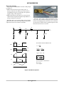
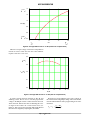
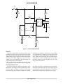
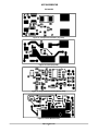
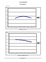
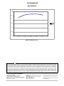
NCP3065BBGEVB Reference Design for Sharp ZENIGATA LED Module Evaluation Board User's Manual http://onsemi.com EVAL BOARD USER’S MANUAL Circuit Description This circuit is proposed for driving the Sharp ZENIGATA LED module in a variety of lighting applications. Configurations like this are found in 12 VAC track lighting applications, automotive applications, and low voltage AC landscaping applications as well as task lighting such as under-cabinet lights and desk lamps that might be powered from standard off-the-shelf 5 and 12 VAC wall adapters. The circuit is based on the NCP3065 operation at ~150 kHz in a non-isolated configuration. Key consideration in this design was achieving flat current regulation across input line variation and output voltage variation with a 12 VAC input. Figure 1. Sharp ZENIGATA LED Module Key Features Small Size for MR-16 Applications Buck-Boost Operation Wide Input and Output Operation Voltage Regulated Output Current Open LED Protection Output Short Circuit Protection Figure 2. NCP3065 Top Side Reference Design 0.457 x 1.148 (11 mm x 29 mm) Figure 3. NCP3065 Bottom Side Reference Design 0.457 x 1.148 (11 mm x 29 mm) Device Application Input Voltage Output Power Topology I/O Isolation NCP3065 Lighting 12 VDC or 12 VAC 3.6 W Buck-Boost None Table 1. SPECIFICATIONS AC Input Voltage 12 VAC Line Transformer (Source Resistance < 0.1 W), MR16 Solid State AC Ballast DC Input 6 V to 16 VDC Output Voltage 8−12 V Output Current 350 mA/550 mA Regulated Semiconductor Components Industries, LLC, 2012 February, 2012 − Rev. 8 1 Publication Order Number: EVBUM2060/D NCP3065BBGEVB SCHEMATIC Figure 4. Buck-Boost Converter Schematic http://onsemi.com 2 NCP3065BBGEVB Basic Power Topology The principle of the Buck-Boost converter is fairly simple (see Figure 5): While in the On-state, the input voltage source is directly connected to the inductor (L). This results in accumulating energy in L. In this stage, the capacitor C supplies energy to the output load; While in the Off-state, the inductor is connected to the output load and capacitor through the Output Diode, so energy is transferred to the load. Also note, when trying to make measurements with a scope probe, that ground is NOT ground. The scope will need to be floating (ground connection removed from the AC wall source) or there will be a ground loop/short circuit that will cause the device to turn off. Remember this is an inverting output. So the negative output will connect to the anode of the LED, and the positive output will connect to the cathode of the LED. Vin IQ ID VSW Vout Vgate IL C RLoad Ton From Inductor Volt Second Balance and: Vgate Toff V + L di dt Vin V o(T off) V i(T on) + L L VSW Vo−Vf V inD + V o(1 * D) IQ Vo D + V in (1 * D) ID Vout can be higher or lower than Vin For D = 0 to 1 Vout is Negative IL Figure 5. Buck-Boost Operation http://onsemi.com 3 NCP3065BBGEVB TSD NC Set Dominant R ILimit Comp Switch Collector Q S Ipk Sense S Q R 0.2 V Switch Emitter Set Dominant OSCILLATOR VCC Ct Ct Vref GND Comp Inv Figure 6. NCP3065 Burst Mode Controller Burst Mode Control The basic control loop consists of a 0.235 V internal Reference, a Feedback Comparator, and two Set-Dominant RS Latches. Basically the NCP3065 allows the Power FET for the Buck-Boost stage to switch ON as the Feedback Voltage falls below the reference voltage. The Power FET will be then be forced OFF unconditionally during Ct Ramp down. R8 is used to sense the inductor current and is fed to the FB pin of the NCP3065. This application produces OFF time instantaneous (Ivalley) inductor current control (see Figure 7). A cycle of switch ON time is only allowed to start once the OFF time Inductor current crosses the Vref threshold. Since the controller does not provide integral PWM control and utilizes only a comparator trip point for feedback, the peak to average load current is not in direct proportion as in a Buck Converter, but rather follows the following formula: I ave ȡ +ȧI Ȣ V ȡ ȣȣ 1* V )V V 1 ) ȧǒ Ǔ ȧȧǒ1 * V 2 L F Ȣ ȤȤ O valley O in VO O ) V in Ǔ Where, Ivalley is the lowest inductor current point. Plotting Iave vs. Vin shows a dramatic curve which would cause a significant change in light output of the LED (see Figure 8). Ipeak Ivalley Ton O Toff Ton Toff Average Load Current = Area During Toff Figure 7. Buck-Boost Inductor Current http://onsemi.com 4 NCP3065BBGEVB 1.4 1.319 1.2 1.0 Iave (Vin) 0.8 0.6 0.408 0.4 0 5 10 3 15 20 20 Vin Figure 8. Average LED Current vs. Vin DC (without Vin Compensation) Therefore an input voltage feed-forward compensation network is used to reduce the error due to the nonlinear response of the Iout vs. Vin curve. 0.4 0.35 0.3 Iave (Vin) 0.2 0.1 0.0 5 6 8 12 10 14 16 18 19 Vin, N Figure 9. Average LED Current vs. Vin DC (with Vin Compensation) R9 and C6 are used to limit the gate to source voltage on the external switch at high input voltage. The resistor divider network of R9 and R2 are used to program and gate to source maximum. A resistive divider network consisting of R3, R5 and summing resistor R4 are used to add Vin proportional voltage to the FB pin in order to reduce the load current as Vin is increased. This has the effect of flattening the curve of Figure 8 and reduces the overall current error (see Figure 9). This average line can be DC shifted with R8 and the ends can be aligned by adjusting R5, R3 and R4. V gs + V in * http://onsemi.com 5 ǒ Ǔ V in R9 R9 ) R2 NCP3065BBGEVB Pulsed Feedback Resistor C2. This effectively limits the maximum achievable duty cycle of the NCP3065. When conditions warrant low duty cycle, R7 and D5 make higher than desired duty cycles unavailable. D7 is necessary to block voltage during the OFF time, since this is Buck-Boost Topology. More information on Pulsed Feedback compensation is available in the NCP3065 data sheet. R7 and D5 are used to reduce the possibility of pulse skipping (see Figure 10). Since burst mode control involves only one feedback voltage, cross-detection per cycle and does not involve the use of a window comparator, it is possible to have skipped pulses which do not effect the DC regulation but could be visible as flicker in an LED application. R7 and D5 add current to the Ct timing capacitor R2 1 kW Q1−B MBT3946DW1T1 U1 8 7 6 5 EN SC IPKS SE VCC TC FB GND NCP3065 1 2 Q1−A MBT3946DW1T1 L1 68 mH MSS1278 D5 3 4 R7 20 kW MMSD4148T1 C2 5.6 nF R9 200 W C6 2 nF 1 2 R5 22 kW R8 0.25 W R4 1.2 kW Figure 10. Pulsed Feedback Resistor AC Operation vs DC regulation for some finite portion ~80% of the 60 Hz line cycle, and then no output for ~20%. This has the effect of reducing the average current by ~20% when operating with AC input. An additional AC compensation network is added to the Vin Compensation to account for the different operating point (see Figure 11). Since there is a half sine wave input to the Buck-Boost stage, there is a different operating point as compared with pure DC input. Since small size is a goal for this design very little input capacitance is used past the full bridge rectifier. Therefore, the input to the converter is a half wave rectified sine wave. Since the regulator is non-functional below ~4 V there are dead spots in the regulation. So we end up with http://onsemi.com 6 NCP3065BBGEVB F1 1A C4 10 mF 35 V R2 1 kW R1 100 W U1 8 7 6 5 C1 1 mF 35 V EN SC IPKS SE VCC TC FB GND NCP3065 1 2 3 4 C2 5.6 nF D8 MMSD4148T1 R3 115 kW C3 1 mF R6 6.04 kW R5 22 kW Figure 11. Pulsed Feedback Resistor Protection consideration specifically in transformer fed systems that carry significant source inductance. The surge device needs to be selected to a voltage that will never exceed the gate to source voltage of the power FET with reasonable voltage margin. This may require some trial and error to select since the clamp voltage will stretch depending on how much energy needs to be absorbed. Z1 and R1, along with the Current limit feature of the NCP3065, are used for open circuit protection. In the event of an open circuit at the load, the loop will try to increase the output voltage in order to satisfy the current demand which feeds back zero current. When (Vin + Vout) exceeds the voltage of Z1, current will flow in R1 which triggers the current limit function of the NCP3065. Short circuit protection is handled with a fuse, F1, on the input. Surge protection from inductive loads is an important Increasing Output Current The reference design is configured for 350 mA average LED current. Increasing the current regulation point on the reference board is as simple as cutting the current sense resistor R8 in half from 250 mW to 125 mW. Also, the input fuse must be increased to accommodate the increased input current draw. Heat sinking may be required depending on the implementation of the Housing and the environmental characteristics when moving to the higher power design. http://onsemi.com 7 NCP3065BBGEVB PC BOARD Figure 12. Components Placement (Top View) Figure 13. Traces (Top View) Figure 14. Components Placement (Bottom View) Figure 15. Traces (Bottom View) http://onsemi.com 8 NCP3065BBGEVB Table 2. BILL OF MATERIALS Qty Ref Value Part Number Description Manufacturer 1 F1 1A MFU0603FF01000P100 Fuse Tyco 1 C3 10 mF GRM21BF51A106ZE15L Ceramic Chip Capacitor Murata 1 C6 1 nF GRM188R71H102KA01D Ceramic Chip Capacitor Murata 1 C1 1 mF GRM188R61E105KA12D Ceramic Chip Capacitor Murata 1 C2 5.6 nF GRM188R71H562KA01D Ceramic Chip Capacitor Murata 1 C4 10 mF GRM32NF51E106ZA01L Ceramic Chip Capacitor Murata 1 C5 10 mF GRM32NF51E106ZA01L Ceramic Chip Capacitor Murata 1 D1 1 A, 30 V MBR130T1G Diode, Schottky ON Semiconductor 1 D2 1 A, 30 V MBR130T1G Diode, Schottky ON Semiconductor 1 D3 1 A, 30 V MBR130T1G Diode, Schottky ON Semiconductor 1 D4 1 A, 30 V MBR130T1G Diode, Schottky ON Semiconductor 1 D6 2 A, 60 V MBRS260T3 Diode, Schottky ON Semiconductor 1 Q1 PNP MBT3946DW1T1 General Purpose NPN Transistor ON Semiconductor 1 D5 0.2 A, 100 V MMSD4148T1 Diode, Small Signal ON Semiconductor 1 D8 0.2 A, 100 V MMSD4148T1 Diode, Small Signal ON Semiconductor 1 Z1 36 V MM5Z36VT1 Diode, ZENER ON Semiconductor 1 L1 68 mH MSS1278-683MLD Inductor, SM Coilcraft 1 U1 40 V, 1.5 A NCP3065DR2G Switching Regulator ON Semiconductor 1 M1 PFET NTGS4111PT1G MOSFET, P ON Semiconductor 1 R4 1.2 kW CRCW04021K20FKED Resistor Vishay/Dale 1 R1 100 W CRCW0402100RFKED Resistor Vishay/Dale 1 R3 162 kW CRCW0402162KFKED Resistor Vishay/Dale 1 R6 196 W CRCW0402196RFKED Resistor Vishay/Dale 1 R7 22 kW CRCW040222K0FKED Resistor Vishay/Dale 1 R5 22 kW CRCW040222K0FKED Resistor Vishay/Dale 1 R2 1 kW CRCW04021K00FKED Resistor Vishay/Dale 1 R9 200 W CRCW0402200RFKED Resistor Vishay/Dale 1 R8 0.25 W CSR1/20.25FICT-ND Resistor Vishay/Dale 1 D7 − P6SMB22CAT3 ZENER, Back to Back ON Semiconductor Table 3. LED MODULE SPECIFICATION (SHARP P/N GW5BWC15L02) Attribute Name Attribute Data Color Temperature Normal White − 5000K CRI 60 Description White LED 3.5 Watt ZENIGATA LED Module, 5000K Dominant Wavelength X = 0.35, Y = 0.35 nm Family GW5xxC15Lx2 Forward Voltage 10.2 V If 350 mA Light Output 3.5 W Luminous Flux Typ 280 lm Package Type 18 mm x 18 mm RoHS Yes http://onsemi.com 9 NCP3065BBGEVB MEASUREMENTS 12 V (ac) Data 0.4 0.38 0.36 Iout 0.34 0.32 0.3 8 9 10 11 12 13 14 15 Figure 16. Iout vs VAC 0.8000 0.7000 0.6000 eff 0.5000 0.4000 0.3000 0.2000 8 9 10 11 12 13 Figure 17. AC Efficiency vs VAC http://onsemi.com 10 14 15 NCP3065BBGEVB MEASUREMENTS 0.8 0.75 0.7 Eff 0.65 0.6 0.55 0.5 7 9 11 13 15 17 19 Figure 18. Efficiency vs VDC ON Semiconductor and are registered trademarks of Semiconductor Components Industries, LLC (SCILLC). SCILLC reserves the right to make changes without further notice to any products herein. SCILLC makes no warranty, representation or guarantee regarding the suitability of its products for any particular purpose, nor does SCILLC assume any liability arising out of the application or use of any product or circuit, and specifically disclaims any and all liability, including without limitation special, consequential or incidental damages. “Typical” parameters which may be provided in SCILLC data sheets and/or specifications can and do vary in different applications and actual performance may vary over time. All operating parameters, including “Typicals” must be validated for each customer application by customer’s technical experts. SCILLC does not convey any license under its patent rights nor the rights of others. SCILLC products are not designed, intended, or authorized for use as components in systems intended for surgical implant into the body, or other applications intended to support or sustain life, or for any other application in which the failure of the SCILLC product could create a situation where personal injury or death may occur. Should Buyer purchase or use SCILLC products for any such unintended or unauthorized application, Buyer shall indemnify and hold SCILLC and its officers, employees, subsidiaries, affiliates, and distributors harmless against all claims, costs, damages, and expenses, and reasonable attorney fees arising out of, directly or indirectly, any claim of personal injury or death associated with such unintended or unauthorized use, even if such claim alleges that SCILLC was negligent regarding the design or manufacture of the part. SCILLC is an Equal Opportunity/Affirmative Action Employer. This literature is subject to all applicable copyright laws and is not for resale in any manner. PUBLICATION ORDERING INFORMATION LITERATURE FULFILLMENT: Literature Distribution Center for ON Semiconductor P.O. Box 5163, Denver, Colorado 80217 USA Phone: 303−675−2175 or 800−344−3860 Toll Free USA/Canada Fax: 303−675−2176 or 800−344−3867 Toll Free USA/Canada Email: [email protected] N. American Technical Support: 800−282−9855 Toll Free USA/Canada Europe, Middle East and Africa Technical Support: Phone: 421 33 790 2910 Japan Customer Focus Center Phone: 81−3−5817−1050 http://onsemi.com 11 ON Semiconductor Website: www.onsemi.com Order Literature: http://www.onsemi.com/orderlit For additional information, please contact your local Sales Representative EVBUM2060/D