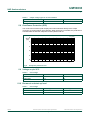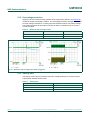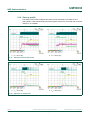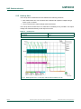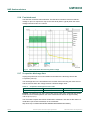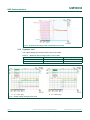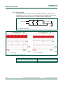
1
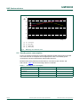
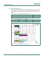
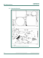
UM10833 TEA1836DB1200 TEA18362LT + TEA1892TS 45 W cool cube charger Rev. 1 — 3 February 2015 User manual Document information Info Content Keywords TEA1836DB1200, TEA18362LT, TEA1892TS, very low standby power consumption, active X-cap discharge, burst mode operation, flyback converter, 45 W, charger, converter, power supply, demo board Abstract This user manual describes the 45 W cool cube demo board with the TEA18362LT and TEA1892TS. The TEA1836DB1200 demo board provides an output of 19.5 V/2.31 A. It has very small dimensions (31 mm 52 mm). It fits in the cool cube casing (outer dimensions). UM10833 NXP Semiconductors TEA1836DB1200 TEA18362LT + TEA1892TS 45 W cool cube charger Revision history Rev Date Description v.1 20150203 first issue Contact information For more information, please visit: http://www.nxp.com For sales office addresses, please send an email to: [email protected] UM10833 User manual All information provided in this document is subject to legal disclaimers. Rev. 1 — 3 February 2015 © NXP Semiconductors N.V. 2015. All rights reserved. 2 of 33 UM10833 NXP Semiconductors TEA1836DB1200 TEA18362LT + TEA1892TS 45 W cool cube charger 1. Introduction WARNING Lethal voltage and fire ignition hazard The non-insulated high voltages that are present when operating this product, constitute a risk of electric shock, personal injury, death and/or ignition of fire. This product is intended for evaluation purposes only. It shall be operated in a designated test area by personnel qualified according to local requirements and labor laws to work with non-insulated mains voltages and high-voltage circuits. This product shall never be operated unattended. 1.1 Scope of this document This user manual describes the 45 W notebook adapter TEA1836DB1200 demo board using the TEA18362LT and TEA1892TS. It contains a set of measurements that shows the main characteristics. 1.2 TEA18362LT The TEA18362LT is a controller IC for low-cost Switched Mode Power Supplies (SMPS) intended for flyback topologies. The built-in green functions provide high efficiency at all power levels. At high power levels, the flyback operates in QR mode. When lowering the power levels, the controller switches to DCM or Frequency Reduction (FR) mode. The peak current is reduced to 25 % of the maximum peak current. At low power levels, when the flyback switching frequency reaches 25 kHz, the flyback converter switches to burst mode. To ensure high efficiency at low power and excellent no-load power performance, a burst mode has been integrated that reduces the opto current to a minimum level. As the switching frequency in this mode has a minimum value of 25 kHz while the burst frequency is always below 800 Hz, the frequencies are outside the audible range. During the non-switching phase of the burst mode, the internal IC supply current is reduced to optimize efficiency further. Valley switching is used in all operating modes. The TEA18362LT includes an OverPower Protection (OPP). The OPP enables the controller to deliver 150 % peak power for a limited amount of time (200 ms) in case of overpower situations. If the output is shorted, the output power is limited to 100 % to keep the average power consumption lower than 5 W. The TEA18362LT is realized in a high-voltage Silicon-On-Insulator (SOI) process. This process combines the advantages of a low-voltage process, like accuracy, high-speed protection functions, and control, while maintaining the high-voltage capabilities like high-voltage start-up and integrated X-cap discharge. The TEA18362LT enables low-cost, highly efficient and reliable supplies for power requirements up to 75 W to be designed easily and with a minimum number of external components. UM10833 User manual All information provided in this document is subject to legal disclaimers. Rev. 1 — 3 February 2015 © NXP Semiconductors N.V. 2015. All rights reserved. 3 of 33 UM10833 NXP Semiconductors TEA1836DB1200 TEA18362LT + TEA1892TS 45 W cool cube charger 1.3 TEA1892TS The TEA1892TS is a member of the generation of Synchronous Rectifier (SR) controller ICs for switched mode power supplies. Its high level of integration enables the design of a cost-effective power supply with a very low number of external components. The TEA1892TS is a controller IC dedicated to synchronous rectification on the secondary side of discontinuous conduction mode and quasi-resonant flyback converters. 1.4 Setup of the 45 W notebook adapter The board is designed for universal mains (90 V (AC) to 265 V (AC)). When a DC input voltage is applied, the power consumption is higher due to continuous activation of the X-capacitor discharge function. The TEA1836DB1200 demo board incorporates two subcircuits: • A DCM/QR type flyback converter • A Synchronous Rectifier (SR) The purpose of the demo board is to show the operation of the TEA18362LT and TEA1892TS in a small-size board. The performance is according to the current general standards including the DoE + CoC efficiency requirements. It can be used as a starting point for further product development. 2. Safety warning The board must be connected to the mains voltage. Touching the board during operation must always be avoided. An isolated housing is obligatory when used in uncontrolled, non-laboratory environments. Galvanic isolation of the mains phase using a variable transformer is always recommended. Figure 1 shows the symbols by which these devices can be recognized. 019aab174 019aab173 a. Isolated Fig 1. UM10833 User manual b. Not isolated Variable transformer (Variac) isolation symbols All information provided in this document is subject to legal disclaimers. Rev. 1 — 3 February 2015 © NXP Semiconductors N.V. 2015. All rights reserved. 4 of 33 UM10833 NXP Semiconductors TEA1836DB1200 TEA18362LT + TEA1892TS 45 W cool cube charger 3. Board photographs a. Top b. Bottom Fig 2. UM10833 User manual TEA1836DB1200 demo board photographs All information provided in this document is subject to legal disclaimers. Rev. 1 — 3 February 2015 © NXP Semiconductors N.V. 2015. All rights reserved. 5 of 33 UM10833 NXP Semiconductors TEA1836DB1200 TEA18362LT + TEA1892TS 45 W cool cube charger 4. Specifications Table 1. TEA1836DB1200 specifications Symbol Description Conditions Value Input specifications Vin input voltage 90 V to 265 V fi input frequency Pi(noload) no-load input power 47 Hz to 64 Hz at 230 V/50 Hz < 25 mW Output specifications UM10833 User manual Vout output voltage 19.5 V Iout output current Io(peak) peak output current for 200 ms at Vi = 90 V at 60 Hz 3A 0 A to 2.31 A thold hold time at 115 V/60 Hz; full load > 10 ms - line regulation - load regulation tstartup start-up time at 115 V/60 Hz 1s efficiency DoE: > 88.5 % at cable end (including 0.5 % margin); CoC: > 89.5 % at cable end (including 0.5 % margin) 92 % - ElectroMagnetic Interference (EMI) CISPR22 compliant pass ±1 % ±1 % All information provided in this document is subject to legal disclaimers. Rev. 1 — 3 February 2015 © NXP Semiconductors N.V. 2015. All rights reserved. 6 of 33 UM10833 NXP Semiconductors TEA1836DB1200 TEA18362LT + TEA1892TS 45 W cool cube charger 5. Measurements 5.1 Test facilities • • • • Oscilloscope: Yokogawa DL9140L AC Power Source: Agilent 6812B Electronic load: Agilent 6063B Digital power meter: Yokogawa WT210 5.2 Efficiency Efficiency measurements are performed at stabilized conditions. The output voltage and output current is measured directly at the PCB connector. Measurements are done for 90 V/60 Hz, 115 V/60 Hz, 230 V/50 Hz, and 265 V/50 Hz. Table 2 shows the average value of 10 boards. Table 2. Iout (A) Efficiency PCB end Vout (V) Pin (W) Efficiency (%) Average 0.585 A to 2.31 A 90 V (AC)/60 Hz 0.24 19.392 5.055 92.07 0.585 19.4 12.33 92.04 1.155 19.406 24.159 92.78 1.725 19.411 36.21 92.47 2.31 19.421 49.22 91.15 5.045 92.25 92.11 115 V (AC)/60 Hz 0.24 19.392 0.585 19.4 12.283 92.40 1.155 19.407 24.052 93.19 1.725 19.411 35.82 93.48 2.31 19.418 48.22 93.02 93.02 230 V (AC)/50 Hz 0.24 19.393 5.106 91.15 0.585 19.403 12.401 91.53 1.155 19.408 24.18 92.71 1.725 19.414 35.87 93.36 2.31 19.421 47.79 93.87 90.20 92.87 265 V (AC)/50 Hz UM10833 User manual 0.24 19.394 5.16 0.585 19.405 12.525 90.63 1.155 19.41 24.39 91.92 1.725 19.418 36.14 92.68 2.31 19.423 48.1 93.28 All information provided in this document is subject to legal disclaimers. Rev. 1 — 3 February 2015 92.13 © NXP Semiconductors N.V. 2015. All rights reserved. 7 of 33 UM10833 NXP Semiconductors TEA1836DB1200 TEA18362LT + TEA1892TS 45 W cool cube charger DDD Ș ,RXW$ (1) Vin = 115 V (AC) (2) Vin = 90 V (AC) (3) Vin = 230 V (AC) (4) Vin = 265 V (AC) Fig 3. Efficiency as a function of Iout 5.3 Standby power consumption Power consumption performance of the total application board without load connected was measured with a Yokogawa WT210 digital power meter. The standby power consumption has been measured 20 minutes after switch-on. Measurements were performed for 90 V/60 Hz, 115 V/60 Hz, 230 V/50 Hz, and 265 V/50 Hz. Table 3 shows the average value of 10 boards. Table 3. UM10833 User manual Standby power consumption Vin V (AC) Pnoload (mW) Vout (V) 90 V/60 Hz 18.5 19.4 115 V/60 Hz 19.1 19.4 230 V/50 Hz 22.9 19.4 265 V/50 Hz 24.8 19.4 All information provided in this document is subject to legal disclaimers. Rev. 1 — 3 February 2015 © NXP Semiconductors N.V. 2015. All rights reserved. 8 of 33 UM10833 NXP Semiconductors TEA1836DB1200 TEA18362LT + TEA1892TS 45 W cool cube charger DDD 3QRORDG P: Fig 4. 9LQ9 Standby power consumption at no-load 5.4 Current for changing between normal and burst mode operation Table 4. Condition Current for changing between normal and burst mode operation 115 V/60 Hz 230 V/50 Hz From normal mode to burst mode operation current (A) 0.40 0.50 power (W) 7.75 9.7 From burst mode to normal mode operation UM10833 User manual current (A) 0.25 0.33 power (W) 4.85 6.4 All information provided in this document is subject to legal disclaimers. Rev. 1 — 3 February 2015 © NXP Semiconductors N.V. 2015. All rights reserved. 9 of 33 UM10833 NXP Semiconductors TEA1836DB1200 TEA18362LT + TEA1892TS 45 W cool cube charger 5.5 Load regulation The output voltage versus load current was measured at the PCB connector. DDD 9RXW 9 ,RXW$ a. Vin = 115 V/60 Hz DDD 9RXW 9 ,RXW$ b. Vin = 230 V/50 Hz Fig 5. UM10833 User manual Output voltage as a function of output current All information provided in this document is subject to legal disclaimers. Rev. 1 — 3 February 2015 © NXP Semiconductors N.V. 2015. All rights reserved. 10 of 33 UM10833 NXP Semiconductors TEA1836DB1200 TEA18362LT + TEA1892TS 45 W cool cube charger 5.6 Line regulation The output voltage versus mains input voltage was measured directly at the output connector for nominal load condition (2.31 A). The values remain within the target of 19.5 V 1 %. DDD 9RXW 9 Fig 6. 9LQ9 Output voltage as function of the mains voltage 5.7 Output voltage regulation in standby mode The output voltage regulation during no load operation was measured for 90 V/60 Hz and 265 V/50 Hz. a. Vin = 90 V at 60 Hz Fig 7. b. Vin = 265 V at 50 Hz Output voltage regulation at no-load UM10833 User manual All information provided in this document is subject to legal disclaimers. Rev. 1 — 3 February 2015 © NXP Semiconductors N.V. 2015. All rights reserved. 11 of 33 UM10833 NXP Semiconductors TEA1836DB1200 TEA18362LT + TEA1892TS 45 W cool cube charger Table 5. Output voltage ripple at no-load condition Symbol 90 V/60 Hz 230 V/50 Hz Vripple (mV) 79 96 5.8 OverPower Protection (OPP) The continuous maximum peak output power was measured directly at the output connector for various mains input voltages. When this level is exceeded, the protection is activated after the internal overpower counter-passes 200 ms. DDD 3RPD[ : Fig 8. 9LQ9 Overpower protection level 5.9 Voltage on pin VCC Table 6. VCC voltage Condition 115 V/60 Hz 230 V/50 Hz no-load 12 12 nominal load 22.9 20.1 5.10 Brownout and start-up level Table 7. UM10833 User manual VCC voltage Condition Brownout (V) Start level (V) no-load 70 79 nominal load 70 79 All information provided in this document is subject to legal disclaimers. Rev. 1 — 3 February 2015 © NXP Semiconductors N.V. 2015. All rights reserved. 12 of 33 UM10833 NXP Semiconductors TEA1836DB1200 TEA18362LT + TEA1892TS 45 W cool cube charger 5.11 Short circuit protection Output short circuit directly at the PCB connectors before switching on the mains voltage or during operation. The system protects and latches during the short circuit condition. With a TEA18362T, the system protects and restarts continuously during the short circuit condition. Table 8. Behavior during output short circuit condition Condition Behavior output short before applying AC mains voltage latch output short circuit during operation at full load and no-load latch Table 9. Condition 90 V/60 Hz 230 V/50 Hz 265 V/50 Hz input power 0.33 W 0.31 W 0.35 W Fig 9. UM10833 User manual Input power at output short circuit condition Short circuit during operation at Vin = 230 V (AC) All information provided in this document is subject to legal disclaimers. Rev. 1 — 3 February 2015 © NXP Semiconductors N.V. 2015. All rights reserved. 13 of 33 UM10833 NXP Semiconductors TEA1836DB1200 TEA18362LT + TEA1892TS 45 W cool cube charger 5.12 Overvoltage protection Applying a short circuit across the optoLED of the optocoupler (OPTO1; see Figure 22) creates an output overvoltage condition. The overvoltage protection is triggered when the AUX pin voltage increases to 3 V during the OVP detection interval. The output voltage was measured directly at the output connector for both a nominal load (2.31 A) and a no-load condition. Table 10. Maximum output voltage at OVP Condition 115 V/60 Hz 230 V/50 Hz no-load 29 V 29 V nominal load (3.37 A) 29 V 29 V a. Io = 0 A b. Io = 2.31 A Fig 10. Maximum output voltage when OVP is triggered 5.13 Start-up time The start-up time is the time between the mains voltage switching on and the nominal output power available at the output. Table 11. UM10833 User manual Start-up time Condition Start-up time 90 V/60 Hz 370 ms 115 V/60 Hz 210 ms 230 V/50 Hz 150 ms All information provided in this document is subject to legal disclaimers. Rev. 1 — 3 February 2015 © NXP Semiconductors N.V. 2015. All rights reserved. 14 of 33 UM10833 NXP Semiconductors TEA1836DB1200 TEA18362LT + TEA1892TS 45 W cool cube charger 5.14 Start-up profile The shape of the output voltage during start-up was measured for 90 V/60 Hz and 265 V/50 Hz. It was measured directly at the output connector for a no-load and a nominal load (2.31 A) condition. a. Vin = 90 V (AC) b. Vin = 265 V (AC) Fig 11. Start-up at nominal output load a. Vin = 90 V (AC) b. Vin = 265 V (AC) Fig 12. Start-up at no output load UM10833 User manual All information provided in this document is subject to legal disclaimers. Rev. 1 — 3 February 2015 © NXP Semiconductors N.V. 2015. All rights reserved. 15 of 33 UM10833 NXP Semiconductors TEA1836DB1200 TEA18362LT + TEA1892TS 45 W cool cube charger 5.15 Hold-up time The hold-up time is defined as the time between the following moments: • After mains switch-off: The moment that the lowest bulk capacitor voltage during a mains cycle is crossed. • The moment that the output voltage starts to decrease. The hold-up time is measured for 115 V/60 Hz for a full load (2.31 A) condition. The output voltage was measured directly at the output connector. Table 12. Hold-up time Condition Hold-up time 115 V/60 Hz 10 ms Fig 13. Hold-up time at Vin = 115 V (AC) and full load condition (2.31 A) UM10833 User manual All information provided in this document is subject to legal disclaimers. Rev. 1 — 3 February 2015 © NXP Semiconductors N.V. 2015. All rights reserved. 16 of 33 UM10833 NXP Semiconductors TEA1836DB1200 TEA18362LT + TEA1892TS 45 W cool cube charger 5.16 Fast latch reset The fast latch reset time was measured. The fast latch reset time is the time that the voltage on pin VCC requires to drop to the reset level (8.65 V typical) when the mains voltage is disconnected. It is 730 ms. Fig 14. Latch reset when disconnecting mains voltage 5.17 X-capacitor discharge time Unplug the power line at no-load condition and measure the discharge time at the X-capacitor (330 nF). The discharge time is the time between the moment of disconnecting the mains source and the moment when the voltage reaches a defined voltage value. Table 13. X-capacitor discharge time test results Condition from 265 V * 2 to 135 V from 265 V * 2 to 60 V X-capacitor discharge time 55 ms 145 ms Remark: The discharge can start 100 ms later (worse case) than measured and shown because in burst mode operation the mains measurement interval is approximately 100 ms (twait(burst)HV). The TEA1836 complies with Nemko Certification: NO081101 and with the DK-40437-UL certification (see for documentation on the certificates http://www.nxp.com/demoboard/TEA1836DB1200.html#documentation). UM10833 User manual All information provided in this document is subject to legal disclaimers. Rev. 1 — 3 February 2015 © NXP Semiconductors N.V. 2015. All rights reserved. 17 of 33 UM10833 NXP Semiconductors TEA1836DB1200 TEA18362LT + TEA1892TS 45 W cool cube charger Fig 15. X-capacitor discharge at 265 V (AC)/50 Hz and no-load 5.18 Dynamic load The output voltage was measured at the end of the board. Table 14. Maximum output voltage ripple in case of OVP Condition Load Output voltage ripple (mV) 115 V/60 Hz Io: 0 % to 100 % 374 230 V/50 Hz Io: 0 % to 100 % 374 a. Vin = 115 V (AC) b. Vin = 230 V (AC) Fig 16. Output voltage during dynamic load UM10833 User manual All information provided in this document is subject to legal disclaimers. Rev. 1 — 3 February 2015 © NXP Semiconductors N.V. 2015. All rights reserved. 18 of 33 UM10833 NXP Semiconductors TEA1836DB1200 TEA18362LT + TEA1892TS 45 W cool cube charger 5.19 Output ripple Output ripple was measured at the end of a 16AWG cable with 1.2 m length using a standard filter of 10 F + 100 nF on the probing position. Output ripple and noise were measured at nominal output current (2.31 A) and at no-load condition (0 A). $GDSWHUFDEOH ) Q) 3UREH 3UREHWLS DDD Fig 17. Measurement setup a. Vin = 90 V (AC) b. Vin = 265 V (AC) Fig 18. Output voltage ripple nominal load Table 15. UM10833 User manual Output voltage ripple at nominal load Condition peak-to-peak output voltage ripple and noise 90 V/60 Hz 177 mV 265 V/50 Hz 108 mV All information provided in this document is subject to legal disclaimers. Rev. 1 — 3 February 2015 © NXP Semiconductors N.V. 2015. All rights reserved. 19 of 33 UM10833 NXP Semiconductors TEA1836DB1200 TEA18362LT + TEA1892TS 45 W cool cube charger a. Vin = 90 V (AC) b. Vin = 265 V (AC) Fig 19. Output voltage ripple at burst mode operation (no-load) Table 16. Output voltage ripple at no-load Condition peak-to-peak output voltage ripple and noise 90 V/60 Hz 70 mV 265 V/50 Hz 96 mV 5.20 EMI performance Conditions: • • • • • UM10833 User manual Type: Conducted EMI measurement Frequency range: 150 kHz to 30 MHz Output power: Full load condition Input voltage: 115 V and 230 V Secondary GND connected to PE GND All information provided in this document is subject to legal disclaimers. Rev. 1 — 3 February 2015 © NXP Semiconductors N.V. 2015. All rights reserved. 20 of 33 UM10833 NXP Semiconductors TEA1836DB1200 TEA18362LT + TEA1892TS 45 W cool cube charger Fig 20. Conducted EMI: Vin = 115 V (AC) - curves Table 17. Conducted EMI: Vmains = 115 V (AC) - sheet Trace 1: EN55022Q Trace 2: EN55022A Trace 3: --- UM10833 User manual Trace Frequency Level dBV Delta limit dB 1 quasi peak 158 kHz 55.25 N 10.31 1 quasi peak 3.97 MHz 41.43 N 14.56 1 quasi peak 230 kHz 47.80 N 14.64 1 quasi peak 4.046 MHz 41.01 N 14.99 2 average 182 kHz 37.77 N 16.62 1 quasi peak 250 kHz 41.94 N 19.80 All information provided in this document is subject to legal disclaimers. Rev. 1 — 3 February 2015 © NXP Semiconductors N.V. 2015. All rights reserved. 21 of 33 UM10833 NXP Semiconductors TEA1836DB1200 TEA18362LT + TEA1892TS 45 W cool cube charger Fig 21. Conducted EMI: Vin = 230 V (AC) - curves Table 18. Conducted EMI: Vin = 230 V (AC) - sheet Trace 1: EN55022Q Trace 2: EN55022A Trace 3: --- UM10833 User manual Trace Frequency Level dBV Delta limit dB 1 quasi peak 258 kHz 53.49 N 8.00 2 average 258 kHz 42.63 N 8.86 2 average 382 kHz 35.00 N 13.23 2 average 20.166 MHz 33.80 N 16.19 1 quasi peak 19.37 MHz 42.46 N 17.53 1 quasi peak 24.706 MHz 41.82 L1 18.17 1 quasi peak 154 kHz 47.03 N 18.74 1 quasi peak 26.958 MHz 41.08 L1 18.91 All information provided in this document is subject to legal disclaimers. Rev. 1 — 3 February 2015 © NXP Semiconductors N.V. 2015. All rights reserved. 22 of 33 UM10833 NXP Semiconductors TEA1836DB1200 TEA18362LT + TEA1892TS 45 W cool cube charger 5.21 Thermal measurements The component temperatures were measured with open frame. The open PCB was placed on the table. After 1 hour of warming up time at full load (2.31 A), the component temperatures were measured using an infrared thermal camera. Tamb = 25 C. The MOSFET switch uses thermal compound for cooling. Table 19. Thermal measurements Component Part reference Temperature (C) Vin = 115 V (AC) TEA1836 U4 76.8 Transformer core T1 84.1 Transformer winding T1 88.5 MOSFET switch SPU07N60C3 Q1 92.5 Clamp diode SA2M D3 83.1 Discharge resistor in peak clamp R7 84.3 SR MOSFFET PSMN012-100YS Q2 63.2 Vin = 230 V (AC) UM10833 User manual TEA1836 U4 73.5 Transformer core T1 84 Transformer winding T1 86.5 MOSFET switch SPU07N60C3 Q1 88.8 Clamp diode SA2M D3 82.7 Discharge resistor in peak clamp R7 84.7 SR MOSFFET PSMN012-100YS Q2 68.7 All information provided in this document is subject to legal disclaimers. Rev. 1 — 3 February 2015 © NXP Semiconductors N.V. 2015. All rights reserved. 23 of 33 xxxxxxxxxxxxxxxxxxxxx xxxxxxxxxxxxxxxxxxxxxxxxxx xxxxxxx x x x xxxxxxxxxxxxxxxxxxxxxxxxxxxxxx xxxxxxxxxxxxxxxxxxx xx xx xxxxx xxxxxxxxxxxxxxxxxxxxxxxxxxx xxxxxxxxxxxxxxxxxxx xxxxxx xxxxxxxxxxxxxxxxxxxxxxxxxxxxxxxxxxx xxxxxxxxxxxx x x xxxxxxxxxxxxxxxxxxxxx xxxxxxxxxxxxxxxxxxxxxxxxxxxxxx xxxxx xxxxxxxxxxxxxxxxxxxxxxxxxxxxxxxxxxxxxxxxxxxxxxxxxx xxxxxxxx xxxxxxxxxxxxxxxxxxxxxxxxx xxxxxxxxxxxxxxxxxxxx xxx NXP Semiconductors UM10833 User manual 6. Schematic 7 50 )/ 653 - / ) $ 9 & S) 9 / P+ $ &; Q) 9$& 5 Nȍ 5 ȍ & ) 9 ȍ ' & Q) 9 ' 60/ ' 60/ 5 Nȍ 5 Nȍ )/ 650 7($76 *1' & Q) 9 5 & S) 9 QF '5,9(5 9R 5 & ȍ Q) 9 & - 9R & Q) 9 5 Nȍ ' %=; &9 ,6(16( '5,9(5 &75/ 3527(&7 7($/7 *1' +9 5 & S) ȍ 9 5 ȍ 2372 5 5 Nȍ 57 Nȍ 5 Nȍ QP 8 7&/7 5 5 ' ȍ %$6 & Q) 9 Nȍ & Q) 9 5 Nȍ & Q) 9 & S) 9 &< & Q) 9 & ) 9 5 Nȍ 5 ȍ 2372 9&& ȍ - *1' Q) 9 8 $8; 5 9 ȍ $ & ) 9 ) 9 & 5 Nȍ 5 Nȍ 4 3601<6 Nȍ 5 ȍ 656(16( 5 ȍ %$6 ' $630 1 - 4 6381& 5 ' $630 ' $630 6(/5(* ' $630 )/ 3 )/ 0 8 9&& S) 9$& 5 Nȍ 8 6&&6. 5 Nȍ DDD Fig 22. TEA1836DB1200 schematic diagram TEA18362LT and TEA1892TS 45 W charger demo board UM10833 24 of 33 © NXP Semiconductors N.V. 2015. All rights reserved. 6* VSDUNJDSPP & Q) 9 TEA1836DB1200 TEA18362LT + TEA1892TS 45 W cool cube charger Rev. 1 — 3 February 2015 All information provided in this document is subject to legal disclaimers. ' %$6 ' 6$0 UM10833 NXP Semiconductors TEA1836DB1200 TEA18362LT + TEA1892TS 45 W cool cube charger 7. Bill Of Materials (BOM) Table 20. TEA1836DB1200 bill of material Reference Description and values Part number Manufacturer C1 capacitor; 68 F; 20 %; 400 V; aluminum; THT 400BXW68MEFC18X20 Rubycon C3 capacitor; 10 F; 20 %; 35 V; aluminum; THT 35ML10MEFC4X7 Rubycon C4 capacitor; 1000 F; 20 %; 25 V; aluminum; 10 mm 20 mm EEUFR1E102 Panasonic C5; C15; C17 capacitor; 100 nF; 10 %; 50 V; X7R; 0402 C1005X7R1H104K050BB TDK C6 capacitor; 47 nF; 10 %; 50 V; X7R; 0402 CGA2B3X7R1H473K050BB TDK C8; C14 capacitor; 1 nF; 10 %; 50 V; X7R; 0402 C0402C102K5RACTU KEMET C10 capacitor; 100 pF; 5 %; 50 V; C0G; 0402 C0402C101J5GACTU KEMET C11 capacitor; 10 nF; 10 %; 50 V; X7R; 0402 C0402C103K5RACTU KEMET C12 capacitor; 680 pF; 10 %; 630 V; X7R; 1206 C1206C681KBRACTU KEMET C18 capacitor; 220 nF; 10 %; 10 V; X5R; 0402 GRM155R61A224KE19D Murata C19 capacitor; 68 pF; 5 %; 50 V; C0G; 0402 C0402C680J5GACTU KEMET C20 capacitor; 1 nF; 10 %; 100 V; X7R; 0603 C1608X7R2A102K080AA TDK C22 capacitor; 1 nF; 5 %; 500 V; X7R; 0805 501R15W102KV4E Johanson Dielectrics C24 capacitor; 3.3 pF; 0.25 pF; 50 V; C0G; 0402 06035A3R3CAT2A AVX C25 capacitor; 4.7 F; 10 %; 35 V; X7R; 0805 C2012X7R1V475K125AC TDK CX1 capacitor; X2; 330 nF; 20 %; 630 V; MKP B32922C3334M189 EPCOS CY1 capacitor; X1/Y1; 220 pF; 10 %; 250 V (AC); DE1B3KX221KA5B DE1 Murata D1; D4; D5 diode; 100 V; 250 mA BAS316 NXP Semiconductors D2 diode; Zener; 8.2 V; 200 mA BZX384-C8V2 NXP Semiconductors D3 diode; 1000 V; 2 A SA2M-E3/61T Vishay D6; D7 diode; 1000 V; 1 A S1ML Taiwan Semiconductor D8; D9; D10; D11 diode; 1 kV; 3 A AS3PM-M3/86A Vishay F1 fuse; 250 V; 2 A; slow blow MCPMP 2A 250V Multicomp L1 CM-choke: T16 12 8 (16.5 mH); 0.6 60T:60T AC10300301 Axis Power Q1 MOSFET-N; 650 V; 7.3 A SPU07N60C3 Infineon Q2 MOSFET-N; 100 V; 15 A; LFPAK PSMN012‐100YS,115 NXP Semiconductors R2 resistor; 0 ; 63 mW; 0402 CRCW04020000Z0ED Vishay R3; R21 resistor; 1 k; 1 %; 63 mW; 0402 CRCW04021K00FKED Vishay R4 resistor; 162 k; 1 %; 63 mW; 0402 CRCW0402162KFKED Vishay R5; R8 resistor; 10 ; 1 %; 63 mW; 0603 - - R6 resistor; 24 k; 1 %; 63 mW; 0402 CRCW040224K0FKED Vishay R7 resistor; 100 k; 1 %; 500 mW; 1206 CRCW1206100KFKEAHP Vishay R9 resistor; 10 k; 1 %; 63 mW; 0402 CRCW040210K0FKED Vishay R10 resistor; 330 ; 1 %; 63 mW; 0402 CRCW0402330RFKED Vishay R13 resistor; jumper; 0 ; 2 A; 250 mW; 1206 - - UM10833 User manual All information provided in this document is subject to legal disclaimers. Rev. 1 — 3 February 2015 © NXP Semiconductors N.V. 2015. All rights reserved. 25 of 33 UM10833 NXP Semiconductors TEA1836DB1200 TEA18362LT + TEA1892TS 45 W cool cube charger Table 20. TEA1836DB1200 bill of material …continued Reference Description and values Part number Manufacturer R15 resistor; 2.2 k; 1 %; 100 mW; 0603 RC0603FR-072K2L Yageo R16 resistor; 10 ; 1 %; 63 mW; 0402 CRCW040210R0FKED Vishay R17 resistor; 4.7 ; 5 %; 63 mW; 0402 CRCW04024R70JNEAIF Vishay R18; R19 resistor; 0.43 ; 1 %; 250 mW; 0805 ERJ6BQFR43V Panasonic R22 resistor; 5.6 k; 1 %; 63 mW; 0402 CRCW04025K60FKED Vishay R23 resistor; 33 k; 1 %; 63 mW; 0402 CRCW040233K0FKED Vishay R24 resistor; 150 k; 1 %; 250 mW; 1206 - - R25 resistor; 43 k; 1 %; 63 mW; 0402 - - R26; R27 resistor; 20 k; 1 %; 250 mW; 1206 - - R28 resistor; jumper; 0 ; 63 mW; 0603 - - R30 resistor; 330 ; 5 %; 63 mW; 0603 - - RT2 resistor; NTC; 100 k; 5 %; 100 mW; 4190K; NTCLE100E3104JB0 mount high against transformer T1 (top) Vishay T1 transformer; RM8; 12P TEA1836DB1200_T1 NXP Semiconductors U1 voltage regulator; 2.495 V to 30 V; 1 %; 150 mA SC431CSK-1TRT Semtech Corporation U2 synchronization rectifier controller; TEA1892TS TEA1892TS-1 NXP Semiconductors U3 optocoupler; 70 V; 50 mA; controller 130 % to 260 % TCLT1008 Vishay U4 SMTP controller; TEA18362LT TEA18362LT NXP Semiconductors UM10833 User manual All information provided in this document is subject to legal disclaimers. Rev. 1 — 3 February 2015 © NXP Semiconductors N.V. 2015. All rights reserved. 26 of 33 UM10833 NXP Semiconductors TEA1836DB1200 TEA18362LT + TEA1892TS 45 W cool cube charger 8. PCB layout 8.1 Copper tracks and area a. Top b. Bottom Fig 23. Demo board PCB layout (copper tracks and areas) UM10833 User manual All information provided in this document is subject to legal disclaimers. Rev. 1 — 3 February 2015 © NXP Semiconductors N.V. 2015. All rights reserved. 27 of 33 UM10833 NXP Semiconductors TEA1836DB1200 TEA18362LT + TEA1892TS 45 W cool cube charger 8.2 Component placement a. Top b. Bottom Fig 24. Demo board PCB layout (component placement) UM10833 User manual All information provided in this document is subject to legal disclaimers. Rev. 1 — 3 February 2015 © NXP Semiconductors N.V. 2015. All rights reserved. 28 of 33 UM10833 NXP Semiconductors TEA1836DB1200 TEA18362LT + TEA1892TS 45 W cool cube charger 9. Transformer data 9.1 Introduction For this demo board, requirements were set to show high performance in a very small 45 W form factor board using a basic circuit configuration. To reach this goal, the transformer design requires extra attention to support the combination of high-efficiency performance while still being EMI-compliant using a 220 pF Y-capacitor. At the same time, the concept must deliver 45 W nominal output power and generate a peak output power that is 50 % higher. An RM8 core was used in combination with a customized bobbin type to build the transformer. 9.2 Transformer data SLQV %RWWRPYLHZ 6LGHYLHZ DDD Fig 25. Transformer data Table 21. UM10833 User manual Technical specifications transformer Description Value/requirement bobbin RM8 ferrite material N87 (EPCOS) or equivalent input voltage 85 V to 265 V (AC) output voltage 19.5 V All information provided in this document is subject to legal disclaimers. Rev. 1 — 3 February 2015 © NXP Semiconductors N.V. 2015. All rights reserved. 29 of 33 UM10833 NXP Semiconductors TEA1836DB1200 TEA18362LT + TEA1892TS 45 W cool cube charger Table 21. Technical specifications transformer …continued Description Value/requirement output current 2.36 A maximum switching frequency 130 kHz inductance 340 H; 3 % 9.3 Transformer winding construction ILOOLQJPDWHULDO 65 $8; $8; 35,0 6+,(/' 6(& 35,0 ZLQGLQJGLUHFWLRQ DDD Fig 26. Transformer winding construction Table 22. Transformer winding construction Layer Name Number of turns Wires parallel Wire type Wire diameter (m) Pin (in) Pin (out) 1 1/2 PRIM 18 2 enameled 212 pin 1 flying lead 2 SEC 8 2 TIW 350 flying lead flying lead 3 SHIELD 1 1 foil (CuSn6) 20 pin 10 - 4 1/2 PRIM 24 1 enameled 280 flying lead pin 3 5 AUX 7 1 enameled 150 pin 10 pin 11 6 AUX2 7 1 TIW 200 pin 11 flying lead 7 SR 4 1 TIW 200 flying lead flying lead UM10833 User manual All information provided in this document is subject to legal disclaimers. Rev. 1 — 3 February 2015 © NXP Semiconductors N.V. 2015. All rights reserved. 30 of 33 UM10833 NXP Semiconductors TEA1836DB1200 TEA18362LT + TEA1892TS 45 W cool cube charger 10. Abbreviations Table 23. Abbreviations Acronym Description BCM Boundary Conduction Mode DCM Discontinuous Conduction Mode EMI ElectroMagnetic Interference MOSFET Metal-Oxide Semiconductor Field-Effect Transistor OCP OverCurrent Protection OPP OverPower Protection OVP OverVoltage Protection OLP Open-Loop Protection PCB Printed-Circuit Board QR Quasi Resonant RMS Root Mean Square SOI Silicon-On-Insulator SR Synchronous Rectification 11. References [1] TEA18361LT data sheet — GreenChip SMPS control IC [2] TEA18361T data sheet — GreenChip SMPS control IC [3] TEA18362LT data sheet — GreenChip SMPS control IC [4] TEA18362T data sheet — GreenChip SMPS control IC [5] TEA18363LT data sheet — GreenChip SMPS control IC [6] TEA18363T data sheet — GreenChip SMPS control IC [7] TEA1892TS data sheet — GreenChip synchronous rectifier controller [8] AN11403 application note — TEA1836XT GreenChip SMPS control IC [9] AN11149 application note — TEA1792 GreenChip synchronous rectifier controller [10] UM10758 user manual — TEA1836DB1094 TEA1836 + TEA1792 65 W notebook adapter UM10833 User manual All information provided in this document is subject to legal disclaimers. Rev. 1 — 3 February 2015 © NXP Semiconductors N.V. 2015. All rights reserved. 31 of 33 UM10833 NXP Semiconductors TEA1836DB1200 TEA18362LT + TEA1892TS 45 W cool cube charger 12. Legal information 12.1 Definitions Draft — The document is a draft version only. The content is still under internal review and subject to formal approval, which may result in modifications or additions. NXP Semiconductors does not give any representations or warranties as to the accuracy or completeness of information included herein and shall have no liability for the consequences of use of such information. NXP Semiconductors does not accept any liability related to any default, damage, costs or problem which is based on any weakness or default in the customer’s applications or products, or the application or use by customer’s third party customer(s). Customer is responsible for doing all necessary testing for the customer’s applications and products using NXP Semiconductors products in order to avoid a default of the applications and the products or of the application or use by customer’s third party customer(s). NXP does not accept any liability in this respect. Export control — This document as well as the item(s) described herein may be subject to export control regulations. Export might require a prior authorization from competent authorities. 12.2 Disclaimers Limited warranty and liability — Information in this document is believed to be accurate and reliable. However, NXP Semiconductors does not give any representations or warranties, expressed or implied, as to the accuracy or completeness of such information and shall have no liability for the consequences of use of such information. NXP Semiconductors takes no responsibility for the content in this document if provided by an information source outside of NXP Semiconductors. In no event shall NXP Semiconductors be liable for any indirect, incidental, punitive, special or consequential damages (including - without limitation - lost profits, lost savings, business interruption, costs related to the removal or replacement of any products or rework charges) whether or not such damages are based on tort (including negligence), warranty, breach of contract or any other legal theory. Notwithstanding any damages that customer might incur for any reason whatsoever, NXP Semiconductors’ aggregate and cumulative liability towards customer for the products described herein shall be limited in accordance with the Terms and conditions of commercial sale of NXP Semiconductors. Right to make changes — NXP Semiconductors reserves the right to make changes to information published in this document, including without limitation specifications and product descriptions, at any time and without notice. This document supersedes and replaces all information supplied prior to the publication hereof. Suitability for use — NXP Semiconductors products are not designed, authorized or warranted to be suitable for use in life support, life-critical or safety-critical systems or equipment, nor in applications where failure or malfunction of an NXP Semiconductors product can reasonably be expected to result in personal injury, death or severe property or environmental damage. NXP Semiconductors and its suppliers accept no liability for inclusion and/or use of NXP Semiconductors products in such equipment or applications and therefore such inclusion and/or use is at the customer’s own risk. Applications — Applications that are described herein for any of these products are for illustrative purposes only. NXP Semiconductors makes no representation or warranty that such applications will be suitable for the specified use without further testing or modification. Customers are responsible for the design and operation of their applications and products using NXP Semiconductors products, and NXP Semiconductors accepts no liability for any assistance with applications or customer product design. It is customer’s sole responsibility to determine whether the NXP Semiconductors product is suitable and fit for the customer’s applications and products planned, as well as for the planned application and use of customer’s third party customer(s). Customers should provide appropriate design and operating safeguards to minimize the risks associated with their applications and products. Evaluation products — This product is provided on an “as is” and “with all faults” basis for evaluation purposes only. NXP Semiconductors, its affiliates and their suppliers expressly disclaim all warranties, whether express, implied or statutory, including but not limited to the implied warranties of non-infringement, merchantability and fitness for a particular purpose. The entire risk as to the quality, or arising out of the use or performance, of this product remains with customer. In no event shall NXP Semiconductors, its affiliates or their suppliers be liable to customer for any special, indirect, consequential, punitive or incidental damages (including without limitation damages for loss of business, business interruption, loss of use, loss of data or information, and the like) arising out the use of or inability to use the product, whether or not based on tort (including negligence), strict liability, breach of contract, breach of warranty or any other theory, even if advised of the possibility of such damages. Notwithstanding any damages that customer might incur for any reason whatsoever (including without limitation, all damages referenced above and all direct or general damages), the entire liability of NXP Semiconductors, its affiliates and their suppliers and customer’s exclusive remedy for all of the foregoing shall be limited to actual damages incurred by customer based on reasonable reliance up to the greater of the amount actually paid by customer for the product or five dollars (US$5.00). The foregoing limitations, exclusions and disclaimers shall apply to the maximum extent permitted by applicable law, even if any remedy fails of its essential purpose. Safety of high-voltage evaluation products — The non-insulated high voltages that are present when operating this product, constitute a risk of electric shock, personal injury, death and/or ignition of fire. This product is intended for evaluation purposes only. It shall be operated in a designated test area by personnel that is qualified according to local requirements and labor laws to work with non-insulated mains voltages and high-voltage circuits. The product does not comply with IEC 60950 based national or regional safety standards. NXP Semiconductors does not accept any liability for damages incurred due to inappropriate use of this product or related to non-insulated high voltages. Any use of this product is at customer’s own risk and liability. The customer shall fully indemnify and hold harmless NXP Semiconductors from any liability, damages and claims resulting from the use of the product. Translations — A non-English (translated) version of a document is for reference only. The English version shall prevail in case of any discrepancy between the translated and English versions. 12.3 Trademarks Notice: All referenced brands, product names, service names and trademarks are the property of their respective owners. GreenChip — is a trademark of NXP Semiconductors N.V. UM10833 User manual All information provided in this document is subject to legal disclaimers. Rev. 1 — 3 February 2015 © NXP Semiconductors N.V. 2015. All rights reserved. 32 of 33 UM10833 NXP Semiconductors TEA1836DB1200 TEA18362LT + TEA1892TS 45 W cool cube charger 13. Contents 1 1.1 1.2 1.3 1.4 2 3 4 5 5.1 5.2 5.3 5.4 5.5 5.6 5.7 5.8 5.9 5.10 5.11 5.12 5.13 5.14 5.15 5.16 5.17 5.18 5.19 5.20 5.21 6 7 8 8.1 8.2 9 9.1 9.2 9.3 10 11 Introduction . . . . . . . . . . . . . . . . . . . . . . . . . . . . 3 Scope of this document . . . . . . . . . . . . . . . . . . 3 TEA18362LT. . . . . . . . . . . . . . . . . . . . . . . . . . . 3 TEA1892TS . . . . . . . . . . . . . . . . . . . . . . . . . . . 4 Setup of the 45 W notebook adapter . . . . . . . . 4 Safety warning . . . . . . . . . . . . . . . . . . . . . . . . . . 4 Board photographs . . . . . . . . . . . . . . . . . . . . . . 5 Specifications. . . . . . . . . . . . . . . . . . . . . . . . . . . 6 Measurements . . . . . . . . . . . . . . . . . . . . . . . . . . 7 Test facilities . . . . . . . . . . . . . . . . . . . . . . . . . . . 7 Efficiency . . . . . . . . . . . . . . . . . . . . . . . . . . . . . 7 Standby power consumption. . . . . . . . . . . . . . . 8 Current for changing between normal and burst mode operation. . . . . . . . . . . . . . . . . . . . . . . . . 9 Load regulation . . . . . . . . . . . . . . . . . . . . . . . . 10 Line regulation . . . . . . . . . . . . . . . . . . . . . . . . 11 Output voltage regulation in standby mode . . 11 OverPower Protection (OPP) . . . . . . . . . . . . . 12 Voltage on pin VCC . . . . . . . . . . . . . . . . . . . . 12 Brownout and start-up level . . . . . . . . . . . . . . 12 Short circuit protection . . . . . . . . . . . . . . . . . . 13 Overvoltage protection . . . . . . . . . . . . . . . . . . 14 Start-up time . . . . . . . . . . . . . . . . . . . . . . . . . . 14 Start-up profile . . . . . . . . . . . . . . . . . . . . . . . . 15 Hold-up time . . . . . . . . . . . . . . . . . . . . . . . . . . 16 Fast latch reset . . . . . . . . . . . . . . . . . . . . . . . . 17 X-capacitor discharge time . . . . . . . . . . . . . . . 17 Dynamic load . . . . . . . . . . . . . . . . . . . . . . . . . 18 Output ripple . . . . . . . . . . . . . . . . . . . . . . . . . . 19 EMI performance . . . . . . . . . . . . . . . . . . . . . . 20 Thermal measurements . . . . . . . . . . . . . . . . . 23 Schematic . . . . . . . . . . . . . . . . . . . . . . . . . . . . . 24 Bill Of Materials (BOM) . . . . . . . . . . . . . . . . . . 25 PCB layout . . . . . . . . . . . . . . . . . . . . . . . . . . . . 27 Copper tracks and area . . . . . . . . . . . . . . . . . 27 Component placement . . . . . . . . . . . . . . . . . . 28 Transformer data . . . . . . . . . . . . . . . . . . . . . . . 29 Introduction. . . . . . . . . . . . . . . . . . . . . . . . . . . 29 Transformer data . . . . . . . . . . . . . . . . . . . . . . 29 Transformer winding construction. . . . . . . . . . 30 Abbreviations . . . . . . . . . . . . . . . . . . . . . . . . . . 31 References . . . . . . . . . . . . . . . . . . . . . . . . . . . . 31 12 12.1 12.2 12.3 13 Legal information . . . . . . . . . . . . . . . . . . . . . . Definitions . . . . . . . . . . . . . . . . . . . . . . . . . . . Disclaimers . . . . . . . . . . . . . . . . . . . . . . . . . . Trademarks . . . . . . . . . . . . . . . . . . . . . . . . . . Contents. . . . . . . . . . . . . . . . . . . . . . . . . . . . . . 32 32 32 32 33 Please be aware that important notices concerning this document and the product(s) described herein, have been included in section ‘Legal information’. © NXP Semiconductors N.V. 2015. All rights reserved. For more information, please visit: http://www.nxp.com For sales office addresses, please send an email to: [email protected] Date of release: 3 February 2015 Document identifier: UM10833