1
High Resolution
Thermocouple/Millivolt Input Module
Cat. No. 1771-IXHR
User Manual
Important User Information
Because of the variety of uses for this product and because of the
differences between solid state products and electromechanical products,
those responsible for applying and using this product must satisfy
themselves as to the acceptability of each application and use of this
product. For more information, refer to publication SGI–1.1 (Safety
Guidelines For The Application, Installation and Maintenance of Solid
State Control).
The illustrations, charts, and layout examples shown in this manual are
intended solely to illustrate the text of this manual. Because of the many
variables and requirements associated with any particular installation,
Allen–Bradley Company cannot assume responsibility or liability for
actual use based upon the illustrative uses and applications.
No patent liability is assumed by Allen–Bradley Company with respect to
use of information, circuits, equipment or software described in this text.
Reproduction of the contents of this manual, in whole or in part, without
written permission of the Allen–Bradley Company is prohibited.
Throughout this manual we make notes to alert you to possible injury to
people or damage to equipment under specific circumstances.
WARNING: Tells readers where people may be hurt if
procedures are not followed properly.
CAUTION: Tells readers where machinery may be damaged
or economic loss can occur if procedures are not followed
properly.
Warnings and Cautions:
- Identify a possible trouble spot.
- Tell what causes the trouble.
- Give the result of improper action.
- Tell the reader how to avoid trouble.
Important: We recommend you frequently backup your application
programs on appropriate storage medium to avoid possible data loss.
1991 Allen-Bradley Company, Inc.
PLC is a registered trademark of Allen-Bradley Company, Inc.
1
Table of Contents
Important User Information . . . . . . . . . . . . . . . . . . . . . . . .
1
Using This Manual . . . . . . . . . . . . . . . . . . . . . . . . . . . . . . .
11
Purpose of Manual . . . . . . . . . . . . . . . . . . . . . . . . . . . . . . . . . . .
Audience . . . . . . . . . . . . . . . . . . . . . . . . . . . . . . . . . . . . . . . . . .
Vocabulary . . . . . . . . . . . . . . . . . . . . . . . . . . . . . . . . . . . . . . . .
Manual Organization . . . . . . . . . . . . . . . . . . . . . . . . . . . . . . . . .
Warnings and Cautions . . . . . . . . . . . . . . . . . . . . . . . . . . . . . . .
Related Products . . . . . . . . . . . . . . . . . . . . . . . . . . . . . . . . . . . .
Product Compatibility . . . . . . . . . . . . . . . . . . . . . . . . . . . . . . . . .
Related Publications . . . . . . . . . . . . . . . . . . . . . . . . . . . . . . . . . .
11
11
11
11
12
12
12
13
Overview of the High Resolution Thermocouple/Millivolt
Input Module . . . . . . . . . . . . . . . . . . . . . . . . . . . . . . .
21
Chapter Objectives . . . . . . . . . . . . . . . . . . . . . . . . . . . . . . . . . . .
Module Description . . . . . . . . . . . . . . . . . . . . . . . . . . . . . . . . . .
Features of the Input Module . . . . . . . . . . . . . . . . . . . . . . . . . . . .
How Analog Modules Communicate with Programmable Controllers
Accuracy . . . . . . . . . . . . . . . . . . . . . . . . . . . . . . . . . . . . . . . . . .
Getting Started . . . . . . . . . . . . . . . . . . . . . . . . . . . . . . . . . . . . .
Chapter Summary . . . . . . . . . . . . . . . . . . . . . . . . . . . . . . . . . . .
21
21
21
22
23
23
23
Installing the High Resolution Thermocouple/Millivolt
Input Module . . . . . . . . . . . . . . . . . . . . . . . . . . . . . . .
31
Chapter Objectives . . . . . . . . . . . . . . . . . . . . . . . . . . . . . . . . . . .
Before You Install Your Input Module . . . . . . . . . . . . . . . . . . . . . .
Electrostatic Damage . . . . . . . . . . . . . . . . . . . . . . . . . . . . . . . . .
Power Requirements . . . . . . . . . . . . . . . . . . . . . . . . . . . . . . . . .
Module Location in the I/O Chassis . . . . . . . . . . . . . . . . . . . . . . .
Module Keying . . . . . . . . . . . . . . . . . . . . . . . . . . . . . . . . . . . . . .
Connecting Wiring . . . . . . . . . . . . . . . . . . . . . . . . . . . . . . . . . . .
Grounding the Input Modules . . . . . . . . . . . . . . . . . . . . . . . . . . .
Installing the Input Module . . . . . . . . . . . . . . . . . . . . . . . . . . . . .
Interpreting the Indicator Lights . . . . . . . . . . . . . . . . . . . . . . . . . .
Chapter Summary . . . . . . . . . . . . . . . . . . . . . . . . . . . . . . . . . . .
31
31
31
31
32
32
33
34
36
36
37
ii
Table of Contents
Module Programming . . . . . . . . . . . . . . . . . . . . . . . . . . . .
41
Chapter Objectives . . . . . . . . . . . . . . . . . . . . . . . . . . . . . . . . . . .
Block Transfer Programming . . . . . . . . . . . . . . . . . . . . . . . . . . . .
PLC-2 Applications . . . . . . . . . . . . . . . . . . . . . . . . . . . . . . . . . .
PLC-3 Program Example . . . . . . . . . . . . . . . . . . . . . . . . . . . . . .
PLC-5 Program Example . . . . . . . . . . . . . . . . . . . . . . . . . . . . . .
Module Scan Time . . . . . . . . . . . . . . . . . . . . . . . . . . . . . . . . . . .
Chapter Summary . . . . . . . . . . . . . . . . . . . . . . . . . . . . . . . . . . .
41
41
41
42
44
45
45
Module Configuration . . . . . . . . . . . . . . . . . . . . . . . . . . . .
51
Chapter Objectives . . . . . . . . . . . . . . . . . . . . . . . . . . . . . . . . . . .
Configuring the Module . . . . . . . . . . . . . . . . . . . . . . . . . . . . . . . .
Input Type . . . . . . . . . . . . . . . . . . . . . . . . . . . . . . . . . . . . . . . . .
Zoom Feature . . . . . . . . . . . . . . . . . . . . . . . . . . . . . . . . . . . . . .
Temperature Scale . . . . . . . . . . . . . . . . . . . . . . . . . . . . . . . . . . .
Real Time Sampling . . . . . . . . . . . . . . . . . . . . . . . . . . . . . . . . . .
Channel Alarms . . . . . . . . . . . . . . . . . . . . . . . . . . . . . . . . . . . . .
Calibration . . . . . . . . . . . . . . . . . . . . . . . . . . . . . . . . . . . . . . . . .
Configuration Block for a Block Transfer Write . . . . . . . . . . . . . . .
Bit/Word Descriptions . . . . . . . . . . . . . . . . . . . . . . . . . . . . . . . . .
Chapter Summary . . . . . . . . . . . . . . . . . . . . . . . . . . . . . . . . . . .
51
51
52
52
52
52
53
53
54
56
58
Module Status and Input Data . . . . . . . . . . . . . . . . . . . . . .
61
Chapter Objectives . . . . . . . . . . . . . . . . . . . . . . . . . . . . . . . . . . .
Reading Data from the Module . . . . . . . . . . . . . . . . . . . . . . . . . .
Bit/Word Descriptions . . . . . . . . . . . . . . . . . . . . . . . . . . . . . . . . .
Chapter Summary . . . . . . . . . . . . . . . . . . . . . . . . . . . . . . . . . . .
61
61
62
63
Module Calibration . . . . . . . . . . . . . . . . . . . . . . . . . . . . . . .
71
Chapter Objective . . . . . . . . . . . . . . . . . . . . . . . . . . . . . . . . . . .
Tools and Equipment . . . . . . . . . . . . . . . . . . . . . . . . . . . . . . . . .
Calibrating your Input Module . . . . . . . . . . . . . . . . . . . . . . . . . . .
About Auto-calibration . . . . . . . . . . . . . . . . . . . . . . . . . . . . . . . .
Performing Auto-calibration . . . . . . . . . . . . . . . . . . . . . . . . . . . .
Performing Manual Calibration . . . . . . . . . . . . . . . . . . . . . . . . . .
Chapter Summary . . . . . . . . . . . . . . . . . . . . . . . . . . . . . . . . . . .
71
71
71
71
72
75
79
Table of Contents
iii
Troubleshooting . . . . . . . . . . . . . . . . . . . . . . . . . . . . . . . .
81
Chapter Objective . . . . . . . . . . . . . . . . . . . . . . . . . . . . . . . . . . .
Diagnostics Reported by the Module . . . . . . . . . . . . . . . . . . . . . .
Troubleshooting with the Indicators . . . . . . . . . . . . . . . . . . . . . . .
Status Reported by the Module . . . . . . . . . . . . . . . . . . . . . . . . . .
Chapter Summary . . . . . . . . . . . . . . . . . . . . . . . . . . . . . . . . . . .
81
81
82
82
84
Specifications . . . . . . . . . . . . . . . . . . . . . . . . . . . . . . . . . .
A-1
High Resolution Thermocouple/Millivolt Input Module Accuracy . . .
Lead Resistance Compensation . . . . . . . . . . . . . . . . . . . . . . . . .
Filtering . . . . . . . . . . . . . . . . . . . . . . . . . . . . . . . . . . . . . . . . . . .
A-2
A-3
A-3
Programming Examples . . . . . . . . . . . . . . . . . . . . . . . . . . .
B1
Sample Programs for the Input Module . . . . . . . . . . . . . . . . . . . .
PLC-3 Family Processors . . . . . . . . . . . . . . . . . . . . . . . . . . . . .
PLC-5 Family Processors . . . . . . . . . . . . . . . . . . . . . . . . . . . . .
B1
B1
B2
Thermocouple Restrictions
(Extracted from NBS Monograph 125 (IPTS-68)) . . . . .
C1
General . . . . . . . . . . . . . . . . . . . . . . . . . . . . . . . . . . . . . . . . . . .
C1
Chapter
Using This Manual
Purpose of Manual
This manual shows you how to use your High Resolution
Thermocouple/Millivolt input module with an Allen–Bradley programmable
controller. It helps you install, program, calibrate, and troubleshoot your
module.
Audience
You must be able to program and operate an Allen–Bradley programmable
controller (PLC) to make efficient use of your input module. In particular, you
must know how to program block transfer instructions.
We assume that you know how to do this in this manual. If you do not, refer to
the appropriate PLC programming and operations manual before you attempt to
program this module.
Vocabulary
In this manual, we refer to:
The individual input module as the “input module” or the ”IXHR”
The Programmable Controller, as the “controller.”
Manual Organization
This manual is divided into eight chapters. The following chart shows each
chapter with its corresponding title and a brief overview of the topics covered in
that chapter.
Chapter
Title
Topics Covered
2
Overview of the Input Module
Description of the module, including general and hardware
features
3
Installing the Input Module
Module power requirements, keying, chassis location
Wiring of field wiring arm
4
Module Programming
How to program your programmable controller for this module
Sample programs
5
Module Configuration
Hardware and software configuration
Module write block format
6
Module Status and Input Data
Reading data from your module
Module read block format
7
Module Calibration
How to calibrate your module
8
Troubleshooting
Diagnostics reported by the module
11
Chapter 1
Using This Manual
Chapter
Title
Appendix A
Specifications
Appendix B
Programming Examples
Appendix C
Thermocouple Characteristics
Warnings and Cautions
Topics Covered
Your module's specifications
Extractions from NBS Monograph 125 (IPTS-68)
This manual contains warnings and cautions.
WARNING: A warning indicates where you may be injured if you
use your equipment improperly.
CAUTION: Cautions indicate where equipment may be damaged
from misuse.
You should read and understand cautions and warnings before performing the
procedures they precede.
Related Products
You can install your input module in any system that uses Allen–Bradley
PLC–3 and PLC–5 programmable controllers with block transfer capability and
the 1771 I/O structure.
Contact your nearest Allen–Bradley office for more information about your
programmable controllers.
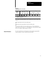
Product Compatibility
12
These input modules can be used with any 1771 I/O chassis. Communication
between the analog module and the processor is bidirectional. The processor
block–transfers output data through the output image table to the module and
block–transfers input data from the module through the input image table. The
module also requires an area in the data table to store the read block and write
block data. I/O image table use is an important factor in module placement and
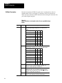
addressing selection. The module’s data table use is listed in the following table.
Chapter 1
Using This Manual
Table 1.A
Compatibility and Use of Data Table
Catalog
Number
1771-IXHR
Input
Image
Bits
8
Use of Data Table
Output Read
Image Block
Bits
Words
8
12/13
Write
Block
Words
27/28
Compatibility
1/2 -slot
Yes
Addressing
Chassis
1-slot
2-slot Series
Yes
Yes
A and B
A = Compatible with 1771-A1, A2, A4 chassis.
B = Compatible with 1771-A1B, A2B, A3B, A4B chassis.
Yes = Compatible without restriction
No = Restricted to complementary module placement
You can place your input module in any I/O module slot of the I/O chassis. You
can put:
two input modules in the same module group
an input and an output module in the same module group.
Do not put the module in the same module group as a discrete high density
module unless you are using 1 or 1/2 slot addressing. Avoid placing this module
close to AC modules or high voltage DC modules.
Related Publications
For a list of publications with information on Allen–Bradley programmable
controller products, consult our publication index SD499.
13
Chapter
Chapter 2
2
Overview of the High Resolution
Thermocouple/Millivolt Input Module
Chapter Objectives
This chapter gives you information on:
features of the input module
how an input module communicates with programmable controllers
Module Description
The High Resolution Thermocouple/Millivolt input module is an intelligent
block transfer module that interfaces analog input signals with any
Allen–Bradley programmable controllers that have block transfer capability.
Note: Use with PLC–2 family programmable controllers is not recommended.
The 1771–IXHR module is only available with 2’s complementary binary as its
only data type. The PLC–2 family does not use 2’s complementary binary.
Block transfer programming moves input data words from the module’s
memory to a designated area in the processor data table in a single scan. It also
moves configuration words from the processor data table to module memory.
The input module is a single slot module which does not require an external
power supply. After scanning the analog inputs, the input data is converted to a
specified data type in a digital format to be transferred to the processor’s data
table on request. The block transfer mode is disabled until this input scan is
complete. Consequently, the minimum interval between block transfer reads is
the same as the total input update time for each analog input module (25ms).
Features of the Input Module
The 1771–IXHR module senses up to 8 differential analog inputs and converts
them to values compatible with Allen–Bradley programmable controllers.
This module’s features include:
8 input channels configurable for thermocouple input ranges or millivolt
input ranges: Types B, E, J, K, T, R and S thermocouples and +100 millivolts
two types of inputs allowed: 4 of one input type and 4 of another
cold junction compensation
scaling to selected temperature range in oC or oF
temperature resolution of 0.1oC or 0.1oF, millivolt resolution to 1 microvolt
user selectable high and low temperature alarms
all features selectable through programming
21
Chapter 2
Overview of the High Resolution
Thermocouple/Millivolt Input Module
self–diagnostics and status reporting at power–up
detection of open circuit if thermocouple fails
automatic offset and gain calibration for each channel
software calibration of all channels, eliminating potentiometers
programmable filters for each group of 4 inputs
X10 magnification (zoom) for millivolt mode
How Analog Modules
Communicate with
Programmable Controllers
The processor transfers data to and from the module using BTW (block transfer
write) and BTR (block transfer read) instructions in your ladder diagram
program. These instructions let the processor obtain input values and status
from the module, and let you establish the module’s mode of operation
(Figure 2.1).
1.
The processor transfers your configuration data and calibration values to
the module using a block transfer write instruction.
2.
External devices generate analog signals that are transmitted to the
module.
Figure 2.1
Communication Between Processor and Module
3
1
5
BTW
Memory
User Program
6
To Output Devices
2
BTR
4
High Resolution
Thermocouple/Millivolt
Input Module
1771-IXHR
3.
22
PC Processor
(PLC-5/40 Shown)
12933-I
The module converts analog signals into binary format, and stores these
values until the processor requests their transfer.
Chapter 2
Overview of the High Resolution
Thermocouple/Millivolt Input Module
4.
When instructed by your ladder program, the processor performs a read
block transfer of the values and stores them in a data table.
5.
The processor and module determine that the transfer was made without
error, and that input values are within specified range.
6.
Your ladder program can use and/or move the data (if valid) before it is
written over by the transfer of new data in a subsequent transfer.
7.
Your ladder program should allow write block transfers to the module only
when enabled by the operator at power–up.
Accuracy
The accuracy of the input module is described in Appendix A.
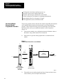
Getting Started
Your input module package contains the following items. Please check that each
part is included and correct before proceeding.
High Resolution
Thermocouple/Millivolt
Input Module
(Cat. No. 1771–IXHR)
User’s Manual
Input Module
1771-IXHR
Field Wiring Arm
Cat. No. 1771-WI
User's Manual
1771-6.5.80
10526-I
Chapter Summary
In this chapter you read about the functional aspects of the input module and
how the module communicates with programmable controllers.
23
Chapter
3
Installing the High Resolution
Thermocouple/Millivolt Input Module
Chapter Objectives
This chapter gives you information on:
calculating the chassis power requirement
choosing the module’s location in the I/O chassis
keying a chassis slot for your module
wiring the input module’s field wiring arm
installing the input module
Before You Install Your Input
Module
Before installing your input module in the I/O chassis you must:
Action required:
Electrostatic Damage
Refer to:
Calculate the power requirements of all modules in each chassis.
Power Requirements
Determine where to place the module in the I/O chassis.
Module Location in the I/O Chassis
Key the backplane connector in the I/O chassis.
Module Keying
Make connections to the wiring arm.
Connecting Wiring and Grounding
Electrostatic discharge can damage semiconductor devices inside this module if
you touch backplane connector pins. Guard against electrostatic damage by
observing the following warning:
CAUTION: Electrostatic discharge can degrade performance or
cause permanent damage. Handle the module as stated below.
Wear an approved wrist strap grounding device when handling the module.
Touch a grounded object to rid yourself of electrostatic charge before handling
the module.
Handle the module from the front, away from the backplane connector. Do not
touch backplane connector pins.
Keep the module in its static–shield bag when not in use, or during shipment.
Power Requirements
Your module receives its power through the 1771 I/O chassis backplane from
the chassis power supply. The maximum current drawn by the
thermocouple/millivolt input module from this supply is 750mA (3.75 Watts).
31
Chapter 3
Installing the High Resolution
Thermocouple/Millivolt Input Module
Add this value to the requirements of all other modules in the I/O chassis to
prevent overloading the chassis backplane and/or backplane power supply.
Module Location in the
I/O Chassis
Place your module in any slot of the I/O chassis except for the extreme left slot.
This slot is reserved for processors or adapter modules.
Group your modules to minimize adverse affects from radiated electrical noise
and heat. We recommend the following.
Group analog and low voltage DC modules away from AC modules or high
voltage DC modules to minimize electrical noise interference.
Do not place this module in the same I/O group with a discrete high–density
I/O module when using 2–slot addressing. This module uses a byte in both
the input and output image tables for block transfer.
After determining the module’s location in the I/O chassis, connect the wiring
arm to the pivot bar at the module’s location.
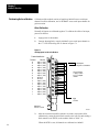
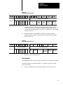
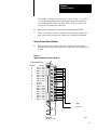
Module Keying
Use the plastic keying bands, shipped with each I/O chassis, for keying the I/O
slot to accept only this type of module.
The input modules are slotted in two places on the rear edge of the circuit
board. The position of the keying bands on the backplane connector must
correspond to these slots to allow insertion of the module. You can key any
connector in an I/O chassis to receive these modules except for the leftmost
connector reserved for adapter or processor modules. Place keying bands
between the following numbers labeled on the backplane connector
(Figure 3.1):
Between 20 and 22
Between 24 and 26
You can change the position of these bands if subsequent system design and
rewiring makes insertion of a different type of module necessary. Use
needlenose pliers to insert or remove keying bands.
Figure 3.1
Keying Positions
32
Chapter 3
Installing the High Resolution
Thermocouple/Millivolt Input Module
Keying Bands
2
4
6
8
10
12
14
16
18
20
22
24
26
28
30
32
34
36
Upper Connector
14288
CAUTION: The High Resolution Thermocouple/Millivolt Input
Module uses the same keying slots as the 1771–IXE
Thermocouple/Millivolt Input Module. If you are replacing a
1771–IXE with a 1771–IXHR, the ladder program must be modified
to accept the new block transfer format.
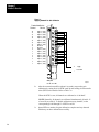
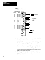
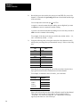
Connecting Wiring
Connect your I/O devices to the 1771–WI field wiring arm shipped with the
module (see Figure 3.2). Attach the field wiring arm to the pivot bar at the
bottom of the I/O chassis. The field wiring arm pivots upward and connects
with the module so you can install or remove the module without disconnecting
the wires.
Connect inputs in successive order starting with channel 1: positive leads to
even–numbered terminals, negative leads to odd–numbered terminals of the
wiring arm. Make connections to channel 1 at wiring arm terminals 18 (+) and
17(–). Follow the connection label on the side of the module for connecting
the remaining inputs (Figure 3.2).
33
Chapter 3
Installing the High Resolution
Thermocouple/Millivolt Input Module
Figure 3.2
Connection Diagram for the 1771-IXHR Inputs
Terminal Identification
+
Channel 1
–
+
–
Channel 2
1
Do not use
3
4
5
6
7
8
1
2
Input 1 (+ lead)
Input 1 (- lead)
Input 2 (+ lead)
Input 2 (- lead)
Input 3 (+ lead)
Input 3 (- lead)
Input 4 (+ lead)
Input 4 (- lead)
Not Used
Not used
Input 5 (+ lead)
Input 5 (- lead)
Input 6 (+ lead)
Input 6 (- lead)
Input 7 (+ lead)
Input 7 (- lead)
Input 8 (+ lead)
Input 8 (- lead)
9
10
11
12
18
17
16
15
14
13
12
11
10
9
8
7
6
5
4
3
2
1
Function
13
14
15
16
17
18
Terminal
Short circuit
unused pins
Connect positive thermocouple leads
to even-numbered terminals, negative
leads to odd-numbered terminals.
Ground cable shield to I/O chassis mounting bolt.
Wiring Arm
Cat. No. 1771-WI
10527-I
Do not connect an input to terminals 9 and 10. They are reserved for the cold
junction temperature sensor inside the wiring arm. Short circuit unused input
terminals by connecting a jumper wire between the positive and negative input
terminals of each unused channel. Refer to appendix A to determine maximum
cable length.
Grounding the Input Modules
34
When using shielded cable or shielded thermocouple extension wire, ground the
foil shield and drain wire only at one end of the cable. We recommend that you
wrap the foil shield and drain wire together and connect them to a chassis
mounting bolt (Figure 3.3). At the opposite end of the cable, tape exposed
shield and drain wire with electrical tape to insulate it from electrical contact.
Chapter 3
Installing the High Resolution
Thermocouple/Millivolt Input Module
Figure 3.3
Cable Grounding
Ground Shield at
I/O chassis
mounting bolt
Shield and drain
twisted into
single strand
Field Wiring Arm
17798
Refer to Wiring and Grounding Guidelines, publication 1770-4.1 for additional information.
35
Chapter 3
Installing the High Resolution
Thermocouple/Millivolt Input Module
Installing the Input Module
When installing your module in an I/O chassis:
1.
First, turn off power to the I/O chassis:
WARNING: Remove power from the 1771 I/O chassis backplane
and wiring arm before removing or installing an I/O module.
Failure to remove power from the backplane could cause injury or
equipment damage due to possible unexpected operation.
Failure to remove power from the backplane or wiring arm could
cause module damage, degradation of performance, or injury.
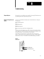
Interpreting the Indicator
Lights
2.
Place the module in the plastic tracks on the top and bottom of the slot that
guides the module into position.
3.
Do not force the module into its backplane connector. Apply firm even
pressure on the module to seat it properly.
4.
Snap the chassis latch over the top of the module to secure it.
5.
Connect the wiring arm to the module.
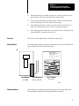
The front panel of the input module contains a green RUN and a red FLT (fault)
indicator (Figure 3.4). At power–up, the green and red indicators are on. An
initial module self–check occurs. If there is no fault, the red indicator turns off.
The green indicator will blink until the processor completes a successful write
block transfer to the module. If a fault is found initially or occurs later, the red
FLT indicator lights. Possible module fault causes and corrective action are
discussed in Chapter 8, Troubleshooting.
Figure 3.4
Diagnostic Indicators
TC/MV
Module
RUN
FLT
10528-I
36
Chapter 3
Installing the High Resolution
Thermocouple/Millivolt Input Module
Chapter Summary
In this chapter you learned how to install your input module in an existing
programmable controller system and how to wire to the field wiring arm.
37
Chapter
Module Programming
Chapter Objectives
In this chapter, we describe
Block Transfer programming
Sample programs in the PLC–3 and PLC–5 processors
Module scan time issues
Block Transfer Programming
Your module communicates with the processor through bidirectional block
transfers. This is the sequential operation of both read and write block transfer
instructions.
The block transfer write (BTW) instruction is initiated when the analog module
is first powered up, and subsequently only when the programmer wants to write
a new configuration to the module. At all other times the module is basically in
a repetitive block transfer read (BTR) mode.
The following example programs accomplish this handshaking routine. These
are minimum programs; all rungs and conditioning must be included in your
application program. You can disable BTRs, or add interlocks to prevent writes
if desired. Do not eliminate any storage bits or interlocks included in the sample
programs. If interlocks are removed, the program may not work properly.
Your analog input module will work with a default configuration of all zeroes
entered in the configuration block. Refer to chapter 5 to see the what this
configuration looks like. Also, refer to Appendix B for example configuration
blocks and instruction addresses to get started.
Your program should monitor status bits (such as overrange, underrange,
alarms, etc.) and block transfer read activity.
The following example programs illustrate the minimum programming required
for communication to take place.
PLC-2 Applications
Due to the number of digits required for high resolution readings, the
1771–IXHR module only reads input values in 2’s complement binary. Since
the PLC–2 family PLCs do not naturally read this data format, the IXHR
module is not recommended for use with PLC–2 family programmable
controllers.
41
Chapter 4
Module Programming
PLC-3 Program Example
Block transfer instructions with the PLC–3 processor use one binary file in a
data table section for module location and other related data. This is the block
transfer control file. The block transfer data file stores data that you want
transferred to the module (when programming a block transfer write) or from
the module (when programming a block transfer read). The address of the block
transfer data files are stored in the block transfer control file.
The industrial terminal prompts you to create a control file when a block
transfer instruction is being programmed. The same block transfer control file
is used for both the read and write instructions for your module. A different
block transfer control file is required for every module.
A sample program segment with block transfer instructions is shown in
Figure 4.1, and described below.
Figure 4.1
PLC-3 Family Sample Program Structure
1
2
BTR
BLOCK XFER READ
RACK:
XXX
GROUP:
X
MODULE:
X = XXXX
DATA:
XXXX:XXXX
LENGTH:
X
CNTL:
XXXX:XXXX
Block Transfer
Read Done Bit
Pushbutton
Power-up
Bit
Block Transfer
Write Done Bit
ENABLE
EN
12
DONE
DN
15
ERROR
ER
13
ENABLE
BTW
BLOCK XFER WRITE
EN
02
RACK:
XXX
GROUP:
X DONE
MODULE:
X = XXXX
DN
05
DATA:
XXXX:XXXX
LENGTH:
X ERROR
ER
CNTL:
XXXX:XXXX
03
Program Action
At power–up, the user program examines the BTR done bit in the block transfer
read file, initiates a write block transfer to configure the module, and then does
consecutive read block transfers continuously. The power–up bit can be
examined and used anywhere in the program.
Rungs 1 and 2 - Rungs 1 and 2 are the block transfer read and write
instructions. The BTR enable bit in rung 1, being false, initiates the first
read block transfer. After the first read block transfer, the module
performs a block transfer write and then does continuous block transfer
reads until the pushbutton is used to request another block transfer write.
42
Chapter 4
Module Programming
After this single block transfer write is performed, the module returns to
continuous block transfer reads automatically.
43
Chapter 4
Module Programming
PLC-5 Program Example
The PLC–5 program is very similar to the PLC–3 program with the following
exceptions:
You must use enable bits instead of done bits as the conditions on each rung.
A separate control file must be selected for each of the BT instructions. Refer
to Appendix B.
Figure 4.2
PLC-5 Family Sample Program Structure
1
2
BTR
BLOCK XFER READ
RACK:
X
GROUP:
X
MODULE:
X
CONTROL:
XXX:XX
DATA FILE:
XXX:XX
LENGTH:
XX
CONTINUOUS:
N
BTR Enable
Pushbutton
BTW Enable
Power-up Bit
BTW
BLOCK XFER WRITE
RACK:
X
GROUP:
X
MODULE:
X
CONTROL:
XXX:XX
DATA FILE:
XXX:XX
LENGTH:
XX
CONTINUOUS:
N
EN
DN
ER
EN
DN
ER
Program Action
Rungs 1 and 2 - At power–up, the program enables a block transfer read
and examines the power–up bit in the BTR file (rung 1). Then, it initiates
one block transfer write to configure the module (rung 2). Thereafter, the
program continuously reads data from the module (rung 1).
A subsequent BTW operation is enabled by a pushbutton switch (rung 2).
Changing processor mode will not initiate a block transfer write unless the first
pass bit is added to the BTW input conditions.
44
Chapter 4
Module Programming
Module Scan Time
Scan time is defined as the amount of time it takes for the input module to read
the input channels and place new data into the data buffer. Scan time for your
module is shown in Figure 4.3.
The following description references the sequence numbers in Figure 4.3.
Following a block transfer write “1” the module inhibits communication until
after it has configured the data and loaded calibration constants “2”, scanned the
inputs “3”, and filled the data buffer “4”. Write block transfers, therefore,
should only be performed when the module is being configured or calibrated.
Any time after the second scan begins “5”, a block transfer read (BTR) request
“6” can be acknowledged.
When operated in the default mode (RTS) = 00, a BTR will be released every
25 milliseconds. When operated in RTS = T, BTR will be waived until
”T”millseconds, at which time 1 BTR will be released.
Figure 4.3
Block Transfer Time
End of
Block
Transfer
Write
Block
Transfer
Write
Time
1
Module available
to perform block
transfer
Configure
Time
2
1st Scan
3
2nd Scan
4
5
3rd Scan
6
7
8
9
10529-I
Internal Scan time = 25msec
T = 25ms, 50ms, 75ms ... 3.1sec.
Chapter Summary
In this chapter, you learned how to program your programmable controller. You
were given sample programs for your PLC–3 and PLC–5 family processors.
You also read about module scan time.
45
Chapter
Module Configuration
Chapter Objectives
In this chapter you will read how to configure your module’s hardware,
condition your inputs and enter your data.
Configuring the Module
Because of the many analog devices available and the wide variety of possible
configurations, you must configure your module to conform to the analog
device and specific application that you have chosen. Data is conditioned
through a group of data table words that are transferred to the module using a
block transfer write instruction.
You can configure the following features for the 1771–IXHR module:
type of input
one or two input types
X10 magnification for millivolt data
oC
or oF
real time sampling
millivolt bias level (zoom mode only)
input filtering
alarming
calibration
Configure your module for its intended operation by means of your
programming terminal and write block transfers.
During normal operation, the processor transfers from 1 to 27 words to the
module when you program a BTW instruction to the module’s address. The
BTW file contains configuration words, high and low channel alarm settings,
and calibration values that you enter for each channel. When a block transfer
length of 0 is programmed, the 1771–IXHR will respond with a default
value of 27.
This module is permanently configured to accept and report data in 2’s
complementary binary format only. It is not recommended for use with PLC–2
family programmable controllers.
51
Chapter 5
Module Configuration
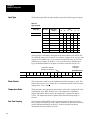
Input Type
The thermocouple/millivolt input module accepts the following types of inputs:
Table 5.A
Types of Inputs
Input Type
Input Type
Temperature
Range oC
05
04
Bits
03
02
01
00
Millivolt
Millivolt
-100 to +100
0
0
0
0
0
0
Thermocouple
B
320 to 1800
1
1
1
1
1
1
E
-270 to 1000
0
0
1
0
0
1
J
-210 to 1200
0
1
0
0
1
0
K
-270 to 1380
0
1
1
0
1
1
R
-50 to 1770
1
0
1
1
0
1
S
-50 to 1770
1
1
0
1
1
0
T
-270 to 400
1
0
0
1
0
0
The input type is selected by setting bits in the block transfer write (BTW) file.
Two different inputs can be selected. You can have 4 inputs set for one type, and
4 inputs set for another type; or you can have all inputs the same. If you select
different types of inputs, set bit 06 to 1. If you do not select 2 different input
types, the module defaults to all inputs set to those selected by bits 00 –02.
Set these bits
for input type.
Set this bit for 2 different
input types (see table 5.D)
Word
1
52
15
14
13
12
11
Sample Time
10
09
08
07
06
T
Z
E
05
04
Input Type
03
02
01
00
Input Type
Zoom Feature
The zoom feature (word 2) can be enabled when millivolt inputs are used. This
feature allows you to view +30mV (in 1µV increments) around a selected value
ranging from –70 to +70mV.
Temperature Scale
The temperature scale reported by the module is selected by setting bit 08 in the
configuration word. When bit 08 is set (1), the temperature is reported in
degrees Fahrenheit. When reset (0), the temperature is reported in degrees
Celsius. The temperature bit 08 is ignored when the millivolt input type is
selected.
Real Time Sampling
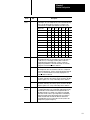
The real time sampling (RTS) mode of operation provides data from a fixed
time period for use by the processor. RTS is invaluable for time based functions
(such as PID and totalization) in the PLC. It allows accurate time based
calculations in local or remote I/O racks.
Chapter 5
Module Configuration
In the RTS mode the module scans and updates its inputs at a user defined time
interval ( ∆T) instead of the default interval. The module ignores block transfer
read (BTR) requests for data until the sample time period elapses. The BTR of a
particular data set occurs only once at the end of the sample period and
subsequent requests for transferred data are ignored by the module until a new
data set is available. If a BTR does not occur before the end of the next RTS
period, a time–out bit is set in the BTR status area. When set, this bit indicates
that at least one data set was not transferred to the processor. (The actual
number of data sets missed is unknown.) The time–out bit is reset at the
completion of the BTR.
Set appropriate bits in the BTW data file to enable the RTS mode. You can
select RTS periods ranging from 25 milliseconds (msec) to 3.1 seconds in
increments of 25msec. Refer to Table 5.B below for a sampling of actual bit
settings. Note that the default mode of operation is implemented by placing all
zeroes in bits 09 through 15.
Table 5.B
Bit Settings for the Real Time Sample Mode
Decimal Bits
15
14
13
12
11
10
09
Sample Time Period
0
0
0
0
0
0
0
Inhibited
0
0
0
0
0
0
1
25 ms
0
0
0
0
0
1
0
50 ms
0
0
0
0
1
0
0
100 ms
0
0
1
0
0
0
0
400 ms
0
0
1
0
1
0
0
500 ms
0
0
1
1
0
0
0
600 ms
0
0
1
1
1
0
0
700 ms
0
1
0
0
0
0
0
800 ms
0
1
0
0
1
0
0
900 ms
0
1
0
1
0
0
0
1.0 sec
0
1
1
1
1
0
0
1.5 sec
1
0
1
0
0
0
0
2.0 sec
1
1
0
0
1
0
0
2.5 sec
1
1
1
1
0
0
0
3.0 sec
1
1
1
1
1
0
0
3.1 sec
Important: Use decimally addressed bit locations for PLC–5 processors.
Channel Alarms
Each channel has high and low alarm values associated with it. These bits and
words are explained in the bit/word definitions in Table 5.D.
Calibration
You have the ability to calibrate this module using auto–calibration or by
manually setting the individual channel words. Words 20 through 27 in the
configuration word (Table 5.D) are the manual calibration words for channels 1
53
Chapter 5
Module Configuration
through 8 respectively. Word 28 activates the auto–calibration feature.
Calibration is explained in chapter 7.
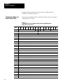
Configuration Block for a
Block Transfer Write
The complete configuration block for the block transfer write to the module is
defined in Table 5.C below.
Table 5.C
Configuration Block for the High Resolution Thermocouple/Millivolt Input
Module Block Transfer Write
Word
1
54
15
14
13
12
11
10
09
Sample Time
08
07
T
Z
06
05
E
04
Type
03
02
01
Type
2
Zoom Value for Group 2 (Channels 5-8)
Zoom Value for Group 1 (Channels 1-4)
3
Filter Value for Group 2 (Channels 5-8)
Filter Value for Group 1 (Channels 1-4)
4
Channel 1 Low Alarm Value
5
Channel 1 High Alarm Value
6
Channel 2 Low Alarm Value
7
Channel 2 High Alarm Value
8
Channel 3 Low Alarm Value
9
Channel 3 High Alarm Value
10
Channel 4 Low Alarm Value
11
Channel 4 High Alarm Value
12
Channel 5 Low Alarm Value
13
Channel 5 High Alarm Value
14
Channel 6 Low Alarm Value
15
Channel 6 High Alarm Value
16
Channel 7 Low Alarm Value
17
Channel 7 High Alarm Value
18
Channel 8 Low Alarm Value
19
Channel 8 High Alarm Value
20
Calibration Values for Channel 1
21
Calibration Values for Channel 2
22
Calibration Values for Channel 3
23
Calibration Values for Channel 4
24
Calibration Values for Channel 5
25
Calibration Values for Channel 6
26
Calibration Values for Channel 7
27
Calibration Values for Channel 8
28
Auto-calibration Request Word
00
Chapter 5
Module Configuration
E = enable bit for input types (refer to bit/word description)
T = temperature scale bit (refer to bit/word description)
Z = zoom enable: 0 = normal 10µV; 1 = X10 (1µV)
55
Chapter 5
Module Configuration
Bit/Word Descriptions
Bit/word descriptions of BTW file words 1 thru 3 (configuration), 4 thru 19
(channel alarm values), and 20 thru 27 (calibration values) are presented in
Table 5.D. Enter data into the BTW instruction after entering the instruction into
your ladder diagram program.
Table 5.D
Bit/Word Definitions for the High Resolution Thermocouple/Millivolt Input
Module
Word
Word 1
Bits
bits 00-02
Description
Input type codes for inputs 1 thru 8 (or 1 thru 4 if bit 06 is set to 1).
Tells the module what type of input device you connected to the
module.
Type
bits 03-05
02
01
00
Millivolt input
0
0
0
"B" thermocouple
1
1
1
"E" thermocouple
0
0
1
"J" thermocouple
0
1
0
"K" thermocouple
0
1
1
"R" thermocouple
1
0
1
"S" thermocouple
1
1
0
"T" thermocouple
1
0
0
Input type codes for inputs 5 thru 8 (bit 06 must be set to 1). Tells the
module what type of input device you connected to inputs 5 thru 8.
Type
56
05
04
03
Millivolt input
0
0
0
"B" thermocouple
1
1
1
"E" thermocouple
0
0
1
"J" thermocouple
0
1
0
"K" thermocouple
0
1
1
"R" thermocouple
1
0
1
"S" thermocouple
1
1
0
"T" thermocouple
1
0
0
bit 06
When set to 0 bits 00-02 define input type for all channels.
When set to 1 bits 00-02 defines input type for channels 1-4,
and bit 03-05 defines input type for channels 5-8.
bit 07
Enables X10 magnification when millivolt inputs have been selected.
Enabling this feature causes the BTR data to display +30.000mV
around the value selected by word 2. Use the digital filter (word 3) to
stabilize the readings when using this mode.
bit 08
Temperature scale bit, when set, reports temperature in oF; when
reset, in oC. The module ignores this bit for millivolt inputs.
Chapter 5
Module Configuration
Word
Word 1
(cont.)
Bits
bits 09-15
Description
Real time sample interval bits determine the sample time for updating
module inputs. You select sample time in 0.025 second intervals using
binary code. (All values between 0.025 and 3.1 seconds in 0.025
second intervals are available.) We tabulated some values for you.
Sample Time
Word 2
Word 3
Words 4
thru 19
15
14
13
12
11
10
09
0.1
0
0
0
0
1
0
0
0.5
0
0
1
0
1
0
0
0.6
0
0
1
1
0
0
0
0.7
0
0
1
1
1
0
0
0.8
0
1
0
0
0
0
0
0.9
0
1
0
0
1
0
0
1.0
0
1
0
1
0
0
0
1.5
0
1
1
1
1
0
0
2.0
1
0
1
0
0
0
0
2.5
1
1
0
0
1
0
0
3.0
1
1
1
1
0
0
0
bits 00-07
Zoom center value for channels 1-4. These values are used when
millivolt inputs have been selected and bit 07 of word 1 has been set
to enable zoom (i.e. 1µV display resolution). Enter a value in 2's
complement binary format ranging from -70mV to +70mV. The
displayed range will then be +30.000mV around the selected value,
displayed in 1µV increments. Refer to Table 5.E
bits 08-15
Zoom center value for channels 5-8. These values are used when
millivolt inputs have been selected. Enter a value in 2's complement
binary format ranging from -70mV to +70mV. The displayed range will
then be +30.000mV around the selected value, displayed in 1µV
increments. Refer to Table 5.E
bits 00-07
Filter values for channels 1-4. The filter operates on the display data
only. Alarms, underrange and overrange operate in real time. The filter
constant is equal to: TC = 0.025(1 + filter value). Refer to Table 5.F.
bits 08-15
Filter values for channels 5-8. The filter operates on the display data
only. Alarms, underrange and overrange operate in real time. The filter
constant is equal to: TC = 0.025(1 + filter value). Refer to Table 5.F
Low and High channel alarm values that you enter via the terminal in
2's complementary binary. Store low and high channel alarms in pairs,
low alarm values in even-numbered words, high alarm values in
odd-numbered words. For example, store channel 1 low and high
alarm values in words 4 and 5, respectively. Alarms are disabled by
setting the low alarm equal to the high alarm. If the zoom feature is
enabled, the alarm values should be the difference between the
"actual alarm limit" and "zoom center value" in word 2. (Refer to the
example PLC-5 program in chapter 5.)
57
Chapter 5
Module Configuration
Word
Bits
Description
Words 20
thru 27
Calibration words are a composite of two independent bytes for each
channel. Enter calibration data in signed magnitude binary only. The
most significant bit in each byte is the sign bit; set for negative, reset
for positive.
Use the high byte (bits 08-15) for offset correction, the low byte (bits
00-07) for gain correction for each channel. Use word 20 for channel
1 thru word 27 for channel 8.
Refer to Chapter 7 for calibration procedures.
Word 28
Auto-calibration request word - used to automatically calibrate
selected channels and save the calibration constants in EEPROM.
(Refer to Chapter 7.)
Table 5.E
Example Zoom Settings for Word 2
Zoom Settings
Bit Settings (15-08) or (07-00)
Zoom center = 70mV (maximum)
01000110 (decimal equivalent 70)
Zoom center = 0mV
00000000 (decimal equivalent 0)
Zoom center = -1mV
11111111 (decimal equivalent -1)
Zoom center = -70mV (minimum)
10111010 (decimal equivalent -70)
Only used in millivolt mode with Z = 1. Millivolt data will be in 1µV resolution with range of +30.000mV.
Zoom will be used to center the range of interest between +70mV. Over and underrange bits will be
asserted outside of the display range. For decimal equivalent values from 71 to 127 and -71 to -128
the zoom center will default to 0.
Table 5.F
Example Filter Values for Word 3
Filter Value
Bit Setting
(15-08) or (07-00)
No filter
0000000
Tau = 50ms
00000001
Tau = 75ms
00000010
Tau = 6.4 seconds
11111111
Filter values increase in increments of 25msec.
Chapter Summary
58
In this chapter you learned how to configure your module’s hardware, condition
your inputs and enter your data.
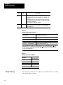
Chapter
6
Module Status and Input Data
Chapter Objectives
In this chapter you will read about:
reading data from your module
input module read block format
Reading Data from the Module
Block transfer read programming moves status and data from the input module
to the processor’s data table in one I/O scan (Table 6.A). The processor user
program initiates the request to transfer data from the input module to the
processor.
During normal operation the module transfers up to 12 words to the processor’s
data table file. The words contain module status and input data from each
channel. During normal operation, when a block transfer length of zero (0)
is programmed, the 1771–IXHR will respond with a default length of 12.
Table 6.A
BTR Word Assignments for the 1771-IXHR Input Module
Decimal Bit
15
14
13
11
10
9
8
7
6
5
4
Not used
Status Codes
2
Inputs overrange
Inputs underrange
3
Inputs > high alarm
Inputs < low alarms
4
Channel 1 input
5
Channel 2 input
6
3
2
1
0
Channel 3 input
:
1
12
1
:
11
Channel 8 input
12
Cold Junction Temperature in oC or oF1
13
Inhibits
Auto-calibration request
= Cold junction temperature is provided in 0.1oC or 0.1oF resolution. The filter time constant (Tau) for
this value is fixed at 6.4 seconds.
61
Chapter 6
Module Status and Input Data
Bit/Word Descriptions
The complete bit/word description for the block transfer read from the module
is defined in Table 6.B.
Table 6.B
Bit/Word Description for the 1771-IXHR Input Module
Word
Word 1
Word 2
Word 3
Words 4-11
Word 12
62
Bit
Definition
Bit 00
Power-up bit is set to indicate that the module is waiting for its first
write block transfer
Bit 01
Out of range bit is set if one or more channel inputs are above or
below the range for which you configured the module
Bit 02
Real time sample time-out bit is set when the module updates an
input buffer with new data before the processor has read the previous
data. Monitor this bit only if you select real time sampling.
Bit 03
Not used
Bit 04
Low cold junction temperature bit is set when the cold junction
temperature is less than 0.0oC or 32.0oF.
Bit 05
High cold junction temperature bit is set when the cold junction
temperature exceeds 60.0oC or 140.0oF.
Bit 06
Dynamic clamp bit. Prevents rapid changes in data due to data
corruption over the opto-isolation barrier as a result of ESD, radiation
bursts, etc.
0 = feature active
1 = feature inhibited
Bit 07
EEPROM calibration values could not be read.
Bits 08-15
Not used
Bits 00-07
Underrange bit for each channel is set to indicate an input is out of
range: bit 00 for channel 1 thru bit 07 for channel 8.
Bits 08-15
Overrange bit for each channel is set to indicate an input is out of
range: bit 08 for channel 1 thru bit 15 for channel 8. Also set for open
channel detection.
Bits 00-07
Low alarm bit for each channel is set to indicate the input is less than
the low limit value you entered in the corresponding low alarm word
(BTW word 4, 6, 8, 10, 12, 14, 16, or 18): bit 00 for channel 1 thru bit
07 for channel 8.
Bits 08-15
High alarm bit for each channel is set to indicate the input has
exceeded the high limit value you entered in the corresponding high
alarm word (BTW word 5, 7, 9, 11, 13, 15, 17, or 19): bit 08 for
channel 1 thru bit 15 for channel 8.
Input for channel 1 through 8 respectively in 0.1oC or 0.1oF resolution
for temperature and 10µV or 1µV resolution for millivolts.
Cold junction temperature in 0.1oC or 0.1oF.
Chapter 6
Module Status and Input Data
Word
Bit
Word 13
Chapter Summary
Definition
Auto-calibration word.
Bit 00
Offset calibration complete bit
Bit 01
Gain calibration complete bit
Bit 02
Save to EEPROM bit
Bits 03-05
Not used
Bit 06
EEPROM fault bit
Bit 07
Calibration fault bit
Bits 08-15
Uncalibrated channel bits
In this chapter you learned the meaning of the status information that the input
module sends to the processor.
63
Chapter
Module Calibration
Chapter Objective
In this chapter we tell you how to calibrate your module.
Tools and Equipment
To calibrate your module you will need the following tools and equipment:
Tool or Equipment
Description
Model/Type
Precision Voltage Source
0-100mV, 1µV resolution
Analogic 3100, Data Precision 8200
or equivalent
Industrial Terminal and
Interconnect Cable
Programming terminal for A-B
family processors
Cat. No. 1770-T3 or Cat. No.
1784-T45, -T47, -T50, etc.
Calibrating your Input
Module
Available from:
Allen-Bradley Company
Highland Heights, OH
The high resolution thermocouple/millivolt input module is shipped already
calibrated. If it becomes necessary to recalibrate the module, you must calibrate
the module in an I/O chassis. The module must communicate with the processor
and industrial terminal.
Before calibrating the module, you must enter ladder logic into the processor
memory, so that you can initiate BTWs to the module, and the processor can
read inputs from the module.
Calibration can be accomplished using either of two methods:
auto–calibration
manual calibration
The auto–calibration method is recommended since it is easier and less time
consuming than manual calibration. Manual calibration can be used if you are
more familiar with this type of calibration, or if you desire to compensate for
thermocouple or lead error.
About Auto-calibration
Auto–calibration calibrates the input by generating offset and gain correction
values and storing them in EEPROM. These values are read out of EEPROM
and placed in RAM memory at initialization of the module.
The auto–calibration routine operates as follows:
- Whenever a block transfer write (BTW) of length 28 is performed to the
module (any time after the module has been powered up), it interrogates
word 28 for a request for auto–calibration.
- The request can be for the following: offset calibration, gain calibration,
save operation (save to EEPROM).
When using auto–calibration, write transfer calibration words 20 through
27 must contain zeroes.
71
Chapter 7
Module Calibration
Performing Auto-calibration
Calibration of the module consists of applying 0.000mV across each input
channel for offset calibration, and +100.000mV across each input channel for
gain correction.
Offset Calibration
Normally all inputs are calibrated together. To calibrate the offset of an input,
proceed as follows:
1.
Apply power to the module.
2.
Connect shorting links, or apply 0.000mV across each input channel on
the 1771–WI field wiring arm as shown in Figure 7.1.
Figure 7.1
Shorting Inputs for Offset Calibration
Terminal Identification
Shorting link.
Repeat for each channel
1
Do not
use
Short each input,
or apply 0.000mV
across each input
channel.
3
4
5
6
7
8
1
2
Input 1 (+ lead)
Input 1 (- lead)
Input 2 (+ lead)
Input 2 (- lead)
Input 3 (+ lead)
Input 3 (- lead)
Input 4 (+ lead)
Input 4 (- lead)
Not Used
Not used
Input 5 (+ lead)
Input 5 (- lead)
Input 6 (+ lead)
Input 6 (- lead)
Input 7 (+ lead)
Input 7 (- lead)
Input 8 (+ lead)
Input 8 (- lead)
9
10
11
12
18
17
16
15
14
13
12
11
10
9
8
7
6
5
4
3
2
1
Function
13
14
15
16
17
18
Terminal
Apply
0.000mV
Wiring Arm
Cat. No. 1771-WI
10530-I
3.
After the connections stabilize (about 10 seconds), request the offset
calibration by setting bit 00 in block transfer write word 28 and sending a
block transfer write (BTW) to the module. Refer to Table 7.A.
When the BTW is sent, all channels are calibrated to 0.000mV.
72
Chapter 7
Module Calibration
Table 7.A
Write Block Transfer Word 28
Word/Bit
15 14 13 12 11 10 09 08 07 06 05 04
Inhibit Calibration on Channel
Word 28
8
7
6
5
4
3
2
03
02
01
00
Requested Auto-Calibration
1
Set these bits to
0
Requested Requested
Requested
Save
clamp
Gain Cal.
Values
inhibit
Requested
Offset Cal.
NOTE: Normally, all channels are calibrated simultaneously (bits 08–15
of word 28 are octal 0). To disable calibration on any channel, set the
corresponding bit 08 through 15 of word 28. To disable the clamp inhibit
function, set bit 06.
4.
Queue block transfer reads (BTRs) to monitor for offset calibration
complete and any channels which may have not calibrated successfully.
Refer to Table 7.B.
Table 7.B
Read Block Transfer Word 13
Word/Bit
15 14 13 12 11 10 09 08
07
06
Uncalibrated Channels
Word 13
8
7
6
5
4
5.
3
05 04 03
02
01
00
Gain Cal.
Complete
Offset Cal.
Complete
Auto-Calibration Status
2
1
Cal.
Fault
EEPROM
Fault
Not used
Save to
EEPROM
Complete
Proceed to Gain Calibration below.
Gain Calibration
Calibrating gain requires that you apply +100.000mV across each input channel.
Normally all inputs are calibrated together. To calibrate the gain of an input,
proceed as follows:
1.
Apply +100.000mV across each input channel as shown in Figure 7.2.
73
Chapter 7
Module Calibration
Figure 7.2
Applying 100.00mV for Gain Calibration
Terminal Identification
Function
1
Do not
use
3
4
5
6
7
8
1
2
Input 1 (+ lead)
Input 1 (- lead)
Input 2 (+ lead)
Input 2 (- lead)
Input 3 (+ lead)
Input 3 (- lead)
Input 4 (+ lead)
Input 4 (- lead)
Not Used
Not used
Input 5 (+ lead)
Input 5 (- lead)
Input 6 (+ lead)
Input 6 (- lead)
Input 7 (+ lead)
Input 7 (- lead)
Input 8 (+ lead)
Input 8 (- lead)
9
10
11
12
18
17
16
15
14
13
12
11
10
9
8
7
6
5
4
3
2
1
13
14
15
16
17
18
Terminal
+
-
Wiring Arm
Cat. No. 1771-WI
2.
Apply
100.000mV
10531-I
After the connections stabilize (about 10 seconds), request the gain
calibration by setting bit 01 in BTW word 28 and sending a block transfer
write (BTW) to the module. Refer to Table 7.A.
When the BTW is sent, all channels are calibrated to +100.00mV.
NOTE: Normally, all channels are calibrated simultaneously (bits 08–15
of word 28 are octal 0). To disable calibration on any channel, set the
corresponding bit 08 through 15 of BTW word 28.
3.
74
Queue BTRs to monitor for gain calibration complete and any channels
which may not have calibrated successfully.
Chapter 7
Module Calibration
Save Calibration Values
If any ”uncalibrated channel” bits (bits 08–15 of BTR word 13) are set, a save
cannot occur. Auto–calibration should be performed again, starting with offset
calibration. If the module has a faulty channel, the remaining functioning
channels can be calibrated by inhibiting calibration on the faulty channel.
The module can be run with the new calibration values, but will lose them on
power down. To save these values, proceed as follows:
Performing Manual Calibration
1.
Request a ”save to EEPROM” by setting bit 02 in BTW word 28 and
sending the BTW to the module. Refer to Table 7.A.
2.
Queue BTRs to monitor for ”save complete”, ”EEPROM fault” and
”calibration fault.” An EEPROM fault indicates a nonoperative EEPROM;
a calibration fault indicates at least one channel was not properly offset or
gain calibrated and a save did not occur.
You calibrate each channel by applying a precision voltage to the input
terminals, comparing correct with actual results, and entering correction into the
corresponding calibration word for that channel. The correction takes affect
after it is transferred to the module by the corresponding BTW instruction in
your ladder diagram program. Always start with offset adjustment followed by
gain adjustment.
Before calibrating the module, you must enter ladder logic into processor
memory, so that you can initiate write block transfers to the module, and the
processor can read inputs from the module. Write transfers will contain
calibration values in words 20 through 27 for the channel you are calibrating.
Use a precision voltage source, such as Data Precision 8200 or equivalent, for
your calibration input voltage.
Setting Channel Offset Calibration
1.
Select the millivolt range and zoom = 0.
2.
Apply 0.000 millivolts to the channel input as shown in Figure 7.3.
75
Chapter 7
Module Calibration
Figure 7.3
Shorting Inputs for Offset Calibration
Terminal Identification
Function
Shorting link.
Repeat for each channel
1
Do not
use
Short each input,
or apply 0.000mV
across each input
channel.
3
4
5
6
7
8
1
2
Input 1 (+ lead)
Input 1 (- lead)
Input 2 (+ lead)
Input 2 (- lead)
Input 3 (+ lead)
Input 3 (- lead)
Input 4 (+ lead)
Input 4 (- lead)
Not Used
Not used
Input 5 (+ lead)
Input 5 (- lead)
Input 6 (+ lead)
Input 6 (- lead)
Input 7 (+ lead)
Input 7 (- lead)
Input 8 (+ lead)
Input 8 (- lead)
9
10
11
12
18
17
16
15
14
13
12
11
10
9
8
7
6
5
4
3
2
1
13
14
15
16
17
18
Terminal
Apply
0.000mV
Wiring Arm
Cat. No. 1771-WI
10532-I
3.
Observe the input value read by the processor (word 4 of the BTR file for
channel 1). It should be 0.
4.
Multiply the difference between your observed value and 0.000 by 3.0933.
Determine the magnitude and sign of the required correction. (With zoom
= 1, divide the difference by 3.2328.)
You can adjust the correction up to +127 binary counts (+410.56µV).
A negative correction means that the reading was too high and you want
to subtract a corrective amount from that reading.
A positive correction means that the reading was too low and you want to
add a corrective amount to that reading.
5.
76
Enter the magnitude and sign of the correction in binary code into the
upper (offset correction) byte of the calibration word for that channel.
(BTW file, word 20, bits 15–08 for channel 1.)
Chapter 7
Module Calibration
For example, if the observed value was 17, enter –53 [(0 – 17) x 3.0933 =
–53] in signed magnitude binary into the upper byte of the calibration
word for that channel. Enter 10110101 in bits 15–08 of word 20. The
lower byte will remain zero at this time.
6.
Repeat steps 3 through 5 for each of the remaining input channels.
7.
Initiate a write block transfer to send the corrections to the module. The
input value read by the processor should now be 0000 for all channels.
Setting Channel Gain Calibration
1.
Now set the precision voltage source for +100.000 millivolts. Allow
sufficient time (at least 10 seconds) for the input filter and voltage source
to settle.
Figure 7.4
Applying 100.000mV for Gain Calibration
Terminal Identification
1
Do not
use
3
4
5
6
7
8
1
2
Input 1 (+ lead)
Input 1 (- lead)
Input 2 (+ lead)
Input 2 (- lead)
Input 3 (+ lead)
Input 3 (- lead)
Input 4 (+ lead)
Input 4 (- lead)
Not Used
Not used
Input 5 (+ lead)
Input 5 (- lead)
Input 6 (+ lead)
Input 6 (- lead)
Input 7 (+ lead)
Input 7 (- lead)
Input 8 (+ lead)
Input 8 (- lead)
9
10
11
12
18
17
16
15
14
13
12
11
10
9
8
7
6
5
4
3
2
1
Function
13
14
15
16
17
18
Terminal
+
-
Wiring Arm
Cat. No. 1771-WI
Apply
100.000mV
10533-I
77
Chapter 7
Module Calibration
2.
Record the input value read by the processor in the BTR file (word 4 for
channel 1). Determine the percentage difference from 10000 and the sign
of the correction.
You can adjust the correction up to +0.19379%.
A negative correction means that the reading was too high and you want
to subtract a corrective amount from that reading.
A positive correction means that the reading was too low and you want to
add a corrective amount to that reading.
For example, if the observed value was 10014, then 10000–10014 = –14,
and –14 divided by 10000 = –0.14%.
3.
Using the following table, select gain correction values that most nearly
add up to the percentage that you determined in step 1. Select a value only
once.
Bit
Value
Bit 07
Sign bit
Bit 06
= 0.0976562%
Bit 05
= 0.0488281%
Bit 04
= 0.024414%
Bit 03
= 0.012207%
Bit 02
= 0.00610351%
Bit 01
= 0.00305175%
Bit 00
= 0.00152587%
Enter the bit code representing the sum of the corrections into the lower
byte (gain correction) of the calibration word for that channel.
For example, to attain the value of 0.140%, you would add:
Percentage
Bit Number
0.0976562
Bit 06
0.024414
Bit 04
0.012207
Bit 03
0.00610351
Bit 02
Total = 0.1403807%
Enter 11011100 in the lower byte of the calibration word for that channel.
This entry would set bits 07 (sign) and 06, 04, 03 and 02 which is
–0.1403807, very close to the required –0.14. Remember to keep the
upper byte the same as it was from step 5.
78
Chapter 7
Module Calibration
4.
Repeat the above steps 2 and 3 for channels 2 through 8.
5.
Initiate a write block transfer to send the corrections to the module. The
input value read by the processor should now be 10000 for all channels.
6.
If the correction changes the result in the wrong direction, change the sign
and reenter it.
Important: If the % correction required is larger than +0.19379, check your
reference voltage. If the reference voltage is correct, perform auto–calibration.
Chapter Summary
In this chapter, you learned how to calibrate your input module.
79
Chapter
8
Troubleshooting
Chapter Objective
We describe how to troubleshoot your module by observing LED indicators and
by monitoring status bits reported to the processor.
Diagnostics Reported by the
Module
At power–up, the module momentarily turns on both indicators as a lamp test,
then checks for
correct RAM operation
EPROM operation
EEPROM operation
a valid write block transfer with configuration data
Thereafter, the module lights the green RUN indicator when operating without
fault, or lights the red FAULT indicator when it detects fault conditions. If the
red FAULT indicator is on, block transfers will be inhibited.
The module also reports status and specific faults (if they occur) in every
transfer of data to the PC processor. Monitor the green and red LED indicators
and status bits in word 1 of the BTR file when troubleshooting your module.
Figure 8.1
LED Indicators
TC/MV
Module
RUN
Green RUN Indicator
FLT
Red Fault (FLT) Indicator
10528-I
81
Chapter 8
Troubleshooting
Troubleshooting with the
Indicators
Table 8.A shows LED indications and probable causes and recommended
actions to correct common faults.
Table 8.A
Troubleshooting Chart for the 1771-IXHR Input Module
Indication
Probable Cause
Recommended Action
Both LEDs are OFF
No power to module
Possible short on the module
LED driver failure
Check power to I/O chassis. Cycle as necessary.
Replace module.
Red FLT LED ON and
Green RUN LED is ON
Microprocessor, oscillator or EPROM failure
Replace module.
Red FLT LED ON
If immediately after power-up, indicates RAM or
EPROM failure.1
Replace module.
If during operation, indicates possible
microprocessor or backplane interface failure.1
Replace module.
Power-up diagnostics successfully completed.
Normal operation.
If LED continues to flash, and write block transfers
(BTW) cannot be accomplished, you have a
possible interface failure.
Replace module.
Green RUN LED is flashing
1 When red LED is on, the watchdog timer has timed out and backplane communications are terminated. Your user program should monitor
communication.
Status Reported by the
Module
Status Reported in Word 1
Design your program to monitor status bits in the lower byte of word 1, and to
take appropriate action depending on your application requirements. You may
also want to monitor these bits while troubleshooting with your industrial
terminal. The module sets a bit (1) to indicate it has detected one or more of the
following conditions as shown in Table 8.B.
Table 8.B
Status Reported in Word 1
82
Word
Bit
Explanation
1
00
Module is powered but has not received its first (configuration) block transfer.
The green LED is flashing.
01
One or more inputs are out of the range for which you configured the module.
02
Module updated its inputs before the processor read them. The RTS interval
timed out before the processor read the data.
03
Not used
Chapter 8
Troubleshooting
Word
Bit
Word 1
(cont)
04
The module's ambient temperature is below 0oC. Temperature readings will
be inaccurate.
05
The module's ambient temperature is above 60oC. Temperature readings will
be inaccurate.
06
Not used
07
EEPROM calibration constants could not be read. The module will continue to
operate but readings may be inaccurate.
08-15
Explanation
Not used
Status Reported in Words 2 and 3
Design your program to monitor over/under range bits, and to take appropriate
action depending on your application requirements. You may also want to
monitor these bits while troubleshooting with your industrial terminal.
Bits 00–07 and 08–15 each represent an input for channels 1–8, respectively.
For example, bit 04 represents input channel 5. The module sets a bit (1) to
indicate it has detected an out of range condition. Refer to Table 8.C.
Table 8.C
Status Reported in Words 2 and 3
Word
2
3
Bit
Condition
00-07
Inputs underrange. Bit 00 is channel 1, bit 07 is channel 8. If input connections and
voltages are correct, this status may indicate failed channel communications with
the microprocessor. If all channels are underrange, this indicates a possible dc/dc
converter failure or a blown fuse.
08-15
Inputs overrange. Bit 08 is channel 1, bit 15 is channel 8. If input connections and
voltages are correct, this status may indicate a failed thermocouple functional
analog block (TC FAB).
00-07
Corresponding channel input value is below the alarm value that you entered for
that channel.
08-15
Corresponding channel input value has exceeded the alarm value that you entered
for that channel.
83
Chapter 8
Troubleshooting
Status Reported in Word 13
Design your program to monitor status bits in word 13 during auto–calibration,
and to take appropriate action depending on your requirements. You may also
want to monitor these bits while troubleshooting with your industrial terminal.
The module sets a bit (1) to indicate it has detected one or more of the following
conditions as shown in Table 8.D.
Table 8.D
Status Reported in Word 13
Word
Bit
13
6
The EEPROM could not be written.
7
Channel(s) could not be calibrated as indicated by bits 08 through 15 respectively.
08-15
Chapter Summary
84
Condition
Bit 08 (channel 1) through bit 15 (channel 8) could not be calibrated. Check field
wiring arm connections and source for proper voltage.
In this chapter, you learned how to interpret the LED status indicators, status
words and troubleshoot your input module.
Appendix
A
Specifications
Number of Inputs
8, all of the same type or 4 each of 2 different types
I/O Chassis Location
Any single I/O module slot
Type of Input (Selectable)
Type B, Pt-30% Rh/Pt-6% Rh
Type E, chromel/constantan
Type J, iron/constantan
Type K, chromel/alumel
Type R, Pt/Pt-13% Rh
Type S, Pt/Pt-10% Rh
Type T, copper/constantan
Millivolt
Thermocouple Linearization
IPTS-68 standard, NBS MN-125
Cold Junction Compensation
Range: 0 to 60oC
Accuracy: +0.5oC
Temperature Scale (Selectable)
oC or oF
Input Resolution
3.2328µV
Display Resolution
0.1oC, 0.1oF; or 1.0µV, 10µV
Input Isolation
1000V peak between inputs, between input and common, and
between input and backplane connections
Common Mode Rejection
120dB at 60Hz, up to 1000V peak
Common Mode Impedance
Greater than 10 megohms
Normal Mode Rejection
60dB at 60Hz over +100mV
Input Overvoltage Protection
120V rms, continuous
Open Input Detection
Open input produces an overrange in less than 10 seconds
Input Connections
18-terminal wiring arm (Cat. No. 1771-WI)
Data Format
2's complement binary
Calibration Methods
Auto - Auto-calibration for offset and gain
Manual - Zero offset and gain adjustment for each channel via
programming terminal
Verify every six months for maintaining absolute accuracy
Processor Compatibility
PLC-3 or PLC-5 family processor using the 1771 I/O structure and
block transfer. (Not recommended for use with PLC-2 family
processors.)
Environmental Conditions
Operating Temperature:
Rate of Change:
Storage Temperature:
Relative Humidity:
(320 to 1800oC)
(-270 to 1000oC)
(-210 to 1200oC)
(-270 to 1380oC)
(-50 to 1770oC)
(-50 to 1770oC)
(-270 to 400oC)
(-100 to +100mV dc)
0 to 60oC (32 to 140oF)
Ambient changes greater than 0.5oC per minute may temporarily
degrade performance during periods of change
-40 to 85oC (-40 to 185oF)
5 to 95% (without condensation)
Backplane Power Consumption
750mA @ 5V; 3.75 Watts maximum
Field Wiring Arm
Cat. No. 1771-WI
Keying
Between 20 and 22
Between 24 and 26
A-1
Appendix A
Specifications
The accuracy of your thermocouple readings depends on:
High Resolution
Thermocouple/Millivolt Input
module accuracy
Module Accuracy
lead resistance effect
accuracy of the thermocouple
The accuracy of the module is shown in Table A.A and Table A.B at ambient
temperature (25oC) and over the temperature range (0–60oC).
Use the calibration procedure in Chapter 7 to adjust your module to compensate
for your specific environment.
Table A.A
Thermocouple Range Accuracy Based on Temperatures Above 0oC
Thermocouple
Type
Temperature
Range oC
Max Error @
Calibration
Temperature (25oC)1
Temperature Drift
oC/oC (0-60oC)
or oF/oF (32-140oF)
B
320 to 1800
+1.07oC/+1.91oF
+0.0746
E
-270 to 1000
+0.50oC/+0.90oF
+0.0400
-210 to 1200
+0.51oC/+0.90oF
+0.0423
-270 to 1380
+0.52oC/+0.94oF
+0.0640
-270 to 400
+0.52oC/+0.92oF
+0.0183
-50 to 1770
+1.14oC/+2.00oF
+0.0914
-50 to 1770
+1.12oC/+2.01oF
+0.0926
J
K
T
R
S
1 Type E, J, K, T, R and S error is specified from 0oC (32oF) to the maximum range of the
thermocouple. Type B is specified from 600oC to maximum range. Error does not include
thermocouple or lead error (see appendix F and page A-3).
Table A.B
Millivolt Range Accuracy
Millivolt
Range
Max Error @ Calibration
Temperature (25oC)
Millivolt Drift
-100 to 100 (Normal mode)
+8.85µV
+3.856µV/oC
-100 to 100 (Zoom mode)
+5.78µV
+3.856µV/oC
Table A.C
Radiated Noise Susceptibility
Radiated Noise
300-1000MHz Circular Wave, Field Strength = 10V/M
A-2
Susceptibility Error
< +1%
Appendix A
Specifications
Lead Resistance
Compensation
Allowable Distances
The open thermocouple detection circuit injects a current of approximately 7.3
nanoamps into the thermocouple cable. A total lead resistance of 1370 ohms
(685 ohms one–way) cable resistance will produce 10uV of error.
Source Impedance Compensation for Millivolt Inputs
Source resistance causes similar errors to occur with millivolt inputs. If source
resistance is less than 100 ohms, no compensation is necessary to maintain stated
accuracy. If source resistance is greater than 100 ohms, the error can be
calculated as follows:
Error (in offset calibration counts) = -
Where
309329 Rs (0.22-Vin)
Rs + 15M ohms
Rs = source resistance (one–way cable resistance)
Vin = applied input voltage
When using thermocouples, Vin is the approximate thermocouple voltage of the
temperature of interest.
VO = VIN + 2VRS
Error = 2VRS
Internal
Module
Circuitry
.22V +-
30megohms
2RS 2VRS
+ Vin
-
Vo
To maintain a display error of < 5uV at Vin = OV, RS should be < 341 ohms.
Refer to NBS NM–125 Thermocouple Reference Tables for determining actual
thermocouple voltage versus temperature readings.
Filtering
Hardware
The analog input module has hardware–based high frequency filters on all
channels to reduce the effect of electrical noise on the input signal. In addition,
a 6–pole digital filter, which begins rolling off at 8.0Hz, is also incorporated.
Software
A first order programmable filter is also available. Filter time constants range
from 0 (disabled) to 255 (6.4 seconds).
A-3
Appendix
Programming Examples
Sample Programs for the Input
Module
The following are sample programs for entering data in the configuration words
of the write block transfer instruction when using the PLC–3 or PLC–5 family
processors.
PLC-3 Family Processors
Following is a sample procedure for entering data in the configuration words of
the write block transfer instruction when using a PLC–3 processor. For a
complete sample program, refer to Figure 4.2.
To enter data in the configuration words, follow these steps:
Example:
Enter the following rung for a write block transfer:
BTW
Power Up Bit
BLOCK XFER WRITE
RACK:
001
GROUP:
1
MODULE
1 = HIGH
DATA:
F0003:0000
LENGTH:
CNTL:
27
FB004:0000
CNTL
EN
12
CNTL
DN
15
CNTL
ER
13
F0003:0000 is the address of the write block transfer data file. You want to
enter/examine word 1.
1.
Press [SHIFT][MODE] to display your ladder diagram on the industrial
terminal.
2.
Press DD,03:0[ENTER] to display the block transfer write file.
The industrial terminal screen should look like Figure B.2. Notice the
highlighted block of zeroes. This highlighted block is the cursor. It should be in
the same place as it appears in Figure B.2. If it is not, you can move it to the
desired position with the cursor control keys. Once you have the highlighted
cursor in the right place, you can go on to step 3.
3.
Enter the data corresponding to your bit selection in words 0 through 4.
B1
Appendix B
Programming Examples
4.
When you have entered your data, press [ENTER]. If you make a mistake,
make sure the cursor is over the word you desire to change. Enter the
correct data and press [ENTER].
Figure B.2
Write Block Transfer for a PLC-3 Processor
START - W0003 : 0000
WORD #
0
1
2
3
00000
00000000 00000000
00000000 00000000
00000000 00000000
00000000 00000000
00004
00000000 00000000
00000000 00000000
00000000 00000000
00000000 00000000
00010
00000000 00000000
00000000 00000000
00000000 00000000
00000000 00000000
00014
00000000 00000000
00000000 00000000
00000000 00000000
00000000 00000000
00020
00000000 00000000
00000000 00000000
00000000 00000000
00000000 00000000
RUNG # [RM000000]
: MEM PROT OFF
DATA MONITOR
PROG : I/O OFF
$ W03:0 - [ ]
NO FORCES :
5.
PLC-5 Family Processors
NO EDITS :
Press [CANCEL COMMAND]. This returns you to the ladder diagram.
The following is a sample procedure for entering data in the configuration
words of the block transfer write instruction when using a PLC–5 processor. For
a complete sample program, refer to figure 4.3.
1.
Enter the following rung:
Power Up Bit
N7:60 is the address of the BTW transfer file.
2.
BTW
BLOCK XFER WRITE
RACK:
0
GROUP:
0
MODULE:
0
CONTROL:
N7:0
DATA FILE:
N7:60
LENGTH:
27
CONTINUOUS:
N
Press [F8],[F5] and enter N7:60 to display the configuration block.
The industrial terminal screen should like Figure B.3.
B2
EN
DN
ER
Appendix B
Programming Examples
Figure B.3
Sample PLC-5 Data File (Hexadecimal Data)
Address
N7:60
N7:70
N7:80
0
1
2
3
50D8
7148
0000
0046
FE70
0000
007F
0352
0000
8EB8
FE70
0000
4
5
7148 8EB8
0352 FE70
0000 0000
6
7
7148
0352
0000
8EB8
FE70
8
9
7148 8EB8
0352 0000
The above data file would configure the module as follow:
”K” thermocouples on inputs 5–8
millivolt inputs on channels 1–4
temperature scale of Celsius
zoom enabled for channels 1–4
real time sampling set to a 1 second scan rate
zoom center set to +70mV (46H = 70D)
filter time constant = 6.4 seconds for channels 1–4
all channel alarms ON
low alarm values for channels 1–4 set (–29.000mV + 70mV) =
41.000mV
high alarm values for channels 1–4 set to (29.000mV + 70mV) =
99.000mV
low alarm values for channels 5–8 set to –40.0oC
high alarm values for channels 5–8 set to +85.0oC
all user calibration values set to 0
Note: Put data file in decimal format to view addresses 61 through 78.
3.
Enter the data corresponding to your bit selections and add alarm and
calibration values, if so desired.
4.
[ESC] returns you to the main menu.
B3
Appendix
C
Thermocouple Restrictions
(Extracted from NBS Monograph 125
(IPTS-68))
General
Following are some restrictions extracted from NBS Monograph 125 (IPTS–68)
issued March 1974 on thermocouples B, E, J, K, R, S and T:
B (Platinum - 30% Rhodium vs Platinum - 6% Rhodium) Type
Thermocouples
“The ASTM manual STP 470 [1970] indicates the following restrictions on the
use of B type thermocouples at high temperatures: They should not be used in
reducing atmospheres, nor in those containing metallic or nonmetallic vapors,
unless suitably protected wiht nonmetallic protecting tubes. They should never
be inserted directly into a metallic primary tube.”
“At temperatures below 450C the Seebeck coefficient of Type B thermocouples
becomes quite small and is almost negligible in the normal room temperature
range. Consequently, in most applications the reference junction temperature of
the thermocouple does not need to be controlled or even known, as long as it is
between 0 and 50C.”
Studies have shown that “a .1 percent change in the Rhodium content of the
Pt–30% Rh thermoelement produces a corresponding change in the
thermocouple voltage of about 15uV (i.e. 1.3C) at 1500C. In contrast a change
of only .01% in the Rhodium content of Pt–6% Rh thermoelement also
produces a voltage change of about 15uV (1.3C) at this temperature.”
“The thermoelectric voltages of Type B thermocouples is sensitive to their
history of annealing, heat treatment and quenching. Calibration of Type B wires
above 1600C is undesirable in most circumstances.”
“ASTM Standard E230–72 in the Annual Book of ASTM Standards [1972]
specifies that the standard limits of error for Type B commercial thermocouples
be + 1/2 percent between 871 and 1705C. Limits of error are not specified for
Type B thermocouples below 871C. The recommended upper temperature limit
for protected thermocouples, 1705C, applies to AWG 24 (0.5mm) wire.”
E (Nickel-Chromium vs Copper-Nickel <Constantan*>) Type Thermocouple
“Type E thermocouples are recommended by the ASTM Manual [1970] for use
in the temperature range from –250 to 871C in oxidizing or inert atmospheres.
C1
Appendix C
Thermocouple Restrictions
The negative thermoelement is subject to deterioration above about 871C, but
the thermocouple may be used up to 1000C for short periods.”
“The ASTM Manual [1970] indicates the following restrictions .. at high
temperatures. They should not be used in sulfurous, reducing or alternately
reducing and oxidizing atmospheres unless suitably protected with protecting
tubes. They should not be used in vacuum (at high temperatures) for extended
times, because the Chromium in the positive thermoelement vaporizes out of
solution and alters the calibration. They should also not be used in atmospheres
that promote ”green–rot” corrosion (those with low, but not negligible, oxygen
content).”
“The negative thermoelement, a copper–nickel alloy, is subject to composition
changes under thermal neutron irradiation since the copper is converted to
nickel and zinc.”
“ASTM Standard E230–72 in the Annual Book of ASTM Standards [1972]
specifies that the standard limits of error for the Type E commercial
thermocouples be +/–1.7C between 0 and 316C and +/–1/2 percent between 316
and 871C. Limits of error are not specified for Type E thermocouples below 0C.
Type E thermocouples can also be supplied to meet special limits of error,
which are less than the standard limits of error given above: +/–1.25C between
0 and 316C and +/–3/8 percent between 316 and 871C. The recommended
upper temperature limit for protected thermocouples, 871C, applies to AWG 8
(3.3mm) wire. For smaller wires the recommended upper temperature decreases
to 649C for AWG 14 (1.6mm), 538C for AWG 20 (.8mm) and 427C for AWG
24 or 28 (0.5 or 0.3mm).
J (Iron vs Copper-Nickel <Constantan*>) Type Thermocouple
The J thermocouple “is the least suitable for accurate thermometry because
there are significant nonlinear deviations in the thermoelectric output from
different manufacturers. ... The total and specific types of impurities that occur
in commercial iron change with time, location of primary ores, and methods of
smelting.”
“Type J thermocouples are recommended by the ASTM [1970] for use in the
temperature range from 0 to 760C in vacuum, oxidizing, reducing or inert
atmospheres. If used for extended times above 500C, heavy gage wires are
recommended because the oxidation rate is rapid at elevated temperatures.”
“They should not be used in sulfurous atmospheres above 500C. Because of
potential rusting and embrittlement, they are not recommended for subzero
temperatures. They should not be cycled above 760C even for a short time if
accurate readings below 760C are desired at a later time.”
“The negative thermoelement, a copper–nickel alloy, is subject to substantial
composition changes under thermal neutron irradiation, since copper is
converted to nickel and zinc.”
C2
Appendix C
Thermocouple Restrictions
“Commercial iron undergoes a magnetic transformation near 769C and <an
alpha – gamma> crystal transformation near 910C. Both of these
transformations, especially the latter, seriously affect the thermoelectric
properties of iron, and therefore, the Type J thermocouples. ... If Type J
thermocouples are taken to high temperatures, especially above 900C, they will
lose accuracy of their calibration when they are recycled to lower
temperatures.”
“ASTM Standard E230–72 in the Annual Book of ASTM Standards [1972]
specifies that the standard limits of error for Type J commercial thermocouples
be +/–2.2C between 0 and 277C and +/–3/4 percent between 277 and 760C.
Limits of error are not specified for Type J thermocouples below 0C or above
760C. Type J thermocouples can also be supplied to meet special limits of error,
which are equal to one half the limits given above. The recommended upper
temperature limit for protected thermocouples, 760C, applies to AWG 8
(3.3mm) wire. For smaller wires the recommended upper temperature decrease
to 593C for AWG 14 (1.6mm), and 371C for AWG 24 or 28 (0.5 or 0.3mm).
* It should be noted that the Constantan element of Type J thermoelements is
NOT interchangeable with the Constantan element of Types T or N due to the
different ratio of copper and nickel in each.
K (Nickel-Chromium vs Nickel-Aluminum) Type Thermocouple
“This type is more resistant to oxidation at elevated temperatures than the Types
E, J or T thermocouples and consequently it finds wide application at
temperatures above 500C.”
“Type K thermocouples may be used at” liquid hydrogen “temperatures.
However, their Seebeck coefficient (about 4uV/K at 20K) is only about
one–half of that of Type E thermocouples. Furthermore, the thermoelectric
homogeneity of KN thermoelements is generally not quite as good as that of EN
thermoelements. Both the KP and the KN thermoelements do have a relatively
low thermal conductivity and good resistance to corrosion in moist atmospheres
at low temperatures.”
“Type K thermocouples are recommended by the ASTM [1970] for continuous
use at temperatures within the range –250 to 1260C in oxidizing or inert
atmospheres. Both the KP and the KN thermoelements are subject to oxidation
when used in air above about 850C, but even so, Type K thermocouples may be
used at temperatures up to about 1350C for short periods with only small
changes in calibration.”
“They should not be used in sulfurous, reducing, or alternately reducing and
oxidizing atmospheres unless suitably protected with protecting tubes. They
should not be used in vacuum (at high temperatures) for extended times because
the Chromium in the positive thermoelement vaporizes out of solution and
C3
Appendix C
Thermocouple Restrictions
alters the calibration. They should also not be used in atmospheres that promote
”green–rot” corrosion (those with low, but not negligible, oxygen content).”
“ASTM Standard E230–72 in the Annual Book of ASTM Standards [1972]
specifies that the standard limits of error for Type K commercial thermocouples
be +/–2.2C between 0 and 277C and +/–3/4 percent between 277 and 1260C.
Limits of error are not specified for the Type K thermocouples below 0C. Type
K thermocouples can also be supplied to meet special limits of error, which are
equal to one half the standard limits of error given above. The recommended
upper temperature limit for protected Type K thermocouples, 1260C, applies for
AWG 8 (3.3mm) wire. For smaller wires it decreases to 1093C for AWG 14
(1.6mm), 982C for AWG 20 (0.8mm), and 871C for AWG 24 or 28 (0.5 or
0.3mm).”
R (Platinum-13% Rhodium vs Platinum) and
S (Platinum-10% Rhodium vs Platinum) Type Thermocouples
“The ASTM manual STP 470 [1970] indicates the following restrictions on the
use of S {and R} type thermocouples at high temperatures: They should not be
used in reducing atmospheres, nor in those containing metallic vapor (such as
lead or zinc), nonmetallic vapors (such as arsenic, phosphorous or sulfur) or
easily reduced oxides, unless suitably protected with nonmetallic protecting
tubes. They should never be inserted directly into a metallic primary tube.”
“The positive thermoelement, platinum–10% rhodium {13% rhodium for R}, is
unstable in a thermal neutron flux because the rhodium converts to palladium.
The negative thermoelement, pure platinum, is relatively stable to neutron
transmutation. However, fast neutron bombardment will cause physical damage,
which will change the thermoelectric voltage unless it is annealed out.”
“The thermoelectric voltages of platinum based thermocouples are sensitive to
their heat treatments. In particular, quenching from high temperatures should be
avoided.”
“ASTM Standard E230–72 in the Annual Book of ASTM Standards [1972]
specifies that the standard limits of error for Type S {and R} commercial
thermocouples be +/–1.4C between 0 and 538C and +/–1/4% between 538 and
1482C. Limits of error are not specified for Type S {or R} thermocouples below
0C. The recommended upper temperature limit for continuous use of protected
thermocouples, 1482C, applies to AWG 24 (0.5mm) wire.
T (Copper vs Copper-Nickel <Constantan*>) Type Thermocouple
“The homogeneity of most Type TP and TN (or EN) thermoelements is
reasonably good. However, the Seebeck coefficient of Type T thermocouples is
moderately small at subzero temperatures (about 5.6uV/K at 20K), being
roughly two–thirds that of Type E thermocouples. This, together with the high
thermal conductivity of Type TP thermoelements, is the major reason why Type
C4
Appendix C
Thermocouple Restrictions
T thermocouples are less suitable for use in the subzero range than Type E
thermocouples.”
“Type T thermocouples are recommended by the ASTM [1970] for use in the
temperature range from –184 to 371C in vacuum or in oxidizing, reducing or
inert atmospheres. The recommended upper temperature limit for continuous
service of protected Type T thermocouples is set at 371C for AWG 14 (1.6mm)
thermoelements, since Type TP thermoelements oxidize rapidly above this
temperature. However, the thermoelectric properties of Type TP
thermoelements are apparently not grossly affected by oxidation since Roeser
and Dahl [1938] observed negligible changes in the thermoelectric voltage of
Nos. 12, 18, and 22 AWG Type TP thermoelements after heating for 30 hours in
air at 500C. At this temperature the Type TN thermoelements have good
resistance to oxidation and exhibit only small changes in thermal emf with long
exposure in air, as shown by the studies of Dahl [1941].” ... “Operation of Type
T thermocouples in hydrogen atmospheres at temperatures above about 370C is
not recommended since severe embrittlement of the Type TP thermoelements
may occur.”
“Type T thermoelements are not well suited for use in nuclear environments,
since both thermoelements are subject to significant changes in composition
under thermal neutron irradiation. The copper in the thermoelement is converted
to nickel and zinc.”
“Because of the high thermal conductivity of Type TP thermoelements, special
care should be exercised in the use of the thermocouples to insure that both the
measuring and reference junctions assume the desired temperatures.”
ASTM Standard E230–72 in the Annual Book of ASTM Standards [1972]
specifies that the standard limits of error for Type T commercial thermocouples
be +/–2 percent between –101 and –59C, +/–.8C between –59 and 93C and
+/–3/4 percent between 93 and 371C. Type T thermocouples can also be
supplied to meet special limits of error, which are equal to one half the standard
limits of error given above (plus a limit of error of +/–1 percent is specified
between –184 and –59C). The recommended upper temperature limit for
protected Type T thermocouples, 371C, applies to AWG 14 (1.6mm) wire. For
smaller wires it decreases to 260C for AWG 20 (0.8mm) and 240C for AWG 24
or 28 (0.5 or 0.3mm).
C5
Index
A
Accuracy, 23
B
K
Keying your module, 32
M
Bit/Word descriptions, 1771-IXE, 56
Module installation, 36
Block transfer programming, 41
Module location, 32
Block transfer read, 61
bit/word descriptions, 1771-IXE, 62
BTR word assignments, 1771-IXE, 61
P
Power requirements, 31
C
Calibration
channel offset, 1771-IXE, 75
procedure for 1771-IXE, 75
tools, 71
Communication, how data is transferred,
22
Compatibility, use of data table, 13
Configuring your module
1771-IXE features, 51
configuration block, 1771-IXE, 54
Pre-installation considerations, 31
Programming example
PLC-3, 42
PLC-5, 44
R
Real time sampling, 52
bit settings, 53
S
Scan time, 45
D
Diagnostic indicators, 36
Diagnostics
indicators, 81
reported by module, 81
F
Field wiring arm, module specific, 33
Filtering, A-3
Specifications, Thermocouple/Millivolt input
module, 1771-IXE, A-1
T
Thermocouple/Millivolt input module,
features, 21
Troubleshooting, table, 1771-IXE, 82
W
Wiring connections, 1771-IXE, 33
G
Grounding, 34
With offices in major cities worldwide
WORLD
HEADQUARTERS
Allen-Bradley
1201 South Second Street
Milwaukee, WI 53204 USA
Tel: (414) 382-2000
Telex: 43 11 016
FAX: (414) 382-4444
EUROPE/MIDDLE
EAST/AFRICA
HEADQUARTERS
Allen-Bradley Europa B.V.
Amsterdamseweg 15
1422 AC Uithoorn
The Netherlands
Tel: (31) 2975/60611
Telex: (844) 18042
FAX: (31) 2975/60222
Publication 1771–6.5.80 – April 1991
As a subsidiary of Rockwell International, one of the world’s largest technology
companies — Allen-Bradley meets today’s challenges of industrial automation with over
85 years of practical plant-floor experience. More than 13,000 employees throughout the
world design, manufacture and apply a wide range of control and automation products
and supporting services to help our customers continuously improve quality, productivity
and time to market. These products and services not only control individual machines but
integrate the manufacturing process, while providing access to vital plant floor data that
can be used to support decision-making throughout the enterprise.
ASIA/PACIFIC
HEADQUARTERS
Allen-Bradley (Hong Kong)
Limited
Room 1006, Block B, Sea
View Estate
28 Watson Road
Hong Kong
Tel: (852) 887-4788
Telex: (780) 64347
FAX: (852) 510-9436
CANADA
HEADQUARTERS
Allen-Bradley Canada
Limited
135 Dundas Street
Cambridge, Ontario N1R
5X1
Canada
Tel: (519) 623-1810
FAX: (519) 623-8930
LATIN AMERICA
HEADQUARTERS
Allen-Bradley
1201 South Second Street
Milwaukee, WI 53204 USA
Tel: (414) 382-2000
Telex: 43 11 016
FAX: (414) 382-2400
P/N 955109–64
Printed in USA