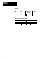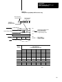
1
RTD Input Module Cat. No. 1771-IR Series B User Manual Important User Information Because of the variety of uses for this product and because of the differences between solid state products and electromechanical products, those responsible for applying and using this product must satisfy themselves as to the acceptability of each application and use of this product. For more information, refer to publication SGI–1.1 (Safety Guidelines For The Application, Installation and Maintenance of Solid State Control). The illustrations, charts, and layout examples shown in this manual are intended solely to illustrate the text of this manual. Because of the many variables and requirements associated with any particular installation, Allen–Bradley Company cannot assume responsibility or liability for actual use based upon the illustrative uses and applications. No patent liability is assumed by Allen–Bradley Company with respect to use of information, circuits, equipment or software described in this text. Reproduction of the contents of this manual, in whole or in part, without written permission of the Allen–Bradley Company is prohibited. Throughout this manual we make notes to alert you to possible injury to people or damage to equipment under specific circumstances. WARNING: Tells readers where people may be hurt if procedures are not followed properly. CAUTION: Tells readers where machinery may be damaged or economic loss can occur if procedures are not followed properly. Warnings and Cautions: - Identify a possible trouble spot. - Tell what causes the trouble. - Give the result of improper action. - Tell the reader how to avoid trouble. Important: We recommend you frequently backup your application programs on appropriate storage medium to avoid possible data loss. 1991 Allen-Bradley Company, Inc. PLC is a registered trademark of Allen-Bradley Company, Inc. Table of Contents Important User Information . . . . . . . . . . . . . . . . . . . . . . . . I Using This Manual . . . . . . . . . . . . . . . . . . . . . . . . . . . . . . . 11 Purpose of Manual . . . . . . . . . . . . . . . . . . . . . . . . . . . . . . . . . . . Audience . . . . . . . . . . . . . . . . . . . . . . . . . . . . . . . . . . . . . . . . . . Vocabulary . . . . . . . . . . . . . . . . . . . . . . . . . . . . . . . . . . . . . . . . Manual Organization . . . . . . . . . . . . . . . . . . . . . . . . . . . . . . . . . Warnings and Cautions . . . . . . . . . . . . . . . . . . . . . . . . . . . . . . . Related Products . . . . . . . . . . . . . . . . . . . . . . . . . . . . . . . . . . . . Product Compatibility . . . . . . . . . . . . . . . . . . . . . . . . . . . . . . . . . Related Publications . . . . . . . . . . . . . . . . . . . . . . . . . . . . . . . . . . 11 11 11 11 12 12 12 13 Overview of the RTD Input Module . . . . . . . . . . . . . . . . . . . 21 Chapter Objectives . . . . . . . . . . . . . . . . . . . . . . . . . . . . . . . . . . . Module Description . . . . . . . . . . . . . . . . . . . . . . . . . . . . . . . . . . Features of the Input Module . . . . . . . . . . . . . . . . . . . . . . . . . . . . How Analog Modules Communicate with Programmable Controllers Accuracy . . . . . . . . . . . . . . . . . . . . . . . . . . . . . . . . . . . . . . . . . . Getting Started . . . . . . . . . . . . . . . . . . . . . . . . . . . . . . . . . . . . . Chapter Summary . . . . . . . . . . . . . . . . . . . . . . . . . . . . . . . . . . . 21 21 21 22 23 23 23 Installing the RTD Input Module . . . . . . . . . . . . . . . . . . . . . 31 Chapter Objectives . . . . . . . . . . . . . . . . . . . . . . . . . . . . . . . . . . . Before You Install Your Input Module . . . . . . . . . . . . . . . . . . . . . . Electrostatic Damage . . . . . . . . . . . . . . . . . . . . . . . . . . . . . . . . . Power Requirements . . . . . . . . . . . . . . . . . . . . . . . . . . . . . . . . . Module Location in the I/O Chassis . . . . . . . . . . . . . . . . . . . . . . . Module Keying . . . . . . . . . . . . . . . . . . . . . . . . . . . . . . . . . . . . . . Connecting Wiring . . . . . . . . . . . . . . . . . . . . . . . . . . . . . . . . . . . Grounding the Input Module . . . . . . . . . . . . . . . . . . . . . . . . . . . . Installing the Input Module . . . . . . . . . . . . . . . . . . . . . . . . . . . . . Interpreting the Indicator Lights . . . . . . . . . . . . . . . . . . . . . . . . . . Chapter Summary . . . . . . . . . . . . . . . . . . . . . . . . . . . . . . . . . . . 31 31 31 32 32 32 33 35 35 36 36 Module Programming . . . . . . . . . . . . . . . . . . . . . . . . . . . . 41 Chapter Objectives . . . . . . . . . . . . . . . . . . . . . . . . . . . . . . . . . . . Block Transfer Programming . . . . . . . . . . . . . . . . . . . . . . . . . . . . PLC-2 Program Example . . . . . . . . . . . . . . . . . . . . . . . . . . . . . . PLC-3 Program Example . . . . . . . . . . . . . . . . . . . . . . . . . . . . . . PLC-5 Program Example . . . . . . . . . . . . . . . . . . . . . . . . . . . . . . Module Scan Time . . . . . . . . . . . . . . . . . . . . . . . . . . . . . . . . . . . 41 41 42 44 46 47 ii Table of Contents Chapter Summary . . . . . . . . . . . . . . . . . . . . . . . . . . . . . . . . . . . 47 Module Configuration . . . . . . . . . . . . . . . . . . . . . . . . . . . . 51 Chapter Objectives . . . . . . . . . . . . . . . . . . . . . . . . . . . . . . . . . . . Configuring Your RTD Module . . . . . . . . . . . . . . . . . . . . . . . . . . . Data Format . . . . . . . . . . . . . . . . . . . . . . . . . . . . . . . . . . . . . . . RTD Type . . . . . . . . . . . . . . . . . . . . . . . . . . . . . . . . . . . . . . . . . Units of Measure . . . . . . . . . . . . . . . . . . . . . . . . . . . . . . . . . . . . Real Time Sampling . . . . . . . . . . . . . . . . . . . . . . . . . . . . . . . . . . Configuring Block for a Block Transfer Write . . . . . . . . . . . . . . . . . Bit/Word Descriptions . . . . . . . . . . . . . . . . . . . . . . . . . . . . . . . . . Default Configuration for the RTD Input Module . . . . . . . . . . . . . . . Chapter Summary . . . . . . . . . . . . . . . . . . . . . . . . . . . . . . . . . . . 51 51 52 52 52 53 54 55 56 56 Module Status and Input Data . . . . . . . . . . . . . . . . . . . . . . 61 Chapter Objectives . . . . . . . . . . . . . . . . . . . . . . . . . . . . . . . . . . . Reading Data from the RTD Module . . . . . . . . . . . . . . . . . . . . . . . Chapter Summary . . . . . . . . . . . . . . . . . . . . . . . . . . . . . . . . . . . 61 61 63 Module Calibration . . . . . . . . . . . . . . . . . . . . . . . . . . . . . . . 71 Chapter Objective . . . . . . . . . . . . . . . . . . . . . . . . . . . . . . . . . . . Tools and Equipment . . . . . . . . . . . . . . . . . . . . . . . . . . . . . . . . . Calibrating your Input Module . . . . . . . . . . . . . . . . . . . . . . . . . . . About Auto-calibration . . . . . . . . . . . . . . . . . . . . . . . . . . . . . . . . Performing Auto-calibration . . . . . . . . . . . . . . . . . . . . . . . . . . . . Performing Manual Calibration . . . . . . . . . . . . . . . . . . . . . . . . . . Chapter Summary . . . . . . . . . . . . . . . . . . . . . . . . . . . . . . . . . . . 71 71 71 71 72 75 78 Troubleshooting . . . . . . . . . . . . . . . . . . . . . . . . . . . . . . . . 81 Chapter Objective . . . . . . . . . . . . . . . . . . . . . . . . . . . . . . . . . . . Diagnostics Reported by the Module . . . . . . . . . . . . . . . . . . . . . . Chapter Summary . . . . . . . . . . . . . . . . . . . . . . . . . . . . . . . . . . . 81 81 83 Specifications . . . . . . . . . . . . . . . . . . . . . . . . . . . . . . . . . . A-1 Programming Examples . . . . . . . . . . . . . . . . . . . . . . . . . . . B1 Sample Programs for the RTD Input Module . . . . . . . . . . . . . . . . . PLC-2 Family Processors . . . . . . . . . . . . . . . . . . . . . . . . . . . . . PLC-3 Family Processors . . . . . . . . . . . . . . . . . . . . . . . . . . . . . PLC-5 Family Processors . . . . . . . . . . . . . . . . . . . . . . . . . . . . . B1 B1 B3 B4 Table of Contents iii Data Table Formats . . . . . . . . . . . . . . . . . . . . . . . . . . . . . . C1 4-Digit Binary Coded Decimal (BCD) . . . . . . . . . . . . . . . . . . . . . . Signed-magnitude Binary . . . . . . . . . . . . . . . . . . . . . . . . . . . . . . Two's Complement Binary . . . . . . . . . . . . . . . . . . . . . . . . . . . . . . C1 C2 C3 Block Transfer (Mini-PLC-2 and PLC-2/20 Processors) . . D1 Multiple GET Instructions - Mini-PLC-2 and PLC-2/20 Processors Setting the Block Length (Multiple GET Instructions only) . . . . . . . . D1 D4 2 and 4-Wire RTD Sensors . . . . . . . . . . . . . . . . . . . . . . . . E1 About 2 and 4-Wire Sensors . . . . . . . . . . . . . . . . . . . . . . . . . . . Connecting 4-Wire Sensors . . . . . . . . . . . . . . . . . . . . . . . . . . . . E1 E2 Differences Between Series A and Series B RTD Input Modules . . . . . . . . . . . . . . . . . . . . . . . . . . . F1 Major Differences between Series . . . . . . . . . . . . . . . . . . . . . . . . F1 Chapter Using This Manual Purpose of Manual This manual shows you how to use your RTD input module with an Allen–Bradley programmable controller. It helps you install, program, calibrate, and troubleshoot your module. Audience You must be able to program and operate an Allen–Bradley programmable controller (PLC) to make efficient use of your input module. In particular, you must know how to program block transfer instructions. We assume that you know how to do this in this manual. If you do not, refer to the appropriate PLC programming and operations manual before you attempt to program this module. Vocabulary In this manual, we refer to: The RTD input module as the “input module” The Programmable Controller, as the “controller.” Manual Organization This manual is divided into eight chapters. The following chart shows each chapter with its corresponding title and a brief overview of the topics covered in that chapter. Chapter Title Topics Covered 2 Overview of the Input Module Description of the module, including general and hardware features 3 Installing the Input Module Module power requirements, keying, chassis location Wiring of field wiring arm 4 Module Programming How to program your programmable controller for these modules Sample programs 5 Module Configuration Hardware and software configuration Module write block format 6 Module Status and Input Data Reading data from your module Module read block format 7 Module Calibration How to calibrate your module 8 Troubleshooting Diagnostics reported by the module 11 Chapter 1 Using This Manual Chapter Title Topics Covered Appendix A Specifications Appendix B Programming Examples Appendix C Data Formats Information on BCD, signed magnitude (12-bit) binary, and 2's complement binary Appendix D Block Transfer with Mini-PLC-2 and Mini-PLC-2/20 How to use GET-GET instructions for block transfer with Mini-PLC-2 and Mini-PLC-2/20 processors Appendix E 2 and 4-wire RTD Sensors Shows wiring connections for 2 and 4-wire sensors Appendix F Differences Between Series A and B Identifies major differences between the series A version and the series B version of the RTD module. Warnings and Cautions Your module's specifications This manual contains warnings and cautions. WARNING: A warning indicates where you may be injured if you use your equipment improperly. CAUTION: Cautions indicate where equipment may be damaged from misuse. You should read and understand cautions and warnings before performing the procedures they precede. Related Products You can install your input module in any system that uses Allen–Bradley programmable controllers with block transfer capability and the 1771 I/O structure. Contact your nearest Allen–Bradley office for more information about your programmable controllers. Product Compatibility 12 This input module can be used with any 1771 I/O chassis. Communication between the discrete analog module and the processor is bidirectional. The processor block–transfers output data through the output image table to the module and block–transfers input data from the module through the input image table. The module also requires an area in the data table to store the read block and write block data. I/O image table use is an important factor in module placement and addressing selection. The module’s data table use is listed in the following table. Chapter 1 Using This Manual Table 1.A Compatibility and Use of Data Table Catalog Number 1771-IR Series B Input Image Bits 8 Use of Data Table Output Read Image Block Bits Words 8 8/9 Write Block Words 14/15 Compatibility 1/2 -slot Yes Addressing Chassis 1-slot 2-slot Series Yes Yes A and B A = Compatible with 1771-A1, A2, A4 chassis. B = Compatible with 1771-A1B, A2B, A3B, A4B chassis. Yes = Compatible without restriction No = Restricted to complementary module placement You can place your input module in any I/O module slot of the I/O chassis. You can put: two input modules in the same module group an input and an output module in the same module group. Do not put the module in the same module group as a discrete high density module unless you are using 1 or 1/2 slot addressing. Avoid placing this module close to AC modules or high voltage DC modules. Related Publications For a list of publications with information on Allen–Bradley programmable controller products, consult our publication index SD499. 13 Chapter Chapter 2 2 Overview of the RTD Input Module Chapter Objectives This chapter gives you information on: features of the input module how an input module communicates with programmable controllers Module Description The RTD input module is an intelligent block transfer module that interfaces analog input signals with any Allen–Bradley programmable controllers that have block transfer capability. Block transfer programming moves input data words from the module’s memory to a designated area in the processor data table in a single scan. It also moves configuration words from the processor data table to module memory. The input module is a single slot module and requires no external power supply. After scanning the analog inputs, the input data is converted to a specified data type in a digital format to be transferred to the processor’s data table on request. The block transfer mode is disabled until this input scan is complete. Consequently, the minimum interval between block transfer reads (50ms) is the same as the total input update time for each analog input module. Features of the Input Module The RTD input module senses up to 6 RTD signals at its inputs and converts them to corresponding temperature or resistance in 4–digit BCD or 16–bit binary format. Module features include: Six resistance temperature detector inputs Reports oC, oF, or ohms for 100 ohm platinum or 10 ohm copper sensors Reports ohms for other types of sensors software configurable 0.1 degree/10 milliohm input resolution auto–calibration open wire detection The module can be configured for 100 ohm platinum or 10 ohm copper RTDs, or other sensor types such as 120 ohm nickel RTDs. Temperature ranges are available in degrees C or F. Values can also be measured in ohms. When using 10 ohm copper RTDs, it is necessary to dedicate your module for exclusive use with 10 ohm copper RTDs. You can configure the module to accept signals from any combination of 100 ohm platinum and other types of non–copper RTDs. Both cases are determined by block transfer write (BTW) selection. 21 Chapter 2 Overview of the RTD Input Module How Analog Modules Communicate with Programmable Controllers The processor transfers data to and from the module using block transfer write (BTW) and block transfer read (BTR) instructions in your ladder diagram program. These instructions let the processor obtain input values and status from the module, and let you establish the module’s mode of operation (figure 2.1). 1. The processor transfers your configuration data and calibration values to the module using a block transfer write instruction. 2. External devices generate analog signals that are transmitted to the module. Figure 2.1 Communication Between Processor and Module 3 5 BTW 1 Memory User Program RTD 2 18 16 14 12 10 8 6 4 2 6 To Output Devices BTR 4 RTD Input Module 1771-IR Series B PC Processor (PLC-5/40 Shown) 12933-I 22 3. The module converts analog signals into binary or BCD format, and stores theses values until the processor requests their transfer. 4. When instructed by your ladder program, the processor performs a read block transfer of the values and stores them in a data table. 5. The processor and module determine that the transfer was made without error, and that input values are within specified range. 6. Your ladder program can use and/or move the data (if valid) before it is written over by the transfer of new data in a subsequent transfer. Chapter 2 Overview of the RTD Input Module 7. Your ladder program should allow write block transfers to the module only when enabled by the operator at power–up. Accuracy The accuracy of the input module is described in Appendix A. Getting Started Your input module package contains the following items. Please check that each part is included and correct before proceeding. RTD Input Module Cat. No. 1771–IR Series B User’s Manual Chapter Summary Input Module Field Wiring Arm User's Manual 1771-IR Series B Cat. No. 1771-WF 1771-6.5.76 In this chapter you read about the functional aspects of the input module and how the module communicates with programmable controllers. 23 Chapter 3 Installing the RTD Input Module Chapter Objectives This chapter gives you information on: calculating the chassis power requirement choosing the module’s location in the I/O chassis keying a chassis slot for your module wiring the input module’s field wiring arm installing the input module Before You Install Your Input Module Before installing your input module in the I/O chassis you must: Action required: Electrostatic Damage Refer to: Calculate the power requirements of all modules in each chassis. Power Requirements Determine where to place the module in the I/O chassis. Module Location in the I/O Chassis Key the backplane connector in the I/O chassis. Module Keying Make connections to the wiring arm. Connecting Wiring and Grounding Electrostatic discharge can damage semiconductor devices inside this module if you touch backplane connector pins. Guard against electrostatic damage by observing the following warning: CAUTION: Electrostatic discharge can degrade performance or cause permanent damage. Handle the module as stated below. Wear an approved wrist strap grounding device when handling the module. Touch a grounded object to rid yourself of electrostatic charge before handling the module. Handle the module from the front, away from the backplane connector. Do not touch backplane connector pins. Keep the module in its static–shield bag when not in use, or during shipment. 31 Chapter 3 Installing the RTD Input Module Power Requirements Your module receives its power through the 1771 I/O chassis backplane from the chassis power supply. The maximum drawn by the RTD module from this supply is 850mA (4.2 Watts). Add the listed value to the requirements of all other modules in the I/O chassis to prevent overloading the chassis backplane and/or backplane power supply. Module Location in the I/O Chassis Place your module in any slot of the I/O chassis except for the extreme left slot. This slot is reserved for processors or adapter modules. Group your modules to minimize adverse affects from radiated electrical noise and heat. We recommend the following. Group analog input and low voltage DC modules away from AC modules or high voltage DC modules to minimize electrical noise interference. Do not place this module in the same I/O group with a discrete high–density I/O module when using 2–slot addressing. This module uses a byte in both the input and output image tables for block transfer. After determining the module’s location in the I/O chassis, connect the wiring arm to the pivot bar at the module’s location. Module Keying Use the plastic keying bands, shipped with each I/O chassis, for keying the I/O slot to accept only this type of module. The input module is slotted in two places on the rear edge of the circuit board. The position of the keying bands on the backplane connector must correspond to these slots to allow insertion of the module. You can key any connector in an I/O chassis to receive this module except for the leftmost connector reserved for adapter or processor modules. Place keying bands between the following numbers labeled on the backplane connector (Figure 3.1): Between 10 and 12 Between 28 and 30 You can change the position of these bands if subsequent system design and rewiring makes insertion of a different type of module necessary. Use needlenose pliers to insert or remove keying bands. 32 Chapter 3 Installing the RTD Input Module Figure 3.1 Keying Positions for the RTD Input Module Keying Bands 2 4 6 8 1 1 1 1 1 2 2 2 2 2 3 3 3 3 0 2 4 6 8 0 2 4 6 8 0 2 4 6 Upper Connector Connecting Wiring Between 10 and 12 Between 28 and 30 12934 Connect your I/O devices to the field wiring arm shipped with the module (see Figure 3.2). Attach the field wiring arm to the pivot bar at the bottom of the I/O chassis. The field wiring arm pivots upward and connects with the module so you can install or remove the module without disconnecting the wires. The wiring arms are specific to the input module. The RTD input module uses field wiring arm cat. no. 1771–WF. Use the inputs in numerical sequence from 1 to 6. Unused inputs that are left open cause the module to report an open input condition. To avoid this, tie all three terminals of the open channel together. Wiring connections are shown in Figure 3.2. The module requires three–conductor shielded cable for signal transmission from RTD devices. This cable consists of three insulated conductors, covered along their entire length by a foil shield and encased in plastic. The shield reduces the effect of induced noise at any point along the cable. In order to do this, the shield must cover the enclosed wires as completely as possible. 33 Chapter 3 Installing the RTD Input Module Figure 3.2 Connection Diagram for RTDs 18 16 14 RTD 12 Chassis Ground 10 8 6 4 2 C B A C B A C B A C B A C B A C B A Terminal Identification Channel 1 Channel 2 Channel 3 Channel 4 Channel 5 Channel 6 12935 Most importantly, you must ground the shield at the chassis end only. We recommend connecting each input cable’s shield to a properly grounded common bus. Refer to Appendix E for 2–wire and 4–wire RTD connections. Cable impedance –– Since the operating principle of the RTD module is based on the measurement of resistance, you must take special care in selecting your input cables. Select a cable that has a consistent impedance throughout its entire length. We recommend Belden 9533 or equivalent. As cable length is directly related to overall cable impedance, keep input cables as short as possible by locating your I/O chassis as near the RTD sensors as I/O module considerations permit. Keep the cable free of kinks and nicks to the shielding material. Maximum cable length is limited by an overall cable impedance of 10 ohms on a single wire. This recommendation is based on considerations of signal degradation due to resistance mismatch between the three conductors within the cable. 34 Chapter 3 Installing the RTD Input Module Grounding the Input Module When using shielded cable, ground the foil shield and drain wire only at one end of the cable. We recommend that you wrap the foil shield and drain wire together and connect them to a chassis mounting bolt (Figure 3.3). At the opposite end of the cable, tape exposed shield and drain wire with electrical tape to insulate it from electrical contact. Figure 3.3 Cable Grounding Ground Shield at I/O chassis mounting bolt Shield and drain twisted into single strand Field Wiring Arm 17798 Refer to Wiring and Grounding Guidelines, publication 1770-4.1 for additional information. Installing the Input Module When installing your module in an I/O chassis: 1. First, turn off power to the I/O chassis: WARNING: Remove power from the 1771 I/O chassis backplane and wiring arm before removing or installing an I/O module. Failure to remove power from the backplane could cause injury or equipment damage due to possible unexpected operation. Failure to remove power from the backplane or wiring arm could cause module damage, degradation of performance, or injury. 35 Chapter 3 Installing the RTD Input Module Interpreting the Indicator Lights 2. Place the module in the plastic tracks on the top and bottom of the slot that guides the module into position. 3. Do not force the module into its backplane connector. Apply firm even pressure on the module to seat it properly. 4. Snap the chassis latch over the top of the module to secure it. 5. Connect the wiring arm to the module. The front panel of the input module contains a green RUN and a red FLT (fault) indicator (Figure 3.4). At power–up, the green and red indicators are on. An initial module self–check occurs. If there is no fault, the red indicator turns off. The green indicator will blink until the processor completes a successful write block transfer to the module. If a fault is found initially or occurs later, the red FLT indicator lights. Possible module fault causes and corrective action are discussed in Chapter 8, Troubleshooting. Figure 3.4 Diagnostic Indicators RTD INPUT RUN FLT Chapter Summary 36 In this chapter you learned how to install your input module in an existing programmable controller system and how to wire to the field wiring arm. Chapter Module Programming Chapter Objectives In this chapter, we describe Block Transfer programming Sample programs in the PLC–2, PLC–3 and PLC–5 processors Module scan time issues Block Transfer Programming Your module communicates with the processor through bidirectional block transfers. This is the sequential operation of both read and write block transfer instructions. The block transfer write (BTW) instruction is initiated when the analog module is first powered up, and subsequently only when the programmer wants to write a new configuration to the module. At all other times the module is basically in a repetitive block transfer read (BTR) mode. The following example programs accomplish this handshaking routine. These are minimum programs; all rungs and conditioning must be included in your application program. You can disable BTRs, or add interlocks to prevent writes if desired. Do not eliminate any storage bits or interlocks included in the sample programs. If interlocks are removed, the program may not work properly. Your analog input module will work with a default configuration of all zeroes entered in the configuration block. See the configuration default section to understand what this configuration looks like. Also, refer to Appendix B for example configuration blocks and instruction addresses to get started. Your program should monitor status bits (such as overrange, underrange) and block transfer read (BTR) activity. The following example programs illustrate the minimum programming required for communication to take place. 41 Chapter 4 Module Programming PLC-2 Program Example Note that PLC–2 processors that do not have the block transfer instruction must use the GET–GET block transfer format which is outlined in Appendix D. Figure 4.1 PLC-2 Family Sample Program Structure Block Transfer Read Done Bit 1 Pushbutton 1 2 3 4 Block Transfer Write Done Bit 5 Done DN 15 Storage Bit A L Pushbutton Storage Bit B L Storage Bit B Power-up Bit U Power-up Bit Storage Bit A Storage Bit B Power-up Bit 7 Storage Bit A 1 42 Enable EN 17 Storage Bit A U Block Transfer Write Done Bit Block Transfer Read Done Bit 6 FILE TO FILE MOVE COUNTER ADDR: XXX POSITION: XXX FILE LENGTH: XXX FILE A: YYYY-XXXX FILE R: XXX-XXX RATE PER SCAN: XXX Storage Bit B BTR Done Bit Enable BLOCK XFER READ EN X7 DATA ADDR: XXX MODULE ADDR: RGS Done BLOCK LENGTH: XX DN FILE: XXXX:XXXX X7 BLOCK XFER WRITE DATA ADDR: XXX MODULE ADDR: RGS BLOCK LENGTH: XX FILE: XXXX:XXXX Enable EN X6 Done DN X6 You can replace the pushbutton with a timer "done" bit to initiate the block transfer write on a timed basis. You can also use any storage bit in memory. Chapter 4 Module Programming Program Action Rung 1 - Block transfer read buffer: the file–to–file move instruction holds the block transfer read (BTR) data (file A) until the processor checks the data integrity. 1. If the data was successfully transferred, the processor energizes the BTR done bit, initiating a data transfer to the buffer (file R) for use in the program. 2. If the data is corrupted during the BTR operation, the BTR done bit is not energized and data is not transferred to the buffer file. In this case, the data in the BTR file will be overwritten by data from the next BTR. Rungs 2 and 3 - These rungs provide for a user–initiated block transfer write (BTW) after the module is initialized at power–up. Pressing the pushbutton locks out BTR operation and initiates a BTW that configures the module. Block transfer writes will continue for as long as the pushbutton remains closed. Rungs 4 and 5 - These rungs provide a ”read–write–read” sequence to the module at power–up. They also insure that only one block transfer (read or write) is enabled during a particular program scan. Rungs 6 and 7 - These rungs are the conditioning block transfer rungs. Include all the input conditioning shown in the example program. 43 Chapter 4 Module Programming PLC-3 Program Example Block transfer instructions with the PLC–3 processor use one binary file in a data table section for module location and other related data. This is the block transfer control file. The block transfer data file stores data that you want transferred to the module (when programming a block transfer write) or from the module (when programming a block transfer read). The address of the block transfer data files are stored in the block transfer control file. The industrial terminal prompts you to create a control file when a block transfer instruction is being programmed. The same block transfer control file is used for both the read and write instructions for your module. A different block transfer control file is required for every module. A sample program segment with block transfer instructions is shown in Figure 4.2, and described below. Figure 4.2 PLC-3 Family Sample Program Structure BTR BLOCK XFER READ RACK: XXX GROUP: X MODULE: X = XXXX DATA: XXXX:XXXX LENGTH: X CNTL: XXXX:XXXX Block Transfer Read Done Bit 1 2 Pushbutton Power-up Bit Block Transfer Write Done Bit ENABLE EN 12 DONE DN 15 ERROR ER 13 ENABLE BTW BLOCK XFER WRITE EN 02 RACK: XXX GROUP: X DONE ,MODULE: X = XXXX DN 05 DATA: XXXX:XXXX ERROR LENGTH: X ER CNTL: XXXX:XXXX 03 Program Action At power–up, the user program examines the BTR done bit in the block transfer read file, initiates a write block transfer to configure the module, and then does consecutive read block transfers continuously. The power–up bit can be examined and used anywhere in the program. Rungs 1 and 2 - Rungs 1 and 2 are the block transfer read and write instructions. The BTR enable bit in rung 1, being false, initiates the first read block transfer. After the first read block transfer, the module performs a block transfer write and then does continuous block transfer reads until the pushbutton is used to request another block transfer write. 44 Chapter 4 Module Programming After this single block transfer write is performed, the module returns to continuous block transfer reads automatically. 45 Chapter 4 Module Programming PLC-5 Program Example The PLC–5 program is very similar to the PLC–3 program with the following exceptions: You must use enable bits instead of done bits as the conditions on each rung. A separate control file must be selected for each of the BT instructions. Refer to Appendix B. Figure 4.3 PLC-5 Family Sample Program Structure 1 2 BTR BLOCK XFER READ X RACK: X GROUP: X MODULE: XXX:XX CONTROL: DATA FILE: XXX:XX LENGTH: XX CONTINUOUS: N BTR Enable Pushbutton Power-up Bit BTW Enable BTW BLOCK XFER WRITE RACK: X GROUP: X MODULE: X CONTROL: XXX:XX DATA FILE: XXX:XX LENGTH: XX CONTINUOUS: N EN DN ER EN DN ER Program Action Rungs 1 and 2 - At power–up, the program enables a block transfer read and examines the power–up bit in the BTR file (rung 1). Then, it initiates one block transfer write to configure the module (rung 2). Thereafter, the program continuously reads data from the module (rung 1). A subsequent BTW operation is enabled by a pushbutton switch (rung 2). Changing processor mode will not initiate a block transfer write unless the first pass bit is added to the BTW input conditions. 46 Chapter 4 Module Programming Module Scan Time Scan time is defined as the amount of time it takes for the input module to read the input channels and place new data into the data buffer. Scan time for your module is shown in Figure 4.4. The following description references the sequence numbers in Figure 4.4. Following a block transfer write “1” the module inhibits communication until after it has configured the data and loaded calibration constants “2”, scanned the inputs “3”, and filled the data buffer “4”. Write block transfers, therefore, should only be performed when the module is being configured or calibrated. Any time after the second scan begins “5”, a BTR request “6” can be acknowledged. When operated in real time sample mode (RTS) = 00, a BTR may occur at any time after “4.” When operated in RTS = T, a BTR will be waived until ”T” milliseconds, at which time 1 BTR will be released. Figure 4.4 Block Transfer Time End of Block Transfer Write Block Transfer Write Time 1 Module available to perform block transfer Configure Time 2 1st Scan 3 2nd Scan 4 5 3rd Scan 6 7 8 9 Internal Scan time = 50msec T = 100ms, 200ms, 300ms ... 3.1sec. Chapter Summary In this chapter, you learned how to program your programmable controller. You were given sample programs for your PLC–2, PLC–3 and PLC–5 family processors. You also read about module scan time. 47 Chapter Module Configuration Chapter Objectives In this chapter you will read how to configure your module’s hardware, condition your inputs and enter your data. Configuring Your RTD Module Because of the many analog devices available and the wide variety of possible configurations, you must configure your module to conform to the analog device and specific application that you have chosen. Data is conditioned through a group of data table words that are transferred to the module using a block transfer write instruction. You can configure the following features for the 1771–IR series B module: data format RTD type units of measure (oC, oF or ohms) real time sampling calibration bias Configure your module for its intended operation by means of your programming terminal and write block transfers (BTW). Note: Programmable controllers that use 6200 software programming tools can take advantage of the IOCONFIG utility to configure this module. IOCONFIG uses menu–based screens for configuration without having to set individual bits in particular locations. Refer to your 6200 software literature for details. During normal operation, the processor transfers from 1 to 14 words to the module when you program a BTW instruction to the module’s address. The BTW file contains configuration words, bias values, and calibration values that you enter for each channel. When a block transfer length of 0 is programmed, the 1771–IR/B will respond with the Series A default of 14. 51 Chapter 5 Module Configuration Data Format You must indicate what format will be used to read data from your module. Typically, BCD is selected with PLC–2 processors, and binary (also referred to as integer or decimal) is selected with PLC–3 and PLC–5 processors. See Table 5.A and Appendix C for details on Data Format. Table 5.A Selecting Format for Reading Data Decimal Bit 10 Octal Bit 12 RTD Type Decimal Bit 9 Octal Bit 11 Data Format 0 0 BCD 0 1 2's complement binary 1 0 Signed magnitude binary 1 1 Same as signed magnitude binary The RTD input module accepts the following types of RTD inputs: RTD Platinum Temperature Range Indication -200 to +870oC (-328 to 1598oF) Underrange Word 1, Bit 10 Ohms 0 1.00 -200 -328 600.00 870 1598 1.00 -200 -328 327.67 260 500 Overange Copper -200 to +260oC (-328 to 500oF) Underrange Overrange Units of Measure 1 oC oF The units of measure reported by the RTD module are selected by setting bits 06–07 in BTW word 1. Units of Measure 07 Bit 06 Degrees C 0 0 Degrees F 0 1 Ohms 1 0 Not used 1 1 If any of bits 0–5 are set (1), the corresponding input channel will be reported in ohms. 52 Chapter 5 Module Configuration Real Time Sampling The real time sampling (RTS) mode of operation provides data from a fixed time period for use by the processor. RTS is invaluable for time based functions (such as PID and totalization) in the PLC. It allows accurate time based calculations in local or remote I/O racks. In the RTS mode the module scans and updates its inputs at a user defined time interval ( ∆T) instead of the default interval. The module ignores block transfer read (BTR) requests for data until the sample time period elapses. The BTR of a particular data set occurs only once at the end of the sample period and subsequent requests for transferred data are ignored by the module until a new data set is available. If a BTR does not occur before the end of the next RTS period, a time–out bit is set in the BTR status area. When set, this bit indicates that at least one data set was not transferred to the processor. (The actual number of data sets missed is unknown.) The time–out bit is reset at the completion of the BTR. Set appropriate bits in the BTW data file to enable the RTS mode. You can select RTS periods ranging from 100 milliseconds (msec) to 3.1 seconds in increments of 100msec. Refer to Table 5.B below for actual bit settings. Note that the default mode of operation is implemented by placing all zeroes in bits 13 through 17. In default mode, the sample time period is 50msec, and the RTS time–out is inhibited. Note that binary representation of the RTS bit string is the RTS period X 100msec. For example, 900msec = 01001 = (9 X 100msec). Table 5.B Bit Settings for the Real Time Sample Mode Decimal Bits Octal Bits 15 17 14 16 13 15 12 14 11 13 Sample Time Period 0 0 0 0 0 RTS inhibited (50msec) 0 0 0 0 1 100 ms 0 0 0 1 0 200 ms 0 0 0 1 1 300 ms 0 0 1 0 0 400 ms 0 0 1 0 1 500 ms 0 0 1 1 0 600 ms 0 0 1 1 1 700 ms 0 1 0 0 0 800 ms 0 1 0 0 1 900 ms 0 1 0 1 0 1.0 sec 0 1 1 1 1 1.5 sec 1 0 1 0 0 2.0 sec 1 1 0 0 1 2.5 sec 1 1 1 1 0 3.0 sec 1 1 1 1 1 3.1 sec Important: Use decimally addressed bit locations for PLC-5 processors. 53 Chapter 5 Module Configuration Configuring Block for a Block Transfer Write The complete configuration block for the block transfer write to the module is defined in Table 5.C below. Table 5.C Configuration Block for RTD Input Module Block Transfer Write Word 1 2 54 17 16 15 14 13 Sample Time (for RTS) 12 11 Data Format 10 ohm resistance @ 25oC 3 Channel 1 Bias 4 Channel 2 Bias 5 Channel 3 Bias 6 Channel 4 Bias 7 Channel 5 Bias 8 Channel 6 Bias 9 Channel 1 calibration 10 Channel 2 calibration 11 Channel 3 calibration 12 Channel 4 calibration 13 Channel 5 calibration 14 Channel 6 calibration 15 Auto-calibration request word 10 RTD Type 07 06 Units of Measure 05 04 03 02 01 Single channel in ohms 00 Chapter 5 Module Configuration Bit/Word Descriptions Bit/word descriptions of BTW file words 1 (configuration), 2 (resistance value of 10 ohm copper RTDs), 3 through 8 (individual channel bias values) and 9 through 14 (individual channel calibration words) are presented below. Enter data into the BTW instruction after entering the instruction into your ladder diagram. Table 5.D Bit/Word Definitions for RTD Input Module Word Bits Description Word 1 bits 00-05 If any of these bits are set, the corresponding input channel will be reported in ohms. If RTDs other than 10 ohm copper or 100 ohm platinum are used you must report those channels in ohms, not degrees. Data format on a channel displayed in ohms will default to binary. bits 06-07 Determines what units of measure the module reports. Units of measure Bits 07 06 Degrees C 0 0 Degrees F 0 1 Ohms 1 0 Not used 1 1 bit 10 In temperature mode: 0 = Entire module is platinum 1 = Entire module is 10 ohm copper. Enter exact value in word 2. In ohms mode: 0 = 30mohm/count resolution 1 = 10mohm/count resolution bits 11-12 Data format bits tell module which format to use for reporting input values to processsor Format bits 13-17 Bits 12 11 4-digit BCD 0 0 2's complement binary 0 1 Signed magnitude (binary) 1 0 Not used 1 1 17 16 15 14 13 0.1 0 0 0 0 1 0.5 0 0 1 0 1 0.6 0 0 1 1 0 0.7 0 0 1 1 1 0.8 0 1 0 0 0 0.9 0 1 0 0 1 1.0 0 1 0 1 0 Real time sample bits. See Table 5.B. Sample Time 55 Chapter 5 Module Configuration Word Bits Description Word 1 (cont.) Default Configuration for the RTD Input Module 1.5 0 1 1 1 1 2.0 1 0 1 0 0 2.5 1 1 0 0 1 3.0 1 1 1 1 0 Word 2 If bit 10 is set in word 1, and temperature readings are desired, word 2 must also be used. Enter the exact resistance of 10 ohm RTD at 25oC in BCD. Range is 9.00 to 11.00 ohms. Values less than 9.00 ohms or greater than 11.00 ohms will default to 10.00 ohms. Non-BCD values will also default to 10.00 ohms. Words 3-8 Individual channel bias words entered in BCD. This value is subtracted from the channel data in the BTR. The bias value is always a positive number. Bias value range is 0<bias<9999. Words 9-14 Individual channel calibration words. Word 15 Auto-calibration request word - used to automatically calibrate selected channels and save the calibration constants in EEPROM. Bit 00 Offset calibration complete Bit 01 Gain calibration complete Bit 02 Save complete Bit 06 EEPROM fault Bit 07 Faulty calibration (no save) Bits 10-15 Channel failed calibration If zeroes are written to the module in all configuration positions, the module will default to: BCD format 100 ohm platinum RTD temperature in degrees C real time sampling = inhibited (sample time = 50msec) Chapter Summary 56 In this chapter you learned how to configure your module’s hardware, condition your inputs and enter your data. Chapter 6 Module Status and Input Data Chapter Objectives In this chapter you will read about: reading data from your module input module read block format Reading Data from the RTD Module Block transfer read programming moves status and data from the input module to the processor’s data table in one I/O scan (Table 6.A). The processor user program initiates the request to transfer data from the input module to the processor. During normal operation, the read block transfer for this module moves up to 8 words from the RTD module in one program scan. The words contain module status and input data from each channel. When a block transfer length of 0 is programmed, the 1771–IR/B will respond with the Series A default of 8 words. The user program initiates the request to transfer data from the RTD module to the processor. Table 6.A BTR Word Assignments for RTD Input Module (1771-IR/B) Decimal Bit 15 14 13 12 11 10 9 8 7 6 5 4 3 2 1 0 Octal Bit 17 16 15 14 13 12 11 10 07 06 05 04 03 02 01 00 0 RTS Timeout EEPROM calibration values not readable Powerup 1 2 Not used Channel Overrange Channel Polarity 3 Channel 1 Data 4 Channel 2 Data 5 Channel 3 Data 6 Channel 4 Data 7 Channel 5 Data 8 Channel 6 Data 9 Auto-calibration Status Word Not used Channel Underrange Channel Overflow 61 Chapter 6 Module Status and Input Data Table 6.B Bit/Word Description for RTD Input Module (1771-IR Series B) Word Bit Definition Word 1 Bits 00-05 Underrange indication for each channel; set when input is below the normal operating range for copper or platinum RTD. Bit 00 for input 1, bit 01 for input 2, etc. See Table 6.C. Bit 06 Power-up bit is set when the module is alive but not yet configured. Bit 07 EEPROM calibration values could not be read. Bits 10-15 Overrange bits are set when the input is above the normal operating range. Bit 10 for input 1, bit 11 for input 2, etc. See Table 6.C. Bit 16 Real time sample time-out bit. See page 5-2. Bit 17 Not used Bit 00-05 When set, indicates that default bias has been subtracted from the input value. Only the remainder is shown in the data word. Each bit relates to a single channel; bit 00 for input 1, etc. Default bias is automatically applied when BCD formatted data cannot be displayed. This will occur when measuring temperatures in Fahrenheit larger than 999.9 degrees. The default bias value which is subtracted is 1000.0. Bits 06-07 Not used Bits 10-15 Sign bits for each channel. When set indicate that a certain input is negative. Bit 10 corresponds to input 1, bit 11 to input 2, etc. These bits are used for BCD and signed magnitude data formats. Bits 16-17 Not used Word 2 Words 3-8 Input data words. The data words must be multiplied or divided by a factor if whole numbers need to be displayed. If you are reading temperature in oF or oC: Then there is an implied decimal point (XXX.X) after the least significant digit. Resolution is 0.1o. If you are reading resistance in milliohms (copper RTDs) (BTW word 1, bit 10 = 1): Then there is an implied decimal point (XXX.XX). If you are reading resistance in milliohms (all other RTDs) (BTW word 1, bit 10 = 0): Multiply the data word by 30 to get the actual value in milliohms. Resolution is 30 milliohms. Word 9 62 Auto-calibration word. Bit 00 Offset calibration complete Bit 01 Gain calibration complete Bit 02 Save complete Bit 06 EEPROM fault Chapter 6 Module Status and Input Data Word Bit Definition Word 9 (cont.) Bit 07 Faulty calibration (no save) Bits 10-15 Channel failed calibration. Bit 10 for input 1, bit 11 for input 2, etc. Table 6.C Overrange and Underrange Values Indication BTW Word 1, Bit 10 RTD Underrange 0 Platinum Overange Underrange Overrange Chapter Summary 1 Copper Ohms oC oF < 1.00 < -200 < -328 > 600.00 > 870 > 1598 < 1.00 < -200 < -328 > 327.67 > 260 > 500 In this chapter you learned the meaning of the status information that the RTD input module sends to the processor. 63 Chapter Module Calibration Chapter Objective In this chapter we tell you how to calibrate your modules. Tools and Equipment In order to calibrate your input module you will need the following tools and equipment: Tool or Equipment Description Model/Type Available from: Industrial Terminal and Interconnect Cable Programming terminal for A-B family processors Cat. No. 1770-T3 or Cat. No. 1784-T45, -T50, etc. Allen-Bradley Company Highland Heights, OH Precision Resistors 1.00 ohm, 1% (quantity of 6) CMF-65-0010-F-T-0 Dale 402.0 ohm, 0.01% (quantity of 6) MAR6-T16-402-.01% TRW Calibrating your Input Module You must calibrate the module in an I/O chassis. The module must communicate with the processor and industrial terminal. Before calibrating your module, you must enter ladder logic into the processor memory, so that you can initiate BTWs to the module, and the processor can read inputs from the module. Calibration can be accomplished using either of two methods: auto–calibration manual calibration About Auto-calibration Auto–calibration calibrates the input by generating offset and gain correction values and storing them in EEPROM. These values are read out of EEPROM and placed in RAM memory at initialization of the module. The auto–calibration routine operates as follows: - Whenever a block transfer write (BTW) is performed to the module (any time after the module has been powered up), it interrogates word 15 for a request for auto–calibration. - The request can be for the following: offset calibration, gain calibration, save operation (save to EEPROM). When using auto–calibration, write transfer calibration words 9 through 14 must contain zeroes. 71 Chapter 7 Module Calibration Performing Auto-calibration Calibration of the module consists of applying 1.00 ohm resistance across each input channel for offset calibration, and 402.00 ohm across each input channel for gain correction. Offset Calibration Normally all inputs are calibrated together. To calibrate the offset of an input, proceed as follows: 1. Connect 1.00 ohm resistors across each input channel as shown in Figure 7.1. Figure 7.1 Resistor Location for Offset Calibration 18 Repeat for each channel 16 1.00 ohm Resistor 14 12 10 8 6 4 2 C B A C B A C B A C B A C B A C B A Terminal Identification Channel 1 Channel 2 Channel 3 Channel 4 Channel 5 Channel 6 12935 72 2. Apply power to the module. 3. After the connections stabilize, request the offset calibration by setting bit 00 in block transfer write word 15 and sending a block transfer write to the module. Refer to Table 7.A. Chapter 7 Module Calibration Table 7.A Write Block Transfer Word 15 Word Bit 17 16 15 14 13 12 11 10 07 06 05 04 03 Inhibit Calibration on Channel Word 15 Set these bits to 0 6 5 4 3 2 02 01 00 Requested Auto-Calibration 1 Set these bits to 0 Requested Requested Save Gain Cal. Values Requested Offset Cal. NOTE: Normally, all channels are calibrated simultaneously (bits 10–15 of word 15 are octal 0). To disable calibration on any channel, set (1) the corresponding bit 10 through 15 of word 15. 4. Queue block transfer reads (BTRs) to monitor for offset calibration complete and any channels which may have not calibrated successfully. Refer to Table 7.B. Table 7.B Read Block Transfer Word 9 Word Bit 17 16 15 14 13 12 11 10 07 06 05 04 03 Uncalibrated Channels Word 9 Not used 6 5 5. 4 3 02 01 00 Gain Cal. Complete Offset Cal. Complete Auto-Calibration Status 2 1 Cal. Fault EEPROM Fault Not used Save to EEPROM Complete Proceed to gain calibration below. Gain Calibration Calibrating gain requires that you apply 402.00 ohms across each input channel. Normally all inputs are calibrated together. To calibrate the gain of an input, proceed as follows: 1. Connect 402.00 ohm resistors across each input channel as shown in Figure 7.2. 73 Chapter 7 Module Calibration Figure 7.2 Resistor Location for Gain Calibration 18 Repeat for each channel 16 402.0 ohm Resistor 14 12 10 8 6 4 2 C B A C B A C B A C B A C B A C B A Terminal Identification Channel 1 Channel 2 Channel 3 Channel 4 Channel 5 Channel 6 12935 2. Apply power to the module. 3. After the connections stabilize, request the gain calibration by setting bit 01 in BTW word 15 and sending a block transfer write (BTW) to the module. Refer to Table 7.A. NOTE: Normally, all channels are calibrated simultaneously (bits 10–15 of word 15 are octal 0). To disable calibration on any channel, set (1) the corresponding bit 10 through 15 of word 15. 4. 74 Queue BTRs to monitor for gain calibration complete and channels which may not have calibrated successfully. Chapter 7 Module Calibration Save Calibration Values If any ”uncalibrated channel” bits (bits 10–15 of BTR word 9) are set, a save cannot occur. Auto–calibration should be performed again, starting with offset calibration. If the module has a faulty channel, the remaining functioning channels can be calibrated by inhibiting calibration on the faulty channel. The module can be run with the new calibration values, but will lose them on power down. To save these values, proceed as follows: 1. Request a ”save to EEPROM” by setting bit 02 in BTW word 15 and sending the BTW to the module. Refer to Table 7.A. 2. Queue BTRs to monitor for ”save complete”, ”EEPROM fault” and ”calibration fault.” An EEPROM fault indicates a nonoperative EEPROM; a calibration fault indicates at least one channel was not properly offset or gain calibrated and a save did not occur. Note: During normal operation, make sure bits 00, 01 and 02 of BTW word 15 are zero (0). Performing Manual Calibration You calibrate each channel by applying a precision resistance across each channel, comparing correct with actual results, and entering correction into the corresponding calibration word for that channel. The correction takes affect after it is transferred to the module by the corresponding BTW instruction in your ladder diagram program. Always start with offset adjustment followed by gain adjustment. Before calibrating the module, you must enter ladder logic into processor memory, so that you can initiate write block transfers to the module, and the processor can read inputs from the module. Words 9 through 14 in the write block transfer file are the module calibration words. Word 9 corresponds to channel 1, word 10 to channel 2, and so on. Each word is composed of two bytes: the upper byte is for offset correction and the lower byte is for gain correction. Refer to Table 7.C. 75 Chapter 7 Module Calibration Table 7.C Module Calibration Words Word/Bit 17 16 15 14 13 12 11 10 07 06 05 04 03 02 9 S Channel 1 Offset S Channel 1 Gain 10 S Channel 2 Offset S Channel 2 Gain 11 S Channel 3 Offset S Channel 3 Gain 12 S Channel 4 Offset S Channel 4 Gain 13 S Channel 5 Offset S Channel 5 Gain 14 S Channel 6 Offset S Channel 6 Gain 01 00 Enter the information for each byte in signed magnitude binary format. In each byte, the most significant bit (bits 17, 7) is a polarity bit. When the polarity bit is set (1), the module anticipates a negative calibration value. A negative calibration value means that your readings are too high and you want to subtract a corrective amount from that reading. A positive calibration value means that your readings are too low and you want to add a corrective amount to that reading. Important: If you have a spare field wiring arm. you may want to temporarily switch it with the module’s present wiring arm. You can use this spare arm for test purposes in order to avoid disconnecting your RTD wiring. Offset Calibration 1. Attach the 1.00 ohm, 1% resistors as shown in Figure 7.1. 2. Examine word 3 (channel 1 data) in the read block transfer file. Note the value. It should be around 1.00 (100 for 10 mohm resolution; 33 for 30 mohm resolution). 3. Examine word 9 of the write block transfer data file. Bits 16–10 make up the offset correction byte. Bit 17 is the sign bit. 4. Subtract the data value that you noted in step 2 from 100. The difference should be within +127 to –127. If it is not, the required correction is beyond the range of software calibration. If the difference is within range, input the difference (positive or negative), in binary form, in bits 17–10 of word 9 in the write block transfer file. For example, if, at 1.00 ohm, word 3 of the read block transfer data file shows 147, you would subtract 147 from 100, which equals –47. You would then enter 10101111 (–47) in the upper byte of word 9. The leading 1 (bit 17) is the polarity bit. It indicates a negative correction factor. That 76 Chapter 7 Module Calibration is, you want to subtract 47 counts from your input data. The lower byte remains 00 during offset calibration. 5. Repeat above steps for channels 2 through 6 respectively. 6. Apply the values by sending a BTW to the module. Gain Calibration 1. Connect the 402.00, .01% resistors to the swing arm as shown in Figure 7.2. 2. Place the module in platinum ohm mode. This provides 30 mohm resolution display. 3. Examine word 3 of the read block transfer data file. It should be around 13400 decimal. Your actual value will be a percentage of 13400. For example, if the data in word 3 is 13408, then: (13400–13408)/134000 = –0.000597. Your actual data value differs from the theoretical value (at 402.0 ohms input resistance) by –0.000597, or –0.0597%. You can compensate for this error by entering the percentage difference in binary coded fraction form. Table 7.D lists the value for bits 7–0. Table 7.D Value for Bits 7 through 0 Bit Value Bit 07 Sign bit Bit 06 = 0.0976562% Bit 05 = 0.0488281% Bit 04 = 0.024414% Bit 03 = 0.012207% Bit 02 = 0.00610351% Bit 01 = 0.00305175% Bit 00 = 0.00152587% 77 Chapter 7 Module Calibration You use the values that most nearly add up to the percentage that you determined in step 8. For example, to attain the value of 0.0597%, you need to add: Percentage Bit Number 0.0488281 Bit 05 0.00610351 Bit 02 0.00305175 Bit 01 0.00152587 Bit 00 Total = 0.0595% As you can see, 0.0595 is smaller than 0.0597, but this value is as close as you can come using the 7 possible values listed in Table 7.D. You would enter 10100111 in the lower byte of word 9. This sets bits 05, 02, 01 and 00, which subtracts a gain correction of 0.0595% from the actual input data value. Important: When you enter data in the least significant byte, remember to reenter the data in the most significant byte in the word. If you don’t, the data in the MSB is lost. Chapter Summary 78 4. Repeat above steps for channels 2 through 6. 5. Apply the values by sending a BTW to the module. In this chapter, you learned how to calibrate your input module. Chapter 8 Troubleshooting Chapter Objective We describe how to troubleshoot your module by observing LED indicators and by monitoring status bits reported to the processor. Diagnostics Reported by the Module At power–up, the module momentarily turns on both indicators as a lamp test, then checks for correct RAM operation EPROM operation EEPROM operation a valid write block transfer with configuration data Thereafter, the module lights the green RUN indicator when operating without fault, or lights the red fault (FLT) indicator when it detects fault conditions. If the red FLT indicator is on, block transfer will be inhibited. The module also reports status and specific faults (if they occur) in every transfer of data to the PC processor. Monitor the green and red LED indicators and status bits in word 1 of the BTR file when troubleshooting your module. Figure 8.1 LED Indicators RTD INPUT RUN Green RUN LED FLT Red Fault (FLT) LED This module uses a read block transfer to transmit data and to monitor module and data status. Word 1 of the read block transfer data file contains module status, power–up, and data out–of–range information. Word 2 contains data polarity and overflow information. Words 3 through 8 are data words. 81 Chapter 8 Troubleshooting Table 8.A shows LED indications and probable causes and recommended actions to correct common faults. Table 8.A Troubleshooting Chart for the RTD Input Module (1771-IR/B) Indication Probable Cause Recommended Action Both LEDs are OFF No power to module Possible short on the module LED driver failure Check power to I/O chassis. Recycle as necessary. Replace module. Red FLT LED ON and Green RUN LED is ON Microprocessor, oscillator or EPROM failure Replace module. Red FLT LED ON If immediately after power-up, indicates RAM or EPROM failure.1 Replace module. If during operation, indicates possible microprocessor or backplane interface failure.1 Replace module. Power-up diagnostics successfully completed. Normal operation. If LED continues to flash, and write block transfers (BTW) cannot be accomplished, you have a possible interface failure. Check ladder logic program. If correct, replace module. Green RUN LED is flashing 1 When red LED is on, the watchdog timer has timed out and backplane communications are terminated. Your user program should monitor communication. Status Reported in Words 1 and 2 Design your program to monitor status bits in words 1 and 2, and to take appropriate action depending on your application requirements. You may also want to monitor these bits while troubleshooting with your industrial terminal. The module sets a bit (1) to indicate it has detected one or more of the following conditions. Table 8.B Status Reported in Words 1 and 2 82 Word Bit Indication 1 00-05 Data underrange. Bit 05 corresponds to channel 6, bit 04 corresponds to channel 5, and so on. If input connections and resistances are correct, this status may indicate failed communications between the channel and microprocessor. If all channels are underrange, a blown fuse or failed dc-dc converter may be the cause. 06 Successful power-up and module is waiting for configuration data. Bit 06 is reset after the first successful block transfer write. 07 EEPROM calibration constants could not be read. The module will continue to operate but readings may be inaccurate. Chapter 8 Troubleshooting Word Bit Word 1 (cont.) 10-15 Data overrange. Bit 15 corresponds to channel 6, bit 14 corresponds to channel 5, and so on. If input connections and resistances are correct, this status may indicate a failed RTD functional analog block (RTD FAB). 16 RTS timed out. The module updated its inputs before the processor read them. 17 Not used. 2 Indication 00-05 Indicates that the default bias of 1000.0 has been subtracted from the measured value. If sending binary data, no overflow occurs unless there is a hardware malfunction. 06-07 Not used 10-15 Data sign bits formatted for BCD or signed magnitude. Bit 10 corresponds to channel 1, bit 11 to channel 2, and so on. 16-17 Not used Status Reported in Word 9 Design your program to monitor status bits in word 9 during calibration, and to take appropriate action depending on your requirements. You may also want to monitor these bits while troubleshooting with your industrial terminal. The module sets a bit (1) to indicate it has detected one or more of the following conditions. Table 8.C Status Reported in Word 13 Word Bit 9 6 The EEPROM could not be written. 7 Channel(s) could not be calibrated as indicated by bits 10 through 15 respectively. 10-15 Chapter Summary Condition Bit 10 (channel 1) through bit 16 (channel 6) could not be calibrated. Check field wiring arm connections and source for proper resistance. In this chapter, you learned how to interpret the LED status indicators and troubleshoot your input module. 83 Appendix A Specifications Module Capacity Six RTD input channels Module Location 1771 I/O Chassis Sensor Type 100 ohm platinum (alpha = 0.00385) or 10 ohm copper (alpha = 0.00386) Other types may be used with report in ohms only Units of measure Temperature in oC Temperature in oF RTD resistance in ohms (10milliohms or 30milliohms resolution) Temperature Range Platinum: -200 to +870oC (-328 to 1598oF) Copper: -200 to +260oC (-328 to +500oF) Resistance Range 1.00 to 600.00 ohms Resolution Platinum: 0.1oC (0.1oF) Copper: 0.3oC (0.5oF) Sensor Excitation 1mA constant current source supplied by module Input Isolation Dielectric Test 1000V peak channel to channel, channel to backplane, for 1 second Common Mode Rejection 120db @ 60Hz up to 1000V peak Common Mode Impedance Greater than 10 megohms Normal Mode Rejection 60db @ 60Hz Input Overvoltage Protection 120V rms continuous Open RTD Response Time Open excitation (terminal A) to overrange: <0.5sec Open common (terminal C) to underrange: <0.5sec Open sense (terminal B): drift high Scan Time (all 6 channels) 50ms Environmental Conditions Operating Temperature Rate of Change Storage Temperature Relative Humidity 0 to 60oC (32 to 140oF) Ambient changes greater than 1.0oC/minute may temporarily degrade performance during periods of change. -40 to 85oC (-40 to 185oF) 5 to 95% noncondensing Backplane Power Consumption 4.25W maximum, 0.85A at 5V Keying Between 10 and 12 Between 28 and 30 Field Wiring Arm Cat. No. 1771-WF A-1 Appendix A Specifications Table A.A 1771-IR Series B Error Summary Based on Temperatures above -200oC RTD Type Range Error @ Calibration Temperature (25oC) (over range) Copper -200 to +260oC (-328 to +500oF) +0.344oC/+0.564oF +0.1306 Platinum -200 to +870oC (-328 to 1598oF) +0.100oC/+0.152oF +0.0717 Table A.B 1771-IR Series B Resistance Error Summary A-2 Drift oC/oC or oF/oF RTD Type Resistance Error @ 25oC (over range) Resistance Drift Ohm/oC Copper +0.074 ohm +0.0213 Platinum +0.075 ohm +0.0213 Appendix Programming Examples Sample Programs for the RTD Input Module The following are sample programs for entering data in the configuration words of the write block transfer instruction when using the PLC–2, PLC–3 or PLC–5 family processors. PLC-2 Family Processors To enter data in the configuration words, follow these steps. NOTE: For complete programming sample, refer to Figure 4.1. Example: Enter the following rung for a write block transfer: Power Up Bit BTW BLOCK XFER WRITE DATA ADDR: 030 MODULE ADDR: 110 BLOCK LENGTH: 14 FILE: 100-115 010 EN 06 110 DN 06 100 is the address of the write block transfer data file. You want to examine configuration word 1. In RUN/PROG Mode Action Result 1. Press [SEARCH]8<data address> Finds the block address transfer instruction 2. Press CANCEL COMMAND Removes preceeding command 3. Press [DISPLAY]0 or 1 Displays the file in binary or BCD 4. Press [SEARCH]51 On line data change Cursor defaults to first entry in file when SEARCH 51 is pressed. 5. Press [INSERT] Writes data to file element B1 Appendix B Programming Examples In PROG Mode Action Result 1. Press [SEARCH]8<data address> Finds the block transfer instruction 2. Press CANCEL COMMAND Removes preceeding command 3. Press [DISPLAY]0 or 1 Displays the file in binary or BCD 4. Press [DISPLAY]001 and enter data Puts cursor on word 1 5. Press [INSERT] Use the above procedure to enter the required words of the write block transfer instruction. Be aware that the block length will depend on the number of channels selected and whether biasing and/or calibration is or is not performed; for example, the block may contain only 1 word if no bias or calibration is performed but may contain 14 words if using 6 inputs with bias and calibration. The PLC–2 family write block transfer data file should look like Figure B.1. Figure B.1 Write Block Transfer Data Transfer for a PLC-2 Family Processor DATA ADDR: 030 BINARY DATA MONITOR BLOCK XFER WRITE MODULE ADDR: 110 FILE: 100-115 POSITION 001 002 003 004 005 006 007 008 B2 BLOCK LENGTH: 14 FILE DATA 00000000 00000000 00000000 00000000 00000000 00000000 00000000 00000000 00000000 00000000 00000000 00000000 00000000 00000000 00000000 00000000 00000000 00000000 00000000 00000000 00000000 00000000 00000000 00000000 00000000 00000000 00000000 00000000 00000000 00000000 00000000 00000000 Appendix B Programming Examples PLC-3 Family Processors Following is a sample procedure for entering data in the configuration words of the write block transfer instruction when using a PLC–3 processor. For a complete sample program, refer to Figure 4.2. To enter data in the configuration words, follow these steps: Example: Enter the following rung for a write block transfer: BTW Power Up Bit BLOCK XFER WRITE RACK: 001 GROUP: 1 MODULE 1 = HIGH DATA: F0003:0000 LENGTH: CNTL: 14 FB004:0000 CNTL EN 12 CNTL DN 15 CNTL ER 13 F0003:0000 is the address of the write block transfer data file. You want to enter/examine word 1. 1. Press [SHIFT][MODE] to display your ladder diagram on the industrial terminal. 2. Press DD,03:0[ENTER] to display the block transfer write file. The industrial terminal screen should look like Figure B.2. Notice the highlighted block of zeroes. This highlighted block is the cursor. It should be in the same place as it appears in figure B.2. If it is not, you can move it to the desired position with the cursor control keys. Once you have the highlighted cursor in the right place, you can go on to step 3. B3 Appendix B Programming Examples 3. Enter the data corresponding to your bit selection in word 0. 4. When you have entered your data, press [ENTER]. If you make a mistake, make sure the cursor is over the word you desire to change. Enter the correct data and press [ENTER]. Figure B.2 Write Block Transfer for a PLC-3 Processor START - W0003 : 0000 WORD # 0 1 2 3 00000 00000000 00000000 00000000 00000000 00000000 00000000 00000000 00000000 00004 00000000 00000000 00000000 00000000 00000000 00000000 00000000 00000000 00010 00000000 00000000 00000000 00000000 00000000 00000000 00000000 00000000 00014 00000000 00000000 00000000 00000000 00000000 00000000 00000000 00000000 00020 00000000 00000000 00000000 00000000 00000000 00000000 00000000 00000000 RUNG # [RM000000] : MEM PROT OFF DATA MONITOR PROG : I/O OFF $ W03:0 - [ ] NO FORCES : 5. PLC-5 Family Processors NO EDITS : Press [CANCEL COMMAND]. This returns you to the ladder diagram. The following is a sample procedure for entering data in the configuration words of the block transfer write instruction when using a PLC–5 processor. For a complete sample program, refer to Figure 4.3. 1. Enter the following rung: Power Up Bit N7:60 is the address of the BTW transfer file. 2. BTW BLOCK XFER WRITE RACK: 0 GROUP: 0 MODULE: 0 CONTROL: N7:0 DATA FILE: N7:60 LENGTH: 14 CONTINUOUS: N Press [F8],[F5] and enter N7:60 to display the configuration block. The industrial terminal screen should like figure B.3. B4 EN DN ER Appendix B Programming Examples Figure B.3 Sample PLC-5 Data File (Hexidecimal Data) Address N7:60 N7:70 0 1 2 3 4 5 6 7 5141 0000 0976 0000 0150 0000 0150 0000 0150 0150 0150 0150 8 9 0000 0000 The above data file would configure the module as follow: copper RTDs on all inputs temperature scale of Fahrenheit channel 1 displayed in ohms output data in BCD format real time sampling set to a 1 second scan rate copper RTD at 25oC is 9.76 ohms all bias values set to subtract 0150 all calibration values set to 0 3. Enter the data corresponding to your bit selections. 4. [ESC] returns you to the main menu. B5 Appendix Data Table Formats 4-Digit Binary Coded Decimal (BCD) The 4–digit BCD format uses an arrangement of 16 binary digits to represent a 4–digit decimal number from 0000 to 9999 (figure C.1). The BCD format is used when the input values are to be displayed for operator viewing. Each group of four binary digits is used to represent a number from 0 to 9. The place values for each group of digits are 20, 21, 22 and 23 (Table C.A). The decimal equivalent for a group of four binary digits is determined by multiplying the binary digit by its corresponding place value and adding these numbers. Figure C.1 4-Digit Binary Coded Decimal 0 X 23 = 0 0 X 22 = 0 0 X 21 = 0 1 1 X 20 = 1 0 X 23 = 0 0 X 22 = 0 2 1 X 21 = 2 0 X 20 = 0 0 X 23 = 0 0 X 22 = 0 3 1 X 21 = 2 1 X 20 = 1 1 X 23 = 8 0 X 22 = 0 0 X 21 = 0 910 1 X 20 = 1 0 0 0 1 0 0 1 0 0 1 1 1 1 0 0 1 12955-I 1 2 3 9 C1 Appendix C Data Formats Table C.A BCD Representation 23 (8) Signed-magnitude Binary Place Value 22 (4) 21 (2) Decimal Equivalent 20 (1) 0 0 0 0 0 0 0 0 1 1 0 0 1 0 2 0 0 1 1 3 0 1 0 0 4 0 1 0 1 5 0 1 1 0 6 0 1 1 1 7 1 0 0 0 8 1 0 0 1 9 Signed–magnitude binary is a means of communicating numbers to your processsor. It should be used with the PLC–2 family when performing computations in the processor. It cannot be used to manipulate binary 12–bit values or negative values. Example: The following binary number is equal to decimal 22. 101102 = 2210 The signed–magnitude method places an extra bit (sign bit) in the left–most position and lets this bit determine whether the number is positive or negative. The number is positive if the sign bit is 0 and negative if the sign bit is 1. Using the signed magnitude method: 0 10110 = +22 1 10110 = –22 C2 Appendix C Data Formats Two's Complement Binary Two’s complement binary is used with PLC–3 processors when performing mathematical calculations internal to the processor. To complement a number means to change it to a negative number. For example, the following binary number is equal to decimal 22. 101102 = 2210 First, the two’s complement method places an extra bit (sign bit) in the left–most position, and lets this bit determine whether the number is positive or negative. The number is positive if the sign bit is 0 and negative if the sign bit is 1. Using the complement method: 0 10110 = 22 To get the negative using the two’s complement method, you must invert each bit from right to left after the first ”1” is detected. In the above example: 0 10110 = +22 Its two’s complement would be: 1 01010 = –22 Note that in the above representation for +22, starting from the right, the first digit is a 0 so it is not inverted; the second digit is a 1 so it is not inverted. All digits after this one are inverted. If a negative number is given in two’s complement, its complement (a positive number) is found in the same way: 1 10010 = –14 0 01110 = +14 All bits from right to left are inverted after the first ”1” is detected. The two’s complement of 0 is not found, since no first ”1” is ever encountered in the number. The two’s complement of 0 then is still 0. C3 Appendix D Block Transfer (Mini-PLC-2 and PLC-2/20 Processors) Multiple GET Instructions Mini-PLC-2 and PLC-2/20 Processors Programming multiple GET instructions is similar to block format instructions programmed for other PLC–2 family processors. The data table maps are identical, and the way information is addressed and stored in processor memory is the same. The only difference is in how you set up block transfer read instructions in your program. For multiple GET instructions, individual rungs of ladder logic are used instead of a single rung with a block transfer instruction. A sample rung using multiple GET instructions is shown in Figure D.1 and described in the following paragraphs. Rung 1: This rung is used to set four conditions. Examine On Instruction (113/02) – This is an optional instruction. When used, block transfers will only be initiated when a certain action takes place. If you do not use this instruction, block transfers will be initiated every I/O scan. First GET Instruction (030/120) – identifies the module’s physical address (120) by rack, group and slot; and where in the accumulated area of the data table this data is to be stored (030). Second GET Instruction (130/060) – indicates the address of the first word of the file (060) that designates where the data will be transferred. The file address is stored in word 130, 1008 above the data address. Output Energize Instruction (012/07) – enables the block transfer read operation. If all conditions of the rung are true, the block transfer read enable bit (07) is set in the output image data table control byte. The output image table control byte contains the read enable bit and the number of words to be transferred. The output energize instruction is defined as follows: - ”0” indicates that it is an output instruction - ”1” indicates the I/O rack address - ”2” indicates the module group location within the rack - ”07” indicates this is a block transfer read operation (if this were a block transfer write operation, ”07” would be replaced by ”06”.) D1 Appendix D Block Transfer (Mini-PLC-2 and PLC-2/20 Processors) Rungs 2 and 3: These output energize instructions (012/01 and 012/02) define the number of words to be transferred. This is accomplished by setting a binary bit pattern in the module’s output image table control byte. The binary bit pattern used (bits 01 and 02 energized) is equivalent to 6 words or channels, and is expressed as 110 in binary notation. Rung Summary: Once the block transfer read operation is complete, the processor automatically sets bit 07 in the input image table status byte and stores the block length of the data transferred. D2 Appendix D Block Transfer (Mini-PLC-2 and PLC-2/20 Processors) Figure D.1 Multiple GET Instructions (Mini-PLC-2 and PLC-2/20 Processors Only) 010 Data Table 07 Output Image Table Control Byte 1 012 R 017 1 2 0 Timer/Counter Accumulated Values Area 027 030 060 Output Image Table ConByte Contains Read trol Enable Bit and Block Length in Binary Code Data Address Contains Module Address in BCD First Address, Destination of Transferred Data 065 07 Input Image Table 110 Status Byte 1 R 0 112 117 6 0 Timer/Counter Preset Values Area 130 Input Image Table Status Byte Contains Done Bit Storage Location Contains File Address in BCD R = Read 07 = Bit Multiple GET Instructions Rung 1 Rung 2 Rung 3 113 02 030 G 120 130 G 060 012 07 012 01 012 02 12172 D3 Appendix D Block Transfer (Mini-PLC-2 and PLC-2/20 Processors) Setting the Block Length (Multiple GET Instructions only) The input module transfers a specific number of words in one block length. The number of words transferred is determined by the block length entered in the output image table control byte corresponding to the module’s address. The bits in the output image table control byte (bits 00 – 05) must be programmed to specify a binary value equal to the number of words to be transferred. For example, Figure D.2 shows if your input module is set up to transfer 6 words, you would set bits 01 and 02 of the lower image table control byte. The binary equivalent of 6 words is 000110. You would also set bit 07 when programming the module for block transfer read operations. Bit 06 is used when block transfer write operations are required. D4 Appendix D Block Transfer (Mini-PLC-2 and PLC-2/20 Processors) Figure D.2 Setting Block Length (Multiple GET Instructions only) Block Transfer Read Enable Bit For Block Transfer Active Operations Only 1 Read 6 Words from Module 0 0 0 0 1 1 0 010 Data Table Output Image Table Control Byte 1 012 R Output Image Table Control Byte Contains Read Enable Bit and Block Length in Binary Code 017 1 2 027 030 0 Number of Words to Transfer Data Address Contains Module Address in BCD Binary Bit Pattern Lower Output Image Table Byte 05 04 03 02 01 00 Default 0 0 0 0 0 0 1 0 0 0 0 0 1 2 0 0 0 0 1 0 3 0 0 0 0 1 1 4 0 0 0 1 0 0 5 0 0 0 1 0 1 6 0 0 0 1 1 0 : : 18 0 1 0 0 1 0 19 0 1 0 0 1 1 12713 D5 Appendix E 2 and 4-Wire RTD Sensors About 2 and 4-Wire Sensors You can connect 2–wire and 4–wire sensors to the RTD module. Before we show you how to do this, let’s examine the differences between 2, 3 and 4–wire sensors. A 2–wire sensor is composed of just that; a sensor and 2 lead wires. Its schematic representation is shown in Figure E.1. Figure E.1 Connections for a 2-Wire Sensor C B A 12950-I A sensor requires at least three leads to compensate for lead resistance error, that is, an error caused by resistance mismatch between the lead wires. Therefore, a 2–wire sensor cannot provide compensation for error caused by lead wire resistance. We do not recommend that you use 2–wire sensors. Three–wire and 4–wire sensors compensate for lead resistance error. Their schematic representation is shown in Figure E.2. The amount of error elimination depends upon the difference between the resistance values of the lead wires. The closer the resistance values are to each other, the greater the amount of error that is eliminated. E1 Appendix E 2 and 4-Wire Sensors Figure E.2 Connections for 3 and 4-Wire Sensors C B A 3-Wire Sensor C B A Leave Open 4-Wire Sensor There are several ways to insure that the lead resistance values match as closely as possible. They are: use heavy gauge wire (16–18 gauge) keep lead distances less than 1000 feet use quality cable that has a small tolerance impedance rating. Connecting 4-Wire Sensors E2 Figure E.3 shows how to connect 4–wire sensors to the field wiring arm of the RTD Input module. A 4–wire sensor has two pairs of leads; one pair for each resistor junction. One wire of the 4 is not used (it does not matter which one). This leaves 3 wires – one pair and one single wire. You must connect the single wire to the terminal marked ”A”. You connect the remaining pair of wires to terminals ”B” and ”C”. It doesn’t matter which wire of the pair connects to terminal ”B” and which wire connects to terminal ”C” so long as all 3 wires are the same AWG gauge. Appendix E 2 and 4-Wire Sensors Figure E.3 Connecting a 4-Wire Sensor to the Field Wiring Arm 18 16 14 RTD 12 Chassis Ground Single lead connects to terminal A Leave 1 lead open 10 8 6 4 Note: In this illustration: Terminal A is the 1mA excitation sourcing current Terminal B is the lead compensation sense input Terminal C is common 2 C B A C B A C B A C B A C B A C B A Terminal Identification Channel 1 Channel 2 Channel 3 Channel 4 Channel 5 Channel 6 12935-I E3 Appendix F Differences Between Series A and Series B RTD Input Modules Major Differences between Series The following is a list of major changes from Series A to Series B RTD Input Module (cat. no. 1771–IR). The customer applied “10 ohm resistance value @ 0oC” is now “10 ohm resistance value @ 25oC” with a range of 9.00 to 11.00 ohms. Calibration is now done automatically using the auto–calibration feature, or manually through programming. Auto–calibration is done at 1.00 ohm and 402.0 ohms. Manual software calibration is done at 1.00 and 402.00 ohms (not 18.83 and 375.61 ohms). The module should be configured for platinum ohms display, not temperature, during the calibration procedure. If EEPROM read of the auto–calibration values fails, BTR WORD 1 bit 7 is asserted. RTS can be reduced to 100ms by programming RTS = 1. The default RTS setting at power up is inhibited and data is available every 50ms for Series B (was 300ms for Series A). Backplane power is approximately 0.85A at 5V. Series A was 1.0A at 5V. Accuracy specifications over RANGE and TEMPERATURE are: Typical Copper = + 4.91oC Platinum = + 2.60oC OHM = + 0.82 Ohms User offset calibration range is +1.29 ohms maximum. Series A was +3.81 ohms. Offset correction is 10.2mohms/bit. User gain correction is now 0.00152588%/LSB for a maximum of +0.193787%. Multiple BTRs may occur before configuration of the module. F1 Appendix F Differences between Series A and Series B When displaying copper (10mohm/bit resolution) in ohms, the resistance will be provided up to 327.67 ohms at which point an overrange will occur (overrange on the Series A was 20.72 ohms). Platinum (30mohm/bit resolution) will over range at 600.00 ohms but continue to measure until the input saturates (Series A was 399.99 ohms). Underrange for the Series B will be 1 ohm but continue to display until the input can no longer track. The Series A underranged at copper – 1.17 ohms; platinum – 18.39 ohms. The Series B continues to track beyond the under or overrange, except overrange on copper which clamps at 327.67 ohms. The Series A clamped the reading at the under or overrange value. Open RTD detection (excitation signal disconnected) will flag an Overrange instead of Underrange. Open RTD detection is < 0.5 seconds. Overrange will continue to function as a flag, even if single channel ohms has been requested. When a channel is displaying temperature and an overrange is detected, BTR temperature data for that channel will be clamped at the RTD maximum temperature (Platinum – 870oC or 598oF with Overflow, if customer bias has not been applied; Copper – 260oC or 500oF). A block transfer with a word length of 00 will return with the Series A block transfer default length (14 for a write; 8 for a read). To access the auto–calibration word, the block transfer length must be set to 15 for a write and 9 for a read. Auto–calibration can be performed on all channels simultaneously or on selected channels. In either case, channels being calibrated must be connected to the precision calibration resistors. The Series B module requires approximately 2 seconds to power up. The red LED is illuminated and the green LED is extinguished if the watchdog timer times out. This module employs a digital filter with 120dB/decade rolloff from a corner frequency of 8 Hz. This Series B module is NOT compatible with the 1771–EX extender board. Use the 1771–EZ extender board with Series B. Platinum RTD tables are based on IEC751 alpha = .00385. The 1771–IR/A was based on MINCO Products, Inc measurements of IEC751 RTDs. F2 Appendix F Differences between Series A and Series B If the module is programmed for RTS = 0 and the PLC is switched from run to program and back to run, an RTS timeout is inhibited on the change from program to run. In ohms mode, bias is able to produce a negative result. The excitation current on Series B flows out of termination A. The excitation current on the series A flowed into termination A. Systems wired according to the IR User’s Manual will work without modification, presuming the transducer is polarity insensitive. Allowable ambient temperature change to maintain accuracy is 1oC/min. F3 Index A Accuracy, 23 auto-calibration gain, 73 offset, 72 performing, 72 saving calibration values, 75 B Bblock transfer read, BTR word assignments, 61 block transfer programming, 41 block transfer read, 61 bit/word assignments, 62 block transfer write, configuration block, 54 BTR word 9, 73 BTW word 15, 73 C cable length, maximum, 34 calibration auto-calibration, 71 tools, 71 types of, 71 words, 76 communication, with programmable controllers, 22 Compatibility, use of data table, 13 configuration, features, 51 Configuring your module, default for 1771-IR, 56 default configuration, 56 all zeroes, 41 diagnostic indicators, 36 diagnostics indicators, 81 reported by module, 81 words reported, 82 differences, between series A and series B, F1 E electrostatic damage, 31 F field wiring arm, 33 catalog number, 33 G grounding, 35 I installation, module, 35 K keying bands, location, 32 keying your module, 32 M configuring your module, 51 bit/word descriptions, 55 word descriptions, 54 manual calibration gain, 77 offset, 76 performing, 75 contents, what your package contains, 23 module description, 21 module location, 32 D data format, 52 data formats 2's complement binary, C3 4-digit binary coded decimal, C1 signed-magnitude binary, C2 O overrange and underrange values, 63 I–2 Index P S Power requirements, 32 scan time, 47 pre-installation considerations, 31 sensors about 2 and 4-wire, E1 connecting 4-wire, E2 programming using 6200 software, 51 with multiple GETs, D1 programming example PLC-2, 42 PLC-3, 44 PLC-5, 46 programs, PLC-2, PLC-3, PLC-5, sample B1 B3 B4 R real time sampling, 53 bit settings, 53 resistance, cable impedance, 34 RTD input module, features, 21 specifications, A-1 error summary, A-2 T troubleshooting, table, 82 types of RTDs, 52 U units of measure, 52 W Wiring connections, 3-wire cable, 33 wiring connections, 33 With offices in major cities worldwide WORLD HEADQUARTERS Allen-Bradley 1201 South Second Street Milwaukee, WI 53204 USA Tel: (414) 382-2000 Telex: 43 11 016 FAX: (414) 382-4444 EUROPE/MIDDLE EAST/AFRICA HEADQUARTERS Allen-Bradley Europa B.V. Amsterdamseweg 15 1422 AC Uithoorn The Netherlands Tel: (31) 2975/60611 Telex: (844) 18042 FAX: (31) 2975/60222 Publication 1771–6.5.76 – March 1991 As a subsidiary of Rockwell International, one of the world’s largest technology companies — Allen-Bradley meets today’s challenges of industrial automation with over 85 years of practical plant-floor experience. More than 13,000 employees throughout the world design, manufacture and apply a wide range of control and automation products and supporting services to help our customers continuously improve quality, productivity and time to market. These products and services not only control individual machines but integrate the manufacturing process, while providing access to vital plant floor data that can be used to support decision-making throughout the enterprise. ASIA/PACIFIC HEADQUARTERS Allen-Bradley (Hong Kong) Limited Room 1006, Block B, Sea View Estate 28 Watson Road Hong Kong Tel: (852) 887-4788 Telex: (780) 64347 FAX: (852) 510-9436 CANADA HEADQUARTERS Allen-Bradley Canada Limited 135 Dundas Street Cambridge, Ontario N1R 5X1 Canada Tel: (519) 623-1810 FAX: (519) 623-8930 LATIN AMERICA HEADQUARTERS Allen-Bradley 1201 South Second Street Milwaukee, WI 53204 USA Tel: (414) 382-2000 Telex: 43 11 016 FAX: (414) 382-2400 P/N 955109–26 Printed in USA