1
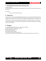
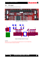
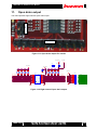
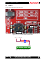
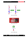
TBS-FMCL-CL Hardware User Manual
TBS-FMCL-CL
Hardware User Manual
Rev.1.01
Rev.1.01
1
TBS-FMCL-CL Hardware User Manual
Revision History
Version
Date
Description
Publisher
Rev.1.00
2012/07/23
Release version
Han
Rev.1.01
2014/06/19
Support information
Pang
Rev.1.01
2
TBS-FMCL-CL Hardware User Manual
Table of Contents
1.
2.
3.
4.
5.
6.
7.
Related Documents and Accessories ............................................................................................................................. 8
Overview..................................................................................................................................................................................... 8
Feature ........................................................................................................................................................................................ 8
Block Diagram .......................................................................................................................................................................... 9
Outlook of the Board ........................................................................................................................................................... 10
Board Dimensions ................................................................................................................................................................. 12
Cameralink connector interface ...................................................................................................................................... 13
7.1.
Frame Grabber input ................................................................................................................ 14
7.1.1.
Base Cameralink input...................................................................................................... 15
7.1.2.
Medium/Full Cameralink input .......................................................................................... 15
7.1.3.
PoCL or not ....................................................................................................................... 16
7.2.
Camera output .......................................................................................................................... 18
7.2.1.
Base Cameralink output ................................................................................................... 19
7.2.2.
Medium/Full Cameralink output ........................................................................................ 19
7.2.3.
PoCL or not ....................................................................................................................... 20
8. FMCL Connector Interface ............................................................................................................................................... 21
8.1.
Frame Grabber input ................................................................................................................ 22
8.1.1.
Base Cameralink input...................................................................................................... 22
8.1.2.
Medium/Full Cameralink input .......................................................................................... 26
8.2.
Camera output .......................................................................................................................... 30
8.2.1.
Base Cameralink output ................................................................................................... 30
8.2.2.
Medium/Full Cameralink output ........................................................................................ 34
9. Optocoupler input ................................................................................................................................................................. 38
10.
TTL input ............................................................................................................................................................................ 39
11.
Open drain output ........................................................................................................................................................... 40
12.
GPIO ..................................................................................................................................................................................... 41
13.
Others .................................................................................................................................................................................. 42
Rev.1.01
3
TBS-FMCL-CL Hardware User Manual
List of Figures
Figure 4-1 Block Diagram................................................................................................................... 9
Figure 5-1 Component Side ............................................................................................................. 10
Figure 5-2 Solder Side ...................................................................................................................... 11
Figure 6-1 Board Dimensions .......................................................................................................... 12
Figure 7-1 Two cameralink connector .............................................................................................. 13
Figure 7-2 Base/Medium/Full select Pin header .............................................................................. 14
Figure 7-3 Frame Grabber Base/Medium/Full select definitions...................................................... 14
Figure 7-4 CL1&CL2 Grabber Base(CN1&CN2) input Pin assign ................................................... 15
Figure 7-5 CL1+CL2 Grabber Medium/Full(CN1+CN2) input Pin assign ........................................ 15
Figure 7-6 PoCL or not select Pin header ........................................................................................ 16
Figure 7-7 Frame Grabber PoCL or not select................................................................................. 16
Figure 7-8 DC12V power supply Pin header ................................................................................... 17
Figure 7-9 DC12V power supply ...................................................................................................... 17
Figure 7-10 Base/Medium/Full select Pin header ............................................................................ 18
Figure 7-11 Frame Grabber Base/Medium/Full select definitions .................................................... 18
Figure 7-12 CL1&CL2 Camera Base(CN1&CN2) output Pin assign ............................................... 19
Figure 7-13 CL1+CL2 Camera Medium/Full(CN1+CN2) output Pin assign .................................... 19
Figure 7-14 PoCL or not select Pin header ...................................................................................... 20
Figure 7-15 Camera output PoCL or not select ............................................................................... 20
Figure 8-1 FMC Low Pin connector ................................................................................................. 21
Figure 8-2 FMC Low Pin connector definitions ................................................................................ 21
Figure 9-1 Optocoupler input Pin header ......................................................................................... 38
Figure 9-2 Four channel Optocoupler input ..................................................................................... 38
Figure 10-1 TTL input Pin header .................................................................................................... 39
Figure 10-2 Eight channel TTL input ................................................................................................ 39
Figure 11-1 Open drain output Pin header ....................................................................................... 40
Figure 11-2 Eight channel Open drain output .................................................................................. 40
Figure 12-1 GPIO Pin header .......................................................................................................... 41
Figure 12-2 Twelve channel GPIO inout .......................................................................................... 41
Figure 13-1 Power output Pin header and Power LED .................................................................... 42
Figure 13-2 Power output connector ................................................................................................ 42
Figure 13-3 LED indicator ................................................................................................................ 43
Figure 13-4 GND connector ............................................................................................................. 43
Figure 13-5 GND test pad ................................................................................................................ 43
List of Tables
Table 8-1 Frame Grabber Base Cameralink input Pin assign .......................................................... 22
Table 8-2 Frame Grabber Medium/Full Cameralink input Pin assign .............................................. 26
Table 8-3 Camera Base Cameralink output Pin assign ................................................................... 30
Table 8-4 Camera Medium/Full Cameralink output Pin assign ........................................................ 34
Rev.1.01
4
TBS-FMCL-CL Hardware User Manual
Introduction
Thank you for purchasing the TBS-FMCL-CL board. Before using the product, be sure to carefully read
this user manual and fully understand how to correctly use the product. First read through this manual,
then always keep it handy.
SAFETY PRECAUTIONS
Be sure to observe these precautions
Observe the precautions listed below to prevent injuries to you or other personnel or damage to property.
• Before using the product, read these safety precautions carefully to assure correct use.
• These precautions contain serious safety instructions that must be observed.
• After reading through this manual, be sure to always keep it handy.
The following conventions are used to indicate the possibility of injury/damage and classify precautions if
the product is handled incorrectly.
Danger
Indicates the high possibility of serious injury or death if the product is handled
incorrectly.
Indicates the possibility of serious injury or death if the product is handled
Warning
incorrectly.
Indicates the possibility of injury or physical damage in connection with houses or
Caution
household goods if the product is handled incorrectly.
The following graphical symbols are used to indicate and classify precautions in this manual.
(Examples)
Turn off the power switch.
Do not disassemble the product.
!
Rev.1.01
Do not attempt this.
5
TBS-FMCL-CL Hardware User Manual
Warning
In the event of a failure, disconnect the power supply.
If the product is used as is, a fire or electric shock may occur. Disconnect the power supply
immediately and contact our sales personnel for repair.
If an unpleasant smell or smoking occurs, disconnect the power supply.
If the product is used as is, a fire or electric shock may occur. Disconnect the power supply
immediately. After verifying that no smoking is observed, contact our sales personnel for
repair.
Do not disassemble, repair or modify the product.
Otherwise, a fire or electric shock may occur due to a short circuit or heat generation. For
inspection, modification or repair, contact our sales personnel.
!
Do not touch a cooling fan.
As a cooling fan rotates in high speed, do not put your hand close to it. Otherwise, it may
cause injury to persons. Never touch a rotating cooling fan.
!
Do not place the product on unstable locations.
Otherwise, it may drop or fall, resulting in injury to persons or failure.
!
If the product is dropped or damaged, do not use it as is.
!
Do not touch the product with a metallic object.
!
Do not place the product in dusty or humid locations or where water may
Otherwise, a fire or electric shock may occur.
Otherwise, a fire or electric shock may occur.
splash.
Otherwise, a fire or electric shock may occur.
!
!
Do not get the product wet or touch it with a wet hand.
Otherwise, the product may break down or it may cause a fire, smoking or electric shock.
Do not touch a connector on the product (gold-plated portion).
Otherwise, the surface of a connector may be contaminated with sweat or skin oil, resulting
in contact failure of a connector or it may cause a malfunction, fire or electric shock due to
static electricity.
Rev.1.01
6
TBS-FMCL-CL Hardware User Manual
Caution
Do not use or place the product in the following locations.
!
• Humid and dusty locations
• Airless locations such as closet or bookshelf
• Locations which receive oily smoke or steam
• Locations exposed to direct sunlight
• Locations close to heating equipment
• Closed inside of a car where the temperature becomes high
• Staticky locations
• Locations close to water or chemicals
Otherwise, a fire, electric shock, accident or deformation may occur due to a short circuit or heat
generation.
!
Do not place heavy things on the product.
Otherwise, the product may be damaged.
■ Disclaimer
This product is a board intended for 1000M Ethernet function. Tokyo Electron Device Limited assumes
no responsibility for any damages resulting from the use of this product for purposes other than those
stated.
Even if the product is used properly, Tokyo Electron Device Limited assumes no responsibility for any
damages caused by:
(1) Earthquake, thunder, natural disaster or fire resulting from the use beyond our responsibility, acts by
a third party or other accidents, the customer’s willful or accidental misuse or use under other
abnormal conditions.
(2) Secondary impact arising from use of this product or its unusable state (business interruption or
others)
(3) Use of this product against the instructions given in this manual.
(4) Malfunctions due to connection to other devices.
Tokyo Electron Device Limited assumes no responsibility or liability for:
(1) Erasure or corruption of data arising from use of this product.
(2) Any consequences or other abnormalities arising from use of this product, or
(3) Damage of this product not due to our responsibility or failure due to modification
This product has been developed by assuming its use for research, testing or evaluation. It is not
authorized for use in any system or application that requires high reliability.
Repair of this product is carried out by replacing it on a chargeable basis, not repairing the faulty devices.
However, non-chargeable replacement is offered for initial failure if such notification is received within
two weeks after delivery of the product.
The specification of this product is subject to change without prior notice.
The product is subject to discontinuation without prior notice.
Rev.1.01
7
TBS-FMCL-CL Hardware User Manual
1. Related Documents and Accessories
Related documents:
All documents relating to this board can be downloaded from our website. Please see attached paper on
the products.
Accessories
8 x Short Pin (Hirose HIF3GA-2.54SP)
2. Overview
The board has two Ports of Cameralink(SDR,26PIN) interface, you can use it as Frame Grabber input or
Camera output. When used as Frame Grabber, the board can be configured as two base input or one
medium input, or one full input. And also we can configure Frame Grabber as PoCL or not. When used
as Camera, the board can be configured as two base output or one medium output, or one full output.
And the board is designed for connection with the platform board with a FPGA Mezzanine Card (FMC)
Low-Pin Count connector.
3. Feature
Two Cameralink(SDR,26PIN) Connector : 3M’s 12226-5150-00FR
One FMCL Connector : Samtec’s ASP-134604-01
Max four channel Optocoupler input
Max eight channel TTL input
Eight channel Open drain output
Twelve channel GPIO(input or output or inout)
Power camera From the platform board(by FMCL) or External power supply(by power connector)
Rev.1.01
8
TBS-FMCL-CL Hardware User Manual
4. Block Diagram
Figure 4-1 shows the TBS-FMCL-CL board’s block diagram.
TBS-FMCL-CL
OPTO input
CN5
4
TTL input
CN6
Cameralink
CN2
8
11
GPIO
CN8
12
FMCL
CN3
CVK3.0
Camera / Frame Grabber
Base
Medium
Full
11
Base
Cameralink
CN1
OD output
CN7
8
Figure 4-1 Block Diagram
Rev.1.01
9
TBS-FMCL-CL Hardware User Manual
5. Outlook of the Board
Figure 5-1 and 5-2 shows the outlook of the TBS-FMCL-CL board.
Figure 5-1 Component Side
Rev.1.01
10
TBS-FMCL-CL Hardware User Manual
Figure 5-2 Solder Side
Rev.1.01
11
TBS-FMCL-CL Hardware User Manual
6. Board Dimensions
Figure 6-1 shows the board dimensions.
External Dimensions:
90 mm (W) x 69 mm (H)
Number of Layers:
4 layers
Board Thickness:
1.6 mm
Material:
FR-4
FMC Connector:
Samtec’s ASP-134604-01
Cameralink Connector:
3M’s 12226-5150-00FR
Figure 6-1 Board Dimensions
Rev.1.01
12
TBS-FMCL-CL Hardware User Manual
7. Cameralink connector interface
The TBS-FMCL-CL have two Cameralink connector(CN1,CN2), and them can be assigned different
Pin definitions when being used as Frame Grabber input board or Camera output board.
Figure 7-1 Two cameralink connector
Rev.1.01
13
TBS-FMCL-CL Hardware User Manual
7.1. Frame Grabber input
The Frame Grabber input board can be configured with two Base cameralink input port or one
medium/Full cameralink input port by jumper select.
JP2
JP10
JP3
JP11
Figure 7-2 Base/Medium/Full select Pin header
l
l
u
2 F
N /
Cem
u
&si
1ad
NBe
C M
3
P t
Jnr
&eo
2ph
POS
J
Figure 7-3 Frame Grabber Base/Medium/Full select definitions
Attention:
when CN2 used as Base cameralink input, Please short JP10 and JP11.
when CN2 used as Medium/Full cameralink input, Please Open JP10 and JP11.
Rev.1.01
14
TBS-FMCL-CL Hardware User Manual
defined as the flowing
4567890123456
1111112222222
4567890123456 4567890123456
1111112222222 1111112222222
)
K
2
d
d
3L210
Nl
l
e
e XCXXX
Ci
K
i
(
h3L210 _____ )h
l
M
M
M
M
M
m
1
+
G
C
X
X
X
X
S
S
u
r
FC
F _____hUUUUUrN
r
r
e
e
+
+
I
I
I
I
I
L
L
L
L
L
o
C
T
T
/e
e
D
D
D
D
D
k
321r
4
-l
---w
(
r
mnLLLLL0EEEEEwe
nC
CCCe
o
3c
e
210o
U
U
U
U
U
0
nC
sI
unF
CCCSSXXXXXP
FFFF1MMMMMPa
I
i
d
B
e
r
M
e
r
b
+
e
b
K
+
+
+
+
b
a
d
d
L
0
2
1
r
+
b
l
lG
d3C
e
e
a
X
X
X
X
K
e
+
+
+
+
i
i
r
+
h
3L210t_____h
1
G
M
M
M
M
M
a
G
S
XCXXXn
SL
r
U
U
U
U
U
C
F
2r_____i
r
rCe
-+-+T
I
I
I
I
I
T ++++e
LeLLLLLm
e
D
D
D
D
D
k
1
2
4
3
w
w
L
L
L
L
L
+
r
r
l
r
Co
n
n
E
E
E
E
E
oCCCCe
e
3c
210n
UUUUUe
n P
MMMMMI
CCCCSSXXXXXI
PFFFFFT
0123
0123
1234567891111 1234567891111
15
Rev.1.01
)
2
N
d
Cl
&e
1i
Nh
G+
r
CS
FC
r
+
+
e
(
Tr
T-k
e
321r
4
e
---w
l2
nC
s
CCCe
10o
e3c
a
nC
CCCSSXXXXXP
BI
r
e
b
b
a
r
d
G
l
e
i
2
+
h
L
G
S
C
r
r
&e-+-+FC +
T
T
e
k
1w4321r
+++n
+l
r
LoCCCCe
210n
e
3c
CPCCCCSSXXXXXI
0123
1234567891111
Medium/Full Cameralink input
7.1.2.
Base Cameralink input
7.1.1.
The CN1 and CN2 connector can be independently used as two Base cameralink input and PIN is
Figure 7-4 CL1&CL2 Grabber Base(CN1&CN2) input Pin assign
cameralink input and PIN is defined as the flowing
The CN1 and CN2 connector can be together used as one Medium cameralink input or one Full
Figure 7-5 CL1+CL2 Grabber Medium/Full(CN1+CN2) input Pin assign
TBS-FMCL-CL Hardware User Manual
7.1.3.
PoCL or not
The Frame Grabber board can be configured with PoCL or not
JP4
JP1
Figure 7-6 PoCL or not select Pin header
2 L
N C
CLo
C
/o
P
1
t
NPo
C n
t
r
o
h
S
4
P22
J/1
3
1
P
J
Figure 7-7 Frame Grabber PoCL or not select
Rev.1.01
16
TBS-FMCL-CL Hardware User Manual
When used as PoCL, you must select DC12V power supply from FMCL (short JP12) or from CN4
connector (Open JP12).
JP12
CN4
Figure 7-8 DC12V power supply Pin header
JS12
VCC_12P
HIF3GA-2.54SP
JP12
VCC_12
2
1
A2-2PA-2.54DSA(71)
CN4
1
2
C13
47uF_25V
D
NVN
2G
C1
V
2
112
A2-2PA-2.54DSA(71)
DGND
DGND
Figure 7-9 DC12V power supply
Rev.1.01
17
TBS-FMCL-CL Hardware User Manual
7.2. Camera output
The Camera output board can be configured with two Base cameralink output port or one medium/Full
cameralink output port by jumper select.
JP2
JP10
JP3
JP11
Figure 7-10 Base/Medium/Full select Pin header
l
l
u
2 F
N /
Cem
u
&si
1ad
NBe
C M
3
P t
Jnr
&eo
2ph
POS
J
Figure 7-11 Frame Grabber Base/Medium/Full select definitions
Attention:
when CN2 used as Base cameralink output, Please short JP10 and JP11.
when CN2 used as Medium/Full cameralink output, Please Open JP10 and JP11.
Rev.1.01
18
TBS-FMCL-CL Hardware User Manual
4567890123456
1111112222222
0123
34567891111
4567890123456 4567890123456
1111112222222 1111112222222
12
0123
34567891111
0123
34567891111
+
)
K
+
+
+
+
2
d0
d
12L3
+
Ne
l
l
e
XXXCXd
K
+
+
e
+
+
Ci
i
_
_
_
_
_
t
+
(
012L3 1
hM
)h
MMMMa
l
-G
C
X
X
S
X
S
X
u
n
r
r
C
_
_
_
_
_
N
F+-+-e
F UUUUUi
r
r
+
e
I
I
I
I
I
L
L
L
L
L
T
T
m
C
/e
e
D
D
D
D
D
k
1234w
w
L
L
L
L
L
++l
+
+r
r
(
r
n0
mnEEEEEe
CCCCo
12c
3e
e
e
UUUUUos
n
nX
MMMMMT
uI
XXXXSSCCCCP
FFFFFPa
I
i
d
B
e
a
M
r
e
a
r
K
m
e
d
d
a
l
l
m 012L3
e
e
C
C
X
X
X
X
K
i
i
a _
_
_
_
_
h
C M
MMMMm012L3h1
+
G
C
S
X
X
S
X
X
CF-+-+r
2rUUUUUh_____ Lr
C
r
e
e
I
I
I
I
I
L
L
L
L
L
o
T
T
Lw
e
e
D
D
D
D
D
k
1234n
w
L
L
L
L
L
r
r
0
l
Co
n o
E
E
E
E
E
CCCCn
3e
e
012c
0UUUUUn
PMMMMM1
FFFFFI PXXXXXSSCCCCI
12
19
Rev.1.01
)
2
N
d
Cl
&e
i
+
1h
G
NS
r
CF+-+-e
Cr
+ T
(
T
e
k
e
n+++l+rr1234w
s
n012c3eeCCCCo
a
BIXXXXXSSCCCCP
a
r
e
m
a
d
C
l
e
i
2
h
L
+G
S
C
r
C
F
r
- T
-+-+e
&e
T1
k
234n
-r
1w---l
r
CCCCn
Lo012c
3e
e
CPXXXXXSSCCCCI
defined as the flowing
12
Medium/Full Cameralink output
7.2.2.
Base Cameralink output
7.2.1.
The CN1 and CN2 connector can be independently used as two Base cameralink output and PIN is
Figure 7-12 CL1&CL2 Camera Base(CN1&CN2) output Pin assign
cameralink output and PIN is defined as the flowing
The CN1 and CN2 connector can be together used as one Medium cameralink output or one Full
Figure 7-13 CL1+CL2 Camera Medium/Full(CN1+CN2) output Pin assign
TBS-FMCL-CL Hardware User Manual
7.2.3.
PoCL or not
The Camera output board’s PoCL or not must be selected according to the Frame Grabber board’s
definitions..
JP4
JP1
Figure 7-14 PoCL or not select Pin header
t
4no
r
e
P
p
h
J
O
S
&
1
3
2
P
J
2
1
r
e
b
b
a
L
r
C
L
G
o
C
ro
P
e
t
P
m
o
a
n
r
F
Figure 7-15 Camera output PoCL or not select
Attention:
Please sure PoCL or not ’setting is no problem before power on
Rev.1.01
20
TBS-FMCL-CL Hardware User Manual
8. FMCL Connector Interface
The board provides Samtec’s FMC Low Pin connector(CN3).
Figure 8-1 FMC Low Pin connector
Figure 8-2 FMC Low Pin connector definitions
And Pin definitions are different when function as Frame Grabber input board or Camera output board,
Rev.1.01
21
TBS-FMCL-CL Hardware User Manual
8.1. Frame Grabber input
8.1.1. Base Cameralink input
Table 8-1 Frame Grabber Base Cameralink input Pin assign
C line (Frame Grabber Base Cameralink input FMCL)
No
FMCL Definitions
I/O
Signal
Described
1
2
3
4
5
6
7
8
9
10
11
12
13
14
15
16
17
18
19
20
21
22
23
24
25
26
27
28
29
30
31
32
33
34
35
36
37
38
39
40
GND
DP0_C2M_P
DP0_C2M_N
GND
GND
DP0_M2C_P
DP0_M2C_N
GND
GND
LA06_P
LA06_N
GND
GND
LA10_P
LA10_N
GND
GND
LA14_P
LA14_N
GND
GND
LA18_P_CC
LA18_N_CC
GND
GND
LA27_P
LA27_N
GND
GND
SCL
SDA
GND
GND
GA0
12P0V
GND
12P0V
GND
3P3V
GND
I
I
I/O
I/O
I/O
I/O
O
O
O
O
-
N/C
N/C
N/C
N/C
FP_TTL_I2
FP_TTL_I1
FP_IO_11
FP_IO_12
FP_IO_6
FP_IO_3
FP_OD_O1
FP_OD_O2
FP_OD_O7
FP_OD_O8
N/C
N/C
N/C
VCC_12P
VCC_12P
N/C
-
FPGA TTL input 2
FPGA TTL input 1
FPGA GPIO inout 11
FPGA GPIO inout 12
FPGA GPIO inout 6
FPGA GPIO inout 3
FPGA Open Drain output 1
FPGA Open Drain output 2
FPGA Open Drain output 7
FPGA Open Drain output 8
12V Power
12V Power
-
Rev.1.01
-
22
TBS-FMCL-CL Hardware User Manual
D line (Frame Grabber Base Cameralink input FMCL)
No
1
2
3
4
5
6
7
8
9
10
11
12
13
14
15
16
17
18
19
20
21
22
23
24
25
26
27
28
29
30
31
32
33
34
35
36
37
38
39
40
FMCL Definitions
I/O
PG_C2M
GND
GND
GBTCLK0_M2C_P
GBTCLK0_M2C_N GND
GND
LA01_P_CC
I
LA01_N_CC
I
GND
LA05_P
I
LA05_N
I
GND
LA09_P
I
LA09_N
I
GND
LA13_P
I/O
LA13_N
I/O
GND
LA17_P_CC
O
LA17_N_CC
O
GND
LA23_P
O
LA23_N
O
GND
LA26_P
O
LA26_N
O
GND
TCK
TDI
TDO
3P3VAUX
TMS
TRST_L
GA1
3P3V
GND
3P3V
GND
3P3V
-
Rev.1.01
Signal
Described
N/C
N/C
N/C
FP_TTL_I4
FP_TTL_I3
FP_TTL_I5
FP_TTL_I6
FP_TTL_I7
FP_TTL_I8
FP_IO_9
FP_IO_10
CL2_CC3P
CL2_CC3N
FP_OD_O3
FP_OD_O4
FP_OD_O6
FP_OD_O5
N/C
N/C
N/C
N/C
N/C
N/C
N/C
N/C
N/C
N/C
FPGA TTL input 4
FPGA TTL input 3
FPGA TTL input 5
FPGA TTL input 6
FPGA TTL input 7
FPGA TTL input 8
FPGA GPIO inout 9
FPGA GPIO inout 10
CL2 Base Camera control singal 3’P side
CL2 Base Camera control singal 3’N side
FPGA Open Drain output 3
FPGA Open Drain output 4
FPGA Open Drain output 6
FPGA Open Drain output 5
-
23
TBS-FMCL-CL Hardware User Manual
G line (Frame Grabber Base Cameralink input FMCL)
No
FMCL Definitions
I/O
Signal
Described
1
2
3
4
5
6
7
8
9
10
11
12
13
14
15
16
17
18
19
20
21
22
23
24
25
26
27
28
29
30
31
32
33
34
35
36
37
38
39
40
GND
CLK1_M2C_P
CLK1_M2C_N
GND
GND
LA00_P_CC
LA00_N_CC
GND
LA03_P
LA03_N
GND
LA08_P
LA08_N
GND
LA12_P
LA12_N
GND
LA16_P
LA16_N
GND
LA20_P
LA20_N
GND
LA22_P
LA22_N
GND
LA25_P
LA25_N
GND
LA29_P
LA29_N
GND
LA31_P
LA31_N
GND
LA33_P
LA33_N
GND
VADJ
GND
I
I
I
I
I
I
O
O
I
I
I/O
I/O
I/O
I/O
I
I
I
I
O
O
I
I
O
O
-
CL1_XCLKP
CL1_XCLKN
CL2_X0P
CL2_X0N
CL2_X2P
CL2_X2N
CL2_SERTCP_F
CL2_SERTCN_F
CL2_SERTFGP
CL2_SERTFGN
FP_IO_7
FP_IO_8
FP_IO_1
FP_IO_2
CL1_X0P
CL1_X0N
CL1_X2P
CL1_X2N
CL1_SERTCP_F
CL1_SERTCN_F
CL1_SERTFGP
CL1_SERTFGN
CL1_CC3P
CL1_CC3N
VCC_VADJ
-
CL1 Base clock singal’P side
CL1 Base clock singal’N side
CL2 Base data singal 0’P side
CL2 Base data singal 0’N side
CL2 Base data singal 2’P side
CL2 Base data singal 2’N side
CL2 Base Serial to Camera signal’P side
CL2 Base Serial to Camera signal’N side
CL2 Base Serial to Grabber signal’P side
CL2 Base Serial to Grabber signal’N side
FPGA GPIO inout 7
FPGA GPIO inout 8
FPGA GPIO inout 1
FPGA GPIO inout 2
CL1 Base data singal 0’P side
CL1 Base data singal 0’N side
CL1 Base data singal 2’P side
CL1 Base data singal 2’N side
CL1 Base Serial to Camera signal’P side
CL1 Base Serial to Camera signal’N side
CL1 Base Serial to Grabber signal’P side
CL1 Base Serial to Grabber signal’N side
CL1 Base Camera control singal 3’P side
CL1 Base Camera control singal 3’N side
VADJ power(3.3V or 2.5V)
-
Rev.1.01
24
TBS-FMCL-CL Hardware User Manual
H line (Frame Grabber Base Cameralink input FMCL)
No
FMCL Definitions
I/O
Signal
Described
1
2
3
4
5
6
7
8
9
10
11
12
13
14
15
16
17
18
19
20
21
22
23
24
25
26
27
28
29
30
31
32
33
34
35
36
37
38
39
40
VREF_A_M2C
PRSNT_M2C_L
GND
CLK0_M2C_P
CLK0_M2C_N
GND
LA02_P
LA02_N
GND
LA04_P
LA04_N
GND
LA07_P
LA07_N
GND
LA11_P
LA11_N
GND
LA15_P
LA15_N
GND
LA19_P
LA19_N
GND
LA21_P
LA21_N
GND
LA24_P
LA24_N
GND
LA28_P
LA28_N
GND
LA30_P
LA30_N
GND
LA32_P
LA32_N
GND
VADJ
I
I
I
I
I
I
O
O
O
O
I/O
I/O
O
O
I
I
I
I
O
O
O
O
O
O
-
N/C
N/C
CL2_XCLKP
CL2_XCLKN
CL2_X1P
CL2_X1N
CL2_X3P
CL2_X3N
CL2_CC1P
CL2_CC1N
CL2_CC2P
CL2_CC2N
FP_IO_5
FP_IO_4
CL2_CC4P
CL2_CC4N
CL1_X1P
CL1_X1N
CL1_X3P
CL1_X3N
CL1_CC1P
CL1_CC1N
CL1_CC2P
CL1_CC2N
CL1_CC4P
CL1_CC4N
VCC_VADJ
CL2 Base clock singal’P side
CL2 Base clock singal’N side
CL2 Base data singal 1’P side
CL2 Base data singal 1’N side
CL2 Base data singal 3’P side
CL2 Base data singal 3’N side
CL2 Base Camera control singal 1’P side
CL2 Base Camera control singal 1’N side
CL2 Base Camera control singal 2’P side
CL2 Base Camera control singal 2’N side
FPGA GPIO inout 5
FPGA GPIO inout 4
CL2 Base Camera control singal 4’P side
CL2 Base Camera control singal 4’N side
CL1 Base data singal 1’P side
CL1 Base data singal 1’N side
CL1 Base data singal 3’P side
CL1 Base data singal 3’N side
CL1 Base Camera control singal 1’P side
CL1 Base Camera control singal 1’N side
CL1 Base Camera control singal 2’P side
CL1 Base Camera control singal 2’N side
CL1 Base Camera control singal 4’P side
CL1 Base Camera control singal 4’N side
VADJ power(3.3V or 2.5V)
Rev.1.01
25
TBS-FMCL-CL Hardware User Manual
8.1.2.
Medium/Full Cameralink input
Table 8-2 Frame Grabber Medium/Full Cameralink input Pin assign
C line (Frame Grabber Medium/Full Cameralink input FMCL)
No
FMCL Definitions
I/O
Signal
Described
1
2
3
4
5
6
7
8
9
10
11
12
13
14
15
16
17
18
19
20
21
22
23
24
25
26
27
28
29
30
31
32
33
34
35
36
37
38
39
40
GND
DP0_C2M_P
DP0_C2M_N
GND
GND
DP0_M2C_P
DP0_M2C_N
GND
GND
LA06_P
LA06_N
GND
GND
LA10_P
LA10_N
GND
GND
LA14_P
LA14_N
GND
GND
LA18_P_CC
LA18_N_CC
GND
GND
LA27_P
LA27_N
GND
GND
SCL
SDA
GND
GND
GA0
12P0V
GND
12P0V
GND
3P3V
GND
I
I
I/O
I/O
I/O
I/O
O
O
O
O
-
N/C
N/C
N/C
N/C
FP_TTL_I2
FP_TTL_I1
FP_IO_11
FP_IO_12
FP_IO_6
FP_IO_3
FP_OD_O1
FP_OD_O2
FP_OD_O7
FP_OD_O8
N/C
N/C
N/C
VCC_12P
VCC_12P
N/C
-
FPGA TTL input 2
FPGA TTL input 1
FPGA GPIO inout 11
FPGA GPIO inout 12
FPGA GPIO inout 6
FPGA GPIO inout 3
FPGA Open Drain output 1
FPGA Open Drain output 2
FPGA Open Drain output 7
FPGA Open Drain output 8
12V Power
12V Power
-
Rev.1.01
-
26
TBS-FMCL-CL Hardware User Manual
D line (Frame Grabber Medium/Full Cameralink input FMCL)
No
1
2
3
4
5
6
7
8
9
10
11
12
13
14
15
16
17
18
19
20
21
22
23
24
25
26
27
28
29
30
31
32
33
34
35
36
37
38
39
40
FMCL Definitions
I/O
PG_C2M
GND
GND
GBTCLK0_M2C_P
GBTCLK0_M2C_N GND
GND
LA01_P_CC
I
LA01_N_CC
I
GND
LA05_P
I
LA05_N
I
GND
LA09_P
I
LA09_N
I
GND
LA13_P
I/O
LA13_N
I/O
GND
LA17_P_CC
I
LA17_N_CC
I
GND
LA23_P
O
LA23_N
O
GND
LA26_P
O
LA26_N
O
GND
TCK
TDI
TDO
3P3VAUX
TMS
TRST_L
GA1
3P3V
GND
3P3V
GND
3P3V
-
Rev.1.01
Signal
Described
N/C
N/C
N/C
FP_TTL_I4
FP_TTL_I3
FP_TTL_I5
FP_TTL_I6
FP_TTL_I7
FP_TTL_I8
FP_IO_9
FP_IO_10
CL2_FULL_CLKP
CL2_FULL_CLKN
FP_OD_O3
FP_OD_O4
FP_OD_O6
FP_OD_O5
N/C
N/C
N/C
N/C
N/C
N/C
N/C
N/C
N/C
N/C
FPGA TTL input 4
FPGA TTL input 3
FPGA TTL input 5
FPGA TTL input 6
FPGA TTL input 7
FPGA TTL input 8
FPGA GPIO inout 9
FPGA GPIO inout 10
CL2 Full Clock singal’P side
CL2 Full Clock singal’N side
FPGA Open Drain output 3
FPGA Open Drain output 4
FPGA Open Drain output 6
FPGA Open Drain output 5
-
27
TBS-FMCL-CL Hardware User Manual
G line (Frame Grabber Medium/Full Cameralink input FMCL)
No
FMCL Definitions
I/O
Signal
Described
1
2
3
4
5
6
7
8
9
10
11
12
13
14
15
16
17
18
19
20
21
22
23
24
25
26
27
28
29
30
31
32
33
34
35
36
37
38
39
40
GND
CLK1_M2C_P
CLK1_M2C_N
GND
GND
LA00_P_CC
LA00_N_CC
GND
LA03_P
LA03_N
GND
LA08_P
LA08_N
GND
LA12_P
LA12_N
GND
LA16_P
LA16_N
GND
LA20_P
LA20_N
GND
LA22_P
LA22_N
GND
LA25_P
LA25_N
GND
LA29_P
LA29_N
GND
LA31_P
LA31_N
GND
LA33_P
LA33_N
GND
VADJ
GND
I
I
I
I
I
I
I
I
I/O
I/O
I/O
I/O
I
I
I
I
O
O
I
I
O
O
-
CL1_XCLKP
CL1_XCLKN
CL2_MEDIUM_X0P
CL2_MEDIUM _X0N
CL2_ MEDIUM _X2P
CL2_ MEDIUM _X2N
N/C
N/C
CL2_ FULL _X0P
CL2_ FULL _X0N
FP_IO_7
FP_IO_8
FP_IO_1
FP_IO_2
CL1_X0P
CL1_X0N
CL1_X2P
CL1_X2N
CL1_SERTCP_F
CL1_SERTCN_F
CL1_SERTFGP
CL1_SERTFGN
CL1_CC3P
CL1_CC3N
VCC_VADJ
-
CL1 Base clock singal’P side
CL1 Base clock singal’N side
CL2 Medium data singal 0’P side
CL2 Medium data singal 0’N side
CL2 Medium data singal 2’P side
CL2 Medium data singal 2’N side
CL2 Full data singal 0’P side
CL2 Full data singal 0’N side
FPGA GPIO inout 7
FPGA GPIO inout 8
FPGA GPIO inout 1
FPGA GPIO inout 2
CL1 Base data singal 0’P side
CL1 Base data singal 0’N side
CL1 Base data singal 2’P side
CL1 Base data singal 2’N side
CL1 Base Serial to Camera signal’P side
CL1 Base Serial to Camera signal’N side
CL1 Base Serial to Grabber signal’P side
CL1 Base Serial to Grabber signal’N side
CL1 Base Camera control singal 3’P side
CL1 Base Camera control singal 3’N side
VADJ power(3.3V or 2.5V)
-
Rev.1.01
28
TBS-FMCL-CL Hardware User Manual
H line (Frame Grabber Medium/Full Cameralink input FMCL)
No
FMCL Definitions
I/O
Signal
Described
1
2
3
4
5
6
7
8
9
10
11
12
13
14
15
16
17
18
19
20
21
22
23
24
25
26
27
28
29
30
31
32
33
34
35
36
37
38
39
40
VREF_A_M2C
PRSNT_M2C_L
GND
CLK0_M2C_P
CLK0_M2C_N
GND
LA02_P
LA02_N
GND
LA04_P
LA04_N
GND
LA07_P
LA07_N
GND
LA11_P
LA11_N
GND
LA15_P
LA15_N
GND
LA19_P
LA19_N
GND
LA21_P
LA21_N
GND
LA24_P
LA24_N
GND
LA28_P
LA28_N
GND
LA30_P
LA30_N
GND
LA32_P
LA32_N
GND
VADJ
I
I
I
I
I
I
I
I
I
I
I/O
I/O
I
I
I
I
I
I
O
O
O
O
O
O
-
N/C
N/C
CL2_MEDIUM_CLKP
CL2_MEDIUM_CLKN
CL2_ MEDIUM_X1P
CL2_ MEDIUM_X1N
CL2_ MEDIUM_X3P
CL2_ MEDIUM_X3N
CL2_FULL_X1P
CL2_FULL_X1N
CL2_FULL_X2N
CL2_FULL_X2P
FP_IO_5
FP_IO_4
CL2_FULL_X4N
CL2_FULL_X4P
CL1_X1P
CL1_X1N
CL1_X3P
CL1_X3N
CL1_CC1P
CL1_CC1N
CL1_CC2P
CL1_CC2N
CL1_CC4P
CL1_CC4N
VCC_VADJ
CL2 Medium clock singal’P side
CL2 Medium clock singal’N side
CL2 Medium data singal 1’P side
CL2 Medium data singal 1’N side
CL2 Medium data singal 3’P side
CL2 Medium data singal 3’N side
CL2 Full data singal 1’P side
CL2 Full data singal 1’N side
CL2 Full data singal 2’N side
CL2 Full data singal 2’P side
FPGA GPIO inout 5
FPGA GPIO inout 4
CL2 Full data singal 4’N side
CL2 Full data singal 4’P side
CL1 Base data singal 1’P side
CL1 Base data singal 1’N side
CL1 Base data singal 3’P side
CL1 Base data singal 3’N side
CL1 Base Camera control singal 1’P side
CL1 Base Camera control singal 1’N side
CL1 Base Camera control singal 2’P side
CL1 Base Camera control singal 2’N side
CL1 Base Camera control singal 4’P side
CL1 Base Camera control singal 4’N side
VADJ power(3.3V or 2.5V)
Rev.1.01
29
TBS-FMCL-CL Hardware User Manual
8.2. Camera output
8.2.1. Base Cameralink output
Table 8-3 Camera Base Cameralink output Pin assign
C line (Camera Base Cameralink output FMCL)
No
FMCL Definitions
I/O
Signal
Described
1
2
3
4
5
6
7
8
9
10
11
12
13
14
15
16
17
18
19
20
21
22
23
24
25
26
27
28
29
30
31
32
33
34
35
36
37
38
39
40
GND
DP0_C2M_P
DP0_C2M_N
GND
GND
DP0_M2C_P
DP0_M2C_N
GND
GND
LA06_P
LA06_N
GND
GND
LA10_P
LA10_N
GND
GND
LA14_P
LA14_N
GND
GND
LA18_P_CC
LA18_N_CC
GND
GND
LA27_P
LA27_N
GND
GND
SCL
SDA
GND
GND
GA0
12P0V
GND
12P0V
GND
3P3V
GND
I
I
I/O
I/O
I/O
I/O
O
O
O
O
-
N/C
N/C
N/C
N/C
FP_TTL_I2
FP_TTL_I1
FP_IO_11
FP_IO_12
FP_IO_6
FP_IO_3
FP_OD_O1
FP_OD_O2
FP_OD_O7
FP_OD_O8
N/C
N/C
N/C
VCC_12P
VCC_12P
N/C
-
FPGA TTL input 2
FPGA TTL input 1
FPGA GPIO inout 11
FPGA GPIO inout 12
FPGA GPIO inout 6
FPGA GPIO inout 3
FPGA Open Drain output 1
FPGA Open Drain output 2
FPGA Open Drain output 7
FPGA Open Drain output 8
12V Power
12V Power
-
Rev.1.01
-
30
TBS-FMCL-CL Hardware User Manual
D line (Camera Base Cameralink output FMCL)
No
1
2
3
4
5
6
7
8
9
10
11
12
13
14
15
16
17
18
19
20
21
22
23
24
25
26
27
28
29
30
31
32
33
34
35
36
37
38
39
40
FMCL Definitions
I/O
PG_C2M
GND
GND
GBTCLK0_M2C_P
GBTCLK0_M2C_N GND
GND
LA01_P_CC
I
LA01_N_CC
I
GND
LA05_P
I
LA05_N
I
GND
LA09_P
I
LA09_N
I
GND
LA13_P
I/O
LA13_N
I/O
GND
LA17_P_CC
O
LA17_N_CC
O
GND
LA23_P
O
LA23_N
O
GND
LA26_P
O
LA26_N
O
GND
TCK
TDI
TDO
3P3VAUX
TMS
TRST_L
GA1
3P3V
GND
3P3V
GND
3P3V
-
Rev.1.01
Signal
Described
N/C
N/C
N/C
FP_TTL_I4
FP_TTL_I3
FP_TTL_I5
FP_TTL_I6
FP_TTL_I7
FP_TTL_I8
FP_IO_9
FP_IO_10
CL2_X1N
CL2_X1P
FP_OD_O3
FP_OD_O4
FP_OD_O6
FP_OD_O5
N/C
N/C
N/C
N/C
N/C
N/C
N/C
N/C
N/C
N/C
FPGA TTL input 4
FPGA TTL input 3
FPGA TTL input 5
FPGA TTL input 6
FPGA TTL input 7
FPGA TTL input 8
FPGA GPIO inout 9
FPGA GPIO inout 10
CL2 Base data singal 1’N side
CL2 Base data singal 1’P side
FPGA Open Drain output 3
FPGA Open Drain output 4
FPGA Open Drain output 6
FPGA Open Drain output 5
-
31
TBS-FMCL-CL Hardware User Manual
G line (Camera Base Cameralink output FMCL)
No
FMCL Definitions
I/O
Signal
Described
1
2
3
4
5
6
7
8
9
10
11
12
13
14
15
16
17
18
19
20
21
22
23
24
25
26
27
28
29
30
31
32
33
34
35
36
37
38
39
40
GND
CLK1_M2C_P
CLK1_M2C_N
GND
GND
LA00_P_CC
LA00_N_CC
GND
LA03_P
LA03_N
GND
LA08_P
LA08_N
GND
LA12_P
LA12_N
GND
LA16_P
LA16_N
GND
LA20_P
LA20_N
GND
LA22_P
LA22_N
GND
LA25_P
LA25_N
GND
LA29_P
LA29_N
GND
LA31_P
LA31_N
GND
LA33_P
LA33_N
GND
VADJ
GND
I
I
I
I
I
I
I
I
O
O
I/O
I/O
I/O
I/O
I
I
I
I
I
I
O
O
O
O
-
CL1_CC1N
CL1_CC1P
CL2_CC4P
CL2_CC4N
CL2_CC2P
CL2_CC2N
CL2_SERTCN_F
CL2_SERTCP_F
CL2_X3N
CL2_X3P
FP_IO_7
FP_IO_8
FP_IO_1
FP_IO_2
CL1_CC4P
CL1_CC4N
CL1_CC2P
CL1_CC2N
CL1_SERTCN_F
CL1_SERTCP_F
CL1_X3N
CL1_X3P
CL1_X1N
CL1_X1P
VCC_VADJ
-
CL1 Base Camera control singal 1’N side
CL1 Base Camera control singal 1’P side
CL2 Base Camera control singal 4’P side
CL2 Base Camera control singal 4’N side
CL2 Base Camera control singal 2’P side
CL2 Base Camera control singal 2’N side
CL2 Base Serial to Camera signal’N side
CL2 Base Serial to Camera signal’P side
CL2 Base data signal 3’N side
CL2 Base data signal 3’P side
FPGA GPIO inout 7
FPGA GPIO inout 8
FPGA GPIO inout 1
FPGA GPIO inout 2
CL1 Base Camera control singal 4’P side
CL1 Base Camera control singal 4’N side
CL1 Base Camera control singal 2’P side
CL1 Base Camera control singal 2’N side
CL1 Base Serial to Camera signal’N side
CL1 Base Serial to Camera signal’P side
CL1 Base data signal 3’N side
CL1 Base data signal 3’P side
CL1 Base data signal 1’N side
CL1 Base data signal 1’P side
VADJ power(3.3V or 2.5V)
-
Rev.1.01
32
TBS-FMCL-CL Hardware User Manual
H line (Camera Base Cameralink output FMCL)
No
FMCL Definitions
I/O
Signal
Described
1
2
3
4
5
6
7
8
9
10
11
12
13
14
15
16
17
18
19
20
21
22
23
24
25
26
27
28
29
30
31
32
33
34
35
36
37
38
39
40
VREF_A_M2C
PRSNT_M2C_L
GND
CLK0_M2C_P
CLK0_M2C_N
GND
LA02_P
LA02_N
GND
LA04_P
LA04_N
GND
LA07_P
LA07_N
GND
LA11_P
LA11_N
GND
LA15_P
LA15_N
GND
LA19_P
LA19_N
GND
LA21_P
LA21_N
GND
LA24_P
LA24_N
GND
LA28_P
LA28_N
GND
LA30_P
LA30_N
GND
LA32_P
LA32_N
GND
VADJ
I
I
I
I
O
O
O
O
O
O
I/O
I/O
O
O
I
I
O
O
O
O
O
O
O
O
-
N/C
N/C
CL2_CC1N
CL2_CC1P
CL2_CC3N
CL2_CC3P
CL2_SERTFGN
CL2_SERTFGP
CL2_XCLKN
CL2_XCLKP
CL2_X2P
CL2_X2N
FP_IO_5
FP_IO_4
CL2_X0P
CL2_X0N
CL1_CC3N
CL1_CC3P
CL1_SERTFGN
CL1_SERTFGP
CL1_XCLKN
CL1_XCLKP
CL1_X2P
CL1_X2N
CL1_X0P
CL1_X0N
VCC_VADJ
CL2 Base Camera control singal 1’N side
CL2 Base Camera control singal 1’P side
CL2 Base Camera control singal 3’N side
CL2 Base Camera control singal 3’P side
CL2 Base Serial to Grabber signal’N side
CL2 Base Serial to Grabber signal’P side
CL2 Base clock singal’N side
CL2 Base clock singal’P side
CL2 Base data singal 2’P side
CL2 Base data singal 2’N side
FPGA GPIO inout 5
FPGA GPIO inout 4
CL2 Base data singal 0’P side
CL2 Base data singal 0’N side
CL1 Base Camera control singal 1’N side
CL1 Base Camera control singal 1’P side
CL1 Base Serial to Grabber signal’N side
CL1 Base Serial to Grabber signal’P side
CL1 Base clock singal’N side
CL1 Base clock singal’P side
CL1 Base data singal 2’P side
CL1 Base data singal 2’N side
CL1 Base data singal 0’P side
CL1 Base data singal 0’N side
VADJ power(3.3V or 2.5V)
Rev.1.01
33
TBS-FMCL-CL Hardware User Manual
8.2.2.
Medium/Full Cameralink output
Table 8-4 Camera Medium/Full Cameralink output Pin assign
C line (Camera Medium/Full Cameralink output FMCL)
No
FMCL Definitions
I/O
Signal
Described
1
2
3
4
5
6
7
8
9
10
11
12
13
14
15
16
17
18
19
20
21
22
23
24
25
26
27
28
29
30
31
32
33
34
35
36
37
38
39
40
GND
DP0_C2M_P
DP0_C2M_N
GND
GND
DP0_M2C_P
DP0_M2C_N
GND
GND
LA06_P
LA06_N
GND
GND
LA10_P
LA10_N
GND
GND
LA14_P
LA14_N
GND
GND
LA18_P_CC
LA18_N_CC
GND
GND
LA27_P
LA27_N
GND
GND
SCL
SDA
GND
GND
GA0
12P0V
GND
12P0V
GND
3P3V
GND
I
I
I/O
I/O
I/O
I/O
O
O
O
O
-
N/C
N/C
N/C
N/C
FP_TTL_I2
FP_TTL_I1
FP_IO_11
FP_IO_12
FP_IO_6
FP_IO_3
FP_OD_O1
FP_OD_O2
FP_OD_O7
FP_OD_O8
N/C
N/C
N/C
VCC_12P
VCC_12P
N/C
-
FPGA TTL input 2
FPGA TTL input 1
FPGA GPIO inout 11
FPGA GPIO inout 12
FPGA GPIO inout 6
FPGA GPIO inout 3
FPGA Open Drain output 1
FPGA Open Drain output 2
FPGA Open Drain output 7
FPGA Open Drain output 8
12V Power
12V Power
-
Rev.1.01
-
34
TBS-FMCL-CL Hardware User Manual
D line (Camera Medium/Full Cameralink output FMCL)
No
1
2
3
4
5
6
7
8
9
10
11
12
13
14
15
16
17
18
19
20
21
22
23
24
25
26
27
28
29
30
31
32
33
34
35
36
37
38
39
40
FMCL Definitions
I/O
PG_C2M
GND
GND
GBTCLK0_M2C_P
GBTCLK0_M2C_N GND
GND
LA01_P_CC
I
LA01_N_CC
I
GND
LA05_P
I
LA05_N
I
GND
LA09_P
I
LA09_N
I
GND
LA13_P
I/O
LA13_N
I/O
GND
LA17_P_CC
O
LA17_N_CC
O
GND
LA23_P
O
LA23_N
O
GND
LA26_P
O
LA26_N
O
GND
TCK
TDI
TDO
3P3VAUX
TMS
TRST_L
GA1
3P3V
GND
3P3V
GND
3P3V
-
Rev.1.01
Signal
Described
N/C
N/C
N/C
FP_TTL_I4
FP_TTL_I3
FP_TTL_I5
FP_TTL_I6
FP_TTL_I7
FP_TTL_I8
FP_IO_9
FP_IO_10
CL2_MEDIUM_X1N
CL2_MEDIUM_X1P
FP_OD_O3
FP_OD_O4
FP_OD_O6
FP_OD_O5
N/C
N/C
N/C
N/C
N/C
N/C
N/C
N/C
N/C
N/C
FPGA TTL input 4
FPGA TTL input 3
FPGA TTL input 5
FPGA TTL input 6
FPGA TTL input 7
FPGA TTL input 8
FPGA GPIO inout 9
FPGA GPIO inout 10
CL2 Medium data singal 1’N side
CL2 Medium data singal 1’P side
FPGA Open Drain output 3
FPGA Open Drain output 4
FPGA Open Drain output 6
FPGA Open Drain output 5
-
35
TBS-FMCL-CL Hardware User Manual
G line (Camera Medium/Full Cameralink output FMCL)
No
FMCL Definitions
I/O
Signal
Described
1
2
3
4
5
6
7
8
9
10
11
12
13
14
15
16
17
18
19
20
21
22
23
24
25
26
27
28
29
30
31
32
33
34
35
36
37
38
39
40
GND
CLK1_M2C_P
CLK1_M2C_N
GND
GND
LA00_P_CC
LA00_N_CC
GND
LA03_P
LA03_N
GND
LA08_P
LA08_N
GND
LA12_P
LA12_N
GND
LA16_P
LA16_N
GND
LA20_P
LA20_N
GND
LA22_P
LA22_N
GND
LA25_P
LA25_N
GND
LA29_P
LA29_N
GND
LA31_P
LA31_N
GND
LA33_P
LA33_N
GND
VADJ
GND
I
I
O
O
O
O
O
O
I/O
I/O
I/O
I/O
I
I
I
I
I
I
O
O
O
O
-
CL1_CC1N
CL1_CC1P
CL2_FULL_X3N
CL2_FULL_X3P
CL2_FULL_X2N
CL2_FULL_X2P
N/C
N/C
CL2_MEDIUM_X3N
CL2_MEDIUM_X3P
FP_IO_7
FP_IO_8
FP_IO_1
FP_IO_2
CL1_CC4P
CL1_CC4N
CL1_CC2P
CL1_CC2N
CL1_SERTCN_F
CL1_SERTCP_F
CL1_X3N
CL1_X3P
CL1_X1N
CL1_X1P
VCC_VADJ
-
CL1 Base Camera control singal 1’N side
CL1 Base Camera control singal 1’P side
CL2 Full data singal 3’N side
CL2 Full data singal 3’P side
CL2 Full data singal 2’N side
CL2 Full data singal 2’P side
CL2 Medium data signal 3’N side
CL2 Medium data signal 3’P side
FPGA GPIO inout 7
FPGA GPIO inout 8
FPGA GPIO inout 1
FPGA GPIO inout 2
CL1 Base Camera control singal 4’P side
CL1 Base Camera control singal 4’N side
CL1 Base Camera control singal 2’P side
CL1 Base Camera control singal 2’N side
CL1 Base Serial to Camera signal’N side
CL1 Base Serial to Camera signal’P side
CL1 Base data signal 3’N side
CL1 Base data signal 3’P side
CL1 Base data signal 1’N side
CL1 Base data signal 1’P side
VADJ power(3.3V or 2.5V)
-
Rev.1.01
36
TBS-FMCL-CL Hardware User Manual
H line (Camera Medium/Full Cameralink output FMCL)
No
FMCL Definitions
I/O
Signal
Described
1
2
3
4
5
6
7
8
9
10
11
12
13
14
15
16
17
18
19
20
21
22
23
24
25
26
27
28
29
30
31
32
33
34
35
36
37
38
39
40
VREF_A_M2C
PRSNT_M2C_L
GND
CLK0_M2C_P
CLK0_M2C_N
GND
LA02_P
LA02_N
GND
LA04_P
LA04_N
GND
LA07_P
LA07_N
GND
LA11_P
LA11_N
GND
LA15_P
LA15_N
GND
LA19_P
LA19_N
GND
LA21_P
LA21_N
GND
LA24_P
LA24_N
GND
LA28_P
LA28_N
GND
LA30_P
LA30_N
GND
LA32_P
LA32_N
GND
VADJ
I
I
I
I
O
O
O
O
O
O
I/O
I/O
O
O
I
I
O
O
O
O
O
O
O
O
-
N/C
N/C
CL2_FULL_X1N
CL2_ FULL_X1P
CL2_FULL_CLKN
CL2_FULL_CLKP
CL2_FULL_X0N
CL2_ FULL_X0P
CL2_MEDIUM_CLKN
CL2_MEDIUM_CLKP
CL2_ MEDIUM_X2P
CL2_ MEDIUM_X2N
FP_IO_5
FP_IO_4
CL2_ MEDIUM_X0P
CL2_ MEDIUM_X0N
CL1_CC3N
CL1_CC3P
CL1_SERTFGN
CL1_SERTFGP
CL1_XCLKN
CL1_XCLKP
CL1_X2P
CL1_X2N
CL1_X0P
CL1_X0N
VCC_VADJ
CL2 Full data singal 1’N side
CL2 Full data singal 1’P side
CL2 Full clock singal’N side
CL2 Full clock singal’P side
CL2 Full data singal 0’N side
CL2 Full data singal 0’P side
CL2 Medium clock singal’N side
CL2 Medium clock singal’P side
CL2 Medium data singal 2’P side
CL2 Medium data singal 2’N side
FPGA GPIO inout 5
FPGA GPIO inout 4
CL2 Medium data singal 0’P side
CL2 Medium data singal 0’N side
CL1 Base Camera control singal 1’N side
CL1 Base Camera control singal 1’P side
CL1 Base Serial to Grabber signal’N side
CL1 Base Serial to Grabber signal’P side
CL1 Base clock singal’N side
CL1 Base clock singal’P side
CL1 Base data singal 2’P side
CL1 Base data singal 2’N side
CL1 Base data singal 0’P side
CL1 Base data singal 0’N side
VADJ power(3.3V or 2.5V)
Rev.1.01
37
TBS-FMCL-CL Hardware User Manual
9. Optocoupler input
The board provides Max four channel Optocoupler input
Figure 9-1 Optocoupler input Pin header
OPT_TTL_I1
0
R47
R48
R49
R50
100_NMT
100_NMT
100_NMT
1
R42
4
OPT1_A
VCC_OPT
100_NMT
VCC_OPT
3
DGND
OPT_TTL_I2
0
4
R44
1
OPT2_A
OPT2_C
3
2
U8
FOD817ASD
DGND
OPT_TTL_I3
0
4
R45
1
OPT3_A
OPT3_C
3
U9
FOD817ASD
2
DGND
OPT4_A
R46
OPT_TTL_I4
0
4
78
1 3456
2
T
PACACACAC
O_
_2
_2
_3
_3
_4
_
_4
1
_1
5CTTTTTTTTD
NCPPPPPPPPN
CVOOOOOOOOG
0
91
DGND
A2-10PA-2.54DSA(71)
OPT1_C
1
R43
0_NMT
U7
FOD817ASD
2
CN5
1
2
3
4
5
6
7
8
9
10
OPT1_A
OPT1_C
OPT2_A
OPT2_C
OPT3_A
OPT3_C
OPT4_A
OPT4_C
3
OPT4_C
2
U10
FOD817ASD
DGND
Figure 9-2 Four channel Optocoupler input
Rev.1.01
38
TBS-FMCL-CL Hardware User Manual
10.
TTL input
JP8
JP7
JP5
JP6
The board provides Max eight channel TTL input
Figure 10-1 TTL input Pin header
JS6
JS7
2
JP8
A2-2PA-2.54DSA(71)
JP7
VCC_TTL
1
2
1
A2-2PA-2.54DSA(71)
JP6
VCC_VADJ
VCC_VADJ
VCC_VADJ
OE1
I0
I1
I2
I3
I4
I5
I6
I7
OE2
VCC
O0
O1
O2
O3
O4
O5
O6
O7
GND
R18
R19
R20
R21
R22
R23
R24
R25
4.7k
4.7k
4.7k
4.7k
4.7k
4.7k
DGND
U11
1
2
4
6
8
17
15
13
11
19
4.7k
0.1uF
4.7k
4.7k_NMT R17
4.7k_NMT R16
4.7k_NMT R15
4.7k_NMT R14
3I
1I
2I
4
I
_
__
_
LL
L
L
L
TTTTT
T_
5I
7I
8
6I
T_
T_
T_
TI
_
_L
_L
_L
_D
6CTTTTL
NCPPPPT
TTTN
CVOOOOTTTTG
0
3456 891
7
OPT_TTL_I1
OPT_TTL_I2
OPT_TTL_I3
OPT_TTL_I4
TTL_I8
TTL_I7
TTL_I6
TTL_I5
4.7k_NMT R13
C14
4.7k_NMT R12
A2-10PA-2.54DSA(71)
DGND
JP5
4.7k_NMT R11
12
1
2
3
4
5
6
7
8
9
10
VCC_TTL
4.7k_NMT R10
CN6
OPT_TTL_I1
OPT_TTL_I2
OPT_TTL_I3
OPT_TTL_I4
TTL_I5
TTL_I6
TTL_I7
TTL_I8
2
1
A2-2PA-2.54DSA(71)
VCC_VADJ
VCC_TTL
JS8
HIF3GA-2.54SP HIF3GA-2.54SP
2
1
A2-2PA-2.54DSA(71)
JS5
HIF3GA-2.54SP HIF3GA-2.54SP
20
18
16
14
12
3
5
7
9
10
FP_TTL_I1
FP_TTL_I2
FP_TTL_I3
FP_TTL_I4
FP_TTL_I8
FP_TTL_I7
FP_TTL_I6
74LCX760MTC
DGND
DGND
Figure 10-2 Eight channel TTL input
Attention:
OPT_TTL_I1, 2, 3, 4 can be used as Optocoupler input or TLL input independently,
but can’t be used both of them at same time.
Rev.1.01
39
TBS-FMCL-CL Hardware User Manual
11.
Open drain output
JP9
The board provides eight channel Open drain output
Figure 11-1 Open drain output Pin header
2
1
A2-2PA-2.54DSA(71)
VCC_VADJ
JS9
JP9
HIF3GA-2.54SP
VCC_VADJ
VCC_VADJ
VCC_OD
R31
R32
R33
4.7k
4.7k
4.7k_NMT R41
R30
4.7k
4.7k_NMT R40
R29
4.7k
4.7k_NMT R39
R28
4.7k
4.7k_NMT R38
R27
4.7k
4.7k_NMT R37
20
18
16
14
12
3
5
7
9
10
4.7k_NMT R36
VCC
O0
O1
O2
O3
O4
O5
O6
O7
GND
4.7k_NMT R35
OE1
I0
I1
I2
I3
I4
I5
I6
I7
OE2
VCC_OD
CN7
OD_O4
OD_O3
OD_O2
OD_O1
OD_O5
OD_O6
OD_O7
OD_O8
OD_O1
OD_O2
OD_O3
OD_O4
OD_O5
OD_O6
OD_O7
OD_O8
1
2
3
4
5
6
7
8
9
10
7
1
2
4
6
8
17
15
13
11
19
FP_OD_O4
FP_OD_O3
FP_OD_O2
FP_OD_O1
FP_OD_O5
FP_OD_O6
FP_OD_O7
FP_OD_O8
4.7k_NMT R34
R26
U12
D
O12345678
_OOOOOOOOD
C
________
7CDDDDDDDDN
NVOOOOOOOOG
C
0
3456 891
4.7k
0.1uF
DGND
12
4.7k
C15
A2-10PA-2.54DSA(71)
74LCX760MTC
DGND
DGND
DGND
Figure 11-2 Eight channel Open drain output
Rev.1.01
40
TBS-FMCL-CL Hardware User Manual
12.
GPIO
The board provides twelve channel GPIO inout.
CN8
Figure 12-1 GPIO Pin header
024
24681
11
02
2_
4_
6_
8_
1
1
_
_
OI
OI
OI
OI
OI
O
I
_
__
__
_D
8PPPPPPN
NFFFFFFG
C
FP_IO_2
FP_IO_4
FP_IO_6
FP_IO_8
FP_IO_10
FP_IO_12
1
1_
3_
5_
7_
9_
1
_
OOOOOOD
I
I
I
I
I
I
_
_
_
_
_
_
N
P
P
P
P
P
P
FFFFFFG
11
3
91
2
4
6
8
10
12
14
57
1
3
5
7
9
11
13
13
CN8
FP_IO_1
FP_IO_3
FP_IO_5
FP_IO_7
FP_IO_9
FP_IO_11
A1-14PA-2.54DSA(71)
DGND
Figure 12-2 Twelve channel GPIO inout
Rev.1.01
41
TBS-FMCL-CL Hardware User Manual
13.
Others
The board provides eight channel Open drain output
D1
D3
CN9
Figure 13-1 Power output Pin header and Power LED
VCC_12
VCC_VADJ
CN9
1
3
2
4
A1-4PA-2.54DSA(71)
24
13
DD
NN
9GG
N
CJ
D
A2
V_
1
_
C
C
CC
VV
DGND
Figure 13-2 Power output connector
Rev.1.01
42
TBS-FMCL-CL Hardware User Manual
VCC_12
VCC_VADJ
R4
R6
2k
100
VADJ_ON
A
A
12V_ON
SML-310MT
SML-310MT
K
D3
K
D1
DGND
DGND
Figure 13-3 LED indicator
Figure 13-4 GND connector
GND
1
TP1
LC-33-G-BLACK
DGND
Figure 13-5 GND test pad
Rev.1.01
43
TBS-FMCL-CL Hardware User Manual
Sales Department
URL: http://www.teldevice.cn/products/index.html
E-mail: [email protected]
HEAD Quarter : No.402, 4F, Building 2, Lujiazui SoftPark No.100, Lane 91, E Shan Rd, Pudong District,
Shanghai P.R.C 200127
TEL:+86-21-6132-9626
FAX:+86-21-6132-9626
Rev.1.01
44