1
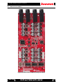
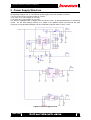
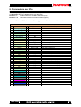
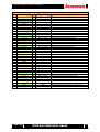
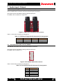
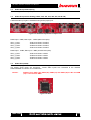
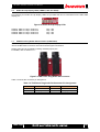
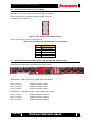
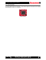
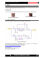
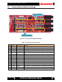
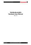
TB-FMCL-ADDA24 Hardware User Manual TB-FMCL-ADDA24 Hardware User Manual Rev.1.00 Rev.1.00 1 TB-FMCL-ADDA24 Hardware User Manual Revision History Version Date Description Publisher Rev.1.00 2012/09/27 Release version Amano Rev.1.00 2 TB-FMCL-ADDA24 Hardware User Manual Table of Contents 1. 2. 3. 4. 5. 6. Related Documents and Accessories ......................................................................................... 8 Overview ...................................................................................................................................... 8 Features....................................................................................................................................... 8 Board Overview ........................................................................................................................... 9 4.1. Block Diagram ........................................................................................................................... 9 4.2. External View of Board ............................................................................................................ 10 4.3. Board Specification .................................................................................................................. 12 Power Supply Structure ............................................................................................................. 13 Connectors and ICs ................................................................................................................... 14 6.1. 7. Audio Input / Output................................................................................................................... 18 7.1. TRS Phone Plug Audio AD Connectors (CN601/602) ............................................................. 18 7.2. Pin Header Audio AD Connector (CN605) .............................................................................. 18 7.3. Audio AD Input Decoupling...................................................................................................... 19 7.4. Audio AD Input Gain Setting (JP301, 302, 303, 304, 305, 306, 307 & 308) ........................... 19 7.5. Audio ADC (IC306) .................................................................................................................. 19 7.6. Audio AD Clip Display LEDs (LED601, 602, 603 & 604) ......................................................... 20 7.7. TRS Phone Plug Audio DA Connectors (CN603/604) ............................................................. 20 7.8. Pin Header Audio DA Connector (CN606) .............................................................................. 21 7.9. Audio DA Output Gain Setting (JP401, 402, 403, 404, 405, 406, 407 & 408) ........................ 21 7.10. 8. 9. FMC Connector for Platform Board Connection (CN201) ....................................................... 14 Audio DAC (IC405) .............................................................................................................. 22 Clock .......................................................................................................................................... 23 8.1. Onboard Clock (IC501, 504).................................................................................................... 23 8.2. Control 24.576 VCXO .............................................................................................................. 23 8.3. Control 22.5792MHz OSC ....................................................................................................... 24 Other Interfaces ......................................................................................................................... 25 9.1. Debug LEDs (LED201, 202) .................................................................................................... 25 10. Factory Default Board Settings ................................................................................................. 26 Rev.1.00 3 TB-FMCL-ADDA24 Hardware User Manual List of Figures Figure3-1 FMC Connector Pin Layout ............................................................................................... 8 Figure4-1 TB-FMCL-ADDA24 Block Diagram.................................................................................... 9 Figure4-2 External View of Board (Component Side) ...................................................................... 10 Figure4-3 External View of Board (Solder Side) ...............................................................................11 Figure4-4 TB-FMCL-ADDA24 Board Dimensions ........................................................................... 12 Figure5-1 Power Supply Circuit ....................................................................................................... 13 Figure7-1 TRS Phone Plug Audio AD Connector ............................................................................ 18 Figure7-2 Pin Header Audio AD Connector ..................................................................................... 18 Figure7-3 Audio AD Input Gain Jumper Pins ................................................................................... 19 Figure7-4 ADC .................................................................................................................................. 19 Figure7-5 Audio AD Clip Display LEDs ............................................................................................ 20 Figure7-6 TRS Phone Plug Audio DA Connector ............................................................................ 20 Figure7-7 Pin Header Audio DA Connector ..................................................................................... 21 Figure7-8 Audio DA Output Gain Jumper Pins ................................................................................ 21 Figure7-9 DAC ................................................................................................................................. 22 Figure8-1 24.576MHz Clock ............................................................................................................ 23 Figure8-2 22.5792MHz Clock .......................................................................................................... 23 Figure8-3 VCXO Circuit.................................................................................................................... 23 Figure8-4 OSC circuit ....................................................................................................................... 24 Figure9-1 Debug LEDs..................................................................................................................... 25 Figure10-1 Factory Default Board Settings ...................................................................................... 26 List of Tables Table 6-1 FMC Connector Pin Assignment for Platform Board Connection .................................... 14 Table 7-1 TRS Phone Plug Audio AD Connector Pin Assignment ................................................... 18 Table 7-2 Pin Header Audio AD Connector Pin Assignment ............................................................ 18 Table 7-3 TRS Phone Plug Audio DA Connector Pin Assignment ................................................... 20 Table 7-4 Pin Header Audio DA Connector Pin Assignment ............................................................ 21 Table 10-1 Factory Default Settings ................................................................................................. 26 Rev.1.00 4 TB-FMCL-ADDA24 Hardware User Manual Introduction Thank you for purchasing the TB-FMCL-ADDA24 board. Before using the product, be sure to carefully read this user manual and fully understand how to correctly use the product. First read through this manual, and then always keep it handy. SAFETY PRECAUTIONS Be sure to observe these precautions Observe the precautions listed below to prevent injuries to you or other personnel or damage to property. Before using the product, read these safety precautions carefully to assure correct use. These precautions contain serious safety instructions that must be observed. After reading through this manual, be sure to always keep it handy. The following conventions are used to indicate the possibility of injury/damage and classify precautions if the product is handled incorrectly. Danger Indicates the high possibility of serious injury or death if the product is handled incorrectly. Indicates the possibility of serious injury or death if the product is handled Warning incorrectly. Indicates the possibility of injury or physical damage in connection with houses or Caution household goods if the product is handled incorrectly. The following graphical symbols are used to indicate and classify precautions in this manual. (Examples) Turn off the power switch. Do not disassemble the product. ! Rev.1.00 Do not attempt this. 5 TB-FMCL-ADDA24 Hardware User Manual Warning In the event of a failure, disconnect the power supply. If the product is used as is, a fire or electric shock may occur. Disconnect the power supply immediately and contact our sales personnel for repair. If an unpleasant smell or smoking occurs, disconnect the power supply. If the product is used as is, a fire or electric shock may occur. immediately. Disconnect the power supply After verifying that no smoking is observed, contact our sales personnel for repair. Do not disassemble, repair or modify the product. Otherwise, a fire or electric shock may occur due to a short circuit or heat generation. For inspection, modification or repair, contact our sales personnel. ! Do not touch a cooling fan. As a cooling fan rotates in high speed, do not put your hand close to it. cause injury to persons. ! Otherwise, it may Never touch a rotating cooling fan. Do not place the product on unstable locations. Otherwise, it may drop or fall, resulting in injury to persons or failure. ! If the product is dropped or damaged, do not use it as is. ! Do not touch the product with a metallic object. ! Do not place the product in dusty or humid locations or where water may Otherwise, a fire or electric shock may occur. Otherwise, a fire or electric shock may occur. splash. Otherwise, a fire or electric shock may occur. ! ! Do not get the product wet or touch it with a wet hand. Otherwise, the product may break down or it may cause a fire, smoking or electric shock. Do not touch a connector on the product (gold-plated portion). Otherwise, the surface of a connector may be contaminated with sweat or skin oil, resulting in contact failure of a connector or it may cause a malfunction, fire or electric shock due to static electricity. Rev.1.00 6 TB-FMCL-ADDA24 Hardware User Manual Caution Do not use or place the product in the following locations. ! Humid and dusty locations Airless locations such as closet or bookshelf Locations which receive oily smoke or steam Locations exposed to direct sunlight Locations close to heating equipment Closed inside of a car where the temperature becomes high Staticky locations Locations close to water or chemicals Otherwise, a fire, electric shock, accident or deformation may occur due to a short circuit or heat generation. ! Do not place heavy things on the product. Otherwise, the product may be damaged. ■ Disclaimer This product is an FPGA Mezzanine Card (hereafter referred to as “FMC”) type of inrevium evaluation board comprising of four audio signal inputs and four audio signal outputs. Tokyo Electron Device Limited assumes no responsibility for any damages resulting from the use of this product for purposes other than those stated. Even if the product is used properly, Tokyo Electron Device Limited assumes no responsibility for any damages caused by: (1) Earthquake, thunder, natural disaster or fire resulting from the use beyond our responsibility, acts by a third party or other accidents, the customer’s willful or accidental misuse or use under other abnormal conditions. (2) Secondary impact arising from use of this product or its unusable state (business interruption or others) (3) Use of this product against the instructions given in this manual. (4) Malfunctions due to connection to other devices. Tokyo Electron Device Limited assumes no responsibility or liability for: (1) Erasure or corruption of data arising from use of this product. (2) Any consequences or other abnormalities arising from use of this product, or (3) Damage of this product not due to our responsibility or failure due to modification This product has been developed by assuming its use for research, testing or evaluation. It is not authorized for use in any system or application that requires high reliability. Repair of this product is carried out by replacing it on a chargeable basis, not repairing the faulty devices. However, non-chargeable replacement is offered for initial failure if such notification is received within two weeks after delivery of the product. The specification of this product is subject to change without prior notice. The product is subject to discontinuation without prior notice. Rev.1.00 7 TB-FMCL-ADDA24 Hardware User Manual 1. Related Documents and Accessories All documents relating to this board can be downloaded from our website Club-X. [Accessory] Board fixing spacer set 2. Overview This board is an optional card equipped with an FMC Low-Pin Count (hereafter referred to as “LPC”) and can be used with the FMC inrevium evaluation board (hereafter referred to as “Platform Board”. The board is designed to allow the user to easily evaluate audio application design features by using it in combination with the Platform Board. The board provides a 4-ch analog input and output interface connected to the audio dedicated high performance Analog Digital Convertor “hereafter referred to as “ADC”) and the Digital Analog Convertor (hereafter referred to as “DAC”). 3. Features ADC Device: DAC Device: Input/output Amplifier: Audio Clock (24.576MHz VXCO): Audio Clock (22.5792MHz): TRS Phone Plug: FMC Connector: TI 192KHz/24bit PCM4204 TI 192KHz/24bit PCM4104 TI OPA1632 Fox FVXO-HC73B-24.576 Kyocera KC7050B22.5792C3 JALCO YKB21-5010 Samtec ASP-134604-01 Figure3-1 FMC Connector Pin Layout *The onboard FMC connector can be only used for the LPC Connector in the above pin layout. For information on real pins, refer to Section 4.6. Rev.1.00 8 TB-FMCL-ADDA24 Hardware User Manual 4. Board Overview 4.1. Block Diagram Figure 4-1 shows the TB-FMCL-ADDA24 block diagram. FMC-LPC for Platform Board DUAL-SUPPLY BUS TRANSCEIVER CN601 OpAmp ADC-BCK OPA1632 YKB21-5010 CN602 ADC-LRCK OpAmp ADC ADC-DOUT0 OPA1632 YKB21-5010 CN605 OpAmp OPA1632 ADC-DOUT1 OpAmp SN74AVCB164245 PCM4204 OPA1632 B6B-XH-A DUAL-SUPPLY BUS TRANSCEIVER CN603 OpAmp DAC-BCK OPA1632 CN604 DAC-LRCK OpAmp OPA1632 DAC DAC-DIN0 YKB21-5010 CN606 OpAmp OPA1632 DAC-DIN1 OpAmp OPA1632 SN74AVCB164245 DUAL-SUPPLY BUS TRANSCEIVER YKB21-5010 24.576MHz 22.5792MHz B6B-XH-A PCM4104 VCXO OSC SN74AVCB164245 Figure4-1 TB-FMCL-ADDA24 Block Diagram Rev.1.00 9 TB-FMCL-ADDA24 Hardware User Manual 4.2. External View of Board Figures 4-2 and 4-3 shows the external view of the TB-FMCL-ADDA24 board. Figure4-2 External View of Board (Component Side) Rev.1.00 10 TB-FMCL-ADDA24 Hardware User Manual Figure4-3 External View of Board (Solder Side) Rev.1.00 11 TB-FMCL-ADDA24 Hardware User Manual 4.3. Board Specification Figure 4-4 shows the TB-FMCL-ADDA24 board specification. External Dimensions: W:160mm x H:69mm (not including projections) Layer Structure: 6-Layer Board Thickness: 1.6mm Material: FR-4 Figure4-4 TB-FMCL-ADDA24 Board Dimensions Rev.1.00 12 TB-FMCL-ADDA24 Hardware User Manual 5. Power Supply Structure Figure 5-1 illustrates the power supply circuit of the TB-FMCL-ADDA24 board. The board generates the following voltages from a +12V external power supply source via the FMC connector: +13.0V/-13.0V from an LT power supply IC “LT3471” +5.0V from an LT power supply IC “LT1763" +3.3V from an LT power supply IC "LT1763" The board is equipped with a voltage level conversion buffer “TI SN74AVCB164245“ for ADC/DAC control. So, the bank voltage (VCCO) of an FPGA on the platform board (connected to the FMC connector on the TB-FMCL-ADDA24) can be configured to support either +2.5V or +3.3V Figure5-1 Power Supply Circuit Rev.1.00 13 TB-FMCL-ADDA24 Hardware User Manual 6. Connectors and ICs 6.1. FMC Connector for Platform Board Connection (CN201) The subsequent pages present the FMC connector pin assignment for Platform Board connection. The Direction field in the table shows a signal direction: Direction = I Platform Board to TB-FMCL-ADDA24 (Input) Direction = O TB-FMCL-ADDA24 to Platform Board (Output) Table 6-1 FMC Connector Pin Assignment for Platform Board Connection C-Row (FMC Connector for Platform Board Connection) Pin# 1 2 3 4 5 6 7 8 9 10 11 12 13 14 15 16 17 18 19 20 21 22 23 24 25 26 27 28 29 30 31 32 33 34 35 36 37 38 39 40 FMC Standard GND DP0_C2M_P DP0_C2M_N GND GND DP0_M2C_P DP0_M2C_N GND GND LA06_P LA06_N GND GND LA10_P LA10_N GND GND LA14_P LA14_N GND GND LA18_P_CC LA18_N_CC GND GND LA27_P LA27_N GND GND SCL SDA GND GND GA0 12P0V GND 12P0V GND 3P3V GND Rev.1.00 I/O I I I I I I I I I - Signal Name N/C N/C N/C N/C DAC_0_MODE DAC_0_RST DAC_0_MUTE DAC_0_SCKI DAC_0_BCK DAC_0_LRCK DAC_0_DIN0 DAC_0_DIN1 DAC_0_FMT0 DAC_0_FMT1 N/C N/C N/C +12V +12V N/C - Description DAC Mode Setup Input DAC Reset Input DAC Mute Setup Input DAC System Clock Input DAC Audio Bit Clock Input DAC Audio L/R Input DAC Audio Data (ch1/ch2) Input DAC Audio Data (ch3/ch4) Input DAC Audio Data Format Setup Input DAC Audio Data Format Setup Input +12V Power Supply +12V Power Supply - 14 TB-FMCL-ADDA24 Hardware User Manual D-Row (FMC Connector for Platform Board Connection) Pin# 1 2 3 4 5 6 7 8 9 10 11 12 13 14 15 16 17 18 19 20 21 22 23 24 25 26 27 28 29 30 31 32 33 34 35 36 37 38 39 40 FMC Standard PG_C2M GND GND GBTCLK0_M2C_P GBTCLK0_M2C_N GND GND LA01_P_CC LA01_N_CC GND LA05_P LA05_N GND LA09_P LA09_N GND LA13_P LA13_N GND LA17_P_CC LA17_N_CC GND LA23_P LA23_N GND LA26_P LA26_N GND TCK TDI TDO 3P3VAUX TMS TRST_L GA1 3P3V GND 3P3V GND 3P3V Rev.1.00 I/O I I I I I I I I I I I I - Signal Name N/C N/C N/C DAC_0_FMT2 DAC_0_FS0 DAC_0_FS1 DAC_0_CS DAC_0_CCLK DAC_0_CDTI ADC_0_RST ADC_0_FS0 ADC_0_FS1 ADC_0_FS2 ADC_0_SDKI ADC_0_SM N/C N/C N/C N/C N/C N/C N/C N/C N/C N/C N/C N/C Description DAC Audio Data Format Setup Input DAC Sampling Mode Setup Input DAC Sampling Mode Setup Input DACSPI Chip Select Input DACSPI Data Clock Input DACSPI Data Input ADC Reset Input ADC Sampling Mode Setup Input ADC Sampling Mode Setup Input ADC Sampling Mode Setup Input ADC System Clock Input ADC Master/Slave Setup Input - 15 TB-FMCL-ADDA24 Hardware User Manual G-Row (FMC Connector for Platform Board Connection) Pin# 1 2 3 4 5 6 7 8 9 10 11 12 13 14 15 16 17 18 19 20 21 22 23 24 25 26 27 28 29 30 31 32 33 34 35 36 37 38 39 40 FMC Standard GND CLK0_M2C_P CLK0_M2C_N GND GND LA00_P_CC LA00_N_CC GND LA03_P LA03_N GND LA08_P LA08_N GND LA12_P LA12_N GND LA16_P LA16_N GND LA20_P LA20_N GND LA22_P LA22_N GND LA25_P LA25_N GND LA29_P LA29_N GND LA31_P LA31_N GND LA33_P LA33_N GND VADJ GND Rev.1.00 I/O O O I I I I I I I I O O O O O O O - Signal Name CLK_24P576 CLK_22P5792 N/C N/C N/C ADC_0_FMT0 ADC_0_FMT1 ADC_0_FMT2 ADC_0_BCK ADC_0_LRCK ADC_0_HPFD N/C N/C VCXO_CTRL0 VCXO_CTRL1 DAC_0_CDT0 ADC_0_DOUT0 ADC_0_DOUT1 ADC_0_CLIP1 ADC_0_CLIP2 ADC_0_CLIP3 ADC_0_CLIP4 N/C N/C VADJ - Description 24.576MHz Clock Output (Single End) 22.5792MHz Clock Output (Single End) ADC Audio Data Format Setup Input ADC Audio Data Format Setup Input ADC Audio Data Format Setup Input ADC Audio Bit Clock Input ADC Audio L/R Clock Input ADC High Pass Filter Setup Input 24.576MHz Clock VCXO Control Input 22.5792MHz Clock Control Input (High: Enable) DACSPI Data Output ADC Audio Data (ch1/ch2) Output ADC Audio Data (ch3/ch4) Output ADC Audio Data (ch1) Clip Flag Output ADC Audio Data (ch2) Clip Flag Output ADC Audio Data (ch3) Clip Flag Output ADC Audio Data (ch4) Clip Flag Output FMC Reference Power Supply (+2.5V/+3.3V) - 16 TB-FMCL-ADDA24 Hardware User Manual H-Row (FMC Connector for Platform Board Connection) Pin# 1 2 3 4 5 6 7 8 9 10 11 12 13 14 15 16 17 18 19 20 21 22 23 24 25 26 27 28 29 30 31 32 33 34 35 36 37 38 39 40 FMC Standard VREF_A_M2C PRSNT_M2C_L GND CLK0_M2C_P CLK0_M2C_N GND LA02_P LA02_N GND LA04_P LA04_N GND LA07_P LA07_N GND LA11_P LA11_N GND LA15_P LA15_N GND LA19_P LA19_N GND LA21_P LA21_N GND LA24_P LA24_N GND LA28_P LA28_N GND LA30_P LA30_N GND LA32_P LA32_N GND VADJ Rev.1.00 I/O O O O O - Signal Name N/C N/C N/C N/C N/C LED201_4 LED201_2 LED202_2 LED202_4 N/C N/C N/C N/C N/C N/C N/C N/C N/C N/C N/C N/C N/C N/C N/C N/C N/C VADJ Description Reference (LED201) Green Control Output Reference (LED201) Red Control Output Reference (LED202) Green Control Output Reference (LED202) Red Control Output FMC Reference Power Supply (+2.5V/+3.3V) 17 TB-FMCL-ADDA24 Hardware User Manual 7. Audio Input / Output 7.1. TRS Phone Plug Audio AD Connectors (CN601/602) The board supports 2-channel analog audio inputs (CH1/2). JALCO YKB21-5010 connectors are used for these signal connections. Input gains can be controlled by setting onboard jumper pins. For details, refer to Section 8. Jumper Pins. Figure7-1 TRS Phone Plug Audio AD Connector Table 7-1 shows the connector pin assignment. Table 7-1 TRS Phone Plug Audio AD Connector Pin Assignment Pin # CN601:1:S CN601:2:T CN601:3:R Name AGND ADC_0_VIN1+ ADC_0_VIN1- Pin # CN602:1:S CN602:2:T CN602:3:R Name AGND ADC_0_VIN2+ ADC_0_VIN2- 7.2. Pin Header Audio AD Connector (CN605) The board supports 2-channel analog audio inputs (CH3/4). JST B6B-XH-A connectors are used for these signal connections. Input gains can be controlled by setting onboard jumper pins. For details, refer to Section 7.4. Figure7-2 Pin Header Audio AD Connector Table 7-2 shows the connector pin assignment. Table 7-2 Pin Header Audio AD Connector Pin Assignment Pin # 1 2 3 4 5 6 Rev.1.00 Name ADC_0_VIN3+ ADC_0_VIN3AGND ADC_0_VIN4+ ADC_0_VIN4AGND 18 TB-FMCL-ADDA24 Hardware User Manual 7.3. Audio AD Input Decoupling The following four audio input capacitors are inserted in series. 7.4. Audio AD Input Gain Setting (JP301, 302, 303, 304, 305, 306, 307 & 308) A desired audio input gain is selectable using these jumper pins. Figure7-3 Audio AD Input Gain Jumper Pins Rated Input + 4dBu, Max Input + 18dBu (balanced inputs): ADC_0_VIN1: ADC_0_VIN2: ADC_0_VIN3: ADC_0_VIN4: JP301 and JP302 = SHORT. JP303 and JP304 = SHORT. JP305 and JP306 = SHORT. JP307 and JP308 = SHORT. Rated Input - 10dBV, Max Input + 4dBV (unbalanced inputs): ADC_0_VIN1: ADC_0_VIN2: ADC_0_VIN3: ADC_0_VIN4: JP301 and JP302 = OPEN. JP303 and JP304 = OPEN. JP305 and JP306 = OPEN. JP307 and JP308 = OPEN. 7.5. Audio ADC (IC306) The board is equipped with a TI PCN4204 device that supports 24bit/192kHz ADC. 4ch analog audio inputs are supported. These audio inputs are connected to the onboard CN601/602/605 connectors via a TI OPA1632. Caution: DSDCLK (24), DSD1 (25), DSD2 (26), DSD3 (27) and DSD4 (28) are NC and SUB (39) is connected to GND. Figure7-4 ADC Rev.1.00 19 TB-FMCL-ADDA24 Hardware User Manual 7.6. Audio AD Clip Display LEDs (LED601, 602, 603 & 604) The following four audio AD clip display LEDs are provided that can be controlled from the ADC state display pin. Figure7-5 Audio AD Clip Display LEDs LED601: LED602: LED603: LED604: State of a clip in Channel 1 State of a clip in Channel 2 State of a clip in Channel 3 State of a clip in Channel 4 Clip = ON Clip = ON Clip = ON Clip = ON 7.7. TRS Phone Plug Audio DA Connectors (CN603/604) The board supports 2-channel analog audio outputs (CH1/ 2). JALCO YKB21-5010 connectors are used for these signal connections. Output gains can be controlled by setting onboard jumper pins. For details, refer to Section 7.9. Figure7-6 TRS Phone Plug Audio DA Connector Table 7-3 shows the connector pin assignment. Table 7-3 TRS Phone Plug Audio DA Connector Pin Assignment Pin # CN603:1:S CN603:2:T CN603:3:R Rev.1.00 Name AGND DAC_0_VOUT1+ DAC_0_VOUT1- Pin # CN604:1:S CN604:2:T CN604:3:R Name AGND DAC_0_VOUT2+ DAC_0_VOUT2- 20 TB-FMCL-ADDA24 Hardware User Manual 7.8. Pin Header Audio DA Connector (CN606) The board supports 2-channel analog audio outputs (CH3/ 4). JST B6B-XH-A connectors are used for these signal connections. Output gains can be controlled by setting onboard jumper pins. For details, refer to Section 7.9 Figure7-7 Pin Header Audio DA Connector Table 7-4 shows the connector pin assignment. Table 7-4 Pin Header Audio DA Connector Pin Assignment Pin # 1 2 3 4 5 6 7.9. Name DAC_0_VOUT3+ DAC_0_VOUT3AGND DAC_0_VOUT4+ DAC_0_VOUT4AGND Audio DA Output Gain Setting (JP401, 402, 403, 404, 405, 406, 407 & 408) A desired audio output gain is selectable using these jumpers. Figure7-8 Audio DA Output Gain Jumper Pins Rated Output + 4dBu, Max Output + 18dBu (balanced outputs): DAC_0_VOUT1: DAC_0_VOUT2: DAC_0_VOUT3: DAC_0_VOUT4: JP401 and JP402 = OPEN JP403 and JP404 = OPEN JP405 and JP406 = OPEN JP407 and JP408 = OPEN Rated Output - 10dBV, Max Output + 4dBV (unbalanced Outputs): DAC_0_VOUT1: DAC_0_VOUT2: DAC_0_VOUT3: DAC_0_VOUT4: Rev.1.00 JP401 and JP402 = SHORT JP403 and JP404 = SHORT JP405 and JP406 = SHORT JP407 and JP408 = SHORT 21 TB-FMCL-ADDA24 Hardware User Manual 7.10. Audio DAC (IC405) The board is equipped with a TI PCN4104 device that supports 24bit/192kHz DAC. 4ch analog audio outputs are supported. These audio outputs are connected to the onboard CN603/604/606 connectors via a TI OPA1632. Figure7-9 DAC Rev.1.00 22 TB-FMCL-ADDA24 Hardware User Manual 8. Clock 8.1. Onboard Clock (IC501, 504) The board provides the following two onboard clock sources: 24.576MHz (VCXO) 22.5792MHz (FIX) The VCXO enables self-oscillation and synchronization with external clock sources (48-kHz only). Figure8-2 22.5792MHz Clock Figure8-1 24.576MHz Clock 8.2. Control 24.576 VCXO 24.576 VCXO(IC501) has a Low Path Filer(LPF) circuit to the frequency control pin(VC). The frequency is adjustable by PWM control method from a FPGA to signal “VCXO_CTRL0”. Figure8-3 VCXO Circuit The frequency is control -150PPM to +150PPM area by 0 to 3.3V voltage. (VC= 1.65: 24.576MHZ) Please refer to the reference design for PWM control method. Also, refer to the datasheet of VCXO(FVXO-HC73B-24.576) http://www.foxonline.com/pdfs/FVXO_HC73.pdf About 24.576 OSC This board can use OSC instead of VCXO. Please contact us if using OSC. Rev.1.00 23 TB-FMCL-ADDA24 Hardware User Manual 8.3. Control 22.5792MHz OSC OSC(IC504) is controlled by signal “VCXO_CTRL1” form FPGA. VCXO_CTRL1: High- Enable, Low- Disable. Figure8-4 OSC circuit About 24.576 VCXO This board can use VCXO instead of OSC. Please contact us if using VCXO. Rev.1.00 24 TB-FMCL-ADDA24 Hardware User Manual 9. Other Interfaces 9.1. Debug LEDs (LED201, 202) These are multi-purpose LEDs connected directly to the Platform Board. A 2-color Rohm SML-522MUW light emitting diode is used. Figure9-1 Debug LEDs Table 9-1 LED201 Control Pin # 8 10 FMC DIR LA02_N LA04_P O O Signal Name LED201_4 LED201_2 Description Green: Low Active Red: Low Active Table 9-2 LED202 Control Pin # 11 13 Rev.1.00 FMC DIR LA04_N LA07_P O O Signal Name LED202_4 LED202_2 Description Green: Low Active Red: Low Active 25 TB-FMCL-ADDA24 Hardware User Manual 10. Factory Default Board Settings No.1 – 8 : SHORT No.9 – 16 : OPEN Figure10-1 Factory Default Board Settings Table 10-1 Factory Default Settings No. Silk No. Initial Setting Function 1 JP301 SHORT Rated Input + 4dBu, Max Input + 18dBu (balanced inputs) 2 JP302 SHORT Rated Input + 4dBu, Max Input + 18dBu (balanced inputs) 3 JP303 SHORT Rated Input + 4dBu, Max Input + 18dBu (balanced inputs) 4 5 6 7 8 9 10 11 12 JP304 JP305 JP306 JP307 JP308 JP401 JP402 JP403 JP404 SHORT SHORT SHORT SHORT SHORT OPEN OPEN OPEN OPEN Rated Input + 4dBu, Max Input + 18dBu (balanced inputs) Rated Input + 4dBu, Max Input + 18dBu (balanced inputs) Rated Input + 4dBu, Max Input + 18dBu (balanced inputs) Rated Input + 4dBu, Max Input + 18dBu (balanced inputs) Rated Input + 4dBu, Max Input + 18dBu (balanced inputs) Rated Output + 4dBu, Max Output + 18dBu (balanced outputs) Rated Output + 4dBu, Max Output + 18dBu (balanced outputs) Rated Output + 4dBu, Max Output + 18dBu (balanced outputs) Rated Output + 4dBu, Max Output + 18dBu (balanced outputs) 13 JP405 OPEN Rated Output + 4dBu, Max Output + 18dBu (balanced outputs) 14 JP406 OPEN Rated Output + 4dBu, Max Output + 18dBu (balanced outputs) 15 JP407 OPEN Rated Output + 4dBu, Max Output + 18dBu (balanced outputs) 16 JP408 OPEN Rated Output + 4dBu, Max Output + 18dBu (balanced outputs) Rev.1.00 26 TB-FMCL-ADDA24 Hardware User Manual PLD Solution Dept. PLD Division URL: http://solutions.inrevium.com/ E-mail: [email protected] HEAD Quarter: Yokohama East Square, 1-4 Kinko-cho, Kanagawa-ku, Yokohama City, Kanagawa, Japan 221-0056 TEL: +81-45-443-4016 FAX: +81-45-443-4058 Rev.1.00 27