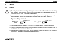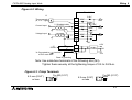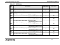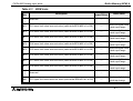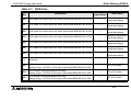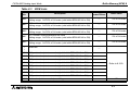
1
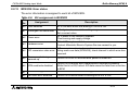
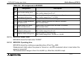
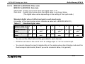
USER’S MANUAL FX2N-8AD Analog input block FX2N-8AD Analog input block Foreword • This manual contains text, diagrams and explanations which will guide the reader in the correct installation and operation of the FX2N-8AD Analog input block. It should be read and understood before attempting to install or use the unit. • Further information can be found in the FX2N Series Hardware Manual for connecting main unit, and the FX Series Programming Manual. • If in doubt at any stage of the installation of FX2N-8AD Analog input block always consult a professional electrical engineer who is qualified and trained to the local and national standards which apply to the installation site. • If in doubt about the operation or use of FX2N-8AD Analog input block please consult the nearest Mitsubisi Electric distributor. • This manual is subject to change without notice. FX2N-8AD Analog input block FX2N-8AD Analog input block USER’S MANUAL Manual number : JY992D86001 Manual revision : A Date : MAY 2000 FX2N-8AD Analog input block ii FX2N-8AD Analog input block Guidelines for the Safety of the User and Protection of the FX2N-8AD Analog input block. This manual provides information for the use of the FX2N-8AD Analog input block. The manual has been written to be used by trained and competent personnel. The definition of such a person or persons is as follows: a) Any engineer who is responsible for the planning, design and construction of automatic equipment using the product associated with this manual, should be of a competent nature, trained and qualified to the local and national standards required to fulfill that role. These engineers should be fully aware of all aspects of safety with regards to automated equipment. b) Any commissioning or service engineer must be of a competent nature, trained and qualified to the local and national standards required to fulfill that job. These engineers should also be trained in the use and maintenance of the completed product. This includes being completely familiar with all associated documentation for said product. All maintenance should be carried out in accordance with established safety practices. c) All operators of the completed equipment should be trained to use that product in a safe and coordinated manner in compliance to established safety practices. The operators should also be familiar with documentation which is connected with the actual operation of the completed equipment. Note : The term ‘completed equipment’ refers to a third party constructed device which contains or uses the product associated with this manual. iii FX2N-8AD Analog input block Note’s on the Symbols Used in this Manual At various times through out this manual certain symbols will be used to highlight points of information which are intended to ensure the users personal safety and protect the integrity of equipment. Whenever any of the following symbols are encountered its associated note must be read and understood. Each of the symbols used will now be listed with a brief description of its meaning. Hardware Warnings 1) Indicates that the identified danger WILL cause physical and property damage. 2) Indicates that the identified danger could POSSIBLY cause physical and property damage. 3) Indicates a point of further interest or further explanation. Software Warnings 4) Indicates special care must be taken when using this element of software. 5) Indicates a special point which the user of the associate software element should be aware. 6) Indicates a point of interest or further explanation. iv FX2N-8AD Analog input block • Under no circumstances will Mitsubishi Electric be liable responsible for any consequential damage that may arise as a result of the installation or use of this equipment. • All examples and diagrams shown in this manual are intended only as an aid to understanding the text, not to guarantee operation. Mitsubishi Electric will accept no responsibility for actual use of the product based on these illustrative examples. • Owing to the very great variety in possible application of this equipment, you must satisfy yourself as to its suitability for your specific application. v FX2N-8AD Analog input block vi FX2N-8AD Analog input block Contents. Guideline ..................................................................................................... iii 1. Introduction............................................................................................1-1 2. External Dimensions .............................................................................2-1 3. Part Name .............................................................................................3-1 4. Installation .............................................................................................4-1 5. Connection to PLC ................................................................................5-1 6. Wiring ....................................................................................................6-1 6.1 Caution ................................................................................................................ 6-1 7. Specifications ........................................................................................7-1 8. Buffer Memory (BFM) ...........................................................................8-1 8.1 Buffer Memories (BFM) lists ................................................................................ 8-3 8.2 Details of buffer memories................................................................................. 8-12 8.2.1 8.2.2 8.2.3 8.2.4 8.2.5 8.2.6 8.2.7 8.2.8 8.2.9 8.2.10 8.2.11 8.2.12 8.2.13 BFM #0, #1: Specifies input mode. ......................................................................... 8-12 BFM #2 to BFM #9: Number of times of averaging ................................................. 8-14 BFM #10 to BFM #17: Channel data ....................................................................... 8-16 BMF #19: Disables setting change.......................................................................... 8-16 BFM #20: Initializes functions.................................................................................. 8-16 BFM #21: Writes I/O characteristics ........................................................................ 8-17 BFM #22: Sets convenient functions ....................................................................... 8-18 BFM #24: Specifies high-speed conversion channel .............................................. 8-19 BFM #26: Upper/lower limit value error status ........................................................ 8-20 BFM #27: A/D data sudden change detection status .............................................. 8-21 BFM #28: Scale over status .................................................................................... 8-22 BFM #29: Error status ............................................................................................. 8-24 BFM #30: Model code ............................................................................................. 8-25 vii FX2N-8AD Analog input block Contents. 8.2.14 BFM #32: Operating time ........................................................................................ 8-25 8.2.15 BFM #41 to BFM #48: Offset data BFM #51 to BFM #58: Gain data............................................................................. 8-26 8.2.16 BFM #61 to BFM #68: Addition data ....................................................................... 8-28 8.2.17 BFM #71 to BFM #78: Lower limit, error set value BFM #81 to BFM #88: Upper limit, error set value .................................................. 8-29 8.2.18 BFM #91 to BFM #98: Sudden change detection set value .................................... 8-31 8.2.19 BFM #99: Clears upper/lower limit value error and sudden change detection error 8-33 8.2.20 BFM #101 to BFM #108: Peak value (minimum value) BFM #111 to BFM #118: Peak value (maximum value) .......................................... 8-34 8.2.21 BFM #109: Peak value reset flag (minimum value) BFM #119: Peak value reset flag (maximum value)................................................ 8-35 8.2.22 BFM #198: Data history sampling time ................................................................... 8-36 8.2.23 BFM #199: Resets or stops data history ................................................................. 8-38 8.2.24 BFM #200 to BFM #3399: Data history ................................................................... 8-39 9. Adjustment of I/O Characteristics ..........................................................9-1 9.1 Standard I/O characteristics ................................................................................ 9-2 9.2 Adjustment of I/O characteristics ......................................................................... 9-7 10.Example program ...............................................................................10-1 Appendix A Associated Manuals List........................................................................... A-1 viii FX2N-8AD Analog input block 1. Introduction 1 Introduction The FX2N-8AD analog input block (hereafter referred to as "FX2N-8AD") converts 8 points of analog input values (voltage input, current input and temperature input) into digital values, and transfers them to the PLC main unit. The FX2N-8AD can be connected to FX0N, FX1N, FX2N and FX2NC Series PLC. 1) Analog inputs can be selected from the voltage input, the current input and the thermocouple input (temperature input) by the input mode setting by the TO instruction given by the PLC main unit and the connection method. At this time, a different analog input can be selected for each channel. 2) The voltage input can be selected within the range from -10 to +10 V. The current input can be selected within the range from -20 to +20 mA and from +4 to +20 mA. The input characteristics can be adjusted for each channel (except while the analog value direct display is used). The thermocouple input can be selected among the K type, J type and T type. (The input characteristics cannot be adjusted when the thermocouple input is used.) 3) The resolution is 0.63 mV (20 V x 1/32,000) or 2.50 mV (20 V x 1/8,000) when the voltage input is used, 2.50 µA (40 mA x 1/16,000) or 5.00 µA (40 mA x 1/8,000) when the current input is used, and 0.1 °C when the thermocouple input is used. 1-1 FX2N-8AD Analog input block Introduction 1 4) Up to two FX2N-8AD units can be connected to FX0N main unit, FX0N extension unit, FX1N main unit. Up to eight FX2N-8AD units can be connected to one FX2N Series PLC. Up to four FX2N8AD units can be connected to one FX2NC Series PLC. (For connection to the FX2NC Series PLC, an FX2NC-CNV-IF is required.) Data transfer with the PLC is performed to buffer memories of the FX2N-8AD by FROM/TO instructions. 1-2 FX2N-8AD Analog input block External Dimensions 7.5(0.30) Figure 2.1: External Dimensions V2+ I2+ I3+ COM1 COM3 V3+ I4+ COM4 COM2 V4+ FX2N-8AD POWER 24V V6+ V5+ I6+ I5+ I8+ COM6 V8+ COM8 I7+ V7+ COM7 COM5 67(2.64) (installation dimension) 105(4.13) 24- 7.5(0.30) I1+ V1+ 24+ 98(3.86) (installation dimension) 75(2.95) 8(0.31) 90(3.54) 2. External Dimensions 2 75(2.95) 8(0.31) Dimensions: mm(inch) Mass(Weight): 0.3 kg(0.66 lbs) 2-1 FX2N-8AD Analog input block External Dimensions 2 MEMO 2-2 FX2N-8AD Analog input block 3. Part Name 3 Part Name Figure 3.1: Part name Installation hole (screw M4) Table 3.1: Status indicator LED Status indicator LED Extension cable V1+ 24+ 24- I1+ V2+ V3+ I3+ COM1 COM3 I2+ V4+ I4+ COM4 COM2 FX2N-8AD Extension connector Indication Description POWER Lit while 5 V power is normally supplied from PLC. 24 V Lit while 24 V power is normally supplied to “24+” and “24-” terminals of FX2N-8AD.V POWER 24V V6+ V5+ I6+ I5+ V8+ I8+ COM6 COM8 V7+ I7+ COM7 COM5 M3 (terminal screw) Hook for DIN rail Terminal arrangement 24+ V1+ I1+ COM1 V3+ I3+ COM3 24- V2+ I2+ COM2 V4+ I4+ COM4 • For wiring, refer to Section 6. • Never perform wiring to • terminals. V6+ I6+ COM6 V8+ I8+ COM8 V5+ I5+ COM5 V7+ I7+ COM7 3-1 FX2N-8AD Analog input block Part Name 3 MEMO 3-2 FX2N-8AD Analog input block 4. Installation 4 Installation Install the FX2N-8AD to the right side of a main unit, extension unit, extension block or special block of the FX0N/FX1N/FX2N/FX2NC Series PLC. The FX 2N -8AD can be installed with a DIN rail (DIN46277 of 35 mm in width) or directly installed with screws M4. For the details, refer to the handy manual supplied together with the PLC main unit.) 4-1 FX2N-8AD Analog input block Installation 4 Figure 4.1: Installation with DIN rail V1+ 24- 24+ I1+ V2+ I2+ • The FX2N-8AD can be installed on a DIN rail (DIN46277) of 35 mm in width as it is. For removal, pull down on the DIN rail mounting hook, then remove the FX2N-8AD. COM1 COM3 V3+ I3+ COM2 I4+ COM4 V4+ FX2N-8AD POWER 24V V6+ V5+ I6+ I5+ I8+ V8+ COM8 COM6 V7+ COM5 COM7 I7+ Hook for DIN rail Figure 4.2: Direct installation 98(3.86) Installation screw M4 • The FX2N-8AD can be installed directly by inserting screws (M4) into installation holes. For the pitch and the position of installation holes, refer to the figure on the left. 67(2.64) Dimensions: mm(inch) 4-2 FX2N-8AD Analog input block 5. Connection to PLC 5 Connection to PLC Connect the FX2N-8AD to the right side of a main unit, extension unit or extension block of FX0N, FX1N, FX2N, FX2NC Series PLC with an extension cable. For connection to a basic unit or extension block of the FX2NC Series PLC, use an FX2NC-CNVIF. Please check power supply availability to determine the number of FX2N-8AD blocks that can be connected to the FX0N, FX1N, FX2N or FX2NC PLCs. A unit No. 0 to 7 is automatically assigned to each special unit or special block connected to a PLC basic unit from the one nearest to the basic unit. The data is read from and written to the FX2N-8AD by FROM/TO instructions given by the basic unit. 5-1 FX2N-8AD Analog input block Connection to PLC 5 MEMO 5-2 FX2N-8AD Analog input block 6. Wiring 6.1 Caution Wiring 6 1) Do not lay signal cable near to high voltage power cable or house them in the same trunking duct. Effects of noise or surge induction may occur. Keep signal cables a safe distance of more than 100 mm (3.94") from these power cables. 2) The terminal screws of the FX2N-8AD are M3 (0.12"), therefore crimp style terminals (see drawing) suitable for use with these screws should be fitted to the cable for wiring. Figure 6.1: Crimp Terminals 6.2 mm (0.24" ) or less For M3 (0.12") For M3 (0.12") 6.2 mm (0.24") or less 3) The terminal tightening torque is 0.5 to 0.8 Nžm. Tighten securely to avoid malfunction. 4) Cut off all phases of power source before installation or performing wiring work in order to avoid electric shock or damage of product. 5) Replace the provided terminal cover before supplying power and operating the unit after installation or wiring work in order to avoid electric shock. 6-1 FX2N-8AD Analog input block Wiring 6 Figure 6.2: Wiring FX2N-8AD *6 Thermocouple (K, J or T type) 5.8kΩ V3+ 250Ω I3+ COM3 *1 Shielded cable Current input 200kΩ *3 V2+ 5.8kΩ 250Ω I2+ COM2 Voltage input V1+ *2 200kΩ CH2 5.8kΩ 250Ω I1+ CH3 200kΩ CH1 COM1 AG +15V *5 DC24V 24+ 24- DC/DC converter *4 Connected to terminal of PLC main unit AG -15V Class D grounding Note: Use solderless terminals of the following size (M3). Tighten them securely at the tightening torque of 0.5 to 0.8 N•m. Figure 6.3: Crimp Terminals 6.2 mm (0.24" ) or less For M3 (0.12") For M3 (0.12") 6.2 mm (0.24") or less 6-2 FX2N-8AD Analog input block Wiring 6 *1 Use a two-core, twisted, shielded cable for the analog input line, and separate it from other power lines or a lines easily induced. *2 If there is voltage ripple in the input or there is noise in the external wiring, connect a capacitor of approximately 0.1 to 0.47 µF, 25 V. *3 For the current input, make sure to short-circuit the “VO+” terminal and the “IO+” terminal (O: input channel No.). *4 Make sure to connect the terminal to the terminal of the PLC main unit to which Class D grounding (100 Ω or less) is performed. *5 The 24 V DC service power supply of the PLC is also available. *6 Use an isolated type thermocouple. - When using the thermocouple input, use compensating conductors suitable to the thermocouple. - Never perform wiring to • terminals. - For the terminal arrangement, refer to Section 3. 6-3 FX2N-8AD Analog input block Wiring 6 MEMO 6-4 FX2N-8AD Analog input block 7. Specifications 7 Specifications Table 7.1: General specifications Item Specifications Ambient temperature 0 to +55 °C during operation, -20 to +70 °C during storage range Ambient humidity 35 to 85 % RH during operation (Dew condensation shall not be allowed.) Vibration resistance In conformance to JIS C0040 Frequency 10 to 57 Hz, half amplitude 0.075 mm, 57 to 150 Hz, acceleration 9.8 m/s2, 10 times in each of X, Y and Z directions (80 times in total) (For product installed with DIN rail: Frequency 10 to 57 Hz, half amplitude 0.035 mm, 57 to 150 Hz, acceleration 4.9 m/s2) Impact resistance In conformance to JIS C0041 147 m/s2 for 11 ms, 3 times in each of X, Y and Z directions with half-sine pulses Noise resistance By noise simulator of noise voltage 1,000 Vp-p, noise width 1 µs and frequency 30 to 100 Hz Withstand voltage 500 V AC for 1 min (between analog input terminal and each terminal of PLC main unit) Insulation resistance In conformance to JEM-1021 5 MΩ or more by 500 V DC Megger (between all terminals as a whole and case) Operating atmosphere Corrosive gas and much dusts shall not be detected. 7-1 FX2N-8AD Analog input block Specifications 7 Table 7.2: Power supply specifications Item Specifications Interface driving power supply 24 V DC±10%, 80 mA (maximum), supplied via terminal from outside CPU driving power supply 5 V DC, 50 mA, supplied via extension cable from PLC main unit Table 7.3: Performance specifications Item Specifications Conversion speed • When only voltage input and current input are used 500 µs x Number of used channels • When thermocouple input is used for 1 or more channels Channel for voltage/current input: 1 ms x Number of used channels Channel for thermocouple input: 40 ms x Number of used channels (Number of used channels indicates number of all channels used for voltage input, current input or thermocouple input.) Insulation method Photocoupler insulates analog input area from PLC. DC/DC converter insulates power supply from analog I/O. Channels are not insulated each other. Number of occupied 8 points (including input points and output points) I/O points Applicable PLC FX0N, FX1N, FX2N, FX2NC Series PLC (For connection to FX2NC Series PLC, FX2NC-CNV-IF is required.) Built-in memory EEPROM 7-2 FX2N-8AD Analog input block Specifications 7 Table 7.4: Voltage/current input specifications Item Voltage input Current input Analog input range -10 to +10 V DC (input resistance: 200 kΩ) Adjustment is enabled in following condition: Offset value: -10 to +9 V Gain value: 10 V or less "Gain - Offset": > 1 V (Resolution is constant.) However, change is disabled while analog value direct display is used. Maximum absolute input: ±15 V -20 to +20 mA DC, +4 to +20 mA DC (input resistance: 250 Ω) Adjustment is enabled in following condition: Offset value: -20 to +17 mA Gain value: 30 mA or less "Gain - Offset": > 3 mA (Resolution is constant.) However, change is disabled while analog value direct display is used. Maximum absolute input: ±30 mA Digital output Signed 16-bit binary Signed 16-bit binary • 2.50 µA (40 mA × 1/16,000) during input of -20 to +20 mA • 5.00 µA (40 mA × 1/8,000) during input of -20 to +20 mA • 2.00 µA (16 mA × 1/8,000) during input of +4 to +20 mA • 4.00 µA (16 mA × 1/4,000) during input of +4 to +20 mA Resolution • 0.63 mV (20 V × 1/32000) • 2.5mV (20 V × 1/8000) Total accuracy Ambient temperature: 25 °C ± 5 °C ±0.3% (±120 µA) against full scale 40 mA Ambient temperature: 25 °C ± 5 °C +4 to +20mA input is same (±120 µA) ±0.3% (±60 mV) against full scale 20 V Ambient temperature: 0 to +55 °C Ambient temperature: 0 to +55 °C ±0.5% (±100 mV) against full scale 20 V ±0.5% (±200 µA) against full scale 40 mA +4 to +20mA input is same (±200 µA) 7-3 FX2N-8AD Analog input block Specifications 7 Table 7.5: Thermocouple input specifications Item K type thermocouple J type thermocouple T type thermocouple Analog input range -100 to 1200 °C -148 to 2192 °F -100 to 600 °C -148 to 1112 °F -100 to 350 °C -148 to 662 °F Digital output Signed 16-bit binary Signed 16-bit binary Signed 16-bit binary Resolution 0.1 °C or 0.1 °F 0.1 °C or 0.1 °F 0.1 °C or 0.1 °F Total accuracy Ambient temperature: 0 to 55 °C ± 1 % Against full scale (-100 °C to 1200 °C / -148 °F to 2192 °F) However, 0 °C to 1000 °C / 32 °F to 1832 °F of K type and 25 °C to 600 °C / 77 °F to 600 °F of J type are 0.5 %. • For the I/O characteristics of the voltage/current/thermocouple input, refer to Section 9. 7-4 FX2N-8AD Analog input block 8. Buffer Memory (BFM) 8 Buffer Memory (BFM) Caution 1) Do not access the buffer memory of “Reserved” (BFM #18, #23, #25, #31, #33 to #40, #49 to 50, #59, #60, #69, #70, #79, #80, #89, #90, #99, #100, #120 to #197) by the FROM/TO instruction. There is a possibility to cause abnormal operation of the FX2N8AD if accessing these buffer memories. 8-1 FX2N-8AD Analog input block Buffer Memory (BFM) 8 Data transfer between the FX2N -8AD and the PLC main unit is performed through buffer memories (hereafter referred to as "BFM") of the FX2N-8AD. Each BFM consists of 1 word, 16 bits. The BFM No. 0 to 3399 and a function are assigned to each BFM. Use FROM/TO instructions to read and write the data between the BFM and the PLC. When the power is turned on from off, the initial value is written to each BFM. When you would like to use different contents of the BFM, create a program for the PLC so that the desired contents are written to the BFM every time the power of the PLC is turned on. (The contents stored in BFM #0, #1, #19, #22, #24, #41 to #48 and #51 to #58 are stored in the built-in EEPROM, and held against power failure.) 8-2 FX2N-8AD Analog input block 8.1 Buffer Memory (BFM) 8 Buffer Memories (BFM) lists Table 8.1: BFM Lists BFM No. Description Hold against power failure Initial value #0 Specifies input mode of CH1 to CH4. ¡ H0000 at shipment #1 Specifies input mode of CH5 to CH8. ¡ H0000 at shipment #2 Number of times of averaging of CH1 Setting range: 1 to 4,095 times 1 #3 Number of times of averaging of CH1 Setting range: 1 to 4,095 times 1 #4 Number of times of averaging of CH1 Setting range: 1 to 4,095 times 1 #5 Number of times of averaging of CH1 Setting range: 1 to 4,095 times 1 #6 Number of times of averaging of CH1 Setting range: 1 to 4,095 times 1 #7 Number of times of averaging of CH1 Setting range: 1 to 4,095 times 1 #8 Number of times of averaging of CH1 Setting range: 1 to 4,095 times 1 #9 Number of times of averaging of CH8 Setting range: 1 to 4,095 times 1 #10 CH1 data (immediate data or average data) K0 #11 CH2 data (immediate data or average data) K0 #12 CH3 data (immediate data or average data) K0 #13 CH4 data (immediate data or average data) K0 #14 CH5 data (immediate data or average data) K0 #15 CH6 data (immediate data or average data) K0 #16 CH7 data (immediate data or average data) K0 #17 CH8 data (immediate data or average data) K0 8-3 FX2N-8AD Analog input block Buffer Memory (BFM) 8 Table 8.1: BFM Lists BFM No. Description Hold against power failure Initial value #18 Reserved #19 Disables setting change of I/O characteristics (BFM #0, BFM #1, BFM #21) and convenient functions (BFM #22). Disables change.: K2, Enables change.: K1 ¡ #20 Initializes functions. (Initializes functions at K1, then returns automatically to K0 after initialization is completed.) K0 #21 Writes I/O characteristics. (Returns automatically to K0 after write of offset/gain value is finished.) K0 #22 Sets convenient functions (data addition, upper/lower limit value detection, sudden change detection and peak value hold). ¡ #23 Reserved #24 Specifies high-speed conversion channel.Setting range: K0 to K8 ¡ #25 Reserved K0 #26 Upper/lower limit value error status (valid while BFM #22 b1 is ON) K0 #27 A/D data sudden change detection status (valid while BFM #22 b2 is ON) K0 #28 Scale over status K0 #29 Error status K0 #30 Model code (K2050) K2050 #31 Reserved K1 at shipment K1 at shipment K0 K1 at shipment 8-4 FX2N-8AD Analog input block Buffer Memory (BFM) 8 Table 8.1: BFM Lists BFM No. Hold against power failure Initial value Operating time 0 to 64,800 (s) After that, 64,800 is kept. Measurement starts when power is turned on, and measured value is reset when power is turned off. K0 Reserved #41 CH1 offset data (mV or µA) ¡ K0 at shipment #42 CH2 offset data (mV or µA) ¡ K0 at shipment #43 CH3 offset data (mV or µA) ¡ K0 at shipment #44 CH4 offset data (mV or µA) ¡ K0 at shipment #45 CH5 offset data (mV or µA) ¡ K0 at shipment #46 CH6 offset data (mV or µA) ¡ K0 at shipment #47 CH7 offset data (mV or µA) ¡ K0 at shipment #48 CH8 offset data (mV or µA) ¡ K0 at shipment Reserved #51 CH1 gain data (mV or µA) ¡ K5000 at shipment #52 CH2 gain data (mV or µA) ¡ K5000 at shipment #53 CH3 gain data (mV or µA) ¡ K5000 at shipment #54 CH4 gain data (mV or µA) ¡ K5000 at shipment #55 CH5 gain data (mV or µA) ¡ K5000 at shipment #32 • • • • • • Description 8-5 FX2N-8AD Analog input block Buffer Memory (BFM) 8 Table 8.1: BFM Lists BFM No. Description Hold against power failure Initial value #56 CH6 gain data (mV or µA) ¡ K5000 at shipment #57 CH7 gain data (mV or µA) ¡ K5000 at shipment #58 CH8 gain data (mV or µA) ¡ K5000 at shipment #59 #60 Reserved #61 CH1 addition data Setting range: -16,000 to +16,000 (valid while BFM #22 b0 is ON) K0 #62 CH2 addition data Setting range: -16,000 to +16,000 (valid while BFM #22 b0 is ON) K0 #63 CH3 addition data Setting range: -16,000 to +16,000 (valid while BFM #22 b0 is ON) K0 #64 CH4 addition data Setting range: -16,000 to +16,000 (valid while BFM #22 b0 is ON) K0 #65 CH5 addition data Setting range: -16,000 to +16,000 (valid while BFM #22 b0 is ON) K0 #66 CH6 addition data Setting range: -16,000 to +16,000 (valid while BFM #22 b0 is ON) K0 #67 CH7 addition data Setting range: -16,000 to +16,000 (valid while BFM #22 b0 is ON) K0 #68 CH8 addition data Setting range: -16,000 to +16,000 (valid while BFM #22 b0 is ON) K0 8-6 FX2N-8AD Analog input block Buffer Memory (BFM) 8 Table 8.1: BFM Lists BFM No. • • • Description Hold against power failure Initial value Reserved #71 CH1 lower limit value error set value (valid while BFM #22 b1 is ON) Minimum digital value inside input range #72 CH2 lower limit value error set value (valid while BFM #22 b1 is ON) Minimum digital value inside input range #73 CH3 lower limit value error set value (valid while BFM #22 b1 is ON) Minimum digital value inside input range #74 CH4 lower limit value error set value (valid while BFM #22 b1 is ON) Minimum digital value inside input range #75 CH5 lower limit value error set value (valid while BFM #22 b1 is ON) Minimum digital value inside input range #76 CH6 lower limit value error set value (valid while BFM #22 b1 is ON) Minimum digital value inside input range #77 CH7 lower limit value error set value (valid while BFM #22 b1 is ON) Minimum digital value inside input range #78 CH8 lower limit value error set value (valid while BFM #22 b1 is ON) Minimum digital value inside input range Reserved CH1 upper limit value error set value (valid while BFM #22 b1 is ON) • • • #81 Maximum digital value inside input range 8-7 FX2N-8AD Analog input block Buffer Memory (BFM) 8 Table 8.1: BFM Lists BFM No. Description Hold against power failure Initial value #82 CH2 upper limit value error set value (valid while BFM #22 b1 is ON) Maximum digital value inside input range #83 CH3 upper limit value error set value (valid while BFM #22 b1 is ON) Maximum digital value inside input range #84 CH4 upper limit value error set value (valid while BFM #22 b1 is ON) Maximum digital value inside input range #85 CH5 upper limit value error set value (valid while BFM #22 b1 is ON) Maximum digital value inside input range #86 CH6 upper limit value error set value (valid while BFM #22 b1 is ON) Maximum digital value inside input range #87 CH7 upper limit value error set value (valid while BFM #22 b1 is ON) Maximum digital value inside input range #88 CH8 upper limit value error set value (valid while BFM #22 b1 is ON) Maximum digital value inside input range Reserved #91 CH1 sudden change detection set value Setting range: 1 to 50% of full scale (valid while BFM #22 b2 is ON) 5% of full scale #92 CH2 sudden change detection set value Setting range: 1 to 50% of full scale (valid while BFM #22 b2 is ON) 5% of full scale #93 CH3 sudden change detection set value Setting range: 1 to 50% of full scale (valid while BFM #22 b2 is ON) 5% of full scale • • • 8-8 FX2N-8AD Analog input block Buffer Memory (BFM) 8 Table 8.1: BFM Lists BFM No. Description Hold against power failure #94 CH4 sudden change detection set value Setting range: 1 to 50% of full scale (valid while BFM #22 b2 is ON) 5% of full scale #95 CH5 sudden change detection set value Setting range: 1 to 50% of full scale (valid while BFM #22 b2 is ON) 5% of full scale #96 CH6 sudden change detection set value Setting range: 1 to 50% of full scale (valid while BFM #22 b2 is ON) 5% of full scale #97 CH7 sudden change detection set value Setting range: 1 to 50% of full scale (valid while BFM #22 b2 is ON) 5% of full scale #98 CH8 sudden change detection set value Setting range: 1 to 50% of full scale (valid while BFM #22 b2 is ON) 5% of full scale Reserved • • • #101 CH1 peak value (minimum value) (valid while BFM #22 b3 is ON) #102 CH2 peak value (minimum value) (valid while BFM #22 b3 is ON) #103 CH3 peak value (minimum value) (valid while BFM #22 b3 is ON) #104 CH4 peak value (minimum value) (valid while BFM #22 b3 is ON) #105 CH5 peak value (minimum value) (valid while BFM #22 b3 is ON) #106 CH6 peak value (minimum value) (valid while BFM #22 b3 is ON) #107 CH7 peak value (minimum value) (valid while BFM #22 b3 is ON) #108 CH8 peak value (minimum value) (valid while BFM #22 b3 is ON) #109 Peak value (minimum value) reset flag Initial value Refer to 8.2.20. K0 8-9 FX2N-8AD Analog input block Buffer Memory (BFM) 8 Table 8.1: BFM Lists BFM No. Description Hold against power failure #110 Unusable #111 CH1 peak value (maximum value) (valid while BFM #22 b3 is ON) #112 CH2 peak value (maximum value) (valid while BFM #22 b3 is ON) #113 CH3 peak value (maximum value) (valid while BFM #22 b3 is ON) #114 CH4 peak value (maximum value) (valid while BFM #22 b3 is ON) #115 CH5 peak value (maximum value) (valid while BFM #22 b3 is ON) #116 CH6 peak value (maximum value) (valid while BFM #22 b3 is ON) #117 CH7 peak value (maximum value) (valid while BFM #22 b3 is ON) #118 CH8 peak value (maximum value) (valid while BFM #22 b3 is ON) #119 Peak value (maximum value) reset flag • • • Reserved Initial value Refer to 8.2.20. K0 Data history sampling time (valid only in channels for which number of times of averaging #198 (BFM #2 to #9) is set to "1") Setting range: 0 to 30,000 ms K0 Resets or stops data history. #199 (valid only in channels for which number of times of averaging (BFM #2 to #9) is set to "1") K0 8-10 FX2N-8AD Analog input block Buffer Memory (BFM) 8 Table 8.1: BFM Lists BFM No. Hold against power failure Initial value #200 CH1 data history (1st value) K0 #201 CH1 data history (2nd value) K0 #202 CH1 data history (3rd value) K0 Description • • • #599 CH1 data history (400th value) K0 #600 CH2 data history (1st value) K0 #601 CH2 data history (2nd value) K0 K0 #602 CH2 data history (3rd value) • • • Data history sampling is valid only in channels for which number of times of averaging (BFM #2 to #9) is set to "1". K0 #1000 CH3 data history (1st value) K0 #1001 CH3 data history (2nd value) K0 #1002 CH3 data history (3rd value) K0 #999 CH2 data history (400th value) • • • #3397 CH8 data history (398th value) K0 #3398 CH8 data history (399th value) K0 #3399 CH8 data history (400th value) K0 8-11 FX2N-8AD Analog input block Buffer Memory (BFM) 8 8.2 Details of buffer memories 8.2.1 BFM #0, #1: Specifies input mode. Specify the input mode of CH1 to CH4 by writing a numeric value to BFM #0. Specify the input mode of CH5 to CH8 by writing a numeric value to BFM #1. In the input mode specification, each BFM is expressed in a 4-digit hexadecimal code, and each channel No. is assigned to each digit. Specify a numeric value 0 to F in each digit for each channel. BFM#0 H¡¡¡¡ BFM#1 H¡¡¡¡ CH1 CH2 CH3 CH4 CH5 CH6 CH7 CH8 ¡=0: Voltage input mode (-10 to +10 V), resolution 0.63 mV (20 V x 1/32,000) ¡=1: Voltage input mode (-10 to +10 V), resolution 2.50 mV (20 V x 1/8,000) ¡=2: Voltage input mode, analog value direct display (-10,000 to +10,000), resolution 1 mV ¡=3: Current input mode (4 to 20 mA), resolution 2.00 µA (16 mA x 1/8,000) ¡=4: Current input mode (4 to 20 mA), resolution 4.00 µA (16 mA x 1/4,000) ¡=5: Current input mode, analog value direct display (4,000 to 20,000), resolution 2.00 µA ¡=6: Current input mode (-20 to +20 mA), resolution 2.50 µA (40 mA x 1/16,000) ¡=7: Current input mode (-20 to +20 mA), resolution 5.00 µA (40 mA x 1/8,000) 8-12 FX2N-8AD Analog input block Buffer Memory (BFM) 8 ¡=8: Current input mode, analog value direct display (-20,000 to +20,000), resolution 2.50 µA ¡=9: Thermocouple input mode, K type, Celsius display (-100 to +1,200°C), resolution 0.1°C ¡=A: Thermocouple input mode, J type, Celsius display (-100 to +600°C), resolution 0.1°C ¡=B: Thermocouple input mode, T type, Celsius display (-100 to +350°C), resolution 0.1°C ¡=C: Thermocouple input mode, K type, Farenheit display (-148 to +2,192°F), resolution 0.1°F ¡=D: Thermocouple input mode, J type, Farenheit display (-148 to +1,112°F), resolution 0.1°F ¡=E: Thermocouple input mode, T type, Farenheit display (-148 to +662°F), resolution 0.1°F ¡=F: Input channel release (unusable) • The input characteristics are automatically changed in accordance with the setting of BFM #0 and BFM #1. (When the voltage input mode or the current input mode is selected, the input characteristics can be changed. However, when the analog value direct display is selected, the input characteristics cannot be changed.) • The setting "release of all input channels (unusable)" is not available. • It takes approximately 5 seconds to change the input mode (BFM #0, BFM #1) (to change each set value). Assue the time interval of 5 seconds or more after change of the input mode until execution of write of each setting (TO instruction). 8-13 FX2N-8AD Analog input block 8.2.2 Buffer Memory (BFM) 8 BFM #2 to BFM #9: Number of times of averaging When using BFM #10 to #17 as the average data, write the number of times of averaging to BFM #2 to BFM #9. The setting range of the number of times of averaging is 1 to 4,095. However, when you set the number of times of averaging to "1", the immediate data (current value) is stored in BFM #10 to BFM #17. When you set the number of times of averaging to "0" or a smaller value, "0" is written. When you set the number of times of averaging to "4,096" or a larger value, "4,096" is written. In either case, a number of times of averaging setting error (BFM #29 b10) occurs. The initial value is "1". 8-14 FX2N-8AD Analog input block Buffer Memory (BFM) 8 Update of average data • When the number of times of averaging (BFM #2 to BFM #9) is set to "400" or less, the average (BFM #10 to BFM #17) is updated every time the A/D conversion processing is performed. At this time, the average is always calculated by sampling of the A/D conversion values as many as the set number of times of averaging from the latest one. The update time is as follows: Average data update time = (A/D conversion time) x Number of channels • When the number of times of averaging (BFM #2 to BFM #9) is set to "401" or more, the average (BFM #10 to BFM #17) is updated every time A/D conversion is performed by as many as the set number of times of averaging. The update time is as follows: Average data update time = (A/D conversion time) x Number of channels x Number of times of averaging In either case above, until the number of times of A/D conversion reaches the set number of times of averaging for the first time, the average at each time point is stored in BFM #10 to BFM #17. 8-15 FX2N-8AD Analog input block 8.2.3 Buffer Memory (BFM) 8 BFM #10 to BFM #17: Channel data The A/D conversion data of each channel is written to BFM #10 to BFM #17. You can select the immediate (current value) data or the average data by setting the number of times of averaging (BFM #2 to BFM #9) described above. 8.2.4 BMF #19: Disables setting change BFM #19 enables or disables the setting change of the I/O characteristics (BFM #0, BFM #1, BFM #21), the convenient functions (BFM #22) and the high-speed conversion channel (BFM #24). K1: Enables change (selected at shipment from factory). K2: Disables change. 8.2.5 BFM #20: Initializes functions BFM #20 initializes all data stored in BFM #0 to BFM #3399, and sets the FX2N-8AD to the status at shipment from the factory. By initialization, the input characteristics are reset to the values set at shipment from the factory (voltage input, offset value K0, gain value K5000). K0: Normal K1: Executes initialization. (Writes K1, then returns automatically to K0 when initialization is completed.) 8-16 FX2N-8AD Analog input block 8.2.6 Buffer Memory (BFM) 8 BFM #21: Writes I/O characteristics Each channel No. is assigned to the lower eight bits of BFM #21. When a bit is set to ON, the offset data (BFM #41 to BFM #48) and the gain data (BFM #51 to BFM #58) of the assigned channel No. are written to the built-in memory (EEPROM), and become valid. You can give the write command to two or more channels at a time. (When you input "HFF", all channels are written.) When write is completed, BFM #21 returns automatically to K0. BFM21 b 1 5, b 14 , b1 3 , b1 2 , b 1 1, b 10 , b9 , b8 , b 7, b 6, b 5, b 4, b 3, b 2, b 1, b 0 Invalid CH8 CH7 CH6 CH5 CH4 CH3 CH2 CH1 8-17 FX2N-8AD Analog input block 8.2.7 Buffer Memory (BFM) 8 BFM #22: Sets convenient functions The functions described below are assigned to b0 to b3 of BFM #22. When a bit is set to ON, the assigned function becomes valid. When a bit is set to OFF, the assigned function becomes invalid. b0: Data addition function The data (BFM #10 to BFM #17), the peak value (BFM #101 to BFM #108, BFM #111 to BFM #118) and the data history (BFM #200 to BFM #3399) of each channel become the measured value added by the addition data (BFM #61 to BFM #68). When using this function, write the value added by the addition data (BFM #61 to BFM #68) to the lower limit value error set value (BFM #71 to BFM #78) and the upper limit value error set value (BFM #81 to BFM #88). The addition data (BFM #61 to BFM #68) is not added to the scale over data (BFM #28). b1: Upper/lower limit value detection function When the A/D conversion data of each channel is outside the range from the lower limit value error set value (BFM #71 to BFM #78) to the upper limit value error set value (BFM #81 to BFM #88), the result is written to the upper/lower limit value error status (BFM #26). b2: Sudden change detection function When the data (BFM #10 to BFM #17) of each channel is updated, if the difference between the previous value and the new value is larger than the sudden change detection set value (BFM #91 to BFM #98), the result is written to the sudden change detection status (BFM #27). b3: Peak value hold function The minimum value of the data (BFM #10 to BFM #17) of each channel is written to BFM #101 to BFM #108, and the maximum value is written to BFM #111 to BFM #118. 8-18 FX2N-8AD Analog input block 8.2.8 Buffer Memory (BFM) 8 BFM #24: Specifies high-speed conversion channel When using only the voltage input mode and the current input mode, you can improve the A/D conversion timing (to 1/4 of the normal timing) for only one channel among CH1 to CH8. However, the conversion timing becomes slower in other channels (to twice of the normal timing). To select a channel, write "K1" (for CH1) to "K8" (for CH8) to BFM #24. (When you write "K0", the high-speed conversion function is not available.) Example: When BFM #24 is set to "K1" Conversion channel 1 2 1 3 1 4 1 5 1 6 1 7 1 8 Conversion timing of CH1: 500 µs x 2 = 1 ms Conversion timing of other channels: 500 µs x 2 x 8 (CH) = 8 ms (Usual conversion timing of each channel: 500 µs x 8 (CH) = 4 ms) • When the thermocouple input mode is used in one or more channels, the high-speed conversion function is not available. 8-19 FX2N-8AD Analog input block 8.2.9 Buffer Memory (BFM) 8 BFM #26: Upper/lower limit value error status When you use the upper/lower limit value detection function (BFM #22 b1), the detection result is written to BFM #26. The lower limit value error or the upper limit value error of each channel is assigned to each bit of BFM #26. When the data (BFM #10 to BFM #17) of each channel is outside the range from the lower limit value error set value (BFM #71 to BFM #78) to the upper limit value error set value (BFM #81 to BFM #88), the corresponding bit turns ON. Once a bit turns ON, it remains ON until it is reset by BFM #99 or the power is turned off. Even while an upper/lower limit value error is detected, the data (BFM #10 to BFM #17) of each channel is continuously updated. Table 8.2: Bit assignment in BFM #26 Bit Channel No. No. b0 b1 b2 b3 b4 b5 b6 b7 CH1 CH2 CH3 CH4 Description Bit Channel No. No. Lower limit value error b8 Upper limit value error b9 Lower limit value error b10 Upper limit value error b11 Lower limit value error b12 Upper limit value error b13 Lower limit value error b14 Upper limit value error b15 CH5 CH6 CH7 CH8 Description Lower limit value error Upper limit value error Lower limit value error Upper limit value error Lower limit value error Upper limit value error Lower limit value error Upper limit value error 8-20 FX2N-8AD Analog input block 8.2.10 Buffer Memory (BFM) 8 BFM #27: A/D data sudden change detection status When you use the sudden change detection function (BFM #22 b2), the detection result is written to BFM #27. The sudden change detection + direction or the sudden change detection - direction of each channel is assigned to each bit of BFM #27. When the data (BFM #10 to BFM #17) of each channel is updated, if the difference between the previous value and the new value is larger than the sudden change detection set value (BFM #91 to BFM #98), the corresponding bit turns ON. At this time, when the new value is larger than the previous value, a bit for the + direction turns ON. when the new value is smaller than the previous value, a bit for the - direction turns ON. Once a bit turns ON, it remains ON until it is reset by BFM #99 or the power is turned off. Even while a sudden change error is detected, the data (BFM #10 to BFM #17) of each channel is continuously updated. Table 8.3: Bit assignment in BFM #27 Bit Channel No. No. b0 b1 b2 b3 b4 b5 b6 b7 CH1 CH2 CH3 CH4 Description Bit Channel No. No. Sudden change error in - direction b8 Sudden change error in + direction b9 Sudden change error in - direction b10 Sudden change error in + direction b11 Sudden change error in - direction b12 Sudden change error in + direction b13 Sudden change error in - direction b14 Sudden change error in + direction b15 CH5 CH6 CH7 CH8 Description Sudden change error in - direction Sudden change error in + direction Sudden change error in - direction Sudden change error in + direction Sudden change error in - direction Sudden change error in + direction Sudden change error in - direction Sudden change error in + direction 8-21 FX2N-8AD Analog input block 8.2.11 Buffer Memory (BFM) 8 BFM #28: Scale over status When the analog input value of each channel is outside the range in which A/D conversion is available, the result is written to BFM #28. Table 8.4: Range in which A/D conversion is available Voltage input mode - 10.240V to 10.235V Current input mode - 20.480mA to 20.470mA Thermocouple input mode K type J type T type -100 °C to 1200 °C -100 °C to 600 °C -100 °C to 350 °C -148 °F to 2192 °F -148 °F to 1112 °F -148 °F to 662 °F Once a bit turns ON, it remains ON until it is overwritten with the OFF status by the TO instruction given by the PLC main unit or the power is turned off. Even while a scale over error is detected, the data (BFM #10 to BFM #17) of each channel is continuously updated. 8-22 FX2N-8AD Analog input block Buffer Memory (BFM) 8 Table 8.5: Bit assignment in BFM #28 Bit Channel No. No. b0 b1 b2 b3 b4 b5 b6 b7 b8 b9 b10 b11 b12 b13 b14 b15 CH1 CH2 CH3 CH4 CH5 CH6 CH7 CH8 Description Scale over: Less than lower limit Scale over: More than upper limit Scale over: Less than lower limit Scale over: More than upper limit Scale over: Less than lower limit Scale over: More than upper limit Scale over: Less than lower limit Scale over: More than upper limit Scale over: Less than lower limit Scale over: More than upper limit Scale over: Less than lower limit Scale over: More than upper limit Scale over: Less than lower limit Scale over: More than upper limit Scale over: Less than lower limit Scale over: More than upper limit 8-23 FX2N-8AD Analog input block 8.2.12 Buffer Memory (BFM) 8 BFM #29: Error status The error information is assigned to each bit of BFM #29. Table 8.6: Bit assignment in BFM #29 Bit No. Assignment Description b0 Error detected b0 is ON while either one among b1 to b4 is ON. b1 Offset/gain set value error Offset/gain value is outside setting range. Set a correct value. b2 Power error 24 V power is not normally supplied. Check wiring and supply voltage. b3 Hardware error FX2N-8AD may have failed. Contact Mitsubishi Electric System Service nearest to you. b4 A/D conversion value error A/D conversion value is abnormal. Using scale over data (BFM #28), check channel in which error has occurred. b5 Thermocouple being warmed up This bit is ON for 20 minutes after power is turned on. BFM read/write disabled This bit is ON during input characteristics change processing. While this bit is ON, correct A/D data cannot be read from or written to BFM. b6 b7 b8 Set value error detected This bit is ON while either bit among b9 to b15 is ON. 8-24 FX2N-8AD Analog input block Buffer Memory (BFM) 8 Table 8.6: Bit assignment in BFM #29 Bit No. Assignment b9 Input mode setting error Input mode (BFM #0, BFM #1) is incorrectly set. Set it within range from 0 to F. b10 Number of times of averaging setting error Number of times of averaging is incorrectly set. Set it within range from 1 to 4,095. b11 b12 Sudden change detection set value error Sudden change detection set value is incorrect. Set a correct value. b13 Upper/lower limit value error set value error Upper/lower limit value error set value is incorrect. Set a correct value. b14 High-speed conversion channel setting error High-speed conversion channel is incorrectly set. Set it within range from 0 to 8. b15 Addition data setting error 8.2.13 Description Addition data is incorrectly set. Set it within range from -16,000 to +16,000. BFM #30: Model code BFM #30 stores the fixed value "K2050". 8.2.14 BFM #32: Operating time BFM #32 stores the continuous operating time of the FX2N-8AD. Measurement starts when the power is turned on, and the measured value is reset when the power is turned off. The measurement range is from 0 to 64,800 (s). After that, 64,800 is kept. 8-25 FX2N-8AD Analog input block 8.2.15 Buffer Memory (BFM) 8 BFM #41 to BFM #48: Offset data BFM #51 to BFM #58: Gain data Offset data : Analog input value when the digital value is "0" Gain data : Analog input value when the digital value is as shown below (The digital value varies depending on the setting of the input mode.) Standard digital value of offset and gain in each input mode (A number in the input mode column indicates a value set in BFM #0, BFM #1.) Table 8.7: Standard digital value Input mode (BFM #0, BFM #1) 0 1 2 3 4 5 6 7 8 Standard offset value 0 0 Unchangeable 0 0 Unchangeable 0 0 Unchangeable Standard gain value 8000 2000 Unchangeable 8000 4000 Unchangeable 8000 4000 Unchangeable • You can set the offset data and the gain data for each channel. • Write the set value in the unit of "mV" for voltage input or "µA" for current input. • You cannot change the input characteristics in the analog value direct display mode and the thermocouple input mode. (Even if you write a numeric value, it is ignored.) 8-26 FX2N-8AD Analog input block Buffer Memory (BFM) 8 Initial offset/gain value (Unit: mV for voltage input, µA for current input) Table 8.8: Initial offset/gain value Input mode (BFM #0, BFM #1) 0 1 2 3 4 5 6 7 8 Initial offset value 0 0 0 4000 4000 4000 0 0 0 5000 5000 5000 20000 20000 20000 20000 20000 20000 Initial gain value Setting range Table 8.9: Setting range Voltage input Current input Offset data -1000 to +9000 (mV) -2000 to +1700 (µA) Gain data Gain value - Offset value = 1,000 to 10,000 (mV) Gain value - Offset value = 3,000 to 30,000 (µA) However, the actual effective input range is "-10 to +10 V" or "-20 to +20 mA". 8-27 FX2N-8AD Analog input block 8.2.16 Buffer Memory (BFM) 8 BFM #61 to BFM #68: Addition data When you use the data addition function (BFM #22 b0), the data (BFM #10 to BFM #17), the peak value (BFM #101 to BFM #108, BFM #111 to BFM #118) and the data history (BFM #200 to BFM #999) of each channel become the measured value added by the addition data (BFM #61 to BFM #68). When using the data addition function, write the value added by the addition data (BFM #61 to BFM #68) to the lower limit value error set value (BFM #71 to BFM #78) and the upper limit value error set value (BFM #81 to BFM #88). Setting range: -16,000 to +16,000 8-28 FX2N-8AD Analog input block 8.2.17 Buffer Memory (BFM) 8 BFM #71 to BFM #78: Lower limit, error set value BFM #81 to BFM #88: Upper limit, error set value When using the upper/lower limit value detection function (BFM #22 b1), write the lower limit value of each channel to BFM #71 to BFM #79 and the upper limit value of each channel to BFM #81 to BFM #88. When using the data addition function (BFM #22 b0) together, write the value added by the addition data (BFM #61 to BFM #68) to BFM #71 to BFM #78 and BFM #81 to BFM #88. Setting range The setting range varies depending on the setting of the input mode (BFM #0, BFM #1). The table below shows the setting range in each input mode. Write the set value in a digital value. Table 8.10: Setting range Initial value Input mode (BFM #0, BFM #1) 0: Voltage input mode (-10 to +10 V), resolution 10 V x 1/16,000 1: Voltage input mode (-10 to +10 V), resolution 10 V x 1/4,000 Setting range Lower Upper limit limit -16384 to 16383 -16384 -4096 to 4095 16383 -4096 4095 2: Voltage input mode, analog value direct display (-10,000 to +10,000) -10200 to 10200 -10200 10200 3: Current input mode (4 to 20 mA), resolution 20 mA x 1/8,000 -1 to 8191 -1 8191 4: Current input mode (4 to 20 mA), resolution 20 mA x 1/4,000 -1 to 4095 -1 4095 5: Current input mode, analog value direct display (4,000 to 20,000) 3999 to 20400 3999 20400 6: Current input mode (-20 to +20 mA), resolution 20 mA x 1/8,000 -8192 to 8191 -8192 8191 8-29 FX2N-8AD Analog input block Buffer Memory (BFM) 8 Table 8.10: Setting range Initial value Input mode (BFM #0, BFM #1) Setting range 7: Current input mode (-20 to +20 mA), resolution 20 mA x 1/4,000 -4096 to 4095 Lower Upper limit limit -4096 4095 8: Current input mode, analog value direct display (-20,000 to +20,000) -20400 to 20400 -20400 20400 9: Thermocouple input mode (K type), Celsius display -1000 to 12000 -1000 12000 A: Thermocouple input mode (J type), Celsius display -1000 to 6000 -1000 6000 B: Thermocouple input mode (T type), Celsius display -1000 to 3500 -1000 3500 C: Thermocouple input mode (K type), Farenheit display -1480 to 21920 -1480 21920 D: Thermocouple input mode (J type), Farenheit display -1480 to 11120 -1480 11120 E: Thermocouple input mode (T type), Farenheit display -1480 to 6620 -1480 6620 -1 1 F: Channel unusable Invalid 8-30 FX2N-8AD Analog input block 8.2.18 Buffer Memory (BFM) 8 BFM #91 to BFM #98: Sudden change detection set value When using the sudden change detection function (BFM #22 b2), write the set value to judge the sudden change. When the data (BFM #10 to BFM #17) of each channel is updated, if the difference between the previous value and the new value is larger than the sudden change detection set value (BFM #91 to BFM #98), the result is written to the sudden change detection status (BFM #27). Setting range The setting range varies depending on the setting of the input mode (BFM #0, BFM #1). The table below shows the setting range in each input mode. Write the set value in a digital value. Table 8.11: Setting range Input mode (BFM #0, BFM #1) Setting range Initial value 0: Voltage input mode (-10 to +10 V), resolution 10 V x 1/16,000 1 to 16383 1600 1: Voltage input mode (-10 to +10 V), resolution 10 V x 1/4,000 1 to 4095 400 2: Voltage input mode, analog value direct display (-10,000 to +10,000) 1 to 10000 1000 3: Current input mode (4 to 20 mA), resolution 20 mA x 1/8,000 1 to 4095 400 4: Current input mode (4 to 20 mA), resolution 20 mA x 1/4,000 1 to 2047 200 5: Current input mode, analog value direct display (4,000 to 20,000) 1 to 8191 800 6: Current input mode (-20 to +20 mA), resolution 20 mA x 1/8,000 1 to 8191 800 7: Current input mode (-20 to +20 mA), resolution 20 mA x 1/4,000 1 to 4095 400 8: Current input mode, analog value direct display (-20,000 to +20,000) 1 to 20000 2000 9: Thermocouple input mode (K type), Celsius display 1 to 6500 650 8-31 FX2N-8AD Analog input block Buffer Memory (BFM) 8 Table 8.11: Setting range Input mode (BFM #0, BFM #1) Setting range Initial value A: Thermocouple input mode (J type), Celsius display 1 to 3500 350 B: Thermocouple input mode (T type), Celsius display 1 to 4500 450 C: Thermocouple input mode (K type), Farenheit display 1 to 11700 1170 D: Thermocouple input mode (J type), Farenheit display 1 to 6300 630 E: Thermocouple input mode (T type), Farenheit display 1 to 4050 405 F: Channel unusable Invalid 0 8-32 FX2N-8AD Analog input block 8.2.19 Buffer Memory (BFM) 8 BFM #99: Clears upper/lower limit value error and sudden change detection error The commands to clear the lower limit value error, the upper limit value error and the sudden change detection error are assigned to the lower three bits of BFM #99. When a bit is set to ON, the flag of the corresponding error status (BFM #26, BFM #27) is reset for all channels at a time. After reset is finished, each bit of BFM #99 returns automatically to OFF. You can set two or more clear commands to ON at a time. Table 8.12: Bit assignment in BFM #99 Bit No. Description b0 Clears lower limit value error. b1 Clears upper limit value error. b2 Clears sudden change detection error. b3 to b15 Unused 8-33 FX2N-8AD Analog input block 8.2.20 Buffer Memory (BFM) 8 BFM #101 to BFM #108: Peak value (minimum value) BFM #111 to BFM #118: Peak value (maximum value) When you use the peak value hold function (BFM #22 b3), one of the convenient functions, the minimum value of the data (BFM #10 to BFM #17) of each channel is written to BFM #101 to BFM #108, and the maximum value is written to BFM #111 to BFM #118. When you use the data addition function (BFM #22 b0) together, the minimum/maximum measured value added by the addition data is written. Initial value When the peak hold function is not used: K0 When the peak hold function is used: Digital value when the power is turned on 8-34 FX2N-8AD Analog input block 8.2.21 Buffer Memory (BFM) 8 BFM #109: Peak value reset flag (minimum value) BFM #119: Peak value reset flag (maximum value) When you use the peak value hold function (BFM #22 b3), BFM #109 clears the peak value (minimum value) stored in BFM #101 to BFM #108, and BFM #119 clears the peak value (maximum value) stored in BFM #111 to BFM #118. The channel No. to be reset is assigned to each bit of BFM #109 and BFM #119. When a bit is set to ON, the peak value of the assigned channel is cleared. (You can set two or more bits to ON at a time.) Table 8.13: Bit assignment BFM #109 Bit No. b15 to b8 b7 b6 b5 b4 b3 b2 b1 b0 Channel No. CH8 CH7 CH6 CH5 CH4 CH3 CH2 CH1 Unusable (BFM No.) (#108) (#107) (#106) (#105) (#104) (#103) (#102) (#101) BFM #119 Bit No. b15 to b8 b7 b6 b5 b4 b3 b2 b1 b0 Channel No. CH8 CH7 CH6 CH5 CH4 CH3 CH2 CH1 Unusable (BFM No.) (#108) (#107) (#106) (#105) (#104) (#103) (#102) (#101) 8-35 FX2N-8AD Analog input block 8.2.22 Buffer Memory (BFM) 8 BFM #198: Data history sampling time Set the data history sampling time. BFM #198 is valid only in channels for which the number of times of averaging (BFM #2 to #9) is set to "1". Setting range 0 to 30,000 ms Sampling cycle When only voltage input and current input are used When the set value is "0" : 500 µs x Number of effective channels When the set value is "1" or more : Set value (ms) x Number of effective channels When thermocouple input is used for one or more channels Channel for voltage input or current input When the set value is "0" or "1": 1 ms x Number of effective channels When the set value is "2" or more: Set value (ms) x Number of effective channels Channel for thermocouple input When the set value is "0" to "39" : 40 ms x Number of effective channels When the set value is "40" or more : Set value (ms) x Number of effective channels 8-36 FX2N-8AD Analog input block Buffer Memory (BFM) 8 When the high-speed conversion mode is used (and only voltage input and current input are used) When the set value is "0" or "1" Channel specified for high-speed conversion : 1 ms Other channels : 1 ms x Number of effective channels When the set value is "2" or more Channel specified for high-speed conversion : Set value (ms) x Number of effective channels Other channels : Set value (ms) x Number of effective channels x 2 • "Number of effective channels" indicates the number of all channels for which the number of times of averaging (BFM #2 to BFM #9) is set to "1" without regard to the input mode (voltage input, current input or thermocouple input). 8-37 FX2N-8AD Analog input block 8.2.23 Buffer Memory (BFM) 8 BFM #199: Resets or stops data history The data history reset function is assigned to the lower eight bits of BFM #199. The data history stop function is assigned to the upper eight bits of BFM #199. Each function is valid only in channels for which the number of times of averaging (BFM #2 to #9) is set to "1". Data history reset function This function clears the sampled data history in each channel. The channel No. to be reset is assigned to each of the lower eight bits of BFM #199. When a bit is set to ON, the data history (all contents from the 1st value to the 400th value) of the assigned channel is cleared. (You can set two or more bits to ON at a time.) When the clear operation is completed, each bit returns automatically to OFF. Table 8.14: Assignment of lower eight bits Bit No. b7 b6 b5 b4 b3 b2 b1 b0 Channel No. CH8 CH7 CH6 CH5 CH4 CH3 CH2 CH1 Data history stop function This function stops temporarily sampling of the data history in the unit of channel. The channel No. to be stopped temporarily is assigned to each of the upper eight bits of BFM #199. When a bit is set to ON, sampling of the data history of the assigned channel is stopped temporarily. (You can set two or more bits to ON at a time.) When a bit is set to OFF, sampling of the data history of the assigned channel restarts. Table 8.15: Assignment of upper eight bits Bit No. b15 b14 b13 b12 b11 b10 b9 b8 Channel No. CH8 CH7 CH6 CH5 CH4 CH3 CH2 CH1 8-38 FX2N-8AD Analog input block 8.2.24 Buffer Memory (BFM) 8 BFM #200 to BFM #3399: Data history The A/D conversion of each channel is sampled, and written to BFM #200 to BFM #3399. The table below shows the assignment of channel No. and BFM No. Data is stored in turn from the smallest BFM No. Up to 400 values can be stored for each channel. When the number of values exceeds "400", the existing data is overwritten with new data from the smallest BFM No. Data history sampling is valid only in channels for which the number of times of averaging (BFM #2 to #9) is set to "1". Table 8.16: Assignment of channel No. and BFM No. Channel No. BFM No. 1st value 2nd value 3rd value ••••• 400th value CH1 #200 #201 #202 ••••• #599 CH2 #600 #601 #602 ••••• #999 CH3 #1000 #1001 #1002 ••••• #1399 CH4 #1400 #1401 #1402 ••••• #1799 CH5 #1800 #1801 #1802 ••••• #2199 CH6 #2200 #2201 #2202 ••••• #2599 CH7 #2600 #2601 #2602 ••••• #2999 CH8 #3000 #3001 #3002 ••••• #3399 • If much data history is read at a time to the PLC main unit by one FROM instruction, a watch dog timer error occurs in the PLC main unit. In such a case, divide the required data history using many FROM instructions, and insert the WDT instruction (watch dog timer refresh instruction) after each FROM instruction. 8-39 FX2N-8AD Analog input block Buffer Memory (BFM) 8 MEMO 8-40 FX2N-8AD Analog input block 9. Adjustment of I/O Characteristics 9 Adjustment of I/O Characteristics At the time of shipment from the factory, the FX2N-8AD has the standard I/O characteristics in accordance with each input mode (BFM #0, BFM #1). In the voltage input mode and the current input mode, you can adjust the standard I/O characteristics for each channel. (You cannot adjust the standard I/O characteristics in the analog value direct output mode and the thermocouple input mode.) 9-1 FX2N-8AD Analog input block Standard I/O characteristics Explanation on description The input mode of the standard I/O characteristics is abbreviated as shown below. 0. Voltage input, -10 to 10V, 20V × 1/32,000 ➃ ➁ ➀ ➂ ➀ : Input mode set in BFM #0, BFM #1 ➁ : Input mode ➂ : Analog input range ➃ : Resolution • In the analog value direct display mode and the thermocouple input mode, ➂ Analog input range and ➃ Resolution are omitted. Figure 9.1: Standard I/O characteristics 0. Voltage input, -10 to +10 V, 20 V × 1/32,000 1. Voltage input, -10 to +10 V, 20 V x 1/8,000 Digital value Digital value 10 -16,000 Approx. -16,320 Input voltage (V) Approx. +10.2 V -10 Approx. +4,080 4,000 Approx. -10.2 V Input voltage (V) Approx. +10.2 V Approx. +16,320 16,000 Approx. -10.2 V 9.1 Adjustment of I/O Characteristics 9 -10 10 -4,000 Approx. -4,080 9-2 FX2N-8AD Analog input block Adjustment of I/O Characteristics 9 2. Voltage input, direct display (-10,000 to +10,000) 3. Current input, 4 to 20 mA, 16 mA x 1/8,000 Digital value Digital value -10 Approx. -10.2 V Input voltage (V) Approx. +10.2 V Approx. -10,200 10,000 8,000 10 -10,000 Approx. +10,200 4. Current input, 4 to 20 mA, 16 mA x 1/4,000 Digital value 0 4 20 Input current (mA) 5. Current input, direct display (4,000 to 20,000) Digital value 20,000 4,000 4,000 0 4 20 Input current (mA) 0 4 20 Input current (mA) 9-3 FX2N-8AD Analog input block Adjustment of I/O Characteristics 9 6. Current input, -20 to +20 mA, 40 mA x 1/16,000 Input current (mA) 7. Current input, -20 to +20 mA, 40 mA x 1/8,000 Digital value Digital value 8,000 4,000 Input current (mA) -20 0 -20 0 20 -8,000 20 -4,000 8. Current input, direct display (-20,000 to +20,000) 9. Thermocouple input, K type, Celsius Digital value Digital value 12,000 20,000 Input current (mA) -20 0 20 Input temperature (°C) -100 0 1,200 -20,000 -1,000 9-4 FX2N-8AD Analog input block Adjustment of I/O Characteristics 9 A. Thermocouple input, J type, Celsius B. Thermocouple input, T type, Celsius Digital value Digital value 6,000 3,500 Input temperature (°C) Input temperature (°C) -100 -100 0 0 600 -1,000 350 -1,000 C. Thermocouple input, K type, Farenheit Digital value D. Thermocouple input, J type, Farenheit Digital value 21,920 11,120 Input temperature (°F) Input temperature (°F) -148 -148 0 -1,480 2,192 0 1,112 -1,480 9-5 FX2N-8AD Analog input block Adjustment of I/O Characteristics 9 E. Thermocouple input, T type, Farenheit Digital value 6,620 Input temperature (°F) -148 0 662 -1,480 9-6 FX2N-8AD Analog input block 9.2 Adjustment of I/O Characteristics 9 Adjustment of I/O characteristics Adjust the I/O characteristics using the buffer memories in the FX2N-8AD. At first, write the input mode to BFM #0 and BFM #1, write the offset data to BFM #41 to BFM #48, then write the gain data to BFM #51 to BFM #58. After that, update the offset data and the gain data of each channel using BFM #21. 9-7 FX2N-8AD Analog input block Adjustment of I/O Characteristics 9 Figure 9.2: Example program X000 Operation start instruction M0 TO P K0 K0 H1600 K1 Specifies the input mode of CH1 to CH4. TO P K0 K1 HFFA1 K1 Specifies the input mode of CH5 to CH8. SET M0 TO T0 K50 *1 TO P K0 K41 K0 K2 Writes the offset value of CH1 and CH2. TO P K0 K51 K1250 K2 Writes the gain value of CH1 and CH2. TO P K0 K44 K0 K1 Writes the offset value of CH4. TO P K0 K54 K10000 K1 Writes the gain value of CH4. TO P K0 K21 H00FF K1 Writes the offset value and gain value of all channels at a time. RST M0 *1 It takes approximately 5 seconds to change the input mode (BFM #0, BMF #1) (to change each set value). Assure the time interval of 5 seconds or more after change of the input mode until execution of write of each setting (TO instruction). • The I/O characteristics can be written (by BFM #21) to one channel at a time, or two or more channels at a time. 9-8 FX2N-8AD Analog input block 10. Example program 10 Example program This section introduces an example of program to take analog data to the PLC using the FX2N8AD. Condition System configuration: The FX2N-8AD (unit No. 0) is connected as a special block nearest to the FX2N/FX2NC Series PLC main unit. Input mode: CH1 and CH2 CH3 and CH4 CH5 and CH6 CH7 and CH8 : Mode 0 (voltage input, -10 to +10 V, resolution 20 V x 1/32,000) : Mode 3 (current input, +4 to +20 mA, resolution 16 mA x 1/8,000) : Mode 9 (thermocouple input, K type, Celsius display) : Mode F (unused) Number of times of averaging: 1 (initial value) in each channel I/O characteristics: Standard I/O characteristics (initial value) in each channel Convenient function: Upper/lower limit value detection function is used. 10-1 FX2N-8AD Analog input block Example program 10 Data history function: Used while sampling time is set to 0 ms (initial value). CH1 to CH4 : Sampling time = 1 ms x 6 (Number of effective channels) = 6 ms CH5 and CH6 : Sampling time = 40 ms x 6 (Number of effective channels) = 240 ms I/O assignment: X001 X002 Y000 to Y017 Y020 to Y037 : Clears the upper/lower limit value error. : Clears the scale over error. : Output the upper/lower limit value error status of each channel. : Output scale over status of each channel. 10-2 FX2N-8AD Analog input block Example program 10 Figure 10.1:Example program Initial pulse M8002 RUN monitor M8000 FNC 79 TO K0 K0 H3300 K1 FNC 79 TO K0 K1 HFF99 K1 TO T0 Clear of upper/ lower limit value error X001 Clear of scale over error X002 Specifies the input mode of CH1 to CH4. Specifies the input mode of CH5 to CH8. Stand by for five seconds. K50 As for the changed input mode, the power failure maintenance is done by EEPROM. The change of program in the input mode and stand by for five seconds can be omitted. At use the input mode memorized in EEPROM. FNC 79 TO P K0 K22 H0002 K1 Enables the upper/lower limit value detection function. FNC 78 FROM K0 K10 D0 K6 FNC 78 FROM K0 K26 K4M0 K1 FNC 78 FROM K0 K28 K4M20 K1 FNC 78 FROM K0 K29 D6 K1 Reads the channel data from CH1 to CH6. (CH1 → D0, CH2 → D1, ..... CH6 → D5) Reads the upper/lower limit value error status. (M0 to M15) Reads the scale over status. (M20 to M25) Reads the error status. (BFM #29 → D6) FNC 79 TO P K0 K99 H0003 K1 Clears the upper/lower limit value error. FNC 79 TO P K0 K28 K0 K1 Clears the scale over error. 10-3 FX2N-8AD Analog input block Example program 10 Lower limit value error of CH1 M0 Y0 Upper limit value error of CH1 M1 ••• Y1 Outputs the upper/lower limit value error status of each channel. Upper limit value error of CH8 M15 Y17 Scale over error of CH1 (lower limit value) M20 Y20 Scale over error of CH1 (upper limit value) M21 ••• Y21 Outputs the scale over error status of each channel. Scale over error of CH8 (upper limit value) M35 Y37 10-4 FX2N-8AD Analog input block T0 Example program 10 FNC 78 FROM K0 K200 D10 K10 FNC 07 WDT FNC 78 FROM Refreshes the watch dog timer.*1 K0 K600 D20 K10 FNC 07 WDT FNC 78 FROM FNC 07 WDT Reads the CH2 data history (for 10 times) to D20 to D29. Refreshes the watch dog timer.*1 K0 K1000 D30 K10 FNC 07 WDT FNC 78 FROM Reads the CH1 data history (for 10 times) to D10 to D19. Reads the CH3 data history (for 10 times) to D30 to D39. Refreshes the watch dog timer.*1 K0 K2200 D60 K10 Reads the CH6 data history (for 10 times) to D60 to D69. Refreshes the watch dog timer.*1 END Note: When many FROM/TO instructions are executed in the same scan, the PLC might have a watchdog timer error. In this case, add a watchdog timer reset (FNC07 WDT) instruction with each FROM/TO instruction. 10-5 FX2N-8AD Analog input block Example program 10 MEMO 10-6 FX2N-8AD Analog input block Appendix A Appendix A: Associated Manuals List For further information manual about FX Series, refer to following table. Table A-1: List of Further Information Manual Manual Name Manual No. Description FX0/FX0N Hardware Manual This manual contains hardware explanations of wiring, JY992D47501 installation and specifications for FX0 and FX0N Series programmable controllers. FX1N Hardware Manual This manual contains hardware explanations of wiring, JY992D88201 installation and specifications for FX1N Series programmable controllers. FX2N Hardware Manual This manual contains hardware explanations of wiring, JY992D66301 installation and specifications for FX2N Series programmable controllers. FX2NC Hardware Manual This manual contains hardware explanations of wiring, JY992D76401 installation and specifications for FX2NC Series programmable controllers. FX Programming Manual This manual contains instruction explanations for the JY992D48301 FX0, FX0S, FX0N, FX, FX2C, FX2N and FX2NC Series programmable controllers. FX Programming Manual II This manual contains instruction explanations for the JY992D88101 FX1S, FX1N, FX2N and FX2NC Series programmable controllers. A-1 FX2N-8AD Analog input block Appendix A MEMO A-2 USER’S MANUAL FX2N-8AD Analog input block HEAD OFFICE: MITSUBISHI DENKI BLDG MARUNOUCHI TOKYO 100-8310 TELEX: J24532 CABLE MELCO TOKYO HIMEJI WORKS: 840, CHIYODA CHO, HIMEJI, JAPAN JY992D86001A (MEE0005) Effective MAY 2000 Specification are subuject tochange without notice.