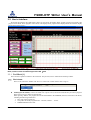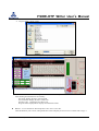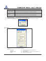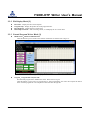
1
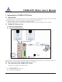
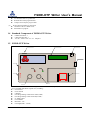
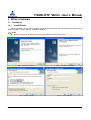
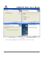
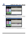
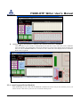
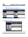
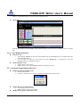
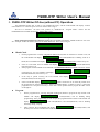
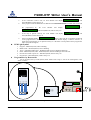
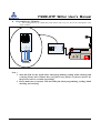
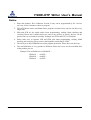
FSIDE-OTP Writer
User’s Manual
Rev. 1.0
May. 2006
Fortune Semiconductor Corp.
FSIDE-OTP-UM-10_EN
CR-004
FSIDE-OTP Writer User’s Manual
Taipei Office:
28F, No.27, Sec. 2, Zhongzheng E. Rd.,
Danshui Town, Taipei County 251, Taiwan
Tel.:886-2-28094742
Fax:886-2-28094874
http://www.fsc.com.tw
This manual contains new product information. Fortune
Semiconductor Corporation reserves the rights to modify the product
specification without further notice. No liability is assumed by Fortune
Semiconductor Corporation as a result of the use of this product. No
rights under any patent accompany the sale of the product.
Fortune Semiconductor Corp.
2/25
Rev. 1.0
FSIDE-OTP Writer User’s Manual
Table of Contents
Page No
1. INTRODUCTION OF FSIDE-OTP WRITER................................................................................ 4
1.1
Introduction ........................................................................................................................................... 4
1.2
FSIDE-OTP Writer Tool ....................................................................................................................... 4
1.3
The Functions of the FSIDE-OTP Writer ........................................................................................... 4
1.4
Standard Component of FSIDE-OTP Writer ..................................................................................... 5
1.5
FSIDE-OTP Writer ............................................................................................................................... 5
1.6
Power System ......................................................................................................................................... 6
1.7
Communication/Program Interface..................................................................................................... 6
1.8
Button ..................................................................................................................................................... 6
1.9
IC Adapt Socket..................................................................................................................................... 6
2. WRITER’S SOFTWARE .................................................................................................................. 8
2.1
Installation ............................................................................................................................................. 8
2.1.1
2.1.2
2.2
Install/Delete ............................................................................................................................................. 8
Execute FSCProgrammer Software .................................................................................................... 10
User’s Interface ................................................................................................................................. 11
2.2.1
2.2.2
2.2.3
2.2.4
2.2.5
2.2.6
2.2.7
2.2.8
Tool Block [1]........................................................................................................................................... 11
File Display Block [2]............................................................................................................................... 15
Normal Program Writer Block [3] ............................................................................................................ 15
Auto Program Writer Block [4] ................................................................................................................ 17
Block Program Writer Block [5]............................................................................................................... 18
Code Display Block [6]............................................................................................................................. 19
Program Status Display Block [7]............................................................................................................. 19
Interface Display Block [8]....................................................................................................................... 20
3. FSIDE-OTP WRITER OFF-LINE (WITHOUT PC) OPERATION .......................................... 21
4. REVISION HISTORY..................................................................................................................... 24
NOTICE: ................................................................................................................................................. 25
Fortune Semiconductor Corp.
3/25
Rev. 1.0
FSIDE-OTP Writer User’s Manual
1. Introduction of FSIDE-OTP Writer
1.1 Introduction
FSIDE-OTP Writer is developed by FSC for all FSC OTP(One Time Programmable) products. This tool uses USB
communication interface. There are two modes, PC on-line and writer off-line operations.
This manual takes FS9821 as an example to describe the operation.
English or Chinese can be used for the window’s language, and this manual takes English version as example.
1.2 FSIDE-OTP Writer Tool
The whole tool set includes two parts:
z Software:FSCProgrammer
z Hardware:FSIDE-OTP Writer
Fig1.1
FSIDE-OTP Writer
FSCProgrammer software provides the friendly interface. FSIDE-OTP Writer hardware is the convenient program mass
production tool. The power supply could be from DC 5Vpower or USB power.
1.3 The Functions of the FSIDE-OTP Writer
The functions of FSIDE-OTP are listed as below:
(1) PC On-line Operation
z Check the OTP IC is blank or not.
z Download the program file.
Fortune Semiconductor Corp.
4/25
Rev. 1.0
FSIDE-OTP Writer User’s Manual
z
z
z
To check the OTP IC’s product ID.
Read the data in the programmed IC.
Compare and verify the program data.
(2) Writer Off-line(without PC) Operation
z Check the OTP IC is blank or not.
z Push button to program.
1.4 Standard Component of FSIDE-OTP Writer
z
z
z
FSIDE-OTP Writer: 1
USB (AB) cable line: 1
AC 100 ~ 240V To DC 5V / 1A Adapter: 1
Power
1.5 FSIDE-OTP Writer
SPI
Boost
Fig1.2 FSIDE-OTP Writer(Topside)
Fig1.2 is FSIDE-OTP Writer topside view, including:
z
DCV Socket
z
Power Switch
z
USB Port
z
Dice Programming COM: Boost mode(COM1)
z
Dice Programming COM: SPI mode(COM2)。
z
IC Adapt Socket
z
LCD Module
z
Button K1、K2。
z
LED light(LED1、LED2)
Fortune Semiconductor Corp.
5/25
Rev. 1.0
FSIDE-OTP Writer User’s Manual
1.6 Power System
z
z
AC 100 ~ 240V To DC 5V / 1A adapter.
DCV Socket, Voltage: DC +5V. Please refer to Fig 1.3.
z
Power Switch
Fig 1.3
DCV Socket
1.7 Communication/Program Interface
(1)
USB Port is the standard USB communication interface. Please connect the PC and the Writer with an USB(AB)
cable. One is the Writer’s USB Port and the other is the PC’s USB port. Please make sure it’s connecting well
before you use it.
(2)
COM1,Boost Mode Program Output Interface: FS9821, FS9822, FS9823, FS9855 and FS6811. It’s a standard
DB9 interface. It’s the interface to program dice.
Pin1~9 definition
Pin1: RUNMP, program signal data line SDA, connect to Boost Mode programmed IC’s SDA pin;
Pin 2: PT21, program signal clock line SCL, connect to Boost Mode programmed IC’s SCK pin;
Pin 3: RESET, reset signal line, connect to Boost Mode programmed IC’s RST pin;
Pin 4: VPP_FS98, program identification voltage(DC 12V)output port, connect to Boost Mode programmed IC’s
VPP pin;
Pin 5: VCC_FS98, Program Power(DC 5.6~6.0 V)output port, connect to Boost Mode programmed IC’s VDD
pin;
Pin 6 ~ Pin 9: VSS_ice (GND), connect to Boost Mode programmed IC’s VSS pin.
(3)
COM2,SPI Mode Program Output Interface: FS9824, FS3861 and etc.
Pin1~9 definition
Pin1:RUNMP, program signal data line SDA, connect to SP1 Mode programmed IC’s SDA pin;
Pin 2:PT21, program signal clock line SCL connect to SP1 Mode programmed IC’s SCK pin;
Pin 3:VPP_FS24, program identification voltage(DC 12V)output port, connect to SP1 Mode programmed IC’s
VPP pin;
Pin 4:VCC_FS98, Program Power(DC 5.6~6.0 V)output port, connect to SP1 Mode programmed IC’s VDD pin;
Pin 5 ~ Pin 9 : VSS_ice (GND), connect to SP1 Mode programmed IC’s VSS pin.
1.8 Button
z
z
Button “K1”: Program the programmed IC.
Button “K2”: Check the programmed IC is blank or not.
1.9 IC Adapt Socket
Please use different IC Adapt Sockets to program different package type OTP ICs. Please refer to the below
description.
(1) FS9823 & FS9822 IC Adapt Socket: The IC Adapt Socket of FS9823 and FS9822 are the same. Please refer to
Fig1.4.
Note: Please use three jumps on “23” marking if you want to program FS9823 or FS98O23. Please use three jumps
on “22” marking if you want to program FS9822 or FS98O22.
Fortune Semiconductor Corp.
6/25
Rev. 1.0
FSIDE-OTP Writer User’s Manual
23
23
22
23
22
30
22
CONNECT1
Fig 1.4
FS9823 & FS9822 IC Adapt Socket Top-side
(2) FS9821 IC Adapt Socket: Please refer to Fig 1.5.
Fig1.5
FS9821 IC Adapt Socket Top-side
(3) FS3861 IC Adapt Socket: Please refer to Fig 1.6.
Fig 1.6
Fortune Semiconductor Corp.
FS3861 IC Adapt Socket Top-side
7/25
Rev. 1.0
FSIDE-OTP Writer User’s Manual
2. Writer’s Software
2.1 Installation
2.1.1
Install/Delete
“FSCProgrammer” can be used for programming all FSC OTP products, but the software only can be used at
Windows system, including WIN 98、WIN 2000、WIN XP.
(1)Install
z Execute “setup.exe”. Please refer to Fig2.1 and install the software step by step.
Step1:Execute “Setup.exe”
Step2:InstallShield Wizward
Step3:Agree to install
Step3: User’s authority
Fortune Semiconductor Corp.
8/25
Rev. 1.0
FSIDE-OTP Writer User’s Manual
Step5:Create the file folder
Step6:Start to install
Step7:安裝進行中
Step8:Installation Completed
圖 2.1 安裝畫面
Note: While installing “FSCProgrammer”, please login as “administrator” to avoid errors occurred.
Fortune Semiconductor Corp.
9/25
Rev. 1.0
FSIDE-OTP Writer User’s Manual
(2)Delete
Step1. Select ”Start->Steup->Control Panel” to open the control window.
Step2. Click “Add/Delete”and find “FSCProgrammer” in the list and click it.
Step3. Click “Delete” to delete the program.
2.1.2
Execute FSCProgrammer Software
After installation,Execute” Start->Program-> FSC-ProgrammerÆFSCProgrammer”. Please refer to Fig 2.2.
Fig 2.2
Fortune Semiconductor Corp.
The User’s Interface of FSCPorgrammer
10/25
Rev. 1.0
FSIDE-OTP Writer User’s Manual
2.2 User’s Interface
We divide the interface into eight blocks. There are tool block, file display block, normal program writer block, auto
program writer block, block program writer block, code display block, program status display block and interface display
block. Please refer to Fig2.3.
Fig 2.3
Function Block of FSCPorgrammer User’s Interface
Note:Please set the resolution higher than 800 × 600.
2.2.1 Tool Block [1]
There are three operation columns in the tool block. They are File, Device Information and Setup column.
(1) File Column
There are two functions “OPEN” and “Save as” in the “File” column. Please refer to Fig 2.4.
z
Fig 2.4 File
OPEN(Open the old files):Please click this icon or press Ctrl+O, and chose (load) the file you want to program.
Please refer to Fig 2.5. Please use the Hex file.
When pressing “OPEN”, the program file will be downloaded to the EEPROM (28C256) in the FSC-OTP Writer,
including the following information:
1. Hex code of the program file
2. The product ID of the programmed IC:FS9821, FS9822….. and etc.
3. EEPROM Identification Code.
Fortune Semiconductor Corp.
11/25
Rev. 1.0
FSIDE-OTP Writer User’s Manual
4.
Program Mode:Boost or SPI.
Fig 2.5
Open (Open the file)
Fig 2.6
Download Successfully
After finishing download the file successfully:
File Name: Display the file’s name and path.
File CheckSum: Display the file’s Check Sum.
File Hex Code: Display the file’s Hex Code.
Program Status Display Block: Display Download Successful.
z
Save as:To save the data at “Read Chip Hex Code” area as a new file.
Click this button or press Ctrl+S, and input the file’s name and path you want to save as. Please refer to Fig 2.7.
Fortune Semiconductor Corp.
12/25
Rev. 1.0
FSIDE-OTP Writer User’s Manual
Fig 2.7
(2) Device Information Column
z
Fig 2.8 Device Information
EEPromData(28C256):Read the data from the EEPROM(28C256) in the FSIDE-OTP writer.
Click this button or press Ctrl+E to start read the data. Please refer to Fig 2.9 after finishing reading data. The
complete hex code will be displayed at “Read Chip Hex Code” area.
Fig 2.9
Message
EPPROM:X
Fortune Semiconductor Corp.
Description
If X shows PASS, the hex file is already downloaded to EEPROM
13/25
Rev. 1.0
FSIDE-OTP Writer User’s Manual
If X shows PASS, the hex file is not downloaded to EEPROM yet.
z
Pro. Type:X Mode
If X shows Boost, it means the programmed IC is Boost mode. Ex: FS9821.
If X shows SP1, it means the programmed IC is SP1 mode. Ex: FS3861.
CheckSum:X
X is stand for the CheckSum of the file.
Protect:X
If X shows Yes, the programmed IC will execute program protection.
If X shows No, the programmed IC will not execute program protection.
Chip Type:X
X is stand for the product ID of the programmed IC
Read Program Chip Type:Read the product ID of the programmed IC
Click this button or press Ctrl+I to start read the product ID of the programmed IC. Please refer to Fig 2.10.
Fig 2.10
(3) Setup
Fig 2.11 Setting Configuration
Click this button or press Ctrl+U to show the setup menu
Including:
Select Chip
Æ Chose the product ID of the programmed IC
Language
Æ Chinese/English
Writer Chip Select
Æ
Chose the ROM Size and mode or the programmed IC
System
Æ Chose the computer’s system
Fortune Semiconductor Corp.
14/25
Rev. 1.0
FSIDE-OTP Writer User’s Manual
2.2.2 File Display Block [2]
z
z
z
z
File Name:Display the file’s name and path.
Program Chip:Display the product ID of the programmed IC.
File Checksum:Display the file’s Check Sum.
Read Chip Checksum:After executing “Read”, it will display the IC’s Check Sum.
2.2.3 Normal Program Writer Block [3]
z
Blank Check:Check IC ERPOM status
Click this button or press Ctrl+B to check the IC is blank or not. Please refer to Fig 2.12。
Fig 2.12 Display blank status of the IC
z
Program:Program and verify the code
Download the program file to FSIDE-OTP writer. Please refer to Fig 2.6.
Click this button or press Ctrl+P to program the IC. After programming, the writer will compare the data in
the IC with the program file. The comparison result will show as Fig2.13.
Fortune Semiconductor Corp.
15/25
Rev. 1.0
FSIDE-OTP Writer User’s Manual
z
z
Fig 2.13 Display Verify Successful status
COMPARE:Compare the data in the IC with the program file
Click this button or press Ctrl+C to compare the data in the IC with the program file. After comparing, the
comparison result will be displayed in program status display block. The data in the IC will be displayed in
“Read Chip Hex Code” area. If the IC’s and the file’s hex codes are different, the address will be displayed
in read. Please refer to Fig 2.14。
Fig 2.14 Display Verify Fail status
Read:Read the IC’s Hex Code
Click this button or press Ctrl+R to read the IC’s hex code. After reading, the reading result will be displayed
in program status display block and shows the IC’s hex code in “Read Chip Hex Code” area.
Fortune Semiconductor Corp.
16/25
Rev. 1.0
FSIDE-OTP Writer User’s Manual
z
Fig2.15 Read OK status
DownLoad:Down load the data in “File Hex Code” into FSC-OTP Writer’s EEPROM
Click this button or press Ctrl+R to download data in the File Hex Code to FSC-OTP writer’s EEPROM.
After downloading, the downloading result will be displayed in program status display block and shows the
file’s hex code in “File Hex Code” area. And the new code’s check sum will be displayed at File CheckSum.
Please refer to Fig 2.16.
Fig 2.16 Display the download status
2.2.4 Auto Program Writer Block [4]
After downloading the file’s data into the EEPROM in FSIDE-OTP writer, and you can chose the process you
want to execute. Click Auto or press Ctrl+A to execute the chosen process。
Fortune Semiconductor Corp.
17/25
Rev. 1.0
FSIDE-OTP Writer User’s Manual
Process:
1. Blank Check:Check the programmed IC is blank or not
2. Program:Program
3. Verify:Compare the data in the IC with the program file (EEPROM data)
4. Program Protect:Protect the programmed IC (0x0000 will be programmed in ROM’s last byte). After
executing program protect, the IC’s data will be read as 0x0000 for all bytes.
While programming
While verifing
Fig 2.17 Execute『Auto』
2.2.5 Block Program Writer Block [5]
z
If you have to do the second time program, you can use this function. Example: Program the Table’s data
Block Program
Fig 2.18 Block Program
Download the program file into EEPROM in FSIDE-OTP writer, or key-in the code in File Hex Code area and
click ”download” to download the data into EEPROM in FSIDE-OTP writer. Input the Start Address and End
Fortune Semiconductor Corp.
18/25
Rev. 1.0
FSIDE-OTP Writer User’s Manual
Address , click ”Black Program” or press Ctrl+W to program the IC.
z
Block Read
Fig 2.19 Block Read
Input the Start Address and End Address, click “Black Program” or press Ctrl+T to read the IC block’s program
data.
2.2.6 Code Display Block [6]
z
File Hex Code:
1.
2.
z
After clicking ”OPEN”, the file will be downloaded into the EEPROM(28C256) in FSIDE-OTP writer
and displayed in this area.
You can input and edit the code directly and click “DownLoad” to download the data into
EEPROM(28C256) in FSIDE-OTP writer.
Read Chip Hex Code:
1.
2.
Display the hex code of the IC
Display the hex code of the EEPROM(28C256) in FSIDE-OTP writer
2.2.7 Program Status Display Block [7]
z
Display the file’s download result
1.
2.
Download Successful
Down fail:Please refer to Fig 2.20. The block will display Down Load Failure.
Fig 2.20 Download Error
z
Display the check result of the IC
1.
2.
z
Chip is Empty: The IC is blank.
Blank Check Fail: The IC is not blank.
Display the program verification result
Fortune Semiconductor Corp.
19/25
Rev. 1.0
FSIDE-OTP Writer User’s Manual
1.
2.
z
Display the reading result
1.
2.
z
Verify successful
Verify fail
Read OK
Read Fail
Display the comparison result
1.
2.
Read OK
Verify Fail
2.2.8 Interface Display Block [8]
There are 3 items displayed in this block: Communication Interface, Software Version and Firmware Version.
1. Communication Interface:Display the communication interface
2. Software Version:Display the FSC-Programmer’s software version
3. Firmware Version:Display the FSIDE-OTP writer’s firmware version
Fortune Semiconductor Corp.
20/25
Rev. 1.0
FSIDE-OTP Writer User’s Manual
3. FSIDE-OTP Writer Off-line (without PC) Operation
The EEPROM 28C256 data is 0xFF in new FSIDE-OTP writer, and the LCD Module will display “Fortune
Semiconductor Co.” when the power is turn on. Please refer to Fig 3.1.
We have to download the Hex Code, product IC, EEPROM ID 、 Program Mode 、 Protect into the
EEPROM28C256 in FSIDE-OTP writer. Please refer to 2.2.1.
Fig 3.1
When download finished and re-start the power, the LCD Module will display ”FSIDE Pro.Device xxxx xxxx
xK”. Example: Product ID FS9821, Boost mode and2K ROM Size. Please refer to Fig 3.2
Fig 3.2
z
Blank Check
1.
Put the programmed IC correctly and push K2 (Blank Check) button to check the IC is blank or not, and
, and LED1(BLK/Fail) is blinking. If the IC is
the LCD Module will display
, and LED2(Pro/Pass) will be always on.
blank, the LCD Module will display
, and LED1(BLK/Fail)
If the IC is not blank, the LCD Module will display
light will be always on.
If the program mode and ROM size are different in the EEPROM 28C256 in FSIDE-OTP writer and the
2.
3.
programmed IC, the LCD Module will display
and LED1(BLK/Fail) will be always on.
z
or
,
, and
4.
If the chip is placed correctly, the LCD Module will display
LED1(BLK/Fail) will be always on.
5.
If the LCD Module display
, please connect the PC to check the product ID of
the programmed IC. Please refer to 2.2.1. If the LCD Module display “Unknown Version”, it means the
programmed IC is not placed correctly or is the older version product. Please program the older version
IC through PC.
Program
1.
Put the programmed IC correctly and push K1(Program) button to program the chip and the LCD
, LED2(Pro/Pass) will be blinking during
Module will display
programming. After programming, it will compare the programmed data and the LCD Module will
display
alternately during verifying.
2.
, and LED2(Pro/Pass) and LED1(BLK/Fail) will be blinking
After verifying, the LCD Module will display
be always on.. xxxxxx is stand for the Checksum of the hex code.
Fortune Semiconductor Corp.
21/25
, and LED2(Pro/Pass) will
Rev. 1.0
FSIDE-OTP Writer User’s Manual
If the verification result is fail, he LCD Module will display
, and
LED1(BLK/Fail) will be always on.
If the program mode and ROM size are different in the EEPROM 28C256 in FSIDE-OTP writer and
3.
4.
the
programmed
IC,
the
LCD
Module
will
or
display
, and LED1(BLK/Fail) will be always on.
z
If the chip is placed correctly, the LCD Module will display
LED1(BLK/Fail) will be always on.
6.
If the LCD Module display
, please connect the PC to check the product ID
of the programmed IC. Please refer to 2.2.1. If the LCD Module display “Unknown Version”, it
means the programmed IC is not placed correctly or is the older version product. Please program the
older version IC through PC.
LED Light Symbol
1.
2.
3.
4.
5.
6.
z
, and
5.
Program:PRO/Pass(LED2) LED is blinking
Blank Check:BLK/Fail(LED1) LED is blinking
Verify:PRO/Pass(LED2) LED、BLK/Fail(LED1) LED are blinking alternately
Read:PRO/Pass(LED2) LED、BLK/Fail(LED1) LED are blinking at the same time
Execute Successful or power on:PRO/Pass(LED2) LED is always on
Execute Fail:BLK/Fail(LED1) LED is always on
Program Dice by Boost mode:
We can program Dice by COM1 (Boost) mode. Please refer to Fig 3.3. We can do it through PC or the
writer’s buttons.
Power
PT2.0
PT2.1
RST
VPP
VDD
VSS
FS9821
FS9822
FS9823
FS3866
FS6811
Boost
FSC
SPI
SDA
RST
SCK
VPP
VSS
VDD
Fig 3.3
Fortune Semiconductor Corp.
22/25
Rev. 1.0
FSIDE-OTP Writer User’s Manual
z
Program Dice by SPI mode:
Power
FSC
GenIO1
GenIO0
VDD
VPP/RST
VSS
FS9824
FS3861
…
We can program Dice by COM2 (SPI) mode. Please refer to Fig 3.4. We can do it through PC or the
writer’s buttons.
SPI
Boost
SCK
SDA
VPP
VDD
VSS
Fig 3.4
Note:
1. SDA and SCK are the signal cables when programming, reading, blank checking and
verifying. Please don’t connect these two pins to any positive or passive devices. Or
the process can’t be executed successfully.
2. Please make sure to separate VPP and VDD pins when programming, reading, blank
checking and verifying.
Fortune Semiconductor Corp.
23/25
Rev. 1.0
FSIDE-OTP Writer User’s Manual
4. Revision History
Version
Date
Page
1.0
2006/5/22
All
Fortune Semiconductor Corp.
Revised Content
New Release
24/25
Rev. 1.0
FSIDE-OTP Writer User’s Manual
Notice:
1. When the product’s ID is Unknown Version, it only can be programmed by PC. And we
can’t use writer’s buttons to check or program.
2. FSC-OTP Writer can be used blank-check, program, read and verity only for one chip every
single time.
3. SDA and SCK are the signal cables when programming, reading, blank checking and
verifying. Please don’t connect these two pins to any positive or passive devices. Or the
process can’t be executed successfully. Example: the PT2.0 and PT2.1 of FS98O21.
4. Please make sure to separate VPP and VDD pins when programming, reading, blank
checking and verifying. Please remove the Regulator connecting to VDD.
5. The last byte of chip’s EPROM is used for program protection. Please don’t use this byte.
6. The real ROM Size of every product is different. Please don’t over use the real ROM Size
of the product you use.
Example: The real ROM size of FS98O2X:
FS98O23 : 0x1FFE;
FS98O22 : 0x0FFE;
FS98O21 : 0x07FE。
Fortune Semiconductor Corp.
25/25
Rev. 1.0