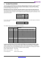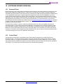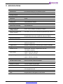
1
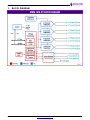
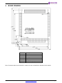
RUBY-MM-1616A Family
PC/104 / PC/104-Plus I/O Modules with 4, 8 or 16 16-Bit Analog Outputs
User Manual Rev A.4 March 2015
Revision
Date
A.3
5/12/2014
A.4
3/2/15
FOR TECHNICAL SUPPORT
PLEASE CONTACT:
[email protected]
Comment
Initial release
Removed register map details
Copyright 2015
Diamond Systems Corporation
www.diamondsystems.com
TABLE OF CONTENTS
1.
2.
Important Safe Handling Information .............................................................................................................3
Models and Features ........................................................................................................................................5
2.1
Description..................................................................................................................................................5
2.2
Features .....................................................................................................................................................5
2.3
Available Models ........................................................................................................................................6
3. Block Diagram ...................................................................................................................................................7
4. BOARD DRAWING ............................................................................................................................................8
5. I/O Connectors ..................................................................................................................................................9
5.1
PC/104 (J1, J2) ..........................................................................................................................................9
5.2
PC/104-Plus PCI Bus Connector (J3) ..................................................................................................... 10
5.3
Analog Output (J4) .................................................................................................................................. 11
5.4
Digital I/O (J5) ......................................................................................................................................... 12
5.5
Ribbon Cable ........................................................................................................................................... 13
6. Architecture Overview ................................................................................................................................... 14
6.1
Bus Interface ........................................................................................................................................... 14
6.2
D/A Circuit ............................................................................................................................................... 14
6.3
Digital I/O ................................................................................................................................................. 14
6.4
Counter/Timers and Clock Sources ........................................................................................................ 15
6.5
Pulse Width Modulators .......................................................................................................................... 15
6.6
Interrupts ................................................................................................................................................. 15
7. Jumper Configuration ................................................................................................................................... 16
7.1
Base Address (ISA models only) ............................................................................................................ 16
7.2
IRQ Selection (ISA models only) ............................................................................................................. 17
7.3
PCI Slot Number (PCI models only) ........................................................................................................ 17
7.4
Bus Select ............................................................................................................................................... 17
7.5
Digital I/O Logic Level ............................................................................................................................. 17
7.6
Digital I/O Pull-Up/Down.......................................................................................................................... 18
7.7
D/A Converter Power On Control ............................................................................................................ 18
7.8
Old Jumper .............................................................................................................................................. 18
7.9
Default Configuration ............................................................................................................................... 18
8. Analog Output Technology ........................................................................................................................... 19
8.1
Output Channel Organization .................................................................................................................. 19
8.2
Output Ranges and Resolution ............................................................................................................... 20
8.3
Output Modes .......................................................................................................................................... 21
8.4
Calibration ............................................................................................................................................... 21
9. Calibration EEPROM ..................................................................................................................................... 22
10. Software Driver Overview ............................................................................................................................. 23
10.1
Universal Driver ....................................................................................................................................... 23
10.2
Control Panel ........................................................................................................................................... 23
11. Specifications................................................................................................................................................. 24
RMM-1616AP-XT User Manual Rev A.4
www.diamondsystems.com
Page 2
1.
IMPORTANT SAFE HANDLING INFORMATION
WARNING!
ESD-Sensitive Electronic Equipment
Observe ESD-safe handling procedures when working with this product.
Always use this product in a properly grounded work area and wear appropriate
ESD-preventive clothing and/or accessories.
Always store this product in ESD-protective packaging when not in use.
Safe Handling Precautions
This board contains several I/O and bus connectors with many connections to sensitive electronic components.
This creates many opportunities for accidental damage during handling, installation and connection to other
equipment. The list here describes common causes of failure found on boards returned to Diamond Systems for
repair. This information is provided as a source of advice to help you prevent damaging your Diamond (or any
vendor’s) embedded computer boards.
ESD damage – This type of damage is usually almost impossible to detect, because there is no visual sign of
failure or damage. The symptom is that the board eventually simply stops working, because some component
becomes defective. Usually the failure can be identified and the chip can be replaced. To prevent ESD damage,
always follow proper ESD-prevention practices when handling computer boards.
Damage during handling or storage – On some boards we have noticed physical damage from mishandling. A
common observation is that a screwdriver slipped while installing the board, causing a gouge in the PCB surface
and cutting signal traces or damaging components.
Another common observation is damaged board corners, indicating the board was dropped. This may or may not
cause damage to the circuitry, depending on what is near the corner. Most of our boards are designed with at
least 25 mils clearance between the board edge and any component pad, and ground / power planes are at least
20 mils from the edge to avoid possible shorting from this type of damage. However these design rules are not
sufficient to prevent damage in all situations.
A third cause of failure is when a metal screwdriver tip slips, or a screw drops onto the board while it is powered
on, causing a short between a power pin and a signal pin on a component. This can cause overvoltage / power
supply problems described below. To avoid this type of failure, only perform assembly operations when the
system is powered off.
Sometimes boards are stored in racks with slots that grip the edge of the board. This is a common practice for
board manufacturers. However our boards are generally very dense, and if the board has components very close
to the board edge, they can be damaged or even knocked off the board when the board tilts back in the rack.
Diamond recommends that all our boards be stored only in individual ESD-safe packaging. If multiple boards are
stored together, they should be contained in bins with dividers between boards. Do not pile boards on top of each
other or cram too many boards into a small location. This can cause damage to connector pins or fragile
components.
Power supply wired backwards – Our boards are not designed to withstand a reverse power supply connection.
This will destroy each IC that is connected to the power supply (i.e. almost all ICs). This type of damage is not
covered under Diamond Systems’ warranty. The board will most likely will be unrepairable and must be replaced.
A chip destroyed by reverse power or by excessive power will often have a visible hole on the top or show some
deformation on the top surface due to vaporization inside the package. Check twice before applying power!
Overvoltage on bus connector – The PC/104-Plus PCI connector on this product is compatible with 3.3V buses
only. If the board is installed on a CPU module with 5V signaling on the PC/104-Plus connector, the FPGA on
board that provides the PCI interface may be damaged. The PC/104 ISA bus connector is 5V tolerant and will
work without problem in any valid PC/104 system.
Overvoltage on analog output – If an analog output is accidentally connected to another output signal or a
power supply voltage, the output can be damaged. On most of our boards, a short circuit to ground on an analog
output will not cause trouble.
RMM-1616AP-XT User Manual Rev A.4
www.diamondsystems.com
Page 3
Overvoltage on digital I/O line – If a digital I/O signal is connected to a voltage above the maximum specified
voltage, the digital circuitry can be damaged. On most of our boards the acceptable range of voltages connected
to digital I/O signals is 0-5V, and they can withstand about 0.5V beyond that (-0.5 to 5.5V) before being damaged.
However logic signals at 12V and even 24V are common, and if one of these is connected to a 5V logic chip, the
chip will be damaged, and the damage could even extend past that chip to others in the circuit.
Bent connector pins –This type of problem is often minor and mostly cosmetic, and is easily fixed by bending
the pins back to their proper shape one at a time with needle-nose pliers. The most common cause of bent
connector pins is when a PC/104 board is pulled off the stack by rocking it back and forth left to right, from one
end of the connector to the other. As the board is rocked back and forth it pulls out suddenly, and the pins at the
end get bent significantly. The same situation can occur when pulling a ribbon cable off of a pin header. However,
if the pins are bent too severely or too often, bending them back can cause them to weaken unacceptably or even
break, and the connector must be replaced.
RMM-1616AP-XT User Manual Rev A.4
www.diamondsystems.com
Page 4
2.
2.1
MODELS AND FEATURES
Description
The Ruby-MM-1616 is a family of PC/104 I/O modules featuring 4, 8 or 16 16-bit analog voltage and current
outputs, and 48 digital I/O lines. The module uses the Analog Devices AD5755 16-channel 16-bit DAC chip for the
D/A outputs and an FPGA with level-shifting transceivers for the DIO lines. A 50-pin connector provides access to
the 16 analog outputs, and another 50-pin connector provides access to the 48 DIO lines. The board operates
o
o
over the industrial temperature range of -40 C to +85 C and is supported by Diamond Systems’ Universal Driver
software. Models are available with either PC/104 or PC/104-Plus I/O expansion buses.
Ruby-MM-1616 utilizes individual digital calibration for each analog output channel. The calibration is performed
at the factory prior to shipment. All analog components are high accuracy and low drift, enabling the board to
avoid the need for recalibration for many applications during its useful lifetime.
2.2
Features
Board Features
4, 8 or 16 analog outputs with 16-bit D/A resolution
Programmable voltage output ranges: 0-5V, 0-10V, ±5V, ±10V, 0-20mA, 4-20mA, 0-24mA
Independent output range for each channel
Waveform generator on up to 16 channels
Simultaneous update of any combination of channels
Multi-channel simultaneous waveform output capability with up to 100KHz waveform update rate
Output current limit +/-5mA per channel in voltage mode
Autocalibration of D/A circuits using the internal offset and gain registers for each channel
40 byte-wide and 8 bit-wide digital I/O lines with programmable direction
2 32-bit programmable counter / timers
4 24-bit pulse width modulators
PC/104 ISA 16-bit bus interface or PC/104-Plus (ISA + PCI) 3.3V 32-bit bus interface
Software Support
Diamond’s Universal Driver software with functions including:
D/A output
D/A waveform generator
Calibration
Digital I/O – bit and byte-wide
Digital I/O – PWM
Mechanical, Electrical, and Environmental
PC/104 compliant form factor
Dimensions: 3.550 x 3.775” (90 x 96mm)
+5VDC input voltage
o
o
-40 C to +85 C operating temperature
RoHS compliant
RMM-1616AP-XT User Manual Rev A.4
www.diamondsystems.com
Page 5
2.3
Available Models
The following models are available, offering a selection of analog outputs for each bus configuration.
Model Number
RMM-1616AP-XT
RMM-816AP-XT
RMM-416AP-XT
RMM-1616A-XT
RMM-816A-XT
RMM-416A-XT
Analog Outputs
16
8
4
16
8
4
RMM-1616AP-XT User Manual Rev A.4
Digital I/O
48
48
48
48
48
48
Bus Interface
PCI + ISA
PCI + ISA
PCI + ISA
ISA
ISA
ISA
www.diamondsystems.com
Notes
Standard stocked item
Standard stocked item
50 unit minimum order
Standard stocked item
Standard stocked item
50 unit minimum order
Page 6
3.
BLOCK DIAGRAM
RMM-1616AP-XT User Manual Rev A.4
www.diamondsystems.com
Page 7
4.
BOARD DRAWING
Connector
J1 & J2
J3
J4
J5
J6
J8
Description
PC/104 connectors
PCI connector
Analog connector
Digital connector
IRQ jumper block
Base Address jumper block
Note: Connectors that are not intended for customer use are not identified or described in this manual.
RMM-1616AP-XT User Manual Rev A.4
www.diamondsystems.com
Page 8
5.
5.1
I/O CONNECTORS
PC/104 (J1, J2)
Connectors J1 and J2 provide the standard PC/104 16-bit ISA bus. These connectors are installed on all standard
models.
The PC/104-Plus has pins for +5V, -5V, 12V, and -12V power. RMM-1616A-XT uses only the +5V pins for power
and does not require any other power source. The 5V pins on the PC/104 and PC/104-Plus connector, if installed,
will both be used by the board, however any one connector’s pins are sufficient for powering the board.
For information on the signal definitions of these connectors, please view the PC/104 or PC/104-Plus
specifications available on www.pc104.org.
View from Top of Board
J1: PC/104 8-bit bus connector
IOCHCHKSD7
SD6
SD5
SD4
SD3
SD2
SD1
SD0
IOCHRDY
AEN
SA19
SA18
SA17
SA16
SA15
SA14
SA13
SA12
SA11
SA10
SA9
SA8
SA7
SA6
SA5
SA4
SA3
SA2
SA1
SA0
Ground
A1
A2
A3
A4
A5
A6
A7
A8
A9
A10
A11
A12
A13
A14
A15
A16
A17
A18
A19
A20
A21
A22
A23
A24
A25
A26
A27
A28
A29
A30
A31
A32
B1
B2
B3
B4
B5
B6
B7
B8
B9
B10
B11
B12
B13
B14
B15
B16
B17
B18
B19
B20
B21
B22
B23
B24
B25
B26
B27
B28
B29
B30
B31
B32
RMM-1616AP-XT User Manual Rev A.4
J2: PC/104 16-bit bus connector
Ground
RESET
+5V
IRQ9
-5V
DRQ2
-12V
0WS+12V
Key
SMEMWSMEMRIOWIORDACK3DRQ3
DACK1DRQ1
RefreshSYSCLK
IRQ7
IRQ6
IRQ5
IRQ4
IRQ3
DACK2TC
BALE
+5V
OSC
Ground
Ground
Ground
MEMCS16IOCS16IRQ10
IRQ11
IRQ12
IRQ15
IRQ14
DACK0DRQ0
DACK5DRQ5
DACK6DRQ6
DACK7DRQ7
+5V
MASTERGround
Ground
www.diamondsystems.com
D0
D1
D2
D3
D4
D5
D6
D7
D8
D9
D10
D11
D12
D13
D14
D15
D16
D17
D18
D19
C0
C1
C2
C3
C4
C5
C6
C7
C8
C9
C10
C11
C12
C13
C14
C15
C16
C17
C18
C19
Ground
SBHELA23
LA22
LA21
LA20
LA19
LA18
LA17
MEMRMEMWSD8
SD9
SD10
SD11
SD12
SD13
SD14
SD15
Key
Page 9
5.2
PC/104-Plus PCI Bus Connector (J3)
Connector J3 provides the standard PC/104-Plus 32-bit PCI bus interface. This connector is installed on all
models with P in the model number.
Warning: The PC/104-Plus connector on RMM-1616A-XT is not 5V tolerant. The board must be used in a
system with 3.3V signaling on the PC/104-Plus connector.
The PC/104-Plus connector has pins for both +3.3V and +5V power. RMM-1616A-XT uses only the +5V pins for
power and does not require +3.3V from the host computer. If the PC/104-Plus connector is not installed, the board
will still obtain +5V from the PC/104 ISA connectors J1 and J2.
For information on the signal definitions of this connector, please view the PC/104-Plus specification available on
www.pc104.org.
A1
A2
A3
A4
A5
A6
A7
A8
A9
A10
A11
A12
A13
A14
A15
A16
A17
A18
A19
A20
A21
A22
A23
A24
A25
A26
A27
A28
A29
A30
GND/KEY5
VI/O
AD05
C/BE0*
GND
AD11
AD14
+3.3V
SERR*
GND
STOP*
+3.3V
FRAME*
GND
AD18
AD21
+3.3V
IDSEL0
AD24
GND
AD29
+5V
REQ0*
GND
GNT1*
+5V
CLK2
GND
+12V
-12V
B1
B2
B3
B4
B5
B6
B7
B8
B9
B10
B11
B12
B13
B14
B15
B16
B17
B18
B19
B20
B21
B22
B23
B24
B25
B26
B27
B28
B29
B30
RMM-1616AP-XT User Manual Rev A.4
Reserved
AD02
GND
AD07
AD09
VI/O
AD13
C/BE1*
GND
PERR*
+3.3V
TRDY*
GND
AD16
+3.3V
AD20
AD23
GND
C/BE3*
AD26
+5V
AD30
GND
REQ2*
VI/O
CLK0
+5V
INTD*
INTA*
REQ3*
C1
C2
C3
C4
C5
C6
C7
C8
C9
C10
C11
C12
C13
C14
C15
C16
C17
C18
C19
C20
C21
C22
C23
C24
C25
C26
C27
C28
C29
C30
+5V
AD01
AD04
GND
AD08
AD10
GND
AD15
SB0*
+3.3V
LOCK*
GND
IRDY*
+3.3V
AD17
GND
AD22
IDSEL1
VI/O
AD25
AD28
GND
REQ1*
+5V
GNT2*
GND
CLK3
+5V
INTB*
GNT3*
www.diamondsystems.com
D1
D2
D3
D4
D5
D6
D7
D8
D9
D10
D11
D12
D13
D14
D15
D16
D17
D18
D19
D20
D21
D22
D23
D24
D25
D26
D27
D28
D29
D30
AD00
+5V
AD03
AD06
GND
M66EN
AD12
+3.3V
PAR
Reserved
GND
DEVSEL*
+3.3V
C/BE2*
GND
AD19
+3.3V
IDSEL2
IDSEL3
GND
AD27
AD31
VI/O
GNT0*
GND
CLK1
GND
RST*
INTD*
GND/KEY3
Page 10
5.3
Analog Output (J4)
Connector J4 brings the analog output signals to a pin header.
VOUT 0
AGND
IOUT 1
VOUT 2
AGND
IOUT 3
VOUT 4
AGND
IOUT 5
VOUT 6
AGND
IOUT 7
VOUT 8
AGND
IOUT 9
VOUT 10
AGND
IOUT 11
VOUT 12
AGND
IOUT 13
VOUT 14
AGND
IOUT 15
EXT TRIG
1
3
5
7
9
11
13
15
17
19
21
23
25
27
29
31
33
35
37
39
41
43
45
47
49
2
4
6
8
10
12
14
16
18
20
22
24
26
28
30
32
34
36
38
40
42
44
46
48
50
IOUT 0
VOUT 1
AGND
IOUT 2
VOUT 3
AGND
IOUT 4
VOUT 5
AGND
IOUT 6
VOUT 7
AGND
IOUT 8
VOUT 9
AGND
IOUT 10
VOUT 11
AGND
IOUT 12
VOUT 13
AGND
IOUT 14
VOUT 15
AGND
DGND
Connector type: 0.1” pitch 50-pin (2x25) dual row right-angle pin header with gold flashing.
Mating cable: Diamond Systems C-50-18
Connector signal definitions
Vout 0-15
Analog voltage outputs; quantity depends on model; All outputs start with Vout 0
and go up from there to Vout 3, Vout 7, or Vout 15
Iout 0-15
Analog current outputs; quantity depends on model; Outputs are aligned in the
same manner as voltage outputs
Agnd
Analog ground; one is provided for each channel, however all analog grounds
are tied together so the application can use one or more as desired.
Ext Trig
External trigger for D/A waveform generator when using external clocking
Dgnd
Digital ground, used as return for Ext Trig signal
RMM-1616AP-XT User Manual Rev A.4
www.diamondsystems.com
Page 11
5.4
Digital I/O (J5)
Connector J5 brings the 48 digital I/O signals to a pin header. These lines have 3.3V logic levels with 5V input
tolerance.
DIO A0
DIO A2
DIO A4
DIO A6
DIO B0
DIO B2
DIO B4
DIO B6
DIO C0
DIO C2
DIO C4
DIO C6
DIO D0
DIO D2
DIO D4
DIO D6
DIO E0
DIO E2
DIO E4
DIO E6
DIO F0
DIO F2
DIO F4
DIO F6
+5VDC
1
3
5
7
9
11
13
15
17
19
21
23
25
27
29
31
33
35
37
39
41
43
45
47
49
2
4
6
8
10
12
14
16
18
20
22
24
26
28
30
32
34
36
38
40
42
44
46
48
50
DIO A1
DIO A3
DIO A5
DIO A7
DIO B1
DIO B3
DIO B5
DIO B7
DIO C1
DIO C4
DIO C6
DIO C7
DIO D1
DIO D3
DIO D5
DIO D7
DIO E1
DIO E3
DIO E5
DIO E7
DIO F1
DIO F4
DIO F6
DIO F7
DGND
Connector type: 0.1” pitch 50-pin (2x25) dual row right-angle pin header with gold flashing.
Mating cable: Diamond Systems C-50-18
Connector signal definitions
DIO A0-A7
Digital I/O port A or 0; directions of all 8 bits are set in unison
DIO B0-B7
Digital I/O port B or 1; directions of all 8 bits are set in unison
DIO C0-C7
Digital I/O port C or 2; directions of all 8 bits are set in unison
DIO D0-D7
Digital I/O port D or 3; directions of all 8 bits are set in unison
DIO E0-E7
Digital I/O port E or 4; directions of all 8 bits are set in unison
DIO F0-F7
Digital I/O port F or 5; directions of each bit is set independently; these bits also
serve as counter and PWM I/O signals
+5VDC
+5VDC available for powering external logic; limited to ~100mA
Dgnd
Digital ground, used as return for Ext Trig signal
RMM-1616AP-XT User Manual Rev A.4
www.diamondsystems.com
Page 12
5.5
Ribbon Cable
The figure below shows Diamond Systems Cable C-50-18, which mates with both I/O connectors J4 and J5 on
the RMM-16161 board. This is a 50-conductor ribbon cable, 18 inches length, with 2x25 .1” pitch IDC female
connectors at both ends.
RMM-1616AP-XT User Manual Rev A.4
www.diamondsystems.com
Page 13
6.
ARCHITECTURE OVERVIEW
6.1
Bus Interface
The RMM-1616A-XT family uses a new FPGA architecture that includes both PCI and ISA bus interfaces. This
allows the full functionality of the board to be offered in both PC/104 (ISA connector only) and PC/104-Plus (ISA
and PCI connector) formats. (A PCI-104 version with only the PCI connector is available by special order.) The
PC/104-Plus models may use either the PCI or ISA connector with a jumper option. In most cases the user will
want to use the default PCI interface.
The board’s register map contains a total of 256 addressable 8-bit registers organized as 16 pages of 16 registers
each. Registers are grouped into pages according to function: A/D, D/A, digital I/O, etc. This page method allows
the board to occupy a small footprint of only 16 bytes in ISA mode. For consistency purposes the identical page
system is utilized in PCI mode as well.
In both PCI and ISA modes all I/O is 8 bits wide. Operations that require 16-bit or wider data, such as D/A
registers, counter/timer registers, and PWM registers, are managed with multiple 8-bit transactions.
6.2
D/A Circuit
The RMM-1616A-XT family utilizes the Analog Devices AD5755 D/A converter for all analog output functions. The
AD5755 provides 4 16-bit DACs with high accuracy, low drift, programmable voltage and current output ranges,
and digital calibration. Up to 4 of these devices may be installed on the board depending on the model. A
precision, low-drift 5V voltage reference circuit provides the basis for the overall accuracy of the analog outputs.
The AD5755 contains an integrated digital calibration circuit consisting of a multiplier and adder. Each time data is
written to a DAC, it undergoes a multiplication / addition operation, and the result is then transferred to the DAC
channel. This operation takes about 5 microseconds to complete. Thus each write to a DAC channel results in a 5
us delay before the output begins to update to the new value. The total settling time for one channel consists of
the settling time for the DAC plus this calibration time.
6.3
Digital I/O
The FPGA provides 48 digital I/O lines that are brought out to a separate I/O connector. All I/O lines are buffered
for protection and have user-configurable pull-up/down resistors as well as user-configurable 3.3V/5V logic levels.
These lines are grouped as 5 8-bit ports and 8 1-bit ports. The 8-bit ports utilize 8-bit bi-directional transceivers
whose directions are individually controlled via a register. The 1-bit ports utilize 1-bit bi-directional transceivers
whose directions are similarly individually controlled via a separate register. These 1-bit ports also serve as
handshake signals for the other 5 ports, as well as I/O signals for the counter/timers and PWMs.
Special functions are enabled on Port F to support digital I/O, counter/timer, and PWM operation. These functions
are controlled via register bits or commands in these other circuit blocks. The special configuration, when
enabled, overrides the current direction and value of the assigned port F bit.
The special functions for digital I/O and counter/timer operation are shown below:
Port F bit
F7
F6
F5
F4
F3
F2
F1
F0
Function
Ack
Latch
Ctr1Clk
Ctr0Clk
Ctr1Out
Ctr0Out
Ctr1Gate
Ctr0Gate
Direction
Out
In
In
In
Out
Out
In
In
I/O signals F3-0 may also be reassigned as PWM outputs as shown below:
Port F bit
F7
F6
F5
F4
F3
F2
F1
F0
Function
PWM3
PWM2
PWM1
PWM0
Direction
Out
Out
Out
Out
When a board reset occurs, all DIO lines are released from any counter or PWM assignment and return to normal
operation. They are reset to input mode, and their output registers are reset to 0.
RMM-1616AP-XT User Manual Rev A.4
www.diamondsystems.com
Page 14
6.4
Counter/Timers and Clock Sources
The FPGA includes 2 32-bit programmable counter/timers that serve a variety of purposes. The most common
uses are a divide-by-n counter to create a programmable rate generator and counting external pulses. Each
counter has programmable input, gate (count enable), and output functions. The input may be selected from the
on-board 50MHz clock, a 1MHz clock derived from the 50MHz clock, or an external signal via one of the 1-bit
digital I/O ports. The gate is optional and also derives from one of the 1-bit ports. The output is also optional. If
enabled it is driven onto one of the 1-bit ports as well. Both positive and negative output polarities are supported.
6.5
Pulse Width Modulators
The FPGA includes 4 24-bit pulse-width modulator circuits. Each circuit includes a period register as well as a
duty cycle register. Both registers may be updated in real-time without stopping the PWM. Duty cycles from 0100% inclusive are supported, as well as both positive and negative output polarity. The PWM clock may be
selected from the on-board 50MHz clock or a 1MHz clock derived from the 50MHz clock. The PWM outputs may
be enabled onto the 1-bit port pins. These are general purpose I/O pins with limited voltage and current capability.
The user must determine whether these pins provide the appropriate voltage and current levels for the intended
application or whether additional buffering or amplification is required.
6.6
Interrupts
Interrupts enable the board to request service independently of program operation, typically in response to a userdefined time interval or an external event. The board supports interrupts from a variety of sources, including both
counter/timers and the digital I/O circuit. The application program is responsible for providing the interrupt service
routine to respond to the interrupt request. An unserviced interrupt request may cause the computer to crash.
Diamond’s Universal Driver software includes built-in interrupt handling routines that can link to user-defined
code. This feature lets you define the conditions that will generate an interrupt and then define the behavior of the
system when an interrupt occurs.
RMM-1616AP-XT User Manual Rev A.4
www.diamondsystems.com
Page 15
7.
JUMPER CONFIGURATION
This section describes how to configure the RMM-1616 board using jumper blocks J6 and J8. An illustration of the
two jumper blocks is shown below. All jumpers which are in use are installed in a vertical orientation across two
pins in the jumper blocks. The board may be supplied with several jumpers installed over only one pin, which is a
storage position. The jumper is not needed in the default configuration but is supplied for possible future use.
Jumpers that are not needed may be removed.
7.1
Base Address (ISA models only)
RMM-1616 occupies a range of 16 bytes in the I/O memory of the PC. The starting address of this 16-byte
window is called the base address. On ISA bus models, the base address is configurable with jumper block J8.
On PCI models, the base address is configured by the BIOS during system startup.
The jumper locations labeled A9 – A6 are used to select the ISA base address. These lines correspond to ISA
bus address lines SA9 – SA4. By definition, the lowest 4 address bits, SA3 – SA0, are all 0 for the base address,
since these are used to select a byte within the 16-byte window. The upper address lines, SA15 – SA10, are
always decoded as 0 to ensure a unique base address decode.
The table below lists the valid base address settings. When a jumper is installed, the corresponding address line
is 0. When a jumper is removed, the corresponding address line is 1. Addresses that are below 100 hex are
considered invalid and should not be configured. The default base address is 300 hex / 768 decimal.
A9
A8
A7
A6
In
In
In
In
Out
Out
Out
Out
Out
Out
Out
Out
Out
Out
Out
Out
In
In
In
In
Out
Out
Out
Out
In
In
Out
Out
In
In
Out
Out
In
In
Out
Out
In
Out
In
Out
In
Out
In
Out
In
Out
In
Out
RMM-1616AP-XT User Manual Rev A.4
Base
Address
(Hex)
100
140
180
1C0
200
240
280
2C0
300
340
380
3C0
Base
Address
(Decimal)
256
320
384
448
512
576
640
704
768
832
896
960
www.diamondsystems.com
default
Page 16
7.2
IRQ Selection (ISA models only)
The ISA bus interrupt level is selected with jumper block J6 from levels 3, 4, 5, 6, 7, 9, 10, 11, 12, and 15. Install a
jumper in any ONE location to select that IRQ number. Only one IRQ may be selected at a time.
The PC/104 bus requires a 1K ohm pull-down resistor on each IRQ line that is in use by a peripheral. If multiple
boards in the system are sharing the same IRQ number, only one board should have the pull-down resistor
installed. The pull-down resistor is enabled with jumper position PD on jumper block J6. The default is IRQ 7 and
pull-down enabled.
In PCI bus systems, the IRQ level is unique to each slot and is selected with the PCI slot selection jumpers.
7.3
PCI Slot Number (PCI models only)
PCI devices in a PC/104 system are configurable to occupy a “slot” on the bus. This emulates the physical slots
on a PCI backplane, where each PCI slot has its own unique signals for ID select, clock, and IRQ. Each PCI
device must be assigned to a unique slot. The PCI slot number for RMM1616 is selected with jumper positions
SL1 and SL0 on jumper block J8. The default is both jumpers installed to set PCI slot ID=00. Note: On many
PC/104-Plus SBCs, slot 0 may already be occupied by a device on the SBC, such as an Ethernet controller or
some other on-board peripheral.
SL1
In
In
Out
Out
7.4
SL0
In
Out
In
Out
Slot
0
1
2
3
Bus Select
On models with both the ISA and PCI connectors installed, the board can be set in auto-bus select mode. In this
mode, if the board is installed in a system with only the PC/104 connector, it will use the ISA interface, and if it is
installed in a system with the PCI connector (with or without the ISA connector), it will use the PCI interface. To
use auto-bus select mode, or to use PCI mode, install a jumper in position PCI on jumper block J8. This is the
default configuration. The jumper must be installed to enable PCI bus mode. If this jumper is removed, the board
will always communicate over the ISA bus, even if the PCI bus is present. The table below lists all the possible
configurations:
Jumper
Out
Out
In
In
7.5
PCI present
No
Yes
No
Yes
ISA present
Yes
Yes
Yes
Yes
Bus Used
ISA
ISA
ISA
PCI
Digital I/O Logic Level
The logic levels for the digital I/O can be set to either +5V or +3.3V logic levels. All DIO lines are configured for
the same voltage levels; it is not possible to configure some for 5V and some for 3.3V operation. The voltage level
is selected on jumper block J8. Install ONE jumper in either the 5V or 3V jumper location. The default is +5V.
WARNING: Install only one jumper in either 5V or 3.3V positions. Installing jumpers in both positions will short the
two power supplies together and cause damage to the board and/or the entire system.
RMM-1616AP-XT User Manual Rev A.4
www.diamondsystems.com
Page 17
7.6
Digital I/O Pull-Up/Down
The digital I/O lines are tied to individual pull-up/down resistors which may be jumpered to either the DIO logic
level voltage selected above or ground using locations UP or DN on jumper block J8, respectively. All DIO lines
are pulled up or down together; it is not possible to configure some for pull-up and some for pull-down. The
default is pull-up.
7.7
D/A Converter Power On Control
The D/A converters can be configured to power up in two modes, selected with jumper position POC on jumper
block J8:
1. Jumper installed: Current outputs are tristated and voltage outputs are tristated.
2. Jumper not installed: Current outputs are tristated and voltage outputs are tied to analog ground with a
30K ohm resistance.
The default setting is "jumper installed".
7.8
Old Jumper
Jumper block J6 has one position labeled "Old". This jumper is reserved for future use and is currently not
enabled.
7.9
Default Configuration
The default configuration (configuration in which the board is shipped from stock) is shown and illustrated below.
Note that both ISA and PCI configurations are provided for all boards, however only the relevant configuration will
matter depending on which bus connector is installed / in use.
ISA base address: 300 hex / 768 decimal
ISA IRQ level: IRQ 7, pull-down resistor enabled
PCI slot number: Slot 0
Bus select: Auto-bus select / PCI bus if available
Digital I/O logic levels: 5V
Digital I/O pull-up/down: Pull-up
D/A power-on control: Current and voltage outputs tristated
RMM-1616AP-XT User Manual Rev A.4
www.diamondsystems.com
Page 18
8.
8.1
ANALOG OUTPUT TECHNOLOGY
Output Channel Organization
The RMM1616A/AP-XT modules use the Analog Devices AD5755 quad 16-bit D/A converter chips to provide the
analog outputs. One to four chips are installed on the board, depending on the model. The channels are
organized as follows:
Board
Channel
0
1
2
3
4
5
6
7
8
9
10
11
12
12
12
12
RMM-1616AP-XT User Manual Rev A.4
Chip
Number
0
0
0
0
1
1
1
1
2
2
2
2
3
3
3
3
Channel Number
on Chip
0
1
2
3
0
1
2
3
0
1
2
3
0
1
2
3
www.diamondsystems.com
Page 19
8.2
Output Ranges and Resolution
These chips provide both voltage and current outputs in multiple output ranges. Each channel on each chip can
be set to a different output range, including voltage and current ranges on the same chip. Each channel has a
voltage output pin, a current output pin and a ground return pin. The application wiring must connect to the
voltage output pin or the current output pin, as needed.
A D/A converter converts a number, or output code, into an output voltage or current that is proportional to the
number. The output range is the range of possible output values, from the smallest (lowest) value up to the
highest (largest) value. The difference between the highest and lowest output value is called the span. For a +/-5V
output range, the span is 10V, and for a 4-20mA output range, the span is 16mA.
The smallest change in output value, or resolution, is equal to 1/2n x the span, in which n = the number of bits (in
this case 16). For a +/-5V output range, the resolution is 10V / 65535 = 153uV. This smallest change is commonly
referred to as 1 LSB or the Least Significant Bit.
RMM-1616AP-XT uses straight binary coding for all output values; the range of output codes is 0-65535. The
theoretical top value, 65536, requires 17 bits to be represented in binary form, which is unachievable in a 16-bit
value. Therefore the top value of each output range is unavailable, and instead the maximum output value is 1
LSB less than the top value. Because the lowest output code is always 0, which is represented in binary form, the
bottom value of each range is always equal to the exact nominal value of the range (within tolerance of the
accuracy).
The table below summarizes all this information for all output ranges on RMM-1616AP-XT.
Range Group
Unipolar Voltage
Unipolar Voltage
Bipolar Voltage
Bipolar Voltage
Current
Current
Current
Output
Range
0-5V
0-10V
+/-5V
+/10V
0-20mA
0-24mA
4-20mA
Span
5V
10V
10V
20V
20mA
24mA
16mA
Resolution
(1 LSB)
76.3uV
153uV
153uV
305uV
0.305uA
0.366uA
0.244uA
D/A Code 0
Output Value
0.0000V
0.0000V
-5.0000V
-10.0000V
0.0000mA
0.0000mA
4.0000mA
D/A Code 65535
Output value
4.9999V
9.9998V
4.9998V
9.9997V
19.9997mA
23.9996mA
19.9998mA
The conversion formula for analog outputs is the same for all ranges and is shown below (minimum output value
= output value for a code of 0 shown in the table above):
Output V/I = (D/A code / 65536) x Span + Minimum output value
On power-up or when the board is reset, all voltage and current output pins are set to a tristate mode. All outputs
are reset to the 0-5V output range with the output code of 0 programmed into the output registers, so that when
outputs are enabled the voltage pins will have 0V on them (and the current pins will remain tristated). The D/A
initialization sequence described later in this manual also sets all outputs to 0-5V range with 0V output. This
sequence can be modified to use a different output range as desired.
RMM-1616AP-XT User Manual Rev A.4
www.diamondsystems.com
Page 20
8.3
Output Modes
Each output channel on RMM-1616AP-XT can be updated individually, or any number of channels can be
updated simultaneously, including different channels on different chips. Simultaneous update is useful when the
application requires precise timing to avoid distortion or errors in the behavior of the controlled device, for
example when controlling the movement of an X-Y table or a laser beam. The Error! Reference source not
found. chapter in this manual describes both single-channel and multi-channel output modes.
8.4
Calibration
Note: The RMM-1616 is factory calibrated. All calibration settings are stored in an on-board EEPROM for instant
automatic recall each time the board powers up. All analog outputs power up to 0V for safety. If recalibration or
calibration for nonstandard D/A ranges are needed, please contact Diamond Systems for technical support.
All analog components contain inherent errors in offset and gain which affect the accuracy of the signals they
generate. These errors are very small on RMM-1616AP-XT; however they are still present and could present a
problem for some high-precision applications. Calibration is used to correct these errors so that the actual output
of the D/A channels is as close as possible to the theoretical output.
The AD5755 D/A converter uses a digital calibration method to correct for offset and gain errors. Each output
channel has a 16-bit Offset register, called the C register, and a 16-bit Gain register, called the M register. This
enables each channel to be calibrated independently for maximum overall accuracy. Each time an output code is
written to a channel, the chip will automatically apply the offset and gain correction to the code, resulting in a
corrected digital value. This corrected value is then converted to the output voltage or current according to the
output range. The calibration process takes about 5us and is unavoidable. This 5us delay is included in the
specified settling time for the analog outputs.
For improved accuracy, the bipolar voltage, unipolar voltage, and current output range groups each have their
own calibration settings. Within any group, for example between the 0-5V and 0-10V ranges, the differences in
errors are very small, so the same calibration values are used for the entire group. However between range
groups the errors are noticeable, so separate calibration values are used for each group.
The calibration values for the unipolar and bipolar voltage range groups are stored in an EEPROM on the board.
On power-up or reset, the unipolar voltage range calibration values are read from the EEPROM and loaded into
the AD5755 chips. If needed, the calibration values for a different range can be read from the EEPROM and
stored. This is explained in the How-to section later in this manual.
Note: There are no calculated calibration values for current output ranges. Instead, default values are used.
When using a current output range, the application software can load the default calibration values into the DACs.
See the Calibration EEPROM information below for the default values.
The conversion formula from the written output code and the calibrated code is as follows:
Corrected code = Written code x (M register / 65535 (0xFFFF)) + (C register – 32768 (0x8000))
The minimum value is always 0, and the maximum value is always 65535 / 0xFFFF. Any result which exceeds
these limits will be automatically set to the limit.
The corrected code is then converted to the output voltage or current according to the formula above.
RMM-1616AP-XT User Manual Rev A.4
www.diamondsystems.com
Page 21
9.
CALIBRATION EEPROM
The board contains an EEPROM that stores the factory calibration settings for the board. For safety, a protected
area of the EEPROM stores a backup copy of the factory calibration settings. In case the calibration settings
become accidentally corrupted, contact Diamond Systems Technical Support for information on how to restore
the calibration settings from the backup copy.
Each channel has its own set of calibration values. Each calibration value is 16 bits, occupying two bytes in the
EEPROM. Each output range group has two calibration values, one for offset (called the C value) and one for
gain (called the M value). There are two output range groups with calibration values, unipolar voltage (0-5V and 010V) and bipolar voltage (+/-5V and +/-10V). Thus there are a total of 8 calibration bytes for each channel, or 128
bytes total for the board:
Unipolar offset (C)
Unipolar gain (M)
Bipolar offset (C)
Bipolar gain (M)
2 bytes
2 bytes
2 bytes
2 bytes
Current output ranges do not have calibration values. The calibration values for all current ranges on all channels
are fixed as follows:
Offset / C value
0x8000
Gain / M value
0xFE00
The calibration data is stored in the EEPROM as shown below:
Hex
0
1
2
3
4
5
6
7
…
3C
3D
3E
3F
Address
Decimal
0
1
2
3
4
5
6
7
…
60
61
62
63
Definition
Channel 0 M (gain) value LSB for unipolar ranges
Channel 0 M (gain) value MSB for unipolar ranges
Channel 0 C (offset) value LSB for unipolar ranges
Channel 0 C (offset) value MSB for unipolar ranges
Channel 1 M (gain) value LSB for unipolar ranges
Channel 1 M (gain) value MSB for unipolar ranges
Channel 1 C (offset) value LSB for unipolar ranges
Channel 1 C (offset) value MSB for unipolar ranges
…
Channel 15 M (gain) value LSB for unipolar ranges
Channel 15 M (gain) value MSB for unipolar ranges
Channel 15 C (offset) value LSB for unipolar ranges
Channel 15 C (offset) value MSB for unipolar ranges
In general you should never have to write new data to the EEPROM, since the analog components on RMM1616A-XT feature high accuracy and very low drift. However reading from the EEPROM is necessary to recall
calibration settings when you change analog output ranges in order to ensure best accuracy. It is advisable to
recall the calibration values from the EEPROM whenever the range is changed from one range group to another.
When changing ranges within a range group, no calibration recall is necessary.
Unipolar voltage range group:
0-5V, 0-10V
Bipolar voltage range group:
+/-5V, +/-10V
Current range group:
0-20mA, 0-24mA, 4-20mA
RMM-1616AP-XT User Manual Rev A.4
www.diamondsystems.com
Page 22
10. SOFTWARE DRIVER OVERVIEW
10.1
Universal Driver
Diamond Systems’ free Universal Driver software provides a powerful and efficient method of accessing all of the
features and capabilities of RMM-1616A-XT. While many I/O boards are very simple in operation and can be
controlled easily with simple I/O commands, the D/A, counter/timers, PWM, and interrupt features of RMM-1616AXT are sophisticated and require complex setup and management to utilize their full capabilities. The how-to
section of this manual provides an overview of the most common uses of the board which can suffice for many
applications if you are using an operating system not supported by Universal Driver. However if you are using an
OS supported by Universal Driver it is far more efficient and effective to use Universal Driver. The Universal
Driver software and documentation are available online at www.diamondsystems.com/products/dscud. The driver
package consists of several downloadable modules: The main driver software package, the board-specific demo
programs, and the documentation.
Universal Driver provides a collection of high level software functions in a library compatible with popular C
language compilers. The functions include board initialization, D/A operations, D/A waveform generator, digital
I/O, counter/timer operations, PWM functions, and interrupts. Universal driver lets you utilize all the features of
RMM-1616 quickly and efficiently without having to deal with register-level commands or complex sequences of
operations. A collection of demo programs provide illustration of the use of the driver functions and also provide a
convenient starting point for your own application development.
10.2
Control Panel
Included with Universal Driver is a Windows Control Panel program (graphical user interface) that runs in
Windows XP and 7. The Control Panel provides a quick way to access all the features of the board in a simple
and intuitive manner. It is highly recommended as a starting point when using the RMM-1616. It can be used to
verify that the board is installed and operating correctly as well as to become familiar with the various capabilities
of the board. The Control Panel is included with the main Universal Driver package.
RMM-1616AP-XT User Manual Rev A.4
www.diamondsystems.com
Page 23
11. SPECIFICATIONS
Host Interface
Interface bus
PC/104 8-bit ISA bus or PC/104-Plus PCI bus
Bus selection
Autodetection with PCI priority; manual ISA override
Analog Outputs
Number of outputs
4, 8 or 16
Resolution
16 bits
Output ranges
0-5V, 0-10V, ±5V, ±10V, 0-20mA, 0-24mA, 4-20mA
Settling time
10us maximum to ±.003%
Linearity error
±2 LSB maximum
Differential nonlinearity
±2 LSB maximum
Monotonicity
15 bits minimum
Output current limit
(voltage outputs)
8mA or 16mA, software selectable per channel
Open-circuit voltage limit
(current outputs)
23V, 24.5V, 27V or 29.5V, software programmable per channel
Reset
All DACs reset to tristate on voltage and current output pins
Programmable clear code, independent value per channel
Waveform Generator
Number of channels
1 to 16
Buffer size per channel
1 to 2048 samples, software programmable
2048 total sample limit
Trigger source
Software, counter/timer or external signal, software selectable
Digital I/O
Number of lines
40 byte-wide, 8 bit-wide, programmable direction
TTL/CMOS compatible
Input voltage
Logic 0: -0.5V min, 0.8V max
Logic 1: 2.0V min, 5.5V max
Output voltage
Logic 0: 0.0V min, 0.4V max
Logic 1: 3.0V min, 4.6V max
Output current
±2.5mA maximum per line
I/O data transfer modes
Normal or latched, software selectable
Counter/Timers
Number of counters
2 32-bit, software programmable
Clock sources
50MHz, 5MHz or external signal, software selectable
Count direction
bidirectional, software programmable; optional automatic reload at
0 for rate generator use
Clock source
Internal or external, software selectable
Gate
Programmable counter gate for each counter
RMM-1616AP-XT User Manual Rev A.4
www.diamondsystems.com
Page 24
PWMs
Number of PWM channels
4 24-bit, software programmable period and on-time
Duty cycle
0 – 100%, programmable
Output polarity
Positive or negative, programmable
Clock sources
50MHz or5MHz, software selectable
Interrupts
Sources
Counter/timer, digital I/O or D/A fault, software selectable
Software support
Universal Driver supports execution of user-supplied code on
interrupt
Mechanical
Dimensions
3.550” x 3.775” / 90.2 x 95.9mm; PC/104 compliant
Component height
Top side: 0.435” / 11.2mm max
Bottom side: 0.1” / 2.5mm max (not including PC/104 connector
pins and PC/104-Plus shroud)
PC/104 stacking
Compatible with both top and bottom stacking
I/O connectors
Dual 50-pin 2x25.1” pitch right angle pin headers; compatible with
industry standard 50-pin ribbon cables
Weight
3.0oz (85g)
General
Operating temperature
-40°C to +85°C
Input power
+5VDC +/-5%
MTBF
100,000 hours (calculated)
RoHS
Compliant
RMM-1616AP-XT User Manual Rev A.4
www.diamondsystems.com
Page 25