1
Faultfinding Guide
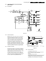
8.2
Circuit description of the current mode
power supply
8.2.1
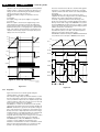
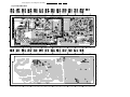
Blockdiagram
Rectifier
Lightning
Protection
CDR779
8.
GB 59
6210
5131
+5V
EMI
FILTER
MAINS
2
2643
6230
Start
Circuit
Comp
Overvoltage
Protection
+12V
5
7
Vcc
6240
9
v
2.5V
-8V
t
CLOCK
Error
Amplifier
+
-
PWM
Verror comparator
+
6250
7125
S
R
Q
latch
VFTD
Output
6220
Isense
Vfb
VDC2
Vsense
Rsense
CONTROL
VDC1
+12V +5V
Vcc
7131
0V
7201
REGULATION
CL 06532151_018.eps
271100
Figure 8-10
8.2.2
Function description
7
VI
MOSFET 7125 is used as a power switch controlled by the
controller IC 7110. When the switch is closed, energy is
transferred from mains to the transformer. This energy is
supplied to the load when the switch is opened. Through
control of the switched-on time, the energy transferred in
each cycle is regulated so that the output voltages are
independent of load or input voltage variations. The
controlling device UC3842 is an integrated pulse width
modulator. A clock signal initiates power pulses at a fixed
frequency. The termination of each output pulse occurs when
a feedback signal of the inductor current reaches a threshold
set by the error signal. In this way the error signal actually
controls the peak inductor current on cycle-by cycle basis.
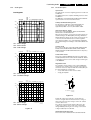
8.2.3
6V
+
16V +
5
GND
2.5V
8
Vref
BIAS
4
6
Rt/ct
1
OSC
2.5V
OUTPUT
S
ERROR AMP
2
Vfb
+
I SENSE COMP
2R
R
1V
+
R
1
COMP
LATCH
3
I sense
Figure B : Blockdiagram UC3842
Description of UC3842
The input voltage Vcc(pin 7) is monitored by a comparator
with hysteresis, enabling the circuit at 16V and disabling the
circuit below 10V. The error amplifier compares a voltage
Vfb(pin 2) related to the output voltage of the power supply,
with an internal 2.5V reference. The current sense
comparator compares the output of the error amplifier with
the switch current Isense(pin 3) of the power supply. The
output of the current sense comparator resets a latch, which
is set every cycle by the oscillator. The output stage is a
totem pole, capable of driving a MOSFET directly
5V
REF
S/R
-
CL 06532151_019.eps
271100
Figure 8-11
8.2.4
Start up sequence
t1: Charging the capacitor at Vcc
C2129 wiil be charged via R3123 and R3134, C2133 and
C2111 via R3129. The output is switched off
During t1.
t2: Charging of output capacitors
When the input voltage of the IC exceeds 14,5V, the circuit is
enabled and starts to produce output pulses. The current
consumption of the circuit increases to about 17mA,
depending on the external loads of the IC. At first, the
GB 60
8.
Faultfinding Guide
CDR779
capacitor at the Vcc pin will discharge because the primairy
auxiliary voltage, coming from winding7-9 is below the Vcc
voltage. At some moment during t2, the primary auxiliary
voltages reaches the same level as Vcc.
This primary auxiliary voltage now determines the Vcc
voltage
t3: regulation
The output voltage of the power supply is in regulation
t4: overload
When the output is shortened, the supply voltage of the
circuit will decrease and after some time drop below the
lower threshold voltage. At that moment, the output will be
disabled and the process of charging the Vcc capacitor starts
again. If the output is still shorted at the next t2 phase, the
complete start-and stop sequence will repeat. The power
supply comes in a hiccup mode.
becomes reversed. This results in a current flow through the
tranformer’s secondary winding via the diodes, electrolytic
capacitors and the load. This current is also ramp shaped but
decreasing.
TimeDEAD phase : when the stored energy has been
supplied to the load, the voltage from the secondary windings
falls below the output voltage(held constant by the
electrolytic capacitors) plus the threshold voltage of the
diodes. The current in the secondary winding stops flowing.
At this point, the drain voltage of the MOSFET is not yet zero
because C2609 between drain and source contains a certain
charge. This charge will start a sine-shaped ringing together
with the transformer’s self-induction.
The oscillator will start a next cyclus which consists of the
described three phases. The time of the different phases
depends on the mains voltage and the load.
TimeDEAD is maximum at an input of 400VDC and minimum
load, it will be zero at an input of 100VDC and overload.
16V
Vcc
12V
V2
Vosc
10V
Vc2134
V1
0V
0
Vcomp
20mA
Vsense
Icc
1mA
Vgate
OUTPUT
Vdrain
short
Idrain
Vo
0
t1
t2
t3
t4
Idiodes
Figure C : Start-up sequence
CL 06532151_020.eps
271100
Figure 8-12
8.2.5
Regulation
Figure 4 shows the most relevant signals during the
regulation phase of the power supply.
The oscillator voltage ramps up and down between V1 and
V2. The voltage at the current sense terminal is compared
every cycle with the output of the error amplifier Vcomp. The
output is switched off when the current sense level exceeds
the level at the output of the error amplifier.
TimeON phase : A drain current will flow from the positive
supply at pin 1 through the transformer’s primary winding, the
MOSFET and Rsense to ground. As the positive voltage at
pin 1 of the transformer is constant, the current will increase
linearly and create a ramp dependent on the mains voltage
and the inductance of the primary winding. A certain amount
of energy is stored in the transformer in the form of a
magnetic field. The polarity of the voltages at the secundary
windings is such that the diodes are non-conducting.
TimeDIODE phase : When the MOSFET is switched off,
energy is no longer supplied to the tranformer. The
inductance of the tranformer now tries to maintain the current
which has been flowing through it at a constant level. The
polarity of the voltage from the transformer therefore
Ton
Tdiode Tdead
CL 06532151_021.eps
271100
Figure 8-13
Faultfinding Guide
8.2.6
Oscillograms
8.2.7
Oscillograms
CH1 2
CH2
CH3 2 V~ ALT MTB5.00us- 0.90dv ch1-
PM3394B
ch1
1
T
3
GB 61
Circuit description
Input circuit
The input circuit consists of a lightning protection circuit and
an EMI filter.
The lightning protection comprises R3120, gasarrestor 1125
and R3124.
The EMI filter is formed by C2120, L5120, C2125 and R3124.
It prevents inflow of noise into/from the mains.
Start circuit and Vcc supply
This circuit is formed by R3123, R3134, C2129, D6129,
R3129, R3111, C2133 and C2111.
When the power plug is connected to the mains voltage, the
stabilised voltage over D6129(24V) will charge C2133 via
R3129. When the voltage reaches 14,5V across C2111, the
control circuit of IC7110 is turned on and the regulation
starts. During regulation, Vcc of IC7110 will be supplied by
the rectified voltage from winding 7-9 via L5132, D6132 and
C2133.
2
ch1 : Drain voltage
ch2 : Drain current
ch3 : Gate voltage
PM3394B
8.
Primary rectifier/smoothing circuit
The AC input is rectified by rectifier bridge 6102 and
smoothed into C2121. The voltage over C2121 is
approximately 300V. It can vary from 100V to 390V.
ch3
ch2
CDR779
CH1 1
CH3 50mV~ ALT MTB5.00us- 0.90dv ch1-
Control circuit
The control circuit exists of IC7110, C2102, C2104, C2107,
C2109, C2110, R3102, R3103, R3104, R3107, R3108,
R3109 and R3110. C2102 and R3110 define the frequency
of the oscillator.
ch1
Power switch circuit
This circuit comprises MOSFET 7125, Rsense 3126, 3127
and 3128, R3125, C2127, L5125, R3112 and R3113. R3125
is a pull-down resistor to remove static charges from the gate
of the MOSFET.
1
ch3
T
Regulation circuit
The regulation circuit comprises opto-coupler 7200 which
isolates the error signal from the control IC on the primary
side and a reference component 7201. The TL431(7201) can
be represented by two components:
• a very stable and accurate reference diode
• a high gain amplifier
3
ch1 : Drain voltage
ch2 : Oscillator voltage
PM3394B
K
CH1 1
CH3 20mV~ ALT MTB5.00us- 0.90dv ch1-
R
ch1
2.5V
1
ch3
T
A
CL 06532151_023.eps
271100
Figure 8-15
3
ch1 : Drain voltage
ch3 : Sense voltage
Figure 8-14
CL 06532151_022.eps
301100
TL431 will conduct from cathode to anode when the
reference is higher than the internal reference voltage of
about 2.5V. If the reference voltage is lower, the cathode
current is almost zero.
The cathode current flows through the LED of the optocoupler. The collector current of the opto-coupler flows
through R3106, producing an error voltage, connected to
voltage feedback pin 14 of IC7110.
Overvoltage protection circuit
This circuit consist of D6114, C2114, R3115and R3116.
GB 62
8.
Faultfinding Guide
CDR779
Secondary rectifier/smoothing circuit
There are 5 rectifier/smoothing circuits on the secondary
side. Each voltage depends on the number of windings of the
transformer.
The -8V supply is regulated by voltage regulator 7249.
When the regulation circuit is interrupted due to an error in
the control loop, the regulated output voltage will increase
(overvoltage). This overvoltage is sensed on the primary
winding 7-9. When an overvoltage longer than 2.0µs is
detected, the output is disabled until Vcc is removed and then
re-applied. The power supply will come in a hiccup mode as
long as the error in the control loop is present.
8.2.8
On/off circuit
In off mode pin 1 and pin 2 of connector 0206 are connected.
The high voltage (-8V, +12V) over opto coupler 7200 forces
this one to conduct . IC 7110 is switched off
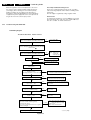
Troubleshooting PSU CDR3-ECO
Faultfinding diagram
TROUBLE SHOOTING POWER SUPPLY
OK
Check DC voltages
+5V +12V -8V VFTD(-38V) VDC1-VDC2(3V8)
power supply OK
NOK
Disconnect the power supply from the MAIN Board
Connect a dummy load resistor 6,8 ohm 10W (min 5W)
on the 5V and
OK
Check DC voltages
+5V +12V -8V VFTD(-38V) VDC1-VDC2(3V8)
power supply OK
check - main board
- front board
- modem board
NOK
OK
Check the +5V
check the fault voltage path
NOK
check 6210-2210-2253-5210
OK
connect the mains inlet to a mains
isolated variac
turn input voltage up and check across
C2121 the voltage
this voltage should be +/- 1,41 x Vin ac
NOK
check the functionality of the following components:
1120-2121-2125-2126-2127-6102-7125
YES
check the load on the secundairy output
check overload circuit 6141-7141-7150
OK
is power supply ticking?
NO
check Vcc on pin 7 IC7110
Vcc = 12V...... 16V
NOK
check 2121-2133-2134-3123-3134-6130-6132
replace 7110
NOK
check 2102 - 3102
replace 7110
OK
check oscillator on pin 4 IC7110
is the osc +- 30kHz working ?
OK
check the voltage on the source of 7125
Vsource = 1,3V ?
YES
check 3125-3126-3127-3128
replace 7125
NO (Vsource = +- 0.8V)
Disconnect diode 6150
start variac from 0V and turn-up slowly
measure the 5V output
If the 5V becoming higher than 5V, the regulator
circuit are damaged
5V NOK
check:3201-3202-3203-3204-3205
3206-3207-3208-7131-7201
replace 7110
check circuit around Ic7110
5V OK
After the power repaired check the 3,3V
Figure 8-16
CL 06532151_024.eps
271100
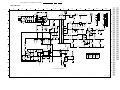
Block diagrams, Circuit diagrams and PWB’s
CDR779
5.
GB 36
PSU CDR3-ECU
6
2131
6210
2n2
SB360
2253
2213
2m2
should be YK type
5
3203
100n
2111
100n
2161
1n8
2102
330p
2109
F219
10u
3236
2252
12K
5K6
3232
3229
3233
D
3220
100u
2222
3222
1K2
UDZ-2.7B
1K2
3223
390R
VDC2
F212
VDC1
E
3202
2202
3204
22n
10K
3K3
10R
100n
F211
C
F209
10u
3221
330u
2220
3201
2201
VFTD
F210
5220
F208
Euro
2121
3122
5120
5121
9122
0101
47u
Reserved
UF1922P
Reserved
Jumper
Unpolarized
WW
100u
2R7
Reserved
CU15D3
Reserved
Unpolarized
USA
220u
Reserved
Reserved
CU15D3
Jumper
Polarized
F
3
-8Vr
1K
G
100R
22K
F122
3109
1K
1
3102
1K
3106
4n7
2106
1K5
3150
100n
2150
6150
UDZ-4.7B
47n
2221
33R
3113
270R
F216
6
B
11
+5Vr
3205
GND
7131
CQY80NG
7
220R
RtCt
F215
8
3K3
VCC
Isense OUTPUT
7254
BC847B
F207
10u
4u7
3206
Vfb
F110
3K3
68R
7253
BC327-25
5226
+12Vr
3207
Vref
BYD33D
4u7
18
3208
4
COMP
5225
6202
BYD33D
6220
100u
10K
2133
16
7
470R
3
15K
3105
56K
3151
F
6132
3234
68R
3224
100u
3225
2250
3128
1R
3127
1R
3126
7110
UC3842A
1SS355
3103
6133
1n
2104
15K
3104
100n
2142
2u2
2141
10K
3141
10R
3142
7150
BC847B
3110
100u
2134
68R
3111
BZX84-C24
4u7
6129
2129
1SS355
22R
UDZ-20B
6141
3112
9
2
10n
22u
2234
7251
BC337-40
BYD33J
68u
6130
5250
-8V
10u
470R
OUT
10
F214
UDZ-22B
1
9
3235
6201
220u
3
GND
8
-8V
F213
3K3
6250
2130
5130
BC857B
7141
7
+12V
1R5
5255
1u
1
6
+5V
F222
7252
BC857B
14
T
5
+5V
6
F221
+12V
2u2
5240 F205 F206
100u
IN
2240
2231
1m
2
BYD33D
13
2242
470p
6240
2
7249
L7908
-8Vr
11
2127
10K
3125
3230
2230
15
OUT
GND
2232
IN
A
4
5
F204
5230 F203
3
2243
100u
2121
1N4006
1N4006
6106
6107
1
BYW98-200
83R
E
3
VDC1
4
+5V
EH-B
2
VFTD
F230
10
F121
+12V
7260
6230
F111
7125
STP3NB60FP 5125
0125
HEATSINK
10K
1
VDC2
F220
C
D
0205
EH-B
3
+12Vr
5
18K
+5V
17
2
3129
0207
2
2260
2
F112
F125
12
1
F201 F202 F223 F224
5210
5131
CT283D3
F106
F108
F109
11
-8V
B
18K
+5Vr
6u8
F107
3123
10
3
T2.0A H 250V
3134
9
0208
S1NB80
6102
8
0260
HEATSINK
F105
4
7
1K
6101
1
2n2
2125
2126
4
3
3117
F104
51214 5120 3
680K
2119
V
F102
1120
F103
220n
2
2120
3120
1
33n
UF1922P4
1
2
2R7
3119
0101
HCS0528
V 2322593
3122
2128
1
F100 F101
3124
470R
CU15D3
A
6100
9122
BZX79-C15
POWER SUPPLY UNIT CDR3-ECO
5
2210
4
BZX79-C15
3
2n2
2
2
1
F217
F218
0206
1
7201
TL431CLP
2
G
EH-B
2
* : Reserved Item Number
H
H
CL 06532151_013.eps
241100
1
2
3
4
5
6
7
8
9
10
11
12
0101 A2
0125 B5
0205 A12
0206 G7
0207 A11
0208 A10
0260 A7
1120 B2
2102 G4
2104 E4
2106 F3
2109 G4
2111 G5
2119 A3
2120 A3
2121 B6
2125 A5
2126 B5
2127 C6
2128 A5
2129 D3
2130 D6
2131 A7
2133 D5
2134 D5
2141 E3
2142 E4
2150 F2
2161 G5
2201 E7
2202 F7
2210 A8
2213 A9
2220 D8
2221 E7
2222 D10
2230 B8
2231 B9
2232 B9
2234 B9
2240 C8
2242 C9
2243 C9
2250 D8
2252 C11
2253 A8
2260 A10
3102 F5
3103 E5
3104 E4
3105 F4
3106 F4
3109 G4
3110 D5
3111 D4
3112 D6
3113 E5
3117 A3
3119 B3
3120 A2
3122 A4
3123 B4
3124 A4
3125 C5
3126 C6
3127 C6
3128 C6
3129 D4
3134 C4
3141 E3
3142 E2
3150 F2
3151 F3
3201 E7
3202 F8
3203 F7
3204 F8
3205 F8
3206 G8
3207 F7
3208 F7
3220 D11
3221 E10
3222 D10
3223 E9
3224 D9
3225 C9
3229 C11
3230 B8
3232 C11
3233 D11
3234 D10
3235 B10
3236 C11
5120 A4
5121 A4
5125 B6
5130 D6
5131 A6
5210 A9
5220 D11
5225 D9
5226 E9
5230 B10
5240 C9
5250 C11
5255 C7
6100 A4
6101 A5
6102 A5
6106 B4
6107 C4
6129 D4
6130 D5
6132 D6
6133 E5
6141 E2
6150 F3
6201 C10
6202 D10
6210 A8
6220 D8
6230 B8
6240 C8
6250 C8
7110 E5
7125 B6
7131 F6
7141 F3
7150 F3
7201 G7
7249 B8
7251 C10
7252 C10
7253 D9
7254 D9
7260 B9
9122 A4
F100 A2
F101 A2
F102 B2
F103 B2
F104 A5
F105 A6
F106 A6
F107 B6
F108 B4
F109 D3
F110 E5
F111 B6
F112 B6
F121 D2
F122 F3
F125 D4
F201 A9
F202 A9
F203 B10
F204 B10
F205 C9
F206 C9
F207 C11
F208 C12
F209 D11
F210 D11
F211 E10
F212 E11
F213 B12
F214 B12
F215 E7
F216 F7
F217 G7
F218 G7
F219 G7
F220 B11
F221 B11
F222 B11
F223 A9
F224 A10
F230 A10
Block diagrams, Circuit diagrams and PWB’s
CDR779
5.
GB 37
Layout PSU CDR3-ECO
POWER SUPPLY UNIT CDR3-ECO - TOP VIEW
POWER SUPPLY UNIT CDR3-ECO - BOTTOM VIEW
CL 06532151_014.eps
241100
Spare parts list
3119
Headphone board
g
2100
2101
2102
2103
2104
2105
4822 126 14585
4822 124 81151
4822 126 14585
4822 124 81151
5322 126 10511
5322 126 10511
100nF 10% 50V
22µF 50V
100nF 10% 50V
22µF 50V
1nF 5% 50V
1nF 5% 50V
5322 117 11726
5322 117 11726
4822 051 20008
4822 051 20008
4822 117 11503
4822 117 11503
4822 051 20122
4822 051 20122
10Ω 5%
10Ω 5%
0Ω jumper . (0805)
0Ω jumper . (0805)
220Ω 1% 0.1W
220Ω 1% 0.1W
1k2 5% 0.1W
1k2 5% 0.1W
f
3100
3101
3102
3104
3106
3107
3108
3109
ce
7102
7103
7104
4822 209 82362 NJM4556D
4822 130 42615 BC817-40
4822 130 42615 BC817-40
PSU CDR3 ECO
Miscellaneous
0025
0060
0101h
1120h
1121
4822 492 63524
4822 492 63524
4822 265 31015
4822 070 32002
4822 265 11253
FIX. TRANSISTOR
FIX. TRANSISTOR
HSC0528
218002.(2A)
FUSE HOLDER 2P
2102
2104
2106
2109
2111
2120h
2121
2238 861 15182
5322 122 31647
5322 126 10223
5322 122 31863
4822 126 14585
4822 121 10697
8222 675 05480
2127
2128
2129
2131h
2133
2134
2141
2142
2150
2161
2201
2202
2210
4822 122 50116
4822 121 70141
4822 124 40769
4822 126 14497
4822 124 42084
4822 124 42084
4822 124 22652
4822 126 14585
4822 126 14585
4822 126 14585
4822 126 14585
5322 122 32654
2020 012 93728
2213
2220
2221
2222
2230
2234
2240
2242
2250
2252
2253
2260
4822 124 41584
4822 124 40849
4822 126 13751
4822 124 42234
4822 124 81144
4822 124 81151
4822 124 40196
4822 124 41584
4822 124 40255
4822 124 40248
2020 558 90449
4822 122 33177
50V 1N8 PM5 R
1nF 10% 63V
4.7nF 10% 63V
63V 330pF PM5
100nF 10% 50V
220nF 20% 275V
EL 47µF /400V YK KC
RUBYCOnF
470pF 10% 1KV
33nF 5% 400V
4.7µF 20% 100V
2.2nF 20% 250V
100µF 20% 35V
100µF 20% 35V
2.2µF 20% 50V
100nF 10% 50V
100nF 10% 50V
100nF 10% 50V
100nF 10% 50V
63V 22nF PM10 R
EL YK 10V S 2200µF PM20
B
100µF 20% 10V
330µF 20% 16V
47nF 10% 63V
100µF 20% 6.3V
1000µF 16V
22µF 50V
220µF 20% 16V
100µF 20% 10V
100µF 20% 63V
10µF 20% 63V
DC DE-F 1KV 4N7 P8020 A
10nF 20% 50V
g
f
3102
3103
3104
3105
3106
3109
3110
3111
3112
3113
3117h
4822 117 10354
4822 051 20339
4822 116 83933
4822 116 83933
4822 051 10102
4822 051 10102
4822 050 21003
4822 116 52199
4822 053 11229
4822 051 10102
4822 053 21684
22k 1% 0.1W
33Ω 5% 0.1W
15k 1% 0.1W
15k 1% 0.1W
1k 2% 0.25W
1k 2% 0.25W
10k 1% 0.6W
68Ω 5% 0.5W
22Ω 5% 2W
1k 2% 0.25W
680k 5% 0.5W
3123
3124
3125
3126
3127
3128
3129
3134
3141
3142
3150
3151
3201
3202
3203
3204
3205
3206
3207
3208
3221
3222
3223
3224
3225
3229
3230
3232
3233
3234
3235
4xxx
4xxx
2322 595 90023 VDR DC 1M A/423V S MAX
800V B
4822 050 21803 18k 1% 0.6W
4822 117 12181 470Ω 20% 0.5W
4822 117 10833 10k 1% 0.1W
4822 116 80176 1Ω 5% 0.5W
4822 116 80176 1Ω 5% 0.5W
4822 116 80676 1Ω5 5% 0.5W
4822 117 10833 10k 1% 0.1W
4822 050 21803 18k 1% 0.6W
4822 117 10833 10k 1% 0.1W
4822 051 20109 10Ω 5% 0.1W
4822 117 11139 1k5 1% 0.1W
4822 117 11148 56k 1% 0.1W
4822 116 52176 10Ω 5% 0.5W
4822 050 13302 3k3 1% 0.4W
4822 116 52175 100Ω 5% 0.5W
4822 117 10833 10k 1% 0.1W
4822 117 11503 220Ω 1% 0.1W
4822 051 20332 3k3 5% 0.1W
4822 051 10102 1k 2% 0.25W
4822 116 83883 470Ω 5% 0.5W
4822 051 20122 1k2 5% 0.1W
4822 051 20122 1k2 5% 0.1W
4822 117 11596 390Ω 1% 0.1W
4822 116 52199 68Ω 5% 0.5W
4822 116 52199 68Ω 5% 0.5W
4822 117 13085 5k6 1% RC12H 0.1W 0805
4822 050 21002 1k 1% 0.6W
4822 117 11383 12k 1% 0.1W
4822 051 20471 470Ω 5% 0.1W
4822 051 20332 3k3 5% 0.1W
4822 116 52269 3k3 5% 0.5W
4822 051 10008 0Ω 5% 0.25W (1206)
4822 051 20008 0Ω 5% 0.25W (0805)
b
5120
5125
5130
5131h
4822 157 11846
4822 157 11411
4822 157 51312
3128 138 38950
5210
5220
4822 157 11722
4822 157 51462
5225
5226
5230
5240
4822 157 53139
4822 157 53139
4822 157 50963
4822 157 51462
5250
4822 157 51462
5255
4822 157 51195
d
6100
6101
6102
6106
6107
6129
6130
6132
6133
6141
6150
6201
6202
4822 130 34281
4822 130 34281
4822 130 83707
4822 130 31603
4822 130 31603
5322 130 80122
4822 130 83649
4822 130 42488
4822 130 83649
4822 130 10656
4822 130 11148
9322 107 43685
9322 102 64685
6210
6220
6230
6240
6250
4822 130 83865
4822 130 42488
4822 130 11415
4822 130 42606
4822 130 32896
ce
7110
7125
7131h
7141
7150
7201
7249
7251
7252
7253
7254
7260
9322 145 88682
4822 130 11417
4822 130 91451
4822 130 60373
5322 130 60159
4822 209 81397
4822 209 82112
4822 130 41344
4822 130 60373
4822 130 41246
5322 130 60159
8222 675 06290
CDR779
10.
GB 77
CD MAINBOARD
Miscellaneous
1000
1004
1006
1205
1206
1207
1208
1209
1210
2422 025 11704 CON BM H 16P F 1.00 FFC
0.3 R
2422 543 00896 RES XTL SM 8M4672 30P
CX-5F R
4822 267 51454 CONN. 11P FEMALE
5322 242 73686 CST12,00MTW-TF01
4822 252 51173 19398E1(1,000A)
4822 252 51173 19398E1(1,000A)
4822 267 60409 CONN 22P FEMALE
4822 265 30987 BMT 7SR>CBL0,3-1,25
2422 025 11704 CON BM H 16P F 1.00 FFC
0.3 R
g
2100
2102
2103
2104
2105
2106
2107
2109
2110
2111
2112
2113
2114
2115
2116
2117
2118
2119
µH 1922P4
2120
100mH z
2121
68µH
2122
SM TRANSFORMER 2123
CT283D3
2124
6.8µH 20% 7.7X9.5
2125
10µH 10% 4X9.8MM
2126
LAL04T100K
2127
4.7µH
2128
4.7µH
2130
2.2µH
2131
10µH 10% 4X9.8MM
2132
LAL04T100K
2133
10µH 10% 4X9.8MM
2134
LAL04T100K
1 µH 20% 4X9.8MM AXIAL 2135
2137
2138
2139
2140
BZX79-B15
2141
BZX79-B15
2142
SINB80
2143
1N4006
2145
1N4006
2146
BZX84-C24
2147
1SS355
2148
BYD33D
2149
1SS355
2150
UDZ20B
2151
UDZ4.7B
2152
UDZ22B
2153
DIO REG SM UDZ2.7B
2154
(RHM0) R
2155
SB360
2156
BYD33D
2157
BYV28-400/20
2158
BYD33J
2159
BYD33M
2160
2161
2162
2163
2164
UC3842A
2165
STP3NB60FP
2166
CQY80NG
2167
BC856B
2168
BC846B
2169
TL431CLPST
2170
MC7908CT
2171
BC337-40
2172
BC856B
2173
BC327-25
2174
BC846B
VOLT.REG.BA12T ROHM 2175
2176
4822 126 14585
4822 126 14585
5322 122 31647
4822 126 14585
4822 124 81286
4822 126 14585
4822 124 81286
5322 122 32654
4822 126 14585
4822 126 14585
4822 126 14585
4822 126 14585
4822 126 14585
4822 126 14585
4822 124 41796
4822 126 13561
4822 126 14585
4822 126 14585
4822 124 41796
4822 126 14585
4822 126 12104
5322 122 31863
4822 126 14585
4822 124 81286
5322 122 34098
5322 122 31863
4822 124 80483
4822 126 14305
4822 126 14585
4822 124 80483
4822 126 13482
4822 126 14305
4822 124 41796
4822 126 14494
4822 126 14494
4822 126 14305
4822 126 14508
4822 126 14238
5322 122 32654
4822 126 14241
4822 126 13692
4822 126 14247
4822 126 13482
4822 124 22726
3198 016 36810
4822 126 12105
5322 124 11919
4822 126 14305
4822 122 33777
4822 124 81286
4822 126 14585
5322 124 11919
4822 126 14305
4822 122 33777
3198 017 34730
4822 126 14494
5322 124 11919
4822 122 31765
4822 126 14549
4822 126 14508
4822 122 33777
3198 017 34730
4822 126 14585
4822 126 13883
5322 126 10794
5322 126 10794
5322 126 10794
5322 126 10794
5322 126 10794
4822 126 14494
4822 124 81286
4822 122 33777
100nF 10% 50V
100nF 10% 50V
1nF 10% 63V
100nF 10% 50V
47µF 20% 16V
100nF 10% 50V
47µF 20% 16V
63V 22nF PM10 R
100nF 10% 50V
100nF 10% 50V
100nF 10% 50V
100nF 10% 50V
100nF 10% 50V
100nF 10% 50V
22µF 20% 16V
220nF 10% 16V
100nF 10% 50V
100nF 10% 50V
22µF 20% 16V
100nF 10% 50V
12nF 5% 50V
63V 330pF PM5
100nF 10% 50V
47µF 20% 16V
10nF 10% 63V
63V 330pF PM5
47µF 20% 6.3V
100nF 10% 16V 0603
100nF 10% 50V
47µF 20% 6.3V
470nF 80/20% 16V
100nF 10% 16V 0603
22µF 20% 16V
22nF 10% 25V 0603
22nF 10% 25V 0603
100nF 10% 16V 0603
180pF 5% 50V 0603
0603 50V 2N2 COL R
63V 22nF PM10 R
0603 50V 330P COL R
47pF 1% 63V
0603 50V 1N5 COL R
470nF 80/20% 16V
4.7µF 35V
0603 25V 680P COL R
50V 33nF PM5
47µF 20% 6.3V
100nF 10% 16V 0603
47pF 5% 63V
47µF 20% 16V
100nF 10% 50V
47µF 20% 6.3V
100nF 10% 16V 0603
47pF 5% 63V
0603 16V 47nF COL
22nF 10% 25V 0603
47µF 20% 6.3V
100pF 2% 63V
33nF 16V O6O3
180pF 5% 50V 0603
47pF 5% 63V
0603 16V 47nF COL
100nF 10% 50V
220pF 5% 50V
220pF 5% 63V
220pF 5% 63V
220pF 5% 63V
220pF 5% 63V
220pF 5% 63V
22nF 10% 25V 0603
47µF 20% 16V
47pF 5% 63V
Electrical diagrams and PWB’s
CDR 3rd gen.
7.
GB 40
CDR MAIN BOARD - CIRCUIT DIAGRAM 7 : POWER PART TESTPOINTS
1
2
3
4
5
6
7
8
9
10
11
12
13
14
1
5556
P12VKILL
+5VA
F800
F801
F803
47u
1
3533
D3V3
100n
2537
GND
2504
F802
2
OUT
2535
2536
IN
100n
3
1A
MP
A
100K
3570
2
7535
LD1117
100R
A
1542
11.8V
BAS216
220u
2568
100u
6553
BLM21
3
11.8V
BC857B
7560
BC857B
7561
14
F804
KILL
1543
D5VS
F807
3531
3560
-8VA
C
100K
KILL_OUT
5555
1A
MP
BLM21
P12V
220u
F825
7549
BC847B
-8VA
12VPWR
12VCP
13
F826
A-8V
F824
BLM21
2558
100u
2561
100n
10
F830
12
5551
7556
MC79L05ABD
2
3552
3
47K
6 IN
OUT
4
3
F812
8
7521-A
MC34072
1
4
2556
5
G
11
7526
BC847B
22u
F491
3546
F846
F836 100R
2
12VCP
2551
F838
L-5V
GND
11.8V
100n
G
5V
10V
5.2V
2562
7522
BC857B
5.2V
F
NC 8
7
3545
6R8
1 F829
2557
12R
100n
F843
3544
47K
5V
3567
22K
L12V
-8VA
BLM21
100n
2575
12R
3541
E
F832
+9SRVPWR
OUT
2574
10K
11V
GND
F841
47u
3557
F831
7528
BC847B
3542
100K
+5VA
1K2
F842
7525
BC857B
100K F818
10n
F845
9
7558
L78M09
2555
100n
2577
5709
3555
0.7V
2n2
2502
GND_CASE
3566
12VPWR
IN
BLM21
GND_CASE
F840
F844
10K
5503
3556
BLM21
2n2
2501
11
BLM21
POWER_UP
3540
10K
8
BCP69
7527
3554
5502
5501
100n
F839
14
F828
12VPWR
7
GNDA
9
F827
2565
100n
2571
5542
BLM21
GND_CASE
10
D
F821
100n
2572
5500
2n2
2500
8
1541
+12VA
F822 F823
7
5541
BLM21
2547
VDC1
100u
VFTD
F817
2548
F816
3
100n
2
6
EH-B
3532
6
2541
F815
5
E
7562
BC847B
7563
BC847B
7524
BC847B
VDC2
1
4 F820
FROM
PSU
2546
BLM21
F811
P12VKILL
1500
D
3539
10K
F
L5V
0.7V
5K6
F813
F814
3538
5
F810
5546
5K6
7520
STD17N05
2
1
47u
3536
100K
10K
3537
0.7V
F809
B
F806
7523
BC847B
C
POWER_UP
F808
4
-8V during
normal
operation
100K
P12V
3
TO DISPLAY BOARD
3559
47u
2543
1A
MP
100n
2544
D5V
5K6
F805
3562
5544
5K6
5543
B
H
F496
23.2V
6501
BAV99
2563
100n
100n
2550
2553
100n
100n
6500
BAV70W
27.5V
F499
F492
2507
10u
F819
P12V
5554 F498
3550
47u
100R
FS30V
F497
27.4V
2505
10u
2506
33n
H
3547
12VCP
15K
12VCP
3548
47K
2552
1n
5
5V
I
8
F835
3553
7521-B
MC34072
7
4.5V
3549
F834 100R
6
3551
3K3
4
4.6V
100R
7548
BC847B
2508
F494
2509
F493
F837
5.2V
100n
F495
17.8V
6502
BZX284-C22
100n
7529
BC857B
+5VA
{POWER_UP,KILL_OUT}
6554
BAV99
4.6V
I
PB CDRW
MAIN-4228-CDR99
3104 123 4228
CL06532018_082.eps
010300
1500 D1
1541 D4
1542 A4
1543 B4
2500 E2
2501 F1
2502 F2
2504 A11
2505 H12
2506 H12
2507 H9
2508 I8
2509 I8
2535 B5
2536 B4
2537 B5
2541 D5
2543 B4
2544 B4
2546 C7
2547 F6
2548 D5
2550 H8
2551 G4
2552 H3
2553 H8
2555 F12
2556 G13
2557 F14
2558 F12
2561 F11
2562 H8
2563 H8
2565 D6
2568 A5
2571 D3
2572 E2
2574 E8
2575 E9
2577 F2
3531 C12
3532 C12
3533 A13
3536 C6
3537 C6
3538 C4
3539 D5
3540 E10
3541 F6
3542 E6
3544 F3
3545 G4
3546 G4
3547 H5
3548 H6
3549 I7
3550 H10
3551 I6
3552 F5
3553 I6
3554 E5
3555 E5
3556 E4
3557 F4
3559 B12
3560 B14
3562 B13
3566 E10
3567 E11
3570 A12
5500 D2
5501 E2
5502 E2
5503 E2
5541 D4
5542 D4
5543 B3
5544 B3
5546 C7
5551 F11
5554 H10
5555 D6
5556 A5
5709 F2
6500 G11
6501 G9
6502 I11
6553 A11
6554 H9
7520 C6
7521-A G4
7521-B I6
7522 H5
7523 C6
7524 C5
7525 E11
7526 G5
7527 E5
7528 F4
7529 I8
7535 A4
7548 I8
7549 F11
7556 F13
7558 E8
7560 B12
7561 B14
7562 C13
7563 C12
F491 G5
F492 H8
F493 I7
F494 I8
F495 I9
F496 H8
F497 H10
F498 H10
F499 H
F800 A
F801 A
F802 A
F803 B
F804 B
F805 B
F806 C
F807 C
F808 B
F809 B
F810 C
F811 C
F812 H
F813 C
F814 C
F815 D
F816 D
F817 D
F818 E
F819 H
F820 D
F821 D
F822 D
F823 D
F824 F
F825 F
F826 F
F827 E
F828 E
F829 F
F830 F
F831 F
F832 E
F834 I
F835 I
F836 H
F837 I
F838 G
F839 E
F840 E
F841 E
F842 E
F843 F
F844 E
F845 F
F846 H
Electrical diagrams and PWB’s
CDR 3rd gen.
7.
GB 52
CDR MAIN BOARD - CIRCUIT DIAGRAM 7 : POWER PART TESTPOINTS
2
3
4
5
6
POWER PART
7
8
9
10
11
12
13
14
1
5556
P12VKILL
+5VA
F800
F801
F802
2
1
D3V3
F803
47u
GND
100n
2537
OUT
2535
IN
100n
2536
1A
MP
2504
7535
LD1117
3
A
3533
3570
2
100R
A
1542
11.8V
BAS216
220u
2568
100u
6553
BLM21
100K
1
BC857B
7560
3
BC857B
7561
11.8V
14
F804
KILL
1543
B
100K
3539
5K6
3531
C
100n
220u
100n
2575
2574
-8VA
12VPWR
13
F826
A-8V
F824
BLM21
2558
100u
2561
100n
10
F830
12
5551
7556
MC79L05ABD
2
3552
3
47K
6 IN
12VCP
OUT
F838
3
F812
8
7521-A
MC34072
1
22u
F491
3546
F846
5V
4
5.2V
5
G
11
7526
BC847B
F836 100R
2
100n
12VCP
2551
2556
GND
11.8V
3545
6R8
L-5V
NC 8
7
G
1
4
F
F829
2557
12R
3544
47K
5V
F825
7549
BC847B
F843
L12V
-8VA
BLM21
3567
22K
100n
12R
3541
11V
F832
+9SRVPWR
10n
F831
F841
OUT
47u
+5VA
F842
3555
7528 1K2
BC847B
GND
3542
E
7525
BC857B
100K F818
2555
100n
2577
5709
0.7V
F845
9
7558
L78M09
IN
3557
GND_CASE
3566
12VPWR
F844
BLM21
GND_CASE
F840
2547
5503
3540
10K
8
10K
3554
BLM21
100K
5501
2565
100u
100n
P12V
BCP69
7527
POWER_UP
BLM21
7
F839
14
F828
12VPWR
GNDA
100n
2572
5542
5502
F827
11
D
F821
BLM21
10K
10
BLM21
3556
9
2
5555
1A
MP
2n2
3
1541
GND_CASE
2502
8
5500
2n2
4
2571
F822 F823
2500
7
5541
BLM21
+12VA
2n2
6
F
-8VA
KILL_OUT
2548
VDC1
5
EH-B
7562
BC847B
7563
BC847B
7524
BC847B
100n
VFTD
F817
6
EH-B
F811
3532
47u
3536
100K
10K
3537
F814
2541
F816
3
2501
FROM PSU
2
5
1
2546
L5V
5K6
6
4 F820
7
F810
BLM21
VDC2
F815
1
1501
0.7V
5
F807
-8V during
normal
operation
P12VKILL
1500
D
F809
F813
0.7V
3538
10K
E
D5VS
5546
7523
BC847B
POWER_UP
F808
4
F806
7520
STD17N05
2
1
3
3560
P12V
C
TO DISPLAY BOARD
3559
47u
2543
1A
MP
100n
2544
D5V
100K
F805
5K6
5544
3562
5543
5K6
B
10V
5.2V
2562
7522
BC857B
H
F496
23.2V
6501
BAV99
2563
100n
100n
2550
2553
100n
100n
6500
BAV70W
27.5V
F499
3550
47u
100R
F492
F819
P12V
5554 F498
FS30V
F497
27.4V
2507
10u
2505
10u
2506
33n
3013
1M
H
3547
12VCP
15K
2552
1n
5
5V
I
6554
BAV99
12VCP
3548
47K
8
F835
4.5V
3549
4
7548
BC847B
2508
F495
100n
17.8V
F494
2509
F493
F834 100R
6
3551
3K3
7521-B
MC34072
7
4.6V
6502
BZX284-C22
I
100n
4.6V
7529
BC857B
3104 123 4228.7
+5VA
F837
3553
5.2V
100R
CL06532018_052.eps
290200
{POWER_UP,KILL_OUT}
1
2
3
4
5
6
7
8
9
10
11
12
13
14
1500 D1
1541 D4
1542 A4
1543 B4
2500 E2
2501 F1
2502 F2
2504 A12
2505 H12
2506 H12
2507 H10
2508 I8
2509 I8
2535 B5
2536 B4
2537 B5
2541 D5
2543 B4
2544 B4
2546 C7
2547 F6
2548 D5
2550 H8
2551 G4
2552 H4
2553 H8
2555 F12
2556 G13
2557 F14
2558 F12
2561 F11
2562 H8
2563 H8
2565 D6
2568 A5
2571 D3
2572 E2
2574 E8
2575 E9
2577 F2
3013 H13
3531 C12
3532 C12
3533 A13
3536 C6
3537 C6
3538 C4
3539 D5
3540 E10
3541 F6
3542 E6
3544 F4
3545 G4
3546 G4
3547 H5
3548 H6
3549 I7
3550 H10
3551 I6
3552 F5
3553 I6
3554 E5
3555 E5
3556 E4
3557 F4
3559 B12
3560 B14
3562 B13
3566 E10
3567 E11
3570 A12
5500 D2
5501 E2
5502 E2
5503 E2
5541 D4
5542 D4
5543 B3
5544 B3
5546 C7
5551 F11
5554 H10
5555 D6
5556 A5
5709 F3
6500 G11
6501 G9
6502 I11
6553 A11
6554 H9
7520 C6
7521-A G4
7521-B I6
7522 H5
7523 C6
7524 C5
7525 E11
7526 G5
7527 E5
7528 F5
7529 I8
7535 A4
7548 I8
7549 F11
7556 F13
7558 E8
7560 B12
7561 B14
7562 C13
7563 C12
F491 G5
F492 H9
F493 I7
F494 I8
F495 I9
F496 H8
F497 H11
F498 H10
F499 H9
F800 A6
F801 A12
F802 A6
F803 B13
F804 B14
F805 B6
F806 C8
F807 C8
F808 B13
F809 B12
F810 C11
F811 C12
F812 H3
F813 C5
F814 C5
F815 D2
F816 D2
F817 D2
F818 E10
F819 H12
F820 D1
F821 D7
F822 D2
F823 D2
F824 F11
F825 F11
F826 F12
F827 E2
F828 E2
F829 F14
F830 F4
F831 F3
F832 E11
F834 I7
F835 I6
F836 H4
F837 I7
F838 G4
F839 E6
F840 E6
F841 E9
F842 E5
F843 F7
F844 E3
F845 F4
F846 H5
Electrical diagrams and PWB’s
CDR 3rd gen.
7.
GB 64
CDR MAIN BOARD - CIRCUIT DIAGRAM 7 : POWER PART TESTPOINTS
2
3
4
5
6
POWER PART
7
8
9
10
11
12
13
A
6555
6556
6557
6553
F801
BAS216
BAS216
BAS216
BAS216
11.8V
3571
2
3533
100K
D3V3
F803
47u
1
100n
2537
GND
2504
F802
2
OUT
2535
2536
IN
100n
3
1A
MP
A
0R
7535
LD1117
1542
3570
100u
2568
BLM21
P12VKILL
+5VA
F800
100R
5556
BC857B
7561
11.8V
BC857B
7560
3
14
F804
KILL
1543
D5VS
L5V
100K
56K
5K6
3531
47u
100n
3539
2576
KILL_OUT
100n
F840
3566
12VPWR
220u
F825
7549
BC847B
12VPWR
12VCP
13
F826
A-8V
F824
BLM21
2558
100u
2561
100n
7556
MC79L05ABD
1
2
3
47K
6 IN
4
F838
3
F812
8
2556
5
G
11
7526
BC847B
22u
F491
3546
5V
10V
5.2V
F846
F836 100R
4
100n
12VCP
2551
7521-A
MC34072
1
2
GND
11.8V
3545
6R8
L-5V
NC 8
7
G
F829
OUT
3552
2562
7522
BC857B
5.2V
H
F496
2550
2553
100n
100n
8
F835
4
3551
3K3
+5VA
7521-B
MC34072
7
7548
BC847B
4.5V
3549
F834 100R
6
3104 123 4228.8
F499
3550
47u
100R
F492
F819
P12V
5554 F498
FS30V
F497
2505
10u
27.4V
2507
10u
2506
33n
3013
1M
H
6554
BAV99
2508
5
I
6500
BAV70W
27.5V
12VCP
3548
47K
5V
6501
BAV99
2563
100n
12VCP
15K
2552
1n
23.2V
100n
3547
4.6V
F494
F493
100n
F495
6502
BZX284-C22
17.8V
2509
100n
I
4.6V
7529
BC857B
F837
3553
5.2V
100R
{POWER_UP,KILL_OUT}
1
2
3
4
F
2557
-8VA
10
F830
12
5551
100n
12R
10n
100n
2575
3567
22K
F843
3544
47K
5V
F832
+9SRVPWR
L12V
-8VA
BLM21
F841
OUT
2574
12R
3541
GND
E
7525
BC857B
100K F818
47u
F831
11V
7528
BC847B
2547
+5VA
F842
1K2
220u
3555
0.7V
3542
2910
IN
F845
9
7558
L78M09
2555
100n
2577
5709
3540
10K
8
F844
BLM21
GND_CASE
100n
P12V
BCP69
7527
10K
5503
7
F839
3554
BLM21
2565
100u
100n
2571
5501
BLM21
12VPWR
GNDA
POWER_UP
GND_CASE
F
5542
14
F828
C
D
BLM21
3557
EH-B
BLM21
5502
F827
2501
EH-B
5555
1A
MP
GND_CASE
11
3532
GNDA
7562
BC847B -8VA
7563
BC847B
F821
100K
9
10
1541
10K
3
2
2572
8
5541
BLM21
2n2
7
4
2502
5
5500
2n2
6
F822 F823
2500
6
F811
+12VA
2n2
5
5K6
+12VCD
2548
VDC1
7
1
5557
BLM21
100n
VFTD
F817
2541
F816
3
4 F820
1501
FROM PSU
2
3556
D
F807
BLM21
VDC2
F815
1
0.7V
5
F810
5546
6
7524
BC847B
P12VKILL
1500
B
F806
7520
STD17N05
2
1
3
2546
3536
100K
10K
3537
0.7V
10K
F809
-8V during
normal
operation
F813
F814
3538
F808
4
7523
BC847B
POWER_UP
3560
P12V
C
TO DISPLAY BOARD
3559
47u
2543
100n
2544
D5V
1A
MP
100K
3563
F805
5K6
5544
3562
5543
5K6
B
E
14
1
220u
1
5
6
7
8
9
10
11
12
13
14
1500 D1
1541 D4
1542 A4
1543 B4
2500 E2
2501 F1
2502 F2
2504 A12
2505 H12
2506 H12
2507 H10
2508 I8
2509 I8
2535 B5
2536 B4
2537 B5
2541 D5
2543 B4
2544 B4
2546 C7
2547 F6
2548 D5
2550 H8
2551 G4
2552 H4
2553 H8
2555 F12
2556 G13
2557 F14
2558 F12
2561 F11
2562 H8
2563 H8
2565 D6
2568 A5
2571 D3
2572 E2
2574 E8
2575 E9
2576 D6
2577 F2
2910 E7
3013 H13
3531 C12
3532 C12
3533 A13
3536 C6
3537 C6
3538 C4
3539 D5
3540 E10
3541 F6
3542 E6
3544 F4
3545 G4
3546 H4
3547 H5
3548 H6
3549 I7
3550 H10
3551 I6
3552 F5
3553 I6
3554 E5
3555 F5
3556 E4
3557 F4
3559 B12
3560 B13
3562 B13
3563 B14
3566 E10
3567 E11
3570 A12
3571 A11
5500 D2
5501 E2
5502 E2
5503 E2
5541 D4
5542 D4
5543 B3
5544 B3
5546 C7
5551 F11
5554 H10
5555 D6
5556 A5
5557 D6
5709 F3
6500 G11
6501 G9
6502 I11
6553 A11
6554 H8
6555 A10
6556 A11
6557 A11
7520 C6
7521-A G4
7521-B I6
7522 H5
7523 C6
7524 C5
7525 E11
7526 G5
7527 E5
7528 F5
7529 I8
7535 A4
7548 I8
7549 F11
7556 F13
7558 E8
7560 B12
7561 B14
7562 C13
CL06532018_065.eps
010300
7563 C12
F491 H5
F492 H9
F493 I7
F494 I8
F495 I9
F496 H8
F497 H11
F498 H10
F499 H9
F800 A6
F801 A12
F802 A6
F803 B13
F804 B14
F805 B6
F806 C8
F807 C8
F808 B13
F809 B12
F810 C11
F811 C12
F812 H3
F813 C5
F814 C5
F815 D2
F816 D2
F817 D2
F818 E10
F819 H12
F820 D1
F821 D7
F822 D2
F823 D2
F824 F11
F825 F11
F826 F12
F827 E2
F828 E2
F829 F14
F830 F4
F831 F3
F832 E11
F834 I7
F835 I6
F836 H4
F837 I7
F838 G4
F839 E6
F840 E6
F841 E9
F842 F5
F843 F7
F844 E3
F845 F4
F846 H5