1
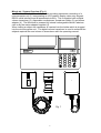
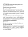
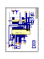
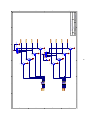
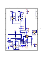
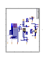
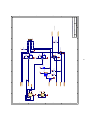
MicroLab Service Manual 069-17 Revision 1.0 November 2002 Micro Medical Limited, P.O. Box 6, Rochester, Kent ME1 2AZ 1 MicroLab - System Overview (Fig. 1) The Micro Medical MicroLab is a data recording spirometer consisting of a microcomputer unit (1) incorporating an LCD graphic display, data entry keypad, RS232 serial interface and all associated circuitry. This is supplied with a digital volume transducer (2), disposable mouthpieces, transducer holder (3) and mains adapter (4). The MicroLab is powered by internal rechargeable Nickel Cadmium cells or by the mains adapter supplied (4). When testing a subject the transducer is inserted into the holder which is plugged into the microcomputer unit. The digital volume transducer is used to measure the subjects expired flow and volume in accordance with the operating manual. micro lab F1 F2 1 GHI 2 3 5 JKL 6 MNO 7PQRS 8TUV / 0 9 WXYZ . Esc Del 4 Micro Medical 1 F3 ABC 3 F4 DEF 4 2 Fig. 1 2 Transducer (Fig. 2) The Micro Medical digital volume transducer consists of an acrylic tube with a vane positioned between two swirl plates. The low inertia vane is attached to a stainless steel pivot which is free to rotate on two jewelled bearings mounted at the centre of the swirl plates. As air is passed through the transducer a vortex is created by the swirl plates which causes the vane to rotate in a direction dependant upon the direction of air flow. The number of rotations is proportional to the volume of air passed through the transducer and the frequency of rotation is proportional to the flow rate. The transducer housing consists of a main body which contains a pair of light emitting diodes (LED’s) and phototransistors. The transducer is fixed to the mouthpiece holder which pushes into the main body and is captured by an “O” ring seal. The LED’s produce infra red beams which are interrupted by the vane twice per revolution. This interruption is sensed by the phototransistors. The output from the collector of each phototransistor will be a square wave with a phase difference between the two of + or - 90 degrees depending upon the direction of flow. There is no routine maintenance required for the transducer other than cleaning according to the instructions in the operating manual. Micro Medical Digital Volume Transducer Rotating vane Infra red emitter Swirl plate Jewelled bearing Infra red detector Volume = k X No. of pulses Volume proportional to the number of pulses Flow proportional to the puse frequency Flow = k / pulse period 3 Microcomputer Unit (Refer to drawings 069-01 to 069-06, and 069-14 to 069-12) The microprocessor control circuit carries out the spirometry routines, monitors the transducer pulses and keypad, and drives the display under the control of the program module. The drawing 069-01 is a hierarchical block diagram showing the connections of the sub-sections. The rest of the drawings are sub-sections and are described in detail below. Micro controller (069-02). U2 is a Hitachi HD64F2318 16 bit microprocessor with 256K of flash memory and 8K of Ram. The system clock is supplied by 20MHz crystal (X1). There is also 512 Kbyte (U4) of external Ram used for running a module and storing variable data. The internal flash is used for the boot software, kernel and the base module. The kernel handles the low level interface to display, keyboard etc. and the base module runs on start-up and gives a choice of which module needs to be executed. The modules are stored in the external 8 Mbyte Flash PROM (U5). The kernel also has a flash filing system which keeps track of all the files in the external Flash PROM. The files can be an executable module or spirometry or other module data. The filing system is similar to the old PC Dos filing system. U6 is just used to control the access to the flash device. The speaker J2 is directly connected to the Port pins and the pins are toggled at 1 KHz to generate the buzzing sound. U2 is used for enabling the internal flash to be overwritten. If a new kernel is downloaded, the flash is enabled and data transferred. U1 is the reset controller, which holds the reset line low for 350 ms on power up. This ensures that the supply has stabilised before the micro starts. TR1 is used by the micro to hold the power supply ON whilst it is writing to the filing system. This is to ensure that data is not corrupted when it is writing and the power is turned off. TR2 allows the micro to turn off the power and switch off the unit. This is normally done when the unit is left on for a long period of time. To preserve the battery, it turns it off. 4 Memory Map 0x000000 0x400000 0x800000 0xC00000 0xFFDC00 – 0x040000 0x480000 256K 512K 0xFFFBFF 8K Internal Flash External Ram for modules Flash Prom (Single address used) Display Controller Internal Ram – stack. Keypad interface (069–15) The 26 keypad switches are arranged in a 5 X 5 matrix and a separate On/Off key. When the keypad is being read by the processor the 5 columns are sequentially driven low by the port lines PE0 – PE4. The state of the 5 rows is read by the port P40 – P44. The diodes in the keypad PCB isolate the outputs from the Port to ensure that a high current will not flow from an output set high to one set low if two keys are pressed simultaneously. The ON/OFF key is connected to the power control circuitry described in the Power Supply section. Resistor RN1 ensures that the keys that are not pressed are read as high. Serial interface (069-15) The uC communicates with the PC or the printer via an RS232 serial interface at 38,4 Kbits per sec baud rate, with 8 bits data, 1 stop bit and no parity. U17 converts the RS232 signal to a logic signal of 3.3V. The uC has two inbuilt serial controllers, SCI0 and SCI1. SCI0 is used for synchronous data transfer whilst SCI1 is used in asynchronous mode for RS232. Real Time Clock (069-15) U18 is a Xicor X1243 real time clock with 2Kbyte of EEPROM. It operates at 32.768 Khz and is powered by the lithium battery. The device requires a very small amount of power during standby mode and as the unit will never drain the battery out, this should be sufficient to keep the clock going for a long period of time before recharging. The clock is set by the processor during the factory set-up and should not require any further adjustment. The date and time can be changed from the system menu. The interface to the clock is via a I2C bus. The uC does not have a dedicated I2C bus, so two port lines (P20 – P21) are used under software to emulate the bus. The EEPROM is used for storing the calibration value and other system data. If the device is ever replaced, the unit will have to be reconfigured and recalibrated. 5 Temperature Sensor U19 is a Dallas DS18S20 temperature sensor operating on their one wire bus protocol. It has an accuracy of 0.5 degree centigrade. A port line P23 is used under software to emulate the one wire bus. The ambient temperature reading is used for adjusting inspiratory flow at ambient temperature to respective flow at body temperature. Transducer interface (069-16) The supply to the two series LED’s inside the transducer housing is provided through TR9 which is switched on or off by TR3. This is controlled by port pin P26 of the processor and is only turned on during a spirometry manoeuvre to conserve power. However, power is supplied to the transducer through D2 continuously when the mains adapter is connected. Inside the transducer housing the two phototransistors used to detect the interrupted infra-red beam are in open collector configuration. The collectors are connected to pins 2 and 3 of SK2. The pull up resistor for the two phototransistors is provided by R37 and R38. The signal from the phototransistor is applied to the pulse timing input of the processor (P16) after being squared up by the action of the Schmitt inverter U13. The signal from the second phototransistor, after conditioning (U14) is applied to a D type latch, clocked by the first phototransistor, to determine the direction of the turbine. The direction signal is fed to uC via port P17. The rising edge of the signal applied to P16 causes an interrupt to be generated in the processor. This interrupt is processed by incrementing a pulse count, timing the period since the last pulse and by reading the state of P17. The pulse count is used to determine the volume passed through the transducer since the start of the test and the pulse period is used to determine the flow at each volume increment. Display (069-03) The display is a high resolution custom graphic 240 by 120 dot LCD. It is controlled by an Epson SED1335 display controller (U24), which directly interface to the uC. The display controller timing is generated by a 10 MHz crystal (X4). U23 is a 32K byte RAM to hold the display data. The LCD display is based on four planes, each requiring different plane voltage. It is biased by 22 V generated by DC-DC controller U9. VR2 varies this voltage which in turn changes the contrast. At dark level, the bias voltage is typically 22.6V and the plane voltages are 20.9V, 19.2V, 3.5V and 1.7V. Of course, they would be slightly different for different contrast level. The plane voltages are generated by resistor ratio dividers (R23, R24, R53, R26, R27) and buffered by quad Op-amp U25. J8 is a connector to the display. 6 Power Supply (069-14) The power to the system is either supplied by the 7.2V ni-cad battery or from an external 9V DC regulated power supply. If the external supply is connected, then TR4 is switched off and the battery is not used. R30 ensures that the battery is trickle charged at all times. The on/off key is conditioned via U10 and applied to set/reset D type flip flop (U11). On every key press, the flip flop toggles between the on and off state. In the On state, TR6 is switched on, switching on TR5. The on state can be held by MC_ONline from the uC whilst it is saving data in the Flash PROM. The uC can also switch the power off by means of the MC_OFF- line which resets U11. U8 is a DC-DC converter with an input range of 0.9V to 10V and an output of 3.3 volts to power the unit. Since the range is up to 10V only, care should be taken not to use any other external power supply, as most of them are unregulated and could output 12V for a 9V unregulated supply. U7 is another DC-DC converter with an output of 9V. This higher supply is used for powering the sensor LEDs. R36 and R7 divide the unregulated voltage to a third and are applied to the A/D converter of the uC. The uC continuously examines the reading and gives a battery low or battery dead warning message. From the reading the uC can also deduce that the external supply is connected, so it can turn itself off if the unit is left on for a long time. Inductors L1 and L2 are placed for EMC filtering and D5 protects the unit from reverse polarity power supply Printer Driver (Drawing 069-04, 069-05, 069-06) The printer driver uses a single chip micro-controller (U12) with on board program memory and RAM to receive serial data from the microprocessor (U2) and control the printer mechanism. The printer mechanism uses stepper motors to drive the print head and paper feed. Each stepper motor uses four lines, driven sequentially. The order in which the lines are driven determines the direction of rotation. The thermal print head uses eight heater elements. The stepper motors and print head signals are generated on port A and B (active high) of the micro-controller (U12). The signals pass through sixteen current transistors (TR10 to TR25). Timing for Port A and B is derived from an adjustable oscillator comprising of U21 and associated components. Adjusting VR1 varies the oscillator frequency and consequently the period for which the thermal elements are energised. This in turn adjusts the print density. After the micro-controller is first reset, the print head is driven to the left until the end switch is activated. The end switch consists of a normally closed pair of contacts accessed at pins 1 and 2 of the printer connector, J7. The end switch is detected by PD5 on the micro-controller. 7 Drawing No. 069-00 Rev. 1.3 Designation Part No. U1 MAX824TEXK-T U2 HD64F2318VTE25 U3 BU4S11 U4 K6T4008V1C-BB70 U5 K9F6408U0A-TCB0 U6 74LCX32 U7 LT1613CS5 U8 LT1613CS5 U9 LT1613CS5 U10 4093 U11 4013 U12 MC68HC705C9ACFN U13 BU4S584 U14 BU4S584 U15 MAX4544EUT-T U16 MAX4544EUT-T U17 MAX3221CAE U18 X1243S8 U19 DS18S20 U20 4013 U21 4069UB U22 LT1084CT U23 GM76C256CLLFW-55-T/R U24 SED1335FOB U25 LM324 U26 LT1613CS5 R1 R2 R3 R4 R5 R6 R7 R8 R9 R10 R11 R12 R13 R14 R15 R16 R17 R18 R19 R20 R21 R22 R23 R24 Date 19/09/02 Page: 1 OF 5 Description. Maxim power monitor, SOT23-5 package Hitachi H8S/2318 microcontroller, TQFP100 package Rohm individual CMOS gate, SOT23-5 package Samsung 512k X 8 bit CMOS static RAM, SOL32/525 Samsung 8M X 8 bit FLASH memory, TSOP44/40 Quad 2-input OR gate Linear Technology DC/DC convertor, SOT23-5 package Linear Technology DC/DC convertor, SOT23-5 package Linear Technology DC/DC convertor, SOT23-5 package CMOS Quad NAND Schmitt input gate, SO-14 package CMOS Dual D Type flip flop, SO-14 package Motorola OTP microprocessor Rohm individual CMOS Schmitt invertor, SOT23-5 Rohm individual CMOS Schmitt invertor, SOT23-5 Maxim SPDT analogue switch, SOT23-6 package Maxim SPDT analogue switch, SOT23-6 package Maxim RS232 transceiver, SSOP16 package Xicor clock calander with 256 X 8 bit RAM, SO-8 package Dallas semiconductor digital thermometer, TO-92B CMOS Dual D Type flip flop, SO-14 package Surface mount unbuffered hex invertor LDO adj 5 amp regulator or National LM1084IT-ADJ Gold Star 32K X 8 bit CMOS static RAM, 28 pin SOP Display driver Quad surface mount op amp Linear Technology DC/DC convertor, SOT23-5 package 100K resistor 1%, 0805 package 10K resistor 1%, 0805 package 10K resistor 1%, 0805 package 100K resistor 1%, 0805 package 100K resistor 1%, 0805 package 100K resistor 1%, 0805 package 100K resistor 1%, 0805 package 100K resistor 1%, 0805 package 100K resistor 1%, 0805 package 100K resistor 1%, 0805 package 100K resistor 1%, 0805 package 100K resistor 1%, 0805 package 4.7K resistor 1%, 0805 package 10K resistor 1%, 0805 package 10K resistor 1%, 0805 package 100K resistor 1%, 0805 package 100K resistor 1%, 0805 package 10 ohm resistor 1%, 0805 package 1K resistor 1%, 0805 package 10K resistor 1%, 0805 package 10K resistor 1%, 0805 package 10K resistor 1%, 0805 package 10K resistor 1%, 0805 package 10K resistor 1%, 0805 package 8 Drawing No. 069-00 Rev. 1.3 Designation Part No. R25 R26 R27 R28 R29 R30 337-717 (F) R31 R32 R33 R34 R35 R36 R37 R38 R39 R40 R41 R42 R43 R44 R45 R46 R47 R48 R49 R50 R51 R52 R53 RN1 107-048 (F) RN2 219-186 (F) RN3 776-701(F) RN4 776-701(F) RN5 776-701(F) RN6 776-701(F) VR1 499-663(F) VR2 T18 S/I S/B S/T 20KA C1 C2 C3 C4 C5 C6 C7 C8 C9 C10 C11 C12 C13 C14 Date 19/09/02 Page: 2 OF 5 Description. 10K resistor 1%, 0805 package 10K resistor 1%, 0805 package 10K resistor 1%, 0805 package 13K resistor 1%, 0805 package 82K resistor 1%, 0805 package 68 ohm 1 watt axial resistor 39K resistor 1%, 0805 package 68K resistor 1%, 0805 package 100 ohm resistor 1%, 0805 package 10K resistor 1%, 0805 package 1K resistor 1%, 0805 package 200K resistor 1%, 0805 package 4.7K resistor 1%, 0805 package 4.7K resistor 1%, 0805 package 10 Meg resistor 1%, 0805 package 220K resistor 1%, 0805 package 100K resistor 1%, 0805 package 1K resistor 1%, 0805 package 1K resistor 1%, 0805 package 1K resistor 1%, 0805 package 10 Meg resistor 1%, 0805 package 22K resistor 1%, 0805 package 22K resistor 1%, 0805 package 150K resistor 1%, 0805 package 150K resistor 1%, 0805 package 2.2K resistor 1%, 0805 package 120 ohm resistor 1%, 0805 package 390 ohm resistor 1%, 0805 package 91K resistor 1%, 0805 package 6 pin, 5 commoned 100K resistor, SIL network 5 pin, 4 commoned 10K resistor, SIL network 1k 4 individual resistor network, 1206 package 1k 4 individual resistor network, 1206 package 1k 4 individual resistor network, 1206 package 1k 4 individual resistor network, 1206 package 20K single turn surface mount preset Piher 20K linear potentiometer 100nF Philips or AVX ceramic, 0805 package 100nF Philips or AVX ceramic, 0805 package 100nF Philips or AVX ceramic, 0805 package 100nF Philips or AVX ceramic, 0805 package 100nF Philips or AVX ceramic, 0805 package 100nF Philips or AVX ceramic, 0805 package 100nF Philips or AVX ceramic, 0805 package 100nF Philips or AVX ceramic, 0805 package 100nF Philips or AVX ceramic, 0805 package 100nF Philips or AVX ceramic, 0805 package 33pF Philips or AVX ceramic, 0805 package 33pF Philips or AVX ceramic, 0805 package 33pF Philips or AVX ceramic, 0805 package 33pF Philips or AVX ceramic, 0805 package 9 Drawing No. 069-00 Rev. 1.3 Designation Part No. C15 197-324 (F) C16 197-324 (F) C17 C18 C19 C20 C21 C22 C23 C24 C25 C26 C27 C28 C29 C30 C31 C32 C33 C34 C35 C36 C37 C38 C39 301-8544 (F) C40 301-8544 (F) C41 197-312 (F) C42 197-312 (F) C43 301-7000 (F) C44 C45 C46 C47 C48 C49 197-312 (F) C50 197-312 (F) C51 C52 C53 556-180 (F) C54 556-180 (F) C55 C56 C57 301-8593 (F) C58 C59 C60 C61 C62 C63 TR1 DTC114EK TR2 DTC114EK Date 19/09/02 Page: 3 OF 5 Description. 47uF/16v Surface mount Tantalum 47uF/16v Surface mount Tantalum 100nF Philips or AVX ceramic, 0805 package 100nF Philips or AVX ceramic, 0805 package 100nF Philips or AVX ceramic, 0805 package 100nF Philips or AVX ceramic, 0805 package 100nF Philips or AVX ceramic, 0805 package 100nF Philips or AVX ceramic, 0805 package 100nF Philips or AVX ceramic, 0805 package 100nF Philips or AVX ceramic, 0805 package 100nF Philips or AVX ceramic, 0805 package 100nF Philips or AVX ceramic, 0805 package 100nF Philips or AVX ceramic, 0805 package 100nF Philips or AVX ceramic, 0805 package 100nF Philips or AVX ceramic, 0805 package 100nF Philips or AVX ceramic, 0805 package 100nF Philips or AVX ceramic, 0805 package 100nF Philips or AVX ceramic, 0805 package 100nF Philips or AVX ceramic, 0805 package 100nF Philips or AVX ceramic, 0805 package 100nF Philips or AVX ceramic, 0805 package 100nF Philips or AVX ceramic, 0805 package 100nF Philips or AVX ceramic, 0805 package 100nF Philips or AVX ceramic, 0805 package 33uF/16v Surface mount Tantalum 33uF/16v Surface mount Tantalum 33uF/16v Surface mount Tantalum 33uF/16v Surface mount Tantalum 100uF/16v 1uF Philips or AVX ceramic, X7R dielectric, 0805 package 1nF Philips or AVX ceramic, 0805 package 1nF Philips or AVX ceramic, 0805 package 33pF Philips or AVX ceramic, 0805 package 33pF Philips or AVX ceramic, 0805 package 33uF/16v Surface mount Tantalum 33uF/16v Surface mount Tantalum 1uF Philips or AVX ceramic, X7R dielectric, 0805 package 390pF Philips or AVX ceramic, 0805 package 47uF/16v Surface mount Electrolytic 47uF/16v Surface mount Electrolytic 10pF Philips or AVX ceramic, 0805 package 10pF Philips or AVX ceramic, 0805 package 47uF/25v Surface mount Tantalum 1uF Philips or AVX ceramic, X7R dielectric, 0805 package 1uF Philips or AVX ceramic, X7R dielectric, 0805 package 1uF Philips or AVX ceramic, X7R dielectric, 0805 package 1uF Philips or AVX ceramic, X7R dielectric, 0805 package 1uF Philips or AVX ceramic, X7R dielectric, 0805 package 100nF Philips or AVX ceramic, 0805 package Rohm NPN digital transistor, SOT-23 package Rohm NPN digital transistor, SOT-23 package 10 Drawing No. 069-00 Rev. 1.3 Designation Part No. TR3 DTC114EK TR4 ZXM62P02E6 TR5 ZXM62P02E6 TR6 FMMT491A TR7 FMMT491A TR8 FMMT491A TR9 DTB113EK TR10 FMMT491A TR11 FMMT491A TR12 FMMT491A TR13 FMMT491A TR14 FMMT491A TR15 FMMT491A TR16 FMMT491A TR17 FMMT491A TR18 FMMT491A TR19 FMMT491A TR20 FMMT491A TR21 FMMT491A TR22 FMMT491A TR23 FMMT491A TR24 FMMT491A TR25 FMMT491A D1 ZHCS1000 D2 ZHCS1000 D3 ZHCS1000 D4 ZHCS1000 D5 ZHCS1000 D6 BAS19 D7 UMN1NTR D8 UMN1NTR D9 UMN1NTR D10 UMN1NTR D11 ZHCS1000 D12 BAS21 D13 BAS21 D14 DE5SC4M D15 U1JC44 D16 ZHCS1000 F1 MICROSMD035-2 L1 NLFC453232-3R3M L2 NLFC453232-3R3M L3 353-1340 (F) L4 353-1340 (F) L5 353-1340 (F) L6 353-1340 (F) L7 353-1340 (F) DISPLAY LTA75R227J PRINTER STP411B-320 J1 J2 J3 J4 95001-2661 Date 19/09/02 Page: 4 OF 5 Description. Rohm NPN digital transistor, SOT-23 package P channel MOSFET SOT23-6 package P channel MOSFET SOT23-6 package Zetex NPN Transistor SOT-23 package Zetex NPN Transistor SOT-23 package Zetex NPN Transistor SOT-23 package Rohm PNP digital transistor, SOT-23 package Zetex NPN Transistor SOT-23 package Zetex NPN Transistor SOT-23 package Zetex NPN Transistor SOT-23 package Zetex NPN Transistor SOT-23 package Zetex NPN Transistor SOT-23 package Zetex NPN Transistor SOT-23 package Zetex NPN Transistor SOT-23 package Zetex NPN Transistor SOT-23 package Zetex NPN Transistor SOT-23 package Zetex NPN Transistor SOT-23 package Zetex NPN Transistor SOT-23 package Zetex NPN Transistor SOT-23 package Zetex NPN Transistor SOT-23 package Zetex NPN Transistor SOT-23 package Zetex NPN Transistor SOT-23 package Zetex NPN Transistor SOT-23 package Zetex Schottky diode, SOT-23 package Zetex Schottky diode, SOT-23 package Zetex Schottky diode, SOT-23 package Zetex Schottky diode, SOT-23 package Zetex Schottky diode, SOT-23 package General purpose diode, SOT-23 package Quad commoned diode, IMN10 package Quad commoned diode, IMN10 package Quad commoned diode, IMN10 package Quad commoned diode, IMN10 package Zetex Schottky diode, SOT-23 package General purpose diode, SOT-23 package General purpose diode, SOT-23 package Dual commoned diode 1A Toshiba diode Zetex Schottky diode, SOT-23 package Tyco 700mA Polyswitch 3.3uH inductor, 1210 package 3.3uH inductor, 1210 package 22uH inductor, 1210 package 22uH inductor, 1210 package 22uH inductor, 1210 package 22uH inductor, 1210 package 22uH inductor, 1210 package Nan Ya 240 X 160 graphic display Seiko thermal printer mechanism 3 way 0.1" pitch pin header 2 way 0.1" pitch pin header 2.5mm DC power socket from G.English Molex 6 way data socket 11 Drawing No. 069-00 Rev. 1.3 Designation Part No. J5 14FMN-BMTTN-TF J6 MDS4 J7 J8 18FMN-BMTTN-TF Date 19/09/02 Page: 5 OF 5 Description. 14 way 1mm pitch cable connector from JST 4 way mini DIN socket 25 way connection to printer mechanism 18 way 1mm pitch cable connector from JST BAT1 3 way PCB socket from JST SPKR PKM35-4A0 Murata piezo ceramic sounder 20MHz crystal, HC49/4H package X1 X2 571-672 (F) 32.768 KHz crystal, WATCH package X3 295-267 (F) 4.0MHz X4 485-081 (F) 10MHz crystal SW1 773-209 (F) 2 pole momentary push switch 12 A B C D 1 1 2 2 SENSIN SCLK SOUT SOUT_ENSENDIR SEN1 SEN2 SEN_EN ON/OFF_KEY KEYIN[0..4] RX TX MODE TEMP_IO RTC_DATA RTC_CLK RTC_ONKEYOUT[0..4] RS232 serial.sch Sensors sensor.sch 3 3 KEYIN[0..4] KEYOUT[0..4] PRINTDATA PRINTACK KEYIN[0..4] KEYOUT[0..4] RX TX MODE TEMP_IO RTC_DATA RTC_CLK SENSIN SCLK SOUT SOUT_ENSENDIR SEN1 SEN2 SEN_EN micro MICRO.sch 4 4 BAT_MON MC_OFF- MC_ON- RESET- D[0..7] RDWRA0 DISP_CS- PRNBUSY RESETONLINE 13 D[0..7] DRIVER1 DRIVER1.SCH 5 RTC_ONBAT_MON MC_OFF- ON/OFF_KEY MC_ON- Power Supply power.sch RESET- D[0..7] RDWRA0 DISP_CS- DISPLAY display.sch PRNBUSY RESETONLINE PRINTDATA PRINTACK PRINTER PRINTER.sch 5 6 6 IN1 IN2 IN3 IN4 IN5 IN6 IN7 IN8 OUT1 OUT2 OUT3 OUT4 OUT5 OUT6 OUT7 OUT8 Date: File: A3 Size Title DRIVER2 DRIVER2.SCH IN9 IN10 IN11 IN12 IN13 IN14 IN15 IN16 OUT9 OUT10 OUT11 OUT12 OUT13 OUT14 OUT15 OUT16 IN1 IN2 IN3 IN4 IN5 IN6 IN7 IN8 OUT1 OUT2 OUT3 OUT4 OUT5 OUT6 OUT7 OUT8 IN9 IN10 IN11 IN12 IN13 IN14 IN15 IN16 OUT9 OUT10 OUT11 OUT12 OUT13 OUT14 OUT15 OUT16 069-01 7 6-Nov-2002 H:\TEMP\069-01.sch Number Revision 1.0 8 8 Sheet of Drawn By: D.E.COCKS MicroLab - Circuit diagram overview 7 A B C D A B C MODE 1 1 VCC R3 10k VCC BU4S11 U3 + C15 47UF/10V VCC 3 5 C1 0.1UF VCC R1 100K VCC 1 2 3 CON3 J1 U1 RES RES PRNBUSY BAT_MON KEYOUT[0..4] SOUT_EN- SEN- SEN_EN SEN1 SENDIR TEMP_IO RTC_DATA RTC_CLK TX RX SOUT SIN SCLK MAX824_EUKT GND WDI VCC C3 0.1UF 2 C5 0.1UF ONLINE Internal Printer. 2 4 5 R2 10k VCC 2 C7 0.1UF 1RESET- 3 0.1UF C17 3 10R R18 33pF VCC KEYOUT[0..4] VCC C11 3 C2 0.1UF KEYOUT0 KEYOUT1 KEYOUT2 KEYOUT3 KEYOUT4 X1 20MHz 87 78 77 79 80 81 82 83 84 85 86 54 55 56 59 89 90 91 92 3 4 5 6 9 11 13 8 10 12 57 58 61 60 66 67 62 64 63 33pF C12 HD64F2318VTE25 AVSS VREF AVCC P40/AN0 P41/AN1 P42/AN2 P43/AN3 P44/AN4 P45/AN5 P46/AN6/DA0 P47/AN7/DA1 4 P20/TIOCA3 P21/TIOCB3 P22/TIOCC3/TMRI0 P23/TIOCD3/TMCI0 P24/TIOCA4/TMRI1 P25/TIOCB4/TMCI1 P26/TIOCA5/TMO0 P27/TIOCB5/TMO1 P14/TIOCA1 P15/TIOCB1/TCLKC P16/TIOCA2 P17/TIOCB2/TCLKD P31/TXD1 P33/RXD1 P35/SCK1/IRQ5 P30/TXD0 P32/RXD0 P34/SCK0/IRQ4 MD0 MD1 MD2 FWE XTAL EXTAL RES STBY NMI U2 4 14 PG4/CS0 PG3/CS1/CS7 PG2/CS2 PG1/CS3/IRQ7/CS6 PG0/IRQ6 PF7/CLK PF6/AS PF5/RD PF4/HWR PF3/LWR/IRQ3 PF2/WAIT/IRQ2 PF1/IRQ1/CS5 PF0/IRQ0/CS4 P10/A20 P11/A21 P12/A22 P13/A23 PA0/A16 PA1/A17 PA2/A18 PA3/A19 PB0/A8 PB1/A9 PB2/A10 PB3/A11 PB4/A12 PB5/A13 PB6/A14 PB7/A15 PC0/A0 PC1/A1 PC2/A2 PC3/A3 PC4/A4 PC5/A5 PC6/A6 PC7/A7 PD0/D8 PD1/D9 PD2/D10 PD3/D11 PD4/D12 PD5/D13 PD6/D14 PD7/D15 PE0/D0 PE1/D1 PE2/D2 PE3/D3 PE4/D4 PE5/D5 PE6/D6 PE7/D7 A16 A17 A18 50 51 52 53 97 96 95 94 93 69 70 71 72 73 74 75 76 VCC 5 100K R4 R19 1K0 1 2 A8 A9 A10 A11 A12 A13 A14 A15 41 42 43 44 45 46 47 48 99 100 1 2 A0 A1 A2 A3 A4 A5 A6 A7 D0 D1 D2 D3 D4 D5 D6 D7 KEYIN0 KEYIN1 KEYIN2 KEYIN3 KEYIN4 M_ON_KEY M_OFF_KEY 32 33 34 35 36 37 38 39 23 24 25 26 27 28 29 30 14 15 16 17 19 20 21 22 5 BUZZER J2 A0 A1 A2 A3 A4 A5 A6 A7 A8 A9 A10 A11 A12 A13 A14 A15 A16 A17 A18 40 42 4 5 43 2 3 24 29 22 12 11 10 9 8 7 6 5 27 26 23 25 4 28 3 31 2 30 1 VCC D0 D1 D2 D3 D4 D5 D6 D7 R/B D0 D1 D2 D3 D4 D5 D6 D7 6 5 4 2 1 74LCX32 U6B 74LCX32 U6A K9F6408U0B-TCB0 SE RE WE WP CE CLE ALE U5 U4 KM68V4000BLT-7L OE WE CS1 A0 A1 A2 A3 A4 A5 A6 A7 A8 A9 A10 A11 A12 A13 A14 A15 A16 A17 A18 6 32 VCC D 1 2 4 41 18 19 20 21 24 25 26 27 13 14 15 17 18 19 20 21 6 3 D0 D1 D2 D3 D4 D5 D6 D7 D0 D1 D2 D3 D4 D5 D6 D7 Date: File: A3 Size Title KEYIN[0..4] 9 13 12 10 74LCX32 74LCX32 U6D U6C D[0..7] M_OFF_KEY M_ON_KEY KEYIN[0..4] 11 8 DISP_CS- RDWR- RESET- D[0..7] A0 1 1 069-02 7 6-Nov-2002 H:\TEMP\069-02.sch Number MC_ON- Revision 1.1 TR2 DTC114EK MC_OFF- TR1 DTC114EK 8 8 Sheet of Drawn By: D.E.COCKS MicroLab - Circuit diagram, processor section 7 3 2 3 2 A B C D A B C 1 2 C42 33UF/16V VPWR 2 + 4 5 22uH L6 on Vin U9 LT1613 D[0..7] Fb SW 3 1 D[0..7] 3 R25 10K 3 R49150K 1 1 SEL 2 SEL 1 VDD XD0 XD1 XD2 XD3 CS VD7 VD6 VD5 VD4 VD3 VD2 VD1 VD0 D7 D6 D5 D4 D3 D2 D1 D0 RW VWR VR2 20K + C57 47UF/25V 3 10MHz X4 4 SED1335F D5 ZHCS1000 VEE 3 15 16 21 33 32 31 30 19 XD0 XD1 XD2 XD3 VCC 42 43 44 45 46 47 48 49 VD7 VD6 VD5 VD4 VD3 VD2 VD1 VD0 DISP_CS- 29 28 27 26 25 24 23 22 D7 D6 D5 D4 D3 D2 D1 D0 WR- 7 14 10pF C55 XG 18 XD 17 N/C 12 N/C 60 VSS 4 36 C26 0.1uF 20 50 51 52 53 54 55 56 57 58 59 1 2 3 4 5 6 8 9 10 34 13 35 37 38 39 40 41 C9 0.1uF U24 VCC A0 VA15 VA14 VA13 VA12 VA11 VA10 VA9 VA8 VA7 VA6 VA5 VA4 VA3 VA2 VA1 VA0 VCE VRD RES XECL RD XSCL LP WF YDIS YD YSCL 10pF C56 N/C 11 D 1 Gnd 2 15 C10 0.1uF A0 VA14 VA13 VA12 VA11 VA10 VA9 VA8 VA7 VA6 VA5 VA4 VA3 VA2 VA1 VA0 RD- RESET- C27 0.1uF C58 1uF 10 9 5 6 3 2 5 R27 10K 12 R26 10K 13 R53 91K R24 10K R23 10K 5 + - + - + - + - 11 4 14 LM324 U25D 8 LM324 U25C 7 LM324 U25B 1 LM324 U25A C59 1uF VEE C60 1uF C61 1uF 6 6 C62 1uF VA0 VA1 VA2 VA3 VA4 VA5 VA6 VA7 VA8 VA9 VA10 VA11 VA12 VA13 VA14 VCC 20 27 22 28 10 9 8 7 6 5 4 3 25 24 21 23 2 26 1 VCC KM62256D CS WE OE VCC A0 A1 A2 A3 A4 A5 A6 A7 A8 A9 A10 A11 A12 A13 A14 U23 GND D0 D1 D2 D3 D4 D5 D6 D7 VCC 14 11 12 13 15 16 17 18 19 7 VD0 VD1 VD2 VD3 VD4 VD5 VD6 VD7 XD3 XD2 XD1 XD0 Date: File: A3 Size Title J8 CON18 069-03 7 6-Nov-2002 H:\TEMP\069-03.sch Number Revision 8 8 Sheet of Drawn By: D.E.COCKS MicroLab - Circuit diagram, display section 18 17 16 15 14 13 12 11 10 9 8 7 6 5 4 3 2 1 1.0 A B C D A B C 1 SW1 P.F 2 VCC ONLINE PRINTDATA PRINTACK RESET- C21 0.1uF 2 C23 0.1uF 1 150K R48 22K R46 C22 0.1uF 100K R17 3 TR7 2 3 390PF C52 33PF C13 C24 0.1uF 1 3 4069UB U21A VCC R16 100K VCC 14 7 2 C25 0.1uF BAS19 D6 VR1 20K 3374X 1 5 4 2 3 FMMT491 2 9 22K R47 2K2 R50 4069UB U21B 10MEG 3 4069UB 4069UB U21D U21C 33PF 4.0 MHz R45 C14 X3 3 8 6 11 13 4069UB U21E VCC 12 4069UB U21F 10 R43 1K 4 3 18 23 40 39 32 33 34 35 36 37 41 38 1 2 43 42 PC0 PC1 PC2 PC3 PC4 PC5 PC6 PC7 PB0 PB1 PB2 PB3 PB4 PB5 PB6 PB7 PA7 PA6 PA5 PA4 PA3 PA2 PA1 PA0 31 30 29 28 27 26 25 24 13 14 15 16 17 19 20 21 5 6 7 8 9 10 11 12 4 MC68HC05C9ACFN(44) NC NC NC NC NC PD7 PD0/RDI PD1/TDO PD2/MISO PD3/MOSI PD4/SCK PD5/SS TCAP TCMP RST IRQ OSC1 OSC2 U12 4 16 VPRINT PRNBUSY C53 47uF 3 5 5 VI V0 U22 LT1084CT GND 1 D 1 390 OHM 120 OHM 2 3 2 1 R52 R51 FMMT491A 1 TR8 C54 47uF 1 RN2 10K OUT9 OUT10 OUT11 OUT12 OUT13 OUT14 OUT15 OUT16 IN9 IN10 IN11 IN12 IN13 IN14 IN15 IN16 VP OUT1 OUT2 OUT3 OUT4 OUT5 OUT6 OUT7 OUT8 IN1 IN2 IN3 IN4 IN5 IN6 IN7 IN8 6 6 5 4 3 2 Date: File: A3 Size Title C8 0.1uF 1K R42 VP CON25 1 2 3 4 5 6 7 8 9 10 11 12 13 14 15 16 17 18 19 20 21 22 23 24 25 J7 069-04 7 6-Nov-2002 H:\TEMP\069-04.sch Number 1.1 Revision 8 8 Sheet of Drawn By: D.E.COCKS MicroLab - Circuit diagram, printer processor R22 10K VCC 7 A B C D A B C 1 IN5 IN6 IN7 IN8 IN1 IN2 IN3 IN4 1 2 3 4 1 2 3 4 2 2 RN4 RN3 8 7 6 5 8 7 6 5 3 3 1 FMMT489 TR21 FMMT489 1 TR20 1 17 FMMT489 1 C18 0.1UF TR24 FMMT489 TR23 1 VP FMMT489 TR19 1 FMMT489 1 TR25 4 3 2 3 2 1 5 D 1 2 3 2 3 2 3 2 3 3 2 4 TR22 4 1 FMMT489 TR18 D8 UMN1 1 FMMT489 2 VP 3 4 5 3 2 3 2 D7 UMN1 OUT8 OUT7 OUT6 OUT5 OUT4 OUT3 OUT2 OUT1 C63 0.1UF 5 5 Date: File: B Size Title 069-05 6-Nov-2002 H:\TEMP\069-05.sch Number Revision 1.1 6 Sheet of Drawn By: D.E.COCKS MicroLab - Circuit diagram, printer driver 1 6 A B C D A B C 1 IN13 IN14 IN15 IN16 IN9 IN10 IN11 IN12 1 2 3 4 1 2 3 4 2 2 RN6 RN5 8 7 6 5 8 7 6 5 3 3 1 FMMT489 TR13 FMMT489 1 TR12 1 18 FMMT489 1 C4 0.1UF TR16 FMMT489 TR15 1 VP FMMT489 TR11 1 FMMT489 1 TR17 4 3 2 3 2 1 5 D 1 2 3 2 3 2 3 2 3 3 2 4 4 VP 4 1 FMMT489 TR10 D10 UMN1 1 3 TR14 FMMT489 2 5 3 2 3 2 D9 UMN1 OUT16 OUT15 OUT14 OUT13 OUT12 OUT11 OUT10 OUT9 C6 0.1UF 5 5 Date: File: B Size Title 069-06 6-Nov-2002 H:\TEMP\069-06.sch Number Revision 1.1 6 Sheet of Drawn By: D.E.COCKS MicroLab - Circuit diagram, printer driver 2 6 A B C D A B C U26 1 3.3uH L1 3.3uH L2 Fb SW MC_OFF- VBAT 3 1 13 12 VBAT 100R R33 1uF C51 BATTERY R44 1K 4093 U10D 11 2 R8 100K R6 100K 2 1 D16 ZHCS1000 4093 U10A C30 0.1UF R5 100K BAT1 BAT7.2V 100K 3 R20 10K + C50 33UF/16V R41 BAS21 D12 9V R15 10K 1 D1 ZHCS1000 C28 0.1UF 2 SEPIC CONVERTER (0.9 - 10V) LT1613 VBACK 2 MC_ON- on Vin ON/OFF_KEY 33UF/16V C49 + 4 5 22uH L7 D15 U1JC44 MICROSMD035-02 F1 2 1 D Gnd 2 POWER J3 1 3 1 3 1 2 1 3 Battery Charger REGULATED POWER SUPPLY 9.0V 14 ZHCS1000 D11 9 8 6 5 4093 U10C 3 4093 U10B D13 BAS21 R30 68R 1 3 5 3 CLK D 4 3 3 10 Q Q 6 S 14 VCC GND 7 R 4 4013 2 U11A 1 TR4 1K R35 R34 10K ZXM62P02E6 9 11 1 CLK D Q 4 Q 4013 12 U11B 13 TR6 FMMT491 R36 200K VPRINT TR5 ZXM62P02E6 DE5SC4M D14 4 3 2 3 7 8 S R 10 R7 100K 19 C31 0.1UF + C43 100UF/16V VPWR 5 C29 0.1UF 5 BAT_MON C40 33UF/16V 6 C41 33UF/16V 6 + + 4 5 4 5 on Vin U8 LT1613 22uH L4 on Vin 7 3 R28 13K 1 R29 Fb SW Date: File: A3 Size Title R31 39K 1uF C44 TP1 GND VDD VCC VSS Number 069-14 7 6-Nov-2002 H:\TEMP\069-14.sch Revision 8 8 TP3 GND 1.0 Sheet of Drawn By: D.E.COCKS TP2 GND + C16 47UF/10V ZHCS1000 3 R32 68K D4 L5 22uH 1 V9INT + C39 33UF/16V MicroLab - Circuit diagram, power supply BAT_MON 3 1 82K D3 ZHCS1000 3 SEPIC CONVERTER (0.9 - 10V) Fb SW 1 SEPIC CONVERTER (0.9 - 10V) U7 LT1613 22uH L3 Gnd 2 Gnd 2 A B C D A B C 1 2 MODE ON/OFF_KEY KEYOUT[0..4] KEYIN[0..4] VCC KEYOUT[0..4] KEYIN[0..4] 3 2 4 1 5 2 VCC 3 RTC_CLK RTC_DATA J6 MINI_DIN_4 3 1 2 3 4 5 6 D 1 4 3 6 9V 6 10M INT SCL SDA 20 VSS VDD VB R40 220K 4 8 7 MAX3221CAE EN FOFF C1+ V+ C1 - TO C2+ FON C2 - TIN VINV RIN RO C48 33PF 8 KEYOUT3 KEYOUT4 16 15 14 13 12 11 10 9 10 KEYOUT2 U17 12 1 2 3 4 14 KEYOUT1 13 11 9 7 5 KEYOUT0 32.768KHz R39 X2 1 2 3 4 5 6 7 VCC 8 U18 X1243S8 0.1UF C33 5 C47 33PF C32 0.1UF RTC_CLK VCC KEYIN4 KEYIN3 KEYIN2 KEYIN1 RTC_DATA R14 10K VCC RN1 100K-RN KEYIN0 4 1 X1 2 X2 5 5 3 VCC VCC J5 ON F1 9 6 C37 0.1UF C34 0.1UF F4 - . 0 ENTER DEL ESC C38 0.1UF VBACK R21 10K VCC KEYPAD-ML3 F3 7 4 1 0.1UF C35 OFF F2 8 5 2 6 TX RX C36 0.1UF TEMP_IO VCC TX RX 6 1 2 3 VCC C20 0.1uF DS18S20 VDD DQ GND U19 Date: File: A3 Size Title 8 069-15 7 6-Nov-2002 H:\TEMP\069-15.sch Number 1.0 8 Sheet of Drawn By: D.E.COCKS Revision MicroLab - Circuit diagram, RS232, RTC and keypad interface Temperature Sensor R13 4K7 VCC C19 0.1uF 7 A B C D A B C 1 3 5 11 CLK D 8 S VCC 10 R CLK D 4013 Q 12 U20B 13 2 40131 U20A Q Q Q 6 S 14 VCC GND 7 R 4 2 SOUT SOUT_EN- SIN SEN_EN SENDIR SEN1 SEN- 1 3 TR3 DTC114EK 1 R10 100K VCC R11 100K VCC TR9 DTB113EK V9INT 9V 2 3 4 D2 ZHCS1000 21 BU4S584 4 BU4S584 4 1 VCC 5 2 U14 1 2 U13 1 VCC VCC 3 5 3 SCLK 3 2 2 3 4 2 3 3 C46 1NF C45 1NF U15 R38 4K7 R37 4K7 5 1 5 VCC MAX4544EUT-T 4 6 5 9 2 2 3 D 1 4 6 5 U16 MAX4544EUT-T R9 100K VCC 6 6 R12 100K VCC RJ11 1 2 3 4 5 6 J4 Date: File: A3 Size Title To Internal Printer. 8 069-16 7 6-Nov-2002 H:\TEMP\069-16.sch Number 1.0 8 Sheet of Drawn By: D.E.COCKS Revision MicroLab - Circuit diagram, sensor interface PRINTDATA PRINTACK 7 A B C D