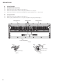
1
SERVICE MANUAL
DGX-220
YPG-225
CONTENTS
SPECIFICATIONS .................................................................... 3
PANEL LAYOUT ........................................................................ 4
CIRCUIT BOARD LAYOUT & WIRING ..................................... 6
BLOCK DIAGRAM .................................................................... 8
DISASSEMBLY PROCEDURE ................................................. 9
LSI PIN DESCRIPTION .......................................................... 15
IC BLOCK DIAGRAM .............................................................. 18
CIRCUIT BOARDS ................................................................. 19
TEST PROGRAM ................................................................... 29
INITIALIZATION ...................................................................... 33
USER DATA BACKUP............................................................. 34
MIDI IMPLEMENTATION CHART ........................................... 35
MIDI DATA FORMAT ............................................................... 36
PARTS LIST
OVERALL CIRCUIT DIAGRAM
PK
001761
HAMAMATSU, JAPAN
’06.04
Copyright (c) Yamaha Corporation. All rights reserved. PDF
DGX-220/YPG-225
IMPORTANT NOTICE
This manual has been provided for the use of authorized Yamaha Retailers and their service personnel. It has been assumed that
basic service procedures inherent to the industry, and more specifically Yamaha Products, are already known and understood by the
users, and have therefore not been restated.
WARNING:
Failure to follow appropriate service and safety procedures when servicing this product may result in personal injury, destruction of expensive components and failure of the product to perform as specified. For
these reasons, we advise all Yamaha product owners that all service required should be performed by an
authorized Yamaha Retailer or the appointed service representative.
IMPORTANT:
This presentation or sale of this manual to any individual or firm does not constitute authorization certification, recognition of any applicable technical capabilities, or establish a principal-agent relationship of
any form.
The data provided is believed to be accurate and applicable to the unit(s) indicated on the cover. The research engineering, and
service departments of Yamaha are continually striving to improve Yamaha products. Modifications are, therefore, inevitable
and changes in specification are subject to change without notice or obligation to retrofit. Should any discrepancy appear to
exist, please contact the distributor's Service Division.
WARNING:
IMPORTANT:
Static discharges can destroy expensive components. Discharge any static electricity your body may have
accumulated by grounding yourself to the ground bus in the unit (heavy gauge black wires connect to
this bus.)
Turn the unit OFF during disassembly and parts replacement. Recheck all work before you apply power to
the unit.
WARNING: CHEMICAL CONTENT NOTICE!
The solder used in the production of this product contains LEAD. In addition, other electrical/electronic and/or plastic (Where
applicable) components may also contain traces of chemicals found by the California Health and Welfare Agency (and possibly
other entities) to cause cancer and/or birth defects or other reproductive harm.
DO NOT PLACE SOLDER, ELECTRICAL/ELECTRONIC OR PLASTIC COMPONENTS IN YOUR MOUTH FOR ANY REASON
WHAT SO EVER!
Avoid prolonged, unprotected contact between solder and your skin! When soldering, do not inhale solder fumes or expose eyes to
solder/flux vapor!
If you come in contact with solder or components located inside the enclosure of this product, wash your hands before handling food.
WARNING
Components having special characteristics are marked
originally installed.
and must be replaced with parts having specification equal to those
SAVING DATA
Saving and backing up your data
The panel settings and some other types of data are not retained in memory when you turn off the power to the
instrument. Save data you want to keep to the Registration Memory.
Saved data may be lost due to malfunction or incorrect operation.
Save important data to a USB storage device/or other external device such as a computer.
Be sure to
perform it
Backing up the USB storage device/external media
To protect against data loss through media damage, we recommend that you save your important data onto two
USB storage devices/external media.
Be sure to
perform it
2
DGX-220/YPG-225
■ SPECIFICATIONS
Keyboards
Effects
• 76 box type keys (E0–G6), with Touch Response.
Display
• LCD display (backlit)
Setup
• STANDBY/ON
• MASTER VOLUME:MIN–MAX
Panel Controls
• SONG, VOICE, STYLE, EASY SONG ARRANGER,
P.A.T. ON/OFF, LESSON L, LESSON R, LESSON
START, METRONOME ON/OFF, PORTABLE GRAND,
DEMO, FUNCTION, MUSIC DATABASE, HARMONY ON/
OFF, DUAL ON/OFF, SPLIT ON/OFF, TEMPO/TAP, [0]–
[9], [+], [-], CATEGORY, Dial, REPEAT & LEARN (ACMP
ON/OFF), A-B REPEAT (INTRO/ENDING/rit.), PAUSE
(SYNC START), START/STOP, REW (MAIN/AUTO FILL),
FF (SYNC STOP), REGIST MEMORY ([MEMORY/BANK],
[1], [2]), SONG MEMORY (REC, [1]–[5], [A])
Realtime Control
• Pitch Bend Wheel
Voice
•
•
•
•
• Reverb:
9 types
• Chorus:
4 types
• Harmony: 26 types
Song
• 30 Preset Songs + 5 User Songs + Accessory CD-ROM
Songs (70)
• Song Clear, Track Clear
• Song Volume
• Song Control: REPEAT & LEARN, A-B REPEAT, PAUSE,
REW, FF, START/STOP
Performance assistant technology
• Chord, Chord/Free
Recording
• Song
User Song:
5 Songs
Recording Tracks: 1, 2, 3, 4, 5, STYLE
MIDI
• Local On/Off
• Keyboard Out
• Initial Send
• Style Out
• External Clock
• Song Out
Auxiliary jacks
116 panel voices + 12 drum/SFX kits + 361 XGlite voices
Polyphony: 32
DUAL
SPLIT
• PHONES/OUTPUT, DC IN 12V, USB, SUSTAIN
Ampli er
• 6W + 6W
Speakers
Style
• 150 Preset Styles + 1 User Style File
• Style Control:ACMP ON/OFF, SYNC STOP,
SYNC START, START/STOP,
INTRO/ENDING/rit., MAIN/AUTO FILL
• Fingering:
Multi Finger, Full Keyboard
• Style Volume
Music Database
• 267
• 12cm x 2 + 3cm x 2
Power Consumption
• 20W
Power Supply
• Adaptor: Yamaha PA-5D AC power adaptor
• Batteries: Six “D” size, R20P (LR20) or equivalent batteries
Dimensions (W x D x H)
Education Feature
• Dictionary
• Lesson 1–3, Repeat & Learn
Registration Memory
• 8 banks x 2 types
Function
• VOLUME:
• OVERALL:
Style Volume, Song Volume
Tuning, Transpose, Split Point, Touch Sensitivity, Pitch Bend Range, Chord Fingering
• MAIN VOICE: Volume, Octave, Pan, Reverb Level,
Chorus Level
• DUAL VOICE: Voice, Volume, Octave, Pan, Reverb Level,
Chorus Level
• SPLIT VOICE: Voice, Volume, Octave, Pan, Reverb Level,
Chorus Level
• EFFECT:
Reverb Type, Chorus Type, Master EQ Type
,
Sustain
• HARMONY:
Harmony Type, Harmony Volume
• 1,178 x 412 x 137 mm (46-3/8" x 16-1/4" x 5-3/8")
Weight
• 8.3kg (18 lbs. 5 oz.) (not including batteries)
Supplied Accessories
• Music Rest
• Accessory CD-ROM
• Owner’s Manual
Optional Accessories
•
•
•
•
AC Power Adaptor:
Footswitch:
Keyboard Stand:
Headphones:
PA-5D
FC4/FC5
LW-16
HPE-150
• Performance assistant technology:
Performance assistant technology Type
• SFF Load:
Style File Load
PC Mode
• PC:
Local On/Off, External Clock, Initial Send,
• MIDI:
Keyboard Out, Style Out, Song Out
• METRONOME: Time Signature Numerator, Time Signature
• LESSON:
• UTILITY:
Denominator, Metronome Volume
Lesson Track (R), Lesson Track (L), Grade
Demo Cancel
3
DGX-220/YPG-225
■ PANEL LAYOUT
• Front Panel
e
r
t
q
y
u i
o
w
!0 !1 !2 !3 !4 !5
@9
• Front Panel
q [STANDBY/ON] switch
!2 [REW]/[MAIN/AUTO FILL] button
w [MASTER VOLUME] control
!3 [FF]/[SYNC STOP] button
e [P.A.T. ON/OFF] button
!4 [PAUSE]/[SYNC START] button
r [MUSIC DATABASE] button
!5 [START/STOP] button
t [FUNCTION] button
!6 [SONG] button
y LESSON [L], [R], [START] buttons
!7 [EASY SONG ARRANGER] button
u [METRONOME ON/OFF] button
!8 [STYLE] button
i [TEMPO/TAP] button
!9 [VOICE] button
o SONG MEMORY
[REC], [1]–[5], [A] buttons
@0 Dial
!0 [REPEAT & LEARN]/
[ACMP ON/OFF] button
!1 [A-B REPEAT]/
[INTRO/ENDING/rit.] button
4
@1 CATEGORY [
] and [
] buttons
DGX-220/YPG-225
!6
!7
!8
!9
@3
@0
@1
@5 @6 @7 @8
@2
@4
• Rear Panel
#0
#1
#2
#3
• Rear Panel
@2 Number buttons [0]–[9],[+] and [-] buttons
#0 USB terminal
@3 [DEMO] button
#1 SUSTAIN jack
@4 REGIST MEMORY [MEMORY/BANK], [1], [2] buttons
#2 PHONES/OUTPUT jack
@5 [PORTABLE GRAND] button
#3 DC IN 12V jack
@6 [SPLIT ON/OFF] button
@7 [DUAL ON/OFF] button
@8 [HARMONY ON/OFF] button
@9 PITCH BEND wheel
5
DGX-220/YPG-225
■ CIRCUIT BOARDS LAYOUT & WIRING
• Upper case
PB
AMJK 4/6
(AMJK 6/6)
PNL
TWL
(Rotary Encoder)
PNR
AM
9
(PN 4/6)
13
12 11
(AMJK 1/6)
10
TWR
(PN 1/5) 8
14
AMJK 5/6
4
5 16
15
6
(STANDBY/ON)
Black
3
1
7
USB
16
(AMJK 3/6)
2
• Lower case
BROWN
BLACK
RED
LEFT SIDE
BLACK
RIGHT SIDE
16
15
MK-76L
6
(PN 5/6)
DMLCD
Black
Red
PN 2/5
(PN 3/5)
(Master Volume)
1
2
3
16
MK-76H
Red
DGX-220/YPG-225
No. Location
q
30
w
40
e
50
r
WH551
t
WH153
y
WH155
u
WH854
i
WH782
o
WH855
!0
WH781
!1
WH784
!2
-!3
WH553
!4
WH558
!5
130
220
!6
Part No.
WC601000
WC601400
WC601500
WG332600
WG332700
WG342900
WG332500
WG331300
WG331500
WG331900
WG332000
WC602600
WB342800
WG342600
V8735600
WG324100
Connector Assembly
MK1
MK4
MK5
VR3
STB2
AMDM2
JK2
ENC
PB2
PN3
PN4
BL
TW4
TW2
BAT
SPL
MK-76L-CN4
MK-76L-CN5
MK-76H-CN1
AM-CN551
AM-CN153
AM-CN155
USB-CN854
PNR-CN782
PB-CN855
PNR-CN781
PNL-CN784
+/AM-CN553
USB-CN558
-+/-
Destination
*1 *5 DMLCD-CN401
*1 *5 DMLCD-CN404
*1 *5 DMLCD-CN405
*2 *5 AM-CN552
*2 *5 AM-CN154
*2 *5 DMLCD-CN101
*2 *5 DMLCD-CN802
*2 *5 PNR-CN783
*2 *5 PML-CN785
*2 *5 DMLCD-CN701
*2 *5 DMLCD-CN703
*3 *6 AM-CN152
*2 *5 TWL +/*2 *5 TWR +/*3 *10 AM-CN151
*3 *10 AM-CN554
USB-CN557
*1
*1
*1
*2
*2
*1
*1
*2
*1
*1
*1
*5
*5
*5
*5
*5
*5
*5
*5
*5
*5
*5
1
*5
*3
*3
*1
*1
*6
*6
*10
*10
Remarks
12P
6P
8P
5P
4P
13P
9P
3P
3P
16P
16P
2P
2P
2P
3P
2P
* The parts with "--" in "Part No." are not available as spare parts.
* 1 : Installation
* 2 : Dip soldering
* 3 : Manual soldering
* 4 : The conductor of a cable and the point of contact of a connector are untited.
* 5 : Edge mark is adjusted to Pin 1 (왕) side.
* 6 : Edge mark is connected to + side.
* 7 : Edge mark is connected to + terminal.
* 8 : White wire is adjusted to Pin 1 (왕) side.
* 9 : White wire is connected to + terminal.
* 10 : Red wire is connected to + terminal.
* 11 : Connected
Caution: Be sure to attach the removed filament tape just as it was before removal.
7
(E0~C3)
PE3-6
IC401
(16P)
+2.5D
+3.3D
16
DECODER
B1-B14
IC402
(16P)
+3.3D
+3.3D
37
DAC
MA01-22
MD00-15
MD01-22
MD00-15
+3.3D
37
64M
ROM
PROG/
WAVE
IC203(48P)
7
2
6
IC501(16P)
BUFFER 1 Lch
/LPF
7
IC502(8P)
A5K
MD01-18
MD00-15
+3.3D
MD01-09
MD00-15
1,6,22
4M
DRAM
IC206(48P) IC204(44P)
+2.5D
+3.3D
+5D
+V
CN558(2P)
CN557(2P)
+
CN554(2P)
13 11
+
L CH
1
R CH
WOOFER R
12cm
4
TWL
JK151
+6V
REGULATOR
IC151(4P)
(PN 4/5,5/5)
+
TWEETER L
3cm
JK551
DC IN 12V
PA-5D
+V
SP_R
+2.5V IC103
REGULATOR
+3.3V IC102
REGULATOR
IC101
+5V
REGULATOR
WOOFER L
12cm
4
-
R
14
BTL
LA4625
SPEAKERS
PHONES
/OUTPUT
9 8 +
6W x 2
+
L
6 POWER AMP
MASTER
VOLUME
Rch
4M
FLASH
ROM
3cm
+
CN553(2P)
VR551
8 fc=27KHz
8
IC551(14P)
AMJK 4/6
CN151(2P)
CN404(6P)
IC301
(128P)
PB0-PB7
CN154(4P)
CN4(12P)
MK-76L
CN5(6P)
CN3(12P)
+5D
SD0
SYSCK
14
BCLK
24bit
WCLK
4,15,46, 24,66,
89,119
90,120
N11-N16,
N21-N26
PA0-PA7,
RS,ENB
+V
12,13
X301
CN2(12P)
PF0
PA0-PA7,
AM (AMJK 1/6)
CN153(4P)
CN405(8P)
CN1(8P)
(C#3~G6)
33 DRIVER
CPU+XG
16.9344MHz
-
CN781(16P)
IC601(80P)
LCD
+5D
RXD1(EN/A), SCLK1(EN/B)
+3.6V
50mS
MK-76H
LED
DRIVER
41
+3.3D
IC302(5P)
5 RESET
16
Keyboard
76KEY(16N)
LCD
DISPLAY
CN152(2P)
117
BACK LIGHT
9
SDI
(PN 4/5,5/5) TWEETER R
LD601
PA0-PA7
2 ADC
PB0-PB7
PA0-PA3
CN552(5P)
PF0
JK854
TWR
LED
TR701-704
IC801
(10P)
+3.3D
RXD0
TXD0
IRQ0
SW
MATRIX
CN101(13P)
8
RESET
SW
MATRIX
PNL (PN 3/5)
LED
DRIVER
12,13
X801
PB0-PB7
+3.3D
AN1
38K0 64
6MHz
SUSTAIN
(PN 1/5)
CN155(13P)
IC802
(64P)
USB
CPU
CN855(3P)
VR751
PITCH BEND
BATT CHECK
25,26 63 1
PB (AMJK 6/6)
PB0-PB7
PA4-PA7
CN782(3P)
USB JK855
FG
PNR
CN701(16P)
SP_R
AN2
+V
CN784(16P)
VBUS
D+
DAN7
CN785(3P)
CN703(16P)
CN783(3P)
DMLCD
CN803(9P)
CN551(5P)
CN802(9P)
Rotary Encoder
EC781
CN854(9P)
AN0
J851
+
BATTERIES
(1.5V x 6)
SW151
STAND
BY/ON
AMJK 5/6
CN401(12P)
28CA1-2001002837
■ BLOCK DIAGRAM
PN 2/5
DGX-220/YPG-225
8
USB (AMJK 3/6)
DATA ENTRY
DGX-220/YPG-225
■ DISASSEMBLY PROCEDURE
1.
Lower Case Assembly(Time required: About 3 minutes)
1-1
1-2
Remove the battery cover assembly. (Fig.1)
Remove the sixteen (16) screws marked [180], the five (5) screws marked [390] and the ten (10) spacers marked [470].
The lower case assembly can then be removed. (Fig.1)
Lower case assembly
<Bottom View>
[180]
[180]
[180]
Battery cover assembly
[390] [470]
[180]
[180]
[390] [470]
[180]
[180]
(Fig.1)
[180]: Bind Head Tapping Screw-B 3.0X8 MFZN2W3 (WE774300)
[390]: Bind Head Tapping Screw-B 3.0X30 MFZN2W3 (WF491000)
[470]: Spacer (WG387800)
9
DGX-220/YPG-225
2.
A.
Spring Terminal
Spring Terminal (+) and (-)
2-1
2-2
2-3
Remove the Lower case assembly. (See procedure 1.)
Remove the battery harness soldered to the spring terminal (+) or (-). (Fig.2)
Remove the hooks (two at each place) and pull out the spring terminal (+) or (-). (Fig.3, Fig.4)
B.
Spring Terminal
2-1
2-2
Remove the Lower case assembly. (See procedure 1.)
Remove spring terminal hooks (two at each place) and pull out the spring terminal. (Fig.4).
Spring terminal (+)
Spring terminals
Spring terminal (-)
Lower case assembly
(Fig.2)
Hook
Hook
Hook
Hook
Spring Terminal(-)
Spring Terminal
Spring Terminal(+)
(Fig.3)
10
(Fig.4)
DGX-220/YPG-225
3.
3-1
3-2
3-3
*
TWL and TWR(PN 4/5, 5/5) Circuit
Boards, Speaker (Tweeter)
(Time required: About 4 minutes for
each)
Sponge
Remove the lower case assembly. (See procedure
1.)
Remove two (2) screws marked [180A]. The
TWL(PN 4/5, 5/5) circuit board can then be
removed. (Fig.6)
Remove the speaker (tweeter). (Fig.5)
The TWR circuit board can be removed in the
same manner.
Speaker (Tweeter)
TWR
[180A]
(AMJK 1/6)
PN 2/5
Speaker
(Tweeter(R))
)
(PN 4/5,5/5)
AM
[180H]
[180I]
PNR
TWL
(Fig.5)
(PN 4/5,5/5)
TWR
or (
[180C]
[380]
LCD unit
TWL
Speaker
(Tweeter(R))
[180E]
[180F]
DMLCD
AMJK 5/6
[180A]
[180D]
AMJK 4/6
PB
(PN 1/5)
[180B]
(AMJK 6/6)
Wheel assembly
Upper Case
(Fig.6)
[180]: Bind Head Tapping Screw-B 3.0X8 MFZN2W3 (WE774300)
[380]: Bind Head Tapping Screw-B 3.0X12 MFZN2W3 (WE987400)
4.
PB(AMJK 6/6) Circuit Board
(Time required: About 4 minutes)
4-1
4-2
Remove the lower case assembly. (See procedure 1.)
Remove two (2) screws marked [180B]. The PB (AMJK 6/6) circuit
board and the wheel assembly can then be removed. (Fig.6)
The wheel assembly is inserted and mounted on the volume shaft of the
PB (AMJK 6/6) circuit board.
*
[380] x 8
3
5.
DMLCD Circuit Board, LCD Unit
(Time required: About 5 minutes)
5-1
5-2
Remove the lower case assembly. (See procedure 1.)
Remove two (2) screws marked [180C] and eight (8) screws marked
[380]. The DMLCD circuit board and LCD unit can then be removed.
(Fig.6)
When installing the DMLCD circuit board, tighten the screws from
No.1 through No.8 in order as shown in Fig.7.
*
4
5
6
DMLCD
1
7
8
2
(Fig.7)
[380]: Bind Head Tapping Screw-B 3.0X12 MFZN2W3 (WE987400)
11
DGX-220/YPG-225
6.
*
6-1
6-2
6-3
6-4
6-5
7.
*
7-1
7-2
7-3
7-4
AM (AMJK 1/6), AMJK 4/6 and AMJK 5/6 Circuit
Boards
(Time required: About 6 minutes)
MASTER VOLUME
The AMJK 4/6 and AMJK 5/6 circuit boards are connected to the
AM (AMJK 1/6) circuit board via wirings.
Remove the lower case assembly. (See procedure 1.)
Remove the master volume knob from the control panel. (Fig.8)
Remove three (3) screws marked [180D]. The AMJK 4/6 circuit
board can then be removed from the upper case. (Fig.6)
Remove two (2) screws marked [180E]. The AMJK 5/6 circuit board
can then be removed from the upper case. (Fig.6)
Remove seven (7) screws marked [180F]. The AM(AMJK 1/6),
AMJK 4/6 and AMJK 5/6 circuit boards can then be removed. (Fig.6)
Cloth
(Fig.8)
PNR (PN 1/5) and PN 2/5 Circuit Boards
(Time required: About 6 minutes)
Cloth
The PN 2/5 circuit board is connected to the PNR (PN 1/5) circuit
board via a wiring.
Remove the lower case assembly. (See procedure 1.)
Remove the encoder knob from the control panel. (Fig.9)
Remove four (4) screws marked [180H]. The PN 2/5 circuit board
can then be removed from the upper case. (Fig.6)
Remove twelve (12) screws marked [180I]. The PNR (PN 1/5) and
PN 2/5 circuit boards can then be removed. (Fig.6)
(Fig.9)
8.
PNL(PN 3/5) Circuit Board
(Time required: About 8 minutes)
8-1
8-2
8-3
Remove the lower case assembly. (See procedure 1.)
Remove the AM(AMJK 1/6), AMJK 4/6 and AMJK 5/6 circuit boards. (See procedure 6.)
Remove ten (10) screws marked [180G]. The PNL (PN 3/5) circuit board can then be removed. (Fig.10)
[180G]
PNL
(PN 3/5)
Upper case
(Fig.10)
[180]: Bind Head Tapping Screw-B 3.0X8 MFZN2W3 (WE774300)
12
Encoder knob
DGX-220/YPG-225
9.
Speaker (Woofer)
(Time required: About 4 minutes)
9-1
9-2
*
Remove the lower case assembly. (See procedure 1.)
Remove four (4) screws marked [200A], then remove the speaker (woofer). (Fig.11)
Left and right speakers (woofers) can be removed in the same manner.
[200A]
E0
[240B] x 3
Speaker
(Woofer(L))
Speaker
(Woofer(R)) [200A]
Lower Case
B0
C6
[240A] x 4
[240A] x 4
[240A] x 4
[240A] x 4
[240A] x 4
G6
[240B] x 3
(Fig.11)
[200]: Bind Head Tapping Screw-B 4.0X10 MFZN2W3 (WE974500)
[240]: Bind Head Tapping Screw-P 3.0X20 MFZN2W3 (WF492000)
10.
White and Black Keys
10-1
10-2
Remove the lower case assembly. (See procedure 1.)
Remove four (4) screws marked [240A] fixing the white/black
keys for each octave (C through B), then remove the white/
black keys for one (1) octave. (Fig.11)
At that time, push hooks on the black keys to lift the rear part,
then pull and slide the keys toward you to remove it. (Fig.12)
For the E0-B0 keys and C6-G6 keys, remove three (3) screws
[240B], push hooks on the black keys to lift the rear part, and
then pull and slide the keys toward you to remove it. (Fig.11)
10-3
Hook
(Fig.12)
13
DGX-220/YPG-225
11.
MK-76L and MK-76H Circuit Boards
(Time required: About 7 minutes for each)
11-1
11-2
Remove the lower case assembly. (See procedure 1.)
Remove the E0-B3 white/black keys. (See procedure 10.)
Remove four (4) screws [220A] and nine (9) screws [220B]. The MK-76L circuit board and the key guide can then be
removed. (Fig.13)
Remove the C3-G6 white/black keys. (See procedure 10.)
Remove five (5) screws [220C] and twelve (12) screws [220D]. The MK-76H circuit board and the key guide can then be
removed. (Fig.13)
When installing the MK-76L circuit board, tighten the screws from No. 1 through No. 13 in order as shown in Fig.14.
When installing the MK-76H circuit board, tighten the screws from No. 1 through No. 17 in order as shown in Fig.14.
11-3
*
*
MK-76L
[220A]
MK-76H
[220C]
Lower Case
[220B]
[220D]
(Fig.13)
[220]: Bind Head Tapping Screw-B 3.0X10 MFZN2W3 (WE774200)
MK-76L
13
2
12
9
8
MK-76H
11
7
6
5
4
3
10
13
1
1
14
3
4
5
15
6
7
8
16
9
10
11 12
17
2
(Fig.14)
12.
Rubber Contact
12-1
Remove the lower case assembly. (See
procedure 1.)
Remove the keyboard assembly corresponding to the rubber contact. (See procedure 10.)
Remove the rubber contact. (Fig.15)
12-2
12-3
Rubber Contact
(Fig.15)
14
DGX-220/YPG-225
■ LSI PIN DESCRIPTION
M38K07M4L-307HP (X5186100) CPU(USB) ......................... 15
YMW767-VTZ (X6055A00) CPU ............................................. 16
NT3881DFG-01 (X3148A00) LCD DRIVER ............................ 17
AK4385ET (X6040A00) DAC .................................................. 17
• M38K07M4L-307HP (X5186100) CPU (USB)
PIN
NO.
1
2
3
4
5
6
7
8
9
10
11
12
13
14
15
16
17
18
19
20
21
22
23
24
25
26
27
28
29
30
31
32
NAME
I/O
FUNCTION
P12/DQ2/AN2 I/O
P13/DQ3/AN3 I/O
P14/DQ4/AN4 I/O
P15/DQ5/AN5 I/O
Port P1 (In/output)
P16/DQ6/AN6 I/O
P17/DQ7/AN7 I/O
CNVSS
____________
-
Ground
RESET
I
System reset input
EccE
-
Analog power supply +3.3V
VREF
I
Reference voltage input
Vss
-
Ground
XIN
I
Clock input
XOUT
O
Clock output
Vcc
-
Power supply +3.3V
CNVSS2
-
Ground
P60(LED0) I/O
P61(LED1) I/O
Port P6 (In/output)
P62(LED2) I/O
P63(LED3) I/O
PVss
-
PVcc
-
Analog power supply +3.3V
DVcc
-
USBVREF
-
USB reference power supply
TrON
O
USB reference voltage output
D0+
I/O
D0-
I/O
P20
I/O
P21
I/O
P22
I/O
P23
I/O
P24
I/O
P25
I/O
USB upstream in/output
Port P2 (In/output)
DMLCD:IC802
PIN
NO.
33
34
35
36
37
38
39
40
41
42
43
44
45
46
47
48
49
50
51
52
53
54
55
56
57
58
59
60
61
62
63
64
NAME
I/O
P26
I/O
P27
I/O
P50/INT0
I/O
FUNCTION
Port P2 (In/output)
Port P5 (In/output)/Interruption input
P51/CNTR0 I/O
Port P5 (In/output)/Timer X function
P52/INT1
I/O
Port P5 (In/output)/Interruption input
P53
I/O
P54
I/O
P55
I/O
P56
I/O
P57
I/O
P00
I/O
P01
I/O
P02
I/O
P03
I/O
P04
I/O
P05
I/O
P06
I/O
P07
I/O
Port P5 (In/output)
Port P0 (In/output)
P40/EXDREQ/RXD I/O
P41/EXDACK/T
XD I/O
_______
P42/EXTC/SCLK
I/O
P43/EXA1/SRDY
I/O
P30
I/O
P31
I/O
P32
I/O
Port P4 (In/output)/External bus interface/Serial I/O
Port P3 (In/output)
P33/EXINT I/O
P34/EXCS
I/O
P35/EXWR I/O
P36/EXRD
Port P3 (In/output)/External bus interface
I/O
P37/EXA0 I/O
P10/DQ0/AN0 I/O
P11/DQ1/AN1 I/O
Port P1 (In/output)
15
DGX-220/YPG-225
YMW767-VTZ (X6055A00) CPU
Pin
No.
1
2
3
4
5
6
7
8
9
10
11
12
13
14
15
16
17
18
19
20
21
22
23
24
25
26
27
28
29
30
31
32
33
34
35
36
37
38
39
40
41
42
43
44
45
46
47
48
49
50
51
52
53
54
55
56
57
58
59
60
61
62
63
64
16
NAME
I/O
VSS
TESTN
PLLBPN
PLLVDD
CIN
PLLVSS
TRSTN
TMS
TCK
TDI
TD0
XI
XO
VSS
VDD
ICN
ECSN
EWRN/PD5
ERDN/PD4
EA3/PD3
EA2/PD2
EA1/PD1
EA0/PD0
IOVDD
ED0/PC0
ED1/PC1
ED2/PC2
ED3/PC3
ED4/PC4
ED5/PC5
ED6/PC6
ED7/PC7
VSS
IRQ0N/PH0
TxD0
RxD0
TxD1/PG2
RxD1/PH1
SCLK1/PH2
SD0
SDI/PH3
BCLK
WCLK/SY0
SYSCLK/PG3
VSS
VDD
IOVDD
PA0
PA1
PA2
PA3
PA4
PA5
PA6
PA7
VSS
PB0
PB1
PB2
PB3
PB4
PB5
PB6
PB7/SYI
I
I
I
I
I
I
O
I
O
I
I
I
I
I
I
I
I
I/O
I/O
I/O
I/O
I/O
I/O
I/O
I/O
I
O
I
O
I
I
O
I
O
O
O
I/O
I/O
I/O
I/O
I/O
I/O
I/O
I/O
I/O
I/O
I/O
I/O
I/O
I/O
I/O
I/O
FUNCTION
VSS
Input for TEST
PLL bypass select
PLLVDD +2.5V
Capacitor terminal for PLL
PLLVSS
JTAG input
JTAG output
Crystal oscillator
Crystal oscillator
VSS
VDD +2.5V
Hardware reset
CPU I/F chip select
CPU I/F write enable
CPU I/F read enable
CPU I/F address bus
IOVDD +3.3V
CPU I/F data bus
VSS
Interrupt input
Serial output
serial input
Serial output
serial input
External synchronization clock
Serial output
serial input
Bit clock output
Word clock output
Clock output
VSS
VDD +2.5V
IOVDD +3.3V
I/O port
VSS
I/O port
DMLCD: IC301
Pin
NAME
No.
65
VSS
66
IOVDD
67
LBN/LWRN/PF6
68 UBN/UWRN/PF7
69
RDN/PF4
70
MD00
71
MD08
72
MD01
73
MD09
74
MD02
75
MD10
76
MD03
77
VSS
78
MD11
79
MD04
80
MD12
81
MD05
82
MD13
83
MD06
84
MD14
85
MD07
86
MD15
87
WRN/PF5
88
VSS
89
VDD
90
IOVDD
91
MA17
92
MA16
93
MA15
94
MA14
95
MA13
96
MA12
97
MA11
98
MA10
99
MA09
100
MA08
101
MA07
102
MA06
103
MA05
104
VSS
105
MA04
106
MA03
107
MA02
108
MA01
109
CS0N/PG0
110
MA18
111
MA19
112
MA21/PF1
113
MA22/PF2
114
MA20
115
MA23/PF3
116
CS1N/PG1
117
MA00/PF0
118
VSS
119
VDD
120
IOVDD
121
CS2N/PE0
122
CS3N/PE1
123 CS4N/CASN/PE2
124
CS5N/PE3
125
CS50RDN/PE4
126
CS51WRN/PE5
127
CS52WRN/PE6
128 CS53WRN/RASN/PE7
I/O
FUNCTION
O
O
O
I/O
I/O
I/O
I/O
I/O
I/O
I/O
I/O
I/O
I/O
I/O
I/O
I/O
I/O
I/O
I/O
O
O
O
O
O
O
O
O
O
O
O
O
O
O
O
O
O
O
O
O
O
O
O
O
O
O
O
O
O
O
O
O
O
O
O
VSS
IOVDD +3.3V
External memory lower-byte enable
External memory upper-byte enable
External memory read enable
External memory data bus
VSS
External memory data bus
External memory write enable
VSS
VDD +2.5V
IOVDD +3.3V
External memory address bus
VSS
External memory address bus
External memory chip select
External memory address bus
External memory address bus
External memory chip select
VSS
VDD +2.5V
IOVDD +3.3V
External memory chip select
DGX-220/YPG-225
• NT3881DFG-01 (X3148A00) LCD DRIVER
PIN NO.
NAME
I/O
1
2
3
4
5
6
7
8
9
10
11
12
13
14
15
16
17
18
19
20
21
22
23
24
25
26
27
28
29
30
31
32
33
34
35
36
37
38
39
40
S22
S21
S20
S19
S18
S17
S16
S15
S14
S13
S12
S11
S10
S9
S8
S7
S6
S5
S4
S3
S2
S1
Vss
OSC1
OSC2
V1
V2
V3
V4
V5
CLK1
CLK2
Vdd
M
D
RS
R/W
E
DB0
DB1
O
O
O
O
O
O
O
O
O
O
O
O
O
O
O
O
O
O
O
O
O
O
● AK4385ET
PIN
NO.
1
2
3
4
5
6
7
8
I
O
FUNCTION
Segment signal output for LCD
driving
Ground
Oscillator
Oscillator
Power supply
O
O
O
O
I
I
I
I/O
I/O
Data latch clock
Data shift clock
Power supply (+5 V)
Alternated signal for LCD driver output
Display data interface
Read/write
Enable
Data interface
Data interface
DMLCD:IC601
PIN NO.
NAME
I/O
41
42
43
44
45
46
47
48
49
50
51
52
53
54
55
56
57
58
59
60
61
62
63
64
65
66
67
68
69
70
71
72
73
74
75
76
77
78
79
80
DB2
DB3
DB4
DB5
DB6
DB7
C1
C2
C3
C4
C5
C6
C7
C8
C9
C10
C11
C12
C13
C14
C15
C16
S40
S39
S38
S37
S36
S35
S34
S33
S32
S31
S30
S29
S28
S27
S26
S25
S24
S23
I/O
I/O
I/O
I/O
I/O
I/O
O
O
O
O
O
O
O
O
O
O
O
O
O
O
O
O
O
O
O
O
O
O
O
O
O
O
O
O
O
O
O
O
O
O
(X6040A00) DAC (Digital to Analog Converter)
NAME
I/O
MCLK
BICK
SDTI
LRCK
PDN
CSN
CCLK
CDTI
I
I
I
I
I
I
I
I
FUNCTION
Master Clock
Audio Serial Data Clock
Audio Serial Date Input
L/R Clock
Power Down mode
Chip Select
Control Data Input
Control Data Input
PIN
NO.
9
10
11
12
13
14
15
16
NAME
I/O
AOUTRAOUTR+
AOUTLAOUTL+
Vss
VDD
DZFR
DZFL
O
O
O
O
O
O
FUNCTION
Data interface
Common signal output for LCD
driving
Segment signal output for LCD
driving
DMLCD:IC501
FUNCTION
Rch Analog out(-)
Rch Analog out(+)
Lch Analog out(-)
Lch Analog out(+)
Ground
Power Supply
Rch Data Zero Input Detect
Lch Data Zero Input Detect
17
DGX-220/YPG-225
■ IC BLOCK DIAGRAM
SN74LV138APWR (X7284A00)
DECODER
SN74LV32APWR (X5647A00)
Quad 2 Input OR
DMLCD: IC401,402
DMLCD:IC207
A
1
B
2
B
C
3
C
G2A
4
G2A
G2B
5
Select
1A
1
14
Vcc
1B
2
13
4B
1Y
2A
2B
2Y
3
12
4
11
5
10
4A
Enable
G1
4Y
6
9
3A
7 GND
8
3Y
Y7
7
GND
8
Output
3B
6
AMJK: IC551
VCC
DC
2
14
OUTPUT PIN TO VCC
SHORT PROTECTOR
RIPPLE
FILTER
PREDRIVER
IN1
1
+
-
LOAD SHORT
PROTECTOR
PREDRIVER
PRE-GND
3
STBY
4
13
POWER
IN
POWER
GND1
POWER
BIAS
CIRCUIT
OVER VOLTAGE/
STANDBY
SW
THERMAL
-OUT1
12
PWR-GND1
11
+OUT1
9
-OUT2
OUTPUT PIN TO GND
SHORT PROTECTOR
SURGE
VCC
SHUT DOWN
PREDRIVER
IN2
6
+
-
LOAD SHORT
PROTECTOR
IN
PREDRIVER
POWER
GND2
5
7
ON TIME
POP
10
8
POWER
OUTPUT PIN TO VCC
SHORT PROTECTOR
POP NOISE
PREVENTION
CIRCUIT
18
OUTPUT PIN TO GND
SHORT PROTECTOR
POWER
PWR-GND2
+OUT2
DMLCD: IC502
16
Vcc
Y0
15
Y0
Output A
1
Y1
14
Y1
Inverting
Input A
2
Y2
13
Y2
Non-Inverting
Input A
3
Y3
12
Y3
-DC Voltage Supply
4
Y4
11
Y4
Y7 Y6 Y5
10
Y5
9
Y6
A
G2B
G1
ENABLEINPUTS SELECTINPUTS
G1 G2A G2B C B A
X
H
X X X X
X
X
H X X X
L
X
X X X X
H
L
L L L L
H
L
L L L H
H
L
L L H L
H
L
L L H H
H
L
L H L L
H
L
L H L H
H
L
L H H L
H
L
L H H H
LA4625 (XY209A00)
Power Amplifier
BA4510F-E2 (X7300A00)
Dual Operational Amplifier
Y0
H
H
H
L
H
H
H
H
H
H
H
Y1
H
H
H
H
L
H
H
H
H
H
H
Output
OUTPUTS
Y2 Y3 Y4 Y5 Y6 Y7
H H H H H H
H H H H H H
H H H H H H
H H H H H H
H H H H H H
L H H H H H
H L H H H H
H H L H H H
H H H L H H
H H H H L H
H H H H H L
+V
-
+
+
-V
-
8
+DC Voltage
Supply
7
Output B
6
Inverting
Input B
5
Non-Inverting
Input B
DGX-220/YPG-225
■ CIRCUIT BOARDS
CONTENTS
AM (AMJK 1/6) Circuit Board (X7176C0) .........................................
AMJK 4/6 (Master Volume) Circuit Board (X7176C0) ......................
AMJK 5/6 (Standby/ON) Circuit Board (X7176C0) ..........................
DMLCD Circuit Board (X7174C0) ....................................................
MK-76H Circuit Board (X2333F0) ....................................................
MK-76L Circuit Board (X2334F0) .....................................................
PB (AMJK 6/6) Circuit Board (X7176C0) .........................................
PN 2/5 (Rotary Encoder) Circuit Board (X7178C0) .........................
PNL (PN 3/5) Circuit Board (X7178C0) ............................................
PNR (PN 1/5) Circuit Board (X7178C0) ...........................................
TWL (PN 4/5, 5/5) Circuit Board (X7178C0) ....................................
TWR (PN 4/5, 5/5) Circuit Board (X7178C0) ...................................
USB (AMJK 3/6) Circuit Board (X7176C0) .......................................
22
22
22
20
25
27
21
24
23
24
21
21
20
19
DGX-220/YPG-225
●
DMLCD Circuit Board
NC
to PN 3/5(PNL)-CN784
NC
to PN 1/5(PNR)-CN781
Install it with this direction.
Coil (WH469300)
L803
Coil (WH469300) is attached to
the pad of R817 and R818.
to USB (AMJK 3/6)-J851
to MK-76L-CN4
NC
to AMJK 3/6(USB)-CN874
NC
to AMJK 1/6(AM)-CN155 to MK-76L-CN5 to MK-76H-CN1
●
USB (AMJK 3/6) Circuit Board
Component Side
Cut the patterns.
to PN 4/5,5/5(TWR)
to DMLCD-CN802
Pattern side
Fix by bond.
SUNTAIN
USB
to WOOFER R
to DMLCD CN803 2pin
C855
Component Side
Fix by bond.
Note: See parts list for details of circuit board component parts.
20
C855
R817 R818
USB (AMJK 3/6): 2NA-WG23590
DGX-220/YPG-225
●
DMLCD Circuit Board
Ceramic capacitor (C815) is soldered
between 2 pin and 3 pin of CN802.
C816
Ceramic capacitor (C816) is soldered
between 4 pin and 6 pin of CN802.
C815
C817
Ceramic capacitor (C817) is soldered
between 3 pin and 4 pin of CN802.
CN802
Fix by bond.
Pattern side
●
PB (AMJK 6/6) Circuit Board
●
●
TWL (PN 4/5, 5/5) Circuit Board
TWR (PN 4/5, 5/5) Circuit Board
PITCH BEND
to AMJK 1/6(AM)-CN553
to AMJK 3/6(USB)-CN558
(Solderd)
to PN 3/5(PNL)-CN785
Component side
DMLCD
PB (AMJK 6/6)
TWL,TWR (PN 4/5, 5/5)
: 2NA-WG23540
: 2NA-WG23590
: 2NA-WG23620
Component side
Note: See parts list for details of circuit board component parts.
21
DGX-220/YPG-225
●
AM (AMJK 1/6) Circuit Board
to PN 3/5-GND
to LCD BACK LIGHT
to AMJK 4/6-CN552
to PN 4/5,5/5(TWL)
to DMLCD-CN101
to AMJK 5/6-CN154
to WOOFER L
to BATTERIES
DC IN 12V
PHONES/
OUTPUT
Not installed
Component side
●
AMJK 4/6 Circuit Board
●
AMJK 5/6 Circuit Board
MASTER VOLUME
STANDBY/ON
to AMJK 1/6(AM)-CN553
Component side
to AMJK 1/6(AM)-CN551
Component side
Note: See parts list for details of circuit board component parts.
22
AM (AMJK 1/6) : 2NA-WG23590
AMJK 4/6
: 2NA-WG23590
AMJK 5/6
: 2NA-WG23590
PNL (PN 3/5): 2NA-WG23620
SONG
2
LESSON
L
MAIN
AUTO FILL
SONG
3
SYNC STOP
SONG
4
SYNC START
SONG
5
LESSON
R
INTRO
ENDING
SONG
1
SONG
REG
P.A.T. ON/OFF
ACMP
ON/OFF
MUSIC
DATA BASE
TEMPO/
TAP
METRONOME
ON/OFF
●
START/
STOP
SONG
A
LESSON
START
FUNCTION
DGX-220/YPG-225
PNL(PN 3/5) Circuit Board
to AMJK 6/6(PB)-CN855
to DMLCD-CN703
Component side
Note: See parts list for details of circuit board component parts.
23
DGX-220/YPG-225
BANK
MEMORY
SCALE:85/100
REGIST
2
REGIST
1
VOICE
STYLE
EASY SONG
ARRANER
PNR (PN 1/5) Circuit Board
SONG
●
●
PN 2/5 Circuit Board
DUAL
ON/OFF
to DMLCD-CN701
SPLIT
ON/OFF
CAREGORY
to PN 2/5-CN783
PORTABLE
GRAND
to PN 1/5(PNR)-CN782
DATA ENTRY
0
+
-
8
9
7
5
6
4
2
DEMO
3
1
HARMONY
ON/OFF
Component side
Component side
Note: See parts list for details of circuit board component parts.
24
PNR (PN 1/5) : 2NA-WG23620
PN 2/5
: 2NA-WG23620
DGX-220/YPG-225
B
B'
A'
A'
B'
B
to MK-76L-CN3
to DMLCD-CN405
A
MK-76H Circuit Board
A
●
Component side
Note: See parts list for details of circuit board component parts.
25
DGX-220/YPG-225
D
D'
C'
Note: See parts list for details of circuit board component parts.
26
D
D'
C'
C
MK-76H Circuit Board
C
●
Patterm side
DGX-220/YPG-225
F
F'
E'
F
F'
to DMLCD-CN404
to DMLCD-CN401
to MK-76H-CN2
E'
E
MK-76L Circuit Board
E
●
Component side
Note: See parts list for details of circuit board component parts.
27
DGX-220/YPG-225
H
H'
G'
H
H'
G'
G
MK-76L Circuit Board
G
●
Patterm side
Note: See parts list for details of circuit board component parts.
28
DGX-220/YPG-225
■ TEST PROGRAM
*
If you execute the test No.47(Factory Set), then the user's preset data may be lost.
Therefore, back up the user's data in advance.
A.
PREPARATION
1) PA-5D or PA-51(AC adaptor) is used.
2) Measuring instruments: frequency counter, level meter (with JIS-C filter)
Note: Connect a stereo plug to the [PHONES/OUTPUT] jack at 33 ohms.
3) Jigs: Foot switch (FC-4 or FC-5), USB cable, USB-MIDI driver(*1)
PC (Install a USB-MIDI driver(*1) in PC and finish the THROUGH setup.)
*1 Obtain the USB-MIDI driver from CD-ROM (X7225A00) for DGX-220/YPG-225 or Yamaha official website.
(URL>>http://www.yamahapkclub.com)
B.
HOW TO ENTER THE TEST PROGRAM
While pressing the C2#, F2 and G2# keys, turn the [STANDBY/ON] switch on.
DGX-220/YPG-225
C2#
G2#
STANDBY
ON
F2
C.
TEST PROCEDURE
1) When the test program is started, "TEST" will be displayed on the LCD.
2) Press the [-] or [+] button of the number buttons to select a test program item.
3) Press the [START/STOP] button to execute the test.
* If the test result is OK, or the test item is completed, press the [START/STOP] button again to return to the test item
selection display.
* Press the [-] or [+] button of the number buttons to select the next test program item.
* When the test result is OK, a carsor (_) is added under the first character of the test item name on display.
If the test result is NG, press the [DEMO] button or the lowest (leftmost) white key to return to the test item selection
display.
D.
TEST PROGRAM LIST (dBu=dBm)
TEST No.
LCD Display
(dBu=dBm)
Test Descriptions, Judgment Criteria
1
001Version
Displays versions.
This test program displays ROM(Program) and USB CPU versions.
(In case of OK: Prog "XXX",USB "XXX", NG: Prog "Err",USB "Err")
2
002Rom Chk1
Checks the ROM that is connected to the CPU bus.
(OK:"Rom OK", NG:"Rom NG")
The test results appear on the LCD. Check that the LCD displays "Rom OK".
3
003 Ram Chk1
Checks the RAM that is connected to the CPU bus.
(OK:"Ram OK", NG:"Ram NG")
The test results appear on the LCD. Check that the LCD displays "Ram OK".
29
DGX-220/YPG-225
TEST No.
30
LCD Display
Test Descriptions, Judgment Criteria
6
006 FRomChk1
Checks the flash ROM that is connected to CPU bus.
The check result appears on the LCD. Check that the LCD displays "FRom OK".
(OK:"FRom OK", NG:"FRom NG")
11
011 TG1 Chk
Outputs the sine wave by changing the channels in sequence from C2 to G4.[32 notes]
Check the sound by hearing that there is no noise or abnormal sound.
After auto-scaling is finished, individual keys can be played.
(If playing two or more keys simultaneously, the first pressed key has priority to make a sound.)
13
013 Pit Chk
Connect the frequency counter to the [PHONES/OUTPUT] jack. (L or R)
Sets PAN to Center and produces a signal at 440.14 Hz ± 0.22 Hz.
Check that the correct signal is produced.
--
--
Output Level Check (33 ohm load)
Connect the level meter(with a JIS-C filter) to the [PHONES/OUTPUT] jack. (L and R)
Set the [MASTER VOLUME] at maximum and check the output level.
PHONES L : -6.0 dBu PHONES R : -6.0 dBu (dBu=dBm)
--
--
Volume Decline Value Check (33 ohm load)
Connect the level meter(with a JIS-C filter) to the [PHONES/OUTPUT] jack. (L and R)
Set the [MASTER VOLUME] at minimum and check the output level.
PHONES L : less than -70.0 dBu PHONES R : less than -70.0 dBu (dBu=dBm)
14
014 Output R
Connect the level meter (with a JIS-C filter) to the [PHONES/OUTPUT] jack. (33 ohm load)
Set the [MASTER VOLUME] at maximum and check the output level (1 kHz sine wave,
PAN=R).
PHONES L : less than -55.0 dBu PHONES R : -6.0 dBu
15
015 Output L
Connect the level meter (with a JIS-C filter) to the [PHONES/OUTPUT] jack. (33 ohm load)
Set the [MASTER VOLUME] at maximum and check the output level (1 kHz sine wave,
PAN=L).
PHONES L : -6.0 dBu PHONES R : less than -55.0 dBu
20
020 SW Chk
Checks the switches on the panel.
Press the switches on the LCD as instructed. A pre-assigned note is output when the switch is
pressed.A rotary encoder is clockwise set up to UP and is counterclockwise set to DOWN. (See
P.32 "Table 1".)The check result appears on the LCD when all the switches are pressed as
instructed. Check that "SW OK" is displayed.
Also, check that no key stick is existed.
(OK:"SW OK", NG:"SW NG", When multiple switches are pressed at the same time:"Over Two")
21
021 A.LedChk
Check that all the LEDs on the panel are on.
28
028 LCD On
Check that all LCD dots are on.
29
029 LCD Off
Check that all LCD dots are off.
31
031 PD1 Chk
Connect the foot switch (FC-4 or FC-5) to the [SUSTAIN] jack.
Check that the C3 note is output when the [START/STOP] button is pressed while stepping the
pedal and the C4 note is output when releasing the pedal. The sound stops when stepping the
pedal again. Check that the LCD displays "PD1 OK".
(OK:"PD1 OK", NG:"PD1 NG")
33
033 PB Chk
Checks the pitch bend wheel.
(First, it checks if the center position of the wheel is correct or not.)
Check that the C3 note is output when rotating the [PITCH BEND] wheel to minimum from
center and the C4 note is output when rotating it to maximum.
(OK:"PB OK", NG:"PB NG", If the center position of the wheel is not correct:"PB C NG")
DGX-220/YPG-225
TEST No.
Test Descriptions, Judgment Criteria
37
037 MIDI Chk
Connect a PC which has installed the driver and main unit USB terminal with a USB cable.
Set the through mode on PC and execute the test.
Confirm that the C4 note is output and "MIDI OK" is displayed on LCD.
41
041 Rom Chk2
Checks the ROM that is connected to the CPU.
The test result appears on the LCD. Check that the LCD displays "Rom OK".
It takes about 15 seconds.
(OK:"Rom OK", NG:"Rom NG")
42
042 Ram Chk2
Check the RAM that is connected to the CPU.
The test results appear on the LCD. Check that the LCD displays "Ram OK".
(OK:"Ram OK", NG:"Ram NG")
45
045 FRomChk2
Checks the flash ROM that is connected to CPU bus.
The check result appears on the LCD. Check that the LCD displays "FRom OK".
It takes about 30 seconds.
(OK:"FRom OK", NG:"FRom NG")
47
047 Factory
All backup domains are initialized and it changes into a factory-shipments state when executing
this test.
(While executing the test: "Fact --", After finishing the test: "Fact End)
48
048 TestExit
Exit from the test program after executing this test.
--
*
LCD Display
--
Noise Level Check (in the normal mode) (33 ohm load)
Connect the level meter(with a JIS-C filter) to the [PHONES/OUTPUT] jack. (L and R)
Set the [MASTER VOLUME] at maximum and check that the noise level is within the range
below.
PHONES L/R: less than -78.0 dBu
Note: As for the test no.41 - 45, it takes time. If you want to skip them, press the [+/YES] button several times to go to the
test no.47 (Factory).
31
DGX-220/YPG-225
Table 1
No.
1
2
3
4
5
6
7
8
9
10
11
12
13
14
15
16
17
18
19
20
21
22
23
24
25
26
27
28
29
30
31
32
33
34
35
36
37
38
39
40
41
42
43
44
45
46
47
48
49
32
SW Name
DIAL UP
DIAL DOWN
P.A.T.
MUSIC DATABASE
FUNCTION
LESSON L
LESSON R
LESSON START
METRONOME
TEMPO/TAP
SONG REC
SONG 1
SONG 2
SONG 3
SONG 4
SONG 5
SONG A
ACMP
INTRO/ENDING
MAIN/AUTO FILL
SYNC STOP
SYNC START
START/STOP
SONG
EASY SONG ARRANGER
STYLE
VOICE
CATEGORY CATEGORY +
TENKEY 1
TENKEY 2
TENKEY 3
TENKEY 4
TENKEY 5
TENKEY 6
TENKEY 7
TENKEY 8
TENKEY 9
TENKEY TENKEY 0
TENKEY +
BANK/MEMORY
REGIST 1
REGIST 2
PORTABLE GRAND
SPLIT
DUAL
HARMONY
DEMO
Display
Dial Up
Dial Dwn
P. A.T.
M.D.B.
Function
Lesson L
Lesson R
LsnStart
Metro
Temp/TAP
Song REC
Song 1
Song 2
Song 3
Song 4
Song 5
Song A
ACMP
Intro
Main/Fil
S. Stop
S. Start
Str/Stp
Song
E.S.A.
Style
Voice
Catego Catego +
Tenkey 1
Tenkey 2
Tenkey 3
Tenkey 4
Tenkey 5
Tenkey 6
Tenkey 7
Tenkey 8
Tenkey 9
Tenkey Tenkey 0
Tenkey +
Memory
Regist 1
Regist 2
Piano
Split
Dual
Harmony
Demo
Note No.
C2
C#2
D2
D#2
E2
F2
F#2
G2
G#2
A2
A#2
B2
C3
C#3
D3
D#3
E3
F3
F#3
G3
G#3
A3
A#3
B3
C4
C#4
D4
D#4
E4
F4
F#4
G4
G#4
A4
A#4
B4
C5
C#5
D5
D#5
E5
F5
F#5
G5
G#5
A5
A#5
B5
C6
DGX-220/YPG-225
■ INITIALIZATION
This function erases all backup data in the instrument's flash memory and restores the initial default settings.
The following initialization procedures are provided.
Backup Clear
To clear data backed up to the internal flash memory - panel user setting, registration memory,
user songs, style file - turn the power on by pressing the [STANDBY/ON] switch while holding
the highest white key on the keyboard.
The backed up data will be erased and the default values restored.
Flash Clear
To clear song data and style files that have been transferred to the internal flash memory from
a computer, turn the power on by pressing the [STANDBY/ON] switch while simultaneously
holding the highest white key on the keyboard and the three highest black keys.
When you execute the Flash Clear operation, song data you have purchased will also
be cleared. Be sure to save data you want to keep to a computer.
33
DGX-220/YPG-225
■ USER DATA BACKUP
To backup user data to external devices, use the "Musicsoft Downloader (bundled software)".
You can use the Musicsoft Downloader to transfer "Backup Files" including the five User Songs stored on the instrument, to a
computer.
List of data that can be backed up
●
User Songs
●
Style Files
●
Registration Memory
●
FUNCTION Settings: Tuning, Split Point, Touch Sensitivity, Style Volume, Song Volume,
Metronome Volume, Grade, Demo Cancel, Master EQ type
PREPARATION
PC (Personal Computer)
USB Cable (A - B Type)
MIDI-USB Driver *1
Musicsoft Downloader (MSD) *1
*1: Obtain these programs from CD-ROM (X7225A00) of the attachment for DGX-220/YPG-225 or Yamaha official website.
(URL>> http://www.yamahapkclub.com)
Install these software in PC beforehand.
DGX-220/YPG-225
USB cable
BACKUP PROCEDURE
1.
2.
3.
4.
5.
6.
7.
8.
9.
Turn off the power of DGX-220/YPG-225.
End all the application software.
Connect the DGX-220/YPG-225 to the PC with a USB cable.
Turn on the power of DGX-220/YPG-225.
Click the Control Panel on PC.
Click "USB-MIDI Driver" on the Control Panel to open the dialog box.
Remove the check from the check box next the word "Thru ON/OFF" in the dialog box.
Start up the Musicsoft Downloader.
If you click "Electronic Musical Instruments" in the Musicsoft Downloader display, and then "System Drive", a file
named "06PG76.BUP" will appear in the lower right corner of the Musicsoft Downloader display.
This is the backup file. For details about how to transmit backup file using the Musicsoft Downloader application,
refer to the Online help in the application.
NOTE:
*
Preset Song data cannot be transmitted from the instrument.
CAUTION:
*
*
34
We recommend that you use a power adaptor rather than batteries when transferring data. The data can be corrupted if the
batteries fail during the transfer.
Do not rename the backup file on the computer. If you do so, it will not be recognized when transferred to the instrument.
DGX-220/YPG-225
■ MIDI IMPLEMENTATION CHART
YAMAHA
Model
[ Portable Grand ]
DGX-220/YPG-225
MIDI Implementation Chart
Transmitted
Recognized
Date:17-NOV-2005
Version:1.0
Remarks
Function...
Basic
Channel
Default
Changed
1 - 16
x
1 - 16
x
Mode
Default
Messages
Altered
3
x
**************
3
x
x
Note
Number
0 - 127
: True voice **************
0 - 127
0 - 127
Velocity
Note ON
Note OFF
o 9nH,v=1-127
x 9nH,v=0
o 9nH,v=1-127
x
After
Touch
Key's
Ch's
x
x
x
x
o 0-24 semi
o 0-24 semi
Pitch Bend
Control
Change
Prog
Change
0,32
1,11,84
6,38
7,10
64
71
72
73
74
91,93
96-97
100-101
o
x
o
o
o
x
o
x
x
o
x
o
*1
*1
*1
*1
*1
o
o
o
o
o
o
o
o
o
o
o
o
o 0 - 127
**************
o 0 - 127
o
o
x
x
x
x
x
x
System
: Clock
Real Time: Commands
o
o
o
o
Aux
x
x
x
x
o
x
o(120,126,127)
o(121)
o(122)
o(123-125)
o
x
: True #
System Exclusive
Common
: Song Pos.
: Song Sel.
: Tune
:All Sound OFF
:Reset All Cntrls
:Local ON/OFF
:All Notes OFF
Mes- :Active Sense
sages:Reset
Bank Select
Data Entry
Sustain
Harmonic Content
Release Time
Attack Time
Brightness
Effect Depth
RPN Inc,Dec
RPN LSB,MSB
*1 Refer to MIDI DATA FORMAT.
Mode 1 : OMNI ON , POLY
Mode 3 : OMNI OFF, POLY
Mode 2 : OMNI ON ,MONO
Mode 4 : OMNI OFF,MONO
o : Yes
x : No
35
DGX-220/YPG-225
■ MIDI DATA FORMAT
NOTE:
1 By default (factory settings) the instrument ordinarily functions
as a 16-channel multi-timbral tone generator, and incoming
data does not affect the panel voices or panel settings. However, the MIDI messages listed below do affect the panel
voices, auto accompaniment, and songs.
• MIDI Master Tuning
• System exclusive messages for changing the Reverb Type
and Chorus Type.
2 Messages for these control change numbers cannot be transmitted from the instrument itself. However, they may be transmitted when playing the accompaniment, song or using the
Harmony effect.
3 Exclusive
<GM System ON> F0H, 7EH, 7FH, 09H, 01H, F7H
• This message automatically restores all default settings for
the instrument, with the exception of MIDI Master Tuning.
<MIDI Master Volume> F0H, 7FH, 7FH, 04H, 01H, ll, mm, F7H
• This message allows the volume of all channels to be
changed simultaneously (Universal System Exclusive).
• The values of “mm” is used for MIDI Master Volume. (Values
for “ll” are ignored.)
<MIDI Master Tuning> F0H, 43H, 1nH, 27H, 30H, 00H, 00H,
mm, ll, cc, F7H
• This message simultaneously changes the tuning value of
all channels.
• The values of “mm” and “ll” are used for MIDI Master Tuning.
• The default value of “mm” and “ll” are 08H and 00H, respectively. Any values can be used for “n” and “cc”.
<Reverb Type> F0H, 43H, 1nH, 4CH, 02H, 01H, 00H, mmH,
llH, F7H
• mm : Reverb Type MSB
• ll : Reverb Type LSB
Refer to the Effect Map for details.
<Chorus Type> F0H, 43H, 1nH, 4CH, 02H, 01H, 20H, mmH,
llH, F7H
• mm : Chorus Type MSB
• ll : Chorus Type LSB
Refer to the Effect Map for details.
4 When the accompaniment is started, an FAH message is transmitted. When accompaniment is stopped, an FCH message is
transmitted. When the clock is set to External, both FAH
(accompaniment start) and FCH (accompaniment stop) are
recognized.
5 Local ON/OFF
<Local ON> Bn, 7A, 7F
<Local OFF> Bn, 7A, 00
Value for “n” is ignored.
■ Effect map
*When a Type LSB value is received that corresponds to no effect type, a value corresponding to the
effect type (coming the closest to the specified value) is automatically set.
*The numbers in parentheses in front of the Effect Type names correspond to the number indicated in
the display.
● REVERB
TYPE LSB
TYPE
MSB
00
000
No Effect
001
(01)Hall1
002
Room
003
004
005...127
01
02
08
16
17
(02)Hall2
(03)Hall3
Stage
(06)Stage1
(07)Stage2
Plate
(08)Plate1
(09)Plate2
18
(04)Room1
19
20
(05)Room2
No Effect
● CHORUS
TYPE LSB
TYPE
MSB
000...063
064
Thru
065
Chorus
066
Celeste
067
Flanger
068...127
36
00
01
02
08
16
17
No Effect
No Effect
(02)Chorus2
(01)Chorus1
(03)Flanger1
(04)Flanger2
18
19
20
PARTS LIST
CONTENTS
OVERALL ASSEMBLY .............................................. 2
LOWER CASE ASSEMBLY ....................................... 5
KEYBOARD ASSEMBLY ........................................... 7
ELECTRICAL PARTS ................................................ 9
Note) DESTINATION ABBREVIATIONS
A:
B:
C:
D:
E:
F:
H:
I:
J:
K:
Australian model
British model
Canadian model
German model
European model
French model
North European model
Indonesian model
Japanese model
Korean model
M:
O:
Q:
T:
U:
V:
W:
N,X:
Y:
WARNING
Components having special characteristics are marked
having specifications equal to those originally installed.
South African model
Chinese model
South-east Asia model
Taiwan model
U.S.A. model
General export model (110V)
General export model (220V)
General export model
Export model
and must be replaced with parts
The numbers in “QTY” shows quantities for each unit.
The parts with “--” in “Part No.” are not available as spare parts.
The mark “}” in the REMARKS column means these parts are interchangeable.
The second letter of the shaded (
) part number is O, not zero.
The second letter of the shaded (
) part number is I, not one.
DGX-220/YPG-225
■ OVERALL ASSEMBLY
Upper case assembly
Music rest
10
U20
U40
U50
U50
U40
220
250
U30
420
U10
300
240
U40
U50
180
230b
260
230a
U40
20
230
Wheel assembly
U50
600
410
30
710
180
180
700
180
750
50
40
320
115
20
80
750a
120
780
720
600
125 340
90
70
740
35
100
110
60
180
140
180
180
220
180
180
150
380
180
180
800
180
440
Battery cover assembly
400
360 Lower case assembly
See page 5.
220
400d
400a
400d
400b
400a
180
470
400e
400c
400b
2
390
DGX-220/YPG-225
PART NO.
DESCRIPTION
*
*
*
10
10
20
30
35
40
--WG279400
WG279500
X0159A00
WG308100
WG308200
WF835300
OVERALL ASSEMBLY
Overall Assembly
Overall Assembly
Upper Case Assembly
Upper Case Assembly
Speaker
Circuit Board
Circuit Board
PN Switch
*
50
*
*
REMARKS
DGX-220/YPG-225
DGX-220 U,C,W,J,O (WG27900)
YPG-225 U,C,W
(WG27910)
DGX-220
YPG-225
TWEETER
(WG23620)(X7178C0)
(WG23620)(X7178C0)
METRONOME ON/OFF
TEMPO/TAP
P.A.T.ON/OFF,FUNCTION,
MUSIC DATABASE
SONG MEMORY(REC,1-5,A)
SONG/STYLE(REPEAT&LEARN
A-B REPEAT,..,START/STOP)
SONG,EASY SONG ARRANGER,
STYLE,VOICE
REGIST MEMORY,1,2,BANK
PORTABLE GRAND,
SPLIT ON/OFF,DUAL ON/OFF,
HARMONY ON/OFF
-,0,+,1-9
LESSON(L,R,START)
CATEGORY(UP,DOWN)
DEMO
(WG23620)(X7178C0)
(WG23620)(X7178C0)
3.0cm
TWL(PN 4/5,5/5)
TWR(PN 4/5,5/5)
x2
部
品
名
総
組
立
総
組
立
総
組
立
上ケ−スAss’y
上ケ−スAss’y
ス
ピ
ー
カ
T W L シ ー ト
T W R シ ー ト
P N ス イ ッ チ
WF834900 PN Switch
x3
P
60
70
WG287600 PN Switch
WF835100 PN Switch
x7
x6
PNスイッチ 印刷品
P N ス イ ッ チ
*
80
WG287500 PN Switch
x4
PNスイッチ 印刷品
*
*
90
100
WG287900 PN Switch
WF835800 PN Switch
x3
x4
PNスイッチ 印刷品
P N ス イ ッ チ
*
*
*
*
*
*
110
115
120
125
140
150
180
220
220
230
230a
230b
240
250
260
300
320
340
360
380
390
400
400a
400b
400c
400d
400e
410
420
440
440
470
600
700
710
720
740
750
750a
780
800
WG287100
WF834800
WG287700
WG283500
WG307900
WG308000
WE774300
VA126100
-VY793100
VY750800
VT440100
V7660600
WG307400
VE968500
WG455700
WG307200
WG307300
-WE987400
WF491000
V9259700
-----V7151200
VU432400
--WG387800
WD365700
WB491100
WF817200
V7838000
WG306500
--V8671300
CB817510
PN Switch
PN Switch
PN Switch
PN Switch
Circuit Board
Circuit Board
Bind Head Tapping Screw-B
Adhesive Tape
Adhesive Tape
Wheel Assembly
Wheel
Spring
Emblem
Circuit Board
Grease
Encoder Knob
Circuit Board
Circuit Board
Lower Case Assembly
Bind Head Tapping Screw-B
Bind Head Tapping Screw-B
Battery Cover Assembly
Battery Cushion White
Cushion
Nonwoven Fabric Cloth
Cushion
Cushion
Push Knob
Knob,V
Adhesive Tape
Adhesive Tape
Spacer
Sponge
Back-lit Assembly
LCD
Rubber Connector
Circuit Board
Connector Assembly
Sponge
LCD Holder
Cord Binder
x12
x3
x2
x1
PNL(PN 3/5)
PNR(PN 1/5)
3.0X8 MFZN2W3
12X50
MY7# 12X50
PSR730
PSR730
PSR620
S-14B-E
PNスイッチ 印刷品
P N ス イ ッ チ
PNスイッチ 印刷品
P N ス イ ッ チ
P N L シ ー ト
P N R シ ー ト
58
Bタイト+BIND
5
粘
着
テ
ー
プ
(WB79380) 5
P E T テ ー プ
ホイールAss’y
ホ
イ
ー
ル PITCH BEND
ホ イ ー ル バ ネ
エ
ン
ブ
レ
ム
(WG23600)(X7176C0)
P
B
シ
ー
ト
グ
リ
ス
エ ン コ ー ダ ツ マ ミ DATA ENTRY
(WG23600)(X7176C0)
A
M
シ
ー
ト
(WG23600)(X7176C0)
U S B シ ー ト
(WG29200)
下ケースAss’y
8
Bタイト+BIND
5
Bタイト+BIND
バッテリーカバーAssy
(V710060) 3
バッテリークッション
(V796870) 2
ク ッ シ ョ ン ( P E )
(V925980) 6
不
織
布
(WA10190) 3
ク ッ シ ョ ン ( P E )
(WA21920)
ク ッ シ ョ ン ( P E )
プ ッ シ ュ ツ マ ミ ク ロ STANDBY/ON
V
ツ
マ
ミ MASTER VOLUME
(V591240) 2
粘
着
テ
ー
プ
(WB79400) 2
P E T テ ー プ
10
ス
ペ
ー
サ
ー
2
ス
ポ
ン
ジ
バックライトAss’y
液 晶 デ ィ ス プ レ イ
2
ゴ ム コ ネ ク タ ー
(WG23560)(X7174C0)
D M L C D シ ー ト
(WC60260)
B
L
束
線
(WC60930) 2
防 振 ス ポ ン ジ P
L C D ホ ル ダ ー
束
線
止
め
U10
U10
U20
U30
U40
WG279400
WG279500
--WG454800
WG454900
WG505500
Upper Case Assembly
Upper Case Assembly
Upper Case
Upper Case
Speaker Grille L
Speaker Grille R
Nonwoven Fabric Cloth
LEFT
RIGHT
90 6 WHITE
上ケースAss’y
上ケースAss’y
上ケース塗装印刷品
上ケース塗装印刷品
SPグリルL塗装品
SPグリルR塗装品
不織布SP GRIL
REF NO.
*
*
*
*
*
*
*
*
*
*
*
*
*
∗ : New part
PB(AMJK 6/6)
G-31KA
BLACK
AM(AMJK 1/6)
USB(AMJK 3/6)
3.0X12 MFZN2W3
3.0X30 MFZN2W3
PT
PE
15X3X0.5
X8X1
0X12X2
BLACK
PSR78
12X90
MY7# 12X90
27
PT
ZTT-410
DMLCD
BL 2P L=70
P
N
ス
イ
ッ
チ
DGX-220
YPG-225
DGX-220
YPG-225
QTY RANK
2
01
01
03
04
03
03
01
38
01
01
03
01
01
01
08
03
01
03
(WG27960)
(WG27970)
6
RANK : Japan only
3
DGX-220/YPG-225
REF NO.
*
*
*
*
U50
PART NO.
WH249100
V8029000
WF324900
WG280500
WH324700
X7225A00
X7225A00
X7226A00
∗ : New parts
4
DESCRIPTION
WD982400 Nonwoven Fabric Cloth
ACCESSORIES
Music Rest
AC Adapter
AC Adapter
Japanese Guide Sheet
Chinese Guide Sheet
CD-ROM
CD-ROM
CD-ROM
72_6_0.35
PA-5D J
PA-5D CHN
DGX ENTRY-H
DGX ENTRY-H
DGX ENTRY-H
部
品
名
不織布SP−GRIL
付
譜
A
A
和
中
C
C
C
属
面
C ア ダ プ タ
C ア ダ プ タ
文 シ ー ト 袋 入
文 シ ー ト 袋 入
D − R O
D − R O
D − R O
品
板
ー
ー
り
り
M
M
M
REMARKS
QTY RANK
10
DGX-220 J
DGX-220 O
DGX-220 J
DGX-22O O
DGX-220 U,C,W,O
YPG-225 U,C,W
DGX-220 J
08
RANK : Japan only
DGX-220/YPG-225
■ LOWER CASE ASSEMBLY
70
30a
30
40a
40
50a
200
50
210
20 Keyboard assembly
See page 7.
170
70
Speaker box
L assembly 190
60
220
220a
190a
200
220
170
200
220a
190b
210
60
190c
180 Speaker box
R assembly
180a
L60
L10
180b
180c
L40
170
L80
130
L60
90
80
L30
80
100
170
L70
L20
L40
120
120
110
10 Lower case sub assembly
5
DGX-220/YPG-225
PART NO.
DESCRIPTION
10
20
30
30a
40
40a
50
50a
60
70
80
90
100
110
120
130
170
170
180
180a
180b
180c
190
190a
190b
190c
200
210
220
220a
-WG292100
-WC601000
-WC601400
-WC601500
-WC620300
---V7060500
V7060700
V7060200
-VA126100
-V8757500
---V8757600
---WE974500
X2549A00
---
LOWER CASE ASSEMBLY
Lower Case Assembly
Lower Case Sub Assembly
Keyboard Assembly
Connector Assembly
Sponge
Connector Assembly
Sponge
Connector Assembly
Sponge
Filter
Nonwoven Fabric Cloth
Nonwoven Fabric Cloth
Nonwoven Fabric Cloth
Contact Spring
Contact Spring
Spring Terminal
Connector Assembly
Adhesive Tape
Adhesive Tape
Speaker Box R Assembly
Packing
Cushion
Cushion
Speaker Box L Assembly
Packing
Cushion
Cushion
Bind Head Tapping Screw-B
Speaker
Connector Assembly
Sponge
L10
L20
L30
L40
L60
L70
L80
WG292100
-VI104400
WE774300
CB043750
----
Lower Case Sub Assembly
Lower Case
Holder
Bind Head Tapping Screw-B
Foot
Cushion
Cushion
Cushion
REF NO.
*
*
*
*
*
∗ : New parts
6
BAT 2P
12X50
MY7# 12X50
RIGHT
PE
1600X15X1.0
60X15X1.0
LEFT
SP PE
1600X15X1.0
60X15X1.0
4.0X10 MFZN2W3
12.0cm 4 ohm 8W
SPL AWG#24
Z
REMARKS
QTY
部
品
名
下 ケ ー ス A s s ’ y DGX-220/YPG-225
下ケースAss’y
(WG29200)
下ケースサブAss’y
16N−E76鍵盤
(V882340)
M
K
1
束
線
防 振 ス ポ ン ジ A
(WC60730) 2
M
K
4
束
線
防 振 ス ポ ン ジ D
(WC60790) 2
M
K
5
束
線
防 振 ス ポ ン ジ E
(WC60800) 2
フ
ィ
ル
タ
ー
2
不
織
布
(WC93090) 2
不
織
布
(V771130) 6
不
織
布
(V771140)
接 点 バ ネ ( + )
接 点 バ ネ ( − )
接
点
バ
ネ
5
B
A
T
束
線
(V873560)
粘
着
テ
ー
プ
9
P E T テ ー プ
(WB79380) 9
SPボックスRAss’y
パ ッ キ ン S P
(VZ16540)
ク ッ シ ョ ン ( P E )
(V901030)
ク ッ シ ョ ン ( P E )
(V956150)
SPボックスLAss’y
パ ッ キ ン S P
(VZ16540)
ク ッ シ ョ ン ( P E )
(V901030)
ク ッ シ ョ ン ( P E )
(V956150)
Bタイト+BIND
48
ス
ピ
ー
カ WOOFER
2
S
P
L
束
線
(WG32410) 2
防 振 ス ポ ン ジ Z
(WG33010) 2
3.0X8 MFZN2W3
T1.6
273X15X1.0
1117X15X1.0
1142X15X1.0
下ケースサブAss’y
下 ケ ー ス 成 形 品
脚取り付け金具天津製
Bタイト+BIND
ゴ
ム
脚
ク ッ シ ョ ン ( P E )
ク ッ シ ョ ン ( P E )
ク ッ シ ョ ン ( P E )
W
MK1 12P L=600
A
MK4 6P L=600
D
MK5 8P L=550
E
GLAY
20X15
40X13X0.5
13X13X0.5
RANK
01
01
01
03
01
05
(WG29230)
(WD55510)
(WD55520)
(WD55530)
4
8
5
2
01
01
RANK : Japan only
DGX-220/YPG-225
■ KEYBOARD ASSEMBLY
240
110
240
90
80
90
240
50
240
10
100
60
10
30
20
70
140
190
20
196
120
150
40
MK circuit board
assembly
180
196
120
160
170
180
M10
M30
130
196
195
196
M50
220
M20
220
Lower case assembly
7
DGX-220/YPG-225
PART NO.
DESCRIPTION
10
20
30
40
50
60
70
80
90
100
110
120
130
140
150
160
170
180
190
195
196
220
240
-V7380300
V7380400
V8678600
V8678700
V8678900
V8679000
V8665900
V8665500
VZ271700
V3413400
V3413500
V3413600
V3413700
V3413800
-V3414000
V8696600
V7380900
V8698900
V8699000
-WE774200
WF492000
KEYBOARD ASSEMBLY
Keyboard Assembly
White Keys
White Keys
White Keys
White Keys
White Keys
White Keys
White Key
White Key
Black Key
Black Key
Black Key
Rubber Contact
Rubber Contact
Rubber Contact
MK Circuit Board Assembly
Felt 76L
Rubber Support
Key Guide
Key Guide 76L
Key Guide 76H
Grease
Bind Head Tapping Screw-B
Bind Head Tapping Screw-P
16N-E76
16N-P CEGB
16N-P DFA
16N-P CE
16N-P DF
16N-P GB
16N-P FA
16N-P G
16N-P E
16N
16N 76#H
16N 76#L
16N-2M OCT 2M
16N-2M 76H 2M
16N-2M 76L 2M
16N2M E76-P P2
1036 11 WHITE
16N E76P
16N
16N-P
16N-P
G-1006Y
3.0X10 MFZN2W3
3.0X20 MFZN2W3
REMARKS
QTY
部
品
名
1 6 N − E 7 6 鍵 盤 DGX-220/YPG-225
16N−E76鍵盤
(V882340)
白 鍵 C E G B − P
5
白 鍵 D F A − P
5
白 鍵 C E − P
白 鍵 D F − P
白 鍵 G B − P
白 鍵 F A − P
白
鍵
G
−
P
白
鍵
E
−
P
黒
鍵
5
黒
鍵
7
6
H
黒
鍵
7
6
L
接点ゴム16N2M
5
接 点 ゴ ム 1 6 N 2 M C6-G6
接 点 ゴ ム 1 6 N 2 M E0-B0
MKシートAss’y
(V868640)
フ ェ ル ト 7 6 L
サ ポ ー ト ラ バ ー
キ
ー
ガ
イ
ド
5
キ ー ガ イ ド 7 6 L
キ ー ガ イ ド 7 6 H
グ
リ
ス
(V627430)
Bタイト+BIND
30
Pタイト+BIND
26
M10
M20
M30
M50
-V8687400
V8687200
V8696300
V3413900
MK Circuit Board Assembly
Circuit Board
Circuit Board
Connector Assembly
Felt 76U
16N2M E76-P P2
MK-76L 16N2M
MK-76H 16N2M
05
1036 5 WHITE
MKシートAss’y
シ ー ト 7 6 L
シ ー ト 7 6 H
中
継
束
線
フ ェ ル ト 7 6 U
REF NO.
∗ : New parts
8
(V868640)
(V868760)(X2334F0)
(V868750)(X2333F0)
RANK
02
02
01
01
01
01
01
01
06
05
05
04
04
04
03
04
04
04
01
07
07
01
02
RANK : Japan only
DGX-220/YPG-225
■ ELECTRICAL PARTS
REF NO.
*
*
*
*
*
*
*
*
*
*
*
*
*
*
*
*
C103
C104
C104
C105
C106
C107
C107
C551
C551
C551
C552
C552
C552
C557
C557
C558
C558
C559
C560
C560
C561
C561
C562
C562
C563
C563
C563
C564
C564
C564
C565
C565
C565
C566
C566
C566
C569
C569
C570
C570
C571
C855
C855
CN151
CN152
CN153
CN153
CN154
PART NO.
DESCRIPTION
WG307200
--WG307400
WG307300
WG306500
V8687200
V8687400
WG307900
-WG308000
WG308100
WG308200
ELECTRICAL PARTS
Circuit Board
Circuit Board
Circuit Board
Circuit Board
Circuit Board
Circuit Board
Circuit Board
Circuit Board
Circuit Board
Circuit Board
Circuit Board
Circuit Board
Circuit Board
AM(AMJK 1/6)
AMJK 4/6
AMJK 5/6
PB(AMJK 6/6)
USB(AMJK 3/6)
DMLCD
MK-76H 16N2M
MK-76L 16N2M
PNL(PN 3/5)
PN 2/5
PNR(PN 1/5)
TWL(PN 4/5,5/5)
TWR(PN 4/5,5/5)
REMARKS
部
品
名
電
気
部
品 DGX-220/YPG-225
A
M
シ
ー
ト
(WG23600)(X7176C0)
AMJK 4/6シート
(WG23600)(X7176C0)
AMJK 5/6シート
(WG23600)(X7176C0)
P
B
シ
ー
ト
(WG23600)(X7176C0)
U S B シ ー ト
(WG23600)(X7176C0)
D M L C D シ ー ト
(WG23560)(X7174C0)
シ ー ト 7 6 H
(V868750)(X2333F0)
シ ー ト 7 6 L
(V868760)(X2334F0)
P N L シ ー ト
(WG23620)(X7178C0)
PN 2/5シート
(WG23620)(X7178C0)
P N R シ ー ト
(WG23620)(X7178C0)
T W L シ ー ト
(WG23620)(X7178C0)
T W R シ ー ト
(WG23620)(X7178C0)
WG307200
--WG307400
WG307300
WE774300
VA078900
VC694800
V3510100
UR849100
VC694800
VC694800
UR828220
V3507400
V5516600
VE327200
VU838100
V5516600
VE327200
VU838100
FG612470
VR025800
FG612470
VR025800
VC694800
UR838100
V3508500
UR827330
V3508300
UR867100
V3512300
UA654470
--UA654470
--UA654470
--UA654470
--UR837470
V3508400
UR837470
V3508400
VC694800
FG612100
VR025000
LB918030
VK024600
VI878200
VY668400
VI878200
Circuit Board
Circuit Board
Circuit Board
Circuit Board
Circuit Board
Bind Head Tapping Screw-B
Jumper Wire
Semiconductive Cera. Cap.
Electrolytic Cap.
Electrolytic Cap.
Semiconductive Cera. Cap.
Semiconductive Cera. Cap.
Electrolytic Cap.
Electrolytic Cap.
Mylar Capacitor
Monolithic Mylar Capacitor
Monolithic Mylar Capacitor
Mylar Capacitor
Monolithic Mylar Capacitor
Monolithic Mylar Capacitor
Ceramic Capacitor-B
Ceramic Capacitor
Ceramic Capacitor-B
Ceramic Capacitor
Semiconductive Cera. Cap.
Electrolytic Cap.
Electrolytic Cap.
Electrolytic Cap.
Electrolytic Cap.
Electrolytic Cap.
Electrolytic Cap.
Mylar Capacitor
Mylar Capacitor
Mylar Capacitor
Mylar Capacitor
Mylar Capacitor
Mylar Capacitor
Mylar Capacitor
Mylar Capacitor
Mylar Capacitor
Mylar Capacitor
Mylar Capacitor
Mylar Capacitor
Electrolytic Cap.
Electrolytic Cap.
Electrolytic Cap.
Electrolytic Cap.
Semiconductive Cera. Cap.
Ceramic Cap.-B
Ceramic Capacitor
Base Post Connector
Wire Trap
Cable Holder
Cable Holder
Cable Holder
AM(AMJK 1/6)
AMJK 4/6
AMJK 5/6
PB(AMJK 6/6)
USB(AMJK 3/6)
3.0X8 MFZN2W3
0.55 TIN
0.1000 25V Z TATET
1000.0 25.0V TP
1000 25.0V RX TP
0.1000 25V Z TATET
0.1000 25V Z TATET
220.00 10.0V RX TP
220.00 10.0V TP
1.0000 50V J
1.0 50V J RX TP
ECQ-V1H105JL3
1.0000 50V J
1.0 50V J RX TP
ECQ-V1H105JL3
470P 50V K RX TP
470P 63V K FORMING
470P 50V K RX TP
470P 63V K FORMING
0.1000 25V Z TATET
100.00 16.0V RX TP
100.00 16.0V TP
33.00 10.0V RX TP
33.00 16.0V TP
10.00 50.0V RX TP
10.00 50.0V TP
0.0470 50V J RX TP
0.0470 50V J
0.0470 100V K TE
0.0470 50V J RX TP
0.0470 50V J
0.0470 100V K TE
0.0470 50V J RX TP
0.0470 50V J
0.0470 100V K TE
0.0470 50V J RX TP
0.0470 50V J
0.0470 100V K TE
47.00 16.0V RX TP
47.00 16.0V TP
47.00 16.0V RX TP
47.00 16.0V TP
0.1000 25V Z TATET
100P 50V K RX TP
100P 63V K FORMING
XH 3P TE
52147 2P TE
51048 4P TE
51048 4P TE
51048 4P TE
A
M
シ
ー
ト
AMJK 4/6シート
AMJK 5/6シート
P
B
シ
ー
ト
U S B シ ー ト
Bタイト+BIND
ジ ャ ン パ ー 線
半 導 体 セ ラ コ ン
ケ
ミ
コ
ン
ケ
ミ
コ
ン
半 導 体 セ ラ コ ン
半 導 体 セ ラ コ ン
ケ
ミ
コ
ン
ケ
ミ
コ
ン
マ イ ラ ー コ ン
積 層 マ イ ラ ー コ ン
積 層 マ イ ラ ー コ ン
マ イ ラ ー コ ン
積 層 マ イ ラ ー コ ン
積 層 マ イ ラ ー コ ン
セ ラ コ ン ( B )
セラコン2B 天津製
セ ラ コ ン ( B )
セラコン2B 天津製
半 導 体 セ ラ コ ン
ケ
ミ
コ
ン
ケ
ミ
コ
ン
ケ
ミ
コ
ン
ケ
ミ
コ
ン
ケ
ミ
コ
ン
ケ
ミ
コ
ン
マ イ ラ ー コ ン
マ イ ラ ー コ ン
マ イ ラ ー コ ン
マ イ ラ ー コ ン
マ イ ラ ー コ ン
マ イ ラ ー コ ン
マ イ ラ ー コ ン
マ イ ラ ー コ ン
マ イ ラ ー コ ン
マ イ ラ ー コ ン
マ イ ラ ー コ ン
マ イ ラ ー コ ン
ケ
ミ
コ
ン
ケ
ミ
コ
ン
ケ
ミ
コ
ン
ケ
ミ
コ
ン
半 導 体 セ ラ コ ン
セ ラ コ ン B
セラコン2B 天津製
ベ ー ス ツ キ ポ ス ト
ワ イ ヤ ー ト ラ ッ プ
ケ ー ブ ル ホ ル ダ ー
ケーブルホルダー天津
ケ ー ブ ル ホ ル ダ ー
∗ : New part
QTY RANK
07
07
(WG23600)(X7176C0)
(WG23600)(X7176C0)
(WG23600)(X7176C0)
(WG23600)(X7176C0)
(WG23600)(X7176C0)
3
30
01
01
01
01
01
01
01
02
02
01
01
01
01
01
01
01
(V551500)
(VS88420)
01
(V551500)
(VS88420)
01
(V551500)
(VS88420)
01
(V551500)
(VS88420)
01
01
01
01
01
01
01
01
RANK : Japan only
9
DGX-220/YPG-225
REF NO.
* CN154
CN155
CN155
CN551
CN551
CN552
CN552
CN553
CN553
CN554
CN557
CN558
CN558
CN854
CN854
CN855
CN855
D151
D151
D152
D153
IC151
IC551
J151
-153
J851
JK151
JK151
JK551
JK551
JK854
JK854
JK855
K551
L852
L852
L852
L853
L853
L853
R151
R152
R551
R552
R553
R554
R555
R556
-559
R560
R561
R562
R563
R817
R818
R861
SW151
TH151
TH151
VR551
VR751
WH153
H153a
WH155
H155a
WH551
H551a
WH553
H553a
WH558
PART NO.
DESCRIPTION
VY668400
VI879100
-VI878300
VZ341700
VI878300
VZ341700
VI878000
VY668300
LB918020
LB918020
VI878000
VY668300
VI878700
VZ341900
VI878100
VZ341600
V8603100
VV731400
WB880900
WB880900
X6980A00
XY209A00
VA078900
VA078900
VA078900
LB302260
V6557600
LB101870
VV943300
VC687500
WE245200
V6802600
-V7634400
VB835000
VT279200
V7634400
VB835000
VT279200
V2548300
V2548200
V2550400
V2550400
V2549500
V2549500
V2550400
WD556700
WD556700
V2548000
V2548000
V2548600
V2548600
V2547300
V2547300
V2549200
VY980400
V8132800
VU847300
WC709800
VZ486300
----------
Cable Holder
Cable Holder
Cable Holder
Cable Holder
Cable Holder
Cable Holder
Cable Holder
Cable Holder
Cable Holder
Base Post Connector
Base Post Connector
Cable Holder
Cable Holder
Cable Holder
Cable Holder
Cable Holder
Cable Holder
Diode
Diode
Diode
Diode
IC
IC
Jumper Wire
Jumper Wire
Jumper Wire
Connector
Connector
Phone Jack
Phone Jack
Phone Jack
Phone Jack
Jack, USB
Heat Sink
Coil
Coil
Coil
Coil
Coil
Coil
Carbon Resistor
Carbon Resistor
Carbon Resistor
Carbon Resistor
Carbon Resistor
Carbon Resistor
Carbon Resistor
Flame Proof C. Resistor
Flame Proof C. Resistor
Carbon Resistor
Carbon Resistor
Carbon Resistor
Carbon Resistor
Carbon Resistor
Carbon Resistor
Carbon Resistor
Push Switch
Fuse
Poly Switch
Rotary Variable Resistor
Rotary Variable Resistor
Connector Assembly
Sponge
Connector Assembly
Sponge
Connector Assembly
Sponge
Connector Assembly
Sponge
Connector Assembly
∗ : New parts
10
51048 4P TE
51048 13P TE
51048 13P TE
51048 5P TE
51048 5P TE
51048 5P TE
51048 5P TE
51048 2P TE
51048 2P TE
XH 2P TE
XH 2P TE
51048 2P TE
51048 2P TE
51048 9P TE
51048 9P TE
51048 3P TE
51048 3P TE
2A02G-01 X0 JI
2A02-05 X0
10EDA40-TA1B2 26
10EDA40-TA1B2 26
BA60BC0T
LA4625
0.55 TIN
0.55 TIN
0.55 TIN
HEC0470-01-630
HTJ-020-05AZ
JACK YKB21-5006
HTJ064-04A
JACK YKB21-5014
JY-6314-01-020
USB 4P SE
BD-FL20-03 TATEJI
FL05RD200AT TATETE
DX001-20UH TATEJI
BD-FL20-03 TATEJI
FL05RD200AT TATETE
DX001-20UH TATEJI
180.0 1/6J 26TP
150.0 1/6J 26TP
10.0K 1/6J 26TP
10.0K 1/6J 26TP
1.8K 1/6 J 26TP
1.8K 1/6 J 26TP
10.0K 1/6J 26TP
2.2 1/4 J TE-26
2.2 1/4 J TE-26
100.0 1/6J 26TP
100.0 1/6J 26TP
330.0 1/6J 26TP
330.0 1/6J 26TP
27.0 1/6J 26TP
27.0 1/6J 26TP
1.0K 1/6 J 26TP
SDDLB15700 J,UC,CE
MF-R185-AP
RUEF185 1.85A 30V
A 5.0K XV014111YGP
B10K EVJ05DF20B14
STB2 NX26AWG
U
AMDM2 NX26AWG
4
VR3 NX26AWG
T
TW4 NX26AWG
3
TW2 NX26AWG
REMARKS
部
品
名
ケーブルホルダー天津
ケ ー ブ ル ホ ル ダ ー
ケーブルホルダー天津
(VY66900)
ケ ー ブ ル ホ ル ダ ー
ケーブルホルダー天津
ケ ー ブ ル ホ ル ダ ー
ケーブルホルダー天津
ケ ー ブ ル ホ ル ダ ー
ケーブルホルダー天津
ベ ー ス ツ キ ポ ス ト
ベ ー ス ツ キ ポ ス ト
ケ ー ブ ル ホ ル ダ ー
ケーブルホルダー天津
ケ ー ブ ル ホ ル ダ ー
ケーブルホルダー天津
ケ ー ブ ル ホ ル ダ ー
ケーブルホルダー天津
ダ
イ
オ
ー
ド
ダ
イ
オ
ー
ド
ダ
イ
オ
ー
ド
ダ
イ
オ
ー
ド
I
C REGULATOR +6V 1.0A
I
C POWER AMP 13.5W
ジ ャ ン パ ー 線
ジ ャ ン パ ー 線
ジ ャ ン パ ー 線
電 源 コ ネ ク タ DC IN 12V
電 源 コ ネ ク タ
ホ ー ン コ ネ ク タ PHONES/OUTPUT
ホ ー ン コ ネ ク タ
ホ ー ン コ ネ ク タ ( 黒 ) SUSTAIN
ホーンコネクタ(黒)
U S B ジ ャ ッ ク USB
放
熱
板
(WF87700)
コ イ ル 2 0 U H
コ イ ル 2 0 U
コイル 20U 天津
コ イ ル 2 0 U H
コ イ ル 2 0 U
コイル 20U 天津
カ ー ボ ン 抵 抗
カ ー ボ ン 抵 抗
カ ー ボ ン 抵 抗
カ ー ボ ン 抵 抗
カ ー ボ ン 抵 抗
カ ー ボ ン 抵 抗
カ ー ボ ン 抵 抗
不燃化カーボン抵抗
不燃化カーボン抵抗
カ ー ボ ン 抵 抗
カ ー ボ ン 抵 抗
カ ー ボ ン 抵 抗
カ ー ボ ン 抵 抗
カ ー ボ ン 抵 抗
カ ー ボ ン 抵 抗
カ ー ボ ン 抵 抗
プ ッ シ ュ S W STANDBY/ON
マ ル チ ヒ ュ ー ズ
ポ リ ス イ ッ チ
二 連 ロ ー タ リ ー V R MASTER VOLUME
ロ ー タ リ ー V R PITCH BEND
S T B 2 束 線
(WG33270)
防 振 ス ポ ン ジ U
(WG32980)
A M D M 2 束 線
(WG34290)
防 振 ス ポ ン ジ 4
(WG34370)
V
R
3
束
線
(WG33260)
防 振 ス ポ ン ジ T
(WG32970)
T
W
3
束
線
(WG34270)
防 振 ス ポ ン ジ 3
(WG34350)
T
W
3
束
線
(WG34270)
QTY RANK
01
01
01
01
01
01
01
01
01
01
01
01
05
02
04
03
02
01
02
01
01
01
01
03
02
03
02
03
2
2
2
2
RANK : Japan only
DGX-220/YPG-225
REF NO.
PART NO.
H558a
WH560
WH854
WH855
WH856
WH857
WH858
--------
C101
C102
C103
C104
C105
C106
C107
C108
C109
C110
C111
C112
-114
C201
-205
C207
-216
C301
-304
C305
C306
C307
C308
C309
C310
C311
C312
-326
C327
C328
C329
-332
C401
C402
C403
-416
C501
C502
C503
C504
C505
C506
C507
C508
C509
-512
C514
C515
C516
C517
C518
C519
C601
-604
C605
C701
-716
C717
C718
-723
C724
WG306500
US145100
US145100
UF037100
UF037100
US145100
US145100
UF037100
US145100
US145100
UF037100
US063100
US145100
US145100
US145100
US145100
US145100
US145100
US145100
US145100
UF028100
US062220
US063470
US145100
US062100
US061220
US061220
US145100
US145100
US062100
US062100
US145100
US145100
US145100
US145100
US061470
US061470
US145100
UF037100
US145100
UF037100
US145100
US145100
US063150
US063150
US062560
US062560
UF066100
UF066100
US062100
US062100
UF028100
US145100
US145100
US145100
UF037100
US062100
US062100
US061470
US062100
US062100
US061470
*
∗ : New part
DESCRIPTION
Sponge
Wiring GND
Connector Assembly
Connector Assembly
Connector Assembly
Connector Assembly
Connector Assembly
1
UL2008P NX26A
JK4 NX26AWG
PB2 NX26AWG
GND3
PLD
JK5
部
品
防 振 ス ポ ン ジ
G
N
D
線
J
K
4
束
P
B
2
束
G N D 3 線
P
L
D
束
J
K
5
束
Circuit Board
Ceramic Capacitor-F (chip)
Ceramic Capacitor-F (chip)
Electrolytic Cap. (chip)
Electrolytic Cap. (chip)
Ceramic Capacitor-F (chip)
Ceramic Capacitor-F (chip)
Electrolytic Cap. (chip)
Ceramic Capacitor-F (chip)
Ceramic Capacitor-F (chip)
Electrolytic Cap. (chip)
Ceramic Capacitor-B (chip)
Ceramic Capacitor-F (chip)
Ceramic Capacitor-F (chip)
Ceramic Capacitor-F (chip)
Ceramic Capacitor-F (chip)
Ceramic Capacitor-F (chip)
Ceramic Capacitor-F (chip)
Ceramic Capacitor-F (chip)
Ceramic Capacitor-F (chip)
Electrolytic Cap. (chip)
Ceramic Capacitor-SL(chip)
Ceramic Capacitor-B (chip)
Ceramic Capacitor-F (chip)
Ceramic Capacitor-SL(chip)
Ceramic Capacitor-CH(chip)
Ceramic Capacitor-CH(chip)
Ceramic Capacitor-F (chip)
Ceramic Capacitor-F (chip)
Ceramic Capacitor-SL(chip)
Ceramic Capacitor-SL(chip)
Ceramic Capacitor-F (chip)
Ceramic Capacitor-F (chip)
Ceramic Capacitor-F (chip)
Ceramic Capacitor-F (chip)
Ceramic Capacitor-CH(chip)
Ceramic Capacitor-CH(chip)
Ceramic Capacitor-F (chip)
Electrolytic Cap. (chip)
Ceramic Capacitor-F (chip)
Electrolytic Cap. (chip)
Ceramic Capacitor-F (chip)
Ceramic Capacitor-F (chip)
Ceramic Capacitor-B (chip)
Ceramic Capacitor-B (chip)
Ceramic Capacitor-SL(chip)
Ceramic Capacitor-SL(chip)
Electrolytic Cap. (chip)
Electrolytic Cap. (chip)
Ceramic Capacitor-SL(chip)
Ceramic Capacitor-SL(chip)
Electrolytic Cap. (chip)
Ceramic Capacitor-F (chip)
Ceramic Capacitor-F (chip)
Ceramic Capacitor-F (chip)
Electrolytic Cap. (chip)
Ceramic Capacitor-SL(chip)
Ceramic Capacitor-SL(chip)
Ceramic Capacitor-CH(chip)
Ceramic Capacitor-SL(chip)
Ceramic Capacitor-SL(chip)
Ceramic Capacitor-CH(chip)
DMLCD
0.1000 25V Z RECT.
0.1000 25V Z RECT.
10 16V
10 16V
0.1000 25V Z RECT.
0.1000 25V Z RECT.
10 16V
0.1000 25V Z RECT.
0.1000 25V Z RECT.
10 16V
1000P 50V K RECT.
0.1000 25V Z RECT.
0.1000 25V Z RECT.
0.1000 25V Z RECT.
0.1000 25V Z RECT.
0.1000 25V Z RECT.
0.1000 25V Z RECT.
0.1000 25V Z RECT.
0.1000 25V Z RECT.
100 10V
220P 50V J RECT.
4700P 50V K RECT.
0.1000 25V Z RECT.
100P 50V J RECT.
22P 50V J RECT.
22P 50V J RECT.
0.1000 25V Z RECT.
0.1000 25V Z RECT.
100P 50V J RECT.
100P 50V J RECT.
0.1000 25V Z RECT.
0.1000 25V Z RECT.
0.1000 25V Z RECT.
0.1000 25V Z RECT.
47P 50V J RECT.
47P 50V J RECT.
0.1000 25V Z RECT.
10 16V
0.1000 25V Z RECT.
10 16V
0.1000 25V Z RECT.
0.1000 25V Z RECT.
1500P 50V K RECT.
1500P 50V K RECT.
560P 50V J RECT.
560P 50V J RECT.
1 50V
1 50V
100P 50V J RECT.
100P 50V J RECT.
100 10V
0.1000 25V Z RECT.
0.1000 25V Z RECT.
0.1000 25V Z RECT.
10 16V
100P 50V J RECT.
100P 50V J RECT.
47P 50V J RECT.
100P 50V J RECT.
100P 50V J RECT.
47P 50V J RECT.
D
チ
チ
チ
チ
チ
チ
チ
チ
チ
チ
チ
チ
チ
チ
チ
チ
チ
チ
チ
チ
チ
チ
チ
チ
チ
チ
チ
チ
チ
チ
チ
チ
チ
チ
チ
チ
チ
チ
チ
チ
チ
チ
チ
チ
チ
チ
チ
チ
チ
チ
チ
チ
チ
チ
チ
チ
チ
チ
チ
チ
チ
名
1
材
線
線
材
線
線
M L C D シ ー ト
ッ プ セ ラ ( F )
ッ プ セ ラ ( F )
ッ プ ケ ミ コ ン
ッ プ ケ ミ コ ン
ッ プ セ ラ ( F )
ッ プ セ ラ ( F )
ッ プ ケ ミ コ ン
ッ プ セ ラ ( F )
ッ プ セ ラ ( F )
ッ プ ケ ミ コ ン
ッ プ セ ラ ( B )
ッ プ セ ラ ( F )
ッ プ セ ラ ( F )
ッ プ セ ラ ( F )
ッ プ セ ラ ( F )
ッ プ セ ラ ( F )
ッ プ セ ラ ( F )
ッ プ セ ラ ( F )
ッ プ セ ラ ( F )
ッ プ ケ ミ コ ン
ッ プ セ ラ ( S L )
ッ プ セ ラ ( B )
ッ プ セ ラ ( F )
ッ プ セ ラ ( S L )
ッ プ セ ラ ( C H )
ッ プ セ ラ ( C H )
ッ プ セ ラ ( F )
ッ プ セ ラ ( F )
ッ プ セ ラ ( S L )
ッ プ セ ラ ( S L )
ッ プ セ ラ ( F )
ッ プ セ ラ ( F )
ッ プ セ ラ ( F )
ッ プ セ ラ ( F )
ッ プ セ ラ ( C H )
ッ プ セ ラ ( C H )
ッ プ セ ラ ( F )
ッ プ ケ ミ コ ン
ッ プ セ ラ ( F )
ッ プ ケ ミ コ ン
ッ プ セ ラ ( F )
ッ プ セ ラ ( F )
ッ プ セ ラ ( B )
ッ プ セ ラ ( B )
ッ プ セ ラ ( S L )
ッ プ セ ラ ( S L )
ッ プ ケ ミ コ ン
ッ プ ケ ミ コ ン
ッ プ セ ラ ( S L )
ッ プ セ ラ ( S L )
ッ プ ケ ミ コ ン
ッ プ セ ラ ( F )
ッ プ セ ラ ( F )
ッ プ セ ラ ( F )
ッ プ ケ ミ コ ン
ッ プ セ ラ ( S L )
ッ プ セ ラ ( S L )
ッ プ セ ラ ( C H )
ッ プ セ ラ ( S L )
ッ プ セ ラ ( S L )
ッ プ セ ラ ( C H )
REMARKS
(WG33500)
(WH31900)
(WH47210)
(WG33150)
(WH47240)
(WH48240)
(WH47220)
QTY RANK
2
(WG23560)(X7174C0)
01
01
01
01
01
01
01
01
01
01
01
01
01
01
01
01
01
01
01
01
01
01
01
01
01
01
01
01
01
01
01
01
01
01
01
01
01
01
01
01
01
01
01
01
01
01
01
01
01
01
01
01
01
01
01
RANK : Japan only
11
DGX-220/YPG-225
*
*
*
*
*
REF NO.
PART NO.
DESCRIPTION
C725
C801
C802
C804
C805
C806
C807
C808
C809
C810
C812
C815
-817
C901
-950
CN101
CN401
CN404
CN405
CN701
CN703
CN802
CN803
D701
D804
-807
IC101
IC102
IC103
IC203
IC204
IC204
IC204
IC206
IC206
IC207
IC301
IC302
IC302
IC401
IC402
IC501
IC502
IC601
IC802
L501
L801
L803
R206
R208
R210
R211
R212
R213
-220
R301
R304
R305
R306
R307
R308
R309
R310
R311
R312
R313
R314
R315
R316
R401
US062100
US145100
US063100
US145100
US062100
US061220
US061220
US145100
UF028100
US145100
US062100
VR027500
VR027500
US145100
US145100
VK025700
VK025600
VF728300
VK025200
VJ861600
VJ861600
VK025300
VB389800
VT332900
V2376600
V2376600
X6959A00
X5889A00
X3679A00
X7319100
X2726A00
X6504A00
X6504B00
X2310A00
X7130A00
X5647A00
X6055A00
X4374A00
X5888A00
X7284A00
X7284A00
X6040A00
X7300A00
X3148A00
X5186100
VY657200
VY657200
WH469300
RD350000
RD357470
RD350000
RD357100
RD357100
RD357470
RD357470
RD356100
RD359100
RD355470
RD357100
RD357470
RD358100
RD358100
RD357470
RD357470
RD354470
RD355100
RD355100
RD354470
RD354470
RD355100
Ceramic Capacitor-SL(chip)
Ceramic Capacitor-F (chip)
Ceramic Capacitor-B (chip)
Ceramic Capacitor-F (chip)
Ceramic Capacitor-SL(chip)
Ceramic Capacitor-CH(chip)
Ceramic Capacitor-CH(chip)
Ceramic Capacitor-F (chip)
Electrolytic Cap. (chip)
Ceramic Capacitor-F (chip)
Ceramic Capacitor-SL(chip)
Ceramic Capacitor-SL
Ceramic Capacitor-SL
Ceramic Capacitor-F (chip)
Ceramic Capacitor-F (chip)
Wire Trap
Wire Trap
Wire Trap
Wire Trap
Wire Trap
Wire Trap
Wire Trap
Base Pin
Diode
Diode
Diode
IC
IC
IC
IC
IC
IC
IC
IC
IC
IC
IC
IC
IC
IC
IC
IC
IC
IC
IC
Chip Inductance
Chip Inductance
Coil
Carbon Resistor (chip)
Carbon Resistor (chip)
Carbon Resistor (chip)
Carbon Resistor (chip)
Carbon Resistor (chip)
Carbon Resistor (chip)
Carbon Resistor (chip)
Carbon Resistor (chip)
Carbon Resistor (chip)
Carbon Resistor (chip)
Carbon Resistor (chip)
Carbon Resistor (chip)
Carbon Resistor (chip)
Carbon Resistor (chip)
Carbon Resistor (chip)
Carbon Resistor (chip)
Carbon Resistor (chip)
Carbon Resistor (chip)
Carbon Resistor (chip)
Carbon Resistor (chip)
Carbon Resistor (chip)
Carbon Resistor (chip)
∗ : New parts
12
100P 50V J RECT.
0.1000 25V Z RECT.
1000P 50V K RECT.
0.1000 25V Z RECT.
100P 50V J RECT.
22P 50V J RECT.
22P 50V J RECT.
0.1000 25V Z RECT.
100 10V
0.1000 25V Z RECT.
100P 50V J RECT.
27P 63V J FORM
27P 63V J FORM
0.1000 25V Z RECT.
0.1000 25V Z RECT.
52147 13P TE
52147 12P TE
52147 6P TE
52147 8P TE
52147 16P TE
52147 16P TE
52147 9P TE
PH 2P TE
1SS355 TE-17 TP
RB500V-40 TAPING
RB500V-40 TAPING
RH5RZ50CA-T1-F
BA33BC0FP
RH5RZ25CA-T1-F
MX23L6415TC-90G
GLT440L16P-40TC
M11L416256SA-35TG
M11L416256SA-35TG
MX29LV400BTC-70G
MX29LV400CBTC-70G
SN74LV32APWR
YMW767-VTZ
S-80136ANMC-JCVT2G
BD45365G
SN74LV138APWR
SN74LV138APWR
AK4385ET
BA4510F-E2
NT3881DFG-01
M38K07M4L-307HP
600 BK1608HM601-T
600 BK1608HM601-T
DLP31SN12ML2L
0 63M J RECT.
47.0K 63M J RECT.
0 63M J RECT.
10.0K 63M J RECT.
10.0K 63M J RECT.
47.0K 63M J RECT.
47.0K 63M J RECT.
1.0K 63M J RECT.
1.0M 63M J RECT.
470.0 63M J RECT.
10.0K 63M J RECT.
47.0K 63M J RECT.
100.0K 63M J RECT.
100.0K 63M J RECT.
47.0K 63M J RECT.
47.0K 63M J RECT.
47.0 63M J RECT.
100.0 63M J RECT.
100.0 63M J RECT.
47.0 63M J RECT.
47.0 63M J RECT.
100.0 63M J RECT.
REMARKS
部
品
名
チ ッ プ セ ラ ( S L )
チ ッ プ セ ラ ( F )
チ ッ プ セ ラ ( B )
チ ッ プ セ ラ ( F )
チ ッ プ セ ラ ( S L )
チ ッ プ セ ラ ( C H )
チ ッ プ セ ラ ( C H )
チ ッ プ セ ラ ( F )
チ ッ プ ケ ミ コ ン
チ ッ プ セ ラ ( F )
チ ッ プ セ ラ ( S L )
セ ラ コ ン S L
セ ラ コ ン S L
チ ッ プ セ ラ ( F )
チ ッ プ セ ラ ( F )
ワ イ ヤ ー ト ラ ッ プ
ワ イ ヤ ー ト ラ ッ プ
ワ イ ヤ ー ト ラ ッ プ
ワ イ ヤ ー ト ラ ッ プ
ワ イ ヤ ー ト ラ ッ プ
ワ イ ヤ ー ト ラ ッ プ
ワ イ ヤ ー ト ラ ッ プ
ベ ー ス ポ ス ト
ダ
イ
オ
ー
ド
ダ
イ
オ
ー
ド
ダ
イ
オ
ー
ド
I
C REGULATOR +5V
I
C REGULATOR +3.3V
I
C REGULATOR +2.5V
I
C MASK ROM
I
C DRAM 4M
I
C
I
C
I
C FLASH ROM 4M
I
C
I
C OR
I
C CPU+XG
I
C RESET
I
C
I
C DECODER
I
C DECODER
I
C D/A CONVERTER
I
C OPAMP
I
C LCD DRIVER
I
C CPU
チ ッ プ イ ン ダ ク タ
チ ッ プ イ ン ダ ク タ
コモンモードコイル
チ
ッ
プ
抵
抗
チ
ッ
プ
抵
抗
チ
ッ
プ
抵
抗
チ
ッ
プ
抵
抗
チ
ッ
プ
抵
抗
チ
ッ
プ
抵
抗
チ
ッ
プ
抵
抗
チ
ッ
プ
抵
抗
チ
ッ
プ
抵
抗
チ
ッ
プ
抵
抗
チ
ッ
プ
抵
抗
チ
ッ
プ
抵
抗
チ
ッ
プ
抵
抗
チ
ッ
プ
抵
抗
チ
ッ
プ
抵
抗
チ
ッ
プ
抵
抗
チ
ッ
プ
抵
抗
チ
ッ
プ
抵
抗
チ
ッ
プ
抵
抗
チ
ッ
プ
抵
抗
チ
ッ
プ
抵
抗
チ
ッ
プ
抵
抗
QTY RANK
01
01
01
01
01
01
01
01
01
01
01
01
01
01
01
01
01
01
01
01
01
01
01
01
03
03
05
05
06
04
01
10
01
01
01
03
05
10
01
01
01
01
01
01
01
01
01
01
01
01
01
01
01
01
01
01
01
01
01
01
01
01
RANK : Japan only
DGX-220/YPG-225
REF NO.
PART NO.
DESCRIPTION
R402
R501
R503
-514
R515
R516
R517
R518
R601
R602
R603
R604
R605
-609
R610
R701
-704
R705
-712
R713
-722
R723
R724
R726
R729
-732
R737
-745
R747
-754
R756
R759
R801
R802
R803
R806
-809
R810
R813
R814
R815
R816
R819
R820
R821
R822
R823
R824
R825
R826
R827
R828
R829
R830
R831
R832
R833
R834
R837
RA401
-403
RA404
-406
RA407
-409
TH601
TR701
-704
TR705
TR801
RD355100
RD350000
RD356470
RD356470
RD355100
RD355100
RD356100
RD356100
RD356150
RD355220
RD354680
RF457910
RD356220
RD356220
RD357100
RD356100
RD356100
RD357330
RD357330
RD356100
RD356100
RD357470
RD357470
RD350000
RD350000
RD350000
RD350000
RD350000
RD357470
RD357470
RD350000
RD350000
RD357470
RD350000
RD350000
RD358100
RD358100
RD357470
RD357470
RD356100
RD357470
RD356150
RD358100
RD357470
RD357100
RD356100
RD357470
RD356270
RD356220
RD350000
RD357100
RD350000
RD358100
RD357470
RD357470
RD350000
RD358100
RD358100
RD355100
RE045100
RE045100
RE046100
RE046100
RE047100
RE047100
V9140600
WB123200
WB123200
VY677600
VV556500
Carbon Resistor (chip)
Carbon Resistor (chip)
Carbon Resistor (chip)
Carbon Resistor (chip)
Carbon Resistor (chip)
Carbon Resistor (chip)
Carbon Resistor (chip)
Carbon Resistor (chip)
Carbon Resistor (chip)
Carbon Resistor (chip)
Carbon Resistor (chip)
Carbon Resistor (chip)
Carbon Resistor (chip)
Carbon Resistor (chip)
Carbon Resistor (chip)
Carbon Resistor (chip)
Carbon Resistor (chip)
Carbon Resistor (chip)
Carbon Resistor (chip)
Carbon Resistor (chip)
Carbon Resistor (chip)
Carbon Resistor (chip)
Carbon Resistor (chip)
Carbon Resistor (chip)
Carbon Resistor (chip)
Carbon Resistor (chip)
Carbon Resistor (chip)
Carbon Resistor (chip)
Carbon Resistor (chip)
Carbon Resistor (chip)
Carbon Resistor (chip)
Carbon Resistor (chip)
Carbon Resistor (chip)
Carbon Resistor (chip)
Carbon Resistor (chip)
Carbon Resistor (chip)
Carbon Resistor (chip)
Carbon Resistor (chip)
Carbon Resistor (chip)
Carbon Resistor (chip)
Carbon Resistor (chip)
Carbon Resistor (chip)
Carbon Resistor (chip)
Carbon Resistor (chip)
Carbon Resistor (chip)
Carbon Resistor (chip)
Carbon Resistor (chip)
Carbon Resistor (chip)
Carbon Resistor (chip)
Carbon Resistor (chip)
Carbon Resistor (chip)
Carbon Resistor (chip)
Carbon Resistor (chip)
Carbon Resistor (chip)
Carbon Resistor (chip)
Carbon Resistor (chip)
Carbon Resistor (chip)
Carbon Resistor (chip)
Carbon Resistor (chip)
Resistor Array
Resistor Array
Resistor Array
Resistor Array
Resistor Array
Resistor Array
Thermistor (chip)
Transistor Array
Transistor Array
Digital Transistor
Transistor
∗ : New part
100.0 63M J RECT.
0 63M J RECT.
4.7K 63M J RECT.
4.7K 63M J RECT.
100.0 63M J RECT.
100.0 63M J RECT.
1.0K 63M J RECT.
1.0K 63M J RECT.
1.5K 63M J RECT.
220.0 63M J RECT.
68.0 63M J RECT.
91.0K D RECT.
2.2K 63M J RECT.
2.2K 63M J RECT.
10.0K 63M J RECT.
1.0K 63M J RECT.
1.0K 63M J RECT.
33.0K 63M J RECT.
33.0K 63M J RECT.
1.0K 63M J RECT.
1.0K 63M J RECT.
47.0K 63M J RECT.
47.0K 63M J RECT.
0 63M J RECT.
0 63M J RECT.
0 63M J RECT.
0 63M J RECT.
0 63M J RECT.
47.0K 63M J RECT.
47.0K 63M J RECT.
0 63M J RECT.
0 63M J RECT.
47.0K 63M J RECT.
0 63M J RECT.
0 63M J RECT.
100.0K 63M J RECT.
100.0K 63M J RECT.
47.0K 63M J RECT.
47.0K 63M J RECT.
1.0K 63M J RECT.
47.0K 63M J RECT.
1.5K 63M J RECT.
100.0K 63M J RECT.
47.0K 63M J RECT.
10.0K 63M J RECT.
1.0K 63M J RECT.
47.0K 63M J RECT.
2.7K 63M J RECT.
2.2K 63M J RECT.
0 63M J RECT.
10.0K 63M J RECT.
0 63M J RECT.
100.0K 63M J RECT.
47.0K 63M J RECT.
47.0K 63M J RECT.
0 63M J RECT.
100.0K 63M J RECT.
100.0K 63M J RECT.
100.0 63M J RECT.
100X4
100X4
1KX4
1KX4
10KX4
10KX4
ERTJ1VT152J 1.5K
IMB10A T110
IMB10A T110
DTC123JKA TP
2SA1037AK Q,R,S TP
部
品
名
チ
ッ
プ
抵
抗
チ
ッ
プ
抵
抗
チ
ッ
プ
抵
抗
チ
ッ
プ
抵
抗
チ
ッ
プ
抵
抗
チ
ッ
プ
抵
抗
チ
ッ
プ
抵
抗
チ
ッ
プ
抵
抗
チ
ッ
プ
抵
抗
チ
ッ
プ
抵
抗
チ
ッ
プ
抵
抗
チ
ッ
プ
抵
抗
チ
ッ
プ
抵
抗
チ
ッ
プ
抵
抗
チ
ッ
プ
抵
抗
チ
ッ
プ
抵
抗
チ
ッ
プ
抵
抗
チ
ッ
プ
抵
抗
チ
ッ
プ
抵
抗
チ
ッ
プ
抵
抗
チ
ッ
プ
抵
抗
チ
ッ
プ
抵
抗
チ
ッ
プ
抵
抗
チ
ッ
プ
抵
抗
チ
ッ
プ
抵
抗
チ
ッ
プ
抵
抗
チ
ッ
プ
抵
抗
チ
ッ
プ
抵
抗
チ
ッ
プ
抵
抗
チ
ッ
プ
抵
抗
チ
ッ
プ
抵
抗
チ
ッ
プ
抵
抗
チ
ッ
プ
抵
抗
チ
ッ
プ
抵
抗
チ
ッ
プ
抵
抗
チ
ッ
プ
抵
抗
チ
ッ
プ
抵
抗
チ
ッ
プ
抵
抗
チ
ッ
プ
抵
抗
チ
ッ
プ
抵
抗
チ
ッ
プ
抵
抗
チ
ッ
プ
抵
抗
チ
ッ
プ
抵
抗
チ
ッ
プ
抵
抗
チ
ッ
プ
抵
抗
チ
ッ
プ
抵
抗
チ
ッ
プ
抵
抗
チ
ッ
プ
抵
抗
チ
ッ
プ
抵
抗
チ
ッ
プ
抵
抗
チ
ッ
プ
抵
抗
チ
ッ
プ
抵
抗
チ
ッ
プ
抵
抗
チ
ッ
プ
抵
抗
チ
ッ
プ
抵
抗
チ
ッ
プ
抵
抗
チ
ッ
プ
抵
抗
チ
ッ
プ
抵
抗
チ
ッ
プ
抵
抗
抵
抗
ア
レ
イ
抵
抗
ア
レ
イ
抵
抗
ア
レ
イ
抵
抗
ア
レ
イ
抵
抗
ア
レ
イ
抵
抗
ア
レ
イ
チ ッ プ サ ー ミ ス タ
トランジスタアレイ
トランジスタアレイ
デジタルトランジスタ
ト ラ ン ジ ス タ
REMARKS
QTY RANK
01
01
01
01
01
01
01
01
01
01
01
01
01
01
01
01
01
01
01
01
01
01
01
01
01
01
01
01
01
01
01
01
01
01
01
01
01
01
01
01
01
01
01
01
01
01
01
01
01
01
01
01
01
01
01
01
01
01
01
01
01
01
01
01
05
05
01
01
RANK : Japan only
13
DGX-220/YPG-225
REF NO.
PART NO.
DESCRIPTION
TR802
X301
X801
X801
VV556400
WE194400
V4093500
WG138100
Transistor
Quartz Crystal Unit
Quartz Crystal Unit
Quartz Crystal Unit
2SC2412K Q,R,S TP
16.9344M HC-49S-SM
6M SMD-49
6.0000M HC-49S-SMD
部
品
名
ト ラ ン ジ ス タ
水
晶
振
動
子
水
晶
振
動
子
水
晶
振
動
子
V8687200
VQ769500
VK025200
VK025600
VB941200
VB941200
Circuit Board
Masking Tape
Wire Trap
Wire Trap
Diode
Diode
MK-76H 16N2M
W=15
52147 8P TE
52147 12P TE
1SS133, 1S176
1SS133, 1S176
シ ー ト 7 6
マ ス キ ン グ テ ー
ワ イ ヤ ー ト ラ ッ
ワ イ ヤ ー ト ラ ッ
ダ
イ
オ
ー
ダ
イ
オ
ー
H
プ
プ
プ
ド
ド
(V868750)(X2333F0)
10
CN01
CN02
D067
-152
V8687400
VQ769500
VK025600
VK025600
VF728300
VB941200
VB941200
Circuit Board
Masking Tape
Wire Trap
Wire Trap
Wire Trap
Diode
Diode
MK-76L 16N2M
W=15
52147 12P TE
52147 12P TE
52147 6P TE
1SS133, 1S176
1SS133, 1S176
シ
マ
ワ
ワ
ワ
ダ
ダ
L
プ
プ
プ
プ
ド
ド
(V868760)(X2334F0)
10
CN03
CN04
CN05
D001
-066
Circuit Board
Circuit Board
Circuit Board
Circuit Board
Circuit Board
Cable Holder
Cable Holder
Cable Holder
Cable Holder
Cable Holder
Cable Holder
Cable Holder
Cable Holder
Wire Trap
Diode
Diode
Diode
Diode
Diode
Diode
Diode
Diode
Encoder
LED
LED
LED
LED
Carbon Resistor
Carbon Resistor
Carbon Resistor
Carbon Resistor
Connector Assembly
Sponge
Connector Assembly
Sponge
Connector Assembly
Sponge
PNL(PN 3/5)
PN 2/5
PNR(PN 1/5)
TWL(PN 4/5,5/5)
TWR(PN 4/5,5/5)
51048 16P TE
51048 16P TE
51048 3P TE
51048 3P TE
51048 3P TE
51048 3P TE
51048 16P TE
51048 16P TE
52147 3P TE
1SS133,1SS176 TE
1N4148(DO-34)
1SS133,1SS176 TE
1N4148(DO-34)
1SS133,1SS176 TE
1N4148(DO-34)
1SS133,1SS176 TE
1N4148(DO-34)
REB161 PVB 15F
BL-S4537 RED
BL-S4537 RED
BL-S4537 RED
BL-S4537 RED
82.0 1/6J 26TP
82.0 1/6J 26TP
82.0 1/6J 26TP
82.0 1/6J 26TP
PN3 NX26AWG
M
ENC NX26AWG
G
PN4 NX26AWG
N
P N L シ ー ト
PN 2/5シート
P N R シ ー ト
T W L シ ー ト
T W R シ ー ト
ケ ー ブ ル ホ ル ダ ー
ケーブルホルダー天津
ケ ー ブ ル ホ ル ダ ー
ケーブルホルダー天津
ケ ー ブ ル ホ ル ダ ー
ケーブルホルダー天津
ケ ー ブ ル ホ ル ダ ー
ケーブルホルダー天津
ワ イ ヤ ー ト ラ ッ プ
ダ
イ
オ
ー
ド
ダイオード 天津製
ダ
イ
オ
ー
ド
ダイオード 天津製
ダ
イ
オ
ー
ド
ダイオード 天津製
ダ
イ
オ
ー
ド
ダイオード 天津製
1 6 形 エ ン コ ー ダ
L
E
D
L
E
D
L
E
D
L
E
D
カ ー ボ ン 抵 抗
カ ー ボ ン 抵 抗
カ ー ボ ン 抵 抗
カ ー ボ ン 抵 抗
P
N
3
束
線
防 振 ス ポ ン ジ M
E
N
C
束
線
防 振 ス ポ ン ジ G
P
N
4
束
線
防 振 ス ポ ン ジ N
(WG23620)(X7178C0)
(WG23620)(X7178C0)
(WG23620)(X7178C0)
(WG23620)(X7178C0)
(WG23620)(X7178C0)
CN781
CN781
CN782
CN782
CN783
CN783
CN784
CN784
CN785
D781
D781
D782
D782
D783
D783
D784
D784
EC781
LD752
LD753
LD754
LD755
R753
R755
R757
R759
WH781
H781a
WH782
H782a
WH784
H784a
WG307900
-WG308000
WG308100
WG308200
VI879400
VY669100
VI878100
VZ341600
VI878100
VZ341600
VI879400
VY669100
VK024700
VB941200
VV437800
VB941200
VV437800
VB941200
VV437800
VB941200
VV437800
VU481300
WG913000
WG913000
WG913000
WG913000
V2547900
V2547900
V2547900
V2547900
-------
X2549A00 Speaker
X0159A00 Speaker
12.0cm 4 ohm 8W
3.0cm
ス
ス
WF817200 LCD
WB491100 Back-lit Assembly
PT
液 晶 デ ィ ス プ レ イ
バックライトAss’y
*
*
*
*
*
*
*
*
*
ー ト 7 6
ス キ ン グ テ ー
イ ヤ ー ト ラ ッ
イ ヤ ー ト ラ ッ
イ ヤ ー ト ラ ッ
イ
オ
ー
イ
オ
ー
ピ
ピ
ー
ー
REMARKS
QTY RANK
01
01
03
07
01
01
01
01
07
01
01
01
01
01
01
01
01
01
01
01
01
01
01
03
SONG
EASY SONG ARRANGER
STYLE
VOICE
カ WOOFER
カ TWEETER
(WG33190)
(WG32900)
(WG33130)
(WG32840)
(WG33200)
(WG32910)
2
2
2
2
2
05
01
08
∗ : New parts
14
RANK : Japan only
A
B
C
D
E
F
G
H
I
J
K
L
M
N
O
<Page1>
■ DGX-220/YPG-225 OVERALL CIRCUIT DIAGRAM (DMLCD)
DGX-220/YPG-225
to PNL(PN 3/5) CN-784
<Page2 B-6>
1
DMLCD
1
Not installed
Not installed
Not installed
2
2
LED DRIVER
Not installed
Not installed
LCD DRIVER
LCD
Not installed
NC
3
3
64M MASK ROM
(PROG/WAVE)
Not installed
Not installed
Not installed
Not installed
Not installed
to PNR(PN 1/5) CN-781
<Page2 B-2>
4
4
4M FLASH ROM
Not installed
4M DRAM
to USB(AMJK 3/6)
<Page 2 H-8>
RESET
NC
5
CPU+XG
5
Not installed
REGULATOR
+5V
Not installed
REGULATOR
+3.3V
USB CPU
6
6
REGULATOR
+2.5V
Not installed
to AM(AMJK 1/6) CN-155
<Page2 J-7>
DAC
7
7
ADC
DECODER
2.7V: ±1.2VP-P
DAC Max. output
±1.375VP-P
Not installed
Not installed
Not installed
OP AMP
8
8
Not installed
Fc=27KHz, Gain +6dB
28CC1-2001002838 2
to USB(AMJK 3/6) CN-854
<Page2 H-9>
9
to MK-76L CN-4
<Page2 G-4>
NC
NC
to MK-76L CN-5
<Page2 G-5>
to MK-76H CN-1
<Page2 G-3>
9
ï RH5RZ50CA-T1-F (X6959A00)
REGULATOR +5V
DMLCD:IC101
BA33BC0FP (X5889A00)
REGULATOR +3.3V
RH5RZ25CA-T1-F (X3679A00)
REGULATOR +2.5V
DMLCD: IC102
DMLCD:IC103
2
1
(セ) :Ceramic Capacitor
10
■ WARNING
Components having special characteristics are marked and
must be replaced with parts having specification equal to those originally installed.
DGX-220/YPG-225
A
2
3
1. GND
2. INPUT
3. OUTPUT
1
1
1. INPUT
2. GND
3. OUTPUT
3
2
3
1. GND
2. INPUT
3. OUTPUT
DGX-220/YPG-225
Note: See Parts list for details of circuit board component parts.
B
C
D
E
10
F
G
H
I
J
K
L
M
N
O
A
B
C
D
E
F
G
H
I
J
K
L
M
O
N
<Page2>
■ DGX-220/YPG-225 OVERALL CIRCUIT DIAGRAM (AM(AMJK 1/6), AMJK 4/6, AMJK 5/6, MK-76H, MK-76L, PB(AMJK 6/6), PN 2/5, PNL(PN 3/5), PNR(PN 1/5), TWL(PN4/5, 5/5), TWR(PN 4/5, 5/5), USB(AMJK 3/6))
DGX-220/YPG-225
1
1
PNR (PN 1/5)
MK-76H
2
2
to DMLCD CN701
<Page1 N-4>
to DMLCD-CN405
<Page1 K-9>
3
3
(C#3~G6)
28CC1-882435
MK-76L
to DMLCD-CN401
<Page1 D-9>
4
4
to DMLCD-CN404
<Page1 J-9>
PN 2/5
(E0~C3)
28CC1-20010002848 1
5
28CC1-20010002848 1
28CC1-8822434
5
DATA ENTRY
STANDBY/ON
AMJK 5/6
PITCH BEND
PB (AMJK 6/6)
PNL (PN 3/5)
28CC1-20010002844 2
Not installed
28CC1-20010002844 2
6
6
AM (AMJK 1/6)
to DMLCD CN703
<Page1 L-1>
Not installed
REGULATOR +6V
to DMLCD-CN101
<Page1 N-7>
7
7
DC-IN
PA-5D
(AC Adaptor)
DC IN 12V
Not installed
POWER AMP
6W X 2
to DMLCD-CN803 2Pin
<Page1 N-5>
USB
SUSTAIN
8
8
1.8K
TWR (PN 4/5,5/5)
USB (AMJK 3/6)
1.8K
PHONES/OUTPUT
TWEETER R
3cm
TWL (PN 4/5,5/5)
Not installed
Solder with the GND pattern.
TWEETER L
3cm
28CC1-20010002848 1
Not installed
Not installed
un-combustion carbon resistor
WOOFER R
12cm
4
28CC1-20010002848 1
9
28CC1-20010002844 2
MASTER VOLUME
9
28CC1-20010002848 1
AMJK 4/6
WH858 WH854 WH857
to DMLCD-CN802
<Page1 C-9>
28CC1-20010002844 2
28CC1-20010002844 2
WOOFER L
12cm
4
(セ) :Ceramic Capacitor
(マ) :Mylar Capacitor
(半セ):Monolithic Ceramic Capacitor
10
10
DGX-220/YPG-225
A
DGX-220/YPG-225
Note: See Parts list for details of circuit board component parts.
B
C
D
E
F
G
H
I
J
K
L
M
N
O