1
SERVICE MANUAL
PSR-E333
YPT-330
* YPT-330 is an overseas export model.(YPT-330 は輸出専用モデルです。)
CONTENTS(目次)
Products names are as follows.
(商品名は以下のようになります。)
For Japanese market(国内向け):
For overseas market(海外向け):
DIGITAL KEYBOARD
SPECIFICATIONS(総合仕様)........................................ 3/4
PANEL LAYOUT(パネルレイアウト)................................ 5
CIRCUIT BOARD LAYOUT & WIRING
(ユニットレイアウト & 結線図).......................................... 7
BLOCK DIAGRAM(ブロックダイアグラム)..................... 8
DISASSEMBLY PROCEDURE(分解手順)....................... 9
LSI PIN DESCRIPTION(LSI 端子機能表)....................... 15
CIRCUIT BOARDS(シート基板図)................................. 17
TEST PROGRAM(テストプログラム)....................... 21/24
BACKUP(バックアップ)............................................ 27/28
INITIALIZATION(初期化)........................................... 27/28
CONNECTING A PERSONAL COMPUTER
( コンピューターと接続する)...................................... 29/30
TRANSFERRING DATA BETWEEN THE PSR-E333/YPT-330 and a COMPUTER
(PSR-E333 とコンピューターの間でデータを送受信する)... 31/33
SYSTEM BOOTING FLOWCHART
(起動フローチャート).................................................. 35/36
PARTS LIST
OVERALL CIRCUIT DIAGRAM(総回路図)
PK 001852
HAMAMATSU, JAPAN
Copyright (c) Yamaha Corporation. All rights reserved. PDF
&
’11.03
PSR-E333/YPT-330
IMPORTANT NOTICE
This manual has been provided for the use of authorized Yamaha Retailers and their service personnel. It has been assumed that basic
service procedures inherent to the industry, and more specifically Yamaha Products, are already known and understood by the users,
and have therefore not been restated.
WARNING :
Failure to follow appropriate service and safety procedures when servicing this product may result in personal injury,
destruction of expensive components and failure of the product to perform as specified. For these reasons, we advise
all Yamaha product owners that all service required should be performed by an authorized Yamaha Retailer or the
appointed service representative.
IMPORTANT :
This presentation or sale of this manual to any individual or firm does not constitute authorization certification,
recognition of any applicable technical capabilities, or establish a principal-agent relationship of any form.
The data provided is belived to be accurate and applicable to the unit(s) indicated on the cover. The research engineering, and service
departments of Yamaha are continually striving to improve Yamaha products. Modifications are, therefore, inevitable and changes in
specification are subject to change without notice or obligation to retrofit. Should any discrepancy appear to exist, please contact the
distributor’s Service Division.
WARNING :
Static discharges can destroy expensive components. Discharge any static electricity your body may have accumulated
by grounding yourself to the ground bus in the unit (heavy gauge black wires connect to this bus.)
IMPORTANT :
Turn the unit OFF during disassembly and parts replacement. Recheck all work before you apply power to the unit.
WARNING: This product contains chemicals known to the State of California to cause cancer, or birth defects or other reproductive harm.
DO NOT PLACE SOLDER, ELECTRICAL/ELECTRONIC OR PLASTIC COMPONENTS IN YOUR MOUTH FOR ANY REASON WHAT SO EVER!
Avoid prolonged, unprotected contact between solder and your skin! When soldering, do not inhale solder fumes or expose eyes to solder/
flux vapor!
If you come in contact with solder or components located inside the enclosure of this product, wash your hands before handling food.
WARNING
Components having special characteristics are marked
originally installed.
and must be replaced with parts having specification equal to those
印の部品は、安全を維持するために重要な部品です。交換する場合は、安全のために必ず指定の部品をご使用ください。
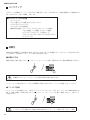
■ SAVING DATA(データの保存)
Be sure to
perform it
2
Saving and backing up your data
Some data items are automatically saved as
backup data in the internal memory even if you
turn the power off. Saved data may be lost due to
malfunction or incorrect operation. Save important
data to external device such as a computer.
必ず実行
作成したデータの保存とバックアップ
この楽器の一部のデータは自動的に保存されるた
め、電源を切ってもデータは消えません。ただし保
存したデータは故障や誤操作などのために失われる
ことがあります。大切なデータは、コンピューター
などの外部機器に保存してください。
PSR-E333/YPT-330
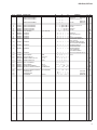
SPECIFICATIONS
Size/Weight
Keyboard
Display
Panel
Voices
Dimensions
WxDxH
4.9kg (10 Ibs. 13 oz.) (not including batteries)
Number of Keys
61
Touch Response
Yes
Type
LCD display
Backlit
Yes
Language
English
Language
English
Tone Generation
Tone Generating Technology
AWM Stereo Sampling
Polyphony
Number of Polyphony (Max.)
32
Preset
Number of Voices
Compatibility
Types
Effects
Function
Preset
Custom
Other Features
Preset
Songs
Recording
Compatible Data
Format
Overall Controls
Miscellaneous
9 types
Chorus
4 types
Ultra-Wide Stereo
3 types
Harmony
26 types
Dual
Yes
Split
Yes
Panel Sustain
Yes
Number of Preset Styles
106
Fingering
Multi fingering
Style Control
ACMP ON/OFF, SYNC START, START/STOP,
INTRO/ENDING/rit., MAIN/AUTO FILL
User Styles
Yes
Music Database
100
One Touch Setting (OTS)
Yes
Number of Preset Songs
102
Number of Songs
5
Number of Tracks
2
Data Capacity
Approx. 10,000 notes (when only “melody” tracks are recorded)
Approx. 5,500 chords (when only “chord” tracks are recorded)
Recording Function
Yes
Playback
SMF
Recording
Original File Format
[1 LISTENING, 2 TIMING, 3 WAITING], [KEYS TO SUCCESS],
[PHRASE REPEAT], [CHORD DICTIONARY], [A-B REPEAT]
Lesson
Functions
140 panel voices + 13 drum/SFX kits + 344 XGlite voices
GM/XGlite
Reverb
Accompaniment
Styles
945 x 369 x 132 mm (37-3/16” x 14-1/2” x 5-3/16”)
Weight
Metronome
Yes
Tempo Range
11 – 280
Transpose
-12 – 0 – +12
Tuning
427.0 - 440.0 - 453.0 Hz
Portable Grand Button
Yes
Storage and
Connectivity
Internal Memory
1.7MB
Connectivity
PHONES/OUTPUT, DC IN, USB TO HOST, SUSTAIN
Amplifiers and
Speakers
Amplifiers
2.5W + 2.5W
Speakers
12cm x 2
Power Supply
• Adaptor: Users within U.S or Europe: PA-130 or an equivalent
Others: PA-3C, PA-130 or an equivalent
• Batteries: Six “AA” size, LR6 or equivalent batteries
Power Consumption
7W (When using PA-130 power adaptor)
Power Supply
Auto Power Off Function
Yes
Included Accessories
• Music Rest
• Owner’s Manual
• AC Power adaptor (PA-130 or an equivalent recommended by Yamaha)
Optional Accessories
• Adaptor: Users within U.S or Europe: PA-130 or an equivalent
Others: PA-3C, PA-130 or an equivalent
• Footswitch: FC4/FC5
• Keyboard Stand: L-2C/L-2L
• Headphones: HPE-150/HPE-30
3
PSR-E333/YPT-330
総合仕様
サイズ / 重量
鍵盤
ディスプレイ
パネル
音源 / 音色
寸法
幅×奥行き×高さ
4.9kg(乾電池含まず)
鍵盤数
61
タッチレスポンス
○
タイプ
液晶
バックライト
○
言語
英語
言語
日本語
音源
音源方式
発音数
最大同時発音数
32
プリセット
音色数
140 パネル音色 + 13 ドラム /SFX キット + 344XGlite 音色
リバーブ
9 種類
コーラス
4 種類
ウルトラワイドステレオ
3 種類
ハーモニー
26 種類
デュアル
○
スプリット
○
パネルサステイン
○
プリセットスタイル数
106
フィンガリング
マルチフィンガリング
スタイルコントロール
スタイルオン / オフ、シンクロスタート、スタート / ストップ、
イントロ / エンディング /rit.、メイン / フィルイン
ユーザースタイル
○
ミュージックデータベース
100
ワンタッチセッティング
○
内蔵曲数
102
録音曲数
5
録音トラック数
2
データ容量
約 10,000 音符 /1 曲、または約 5,500 コード /1 曲
録音機能
○
音源フォーマット
タイプ
効果
ファンクション
プリセット
伴奏スタイル
カスタマイズ
その他特長
プリセット
録音再生
ファンクション
録音
GM/XGlite
SMF
録音フォーマット
オリジナルフォーマット
レッスン
[ ソングマスター ]、[1 お手本、2 タイミング、3 マイペース ]、
[ フレーズ練習 ]、[A-B リピート ]、[ コード辞書 ]
全体設定
メトロノーム
○
テンポ
11 ∼ 280
トランスポーズ
-12 ∼ 0 ∼ +12
チューニング
427.0 ∼ 440.0 ∼ 453.0 Hz
ピアノボタン
○
内蔵メモリー
電源部
4
約 1.7MB
USB TO HOST、DC IN 12V、
ヘッドフォン / 外部出力(ステレオ標準フォン)、サステイン
接続端子
アンプ / スピーカー
AWM ステレオサンプリング
再生フォーマット
その他
メモリー
945 × 369 × 132(mm)
質量
アンプ出力
2.5W + 2.5W
スピーカー
12cm × 2
電源
電源アダプター:PA-3C(またはヤマハ推奨の同等品)
電池:単 3 乾電池(1.5V)× 6(別売)
消費電力
12W(電源アダプター PA-3C 使用時)
電池寿命
アルカリ電池で約 8 時間
オートパワーオフ機能
○
付属品
取扱説明書、電源アダプター(PA-3C またはヤマハ推奨の同等品)、
ソングブック、保証書、譜面立て
オプション(別売)品
ソフトケース(SCC-51/SCC-52)
、キーボードスタンド(L-2L/L-2C)、
ヘッドフォン(HPE-150/HPE-30)
、フットスイッチ(FC4/FC5)
PSR-E333/YPT-330
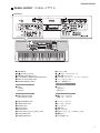
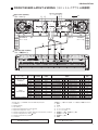
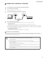
PANEL LAYOUT(パネルレイアウト)
Front Panel
/
2
)
4
*
0
-
6
1
'RAND0NO
■ Front Panel
q [ ] (Standby/On) switch
w [MASTER VOLUME] control
e [1 LISTENING 2 TIMING 3 WAITING] button
r [KEYS TO SUCCESS] button
t [PHRASE REPEAT] button
■ フロントパネル
q [ ] (スタンバイ/オン)スイッチ
w [全体音量]コントロール
e [1 お手本 2 タイミング 3 マイペース]ボタン
r [ソングマスター ]ボタン
t [フレーズ練習]ボタン
When the lesson mode
レッスンのとき
y PART
[L] button
[R] button
y パート
[左手]ボタン
[右手]ボタン
When the recording mode
録音のとき
y [REC TRACK 2] button
[REC TRACK 1] button
y [録音トラック 2]ボタン
[録音トラック 1]ボタン
u [METRONOME] button
i [TEMPO/TAP] button
o [SONG] button
!0 [VOICE] button
!1 [STYLE] button
!2 Number buttons [0]–[9], [+/YES], [-/NO]
!3 [FUNCTION] button
!4 [DEMO/BGM] button
u [メトロノーム]ボタン
i [テンポ/タップ]ボタン
o [ソング]ボタン
!0 [楽器]ボタン
!1 [スタイル]ボタン
!2 数字ボタン[0] ∼ [9]、[+/YES]、[−/NO]
!3 [機能]ボタン
!4 [デモ/BGM]ボタン
5
PSR-E333/YPT-330
When the Song mode
ソングのとき
!5 [A-B REPEAT] button
!6 [REW] button
!7 [FF] button
!8 [PAUSE] button
!5 [A-B リピート]ボタン
!6 [巻戻し]ボタン
!7 [早送り]ボタン
!8 [一時停止]ボタン
When the Style mode
スタイルのとき
!5 [ACMP ON/OFF] button
!6 [INTRO/ENDING/rit.] button
!7 [MAIN/AUTO FILL] button
!8 [SYNC START] button
!5 [スタイル オン/オフ]ボタン
!6 [イントロ/エンディング/rit.]ボタン
!7 [メイン/フィルイン]ボタン
!8 [シンクロスタート]ボタン
!9 [START/STOP] button
@0 [REC] button
@1 [PORTABLE GRAND] button
@2 [MUSIC DATABASE] button
@3 [ULTRA-WIDE STEREO] button
@4 [SPLIT] button
@5 [DUAL] button
@6 [HARMONY] button
@7 [TOUCH] button
@8 Drum Kit icons
!9 [スタート/ストップ]ボタン
@0 [録音]ボタン
@1 [グランドピアノ]ボタン
@2 [ミュージックデータベース]ボタン
@3 [ウルトラワイドステレオ]ボタン
@4 [スプリット]ボタン
@5 [デュアル]ボタン
@6 [ハーモニー ]ボタン
@7 [タッチ]ボタン
@8 ドラムキット
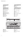
Rear Panel
■ Rear Panel
@9 SUSTAIN jack
#0 USB terminal
#1 PHONES/OUTPUT jack
#2 DC IN jack
6
■ リアパネル
@9 サステイン端子
#0 USB端子
#1 ヘッドフォン/外部出力端子
#2 DC IN端子
PSR-E333/YPT-330
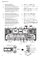
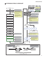
CIRCUIT BOARD LAYOUT & WIRING(ユニットレイアウト & 結線図)
BACK-LIT ASSEMBLY
(バックライト Ass’
y)
Upper case assembly
(上ケース Ass’
y)
PNAM
DMLCD
PNAM
2/3
SPEAKER R
(スピーカ 右)
PNAM 3/3
=B
1/3
>
2 8
SPEAKER L
(スピーカ 左)
;
.
Lower key bed assembly
(下ケース鍵盤 Ass’
y)
q
w
e
r
t
y
u
i
o
!0
!1
!2
!3
@
61L-MK
No.
:
61H-MK
Unit Name
(ユニット名)
Location
Parts No. Connector Assembly
Destination
(ロケーション) (部品番号)
(束線名)
(配線先)
30
WE13850R
MK1
61H-MK-CN1
*1 *4
DMLCD-CN102
40
WE13870R
MK2
61H-MK-CN2
*1 *4
DMLCD-CN104
LOWER KEY BED
ASSEMBLY
50
WE13880R
MK3
61L-MK-CN5
*1 *4
DMLCD-CN103
120
(WQ73930)
BATT
CONTACT SPRING (+/–) *2 *6
PNAM1/3-CN506
UPPER CASE ASSEMBLY
350
WE141400
BL
BACK-LIT ASSEMBLY *2 *5
PNAM1/3-CN501
WH103
(WQ66100)
AMDM
PNAM1/3-CN503
*3 *9
DMLCD-CN108
WH104
(WQ66030)
PN1
PNAM1/3-CN502
*3 *9
PNAM2/3-CN303
WH105
(WQ66120)
MVR
PNAM1/3-CN504
*3 *9
PNAM3/3-CN401
PNAM
WH201
(WQ66140)
SP
PNAM1/3-CN505
*3 *9
SPEAKER L
CIRCUIT BOARD
WH202
(WQ66140)
SP
PNAM2/3-CN202
*3 *9
SPEAKER R
WH301
(WQ66060)
PN2
PNAM2/3-CN301
*3 *9
DMLCD-CN106
WH302
(WW15820)
JACK
PNAM2/3-CN304
*3 *9
DMLCD-CN107
KEYBOARD ASSEMBLY
220
V869620R
61H-MK-CN3
*1 *4
61L-MK-CN4
* The parts with “( )” in “Part No.” are not available as spare parts.
*1: Installation
*2: Manual soldering
*3: Dip soldering
*4: Edge mark is adjusted to Pin 1 mark ( mark).
*5: Edge mark is adjusted to + mark.
*6: Red wire is connected to (+) terminal. Black wire is connected to (–) terminal.
*7: Red wire is adjusted to Pin 1 mark ( mark).
*8: Red wire is connected to (+) terminal.
*9: Connected
Caution: Be sure to attach the removed filament tape just as it
was before removal.
*1
*1
*1
*1
*1
*1
*3
*3
*2
*2
*1
*1
*1
*4
*4
*4
*7
*4
*4
*9
*9
*5
*5
*4
*4
*4
Remarks
(備考)
12P L=220
5P L=250
7P L=190
3P
2P L=70
11P
10P
5P
2P
2P
13P
3P
12P L=210
* 部品番号が ( ) で囲まれている部品は、サービス部品として準備されていません。
*1: 差込み
*2: 手半田
*3: ディップ
*4: エッジマークが 1 ピン側 ( )
*5: エッジマークが + 側 (+)
*6: 赤色線材が (+) 端子、黒色線材が (‒) 端子
*7: 赤色線材が 1 ピン側 ( )
*8: 赤色線材が (+) 端子
*9: 接続済
注意 : 一度剥がしたフィラメントテープは、取り外す前と同じよ
うに、取り付けてください。
7
61L-MK
61H-MK
(C1–B3)
(C4–C6)
PNAM 2/3
SW MATRIX
CN5
(7P)
CN2
(5P)
DMLCD
CN104
(5P)
CN102
(12P)
CN303
(10P)
CN106
(13P)
CN107
(3P)
PB[0]–PB[7]
N11–N16, N21–N26
33
LCD
DISPLAY
IC101
(80P)
36,38–46
41
3–12,
173,174
+1.8V
143–150
+3.3D
25,56,57,68,74,
112,151
36,50,
135–142
REGULATOR
+3.3V
+3.3D
+1.8D
RESET
+4.2 54ms
16.9344 MHz
Crystal SMD-49
F Tolerance±100PPM
1
130
SWL01U
21
X101
48 MHz
CERAMIC
F Tolerance±0.25%
X102
65,66,75
FUNC_DP,FUNC_DM,VBUS
71 72
9,10
77,79–85,
91–100,
103–110,
113–126,128
2,3
1
BUFFER/ 7
5,6 LPF
fc=34 KHz
IC108 (8P)
PSWO
164
22
DAC
IC104 (16P)
/PSWI
43
102,155,
156,159
(SW501–513)
+5A
CN503
(11P)
8
11,12
24bit
L ch
R ch
MASTER
VOLUME
L
A5K Ω
LDQM,UDQM,RCLK,/CS4
4Ω 12cm
SW MATRIX
+5D
+5A
14
1–4
SPEAKER L
CN501
(2P)
CN108
(11P)
REGULATOR
+1.8V
IC110(4P)
+5A
SD0,SYSCLK,
35,37, BCLK,WCLK
39,40
IC102
(176P)
2
BACK-LIT ASSEMBLY
CN505
(2P)
PA3–PA7
LCD DRIVER
PB0–PB2
PA[0]–PA[7],
ENB,RS
PH[3]
KYB01–KYB07
KYB07–KYB11
38,157,158,
160,166
CN502
(10P)
PNAM 1/3
+5D
23,31,54,64,70,
111,153
+5D
CN101
4Ω 12cm
PA[3]–PA[7]
13,14,157,
167–170
USB
To Host
SPEAKER R
CN301
(13P)
IC111(5P)
IC106
(5P)
CN202
(2P)
CN1
(12P)
CN304
(3P)
CN103
(7P)
PA[3]–PA[7]
PB[3]–PB[7]
SW37-61
B07–B11
B01–B07
(SW301–324)
CN3
(12P)
N11–N16, N21–N26
CN4
(12P)
SW1-36
VR401
CN401
(5P)
R
CN504
(5P)
POWER AMP5
11
12
L
2.5W x 2
BA5417
PHONES
/OUTPUT
R
3
IC502
(15P)
JK501
8
PNAM 3/3
/CS0,
MA[1]–MA[23],
MD[0]–MD[15]
/CS1,
MA[1]–MA[22],
MD[0]–MD[15]
MA[1]–MA[11],
MA[13],MA[17],
MA[18],
MD[0]–MD[15]
64M
FLASH ROM
PROG./WAVE
16M
FLASH ROM
16M
SDRAM
IC107
(56P)
IC109
(48P)
IC103
(50P)
16,29,43,53
37,47
1,7,13,25,38,44
14,18,
35,36
TR501,
TR502
IC501(3P)
+5V
REGULATOR
+5V
+B
STANDBY
SW
CN506
(3P)
+
–
BATTERY
1.5V x 6
AA-size,SUM-3,R6 batteries
CN503
(11P)
SW514
DC-IN
12V
AC adaptor
PA-3C/PA-130/PA-130A
+3.3D
JK502
28CA1-2001072757-1
BLOCK DIAGRAM(ブロックダイアグラム)
Keyboard 61KEY
(16N)
SUSTAIN
JK303
PSR-E333/YPT-330
8
TOUCH RESPONSE
PSR-E333/YPT-330
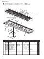
DISASSEMBLY PROCEDURE(分解手順)
Caution: Be sure to attach the removed filament tape just as it was before removal.
注意 : 分解時に取り外したフィラメントテープは、必ず元通りに取り付けてください。
1.
1-1
*
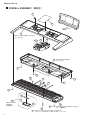
Lower Case Assembly
1.
下ケース Ass’y(所要時間 : 約 2 分)
(Time required: About 2 minutes)
Remove the five (5) screws marked [80A], two (2)
screws marked [90] and two (2) screws marked
[100A]. The lower case assembly can then be
removed. (Fig.1)
1-1
[80A] のネジ 5 本、[90] のネジ 2 本と [100A] のネ
ジ 2 本を外して、下ケース Ass’
y を外します。
(図 1)
※
下ケース Ass’y を取り付けるときは、[90] のネジを締め
てから他のネジを締めてください。(図 1)
When installing the lower case assembly, first
tighten the screw marked [90] and then the remaining
screws. (Fig. 1)
Bottom view(下から見た図)
[80A]
[100A]
[80A]
LOWER CASE ASSEMBLY
(下ケースAss’
y)
[90]
Positioning screw
(位置決めネジ)
[100A]
[80A]
[90]
BATTERY COVER ASSEMBLY
(電池蓋Ass'y)
Positioning screw
(位置決めネジ)
Top view(上から見た図)
SP GRILLE
(SPグリル)
KNOB
(Vツマミ)
Fig.1(図1)
SP GRILLE
(SPグリル)
9
PSR-E333/YPT-330
2.
DMLCD Circuit Board
2.
DMLCD シート(所要時間 : 約 3 分)
2-1
2-2
(Time required: About 3 minutes)
Remove the lower case assembly. (See procedure 1.)
Remove the ten (10) screws marked [385]. The
DMLCD circuit board can then be removed. (Fig.2)
2-1
2-2
下ケース Ass’y を外します。
(1 項参照)
[385] のネジ 10 本を外して、DMLCD シートを外
します。(図 2)
※
DMLCD シートを取り付けるときは、1 から 10 の順で
ネジを締めてください。(図 2)
DMLCD シートを交換した場合は、テストプログラムの
Factory Set を実行してください。
*
*
When installing the DMLCD circuit board, tighten the
screws 1 through 10 in numerical order. (Fig. 2)
If the DMLCD circuit board is replaced, execute the
“Factory Set” in the test program.
※
3.
LCD (Time required: About 3 minutes)
3.
液晶ディスプレイ(所要時間 : 約 3 分)
3-1
3-2
3-3
3-4
3-5
Remove the lower case assembly. (See procedure 1)
Remove the DMLCD circuit board. (See procedure 2)
Remove the LCD holder and rubber connector. (Fig. 3)
Remove the back-lit assembly. (Fig. 3)
Remove the LCD. (Fig. 3)
3-1
3-2
3-3
*
When attaching the rubber connector, set the
conductive part to face inside. (Fig. 3)
Avoid touching the conductive part of the rubber
connector as much as possible. Should foreign
matter or dirt adhere, remove such contamination
using adhesive tape or the like. Do not wipe off using
solvents such as benzene or alcohol. (Fig. 3)
下ケース Ass’y を外します。
(1 項参照)
DMLCD シートを外します。
(2 項参照)
LCD ホルダーとゴムコネクターを外します。
(図 3)
バックライト Ass’y を外します。
(図 3)
液晶ディスプレイを外します。(図 3)
*
3-4
3-5
※
ゴムコネクタ−を取り付けるときは導電部を内側にして
ください。(図 3)
ゴムコネクタ−の導電部には極力触れないようにしてく
ださい。異物、ごみ等が付着した場合は粘着テープ等で
取り除き、ベンゼン・アルコール等の溶剤では拭かない
でください。(図 3)
※
Bottom view(下から見た図)
[370]
[A]
PNAM 1/3
[380C]
[385]
[385]
PNAM
2/3
3
1
[380C]
LOUD SPEAKER
(スピーカ)
5
6
DMLCD
1
[80B]
4
[100B]
7
8
PNAM 3/3
[380B]
[370]
[A]
10
9
2
[380B]
1
2
2
[385]
[380B]
LOWER KEY BED ASSEMBLY
(下ケース鍵盤Ass’y)
[380A]
[80B]
LOUD SPEAKER
(スピーカ)
Fig.2(図2)
LCD
(液晶ディスプレイ)
RUBBER CONNECTOR
(ゴムコネクター)
BACK-LIT ASSEMBLY
(バックライトAss’y)
CONDUCTOR SIDE
(導電側)
RUBBER CONNECTOR
(ゴムコネクター)
DMLCD
RUBBER CONNECTOR
(ゴムコネクター)
Fig.3(図3)
10
LCD HOLDER
(LCDホルダー-BL)
PSR-E333/YPT-330
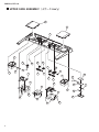
4.
PNAM Circuit Board (1/3, 2/3, 3/3)
4.
4-1
4-2
Remove the lower case assembly. (See procedure 1)
PNAM Circuit Board 3/3
(Time required: About 2 minutes)
Remove the knob from the control panel surface.
(Fig. 1, Fig. 4)
Remove the three (3) screws marked [380A]. The
PNAM circuit board 3/3 can then be removed. (Fig. 2)
PNAM Circuit Board 1/3
(Time required: About 3 minutes)
Remove the PNAM circuit board 3/3.
(See procedure 4-2)
Remove the sixteen (16) screws marked [380B].
The PNAM circuit board 1/3 can then be removed.
(Fig. 2)
4-1
4-2
4-2-1
4-2-1
4-2-2
4-3
4-3-1
4-3-2
*
When installing the PNAM circuit board 1/3, tighten
the screws 1, 2 in that order and then the remaining
screws. (Fig. 2)
下ケース Ass’y を外します。
(1 項参照)
PNAM シート 3/3(所要時間:約 2 分)
コントロールパネル面から V ツマミを外します。
(図 1、図 4)
4-2-2 [380A]のネジ 3 本を外して、PNAM シート 3/3
を外します。(図 2)
4-3
PNAM シート 1/3(所要時間:約 3 分)
4-3-1 PNAM シート 3/3 を外します。
(4-2 項参照)
4-3-2 [380B]のネジ 16 本を外して、PNAM シート 1/3
を外します。(図 2)
※
※
PNAM circuit board (2/3)
(Time required: About 3 minutes)
4-4-1 Remove the thirteen (13) screws marked [380C].
The PNAM circuit board 2/3 can then be removed.
(Fig. 2)
5.
5-1
5-2
*
6.
6-1
6-2
*
7.
7-1
7-2
PNAM シート 1/3 を取り付けるときは、1、2 の順でネ
ジを締めてから他のネジを締めてください。(図 2)
4-4
PNAM シート 2/3(所要時間:約 3 分)
4-4-1 [380C]のネジ 13 本を外して、PNAM シート 2/3
を外します。(図 2)
4-4
*
PNAM シート(1/3、2/3、3/3)
PNAM シート 2/3 を取り付けるときは、1、2 の順でネ
ジを締めてから他のネジを締めてください。(図 2)
KNOB
(Vツマミ)
When installing the PNAM circuit board 2/3, tighten
the screws 1, 2 in that order and then the remaining
screws. (Fig. 2)
Fig.4(図4)
: 約 2 分)
スピーカ(所要時間
Speaker (Time required: About 2 minutes)
Remove the lower case assembly. (See procedure 1)
Remove the four (4) screws marked [370]. The
speaker can then be removed. (Fig. 2)
5.
The right and left speakers can be removed in the
same manner.
※
左右のスピーカは同じように外せます。
SP Grille (Time required: About 3 minutes each)
6.
SP グリル(所要時間 : 各約 3 分)
Remove the lower case assembly. (See procedure 1)
Align the eight (8) [A]s the groove in the upper
case assembly and remove the SP grille. (Fig. 1,
Fig. 2)
6-1
6-2
5-1
5-2
下ケース Ass’y を外します。
(1 項参照)
[370]のネジ 4 本を外して、スピーカを外します。
(図 2)
下ケース Ass ’y を外します。
(1 項参照)
[A]の 8 箇所を、
上ケース Ass’
y の溝と平行にして、
SP グリルを外します。(図 1、図 2)
※
左右の SP グリルは同じように外せます。
Lower Key Bed Assembly
7.
下ケース鍵盤 Ass’y(所要時間 : 各約 2 分)
(Time required: About 2 minutes each)
Remove the lower case assembly. (See procedure 1)
Remove the two (2) screws marked [80B]
and screw marked [100B]. The lower key bed
assembly can then be removed. (Fig. 2)
7-1
7-2
下ケース Ass’y を外します。
(1 項参照)
[80B]のネジ 2 本と、
[100B]のネジ 1 本を外して、
下ケース鍵盤 Ass’y を外します。
(図 2)
The right and left SP grilles can be removed in the
same manner.
11
PSR-E333/YPT-330
8.
Disassembling Keyboard Assembly
(Time required: About 13 minutes)
Remove the lower case assembly. (See procedure 1.)
8-1
8-2
Remove the lower key bed assembly.
(See procedure 7.)
8-3
White Keys and Black Keys
8-3-1 White and black keys for one octave unit are
integrated as a set. There are five sets in total.
Only the C6 white key, unlike the other keys, is not
integrated in a set. (Fig.5)
8-3-2 To remove a set, remove the four (4) each screws
marked [120A]. The white and black keys in the
set can then be removed. (Fig.5)
When removing, unfasten the two (2) hooks at the
back of the black keys upward, and lift the white
and black keys while pulling them toward you a
little. (Photo 1)
8-3-3 To remove the white key C6, remove the screw
marked [120B], unhook as described in Procedure
8-3-2, and pull out toward you. (Fig.5)
*
When all white and black keys were removed, first
attach the white and black keys C3 ~ B3 aligning
them with the boss, and then attach the remaining
white and black keys. (Fig. 5)
8.
鍵盤 Ass’y の分解(所要時間 : 約 13 分)
8-1
8-2
8-3
8-3-1
下ケース Ass’y を外します。
(1 項参照)
下ケース鍵盤 Ass’y を外します。
(7 項参照)
白鍵、黒鍵
白鍵、黒鍵は、左側から 1 オクターブ単位のセッ
トになっていて、全部で 5 セットあります。C6
鍵は白鍵 1 個のみです。
(図 5)
セットのものは、[120A] のネジ 4 本ずつ外してそ
れぞれ 1 セット分の白鍵・黒鍵を外します。
(図 5)
この時、黒鍵の後ろ側にある 2 つのフックを上方
向に外し、白鍵・黒鍵を少し手前に引きながら持
ち上げます。
(写真 1)
C6 の白鍵は [120B] のネジ 1 本を外して、8-3-2 項
のようにフックを外して手前に引きながら外しま
す。(図 5)
8-3-2
8-3-3
※
すべての白鍵・黒鍵を外した場合の組み立ては、最初に
C3 ∼ B3 の白鍵・黒鍵をボスに合わせて組み付けてから、
他の白鍵・黒鍵を組み付けてください。(図 5)
8-4
8-4-1
接点ゴム
外そうとする接点ゴムに対応した白鍵・黒鍵を外
します。(図 5、8-3 項参照)
それぞれの接点ゴムを外します。
(写真 2、図 6)
8-4-2
8-4
Rubber Contact
8-4-1 Remove the white and black keys corresponding
to the rubber contacts to be removed. (See Fig.5
and Procedure 8-3.)
8-4-2 Remove the rubber contacts. (Photo 2, Fig.6)
Boss
(ボス)
[120A]
Top view(上から見た図)
[120A]
[120A]
B2 C3
C1
KEYBOARD ASSEMBLY
(鍵盤Ass’y)
HOOK (フック)
Photo 1(写真1)
12
[120A]
[120A]
[120A]
B3 C4
[120B]
C6
Fig.5(図5)
RUBBER CONTACT (接点ゴム)
Photo 2(写真2)
PSR-E333/YPT-330
Top view(上から見た図)
RUBBER CONTACT
RUBBER CONTACT
(接点ゴム)
(接点ゴム)
RUBBER CONTACT
RUBBER CONTACT
[100C] [100D]
(接点ゴム)
(接点ゴム)
RUBBER CONTACT
(接点ゴム)
[100C]
[100C]
[100C]
[100D]
[100D]
61H
[110A]
61H-MK
[110A]
61L-MK
[110B]
Fig.6(図6)
61L-MK
9
2
3
10
4
61H-MK
11
5
6
7
8
12
6
1
1
7
3
4
8
5
2
Fig.7(図7)
8-5
Circuit Board 61L-MK
8-5-1 Remove the white and black keys from C1 to B3.
(See Fig.5 and Procedure 8-3.)
8-5-2 Remove the four (4) screws marked [100C] and
eight (8) screws marked [110A]. The circuit board
61L-MK can then be removed. (Fig.6)
*
When installing the circuit board 61L-MK, tighten the
screws 1 through 12 in numerical order as shown in
the figure “61L-MK” in Fig.7. (Fig.7)
8-6
Circuit Board 61H-MK
8-6-1 Remove the white and black keys from C4 to C6.
(See Fig.5 and Procedure 8-3.)
8-6-2 Remove the three (3) screws marked [100D] and
five (5) screws marked [110B]. The circuit board
61H-MK can then be removed. (Fig.6)
*
シート 61L
C1 ∼ B3 の白鍵・黒鍵を外します。
(図 5、8-3 項参照)
8-5-2 [100C] のネジ 4 本と [110A] のネジ 8 本を外して、
シート 61L を外します。
(図 6)
8-5
8-5-1
※
シート 61L を取り付けるときは、図 7 のシート 61L 図
の番号 1 ∼ 12 の順にネジを締めてください。(図 7)
シート 61H
C4 ∼ C6 の白鍵・黒鍵を外します。
(図 5、8-3 項参照)
8-6-2 [100D] のネジ 3 本と [110B] のネジ 5 本を外して、
シート 61H を外します。
(図 6)
8-6
8-6-1
※
シート 61H を取り付けるときは、図 7 のシート 61H 図
の番号 1 ∼ 8 の順にネジを締めてください。(図 7)
When installing the circuit board 61H-MK, tighten the
screws 1 through 8 in numerical order as shown in
the figure “61H-MK” in Fig.7. (Fig.7)
13
PSR-E333/YPT-330
9.
How to Remove Spring Terminals
9.
9-1
Spring Terminal A and Spring Terminal B
9-1
9-1-1
9-1-2
9-1-3
(Time required: About 4 minutes each)
9-1-1 Remove the lower case assembly. (See procedure 1.)
9-1-2 Remove the lower key bed assembly.
(See procedure 7.)
9-1-3 Remove the white and black keys from C1 to B2
(See Fig. 5 and Procedure 8-3.)
9-1-4 Remove the BATT connector assembly soldered
to the spring terminal A and spring terminal B.
(Photo 3)
9-1-5 Reverse the lower key bed assembly and remove
the battery cover assembly. (Fig.1)
9-1-6 Lift the spring terminal A a little and slide it in the
upper right direction to remove it. (Fig.8)
9-1-7 Remove the hook for the spring terminal B to pull
it out from inside. (Fig.8)
9-2
Spring Terminal C and Spring Terminal D
接点バネの外し方
9-1-4
9-1-5
9-1-6
9-1-7
9-2
9-2-1
9-2-2
接点バネ A、接点バネ B(所要時間 : 各約 4 分)
下ケース Ass’y を外します。
(1 項参照)
下ケース鍵盤 Ass’y を外します。
(7 項参照)
C1 ∼ B2 の白鍵・黒鍵を外します。
(図 5、8-3 項参照)
接点バネ A、接点バネ B に半田付けされている
BATT 束線を外します。
(写真 3)
下ケース鍵盤 Ass’y を裏返して、電池蓋 Ass’y
を外します。(図 1)
接点バネ A は、上に少し引き上げ、右上にスライ
ドして外します。(図 8)
接点バネ B は、フックを外して、内側から引き出
します。(図 8)
接点バネ C、接点バネ D(所要時間 : 各約 1 分)
電池蓋 Ass’y を外します。
(9-1-5 項参照)
フックを外して、接点バネ C、接点バネ D を引き
出します。
(図 8、図 9)
(Time required: About 1 minute each)
9-2-1 Remove the battery cover assembly.
(See procedure 9-1-5)
9-2-2 Remove the hooks to pull out the spring terminal
C and spring terminal D. (Fig.8, Fig.9)
SPRING TERMINAL D
(接点バネD)
SPRING TERMINAL B
SPRING TERMINAL A
(接点バネB)
(接点バネA) HOOK
HOOK
(フック)
(フック)
SOLDERING
(半田付け)
SPRING TERMINAL B
SPRING TERMINAL A
(接点バネB)
(接点バネA)
Fig.8(図8)
SPRING TERMINAL C
(接点バネC)
SPRING TERMINAL C
HOOK
(接点バネC)
(フック)
HOOK
(フック)
BATT CONNECTOR ASSEMBLY
(BATT束線)
Photo 3(写真3)
Fig.9(図9)
14
PSR-E333/YPT-330
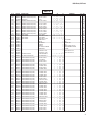
LSI PIN DESCRIPTION(LSI 端子機能表)
AK4385ET (X6040A01) DAC (Digital to Analog Converter) .................................................................15
NT3881DFG-01 (X3148A0R) LCD DRIVER ........................................................................................15
SWL01U (YA876A00) CPU ..................................................................................................................16
NT3881DFG-01 (X3148A00) LCD DRIVER
PIN
NO.
NAME
I/O
1
2
3
4
5
6
7
8
9
10
11
12
13
14
15
16
17
18
19
20
21
22
23
24
25
26
27
28
29
30
31
32
33
34
35
36
37
38
39
40
S22
S21
S20
S19
S18
S17
S16
S15
S14
S13
S12
S11
S10
S9
S8
S7
S6
S5
S4
S3
S2
S1
Vss
OSC1
OSC2
V1
V2
V3
V4
V5
CLK1
CLK2
Vdd
M
D
RS
R/W
E
DB0
DB1
O
O
O
O
O
O
O
O
O
O
O
O
O
O
O
O
O
O
O
O
O
O
FUNCTION
Segment signal output for LCD
driving
Ground
Oscillator
Oscillator
I
O
Power supply
O
O
O
O
I
I
I
I/O
I/O
Data latch clock
Data shift clock
Power supply (+5 V)
Altamated signal for LCD driver outout
Display data interface
Read/write
Enable
Data interface
Data interface
DMLCD: IC101
PIN
NO.
41
42
43
44
45
46
47
48
49
50
51
52
53
54
55
56
57
58
59
60
61
62
63
64
65
66
67
68
69
70
71
72
73
74
75
76
77
78
79
80
NAME
I/O
DB2
DB3
DB4
DB5
DB6
DB7
C1
C2
C3
C4
C5
C6
C7
C8
C9
C10
C11
C12
C13
C14
C15
C16
S40
S39
S38
S37
S36
S35
S34
S33
S32
S31
S30
S29
S28
S27
S26
S25
S24
S23
I/O
I/O
I/O
I/O
I/O
I/O
O
O
O
O
O
O
O
O
O
O
O
O
O
O
O
O
O
O
O
O
O
O
O
O
O
O
O
O
O
O
O
O
O
O
FUNCTION
Data interface
Common signal output for LCD
driving
Segment signal output for LCD
driving
AK4385ET (X6040A01) DAC (Digital to Analog Converter)
PIN
NO.
1
2
3
4
5
6
7
8
NAME
I/O
MCLK
BICK
SDTI
LRCK
PDN
CSN
CCLK
CDTI
I
I
I
I
I
I
I
I
FUNCTION
Master Clock
Audio Serial Data Clock
Audio Serial Date Input
L/R Clock
Power Down mode
Chip Select
Control Data Input
Control Data Input
PIN
NO.
9
10
11
12
13
14
15
16
NAME
I/O
AOUTRAOUTR+
AOUTLAOUTL+
Vss
VDD
DZFR
DZFL
O
O
O
O
O
O
DMLCD: IC104
FUNCTION
Rch Analog out(-)
Rch Analog out(+)
Lch Analog out(-)
Lch Analog out(+)
Ground
Power Supply
Rch Data Zero Input Detect
Lch Data Zero Input Detect
15
PSR-E333/YPT-330
SWL01U (YA876A00) CPU
16
PIN
NO.
NAME
I/O
1
2
3
4
5
6
7
8
9
10
11
12
13
14
15
16
17
18
19
20
21
22
23
24
25
26
27
28
29
30
31
32
33
34
35
36
37
38
39
40
41
42
43
44
45
46
47
48
49
50
51
52
53
54
55
56
57
58
59
60
61
62
63
64
65
66
67
68
69
70
71
72
73
74
75
76
77
78
79
80
81
82
83
84
85
86
87
88
NC
NC
EA3/PD3/KYN24
EA2/PD2/KYN23
EA1/PD1/KYN22
EA0/PD0/KYN21
ED0/PC0/KYN11
ED1/PC1/KYN12
ED2/PC2/KYN13
ED3/PC3/KYN14
ED4/PC4/KYN15
ED5/PC5/KYN16
ED6/PC6/KYB05
ED7/PC7/KYB06
PROTN
BISTMD
BISTCLK
PLLBPN
TESTN
VSS
XI
XO
VDD
VSS
IOVDD
TRSTN
TMS
TCK
TDI
TDO
VDD
PLLVDD
VSS
PLLVSS
WCLK/SYO
PFO
SDO1
SDO0
BCLK
SYSCLK/PG3
SDI/PH3
VSS
IRQON/PHO
NC
NC
NC
NC
TXD0/PG4
RXD0/PH4
TXD1/PG2
RXD1/PH1
SCLK1/PH2
UCTL
VDD
VSS
AVDD
AVREF
AN0
AN1
AN2
AN3
AGNDREF
AVSS
USBVDD
FUNC_DM
FUNC_DP
USBVSS
USBIOVDD
VSS
VDD
XI_UCLK
XO_UCLK
VSS
IOVDD
VBUS
PULLUPE
CS0N/PG0
RDN/PF4
MA01
MD00
MD08
MD01
MD09
MD02
MD10
NC
NC
NC
I
I
I
I
I/O
I/O
I/O
I/O
I/O
I/O
I/O
I/O
I
I
I
I
I
O
I/O
I
I
I
I
I
O
O
O
O
O
O
I
I
O
I
O
I
I
I
I
I
I
I
I
I
I/O
I/O
I
O
I/O
I
O
O
O
O
I/O
I/O
I/O
I/O
I/O
I/O
-
FUNCTION
DMLCD: IC102
PIN
NO.
89
90
91
92
ON/OFF signal from the keyboard
93
94
95
96
97
98
Key selection signal to the keyboard
99
100
101
102
Determines if the product is a prototype
103
104
Memory BIST mode (1: BIST mode)
105
Memory BIST clock
106
PLL bypass mode (0: PLL bypass)
107
Test mode
108
Digital Core ground
109
Crystal oscillator input (33.8688 MHz)
110
Crystal oscillator output
111
Digital Core power supply
112
Digital Core ground
113
I/O power supply
114
JTAG I/F reset
115
JTAG I/F mode
116
JTAG I/F clock
117
JTAG I/F input
118
JTAG I/F output
119
Digital Core power supply
Digital PLL power supply (common with Core power supply inside) 120
121
Digital Core ground
Digital PLL ground (common with Core ground inside) 122
123
Word clock (1 Fs = 44.1 kHz)
124
Output-only port
125
Audio output data (with EQ & compressor)
(SWL01 equivalent output data)/Selection signal to the keyboard 126
127
Bit clock (64Fs)
128
System clock (256Fs/384Fs/768Fs)
129
Serial audio input data
130
Digital Core ground
131
Interrupt input
132
133
Connection to the GND
134
135
136
Serial port I/F
137
Serial port I/F
138
Serial port I/F
139
Serial port I/F
140
Serial port I/F
Fixed L when USB is in use/Fixed H when not in use 141
142
Digital Core power supply
143
Digital Core ground
144
Analog power supply
145
ADC reference
146
147
ADC input
148
149
150
ADC ground reference
151
Analog ground
USB I/O power supply 1.8v (Pullup when not in use) 152
153
USB data 154
USB data +
155
USB I/O ground
USB I/O power supply 3.3v (Pullup when not in use) 156
157
Digital Core ground
158
Digital Core power supply
159
Crystal oscillator input (48 MHz)
160
Crystal oscillator output
161
Digital Core ground
162
I/O power supply
163
USB Vbus
164
USB Pullup enable
165
Chip select for area 2
166
External memory read signal
167
External memory address
168
169
170
External memory data bus
171
172
173
174
175
Connection to the GND
176
Connection to the GND
NAME
I/O
NC
NC
MD03
MD11
MD04
MD12
MD05
MD13
MD06
MD14
MD07
MD15
VSS
CS50RDN/PE4/RCLK
MA17
MA23
MA16
MA15
MA14
MA13
MA12
MA11
VDD
IOVDD
MA10
MA09
MA20
MA21/PF1
MA22/PF2
MA19
MA18
MA08
MA07
MA06
MA05
MA04
MA03
MA02
MA00
CS1N/PG1
VSS
ICN
VSS
NC
NC
NC
PA0
PA1
PA2
PA3
PA4
PA5
PA6
PA7
PB0
PB1
PB2
PB3
PB4
PB5
PB6
PB7
IOVDD
VSS
VDD
WRN/PF5/WEN
UBN/PF7/UDQM
LBN/PF6/LDQM
CS2N/PE0/KYB07
CS3N/PE1/KYB08
CS4N/PE2
CS5N/PE3/KYB09
CS51WRN/PE5/KYB12
CS52WRN/PE6/KYB13
CS53WRN/PE7
PF3
PJ5
PJ4/KYB11
PJ3/KYB01
PJ2/KYB04
PJ1/KYB03
PJ0/KYB02
VSS
ECSN
EWRN/PD5/KYN26
ERDN/PD4/KYN25
NC
NC
I/O
I/O
I/O
I/O
I/O
I/O
I/O
I/O
I/O
I/O
O
O
O
O
O
O
O
O
O
I/O
O
O
O
O
O
O
O
O
O
O
O
O
O
O
O
O
I
I/O
I/O
I/O
I/O
I/O
I/O
I/O
I/O
I/O
I/O
I/O
I/O
I/O
I/O
I/O
I/O
I/O
O
O
O
O
O
O
O
O
O
O
O
O
O
O
O
O
O
I
I
I
-
FUNCTION
Connection to the GND
External memory data bus
Digital Core ground
Priority of setup) PE4 > RCLK(SDRAM) > CS50RDN
External memory address
Digital Core power supply
I/O power supply
External memory address
Chip select for area 3
Digital Core ground
Reset
Digital Core ground
Connection to the GND
Universal I/O port
I/O power supply
Digital Core ground
Digital Core power supply
Priority of setup) PF5 > WEN(SDRAM) > WRN
Priority of setup) PF7 > UDQM(SDRAM) > UBN
Priority of setup) PF6 > LDQM(SDRAM) > LBN
Chip select for area 4
Chip select for area 5
Chip select for area 6
Chip select for area 7
For luminescent keyboard
Output-only port
Used as key selection signal to the keyboard
Digital Core ground
Chip select input from external CPU
Write enable input from external CPU
Read enable input from external CPU
Connection to the GND
PSR-E333/YPT-330
CIRCUIT BOARDS(シート基板図)
DMLCD Circuit Board (YC994C0) .............................................................................................19
PNAM 1/3 Circuit Board (YD033C0) .........................................................................................18
PNAM 2/3 Circuit Board (YD033C0) .........................................................................................17
PNAM 3/3 Circuit Board (YD033C0) .........................................................................................18
61H-MK Circuit Board (X2335D0) .............................................................................................20
61L-MK Circuit Board (X2336C0) .............................................................................................20
Note: See parts list for details of circuit board component parts.
注:
シートの部品詳細はパーツリストをご参照ください。
PNAM 2/3 Circuit Board
to DMLCD-CN107
to SPEAKER R
not installed
not installed
to DMLCD-CN106
SUSTAIN
to PNAM 1/3-CN502
Component side(部品側)
2NA-WV92640-1
17
PSR-E333/YPT-330
PNAM 1/3 Circuit Board
PHONES/OUTPUT
to BACK-LIT ASSEMBLY
DC IN
to BATTERIES
to PNAM 2/3-CN303
to DMLCD-CN108
to SPEAKER L
Component side(部品側)
PNAM 3/3 Circuit Board
Component side(部品側)
18
2NA-WV92640-1
PSR-E333/YPT-330
DMLCD Circuit Board
Scale: 90/100
to PNAM 2/3-CN301
to PNAM 2/3-CN304
to 61H-MK-CN2
to 61H-MK-CN1
to 61L-MK-CN5
USB
not installed
to PNAM 1/3-CN503
Component side(部品側)
Pattern side(パターン側)
2NA-WV66390-1
19
PSR-E333/YPT-330
61H-MK Circuit Board
Scale: 70/100
A
to DMLCD-CN102
to 61L-MK-CN4
to DMLCD-CN104
A’
A
A’
Component side(部品側)
61L-MK Circuit Board
B
B’
B
B’
to DMLCD-CN103
to 61H-MK-CN3
Component side(部品側)
20
61H-MK: 2NAKB-V869540
61L-MK: 2NAKB-V869520
PSR-E333/YPT-330
TEST PROGRAM
* If the test number 52 “Factory Set” is executed, the data already set will be lost.
1
Preparations
1) Use an AC adaptor PA-3C, PA-130 or PA-130A.
2) Measuring device: Frequency counter, which can detect thousandth value or more, Level meter (with JIS-C filter), Oscilloscope
Note: Use a stereo plug and connect a load resistor of 33 Ω to the [PHONES/OUTPUT] jack for measurement unless
otherwise specified. Input impedance of the measuring device should be 1 MΩ or more.
3) Jig: Foot switch (FC-4 or FC-5), MIDI cable
4) Controller settings
MASTER VOLUME : MAX
PEDAL
: OFF
WIDE
: OFF
Others
: Initial setting when the power is turned on
2
Starting up the Test Program
While holding down the keys [C#2], [F2] and [G#2] simultaneously, press the [STANDBY / ON] switch.
C#2
G#2
F2
3
Test procedure
1) When the test program is started, “TEST” will be displayed on the LCD.
2) Press the [Tenkey –] or [Tenkey +] button to select a test program item.
3) Press the [START/STOP] button to execute the test.
If the result is OK or test item is completed, press the [START/STOP] button again to return to the item selection display.
Press the [Tenkey –] or [Tenkey +] button to select the next test item.
A cursor (“_”) is shown below the first character of the item for which the test results are OK.
If the result is NG, press the [DEMO/BGM] button or the lowest key (white key C1) to return to the item selection display.
4
Test Program List
TEST No
LCD display
1
001: Version
2
002: Mem1 All
3
003: Rom Chk1
4
004: Ram Chk1
5
005: FRomChk1
(dBu=dBm)
Test descriptions, judging conditions, etc.
Displays version of the ROM.
Using the tenkeys, each data version can be displayed as follows.
[Tenkey 1] Main Program Version
“∗∗∗ Main”
[Tenkey 2] Boot Program Version
“∗∗∗ Boot”
[Tenkey 3] Style Data Version
“∗∗∗ Style”
[Tenkey 4] Song Data Version
“∗∗∗ Song”
[Tenkey 5] Voice Parameter Version
“∗∗∗ Param”
[Tenkey 6] Wave Data Version
“∗∗∗ Wave”
∗∗∗ : Version
Checks the ROM, RAM and FROM connected to the CPU bus.
Make sure that “Mem1 OK” is displayed on the LCD.
* If the test result is OK, the tests “003: Rom Chk1”, “004: Ram Chk1” and “005:
FRom Chk1” can be skipped.
Checks the ROM connected to the CPU bus.
Make sure that “Rom OK” is displayed on the LCD.
Checks the RAM connected to the CPU bus.
Make sure that “Ram OK” is displayed on the LCD.
Checks the FROM connected to the CPU bus.
Make sure that “FRom OK” is displayed on the LCD.
21
PSR-E333/YPT-330
TEST No
LCD display
8
008: TG1 Chk
9
009: Pit Chk
10
010: Output R
11
011: Output L
21
021: SW Chk
25
26
29
025: LCD On
026: LCD Off
029: PD1 Chk
47
047: Rom Chk2
48
048: Ram Chk2
49
049: FRomChk2
52
052: Factory
53
053: TestExit
Test descriptions, judging conditions, etc.
Plays each key automatically in the order of scale (auto-scaling). (32 notes from C2 to G4 will be played.)
Make sure that there is no abnormal sounds or noise. When the auto-scaling is finished, “TG1 End”
will be shown. Press a key to play a sound. (Single note, the key pressed first will be played)
Checks pitch accuracy.
Connect the frequency counter to the [PHONES/OUTPUT] jack. (Either L or R)
Make sure that the correct signal is output. (441.0 Hz ± 0.2 Hz)
Amount of volume decay
Connect the level meter (with JIS-C fi lter) to the L/R of the [PHONES/OUTPUT] jack. (33 Ω load)
Turn the [MASTER VOLUME] to the minimum and measre the amount of volume decay.
· PHONES L, R: -70 dBu or less
Connect the level meter (with JIS-C filter) to the L/R of the [PHONES/OUTPUT] jack.
(33 Ω load)
Set the [MASTER VOLUME] to the maximum level and check the output level.
· PHONES R: –1.0 dBu ± 2 dB
· PHONES L: –45.0 dBu or less
Connect the level meter (with JIS-C filter) to the L/R of the [PHONES/OUTPUT] jack.
(33 Ω load)
Set the [MASTER VOLUME] to the maximum level and check the output level.
· PHONES L: –1.0 dBu ± 2 dB
· PHONES R: –45.0 dBu or less
Checks the switches on the panel. Press the switches as shown in the LCD. When a switch is
pressed, a sound is played at the prescribed pitch. (Refer to the Switch test item list on the next
page.)
Make sure that “SW OK” is displayed on the LCD when all the switches are pressed as indicated. To
cancel the running test, press the [DEMO/BGM] button or the lowest key (white key C1) to return to the
item selection display.
Make sure that all the dots on the LCD are turned on.
Make sure that all the dots on the LCD are turned off.
Connect a footswitch (FC-4 or FC-5) to the [SUSTAIN] jack.
Check that C3 sound is played when the [Start/Stop] button is pressed with the pedal depressed and
that C4 sound is played when the pedal is released. Depress the pedal again and the sound will be
stopped.
Make sure that “PD1 OK” is displayed on the LCD.
Checks the ROM connected to the CPU bus.
Make sure that “Rom OK” is displayed on the LCD.
It will take about 12 seconds for the check.
Checks the RAM connected to the CPU bus.
Make sure that “Ram OK” is displayed on the LCD.
Checks the FROM connected to the CPU bus.
Make sure that “FRom OK” is displayed on the LCD.
It will take about 95 seconds for the check.
Initializes the entire backup area to reset to the factory default.
“Fact” is displayed on the LCD during the test.
“Fact End” is displayed on the LCD when the test is finished.
This will leave the test program and change to the play mode.
• Other Tests
Popping Noise Check
Connect the oscilloscope to the L/R of the [PHONES/OUTPUT] jack and turn on and then off the [STANDBY/ON] switch. Make
sure that popping noise level is 1.0 Vp-p or less, and that no abnormal sound or popping noise is output from the speakers.
Noise Level Check
Connect the level meter (with JIS-C filter) to the L/R of the [PHONES/OUTPUT] jack. (33 Ω load)
Set the [MASTER VOLUME] to the maximum level and check the noise level.
· PHONES L, R: –75 dBu or less
22
PSR-E333/YPT-330
Switch test item list
Turn
SW Name
LCD Display
Note Number
1
1 LISTENING 2 TIMING 3 WAITING
Lesson
C2
2
KEYS TO SUCCESS
Keys
C#2
3
PHRASE REPEAT
P Rep
D2
4
METRONOME
Metro
D#2
5
TEMPO/TAP
Temp/TAP
6
PART L
Left
F2
7
PART R
Right
F#2
8
SONG
Song
G2
9
VOICE
Voice
G#2
10
STYLE
Style
A2
11
TENKEY 1
Tenkey 1
A#2
12
TENKEY 2
Tenkey 2
B2
13
TENKEY 3
Tenkey 3
C3
14
TENKEY 4
Tenkey 4
C#3
15
TENKEY 5
Tenkey 5
D3
16
TENKEY 6
Tenkey 6
D#3
17
TENKEY 7
Tenkey 7
E3
18
TENKEY 8
Tenkey 8
F3
19
TENKEY 9
Tenkey 9
F#3
20
TENKEY –
Tenkey ‒
G3
21
TENKEY 0
Tenkey 0
G#3
22
TENKEY +
Tenkey +
A3
23
FUNCTION
Function
A#3
24
DEMO/BGM
Demo
B3
25
A-B REPEAT
AB Rep
C4
26
REW
Rew
C#4
27
FF
FF
D4
28
PAUSE
Pause
D#4
29
START/STOP
StartStp
30
REC
Record
F4
31
PORTABLE GRAND
GP
F#4
32
MUSIC DATABASE
MDB
G4
33
ULTRA-WIDE STEREO
WIDE
G#4
34
SPLIT
Split
A4
35
DUAL
Dual
A#4
36
HARMONY
Harmony
B4
37
TOUCH
Touch
C5
E2
E4
23
PSR-E333/YPT-330
テストプログラム
※テストナンバー 52 の Factory Set を実行すると、設定したデータが失われます。
1
準備
1) AC アダプターは PA-3C、PA-130 または PA-130A を使用します。
2) 測定器 : 周波数カウンター(小数点以下 3 桁以上測定可能なもの)
、レベルメーター (JIS-C フィルター使用 )、オシロ
スコープ
注)特に指示のない限りステレオプラグを用い、[ ヘッドフォン / 外部出力 ] 端子に 33 Ωの負荷抵抗を接続して測定
します。測定器の入力インピーダンスは 1 M Ω以上であること。
3) 治具 : フットスイッチ(FC-4 または FC-5)
、MIDI ケーブル
4) コントロール状態
[ 全体音量 ] コントロール :最大
PEDAL
:OFF
WIDE
:OFF
その他
:電源 ON 時のデフォルト状態
2
テストプログラムの起動
[C#2]、[F2]、[G#2] の鍵盤を同時に押しながら、[ スタンバイ / オン ] スイッチを押します。
C#2
G#2
F2
3
テストの進め方
1)テストプログラムが起動されると、LCD に“TEST”が表示されます。
2)[ テンキー ‒] または [ テンキー +] ボタンを押して、テストプログラムの項目を選択します。
3)[ スタート / ストップ ] ボタンを押してテストを実行します。
結果が OK、またはテスト項目終了の場合は、再度 [ スタート / ストップ ] ボタンを押して項目選択表示に戻ります。
[ テンキー ‒] または [ テンキー +] ボタンを押して、次のテスト項目を選択します。
テスト結果が OK だった項目名の一字目下にカーソル(
“_”)が表示されます。
結果が NG の場合は、[ デモ / BGM] ボタンまたは鍵盤の最低音(白鍵 C1)を押して、項目選択画面に戻ります。
4
テスト一覧
テスト No
LCD 表示
1
001: Version
24
2
002: Mem1 All
3
003: Rom Chk1
4
004: Ram Chk1
5
005: FRomChk1
(dBu=dBm)
テスト内容及び判定条件など
ROM のバージョンを表示します。
テンキーを押すと以下のデータ毎のバージョンを表示します。
[ テンキー 1] Main Program Version
“∗∗∗ Main”
[ テンキー 2] Boot Program Version
“∗∗∗ Boot”
[ テンキー 3] Style Data Version
“∗∗∗ Style”
[ テンキー 4] Song Data Version
“∗∗∗ Song”
[ テンキー 5] Voice Parameter Version “∗∗∗ Param”
[ テンキー 6] Wave Data Version
“∗∗∗ Wave”
∗∗∗ : Version
CPU のバスに接続されている ROM、RAM、FROM をチェックします。
LCD に“Mem1 OK”が表示されることを確認します。
※ テスト結果が OK の場合は、
“003: Rom Chk1”
“004: Ram Chk1”
、
“005: FRom Chk1”
、
のテストを省略できます。
CPU のバスに接続されている ROM をチェックします。
LCD に“Rom OK”が表示されることを確認します。
CPU のバスに接続されている RAM をチェックします。
LCD に“Ram OK”が表示されることを確認します。
CPU のバスに接続されている FROM をチェックします。
LCD に“FRom OK”が表示されることを確認します。
PSR-E333/YPT-330
テスト No
LCD 表示
8
008: TG1 Chk
9
009: Pit Chk
10
010: Output R
11
011: Output L
21
021: SW Chk
25
26
29
025: LCD On
026: LCD Off
029: PD1 Chk
47
047: Rom Chk2
48
048: Ram Chk2
49
049: FRomChk2
52
052: Factory
53
053: TestExit
テスト内容及び判定条件など
鍵盤を自動的にスケーリングします。(発音鍵域は、C2 から G4 までの 32 音です。
)
異音、ノイズの無いことを確認します。オートスケーリングが終了すると、
“TG1 End”
と表示され鍵盤を弾くことで発音します。(単音、先着優先)
ピッチ精度のチェック。
[ ヘッドフォン / 外部出力 ] 端子に周波数カウンターを接続します。
(L か R のどちらか)
正しい信号が出力されていることを確認します。(441.0 Hz ± 0.2 Hz)
ボリューム減衰値
[ ヘッドフォン / 外部出力 ] 端子の L, R にレベルメーター(JIS-C フィルター使用)を接続
します。(33 Ω負荷)
[ 全体音量 ] コントロールを最小にして、ボリューム減衰値を測定します。
・PHONES L, R: ‒70.0 dBu 以下
[ ヘッドフォン / 外部出力 ] 端子の L, R にレベルメーター(JIS-C フィルター使用)を接続
します。(33 Ω負荷)
[ 全体音量 ] コントロールを最大にして、出力レベルをチェックします。
・PHONES R: ‒1.0 dBu ± 2 dB
・PHONES L: ‒45.0 dBu 以下
[ ヘッドフォン / 外部出力 ] 端子の L, R にレベルメーター(JIS-C フィルター使用)を接続
します。(33 Ω負荷)
[ 全体音量 ] コントロールを最大にして、出力レベルをチェックします。
・PHONES L: ‒1.0 dBu ± 2 dB
・PHONES R: ‒45.0 dBu 以下
パネル上のスイッチをチェックします。LCD に表示されたスイッチを指示通りに押します。ス
イッチを押すと決められた音程で発音します。(次頁の SW テスト項目リスト参照)
全部のスイッチを指示通りに押したとき、LCD に“SW OK”が表示されることを確認します。
途中で中止する場合は、[ デモ / BGM] ボタンまたは鍵盤の最低音(白鍵:C1)を押すと選択
画面に戻ります。
LCD のすべてのドットが点灯することを確認します。
LCD のすべてのドットが消えることを確認します。
[ サステイン ] 端子にフットスイッチ(FC-4 または FC-5)を接続します。
ペダルを踏んだ状態で [ スタート / ストップ ] ボタンを押すと C3 を発音し、ペダルを離
すと C4 を発音することを確認します。再度ペダルを踏むと消音します。
LCD に“PD1 OK”と表示されることを確認します。
CPU のバスに接続されている ROM をチェックします。
LCD に“Rom OK”が表示されることを確認します。
検査には約 12 秒かかります。
CPU のバスに接続されている RAM をチェックします。
LCD に“Ram OK”が表示されることを確認します。
CPU のバスに接続されている FROM をチェックします。
LCD に“FRom OK”が表示されることを確認します。
検査には約 95 秒かかります。
すべてのバックアップ領域を初期化して工場出荷状態にします。
テスト中 LCD に“Fact”が表示されます。
テストが終わると、LCD に“Fact End”が表示されます。
実行すると、テストプログラムから抜けて、プレイモードになります。
• その他の検査
ポップノイズチェック
[ ヘッドフォン / 外部出力 ] 端子の L, R にオシロスコープを接続して、
[ スタンバイ / オン ] スイッチをオン、
オフします。
ポップノイズが 1.0 Vp-p 以下であることとスピーカーから異音やポップ音が出ないことを確認します。
ノイズレベルチェック
[ ヘッドフォン / 外部出力 ] 端子の L, R にレベルメーター(JIS-C フィルター使用)を接続します。
(33 Ω負荷)
[ 全体音量 ] コントロールを最大にして、ノイズレベルをチェックします。
・ PHONES L, R: ‒75 dBu 以下
25
PSR-E333/YPT-330
SW テスト項目リスト
順番
26
SW 名
ディスプレイ表示
ノート番号
1
1 お手本 2 タイミング 3 マイペース
Lesson
C2
2
ソングマスター
Keys
C#2
3
フレーズ練習
P Rep
D2
4
メトロノーム
Metro
D#2
5
テンポ / タップ
Temp/TAP
6
左手
Left
F2
7
右手
Right
F#2
8
ソング
Song
G2
9
楽器
Voice
G#2
10
スタイル
Style
A2
11
テンキー 1
Tenkey 1
A#2
12
テンキー 2
Tenkey 2
B2
13
テンキー 3
Tenkey 3
C3
14
テンキー 4
Tenkey 4
C#3
15
テンキー 5
Tenkey 5
D3
16
テンキー 6
Tenkey 6
D#3
17
テンキー 7
Tenkey 7
E3
18
テンキー 8
Tenkey 8
F3
19
テンキー 9
Tenkey 9
F#3
20
テンキー ‒
Tenkey ‒
G3
21
テンキー 0
Tenkey 0
G#3
22
テンキー +
Tenkey +
A3
23
機能
Function
A#3
24
デモ / BGM
Demo
B3
25
A-B リピート
AB Rep
C4
26
巻戻し
Rew
C#4
27
早送り
FF
D4
28
一時停止
Pause
D#4
29
スタート / ストップ
StartStp
30
録音
Record
F4
31
グランドピアノ
GP
F#4
32
ミュージックデータベース
MDB
G4
33
ウルトラワイドステレオ
WIDE
G#4
34
スプリット
Split
A4
35
デュアル
Dual
A#4
36
ハーモニー
Harmony
B4
37
タッチ
Touch
C5
E2
E4
PSR-E333/YPT-330
BACKUP
The following settings are always backed up, and are maintained even when the power is turned off.
If you want to initialize the settings, use the Initialize operation “Initialization” as explained below.
Backup parameters
• User Songs
• Style Number 107
• Touch Response on/off
• Passing status of Song and Step
• FUNCTION Settings: Tuning, Split Point, Touch Sensitivity, Style Volume, Song
Volume, Metronome Volume, Your Tempo, Demo Group,
Demo Play Mode, Demo Cancel, Master EQ type, Panel
Sustain, Auto Power Off
INITIALIZATION
This function erases all backup data in the instrument’s flash memory and restores the initial default settings. The following initialization
procedures are provided.
• Initialization
To clear data backed up to the internal flash memory turn the power on by pressing the [ ] (Standby/On) switch while holding the highest white key on the keyboard. The backed up data will be erased and the default values restored.
When you execute the Initialization, backup parameters will be cleared.
Initialization does not delete the files transferred from the computer. If you want to delete the files, see “Deleting Files” below.
• Deleting Files
To clear song and style files that have been transferred to the internal flash memory from a computer, turn the power on by pressing the
[ ] (Standby/On) switch while simultaneously holding the highest white key on the keyboard and the three highest black keys.
When you delete the files, Song data and Style data you have purchased and downloaded will also be
cleared. Make sure to save your important data by transferring to a computer using Musicsoft Downloader.
(Refer to page 31)
27
PSR-E333/YPT-330
バックアップ
以下のデータは自動的にバックアップされるため、電源を切ってもデータは消えません。設定を初期設定(工場出荷時の状
態)に戻すときは、下記の「初期化」を行います。
● バックアップされる内容
・ユーザーソング
・スタイル番号 107 に登録されたスタイルファイル
・タッチレスポンス オン / オフ
・ソングとステップの合格記録
・機能設定の各設定: チューニング、スプリットポイント、タッチ感度、
スタイル音量、ソング音量、メトロノーム音量、
ユアテンポ、デモグループ、デモ再生モード、
デモキャンセル、マスター EQ タイプ、
パネルサステイン、
オートパワーオフ
初期化
楽器の設定を初期設定(工場出荷時の状態)に戻すことができます。尚、初期化すると、すべてのデータが消去されますの
で、大切なデータは事前にコンピューターに保存する必要があります。
● 初期化の方法
鍵盤の最高音(白鍵)を押しながら[
]
(スタンバイ / オン)スイッチを押して電源を入れると、楽器は初期設定に戻ります。
初期化するとユーザーソングと、スタイル番号 107 番の登録も消去されます。
コンピューターから転送されたファイルだけは初期化では消去できませんので、「ファイルの削除」を行ってください。
● ファイルの削除
コンピューターから本体内部メモリーに転送したソングデータやスタイルファイルをクリアしたいときは、鍵盤の最高音(白
鍵)と一番高い黒鍵 3 つを同時に押しながら[ ](スタンバイ / オン)スイッチを押して電源を入れると、上記のデータ
は消去されます。
「ファイルの削除」を行うと、購入した有料のソングデータやスタイルファイルも消去されます。消去し
たくないデータは、必要に応じて Musicsoft Downloader でコンピューターに保存します。
(33 ページ参照)
28
PSR-E333/YPT-330
CONNECTING A PERSONAL COMPUTER
1
2
3
Turn off the power of the instrument before connecting a USB cable.
Turn on the power of the computer.
Quit any open application software on the computer.
Connect the instrument and the computer via a USB cable.
USB terminal
USB terminal
PSR-E333/
YPT-330
USB cable
4
Turn on the power of the instrument.
When you connect the instrument to a computer for the first time, the driver is installed automatically.
Operating System (OS)
Windows XP (SP3 or later)/Windows Vista *Only 32-bit, Windows 7, Mac OS X Version 10.5.0–10.6.x
When data communication is unstable or some problem occurs even though you’ve executed the above instructions, download
the Yamaha Standard USBMIDI driver from the following URL then install it to your computer. For instructions on installation,
refer to the Install Guide included in the package file.
http://download.yamaha.com/
For details about OS for Yamaha Standard USB-MIDI driver, visit the URL above.
Precautions when using the USB terminal
When connecting the computer to the USB terminal, make sure to observe the following points. Failing to do so risks freezing the
computer and corrupting or losing the data. If the computer or the instrument freezes, restart the application software or the computer OS,
or turn the power to the instrument off then on again.
• Use an AB type USB cable of less than about 3 meters. USB 3.0 cables cannot be used.
• Before connecting the computer to the USB terminal, exit from any power-saving mode of the computer (such as
suspend, sleep, standby).
• Before turning on the power to the instrument, connect the computer to the USB terminal.
• Execute the following before turning the power to the instrument on/off or plugging/unplugging the USB cable
to/from the USB terminal.
· Quit any open application software on the computer.
· Make sure that data is not being transmitted from the instrument. (Data is transmitted only by playing notes on
the keyboard or playing back a song.)
• While the computer is connected to the instrument, you should wait for six seconds or more between these operations: (1) when turning the power of the instrument off then on again, or (2) when alternately connecting/disconnecting the USB cable.
29
PSR-E333/YPT-330
コンピューターと接続する
1
2
3
USB ケーブルを接続する前に、楽器の電源を切ります。
コンピューターを起動させます。
コンピューター上のアプリケーションは、起動させないでください。
楽器とコンピューターを USB ケーブルで接続します。
USB 端子
USB 端子
PSR-E333
USB ケーブル
4
楽器の電源を入れます。
お使いのコンピューターに USB-MIDI ドライバーが自動でインストールされます。
対応 OS: Windows XP(SP3 以上)/ Vista *32 ビットのみ対応、
Windows 7、Mac OS X Version 10.5.0 ∼ 10.6.x
通常はこの状態で通信できますが、動作が不安定だったり、不具合が発生したりする場合は、ヤマハ標準の USBMIDI ドライバーを下記の URL からインストールして使用します。インストール方法は、ダウンロードファイルに
付属されているインストールガイドを参照してください。
http://www.yamaha.co.jp/download/usb_midi/
ヤマハ標準の USB-MIDI ドライバーの対応 OS については、上記 URL で確認します。
■ USB 端子ご使用時の注意
USB 端子でコンピューターと接続するときは、以下のことを行います。以下のことを行わないと、コンピューターや本体
が停止(ハングアップ)して、データが壊れたり、失われたりするおそれがあります。コンピューターや本体が停止したと
きは、アプリケーションやコンピューターを再起動したり、本体の電源を入れなおします。
• USB ケーブルは、AB タイプのものを使用します。また、3 メートル以下のケーブルをご使用ください。
(USB3.0 ケーブルは使用できません)
• USB 端子でコンピューターと接続する前に、コンピューターの省電力(サスペンド / スリープ / スタ
ンバイ / 休止)モードを解除します。
• 本体の電源を入れる前に、USB 端子とコンピューターを接続します。
• 本体の電源オン / オフや USB ケーブルの抜き差しをする前に、以下のことを行います。
· すべてのアプリケーションを終了させる。
· 本体から演奏データが送信されていないか確認する。
(鍵盤を演奏したりソングを再生させると、本体からデータが送信されます。
)
• 本体の電源オン / オフや USB ケーブルの抜き差しは、6 秒以上間隔を空けて行います。
30
PSR-E333/YPT-330
TRANSFERRING DATA BETWEEN THE PSR-E333/YPT-330 and a COMPUTER
This instrument includes 102 preset Songs and 106 Styles, but you can load other Songs and Styles from your computer and use them in
the same way as the preset Songs and Styles as long as the loaded Song is SMF format 0* or the loaded Style is SFF (Style File Format).
Loaded Song data will be stored to Song numbers beginning with 108 and one of the loaded Style/s can be registered as the 107th Style.
In order to perform the operations described in this section you will need to use a computer connected to the Internet to download the free
Musicsoft Downloader application.
* The SMF (Standard MIDI File) format is one of the most common and widely compatible sequence formats used for storing sequence
data. Most commercially available MIDI sequence data is provided in SMF Format 0.
Installing Musicsoft Downloader
You can download the “Musicsoft Downloader” application from the following website.
Make sure that your computer has an Internet connection.
http://download.yamaha.com/
NOTE
Please use Musicsoft Downloader version 5.6.1 or later.
Please visit the URL above to get the information on the computer system requirements for Musicsoft Downloader.
Transferring Data by using the Musicsoft Downloader
You can transmit Song files and Style Files from your computer to the Flash Memory on your instrument by Musicsoft Downloader.
You can also transfer backup data other than the “Passing status of Song and Step” to a computer as a backup file.
For Musicsoft Downloader operating instructions see the Help menu: launch the Musicsoft Downloader application and click “Help.”
Data that can be loaded to this instrument from a computer
• Songs
: 256 Songs max (Song numbers 108–)
• Data
: Approx. 1.7MB
• Data Format : SMF Format 0 and 1
• File
: 11PK3.BUP (Backup file)
***.mid (MIDI Song)
***.sty (Style File)
Musicsoft Downloader Operations
Move the file from the computer to “Flash Memory” under “Electronic Musical Instruments.”
NOTE
• The Musicsoft Downloader application may not be able to access the instrument in the following cases:
· During Style playback
· During Song playback
• Close the window to exit from the Musicsoft Downloader and re-enable control of the instrument.
• Use the power adaptor when transferring data.
The data can be corrupted if the batteries fail during the transfer.
• Never turn the power off and never plug/unplug the AC power adaptor during data transmission. Not only
will the data fail to be transferred and saved, but operation of the flash memory may become unstable and
its contents may disappear completely when the power is turned on or off.
31
PSR-E333/YPT-330
Data that can be transferred to a computer from this instrument
• Backup file (11PK3.BUP: backup data containing five User Songs)
• Songs transferred from a computer
Musicsoft Downloader Operations
Move the file from “System Drive” under “Electronic Musical Instruments” to the computer.
Erasing Transferred Song Data from Internal Memory
To erase all Songs transferred from the computer, use the “Deleting Files” function on
page 27. To erase specific Songs transferred from the computer, use the Delete function
on Musicsoft Downloader.
NOTE
• Preset Song data cannot be transmitted from the PSR-E333/YPT-330.
• “Passing status of Song and Step” cannot be transferred from the PSR-E333/YPT-330 as a “backup file.”
• The backup data, including the five User Songs is transmitted/received as a single file. As a result, all backup data
(including the five Songs) will be overwritten every time you transmit or receive. Keep this in mind when transferring data.
• Do not rename the backup file on the computer. If you do so, it will not be recognized when transferred to the
instrument.
32
PSR-E333/YPT-330
PSR-E333 とコンピューターの間でデータを送受信する
この楽器はソング (1 ∼ 102) を内蔵していますが、そのほかに 108 番以降のソング番号に、コンピューターからソングデー
タを転送することができます。転送した SMF フォーマット 0* のソングは鳴らしたり、レッスンしたりすることができます。
また、コンピューターから楽器内部の内部メモリーにスタイルファイルを転送することもできます。この操作をするために
は、ソング転送用アプリケーション「Musicsoft Downloader」をダウンロードし、ご使用のコンピューターにインストール
する必要があります。
※ SMF フォーマット 0 は、演奏データを記録するシーケンスフォーマットの 1 つです。市販のソングデータの多くが SMF
フォーマット 0 でつくられています。
● Musicsoft Downloader をインストールする
コンピューターを使用し、インターネット上の以下の URL から Musicsoft Downloader をダウンロードします。続けてイン
ストールを行います。
http://www.yamaha.co.jp/download/msd/
Musicsoft Downloader を使用するために必要なコンピューターシステムは、上記 URL でご確認ください。
NOTE
Musicsoft Downloader はバージョン 5.6.1 以上を使用してください。
● Musicsoft Downloader を使ってファイルを送受信する
Musicsoft Downloader を使って、楽器の内部メモリーにソングファイルまたはスタイルファイルを転送します。また、バッ
クアップデータ(
“ソングとステップの合格記録”を除く)を、
「バックアップファイル」としてコンピューターに送信します。
Musicsoft Downloader の使用方法は、Musicsoft Downloader についているヘルプ「コンピューターと電子楽器の間でデータ
を転送する(プロテクトのかかっていないデータの場合)」をご参照ください。
● 楽器がコンピューターから受信できる内容
・ソング量: 最大 256 ファイル ( ソング番号 108 ∼ )
・データ量: 約 1.7MB
・データフォーマット:SMF Format 0 と 1
・ファイル: 11PK3.BUP( ユーザーファイル )
***.mid (MIDI ソング )
***.sty ( スタイルファイル )
【操作】
ファイル追加後、「電子楽器」→「Flash Memory」にファイルを移動します。
NOTE
• 以下の場合は、「Musicsoft Downloader」からこの楽器にアクセスできません。
・ スタイルが再生しているとき
・ ソングが再生しているとき
• 楽器の操作を行うには、Musicsoft Downloader の画面を閉じて終了させる必要があります。
• ファイル名が全角文字だと転送できません。半角文字(カナ、英数字)を使用してください。
• Musicsoft Downloader でソングデータを転送するときは必ず電源アダプターを使用してください。電
池でご使用中、送受信時に電池がなくなるとデータがこわれる原因になります。
• データ送信中は電源を切ったり、電源アダプターを抜き差ししないでください。送信中のデータが保
存されないだけではなく、内部メモリーの動作が不安定になり、メモリー内容がすべて消える可能性
があります。
33
PSR-E333/YPT-330
● 楽器からコンピューターへ送信できる内容
・バックアップファイル:11PK3.BUP(ユーザーソングを含むバックアップデータ)
・コンピューターから転送したソング
【操作】
「電子楽器」→「System Drive」の中にある「11PK3.BUP」をコンピューターに移動します。
● 内部メモリー内のソングデータを削除する
コンピューターから楽器へ転送したソング(ソング番号 108 ∼)を 1 曲ずつ削除する
ときは、Musicsoft Downloader の画面上で行ってください。すべての曲を削除した
いときは、28 ページの「ファイルの削除」を行ってください。
NOTE
• 内蔵ソングは送信できません。
•「ソングとステップの合格記録」はバックアップデータとして、コンピューターに保存されません。
• ユーザーソング 5 曲を含むバックアップデータは、1 つのファイルとして送受信されます。このため送
受信のたびにユーザーソング 5 曲を含むバックアップデータはすべて上書きされます。
• コンピューター上でバックアップファイルをリネーム(書き換え)したり、変更しないでください。
楽器が誤動作する可能性があります。
34
PSR-E333/YPT-330
SYSTEM BOOTING FLOWCHART
Meaning of marks
Normal Process
Description of
NG judgment
Judgment
Description of
operation
Indication
RAM Process
Power On
IC102 164Pin PF3 L → H
Boot
When the power button is
pressed and released, the
backlight turns off and the LED
does not light at all.
Starts OS
Check the power supply.
If there is no problem with the
power supply, replace the
DMLCD board.
Timer interrupt setup
IC102 36Pin PFO L → HLHL···
IC102 50Pin PG2 H → HLHL···
Cancels interrupt
*
Completes initialization task
Starts initialization task
If it boots but does not run up to here,
the PROGRAM ROM (IC107) /
SDRAM (IC103) usually is not the
problem.
SWL01U (IC102)/DataFlash (IC109)
is defective.
Interrupt vector setup
SW/LED initialization
drive signal output
Judges test program after waiting
for 100 ms
Interrupt priority,
edge/level setup
Test Program ?
YES
NO
Serial driver initialization
Opening indication
("YAMAHA")
Test Program
("TEST") indication
Timer driver initialization
Test program
ADSP initialization
The keyboard is defective if it is
impossible to enter the test
IC102 165Pin PJ5 L → H
Cancels MUTE
Sound can be played by PAD/MIDI
Backup RAM initilaization
Various task initialization
Backup parameter setup
Non-backup parameter
setup
Main screen
("GrandPno")
indication
If keys produce sound, but
nothing is displayed, the LCD
IC or the wiring around the
LCD is defective.
Enabling MIDI (Serial)
Normal operation
*
LCD display refresh timing after
exiting interrupt
The signal does not continuously
change, and if the screen refreshing
stops the signal does not change.
500μsec
230nsec
36pin
lcd en
50pin
lcd rs
Refreshing LCD display contents
35
PSR-E333/YPT-330
起動フローチャート
解説
Power On
IC102 164Pin PF3 L → H
通常処理
NG 判定解説
判断
動作解説
表示
Boot
RAM 関連処理
電源を押して離したときにバッ
クライトが切れたり、LEDがま
ったくつかない。
OS 起動
電源を確認してください。
電源に異常ない場合、DMLCD
基板交換をしてください。
タイマー割り込み設定
IC102 36 Pin PFO L → HLHL···
IC102 50Pin PG2 H → HLHL···
割り込み解除
*
初期化タスク終了
初期化タスク起動
Bootは通るがここまで動作しない
場合、Program ROM (IC107) /
SDRAM (IC103)は、ほぼ問題ない。
SWL01U (IC102) / DataFlash (IC109)
が不良。
割り込みベクタ設定
SW/LED
初期ドライブ信号出力
100mSec 後にテストモードの判断
割り込みプライオリティ、
エッジ / レベル設定
テストモード ?
YES
NO
シリアルドライバ
初期化
オープニング画面
("YAMAHA")
表示
タイマードライバ
初期化
テストプログラム
("TEST")
表示
テストプログラムルーチン
ADSP 初期化
IC102 165Pin PJ5 L → H
テストに入れない場合、鍵盤の不良
MUTE 解除
PAD/MIDI で音を鳴らすことが可能
バックアップ RAM
初期化
各種タスク初期化
バックアップ変数の
初期設定
非バックアップ変数の
初期設定
メイン画面
("GrandPno")
表示
MIDI(Serial)許可
*
割り込み解除後、LCD表示更新
のタイミング
通常動作
信号が変化し続けるのではなく、
画面の表示更新がなくなると
信号は変化しません。
500μsec
230nsec
36pin
lcd en
50pin
lcd rs
LCD表示内容更新中
36
押鍵すれば発音するが、画面
が表示しない場合、LCD IC
またはLCD周辺結線の不良。
PARTS LIST
CONTENTS(目次)
OVERALL ASSEMBLY(総組立)..................................... 2
UPPER CASE ASSEMBLY(上ケ−ス Ass'y)................. 4
LOWER KEY BED ASSEMBLY(下ケース鍵盤 Ass'y)... 6
KEYBOARD ASSEMBLY(16N-C61-2M)........................ 7
ELECTRICAL PARTS(電気部品)............................. 8–12
Notes : DESTINATION ABBREVIATIONS
A:
B:
C:
D:
E:
F:
H:
I :
J :
K:
Australian model
British model
Canadian model
German model
European model
French model
North European model
Indonesian model
Japanese model
Korean model
M : South African model
O : Chinese model
P : Brazilian model
Q : South-east Asia model
T : Taiwan model
U : U.S.A. model
V : General export model (110V)
W: General export model (220V)
N,X: General export model
Y : Export model
WARNING
Components having special characteristics are marked
specification equal to those originally installed.
and must be replaced with parts having
印の部品は、安全を維持するために重要な部品です。交換する場合は、安全のために必ず指定の部品を
ご使用ください。
• The numbers “QTY” show quantities for each unit.
• The parts with “--” in “PART NO.” are not available as spare parts.
• This mark “ } ” in the REMARKS column means these parts are interchangeable.
) part number is O, not zero.
• The second letter of the shaded (
) part number is I, not one.
• The second letter of the shaded (
• 部品価格ランクは、変更になることがあります。
• QTY 欄に記されている数字は、各ユニット当たりの使用個数です。
• PART NO. が“--”の部品は、サービス用部品として準備されておりません。
• REMARKS 欄の「 } 」マークの部品は、併用部品です。
• 網掛けの付いた PART NO. の 2 番目の文字は「ゼロ」ではなく、
「オー」です。
• 網掛けの付いた PART NO. の 2 番目の文字は「イチ」ではなく、
「アイ」です。
PSR-E333/YPT-330
OVERALL ASSEMBLY(総組立)
50
130
MUSIC STAND
(譜面板)
10
UPPER CASE ASSEMBLY: See page 4
(上ケースAss'y)
WH104
160
170
※
30 LOWER CASE ASSEMBLY
(下ケースAss'y)
90
100
150
150
80
90
150
80
70b
70
BATTERY COVER
ASSEMBLY
(電池蓋Ass'y)
70a
70c
20
80
100
LOWER KEY BED ASSEMBLY: See page 6
(下ケース鍵盤Ass'y)
Note: Tighten this screw perpendicularly to the panel face.
( 注:このネジは、パネル面に対して垂直にネジ締めしてください。)
2
PSR-E333/YPT-330
---
DESCRIPTION
OVERALL ASSEMBLY
OVERALL ASSEMBLY
OVERALL ASSEMBLY
10
10
----
OVERALL ASSEMBLY
UPPER CASE ASSEMBLY
UPPER CASE ASSEMBLY
10
20
30
50
70
70a
70b
70c
80
90
100
130
130
150
160
170
--WQ353700
VU43240R
WR080100
---WE98740R
WF48930R
WF491001
WW122300
WW122400
WH347400
---
UPPER CASE ASSEMBLY
LOWER KEY BED ASSEMBLY
LOWER CASE ASSEMBLY
KNOB V BLACK
BATTERY COVER ASSEMBLY
BATTERY COVER
BATTERY CUSHION
NONWOVEN FABRIC CLOTH
BIND HEAD TAPPING SCREW-B
BIND HEAD TAPPING SCREW-B
BIND HEAD TAPPING SCREW-B
LCD PANEL PRINTED
LCD PANEL PRINTED
NONWOVEN FABRIC CLOTH
FILAMENT TAPE
SPONGE
WR080200
WR080300
V8028600
WK014600
WR526500
WR526600
WF322000
ACCESSORIES
MUSIC STAND
MUSIC STAND
AC ADAPTOR
AC ADAPTOR
AC ADAPTOR
AC ADAPTOR
AC ADAPTOR
REF NO.
*
*
PART NO.
*: New Parts
J
J
WHITE
3.0X12 MFZN2W3
3.0X20 MFZN2W3
3.0X30 MFZN2W3
40X4X0.5
12X55
PA-3C J
PA-130U U
PA-130A E
PA-130A B
PA-3C CHN
部
総
総
総
REMARKS
名
立 PSR-E333/YPT-330
(WW12170)
立 PSR-E333 J
立 PSR-E333 U,C,E,B,K,O,Y
(WW12160)
(WW12180)
総
組
立 YPT-330
(WW12200)
上 ケ ー ス A s s ’ y PSR-E333 J
上 ケ ー ス A s s ’ y PSR-E333 U,C,E,B,K,O,Y
(WW12190)
(WW12210)
上 ケ ー ス A s s ’ y YPT-330
(WQ35360)
下ケース鍵盤Ass’y
下ケースAss’y
V
ツ
マ
ミ MUSTER VOLUME
電 池 蓋 A s s ’ y
(WD87980)
バ ッ テ リ ー カ バ ー
(WR08000)
バッテリークッション
(WD88000)
不
織
布
Bタイト+BIND
Bタイト+BIND
Bタイト+BIND
L C D パ ネ ル 印 刷 品 PSR-E333
L C D パ ネ ル 印 刷 品 YPT-330
不
織
布
(WN45520)
フィラメントテープ
(WW30520)
防 振 ス ポ ン ジ
付
譜
譜
A
A
A
A
A
品
組
組
組
C
C
C
C
C
ア
ア
ア
ア
ア
属
面
面
ダ
ダ
ダ
ダ
ダ
プ
プ
プ
プ
プ
タ
タ
タ
タ
タ
品
立
立
ー
ー
ー
ー
ー
PSR-E333
YPT-330
PSR-E333 J
PSR-E333 C/YPT-330 U
E
B
O
QTY
RANK
08
01
02
2
7
2
3
01
01
01
3
10
05
99
07
08
08
07
RANK: Japan only
3
PSR-E333/YPT-330
UPPER CASE ASSEMBLY(上ケ−ス Ass'y)
20
20
10
40
200
50
100
90
60
70
380
370
80
470
110
410
140
300
40
120
200
350
130
420
330
340
370
200
310
380
380
320
385
380
4
380
310
PSR-E333/YPT-330
---
DESCRIPTION
UPPER CASE ASSEMBLY
UPPER CASE ASSEMBLY
UPPER CASE ASSEMBLY
*
*
*
*
10
10
10
20
20
40
50
60
70
80
90
-WW122200
WV701100
WV701200
WV701700
WQ354200
YD136A00
WQ354400
WV691700
WV691800
WV691900
WV692000
UPPER CASE ASSEMBLY
UPPER CASE FINISHED
UPPER CASE FINISHED
UPPER CASE FINISHED
SP GRILLE FINISHED
SP GRILLE FINISHED
LOUD SPEAKER
PN SWITCH
PN SWITCH
PN SWITCH
PN SWITCH
PN SWITCH
*
100
WV692100 PN SWITCH
x3
*
110
WV692200 PN SWITCH
x5
*
120
WV692300 PN SWITCH
x3
*
*
*
*
130
140
200
300
310
310
320
330
340
350
370
380
385
410
420
470
WV692400
WV692500
WV926600
WW021600
V783800R
WP352300
V717230R
WE20020R
WV664000
WE141400
WE97460R
WE774301
WE98740R
----
REF NO.
*
*
*
*
*
*
PART NO.
*: New Parts
PN SWITCH
PN SWITCH
CIRCUIT BOARD
CRYSTAL DISPLAY
RUBBER CONNECTOR 105
RUBBER CNNECTOR
LCD HOLDER
BACK-LIT ASSEMBLY
CIRCUIT BOARD
CONNECTOR ASSEMBLY
BIND HEAD TAPPING SCREW-B
BIND HEAD TAPPING SCREW-B
BIND HEAD TAPPING SCREW-B
ANTIVIBRATION L
ANTIVIBRATION R
CUSHION(PE)
J
J
12.0cm 4ohm 3W
x1
x3
x12
x2
x4
x4
x1
PNAM
TTR2A1229
ZTT-710
ZEBRA
DMLCD
BL 2P L=70
4.0X8 MFZN2W3
3.0X8 MFZN2W3
3.0X12 MFZN2W3
55X25X1
部
上ケース
上ケース
上ケース
品
Ass’
Ass’
Ass’
REMARKS
名
y PSR-E333/YPT-330
(WW12200)
y PSR-E333 J
y PSR-E333 U,C,E,B,K,O,Y
(WW12190)
(WW12210)
上 ケ ー ス A s s ’ y YPT-330
上 ケ ー ス 塗 装 印 刷 品 PSR-E333 J
上 ケ ー ス 塗 装 印 刷 品 PSR-E333 U,C,E,B,K,O,Y
上 ケ ー ス 塗 装 印 刷 品 YPT-330
S P グ リ ル 塗 装 品 PSR-E333
S P グ リ ル 塗 装 品 YPT-330
ス
ピ
ー
カ
P N ス イ ッ チ Standby/On
P N ス イ ッ チ SONG,VOICE,STYLE
P N ス イ ッ チ 0-9,+,P N ス イ ッ チ FUNCTION,DEMO/BGM
P N ス イ ッ チ METRONOME,TEMPO/TAP,
PART L,PART R
P N ス イ ッ チ 1 LISTENING 2 TIMING 3 WAITING,
KEYS TO SUCCESS,PHRASE REPEAT
P N ス イ ッ チ A-B REPEAT, REW, FF,
PAUSE,START/STOP
P N ス イ ッ チ PORTABLE GRAND,
MUSIC DATABASE,
ULTRA-WIDE STEREO
P N ス イ ッ チ SPLIT,DUAL,HARMONY,TOUCH
P N ス イ ッ チ REC
P N A M シ ー ト 1/3-3/3
液 晶 デ ィ ス プ レ イ
ゴ ム コ ネ ク タ ー
ゴ ム コ ネ ク タ ー
LCDホルダー−BL
バックライトAss’y
D M L C D シ ー ト
B
L
線
材
Bタイト+BIND
Bタイト+BIND
Bタイト+BIND
(WY04060)
防 振 シ ー ト L
(WY04070)
防 振 シ ー ト R
(WW96180)
ク ッ シ ョ ン( P E )
QTY
RANK
2
2
2
06
01
2
2
03
01
06
8
32
10
01
01
01
01
RANK: Japan only
5
PSR-E333/YPT-330
LOWER KEY BED ASSEMBLY(下ケース鍵盤 Ass'y)
50
30
40
20 KEYBOARD ASSEMBLY : See page 7
(16N-C61-2M鍵盤)
The BATT connector assembly 120 is
solderd to the terminals 70 and 80 .
(BATT束線 120 は 70 、80 に半田付です。)
120
10
60
100
80
150
60
90
100
70
60
110
*
REF NO.
PART NO.
10
20
30
40
50
60
70
80
90
100
110
120
150
-WD83950R
-WE13850R
WE13870R
WE13880R
WW693500
WD87920R
WD87930R
WD87940R
WD87970R
WD896800
-WG479400
*: New Parts
6
110
DESCRIPTION
LOWER KEY BED ASSEMBLY
LOWER KEY BED ASSEMBLY
LOWER CASE F
KEYBOARD ASSEMBLY
CONNECTOR ASSEMBLY
CONNECTOR ASSEMBLY
CONNECTOR ASSEMBLY
RUBBER FOOT
SPRING TERMINAL A
SPRING TERMINAL B
SPRING TERMINAL C
SPRING TERMINAL D
NONWOVEN FABRIC CLOTH
CONNECTOR ASSEMBLY
FILAMENT TAPE
16N C61 P2M
MK1 12P L=220
MK2 5P L=250
MK3 7P L=190
BATT 3P
12mmX50mm
REMARKS
部
品
名
下 ケ ー ス 鍵 盤 A s s ’ y PSR-E333/YPT-330
(WQ35360)
下ケース鍵盤Ass’y
下 ケ ー ス 成 形 品( F )
(WE12670)
16N−C61−2M
M
K
1
束
線
M
K
2
束
線
M
K
3
束
線
ゴ
ム
脚
接 点 バ ネ A
接 点 バ ネ B
接 点 バ ネ C
接 点 バ ネ D
不
織
布 On Battery Box
(WQ73930)
B A T T 束 線
フィラメントテープ
QTY
RANK
08
14
01
01
01
3
3
2
2
01
01
01
01
01
RANK: Japan only
PSR-E333/YPT-330
KEYBOARD ASSEMBLY(16N-C61-2M)
120
40
110
10
120
40
50
20
100
151
50
10
110
220
100
120
80
60
20
152
85
30
90
LOWER CASE F : See page 6.
(下ケース成形品(F)
)
REF NO.
PART NO.
10
10
20
20
30
40
50
60
80
85
90
100
110
120
151
152
220
-V3412600
WB12520R
V3412700
WB12530R
V476030R
VZ27170R
V3413601
V747740R
VZ303000
VZ302901
WA52510R
WE774301
WH899400
WF49200R
V869530R
V869550R
V869620R
*: New Parts
DESCRIPTION
KEYBOARD ASSEMBLY
KEYBOARD ASSEMBLY
WHITE KEYS
WHITE KEYS
WHITE KEYS
WHITE KEYS
WHITE KEY
BLACK KEYS
RUBBER CONTACT
RUBBER CONTACT
FELT L WHITE
FELT U WHITE
CUSHION SHEET
BIND HEAD TAPPING SCREW-B
BIND HEAD TAPPING SCREW-P
BIND HEAD TAPPING SCREW-P
CIRCUIT BOARD
CIRCUIT BOARD
CONNECTOR ASSEMBLY
16N C61 P2M
CEGB
CEGB
DFA
DFA
C'
16N-2M OCT
16N-2M 13K
11X827
3.0X5X836
3.0X8 MFZN2W3
3.0X12 MFZN2W3 SP
3.0X20 MFZN2W3
61L-MK
61H-MK
16N-2M-C61 L=210
REMARKS
部
品
名
1 6 N − C 6 1 − 2 M PSR-E333/YPT-330
(WE12670)
16N−C61−2M
白 鍵 C E G B
白 鍵 C E G B
白
鍵
D
F
A
白
鍵
D
F
A
白
鍵
C
’
黒
鍵
接点ゴム16N2M
接点ゴム16N2M
フ
ェ
ル
ト
L
フ
ェ
ル
ト
U
ク ッ シ ョ ン シ ー ト
Bタイト+BIND
Pタイト+BIND
Pタイト+BIND
シ ー ト 6 1 L
シ ー ト 6 1 H
中
継
束
線
QTY
RANK
14
5
5
5
5
5
4
7
13
21
02
02
02
02
04
04
02
02
01
01
01
01
04
06
01
RANK: Japan only
7
PSR-E333/YPT-330
ELECTRICAL PARTS(電気部品)
DMLCD
REF NO.
*
*
*
CN101
CN102
CN103
CN104
CN106
CN107
CN108
C101
C102
-104
C105
C106
-108
C110
C111
C114
-116
C117
C118
-120
C121
C122
-125
C128
C129
C130
C131
C132
-135
C136
C137
C139
-142
C144
C146
-157
C158
C159
-170
C171
C172
-174
C175
C176
C177
C178
C179
C180
C181
C182
C183
C184
C185
C186
C187
C188
C189
C190
C191
* C193
* C194
C196
C197
WV664000
WV926600
V869550R
V869530R
DESCRIPTION
ELECTRICAL PARTS
CIRCUIT BOARD
CIRCUIT BOARD
CIRCUIT BOARD
CIRCUIT BOARD
DMLCD
PNAM
61H-MK
61L-MK
部
品
電
気
部
D M L C D シ ー
P N A M シ ー
シ ー ト 6 1
シ ー ト 6 1
WV664000
V6802600
VK02560R
VK025100
VK024900
VK02570R
VK024700
VK025500
US635100
US662100
US662100
US635100
US662100
US662100
US635100
US635100
US662100
US662100
US635100
US662100
US662100
UF037100
US662220
US662220
US662220
US662220
US662100
US662100
US662220
US662220
US661270
US661270
US635100
US635100
US635100
US635100
US635100
UF01747R
US635100
US635100
US663100
US635100
US635100
US046100
UF037100
US634100
US634100
US663270
US634100
US663270
US663270
US635100
US635100
UF06610R
US663270
US635100
UF06610R
UF03810R
US635100
US635100
WK145900
WK145900
WN019700
US662100
CIRCUIT BOARD
CONNECTOR
CONNECTOR
CONNECTOR
CONNECTOR
CONNECTOR
CONNECTOR
CONNECTOR
CERAMIC CAPACITOR (CHIP)
CERAMIC CAPACITOR (CHIP)
CERAMIC CAPACITOR (CHIP)
CERAMIC CAPACITOR (CHIP)
CERAMIC CAPACITOR (CHIP)
CERAMIC CAPACITOR (CHIP)
CERAMIC CAPACITOR (CHIP)
CERAMIC CAPACITOR (CHIP)
CERAMIC CAPACITOR (CHIP)
CERAMIC CAPACITOR (CHIP)
CERAMIC CAPACITOR (CHIP)
CERAMIC CAPACITOR (CHIP)
CERAMIC CAPACITOR (CHIP)
CAPACITOR
CERAMIC CAPACITOR (CHIP)
CERAMIC CAPACITOR (CHIP)
CERAMIC CAPACITOR (CHIP)
CERAMIC CAPACITOR (CHIP)
CERAMIC CAPACITOR (CHIP)
CERAMIC CAPACITOR (CHIP)
CERAMIC CAPACITOR (CHIP)
CERAMIC CAPACITOR (CHIP)
CERAMIC CAPACITOR (CHIP)
CERAMIC CAPACITOR (CHIP)
CERAMIC CAPACITOR (CHIP)
CERAMIC CAPACITOR (CHIP)
CERAMIC CAPACITOR (CHIP)
CERAMIC CAPACITOR (CHIP)
CERAMIC CAPACITOR (CHIP)
CAPACITOR
CERAMIC CAPACITOR (CHIP)
CERAMIC CAPACITOR (CHIP)
CERAMIC CAPACITOR (CHIP)
CERAMIC CAPACITOR (CHIP)
CERAMIC CAPACITOR (CHIP)
CERAMIC CAPACITOR (CHIP)
CAPACITOR
CERAMIC CAPACITOR (CHIP)
CERAMIC CAPACITOR (CHIP)
CERAMIC CAPACITOR (CHIP)
CERAMIC CAPACITOR (CHIP)
CERAMIC CAPACITOR (CHIP)
CERAMIC CAPACITOR (CHIP)
CERAMIC CAPACITOR (CHIP)
CERAMIC CAPACITOR (CHIP)
CAPACITOR
CERAMIC CAPACITOR (CHIP)
CERAMIC CAPACITOR (CHIP)
CAPACITOR
CAPACITOR
CERAMIC CAPACITOR (CHIP)
CERAMIC CAPACITOR (CHIP)
CERAMIC CAPACITOR (CHIP)
CERAMIC CAPACITOR (CHIP)
CERAMIC CAPACITOR (CHIP)
CERAMIC CAPACITOR (CHIP)
DMLCD
USB 4P SE
52147 12P TE
52147 7P TE
52147 5P TE
52147 13P TE
52147 3P TE
52147 11P TE
0.100 16V Z RECT.
100P 50V J RECT.
100P 50V J RECT.
0.100 16V Z RECT.
100P 50V J RECT.
100P 50V J RECT.
0.100 16V Z RECT.
0.100 16V Z RECT.
100P 50V J RECT.
100P 50V J RECT.
0.100 16V Z RECT.
100P 50V J RECT.
100P 50V J RECT.
10 16V
220P 50V K RECT.
220P 50V K RECT.
220P 50V K RECT.
220P 50V K RECT.
100P 50V J RECT.
100P 50V J RECT.
220P 50V K RECT.
220P 50V K RECT.
27P 50V J RECT.
27P 50V J RECT.
0.100 16V Z RECT.
0.100 16V Z RECT.
0.100 16V Z RECT.
0.100 16V Z RECT.
0.100 16V Z RECT.
47 6.3V
0.100 16V Z RECT.
0.100 16V Z RECT.
1000P 50V K RECT.
0.100 16V Z RECT.
0.100 16V Z RECT.
1.00 25V K RECT.
10 16V
0.010 16V K RECT.
0.010 16V K RECT.
2700P 50V K RECT.
0.010 16V K RECT.
2700P 50V K RECT.
2700P 50V K RECT.
0.100 16V Z RECT.
0.100 16V Z RECT.
1 50V
2700P 50V K RECT.
0.100 16V Z RECT.
1 50V
100 16V
0.100 16V Z RECT.
0.100 16V Z RECT.
0.47 10V K 1005
0.47 10V K 1005
2.200 16V K RECT.
100P 50V J RECT.
D
U
ワ
ワ
ワ
ワ
ワ
ワ
チ
チ
チ
チ
チ
チ
チ
チ
チ
チ
チ
チ
チ
チ
チ
チ
チ
チ
チ
チ
チ
チ
チ
チ
チ
チ
チ
チ
チ
チ
チ
チ
チ
チ
チ
チ
チ
チ
チ
チ
チ
チ
チ
チ
チ
チ
チ
チ
チ
チ
チ
チ
チ
チ
チ
チ
PART NO.
*: New Parts
8
REMARKS
名
品 PSR-E333/YPT-330
(WV66390)(YC994C0)
ト
(YD033C0)
ト 1/3-3/3
(V869540)(X2335D0)
H
(V869520)(X2336C0)
L
M L C D シ ー ト
S B ジ ャ ッ ク USB
イ ヤ ー ト ラ ッ プ
イ ヤ ー ト ラ ッ プ
イ ヤ ー ト ラ ッ プ
イ ヤ ー ト ラ ッ プ
イ ヤ ー ト ラ ッ プ
イ ヤ ー ト ラ ッ プ
ッ プ セ ラ( F )
ッ プ セ ラ( C H )
ッ プ セ ラ( C H )
ッ プ セ ラ( F )
ッ プ セ ラ( C H )
ッ プ セ ラ( C H )
ッ プ セ ラ( F )
ッ プ セ ラ( F )
ッ プ セ ラ( C H )
ッ プ セ ラ( C H )
ッ プ セ ラ( F )
ッ プ セ ラ( C H )
ッ プ セ ラ( C H )
ッ プ ケ ミ コ ン
ッ プ セ ラ( B )
ッ プ セ ラ( B )
ッ プ セ ラ( B )
ッ プ セ ラ( B )
ッ プ セ ラ( C H )
ッ プ セ ラ( C H )
ッ プ セ ラ( B )
ッ プ セ ラ( B )
ッ プ セ ラ( C H )
ッ プ セ ラ( C H )
ッ プ セ ラ( F )
ッ プ セ ラ( F )
ッ プ セ ラ( F )
ッ プ セ ラ( F )
ッ プ セ ラ( F )
ッ プ ケ ミ コ ン
ッ プ セ ラ( F )
ッ プ セ ラ( F )
ッ プ セ ラ( B )
ッ プ セ ラ( F )
ッ プ セ ラ( F )
ッ プ セ ラ( B )
ッ プ ケ ミ コ ン
ッ プ セ ラ( B )
ッ プ セ ラ( B )
ッ プ セ ラ( B )
ッ プ セ ラ( B )
ッ プ セ ラ( B )
ッ プ セ ラ( B )
ッ プ セ ラ( F )
ッ プ セ ラ( F )
ッ プ ケ ミ コ ン
ッ プ セ ラ( B )
ッ プ セ ラ( F )
ッ プ ケ ミ コ ン
ッ プ ケ ミ コ ン
ッ プ セ ラ( F )
ッ プ セ ラ( F )
ッ
プ
セ
ラ
ッ
プ
セ
ラ
ッ
プ
セ
ラ
ッ プ セ ラ( C H )
QTY
RANK
06
04
(WV66390)(YC994C0)
02
01
01
01
01
01
01
01
01
01
01
01
01
01
01
01
01
01
01
01
01
01
01
01
01
01
01
01
01
01
01
01
01
01
01
01
01
01
01
01
01
01
01
01
RANK: Japan only
PSR-E333/YPT-330
DMLCD
REF NO.
*
*
*
*
*
C198
C200
C201
C202
C203
C206
C207
C209
C211
C212
C213
-222
C223
-251
DA101
DA101
DA102
DA102
IC101
IC102
IC103
IC104
IC106
IC107
IC108
IC109
IC110
IC111
L101
L102
R101
-103
R104
R105
R106
R107
R110
R111
R113
R114
R115
R116
R117
R118
R119
R120
R121
R122
R123
R124
R125
R126
R131
R133
-135
R136
R140
-142
R144
R146
R152
R153
R155
R156
R157
R158
R160
R162
R163
R164
PART NO.
WN019700
US662100
US662100
UF01747R
US662100
US662100
US635100
US662100
US662100
US663100
US662100
US662100
US635100
US635100
V9424900
WV973800
V9424900
WV973800
X3148A0R
YA876A00
X2590C00
X6040A01
X4498A00
YD147200
YA326A00
X3042E00
YC287A00
YD113A00
WK139000
WE863900
RD456220
RD456220
RF45791R
RD456220
RD456220
RD455820
RD456220
RD457100
RD456270
RD457100
RD45615R
RD45747R
RD45747R
RD457100
RD457100
RD45612R
RD456100
RD458470
RD45547R
RD458470
RD459100
RD457100
RD45747R
RD455100
RD455100
RD45522R
RD45747R
RD45747R
RD457100
RD458470
RD454220
RD454220
RD459100
RD454330
RD455100
RD45747R
RD457100
RD456470
RD456470
RD456220
*: New Parts
DESCRIPTION
CERAMIC CAPACITOR (CHIP)
CERAMIC CAPACITOR (CHIP)
CERAMIC CAPACITOR (CHIP)
CAPACITOR
CERAMIC CAPACITOR (CHIP)
CERAMIC CAPACITOR (CHIP)
CERAMIC CAPACITOR (CHIP)
CERAMIC CAPACITOR (CHIP)
CERAMIC CAPACITOR (CHIP)
CERAMIC CAPACITOR (CHIP)
CERAMIC CAPACITOR (CHIP)
CERAMIC CAPACITOR (CHIP)
CERAMIC CAPACITOR (CHIP)
CERAMIC CAPACITOR (CHIP)
DIODE ARRAY
DIODE ARRAY
DIODE ARRAY
DIODE ARRAY
IC
IC
IC
IC
IC
IC
IC
IC
IC
IC
CHIP INDUCTANCE
COIL INDUCTANCE CHIP
CARBON RESISTOR (CHIP)
CARBON RESISTOR (CHIP)
CARBON RESISTOR (CHIP)
CARBON RESISTOR (CHIP)
CARBON RESISTOR (CHIP)
CARBON RESISTOR (CHIP)
CARBON RESISTOR (CHIP)
CARBON RESISTOR (CHIP)
CARBON RESISTOR (CHIP)
CARBON RESISTOR (CHIP)
CARBON RESISTOR (CHIP)
CARBON RESISTOR (CHIP)
CARBON RESISTOR (CHIP)
CARBON RESISTOR (CHIP)
CARBON RESISTOR (CHIP)
CARBON RESISTOR (CHIP)
CARBON RESISTOR (CHIP)
CARBON RESISTOR (CHIP)
CARBON RESISTOR (CHIP)
CARBON RESISTOR (CHIP)
CARBON RESISTOR (CHIP)
CARBON RESISTOR (CHIP)
CARBON RESISTOR (CHIP)
CARBON RESISTOR (CHIP)
CARBON RESISTOR (CHIP)
CARBON RESISTOR (CHIP)
CARBON RESISTOR (CHIP)
CARBON RESISTOR (CHIP)
CARBON RESISTOR (CHIP)
CARBON RESISTOR (CHIP)
CARBON RESISTOR (CHIP)
CARBON RESISTOR (CHIP)
CARBON RESISTOR (CHIP)
CARBON RESISTOR (CHIP)
CARBON RESISTOR (CHIP)
CARBON RESISTOR (CHIP)
CARBON RESISTOR (CHIP)
CARBON RESISTOR (CHIP)
CARBON RESISTOR (CHIP)
CARBON RESISTOR (CHIP)
2.200 16V K RECT.
100P 50V J RECT.
100P 50V J RECT.
47 6.3V
100P 50V J RECT.
100P 50V J RECT.
0.100 16V Z RECT.
100P 50V J RECT.
100P 50V J RECT.
1000P 50V K RECT.
100P 50V J RECT.
100P 50V J RECT.
0.100 16V Z RECT.
0.100 16V Z RECT.
1SS372 TE85L
DB3J316F0L 0.10A X
1SS372 TE85L
DB3J316F0L 0.10A X
NT3881DFG-01
SWL01U
W9816G6IH-7
AK4385ET
BD5242G
MR27T6402L-3HBTNZ0
BA4580RF-E2
MX29LV160DBTI-70G
RP130Q181D-TR-F
RP131H331D-T1-FE
600 BK1005HM601-T
DLP11SN900HL2L 1
2.2K 63M J RECT.
2.2K 63M J RECT.
91.0K D RECT.
2.2K 63M J RECT.
2.2K 63M J RECT.
820.0 63M J RECT.
2.2K 63M J RECT.
10.0K 63M J RECT.
2.7K 63M J RECT.
10.0K 63M J RECT.
1.5K 63M J RECT.
47.0K 63M J RECT.
47.0K 63M J RECT.
10.0K 63M J RECT.
10.0K 63M J RECT.
1.2K 63M J RECT.
1.0K 63M J RECT.
470.0K 63M J RECT.
470.0 63M J RECT.
470.0K 63M J RECT.
1.0M 63M J RECT.
10.0K 63M J RECT.
47.0K 63M J RECT.
100.0 63M J RECT.
100.0 63M J RECT.
220.0 63M J RECT.
47.0K 63M J RECT.
47.0K 63M J RECT.
10.0K 63M J RECT.
470.0K 63M J RECT.
22.0 63M J RECT.
22.0 63M J RECT.
1.0M 63M J RECT.
33.0 63M J RECT.
100.0 63M J RECT.
47.0K 63M J RECT.
10.0K 63M J RECT.
4.7K 63M J RECT.
4.7K 63M J RECT.
2.2K 63M J RECT.
部
チ
チ
チ
チ
チ
チ
チ
チ
チ
チ
チ
チ
チ
チ
ダ
ダ
ダ
ダ
I
I
I
I
I
I
I
I
I
I
チ
コ
チ
チ
チ
チ
チ
チ
チ
チ
チ
チ
チ
チ
チ
チ
チ
チ
チ
チ
チ
チ
チ
チ
チ
チ
チ
チ
チ
チ
チ
チ
チ
チ
チ
チ
チ
チ
チ
チ
チ
チ
品
名
ッ
プ
セ
ラ
ッ プ セ ラ( C H )
ッ プ セ ラ( C H )
ッ プ ケ ミ コ ン
ッ プ セ ラ( C H )
ッ プ セ ラ( C H )
ッ プ セ ラ( F )
ッ プ セ ラ( C H )
ッ プ セ ラ( C H )
ッ プ セ ラ( B )
ッ プ セ ラ( C H )
ッ プ セ ラ( C H )
ッ プ セ ラ( F )
ッ プ セ ラ( F )
イ オ ー ド ア レ イ
イ オ ー ド ア レ イ
イ オ ー ド ア レ イ
イ オ ー ド ア レ イ
C
C
C
C
C
C
C
C
C
C
ッ プ イ ン ダ ク タ
モンモードコイル
ッ
プ
抵
抗
ッ
プ
抵
抗
ッ
プ
抵
抗
ッ
プ
抵
抗
ッ
プ
抵
抗
ッ
プ
抵
抗
ッ
プ
抵
抗
ッ
プ
抵
抗
ッ
プ
抵
抗
ッ
プ
抵
抗
ッ
プ
抵
抗
ッ
プ
抵
抗
ッ
プ
抵
抗
ッ
プ
抵
抗
ッ
プ
抵
抗
ッ
プ
抵
抗
ッ
プ
抵
抗
ッ
プ
抵
抗
ッ
プ
抵
抗
ッ
プ
抵
抗
ッ
プ
抵
抗
ッ
プ
抵
抗
ッ
プ
抵
抗
ッ
プ
抵
抗
ッ
プ
抵
抗
ッ
プ
抵
抗
ッ
プ
抵
抗
ッ
プ
抵
抗
ッ
プ
抵
抗
ッ
プ
抵
抗
ッ
プ
抵
抗
ッ
プ
抵
抗
ッ
プ
抵
抗
ッ
プ
抵
抗
ッ
プ
抵
抗
ッ
プ
抵
抗
ッ
プ
抵
抗
ッ
プ
抵
抗
ッ
プ
抵
抗
ッ
プ
抵
抗
REMARKS
QTY
RANK
01
01
01
01
01
01
01
01
LCD DRIVER
CPU
SDRAM 16M
DAC
CMOS Voltage Detector
PROGRAMMED P2ROM
OP AMP
FLASH ROM 16M
REGULATOR +1.8V
REGULATOR +3.3V
05
04
03
01
03
01
01
01
01
01
01
01
01
01
01
01
01
01
01
01
01
01
01
01
01
01
01
01
01
01
01
01
01
01
01
01
01
01
01
01
01
01
01
RANK: Japan only
9
PSR-E333/YPT-330
DMLCD & PNAM
REF NO.
R165
R166
R167
R168
R169
R170
R171
R172
R173
R174
R175
R176
R177
R178
R180
R183
-188
R190
R192
-198
R200
R202
RA101
-103
RA104
-106
RA107
-109
RA110
-117
TR101
TR102
TR103
TR104
X101
* X102
*
C516
CN202
CN301
CN303
CN304
CN401
CN501
CN502
CN503
CN504
CN505
CN506
D505
FZ501
IC501
IC502
JK303
JK501
JK502
K501
K502
L501
L502
TR502
VR401
WH103
WH104
WH105
WH201
PART NO.
RD456470
RD456470
RD45518R
RD456220
RD45518R
RD456220
RD456220
RD45518R
RD45518R
RD457100
RD455100
RD455100
RD456100
RD45615R
RD456100
RD455100
RD455100
RD456100
RD455100
RD455100
RD456100
RD45747R
WH209400
WH209400
WH213400
WH213400
WH207000
WH207000
WH213400
WH213400
VV556400
VV556500
VV556500
VV556400
WE19440R
WV922800
DESCRIPTION
CARBON RESISTOR (CHIP)
CARBON RESISTOR (CHIP)
CARBON RESISTOR (CHIP)
CARBON RESISTOR (CHIP)
CARBON RESISTOR (CHIP)
CARBON RESISTOR (CHIP)
CARBON RESISTOR (CHIP)
CARBON RESISTOR (CHIP)
CARBON RESISTOR (CHIP)
CARBON RESISTOR (CHIP)
CARBON RESISTOR (CHIP)
CARBON RESISTOR (CHIP)
CARBON RESISTOR (CHIP)
CARBON RESISTOR (CHIP)
CARBON RESISTOR (CHIP)
CARBON RESISTOR (CHIP)
CARBON RESISTOR (CHIP)
CARBON RESISTOR (CHIP)
CARBON RESISTOR (CHIP)
CARBON RESISTOR (CHIP)
CARBON RESISTOR (CHIP)
CARBON RESISTOR (CHIP)
RESISTOR ARRAY
RESISTOR ARRAY
RESISTOR ARRAY
RESISTOR ARRAY
RESISTOR ARRAY
RESISTOR ARRAY
RESISTOR ARRAY
RESISTOR ARRAY
TRANSISTOR
TRANSISTOR
TRANSISTOR
TRANSISTOR
QUARTZ CRYSTAL UNIT
RESONATOR CERAMIC
WV926600
--WE774301
UR849100
VI878000
VI879100
VI878800
VI878100
VI878300
VK024600
VI878800
VI878900
VI878300
VI878000
VL844700
WV008800
WY516700
X9491A00
XV771A00
VC68750R
VV943300
V655760R
--VT27920R
VT27920R
WD92690R
WC70980R
-----
CIRCUIT BOARD
SILICON GREASE
SILICON GREASE
BIND HEAD TAPPING SCREW-B
ELECTROLYTIC CAPACITOR
CONNECTOR
CONNECTOR
CONNECTOR
CONNECTOR
CONNECTOR
CONNECTOR
CONNECTOR
CONNECTOR
CONNECTOR
CONNECTOR
CONNECTOR
DIODE
FUSE
IC
IC
CONNECTOR
CONNECTOR
CONNECTOR
HEAT SINK
PLATE FOR EMC
COIL
COIL
TRANSISTOR
ROTARY VARIABLE RESISTOR
CONNECTOR ASSEMBLY
CONNECTOR ASSEMBLY
CONNECTOR ASSEMBLY
CONNECTOR ASSEMBLY
*: New Parts
10
4.7K 63M J RECT.
4.7K 63M J RECT.
180.0 63M J RECT.
2.2K 63M J RECT.
180.0 63M J RECT.
2.2K 63M J RECT.
2.2K 63M J RECT.
180.0 63M J RECT.
180.0 63M J RECT.
10.0K 63M J RECT.
100.0 63M J RECT.
100.0 63M J RECT.
1.0K 63M J RECT.
1.5K 63M J RECT.
1.0K 63M J RECT.
100.0 63M J RECT.
100.0 63M J RECT.
1.0K 63M J RECT.
100.0 63M J RECT.
100.0 63M J RECT.
1.0K 63M J RECT.
47.0K 63M J RECT.
1.0K X 4
1.0K X 4
47K X 4
47K X 4
100 X 4
100 X 4
47K X 4
47K X 4
2SC2412K Q,R,S TP
2SA1037AK Q,R,S TP
2SA1037AK Q,R,S TP
2SC2412K Q,R,S TP
16.9344MHz HC-49S-SM
48MHz CSTCW48M0XZ301
PNAM
G-746
X-113A G746
3.0X8 MFZN2W3
1000 25.0V RX TP
51048 2P TE
51048 13P TE
51048 10P TE
51048 3P TE
51048 5P TE
52147 2P TE
51048 10P TE
51048 11P TE
51048 5P TE
51048 2P TE
XH 3P TE
2A02-A0 TE-52
TSD 2A 250V (P)
KIA78D05PI-U/P
BA5417 5.0W 2ch
JACK YKB21-5014
HTJ064-04A
HTJ-020-05AZ
FL5R200QN 20uH
FL5R200QN 20uH
2SB1342
A 5.0K XV014111YGP
AMDM 11P
PN1 10P
MVR 5P
SP 2P
部
品
名
チ
ッ
プ
抵
抗
チ
ッ
プ
抵
抗
チ
ッ
プ
抵
抗
チ
ッ
プ
抵
抗
チ
ッ
プ
抵
抗
チ
ッ
プ
抵
抗
チ
ッ
プ
抵
抗
チ
ッ
プ
抵
抗
チ
ッ
プ
抵
抗
チ
ッ
プ
抵
抗
チ
ッ
プ
抵
抗
チ
ッ
プ
抵
抗
チ
ッ
プ
抵
抗
チ
ッ
プ
抵
抗
チ
ッ
プ
抵
抗
チ
ッ
プ
抵
抗
チ
ッ
プ
抵
抗
チ
ッ
プ
抵
抗
チ
ッ
プ
抵
抗
チ
ッ
プ
抵
抗
チ
ッ
プ
抵
抗
チ
ッ
プ
抵
抗
抵
抗
ア
レ
イ
抵
抗
ア
レ
イ
抵
抗
ア
レ
イ
抵
抗
ア
レ
イ
抵
抗
ア
レ
イ
抵
抗
ア
レ
イ
抵
抗
ア
レ
イ
抵
抗
ア
レ
イ
ト ラ ン ジ ス タ 2 S C
ト ラ ン ジ ス タ 2 S A
ト ラ ン ジ ス タ 2 S A
ト ラ ン ジ ス タ 2 S C
水
晶
振
動
子
セ ラ ミ ッ ク 振 動 子
P N A M シ ー ト
シ リ コ ン グ リ ス
シ リ コ ン グ リ ス
Bタイト+BIND
ケ
ミ
コ
ン
ケ ー ブ ル ホ ル ダ ー
ケ ー ブ ル ホ ル ダ ー
ケ ー ブ ル ホ ル ダ ー
ケ ー ブ ル ホ ル ダ ー
ケ ー ブ ル ホ ル ダ ー
ワ イ ヤ ー ト ラ ッ プ
ケ ー ブ ル ホ ル ダ ー
ケ ー ブ ル ホ ル ダ ー
ケ ー ブ ル ホ ル ダ ー
ケ ー ブ ル ホ ル ダ ー
ベ ー ス ツ キ ポ ス ト
ダ
イ
オ
ー
ド
ヒ ユ ー ズ 2 5 0 V
I
C
I
C
ホ ー ン コ ネ ク タ( 黒 )
ホ ー ン コ ネ ク タ
電 源 コ ネ ク タ
放
熱
板
E M C 対 策 金 具
コ イ ル 2 0 U 天 津
コ イ ル 2 0 U 天 津
ト ラ ン ジ ス タ 2 S B
二連ロータリーVR
A M D M 線 材
P
N
1
線
材
M
V
R
線
材
S
P
線
材
REMARKS
QTY
RANK
01
01
01
01
01
01
01
01
01
01
01
01
01
01
01
01
01
01
01
01
01
01
01
01
01
01
01
01
01
01
01
01
01
1/3-3/3
(YD033C0)
(0412125)
(VA79810)
3
01
01
01
01
01
01
01
01
01
01
01
01
01
01
REGULATOR +5V
POWER AMP 2.5W X 2
SUSTAIN
PHONES/OUTPUT
DC IN
(WY45590)
(WY45760)
03
01
02
04
01
01
02
02
MUSTER VOLUME
(WQ66100)
(WQ66030)
(WQ66120)
(WQ66140)
RANK: Japan only
PSR-E333/YPT-330
PNAM
REF NO.
WH202
WH301
WH302
*
*
*
*
C501
C502
C504
C505
C506
C508
C510
C512
C513
C514
C515
C519
C520
C521
C522
C523
C524
C525
C530
-534
D302
-306
D502
-504
J301
J302
J502
-507
R309
R501
R501
R502
R502
R503
-506
R503
-506
R507
R507
R508
R508
R509
R509
R510
R510
R511
R512
R512
R513
R514
R514
R515
R515
R516
R516
R517
R517
R518
R518
R519
R519
R520
R520
R521
R521
R523
PART NO.
----UR838470
VC69480R
UR866100
UR866100
WW465600
VC69480R
UR837470
WW465600
UR837470
UR838100
UR838100
VE326200
UR838100
VE326200
UR838470
UR838470
UR837470
UR837470
VC69480R
VC69480R
VD631600
VD631600
VD631600
VD631600
-----HF455180
V254830R
HF455180
V254830R
HF45710R
HF45710R
V255040R
V255040R
HF45547R
V254880R
HF45610R
V254920R
HF45610R
V254920R
HF45547R
V254880R
WW158100
HF457470
V255120R
WW158100
HF455330
V254860R
HF455330
V254860R
HF45718R
V255070R
HF45712R
V255050R
HF457470
V255120R
HF45510R
V254800R
HF45510R
V254800R
HF456330
V254980R
HF457470
*: New Parts
DESCRIPTION
CONNECTOR ASSEMBLY
CONNECTOR ASSEMBLY
CONNECTOR ASSEMBLY
JUMPER CABLE
ELECTROLYTIC CAPACITOR
SEMICONDUCTOR CERAMIC CAP.
ELECTROLYTIC CAPACITOR
ELECTROLYTIC CAPACITOR
CERAMIC CAPACITOR
SEMICONDUCTOR CERAMIC CAP.
ELECTROLYTIC CAPACITOR
CERAMIC CAPACITOR
ELECTROLYTIC CAPACITOR
ELECTROLYTIC CAPACITOR
ELECTROLYTIC CAPACITOR
MONOLITHIC POLYESTER F. CAP.
ELECTROLYTIC CAPACITOR
MONOLITHIC POLYESTER F. CAP.
ELECTROLYTIC CAPACITOR
ELECTROLYTIC CAPACITOR
ELECTROLYTIC CAPACITOR
ELECTROLYTIC CAPACITOR
SEMICONDUCTOR CERAMIC CAP.
SEMICONDUCTOR CERAMIC CAP.
DIODE
DIODE
DIODE
DIODE
JUMPER CABLE
JUMPER CABLE
JUMPER CABLE
JUMPER CABLE
JUMPER CABLE
CARBON RESISTOR
CARBON RESISTOR
CARBON RESISTOR
CARBON RESISTOR
CARBON RESISTOR
CARBON RESISTOR
CARBON RESISTOR
CARBON RESISTOR
CARBON RESISTOR
CARBON RESISTOR
CARBON RESISTOR
CARBON RESISTOR
CARBON RESISTOR
CARBON RESISTOR
CARBON RESISTOR
CARBON RESISTOR
FLAME PROOF CARBON RESISTOR
CARBON RESISTOR
CARBON RESISTOR
FLAME PROOF CARBON RESISTOR
CARBON RESISTOR
CARBON RESISTOR
CARBON RESISTOR
CARBON RESISTOR
CARBON RESISTOR
CARBON RESISTOR
CARBON RESISTOR
CARBON RESISTOR
CARBON RESISTOR
CARBON RESISTOR
CARBON RESISTOR
CARBON RESISTOR
CARBON RESISTOR
CARBON RESISTOR
CARBON RESISTOR
CARBON RESISTOR
CARBON RESISTOR
SP 2P
PN2 13P
JACK 3P
0.55 TIN
470.00 16.0V RX TP
0.1000 25V Z TATET
1.00 50.0V RX TP
1.00 50.0V RX TP
470P 63V K TATETE0.1000 25V Z TATET
47.00 16.0V RX TP
470P 63V K TATETE47.00 16.0V RX TP
100.00 16.0V RX TP
100.00 16.0V RX TP
0.15 50V J RX TP
100.00 16.0V RX TP
0.15 50V J RX TP
470.00 16.0V RX TP
470.00 16.0V RX TP
47.00 16.0V RX TP
47.00 16.0V RX TP
0.1000 25V Z TATET
0.1000 25V Z TATET
1SS133,176,HSS104
1SS133,176,HSS104
1SS133,176,HSS104
1SS133,176,HSS104
0.55 TIN
0.55 TIN
0.55 TIN
0.55 TIN
0.55 TIN
180.0 1/4 J AX TP
180.0 1/6J 26TP
180.0 1/4 J AX TP
180.0 1/6J 26TP
10.0K 1/4 J AX TP
10.0K 1/4 J AX TP
10.0K 1/6J 26TP
10.0K 1/6J 26TP
470.0 1/4 J AX TP
470.0 1/6J 26TP
1.0K 1/4 J AX TP
1.0K 1/6 J 26TP
1.0K 1/4 J AX TP
1.0K 1/6 J 26TP
470.0 1/4 J AX TP
470.0 1/6J 26TP
2.2 1/4 J T26
47.0K 1/4 J AX TP
47.0K 1/6J 26TP
2.2 1/4 J T26
330.0 1/4 J AX TP
330.0 1/6J 26TP
330.0 1/4 J AX TP
330.0 1/6J 26TP
18.0K 1/4 J AX TP
18.0K 1/6J 26TP
12.0K 1/4 J AX TP
12.0K 1/6J 26TP
47.0K 1/4 J AX TP
47.0K 1/6J 26TP
100.0 1/4 J AX TP
100.0 1/6J 26TP
100.0 1/4 J AX TP
100.0 1/6J 26TP
3.3K 1/4 J AX TP
3.3K 1/6 J 26TP
47.0K 1/4 J AX TP
部
S
P
J
ジ
ケ
半
ケ
ケ
セ
半
ケ
セ
ケ
ケ
ケ
積
ケ
積
ケ
ケ
ケ
ケ
半
半
ダ
ダ
ダ
ダ
ジ
ジ
ジ
ジ
ジ
カ
カ
カ
カ
カ
カ
カ
カ
カ
カ
カ
カ
カ
カ
カ
カ
不
カ
カ
不
カ
カ
カ
カ
カ
カ
カ
カ
カ
カ
カ
カ
カ
カ
カ
カ
カ
品
P
線
N
2
線
A C K 線
ャ ン パ ー
ミ
コ
導 体 セ ラ コ
ミ
コ
ミ
コ
ラ
コ
導 体 セ ラ コ
ミ
コ
ラ
コ
ミ
コ
ミ
コ
ミ
コ
層 マ イ ラ ー コ
ミ
コ
層 マ イ ラ ー コ
ミ
コ
ミ
コ
ミ
コ
ミ
コ
導 体 セ ラ コ
導 体 セ ラ コ
イ
オ
ー
イ
オ
ー
イ
オ
ー
イ
オ
ー
ャ ン パ ー
ャ ン パ ー
ャ ン パ ー
ャ ン パ ー
ャ ン パ ー
ー ボ ン 抵
ー ボ ン 抵
ー ボ ン 抵
ー ボ ン 抵
ー ボ ン 抵
ー ボ ン 抵
ー ボ ン 抵
ー ボ ン 抵
ー ボ ン 抵
ー ボ ン 抵
ー ボ ン 抵
ー ボ ン 抵
ー ボ ン 抵
ー ボ ン 抵
ー ボ ン 抵
ー ボ ン 抵
燃化カーボン抵
ー ボ ン 抵
ー ボ ン 抵
燃化カーボン抵
ー ボ ン 抵
ー ボ ン 抵
ー ボ ン 抵
ー ボ ン 抵
ー ボ ン 抵
ー ボ ン 抵
ー ボ ン 抵
ー ボ ン 抵
ー ボ ン 抵
ー ボ ン 抵
ー ボ ン 抵
ー ボ ン 抵
ー ボ ン 抵
ー ボ ン 抵
ー ボ ン 抵
ー ボ ン 抵
ー ボ ン 抵
名
材
材
材
線
ン
ン
ン
ン
ン
ン
ン
ン
ン
ン
ン
ン
ン
ン
ン
ン
ン
ン
ン
ン
ド
ド
ド
ド
線
線
線
線
線
抗
抗
抗
抗
抗
抗
抗
抗
抗
抗
抗
抗
抗
抗
抗
抗
抗
抗
抗
抗
抗
抗
抗
抗
抗
抗
抗
抗
抗
抗
抗
抗
抗
抗
抗
抗
抗
REMARKS
(WQ66140)
(WQ66060)
(WW15820)
(VA07890)
QTY
RANK
01
01
01
01
01
01
01
01
01
01
01
01
01
01
01
01
01
01
01
01
01
01
(VA07890)
(VA07890)
(VA07890)
(VA07890)
(VA07890)
01
01
01
01
01
01
01
01
01
01
01
01
01
01
01
01
01
01
RANK: Japan only
11
PSR-E333/YPT-330
PNAM and 61H-MK and 61L-MK
PART NO. DESCRIPTION
R523 V255120R CARBON RESISTOR
TR501 I C 1 7 4 0 7 0 TRANSISTOR
47.0K 1/6J 26TP
2SC1740S R,S
部
品
名
カ ー ボ ン 抵 抗
ト ラ ン ジ ス タ 2 S C
REF NO.
*
*
QTY
RANK
01
V869550R
VK02560R
VK024900
VK02560R
VB941200
VB941200
WP977700
WP977700
CIRCUIT BOARD
CONNECTOR
CONNECTOR
CONNECTOR
DIODE
DIODE
DIODE
DIODE
61H-MK
52147 12P TE
52147 5P TE
52147 12P TE
1SS133,1SS176 TE-5
1SS133,1SS176 TE-5
HSS4148TA-E Q TE
HSS4148TA-E Q TE
シ ー ト 6 1
ワ イ ヤ ー ト ラ ッ
ワ イ ヤ ー ト ラ ッ
ワ イ ヤ ー ト ラ ッ
ダ
イ
オ
ー
ダ
イ
オ
ー
ダ
イ
オ
ー
ダ
イ
オ
ー
H
プ
プ
プ
ド
ド
ド
ド
(V869540)(X2335D0)
CN01
CN02
CN03
D073
-122
D073
-122
06
01
01
01
01
01
V869530R
VK02560R
VK025100
VB941200
VB941200
WP977700
WP977700
CIRCUIT BOARD
CONNECTOR
CONNECTOR
DIODE
DIODE
DIODE
DIODE
61L-MK
52147 12P TE
52147 7P TE
1SS133,1SS176 TE-5
1SS133,1SS176 TE-5
HSS4148TA-E Q TE
HSS4148TA-E Q TE
シ ー ト 6 1
ワ イ ヤ ー ト ラ ッ
ワ イ ヤ ー ト ラ ッ
ダ
イ
オ
ー
ダ
イ
オ
ー
ダ
イ
オ
ー
ダ
イ
オ
ー
L
プ
プ
ド
ド
ド
ド
(V869520)(X2336C0)
CN04
CN05
D001
-072
D001
-072
04
01
01
01
01
12.0cm 4ohm 3W
TTR2A1229
ス
ピ
ー
カ
液 晶 デ ィ ス プ レ イ
YD136A00 LOUD SPEAKER
WW021600 CRYSTAL DISPLAY
*: New Parts
12
REMARKS
2
RANK: Japan only
A
B
C
D
E
F
G
H
I
J
K
L
PSR-E333/YPT-330 OVERALL CIRCUIT DIAGRAM (DMLCD, PNAM 1/3, PNAM 2/3, PNAM 3/3, 61H-MK, 61L-MK)
1
PSR-E333/YPT-330
1
FLASH ROM 16M
SDRAM 16M
XX
PNR
XX
<E:5>
<G:3, G:5>
<H:5>
LCD DRVER
2
2
XX
XX
XX
<D:2>
CMOS
Voltage
Detector
XX
PNAM 2/3
3
SPEAKER R
28CC1-2001072746-1 1
3
PNAM 3/3
XX
MVR
CPU
(SWL01U)
MASTER
VOLUME
XX
XX
XX
4
USB
To Host
XX
XX
4
XX
XX
<G:5>
SUSTAIN
XX
PROGRAMMED P2ROM
28CC1-2001072746-1 1
XX
XX
PNAM 1/3
XX
XX
REGULATOR +3.3V
PNL
5
(REC TRACK 2)
<D:2>
XX
DAC
REGULATOR +1.8V
XX
5
(REC TRACK 1)
XX
(A-B REPEAT)
<C:4>
<D:2>
<D:2>
(REW)
(FF)
(CLEAR)
(PAUSE)
OP AMP
DMLCD
6
6
28CC1-2001072759-1 2
POWER AMP
SPEAKER L
61H-MK
(C4–C6)
WARNING
Components having special characteristics are marked
and must be
replaced with parts having specification equal to those originally installed.
PHONES/
OUTPUT
XX
安全上の注意
XX
印の部品は、安全を維持するために重要な部品です。
交換する場合は、安全のため必ず指定の部品をご使用ください。
7
7
XX
XX : Not installed(未実装)
BATTERY
28CC1-8822437
Note : See parts list for details of circuit board component parts.
XX
注 : シート部品詳細は、パーツリストをご参照ください。
XX
DC IN 12V
61L-MK
PA-3C/PA-130/PA-130A
XX
(C1–B3)
to LCD BACK LIGHT
XX
REGULATOR +5V
XX
8
8
28CC1-2001072746-1 1
9
28CC1-8822436
PSR-E333/YPT-330
A
B
C
D
E
F
G
PSR-E333/YPT-330
H
I
J
K
L
9