1
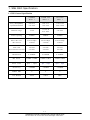
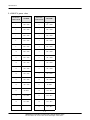
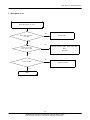
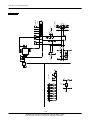
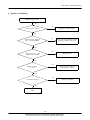
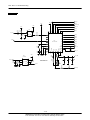
GSM TELEPHONE
SGH-X460
SERVICE
GSM TELEPHONE
Manual
CONTENTS
1.
Specification
2.
Circuit Description
3.
Exploded Views and Parts List
4.
Electrical Parts List
5.
Block Diagrams
6.
PCB Diagrams
7.
Flow Chart of Troubleshooting
ELECTRONICS
ⓒ Samsung Electronics Co.,Ltd. May. 2004
This Service Manual is a property of Samsung Electronics Co.,Ltd.
Any unauthorized use of Manual can be punished under applicable
Printed in Korea.
International and/or domestic law.
Code No.: GH68-05344A
BASIC.
1. SGH-X460 Specification
1. GSM General Specification
GS M9 0 0
Ph a se 1
E GS M 9 0 0
Ph a se 2
DC S 1 8 0 0
P h as e 1
F r eq . B a n d [M Hz ]
Up l in k / Do w n li n k
8 9 0 ~9 1 5
9 3 5 ~9 6 0
8 8 0 ~9 1 5
9 2 5 ~9 6 0
1 7 1 0 ~1 7 8 5
1 8 0 5 ~1 8 8 0
A RF C N r a n g e
1 ~1 2 4
0~124 &
9 7 5 ~1 0 2 3
5 1 2 ~8 8 5
T x /R x s p ac in g
4 5 MHz
4 5 MHz
9 5 M Hz
Mo d . B i t r at e/
Bi t Pe r i o d
270.833kbps
3.692us
2 7 0 .8 3 3 k b p s
3 .6 9 2 u s
270.833kbps
3.692us
Ti me Sl o t
P er io d / F r am e P er i o d
576.9us
4 .6 1 5 m s
5 7 6 .9 u s
4 .6 1 5 m s
576.9us
4 .6 1 5 m s
Mo d u l a ti o n
0 .3 G MS K
0 .3 G MS K
0 .3 GM SK
M S P o we r
3 3 d Bm ~1 3 d B m
3 3 d Bm ~5 d B m
3 0 d B m ~0 d B m
Po w er C l as s
5 p cl ~ 1 5 p c l
5pcl ~ 19pcl
0pcl ~ 15pcl
Se n si t iv i t y
-102dBm
- 1 0 2 d Bm
-100dBm
TDM A M u x
8
8
8
C el l Ra d iu s
3 5 Km
3 5 Km
2 Km
1-1
SAMSUNG Proprietary-Contents may change without notice
This Document can not be used without Samsung's authorization
Specification
2. GSM TX power class
TX Power
control level
GSM900
TX Power
DCS1800
control level
5
33±2 dBm
0
30±3 dBm
6
31±2 dBm
1
28±3 dBm
7
29±2 dBm
2
26±3 dBm
8
27±2 dBm
3
24±3 dBm
9
25±2 dBm
4
22±3 dBm
10
23±2 dBm
5
20±3 dBm
11
21±2 dBm
6
18±3 dBm
12
19±2 dBm
7
16±3 dBm
13
17±2 dBm
8
14±3 dBm
14
15±2 dBm
9
12±4 dBm
15
13±2 dBm
10
10±4 dBm
16
11±3 dBm
11
8±4dBm
17
9±3dBm
12
6±4 dBm
18
7±3 dBm
13
4±4 dBm
19
5±3 dBm
14
2±5 dBm
15
0±5 dBm
1-2
SAMSUNG Proprietary-Contents may change without notice
This Document can not be used without Samsung's authorization
2. SGH-X460 Circuit Description
Ⅰ. SGH-X460 RF Circuit Description
A. RX PART
1. ASM(U102)
→ Switching Tx, Rx path for GSM900, DCS1800 by logic controlling.
2. ASM Control Logic
→ Truth Table
VC_1
VC_2
GSM Tx Mode
H
L
DCS Tx Mode
L
H
GSM Rx Mode
L
L
DCS Rx Mode
L
L
3. FILTER
To convert Electromagnetic Field Wave to Acoustic Wave and then pass the specific frequency
band.
- GSM FILTER (F100) → For filtering the frequency band between 925 ~ 960 MHz
- DCS FILTER (F101) → For filtering the frequency band 1805 and 1880 MHz.
4. VC-TCXO (OSC101)
To generate the 26MHz reference clock to drive the logic and RF.
After additional process, the reference clock applies to the U100 Rx IQ demodulator and Tx
IQ modulator.
The oscillator for RX IQ demodulator and Tx modulator are controlled by serial data to select
channel and use fast lock mode for GPRS high class operation.
5. UAA3536(U100)
This chip integrates two differential-input LNAs.
The GSM input supports the E-GSM, DCS input supports the DCS1800. The LNA inputs are
matched to the 150 ohm differential output SAW filters through external LC matching network.
Image-reject mixer downconverts the RF signal to a 100 KHz intermediate frequency(IF) with
the RFLO from OSC100 voltage-controlled oscillator. The RFLO frequency is between 1801 ~
1921 MHz.
The Mixer output is amplified with an analog programmable gain amplifier(PGA), which is
controlled by AGAIN.
The quadrature IF signal is digitized with high resolution A/D converts (ADC).
2-1
SAMSUNG Proprietary-Contents may change without notice
This Document can not be used without Samsung's authorization
Circuit Description
B. TX PART
Baseband IQ signal fed into offset PLL, this function is included inside of U100 chip.
UAA3536 chip generates modulator signal which power level is about 1.5dBm and fed into
Power Amplifier(U105).
The PA output power and power ramping are well controlled by Auto Power Control circuit.
We use offset PLL below table.
Modulation Spectrum
200kHz offset
30 kHz bandwidth
GSM
-35dBc
DCS
-35dBc
400kHz offset
30 kHz bandwidth
GSM
-66dBc
DCS
-65dBc
600kHz ~ 1.8MHz offset
30 kHz bandwidth
GSM
-75dBc
DCS
-68dBc
Ⅱ. Baseband Circuit description of SGH-X460
A. PCF50601
1. Power Management
Ten low-dropout regulators designed specifically for GSM applications power the terminal and
help ensure optimal system performance and long battery life. A programmable boost converter
provides support for 1.8V, 3.0V, and 5.0V SIMs, while a self-resetting, electronically fused
switch supplies power to external accessories. Ancillary support functions, such as RTC module
and High Voltage Charge pump, Clock generator, aid in reducing both board area and system
complexity.
I2C BUS serial interface provides access to control and configuration registers. This interface
gives a microprocessor full control of the PCF50601 and enables system designers to maximize
both standby and talk times.
Supervisory functions. including a reset generator, an input voltage monitor, and a temperature
sensor, support reliable system design. These functions work together to ensure proper system
behavior during start-up or in the event of a fault condition(low microprocessor voltage,
insufficient battery energy, or excessive die temperature).
2. Backlight Brightness Modulator
The Backlight Brightness Modulator (BBM) contains a programmable Pulse-width modulator
(PWM) and FET to modulate the intensity of a series of LED’s or to control a DC/DC
converter that drives LCD backlight.
This phone (SGH-X460) use PWM.
2-2
SAMSUNG Proprietary-Contents may change without notice
This Document can not be used without Samsung's authorization
Circuit Description
3. Clock Generator
The Clock Generator (CG) generates all clocks for internal and external usage. The 32768 Hz
crystal oscillator provides an accurate low clock frequency for the PCF50601 and other circuitry.
B. Connector
1. LCD Connector
LCD is consisted of main LCD(color 65K UFB LCD) and small LCD(B/W). Chip select
signals, LCD_MAIN_CS and LCD_SUB_CS, can enable Each LCD. Backlight signal enables
white LED of main LCD and small LCD. "RESET_2V8" signal initiates the Reset process of
the LCD.
16-bit data lines(HD(0)~HD(15)) transfers data and commands to LCD through by pass
capacitor.
"SPK_P" and "SPK_N" from OM6357 are used for audio speaker. And "VDD_VIB" from
PCF50601 enables the motor.
2. Key
This is consisted of key interface pins among OM6357, KBIO(0:7). These signals compose the
matrix. Result of matrix informs the key status to key interface in the OM6357. Power on/off
key is separated from the matrix. So power on/off signal is connected with PCF50601 to enable
PCF50601. twelve key LED use the "VBAT" supply voltage.
"VDD_KEY" signal enables
LEDs with current control. "FLIP" informs the status of folder (open or closed) to the OM6357.
This uses the hall effect IC, A3210ELH. A magnet under main LCD enables A3210ELH.
3. EMI ESD Filter
This system uses the EMI ESD filter, EMIF09 to protect noise from IF CONNECTOR part.
4. IF connetor
It is 24-pin connector. They are designed to use VBAT, V_EXT_CHARGE, TXD0, RXD0,
RTS0, CTS0, JIG_REC, CHARGER_OK, RXD1, TXD1, AUX_MIC, AUX_SPK and GND.
They connected to power supply IC, microprocessor and signal processor IC.
2-3
SAMSUNG Proprietary-Contents may change without notice
This Document can not be used without Samsung's authorization
Circuit Description
C. Battery Charge Management
A complete constant-current/constant-voltage linear charger for single cell lithium-ion batteries.
If TA connected to phone, "CHARGER_OK" enable charger IC and supply current to battery.
when fault condition caused, "CHG_ON" signal level change low to high and charger IC stop
charging process.
D. Audio
EARP_P and EARP_N from OM6357 are connected to the main speaker. AUXSP is connected to
the Hands free kit. MIC_P and MIC_N are connected to the main MIC. And AUX_MIC_P and
AUX_MIC_N are connected to the Hands free kit.
YMU762C is a LSI for portable telephone that is capable of playing high quality music by
utilizing FM synthesizer and ADPCM decoder that are included in this device.
As a synthesis, YMU762MA3 is equipped 32 voices with different tones. Since the device is
capable of simultaneously generating up to synchronous with the play of the FM synthesizer,
various sampled voices can be used as sound effects.
Since the play data of YMU762MA3 are interpreted at anytime through FIFO, the length of the
data(playing period) is not limited, so the device can flexibly support application such as incoming
call melody music distribution service. The hardware sequencer built in this device allows playing
of the complex music without giving excessive load to the CPU of the portable telephones.
Moreover, the registers of the FM synthesizer can be operated directly for real time sound
generation, allowing, for example, utilization of various sound effects when using the game
software installed in the portable telephone.
YMU762 includes a speaker amplifier with high ripple removal rate whose maximum output is
550mW (SPVDD=3.6V). The device is also equipped with conventional function including a
vibrator synchronous with music.
For the headphone, it is provided with a stereophonic output terminal.
For the purpose of enabling YMU762MA3 to demonstrate its full capabilities, Yamaha purpose to
use "SMAF:Synthetic music Mobile Application Format" as a data distribution format that is
compatible with multimedia.
Since the SMAF takes a structure that sets importance on the synchronization between sound and
images, various contents can be written into it including incoming call melody with words that can
be used for training karaoke, and commercial channel that combines texts, images and sounds, and
others.
The hardware sequencer of YMU762MA3 directly interprets and plays blocks relevant to synthesis
(playing music and reproducing ADPCM with FM synthesizer) that are included in data distributed
in SMAF.
2-4
SAMSUNG Proprietary-Contents may change without notice
This Document can not be used without Samsung's authorization
Circuit Description
E. Memory
Signals in the OM6357 enable two memories. They use only one volt supply voltage, VDD3 in
the PCF50601. This system uses Samsung's memory, KBB06A300M-T402. It is consisted of 128M
bits flash NOR memory and 128M bits flash NAND memory and 32M bits UtRAM. It has 16 bit
data line, HD[0~15] which is connected to OM6357. It has 23 bit address lines, HA[1~23].
CS_NAND and NCSRAM signals is chip select.
Writing process, HWR_N is low and it enables writing process to flash memory and SRAM.
During reading process, HRD_N is low and it enables reading process to flash memory and
SRAM. Each chip select signals in the OM6357 select memory among 2 flash memory and
UtRAM.
Reading or writing procedure is processed after HWR_N or HRD_N is enabled. Memories use
reset, which is VDD3 delay from PCF50601. HA[22] signal enables lower byte of SRAM and
HA[22] signal enables higher byte of SRAM.
F. OM6357
OM6357 is consisted of ARM core and DSP core. It has 8x1Kword on-chip program/data RAM,
55 Kwords on-chip program ROM in the DSP. It has 4K*32bits ROM and 2K*32bits RAM in the
ARM core. DSP is consisted of KBS, JTAG, EMI and UART. ARM core is consisted of EMI,
PIC(Programmable Interrupt Controller), reset/power/clock unit, DMA controller, TIC(Test Interface
Controller), eripheral bridge, PPI, SSI(Synchronous Serial Interface), ACC(Asynchronous
communications controllers), timer, ADC, RTC(Real-Time Clock) and keyboard interface.
KBIO(0:7), address lines of DSP core and HD[0~15]. HA[1~23], address lines of ARM core and
HD[0~15], data lines of ARM core are connected to memory, YMU762. MV317S(Camera DSP
Chip) controls the communication between ARM core and DSP core.
CS_NAND, NCSRAM, NCSFLASH in the ARM core are connected to each memory. HWR_N
and HRD_N control the process of memory. External IRQ(Interrupt Request) signals from each
units, such as, PMU need the compatible process.
KBIO[0~7] receive the status from key and RXD0/TXD0/IrDA_DOWN are used for the
communications using IRDA and data link cable(DEBUG_DTR/RTS/TXD/RXD/CTS/DSR).
It has JTAG control pins(TDI/TDO/TCK) for ARM core and DSP core. It receives 13MHz clock
in CKI pin from external TCXO. ADC(Analog to Digital Convertor) part receives the status of
temperature, battery type and battery voltage.
G. VC_TCXO-214C6(26MHz)
This system uses the 26MHz TCXO, VC_TCXO-214C6. AFC control signal from OM6357
controls frequency from 26MHz X-tal. The clock output frequency of UAA3536HN is 13MHz.
This clock is connected to OM6357, YMU762.
2-5
SAMSUNG Proprietary-Contents may change without notice
This Document can not be used without Samsung's authorization
3. SGH-X460 Exploded View and its Parts list
1. Cellular phone Exploded View-1
QFU01
QLC67
QMO02
QFR01
QSP04
QFL01
QKP01
QCR04
QSC11
QMW01
QSC12
QVK01
QMP01
QME02
QIF01
QAN02
QVO01
QRE01
QRF01
QCR04
QBA18
3-1
SAMSUNG Proprietary-Contents may change without notice
This Document can not be used without Samsung's authorization
Exploded view and its Part list
2. Cellular phone Parts list
Location
Description
NO.
SEC CODE
QFU01
FOLDER UPPER
GH75-04524A
QLC67
LCD
GH07-00564A
QSP04
SPEAKER
3001-001574
QMO02
MOTOR
3101-001315
QFL01
FOLDER LOWER
GH75-04525A
QMW01
MAIN WINDOW LCD
GH75-04528A
QFR01
FRONT COVER
GH75-04523A
QVO01
VOLUME KEY
GH75-04529A
QKP01
KEYPAD
GH75-04527A
QMP01
MAIN PBA
GH92-01799A
QVK01
VOL KEY FPCB
GH59-01419A
QAN02
INTENNA
GH42-00425A
QME02
METAL DOME
GH59-01418A
QRE01
REAR COVER
GH75-04526A
QIF01
IF COVER
GH72-13265A
QRF01
RF COVER
GH72-15078A
QCR04
SCREW
6001-001479
QBA18
BATTERY
GH43-01418A
QSC11
FOLDER SCREW CAP R
GH74-09038A
QSC12
FOLDER SCREW CAP L
GH74-09039A
3-2
SAMSUNG Proprietary-Contents may change without notice
This Document can not be used without Samsung's authorization
Remark
Exploded view and its Part list
3. Test Jig (GH80-01909A)
3-1. RF Test Cable
3-2. Test Cable
(GH39-00261A)
3-3. Serial Cable
(GH39-00217A)
3-4. Power Supply Cable
3-5. DATA CABLE
(GH39-00143B)
3-6. TA
(GH44-00482A)
3-3
SAMSUNG Proprietary-Contents may change without notice
This Document can not be used without Samsung's authorization
4. SGH-X460 Electrical Parts List
Design LOC
SEC CODE
0403-001427
ZD301
0406-001167
ZD604,ZD605
0406-001201
V501,V502,V601,V602
0406-001201
V603,ZD401,ZD402
0406-001201
ZD501,ZD502,ZD503
0406-001201
ZD504,ZD505,ZD506
0505-001423
U606
0601-001790 LED500,LED501,LED502
0601-001790 LED503,LED504,LED505
0601-001790 LED506,LED507,LED508
0601-001790
LED510,LED511
0801-002237
U301
0801-002882 U202,U303,U602,U603
1001-001253
U502
1009-001010
SW500
1109-001280
U300
1201-002075
U105
1202-001036
U501
1203-003105
U500
1203-003109
U304
1204-002161
U302
1205-002276
U200
1205-002327
U100
1205-002350
U400
1404-001221
V300
1405-001082
V301,V302,V304,V604
1405-001082
V605,V606,V607,V608
1405-001082
V609,V610,V611,V612
1405-001082
V613
2007-000140
R104,R311
2007-000141 R101,R205,R206,R314
2007-000142
R116
2007-000146
R308
2007-000148 R107,R118,R121,R124
2007-000148 R132,R133,R201,R400
2007-000148
R401,R504
2007-000157
R312,R316
2007-000162 R200,R202,R203,R303
2007-000162 R306,R307,R313,R315
SEC CODE
2007-000162
2007-000162
2007-000171
2007-000171
2007-000172
2007-000173
2007-000173
2007-000173
2007-000174
2007-000242
2007-000566
2007-000982
2007-001288
2007-001301
2007-001305
2007-001313
2007-001325
2007-003001
2007-007001
2007-007008
2007-007009
2007-007014
2007-007100
2007-007107
2007-007148
2007-007311
2007-007334
2007-007480
2007-007489
2007-007573
2007-008117
2203-000233
2203-000233
2203-000254
2203-000254
2203-000278
2203-000278
2203-000278
2203-000359
Design LOC
R317,R323,R324,R501
R600,R601
R102,R105,R111,R112
R207,R305,R403,R532
R103
R507,R509,R510,R511
R512,R513,R516,R517
R531
R109
R502,R506
R106,R108,R320
R119,R120,R122,R123
R125,R129
R514,R515
R113,R115
R301
R304
R114
R204
R127,R128,R130,R131
R117
R300,R302
R402
R321,R322
R100
R110,R134
R519
R521,R522
R135,R518
R319
R318
C103,C104,C121,C300
C316
C125,C151,C154,C200
C201,C302,C405
C134,C143,C144,C501
C502,C510,C511,C601
C602,C603
C150,C310
4-1
SAMSUNG Proprietary-Contents may change without notice
This Document can not be used without Samsung's authorization
Electrical Parts List
SEC CODE
2203-000425
2203-000438
2203-000550
2203-000585
2203-000585
2203-000609
2203-000679
2203-000800
2203-000812
2203-000812
2203-000812
2203-000854
2203-000940
2203-000995
2203-000995
2203-001153
2203-001652
2203-002443
2203-002525
2203-003054
2203-005054
2203-005056
2203-005057
2203-005065
2203-005138
2203-005288
2203-005382
2203-005481
2203-005482
2203-005482
2203-005482
2203-005482
2203-005482
2203-005482
2203-005482
2203-005482
2203-005482
2203-005482
2203-006053
Design LOC
C102,C109
C123,C153,C305,C313
C127
C126,C130,C131,C132
C133
C128
C303,C432,C604
C117
C137,C142,C145,C156
C202,C207,C320,C321
C431,C528
C100,C107,C129
C149,C152
C529,C530,C607,C608
C609,C610,C611,C612
C138,C146
C410,C422
C503
C110
C407,C409
C430
C141
C114,C120
C122,C420
C108
C139
C155
C116,C118
C105,C106,C113,C115
C119,C203,C204,C205
C206,C208,C209,C210
C211,C212,C213,C214
C215,C216,C217,C218
C219,C220,C301,C304
C306,C309,C312,C319
C401,C403,C404,C408
C414,C417,C428,C504
C505,C509
C124,C308,C421,C424
SEC CODE
2203-006053
2203-006093
2203-006137
2203-006208
2203-006257
2203-006324
2301-001197
2301-001213
2404-001105
2404-001225
2404-001239
2404-001268
2404-001333
2703-001734
2703-002199
2703-002200
2703-002203
2703-002208
2703-002308
2703-002368
2703-002700
2801-004339
2806-001329
2809-001287
2901-001246
2901-001286
2904-001469
2904-001470
2909-001216
3301-001105
3301-001362
3301-001438
3705-001242
3709-001298
3710-002115
3711-005487
3722-002067
4302-001157
Design LOC
C425,C426,C427
C411,C524
C307
C402,C406,C413
C317
C412,C415
C111
C112
C314
C418,C419,C423,C429
C136
C135,C315
C500,C527
L104
L106
L101
L103
L100,L102
L109,L110
L112
L108
X1
OSC100
OSC101
U305
F600,F601,F602,F603
F100
F101
U102
L400,L501,L502
L503
R503,R505
CON101
CN500
CN300
CN600
EAR500
BAT400
4-2
SAMSUNG Proprietary-Contents may change without notice
This Document can not be used without Samsung's authorization
5. SGH-X460 Block Diagrams
1. RF Solution Block Diagram
HITACHI METAL ANT SWITCH
FUJITSU EGSM RX SAW Filter
FAR-F5EB-942M50-B28C
IL=2.7dB max
Ripple=1.7 dB max
SHS-C090F
Imax = 10 mA
Freq (MHz)
Loss
880 - 915
1.5 dB
925 - 960
1.0 dB
1710 -1785
1.5 dB
1805 -1880
1.1 dB
Atten 2xfo : 24dB,25dB(GSM,DCS)
3xfo : 24dB,25dB(GSM,DCS)
Pins IA,IB,QA and QB
V QI : 1.25V typ . , 1.15V mi
, 1.35V max
n
Vmod : 0.5V pp
+ I OUT
- I OUT
QUA
D
10
kHz+fmod
0
FUJITSU DCS RX SAW Filter
FAR-F6EB-1G8425-B2BC
IL= 3.3dB max
Ripple= 2.0dB max
+ Q OUT
- Q OUT
VREG
Vcc_RF_LO
VC1
VC2
Vcc_RF_VCO
FESW1
DIV
~
GSM/DCS
Vcc_SYN
Frac
N
DIV
VREG
Vcc_REF(2.4V typ.)
f compRF =26MHz
FESW2
Discrete
3 rd Order
Loop Filter
REFIN
PFD
CP
FESW1
26MH
z
FESW2
I+
DIV
QUA
D
OFFSET Mixer input power
-16dBm max, -22dBm min
VBAT
pi PAD
Vcc_Tx_BURST
GSM IN
pi PAD
VRAMP
~
~
I-
Discrete
3 rd Order
Loop Filter
f TXIF
60/114MHz
CP
Q+
Q-
REF_13M
3W
BUS
CT
RE
L
G
DATA
CLK
PWR
EN
Philips Transceiver
UAA3536
DCS S/W
1:1/2
fmod
PFD
GSM S/W
TX ENABLE
BAND SELECT
DCS IN
RFMD PAM
RF3146
GSM: Pout = 35.0 dBm E = 55%
DCS: Pout = 33.0 dBm E = 60%
pi PAD
VBat (3.6V typ 3.0V min)
MURATA
TX VCO
MQW510C869M
GSM = 824 ~ 915 MHz
(Vt=0.5V ~ 3.0 V )
DCS = 1710 ~ 1910 MHz
(Vt=0.5V ~ 3.0 V )
Pout= 4.0~9.5dBm typ.,Ic <= 25mA
Harmonics <= -15dBc
VTCX
O
VCC_SYN (2.7V , 100mA )
VCC_RX_TX (2.7V ,100mA )
VCC_RF_VCO (2.70V , 100mA )
VCC_TX_BURST(2.7V , 100mA )
VCC_CP (4.0V , 25mA )
PON_TX
PON_SYNT
RF1_VDD
RF2_VDD
RF1_VDDS
RF2_VDDS
HV
S
PMU
V_MODE
AVDD(1.35V min 2.65V max , 100mA )
VDD1 (1.35V min 2.95V max , 150mA )
5-1
SAMSUNG Proprietary-Contents may change without notice
This Document can not be used without Samsung's authorization
VDD2 (1.35V min 3.45V max , 150mA )
VDD3 (1.35V min 3.45V max , 100mA )
VDD4 (1.35V min 3.45V max , 150mA )
EN
RXON
TXON
SYNON
FESWON
Block Diagrams
2. Base Band Solution Block Diagram
MIC
BB INTERFACE
Serial Data
Interface
RECEIVER
SPEAKER
VIBRATOR
OM6357
Battery
Type
Battery
Voltage
I/O
Interface
Battery
Temperature
A/D
Interface
VCC_CP
VCC_SYN
MELODY IC
(40 Poly)
RF INTERFACE
VCC_RX_TX
VCC_RF_VCO
SYSTEM CLOCK
(26MHz)
AFC
VCC_TX_BURST
VDD1
SRAM
(32M bit)
RAMP
VDD2
FLASH
(256M bit)
VDD3
VDD_VIB
Li-Ion Battery
(Slim)
MIC_BIAS
PMU
VDD_KEY
KEY_BOARD
VDD_AMP
LCD
Charging
Circuit
RTC_CLOCK
(32.768KHz)
AVDD
SIM CARD
AVDD_TEMP
5-2
SAMSUNG Proprietary-Contents may change without notice
This Document can not be used without Samsung's authorization
6. SGH-X460 PCB Diagrams
1. Main PCB Top Diagram
6-1
SAMSUNG Proprietary-Contents may change without notice
This Document can not be used without Samsung's authorization
PCB Diagrams
2. Main PCB Bottom Diagram
6-2
SAMSUNG Proprietary-Contents may change without notice
This Document can not be used without Samsung's authorization
7. SGH-X460 Flow Chart of Troubleshooting
1. Power On
' Power On ' does not work
Yes
Check the Battery Voltage
is more than 3.4V
No
Change the Battery
Yes
No
C410(V_ISUP) = 2.7V?
Check the PMU related to V_ISUP
Yes
Check the Clock at
R402=32KHZ
No
Resolder X1
Yes
No
C427 (VDD1) = "H"?
Check the VDD1 circuit
Yes
C426(VDD2) & C425(VDD3)
= 2.8V?
No
Check the VDD2,VDD3 circuit
Yes
Check for the clock at C121
= 26MHz
No
Check the clock generation circuit
(related to OSC101)
Yes
Check the initial operation
Yes
END
7-1
SAMSUNG Proprietary-Contents may change without notice
This Document can not be used without Samsung's authorization
Flow Chart of Troubleshooting
VBAT
BACKLIGH
T
IT_PMU
JIG_REC
RECO1
JACK_IN
32K
RSTON
ONKEY_N
CHARGER_O
K
REF_O
N
VCC_SYN
VCC_RX_TX
MIC_BIAS
R401
10K
VDD_3V05
C401
100NF
C412
2.2UF
C411
1UF
C418
10UF
C429
10UF
6.3V
C404
100NF
BAT400
ML414R-F9GE
C410
470NF
VDD_3V05
C419
10UF
VBAT
C417
100NF
C427
1UF
PMU (IC)
U400
SCL
SDA
refgnd
PCF50601ET1-N5
E3
F2
REFC
REFGND
MICBIAS
H8
K6
J6
VBAT
VBAT
ISUPA
ISUPD
VBACK
H6
J4
BLVBAT
BLVDD
BBMSW
BBMGN
D
K4
J5
B7
A7
C5
A8
H5
TM
12C
INTERFACE
ON-CHIP
REFERENCE
&
MIC BIAS
TEMP HIGH
SENSOR
INTERNAL
SUPPLY
MODULE
CONTROL
SUPPLY &
BACKLIGHT
LINREG
SWITCH
D10
control
status
data
ON/OFF
CONTROL
internal
clocks
C10
CLOCK
PLL
GENERATO
R
REAL-TIME
CLOCK
F1 F3 E9
VBAT
4.7UF
C402
100NF
C403
R402
10M
100NF
1
2
SIMIO
SIMCLK
SIM_VCC
SIM_RST
SIM_CLK
SIM_IO
C432
27PF
C415
2.2UF
32K
VBAT
AVDD_TEM
P
CN500
PC-D6-A3-H3.0-S
6 6
5 5
4 4
G G G G
10 9 8 7
1 1
2 2
33
AVDD
VCC_CP
RF power supply
VDD_KEY VDD_AMP
L400
BLM11A102SPT
C413
4.7UF
C409
9PF
C407
X1
9PF
FC-135 (0.032768MHz
)
C420
1UF
R403
0
This Document can not be used without Samsung's authorization
SIM
100NF
VBAT
C414
C421
1UF
SAMSUNG Proprietary-Contents may change without notice
C431
33PF
C428
VCC C2
CLK C3
RST C1
IO D2
CPRESD1
SIMIO B8
SIMCLKC6
K8
OSC32I
K9
OSC32O
CHRVBATD3
CHRREGE2
CHRIV E1
HVSVBATC8
HVSGND B9
HVSSCPC9
HVSSCNA10
HVSOC B10
HVSVDD D8
NC 2
NC 1
C423
10UF
6.3V
7-2
VBAT
B2 A2 B1A1
SIM
CHARGE
PUMP
SIM
INTERFACE
32KHz XTA
L
OSCILLATO
R
BATTERY
VOLTAGE
MONITOR
CHARGE
CONTROL
PUMP+
(CHARGE
SUPPLY
HIGH VOLTAGE
LINREG
)
C422
470NF
K10A5 B5 A6 B6B3 A3
V_ISUP
G3G2G1 H4 H2 H1J1 F8 B4 A4 J8 J9 J7 K7
VIB
Baseband power supply
K3 H3 D9 A9 J2K1K2
reference
voltage
bias currents
calibration
htmp
internal
supply
E4 F5 F4 G4J3 G5 K5 F6 G6G7 G8F7 E6 E7 D7 C7 D6E5 D5D4C4
RF1SW
S
RF1VDDS
RF2SW
S
RF2VDDS
G9 RFVBAT
G10 RF1VDD
F10 RF1SNS
H10 RF2VDD
RF2SNS
H9
E8
F9
E10
J10
H7
VBAT
AVDDS
VDD1
10K
SCL
SDA
C405
10NF
C408
100NF
C406
4.7UF
ZD402
uClamp0501H
ZD401
uClamp0501H
C416
NC
C426
1UF
AUXON
ONKEY
RSTO
R400
C430
4.7PF
V_ISUP
C425
1UF
VIBVBA
T
VIBVDD
INT
DVDD1
DVDD1VBA
TDVDD1
SEL12RB
SIMGND
SIMSC
P
SIMSCN
AVDDVBA
T
AVDDVBA
T
AVDD
AVDD
AVDD
PON_SYN
VCC_RF_VCO
PON_TX
VCC_TX_BURST
RF power supply
Baseband power supply
VDD1
VDD2
VDD3
VDD_VIB
V_MODE
VIB
C424
1UF
HFA
HFAVBA
T
HFAVBA
T
HFAVDD
HFAVDD
DVDD2
DVDD2
DVDD2
htmp
SIMVBAT
SEL3RB
DVDD3VBA
TDVDD3
DVDD3
DVDD3
DVDD4ON
DVDD4VBA
T
DVDD4
DVDD4
INTERRUPT
GENERATO
R
DVDD2VBAT
CLK32
REC2
REC1
REC3
VSS1
VSS2
VSS3
VSS4
VSS5
VSS6
VSS7
VSS8
VSS9
VSS10
VSS11
VSS12
VSS13
VSS14
VSS15
VSS16
VSS17
VSS18
VSS19
VSS20
VSS21
ovdd
SLPMOD
VPROG
2
1
Flow Chart of Troubleshooting
2. Initial
Initial Failure
Yes
No
Check the circuit related to reset
R200 (RSTON) ="H"?
Yes
No
Is U303 pin 4,6
(memory CE) OK?
Check the U303
Yes
Check the circuit around
LCD & U302 (Short or not solder)
Yes
END
7-3
SAMSUNG Proprietary-Contents may change without notice
This Document can not be used without Samsung's authorization
Flow Chart of Troubleshooting
RSTO
N
CS_NAND
VDD3
43
5
6
C220
100NF
HA(1:23)
Y1
2
1
D_REF_13M
32K
HD(0:15)
0
HWR_N
HRD_N
LCD_MEL_CS
M_RST
NCSRAM
KBIO(0:7)
A
CHG_ON
SUB_BACKLIGH
T
SUB_MEL_EN
END_OF_CHARGE
FLIP
LCD_MAIN_EN
CTS0
EAR_SWITCH
NCSFLASH
CS_N3
1
HA(20)
A
GND
_E
U202
NC7SZ19L6X
VCC
Y0
CS_N2
X
CS_N0
X
MELODY_CS
X
0
VDD3V
R202
100K
DD3
R203
100K
R200
HD(0)
HD(1)
HD(2)
HD(3)
HD(4)
HD(5)
HD(6)
HD(7)
HD(8)
HD(9)
HD(10)
HD(11)
HD(12)
HD(13)
HD(14)
HD(15)
HA(1)
HA(2)
HA(3)
HA(4)
HA(5)
HA(6)
HA(7)
HA(8)
HA(9)
HA(10)
HA(11)
HA(12)
HA(13)
HA(14)
HA(15)
HA(16)
HA(17)
HA(18)
HA(19)
HA(20)
HA(21)
HA(22)
HA(23)
KBIO(7)
KBIO(6)
KBIO(5)
KBIO(4)
KBIO(3)
KBIO(2)
KBIO(1)
KBIO(0)
VDD3
pin G2
100K
VDD3
pin L3
CGU
OOL
GPIO
EMI
GPIO0
GPIO1
GPIO2
GPIO3
GPIO4
GPIO5
GPIO6
GPIO7
GPIO8
GPIO9
GPIO10
KBS
VDD1
VDD1
PCF50874
SC
VDD2
P8
C1
VDD3
PDCU
SIOY
SIOX
DSP
RFCU
IIC
SIMU
PWM
JTAG
AVDD
C208
100NF
VDD1
F12
C9
D
A
D
A
D
A
D
A
D
A
D
D
D
A
A
A
D
A
AVDD
PCF50732
B_WR
GROUND
J_SEL
B_TDI
B_TMS
B_TCK
B_TDO
B_TRST
N9
GPON2
L10
GPON1
G10
AUXST
D5
RFSIG0
A6
RFSIG1
D6
RFSIG2
B6
RFSIG3
A7
RFSIG4
C7
RFSIG5
B7
RFSIG6
C6
RFSIG7
E7
RFSIG8
K10
RFSIG9
D7
RFSIG10
H12
RXON
G12
TXON
E10
CCLK
E9
CDO
D8
CDI
D9
CEN
VDD1
AVDD
pin D14
C204
100NF
100NF
pin C9
pin C8
C203
100NF
RFE_N0 J12
RFE_N2 K12
VREF C14 C209
AUXDAC1 E12
AUXDAC2 D13
AUXDAC3 D12
QP H13
QN H14
IP J13
IN J14
AUXADC1 F14
AUXADC2 G14
AUXADC3 E14
AUXADC4 F13
A13
B13
B14
A14
EARP B10
EARN A11
AUXSP A10
BUZ B11
MICP
MICN
AUXMICP
AUXMICN
MCLK D10
SCK C2
SDA B3
ADI A8
AFS B9
ACLK B8
ADO A9
BOEN G11
BDIO E11
BIEN F10
BIOCLK F11
SIMIO M13
SIMCLK M14
SIMERR M11
PWM1 E6
PWM0 F4
J_SEL
TDI
TMS
TCK
TDO
TRST_N
HWR_N
C207
33PF
R201
TP202
TP203
TP204
TP205
R204
C200
10NF
AVDD
pin F12
10K
3.9K
JIG_REC
C205
100NF
C206
100NF
B
V_MODE
REF_ON
GSM_TXVCO_EN
DCS_TXVCO_EN
PAM_TX_EN
GSM_ANT_SW
DCS_ANT_SW
PON_SYN
PON_TX
PON_RX
RF_BBI_CLK
RF_BBI_DATA
RF_EN_SYN
AFC
RAMP
QRX_TX_P
QRX_TX_N
IRX_TX_P
IRX_TX_N
MES_BATT
AVDD
C201
10NF
pin C12
pin B12
17
18
19
20
21
22
23
24
25
26
27
28
29
30
31
32
JTAG-32PIN
U203
1
TRST
1
2
TDO
2
TDI
3 3
4
TMS
4
5
TCK
5
6
F-WE
6
7
V_BATT GND
8
GND
V_BUS
9
HP/POWERD+
RXD
D- 10
11
TXD
SPK+
12
28
SPK13
29
MIC+
14
30
MOT+
15
31
15
16
ANT
16
AVDD_TEMP
C202
33PF
2.2K
R206
VDD2
2.2K
R205
TEMP_PRODUCT
VF
EARP_P
EARP_N
AUXSP
EARP_H
F
MIC_P
MIC_N
AUX_MIC_P
AUX_MIC_N
D_REF_13M
VDD1
DD
FSC
DCL
DU
BOEN
BDIO
BIEN
BIOCLK
SIMIO
SIMCLK
IT_PMU
TRST_N
TDO
TDI
TMS
TCK
HWR_N
VBAT
CHARGER_O
K
RXD0
TXD0
CTS0
RTS0
CHARGER_O
K
ANT
SCL
SDA
SPK_P
SPK_N
MIC+
VDD_VIB
This Document can not be used without Samsung's authorization
L3
0
SAMSUNG Proprietary-Contents may change without notice
U200
OM6357
P11
CKI
P13
CKI32I
P14
CKI32O
HD0
HD1
HD2
HD3
HD4
HD5
HD6
HD7
HD8
HD9
HD10
HD11
HD12
HD13
HD14
HD15
HA1
HA2
HA3
HA4
HA5
HA6
HA7
HA8
HA9
HA10
HA11
HA12
HA13
HA14
HA15
HA16
HA17
HA18
HA19
HA20
HA21
HA22
HA23
HWR_N
HRD_N
C10
RESETN
M10
RSTO_N
H10
RST_N
K14
AUXON
H4
H3
H2
J3
E5
H1
B1
E4
F3
F2
F1
E1
D1
E3
E2
B2
M4
P3
L4
N3
K5
M3
P2
N2
M1
N1
L2
L1
M2
J2
J5
K3
J4
K4
K2
G4
P5
N6
L6
L5
H5
KBIO7
KBIO6
KBIO5
KBIO4
KBIO3
KBIO2
KBIO1
KBIO0
G3
CS_N3
M5
CS_N2
G5
CS_N1
N4
CS_N0
M12
K9
L8
M9
P7
L7
L9
N7
P6
N8
K8
L14
L12
L13
L11
J11
K13
J10
K11
R207
7-4
D14
B12
C12
VDD_BB
VDD_D
VDD_REF
VDD_VB
VDD_VBOUT
E13
VSS_BB
D11
VSS_D
C13
VSS_REF
A12
VSS_VB
C11
VSS_VBOUT
CSI
BSI
ASI
P12
AVDD
AVSS
K7 VSS_A
J1 VSS_B
M7 VSS_C
N10
VSS_E
N14
VSS_F
N11
VSS_G
G13 VSS_H
E8
VSS_I
C3
VSS_K
G1 VSS_M
K1
VSS_N
P1
VSS_O
N5
VSS_P
H11
RXD1
A4 TXD
P4
M6
G2
VDDE3_A
VDDE3_B
VDDE3_F
VDDE3_G
P10
P9
N12
C8
VDDE1_A
VDDE1_B
VDDE1_C
VDDE1_D
TDI
TMS
TCK
TDO
TRST_N
J_SEL
D2
A2
A3
D3
A1
B4
TDI
TMS
TCK
TDO
TRST_N
J_SEL
UART1
D4
VDDE2_C
VDDE2_E
F5
N13
M8
K6
RXD1
TXD1
X
VDD3
pin M6
C219 100NF
VDDC_A
VDDC_B
VDDC_C
VDDC_D
UART0
B5
CTS0_N
A5
RXT0_N
C5
TXD0
C4
RXD0
CTS0
RTS0
TXD0
RXD0
0
VDD3
pin P4
C218 100NF
0
VDD2
pin C1
C217 100NF
X
VDD2
pin P8
C216 100NF
1
VDD1
C213 100NF
pin H11
C215 100NF
X
VDD1
C212 100NF
pin P9
pin M8
C214 100NF
IMAGE_CS
VDD1
pin N12
pin N13
C211 100NF
CS_NAND
VDD1
pin F5
C210 100NF
Flow Chart of Troubleshooting
3. Charging Part
Abnormal charging part
Yes
No
Check the U304 pin 2
> 4.9V
Check the the circuit related to
CHARGER_OK
Yes
No
U304 pin 6 = "H"?
Resolder or replace U304
Yes
No
U304 pin 5 (CHG_ON)
= "L"?
Check the circuit related to
CHG_ON signal
Yes
No
U304 pin 7
≒ 4.2V?
Resolder or replace U304
Yes
END
7-5
SAMSUNG Proprietary-Contents may change without notice
This Document can not be used without Samsung's authorization
Flow Chart of Troubleshooting
VDD2
Charge of Battery
R316
47K
U304
1 VL
_CHG 8
2 IN
BATT 7
3
4
C315
10UF
10V
ZD301
UDZS8.2B
C316
100PF
C317
470nF
R318
2.7K
GND
ISET
_ACOK
END_OF_CHARGE
VBAT
6
CHARGER_O
K
_EN 5
G GG G
9 10 11 12
MAX1508ETA
C314
10UF
6.3V
CHG_ON
V302
VC040205X150R
+DCVOLT
V301
VC040205X150R
R319
330K,1%
MES_BATT
R320
220K
AVDD_TEM
P
R321
100K,1%
3
V300
NCP15WB473J04RC
TEMP_PRODUCT
R322
100K,1%
THERMISTER
PCB_HOLE
7-6
SAMSUNG Proprietary-Contents may change without notice
This Document can not be used without Samsung's authorization
V304
Flow Chart of Troubleshooting
4. Sim Part
Phone can't access SIM Card
Yes
No
CN500 pin 1,5 = "H"?
Check the sim charge pump
Yes
No
After Power ON,
Check SIMCLK Signal on CN500
pin3 in a few second
Check the 32k OSC
Yes
No
After SIM card insert,
CN500 pin 2 = "H(SIM_RST)"?
Replace PBA
Yes
Check the SIM Card
Yes
END
7-7
SAMSUNG Proprietary-Contents may change without notice
This Document can not be used without Samsung's authorization
Flow Chart of Troubleshooting
VBAT
BACKLIGH
T
IT_PMU
JIG_REC
RECO
1
JACK_IN
32K
RSTO
N
ONKEY_N
CHARGER_O
K
REF_O
N
VCC_SYN
MIC_BIAS
R401
10K
VDD_3V05
C401
100NF
C412
2.2UF
C411
1UF
C429
10UF
6.3V
C404
100NF
BAT400
ML414R-F9GE
C410
470NF
VDD_3V05
C419
10UF
C406
4.7UF
PMU (IC)
U400
SCL
SDA
refgnd
PCF50601ET1-N5
E3
F2
REFC
REFGND
MICBIAS
H8
K6
J6
VBAT
ISUPA
ISUPD
VBACK
H6
J4
BLVBAT
BLVDD
BBMSW
BBMGN
D
K4
J5
VBAT
B7
A7
C5
A8
H5
TM
12C
INTERFACE
ON-CHIP
REFERENCE
&
MIC BIAS
TEMP HIGH
SENSOR
INTERNAL
SUPPLY
MODULE
CONTROL
SUPPLY &
BACKLIGHT
LINREG
SWITCH
D10
contro l
status
data
ON/OFF
CONTROL
internal
clocks
C10
CLOCK
PLL
GENERATO
R
REAL-TIME
CLOCK
F1 F3 E9
VBAT
VBAT
C414
4.7UF
C402
100NF
C403
R402
10M
100NF
2
1
SIMIO
SIMCLK
SIM_VCC
SIM_RST
SIM_CLK
SIM_IO
C432
27PF
C415
2.2UF
32K
VBAT
AVDD_TEM
P
CN500
PC-D6-A3-H3.0-S
6 6
5 5
4 4
G G G G
10 9 8 7
1 1
2 2
33
AVDD
VCC_CP
RF power supply
VDD_KEY VDD_AMP
L400
BLM11A102SPT
C413
4.7UF
C409
9PF
C407
X1
9PF
FC-135 (0.032768MHz
)
C420
1UF
R403
0
This Document can not be used without Samsung's authorization
SIM
100NF
VCC C2
CLK C3
RST C1
IO D2
CPRESD1
SIMIO B8
SIMCLKC6
OSC32I K8
K9
OSC32O
CHRVBATD3
CHRREGE2
CHRIV E1
HVSVBATC8
HVSGND B9
HVSSCPC9
HVSSCNA10
HVSOC B10
HVSVDD D8
C421
1UF
SAMSUNG Proprietary-Contents may change without notice
C431
33PF
C428
PUMP+
LINREG
)
NC 2
1
NC
C423
10UF
6.3V
7-8
VBAT
B2 A2 B1A1
SIM
CHARGE
PUMP
SIM
INTERFACE
32KHz XTA
L
OSCILLATO
R
BATTERY
VOLTAGE
MONITOR
CHARGE
CONTROL
HIGH VOLTAGE
SUPPLY
(CHARGE
C422
470NF
K10A5 B5 A6 B6B3 A3
V_ISUP
G3G2G1 H4 H2 H1J1 F8 B4 A4J8 J9 J7 K7
VIB
Baseband power supply
K3 H3 D9 A9 J2K1 K2
reference
voltage
bias currents
calibration
htmp
internal
supply
E4 F5 F4 G4J3 G5 K5 F6 G6G7 G8F7 E6 E7 D7C7 D6 E5 D5 D4 C4
RF1SW
S
RF1VDDS
RF2SW
S
RF2VDDS
G9 RFVBAT
G10 RF1VDD
F10 RF1SNS
H10 RF2VDD
RF2SNS
H9
E8
F9
E10
J10
H7
VBAT
AVDDS
VDD1
10K
SCL
SDA
C405
10NF
C408
100NF
VBAT
C417
100NF
C427
1UF
AUXON
ONKEY
RSTO
R400
C430
4.7PF
V_ISUP
ZD402
uClamp0501H
ZD401
uClamp0501H
C416
NC
C426
1UF
VIBVBA
T
VIBVD
D
VCC_RX_TX
C418
10UF
C425
1UF
HFA
HFAVBA
T
HFAVBA
T
HFAVDD
HFAVDD
PON_SYN
VCC_RF_VCO
PON_TX
VCC_TX_BURST
RF power supply
Baseband power supply
VDD1
VDD2
VDD3
VDD_VIB
V_MODE
VIB
C424
1UF
DVDD2VBAT
SIMGND
SIMSC
P
SIMSCN
AVDDVBA
T
AVDDVBA
T
AVDD
AVDD
AVDD
INTERRUPT
GENERATO
R
DVDD2
DVDD2
DVDD2
htmp
SIMVBAT
SEL3RB
DVDD3VBA
TDVDD3
DVDD3
DVDD3
DVDD4ON
DVDD4VBA
T
DVDD4
DVDD4
INT
DVDD1
DVDD1VBA
TDVDD1
SEL12RB
CLK32
REC2
REC1
REC3
VSS1
VSS2
VSS3
VSS4
VSS5
VSS6
VSS7
VSS8
VSS9
VSS10
VSS11
VSS12
VSS13
VSS14
VSS15
VSS16
VSS17
VSS18
VSS19
VSS20
VSS21
ovdd
SLPMOD
VPRO
G
2
1
Flow Chart of Troubleshooting
5. Microphone Part
Microphone does not work
Yes
No
Check the connection
from MIC
Resolder MIC
Yes
No
Resolder the R503, R505, C505, C509, R532,
Check the circuit
from U200 to MIC
R502,
and R506
Yes
No
Check the MIC
Replace the MIC
Yes
END
7-9
SAMSUNG Proprietary-Contents may change without notice
This Document can not be used without Samsung's authorization
Flow Chart of Troubleshooting
Microphone
1
2
C506
NC
NC
C501
10PF
MIC+
VDD2
R519
200K,1%
R522
130K,1%
C530
47PF
R503
BLM10B750SBPT
R532
0
Close to MC
P
C500
33UF
4V
R504
10K
VDD2
8
C527
33UF
4V
1
U501-1
C528
33PF
C502
10PF
C508
NC
C511
10PF
MIC_P
MIC_N
EAR_SWITCH
C532
100NF
EARP_N
4 TC75W56FK-TE12L
17
16
C533
1UF
U503
R1141Q331D-TR
1 VOUT VDD 4
3
GND CE
2
VBAT
VBAT
VDD_KE
Y
2
GND
BYP 4
VOUT
U500
MIC5219-3.3BM5
15
VIN
3 CTL
C504
100NF
C524
10UF
6.3V
L503
BLM10A102SGPT
VDD2
C531
470PF
KEY_LED
R510
22
OUT 2
SW500
A3212ELH-SAMSUNG
1 VCC
3
GND
FLIP
R507
22
R512
22
R513
22
C503
330PF
R501
100K
VDD2
R511
22
FLIP
R514
68
R515
68
R516
22
R517
22
LED511 LED500 LED501 LED502 LED503 LED504 LED505 LED506 LED507
LED508
R531
22
LED510
R509
22
This Document can not be used without Samsung's authorization
R502
1.5K
C505
100NF
C509
100NF
R506
1.5K
3
2
D1
1S1 15
V+ 14
4S2 13
SAMSUNG Proprietary-Contents may change without notice
MIC_BIAS
R505
BLM10B750SBPT
1
12
GND
L501
BLM11A102SPT
2
22 21
L502
BLM11A102SPT
3
11
STG3699
U502
4
2S2
GND
3S1
D3
10
7-10
Close to microphone
C525
NC
ZD501
uClamp0501H
C507
C510
10PF
VDD2
R518
150K,1%
R521
130K,1%
ZD506
uClamp0501H
C526
NC
5
6
ZD505
uClamp0501H
7
ZD503
uClamp0501H
MIC
M700
JACK_IN
U501-2
TC75W56FK-TE12L
ZD504
uClamp0501H
MICROPHONE
3
1
4
5
2
6
EAR500
7000-2.5G-DB1A
47PF
5
6
7
8
AMP_N
9
NC
NC
D4
AMP_P
SPK_P
A
1S2
AMP_N
AMP_P
1-2IN
3-4IN
B
4S1
SPK_N
EARP_P
D2
2S1
3S2
EARPIECE
C529
ZD502
uClamp0501H
V501
uClamp0501H
V502
uClamp0501H
Flow Chart of Troubleshooting
6. Speaker Part(Melody)
Speaker does not work
Yes
No
U301 pin 5 = 2.85V?
Resolder or replace U301
Yes
No
Check the Clock signal at
Pin 1 of U302 (13MHz)
Check the clock generation circuit
(related to OSC101 and U301)
Yes
No
U302 pin 17,18 ≒ 1.8V?
(When U400 operate)
Resolder U302
Yes
No
CN600 pin 28,30
≒ 1.8V?
Check the circuit related to
"SPK_P/SPK_N" signal
Yes
No
Is Speaker working?
Change the Speaker
Yes
END
7-11
SAMSUNG Proprietary-Contents may change without notice
This Document can not be used without Samsung's authorization
Flow Chart of Troubleshooting
Speaker
HRD_N
VDD3
VDD2
HA(1)
MELODY_C
S
VDD2
HWR_N
VDD2
HD(0)
U301
33
D5
4
U302
NC
D6
6
YMU762C-QZE2
D7
SPVSS
25
HD(4)
HD(5)
HD(6)
HD(7)
VIB
AMP_N
C303
27PF
G
SPOUT
1
AMP_P
36
16
SPVDD
15
EQ2
EQ1
EQ3
14
C304
100NF
13
C306
100NF
10
C305
1NF
35
G
VREF
SPOUT
2
12
9
VSS
HPOUTR
R304
3.3K
MTR
11
8
VDD
HPOUT-L/MONO
7
PLLC
24
/RST
5
M_RST
HD(3)
23
D4
22
/IRQ
HD(2)
21
D3
20
27
26
G
D1
29
30
28
D0
/WR
/CS
32
31
D2
LED
3
TC7SH04FU-TE85L
19
CLKI
A0
R301
330
4
18
OUT
/RD
34
IN
GND
17
3
HD(1)
5
2
R302
51K
VCC
G
2
MEL_13M
NC
IOVDD
1
1
C300
100PF
R300
51K
VDD3
U606
C307
22NF
FDG6323L
3
RESET_2V8
2
C320
33PF
R324
100K
1
V.C1-2 VIN,R1
V.C1-1 ON/OFF
R2
VDD_AMP
R305
0
4
5
MELODY IC
R323
100K
6
C308
1UF
10V
R308
6.8K
C309
100NF
C321
33PF
R312 C310
47K 150PF
R1,C1
RSTO
N
R314
2.2K
C312
100NF
EARP_H
F
7-12
SAMSUNG Proprietary-Contents may change without notice
This Document can not be used without Samsung's authorization
Flow Chart of Troubleshooting
7. Key Data Input
Check Initial Operation
Yes
No
When one of the keys is
pushed,
is it displayed on LCD?
Check the Dome sheet & Key Pad
Yes
No
When one of the keys is
pushed,
KBIO signal is OK?
Replace the PBA
Yes
END
7-13
SAMSUNG Proprietary-Contents may change without notice
This Document can not be used without Samsung's authorization
Flow Chart of Troubleshooting
8. Receiver Part
Receiver does not work
Yes
No
Resolder or replace U502
U502 pin 3,8,12,15 = 1.5V?
Yes
No
Resolder EAR500
EAR500 pin 5 = short?
Yes
No
Resolder EAR500
EAR500 pin 2,3,5 = 1.5V?
Yes
No
Replace CN600
CN600 pin 28,30 = 1.5V?
Yes
No
Check the soldering of the
speaker wire
Modify the speaker wire soldering
Yes
No
Replace the Receiver
Is Receiver working?
Yes
END
7-14
SAMSUNG Proprietary-Contents may change without notice
This Document can not be used without Samsung's authorization
Flow Chart of Troubleshooting
9. Back Light (for Color Main LCD)
Backlight does not work
Yes
No
Is LCD Contrast set on high
level in the Menu?
Set LCD Contrast on high level
Yes
No
Resolder R606, R323
CN600 pin 24 = 2.8V?
Yes
No
Replace the PBA
CN600 pin 29 = 3.05V?
Yes
Replace the LCD Module
Yes
END
7-15
SAMSUNG Proprietary-Contents may change without notice
This Document can not be used without Samsung's authorization
Flow Chart of Troubleshooting
10. Key Back Light
Key Backlight does not work
Yes
No
Check the PMU related to "VDD_KEY"
U500 pin 3 = "H"?
Yes
No
Resolder or replace U500
U500 pin 5 = "H"?
Yes
END
7-16
SAMSUNG Proprietary-Contents may change without notice
This Document can not be used without Samsung's authorization
Flow Chart of Troubleshooting
11. GSM Receiver
RX ON
RF input : CH center freq : +67.7kHz
Amp : -50dBm
Yes
No
U102 Pin10
>= -65dBm
Resolder CON101, L112
Yes
No
U102 pin8
>= -65dBm
Check U102
pin7 = L, pin4 = L
No
Check ANT Switch
control circuit
Yes
Yes
Resoder U102
No
F100 pin1
>= -70dBm
Resolder F100, C100, L103
Yes
U100
pin32 >= -70dBm
pin33 >= -70dBm
No
Resolder L100, L101, L102
Yes
U100 pin6, 7, 8, 9
>= 1V
No
Check & Resolder
U100
RF26MHz, RF PSU Part
Yes
R119, R120, R122,
R123 >= 1V
Yes
Check U200
END
7-17
SAMSUNG Proprietary-Contents may change without notice
This Document can not be used without Samsung's authorization
Flow Chart of Troubleshooting
12. GSM Transmitter
TX ON (5Level)
Yes
Yes
U102 pin10
>= 20dBm
Resolder CON101, L112
No
Yes
U102 pin10
>= 20dBm
Check U102
pin7 = H (2.68V),
pin4 = L
Yes
Change or Resolder U102
No
No
Yes
U105 pin6
>= 20dBm
Check ANT Switch
control circuit
Resolder C138, C139
No
Yes
U105 pin48
>= -11dB
Check U105
+VBATT, pin42,43,
48 OK?
Yes
Resolder or Change U105
No
Check +VBATT or PAM
control signal
No
Yes
U105 pin48
>= -8dBm
Resolder R125, R127, R128
No
U100 pin6, 7, 8, 9
>= 500mV
No
Check & Resolder RFLO
signal, RF26MHz,
RF PSU Part
Yes
Check U200
Check U100 pin 10,
22,23>=2.7V
OK?
END
Resolder U100
7-18
SAMSUNG Proprietary-Contents may change without notice
This Document can not be used without Samsung's authorization
Flow Chart of Troubleshooting
13. DCS Receiver
RX ON
RF input : CH center freq : +67.7kHz
Amp : -50dBm
Yes
No
U102 pin10
>= -65dBm
Resolder CON201, L112
Yes
No
U102 pin5
>= -65dBm
Check U102
pin7 = L, pin4 = L
No
Check ANT Switch
control circuit
Yes
Yes
Resoder MODULE1
No
F101 pin1
>= -70dBm
Resolder F101, C107, L106
Yes
U100
pin38 >= -70dBm
pin39 >= -70dBm
No
Resolder C102, C109, L104
Yes
U100 pin6, 7, 8, 9
>= 1V
No
Check & Resolder
U100
RF26MHz, RF PSU Part
Yes
R119, R120, R122,
R123 >= 1V
Yes
Check U200
END
7-19
SAMSUNG Proprietary-Contents may change without notice
This Document can not be used without Samsung's authorization
Flow Chart of Troubleshooting
14. DCS Transmitter
TX ON (0Level)
Yes
Yes
U102 pin10
>= 13dBm
Resolder CON101, L112
No
Yes
U102 pin1
>= 13dBm
Check U102
pin7 = L,
pin4 = H (2.68V)
Yes
Change or Resolder U102
No
No
Yes
U105 pin31
>= 13dBm
Check ANT Switch
control circuit
Resolder C141
No
Yes
U105 pin37
>15dBm
Check U105
+VBATT, 42,43,
37 OK?
Yes
Resolder or Change U105
No
Check +VBATT or PAM
control signal
No
Yes
U105 pin37
>= 12dBm
Resolder R129, R130, R131
No
U101 pin6, 7, 8, 9
>= 500mV
Yes
Check & Resolder RFLO
signal, RF26MHz,
RF PSU Part
No
No
Check U200
Check U100 pin 10,
22,23>=2.7V
OK?
END
Yes
Resolder U100
7-20
SAMSUNG Proprietary-Contents may change without notice
This Document can not be used without Samsung's authorization
Flow Chart of Troubleshooting
Transmitter
C100
39PF
OUT
F100
FAR-F5EB-942M50-B28CH
3
1 IN
L100
2.2nH
L102
2.2nH
L101
18nH
C108
1.8NF
30
29
28
27
26
25
24
U100
UAA3536HN/C3
3
45
67
89
23
22
10
21
C111
390PF
EN
17
18
19
20
RFCPVCC
CLK
DATA
11
12
13
14
15
16
REFVCCFILM
(2012)
REFI
N
REFGND
CLKFDBX
CLKOUT
CAFCSUP
41
C117
C130
220PF
C116
47NF
R119
5.6K
X7R
(1005)
C110
560PF
C132
220PF
3
G1
IN
1
3
VCC
4
R104
1K
C154
10NF
OUT
C133
220PF
R120
5.6K
C143
10PF
R122
5.6K
R118
10K
C105
100NF
R103
10
R106
220K
R107
10K
C125
10NF
R112
0
R123
5.6K
R133
10K
L108
4.7nH
C155
C121
100PF
VC-TCXO-214C6(26MHz
)
GND VCON
2
1
OSC101
R100
3.6K
FILM
(2012)
C112
6.8NF
R101
2.2K
33NF
(1608)
C131
220PF
5
68nH
6
68nH
4
CON101
CRS5001-1702
2 OUT
G4 G3 G2
L109
R132
10K
C103
100PF
C118
47NF
R108
220K
ANT1
6PF
R116
2.7K
C104
100PF
ANT
C106
100NF
C114
8.2PF
C115
100NF
FE_SW
1
FE_SW
2
VCC_RF_VCO
PON_SYN
PON_RX
VCC_SYN
VCC_CP
RF_EN_SYN
RF_BBI_CLK
RF_BBI_DATA
AFC
MEL_13M
D_REF_13M
QRX_TX_N
QRX_TX_P
IRX_TX_N
IRX_TX_P
PON_TX
SAMSUNG Proprietary-Contents may change without notice
C101
NC
RFVCC
2
L112
1.8NH
L110
C144
10PF
7-21
31
GSMIA
GSMIB
RFGND1
PCSI
A
PCSI
B
RFGND2
DCSIA
DCSIB
1
FESWON
GND2
GND3
GND4
NC1
NC2
RFCPO
U102
SHS-C090F
10
ANT
7
EGSM_TX
VC1
DCS_TX
4
EGSM_RX
VC2
DCS_RX
G G G G G G G
14 13 1211 9 6 2
This Document can not be used without Samsung's authorization
32
34
33
37
36
35
38
39
40
42
43
44
45
46
R110
22K,1%
SYNVCC
IFVCC
OUT 4
G
L104
6.8nH
R102
0
47
R109
3
1
8
5
RXON
QB
C102
18PF
C109
18PF
C113
100NF
VCC_TX_BURST
R117
75
C126
220PF
SYNON
QA
L105
NC
C156
33PF
0
R114
12
C128
22NF
C139
1PF
EGSMRX
DCSRX
RFVCOVCC
IB
G
25
R111
C123
1NF
C127
20PF
C138
68PF
C141
6.8PF
L111
NC
FESW
1
L103
15nH
C124
1UF
10
14
6
4
5
7
30
32
34
49
50
51
52
53
54
RFTUNE
IA
F101
FAR-F6EB-1G8425-B2BCH
3
OUT
1 IN
OUT 4
G
5
8
VC
G
3 6 7 9 11 13
23 24 25 26 27 28 29 33 36 44 38
GSM850/900OUT
GND
GND
31
DCS/PCSOUT
GND
GND
GND
GND
GND
GND
GND
GND
GND
GND
GNDTUNE
TXON
TXCPVC
C
EGSMRX
C107
39PF
G
2
12
OSC100
MQW510C869M
OUT1
4
42
39
RFLOVC
C
TXCPO
DCSRX
L106
12nH
R115
120
5
1
OUT2
2
43
35
U105
RF3146
21
GND1
FESW
2
EXTRES
FE_SW1
FE_SW2
R105
0
C120
8.2PF
R113
120
C129
39PF
C134
10PF
3 8 9 10 11 12 13 14 15 16 17 22
GSM850/900I
N
GND1GSM
VCC1GSM
GSMINTERGND
DCS/PCSI
N
20
C152 C153
470PF 1NF
TXRFI
VCC_RX_TX
GSM_ANT_SW
VCC_CP
C119
100NF
C122
1UF
R121
10K
(1608)
R124
10K
C137
33PF
48
47
1
46
37
VB2
SW2
VCC_SYN
DCSTX
EGSMTX
GSM_TXVCO_EN
DCS_TXVCO_EN
VBAT
R127
300
R131
300
C135
10UF
10V
18
18
BANDSEL
TXENABLE
19
C150
C151
150PF 10NF
VCC1
SW1
VRAMP
18
NC
NC
NC
NC
NC
NC
NC
NC
NC
NC
NC
VCC2DCS/PCS
C136
100UF
6.3V
R125
R128
300
R130
300
40
41
45
2
VCC2GS
M
C149
470PF
VBATT
VCC3DCS/PCS
R129
C145
33PF
R135
150K,1%
C148
NC
VCCOUT
EGSMTX
C142
33PF
R134
22K,1%
C146
68PF
VCC3GS
M
DCSTX
DCS_ANT_SW
PAM_TX_EN
RAMP
C147
NC
VBATT
VCCOUT
G
VB1
G
G
G
G
G
NC
NC
NC
NC
NC
NC
NC
NC
NC
NC
NC
NC