1
Master Product Selector Guide
February 2001
Fujitsu Microelectronics, Inc.
Contents
Introduction. . . . . . . . . . . . . . . . . . . . . . . . . . . . . . . . . . . . . . . . . . . . . . . . . . . . . . . . . . . . . . . . . . . . . . . . . . . . 1
Application Specific ICs (ASICs). . . . . . . . . . . . . . . . . . . . . . . . . . . . . . . . . . . . . . . . . . . . . . . . . . . . . . . . . . . 3
ASIC . . . . . . . . . . . . . . . . . . . . . . . . . . . . . . . . . . . . . . . . . . . . . . . . . . . . . . . . . . . . . . . . . . . . . . . . . . . . . . . . . . . . . . 4
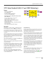
CE81 Series Embedded Array (0.18µm CMOS Technology) . . . . . . . . . . . . . . . . . . . . . . . . . . . . . . . . . . . . . . . . . . 5
Features . . . . . . . . . . . . . . . . . . . . . . . . . . . . . . . . . . . . . . . . . . . . . . . . . . . . . . . . . . . . . . . . . . . . . . . . . . . . . . . . 5
Description . . . . . . . . . . . . . . . . . . . . . . . . . . . . . . . . . . . . . . . . . . . . . . . . . . . . . . . . . . . . . . . . . . . . . . . . . . . . . . 5
A-Series with 44µm Inline Pad Pitch and TAB . . . . . . . . . . . . . . . . . . . . . . . . . . . . . . . . . . . . . . . . . . . . . . 5
I-Series with 70µm Inline Pad Pitch . . . . . . . . . . . . . . . . . . . . . . . . . . . . . . . . . . . . . . . . . . . . . . . . . . . . . . . 5
S-Series with 66µm Stagger Pad Pitch . . . . . . . . . . . . . . . . . . . . . . . . . . . . . . . . . . . . . . . . . . . . . . . . . . . . . 6
ASIC Design Kit and EDA Support . . . . . . . . . . . . . . . . . . . . . . . . . . . . . . . . . . . . . . . . . . . . . . . . . . . . . . . 6
Package Availability . . . . . . . . . . . . . . . . . . . . . . . . . . . . . . . . . . . . . . . . . . . . . . . . . . . . . . . . . . . . . . . . . . . 7
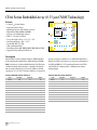
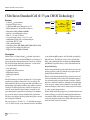
CS81 Series Standard Cell (0.18µm CMOS Technology) . . . . . . . . . . . . . . . . . . . . . . . . . . . . . . . . . . . . . . . . . . . . . 8
Features . . . . . . . . . . . . . . . . . . . . . . . . . . . . . . . . . . . . . . . . . . . . . . . . . . . . . . . . . . . . . . . . . . . . . . . . . . . . . . . . 8
Description . . . . . . . . . . . . . . . . . . . . . . . . . . . . . . . . . . . . . . . . . . . . . . . . . . . . . . . . . . . . . . . . . . . . . . . . . . . . . . 8
ASIC Design Kit and EDA Support . . . . . . . . . . . . . . . . . . . . . . . . . . . . . . . . . . . . . . . . . . . . . . . . . . . . . . . 9
Package Availability . . . . . . . . . . . . . . . . . . . . . . . . . . . . . . . . . . . . . . . . . . . . . . . . . . . . . . . . . . . . . . . . . . 10
CE71 Series Embedded Array (0.25 µm CMOS Technology) . . . . . . . . . . . . . . . . . . . . . . . . . . . . . . . . . . . . . . . . 11
Features . . . . . . . . . . . . . . . . . . . . . . . . . . . . . . . . . . . . . . . . . . . . . . . . . . . . . . . . . . . . . . . . . . . . . . . . . . . . . . . 11
Description . . . . . . . . . . . . . . . . . . . . . . . . . . . . . . . . . . . . . . . . . . . . . . . . . . . . . . . . . . . . . . . . . . . . . . . . . . . . . 11
J-Series with 66µm Stagger Pad Pitch and Wire Bonding . . . . . . . . . . . . . . . . . . . . . . . . . . . . . . . . . . . . . 11
K-Series with 88µm Inline Pad Pitch and Wire Bonding . . . . . . . . . . . . . . . . . . . . . . . . . . . . . . . . . . . . . . 12
L-Series with 44µm Inline Pad Pitch and Au Bump . . . . . . . . . . . . . . . . . . . . . . . . . . . . . . . . . . . . . . . . . . 12
T-Series with 88mm Inline Pad Pitch and Wire Bonding . . . . . . . . . . . . . . . . . . . . . . . . . . . . . . . . . . . . . . 12
ASIC Design Kit and EDA Support . . . . . . . . . . . . . . . . . . . . . . . . . . . . . . . . . . . . . . . . . . . . . . . . . . . . . . 13
Package Availability . . . . . . . . . . . . . . . . . . . . . . . . . . . . . . . . . . . . . . . . . . . . . . . . . . . . . . . . . . . . . . . . . . 14
CS71 Series Standard Cell (0.25 µm CMOS Technology) . . . . . . . . . . . . . . . . . . . . . . . . . . . . . . . . . . . . . . . . . . . 15
Features . . . . . . . . . . . . . . . . . . . . . . . . . . . . . . . . . . . . . . . . . . . . . . . . . . . . . . . . . . . . . . . . . . . . . . . . . . . . . . . 15
Description . . . . . . . . . . . . . . . . . . . . . . . . . . . . . . . . . . . . . . . . . . . . . . . . . . . . . . . . . . . . . . . . . . . . . . . . . . . . . 15
ASIC Design Kit and EDA Support . . . . . . . . . . . . . . . . . . . . . . . . . . . . . . . . . . . . . . . . . . . . . . . . . . . . . . 16
Package Availability . . . . . . . . . . . . . . . . . . . . . . . . . . . . . . . . . . . . . . . . . . . . . . . . . . . . . . . . . . . . . . . . . . 17
CE66 Series Embedded Array (0.35 µm CMOS Technology) . . . . . . . . . . . . . . . . . . . . . . . . . . . . . . . . . . . . . . . . 18
Features . . . . . . . . . . . . . . . . . . . . . . . . . . . . . . . . . . . . . . . . . . . . . . . . . . . . . . . . . . . . . . . . . . . . . . . . . . . . . . . 18
Description . . . . . . . . . . . . . . . . . . . . . . . . . . . . . . . . . . . . . . . . . . . . . . . . . . . . . . . . . . . . . . . . . . . . . . . . . . . . . 18
P-Series with 100µm Inline Pad Pitch. . . . . . . . . . . . . . . . . . . . . . . . . . . . . . . . . . . . . . . . . . . . . . . . . . . . . 18
S-Series with 70µm Inline Pad Pitch. . . . . . . . . . . . . . . . . . . . . . . . . . . . . . . . . . . . . . . . . . . . . . . . . . . . . . 18
ASIC Design Kit and EDA Support . . . . . . . . . . . . . . . . . . . . . . . . . . . . . . . . . . . . . . . . . . . . . . . . . . . . . . 19
Package Availability . . . . . . . . . . . . . . . . . . . . . . . . . . . . . . . . . . . . . . . . . . . . . . . . . . . . . . . . . . . . . . . . . . 19
Fujitsu Microelectronics, Inc.
i
Master Product Selector Guide
CS66 Series Standard Cell (0.35 µm CMOS Technology). . . . . . . . . . . . . . . . . . . . . . . . . . . . . . . . . . . . . . . . . . . .20
Features. . . . . . . . . . . . . . . . . . . . . . . . . . . . . . . . . . . . . . . . . . . . . . . . . . . . . . . . . . . . . . . . . . . . . . . . . . . . . . . .20
Description . . . . . . . . . . . . . . . . . . . . . . . . . . . . . . . . . . . . . . . . . . . . . . . . . . . . . . . . . . . . . . . . . . . . . . . . . . . . .20
Applications . . . . . . . . . . . . . . . . . . . . . . . . . . . . . . . . . . . . . . . . . . . . . . . . . . . . . . . . . . . . . . . . . . . . . . . . . . . .21
ASIC Design Kit and EDA Support. . . . . . . . . . . . . . . . . . . . . . . . . . . . . . . . . . . . . . . . . . . . . . . . . . . . . . .21
Package Availability . . . . . . . . . . . . . . . . . . . . . . . . . . . . . . . . . . . . . . . . . . . . . . . . . . . . . . . . . . . . . . . . . .22
CE61 Series Embedded Array (0.28µm Leff) . . . . . . . . . . . . . . . . . . . . . . . . . . . . . . . . . . . . . . . . . . . . . . . . . . . . .23
Features. . . . . . . . . . . . . . . . . . . . . . . . . . . . . . . . . . . . . . . . . . . . . . . . . . . . . . . . . . . . . . . . . . . . . . . . . . . . . . . .23
Description . . . . . . . . . . . . . . . . . . . . . . . . . . . . . . . . . . . . . . . . . . . . . . . . . . . . . . . . . . . . . . . . . . . . . . . . . . . . .23
E-Series, 70µm Staggered Pad Pitch, Optimized for Pad-Limited Designs . . . . . . . . . . . . . . . . . . . . . . . .23
F-Series, Optimized for Core-Limited Designs . . . . . . . . . . . . . . . . . . . . . . . . . . . . . . . . . . . . . . . . . . . . . .23
ASIC Design Kit and EDA Support. . . . . . . . . . . . . . . . . . . . . . . . . . . . . . . . . . . . . . . . . . . . . . . . . . . . . . .24
Package Availability . . . . . . . . . . . . . . . . . . . . . . . . . . . . . . . . . . . . . . . . . . . . . . . . . . . . . . . . . . . . . . . . . .24
ARC Processor Core . . . . . . . . . . . . . . . . . . . . . . . . . . . . . . . . . . . . . . . . . . . . . . . . . . . . . . . . . . . . . . . . . . . . . . . . .25
Sonet STS-3c/SDH STM-1 Framer Core . . . . . . . . . . . . . . . . . . . . . . . . . . . . . . . . . . . . . . . . . . . . . . . . . . . . . . . . .26
ARM7TDMI™ Processor Core . . . . . . . . . . . . . . . . . . . . . . . . . . . . . . . . . . . . . . . . . . . . . . . . . . . . . . . . . . . . . . . .27
UTOPIA Level II . . . . . . . . . . . . . . . . . . . . . . . . . . . . . . . . . . . . . . . . . . . . . . . . . . . . . . . . . . . . . . . . . . . . . . . . . . .28
PCI Peripheral Core . . . . . . . . . . . . . . . . . . . . . . . . . . . . . . . . . . . . . . . . . . . . . . . . . . . . . . . . . . . . . . . . . . . . . . . . .30
USB Function Core . . . . . . . . . . . . . . . . . . . . . . . . . . . . . . . . . . . . . . . . . . . . . . . . . . . . . . . . . . . . . . . . . . . . . . . . . .31
USB Host Controller Core . . . . . . . . . . . . . . . . . . . . . . . . . . . . . . . . . . . . . . . . . . . . . . . . . . . . . . . . . . . . . . . . . . . .32
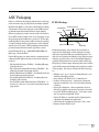
ASIC Packaging . . . . . . . . . . . . . . . . . . . . . . . . . . . . . . . . . . . . . . . . . . . . . . . . . . . . . . . . . . . . . . . . . . . . . . . . . . . .33
FC-BGA Packages . . . . . . . . . . . . . . . . . . . . . . . . . . . . . . . . . . . . . . . . . . . . . . . . . . . . . . . . . . . . . . . . . . . . . . .33
FBGA Packages . . . . . . . . . . . . . . . . . . . . . . . . . . . . . . . . . . . . . . . . . . . . . . . . . . . . . . . . . . . . . . . . . . . . . . . . .34
EBA Packages . . . . . . . . . . . . . . . . . . . . . . . . . . . . . . . . . . . . . . . . . . . . . . . . . . . . . . . . . . . . . . . . . . . . . . . . . .34
FDH-BGA Packages. . . . . . . . . . . . . . . . . . . . . . . . . . . . . . . . . . . . . . . . . . . . . . . . . . . . . . . . . . . . . . . . . . . . . .35
TAB-BGA Packages. . . . . . . . . . . . . . . . . . . . . . . . . . . . . . . . . . . . . . . . . . . . . . . . . . . . . . . . . . . . . . . . . . . . . .35
PBGA Packages . . . . . . . . . . . . . . . . . . . . . . . . . . . . . . . . . . . . . . . . . . . . . . . . . . . . . . . . . . . . . . . . . . . . . . . . .36
QFP Packages . . . . . . . . . . . . . . . . . . . . . . . . . . . . . . . . . . . . . . . . . . . . . . . . . . . . . . . . . . . . . . . . . . . . . . . . . . .36
CPGA Packages . . . . . . . . . . . . . . . . . . . . . . . . . . . . . . . . . . . . . . . . . . . . . . . . . . . . . . . . . . . . . . . . . . . . . . . . .37
ASIC Mixed-Signal and Analog Macros . . . . . . . . . . . . . . . . . . . . . . . . . . . . . . . . . . . . . . . . . . . . . . . . . . . . . . . . .38
Design Support . . . . . . . . . . . . . . . . . . . . . . . . . . . . . . . . . . . . . . . . . . . . . . . . . . . . . . . . . . . . . . . . . . . . . . . . . .39
Microcontrollers . . . . . . . . . . . . . . . . . . . . . . . . . . . . . . . . . . . . . . . . . . . . . . . . . . . . . . . . . . . . . . . . . . . . . . . 41
F2MC . . . . . . . . . . . . . . . . . . . . . . . . . . . . . . . . . . . . . . . . . . . . . . . . . . . . . . . . . . . . . . . . . . . . . . . . . . . . . . . . . . . .42
8- and 16-bit Flexible Microcontrollers . . . . . . . . . . . . . . . . . . . . . . . . . . . . . . . . . . . . . . . . . . . . . . . . . . . . . . .42
F2MC-8L Series Features. . . . . . . . . . . . . . . . . . . . . . . . . . . . . . . . . . . . . . . . . . . . . . . . . . . . . . . . . . . . . . . . . .42
F2MC-16L/16LX/16F Series Features . . . . . . . . . . . . . . . . . . . . . . . . . . . . . . . . . . . . . . . . . . . . . . . . . . . . . . . .42
F2MC-8L/Low Power/Low Voltage Microcontrollers . . . . . . . . . . . . . . . . . . . . . . . . . . . . . . . . . . . . . . . .43
F2MC-16L High Performance/Low Power/Low Voltage Microcontrollers . . . . . . . . . . . . . . . . . . . . . . . .45
F2MC-16LX High Performance/Low Power Microcontrollers . . . . . . . . . . . . . . . . . . . . . . . . . . . . . . . . . .46
F2MC-16F High Speed/High Performance Microcontrollers . . . . . . . . . . . . . . . . . . . . . . . . . . . . . . . . . . .47
ii
Fujitsu Microelectronics, Inc.
FR Series. . . . . . . . . . . . . . . . . . . . . . . . . . . . . . . . . . . . . . . . . . . . . . . . . . . . . . . . . . . . . . . . . . . . . . . . . . . . . . . . . . 48
32-bit Flexible Microcontrollers . . . . . . . . . . . . . . . . . . . . . . . . . . . . . . . . . . . . . . . . . . . . . . . . . . . . . . . . . . . . 48
FR Features . . . . . . . . . . . . . . . . . . . . . . . . . . . . . . . . . . . . . . . . . . . . . . . . . . . . . . . . . . . . . . . . . . . . . . . . . . . . 48
Ethernet®. . . . . . . . . . . . . . . . . . . . . . . . . . . . . . . . . . . . . . . . . . . . . . . . . . . . . . . . . . . . . . . . . . . . . . . . . . . . . 49
Ethernet Products . . . . . . . . . . . . . . . . . . . . . . . . . . . . . . . . . . . . . . . . . . . . . . . . . . . . . . . . . . . . . . . . . . . . . . . . . . . 50
Evaluation Kits . . . . . . . . . . . . . . . . . . . . . . . . . . . . . . . . . . . . . . . . . . . . . . . . . . . . . . . . . . . . . . . . . . . . . . . . . . . . . 51
ATM . . . . . . . . . . . . . . . . . . . . . . . . . . . . . . . . . . . . . . . . . . . . . . . . . . . . . . . . . . . . . . . . . . . . . . . . . . . . . . . . 53
ATM Products . . . . . . . . . . . . . . . . . . . . . . . . . . . . . . . . . . . . . . . . . . . . . . . . . . . . . . . . . . . . . . . . . . . . . . . . . . . . . 54
ADSL . . . . . . . . . . . . . . . . . . . . . . . . . . . . . . . . . . . . . . . . . . . . . . . . . . . . . . . . . . . . . . . . . . . . . . . . . . . . . . . 55
ADSL Products. . . . . . . . . . . . . . . . . . . . . . . . . . . . . . . . . . . . . . . . . . . . . . . . . . . . . . . . . . . . . . . . . . . . . . . . . . . . . 56
Development Kits . . . . . . . . . . . . . . . . . . . . . . . . . . . . . . . . . . . . . . . . . . . . . . . . . . . . . . . . . . . . . . . . . . . . . . . . . . . 56
Application Specific Controllers . . . . . . . . . . . . . . . . . . . . . . . . . . . . . . . . . . . . . . . . . . . . . . . . . . . . . . . . . . 57
IEEE 1394 Controller . . . . . . . . . . . . . . . . . . . . . . . . . . . . . . . . . . . . . . . . . . . . . . . . . . . . . . . . . . . . . . . . . . . . . . . . 58
SCSI Controllers. . . . . . . . . . . . . . . . . . . . . . . . . . . . . . . . . . . . . . . . . . . . . . . . . . . . . . . . . . . . . . . . . . . . . . . . . . . . 60
Wireless . . . . . . . . . . . . . . . . . . . . . . . . . . . . . . . . . . . . . . . . . . . . . . . . . . . . . . . . . . . . . . . . . . . . . . . . . . . . . 61
SAW Filters . . . . . . . . . . . . . . . . . . . . . . . . . . . . . . . . . . . . . . . . . . . . . . . . . . . . . . . . . . . . . . . . . . . . . . . . . . . . . . . 62
F5CM (B2) DMS Series (Balanced SAW Filters). . . . . . . . . . . . . . . . . . . . . . . . . . . . . . . . . . . . . . . . . . . . . . . 63
F5CE (D2) DMS Series (Dual Mode SAW Filters). . . . . . . . . . . . . . . . . . . . . . . . . . . . . . . . . . . . . . . . . . . . . . 64
F5CH (L2) Series (Ladder SAW Filters) . . . . . . . . . . . . . . . . . . . . . . . . . . . . . . . . . . . . . . . . . . . . . . . . . . . . . . 65
F5CE/F6CE (K2) Series (Ladder SAW Filters). . . . . . . . . . . . . . . . . . . . . . . . . . . . . . . . . . . . . . . . . . . . . . . . . 66
F5CP/F6CP (D2) Series (Dual Mode SAW Filters) . . . . . . . . . . . . . . . . . . . . . . . . . . . . . . . . . . . . . . . . . . . . . 67
F6CE (L2) Series (Ladder SAW Filters) . . . . . . . . . . . . . . . . . . . . . . . . . . . . . . . . . . . . . . . . . . . . . . . . . . . . . . 68
D5CC (D1) Series (Antenna Duplexer) . . . . . . . . . . . . . . . . . . . . . . . . . . . . . . . . . . . . . . . . . . . . . . . . . . . . . . . 69
G5CH/G5CN/G6CH/G6CS (L2/D2) Series (Dual SAW Filters) . . . . . . . . . . . . . . . . . . . . . . . . . . . . . . . . . . . 70
PLLs . . . . . . . . . . . . . . . . . . . . . . . . . . . . . . . . . . . . . . . . . . . . . . . . . . . . . . . . . . . . . . . . . . . . . . . . . . . . . . . . . . . . . 72
Single Super PLLs . . . . . . . . . . . . . . . . . . . . . . . . . . . . . . . . . . . . . . . . . . . . . . . . . . . . . . . . . . . . . . . . . . . . . . . 73
The MB15C Series . . . . . . . . . . . . . . . . . . . . . . . . . . . . . . . . . . . . . . . . . . . . . . . . . . . . . . . . . . . . . . . . . . . 73
The MB15S Series. . . . . . . . . . . . . . . . . . . . . . . . . . . . . . . . . . . . . . . . . . . . . . . . . . . . . . . . . . . . . . . . . . . . 74
Dual Super PLLs . . . . . . . . . . . . . . . . . . . . . . . . . . . . . . . . . . . . . . . . . . . . . . . . . . . . . . . . . . . . . . . . . . . . . . . . 75
The MB15E Series. . . . . . . . . . . . . . . . . . . . . . . . . . . . . . . . . . . . . . . . . . . . . . . . . . . . . . . . . . . . . . . . . . . . 75
The MB15U Series . . . . . . . . . . . . . . . . . . . . . . . . . . . . . . . . . . . . . . . . . . . . . . . . . . . . . . . . . . . . . . . . . . . 76
The MB15F Series. . . . . . . . . . . . . . . . . . . . . . . . . . . . . . . . . . . . . . . . . . . . . . . . . . . . . . . . . . . . . . . . . . . . 77
Evaluation Kits. . . . . . . . . . . . . . . . . . . . . . . . . . . . . . . . . . . . . . . . . . . . . . . . . . . . . . . . . . . . . . . . . . . . . . . . . . 78
Prescalers . . . . . . . . . . . . . . . . . . . . . . . . . . . . . . . . . . . . . . . . . . . . . . . . . . . . . . . . . . . . . . . . . . . . . . . . . . . . . . . . . 80
Bipolar Prescalers - 200 MHz to 2.7 GHz. . . . . . . . . . . . . . . . . . . . . . . . . . . . . . . . . . . . . . . . . . . . . . . . . . 80
Fujitsu Microelectronics, Inc.
iii
Master Product Selector Guide
High Performance CMOS Digital to Analog Converters . . . . . . . . . . . . . . . . . . . . . . . . . . . . . . . . . . . . . . . . . . . . .81
MB86060 Interpolating Filters . . . . . . . . . . . . . . . . . . . . . . . . . . . . . . . . . . . . . . . . . . . . . . . . . . . . . . . . . . . . . .82
Development Kit Support . . . . . . . . . . . . . . . . . . . . . . . . . . . . . . . . . . . . . . . . . . . . . . . . . . . . . . . . . . . . . . . . . .82
High Performance, Leading-Edge Memory . . . . . . . . . . . . . . . . . . . . . . . . . . . . . . . . . . . . . . . . . . . . . . . . . . 83
FCRAM. . . . . . . . . . . . . . . . . . . . . . . . . . . . . . . . . . . . . . . . . . . . . . . . . . . . . . . . . . . . . . . . . . . . . . . . . . . . . . . . . . .84
16 MEG SDR interface FCRAM . . . . . . . . . . . . . . . . . . . . . . . . . . . . . . . . . . . . . . . . . . . . . . . . . . . . . . . . .84
16 MEG SRAM interface FCRAM . . . . . . . . . . . . . . . . . . . . . . . . . . . . . . . . . . . . . . . . . . . . . . . . . . . . . . .84
16 MEG SRAM interface FCRAM with power down mode. . . . . . . . . . . . . . . . . . . . . . . . . . . . . . . . . . . .84
Flash . . . . . . . . . . . . . . . . . . . . . . . . . . . . . . . . . . . . . . . . . . . . . . . . . . . . . . . . . . . . . . . . . . . . . . . . . . . . . . . . . . . . .85
Flash Memory Table. . . . . . . . . . . . . . . . . . . . . . . . . . . . . . . . . . . . . . . . . . . . . . . . . . . . . . . . . . . . . . . . . . . . . .85
5V-only Flash Memory Devices – MBM29F series . . . . . . . . . . . . . . . . . . . . . . . . . . . . . . . . . . . . . . . . . .85
3V-only Flash Memory – MBM29LV series. . . . . . . . . . . . . . . . . . . . . . . . . . . . . . . . . . . . . . . . . . . . . . . .85
Dual-Operation 3V Flash Memory – MBM29DL Series . . . . . . . . . . . . . . . . . . . . . . . . . . . . . . . . . . . . . .85
Dual-Operation 2.5V Flash Memory (2.3V to 2.7V) – MBM29DD Series . . . . . . . . . . . . . . . . . . . . . . . .85
1.8V-only Flash Memory (1.8V to 2.2V) – MBM29SL series. . . . . . . . . . . . . . . . . . . . . . . . . . . . . . . . . .86
Page Mode Devices – MBM29PL Series. . . . . . . . . . . . . . . . . . . . . . . . . . . . . . . . . . . . . . . . . . . . . . . . . . .86
NAND FLASH – MBM30 Series . . . . . . . . . . . . . . . . . . . . . . . . . . . . . . . . . . . . . . . . . . . . . . . . . . . . . . . .86
3V stacked type MCP (Flash + RAM) Device – MB84VD series . . . . . . . . . . . . . . . . . . . . . . . . . . . . . . .86
2.5V stacked type MCP (Flash + RAM) Device – MB84LD series . . . . . . . . . . . . . . . . . . . . . . . . . . . . . .86
Color Plasma Displays . . . . . . . . . . . . . . . . . . . . . . . . . . . . . . . . . . . . . . . . . . . . . . . . . . . . . . . . . . . . . . . . . . 87
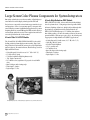
Large Screen Color Plasma Components for System Integrators . . . . . . . . . . . . . . . . . . . . . . . . . . . . . . . . . . . . . . .88
42-inch Wide-VGA PDP Module. . . . . . . . . . . . . . . . . . . . . . . . . . . . . . . . . . . . . . . . . . . . . . . . . . . . . . . . . . . .88
42-inch High Definition PDP Module . . . . . . . . . . . . . . . . . . . . . . . . . . . . . . . . . . . . . . . . . . . . . . . . . . . . . . . .88
37-inch XGA PDP Module. . . . . . . . . . . . . . . . . . . . . . . . . . . . . . . . . . . . . . . . . . . . . . . . . . . . . . . . . . . . . . . . .89
Future PDP Modules. . . . . . . . . . . . . . . . . . . . . . . . . . . . . . . . . . . . . . . . . . . . . . . . . . . . . . . . . . . . . . . . . . . . . .89
15-inch Active Matrix TFT-LCD . . . . . . . . . . . . . . . . . . . . . . . . . . . . . . . . . . . . . . . . . . . . . . . . . . . . . . . . . . . .90
Advanced Packaging Technology. . . . . . . . . . . . . . . . . . . . . . . . . . . . . . . . . . . . . . . . . . . . . . . . . . . . . . . . . . 91
Chip Scale Package (CSP) . . . . . . . . . . . . . . . . . . . . . . . . . . . . . . . . . . . . . . . . . . . . . . . . . . . . . . . . . . . . . . . . .92
Bump Chip Carrier™ (BCC™, BCC++™) . . . . . . . . . . . . . . . . . . . . . . . . . . . . . . . . . . . . . . . . . . . . . . . . . . . .93
Electrical Characteristics (Self-Inductance). . . . . . . . . . . . . . . . . . . . . . . . . . . . . . . . . . . . . . . . . . . . . . . . .93
Reliability Criteria . . . . . . . . . . . . . . . . . . . . . . . . . . . . . . . . . . . . . . . . . . . . . . . . . . . . . . . . . . . . . . . . . . . .93
BCC Package Family . . . . . . . . . . . . . . . . . . . . . . . . . . . . . . . . . . . . . . . . . . . . . . . . . . . . . . . . . . . . . . . . . .93
Wafer Bumping . . . . . . . . . . . . . . . . . . . . . . . . . . . . . . . . . . . . . . . . . . . . . . . . . . . . . . . . . . . . . . . . . . . . . . . . . . . . .94
Single-Chip Solutions . . . . . . . . . . . . . . . . . . . . . . . . . . . . . . . . . . . . . . . . . . . . . . . . . . . . . . . . . . . . . . . . . . . . . . . .95
BGA Package . . . . . . . . . . . . . . . . . . . . . . . . . . . . . . . . . . . . . . . . . . . . . . . . . . . . . . . . . . . . . . . . . . . . . . . . . . .95
FCBGA . . . . . . . . . . . . . . . . . . . . . . . . . . . . . . . . . . . . . . . . . . . . . . . . . . . . . . . . . . . . . . . . . . . . . . . . . . . . . . . .95
iv
Fujitsu Microelectronics, Inc.
Wafer Fab Services . . . . . . . . . . . . . . . . . . . . . . . . . . . . . . . . . . . . . . . . . . . . . . . . . . . . . . . . . . . . . . . . . . . . . 97
CMOS Technology. . . . . . . . . . . . . . . . . . . . . . . . . . . . . . . . . . . . . . . . . . . . . . . . . . . . . . . . . . . . . . . . . . . . . . . . . . 98
Device Characteristics . . . . . . . . . . . . . . . . . . . . . . . . . . . . . . . . . . . . . . . . . . . . . . . . . . . . . . . . . . . . . . . . . 98
Device Performance . . . . . . . . . . . . . . . . . . . . . . . . . . . . . . . . . . . . . . . . . . . . . . . . . . . . . . . . . . . . . . . . . . 98
Interconnect Characteristics . . . . . . . . . . . . . . . . . . . . . . . . . . . . . . . . . . . . . . . . . . . . . . . . . . . . . . . . . . . . 98
Test Capability. . . . . . . . . . . . . . . . . . . . . . . . . . . . . . . . . . . . . . . . . . . . . . . . . . . . . . . . . . . . . . . . . . . . . . . 99
Representatives . . . . . . . . . . . . . . . . . . . . . . . . . . . . . . . . . . . . . . . . . . . . . . . . . . . . . . . . . . . . . . . . . . . . . . . 100
Distributors . . . . . . . . . . . . . . . . . . . . . . . . . . . . . . . . . . . . . . . . . . . . . . . . . . . . . . . . . . . . . . . . . . . . . . . . . . 102
Fujitsu Microelectronics, Inc.
v
Master Product Selector Guide
vi
Fujitsu Microelectronics, Inc.
Introduction
Fujitsu Microelectronics, Inc.
Your Partner in Semiconductors and Electronic Devices
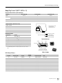
Welcome to the Master Product Selector Guide!
Inside these pages, you will find a comprehensive portfolio of advanced semiconductors and
electronic devices from Fujitsu Microelectronics, Inc. (FMI). Our product line includes
Application Specific Integrated Circuits (ASICs) and Application Specific Standard Products
(ASSPs) such as microcontrollers and network/wireless ICs. FMI’s memory products include
Application Specific Memories (ASMs) such as Fast Cycle RAM (FCRAMTM), and standard
products such as flash and DRAM. The company also markets flat display panels, and provides
advanced packaging and wafer fabrication services. These products and services, known for
their quality and reliability, are helping Fujitsu customers succeed.
This guide can help you choose from the more than 1,000 products available. For further
information, visit FMI’s web site at http://www.fujitsumicro.com or call the Customer
Response Center (1-800-866-8608). You’ll find that FMI has the innovative solutions to
help you succeed.
Fujitsu Microelectronics, Inc.
1
Master Product Selector Guide
Capabilities
As a subsidiary of Fujitsu Limited, a leading $50 billion
Internet-focused, information-solutions provider, FMI
utilizes Fujitsu’s extensive global resources including its indepth engineering support, sub-micron process and
packaging technologies, and world-class manufacturing
network. FMI combines these global resources with its local
capabilities and customer partnerships to provide end-to-end
System LSI solutions.
In addition to the quality and reliability of its products,
Fujitsu’s semiconductor group is known for its ability to
integrate components to provide total solutions. FMI follows
a systems-level approach. Rather than focusing on individual
components, FMI looks at the whole system and identifies the
particular chip needed to solve a customer’s problem. This
system-level approach is a key strength and is only possible
because of FMI’s extensive engineering capabilities.
2
Fujitsu Microelectronics, Inc.
FMI’s extensive network of design, manufacturing and
marketing operations throughout the U.S. demonstrates
Fujitsu’s commitment to this marketplace. FMI’s engineers in
its design centers in San Jose, Dallas, and Raleigh, North
Carolina, work with Fujitsu’s engineering organizations
worldwide. A part of Fujitsu’s worldwide manufacturing
network, FMI’s expanded wafer fabrication facility in
Gresham, Oregon, produces leading-edge flash and other
memory products.
Finally, FMI backs up its development and manufacturing
efforts with a quality support program, giving customers
maximum flexibility in fit, form, and function. FMI’s
Customer Response Center is one of the best in the industry.
Additionally, FMI offers demand-pull programs, Just In
Time (JIT) deliveries, Electronic Data Interchange (EDI)
systems, buffer-inventory, and configure-to-order programs.
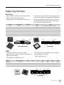
Application Specific ICs
(ASICs)
As a leading-edge ASIC producer, FMI provides products and services that help its
customers succeed in today’s market segments. FMI specializes in providing cost-effective
deep submicron CMOS ASIC solutions for performance-driven applications. FMI offers
ASIC products ranging from embedded arrays to standard cells in 0.18µm, 0.25µm and
0.35µm CMOS process technologies.
FMI’s ASIC family is a series of high-performance embedded arrays and standard cells,
featuring full support for mixed-signal macros and embedded DRAM, as well as diffused
RAMs, ROMs, and a wide variety of reusable embedded SOC cores supported by Fujitsu’s
IPWare™. Embedded synchronous DRAMs, up to 64Mb, are now available in Fujitsu’s
0.18µm technology. Three and four metal layers are standard in all ASIC process
technologies, and an optional fifth layer is available for area bump designs in 0.18µm
process, providing up to 1,320 signal I/Os. A wide range of voltage choices for the core and
a dual power supply option for the I/Os make FMI ASICs extremely versatile. In addition to
providing high-performance core operation at low power, FMI’s ASIC is also capable of
interfacing with both higher voltage and high-speed I/Os.
FMI ASICs & System LSI Solutions
•
•
•
•
0.18-micron (0.13µm Leff) technology in production
0.11-micron (0.07µm Leff) technology introduced
Multi-million gates of logic: up to 28M gates in 0.18-micron
Embedded memory blocks:
- RAMs, ROMs, Register Files and more
•
•
•
•
Large-capacity Embedded DRAMs: up to 64Mb per chip
Library of Verified Cores
Analog and Mixed-signal macros: 10-bit DACs & ADCs
High Pin-count Flip-chip Ball Grid Array (FC-BGA) packaging
- 2116 pins FC-BGA package in 1mm ball pitch
• Design Methodology for hierarchical timing driven flow
• Global Support Network – Design and Customer Response Centers
Fujitsu Microelectronics, Inc.
3
Master Product Selector Guide
ASIC
Fujitsu fully supports an “open” design flow that allows designers
to use the EDA tools of their choice from all mainstream EDA vendors. Three major third party EDA vendors supported are
Cadence, Synopsys, and Mentor Graphics. The official signoff
EDA simulation tools are Cadence Verilog, Synopsys VCS and
VSS, and Model-sim (Verilog/VHDL) from Mentor Graphics.
Other popular third party tools supported are as follows:
Synopsys
Design Compiler, Movie/Prime Time, Design Power/Power Compiler, and TestGen/Test Compiler
Cadence
NC-Verilog, Leapfrog, Design Planner, CTGen, PBOpt,
Wroute/SE, Hyper Extract and Dracula
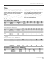
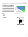
Product
Drawn Geometry (µm)
CX61
0.35
DesignVerifyer from Chrysalis and WattWatcher from Sante.
Fujitsu’s packaging options span a wide range–from low-cost plastic QFPs and BGAs, to high pin-count FBGA and FCBGA–so
that the designers can choose the optimal package to fit their
unique design criteria.
Fujitsu recognizes that today’s designers need total solutions in
order to successfully implement their ASIC designs. In addition to
Fujitsu’s industry-leading silicon process and packaging technology, the company also offers a wide range of system-level design
support tools, including clock skew measurement, scan insertion,
and ATPG test support, as well as RAM and ROM compilers.
FMI’s U.S.-based multidisciplinary engineering support staff is
ready to assist customers.
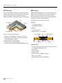
Descriptions
Embedded array
68K to 2M gates, 144 to 672 signal I/Os, 81 ps gate delay, 0.17µW/gate/MHz
CX66
0.35
Embedded array and standard cells
CX71
0.25
Embedded array and standard cells
CX81
0.18
Embedded array and standard cells
91K to 1.1M gates, 126 to 312 signal I/Os, 93 ps gate delay, 0.15µW/gate/MHz
167K to 8M gates, 88 to 506 signal I/Os, 60 ps gate delay, 0.06µW/gate/MHz
540K to 22M gates, 126 to 1320 signal I/Os, 53 ps gate delay, 0.022µW/gate/MHz
4
Fujitsu Microelectronics, Inc.
Application Specific ICs (ASICs)
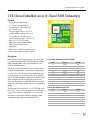
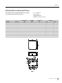
CE81 Series Embedded Array (0.18µm CMOS Technology)
Features
•
•
•
•
•
•
•
•
•
•
•
•
•
•
0.13µm effective channel length
3 to 5 layers of metal interconnects
Very high-density: 86K raw gates/mm2
Up to 23 million gates
Core power supply voltage: 1.8V to 1.1V
8 nW/gate/MHz power dissipation at 1.1V
12 ps gate delay at 1.8V and 1 fan-out
Junction temperature range: –40 to +125° C
I/Os: 3.3V, 2.5V, 1.8V, 5V tolerant
High-density diffused RAMs and ROMs
High-speed mixed-signal macros
Analog PLLs
Wide selection of advanced packaging options
Proven design methodology and tool support
Description
Fujitsu’s CE81 is a series of high performance, 0.18µm (0.13µm
Leff) CMOS embedded arrays that include full support of diffused
high-speed RAMs, ROMs, analog, mixed-signal macros, and a
variety of embedded functions.
The CE81 series offers density and performance similar to those of
standard-cell implementation, yet has the time-to-market advantage of gate arrays. The CE81 series devices include 44µm, 66µm,
or 70µm pad pitch for a cost-effective solution for both pad-limited and core-limited designs. The inline pads are available in both
70µm and 44µm pad pitch. The 70µm pads are wire bonded,
whereas the 44µm pads are used with TAB. The 66µm wire-bond
stagger pads can be used for optimizing the die area of pad-limited
designs.
The CE81 chip cores can operate at 1.8V to 1.1V. The I/Os, operating at 1.8V, 2.5V, or 3.3V, can conveniently interface with various
types of devices. The CE81, which features very low power and
high density, is well suited for hand-held computing, graphics,
communication and consumer electronics applications.
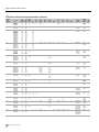
A-Series with 44µm Inline Pad Pitch and TAB
Frame
Total Gates
Total Pads
A4
1,032K
304
A5
1,370K
352
A6
1,930K
420
A7
2,930K
520
A8
4,137K
620
A9
5,552K
720
AA
7,039K
812
AB
8,394K
888
AC
9,787K
960
AD
11,300K
1,032
AE
14,045K
1,152
I-Series with 70µm Inline Pad Pitch
Frame
Total Gates
Total Pads
I1
527K
144
I2
791K
176
I3
1,110K
208
I4
1,483K
240
I5
1,689K
256
I6
2,385K
304
I7
3,207K
352
Fujitsu Microelectronics, Inc.
5
Master Product Selector Guide
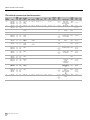
I-Series with 70µm Inline Pad Pitch
Frame
Total Gates
Total Pads
I8
4,150K
400
I9
5,791K
472
IA
7,249K
528
S-Series with 66µm Stagger Pad Pitch
Frame
Total Gates
Total Pads
SA
7,852K
585
SB
9,203K
632
SC
10,658K
680
SD
12,235K
728
SE
15,085K
808
SF
19,580K
920
SG
23,532K
1,008
Mixed-Signal Macros
A/D Converters
• 8-bit: 50 MS/s high-speed 3.3V
• 8-bit: 25 MS/s high-speed 3.3V
• 8-bit: 1 MS/s 3.3V
D/A Converters
• 10-bit: 30 MS/s 3.3V
• 8-bit: 50 MS/s 3.3V
• 8-bit: 1 MS/s 3.3V
Multiplier Compiler
• Multiplicand (m): 4 ≤ m ≤ 32
• Multiplier (n): 4 ≤ n ≤ 32 (even numbers only)
Memory Macros
• SRAM Compiler: single and dual port (1 R/W, 1R), up to 72K
bits per block
• High-speed SRAMS, up to 144K bits per block
• High-density SRAMS (1RW), 512K~ 1.1M bits (under development)
• Register files: 2R/2W
• ROM Compiler: up to 512K bits per block
Phase-Locked Loops
• Analog: up to 800 MHz
6
Fujitsu Microelectronics, Inc.
I/Os
• 1.8V, 2.5V, and 3.3V CMOS (2.5V is under development)
• Slew-rate controlled
• Capable of driving large loads: 2, 4, 8, and 12 mA sinking current
• Transceivers under development: P-CML, LVDS, PCI, SSTL,
and GTL+
• AGP 2X and 4X
• 2.5 Gbps with clock recovery and Serdes (under development)
• To be developed: 5V tolerant buffers
SOC IP Cores
• ARC 32-bit RISC
• 10/100 MAC
• 64/256 QAM
• MPEG2 Decoder/Demultiplexer
• 8VSB TV Demodulator
• AC3 Dolby Voice Decoder
• JPEG Encoder and Decoder
• PCI – 33/66 MHz, 32/64-bit cores
• USB Host Controller/Device
• I 2C
• IDE (ATA3) Host Controller
• Smart Card I/F
• IRDA I/R Interface
• To be developed:
• ARM 7TDMI Hard Macro
• Oak DSP Hard Macro
• More IPs are being added
ASIC Design Kit and EDA Support
Design Kit
Description
Verilog Logic Simulators from
Cadence, Synopsys, and
Mentor
Verilog-XL, NC-Verilog, VCS, Model-sim (Verilog)
VHDL/VITAL Logic Simulators
from Synopsys, Cadence, and
Mentor
VSS, Model-sim (VHDL), V-System, Leapfrog
Synthesis, DFT, and STA tools
from Synopsys
Design Compiler, Test Compiler, and PrimeTime
Other EDA Tools
Chrysalis Design Verifyer and Sente Watt
Watcher
Application Specific ICs (ASICs)
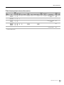
Package Availability
No. of Pins
Frame Size
Thin QFP Package (0.5 mm pin pitch)
100
I1, I2
120
I1, I2
Low-profile QFP Package (0.5 mm pin pitch)
144
I1, I2
176
I2, I3
208
I4, I5
Heat-spread QFP Package (0.5 mm pin pitch)
208
I3, I4, I5
240
I4, I5, I6, I7
304
I7, I8, I9, IA, SB, SC, SD, SE, SF, SG
Heat-spread QFP Package (0.4 mm pin pitch)
256
I6, I7, I8, I9
TAB Ball Grid Array (0.8 mm ball pitch)
304
A4, A5
352
A5, A6
TAB Ball Grid Array (1.0 mm ball pitch)
480
A6, A7
560
A7, A8
660
A8, A9
720
A9, AA, AB, AC, AD, AE
Enhanced Ball Grid Array (1.27 mm ball pitch)
567
SA, SB
672
SC, SD
Fine-pitch Ball Grid Array (0.8 mm ball pitch)
112
I1, I2
144
I1, I2
168
I3
176
I3
192
I4, I5
224
I5, I6
272
I6, I7, I8
320
I6, I7, I8
Fine-pitch Ball Grid Array (0.75 mm ball pitch)
288
I6, I7, I8, I9, IA
Fine-pitch Ball Grid Array (0.5 mm ball pitch)
112
I1, I2, I3
176
I2, I3, I4, I5, I6
240
I6, I7, I8
304
I8, I9
368
IA
Fujitsu Microelectronics, Inc.
7
Master Product Selector Guide
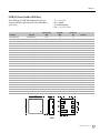
CS81 Series Standard Cell (0.18µm CMOS Technology)
Features
•
•
•
•
•
•
•
•
•
•
•
•
•
•
•
0.13µm effective channel length
3 to 5 layers of metal interconnects
Very high density: 110K raw gates/mm2
Up to 28 million gates
Core power supply voltage: 1.8V to 1.1V
5 nW/gate/MHz power dissipation at 1.1V
11 ps gate delay at 1.8V and 1 fan-out
Junction temperature range: –40 to +125°C
I/Os: 3.3V, 2.5V, 1.8V, 5V tolerant
High-density diffused RAMs and ROMs
High-speed mixed-signal macros
Analog PLLs
Wide selection of advanced packaging options
Proven design methodology and tool support
Two cell libraries: high-performance and high-density
Description
Fujitsu’s CS81, a 0.18µm (0.13µm Leff) standard-cell product, is
based on Fujitsu’s state-of-the-art CMOS process technology, a
deep sub-micron process designed for today’s high-density and
low-power SOC products. The cell library, which is optimized for
synthesis-based designs, has accurate timing and power-characterized data, cell areas, and statistical wire-load models. The CS81
standard-cell library contains both high-performance and highdensity cells, giving designers the option of combining both types
of standard cell blocks on the same chip. The CS81 library supports popular third-party tools and data-exchange file standards.
The CS81 chip cores can operate at 1.8V to 1.1V. The I/Os, operating at 1.8V, 2.5V, 3.3V, or 5V tolerance, can conveniently interface
with various types of devices. Interface options include low-swing,
high-speed I/Os and high-speed bus interface I/Os.
Both inline and staggered I/O pad configurations are available.
Inline pads are available in both 70µm and 44µm pad pitch. The
70µm pads are wire bonded, whereas the 44µm pads are used with
TAB. The 66µm wire-bond stagger pads can be used for optimizing the die area of pad-limited designs.
In addition to the traditional QFP packages, the CS81 family is
available in TAB, EBGA, FBGA, and Flip-chip BGA packages.
8
Fujitsu Microelectronics, Inc.
CS81 offers a rich set of ADCs and DACs, PLLs, high-speed RAMs
and ROMs, as well as a variety of other embedded functions. The
following blocks will be available in the near future:
• Special high-speed I/Os: T-LVTTL, P-CML, LVDS, SSTL, and
HSTL
• Special-purpose Interfaces: PCI, AGP, and USB
Design Methodology
Fujitsu’s design methodology ensures first-time silicon success by
integrating proprietary point tools with popular, sign-off-quality,
industry-standard CAD tools such as:
• Logic design rule checker
• Delay calculator
• Quasi 3-D parasitic extraction tool
Fujitsu’s clock-driven design methodology is devised for low power
and low skew. The methodology identifies the best-suited clock distribution strategy for a given design and predicts performance in
advance. Fujitsu supports co-simulation, emulation and high-level
floor-planning to optimize the power, timing, and size of the
design. This enables the designer to make effective architecturallevel decisions to achieve optimal design solutions.
Application Specific ICs (ASICs)
Fujitsu’s design methodology supports cycle-based simulators and
formal verification, as well as static timing analysis and the more
conventional VHDL and Verilog simulators. Fujitsu’s design-fortest strategy includes boundary scan (JTAG) and full and partial
scan, as well as a built-in self-test for memory.
Applications
CS81 offers high-density standard cells for very low-power applications. Also provided in CS81 are high-performance and areaoptimized memories, mixed-signal blocks, analog functions, a rich
set of IP Cores and Mega Macros, and various I/O interfaces. The
CS81 ASIC design kit, combined with its supported EDA tool sets,
is poised for chip developments that require ease-of-tool use,
proven design flow and a quick time to market.
Mixed-Signal Macros
A/D Converters
• 8-bit: 50 MS/s high-speed 3.3V
• 8-bit: 25 MS/s high-speed 3.3V
• 8-bit: 1 MS/s 3.3V
D/A Converters
• 10-bit: 30 MS/s 3.3V
• 8-bit: 50 MS/s 3.3V
• 8-bit: 1 MS/s 3.3V
Multiplier Compiler
• Multiplicand (m): 4 ≤ m ≤ 32
• Multiplier (n): 4 ≤ n ≤ 32 (even numbers only)
Memory Macros
• SRAM Compiler: single and dual port (1RW/1R), up to 72K
bits per block
• High-speed SRAMs, up to 144K bits
• High-density SRAMs (1RW) 512K ~ 1.1M bits (under development)
• Register files: 2R/2W
• ROM Compiler: up to 512K bits per block
Phase-Locked Loops
• Analog: up to 800 MHz
I/Os
• 1.8V, 2.5V, and 3.3V CMOS (2.5V is under development)
• Slew-rate controlled
• Capable of driving large loads: 2, 4, 8, and 12 mA sinking current
• Transceivers under development: P-CML, LVDS, PCI, SSTL,
and GTL
• AGP 2X and 4X
• 2.5 Gbps with clock recovery and Serdes (under development)
• To be developed: 5V tolerant buffers
SOC IP Cores
• ARC 32-bit RISC
• 10/100 MAC
• 64/256 QAM
• MPEG2 Decoder/Demultiplexer
• 8VSB TV Demodulator
• AC3 Dolby Voice Decoder
• JPEG Encoder and Decoder
• PCI – 33/66 MHz, 32/64 bit cores
• USB Host Controller/Device
• I 2C
• IDE (ATA3) Host Controller
• Smart Card I/F
• IRDA I/R Interface
• To be developed:
• ARM 7TDMI Hard Macro
• Oak DSP Hard Macro
• More IPs are being added
ASIC Design Kit and EDA Support
Design Kit
Description
Verilog Logic Simulators from
Cadence, Synopsys, and Mentor
Verilog-XL, NC Verilog, VCS, Model-sim
(Verilog)
VHDL/VITAL Logic Simulators
from Synopsys,Cadence, and
Mentor
VSS, Model-sim (VHDL) V-System, Leapfrog
Synthesis, DFT, and STA tools from
Synopsys
Design Compiler, Test Compiler, and
PrimeTime
Other EDA Tools
Chrysalis Design Verifyer and Cadence DP
Fujitsu Microelectronics, Inc.
9
Master Product Selector Guide
Package Availability
No. of Pins/Balls
Pin/Ball Pitch
Dimensions
304
0.8 mm
21 mm
352
0.8 mm
23 mm
480
1.0 mm
31 mm
TAB-BGA (Cavity-down)
560
1.0 mm
35 mm
660
1.0 mm
40 mm
720
1.0 mm
40 mm
576
1.27 mm
40 mm
672
1.27 mm
45 mm
208
0.50 mm
28 mm
240
0.50 mm
32 mm
256
0.40 mm
28 mm
304
0.50 mm
40 mm
100
0.50 mm
14 mm
120
0.50 mm
20 mm
144
0.50 mm
20 mm
176
0.50 mm
24 mm
208
0.50 mm
28 mm
112
0.80 mm
10 mm
144
0.80 mm
12 mm
168
0.80 mm
12 mm
176
0.80 mm
12 mm
192
0.80 mm
14 mm
224
0.80 mm
16 mm
240
0.50 mm
10 mm
272
0.80 mm
18 mm
288
0.75 mm
18 mm
304
0.50 mm
12 mm
320
0.80 mm
18 mm
368
0.50 mm
14 mm
1,089
1.27 mm
42.4 mm
1,225
1.27 mm
45.0 mm
1,369
1.27 mm
47.5 mm
1,681
1.00 mm
42.5 mm
1,849
1.00 mm
45.0 mm
2,116
1.00 mm
47.5 mm
EBGA (Cavity-down)
HQFP (Cavity-up)
TQFP (Cavity-up)
LQFP (Cavity-up)
FBGA (Cavity-up)
FC-BGA (Cavity-down)
10
Fujitsu Microelectronics, Inc.
Application Specific ICs (ASICs)
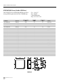
CE71 Series Embedded Array (0.25 µm CMOS Technology)
Features
•
•
•
•
•
•
•
•
0.18µm Leff (0.24µm drawn)
Propagation delay of 61 ps
Separate core and I/O supply voltages
Mixed-signal macros—A/D and D/A converters
I/Os: 2.5V, 3.3V and 5V tolerant
Core power supply voltage: 2.5V, 1.8V, 1.5V
Junction temperature: -40°C ~125°C
High-performance and special I/Os: PCML, LVDS, PCI, SSTL,
GTL+, AGP, USB
• Analog and digital PLLs
• Packaging options: QFP, HQFP, BGA, TBGA
• Support for major third party EDA tools
Description
Fujitsu’s CE71 is a series of high-performance, 0.18µm Leff CMOS
embedded arrays that include full support of diffused high-speed
RAMs, ROMs, mixed-signal macros, and a variety of other embedded functions.
The CE71 series offers density and performance similar to those of
standard cells, yet provides the time-to-market advantage of gate
arrays. The CE71 series devices include 44µm, 66µm, or 88µm pad
pitch for a cost-effective solution for both pad-limited and corelimited designs.
With a nominal 1.5V to 2.5V core operation and with 2.5V and
3.3V/5V tolerant I/Os, the CE71 series features a very low-power
consumption of 0.06µW/gate/MHz. Potential applications for the
CE71 series include computing, graphics, communications, networking, wireless, and consumer designs.
J-Series with 66µm Stagger Pad Pitch and Wire Bonding
Frame
Total Gates
Total Pads
Signals
CE71J1
216K
192
152
CE71J2
312K
224
152
CE71J3
488K
272
178
CE71J4
703K
320
206
CE71J5
911K
360
264
CE71J6
1,098K
392
304
CE71J7
1,302K
424
360
CE71J8
1,524K
456
360
CE71J9
2,020K
520
360
CE71JA
2,586K
584
472
CE71JB
3,055K
632
472
CE71JC
3,564K
680
506
CE71JD
4,113K
728
506
CE71JE
5,114K
808
506
CE71JF
6,698K
920
506
CE71JG
8,096K
1,008
506
Fujitsu Microelectronics, Inc.
11
Master Product Selector Guide
K-Series with 88µm Inline Pad Pitch and Wire Bonding
Frame
Total Gates
Total Pads
Signals
Frame
Total Gates
Total Pads
Signals
CE71K1
167K
100
88
CE71T2
347K
144
128
CE71K2
237K
120
102
CE71T3
524K
176
156
CE71K3
348K
144
126
CE71T4
734K
208
178
CE71K4
524K
176
152
CE71T5
845K
224
192
CE71K5
734K
208
178
CE71T6
963K
240
206
CE71K6
963K
240
206
CE71T7
1,110K
256
220
CE71K7
1,110K
256
220
CE71T8
1,407K
288
248
CE71K8
1,559K
304
264
CE71T9
1,559K
304
264
264
L-Series with 44µm Inline Pad Pitch and Au Bump
12
T-Series with 88µm Inline Pad Pitch and Wire Bonding
CE71TA
1.827K
328
CE71TB
2, 088K
352
312
2,398K
376
312
Frame
Total Gates
Total Pads
Signals
CE71TC
CE71L4
356K
304
264
CE71TD
3,040K
424
360
CE71L5
476K
352
304
CE71TE
3,645K
464
360
CE71L6
677K
420
360
CE71TG
5,152K
552
264
CE71L7
1,034K
520
428
CE71L8
1,469K
620
504
CE71L9
1,976K
720
504
CE71LA
2,513K
812
504
CE71LB
3,001K
888
504
CE71LC
3,506K
960
504
CE71LD
4,050K
1,032
504
CE71LE
5,043K
1,152
504
Fujitsu Microelectronics, Inc.
Application Specific ICs (ASICs)
Mixed-Signal Macros
D/A Converters
•
•
•
•
10-bit: 1MS/s, 1.5MS/s,
30 MS/s, 50 MS/s
100 MS/s, 220 MS/s
8-bit: 200 KS/s, 1MS/s, 50 MS/s
A/D Converters
•
•
•
•
12-bit: 1 MS/s
10-bit: 1 MS/s, 20MS/s, 40 MS/s
8-bit: 1MS/s, 30 MS/s, 50 MS/s
6-bit: 100 MS/s, 500 MS/s
Multiplier Compiler
• Multiplicand (m): 4 ≤ m ≤ 32
• Multiplier (n): 4 ≤ n ≤ 32 (even numbers only)
Memory Macros
• SRAM Compiler: single and dual port (1 R/W, 1R), up to 72K
bits per block, both BUS and Partial Write
• ROM Compiler: up to 512K bits per block
• High-density single-port RAM 288K bits
• Register file (2R/W, 2R/2W), up to 4,608 bits
Phase-Locked Loops
• Analog: up to 250 MHz (622 MHz under development)
I/Os
• 2.5V, 3.3V and 5V tolerant
• Slew-rate controlled
• CMOS, TTL, PCML, T-LVTTL, LVDS, PCI, SSTL, GTL+,
AGP, USB
SOC IP Cores
• ARM 7TDMI Hard Macro
• ARC 32-bit RISC
• 834/836 SPARClite Hard Macros
• Oak DSP Hard Macro
• 10/100 MAC
• 64/256 QAM
• MPEG2 Decoder/Demultiplexer
• 8VSB TV Demodulator
• AC-3 Dolby Voice Decoder
• JPEG Encoder and Decoder
• PCI-33/66 MHz, 32/64-bit cores
• USB Host ControllerDevice
• I 2C
• IDE (ATA3) Host Controller
• Smart Card I/F
• IRDA I/R Interface
• More IPs are being added
ASIC Design Kit and EDA Support
Design Kit
Description
Verilog Logic Simulators
from Cadence, Synopsys and
Mentor
Verilog-XL, NC-Verilog, VCS, Model-sim (Verilog)
VHDL/VITAL Logic
Simulators from Synopsys,
Cadence, and Mentor
VSS, Model-sim (VHDL), V-System, Leapfrog
Synthesis, power, DFT, and
STA tools from Synopsys
Design Compiler, Design Power, Test Compiler,
PrimeTime, MOTIVE, and Sunrise TestGen
Other EDA Tools
Chrysalis Design Verifyer and Sente Watt Watcher
Fujitsu Microelectronics, Inc.
13
Master Product Selector Guide
Package Availability
Number of Pins
Frame Size
Thin and Low Profile QFP Package (0.4, 0.5 mm lead pitch)
100
K1, K2
120
K2, K3
144
K3, K4, K8, T2, T3
176
K4, K5, T3, T4
208
T4, T5, T6, T7, 78, 79
256
T8, T9, TA, TB, TC
Shrink QFP Package (0.5 mm lead pitch)
176
J1, J2, K4, K5
208
J3, J4, J5, K5, K6, K7, K8
240
J4, J5, J6, K6, K7, K8
Heatspreader QFP Package (0.4, 0.5 mm lead pitch)
208
J3, J4, J5, J6, J7, J8, J9, K5, K6, K7, K8, T4, T5,
T6, T7, T8, T9
240
J4, J5, J6, J7, J8, J9, JA, K6, K7, K8, T6, T7, T8,
T9, TA
256
J5, J6, J7, J8, J9, T7, T8, T9, TA, TB, TC
304
J7, J8, J9, JA, JB, JC, JD, JE, JF, JG, TB, TC, TD,
TE, TG
Ball Grid Array (1.27 mm ball pitch)
256
J3, J4, T7, T8, T9, TA, TB
352
J6, J7, J8, TB, TC, TD
420
J8, J9, TD, TE
576
JA, JB
672
JC, JD
Fine-Pitch Ball Grid Array (0.75, 0.8 mm ball pitch)
144
T3
176
T3, T4
224
T5, T6, T7, T8, T9
288
T8, T9, TA, TB, TC
Tab Ball Grid Array (0.8, 1.0 mm ball pitch)
304
L4, L5
352
L5, L6, L7
480
L6, L7
560
L7, L8, LB, LC
660
L8, L9
720
L9, LA, LB, LC, LD, LE
14
Fujitsu Microelectronics, Inc.
Application Specific ICs (ASICs)
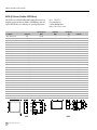
CS71 Series Standard Cell (0.25 µm CMOS Technology)
Features
•
•
•
•
•
•
•
•
•
•
•
•
0.18µm Leff (0.24µm drawn)
Up to 10 million gates
0.05 µW/gate/MHz power dissipation
2.5V, 3.3V, 5V tolerant I/O options
Special high-performance I/Os-PCML, LVDS, PCI, SSTL,
GLT+, AGP, USB
Core power supply voltage: 2.5V, 1.8V, 1.5V
Junction temperature: -40°C~125°C
High-performance embedded SRAM and DRAM
Analog and digital PLLs
Powerful mixed-signal offering—A/D and D/A convertors
Advanced packaging
Proven design methodology and tool support
2.5V Device
3.3V Device
5.0V Device
2.5V CMOS
3.3V CMOS
5.0V TTL
2.5V
CMOS
CS71
3.3V Dual Power Supply
CMOS
(3.3V/2.5V)
T-LVTTL
P-CML
LVDS
SSTL
GTL+
ADC/DAC
5.0V
Tolerant
PCI
AGP
USB
PCI Bus
AGP Bus
USB Devices
High-Speed
Interface
High-speed
Devices
Analog
Interface
Description
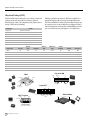
Fujitsu’s CS71, a 0.25µm (0.18µm Leff) standard cell product, is
based on Fujitsu’s state-of-the-art CMOS process technology–a
process designed for high performance and high integration. The
CS71 family offers up to 10 million gates, using as many as five layers of metal.
The CS71 standard cell library is the most aggressive and enhanced
library for implementing today’s deep submicron system-on-silicon
designs. The cell library is optimized for synthesis-based designs,
and is designed for low power.
The core process operates at 1.5V, 1.8V, and 2.5V with I/Os operating at 2.5V, 3.3V, or 5V tolerant conditions.
The library supports the most popular third-party tools and data
exchange file standards.
Both standard and staggered I/O pad configurations are available
at 44µm, 66µm, and 88µm pad pitches. Interface options include
low-swing, high-speed I/Os, and high-speed bus interface I/Os.
In addition to the traditional QFP packages, the CS71 family is
available in Ball Grid Array.
CS71 offers a rich set of ADCs and DACs, digital and analog
PLLs, high-speed RAMs, ROMs, and DRAMs, as well as a variety
of other embedded functions.
Design Methodology
Fujitsu’s design methodology ensures first-silicon success by integrating proprietary point tools with the most popular, sign-off
quality, industry-standard CAD tools.
Fujitsu’s clock-driven design methodology is devised for low power
and low skew. It identifies the best suited clock distribution strategy for a given design and predicts performance in advance. Fujitsu
supports co-simulation, emulation, and high-level floorplanning
to ease the power, timing, and size estimation of the design. This
enables the designer to make effective architectural- level decisions
toward achieving optimal design solutions.
Fujitsu’s design methodology supports cycle-based simulators and
formal verification, as well as static timing analysis and the more
conventional VHDL and Verilog simulators. Fujitsu design-fortest strategy includes boundary scan (JTAG), full and partial scan,
as well as a built-in self-test for memory.
Applications
CS71 offers high integration and performance and low-power performance and low-power consumption. High-performance
transmission and switching applications, as well as power-sensitive
applications, such as mobile computing and mobile communications, can benefit from this technology.
Fujitsu Microelectronics, Inc.
15
Master Product Selector Guide
Mixed-Signal Macros
D/A Converters
• 10-bit: 1 MS/s, 1.5 MS/s.
30 MS/s, 50 MS/s,
100 MS/s, 220 MS/s
• 8-bit: 200 KS/s, 1 MS/s, 50 MS/s
A/D Converters
•
•
•
•
12-bit: 1 MS/s
10-bit: 1 MS/s, 20 MS/s, 40 MS/s
8-bit: 1 MS/s, 30 MS/s, 50 MS/s
6-bit: 100 MS/s, 500 MS/s
Memory Macros
• SRAM Compiler: single and dual port (1 R/W, 1R), up to 72K
bits per block, both BUS and Partial Write
• ROM Compiler: up to 512K bits per block
• High-density single-port RAM 288K bits
• Register file (2R/W, 2R/2W), up to 4,608 bits
Phase-Locked Loops
• Analog: up to 250 MHz (622 MHz under development)
I/Os
• 2.5V, 3.3V and 5V tolerant
• Slew-rate controlled
• CMOS, TTL, PCML, T-LVTTL, LVDS, PCI, SSTL, GTL+,
AGP, USB
SOC IP Cores
• ARM 7TDMI Hard Macros
• ARC 32-bit RISC
• 834/836 SPARClite Hard Macros
• Oak DSP Hard Macro
• 10/100 MAC
• 64/256 QAM
• MPEG2 Decoder/Demultiplexer
• 8VSB TV Demodulator
• AC-3 Dolby Voice Decoder
• JPEG Encoder and Decoder
• PCI-33/66 MHz, 32/64-bit cores
• USB Host Controller Device
• I2C
• IDE (ATA3) Host Controller
• Smart Card I/F
• IRDA I/R Interface
• More IPs are being added
16
Fujitsu Microelectronics, Inc.
ASIC Design Kit and EDA Support
Design Kit
Description
Verilog Logic Simulators
from Cadence, Synopsys,
and Mentor
Verilog-XL, NC-Verilog, VCS, Model-sim (Verilog)
VHDL/VITAL Logic
Simulators from Synopsys,
Cadence, and Mentor
VSS, Model-sim (VHDL), V-System, Leapfrog
Synthesis, power, DFT, and
STA tools from Synopsys
Design Compiler, Design Power, Test Compiler,
PrimeTime, MOTIVE, and Sunrise TestGen
Other EDA Tools
Chrysalis Design Verifyer and Sente Watt Watcher
Application Specific ICs (ASICs)
Package Availability
No. of Pins
Frame Size
Thin and Low QFP Packages (0.4, 0.5 mm lead pitch)
100
K1, K2
120
K2, K3
144
K3, K4, K8, T2, T3
176
K4, K5, T3, T4
208
T4, T5, T6, T7, T8, T9
256
T8, T9, TA, TB, TC
Shrink QFP Package (0.5 mm lead pitch)
176
J1, J2, K4, K5
208
J3, J4, J5, K5, K6, K7, K8
240
J4, J5, J6, K6, K7, K8
Heatspreader QFP Package (0.4, 0.5 mm lead pitch)
208
J3, J4, J5, J6, J7, J8, J9, K5, K6, K7, K8, T4, T5,
T6, T7, T8, T9
240
J4, J5, J6, J7, J8, J9, JA, K6, K7, K8, T6, T7, T8,
T9, TA
256
J5, J6, J7, J8, J9, T7, T8, T9, TA, TB, TC
304
J7, J8, J9, JA, JB, JC, JD, JE, JF, JG, TB, TC, TE,
TG
Ball Grid Array (1.27 mm ball pitch)
256
J3, J4, T7, T8, T9, TA, TB
352
J6, J7, J8, TB, TC, TD
420
J8, J9, TD, TE
576
JA, JB
672
JC, JD
Fine-Pitch Ball Grid Array (0.75, 0.8 mm ball pitch)
144
T3
176
T3, T4
224
T5, T6, T7, T8, T9
288
T8, T9, TA, TB, TC
Tab Ball Grid Array (0.8, 1.0 mm ball pitch)
304
L4, L5
352
L5, L6, L7
480
L6, L7
580
L7, L8, LB, LC
660
L8, L9
720
L9, LA, LB, LC, LD, LE
Fujitsu Microelectronics, Inc.
17
Master Product Selector Guide
CE66 Series Embedded Array (0.35 µm CMOS Technology)
Features
•
•
•
•
•
•
•
•
•
•
•
•
0.28µm Leff (0.34µm drawn)
Propagation delay of 98 ps
Mixed signal macros: A/D and D/A converters
High-density diffused RAMs and ROMs
Separate core and I/O supply voltages
I/Os: 5V, 3.3V and 5V tolerant
Core power supply voltage: 3.3V, 2.5V ~2.0V
Junction temperature: -40°C ~125°C
Special I/Os: PCI, I2C, USB
Analog and digital PLLs
Packaging options: QFP, HQFP, LQFP, TQFP, PBGA, FBGA
Support for major third party EDA tools
Embedded
Hard
Macro
5V I/O
5V I/O
5V I/O
5V I/O
5V I/O
3V I/O
3V I/O
3V I/O
PCML
3V I/O
3V I/O
5V I/O
5V I/O
5V I/O
5V I/O
5V I/O
Fixed
Layout
Soft Macro
Clk
Clock Tree
Fixed
Layout
Soft Macro
Description
Fujitsu’s CE66 is a series of high-performance, CMOS embedded
arrays featuring mixed-signal macros, diffused high-speed RAMs,
ROMs, and a variety of other embedded functions. The CE66 series
combines the density and performance of standard cells with the
time-to-market advantage of gate arrays. In addition, the I/Os,
operating at 5V, 3.3V and 5V tolerant conditions, are designed to
provide cost-effective solutions for core-limited and pad-limited
designs. The CE66 series features a very low power consumption of
0.29µW/gate/MHz at 3.3V. Potential applications for the CE66
series include the consumer market, communications, and networking designs.
P-Series with 100µm Inline Pad Pitch
S-Series with 70µm Inline Pad Pitch
18
Frame
Total Gates
Total Pads
Signals
Frame
Total Gates
Total Pads
CE66P1
188K
144
126
CE66S1
91K
144
Signals
126
CE66P2
233K
160
138
CE66S2
113K
160
138
CE66P3
283K
176
132
CE66S3
137K
176
152
CE66P4
337K
192
152
CE66S4
164K
192
160
CE66P5
396K
208
178
CE66S5
207K
216
178
CE66P6
427K
216
178
CE66S6
256K
240
193
CE66P7
460K
224
178
CE66S7
311K
264
228
CE66P8
528K
240
206
CE66S8
391K
296
248
CE66P9
602K
256
228
CE66S9
481k
328
248
CE66PA
680K
272
228
CE66SA
580K
360
312
CE66PB
761K
288
228
CE66PC
847K
304
264
CE66PD
940K
320
264
CE66PE
1037K
336
264
CE66PF
1138K
352
312
Fujitsu Microelectronics, Inc.
Application Specific ICs (ASICs)
Mixed-Signal Macros
• More IPs are being added
D/A Converters
ASIC Design Kit and EDA Support
•
•
•
•
•
8-bit: 220 MHz (video)
8-bit: 50 MHz (video)
8-bit: 1.5 MHz (general purpose)
10-bit: 30 MHz (general purpose)
10-bit: 1.5 MHz (general purpose)
A/D Converters
•
•
•
•
6-bit: 300 MHz (disk)
8-bit: 50 MHz (video)
10-bit: 20 MHz (general purpose)
10-bit: 1 MHz (general purpose)
Design Kit
Description
Verilog Logic Simulators from
Cadence, Synopsys and Mentor
Verilog-XL, NC-Verilog, VCS, Model-sim
(Verilog)
VHDL/VITAL Logic
VSS, Model-sim (VHDL), V-System,
Simulators from Synopsys,
Leapfrog
Cadence and Mentor
Synthesis, DET, and STA tools from
Synopsys
Design Compiler, Test Compiler, PrimeTime,
MOTIVE, and Sunrise TestGen
Other EDA Tools
Chrysalis Design Verifyer
Package Availability
Multiplier Compiler
• Multiplicand (m): 4 < m < 32
• Multiplier (n): 4 < n < 32 (even numbers only)
No. of Pins
Memory Macros
• SRAM Compiler: single and dual port (1 R/W, 1R),
up to 72K bits per block, partial write option
• ROM Compiler: up to 512K bits per block
• Delay line: up to 32K bits
LQFP
Frame Size
TQFP
100
100
P1, P2, P3, P4, P5, P6, P7, P8, P9, PA, PB, PC, PD, PE, PF, S1, S2
P1, P2, P3, P4, P5, P6, P7, P8, P9, PA, PB, PC, PD, PE, PF, S1, S2
144
P1, P2, P3, P4, P5, P6, P7, P8, P9, PA, PB, PC, PD, PE, PF, S1, S2
176
P3, P4, P5, P6, P7, P8, P9, PA, PB, PC, PD, PE, PF
208
P6, P7, P8, P9, PA, PB, PC, PD, S5, S6, S7
120
P1, P2, P3, P4, P5, P6, P7, P8, P9, PA, PB, PC, PD, PE, PF, S1, S2
144
P1, P2, P3, P4, P5, P6, P7, P8, P9, PA, PB, PC, PD, PE, PF, S1, S2
160
P2, P3, P4, P5, P6, P7, P8, P9, PA, PB, PC, PD, PE, PF, S2, S3, S4
176
P3, P4, P5, P6, P7, P8, P9, PA, PB, PC, PD, PE, PF, S3, S4
208
P5, P6, P7, P8, P9, PA, PB, PC, PD, PE, PF, S5, S6
240
P8, P9, PA, PB, PC, PD, PE, PF, S7, S8
256
P9, PA, PB, PC, PD, PE, PF
QFP
Phase-Locked Loops
• Analog: 50- 200 MHz
• Digital: 180-360 MHz (Preliminary)
I/Os
• 3.3V, 5V and 5V tolerant
• Slew-rate controlled
• CMOS, TTL, LVTTL, T-LVTTL, SDRAM I/F, PCI, I2C, USB
HQFP
SOC IP Cores
• ARC 32-bit RISC
• 832/833/835 SPARClite Hard Macros
• Oak DSP Hard Macro
• 10/100 MAC
• 64/256 QAM
• MPEG2 Decoder/Demultiplexer
• 8VSB TV Demodulator
• AC-3 Dolby Voice Decoder
• JPEG Encoder and Decoder
• PCI-33/66 MHZ, 32/64-bit cores
• USB Host Controller/Device
• I2C
• IDE (ATA3) Host Controller
• Smart Card I/F
• IRDA I/R Interface
208
P5, P6, P7, P8, P9, PA, PB, PC, PD, PE, PF, S5, S6
240
P8, P9, PA, PB, PC, PD, PE, PF, S7, S8
256
P9, PA, PB, PC, PD, PE, PF, S8
304
PC, PD, PE, PF, S9, SA
PBGA
256
P9, PA, PB, PC, PD, PE, PF, S7, S8
352
PF, SA
FBGA
112
P2, P3, P4, P5, P6, P7, S1, S2, S3
144
P3, P4, P5, P6, P7, S1, S2, S3, S4
168
P6, P7, P8, P9, S3, S4, S5, S6, S7
176
P3, P4, P5, P6, P7, P8, P9, PA, PB, PC, PD, S3, S4
192
P4, P5, P6, P7, P8, P9, PA, PB, PC, PD, PE, PF, S4, S5
224
P7, P8, P9, PA, PB, PC, PD, PE, PF, S6, S7
288
PC, PD, PE, PF, S8, S9, SA
Fujitsu Microelectronics, Inc.
19
Master Product Selector Guide
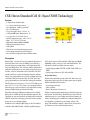
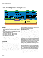
CS66 Series Standard Cell (0.35 µm CMOS Technology)
Features
•
•
•
•
•
•
•
•
•
•
•
•
•
•
0.28µm Leff (0.34µm drawn)
Propagation delay of 98 ps
0.3µW/gate/MHz power dissipation @ 3.3V
Mixed-signal macros: A/D and D/A converters
High-density diffused RAMs and ROMs
Separate core and I/O supply voltages
I/Os: 5V, 3.3V and 5V tolerant
Core power supply voltage: 3.3V, 2.5V ~2.0V
100µm inline pad pitch for core-limited designs
Special I/Os: PCI, I2C, USB
Analog and digital PLLs
Packaging options: QFP, HQFP, LQFP, TQFP, PBGA, FBGA
Support for major third party EDA tools
High-performance SRAM and DRAM
3.3V Device
3.3V CMOS
3.3V
CMOS
CS66
Dual Power Supply
5.0V Device
5.0V TTL
5.0V
Tolerant
(5.0V/3.3V)
T-LVTTL
P-CML
LVDS
SDRAM I/F
SSTL
GTL
High-Speed
Interface
High-Speed
Devices
Analog
Interface
ADC/DAC
PCI
USB
PCI Bus
USB Devices
Description
Fujitsu’s CS66, a 0.35µm (0.28µm Leff) standard cell product is
based on the state-of-the-art Fujitsu CMOS process technology–a
process designed for high integration and cost effective solutions.
The cell-based design enables the realization of “system-on-silicon” applications that include the following:
•
•
•
•
•
User-defined logic
Sophisticated analog functions
High-density memory
Intelligent peripherals
Cores
The CS66 technology is based on an enhanced 3.3V process that
provides fast performance along with 3.3V power savings. The
CS66 standard cell library is an aggressive and optimal library for
implementing today’s high-performance deep submicron systemson-silicon. The CS66 supports dense, high-clock frequency, system-level designs that meet the performance, integration, and
power management requirements of networking, telecommunication, electronic data processing, and digital video applications.
The library also supports the most popular third- party tools and
data exchange file standards.
The core operates at 3.3V and 2.5V ~ 2V, with I/Os operating at
3.3V, 5V and 5V tolerant, or any combination of these. In addition
20
Fujitsu Microelectronics, Inc.
to the traditional QFP packages, the CS66 family is available in
Ball Grid Array. The CS66 also offers a rich set of ADCs and
DACs, analog and digital PLLs, and high-speed RAMs, ROMs,
and DRAMs, along with a variety of other embedded functions.
Design Methodology
Fujitsu’s design methodology ensures first-silicon success by integrating proprietary point tools with the most popular sign-off
quality, industry-standard CAD tools.
Fujitsu’s clock-driven design methodology offers low power and
low skew. It identifies the best-suited clock distribution strategy
for a given design and predicts performance in advance. Fujitsu
supports co-simulation, emulation, and high-level floorplanning
to ease the power, timing, and size estimation of the design. This
enables the designer to make effective architectural-level decisions
to achieve optimal design solutions.
Fujitsu’s design methodology supports cycle-based simulators and
formal verification, as well as static timing analysis and the more
conventional VHDL and Verilog simulators. Fujitsu’s design-fortest strategy includes boundary scan (JTAG), full and partial scan,
as well as a built-in self-test for memory.
Application Specific ICs (ASICs)
Applications
High-performance transmission and switching applications and
power-sensitive applications, such as mobile computing and mobile
communications, can benefit from this technology.
Mixed-Signal Macros
D/A Converters
•
•
•
•
•
8-bit: 220 MHz (video)
8-bit: 50 MHz (video)
8-bit: 1.5 MHz (general purpose)
10-bit: 30 MHz (general purpose)
10-bit: 1.5 MHz (general purpose)
A/D Converters
•
•
•
•
6-bit: 300 MHz (disk)
8-bit: 50 MHz (video)
10-bit: 20 MHz (general purpose)
10-bit: 1 MHz (general purpose)
Multiplier Compiler
• Multiplicand (m): 4 < m < 32
• Multiplier (n): 4 < n < 32 (even numbers only)
Memory Macros
• SRAM Compiler: single and dual port (1 R/W, 1R),
up to 72K bits per block, partial write option
• ROM Compiler: up to 512K bits per block
• Delay line: up to 32K bits
Phase-Locked Loops
• Analog: 50- 200 MHz
• Digital: 180-360 MHz (Preliminary)
SOC IP Cores
• ARC 32-bit RISC
• 832/833/835 SPARClite Hard Macros
• Oak DSP Hard Macro
• 10/100 MAC
• 64/256 QAM
• MPEG2 Decoder/Demultiplexer
• 8VSB TV Demodulator
• AC-3 Dolby Voice Decoder
• JPEG Encoder and Decoder
• PCI-33/66 MHZ, 32/64-bit cores
• USB Host Controller/Device
• I 2C
• IDE (ATA3) Host Controller
• Smart Card I/F
• IRDA I/R Interface
• More IPs are being added
ASIC Design Kit and EDA Support
Verilog Logic Simulators from
Cadence, Synopsys and Mentor
Verilog-XL, NC-Verilog, VCS, Model-sim
(Verilog)
VHDL/VITAL Logic
VSS, Model-sim (VHDL), V-System,
Simulators from Synopsys,
Leapfrog
Cadence and Mentor
Synthesis, power, DFT, and STA tools
from Synopsys
Design Compiler, Design Power, Test
Compiler, PrimeTime, MOTIVE, and
Sunrise TestGen
Other EDA Tools
Chrysalis Design Verifyer
I/Os
• 3.3V, 5V and 5V tolerant
• Slew-rate controlled
• CMOS, TTL, LVTTL, T-LVTTL, SDRAM I/F, PCI, I2C, USB
Fujitsu Microelectronics, Inc.
21
Master Product Selector Guide
þ
Package Availability
No. of Pins
Frame Size
TQFP
100
P1, P2, P3, P4, P5, P6, P7, P8, P9, PA, PB, PC, PD, PE, PF, S1, S2
100
P1, P2, P3, P4, P5, P6, P7, P8, P9, PA, PB, PC, PD, PE, PF, S1, S2
144
P1, P2, P3, P4, P5, P6, P7, P8, P9, PA, PB, PC, PD, PE, PF, S1, S2
176
P3, P4, P5, P6, P7, P8, P9, PA, PB, PC, PD, PE, PF
208
P6, P7, P8, P9, PA, PB, PC, PD, S5, S6, S7
120
P1, P2, P3, P4, P5, P6, P7, P8, P9, PA, PB, PC, PD, PE, PF, S1, S2
144
P1, P2, P3, P4, P5, P6, P7, P8, P9, PA, PB, PC, PD, PE, PF, S1, S2
160
P2, P3, P4, P5, P6, P7, P8, P9, PA, PB, PC, PD, PE, PF, S2, S3, S4
176
P3, P4, P5, P6, P7, P8, P9, PA, PB, PC, PD, PE, PF, S3, S4
208
P5, P6, P7, P8, P9, PA, PB, PC, PD, PE, PF, S5, S6
240
P8, P9, PA, PB, PC, PD, PE, PF, S7, S8
256
P9, PA, PB, PC, PD, PE, PF
LQFP
QFP
HQFP
208
P5, P6, P7, P8, P9, PA, PB, PC, PD, PE, PF, S5, S6
240
P8, P9, PA, PB, PC, PD, PE, PF, S7, S8
256
P9, PA, PB, PC, PD, PE, PF, S8
304
PC, PD, PE, PF, S9, SA
256
P9, PA, PB, PC, PD, PE, PF, S7, S8
352
PF, SA
112
P2,P3, P4, P5, P6, P7, S1, S2, S3
144
P3, P4, P5, P6, P7, S1, S2, S3, S4
168
P6, P7, P8, P9, S3, S4, S5, S6, S7
176
P3, P4, P5, P6, P7, P8, P9, PA, PB, PC, PD, S3, S4
192
P4, P5, P6, P7, P8, P9, PA, PB, PC, PD, PE, PF, S4, S5
224
P7, P8, P9, PA, PB, PC, PD, PE, PF, S6, S7
288
PC, PD, PE, PF, S8, S9, SA
PBGA
FBGA
22
Fujitsu Microelectronics, Inc.
Application Specific ICs (ASICs)
CE61 Series Embedded Array (0.28µm Leff )
Features
•
•
•
•
•
•
•
•
0.28µm Leff (0.35µm drawn)
Propagation delay of 85 ps
Mixed-signal macros: A/D and D/A converters
High-density diffused RAMs and ROMs
Separate core and I/O supply voltages
I/Os: 5V, 3.3V and 5V tolerant
70µm staggered pad pitch for pad-limited designs
High-performance and special I/Os: 311 PCML, 250 MHz
LVDS, PCI, SSTL
• Analog and digital PLLs
• Packaging options: QFP, HQFP, BGA
• Support for major third party EDA tools
Embedded
Hard
Macro
Clk
5V I/O
5V I/O
5V I/O
5V I/O
5V I/O
3V I/O
3V I/O
3V I/O
PCML
3V I/O
3V I/O
5V I/O
5V I/O
5V I/O
5V I/O
5V I/O
Fixed
Layout
Soft Macro
Clock Tree
Fixed
Layout
Soft Macro
Description
Fujitsu’s CE61 is a series of high-performance, CMOS embedded
arrays, featuring full support of mixed-signal macros, as well as
diffused high-speed RAMs, ROMs, and a variety of other embedded functions. The CE61 series offers density and performance
approaching standard cells, yet provides the time-to-market
advantage of gate arrays. The E-series is optimized for pad-limited
designs, and the F-series offers a cost-effective solution for corelimited designs. A fifth metal layer option is also available for area
bump designs, providing over 1,000 I/O pads.
Featuring true 3.3V internal operation, with 3.3V, 5V and 5V tolerant I/Os, the CE61 series features very low-power consumption
of 0.32µW/gate/MHz. Potential applications for the CE61 series
include computing, graphics, communications, networking, wireless, and consumer designs.
E-Series, 70µm Staggered Pad Pitch,
Optimized for Pad-Limited Designs
Frame
Total Gates
Total Pads
CE61E71
1,584K
672
CE61E59
1,149K
576
CE61E45
784K
480
CE61E35
602K
424
CE61E25
403K
352
CE61E19
280K
304
CE61E15
193K
256
CE61E09
120K
208
CE61E08
80K
176
CE61E07
64K
160
F-Series, Optimized for Core-Limited Designs
Frame
Total Gates
Total Pads
CE61F80
2,026K
456
CE61F70
1,508K
400
CE61F60
1,182K
400
CE61F50
913K
352
CE61F40
664K
304
CE61F30
476K
256
CE61F20
303K
208
CE61F10
132K
144
Fujitsu Microelectronics, Inc.
23
Master Product Selector Guide
Mixed-Signal Macros
D/A Converters
• 8-bit, 30 MHz (video)
• 8-bit, 50 MHz (video)
• 8-bit, 220 MHz (video)
• 10-bit, 1.5 MHz (general purpose)
• 8-bit, 200 kHz (general purpose)
A/D Converters
• 8-bit, 50 MHz (video)
• 6-bit, 300 MHz (disk drive)
• 10-bit 20 MHz (digital communications)
• 8-bit, 400 kHz (general purpose)
• 10-bit, 1 MHz (general purpose)
Multiplier Compiler
• Multiplicand (m): 4 ≤ m ≤32
• Multiplier (n): 4 ≤ n ≤32 (even number only)
Memory Macros
• SRAM Compiler: single and dual port (1 R/W, 1R), up to 72K
bits per block
• ROM Compiler: up to 512K bits per block
Phase-Locked Loops
• Digital: 180 to 360 MHz
• Analog: 50 to 200 MHz
ASIC Design Kit and EDA Support
Design Kit
Description
Verifire (VCS, Cadence Tools,
Synopsys, Synthesis)
VCS
Verilog-XL
Sign-off Simulation
Veritime
Verifault
Design Compiler (Synopsys)
Vhdlfire
All Vital compliance tools
Sign-off Simulation
Design Time
Design Compiler
Other EDA Tools
Motive, Sunrise, HLD, DesignPower
Package Availability
Number of Pins
Frame Size
Quad Flat Packages (1.0, 0.8, 0.65 mm pitch)
64
F10
80
F10
100
F10
120
F10, E7/8/9/15/19/25/35/45
160
E7/8/9/15/19/25/35/45/59, F20/30/40/50/60/70/80
Shrink Quad Flat Packages (0.5 mm pitch)
64
E7/8/9, F10
80
E7/8/9, F10
100
E9/15, F10
I/Os
• 5V, 3.3V, and 5V tolerant
• Slew-rate controlled
• CMOS, TTL, PCML/PECL, LVDS, PCI, SSTL, 1284, GTL+
120
E7/8/9/15/19/25/35/45, F10
144
E7/8/9/15/19/25/35/45, F20/30/40/50
IPs and Mega Macros
To achieve the highest level of integration for our customers,
Fujitsu offers a rich set of intellectual properties (IPs), developed
either internally or acquired through strategic relationships with
IP providers.
Interface Functions
• ARC: 32-bit embedded core
• OakDSPCore®: 16-bit fixed point DSP core
• PCI core
• 10/100 Ethernet MAC
• P1394
• USB
High-Performance Functions
• MPEG2 (Q1’99)
• 16/64/256 QAM (Q1’99)
• QPSK (Q1’99)
24
Fujitsu Microelectronics, Inc.
176
E8/9/15/19/25/35/45, F20/30/40/50
208
E9/15/19/25/35/45/59, F20/30/40/50/60/70/80
240
E15/19/25/35/45/59, F30/40/50/60/70
256
F40/50/60/70/80
304
F50/60/70/80
256 (0.4 mm)
E19/25/35/45/59
Heatspreader Quad Flat Packages (0.5 mm pitch)
208
E9/15/19/25/35/45/59/71, F20/30/40/50/60/70/80
240
E15/19/25/35/45/58/71, F30/40/50/60/70/80
256
F40/50/60/70/80
304
E35/45/59/71, F50/60/70/80
256 (0.4 mm)
E19/25/35/45/59/71
Ball Grid Array (1.27 mm pitch)
256
E15/19, F40/50
352
E25/35, F60/70
420
E35/45, F60/70
576
E45/59
672
E71
Application Specific ICs (ASICs)
ARC Processor Core
Features
•
•
•
•
•
•
Application-specific custom core instruction
Eliminates the need for separate DSP and processor
Supports operation of 80 MHz (typical) at 2.5V
Single hardware and software development environment
Small die size
Embedded on-chip debug logic
Benefits
•
•
•
•
50% reduction in power dissipation
High performance for demanding applications
Cost effective for ASIC integration
Embedded system ready for fast time-to-market
Description
ARC is comprised of a Base RISC Engine, the ARC Extension
Library, the Architect, integrated test suites, multi-interface architecture, the ARC Co-design toolset, a complete software
development toolchain, and both hardware and software emulators. Provided as a synthesizable “soft macro” with the
configuration controlled by the user through the ARC Architect
test suite, the ARC architecture can be configured to meet specific
performance and cost targets enabling customers to effectively
manage their design process at the system level.
The ARC is a 4-stage pipeline processor incorporating full 32-bit
instructions, data and addressing. The instruction set is orthogonal with all addressing modes implemented on all arithmetic and
logical instructions, as well as optional conditional execution on
all instructions. The processor has separate instruction and data
buses, and a number of external interrupt signals.
The ARC offers 32 separate instructions; the first 16 instructions
are pre-defined in the base case and provide a set of arithmetic and
logical instructions as well as load/store and branch/jump instructions. The remaining 16 instructions are available for the customer
to add application-specific extensions; these may be instructions
from the ARC library or ones that have been developed by the customer. Extension instructions can be single or multi-cycle and can
be built with instruction-specific local memory that is separate
from any of the other ARC memory systems.
The ARC development environment provides a seamless simulation
and testing environment, essentially providing many levels of ARC
code simulation and testing. The ARC High C software development toolchain is directly linked into the flow providing detailed
information about the ARC at each step in the design flow.
This core is ideally suited for a variety of applications in the consumer space in Global Positioning Systems (GPS), handheld
devices, digital cameras, cordless phones, as well as in the networking space in router applications.
Deliverables
A Fujitsu application engineer works with the customer to determine the process technology best suited to the customer’s specific
need. After the technology is selected, the following deliverables
are supplied to the customer:
• RTL source codes written in VHDL
• VHDL Test Bench for functional verification
Fujitsu Microelectronics, Inc.
25
Master Product Selector Guide
Sonet STS-3c/SDH STM-1 Framer Core
Features
Description
•
•
•
•
The Sonet Framer macro implements the transmission convergence
sublayer required by Sonet STS-3c and SDH STM1 for ATM data
transport. The macro has been designed with a hierarchy that contains the framing functions, cell handling functions and
configuration/register access handling in separate submodules.
Compliant with ITU-T I.432, ANSI and Bellcore 253 compliant
System interface via Utopia Level II
Simple byte format line interface
Processes the following overhead bytes:
- Section (OOF, LOF, LOS alarms, B1 BIP and J0 access)
- Line (L-AIS, L-RDI alarms, B2 BIP, K1, K2 access for APS, M1
(L-FECV) and S1)
- Path (P-AIS, P-RDI, P-LOP, P-PLM, P-UNEQ alarms, B3 BIP, J1
access, C2 processing for ATM payload (13 hex), and G1 (P-FECV))
• Cell handling includes:
- Cell delineation using HEC/HEC calculation and insertion
- Cell header error detection/correction
- Cell payload scrambling/de-scrambling
- Idle cell and unassigned cell handling
- Statistics event triggering
- Interfaces directly to Cell Buffer macro
Benefits
• Rich features compatible with industry standards
• Industry standard Utopia Level II interface
• Easy interface to SONET/SDH transceiver
The transmit ATM cell stream is mapped into a Sonet/SDH 155
Mbps framing structure, inserting the required framing overhead
bytes. This data is output in byte format across a simple interface,
where it can be passed on to a Sonet/SDH transceiver. The receive
path takes a byte stream from a Sonet/SDH 155 Mbps transceiver,
extracting and processing the framing overhead bytes and passing
the ATM stream on. Framer configuration and overhead byte
access will be handled across a common slave only bus interface.
The framer on power-up is already configured for basic operation.
This core is ideally suited for a variety of applications in the wide
area networking space, including, ATM switches, routers, IP
switches, and more emerging equipment in the optical transport
arena.
Deliverables
Fujitsu’s application engineers work with customers and help them
select process technology that will suit the customer’s specific need.
After the technology is selected, the following can be supplied to
the customer:
• Encrypted RTL source codes written in Verilog HDL representing the entire hierarchical OC-3 Framer core design.
• Encrypted Verilog Test Bench for functional verification.
• A hierarchical gate level netlist of the framer core.
26
Fujitsu Microelectronics, Inc.
Application Specific ICs (ASICs)
ARM7TDMI™ Processor Core
Features
•
•
•
•
•
•
•
32-bit addressing
Thumb® 16-bit instruction set extension
Supports operation of 100 MHz (typical) at 2.5V
Static design and low-power dissipation of 0.6 mW/MHz
Small die size
Embedded ICE and on-chip debug logic
Well-supported hardware and software environment
Benefits
• 4 GB linear address space removes need for segmented, banked,
or overlaid memory
• 32-bit performance at 8-, 16-bit system cost
• High performance for demanding applications
• Ideal for low-power applications, such as cellular phones and
hand-held devices
• Embedded system ready for fast time to market
Description
The ARM7TDMI embedded CPU core is part of Fujitsu’s
IPWare™ Library. The Fujitsu ARM7TDMI processor core, developed by ARM, is implemented in Fujitsu’s 0.25µm process
technology. This core contains all of the ARM7TDMI processor
features, including a 32-bit RISC engine, Thumb instruction set
(smaller code size), debug functions, multiplier, and embedded ICE
support logic. The ARM7TDMI processor is supported by multiple hardware and software vendors through a wide array of
development tools and RTOS created by ARM.
The ARM7TDMI processor supports speeds up to 100 MHz (typical case) at 2.5V and 66 MHz (worst case) at 2.3V, 125C, process
slow. The core will consume 0.6 mW per MHz(average) at 2.5V,
which makes it ideal for the low power applications market. The
core area is just 1.1 mm2, making it very cost competitive for ASIC
integration.
Fujitsu’s ARM core is supported by MicroPak™ peripherals provided by ARM, including Advance Peripheral Bus (timer,
interrupt controller, remap, and pause controller), and Advanced
System Bus (external memory interface, test interface controller,
decoder, arbiter, and reset controller). Fujitsu is developing additional peripherals such as cache controller and an embedded
DRAM controller to assist our customers with complex system-ona-chip designs.
Deliverables
The Fujitsu value-added ARM7TDMI Processor Core enables our
customers to design a variety of complex system-on-a-chip ASIC
designs resulting in fast time-to-market.
A Fujitsu application engineer works with the customer to identify
the customers’ specific IP requirements. Fujitsu will provide the
customer with the following information to support the
ARM7TDMI core:
• Verilog Model
- Front-end simulation
- C model with Verilog wrapper
• Design Compiler Model
- Timing analysis
• Library Exchange Format (LEF)
- Floorplanning
- Place and Route
Fujitsu Microelectronics, Inc.
27
Master Product Selector Guide
UTOPIA Level II
Features
Description
•
•
•
•
The Utopia Level II interface provides a standard interface between
a single ATM layer device and multiple PHY layer devices. The
macro can also be configured as a Utopia Level 1 interface, which
is used to provide a standard interface between a single ATM layer
device and a single PHY layer device. The macro may be used in
either ATM Layer or PHY Layer mode. Eight or 16-bit Utopia
data is supported. The macro also performs data flow control
between the two layers: parity checking and port address/poll
address routing.
•
•
•
•
PHY layer or ATM layer operation
Level II and Level I support
Cell and octet-level handshake support in Level I
Supports 8- or 16-bit Utopia Interface; simple interface to cell
buffer macro
Basic polling interfaces allowing user defined polling schemes
Supports a range of cell sizes from 52 to 64 bytes
Support flexible, user-configurable polling schemes via simple
synchronous interfaces
Operates at 52 MHz
Benefits
• Support for ATM Forum specification Level I and II
• Simple synchronous interface to cell buffer macro
• Allows target device address decoding or polling schemes to be
attached externally
A routing tag (0–15 bytes long) may be added to each ATM cell,
which is treated as an extension of the cell. Likewise, an ATM cell
may include an HEC field. Corresponding UDF1 and UDF2 bytes
are included in the cell, depending on whether 8- or 16-bit mode is
selected.
This core is ideally suited for a variety of applications in the local
area networking (LAN) space for LAN switches and ATM access
switches. It can also be employed in wide area networking (WAN)
space for WAN switches, routers, as well as applications in Central
Office (CO) and Consumer Premise Equipment (CPE) equipment.
Deliverables
A Fujitsu application engineer works with the customer to help
them select the process technology that best suits the customer’s
specific need. After the technology is selected, the following deliverables are supplied to the customer:
• Encrypted RTL source codes written in Verilog HDL, representing the entire hierarchical Utopia II/I core design
• Encrypted Verilog Test Bench for functional verification
• A hierarchical gate-level netlist of the framer core
28
Fujitsu Microelectronics, Inc.
Application Specific ICs (ASICs)
10/100 Mbps Ethernet MAC Core
Features
Description
• DMA Independent Interface (DII) for generic interface to the
System Bus
• 10/100 Mbps Media Independent Interface (MII) for connecting
various types of Physical Layers
• Optional 7-wire interface for connecting legacy 10 Mbps Physical Layer
• Full IEEE 802.3/802.3u compliant
• Address Recognition Logic (ARL) for destination address
lookup and filtering
• Optional external CAM, ROM, or EEPROM interface
• PAUSE Flow Control operation for full-duplex link (802.3x)
• Parallel CRC and pad generation
• Command and Status Registers (CSR) that provide various softprogrammable features and minimize connection wires
The 10/100 MAC core is part of the Fujitsu IPWare™ Library.
The 10/100 MAC core is a PAUSE Flow Control Ethernet Media
Access Controller (MAC) capable of both 10 and 100 Mbps data
operation. It is fully compliant with the IEEE 802.3 and 802.3u
Specifications that employ Carrier Sense Multiple Access with Collision Detection (CSMA/CD) protocol. The PAUSE Flow control
provides hardware support for full-duplex flow control.
Benefits
•
•
•
•
•
•
Soft core that can be implemented in any technology
University of New Hampshire (UNH) compliant core
IEEE 802.3/802.3u compliant core with PAUSE capability
Optional serial interface for external ROM/EEPROM
Synchronous Clock design
Internal Scan and JTAG Boundary Scan that can be inserted by
the customer before netlist handoff or by Fujitsu after design
handoff
The MAC has a standard MII for connecting to any 10 or 100
Mbps MII-supported PHY, such as 100Base-T4, 100Base-FX,
10Base-T, and 10Base-F. If the optional 7-wire interface is chosen,
it can provide connection to the legacy 10 Mbps Physical Layer,
namely 10Base-T, 10Base-2, 10Base-5, and even 10Base-F.
The DMA independent interface (DII) is a generic interface that
uses a simple handshake protocol. It can be connected to a number
of standard DMA interfaces and system buses, such as PCI, ISA,
EISA, 680x0, nuBus, etc.
The CSR in the MAC ASIC core provides various soft-programmable features. These on-board registers also minimize the number of
connection wires between the Bus Interface Unit and the MAC
ASIC core. The CSR registers can be programmed to handle nonstandard packet sizes such as Long Packets and Short Packets.
Short Packets are very useful for fast testing.
Deliverables
Fujitsu’s application engineer works with customers and helps
them select process technology that will suit the customer’s specific
need. After the technology is selected, the following can be supplied to the customer:
• Encrypted RTL source codes written in Verilog HDL rep-resenting the entire hierarchical MAC core design
• Encrypted Verilog Test Bench of the standalone MAC cores for
functional verification
• A hierarchical gate level netlist of the MAC core
Fujitsu Microelectronics, Inc.
29
Master Product Selector Guide
PCI Peripheral Core
Features
•
•
•
•
•
•
•
PCI V2.1 compliant
32-bit or 64-bit PCI Bus
32-bit or 64-bit Application Datapath
33 MHz and 66 MHz Speed Options
Fast back-to-back Master Cycles Support
Full Bandwidth Burst Support
Read-only PCI Configuration Register can be optionally downloaded from an EEPROM at system start-up
• Memory Write and Invalidate Support
• Dual Address Cycles Support
Benefits
• Soft core that can be implemented in any technology
• Rigorous testing performed to ensure PCI compliance and functional correctness for a wide range of operations
• Synchronous or asynchronous application interfaces
• Internal scan and JTAG boundary scan can be inserted by customer before netlist handoff or by Fujitsu after handoff
Description
The PCI Synthesizable Core is a part of the Fujitsu IPWare™
Library. The Fujitsu PCI Cores are RTL synthesizable modules
that provide an interface between an application and the PCI bus.
All PCI protocol and timing requirements are handled by the core,
which is controlled through a simple application interface.
The Fujitsu PCI Cores are available in 32-bit or 64-bit bus paths
on either the PCI bus or the application interface. The FIFO can be
configured to different depths. Also, Fujitsu can provide these
cores without any FIFOs.
30
Fujitsu Microelectronics, Inc.
The Fujitsu PCI Core family is architected for 33 MHz and 66
MHz performance, and verified through a combination of logic
synthesis, floorplanning, place and route, and post layout timing
verification with deep-submicron libraries.
The PCI Cores offer synchronous or asynchronous application
interfaces. Asynchronous PCI Cores synchronize control and data
signals between the PCI clock and an application clock, which may
operate at a different frequency. The synchronous PCI Cores
assume that all signals to and from the application are synchronized to the PCI clock.
The read-only register within the PCI configuration space can be
optionally downloaded from an EEPROM at system startup. Information such as vendor ID, which is typically hard-coded into the
chip incorporating the PCI core, can be loaded at system start.
This allows the same chip to be used in more than one system.
Deliverables
The Fujitsu family of application-optimized synthesizable PCI
cores has become the de facto standard for designers who need high
PCI performance, off-the-shelf availability, and fast incorporation
into ASIC designs.
Fujitsu’s application engineer works with customers and helps
them select process technology that will suit the customer’s specific
need. After the technology is selected, the following can be supplied to the customer:
• Encrypted RTL source codes written in Verilog and representing the entire hierarchical PCI core design
• A hierarchical gate level netlist of the PCI core
Application Specific ICs (ASICs)
USB Function Core
Features
•
•
•
•
•
•
USBV1.0 compliant
12 Mb/s or 1.5 Mb/s data transfer rate
Scalable physical parameters
Selectable synchronous/asynchronous reset mode
Suspend/resume logic provided
Programmable number of end-points
Benefits
•
•
•
•
•
Soft core that can be implemented in any technology
Silicon-proven to decrease time-to-market
Provides longer battery life in portable devices
Scalability to meet different application speeds
Supports a wide range of USB function device classes (low cost,
low and medium speed)
Description
The USB Function Core is a synthesizable core and is part of the
Fujitsu IPWare ™ Library. This core is fully compliant with revision 1.0 of the USB specification.
This core includes two main modules: the Serial Interface Engine
(SIE) and the Device Configuration module as shown in the block
diagram.
The SIE module contains the receiver, transmitter, bus control,
function control, I/O control, clock recovery, and power management/timing control modules. Together these modules manage the
bit-level USB protocol. The SIE module transmits and receives
USB packets, and handles parallel-to-serial and serial-to-parallel
data conversion, NRZI encoding/decoding, bit surfing/stripping,
and CRC checking generation. The SIE also monitors for and handles reset, suspend, and resume signaling.
The Device Configuration module contains the device request control, configuration scan, and endpoint information register
modules. The device request control module receives and handles
device requests, either processing them or passing them to an
application for processing. The configuration scan module accesses
the device, configuration, interface, and end-point descriptors.
The core expects the descriptors to be stored in a ROM or in
another addressable element within the application logic. The endpoint information register module holds the current
configuration, interface, and end-point information for the device.
The USB Function Core is ideally suited for a variety of applications including, but not limited to, pointing devices, scanners,
cameras, fax machines, printers, joysticks, and keyboards.
Deliverables
A Fujitsu Microelectronics, Inc. application engineer works with
the customer to select the process technology best suited to meet
the customer’s specific needs. After the technology is selected, the
following information can be supplied to the customer:
• Encrypted Verilog RTL source code
• A hierarchical gate level netlist
Fujitsu Microelectronics, Inc.
31
Master Product Selector Guide
USB Host Controller Core
Features
Description
•
•
•
•
•
The USB Host Controller is a synthesizable core and is part of the
Fujitsu IPWare ™ Library.
USBV1.0 compliant
Open HCIV1.0 compliant
33 MHz PCIV2.1 compliant
12 Mb/s or 1.5 Mb/s data transfer rate
Integrated root hub
Benefits
•
•
•
•
Soft core that can be implemented in any technology
Silicon-proven to reduce time-to-market
Legacy keyboard and mouse support
Supports control, bulk, isochronous, and interrupt data transfer types to support various applications
The core has a complete PCI to USB interface. It is fully compliant
with USB specification 1.0 and the USB Open HCI specification
authored by Microsoft, Compaq, and National Semiconductor. On
the PCI side, it is compliant with PCI V2.1. The core can be used
on a PC motherboard with a PCI bus or a stand-alone PCI-based
ASSP.
The USB interface contains two primary modules. One is the serial
interface engine (SEI), responsible for the bus protocol, and the
other is the root hub, used to expand the number of USB ports.
The USB Host Controller incorporates much of the intelligence
required for processing incoming and outgoing data, as well as legacy keyboard support for PS/2 keyboards con-nected to PS/2
keyboard controllers through Port 60/64.
This core is ideally suited for a variety of applications ranging
from palmtop computing, mobile computing, and other consumerrelated applications such as medical monitoring devices.
Deliverables
A Fujitsu Microelectronics, Inc. application engineer works with
the customer to select the process technology best suited to meet
the customer’s specific needs. After the technology is selected, the
following information can be supplied to the customer:
• Encrypted Verilog RTL source code
• A hierarchical gate level netlist of the USB core
32
Fujitsu Microelectronics, Inc.
Application Specific ICs (ASICs)
ASIC Packaging
Fujitsu, a world leader in packaging and interconnect technology,
offers an extensive range of packages from the industry-standard
Quad Flat Pack (QFP) to a wide variety of Ball Grid Array (BGA)
configurations. Fujitsu owns and operates several ISO-level package manufacturing and assembly facilities in Japan, shipping
millions of packages per month to meet the needs of its customers.
For its ASIC customers, Fujitsu offers "one-stop shopping" for all
their packaging needs. In addition to a robust set of "off-the-shelf"
standard packages, Fujitsu offers its ASIC customers the capability
of complete in-house turnkey package design, as well as assembly
and test services. The range of ASIC packaging solutions Fujitsu
provides includes lead insertion matrix-type PGAs to surface
mount Flat Quad Lead, type – QFP, LQFP, TQFP, HQFP, and
Matrix type – BGAs and LGAs.
Fujitsu’s BGA packages are ideally suited for communication and
computation ASIC applications and are offered in the following
categories:
• Flip-chip Ball Grid Arrays (FC-BGA) – Providing GHz range
packaging solutions
• Tape-automated-bonding Ball Grid Arrays (TAB-BGA) – Providing thermal-enhanced packaging solutions
• Enhanced Ball Grid Arrays (EBGA) – Providing Electrical and
thermal-enhanced packaging solutions
• Fine-pitch Ball Grid Arrays (FBGA) – Providing Chip-Scale
Packaging (CSP) solutions
• Face-down Heat-enhanced Ball Grid Arrays (FDH-BGA) – A
new line to be offered as a cost-effective thermal enhanced packaging solution
FC-BGA Packages
Encapsulation
Adhesive
Themal Compound
Chip Capacitor
Area Bump
LSI
Glass Ceramic (thick-film)
Cu Lid
Solder Ball
Traditional packaging, with perimeter wire-bonded dies, no
longer meets the requirements of today’s high pin-count chips,
such as those required in GHz-range sustained frequencies. As a
result, the more sophisticated, bumped-area flip-chip interconnect
technology is preferred, due to its excellent thermal dissipation
capability which is inherent in its structure. Inside its Flip-chip
BGA packages, Fujitsu’s unique wiring strip interconnect technology has further enhanced the thermal and electrical characteristics
of these packages. Key features of Fujitsu’s FC-BGA technology
are:
• High pin-count – up to 2116 pin in 1.00mm ball-pitch, yet in
small sizes and in lighter weights
• Some offerings of FC-BGAs are in 1.27mm ball pitch
• Excellent electrical properties – low dielectric constant and
inductance in multi-layer (10 or 17 layers) build-up substrate
technology
• Superb power dissipation – further augmented by the use of
thermal vias, thermal compounds, heat spreaders or heat sinks
• Low profile JEDEC-standard packages – easily surface mountable on conventional standard PC boards
• Fujitsu’s FC-BGAs are especially suited for high integration
computing and communication applications
• Ultra thin profile, including heat spreaders (2.5mm –3mm)
• Moisture resistant (JDEC Level 4)
Fujitsu Microelectronics, Inc.
33
Master Product Selector Guide
FBGA Packages
EBA Packages
Fine-pitch BGA (FBGA) technology, one of Fujitsu’s Chip Scale
Packaging (CSP) solutions, provides the benefits of reduced package space and weight. Utilizing a polyamide tape substrate,
FBGAs are available in rectangular and square body size packages.
Enhanced BGA (EBGA) packages offer cost-effective electrical and
thermal solutions for mid-range pin-count chips. Its multi-layer
substrate provides excellent electrical performance. Fujitsu’s
EBGAs have built-in ultra-thin heat spreaders for improved CTE
characteristics and superb thermal dissipation.
The EBGA packages are available in two styles:
Die
1-Tier Type
Encapsulant
Au Wire
• 2 to 4 layers of lamination
• 200-300 MHz performance
2-Tier Type
Solder
Polyimide Substrate
Die Attach
Features of Fine-pitch BGA packages are:
• Can be low pin count packages – some as low as 112 pins
• JEDEC-approved fine Ball pitch with the lowest pitch at just
0.5mm and the highest at 0.8mm
• Small-outline and Low-profile package
• Provides cost-effective packaging density
• Good replacement candidate for QFP/Shrink-QFP technology
• 7 layers of lamination
• High performance – up to 800 MHz
Heat Spreader
PWB
Solder Ball
Die
Thermal Compound
Sealing Resin
Au Wire
Standard Features
• Cavity down with various types of thermal-efficient heat-spreaders for high-power design applications
• Square outline
• 1.27mm ball pitch
• Ultra-thin profile
• Surface mountable and JEDEC compliant
• Wire (Au-wire) bonding
• Sealed resin in the cavity for high reliability
34
Fujitsu Microelectronics, Inc.
Application Specific ICs (ASICs)
FDH-BGA Packages
TAB-BGA Packages
Soon to be added to Fujitsu’s packaging family is the Faced-down
Heat-spreader BGA, which is a cost-effective Thermal-enhanced
packaging solution.
Heat Spreader
Die
Stiffener
The main features of the FDH-GBA are:
•
•
•
•
•
Printed circuit board: FR-4 (High Tg type)
Heat spreader: Copper with Ni plating
Adhesive: Silver epoxy paste
Wire bonding: Au wire
Mold resin: Epoxy type
Anchor holes
(filled resin)
Pattern
(Cu)
Adhesive
Via
Heat Spreader
Die
Tape
Mold Resin
FR-4
High Tg
Au Wire
Solder Resist
Solder Ball
Encapsulation
Solder Ball
In Tape Automated Bonding BGA (TAB-BGA) packages, Cu leads
connect the package lead-frame directly to the pad Au-bumps,
thereby eliminating the bond wires and the conventional maximum
bond-wire length constraint. In conventional wire-bond technology the maximum bond wire length and its angle constraints
sometimes prevents a small die to fit into a large cavity package.
However, in TAB-BGAs, the package lead-frame is custom
designed for each die based on its die size and pin-count. As a
result, both the lengths and the angles of the Cu leads are optimized for that particular application. Consequently, this method
facilitates the reduction of the PAD pitch as much as possible. Padlimited designs can decrease/optimize die size through the use of
its reduced PAD pitch.
Fujjitsu’s TAB-BGA packages with metal heat spreaders are excellent for high-power chips requiring high-thermal dissipation.
Additional features of the TAB-BGA package are as follows:
•
•
•
•
•
•
•
Supports high pin-counts: 272-720 pins
Provides Flexibility in pin assignment
Square body
0.8mm and 1.00mm ball pitch
Excellent heat dissipation with heat spreader
Low profile package
Cost-effective packaging for high pin-count designs
Fujitsu Microelectronics, Inc.
35
Master Product Selector Guide
PBGA Packages
QFP Packages
Plastic BGA is an Over Molded Pad Array Carrier (OMPAC) style
package designed for low-cost applications. This BGA utilizes a
four-layer printed circuit board substrate that provides a high level
of electrical performance. PBGA packages provide good thermal
performance with moderate power dissipation. Thermal performance can be further enhanced through the use of additional
thermal vias and balls placed directly under the die mounting area.
Epoxy-filled through holes in the substrate ensure a high level of
reliability. For very cost-sensitive designs, a lower performance,
two-layer low-cost printed circuit board version of PBGA is also
available.
Fujitsu offers both plastic and ceramic QFP packages in 1.00,
0.80, 0.65, 0.50 and 0.40 mm lead pitches. The leads of this package extend out from four sides of the package. The leads are either
gullwing (L-shaped) or straight. These packages conform to
industry standards with pin counts ranging from 32 to 304 pins.
Lead frames are constructed with either iron/nickel alloy or copper
alloy that offers good thermal and electrical performance. The
Shrink-QFP (SQFP) uses a 0.5 mm lead pitch in lead counts ranging from 64 to 304. For example, a regular 144-pin QFP package
is 28x28 mm in 0.65mm lead pitch. Whereas, the same 144-pin
shrink version SQFP is just 20x20 mm in 0.5mm lead pitch.
The Heat spread-QFP (HQFP) package uses a heat-spreader that is
attached to the bottom of the die and then attached to the leadframe with adhesive tape. HQFP offers better thermal performance
than traditional QFP packages.
Mold Resin
PC Board
Key Features include:
• 1.27mm ball pitch
• Square body
• Pin-count: 256-480 pins
36
Fujitsu Microelectronics, Inc.
LSI Chip
Solder Ball
For ASIC applications, two additional types of QFP packages,
Low-profile QFP (LQFP) and Thin QFP (TQFP), are available.
Mounting height of the TQFP packages is the thinnest with a maximum height of only 1.27mm. The LQFP packages have smaller
body size than the regular QFP. The lead pitch in both LQFP and
TQFP packages are 0.40 and 0.50 mm.
Application Specific ICs (ASICs)
CPGA Packages
Ceramic PGA (laminated)
Cap (ceramic, metal)
Seal
(Low melting point
braze metal)
Metalize
(tungusten)
Laminated ceramic
(alumina)
Pin (Kovar)
Although Ceramic Pin Grid Array packages (CPGA) are less popular today due to cost and lower value compared to QFPs and
BGAs, some of the low-end Fujitsu ASIC series are still being
offered in CPGA packages. All CPGA packages have 2.54mm leadpitch and they are available in 321, 361 and 401 pin counts.
The leads on this package extend straight down from the bottom of
the package in a grid arrangement.
Fujitsu Microelectronics, Inc.
37
Master Product Selector Guide
ASIC Mixed-Signal and Analog Macros
M5
M4
M3
Capacitor
Resistor
M2
M1
Analog VSS
P-well
N-well
Deep N-well
Epi
P-well
N-well
Digital VSS/Gnd
Digital Circuit
Analog Circuit
P-Sub
Features
• Leading-edge 0.35, 0.25, and 0.18-micron technologies, with a
choice of standard twin-well or high performance triple-well
design
• Well-adapted to Standard Cells and Embedded Arrays, including Embedded DRAM ASIC products
• A/D converters: 6-bit to 10-bit, 1MS/s to 200 MS/s
• D/A converters: 8-bit to 10-bit, 1 MS/s to 100 MS/s
• Analog PLLs and other analog functions
• Low power consumption
• Disable pin for reducing power consumption and IDDQ test
• Precision resistors and capacitors for analog designs (see illustration above)
Description
Technology Overview
To achieve the highest level of system integration, Fujitsu offers a
variety of analog and mixed-signal macros for customer use in conjunction with its Embedded Arrays and Standard Cell libraries.
Data communications, networking, graphics, and digital
audio/video are among the applications that can take advantage of
these mixed-signal and analog macros. Additionally, embedded
RAMs, ROMs, phase-locked loops (PLLs), and other SOC IP cores
38
Fujitsu Microelectronics, Inc.
from Fujitsu’s IPWare™ are provided to enable customers to implement system-level solutions on a single chip.
Triple-Well CMOS Process
Fujitsu’s triple-well process allows a P-well to be placed inside an
N-well, resulting in three types of well structures, as shown in the
illustration above. This third type of well is useful for isolating circuitry within it from other sections on the chip by the reverse bias
between the N-well and the P-substrate. For mixed-signal designs,
where noise injection can be a problem, the analog sections can be
completely isolated from the digital section by using this third type
of well structure. There is no resistive path between the analog and
digital circuit, since the P-well connected to the analog VSS is isolated from the digital VSS/ground by a reverse biased N-well. The
triple-well also significantly reduces the capacitive coupling
between the analog VSS and digital VSS/ground. Consequently, a
high degree of isolation is achieved for sensitive analog circuits
from detrimental digital noise sources.
Triple-well enables Fujitsu to design high-precision analog macros, such as the 10-bit DAC, for mixed-signal ASICs. With triplewell, the sensitive analog circuits of mixed-signal ASICs are protected from the noise sources of high-speed digital logic blocks.
This isolation technique facilitates in positioning digital and
mixed-signal blocks in the closest proximity possible, thereby
reducing the overall die size.
Application Specific ICs (ASICs)
Design Support
IEEE is involved in an ongoing process to define and standardize a
common analog behavioral modeling language, called VHDL-A.
Fujitsu will support VHDL-A when it is ratified. Currently,
Fujitsu supports the following mixed-signal simulation tools:
Behavioral/Gate Level Simulation
Verilog Digital gate level libraries
Analog macro functional models
VHDL Digital gate level VITAL compliant libraries
Analog macro functional models
Phase-Locked Loops (PLLs)
• Analog: up to 250 MHz (622 MHz under development)
0.18µm Macro Library
D/A Converters
10-bit: 100 MS/s, 3.3V
10-bit: 50 MS/s, 3.3V
10-bit: 1.5 MS/s, 3.3V
8-bit: 50 MS/s, 3.3V
8-bit: 1 MS/s, 3.3V
Interface Timing Models for STA
Synopsys Design Compiler and Prime Time
Transistor-Level Simulation
Hspice Spice netlist and Level 28 and BSIM-3 models
Phase-Locked Loops (PLLs)
• Analog: up to 800 MHz
0.35µm Macro Library
D/A Converters
Other Analog Macros in ASIC
10-bit: 30 MS/s (general-purpose)
10 bit: 1.5 MS/s (general-purpose)
8-bit: 50 MS/s, 3.3V
8-bit: 30 MS/s, 3.3V
8-bit: 200 kS/s (general-purpose)
A/D Converters
10-bit: 20 MS/s, 3.3V
10-bit: 1 MS/s, 3.3V
8-bit: 50 MS/s, 3.3V
6-bit: 100 kS/s, 3.3V
Phase-Locked Loops (PLLs)
• Analog: 50-200 MHz
• Digital: 180-360 MHz
Op-amps:
Bias and Vref Circuits:
Analog Switches:
0.25µm Macro Library
D/A Converters
A/D Converters
10-bit: 100 MS/s, 2.5V
10-bit: 30 MS/s, 2.5V
10-bit: 1.5 MS/s, 2.5V
10-bit: 50 MS/s, 3.3V
10-bit: 1 MS/s, 3.3V
8-bit: 1.5 MS/s, 3.3V
8-bit: 50 MS/s, 2.5V
8-bit: 200 kS/s, 2.5V
8-bit: 50 MS/s, 3.3V
8-bit: 200 kS/s, 3.3V
10-bit: 30 MS/s, 2.5V
10-bit: 20 MS/s, 2.5V
10-bit: 1 MS/s, 2.5V
10-bit: 1 MS/s, 3.3V
8-bit: 70 MS/s, 2.5V
8-bit: 50 MS/s, 2.5V
8-bit: 1 MS/s, 2.5V
8-bit: 30 MS/s, 3.3V
8-bit: 1 MS/s, 3.3V
6-bit: 100 MS/s, 2.5V
Delay Locked Loops (DLLs):
Comparators:
Fuses:
A/D Converters
10-bit: 30 MS/s, 2.5V
10-bit: 50 MS/s, 3.3V
10-bit: 30 MS/s, 3.3V
8-bit: 500 kS/s, 3.3V
8-bit: 50 MS/s, highspeed 3.3V
8-bit: 25 MS/s, highspeed 3.3V
8-bit: 1 MS/s, 3.3V
6-bit: 200 MS/s
General-purpose, low noise,
high speed, unity-gain
buffer, and speaker amplifier
Various kinds, including
high stability bandgap
reference
General-purpose, 1-ch, 1-ch
inv, and 2-ch
20-400 MHz
High-speed general purpose
Detectors and bias circuits
Fujitsu Microelectronics, Inc.
39
Master Product Selector Guide
40
Fujitsu Microelectronics, Inc.
Microcontrollers
Fujitsu offers a broad spectrum of 8-, 16-, and 32-bit microcontrollers, covering general
purpose and application-specific types, with a rich variety of features, including the latest
technologies, such as on-chip Flash ROM. All are supported by quality software and
hardware development tools, making Fujitsu the ideal one-stop-shop for those seeking to
make their products benefit from the microcontroller revolution.
Fujitsu Microelectronics, Inc.
41
Master Product Selector Guide
F2MC
8- and 16-bit Flexible Microcontrollers
F2MC-16L/16LX/16F Series Features
F2MC, which stands for Fujitsu Flexible Microcontrollers,
includes Fujitsu's original general-purpose and applicationspecific microcomputers. The F2MC line includes the F2MC-8L
series with an 8-bit architecture and the F2MC-16L/16LX/16F
series with a 16-bit architecture. The F2MC provides an efficient
development system that supports a flexible range of needs.
Memory Space: 16 MB maximum
Fujitsu also provides software support packages to backup endusers, such as a powerful emulator that supports debugging of realtime processing in application software development, and a macro
assembler and C compiler that support large-scale software
development.
2
Multiple interrupts based on eight priority levels
F MC-8L Series Features
Minimum instruction cycle: 0.32µs/12.5 MHz
Operating voltage: 2.2V to 6.0V
Data retention voltage: 1.5V minimum
Clock gear function: Four-stage software selectable instruction
cycles
Reinforced 32-bit operation using a 32-bit accumulator/register:
• 32-bits x 32-bits
• 16-bits x 16-bits
• 32-bits ÷ 16-bits
F2MC-16L
Minimum instruction cycle: 62.5 ns/16 MHz
Operating voltage range: 2.7V to 5.5V
Pipeline processing using a four-byte queue
Built-in PLL clock multiplier that can be set to x1, x2, x3, and x4
Expanded low power management modes: PLL operation, Stop,
Sleep, Watch, Intermittent CPU operation
Number of instructions: 340
F2MC-16LX
Memory space: 64 KB maximum
Minimum instruction cycle: 62.5 ns/16 MHz
Memory-mapped I/O
Operating voltage range: 3.0V to 5.5V
8-bit general-purpose register (8 registers/banks, up to 32 banks)
Bug avoidance by program patch processing
Enhanced multiple interrupt handling
Expansion from F2MC-16L functions plus signed
multiplication/division instructions
Powerful arithmetic operation and transfer functions:
Multiplication/division instructions
F2MC-16F
• 8-bit x 8-bit = 16-bit, 16-bit/8-bit = 8-bit
• Up to 16-bit data transfer
Enhanced high-speed signed operation
Number of instructions: 136
Pipeline processing using an eight-byte queue and high-speed
operation with Harvard architecture
Enhanced C and real-time OS instructions
External bus access cycle equivalent to internal bus access cycle
(two cycles)
Number of instructions: 420
42
Fujitsu Microelectronics, Inc.
Microcontrollers
F2MC-8L/Low Power/Low Voltage Microcontrollers
Features
Series
MB89xxx
Clock
MHz
(kHz)
Special
Features
PowerSaving
Modes
Yes
(A-Version with
on-chip Remote
Control
SLEEP
STOP
CLOCK
48
–
Yes
(A-Version with
on-chip
Remote Control)
SLEEP
STOP
CLOCK
48
12 x 10 bit
–
Yes
VFD Driver
(24 outputs)
12 bit
Programmable
Pulse Generator
SLEEP
STOP
CLOCK
64
1 x 8 bit
8 x 8bit
–
Yes
VFD Driver
(24 outputs)
SLEEP
STOP
CLOCK
64
–
1 x 8 bit
–
4 x 36
Yes
Remote Control,
(A-Version
with on-chip
LCD voltage
booster)
SLEEP
STOP
CLOCK
80
2 x 8 bit
or
1 x 16 bit
–
1 x 8 bit
8 x 8 bit
4 x 24
Yes
Remote Control,
(A-Version
with on-chip
LCD voltage
booster)
SLEEP
STOP
CLOCK
80
–
2 x 8 bit
or
1 x 16 bit
–
1 x 8 bit
–
–
Yes
DTMF
Generator
SLEEP
STOP
CLOCK
48
–
–
2 x 8 bit
or
1 x 16 bit
–
1 x 8 bit
–
–
Yes
–
SLEEP
STOP
CLOCK
48
12
–
–
2 x 8 bit
or
1 x 16 bit
–
1 x 8 bit
–
4 x 32
Yes
Remote
Control
SLEEP
STOP
CLOCK
64
22
20
20
22
20
20
22
22
20
20
11
–
–
2 x 8 bit
or
1 x 16 bit
–
1 x 8 bit
–
8 x 8 bit
8 x 8 bit
–
8 x 8 bit
8 x 8 bit
–
–
8 x 8 bit
8 x 8 bit
–
Yes
Remote
Control,
9 x High
Current
Outputs
(H version)
SLEEP
STOP
28
12.5
(32)
53
12
2 x 8 bit
1 x 8 bit
1 x 16 bit
2 ch
1 x 8 bit
8 x 10 bit
–
–
2 x 12 bit +
1 x 6 bit PPG
I2C-Interface
(C versions)
3V & 5V(H) mask
versions
SLEEP
STOP
CLOCK
64
1024
2048
2048
12.5
(32)
66
5
2 x 8 bit
1 x 8 bit
1 x 16 bit
and
4 x 8 bit
or
2 x 16 bit
2 ch
1 x 8 bit
8 x 10 bit
4 x 32
–
D/A Converter,
6 bit
Programmable
Pulse Generator
Dual power supply
3V & 3V-5V
needed
SLEEP
STOP
CLOCK
100
32
48
1024
1024
10
(32)
54
6
2 x 8 bit
1 x 8 bit
2 x 8 bit
or
1 x 16 bit
2 ch
1 x 8 bit
8 x 10 bit
4 x 24
–
1 x 6 bit PPG
1 x 12 bit PPG
I2C-Interface
(C versions)
3V & 5V(H) mask
versions
SLEEP
STOP
CLOCK
80
MB89577 [4]
MB89P579[4]
32
60
3072
3072
10
(32)
65
4
–
–
2 x 8 bit
or
1 x 16 bit
1 ch
1 x 8 bit
12 x 10 bit
4 x 14
–
DAC: 8 bit x 2 ch
I2C I/F
SLEEP
STOP
CLOCK
SUB
100
580
MB89583[4]
MB89585[4]
MB89P585
8
16
16
512
1024
1024
0.33
53
8
2 x 8 bit
–
–
1 ch
–
–
–
–
USB Function
SLEEP
STOP
64
590
MB89593[4]
MB89595[4]
MB89P595
8
16
16
512
1024
1024
0.33
45
8
2 X 8 bit
–
–
1 ch
–
–
–
–
USB Function +
Hub
SLEEP
STOP
64
Part [1] [2]
ROM/
OTP kB
RAM
Byte
Ext.
Inter.
PWM
Timer
PWC
Timer
Timer/
Counter
UART
Serial
I/O
A/D
Conv.
LCD
Contr.
Buzzer
120/A
MB89121
MB89123A
MB89125A
4
8
16
128
256
256
4.2
(32)
36
3
11
11
–
–
2 x 8 bit
or
1 x 16 bit
–
1 x 8 bit
–
–
130/A
MB89131
MB89P131 [3]
MB89133A
MB89P133A
MB89135L
MB89P135A
4
4
8
8
16
16
128
128
256
256
256
512
4.2
(32)
36
3
3
11
11
11
11
–
–
2 X 8 bit
or
1 x 16 bit
–
1 x 8 bit
4 x 8 bit
MB89144A
MB89144
MB89145
MB89146
MB89P147
12
12
16
24
32
256
256
512
768
1024
8
(32)
55
2
1 x 8 bit
–
2 x 8 bit
or
1 x 16 bit
–
1 x 8 bit
MB89143A
8
256
8
(32)
54
2
–
–
2 x 8 bit
or
1 x 16 bit
–
150/A
MB89151/A
MB89152/A
MB89153/A
MB89154/A
MB89155/A
MB89P155/A
4
6
8
12
16
16
128
256
256
256
256
256
4.2
(32)
43
12
–
–
2 x 8 bit
or
1 x 16 bit
160/A
MB89161/A
MB89163/A
MB89165/A
MB89P165/A
4
8
16
16
128
256
512
512
4.2
(32)
54
12
2 x 8 bit
–
170/A
MB89173
MB89P173
MB89174A
MB89P175A
8
8
12
16
384
384
512
512
3.58
(32)
7.16
(32)
37
11
–
170L
MB89173L
MB89174L
8
12
384
512
3.58
(32)
37
11
180
MB89181
MB89182
MB89183
MB89184
MB89185
MB89P185
4
6
8
12
16
16
128
256
256
256
256
256
4.2
(32)
43
MB89191
MB89191A
MB89191AH
MB89193
MB89193A
MB89193AH
MB89195
MB89P195
MB89195A
MB89P195A
4
4
4
8
8
8
16
16
16
16
128
128
128
256
256
256
256
256
256
256
4.2
MB89537/C/H/HC
MB89538/C/H/HC
MB89P538
32
48
48
1024
2048
2048
MB89557A
MB89558A
MB89P558A
32
48
48
MB89567/C/H/HC
MB89P568
570
140
190/A/AH
530/C/H/HC
550A
560/C/H/HC
Ports
Pin
Count
Fujitsu Microelectronics, Inc.
43
Master Product Selector Guide
F2MC-8L/Low Power/Low Voltage Microcontrollers (continued)
Features
Series
MB89xxx
Clock
MHz
(kHz)
Ports
Ext.
Inter.
PWM
Timer
PWC
Timer
Timer/
Counter
UART
Serial
I/O
A/D
Conv.
LCD
Contr.
Buzzer
Special
Features
80
80
80
10
33
1
1 x 8 bit
–
–
–
1 x 8 bit
–
–
–
–
SLEEP
STOP
48
8
16
256
512
10
53
4
1 x 8 bit
1 x 8 bit
1 x 16 bit
–
2 x 8 bit
–
–
Yes
External Bus
Interface
SLEEP
STOP
64
MB89623R
MB89625R
MB89P625
MB89626R
MB89627R
MB89P627
MB89628R
MB89629R
MB89P629
MB89T623
MB89T625
MB89T627
8
16
16
24
32
32
24
32
32
ext
ext
ext
256
512
512
768
1024
1024
3072
3072
4096
256
512
1024
10
53
53
53
53
53
53
53
53
53
34
34
34
4
1 x 8 bit
1 x 8 bit
1 x 16 bit
–
2 x 8 bit
8 x 8 bit
–
Yes
External Bus
Interface
SLEEP
STOP
64
630
MB89635R
MB89636R
MB89637R
MB89P637
MB89T635R
MB89T637R
16
24
32
32
ext
ext
512
768
1024
1024
512
1024
10
(32)
53
53
53
53
34
34
4
2 x 8 bit
1 x 8 bit
1 x 16 bit
1 ch
1 x 8 bit
8 x 10 bit
–
Yes
External Bus
SLEEP
STOP
CLOCK
64
640
MB89643
MB89645
MB89646
MB89647
MB89P647
8
16
24
32
32
256
512
768
1024
1024
10
(32)
65
9
2 x 8 bit
1 x 8 bit
1 x 16 bit
–
2 x 8 bit
8 x 8 bit
–
Yes
External Bus
Interface
D/A conv.
2 x 8 bit
SLEEP
STOP
CLOCK
80
650A
MB89653AR
MB89655AR
MB89656AR
MB89657AR
MB89P657A
8
16
24
32
32
256
512
768
1024
1024
10
(32)
64
16
2 x 8 bit
–
4 x 8 bit
or
2 x 16 bit
–
1 x 8 bit
8 x 8 bit
4 x 32
Yes
–
SLEEP
STOP
CLOCK
100
660
MB89663R
MB89665R
MB89P665
8
16
16
256
512
512
10
52
4
1 x 8 bit
–
2 x 8 bit
or
1 x 16 bit
1 ch
1 x 8 bit
8 x 8 bit
–
–
2 x Input Capture
2 x Output Compare
SLEEP
STOP
HWSTB
64
670A
MB89673R
MB89673AR
MB89675R
MB89675AR
MB89677A/AR
MB89P677A
8
8
16
16
32
32
384
384
512
512
1024
1024
10
69
8
3 x 8 bit
6 x 8 bit
3 x 8 bit
6 x 8 bit
6 x 8 bit
6 x 8 bit
–
1 x 16
bit
and
2 x 8 bit
or
2 x 16
bit
1 ch
1 x 8 bit
8 x 10 bit
–
Yes
External Bus
Up/Down
Counter 2 ch
SLEEP
STOP
80
680
MB89689
MB89P689
60
60
2048
2048
8
(32)
85
16
1 x 8 bit
–
2 x 8 bit
or
1 x 16
bit
1 ch
1 x 8 bit
8 x 8 bit
–
Yes
Modem Signal
Output
SLEEP
STOP
CLOCK
100
810A
MB89816A
MB89P817A
24
32
2048
2048
5
(32)
53
8
2 x 8 bit
–
1 x 16
bit
1 ch
1 x 8 bit
–
–
–
–
SLEEP
STOP
CLOCK
64
820
MB89821
MB89823
MB89P825
4
8
16
128
256
256
5
32
2
1 x 8 bit
1 x 8 bit
–
1 ch
1 x 8 bit
–
4 x 50
–
–
SLEEP
STOP
80
850
MB89855R
MB89857
MB89P857
MB89T855
16
32
32
ext
512
1024
1024
512
10
53
4
2 x 8 bit
–
–
1 ch
1 x 8 bit
8 x 10 bit
–
–
External Bus
Interface
Motor PWM
SLEEP
STOP
64
860
MB89865
MB89867
MB89P867
16
32
32
512
1024
1024
10
10
10
68
68
68
4
4
4
2 x 8 bit
–
–
1 ch
1 x 8 bit
8 x 10 bit
–
–
External Bus
Interface
Motor PWM
SLEEP
STOP
48
80
80
80
870
MB89875
MB89P875
16
16
512
512
10
(32)
45
8
1 x 8 bit
–
2 x 8 bit
or
1 x 16 bit
–
1 x 8 bit
10 bit x 8
ch
4 x 24
Yes
–
SLEEP
STOP
CLOCK
80
890
MB89898
MB89899
MB89P899
48
60
60
1536
2048
2048
8
(32)
85
16
1 x 8 bit
–
2 x 8 bit
or
1 x 16 bit
–
1 x 8 bit
8 x 8 bit
–
Yes
Modem Signal
Output, DTMF
Generator
SLEEP
STOP
CLOCK
100
910
MB89913
MB89915
MB89P915
8
16
16
256
512
512
8
(32)
39
2
1 x 8 bit
–
1 x 16
bit
–
1 x 8 bit
8 x 8 bit
–
Yes
VFD Driver,
(24 outputs)
Low Voltage
Detection Reset
SLEEP
STOP
CLOCK
48
920
MB89923
MB89925
MB89P928
8
16
48
256
512
1024
8
69
4
2 x 8 bit
–
–
1 ch
1 x 8 bit
8 x 10 bit
4 x 28
–
Low Voltage
Detection, PPG
Timer, Input
Capture, Output
Compare
SLEEP
STOP
80
Part [1] [2]
ROM/
OTP kB
RAM
Byte
600
MB89601
MB89P601
MB89603
4
4
8
610
MB89613R
MB89615R
620
44
Fujitsu Microelectronics, Inc.
PowerSaving
Modes
Pin
Count
Microcontrollers
F2MC-8L/Low Power/Low Voltage Microcontrollers (continued)
Features
Series
MB89xxx
Clock
MHz
(kHz)
Ports
Ext.
Inter.
PWM
Timer
PWC
Timer
Timer/
Counter
UART
Serial
I/O
A/D
Conv.
LCD
Contr.
Buzzer
512
512
10
21
11
1 x 8 bit
–
1 x 8 bit
1 ch
1 x 8 bit
8 x 10 bit
–
–
Input Capture 1 ch,
12 bit
Programmable
Pulse Generator
SLEEP
STOP
30
8
16
512
512
8
37
3
2 x 8 bit
–
2 x 16 bit
or
1 x 16 bit
–
–
2 x 8 bit
4 x 17
–
Stepper Motor
Driver 2 ch, 3.5 to
5.5V Operation,
Low Voltage Reset,
External Voltage
Monitor Interrupt
SLEEP
STOP
48
MB89951
MB89953
MB89P955
4
8
16
128
256
512
5
33
2
1 x 8 bit
1 x 8 bit
–
1 ch
1 x 8 bit
–
4 x 42
–
–
SLEEP
STOP
64
960
MB89965C
MB89P965A
16
16
512
512
10
(32)
35
11
–
–
2 x 8 bit
or 1 x 16
bit
–
1 x 8 bit
4 x 10 bit
–
–
I2C-Interface, 3.0
to 5.5V Operation
SLEEP
STOP
CLOCK
48 or
64
980
MB89983[4]
MB89P985[4]
8
16
256
512
4.2
(32)
47
12
2 x 8 bit
–
2 x 8 bit
or
1 x 16 bit
–
–
4 x 8 bit
4 x 14
Yes
–
SLEEP
STOP
CLOCK
SUB
64
990
MB89997
32
128
4.2
22
11
–
–
2 x 8 bit
or 1 x 16
bit
–
–
–
–
–
Remote Control
SLEEP
STOP
28
Part [1] [2]
ROM/
OTP kB
RAM
Byte
930
MB89935
MB89P35
16
16
940
MB89943
MB89P945
950
1.
2.
3.
4.
Special
Features
PowerSaving
Modes
Pin
Count
All series feature a built-in Watchdog Timer
All series are available in QFP Package and many in SH-DIP
MB89Pxxx signifies OTP device
Under development
F2MC-16L High Performance/Low Power/Low Voltage Microcontrollers
Part
ROM/
OTP
kB
RAM
Byte
610A
MB90611A
MB90613A
ext
ext
620A
MB90622A
MB90623A
MB90P623A
630A
Series
MB90xxx
UART
Serial
I/O
A/D
Conv.
External
Bus
Interface
Prog. Pulse
Gen.
Special Features
PowerSaving
Modes
Clock MHz (kHz)
Ports
ICU/OCU
Timer/
Counter
Pin
Count
1024
3072
16 (PLL ext. 4 MHz)
52
–
2 x 16 bit
3 ch
–
8 x 10 bit
Yes
2 ch x 8 bit or
1 ch x 16 bit
Chip Select
Outputs
SLEEP
STOP, ...
100
32
48
48
1664
2048
2048
12 (PLL ext. 4 MHz)
(32 kHz)
59
–
3 x 16 bit
1 ch
1 x 8 bit
4 x 10 bit
–
2 ch x 16 bit
LCD Controller
4 x 32
SLEEP
STOP, ...
100
MB90632A
MB90634A
MB90P634A
32
64
64
1024
2048
3072
16 (PLL ext. 4 MHz)
82
2 ch/4 ch
–
1 ch
2 x 8 bit
8 x 10 bit
Yes
2 ch x 8 bit or
1 ch x 16 bit
2 ch D/A Converter,
Up Down Counter
SLEEP
STOP
100
640A
MB90641A
MB90P641A
64
64
2048
2048
16 (PLL ext. 4 MHz)
83
–
5 x 16 bit
2 ch
–
–
Yes
2 ch x 8 bit or
1 ch x 16 bit
Chip Select
Outputs
SLEEP
STOP, ...
100
650A
MB90652A
MB90653A
MB90P653A
MB90654A [1]
MB90F654A [1]
64
128
128
256
256
3072
5120
5120
8192
8192
16 (PLL ext. 4 MHz)
(32 kHz)
79
2 ch/4 ch
–
1 ch
2 x 8 bit
8 x 10 bit
Yes
2 ch x 8 bit or
1 ch x 16 bit
2 ch D/A Converter,
Up Down Counter,
I2C- Interface
SLEEP
STOP,...
100
660A
MB90662A
MB90663A
MB90P663A
32
48
48
1664
2048
2048
16 (PLL ext. 4 MHz)
51
–
4 x 16 bit
1 ch
–
8 x 10 bit
–
–
AC Inverter Motor,
(Multi Function
Timer) PWM
SLEEP
STOP, ...
64
670
MB90671
MB90672
MB90673
MB90P673
MB90T673
16
32
48
48
ext
640
1664
2048
2048
2048
16 (PLL ext. 4 MHz)
65
4 ch/8 ch
(24 bit)
2 x 16 bit
2 ch
–
8 x 10 bit
Yes
2 ch x 8 bit or
1 ch x 16 bit
–
SLEEP
STOP, ...
80
675
MB90676
MB90677
MB90678
MB90P678
MB90T678
32
48
64
64
ext
1644
2048
3072
3072
2048
16 (PLL ext. 4 MHz)
84
4 ch/8 ch
(24 bit)
2 x 16 bit
2 ch
–
8 x 10 bit
Yes
2 ch x 8 bit or
1 ch x 16 bit
I2C-Interface
SLEEP
STOP, ...
100
1.
Under development
Fujitsu Microelectronics, Inc.
45
Master Product Selector Guide
F2MC-16LX High Performance/Low Power Microcontrollers
Part
ROM/
Flash
kB
RAM
Byte
Clock MHz
(kHz)
420
MB90427A
MB90428A
MB90F428A
64
128
128
4096
6144
6144
470
MB90473,
MB90474,
MB90F474
128
256
256
475
MB90F476
495
Series
MB90xxx
Ports
ICU/OCU
Timer/
Counter
UART
Serial
I/O
A/D
Conv.
16 (PLL ext.
4 MHz)
(32 kHz)
58
4 ch/ 0 ch
1 x 16 bit
2 ch
–
8 x 10 bit
10240
16384
16384
20 (PLL ext.
(32 kHz)
84
2 ch/ 6 ch
1 x 16 bit
1 ch
2 ch
8 x 10 bit
192
4096
20 (PLL ext.
(32 kHz)
84
2 ch/ 6 ch
1 x 16 bit
1 ch
2 ch
MB90497
MB90F497
64
64
2048
16 (PLL ext.
(32 kHz)
49
4 ch/ 0 ch
2 x 16 bit
1 ch
520
MB90522A
MB90F523A
MB90523A
64
128
128
3072
4096
4096
16 (PLL ext.
4 MHz)
(32 kHz)
85
2 ch/8 ch
2 x 16 bit
540
MB90543
MB90F543
128
128
6144
6144
16 (PLL ext.
4 MHz) (32
kHz)
81
8 ch/2 ch
or
6 ch/4 ch
545 [1]
MB90549
MB90F549
128
128
4096
4096
16 (PLL ext.
4 Mhz)
(32 kHz)
81
550A
MB90552A
MB90553A
MB90F553A
64
128
128
2048
4096
4096
16 (PLL ext.
4 MHz)
560
MB90561
MB90562
MB90F562
32
64
64
1024
2048
2048
565
MB90567
MB90568
MB90F568
96
128
128
570
MB90573
MB90574A
MB90F574A
580
External
Bus
Interface
Prog.
Pulse
Gen.
Special Features
PowerSaving
Modes
Supply
Volts
Pin
Count
3 ch x 16
bit
CAN 1 ch, WDT,
sound generator,
SMC, LCD controller
4 x 24
SLEEP
STOP, ...
–
4.5 to 5.5
100
yes
3 ch x 16
bit
WDT, I2C, PWC,
DMA controller,
SLEEP
STOP, ...
1.8 to 3.6,
1.8 to 3.6
2.4 to 3.6
100
8 x 10 bit
yes
3 ch x 16
bit
WDT, I2C, , DMA
controller,
SLEEP
STOP, ...
2.7 - 3.6
100
0 ch
8 x 10 bit
–
1 ch x 16
bit
CAN, WDT,
SLEEP
STOP, ...
4.5 - 5.5
64
1 ch
2 x 8 bit
8 x 10 bit
–
2 ch x 8 bit
or
1 ch x 16
bit
LCD Controller 4 x 32
2 ch D/A Converter,
Up Down Counter
SLEEP
STOP, ...
3.0 to 5.5
4.5 to 5.5
120
2 x 16 bit
2 ch
1 x 8 bit
8 x 10 bit
Yes
4 ch x 8 or
16 bit
2 ch CAN 2.0B
Interface
SLEEP
STOP, ...
3.0 to 5.5
4.5 to 5.5
100
8 ch/2 ch
or
6 ch/4 ch
2 x 16 bit
2 ch
1 x 8 bit
8 x 10 bit
Yes
4 ch x 8 or
16 bit
CAN 2.0B Interface
SLEEP
STOP, ...
3.0 to 5.5
4.5 to 5.5
100
83
4 ch/4 ch
2 x 16 bit
1 ch
2 x 8 bit
8 x 10 bit
Yes
6 ch x 8 bit
or
3 ch x 16
bit
2 ch I2C-Interface,
Clock Monitor Output
SLEEP
STOP, ...
3.5 to 5.5
3.5 to 5.5
4.5 to 5.5
100
16 (PLL ext.
4 MHz)
50
4 ch/4 ch
2 x 16 bit
2 ch
–
8 x 10 bit
–
6 ch x 8 bit
or
3 ch x 16
bit
3 ch PPG for AC or
DC motor control
Wave Generator
SLEEP
STOP, ...
3.5 to 5.5
3.5 to 5.5
4.5 to 5.5
64
3072
4096
4096
16 (PLL ext.
4 MHz)
51
4 ch/4 ch
2 x 16 bit
2 ch
–
8 x 10 bit
–
6 ch x 8 bit
WDT
SLEEP
STOP, ...
2.4 to 3.6
64
128
256
256
5120
10240
10240
16 (PLL ext.
4 MHz) (32
kHz)
97
2 ch/4 ch
–
2 ch
3 x 8 bit
8 x 10 bit
Yes
2 ch x 8 bit
2 ch D/A Converter
2 ch Up Down
Counter
I2
C-Interface Chip
Select Outputs
SLEEP
STOP, ...
3.0 to 5.5
3.0 to 5.5
4.5 to 5.5
120
MB90583
MB90F583B
MB90587
128
128
64
6144
6144
4096
16 PLL ext.
4 MHz) (32
kHz)
77
4 ch/2 ch
3 x 16 bit
5 ch
2 x 8 bit
8 x 10 bit
Yes
2 ch x 8 bit
2 ch D/A Converter,
PWC, Clock Monitor
Output, IE Bus Controller
SLEEP
STOP, ...
3.0 to 5.5
4.5 to 5.5
3.0 - 5.5
100
590
MB90594
MB90F594A
MB90F591
MB90591
256
256
384
384
6144
6144
8192
8192
16 (PLL ext.
4 MHz)
78
6 ch/6 ch
2 x 16 bit
3 ch
1 x 8 bit
8 x 10 bit
–
6 ch x 8 bit
or
6 ch x 16
bit
2 ch CAN 2.0B
Interface
4 ch Stepper Motor
Driver, Sound Generator
WDT,
SLEEP
STOP, ...
4.5 to 5.5
4.5 to 5.5
4.5 to 5.5
4.5 to 5.5
100
595
MB90598
MB90F598
128
128
4096
4096
16 (PLL ext.
4 MHz)
78
4 ch/4ch
2 x 16 bit
2 ch
1 x 8 bit
8 x 10 bit
–
12 ch x 8
bit
or
6 ch x 16
bit
CAN 2.0B Interface 4
ch Stepper Motor
Driver
SLEEP
STOP, ...
4.5 to 5.5
4.5 to 5.5
100
1.
Under development
46
Fujitsu Microelectronics, Inc.
Microcontrollers
F2MC-16F High Speed/High Performance Microcontrollers
Part
ROM/
OTP
Flash
kB
RAM
Byte
Clock
MHz
Ports
ICU/OCU
Timer/
Counter
UART
Serial I/O
A/D Conv.
External
Bus
Interface
Prog. Pulse
Gen.
210
MB90214
MB90P214B
64
64
3072
4096
16
65
–
4 x 16 bit
3 ch
–
8 x 10 bit
Yes
220
MB90223
MB90224
MB90P224A/B
64
96
96
3072
4608
4608
12
16
16
102
4 ch/8 ch
6 x 16 bit
4 ch
–
16 x 10
bit
230
MB90233
MB90234
MB90P234
48
96
96
2048
3072
3072
16
84
4 ch/6 ch
6 x 16 bit
1 ch
1 ch
242
MB90F243 [2]
MB90F243H
MB90F244
MB90242A
MB90F245
128
128
128
ext.
192
1024
1024
1152
2048
1536
16
20
25
16
62
62
63
38
4 ch/
2 x 16 bit
2 x 16 bit
3 x 16 bit
2 x 16 bit
1 ch
246A
MB90246A
ext
4096
16
57
2 ch/
3 x 16 bit
1 ch
1.
2.
MB90Pxxx signifies OTP device
MB90Fxxx signifies Flash device
Series
MB90xxx [1]
Special Features
PowerSaving
Modes
1 ch x 8 bit
Write inhibit RAM, Gear
Function
SLEEP
STOP, ...
80
Yes
2 ch x 16 bit
4 x PWC 4 ch. Write Inhibit
RAM, Gear Function
SLEEP
STOP, ...
120
8 x 10 bit
Yes
1 ch x 8 bit
D/A Converter, S-EEPROM
Interface, Level Comparator,
6 ch PWM
SLEEP
STOP, ...
100
1 ch
6 x 10 bit
6 x 10 bit
8 x 10 bit
6 x 10 bit
Yes
–
Product Sum Unit
SLEEP
STOP, ...
80
2 ch
8 x 10 bit
Yes
–
Product Sum Unit, 3 ch D/A
Converter, 4 ch PWM
SLEEP
STOP, ...
100
Fujitsu Microelectronics, Inc.
Pin
Count
47
Master Product Selector Guide
FR Series
32-bit Flexible Microcontrollers
FR Features
FR, which stands for Fujitsu RISC, is the latest generation of
Fujitsu general-purpose and application-specific microcomputers.
The FR provides an efficient development system that supports a
flexible range of needs.
• RISC core with 5-stage pipeline and harvard bus architecture
• Operating at up to 50 MHz
• 16-bit fixes length commands for double word transfers that
increase performance
• Instruction cache to buffer frequently used instructions, for
increased performance
• Internal RAM
• Internal nonvolatile memory (Flash or ROM)
• DRAM and DMA controllers
• Standard peripherals (UART, timers, counters, PWM, A/D)
• Power down modes
• Number of instructions: 160
Fujitsu also provides software support packages to backup endusers, such as a powerful emulator that supports debugging of realtime processing in application software development, and a macro
assembler and C compiler that support large-scale software
development.
Part
ROM/ OTP
Flash kB
RAM
Byte
Clock
MHz
Ports
101A
MB91101A
0
2048
50
106
MB91106
127
2048
109
MB91F109
254
110
MB91110
130
MB91F133
1.
MB90Pxxx signifies OTP device
48
Fujitsu Microelectronics, Inc.
Series
MB91xxx [1]
External
Bus
Interface
Prog. Pulse
Gen.
4ch x
10 bit
Yes
–
0
4ch x
10 bit
Yes
3
0
4ch x
10 bit
2 ch 16 bit
1
0
–
5 ch x
16
–
ICU/OCU
Timer/
Counter
54
–
50
54
4096
25
0 (but 16 KB
instruction
RAM)
5120
254
6144
PowerSaving
Modes
Pin
Count
Instruction cache, DRAM
controller , DMA controller,
PWM, bit search module
Yes
100
–
DRAM controller , DMA
controller, PWM, bit search
module
Yes
100
Yes
–
DRAM controller , DMA
controller, PWM, bit search
module
Yes
100
4ch x 8
bit
Yes
6 ch x 16 bit
16 KB instruction RAM,
internal instruction cache,
DRAM controller , DMA
controller, , bit search
module
Yes
144
8 ch x
10 bit
Yes
6 ch x 16 bit
2 KB instruction RAM,
Yes
144
UART
Serial
I/O
A/D
Conv.
3 ch 16 bit
3
0
–
3 ch 16 bit
3
54
–
3 ch 16 bit
50
Yes
–
33
yes
–
Special Features
Ethernet
®
In 1983, FMI introduced the first commercially available Ethernet controller and
Manchester encoder/decoder chip-set. Today, with close to two decades of experience, FMI
continues to bring customers easy-to-use products for a variety of networking applications.
FMI's current LAN portfolio includes, amongst others, a 10/100 MAC, 10 Mbps full duplex
MAC, a 10 BaseT PHY and a high-speed xDSL WAN Ethernet Bridge controller. Our LAN
products are targeted for applications like, xDSL modems, set-top-boxes, home networks,
routers and switches. Each LAN device is supported by a development kit that allows the
designer to write sample test codes for the device before prototyping it in the design.
The Fujitsu MB86961A is a full duplex 10Mbps Ethernet Transceiver (PHY) that provides
direct interface to 10Base-T outputs. It is ideal for twisted-pair Ethernet applications and
provides a universal ability to interface with most popular controllers. Functions like pulse
shaping and filtering eliminates the need for external filtering components, thus reducing
the overall system cost. The MB86961A provides outputs for receive, transmit, collision and
link-test LEDs, and is compatible with both shielded and unshielded twisted-pair cables.
The MB86961A offers a unique feature of reducing power consumption by automatically
shutting down unused ports. It is available in both 44-pin PLCC and 48-pin PQFP
packages. Typical applications include set-top-box, xDSL and home gateways.
The Fujitsu MB86967 is a low cost, single-chip 10 Mbps Ethernet LAN controller that
includes a JEIDA4.2 standard PC Card interface, an ISA interface and a generic bus
interface. The buffer manager has functions for arbitration and management of external
memory and these substantially reduce software overhead. These functions provide
simultaneous access from the host and data link controller and concurrent updating of
transmit and receive buffer pointers. System bus interface configuration includes I/O and
memory mapping, DMA access or a combination of these. MB86967 supports both burst as
well as single DMA transfer operations. With a 20 Mbps bandwidth, the interface allows
full use of the architecture's throughput capability. The MB86967 contains 64-bit hash
table for multicast address filter and is capable of removing or receiving long packets. The
device comes in a 100-pin LQFP package. MB86967 is ideal for 10Mbps full-duplex
Ethernet solutions. Typical applications include printers, plotters, POS, internet
applications, ovens, dishwashers, microwaves and the like.
Fujitsu Microelectronics, Inc.
49
Master Product Selector Guide
The Fujitsu MB86976 xDSL WAN Ethernet Bridge Controller is a
CMOS VLSI device designed for LAN-WAN bridging applications. The MB86976 offers a high level of integration to provide
flexibility and seamless integration of a 10Mbps Ethernet over
xDSL for Small Office Home Office (SOHO) access. The controller
accepts LAN packets directly through its on-chip 10Mbps Ethernet Media Access Controller (MAC) and accepts a WAN serial bit
stream (PPP, PPP-LEX or HDLC) with a maximum bit rate of
6 Mbps. It also provides LAN-to-WAN and WAN-to-LAN translation between LAN packets and the serial bit stream. The MB86976
includes a hardware-based, advanced MAC address filter with programmable features that can accept or reject packets, thus
enhancing complex bridging, routing and firewall capabilities.
The highly integrated MB86976 device also supports system
designs with standard interfaces. The processor interface supports
8-bit and 16-bit, multiplexed and non-multiplexed microcontrollers from Intel, Philips and Siemens. The MB86976 also interfaces
to standard 70ns fast page mode 256KX16 DRAMs (such as
Fujitsu's MB814260-70), standard 10 Mbps Ethernet Transceiver
(such as Fujitsu's MB86961A) and standard Discrete Multitone
(DMT) or Carrierless Amplitude and Phase (CAP) xDSL modem
chipsets. The device comes in a 144-pin PQFP package. It is ideal
for building xDSL ready Ethernet remote routers and modern
equipment.
The Fujitsu MB86974 is a PAUSE Flow control Ethernet controller that operates at either 100Mbps or 10Mbps. In half-duplex
mode, the controller implements the IEEE 802.3 Carrier Sense
Multiple Access with Collision Detect (CSMA/CD) protocol. In
full duplex mode, the controller implements the IEEE 802.3 MAC
control layer. The controller offers direct PCI interface with DMA
burst mode, burst size control and support for big and little endian
modes. The device features large arbitration DMA and FIFO buffers, on-chip CAM and EEPROM support. Because of on-chip
memory buffering capability, the controller does not require external local buffer memory. The MB86974 comes in a 144-pin LQFP
package. Typical applications include set-top-box, xDSL, cable
modem and home gateways.
Information on FMI’s current LAN products is included in this
section. FMI has additional products in development, including
several that are intended for Fast Ethernet and remote access
applications.
Ethernet Products
Functions
Controller
Encoder/Decoder
10-BASE-T
Transceiver
✔
✔
✔
✔
✔
✔
44-pin PLCC,
✔
✔
✔
✔
100-pin SQFP
Controller with generic bus interface
✔
✔
Controller with ISA and generic bus interface
✔
✔
✔
✔
Part Number
Device Description
MB86967
Controller with generic ISA and PC-card bus
interface
MB86961A
Twisted Pair Transceiver
MB86964
Controller with generic bus interface
MB86960
MB86965B
MB86974
Controller
✔
MB86976
LAN-WAN Bridge
On-Chip
Filters
Package
100-pin LQFP
48-pin PQFP
50
Fujitsu Microelectronics, Inc.
100-pin PQFP
160-pin PQFP
144 LQFP
144-pin PQFP
Ethernet®
Evaluation Kits
Evaluation Kit
Product
DK86964
MB86964
OrCAD schematics, PADS PCB database, Gerber files, User guide, drivers for Novell, Windows 95/98 and DOS,
data sheet and application notes.
Includes
DK86965B
MB86965B
OrCAD schematics, PAD PCB database, Gerber files, drivers for Novell and Windows 95/98, data sheet, application
notes and user guide.
DK86967
MB86967
OrCAD schematics, PAD PCB database, Gerber files, drivers for Novell and Windows 95/98, data sheet, application
notes and user guide.
DK86967
MB86960
OrCAD schematics, PADS PCB database, Gerber files, User guide/ programmer's manual, drivers for Novell,
Windows 95/98 and DOS, data sheet and application notes.
DK86967
MB86961A
OrCAD schematics, PADS PCB database, Gerber files, User guide/ programmer's manual, drivers for Novell,
Windows 95/98 and DOS, data sheet and application notes.
DK86974
MB86974
OrCAD schematics, PADS PCB database, Gerber files, User guide/programmer's manual, drivers for Novell,
Windows 95/98 and OS/2, data sheet and application notes.
DK86976
MB86976
OrCAD schematics, PADS PCB database, Gerber files, User guide/ programmer's manual, Host code including
license agreement for source code, data sheet and application notes.
Fujitsu Microelectronics, Inc.
51
Master Product Selector Guide
52
Fujitsu Microelectronics, Inc.
ATM
Fujitsu is an early innovator in the field of ATM and is a primary member of the ATM
Forum, a group established to investigate the use of ATM within private networks.
The Fujitsu MB86680 is a self-routing switch element (SRE) for use in ATM switch fabrics.
It is ideally suited to applications in a variety of customer-premises equipment, such as ATM
hubs and network access controllers. The device is organized as a 4x4 switch with separate
input and output ports for matrix expansion.
The Fujitsu MB86681 is a self-routing switch element similar to the MB86680 described
above but with additional features.
The Fujitsu MB86687A is an ATM protocol controller which autonomously terminates
ATM Adaptation Layer Standards Type 3/4 and Type 5. The device is ideally suited to
applications in a variety of customer-premises equipment, such as ATM workstation adapter
cards and ATM hubs. The device supports simultaneous segmentation and reassemble up to
1024 virtual circuits (VCs). The MB86687A supports up to 12 peak segmentation rates
with leaky bucket averaging on a per VC basis, with optional bucket fill before
segmentation continues.
The Fujitsu MB86688A FireBurst25 ATM 25.6 Mbps Multi-PHY device is a highly
integrated, multiple-port interface between the magnetics and the ATM Adaptation Layer
of an ATM system. Implementing six UNI ports on a single device significantly reduces the
cost per port. Each of the six UNI ports provides framing and transceiver functions
according to the ATM Forum 25.6 Mbps Physical Layer Specification. The device has a 16bit UTOPIA Level 2-compliant ATM cell interface that can operate at up to 52 MHz.
Six 25.6 Mbps cell streams are concentrated onto a single Multi-PHY UTOPIA interface
under the control of an ATM Layer device. Mixed-signal technology is used to implement all
the Physical Layer circuitry at each UNI port. All Physical Media Dependent (PMD)
functions, including line drivers, equalization, and clock recovery are included in each
transceiver block. Transmission Convergence (TC) functions are performed by each 25.6
Mbps framer block.
The FireBurst25 is designed for use in any UTOPIA Level 2-based system, including 622
Mbps switches and stand-alone concentrators.
Fujitsu Microelectronics, Inc.
53
Master Product Selector Guide
The Fujitsu MB86689 Address Translation Controller provides an
autonomous high-speed translation function of ATM cell header
information in real time at 155 Mbps. The translation supports
replacement of ATM virtual path (VPI) and virtual channel (VCI)
identifiers and also allows a 24-bit routing tag to be appended.
The device is designed to interface directly with the MB86683 Network Termination Controller (NTC) described above, which will
be located at ATM switch input/output ports. The MB86689 also
incorporates an 8-bit parallel cell stream interface which facilitates
autonomous in-line address translation.
The MB582/3 transceivers are designed for 155.52 Mbps serial
data transmission for ATM, SDH, and SONET applications. The
MB582 transmitter provides the parallel-to-serial conversion on
the 8-bit parallel input signal, while the MB583 receiver converts
the received serial signal to an 8-bit parallel output signal and also
performs the clock recovery function.
The FireStreamTM155 (MB86697) is a high performance ATM
protocol controller which autonomously terminates ATM Adaptation Layer standard Type 5 (AAL5). ATM cells are received
through a UTOPIA v2.01 compliant interface. Simultaneous seg-
mentation and reassembly can be achieved at an average rate in
excess of 155Mbps.
The FireStreamTM155G (MB86698) is a high performance ATM
protocol controller which autonomously terminates ATM Adaptation Layer standard Type 5 (AAL5). ATM cells are passed via a
UTOPIA v2.01 compliant interface. Access to system memory is
through a 50MHz generic bus interface to achieve simultaneous
segmentation and reassembly at an average rate in excess of
155Mbps.
All ATM Forum traffic classes (ABR, VBR, CBR, UBR) are supported with traffic management to ATM Forum TM4.0
specification on up to 65536 virtual circuits (VCs). The FireStream devices are ideally suited to many ATM applications
including ATM switches, access units, adapter cards and multiprotocol hubs, bridges and routers.
The devices have an operating voltage of +5 volts, are fabricated in
Fujitsu’s high-speed bipolar technology, and have a wide temperature operating range of –40 to +85°C. Both are packaged in 48pin plastic quad flat packages.
ATM Products
Part Number
Device Description
Speed
Package
MB86680
Self-routing ATM switch element (SRE)
4 x 155 Mbps
176-pin SQFP
MB86681
Enhanced ATM switch element (SRE-L)
4 x 330 Mbps
208-pin SQFP
MB86687A
32-bit ATM SAR with generic bus (ALC)
155 Mbps
208-pin SQFP
MB86689
ATM address translation controller (ATC)
155 Mbps
80-pin QFP
MB582/3
SONET transmitter/receiver pair (Txcrv)
155 Mbps
48-pin SQFP
MB86688
FireBurst25 Multi-Phy ATM framer (FB25)
6 x 25.6 Mbps
208-pin HQFP
MB86697
FireStream155 SAR with PCI bus and 4K VC (FS155)
155 Mbps
240-pin HQFP
MB86698
FireStream155G SAR with generic processor bus and 4K VC (FS155G)
155 Mbps
240-pin HQFP
54
Fujitsu Microelectronics, Inc.
ADSL
Fujitsu Microelectronics, Inc. (FMI) now offers the industry’s most highly integrated ATMbased Asymmetric Digital Subscriber Line (ADSL) modem. The fully featured Discrete
Multi Tone (DMT) modem IC is capable of echo-cancelled operation over POTS or ISDN.
The product integrates dedicated power-optimizing digital processing hardware with a very
low-noise, high-resolution analog front end (AFE).
The integrated AFE offers one of the lowest noise receive paths available for ADSL that,
together with its world-class 15-bit A-to-D and D-to-A converters, provides superior
performance over varied loop conditions.
ATM expertise from Fujitsu completes the collaborative design with a UTOPIA cell
interface allowing simple interoperation with Fujitsu's family of ATM devices. Additionally,
serial data interfaces provide a seamless connection to Fujitsu's MB86976 Ethernet bridge
controller for packet-mode applications.
The MB86670 (KeyWave device) uses 32 Kbytes of external interleave RAM. A hostprocessor running software supplied by Fujitsu, configures and controls the modem's
operation. This software configurability allows KeyWave to offer ANSI T1.413 Category 2,
G.dmt and G.lite modes of operation for both central office (CO) and remote-terminal
(ATU-R) applications. An external line driver, transformer and passive R-C hybrid
components complete the analog line interface.
The high integration of the modem and the ability for a single host to control multiple
modems allow high packing densities to be achieved at the CO as well as at the ATU-R side.
The modem's single 3.3-volt supply simplifies ATU-R designs.
The MB86670 KeyWave has been designed in 0.35-micron CMOS technology using
Fujitsu's triple-well process to provide the necessary analog/digital isolation required for
low-noise performance.
Fujitsu Microelectronics, Inc.
55
Master Product Selector Guide
The Fujitsu MB86626 (KeyWaveAFE device) is a complete analog
front end for ADSL modems. The device integrates high resolution
analog to digital converters (ADC) and digital to analog converters (DAC), and combined with active filtering significantly reduces
the requirements placed on external components. The architecture
supports both analog and digital echo cancellation (EC). The
MB86626 KeyWaveAFE is ideal for cost sensitive Customer
Premise Equipment (CPE) and power sensitive Central Office (CO)
equipment.
ADSL Products
Part No.
Device Name
Description
Typical Applications
Package
MB86670
KeyWave
Single-chip ADSL device for Remote Terminal (RT)
and Central Office (CO) applications
RT/ CPE and CO / DSLAM equipment.
240-pin HQFP
MB86626
KeyWave AFE
15-bit Analog Front End (ADC & DAC )
RT/ CPE and CO / DSLAM equipment.
80-pin LQFP
Development Kits
Part No.
For
Includes
DK86670-C
KeyWave – (CO application)
ADSL modem board, supporting software, user guide, schematics, data sheet and
applications notes.
Y
DK86670-R
KeyWave – (CPE applications)
ADSL modem board, supporting software, user guide, schematics, data sheet and
applications notes.
Y
DK86626-2
KeyWave AFE
AFE, transmit Amplifier, Hybrid and DSP interface, supporting software, user guide,
schematics, data sheet and application notes.
Y
56
Fujitsu Microelectronics, Inc.
Available
Application Specific
Controllers
Since 1985, FMI has empowered customers in the general-purpose, high-performance SCSI
IC market with superior performance in applications including large disk array controllers,
workstations, high-end PCs, and more.
Fujitsu’s ongoing commitment to this industry continues to produce exciting
breakthroughs in enhanced integration, as well as reduced size, cost and power
consumption. Fujitsu’s rapid adoption of the IEEE 1394 standard, for example, is already
showing returns in upcoming 400-megabit serial bus controller and gigabit solutions in
development.
Fujitsu Microelectronics, Inc.
57
Master Product Selector Guide
IEEE 1394 Controller
Fujitsu’s 1394 integrated circuit design philosophy is based on the
principle that 1394 will be the universal interface for a broad variety of applications that will cross over the traditional boundary
between computer and consumer markets. For this vision to
become a reality, the cost of implementing 1394 must be driven
down to a level comparable to the application-specific interfaces
that 1394 is designed to replace. At the same time 1394 must maintain interoperability and compliance with the standards that are
still evolving today.
The root of the cost model is the silicon and the controller software
that links the low level world of 1394 logic with the systems that
are all expected to seamlessly create a high speed personal network.
Fujitsu Microelectronics understands these challenges from top to
bottom and is developing silicon to meet the disparate needs of the
increasingly diverse 1394 application base. Our approach has been
to target specific application segments and identify the unique
requirements and integrate the highest level of functionality without restricting the user from implementing unique features. The
trade-off between over integration and under integration is always
a challenge.
Over integration results in excessive costs, reduced flexibility,
increased power consumption or all of the above. Too little integration and the application cost may be impacted through higher
chip count, increased board space, and most importantly, forcing
more control and processing function into the software stack
where execution is less than optimal.
Fujitsu’s first 1394 IC implementations, the MB86611 and
MB86612 were developed primarily for the Japanese consumer
products marketplace and were designed to the 1394 1995 specification for S100 data rates. The cornerstone of Fujitsu’s 1394 LSI
design methodology has been the integration of the complete PHY,
including transceivers, PLL, node ID and arbitration logic, with
the upper level LINK functions into a single 3.3-volt integrated
circuit. In addition to LINK and PHY logic, these devices were
equipped with additional hardware designed to perform higher
level functions (above the LINK layer) such as time stamp process-
58
Fujitsu Microelectronics, Inc.
ing and frame pulse regeneration for both DVC and DVB (MPEG)
protocols. This is actually an application layer function that normally would be executed more slowly in software.
Description
Fujitsu is now developing new products designed for the US and
European markets that have been designed to 1394a, and OHCI
specifications. Supporting S400 data rates, these products target
both host (PC motherboards and add-in cards) and peripheral
applications including, printers, scanners, video conference cameras, set top boxes and storage subsystems.
The MB86613 is a complete OHCI chip that features support for
13 independent DMA contact programs including support for 4
isochronous channels. A large 6K byte FIFO is designed to buffer
PCI speed variations and reduce the risk of a FIFO overrun condition. The MB86613 includes many of the latest OHCI and 1394a
features including Fairness Control, Physical Upper Bound registers, Fly-By Arbitration, Suspend/Resume, Ping Packet and
Second Cycle Limit. The MB886613 supports line power with
remote power with Link On capability through all three 1394
ports.
Fujitsu recently introduced a low-cost version of the MB86613,
the MB86613L. The single-port “L” version is housed in a 100pin package. (The non-“L” version uses a 144-pin package.) Other
than the reduced port and pin count, the “L” version is identical to
the MB86613.
The MB86614 is an S400 device that supports all of the 1394a features listed above, but is supplied in a simple two-port device. The
MB86614 also sheds the PCI/OHCI interface for a generic 16-bit
interface and features hardware support of the SBP-2 chain readand-write commands, which significantly reduces control overhead. The device is intended for applications such as printers,
scanners and cameras. The MB86614 comes in two configurations:
a common DMA/CPU interface and a separate DMA/CPU interface channels.
Application Specific Controllers
Part Number
Device Description
Ports
Speed (Mbps)
Availability
MB86611
AV application (DVC Support)
2
100
Immediate
MB86612
MPEG support for DVB and STB applications
2
100
Immediate
MB86613
PCI/OHCI Host Controller
3
400
Immediate
MB86613L
Low cost OHCI application
1
400
Nov ‘00
MB86614
SBP-2 support for 1394 peripherals
2
400
Immediate
MB86615
Low cost AV application
1
100
Immediate
MB86616
SCSI to 1394 Tailgate
2
400
Immediate [1]
MB86617
5C copy protection
3
400
Dec ‘00 [1]
MB86618
DMA version of MB86616
2
400
Jan ‘01 [1]
MB866YY
800 Mbit PHY (only)
2
800
Jun ‘01
1.
Due to high level of development effort required for these produces, a minimum volume requirement will apply. Contact FMI sales office for specifics.
Fujitsu Microelectronics, Inc.
59
Master Product Selector Guide
SCSI Controllers
Fujitsu’s current product offering includes parallel implementations with Fast-10, Fast-20, and wide options (see table).
Additional features serve to further enhance performance and
simplify design-in:
A block diagram of the MB86600 Series architecture is shown
below. Fujitsu has taken a core architecture approach with the
MB86600 Series family, making it easier to migrate designs within
the product line. On-chip features have been carefully chosen to
provide maximum benefit to the greatest number of designers. An
internal processor executes SCSI operations and user-definable
strings, thus increasing design flexibility and reducing system
overhead. User program memory stores custom SCSI operations
on-chip, further reducing the need to access external system
components.
•
•
•
•
•
Support for Fast-10, Fast-20, and wide (ultra SCSI) options
Support for command queuing
Single-ended drivers (support for external differential drivers)
Programmable interrupt system
Separate send and receive buffers for commands, status, and messages
• Terabyte transfer counter
• Auto selection/reselection mode
• Diagnostic mode
MPU Interface
MB86604
16-bit General Purpose Interface
MB86606
32-Bit PCI Interface (including DMA Controller)
DMA Interface or Controller
Main Register
User Memory
MB86604: 256-Byte
MB86606: 2K-Byte
Timer
Internal Processor
Phase CNTL
Transfer CNTL
Data FIFO
MB86604: 32-Byte
MB86606: 512-Byte
32-Byte Receive
Buffer (MSG,
CMD, Status)
32-Byte Send
Buffer (MSG,
CMD, Status)
SCSI Interface
MB86600 Series Core Block Diagram
Part Number
SCSI Bus Width
User RAM
MB86604
8-bit
256-Byte
32-Byte
100/QFP
Fast, SCSI general purpose interface
MB86606
16-bit
2K-Byte
512-Byte
144/SQFP
Fast-20 SCSI
60
Fujitsu Microelectronics, Inc.
Data FIFO
Package (Pin/Type)
Features
Wireless
Fujitsu is a leading worldwide supplier of SAW filters. Approximately half the cellular
phones currently in use worldwide utilize Fujitsu’s technology. Our most recent SAW filters
meet the stringent size and weight requirements of personal communications systems.
Fujitsu offers one of the industry’s largest selections of single and dual Super PLLs and a
wide range of Prescaler devices. The new SL series of Super PLLs, based on Fujitsu’s fourthgeneration technology, exhibits the low power consumption and excellent noise
characteristics demanded by digital cellular products.
FMI’s RF customers have the advantage of advanced packaging technologies, an area in
which Fujitsu is an acknowledged world leader. For example, Fujitsu’s PLL frequency
synthesizers can be produced using the new BCC surface-mount packaging technology. The
low-cost and space-efficient BCC packages dramatically reduce the size of the mounting
area, providing size and weight advantages without sacrificing flexibility.
Fujitsu Microelectronics, Inc.
61
Master Product Selector Guide
SAW Filters
Fujitsu’s extensive range of SAW filters for portable, mobile, and
fixed communications is one of the most advanced in the world.
These filters are fabricated using Fujitsu’s proprietary quartz lithium tantalate (LiTaO3). This technology allows the manufacture of
SAW filters with wide bandwidth, low insertion loss, and high
stop-band attenuation. The product range is constantly expanding
to meet the challenges of both analog and digital communications
62
Fujitsu Microelectronics, Inc.
systems. For example, advanced packaging technology has led to
the development of low-loss antenna filters and high-performance
duplexer filters. The 881/836 MHz SAW duplexer is a leading-edge
product and the 1900 MHz SAW filters make it possible to design
smaller and lighter PCS subscriber equipment. By applying multichip technology, Fujitsu offers a range of dual SAW filters for
RF/Mixer applications.
Wireless
F5CM (B2) DMS Series (Balanced SAW Filters)
The F5CM series filters are designed for RF interstage applications featuring balanced/unbalanced I/O ports.
•
•
•
•
TA = –30 to 85°C
PIN = 10 mW
Small inband ripple
CM Pkg = 3.0 x 3.0 x 1.2 mm
Application
Center Frequency
(MHz)
F5CM-902M50-B263
GSM (Tx)
902.5
25
3.2
F5CM-902M50-B264
GSM (Tx)
902.5
25
3.0
F5CM-902M50-B265
GSM (Tx)
902.5
25
3.6
F5CM-947M50-B260
GSM (Rx)
947.5
25
3.0
F5CM-947M50-B261
GSM (Rx)
947.5
25
2.8
Part Number
Bandwidth
(MHz)
Insertion Loss
(dB)
F5CM-947M50-B262
GSM (Rx)
947.5
25
3.3
F5CM-836M50-B268
Amps/CDMA (Tx)
836.5
25
2.8
F5CM-881M50-B266
Amps/CDMA (Rx)
881.5
25
2.8
F5CM-897M50-B271
EGSM (Tx)
897.5
35
TBA
F5CM-942M50-B270
EGSM (Rx)
942.5
35
3.8
Description
Input
Output
Ω balanced
100Ω balanced
150Ω balanced
50Ω unbalanced
50Ω unbalanced
50Ω unbalanced
50Ω balanced
50Ω unbalanced
50Ω balanced
50Ω unbalanced
Ω unbalanced
50Ω unbalanced
50Ω unbalanced
50Ω balanced
100Ω balanced
150Ω balanced
50Ω unbalanced
50Ω balanced
50Ω unbalanced
50Ω balanced
50
50
F5CM
Fujitsu Microelectronics, Inc.
63
Master Product Selector Guide
F5CE (D2) DMS Series (Dual Mode SAW Filters)
The F5CE (D2) DMS filters have high stop-band attenuation and
excellent pass-band flatness.
Part Number
Application
•
•
•
•
TA = –30 to 85°C
PIN = 10 mW
50-ohm I/O impedance
Pkg = 3.0 x 3.0 x 1.2 mm
Center Frequency
(MHz)
Bandwidth
(MHz)
Insertion Loss
(dB)
2.6
F5CE-950M00-D230
PDC (Tx)
950.0
20
F5CE-895M50-D243S
PDC (Tx)
895.5
5.0
F5CE-820M00-D231
PDC (Rx)
820.0
20
2.5
F5CE-836M50-D232
AMPS (Tx)
836.5
25
2.7
F5CE-881M50-D233
AMPS (Rx)
881.5
25
2.7
F5CE-902M50-D234
GSM (Tx)
902.5
25
2.8
F5CE-947M50-D235
GSM (Rx)
947.5
25
2.7
F5CE-915M00-D238
ISM 900 (Tx)
915.0
7
3.2
F5CE-897M50-D241
EGSM (Tx)
897.5
35
TBA
F5CE-942M50-D240
EGSM (Rx)
942.5
35
3.7
F5CE
64
Fujitsu Microelectronics, Inc.
Wireless
F5CH (L2) Series (Ladder SAW Filters)
The F5CH family of LiTaO3 SAW bandpass filters have been
designed for RF filter applications in the 700 to 1000 MHz frequency range.
Part Number
F5CH-836M50-L2AL
•
•
•
•
TA = –30 to 85°C
PIN = 200 mW
50-ohm I/O impedance
Pkg = 3.8 x 3.8 x 1.5 mm
Application
Center Frequency
(MHz)
Bandwidth
(MHz)
Insertion Loss
(dB)
AMPS/CDMA (Tx)
836.5
25
1.6
F5CH-836M50-L2AW
AMPS/CDMA (Tx)
836.5
25
2.6
F5CH-881M50-L2AM
AMPS/CDMA (Rx)
881.5
25
2.5
F5CH-881M50-L2AV
AMPS/CDMA (Rx)
881.5
25
3.0
F5CH-888M50-L2CL
ETACS (Tx)
888.5
33
3.0
F5CH-888M50-L2CW
ETACS (Tx)
888.5
33
3.8
F5CH-933M50-L2CM
ETACS (Rx)
933.5
33
3.8
F5CH-911M50-L2DL
NTACS (Tx)
911.5
27
2.6
F5CH-856M50-L2DM
NTACS (Rx)
856.5
27
2.5
F5CH-902M50-L2EL
GSM (Tx)
902.5
25
1.8
F5CH-902M50-L2EW
GSM (Tx)
902.5
25
2.9
F5CH-947M50-L2EM
GSM (Rx)
947.5
25
2.5
Comments
High rejection
High rejection
High rejection
High rejection
F5CH-947M50-L2EV
GSM (Rx)
947.5
25
2.8
F5CH-897M50-L2KL
EGSM (Tx)
897.5
35
2.4
F5CH-942M50-L2KM
EGSM (Rx)
942.5
35
3.2
F5CH-942M50-L2KV
EGSM (Rx)
942.5
35
3.0
High rejection
F5CH-950M00-L2FW
PDC800 (Tx)
950.0
20
2.8
High rejection
F5CH-820M00-L2FM
PDC800 (Rx)
820.0
20
1.8
F5CH-820M00-L2FV
PDC800 (Rx)
820.0
20
3.0
High rejection
F5CH-940M50-L2MD
Dual-PDC800 (Tx)
940.5
33
2.7
High rejection
High rejection
F5CH-915M00-L2JW
ISM900
915.0
26
3.0
F5CH-906M00-L2PA
J-CDMA (Tx)
906.0
38
TBA
F5CH-906M00-L2PZ
J-CDMA (Tx)
906.0
38
TBA
F5CH-851M00-L2PB
J-CDMA (Rx)
851.0
38
TBA
F5CH-935M00-L2LD
2 WAY PAGER
935.0
12
TBA
High rejection
High Atten
F5CH
Fujitsu Microelectronics, Inc.
65
Master Product Selector Guide
F5CE/F6CE (K2) Series (Ladder SAW Filters)
The F5/F6CE (K2) series of LiTaO3 ladder SAW filters are used for
interstage RF filter applications in the 700 to 1700 MHz range.
•
•
•
•
TA = –30 to 85°C
PIN = 200 mW
50-ohm I/O impedance
Pkg = 3.0 x 3.0 x 1.2 mm
Part Number
Application
Center Frequency
(MHz)
Bandwidth
(MHz)
Insertion Loss
(dB)
F5CE-836M50-K205
AMPS (Tx)
836.5
25
2.7
High rejection
F5CE-836M50-K225
AMPS (Tx)
836.5
25
2.0
Low loss
F5CE-836M50-K230
AMPS (Tx)
836.5
25
2.7
High Atten
Low loss
Comments
F5CE-881M50-K206
AMPS (Rx)
881.5
25
2.0
F5CE-881M50-K287
AMPS (Rx)
881.5
25
2.0
F5CE-881M50-K210
AMPS (Rx)
881.5
25
2.7
F5CE-897M50-K226
EGSM (Tx)
897.5
35
2.5
F5CE-897M50-K231
EGSM (Tx)
897.50
35
2.3
F5CE-942M50-K216
EGSM (Rx)
942.5
35
2.5
F5C3-942M50-K288
EGSM (Rx)
942.5
35
2.0
F5CE-950M00-K201
PDC800 (Tx)
950.0
20
3.0
F5CE-941M50-K208
PDC800 (Tx)
941.5
35
F5CE-942M50-K209
PDC800 (Tx)
942.5
35
F5CE-820M00-K202
PDC800 (Rx)
820.0
20
F5CE-820M00-K204
PDC800 (Rx)
820.0
20
3.0
High rejection
F5CE-906M00-K211
JCDMA (Tx)
906.0
38
2.5
Low loss
F5CE-906M00-K215
JCDMA (Tx)
906.0
38
3.0
High rejection
F5CE-851M00-K212
JCDMA (Rx)
851.0
38
2.5
F5CE-902M50-K213
GSM (Tx)
902.5
25
2.4
F5CE-947M50-K214
GSM (Rx)
947.5
25
2.0
F5CE-947M50-K228
GSM (Rx)
947.5
25
2.5
F6CE-1G4410-K220
PDC 1.5G (Tx)
1441.0
24
2.2
F6CE-1G4890-K221
PDC 1.5G (Rx)
1489.0
24
2.5
F6CE-1G6190-K222
PDC 1.5G (Lo)
1619.0
24
2.4
F5CE/F6CE
66
Fujitsu Microelectronics, Inc.
High rejection
High Atten
2.1
Low loss
Wireless
F5CP/F6CP (D2) Series (Dual Mode SAW Filters)
The F5/F6CE (D2) series of LiTaO3 DMS filters are used for interstage RF filter applications in the 700 to 1700 MHz range.
Part Number
•
•
•
TA = –30 to 85°C
50-ohm I/O impedance
Pkg = 2.5x2.0x 1.2 mm
Center Frequency
(MHz)
Application
Bandwidth
(MHz)
EGSM (Rx)
942.5
35
F5CP-950M00-D209
PDC800 (Tx)
950.0
20
F5CP-820M00-D202
PDC800 (Rx)
820.O
20
F5CP-836M50-D203
AMPS (Tx)
836.5
25
F5CP-881M50-D204
AMPS (Rx)
881.5
25
F5CP-902M50-D205
GSM (Tx)
902.5
25
F5CP-947M50-D206
GSM (Rx)
947.5
25
F6CP-1G4410-D207
PDC1.5G (Tx)
1441.0
24
F6CP-1G4890-D208
PDC1.5G (Rx)
1489.0
24
0.63 ± 0.10
F5CP-942M50-D201
0.88 ± 0.10
0.9 ± 0.10
2.5 ± 0.10
4
0.5 min.
2.0 ± 0.10
3
(C 030)
INDEX
2
1
4 − R0.18
0.5 min.
F5CP/F6CP
Fujitsu Microelectronics, Inc.
67
Master Product Selector Guide
F6CE (L2) Series (Ladder SAW Filters)
The F6CE series of LiTaO3 ladder SAW bandpass filters have been
designed for applications in the 1000 to 2500 MHz range and offer
superior RF stability over a wide range of operating temperatures.
Part Number
F6CE-1G5754-L2UA
•
•
•
•
TA = –30 to 85°C
Low insertion loss
50-ohm I/O impedance
Pkg = 3.0 x 3.0 x 1.2 mm
Application
Center Frequency
(MHz)
Bandwidth
(MHz)
Insertion Loss
(dB)
GPS
1575.42
2
2.7
Comments
F6CE-1G7475-L2YA
PCN (Tx)
1747.5
75
3.0
F6CE-1G8425-L2YE
PCN (Rx)
1842.5
75
TBA
F6CE-1G8425-L2YB
PCN (Rx)
1842.5
75
3.3
F6CE-1G8800-L2XA
US-PCS (Tx)
1880.0
60
3.2
High rejection
F6CE-1G8800-L2XZ
US-PCS (Tx)
1880.0
60
3.7
High rejection
High rejection
F6CE-1G8800-L2XJ
US-PCS (Tx)
1880.0
60
2.7
F6CE-1G8650-L2XDX
US-PCS (Tx)
1865.0
30
TBA
F6CE-1G8950-L2XEX
US-PCS (Tx)
1895.0
30
TBA
F6CE-1G9600-L2XB
US-PCS (Rx)
1960.0
60
3.3
F6CE-1G9600-L2XK
US-PCS (Rx)
1960.0
60
3.2
F6CE-1G9600-L2XY
US-PCS (Rx)
1960.0
60
3.5
F6CE-1G9450-L2XF
US-PCS (Rx)
1945.0
30
TBA
F6CE-1G9750-L2XG
US-PCS (Rx)
1975.0
30
TBA
High rejection
High rejection
F6CE-1G7300-L2TC
Korea-PCS (Tx)
1730.0
40
2.2
High rejection
F6CE-1G7475-L2YAC
Korea-PCS (Tx)
1747.5
60
2.5
High rejection
F6CE-1G7650-L2TA
Korea-PCS (Tx)
1765.0
30
2.2
High rejection
F6CE-1G8200-L2TD
Korea-PCS (Rx)
1820.0
40
2.2
High rejection
F6CE-1G8425-L2YBC
Korea-PCS (Rx)
1842.5
60
3.0
High rejection
F6CE-1G8550-L2TB
Korea-PCS (Rx)
1855.0
30
2.2
High rejection
F6CE-2G4485-L2RA
Bluetooth
2448.5
97
4.0
F6CE-2G4418-L2RB
Bluetooth
2441.75
83.5
3.2
F6CE-1G9065-L2UD
PHS
1906.55
22.80
TBA
F6CE-2G4500-L2WA
Wireless LAN
2450.0
97
4.0
F6CE-2G4840-L2WC
Wireless LAN
2484.0
26
2.5
F6CE-2G4418-L2WD
Wireless LAN
2441.75
83.5
3.2
F6CE-1G9500-L2ZP
W-CDMA (Tx)
1950.0
60
3.2
F6CE-2G1400-L2ZQ
W-CDMA (Rx)
2140.0
60
3.2
F6CH
68
Fujitsu Microelectronics, Inc.
F6CE
Wireless
D5CC (D1) Series (Antenna Duplexer)
The D5CC series of LiTaO3 ladder SAW antenna duplexers are in
the frequency range of 700 to 1000 MHz. The D5CC series has a
transmitter filter, receiver filter, and matching circuit, all housed
in a small package.
Part Number
D5CC-881M50-D1C5
D5CC-881M50-D1C6
D5CC-881M50-D1C7
D5CC-881M50-D1C8
•
•
•
•
TA = –30 to 85 °C
High power, 1.2W maximum
50-ohm I/O impedance
Pkg = 9.5 x 7.5 x 2.2 mm
Application
Center Frequency
(MHz)
Bandwidth
(MHz)
AMPS (Tx)
836.5
TBA
AMPS (Rx)
881.5
TBA
AMPS (Tx)
836.5
TBA
AMPS (Rx)
881.5
AMPS (Tx)
836.5
AMPS (Rx)
881.5
AMPS (Tx)
836.5
AMPS (Rx)
881.5
TBA
TBA
D5CC
Fujitsu Microelectronics, Inc.
69
Master Product Selector Guide
G5CH/G5CN/G6CH/G6CS (L2/D2) Series (Dual SAW Filters)
This series of dual SAW filters make it possible to shrink the size of
portable wireless communications equipment by offering dual filters with internal matching in a single package.
•
•
•
•
•
TA = –30 to 85 °C
50-ohm I/O impedance
Low insertion loss
Pkg = CN - 3.0 x 3.0 x 1.2 mm
Pkg = CH - 3.8 x 3.8 x 1.5 mm
Part Number
Application
BPF
Filter No.
Center Frequency
(MHz)
Bandwidth
(MHz)
Insertion Loss
(dB)
Internal
Connection
G5CN-942M50-D291
PDC800 (Tx)
1
893.5
9
2.8
1 in/2 out
2
942.5
35
2.8
G5CH-942M50-D294
PDC800 (Tx)
1
895.5
5
2.5
2
942.5
35
3.2
1
826.5
33
2.7
2
877.5
15
2.8
1
839.0
14
2.5
2
865.0
10
2.5
1
836.5
25
2.9
2
1880.0
60
3.0
1
881.5
25
3.3
2
1960.0
60
2.8
1
902.5
25
3.4
2
1747.5
75
3.3
1
947.5
25
3.3
2
1842.5
75
2.8
1
942.5
35
2.7
2
1842.5
75
2.7
G5CN-877M50-D292
G5CH-865M00-L212
G6CH-1G8800-L214
G6CH-1G9600-L215
G6CH-1G7475-L216
G6CH-1G8425-L217
G6CH-1G8425-L224
G6CH-1G8425-L218
G6CH-1G8950-L210D
G6CN-1G8950-L231
G6CH-1G9750-L230
PDC800 (Rx)
J-CDMA (Rx)
AMPS + PCS (Tx)
AMPS + PCS (Rx)
GSM + PCN (Tx)
GSM + PCN (Rx)
EGSM + PCN (Rx)
EGSM + PCN (Rx)
PCS Half Band
PCS Half Band
PCS Half Band
G6CH-1G9600-L219
G6CH-1G9600-L226
70
PCN+PCS
EGSM+PCS
Fujitsu Microelectronics, Inc.
1
942.5
35
2.2
2
1842.5
75
2.7
1
1865.0
30
2.0
2
1895.0
30
2.1
1
1865.0
30
TBA
2
1895.0
30
TBA
1
1945.0
30
2.4
2
1975.0
30
2.3
1
1842.5
75
3.1
2
1960.0
60
3.1
1
942.5
TBA
TBA
2
1960.0
TBA
TBA
Comment
1 in/2 out
1 in/2 out
2 in/2 out
2 in/2 out
2 in/2 out
2 in/2 out
2 in/2 out
2 in/2 out
2 in/2 out
2 in/2 out
2 in/2 out
2 in/2 out
2 in/2 out
2 in/2 out
High rejection
Wireless
1
7
5
1 in/2 out type
G5CN
G5CH
1
7
3
5
2 in/2 out type
Fujitsu Microelectronics, Inc.
71
Master Product Selector Guide
PLLs
With the introduction of the MB1501 Super PLL, a high frequency PLL with integral prescaler, Fujitsu established the first
PLL industry standard. Today, the company offers one of the
industry’s largest selections of PLL frequency synthesizers anywhere in the world. We are continuing our technical leadership
position through the constant development of new Super PLLs.
These are being designed into hundreds of applications used
around the world, including CATV, set-top boxes, pagers, digital
cellular radios, and cordless telephone systems. For example, the
submi-cron CMOS MB15C03 was developed for the pager market
and consumes only 500 microwatts of power while achieving a high
level of performance. Using Fujitsu’s advanced BiCMOS process,
the MB15E03SL 1.2 GHz Super PLL consumes only 7.5 milliwatts of power while meeting the stringent requirements of digital
com-munications, including GSM, PCS, PHS, DECT, and PDC.
advanced 0.65-micron BiCMOS process. The UL Series Super
PLLs consists of integer Dual PLLs as well as Factional-N Dual
PLLs**. Power consumption is greatly reduced for power-sensitive
portable wireless applications. Balanced constant output current
charge pumps are standard on all UL Series PLLs. This design feature has greatly enhanced phase noise performance for digital
cellular applications.
Fujitsu is now preparing to introduce its fifth generation Super
PLL technology, the UL series*, developed using Fujitsu’s
** Only the RF PLL is Fractional-N.
fREF
Reference Counter
1/R
This new series of advanced PLLs will give wireless systems designers outstanding value from a price and performance perspective.
They will be available in Fujitsu’s new, advanced subminiature
BCC packaging technology with less than one-half the footprint of
standard SSOP packages.
* Product to be launched in 2001. Contact FMI Marketing for
additional information.
Phase Detector
Charge Pump
Loop Filter
Program Counter
1/N
Dual Modulus
Prescaler
1/M and 1/(M+1)
VCO
Swallow Counter
1/A
Shift Register and
Modulus Control
Enable
Clock
Data
Super PLL Block Diagram
72
Fujitsu Microelectronics, Inc.
fOUT
Wireless
Single Super PLLs
The MB15C101 and MB15C103 are exclusive intermediate frequency (IF) band PLLs featuring two sets of fixed divide ratios for
the program counter, the swallow counter, and the reference
counter. The MB15C101 is ideal for PHS systems and the
MB15C103 for PDC systems. A single pin setting (DIV pin) will
select one of the two fixed divider settings. Both devices operate
over a supply range of 2.4 to 3.6V.
The MB15C Series
The C-series PLL family includes the MB15C02 and MB15C03
and represents Fujitsu's PLL offering for low-voltage
applications.
These devices are constructed in a 0.35-micron CMOS process that
has a low- threshold voltage which enables operation down to a
power supply voltage of 1V. The prescaler is also constructed in
CMOS. These parts are suited to pager applications using POCSAG, FLEX, or the European ERMES standard.
The MB15C101 and MB15C103 are available in either an 8-pin
SSOP or 16-pin BCC package.
The MB15C700 series PLLs consist of an IF PLL and a VCO on
chip. These PLLs are housed in the new Fujitsu 20-pin BCC package ( 3.4mm X 3.6mm ). This offers a tremendous mounting area
and volume savings.
The C-series PLL family also includes the MB15C100 and
MB15C700 series PLLs. These IF PLLs are Masked Programmed
to customer specific requiremnts.
The MB15C Series
Part
Number
MB15C02
MB15C03
MB15C101
MB15C103
Max. Input
Frequency
(MHz)
Prescaler
Features [1]
ICC
(mA)
VCC
(V)
220
PS
1.2
330
PS
90
Div.
Ratio 2
Program
Counter
Swallow
Counter
Ref. Counter
Type
Ref.
Counter
Range
Package [2]
Application
Div.
Ratio 1
1.0
16/20-pin
SSOP
Pagers
64/65
—
5-4095
0-63
Programmable
16-16383
1.8
1.2
16/20-pin
SSOP
Pagers
64/65
—
5-4095
0-63
Programmable
16-16383
PS
1.0
1.0
16-pin
SSOP
Pagers
64/65
—
5-4095
0-63
Programmable
5-16383
120
PS
1.4
1.2
16-pin
SSOP
Pagers
64/65
—
5-4095
0-63
Programmable
5-16383
270
FIXED
DIV = “H”
1.0
3.0
8-pin SSOP,
16-pin BCC
PHS
16/17
—
291
7
Fixed
384
FIXED
Div = “L”
—
—
—
—
16/17
—
33
12
Fixed
40
FIXED
DIV = “H”
0.9
3.0
8-pin SSOP,
16-pin BCC
PDC
16/17
—
27
13
Fixed
32
FIXED
Div = “L”
—
—
—
—
16/17
—
161
15
Fixed
256
200
MB15C1xx
500
MASKED
1.2
3.0
8-pin SSOP,
16-pin BCC
IF LO
16/17
32/33
5-4095
0-31
Mask
5-4095
MB15C7xx
400
MASKED
4.5
2.5
20-pin BCC
IF LO &
VCO
8/9
16/17
32/33
5-4095
0-31
Mask
5-4095
1.
2.
PS = Power-save mode, SC = Super Charger (Balanced Output Charge Pump)
Package suffix: PFV = SSOP, PFV1 = 16-pin SSOP, PV1 = 16-pin BCC, PFV2 = 20-pin SSOP
Fujitsu Microelectronics, Inc.
73
Master Product Selector Guide
The MB15S Series
The MB15Sxx series is a fixed-frequency synthesizer. This singlefrequency PLL has an integrated prescaler that can operate at frequencies up to 300 MHz. The reference, program, and pulse swallow counters have fixed ratios that the user can select via a metal
mask option at production time. Two fixed frequencies can be programmed and switched via a single control pin or the user can
choose a single frequency with a power-save function by selecting
the hardware PS option. The part is, therefore, customized for
each application and eliminates the need for a programming
controller.
For compactness, the devices are packaged in a choice of either 8pin SOP (Small Outline Package) or 8-pin SSOP.
The MB15S Series
Part
Number
Max. Input
Frequency
(MHz)
MB15Sxx
MB15S02
1.
2.
Prescaler
Application
Div.
Ratio 1
Div.
Ratio 2
Program
Counter
Swallow
Counter
Ref.
Counter
Type
Ref.
Counter
Range
IF LO
16/17
32/33
5-4095
0-31
Mask
0-4095
8-pin SSOP
GSM
16/17
—
17
12
Fixed
13
8-pin SSOP
GSM
16/17
—
7
4
Fixed
13
Features[1]
ICC
(mA)
VCC
(V)
Package [2]
300
MASK
3.5
3
8-pin SOP/SSOP
284
FIXED
3.5
3
116
FIXED
3.5
3
Mask programmed
Package suffix: PFV = SSOP, PFV1 = 16-pin SSOP, PV1 = 16-pin BCC, PFV2 = 20-pin SSOP.
The MB15E Series
The E-series PLL family features a hardware power-save (PS) mode
controlled from a single pin and a hardware charge pump output
selection controlled from a single pin (ZC).
The PS mode enables the switching of the PLL in and out of its
standby status without using the 3-wire bus, saving time, and
therefore power, when switching.
Using the ZC pin permits the user to switch the charge pump into a
high-impedance mode. This switching is useful for open-loop modula-tion schemes in which the VCO is set to a particular frequency
and the loop is opened to allow the VCO to run free. Stringent
requirements are placed on the leakage current of the components
connected to the tuning pin on the VCO, therefore, the loop filter
capacitors must exhibit low leakage characteristics. The ZC pin
74
Fujitsu Microelectronics, Inc.
enables this high- impedance mode without the requirement to
access the 3-wire bus.
The E-series also features a separate charge pump power supply pin
(Vp) to allow the user to operate this part of the PLL device at
>3V. This enables the user to have a greater VCO tuning range.
The Vp pin must be operated at a voltage greater than or equal to
VCC and less than 6V.
Of particular interest is the MB15ExxSL series of devices. These
single PLLs feature very low operating current specifications and
use a highly balanced charge pump with a selectable 6 mA or 1.5
mA output. The user can select the charge pump current via the 3wire programming interface. This increased design flexibility helps
to optimize PLL performance.
The E-series is available in 16-pin SSOP and 16-pin BCC-S
packages.
Wireless
The MB15E Series
Max.
Input
Frequency
(MHz)
MB15E03
MB15E03L
Part
Number
Prescaler
Features [1]
ICC
(mA)
VCC
(V)
Package [2]
1200
PS/ZC
3.5
3
1200
PS/ZC
2.5
3
MB15E03SL
1200
PS/ZC
Prog. CP
2.0/2.5
MB15E05
2000
PS/ZC
MB15E05L
2000
PS/ZC
MB15E05SL
2000
MB15E07
1800
2500
PS/ZC
8
3
16-pin SSOP, BCC
MB15E07L
2000
PS/ZC
4.5
3
16-pin SSOP, BCC
2500
PS/ZC
4.5
3
16-pin SSOP, BCC
2500
PS/ZC
Prog. CP
3.5/4
2.7/3
16-pin SSOP, BCC
MB15E07SL
1.
2.
Ref.
Counter
Range
Application
Div.
Ratio 1
Div.
Ratio 2
Program
Counter
Swallow
Counter
Ref. Counter
Type
16-pin SSOP, BCC
PDC, GSM, ADC
64/65
128/129
5-2047
0-127
Programmable
5-16383
16-pin SSOP, BCC
PDC, GSM, IS-54,
IS-95
64/65
128/129
5-2047
0-127
Programmable
5-16383
2.7/3
16-pin SSOP BCC
PDC, GSM, IS-54,
IS-95
64/65
128/129
3-2047
0-127
Programmable
3-16383
6
3
16-pin SSOP, BCC
DCS, PCS, DECT
64/65
128/129
5-2047
0-127
Programmable
5-16383
4
3
16-pin SSOP, BCC
DCS, PCS, DECT
64/65
128/129
5-2047
0-127
Programmable
5-16383
PS/ZC
Prog. CP
3.0/3.5
2.7/3
16-pin SSOP, BCC
DCS, PCS, DECT
64/65
128/129
3-2047
0-127
Programmable
3-16383
PS/ZC
8
3
16-pin SSOP, BCC
DCS, PCS
32/33
64/65
5-2047
0-127
Programmable
5-16383
DCS, PCS, WLAN
—
64/65
5-2047
0-127
Programmable
5-16383
DCS, PCS, WLAN
32/33
64/65
5-2047
0-127
Programmable
5-16383
DCS, PCS, WLAN
—
64/65
5-2047
0-127
Programmable
5-16383
DCS, PCS, WLAN
32/33
64/65
3-2047
0-127
Programmable
3-16383
PS = Power-save mode, ZC = Output Impedance Control Pin, Prog. CP = Programmable Charge Pump
Package suffix: PFV = SSOP, PFV1 = 16-pin SSOP, PV1 = 16-pin BCC, PFV2 = 20-pin SSOP
Dual Super PLLs
The MB15U Series
The MB15U10 is a dual-frequency synthesizer with both channels
operating at up to 1.1 GHz. This makes the MB15U10 suitable for
a radio system that requires separate LOs for the first receive (RX)
and transmit (TX) down conversions. The MB15U10 device is pincompatible to the UMA1015MA. The part features:
• Separate Vp and VCC inputs
• A PS function actuated either by a pin (PS) or by software control
• A charge pump that allows the conversion gain to be set via an
external resistor
Power supply can be between 2.6 and 5.5V. The MB15U10 is
available in a 20-pin SSOP package.
The MB15U36 is a dual RF frequency synthesizer, with the RF1
PLL operating at 2.0 GHz and the RF2 PLL operating at 1.2 GHz
over a wide supply voltage range of 3.0 to 5.0V. It features low
operating current and utilizes a highly balanced charge pump with
a selectable 1.0 mA or 4.0 mA output when using a 3V supply. A
programmable power-save feature allows independent shut-down
control of either PLL to minimize power drain in portable
applications.
The MB15U36 is pin and function compatible with the LMX2336
dual PLL. It is available in a 20-pin SSOP package.
Fujitsu Microelectronics, Inc.
75
Master Product Selector Guide
The MB15U Series
Part
Number
MB15U10
Max. Input
Frequency
(MHz)
Prescaler
Div.
Ratio 1
Div.
Ratio 2
Program
Counter
Swallow
Counter
Ref. Counter
Type
Ref.
Counter
Range
GSM, 800PDC,
IS-54, IS-95
—
—
1024131071
—
Programmable
6-4095
—
—
—
—
1024131071
—
Programmable
6-4095
20-pin TSSOP
PHS, PCN
32/33
64/65
3-2047
0-127
Programmable
3-32767
3-32767
Features [1]
ICC
(mA)
VCC
(V)
Package [2]
Application
PS
3.5/5.5
3/5
20-pin SSOP
3.5/5.5
3/5
PS
5
3
1100
Prog. CP
1100
PS
Prog. CP
MB15U30
2500
510
PS
—
—
—
—
8/9
16/17
3-2047
0-127
Programmable
MB15U32
1200
PS
6
3
20-pin SSOP
PCS, PHS, PCN
64/65
128/129
3-2047
0-127
Programmable
3-32767
510
PS
—
—
—
—
8/9
16/17
3-2047
0-127
Programmable
3-32767
PS
3.5/6
3/5
20-pin SSOP
CATV/STB, DECT,
DCS,
64/65
128/129
3-2047
0-127
Programmable
3-32767
64/65
128/129
3-2047
0-127
Programmable
3-32767
MB15U36
2000
Prog. CP
PCS, GSM, IS-54,
IS-95
1200
PS
2.5/3
3/5
—
—
Prog. CP
1.
2.
PS = Power-save mode, Prog. CP = Programmable Charge Pump
Package suffix: PFV = SSOP, PFV1 = 16-pin SSOP, PV1 = 16-pin BCC, PFV2 = 20-pin SSOP
The MB15F Series
The F-series PLL family is comprised of high-performance, dualchannel PLLs. In some cases, such as the MB15F02, the channels
support RF and IF frequencies:
• A radio frequency (RF) channel to generate a first LO (local
oscillator)
• An intermediate frequency (IF) channel to generate a second LO
In other dual PLLs, such as the MB15F07SL, the channels support
two RF frequencies generating the LOs for both the transmit and
76
Fujitsu Microelectronics, Inc.
receive chains, making the F-series ideal for double-superhet radio
systems.
Of particular interest is the MB15FxxSL series of dual PLLs.
These PLLs feature very low operating current specifications and
use a highly balanced charge pump with a selectable 6 mA or 1.5
mA out-put. The user can select the charge pump current via the 3wire programming interface. This increased design flexibility helps
to optimize PLL performance.
The F-series is available in 16-pin SSOP and 16-pin BCC-D
packages.
Wireless
The MB15F Series
Max.
Input
Frequency
(MHz)
MB15F02
MB15F02L
250
PS
1.5
3
MB15F02SL
1200
PS
1.8/
2.0
2.7/ 3
1.2/
1.5
2.7/ 3
Prog. CP
2000
PS
6
500
PS
1800
250
Part Number
Prescaler
Features [1]
ICC
(mA)
VCC
(V)
1200
PS
3.5
3.5
500
PS
2.5
3
1200
PS
2.5
3
MB15F03SL
MB15F07SL
0-127
Programmable
5-16383
—
16/17
32/33
5-2047
0-127
Programmable
5-16383
GSM, 800PDC,
IS-54, IS-95
64/65
128/129
5-2047
0-127
Programmable
5-16383
—
—
16/17
32/33
5-2047
0-127
Programmable
5-16383
16-pin
SSOP, BCC
GSM, 800PDC, IS54, IS-95
64/65
128/129
3-2047
0-127
Programmable
3-16383
—
—
8/9
16/17
3-2047
0-127
Programmable
3-16383
3
16-pin
SSOP, BCC
DCS, PCS, DECT,
PHS, IS-54, IS-95
64/65
128/129
5-2047
0-127
Programmable
5-16383
3
3
—
—
16/17
32/33
5-2047
0-127
Programmable
5-16383
PS
3.5
3
16-pin
SSOP, BCC
DCS, DECT, PHS,
IS-54, IS-95
64/65
128/129
5-2047
0-127
Programmable
5-16383
PS
1.5
3
—
—
16/17
32/33
5-2047
0-127
Programmable
5-16383
PS
2.3/
1.2
2.7/3
16-pin
SSOP, BCC
DCS, DECT, PHS,
IS-54, IS-95
64/65
128/129
3-2047
0-127
Programmable
3-16383
1.2/
1.5
2.7/ 3
—
—
8/9
16/17
3-2047
0-127
Programmable
3-16383
Prog. CP
2000
PS
5
3
20-pin
SSOP
DCS, DECT, PHS,
PCS, IS-54, IS-95
64/65
128/129
5-2047
0-127
Programmable
5-16383
2000
PS
6
3
—
—
64/65
128/129
5-2047
0-127
Programmable
5-16383
1800
PS
3.4
3
16-pin
SSOP, BCC
PHS
64/65
128/129
5-2047
0-127
Programmable
5-16383
1750
PS
PS
233.15
PS
1.6
3
—
—
16/17
—
291
7
Fixed
384
1100
PS
2.5/
2.75
2.7/ 3
16-pin
SSOP, BCC
GSM, 800PDC,
IS-54, IS-95
64/65
128/129
3-2047
0-127
Programmable
3-16383
2.5/
2.75
2.7/ 3
—
—
64/65
128/129
3-2047
0-127
Programmable
3-16383
4.4/
4.7
2.7/ 3
16-pin
SSOP, BCC
DCS, PCS, WLAN
32/33
64/65
3-2047
0-127
Programmable
3-16383
2.6/
2.8
2.7/3
—
—
16/17
32/33
3-2047
0-127
Programmable
3-16383
Prog. CP
PS
—
2.4 to
3.6
TSSOP-20
Thin BCC-20
PCS, GSM
—
—
3-2047
0-127
Programmable
3-16383
—
2.4 to
3.6
—
—
—
—
3-2047
0-127
Programmable
3-16383
—
2.7 to
3.6
TSSOP-20
PCS, GSM
—
—
Frac – N
—
—
—
—
—
—
PS
2500
PS
Prog. CP
1100
PS
1200 to
2600
Prog. CP
300 to
1200
Prog. CP
1300 to
2600
Prog. CP
300 to
1200
1.
2.
3.
5-2047
—
Prog. CP
MB15F8xUL [3]
128/129
16-pin
SSOP, BCC
1100
MB15xUL [3]
Ref.
Counter
Range
64/65
Prog. CP
MB15F08SL
Ref. Counter
Type
GSM, 800PDC,
IS-54, IS-95
600
MB15F05L
Swallow
Counter
16-pin
SSOP, BCC
Prog. CP
MB15F04
Program
Counter
Application
500
MB15F03L
Div.
Ratio 2
Package [2]
Prog. CP
MB15F03
Div.
Ratio 1
PS
PS
—
—
2.7 to
3.6
Thin BCC-20
—
RF PLL
—
—
—
—
PS = Power-save mode, Prog. CP = Programmable Charge Pump
Package suffix: PFV = SSOP, PFV1 = 16-pin SSOP, PV1 = 16-pin BCC, PFV2 = 20-pin SSOP
Product to be launched in 2001. Contact FMI Marketing for additional information. Values shown are target specifications.
Fujitsu Microelectronics, Inc.
77
Master Product Selector Guide
Evaluation Kits
Evaluation Kit
Series
Package
Includes
MB1500EB01-EVAL
MB15ExxSL
SSOP
Evaluation board, product sample, user guide, programming software, data sheet and user guide.
MB1500EB01B-EVAL
MB15ExxSL
BCC
Evaluation board, product sample, user guide, programming software, data sheet and user guide.
MB1500EB13-EVAL
MB15FxxSL
SSOP
Evaluation board, product sample, user guide, programming software, data sheet and user guide.
MB1500EB13B-EVAL
MB15FxxSL
BCC
Evaluation board, product sample, user guide, programming software, data sheet and user guide.
78
Fujitsu Microelectronics, Inc.
Wireless
8-Pin SSOP
16-Pin SSOP
16-Pin Plastic BCC (LCC-16P-MO4)
16-Pin Plastic BCC (LCC-16P-MO6)
20-Pin SSOP
Fujitsu Microelectronics, Inc.
79
Master Product Selector Guide
Prescalers
Fujitsu’s Telecom IC product offering includes a wide range of
leading edge RF/Wireless parts for use in diverse applications, such
as cellular telephones, cordless telephones, PCS/PCN systems,
wireless PBX systems, wireless LAN/WAN systems, pagers, cable
television converter boxes, and a variety of portable wireless com-
munication devices. As part of Fujitsu’s total wireless solutions, a
wide range of prescaler devices are offered capable of satisfying the
technical requirements of today’s diverse applications. Features
include devices covering the 200 MHz to 2.7 GHz range, low
power consumption, and a multitude of divide ratios.
Bipolar Prescalers - 200 MHz to 2.7 GHz
Device Part No.
MB501L
Frequency (Maximum)
Divide Ratio
ICC(Typ)
VCC
Package
1.1 GHz
64/65, 128/129
10 mA
5V
8-pin DIP, SOP
MB501LV
1.1 GHz
64/65, 128/129
12 mA
3V
8-pin DIP, SOP
MB501SL
1.1 GHz
64/65, 128/129
5 mA
5V
8-pin DIP, SOP
MB504L
520 MHz
32/33, 64/65
5 mA
5V
8-pin DIP, SOP
MB504LV
520 MHz
32/33, 64/65
6 mA
3V
8-pin DIP, SOP
MB505-16
1.6 GHz
128, 256
9 mA
5V
8-pin DIP, SOP
MB506
2.4 GHz
64, 128, 256
18 mA
5V
8-pin DIP, SOP
MB507
1.6 GHz
128/129, 256/257
18 mA
5V
8-pin DIP, SOP
MB508
2.3 GHz
128/129, 256/257,
512/514
24 mA
5V
8-pin DIP, SOP
MB509
1.1 GHz
64/65, 128/129
12 mA
5V
8-pin DIP, SOP
MB510
2.7 GHz
128/144, 256/272
10 mA
5V
8-pin DIP, SOP
MB511
1.0 GHz
1, 2, 8
23 mA
5V
8-pin DIP, SOP
80
Fujitsu Microelectronics, Inc.
Wireless
High Performance CMOS Digital to Analog Converters
Features
MB86060
• 16-bit interpolating DAC
• 100 MSa/s input data with x4 interpolation enabled
• Programmable high-pass-filtered dither
• Selectable second order noise shaping
• Internal programmable low phase noise clock multiplier
• Guaranteed synchronization between multiple devices
• Low power, 3.3V operation (385 mW @ 32 MSa/s input, x4)
MB86061
• 12-bit 400 MSa/s DAC
• True ECL digital interface ( –2V supply)
• 85 dBc SFDR @ 10 MHz, 200 MSa/s (shuffle on)
• Low power +3.3V and –2V operation (308 mW @ 300 MSa/s)
• Plastic package 64-pin QFP
MB86060 Functional Block Diagram
Description
The MB86060 is a high performance, 12-bit, 400 MSa/s Digital to
Analog Converter (DAC) with a 16-bit interpolation filtering
front-end. Fujitsu’s proprietary architecture (patent pending)
delivers high speed with low power consumption.
Design flexibility is provided by selectable input interpolation filters, programmable dither, and noise-shaping facilities. Excellent
Spurious Free Dynamic Range (SFDR) performance, along with
high-speed conversion and low power, make this device particularly suitable for high performance communication systems.
In particular, this includes direct IF synthesis applications,
such as multi-carrier, Edge, UMTS, and W-CDMA/CDMA-2000.
The MB86061 is a high performance, 12-bit, 400 MSa/s
DAC based on the same proprietary converter core used in
the MB86060.
MB86061 Functional Block Diagram
Excellent SFDR performance, paired with high-speed conversion
and low power, make the device particularly suitable for high
performance communication systems, graphics, and test and
instrumentation equipment applications.
Both DACs are fabricated in Fujitsu’s advanced 0.35µm Triple
Well CMOS technology. Devices are characterized and guaranteed
over the full industrial temperature range of –40 °C to +85 °C.
Fujitsu Microelectronics, Inc.
81
Master Product Selector Guide
MB86060 Interpolating Filters
Development Kit Support
The integration of interpolating filters provides a number of key
benefits in system implementation. In general, improved performance can be gained by using a higher DAC conversion rate.
Interpolation provides a higher level of oversampling from the
generated signal. For the designer, the traditional problem with
this approach has been generating the required high-speed digital
data. Integrating this processing within the DAC alleviates this
problem. Other benefits include a reduced effect because of the
Sinx/x roll-off, which for a conventional DAC represents –4 dB at
Nyquist, compared to only –0.22 dB with x4 interpolation. The
sharp cutoff and effective stopband attenuation of the digital
interpolation filter significantly improve out-of-band SFDR.
Comprehensive development kits (DK86060 and DK86061) are
available for both the MB86060 and MB86061 DACs. Each kit
includes an evaluation board that allows a user to quickly perform
a comprehensive evaluation of the device. The board provides a
complete evaluation environment for the DAC. A transformer
coupled differential output interface is provided to simplify integration into target applications and development environments.
An RF clock source can be connected via the transformer coupled
input, and digital input data is connected via a 40-way IDC header.
82
Fujitsu Microelectronics, Inc.
The DK86060 and DK86061 development kits include the
following:
•
•
•
•
Evaluation board with a pre-installed DAC device
Spare DAC chip for customer development
Power supply connector
Comprehensive user manual
High Performance,
Leading-Edge Memory
Fujitsu offers an extensive selection of memory products focused on Fast Cycle RAM
(FCRAM), and Flash technologies. FCRAM offers fast, random accessibility and lowpower consumption making it ideal for cellular applications, as well as consumer
applications, including printers and digital cameras. Fujitsu’s Flash memory product line
features 5V, 3V, 2.5V and 1.8V technologies in a range of densities from 8M to 64M. It is
ideal for mobile applications, and as Fujitsu supports MCP, it can also be used for small
space device applications.
Fujitsu Microelectronics, Inc.
83
Master Product Selector Guide
FCRAM
In the past, Fujitsu was developing commodity DRAM mainly for
PC applications. From now on, Fujitsu will focus on FCRAM
memory and non-PC markets. FCRAM stands for Fast Cycle
RAM. FCRAM has excellent DRAM core technology, and we will
develop many types of FCRAM to satisfy each market's individual
requirement. Our target markets for FCRAM are networking,
multi-media, and mobile applications which need high density and
low power like PDA, cellular phone, wireless modem and so on.
refresh is not necessary. Refresh is executed internally. We can
develop FCRAM to meet customer’s customized requirements.
SDR interface FCRAM targets consumer applications such as
printers or digital still cameras. The 16M SDR interface FCRAM’s
part numbers are MB81E16822 and MB81E161622. Those
devices can achieve better performance than PC100 SDRAM with
low frequency using CAS latency=1.
SRAM interface FCRAM primarily targets cellular applications.
The 16M SRAM interface FCRAM’s part numbers are
MB82D01160 and MB82D01161. The MB82D01161 features a
power down mode.
Major features of FCRAM are fast random accessibility and low
power consumption. In the case of FCRAM, pre-charge time can be
hidden by other commands because of new core technology so that
FCRAM satisfies applications requiring fast random accessibility.
SRAM type of FCRAM can be operated similar to SRAM so that
16 MEG SDR interface FCRAM
PART NUMBER
ORGANIZED
Vcc
I/O
clock
Package
Pkg width
MB81E16822-10FN
2 x 1M x 8
3.3V
LVTTL
100MHz @CL=2
54pin-TSOP
400mil
MB81E16822-12FN
2 x 1M x 8
3.3V
LVTTL
100MHz @CL=2
54pin-TSOP
400mil
MB81E161622-10FN
2 x 512k x 16
3.3V
LVTTL
100MHz @CL=2
54pin-TSOP
400mil
MB81E161622-12FN
2 x 512k x 16
3.3V
LVTTL
100MHz @CL=2
54pin-TSOP
400mil
16 MEG SRAM interface FCRAM
PART NUMBER
ORGANIZED
Vcc
I/O
Access time
Stanby current
Package
MB82D01160-90FN
1M x 16
2.3v - 2.7v / 2.7v - 3.0v
CMOS
90ns
200 uA
48ball-FBGA
MB82D01160-10FN
1M x 16
2.3v - 2.7v / 2.7v - 3.0v
CMOS
100ns
200uA
48ball-FBGA
MB82D01160-90LFN
1M x 16
2.3v - 2.7v / 2.7v - 3.0v
CMOS
90ns
100uA
48ball-FBGA
MB82D01160-10LFN
1M x 16
2.3v - 2.7v / 2.7v - 3.0v
CMOS
100ns
100uA
48ball-FBGA
16 MEG SRAM interface FCRAM with power down mode
PART NUMBER
ORGANIZED
Vcc
I/O
Access time
Stanby current
Package
MB82D01161-90FN
1M x 16
2.3v - 2.7v / 2.7v - 3.0v
CMOS
90ns
200 uA
48ball-FBGA
MB82D01161-10FN
1M x 16
2.3v - 2.7v / 2.7v - 3.0v
CMOS
100ns
200uA
48ball-FBGA
MB82D01161-90LFN
1M x 16
2.3v - 2.7v / 2.7v - 3.0v
CMOS
90ns
100uA
48ball-FBGA
MB82D01161-10LFN
1M x 16
2.3v - 2.7v / 2.7v - 3.0v
CMOS
100ns
100uA
48ball-FBGA
84
Fujitsu Microelectronics, Inc.
High Performance, Leading-Edge Memory
Flash
The voltage for Flash is decreasing from 5V to 3V, from 3V to
2.5V, and from 2.5V to 1.8V. Next voltage will be 1.65V. The main
application of Flash is mobile applications. Most mobile applications are operated by battery, so low voltage requirement is
mandatory.
operation type, page mode + Dual operation type, and Burst mode
+ Dual operation type.
We also support MCP package containing Flash and SRAM, or
Flash and FCRAM. At the present time reasonably priced
16M SRAM does not exist. Flash and FCRAM MCP are good
applications where a high density of RAM is required.
Fujitsu's MBM29SL series can be operated at 1.8V. We are supporting 16M conventional type of Flash. We are supporting Dual
Shown below is the current Flash line up.
Flash Memory Table
5V-only Flash Memory Devices – MBM29F series
Part Number
Organization
Speed
(ns)
PLCC
32pin
TSOP
32pin
TSOP
40pin
TSOP
48pin
SOP
44pin
16Mb
MBM29F016E
2Mx8
70/90/120
—
—
—
PFTN
—
32Mb
MBM29F033C [1]
4Mx8
90
—
—
PTN
—
—
Density
1.
Address don’t care for Write/Erase
3V-only Flash Memory – MBM29LV series
Density
Part Number
Speed
(ns)
Organization
PLCC
32pin
CSOP
48pin
SON
40pin
TSOP
32pin
TSOP
40pin
TSOP
48pin
FBGA
48ball
16Mb
MBM29LV160TE/BE
2Mx8/1Mx16
70/90/120
—
—
—
—
—
TN
PBT
32Mb
MBM29LV320TE/BE [1]
4Mx8/2Mx16
80/90/120
—
—
—
—
—
TN
(TBD)
MBM29LV650UE
4Mx16
90/120
—
—
—
—
—
TN
—
MBM29LV651UE
4Mx16
90/120
—
—
—
—
—
TN
—
MBM29LV652UE
4Mx16
90/120
—
—
—
—
—
—
PBT [2]
64Mb
1.
2.
ES will be available around July. ‘00.
FBGA 63-ball
Dual-Operation 3V Flash Memory – MBM29DL Series
Density
16Mb
32Mb
Part Number
Organization
Speed
(ns)
Bank 1
Bank 2
TSOP
48pin
FBGA
48ball
MBM29DL162TE/BE
2Mx8/1Mx16
70
2M
14M
TN
PBT
MBM29DL163TE/BE
2Mx8/1Mx16
70
4M
12M
TN
PBT
MBM29DL164TE/BE
2Mx8/1Mx16
70
8M
8M
TN
PBT
MBM29DL322TE/BE
4Mx8/2Mx16
80/90
4M
28M
TN
PBT
MBM29DL323TE/BE
4Mx8/2Mx16
80/90
8M
24M
TN
PBT
MBM29DL324TE/BE
4Mx8/2Mx16
80/90
16M
16M
TN
PBT
Dual-Operation 2.5V Flash Memory (2.3V to 2.7V) – MBM29DD Series
Density
16Mb
32Mb
Part Number
Organization
Speed
(ns)
Bank 1
Bank 2
TSOP
48pin
PFTN
MBM29DD161TD/BD
2Mx8/1Mx16
110
0.5M
15.5M
MBM29DD162TD/BD
2Mx8/1Mx16
110
2M
14M
PFTN
MBM29DD322TE/BE
4Mx8/2Mx16
90 / 120
8M
24M
PFTN
Fujitsu Microelectronics, Inc.
85
Master Product Selector Guide
1.8V-only Flash Memory (1.8V to 2.2V) – MBM29SL series
Part Number
Organization
Speed
(ns)
TSOP
48pin
FBGA
48ball
MBM29SL160TD/BD
2Mx8/1Mx16
100/120
PFTN
PBT
Density
16Mb
(0.33um)
Page Mode Devices – MBM29PL Series
Density
16Mb
Part Number
Organization
Speed
(ns)
Page mode
Access
Burst mode
Access
Page cycle
Package
MBM29PL160TD/BD
2Mx8/1Mx16
75
25/35
NA
8 word mode
PF (SOP-44)
PFTN (TSOP-48)
NAND FLASH – MBM30 Series
Part Number
Organization
Random Access
(us)
Serial Access
(ns)
TSOP type-2
TSOP type-1
32Mb
MBM30LV0032
4Mx8
7
35
PFTN (44 pin)
—
64Mb
MBM30LV0064
8Mx8
7
35
PFTN (44pin)
—
MBM30LV0128
16Mx8
10
35
—
PFTN (48 pin)
MBM30AL0128
8Mx16
10
35
—
PFTN (48 pin)
Density
128Mb
1.
[1]
ES will be available around 3Q00.
3V stacked type MCP (Flash + RAM) Device – MB84VD series
Density
16M+2M
Part Number
[1]
16M+4M
32M+4M
Suffix
Flash
RAM
Size
MCP2000
✓
MB84VD2108xEA/09xEA
–85PBS
29DL16xTE/BE
2M
7x7.2x1.2
MB84VD2118xA/19xA
–85PBS
29DL16xTD/BD
4M
8x11x1.4
MB84VD2118xEA/19xEA
–85PBS
29DL16xTE/BE
4M
7x7.2x1.2
MB84VD2218xEB/19xEB
–90PBS
29DL16xTE/BE
4M
8x11.6x1.4
MB84VD2218xEC/19xEC
–90PBS
29DL16xTE/BE
4M
8x11.6x1.4
MB84VD2218xEE/19xEE
–90PBS
29DL16xTE/BE
4M
8x11.6x1.4
MB84VD2218xEA/19EA
–90PBS
29DL32xTE/BE
4M
7x11x1.2
✓
MB84VD2218xEG/19EG
–90PBS
29DL32xTE/BE
4M
7x11x1.2
✓
MB84VD2218xEH/19EH
–90PBS
29DL32xTE/BE
4M
7x11x1.2
✓
✓
32M+8M
MB84VD2228xEx/29xEx
–90PBS
29DL32xTE/BE
8M
7x12x1.2
✓
32M+16M
MB84VD2238xEF/39xEF
–90PBS
29DL32xTE/BE
16M FCRAM
7x11x1.2
✓
64M+8M
MB84VD23280Ex
–90PBS
29DL640E
8M
11x12x1.4
✓
64M+16M
MB84VD23380EF
–90PBS
29DL640E
16M FCRAM
11x12x1.4
✓
MCP2000
1.
Not recommended for new design.
2.5V stacked type MCP (Flash + RAM) Device – MB84LD series
Density
16M+4M
Part Number
Suffix
Flash
RAM
Size
MB84LD2118xA/19xA
–90PBS
29DD16xTD/BD
4M
8x11x1.4
MB84LD2118xD/19xD
–90PBS
29DD16xTD/BD
4M
8x11x1.4
32M+4M
MB84LD2218xED/19xED
–12PBS
29DD32xTE/BE
4M
8x11.6x1.4
32M+8M
MB84LD2228xEx/29xEx
–11PBS
29DD32xTE/BE
8M
7x12x1.2
✓
32M+16M
MB84LD2238xEF/39xEF
–12PBS
29DD32xTE/BE
16M FCRAM
7x11x1.2
✓
64M+16M
MB84LD2338xEF
–10PBS
29DL640E
16M FCRAM
11x12x1.4
✓
86
Fujitsu Microelectronics, Inc.
Color Plasma Displays
Nothing brings today's exciting new multimedia applications to life like innovative large
screen color Plasma Display Panels (PDP). PDP takes advantage of an advanced flat panel
display technology, developed by Fujitsu Hitachi Plasma Display Limited (FHP), to
produce extremely clear high-quality graphic and video images in large-screen, thin-depth
formats. The technology uses an array of cells, or “pixels”, that are composed of three subpixels corresponding to the colors red, green, and blue. Within each sub-pixel, phosphors
and a special Gas-discharge react to produce colored light. Advanced electronics control
each sub-pixel individually, producing up to 16.7 million colors.
FMI offers the unique opportunity for system integrators and display monitor
manufacturers to build their own monitors based on FHP supplied color PDP modules.
Our products are available in various sizes and formats. Please contact Fujitsu
Microelectronics (FMI) with any questions.
Fujitsu Microelectronics, Inc.
87
Master Product Selector Guide
Large Screen Color Plasma Components for System Integrators
Our unique technologies create the new market of flat display systems. Instead of current display technologies like CRTs and
Projections, we can provide various business opportunities for system integrators. Some of our customers prefer to integrate their
own flat display systems for individualized applications by custom
designing monitors around FMI supplied PDP modules. Doing a
custom design enables the creation of new applications and better
serves the specialized needs of end customers.
42-inch Wide-VGA PDP Module
The 42-inch Wide-VGA PDP, FPF42C10660UE, is the world’s
leading product in plasma display monitor market. Since 1996,
this product has been installed in various places, like Flight Information at Airport, Presentation Rooms, Retailer Shops, as well as
High-end Home Theater.
•
•
•
•
•
42-inch diagonal 16:9 wide screen; 36.2” (H) x 20.4” (V)
852 (H) x 480 (V) pixels
350 cd/m2 brightness (High brightness mode)
580 :1 high contrast ratio
16.7 million colors (equivalent 256 grayscale for each RGB
color)
• Over 160 degree wide viewing angle
• Thin depth: 1.6 inches
• Light weight: 35.3 lbs.
Example of integrated product, including third-party-supplied enclosure, optical filter, and electronics.
88
Fujitsu Microelectronics, Inc.
42-inch High Definition PDP Module
FHP’s, FPF42C128128UA, is the world’s first wide high-definition color plasma device. Using unique technology named ALIS
(Alternate Lighting of Surfaces), which is the breakthrough driving technology originally invented by Fujitsu Limited, the
FPF42C128128UA displays up to 3.15 million dots and more
than 1,000 scan lines, over twice the number of lines of the current
generation PDPs. With an aspect ratio of 16:9, the 42-inch panel
is appropriate for high-definition TV (HDTV) applications.
•
•
•
•
•
•
•
•
42-inch diagonal 16:9 wide screen; 36.3” (H) x 20.6” (V)
1024 (H) x 1024 (V) pixels
450 cd/m2 high brightness
350 : 1 contrast ratio
16.7 million colors
Over 160 degree wide viewing angle
Thin depth:1.6 inches
Light weight: 35.3 lbs.
Color Plasma Displays
37-inch XGA PDP Module
Future PDP Modules
The new XGA PDP module, FPF37C12896UB, is the thinnest,
lightest and brightest flat panel screen in the industry. The 37inch display features a 400:1 contrast with a wide viewing angle
that preserves images even at the edge of the screen. Colors are displayed in two modes, either 2.1 million (Mode A) or 16.8 million
(Mode B). The aspect ratio is 4:3, similar to a computer or TV
screen. The 37-inch module is ideal for applications such as public
kiosks, flight-information displays and advertising applications.
FHP is currently developing two new models for the expanding
PDP market. One is 32-inch High Definition model and another is
37-inch High Definition model. Both products will be available in
2001 with the following target specifications.
•
•
•
•
•
•
•
•
37-inch diagonal 4:3 screen; 29.6” (H) x 22.2” (V)
1024 (H) x 768 (V) pixels
300 cd/m2 brightness
400 : 1 contrast ratio
2.1 or 16.7 million colors (depend on operation mode)
Over 160 degree wide viewing angle
Thin depth: 2.8 inches
Light weight: 35.3 lbs.
32-inch High Definition PDP Module
• 32 inches diagonal 16:9 wide screen; 28.2” (H) x 15.7” (V)
• 852 (H) x 1024 (V) pixels
• 650 cd/m2 high brightness
• 16.7 million colors
• Over 160 degree wide viewing angle
• Depth: 2.6 inches
• Weight: 27 lbs.
37-inch High Definition PDP Module
• 37 inches diagonal 16:9 wide screen; 32.6” (H) x 18.1” (V)
• 1024 (H) x 1024 (V) pixels
• 650 cd/m2 high brightness
• 16.7 million colors
• Over 160 degree wide viewing angle
• Depth: 2.6 inches
• Weight: 35 lbs.
More detailed information will be available soon.
Fujitsu Microelectronics, Inc.
89
Master Product Selector Guide
15-inch Active Matrix TFT-LCD
High-Quality Image
Features
• Unparalleled image quality
• 15.0-inch diagonal screen
• 1,024 x 768 XGA resolution
• Ultra-wide viewing angle
• High contrast ratio
• High brightness
• 262,144 vivid colors
• 50k hour backlight life
• Replaceable backlights
• 5V power input
Using Fujitsu’s Multi-Domain Vertical Alignment LCD panel
technologies, the unit features a wide viewing angle, high-contrast
ratio, and high-speed response.
Large Screen
This large screen TFT-LCD has an effective display diagonal length
of 15 inches (38cm).
High-Definition, Full-color Display
This high-definition, full-color display has 1024 x 768 dots and
262,144 vivid colors.
Easy-to-Use Single-Source Power Supply
A 5V single-source power supply operates the display.
Replaceable Backlight
CCFLs for backlight are easily replaced.
Super-Fast Response Time
25ms (total = rise + fall).
Long Backlight Life
50,000 hours
Item
Description
FLC38XGC6V
Display type
A 15.0-inch active matrix TFT-LCD, the FLC38XGC6V is one of
Fujitsu’s most technologically advanced products. This display utilizes Fujitsu’s proprietary Multi-Domain Vertical Alignment
active matrix TFT-LCD panel technology to achieve unparalleled
image quality. The display’s most notable features include an ultrawide viewing angle (160-degrees both vertical and horizontal),
high contrast ratio (300:1), and high brightness (250 cd/m2).
Call today to find out why this display is an ideal fit for use in large
screen monitors, medical instrumentation, financial transaction,
industrial process control, and defense applications.
LCD panel
Display size
Pixels
Pixel pitch
Display area
Optional features
Colors
Contrast ratio
Brightness
Viewing angle
Response time
Electrical features
Interface
Backlight
Dimensions
90
Fujitsu Microelectronics, Inc.
Active matrix (TFT)
Diagonal 38 cm (15.0 inch)
1024 x RGB (H) x 768 (V)
0.297 (H) x 0.297 (V) mm
304.1 (H) x 228.1 (V) mm
262,144 colors
300:1 typical
250cd/m2 typical
160 degrees horizontal,
160 degrees vertical
25ms (total = rise + fall)
CMOS digital
4 CCFLs, sidelight
347.3 (W) x 263.5 (H) x 15.8 (D) mm
Advanced Packaging
Technology
Services offered:
• Design
• Model/Simulation
• Samples
• Assembly
• Test
• Reliability
• Procurement
Fujitsu provides the ultimate “one-stop shopping”– turnkey and post-silicon
subcontracting services, including package design, assembly, and test. Today, customers
look to us for leadership in packaging technology and continue with us because we go
beyond traditional customer service to earn and keep the business. We have invested in
capital equipment, people, and factories to reduce your time-to-market risk. We believe in
partnering with you, our customers, from initial design and development to high-volume
production. Whether brainstorming for your optimal packaging needs, creating innovative
custom or standard packages, or implementing your test strategy into our hardware and
software solutions, Fujitsu can meet your packaging needs.
Fujitsu Microelectronics, Inc.
91
Master Product Selector Guide
Chip Scale Package (CSP)
Fujitsu has CSP solutions that replace your existing conventional
packages and provide the benefits of board space reduction,
reduced package weight, and competitive pricing. Fujitsu offers a
line-up of CSP packages including:
Package Type
Utilizing a polyimide tape substrate, FBGAs are available in rectangular and square body size packages in standard I/O counts.
The leadless molded BCC’s unique Au gold terminals bring the signal connection closer to the ground plane, providing the benefit of
reduced self-inductance and capacitance. Molded SONs provide the
option of stackable memory packaging in a 3-D configuration.
Package
Wafer Level
Super CSP™ (SCSP™)
Leadless
Bump Chip Carrier™ (BCC™)
Substrate
Tape
Fine Pitch Ball Grid Array (FBGA)
Laminate
Chip Scale BGA
Tape/Laminate
Stacked CSP
Leadframe
Small Outline Non-Leaded (SON)
I/O Count
Body Size
(mm)
Pitch (mm)
Thickness
(mm)
Max Die Size
(mm)
Thermal
Resistance
Substrate
Interconnect
FBGA
48
6x8
0.8
1.0
5 x 6.5
60
Tape
WB
BCC
16
4.2 x 4.55
0.65
0.8
2.1 x 2.5
200
None
WB/bump
BCC
24
4x4
0.5
0.8
2.7 x 2.7
110
None
WB/bump
BCC
32
5x5
0.5
0.8
3.4 x 3.4
90
None
WB/bump
BCC
48
7x7
0.5
0.8
5x5
70
None
WB/bump
BCC
64
9x9
0.5
0.8
7x7
60
None
WB/bump
Package Type
Chip Scale BGA
48
7x7
0.75
0.2-1.4
~5 x 5
70
Laminate
WB
SON
40
10 x 10.75
0.5
1.0
N/A
32
Leadframe
WB
SON
46
10 x 12
0.5
1.0
N/A
32
Leadframe
WB
Wafer size
0.75
None
FC/RDL
Super CSP
.
Chip Scale BGA
FBGA
Au Wire
Mold Resin
Die
Die
Encapsulant
Au Wire
Solder
Polyimide
Tape Substrate
Die Attach
Laminat Substrate
Al
Si
BCC™ Leadless
Au Wire
Die
Resin
Metal Post
(Cu/Barrier)
Redistribution Line (Cu)
SIN
Polymide Layer
Encapsulant
SON Leadframe
Solder Ball
Terminal
Au Stud Bump
Base (Insulator)
Terminal (Resin Bump)
Resin Protrusion with Metal
(Enhanced Versions Available)
92
Fujitsu Microelectronics, Inc.
Solder Ball
Super CSP™
Wire
Die
Inner Lead
Resin
Advanced Packaging Technology
Bump Chip Carrier™ (BCC™, BCC++™)
Electrical Characteristics (Self-Inductance)
Package [1]
Wire Length (mm)
BCC32
BCC32++
signal
ground
LQFP32
1.
Lead Length (mm)
Self Inductance (nH)
0.8-1.5
0
0.8-1.5
0.8-1.5
0
0.8-1.5
0.4-0.6
0
0.4-0.6
0.8-1.5
1.7-2.0
2.5-3.5
Die size: 2.6 mm square
Thermal Performance (Wind Velocity = 0m/s)
SSOP16 = 225°C/W
• Resin protrusion covered
with 4-layer metal
BCC16 = 185°C/W
• Characteristic process
LQFP48 = 125°C/W
BCC32 = 90°C/W
BCC32++ = 70°C/W
Resin protrusion
Reliability Criteria
Evaluation Item
Condition
HTS
150°C, 1000 hours
TBAC [1]
100°C, VCC=3.6V, 504 hours
THB-AC [1]
85°C 85%, VCC=3.6V, 504 hours
PTHS1 [2]
121°C, 100%, 2 atms, 504 hours
PTHB [1]
121°C, 100%, 2 atms, VCC=3.6V, 144 hours
TC [1]
-65°C/150°C, -1000 cycles
T/S
100°C/0°C, 500 cycles
1.
2.
For evaluation, a separate printed circuit board and socket are required.
Precondition: Baking (125°C 24H) + moisture absorption (85°C / 85% / 48H) + IR250°C
(max.)
4 layer metal structure
{
Pd
Ni
Pd
Au
Ensuring wire bonding
Preventing diffusion
Ensuring solderability
Ensuring solderability
Terminal Structure
Au Wire
Die
Resin
Au Stud Bump
Base (Insulator)
Terminal (Resin Bump)
Resin Protrusion with Metal
(Enhanced Versions Available)
BCC++ Package
BCC Package Family [1]
1.
I/O Count
Body Size (mm)
Substrate
1st Level
Assembly
2nd Level Assembly
16
3.4 x 4.55
Leadframe
WB
Leadless, 0.65 mm
Narrow type
16
3.4 x 4.55
Leadframe
WB
Leadless, 0.65 mm
Wide type
Leadless, 0.5 mm
24
4x4
Leadframe
WB
24++
4x4
Leadframe
WB
Leadless, 0.5 mm
32
5x5
Leadframe
WB
Leadless, 0.5 mm
32++
5x5
Leadframe
WB
Leadless, 0.5 mm
Leadless, 0.5 mm
48
5x5
Leadframe
WB
48++
7x7
Leadframe
WB
Leadless, 0.5 mm
64
9x9
Leadframe
WB
Leadless, 0.5 mm
64++
9x9
Leadframe
WB
Leadless, 0.5 mm
Notes
Electrical/thermal enhanced
Electrical/thermal enhanced
Electrical/thermal enhanced
Smaller/custom package size and pin configurations are available.
Fujitsu Microelectronics, Inc.
93
Master Product Selector Guide
Wafer Bumping
Wafer Size
Solder Composition
α - Particles
6" (150 mm)
95 : 5
Standard
6" (150 mm)
38 : 62
Low α
8" (200 mm)
38 : 62
Low α
Solder ball
• High temperature
• Eutectic
Barrier metal
Ni (plated)
Ni (sputtered)
Ti (sputtered)
Parameter
Design Rule
Bump height (average)
85 ~ 120µm
Bump height allowance
±15µm (in wafer); ±10µm (in chip)
Bump diameter
120µm typical (with bump height 100µm)
Al pad
Silicon
Bump pitch
200µm minimum (’98); 100µm (’99); 85µm (’98)
Solder selection
Pb38Sn62 (standard/low α); Pb95/Sn5 (standard)
Wafer thickness
400µm (6" wafer); 550µm (8" wafer)
94
Fujitsu Microelectronics, Inc.
Passivation
Cross section of solder bump
• Standard
• Low alpha
• Au stud bumping
Advanced Packaging Technology
Single-Chip Solutions
BGA Package
Fujitsu offers a wide variety of BGA solutions, ranging from costeffective Plastic BGAs (PBGAs) and Enhanced BGAs (EBGAs) to
Flip-Chip BGAs (FCBGAs). EBGAs are the next-generation IC
design: higher I/O, ultra-thin profile, superior electrical performance, and enhanced thermal management.
• Enhanced electrical, mechanical, and thermal performance
• JEDEC-compliant standard PBGA packages
• Tailored to higher I/O counts and higher clock frequencies
I/O Count
Body Size (mm)
Pitch (mm)
256
27 x 27
1.27
Standard
352
35 x 35
1.27
Standard/EBGA
416
40 x 40
1.27
EBGA
420
35 x 35
1.27
Standard
480
35 x 35
1.27
Standard
576
40 x 40
1.27
EBGA
672
40 x 40
1.27
EBGA
Mold Resin
Type
Notes
Other package sizes and types are available
EBGA: thermal/electrical enhanced
Substrate
Die
Substrate
Solder Ball
Die
Wire Bonding
Standard Molded BGA
Metal Plate
Potting Resin
Solder Ball
Enhanced BGA
FCBGA
• Custom and standard I/O count from 500 to 1000 +
• Enhanced electrical, mechanical, and thermal performance and
improved ground wireability
• Ultra-thin profiles, including heatspreaders
I/O Count
Body Size (mm x mm)
400-600 range
40 x 40
600-900 range
40 x 40
1000 + range
1.
[1]
40 x 40
9 Rows
• Full in-house package design, assembly, and test capabilities
• Wafer bumping service is available
• JEDEC-compliant packages
8 Rows
7 Rows
6 Rows
576
992
896
792
5 Rows
4 Rows
Pitch
500
416
1.27 mm
680
560
1.0 mm
1080
1.0 mm
Custom design and body sizes are available.
Underfill
Die
Metal Plate
Build-up Substrate
Stiffner
Solder Ball
Flip-Chip BGA
Fujitsu Microelectronics, Inc.
95
Master Product Selector Guide
96
Fujitsu Microelectronics, Inc.
Wafer Fab Services
Fujitsu is a true leading-edge wafer foundry. We provide complete IC manufacturing
solutions from mask-making to tested and packaged ICs, using 0.18-micron to 0.8-micron
CMOS logic process, mixed signal, embedded SRAM technologies, as well as dual gate oxide
for various VDD applications. With our total manufacturing capabilities, we can provide
better cycle time as well as cost-effective and performance-driven IC solutions to our
customers. Fujitsu’s wafer fab services’ business strategy also focuses on forming long-term,
mutually beneficial partnerships with our customers.
Fujitsu Microelectronics, Inc.
97
Master Product Selector Guide
CMOS Technology
Device Characteristics
Technology
Gate oxide, nm (as grown)
Gate oxide, nm (electrical)
Supply voltage, V
0.5µm
0.35µm
0.25µm
0.18µm
9
7
5.5
3
11
8.5
6
4
3.3 (5V optional)
3.3 (5V optional)
2.5 (3.3V optional)
1.8 (3.3V optional)
NMOS Vth’V
0.44
0.45
0.45
0.35
PMOS Vth’V
-0.78
-0.65
-0.45
-0.35
NMOS IDsat’mA/µm
0.39
0.55
0.53
0.55
PMOS IDsat’mA/µm
-0.18
-0.25
-0.24
-0.24
0.5µm
0.35µm
0.25µm
0.18µm
25
66
180
528
Device Performance
Technology
Transistor density, K/sq mm
Gate density, K/sq mm
Gate delay, ps
6
16
45
132
Inverter, fan out = 1
67
46
37
24
2-NAND, FO = 1
100
57
42
39
SRAM cell size (6T), sq µm
110
31
11.6
5.5
SRAM speed (taa), ns
6.0
2.4
2.2
1.4
0.5µm
0.35µm
0.25µm
0.18µm
3
5
5
5
1.60
1.25
0.68
0.54
Interconnect Characteristics
Technology
Number of metal layers [1]
Metal pitches, µm
Contacted
Line & space
Gate metallization
Rpoly’ Ω/square
1.35
1.10
0.64
0.54
Silicide
Silicide
Salicide
Salicide
15
8
6.4
6
None
Silicide
Salicide
Salicide
80
5
7
6
Via filing
CVD
CVD
CVD
CVD
Stacked vias
None
All
All
All
Planarization technique
SOG
SOG/CMP
CMP
CMP
S/D metallization
R s/d’ Ω/square
1.
98
Metal pitches shown are M1 only.
Fujitsu Microelectronics, Inc.
Wafer Fab Services
Test Capability
Fujitsu’s CMOS Technology Roadmap
Tester
Comment
T3320
Logic
T3340
Logic
T338X
Logic
T6671
Logic
T7341
Mixed
HP9495
Mixed
HP94000
Mixed
RF9490XL
Mixed
WL93a
Mixed
TS1000
Mixed
TS2000
Mixed
Services
• Super-quick or quick prototype fabrication
• Wafer sort
• Packaging
• Final test
• Burn-in
• Product qualification
Customer
Standard Service
Fujitsu
Documents
Preparation for library, macro
GDS
Mask Generation
Wafer Processing
Customer
Documents
Library, Macro
Unsorted Wafers
Option
Test Data
Wafer Sort
Sorted Wafer
Assembly Spec.
Packaging
Untested LSI
Test Data
Final Test
Tested LSI
Wafer Foundry Services Business Model
Fujitsu Microelectronics, Inc.
99
Master Product Selector Guide
Representatives
USA
Alabama
ComRep, Inc.
190 Lime Quarry Road
Suite 212
Madison, AL 35758
Tel: 256/772-9982
Fax: 256/772-8693
Arizona
Millennium Sales
2222 East Camelback Road
Suite 222
Phoenix, AZ 85016
Tel: 602/707-5600
Fax: 602/707-5605
California
Infinity Sales, Inc.
26560 W. Agoura Road
Suite 203
Calabasas, CA 91302
Tel: 818/880-6480
Fax: 818/880-1922
Innovation Sales
6440 Lusk Blvd.
SuiteD200
San Diego, CA 92121
Tel: 858/535-9300
Fax: 858/550-3707
Infinity Sales, Inc.
20 Corporate Park
Suite 100
Irvine, CA 92606
Tel: 949/833-0300
Fax: 949/833-0303
Insight Electronics
9980 Huennekens Street
San Diego, CA 92121
Tel: 858/450-8500
Fax: 858/780-8552
98
Fujitsu Microelectronics, Inc.
Paragon Technical, Inc.
3350 Scott Blvd., Bldg. 23A
Santa Clara, CA 95054
Tel: 408/969-0900
Fax: 408/969-0222
Colorado
Innovation Sales
2450 Central Ave.
Suite P-5
Boulder, CO 80301
Tel: 303/402-9300
Fax: 303/402-9500
Connecticut
PROCOMP
4 Norris Lane
Brookfield, CT 06804
Tel: 203/775-4740
Fax: 203/775-4740
Florida
Semtronic Associates
(Distribution Group)
14004 Roosevelt Blvd.
Suite 604
Clearwater, FL 33762
Tel: 727/507-0504
Fax: 727/539-0601
Semtronic Associates
(Distribution Group)
3301 NW 55th Street
Ft. Lauderdale, FL 33309
Tel: 954/731-2484
Fax: 954/731-1019
Semtronic Associates
(Distribution Group)
600 S. Northlake Blvd.
Suite 270
Altamonte Springs, FL 32701
Tel: 407/831-0451
Fax: 407/831-6055
Georgia
ComRep, Inc.
3260 Peachtree Industrial Blvd.
Suite 10
Duluth, GA 30096
Tel: 770/814-9959
Fax: 770/814-9960
Illinois
Core Sales
1721 Moonlake Blvd.
Hoffman Estates, IL 60194
Tel: 847/843-8888
Fax: 847/490-5354
Indiana
VAI Technology
11451 Overlook Drive
Fishers, IN 46038
Tel: 317/570-0707
Fax: 317/845-8650
Massachusetts
PROCOMP
1049 East St.
Tewksbury, MA 01876
Tel: 978/858-0100
Fax: 978/858-0110
Maryland
Arbotek Asso. Inc.
4550 M Ritchie Highway
Suite 148
Severna Park, MD 21146
Tel: 301/865-8655
Fax: 301/865-8654
Michigan
R. C. Merchant & Co., Inc.
23735 Research Drive
Farmington Hills, MI 48335
Tel: 248/476-4600
Fax: 248/476-3162
RC Merchant & Company, Inc.
815 Main Street
St. Joseph, MI 49085
Tel: 616/983-7378
Fax: 616/983-3506
Minnesota
Beta Technology
18283 Minnetonka Blvd.,
Suite C
Deephaven, MN 55391
Tel: 612/473-2680
Fax: 612/473-2690
New Jersey
Technical Applications & Marketing
(T.A.M.)
91 Clinton Road
Suite 1D
Fairfield, NJ 07004
Tel: 973/575-4130
Fax: 973/575-4563
New York
Quality Components
116 Fayette Street
Manlius, NY 13104
Tel: 315/682-8885
Fax: 315/682-2277
North Carolina
ComRep, Inc.
Jefferson Square
308-d West Millbrook Rd.
Raleigh, NC 26709
Tel: 919/845-6369
Fax: 919/845-6358
ComRep, Inc.
8318 Pineville-Matthews Rd.
Suite 281J
Charlotte, NC 28226
Tel: 704/341-7747
Fax: 704/341-7748
Representatives
Ohio
Technical Marketing, Inc.
3445 Executive Center Drive
Suite 252
Austin, TX 78731
Tel: 512/343-6976
Fax: 512/343-7986
Mid-Star
35 Compark Road
Suite 204
Centerville, OH 45459
Tel: 937/439-5700
Fax: 937/439-6657
Utah
Mid-Star
4312 Harper Street
Perry, OH 44081
Tel: 440/259-2408
Fax: 440/259-2409
Innovation Sales
3005 Dickens Pl.
Salt Lake City, UT 84108
Tel: 801/583-7880
Fax: 801/583-7881
Mid-Star
2530 Revere Dr.
Akron, OH 44333
Tel: 330/867-7633
Fax: 216/274-6456
Virginia
Oregon
Phase II Technical Sales
9400 S.W. BeavertonHillsdale Hwy., Suite 140
Beaverton, OR 97005
Tel: 503/292-7922
Fax: 503/292-7903
Texas
Technical Marketing, Inc.
3320 Wiley Post Road
Carrollton, TX 75006
Tel: 972/387-3601
Fax: 972/387-3605
Technical Marketing, Inc.
2825 Wilcrest
Suite 210
Houston, TX 77042
Tel: 713/783-4497
Fax: 713/783-5307
Arbotek Asso. Inc.
4121 Plank Road
Suite 422
Fredericksburg, VA 22407
Tel: 540/785-2856
Fax: 603/853-9251
Washington
Phase II Technical Sales
12025 115th Ave., N.E.
Suite 200
Kirkland, WA 98034
Tel: 425/821-8313
Fax: 425/823-4089
Argentina
Mexico
Insight Electronics-Latin America
Blanco Encalada #193 oficina 35
San Ysidro, BS, Argentina
C.P. 1642
Tel: 011 (54114) 735-2659
Insight Electronics-Mexico Division
Carretera Base Aerea Militar
#5850 Km. 5, Edif.9
Zapopan, Jalisco Mexico
C.P. 45100
Tel: (011) 523/818-3286
Fax: (011) 523/818-3291
Brazil
Insight Electronics-Latin America
Rua Alcides Ricardini neves
12-CJ 1306-13 Andar
CEP 04575-050
Sao Paulo, SP, Brazil
Tel: (011) (5511) 5505-6501
Fax: (011) (5511) 5505-6702
Insight Electronics-Latin America
Rua Gil Stein Ferreira
357-Sala 607-6 Andar
CEP 88301-210
Itaja, SC, Brazil
Tel: (011) (5547) 348-6488
Fax: (011) (5547) 344-4747
Insight Electronics-Latin America
Rua Teodoro Langaard, 815
13070-060
Campinas, SP, Brazil
Tel: (011) (5519) 243-0090
Fax: (011) (5519) 212-2773
Canada
Pipe-Thompson Technologies, Inc.
2155 Dunwin Drive, Unit #7
Mississauga, Ontario L5L 4M1
Tel: 905/607-1850
Fax: 905/607-1858
Pipe-Thompson Technologies, Inc.
38 Auriga Drive
Suite 254
Nepean, Ontario K2E 8A5
Tel: 613/723-6494
Fax: 613/723-0969
Insight Electronics-Mexico Division
Cerro de la Silla #600-B-13
Fracc. Monterrey
Tijuana, B.C Mexico C.P. 2210070
Tel: (011) 526/684-4748
Fax: (011) 526/684-4749
Insight Electronics-Mexico Division
Montecito #38-Edificio World
Trade Center
Col. Napoles C.P. 03810
Mexico D.F.
Tel: (011) 525/488-0119
Fax: (011) 525/488-0179
Mision de Guadalupe No. 1968
Av Compas Eliseos #9050
1A First Floor
Fraccionamiento Campos Eliseos
CD Juarez, Chihuahua, Mexico
Tel: (011) 521/625-0503
Fax: (011) 521/625-0524
Insight Electronics-Mexico Division
Ave. Fundidora #502
Edificio Centermex Local #99
Monterrey, Mexico C.P. 64010
Tel: (011) 528/369-6711
Fax: (011) 528/369-6713
Puerto Rico
Semtronic Associates
#125 Carite St.
Crown Hills, PR 00926
Tel: 787/766-0700
Fax: 787/763-8071
Fujitsu Microelectronics, Inc.
99
Master Product Selector Guide
Distributors
Impact Technologies
(858) 622-8110
www.impactna.com
Pioneer-Standard
(440) 519-6200
www.pios.com
100
Fujitsu Microelectronics, Inc.
Canada
Mexico
Impact Technologies
www.impactna.com
Insight Electronics
(525) 488-0119
www.insight-electronics.com
Pioneer-Standard
(440) 519-6200
www.pios.com
South America
Insight Electronics
Argentina (541) 735269
Brazil (5511) 55056702
www.insight-electronics.com
FUJITSU MICROELECTRONICS, INC.
CORPORATE HEADQUARTERS
3545 North First Street
San Jose, California 95134-1804
http://www.fujitsumicro.com
Customer Response Center:
(800) 866-8608
Fax: (408) 922-9179
SALES OFFICES
Atlanta
2400 Lakeview Parkway
Suite 675
Alpharetta, Georgia 30004
Dallas
Dominion Plaza “A”
17304 Preston Road, Suite 750
Dallas Texas 75252-5675
Boston
1601 Trapelo Road, 2nd Floor
Waltham, Massachusetts 02154-7300
Denver
12000 North Washington Street
Suite 370
Thornton, Colorado 80241-1900
Chicago
767 Pennsylvania Ave.
Suite #2
Palantine, Illinois 60074
Minneapolis
3800 W. 80th Street, Suite 430
Bloomington, Minnesota 55431-4419
New York
Hauppauge Office Park
Building 2, Suite 420
898 Veterans Memorial Highway
Hauppauge, New York 11788-2941
Irvine
Century Centre
2603 Main Street, Suite 510
Irvine, California 92614-6232
Portland
9900 SW Wilshire #220
Portland, Oregon 97225
Raleigh
One Park Drive, Suite 210
Research Triangle Park
Raleigh, North Carolina 27709
San Jose
3545 North First Street
San Jose, California 95134-1804
San Jose
30 Rio Robles
San Jose, California 95134
DESIGN CENTERS
Dallas
Dominion Plaza “A”
17304 Preston Road, Suite 750
Dallas, Texas 75252-5675
© 2000 Fujitsu Microelectronics, Inc.
All company and product names are trademarks or
registered trademarks of their respective owners. All
rights Reserved. The information contained in this
document has been carefully checked and is believed to be
reliable. However, Fujitsu Microelectronics, Inc. assumes
no responsibility for inaccuracies. Fujitsu
Microelectronics, Inc. reserves the right to change
products or specifications without notice.