1
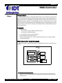
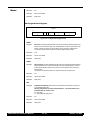
IDT™ Interprise™ 79RC32434
Integrated Communications
Processor
User Reference Manual
January 2005
2975 Stender Way, Santa Clara, California 95054
Telephone: (800) 345-7015 • TWX: 910-338-2070 • FAX: (408) 330-1748
Printed in U.S.A.
©2005 Integrated Device Technology, Inc.
GENERAL DISCLAIMER
Integrated Device Technology, Inc. reserves the right to make changes to its products or specifications at any time, without notice, in order to improve design or performance
and to supply the best possible product. IDT does not assume any responsibility for use of any circuitry described other than the circuitry embodied in an IDT product. The
Company makes no representations that circuitry described herein is free from patent infringement or other rights of third parties which may result from its use. No license is
granted by implication or otherwise under any patent, patent rights or other rights, of Integrated Device Technology, Inc.
CODE DISCLAIMER
Code examples provided by IDT are for illustrative purposes only and should not be relied upon for developing applications. Any use of the code examples below is completely
at your own risk. IDT MAKES NO REPRESENTATIONS OR WARRANTIES OF ANY KIND CONCERNING THE NONINFRINGEMENT, QUALITY, SAFETY OR SUITABILITY
OF THE CODE, EITHER EXPRESS OR IMPLIED, INCLUDING WITHOUT LIMITATION ANY IMPLIED WARRANTIES OF MERCHANTABILITY, FITNESS FOR A PARTICULAR PURPOSE, OR NON-INFRINGEMENT. FURTHER, IDT MAKES NO REPRESENTATIONS OR WARRANTIES AS TO THE TRUTH, ACCURACY OR COMPLETENESS
OF ANY STATEMENTS, INFORMATION OR MATERIALS CONCERNING CODE EXAMPLES CONTAINED IN ANY IDT PUBLICATION OR PUBLIC DISCLOSURE OR
THAT IS CONTAINED ON ANY IDT INTERNET SITE. IN NO EVENT WILL IDT BE LIABLE FOR ANY DIRECT, CONSEQUENTIAL, INCIDENTAL, INDIRECT, PUNITIVE OR
SPECIAL DAMAGES, HOWEVER THEY MAY ARISE, AND EVEN IF IDT HAS BEEN PREVIOUSLY ADVISED ABOUT THE POSSIBILITY OF SUCH DAMAGES. The code
examples also may be subject to United States export control laws and may be subject to the export or import laws of other countries and it is your responsibility to comply with
any applicable laws or regulations.
LIFE SUPPORT POLICY
Integrated Device Technology's products are not authorized for use as critical components in life support devices or systems unless a specific written agreement pertaining to
such intended use is executed between the manufacturer and an officer of IDT.
1. Life support devices or systems are devices or systems which (a) are intended for surgical implant into the body or (b) support or sustain life and whose failure to perform,
when properly used in accordance with instructions for use provided in the labeling, can be reasonably expected to result in a significant injury to the user.
2. A critical component is any components of a life support device or system whose failure to perform can be reasonably expected to cause the failure of the life support device
or system, or to affect its safety or effectiveness.
The IDT logo is a registered trademark of Integrated Device Technology, Inc. IDT, Interprise, RISController, RISCore, RC3041, RC3052, RC3081, RC32134, RC32332, RC32333, RC32334, RC32336, RC32355,
RC32351, RC32365, RC32434, RC32438, RC32364, RC36100, RC4700, RC4640, RC64145, RC4650, RC5000, RC64474, RC64475 are trademarks of Integrated Device Technology, Inc.
.
Powering What's Next and Enabling A Digitally Connected World are service marks of Integrated Device Technology, Inc. Q, QSI, SynchroSwitch and Turboclock are registered trademarks of Quality Semiconductor, a wholly-owned subsidiary of Integrated Device Technology, Inc.
About This Manual
Notes
Introduction
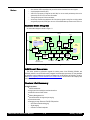
This user reference manual includes hardware and software information on the RC32434, a high performance integrated processor that combines a high performance 32-bit CPU core with system logic to
provide direct connection to boot memory, main memory, I/O, and PCI. It also includes on-chip peripherals
such as DMA channels, reset circuitry, interrupts, timers, and UARTs. Each chapter is designed to cover the
following topics:
High level feature summary of the specific module
Summary of the register set associates with a specific module
Outline of the operation of the module
Detailed register description.
Finding Additional Information
Information not included in this manual such as mechanicals, package pin-outs, and electrical characteristics can be found in the data sheet for this device, which is available from the IDT website (www.idt.com)
as well as through your local IDT sales representative.
Content Summary
Chapter 1, “RC32434 Device Overview,” provides a complete introduction to the performance capabilities of the RC32434. Included in this chapter is a summary of features for the device as well as a system
block diagram and internal register maps.
Chapter 2, “MIPS32 4Kc Processor Core,” provides basic information on the architecture and operation of the 4Kc™ processor core from MIPS® Technologies as it applies to the RC32434.
Chapter 3, “Clocking and Initialization,” discusses the reset initialization sequence required by the
RC32434 and provides information on boot vector settings and clock signals.
Chapter 4, “System Integrity Functions,” discusses system integrity functions, including the registers
that log system activity and that can be used to indicate the source of hardware or software errors.
Chapter 5, “Bus Arbitration,” describes the internal arbitration mechanism used among the various
on-chip modules. The chapter also describes the bus protocol used by an external bus master to gain
ownership of the memory and peripheral bus.
Chapter 6, “Device Controller,” describes the operation of the device controller, including registers
and device transactions, which provides a glueless interface to SRAMs, ROMs/PROMs/EEPROMs, dual
port memories, and other devices.
Chapter 7, “Double Data Rate (DDR) Controller,” describes the features, functions, and operation of
the DDR Controller, including a description of the registers.
Chapter 8, “Interrupt Controller,” provides information about the interrupt controller and interrupt
source descriptions.
Chapter 9, “DMA Controller,” describes the DMA controller, channels, descriptors, registers, transactions, and operations.
Chapter 10, “PCI Bus Interface,” describes the features, functions, and operations of the PCI bus
interface on the RC32434.
Chapter 11, “Ethernet Interfaces,” discusses the two Ethernet interfaces on the RC32434 which can
be used in applications such as SOHO routers or high speed modems for PCs.
79RC32434 User Reference Manual
i
January 12, 2005
IDT About This Manual
Notes
Documentation Conventions and Definitions
Chapter 12, “General Purpose I/O Controller,” describes this controller and how it is configured to
operate as a general purpose I/O or as an alternate function.
Chapter 13, “UART Controller,” provides information about the two separate UARTs within the
RC32434, including the UART registers.
Chapter 14, “Counter Timers,” describes the three general purpose 32-bit counter/timers on the
RC32434.
Chapter 15, “I2C Bus Interface,” describes the standard I2C bus interface, supporting both master and
slave operations, that is implemented on the RC32434.
Chapter 16, “Serial Peripheral Interface,” describes the SPI master interface which uses three signals
to connect to low-cost SPI peripherals and memory.
Chapter 17, “Non-Volatile RAM (NVRAM),” describes the design and operation of the NVRAM feature
and includes a reference to the Authorization Unit which prevents unauthorized software from running on
the system.
Chapter 18, “JTAG Boundary Scan,” discusses an enhanced JTAG interface, including a system logic
TAP controller, signal definitions, a test data register, an instruction register, and usage considerations.
Chapter 19, “EJTAG System,” describes the EJTAG’s features, its Debug Control Register, TAP registers, EJTAG Probe, hardware breakpoints, and other related topics.
Appendix A, “4Kc Processor Core Instructions,” contains additional information about the 4Kc
processor core instruction set.
Documentation Conventions and Definitions
Throughout this manual the following conventions and terms are used:
To avoid confusion when dealing with a mixture of “active-low” and “active-high” signals, the terms
assertion and negation are used. The term assert or assertion is used to indicate that a signal is
active or true, independent of whether that level is represented by a high or low voltage. The term
negate or negation is used to indicate that a signal is inactive or false.
To define the active polarity of a signal, a suffix will be used. Signals ending with an ‘N’ should be
interpreted as being active, or asserted, when at a logic zero (low) level. All other signals (including
clocks, buses and select lines) will be interpreted as being active, or asserted, when at a logic one
(high) level.
To define buses, the most significant bit (MSB) will be on the left and least significant bit (LSB) will
be on the right. No leading zeros will be included.
To represent numerical values, either decimal, binary, or hexadecimal formats will be used. The
binary format is as follows: 0bDDD, where “D” represents either 0 or 1; the hexadecimal format is
as follows: 0xDD, where “D” represents the hexadecimal digit(s); otherwise, it is decimal.
Unless otherwise denoted, a byte will refer to an 8-bit quantity. A halfword will refer to a 16-bit quantity. A triple-byte will refer to a 24-bit quantity. A word will refer to a 32-bit quantity, and a double or
double word will refer to a 64-bit quantity.
A bit is set when its value is 0b1. A bit is cleared when its value is 0b0.
The compressed notation ABC[x|y|z]D refers to ABCxD, ABCyD, and ABCzD.
The compressed notation ABC[x..y]D refers to ABCxD, ABC(x+1)D, ABC(x+2)D, ... ABCyD.
In words, bit 31 is always the most significant bit and bit 0 is the least significant bit. In halfwords, bit
15 is always the most significant bit and bit 0 is the least significant bit. In bytes, bit 7 is always the
most significant bit and bit 0 is the least significant bit.
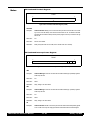
The ordering of bytes within words is referred to as either “big endian” or “little endian.” Big endian
systems label byte zero as the most significant (leftmost) byte of a word. Little endian systems label
byte zero as the least significant (rightmost) byte of a word.
79RC32434 User Reference Manual
ii
January 12, 2005
IDT About This Manual
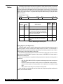
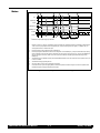
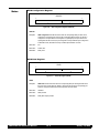
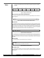
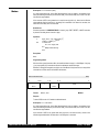
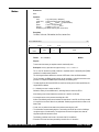
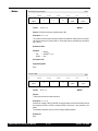
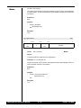
Signal Terminology
Notes
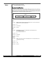
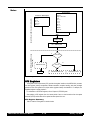
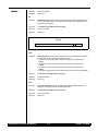
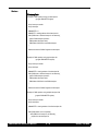
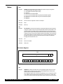
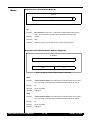
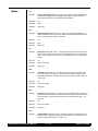
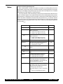
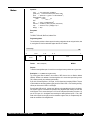
bit 31
0
bit 0
1
2
3
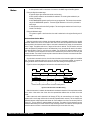
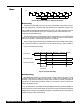
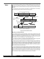
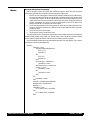
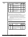
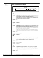
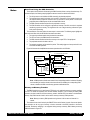
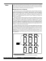
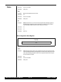
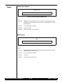
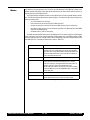
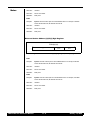
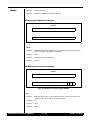
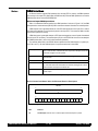
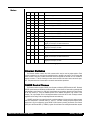
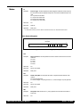
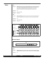
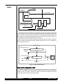
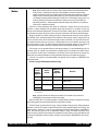
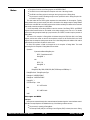
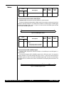
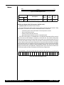
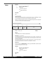
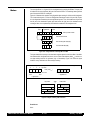
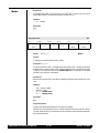
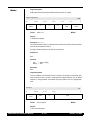
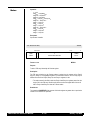
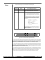
Address of Bytes within Words: Big Endian
bit 31
3
bit 0
2
1
0
Address of Bytes within Words: Little Endian
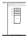
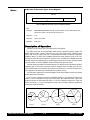
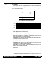
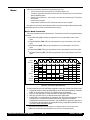
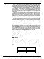
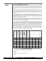
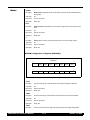
Figure 1 Example of Byte Ordering for “Big Endian” or “Little Endian” System Definition
A read-only: register, bit, or field is one which can be read but not modified
A sticky bit is a bit that remains set after being set by hardware until a zero is written to it. Writing a
one to a sticky has no effect on its value.
A zero field in a register, denoted as “0” in register figures, must be written with a value of zero and
returns a value of zero when read.
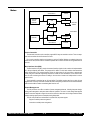
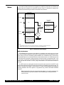
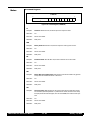
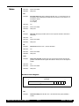
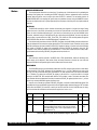
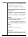
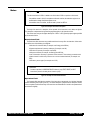
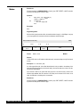
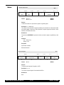
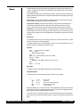
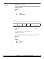
Signal Terminology
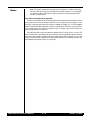
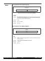
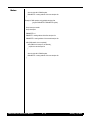
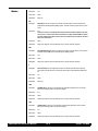
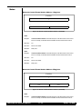
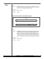
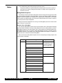
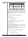
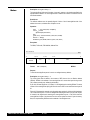
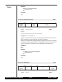
Throughout this manual, when describing signal transitions, the following terminology is used:
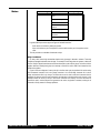
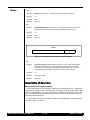
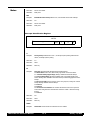
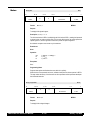
Rising edge indicates a low-to-high (0 to 1) transition.
Falling edge indicates a high-to-low (1 to 0) transition.
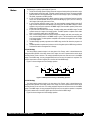
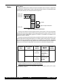
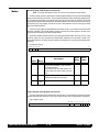
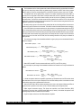
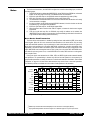
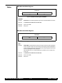
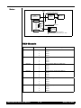
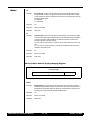
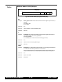
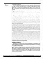
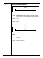
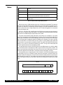
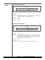
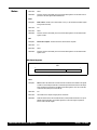
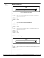
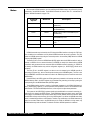
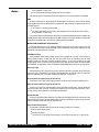
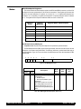
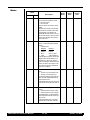
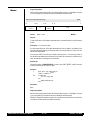
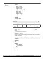
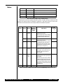
These terms are illustrated in Figure 2.
single clock cycle
1
2
high-to-low
transition
3
4
low-to-high
transition
Figure 2 Signal Transitions
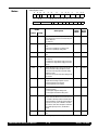
Revision History
November 6, 2003: Initial publication.
January 15, 2004: In Chapters 1 and 5, changed name of PMBus Arbiter Sneak Access Control
Register to PMBus Arbiter Park Control Register. Also in Chapter 5, removed all reference to Sneak Access
functions.
January 26, 2004: In Chapter 11, changed the LPE bit description in Ethernet MAC Configuration
Register #2. In Table 3.3, changed BCV labels to MADDR.
March 26, 2004: In Chapter 1, Page 1-5, changed DEVTYPE in IMP field to 0x1. In Chapter 2: changed
reset state to zero for RP field in Table 2.39 deleted references to RP field throughout chapter; and deleted
Register Controlled Power Management section on page 2-84.
April 20, 2004: Added new I2C chapter, Chapter 15, and re-numbered the remaining chapters.
79RC32434 User Reference Manual
iii
January 12, 2005
IDT About This Manual
Notes
Revision History
January 12, 2005: Revised page 1-5, Table 18.3, Figure 19.28, and Table 19.44 to reflect addition of
part number 0x217 which includes the I2C feature.
79RC32434 User Reference Manual
iv
January 12, 2005
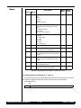
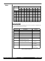
Table of Contents
Notes
1 RC32434 Device Overview
Introduction ..................................................................................................................................1-1
Key Features ...............................................................................................................................1-1
System Block Diagram ................................................................................................................1-2
Additional Resources...................................................................................................................1-2
Feature List Summary .................................................................................................................1-2
System Identification....................................................................................................................1-5
Logic Diagram — RC32434.........................................................................................................1-6
Pin Characteristics.......................................................................................................................1-7
Pin Description.............................................................................................................................1-9
Default Memory Map .................................................................................................................1-16
RC32434 Internal Register Map ................................................................................................1-17
2 MIPS32 4Kc Processor Core
Introduction ..................................................................................................................................2-1
Functional Overview ...................................................................................................................2-1
Features.......................................................................................................................................2-1
Functional Overview ....................................................................................................................2-3
Blocks.................................................................................................................................2-3
Pipeline Description .....................................................................................................................2-6
Instruction Cache Miss .......................................................................................................2-8
Multiply/Divide Operations..................................................................................................2-9
MDU Pipeline .....................................................................................................................2-9
Branch Delay....................................................................................................................2-14
Data Bypassing ................................................................................................................2-14
Interlock Handling.............................................................................................................2-16
Slip Conditions .................................................................................................................2-17
Instruction Interlocks ........................................................................................................2-18
Instruction Hazards ..........................................................................................................2-19
Memory Management................................................................................................................2-20
Modes of Operation..........................................................................................................2-21
Translation Lookaside Buffer............................................................................................2-27
Virtual to Physical Address Translation ............................................................................2-31
System Control Coprocessor ...........................................................................................2-35
Exceptions .................................................................................................................................2-35
Exception Conditions........................................................................................................2-35
Exception Priority .............................................................................................................2-35
Exception Vector Locations ..............................................................................................2-36
General Exception Processing.........................................................................................2-38
Debug Exception Processing ...........................................................................................2-39
Exceptions........................................................................................................................2-39
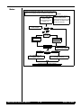
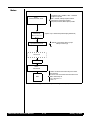
Exception Handling and Servicing Flowcharts .................................................................2-49
79RC32434 User Reference Manual
v
January 12, 2005
IDT Table of Contents
Notes
CP0 Registers............................................................................................................................2-54
CP0 Register Summary ...................................................................................................2-54
CP0 Registers ..................................................................................................................2-56
Hardware and Software Initialization .........................................................................................2-80
Hardware Initialized Processor State ...............................................................................2-81
Software Initialized Processor State ................................................................................2-81
Caches.......................................................................................................................................2-82
Cache Protocols...............................................................................................................2-83
Instruction Cache .............................................................................................................2-84
Data Cache ......................................................................................................................2-84
Memory Coherence Issues ..............................................................................................2-84
Power Management...................................................................................................................2-84
Instruction-Controlled Power Management......................................................................2-84
Instruction Set............................................................................................................................2-85
Load and Store Instructions .............................................................................................2-85
Computational Instructions...............................................................................................2-86
Control Instructions ..........................................................................................................2-87
Coprocessor Instructions .................................................................................................2-87
Enhancements to the MIPS Architecture .........................................................................2-87
Processor Core Instructions ......................................................................................................2-88
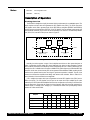
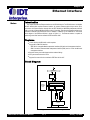
3 Clocking and Initialization
Introduction ..................................................................................................................................3-1
Block Diagram .............................................................................................................................3-1
Reset Register Description ..........................................................................................................3-2
Reset/Initialization Registers .......................................................................................................3-2
Reset Register ...................................................................................................................3-2
Boot Configuration Vector Register....................................................................................3-2
Description of Operation..............................................................................................................3-3
Clocking Overview .............................................................................................................3-3
Boot Configuration Vector ..................................................................................................3-4
Reset and Initialization .......................................................................................................3-6
4 System Integrity Functions
Introduction ..................................................................................................................................4-1
Features.......................................................................................................................................4-1
Functional Overview ....................................................................................................................4-1
System Integrity Register Description.......................................................................................... 4-1
System Integrity Registers...........................................................................................................4-2
Error Control and Status Register ......................................................................................4-2
CPU Error Address Register ..............................................................................................4-5
Description of Operation ..............................................................................................................4-6
Address Space Monitor ......................................................................................................4-6
Watchdog Timer ................................................................................................................. 4-7
IPBus Slave Acknowledge Errors ......................................................................................4-8
79RC32434 User Reference Manual
vi
January 12, 2005
IDT Table of Contents
Notes
5 Bus Arbitration
Introduction ..................................................................................................................................5-1
Functional Overview ....................................................................................................................5-1
IPBus Register Description..........................................................................................................5-1
IPBus Registers ...........................................................................................................................5-2
IPBus Arbiter Control Register ...........................................................................................5-2
IPBus Arbiter Priority Configuration Register .....................................................................5-3
IPBus Arbiter Bus Master Configuration Register ..............................................................5-4
IPBus Idle Transaction Cycle Count Register ....................................................................5-5
Description of Operation ..............................................................................................................5-5
Example IPBus Arbiter Configurations...............................................................................5-8
PMBus Arbitration......................................................................................................................5-12
IPBus Idle.........................................................................................................................5-12
IPBus Active.....................................................................................................................5-12
Bus Parking......................................................................................................................5-12
PMBus Registers .......................................................................................................................5-12
PMBus Arbitration Register Description...........................................................................5-12
PMBus Arbiter Processor Priority Register ......................................................................5-13
PMBus Arbiter Park Control Register...............................................................................5-13
6 Device Controller
Introduction ..................................................................................................................................6-1
Features.......................................................................................................................................6-1
Device Controller Register Description........................................................................................6-1
Device Controller Registers .........................................................................................................6-2
Device [0..3] Base Register................................................................................................6-2
Device [0..3] Mask Register ...............................................................................................6-3
Device [0..3] Control Register ............................................................................................6-3
Device [0..3] Timing Control Register.................................................................................6-6
Bus Transaction Timer Control and Status Register ..........................................................6-7
Bus Transaction Timer Compare Register .........................................................................6-8
Bus Transaction Timer Address Register...........................................................................6-8
Device Decoupled Access Control and Status Register ....................................................6-9
Device Decoupled Access Address Register...................................................................6-10
Device Decoupled Access Data Register.........................................................................6-10
Description of Operation ............................................................................................................ 6-11
Memory And Peripheral Bus Transaction Timer...............................................................6-12
Device Read Transaction .................................................................................................6-13
Burst Device Read Transaction........................................................................................6-15
Device Write Transaction .................................................................................................6-16
Burst Device Write Transaction........................................................................................6-18
Decoupled CPU Device Transactions ..............................................................................6-19
7 DDR Controller
Introduction ..................................................................................................................................7-1
Features.......................................................................................................................................7-1
Additional Resources...................................................................................................................7-1
DDR Controller Register Description ...........................................................................................7-1
79RC32434 User Reference Manual
vii
January 12, 2005
IDT Table of Contents
Notes
DDR Registers.............................................................................................................................7-2
DDR Control Register ........................................................................................................7-2
DDR Base Register ............................................................................................................7-6
DDR Mask Register ...........................................................................................................7-6
DDR Alternate Base Register ............................................................................................7-7
DDR Alternate Mask Register ............................................................................................7-7
DDR Alternate Mapping Register.......................................................................................7-8
DDR Custom Transaction Register ....................................................................................7-8
Refresh Timer Count Register............................................................................................7-9
Refresh Timer Compare Register ....................................................................................7-10
Refresh Timer Control Register........................................................................................7-10
Description of Operation ............................................................................................................ 7-11
DDR Address Multiplexing Scheme .................................................................................7-12
DDR Command Encoding................................................................................................7-13
DDR Read Data Capture Register ...................................................................................7-13
DDR Address Mapping ....................................................................................................7-14
DDR Initialization..............................................................................................................7-15
DDR Refresh Timer..........................................................................................................7-16
DDR Read Transaction ....................................................................................................7-16
DDR Write Transaction ....................................................................................................7-18
DDR Refresh Transaction ................................................................................................7-19
DDR Custom Transaction ................................................................................................7-20
Example of DDR SDRAM Initialization ......................................................................................7-22
8 Interrupt Controller
Introduction ..................................................................................................................................8-1
Features.......................................................................................................................................8-1
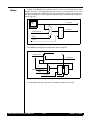
Block Diagram .............................................................................................................................8-2
Interrupt Controller Register Description .....................................................................................8-2
Interrupt Controller Registers.......................................................................................................8-3
Interrupt Pending [2..6] Register ........................................................................................8-3
Interrupt Test [2..6] Register ...............................................................................................8-3
Interrupt Mask [2..6] Register .............................................................................................8-4
Non-Maskable Interrupt Pin Status Register......................................................................8-4
Interrupt Status Description .........................................................................................................8-5
Non-Maskable Interrupts .............................................................................................................8-6
9 DMA Controller
Introduction ..................................................................................................................................9-1
Features.......................................................................................................................................9-1
DMA Controller Block Diagram....................................................................................................9-1
DMA Controller Register Description...........................................................................................9-2
DMA Controller Registers ............................................................................................................9-3
DMA [0..5] Control Register ...............................................................................................9-3
DMA [0..5] Status Register.................................................................................................9-4
DMA [0..5] Status Mask Register .......................................................................................9-5
DMA [0..5] Descriptor Pointer Register ..............................................................................9-6
DMA [0..5] Next Descriptor Pointer Register......................................................................9-6
79RC32434 User Reference Manual
viii
January 12, 2005
IDT Table of Contents
Notes
Device Command Field......................................................................................................9-7
Data Flow Within the RC32434 ...................................................................................................9-7
The IPBus™.......................................................................................................................9-7
4Kc Core as Bus Master ....................................................................................................9-8
DMA Controller...................................................................................................................9-8
No Alignment Restrictions..................................................................................................9-8
Data Flow Using the DMA Controller .................................................................................9-9
Memory-to-Memory Transfer..............................................................................................9-9
DMA Channels...........................................................................................................................9-10
Internal DMA Operations ........................................................................................................... 9-11
DMA Registers .................................................................................................................9-12
DMA Stopping Conditions ................................................................................................9-13
DMA Descriptor Lists and Chaining .................................................................................9-14
Memory to Memory DMA Operations ........................................................................................9-15
Examples ...................................................................................................................................9-16
10 PCI Bus Interface
Introduction ................................................................................................................................10-1
Features.....................................................................................................................................10-1
PCI Register Description ...........................................................................................................10-2
PCI Bus Registers .....................................................................................................................10-3
PCI Control Register ........................................................................................................10-3
PCI Status Register..........................................................................................................10-5
PCI Status Mask Register ................................................................................................10-9
PCI Configuration Address Register ..............................................................................10-12
PCI Configuration Data Register....................................................................................10-13
PCI Local Base Address [0|1|2|3] Register ....................................................................10-14
PCI Local Base Address [0|1|2|3] Control......................................................................10-14
PCI Local Base Address [0|1|2|3] Mapping Register .....................................................10-15
PCI Decoupled Access Control Register........................................................................10-16
PCI Decoupled Access Status Register.........................................................................10-16
PCI Decoupled Access Status Mask Register ...............................................................10-17
PCI Decoupled Access Data Register............................................................................10-19
PCI DMA Channel 4 Configuration Register ..................................................................10-19
PCI DMA Channel 5 Configuration Register ..................................................................10-20
PCI Target Control Register ...........................................................................................10-21
PCI Inbound Message [0|1] Register .............................................................................10-22
PCI Outbound Message [0|1] Register...........................................................................10-22
PCI Inbound Doorbell Register ......................................................................................10-23
PCI Inbound Interrupt Cause Register ...........................................................................10-23
PCI Inbound Interrupt Mask Register.............................................................................10-24
PCI Outbound Doorbell Register....................................................................................10-25
PCI Outbound Interrupt Cause Register ........................................................................10-25
PCI Outbound Interrupt Mask Register ..........................................................................10-26
Vendor ID Register .........................................................................................................10-27
Device ID Register .........................................................................................................10-27
Command Register ........................................................................................................10-28
Status Register...............................................................................................................10-29
Device Revision ID Register...........................................................................................10-31
79RC32434 User Reference Manual
ix
January 12, 2005
IDT Table of Contents
Notes
Class Code Register ......................................................................................................10-31
Cache Line Size Register...............................................................................................10-32
Master Latency Register ................................................................................................10-32
Header Type Register ....................................................................................................10-33
BIST Register.................................................................................................................10-33
PCI Base Address [0|1|2|3] Register..............................................................................10-34
Subsystem Vendor ID ....................................................................................................10-35
Subsystem ID Register ..................................................................................................10-35
Interrupt Line Register....................................................................................................10-35
Interrupt Pin Register .....................................................................................................10-36
Minimum Grant Register ................................................................................................10-36
Maximum Latency Register............................................................................................10-37
Target Ready Time-out Register ....................................................................................10-37
Retry Limit Register........................................................................................................10-38
PCI Base Address [0|1|2|3] Control ...............................................................................10-38
PCI Base Address [0|1|2|3] Mapping Register...............................................................10-40
PCI Management Register .............................................................................................10-41
Description of Operation ..........................................................................................................10-41
Use of Decoupled PCI Transactions ..............................................................................10-41
IPBus Access .................................................................................................................10-42
Reset..............................................................................................................................10-43
Disabled Mode ...............................................................................................................10-43
PCI Host Mode...............................................................................................................10-43
PCI Satellite Mode .........................................................................................................10-45
PCI Transactions............................................................................................................10-46
Endianness and PCI Swapping......................................................................................10-47
PCI Master .....................................................................................................................10-47
Decoupled PCI Master Transactions..............................................................................10-51
PCI Master—PCI to Memory DMA (DMA Channel 4) ....................................................10-51
PCI Master — Memory to PCI DMA (DMA Channel 5) ..................................................10-54
PCI Target ......................................................................................................................10-56
Transaction Ordering......................................................................................................10-59
PCI Messaging Unit .......................................................................................................10-60
PCI Configuration Registers...........................................................................................10-60
11 Ethernet Interface
Introduction ................................................................................................................................ 11-1
Features..................................................................................................................................... 11-1
Block Diagram ........................................................................................................................... 11-1
Ethernet Register Description.................................................................................................... 11-2
Ethernet Interface Registers ...................................................................................................... 11-3
Ethernet Interface Control Register.................................................................................. 11-3
Ethernet FIFO Transmit Threshold Register .................................................................... 11-5
Ethernet Address Recognition Control Register............................................................... 11-6
Ethernet Hash Table Register .......................................................................................... 11-7
Ethernet Station Address [0|1|2|3] Low Register ............................................................. 11-7
Ethernet Station Address [0|1|2|3] High Register............................................................. 11-8
Ethernet Receive Byte Count Register ............................................................................ 11-9
Ethernet Receive Packet Count Register......................................................................... 11-9
Ethernet Receive Undersized Packet Count Register.................................................... 11-10
79RC32434 User Reference Manual
x
January 12, 2005
IDT Table of Contents
Notes
Ethernet Receive Fragment Count Register .................................................................. 11-10
Ethernet Transmit Byte Count Register.......................................................................... 11-11
Ethernet Generate Pause Frame Register..................................................................... 11-11
Ethernet Pause Frame Status Register ......................................................................... 11-12
Ethernet Control Frame Station Address 0 Register ...................................................... 11-12
Ethernet Control Frame Station Address 1 Register ...................................................... 11-13
Ethernet Control Frame Station Address 2 Register ...................................................... 11-13
Ethernet MAC Configuration Register #1....................................................................... 11-14
Ethernet MAC Configuration Register #2....................................................................... 11-15
Ethernet Back-to-Back Inter-Packet Gap Register......................................................... 11-18
Ethernet Non Back-to-Back Inter-Packet Gap Register ................................................. 11-19
Ethernet Collision Window and Retry Register .............................................................. 11-19
Ethernet Maximum Frame Length Register ................................................................... 11-20
Ethernet MAC Test Register........................................................................................... 11-21
MII Management Configuration Register........................................................................ 11-21
MII Management Command Register ............................................................................ 11-22
MII Management Address Register................................................................................ 11-23
MII Management Write Data Register ............................................................................ 11-23
MII Management Read Data Register............................................................................ 11-24
MII Management Indicators Register ............................................................................. 11-24
Description of Operation .......................................................................................................... 11-25
Ethernet Physical Layer Interface .................................................................................. 11-25
Input and Output FIFOs ................................................................................................. 11-26
Address Recognition Logic ............................................................................................ 11-27
DMA Interface.......................................................................................................................... 11-30
Ethernet Input DMA Operations ..................................................................................... 11-30
Ethernet Output DMA Operations .................................................................................. 11-31
Ethernet Statistics.................................................................................................................... 11-34
PAUSE Control Frames ........................................................................................................... 11-34
Ethernet MII Management Interface ........................................................................................ 11-35
Ethernet Clock Prescalar ......................................................................................................... 11-36
Programming Example ............................................................................................................ 11-36
12 General Purpose I/O Controller
Introduction ................................................................................................................................12-1
General Purpose I/O Register Description ................................................................................12-1
General Purpose I/O Registers..................................................................................................12-1
GPIO Function Register ...................................................................................................12-1
GPIO Configuration Register ...........................................................................................12-2
GPIO Data Register .........................................................................................................12-2
GPIO Interrupt Level Register..........................................................................................12-3
GPIO Interrupt Status Register ........................................................................................12-3
GPIO Non-maskable Interrupt Enable Register ...............................................................12-4
Functional Overview ..................................................................................................................12-4
Description of Operation ............................................................................................................12-5
GPIO Pin Configured As Input .........................................................................................12-5
GPIO Pin Configured As Output ......................................................................................12-5
GPIO Pin Configured As an Alternate Function ...............................................................12-5
GPIO Pins As Interrupt Sources ......................................................................................12-6
79RC32434 User Reference Manual
xi
January 12, 2005
IDT Table of Contents
Notes
GPIO Pins As Non-maskable Interrupt Sources ..............................................................12-6
13 UART Controller
Introduction ................................................................................................................................13-1
Features.....................................................................................................................................13-1
UART Register Description........................................................................................................13-1
UART Registers.........................................................................................................................13-2
Receive Buffer Register ...................................................................................................13-2
Transmit Holding Register................................................................................................13-3
Interrupt Enable Register .................................................................................................13-3
Interrupt Identification Register ........................................................................................13-4
FIFO Control Register ......................................................................................................13-5
Line Control Register .......................................................................................................13-6
Modem Control Register ..................................................................................................13-7
Line Status Register .........................................................................................................13-9
Modem Status Register..................................................................................................13-10
Scratch Register.............................................................................................................13-12
Reset Register ...............................................................................................................13-12
Divisor Latch Low Register ............................................................................................13-13
Divisor Latch High Register............................................................................................13-13
Description of Operation ..........................................................................................................13-13
Overview ........................................................................................................................13-13
Baud Rate Selection ......................................................................................................13-14
UART Interrupts .............................................................................................................13-15
UART Channel Reset.....................................................................................................13-15
14 Counter/Timers
Functional Overview ..................................................................................................................14-1
Features.....................................................................................................................................14-1
Counter/Timers Register Description.........................................................................................14-1
Counter/Timers Registers..........................................................................................................14-2
Counter Timer [0|1|2] Count Register...............................................................................14-2
Counter Timer [0|1|2] Compare Register .........................................................................14-2
Counter Timer [0|1|2] Control Register.............................................................................14-3
Counter Timer [0|1|2] Clock Select Register ....................................................................14-3
Theory of Operation...................................................................................................................14-4
15 I2C Bus Interface
Introduction ................................................................................................................................15-1
Features.....................................................................................................................................15-1
Block Diagram ...........................................................................................................................15-1
Functional Overview and Theory of Operation ..........................................................................15-1
I2C Register Description............................................................................................................15-2
I2C Bus Control Register ..................................................................................................15-3
I2C Bus Data Input Register ............................................................................................15-4
I2C Bus Data Output Register..........................................................................................15-4
I2C Bus Clock Prescalar............................................................................................................15-4
79RC32434 User Reference Manual
xii
January 12, 2005
IDT Table of Contents
Notes
I2C Bus Master Interface ...........................................................................................................15-5
Example I2C Bus Transactions ........................................................................................15-7
I2C Bus Master Command Register...............................................................................15-10
I2C Bus Master Status Register.....................................................................................15-10
I2C Bus Master Status Mask Register ........................................................................... 15-11
I2C Bus Slave Interface ...........................................................................................................15-12
Example of I2C Bus Transaction....................................................................................15-12
I2C Bus Slave Status Register.......................................................................................15-14
I2C Bus Slave Status Mask Register .............................................................................15-16
I2C Bus Slave Address Register....................................................................................15-17
I2C Bus Slave Acknowledge Register............................................................................15-18
Programming Example ............................................................................................................15-18
16 Serial Peripheral Interface
Introduction ................................................................................................................................16-1
Block Diagram ...........................................................................................................................16-1
SPI Register Description............................................................................................................16-2
SPI Registers.............................................................................................................................16-2
SPI Clock Prescalar Register ...........................................................................................16-2
SPI Control Register ........................................................................................................16-3
SPI Status Register ..........................................................................................................16-4
SPI Data Register ............................................................................................................16-5
Serial I/O Function Register .............................................................................................16-6
Serial I/O Configuration Register .....................................................................................16-7
Serial I/O Data Register ...................................................................................................16-8
Description of Operation ............................................................................................................16-9
SPI Setup .........................................................................................................................16-9
Serial Bit I/O Pins .............................................................................................................16-9
PCI Serial EEPROM Mode (Microwire)..........................................................................16-10
SPI Interface Mode ........................................................................................................ 16-11
SPI Clock Prescalar ....................................................................................................... 16-11
Master Programming Example ................................................................................................ 16-11
SPI Initialization.............................................................................................................. 16-11
17 Non-Volatile RAM (NVRAM)
Introduction ................................................................................................................................17-1
Block Diagram ...........................................................................................................................17-1
Reset Register Description ........................................................................................................17-2
NVRAM Registers......................................................................................................................17-2
NVRAM Status Register...................................................................................................17-3
NVRAM Status Mask Register .........................................................................................17-3
NVRAM Configuration 0 Register.....................................................................................17-4
NVRAM Configuration 1 Register (NVRCFG1) ................................................................17-5
Description of Operation ............................................................................................................17-7
NVRAM Interfaces and Organization.........................................................................................17-9
Reset Operation .............................................................................................................17-10
NVRAM IPBus Interface.................................................................................................17-10
NVRAM JTAG Interface ................................................................................................17-10
79RC32434 User Reference Manual
xiii
January 12, 2005
IDT Table of Contents
Notes
NVRAM Commands ................................................................................................................17-13
Authorization Unit ....................................................................................................................17-14
18 JTAG Boundary Scan
Introduction ................................................................................................................................18-1
System Logic TAP Controller Overview.....................................................................................18-2
Signal Definitions .......................................................................................................................18-2
Test Data Register (DR).............................................................................................................18-3
Boundary Scan Registers ................................................................................................18-3
Instruction Register (IR).............................................................................................................18-5
EXTEST ...........................................................................................................................18-6
SAMPLE/PRELOAD ........................................................................................................18-7
BYPASS ...........................................................................................................................18-7
CLAMP.............................................................................................................................18-7
DEVICEID ........................................................................................................................18-7
VALIDATE ........................................................................................................................18-8
RESERVED......................................................................................................................18-8
UNUSED ..........................................................................................................................18-8
Usage Considerations ...............................................................................................................18-8
19 EJTAG System
Introduction ................................................................................................................................19-1
Functional Description ...............................................................................................................19-1
EJTAG Components.........................................................................................................19-2
Register and Memory Map Overview...............................................................................19-3
Pin Description...........................................................................................................................19-6
EJTAG Processor Core Extensions...........................................................................................19-6
Overview ..........................................................................................................................19-6
Debug Mode Execution....................................................................................................19-7
Debug Exceptions ..........................................................................................................19-13
Debug Mode Exceptions ................................................................................................19-19
Interrupts and NMIs........................................................................................................19-21
Reset and Soft Reset of Processor................................................................................19-22
EJTAG Instructions.........................................................................................................19-23
EJTAG Coprocessor 0 Registers ...................................................................................19-24
Debug Control Register ...........................................................................................................19-30
Hardware Breakpoints .............................................................................................................19-32
Instruction Breakpoint Features .....................................................................................19-32
Data Breakpoint Features ..............................................................................................19-33
Overview of Instruction and Data Breakpoint Registers.................................................19-33
Conditions for Matching Breakpoints .............................................................................19-35
Debug Exceptions from Breakpoints..............................................................................19-40
Breakpoints Used as Triggerpoints ................................................................................19-42
Instruction Breakpoint Registers ....................................................................................19-43
Data Breakpoint Registers .............................................................................................19-47
Recommendations for Implementing Hardware Breakpoints.........................................19-51
Breakpoint Examples .....................................................................................................19-52
EJTAG Test Access Port..........................................................................................................19-54
79RC32434 User Reference Manual
xiv
January 12, 2005
IDT Table of Contents
Notes
TAP Signals....................................................................................................................19-55
TAP Controller ................................................................................................................19-56
Instruction Register and Special Instructions .................................................................19-58
TAP Data Registers........................................................................................................19-59
Examples of Use ............................................................................................................19-68
Probe Interfaces ......................................................................................................................19-72
Mechanical Connector ...................................................................................................19-72
Target System PCB Design............................................................................................19-73
Using the EJTAG Probe .................................................................................................19-74
Probe Requirements and Recommendations ................................................................19-75
Connecting Multiple EJTAG Controllers .........................................................................19-76
Connecting EJTAG and JTAG Controllers .....................................................................19-76
Appendix A 4Kc Processor Core Instructions
Introduction ................................................................................................................................. A-1
Understanding the Instruction Set .............................................................................................. A-1
Instruction Fields ............................................................................................................... A-2
Instruction Descriptive Name and Mnemonic.................................................................... A-3
Format Field ...................................................................................................................... A-3
Purpose Field .................................................................................................................... A-3
Description Field ............................................................................................................... A-3
Restrictions Field............................................................................................................... A-4
Operation Field.................................................................................................................. A-4
Exceptions Field................................................................................................................ A-5
Programming Notes and Implementation Notes Fields..................................................... A-5
Operation Section Notation and Functions ................................................................................. A-5
Instruction Execution Ordering.......................................................................................... A-5
Special Symbols in Pseudocode Notation ........................................................................ A-6
Pseudocode Functions...................................................................................................... A-7
Op and Function Subfield Notation ..................................................................................A-11
CPU Opcode Map......................................................................................................................A-11
Instruction Set........................................................................................................................... A-13
79RC32434 User Reference Manual
xv
January 12, 2005
IDT Table of Contents
Notes
79RC32434 User Reference Manual
xvi
January 12, 2005
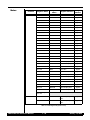
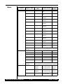
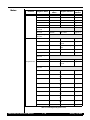
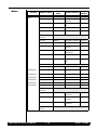
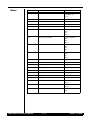
List of Tables
Notes
Table 1.1
Table 1.2
Table 1.3
Table 1.4
Table 2.1
Table 2.2
Table 2.3
Table 2.4
Table 2.5
Table 2.6
Table 2.7
Table 2.8
Table 2.9
Table 2.10
Table 2.11
Table 2.12
Table 2.13
Table 2.14
Table 2.15
Table 2.16
Table 2.17
Table 2.18
Table 2.19
Table 2.20
Table 2.21
Table 2.22
Table 2.23
Table 2.24
Table 2.25
Table 2.26
Table 2.27
Table 2.28
Table 2.29
Table 2.30
Table 2.31
Table 2.32
Table 2.33
Table 2.34
Table 2.35
Table 2.36
Table 2.37
Table 2.38
Table 2.39
Table 2.40
Table 2.41
Table 2.42
Table 2.43
Table 2.44
Table 2.45
Pin Characteristics............................................................................................................1-7
Pin Description..................................................................................................................1-9
RC32434 Default Memory Map Following a Cold Reset ................................................1-16
Internal Register Map .....................................................................................................1-17
4Kc Core Instruction Latencies.......................................................................................2-10
4Kc Core Instruction Repeat Rates ................................................................................ 2-11
Pipeline Interlocks...........................................................................................................2-16
Instruction Interlocks.......................................................................................................2-18
Instruction Hazards.........................................................................................................2-19
User Mode Segments .....................................................................................................2-23
Kernel Mode Segments ..................................................................................................2-25
Physical Address and Cache Attributes for dseg, dmseg, and drseg Address Spaces..2-26
CPU Access to drseg Address Range............................................................................2-27
CPU Access to dmseg Address Range ..........................................................................2-27
TLB Tag Entry Fields ......................................................................................................2-29
TLB Data Entry Fields.....................................................................................................2-30
TLB Instructions..............................................................................................................2-35
Priority of Exceptions ......................................................................................................2-36
Exception Vector Base Addresses..................................................................................2-37
Exception Vector Offsets ................................................................................................2-37
Exception Vectors ...........................................................................................................2-37
Debug Exception Vector Addresses ...............................................................................2-39
Register States an Interrupt Exception ...........................................................................2-43
Register States on a Watch Exception ...........................................................................2-44
CP0 Register States on an Address Exception Error .....................................................2-45
CP0 Register States on a TLB Refill Exception..............................................................2-45
CP0 Register States on a TLB Invalid Exception ...........................................................2-46
Register States on a TLB Modified Exception ................................................................2-49
CP0 Registers.................................................................................................................2-55
CP0 Register Field Types ...............................................................................................2-56
Index Register Field Descriptions ...................................................................................2-57
Random Register Field Descriptions ..............................................................................2-57
EntryLo0, EntryLo1 Register Field Descriptions .............................................................2-58
Cache Coherency Attributes...........................................................................................2-59
Context Register Field Descriptions ...............................................................................2-59
PageMask Register Field Descriptions...........................................................................2-60
Values for the Mask Field of the PageMask Register .....................................................2-60
Wired Register Field Descriptions ..................................................................................2-61
BadVAddr Register Field Descriptions............................................................................2-62
Count Register Field Descriptions ..................................................................................2-62
EntryHi Register Field Descriptions ................................................................................2-63
Compare Register Field Description...............................................................................2-63
Status Register Field Description ...................................................................................2-64
Cause Register Field Descriptions .................................................................................2-67
Cause Register ExcCode Field Descriptions..................................................................2-68
EPC Register Field Description ......................................................................................2-69
PRId Register Field Descriptions....................................................................................2-69
Config Register Field Descriptions .................................................................................2-70
Cache Coherency Attributes...........................................................................................2-71
79RC32434 User Reference Manual
xvii
January 12, 2005
IDT List of Tables
Notes
Table 2.46
Table 2.47
Table 2.48
Table 2.49
Table 2.50
Table 2.51
Table 2.52
Table 2.53
Table 2.54
Table 2.55
Table 2.56
Table 2.57
Table 2.58
Table 3.1
Table 3.2
Table 3.3
Table 3.4
Table 4.1
Table 4.2
Table 4.3
Table 5.1
Table 5.2
Table 5.3
Table 6.1
Table 6.2
Table 7.1
Table 7.2
Table 7.3
Table 7.4
Table 8.1
Table 8.2
Table 8.3
Table 8.4
Table 8.5
Table 9.1
Table 9.2
Table 9.3
Table 9.4
Table 10.1
Table 10.2
Table 10.3
Table 10.4
Table 10.5
Table 10.6
Table 10.7
Table 10.8
Table 10.9
Table 10.10
Table 11.1
Table 11.2
Table 11.3
Table 11.4
Table 11.5
Table 12.1
Table 12.2
Config1 Register Field Descriptions — Select 1.............................................................2-71
LLAddr Register Field Descriptions ................................................................................2-73
WatchLo Register Field Descriptions..............................................................................2-73
WatchHi Register Field Descriptions ..............................................................................2-74
Debug Register Field Descriptions .................................................................................2-75
DEPC Register Field Description....................................................................................2-77
ErrCtl Register Field Descriptions...................................................................................2-78
TagLo Register Field Descriptions..................................................................................2-79
DataLo Register Field Descriptions ................................................................................2-79
ErrorEPC Register Field Descriptions ............................................................................2-80
DeSave Register Field Descriptions...............................................................................2-80
Instruction and Data Cache Attributes............................................................................2-82
Byte Access within a Word .............................................................................................2-86
Reset Register Map..........................................................................................................3-2
Processor Clock PLL Multiplier Modes.............................................................................3-3
Boot Configuration Encoding............................................................................................3-5
Pin States During Reset .................................................................................................3-10
System Integrity Register Map..........................................................................................4-1
Address Space Monitor Undecoded Address Error Reporting .........................................4-6
IPBus Slave Acknowledge Error Reporting ......................................................................4-8
Bus Master Index..............................................................................................................5-1
IPBus Arbitration Register Map ........................................................................................5-1
PMBus Arbitration Register Map ....................................................................................5-12
Device Controller Register Map........................................................................................6-1
Default Values for Device Configuration Registers.........................................................6-12
DDR Controller Register Map...........................................................................................7-1
Supported DDR Configurations ...................................................................................... 7-11
DDR Address Multiplexing..............................................................................................7-12
DDR Command Encoding ..............................................................................................7-13
Interrupt Controller Register Map ..................................................................................... 8-2
IPEND2 Interrupt Source Description...............................................................................8-5
IPEND3 Interrupt Source Description...............................................................................8-5
IPEND5 Interrupt Source Description...............................................................................8-5
IPEND6 Interrupt Source Description...............................................................................8-6
DMA Register Map ...........................................................................................................9-2
DMA Channels and Device Selects................................................................................9-10
Memory to DMA FIFO DMA Operations.........................................................................9-15
DMA FIFO to Memory DMA Operations.........................................................................9-15
PCI Register Map ...........................................................................................................10-2
PCI Bus Interface FIFO Sizes.......................................................................................10-42
PCI Arbitration Pin Functionality in PCI Host Mode with Internal Arbiter Enabled........10-44
PCI Arbitration Pin Functionality in PCI Host Mode Using External Arbiter..................10-44
PCI Arbitration Pin Functionality in PCI Satellite Mode ................................................10-46
Supported PCI Transactions.........................................................................................10-46
PCI Device Fields to IDSEL Mapping...........................................................................10-49
PCI to Memory DMA Operations ..................................................................................10-52
Memory to PCI DMA Operations ..................................................................................10-55
PCI Configuration Registers .........................................................................................10-61
Ethernet Register Map.................................................................................................... 11-2
Ethernet Interface Input DMA Operations..................................................................... 11-30
Ethernet Interface Output DMA Operations.................................................................. 11-32
Padding Operation........................................................................................................ 11-34
MIIMIND_NV Bit Operation........................................................................................... 11-35
General Purpose I/O Register Map ................................................................................12-1
General Purpose I/O Pin Alternate Function ..................................................................12-4
79RC32434 User Reference Manual
xviii
January 12, 2005
IDT List of Tables
Notes
Table 12.3
Table 13.1
Table 13.2
Table 13.3
Table 14.1
Table 15.1
Table 15.2
Table 15.3
Table 16.1
Table 16.2
Table 17.1
Table 17.2
Table 17.3
Table 17.4
Table 17.5
Table 17.6
Table 18.1
Table 18.2
Table 18.3
Table 19.1
Table 19.2
Table 19.3
Table 19.4
Table 19.5
Table 19.6
Table 19.7
Table 19.8
Table 19.9
Table 19.10
Table 19.11
Table 19.12
Table 19.13
Table 19.14
Table 19.15
Table 19.16
Table 19.17
Table 19.18
Table 19.19
Table 19.20
Table 19.21
Table 19.22
Table 19.23
Table 19.24
Table 19.25
Table 19.26
Table 19.27
Table 19.28
Table 19.29
Table 19.30
Table 19.31
Table 19.32
Table 19.33
Table 19.34
Table 19.35
Table 19.36
Possible GPIO Configurations........................................................................................12-6
UART Register Map........................................................................................................13-1
UART Input/Output Pins ...............................................................................................13-14
Divisor Values for Typical Baud Rates and IPBus Clock Frequencies .........................13-15
Counter/Timers Register Map.........................................................................................14-1
I2C Register Map............................................................................................................15-2
I2C Bus Master Interface Commands.............................................................................15-5
I2C Bus Data Transfer Abbreviations .............................................................................15-7
SPI Register Map............................................................................................................16-2
Serial I/O Pin Configuration ..........................................................................................16-10
Reset Register Map........................................................................................................17-2
NVRAM Commands .......................................................................................................17-8
NVRAM Fixed Field Organization...................................................................................17-9
NVRAM JTAG Instructions ...........................................................................................17-10
NVRAM JTAG_CMD Instruction Format....................................................................... 17-11
JTAG NVRAM_STAT Instruction Format ......................................................................17-12
JTAG Pin Descriptions....................................................................................................18-2
Instructions Supported By RC32434’s JTAG Boundary Scan ........................................18-6
System Controller Device Identification Register............................................................18-7
Overview of Coprocessor 0 Registers for EJTAG...........................................................19-3
Overview of Debug Control Register as Memory-mapped Register for EJTAG .............19-3
Overview of Instruction Hardware Breakpoint Registers ................................................19-4
Overview of Data Hardware Breakpoint Registers .........................................................19-4
Overview of Test Access Port Registers.........................................................................19-5
JTAG / EJTAG Pin Description .......................................................................................19-6
Overview of Test Access Port Registers.........................................................................19-8
Physical Address and Cache Attribute for dseg’s dmsg and drseg ................................19-9
Access to dmseg Address Range...................................................................................19-9
Access to drseg Address Range ..................................................................................19-10
SYNC Instruction References.......................................................................................19-12
“Required” CP0 and dseg Hazard Spacing ..................................................................19-13
Priority of Non-Debug and Debug Exceptions..............................................................19-14
Debug Exception Vector Location.................................................................................19-15
Priority of Non-Debug and Debug Exceptions..............................................................19-19
Coprocessor 0 Registers for EJTAG.............................................................................19-25
Debug Register Field Descriptions ...............................................................................19-26
DEPC Register Field Description..................................................................................19-30
DESAVE Register Field Description .............................................................................19-30
DCR Register Field Descriptions..................................................................................19-31
Instruction Breakpoint Register Summary ....................................................................19-34
Data Breakpoint Register Description...........................................................................19-34
Instruction Breakpoint Condition Parameters ...............................................................19-36
Data Breakpoint Condition Parameters ........................................................................19-37
BYTELANE at Unaligned Address for 32-bit Processors .............................................19-39
Behavior on Precise Exceptions from Data Breakpoints ..............................................19-41
Behavior on Precise Exceptions from Data Breakpoints ..............................................19-41
Rules for Update of BS Bits on Data Triggerpoints ......................................................19-43
Instruction Breakpoint Register Mapping......................................................................19-43
IBS Register Field Description......................................................................................19-44
IBAn Register Field Description....................................................................................19-45
IBMn Register Field Description ...................................................................................19-45
IBASIDn Register Field Description..............................................................................19-46
IBCn Register Field Description....................................................................................19-46
Data Breakpoint Register Mapping...............................................................................19-47
DBS Register Field Description ....................................................................................19-47
79RC32434 User Reference Manual
xix
January 12, 2005
IDT List of Tables
Notes
Table 19.37
Table 19.38
Table 19.39
Table 19.40
Table 19.41
Table 19.42
Table 19.43
Table 19.44
Table 19.45
Table 19.46
Table 19.47
Table 19.48
Table 19.49
Table 19.50
Table 19.51
Table 19.52
Table 19.53
Table A.1
Table A.2
Table A.3
Table A.4
Table A.5
Table A.6
Table A.7
Table A.8
Table A.9
Table A.10
Table A.11
Table A.12
Table A.13
Table A.14
Table A.15
DBAn Register Field Description ..................................................................................19-48
DBMn Register Field Description..................................................................................19-49
DBASIDn Register Field Description ............................................................................19-49
DBCn Register Field Description..................................................................................19-50
DBVn Register Field Description ..................................................................................19-51
EJTAG TAP Instruction Overview .................................................................................19-58
EJTAG TAP Data Registers..........................................................................................19-59
Device ID Register Field Description............................................................................19-61
Implementation Register Field Description...................................................................19-62
Data Register Field Description....................................................................................19-63
Data Register Contents for 32-bit Processors ..............................................................19-63
Address Register Field Description ..............................................................................19-64
EJTAG Control Register Field Description....................................................................19-65
Combinations of ProbTrap and ProbEn........................................................................19-68
Bypass Register Field Description................................................................................19-68
Information Provided to Probe at Processor Access ....................................................19-70
EJTAG Connector Pinout..............................................................................................19-73
Symbols Used in Instruction Operation Statements ........................................................ A-6
AccessLength Specifications for Loads/Stores................................................................ A-9
Encoding of the Opcode Field ........................................................................................A-11
Special Opcode Encoding of Function Field...................................................................A-11
Special2 Opcode Encoding of Function Field................................................................ A-12
RegImm Encoding of rt Field ......................................................................................... A-12
COP0 Encoding of rs Field ............................................................................................ A-12
CP0 Encoding of Function Field when rs=CO ............................................................... A-13
Instruction Set................................................................................................................ A-13
Values of the hint Field for the PREF Instruction ........................................................... A-70
Use of Effective Address ............................................................................................. A-103
Encoding of Bits [17:16] of CACHE Instruction............................................................ A-104
Encoding of Bits [20:18] of CACHE Instruction ErrCtl[WST,SPR] Cleared.................. A-104
Encoding of Bits [20:18] of CACHE Instruction ErrCtl[WST] Set, ErrCtl[SPR]
Cleared ........................................................................................................................ A-105
Encoding of Bits [20:18] of CACHE Instruction ErrCtl[SPR] Set.................................. A-106
79RC32434 User Reference Manual
xx
January 12, 2005
List of Figures
Notes
Figure 1.1
Figure 1.2
Figure 1.3
Figure 2.1
Figure 2.2
Figure 2.3
Figure 2.4
Figure 2.5
Figure 2.6
Figure 2.7
Figure 2.8
Figure 2.9
Figure 2.10
Figure 2.11
Figure 2.12
Figure 2.13
Figure 2.14
Figure 2.15
Figure 2.16
Figure 2.17
Figure 2.18
Figure 2.19
Figure 2.20
Figure 2.21
Figure 2.22
Figure 2.23
Figure 2.24
Figure 2.25
Figure 2.26
Figure 2.27
Figure 2.28
Figure 2.29
Figure 2.30
Figure 2.31
Figure 2.32
Figure 2.33
Figure 2.34
Figure 2.35
Figure 2.36
Figure 3.1
Figure 3.2
Figure 3.3
Figure 3.4
Figure 3.5
Figure 3.6
Figure 3.7
Figure 3.8
Figure 4.1
Figure 4.2
RC32434 Block Diagram ..................................................................................................1-2
System Identification Register (SYSID) ............................................................................1-5
Logic Diagram for the RC32434 .......................................................................................1-6
RC32434 Block Diagram ..................................................................................................2-3
Address Translation During a Cache Access in the 4Kc Core .........................................2-5
4Kc Core Pipeline Stages.................................................................................................2-7
4Kc Instruction Cache Miss Timing ..................................................................................2-8
Load/Store Cache Miss Timing.........................................................................................2-9
MDU Pipeline Behavior During Multiply Operations .......................................................2-11
MDU Pipeline Flow During a 32x16 Multiply Operation..................................................2-12
MDU Pipeline Flow During a 32x32 Multiply Operation..................................................2-13
MDU Pipeline Flow During an 8-bit Divide (DIV) Operation ...........................................2-13
MDU Pipeline Flow During a 16-bit Divide (DIV) Operation ...........................................2-13
MDU Pipeline Flow During a 24-bit Divide (DIV) Operation ...........................................2-13
MDU Pipeline Flow During a 32-bit Divide (DIV) Operation ...........................................2-14
IU Pipeline Branch Delay................................................................................................2-14
IU Pipeline Data Bypass .................................................................................................2-15
IU Pipeline M to E Bypass ..............................................................................................2-15
IU Pipeline A to E Data Bypass ......................................................................................2-16
IU Pipeline Slip after MFHI .............................................................................................2-16
Instruction Cache Miss Slip ............................................................................................2-18
Address Translation During a Cache Access .................................................................2-21
4K Processor Core Virtual Memory Map ........................................................................2-22
User Mode Virtual Address Space..................................................................................2-23
Kernel Mode Virtual Address Space...............................................................................2-24
Debug Mode Virtual Address Space...............................................................................2-26
JTLB Entry (Tag and Data).............................................................................................2-28
Overview of a Virtual-to-Physical Address Translation...................................................2-31
32-bit Virtual Address Translation...................................................................................2-32
TLB Address Translation Flow in the 4Kc Processor Core.............................................2-34
Register States on a Coprocessor Unusable Exception.................................................2-48
General Exception Handler (HW) ...................................................................................2-50
General Exception Servicing Guidelines (SW) ...............................................................2-51
TLB Miss Exception Handler (HW) .................................................................................2-52
TLB Exception Servicing Guidelines (SW) .....................................................................2-53
Reset, Soft Reset, and NMI Exception Handling and Servicing Guidelines ...................2-54
Wired and Random Entries in the TLB ...........................................................................2-61
Cache Array Formats......................................................................................................2-83
Instruction Set Formats...................................................................................................2-85
System Block Diagram of Reset and Boot Configuration Vector Generation ...................3-1
Reset Register (RESET)...................................................................................................3-2
Boot Configuration Vector Register (BCV) .......................................................................3-2
RC32434 Clocking Architecture........................................................................................3-3
COLD Reset Operation with External Boot Configuration Vector.....................................3-7
COLD Reset Operation with Internal Boot Configuration Vector ......................................3-8
Externally Initiated Warm Reset .......................................................................................3-9
Internally Initiated Warm Reset.......................................................................................3-10
Error Control and Status Register (ERRCS).....................................................................4-2
Watchdog Timer Count Register (WTCOUNT).................................................................4-4
79RC32434 User Reference Manual
xxi
January 12, 2005
IDT List of Figures
Notes
Figure 4.3
Figure 4.4
Figure 4.5
Figure 5.1
Figure 5.2
Figure 5.3
Figure 5.4
Figure 5.5
Figure 5.6
Figure 5.7
Figure 5.8
Figure 5.9
Figure 5.10
Figure 5.11
Figure 5.12
Figure 5.13
Figure 5.14
Figure 5.15
Figure 5.16
Figure 6.1
Figure 6.2
Figure 6.3
Figure 6.4
Figure 6.5
Figure 6.6
Figure 6.7
Figure 6.8
Figure 6.9
Figure 6.10
Figure 6.11
Figure 6.12
Figure 6.13
Figure 6.14
Figure 6.15
Figure 6.16
Figure 6.17
Figure 7.1
Figure 7.2
Figure 7.3
Figure 7.4
Figure 7.5
Figure 7.6
Figure 7.7
Figure 7.8
Figure 7.9
Figure 7.10
Figure 7.11
Figure 7.12
Figure 7.13
Figure 7.14
Figure 7.15
Figure 7.16
Figure 7.17
Figure 8.1
Figure 8.2
Watchdog Timer Compare Register (WTCOMPARE) ......................................................4-4
Watchdog Timer Control Register (WTC).........................................................................4-5
CPU Error Address Register (CEA)..................................................................................4-5
IPBus Arbiter Control Register (IPAC)..............................................................................5-2
IPBus Arbiter Priority Configuration [0..3] Register (IPAP[0..3]C) ....................................5-3
IPBus Arbiter Bus Master [0..8] Configuration Register (IPABM[0..8]) .............................5-4
IPBus Idle Transaction Cycle Count Register (IPAITCC) .................................................5-5
Illustration of IPbus Arbitration Algorithm..........................................................................5-5
IPBus Arbitration Algorithm Flow Chart ............................................................................5-7
IPBus Arbiter Configuration for Strict Priority Arbitration ..................................................5-8
Example Operation of IPBus Arbiter with Strict Priority Arbitration...................................5-8
IPBus Arbiter Configuration for Fair Arbitration ................................................................5-9
Example Operation of IPBus Arbiter with Fair Arbitration.................................................5-9
IPBus Arbiter Configuration for Priority Arbitration with Fairness ...................................5-10
Example Operation of IPBus Arbiter with Priority Arbitration with Fairness....................5-10
IPBus Arbiter Configuration for Weighted Round Robin.................................................5-11
Example Operation of IPBus Arbiter with Weighted Round Robin .................................5-11
PMBus Arbiter Processor Priority Register (PMAPP).....................................................5-13
PMBus Arbiter Park Control Register (PMAPC) .............................................................5-13
Device [0..3] Base Register (DEV[0..3]BASE)..................................................................6-2
Device [0..3] Mask Register (DEV[0..3]MASK).................................................................6-3
Device [0..3] Control Register (DEV[0..3]C) .....................................................................6-3
Device [0..3] Timing Control Register (DEV[0..3]TC) .......................................................6-6
Bus Timer Control and Status Register (BTCS) ...............................................................6-7
Bus Transaction Timer Compare Register (BTCOMPARE) .............................................6-8
Bus Transaction Timer Address Register (BTADDR).......................................................6-8
Device Decoupled Access Control and Status Register (DEVDACS) ..............................6-9
Device Decoupled Access Address Register (DEVDAA) ...............................................6-10
Device Decoupled Access Data Register (DEVDAD).....................................................6-10
Generic Device Read Transaction..................................................................................6-13
Device Read Transaction1 (WAITACKN Configured As Wait) .......................................6-14
Device Read Transaction (WAITACKN Configured As Transfer Acknowledge) ............6-14
Generic Burst Device Read Transaction ........................................................................6-15
Burst Device Read Transaction......................................................................................6-16
Generic Device Write Transaction2 ................................................................................6-17
Generic Burst Device Write Transaction.........................................................................6-18
DDR Control Register (DDRC) .........................................................................................7-2
DDR Read Data Capture Register (DDRRDC).................................................................7-5
DDR Base Register (DDRBASE)......................................................................................7-6
DDR Mask Register (DDRMASK).....................................................................................7-6
DDR Alternate Base Register (DDRABASE)....................................................................7-7
DDR Alternate Mask Register (DDRAMASK)...................................................................7-7
DDR Alternate Mapping Register (DDRAMAP) ................................................................7-8
DDR Custom Transaction Register (DDRCUST) .............................................................7-8
Refresh Timer Count Register (RCOUNT) .......................................................................7-9
Refresh Timer Compare Register (RCOMPARE)...........................................................7-10
Refresh Timer Control Register (RTC) ...........................................................................7-10
DDR Read Data Capture Edge Select Configurations ...................................................7-14
DDR Alternate Address Mapping....................................................................................7-15
DDR SDRAM Read Transaction with Wrong Page Active in Bank (Bank Page Miss) ...7-17
DDR SDRAM Write Transaction with Wrong Page Active in Bank (Bank Page Miss) ...7-18
DDR SDRAM Refresh Transaction with Active Pages ...................................................7-20
DDR SDRAM Custom Transaction.................................................................................7-21
Mapping of Interrupts to the CPU Cause Register ...........................................................8-2
Interrupt Pending [2..6] Register (IPEND[2..6]) ................................................................8-3
79RC32434 User Reference Manual
xxii
January 12, 2005
IDT List of Figures
Notes
Figure 8.3
Figure 8.4
Figure 8.5
Figure 9.1
Figure 9.2
Figure 9.3
Figure 9.4
Figure 9.5
Figure 9.6
Figure 9.7
Figure 9.8
Figure 9.9
Figure 9.10
Figure 9.11
Figure 10.1
Figure 10.2
Figure 10.3
Figure 10.4
Figure 10.5
Figure 10.6
Figure 10.7
Figure 10.8
Figure 10.9
Figure 10.10
Figure 10.11
Figure 10.12
Figure 10.13
Figure 10.14
Figure 10.15
Figure 10.16
Figure 10.17
Figure 10.18
Figure 10.19
Figure 10.20
Figure 10.21
Figure 10.22
Figure 10.23
Figure 10.24
Figure 10.25
Figure 10.26
Figure 10.27
Figure 10.28
Figure 10.29
Figure 10.30
Figure 10.31
Figure 10.32
Figure 10.33
Figure 10.34
Figure 10.35
Figure 10.36
Figure 10.37
Figure 10.38
Figure 10.39
Figure 10.40
Figure 10.41
Interrupt Test [2..6] Register (ITEST[2..6]) .......................................................................8-3
Interrupt Mask [2..6] Register (IMASK[2..6]).....................................................................8-4
Non-Maskable Interrupt Pin Status...................................................................................8-4
DMA Block Diagram .........................................................................................................9-1
DMA [0..5] Control Register (DMA[0..5]C)........................................................................9-3
DMA [0..5] Status Register (DMA[0..5]S) .........................................................................9-4
DMA [0..5] Status Mask Register (DMA[0..5]SM).............................................................9-5
DMA [0..5] Descriptor Pointer Register (DMA[0..5]DPTR) ...............................................9-6
DMA [0..5] Next Descriptor Pointer Register (DMA[0..5]NDPTR) ....................................9-6
Device Command Field for Memory to Memory DMA Descriptors ...................................9-7
Anatomy of DMA Operations............................................................................................ 9-9
Memory to Memory DMA Transfers................................................................................9-10
DMA Descriptor ..............................................................................................................9-11
DMA Chaining Example..................................................................................................9-14
PCI Interface Block Diagram ..........................................................................................10-1
PCI Control Register (PCIC)...........................................................................................10-3
PCI Status Register (PCIS) ............................................................................................10-5
PCI Status Mask Register (PCISM) ...............................................................................10-9
PCI Configuration Address Register (PCICFGA) .........................................................10-12
PCI Configuration Data Register (PCICFGD)...............................................................10-13
PCI Local Base Address [0|1|2|3] Register (PCILBA[0|1|2|3])......................................10-14
PCI Local Base Address [0|1|2|3] Control (PCILBA[0|1|2|3]C).....................................10-14
PCI Local Base Address [0|1|2|3] Mapping Register (PCILBA[0|1|2|3]M)....................10-15
PCI Decoupled Access Control Register (PCIDAC) .....................................................10-16
PCI Decoupled Access Status Register (PCIDAS).......................................................10-16
PCI Decoupled Access Status Mask Register (PCIDASM)).........................................10-17
PCI Decoupled Access Data Register (PCIDAD) .........................................................10-19
PCI DMA Channel 4 Configuration Register (PCIDMA4C)...........................................10-19
Device Command Field for Memory to PCI DMA Descriptors ......................................10-20
Device Control and Status Value for Memory to PCI DMA Descriptors .......................10-20
PCI DMA Channel 5 Configuration Register (PCIDMA5C)...........................................10-20
PCI Target Control Register (PCITC) ...........................................................................10-21
PCI Inbound Message [0|1] Register (PCIIM[0|1]) .......................................................10-22
PCI Outbound Message [0|1] Register (PCIOM[0|1])...................................................10-22
PCI Inbound Doorbell Register (PCIID) ........................................................................10-23
PCI Inbound Interrupt Cause Register (PCIIIC)............................................................10-23
PCI Inbound Interrupt Mask Register (PCIIIM) .............................................................10-24
PCI Outbound Doorbell Register (PCIOD) ...................................................................10-25
PCI Outbound Interrupt Cause Register (PCIOIC) .......................................................10-25
PCI Outbound Interrupt Mask Register (PCIOIM) ........................................................10-26
Vendor ID Register (VENDOR_ID)...............................................................................10-27
Device ID Register (DEVICE_ID) .................................................................................10-27
Command Register (COMMAND) ................................................................................10-28
Status Register (STATUS)............................................................................................10-29
Device Revision ID Register (REVISION_ID)...............................................................10-31
Class Code Register (CLASS_CODE) .........................................................................10-31
Class Code Register (CLASS_CODE) .........................................................................10-32
Master Latency Register (MASTER_LATENCY)..........................................................10-32
Header Type Register (HEADER_TYPE).....................................................................10-33
Header Type Register (BIST) .......................................................................................10-33
PCI Base Address [0|1|2|3] Register (PBA[0|1|2|3]).....................................................10-34
Subsystem Vendor ID Register (SVI) ...........................................................................10-35
Subsystem ID Register (SUBSYSTEM_ID)..................................................................10-35
Interrupt Line Register (INTERRUPT_LINE) ................................................................10-35
Interrupt Pin Register (INTERRUPT_PIN)....................................................................10-36
79RC32434 User Reference Manual
xxiii
January 12, 2005
IDT List of Figures
Notes
Figure 10.42
Figure 10.43
Figure 10.44
Figure 10.45
Figure 10.46
Figure 10.47
Figure 10.48
Figure 10.49
Figure 10.50
Figure 11.1
Figure 11.2
Figure 11.3
Figure 11.4
Figure 11.5
Figure 11.6
Figure 11.7
Figure 11.8
Figure 11.9
Figure 11.10
Figure 11.11
Figure 11.12
Figure 11.13
Figure 11.14
Figure 11.15
Figure 11.16
Figure 11.17
Figure 11.18
Figure 11.19
Figure 11.20
Figure 11.21
Figure 11.22
Figure 11.23
Figure 11.24
Figure 11.25
Figure 11.26
Figure 11.27
Figure 11.28
Figure 11.29
Figure 11.30
Figure 11.31
Figure 11.32
Figure 11.33
Figure 11.34
Figure 11.35
Figure 11.36
Figure 12.1
Figure 12.2
Figure 12.3
Figure 12.4
Figure 12.5
Figure 12.6
Figure 13.1
Figure 13.2
Figure 13.3
Figure 13.4
Minimum Grant Register (MIN_GNT) ...........................................................................10-36
Maximum Latency Register (MAX_LAT) ......................................................................10-37
Target Time-out Register (TRDY_TIMEOUT) ..............................................................10-37
Retry Limit Register (RETRY_LIMIT) ...........................................................................10-38
PCI Base Address [0|1|2|3] Control (PBA[0|1|2|3]C) ....................................................10-38
PCI Base Address [0|1|2|3] Mapping Register (PBA[0|1|2|3]M) ...................................10-40
PCI Management Register (PMGT)..............................................................................10-41
Device Command Field for PCI to Memory DMA Descriptors ......................................10-53
Device Control and Status Value for PCI to Memory DMA Descriptors .......................10-53
Ethernet Interface Block Diagram...................................................................................11-1
Ethernet Interface Control Register (ETHINTFC) ...........................................................11-3
Ethernet FIFO Transmit Threshold Register (ETHFIFOTT) ...........................................11-5
Ethernet Address Recognition Control Register (ETHARC)...........................................11-6
Ethernet Hash Table [0|1] Register (ETHHASH[0|1]).....................................................11-7
Ethernet Station Address [0|1|2|3] Low Register (ETHSAL[0|1|2|3])..............................11-7
Ethernet Station Address [0|1|2|3] High Register (ETHSAH[0|1|2|3]) ............................11-8
Ethernet Receive Byte Count (ETHRBC) .......................................................................11-9
Ethernet Receive Packet Count (ETHRPC) ...................................................................11-9
Ethernet Receive Undersized Packet Count (ETHRUPC)............................................11-10
Ethernet Receive Fragment Count (ETHRFC) .............................................................11-10
Ethernet Transmit Byte Count (ETH[0|1]TBC)..............................................................11-11
Ethernet Generate Pause Frame Register (ETHGPF) .................................................11-11
Ethernet Pause Frame Status Register (ETHPFS) ......................................................11-12
Ethernet Control Frame Station Address 0 (ETHCFSA0).............................................11-12
Ethernet Control Frame Station Address 1 (ETHCFSA1).............................................11-13
Ethernet Control Frame Station Address 2 (ETHCFSA2).............................................11-13
Ethernet MAC Configuration Register #1 (ETHMAC1).................................................11-14
Ethernet MAC Configuration Register #2 (ETHMAC2).................................................11-15
Ethernet Back-to-Back Inter-Packet Gap Register (ETHIPGT) ....................................11-18
Ethernet Non Back-to-Back Inter-Packet Gap Register (ETHIPGR) ............................11-19
Ethernet Collision Window and Retry Register (ETHCLRT).........................................11-19
Ethernet Maximum Frame Length Register (ETHMAXF) .............................................11-20
Ethernet MAC Test Register (ETHMTEST)..................................................................11-21
MII Management Configuration Register (MIIMCFG) ...................................................11-21
MII Management Command Register (MIIMCMD) .......................................................11-22
MII Management Address Register (MIIMADDR).........................................................11-23
MII Management Write Data Register (MIIMWTD).......................................................11-23
MII Management Read Data Register (MIIMRDD) .......................................................11-24
MII Management Indicators Register (MIIMIND) ..........................................................11-24
Ethernet Management Clock Prescalar Register (ETHMCP) .......................................11-25
Word in Ethernet Input or Output FIFO.........................................................................11-27
Representation of MAC Address ..................................................................................11-27
Ethernet Address Filtering Algorithm............................................................................11-29
Device Control and Status Value for Ethernet Receive Descriptors.............................11-30
Device Control and Status Value for Ethernet Transmit Descriptors............................11-32
GPIO Function Register (GPIOFUNC) ...........................................................................12-1
GPIO Configuration Register (GPIOCFG) ......................................................................12-2
GPIO Data Register (GPIOD).........................................................................................12-2
GPIO Interrupt Level Register (GPIOILEVEL)................................................................12-3
GPIO Interrupt Status Register (GPIOISTAT) ................................................................12-3
GPIO Non-maskable Interrupt Enable Register (GPIONMIEN)......................................12-4
UART0 Receive Buffer Register (UART0RB).................................................................13-2
UART0 Transmit Holding Register (UART0TH) .............................................................13-3
UART0 Interrupt Enable Register (UART0IE) ................................................................13-3
UART0 Interrupt Identification Register (UART0II).........................................................13-4
79RC32434 User Reference Manual
xxiv
January 12, 2005
IDT List of Figures
Notes
Figure 13.5
Figure 13.6
Figure 13.7
Figure 13.8
Figure 13.9
Figure 13.10
Figure 13.11
Figure 13.12
Figure 13.13
Figure 14.1
Figure 14.2
Figure 14.3
Figure 14.4
Figure 15.1
Figure 15.2
Figure 15.3
Figure 15.4
Figure 15.5
Figure 15.6
Figure 15.7
Figure 15.8
Figure 15.9
Figure 15.10
Figure 15.11
Figure 15.12
Figure 15.13
Figure 15.14
Figure 15.15
Figure 15.16
Figure 15.17
Figure 15.18
Figure 15.19
Figure 15.20
Figure 16.1
Figure 16.2
Figure 16.3
Figure 16.4
Figure 16.5
Figure 16.6
Figure 16.7
Figure 16.8
Figure 16.9
Figure 17.1
Figure 17.2
Figure 17.3
Figure 17.4
Figure 17.5
Figure 17.6
Figure 17.7
Figure 18.1
Figure 18.2
Figure 18.3
Figure 18.4
Figure 18.5
Figure 18.6
UART0 FIFO Control Register (UART0FC)....................................................................13-5
UART0 Line Control Register (UART0LC) .....................................................................13-6
UART0 Modem Control Register (UART0MC) ...............................................................13-7
UART0 Line Status Register (UART0LS) .......................................................................13-9
UART0 Modem Status Register (UART0MS)...............................................................13-10
UART0 Scratch Register (UART0S).............................................................................13-12
UART0 Reset Register .................................................................................................13-12
UART0 Divisor Latch Low Register (UART0DLL) ........................................................13-13
UART0 Divisor Latch High Register (UART0DLH) .......................................................13-13
Counter Timer [0|1|2] Count Register (COUNT[0|1|2])...................................................14-2
Counter Timer [0|1|2] Compare Register (COMPARE[0|1|2]) ........................................14-2
Counter Timer [0|1|2] Control Register (CTC[0|1|2]) ......................................................14-3
Counter Timer [0|1|2] Clock Select Register (CTCSEL[0|1|2]) .......................................14-3
I2C Bus Interface Block Diagram....................................................................................15-1
I2C Bus Control Register (I2CC).....................................................................................15-3
I2C Bus Data Input Register (I2CDI) ..............................................................................15-4
I2C Bus Data Output Register (I2CDO)..........................................................................15-4
I2C Bus Clock Prescalar Register (I2CCP) ....................................................................15-5
Using the I2C Bus Clock (SCL) to Adapt the Operating Rate.........................................15-6
Master Operation: Master Transmitter Addressing a Slave Receiver (7-bit Address) ....15-8
Master Operation: Master Receiver Addressing a Slave Transmitter (7-bit Address) ....15-9
Master Operation: Master Interface Initiated Repeated Start Condition .........................15-9
Master Operation: Addressing a 10-bit Slave as a Slave Transmitter ............................15-9
I2C Bus Master Command Register (I2CMCMD).........................................................15-10
I2C Bus Master Status Register (I2CMS) .....................................................................15-10
I2C Bus Master Status Mask Register (I2CMSM) ........................................................15-11
Slave Operation: Master Transmitter Addressing a Slave Receiver (7-bit Address) ....15-13
Slave Operation: Master Receiver Addressing a Slave Transmitter (7-bit Address) ....15-14
Slave Operation: Addressing a 10-bit Slave as a Slave Transmitter ............................15-14
I2C Bus Slave Status Register (I2CSS)........................................................................15-14
I2C Bus Slave Status Mask Register (I2CSSM) ...........................................................15-16
I2C Bus Slave Address Register (I2CSADDR).............................................................15-17
I2C Bus Slave Acknowledge Register (I2CSACK) .......................................................15-18
SPI and PCI Serial EEPROMs Interfacing......................................................................16-1
SPI Clock Prescalar Register (SPCP) ............................................................................16-2
SPI Control Register (SPC) ............................................................................................16-3
Serial Peripheral Interface (SPI) Clock/Data Timing.......................................................16-4
SPI Status Register (SPS)..............................................................................................16-4
SPI Data Register (SPD) ................................................................................................16-5
Serial I/O Function Register (SIOFUNC) ........................................................................16-6
Serial I/O Configuration Register (SIOCFG)...................................................................16-7
Serial I/O Data Register (SIOD)......................................................................................16-8
NVRAM Block Diagram ..................................................................................................17-1
NVRAM Command Register (NVRCMD)........................................................................17-2
NVRAM Status Register (NVRS)....................................................................................17-3
NVRAM Status Mask Register (NVRSM) .......................................................................17-3
NVRAM Configuration 0 Register (NVRCFG0) ..............................................................17-4
NVRAM Configuration 1 Register (NVRCFG1) ..............................................................17-5
NVRAM JTAG_CMD Instruction Format ......................................................................17-11
Dual TAP Controller Block Diagram ...............................................................................18-1
Diagram of the JTAG Logic ............................................................................................18-2
State Diagram of RC32434’s TAP Controller .................................................................18-3
Diagram of Observe-only Input Cell................................................................................18-4
Diagram of Output Cell ...................................................................................................18-4
Diagram of Output Enable Cell....................................................................................... 18-5
79RC32434 User Reference Manual
xxv
January 12, 2005
IDT List of Figures
Notes
Figure 18.7
Figure 18.8
Figure 19.1
Figure 19.2
Figure 19.3
Figure 19.4
Figure 19.5
Figure 19.6
Figure 19.7
Figure 19.8
Figure 19.9
Figure 19.10
Figure 19.11
Figure 19.12
Figure 19.13
Figure 19.14
Figure 19.15
Figure 19.16
Figure 19.17
Figure 19.18
Figure 19.19
Figure 19.20
Figure 19.21
Figure 19.22
Figure 19.23
Figure 19.24
Figure 19.25
Figure 19.26
Figure 19.27
Figure 19.28
Figure 19.29
Figure 19.30
Figure 19.31
Figure 19.32
Figure 19.33
Figure 19.34
Figure 19.35
Figure 19.36
Figure 19.37
Figure 19.38
Figure 19.39
Figure 19.40
Figure 19.41
Figure A.1
Figure A.2
Figure A.3
Figure A.4
Figure A.5
Figure A.6
Figure A.7
Figure A.8
Figure A.9
Figure A.10
Figure A.11
Diagram of Bidirectional Cell .........................................................................................18-5
System Controller Device ID Instruction Format.............................................................18-8
Simplified EJTAG Block Diagram ...................................................................................19-2
Virtual Address Spaces with Debug Mode Segments ....................................................19-8
Debug Register Format ................................................................................................19-26
DEPC Register Forma..................................................................................................19-29
DESAVE Register Format ............................................................................................19-30
DCR Register Format ...................................................................................................19-31
Instruction Breakpoint Overview...................................................................................19-33
Data Breakpoint Overview ............................................................................................19-33
IBS Register Format .....................................................................................................19-44
IBAn Register Format ...................................................................................................19-44
IBMn Register Format...................................................................................................19-45
IBASIDn Register Format .............................................................................................19-45
IBCn Register Format...................................................................................................19-46
DBS Register Format....................................................................................................19-47
DBAn Register Format..................................................................................................19-48
DBMn Register Format .................................................................................................19-49
DBASIDn Register Format............................................................................................19-49
DBCn Register Format .................................................................................................19-50
DBVn Register Format..................................................................................................19-51
Data Break on Store with Value Compare....................................................................19-54
Data Break on Store with Value Compare....................................................................19-54
Test Access Port (TAP) Overview ................................................................................19-55
EJTAG TAP Controller State Diagram..........................................................................19-56
JTAG_TDI to JTAG_TDO Path in Shift Mode State .....................................................19-57
JTAG_TDI to JTAG_TDO Path for Selected Data Register(s) in Shift-DR State .........19-57
JTAG_TDI to JTAG_TDO Path in Shft-DR State and ALL Instruction is Selected .......19-59
JTAG_TDI to JTAG_TDO Path in Shift-DR State and FASTDATA Instruction is
Selected........................................................................................................................19-59
Device ID Register Format ...........................................................................................19-61
Implementation Register Format ..................................................................................19-61
Data Register Format ...................................................................................................19-62
Address Register Format..............................................................................................19-64
EJTAG Control Register Format...................................................................................19-64
Bypass Register Format ...............................................................................................19-68
TAP Operation Example...............................................................................................19-69
Write Processor Access Example.................................................................................19-71
Read Processor Access Example ................................................................................19-72
EJTAG Connector Mechanical Dimensions..................................................................19-73
Target System Electrical EJTAG Connection...............................................................19-74
Target System Layout for EJTAG Connection..............................................................19-75
Daisy Chaining of Multi-core EJTAG TAP Controllers..................................................19-76
Connecting EJTAG and JTAG Controllers ...................................................................19-77
Example of Instruction Description .................................................................................. A-2
Example of Instruction Fields........................................................................................... A-3
Example of Instruction Descriptive and Mnemonic Name ............................................... A-3
Example of Instruction Format......................................................................................... A-3
Example of Instruction Purpose....................................................................................... A-3
Example of Instruction Description .................................................................................. A-4
Example of Instruction Restrictions ................................................................................. A-4
Sample Instruction Operation .......................................................................................... A-5
Sample Instruction Exception .......................................................................................... A-5
Sample Instruction Programming Notes.......................................................................... A-5
Unaligned Word Load Using LWL and LWR ................................................................. A-54
79RC32434 User Reference Manual
xxvi
January 12, 2005
IDT List of Figures
Notes
Figure A.12
Figure A.13
Figure A.14
Figure A.15
Figure A.16
Figure A.17
Figure A.18
Figure A.19
Bytes Loaded by LWL Instruction.................................................................................. A-54
Unaligned Word Load Using LWL and LWR ................................................................. A-56
Bytes Loaded by LWL Instruction.................................................................................. A-56
Unaligned Word Store Using SWL and SWR................................................................ A-85
Bytes Stored by an SWL Instruction.............................................................................. A-85
Unaligned Word Store Using SWR and SW .................................................................. A-87
Bytes Stored by SWR Instruction .................................................................................. A-87
Use of Address Fields to Select Index and Way.......................................................... A-103
79RC32434 User Reference Manual
xxvii
January 12, 2005
IDT List of Figures
Notes
79RC32434 User Reference Manual
xxviii
January 12, 2005
Chapter 1
RC32434 Device
Overview
Notes
Introduction
The objective of this chapter is to provide an overview of the capabilities of the RC32434 device. In addition, this chapter is a centralized resource for three standard items:
Summary of the address map for all the registers included in this device. The functionality of each
register bit is covered in the relevant chapter within this manual.
Default address memory map.
Pin description list, pin types, drive strengths, and alternate functions.
The RC32434 is a member of the IDT™ Interprise™ family of PCI integrated communications processors. It is a general-purpose integrated processor that incorporates a high performance CPU core and a
number of on-chip peripherals. The integrated processor is designed to transfer information from I/O
modules to main memory with minimal CPU intervention, using a highly sophisticated direct memory
access (DMA) engine. All data transfers through the RC32434 are achieved by writing data from an on-chip
I/O peripheral to main memory and then out to another I/O module.
Key Features
The key features of this part include the following:
–
–
–
–
–
A 32-bit CPU core 100% compatible with the MIPS32 instruction set architecture (ISA). Specifically, this core features the 4kc developed by MIPS Technologies Inc. (www.mips.com). This core
issues a single instruction per cycle, includes a five stage pipeline and is optimized for applications
that require integer arithmetic. The version in the RC32434 includes 8 KB instruction and 8 KB
data caches. Both caches are 4-way set associative and can be locked on a per line basis, which
allows the programmer control over this precious on-chip memory resource. The core also
features a memory management unit (MMU). The CPU core also incorporates an enhanced joint
test access group (EJTAG) interface that is used to interface to in-circuit emulator tools, providing
access to internal registers and enabling the part to be controlled externally, simplifying the system
debug process. The use of this core allows IDT's customers to leverage the broad range of software and development tools available for the MIPS architecture, including operating systems,
compilers and in-circuit emulators.
High performance double data rate (DDR) memory controller. This supports x16 memory configurations up to 1Gb.
A dedicated local memory/IO controller including a de-multiplexed 8-bit data and 26-bit address
bus. This device includes all of the signals required to interface directly to as many as four Intel or
Motorola-style external peripherals.
One Ethernet Channel supporting 10Mbps and 100Mbps speeds and providing a standard media
independent interface (MII) or Reduced MII (RMII) to enable a wide range of external devices to
be connected up efficiently.
A PCI interface compatible with version 2.2 of the PCI specification. An on-chip arbiter supports
up to six external bus masters, supporting both fixed priority and rotating priority arbitration
schemes. The part can support both satellite and host PCI configurations, enabling the RC32434
to act as a slave controller for a PCI add-in card application or as the primary PCI controller in the
system. The PCI interface can be operated synchronously or asynchronously to the other IO interfaces on the RC32434 device.
79RC32434 User Reference Manual
1-1
January 12, 2005
IDT
Notes
– One standard 16550-compatible serial port which includes hardware flow control signals.
– A serial peripheral interface (SPI).
– 4 KB of on-chip memory (configured as 1kx32 bits) for use as scratch pad memory that can be
accessed by the CPU core and other IO modules.
– Three general-purpose 32-bit counter/timers.
– An interrupt controller that multiplexes all of the interrupt signals coming from on-chip modules
and general purpose I/O (GPIO) pins onto one of five available interrupt sources to the CPU core.
System Block Diagram
An internal block diagram is shown in Figure 1.1.
MII/RMII
MIPS-32
CPU Core
ICE
EJTAG
MMU
D. Cache
I. Cache
Interrupt
Controller
I2C Bus
:
:
I2C
Controller
1 Ethernet
10/100
Interface
3 Counter
Timers
NVRAM
Controller
DMA
Controller
PMBus
DDR
(16-bit)
IPBusTM
DDR
Controllers
Memory & I/O
Controller
Bus/System
Integrity
Monitor
Memory &
Peripheral Bus (8-bit)
1 UART
(16550)
Serial Channel
GPIO
Interface
GPIO Pins
Arbiter
SPI
Controller
SPI Bus
PCI
Master/Target
Interface
PCI Arbiter
(Host Mode)
PCI Bus
Figure 1.1 RC32434 Block Diagram
Additional Resources
This device provides a performance upgrade for existing users of the RC32332, RC32333, and
RC32334 (referred to as the RC3233x series) integrated communications processors. IDT has developed
an application note that addresses the migration of software from the RC3233x to the RC32434. This document, AN-445, Migrating RC3233x Software to the RC32434 Device, can be found on the company’s web
site at www.idt.com.
Feature List Summary
32-bit Processor
MIPS32 architecture
Single-cycle 32x16 multiply accumulate instructions
8 KB Instruction and Data Caches
Memory Management Unit
8-word write buffer that supports byte merging
Power-down modes
Debugging through Enhanced JTAG (EJTAG) interface
– Non-intrusive real-time debugging
– Single stepping
– Instruction and data breakpoints
79RC32434 User Reference Manual
1-2
January 12, 2005
IDT
Notes
PCI Interface
32-bit PCI revision 2.2 compliant
Supports host or satellite operation in both master and target modes
PCI clock
– Supports PCI clock frequencies from 16 MHz to 66 MHz
– PCI clock may be asynchronous to master clock (CLK)
PCI arbiter in Host mode
– Supports 6 external masters
– Fixed priority or round robin arbitration
PCI Messaging Unit
Ethernet Interface
10 and 100 Mb/s ISO/IEC 8802-3:1996 compliant
Supports MII or RMII PHY interface
– IEEE 802.3u compatible Media Independent Interfaces (MII) with serial management interface
– RMII Consortium’s Reduced Media Independent Interface (RMII) version 1.2 with the MII serial
management interface
Supports 64 entry hash table based multicast address filtering
512 byte transmit and receive FIFOs
Supports flow control functions outlined in IEEE Std. 802.3x-1997
DDR Memory Controller
Supports up to 256 MB of DDR SDRAM
Supports 16-bit width using 8 or 16-bit devices
Supports 64 Mb, 128 Mb, 256 Mb, 512 Mb, and 1Gb DDR SDRAM devices
Automatic refresh generation
Memory and Peripheral Device Controller
Provides “glueless” interface to standard SRAM, Flash, ROM, dual-port memory, and peripheral
devices
–
–
–
–
–
–
–
–
Demultiplexed address and data buses
8-bit data bus
26-bit address bus
4 chip selects
Control for external data bus buffers
Automatic byte gathering and scattering
Flexible protocol configuration parameters
Programmable number of wait states (0 to 63)
Programmable postread/postwrite delay (0 to 31)
Supports external wait state generation
Supports Intel and Motorola style peripherals
Write protect capability per chip select
Programmable bus transaction timer generates warm reset when counter expires
Non-Volatile RAM
Provides 512-bits of non-volatile storage
Eliminates need for external boot configuration vector
Stores initial PCI configuration register values when PCI configured to operate in satellite mode
with suspended CPU execution
Authorization unit ensures only authorized software will operate on the system
79RC32434 User Reference Manual
1-3
January 12, 2005
IDT
Notes
DMA Controller
6 DMA channels
– Two channels for PCI (PCI to Memory and Memory to PCI)
– Two channels for Ethernet interface (transmit/receive)
– Two DMA channels for memory to memory DMA operations
Provides flexible descriptor based operation
Supports unaligned transfers (i.e., source or destination address may be on any byte boundary)
with arbitrary byte length
Serial Peripheral Interface (SPI)
Supports master mode
General Purpose I/O Controller
14 general purpose input/output pins
Each pin may be used as an active high or active low level interrupt or non-maskable interrupt input
Each signal may be used as bit input or output port
Interrupt Controller
Allows status of all interrupt sources to be read
Each interrupt source may be masked
Provides interrupt test capability
Universal Asynchronous Receiver Transmitter (UART)
Compatible with the 16550 and 16450 UARTs
Modem control functions (CTS, RTS)
16-byte transmit and receive buffers
Programmable baud rate generator derived from the system clock
Fully programmable serial characteristics:
– 5, 6, 7, or 8 bit characters
– Even, odd, or no parity bit generation and detection
– 1, 1-1/2, or 2 stop bit generation
Line break generation and detection
False start bit detection
Internal loopback mode
Counter/Timers
Three general purpose 32-bit counter timers
Timers may be cascaded
Selectable counter timer clock source
– IPBus clock
– Clock input on GPIO pin 4
– Clock input on GPIO pin 5
I2C Bus
Supports standard 100 Kbps mode as well as 400 Kbps fast mode
Supports 7-bit and 10-bit addressing
Supports four modes: master transmitter, master receiver, slave transmitter, slave receiver
System Integrity Functions
Programmable watchdog timer generates NMI when counter expires
Address space monitor reports error in response to accesses to undecoded address regions
79RC32434 User Reference Manual
1-4
January 12, 2005
IDT
Notes
Enhanced JTAG and ICE Interface
Compatible with IEEE Std. 1149.1-1990
System Identification
In addition to the MIPS processor revision identification (PRId) register located in CP0 of the CPU, the
RC32434 contains a system identification register (SYSID). The SYSID register, which is always located at
address 0x1800_0018, may be used by software to determine the vendor, implementation, and revision of
an integrated processor. The format for this register is shown in Figure 1.2.
SYSID
31
0
VENDOR
IMP
REV
12
12
8
Figure 1.2 System Identification Register (SYSID)
REV
Description:
Revision. This field contains the revision of the integrated processor. It may be used by software to
identify the revision of a particular implementation.
Initial Value:
0x0
Read Value:
Revision Number
Write Effect:
Read-only
IMP
Description:
Implementation. This field contains the implementation ID of the integrated processor.
0x215 - RC32434 with NVRAM
0x217 - RC32434 with NVRAM and I2C
Initial Value:
0x6
Read Value:
Implementation
Write Effect:
Read-only
VENDOR
Description:
Vendor. This field contains the vendor of the integrated processor. The currently defined vendor is:
0 Integrated Device Technology
Initial Value:
0x0
Read Value:
Vendor
Write Effect:
Read-only
79RC32434 User Reference Manual
1-5
January 12, 2005
IDT
Notes
Logic Diagram — RC32434
System
Signals
Ethernet
EJTAG / JTAG
Signals
General Purpose
I/O
CLK
COLDRSTN
RSTN
EXTCLK
EXTBCV
MIIMDC
MIIMDIO
MIICL
MIICRS
MIIRXCLK
MIIRXD[3:0]
MIIRXDV
MIIRXER
MIITXCLK
MIITXD[3:0]
MIITXENP
MIITXER
4
22
8
14
2
4
4
2
2
JTAG_TRST_N
JTAG_TCK
JTAG_TDI
JTAG_TDO
JTAG_TMS
EJTAG_TMS
GPIO[13:0]
SPI
SDO
SCK
SDI
I2C-Bus
SDA
SCL
16
BDIRN
BOEN
WEN
CSN[3:0]
MADDR[21:0]
MDATA[7:0]
OEN
RWN
WAITACKN
Memory
and
Peripheral
Bus
DDRADDR[13:0]
DDRBA[1:0]
DDRCASN
DDRCKE
DDRCKN
DDRCKP
DDRCSN
DDRDATA[15:0]
DDRDM[1:0]
DDRDQS[1:0]
DDRRASN
DDRVREF
DDRWEN
DDR Bus
PCIAD[31:0]
PCICBEN[3:0]
PCICLK
PCIDEVSELN
PCIFRAMEN
PCIGNTN[3:0]
PCIIRDYN
PCILOCKN
PCIPAR
PCIPERRN
PCIREQN[3:0]
PCIRSTN
PCISERRN
PCISTOPN
PCITRDYN
PCI Bus
RC32434
32
4
14
4
4
VccCore
VccI/O
Vss
VccPLL
VssPLL
Power/Ground
Figure 1.3 Logic Diagram for the RC32434
79RC32434 User Reference Manual
1-6
January 12, 2005
IDT
Notes
Pin Characteristics
Function
Memory and
Peripheral Bus
DDR Bus
Pin Name
Type
Buffer
I/O Type
BDIRN
O
LVTTL
High Drive
BOEN
O
LVTTL
High Drive
WEN
O
LVTTL
High Drive
CSN[3:0]
O
LVTTL
High Drive
MADDR[21:0]
O
LVTTL
High Drive
MDATA[7:0]
I/O
LVTTL
High Drive
OEN
O
LVTTL
High Drive
RWN
O
LVTTL
High Drive
WAITACKN
I
LVTTL
STI
DDRADDR[13:0]
O
SSTL_2
SSTL_2
DDRBA[1:0]
O
SSTL_2
SSTL_2
DDRCASN
O
SSTL_2
SSTL_2
DDRCKE
O
SSTL_2 /
LVCMOS
SSTL_2
DDRCKN
O
SSTL_2
SSTL_2
DDRCKP
O
SSTL_2
SSTL_2
DDRCSN
O
SSTL_2
SSTL_2
DDRDATA[15:0]
I/O
SSTL_2
SSTL_2
DDRDM[1:0]
O
SSTL_2
SSTL_2
DDRDQS[1:0]
I/O
SSTL_2
SSTL_2
DDROEN[3:0]
O
SSTL_2
SSTL_2
DDRRASN
O
SSTL_2
SSTL_2
DDRVREF
I
Analog
SSTL_2
DDRWEN
O
SSTL_2
SSTL_2
Internal
Resistor
Notes1
pull-up
Table 1.1 Pin Characteristics (Sheet 1 of 3)
79RC32434 User Reference Manual
1-7
January 12, 2005
IDT
Notes
Function
PCI Bus Interface2
Pin Name
Type
Buffer
I/O Type
Internal
Resistor
Notes1
PCIAD[31:0]
I/O
PCI
PCI
PCICBEN[3:0]
I/O
PCI
PCI
I
PCI
PCI
PCIDEVSELN
I/O
PCI
PCI
pull-up on board
PCIFRAMEN
I/O
PCI
PCI
pull-up on board
PCIGNTN[3:0]
I/O
PCI
PCI
pull-up on board
PCIIRDYN
I/O
PCI
PCI
pull-up on board
PCILOCKN
I/O
PCI
PCI
PCIPAR
I/O
PCI
PCI
PCIPERRN
I/O
PCI
PCI
PCIREQN[3:0]
I/O
PCI
PCI
pull-up on board
PCIRSTN
I/O
PCI
PCI
pull-down on
board
PCISERRN
I/O
PCI
Open Collector; PCI
pull-up on board
PCISTOPN
I/O
PCI
PCI
pull-up on board
PCITRDYN
I/O
PCI
PCI
pull-up on board
General Purpose
I/O
GPIO[8:0]
I/O
LVTTL
High Drive
GPIO[13:9]
I/O
PCI
Serial Peripheral
Interface
SCK
I/O
LVTTL
High Drive
pull-up
pull-up on board
SDI
I/O
LVTTL
High Drive
pull-up
pull-up on board
SDO
I/O
LVTTL
High Drive
pull-up
pull-up on board
SCL
I/O
LVTTL
LowDrive/STI
pull-up on board3
SDA
I/O
LVTTL
LowDrive/STI
pull-up on board3
MIICL
I
LVTTL
STI
pull-down
MIICRS
I
LVTTL
STI
pull-down
MIIRXCLK
I
LVTTL
STI
pull-up
MIIRXD[3:0]
I
LVTTL
STI
pull-up
MIIRXDV
I
LVTTL
STI
pull-down
MIIRXER
I
LVTTL
STI
pull-down
MIITXCLK
I
LVTTL
STI
pull-up
MIITXD[3:0]
O
LVTTL
Low Drive
MIITXENP
O
LVTTL
Low Drive
MIITXER
O
LVTTL
Low Drive
MIIMDC
O
LVTTL
Low Drive
MIIMDIO
I/O
LVTTL
Low Drive
PCICLK
I2C-Bus Interface
Ethernet Interfaces
pull-up
pull-up on board
pull-up
Table 1.1 Pin Characteristics (Sheet 2 of 3)
79RC32434 User Reference Manual
1-8
January 12, 2005
IDT
Notes
Function
JTAG / EJTAG
JTAG / EJTAG
(Cont.)
System
Pin Name
Type
Buffer
I/O Type
Internal
Resistor
JTAG_TRST_N
I
LVTTL
STI
pull-up
JTAG_TCK
I
LVTTL
STI
pull-up
JTAG_TDI
I
LVTTL
STI
pull-up
JTAG_TDO
O
LVTTL
Low Drive
JTAG_TMS
I
LVTTL
STI
pull-up
EJTAG_TMS
I
LVTTL
STI
pull-up
CLK
I
LVTTL
STI
EXTBCV
I
LVTTL
STI
EXTCLK
O
LVTTL
High Drive
COLDRSTN
I
LVTTL
STI
I/O
LVTTL
Low Drive /
STI
RSTN
Notes1
pull-down
pull-up
pull-up on board
Table 1.1 Pin Characteristics (Sheet 3 of 3)
1.
External pull-up required in most system applications. Some applications may require additional pull-ups not identified in this
table.
2.
The PCI pins have internal pull-ups but they are too weak to guarantee system validity. Therefore, board pull-ups are mandatory where indicated. GPIO alternate function pins for PCI must also have board pull-ups.
3. Use a 2.2K pull-up resistor for I2C
pins.
Pin Description
The following table lists the function of the pins provided on the RC32434. Some of the functions listed
may be multiplexed onto the same pin.
Signal
Type
Name/Description
CLK
I
Master Clock. This is the master clock input. The processor frequency is a multiple of this clock frequency. This clock is used as the system clock for all memory and peripheral bus operations.
EXTBCV
I
Load External Boot Configuration Vector. When this pin is asserted (i.e.,
high) the boot configuration vector is loaded from an externally supplied value
during a cold reset. When this pin is negated, the boot configuration vector is
taken from the NVRAM located on-chip.
EXTCLK
O
External Clock. This clock is used for all memory and peripheral bus operations.
COLDRSTN
I
Cold Reset. The assertion of this signal initiates a cold reset. This causes the
processor state to be initialized, boot configuration to be loaded, and the internal
PLL to lock onto the master clock (CLK).
I/O
Reset. The assertion of this bidirectional signal initiates a warm reset. This signal is asserted by the RC32434 during a warm reset.
System
RSTN
Table 1.2 Pin Description (Sheet 1 of 7)
79RC32434 User Reference Manual
1-9
January 12, 2005
IDT
Notes
Signal
Type
Name/Description
Memory and Peripheral Bus
BDIRN
O
External Buffer Direction. Controls the direction of the external data bus buffer
for the memory and peripheral bus. If the RC32434 memory and peripheral bus
is connected to the A side of a transceiver, such as the IDT74FCT245, then this
pin may be directly connected to the direction control (e.g., BDIR) pin of the
transceiver.
BOEN
O
External Buffer Enable. This signal provides an output enable control for an
external buffer on the memory and peripheral data bus.
WEN
O
Write Enable. This signal is the memory and peripheral bus write enable.
CSN[3:0]
O
Chip Selects. These signals are used to select an external device on the memory and peripheral bus.
MADDR[21:0]
O
Address Bus. 22-bit memory and peripheral bus address bus.
MADDR[25:22] are available as GPIO alternate functions.
MDATA[7:0]
I/O
Data Bus. 8-bit memory and peripheral data bus.
OEN
O
Output Enable. This signal is asserted when data should be driven by an external device on the memory and peripheral bus.
RWN
O
Read Write. This signal indicates if the transaction on the memory and peripheral bus is a read transaction or a write transaction. A high level indicates a read
from an external device. A low level indicates a write to an external device.
WAITACKN
I
Wait or Transfer Acknowledge. When configured as wait, this signal is
asserted during a memory and peripheral bus transaction to extend the bus
cycle. When configured as a transfer acknowledge, this signal is asserted during
a transaction to signal the completion of the transaction.
DDRADDR[13:0]
O
DDR Address Bus. 14-bit multiplexed DDR address bus. This bus is used to
transfer the addresses to the DDRs.
DDRBA[1:0]
O
DDR Bank Address. These signals are used to transfer the bank address to the
DDRs.
DDRCASN
O
DDR Column Address Strobe. DDR column address strobe which is asserted
during DDR transactions.
DDRCKE
O
DDR Clock Enable. DDR clock enable which is asserted during normal DDR
operation. This signal is negated during a cold reset or during a power down
operation.
DDRCKN
I/O
DDR Negative DDR clock. This signal is the negative clock of the differential
DDR clock pair.
DDRCKP
I/O
DDR Positive DDR clock. This signal is the positive clock of the differential
DDR clock pair.
DDRCSN
O
DDR Chip Select. This active low signal is used to select DDR device(s) on the
DDR bus.
DDRDATA[15:0]
I/O
DDR Data Bus. 16-bit DDR data bus is used to transfer data between the
RC32434 and the DDR devices. Data is transferred on both edges of the clock.
DDRDM[1:0]
O
DDR Data Write Enables. Byte data write enables are used to enable specific
byte lanes during DDR writes.
DDRDM[0] corresponds to DDRDATA[7:0]
DDRDM[1] corresponds to DDRDATA[15:8]
DDR Bus
Table 1.2 Pin Description (Sheet 2 of 7)
79RC32434 User Reference Manual
1 - 10
January 12, 2005
IDT
Notes
Signal
Type
Name/Description
DDRDQS[1:0]
I/O
DDR Data Strobes. DDR byte data strobes are used to clock data between
DDR devices and the RC32434. These strobes are inputs during DDR reads
and outputs during DDR writes.
DDRDQS[0] corresponds to DDRDATA[7:0]
DDRDQS[1] corresponds to DDRDATA[15:8]
DDRRASN
O
DDR Row Address Strobe. DDR row address strobe is asserted during DDR
transactions.
DDRVREF
I
DDR Voltage Reference. SSTL_2 DDR voltage reference generated by an
external source.
DDRWEN
O
DDR Write Enable. DDR write enable is asserted during DDR write transactions.
PCIAD[31:0]
I/O
PCI Multiplexed Address/Data Bus. Address is driven by a bus master during
initial PCIFRAMEN assertion. Data is then driven by the bus master during
writes or by the bus target during reads.
PCICBEN[3:0]
I/O
PCI Multiplexed Command/Byte Enable Bus. PCI commands are driven by
the bus master during the initial PCIFRAMEN assertion. Byte enables are driven
by the bus master during subsequent data phase(s).
PCI Bus
PCICLK
I
PCI Clock. Clock used for all PCI bus transactions.
PCIDEVSELN
I/O
PCI Device Select. This signal is driven by a bus target to indicate that the target has decoded the address as one of its own address spaces.
PCIFRAMEN
I/O
PCI Frame. Driven by a bus master. Assertion indicates the beginning of a bus
transaction. Negation indicates the last data.
PCIGNTN[3:0]
I/O
PCI Bus Grant.
In PCI host mode with internal arbiter:
The assertion of these signals indicates to the agent that the internal RC32434
arbiter has granted the agent access to the PCI bus.
In PCI host mode with external arbiter:
PCIGNTN[0]: asserted by an external arbiter to indicate to the RC32434 that
access to the PCI bus has been granted.
PCIGNTN[3:1]: unused and driven high.
In PCI satellite mode:
PCIGNTN[0]: this signal is asserted by an external arbiter to indicate to the
RC32434 that access to the PCI bus has been granted.
PCIGNTN[3:1]: unused and driven high.
Note: When the GPIO register is programmed in the alternate function mode for
bits GPIO [10] and [12], these bits become PCIGNTN [4] and [5] respectively.
PCIIRDYN
I/O
PCI Initiator Ready. Driven by the bus master to indicate that the current data
can complete.
PCILOCKN
I/O
PCI Lock. This signal is asserted by an external bus master to indicate that an
exclusive operation is occurring.
PCIPAR
I/O
PCI Parity. Even parity of the PCIAD[31:0] bus. Driven by the bus master during
address and write data phases. Driven by the bus target during the read data
phase.
Table 1.2 Pin Description (Sheet 3 of 7)
79RC32434 User Reference Manual
1 - 11
January 12, 2005
IDT
Notes
Signal
Type
Name/Description
PCIPERRN
I/O
PCI Parity Error. If a parity error is detected, this signal is asserted by the
receiving bus agent 2 clocks after the data is received.
PCIREQN[3:0]
I/O
PCI Bus Request.
In PCI host mode with internal arbiter:
These signals are inputs whose assertion indicates to the internal RC32434
arbiter that an agent desires ownership of the PCI bus.
In PCI host mode with external arbiter:
PCIREQN[0]: asserted by the RC32434 to request ownership of the PCI bus.
PCIREQN[3:1]: unused and driven high.
In PCI satellite mode:
PCIREQN[0]: this signal is asserted by the RC32434 to request use of the PCI
bus.
PCIREQN[1]: PCIIDSELP and is used as a chip select during configuration read
and write transactions.
PCIREQN[3:2]: unused and driven high.
Note: When the GPIO register is programmed in the alternate function mode for
bits GPIO [9] and [11], these bits become PCIREQN [4] and [5] respectively.
PCIRSTN
I/O
PCI Reset. In host mode, this signal is asserted by the RC32434 to generate a
PCI reset. In satellite mode, assertion of this signal initiates a warm reset.
PCISERRN
I/O
PCI System Error. This signal is driven by an agent to indicate an address parity error, data parity error during a special cycle command, or any other system
error. Requires an external pull-up.
PCISTOPN
I/O
PCI Stop. Driven by the bus target to terminate the current bus transaction for
example to indicate a retry.
PCITRDYN
I/O
PCI Target Ready. Driven by the bus target to indicate that the current data can
complete.
General Purpose Input/Output
GPIO[0]
I/O
General Purpose I/O.
This pin can be configured as a general purpose I/O pin.
Alternate function pin name: U0SOUT
Alternate function: UART channel 0 serial output
GPIO[1]
I/O
General Purpose I/O.
This pin can be configured as a general purpose I/O pin.
Alternate function pin name: U0SINP
Alternate function: UART channel 0 serial input
GPIO[2]
I/O
General Purpose I/O.
This pin can be configured as a general purpose I/O pin.
Alternate function pin name: U0RSTN
Alternate function: UART channel 0 request to send
GPIO[3]
I/O
General Purpose I/O.
This pin can be configured as a general purpose I/O pin.
Alternate function pin name: U0CTSN
Alternate function: UART channel 0 Clear to send
Table 1.2 Pin Description (Sheet 4 of 7)
79RC32434 User Reference Manual
1 - 12
January 12, 2005
IDT
Notes
Signal
Type
Name/Description
GPIO[4]
I/O
General Purpose I/O.
This pin can be configured as a general purpose I/O pin.
Alternate function pin name: MADDR[22]
Alternate function: Memory and peripheral bus address
GPIO[5]
I/O
General Purpose I/O.
This pin can be configured as a general purpose I/O pin.
Alternate function pin name: MADDR[23]
Alternate function: Memory and peripheral bus address
GPIO[6]
I/O
General Purpose I/O.
This pin can be configured as a general purpose I/O pin.
Alternate function pin name: MADDR[24]
Alternate function: Memory and peripheral bus address
GPIO[7]
I/O
General Purpose I/O.
This pin can be configured as a general purpose I/O pin.
Alternate function pin name: MADDR[25]
Alternate function: Memory and peripheral bus address
GPIO[8]
I/O
General Purpose I/O.
This pin can be configured as a general purpose I/O pin.
Alternate function pin name: CPU
Alternate function: CPU or DMA debug output pin
GPIO[9]
I/O
General Purpose I/O.
This pin can be configured as a general purpose I/O pin.
Alternate function pin name: PCIREQN[4]
Alternate function: PCI Request 4
GPIO[10]
I/O
General Purpose I/O.
This pin can be configured as a general purpose I/O pin.
Alternate function pin name: PCIGNTN[4]
Alternate function: PCI Grant 4
GPIO[11]
I/O
General Purpose I/O.
This pin can be configured as a general purpose I/O pin.
Alternate function pin name: PCIREQN[5]
Alternate function: PCI Request 5
GPIO[12]
I/O
General Purpose I/O.
This pin can be configured as a general purpose I/O pin.
Alternate function pin name: PCIGNTN[5]
Alternate function: PCI Grant 5
GPIO[13]
I/O
General Purpose I/O.
This pin can be configured as a general purpose I/O pin.
Alternate function pin name: PCIMUINTN
Alternate function: PCI Messaging unit interrupt output
SCK
I/O
Serial Clock. This signal is used as the serial clock output. It may also be used
as a bit input/output port.
SDI
I/O
Serial Data Input. This signal is used to shift in serial data. It may also be used
as a bit input/output port.
SDO
I/O
Serial Data Output. This signal is used shift out serial data.
SPI Interface
Table 1.2 Pin Description (Sheet 5 of 7)
79RC32434 User Reference Manual
1 - 13
January 12, 2005
IDT
Notes
Signal
Type
Name/Description
I2C Bus Interface
SCL
I/O
I2C Clock. I2C-bus clock.
SDA
I/O
I2C Data Bus. I2C-bus data bus.
Ethernet Interfaces
MIICL
I
Ethernet MII Collision Detected. This signal is asserted by the ethernet PHY
when a collision is detected.
MIICRS
I
Ethernet MII Carrier Sense. This signal is asserted by the ethernet PHY when
either the transmit or receive medium is not idle.
MIIRXCLK
I
Ethernet MII Receive Clock. This clock is a continuous clock that provides a
timing reference for the reception of data. This pin also functions as the RMII
REF_CLK input.
MIIRXD[3:0]
I
Ethernet MII Receive Data. This nibble wide data bus contains the data
received by the ethernet PHY. This pin also functions as the RMII RXD[1:0]
input.
MIIRXDV
I
Ethernet MII Receive Data Valid. The assertion of this signal indicates that
valid receive data is in the MII receive data bus. This pin also functions as the
RMII CRS_DV input.
MIIRXER
I
Ethernet MII Receive Error. The assertion of this signal indicates that an error
was detected somewhere in the ethernet frame currently being sent in the MII
receive data bus. This pin also functions as the RMII RX_ER input.
MIITXCLK
I
Ethernet MII Transmit Clock. This clock is a continuous clock that provides a
timing reference for the transfer of transmit data.
MIITXD[3:0]
O
Ethernet MII Transmit Data. This nibble wide data bus contains the data to be
transmitted. This pin also functions as the RMII TXD_[1:0] output.
MIITXENP
O
Ethernet MII Transmit Enable. The assertion of this signal indicates that data
is present on the MII for transmission. This pin also functions as the RMII
TX_EN output.
MIITXER
O
Ethernet MII Transmit Coding Error. When this signal is asserted together
with MIITXENP, the ethernet PHY will transmit symbols which are not valid data
or delimiters.
MIIMDC
O
MII Management Data Clock. This signal is used as a timing reference for
transmission of data on the management interface.
MIIMDIO
I/O
MII Management Data. This bidirectional signal is used to transfer data
between the station management entity and the ethernet PHY.
JTAG / EJTAG
EJTAG_TMS
I
EJTAG Mode. The value on this signal controls the test mode select of the
EJTAG Controller. When using the JTAG boundary scan, this pin should be left
disconnected (since there is an internal pull-up) or driven high.
JTAG_TCK
I
JTAG Clock. This is an input test clock used to clock the shifting of data into or
out of the boundary scan logic, JTAG Controller, or the EJTAG Controller.
JTAG_TCK is independent of the system and the processor clock with a nominal 50% duty cycle.
JTAG_TDI
I
JTAG Data Input. This is the serial data input to the boundary scan logic, JTAG
Controller, or the EJTAG Controller.
Table 1.2 Pin Description (Sheet 6 of 7)
79RC32434 User Reference Manual
1 - 14
January 12, 2005
IDT
Notes
Signal
Type
Name/Description
JTAG_TDO
O
JTAG Data Output. This is the serial data shifted out from the boundary scan
logic, JTAG Controller, or the EJTAG Controller. When no data is being shifted
out, this signal is tri-stated.
JTAG_TMS
I
JTAG Mode. The value on this signal controls the test mode select of the
boundary scan logic or JTAG Controller. When using the EJTAG debug interface, this pin should be left disconnected (since there is an internal pull-up) or
driven high.
JTAG_TRST_N
I
JTAG Reset. This active low signal asynchronously resets the boundary scan
logic, JTAG TAP Controller, and the EJTAG Debug TAP Controller. An external
pull-up on the board is recommended to meet the JTAG specification in cases
where the tester can access this signal. However, for systems running in functional mode, one of the following should occur:
1) actively drive this signal low with control logic
2) statically drive this signal low with an external pull-down on the board
3) clock JTAG_TCK while holding EJTAG_TMS and/or JTAG_TMS high.
Table 1.2 Pin Description (Sheet 7 of 7)
79RC32434 User Reference Manual
1 - 15
January 12, 2005
IDT
Notes
Default Memory Map
The RC32434 contains 2 initially-enabled physical address regions. They are: Boot device region (i.e.,
Device 0) and an internal register region. Associated with each memory region (i.e., device, DDR, or onchip memory) is a base and mask register pair. When a bit in the mask register is set, then the corresponding physical address bit generated by the CPU participates in address comparisons for the region. If
a bit in the mask register is cleared, then the corresponding physical address bit does not participate in
address comparisons for the region. When the CPU, PCI, or DMA controller generates a physical address,
the address is compared with all non-masked bits in each base register. If all non-masked physical address
bits match a base register, then the corresponding address region is selected. If no base register matches
or if multiple base registers match, then no region is selected and the address space monitor reports an
error (see Chapter 4, System Integrity).
The initial default memory map following a cold reset is shown in Table 1.3. Software may alter this
default configuration by modifying the base and mask registers. Base and mask registers should not be
modified for the region(s) from which the CPU is executing.
Physical Address
Range
Size
0x0000_0000 to 0x17FF_FFFF
384 MB
Unused
0x1800_0000 to 0x181F_FFFF
2 MB
RC32434 internal registers
RC32434 Memory
Region
0x1820_0000 to 0x1BFF_FFFF 62 MB
Unused
0x1C00_0000 to 0x1FFF_FFFF 64 MB
Device 0 (CSN[0])
0x2000_0000 to 0xFFFF_FFFF Approx.
3 GB
Reset Initialization
DEV0BASE
0x1C00
DEV0MASK
0xFC00
Unused
Table 1.3 RC32434 Default Memory Map Following a Cold Reset
79RC32434 User Reference Manual
1 - 16
January 12, 2005
IDT
Notes
RC32434 Internal Register Map
The physical address of a RC32434 internal register is equal to the register offset, shown in Table 1.4,
added to the base value 0x1800_0000. The RC32434 internal register region is not fully decoded.1 Unless
otherwise noted, all registers should be accessed as aligned 32-bit quantities. Also, all internal registers
should be accessed through non-cacheable addresses.
Function
System
Identification
Reset and
Initialization
Device Controller
Register Offset
Register
Name
0x00_0000 through
0x00_0017
Reserved
0x00_0018
SYSID
0x00_001C
Reserved
0x00_0020 through
0x00_7FFF
Reserved
0x00_8000
Register Function
Page
Number
System Identification
page 1-5
RESET
Reset
page 3-2
0x00_8004
BCV
Boot configuration
page 3-2
0x00_8008
CEA
CPU error address
Note: This register can only
be accessed by the CPU. It
cannot be accessed by IPBus
masters.
page 4-5
0x00_800C through
0x00_FFFF
Reserved
0x01_0000
DEV0BASE
Device 0 Base
page 6-2
0x01_0004
DEV0MASK
Device 0 Mask
page 6-3
0x01_0008
DEV0C
Device 0 Control
page 6-3
0x01_000C
DEV0TC
Device 0 Timing control
page 6-6
0x01_0010
DEV1BASE
Device 1 Base
page 6-2
0x01_0014
DEV1MASK
Device 1 Mask
page 6-3
0x01_0018
DEV1C
Device 1 Control
page 6-3
0x01_001C
DEV1TC
Device 1 Timing control
page 6-6
0x01_0020
DEV2BASE
Device 2 Base
page 6-2
0x01_0024
DEV2MASK
Device 2 Mask
page 6-3
0x01_0028
DEV2C
Device 2 Control
page 6-3
0x01_002C
DEV2TC
Device 2 Timing control
page 6-6
0x01_0030
DEV3BASE
Device 3 Base
page 6-2
Table 1.4 Internal Register Map (Sheet 1 of 10)
1. Addresses for each function may be partitioned into two regions. Region one includes addresses from the start
of the function’s address range to one less than the lowest address that modulo 256 is zero and which is greater
than or equal to the highest defined register for that function. Region two consists of those function addresses not
in region one. For the system identification function, region one would consist of 0x00_0000 through 0x00_00FF
and region two could consist of 0x00_0100 through 0x00_7FFF. Reads from a region one reserved address return
zero. Writes to a region one reserved address are ignored. Reads and writes to region two result in an undecoded
address error. For more information, see “Address Space Monitor” on page 4-6.
79RC32434 User Reference Manual
1 - 17
January 12, 2005
IDT
Notes
Function
Device Controller
(Cont.)
DDR Controller
PMBus Arbiter
Counter/Timers
Register Offset
Register
Name
Register Function
Page
Number
0x01_0034
DEV3MASK
Device 3 Mask
page 6-3
0x01_0038
DEV3C
Device 3 Control
page 6-3
0x01_003C
DEV3TC
Device 3 Timing control
page 6-6
0x01_0040
BTCS
Bus Timer Control and Status
page 6-7
0x01_0044
BTCOMPARE
Bus Transaction Timer Compare
page 6-8
0x01_0048
BTADDR
Bus Transaction Timer
Address
page 6-8
0x01_004C
DEVDACS
Device Decoupled Access
Control and Status
page 6-9
0x01_0050
DEVDAA
Device Decoupled Access
Address
page 6-10
0x01_0054
DEVDAD
Device Decoupled Access
Data
page 6-10
0x01_0058 through
0x01_7FFF
Reserved
0x01_8000
DDRBASE
DDR base
page 7-6
0x01_8004
DDRMASK
DDR mask
page 7-6
0x01_8008 through
0x01_800C
Reserved
0x01_8010
DDRC
DDR control
page 7-2
0x01_8014
DDRABASE
DDR alternate base
page 7-7
0x01_8018
DDRAMASK
DDR alternate mask
page 7-7
0x01_801C
DD0AMAP
DDR alternate mapping
page 7-8
0x01_8020
DDRCUST
DDR Custom transaction
page 7-8
0x01_8024
DDRRDC
DDR Read Data Capture
page 7-5
0x01_8028 through
0x01_BFFF
Reserved
0x02_0000
PMAPP
PMBus arbiter processor priority
page 5-13
0x02_0004
PMAPC
PMBus arbiter park control
page 5-13
0x02_0008 through
0x02_7FFF
Reserved
0x02_8000
COUNT0
Counter timer 0 count
page 14-2
0x02_8004
COMPARE0
Counter timer 0 compare
page 14-2
0x02_8008
CTC0
Counter timer 0 control
page 14-3
0x02_800C
CTCSEL0
Counter timer 0 clock select
page 14-3
0x02_8010
COUNT1
Counter timer 1 count
page 14-2
0x02_8014
COMPARE1
Counter timer 1 compare
page 14-2
Table 1.4 Internal Register Map (Sheet 2 of 10)
79RC32434 User Reference Manual
1 - 18
January 12, 2005
IDT
Notes
Function
Counter/Timers
(cont.)
System Integrity
Functions
Interrupt Controller
Register Offset
Register
Name
Register Function
Page
Number
0x02_8018
CTC1
Counter timer 1 control
page 14-3
0x02_801C
CTCSEL1
Counter timer 1 clock select
page 14-3
0x02_8020
COUNT2
Counter timer 2 count
page 14-2
0x02_8024
COMPARE2
Counter timer 2 compare
page 14-2
0x02_8028
CTC2
Counter timer 2 control
page 14-3
0x02_802C
CTCSEL2
Counter timer 2 clock select
page 14-3
0x02_8030
RCOUNT
Refresh timer count
page 7-9
0x02_8034
RCOMPARE
Refresh timer compare
page 7-10
0x02_8038
RTC
Refresh timer control
page 7-10
0x02_803C through
0x02_FFFF
Reserved
0x03_0000 through
0x03_002C
Reserved
0x03_0030
ERRCS
Error control and status
page 4-2
0x03_0034
WTCOUNT
Watchdog timer count
page 4-4
0x03_0038
WTCOMPARE
Watchdog timer compare
page 4-4
0x03_003C
WTC
Watchdog timer control
page 4-5
0x03_0040 through
0x03_7FFF
Reserved
0x03_8000
IPEND2
Interrupt pending 2
page 8-3
0x03_8004
ITEST2
Interrupt test 2
page 8-3
0x03_8008
IMASK2
Interrupt mask 2
page 8-4
0x03_800C
IPEND3
Interrupt pending 3
page 8-3
0x03_8010
ITEST3
Interrupt test 3
page 8-3
0x03_8014
IMASK3
Interrupt mask 3
page 8-4
0x03_8018
IPEND4
Interrupt pending 4
page 8-3
0x03_801C
ITEST4
Interrupt test 4
page 8-3
0x03_8020
IMASK4
Interrupt mask 4
page 8-4
0x03_8024
IPEND5
Interrupt pending 5
page 8-3
0x03_8028
ITEST5
Interrupt test 5
page 8-3
0x03_802C
IMASK5
Interrupt mask 5
page 8-4
0x03_8030
IPEND6
Interrupt pending 6
page 8-3
0x03_8034
ITEST6
Interrupt test 6
page 8-3
0x03_8038
IMASK6
Interrupt mask 6
page 8-4
0x03_803C
NMIPS
Non-maskable interrupt pin
status
page 8-4
0x03_8040 through
0x03_FFFF
Reserved
Table 1.4 Internal Register Map (Sheet 3 of 10)
79RC32434 User Reference Manual
1 - 19
January 12, 2005
IDT
Notes
Function
DMA Controller
IPBus Arbiter
Register Offset
Register
Name
Register Function
Page
Number
0x04_0000
DMA0C
DMA 0 control
page 9-3
0x04_0004
DMA0S
DMA 0 status
page 9-4
0x04_0008
DMA0SM
DMA 0 status mask
page 9-5
0x04_000C
DMA0DPTR
DMA 0 descriptor pointer
page 9-6
0x04_0010
DMA0NDPTR
DMA 0 next descriptor pointer
page 9-6
0x04_0014
DMA1C
DMA 1 control
page 9-3
0x04_0018
DMA1S
DMA 1 status
page 9-4
0x04_001C
DMA1SM
DMA 1 status mask
page 9-5
0x04_0020
DMA1DPTR
DMA 1 descriptor pointer
page 9-6
0x04_0024
DMA1NDPTR
DMA 1 next descriptor pointer
page 9-6
0x04_0028
DMA2C
DMA 2 control
page 9-3
0x04_002C
DMA2S
DMA 2 status
page 9-4
0x04_0030
DMA2SM
DMA 2 status mask
page 9-5
0x04_0034
DMA2DPTR
DMA 2 descriptor pointer
page 9-6
0x04_0038
DMA2NDPTR
DMA 2 next descriptor pointer
page 9-6
0x04_003C
DMA3C
DMA 3 control
page 9-3
0x04_0040
DMA3S
DMA 3 status
page 9-4
0x04_0044
DMA3SM
DMA 3 status mask
page 9-5
0x04_0048
DMA3DPTR
DMA 3 descriptor pointer
page 9-6
0x04_004C
DMA3NDPTR
DMA 3 next descriptor pointer
page 9-6
0x04_0050
DMA4C
DMA 4 control
page 9-3
0x04_0054
DMA4S
DMA 4 status
page 9-4
0x04_0058
DMA4SM
DMA 4 status mask
page 9-5
0x04_005C
DMA4DPTR
DMA 4 descriptor pointer
page 9-6
0x04_0060
DMA4NDPTR
DMA 4 next descriptor pointer
page 9-6
0x04_0064
DMA5C
DMA 5 control
page 9-3
0x04_0068
DMA5S
DMA 5 status
page 9-4
0x04_006C
DMA5SM
DMA 5 status mask
page 9-5
0x04_0070
DMA5DPTR
DMA 5 descriptor pointer
page 9-6
0x04_0074
DMA5NDPTR
DMA 5 next descriptor pointer
page 9-6
0x04_0078 through
0x04_7FFF
Reserved
0x04_8000
IPAP0C
IPBus arbiter priority 0 configuration
page 5-3
0x04_8004
IPAP1C
IPBus arbiter priority 1 configuration
page 5-3
Table 1.4 Internal Register Map (Sheet 4 of 10)
79RC32434 User Reference Manual
1 - 20
January 12, 2005
IDT
Notes
Function
Register Offset
Register
Name
Register Function
Page
Number
IPBus Arbiter (Cont.) 0x04_8008
IPAP2C
IPBus arbiter priority 2 configuration
page 5-3
0x04_800C
IPAP3C
IPBus arbiter priority 3 configuration
page 5-3
0x04_8010
IPABM0C
IPBus arbiter bus master 0
configuration
page 5-4
0x04_8014
IPABM1C
IPBus arbiter bus master 1
configuration
page 5-4
0x04_8018
IPABM2C
IPBus arbiter bus master 2
configuration
page 5-4
0x04_801C
IPABM3C
IPBus arbiter bus master 3
configuration
page 5-4
0x04_8020
IPABM4C
IPBus arbiter bus master 4
configuration
page 5-4
0x04_8024
IPABM5C
IPBus arbiter bus master 5
configuration
page 5-4
0x04_8028
IPABM6C
IPBus arbiter bus master 6
configuration
page 5-4
0x04_802C
IPABM7C
IPBus arbiter bus master 7
configuration
page 5-4
0x04_8030
IPABM8C
IPBus arbiter bus master 8
configuration
page 5-4
0x04_8034
IPAC
IPBus arbiter control
page 5-2
0x04_8038
IPAITCC
IPBus arbiter idle transaction
cycle count
page 5-5
0x04_803C through
0x04_FFFF
Reserved
0x05_0000
GPIOFUNC
GPIO function
page 12-1
0x05_0004
GPIOCFG
GPIO configuration
page 12-2
0x05_0008
GPIOD
GPIO data
page 12-2
0x05_000C
GPIOILEVEL
GPIO interrupt level
page 12-3
0x05_0010
GPIOISTAT
GPIO interrupt status
page 12-3
0x05_0014
GPIONMIEN
GPIO nonmaskable interrupt
enable
page 12-4
0x05_0018 through
0x05_FFFF
Reserved
0x05_8000
UART0RB /
UART0TH /
UART0DLL
UART 0 receive buffer /
UART 0 transmit holding /
UART 0 divisor latch low
page 13-2
page 13-3
page 13-13
0x05_8004
UART0IE /
UART0DLH
UART 0 interrupt enable /
UART 0 divisor latch high
page 13-3
page 13-13
0x05_8008
UART0II / UART0FC UART 0 interrupt identification
UART 0 FIFO control
GPIO Controller
UART
page 13-4
page 13-5
Table 1.4 Internal Register Map (Sheet 5 of 10)
79RC32434 User Reference Manual
1 - 21
January 12, 2005
IDT
Notes
Function
UART (Cont.)
Ethernet Interface
Management Clock
Register Offset
Register
Name
Register Function
Page
Number
0x05_800C
UART0LC
UART 0 line control
page 13-6
0x05_8010
UART0MC
UART 0 modem control
page 13-7
0x05_8014
UART0LS
UART 0 line status
page 13-9
0x05_8018
UART0MS
UART 0 modem status
page 13-10
0x05_801C
UART0S
UART 0 scratch
page 13-12
0x05_8020 through
0x05_803C
Reserved
0x05_8040
UART0RR
UART 0 Reset
page 13-12
0x05_8044 through
0x05_FFFF
Reserved
0x06_0000
ETHINTFC
Ethernet interface control
page 11-3
0x06_0004
ETHFIFOTT
Ethernet FIFO transmit
threshold
page 11-5
0x06_0008
ETHARC
Ethernet address recognition
control
page 11-6
0x06_000C
ETHHASH0
Ethernet hash table 0
page 11-7
0x06_0010
ETHHASH1
Ethernet hash table 1
page 11-7
0x06_0014 through
0x06_0020
Reserved
0x06_0024
ETHPFS
Ethernet pause frame status
page 11-12
0x06_0028
ETHMCP
Ethernet management clock
prescalar
page 11-25
0x06_002C through
0x06_00FF
Reserved
0x06_0100
ETHSAL0
Ethernet station address 0
low
page 11-7
0x06_0104
ETHSAH0
Ethernet station address 0
high
page 11-8
0x06_0108
ETHSAL1
Ethernet station address 1
low
page 11-7
0x06_010C
ETHSAH1
Ethernet station address 1
high
page 11-8
0x06_0110
ETHSAL2
Ethernet station address 2
low
page 11-7
0x06_0114
ETHSAH2
Ethernet station address 2
high
page 11-8
0x06_0118
ETHSAL3
Ethernet station address 3
low
page 11-7
0x06_011C
ETHSAH3
Ethernet station address 3
high
page 11-8
0x06_0120
ETHRBC
Ethernet receive byte count
page 11-9
Table 1.4 Internal Register Map (Sheet 6 of 10)
79RC32434 User Reference Manual
1 - 22
January 12, 2005
IDT
Notes
Function
Ethernet Interface
(Cont.)
Register Offset
Register
Name
Register Function
Page
Number
0x06_0124
ETHRPC
Ethernet receive packet count
page 11-9
0x06_0128
ETHRUPC
Ethernet receive undersized
packet count
page 11-10
0x06_012C
ETHRFC
Ethernet receive fragment
count
page 11-10
0x06_0130
ETHTBC
Ethernet transmit byte count
page 11-11
0x06_0134
ETHGPF
Ethernet generate pause
frame
page 11-11
0x06_0138 through
0x06_01FF
Reserved
0x06_0200
ETHMAC1
Ethernet MAC configuration 1
page 11-14
0x06_0204
ETHMAC2
Ethernet MAC configuration 2
page 11-15
0x06_0208
ETHIPGT
Ethernet back-to-back interpacket gap
page 11-18
0x06_020C
ETHIPGR
Ethernet non back-to-back
inter-packet gap
page 11-19
0x06_0210
ETHCLRT
Ethernet collision window
retry
page 11-19
0x06_0214
ETHMAXF
Ethernet maximum frame
length
page 11-20
0x06_0218
Reserved
0x06_021C
ETHMTEST
Ethernet MAC test
page 11-21
MII Management
0x06_0220
MIIMCFG
MII management configuration
page 11-21
MII Management
0x06_0224
MIIMCMD
MII management command
page 11-22
MII Management
0x06_0228
MIIMADDR
MII management address
page 11-23
MII Management
0x06_022C
MIIMWTD
MII management write data
page 11-23
MII Management
0x06_0230
MIIMRDD
MII management read data
page 11-24
MII Management
0x06_0234
MIIMIND
MII management indicators
page 11-24
0x06_0238 through
0x06_023C
Reserved
0x06_0240
ETHCFSA0
Ethernet control frame station address 0
page 11-12
0x06_0244
ETHCFSA1
Ethernet control frame station address 1
page 11-13
0x06_0248
ETHCFSA2
Ethernet control frame station address 2
page 11-13
0x06_024C through
0x6_FFFF
Reserved
Table 1.4 Internal Register Map (Sheet 7 of 10)
79RC32434 User Reference Manual
1 - 23
January 12, 2005
IDT
Notes
Function
I2C
Register Offset
page 15-3
I2CDI
I2
page 15-4
0x6_8008
I2CDO
2
I C bus data output
page 15-4
0x6_800C
I2CCP
I2C bus clock prescalar
page 15-5
I2CMCMD
I2
page 15-10
I2CMS
2
I C bus master status
page 15-10
0x6_8018
I2CMSM
I2
page 15-11
0x6_801C
I2CSS
I2C bus slave status
page 15-14
I2CSSM
2
I C bus slave status mask
page 15-16
I2CSADDR
I2C bus slave address
page 15-17
0x6_8028
I2CSACK
I2
page 15-18
0x6_802C through
0x6_FFFF
Reserved
0x07_0000
SPCP
SPI clock prescalar
page 16-2
0x07_0004
SPC
SPI control
page 16-3
0x07_0008
SPS
SPI status
page 16-4
0x07_000C
SPD
SPI data
page 16-5
0x07_0010
SPIBIOFUNC
Serial bit I/O function
page 16-6
0x07_0014
SPIBIOCFG
Serial bit I/O configuration
page 16-7
0x07_0018
SPIBIOD
Serial bit I/O data
page 16-8
0x07_001C through
0x7_7FFF
Reserved
0x07_8000
NVRCMD
NVRAM command
page 17-2
0x07_8004
NVRS
NVRAM status
page 17-3
0x07_8008
NVRSM
NVRAM status mask
page 17-3
0x07_800C
NVRCFG0
NVRAM configuration 0
page 17-4
0x07_8010
NVRCFG1
NVRAM configuration 1
page 17-5
0x07_8014 through
0x7_9FFF
Reserved
0x07_A000 through
0x07_A07F
NVRAM memory array
0x07_A080 through
0x07_FFFF
Reserved
0x08_0000
PCIC
PCI control
page 10-3
0x08_0004
PCIS
PCI status
page 10-5
0x08_0008
PCISM
PCI status mask
page 10-9
0x08_000C
PCICFGA
PCI configuration address
page 10-12
0x08_0010
PCICFGD
PCI configuration data
page 10-13
0x6_8014
0x6_8020
0x6_8024
PCI Bus Interface
Page
Number
I2C bus control
0x6_8010
NVRAM
Register Function
I2CC
0x6_8000
0x6_8004
Serial Peripheral
Interface
Register
Name
C bus data input
C bus master command
C bus master status mask
C bus slave acknowledge
page 17-9
Table 1.4 Internal Register Map (Sheet 8 of 10)
79RC32434 User Reference Manual
1 - 24
January 12, 2005
IDT
Notes
Function
PCI Bus Interface
(Cont.)
Register Offset
Register
Name
Register Function
Page
Number
0x08_0014
PCILBA0
PCI local base address 0
page 10-14
0x08_0018
PCILBA0C
PCI local base address 0 con- page 10-14
trol
0x08_001C
PCILBA0M
PCI local base address 0
mapping
page 10-15
0x08_0020
PCILBA1
PCI local base address 1
page 10-14
0x08_0024
PCILBA1C
PCI local base address 1 con- page 10-14
trol
0x08_0028
PCILBA1M
PCI local base address 1
mapping
page 10-15
0x08_002C
PCILBA2
PCI local base address 2
page 10-14
0x08_0030
PCILBA2C
PCI local base address 2 con- page 10-14
trol
0x08_0034
PCILBA2M
PCI local base address 2
mapping
page 10-15
0x08_0038
PCILBA3
PCI local base address 3
page 10-14
0x08_003C
PCILBA3C
PCI local base address 3 con- page 10-14
trol
0x08_0040
PCILBA3M
PCI local base address 3
mapping
0x08_0044
PCIDAC
PCI decoupled access control page 10-16
0x08_0048
PCIDAS
PCI decoupled access status
page 10-16
0x08_004C
PCIDASM
PCI decoupled access status
mask
page 10-17
0x08_0050
PCIDAD
PCI decoupled access data
page 10-19
0x08_0054
PCIDMA4C
PCI DMA channel 4 configuration
page 10-19
0x08_0058
PCIDMA5C
PCI DMA channel 5 configuration
page 10-20
0x08_005C
PCITC
PCI target control
page 10-21
0x08_0060 through
0x8_7FFF
Reserved
page 10-15
Table 1.4 Internal Register Map (Sheet 9 of 10)
79RC32434 User Reference Manual
1 - 25
January 12, 2005
IDT
Notes
Function
Register Offset
PCI Messaging Unit 0x08_8000 through
0x8_800C
Reserved
Register
Name
Register Function
Page
Number
Reserved
0x08_8010
PCIIM0
PCI Inbound Message 0
page 10-22
0x08_8014
PCIIM1
PCI Inbound Message 1
page 10-22
0x08_8018
PCIOM0
PCI Outbound Message 0
page 10-22
0x08_801C
PCIOM1
PCI Outbound Message 1
page 10-22
0x08_8020
PCIID
PCI Inbound Doorbell
page 10-23
0x08_8024
PCIIIC
PCI Inbound Interrupt Cause
page 10-23
0x08_8028
PCIIIM
PCI Inbound Interrupt Mask
page 10-24
0x08_802C
PCIOD
PCI Outbound Doorbell
page 10-25
0x08_8030
PCIOIC
PCI Outbound Interrupt
Cause
page 10-25
0x08_8034
PCIOIM
PCI Outbound Interrupt Mask
page 10-26
0x08_8038 through
0x8_FFFF
Reserved
0x09_0000 through
0x1F_FFFF
Reserved
Table 1.4 Internal Register Map (Sheet 10 of 10)
79RC32434 User Reference Manual
1 - 26
January 12, 2005
Chapter 2
MIPS32 4Kc Processor Core
Notes
Introduction
The MIPS32™ 4Kc™ processor core from MIPS® Technologies is a high performance, low power, 32 bit
MIPS RISC core intended for custom system-on-silicon applications. The 4Kc processor incorporates
aspects of both the MIPS Technologies R3000® and R4000® processors. This chapter provides basic information on the architecture and operation of the 4Kc processor core as it applies to the RC32434. Additional
information about the 4Kc core can be obtained by contacting MIPS Technologies or visiting their 4Kc web
page at: http://www.mips.com/products/s2p4.html.
Functional Overview
The 4Kc core contains a fully-associative translation lookaside buffer (TLB) based MMU (Memory
Management Unit) and a pipelined MDU (Multiply/Divide Unit). The instruction and data caches are both 8
Kbytes in size and organized as 4-way set associative. On a cache miss, loads are blocked only until the
first critical word becomes available. The pipeline resumes execution while the remaining words are being
written to the cache. Both caches are virtually indexed and physically tagged. Virtual indexing allows the
cache to be indexed in the same clock in which the address is generated rather than waiting for the virtualto-physical address translation in the Memory Management Unit (MMU).
The 4Kc core executes the MIPS32 instruction set architecture (ISA). The MIPS32 ISA contains all
MIPS II instructions as well as special multiply-accumulate, conditional move, prefetch, wait, and zero/one
detect instructions. The R4000-style memory management unit of the 4Kc core contains a 3-entry instruction TLB (ITLB), a 3-entry data TLB (DTLB), and a 16 dual-entry joint TLB (JTLB) with variable page sizes.
The 4Kc MDU supports a maximum issue rate of one 32x16 multiply (MUL/MULT/MULTU), multiply-add
(MADD/MADDU), or multiply-subtract (MSUB/MSUBU) operation per clock, or one 32x32 MUL, MADD, or
MSUB every other clock. The basic Enhanced JTAG (EJTAG) features provide CPU run control with stop,
single stepping and re-start, and with software breakpoints through the SDBBP instruction. In addition,
optional instruction and data virtual address hardware breakpoints, and optional connection to an external
EJTAG probe through the Test Access Port (TAP) may be included.
Features
32-bit Address and Data Paths
MIPS32 compatible instruction set
All MIPSII™ instructions
Multiply-add and multiply-subtract instructions (MADD, MADDU, MSUB, MSUBU)
Targeted multiply instruction (MUL)
Zero and one detect instructions (CLZ, CLO)
Wait instruction (WAIT)
Conditional move instructions (MOVZ, MOVN)
Prefetch instruction (PREF)
–
–
–
–
–
–
–
79RC32434 User Reference Manual
2-1
January 12, 2005
IDT
Notes
Cache Sizes
8KB instruction and data caches
4-Way set associative
Loads that miss in the cache are blocked only until critical word is available
Write-through, no write-allocate
128 bit (16-byte) cache line size, word sectored - suitable for standard 32-bit wide single-port
SRAM
– Virtually indexed, physically tagged
– Cache line locking support
R4000 Style Privileged Resource Architecture
– Count/compare registers for real-time timer interrupts
– Instruction and data watch registers for software breakpoints
– Separate interrupt exception vector
Programmable Memory Management Unit
– 16 dual-entry R4000 style JTLB with variable page sizes
– 3-entry instruction TLB
– 3-entry data TLB
Multiply-Divide Unit
– Max issue rate of one 32x16 multiply per clock
– Max issue rate of one 32x32 multiply every other clock
– Early in divide control. Minimum 11, maximum 34 clock latency on divide
Power Control
– No minimum frequency
– Power-down mode (triggered by WAIT instruction)
– Support for software-controlled clock divider
EJTAG Debug Support
– CPU control with start, stop, and single stepping
– Software breakpoints via the SDBBP instruction
– Optional hardware breakpoints on virtual addresses; 4 instruction and 2 data breakpoints, 2
instruction and 1 data breakpoint, or no breakpoints
– Test Access Port (TAP) facilitates high speed download of application code
–
–
–
–
–
79RC32434 User Reference Manual
2-2
January 12, 2005
IDT
Notes
Functional Overview
Figure 2.1 shows a block diagram of the 4Kc CPU core.
EJTAG
Execution Core
(RF/ALU/Shift
System
Coprocessor
MMU
Cache
Controller
TLB or FM
D-Cache
TAP
BIU
Off-Chip
Debug I/F
On-Chip Bus(es)
I-Cache
Thin I/F
MDU
Power
Mgmt
Figure 2.1 RC32434 Block Diagram
Blocks
The following sections describe the various blocks in the 4Kc processor core.
Execution Unit
The execution unit includes:
32-bit adder used for calculating the data address
Address unit for calculating the next instruction address
Logic for branch determination and branch target address calculation
Load aligner
Bypass multiplexers used to avoid stalls when executing instruction streams where data-producing
instructions are followed closely by consumers of their results
Zero/One detect unit for implementing the CLZ and CLO instructions
ALU for performing bitwise logical operations
Shifter and Store aligner
The core execution unit implements a load-store architecture with single-cycle Arithmetic Logic Unit
(ALU) operations (logical, shift, add, subtract) and an autonomous multiply-divide unit. The core contains
thirty-two 32-bit general-purpose registers used for scalar integer operations and address calculation. The
register file consists of two read ports and one write port and is fully bypassed to minimize operation latency
in the pipeline.
Multiply/Divide Unit (MDU)
The Multiply/Divide unit performs multiply and divide operations. In the 4Kc processor, the MDU consists
of a 32x16 booth-encoded multiplier, result-accumulation registers (HI and LO), a divide state machine, and
all multiplexers and control logic required to perform these functions. This pipelined MDU supports execution of a 16x16 or 32x16 multiply operation every clock cycle; 32x32 multiply operations can be issued
every other clock cycle. Appropriate interlocks are implemented to stall the issue of back-to-back 32x32
multiply operations. Divide operations are implemented with a simple 1 bit per clock iterative algorithm and
may require up to 35 clock cycles (worst case scenario) to complete. In the early stages of executions, the
algorithm detects a sign extension of the dividend and, if its actual size is 24, 16, or 8 bits. Based on this
79RC32434 User Reference Manual
2-3
January 12, 2005
IDT
Notes
information, the divider will skip 7, 15, or 23 iterations respectively (out of a total of 32 iterations). An
attempt to issue a subsequent MDU instruction while a divide is still in progress causes a pipeline stall until
the divide operation is completed.
An additional multiply instruction, MUL, is implemented. This instruction specifies that the lower 32 bits
of the multiply result be placed in the register file instead of the HI/LO register pair. By avoiding the explicit
move from the LO (MFLO) instruction (required when using the LO register) and by supporting multiple
destination registers, the throughput of multiply-intensive operations is increased.
Two instructions, multiply-add (MADD/MADDU) and multiply-subtract (MSUB/MSUBU), are used to
perform the multiply-add and multiply-subtract operations. The MADD instruction multiplies two numbers
and then adds the product to the current contents of the HI and LO registers. Similarly, the MSUB instruction multiplies two operands and then subtracts the product from the HI and LO registers. The MADD/
MADDU and MSUB/MSUBU operations are commonly used in Digital Signal Processor (DSP) algorithms.
System Control Coprocessor (CP0)
In the MIPS architecture, CP0 is responsible for the virtual-to-physical address translation, cache protocols, the exception control system, the processor’s diagnostics capability, operating mode selection (kernel
vs. user mode), and the enabling/disabling of interrupts. Configuration information, such as cache size, set
associativity, and EJTAG debug features, is available by accessing the CP0 registers. Additional information on CP0 registers can be found in the CP0 Registers section. Additional information on EJTAG can be
found in Chapter 19.
Memory Management Unit (MMU)
Each core contains an MMU that interfaces between the execution unit and the cache controller, shown
in Figure 2.1. Although the 4Kc core implements a 32-bit architecture, the Memory Management Unit
(MMU) is modeled after the MMU found in the 64-bit R4000 family, as defined by the MIPS32 architecture.
The 4Kc core implements an MMU based on a Translation Lookaside Buffer (TLB). The TLB actually
consists of three translation buffers: a 16 dual-entry fully associative Joint TLB (JTLB), a 3-entry fully associative Instruction TLB (ITLB), and a 3-entry fully associative data TLB(DTLB). The ITLB and DTLB, also
referred to as the micro TLBs, are managed by the hardware and are not software visible. The micro TLBs
contain subsets of the JTLB. When translating addresses, the corresponding micro TLB (I or D) is accessed
first. If there is no matching entry, the JTLB is used to translate the address and refill the micro TLB. If the
entry is not found in the JTLB, an exception is taken. To minimize the micro TLB miss penalty, the JTLB is
looked-up in parallel with the DTLB for data references. This results in a 1 cycle stall for a DTLB miss and a
2 cycle stall for an ITLB miss.
Figure 2.2 shows how the ITLB, DTLB, and JTLB are used in the 4Kc core.
79RC32434 User Reference Manual
2-4
January 12, 2005
IDT
Notes
Instruction
Address
Calculator
Virtual Address
I-Cache
ITLB
Comparator
IVA
Entry
Instruction
Hit/Miss
Entry
Data Hit/Miss
JTLB
Data Address
Calculator
DTLB
Virtual Address
Comparator
D-Cache
Figure 2.2 Address Translation During a Cache Access in the 4Kc Core
Cache Controller
The data and instruction cache controllers support 8KB 4-way set associative caches. There are separate cache controllers for the I-Cache and D-Cache.
Each cache controller contains and manages a one-line fill buffer. Besides accumulating data to be
written to the cache, the fill buffer is accessed in parallel with the cache and data can be bypassed back to
the core.
Bus Interface Unit (BIU)
The Bus Interface Unit (BIU) controls the external interface signals. It also contains the implementation
of a 32-byte collapsing write-buffer. The purpose of this buffer is to hold and combine write transactions
before issuing them to the external interface. Since the data caches for all cores follow a write-through
cache policy, the write-buffer significantly reduces the number of write transactions on the external interface, as well as reducing the amount of stalling in the core due to issuance of multiple writes in a short
period of time.
The write-buffer is organized as two 16-byte buffers. Each buffer contains data from a single 16-byte
aligned block of memory. One buffer contains the data currently being transferred on the external interface,
while the other buffer contains accumulating data from the core.
Power Management
The 4Kc processor core offers a number of power management features, including low-power design,
active power management, and power-down modes of operation. This core is a static design that supports
a WAIT instruction designed to signal the rest of the device that execution and clocking should be halted,
thereby reducing system power consumption during idle periods.
The 4Kc core provides two mechanisms for system-level, low-power support:
Register-controlled power management
Instruction-controlled power management
79RC32434 User Reference Manual
2-5
January 12, 2005
IDT
Notes
In register-controlled power management mode, the 4Kc core provides three bits in the CP0 Status
register for software control of the power management function and allows interrupts to be serviced even
when the core is in power-down mode. In instruction-controlled power-down mode, execution of the WAIT
instruction is used to invoke low-power mode.
For additional information on power management, refer to the Power Management section.
Instruction Cache
The instruction cache is 8 Kbytes in size. The cache is virtually indexed and physically tagged, allowing
the virtual-to-physical address translation to occur in parallel with the cache access rather than having to
wait for the physical address translation. The tag holds 22 bits of the physical address, 4 valid bits, a lock
bit, and the LRF (Least Recently Filled) replacement bit.
All cores support instruction cache locking. Cache locking allows critical code to be locked into the
cache on a per-line basis, enabling the system designer to maximize the efficiency of the system cache.
Cache locking is always available on all instruction cache entries. Entries can be marked as locked or
unlocked (by setting or clearing the lock-bit) on a per-entry basis using the CACHE instruction.
Data Cache
The data cache is 8-Kbytes in size. The cache is virtually indexed and physically tagged, allowing the
virtual-to-physical address translation to occur in parallel with the cache access. The tag holds 22 bits of the
physical address, 4 valid bits, a lock bit, and the LRF replacement bit.
In addition to instruction cache locking, all cores also support a data cache locking mechanism identical
to the instruction cache, with critical data segments to be locked into the cache on a per-line basis. The
locked contents cannot be selected for replacement on a cache miss, but can be updated on a store hit.
Cache locking is always available on all data cache entries. Entries can be marked as locked or
unlocked on a per-entry basis using the CACHE instruction.
The physical data cache memory must be byte-writable to support non-word store operations.
EJTAG Controller
All cores provide basic EJTAG support with debug mode, run control, single step and software breakpoint instruction (SDBBP) as part of the core. These features allow for the basic software debug of user and
kernel code.
Optional EJTAG features include hardware breakpoints. A 4K core may have four instruction breakpoints and two data breakpoints, two instruction breakpoints and one data breakpoint, or no breakpoints.
The hardware instruction breakpoints can be configured to generate a debug exception when an instruction
is executed anywhere in the virtual address space. Bit mask and address space identifier (ASID) values
may apply in the address compare. These breakpoints are not limited to code in RAM like the software
instruction breakpoint (SDBBP). The data breakpoints can be configured to generate a debug exception on
a data transaction. The data transaction may be qualified with both virtual address, data value, size, and
load/store transaction type. Bit mask and ASID values may apply in the address compare, and byte mask
may apply in the value compare.
An optional Test Access Port (TAP), which provides for the communication from an EJTAG probe to the
CPU through a dedicated port, may also be applied to the core. This provides the possibility for debugging
without debug code in the application and for download of application code to the system.
For additional information on the EJTAG controller, refer to Chapter 19, EJTAG System.
Pipeline Description
The MIPS32 4Kc processor core implements a 5-stage pipeline similar to the original R3000 pipeline.
The five stages are:
Instruction (I stage)
Execution (E stage)
79RC32434 User Reference Manual
2-6
January 12, 2005
IDT
Notes
Memory (M stage)
Align/Accumulate (A stage)
Writeback (W stage)
This pipeline allows the processor to achieve high frequency while minimizing device complexity,
reducing both cost and power consumption. The 4Kc core implements a “Bypass” mechanism that allows
the result of an operation to be sent directly to the instruction that needs it without having to write the result
to the register and then read it back.
Figure 2.3 shows the operations performed in each pipeline stage of the 4Kc processor.
I-Cache
I
E
M
A
I-TLB
W
I Dec
A->E Bypass
M->E Bypass
I Dec
D-AC
I-AC1
I-AC2
D-Cache
Align
RegW
D-TLB
A->E Bypass
MUL
D-AC
D-Cache
D-TLB
Align
RegW
Mult, Macc 16x16, 32x16
CPA
RegW
Mult, Macc
CPA
RegW
32x32
Divide
Sign Adjust
I-AC2
ALU Op
IU-Pipeline
I-TLB
RegRd
I-AC1
ALU Op
RegRd
RegW
MDU-Pipeline
I-Cache
MUL
CPA
Mult, Macc
Divide
Sign Adjust
RegW
: I$ Tag and Data read
: I-TLB Look-up
: Instruction Decode
: Register file read
: Instruction Address Calc stage 1 and 2
: Arithmetic Logic and Shift operations
: Data Address Calculation
: D$ Tag and Data read
: D-TLB Look-up
: Load data aligner
: Register file write or HI/LO write
: The MUL instr. Uses MDU-Pipeline write Reg file
: Carry Propagate Adder
: Multiply and Multiply Accumulate instructions
: Divide instructions
: Last stage of Divide is a sign adjustment
: One or more stall cycles.
Figure 2.3 4Kc Core Pipeline Stages
During the Instruction fetch stage:
An instruction is fetched from the instruction cache
The ITLB performs a virtual-to-physical address translation.
During the Execution stage:
Operands are fetched from the register file
Operands from M and A stage are bypassed to this stage
The Arithmetic Logic Unit (ALU) begins the arithmetic or logical operation for register-to-register
instructions
The ALU calculates the data virtual address for load and store instructions
The ALU determines whether the branch condition is true and calculates the virtual branch target
address for branch instructions
Instruction logic selects an instruction address
All multiply and divide operations begin in this stage.
During the Memory Fetch stage:
The arithmetic or logic ALU operation completes
The data cache fetch and the data virtual-to-physical address translation are performed for load
and store instructions
Data TLB and data cache lookup are performed and a hit/miss determination is made
A 16x16 or 32x16 MUL operation completes in the array and stalls for one clock in the M stage to
complete the carry-propagate-add in the M stage
A 32x32 MUL operation stalls for two clocks in the M stage to complete second cycle of the array
and the carry-propagate-add in the M stage
A 16x16 or 32x16 MULT/MADD/MSUB operation completes in the array
A 32x32 MULT/MADD/MSUB operation stalls for one clock in the MMDU stage of the MDU pipeline
to complete second cycle in the array
79RC32434 User Reference Manual
2-7
January 12, 2005
IDT
Notes
A divide operation stalls for a maximum of 32 clocks in the MMDU stage of the MDU pipeline.
During the Align/Accumulate stage:
A separate aligner aligns loaded data with its word boundary
A MUL operation makes the result available for writeback. The actual register writeback is performed in the W stage
A MULT/MADD/MSUB operation performs the carry-propagate-add. This includes the accumulate
step for the MADD/MSUB operations. The actual register writeback to HI and LO is performed in
the W stage.
A divide operation perform the final Sign-Adjust. The actual register writeback to HI and LO is performed in the W stage.
During the Writeback stage:
For register-to-register or load instructions, the result is written back to the register file during the W
stage.
Instruction Cache Miss
When the instruction cache is indexed, the instruction address is translated to determine if the required
instruction resides in the cache. An instruction cache miss occurs when the requested instruction address
does not reside in the instruction cache. When a cache miss is detected in the I stage, the core transitions
to the E stage. The pipeline stalls in the E stage until the miss is resolved. The bus interface unit must
select the address from multiple sources. If the address bus is busy, the request will remain in this arbitration stage (B-ASel in Figure 2.4) until the bus is available. The core drives the selected address onto the
bus. The number of clocks required to access the bus is determined by the access time of the array that
contains the data. The number of clocks required to return the data once the bus is accessed is also determined by the access time of the array.
Once the data is returned to the core, the critical word is written to the instruction register for immediate
use. The bypass mechanism allows the core to use the data once it becomes available, as opposed to
having the entire cache line written to the instruction cache, then reading out the required word.
Figure 2.4 shows a timing diagram of an instruction cache miss for the 4Kc core.
I
I-Cache
I-TLB I-TLB
E
B-ASel
E
E
Bus*
IC-Bypass
E
RegRd
I Dec
I-A1
ALU Op
I-A2
* Contains all of the cycles that address and data are utilizing the bus.
Figure 2.4 4Kc Instruction Cache Miss Timing
When the data cache is indexed, the data address is translated to determine if the required data resides
in the cache. A data cache miss occurs when the requested data address does not reside in the data
cache.
When a data cache miss is detected in the M stage (D-TLB), the core transitions to the A stage. The
pipeline stalls in the A stage until the miss is resolved (requested data is returned). The bus interface unit
arbitrates between multiple requests and selects the correct address to be driven onto the bus (B-ASel in
Figure 2.5). The core drives the selected address onto the bus. The number of clocks required to access
the bus is determined by the access time of the array containing the data. The number of clocks required to
return the data once the bus is accessed is also determined by the access time of the array.
79RC32434 User Reference Manual
2-8
January 12, 2005
IDT
Notes
Once the data is returned to the core, the critical word of data passes through the aligner before being
forwarded to the execution unit and register file. The bypass mechanism allows the core to use the data
once it becomes available, as opposed to having the entire cache line written to the data cache, then
reading out the required word.
Figure 2.5 shows a timing diagram of a data cache miss for the 4Kc core.
M
E
RegR
ALU1
A
A
A
B-ASel
Bus*
DC Bypass
A
W
D-Cache
D-TLB
Align
RegW
* Contains all of the time that address and data are utilizing the bus.
Figure 2.5 Load/Store Cache Miss Timing
Multiply/Divide Operations
The 4Kc core implements the standard MIPS II™ multiply and divide instructions. In addition, several
new instructions have been added that enhance the core’s performance.
The targeted multiply instruction, MUL, specifies that multiply results are placed in the general purpose
register file instead of the HI/LO register pair. By avoiding the explicit MFLO instruction, required when
using the LO register, and by supporting multiple destination registers, the throughput of multiply-intensive
operations is increased.
Four instructions — multiply-add (MADD), multiply-add-unsigned (MADDU), multiply-subtract (MSUB),
and multiply-subtract-unsigned (MSUBU) — are used to perform the multiply-accumulate and multiplysubtract operations. The MADD/MADDU instruction multiplies two numbers and then adds the product to
the current contents of the HI and LO registers. Similarly, the MSUB/MSUBU instruction multiplies two operands and then subtracts the product from the HI and LO registers. The MADD/MADDU and MSUB/MSUBU
operations are commonly used in DSP algorithms.
All multiply operations (except the MUL instruction) write to the HI/LO register pair. All integer operations
write to the general purpose registers (GPR). Because MDU operations write to different registers than
integer operations, integer instructions that follow MDU operations can execute before the MDU operation
has finished. The MFLO and MFHI instructions are used to move data from the HI/LO register pair to the
GPR file. If a MFLO or MFHI instruction is issued before the MDU operation finishes, the instruction will stall
to wait for the data.
MDU Pipeline
The 4Kc processor core contains an autonomous multiply/divide unit (MDU) with a separate pipeline for
multiply and divide operations. This pipeline operates in parallel with the integer unit (IU) pipeline and does
not stall when the IU pipeline stalls. This allows long-running MDU operations, such as a divide, to be
partially masked by system stalls and/or other integer unit instructions.
The MDU consists of a 32x16 booth encoded multiplier, result/accumulation registers (HI and LO), a
divide state machine, and all necessary multiplexers and control logic. The first number shown (‘32’ of
32x16) represents the rs operand. The second number (‘16’ of 32x16) represents the rt operand. The core
only checks the latter (rt) operand value to determine how many times the operation must pass through the
multiplier. The 16x16 and 32x16 operations pass through the multiplier once. A 32x32 operation passes
through the multiplier twice.
79RC32434 User Reference Manual
2-9
January 12, 2005
IDT
Notes
The MDU supports execution of a 16x16 or 32x16 multiply operation every clock cycle; 32x32 multiply
operations can be issued every other clock cycle. Appropriate interlocks are implemented to stall the issue
of back-to-back 32x32 multiply operations. Multiply operand size is automatically determined by logic built
into the MDU. Divide operations are implemented with a simple 1 bit per clock iterative algorithm with an
early in detection of sign extension on the dividend (rs). Any attempt to issue a subsequent MDU instruction
while a divide is still active causes an IU pipeline stall until the divide operation is completed.
Table 2.1 lists the latencies (number of cycles until a result is available) for multiply and divide instructions. The latencies are listed in terms of pipeline clocks. In this table “latency” refers to the number of
cycles necessary for the first instruction to produce the result needed by the second instruction.
Operand Size of
1st Instruction1
Instruction Sequence
1st Instruction
2nd Instruction
Latency
Clocks
16 bit
MULT/MULTU, MADD/
MADDU, or MSUB/
MSUBU
MADD/MADDU, MSUB/
MSUBU, or MFHI/MFLO
1
32 bit
MULT/MULTU, MADD/
MADDU, or MSUB/
MSUBU
MADD/MADDU, MSUB/
MSUBU, or MFHI/MFLO
2
16 bit
MUL
Integer operation2
23
32 bit
MUL
Integer operation2
23
8 bit
DIVU
MFHI/MFLO
9
16 bit
DIVU
MFHI/MFLO
17
24 bit
DIVU
MFHI/MFLO
25
32 bit
DIVU
MFHI/MFLO
33
8 bit
DIV
MFHI/MFLO
104
16 bit
DIV
MFHI/MFLO
184
24 bit
DIV
MFHI/MFLO
264
32 bit
DIV
MFHI/MFLO
344
any
MFHI/MFLO
Integer operation2
2
any
MTHI/MTLO
MADD/MADDU or
MSUB/MSUBU
1
Table 2.1 4Kc Core Instruction Latencies
1.
For multiply operations, this is the rt operand. For divide operations, this is the rs operand.
2.
Integer operation refers to any integer instruction that uses the result of a previous MDU operation.
3. This
does not include the 1 or 2 IU pipeline stalls (16 bit or 32 bit) that MUL operation causes regardless of the
following instruction. These stalls do not add to the latency of 2.
4.
If both operands are positive, the Sign Adjust stage is bypassed. Latency is then the same as for DIVU.
In Table 2.1, a latency of one means that the first and second instruction can be issued back to back in
the code without the MDU causing any stalls in the IU pipeline. A latency of two means that if the instructions are issued back to back, the IU pipeline will be stalled for one cycle. An MUL operation is special
because it needs to stall the IU pipeline in order to maintain its register file write slot. Consequently, the
MUL 16x16 or 32x16 operation will always force a one cycle stall of the IU pipeline, and the MUL 32x32 will
force a two cycle stall. If the integer instruction immediately following the MUL operation uses its (MUL
operation) result, an additional stall is forced on the IU pipeline.
79RC32434 User Reference Manual
2 - 10
January 12, 2005
IDT
Notes
Table 2.2 lists the repeat rates (peak issue rate of cycles until the operation can be reissued) for multiply
accumulate/subtract instructions. The repeat rates are listed in terms of pipeline clocks. In this table “repeat
rate” refers to the case where the first MDU instruction is back to back with the second instruction.
Instruction Sequence
Operand Size of
1st Instruction
1st Instruction
2nd Instruction
Repeat Rate
16 bit
MULT/MULTU,
MADD/MADDU,
MSUB/MSUBU
MADD/MADDU,
MSUB/MSUBU
1
32 bit
MULT/MULTU,
MADD/MADDU,
MSUB/MSUBU
MADD/MADDU, MSUB/
MSUBU
2
Table 2.2 4Kc Core Instruction Repeat Rates
The 32x16 multiply operation requires one clock of each pipeline stage to complete. The 32x32 requires
two clocks in the MMDU pipe-stage. The MDU pipeline is shown as the shaded areas of Figure 2.6 and
always starts a computation in the final phase of the E stage. As shown in Figure 2.6, the MMDU pipe-stage
of the MDU pipeline occurs in parallel with the M stage of the IU pipeline, the AMDU stage occurs in parallel
with the A stage, and the WMDU stage occurs in parallel with the W stage. However, in case the instruction
in the MDU pipeline needs multiple passes through the same MDU stage, this parallel behavior will be
skewed by one or more clocks. This is not a problem because results in the MDU pipeline are written to HI
and LO registers, while the integer pipeline results are written to the register file.
Figure 2.6 shows the pipeline flow for the following sequence:
32x16 multiply (Mult1)
Add
32x32 multiply (Mult2)
Sub
Mult1
Add
cycle 1
cycle 2
cycle 3
cycle 4
cycle 5
I
E
MMDU
AMDU
WMDU
I
E
M
A
W
I
E
MMDU
I
E
Mult2
Sub
cycle 6
cycle 7
cycle 8
MMDU
AMDU
WMDU
M
A
W
Figure 2.6 MDU Pipeline Behavior During Multiply Operations
79RC32434 User Reference Manual
2 - 11
January 12, 2005
IDT
Notes
The following is a cycle-by-cycle analysis of Figure 2.6.
1. The first 32x16 multiply operation (Mult1) enters the I stage and is fetched from the instruction cache.
2. An Add operation enters the I stage. The Mult1 operation enters the E stage. The integer and MDU
pipelines share the I and E pipeline stages. At the end of the E stage in cycle 2, the multiply operation (Mult1) is passed to the MDU pipeline.
3. In cycle 3 a 32x32 multiply operation (Mult2) enters the I stage and is fetched from the instruction
cache. Since the Add operation has not yet reached the M stage by cycle 3, there is no activity in
the M stage of the integer pipeline at this time.
4. In cycle 4 the Sub instruction enters I stage. The second multiply operation (Mult2) enters the E
stage. And the Add operation enters M stage of the integer pipe. Since the Mult1 multiply is a 32x16
operation, only one clock is required for the MMDU stage, hence the Mult1 operation passes to the
AMDU stage of the MDU pipeline.
5. In cycle 5 the Sub instruction enters E stage. The Mult2 multiply enters the MMDU stage. The Add
operation enters the A stage of the integer pipeline. The Mult1 operation completes and is written
back in to the HI/LO register pair in the WMDU stage.
6. Since a 32x32 multiply requires two passes through the multiplier, with each pass requiring one
clock, the 32x32 Mult2 remains in the MMDU stage in cycle 6. The Sub instruction enters M stage
in the integer pipeline. The Add operation completes and is written to the register file in the W stage
of the integer pipeline.
7. The Mult2 multiply operation progresses to the AMDU stage, and the Sub instruction progress to A
stage.
8. The Mult2 operation completes and is written to the HI/LO registers pair the WMDU stage, while the
Sub instruction write to the register file in W stage.
32x16 Multiply
The 32x16 multiply operation begins in the last phase of the E stage, which is shared between the
integer and MDU pipelines. In the latter phase of the E stage, the rs and rt operands arrive and the booth
recoding function occurs at this time. The multiply calculation requires one clock and occurs in the MMDU
stage. In the AMDU stage, the carry-propagate-add function occurs and the operation is completed. The
result is written back to the HI/LO register pair in the first half of the WMDU stage.
Figure 2.7 shows a diagram of a 32x16 multiply operation.
Clock
1
E
Booth
2
MMDU
3
AMDU
Array
CPA
4
WMDU
Reg WR
Figure 2.7 MDU Pipeline Flow During a 32x16 Multiply Operation
32x32 Multiply
The 32x32 multiply operation begins in the last phase of the E stage, which is shared between the
integer and MDU pipelines. In the latter phase or the E stage, the rs and rt operands arrive and the booth
recoding function occurs at this time. The multiply calculation requires two clocks and occurs in the MMDU
stage. In the AMDU stage, the carry-propagate-add (CPA) function occurs and the operation is completed.
The result is written back to the HI/LO register pair in the first half of the WMDU stage.
Figure 2.8 shows a diagram of a 32x32 multiply operation.
79RC32434 User Reference Manual
2 - 12
January 12, 2005
IDT
Notes
Clock
1
2
E
MMDU
MMDU
AMDU
Array
Booth
Array
CPA
Booth
3
4
5
WMDU
Reg WR
Figure 2.8 MDU Pipeline Flow During a 32x32 Multiply Operation
Divide Operations
Divide operations are implemented using a simple non-restoring division algorithm. This algorithm works
only for positive operands, thus the first cycle of the MMDU stage is used to negate the rs operand (RS
Adjust) if needed. Note that this cycle is executed even if the adjustment is not necessary. At maximum, the
next 32 clocks (3-34) execute an iterative add/subtract function. In cycle 3, an early in detection is
performed in parallel with the add/subtract. The adjusted rs operand is detected to be zero extended on the
upper most 8, 16, or 24 bits. If this is the case the following 7, 15, or 23 cycles of the add/subtract iterations
are skipped.
The remainder adjust (Rem Adjust) cycle is required if the remainder was negative. Note that this cycle
is taken even if the remainder was positive. A sign adjust is performed on the quotient and/or remainder if
necessary. Note that the sign adjust cycle is skipped if both operands are positive. In this case the Rem
Adjust is moved to the AMDU stage.
Figures 2.9 through 2.12 show the latency for 8, 16, 24, and 32-bit divide operations, respectively. The
repeat rate is either 11, 19, 27, or 35 cycles (one less if the Sign Adjust stage is skipped) since a second
divide can be in the RS Adjust stage when the first divide is in the Reg WR stage.
Clock
1
E Stage
2
3
4-10
11
12
13
MMDU Stage
MMDU Stage
MMDU Stage
MMDU Stage
AMDU Stage
WMDU Stage
RS Adjust
Add/Subtract
Add/Subtract
Rem Adjust
Sign Adjust
Reg WR
Early In
Figure 2.9 MDU Pipeline Flow During an 8-bit Divide (DIV) Operation
Clock
1
E Stage
2
3
19
20
21
MMDU Stage
MMDU Stage
MMDU Stage
4-18
MMDU Stage
AMDU Stage
WMDU Stage
RS Adjust
Add/Subtract
Add/Subtract
Rem Adjust
Sign Adjust
Reg WR
Early In
Figure 2.10 MDU Pipeline Flow During a 16-bit Divide (DIV) Operation
Clock
1
E Stage
2
3
MMDU Stage
MMDU Stage
RS Adjust
Add/Subtract
4-26
27
28
29
MMDU Stage
MMDU Stage
AMDU Stage
WMDU Stage
Add/Subtract
Rem Adjust
Sign Adjust
Reg WR
Early In
Figure 2.11 MDU Pipeline Flow During a 24-bit Divide (DIV) Operation
79RC32434 User Reference Manual
2 - 13
January 12, 2005
IDT
Notes
Clock
1
E Stage
35
36
37
MMDU Stage
2
MMDU Stage
3
MMDU Stage
4-34
MMDU Stage
AMDU Stage
WMDU Stage
RS Adjust
Add/Subtract
Add/Subtract
Rem Adjust
Sign Adjust
Reg WR
Early In
Figure 2.12 MDU Pipeline Flow During a 32-bit Divide (DIV) Operation
Branch Delay
The pipeline has a branch delay of one cycle. The one-cycle branch delay is a result of the branch decision logic operating during the E pipeline stage. This allows the branch target address calculated in the
previous stage to be used for the instruction access in the following E stage. The branch delay slot means
that no bubbles are injected into the pipeline on branch instructions. The address calculation and branch
condition check are both performed in the E stage. The target PC is used for the next instruction in the
I stage (2nd instruction after the branch).
The pipeline begins the fetch of either the branch path or the fall-through path in the cycle following the
delay slot. After the branch decision is made, the processor continues with the fetch of either the branch
path (for a taken branch) or the fall-through path (for the non-taken branch).
The branch delay means that the instruction immediately following a branch is always executed, regardless of the branch direction. If no useful instruction can be placed after the branch, then the compiler or
assembler must insert a NOP instruction in the delay slot.
Figure 2.13 illustrates the branch delay.
Jump or Branch
One Cycle
One Cycle
One Cycle
One Cycle
One Cycle
I
E
M
A
W
I
E
M
A
W
I
E
M
A
Delay Slot Instruction
Jump Target Instruction
One Cycle
One Clock
Branch Delay
Figure 2.13 IU Pipeline Branch Delay
Data Bypassing
Most MIPS32 instructions use one or two register values as source operands for the execution. These
operands are fetched from the register file in the first part of E stage. The ALU straddles the E to M
boundary, and can present the result early in M stage. However, the result is not written in the register file
until W stage. This leaves following instructions unable to use the result for 3 cycles. To overcome this
problem, Data bypassing is used.
Between the register file and the ALU, a data bypass multiplexer is placed on both operands (see Figure
2.14). This enables the 4K core to forward data from preceding instructions which have the target register of
the first instruction as one of the source operands. An M to E bypass and an A to E bypass feed the bypass
multiplexers. A W to E bypass is not needed, as the register file is capable of making an internal bypass of
Rd write data directly to the Rs and Rt read ports.
79RC32434 User Reference Manual
2 - 14
January 12, 2005
IDT
Notes
I stage
E stage
A to E bypass
M stage
A stage
W stage
M to E bypass
Instruction
Rs Addr
Rs Read
Rt Addr
Reg File
Rd Write
ALU
E stage
ALU
M stage
Rt Read
Load data, HI/LO Data or
CP0 data
Bypass
multiplexers
Figure 2.14 IU Pipeline Data Bypass
Figure 2.15 shows the Data bypass for an Add1 instruction followed by a Sub2 and another Add3
instruction. The Sub2 instruction uses the output from the Add1 instruction as one of the operands, and
thus the M to E bypass is used. The following Add3 uses the result from both the first Add1 instruction and
the Sub2 instruction. Since the Add1 data is now in A stage, the A to E bypass is used, and the M to E
bypass is used to bypass the Sub2 data to the Add2 instruction.
ADD1
R3=R2+R1
SUB2
R4=R3-R7
One Cycle
One Cycle
One Cycle
One Cycle
One Cycle
I
E
M
A
W
M to E bypass
I
E
One Cycle
A to E bypass
M
A
W
E
M
A
M to E bypass
I
ADD3
R5=R3+R4
Figure 2.15 IU Pipeline M to E Bypass
Load Delay
Load delay means that data fetched by a load instruction is not available in the integer pipeline until after
the load aligner is in A stage. All instructions need the source operands available in E stage. An instruction
immediately following a load instruction will, if it has the same source register as the target of the load,
cause an instruction interlock pipeline slip in E stage (see the Instruction Interlocks section). If the second
instruction after the load (not the first instruction), uses the data from the load, the A to E bypass exists to
provide for stall free operation (refer to Figure 2.14). An instruction flow of this is shown in Figure 2.16.
79RC32434 User Reference Manual
2 - 15
January 12, 2005
IDT
Notes
One Cycle
Load Instruction
One Cycle
I
One Cycle
E
M
One Cycle
One Cycle
A
W
One Cycle
Data bypass from A to E
I
Consumer of Load Data Instruction
E
M
A
W
I
E
M
A
One Clock
Load Delay
Figure 2.16 IU Pipeline A to E Data Bypass
Move from HI/LO and CP0 Delay
As indicated in Figure 2.14, not only load data but also data from a move from the HI or LO register
instruction (MFHI/MFLO) or a move from CP0 (MFC0) can enter the IU-Pipeline in A stage. That is, data is
not available in the integer pipeline until early in the A stage. The A to E bypass is available for this data.
But as for Loads, the instruction immediately following one of these instructions can not use this data right
away. If it does, it will cause an instruction interlock slip in E stage (refer to the Instruction Interlocks
section). An interlock slip after an MFHI is illustrated in Figure 2.17.
MFHI (to R3)
One Cycle
One Cycle
I
E
M
I
slip
ADD (R4=R3+R5)
One Cycle
One Cycle
One Cycle
E
M
One Cycle
W
A
Data bypass from A to E
A
One Cycle
W
Figure 2.17 IU Pipeline Slip after MFHI
Interlock Handling
Smooth pipeline flow is interrupted when cache misses occur or when data dependencies are detected.
Interruptions handled using hardware, such as cache misses, are referred to as interlocks. At each cycle,
interlock conditions are checked for all active instructions.
Table 2.3 lists the types of pipeline interlocks for the 4Kc processor core.
Interlock Type
ITLB Miss
Source
Slip Stage
Instruction TLB
I Stage
ICache Miss
Instruction cache
E Stage
Instructions
Producer-consumer hazards
DTLB Miss
E/M Stage
Hardware Dependencies
(MDU/TLB)
E Stage
Data TLB
M Stage
Table 2.3 Pipeline Interlocks (Sheet 1 of 2)
79RC32434 User Reference Manual
2 - 16
January 12, 2005
IDT
Notes
Interlock Type
Data Cache Miss
Source
Slip Stage
Load that misses in data
cache
W Stage
Multi-cycle cache Op
Sync
Store when write through
buffer full
EJTAG breakpoint on store
VA match needing data value
comparison
Store hitting in fill buffer
Table 2.3 Pipeline Interlocks (Sheet 2 of 2)
In general, MIPS processors support two types of hardware interlocks:
Stalls, which are resolved by halting the pipeline
Slips, which allow one part of the pipeline to advance while another part of the pipeline is held
static.
The 4Kc processor core handles all interlocks as slips.
Slip Conditions
On every clock, internal logic determines whether each pipe stage is allowed to advance. These slip
conditions propagate backwards down the pipe. For example, if the M stage does not advance, neither will
the E or I stages. Slipped instructions are retried on subsequent cycles until they issue. The back end of the
pipeline advances normally during slips in an attempt to resolve the conflict. NOPS are inserted into the
bubble in the pipeline.
Figure 2.18 shows a diagram of a two-cycle slip. In the first clock cycle, the pipeline is full and the cache
miss is detected. Instruction I0 is in the A stage, instruction I1 is in the M stage, instruction I2 is in the E
stage, and instruction I3 is in the I stage. The cache miss occurs in clock 2 when the I4 instruction fetch is
attempted. I4 advances to the E-stage and waits for the instruction to be fetched from main memory. In this
example it takes two clocks (3 and 4) to fetch the I4 instruction from memory. Once the cache miss is
resolved in clock 4 and the instruction is bypassed to the cache, the pipeline is restarted, causing the I4
instruction to finally execute it’s E-stage operations.
79RC32434 User Reference Manual
2 - 17
January 12, 2005
IDT
Notes
Clock
1
2
3
1
4
5
2
3
6
Stage
I
I3
I4
I5
I5
I5
I6
E
I2
I3
I4
I4
I4
I5
M
I1
I2
I3
0
0
I4
A
I0
I1
I2
I3
0
0
1 Cache miss detected
2 Critical word received
3 Execute E-stage
Figure 2.18 Instruction Cache Miss Slip
Instruction Interlocks
Most instructions can be issued at a rate of one per clock cycle. In some cases, in order to ensure a
sequential programming model, the issue of an instruction is delayed to ensure that the results of a prior
instruction will be available. Table 2.4 details the instruction interactions that delay the issuance of an
instruction into the processor pipeline.
1st Instruction
2nd Instruction
Issue Delay
(in Clock
Cycles)
Slip Stage
LB/LBU/LH/LHU/LL/LW/LWL/LWR
Consumer of load data
1
E stage
MFC0
Consumer of destination
register
1
E stage
MFLO/MFHI
0
M stage
1
M stage
2
E stage
3
E stage
Non-Consumer of target
data
1
E stage
2
E stage
Consumer of target data
1
E stage
MULT/MUL/MADD/
MSUB/MTHI/MTLO/DIV
0
E stage
1
E stage
Until DIV completes
E stage
MULT/MADD/
MSUB
16x32b
MUL
16x32b
32x32b
Consumer of target data
32x32b
MUL
16x32b
32x32b
MFHI and MFLO
MULT/MADD/
MSUB
16x32b
32x32b
DIV
MULT/MUL/MADD/
MSUB/MTHI/MTLO/
MFHI/MFLO/DIV
Table 2.4 Instruction Interlocks (Sheet 1 of 2)
79RC32434 User Reference Manual
2 - 18
January 12, 2005
IDT
Notes
2nd Instruction
Issue Delay
(in Clock
Cycles)
Slip Stage
MFC0
Consumer of target data
1
E stage
TLBWR/TLBWI
Load/Store/PREF/
CACHE/Cop0 op
2
E stage
1
E stage
1st Instruction
TLBR
Table 2.4 Instruction Interlocks (Sheet 2 of 2)
Instruction Hazards
In general, the core ensures that instructions are executed following a fully sequential program model.
Each instruction in the program sees the results of the previous instruction. There are some exceptions to
this model. These exceptions are referred to as instruction hazards.
Table 2.5 shows the instruction hazards that exist in the core. The first and second instruction fields indicate the combination of instructions that do not ensure a sequential programming model. The Spacing field
indicates the number of unrelated instructions (such as NOPs or SSNOPs) that should be placed between
the first and second instructions of the hazard in order to ensure that the effects of the first instruction are
seen by the second instruction. Entries in the table that are listed as 0 are traditional MIPS hazards which
are not hazards on the 4Kc core. (MT Compare to Timer Interrupt cleared is system dependent since Timer
Interrupt is an output of the core that can be returned to the core on one of the SI_Int pins. This number is
the minimum time due its passage through the core’s I/O registers. Typical implementations will not add any
latency to this).
1st Instruction
2nd Instruction
Watch Register Write
Spacing
(Instructions)
Instruction Fetch Matching
Watch Register
2
Load/Store Reference Matching
Watch Register
0
Instruction fetch affected by new
page mapping
3
Load/Store affected by new
page mapping
0
TLBP/TLBR
0
TLBR
Move from Coprocessor Zero
Register
0
Move to EntryHi
TLBWR/TLBWI/TLBP
1
Move to EntryLow0 or EntryLo1
TLBWR/TLBWI
0
Move to EntryHi
Load/Store affected by new
ASID
1
Move to EntryHi
Instruction fetch affected by new
ASID
3
TLBP
Move from Coprocessor Zero
Register
0
Move to Index Register
TLBR/TLBWI
1
TLBWI/TLBWR
Table 2.5 Instruction Hazards (Sheet 1 of 2)
79RC32434 User Reference Manual
2 - 19
January 12, 2005
IDT
Notes
1st Instruction
2nd Instruction
Change to CU Bits in Status
Register
Coprocessor Instruction
Spacing
(Instructions)
1
Move to EPC, ErrorPC, or DEPC ERET
1
Move to Status Register
ERET
0
Set of IP in Cause Register
Interrupted Instruction
3
Any Other Move to Coprocessor
0 Registers
Instruction Affected by Change
2
CACHE instruction operating on
I$
Instruction fetch seeing new
cache state
3
LL
Move From LLAddr
1
Move to Compare
Instruction not seeing Timer
Interrupt
41
Table 2.5 Instruction Hazards (Sheet 2 of 2)
1.
This is the minimum value. Actual value is system-dependent since it is a function of the sequential logic between
the SI-TimerInt output and the external logic which feeds SI-TimerInt back into one of the SI_Int inputs.
Memory Management
The MMU in a 4Kc processor core will translate any virtual address to a physical address before a
request is sent to the cache controllers for tag comparison or to the bus interface unit for an external
memory reference. This translation is a very useful feature for operating systems when trying to manage
physical memory to accommodate multiple tasks active in the same memory, possibly on the same virtual
address but of course in different locations in physical memory. Other features handled by the MMU are
protection of memory areas and defining the cache protocol.
In the 4Kc processor core, the MMU is TLB based. The TLB consists of three address translation
buffers: a 16 dual-entry fully associative Joint TLB (JTLB), a 3-entry instruction micro TLB (ITLB), and a 3entry data micro TLB (DTLB). When an address is translated, the appropriate micro TLB (ITLB or DTLB) is
accessed first. If the translation is not found in the micro TLB, the JTLB is accessed. If there is a miss in the
JTLB, an exception is taken.
Figure 2.19 shows how the memory management unit interacts with cache accesses in the 4Kc core.
79RC32434 User Reference Manual
2 - 20
January 12, 2005
IDT
Notes
Instruction
Cache
RAM
Instruction Virtual
Address
(IVA)
Tag (IPA)
Instruction
Physical Address
(IPA)
ITLB
IVA
Comparator
Instruction Hit/
Miss
Entry
JTLB
Entry
Data
Virtual Address
(DVA)
Data
Physical Address
(DPA)
DTLB
Data Cache
RAM
Data Hit/Miss
Comparator
Tag (DPA)
Figure 2.19 Address Translation During a Cache Access
Modes of Operation
The 4Kc processor core supports three modes of operation:
User mode
Kernel mode
Debug mode
User mode is most often used for application programs. Kernel mode is typically used for handling
exceptions and privileged operating system functions, including CP0 management and I/O device
accesses. Debug mode is used for software debugging and most likely occurs within a software development tool. The address translation performed by the MMU depends on the mode in which the processor is
operating.
Virtual Memory Segments
The Virtual memory segments are different depending on the mode of operation. Figure 2.20 shows the
segmentation for the 4 GByte (232 bytes) virtual memory space addressed by a 32-bit virtual address, for
the three modes of operation.
The core enters Kernel mode both at reset and when an exception is recognized. While in Kernel mode,
software has access to the entire address space, as well as all CP0 registers. User mode accesses are
limited to a subset of the virtual address space (0x0000_0000 to 0x7FFF_FFFF) and can be inhibited from
accessing CP0 functions. In User mode, virtual addresses 0x8000_0000 to 0xFFFF_FFFF are invalid and
cause an exception if accessed.
Debug mode is entered on a debug exception. While in Debug mode, the debug software has access to
the same address space and CP0 registers as for Kernel mode. In addition, while in Debug mode the core
has access to the debug segment dseg. This area overlays part of the kernel segment kseg3. dseg access
in Debug mode can be turned on or off, allowing full access to the entire kseg3 in Debug mode, if so
desired.
79RC32434 User Reference Manual
2 - 21
January 12, 2005
IDT
Notes
Virtual Address
User Mode
Kernel Mode
0xFFFF_FFFF
Debug Mode
kseg3
0xF400_0000
0xF3FF_FFFF
kseg3
dseg
kseg3
0xF200_0000
0xF1FF_FFFF
0xE000_0000
0xDFFF_FFFF
kseg2
kseg2
0xC000_0000
0xBFFF_FFFF
kseg1
kseg1
kseg0
kseg0
kuseg
kuseg
0xA000_0000
0x9FFF_FFFF
0x8000_0000
0x7FFF_FFFF
useg
0x0000_0000
Figure 2.20 4K Processor Core Virtual Memory Map
Each of the segments shown in Figure 2.20 is either mapped or unmapped. The following two subsections, Unmapped Segments and Mapped Segments, explain the distinction. Following this, the User Mode,
Kernel Mode, and Debug Mode sections specify which segments are actually mapped and unmapped.
Unmapped Segments
An unmapped segment in the 4Kc core does not use the TLB to translate from virtual to physical
address. Especially after reset, it is important to have unmapped memory segments because the TLB is not
yet programmed to perform the translation.
Unmapped segments have a fixed simple translation from virtual to physical address. Except for kseg0,
unmapped segments are always uncached. The cacheability of kseg0 is set in the K0 field of the CP0
Register Config (see the Config Register (CP0 Register 16, Select 0) section later in this chapter.
Mapped Segments
A mapped segment in the 4Kc core does use the TLB. The translation of mapped segments is handled
on a per-page basis. Included in this translation is information defining whether the page is cacheable or
not, and the protection attributes that apply to the page.
79RC32434 User Reference Manual
2 - 22
January 12, 2005
IDT
Notes
User Mode
In user mode, a single 2 GByte (231 bytes) uniform virtual address space called the user segment (useg)
is available. Figure 2.21 shows the location of user mode virtual address space.
32 bit
0xFFFF_FFFF
Address
Error
0x8000_0000
0x7FFF_FFFF
2GB
Mapped
useg
0x0000_0000
Figure 2.21 User Mode Virtual Address Space
The user segment starts at address 0x0000_0000 and ends at address 0x7FFF_FFFF. Accesses to all
other addresses cause an address error exception.
The processor operates in User mode when the Status register contains the following bit values:
UM = 1
EXL = 0
ERL = 0
In addition to the above values, the DM bit in the Debug register must be 0. Table 2.6 lists the characteristics of the useg User mode segments.
Status Register
Address Bit
Value
32-bit
A(31)=0
Bit Value
EXL
ERL
UM
0
0
1
Segment
Name
Address
Range
useg
0x0000_0000
0x7FFF_FFFF
Segment Size
2 GByte 231 bytes)
Table 2.6 User Mode Segments
All valid user mode virtual addresses have their most-significant bit cleared to 0, indicating that user
mode can only access the lower half of the virtual memory map. Any attempt to reference an address with
the most-significant bit set while in user mode causes an address error exception.
The system maps all references to useg through the TLB. The virtual address is extended with the
contents of the 8-bit ASID field to form a unique virtual address before translation. Bit settings within the
TLB entry for the page determine the cacheability of a reference.
Kernel Mode
The processor operates in Kernel mode when the DM bit in the Debug register is 0 and the Status
register contains one or more of the following values:
UM = 0
ERL = 1
EXL = 1
79RC32434 User Reference Manual
2 - 23
January 12, 2005
IDT
Notes
When a non-debug exception is detected, EXL or ERL will be set and the processor will enter Kernel
mode. At the end of the exception handler routine, an Exception Return (ERET) instruction is generally
executed. The ERET instruction jumps to the Exception PC, clears ERL, and clears EXL if ERL=0. This
may return the processor to User mode.
Kernel mode virtual address space is divided into regions differentiated by the high-order bits of the
virtual address, as shown in Figure 2.22. Also, Table 2.7 lists the characteristics of the Kernel mode
segments.
0xFFFF_FFFF
0xE000_0000
0xDFFF_FFFF
0xC000_0000
0xBFFF_FFFF
0xA000_0000
0x9FFF_FFFF
0x8000_0000
0x7FFF_FFFF
Kernel virtual address space
Mapped, 512MB
kseg3
Kernel virtual address space
Mapped, 512MB
kseg2
Kernel virtual address space
Unmapped, Uncached, 512MB
kseg1
Kernel virtual address space
Unmapped, 512MB
kseg0
Mapped, 2048MB
kuseg
0x0000_0000
Figure 2.22 Kernel Mode Virtual Address Space
79RC32434 User Reference Manual
2 - 24
January 12, 2005
IDT
Notes
Address
Bit Values
Status Register Is
One Of These
Values
Segment
Name
Address
Range
Segment
Size
kuseg
0x0000_0000
0x7FFF_FFFF
2 GBytes
(231 bytes)
kseg0
0x8000_0000
0x9FFF_FFFF
512 MBytes
(229 bytes)
A(31:29)=1012
kseg1
0xA000_0000
0xBFFF_FFFF
512 MBytes
(229 bytes)
A(31:29)=1102
kseg2
0xC000_0000
0xDFFF_FFFF
512 MBytes
(229 bytes)
A(31:29)=1112
kseg3
0xE000_0000
0xFFFF_FFFF
512 MBytes
(229 bytes)
UM
EXL
ERL
A(31)=0
A(31:29)=1002
(UM = 0 or EXL = 1 or
ERL = 1) and DM = 0
Table 2.7 Kernel Mode Segments
Kernel Mode, User Space (kuseg)
In Kernel mode, when the most-significant bit of the virtual address (A31) is cleared, the 32-bit kuseg
virtual address space is selected and covers the full 231 bytes (2 GByte) of the current user address space
mapped to addresses 0x0000_0000 - 0x7FFF_FFFF. The virtual address is extended with the contents of
the 8-bit ASID field to form a unique virtual address.
When ERL = 1 in the Status register, the user address region becomes a 231-byte unmapped and
uncached address space. While in this setting, the kuseg virtual address maps directly to the same physical
address, and does not include the ASID field.
Kernel Mode, Kernel Space 0 (kseg0)
In Kernel mode, when the most-significant three bits of the virtual address are 1002, 32-bit kseg0 virtual
address space is selected; it is the 229-byte (512-MByte) kernel virtual space located at addresses
0x8000_0000 - 0x9FFF_FFFF. References to kseg0 are unmapped; the physical address selected is
defined by subtracting 0x8000_0000 from the virtual address. The K0 field of the Config register controls
cacheability.
Kernel Mode, Kernel Space 1 (kseg1)
In Kernel mode, when the most-significant three bits of the 32-bit virtual address are 1012, 32-bit kseg1
virtual address space is selected. kseg1 is the 229-byte (512-MByte) kernel virtual space located at
addresses 0xA000_0000 - 0xBFFF_FFFF. References to kseg1 are unmapped; the physical address
selected is defined by subtracting 0xA000_0000 from the virtual address. Caches are disabled for accesses
to these addresses, and physical memory (or memory-mapped I/O device registers) are accessed directly.
Kernel Mode, Kernel Space 2 (kseg2)
In Kernel mode, when UM = 0, ERL = 1, or EXL = 1 in the Status register, and DM = 0 in the Debug
register, and the most-significant three bits of the 32-bit virtual address are 1102, 32-bit kseg2 virtual
address space is selected. This 229-byte (512-MByte) kernel virtual space is mapped through the TLB in the
4Kc processor core.
Kernel Mode, Kernel Space 3 (kseg3)
In Kernel mode, when the most-significant three bits of the 32-bit virtual address are 1112, the kseg3
virtual address space is selected. This 229-byte (512-MByte) kernel virtual space is mapped through the
TLB in the 4Kc processor core.
79RC32434 User Reference Manual
2 - 25
January 12, 2005
IDT
Notes
Debug Mode
Debug mode address space is identical to Kernel mode address space with respect to mapped and
unmapped areas, except for kseg3. In kseg3, a debug segment dseg co-exists in the virtual address range
0xFF20_0000 to 0xFF3F_FFFF. The layout is shown in Figure 2.23.
0xFFFF_FFFF
0xFF40_0000
0xFF20_0000
dseg
kseg1
kseg0
Unmapped
Mapped if mapped in Kernel Mode
0x0000_0000
Figure 2.23 Debug Mode Virtual Address Space
The dseg is sub-divided into the dmseg segment at 0xFF20_0000 to 0xFF2F_FFFF which is used when
the probe services the memory segment, and the drseg segment at 0xFF30_0000 to 0xFF3F_FFFF which
is used when memory mapped debug registers are accessed. The subdivision and attributes for the
segments are shown in Table 2.8.
Accesses to memory that would normally cause an exception if tried from kernel mode cause the core to
re-enter debug mode via a debug mode exception. This includes accesses usually causing a TLB exception
(4Kc core only), with the result that such accesses are not handled by the usual memory management
routines. The unmapped kseg0 and kseg1 segments from kernel mode address space are available from
debug mode, which allows the debug handler to be executed from uncached and unmapped memory.
Generates
Physical
Address
Segment
Name
Sub-segment
Name
Virtual
Address
dseg
dmseg
0xFF20_0000
through
0xFF2F_FFFF
mseg maps to
addresses 0x0_0000
- 0xF_FFFF in
EJTAG probe memory space.
drseg
0xFF30_0000
through
0xFF3F_FFFF
drseg maps to the
breakpoint registers
0x0_0000 0xF_FFFF
Cache
Attribute
Uncached
Table 2.8 Physical Address and Cache Attributes for dseg, dmseg, and drseg Address Spaces
Conditions and Behavior for Access to drseg and EJTAG Registers
The behavior of CPU access to the drseg address range at 0xFF30_0000 to 0xFF3F_FFFF is determined as shown in Table 2.9.
79RC32434 User Reference Manual
2 - 26
January 12, 2005
IDT
Notes
Transaction
LSNM bit in
Debug Register
Load / Store
Access
1
Fetch
Kernel mode address space (kseg3)
Don’t care
Load / Store
drseg, see comments below
0
Table 2.9 CPU Access to drseg Address Range
Debug software is expected to read the debug control register (DCR) to determine which other memory
mapped registers exist in drseg. The value returned in response to a read of any unimplemented memory
mapped register is unpredictable, and writes are ignored to any unimplemented register in the drseg.
The allowed access size is limited for the drseg. Only word size transactions are allowed. Operation of
the processor is undefined for other transaction sizes.
Conditions and Behavior for Access to dmseg, EJTAG Memory
The behavior of CPU access to the dmseg address range at 0xFF20_0000 to 0xFF2F_FFFF is determined by Table 2.10.
ProbEn bit in
DCR Register
LSNM bit in
Debug
Register
Access
Don’t care
1
Kernel mode address space (kseg3)
Fetch
1
Don’t care
dmseg
Load / Store
1
0
Fetch
0
Don’t care
Load / Store
0
0
Transaction
Load / Store
See comments below
Table 2.10 CPU Access to dmseg Address Range
The case with access to the dmseg when the ProbEn bit in the DCR register is 0 is not expected to
happen. Debug software is expected to check the state of the ProbEn bit in DCR register before attempting
to reference dmseg. If such a reference does happen, the reference hangs until it is satisfied by the probe.
The probe can not assume that there will never be a reference to dmseg if the ProbEn bit in the DCR
register is 0 because there is an inherent race between the debug software sampling the ProbEn bit as 1
and the probe clearing it to 0.
Translation Lookaside Buffer
The following subsections discuss the TLB memory management scheme used in the 4Kc processor
core. The TLB consists of one joint and two micro address translation buffers:
16 dual-entry fully associative Joint TLB (JTLB)
3-entry fully associative Instruction micro TLB (ITLB)
3-entry fully associative Data micro TLB (DTLB).
79RC32434 User Reference Manual
2 - 27
January 12, 2005
IDT
Notes
Joint TLB
The 4Kc core implements a 16 dual-entry, fully associative Joint TLB that maps 32 virtual pages to their
corresponding physical addresses. The JTLB is organized as 16 pairs of even and odd entries containing
pages that range in size from 4-KBytes to 16-MBytes into the 4-GByte physical address space. The
purpose of the TLB is to translate virtual addresses and their corresponding Address Space Identifier
(ASID) into a physical memory address. The translation is performed by comparing the upper bits of the
virtual address (along with the ASID bits) against each of the entries in the tag portion of the JTLB structure.
Because this structure is used to translate both instruction and data virtual addresses, it is referred to as a
“joint” TLB.
The JTLB is organized in page pairs to minimize its overall size. Each virtual tag entry corresponds to
two physical data entries, an even page entry and an odd page entry. The highest order virtual address bit
not participating in the tag comparison is used to determine which of the two data entries is used. Since
page size can vary on a page-pair basis, the determination of which address bits participate in the comparison and which bit is used to make the even-odd determination must be determined dynamically during the
TLB lookup.
Figure 2.24 shows the contents of one of the 16 dual-entries in the JTLB.
PageMask[24:13]
Tag Entry
Data Entries
VPN2[31:13]
GG
ASID[7:0]
19
1
8
PFN0[31:12]
C0[2:0]
D0
V0
PFN1[31:12]
C1[2:0]
D1
V1
20
3
1
1
Figure 2.24 JTLB Entry (Tag and Data)
79RC32434 User Reference Manual
2 - 28
January 12, 2005
IDT
Notes
Table 2.11 and Table 2.12 explain each of the fields in a JTLB entry.
Field Name
PageMask[24:13]
Description
Page Mask Value. The Page Mask defines the page size by masking the appropriate
VPN2 bits from being involved in a comparison. It is also used to determine which
address bit is used to make the even-odd page (PFN0-PFN1) determination. See the
table below.
PageMask[11:0]
Page Size
Even/Odd Bank Select
Bit
0000_0000_0000
4KB
VAddr[12]
0000_0000_0011
16KB
VAddr[14]
0000_0000_1111
64KB
VAddr[16]
0000_0011_1111
256KB
VAddr[18]
0000_1111_1111
1MB
VAddr[20]
0011_1111_1111
4MB
VAddr[22]
1111_1111_1111
16MB
VAddr[24]
The PageMask column above show all the legal values for PageMask. Because each
pair of bits can only have the same value, the physical entry in the JTLB will only save
a compressed version of the PageMask using only 6 bits. However, this is transparent
to software, which will always work with a 12 bit field.
VPN2[31:13]
Virtual Page Number divided by 2. This field contains the upper bits of the virtual page
number. Because it represents a pair of TLB pages, it is divided by 2. Bits 31:25 are
always included in the TLB lookup comparison. Bits 24:13 are included depending on
the page size, defined by PageMask.
G
Global Bit. When set, indicates that this entry is global to all processes and/or threads
and thus disables inclusion of the ASID in the comparison.
ASID[7:0]
Address Space Identifier. Identifies which process or thread this TLB entry is associated with.
Table 2.11 TLB Tag Entry Fields
79RC32434 User Reference Manual
2 - 29
January 12, 2005
IDT
Notes
Field Name
Description
PFN0[31:12],
PFN1[31:12]
Physical Frame Number. Defines the upper bits of the physical address. For page
sizes larger than 4 KBytes, only a subset of these bits is actually used.
C0[2:0],
C1[2:0]
Cacheability. Contains an encoded value of the cacheability attributes and determines
whether the page should be placed in the cache or not. The field is encoded as follows:
C[2:0]
Coherency Attribute
000
Cacheable, noncoherent, write-through, no write allocated
001
Cacheable, noncoherent, write-through, no write allocated
010
Uncached
011
Cacheable, noncoherent, write-through, no write allocated
100
Cacheable, noncoherent, write-through, no write allocated
101
Cacheable, noncoherent, write-through, no write allocated
110
Cacheable, noncoherent, write-through, no write allocated
111
Cacheable, noncoherent, write-through, no write allocated
D0,
D1
“Dirty” or Write-enable Bit. Indicates that the page has been written, and/or is writable.
If this bit is set, stores to the page are permitted. If the bit is cleared, stores to the page
cause a TLB Modified exception.
V0,
V1
Valid Bit. Indicates that the TLB entry and, thus, the virtual page mapping are valid. If
this bit is set, accesses to the page are permitted. If the bit is cleared, accesses to the
page cause a TLB Invalid exception.
Table 2.12 TLB Data Entry Fields
In order to fill an entry in the JTLB, software executes a TLBWI or TLBWR instruction (see the TLB
Instructions section). Prior to invoking one of these instructions, several CP0 registers must be updated
with the information to be written to a TLB entry:
PageMask is set in the CP0 PageMask register
VPN2 and ASID are set in the CP0 EntryHi register
PFN0, C0, D0, V0 and G bit are set in the CP0 EntryLo0 register
PFN1, C1, D1, V1 and G bit are set in the CP0 EntryLo1 register.
Note that the global bit “G” is part of both EntryLo0 and EntryLo1. The resulting “G” bit in the JTLB entry
is the logical AND between the two fields in EntryLo0 and EntryLo1. For additional information, refer to
section “CP0 Registers” on page 2-56.
The address space identifier (ASID) helps to reduce the frequency of TLB flushing on a context switch.
The existence of the ASID allows multiple processes to exist in both the TLB and instruction caches. The
ASID value is stored in the EntryHi register and is compared to the ASID value of each entry.
Instruction TLB
The ITLB is a small 3-entry, fully associative TLB dedicated to performing translations for the instruction
stream. The ITLB only maps 4-Kbyte pages/sub-pages.
The ITLB is managed by hardware and is transparent to software. If a fetch address cannot be translated by the ITLB, the JTLB is accessed to attempt to translate it in the following clock cycle. If successful,
the translation information is copied into the ITLB. The ITLB is then re-accessed and the address will be
successfully translated. This results in an ITLB miss penalty of at least 2 cycles (if the JTLB is busy with
other operations, it may take additional cycles).
79RC32434 User Reference Manual
2 - 30
January 12, 2005
IDT
Notes
Data TLB
The DTLB is a small 3-entry, fully associative TLB which provides a faster translation for Load/Store
addresses than is possible with the JTLB. The DTLB only maps 4-Kbyte pages/sub-pages.
Like the ITLB, the DTLB is managed by hardware and is transparent to software. Unlike the ITLB, when
translating Load/Store addresses, the JTLB is accessed in parallel with the DTLB. If there is a DTLB miss
and a JTLB hit, the DTLB can be reloaded that cycle. The DTLB is then re-accessed and the translation will
be successful. This parallel access reduces the DTLB miss penalty to 1 cycle.
Virtual to Physical Address Translation
Converting a virtual address to a physical address begins by comparing the virtual address from the
processor with the virtual addresses in the TLB. There is a match when the virtual page number (VPN) of
the address is the same as the VPN field of the entry, and either:
The Global (G) bit of both the even and odd pages of the TLB entry are set, or
The ASID field of the virtual address is the same as the ASID field of the TLB entry.
This match is referred to as a TLB hit. If there is no match, a TLB miss exception is taken by the
processor and software is allowed to refill the TLB from a page table of virtual/physical addresses in
memory.
Figure 2.25 shows the logical translation of a virtual address into a physical address. In this figure, the
virtual address is extended with an 8-bit address-space identifier (ASID), which reduces the frequency of
TLB flushing during a context switch. This 8-bit ASID contains the number assigned to that process and is
stored in the CP0 EntryHi register.
1.Virtual address (VA) represented by the
virtual page number (VPN) is compared
with tag in TLB.
2. If there is a match, the page frame
number (PFN0 or PFN1) representing
the upper bits of the physical address
(PA) is output from the TLB.
Virtual Address
G
ASID
VPN
G
ASID
VPN2
C0 D0 V0
PFN0
C1 D1 V1
PFN1
Offset
TLB
Entry
TLB
3. The Offset, which does not pass through
the TLB, is then concatenated with the PFN.
PFN
Offset
Physical Address
Figure 2.25 Overview of a Virtual-to-Physical Address Translation
If there is a virtual address match in the TLB, the physical frame number (PFN) is output from the TLB
and concatenated with the Offset, to form the physical address. The Offset represents an address within the
page frame space. As shown in Figure 2.25, the Offset does not pass through the TLB.
79RC32434 User Reference Manual
2 - 31
January 12, 2005
IDT
Notes
Figure 2.26 shows a flow diagram of the 4Kc core address translation process. The top portion of the
figure shows a virtual address for a 4-KByte page size. The width of the Offset is defined by the page size.
The remaining 20 bits of the address represent the virtual page number (VPN) that indexes the 1M-entry
page table.
The bottom portion of Figure 2.26 shows the virtual address for a 16-MByte page size. The remaining 8
bits of the address represent the VPN that indexes the 256-entry page table.
39
ASID
Virtual address with 1M (220) 4-KByte pages
20 bits = 1M pages
32 31
12 11
VPN
Offset
20
12
8
0
Offset passed unchanged to
physical memory.
Virtual-to-physical
translation in TLB
Bit 31 of the virtual address
selects user and kernel address
spaces.
TLB
31
32-bit Physical Address
PFN0/1
Virtual-to-physical
translation in TLB
Offset passed unchanged to
physical memory.
TLB
39
32 31
ASID
8
0
Offset
24 23
0
VPN
Offset
8
24
8 bits = 256 pages
Virtual Address with 256 (28)16-MByte pages
Figure 2.26 32-bit Virtual Address Translation
Hits, Misses, and Multiple Matches
Each JTLB entry contains a tag and two data fields. If a match is found, the upper bits of the virtual
address are replaced with the page frame number (PFN) stored in the corresponding entry in the data array
of the JTLB. The granularity of JTLB mappings is defined in terms of TLB pages. The 4Kc core JTLB
supports pages of different sizes ranging from 4 KB to 16 MB in powers of 4. If a match is found, but the
entry is invalid (i.e., the V bit in the data field is 0), a TLB Invalid exception is taken.
If no match occurs (TLB miss), an exception is taken and software refills the TLB from the page table
resident in memory. Figure 2.27 shows the translation and exception flow of the TLB.
Software can write over a selected TLB entry or use a hardware mechanism to write into a random entry.
The Random register selects which TLB entry to use on a TLBWR. This register decrements almost every
cycle, wrapping to the maximum once it’s value is equal to the Wired register. Thus, TLB entries below the
Wired value cannot be replaced by a TLBWR allowing important mappings to be preserved. In order to
reduce the possibility for a livelock situation, the Random register includes a 10b LFSR that introduces a
pseudo-random perturbation into the decrementing.
The 4Kc core implements a TLB write-compare mechanism to ensure that multiple TLB matches do not
occur. On the TLB write operation, the VPN2 field to be written is compared with all other entries in the TLB.
If a match occurs, the 4Kc core takes a machine-check exception, sets the TS bit in the CP0 Status
register,. For additional information on exceptions, see “Exceptions” on page 2-39. There is a hidden bit in
each TLB entry that is cleared on a ColdReset. This bit is set once the TLB entry is written and is included
in the match detection. Therefore, uninitialized TLB entries will not cause a TLB shutdown.
79RC32434 User Reference Manual
2 - 32
January 12, 2005
IDT
Notes
Note: This hidden initialization bit leaves the entire JTLB invalid after a ColdReset, eliminating
the need to flush the TLB. But, to be compatible with other MIPS processors, it is recommended
that software initialize all TLB entries with unique tag values and V bits cleared before the first
access to a mapped location.
Page Sizes and Replacement Algorithm
To assist in controlling both the amount of mapped space and the replacement characteristics of various
memory regions, the 4Kc core provides two mechanisms. First, the page size can be configured, on a per
entry basis, to map page sizes ranging from 4 KByte to 16 MByte (in multiples of 4). The CP0 PageMask
register is loaded with the desired page size, which is then entered into the TLB when a new entry is written.
Thus, operating systems can provide special-purpose maps. For example, a typical frame buffer can be
memory mapped with only one TLB entry.
The second mechanism controls the replacement algorithm when a TLB miss occurs. To select a TLB
entry to be written with a new mapping, the 4Kc core provides a random replacement algorithm. However,
the processor also provides a mechanism whereby a programmable number of mappings can be locked
into the TLB via the CP0 Wired register, thus avoiding random replacement. For additional information, see
“Wired Register (CP0 Register 6, Select 0)” on page 2-60.
79RC32434 User Reference Manual
2 - 33
January 12, 2005
IDT
Notes
Virtual Address (Input)
For valid address space,
see the section describing
Modes of operation in this
chapter.
Address
Error
No
VPN and
ASID
Yes
User
Address?
Exception
User
Mode?
No
Yes
Unmapped
Address
kseg0/kseg1
Address
Yes
No
VPN
Match?
Yes
No
Global
Yes
Yes
No
Write?
No
Dirty
D = 1?
No
TLB
Modified
Yes
Noncacheable
Yes
No
Yes
Valid
V = 1?
Yes
ASID
Match?
No
G = 1?
C=010 or
C=111?
No
TLB
Invalid
TLB Refill
Access
Access
Main
Cache
Memory
Physical Address (Output)
Figure 2.27 TLB Address Translation Flow in the 4Kc Processor Core
TLB Instructions
Table 2.13 lists the 4Kc core’s TLB-related instructions. For additional information on these instructions,
see Appendix A, 4Kc Processor Core Instructions.
79RC32434 User Reference Manual
2 - 34
January 12, 2005
IDT
Notes
Op Code
Description of Instructions
TLBP
Translation Lookaside Buffer Probe
TLBR
Translation Lookaside Buffer Read
TLBWI
Translation Lookaside Buffer Write Index
TLBWR
Translation Lookaside Buffer Write Random
Table 2.13 TLB Instructions
System Control Coprocessor
The System Control Coprocessor (CP0) is implemented as an integral part of the 4Kc processor core
and supports memory management, address translation, exception handling, and other privileged operations. Certain CP0 registers are used to support memory management. For additional information on the
CP0 register set, see the CP0 Registers section later in this chapter.
Exceptions
The 4Kc processor core receives exceptions from a number of sources, including translation lookaside
buffer (TLB) misses, arithmetic overflows, I/O interrupts, and system calls. When the CPU detects one of
these exceptions, the normal sequence of instruction execution is suspended and the processor enters
kernel mode.
In kernel mode, the core disables interrupts and forces execution of a software exception processor
(called a handler) located at a fixed address. The handler saves the context of the processor, including the
contents of the program counter, the current operating mode, and the status of the interrupts (enabled or
disabled). This context is saved so it can be restored when the exception has been serviced.
When an exception occurs, the core loads the Exception Program Counter (EPC) register with a location
where execution can restart after the exception has been serviced. The restart location in the EPC register
is the address of the instruction that caused the exception or, if the instruction was executing in a branch
delay slot, the address of the branch instruction immediately preceding the delay slot. To distinguish
between the two, software must read the BD bit in the CP0 Cause register.
Exception Conditions
When an exception condition occurs, the relevant instruction and all those that follow it in the pipeline
are cancelled. Accordingly, all stall conditions and all later exception conditions that may have referenced
this instruction are inhibited; there is no benefit in servicing stalls for a cancelled instruction.
When an exception condition is detected on an instruction fetch, the core aborts that instruction and all
instructions that follow. When this instruction reaches the W stage, the exception flag causes it to write
various CP0 registers with the exception state, change the current program counter (PC) to the appropriate
exception vector address, and clear the exception bits of earlier pipeline stages.
This implementation allows all preceding instructions to complete execution and prevents all subsequent instructions from completing. Thus, the value in the EPC (ErrorEPC for errors or DEPC for debug
exceptions) is sufficient to restart execution. It also ensures that exceptions are taken in the order of execution; an instruction taking an exception may itself be killed by an instruction further down the pipeline that
takes an exception in a later cycle.
Exception Priority
Table 2.14 lists all possible exceptions and the relative priority of each, highest to lowest. Several of
these exceptions can happen simultaneously. If that happens, the exception with the highest priority is the
one taken.
79RC32434 User Reference Manual
2 - 35
January 12, 2005
IDT
Notes
Exception
Condition
Reset
Assertion of SI_ColdReset signal.
Soft Reset
Assertion of SI_Reset signal.
DSS
EJTAG Debug Single Step.
DINT
EJTAG Debug Interrupt. Caused by the assertion of the external EJ_DINT input, or by
setting the EjtagBrk bit in the ECR register.
NMI
Asserting edge of SI_NMI signal.
Machine Check
TLB write that conflicts with an existing entry.
Interrupt
Assertion of unmasked HW or SW interrupt signal.
Deferred Watch
Deferred Watch (unmasked by K|DM->!(K|DM) transition).
DIB
EJTAG debug hardware instruction break matched.
WATCH
A reference to an address in one of the watch registers (fetch).
AdEL
Fetch address alignment error.
User mode fetch reference to kernel address.
TLBL
Fetch TLB miss.
Fetch TLB hit to page with V=0.
IBE
Instruction fetch bus error.
DBp
EJTAG Breakpoint (execution of SDBBP instruction).
Sys
Execution of SYSCALL instruction.
Bp
Execution of BREAK instruction.
CpU
Execution of a coprocessor instruction for a coprocessor that is not enabled.
RI
Execution of a Reserved Instruction.
Ov
Execution of an arithmetic instruction that overflowed.
Tr
Execution of a trap (when trap condition is true).
DDBL / DDBS
EJTAG Data Address Break (address only) or EJTAG Data Value Break on Store
(address and value).
WATCH
A reference to an address in one of the watch registers (data).
AdEL
Load address alignment error.
User mode load reference to kernel address.
AdES
Store address alignment error.
User mode store to kernel address.
TLBL
Load TLB miss.
Load TLB hit to page with V=0.
TLBS
Store TLB miss.
Store TLB hit to page with V=0.
Table 2.14 Priority of Exceptions
Exception Vector Locations
The Reset, Soft Reset, and NMI exceptions are always vectored to location 0xBFC0_0000. Debug
exceptions are vectored to location 0xBFC0_0480 or to location 0xFF20_0200 if the ProbTrap bit is 0 or 1,
respectively, in the EJTAG Control register (ECR). Addresses for all other exceptions are a combination of a
vector offset and a base address. Table 2.15 gives the base address as a function of the exception and
79RC32434 User Reference Manual
2 - 36
January 12, 2005
IDT
Notes
whether the BEV bit is set in the Status register. Table 2.16 gives the offsets from the base address as a
function of the exception. Table 2.17 combines these two tables into one that contains all possible vector
addresses as a function of the state that can affect the vector selection.
StatusBEV
Exception
0
1
Reset, Soft Reset, NMI
0xBFC0_0000
Debug (with ProbTrap = 0 in the ECR)
0xBFC0_0480
Debug (with ProbTrap = 1 in the ECR)
0xFF20_0200
(in dmseg handled by probe, and not system memory)
Other
0x8000_0000
0xBFC0_0200
Table 2.15 Exception Vector Base Addresses
Exception
Vector Offset
TLB refill, EXL = 0 (4Kc core)
0x000
Reset, Soft Reset, NMI
0x000
(uses reset base address)
General Exception
0x180
Interrupt, CauseIV = 1
0x200
Table 2.16 Exception Vector Offsets
BEV
EXL
IV
EJTAG
ProbTrap
Reset, Soft
Reset, NMI
x
x
x
x
0xBFC0_0000
Debug
x
x
x
0
0xBFC0_0480
Debug
x
x
x
1
0xFF20_0200 (in dmseg)
TLB Refill
0
0
x
x
0x8000_0000
TLB Refill
0
1
x
x
0x8000_0180
TLB Refill
1
0
x
x
0xBFC0_0200
TLB Refill
1
1
x
x
0xBFC0_0380
Interrupt
0
0
0
x
0x8000_0180
Interrupt
0
0
1
x
0x8000_0200
Interrupt
1
0
0
x
0xBFC0_0380
Interrupt
1
0
1
x
0xBFC0_0400
All others
0
x
x
x
0x8000_0180
All others
1
x
x
x
0xBFC0_0380
Exception
Vector
Table 2.17 Exception Vectors
79RC32434 User Reference Manual
2 - 37
January 12, 2005
IDT
Notes
General Exception Processing
With the exception of Reset, Soft Reset, NMI, and Debug exceptions, which have their own special
processing as described below, exceptions have the same basic processing flow:
1. If the EXL bit in the Status register is cleared, the EPC register is loaded with the PC at which execution will be restarted and the BD bit is set appropriately in the Cause register. If the instruction is not
in the delay slot of a branch, the BD bit in Cause will be cleared and the value loaded into the EPC
register is the current PC. If the instruction is in the delay slot of a branch, the BD bit in Cause is set
and EPC is loaded with PC-4. If the EXL bit in the Status register is set, the EPC register is not
loaded and the BD bit is not changed in the Cause register.
2. The CE and ExcCode fields of the Cause registers are loaded with the values appropriate to the
exception. The CE field is loaded, but not defined, for any exception type other than a coprocessor
unusable exception.
3. The EXL bit is set in the Status register.
4. The processor is started at the exception vector.
The value loaded into EPC represents the restart address for the exception and need not be modified by
exception handler software in the normal case. Software need not look at the BD bit in the Cause register
unless is wishes to identify the address of the instruction that actually caused the exception.
Note that individual exception types may load additional information into other registers. This is noted in
the description of each exception type below.
Operation:
if StatusEXL = 0 then
if InstructionInBranchDelaySlot then
EPC << PC - 4
CauseBD << 1
else
EPC << PC
CauseBD << 0
endif
if ExceptionType = TLBRefill then
vectorOffset << 0x000
elseif (ExceptionType = Interrupt) and
(CauseIV = 1) then
vectorOffset << 0x200
else
vectorOffset << 0x180
endif
else
vectorOffset << 0x180
endif
CauseCE << FaultingCoprocessorNumber
CauseExcCode << ExceptionType
StatusEXL << 1
if StatusBEV = 1 then
PC << 0xBFC0_0200 + vectorOffset
else
PC << 0x8000_0000 + vectorOffset
endif
79RC32434 User Reference Manual
2 - 38
January 12, 2005
IDT
Notes
Debug Exception Processing
All debug exceptions have the same basic processing flow:
1. The DEPC register is loaded with the program counter (PC) value at which execution will be restarted
and the DBD bit is set appropriately in the Debug register. The value loaded into the DEPC register
is the current PC if the instruction is not in the delay slot of a branch, or the PC-4 of the branch if the
instruction is in the delay slot of a branch.
2. The DSS, DBp, DDBL, DDBS, DIB and DINT bits (D* bits at [5:0]) in the Debug register are updated
appropriately depending on the debug exception type.
3. Halt and Doze bits in the Debug register are updated appropriately.
4. DM bit in the Debug register is set to 1.
5. The processor is started at the debug exception vector.
The value loaded into DEPC represents the restart address for the debug exception and need not be
modified by the debug exception handler software in the usual case. Debug software need not look at the
DBD bit in the Debug register unless it wishes to identify the address of the instruction that actually caused
the debug exception.
A unique debug exception is indicated through the DSS, DBp, DDBL, DDBS, DIB and DINT bits (D* bits
at [5:0]) in the Debug register.
No other CP0 registers or fields are changed due to the debug exception, thus no additional state is
saved.
Operation:
if InstructionInBranchDelaySlot then
DEPC << PC-4
DebugDBD << 1
else
DEPC << PC
DebugDBD << 0
endif
DebugD* bits at at [5:0] <- DebugExceptionType
DebugHalt << HaltStatusAtDebugException
DebugDoze << DozeStatusAtDebugException
DebugDM << 1
if EJTAGControlRegisterProbTrap = 1 then
PC << 0xFF20_0200
else
PC << 0xBFC0_0480
endif
The same debug exception vector location is used for all debug exceptions. The location is determined
by the ProbTrap bit in the EJTAG Control register (ECR), as shown in Table 2.18.
ProbTrap bit in
ECR Register
Debug Exception Vector Address
0
0xBFC0_0480
1
0xFF20_0200 in dmseg
Table 2.18 Debug Exception Vector Addresses
Exceptions
The following subsections describe each of the exceptions listed in the same sequence as shown in
Table 2.14.
79RC32434 User Reference Manual
2 - 39
January 12, 2005
IDT
Notes
Reset Exception
A reset exception occurs when the SI_ColdReset signal is asserted to the processor. This exception is
not maskable. When a Reset exception occurs, the processor performs a full reset initialization, including
aborting state machines, establishing critical state, and generally placing the processor in a state in which it
can execute instructions from uncached, unmapped address space. On a Reset exception, the state of the
processor in not defined, with the following exceptions:
The Random register is initialized to the number of TLB entries - 1 (4Kc core.
The Wired register is initialized to zero (4Kc core)
The Config register is initialized with its boot state
The BEV, TS, SR, NMI, and ERL fields of the Status register are initialized to a specified state
The I, R, and W fields of the WatchLo register are initialized to 0
The ErrorEPC register is loaded with PC-4 if the state of the processor indicates that it was executing an instruction in the delay slot of a branch. Otherwise, the ErrorEPC register is loaded with PC.
Note that this value may or may not be predictable.
PC is loaded with 0xBFC0_0000.
Cause Register ExcCode Value:
None
Additional State Saved:
None
Entry Vector Used:
Reset (0xBFC0_0000)
Operation:
Random << TLBEntries - 1
Wired << 0
Config << ConfigurationState
StatusBEV << 1
StatusTS << 0
StatusSR << 0
StatusNMI << 0
StatusERL << 1
WatchLoI << 0
WatchLoR << 0
WatchLoW << 0
if InstructionInBranchDelaySlot then
ErrorEPC << PC - 4
else
ErrorEPC << PC
endif
PC << 0xBFC0_0000
Soft Reset Exception
A soft reset exception occurs when the SI_Reset signal is asserted to the processor. This exception is
not maskable. When a soft reset exception occurs, the processor performs a subset of the full reset initialization. Although a soft reset exception does not unnecessarily change the state of the processor, it may be
forced to do so in order to place the processor in a state in which it can execute instructions from uncached,
unmapped address space. Since bus, cache, or other operations may be interrupted, portions of the cache,
memory, or other processor state may be inconsistent. In addition to any hardware initialization required,
the following state is established on a soft reset exception:
The BEV, TS, SR, NMI, and ERL fields of the Status register are initialized to a specified state.
79RC32434 User Reference Manual
2 - 40
January 12, 2005
IDT
Notes
The ErrorEPC register is loaded with PC-4 if the state of the processor indicates that it was executing an instruction in the delay slot of a branch. Otherwise, the ErrorEPC register is loaded with PC.
Note that this value may or may not be predictable.
PC is loaded with 0xBFC0_0000.
Cause Register ExcCode Value:
None
Additional State Saved:
None
Entry Vector Used:
Reset (0xBFC0_0000)
Operation:
StatusBEV << 1
StatusTS << 0
StatusSR << 1
StatusNMI << 0
StatusERL << 1
if InstructionInBranchDelaySlot then
ErrorEPC << PC - 4
else
ErrorEPC << PC
endif
PC << 0xBFC0_0000
Debug Single Step Exception
A debug single step exception occurs after the CPU has executed one/two instructions in non-debug
mode, when returning to non-debug mode after debug mode. One instruction is allowed to execute when
returning to a non jump/branch instruction, otherwise two instructions are allowed to execute since the
jump/branch and the instruction in the delay slot are executed as one step. Debug single step exceptions
are enabled by the SSt bit in the Debug register, and are always disabled for the first one/two instructions
after a DERET.
The DEPC register points to the instruction on which the debug single step exception occurred, which is
also the next instruction to single step or execute when returning from debug mode. So the DEPC will not
point to the instruction which has just been single stepped, but rather the following instruction. The DBD bit
in the Debug register is never set for a debug single step exception, since the jump/branch and the instruction in the delay slot is executed in one step.
Exceptions occurring on the instruction(s) executed with debug single step exception enabled are taken
even though debug single step was enabled. For a normal exception (other than reset), a debug single step
exception is then taken on the first instruction in the normal exception handler. Debug exceptions are unaffected by single step mode, e.g. returning to a SDBBP instruction with debug single step exceptions
enabled causes a debug software breakpoint exception, and the DEPC will point to the SDBBP instruction.
However, returning to an instruction (not jump/branch) just before the SDBBP instruction, causes a debug
single step exception with the DEPC pointing to the SDBBP instruction.
To ensure proper functionality of single step, the debug single step exception has priority over all other
exceptions, except reset and soft reset.
Debug Register Debug Status Bit Set
DSS
Additional State Saved
None
Entry Vector Used
79RC32434 User Reference Manual
2 - 41
January 12, 2005
IDT
Notes
Debug exception vector
Debug Interrupt Exception
A debug interrupt exception is either caused by the EjtagBrk bit in the EJTAG Control register (controlled
through the TAP) or caused by the debug interrupt request signal to the CPU.
The debug interrupt exception is an asynchronous debug exception which is taken as soon as possible,
but with no specific relation to the executed instructions. The DEPC register is set to the instruction where
execution should continue after the debug handler is through. The DBD bit is set based on whether the
interrupted instruction was executing in the delay slot of a branch.
Debug Register Debug Status Bit Set
DINT
Additional State Saved
None
Entry Vector Used
Debug exception vector
Non-Maskable Interrupt (NMI) Exception
A non-maskable interrupt exception occurs when the SI_NMI signal is asserted to the processor.
SI_NMI is an edge sensitive signal - only one NMI exception will be taken each time it is asserted. An NMI
exception occurs only at instruction boundaries, so it does not cause any reset or other hardware initialization. The state of the cache, memory, and other processor states are consistent and all registers are
preserved, with the following exceptions:
The BEV, TS, SR, NMI, and ERL fields of the Status register are initialized to a specified state.
The ErrorEPC register is loaded with PC-4 if the state of the processor indicates that it was executing an instruction in the delay slot of a branch. Otherwise, the ErrorEPC register is loaded with PC.
PC is loaded with 0xBFC0_0000.
Cause Register ExcCode Value:
None
Additional State Saved:
None
Entry Vector Used:
Reset (0xBFC0_0000)
Operation:
StatusBEV << 1
StatusTS << 0
StatusSR << 0
StatusNMI << 1
StatusERL << 1
if InstructionInBranchDelaySlot then
ErrorEPC << PC - 4
else
ErrorEPC << PC
endif
PC << 0xBFC0_0000
Machine Check Exception
A machine check exception occurs when the processor detects an internal inconsistency. The following
condition causes a machine check exception:
79RC32434 User Reference Manual
2 - 42
January 12, 2005
IDT
Notes
The detection of multiple matching entries in the TLB in a TLB-based MMU. The core detects this
condition on a TLB write and prevents the write from being completed. The TS bit in the Status register is set to indicate this condition. This bit is only a status flag and does not affect the operation of
the device. Software clears this bit at the appropriate time. This condition is resolved by flushing the
conflicting TLB entries. The TLB write can then be completed.
Cause Register ExcCode Value:
MCheck
Additional State Saved:
None
Entry Vector Used:
General exception vector (offset 0x180)
Interrupt Exception
The interrupt exception occurs when one or more of the eight interrupt requests is enabled by the Status
register and the interrupt input is asserted. The delay from assertion of an unmasked interrupt to fetch of the
first instructions at the exception vector is a minimum of 5 clock cycles. More may be needed if a committed
instruction has to complete before the exception can be taken. A SYNC instruction which has already
started flushing the cache and write buffers must wait until this is completed before the interrupt exception
can be taken.
Register ExcCode Value:
Int
Additional State Saved:
Register State
Value
CauseIP
Indicates the interrupts that are pending.
Table 2.19 Register States an Interrupt Exception
Entry Vector Used:
General exception vector (offset 0x180) if the IV bit in the Cause register is 0;
interrupt vector (offset 0x200) if the IV bit in the Cause register is 1.
Debug Instruction Break Exception
A debug instruction break exception occurs when an instruction hardware breakpoint matches an
executed instruction. The DEPC register and DBD bit in the Debug register indicates the instruction that
caused the instruction hardware breakpoint to match. This exception can only occur if instruction hardware
breakpoints are implemented.
Debug Register Debug Status Bit Set:
DIB
Additional State Saved:
None
Entry Vector Used:
Debug exception vector
79RC32434 User Reference Manual
2 - 43
January 12, 2005
IDT
Notes
Watch Exception — Instruction Fetch or Data Access
The Watch facility provides a software debugging vehicle by initiating a watch exception when an
instruction or data reference matches the address information stored in the WatchHi and WatchLo registers.
A Watch exception is taken immediately if the EXL and ERL bits of the Status register are both zero and the
DM bit of the Debug is also zero. If any of those bits is a one at the time that a watch exception would
normally be taken, the WP bit in the Cause register is set, and the exception is deferred until both all three
bits are zero. Software may use the WP bit in the Cause register to determine if the EPC register points to
the instruction that caused the watch exception or if the exception actually occurred while in kernel mode.
The Watch exception can occur on either an instruction fetch or a data access. Watch exceptions that
occur on an instruction fetch have a higher priority than watch exceptions that occur on a data access.
Register ExcCode Value:
WATCH
Additional State Saved:
Register State
Value
CauseWP
Indicates that the watch exception was deferred until after
StatusEXL, StatusERL, and DebugDM were zero. This bit
directly causes a watch exception, so software must clear
this bit as part of the exception handler to prevent a watch
exception loop at the end of the current handler execution.
Table 2.20 Register States on a Watch Exception
Entry Vector Used:
General exception vector (offset 0x180)
Address Error Exception — Instruction Fetch/Data Access
An address error exception occurs on an instruction or data access when an attempt is made to execute
one of the following:
Fetch an instruction, load a word, or store a word that is not aligned on a word boundary
Load or store a halfword that is not aligned on a halfword boundary
Reference the kernel address space from user mode.
Note that in the case of an instruction fetch that is not aligned on a word boundary, PC is updated before
the condition is detected. Therefore, both EPC and BadVAddr point to the unaligned instruction address. In
the case of a data access, the exception is taken if either an unaligned address or an address that was
inaccessible in the current processor mode was referenced by a load or store instruction.
Cause Register ExcCode Value:
ADEL: Reference was a load or an instruction fetch
ADES: Reference was a store
Additional State Saved:
79RC32434 User Reference Manual
2 - 44
January 12, 2005
IDT
Notes
Register State
Value
BadVAddr
Failing address
ContextVPN2
UNPREDICTABLE
EntryHiVPN2
UNPREDICTABLE
EntryLo0
UNPREDICTABLE
EntryLo1
UNPREDICTABLE
Table 2.21 CP0 Register States on an Address Exception Error
Entry Vector Used:
General exception vector (offset 0x180)
TLB Refill Exception — Instruction Fetch or Data Access
During an instruction fetch or data access, a TLB refill exception occurs when no TLB entry in a TLBbased MMU matches a reference to a mapped address space and the EXL bit is 0 in the Status register.
Note that this is distinct from the case in which an entry matches but has the valid bit off. In that case, a TLB
Invalid exception occurs.
Cause Register ExcCode Value:
TLBL: Reference was a load or an instruction fetch
TLBS: Reference was a store
Additional State Saved:
Register State
BadVAddr
Value
Failing address
Context
The BadVPN2 fields contains VA31:13 of the failing
address.
EntryHi
The VPN2 field contains VA31:13 of the failing address; the
ASID field contains the ASID of the reference that missed.
EntryLo0
UNPREDICTABLE
EntryLo1
UNPREDICTABLE
Table 2.22 CP0 Register States on a TLB Refill Exception
Entry Vector Used:
TLB refill vector (offset 0x000) if StatusEXL = 0 at the time of exception;
general exception vector (offset 0x180) if StatusEXL = 1 at the time of exception.
TLB Invalid Exception — Instruction Fetch or Data Access (4Kc core)
During an instruction fetch or data access, a TLB invalid exception occurs in one of the following cases:
No TLB entry in a TLB-based MMU matches a reference to a mapped address space; and the EXL
bit is 1 in the Status register
A TLB entry in a TLB-based MMU matches a reference to a mapped address space, but the
matched entry has the valid bit off
The virtual address is greater than or equal to the bounds address in a FM-based MMU.
Cause Register ExcCode Value:
79RC32434 User Reference Manual
2 - 45
January 12, 2005
IDT
Notes
TLBL: Reference was a load or an instruction fetch
TLBS: Reference was a store
Additional State Saved:
Register State
BadVAddr
Value
Failing address
Context
The BadVPN2 field contains VA31:13 of the failing address.
EntryHi
The VPN2 field contains VA31:13 of the failing address; the
ASID field contains the ASID of the reference that missed.
EntryLo0
UNPREDICTABLE
EntryLo1
UNPREDICTABLE
Table 2.23 CP0 Register States on a TLB Invalid Exception
Entry Vector Used:
General exception vector (offset 0x180)
Bus Error Exception — Instruction Fetch or Data Access
A bus error exception occurs when an instruction or data access makes a bus request (due to a cache
miss or an uncacheable reference) and that request terminates in an error. The bus error exception can
occur on either an instruction fetch or a data access. Bus error exceptions that occur on an instruction fetch
have a higher priority than bus error exceptions that occur on a data access.
Bus errors taken on the requested (critical) word of an instruction fetch or data load are precise. Other
bus errors, such as stores or non-critical words of a burst read, can be imprecise. These errors are taken
when the EB_RBErr or EB_WBErr signals are asserted and may occur on an instruction that was not the
source of the offending bus cycle.
Cause Register ExcCode Value:
IBE:Error on an instruction reference
DBE:Error on a data reference
Additional State Saved:
None
Entry Vector Used:
General exception vector (offset 0x180)
Debug Software Breakpoint Exception
A debug software breakpoint exception occurs when an SDBBP instruction is executed. The DEPC
register and DBD bit in the Debug register will indicate the SDBBP instruction that caused the debug exception.
Debug Register Debug Status Bit Set:
DBp
Additional State Saved:
None
Entry Vector Used:
Debug exception vector
79RC32434 User Reference Manual
2 - 46
January 12, 2005
IDT
Notes
Execution Exception — System Call
The system call exception is one of the six execution exceptions. All of these exceptions have the same
priority. A system call exception occurs when a SYSCALL instruction is executed.
Cause Register ExcCode Value:
Sys
Additional State Saved:
None
Entry Vector Used:
General exception vector (offset 0x180)
Execution Exception — Breakpoint
The breakpoint exception is one of the six execution exceptions. All of these exceptions have the same
priority. A breakpoint exception occurs when a BREAK instruction is executed.
Cause Register ExcCode Value:
Bp
Additional State Saved:
None
Entry Vector Used:
General exception vector (offset 0x180)
Execution Exception — Reserved Instruction
The reserved instruction exception is one of the six execution exceptions. All of these exceptions have
the same priority. A reserved instruction exception occurs when a reserved or undefined major opcode or
function field is executed.
Cause Register ExcCode Value:
RI
Additional State Saved:
None
Entry Vector Used:
General exception vector (offset 0x180)
Execution Exception — Coprocessor Unusable
The coprocessor unusable exception is one of the six execution exceptions. All of these exceptions
have the same priority. A coprocessor unusable exception occurs when an attempt is made to execute a
coprocessor instruction for one of the following:
A corresponding coprocessor unit that has not been marked usable by setting its CU bit in the Status register
CP0 instructions, when the unit has not been marked usable, and the processor is executing in user
mode.
Cause Register ExcCode Value:
CpU
Additional State Saved:
79RC32434 User Reference Manual
2 - 47
January 12, 2005
IDT
Notes
Register State
CauseCE
Value
Unit number of the coprocessor being referenced
Figure 2.28 Register States on a Coprocessor Unusable Exception
Entry Vector Used:
General exception vector (offset 0x180)
Execution Exception — Integer Overflow
The integer overflow exception is one of the six execution exceptions. All of these exceptions have the
same priority. An integer overflow exception occurs when selected integer instructions result in a 2’s
complement overflow.
Cause Register ExcCode Value:
Ov
Additional State Saved:
None
Entry Vector Used:
General exception vector (offset 0x180)
Execution Exception — Trap
The trap exception is one of the six execution exceptions. All of these exceptions have the same priority.
A trap exception occurs when a trap instruction results in a TRUE value.
Cause Register ExcCode Value:
Tr
Additional State Saved:
None
Entry Vector Used:
General exception vector (offset 0x180)
Debug Data Break Exception
A debug data break exception occurs when a data hardware breakpoint matches the load/store transaction of an executed load/store instruction. The DEPC register and DBD bit in the Debug register will indicate
the load/store instruction that caused the data hardware breakpoint to match. The load/store instruction that
caused the debug exception has not completed, e.g. not updated the register file, and the instruction can be
re-executed after returning from the debug handler.
Debug Register Debug Status Bit Set:
DDBL for a load instruction or DDBS for a store instruction
Additional State Saved:
None
Entry Vector Used:
Debug exception vector
TLB Modified Exception — Data Access
During a data access, a TLB modified exception occurs on a store reference to a mapped address if the
following condition is true:
79RC32434 User Reference Manual
2 - 48
January 12, 2005
IDT
Notes
The matching TLB entry in a TLB-based MMU is valid, but not dirty.
Cause Register ExcCode Value:
Mod
Additional State Saved:
Register State
BadVAddr
Value
Failing address
Context
The BadVPN2 field contains VA31:13 of the failing address.
EntryHi
The VPN2 field contains VA31:13 of the failing address; the
ASID field contains the ASID of the reference that missed.
EntryLo0
UNPREDICTABLE
EntryLo1
UNPREDICTABLE
Table 2.24 Register States on a TLB Modified Exception
Entry Vector Used:
General exception vector (offset 0x180)
Exception Handling and Servicing Flowcharts
The remainder of this chapter contains flowcharts for the following exceptions and guidelines for their
handlers:
General exceptions and their exception handler
TLB miss exceptions and their exception handler (4Kc core)
Reset, soft reset and NMI exceptions, and a guideline to their handler
Debug exceptions.
Generally speaking, the exceptions are handled by hardware (HW); the exceptions are then serviced by
software (SW). Note that unexpected debug exceptions to the debug exception vector at 0xBFC0_0200
may be viewed as a reserved instruction since uncontrolled execution of a SDBBP instruction caused the
exception. The DERET instruction must be used at return from the debug exception handler, in order to
leave debug mode and return to non-debug mode. The DERET instruction returns to the address in the
DEPC register.
79RC32434 User Reference Manual
2 - 49
January 12, 2005
IDT
Notes
Exceptions other than Reset, Soft Reset, NMI, or first-level TLB miss. Note:
Interrupts can be masked by IE or IMs, and Watch is masked if EXL = 1.
Comments
EntryHi << VPN2, ASID
Context << VPN2
Set Cause EXCCode,CE
BadVA << VA
Check if exception within
another exception
=1
EXL
=0
EntryHi and Context are set only for
TLB Invalid, Modified, & Refill
exceptions. BadVA is set only for TLB
Invalid, Modified, and Refill exceptions.
Note: Not set on Bus Errors.
=0
Instr. in
Br.Dly. Slot?
EPC << (PC - 4)
EPC << PC
EXL << 1
=0 (normal)
PC << 0x8000_0000 + 180
(unmapped, cached)
Status.BEV
Processor forced to Kernel
Mode & interrupt disabled
=1 (bootstrap)
PC << 0xBFC0_0200 + 180
(unmapped, uncached)
To General Exception Servicing Guidelines
Figure 2.29 General Exception Handler (HW)
79RC32434 User Reference Manual
2 - 50
January 12, 2005
IDT
Notes
Comments
* Unmapped vector so TLBMod, TLBInv, or TLB Refill
exceptions not possible
* EXL=1 so Watch, Interrupt exceptions disabled
* OS/System to avoid all other exceptions
* Only Reset, Soft Reset, NMI exceptions possible
MFC0 Context, EPC, Status, Cause
MTC0 Set Status bits:
UM << 0, EXL << 0,
IE << 1
(Optional - only to enable Interrupts while keeping Kernel Mode)
Check Cause value & Jump to
appropriate Service Code
* After EXL=0, all exceptions allowed. (except
interrupt if masked by IE)
Service Code
EXL = 1
MTC0 EPC,STATUS
* ERET is not allowed in the branch delay slot of another
Jump Instruction
* Processor does not execute the instruction which is in the
ERET’s branch delay slot
* PC << EPC; EXL << 0
* LLbit << 0
ERET
Figure 2.30 General Exception Servicing Guidelines (SW)
79RC32434 User Reference Manual
2 - 51
January 12, 2005
IDT
Notes
EntryHi << VPN2, ASID
Context << VPN2
Set Cause EXCCode,CE
BadVA << VA
yes
Instr. in Br.Dly.
Slot?
=1
EXL
no
=1
EXL
Check if exception within another
exception
=0
=0
EPC << PC
Cause.BD << 0
EPC << (PC - 4)
Cause.BD << 1
Vec. Off. = 0x000
Vec. Off. = 0x180
Points to General Exception
EXL << 1
= 0 (normal)
Status.BEV
PC << 0x8000_0000 +
Vec.Off.(unmapped. cached)
Processor forced to Kernel Mode &
interrupt disabled
= 1 (bootstrap)
PC << 0xBFC0_0200 + Vec.Off.(unmapped.
uncached)
To TLB Exception Servicing Guidelines
Figure 2.31 TLB Miss Exception Handler (HW)
79RC32434 User Reference Manual
2 - 52
January 12, 2005
IDT
Notes
Comments
* Unmapped vector so TLBMod, TLBInv, or TLB Refill
exceptions not possible
* EXL=1 so Watch, Interrupt exceptions disabled
* OS/System to avoid all other exceptions
* Only Reset, Soft Reset, NMI exceptions possible
MFC0 -CONTEXT
Service Code
* Load the mapping of the virtual address in Context Reg. Move
it to EntryLo and write into the TLB
* There could be a TLB miss again during the mapping of the
data or instruction address. The processor will jump to the
general exception vector since the EXL is 1. (Option to
complete the first level refill in the general exception handler or
ERET to the original instruction and take the exception again)
ERET
* ERET is not allowed in the branch delay slot of another Jump
Instruction
* Processor does not execute the instruction which is in the
ERET’s branch delay slot
* PC << EPC; EXL << 0
* LLbit << 0
Figure 2.32 TLB Exception Servicing Guidelines (SW)
79RC32434 User Reference Manual
2 - 53
January 12, 2005
IDT
Notes
Reset Exception
Random << TLBENTRIES - 1
Wired << 0
Config << Reset state
Status:
BEV << 1
TS << 0
SR << 0
NMI << 0
ERL << 1
Soft Reset or NMI Exception
Reset, Soft Reset & NMI Exception Handling (HW)
Status:
BEV << 1
TS << 0
SR << 1/0
NMI << 0/1
ERL << 1
WatchLo:
I,R,W << 0
ErrorEPC << PC
=1
Guidelines (SW)
Reset, Soft Reset & NMI Servicing
PC << 0xBFC0_0000
Status.NMI
=0
=0
NMI Service Code
Status.SR
=1
ERET
Soft Reset Service Code
Reset Service Code
(Optional)
Figure 2.33 Reset, Soft Reset, and NMI Exception Handling and Servicing Guidelines
CP0 Registers
The System Control Coprocessor (CP0) provides the register interface to the MIPS32 4Kc processor
core and supports memory management, address translation, exception handling, and other privileged
operations. Each CP0 register has a unique number (register number) that identifies it. For example, the
PageMask register is register number 5.
For information on the EJTAG registers, refer to Chapter 19, EJTAG System.
After updating a CP0 register, there is a hazard period of zero or more instructions from the update
instruction (MTC0) until the effect of the update has taken place in the core.
CP0 Register Summary
Table 5-1 lists the CP0 registers in numerical order.
79RC32434 User Reference Manual
2 - 54
January 12, 2005
IDT
Notes
Register
Number
Register Name
0
Index1
1
Random1
Randomly generated index into the TLB array
2
EntryLo01
Low-order portion of the TLB entry for even-numbered virtual pages
3
EntryLo11
Low-order portion of the TLB entry for odd-numbered virtual pages
4
Context2
5
PageMask1
Function
Index into the TLB array
Pointer to page table entry in memory
1
Controls the variable page sizes in TLB entries
6
Wired
Controls the number of fixed (“wired”) TLB entries
7
Reserved
Reserved
8
BadVAddr2
Reports the address for the most recent addressrelated exception
9
Count2
10
EntryHi1
Processor cycle count
2
High-order portion of the TLB entry.
Timer interrupt control
11
Compare
12
Status2
Processor status and control
13
Cause2
Cause of last exception
2
Program counter at last exception
14
EPC
15
PRId
16
Config/Config1
Configuration register
17
LLAddr
Load linked address
18
WatchLo2
Watchpoint address (low order)
19
WatchHi2
Watchpoint address (high order) and mask
20 - 22
Reserved
Reserved
23
Debug3
Debug control and exception status
24
DEPC3
Program counter at last debug exception
25
Reserved
26
ErrCtl
27
Reserved
28
TagLo/DataLo
29
Reserved
Reserved
30
ErrorEPC2
Program counter at last error
31
DESAVE3
Debug handler scratchpad register
Processor identification and revision
Reserved
Controls access to data and SPRAM arrays for
CACHE instruction
Reserved
Low-order portion of cache tag interface
Table 2.25 CP0 Registers
1.
Registers used in memory management.
2. Registers
3.
used in exception processing.
Registers used in debug.
79RC32434 User Reference Manual
2 - 55
January 12, 2005
IDT
Notes
CP0 Registers
The CP0 registers provide the interface between the ISA and the architecture. Each register is
discussed below, with the registers presented in numerical order, first by register number, then by select
field number. For each register described below, field descriptions include the read/write properties of the
field and the reset state of the field. Table 2.26 summarizes the read/write properties of the field.
Read/Write
Notation
Hardware Interpretation
Software Interpretation
R/W
A field in which all bits are readable and writable by software and, potentially, by hardware.
Hardware updates of this field are visible by software read. Software updates of this
field are visible by hardware read.
If the reset state of this field is “Undefined,” either software or hardware must initialize
the value before the first read will return a predictable value. This should not be confused with the formal definition of UNDEFINED behavior.
R
A field that is either static or is updated
only by hardware.
If the Reset State of this field is either “0”
or “Preset”, hardware initializes this field
to zero or to the appropriate state,
respectively, on powerup.
If the Reset State of this field is “Undefined”, hardware updates this field only
under those conditions specified in the
description of the field.
A field to which the value written by software is ignored by hardware. Software
may write any value to this field without
affecting hardware behavior. Software
reads of this field return the last value
updated by hardware.
If the Reset State of this field is “Undefined,” software reads of this field result in
an UNPREDICTABLE value except after
a hardware update done under the conditions specified in the description of the
field.
0
A field that hardware does not update,
and for which hardware can assume a
zero value.
A field to which the value written by software must be zero. Software writes of
non-zero values to this field may result in
UNDEFINED behavior of the hardware.
Software reads of this field return zero as
long as all previous software writes are
zero.
If the Reset State of this field is “Undefined,” software must write this field with
zero before it is guaranteed to read as
zero.
Table 2.26 CP0 Register Field Types
Index Register (CP0 Register 0, Select 0)
The Index register is a 32-bit read/write register that contains the index used to access the TLB for
TLBP, TLBR, and TLBWI instructions. The width of the index field is 4-bits wide in order to address the 16
entries in the TLB. The operation of the processor is UNDEFINED if a value greater than or equal to the
number of TLB entries is written to the Index register. This register is only valid with the TLB.
79RC32434 User Reference Manual
2 - 56
January 12, 2005
IDT
Notes
IIndex Register Format
31 30
4 3
P
0
Fields
0
Index
Read/
Write
Reset
State
Probe Failure. Set to 1 when the previous TLBProbe
(TLBP) instruction failed to find a match in the TLB.
R
Undefined
0
0
R/W
Undefined
Description
Name
Bit(s)
P
31
0
30:4
Must be written as zero; returns zero on read.
Index
3:0
Index to the TLB entry affected by the TLBRead and
TLBWrite instructions.
Table 2.27 Index Register Field Descriptions
Random Register (CP0 Register 1, Select 0)
The Random register is a read-only register whose value is used to index the TLB during a TLBWR
instruction. The width of the Random field is calculated in the same manner as that described for the Index
register above.
The value of the register varies between an upper and lower bound as follow:
A lower bound is set by the number of TLB entries reserved for exclusive use by the operating system (the contents of the Wired register). The entry indexed by the Wired register is the first entry
available to be written by a TLB Write Random operation.
An upper bound is set by the total number of TLB entries minus 1.
The Random register is decremented by one almost every clock wrapping after the value in the Wired
register is reached. To enhance the level of randomness and reduce the possibility of a live lock condition,
an LFSR register is used that prevents the decrement pseudo-randomly.
The processor initializes the Random register to the upper bound on a Reset exception and when the
Wired register is written.
This register is only valid with the TLB.
Random Register Format
31
4 3
0
Fields
Description
0
Random
Read/
Write
Reset
State
Name
Bit(s)
0
31:4
Must be written as zero; returns zero on read.
0
0
Random
3:0
TLB Random Index
R
TLB
Entries - 1
Table 2.28 Random Register Field Descriptions
79RC32434 User Reference Manual
2 - 57
January 12, 2005
IDT
Notes
EntryLo0, EntryLo1 (CP0 Registers 2 and 3, Select 0)
The pair of EntryLo registers act as the interface between the TLB and the TLBR, TLBWI, and TLBWR
instructions. For a TLB-based MMU, EntryLo0 holds the entries for even pages and EntryLo1 holds the
entries for odd pages. The contents of the EntryLo0 and EntryLo1 registers are undefined after an address
error, TLB invalid, TLB modified, or TLB refill exceptions. These registers are only valid with the TLB.
EntryLo0, EntryLo1 Register Format
31 30 29
26 25
R
6 5
0
PFN
Fields
Description
3 2 1 0
C
D V G
Read/
Write
Reset
State
Name
Bit(s)
R
31:30
Reserved. Should be ignored on writes; returns zero
on read.
R
0
0
29:26
These 4 bits are normally part of the PFN. However,
since the core supports only 32-bits of physical
address, the PFN is only 20-bits wide. Therefore, bits
29:26 of this register must be written with zeros.
R/W
0
PFN
25:6
Page Frame Number. Corresponds to bits 31:12 of
the physical address.
R/W
Undefined
C
5:3
Coherency attribute of the page. See Table 2.30.
R/W
Undefined
D
2
“Dirty” or write-enable bit, indicating that the page
has been written, and/or is writable. If this bit is a
one, stores to the page are permitted. If this bit is a
zero, stores to the page cause a TLB Modified
exception.
R/W
Undefined
V
1
Valid bit, indicating that the TLB entry, and thus the
virtual page mapping are valid. If this bit is a one,
accesses to the page are permitted. If this bit is a
zero, accesses to the page cause a TLB Invalid
exception.
R/W
Undefined
G
0
Global bit. On a TLB write, the logical AND of the G
bits in both the EntryLo0 and EntryLo1 registers
become the G bit in the TLB entry. If the TLB entry G
bit is a one, ASID comparisons are ignored during
TLB matches. On a read from a TLB entry, the G bits
of both EntryLo0 and EntryLo1 reflect the state of the
TLB G bit.
R/W
Undefined
Table 2.29 EntryLo0, EntryLo1 Register Field Descriptions
Table 2.30 lists the encoding of the C field of the EntryLo0 and EntryLo1 registers and the K0 field of the
Config register.
79RC32434 User Reference Manual
2 - 58
January 12, 2005
IDT
Notes
C(5:3) Value
0, 1, 31, 4, 5, 6
1
2 ,7
Cache Coherency Attributes
Cacheable, noncoherent, write through, no write allocate
Uncached
Table 2.30 Cache Coherency Attributes
1.
These two values are required by the MIPS32 architecture. No other values are used. For example, values 0,
1, 4, 5 and 6 are not used and are mapped to 3. The value 7 is not used and is mapped to 2. Note that these
values do have meaning in other MIPS Technologies processor implementations. Refer to the MIPS32 specification for more information.
Context Register (CP0 Register 4, Select 0)
The Context register is a read/write register containing a pointer to an entry in the page table entry (PTE)
array. This array is an operating system data structure that stores virtual-to-physical translations. During a
TLB miss, the operating system loads the TLB with the missing translation from the PTE array. The Context
register duplicates some of the information provided in the BadVAddr register but is organized in such a
way that the operating system can directly reference an 8-byte page table entry (PTE) in memory.
A TLB exception (TLB Refill, TLB Invalid, or TLB Modified) causes bits VA31:13 of the virtual address to
be written into the BadVPN2 field of the Context register. The PTEBase field is written and used by the
operating system. Refer to Table 2.31. The BadVPN2 field of the Context register is not defined after an
address error exception. This register is only valid with the TLB.
Context Register Format
31
23 22
PTEBase
4 3
0
BadVPN2
Fields
Description
0
Read/
Write
Reset
State
Name
Bit(s)
PTEBase
31:23
This field is for use by the operating system and is
normally written with a value that allows the operating system to use the Context Register as a pointer
into the current PTE array in memory.
R/W
Undefined
BadVPN2
22:4
This field is written by hardware on a TLB miss for
the 4Kc core. It contains bits VA31:13 of the virtual
address that missed.
R
Undefined
0
3:0
Must be written as zero; returns zero on read.
0
0
Table 2.31 Context Register Field Descriptions
PageMask Register (CP0 Register 5, Select 0)
The PageMask register is a read/write register used for reading from and writing to the TLB. It holds a
comparison mask that sets the variable page size for each TLB entry, as shown in Table 2.33. Behavior is
UNDEFINED if a value other than those listed is used. This register is only valid with the TLB.
79RC32434 User Reference Manual
2 - 59
January 12, 2005
IDT
Notes
PageMask Register Format
31
25 24
13 12
0
0
Mask
Fields
Name
Bit(s)
Mask
24:13
0
31:25 and
12:0
0
Description
Read/
Write
Reset
State
R/W
Undefined
0
0
The Mask field is a bit mask in which a “1” indicates
that the corresponding bit of the virtual address
should not participate in the TLB match.
Must be written as zero; returns zero on read.
Table 2.32 PageMask Register Field Descriptions
Page Size
Bit
24
23
22
21
20
19
18
17
16
15
14
13
4 KBytes
0
0
0
0
0
0
0
0
0
0
0
0
16 KBytes
0
0
0
0
0
0
0
0
0
0
1
1
64 KBytes
0
0
0
0
0
0
0
0
1
1
1
1
256 KBytes
0
0
0
0
0
0
1
1
1
1
1
1
1 MByte
0
0
0
0
1
1
1
1
1
1
1
1
4 MByte
0
0
1
1
1
1
1
1
1
1
1
1
16 Mbyte
1
1
1
1
1
1
1
1
1
1
1
1
Table 2.33 Values for the Mask Field of the PageMask Register
Wired Register (CP0 Register 6, Select 0)
The Wired register is a read/write register that specifies the boundary between the wired and random
entries in the TLB as shown in Figure 2.34. The width of the Wired field is calculated in the same manner as
that described for the Index register above. Wired entries are fixed, non-replaceable entries that are not
overwritten by a TLBWR instruction. Wired entries can be overwritten by a TLBWI instruction. The Wired
register is set to zero by a Reset exception. Writing the Wired register causes the Random register to reset
to its upper bound. The operation of the processor is undefined if a value greater than or equal to the
number of TLB entries is written to the Wired register. This register is only valid with a TLB.
79RC32434 User Reference Manual
2 - 60
January 12, 2005
IDT
Notes
Random
Entry n-1
10
Entry 10
Wired
Wired Register
Entry 0
Figure 2.34 Wired and Random Entries in the TLB
Wired Register Format
31
4 3
0
Fields
Description
Name
Bit(s)
0
31:4
Must be written as zero; returns zero on read.
Wired
3:0
TLB wired boundary.
0
Wired
Read/
Write
Reset
State
0
0
R/W
0
Table 2.34 Wired Register Field Descriptions
BadVAddr Register (CP0 Register 8, Select 0)
The BadVAddr register is a read-only register that captures the most recent virtual address that caused
one of the following exceptions:
Address error (AdEL or AdES)
TLB Refill
TLB Invalid
TLB Modified
The BadVAddr register does not capture address information for cache or bus errors, since neither is an
addressing error.
79RC32434 User Reference Manual
2 - 61
January 12, 2005
IDT
Notes
BadVAddr Register Format
31
0
BadVAddr
Fields
Name
Bit(s)
BadVAddr
31:0
Description
Bad virtual address
Read/
Write
Reset
State
R
Undefined
Table 2.35 BadVAddr Register Field Descriptions
Count Register (CP0 Register 9, Select 0)
The Count register acts as a timer, incrementing at a constant rate whether or not an instruction is
executed, retired, or any forward progress is made through the pipeline. The counter increments every
other clock. The Count register can be written for functional or diagnostic purposes, including at reset or to
synchronize processors. Whether the Count register continues incrementing while the processor is in
debug mode is determined by the CountDM bit in the Debug register. Refer to section “Debug Register
(CP0 Register 23)” on page 2-74.
Count Register Format
31
0
Count
Fields
Name
Bit(s)
Count
31:0
Description
Interval counter.
Read/
Write
Reset
State
R/W
Undefined
Table 2.36 Count Register Field Descriptions
EntryHi Register (CP0 Register 10, Select 0)
The EntryHi register contains the virtual address match information used for TLB read, write, and access
operations. A TLB exception (TLB Refill, TLB Invalid, or TLB Modified) causes bits VA31:13 of the virtual
address to be written into the VPN2 field of the EntryHi register. The ASID field is written by software with
the current address space identifier value and is used during the TLB comparison process to determine
TLB match. The VPN2 field of the EntryHi register is not defined after an address error exception. This
register is only valid with the TLB.
79RC32434 User Reference Manual
2 - 62
January 12, 2005
IDT
Notes
EntryHi Register Format
31
13 12
VPN2
Fields
8 7
0
Description
Name
Bit(s)
VPN2
31:13
VA31:13 of the virtual address (virtual page number /
2). This field is written by hardware on a TLB exception or on a TLB read, and is written by software
before a TLB write.
0
12:8
Must be written as zero; returns zero on read.
ASID
7:0
Address space identifier. This field is written by hardware on a TLB read and by software to establish the
current ASID value for TLB write and against which
TLB references match each entry’s TLB ASID field.
0
ASID
Read/
Write
Reset
State
R/W
Undefined
0
0
R/W
Undefined
Table 2.37 EntryHi Register Field Descriptions
Compare Register (CP0 Register 11, Select 0)
The Compare register acts in conjunction with the Count register to implement a timer and timer interrupt function. The timer interrupt is an output of the cores. The Compare register maintains a stable value
and does not change on its own. When the value of the Count register equals the value of the Compare
register, the SI_TimerInt pin is asserted. This pin will remain asserted until the Compare register is written.
The SI_TimerInt pin can be fed back into the core on one of the interrupt pins to generate an interrupt.
Traditionally, this has been done by connecting it with hardware interrupt 5 to set interrupt bit IP(7) in the
Cause register.
For diagnostic purposes, the Compare register is a read/write register. In normal use, however, the
Compare register is write-only. Writing a value to the Compare register, as a side effect, clears the timer
interrupt.
Compare Register Format
31
0
Compare
Fields
Name
Bit(s)
Compare
31:0
Description
Interval count compare value
Read/
Write
Reset
State
R/W
Undefined
Table 2.38 Compare Register Field Description
Status Register (CP0 Register 12, Select 0)
The Status register (SR) is a read/write register that contains the operating mode, interrupt enabling,
and the diagnostic states of the processor. Fields of this register combine to create operating modes for the
processor, as follows:
79RC32434 User Reference Manual
2 - 63
January 12, 2005
IDT
Notes
Interrupt Enable: Interrupts are enabled when all of the following conditions are true:
IE = 1
EXL = 0
ERL = 0
DM = 0
If these conditions are met, the settings of the IM and IE bits enable the interrupt.
Operating Modes: If the DM bit in the Debug register is 1, the processor is in debug mode. Otherwise the
processor is in either kernel or user mode. The following CPU Status register bit settings determine user or
kernel mode.
User mode: UM = 1, EXL = 0, and ERL = 0
Kernel mode: UM = 0, or EXL = 1, or ERL = 1
Coprocessor Accessibility: The Status register CU bits control coprocessor accessibility. If any coprocessor is unusable, an instruction that accesses it generates an exception.
Coprocessor 0 is always enabled in kernel mode, regardless of the setting of the CU0 bit.
Status Register Format
31
28 27 26 25 24 23 22 21 20 19 18 17 16 15
CU3-CU0
0 R RE
0
BE TS SR N 0
V
MI
Fields
0
8 7
IM7-IM0
5 4 3 2 1 0
R
U R ER EX IE
M
L L
Read/
Write
Reset
State
Controls access to coprocessors 3, 2, 1, and 0,
respectively:
0: access not allowed
1: access allowed
Coprocessor 0 is always usable when the processor
is running in kernel mode, independent of the state of
the CU0 bit.
The core does not support coprocessors 1-3, but
CU3:1 can still be set. However, processor behavior
is unpredictable if a coprocessor instruction to coprocessors 1-3 is attempted with the corresponding
CU3:1 bit set.
R/W
Undefined
27
This bit must be written as zero; returns zero on read.
R/W
0
R
26
This bit must be ignored on writes and read as zero.
R
0
RE
25
Used to enable reverse-endian memory references
while the processor is running in user mode:
0: User mode uses configured endianness
1: User mode uses reversed endianness
Kernel or debug mode references are not affected by
the state of this bit.
R/W
Undefined
0
24:23
This bit must be written as zero; returns zero on read.
R
0
BEV
22
R/W
1
Name
Bit(s)
CU3-CU0
31:28
0
Description
Controls the location of exception vectors:
0: Normal
1: Bootstrap
Table 2.39 Status Register Field Description (Sheet 1 of 3)
79RC32434 User Reference Manual
2 - 64
January 12, 2005
IDT
Notes
Fields
Description
Read/
Write
Reset
State
Name
Bit(s)
TS
21
TLB shutdown. This bit is set if a TLBWI or TLBWR
instruction is issued that would cause a TLB shutdown condition if allowed to complete.
Software can only write a 0 to this bit to clear it and
cannot force a 0-1 transition.
R/W
0
SR
20
Indicates that the entry through the reset exception
vector was due to a Soft Reset:
0: Not Soft Reset (NMI or hard reset)
1: Soft Reset
Software can only write a 0 to this bit to clear it and
cannot force a 0-1 transition.
R/W
1 for Soft
Reset; 0
otherwise
NMI
19
Indicates that the entry through the reset exception
vector was due to an NMI.
0: Not NMI (soft or hard reset)
1: NMI
Software can only write a 0 to this bit to clear it and
cannot force a 0-1 transition.
R/W
1 for NMI;
0 otherwise
0
18
Must be written as zero; returns zero on read.
R
0
R
17:16
Reserved. Must be ignored on write and read as
zero.
R
0
IM[7:0]
15:8
Interrupt Mask: Controls the enabling of each of the
external, internal, and software interrupts. An interrupt is taken if interrupts are enabled and the corresponding bits are set in both the Interrupt Mask field
of the Status register and the Interrupt Pending field
of the Cause register and the IE bit is set in the Status register.
0: Interrupt request disabled
1: Interrupt request enabled
R/W
Undefined
R
7:5
Reserved. Must be ignored on write and read as
zero.
R
0
UM
4
Indicates that the processor is operating in user
mode:
0: processor is operating in kernel mode
1: processor is operating in user mode
Note that the processor can also be in kernel mode if
EXR or ERL are set. This condition does not affect
the state of the UM bit.
R/W
Undefined
R
3
Reserved. Must be ignored on write and read as
zero.
R
0
Table 2.39 Status Register Field Description (Sheet 2 of 3)
79RC32434 User Reference Manual
2 - 65
January 12, 2005
IDT
Notes
Fields
Description
Read/
Write
Reset
State
Name
Bit(s)
ERL
2
Error Level. Set by the processor when a Reset, Soft
Reset, or NMI exception is taken.
0: normal level
1: error level
When ERL is set:
The processor is running in kernel mode.
Interrupts are disabled.
The ERET instruction uses the return address held in
ErrorEPC instead of EPC.
kuseg is treated as an unmapped and uncached
region. This allows main memory to be accessed in
the presence of cache errors. Behavior is UNDEFINED if ERL is set while executing code in useg/
kuseg.
R/W
1
EXL
1
Exception Level. Set by the processor when any
exception other than a Reset, Soft Reset, or NMI
exception is taken.
0: normal level
1: exception level
When EXL is set:
The processor is running in kernel mode.
Interrupts are disabled.
In the 4Kc core, TLB refill exceptions use the general
exception vector instead of the TLB refill vector.
EPC is not updated if another exception is taken.
R/W
Undefined
IE
0
Interrupt Enable. Acts as the master enable for software and hardware interrupts:
0: disables interrupts
1: enables interrupts
R/W
Undefined
Table 2.39 Status Register Field Description (Sheet 3 of 3)
Cause Register (CP0 Register 13, Select 0)
The Cause register primarily describes the cause of the most recent exception. In addition, fields also
control software interrupt requests and the vector through which interrupts are dispatched. With the exception of the IP[1:0], IV, and WP fields, all fields in the Cause register are read-only.
Cause Register Format
31 30 29 28 27
BD 0
CE
79RC32434 User Reference Manual
24 23 22 21
0
IV WP
2 - 66
16 15
0
10 9 8 7 6
IP[7:2]
IP[1:0] 0
2 1 0
Exc Code
0
January 12, 2005
IDT
Notes
Fields
Read/
Write
Reset
State
Indicates whether the last exception taken occurred
in a branch delay slot:
0: Not in delay slot
1: In delay slot
Note that the BD bit is not updated on a new exception if the EXL bit is set.
R
Undefined
29:28
Coprocessor unit number referenced when a Coprocessor Unusable exception is taken. This field is
loaded by hardware on every exception but is unpredictable for all exceptions except for Coprocessor
Unusable.
R
Undefined
IV
23
Indicates whether an interrupt exception uses the
general exception vector or a special interrupt vector:
0: Use the general exception vector (0x180)
1: Use the special interrupt vector (0x200)
R/W
Undefined
WP
22
Indicates that a watch exception was deferred
because StatusEXL or StatusERL were a one at the
time the watch exception was detected. This bit both
indicates that the watch exception was deferred and
causes the exception to be initiated once StatusEXL
and StatusERL are both zero. As such, software must
clear this bit as part of the watch exception handler to
prevent a watch exception loop.
Software can only write a 0 to this bit to clear it and
cannot force a 0-1 transition.
R/W
Undefined
IP[7:2]
15:10
Indicates an external interrupt is pending:
15: Hardware interrupt 5 or timer interrupt
14: Hardware interrupt 4
13: Hardware interrupt 3
12: Hardware interrupt 2
11: Hardware interrupt 1
10: Hardware interrupt 0
R
Undefined
IP[1:0]
9:8
Controls the request for software interrupts:
9: Request software interrupt 1
8: Request software interrupt 0
R/W
Undefined
Exc Code
6:2
Exception code — see Table 2.41.
R
Undefined
0
30, 27:24,
21:16, 7,
1:0
Must be written as zero; returns zero on read.
R
0
Name
Bit(s)
BD
31
CE
Description
Table 2.40 Cause Register Field Descriptions
79RC32434 User Reference Manual
2 - 67
January 12, 2005
IDT
Notes
Exception
Code Value
Mnemonic
0
Int
1
Mod
TLB modification exception
2
TLBL
TLB exception (load or instruction fetch)
3
TLBS
TLB exception (store)
4
AdEL
Address error exception (load or instruction fetch)
5
AdES
Address error exception (store)
6
IBE
Bus error exception (instruction fetch)
7
DBE
Bus error exception (data reference: load or store)
8
Sys
Syscall exception
9
Bp
Breakpoint exception
10
RI
Reserved instruction exception
11
CpU
Coprocessor Unusable exception
12
Ov
Integer Overflow exception
13
Tr
Trap exception
14-22
—
Reserved
23
WATCH
Reference to WatchHi/WatchLo address
24
MCheck
Machine check
25-31
—
Description
Interrupt
Reserved
Table 2.41 Cause Register ExcCode Field Descriptions
Exception Program Counter (CP0 Register 14, Select 0)
The Exception Program Counter (EPC) is a read/write register that contains the address at which
processing resumes after an exception has been serviced. All bits of the EPC register are significant and
must be writable.
For synchronous (precise) exceptions, the EPC contains one of the following:
The virtual address of the instruction that was the direct cause of the exception
The virtual address of the immediately preceding branch or jump instruction, when the exception
causing instruction is in a branch delay slot and the Branch Delay bit in the Cause register is set.
On new exceptions, the processor does not write to the EPC register when the EXL bit in the Status
register is set. However, the register can still be written via the MTC0 instruction.
79RC32434 User Reference Manual
2 - 68
January 12, 2005
IDT
Notes
EPC Register Format
31
0
EPC
Fields
Name
Bit(s)
EPC
31:0
Description
Read/
Write
Reset
State
R/W
Undefined
Exception Program Counter
Table 2.42 EPC Register Field Description
Processor Identification (CP0 Register 15, Select 0)
The Processor Identification (PRId) register is a 32-bit read-only register that contains information identifying the manufacturer, manufacturer options, processor identification, and revision level of the processor.
PRId Register Format
31
24 23
R
16 15
Company ID
Fields
8 7
0
Processor ID
Description
Revision
Read/
Write
Reset
State
Name
Bit(s)
R
31:24
Reserved. Must be ignored on write and read as
zero.
R
0
Company
ID
23:16
Identifies the company that designed or manufactured the processor. In all three cores this field contains a value of 1 to indicate MIPS Technologies, Inc.
R
1
Processor
ID
15:8
Identifies the type of processor. This field allows software to distinguish between the various types of
MIPS Technologies processors. This field contains a
value of 0x80 for the 4Kc processor.
R
0x80
Revision
7:0
Specifies the revision number of the processor. This
field allows software to distinguish between one revision and another of the same processor type. Current values are:
0x1: 1.1-2.2
0x2: 2.3-2.4
0x3: 2.5-2.6
0x4: 3.0
0x5: 3.1
0x6: 3.2
0x7: 3.3
0x8: 3.4
0x9: 3.5
0xA: 3.6
R
0x0A
Table 2.43 PRId Register Field Descriptions
79RC32434 User Reference Manual
2 - 69
January 12, 2005
IDT
Notes
Config Register (CP0 Register 16, Select 0)
The Config register specifies various configuration and capabilities information. Most of the fields in the
Config register are initialized by hardware during the Reset exception process, or are constant. One field,
K0, must be initialized by software in the Reset exception handler.
Register Format — Select 0
31 30
M
28 27
K23
25 24
KU
21 20 19 18 17 16 15 14 13 12
R
MDU R MM BM BE AT
Fields
10 9
AR
Description
7 6
MT
3 2
0
0
K0
Read/
Write
Reset
State
Name
Bit(s)
M
31
This bit is hardwired to ‘1’ to indicate the presence of
the Config1 register.
R
1
K23
30:28
This field is reserved (must be written as 0; returns 0
on read).
FM: R/W
TLB: 0
FM: 010
TLB: 000
KU
27:25
This field is reserved (must be written as 0; returns 0
on read).
FM: R/W
TLB: 0
FM: 010
TLB: 000
0
24:21
Must be written as 0. Returns 0 on read.
0
0
MDU
20
This bit indicates the MDU type.
0 = Fast Multiplier Array
1 = Reserved
R
Preset
0
19
Must be written as 0. Returns 0 on read.
0
0
MM
18:17
This field contains the merge mode for the 32-byte
collapsing write buffer:
00 = No Merging
01 = SysAD Valid merging
10 = Full merging
11 = Reserved
R
Externally
Set
BM
16
Burst order.
0: Sequential
1: SubBlock
R
Externally
Set
BE
15
Indicates the endian mode in which the processor is
running:
0: Little endian
1: Big endian
R
Externally
Set
AT
14:13
Architecture type implemented by the processor.
This field is always 00 to indicate MIPS32.
R
00
AR
12:10
Architecture revision level. This field is always 000 to
indicate revision 1.
0: Revision 1
1-7: Reserved
R
000
MT
9:7
MMU Type:
1: Standard TLB
All other values: Reserved
R
Preset
0
6:3
Must be written as zero; returns zero on read.
0
0
K0
2:0
Kseg0 coherency algorithm. Refer to Table 2.45 for
the field encoding.
R/W
010
Table 2.44 Config Register Field Descriptions
79RC32434 User Reference Manual
2 - 70
January 12, 2005
IDT
Notes
C(2:0) Value
Cache Coherency Attribute
0, 1, 31, 4, 5, 6
Cacheable, noncoherent, write-through, no write allocate
1
2 ,7
Uncached
Table 2.45 Cache Coherency Attributes
1.
These two values are required by the MIPS32 architecture. No other values are used. For example, values 0, 1, 4, 5 and 6 are not used and are mapped to 3. The value 7 is not used and is
mapped to 2. Note that these values do have meaning in other MIPS Technologies processor implementations. Refer to the MIPS32 specification for more information.
Config1 Register (CP0 Register 16, Select 1)
The Config1 register is an adjunct to the Config register and encodes additional capabilities information.
All fields in the Config1 register are read-only. The instruction and data cache configuration parameters
include encodings for the number of sets per way, the line size, and the associativity. The total cache size
for a cache is therefore:
Associativity * Line Size * Sets Per Way
If the line size is zero, there is no cache implemented.
Config1 Register Format — Select 1
31 30
0
25 24
MMU Size
22 21
IS
19 18
IL
Fields
16 15
IA
13 12
DS
10 9
DL
7 6 5 4 3 2 1 0
DA
Description
0
PC WR CA EP FP
Read/
Write
Reset
State
Name
Bit(s)
0
31
This bit is reserved to and must be read or written as
zero.
R
0
MMU Size
30:25
This field contains the number of entries in the TLB
minus one. The field is read as 15 decimal.
R
Preset
IS
24:22
This field contains the number of instruction cache
sets per way. Three options are available. All others
values are reserved:
0x0: 64
0x1: 128
0x2: 256
0x3 - 0x7: Reserved
R
Preset
IL
21:19
This field contains the instruction cache line size. If
an instruction cache is present, it must contain a
fixed line size of 16 bytes.
0x0: No Icache present
0x3: 16 bytes
0x1, 0x2, 0x4 - 0x7: Reserved
R
Preset
IA
18:16
This field contains the level of instruction cache associativity.
0x0: Direct mapped
0x1: 2-way
0x2: 3-way
0x3: 4-way
0x4 - 0x7: Reserved
R
Preset
Table 2.46 Config1 Register Field Descriptions — Select 1 (Sheet 1 of 2)
79RC32434 User Reference Manual
2 - 71
January 12, 2005
IDT
Notes
Fields
Description
Read/
Write
Reset
State
Name
Bit(s)
DS
15:13
This field contains the number of data cache sets per
way:
0x0: 64
0x1: 128
0x2: 256
0x3 - 0x7: Reserved
R
Preset
DL
12:10
This field contains the data cache line size. If a data
cache is present, it must contain a line size of 16
bytes.
0x0: No Dcache present
0x3: 16 bytes
0x1, 0x2, 0x4 - 0x7: Reserved
R
Preset
DA
9:7
This field contains the type of set associativity for the
data cache:
0x0: Direct mapped
0x1: 2-way
0x2: 3-way
0x3: 4-way
0x4 - 0x7: Reserved
R
Preset
0
6:5
Must be written as zero; returns zero on read.
0
0
PC
4
Performance Counter registers implemented. Always
a 0 since the cores do not implement any.
R
0
WR
3
Watch registers implemented. This bit always reads
as 1 since the cores each contain one pair of Watch
registers.
R
1
CA
2
Code compression (MIPS16™) implemented. This
bit always reads as 0 because MIPS16 is not supported.
R
0
EP
1
EJTAG present: This bit is always set to indicate that
the core implements EJTAG.
R
1
FP
0
FPU implemented. This bit is always zero since the
core does not contain a floating-point unit.
R
0
Table 2.46 Config1 Register Field Descriptions — Select 1 (Sheet 2 of 2)
Load Linked Address (CP0 Register 17, Select 0)
The LLAddr register contains the physical address read by the most recent Load Linked (LL) instruction.
This register is for diagnostic purposes only, and serves no function during normal operation.
LLAddr Register Format
31
28 27
0
0
79RC32434 User Reference Manual
PAddr[31:4]
2 - 72
January 12, 2005
IDT
Notes
Fields
Name
Bit(s)
0
31:28
PAddr[31:4]
27:0
Read/
Write
Reset
State
Must be written as zero; returns zero on read.
0
0
This field encodes the physical address read by the
most recent Load Linked instruction.
R
Undefined
Description
Table 2.47 LLAddr Register Field Descriptions
WatchLo Register (CP0 Register 18)
The WatchLo and WatchHi registers together provide the interface to a watchpoint debug facility that
initiates a watch exception if an instruction or data access matches the address specified in the registers.
As such, they duplicate some functions of the EJTAG debug solution. Watch exceptions are taken only if
the EXL and ERL bits are zero in the Status register. If either bit is a one, the WP bit is set in the Cause
register, and the watch exception is deferred until both the EXL and ERL bits are zero.
The WatchLo register specifies the base virtual address and the type of reference (instruction fetch,
load, store) to match.
WatchLo Register Format
31
3 2 1 0
VAddr
Fields
I R W
Read/
Write
Reset
State
This field specifies the virtual address to match. Note
that this is a doubleword address, since bits [2:0] are
used to control the type of match.
R/W
Undefined
2
If this bit is set, watch exceptions are enabled for
instruction fetches that match the address.
R/W
0 for Cold
Reset
only.
R
1
If this bit is set, watch exceptions are enabled for
loads that match the address.
R/W
0 for Cold
Reset
only.
W
0
If this bit is set, watch exceptions are enabled for
stores that match the address.
R/W
0 for Cold
Reset
only.
Name
Bit(s)
VAddr
31:3
I
Description
Table 2.48 WatchLo Register Field Descriptions
WatchHi Register (CP0 Register 19)
The WatchLo and WatchHi registers together provide the interface to a watchpoint debug facility that
initiates a watch exception if an instruction or data access matches the address specified in the registers.
As such, they duplicate some functions of the EJTAG debug solution. Watch exceptions are taken only if
the EXL and ERL bits are zero in the Status register. If either bit is a one, the WP bit is set in the Cause
register, and the watch exception is deferred until both the EXL and ERL bits are zero.
79RC32434 User Reference Manual
2 - 73
January 12, 2005
IDT
Notes
The WatchHi register contains information that qualifies the virtual address specified in the WatchLo
register: an ASID, a Global (G) bit, and an optional address mask. If the G bit is 1, any virtual address reference that matches the specified address will cause a watch exception. If the G bit is a 0, only those virtual
address references for which the ASID value in the WatchHi register matches the ASID value in the EntryHi
register cause a watch exception. The optional mask field provides address masking to qualify the address
specified in WatchLo.
WatchHi Register Format
31 30 29
24 23
0 G
0
16 15
ASID
Fields
12 11
0
3 2
MASK
Description
Name
Bit(s)
0
31
Must be written as zero; returns zero on read.
G
30
If this bit is one, any address that matches that specified in the WatchLo register causes a watch exception. If this bit is zero, the ASID field of the WatchHi
register must match the ASID field of the EntryHi register to cause a watch exception.
0
29:24
Must be written as zero; returns zero on read.
ASID
23:16
ASID value which is required to match that in the
EntryHi register if the G bit is zero in the WatchHi
register.
0
0
Read/
Write
Reset
State
0
0
R/W
Undefined
0
0
R/W
Undefined
Table 2.49 WatchHi Register Field Descriptions
Debug Register (CP0 Register 23)
The Debug register is used to control the debug exception and provide information about the cause of
the debug exception and when re-entering at the debug exception vector due to a normal exception in
debug mode. The read-only information bits are updated every time the debug exception is taken or when a
normal exception is taken when already in debug mode.
Only the DM bit and the EJTAGver field are valid when read from non-debug mode; the value of all other
bits and fields is UNPREDICTABLE. Operation of the processor is UNDEFINED if the Debug register is
written from non-debug mode.
Some of the bits and fields are only updated on debug exceptions and/or exceptions in debug mode, as
shown below:
– DSS, DBp, DDBL, DDBS, DIB, DINT are updated on both debug exceptions and on exceptions in
debug modes
– DExcCode is updated on exceptions in debug mode, and is undefined after a debug exception
– Halt and Doze are updated on a debug exception, and is undefined after an exception in debug
mode
– DBD is updated on both debug and on exceptions in debug modes.
All bits and fields are undefined when read from normal mode, except those explicitly described to be
defined, such as EJTAGver and DM.
79RC32434 User Reference Manual
2 - 74
January 12, 2005
IDT
Notes
Debug Register Format
31
30 29
28
DBD DM R
17
27
26
25
LSNM Doze Halt
15 14
Ver
10 9
DExcCode
Fields
R
24
CountDM IBusEP
8
SSt
7
6
R
5
23 22
21
20
19 18
R
DBusEP
IEXI
R
4
3
2
1
0
DINT DIB DDBS DDBL DBp DSS
Read/
Write
Reset
State
Indicates whether the last debug exception or exception in debug mode, occurred in a branch delay slot:
0: Not in delay slot
1: In delay slot
R
Undefined
30
Indicates that the processor is operating in debug
mode:
0: Processor is operating in non-debug mode
1: Processor is operating in debug mode
R
0
R
29
Reserved. Must be written as zero; returns zero on
read.
R
0
LSNM
28
Controls access of load/store between dseg and
main memory:
0: Load/stores in dseg address range goes to dseg.
1: Load/stores in dseg address range goes to main
memory.
R/W
0
Doze
27
Indicates that the processor was in any kind of low
power mode when a debug exception occurred:
0: Processor not in low power mode when debug
exception occurred
1: Processor in low power mode when debug exception occurred
R
Undefined
Halt
26
Indicates that the internal system bus clock was
stopped when the debug exception occurred:
0: Internal system bus clock stopped
1: Internal system bus clock running
R
Undefined
CountDM
25
Indicates the Count register behavior in debug mode.
Encoding of the bit is:
0: Count register stopped in debug mode
1: Count register increments in debug mode
R/W
1
IBusEP
24
Instruction fetch Bus Error exception Pending. Set
when an instruction fetch bus error event occurs or if
a 1 is written to the bit by software. Cleared when a
Bus Error Exception on Instruction Fetch is taken by
the processor, and by reset. If IBusEP is set when
IEXI is cleared, a Bus Error exception on instruction
fetch is taken by the processor, and IBusEP is
cleared.
R/W1
0
R
23:22
Reserved. Must be written as zero; returns zero on
read.
R
0
Name
Bit(s)
DBD
31
DM
Description
Table 2.50 Debug Register Field Descriptions (Sheet 1 of 3)
79RC32434 User Reference Manual
2 - 75
January 12, 2005
IDT
Notes
Fields
Description
Read/
Write
Reset
State
Name
Bit(s)
DBusEP
21
Data access Bus Error exception Pending. Covers
imprecise bus errors on data access, similar to
behavior of IBusEP for imprecise bus errors on an
instruction fetch.
R/W1
0
IEXI
20
Imprecise Error eXception Inhibit controls exceptions
taken due to imprecise error indications. Set when
the processor takes a debug exception or exception
in debug mode. Cleared by execution of the DERET
instruction. Otherwise modifiable by debug mode
software. When IEXI is set then the imprecise error
exceptions from bus error on instruction fetch or data
access, cache error or machine check are inhibited
and deferred until the bit is cleared.
R/W
0
R
19:18
Reserved. Must be written as zero; returns zero on
read.
R
0
Ver
17:15
EJTAG version
R
1
DExcCode
14:10
Indicates the cause of the latest exception in debug
mode. The field is encoded as the ExcCode field in
the Cause register for those normal exceptions that
may occur in debug mode.
Value is undefined after a debug exception.
R
Undefined
R
9
Reserved. Must be written as zero; returns zero on
read.
R
0
SSt
8
Controls if debug single step exception is enabled:
0: No debug single step exception enabled
1: Debug single step exception enabled
R/W
0
R
7:6
Reserved. Must be written as zero; returns zero on
read.
R
0
DINT
5
Indicates that a debug interrupt exception occurred.
Cleared on exception in debug mode.
0: No debug interrupt exception
1: Debug interrupt exception
R/W
Undefined
DIB
4
Indicates that a debug instruction break exception
occurred. Cleared on exception in debug mode.
0: No debug instruction exception
1: Debug instruction exception
R
Undefined
DDBS
3
Indicates that a debug data break exception occurred
on a store. Cleared on exception in debug mode.
0: No debug data exception on a store
1: Debug instruction exception on a store
R
Undefined
Table 2.50 Debug Register Field Descriptions (Sheet 2 of 3)
79RC32434 User Reference Manual
2 - 76
January 12, 2005
IDT
Notes
Fields
Description
Read/
Write
Reset
State
Name
Bit(s)
DDBL
2
Indicates that a debug data break exception occurred
on a load. Cleared on exception in debug mode.
0: No debug data exception on a load
1: Debug instruction exception on a load
R
Undefined
DBp
1
Indicates that a debug software breakpoint exception
occurred. Cleared on exception in debug mode.
0: No debug software breakpoint exception
1: Debug software breakpoint exception
R
Undefined
DSS
0
Indicates that a debug single step exception
occurred. Cleared on exception in debug mode.
0: No debug single step exception
1: Debug single step exception
R
Undefined
Table 2.50 Debug Register Field Descriptions (Sheet 3 of 3)
Debug Exception Program Counter Register (CP0 Register 24)
The Debug Exception Program Counter (DEPC) register is a read/write register that contains the
address at which processing resumes after a debug exception or debug mode exception has been
serviced. For synchronous (precise) debug and debug mode exceptions, the DEPC contains either:
– The virtual address of the instruction that was the direct cause of the debug exception, or
– The virtual address of the immediately preceding branch or jump instruction, when the debug
exception causing instruction is in a branch delay slot, and the Debug Branch Delay (BDB) bit in
the Debug register is set.
For asynchronous debug exceptions (debug interrupt), the DEPC contains the virtual address of the
instruction where execution should resume after the debug handler code is executed.
DEPC Register Format
31
0
DEPC
Fields
Name
Bit(s)
DEPC
31:0
Description
The DEPC register is updated with the virtual
address of the instruction that caused the debug
exception. If the instruction is in the branch delay
slot, the virtual address of the immediately preceding
branch or jump instruction is placed in this register.
Execution of the DERET instruction causes a jump to
the address in the DEPC.
Read/
Write
Reset
State
R/W
Undefined
Table 2.51 DEPC Register Field Description
79RC32434 User Reference Manual
2 - 77
January 12, 2005
IDT
Notes
ErrCtl Register (CP0 Register 26, Select 0)
Note: This register was added to version 3.5 of the core. It is reserved in earlier versions.
The ErrCtl register provides a mechanism for enabling software testing of the way-select and data RAM
arrays for both the ICache and DCache. The way-selection RAM test mode is enabled by setting the WST
bit. It modifies the functionality of the CACHE Index Load Tag and Index Store Tag operations so that they
modify the way-selection RAM and leave the Tag RAMs untouched. When this bit is set, the lower 6 bits of
the PA field in the TagLo register are used as the source and destination for Index Load Tag and Index
Store Tag CACHE operations.
The WST bit also enables the data RAM test mode. When this bit is set, the Index Store Data CACHE
instruction is enabled. This CACHE operation writes the contents of the DataLo register to the word in the
data array that is indicated by the index and byte address.
The SPR bit enables CACHE accesses to the optional Scratchpad RAMs. When this bit is set, Index
Load Tag, Index Store Tag, and Index Store Data CACHE instructions will send reads or writes to the
Scratchpad RAM port. The effects of these operations are dependent on the particular Scratchpad implementation.
ErrCtl Register Format
31 30 29
R
28 27
0
WST SPR
R
Fields
Description
Read/
Write
Reset
State
Name
Bit(s)
WST
29
Indicates whether the tag array or the way-select
array should be read/written on Index Load/Store
Tag CACHE instructions.
Also enables the Index Store Data CACHE instruction which writes the contents of DataLo to the data
array.
R/W
0
SPR
28
Forces indexed CACHE instructions to operate on
the ScratchPad RAM instead of the cache
R/W
0
R
31:30,
27:0
0
0
Must be written as zero; returns zero on reads.
Table 2.52 ErrCtl Register Field Descriptions
TagLo Register (CP0 Register 28, Select 0)
The TagLo register acts as the interface to the cache tag array. The Index Store Tag and Index Load Tag
operations of the CACHE instruction use the TagLo register as the source of tag information, respectively.
TagLo Register Format
31
10 9 8 7 6 5 4 3 2
PA
79RC32434 User Reference Manual
2 - 78
R
Valid
1
0
R L LRF R
January 12, 2005
IDT
Notes
Fields
Read/
Write
Reset
State
R/W
Undefined
0
0
R/W
Undefined
0
0
Specifies the lock bit for the cache tag. When this bit
is set, the corresponding cache line should not be
replaced by the cache replacement algorithm.
R/W
Undefined
1
LRF. One bit of the LRF bits for the set this cache
line is a part of. This bit is inverted every time a new
cache line is filled in the cache entry.
R/W
Undefined
0
Must be written as zero; returns zero on read.
0
0
Description
Name
Bit(s)
PA
31:10
R
9:8
Must be written as zero; returns zero on read.
Valid
7:4
This field indicates whether the corresponding word
in the cache line is valid in the cache.
R
3
Must be written as zero; returns zero on read.
L
2
LRF
R
This field contains the physical address of the cache
line being stored.
Table 2.53 TagLo Register Field Descriptions
DataLo Register (CP0 Register 28, Select 1)
The DataLo register acts as the interface to the cache data array. The Index Load Tag operation of the
CACHE instruction reads the corresponding data values into the DataLo register. This register was made
writeable on revision 3.5 of the core and the Index Store Data operation of the CACHE instruction was
added. This operation will write the cache data array with the value of this register.
DataLo Register Format
31
0
DATA
Fields
Name
Bit(s)
DATA
31:0
Description
Low-order data read from the cache data array.
Read/
Write
Reset
State
R/W
Undefined
Table 2.54 DataLo Register Field Descriptions
ErrorEPC (CP0 Register 30, Select 0)
The ErrorEPC register is a read-write register, similar to the EPC register, except that ErrorEPC is used
on error exceptions. All bits of the ErrorEPC register are significant and must be writable. It is also used to
store the program counter on Reset, Soft Reset, and non-maskable interrupt (NMI) exceptions.
The ErrorEPC register contains the virtual address at which instruction processing can resume after
servicing an error. This address can be:
– The virtual address of the instruction that caused the exception
– The virtual address of the immediately preceding branch or jump instruction when the error
causing instruction is in a branch delay slot.
Unlike the EPC register, there is no corresponding branch delay slot indication for the ErrorEPC register.
79RC32434 User Reference Manual
2 - 79
January 12, 2005
IDT
Notes
ErrorEPC Register Format
31
0
ErrorEPC
Fields
Name
Bit(s)
ErrorEPC
31:0
Description
Error Exception Program Counter
Read/
Write
Reset
State
R/W
Undefined
Table 2.55 ErrorEPC Register Field Descriptions
DeSave Register (CP0 Register 31)
The Debug Exception Save (DeSave) register is a read/write register that functions as a simple memory
location. This register is used by the debug exception handler to save one of the GPRs that is then used to
save the rest of the context to a pre-determined memory area (such as in the EJTAG Probe). This register
allows the safe debugging of exception handlers and other types of code where the existence of a valid
stack for context saving cannot be assumed.
DeSave Register Format
31
0
DESAVE
Fields
Name
Bit(s)
DESAVE
31:0
Description
Debug exception save contents.
Read/
Write
Reset
State
R/W
Undefined
Table 2.56 DeSave Register Field Descriptions
Hardware and Software Initialization
The 4Kc processor core is not fully initialized by reset. Only a minimal subset of the processor state is
cleared. This is enough to bring the core up while running in unmapped and uncached code space. All other
processor states can then be initialized by software. SI_ColdReset is asserted after power-up to bring the
device into a known state. Soft reset can be forced by asserting the SI_Reset pin. This can be used when
the device is already up and running and does not need as much initialization.
79RC32434 User Reference Manual
2 - 80
January 12, 2005
IDT
Notes
Hardware Initialized Processor State
Coprocessor Zero State
Much of the hardware initialization occurs in Coprocessor Zero.
– Random - set to maximum value on Reset
– Wired - set to 0 on Reset
– StatusBEV - set to 1 on Reset/SoftReset
– StatusTS - cleared to 0 on Reset/SoftReset
– StatusSR - cleared to 0 on Reset, set to 1 on SoftReset
– StatusNMI - cleared to 0 on Reset/SoftReset
– StatusERL - set to 1 on Reset/SoftReset
– WatchLoI,R,W - cleared to 0 on Reset
– Config fields related to static inputs - set to input value by Reset
– ConfigK0 - set to 010 (uncached) on Reset
– DebugDM - cleared to 0 on Reset/SoftReset (unless EJTAGBOOT option is used to boot
into DebugMode (see the EJTAG Debug Support section for more information)
– DebugLSNM - cleared to 0 on Reset/SoftReset
– DebugIBusEP - cleared to 0 on Reset/SoftReset
– DebugDBusEP - cleared to 0 on Reset/SoftReset
– DebugIEXI - cleared to 0 on Reset/SoftReset
– DebugSSt - cleared to 0 on Reset/SoftReset.
TLB Initialization
Each TLB entry has a “hidden” state bit which is set by Reset/SoftReset and is cleared when the TLB
entry is written. This bit disables matches and prevents “TLB Shutdown” conditions from being generated
by the power-up values in the TLB array (when two or more TLB entries match on a single address). This bit
is not visible to software.
Bus State Machines
All pending bus transactions are aborted and the state machines in the bus interface unit are reset when
a Reset or SoftReset exception is taken.
Static Configuration Inputs
All static configuration inputs (defining the bus mode and cache size for example) should only be
changed during Reset.
Fetch Address
Upon Reset/SoftReset, unless the EJTAGBOOT option is used, the fetch is directed to VA 0xBFC00000
(PA 0x1FC00000). This address is in kseg1, which is unmapped and uncached, so that the TLB and caches
do not require hardware unitization.
Software Initialized Processor State
Software is required to initialize the following parts of the device.
Register File
The register file powers up in an unknown state with the exception of r0 which is always 0. Initializing the
rest of the register file is not required for proper operation. Good code will generally not read a register
before writing to it, but the boot code can initialize the register file for added safety.
TLB
Because of the hidden bit indicating initialization, the 4Kc processor core does not require TLB initialization upon ColdReset. This is a feature of the 4Kc core.
79RC32434 User Reference Manual
2 - 81
January 12, 2005
IDT
Notes
Note: When initializing the TLB, care must be taken to avoid creating a “TLB Shutdown”
condition where two TLB entries could match on a single address. Unique virtual addresses
should be written to each TLB entry to avoid this.
Caches
The cache tag and data arrays power up to an unknown state and are not affected by reset. Every tag in
the cache arrays should be initialized to an invalid state using the CACHE instruction (typically the Index
Invalidate function). This can be a long process, especially since the instruction cache initialization needs to
be run in an uncached address region.
Coprocessor Zero State
Miscellaneous Cop0 states need to be initialized prior to leaving the boot code. There are various
exceptions that are blocked by ERL=1 or EXL=1 and that are not cleared by Reset. These can be cleared to
avoid taking spurious exceptions when leaving the boot code.
Cause: WP (Watch Pending), SW0/1 (Software Interrupts) should be cleared.
Config: K0 should be set to the desired Cache Coherency Algorithm (CCA) prior to accessing
kseg0.
Count: Should be set to a known value if Timer Interrupts are used.
Compare: Should be set to a known value if Timer Interrupts are used. The write to compare will
also clear any pending Timer Interrupts (Thus, Count should be set before Compare to avoid any
unexpected interrupts).
Status: Desired state of the device should be set.
Other Cop0 state: Other registers should be written before they are read. Some registers are not
explicitly writable, and are only updated as a by-product of instruction execution or a taken exception. Uninitialized bits should be masked off after reading these registers.
Caches
The 4Kc processor core supports separate instruction and data caches which may be flexibly configured
at build time for various sizes, organizations, and set-associativities. The use of separate caches allows
instruction and data references to proceed simultaneously. Both caches are virtually indexed and physically
tagged, allowing cache access to occur in parallel with virtual-to-physical address translation. The instruction and data caches are independently configured. Each cache is accessed in a single processor cycle.
Cache refills are performed using a 4-word fill buffer, which holds data returned from memory during a 4beat burst transaction. The critical miss word is always returned first. The caches are blocking until the critical word is returned, but the pipeline may proceed while the other 3 beats of the burst are still active on the
bus. Table 2.57 lists the instruction and data cache attributes for the RC32434.
Parameter
Instruction
Data
Size
8 KBytes
8 KBytes
Number of Cache Sets
256
256
Lines Per Set (Associativity)
4 way set associative
4 way set associative
Line Size
16 Bytes
16 Bytes
Read Unit
32-bits
32-bits
Write Policy
N/A
write-through without write-allocate
Miss restart after transfer of
miss word
miss word
Cache Locking
per line
per line
Table 2.57 Instruction and Data Cache Attributes
79RC32434 User Reference Manual
2 - 82
January 12, 2005
IDT
Notes
Software can identify the instruction or data cache configuration by reading the appropriate bits of the
Config1 register (see section Config1 Register (CP0 Register 16, Select 1) earlier in this chapter.
Cache Protocols
Cache Organization
The instruction and data caches each consist of two arrays: a tag array and a data array. The caches
are virtually indexed, since a virtual address is used to select the appropriate line within both the tag and
data arrays. The caches are physically tagged, as the tag array contains a physical, not virtual, address.
The tag and data arrays hold “n” ways of information per line, corresponding to the n-way set associativity of the cache, where “n” can be between 1 and 4 for a cache. Figure 2.35 shows the format of each line
of the tag and data arrays for each way. A tag entry consists of the upper 22 bits of the physical address
(bits [31:10]), 4 valid bits (one for each data word in the line), a lock bit and a LRF bit. A data entry contains
the four 32-bit words in the line, for a total of 16 bytes. Not every word need be present in the data array,
hence the per-word validity information stored with the tag. A word is the minimum valid quanta, so it is not
possible to hold a partially valid subword. Once a valid word is resident in the cache, then a byte, halfword,
or tri-byte stores can update a portion of the word.
Tag:
22
PA
Data:
32
Word3
4
Valid
1
1
L LRF
32
Word2
32
Word1
32
Word0
Figure 2.35 Cache Array Formats
Cacheability Attributes
The 4Kc processor core supports the following cacheability attributes:
– Uncached: Addresses in a memory area indicated as uncached are not read from the cache.
Stores to such addresses are written directly to main memory, without changing cache contents.
– Write-through: Loads and instruction fetches first search the cache, reading main memory only if
the desired data does not reside in the cache. On data store operations, the cache is first searched
to see if the target address is cache resident. If it is resident, the cache contents are updated, and
main memory is also written. If the cache lookup misses on a store, only main memory is written.
Hence, the allocation policy on a cache miss is read-allocate only.
Some segments of memory employ a fixed caching policy; for example the kseg1 is always uncacheable. Other segments of memory allow the caching policy to be selected by software. Generally, the cache
policy for these programmable regions is defined by a cacheability attribute field associated with that region
of memory. For additional information, see “Memory Management” on page 2-20.
Replacement Policy
The replacement policy refers to how a way is chosen to hold an incoming cache line on a miss which
will result in a cache fill, when a cache is at least two-way set associative. In a direct mapped cache (oneway set associative), the replacement policy is irrelevant since there is only one way available. The replacement policy is least recently filled (LRF), first considering invalid ways and excluding any locked ways. On a
cache miss, the valid, lock and LRF bits for each tag entry of the selected line may be used to determine the
way which will be chosen. The number of tag entries which are looked at depends on the set associativity of
the cache.
First the valid bits are inspected. If an invalid way is available, as determined by all 4 of the valid bits in a
tag being zero, then that way will be selected. If more than one invalid way is available, then the first one
found starting from way0 will be selected.
79RC32434 User Reference Manual
2 - 83
January 12, 2005
IDT
Notes
If all ways are valid, then any locked ways will be excluded from consideration for replacement. If all
ways are locked, then no replacement can occur to that line. For the unlocked ways, the LRF bits from each
tag are used to identify the way which has been filled least recently, and that way is selected for replacement. When the new tag is written during the line fill, its LRF bit is modified to indicate that way is no longer
the least recently filled.
Instruction Cache
The instruction cache is a memory block of 8 KBytes. The virtually indexed, physically tagged cache
allows the virtual-to-physical address translation to occur in parallel with the cache access rather than
having to wait for the physical address translation.
The 4Kc core supports instruction cache-locking. Cache locking allows critical code or data segments to
be locked into the cache on a “per-line” basis, enabling the system programmer to maximize the efficiency
of the system cache. The cache locking function is always enabled on all instruction cache entries. Entries
can then be marked as locked or unlocked on a per entry basis using the CACHE instruction.
Data Cache
The data cache is a memory block of 8 KBytes. The virtually indexed, physically tagged cache allows
the virtual-to-physical address translation to occur in parallel with the cache access rather than having to
wait for the physical address translation.
The core also supports a data cache locking mechanism identical to the instruction cache. Critical data
segments to be locked into the cache on a “per-line” basis. The locked contents can be updated on a store
hit, but cannot be selected for replacement on a miss.
The cache locking function is always enabled on all data cache entries. Entries can then be marked as
locked or unlocked on a per entry basis using the CACHE instruction.
Memory Coherence Issues
A cache presents coherency issues within the memory hierarchy which must be considered in the
system design. Since a cache holds a copy of memory data, it is possible for another memory master to
modify a memory location, thus making other copies of that location stale if those copies are still in use. A
detailed discussion of memory coherence is beyond the scope of this document, but following are a few
related comments.
The 4Kc processor core contains no direct hardware support for managing coherency with respect to its
caches, so it must be handled via system design or software. The 4Kc caches are write-through, so all data
writes will eventually be sent to memory. Due to write buffers, however, there could be a delay in how long it
takes for the write to memory to actually occur. If another memory master updates cacheable memory
which could also be in the 4Kc caches, then those locations may need to be flushed from the cache. The
only way to accomplish this invalidation is by use of the CACHE instruction.
The SYNC instruction may also be useful to software enforcing memory coherence, as it flushes the 4Kc
processor core’s write buffers.
Power Management
Instruction-Controlled Power Management
The second mechanism for invoking power down mode is through execution of the WAIT instruction. If
the bus is idle at the time the WAIT instruction reaches the M stage of the pipeline, the internal clocks are
suspended and the pipeline is frozen. However, the internal timer and some of the input pins (SI_Int[5:0],
SI_NMI, SI_Reset, SI_ColdReset, and EJ_DINT) continue to run. If the bus is not idle at the time the WAIT
instruction reaches the M stage, the pipeline stalls until the bus becomes idle, at which time the clocks are
stopped. Once the CPU is in instruction controlled power management mode, any enabled interrupt, NMI,
debug interrupt, or reset condition causes the CPU to exit this mode and resume normal operation. While
the part is in this low-power mode, the SI_SLEEP signal is asserted to indicate to external agents what the
state of the chip is.
79RC32434 User Reference Manual
2 - 84
January 12, 2005
IDT
Notes
Instruction Set
The 4Kc core processor has 3 instruction set formats — immediate, jump, and register — as shown in
Figure 2.36. Each CPU instruction consists of a single 32-bit word, aligned on a word boundary.
I-Type (Immediate)
31
26 25
21 20
16 15
op
rs
rt
J-Type (Jump)
31
26 1525
op
0
immediate
0
target
R-Type (Register)
31
26 25
21 20
16 15
11 10
65
op
rs
rt
rd
sa
0
funct
op
6-bit operation code
rs
5-bit source register specifier
rt
5-bit target (source/destination) register or branch condition
immediate
16-bit immediate value, branch displacement or address
displacement
target
26-bit jump target address
rd
5-bit destination register specifier
sa
5-bit shift amount
funct
6-bit function field
Figure 2.36 Instruction Set Formats
Load and Store Instructions
Load and store are immediate (I-type) instructions that move data between memory and the general
registers. The only addressing mode that load and store instructions directly support is base register plus
16-bit signed immediate offset.
Scheduling a Load Delay Slot
A load instruction that does not allow its result to be used by the instruction immediately following is
called a delayed load instruction. The instruction slot immediately following this delayed load instruction is
referred to as the load delay slot. The instruction immediately following a load instruction can use the
contents of the loaded register. However, in such cases, hardware interlocks insert additional real cycles.
Although not required, the scheduling of load delay slots can be desirable for performance.
Defining Access Types
Access type indicates the size of a core data item to be loaded or stored, set by the load or store instruction opcode. Regardless of access type or byte ordering (endianness), the address given specifies the loworder byte in the addressed field. For a big-endian configuration, the low-order byte is the most-significant
byte; for a little-endian configuration, the low-order byte is the least-significant byte.
The access type and the three low-order bits of the address define the bytes accessed within the
addressed word as shown in Table 2.58. Only the combinations shown in Table 2.58 are permissible; other
combinations cause address error exceptions.
79RC32434 User Reference Manual
2 - 85
January 12, 2005
IDT
Notes
Access Type
Bytes Accessed
Low Order
Address Bits
Big Endian
31...........0
Little Endian
31...........0
Byte
Byte
2
1
0
Word
0
0
0
0
1
2
Triple byte
0
0
0
0
1
2
0
0
1
1
2
0
0
0
0
1
0
0
0
0
0
0
1
0
1
0
0
1
1
Half word
Byte
0
3
3
3
3
2
1
0
2
1
0
2
1
1
1
2
3
3
0
2
0
0
1
1
2
2
3
3
Table 2.58 Byte Access within a Word
Computational Instructions
Computational instructions can be either in register (R-type) format, in which both operands are registers, or in immediate (I-type) format, in which one operand is a 16-bit immediate.
Computational instructions perform the following operations on register values:
Arithmetic
Logical
Shift
Multiply
Divide
These operations fit in the following four categories of computational instructions:
– ALU Immediate instructions
– Three-operand Register-type Instructions
– Shift Instructions
– Multiply And Divide Instructions
Cycle Timing for Multiply and Divide Instructions
Any multiply instruction in the integer pipeline is transferred to the multiplier as remaining instructions
continue through the pipeline; the product of the multiply instruction is saved in the HI and LO registers. If
the multiply instruction is followed by an MFHI or MFLO before the product is available, the pipeline interlocks until this product does become available. For more information on instruction latency and repeat
rates, see “Pipeline Description” on page 2-6.
Jump and Branch Instructions
Jump and branch instructions change the control flow of a program. All jump and branch instructions
occur with a delay of one instruction: that is, the instruction immediately following the jump or branch (this is
known as the instruction in the delay slot) always executes while the target instruction is being fetched from
storage.
79RC32434 User Reference Manual
2 - 86
January 12, 2005
IDT
Notes
Overview of Jump Instructions
Subroutine calls in high-level languages are usually implemented with Jump or Jump and Link instructions, both of which are J-type instructions. In J-type format, the 26-bit target address shifts left 2 bits and
combines with the high-order 4 bits of the current program counter to form an absolute address. Returns,
dispatches, and large cross-page jumps are usually implemented with the Jump Register or Jump and Link
Register instructions. Both are R-type instructions that take the 32-bit byte address contained in one of the
general purpose registers. For more information about jump instructions, see the Instruction Set section
earlier in this chapter.
Overview of Branch Instructions
All branch instruction target addresses are computed by adding the address of the instruction in the
delay slot to the 16-bit offset (shifted left 2 bits and sign-extended to 32 bits). All branches occur with a
delay of one instruction. If a conditional branch likely is not taken, the instruction in the delay slot is nullified.
Branches, jumps, ERET, and DERET instructions should not be placed in the delay slot of a branch or jump.
Control Instructions
Control instructions allow the software to initiate traps; they are always R-type.
Coprocessor Instructions
CP0 instructions perform operations on the System Control Coprocessor registers to manipulate the
memory management and exception handling facilities of the processor. For a listing of CP0 instructions,
refer to Appendix A, 4Kc Processor Core Instructions, in this manual.
Enhancements to the MIPS Architecture
The core execution unit implements the MIPS32 architecture, which includes the following instructions:
– CLO – Count Leading Ones
– CLZ – Count Leading Zeros
– MADD – Multiply and Add Word
– MADDU – Multiply and Add Unsigned Word
– MSUB – Multiply and Subtract Word
– MSUBU – Multiply and Subtract Unsigned Word
– MUL – Multiply Word to Register
– SSNOP – Superscalar Inhibit NOP.
CLO - Count Leading Ones
The CLO instruction counts the number of leading ones in a word. The 32-bit word in the GPR rs is
scanned from most-significant to least-significant bit. The number of leading ones is counted and the result
is written to the GPR rd. If all 32 bits are set in the GPR rs, the result written to the GPR rd is 32.
CLZ - Count Leading Zeros
The CLZ instruction counts the number of leading zeros in a word. The 32-bit word in the GPR rs is
scanned from most-significant to least-significant bit. The number of leading zeros is counted and the result
is written to the GPR rd. If all 32 bits are cleared in the GPR rs, the result written to the GPR rd is 32.
MADD - Multiply and Add Word
The MADD instruction multiplies two words and adds the result to the HI/LO register pair. The 32-bit
word value in the GPR rs is multiplied by the 32-bit value in the GPR rt, treating both operands as signed
values, to produce a 64-bit result. The product is added to the 64-bit concatenated values in the HI and LO
register pair. The resulting value is then written back to the HI and LO registers. No arithmetic exception
occurs under any circumstances.
79RC32434 User Reference Manual
2 - 87
January 12, 2005
IDT
Notes
MADDU - Multiply and Add Unsigned Word
The MADDU instruction multiplies two unsigned words and adds the result to the HI/LO register pair.
The 32-bit word value in the GPR rs is multiplied by the 32-bit value in the GPR rt, treating both operands
as unsigned values, to produce a 64-bit result. The product is added to the 64-bit concatenated values in
the HI and LO register pair. The resulting value is then written back to the HI and LO registers. No arithmetic
exception occurs under any conditions.
MSUB - Multiply and Subtract Word
The MSUB instruction multiplies two words and subtracts the result from the HI/LO register pair. The 32bit word value in the GPR rs is multiplied by the 32-bit value in the GPR rt, treating both operands as signed
values, to produce a 64-bit result. The product is subtracted from the 64-bit concatenated values in the HI
and LO register pair. The resulting value is then written back to the HI and LO registers. No arithmetic
exception occurs under any circumstances.
MSUBU - Multiply and Subtract Unsigned Word
The MSUBU instruction multiplies two unsigned words and subtracts the result from the HI/LO register
pair. The 32-bit word value in the GPR rs is multiplied by the 32-bit value in the GPR rt, treating both operands as unsigned values, to produce a 64-bit result. The product is subtracted from the 64-bit concatenated
values in the HI and LO register pair. The resulting value is then written back to the HI and LO registers. No
arithmetic exception occurs under any circumstances.
MUL - Multiply Word
The MUL instruction multiplies two words and writes the result to a GPR. The 32-bit word value in the
GPR rs is multiplied by the 32-bit value in the GPR rt, treating both operands as signed values, to produce
a 64-bit result. The least-significant 32 bits of the product are written to the GPR rd. The contents of the HI
and LO register pair are not defined after the operation. No arithmetic exception occurs under any circumstances.
SSNOP- Superscalar Inhibit NOP
The 4Kc processor core treats this instruction as a regular NOP.
Processor Core Instructions
The 4Kc Processor Core Instructions are discussed in Appendix A of this user manual.
79RC32434 User Reference Manual
2 - 88
January 12, 2005
Chapter 3
Clocking and Initialization
Notes
Introduction
This chapter discusses the reset initialization sequence that is required by the RC32434 device and
includes information on the boot vector settings. These settings are used to configure the processor for the
remainder of the power-up sequence. This chapter also provides a description of the clock signals that are
used on the RC32434.
Block Diagram
Figure 3.1 illustrates how the boot configuration vector and reset signals may be generated in a system.
External
Device
RC32434
External
Device
External
Device
RSTN
Reset
Generator
Vcc
...
COLDRSTN
FCT245
MADDR[15:0]
Low Speed
Device
or
Memory
OE
...
High Speed
Device
or
Memory
FCT245
(Boot vector)
OE DIR
BOEN
BDIRN
Figure 3.1 System Block Diagram of Reset and Boot Configuration Vector Generation
79RC32434 User Reference Manual
3-1
January 12, 2005
IDT
Notes
Reset Register Description
Register Offset1
Register Name
Register Function
Size
0x00_8000
RESET
Reset
32-bit
0x00_8004
BCV
Boot configuration vector
32-bit
See Chapter 4.
32-bit
2
0x00_8008
CEA
0x00_800C through 0x00_FFFF
Reserved
Table 3.1 Reset Register Map
1.
The address of the register is equal to the register offset added to the base value of 0x1800_0000.
2.
Note that the CEA register is discussed in Chapter 4.
Reset/Initialization Registers
Reset Register
RESET
31
0
R
32
Figure 3.2
Reset Register (RESET)
R
Description:
Reset. A write of the value 0x8000_0001 to this register causes the RC32434 to generate a
warm reset. A write of any other value has no effect.
Initial Value:
Undefined
Read Value:
Undefined
Write Effect:
Write value of 0x8000_0001 generates a warm reset
Boot Configuration Vector Register
BCV
31
0
0
BCV
16
16
Figure 3.3 Boot Configuration Vector Register (BCV)
BCV
Description:
Boot Configuration Vector. This field contains the boot configuration vector read in by the
RC32434 during a cold reset. See Table 3.3 for a description of the encoding of this vector.
Initial Value:
Boot configuration vector
79RC32434 User Reference Manual
3-2
January 12, 2005
IDT
Notes
Read Value:
Boot configuration vector
Write Effect:
Read-only
Description of Operation
Clocking Overview
The RC32434 is designed to simplify the external clocking requirements for an embedded system. The
device requires one input clock which generates the CPU pipeline clock (PCLK). The PCLK controls the
CPU pipeline and is used to generate clocks for the DDR memory subsystem (DDRCKP and DDRCKN)
and the memory and peripheral bus (EXTCLK). If the PCI interface is to be operated synchronously with
other RC32434 interfaces, the PCI clock can be tied externally to the EXTCLK. The relationship between
CLK, PCLK, ICLK, and the EXTCLK pin are shown in Figure 3.4.
RC32434
Most
On-Chip
Logic
CPU
CLK
PLL
PCLK
CPU Pipeline Clock Multiplier
(bypass, 3, 4, 6, 8)
Divider
Constant 2
EXTCLK
Divider
ICLK
External Clock Divider
(1, 2, 4)
Clock for DDR Memory
Figure 3.4 RC32434 Clocking Architecture
Internally, the device supports a range of clock multipliers and divisors to allow system designers to
select a combination that best meets their needs. Additionally, this device has been designed to operate
from a relatively low external clock frequency without compromising the CPU or memory performance. For
example, the use of a 33MHz clock can support a 266MHz CPU pipeline frequency and standard DDR 266
memories. In this case, the local memory bus can be operated at either 66MHz or 33MHz, enabling the PCI
interface to be operated from the same clock signal if synchronous operation is desired. The use of low
external clock frequencies simplifies board design and reduces noise emissions. Refer to Table 3.2 for
more information on the clock ratios that are supported.
A PLL multiplies the master clock input and generates an internal CPU pipeline clock (PCLK) and an
IPBus clock (ICLK). The CPU pipeline clock is equal to the master clock input multiplied by the value
selected by the CPU Pipeline Clock Multiplier field in the boot configuration vector during a cold reset. Care
must be exercised to ensure that the master clock input frequency falls within the range supported by a
selected mode. For example, when “multiply by 3” is selected, the master clock input frequency must be
between 41.7 MHz and 83.3 MHz.
CPU Pipeline Clock
Multiplier
CLK
PCLK
PLL Configuration
Min1
Max1
Min1
Max1
NF
NR
OD
DIV
PLL Bypass
-
-
-
-
-
-
-
-
Multiply by 2
62.5
125
125
250
24
6
1
1
Multiply by 3
41.7
83.3
125
250
24
4
1
1
Multiply by 4
62.5
125
250
500
24
6
1
0
Table 3.2 Processor Clock PLL Multiplier Modes (Sheet 1 of 2)
79RC32434 User Reference Manual
3-3
January 12, 2005
IDT
Notes
CPU Pipeline Clock
Multiplier
CLK
Min1
Multiply by 5 - slow mode
PCLK
1
PLL Configuration
Max
Min
1
1
Max
NF
NR
OD
DIV
25
50
125
250
20
2
1
1
Multiply by 5 - fast mode
50
100
250
500
25
5
1
0
Multiply by 6 - slow mode
20.9
41.6
125
250
12
1
1
1
Multiply by 6 - fast mode
41.6
83.3
250
500
24
4
1
0
Multiply by 8
31.3
62.5
250
500
24
3
1
0
Multiply by 10
25
50
250
500
20
2
1
0
Table 3.2 Processor Clock PLL Multiplier Modes (Sheet 2 of 2)
1.
Frequency in MHz.
The CPU pipeline clock (PCLK) is divided by two to form the IPBus clock (ICLK). All of the logic that
interfaces to the IPBus uses this clock. The IPBus clock is further divided by the value selected in the
External Clock Divider field in the boot configuration vector to generate an external clock output on the
EXTCLK pin. The external clock output (EXTCLK) is used by the memory and peripheral bus.
Boot Configuration Vector
The boot configuration vector is read by RC32434 during a cold reset. When the External Boot Configuration Vector (EXTBCV) pin is asserted during a cold reset, the boot configuration vector is obtained by
reading the value on the MADDR[15:0] bus. If the EXTBCV pin is negated during a cold reset, the boot
configuration vector is obtained from an internal non-volatile memory. The boot configuration vector defines
essential RC32434 parameters that are required once the cold reset completes.
The encoding of the boot configuration vector is described in Table 3.3. The Boot Configuration Vector
(BCV) register is shown in Figure 3.3. The value of the boot configuration vector read in by the RC32434
during a cold reset may be determined at any time by reading this register. Also, the value of all the boot
configuration vector bits, including those which are reserved, are stored in this register.
79RC32434 User Reference Manual
3-4
January 12, 2005
IDT
Notes
Signal
Name/Description
MADDR[3:0]
CPU Pipeline Clock Multiplier. This field specifies the value by which the PLL multiplies the master clock input (CLK) to obtain the processor clock frequency (PCLK).
See Table 3.2 for master clock input frequency constraints.
0x0 - PLL Bypass
0x1 - Multiply by 3
0x2 - Multiply by 4
0x3 - Multiply by 5 - Reserved
0x4 - Multiply by 5
0x5 - Multiply by 6 - Reserved
0x6 - Multiply by 6
0x7 - Multiply by 8
0x8 - Multiply by 10
0x9 through 0xF - Reserved
MADDR[5:4]
External Clock Divider. This field specifies the value by which the IPBus clock (ICLK)
is divided in order to generate the external clock output on the EXTCLK pin.
0x0 - Divide by 1
0x1 - Divide by 2
0x2 - Divide by 4
0x3 - Reserved
MADDR[6]
Endian. This bit specifies the endianness.
0x0 - Little endian
0x1 - Big endian
MADDR[7]
Reset Mode. This bit specifies the length of time the RSTN signal is driven.
0x0 - Normal reset: RSTN driven for minimum of 4000 clock cycles. If the internal boot
configuration vector is selected, the expiration of an 18-bit counter operating at the
master clock input (CLK) frequency is used as the PLL stabilization delay.
0x1 - Reserved
MADDR[10:8]
PCI Mode. This bit controls the operating mode of the PCI bus interface. The initial
value of the EN bit in the PCIC register is determined by the PCI mode.
0x0 - Disabled (EN initial value is zero)
0x1 - PCI satellite mode with PCI target not ready (EN initial value is one)
0x2 - PCI satellite mode with suspended CPU execution (EN initial value is one)
0x3 - PCI host mode with external arbiter (EN initial value is zero)
0x4 - PCI host mode with internal arbiter using fixed priority arbitration algorithm
(EN initial value is zero)
0x5 - PCI host mode with internal arbiter using round robin arbitration algorithm
(EN initial value is zero)
0x6 - Reserved
0x7 - Reserved
MADDR[11]
Disable Watchdog Timer. When this bit is set, the watchdog timer is disabled following a cold reset.
0x0 - Watchdog timer enabled
0x1 - Watchdog timer disabled
MADDR[15:12]
Reserved. Must be set to zero.
Table 3.3 Boot Configuration Encoding
79RC32434 User Reference Manual
3-5
January 12, 2005
IDT
Notes
Reset and Initialization
The RC32434 may be reset with either a warm reset or a cold reset.
Cold Reset
A cold reset is initiated through the assertion of the cold reset (COLDRSTN) pin. The COLDRSTN pin is
typically asserted by an external voltage monitor or reset switch at power-up. A cold reset causes the
RC32434 to initialize its internal state, assert the reset (RSTN) bidirectional pin, and read the boot configuration vector. No internal state information of any kind is preserved across a cold reset.
During a cold reset, the RC32434 uses a boot configuration vector to specify the operating parameters
of the device. When the EXTBCV pin is negated during a cold reset, the boot configuration vector is read
from an internal non-volatile memory (NVRAM) which is described in Chapter 16. When the EXTBCV pin is
asserted during a cold reset, the boot configuration vector is read from the bottom 16-bits of the memory
and peripheral bus address signals (MADDR[15:0]) and the value stored in NVRAM is ignored.
Using the boot configuration vector, the internal phase lock loop locks onto the master clock input (CLK)
and generates the CPU pipeline clock (PCLK) and the IPBus clock (ICLK). Once the processor clock stabilizes, the RSTN pin is tri-stated. The RC32434 then waits a minimum of 4000 master clock cycles to allow
the RSTN pin to be pulled up by an external resistor and samples the state of the RSTN pin and the
PCIRSTN pin if the PCI interface is selected to operate in satellite mode by the boot configuration vector. If
RSTN is negated and if the PCI interface is selected to operate in satellite mode and the de-glitched
PCIRSTN signal is also negated, the CPU begins execution by taking a MIPS soft reset exception. If RSTN
is still asserted, the RC32434 waits a minimum of 4000 master clock cycles and repeats the above process.
If the PCI interface is selected to operate in satellite mode and the de-glitched PCIRSTN signal is asserted,
the RC32434 remains in a reset state until PCIRSTN is negated (or until COLDRSTN or RSTN are asserted
at which point a cold or warm reset process begins). A cold reset in which an external boot configuration is
loaded is shown in Figure 3.5.
A cold reset in which an internal boot configuration is used is shown in Figure 3.6. The operation is
similar to that for an external boot configuration vector except that the address bus is driven by the
RC32434 throughout the cold reset and the boot configuration vector is obtained from the internal NVRAM.
WARNING: External logic that uses the external clock (EXTCLK) generated by the RC32434 and that
requires a synchronous reset must use RSTN as the reset signal because EXTCLK is not generated until
after COLDRSTN is negated. The state of the external clock (EXTCLK) pin is undefined until a valid boot
configuration vector is loaded.
79RC32434 User Reference Manual
3-6
January 12, 2005
IDT
Notes
1
2
3
4
5
6
CLK
COLDRSTN
*
RSTN
MADDR[15:0]
Boot Configuration Vector
Driven
Driven
MADDR[21:16]
EXTCLK
EXTBCV
* COLDRSTN sampled negated (high) by the RC32434
1.
≥ 4000 CLK
clock cycles
≥ 4000 CLK
clock cycles
EXTBCV is asserted (i.e., pulled-up). COLDRSTN is asserted by external logic. The RC32434 responds by immediately tri-stating the bottom
16-bits of the memory and peripheral address bus (MADDR[15:0]), driving the remaining address bus signals (i.e., MADDR[21:16]), and
asserting RSTN. EXTCLK is undefined at this point.
2.
External logic drives the boot configuration vector on MADDR[15:0].
3.
External logic negates COLDRSTN and tri-states the boot configuration vector on MADDR[15:0]. In response, the RC32434 stops sampling
the boot configuration vector and retains the boot configuration vector value seen two clock cycles earlier (i.e., the value on the MADDR[15:0]
lines two rising edges of CLK earlier). Within 16 CLK clock cycles after COLDRSTN is sampled negated, the RC32434 begins driving
MADDR[15:0].
4.
The RC32434 waits for the NVRAM to initialize (if the Disable NVRAM Initialization mode is not selected in the boot configuration vector) and
for the PLL to stabilize.
5.
The RC32434 then begins generating EXTCLK.
6.
After at least 4000 CLK clock cycles, the RC32434 tri-states RSTN.
7.
At least 4000 CLK clock cycles after negating RSTN, the RC32434 samples RSTN. If RSTN is negated, cold reset has completed and the
RC32434 CPU begins executing by taking MIPS reset exception.
Figure 3.5 COLD Reset Operation with External Boot Configuration Vector
79RC32434 User Reference Manual
3-7
January 12, 2005
IDT
Notes
1
2
3
4
5
CLK
COLDRSTN
RSTN
MADDR[15:0]
MADDR[21:16]
EXTCLK
EXTBCV
≥ 4000 CLK clock cycles ≥ 4000 CLK clock cycles
1.
EXTBCV is negated (i.e., tied low). COLDRSTN is asserted by external logic. The RC32434 responds by driving the address bus (i.e.,
MADDR[21:0]), asserting RSTN and driving EXTCLK low.
2.
External logic negates COLDRSTN. In response, the RC32434 waits for the NVRAM to initialize, reads the boot configuration vector from
internal NVRAM, and waits for the internal PLL to stabilize.
To aid in debugging, the RC32434 provides boot status information on the MADDR signals between steps 2 and 5. MADDR[17:16] is driven
with the boot stage and MADDR[15:0] is driven with the current boot configuration vector.
Boot stage 0: Time between COLDRSTN asserted and NVRAM initialization completed. MADDR[15:0] driven with 0x0000.
Boot stage 1: Time between NVRAM initialization completed and retrieval of boot configuration vector. MADDR[15:0] driven with 0x0000.
Boot stage 2: Waiting for internal PLL to stabilize. MADDR[15:0] driven with boot configuration vector read from NVRAM.
Boot stage 3:PLL has stabilized and the RC32434 waiting for negation of RSTN (step 5). MADDR[15:0] driven with boot configuration vector.
3.
The RC32434 begins generating EXTCLK.
4.
After at least 4000 CLK clock cycles after starting to generate EXTCLK, the RC32434 tri-states RSTN.
5.
4000 CLK clock cycles after negating RSTN, the RC32434 samples RSTN. If RSTN is negated then the cold reset has completed and the
RC32434 CPU begins executing by taking a MIPS reset exception.
Figure 3.6 COLD Reset Operation with Internal Boot Configuration Vector
Warm Reset
A warm reset may be initiated by one of eight conditions:
Assertion of the reset pin (RSTN) by an external agent
A CPU write of 0x8000_0001 to the Reset (RESET) register
An bus transaction timer time-out
A watchdog timer time-out with the WRE bit set in the ERRCS register
A CPU or PCI master write setting the Warm Reset (WR) bit in the PCI Management (PCIMGT)
register in PCI configuration space
Assertion of the PCI reset signal (PCIRSTN) when operating in PCI satellite mode
Generation of a processor reset by EJTAG debug software by setting of the PrRst bit in the EJTAG
control register (i.e., assertion of the EJ_PrRst output signal by the CPU core)
When one of these conditions occurs, the RC32434 asserts the RSTN pin for a minimum of 4000 CLK
clock cycles. The RC32434 then tri-states RSTN and waits an additional 4000 CLK clock cycles and examines the state of the RSTN pin and the PCIRSTN pin if the PCI interface is selected to operate in satellite
mode by the boot configuration vector. If RSTN is negated and if the PCI interface is selected to operate in
satellite mode and the de-glitched PCIRSTN signal is also negated, the CPU begins execution by taking a
MIPS soft reset exception1. If RSTN is still asserted, the warm reset procedure above is repeated. If the PCI
1. The assertion of CSN[0] will occur no sooner than 16 clock cycles after the RC32434 samples RSTN negated.
79RC32434 User Reference Manual
3-8
January 12, 2005
IDT
Notes
interface is selected to operate in satellite mode and the de-glitched PCIRSTN signal is asserted, the
RC32434 remains in a warm reset until it is negated (or until RSTN is asserted again at which point the
warm reset process repeats).
The delay between tri-stating the RSTN pin and then sampling it to determine if it is asserted allows
RSTN to be pulled up with an external resistor. During a warm reset, all memory and peripheral bus transactions are inhibited. The DDR controller continues operation across warm resets and may generate a
refresh transaction during a warm reset.
A warm reset causes the following:
All blocks within the RC32434 are reset with the exception of the CPU and CPU BIU
The CPU takes a MIPS soft reset exception
All registers are reset to their initial value except the following:
– BTCOMPARE1, BTADDR, and BTCS registers
– PCIC register (except the TNR bit which is set or cleared depending on the PCI mode and the IGM
bit which is reset on a warm reset)
– TO bit in the WTC register
– EN bit in the WTC register (if the warm reset was not caused by the expiration of the watchdog
timer)
– WTO bit in the ERRCS register
– WR bit in the PCIS register
– Registers in PCI configuration space
– DDR controller registers
– Registers in the NVRAM controller and authorization block
Note that all PCI registers are reset to their initial value if the warm reset was the result of an assertion of
the PCI reset signal when operating in PCI satellite mode. An externally initiated warm reset caused by
assertion of RSTN by an external agent is illustrated in Figure 3.7. An internally initiated warm reset, for
example, caused by a write of 0x8000_0001 to the RESET register is illustrated in Figure 3.8.
1
3
2
4
5
6
CLK
COLDRSTN
RSTN
FFFF_FFFF
MDATA[7:0]
Mem Control Signals
Active
Deasserted
≥ 4000 CLK
clock Cycles
Active
≥ 4000 CLK
clock Cycles
1.
Warm reset condition caused by assertion of RSTN by an external agent.
2.
The RC32434 tri-states the data bus, MDATA[7:0], negates all memory control signals, and itself asserts RSTN. The RC32434 continues to
drive the address bus throughout the entire warm reset.
3.
The RC32434 negates RSTN after 4000 master clock (CLK) clock cycles.
4.
External logic negates RSTN.
5.
The RC32434 samples RSTN negated at least 4000 master clock (CLK) clock cycles after step 3 and starts driving the data bus,
MDATA[7:0].
6.
CPU begins executing by taking a MIPS soft reset exception. The assertion of CSN[0] will occur no sooner than 16 clock cycles after the
RC32434 samples RSTN negated (i.e., step 5).
Figure 3.7 Externally Initiated Warm Reset
1. If the warm reset is the result of a bus transaction time-out then the BTCOMPARE field is initialized to 0xFFFF.
79RC32434 User Reference Manual
3-9
January 12, 2005
IDT
Notes
2
1
3
4
CLK
COLDRSTN
RSTN
FFFF_FFFF
MDATA[7:0]
Mem Control Signals
Active
Deasserted
Active
1.
Warm reset condition caused by a CPU write of 0x8000_0001 to the RESET register. the RC32434 tri-states the data bus, MDATA[7:0],
negates all memory control signals, and asserts RSTN.
2.
The RC32434 negates RSTN after 4000 or 50 master clock (CLK) clock cycles.
3.
The RC32434 samples RSTN negated after waiting at least 4000 master clock (CLK) clock cycles and starts driving the data bus,
MDATA[7:0].
4.
CPU begins executing by taking a MIPS soft reset exception. The assertion of CSN[0] will occur no sooner than 16 clock cycles after the
RC32434 samples RSTN negated (i.e., step 5).
Figure 3.8 Internally Initiated Warm Reset
Pin State During Reset
Table 3.4 shows the state of each pin during cold reset (COLDRSTN pin asserted low) and warm reset
(RSTN pin asserted low). Because input-only pins are never driven, they are not included in this table.
Function
Memory and
Peripheral Bus
Type
Cold Reset
Warm
Reset
BDIRN
O
high
high
BOEN
O
high
high
WEN
O
high
high
CSN[3:0]
O
high
high
MADDR[15:0]
I/O
low or Z1
high
MADDR[21:16]
O
low
high
MDATA[7:0]
I/O
Z
Z
OEN
O
high
high
RWN
O
high
high
Pin Name
Table 3.4 Pin States During Reset (Sheet 1 of 3)
79RC32434 User Reference Manual
3 - 10
January 12, 2005
IDT
Notes
Pin Name
Type
Cold Reset
Warm
Reset
DDRADDR[13:0]
O
low
low
DDRBA[1:0]
O
low
low
DDRCASN
O
high
high
DDRCKE
O
low
no change
DDRCKN
O
high
toggle
DDRCKP
O
low
toggle
DDRCSN
O
high
high
DDRDATA[15:0]
I/O
Z
Z
DDRDM[1:0]
I/O
high
high
DDRDQS[1:0]
I/O
Z
Z
DDRRASN
O
high
high
DDRWEN
O
high
high
PCIAD[31:0]
I/O
Z
Z
PCICBEN[3:0]
I/O
Z
Z
PCIDEVSELN
I/O
Z
Z
PCIFRAMEN
I/O
Z
Z
PCIGNTN[3:0]
I/O
low, high, Z2
low, high, Z2
PCIIRDYN
I/O
Z
Z
PCILOCKN
I/O
Z
Z
PCIPAR
I/O
Z
Z
PCIPERRN
I/O
Z
Z
PCIREQN[3:0]
I/O
high, Z2
high, Z2
PCIRSTN
I/O
Z
low, Z3
PCISERRN
I/O
Z
Z
PCISTOPN
I/O
Z
Z
PCITRDYN
I/O
Z
Z
General Purpose
I/O
GPIO[13:0]
I/O
Z
Z
Serial Interface
SCK
I/O
Z
Z
SDI
I/O
Z
Z
SDO
I/O
Z
Z
MIITXD[3:0]
O
low
low
MIITXENP
O
low
low
MIITXER
O
low
low
MIIMDC
O
low
low
MIIMDIO
I/O
Z
Z
Function
DDR Bus
PCI Bus Interface
Ethernet Interface
Table 3.4 Pin States During Reset (Sheet 2 of 3)
79RC32434 User Reference Manual
3 - 11
January 12, 2005
IDT
Notes
Function
Pin Name
Type
Cold Reset
Warm
Reset
JTAG / EJTAG
JTAG_TDO
O
Z
Z
Miscellaneous
EXTCLK
O
low
toggle
RSTN
I/O
low
low
Table 3.4 Pin States During Reset (Sheet 3 of 3)
1.
MADDR[15:0] are driven low for an internal boot configuration vector (EXTBCV pin asserted high)
or are tri-stated for an external boot configuration vector (EXTBCV pin asserted low).
2.
To determine the actual pin state, refer to Chapter 10, Tables 10.3, 10.4, and 10.5.
3.
In PCI satellite mode, PCIRSTN is Z. In PCI host mode, PCIRSTN is low.
79RC32434 User Reference Manual
3 - 12
January 12, 2005
Chapter 4
System Integrity Functions
Notes
Introduction
This chapter describes the system integrity functions on the RC32434. The system integrity module
includes several registers that log system activity. These registers can be used to indicate the source of
hardware or software errors.
Features
Programmable bus transaction timer generates warm reset when counter expires
Address space monitor
Programmable watchdog timer generates NMI when counter expires
Functional Overview
The RC32434 supports three functions to monitor activity within the system and report potential hardware or software error conditions.
The first function is the bus transaction timer. The bus transaction timer times memory and peripheral
bus transactions, generating a warm reset if a transaction does not complete within a specified number of
clock cycles. The bus transaction timer is part of the device controller. For more information on the bus
transaction timer, see the Memory and Peripheral Bus Transaction Timer section in Chapter 6.
A second function is the address space monitor. The address space monitor generates an error in
response to bus transactions with invalid RC32434 local address space addresses. This applies to transactions generated by the CPU as well as the PCI and DMA controllers.
A third function is the watchdog timer. The watchdog timer is a general purpose timer that, if not periodically reset by software, generates a nonmaskable interrupt (NMI) exception to the CPU or a warm reset.
The watchdog timer is independent from the three general purpose timers described in Chapter 14, Counter
Timers.
System integrity functions are controlled and their status is reported in the Error Control and Status
(ERRCS) Register. The bus transaction timer, the address space monitor, and the watchdog timer are all
enabled following a cold reset. The bus timer and watchdog timer can be individually disabled by software.
The address of an undecoded CPU read/write operation or IPBus slave acknowledge error is recorded
in the CPU Error Address (CEA) register. This register is only accessible by the CPU since it is located in
the CPU BIU.
System Integrity Register Description
Register Offset1
Register Name
Register Function
Size
0x03_0000 through 0x03_002C
Reserved
0x03_0030
ERRCS
Error control and status
32-bit
0x03_0034
WTCOUNT
Watchdog timer count
32-bit
0x03_0038
WTCOMPARE
Watchdog timer compare
32-bit
Table 4.1 System Integrity Register Map (Sheet 1 of 2)
79RC32434 User Reference Manual
4-1
January 12, 2005
IDT
Notes
Register Offset1
Register Name
0x03_003C
WTC
0x03_0040 through 0x03_7FFF
Reserved
0x00_80082
CEA
Register Function
Size
Watchdog timer control
32-bit
CPU error address
Note: This register can only be accessed by
the CPU. It cannot be accessed by IPBus
masters.
32-bit
Table 4.1 System Integrity Register Map (Sheet 2 of 2)
1. The
address of the register is equal to the register offset added to the base value of 0x1800_0000.
2.
Addresses for each function may be partitioned into two regions. Region one includes addresses from the start of the function’s
address range to one less than the lowest address that modulo 256 is zero and which is greater than or equal to the highest
defined register for that function. Region two consists of those function addresses not in region one. For the system identification
function, region one would consist of 0x00_0000 through 0x00_00FF and region two could consist of 0x00_0100 through
0x00_7FFF. Reads from a region one reserved address return zero. Writes to a region one reserved address are ignored. Reads
and writes to region two result in an undecoded address error. For more information, refer to the Address Space Monitor section
later in this chapter.
System Integrity Registers
Error Control and Status Register
ERRCS
31
0
0
WRE SAE UDR UDW UPR UPW UCR UCW WNE WTO
22
1
Figure 4.1
1
1
1
1
1
1
1
1
1
Error Control and Status Register (ERRCS)
WTO
Description:
Watchdog Timer Time Out. When the watchdog timer times-out and either the WNE or WRE bit in
this register is set, this bit is set.
Initial Value:
0x0
Read Value:
Status (this field is not modified due to a warm reset)
Write Effect:
Sticky bit (a sticky bit is set by the hardware and can only be cleared by the CPU)
WNE
Description:
Watchdog Timer NMI Enable. When this bit is cleared, the watchdog timer is masked from generating an NMI. When the watchdog timer expires, and this bit is set, and the WRE bit is cleared, an
NMI is generated.
0 Watchdog timer NMI masked
1 Watchdog timer NMI enabled (unmasked)
Initial Value:
0x1
Read Value:
Previous value written
Write Effect:
Modify value
UCW
Description:
79RC32434 User Reference Manual
Undecoded CPU Write. This bit is set when the CPU writes to an undecoded address space. This
bit is presented to the interrupt handler as the undecoded CPU write interrupt source.
4-2
January 12, 2005
IDT
Notes
Initial Value:
0x0
Read Value:
Status
Write Effect:
Sticky bit. The interrupt service routine must clear this bit.
UCR
Description:
Undecoded CPU Read. This bit is set when the CPU reads from an undecoded address space.
This bit is presented to the interrupt handler as the undecoded CPU read interrupt source.
Initial Value:
0x0
Read Value:
Status
Write Effect:
Sticky bit. The interrupt service routine must clear this bit.
UPW
Description:
Undecoded PCI Write. This bit is set when the PCI interface writes to an undecoded address
space. This bit is presented to the interrupt handler as the undecoded PCI write interrupt source.
Initial Value:
0x0
Read Value:
Status
Write Effect:
Sticky bit. The interrupt service routine must clear this bit.
UPR
Description:
Undecoded PCI Read. This bit is set when the PCI interface reads from an undecoded address
space. This bit is presented to the interrupt handler as the undecoded PCI read interrupt source.
Initial Value:
0x0
Read Value:
Status
Write Effect:
Sticky bit. The interrupt service routine must clear this bit.
UDW
Description:
Undecoded DMA Write. This bit is set when the DMA writes to an undecoded address space. This
bit is presented to the interrupt handler as the undecoded DMA write interrupt source.
Initial Value:
0x0
Read Value:
Status
Write Effect:
Sticky bit. The interrupt service routine must clear this bit.
UDR
Description:
Undecoded DMA Read. This bit is set when the DMA interface reads from an undecoded address
space. This bit is presented to the interrupt handler as the undecoded DMA read interrupt source.
Initial Value:
0x0
Read Value:
Status
Write Effect:
Sticky bit. The interrupt service routine must clear this bit.
SAE
Description:
IPBus Slave Acknowledge Error. This bit is set when an IPBus slave signals a slave acknowledge
error.
Initial Value:
0x0
79RC32434 User Reference Manual
4-3
January 12, 2005
IDT
Notes
Read Value:
Status
Write Effect:
Sticky bit. The interrupt service routine must clear this bit.
WRE
Description:
Watchdog Timer Warm Reset Enable. When this bit is set and the watchdog timer times-out, a
warm reset is generated. When this bit is cleared, a warm reset is never generated due to a watchdog timer time-out.
0 - No warm reset on watchdog timer time-out
1 - Generate warm reset on watchdog timer time-out
Initial Value:
0x0
Read Value:
Previous value written
Write Effect:
Modify value
Watchdog Timer Count Register
WTCOUNT
31
0
COUNT
32
Figure 4.2 Watchdog Timer Count Register (WTCOUNT)
COUNT
Description:
Watchdog Timer Count. This field contains the current watchdog timer count value.
Initial Value:
0x0000_0000
Read Value:
Current watchdog timer count
Write Effect:
Set watchdog timer count
Watchdog Timer Compare Register
WTCOMPARE
31
0
COMPARE
32
Figure 4.3 Watchdog Timer Compare Register (WTCOMPARE)
COMPARE
Description:
Compare Value. This field contains the maximum watchdog timer count value. When the value
in the WTCOUNT register equals this value, the watchdog timer expires.
Initial Value:
0xFFFF_FFFF
Read Value:
Previous value written
79RC32434 User Reference Manual
4-4
January 12, 2005
IDT
Notes
Write Effect:
Modify value
Watchdog Timer Control Register
WTC
31
0
0
TO
EN
30
1
1
Figure 4.4 Watchdog Timer Control Register (WTC)
EN
Description:
Enable. When this bit is set, the watchdog timer is enabled. Clearing this bit disables the watchdog timer. Neither enabling nor disabling the timer affects the watchdog timer count value.
The EN bit is automatically cleared when the watchdog timer expires and the WNE bit or the
WRE bit in the ERRCS register is set. The state of the EN bit is preserved across warm resets
not caused by the expiration of the watchdog timer.
Initial Value:
See boot configuration vector (i.e., disable watchdog timer bit) in Table 3.3.
Read Value:
Previous value written
Write Effect:
Modify value
TO
Description:
Time Out. This bit is set to a one to indicate that the watchdog timer has expired. Once this bit is
set, it will remain set until a zero is written into this field.
Initial Value:
0x0
Read Value:
Status (this field is not modified when a warm reset occurs)
Write Effect:
Sticky bit
CPU Error Address Register
CEA
31
0
ADDR
32
Figure 4.5
CPU Error Address Register (CEA)
ADDR
Description:
Address. This field contains the physical address of the first CPU transaction which resulted in
an undecoded address error or slave acknowledge error. This register is only updated when an
undecoded address error or slave acknowledge error occurs if the ADDR field is all ones (i.e.,
0xFFFF_FFFF).
Initial Value:
0xFFFF_FFFF
79RC32434 User Reference Manual
4-5
January 12, 2005
IDT
Notes
Read Value:
Physical address of the last CPU transaction that resulted in an undecoded address error or previous value written.
Write Effect:
Modify value
Description of Operation
Address Space Monitor
The address space monitor observes physical addresses in transactions generated by the CPU, PCI,
and DMA controller and generates an error if the address does not decode to a valid region within the
RC32434 memory map or if an address maps to two regions due to mis-configuration of a region’s base
and mask registers. Table 4.2 summarizes the methods used to report an undecoded address or redundant
mapping errors to the CPU, PCI, and DMA controller. The address space monitor is always enabled.
If an undecoded address error is detected during a single byte, half-word, or word DMA transfer, the CA
field in the DMA descriptor is incremented by one byte, half-word, or word respectively and the COUNT field
is decremented accordingly. If an undecoded address error is detected in a burst DMA transfer, the COUNT
and CA fields in the DMA descriptor are unmodified.
Bus
Master
CPU
PCI
Bus Master
Operation
Undecoded Address Error Reporting Mechanism
CPU read operation
CPU bus error exception and Undecoded CPU Read (UCR) bit set in the
ERRCS register. The CPU Error Address (CEA) register contains the
address of the undecoded read.
CPU write operation
CPU core interrupt from UCW bit (Undecoded CPU Write (UCW) bit is
set in the ERRCS register. The CPU Error Address (CEA) register contains the address of the undecoded write.
PCI read operation
If the address does not decode to a valid region, the PCI transaction is
terminated with a Target Abort, the Undecoded PCI Read (UPR) bit set in
ERRCS register, and the Target Address Error (TAE) bit is set in the PCI
Status (PCIS) register. If the address maps to two or more regions (i.e.,
is redundantly mapped), the transaction completes without error from
one of the regions (a Target Abort is not signalled, the UPR bit is not set,
and the TAE bit is not set). For additional information, refer to Chapter
10, section “Target Error Handling” on page 10-59.
PCI write operation
If the address does not decode to a valid region, the Undecoded PCI
Write (UPW) bit set in ERRCS register, a PCI system error is signalled on
the PCI bus through the assertion of the SERRN signal if the SEN bit is
set in the PCI COMMAND register, and the Target Address Error (TAE)
bit is set in the PCI Status (PCIS) register. If the address maps to two or
more regions (i.e., is redundantly mapped), the transaction completes
without error to one of the regions (UPW is not set, SERRN is not
asserted, and TAE is not set). In no case is the transaction terminated
with a Target Abort. For additional information, refer to Chapter 10, section “Target Error Handling” on page 10-38.
Table 4.2 Address Space Monitor Undecoded Address Error Reporting (Sheet 1 of 2)
79RC32434 User Reference Manual
4-6
January 12, 2005
IDT
Notes
Bus
Master
DMA
Bus Master
Operation
Undecoded Address Error Reporting Mechanism
DMA descriptor read The Error (E) bit is set in corresponding DMA status (DMAxS) register
and the Undecoded DMA Read (UDR) bit is set in the ERRCS register.
DMA descriptor write The Error (E) bit is set in corresponding DMA status (DMAxS) register
and the Undecoded DMA Write (UDW) bit is set in the ERRCS register.
DMA data read
The terminated (T) bit is set in the descriptor in which the error was
detected. The Undecoded DMA Read (UDR) bit is set in the ERRCS register.
DMA data write
The terminated (T) bit is set in the descriptor in which the error was
detected. The Undecoded DMA Write (UDW) bit is set in the ERRCS register.
Table 4.2 Address Space Monitor Undecoded Address Error Reporting (Sheet 2 of 2)
Watchdog Timer
The watchdog timer generates an NMI when it times out and the watchdog timer NMI enable (WNE) bit
is set in the ERRCS register. In addition, the watchdog timer may be configured to generate a warm reset
when it times out by setting the watchdog timer warm reset enable (WRE) bit in the ERRCS register. If both
the WNE bit and WRE bits are cleared, then the watchdog timer operates as a general purpose counter
timer.
The watchdog timer is enabled by setting the enable (EN) bit in the watchdog timer control (WTC)
register. When this occurs, the watchdog timer begins incrementing its current watchdog timer count value
with each IPBus clock (ICLK) cycle. The CPU may determine the current watchdog timer count value by
reading the Watchdog Timer Count Register (WTCOUNT). Writing to this register modifies the watchdog
timer count value. For normal operation, this register should be initialized to zero prior to enabling the
watchdog timer. Following a cold reset, the watchdog timer is normally enabled. The watchdog timer may
be disabled by setting the Disable Watchdog Timer bit in the boot configuration vector.
When the watchdog timer count value matches the value in the Watchdog Timer Compare Register
(WTCOMPARE), the timer expires1. When this occurs, the time out (TO) bit in the Watchdog Timer Control
Register (WTC) is set. In addition, if the Watchdog Timer Warm Reset Enable (WRE) or Watchdog Timer
NMI Enable (WNE) bits are set in the Error Control and Status Register (ERRCS), the Watchdog Timer
Time-Out (WTO) bit is set in the ERRCS register.
If the watchdog timer is enabled to generate an NMI interrupt (i.e., the WNE bit is set) and the timer
expires, the watchdog timer time out (WTO) bit in the ERRCS register is set, the EN bit in the WTC register
is cleared, and an NMI is generated.
If the watchdog timer is configured to generate a warm reset (i.e., the WRE bit is set) and the timer
expires, the TO bit in the WTC register and WTO bit in the ERRCS register are set, the EN bit in the WTC
register is cleared, and a warm reset is generated. The TO and WTO bits are not modified due to a warm
reset.
Setting both the WNE and WRE bits results simply in a warm reset, causing all watchdog timer registers
and fields, except the TO and WTO bits, to take on their initial value. If neither the WNE or WRE bits are
set, the watchdog timer behaves simply as a timer. When it expires, it resets its count value to zero and
begins incrementing at the master clock frequency. The TO bit is presented as an interrupt source to the
interrupt handler.
1. The counter timer expires at the point when the value in the WTCOUNT register first equals the value in the
WTCOMPARE register (i.e., the rising edge of the master clock, that is CLK (WTCOUNT = WTCOMPARE)).
79RC32434 User Reference Manual
4-7
January 12, 2005
IDT
Notes
IPBus Slave Acknowledge Errors
The IPBus provides a general mechanism for slaves to report errors to IPBus masters during a read or
write transaction. Each IPBus slave that may generate an IPBus slave acknowledge error must have two
sticky bits that serve as interrupt sources. One bit is set on the occurrence of a slave acknowledge error
during a read transaction while the other is set on the occurrence of a slave acknowledge error during a
write transaction.
The only IPBus slave in the RC32434 device that generates slave acknowledge errors is the PCI interface. See Chapter 10, PCI Bus Interface, for conditions that result in a PCI slave acknowledge error. Table
4.3 summarizes the methods used to report IPBus slave acknowledge errors.
The DMA controller does not stop a burst transfer when a slave acknowledge error is detected. It
completes the burst transfer and, as a result, the CA field in the descriptor in which the error is detected is
set to the last address of the burst transfer. The COUNT is updated accordingly. A slave acknowledge error
during a memory to peripheral DMA results in undefined data being written to the peripheral (in order to
complete the DMA burst transfer). A slave acknowledge error during a peripheral to memory DMA results in
data read from the peripheral being discarded (in order to complete the DMA burst transfer).
.
Bus
Master
CPU
PCI
DMA
Bus Master
Operation
IPBus Slave Acknowledge Error
Reporting Mechanism
CPU read operation
A CPU bus error exception is generated and the Slave Acknowledge
Error (SAE) bit is set in the ERRCS register. The CPU Error Address
(CEA) register contains the address of the transaction which resulted in
an IPBus slave acknowledge error. A sticky bit is set in the IPBus slave
that generated the error. The sticky bit may be selected as an interrupt
source. For additional information, see Chapter 10, section “Master Error
Handling” on page 10-50.
CPU write operation
A slave acknowledge error is not generated by the PCI interface when a
CPU generated PCI master write transaction experiences a fatal error.
For additional information, see Chapter 10, section “Target Error Handling” on page 10-59.
PCI read operation
Since the only interface that supports Slave Acknowledge Errors in the
RC32434 is the PCI interface, this condition never occurs.
PCI write operation
Since the only interface that supports Slave Acknowledge Errors in the
RC32434 is the PCI interface, this condition never occurs.
DMA descriptor read This condition never occurs in the RC32434.
DMA descriptor write This condition never occurs in the RC32434.
DMA data read
This condition never occurs in the RC32434.
DMA data write
This condition never occurs in the RC32434.
Table 4.3 IPBus Slave Acknowledge Error Reporting
79RC32434 User Reference Manual
4-8
January 12, 2005
Chapter 5
Bus Arbitration
Notes
Introduction
This chapter describes the internal bus arbitration mechanism used among the various on-chip modules
and explains the bus protocol used by an external bus master to gain ownership of the memory and peripheral bus.
Functional Overview
The RC32434 has two internal buses, the IPBus and PMBus. It also has one external bus, the memory
and peripheral bus. A bus master may have ownership of one or more buses at any given time, but no two
masters can own the same bus at the same time. There are 8 potential IPBus masters. They consist of the
6 DMA channels, the PCI target interface, and the CPU when it is reading or writing devices on the IPBus.
Each potential IPBus master is assigned a bus master index (see Table 5.1). There are 9 indices. The
PCI target interface is allocated two indices: One for the first target read or write transfer and one for subsequent target read transfers. This allows the initial data transfer of a target read or write transaction to be
given a higher priority than subsequent reads and writes.
Index
Bus Master
0
Ethernet Channel 0 Receive
1
Ethernet Channel 0 Transmit
2
Memory to Memory (Memory to Holding FIFO)
3
Memory to Memory (Holding FIFO to Memory)
4
PCI (PCI to Memory)
5
PCI (Memory to PCI)
6
PCI Target
7
PCI Target - Read and Write Start
8
CPU (CPU accesses to IPBus)
Table 5.1 Bus Master Index
IPBus Register Description
Register Offset1
Register Name
Register Function
Size
0x04_8000
IPAP0C
IPBus arbiter priority 0 configuration
32-bit
0x04_8004
IPAP1C
IPBus arbiter priority 1 configuration
32-bit
0x04_8008
IPAP2C
IPBus arbiter priority 2 configuration
32-bit
0x04_800C
IPAP3C
IPBus arbiter priority 3 configuration
32-bit
0x04_8010
IPABM0C
IPBus arbiter bus master 0 configuration
32-bit
0x04_8014
IPABM1C
IPBus arbiter bus master 1 configuration
32-bit
Table 5.2 IPBus Arbitration Register Map
79RC32434 User Reference Manual
5-1
January 12, 2005
IDT
Notes
Register Offset1
Register Name
Register Function
Size
0x04_8018
IPABM2C
IPBus arbiter bus master 2 configuration
32-bit
0x04_801C
IPABM3C
IPBus arbiter bus master 3 configuration
32-bit
0x04_8020
IPABM4C
IPBus arbiter bus master 4 configuration
32-bit
0x04_8024
IPABM5C
IPBus arbiter bus master 5 configuration
32-bit
0x04_8028
IPABM6C
IPBus arbiter bus master 6 configuration
32-bit
0x04_802C
IPABM7C
IPBus arbiter bus master 7 configuration
32-bit
0x04_8030
IPABM8C
IPBus arbiter bus master 8 configuration
32-bit
0x04_8034
IPAC
IPBus arbiter control
32-bit
0x04_8038
IPAITCC
IPBus arbiter idle transaction cycle count
32-bit
0x04_803C through 0x04_FFFF
Reserved
Table 5.2 IPBus Arbitration Register Map
1.
The address of the register is equal to the register offset added to the base value of 0x1800_0000.
IPBus Registers
IPBus Arbiter Control Register
IPAC
31
0
0
27
MSK DRM DWM
1
1
1
0
2
Figure 5.1 IPBus Arbiter Control Register (IPAC)
DWM
Description:
Disable Write Transaction Merging. When this bit is set, write transaction merging is disabled
for all IPBus masters.
Initial Value:
0x0
Read Value:
Previous value written
Write Effect:
Modify value
DRM
Description:
Disable Read Transaction Merging. When this bit is set, read transaction merging is disabled
for all IPBus masters.
Initial Value:
0x0
Read Value:
Previous value written
Write Effect:
Modify value
MSK
Description:
Mask Bus Ownership Requests. When this bit is set, all bus ownership requests are masked
except those from the CPU.
Initial Value:
0x0
79RC32434 User Reference Manual
5-2
January 12, 2005
IDT
Notes
Read Value:
Previous value written
Write Effect:
Modify value
IPBus Arbiter Priority Configuration Register
IPAP[0..3]C
31
0
0
CPTC
0
MF
PTC
2
14
1
1
14
Figure 5.2 IPBus Arbiter Priority Configuration [0..3] Register (IPAP[0..3]C)
PTC
Description:
Priority Transaction Count. This field contains the transaction count for the corresponding arbitration priority.
Initial Value:
0x1
Read Value:
Previous value written
Write Effect:
Modify value
MF
Description:
Maintain Fairness. When this bit is set, the fairness bit mentioned in Figure 5.6 is not cleared
when the CPTC for a priority reaches zero. This allows fairness to be maintained across arbitration epochs.
The MF bit must be set when fair arbitration or priority arbitration with fairness algorithms are
desired.
Initial Value:
0x1
Read Value:
Previous value written
Write Effect:
Modify value
CPTC
Description:
Current Priority Transaction Count. This field contains the current arbitration transaction count
for the corresponding arbitration priority. This field is provided for status only and cannot be modified by the CPU.
Initial Value:
0x1
Read Value:
Status
Write Effect:
Read-only
79RC32434 User Reference Manual
5-3
January 12, 2005
IDT
Notes
IPBus Arbiter Bus Master Configuration Register
IPABM[0..8]C
31
0
0
CMTC
0
MSK
P
MTC
4
12
1
1
2
12
Figure 5.3 IPBus Arbiter Bus Master [0..8] Configuration Register (IPABM[0..8])
MTC
Description:
Master Transaction Count. This field contains the transaction count for the corresponding bus
master.
Initial Value:
0x0
Read Value:
Previous value written
Write Effect:
Modify value
P
Description:
Priority. This field contains the arbitration priority for the corresponding bus master.
Initial Value:
0x0
Read Value:
Previous value written
Write Effect:
Modify value
MSK
Description:
Mask Bus Ownership Requests. When this bit is set, bus ownership requests from the corresponding bus master are masked. CPU bus ownership requests can never be masked.
Initial Value:
0x0
Read Value:
Previous value written
Write Effect:
Modify value (read only for index 8, the CPU)
CMTC
Description:
Current Master Transaction Count. This field contains the current arbitration transaction count
for the corresponding bus master. This field is provided for status only and cannot be modified by
the CPU.
Initial Value:
0x0
Read Value:
Status
Write Effect:
Read-only
79RC32434 User Reference Manual
5-4
January 12, 2005
IDT
Notes
IPBus Idle Transaction Cycle Count Register
IPAITCC
31
0
0
ITCC
23
9
Figure 5.4 IPBus Idle Transaction Cycle Count Register (IPAITCC)
ITCC
Description:
Idle Transaction Cycle Count. This field contains the number of clock cycles the IPBus must be
idle before it is viewed as an idle transaction. See Figure 5.6.
Initial Value:
0x10
Read Value:
Previous value written
Write Effect:
Modify value
Description of Operation
The IPBus has four priorities. Zero is the lowest and three is the highest.
Each IPBus priority has an associated IPBus Arbiter Priority Configuration (IPAPxC) register. The
IPAPxC register contains a Priority Transaction Count (PTC) and Current Priority Transaction Count
(CPTC) field. Each bus master index has a corresponding IPBus Arbiter Bus Master Configuration
(IPABMxC) register. The CMTC field in IPABMxC indicates the current transaction count for the corresponding bus master while MTC indicates the transaction count. The MSK field in IPABMxC allows bus
ownership requests to be masked from the corresponding bus master index. CPU bus ownership requests
cannot be masked. The P field in IPABMxC contains the IPBus priority for the bus master.
The arbiter should be initialized in the following manner. First, the MTC field of all bus masters should be
configured. Next, the PTC field of all priorities should be configured. Since the arbiter only looks at the
CPTC and CMTC fields, the configuration will take affect in the next epoch (i.e., when CPTC reaches zero).
The configuration of the arbiter may be modified when the system is running.
The IPBus arbiter implements an enhanced Weighted Round Robin arbitration scheme that supports
priorities and full resource utilization.
Figure 5.5 shows a graphical view of the bus arbitration algorithm. In this example, bus masters with
indices 4, 8, and 11 are assigned a priority of three (the highest). Bus masters with indices 3 and 15 are
assigned a priority of two. Bus masters with indices 1, 5, and 14 are assigned a priority of one. Finally, bus
masters with indices 2, 9, 13, and 16 are assigned a priority of zero (the lowest). Arbitration requests from
the other bus masters are masked.
M11
M3
M4
M5
M1
M9
M2
M15
M16
M8
M14
Priority 3
Priority 2
Priority 1
M13
Priority 0
Figure 5.5 Illustration of IPbus Arbitration Algorithm
79RC32434 User Reference Manual
5-5
January 12, 2005
IDT
Notes
The circumference of the circles represent the number of IPBus transactions required before the arbitration epoch for that priority restarts. When an arbitration epoch restarts, the CMTC field of all bus masters
with that priority is set to the corresponding MTC, and the CPTC field of the priority is set to the PTC field.
The algorithm looks at the highest priority. If there is a bus master requesting service whose CMTC is
non-zero, the bus is granted to that master. If multiple masters exist, the bus is granted to the master that
currently owns the bus. If none of the masters currently own the bus, the bus is granted to the master with
the lowest index. The CMTC for the bus master that was granted the bus and the CPTC of all priorities
higher than or equal to the master priority are decremented. If no such bus master was granted the bus, the
algorithm repeats for the next highest priority.
Because priority is given to the master which currently has the bus, the arbiter will tend to cause transactions to the same bus master to be clustered. This feature is desired to allow IPBus transaction merging.
If the CMTC field for a bus master reaches zero, the bus master is not granted ownership until the CPTC
of the corresponding priority reaches zero and the arbitration epoch for the priority restarts. Thus, the MTC
field of a bus master can be viewed as limiting the percentage of bus bandwidth allocated to the bus master.
The MTC fields of all bus masters with a given priority are normally less than or equal to the PTC field of the
priority. If the sum is less than the PTC field, then the remaining transfers for the priority are allocated to
lower priorities.
The minimum percentage of bus bandwidth available for a given priority can be calculated as follows for
the above example:
BW available to priority 3 = 100%
MTC8 + MTC 4 + MTC 11⎞
BW available to priority 2 = ⎛⎝ 1 – ------------------------------------------------------------------⎠ x100%
PTC
3
MTC 3 + MTC 15⎞
MTC 8 + MTC 4 + MTC 11⎞ ⎛
BW available to priority 1 = ⎛ 1 – ------------------------------------------------------------------⎠ x ⎝ 1 – ------------------------------------------⎠ x100%
⎝
PTC
PTC
3
2
MTC 8 + MTC 4 + MTC 11⎞ ⎛
MTC 3 + MTC 15⎞
BW available to priority 0 = ⎛ 1 – ------------------------------------------------------------------⎠ x ⎝ 1 – ------------------------------------------⎠
⎝
PTC 3
PTC 2
MTC 1 + MTC5 + MTC 14⎞
⎛ 1 – ------------------------------------------------------------------⎠ x100%
⎝
PTC
1
Where MTCi is the MTC for the bus master with index i and PTCj is the PTC for priority j.
As an example, the percentage of bus bandwidth available to bus masters 3 and 4 may be calculated as
follows:
MTC
BW available to bus master 4 = ---------------4- x100%
PTC 3
MTC
MTC 8 + MTC 4 + MTC 11⎞
BW available to bus master 3 = ---------------3- x ⎛⎝ 1 – ------------------------------------------------------------------⎠ x100%
PTC 2
PTC 3
It should be apparent that these equations approximate bus bandwidth since the IPBus arbiter deals
with transactions and not clock cycles. Despite this fact, the IPBus arbiter provides a mechanism to bound
service delays and provide a guaranteed level of service.
When the CMTC field of all bus masters requesting service is zero, then instead of allowing the IPBus to
go idle, the bus is granted in a fair manner to one of the bus master(s) with the highest priority.
IPBus supports transaction merging. This allows burst transfers to the Double Data Rate (DDR)
controller that are longer than a maximal length DMA burst (16 words). It also allows the system to limit
queueing delays and hence minimize the size of buffers.
Figure 5.6 depicts a flow chart of the IPBus arbitration algorithm.
79RC32434 User Reference Manual
5-6
January 12, 2005
IDT
Notes
START
any bus master requesting
ownership of the bus with a
non-zero CMTC?
•
Decrement the CMTC of the bus master that was granted the
bus.
•
Decrement the CPTC of all priorities higher than or equal to the
priority of the master that was granted the bus.
•
Grant ownership to the master with highest priority that is
requesting the bus. If multiple bus masters share the highest
priority, then choose one in a fair manner as follows:
a Select the bus master with the lowest index that
has highest priority, is requesting ownership of the
bus, and does not have its fairness bit set.*
YES
b If all of these bus masters have their fairness bit
set, then clear the fairness bit of all bus masters
with highest priority and go back to step a.
NO
has the bus been
idle for 16 clock cycles?
Grant ownership to the bus master with highest priority that is
requesting the bus and has a non-zero CMTC. If multiple
masters share these characteristics, then grant the bus to the
master that currently owns the bus. If none of the masters with
these characteristics currently own the bus, then grant the bus
to the master with the lowest index.
YES
NO
any bus master requesting
ownership of the bus with a
zero CMTC?
•
YES
•
Set the fairness bit of the bus master that is granted ownership
of the bus.
•
Decrement the CPTC of all priorities.
•
Decrement the CPTC of all priorities.
NO
loop through all priorities
p = 0 through 3
is CPTC for priority p equal
to zero?
YES
NO
looping done?
•
Set the CPTC for priority p equal to its corresponding PTC.
•
For all bus masters with priority p, set their CMTC equal to the
corresponding MTC.
•
If the MF bit in the corresponding IPAPxC register is cleared,
then for all bus masters with priority p, clear the bus master’s
fairness bit.*
NO
*The fairness bit is used internally by the arbiter and is not visible to software
YES
Figure 5.6 IPBus Arbitration Algorithm Flow Chart
79RC32434 User Reference Manual
5-7
January 12, 2005
IDT
Notes
Example IPBus Arbiter Configurations
To illustrate the operation of the IPBus arbiter, this section examines several IPBus arbiter configurations. For simplicity, only three priorities and four bus masters are considered. The examples can be easily
extended to all priorities and bus masters.
Strict Priority Arbitration
Figure 5.7 shows an IPBus arbiter configuration that implements strict priority. In this example, masters
with priority three are given preference over masters with lower priorities. Priority two is given preference
over priority one. Since the PTC and MTC values for priority three are one, a new arbitration epoch begins
each time the bus is granted to a priority three master.
Figure 5.8 illustrates the operation of the IPBus arbiter with the configuration in Figure 5.7. Each rectangle represents one transaction or 64 clock cycles. The value in a rectangle shows the current value of
CPTC or CMTC. The bottom row shows the current bus master. A rectangle is shaded if the corresponding
bus master is requesting ownership of the bus.
Priority 3
PTC3=1
MTC1=1
MTC2=1
Priority 2
PTC2=1
MTC3=1
Priority 1
PTC1=1
MTC4=1
Figure 5.7 IPBus Arbiter Configuration for Strict Priority Arbitration
MF=0
CMTC1=1
CMTC2=1
CMTC3=1
CMTC4=1
CPTC1=1
CPTC2=1
CPTC3=1
Bus Ownership
1
1
1
1
1
1
1
1
Idle
2
3
4
5
6
1
1
1
1
1
1
1
1
1
1
1
1
1
1
1
1
1
1
1
1
1
1
1
1
1
1
1
1
1
1
1
1
1
1
1
Master 1 Master 2 Master 3 Master 1 Master 4
7
1
1
1
1
1
1
1
Idle
8
9
10
11
12
1
1
1
1
1
1
1
1
1
1
1
1
1
1
1
1
1
1
1
1
1
1
1
1
1
1
1
1
1
1
1
1
1
1
1
Master 1 Master 1 Master 1 Master 2 Master 2
Figure 5.8 Example Operation of IPBus Arbiter with Strict Priority Arbitration
Column 1: All 4 masters are requesting the bus.
Column 2: However, master 1 has the highest priority and, therefore, is granted the bus.
Column 3: Master 2 is granted the bus since it has the next lowest index.
Column 4: Master 3 is granted the bus since it has the next lowest index.
Column 5: Master 1 is granted the bus again because it started requesting bus ownership in column 4
while master 4 was also requesting the bus. However, master 1 has a higher priority.
Column 6: Master 4, which has the lowest priority, is granted the bus since no other master is
requesting it.
Columns 7 through 12: Masters 1 and 2 request the bus and neither of them was the last owner of the
bus. Since master 1 has the lower index, it is granted the bus in column 8. Here, it requests the bus
again and continues to do so in column 9. In column 10, it stops requesting the bus and bus ownership
gets transferred to master 2 in column 11. However, master 1 requests the bus again in column 11. But
this time, since master 2 is also requesting the bus and since it was, in fact, the last owner of the bus,
bus ownership is given to master 2 in column 12.
79RC32434 User Reference Manual
5-8
January 12, 2005
IDT
Notes
Fair Arbitration
Figure 5.9 shows an IPBus arbiter configuration that implements fair arbitration. In this configuration the
MF bit in the IPAP3C register must be set. This maintains fairness across arbitration epochs.1 Since all
masters have the same priority and a zero MTC, access to the bus is granted in a fair manner using the fairness bit method described in Figure 5.6.
Priority 3
PTC3=1
MTC1=0
MTC2=0
MTC3=0
MTC4=0
Priority 2
PTC2=0
Priority 1
PTC1=0
Figure 5.9 IPBus Arbiter Configuration for Fair Arbitration
MF=1
CMTC1=0
CMTC2=0
CMTC3=0
CMTC4=0
CPTC1=0
CPTC2=0
CPTC3=1
Bus Ownership
1
2
0
0
0
0
0
0
1
Idle
3
4
5
6
0
0
0
0
0
0
0
0
0
0
0
0
0
0
0
0
0
0
0
0
0
0
0
0
0
0
0
0
0
0
1
1
1
1
1
Master 1 Master 2 Master 3 Master 4 Master 1
Figure 5.10
7
0
0
0
0
0
0
1
Idle
8
10
9
11
12
0
0
0
0
0
0
0
0
0
0
0
0
0
0
0
0
0
0
0
0
0
0
0
0
0
0
0
0
0
0
1
1
1
1
1
Master 2 Master 1 Master 2 Master 1 Master 2
Example Operation of IPBus Arbiter with Fair Arbitration
Column 1: Masters 1 through 4 are requesting the bus.
Column 2: Because master 1 has the lowest index, it is granted the bus.
Column 3: Because master 2 has the next lowest index, it is granted the bus.
Column 4: Because master 3 has the next lowest index, it is granted the bus. Note that even though
master 1 is requesting the bus, it is not granted bus ownership.
Column 5: Because master 4 has the next lowest index, it gets the bus. Note that even though master 1
is still requesting the bus, it is not granted bus ownership.
Column 6: Master 1 is granted the bus because it is the next master in the loop.
Column 7: Bus is idle, and masters 1 and 2 are the only masters requesting the bus.
Column 8: Because master 1 was the last owner of the bus, master 2 is the next master in the loop and
is therefore granted the bus. Master 2 continues to request the bus.
Column 9: Master 1 is now the next master in the loop and is granted the bus even though master 2 is
requesting it. Master 1 continues to request the bus.
Column 10: Master 2 is granted the bus since it is the next master in the loop. Also, master 2 stops
requesting the bus.
Column 11: Master 1 is granted the bus since it was the next master in the loop, and master 2 starts
requesting the bus.
Column 12: Master 2 is granted the bus. No master is requesting the bus.
1. If the MF bit were not set, then the fairness bit would be cleared each clock cycle since PTC is equal to one. This
would result in the bus being granted unfairly to the bus master with the lowest index.
79RC32434 User Reference Manual
5-9
January 12, 2005
IDT
Notes
Priority Arbitration with Fairness
A difficulty with strict priority arbitration, presented above, is that it can lead to starvation within a priority.
For the example in Figure 5.8, it is possible for master 2 to starve since it has a higher index than master
one. If master 1 continuously requests the bus, master 2 will starve. Priority arbitration with fairness within a
priority eliminates this starvation. As in the fair arbitration example, the MF bit in the IPAP3C register must
be set. This maintains fairness across arbitration epochs.
Figure 5.11 shows an IPBus arbiter configuration that implements priority arbitration with fairness.
Ownership is granted to the bus master with the highest priority level which is requesting the bus. If multiple
bus masters are requesting ownership and share the same priority level, ownership is granted in a fair
manner within the priority level.
Priority 3
PTC3=0
MTC1=0
MTC2=0
Priority 2
PTC2=0
MTC3=0
Priority 1
PTC1=0
MTC4=0
Figure 5.11 IPBus Arbiter Configuration for Priority Arbitration with Fairness
MF=1
CMTC1=0
CMTC2=0
CMTC3=0
CMTC4=0
CPTC1=0
CPTC2=0
CPTC3=0
Bus Ownership
1
0
0
0
0
0
0
0
Idle
2
3
4
5
6
0
0
0
0
0
0
0
0
0
0
0
0
0
0
0
0
0
0
0
0
0
0
0
0
0
0
0
0
0
0
0
0
0
0
0
Master 1 Master 2 Master 3 Master 1 Master 4
7
0
0
0
0
0
0
0
Idle
8
9
10
11
12
0
0
0
0
0
0
0
0
0
0
0
0
0
0
0
0
0
0
0
0
0
0
0
0
0
0
0
0
0
0
0
0
0
0
0
Master 2 Master 1 Master 2 Master 1 Master 2
Figure 5.12 Example Operation of IPBus Arbiter with Priority Arbitration with Fairness
Columns 1 through 3: Descriptions for Figure 5.12 are similar to descriptions given for Figure 5.10.
Column 4: Master 3 is granted bus ownership, while masters 1 and 4 are both requesting the bus.
Column 5: Master 1 is granted the bus. Master 4 has to wait since master 1 has a higher priority.
Columns 6 through 12: Descriptions for Figure 5.12 are similar to descriptions given for Figure 5.10.
79RC32434 User Reference Manual
5 - 10
January 12, 2005
IDT
Notes
Weighted Round Robin
Figure 5.13 shows an IPBus arbiter configuration that implements weighted round robin. Master 1 is
allocated 33.3% of the transaction, master 2 is allocated 4.8%, master 3 is allocated 14.3%, and master 4 is
allocated 47.6%.
Priority 3
PTC3=21
MTC1=7
MTC2=1
MTC3=3
MTC4=10
Priority 2
PTC2=0
Priority 1
PTC1=0
Figure 5.13 IPBus Arbiter Configuration for Weighted Round Robin
MF=0
CMTC1=7
CMTC2=1
CMTC3=3
CMTC4=10
CPTC1=0
CPTC2=0
CPTC3=21
Bus Ownership
1
7
1
3
10
0
0
21
Idle
2
3
4
5
6
6
6
5
1
0
0
0
3
3
2
2
10
10
10
10
0
0
0
0
0
0
0
0
20
19
18
17
Master 1 Master 2 Master 3 Master 1
6
5
0
2
10
0
0
16
Idle
7
8
9
10
11
12
4
3
2
1
0
0
0
0
0
0
0
0
2
2
2
2
2
1
10
10
10
10
10
10
0
0
0
0
0
0
0
0
0
0
0
0
15
14
13
12
11
10
Master 1 Master 1 Master 1 Master 1 Master 1 Master 3
Figure 5.14 Example Operation of IPBus Arbiter with Weighted Round Robin
In Figure 5.13, note that the sum of the values of master transaction counts for all bus masters within a
priority MUST equal the priority transaction count for the corresponding arbitration priority.
Column 1: Masters 1, 2, and 3 request the bus. Master 1 has the lowest index among them.
Column 2: Master 1 is granted the bus, its MTC is reduced by 1 (from 7 to 6). Masters 2 and 3 continue
to request the bus.
Column 3: Since master 1 is not requesting the bus, the master with the next lowest index, i.e. master 2,
is granted the bus. The MTC for master 2 is reduced by 1 to zero. This value of zero disqualifies it from
getting the bus.
Column 4: Master 3, which has the next lowest index, is granted the bus. Master 1 requests the bus
again.
Column 5: Master 1 is granted the bus and its MTC is reduced by 1. It stops requesting the bus here.
Column 6: Masters 1 and 2 start requesting the bus.
Column 7: Master 1 is granted the bus since it had the lower index and its MTC is reduced by 1.
Columns 8 and 9: Masters 1 and 2 request the bus continuously. Master 1 keeps getting the bus since
it is the last bus owner and its MTC keeps reducing by 1 each time it is granted the bus. Also, the MTC
for master 2 is zero.
Column 10: Master 3 starts requesting the bus while master 1 owns the bus and while master 1 and 2
are both requesting the bus.
Column 11: Because master 1 is the most recent owner of the bus, it is granted the bus. Its MTC is now
zero.
79RC32434 User Reference Manual
5 - 11
January 12, 2005
IDT
Notes
Column 12: Masters 1, 2, and 3 are requesting the bus. Although masters 1 and 2 have a lower index
than master 3, master 3 is granted the bus because the MTC values for masters 1 and 2 are now zero,
whereas master 3 has a non-zero MTC value.
PMBus Arbitration
Since the PMBus and DDR controller operate at twice the IPBus clock rate, they have twice the available bandwidth. The goal of PMBus arbitration is to utilize this spare bus bandwidth for CPU transactions to
DDR without adversely affecting IPBus performance. Since there are buffers associated with the IPBus
Master Bus Bridge that links the IPBus to the PMBus, it is possible for the IPBus to be active while the
PMBus is idle.
IPBus Idle
If the PMBus and IPBus are idle, then the CPU is granted access to memory without delay (i.e., nothing
to arbitrate).
IPBus Active
If the IPBus is active and the CPU has higher priority than the current or pending1 IPBus transaction,
then the CPU is granted ownership of the PMBus and the IPBus transaction is delayed. If the IPBus is
active and the CPU priority is equal to that of the current or pending IPBus transaction, then access to the
PMBus is granted in a fair manner (i.e., access alternates between an IPBus transaction and the CPU). If
the IPBus is active and the CPU priority is less than that of the current or pending IPBus transaction, then
access to the PMBus is granted to the IPBus transaction and the CPU is delayed.
Bus Parking
When the PMBus is idle, it is normally parked on the CPU in order to minimize CPU memory access
latency. When the Park On IPBus (POI) bit is set in the PMBus Arbiter Park Control (PMAPC) register, the
PMBus is parked on the IPBus when it is idle. This minimizes IPBus master memory access latency rather
than CPU latency.
PMBus Registers
PMBus Arbitration Register Description
Register Offset1
Register Name
Register Function
Size
0x02_0000
PMAPP
PMBus arbiter processor priority
32-bit
0x02_0004
PMAPC
PMBus arbiter park control
32-bit
0x02_0008 through 0x02_7FFF
Reserved
Table 5.3 PMBus Arbitration Register Map
1.
The address of the register is equal to the register offset added to the base value of 0x1800_0000.
1. When an IPBus master requests the IPBus, a transaction is considered to be pending since eventually the
IPBus will be granted to the master.
79RC32434 User Reference Manual
5 - 12
January 12, 2005
IDT
Notes
PMBus Arbiter Processor Priority Register
PMAPP
31
0
0
P
30
2
Figure 5.15 PMBus Arbiter Processor Priority Register (PMAPP)
P
Description:
Processor Priority. This two bit field contains the CPU priority used for PMBus arbitration.
Unlike the priority in the IPABM16C register which is used for CPU accesses to the IPBus, this
priority is used for access to DDR or devices on the memory and peripheral bus.
Initial Value:
0x0
Read Value:
Previous value written
Write Effect:
Modify value
PMBus Arbiter Park Control Register
PMAPC
31
0
0
POI
0
27
1
4
Figure 5.16 PMBus Arbiter Park Control Register (PMAPC)
POI
Description:
Park On IPBus. When the PMBus is idle, it is normally parked on the CPU. When the PMBus is
idle and this bit is set, the PMBus is parked on the IPBus.
Initial Value:
0x0
Read Value:
Previous value written
Write Effect:
Modify value
79RC32434 User Reference Manual
5 - 13
January 12, 2005
IDT
Notes
79RC32434 User Reference Manual
5 - 14
January 12, 2005
Chapter 6
Device Controller
Notes
Introduction
The device controller on the RC32434 device provides a glueless interface to: SRAMs, ROMs/PROMs/
EEPROMs, dual port memories, and many peripheral devices. The device controller generates all of the
signals required to support both Intel and Motorola style peripherals and can directly control up to six
devices. Additional devices may be supported through external decoding of the address bus.
Features
Provides “glueless” interface to standard SRAM, Flash, ROM, dual-port memory, and peripheral
devices
Demultiplexed address and data buses
8-bit data bus
26-bit address bus
4 chip selects
Control for external data bus buffers
Automatic byte gathering and scattering
–
–
–
–
–
–
–
–
Flexible protocol configuration parameters
Programmable number of wait states (0 to 63)
Programmable postread/postwrite delay (0 to 31)
Supports external wait state generation
Supports Intel and Motorola style peripherals
Write protect capability per chip select
Programmable bus transaction timer generates warm reset when counter expires
Device Controller Register Description
Register Offset1
Register Name
Register Function
Size
0x01_0000
DEV0BASE
Device 0 Base
32-bit
0x01_0004
DEV0MASK
Device 0 Mask
32-bit
0x01_0008
DEV0C
Device 0 Control
32-bit
0x01_000C
DEV0TC
Device 0 Timing control
32-bit
0x01_0010
DEV1BASE
Device 1 Base
32-bit
0x01_0014
DEV1MASK
Device 1 Mask
32-bit
0x01_0018
DEV1C
Device 1 Control
32-bit
0x01_001C
DEV1TC
Device 1 Timing control
32-bit
0x01_0020
DEV2BASE
Device 2 Base
32-bit
0x01_0024
DEV2MASK
Device 2 Mask
32-bit
0x01_0028
DEV2C
Device 2 Control
32-bit
0x01_002C
DEV2TC
Device 2 Timing control
32-bit
0x01_0030
DEV3BASE
Device 3 Base
32-bit
Table 6.1 Device Controller Register Map
79RC32434 User Reference Manual
6-1
January 12, 2005
IDT
Notes
Register Offset1
Register Name
Register Function
Size
0x01_0034
DEV3MASK
Device 3 Mask
32-bit
0x01_0038
DEV3C
Device 3 Control
32-bit
0x01_003C
DEV3TC
Device 3 Timing control
32-bit
0x01_0040
BTCS
Bus Timer Control and Status
32-bit
0x01_0044
BTCOMPARE
Bus Transaction Timer Compare
32-bit
0x01_0048
BTADDR
Bus Transaction Timer Address
32-bit
0x01_004C
DEVDACS
Device Decoupled Access Control and
Status
32-bit
0x01_0050
DEVDAA
Device Decoupled Access Address
32-bit
0x01_0054
DEVDAD
Device Decoupled Access Data
32-bit
0x01_0058 through 0x01_7FFF
Reserved
Table 6.1 Device Controller Register Map
1.
The address of the register is equal to the register offset added to the base value of 0x1800_0000.
Device Controller Registers
Device [0..3] Base Register
DEV[0..3]BASE
31
0
BASEADDR
0
16
16
Figure 6.1 Device [0..3] Base Register (DEV[0..3]BASE)
BASEADDR
Description:
Base Address. This field specifies the upper 16-bits of the device space base address.
Initial Value:
0x0 (Device 0 has an initial value of 0x1C00 following a cold reset but is initialized to 0x0 following a warm reset if the Alternate Boot (AB) bit is set in the PMGT register in the PCI interface. If
the AB bit is not set, this field initializes to 0x1C00 following a warm reset).
Read Value:
Previous value written
Write Effect:
Modify value
79RC32434 User Reference Manual
6-2
January 12, 2005
IDT
Notes
Device [0..3] Mask Register
DEV[0..3]MASK
31
0
MASK
0
16
16
Figure 6.2 Device [0..3] Mask Register (DEV[0..3]MASK)
MASK
Description:
Address Mask. This field determines which bits of the upper 16-bits of the address participate in
address comparisons. When a bit is set in this field, the corresponding address bit participates in
address comparisons. When a bit is cleared in this field, the corresponding address bit is masked
and does not participate in address comparisons.
When the MASK field is zero, the device is disabled and does not appear in the memory map.
Initial Value:
0x0 (Device 0 has an initial value of 0xFC00 following a cold reset but is initialized to 0x0 following a warm reset if the Alternate Boot (AB) bit is set in the PMGT register. If the AB bit is not set,
this field initializes to 0xFC00 following a warm reset.
Read Value:
Previous value written
Write Effect:
Modify value
Device [0..3] Control Register
DEV[0..3]C
31
16
0
1
WAM BWE BRE
1
1
1
WWS
RWS
6
6
15
0
BWD
OED
CSD
WP
BE
DS
4
4
4
1
1
2
Figure 6.3 Device [0..3] Control Register (DEV[0..3]C)
DS
Description:
Device Size. This field specifies the data path width of the device.
0 8-bit device
1 16-bit device
2 reserved
3 reserved
Initial Value:
0x0
Read Value:
Previous value written
Write Effect:
Read-only
79RC32434 User Reference Manual
6-3
January 12, 2005
IDT
Notes
BE
Description:
Buffer Enable. When this bit is set, accesses to the device cause the BOEN signal to be
asserted during device transactions.
Initial Value:
0x1
Read Value:
Previous value written
Write Effect:
Modify value
WP
Description:
Write Protect. When this bit is set, writes to the device are disabled.
0 Writes to the device are enabled
1 Writes to the device are disabled
Initial Value:
0x1
Read Value:
Previous value written
Write Effect:
Modify value
CSD
Description:
Chip Select Delay. This field contains the delay in clock cycles by which the assertion of chip
select (CSNx) is delayed from the start of a transaction. Programming this value to be greater
than or equal to RWS or WWS causes CSNx not be asserted in the transaction.
Initial Value:
0xF
Read Value:
Previous value written
Write Effect:
Modify value
OED
Description:
Output Enable Delay. This field contains the delay in clock cycles by which the assertion of output enable (OEN) is delayed from the start of a read transaction. Programming this value to be
greater than or equal to RWS prevents the assertion of OEN in the transaction.
Initial Value:
0xF
Read Value:
Previous value written
Write Effect:
Modify value
BWD
Description:
Byte Write Enable Delay. This field contains the delay in clock cycles by which the assertion of
the write enable signal (WEN) is delayed from the start of a write transaction. Programming this
value to be greater than or equal to WWS prevents the assertion of WEN in the transaction.
Initial Value:
0xF
Read Value:
Previous value written
Write Effect:
Modify value
RWS
Description:
Read Wait States. This field specifies the number of wait states during device read transactions.
A value of zero in this field is treated as an RWS value of one.
Initial Value:
0x3F
79RC32434 User Reference Manual
6-4
January 12, 2005
IDT
Notes
Read Value:
Previous value written
Write Effect:
Modify value
WWS
Description:
Write Wait States. This field specifies the number of wait states during device write transactions. A value of zero in this field is treated as a WWS value of one.
The WWS field must be initialized to a value greater than one if the device is configured to support burst device write transactions and WAITACKN is configured as a wait input which may be
asserted during the transaction.
Initial Value:
0x3F
Read Value:
Previous value written
Write Effect:
Modify value
BRE
Description:
Burst Read Enable. When this bit is set, the device controller performs burst device read transactions whenever possible. When this bit is cleared, burst device read transactions are never
generated to the device.
Initial Value:
0x0
Read Value:
Previous value written
Write Effect:
Modify value
BWE
Description:
Burst Write Enable. When this bit is set, the device controller performs burst device write transactions whenever possible. When this bit is cleared, burst device write transactions are never
generated to the device.
Initial Value:
0x0
Read Value:
Previous value written
Write Effect:
Modify value
WAM
Description:
Wait/Ack Mode. This bit controls the operation of the WAITACKN signal. When this bit is a one,
the WAITACKN signal operates as a Motorola style active low transfer acknowledge signal.
When this bit is a zero, the WAITACKN signal operates as an Intel style active low wait signal.
Initial Value:
0x0
Read Value:
Previous value written
Write Effect:
Modify value
79RC32434 User Reference Manual
6-5
January 12, 2005
IDT
Notes
Device [0..3] Timing Control Register
DEV[0..3]TC
31
0
0
CSH
WDH
PWD
PRD
19
2
3
4
4
Figure 6.4 Device [0..3] Timing Control Register (DEV[0..3]TC)
PRD
Description:
Postread Delay. This field contains the delay, in clock cycles, from when the RC32434 clocks in
data from the data bus during a device read transaction until the start of a new transaction. Programming this value to zero results in a postread delay of one clock cycle.
If PRD or PWD is equal to or less than CSH, chip select may remain asserted between transactions to the same device (i.e., back-to-back transactions).
Initial Value:
0xF
Read Value:
Previous value written
Write Effect:
Modify value
PWD
Description:
Postwrite Delay. This field contains the delay, in clock cycles, from when the RC32434 negates
the write enable signal during a device write transaction until the start of a new transaction. Programming this value to zero results in a postread delay of one clock cycle.
If PRD or PWD is equal to or less than CSH, chip select may remain asserted between transactions to the same device (i.e., back-to-back transactions).
If PWD is equal to or less than WDH and if BWD is zero, the write enable signal may remain
asserted between write transactions to the same device (i.e., back-to-back write transactions).
Initial Value:
0xF
Read Value:
Previous value written
Write Effect:
Modify value
WDH
Description:
Write Data Hold. This field contains the delay, in clock cycles, from when the RC32434 negates
the write enable signals during a device write transaction until the buffer output enable (BOEN) is
negated and the data bus (MDATA[15:0]) is tri-stated. Buffer output enable is negated and the
data bus is tri-stated when PWD expires regardless of the value of this field.
Initial Value:
0x7
Read Value:
Previous value written
Write Effect:
Modify value
CSH
Description:
Chip Select Hold. This field contains the delay, in clock cycles, from when the RC32434
negates the write enable signal during a device write transaction or when output enable is
negated during a device read transaction until the chip select signal is negated. Chip select is
negated when PRD/PWD expires regardless of the value of this field.
Initial Value:
0x3
79RC32434 User Reference Manual
6-6
January 12, 2005
IDT
Notes
Read Value:
Previous value written
Write Effect:
Modify value
Bus Transaction Timer Control and Status Register
BTCS
31
0
0
29
BTE BTO
1
1
TT
1
Figure 6.5 Bus Timer Control and Status Register (BTCS)
TT
Description:
Transaction Type. This bit records the transaction type (read or write) of the first transaction in
which the bus transaction timer timed-out.
0 write transaction
1 read transaction
Initial Value:
Undefined (this field is not modified due to a warm reset)
Read Value:
Current value
Write Effect:
Modify Value
BTO
Description:
Bus Transaction Timer Time-out. When the bus transaction timer times-out, this bit is set.
Initial Value:
0x0
Read Value:
Status (this field is not modified due to a warm reset)
Write Effect:
Sticky bit (a sticky bit is set by the hardware and can only be cleared by the CPU)
BTE
Description:
Bus Transaction Timer Enable. When this bit is set, the bus transaction timer is enabled. When
the bus transaction timer is enabled, all memory and peripheral bus transactions are timed.
Initial Value:
0x1 (this field is not modified due to a warm reset)
Read Value:
Previous value written
Write Effect:
Modify value
79RC32434 User Reference Manual
6-7
January 12, 2005
IDT
Notes
Bus Transaction Timer Compare Register
BTCOMPARE
31
0
0
COMPARE
16
16
Figure 6.6 Bus Transaction Timer Compare Register (BTCOMPARE)
COMPARE
Description:
Bus Transaction Timer Compare Value. This field contains the maximum bus transaction timer
count value in the external clock (EXTCLK) clock cycles. If a bus transaction exceeds this number of clock cycles, the bus transaction timer times-out.
Initial Value:
0xFFFF
Read Value:
Previous value written
Write Effect:
Modify value
Bus Transaction Timer Address Register
BTADDR
31
0
ADDR
32
Figure 6.7 Bus Transaction Timer Address Register (BTADDR)
ADDR
Description:
Address. This field contains the physical address of the transaction in which the bus transaction
timer time-out occurred.
Initial Value:
Undefined (this field is not modified due to a warm reset)
Read Value:
Current value
Write Effect:
Read-only
79RC32434 User Reference Manual
6-8
January 12, 2005
IDT
Notes
Device Decoupled Access Control and Status Register
DEVDACS
31
0
0
B
F
ERR
SIZE
OP
26
1
1
1
2
1
Figure 6.8 Device Decoupled Access Control and Status Register (DEVDACS)
OP
Description:
Operation. This field encodes the decoupled access operation.
0 - write
1 - read
Initial Value:
0x0
Read Value:
Previous value written
Write Effect:
Modify value
SIZE
Description:
Size. This field encodes the size of the decoupled access operation.
0 - byte
1 - halfword
2 - triple byte
3 - word
Initial Value:
0x0
Read Value:
Previous value written
Write Effect:
Modify value
ERR
Description:
Error. This bit is set if an error occurred while executing a decoupled access operation. The ERR
bit is set under the following conditions:
- Decoupled access to an address that does not map to a device
- Multi-byte decoupled access that crosses a word boundary
- Memory and peripheral bus transaction time-out during a decoupled access
Initial Value:
0x0
Read Value:
Status
Write Effect:
Sticky bit (a sticky bit is set by the hardware and can only be cleared by the CPU)
F
Description:
Finished. This bit is set when a decoupled access operation completes.
Initial Value:
0x0
Read Value:
Status
Write Effect:
Sticky bit (a sticky bit is set by the hardware and can only be cleared by the CPU)
B
Description:
79RC32434 User Reference Manual
Busy. This bit is set when a decoupled access operation is in progress.
6-9
January 12, 2005
IDT
Notes
Initial Value:
0x0
Read Value:
Status
Write Effect:
Read-only
Device Decoupled Access Address Register
DEVDAA
31
0
ADDR
32
Figure 6.9 Device Decoupled Access Address Register (DEVDAA)
ADDR
Description:
Address Field. Writing to this register initiates a decoupled access operation to the address written to this field. The type of operation is defined by the OP field in the DEVDACS register.
Initial Value:
0x0
Read Value:
0x0
Write Effect:
Initiate a decoupled access operation.
Device Decoupled Access Data Register
DEVDAD
31
0
DATA
32
Figure 6.10 Device Decoupled Access Data Register (DEVDAD)
DATA
Description:
Data Field. This register contains the return value of the previous decoupled access operation or
the value to be written to the device. Data quantities in this field are always right aligned. Therefore, word operations use all four byte lanes. Triple-byte operations always use the right three
bytes leaving DATA[31:24] undefined. Word operations always use the right two bytes leaving
DATA[31:16] undefined. Finally, byte operations always use the right most byte leaving
DATA[31:8] undefined.
Initial Value:
0x0
Read Value:
Return value of previous decoupled access operation (value read from device for read operations, or value written to device for write operations)
Write Effect:
Modify value
79RC32434 User Reference Manual
6 - 10
January 12, 2005
IDT
Notes
Description of Operation
The following memory and peripheral bus signals are managed by the device controller during device
transactions:
– MADDR[25:0] (address bus, MADDR[21:0] directly available as I/O pins, MADDR[25:22] are
GPIO alternate functions)
– MDATA[7:0] (data bus)
– OEN (output enable, may be used as Intel style read signal)
– WEN (write enable, may be used as Intel style write signal)
– RWN (Motorola style read/write signal)
– CSN[3:0] (chip selects)
– WAITACKN (configurable as Intel style wait signal or Motorola style transfer acknowledge signal)
– BOEN (external data bus buffer output enable)
– BDIRN (external data bus buffer direction).
All memory and peripheral bus transactions are synchronous to the master clock (EXTCLK). Therefore,
all of the timing parameters in the Device Control (DEVxC) and Device Timing Control (DEVxTC) registers
are in terms of master clock (EXTCLK) clock cycles.
The endianess of the RC32434 is selected during boot configuration. The RC32434 only supports a
device width of 8-bits in the device size (DS) field of the device [0..3] control register (DEV[0..3]C). The
RC32434 performs byte gathering during read transactions and byte scattering during write transactions,
allowing word and half-word read and write operations. The RC32434’s address bus is always driven with a
byte address.
The RC32434 supports four transaction types: a device read transaction, a burst device read transaction, a device write transaction, and a burst device write transaction. Transaction parameters for each
device are programmed in the corresponding device [0..3] control register (DEV[0..3]C) and device [0..3]
timing control (DEV[0..3]TC) register. In particular, the wait/ack mode (WAM) bit in the DEVxC register
controls whether the WAITACKN signal operates as an Intel style wait signal or as a Motorola style
acknowledge signal. Although WAITACKN is classified as an asynchronous input, asynchronous input
setup and hold times are provided to support systems that use master clock to generate it. If the setup and
hold times are met for the assertion of WAITACKN, the RC32434 is guaranteed to recognize it on a
specific rising edge of the clock.
By configuring the programmable parameters in the DEVxC and DEVxTC registers, Intel and Motorola
style bus transactions may be generated. Burst read transactions to devices which do not support burst
reads may be disabled by clearing the burst read enable (BRE) bit in the corresponding DEVxC register.
Burst write transactions to devices which do not support burst writes may be disabled by clearing the burst
write enable (BWE) bit in the corresponding DEVxC register. All writes to a device may be disabled by
setting the write protect (WP) bit in the corresponding DEVxC register.
Address decoding for each device chip select is controlled by the device [0..3] base (DEV[0..3]BASE)
and device [0..3] mask (DEV[0..3]MASK) registers. The device mask register is used to select which bits
are used for address decoding. When a bit in this register is a one, the corresponding address bit is active
in address comparisons. If a bit in this register is a zero, the corresponding address bit does not participate
in address comparisons1. All of the active address bits not masked by the device mask register are
compared to the value in the device base register. If they all match, then the corresponding device chip
select is asserted.
The device controller provides the control signals necessary to control external buffers, such as
74FCT245s, on the data bus (MDATA[15:0]). The buffer output enable (BOEN) pin is the enable for such
buffers, while the external buffer direction (BDIRN) pin controls the direction. During device transactions,
the BDIRN output is always in the opposite state of the RWN pin. The BOEN output is asserted during
device transactions if the buffer enable (BE) bit is set in the DEVxC register.
1. If all the bits in the mask register are cleared, the address space is disabled.
79RC32434 User Reference Manual
6 - 11
January 12, 2005
IDT
Notes
Device zero is the boot device and contains the boot exception vector. Since read operations to this
device must take place before software can initialize the system, the DEV0C and DEV0TC registers must
have default values that allow the boot device to be read following a cold reset. Initial values for the DEVxC
and DEVxTC registers for all devices are summarized in Table 6.2. These values may be modified during
system initialization.
The RC32434 read accesses to the Memory and Peripheral Bus may or may not read “past” the ending
address of a transaction. CPU accesses to the Memory and Peripheral Bus are always exact and never
result in over-reading. PCI master and general DMA operations to the Memory and Peripheral Bus are not
always exact, and data may be read “past” the ending address of a transaction.
Table 6.2 shows the default values for the Device Configuration registers.
Register Field
DEVxC
DEVxTC
Initial
Value
Description/Comment
DS
0x0
Device Size. The RC32434 only supports an 8-bit device size.
BE
0x1
Buffer Enable. Initial value places the boot device on buffered data bus.
WP
0x1
Write Protect. Initial value disables writes to the boot device.
BRE
0x0
Burst Read Enable. Burst reads are disabled from the boot device.
BWE
0x0
Burst Write Enable. Burst writes are disabled to the boot device.
RWS
0x3F
Read Wait States. Initially configured for maximum number of wait states.
WWS
0x3F
Write Wait States. Initially configured for maximum number of wait states.
WAM
0x0
Wait/Ack Mode. Initially configured for wait mode.
CSD
0xF
Chip Select Delay. Initially configured for maximum delay.
OED
0xF
Output Enable Delay. Initially configured for maximum delay.
BWD
0xF
Byte Write Enable Delay. Initially configured for maximum delay.
PRD
0xF
Postread Delay. Initially configured for maximum delay.
PWD
0xF
Postwrite Delay. Initially configured for maximum delay.
WDH
0x7
Write Data Hold. Initially configured for maximum delay.
CSH
0x3
Chip Select Hold. Initially configured for maximum delay.
Table 6.2 Default Values for Device Configuration Registers
Memory And Peripheral Bus Transaction Timer
When enabled, the memory and peripheral bus transaction timer times all the memory and peripheral
bus transactions. The memory and peripheral bus transaction timer is enabled by setting the bus transaction timer enable (BTE) bit in the BTCS register.
At the start of each memory and peripheral bus transaction in which the bus transaction timer is
enabled, an internal 16-bit counter is initialized to zero. The counter increments with each passing external
clock (EXTCLK) clock cycle until the bus transaction completes. If the counter value ever exceeds the value
in the Compare (COMPARE) field in the Bus Timer Compare (BTCOMPARE) register, a bus transaction
timer time-out occurs.
79RC32434 User Reference Manual
6 - 12
January 12, 2005
IDT
Notes
When the bus transaction timer times-out, the following actions occur:
– The bus transaction timer time out (BTO) bit in the BTCS register is set
– The address of the transaction which caused the time out is recorded in the bus transaction timer
address (BTADDR) register
– The type of bus transaction (i.e., read or write) is recorded in the transaction type (TT) field of the
BTCS register
– A warm reset is generated
– Compare field is initialized to 0xFFFF and the bus transaction timer is enabled.
Only devices on the memory and peripheral bus with an Intel style wait signal or Motorola style transfer
acknowledge signal can cause the bus transaction timer to time out.
Device Read Transaction
This section describes the device read transaction. The transaction involves five programmable timing
parameters:
Chip Select Delay (CSD). CSD may be programmed to be any value between 0 and 15 clock
cycles.
Output Enable Delay (OED). OED may be programmed to be any value between 0 and 15 clock
cycles.
Read Wait States (RWS). RWS may be programmed to be any value between 1 and 63 clock
cycles.
Postread Delay (PRD). PRD may be programmed to be any value between 0 and 15 clock cycles.
Chip Select Hold Delay (CSH). CSH may be programmed to be any value between 0 and 3 clock
cycles.
RWS
PRD
EXTCLK
MADDR[25:0]
Address Valid
RWN
CSNx
CSD
CSH
WEN
OEN
OED
MDATA[7:0]
Data Valid
BOEN
WAITACKN
Transaction
Transaction
Figure 6.11 Generic Device Read Transaction1
The device read transaction, with WAITACKN configured as a wait input, consists of the following steps.
1. The RC32434 drives the address bus (MADDR[25:0]), drives RWN high and BDIRN low, and asserts
BOEN2 on the rising edge of EXTCLK. This indicates the start of a transaction.
2. CSD clock cycles after step one, the RC32434 asserts the appropriate chip select (CSNx).
3. OED clock cycles after step one, the RC32434 asserts output enable (OEN).
4. If WAITACKN is not asserted during the transaction, then RWS clock cycles after step one the
RC32434 clocks in the data from the data bus (MDATA[7:0]), negates OEN and BOEN.
If WAITACKN is asserted during the transaction, then the RWS field is ignored from that point on.
The RC32434 clocks in the data on the data bus (MDATA[7:0]), negates OEN and BOEN one clock
cycle after it samples WAITACKN negated.
1. The programmable parameters shown in this figure are for illustrative purposes only and may be varied.
2. BOEN is only asserted if the buffer enable (BE) bit is set in the device control register (DEVxC).
79RC32434 User Reference Manual
6 - 13
January 12, 2005
IDT
Notes
5.
6.
CSH clock cycles after step four, the RC32434 negates chip select.
PRD clock cycles after step four, the RC32434 may modify the address on the address bus
(MADDR[25:0]) and may begin a new transaction (the postread delay provides time for slow devices
to get off the bus before issuing another transaction).
Figure 6.12 illustrates the effect of asserting the WAITACKN signal when it is configured as a wait signal.
In this transaction, even though RWS + PRD was programed for eight clock cycles the transaction
completes in seven clock cycles. This is because WAITACKN was asserted during the third clock cycle in
the transaction and was negated during the fourth clock cycle. This caused the RC32434 to clock in the
data on the fifth clock cycle and terminate the transaction early. The transaction could have been extended
beyond eight clock cycles by holding WAITACKN asserted for several clock cycles.
When configured as a wait signal, WAITACKN must be asserted at least two clock cycles prior to the
end of RWS. WAITACKN assertions after this point are ignored. Thus, to use WAITACKN in this mode,
RWS must have a value greater than or equal to three.
PRD
RWS
EXTCLK
MADDR[25:0]
Address Valid
RWN
CSNx
CSD
CSH
WEN
OED
OEN
MDATA[7:0]
Data Valid
BOEN
WAITACKN
Transaction
Transaction
Figure 6.12 Device Read Transaction1 (WAITACKN Configured As Wait)
The WAITACKN signal may be configured as an Intel style wait signal or as a Motorola style transfer
acknowledge signal. Up to this point, this section has only considered WAITACKN configured as a wait
signal. When WAITACKN is configured as transfer acknowledge, the read wait states (RWS) value is
ignored and the assertion of WAITACKN signals the completion of the transaction.
PRD
EXTCLK
MADDR[25:0]
Address Valid
RWN
CSNx
CSD
CSH
WEN
OEN
OED
MDATA[7:0]
Data Valid
BOEN
WAITACKN
Transaction
Transaction
Figure 6.13 Device Read Transaction1 (WAITACKN Configured As Transfer Acknowledge)
1. The programmable parameters shown in this figure are for illustrative purposes only and may be varied.
79RC32434 User Reference Manual
6 - 14
January 12, 2005
IDT
Notes
The device read transaction, with WAITACKN configured as a transfer acknowledge input, consists of
the following steps.
1. The RC32434 drives the address bus (MADDR[25:0]), drives RWN high and BDIRN low, and asserts
BOEN1 on the rising edge of EXTCLK. This indicates the start of a transaction.
2. CSD clock cycles after step one, the RC32434 asserts the appropriate chip select (CSNx).
3. OED clock cycles after step one, the RC32434 asserts output enable (OEN).
4. The external device asserts WAITACKN once it has driven valid data onto the data bus and is ready
for the transaction to complete.
5. One clock cycle after the RC32434 samples WAITACKN asserted, it clocks in the data on the data
bus (MDATA[7:0]), and negates OEN and BOEN.
6. CSH clock cycles after step five, the RC32434 negates CSNx.
7. When the external device observes that CSNx is negated, it tri-states the data bus and negates
WAITACKN.
8. PRD clock cycles after step five, the RC32434 may modify the address on the address bus
(MADDR[25:0]) and may begin a new transaction (the postread delay provides time for slow devices
to get off the bus before issuing another transaction).
Burst Device Read Transaction
The burst device read transaction is enabled by setting the burst read enable bit (BRE) in the device
control register. When this bit is set, consecutive read transactions to the same device, such as during
cache refills and DMA operations, may be performed in a back-to-back manner as shown in Figure 6.14.
Burst device read transactions do not support WAITACKN configured as a transfer acknowledge input.
Regardless of the state of WAM in the DEVxC register, wait mode is selected. When configured as a wait
signal, WAITACKN must be asserted at least two clock cycles prior to the end of RWS. WAITACKN assertions after this point are ignored. Thus, to use WAITACKN in this mode, RWS must have a value greater
than or equal to three.
During burst device read transactions the CSNx, OEN, and BOEN signals remain asserted between
read operations. The postread delay is inserted only after the last read operation in the transaction. All
programmable parameters are exactly the same as in a device read transaction described in “Device Read
Transaction” on page 6-13. A burst device read transaction may consist of two or more read operations.
The RC32434 provides no indication as to the number of read operations in the transaction.
RWS
RWS
RWS
Address Valid
Address Valid
Address Valid
RWS
PRD
EXTCLK
MADDR[25:0]
Address Valid
RWN
CSNx
CSD
CSH
WEN[1:0]
OEN
MDATA[7:0]
OED
Data 1
Data 2
Data 3
Data 4
BOEN
WAITACKN
Transaction
Transaction
Figure 6.14 Generic Burst Device Read Transaction2
1.
BOEN is only asserted if the buffer enable (BE) bit is set in the device control register (DEVxC).
2. The programmable parameters shown in this figure are for illustrative purposes only and may be varied.
79RC32434 User Reference Manual
6 - 15
January 12, 2005
IDT
Notes
The burst device read transaction consists of the following steps.
1. The RC32434 drives the address bus (MADDR[25:0]), drives RWN high and BDIRN low, and asserts
BOEN1 on the rising edge of EXTCLK. This indicates the start of a transaction.
2. CSD clock cycles after step one, the RC32434 asserts the appropriate chip select (CSNx).
3. OED clock cycles after step one, the RC32434 asserts output enable (OEN).
4. If WAITACKN is not asserted during the transaction, RWS clock cycles after step one the RC32434
clocks in the data from the data bus (MDATA[7:0]) and modifies the address on the address bus
(MADDR[25:0]).
If WAITACKN is asserted during the transaction, then the RWS field is ignored from that point until
WAITACKN is negated. The RC32434 clocks in the data on the data bus (MDATA[7:0]) and modifies
the address on the address bus (MADDR[25:0]) in the clock cycle after it samples WAITACKN
negated.
5. After RWS clock cycles, if WAITACKN is not asserted during the transaction, the RC32434 clocks in
the data from the data bus (MDATA[7:0]) and if this is not the last read operation in the transaction,
it modifies the address on the address bus (MADDR[25:0]).
If WAITACKN is asserted during any point during the read operation, the RWS field is ignored from
that point until WAITACKN is negated. If this is not the last read operation in the transaction, then in
the clock cycle after the RC32434 samples WAITACKN negated, it clocks in the data on the data
bus (MDATA[15:0]) and modifies the address on the address bus (MADDR[25:0]).
6. If there are more read operations in the burst device read transaction, go to step five.
7. CSH clock cycles after step five, the RC32434 negates chip select.
8. PRD clock cycles after step five, the RC32434 may modify the address on the address bus
(MADDR[25:0]) and may begin a new transaction (the postread delay provides time for slow devices
to get off the bus before issuing another transaction).
Figure 6.15 illustrates the effect of asserting the WAITACKN signal when it is configured as a wait signal
in a burst device read transaction. The transaction in this example had RWS programmed as three clock
cycles and consists of two read operations. The first read operation completed in three clock cycles, as
programmed. The assertion of WAITACKN during the second read operations extends the operations to
four clock cycles.
PRD
RWS
EXTCLK
Address Valid
MADDR[25:0]
Address Valid
RWN
CSNx
CSD
CSH
WEN
OEN
OED
Data 1
MDATA[7:0]
Data 2
BOEN
WAITACKN
Transaction
Transaction
Figure 6.15 Burst Device Read Transaction2
Device Write Transaction
This section describes the device write transaction. The transaction involves six programmable timing
parameters:
Chip Select Delay (CSD). CSD may be programmed to be any value between 0 and 15 clock
cycles.
Byte Write Enable Delay (BWD). BWD may be programmed to be any value between 0 and 15
1. BOEN is only asserted if the buffer enable (BE) bit is set in the device control register (DEVxC).
2. The programmable parameters shown in this figure are for illustrative purposes only and may be varied.
79RC32434 User Reference Manual
6 - 16
January 12, 2005
IDT
Notes
clock cycles.
Write Wait States (WWS). WWS may be programmed to be any value between 1 and 63 clock
cycles.
Postwrite Delay (PWD). PWD may be programmed to be any value between 0 and 15 clock cycles.
Chip Select Hold Delay (CSH). CSH may be programmed to be any value between 0 and 3 clock
cycles.
Write Data Hold Delay (WDH). WDH may be programmed to be any value between 0 and 7 clock
cycles.
WWS
PWD
EXTCLK
Address Valid
MADDR[25:0]
RWN
CSNx
WEN[
CSD
CSH
BWD
OEN
MDATA[7:0]
Data Valid
WDH
BOEN
WAITACKN
Transaction
Transaction
Figure 6.16 Generic Device Write Transaction2
The device write transaction, with WAITACKN configured as a wait input, consists of the following steps.
1. The RC32434 drives the address bus (MADDR[25:0]), drives RWN low and BDIRN high, asserts
BOEN1, and drives the data to be written on the data bus (MDATA[7:0]) on the rising edge of
EXTCLK. This indicates the start of a transaction.
2. CSD clock cycles after step one, the RC32434 asserts the appropriate chip select (CSNx).
3. BWD clock cycles after step one, the RC32434 asserts write enable (WEN).
4. If WAITACKN is not asserted during the transaction, the WWS clock cycles after step one the
RC32434 negates all write enable (WEN).
If WAITACKN is asserted during the transaction, the WWS field is ignored from that point on. The
RC32434 negates all byte write enables in the clock cycle after it samples WAITACKN negated.
5. CSH clock cycles after step four, the RC32434 negates chip select.
6. WDH clock cycles after step four, the RC32434 negates BOEN and tri-states the data bus
(MDATA[7:0]).
7. PWD clock cycles after step four, the RC32434 may modify the address on the address bus
(MADDR[25:0]) and may begin a new transaction.
When configured as a wait signal, WAITACKN must be asserted at least two clock cycles prior to the
end of WWS. WAITACKN assertions after this point are ignored. Thus, to use WAITACKN in this mode,
WWS must have a value greater than or equal to three.
1. BOEN is only asserted if the buffer enable (BE) bit is set in the device control register (DEVxC).
79RC32434 User Reference Manual
6 - 17
January 12, 2005
IDT
Notes
The device write transaction, with WAITACKN configured as a transfer acknowledge input, consists of
the following steps.
1. The RC32434 drives the address bus (MADDR[25:0]), drives RWN low and BDIRN high, asserts
BOEN1, and drives the data to be written on the data bus (MDATA[7:0]) on the rising edge of
EXTCLK. This indicates the start of a transaction.
2. CSD clock cycles after step one, the RC32434 asserts the appropriate chip select (CSNx).
3. BWD clock cycles after step one, the RC32434 asserts write enable (WEN).
4. The external device asserts WAITACKN once it has captured the data on the data bus and is ready
for the transaction to complete.
5. CSH clock cycles after the RC32434 samples WAITACKN asserted, the RC32434 negates CSNx.
6. When the external device observes that CSNx is negated, it negates WAITACKN.
7. WDH clock cycles after the RC32434 samples WAITACKN asserted, the RC32434 negates BOEN.
8. PWD clock cycles after the RC32434 samples WAITACKN asserted, it tri-states the data bus
(MDATA[7:0]), may modify the address on the address bus (MADDR[25:0]), and may begin a new
transaction.
Burst Device Write Transaction
The burst device write transaction is enabled by setting the burst write enable bit (BWE) in the device
control register. When this bit is set, consecutive write transactions to the same device, such as occur
during DMA operations, may be performed in a back-to-back manner. Burst device write transactions do not
support WAITACKN configured as a transfer acknowledge input. When configured as a wait signal, WAITACKN must be asserted at least two clock cycles prior to the end of WWS. WAITACKN assertions after this
point are ignored. Thus, to use WAITACKN in this mode, WWS must have a value greater than or equal to
three.
During burst device write transactions, CSNx, WEN, and BOEN signals remain asserted between write
operations. The postwrite delay is inserted only after the last write operation in the transaction. All programmable parameters are exactly the same as in a device write transaction described in section “Device Write
Transaction” on page 6-16. A burst device write transaction may consist of two or more write operations.
The RC32434 provides no indication as to the number of write operations in the transaction.
WWS
WWS
WWS
Address Valid
Address Valid
Address Valid
WWS
PWD
EXTCLK
MADDR[25:0]
Address Valid
RWN
CSNx
CSD
WEN[
BWD
CSH
OEN
MDATA[7:0]
Data 1
Data 2
Data 3
Data 4
WDH
BOEN
WAITACKN
Transaction
Transaction
Figure 6.17 Generic Burst Device Write Transaction1
1. The programmable parameters shown in this figure are for illustrative purposes only and may be varied.
79RC32434 User Reference Manual
6 - 18
January 12, 2005
IDT
Notes
The burst device write transaction consists of the following steps.
1. The RC32434 drives the address bus (MADDR[25:0]), drives RWN low and BDIRN high, asserts
BOEN1, and drives the data to be written on the data bus (MDATA[7:0]) on the rising edge of
EXTCLK. This indicates the start of a transaction.
2. CSD clock cycles after step one, the RC32434 asserts the appropriate chip select (CSNx).
3. BWD clock cycles after step one, the RC32434 asserts write enable (WEN).
4. If WAITACKN is not asserted during the transaction, the WWS clock cycles after step one the
RC32434 drives the next data to be written on the data bus (MDATA[7:0]) and modifies the address
on the address bus (MADDR[25:0]).
If WAITACKN is asserted during the transaction, the WWS field is ignored from that point until WAITACKN is negated. The RC32434 drives the next data to be written on the data bus (MDATA[7:0])
and modifies the address on the address bus (MADDR[25:0]) in the clock cycle after it samples
WAITACKN negated.
5. After WWS clock cycles, if WAITACKN is not asserted during the transaction, the RC32434 clocks
in the data from the data bus (MDATA[7:0]) and, if this is not the last write operation in the transaction, modifies the address on the address bus (MADDR[25:0]).
If WAITACKN is asserted during any point during the read operation, the WWS field is ignored from
that point until WAITACKN is negated. In the clock cycle after the RC32434 samples WAITACKN
negated, if this is not the last write operation in the transaction, it drives the next data to be written
on the data bus (MDATA[7:0]) and modifies the address on the address bus (MADDR[25:0]).
6. If there are more writes operations in the burst device write transaction, go to step five.
7. CSH clock cycles after step five, the RC32434 negates chip select.
8. WDH clock cycles after step five, the RC32434 negates BOEN.
9. PWD clock cycles after step five, the RC32434 tri-states the data bus (MDATA[7:0]), may modify the
address on the address bus (MADDR[25:0]), and may begin a new transaction.
Decoupled CPU Device Transactions
CPU accesses to a device on the memory and peripheral bus may take a significantly longer time to
complete than normal PMBus transactions. One reason for this is the fact that the memory and peripheral
bus can run at one eighth the frequency of the PMBus. Other reasons are wait states, post read delays, and
post write delays.
Locking up the PMBus may have adverse affects on the real-time performance of the system. For
example, it may lead to Ethernet FIFO overflows and underflows. Since the PMBus does not support split
transactions there is no way to avoid this issue with traditional CPU read and write operations. To avoid
locking up the PMBus, the device controller supports decoupled CPU accesses. Decoupled CPU accesses
allow CPU device read and write operations to complete without locking up the PMBus. The CPU encodes
the type of operation (read or write) in the OP field and the size of the operation (byte, halfword, triple-byte,
word) in the SIZE field.
All multi-byte decoupled read and write operations must be contained in a single word (e.g., it is invalid
to initiate a decoupled read from a byte address of 0x3 or a word read from a non-word aligned address).
Initiating a multi-byte decoupled read or write operation that crosses a word boundary results in undefined
data and the Error (ERR) bit being set in the DEVDACS register.
To initiate a read operation, the CPU writes a local address that maps to a device to the DEVDAA
register. The CPU write completes on the PMBus without delay. A read of the size specified in the SIZE field
is then performed from the device address written. When the read completes, the data read from the device
updates the DATA field of the DEVDAD register and the F bit is set.
To initiate a write operation, the CPU writes the data to be written to the DATA field of the DEVDAD
register and then writes the address to be written to the DEVDAA register. Both writes complete without
delay. A write of the size specified in the SIZE field is then performed to the device using data from the
DEVDAD register. When the write completes, the F bit is set. The F bit is presented to the interrupt handler
as an interrupt source.
If an error occurs during the device operation or if the address written to the DEVDAA register does not
map to a device on the memory and peripheral bus, the error (ERR) bit is set in the DEVDACS register
when the F bit is set.
1. BOEN is only asserted if the buffer enable (BE) bit is set in the device control register (DEVxC).
79RC32434 User Reference Manual
6 - 19
January 12, 2005
IDT
Notes
Note: It is recommended that direct CPU device accesses be used only to execute code from
device space and that CPU device accesses to slow external devices use decoupled CPU device
transactions.
79RC32434 User Reference Manual
6 - 20
January 12, 2005
Chapter 7
DDR Controller
Notes
Introduction
This chapter describes the features, functions, and operations of the Double Data Rate (DDR) controller.
A complete description of the DDR registers is also included.
Features
Supports up to 256 MB of DDR SDRAM
Supports a 16-bit wide data port using x8 or x16 bit wide DDR SDRAM devices
Supports 64 Mb, 128 Mb, 256 Mb, 512 Mb, and 1Gb DDR SDRAM devices
Automatic refresh generation
Additional Resources
IDT has developed an application note that focuses on designing an interface between the RC32434
and DDR memory and provides some layout considerations. This document —AN-371, Interfacing the
RC32434 with DDR SDRAM Memory — can be found on the company’s web site at www.idt.com.
DDR Controller Register Description
Register Offset1
Register Name
Register Function
Size
0x01_8000
DDRBASE
DDR base
32-bit
0x01_8004
DDRMASK
DDR mask
32-bit
0x01_8008 through 0x01_800C
Reserved
0x01_8010
DDRC
DDR control
32-bit
0x01_8014
DDRABASE
DDR alternate base
32-bit
0x01_8018
DDRAMASK
DDR alternate mask
32-bit
0x01_801C
DDRAMAP
DDR alternate mapping
32-bit
0x01_8020
DDRCUST
DDR Custom transaction
32-bit
0x01_8024
DDRRDC
DDR Read Data Capture
32-bit
0x01_8028 through 0x01_FFFF
Reserved
0x02_8030
RCOUNT
Refresh timer count
32-bit
0x02_8034
RCOMPARE
Refresh timer compare
32-bit
0x02_8038
RTC
Refresh timer control
32-bit
Table 7.1 DDR Controller Register Map
1. The address of the register
79RC32434 User Reference Manual
is equal to the register offset added to the base value of 0x1800_0000.
7-1
January 12, 2005
IDT
Notes
DDR Registers
DDR Control Register
DDRC
31
16
RE
ATP
SDS
0
CL
RCD
AP
RP
RFC
1
2
1
1
2
2
1
2
4
15
0
DTYPE
5
WR
DBW
ATA
0
2
1
3
5
Figure 7.1 DDR Control Register (DDRC)
ATA
Description:
Active to Active/Auto Refresh. This field specifies the minimum number of DDR clock cycles
between an Active and a subsequent Active or Auto Refresh command.
0 5 clock cycles
1 6 clock cycles
2 7 clock cycles
3 8 clock cycles
4 9 clock cycles
5 10 clock cycles
6 11 clock cycles
7 12 clock cycles
Initial Value:
0x3 (this field is not modified due to a warm reset)
Read Value:
Previous value written
Write Effect:
Modify value
DBW
Description:
Data Bus Width. This field specifies the width of the DDR control data bus.
0 16-bit data bus width
1 Reserved
Initial Value:
0x0 (this field is not modified due to a warm reset)
Read Value:
Previous value written
Write Effect:
Read-only
WR
Description:
Write Recovery. This field specifies the minimum number of DDR clock cycles from the completion of a WRITE operation to a PRECHARGE command.
0 3 clock cycles
1 4 clock cycles
2 5 clock cycles
3 6 clock cycles
Initial Value:
0x3 (this field is not modified due to a warm reset)
Read Value:
Previous value written
Write Effect:
Modify value
79RC32434 User Reference Manual
7-2
January 12, 2005
IDT
Notes
DTYPE
Description:
DDR Device Type. This field selects the DDR device type.
0
reserved
1
64Mb, 1M x 16 x 4
2
64Mb, 2M x 8 x 4
3
reserved
4
reserved
5
128Mb, 2M x 16 x 4
6
128Mb, 4M x 8 x 4
7
reserved
8
reserved
9
256Mb, 4M x 16 x 4
10
256Mb, 8M x 8 x 4
11
reserved
12
reserved
13
reserved
14
512Mb, 8M x 16 x 4
15
512Mb, 16M x 8 x 4
16
reserved
17
reserved
18
1Gb, 16M x 16 x 4
19
1Gb, 32M x 8 x 4
20
reserved
.
.
.
31
reserved
Initial Value:
0x1 (this field is not modified due to a warm reset)
Read Value:
Previous value written
Write Effect:
Modify value
RFC
Description:
Refresh Clock Cycles. This field specifies the AUTO Refresh command period in DDR clock
cycles. Permissible values are zero through 15. A value of zero has the same effect as programming this field to one.
Initial Value:
0xF (this field is not modified due to a warm reset)
Read Value:
Previous value written
Write Effect:
Modify value
RP
Description:
Precharge Delay. This field specifies the number of DDR clock cycles between a PRECHARGE
command and a subsequent row access.
0 1 clock cycle
1 2 clock cycles
2 3 clock cycles
3 4 clock cycles
Initial Value:
0x3 (this field is not modified due to a warm reset)
Read Value:
Previous value written
Write Effect:
Modify value
79RC32434 User Reference Manual
7-3
January 12, 2005
IDT
Notes
AP
Description:
Auto Precharge Enable. This field controls the value driven on Auto Precharge (shown as “AP”
in Table 7.3) bit during DDR transactions. If auto precharge is enabled, the row being accessed
is precharged at the completion of a read or write transaction.
0 Auto precharge disabled (AP=0).
1 Auto precharge enabled (AP=1).
Initial Value:
0x1 (this field is not modified due to a warm reset)
Read Value:
Previous value written
Write Effect:
Modify value
RCD
Description:
Active to Read or Write Delay. This field specifies the minimum number of DDR clock cycles
between the issuing of a DDR ACTIVE command and a READ or WRITE command.
0 1 clock cycle
1 2 clock cycles
2 3 clock cycles
3 4 clock cycles
Initial Value:
0x2 (this field is not modified due to a warm reset)
Read Value:
Previous value written
Write Effect:
Modify value
CL
Description:
CAS Latency. This field contains the CAS latency value in DDR clock cycles.
0 2 clock cycles
1 2.5 clock cycles
2 3 clock cycles
3 4 clock cycles
Initial Value:
0x2 (this field is not modified due to a warm reset)
Read Value:
Previous value written
Write Effect:
Modify value
SDS
Description:
Single Data Strobe. The DDR controller normally operates with a DDR data strobe per byte
lane. Some DDR devices have a single data byte strobe for ALL byte lanes. When this bit is set,
DDRDQS[0] is used for all byte lanes.
Initial Value:
0x0 (this field is not modified due to a warm reset)
Read Value:
Previous value written
Write Effect:
Modify value
ATP
Description:
Active To Precharge. This field specifies the minimum number of DDR clock cycles from an
ACTIVE command to READ or WRITE command with auto precharge (this field corresponds to
the tRAS(MIN) DDR timing parameter).
0 5 clock cycles
1 6 clock cycles
2 7 clock cycles
3 8 clock cycles
Initial Value:
0x3 (this field is not modified due to a warm reset)
79RC32434 User Reference Manual
7-4
January 12, 2005
IDT
Notes
Read Value:
Previous value written
Write Effect:
Modify value
RE
Description:
Refresh Enable. When this bit is set and the DDR refresh timer expires, a DDR refresh transaction is queued. When this bit is cleared, a DDR refresh transaction is never generated regardless
of the state of the refresh timer.
Initial Value:
0x1 (this field is not modified due to a warm reset)
Read Value:
Previous value written
Write Value:
Modify value
DDRRDC
31
0
0
ACE
CES
29
1
2
Figure 7.2 DDR Read Data Capture Register (DDRRDC)
CES
Description:
Capture Edge Select. This bit controls the PCLK edge used to capture data during a DDR read
transaction when the Auto Capture Enable (ACE) bit is cleared.
0 - Capture data on early positive edge of PCLK that corresponds to the negative edge of
DDRCKP
1 - Capture data on early positive edge of PCLK that corresponds to the positive edge of
DDRCKP
2 - Capture data on late positive edge of PCLK that corresponds to the negative edge of
DDRCKP
3 - Capture data on late positive edge of PCLK that corresponds to the positive edge of DDRCKP
Initial Value:
0x0 (this field is not modified due to a warm reset)
Read Value:
Previous value written
Write Value:
Modify value
ACE
Description:
Auto Capture Enable. When this bit is set, the DDR controller automatically determines the
PCLK edge used to capture data during a DDR read transaction.
Initial Value:
0x1 (this field is not modified due to a warm reset)
Read Value:
Previous value written
Write Value:
Modify value
79RC32434 User Reference Manual
7-5
January 12, 2005
IDT
Notes
DDR Base Register
DDRBASE
31
0
BASEADDR
0
16
16
Figure 7.3 DDR Base Register (DDRBASE)
BASEADDR
Description:
Base Address. This 16-bit field specifies the upper 16 bits of the DDR base address.
Initial Value:
0x0 (this field is not modified due to a warm reset)
Read Value:
Previous value written
Write Effect:
Modify value
DDR Mask Register
DDRMASK
31
0
MASK
0
16
16
Figure 7.4 DDR Mask Register (DDRMASK)
MASK
Description:
Address Mask. This field determines which bits of the upper 16-bits of the address participate in
address comparisons. When a bit is set in this field, the corresponding address bit participates in
address comparisons. When a bit is cleared in this field, the corresponding address bit is masked
and does not participate in address comparisons.
When the MASK field is zero, the DDR space is disabled and does not appear in the memory
map.
Initial Value:
0x0 (this field is not modified due to a warm reset)
Read Value:
Previous value written
Write Effect:
Modify value
79RC32434 User Reference Manual
7-6
January 12, 2005
IDT
Notes
DDR Alternate Base Register
DDRABASE
31
0
BASEADDR
0
16
16
Figure 7.5 DDR Alternate Base Register (DDRABASE)
BASEADDR
Description:
Base Address. This 16-bit field specifies the upper 16 bits of the alternate DDR 0 base address.
Initial Value:
0x0 (this field is not modified due to a warm reset)
Read Value:
Previous value written
Write Effect:
Modify value
DDR Alternate Mask Register
DDRAMASK
31
0
MASK
0
16
16
Figure 7.6 DDR Alternate Mask Register (DDRAMASK)
MASK
Description:
Address Mask. This field determines which bits of the upper 16-bits of the address participate in
address comparisons. When a bit is set in this field, the corresponding address bit participates in
address comparisons. When a bit is cleared in this field, the corresponding address bit is masked
and does not participate in address comparisons.
When the MASK field is zero, the alternate DDR space is disabled and does not appear in the
memory map.
Initial Value:
0x0 (this field is not modified due to a warm reset)
Read Value:
Previous value written
Write Effect:
Modify value
79RC32434 User Reference Manual
7-7
January 12, 2005
IDT
Notes
DDR Alternate Mapping Register
DDRAMAP
31
0
MAP
0
16
16
Figure 7.7 DDR Alternate Mapping Register (DDRAMAP)
MAP
Description:
Map Address. This field contains the DDR mapping address for transactions mapped to DDR
chip select zero using the alternate address mapping range. Address bits that participated in
address comparison are substituted with values in this field.
Initial Value:
0x0 (this field is not modified due to a warm reset)
Read Value:
Previous value written
Write Effect:
Modify value
DDR Custom Transaction Register
DDRCUST
31
0
0
BA
24
2
CKE CAS RAS
1
1
1
WE
CS
1
2
Figure 7.8 DDR Custom Transaction Register (DDRCUST)
CS
Description:
DDR Chip Select. This field is used to enable a DDR custom transaction and specifies which
chip select(s) should be asserted during the transaction. After the DDR custom transaction completes, the value of this field is automatically reset to zero.
0 Chip select is not asserted
1 Chip select is asserted
2 Reserved
3 Reserved
Initial Value:
0x0 (this field is not modified due to a warm reset)
Read Value:
Previous value written (or zero after a DDR custom transaction completes)
Write Effect:
Modify value
WE
Description:
DDR Write Enable. This field specifies the state of the DDRWEN signal during a DDR custom
transaction.
Initial Value:
0x1 (this field is not modified due to a warm reset)
Read Value:
Previous value written
Write Effect:
Modify value
RAS
79RC32434 User Reference Manual
7-8
January 12, 2005
IDT
Notes
Description:
DDR RAS Status. This field specifies the state of the DDRRASN signal during a DDR custom
transaction.
Initial Value:
0x1 (this field is not modified due to a warm reset)
Read Value:
Previous value written
Write Effect:
Modify value
CAS
Description:
DDR CAS Status. This field specifies the state of the DDRCASN signal during a DDR custom
transaction.
Initial Value:
0x1 (this field is not modified due to a warm reset)
Read Value:
Previous value written
Write Effect:
Modify value
CKE
Description:
DDR Clock Enable. This field specifies the state of the DDRCKE signal during a DDR custom
transaction.
Initial Value:
0x1 (this field is not modified due to a warm reset)
Read Value:
Previous value written
Write Effect:
Modify value
BA
Description:
DDR Bank Address. This field specifies the state of the DDRBA[1:0] signals during a DDR custom transaction.
Initial Value:
0x3 (this field is not modified due to a warm reset)
Read Value:
Previous value written
Write Effect:
Modify value
Refresh Timer Count Register
RCOUNT
31
0
0
COUNT
16
16
Figure 7.9 Refresh Timer Count Register (RCOUNT)
COUNT
Description:
Current Count. This 16-bit field contains the current refresh timer count value.
Initial Value:
0x0000 (this field is not modified due to a warm reset)
Read Value:
Current refresh timer count
Write Effect:
Read-only
79RC32434 User Reference Manual
7-9
January 12, 2005
IDT
Notes
Refresh Timer Compare Register
RCOMPARE
31
0
0
COMPARE
16
16
Figure 7.10 Refresh Timer Compare Register (RCOMPARE)
COMPARE
Description:
Compare Value. This 16-bit field contains the maximum refresh timer count value. When the
value in the RCOUNT register equals this value, the refresh timer expires. When the refresh
timer is enabled, writing to this register causes the refresh timer to abort its current count and
begin counting from zero.
Initial Value:
0xFFFF (this field is not modified due to a warm reset)
Read Value:
Previous value written
Write Effect:
Modify value
Refresh Timer Control Register
RTC
0
31
Y
y
0
RQE
TO
CE
29
1
1
1
Figure 7.11 Refresh Timer Control Register (RTC)
CE
Description:
Counter Enable. When this bit is set to a zero, the refresh timer is disabled. Setting this bit to a
one enables the refresh timer. When enabled, the refresh timer begins counting up from zero.
Initial Value:
0x0 (this field is not modified due to a warm reset)
Read Value:
Previous value written
Write Effect:
Modify value
TO
Description:
Time-out. This bit is set to a one to indicate that the refresh timer has expired. Once this bit is
set, it will remain set until a zero is written into this field by the CPU. This bit is not automatically
cleared when the CE bit is cleared. If both the counter timer and the CPU attempt to update this
field concurrently, the counter timer will take precedence.
Initial Value:
0x0 (this field is not modified due to a warm reset)
Read Value:
Status
Write Effect:
Sticky bit (a sticky bit is set by the hardware and can only be cleared by the CPU)
79RC32434 User Reference Manual
7 - 10
January 12, 2005
IDT
Notes
RQE
Description:
Refresh Queue Exceeded. This bit is set to a one to indicate that the refresh queue limit of eight
refresh transactions has been exceeded and that a DDR refresh transaction has been discarded.
This bit should never be set under normal operation.
Initial Value:
0x0 (this field is not modified due to a warm reset)
Read Value:
Status
Write Effect:
Sticky bit (a sticky bit is set by the hardware and can only be cleared by the CPU)
Description of Operation
The DDR controller provides a glueless interface to industry standard Double Data Rate (DDR)
Synchronous Dynamic Random Access Memories (SDRAMs). The DDR controller supports a 16-bit data
path and performs byte gathering and scattering. The DDR controller provides two bank address lines to
support DDR memory chips with four internal banks. The supported DDR organizations are shown in Table
7.2.
DDR Size and
Type
64Mb Components
128Mb Components
256Mb Components
512Mb Components
1024Mb Components
DDR
Organization
Total System
Memory
2M x 8 x 4 banks
16MB
1M x 16 x 4 banks
8MB
4M x 8 x 4 banks
32MB
2M x 16 x 4 banks
16MB
8M x 8 x 4 banks
64MB
4M x 16 x 4 banks
32MB
16M x 8 x 4 banks
128MB
8M x 16 x 4 banks
64MB
32M x 8 x 4 banks
256MB
16M x 16 x 4 banks
128MB
Table 7.2 Supported DDR Configurations
The RC32434 has a dedicated DDR bus that is managed by the DDR controller. The DDR bus consists
of the following pins:
DDRCKP and DDRCKN (differential clock output)
DDRCKE (DDR clock enable)
DDRCSN (DDR chip select)
DDRRASN (DDR row address strobe)
DDRCASN (DDR column address strobe)
DDRWEN (DDR write enable)
DDRDM[1:0] (DDR byte write mask)
DDRBA[1:0] (DDR bank address)
DDRADDR[13:0] (multiplexed DDR address bus)]
DDRDATA[15:0] (DDR data bus)
DDRDQS[1:0] (DDR byte data strobes)
79RC32434 User Reference Manual
7 - 11
January 12, 2005
IDT
Notes
DDRVREF (SSTL_2 DDR voltage reference generated by an external source)
The differential DDR clock (DDRCKP and DDRCKN) has a frequency and phase relationship equal to
the IPBus clock (ICLK). All DDR transactions are synchronous to these clocks. Thus, all of the timing
parameters in the DDR Control (DDRC) register are in terms of DDR clock cycles.
The DDR controller contains a single control register (DDRC). The DDR controller supports only
sequential burst lengths of two. This burst length refers to the burst length value programmed in the DDR’s
MODE register. The RC32434 supports burst read and write transactions of any length. The Data Bus
Width (DBW) field in this register must be set to 16 bits.
During DDR transactions, the address bus is multiplexed as shown in Table 7.3. The exact address
multiplexing is dependent on the DDR device type selected in the device type (DTYPE) field of the DDRC
register. Selecting an invalid DTYPE results in the same multiplexing as that for 64Mb devices organized as
2M x 8 x 4 banks. Address and bank select signals connect directly to the corresponding DDR pins.
Warning: Failure to properly configure the DDRC register with the proper DDR SDRAM parameters
may result in a hardware lock-up.
Each chip select supports four page comparators. Although each page comparator is 14 bits in size, not
all bits are used in all DDR configurations. When the CPU performs a read or write operation to DDR space,
the page comparator associated with the selected DDR bank is checked. If the bank was left active and the
value in the comparator matches the DDR row address, the access can be made without first closing the
currently active page and opening a different page. Otherwise, if the active page in the comparator does not
match the DDR row address, the active page must first be closed (i.e., precharged) and the correct page
opened (i.e., made active) before the access may be performed. Finally, if no page is active in the bank, the
required page must first be opened (i.e., made active) before the access may be performed.
The DDR controller normally operates with a DDR data strobe per byte lane (i.e., DDRDQS[1:0]). Some
DDR devices have a single data byte strobe for ALL byte lanes. When the Single Data Strobe (SDS) bit is
set in the DDRC register, DDRDQS[0] is used for all byte lanes.
DDR Address Multiplexing Scheme
DDR
Organization
Cycle
DDR
Bank
1
DDR Address
0
13
12
11
10
9
8
7
6
5
4
3
2
1
0
a22
x1
x
a21
a20
a19
a18
a17
a16
a15
a14
a13
a12
a11
a10
x
a9
a8
a7
a6
a5
a4
a3
a2
a1
64Mb 2Mx8x4 banks
(9-bit page)
Row
Column
a23
a22
x
x
x
AP
64Mb 1Mx16x4 banks
(8-bit page)
Row
a22
a21
x
x
a20
a19
a18
a17
a16
a15
a14
a13
a12
a11
a10
a9
Column
a22
a21
x
x
x
AP
x
x
a8
a7
a6
a5
a4
a3
a2
a1
Row
a24
a23
x
x
a22
a21
a20
a19
a18
a17
a16
a15
a14
a13
a12
a11
Column
a24
a23
x
x
x
AP
a10
a9
a8
a7
a6
a5
a4
a3
a2
a1
128Mb 2Mx16x4 banks
(9-bit page)
Row
a23
a22
x
x
a21
a20
a19
a18
a17
a16
a15
a14
a13
a12
a11
a10
Column
a23
a22
x
x
x
AP
x
a9
a8
a7
a6
a5
a4
a3
a2
a1
256Mb 8Mx8x4 banks
(10-bit page)
Row
a25
a24
x
a23
a22
a21
a20
a19
a18
a17
a16
a15
a14
a13
a12
a11
Column
a25
a24
x
x
x
AP
a10
a9
a8
a7
a6
a5
a4
a3
a2
a1
Row
a24
a23
x
a22
a21
a20
a19
a18
a17
a16
a15
a14
a13
a12
a11
a10
Column
a24
a23
x
x
x
AP
x
a9
a8
a7
a6
a5
a4
a3
a2
a1
Row
a26
a25
x
a24
a23
a22
a21
a20
a19
a18
a17
a16
a15
a14
a13
a12
Column
a26
a25
x
x
a11
AP
a10
a9
a8
a7
a6
a5
a4
a3
a2
a1
128Mb 4Mx8x4 banks
(10-bit page)
256Mb 4Mx16x4 banks
(9-bit page)
512Mb 16Mx8x4 banks
(11-bit page)
a23
2
Table 7.3 DDR Address Multiplexing (Sheet 1 of 2)
79RC32434 User Reference Manual
7 - 12
January 12, 2005
IDT
Notes
DDR
Organization
512Mb 8Mx16x4 banks
(10-bit page)
1024Mb 32Mx8x4 banks
(11-bit page)
Cycle
DDR
Bank
DDR Address
1
0
13
12
11
10
9
8
7
6
5
4
3
2
1
0
Row
a25
a24
x
a23
a22
a21
a20
a19
a18
a17
a16
a15
a14
a13
a12
a11
Column
a25
a24
x
x
x
AP
a10
a9
a8
a7
a6
a5
a4
a3
a2
a1
Row
a27
a26
a25
a24
a23
a22
a21
a20
a19
a18
a17
a16
a15
a14
a13
a12
Column
a27
a26
x
x
a11
AP
a10
a9
a8
a7
a6
a5
a4
a3
a2
a1
a26
a25
a24
a23
a22
a21
a20
a19
a18
a17
a16
a15
a14
a13
a12
a11
a26
a25
x
x
x
AP
a10
a9
a8
a7
a6
a5
a4
a3
a2
a1
1024Mb 16Mx16x4 banks Row
(10-bit page)
Column
Table 7.3 DDR Address Multiplexing (Sheet 2 of 2)
1.
Don’t care.
2.
Auto Precharge.
DDR Command Encoding
Command
Description
DDRRASN
DDRCASN
DDRWEN
NOP
No operation
H
H
H
ACTIVE
Select active bank and row
L
H
H
READ
Select bank and column, perform
read
H
L
H
WRITE
Select bank and column, perform
write
H
L
L
AUTO-REFRESH
Enter auto-refresh mode
L
L
H
PRECHARGE
Deactivate row in bank or banks
L
H
L
Table 7.4 DDR Command Encoding
DDR Read Data Capture Register
Figure 7.12 shows the PCLK1 edges which can be configured for DDR read data capture. The edges
shown correspond to the PCLK edges which will capture the first data quantity of the read transaction (i.e.,
DDRDATA[15:0] = D0). Subsequent data words are captured with subsequent PCLK positive edges. Note
that the capturing edges are relative to the CAS latency (CL) programmed in the DDRC register. Figure
7.12 shows the capturing edges when CL = 2. As a rule, the first capture edge (CES=0) is always the positive PCLK edge corresponding to CL + 1/2 DDRCKP edges from the time the first read command is issued
(DDRCMD = READ).2
1. PCLK is the internal clock used by the DDR Controller.
2. DDRCMD represents the concatenation of DDRRASN, DDRCASN, and DDRWEN.
79RC32434 User Reference Manual
7 - 13
January 12, 2005
IDT
Notes
CAPTURE EDGE SELECT (CES)
0 1
2
3
CL
PCLK (INTERNAL)
DDRCKP
DDRCKN
DDRCSN
Col A0
DDRADDR[13:0]
DDRCMD
NOP
RD
NOP
NOP
NOP
NOP
NOP
NOP
NOP
DDRCKE
DDRBA[1:0]
BNKx
DDRDM[1:0]
DDRDQSx
D0
DDRDATA[15:0]
Figure 7.12
D1
DDR Read Data Capture Edge Select Configurations
The selection of which PCLK edge is used to capture data depends on the read data access loop delay
(i.e., DDRCKPx → DDRDATA) of a system. This selection has to take into account the PCLK → DDRCKP
delay, as well as DDRCKP and DDRDATA board delays. For systems with a short read data access loop
delay, CES may be configured to 0 or 1. For systems with a long read data access loop delay, CES may be
configured to 2 or 3. The user must do a careful analysis of the board delays when programming CES.
When the ACE bit is set (recommended), the DDR Controller automatically determines which PCLK
edge should be used to capture the read data (i.e., the CES field is ignored). In this mode the user must
only ensure that the read data access loop delay does not exceed one DDRCKP cycle.
DDR Address Mapping
The DDR banks can be located anywhere in the RC32434’s local address space. The address of the
DDR banks corresponding to each DDR chip select can be allocated independently.
Address decoding for each DDR chip select is controlled by the DDR base (DDRBASE) and DDR mask
(DDRMASK) registers. The DDR mask register is used to select which bits are used for address decoding.
When a bit in this register is a one, the corresponding address bit is active in address comparisons. If a bit
in this register is a zero, the corresponding address bit does not participate in address comparisons.1 The
base address register specifies the base physical address for each DDR chip select. All of the active
address bits not masked by the DDR mask register are compared to the value in the DDR base register. If
they all match, then the corresponding DDR chip select is asserted.
To facilitate PCI booting from a DDR-only memory system, an alternate address mapping range is
supported. The alternate address range is configured using the DDR alternate base (DDRABASE) and
DDR alternate mask (DDRAMASK) registers. The DDR alternate mapping (DDRAMAP) register specifies
the value of DDR address bits that are mapped by the DDR mask register. This allows the DDR address to
be offset from the RC32434’s local address.
1. If all the bits in the mask register are cleared, the address space is disabled.
79RC32434 User Reference Manual
7 - 14
January 12, 2005
IDT
Notes
The normal and alternate base and mask registers for the DDR chip select allow two RC32434 local
address ranges to be mapped to the same DDR chip select. Figure 7.13 illustrates this mapping. Care
should be exercised when using this feature to ensure data cache coherence.
Physical Address
DDRBASE
Physical Memory
DDRCSN
DDRMASK
DDR
DDR
DDR & DDR ALT
Overlap
Region
DDR
DDRABASE
DDRAMASK
DDR ALTERNATE
Mapping
Logic
DDRAMAP
NOTES:
1. Register DDRAMAP controls the location of the overlap region within DDR space. The Mapping Logic substitutes address bits that
participate in address comparison (i.e., non-masked bits) with the corresponding bits in the DDRAMAP register.
Figure 7.13 DDR Alternate Address Mapping
DDR Initialization
DDR SDRAMs must be powered up and initialized in a predefined manner before they may be used.
See the DDR SDRAM manufacturer’s data sheet for power sequencing and timing initialization requirements. During a cold reset, the RC32434 maintains DDRCKE at an LVCMOS low level to ensure that the
DQ and DQS outputs of any connected DDRs are tri-stated. CKE will remain at a LVCMOS low level until
the first DDR custom transaction is performed at which point CKE will take on the appropriate SSTL_2 low
or high value or until the first normal DDR transaction at which point CKE will take on an SSTL_2 high
value. Note that CKE will take on a SSTL_2 high value whenever a non-custom DDR transaction is
executed.
Each DDR contains two mode registers that define the specific mode of operation for the DDR. The first
mode register selects the following: the burst length, the burst type, CAS latency, and operating mode. The
second, or extended, mode register is used to reset the DLL within the DDR SDRAM and to configure its
operating parameters. Both mode registers are programmed using a DDR LOAD MODE REGISTER
command.
Note: Care should be taken when programming these registers. If not properly programmed, the
DDR SDRAM chips may inhibit the assertion of the DDRDQS signal, causing the RC32434
device to lock-up.
79RC32434 User Reference Manual
7 - 15
January 12, 2005
IDT
Notes
In order to support compatibility with a wide range of devices, the DDR controller does not directly
support DDR LOAD MODE REGISTER commands. Instead, this command must be synthesized using a
DDR custom transaction. To initiate a DDR custom transaction, the chip select in the CS field of the
DDRCUST register is set to be asserted. The desired DDR command is then programmed by setting the
BA, CKE, CAS, RAS, WE, and CS fields to the desired state in the DDRCUST register. On the next
decoded DDR memory cycle, a transaction will be issued to the DDR with the command programmed in the
DDRCUST register. The chip select signal is asserted for one clock cycle, but the state of the other control
signals — DDRRASN, DDRCASN, DDRCKEN, and DDRWEN — reflect the state programmed in the
DDRCUST register until a new transaction is issued by the DDR controller. The DDR address bus (i.e.,
DDRADDR[13:0]) is driven with the PMBus word address bits (i.e., A[15:2]) that generated the DDR custom
transaction. Using this mechanism, most DDR commands, including LOAD MODE REGISTER, may be
synthesized by the CPU. Note that during a DDR custom transaction, no data is read from or written to the
DDR (i.e., the DDR data bus remains tri-stated). After the DDR custom transaction completes, the value of
the CS field in the DDRCUST register is automatically reset to zero.
DDR Refresh Timer
The DDR controller contains a refresh timer which may be used to automatically issue DDR refresh
transactions. The DDR refresh timer is a 16-bit timer which uses the IPBus clock (ICLK) as its time base.
When enabled, the counter begins counting up from zero. The current value of the counter may be determined by reading the COUNT field in the RCOUNT register. When the value in this count field is equal to
the COMPARE field of the RCOMPARE register, the refresh timer expires. This causes the TO bit in the
RTC register to be set, a DDR refresh transaction to be queued if the RE bit in the DDRC register is set, and
the counter to reset and begin counting up from zero.
When a refresh transaction is queued, the DDR controller waits for the DDR bus to become available
(i.e., current transaction to complete). A refresh transaction is then issued. The DDR refresh timer may
queue up to a maximum of eight refresh transactions. If the DDR refresh timer attempts to queue more than
eight refresh transactions, the Refresh Queue Exceeded (RQE) bit is set in the RTC register and the
refresh transaction is discarded.
When automatic generation of DDR refresh transactions is not required, the DDR refresh timer may be
used as a general purpose timer. This is done by setting the RE bit in the DDRC register to zero which
disables the queueing of DDR refresh transactions. The TO sticky bit in the RTC register is an input to the
interrupt controller.
DDR Read Transaction
All DDR read transactions consist of a burst read of an even number of 16-bit data quantities.
The transaction involves four programmable parameters:
Active to Read or Write Delay (RCD). RCD may be programmed to be any value between 1 and 4
DDR clock cycles.
CAS Latency (CL). CL may be programmed to values between 2 and 4 DDR clock cycles.
Precharge Delay (RP). RP may be programmed to be any value between 1 and 4 DDR clock
cycles.
Active to Precharge (ATP). ATP may be programmed to be any value between 5 and 8 DDR clock
cycles.
When the auto precharge bit (AP) in the DDRC register is set, only the last read operation in the transaction has the auto precharge address bit (DDRADDR[10]) set. That is, only the last read operation performs
an automatic precharge.
79RC32434 User Reference Manual
7 - 16
January 12, 2005
IDT
Notes
ATP = 8
RP = 2
RCD = 2
CL = 2
DDRCKP
DDRCKN
DDRCSN
AP = 0
DDRADDR[13:0]
DDRCMD
NOP
Row A
PRECHG NOP
ACTV
NOP
Col A0
Col A2
RD
RD
BNKx
BNKx
NOP
NOP
NOP
NOP
PRECHG NOP
DDRCKE
DDRBA[1:0]
BNKx
BNKx
BNKx
DDRDM[1:0]
DDRDQSx
DDRDATA[15:0]
D0 D1 D2 D3
Transaction
READ TRANSACTION
NEXT TRANSACTION
NOTES:
1. DDRCMD represents the concatenation of DDRRASN, DDRCASN, and DDRWEN.
Figure 7.14 DDR SDRAM Read Transaction with Wrong Page Active in Bank (Bank Page Miss)1
A DDR SDRAM read transaction in which the wrong page is active in a bank is shown in Figure 7.14. If
no pages had been active, the transaction would have started with the ACTIVE command (i.e., step three
below). If the correct page had been active (bank page hit), the transaction would have started with the
READ command (i.e., step five below). A DDR SDRAM read transaction in which the wrong page is active
in a bank consists of the following steps.
1.
The RC32434 asserts the DDR SDRAM chip select (DDRCSN), drives the bank select pins
(DDRBA[1:0]) with the value of the bank to be precharged, drives the AP address bit low (see Table
7.3) to indicate that only that bank is to be precharged, and drives the PRECHARGE command (see
Table 7.4) on the rising edge of DDRCKPx. This indicates the start of a transaction.
2.
One clock cycle after step 1, the RC32434 drives the NOP command (see Table 7.4).
3.
RP clock cycles after step 1, the RC32434 drives the bank select pins (DDRBA[1:0]) with the value
of the bank to be accessed, drives the address bus (DDRADDR[13:0]) with the DDR SDRAM row
address, and drives the ACTIVE command (see Table 7.4) on the rising edge of DDRCKP. Note that
step 2 is skipped if the value of RP = 1 (see DDRC Register).
4.
One clock cycle after step 3, the RC32434 drives the NOP command (see Table 7.4).
5. RCD clock cycles after step 3, the RC32434 drives the address bus (DDRADDR[13:0]) with the DDR
SDRAM column address, and drives the READ command (see Table 7.4). Note that step 4 is
skipped if the value of RCD = 1 (see DDRC register).
6.
One clock cycle after step 5, the RC32434 may drive the NOP or READ command depending on the
amount of data to be read. Figure 7.14 shows a read of four words, and thus two read commands
are issued (each read command returns a pair of data). During the last read command issued, the
RC32434 may assert the auto-precharge (AP) bit of the address bus (see Table 7.3) depending on
the state of the AP field in the DDRC register.
7.
One clock cycle after step 6, the RC32434 drives the NOP command.
1. The programmable parameters shown in Figure 7.14 are for illustrative purposes only and may vary.
79RC32434 User Reference Manual
7 - 17
January 12, 2005
IDT
Notes
8.
CL clock cycles after step 5, the RC32434 opens its input buffers and accepts the read data from the
data bus (DDRDATA[15:0]) as well as the DDR read data strobes (DDRDQS[1:0]). The input buffers
remain open until the data and strobes corresponding to the last read command reach the
RC32434.1
9.
One clock cycle after the data and strobes for the last read command are accepted into the
RC32434, DDRCSN is negated, the transaction is completed, and a new transaction may begin.
DDR Write Transaction
All DDR write transactions consist of a burst write of an even number of 16-bit data quantities. The DDR
byte write masks (DDRDM[1:0]) are used to mask bytes which should not be modified.
The transaction involves four programmable parameters:
Active to Read or Write Delay (RCD). RCD may be programmed to be any value between 1 and 4
DDR clock cycles.
Precharge Delay (RP). RP may be programmed to be any value between 1 and 4 DDR clock
cycles.
Write Recovery (WR). WR may be programmed to any value between 1 and 4 DDR clock cycles.
Active to Precharge (ATP). ATP may be programmed to be any value between 5 and 8 DDR clock
cycles.
When the auto precharge bit (AP) in the DDRC register is set, only the last write operation in the transaction has the auto precharge address bit (DDRADDR[10]) set. That is, only the last write operation
performs an automatic precharge.
ATP = 8
RCD = 2
RP = 2
WR = 3
DDRCKP
DDRCKN
DDRCSN
Row A
DDRADDR[13:0]
DDRCMD
NOP
PRECHG NOP
ACTV
NOP
Col A0
Col A2
WR
WR
BNKx
BNKx
NOP
NOP
NOP
NOP
PRECHG NOP
DDRCKE
DDRBA[1:0]
DDRDM[1:0]
BNKx
BNKx
FF
BNKx
DM0 DM1 DM2 DM3
FF
DDRDQSx
D0
DDRDATA[15:0]
Transaction
D1 D2
WRITE TRANSACTION
D3
NEXT TRANSACTION
NOTES:
1. DDRCMD represents the concatenation of DDRRASN, DDRCASN, and DDRWEN.
Figure 7.15 DDR SDRAM Write Transaction with Wrong Page Active in Bank (Bank Page Miss)2
1. The input buffers remain open for a maximum of (CL+ 2) DDRCKP cycles after the last read command is issued.
This puts an upper time limit on the read data access loop (DDRCKP → DDRDATA) of a system.
2. The programmable parameters shown in Figure 7.15 are for illustrative purposes only and may vary.
79RC32434 User Reference Manual
7 - 18
January 12, 2005
IDT
Notes
A DDR SDRAM write transaction in which the wrong page is active in a bank is shown in Figure 7.15. If
no pages had been active, the transaction would have started with the ACTIVE command (i.e., step three
below). If the correct page had been active (bank page hit), the transaction would have started with the
WRITE command (i.e., step five below). A DDR SDRAM write transaction in which the wrong page is active
consists of the following steps.
1.
The RC32434 asserts the DDR SDRAM chip select (DDRCSN), drives the bank select pins
(DDRBA[1:0]) with the value of the bank to be precharged, drives the AP address bit low (see Table
7.3) to indicate that only that bank is to be precharged, and drives the PRECHARGE command (see
Table 7.4) on the rising edge of DDRCKP. This indicates the start of a transaction.
2.
One clock cycle after step 1, the RC32434 drives the NOP command (see Table 7.4).
3.
RP clock cycles after step 1, the RC32434 drives the bank select pins (DDRBA[1:0]) with the value
of the bank to be accessed, drives the address bus (DDRADDR[13:0]) with the DDR SDRAM row
address, and drives the ACTIVE command (see Table 7.4) on the rising edge of DDRCKP. Note that
step 2 is skipped if the value of RP = 1 (see DDRC Register).
4.
One clock cycle after step 3, the RC32434 drives the NOP command (see Table 7.4).
5. RCD clock cycles after step 3, the RC32434 drives the address bus (DDRADDR[13:0]) with the DDR
SDRAM column address, and drives the WRITE command (see Table 7.4). Note that step 4 is
skipped if the value of RCD = 1 (see DDRC register).
6.
One clock cycle after step 5, the RC32434 may drive the NOP or WRITE command depending on
the amount of data to be written. Figure 7.15 shows a write of four words, and thus two write
commands are issued (each write command writes a pair of data). During the last write command
issued, the RC32434 may assert the auto-precharge (AP) bit of the address bus (see Table 7.3)
depending on the state of the AP field in the DDRC register.
7.
A half clock cycle after step 6, the RC32434 starts driving the DDR data bus (DDRDATA[15:0]) as
well as the DDR data strobes (DDRDQS[1:0]). This ensures that the RC32434 meets the DDR
SDRAM’s write-preamble requirement.
8.
A half clock cycle after step 7, the RC32434 starts to toggle the DDR data strobes (DDRDQS[1:0]).
For each write command issued, each strobe is toggled twice (first low to high and then high to low).
In Figure 7.15, two write commands are issued and thus each strobe is toggled four times. Note that
at this time the RC32434 also drives the DDR data bus (DDRDATA[15:0]) and DDR data masks
(DDRDM[1:0]) in such a way that, for each data, the DDR strobes toggle at the center of the data
window.
9.
A half clock cycle after the RC32434 stops toggling the DDR data strobes, the RC32434 starts its
write recovery count (WR field of the DDRC register).
10. A full clock cycle after the RC32434 stops toggling the DDR data strobes, the RC32434 stops driving
the strobes and data bus. This ensures that the RC32434 meets the DDR SDRAM’s write-postamble requirement.1
11. WR-2 clock cycles after step 9, the RC32434 negates DDRCSN, the transaction is completed, and
a new transaction may begin.
DDR Refresh Transaction
The DDR refresh transaction involves two programmable parameters:
Precharge Delay (RP). RP may be programmed to be any value between 1 and 4 DDR clock
cycles.
Refresh Clock Cycles (RFC). RFC may be programmed to be any value between 1 and 15 DDR
clock cycles.
1. The RC32434 meets the minimum write postamble requirement set by the DDR SDRAM specification. The
maximum limit for this parameter is not required to be met, even though DDR SDRAM specification has a value
for it. Not meeting this requirement does not affect the DDR SDRAM chip nor the RC32434’s bus turn-around
time.
79RC32434 User Reference Manual
7 - 19
January 12, 2005
IDT
Notes
RFC = 7
RP = 2
DDRCKP
DDRCKN
DDRCSN
AP=1
DDRADDR[13:0]
DDRCMD
NOP
PRECHG NOP
AR
NOP
NOP
NOP
NOP
NOP
NOP
NOP
ACTV
NOP
DDRCKE
BNKx
DDRBA[1:0]
DDRDM[1:0]
DDRDQS[1:0]
DDRDATA[15:0]
Transaction
NEXT TRANSACTION
REFRESH TRANSACTION
NOTES:
1. DDRCMD = AR implies Auto-Refresh.
2. The command PRE-CHARGE ALL (DDRCMD = PRECHARGE, AP=1) is only issued when at least one DDR bank is active prior
to the Auto-Refresh command.
3. The DDRDATA and DDRDQS lines are tri-stated during Auto-Refresh transactions.
Figure 7.16 DDR SDRAM Refresh Transaction with Active Pages1
A DDR SDRAM refresh transaction is queued for execution whenever the DDR Refresh Timer expires
and the refresh enable bit (RE) in the DDRC register is set. If no active pages exists in any of the DDR
SDRAM banks, the refresh transaction simply consists of an auto refresh command followed by RFC clock
cycles (i.e., the transaction starts with step three below). If there exists an active page in any of the DDR
SDRAMs, a precharge-all command is first issued to deactivate all banks in all of the DDRs. This action is
followed by an auto-refresh command, then followed by RFC clock cycles. A DDR SDRAM refresh transaction with active pages is shown in Figure 7.16 and consists of the following steps.
1.
The RC32434 asserts the DDR SDRAM chip select (DDRCSN), drives the AP address bit high (see
Table 7.3) to indicate that all banks are to be precharged, and drives the PRECHARGE command
(see Table 7.4) on the rising edge of DDRCKP. This indicates the start of a transaction.
2.
One clock cycle after step 1, the RC32434 drives the NOP command (see Table 7.4).
3.
RP clock cycles after step 1, the RC32434 drives the AUTO-REFRESH command (see Table 7.4).
Note that step 2 is skipped if the value of RP = 1 (see DDRC register).
4.
One clock cycle after step 3, the RC32434 drives the NOP command (see Table 7.4).
5.
RFC clock cycles after step 4, the RC32434 negates the DDR SDRAM chip select (DDRCSN), the
transaction is completed, and a new transaction may begin.
DDR Custom Transaction
The DDR Custom Transaction involves seven programmable parameters:
DDR Chip Select (CS). CS may be programmed to select DDRCSN.
DDR Write Enable Status (WE). WE specifies the state of the DDRWEN pin during a DDR custom
transaction.
1. The programmable parameters shown in Figure 7.15 are for illustrative purposes only and may vary.
79RC32434 User Reference Manual
7 - 20
January 12, 2005
IDT
Notes
DDR RAS Status (RAS). RAS specifies the state of the DDRRASN pin during a DDR custom transaction.
DDR CAS Status (CAS). CAS specifies the state of the DDRCASN signal during a DDR custom
transaction.
DDR Clock Enable Status (CKE). CKE specifies the state of the DDRCKE signal during a DDR custom transaction.
DDR Bank Address Status (BA). BA specifies the state of the DDRBA[1:0] signals during a DDR
custom transaction.
DDR Auto Precharge Enable (AP). AP specifies the state of the auto precharge address bit during
a DDR custom transaction.
DDRCKP
DDRCKN
DDRCSN
A[15:2]
DDRADDR[13:0]
DDRCMD
NOP
NOP
NOP
Custom Custom
Custom Custom Custom Custom Custom
Custom
ACTV
NOP
DDRCKE
DDRBA[1:0]
Custom
BNKx
DDRDM[1:0]
DDRDQS[1:0]
DDRDATA[15:0]
Transaction
CUSTOM TRANS
NEXT TRANSACTION
Figure 7.17 DDR SDRAM Custom Transaction
A DDR SDRAM Custom transaction is shown in Figure 7.17 and consists of the following steps.
1.
The CPU configures the programmable parameters in the DDRCUST register for the desired DDR
SDRAM custom transaction.
2.
The CPU performs a write operation to DDR SDRAM space. This causes the RC32434 to assert the
chip select (DDRCSN) programmed in the CS field of the DDRCUST register, drive the address bus
(DDRADDR[13:0]) with the CPU address bits [15:2], drive the bank select pins (DDRBA[1:0]) with
the value programmed in the BA field of the DDRCUST register, drive the DDRCKE pin with the
value programmed in the CKE field of the DDRCUST register, and drive the DDR SDRAM custom
command programmed in the RAS, CAS, and WE fields of the DDRCUST register. Note that the
DDRDM[1:0] pins are automatically negated during custom transactions, and that the
DDRDATA[15:0] and DDRDQS[1:0] pins are not driven.
3.
One clock cycle after step 2, the RC32434 negates all of the asserted chip selects and clears the
address and bank select pins. The DDR SDRAM custom command programmed in the DDRCUST
register continues to be driven until the next DDR transaction. At this point, the transaction is
completed and a new transaction may begin.
4.
Note that step 2 must be a write operation to DDR SDRAM space. Still, the write data for this operation is meaningless. Only the address bits [15:2] of the transaction are meaningful as they are
driven onto the DDRADDR[13:0] pins.
79RC32434 User Reference Manual
7 - 21
January 12, 2005
IDT
Notes
Example of DDR SDRAM Initialization
Disclaimer: This example is for illustrative purposes only and should not be relied upon until IDT
has tested the program on actual silicon, at which time this disclaimer will be removed.
The IDT79EB434 board uses one Micron MT46V16M16 (4 Meg x 16 x 4 banks) DDR SDRAM device
tied to DDRCSN.
The specifics of the DDR SDRAM device are listed below:
#define DDR_CTL_BASE
#define RCOUNT
PHYS_TO_K1(0x18018010)
PHYS_TO_K1(0x18028024)
#define DATA_PATTERN
0xA5A5A5A5
#define DDR0_BASE_VAL
0x00000000
#define DDR0_MASK_VAL
0xFE000000
#define DDR1_BASE_VAL
0x04000000
#define DDR1_MASK_VAL
0x00000000
#define DDR0_ABASE_VAL
0x08000000
#define DDR0_AMASK_VAL
0x00000000
#if MHZ == 100000000
#define DDRC_VAL_NORMAL
#define DDRC_VAL_AT_INIT
0x82984940
0x02984940
#elif MHZ == 133000000
#define DDRC_VAL_NORMAL
#define DDRC_VAL_AT_INIT
0xA32A4980
0x232A4980
#endif
#define DDR_REF_CMP_FAST
#define DDR_REF_CMP_VAL
#define DDR_CUST_NOP
0x00000080
0x00000080
0x0000003F
#define DDR_CUST_PRECHARGE 0x00000033
#define DDR_CUST_REFRESH
0x00000027
#define DDR_LD_MODE_REG
0x00000023
#define DDR_LD_EMODE_REG
0x00000063
/*
* All generated addresses for DDR init during custom transactions are shifted
* by two address lines - see spec for used DDR chip
79RC32434 User Reference Manual
7 - 22
January 12, 2005
IDT
Notes
*/
#define DDR_PRECHARGE_OFFSET 0x00001000 /* 0x0400 - 9-bit page*/
#define DDR_EMODE_VAL
0x00000000 /* 0x0000 */
#define DDR_DLL_RES_MODE_VAL 0x00000584 /* 0x0161 - Reset DLL, CL2.5 */
#define DDR_DLL_MODE_VAL
0x00000184 /* 0x0061 - CL2.5 */
/* ------------- INITIALIZE DDR SDRAM CONTROLLER ---------------------------*/
li t1, 0x0
/* Add 200 microseconds of delay */
li t2, DELAY_200USEC
1:
add t1, 1
bne t1, t2, 1b
nop
/*-------------- Initialize DDR Base and Mask Registers --------------------*/
li t0, DDR_BASE
/* Load the DDRC, reset Refresh Enable */
li t1, DDRC_VAL_AT_INIT
sw t1, 0x10(t0)
sw zero, 0x4(t0)
sw zero, 0xc(t0)
sw zero, 0x18(t0)
/* Store DDR0BASE */
li t1, DDR0_BASE_VAL
sw t1, 0x0(t0)
/* Store DDR0MASK */
li t1, DDR0_MASK_VAL
sw t1, 0x4(t0)
/* Store DDR1BASE */
li t1, DDR1_BASE_VAL
sw t1, 0x8(t0)
79RC32434 User Reference Manual
7 - 23
January 12, 2005
IDT
Notes
/* Load DDR1MASK to disable DDR CS1 */
li t1, DDR1_MASK_VAL
sw t1, 0x0C(t0)
/* Store DDR0ABASE */
li t1, DDR0_BASE_VAL
sw t1, 0x14(t0)
/* Load DDR0AMASK to disable alternate Mapping */
li t1, DDR0_AMASK_VAL
sw t1, 0x18(t0)
li t1, DDR_CUST_NOP
/* Write to DDR Custom transaction register */
sw t1, 0x20(t0)
li t2, DATA_PATTERN
li t1, 0xA0000000 | DDR0_BASE_VAL
sw t2, 0x0(t1)
/* Add 200 microseconds of delay */
li t1, 0x0
li t2, DELAY_200USEC
1:
add t1, 1
bne t1, t2, 1b
nop
/* Register t0 carries pointer to the DDR_BASE: 0xB8018000 */
li t1, DDR_CUST_PRECHARGE
sw t1, 0x20(t0) /* Write to DDR Custom transaction register */
/* Generate A10 high to pre-charge both the banks */
li t2, DATA_PATTERN
li t1, 0xA0000000 | DDR_PRECHARGE_OFFSET | DDR0_BASE_VAL
sw t2, 0x0(t1)
/* Register t0 carries pointer to the DDR_BASE: 0xB8018000 */
li t1, DDR_LD_EMODE_REG
79RC32434 User Reference Manual
7 - 24
January 12, 2005
IDT
Notes
sw t1, 0x20(t0) /* Write to DDR Custom transaction register */
/* Generate EMODE register contents on A15-A2 */
li t2, DATA_PATTERN
li t1, 0xA0000000 | DDR_EMODE_VAL | DDR0_BASE_VAL
sw t2, 0x0(t1)
/* Register t0 carries pointer to the DDR_BASE: 0xB8018000 */
li t1, DDR_LD_MODE_REG
sw t1, 0x20(t0) /* Write to DDR Custom transaction register */
/* Generate Mode register contents on the address bus A15-A2 */
li t2, DATA_PATTERN
li t1, 0xA0000000 | DDR_DLL_RES_MODE_VAL | DDR0_BASE_VAL
sw t2, 0x0(t1)
/* Delay of 1.6 microseconds ~ 300 delay iteration value */
li t1, 0x0
li t2, 500
1:
add t1, 1
bne t1, t2, 1b
nop
/* Register t0 carries pointer to the DDR_BASE: 0xB8018000 */
li t1, DDR_CUST_PRECHARGE
sw t1, 0x20(t0) /* Write to DDR Custom transaction register */
/* Generate A10 high to pre-charge both the banks */
li t2, DATA_PATTERN
li t1, 0xA0000000 | DDR_PRECHARGE_OFFSET | DDR0_BASE_VAL
sw t2, 0x0(t1)
/* Implements 9 cycles of Auto refresh allowing
sufficient margin for stability*/
li t4, 9
li t3, 0
1:
li t1, DDR_CUST_REFRESH
79RC32434 User Reference Manual
7 - 25
January 12, 2005
IDT
Notes
sw t1, 0x20(t0) /* Write to DDR Custom transaction register */
/* Read it back to flush CPU write buffers */
lw t1, 0x20(t0)
/* Access DDR */
li t2, DATA_PATTERN
li t1, 0xA0000000 | DDR0_BASE_VAL
sw t2, 0x0(t1)
add t3, 1
bne t3, t4, 1b
nop
/* Register t0 carries pointer to the DDR_BASE: 0xB8018000 */
li t1, DDR_LD_MODE_REG
sw t1, 0x20(t0) /* Write to DDR Custom transaction register */
/* Generate Mode Register contents on the address bus A12-A0 */
li t2, DATA_PATTERN
li t1, 0xA0000000 | DDR_DLL_MODE_VAL | DDR0_BASE_VAL
sw t2, 0x0(t1)
/* Initialize the refresh timer with fast refresh count */
li t0, RCOUNT
li t1, DDR_REF_CMP_FAST
/* Set the RCOMPARE register */
sw t1, 0x4(t0)
/* Enable the Refresh timer */
li t1, 0x1
/* CE set to enabled the Refresh counter */
sw t1, 0x8(t0)
/* Enable RE-refresh enable in the DDRC register */
li t0, DDR_BASE
li t1, DDRC_VAL_NORMAL
sw t1, 0x10(t0)
79RC32434 User Reference Manual
7 - 26
January 12, 2005
IDT
Notes
/* Add 200 microseconds of delay */
li t1, 0x0
li t2, DELAY_200USEC
1:
add t1, 1
bne t1, t2, 1b
nop
li t0, RCOUNT
/* Disable the refresh counter before changing the compare value */
li t1, 0x0
sw t1, 0x8(t0)
/* Set the RCOMPARE register */
li t1, DDR_REF_CMP_VAL
sw t1, 0x4(t0)
/* Enable the Refresh timer */
li t1, 0x1
/* CE set to enabled the Refresh counter */
sw t1, 0x8(t0)
/* Add 200 microseconds of delay */
li t1, 0x0
li t2, DELAY_200USEC
1:
add t1, 1
bne t1, t2, 1b
nop
79RC32434 User Reference Manual
7 - 27
January 12, 2005
IDT
Notes
79RC32434 User Reference Manual
7 - 28
January 12, 2005
Chapter 8
Interrupt Controller
Notes
Introduction
This chapter describes the operation of the Interrupt Controller which multiplexes all the interrupt
sources from on-chip modules and the GPIO pins onto the five available interrupt sources of the CPU
(IP[6:2]). These interrupt inputs correspond to the IP[6:2] bits of the CPU CP0 CAUSE register. (IP[1:0] are
software interrupts, and IP[7] is used by the counter timer in the CPU.)
Each of the IP[6:2] bits in the CPU CAUSE Register has three corresponding registers in the Interrupt
Controller:
The Interrupt Pending Register, a 32-bit register that indicates the source of the interrupt.
The Interrupt Mask Register, a 32-bit register. Each bit in the Interrupt Mask Register corresponds
to the equivalent bit in the Interrupt Pending Register. Setting a bit in the Interrupt Mask Register
masks the generation of an interrupt for this source.
The Interrupt Test Register, a 32-bit register. Each bit in the Interrupt Test Register corresponds to a
bit in the Interrupt Pending Register. Setting a bit in the Interrupt Test Register causes the same
behavior as an interrupt request from the corresponding interrupt source in the Interrupt Pending
Register. This register may be used to test software interrupt handlers without the need to actually
generate the condition required to produce an interrupt request.
The Interrupt Controller has no priority levels. All sources have the same priority. If multiple interrupts
are pending, it is the responsibility of the software to assign any priority.
The Interrupt Controller multiplexes the interrupt sources to the CPU. The interrupt clearing or assertion
may take several clock cycles to show up in the Interrupt Pending Register, depending on the source of the
interrupt. To clear the interrupt, the software must clear the source.
Features
Allows status of all interrupt sources to be read
Each interrupt source may be masked
Provides interrupt test capability
79RC32434 User Reference Manual
8-1
January 12, 2005
IDT
Notes
Block Diagram
RC32434
Interrupt Controller Registers
MIPS32 CPU
Cause Register
31
IPEND2
IMASK3
IPEND3
IMASK4
IPEND4
IMASK5
IPEND5
IMASK6
IPEND6
IP[2]
...
IMASK2
0
...
31
IP[3]
0
...
31
IP[4]
0
...
31
IP[5]
0
...
31
IP[6]
0
Figure 8.1 Mapping of Interrupts to the CPU Cause Register
Interrupt Controller Register Description
Register Offset1
Register Name
Register Function
Size
0x03_8000
IPEND2
Interrupt pending 2
32-bit
0x03_8004
ITEST2
Interrupt test 2
32-bit
0x03_8008
IMASK2
Interrupt mask 2
32-bit
0x03_800C
IPEND3
Interrupt pending 3
32-bit
0x03_8010
ITEST3
Interrupt test 3
32-bit
0x03_8014
IMASK3
Interrupt mask 3
32-bit
0x03_8018
IPEND4
Reserved
32-bit
0x03_801C
ITEST4
Reserved
32-bit
0x03_8020
IMASK4
Reserved
32-bit
0x03_8024
IPEND5
Interrupt pending 5
32-bit
0x03_8028
ITEST5
Interrupt test 5
32-bit
0x03_802C
IMASK5
Interrupt mask 5
32-bit
0x03_8030
IPEND6
Interrupt pending 6
32-bit
0x03_8034
ITEST6
Interrupt test 6
32-bit
0x03_8038
IMASK6
Interrupt mask 6
32-bit
0x03_803C
NMIPS
Non-maskable interrupt pin status
32-bit
0x03_8040 through 0x03_FFFF
Reserved
Table 8.1 Interrupt Controller Register Map
1.
The address of the register is equal to the register offset added to the base value of 0x1800_0000.
79RC32434 User Reference Manual
8-2
January 12, 2005
IDT
Notes
Interrupt Controller Registers
Interrupt Pending [2..6] Register
Note: IPEND4 is reserved. Use only IPEND2, IPEND3, IPEND5, and IPEND6.
IPEND[2..6]
31
0
IPEND
32
Figure 8.2 Interrupt Pending [2..6] Register (IPEND[2..6])
IPEND
Description:
Interrupt Pending. Each bit in this field corresponds to an interrupt source. When a bit is set, the
corresponding interrupt source is requesting service. Note that this register shows interrupts
which are currently requesting service but may be “masked” from actually generating an interrupt
exception.
Initial Value:
Undefined
Read Value:
Status
Write Effect:
Read-only
Interrupt Test [2..6] Register
Note: ITEST4 is reserved. Do not use.
ITEST[2..6]
31
0
ITEST
32
Figure 8.3 Interrupt Test [2..6] Register (ITEST[2..6])
ITEST
Description:
Interrupt Test. Each bit in this field corresponds to an interrupt source in the corresponding Interrupt Pending (IPEND) register. When a bit in this field is set, it appears to the interrupt controller
that the corresponding interrupt source in the IPEND register is requesting service.
Initial Value:
0x0
Read Value:
Previous value written
Write Effect:
Modify value
79RC32434 User Reference Manual
8-3
January 12, 2005
IDT
Notes
Interrupt Mask [2..6] Register
Note: IMASK4 is reserved. Do not use.
IMASK[2..6]
31
0
IMASK
32
Figure 8.4 Interrupt Mask [2..6] Register (IMASK[2..6])
IMASK
Description:
Interrupt Mask. Each bit in this register masks the corresponding interrupt source in the IPENDx
register. When a bit in this field is set, the corresponding interrupt source (as well as interrupt test
bit) is masked from generating an interrupt exception.
Initial Value:
Bits that correspond to an interrupt source in the IPENDx register are initialized to 0x1. Reserved
bits are initialized to 0x0 and cannot be modified.
Read Value:
Previous value written
Write Effect:
Modify value
Non-Maskable Interrupt Pin Status Register
NMIPS
31
0
0
GPIO
31
1
Figure 8.5 Non-Maskable Interrupt Pin Status
GPIO
Description:
GPIO Non-Maskable Interrupt. A GPIO non-maskable interrupt causes this sticky bit to be set.
A GPIO non-maskable interrupt occurs when a bit in GPIOSTAT register is set and the corresponding bit is set in GPIONMIEN register (see Chapter 12). The assertion of this bit results in a
non-maskable interrupt.
Initial Value:
0x0
Read Value:
Status
Write Effect:
Sticky bit (a sticky bit is set by the hardware and can only be cleared by the CPU)
79RC32434 User Reference Manual
8-4
January 12, 2005
IDT
Notes
Interrupt Status Description
Bit
Interrupt/Status Description
Refer to
0
Counter Timer 0. Corresponds to the TO bit in the CTC0 register.
Chapter 14
1
Counter Timer 1. Corresponds to the TO bit in the CTC1 register.
Chapter 14
2
Counter Timer 2. Corresponds to the TO bit in the CTC2 register.
Chapter 14
3
Refresh Timer. Corresponds to TO bit in the RTC register.
Chapter 7
4
Watchdog Timer Time-Out. Corresponds to TO bit in the WTC register.
Chapter 4
5
Undecoded CPU Write. Corresponds to UCW bit in the ERRCS register.
Chapter 4
6
Undecoded CPU Read. Corresponds to UCR bit in the ERRCS register.
Chapter 4
7
Undecoded PCI Write. Corresponds to UPW bit in the ERRCS register.
Chapter 4
8
Undecoded PCI Read. Corresponds to UPR bit in the ERRCS register.
Chapter 4
9
Undecoded DMA Write. Corresponds to UDW bit in the ERRCS register.
Chapter 4
10
Undecoded DMA Read. Corresponds to UDR bit in the ERRCS register.
Chapter 4
11
IPBUs Slave Acknowledge Error. Corresponds to SAE bit in the ERRCS register.
Chapter 4
12-31 Reserved.
Table 8.2 IPEND2 Interrupt Source Description
Bit
Interrupt/Status Description
Refer to
0
DMA Channel 0. OR of the bits in the DMA0S not masked by DMA0SM.
Chapter 9
1
DMA Channel 1. OR of the bits in the DMA1S not masked by DMA1SM.
Chapter 9
2
DMA Channel 2. OR of the bits in the DMA2S not masked by DMA2SM.
Chapter 9
3
DMA Channel 3. OR of the bits in the DMA3S not masked by DMA3SM.
Chapter 9
4
DMA Channel 4. OR of the bits in the DMA4S not masked by DMA4SM.
Chapter 9
5
DMA Channel 5. OR of the bits in the DMA5S not masked by DMA5SM.
Chapter 9
6-31
Reserved.
Table 8.3 IPEND3 Interrupt Source Description
Bit
Interrupt/Status Description
Refer to
0
UART General Interrupt 0.
Chapter 13
1
UART TXRDY 0 Interrupt.
Chapter 13
2
UART RXRDY 0 Interrupt.
Chapter 13
3
PCI Interrupt. OR of bits in PCIS not masked by PCISM.
Chapter 10
4
PCI Decoupled Access Interrupt. OR of bits in the PCIDAS register not masked by
PCIDASM.
Chapter 10
5
SPI Interrupt. Corresponds to SPIF and MODF bits in the SPS register.
Chapter 16
6
Device Decoupled Operation Done. Corresponds to the F bit in the DEVDACS regis- Chapter 6
ter.
7
Reserved.
Table 8.4 IPEND5 Interrupt Source Description (Sheet 1 of 2)
79RC32434 User Reference Manual
8-5
January 12, 2005
IDT
Notes
Bit
Interrupt/Status Description
Refer to
8
Reserved.
9
Ethernet Input FIFO Overflow. Corresponds to OVR bit in ETHINTFC register.
Chapter 11
10
Ethernet Output FIFO Underflow. Corresponds to UND bit in ETHINTFC register.
Chapter 11
11
Ethernet Pause Frame Done. Corresponds to PFD bit in ETHOS register.
Chapter 11
12
NVRAM Interrupt. OR of bits in the NVRS register not masked by NVRSM.
Chapter 16
13-31 Reserved.
Table 8.4 IPEND5 Interrupt Source Description (Sheet 2 of 2)
Bit
Interrupt/Status Description
Refer to
0
GPIO 0. Corresponds to bit 0 of the GPIOISTAT register.
Chapter 12
1
GPIO 1. Corresponds to bit 1 of the GPIOISTAT register.
Chapter 12
2
GPIO 2. Corresponds to bit 2 of the GPIOISTAT register.
Chapter 12
3
GPIO 3. Corresponds to bit 3 of the GPIOISTAT register.
Chapter 12
4
GPIO 4. Corresponds to bit 4 of the GPIOISTAT register.
Chapter 12
5
GPIO 5. Corresponds to bit 5 of the GPIOISTAT register.
Chapter 12
6
GPIO 6. Corresponds to bit 6 of the GPIOISTAT register.
Chapter 12
7
GPIO 7. Corresponds to bit 7 of the GPIOISTAT register.
Chapter 12
8
GPIO 8. Corresponds to bit 8 of the GPIOISTAT register.
Chapter 12
9
GPIO 9. Corresponds to bit 9 of the GPIOISTAT register.
Chapter 12
10
GPIO 10. Corresponds to bit 10 of the GPIOISTAT register.
Chapter 12
11
GPIO 11. Corresponds to bit 11 of the GPIOISTAT register.
Chapter 12
12
GPIO 12. Corresponds to bit 12 of the GPIOISTAT register.
Chapter 12
13
GPIO 13. Corresponds to bit 13 of the GPIOISTAT register.
Chapter 12
14-31 Reserved.
Table 8.5 IPEND6 Interrupt Source Description
Non-Maskable Interrupts
Sources of non-maskable interrupts
– Watchdog timer time-out
– Setting the NMI bit in the PCI Management (PMGT) register
– GPIO pin(s) programmed to generate an NMI
The source of an NMI may be determined by checking corresponding status registers
79RC32434 User Reference Manual
8-6
January 12, 2005
Chapter 9
DMA Controller
Notes
Introduction
The DMA controller consists of 6 independent DMA channels, all of which operate in exactly the same
manner. All DMA channels support fly-by DMA operations between memory and a peripheral device.1 A
single DMA channel may be multiplexed among 4 different devices using the device select (DS) field in a
DMA descriptor (refer to Table 9.2). The external DMA channels (i.e., DMA channels 0 and 1) use the
device select field to determine the direction of the DMA transfer (memory to external peripheral or external
peripheral to memory). The DS field is unused by the other DMA channels (i.e., DMA channels 2 through 5)
and must be set to zero.
Features
6 DMA channels:
– two channels for PCI (PCI to Memory and Memory to PCI)
– two channels for the Ethernet interface
– two channels for memory to memory operations
Provides flexible descriptor based operation
Supports unaligned transfers (i.e., source or destination address may be on any byte boundary)
with arbitrary byte length.
DMA Controller Block Diagram
Figure 9.1 illustrates a simplified block diagram of the DMA Controller and the internal IPBus on the
RC32434.
RC32434
PMBus
DMA
State Machine
DDR
Controller
Device
Controller
Channel 0
Channel 5
On-chip
peripherals
IPBus
Figure 9.1 DMA Block Diagram
1. DMA operations are automatically supported across memory regions (for example, across DDR bank 0 and
DDR bank 1) as long as the physical addresses are contiguous and the memory regions have a size which is
greater than 64 KB.
79RC32434 User Reference Manual
9-1
January 12, 2005
IDT
Notes
DMA Controller Register Description
Register Offset1
Register Name
Register Function
Size
0x04_0000
DMA0C
DMA 0 control
32-bit
0x04_0004
DMA0S
DMA 0 status
32-bit
0x04_0008
DMA0SM
DMA 0 status mask
32-bit
0x04_000C
DMA0DPTR
DMA 0 descriptor pointer
32-bit
0x04_0010
DMA0NDPTR
DMA 0 next descriptor pointer
32-bit
0x04_0014
DMA1C
DMA 1 control
32-bit
0x04_0018
DMA1S
DMA 1 status
32-bit
0x04_001C
DMA1SM
DMA 1 status mask
32-bit
0x04_0020
DMA1DPTR
DMA 1 descriptor pointer
32-bit
0x04_0024
DMA1NDPTR
DMA 1 next descriptor pointer
32-bit
0x04_0028
DMA2C
DMA 2 control
32-bit
0x04_002C
DMA2S
DMA 2 status
32-bit
0x04_0030
DMA2SM
DMA 2 status mask
32-bit
0x04_0034
DMA2DPTR
DMA 2 descriptor pointer
32-bit
0x04_0038
DMA2NDPTR
DMA 2 next descriptor pointer
32-bit
0x04_003C
DMA3C
DMA 3 control
32-bit
0x04_0040
DMA3S
DMA 3 status
32-bit
0x04_0044
DMA3SM
DMA 3 status mask
32-bit
0x04_0048
DMA3DPTR
DMA 3 descriptor pointer
32-bit
0x04_004C
DMA3NDPTR
DMA 3 next descriptor pointer
32-bit
0x04_0050
DMA4C
DMA 4 control
32-bit
0x04_0054
DMA4S
DMA 4 status
32-bit
0x04_0058
DMA4SM
DMA 4 status mask
32-bit
0x04_005C
DMA4DPTR
DMA 4 descriptor pointer
32-bit
0x04_0060
DMA4NDPTR
DMA 4 next descriptor pointer
32-bit
0x04_0064
DMA5C
DMA 5 control
32-bit
0x04_0068
DMA5S
DMA 5 status
32-bit
0x04_006C
DMA5SM
DMA 5 status mask
32-bit
0x04_0070
DMA5DPTR
DMA 5 descriptor pointer
32-bit
0x04_0074
DMA5NDPTR
DMA 5 next descriptor pointer
32-bit
0x04_0078 through 0x04_7FFF
Reserved
Table 9.1 DMA Register Map
1.
The address of the register is equal to the register offset added to the base value of 0x1800_0000.
79RC32434 User Reference Manual
9-2
January 12, 2005
IDT
Notes
DMA Controller Registers
DMA [0..5] Control Register
DMA[0..5]C
31
0
0
ABORT
0
DM
RUN
27
1
2
1
1
Figure 9.2 DMA [0..5] Control Register (DMA[0..5]C)
RUN
Description:
RUN. This bit is automatically set to a one when a DMA operation begins (i.e., when a value is
written into the DMAxDPTR register). If this bit is set to one, writing a zero into it halts DMA
descriptor processing. The halting of DMA descriptor processing is acknowledged when the H bit
in the DMAxS register is set. When the RUN bit is cleared, writes should not be performed to the
DMAxDPTR and DMAxNDPTR registers until the H bit is set.
Initial Value:
0x0
Read Value:
Previous value written
Write Effect:
Writing a one has no effect; writing a zero clears the bit if it is set.
DM
Description:
Done Mask. When this bit is set to one, DMA done events, signalled by the selected device, are
ignored.
Initial Value:
Undefined
Read Value:
Previous value written
Write Effect:
Modify value
ABORT
Description:
Abort. Writing a one to this field causes the DMA controller to abort the current DMA operation if
one is in progress. The aborting of a DMA operation is acknowledged when the H bit in the
DMAxS register is set. When a DMA operation is in the process of being aborted, writes should
not be performed to the DMAxDPTR and DMAxNDPTR registers until the H bit is set.
Aborting a DMA operation may result in an undefined value in the DEVCS and DEVCMD fields of
the descriptor currently being processed. In addition, the associated peripheral may be left in an
undefined state. Therefore, the corresponding peripheral should always be reset following the
abortion of a DMA operation.1
Initial Value:
Undefined
Read Value:
0x0
Write Effect
Writing a one to this field causes the DMA controller to abort the current DMA operation.
1.
Following the abortion of a memory to memory DMA operation, the DMA holding FIFO may contain undefined data. This data
must be emptied by initiating DMA operations to empty the FIFO.
79RC32434 User Reference Manual
9-3
January 12, 2005
IDT
Notes
DMA [0..5] Status Register
DMA[0..5]S
31
0
0
H
E
C
D
F
27
1
1
1
1
1
Figure 9.3 DMA [0..5] Status Register (DMA[0..5]S)
F
Description:
Finished. This bit is set when a descriptor with the IOF bit set completes due to a finished event.
Initial Value:
Undefined
Read Value:
Status
Write Effect:
Sticky bit (a sticky bit is set by the hardware and can only be cleared by the CPU)
D
Description:
Done. This bit is set when a descriptor with the IOD bit set completes due to a done event.
Initial Value:
Undefined
Read Value:
Status
Write Effect:
Sticky bit (a sticky bit is set by the hardware and can only be cleared by the CPU)
C
Description:
Chain. This bit is set when a descriptor chaining operation takes place.
Initial Value:
Undefined
Read Value:
Status
Write Effect:
Sticky bit (a sticky bit is set by the hardware and can only be cleared by the CPU)
E
Description:
Error. This bit is set when an error is detected by the DMA during descriptor processing.
Initial Value:
Undefined
Read Value:
Status
Write Effect:
Sticky bit (a sticky bit is set by the hardware and can only be cleared by the CPU)
H
Description:
Halt. This bit is set when the DMA halts descriptor processing and is idle.
Initial Value:
Undefined
Read Value:
Status
Write Effect:
Sticky bit (a sticky bit is set by the hardware and can only be cleared by the CPU)
79RC32434 User Reference Manual
9-4
January 12, 2005
IDT
Notes
DMA [0..5] Status Mask Register
DMA[0..5]SM
31
0
0
H
E
C
D
F
27
1
1
1
1
1
Figure 9.4 DMA [0..5] Status Mask Register (DMA[0..5]SM)
F
Description:
Finished. When this bit is set, the F bit in the DMAxS register is masked from generating an
interrupt.
Initial Value:
0x1
Read Value:
Previous value written
Write Effect:
Modify value
D
Description:
Done. When this bit is set, the D bit in the DMAxS register is masked from generating an interrupt.
Initial Value:
0x1
Read Value:
Previous value written
Write Effect:
Modify value
C
Description:
Chain. When this bit is set, the C bit in the DMAxS register is masked from generating an interrupt.
Initial Value:
0x1
Read Value:
Previous value written
Write Effect:
Modify value
E
Description:
Error. When this bit is set, the E bit in the DMAxS register is masked from generating an interrupt.
Initial Value:
0x1
Read Value:
Previous value written
Write Effect:
Modify value
H
Description:
Halt. When this bit is set, the H bit in the DMAxS register is masked from generating an interrupt.
Initial Value:
0x1
Read Value:
Previous value written
Write Effect:
Modify value
79RC32434 User Reference Manual
9-5
January 12, 2005
IDT
Notes
DMA [0..5] Descriptor Pointer Register
DMA[0..5]DPTR
31
0
DPTR
32
Figure 9.5 DMA [0..5] Descriptor Pointer Register (DMA[0..5]DPTR)
DPTR
Description:
Descriptor Pointer. This 32-bit field is written with the physical address of the first descriptor in
a descriptor list. Writing a value to this register automatically starts DMA descriptor processing
and causes the RUN bit in the DMAxC register to be set. This register should not be modified
while the DMA is active (i.e., the RUN bit is set). The value read from this register is the address
of the currently active DMA descriptor if the DMA is running or the address of the last descriptor
processed if the DMA has halted.
Writing a zero to this field modifies its contents but does not cause DMA descriptor processing to
start.
Note: The NDPTR field in the DMAxNDPTR register should be initialized to zero prior to initializing the DPTR field since writing a descriptor address to DPTR will start DMA descriptor processing.
Initial Value:
Undefined
Read Value:
Physical address of currently active descriptor or last descriptor processed
Write Effect:
Modify value and start DMA operation
DMA [0..5] Next Descriptor Pointer Register
DMA[0..5]NDPTR
31
0
NDPTR
32
Figure 9.6 DMA [0..5] Next Descriptor Pointer Register (DMA[0..5]NDPTR)
NDPTR
Description:
Next Descriptor Pointer. This 32-bit field contains the address of the first descriptor in the
descriptor list to be used for chaining. If this field is a zero, DMA chaining is disabled.
Writing to this register when the DMA is not running causes the DMA to start and a chaining
operation to take place.
Writing a zero to this field modifies its contents but does not cause DMA descriptor processing to
start.
Initial Value:
Undefined
Read Value:
Address of next descriptor in descriptor chain
Write Effect:
Modify value
79RC32434 User Reference Manual
9-6
January 12, 2005
IDT
Notes
Device Command Field
DEVCMD
2
0
TS
3
Figure 9.7 Device Command Field for Memory to Memory DMA Descriptors
TS
Transfer Size. This field specifies the DMA burst transfer size used to access memory during
memory to memory DMA operations.
0 - byte1
1 - halfword1
2 - word
3 - 2 words
4 - 4 words
5 - 6 words
6 - 8 words
7 - 16 words
1.
Byte and halfword transfer sizes result in data being read multiple times from memory. Therefore, these transfer sizes should
be avoided.
Data Flow Within the RC32434
The RC32434 is primarily an engine designed to efficiently move data between interfaces. Data is
received from one of the interfaces, stored in the main memory, then transferred out on another interface.
Thus, understanding the operation data flow within the RC32434 is very important in understanding the
behavior of the device and how to optimize the internal resources to meet the needs of various applications.
The IPBus™
The internal IPBus in the RC32434 is the backbone of the device and is connected to every module in
the RC32434. It is used to transfer all the data within the device and to make the connection between the
external main memory and the on-chip peripherals. There are two potential bus masters on the IPBus: The
CPU core and the DMA Controller (through one of its DMA channels). The processor core and the DMA
Controller must arbitrate to acquire ownership of the IPBus (as described in Chapter 5, Bus Arbitration).
Once the IPBus is granted to a master, data can be transferred within the RC32434. All other interfaces
connected to the IPBus are slaves, including the Device Controller. To transfer data, one of the bus masters
must request data from or send data to the slave.
None of the on-chip peripherals on the RC32434 have IPBus mastership capability. Rather, each has its
internal FIFO to buffer the incoming and the outgoing data. The peripheral receives output data from the
IPBus (either DMA or CPU) in its transmit FIFO and sends it out the interface bus. Or it receives input data
from the interface bus in its receive FIFO and requests service from an IPBus master through an interrupt or
status flag to the CPU or a request to the DMA Controller. The internal FIFOs are only used to compensate
for the IPBus arbitration and access latency. The external memory (DDR or memory/IO) is used as the
primary storage location for the incoming and outgoing data. Thus, all the data movement within the
RC32434 must pass through the memory — either DDR through the DDR controller, or SRAM / dual port
through the Device Controller. The DMA Controller can transfer data between peripherals via external
memory. As an example, input data from the Ethernet port will be stored in external memory first. The CPU
will then process the data for appropriate protocol conversion. The data will then be transferred from the
DDR memory to the PCI interface.
79RC32434 User Reference Manual
9-7
January 12, 2005
IDT
Notes
The CPU core can access any of the on-chip peripherals for data transfer and reception. Some peripherals, like the Ethernet interface and PCI interface, have associated DMA channels that can be used to
transfer and receive data.
4Kc Core as Bus Master
When the 4Kc processor core is the IPBus master, it can read and write data from or to any peripheral to
transmit and receive the data. This is accomplished through the execution of the standard load and store
instructions of the 4Kc core. This usually includes several steps: The 4Kc core loads the data from main
memory into one of its internal registers and then writes it to the peripherals for transmission. The reverse
occurs for the reception of data. Usually, the internal peripherals will be accessed as non-cached entries by
the processor core. However, the use of the Prefetch-with-ignore-Hit instruction enables the processor core
to treat some of the peripherals as cached entries, thus speeding up the processing of the data by the 4Kc
core. This usually is used when the 4Kc core needs to process the header of a packet for decision making.
For most “slow” peripherals (like UART), using the processor core is more than adequate to maintain the
speed requirements of the interface. However, for fast interfaces like Ethernet, using the core to transfer the
data is not recommended. Rather, the associated DMA channels should be used to maintain the wire speed
of these interfaces.
DMA Controller
As mentioned above, a DMA channel should be used with a fast peripheral to maintain the wire speed
on the interface. The DMA Controller plays a critical role in the data movement within the RC32434 and in
maintaining the wire speed on the various interfaces. The DMA Controller is one of the most complex
blocks on the RC32434 and offers a number of capabilities tailored to enhance data movement capabilities.
Understanding the operation of the DMA Controller is critical to understanding the operation and the data
movement within the RC32434. The DMA Controller is tightly coupled to the internal IPBus and to the
various on-chip peripherals to enable the RC32434 to meet the wire speed of the various interfaces.The
DMA Controller supports 6 DMA channels (see Table 9.2). Each DMA channel services only one peripheral
in one direction (input or output). As an example, DMA channel 0 services the Ethernet Controller in the
input direction only.
The DMA Controller implements fly-by DMA operations. A fly-by operation transfers data between an
on-chip peripheral and memory using a single transaction. Non-fly-by operations require two transactions:
– One to move data between an on-chip peripheral and an internal buffer
– Another to move the data from the internal buffer to memory.
The DMA Controller arbitrates for the IPBus and then monitors the fly-by transfer of data between the
Memory Controller and the on-chip peripheral. The fly-by implementation enhances the bandwidth of the
DMA because it eliminates the extra clock cycles that would be needed to temporarily store the data.
The DMA Controller supports any length of packet transfer. Each packet is divided into bursts of up to 16
words maximum. Some interfaces can generate smaller bursts. The DMA Controller re-arbitrates for the
IPBus at the end of each burst transfer. The maximum burst size of 16 words enables the software to maintain a balance between the DMA transfers and the 4Kc core instruction fetches and data transfers.
No Alignment Restrictions
To support the needs of most data communication protocols and standard data communication drivers,
the DMA Controller does not impose any alignment restrictions on the data. The data in memory to be
transferred by the DMA Controller can be located anywhere in the main memory and start on any byte
boundary. For example, the data to be transferred can start at byte 2 within a word and be 1000 bytes long.
Similarly, the received data can be stored anywhere in the main memory without any byte alignment or
length restrictions. Further, there is no relationship required between the alignment or length of the transmitted data and the received data. For example, the received data can start at byte 3 within the word and be
561 bytes long.
79RC32434 User Reference Manual
9-8
January 12, 2005
IDT
Notes
Data Flow Using the DMA Controller
The reception and transmission of data using the DMA Controller follows a series of standard steps. For
the data reception, the following steps highlight the data and control flow within the RC32434.
1.
2.
3.
4.
The 4Kc processor core initializes the DMA channel for the desired peripheral.
The peripheral starts receiving the data in its input FIFO. Depending on the peripheral used, once
the required number of bytes are received in the FIFO or when an “end of packet” is received, the
peripheral places a DMA request with its associated DMA channel.
The DMA channel transfers the data from the peripheral to memory.
The DMA Controller can be configured to generate an interrupt to the 4Kc core when it completes
transferring a packet to memory. This signals the 4Kc core to begin executing software for higher
level protocol processing.
The transmission of the data follows the same steps in reverse order. The following steps highlight the
data and control flow within the RC32434 when data is transmitted.
1.
2.
3.
4.
5.
The upper layer software stacks ready the data for transmission.
The 4Kc core sets up the DMA channel for transmission.
The DMA channel transfers the data from memory to the output FIFO of the peripheral.
The peripheral transmits the data on its bus.
The operation continues until the end of the packet. This usually triggers an interrupt to the 4Kc core
which ends the DMA operation.
Figure 9.8 illustrates the simplified data movement operation within the RC32434.
IPBus
3. Load descriptor from DDR
DMA
State Machine
DDR
Controller
DDR
2. Appropriate channel is
selected
4. Transfer data
Channel 2
5. Store
descriptor
to memory
and end
the transfer
1. Issue request to transfer data
On-chip
peripherals
Channel 5
Figure 9.8 Anatomy of DMA Operations
Note: A DMA operation should not be started if the corresponding interface is disabled. Disabling
and re-enabling an interface should not be done without first disabling the corresponding DMA
channel, otherwise the DMA controller may generate undefined behavior.
Memory-to-Memory Transfer
The DMA Controller has a 16-word internal FIFO that is only used during memory-to-memory transfers.
This FIFO is needed to temporarily store the data between transfers. To do a memory-to-memory DMA
operation, the data is read from the source memory, stored in the DMA FIFO, then written in the destination
memory. Only DMA channels 2 and 3 can be used for memory-to-memory DMA operations.
Note: Memory-to-memory DMA operations using channel 2 will not start until channel 3 is
started.
The maximum burst size is limited by the DMA FIFO size and is fixed at 16 words. Source and destination memories can be any type of memory or device connected to the DDR Controller or the Device
Controller. Endianness swapping is not supported during memory-to-memory DMA. Memory-to-memory
DMA is illustrated in Figure 9.9.
79RC32434 User Reference Manual
9-9
January 12, 2005
IDT
Notes
IPBus
1. Channel 2 reads the data.
DMA
State Machine
DDR
Controller
DDR
Channel 2
On-chip
DMA 16 word
FIFO
2. Channel 3 writes the data.
On-chip
peripherals
Channel 5
No endianness swapping supported
Source/destination can be memory, IO, DDR
Figure 9.9 Memory to Memory DMA Transfers
DMA Channels
DMA Channel
Device Select
Channel 0
0
1
2
3
0
1
2
3
0
1
2
3
0
1
2
3
0
1
2
3
0
1
2
3
Channel 1
Channel 2
Channel 3
Channel 4
Channel 5
Device Description
Ethernet Channel 0 Receive
reserved
reserved
reserved
Ethernet Channel 0 Transmit
reserved
reserved
reserved
Memory to Memory (Memory to Holding FIFO)
reserved
reserved
reserved
Memory to Memory (Holding FIFO to Memory)
reserved
reserved
reserved
PCI (PCI to Memory)
reserved
reserved
reserved
PCI (Memory to PCI)
reserved
reserved
reserved
Table 9.2 DMA Channels and Device Selects
79RC32434 User Reference Manual
9 - 10
January 12, 2005
IDT
Notes
Internal DMA Operations
All DMA operations are performed by reading DMA descriptors from memory. A DMA descriptor is read
from memory to determine control information when a DMA descriptor operation begins; the descriptor is
written back to memory with updated status information when a DMA descriptor operation completes. As
shown in Figure 9.10, a DMA descriptor consists of four words and must be word aligned.1 The first word of
a descriptor contains general DMA control and status information, such as the COUNT field which holds the
number of bytes to transfer.2 The three bit device command (DEVCMD) field is used to pass device specific
control information to a peripheral at the start of a DMA descriptor operation and to record peripheral status
information at the end of a DMA descriptor operation. When a DMA descriptor operation begins, DEVCMD
is read from memory and transferred to the selected device. When a DMA descriptor operation completes,
updated status information is read from the selected device and written back to the DEVCMD field of the
DMA descriptor in memory. The device select (DS) field selects the peripheral device to be used during the
DMA descriptor operation. The encoding of the DS field for each of the 6 DMA channels is shown in Table
9.2.
1
1
1
1
F
D
T
IOD
1
1
1
IOF COD COF
3
2
2
18
DEVCMD
DS
reserved
COUNT
CA
DEVCS
LINK
Figure 9.10 DMA Descriptor
F
Finished. This bit is set when the DMA controller finishes descriptor processing due to a finished
event (COUNT equal to zero). Note that this bit is not cleared if the condition did not occur. If this bit is
initially set in the Descriptor Register and the condition causing the DMA transaction to stop is not
related to this bit, this bit will remain set in the DMA Descriptor written back to memory.
D
Done. This bit is set when the DMA controller finishes descriptor processing due to a done event
(selected device generates done). Note that this bit is not cleared if the condition did not occur. If this
bit is initially set in the Descriptor Register and the condition causing the DMA transaction to stop is
not related to this bit, this bit will remain set in the DMA Descriptor written back to memory.
T
Terminated. This bit is set when DMA descriptor processing is abnormally terminated. This occurs
when the RUN bit in the DMA control register is cleared during a DMA operation or when the bus
transaction timer times-out during a DMA bus transaction. Note that this bit is not cleared if the condition did not occur. If this bit is initially set in the Descriptor Register and the condition causing the DMA
transaction to stop is not related to this bit, this bit will remain set in the DMA Descriptor written back to
memory.
IOD
Interrupt On Done. When this bit is set and the DMA controller finishes descriptor processing due to
a done event, then the D bit in the DMAxS register is set.
IOF
Interrupt On Finished. When this bit is set and the DMA controller finishes descriptor processing due
to a finished event, then the F bit in the DMAxS register is set.
COD
Chain On Done. When this bit is set and the DMA controller finishes descriptor processing due to a
done event, the DMA controller loads the next descriptor pointed to by the DMAxNDPTR register.
1. The address 0x0000_0000 is used to indicate the end of a DMA descriptor list. Therefore, a DMA descriptor
may begin at any word address except 0x0000_0000.
2. The DMA controller supports zero length DMA operations (i.e., descriptors with the COUNT field equal to zero).
Zero length DMA operations result in the transfer of DEVCMD and DEVCS as well as the updating of the DMA
descriptor but cause no data to be transferred.
79RC32434 User Reference Manual
9 - 11
January 12, 2005
IDT
Notes
COF
Chain On Finished. When this bit is set and the DMA controller finishes descriptor processing due a
finished event, the DMA controller loads the next descriptor pointed to by the DMAxNDPTR register.
DEVCMD
Device Command. This field is a device specific command field which is passed to the selected
device at the start of a DMA operation.
DS
Device Select. This field selects the peripheral device used during the DMA descriptor operation. See
Table 9.2 for the encoding of this field.
COUNT
Byte Count. This field specifies the number of bytes to transfer during the DMA descriptor operation.
CA
Current Address. This 32-bit field is initialized with the DMA starting address at the start of a DMA
operation and is updated when descriptor processing is completed.
DEVCS
Device Control and Status. This 32-bit field is initialized with peripheral device specific control information. When descriptor processing completes, this field is updated with peripheral specific status
information.
LINK
Link. This 32-bit field points to the next descriptor in the descriptor list.
The second word of a DMA descriptor, the current address (CA) field, is initialized with the address of a
data buffer to which data DMAed from a peripheral is written or from which data DMAed to a peripheral is
read. When a DMA descriptor operation begins, the starting address is loaded into a current address
register in the DMA controller. After each DMA data transfer, the current address register is modified by the
size of the data transfer. Thus, when a DMA descriptor operation completes, the CA field of the DMA
descriptor in memory contains the address of the next data quantity to be transferred had the DMA
descriptor operation not completed. For example, if CA is initialized to x and COUNT is initialized to y during
a DMA operation from a peripheral to memory, the first data quantity from the peripheral would be written to
physical address x. Assuming the DMA descriptor operation runs until the COUNT field reaches zero, the
value of the CA field in memory when the DMA operation completes would be x + y.
The third word of a DMA descriptor, the device control and status (DEVCS) field, is used to pass device
specific control information to a peripheral at the start of a DMA descriptor operation, and to record peripheral status information at the end of a DMA descriptor operation. When a DMA descriptor operation begins,
DEVCS is read from memory and transferred to the selected device. When a DMA descriptor operation
completes, updated status information is read from the selected device and written back to the DEVCS field
of the DMA descriptor in memory. The fourth word of a DMA descriptor, the link (LINK) field, contains the
physical address of the next DMA descriptor in a descriptor list (i.e., the next DMA descriptor in a linked list
of DMA descriptors).The link field is set to zero in the last descriptor within a descriptor list.
DMA Registers
Each DMA channel has five registers. A channel is controlled by a DMA control (DMA[0..5]C) register,
and the status of a DMA channel is reported in a DMA status (DMA[0..5]S) register. The bits in a DMA
status register, which are not masked by the corresponding DMA status mask (DMA[0..5]SM) register, are
ORed together and presented to the interrupt controller. A DMA operation is begun by writing the starting
address of the first descriptor in a descriptor list into the DMA descriptor pointer (DMA[0..5]DPTR) register
of a DMA channel.1 As a side effect of writing this register, a DMA operation begins and the run (RUN) bit in
the corresponding DMAxC register is set. The DMA channel performs DMA descriptor processing,
executing the dictated DMA descriptor operations until a DMA descriptor is reached with a zero in its LINK
field. This signals the completion of DMA operation and causes the RUN bit in the DMAxC register to be
cleared and the halt (H) bit in the DMAxS register to be set. During DMA descriptor processing, the
DMAxDPTR register may be read to determine the address of the descriptor currently being processed.
1. Initiating a DMA operation to a disabled internal peripheral results in undefined behavior.
79RC32434 User Reference Manual
9 - 12
January 12, 2005
IDT
Notes
DMA Stopping Conditions
A DMA descriptor operation has three stopping conditions: finished, done, and terminated. The stopping
conditions which cause a descriptor operation to complete is recorded in the finished (F), done (D), and
terminated (T) bits of the first word in a descriptor. When the DMA controller updates the first word of a
descriptor, only the F, D, and T bits are set. For example, if the T bit was initially set in the descriptor and the
DMA stopping condition was finished, the T bit would remain set in the descriptor written back to memory.
Finished Condition: When a DMA operation begins, the COUNT field is loaded from the descriptor in
memory into a byte counter associated with the DMA channel. The byte counter is decremented by the
DMA transfer size after each data transfer. The finished stopping condition occurs when the byte counter
reaches zero (i.e., there are no more bytes to transfer). This causes the F bit in the DMA descriptor to be
set. If the interrupt on finished (IOF) bit in the descriptor has been initialized to a one, the F bit in the DMAxS
register is also set. If the chain on finished (COF) bit in the descriptor has been initialized to a one, a DMA
chaining operation takes place.
Done Condition: The done stopping condition occurs when the selected device signals a done event.
Done events allow a selected peripheral to terminate a DMA operation at an arbitrary point (for example, at
the end of packet). A DMA channel may be configured to ignore done events by setting the done mask
(DM) bit in the DMAxC register. The done stopping condition occurs when a done event is signalled by the
selected peripheral device and the DM bit is cleared. This causes the D bit in the DMA descriptor to be set.
If the interrupt on done (IOD) bit in the descriptor has been initialized to a one, the D bit in the DMAxS
register is also set. If the chain on done (COD) bit in the descriptor has been initialized to a one, a DMA
chaining operation takes place.
It is possible for a DMA descriptor operation to complete due to multiple stopping conditions. For
example, it is possible to have a simultaneous finished and done stopping condition which causes both the
F and D bits in the DMA descriptor to be set.
Terminated Condition: A DMA operation is halted when the RUN bit in the DMAxC register is cleared.
A halted DMA operation results in a terminated stopping condition for the descriptor being processed and
causes the DMA operation to complete. When this occurs, the DMA controller performs the following:
discontinues the current DMA descriptor operation, sets the T bit, and updates all other status information in
the descriptor.1 The descriptor contents are then written back to memory. When the descriptor write
completes, the halt (H) bit in the DMAxS register is set to acknowledge that the DMA operation has been
halted. When a DMA operation is halted by clearing the RUN bit, writes to the DMAxDPTR and DMAxNDPTR should not be performed until the halt (H) bit is set.
Note: Under certain conditions the Terminated status bit is not set. An example is when a zero
length DMA operation is performed.
The DMA controller may be incorrectly programmed with an address which does not map to a valid
device. When this occurs, the address space monitor reports an error to the DMA controller. If the DMA
controller attempts to read a DMA descriptor from an undecoded address, the DMA operation is terminated
causing the error (E) bit and the halt (H) bit to be set in the DMAxS register and the RUN bit to be cleared
the DMAxC register. If the DMA controller attempts to read or write a DMA data buffer that corresponds to
an undecoded address, the DMA operation is terminated. This results in the DMA discontinuing the current
DMA descriptor operation, clearing the RUN bit in the DMAxS register, setting the T bit in the descriptor,
and updating all other status information in the descriptor. Once the descriptor contents are written back to
memory, the halt (H) bit and error (E) bit in the DMAxS register are set.
Clearing the RUN bit in the DMAxC register provides a means of orderly halting a DMA operation but
sometimes a need exists to abort a DMA operation without cooperation from the peripheral. For example,
resetting a peripheral during a DMA operation may make it impossible to halt a DMA operation since the
DMA will wait indefinitely for the peripheral to supply updated DEVCS and DEVCMD values. A DMA operation may be aborted without cooperation from a peripheral by writing a one to the Abort (A) bit in the DMAxC
register. This causes the DMA channel to complete the current DMA transaction on the bus if one is in
1. Clearing the RUN bit during a zero length DMA operation (i.e., one in which the descriptor COUNT field is equal
to zero) may not result in the terminated (T) bit being set in the descriptor.
79RC32434 User Reference Manual
9 - 13
January 12, 2005
IDT
Notes
progress, write back the descriptor1 with the terminated (T) bit set, set the Halt (H) bit in the DMAxS
register, and clear the RUN bit. If a DMA operation is aborted while the DMA is in the process of following a
link or performing a chaining operation, the terminated bit will not be set in any descriptor. After a DMA
operation is aborted to an internal peripheral, the peripheral should be reset.
DMA Descriptor Lists and Chaining
A DMA descriptor list consists of a linked list of DMA descriptors, with the LINK field of each descriptor
pointing to the next descriptor in the list. The LINK field of the last descriptor in a descriptor list is zero.
Descriptor list processing begins when the address of a DMA descriptor is written to the DMAxDPTR
register. This causes the DMA controller to read a descriptor from memory, performs the specified DMA
operation, update the descriptor status information, and follows the LINK field to the next descriptor in the
descriptor list. The DMAxDPTR register may be read at any time to determine the currently active
descriptor in the descriptor list.
DMA chaining is enabled by initializing the DMA next descriptor pointer (DMAxNDPTR) with the starting
address of a DMA descriptor list. When the DMA controller completes the operation associated with the last
descriptor in a descriptor list, and DMA chaining is not enabled (that is, DMAxNDPTR is zero), the halt (H)
bit in the DMAxS register is set and the DMA halts. If DMA chaining is enabled, the DMA controller loads
the address in the DMAxNDPTR into the DMAxDPTR register, sets the value of the DMAxNDPTR register
to zero, sets the chain (C) bit in the DMAxS register, and begins processing the descriptor pointed to by
DMAxDPTR. The DMA controller continues processing descriptors until it once again reaches the end of a
descriptor list, at which point the above process repeats.
An example of DMA chaining is shown in Figure 9.11. In this example, DMAxDPTR is initialized with the
starting address of the descriptor list ABC, and DMAxNDPTR is initialized with a pointer to the starting
address of descriptor list XYZ. When the DMA controller completes the operation associated with descriptor
C, the value in DMAxNDPTR is loaded into DMAxDPTR, DMAxNDPTR is set to zero, the C bit in the
DMAxS register is set, and the DMA continues with the DMA operation specified by descriptor X. If the
DMAxNDPTR register is not updated by the CPU during the processing of descriptor list XYZ, the completion of the DMA operation associated with descriptor Z causes the H bit in the DMA status register to be set
and the DMA to halt.
A
B
C
Data
Buffer
Data
Buffer
Data
Buffer
X
Y
Z
Data
Buffer
Data
Buffer
Data
Buffer
DMAxDPTR
DMAxNDPTR
Figure 9.11 DMA Chaining Example
1. Aborting a DMA operation may result in undefined values in the DEVCS and DEVCMD fields.
79RC32434 User Reference Manual
9 - 14
January 12, 2005
IDT
Notes
DMA chaining may be initiated in the middle of a descriptor list based on the descriptor stopping condition. If the chain on done (COD) bit is set in a descriptor and the DMA stopping condition for the descriptor
is due to a done event, DMA chaining takes place. This causes the DMA controller to stop processing
descriptors in the current descriptor list and to continue with those in the descriptor list pointed to by DMAxNDPTR. If DMAxNDPTR is zero, the DMA halts. Finished events may also be programmed to cause DMA
chaining. If the chain on finished (COF) bit is set in a descriptor and the DMA stopping condition for the
descriptor is due to a finished event, DMA chaining occurs.
Writing to the DMAxNDPTR register while the DMA is running (i.e., the RUN bit is set) simply modifies
the value of the register. Writing to the DMAxNDPTR register while the DMA is not running (i.e., the RUN bit
is cleared) not only modifies the value of DMAxNDTPR but also causes a chaining operation to take place.
This causes DMAxNDPTR to be loaded into DMAxDPTR, the value of DMAxNDPTR to be set to zero, the
chain (C) bit to be set, the RUN bit to be set, and a DMA operation to begin.
Memory to Memory DMA Operations
A FIFO between DMA channels two and three allows the DMA controller to be used for memory to
memory DMA transfers. When DMA channel two device zero is selected, data is read from memory and
written into a DMA FIFO. When DMA channel three device zero is selected, data is read from the DMA
FIFO and written to memory. Thus, by using these DMA channels together, data may be DMAed from
memory to memory.1
The DMA FIFO allows burst transfers of up to 16 words (64-bytes) to be buffered between DMA channels two and three. The DMA channel two and three descriptor DEVCMD field, shown in Figure 9.7,
contains a Transfer Size (TS) field that specifies the DMA transfer burst size. The DMA transfer burst size
for the two DMA channels need not be the same values.
The DEVCS field is not used during memory to memory DMA operations. Table 9.3 summarizes the
memory to DMA FIFO DMA operations and Table 9.4 summarizes DMA FIFO to memory DMA operations.
DMA Request Event
DMA FIFO has room for a burst transfer of the size specified by the TS field.
DMA Done Event
DMA done event is never generated.
DMA Terminated Event
DMA terminated event is never generated by the FIFO.
DMA Transfer Size
The DMA controller will attempt to transfer a burst of the size specified in the TS field
from memory to the DMA FIFO. Fewer words will be transferred if the byte count
reaches zero.
Limitations
None. A DMA operation may start and end on any byte boundary and may contain any
number of words.
Table 9.3 Memory to DMA FIFO DMA Operations
DMA Request Event
DMA FIFO contains enough data for a burst transfer of the size specified by the TS
field, or the last word of a DMA operation has been transferred to the FIFO.
DMA Done Event
DMA done event is never generated.
DMA Terminated Event
DMA terminated event is never generated.
DMA Transfer Size
The DMA controller will attempt to transfer a burst of the specified size in the TS field
from the DMA FIFO to memory. Fewer words will be transferred if the byte count
reaches zero, or the last word of a DMA operation has been transferred to the FIFO.
Limitations
None. A DMA operation may start and end on any byte boundary and may contain any
number of words.
Table 9.4 DMA FIFO to Memory DMA Operations
1. Note that DMA operations will not start until both DMA channels are enabled.
79RC32434 User Reference Manual
9 - 15
January 12, 2005
IDT
Notes
Examples
Example 1: DMA operation using one descriptor list
(program DMAxDPTR register)
Set up interrupt controller
Set up descriptor
DMAxNDPTR = 0
DMAxDPTR = starting address of the descriptor list
while (DMA done or finished interrupt is not detected) {
perform DMA descriptor operation
DMA updates descriptor status
DMA follows LINK field to next DMA descriptor
}
Read the status from DMAxS register and descriptors
Example 2: DMA operation using one descriptor list
(program DMAxNDPTR register)
Set up interrupt controller
Set up descriptor
DMAxNDPTR = starting address of the descriptor list
while (DMA done or finished interrupt is not detected) {
perform DMA descriptor operation
DMA updates descriptor status
DMA follows LINK field to next DMA descriptor
}
Read the status from DMAxS register and descriptors
Example 3: DMA operation using multiple descriptor lists
(program DMAxNDPTR register)
Set up interrupt controller
Set up descriptors
DMAxNDPTR = starting address of the first descriptor list
while (DMA transfer is not completed) {
while (DMA chain interrupt is not detected) {
prepare the next descriptor list
}
79RC32434 User Reference Manual
9 - 16
January 12, 2005
IDT
Notes
clear the chain bit in DMAxS register
DMAxNDPTR = starting address of the next descriptor list
}
Example 4: DMA operation using multiple descriptor lists
(program DMAxDPTR & DMAxNDPTR register)
Set up interrupt controller
Set up descriptors
DMAxNDPTR = 0
DMAxDPTR = starting address of the first descriptor list
DMAxNDPTR = starting address of the second descriptor list
while (DMA transfer is not completed) {
while (DMA chain interrupt is not detected) {
prepare the next descriptor list
}
clear the chain bit in DMAxS register
DMAxNDPTR = starting address of the next descriptor list
}
79RC32434 User Reference Manual
9 - 17
January 12, 2005
IDT
Notes
79RC32434 User Reference Manual
9 - 18
January 12, 2005
Chapter 10
PCI Bus Interface
Notes
Introduction
The PCI bus interface on the RC32434 complies with PCI Local Bus Specification Revision 2.2 and
provides a bus bridge between the RC32434’s internal IPBus and the PCI bus. The PCI bus interface may
be configured to operate in host or satellite mode. This is controlled by the PCI mode selected during boot
configuration. The operating mode can be determined by reading the PCI Mode (PCIM) field in the PCIC
register.
The PCI clock is always an input and may be asynchronous to the master clock input. The PCI interface
supports operation at frequencies from 16 MHz to 66 MHz. The PCI clock may be stopped and there is no
minimum master clock to PCI clock ratios. The interface implements 3.3V PCI compliant pads. The PCI bus
interface never merges separate writes into a single transaction.
Figure 10.1 shows a block diagram of the PCI bus interface.
IPBus
IPBus Fly-by
DMA Interface
PCI
DMA
Output
FIFO
IPBus Master
Interface
IPBus Slave Interface
PCI
DMA
Input
FIFO
CPU
Master
Output
FIFO
CPU
Master
Input
FIFO
PCI
Regs.
PCI
Messaging
Unit
PCI
Arbiter
PCI Master Interface
PCI
Config.
Regs
PCI
Target
Output
FIFO
PCI
Target
Input
FIFO
PCI Target Interface
PCI Bus
Figure 10.1 PCI Interface Block Diagram
Features
32-bit PCI revision 2.2 compliant
Supports host or satellite operation in both master and target modes
PCI clock
– Supports PCI clock frequencies from 16 MHz to 66 MHz
– PCI clock may be asynchronous to master clock (CLK)
PCI arbiter in Host mode
– Supports 6 external masters
– Fixed priority or round robin arbitration
PCI Messaging Unit
79RC32434 User Reference Manual
10 - 1
January 12, 2005
IDT
Notes
PCI Register Description
Register Offset1
Register Name
Register Function
Size
PCI Bus Interface
0x08_0000
PCIC
PCI control
32-bit
0x08_0004
PCIS
PCI status
32-bit
0x08_0008
PCISM
PCI status mask
32-bit
0x08_000C
PCICFGA
PCI configuration address
32-bit
0x08_0010
PCICFGD
PCI configuration data
32-bit
0x08_0014
PCILBA0
PCI local base address 0
32-bit
0x08_0018
PCILBA0C
PCI local base address 0 control
32-bit
0x08_001C
PCILBA0M
PCI local base address 0 mapping
32-bit
0x08_0020
PCILBA1
PCI local base address 1
32-bit
0x08_0024
PCILBA1C
PCI local base address 1 control
32-bit
0x08_0028
PCILBA1M
PCI local base address 1 mapping
32-bit
0x08_002C
PCILBA2
PCI local base address 2
32-bit
0x08_0030
PCILBA2C
PCI local base address 2 control
32-bit
0x08_0034
PCILBA2M
PCI local base address 2 mapping
32-bit
0x08_0038
PCILBA3
PCI local base address 3
32-bit
0x08_003C
PCILBA3C
PCI local base address 3 control
32-bit
0x08_0040
PCILBA3M
PCI local base address 3 mapping
32-bit
0x08_0044
PCIDAC
PCI decoupled access control
32-bit
0x08_0048
PCIDAS
PCI decoupled access status
32-bit
0x08_004C
PCIDASM
PCI decoupled access status mask
32-bit
0x08_0050
PCIDAD
PCI decoupled access data
32-bit
0x08_0054
PCIDMA4C
PCI DMA channel 4 configuration
32-bit
0x08_0058
PCIDMA5C
PCI DMA channel 5 configuration
32-bit
0x08_005C
PCITC
PCI target control
32-bit
0x08_0060 through 0x08_7FFF
Reserved
PCI Messaging Unit
0x08_8000 through 0x08_800C
Reserved
0x08_8010
PCIIM0
PCI Inbound Message 0
32-bit
0x08_8014
PCIIM1
PCI Inbound Message 1
32-bit
0x08_8018
PCIOM0
PCI Outbound Message 0
32-bit
0x08_801C
PCIOM1
PCI Outbound Message 1
32-bit
0x08_8020
PCIID
PCI Inbound Doorbell
32-bit
0x08_8024
PCIIIC
PCI Inbound Interrupt Cause
32-bit
0x08_8028
PCIIIM
PCI Inbound Interrupt Mask
32-bit
Table 10.1 PCI Register Map (Sheet 1 of 2)
79RC32434 User Reference Manual
10 - 2
January 12, 2005
IDT
Notes
Register Offset1
Register Name
Register Function
Size
0x08_802C
PCIOD
PCI Outbound Doorbell
32-bit
0x08_8030
PCIOIC
PCI Outbound Interrupt Cause
32-bit
0x08_8034
PCIOIM
PCI Outbound Interrupt Mask
32-bit
0x08_8038 through 0x8_FFFF
Reserved
Table 10.1 PCI Register Map (Sheet 2 of 2)
1.
The address of the register is equal to the register offset added to the base value of 0x1800_0000.
PCI Bus Registers
PCI Control Register
PCIC
31
0
0
IGM
PCIM
22
1
3
EAP AAA
1
1
IEN
1
SCE TNR
1
1
EN
1
Figure 10.2 PCI Control Register (PCIC)
EN
Description:
Enable. When this bit is set, the PCI bus interface is enabled. When this bit is cleared, the PCI
bus interface is disabled and enters a benign low power mode. While in this mode, all transactions except for configuration accesses will be ignored. Configuration accesses will receive a
retry response. Disabling and then re-enabling the PCI bus interface resets all of the logic associated with the PCI bus interface.
Initial Value:
The enable bit is set when the PCI mode boot configuration selects a PCI satellite mode. In all
other modes, the enable bit is cleared. See PCI mode boot configuration in Table 3.3 of Chapter
3.
(A warm reset does not modify this field except under the following conditions: the warm
reset occurs as a result of the assertion of the PCI reset signal and the RC32434 is operating in PCI satellite mode. When a warm reset occurs under the above conditions, this field
takes on its initial value.)
Read Value:
Previous value written
Write Effect:
Modify value
TNR
Description:
Target Not Ready. When this bit is set, the PCI bus interface issues a retry to all target transactions and delayed reads are never performed.
0x0 - Normal operation
0x1 - Target not ready (retry all target transactions)
Initial Value:
0x1 (A warm reset causes the Target Not Ready (TNR) bit to be set in all PCI modes.
Read Value:
Previous value written
Write Effect:
Modify value
SCE
Description:
79RC32434 User Reference Manual
Suspend CPU Execution. When this bit is set, CPU execution is suspended.
Note: Software should never set this bit because it may cause the system to lock up.
10 - 3
January 12, 2005
IDT
Notes
Initial Value:
See PCI mode boot configuration in Table 3.3 of Chapter 3.
(A warm reset does not modify this field except under the following conditions: the warm
reset occurs as a result of the assertion of the PCI reset signal and the RC32434 is operating in PCI satellite mode. When a warm reset occurs under the above conditions, this field
takes on its initial value.)
Read Value:
Previous value written
Write Effect:
Modify value
IEN
Description:
IPBus Error Enable. When this bit is set, the PCI interface will signal IPBus slave acknowledge
errors during CPU master read transactions when an error occurs. When this bit is cleared,
IPBus slave acknowledge errors are masked.
Initial Value:
0x1
(A warm reset does not modify this field except under the following conditions: the warm
reset occurs as a result of the assertion of the PCI reset signal and the RC32434 is operating in PCI satellite mode. When a warm reset occurs under the above conditions, this field
takes on its initial value.)
Read Value:
Previous value written
Write Effect:
Modify value
AAA
Description:
Arbiter Arbitration Algorithm. When the PCI bus interface is configured to operate in PCI host
with internal arbiter mode, this bit selects the arbitration algorithm used by the internal arbiter.
This bit has no effect in PCI satellite mode or in PCI host mode using an external arbiter.
0x0 - Round robin arbitration algorithm
0x1 - Fixed priority arbitration algorithm
Initial Value:
See PCI mode boot configuration in Table 3.3 of Chapter 3.
(A warm reset does not modify this field except under the following conditions: the warm
reset occurs as a result of the assertion of the PCI reset signal and the RC32434 is operating in PCI satellite mode. When a warm reset occurs under the above conditions, this field
takes on its initial value.)
Read Value:
Previous value written
Write Effect:
Modify value
EAP
Description:
Enable Arbiter Parking. When this bit is set and the PCI bus interface is configured to operate
in PCI host mode with an internal arbiter, PCI bus parking is enabled. Enabling bus parking
causes the internal PCI arbiter to “park” the bus on the last master granted the bus as long as no
other master requests the bus.
Initial Value:
0x0
(A warm reset does not modify this field except under the following conditions: the warm
reset occurs as a result of the assertion of the PCI reset signal and the RC32434 is operating in PCI satellite mode. When a warm reset occurs under the above conditions, this field
takes on its initial value.)
Read Value:
Previous value written
Write Effect:
Modify value
79RC32434 User Reference Manual
10 - 4
January 12, 2005
IDT
Notes
PCIM
Description:
PCI Mode. This field indicates the PCI operating mode selected during boot configuration.
0x0 - Disabled (EN bit in PCIC register is cleared)
0x1 - PCI satellite mode with PCI target not ready
0x2 - Reserved
0x3 - PCI host mode with external arbiter
0x4 - PCI host mode with internal arbiter using fixed priority arbitration algorithm
0x5 - PCI host mode with internal arbiter using round robin arbitration algorithm
0x6 - Reserved
0x7 - Reserved
Initial Value:
See PCI mode boot configuration in Table 3.3 of Chapter 3.
Read Value:
Status
Write Effect:
Read-only
IGM
Description:
Idle Grant Mode. This bit controls the operation of the internal arbiter when the PCI interface is
configured to operate in a PCI host mode with internal arbiter. When the internal arbiter is used
and this bit is cleared, the arbiter operates in a static idle grant mode. This means that once a
grant is asserted to a given master, the grant will remain asserted until the requested transaction
completes and 16 PCI clock cycles have elapsed. When the internal arbiter is used and this bit is
set, the arbiter operates in a dynamic idle grant mode. This means that while the PCI bus is idle,
the arbiter may take away a grant from one master and pass it to another. For optimal PCI
throughput, this bit should be set to one.
Initial Value:
0x0
Read Value:
Previous value written
Write Effect:
Modify value
PCI Status Register
PCIS
31
16
0
RIP
PRD
14
1
1
0
15
BME RLE
1
1
TAE
PE
1
1
OSE SSE RMA RTA
1
1
1
1
STA MDPE CRE CWE
1
1
1
1
II
NMI
WR
NVD
1
1
1
1
Figure 10.3 PCI Status Register (PCIS)
NVD
Description:
79RC32434 User Reference Manual
NVRAM Done. Whenever the initial value for PCI Configuration registers needs to read from
NVRAM, this bit is cleared and remains cleared until the NVRAM values have been loaded.
Once the values have been loaded, this bit is set.
PCI Configuration register values are loaded from NVRAM when Cedar is configured to operate
in PCI satellite mode with suspended CPU execution and a cold reset occurs or a warm reset
occurs due to assertion of the PCI reset signal.This bit is always cleared in the other PCI modes.
10 - 5
January 12, 2005
IDT
Notes
Initial Value:
0x0
Read Value:
Status
Write Effect:
Read only
WR
Description:
Warm Reset. This bit is set when a PCI master or the CPU writes a one to the Warm Reset
(WR) bit in the PCI Management (PMGT) register. The state of this bit is preserved across warm
resets.
Initial Value:
0x0
(A warm reset does not modify this field except under the following conditions: the warm
reset occurs as a result of the assertion of the PCI reset signal and the RC32434 is operating in PCI satellite mode. When a warm reset occurs under the above conditions, this field
takes on its initial value.)
Read Value:
Status
Write Effect:
Sticky bit (a sticky bit is set by the hardware and can only be cleared by the CPU)
NMI
Description:
Non-maskable Interrupt. This bit is set when a PCI master or the CPU writes a one to the Nonmaskable Interrupt (NMI) bit in the PCI Management (PMGT) register.
Initial Value:
0x0
Read Value:
Status
Write Effect:
Sticky bit (a sticky bit is set by the hardware and can only be cleared by the CPU)
II
Description:
Inbound Interrupt. This bit represents the OR of all of the bits in the PCI Inbound Interrupt
Cause (PCIIC) register which are not masked in the PCI Inbound Interrupt Mask (PCIIM) register.
Initial Value:
0x0
Read Value:
Status
Write Effect:
Read-only
CWE
Description:
CPU Write Error. This bit is set if a CPU PCI write transaction experienced an error and the
IPBus Error Enable (IEN) bit is set in the PCIC register.
Initial Value:
0x0
Read Value:
Status
Write Effect:
Sticky bit (a sticky bit is set by the hardware and can only be cleared by the CPU)
CRE
Description:
CPU Read Error. This bit is set if a CPU PCI read transaction experienced an error and the
IPBus Error Enable (IEN) bit is set in the PCIC register.
Initial Value:
0x0
Read Value:
Status
Write Effect:
Sticky bit (a sticky bit is set by the hardware and can only be cleared by the CPU)
79RC32434 User Reference Manual
10 - 6
January 12, 2005
IDT
Notes
MDPE
Description:
Master Data Parity Error Detected. This bit is set whenever the MDPE bit in the PCI Configuration STATUS register is set.
Initial Value:
0x0
Read Value:
Status
Write Effect:
Sticky bit (a sticky bit is set by the hardware and can only be cleared by the CPU)
STA
Description:
Signalled Target Abort Status. This bit is set whenever the STA bit in the PCI Configuration
STATUS register is set.
Initial Value:
0x0
Read Value:
Status
Write Effect:
Sticky bit (a sticky bit is set by the hardware and can only be cleared by the CPU)
RTA
Description:
Received Target Abort Status. This bit is set whenever the RTA bit in the PCI Configuration
STATUS register is set.
Initial Value:
0x0
Read Value:
Status
Write Effect:
Sticky bit. When set, this bit cannot be cleared until the corresponding bit in the Status Register
is cleared.
RMA
Description:
Received Master Abort Status. This bit is set whenever the RMA bit in the PCI Configuration
STATUS register is set.
Initial Value:
0x0
Read Value:
Status
Write Effect:
Sticky bit. When set, this bit cannot be cleared until the corresponding bit in the Status Register
is cleared.
SSE
Description:
Signalled System Error. This bit is set whenever the SSE bit in the PCI Configuration STATUS
register is set.
Initial Value:
0x0
Read Value:
Status
Write Effect:
Sticky bit (a sticky bit is set by the hardware and can only be cleared by the CPU)
OSE
Description:
Observed System Error. This bit is set whenever a system error is observed on the PCI bus
(i.e., the SERRN pin is asserted).
Initial Value:
0x0
Read Value:
Status
Write Effect:
Sticky bit (a sticky bit is set by the hardware and can only be cleared by the CPU)
79RC32434 User Reference Manual
10 - 7
January 12, 2005
IDT
Notes
PE
Description:
Parity Error. This bit is set whenever the PE bit in the PCI Configuration STATUS register is set.
Initial Value:
0x0
Read Value:
Status
Write Effect:
Sticky bit (a sticky bit is set by the hardware and can only be cleared by the CPU)
TAE
Description:
Target Address Error. This bit is set if the PCI bus interface generates an invalid local address
on the IPBus due to a PCI target transaction. For more information, see Table 4.2 in Chapter 4.
Initial Value:
0x0
Read Value:
Status
Write Effect:
Sticky bit (a sticky bit is set by the hardware and can only be cleared by the CPU)
RLE
Description:
Retry Limit Exceeded. This bit is set if the PCI bus interface terminated a master transaction
with an error because the retry limit specified in the RETRY_LIMIT register in PCI configuration
space was exceeded.
Initial Value:
0x0
Read Value:
Status
Write Effect:
Sticky bit (a sticky bit is set by the hardware and can only be cleared by the CPU)
BME
Description:
Bus Master Error. This bit is set if the PCI bus interface terminated a master transaction with an
error because the transaction could not be completed since the Bus Master Enable (BM) bit in
the COMMAND register in PCI configuration space was not set.
Initial Value:
0x0
Read Value:
Status
Write Effect:
Sticky bit (a sticky bit is set by the hardware and can only be cleared by the CPU)
PRD
Description:
Pending Read Discarded. This bit is set if a pending read was discarded because the discard
timer expired.
Initial Value:
0x0
Read Value:
Status
Write Effect:
Sticky bit (a sticky bit is set by the hardware and can only be cleared by the CPU)
RIP
Description:
Reset In Progress. When the EN bit is cleared, the PCI interface is reset (note that this does
NOT result in a PCI reset). This bit is set to indicate that a PCI interface reset is in progress. This
reset may take several clock cycles to complete due to the crossing of clock domains. When the
PCI interface reset has completed, this bit is cleared and the PCI interface may be re-enabled by
setting the EN bit.
Initial Value:
0x0
79RC32434 User Reference Manual
10 - 8
January 12, 2005
IDT
Notes
Read Value:
Status
Write Effect:
Read-only
PCI Status Mask Register
PCISM
31
16
0
RIP
PRD
14
1
1
0
15
BME RLE
1
1
TAE
PE
1
1
OSE SSE RMA RTA
1
1
1
1
STA
MDPE
1
1
CRE CWE
1
1
II
NMI
WR
NVD
1
1
1
1
Figure 10.4 PCI Status Mask Register (PCISM)
NVD
Description:
NVRAM Done. When this bit is set, the NVD bit in the PCIS register is masked from generating
an interrupt.
Initial Value:
0x1
Read Value:
Previous value written
Write Effect:
Modify value
WR
Description:
Warm Reset. When this bit is set, the WR bit in the PCIS register is masked from generating an
interrupt.
Initial Value:
0x1
Read Value:
Previous value written
Write Effect:
Modify value
NMI
Description:
Non-maskable Interrupt. When this bit is set, the NMI bit in the PCIS register is masked from
generating an interrupt.
Initial Value:
0x1
Read Value:
Previous value written
Write Effect:
Modify value
II
Description:
Inbound Interrupt. When this bit is set, the II bit in the PCIS register is masked from generating
an interrupt.
Initial Value:
0x1
79RC32434 User Reference Manual
10 - 9
January 12, 2005
IDT
Notes
Read Value:
Previous value written
Write Effect:
Modify value
CWE
Description:
CPU Write Error. When this bit is set, the CWE bit in the PCIS register is masked from generating an interrupt.
Initial Value:
0x1
Read Value:
Previous value written
Write Effect:
Modify value
CRE
Description:
CPU Read Error. When this bit is set, the CRE bit in the PCIS register is masked from generating an interrupt.
Initial Value:
0x1
Read Value:
Previous value written
Write Effect:
Modify value
MDPE
Description:
Master Data Parity Error. When this bit is set, the MDPE bit in the PCIS register is masked from
generating an interrupt.
Initial Value:
0x1
Read Value:
Previous value written
Write Effect:
Modify value
STA
Description:
Signalled Target Abort. When this bit is set, the STA bit in the PCIS register is masked from
generating an interrupt.
Initial Value:
0x1
Read Value:
Previous value written
Write Effect:
Modify value
RTA
Description:
Received Target Abort. When this bit is set, the RTA bit in the PCIS register is masked from
generating an interrupt.
Initial Value:
0x1
Read Value:
Previous value written
Write Effect:
Modify value
RMA
Description:
Received Master Abort Status. When this bit is set, the RMA bit in the PCIS register is masked
from generating an interrupt.
Initial Value:
0x1
79RC32434 User Reference Manual
10 - 10
January 12, 2005
IDT
Notes
Read Value:
Previous value written
Write Effect:
Modify value
SSE
Description:
Signalled System Error. When this bit is set, the SSE bit in the PCIS register is masked from
generating an interrupt.
Initial Value:
0x1
Read Value:
Previous value written
Write Effect:
Modify value
OSE
Description:
Observed System Error. When this bit is set, the OSE bit in the PCIS register is masked from
generating an interrupt.
Initial Value:
0x1
Read Value:
Previous value written
Write Effect:
Modify value
PE
Description:
Parity Error. When this bit is set, the PE bit in the PCIS register is masked from generating an
interrupt.
Initial Value:
0x1
Read Value:
Previous value written
Write Effect:
Modify value
TAE
Description:
Target Address Error. When this bit is set, the TAE bit in the PCIS register is masked from generating an interrupt.
Initial Value:
0x1
Read Value:
Previous value written
Write Effect:
Modify value
RLE
Description:
Retry Limit Exceeded. When this bit is set, the RLE bit in the PCIS register is masked from generating an interrupt.
Initial Value:
0x1
Read Value:
Previous value written
Write Effect:
Modify value
BME
Description:
Bus Master Error. When this bit is set, the BME bit in the PCIS register is masked from generating an interrupt.
Initial Value:
0x1
79RC32434 User Reference Manual
10 - 11
January 12, 2005
IDT
Notes
Read Value:
Previous value written
Write Effect:
Modify value
PRD
Description:
Pending Read Discard. When this bit is set, the PRD bit in the PCIS register is masked from
generating an interrupt.
Initial Value:
0x1
Read Value:
Previous value written
Write Effect:
Modify value
RIP
Description:
Reset In Progress. When this bit is set, the RIP bit in the PCIS register is masked from generating an interrupt.
Initial Value:
0x1
Read Value:
Previous value written
Write Effect:
Modify value
PCI Configuration Address Register
PCICFGA
31
0
EN
0
BUS
DEV
FUNC
REG
0
1
7
8
5
3
6
2
Figure 10.5 PCI Configuration Address Register (PCICFGA)
REG
Description:
Register. This field specifies the PCI register address (i.e., the address of a 32-bit quantity within
the target function’s configuration space).
Initial Value:
0x0
Read Value:
Previous value written
Write Effect:
Modify value
FUNC
Description:
Function. This field specifies the PCI function number.
Initial Value:
0x0
Read Value:
Previous value written
Write Effect:
Modify value
DEV
Description:
Device. This field specifies the PCI device number.
Initial Value:
0x0
79RC32434 User Reference Manual
10 - 12
January 12, 2005
IDT
Notes
Read Value:
Previous value written
Write Effect:
Modify value
BUS
Description:
Bus. This field specifies the PCI bus number.
Initial Value:
0x0
Read Value:
Previous value written
Write Effect:
Modify value
EN
Description:
Enable. When this bit is set, accesses to the PCI Configuration Data (PCICFGD) register are
translated into PCI configuration accesses. Since there is no analogous PC-AT I/O address
space in the MIPS architecture, this bit cannot be cleared and is read-only.
Initial Value:
0x1
Read Value:
0x1
Write Effect:
Read-only
PCI Configuration Data Register
PCICFGD
31
0
DATA
32
Figure 10.6 PCI Configuration Data Register (PCICFGD)
DATA
Description:
Data. Reading this register results in a PCI configuration read transaction using the information
in the PCI Configuration Address (PCICFGA) register. The value returned to the processor is the
result of the read. Writing this register results in a PCI configuration write transaction using the
data value written to this register.
Initial Value:
0x0
Read Value:
Previous value written
Write Effect:
Modify value
79RC32434 User Reference Manual
10 - 13
January 12, 2005
IDT
Notes
PCI Local Base Address [0|1|2|3] Register
PCILBA[0|1|2|3]
31
0
BADDR
0
24
8
Figure 10.7 PCI Local Base Address [0|1|2|3] Register (PCILBA[0|1|2|3])
BADDR
Description:
Base Address. This field specifies the local address bits to use for decoding IPBus transactions
to PCI transactions. All of the local address bits that are active (i.e., those whose bit position is
greater than or equal to size) are compared to the corresponding bits in this field. If they all
match, the corresponding transaction is mapped to the PCI bus.
Initial Value:
0x0
Read Value:
Previous value written
Write Effect:
Modify value
PCI Local Base Address [0|1|2|3] Control
PCILBA[0|1|2|3]C
31
0
0
RT
FE
SIZE
0
MSI
23
1
1
5
1
1
Figure 10.8 PCI Local Base Address [0|1|2|3] Control (PCILBA[0|1|2|3]C)
MSI
Description:
Memory Space Indicator. The value of this bit determines the type of transaction issued on the
PCI bus for local transactions that map to the PCI bus through PCILBAx.
0x0 - Memory transactions
0x1 - I/O transactions
Initial Value:
0x0
Read Value:
Previous value written
Write Effect:
Modify value
SIZE
Description:
Address Space Size. This field indicates the size (in bits) of the address space for the corresponding local base address register. A size value less than eight disables the address space
(i.e., no addresses will match).
Initial Value:
0x0
Read Value:
Previous value written
Write Effect:
Modify value
79RC32434 User Reference Manual
10 - 14
January 12, 2005
IDT
Notes
FE
Description:
Force Endianess. This bit controls the endianess for local transactions that map the PCI bus
through the PCIBLAx register. This register overrides the system controller endianess settings
and will swap bytes as needed to maintain the desire endianess for all PCI transactions that map
through the affected register.
0x0 - Big Endian
0x1 - Little Endian
Initial Value:
0x0
Read Value:
Previous value written
Write Effect:
Modify value
RT
Description:
Read Transaction. This bit controls the type of PCI transaction(s) issued in response to IPBus
master reads that map through PCILBAx to the PCI bus when the MSI bit configures PCILBAx to
use memory transactions. When the MSI bit is set, IPBus read operations use PCI I/O read
transactions regardless of the state of this bit.
0x0 - Issue memory read transaction(s) on PCI bus and pass data to IPBus as it becomes available.
0x1 - Issue memory read line transaction(s) on the PCI bus and prefetch entire cache lines in
anticipation of future IPBus reads.
Initial Value:
0x0
Read Value:
Previous value written
Write Effect:
Modify value
PCI Local Base Address [0|1|2|3] Mapping Register
PCILBA[0|1|2|3]M
31
0
MADDR
0
24
8
Figure 10.9 PCI Local Base Address [0|1|2|3] Mapping Register (PCILBA[0|1|2|3]M)
MADDR
Description:
Mapping Address. This field contains the PCI base address for local transactions mapped to
the PCI bus through the PCILBAx register. Local transaction address bits 31 through the value of
the SIZE field in the PCILBAxC register are replaced by corresponding bits in this field for local
transactions that map to the PCI bus through the PCILBAx register.
Initial Value:
0x0
Read Value:
Previous value written
Write Effect:
Modify value
79RC32434 User Reference Manual
10 - 15
January 12, 2005
IDT
Notes
PCI Decoupled Access Control Register
PCIDAC
31
0
0
DEN
31
1
Figure 10.10 PCI Decoupled Access Control Register (PCIDAC)
DEN
Description:
Decoupled Access Enable. When this bit is set, PCI decoupled mode is enabled and all CPU
PCI read transactions are decoupled. This mode affects all IPBus read transactions that map to
the IPBus including those generated by the DMA.
Initial Value:
0x0
Read Value:
Previous value written
Write Effect:
Modify value
PCI Decoupled Access Status Register
PCIDAS
31
0
0
IFF
IFE
25
1
1
OFF OFE
1
1
E
B
D
1
1
1
Figure 10.11 PCI Decoupled Access Status Register (PCIDAS)
D
Description:
Done. This bit is set when a decoupled CPU PCI read operation has completed and a valid value
may be read from the PCIDAD register.
Initial Value:
0x0
Read Value:
Status
Write Effect:
Sticky bit (a sticky bit is set by the hardware and can only be cleared by the CPU)
B
Description:
Busy. This bit is set while a decoupled CPU PCI read operation is being processed.
Initial Value:
0x0
Read Value:
Status
Write Effect:
Read-only
E
Description:
Error. This bit is set if an error was detected while performing a decoupled access PCI read.
Initial Value:
0x0
Read Value:
Status
79RC32434 User Reference Manual
10 - 16
January 12, 2005
IDT
Notes
Write Effect:
Sticky bit (a sticky bit is set by the hardware and can only be cleared by the CPU)
OFE
Description:
Output FIFO Empty. This bit is set while the CPU master output FIFO is empty.
Initial Value:
0x1
Read Value:
Status
Write Effect:
Read-only
OFF
Description:
Output FIFO Full. This bit is set while the CPU master output FIFO is full.
Initial Value:
0x0
Read Value:
Status
Write Effect:
Read-only
IFE
Description:
Input FIFO Empty. This bit is set while the CPU Master Input FIFO is empty.
Initial Value:
0x1
Read Value:
Status
Write Effect:
Read-only
IFF
Description:
Input FIFO Full. This bit is set while the CPU Master Input FIFO is full.
Initial Value:
0x0
Read Value:
Status
Write Effect:
Read-only
PCI Decoupled Access Status Mask Register
PCIDASM
31
0
0
IFF
IFE
25
1
1
OFF OFE
1
1
E
B
D
1
1
1
Figure 10.12 PCI Decoupled Access Status Mask Register (PCIDASM))
D
Description:
Done. When this bit is set, the D bit in the PCIDAS register is masked from generating a PCI
decoupled access interrupt.
Initial Value:
0x1
Read Value:
Previous value written
Write Effect:
Modify value
79RC32434 User Reference Manual
10 - 17
January 12, 2005
IDT
Notes
B
Description:
Busy. When this bit is set, the B bit in the PCIDAS register is masked from generating a PCI
decoupled access interrupt.
Initial Value:
0x1
Read Value:
Previous value written
Write Effect:
Modify value
E
Description:
Error. When this bit is set, the E bit in the PCIDAS register is masked from generating a PCI
decoupled access interrupt.
Initial Value:
0x1
Read Value:
Previous value written
Write Effect:
Modify value
OFE
Description:
Output FIFO Empty. When this bit is set, the OFE bit in the PCIDAS register is masked from
generating a PCI decoupled access interrupt.
Initial Value:
0x1
Read Value:
Previous value written
Write Effect:
Modify value
OFF
Description:
Output FIFO Full. When this bit is set, the OFF bit in the PCIDAS register is masked from generating a PCI decoupled access interrupt.
Initial Value:
0x1
Read Value:
Previous value written
Write Effect:
Modify value
IFE
Description:
Input FIFO Empty. When this bit is set, the IFE bit in the PCIDAS register is masked from generating a PCI decoupled access interrupt.
Initial Value:
0x1
Read Value:
Previous value written
Write Effect:
Modify value
IFF
Description:
Input FIFO Full. When this bit is set, the IFF bit in the PCIDAS register is masked from generating a PCI decoupled access interrupt.
Initial Value:
0x1
Read Value:
Previous value written
Write Effect:
Modify value
79RC32434 User Reference Manual
10 - 18
January 12, 2005
IDT
Notes
PCI Decoupled Access Data Register
PCIDAD
31
0
DATA
32
Figure 10.13 PCI Decoupled Access Data Register (PCIDAD)
DATA
Description:
Data Field. This register contains the return value of a decoupled PCI CPU read operation.
Initial Value:
0x0
Read Value:
Return value of previously initiated decoupled PCI CPU read operation
Write Effect:
Modify value
PCI DMA Channel 4 Configuration Register
PCIDMA4C
31
0
0
OUR
MBS
19
1
12
Figure 10.14 PCI DMA Channel 4 Configuration Register (PCIDMA4C)
MBS
Description:
Maximum Burst Size. This field specifies the maximum number of words allowed in a PCI to
memory DMA operation. A value of 0x0 corresponds to 0x1000 (i.e., 4K word transfer).
Initial Value:
0x8
Read Value:
Previous value written
Write Effect:
Modify value
OUR
Description:
79RC32434 User Reference Manual
Optimize Unaligned Burst Reads. When this bit is cleared, the PCI interface honors byte
enables at the start and end of unaligned PCI burst read transfers generated by the DMA controller. This results in the PCI interface potentially generating three separate transactions for a single unaligned DMA burst read transfer; one PCI transaction for the partial byte transfer at the
start of the burst, one PCI transaction for the aligned portion of the burst transfer, and one PCI
transaction for the partial byte transfer at the end of the burst transfer. These three transactions
are treated by the PCI interface as three independent transactions.
In most cases, byte enables generated during partial word PCI memory transactions are irrelevant as they have no side effect. Thus, entire words could simply have been read from memory
and unneeded data discarded. When this bit is set during a DMA read transfer that is programmed to generate Memory Read, Memory Read Line, or Memory Read Multiple transactions,
the PCI interface will read complete words and discard unneeded data. This improves unaligned
PCI burst read transfer performance because it allows an entire burst read transfer generated by
the DMA controller to be serviced as one PCI transaction.
10 - 19
January 12, 2005
IDT
Notes
Initial Value:
0x0
Read Value:
Previous value written
Write Effect:
Modify value
DEVCMD
2
0
SB
PT
1
2
Figure 10.15 Device Command Field for Memory to PCI DMA Descriptors
PT
PCI Transaction. This field specifies the PCI transaction used to write data to the PCI bus.
0x0 Memory Write
0x1 Memory Write and Invalidate
0x2 Reserved
0x3 I/O Write
SB
Swap Bytes. This field controls byte swapping for data written to the PCI bus during a memory
to PCI DMA operation.
DEVCS
31
0
PCIADDR
32
Figure 10.16 Device Control and Status Value for Memory to PCI DMA Descriptors
PCIADDR
PCI Address. This field specifies the starting PCI address for memory to PCI DMA operations.
PCI DMA Channel 5 Configuration Register
PCIDMA5C
31
0
0
MBS
20
12
Figure 10.17 PCI DMA Channel 5 Configuration Register (PCIDMA5C)
MBS
Description:
79RC32434 User Reference Manual
Maximum Burst Size. This field specifies the number the maximum number of words allowed in
a memory to PCI DMA operation. A value of 0x0 corresponds to 0x1000 (i.e., 4K word transfers).
10 - 20
January 12, 2005
IDT
Notes
Initial Value:
0x8
Read Value:
Previous value written
Write Effect:
Modify value
PCI Target Control Register
PCITC
31
0
0
12
DDT RDR
1
1
0
DTIMER
RTIMER
2
8
8
Figure 10.18 PCI Target Control Register (PCITC)
RTIMER
Description:
Retry Timer. This field specifies the number of PCI clock cycles the PCI interface will wait for the
first data of an access before issuing a retry. PCI Specification 2.2 sets the maximum limit of this
timer at 16 PCI clock cycles, but in some systems it may be necessary to extend this limit.
The minimum retry timer value is eight. Values less than eight are aliased to eight.
Initial Value:
0x10
Read Value:
Previous value written
Write Effect:
Modify value
DTIMER
Description:
Disconnect Timer. This field specifies the number of PCI clock cycles the PCI interface will wait
between data phases in an access before issuing a disconnect. PCI Specification 2.2 sets the
maximum limit of this timer at 8 PCI clock cycles, but in some systems it may be necessary to
extend this limit.
The minimum disconnect timer value is four. Values less than four are aliased to four.
Initial Value:
0x8
Read Value:
Previous value written
Write Effect:
Modify value
RDR
Description:
Retry When Delayed Read. When this bit is set, all transactions are retried as long as there is
an uncompleted delayed read.
Warning: setting this bit may violate PCI Specification 2.2 -- see implementation note in
PCI Specification 2.2, section 3.3.3.3.4.
0x0 - Post writes
0x1 - Retry writes when delayed read
Initial Value:
0x0
Read Value:
Previous value written
Write Effect:
Modify value
79RC32434 User Reference Manual
10 - 21
January 12, 2005
IDT
Notes
DDT
Description:
Disable Discard Timer. When a master does not repeat a delayed read request within 215 PCI
clock cycles the PCI interface discards the delayed completion. When this bit is set, delayed
completions are never discarded.
0x0 - Discard timer enabled
0x1 - Discard timer disabled
Initial Value:
0x0
Read Value:
Previous value written
Write Effect:
Modify value
PCI Inbound Message [0|1] Register
PCIIM[0|1]
31
0
MSG
32
Figure 10.19 PCI Inbound Message [0|1] Register (PCIIM[0|1])
MSG
Description:
Message. When written, the value of the register is modified and the corresponding message bit
(IM0 or IM1) is set in the PCI Inbound Interrupt Cause (PCIIIC) register. This register is intended
for passing messages from the PCI bus to the CPU and thus can only be written by PCI bus
masters. The CPU may read this register, but CPU writes are ignored.
Initial Value:
0x0
Read Value:
Previous value written
Write Effect:
Modify value (CPU writes are ignored)
PCI Outbound Message [0|1] Register
PCIOM[0|1]
31
0
MSG
32
Figure 10.20 PCI Outbound Message [0|1] Register (PCIOM[0|1])
MSG
Description:
Message. When written, the value of the register is modified and the corresponding message bit
(OM0 or OM1) is set in the PCI Outbound Interrupt Cause (PCIOIC) register. This register is
intended for passing messages from the CPU to the PCI bus and thus may only be written by the
CPU. PCI bus masters may read this register, but PCI bus master writes are ignored.
Initial Value:
0x0
79RC32434 User Reference Manual
10 - 22
January 12, 2005
IDT
Notes
Read Value:
Previous value written
Write Effect:
Modify value (PCI bus master writes are ignored)
PCI Inbound Doorbell Register
PCIID
31
0
INDOOR
32
Figure 10.21 PCI Inbound Doorbell Register (PCIID)
INDOOR
Description:
Inbound Doorbell. Writing a one to a bit in this field by a PCI bus master causes the bit to be
set. Writing a one to a bit in this field by the CPU clears the bit if it was set. The Inbound Doorbell
(ID) bit in the PCI Inbound Interrupt Cause (PCIIIC) register is set if any of the bits in this register
are set.
Initial Value:
0x0
Read Value:
Previous value written
Write Effect:
Modify value (PCI bus master writes one to set bit; CPU writes one to clear bit)
PCI Inbound Interrupt Cause Register
PCIIIC
31
0
0
ID
IM1
IM0
29
1
1
1
Figure 10.22 PCI Inbound Interrupt Cause Register (PCIIIC)
IM0
Description:
Inbound Message 0. This bit is set when the PCI Inbound Message 0 (PCIIM0) register is written to by a PCI bus master.
Initial Value:
0x0
Read Value:
Status
Write Effect:
Sticky, writing a one clears this bit
IM1
Description:
Inbound Message 1. This bit is set when the PCI Inbound Message 1 (PCIIM1) register is written to by a PCI bus master.
Initial Value:
0x0
Read Value:
Status
79RC32434 User Reference Manual
10 - 23
January 12, 2005
IDT
Notes
Write Effect:
Sticky, writing a one clears this bit
ID
Description:
Inbound Doorbell. This bit is set when any bit in the PCI Inbound Doorbell (PCIID) register is
set. This bit is read-only and simply represents the OR of all the bits in the PCIID register.
Initial Value:
0x0
Read Value:
Status
Write Effect:
Read-only
PCI Inbound Interrupt Mask Register
PCIIIM
31
0
0
ID
IM1
IM0
29
1
1
1
Figure 10.23 PCI Inbound Interrupt Mask Register (PCIIIM)
IM0
Description:
Inbound Message 0. When this bit is set, the IM0 bit in the PCIIIC register is masked from setting the Inbound Interrupt (II) bit in the PCI Status (PCIS) register.
Initial Value:
0x1
Read Value:
Previous value written
Write Effect:
Modify value
IM1
Description:
Inbound Message 1. When this bit is set, the IM1 bit in the PCIIIC register is masked from setting the Inbound Interrupt (II) bit in the PCI Status (PCIS) register.
Initial Value:
0x1
Read Value:
Previous value written
Write Effect:
Modify value
ID
Description:
Inbound Doorbell. When this bit is set, the ID bit in the PCIIIC register is masked from setting
the Inbound Interrupt (II) bit in the PCI Status (PCIS) register.
Initial Value:
0x1
Read Value:
Previous value written
Write Effect:
Modify value
79RC32434 User Reference Manual
10 - 24
January 12, 2005
IDT
Notes
PCI Outbound Doorbell Register
PCIOD
31
0
OUTDOOR
32
Figure 10.24 PCI Outbound Doorbell Register (PCIOD)
OUTDOOR
Description:
Outbound Doorbell. Writing a one to a bit in this field by the CPU causes the bit to be set. Writing a one to a bit in this field by a PCI master clears the bit if it was set. The Outbound Doorbell
(OD) bit in the PCI Outbound Interrupt Cause (PCIOIC) register is set if any of the bits in this register are set.
Initial Value:
0x0
Read Value:
Previous value written
Write Effect:
Modify value (CPU writes one to set bit; PCI bus master writes one to clear bit)
PCI Outbound Interrupt Cause Register
PCIOIC
31
0
0
OD
29
1
OM1 OM0
1
1
Figure 10.25 PCI Outbound Interrupt Cause Register (PCIOIC)
OM0
Description:
Outbound Message 0. This bit is set when the PCI Outbound Message 0 (PCIOM0) register is
written to by the CPU.
Initial Value:
0x0
Read Value:
Status
Write Effect:
Sticky, writing a one clears this bit
OM1
Description:
Outbound Message 1. This bit is set when the PCI Outbound Message 1 (PCIOM1) register is
written to by the CPU.
Initial Value:
0x0
Read Value:
Status
Write Effect:
Sticky, writing a one clears this bit
OD
Description:
79RC32434 User Reference Manual
Outbound Doorbell.This bit is set when any bit in the PCI Outbound Doorbell (PCIOD) register
is set. This bit is read-only and simply represents the OR of all the bits in the PCIOD register.
10 - 25
January 12, 2005
IDT
Notes
Initial Value:
0x0
Read Value:
Status
Write Effect:
Read-only
PCI Outbound Interrupt Mask Register
PCIOIM
31
0
0
OD
29
1
OM1 OM0
1
1
Figure 10.26 PCI Outbound Interrupt Mask Register (PCIOIM)
OM0
Description:
Outbound Message 0. This bit is set when the OM0 bit in the PCIOIC register is masked from
generating a PCI interrupt output.
Initial Value:
0x0
Read Value:
Previous value written
Write Effect:
Modify value
OM1
Description:
Outbound Message 1. This bit is set when the OM1 bit in the PCIOIC register is masked from
generating a PCI interrupt output.
Initial Value:
0x0
Read Value:
Previous value written
Write Effect:
Modify value
OD
Description:
Outbound Doorbell. This bit is set when the OD bit in the PCIOIC register is masked from generating a PCI interrupt output.
Initial Value:
0x0
Read Value:
Previous value written
Write Effect:
Modify value
79RC32434 User Reference Manual
10 - 26
January 12, 2005
IDT
Notes
Vendor ID Register
VENDOR_ID
15
0
ID
16
Figure 10.27 Vendor ID Register (VENDOR_ID)
ID
Description:
ID. This field specifies the vendor of the device. It should be initialized to 0x111D which corresponds to the vendor IDT.
Initial Value:
0x111D or value initialized from NVRAM
Read Value:
Previous value written
Write Effect:
CPU can modify value, read-only from PCI bus
Device ID Register
DEVICE_ID
15
0
ID
16
Figure 10.28 Device ID Register (DEVICE_ID)
ID
Description:
ID. This field specifies the device ID. Initialize this field to the value in the IMP field which can be
found in “System Identification Register (SYSID)” on page 1-5.
Initial Value:
0x0 or value initialized from NVRAM
Read Value:
Previous value written
Write Effect:
CPU can modify value, read-only from PCI bus
79RC32434 User Reference Manual
10 - 27
January 12, 2005
IDT
Notes
Command Register
COMMAND
15
0
FBB SEN
0
1
6
1
0
PEN
0
MWI
0
BM
MEM
IO
1
1
1
1
1
1
1
1
Figure 10.29 Command Register (COMMAND)
I/O
Description:
I/O Enable. When this bit is set, the device responds to I/O space accesses.
Initial Value:
0x0
Read Value:
Previous value written
Write Effect:
Modify value
MEM
Description:
Memory Enable. When this bit is set, the device responds to memory space accesses.
Initial Value:
0x0
Read Value:
Previous value written
Write Effect:
Modify value
BM
Description:
Bus Master Enable. When this bit is set, the device is allowed to act as a PCI master.
Initial Value:
0x0
Read Value:
Previous value written
Write Effect:
Modify value
MWI
Description:
Memory Write and Invalidate Enable. When this bit is set, the PCI bus interface may generate
memory write and invalidate transactions on the PCI bus.
Initial Value:
0x0
Read Value:
Previous value written
Write Effect:
Modify value
PEN
Description:
Parity Error Enable. When this bit is set, the device must take its normal action when a parity
error is detected (See PCI Specification 2.2). When this bit is cleared, the device sets its Parity
Error (PE) bit in the PCI STATUS register, does not assert PERRN, and continues normal operation.
Initial Value:
0x0
Read Value:
Previous value written
Write Effect:
Modify value
79RC32434 User Reference Manual
10 - 28
January 12, 2005
IDT
Notes
SEN
Description:
System Error Enable. When this bit is set, the SERRN drive is enabled. When this bit is cleared,
the SERRN driver is disabled.
This bit and the PEN bit must be set to report address phase parity errors.
Initial Value:
0x0
Read Value:
Previous value written
Write Effect:
Modify value
FBB
Description:
Fast Back to Back Enable. When this bit is set, the PCI bus interface is allowed to generate fast
back-to-back transactions to different agents as described in PCI Specification 2.2, section 2.4.2.
When this bit is cleared, fast back-to-back transactions are only performed to the same agent.
Note: The RC32434 never generates fast back-to-back transactions.
Initial Value:
0x0
Read Value:
Previous value written
Write Effect:
Modify value
Status Register
STATUS
15
0
PE
1
SSE RMA RTA
STA
DST
MDPE
FBB
0
M66
0
1
1
2
1
1
1
1
5
1
1
Figure 10.30 Status Register (STATUS)
M66
Description:
66 MHz Capable. When this bit is set, it indicates that the device PCI bus interface can be operated at 66 MHz.
Initial Value:
0x1
Read Value:
Current value
Write Effect:
No effect, this bit is hardwired to a one.
FBB
Description:
Fast Back-to-Back Capable. When this bit is set, it indicates the target is capable of accepting
fast back-to-back transactions when the transactions are not to the same agent.
Initial Value:
0x1
Read Value:
Current value
Write Effect:
No effect, this bit is hardwired to a one.
79RC32434 User Reference Manual
10 - 29
January 12, 2005
IDT
Notes
MDPE
Description:
Master Data Parity Error Detected. This bit is set when three conditions are met: (1) the bus
agent asserted PERRN on a read or observed PERRN asserted on a write; (2) the agent setting
the bit acted as the bus master for the operation in which the error occurred; and (3) the PEN bit
is set in the COMMAND register.
Initial Value:
0x0
Read Value:
Status
Write Effect:
PCI Sticky bit (set by hardware: write of one clears bit, write of zero has no effect).
DST
Description:
Device Select Timing. This field indicates the slowest timing of PCIDEVSELN when the PCI
bus interface responds to a PCI transaction as a target.
Initial Value:
0x1
Read Value:
0x1
Write Effect:
No effect, this field is hardwired to a 0x1.
STA
Description:
Signalled Target Abort Status. This bit is set by the PCI bus interface whenever it acts as a
PCI target and terminates a transaction with a Target-Abort.
Initial Value:
0x0
Read Value:
Status
Write Effect:
PCI Sticky bit (set by hardware: write of one clears bit, write of zero has no effect).
RTA
Description:
Received Target Abort Status. This bit is set by the PCI bus interface whenever it acts as a
master and a transaction is terminated with a Target-Abort.
Initial Value:
0x0
Read Value:
Status
Write Effect:
PCI Sticky bit (set by hardware: write of one clears bit, write of zero has no effect).
RMA
Description:
Received Master Abort Status. This bit is set by the PCI bus interface whenever it acts as a
PCI master and terminates a host-to-PCI transaction with a Master Abort.
Initial Value:
0x0
Read Value:
Status
Write Effect:
PCI Sticky bit (set by hardware: write of one clears bit, write of zero has no effect).
SSE
Description:
Signaled System Error. This bit is set by the PCI bus interface whenever it asserts PCISERRN.
Initial Value:
0x0
Read Value:
Status
Write Effect:
PCI Sticky bit (set by hardware: write of one clears bit, write of zero has no effect).
79RC32434 User Reference Manual
10 - 30
January 12, 2005
IDT
Notes
PE
Description:
Parity Error. This bit is set by the device whenever it detects a parity error, even if parity error
handling is disabled.
Initial Value:
0x0
Read Value:
Status
Write Effect:
PCI Sticky bit (set by hardware: write of one clears bit, write of zero has no effect).
Device Revision ID Register
REVISION_ID
7
0
ID
8
Figure 10.31 Device Revision ID Register (REVISION_ID)
ID
Description:
ID. This register contains the current revision identifier for the device.
Initial Value:
0x0 or value initialized from NVRAM
Read Value:
Previous value written
Write Effect:
CPU can modify value, read-only from PCI bus
Class Code Register
CLASS_CODE
23
0
CCV
24
Figure 10.32 Class Code Register (CLASS_CODE)
CCV
Description:
Class Code Value. This field identifies the function of the device. See Appendix D in the PCI
Specification 2.2 for a complete list of class codes.
Initial Value:
0x0 or value initialized from NVRAM
Read Value:
Previous value written
Write Effect:
CPU can modify value, read-only from PCI bus
79RC32434 User Reference Manual
10 - 31
January 12, 2005
IDT
Notes
Cache Line Size Register
CACHE_LINE_SIZE
7
0
CLS
8
Figure 10.33 Class Code Register (CLASS_CODE)
CLS
Description:
Cache Line Size. This field specifies the size of a cache line in 32-bit words. This field may only
be initialized to the following values: 0, 1, 2, 4, 8, 16, 32, 64, 128. Initializing this field to any other
value results in the same behavior as initializing this field to zero.
Note: The PCI master and PCI target transactions use these values differently. For PCI master
transactions where the processor is the master initiating a read from another device on the PCI
bus, initializing this field to 4 or less results in a 4 word prefetch on the PCI bus while initializing
this field to 8 or greater results in an 8 word prefetch (see “Master Memory Read Line” on page
10-50). For PCI target read transactions where the processor is the target device, this field
directly controls the number of bytes prefetched. A setting of zero results in a one byte prefetch,
otherwise the prefetch matches the setting, e.g., 1 if setting is 1, 2 if setting is 2 ..... 64 if setting is
64, and 128 if setting is 128.
Initial Value:
0x0
Read Value:
Previous value written
Write Effect:
Modify value
Master Latency Register
MASTER_LATENCY
7
0
ML
0
6
2
Figure 10.34 Master Latency Register (MASTER_LATENCY)
ML
Description:
Master Latency. This field specifies the value of the PCI Latency Timer for the PCI bus interface
when operating as a PCI bus master in units of four PCI bus clock cycles.
Initial Value:
0x0
Read Value:
Previous value written
Write Effect:
Modify value
79RC32434 User Reference Manual
10 - 32
January 12, 2005
IDT
Notes
Header Type Register
HEADER_TYPE
7
0
HT
8
Figure 10.35 Header Type Register (HEADER_TYPE)
HT
Description:
Header Type. This field identifies the layout of the second part of the predefined header (beginning at byte 0x10 in PCI configuration space). See section 6.2.1 of PCI Specification 2.2 for information on this field.
Initial Value:
0x0 or value initialized from NVRAM
Read Value:
Previous value written
Write Effect:
CPU can modify value, read-only from PCI bus
BIST Register
BIST
7
0
BIST
8
Figure 10.36 Header Type Register (BIST)
BIST
Description:
Built In Self Test. The RC32434 does not implement this optional PCI register and functionality.
Thus, the value of this field should be zero.
Initial Value:
0x0 or value initialized from NVRAM
Read Value:
Current value
Write Effect:
No effect, this bit is hardwired to a 0x0.
79RC32434 User Reference Manual
10 - 33
January 12, 2005
IDT
Notes
PCI Base Address [0|1|2|3] Register
PBA[0|1|2|3]
31
0
BADDR
0
P
0
MSI
24
4
1
2
1
Figure 10.37 PCI Base Address [0|1|2|3] Register (PBA[0|1|2|3])
MSI
Description:
Memory Space Indicator. This bit determines if the base address register maps into memory or
I/O space.
0x0 - Memory space
0x1 - I/O space
Initial Value:
0x0
Read Value:
Value in MSI field of corresponding PBAxC register
Write Effect:
Read-only
P
Description:
Prefetchable. When the MSI field indicates that the base address register maps into memory
space, this bit indicates if the memory is prefetchable.
0x0 - Non-prefetchable
0x1 - Prefetchable (no side effect on reads and write merging is allowed)
Initial Value:
0x0
Read Value:
Value in P field of corresponding PBAxC register
Write Effect:
Read-only
BADDR
Description:
Base Address. This field specifies the PCI address bits to use for decoding a PCI transaction to
a local transaction. See the PCI specification for more information.
The value of the SIZE field in the corresponding PBAxC register controls which bits in this field
may be modified by a PCI master or the CPU. Bits that cannot be modified are always zero.
Initial Value:
0x0
Read Value:
Previous value written
Write Effect:
Modify value
79RC32434 User Reference Manual
10 - 34
January 12, 2005
IDT
Notes
Subsystem Vendor ID
SUBSYSTEM_VENDOR_ID
15
0
SVI
16
Figure 10.38 Subsystem Vendor ID Register (SVI)
SVI
Description:
Subsystem Vendor ID. This field identifies the vendor of the PCI device subsystem.
Initial Value:
0x0 or value initialized from NVRAM
Read Value:
Previous value written
Write Effect:
CPU can modify value, read-only from PCI bus
Subsystem ID Register
SUBSYSTEM_ID
15
0
SI
16
Figure 10.39 Subsystem ID Register (SUBSYSTEM_ID)
SI
Description:
Subsystem ID. This field identifies the subsystem of the PCI device subsystem.
Initial Value:
0x0 or value initialized from NVRAM
Read Value:
Previous value written
Write Effect:
CPU can modify value, read-only from PCI bus
Interrupt Line Register
INTERRUPT_LINE
7
0
IL
8
Figure 10.40 Interrupt Line Register (INTERRUPT_LINE)
IL
Description:
79RC32434 User Reference Manual
Interrupt Line. The value of this field identifies the system controller(s) input to which the interrupt pin of the device is connected.
10 - 35
January 12, 2005
IDT
Notes
Initial Value:
0x0
Read Value:
Previous value written
Write Effect:
Modify value
Interrupt Pin Register
INTERRUPT_PIN
7
0
IP
8
Figure 10.41 Interrupt Pin Register (INTERRUPT_PIN)
IP
Description:
Interrupt Pin. This field identifies the interrupt pin the device (or device function) uses.
Initial Value:
0x0 or value initialized from NVRAM
Read Value:
Previous value written
Write Effect:
CPU can modify value, read-only from PCI bus
Minimum Grant Register
MIN_GNT
7
0
MIN_GNT
8
Figure 10.42 Minimum Grant Register (MIN_GNT)
MIN_GNT
Description:
Minimum Grant. This field identifies how long of a burst period is needed. Units are in 0.25 µsec
increments assuming a 33 MHz PCI clock. A value of 0 indicates no restriction is needed. See
PCI Specification 2.2, Section 6.2.4 for details and a FIFO resource example.
Initial Value:
0x0 or value initialized from NVRAM
Read Value:
Previous value written
Write Effect:
CPU can modify value, read-only from PCI bus
79RC32434 User Reference Manual
10 - 36
January 12, 2005
IDT
Notes
Maximum Latency Register
MAX_LAT
7
0
MAX_LAT
8
Figure 10.43 Maximum Latency Register (MAX_LAT)
MAX_LAT
Description:
Maximum Latency. This field identifies how often access to the PCI bus is needed. Units are in
0.25 µsec increments assuming a 33 MHz PCI clock. A value of 0 indicates no restrictions are
needed. See PCI Specification 2.2, Section 6.2.4 for details and a FIFO resource example.
Initial Value:
0x0 or value initialized from NVRAM
Read Value:
Previous value written
Write Effect:
CPU can modify value, read-only from PCI bus
Target Ready Time-out Register
TRDY_TIMEOUT
7
0
TT
8
Figure 10.44 Target Time-out Register (TRDY_TIMEOUT)
TT
Description:
Target Time-out. This field indicates how many PCI clock cycles the PCI bus interface will wait
as a master for the assertion of TRDYN. Setting this field to zero results in an infinite time-out
period (i.e., no time-out).
Initial Value:
0x80
Read Value:
Previous value written
Write Effect:
Modify value
79RC32434 User Reference Manual
10 - 37
January 12, 2005
IDT
Notes
Retry Limit Register
RETRY_LIMIT
7
0
RL
8
Figure 10.45 Retry Limit Register (RETRY_LIMIT)
RL
Description:
Retry Limit. This field indicates how many times the PCI bus interface will retry a transaction.
Setting this field to zero results in an infinite retry limit (i.e., no limit).
Initial Value:
0x80
Read Value:
Previous value written
Write Effect:
Modify value
PCI Base Address [0|1|2|3] Control
PBA[0|1|2|3]C
31
0
0
18
TRP MRM MRL
1
1
1
MR
PP
SB
SIZE
P
MSI
2
1
1
5
1
1
Figure 10.46 PCI Base Address [0|1|2|3] Control (PBA[0|1|2|3]C)
MSI
Description:
Memory Space Indicator. The value of this bit determines the value advertised in the MSI bit of
the corresponding PBAx register.
0x0 - Memory space
0x1 - I/O space
Initial Value:
0x0
Read Value:
Previous value written
Write Effect:
Modify value
P
Description:
Prefetchable. The value of this bit determines the value advertised in the P bit of the corresponding PBAx register. This bit does not affect operation of the PCI interface (i.e., it may not
actually perform pefetching). Prefetching operation for PCI PARx mapped transactions is controlled by the Perform Prefetch (PP) bit in this register.
0x0 - Non-prefetchable
0x1 - Prefetchable
Initial Value:
0x0
Read Value:
Previous value written
Write Effect:
Modify value
79RC32434 User Reference Manual
10 - 38
January 12, 2005
IDT
Notes
SIZE
Description:
Address Space Size. This field indicates the size of the address space for the corresponding
PCI base address register. All bits greater than or equal to SIZE in PBAx may be modified. Bits
less than SIZE and greater than or equal to bit four always return a value of zero when read and
cannot be modified. Setting the SIZE field to a value less than eight results in all bits in the corresponding PBAx register taking on a zero value. This effectively disables the PCI base address
register.
Initial Value:
0x0
Read Value:
Previous value written
Write Effect:
Modify value
SB
Description:
Swap Bytes. This bit controls byte swapping for PCI transactions that map to the local bus
through the PBAx register.
0x0 - No byte swapping
0x1 - Swap bytes
Initial Value:
0x0
Read Value:
Previous value written
Write Effect:
Modify value
PP
Description:
Perform Prefetching. This bit controls the prefetching behavior for PCI read transactions that
map to the local bus through PBAx.
0x0 - Do not perform prefetching for any transactions
0x1 - Perform prefetching as indicated by the MR, MRL, and MRM fields in this register
Initial Value:
0x1
Read Value:
Previous value written
Write Effect:
Modify value
MR
Description:
Memory Read Behavior. This bit controls the behavior of PCI memory read transactions.
0x0 - Read data indicated by transaction (no prefetching)
0x1 - Treat memory read transactions as memory read line transaction
0x2 - Treat memory read transactions as memory read multiple transaction
0x3 - reserved
Initial Value:
0x0
Read Value:
Previous value written
Write Effect:
Modify value
MRL
Description:
Memory Read Line Prefetching Behavior. This bit controls the behavior of PCI memory read
line transactions.
0x0 - Prefetch data to end of cache line
0x1 - Treat memory read line transactions as memory read multiple transactions
Initial Value:
0x0
79RC32434 User Reference Manual
10 - 39
January 12, 2005
IDT
Notes
Read Value:
Previous value written
Write Effect:
Modify value
MRM
Description:
Memory Read Multiple Prefetching Behavior. This bit controls the behavior of PCI memory
read multiple transactions on the local bus.
0x0 - Conservative Prefetching. Prefetch a 16 word burst from local address space whenever
there are less than 8 words in the PCI target output FIFO.
0x1 - Aggressive Prefetching. Keep prefetching 16 word bursts from local address space as long
as room exists for them in the PCI target output FIFO.
Initial Value:
0x0
Read Value:
Previous value written
Write Effect:
Modify value
TRP
Description:
Target Read Priority. When this bit is set, PCI target read transactions that map to the
RC32434’s local address space using the corresponding base address are given priority over
posted writes in the PCI target input buffer. When this bit is set, PCI transaction ordering constraints are violated. For more information, see section “Transaction Ordering” on page 10-59.
Warning: setting this bit will violate the PCI Specification 2.2 since read transactions will
be completed before posted write transactions.
Initial Value:
0x0
Read Value:
Previous value written
Write Effect:
Modify value
PCI Base Address [0|1|2|3] Mapping Register
PBA[0|1|2|3]M
31
0
MADDR
0
24
8
Figure 10.47 PCI Base Address [0|1|2|3] Mapping Register (PBA[0|1|2|3]M)
MADDR
Description:
Mapping Address. This field contains the local base address for PCI transactions mapped to
the local bus through the PBAx register. PCI transaction address bits 31 through the value of the
SIZE field in the PBAxC register are replaced by corresponding bits in this field for PCI transactions that map to the local bus through the PBAx register.
Initial Value:
0x0
Read Value:
Previous value written
Write Effect:
Modify value
79RC32434 User Reference Manual
10 - 40
January 12, 2005
IDT
Notes
PCI Management Register
PMGT
31
0
0
29
AB
NMI
WR
1
1
1
Figure 10.48 PCI Management Register (PMGT)
WR
Description:
Warm Reset. Writing a one to this register generates an RC32434 warm reset.
Initial Value:
0x0
Read Value:
Current warm reset state
0x0 - normal operation
0x1 - warm reset
Write Effect:
Writing a one generates an RC32434 warm reset
NMI
Description:
Non-Maskable Interrupt. Writing a one to this register causes the NMI bit to be set in the PCI
Status (PCIS) register and results in a CPU non-maskable interrupt.
Initial Value:
0x0
Read Value:
0x0
Write Effect:
Writing a one generates a non-maskable interrupt
AB
Description:
Alternate Boot. When this bit is set, device 0 is disabled following a warm reset and the system
is assumed to be using DDR as the boot device.
Initial Value:
0x0
Read Value:
0x0
Write Effect:
Modify value
Description of Operation
Use of Decoupled PCI Transactions
The PCI portion of the system controller sits on the IPBus. Therefore, read and write transactions to and
from this block consume some of the available IPBus bandwidth and must be factored into the overall
system bus utilization for a given system. To maximize performance, the number of local IPBus cycles
consumed for a given transaction should be minimized. The PCI system controller is designed to automatically do this for most types of transactions.
In the case of DMA operations to or from the PCI, the transaction is initiated by the DMA. Prior to taking
control of the IPBus, the DMA automatically waits for the data to become available in the master read case
or for space to be available in the output FIFO for the master write case. This prevents the DMA from
wasting bandwidth sitting on the IPBus waiting for data to become available. In the case of target reads and
target writes from an external PCI master to the RC32434 as a PCI target, data is fetched or queued efficiently. No user intervention is required.
79RC32434 User Reference Manual
10 - 41
January 12, 2005
IDT
Notes
However, in cases where the CPU core rather than the DMA controller initiates a master read or a
master write, users must be careful not to monopolize the IPBus which will reduce available bandwidth. The
RC32434 contains the following mechanism for decoupling both CPU master reads and CPU master writes.
In the master write case, the CPU core can check the status of the master write FIFO prior to beginning
the write via the OFE (Output FIFO Empty) bit, bit[3], of the PCI Decoupled Access Status Register
(PCIDAS). If this bit is set, the FIFO is empty. Then the CPU core can safely initiate a master write or a
burst of 4 writes, since enough space is guaranteed for the transaction to be queued immediately without
stalling the IPBus.
In the master read case, the user can enable the Decoupled Access Mode via the DEN bit in the PCI
Decoupled Access Control Register (PCIDAC). When the DEN bit is set, any master read to the PCI
memory space will return a "0" immediately. The program can then either rely on polling or use an interrupt
generated from the PCI Decoupled Access Status Register (PCIDAS) Done bit (D) to indicate that the read
has been completed. Upon completion, the data will be available in the PCI Decoupled Access Data
Register (PCIDAD).
If the user opts not to enable this mode, some amount of efficiency will be lost waiting for CPU-initiated
master reads to complete. In most applications, this is probably acceptable as the number of CPU-initiated
master reads is generally small. However, in the case of PCI bridges, failure to use the decoupled master
read mechanism could result in the read timing out and causing a bus error. This error occurs when the
CPU core attempts a master read while the bridge has data queued in its write FIFO and is attempting to
initiate target writes to the RC32434 device to clear the queue. The bridge will pass the read to the device
on the other side, but when that target PCI device returns the requested read data to the bridge, the bridge
will hold the data until the bridge manages to clear its write FIFO. However, since the CPU core is not using
decoupled reads, the CPU holds the IPBus until the transaction completes. As long as the CPU is sitting on
the IPBus, the bridge can only do writes until the target write FIFO fills up on the RC32434. When the target
write FIFO is full, the RC32434 refuses to take any further target writes. The RC32434 cannot empty the
target write FIFO — the IPBus must do that — and the CPU continues to wait for the read to complete.
Because the RC32434 will not take any more target writes and the bridge will not pass the read data
through until it completes its writes, the RC32434 and the bridge are now "deadlocked".
The deadlock will only be broken when the RC32434 PCI master transaction retry counter is exceeded.
At that point, the system will generate a bus error. The interrupt handler must correct the problem. This
obviously imposes a significant performance penalty.
Therefore, IDT strongly recommends the use of decoupled master reads and checking the status of the
output FIFO empty bit prior to generating CPU-initiated master reads or master writes, especially when the
RC32434 is being used with a PCI bridge.
IPBus Access
Access to the IPBus is determined by the IPBus arbiter.
The PCI interface contains six FIFOs, shown in Table 10.2. The PCI DMA output FIFO is used for
memory to PCI DMA operations. The PCI DMA input FIFO is used for PCI to memory DMA operations. The
CPU master output FIFO is used for CPU writes to the PCI bus while the CPU master input FIFO is used for
CPU reads of the PCI bus. The PCI target output FIFO is used for PCI master reads of the RC32434 local
address space while the PCI target input FIFO is used for PCI master writes to the RC32434 local address
space.
FIFO
Size
PCI DMA Output FIFO
64 words
PCI DMA Input FIFO
64 words
CPU Master Output FIFO
4 words
Table 10.2 PCI Bus Interface FIFO Sizes (Sheet 1 of 2)
79RC32434 User Reference Manual
10 - 42
January 12, 2005
IDT
Notes
FIFO
Size
CPU Master Input FIFO
8 words
PCI Target Output FIFO
64 words
PCI Target Input FIFO
64 words
Table 10.2 PCI Bus Interface FIFO Sizes (Sheet 2 of 2)
Reset
Assertion of a PCI reset, either a warm or cold reset, causes all of the PCI interface pins to be tri-stated
during the reset condition.1 This reaction is asynchronous to the PCI clock or master clock input (CLK) and
is immediate.
A warm or cold reset and the subsequent enabling of the PCI interface may result in the PCI bus interface being enabled during an active bus (e.g., in the middle of a burst transfer between two other devices).
This may also occur due to the delay in locking the PLL following a PCI reset when the RC32434 is used in
satellite mode. The PCI bus interface handles this condition. If the RC32434 becomes active during a PCI
transaction, the RC32434 will ignore events on the PCI bus until the transaction is completed. For additional
information, refer to the Reset Implementation note in section 4.3.2 of PCI Specification 2.2.
During a cold reset, the RC32434’s PCI reset output is tri-stated since it is not yet known if the RC32434
will be operating in host or satellite mode. Therefore, system designers should pull the PCI reset signal
down so that it is held low following the application of power to the system.
Disabled Mode
When the EN bit in the PCIC register is cleared, the PCI bus interface is disabled. The PCI bus interface
may be permanently disabled during boot configuration by selecting the disable PCI mode. When disabled,
the PCI bus interface enters a benign low-power mode. While in this mode, all transactions except for
configuration accesses will be ignored. Configuration accesses will receive a retry response.The values on
all PCI input pins are ignored. The PCI clock (PCICLK) should be driven to a valid logic level on the board.
When the PCI bus interface is disabled, all of the PCI pins are tri-stated except PCIGNTN[3:1] and thus
should be held at a valid logic level on the board. PCIGNTN[3:1] signals are driven high when the interface
is disabled. The PCI bus interface may be disabled at any time after a cold reset by clearing the enable
(EN) bit in the PCI configuration (PCIC) register.
Disabling and then re-enabling the PCI bus interface resets all of the logic associated with the PCI bus
interface and causes all FIFOs to be reset. The states of all status registers are reset to their initial values,
but the states of all configuration registers are preserved.
PCI Host Mode
Reset and Initialization
In PCI host mode, the PCI reset pin (PCIRSTN) is an output. The PCIRSTN pin is asserted whenever
the EN bit in the PCIC register is cleared (e.g., as the result of a warm or cold reset). Software should
ensure that the PCIRSTN pin is asserted for a minimum of 1 ms after power has stabilized and 100 µs after
the PCI clock has stabilized.
After reset, the RC32434 boots from the boot device. The PCI interface is then enabled, causing the PCI
reset pin to be de-asserted (i.e., taking the PCI bus out of reset). Initially, the Target Not Ready (TNR) bit is
set in the PCIC register. This causes all PCI bus interface target transactions to be retried and allows the
RC32434 to initialize the PCI interface and configuration registers. Once the RC32434 device completes
the initialization sequence, it clears the Target Not Ready (TNR) bit, allowing PCI masters to access the
RC32434.
1. An exception to this is the PCI reset signal PCIRSTN. When the RC32434 is configured to operate in PCI host
mode, PCIRSTN will be asserted whenever the EN bit is cleared (set to zero).
79RC32434 User Reference Manual
10 - 43
January 12, 2005
IDT
Notes
A warm reset may be initiated by writing to the Warm Reset (WR) bit in the PCI Management (PMGT)
register in PCI configuration space. An NMI to the CPU core may be initiated by writing to the NonMaskable Interrupt (NMI) bit in the PMGT register. A PCI host may use these features to reset/reboot the
RC32434 device.
The CPU core may generate a PCI reset by clearing the EN bit in the PCIC register or by initiating a
warm or cold reset. Note that system designers may choose to generate the PCI reset signal using external
logic rather than the RC32434 PCIRSTN signal. In such a configuration, the externally-generated reset
should be configured to generate a warm or cold reset.
Bus Arbitration
PCI arbitration mode in host mode is determined by the PCI mode selected during boot configuration.
The PCI host can be configured to use an external arbiter or internal arbiter. The function of the
PCIREQN[5:0] and PCIGNTN[5:0] signals is determined by the PCI mode selected 1 and is dependent on
whether the internal arbiter is used or an external arbiter is selected.
Pin Name
Type
Description
PCIREQN[5:0]
I
PCI Request. The assertion of these signals indicates to the internal
RC32434 arbiter that an agent desires use of the PCI bus.
PCIGNTN[5:0]
O
PCI Grant. The assertion of these signals indicates to the agent that the
internal RC32434 arbiter has granted the agent access to the PCI bus.
Table 10.3 PCI Arbitration Pin Functionality in PCI Host Mode with Internal Arbiter Enabled
Pin Name
Type
Description
PCIREQN[0]
O
PCI Request. This signal is asserted by the RC32434 to request use of
the PCI bus. While PCIRSTN is asserted, the RC32434 tri-states this
signal.
PCIREQN[5:1]
O
Unused. These signals are unused in this mode and driven high.
PCIGNTN[0]
I
PCI Grant. This signal is asserted by an external arbiter to indicate to
the RC32434 that access to the PCI bus has been granted. While
PCIRSTN is asserted, the RC32434 ignores the state of this signal.
PCIGNTN[5:1]
O
Unused. These signals are unused in this mode and driven high.
Table 10.4 PCI Arbitration Pin Functionality in PCI Host Mode Using External Arbiter
The internal arbiter supports up to six external devices. The default arbitration algorithm used by the
internal arbiter is selected by the PCI mode during boot configuration. The algorithm may be modified
through the Arbiter Arbitration Algorithm (AAA) bit in the PCIC register. The two algorithms are:
Round robin arbitration algorithm - ownership is granted in a fixed rotating sequence (RC32434,
PCIREQN[0], PCIREQN[1], PCIREQN[2], PCIREQN[3], PCIREQN[4], PCIREQN[5]).
Fixed priority arbitration algorithm - the priority order (highest to lowest) is RC32434, PCIREQN[0],
PCIREQN[1], PCIREQN[2], PCIREQN[3], PCIREQN[4], PCIREQN[5].
The RC32434 internal arbiter will guarantee that the PCI “Trhff” (time from reset high-to-first-frame#
assertion) specification will be met by not granting the bus for at least eight clock cycles after negation of
the PCI reset or the enabling of the PCI interface.
1. PCIREQN[4] is an alternate function of GPIO[9], PCIREQN[5] is an alternate function of GPIO[11], PCIGNTN[4]
is an alternate function of GPIO[10], and PCIGNTN[5] is an alternate function of GPIO[12].
79RC32434 User Reference Manual
10 - 44
January 12, 2005
IDT
Notes
Interrupts
In host mode, the RC32434 does not provide any dedicated interrupt inputs. GPIO pins may be used as
interrupt inputs. Although no GPIO pins are dedicated for PCI interrupts, GPIO pins GPIO[13:9] have PCI
buffers (refer to Table 1.2 in Chapter 1).
The PCI messaging unit operates in both satellite and host modes. The PCI messaging unit interrupt
output (i.e., PCIMUINTN) is a GPIO alternate function output (refer to Table 12.1 in Chapter 12). When
configured as an alternate function, this pin is tri-stated when not asserted (i.e., it acts as an open collector
output).
PCI Satellite Mode
Reset and Initialization
The PCI bus interface supports PCI satellite mode with target not ready. In PCI satellite mode, the PCI
reset pin (PCIRSTN) is an input. Assertion of the PCI reset pin causes the RC32434 to perform a warm
reset and to reset the state of all registers in the PCI interface to their initial value (including PCI configuration registers).
An RC32434 warm reset may be initiated by writing to the Warm Reset (WR) bit in the PCI Management
(PMGT) register in PCI configuration space. A CPU NMI may be initiated by writing to the Non-Maskable
Interrupt (NMI) bit in the PMGT register. A PCI host may use this feature to reset/reboot the RC32434.
PCI Satellite Mode with Target Not Ready
The sequence of events after reset is as follows: the RC32434 boots from the boot device. Initially, the
Target Not Ready (TNR) bit is set in the PCIC register. This causes all PCI bus interface target transactions
to be retried. It also allows the RC32434 to boot, initialize the system, and initialize the PCI interface and
configuration registers. Once initialization is completed, it clears the Target Not Ready (TNR) bit, allowing
PCI masters to access the RC32434.
PCI Satellite Mode with Suspended CPU Execution
CPU execution is suspended when the system is reset since the Suspend CPU Execution (SCE) bit is
set in the PCIC register. Since CPU execution is suspended in this mode, the watchdog timer should be
initially disabled by setting the Disable Watchdog Timer bit in the boot configuration vector (see “Boot
Configuration Vector” on page 3-4).
The Target Not Ready (TNR) bit is initially set in the PCIC register. The PCI interface loads the PCI
configuration registers from the NVRAM. Once the PCI configuration registers are initialized, the TNR bit is
automatically cleared, allowing PCI hosts to access all of the RC32434’s memory mapped registers and
memory. A PCI host configures the RC32434. For example, it can initialize the device controller or DDR
controller and load boot code into memory. The PCI host can also change PCI and device address
mapping, allowing the CPU to boot directly from PCI memory.
Note: There are two address mapping regions for DDR0. This allows DDR0 space to be mapped
to address 0x0000_0000 using the normal mapping mechanism and allows the MIPS boot
exception vector memory space starting at 0x1FC0_00000 to be mapped to DDR0 using the
second mapping region. For more information, see Chapter 7, DDR Controller.
When the PCI host has completed configuring the RC32434 and/or loading boot code, it clears the SCE
bit, allowing the CPU to begin execution. The CPU begins executing at the MIPS reset exception vector
whose physical address is 0x1FC0_0000. The CPU can only boot from a 32-bit port-width device on the
PCI bus. There is no need to disable the bus timer in this mode since setting the SCE bit disables CPU
accesses to the PMBus. Because there is no CPU transaction on the PMBus or IPBus, there is no possibility of a bus time-out.
Bus Arbitration
In satellite mode, the RC32434 device always uses an external arbiter. Table 10.5 summarizes the function of the bus arbitration pins in satellite mode.
79RC32434 User Reference Manual
10 - 45
January 12, 2005
IDT
Notes
Pin Name
Type
Description
PCIREQN[0]
O
PCI Request. This signal is asserted by the RC32434 to request use of
the PCI bus. While PCIRSTN is asserted, the RC32434 tri-states this
signal.
PCIREQN[1]
I
Initialization Device Select. In satellite mode this signal takes on the
alternate function of PCIIDSELP and is used as a chip select during
configuration read and write transactions.
PCIREQN[5:2]
O
Unused. These signals are unused in this mode and driven high.
PCIGNTN[0]
I
PCI Grant. This signal is asserted by an external arbiter to indicate to
the RC32434 that access to the PCI bus has been granted. While
PCIRSTN is asserted, the RC32434 ignores the state of this signal.
PCIGNTN[5:1]
O
Unused. These signals are unused in this mode and driven high.
Table 10.5 PCI Arbitration Pin Functionality in PCI Satellite Mode
Interrupts
In satellite mode, the RC32434 device does not provide any dedicated interrupt outputs. The PCI
messaging unit operates in both satellite and host modes. The PCI messaging unit interrupt output (i.e.,
PCIMUINTN) is a GPIO alternate function output (refer to Table 12.1 in Chapter 12). Although no GPIO pins
are dedicated for PCI interrupts, GPIO pins 29:26 have PCI buffers (refer to Table 1.3 in Chapter 1).
PCI Configuration Space Register
When booting in PCI satellite mode with suspended CPU execution, the PCI configuration registers
whose addresses are less than 0x80 in PCI configuration space are loaded from values in NVRAM. For
additional information, see Chapter 16, Serial Peripheral Interface. When the PCI NVRAM Done (NVD) bit
is set in the PCIS register, the PCI interface has completed PCI configuration space register initialization.
PCI Transactions
Table 10.6 summarizes the PCI command codes supported by the PCI bus interface. The sections
following this table describe how these transactions are generated for master and target configurations.
CBEN[3:0]
Command
IPBus
Master
DMA
Ch. 4 PCI
Master
DMA
Ch. 5 PCI
Master
PCI
Target
0000
Interrupt Acknowledge
No
No
No
Ignored
0001
Special Cycle
No
No
No
Ignored
0010
I/O Read
Yes
Yes
No
Yes
0011
I/O Write
Yes
No
Yes
Yes
0100
Reserved
No
No
No
Ignored
0101
Reserved
No
No
No
Ignored
0110
Memory Read
Yes
Yes
No
Yes
0111
Memory Write
Yes
No
Yes
Yes
1000
Reserved
No
No
No
Ignored
1001
Reserved
No
No
No
Ignored
Table 10.6 Supported PCI Transactions (Sheet 1 of 2)
79RC32434 User Reference Manual
10 - 46
January 12, 2005
IDT
Notes
CBEN[3:0]
Command
IPBus
Master
DMA
Ch. 4 PCI
Master
DMA
Ch. 5 PCI
Master
PCI
Target
1010
Configuration Read
Yes
No
No
Yes
1011
Configuration Write
Yes
No
No
Yes
1100
Memory Read Multiple
No
No
Yes
Yes
1101
Dual Address Cycle
No
No
No
Ignored
1110
Memory Read Line
Yes
Yes
No
Yes
1111
Memory Write-and-Invalidate
No
No
Yes
Yes
Table 10.6 Supported PCI Transactions (Sheet 2 of 2)
Endianness and PCI Swapping
When the RC32434 acts as a PCI master or target, its endianness may be different from that of the PCI
bus. A PCI bus typically operates in little endian mode while the CPU may operate in either big or little
endian mode. To support systems in which the endianness of the CPU differs from that of the PCI bus, the
RC32434 provides swap bits as follows.
– SB bits in the PCI Base Address Control (PBA[0|1|2|3]C) registers. These bits control swapping
of data during RC32434 PCI target transactions.
– SB bits in the PCI Local Base Address (PCILBA[0|1|2|3]C) registers. These bits control swapping
of data during the RC32434 PCI master transactions generated by the CPU.
– SB bits in the DEVCMD field of the PCI DMA descriptors. These bits control swapping of data
during the RC32434 PCI master transactions generated by the DMA.
PCI Master
The PCI master interface, shown in Figure 10.1, provides the ability for the CPU core to read and write
to PCI memory and I/O space. In addition, it allows the CPU core to perform PCI configuration operations.
Although the PCI master interface is an IPBus slave interface, it does not support transactions from masters
other than the CPU core itself. A transaction to memory by any IPBus master other than the CPU core that
maps to PCI space is not acknowledged by the PCI interface and results in an undecoded address error.
The PCI bus interface provides four mapping regions from an IPBus local address space to the PCI bus.
Each mapping region has a corresponding PCI Local Base Address (PCILBAx) register, PCI Local Base
Address Control (PCILBAxC) register, and PCI Local Base Address Mapping (PCILBAxM) register. The
PCILBAx holds the local address space base address. The PCILBAxC register holds the configuration
information for the mapping region. The PCILBAxM register holds the base address of PCI transactions that
map to the PCI Bus address space through PCILBAx. Local Base Addresses in PCILBAx registers should
be non-overlapping. If they are overlapping, one will be chosen. The PCI addresses which are mapped by
one or more PCILBAxM registers may overlap.
The PCI master interface does not support PCI locking and thus will never assert the PCILOCKN signal.
The PCI master interface will queue a maximum of four writes to the PCI bus and one read from the PCI
bus. The PCI master interface honors byte enables, allowing individual bytes to be read and written using
I/O and memory PCI transactions.
When a PCI master interface issues a memory read, memory read line, or a memory read multiple
transaction that is terminated early (e.g., a target disconnect), the PCI master may reissue the read using
the preferred read transaction. See PCI Specification 2.2, section 3.1.2 for the definition of preferred read
transactions.
Master I/O Read
All IPBus read transactions whose addresses match the base address in a PCI Local Base Address
(PCILBAx) register configured for I/O space (i.e., the MSI bit is set in the corresponding PCI Local Base
Address Control (PCILBAxC) register) result in an I/O read transaction on the PCI bus. The value in the
79RC32434 User Reference Manual
10 - 47
January 12, 2005
IDT
Notes
corresponding PCI Local Base Address Map (PCILBAxM) register maps the upper bits of the local IPBus
address to the PCI I/O read address, as indicated by the SIZE field of the PCILBAxC register. The byte
enables on the PCI bus correspond to the size/byte enables of the IPBus read operation (i.e., byte, halfword, triple-byte or word). All IPBus initiated I/O read transactions translate into single data phase PCI
transactions even if a burst transaction was generated on the IPBus (i.e., bursts are not supported).
Master I/O Write
All IPBus write transactions whose addresses match the base address in a PCI Local Base Address
(PCILBAx) register configured for I/O space (i.e., the MSI bit is set in the corresponding PCI Local Base
Address Control (PCILBAxC) register) result in an I/O write transaction on the PCI bus. The value in the
corresponding PCI Local Base Address Map (PCILBAxM) register maps the upper bits of the local IPBus
address, as indicated by the SIZE field of the PCILBAxC register, to the PCI I/O read address. The value
written on the PCI bus corresponds to the data value of the IPBus write transaction. The byte enables on
the PCI bus correspond to the size/byte enables of the IPBus write operation (i.e., byte, halfword, triplebyte, or word). IPBus initiated I/O write transactions may contain one or more data phases (i.e., bursts are
supported).
Master Memory Read
An IPBus read transaction will result in a memory read transaction on the PCI Bus when the following
conditions are met:
– The address matches the base address in a PCI Local Base Address (PCILBAx) register that is
configured for memory space (i.e., the MSI bit is cleared in the corresponding PCI Local Base
Address Control (PCILBAxC) register)
– Read Transaction (RT bit in corresponding PCILBAxC) bit is cleared, resulting in a memory read
transaction on the PCI bus.
The value in the corresponding PCI Local Base Address Map (PCILBAxM) register maps the upper bits
of the local IPBus address, as indicated by the SIZE field of the PCILBAxC register, to the PCI memory read
address. The byte enables on the PCI bus correspond to the size/byte enables of the IPBus read operation
(i.e., byte, halfword, triple-byte, or word).
Master Memory Write
All IPBus write transactions whose addresses match the base address in a PCI Local Base Address
(PCILBAx) register that is configured for memory space (i.e., the MSI bit is cleared in the corresponding PCI
Local Base Address Control (PCILBAxC) register) result in a memory write transaction on the PCI bus. The
value in the corresponding PCI Local Base Address Map (PCILBAxM) register maps the upper bits of the
local IPBus address, as indicated by the SIZE field of the PCILBAxC register, to the PCI memory write
address. The value written on the PCI bus corresponds to the data value of the IPBus write transaction. The
byte enables on the PCI bus correspond to the size/byte enables of the IPBus write operation (i.e., byte,
halfword, triple-byte, or word).
The PCI bus interface will attempt to perform burst PCI memory write transactions whenever possible.
The PCI interface will add a data phase to the memory write transaction in progress if:
–
Data exists in the CPU master output FIFO whose address is equal to that of the current data
quantity being transferred plus four
– The Master Latency Timer has not expired.
Master Configuration Read
To generate a PCI configuration read transaction, an IPBus master (e.g., CPU core) writes the desired
configuration register address to the PCI Configuration Address (PCICFGA) register and performs a read
from the PCI Configuration Data (PCICFGD) register. The value returned to the IPBus master will be that
received from the configuration read transaction. During the configuration read transaction, the PCI byte
enables will correspond to the size of the data read from the PCICFGD register (i.e., byte, halfword, triplebyte, or word).
79RC32434 User Reference Manual
10 - 48
January 12, 2005
IDT
Notes
If the BUS field in the PCI Configuration Address (PCICFGA) register is zero, a Type 0 configuration
read transaction is performed. If the BUS field is non-zero, a Type 1 configuration read transaction is
performed. See section 3.2.2.3 of PCI Specification 2.2 for more information. For Type 1 configuration
transactions, the PCIAD[30:2] takes on the value of the corresponding bit positions in the PCICFGA
register. PCIAD[1:0] takes on the value 0x01 and PCIAD[31] takes on the value 0x0. For Type 0 configuration transactions, the DEVICE field in the PCI Configuration Address (PCICFGA) register is used to select
the IDSEL line of the PCI satellite to be configured. The DEVICE field to IDSEL mapping is shown in Table
10.7.
Device
Number
Address
Line
Device
Number
Address
Line
Device
Number
Address
Line
0x00
Internal Access
0x08
PCIAD[18]
0x10
PCIAD[26]
0x01
PCIAD[11]
0x09
PCIAD[19]
0x11
PCIAD[27]
0x02
PCIAD[12]
0x0A
PCIAD[20]
0x12
PCIAD[28]
0x03
PCIAD[13]
0x0B
PCIAD[21]
0x13
PCIAD[29]
0x04
PCIAD[14]
0x0C
PCIAD[22]
0x14
PCIAD[30]
0x05
PCIAD[15]
0x0D
PCIAD[23]
0x15
PCIAD[31]
0x06
PCIAD[16]
0x0E
PCIAD[24]
0x07
PCIAD[17]
0x0F
PCIAD[25]
Table 10.7 PCI Device Fields to IDSEL Mapping
A Type 0 configuration transaction whose corresponding DEVICE field is 0x00 corresponds to the
RC32434 and is handled internally without generating a PCI transaction. When one of the PCI address bits
(PCIAD[31:11]) is set to one and PCIAD[1:0] are both zero, a PCI configuration read transaction is generated for the corresponding DEVICE field.
All PCI configuration transactions use address stepping to allow for IDSEL predriving. Refer to PCI
Specification 2.2, section 3.2.2.5 for more information. Performing a PCI configuration read from a nonexisting device results in the DEVSELN signal not being asserted by a PCI target. This results in a master
abort of the transaction and the setting of the Receive Master Abort Status (RMA) bit in the STATUS
register in PCI configuration space, value 0xFFFF_FFFF being returned to the IPBus master, and an IPBus
slave acknowledge error if the IPBus Error Enable (IEN) bit is set in the PCICFG register. The setting of the
RMA bit may be used to signal a CPU interrupt.
The RC32434 does not support the generation of burst configuration read transactions. All configuration
read transactions have a single data phase. When the PCI interface is set to operate in decoupled mode
(i.e., the Decoupled Access Enable (DEN) bit is set in the PCI Decoupled Access Control (PCIDAC)
register), then the value read from the PCICFGD is not valid until the Done (D) bit is set in the PCI Decoupled Access Status (PCIDAS) register. The Error (E) and Busy (B) bits in the PCIDAS register reflect the
status of the operation.
Master Configuration Write
To generate a PCI configuration write transaction, an IPBus master (e.g., CPU core) writes the desired
configuration register address to the PCI Configuration Address (PCICFGA) register and performs a write to
the PCI Configuration Data (PCICFGD) register. The value written by the IPBus master will be used for the
PCI configuration write, and the PCI byte enables will correspond to the size of the data written (i.e., byte,
halfword, triple-byte, or word).
If the BUS field in the PCI Configuration Address (PCICFGA) register is zero, a Type 0 configuration
read transaction is performed. If the BUS field is non-zero, a Type 1 configuration read transaction is
performed. See section 3.2.2.3 of PCI Specification 2.2 for more information. For Type 1 configuration
transactions, the PCIAD[30:2] takes on the value of the corresponding bit positions in the PCICFGA
register. PCIAD[1:0] takes on the value 0x01 and PCIAD[31] takes on the value 0x0. For Type 0 configuration transactions, the DEVICE field in the PCI Configuration Address (PCICFGA) register is used to select
79RC32434 User Reference Manual
10 - 49
January 12, 2005
IDT
Notes
the IDSEL line of the PCI satellite to be configured. The DEVICE field to IDSEL mapping is shown in Table
10.7. A Type 0 configuration transaction whose corresponding DEVICE field is 0x00 corresponds to the
RC32434 and is handled internally without generating a PCI transaction. When one of the PCI address bits
(PCIAD[31:11]) is set to one and PCIAD[1:0] are both zero, a PCI configuration write transaction is generated for the corresponding DEVICE field.
All PCI configuration transactions use address stepping to allow for IDSEL predriving. Refer to PCI
Specification 2.2, section 3.2.2.5 for more information. Performing a PCI configuration write to a nonexisting
device results in the DEVSELN signal not being asserted by a PCI target. This results in a master abort of
the transaction and the setting of the Receive Master Abort Status (RMA) bit in the STATUS register in PCI
configuration space. The setting of the RMA bit may be used to signal a CPU interrupt. The RC32434 does
not support generation of burst configuration write transactions. All configuration write transactions have a
single data phase.
When the PCI interface is set to operate in decoupled mode (i.e., the Decoupled Access Enable (DEN)
bit is set in the PCI Decoupled Access Control (PCIDAC) register), then the Done (D), Error (E), and Busy
(B) bits in the PCI Decoupled Access Status (PCIDAS) register reflect the status of the operation.
Master Memory Read Line
All IPBus read transactions — whose address matches the base address in a PCI Local Base Address
(PCILBAx) register that is configured for memory space (i.e., the MSI bit is cleared in the corresponding PCI
Local Base Address Control (PCILBAxC) register) and whose Read Transaction (RT bit in corresponding
PCILBAxC) bit is set — result in a memory read line transaction on the PCI bus. The value in the corresponding PCI Local Base Address Map (PCILBAxM) register maps the upper bits of the local IPBus
address, as indicated by the SIZE field of the PCILBAxC register, to the PCI memory read address.
Setting the Read Transaction (RT) bit in the corresponding PCILBAxC register indicates to the PCI interface that a memory read line transaction should be used to prefetch data when the read transaction maps
to the corresponding PCILBAx register. The PCI bus interface will supply the data quantity requested by the
IPBus master read and will queue prefetch data in the IPBus Master PCI input FIFO. Subsequent sequential reads that map to PCILBAx will result in queued data being returned.
The memory read line is used when a PCI master will read more than one word but no more than a
cache line. Memory read line transactions resulting from IPBus master read transactions will cause the PCI
bus interface to issue a memory read line burst transaction that transfers either an entire cache line or eight
words, whichever is smaller. The 8 word limit allows the CACHE_LINE_SIZE register in PCI configuration
space to be set larger than the size of the IPBus master PCI input FIFO. For example, setting the
CACHE_LINE_SIZE register to 16 words still results in only 8 words being transferred.
Prefetch data in the CPU master input FIFO is flushed when an IPBus write transaction maps to the PCI
bus.
Master Error Handling
IPBus master fatal errors are: target timeout error, PCI target terminates with a Target Abort, transaction
could not be completed because the RETRY_LIMIT was exceeded, parity error, and the transaction could
not be completed because the BM bit is not set in the COMMAND register.
An IPBus master fatal error is not propagated to the IPBus on prefetched data that is not subsequently
read by an IPBus master (i.e., if the error occurs on prefetched data, it is ignored unless the data is actually
used). If a CPU generated PCI master read transaction experiences a fatal error, the CPU master input
FIFO is flushed and an IPBus slave acknowledge error is generated if the IPBus Error Enable (IEN) bit is
set in the PCI Control (PCIC) register. When a slave acknowledge error is generated, the CPU Read Error
(CRE) bit is set in the PCI Status (PCIS) register. If IEN is not set, the error is ignored.
If a CPU generated PCI master write transaction experiences a fatal error, an IPBus slave acknowledge
error is generated and the CPU Write Error (CWE) bit is set in the PCIS register. A slave acknowledge error
is not generated.
79RC32434 User Reference Manual
10 - 50
January 12, 2005
IDT
Notes
Decoupled PCI Master Transactions
CPU core accesses to the PCI bus may take a significantly longer time to complete than normal IPBus
transactions. One reason for this is the fact that the PCI bus can run at one quarter the frequency of the
IPBus. Other reasons are: PCI arbitration delays, retried PCI transactions, and PCI wait states.
Reads from the CPU core to the PCI bus will lock up the IPBus until the transaction completes. Writes
from the CPU core to the PCI bus when the CPU master output FIFO is full will also lock up the IPBus until
a write transaction completes and space becomes available in the FIFO. Locking up the IPBus may have
adverse affects on the real-time performance of the system. For example, it may lead to Ethernet FIFO
overflows and underflows.
The programmer may avoid locking up the IPBus due to CPU core-initiated writes to the PCI bus by
making sure that the CPU master output FIFO is not full prior to performing a write. This may be determined
by observing the state of the Output FIFO Full (OFF) bit in the PCI Decoupled Access Status (PCIDAS)
Register. Since the IPBus does not support split transactions, there is no way to avoid locking up the IPBus
using traditional CPU reads of the PCI bus.
To overcome this difficulty, the PCI bus interface supports decoupled read accesses. Decoupled read
accesses are enabled when the Decoupled Access Enable (DEN) bit is set in the PCI Decoupled Access
Control (PCIDAC) register. When the DEN bit is set, any CPU core-initiated read of an address that maps to
PCI space is completed immediately with a value of zero being returned to the CPU core. The PCI bus
interface then performs the read operation on the PCI bus. While a decoupled access is in progress, the
Busy (B) bit is set in the PCIDAS register. When the read operation completes, the Done (D) bit is set in the
PCIDAS register, the B bit is cleared, and the value read from the PCI bus is available in the PCI Decoupled
Access Data (PCIDAD) register. The CPU may read this value, thus completing the decoupled PCI read
operation. If an error was detected while performing the PCI read, the Error (E) bit is set and the value in the
PCIDAD register is undefined. Note that the D bit will not be set under this condition.
The state of the PCI CPU input and output FIFOs may be determined by examining the state of the
OFE, OFF, IFE, and IFF bits in the PCI decoupled access status register. Since these bits reflect the realtime status of the FIFO, it may be difficult for software running on the CPU to observe all FIFO status transitions. For example, writing to the PCI bus and then reading the status of the OFE bit may show the FIFO as
empty because the PCI transaction may complete before the status register can be read by the CPU.
All of the bits in the PCIDAS register not masked by the PCI decoupled access status mask register are
ORed together and presented to the interrupt controller as the PCI decoupled access interrupt.
Note that when the DEN bit is set in the PCIDAC register, configuration read and write transactions to
devices other than the RC32434 are also performed in a decoupled manner. Configuration read and writes
to internal RC32434 configuration registers are never performed in a decoupled manner. Also note that
IPBus bursts from the CPU core do not translate into PCI bus burst transactions. In general, IPBus burst
transactions are split into a series of PCI transactions. The exception to this is when a decoupled transaction maps to a PCI region that is configured to perform prefetching (i.e., a memory read line transaction).
When this occurs, a PCI burst transaction is generated to prefetch the data.
PCI Master—PCI to Memory DMA (DMA Channel 4)
DMA channel 4 allows DMA operations to be performed that transfer data from the PCI bus to either the
DDR or local memory. These DMA operations are limited to 32KB minus 8 bytes (0x7FF8 bytes) per DMA
descriptor. Initiating a memory to PCI DMA operation with more than 32KB minus 8 bytes (0x7FF8 bytes)
per DMA descriptor produces undefined results.
PCI DMA operations do not use local mapping registers. The starting PCI address for a DMA operation
is specified in the DEVCS field of the DMA descriptor. This starting address is used for I/O as well as
memory PCI transactions. The PCI starting address in DEVCS and the local starting address (specified in
the CA field of the descriptor) may start on any byte boundary.
The PT field in the DEVCMD field of the DMA descriptor specifies the type of PCI transaction to use for
the DMA operation. The SB field indicates whether bytes read from the PCI bus should be swapped or
passed unmodified into the PCI DMA input FIFO. The PCI bus interface will begin issuing PCI bus transac-
79RC32434 User Reference Manual
10 - 51
January 12, 2005
IDT
Notes
tions based on the type specified in the PT field of the DMA descriptor’s DEVCMD field, starting at the
address specified in the DEVCS field. Data will be read from the PCI bus whenever there is space for at
least 16 words in the PCI DMA input FIFO.
The PCI bus interface will attempt to burst as much data from the PCI bus as possible during a transaction. The PCI burst length is determined by system conditions. The transaction will continue as long as the
following conditions exist:
–
–
–
–
it is not terminated by the PCI target
there exists at least one free word in the PCI DMA input FIFO
the byte count specified in the COUNT field of the DMA descriptor has not reached zero
the number of data phases has not exceeded that specified in the Maximum Burst Size (MBS)
field of the PCIDMA4C register
– the Master Latency Timer has not expired.
The DMA controller transfers data from the PCI DMA input FIFO to memory whenever a DMA request
event is generated. The PCI bus interface generates a DMA request event to the DMA controller for DMA
channel 4 whenever there are 16 words of data or data corresponding to the end of a DMA operation in the
PCI DMA input FIFO. A summary of DMA events is shown in Table 10.8.
Event
Description
DMA Request Event
A request event is generated whenever 16 words of data or data corresponding to the end of a DMA operation are present in the PCI DMA
input FIFO. PCI to memory DMA operations will generate DMA request
events during IPBus transactions as long as the above conditions are
met for subsequent data in the FIFO.
DMA Done Event
A DMA done event is never generated.
DMA Terminated Event
A DMA terminated event is generated if any of the following occur: PCI
master terminates transaction with a Master Abort (i.e., no target
responds to transaction), PCI target terminates transaction with a Target Abort, transaction could not be completed because the
RETRY_LIMIT was exceeded, the transaction could not be completed
because the BM bit is not set in the COMMAND register, and detection
of a PCI parity error.
DMA Transfer Size
16 words.
Limitations
None. A DMA operation may start and end on any local address or PCI
address byte boundary and may contain any number of bytes
Table 10.8 PCI to Memory DMA Operations
79RC32434 User Reference Manual
10 - 52
January 12, 2005
IDT
Notes
DEVCMD
2
0
SB
PT
1
2
Figure 10.49 Device Command Field for PCI to Memory DMA Descriptors
PT
PCI Transaction. This field specifies the PCI transaction used to read data from the PCI bus.
0x0 Memory Read
0x1 Memory Read Line
0x2 Memory Read Multiple
0x3 I/O Read
SB
Swap Bytes. This field controls byte swapping for a data read from the PCI bus during a PCI to
memory DMA operation.
DEVCS
31
0
PCIADDR
32
Figure 10.50 Device Control and Status Value for PCI to Memory DMA Descriptors
PCIADDR
PCI Address. This field specifies the starting PCI address for PCI to memory DMA operations.
Channel 4 Memory Read
PCI memory read transactions are generated during PCI to memory DMA operations if the PCI Transaction (PT) field in the DEVCMD field of the DMA descriptor is set to memory read. The PCI bus interface will
attempt to generate a burst transaction when possible.
Channel 4 Memory Read Multiple
PCI memory read transactions are generated during PCI to memory DMA operations if the PCI Transaction (PT) field in the DEVCMD field of the DMA descriptor is set to memory read multiple. The PCI bus interface will attempt to generate a burst transaction when possible. After a PCI disconnect, the PCI to memory
DMA operation may generate a “preferred” memory read transaction (i.e., a memory read line or memory
read transaction). For a definition of preferred memory, refer to PCI Specification 2.2.
Channel 4 Memory Read Line
PCI memory read transactions are generated during PCI to memory DMA operations if the PCI Transaction (PT) field in the DEVCMD field of the DMA descriptor is set to memory read line. The PCI bus interface
will attempt to generate a burst transaction when possible. After a PCI disconnect, the PCI to memory DMA
operation may generate a preferred memory read transaction (i.e., a memory read transaction.)
79RC32434 User Reference Manual
10 - 53
January 12, 2005
IDT
Notes
Channel 4 I/O Read
PCI I/O read transactions are generated during PCI to memory DMA operations if the PCI Transaction
(PT) field in the DEVCMD field of the DMA descriptor is set to I/O read. The PCI bus interface will attempt to
generate a burst transaction when possible.
Channel 4 Error Handling
PCI to memory fatal errors are:
–
–
–
–
PCI target terminates with a Target Abort
transaction could not be completed because the RETRY_LIMIT was exceeded
transaction could not be completed because the BM bit is not set in the COMMAND register
detection of a PCI parity error.
If any of the above fatal errors are detected during a DMA operation, the DMA operation is halted with a
terminated condition (i.e., the T bit is set in the descriptor) and the DMA descriptor’s DEVCS field is
updated with the address of the error. The DMA descriptor’s Current Address (CA) field contains the
address to which the data (where the error occurred) should have been written. Note that no write actually
takes place. The COUNT field contains the actual number of bytes transferred. All data queued in the PCI
DMA input FIFO before the error occurred is written to memory before the DMA operation is halted.
PCI Master — Memory to PCI DMA (DMA Channel 5)
DMA channel 5 allows DMA operations to be performed that transfer data from either the DDR or local
memory to the PCI bus. These DMA operations are limited to 32KB minus 8 bytes (0x7FF8 bytes) per DMA
descriptor. Initiating a memory to PCI DMA operation with more than 32KB minus 8 bytes (0x7FF8 bytes)
per DMA descriptor produces undefined results.
PCI DMA operations do not use local mapping registers. The starting PCI address for a DMA operation
is specified in the DEVCS field of the DMA descriptor. This starting address is used for I/O as well as
memory PCI transactions. The PCI starting address in DEVCS and the local starting address (specified in
the CA field of the descriptor) may start on any byte boundary.
The PT field in the DEVCMD field of the DMA descriptor specifies the type of PCI transaction to use for
the DMA operation. The SB field indicates whether bytes read from the RC32434’s memory and written to
the PCI bus should be swapped or passed unmodified. The PCI bus interface will begin issuing PCI bus
transactions of the type specified in the PT field of the DMA descriptor’s DEVCMD field and starting at the
address specified in the DEVCS field. Data will be written to the PCI bus whenever there are at least 16
words in the PCI DMA output FIFO or the PCI DMA output FIFO contains the last word of a DMA transfer.
The PCI bus interface will attempt to burst as much data to the PCI bus as possible during a transaction.
For memory write, memory write and invalidate, and I/O write transactions, the PCI burst transaction length
is determined by system conditions. The transaction will continue as long as the following conditions exist:
– it is not terminated by the PCI target
– there exists at least one available word in the PCI DMA output FIFO
– the byte count specified in the COUNT field of the DMA descriptor has not reached zero
– the number of data phases has not exceeded that specified in the Maximum Burst Size (MBS)
field of the PCIDMA5C register
– the Master Latency Timer has not expired.
The DMA controller transfers data from the RC32434’s memory to the PCI DMA output FIFO whenever
a DMA request event is generated. The PCI bus interface generates a DMA request event to the DMA
controller for DMA channel 5 whenever there are 16 free words available in the PCI DMA output FIFO. A
summary of DMA events is shown in Table 10.9.
79RC32434 User Reference Manual
10 - 54
January 12, 2005
IDT
Notes
Event
Description
DMA Request Event
A request event is generated whenever 16 free words are available in
the PCI DMA output FIFO. Memory to PCI DMA operations will generate DMA request events during IPBus transactions as long as the above
conditions are met for subsequent data in the FIFO.
DMA Done Event
A DMA done event is never generated.
DMA Terminated Event
A DMA terminated event is generated if any of the following occur: PCI
master terminates transaction with a Master Abort (i.e., no target
responds to transaction), PCI target terminates with a Target Abort,
transaction could not be completed because the RETRY_LIMIT was
exceeded, the transaction could not be completed because the BM bit is
not set in the COMMAND register, and detection of a PCI parity error.
DMA Transfer Size
16 words.
Limitations
None. A DMA operation may start and end on any local address or PCI
address byte boundary and may contain any number of bytes
Table 10.9 Memory to PCI DMA Operations
Channel 5 Memory Write
PCI memory write transactions are generated during memory to PCI DMA operations if the PCI Transaction (PT) field in the DEVCMD field of the DMA descriptor is set to memory write. The PCI bus interface will
attempt to generate a burst transaction when possible.
Channel 5 Memory Write and Invalidate
PCI memory write and invalidate transactions are generated during memory to PCI DMA operations if
the PCI Transaction (PT) field is set to memory write and invalidate and the MWI bit is set in the COMMAND
register in PCI configuration space. If the Memory Write and Invalidate Enable (MWI) bit is not set in the
COMMAND register in PCI configuration space and the PT field indicates memory write and invalidate
transactions, the DMA will perform the operation using memory write transactions.
It is the responsibility of software to make sure that memory to PCI DMA operations that use memory
write and invalidate transactions start on a cache line boundary and transfer an integral number of cache
lines. To ensure this, the PCI bus interface will wait until the required number of words for a cache line are
present in the PCI DMA output FIFO before initiating a memory write and invalidate transaction on the PCI
bus.
If the starting address for a DMA transfer is not on a cache line boundary or does not contain the
number of words required for a complete cache line, the PCI bus interface will use memory write transactions. If the MWI bit is not set in the COMMAND register in PCI configuration space, the PCI bus interface
will use memory write transactions. If a target disconnects before a complete cache line is transferred, the
PCI bus interface will complete the remainder of the transfer using memory write transaction(s).
Channel 5 I/O Write
PCI I/O write transactions are generated during memory to PCI DMA operations if the PCI Transaction
(PT) field in the DEVCMD field of the DMA descriptor is set to I/O write. The PCI bus interface will attempt
to generate a burst transaction when possible.
79RC32434 User Reference Manual
10 - 55
January 12, 2005
IDT
Notes
Channel 5 Error Handling
Memory to PCI fatal errors are:
–
–
–
–
PCI target terminates with a Target Abort
transaction could not be completed because the RETRY_LIMIT was exceeded
transaction could not be completed because the BM bit is not set in the COMMAND register
detection of a PCI parity error.
If any of the above fatal errors are detected during a DMA operation, the DMA operation is halted with a
terminated condition (i.e., the T bit is set in the descriptor) and the DMA descriptor’s DEVCS field is
updated with the approximate address of the error. The address is approximate as it may be off by several
words. The DMA descriptor’s Current Address (CA) field contains the address of the last data quantity
transferred to the PCI DMA output FIFO, not the corresponding address of where the PCI error occurred.
Similarly, the COUNT field contains the number of bytes transferred to the PCI DMA output FIFO, not the
number of bytes written to the PCI bus. All data queued in the PCI DMA output FIFO is discarded (i.e., the
FIFO is flushed) when a fatal error is detected.
PCI Target
PCI target mode will support up to 11 queued commands. These commands can be either 11 queued
writes or 10 queued writes and one queued read. Exceeding these queue limits will result in the PCI host
transaction being retried until the command can be accepted.
The PCI target interface, shown in Figure 10.1, allows an external PCI master to read and write any
RC32434 local memory address in the same manner as the CPU core. This allows a PCI master to access
the RC32434’s memory (i.e., DDR or a device) or any internal register. The PCI target interface allows PCI
masters to access 8/16/32-bit memory. The PCI target interface will automatically perform byte scattering
(writes) and gathering (reads) for devices on the memory and peripheral bus and DDR SDRAM. The PCI
target interface is expected to obey the same access and alignment rules as the CPU for accesses to
internal RC32434 registers.
The PCI bus interface provides four mapping regions from the PCI space to the RC32434’s local
address space. Each mapping region has a corresponding PCI Base Address (PBAx) register, PCI Base
Address Control (PBAxC) register, and PCI Base Address Mapping (PBAxM) register. These registers are
all part of the PCI configuration. The PBAx registers correspond to the BAR registers in PCI Specification
2.2. Their initial values and configuration, however, are controlled by the PBAxC register. The PBAxC
register holds the configuration information for the mapping region.
The Memory Space Indicator (MSI) field in a PBAxC controls how space is advertised (I/O or memory).
If the space is advertised by the MSI as memory, the Prefetchable (P) bit controls prefetching. If the space
is advertised as I/O, the Prefetchable bit is inactive. The Swap Bytes (SB) field in a PBAxC controls whether
bytes are swapped or passed unmodified between the IPBus and the PCI bus when the PCI bus interface is
accessed as a target. The PBAxM register holds the local address space base address of PCI transactions
that map to the local address space through PBAx.
The local address mapped by a PBAxM register may be any valid local address. These local addresses
are decoded in the same manner as CPU physical addresses. The local addresses mapped by one or more
PBAxM registers may be overlapping. PCI Base Addresses in PBAx registers should be non-overlapping. If
they are overlapping, one will be chosen.
PCI target burst transactions which attempt to burst data beyond the address space allocated to a PBAx
will terminate with a target disconnect without data. The PCI address spaces mapped by two PBAx registers may be contiguous. PCI target burst transactions which attempt to burst data across adjacent address
spaces mapped by PBAx registers will terminate with a target disconnect without data. The PCI Target
Control Register (PCITC) contains fields which control the behavior of the PCI bus interface when acting as
a PCI target.
The retry timer controls the number of PCI clock cycles the PCI interface will wait for the first data of an
access before issuing a retry. This is used during read operations (i.e., memory read, memory read
multiple, memory read line, and I/O read) to specify the number of PCI clock cycles the PCI bus interface is
79RC32434 User Reference Manual
10 - 56
January 12, 2005
IDT
Notes
allowed (delay supplying the first data quantity of a transaction) before the transaction must be retried.
During write operations (i.e., memory write, memory write and invalidate, and I/O write), this field specifies
the number of PCI clock cycles the PCI bus interface is allowed to wait for space to appear in the PCI target
input FIFO before a transaction must be retried.
The initial value for the retry timer is specified in the Retry Timer (RTIMER) field of the PCITC register.
PCI Specification 2.2 sets the maximum to 16 PCI clock cycles, but the RC32434 allows this limit to be
extended to 255 clock cycles. The disconnect timer controls the number of PCI clock cycles the PCI interface will wait for between data transfers. If the PCI bus interface is unable to accept data before the timer
expires, it issues a disconnect. PCI Specification 2.2 sets the maximum to 8 PCI clock cycles, but the
RC32434 allows this limit to be extended to 255 clock cycles.
The PCI bus interface supports target delayed reads. The PCI bus interface supports only one pending
delayed read. If a read is attempted while a delayed read is pending, the transaction is retried and a
delayed read is not initiated for the transaction. The PCI master that initiates a delayed read is expected to
retry the transaction until the read completes. The PCI bus interface contains a discard timer. If the master
does not repeat a delayed read request within 215 clock cycles, the discard timer will expire and discard the
pending read. This is necessary to ensure that a malfunctioning PCI master (e.g., one which has a pending
delayed read) does not cause the RC32434 to deadlock. If the discard timer expires and a pending read is
discarded, the Pending Read Discarded (PRD) bit is set in the PCIS register. The discard timer may be
disabled by setting the Disable Discard Timer (DDT) bit in the PCITC register.
The PCI transaction ordering constraints may be viewed as favoring target write operations since only a
single delayed read is allowed when there are posted writes. By contrast, multiple posted writes are allowed
when there is a delayed read. In an effort to provide some level of fairness, the PCI bus interface supports
a mode in which all transactions are retried when there is a delayed read. When the Retry when Delayed
Read (RDR) bit is set in the PCITC register, all PCI target transactions are retired as long as there is a
pending delayed read.
The PCI bus interface allows normal PCI target transaction ordering constraints to be overridden for
improved efficiency in some system scenarios. For more information, see the Transaction Ordering section
later in this chapter. The PCI bus interface supports target locking. Once a lock has been established, all
PCI target transactions to the RC32434 are retried until the lock has been released. The RC32434 does not
implement locked operations on the IPBus. Therefore, lock operations are only useful for creating atomic
sequences as seen by masters on the PCI bus.
The RC32434 does not support IPBus master accesses to PCI addresses that map to its PCI target
interface. An IPBus master access to a PCI address that maps to the RC32434’s PCI target interface
results in a master abort. Also, the RC32434 does not support PCI bus master accesses to the RC32434’s
local memory that maps to PCI space. These operations do not damage hardware, but their results are
undefined.
Target I/O Read
PCI I/O read transactions that map to a PCI Base Address (PBAx) register are converted to local IPBus
read operations. Data from an I/O read transaction is translated using the PBAxM register into a local IPBus
address. PCI I/O read transactions are not allowed to burst. The RC32434 PCI I/O interface is a 32-bit interface. Byte and halfword Target I/O transactions are not supported.
The PCI memory write maximum completion time limit of 10 microseconds (see section 3.5.3 in PCI
Specification 2.2) is met under normal system conditions, but this limit may be violated in some system
configurations. For example, setting the RDR bit may violate this specification. Another example is when
PCI target bus requests are masked in the IPBus arbiter. It is the responsibility of the system designer
(hardware and software) to guarantee adherence to this requirement.
79RC32434 User Reference Manual
10 - 57
January 12, 2005
IDT
Notes
Target I/O Write
PCI I/O write transactions that map to a PCI Base Address (PBAx) register are converted to local IPBus
write operations and posted to the PCI target input FIFO. PCI I/O write transactions are posted to the PCI
target input FIFO and are not allowed to burst. The RC32434 PCI I/O interface is a 32-bit interface. Byte
and halfword Target I/O transactions are not supported.
Target Memory Read
PCI memory read transactions that map to a PCI Base Address (PBAx) register are mapped to local
IPBus read operation(s). The behavior of PCI target memory read operations is determined by the state of
the Memory Read Behavior (MR) field in the corresponding PBAxC register. If MR field is 0x0, the memory
read behaves as described below. If the MR field is 0x1, the memory read transaction behaves in the same
manner as a memory read line transaction. If the MR field is 0x2, the memory read transaction behaves in
the same manner as a memory read multiple transaction.
PCI memory read transactions that map to a PCI Base Address (PBAx) register are mapped to a local
IPBus word read operation. PCI memory read transactions are not allowed to burst unless the memory read
is mapped to a memory read line or memory read multiple.
Target Memory Write
PCI memory write transactions that map to a PCI Base Address (PBAx) register are mapped to a local
IPBus write operation(s) and posted into the PCI target input FIFO. The PCI bus interface will attempt to
extend memory write burst transaction for as long as possible. A burst transaction will be retried by the
RC32434 if the PCI target input FIFO is full for a period of time which exceeds the programmed RTIMER/
DTIMER value in the PCITC register.
Target Configuration Read
PCI configuration read transactions return the value of the register in PCI configuration space with
address PCIAD[7:2]. The PCI bus interface does not support target burst configuration read transactions. If
a configuration read transaction consists of more than a single data phase, the target will terminate the
transaction with a disconnect.
Target Configuration Write
PCI configuration write transactions return the value of the register in PCI configuration space with
address PCIAD[7:2]. The PCI bus interface will use the byte enables to determine which bytes of the word
address by PCIAD[7:2] are being modified. The PCI bus interface does not support target burst configuration write transaction. If a configuration write transaction consists of more than a single data phase, the
target will terminate the transaction with a disconnect.
Target Memory Read Multiple
PCI memory read multiple transactions that map to a PCI Base Address (PBAx) register are mapped to
local IPBus read operations. Memory read multiple transactions fetch not only the data requested by the
data phase of the transaction but cause the PCI bus interface to prefetch additional data. The prefetching
behavior is controlled by the Memory Read Multiple Prefetching Behavior (MRM) bit. If cleared, the PCI bus
interface performs conservative prefetching. Otherwise, the PCI bus interface performs aggressive
prefetching.
In conservative prefetching, the PCI bus interface will prefetch 16 words whenever a memory read
multiple transaction is in progress and there are less than 8 words available in the PCI target output FIFO.
In aggressive prefetching, the PCI bus interface will continue prefetching bursts of 16 words as long as
room exists in the PCI target output FIFO. The PCI target output FIFO will discard prefetched data in the
FIFO when a memory read line multiple burst transaction completes.
79RC32434 User Reference Manual
10 - 58
January 12, 2005
IDT
Notes
Target Memory Read Line
PCI memory read multiple transactions that map to a PCI Base Address (PBAx) register are mapped to
local IPBus read operations. The prefetching behavior is controlled by the Memory Read Line Prefetching
Behavior (MRL) bit. If cleared, the PCI bus interface will prefetch data to the end of the cache line. If the
MRL bit is set, the PCI bus interface will translate a memory read line transaction to a memory read multiple
transaction.
Target Memory Write and Invalidate
PCI memory write and invalidate transactions that map to a PCI Base Address (PBAx) register are
translated into memory write transactions.
Target Error Handling
Data parity errors detected during target transactions are handled as defined in PCI Specification 2.2
(i.e., the PE bit in the STATUS register is set and PERRN is asserted if the PEN bit is set in the COMMAND
register) and the transaction is completed as though no error was detected (i.e., writes are performed and
reads deliver possibly corrupted data).
Address parity errors detected during target read transactions result in termination of the transaction
with a Target Abort. An IPbus transaction is not generated when an address parity error is detected during a
target read transaction. Address parity errors detected during target write transactions result in termination
of the transaction with a Target Abort. An IPbus transaction is not generated when an address parity error is
detected during a target write transaction.
The PCI bus interface terminates a target read or write transaction with a Target Abort if the address
space monitor detects a PCI master attempting to access an invalid local address range. For more information, refer to the Address Space Monitor section in Chapter 4, System Integrity Functions. If the transaction
was a delayed read, a target abort is signaled when the transaction is retried. If the PCI transaction was a
posted write, the transaction is viewed as completed by the PCI bus master and results in the PCI bus interface signalling a PCI system error by asserting SERRN for one PCI clock cycle if the System Error Enable
(SEN) bit is set in the COMMAND register.
An address space monitor error detected during servicing of a posted target write transaction may result
in multiple assertions of SERRN. Data for a posted write transaction is queued in the PCI target input FIFO
and segmented into one or more IPBus transactions. Each IPBus transaction is treated independently. If an
undecoded address is detected in an IPBus transaction, the remaining IPBus transaction data in the input
FIFO is discarded and SERRN is asserted for one PCI clock cycle if the SEN bit is set. Since a posted PCI
write transaction may result in multiple IPBus transactions, this may result in multiple assertions of SERRN.
The address space monitor may not detect an error if a PCI master attempts to access a local address
in which two regions overlap. Specifically, if a region (e.g., device space) overlaps with internal RC32434
registers and these registers are not DDR, Device Controller, System Identification, Reset and Initialization,
PMBus Arbiter, or Refresh Controller registers, an error will not be detected. When this occurs, the internal
register(s) will be modified and no error will be signalled.
Transaction Ordering
IPBus master (i.e., CPU) reads and writes to the PCI bus maintain the total ordering defined by the
ordering of transactions on the IPBus. IPBus master PCI read and write transactions are given precedence
over PCI DMA read and write operations.
PCI DMA read and write operations are given fair access to the PCI bus. This means that if PCI to
Memory and Memory to PCI DMA operations are in progress, access to the PCI bus will alternate between
PCI DMA reads and PCI DMA writes. Prefetched data in the CPU master input FIFO is flushed if an IPBus
master write is performed that maps to the PCI bus. IPBus master writes may be posted in the CPU master
output FIFO. A IPBus master read from the PCI bus cannot complete until all posted writes in the CPU
master output FIFO have completed.
79RC32434 User Reference Manual
10 - 59
January 12, 2005
IDT
Notes
Software may use the IPbus master (i.e., CPU) read/write ordering constraints to flush the CPU master
output FIFO. A CPU read will not complete until all writes in the CPU master output FIFO have completed.
No ordering constraints are enforced between CPU and DMA transactions. No ordering constraints are
enforced between PCI to Memory and Memory to PCI DMA operations.
A PCI to Memory DMA operation completes when the last data quantity of the DMA operation is written
to the RC32434’s local memory (i.e., DDR or device). A Memory to PCI DMA operation completes when the
last data quantity of the DMA operation is written to the PCI. This implies that the PCI DMA output FIFO can
only contain data associated with one DMA operation at a time.
Target writes which are posted by the PCI bus interface must complete in the order in which they
occurred on the PCI bus. No ordering constraints are enforced between writes posted by an IPBus master
(i.e., CPU core) and by an external PCI master to the RC32434’s PCI target interface.
Due to transaction ordering constraints, a PCI target read is not allowed to complete as long as there
are posted writes in the PCI target input FIFO. The RC32434 will retry the read if it cannot be completed in
the allotted time. The PCI target interface supports one delayed read. The delayed read cannot complete
until all previous posted writes have completed.
The PCI transaction ordering constraints may be viewed as favoring target write operations since only a
single delayed read is allowed when there are posted writes, while multiple posted writes are allowed when
there is a delayed read. In an effort to provide some level of fairness, the PCI bus interface supports a mode
in which all transactions are retried when there is a delayed read. When the Retry when Delayed Read
(RDR) bit is set in the PCITC register, all PCI target transactions are retired as long as there is a pending
delayed read.
In some system scenarios, it may be desirable to violate PCI target transaction ordering constraints in
order to improve performance. Normally, a PCI target read is not allowed to complete until all previously
posted writes to the target have completed. In situations where one can guarantee that input and output
buffers never overlap, this constraint may be overly restrictive.
When the Target Read Priority (TRP) bit is set in a PCI Base Address Control (PBAxC) register, target
read transactions that map to the RC32434’s local address space using that PCI base address are allowed
to complete even if there are posted targeted write transactions. Since the TRP bit only affects target reads
that map using that PCI base address, a synchronization barrier may be implemented by performing a
target read to a different PCI base address that does not have the TRP bit set.
PCI Messaging Unit
The RC32434 provides message and doorbell registers to facilitate efficient communication between
PCI agents and the CPU. The messaging unit is a subset of the I2O Messaging Unit as well as that implemented by the Intel i960Rx. There are different behaviors for some of the registers depending on if they are
written by the CPU or by a PCI master. All of the bits in the PCI Inbound Interrupt Cause (PCIIIC) register
which are not masked by the PCI Inbound Interrupt Mask (PCIIIM) register are ORed and result in the
status of the Inbound Interrupt (II) bit in the PCI Status (PCIS) register. All of the bits in the PCI Outbound
Interrupt Cause (PCIOIC) register which are not masked by the PCI Outbound Interrupt Mask (PCIOIM)
register are ORed together. If this ORed value is a one, the PCI Messaging Unit Interrupt (PCIMUINTN)
signal is driven low. Otherwise, if the ORed value is a zero, the PCIMUINTN signal is tri-stated. The
PCIMUINTN signal is a GPIO alternate function output (for more information, refer to Chapter 12, General
Purpose I/O Controller).
PCI Configuration Registers
The registers in this section are not memory mapped in the RC32434’s memory space. They may be
read and written by the CPU core or the Ethernet PCI master using PCI configuration read and write operations.Table 10.10 shows the PCI configuration space registers.
Addresses between 0x00 and 0x3F follow the Type 00h Configuration Space Header defined by PCI
Specification 2.2. Addresses between 0x40 and 0x7F contain device dependent registers. Addresses
between 0x80 and 0xFF are not used. Shaded fields are read-only to an external PCI bus master. The CPU
core may read and modify any PCI configuration register or field in either host or satellite mode.
79RC32434 User Reference Manual
10 - 60
January 12, 2005
IDT
Notes
The PCI serial EEPROM interface loads the initial value of all PCI configuration registers, shown as
shaded in Table 10.10. Values shown as “xxxxxxxx” are don’t care values. Registers in PCI configuration
space are unaffected by a warm reset except when the warm reset is the result of the assertion of the PCI
reset signal when operating in PCI satellite mode. When this occurs, all PCI registers are set to their initial
values.
Address
31
0
0x00
DEVICE_ID
VENDOR_ID
0x04
STATUS
COMMAND
0x08
0x0C
CLASS _CODE
BIST
HEADER_TYPE
REVISION_ID
MASTER_LATENCY
0x10
PBA0
0x14
PBA1
0x18
PBA2
0x1C
CACHE_LINE_SIZE
PBA3
0x20
xxxxxxxx
xxxxxxxx
xxxxxxxx
xxxxxxxx
0x24
xxxxxxxx
xxxxxxxx
xxxxxxxx
xxxxxxxx
0x28
xxxxxxxx
xxxxxxxx
xxxxxxxx
xxxxxxxx
0x2C
0x30
SUBSYSTEM_ID
xxxxxxxx
SUBSYSTEM_VENDOR_ID
xxxxxxxx
xxxxxxxx
xxxxxxxx
INTERRUPT_PIN
INTERRUPT_LINE
RETRY_LIMIT
TRDY_TIMEOUT
1
0x34
Reserved
0x38
Reserved1
0x3C
0x40
MAX_LAT
MIN_GNT
Reserved1
0x44
PBA0C
0x48
PBA0M
0x4C
PBA1C
0x50
PBA1M
0x54
PBA2C
0x58
PBA2M
0x5C
PBA3C
0x60
PBA3M
0x64
PMGT
0x68 - 0x7F
Reserved1
0x80 - 0xFF
Reserved1
Table 10.10 PCI Configuration Registers
1. Writes to reserved
79RC32434 User Reference Manual
fields are ignored. Reserved fields always return a value of zero when read.
10 - 61
January 12, 2005
IDT
Notes
79RC32434 User Reference Manual
10 - 62
January 12, 2005
Chapter 11
Ethernet Interface
Notes
Introduction
This chapter describes the Ethernet interface on the RC32434 device. The RC32434 has a 10/100 Mb/s
ISO/IEC 8802-3:1996 compliant Ethernet interface. An external Ethernet physical layer device (PHY)
connects to the Ethernet interface through either an IEEE Std 802.3u-1995 Media Independent Interface
(MII) or through a Reduced MII Specification version 1.2 interface. This allows the Ethernet interface to be
used with a multitude of physical layers such as: 10BASE-T, 100BASE-TX, and 100BASE-FX. A functional
block diagram of the Ethernet interface is shown in Figure 11.1. The Ethernet interface is capable of
performing control flow functions outlined in IEEE Std 802.3x-1997.
Features
10 and 100 Mb/s ISO/IEC 8802-3:1996 compliant
Support MII or RMII PHY interface
– IEEE 802.3u compatible Media Independent Interfaces (MII) with serial management interface
– RMII Consortium’s Reduced Media Independent Interface (RMII) version 1.2 with the MII serial
management interface
Supports 64 entry hash table based multicast address filtering
512 byte transmit and receive FIFOs
Supports flow control functions outlined in IEEE Std. 802.3x-1997
Block Diagram
Ethernet I/O
Pin Multiplexor
RMII
Converter
MII
Ethernet MAC
Address
Recognition
Logic
MII Logic
Management
CSMA/CD MAC
DMA
Interface
IPBus™
Figure 11.1 Ethernet Interface Block Diagram
79RC32434 User Reference Manual
11 - 1
January 12, 2005
IDT
Notes
As illustrated in Figure 11.1, the Ethernet interface consists of seven major blocks:
– An Ethernet MAC (medium access controller), which includes a CSMA/CD MAC, a management
interface to an external PHY, and implements the MII pin level interface
– A 512 byte input FIFO connected to the MAC
– A 512 byte output FIFO connected to the MAC
– Address recognition logic, which determines if an Ethernet frame received on the MII should be
passed to the input FIFO
– DMA interface, which allows the input and output FIFOs to be read and written by the DMA
Controller.
– An MII to RMII converter
– A pin multiplexor that selects between RMII or MII I/O
The Ethernet interface is enabled by setting the EN bit in the Ethernet interface control (ETHINTFC)
register.
Ethernet Register Description
Register Offset1
Register Name
Register Function
Size
0x06_0000
ETHINTFC
Ethernet interface control
32-bit
0x06_0004
ETHFIFOTT
Ethernet FIFO transmit threshold
32-bit
0x06_0008
ETHARC
Ethernet address recognition control
32-bit
0x06_000C
ETHHASH0
Ethernet hash table 0
32-bit
0x06_0010
ETHHASH1
Ethernet hash table 1
32-bit
0x06_0014 through 0x06_0020
Reserved
0x06_0024
ETHPFS
Ethernet pause frame status
32-bit
0x06_0028
ETHMCP
Ethernet management clock prescalar
32-bit
0x06_002C through 0x06_00FF
Reserved
0x06_0100
ETHSAL0
Ethernet station address 0 low
32-bit
0x06_0104
ETHSAH0
Ethernet station address 0 high
32-bit
0x06_0108
ETHSAL1
Ethernet station address 1 low
32-bit
0x06_010C
ETHSAH1
Ethernet station address 1 high
32-bit
0x06_0110
ETHSAL2
Ethernet station address 2 low
32-bit
0x06_0114
ETHSAH2
Ethernet station address 2 high
32-bit
0x06_0118
ETHSAL3
Ethernet station address 3 low
32-bit
0x06_011C
ETHSAH3
Ethernet station address 3 high
32-bit
0x06_0120
ETHRBC
Ethernet receive byte count
32-bit
0x06_0124
ETHRPC
Ethernet receive packet count
32-bit
0x06_0128
ETHRUPC
Ethernet receive undersized packet count
32-bit
0x06_012C
ETHRFC
Ethernet receive fragment count
32-bit
0x06_0130
ETHTBC
Ethernet transmit byte count
32-bit
0x06_0134
ETHGPF
Ethernet generate pause frame
32-bit
0x06_0138 through 0x06_01FF
Reserved
Table 11.1 Ethernet Register Map (Sheet 1 of 2)
79RC32434 User Reference Manual
11 - 2
January 12, 2005
IDT
Notes
Register Offset1
Register Name
Register Function
Size
0x06_0200
ETHMAC1
Ethernet MAC configuration 1
32-bit
0x06_0204
ETHMAC2
Ethernet MAC configuration 2
32-bit
0x06_0208
ETHIPGT
Ethernet back-to-back inter-packet gap
32-bit
0x06_020C
ETHIPGR
Ethernet non back-to-back inter-packet gap
32-bit
0x06_0210
ETHCLRT
Ethernet collision window retry
32-bit
0x06_0214
ETHMAXF
Ethernet maximum frame length
32-bit
0x06_0218
Reserved
0x06_021C
ETHMTEST
Ethernet MAC test
32-bit
0x06_0220
MIIMCFG
MII management configuration
32-bit
0x06_0224
MIIMCMD
MII management command
32-bit
0x06_0228
MIMMADDR
MII management address
32-bit
0x06_022C
MIIMWTD
MII management write data
32-bit
0x06_0230
MIIMRDD
MII management read data
32-bit
0x06_0234
MIIMIND
MII management indicators
32-bit
0x06_0238 through 0x06_023C
Reserved
0x06_0240
ETHCFSA0
Ethernet control frame station address 0
32-bit
0x06_0244
ETHCFSA1
Ethernet control frame station address 1
32-bit
0x06_0248
ETHCFSA2
Ethernet control frame station address 2
32-bit
0x06_024C through 0x06_FFFF
Reserved
Table 11.1 Ethernet Register Map (Sheet 2 of 2)
1.
The address of the register is equal to the register offset added to the base value of 0x1800_0000.
Ethernet Interface Registers
Ethernet Interface Control Register
ETHINTFC
31
0
0
IOM
24
2
UND OVR JAM
1
1
1
RIP
ITS
EN
1
1
1
Figure 11.2 Ethernet Interface Control Register (ETHINTFC)
EN
Description:
Enable. When this bit is set to 1, the Ethernet interface is enabled. When this bit is set to 0, the
Ethernet interface is disabled. Disabling and then re-enabling the Ethernet interface initializes all
of the Ethernet interface logic to its initial default state (i.e., all registers are set to their initial values and input and output FIFOs are empty.
Initial Value:
0x0
79RC32434 User Reference Manual
11 - 3
January 12, 2005
IDT
Notes
Read Value:
Previous value written
Write Effect:
Modify value
ITS
Description:
Ignore Transmit Status. When this bit is set to 1, multiple Ethernet packets may be queued by
the DMA Controller in the output FIFO. In this mode, control bits in the DEVCS field of the DMA
descriptor should be initialized to 0, and status information is not written back to the DEVCS field
when a packet is transmitted. When this bit is set to 0, the output FIFO can only hold one packet.
The DMA controller will update the status information in the DEVCS field after the packet has
been transmitted.
Initial Value:
0x0
Read Value:
Previous value written
Write Effect:
Modify value
RIP
Description:
Reset In Progress. When the EN bit is cleared to 0, an Ethernet interface reset is generated,
and this bit is set to indicate that an Ethernet interface reset is in progress. The reset may take
several clock cycles to complete due to the crossing of multiple clock domains. When the reset
has completed, this bit is cleared to 0 and the Ethernet interface may be re-enabled by setting
the EN bit to 1.
Initial Value:
0x0
Read Value:
Status
Write Effect:
Read-only
JAM
Description:
Transmit Half Duplex Flow Control. When this bit is set to 1, the Ethernet MAC transmits a
preamble on the wire causing other MACs to defer. This may be used as a means of achieving
half duplex flow control. When this bit is set to 0, the preamble is not transmitted.
Initial Value:
0x0
Read Value:
Previous value written
Write Effect:
Modify value
OVR
Description:
Input FIFO Overflow. This bit is set to 1 when the input FIFO overflows. If the overflow occurs
before 64-bytes of a packet are received and written into the input FIFO, the entire contents of
the packet are discarded. If more than 64-bytes of the packet are received and written into the
input FIFO and an overflow occurs, the remaining bytes of the packet are discarded and the
OVR bit is set in the DMA descriptor when the packet is transferred to memory. Once the input
FIFO overflows, all subsequent packets are discarded until space is available in the input FIFO.
Note: For all other errors, packets are received.
Initial Value:
0x0
Read Value:
Status
Write Effect:
Sticky bit (a sticky bit is set by the hardware and can only be cleared by the CPU)
UND
Description:
Output FIFO Underflow. This bit is set to 1 if frame transmission is aborted due to an output
FIFO underflow. An output FIFO underflow condition would typically be due to latencies within
the system and should not occur under normal operating conditions. When this condition occurs,
the remainder of the data for the current frame is discarded. However, subsequent frames are
transmitted properly.
Initial Value:
0x0
Read Value:
Status
Write Effect:
Sticky bit (a sticky bit is set by the hardware and can only be cleared by the CPU)
79RC32434 User Reference Manual
11 - 4
January 12, 2005
IDT
Notes
IOM
Description:
I/O Mode. This field control the operating mode of the Ethernet I/O pins.
0x0 - MII interface
0x1 - RMII interface with a speed of 10Mbps
0x2 - RMII interface with a speed of 100Mbps
0x3 - Reserved
Initial Value:
0x0
Read Value:
Previous value written
Write Effect:
Modify value
Ethernet FIFO Transmit Threshold Register
ETHFIFOTT
31
0
0
TTH
25
7
Figure 11.3 Ethernet FIFO Transmit Threshold Register (ETHFIFOTT)
TTH
Description:
Transmit Threshold. This field contains the number of words which must be present in the
Ethernet output FIFO in order for the MAC to start transmitting the frame. The MAC will begin
transmitting the frame before the threshold is reached if the last byte of a packet is written into
the FIFO.
For correct operation of the Ethernet interface, this field should be set to a value greater than or
equal to the number of words programmed in the COLWIN field in the ETHCLRT register minus
two words (that is, do not count SFD or preamble).
Care should be exercised in determining the value selected for the transmit threshold, since misconfiguration could lead to a deadlock. For example, if this field is set to 125 words and the transmit FIFO contains 120 words, further DMA transmit requests will not be generated since the
remaining space in the transmit FIFO is not at least 16 words. In addition, the Ethernet MAC will
not start transmitting the frame since the transmit threshold has not been reached, thus resulting
in a deadlock.
Initial Value:
Undefined
Read Value:
Previous value written
Write Effect:
Modify value
79RC32434 User Reference Manual
11 - 5
January 12, 2005
IDT
Notes
Ethernet Address Recognition Control Register
ETHARC
31
0
0
AB
AFM
AM
PRO
28
1
1
1
1
Figure 11.4 Ethernet Address Recognition Control Register (ETHARC)
PRO
Description:
Promiscuous Mode. When this bit is set to 1, all incoming packets are received regardless of
their destination address and other address registers are overridden. When this bit is set to 0,
this function is disabled.
Initial Value:
Undefined
Read Value:
Previous value written
Write Effect:
Modify value
AM
Description:
Accept All Multicast Packets. When this bit is set to 1, all incoming packets with a multicast
destination address are accepted. When this bit is set to 0, this function is disabled.
Initial Value:
Undefined
Read Value:
Previous value written
Write Effect:
Modify value
AFM
Description:
Accept Filtered Multicast Packets. When this bit is set to 1, multicast packets which pass
address filtering are accepted. When this bit is set to 0, this function is disabled.
Initial Value:
Undefined
Read Value:
Previous value written
Write Effect:
Modify value
AB
Description:
Accept Broadcast Packets. When this bit is set to 1, all incoming packets with a broadcast destination address are received. When this bit is set to 0, this function is disabled.
Initial Value:
Undefined
Read Value:
Previous value written
Write Effect:
Modify value
79RC32434 User Reference Manual
11 - 6
January 12, 2005
IDT
Notes
Ethernet Hash Table Register
ETHHASH[0|1]
31
0
HASH
32
Figure 11.5 Ethernet Hash Table [0|1] Register (ETHHASH[0|1])
HASH
Description:
Hash Table Bit Vector. This 32-bit field contains a hash table used for multicast address filtering. The hash table is 64 bits in size with the lower 32 bits stored in HASH0 and the upper 32 bits
stored in HASH1. Bit x in the HASHy register corresponds to bit 32y+x in the hash table.
Initial Value:
Undefined
Read Value:
Previous value written
Write Effect:
Modify value
Ethernet Station Address [0|1|2|3] Low Register
ETHSAL[0|1|2|3]
31
0
BYTE2
BYTE3
BYTE4
BYTE5
8
8
8
8
Figure 11.6 Ethernet Station Address [0|1|2|3] Low Register (ETHSAL[0|1|2|3])
BYTE5
Description:
Byte Five. This field contains byte five of the 48-bit MAC address. For example, for the MAC
address AC-DE-48-00-00-80, this field holds the value 80.
Initial Value:
Undefined
Read Value:
Previous value written
Write Effect:
Modify value
BYTE4
Description:
Byte Four. This field contains byte four of the 48-bit MAC address. For example, for the MAC
address AC-DE-48-00-00-80, this field holds the value 00.
Initial Value:
Undefined
Read Value:
Previous value written
Write Effect:
Modify value
BYTE3
Description:
79RC32434 User Reference Manual
Byte Three. This field contains byte three of the 48-bit MAC address. For example, for the MAC
address AC-DE-48-00-00-80, this field holds the value 00.
11 - 7
January 12, 2005
IDT
Notes
Initial Value:
Undefined
Read Value:
Previous value written
Write Effect:
Modify value
BYTE2
Description:
Byte Two. This field contains byte Two of the 48-bit MAC address. For example, for the MAC
address AC-DE-48-00-00-80, this field holds the value 48.
Initial Value:
Undefined
Read Value:
Previous value written
Write Effect:
Modify value
Ethernet Station Address [0|1|2|3] High Register
ETHSAH[0|1|2|3]
31
0
0
BYTE0
BYTE1
16
8
8
Figure 11.7 Ethernet Station Address [0|1|2|3] High Register (ETHSAH[0|1|2|3])
BYTE1
Description:
Byte One. This field contains byte one of the 48-bit MAC address. For example, for the MAC
address AC-DE-48-00-00-80, this field holds the value DE.
Initial Value:
Undefined
Read Value:
Previous value written
Write Effect:
Modify value
BYTE0
Description:
Byte Zero. This field contains byte zero of the 48-bit MAC address. For example, for the MAC
address AC-DE-48-00-00-80, this field holds the value AC.
Initial Value:
Undefined
Read Value:
Previous value written
Write Effect:
Modify value
79RC32434 User Reference Manual
11 - 8
January 12, 2005
IDT
Notes
Ethernet Receive Byte Count Register
ETHRBC
31
0
ETHRBC
32
Figure 11.8 Ethernet Receive Byte Count (ETHRBC)
ETHRBC
Description:
Ethernet Receive Byte Count. Total number of bytes in all packets received by the Ethernet
interface (including bad packets, packets discarded by hardware, and control frames). This value
does not include SFD or preamble bytes. Reading this register atomically clears its value to zero.
Initial Value:
Undefined
Read Value:
Return value and reset field to zero
Write Effect:
Read-only
Ethernet Receive Packet Count Register
ETHRPC
31
0
ETHRPC
32
Figure 11.9 Ethernet Receive Packet Count (ETHRPC)
ETHRPC
Description:
Ethernet Receive Packet Count. Total number of Ethernet packets received (including packets
discarded by hardware as well as control packets). Reading this register automatically clears its
value to zero.
Initial Value:
Undefined
Read Value:
Return value and reset field to zero
Write Effect:
Read-only
79RC32434 User Reference Manual
11 - 9
January 12, 2005
IDT
Notes
Ethernet Receive Undersized Packet Count Register
ETHRUPC
31
0
ETHRUPC
32
Figure 11.10 Ethernet Receive Undersized Packet Count (ETHRUPC)
ETHRUPC
Description:
Ethernet Receive Undersize Packet Count. Total number of Ethernet packets discarded by
hardware since they were less than 64 bytes in size but were otherwise well formed. Reading
this register atomically clears its value to zero.
Initial Value:
Undefined
Read Value:
Return value and reset field to zero
Write Effect:
Read-only
Ethernet Receive Fragment Count Register
ETHRFC
31
0
ETHRFC
32
Figure 11.11 Ethernet Receive Fragment Count (ETHRFC)
ETHRFC
Description:
Ethernet Receive Fragment Count. Total number of Ethernet packets discarded by hardware
since they were less than 64 bytes in size and had either a CRC error or an alignment error (that
is, not an integral number of bytes). Reading this register atomically clears its value to zero.
Initial Value:
Undefined
Read Value:
Return value and reset field to zero
Write Effect:
Read-only
79RC32434 User Reference Manual
11 - 10
January 12, 2005
IDT
Notes
Ethernet Transmit Byte Count Register
ETHTBC
31
0
ETHTBC
32
Figure 11.12 Ethernet Transmit Byte Count (ETH[0|1]TBC)
ETHTBC
Description:
Ethernet Transmit Byte Count. Total number of bytes transmitted by the Ethernet interface
(includes control frames and retransmissions). This value does not include SFD, preamble, or
jam bytes. Reading this register atomically clears its value to zero.
Initial Value:
Undefined
Read Value:
Return value and reset field to zero
Write Effect:
Read-only
Ethernet Generate Pause Frame Register
ETHGPF
15
0
0
PTV
16
16
Figure 11.13 Ethernet Generate Pause Frame Register (ETHGPF)
PTV
Description:
Pause Timer Value. Writing any value into this register causes a PAUSE control frame to be
generated by the MAC. The value written to this field (PTV) is used as the PAUSE timer value for
the generated frame. Once the MAC has completed transmitting the PAUSE control frame, the
Pause Frame Done (PFD) bit is set in the ETHPFS register.
Writes to this register that occur before the MAC has completed transmitting a PAUSE control
frame due to a prior write are ignored (that is, they neither modify the register’s contents nor
result in the generation of a PAUSE control frame).
Initial Value:
0x0
Read Value:
Previous value written
Write Effect:
Modify value and generate PAUSE control frame
79RC32434 User Reference Manual
11 - 11
January 12, 2005
IDT
Notes
Ethernet Pause Frame Status Register
ETHPFS
31
0
0
PFD
31
1
Figure 11.14 Ethernet Pause Frame Status Register (ETHPFS)
PFD
Description:
Pause Frame Done. This bit is set to 1 when the MAC completes PAUSE control frame transmission. The state of this bit is presented to the interrupt handler as an interrupt source.
Initial Value:
Undefined
Read Value:
Status
Write Effect:
Sticky bit (a sticky bit is set by the hardware and can only be cleared by the CPU)
Ethernet Control Frame Station Address 0 Register
ETHCFSA0
31
16
0
16
15
0
CFSA5
CFSA4
8
8
Figure 11.15 Ethernet Control Frame Station Address 0 (ETHCFSA0)
CFSA4
Description:
Control Frame Station Address 4. This field holds byte 4 of the station address used for control
frames. For example, for the MAC address AC-DE-48-00-00-80, this field holds the value 00.
Initial Value:
0x0
Read Value:
Previous value written
Write Effect:
Modify value
CFSA5
Description:
Control Frame Station Address 5. This field holds byte 5 of the station address used for control
frames. For example, for the MAC address AC-DE-48-00-00-80, this field holds the value 80.
Initial Value:
0x0
Read Value:
Previous value written
Write Effect:
Modify value
79RC32434 User Reference Manual
11 - 12
January 12, 2005
IDT
Notes
Ethernet Control Frame Station Address 1 Register
ETHCFSA1
31
16
0
16
15
0
CFSA3
CFSA2
8
8
Figure 11.16 Ethernet Control Frame Station Address 1 (ETHCFSA1)
CFSA2
Description:
Control Frame Station Address 2. This field holds byte 2 of the station address used for control
frames. For example, for the MAC address AC-DE-48-00-00-80, this field holds the value 48.
Initial Value:
0x0
Read Value:
Previous value written
Write Effect:
Modify value
CFSA3
Description:
Control Frame Station Address 3. This field holds byte 3 of the station address used for control
frames. For example, for the MAC address AC-DE-48-00-00-80, this field holds the value 00.
Initial Value:
0x0
Read Value:
Previous value written
Write Effect:
Modify value
Ethernet Control Frame Station Address 2 Register
ETHCFSA2
31
16
0
16
15
0
CFSA1
CFSA0
8
8
Figure 11.17 Ethernet Control Frame Station Address 2 (ETHCFSA2)
CFSA0
Description:
79RC32434 User Reference Manual
Control Frame Station Address 0. This field holds byte 0 of the station address used for control
frames. For example, for the MAC address AC-DE-48-00-00-80, this field holds the value AC.
11 - 13
January 12, 2005
IDT
Notes
Initial Value:
0x0
Read Value:
Previous value written
Write Effect:
Modify value
CFSA1
Description:
Control Frame Station Address 1. This field holds byte 1 of the station address used for control
frames. For example, for the MAC address AC-DE-48-00-00-80, this field holds the value DE.
Initial Value:
0x0
Read Value:
Previous value written
Write Effect:
Modify value
Ethernet MAC Configuration Register #1
ETHMAC1
31
16
0
16
15
0
MR
0
LB
1
10
1
TFC RFC PAF
1
1
1
RE
1
Figure 11.18 Ethernet MAC Configuration Register #1 (ETHMAC1)
RE
Description:
Receive Enable. When this bit is set to 1, the MAC is enabled to receive Ethernet frames. When
this bit is set to 0, this function is disabled and all incoming traffic is discarded.
Initial Value:
0x0
Read Value:
Previous value written
Write Effect:
Modify value
PAF
Description:
Pass All Frames. When this bit is set to 1, the MAC passes all frames to the input FIFO regardless of the frame type (i.e., normal frame or control frame). When this bit is set to 0, control
frames are discarded and only normal frames are written to the input FIFO.
Initial Value:
0x0
Read Value:
Previous value written
Write Effect:
Modify value
RFC
Description:
Receive Flow Control. When this bit is set to 1, the MAC will act upon received PAUSE flow
control frames. When this bit is set to 0, PAUSE flow control frames are ignored.
Initial Value:
0x0
79RC32434 User Reference Manual
11 - 14
January 12, 2005
IDT
Notes
Read Value:
Previous value written
Write Effect:
Modify value
TFC
Description:
Transmit Flow Control. When this bit is set to 1, the MAC will transmit PAUSE flow control
frames. When this bit is set to 0, pause flow control frames are blocked.
Initial Value:
0x0
Read Value:
Previous value written
Write Effect:
Modify value
LB
Description:
Loopback. When this bit is set to 1, the MAC transmit interface is looped back to the MAC
receive interface. When this bit is set to 0, the MAC is in its normal operation mode.
Initial Value:
0x0
Read Value:
Previous value written
Write Effect:
Modify value
MR
Description:
MAC Reset. When this bit is set to 1, the MAC logic is reset. When this bit is set to 0, the MAC is
in its normal operation mode.
Initial Value:
0x0
Read Value:
Previous value written
Write Effect:
Modify value
Ethernet MAC Configuration Register #2
ETHMAC2
31
16
0
16
15
0
0
ED
BP
NB
0
1
1
1
1
2
LPE PPE APE VPE PEN CEN
1
1
1
1
1
1
DC
1
HFE FLC
1
1
FD
1
Figure 11.19 Ethernet MAC Configuration Register #2 (ETHMAC2)
FD
Description:
Full Duplex. When this bit is set to 1, the MAC is selected to operate in full-duplex mode. When
this bit is set to 0, the MAC is selected to operate in half-duplex mode.
Initial Value:
0x0
Read Value:
Status
Write Effect:
Modify value
79RC32434 User Reference Manual
11 - 15
January 12, 2005
IDT
Notes
FLC
Description:
Frame Length Checking. When this bit is set to 1, both transmit and receive frame lengths are
compared to the length/type field. If the length/type field represents a length, a check is performed. When this bit is set to 0, Frame Length Checking is disabled.
Initial Value:
0x0
Read Value:
Status
Write Effect:
Modify value
HFE
Description:
Huge Frame Enable. When this bit is set to 1, frames of any length may be transmitted and
received. When this bit is set to 0, transmission is aborted after the length in ETHMAXF has been
reached and the remainder of the frame is discarded.
Initial Value:
0x0
Read Value:
Status
Write Effect:
Modify value
DC
Description:
Delayed CRC. When this bit is set to 1, a four byte proprietary header exists on the front of all
IEEE 802.3 frames. CRCs are not computed over the proprietary header. Thus, when this bit is
set to 1, CRC calculations are delayed by four bytes. When this bit is set to 0, Delayed CRC is
disabled.
Initial Value:
0x0
Read Value:
Previous value written
Write Effect:
Modify value
CEN
Description:
CRC Enable. When this bit is set to 1, the MAC pads all short frames and appends a CRC to
every frame. When this bit is cleared to 0, frames passed to the MAC are assumed to have a
valid length and CRC (that is, these operations are performed in software). Refer to Table 11.4
on page 11-34.
Initial Value:
0x0
Read Value:
Previous value written
Write Effect:
Modify value
PEN
Description:
Pad Enable. When this bit is set to 1, the MAC pads short transmit frames and computes and
appends a CRC on all transmit frames. When this bit is set to 0, frames are padded prior to being
passed to the MAC (i.e., padding operation is performed by software). Refer to Table 11.4 on
page 11-34.
Initial Value:
0x0
Read Value:
Previous value written
Write Effect:
Modify value
VPE
Description:
79RC32434 User Reference Manual
VLAN Pad Enable. When this bit is set to 1 and padding is enabled, short transmit frames are
padded to 64 bytes. If padding is enabled and this bit is cleared to 0, short transmit frames are
padded to 60 bytes. Refer to Table 11.4 on page 11-34.
11 - 16
January 12, 2005
IDT
Notes
Initial Value:
0x0
Read Value:
Previous value written
Write Effect:
Modify value
APE
Description:
Auto Pad Enable. When this bit is set to 1 and padding is enabled, the MAC automatically
detects the frame type, either tagged or untagged, by comparing the two bytes following the
source address with 0x1800 (VLAN protocol ID) and pads accordingly. Untagged frames are
padded to 60 bytes while tagged frames are padded to 64 bytes. When this bit is set to 0, the
Auto Padding function is disabled. Refer to Table 11.4 on page 11-34.
Initial Value:
0x0
Read Value:
Previous value written
Write Effect:
Modify value
PPE
Description:
Pure Preamble Enforcement. When this bit is set to 1, the MAC will verify the content of the
preamble to ensure it contains 0x55 and is error-free. A frame with an error in the preamble is
discarded. When this bit is cleared, no preamble checking is performed.
Initial Value:
0x0
Read Value:
Previous value written
Write Effect:
Modify value
LPE
Description:
MII Long Preamble Enforcement. When this bit is set to 1 and the interface is set to operate in
MII mode, the MAC only allows receive frames that contain preamble fields less than 12 bytes in
length. When this bit is cleared to 0 or the interface is set to operate in RMII mode, the MAC
allows any length preamble.
Initial Value:
0x0
Read Value:
Previous value written
Write Effect:
Modify value
NB
Description:
No Backoff. When this bit is set to 1, the MAC will immediately re-transmit following a collision
rather than using the Binary Exponential Backoff algorithm. When this bit is set to 0, the MAC will
use the Binary Exponential Backoff algorithm.
Initial Value:
0x0
Read Value:
Previous value written
Write Effect:
Modify value
BP
Description:
Back Pressure / No Backoff. When this bit is set to 1, after incidentally causing a collision during back pressure, the MAC will immediately re-transmit without backoff. This reduces the
chance of further collisions and ensures that transmit frames get sent.
Initial Value:
0x0
Read Value:
Previous value written
Write Effect:
Modify value
79RC32434 User Reference Manual
11 - 17
January 12, 2005
IDT
Notes
ED
Description:
Excess Defer. When this bit is set to 1, the MAC will defer indefinitely. When this bit is set to 0,
the MAC will abort when the excess deferral limit is reached. For information on the deferral limit,
refer to section 5.2.4.1 of the IEEE 802.3 Specification (Ethernet).
Initial Value:
0x0
Read Value:
Previous value written
Write Effect:
Modify value
Ethernet Back-to-Back Inter-Packet Gap Register
ETHIPGT
31
16
0
16
15
0
0
IPGT
9
7
Figure 11.20 Ethernet Back-to-Back Inter-Packet Gap Register (ETHIPGT)
IPGT
Description:
Inter-Packet Gap. This is a programmable field representing the nibble time offset of the minimum possible period between the end of any transmitted packet to the beginning of the next. In
Full-Duplex mode, the register value should be the desired period in nibble times minus 3. In
Half-Duplex mode, the register value should be the desired period in nibble times minus 6. In
Full-Duplex mode, the recommended setting is 0x15 (21d), which represents the minimum IPG
of 0.96 µs (in 100 Mb/s) or 9.6 µs (in 10 Mb/s). In Half-Duplex the recommended setting is 0x12
(18d), which also represents the minimum IPG of 0.96 µs (in 100 Mb/s) or 9.6 µs (in 10 Mb/s).
Initial Value:
0x0
Read Value:
Previous value written
Write Effect:
Modify value
79RC32434 User Reference Manual
11 - 18
January 12, 2005
IDT
Notes
Ethernet Non Back-to-Back Inter-Packet Gap Register
ETHIPGR
31
16
0
16
15
0
0
IPGR1
0
IPGR2
1
7
1
7
Figure 11.21 Ethernet Non Back-to-Back Inter-Packet Gap Register (ETHIPGR)
IPGR2
Description:
Non Back-to-Back Inter-Packet Gap Part 2. This field contains a field which represents the non
back-to-back inter-packet gap. The default value of 0x12 represents a minimum value of 0.96 µs
at 100 Mb/s or 9.6 µs at 10 Mb/s.
Initial Value:
0x0
Read Value:
Previous value written
Write Effect:
Modify value
IPGR1
Description:
Non Back-to-Back Inter-Packet Gap Part 1. This field contains the field which represents the
optional carrier sense window referenced in IEEE 802.3/4.2.3.2.1 “Carrier Deference.” If carrier
is detected during the timing of IPGR1, the MAC defers to carrier. If carrier becomes active after
IPGR1, the MAC continues timing IPGR2 and transmits, knowingly causing a collision, thus
ensuring fair access to the medium. Its range of values are 0x0 to IPGR2.
Initial Value:
0x0
Read Value:
Previous value written
Write Effect:
Modify value
Ethernet Collision Window and Retry Register
ETHCLRT
31
16
0
16
15
0
0
COLWIN
0
MAXRET
2
6
4
4
Figure 11.22 Ethernet Collision Window and Retry Register (ETHCLRT)
79RC32434 User Reference Manual
11 - 19
January 12, 2005
IDT
Notes
MAXRET
Description:
Maximum Retransmissions. This field specifies the number of retransmission attempts following a collision before transmission of the frame is aborted due to excessive collisions.
Initial Value:
0xF
Read Value:
Previous value written
Write Effect:
Modify value
COLWIN
Description:
Collision Window. This field represents the slot time or collision window during which collisions
occur in properly configured networks. Since the collision window starts at the beginning of transmission, the preamble and SFD are included. Its default value of 0x37 corresponds to the count
of frame bytes at the end of the window.
Initial Value:
0x37
Read Value:
Previous value written
Write Effect:
Modify value
Ethernet Maximum Frame Length Register
ETHMAXF
31
16
0
16
15
0
MAXF
16
Figure 11.23 Ethernet Maximum Frame Length Register (ETHMAXF)
MAXF
Description:
Maximum Frame Length. This field contains the maximum frame length supported by the MAC.
The default value 0x0600 represents a maximum receive frame of 1536 bytes. The maximum
untagged Ethernet frame size is 1518 bytes. A tagged frame adds four bytes for a total of 1522
bytes.
Initial Value:
0x0600
Read Value:
Previous value written
Write Effect:
Modify value
79RC32434 User Reference Manual
11 - 20
January 12, 2005
IDT
Notes
Ethernet MAC Test Register
ETHMTEST
31
16
0
16
15
0
0
TB
0
13
1
2
Figure 11.24 Ethernet MAC Test Register (ETHMTEST)
TB
Description:
Test Back Pressure. When this bit is set to 1, the MAC asserts back pressure on the link. Back
pressure causes the preamble to be transmitted, raising carrier sense. When this bit is set to 0,
the Test Back pressure function is disabled.
Initial Value:
0x0
Read Value:
Previous value written
Write Effect:
Modify value
MII Management Configuration Register
MIIMCFG
31
16
0
16
15
0
R
0
RSV
0
1
11
2
2
Figure 11.25 MII Management Configuration Register (MIIMCFG)
RSV
Description:
Reserved. Any value may be written to this field.
Initial Value:
Undefined
Read Value:
Previous value written
Write Effect:
Modify value
R
Description:
Reset MII Management Logic. When this bit is set to 1, the Ethernet MII management logic is
reset. When this bit is set to 0, the Ethernet MII management logic is in normal operational mode.
Initial Value:
0x1
79RC32434 User Reference Manual
11 - 21
January 12, 2005
IDT
Notes
Read Value:
Previous value written
Write Effect:
Modify value
MII Management Command Register
MIIMCMD
31
16
0
16
15
0
0
SCN
RD
14
1
1
Figure 11.26 MII Management Command Register (MIIMCMD)
RD
Description:
Read. When this bit is set to 1, the MII management interface performs a single read operation.
The data read is returned in the MII management read data (MIIMRDD) register.
Initial Value:
0x0
Read Value:
Previous value written
Write Effect:
Modify value
SCN
Description:
Scan. When this bit is set to 1, the MII management interface performs continuous read operations. This is useful for monitoring status.
Initial Value:
0x0
Read Value:
Previous value written
Write Effect:
Modify value
79RC32434 User Reference Manual
11 - 22
January 12, 2005
IDT
Notes
MII Management Address Register
MIIMADDR
31
16
0
16
15
0
0
PHYADDR
0
REGADDR
3
5
3
5
Figure 11.27 MII Management Address Register (MIIMADDR)
REGADDR
Description:
Register Address. This field contains the 5-bit register address used for MII management operations.
Initial Value:
0x0
Read Value:
Previous value written
Write Effect:
Modify value
PHYADDR
Description:
PHY Address. This field contains the 5-bit PHY address used for MII management operations.
Initial Value:
0x0
Read Value:
Previous value written
Write Effect:
Modify value
MII Management Write Data Register
MIIMWTD
31
16
0
16
15
0
WDATA
16
Figure 11.28 MII Management Write Data Register (MIIMWTD)
WDATA
Description:
Write Data. When this field is written, a MII management write cycle is performed using the 16bit data value written and the pre-configured PHY and register address from the MII management address (MIIMADDR) register.
Initial Value:
0x0000
79RC32434 User Reference Manual
11 - 23
January 12, 2005
IDT
Notes
Read Value:
Previous value written
Write Effect:
Modify value and initiate a MII management write cycle
MII Management Read Data Register
MIIMRDD
31
16
0
16
15
0
RDATA
16
Figure 11.29 MII Management Read Data Register (MIIMRDD)
RDATA
Description:
Read Data. Following a MII management read cycle, this field contains the data read. The NV bit
is set to 0 when data is valid following the read operation.
Initial Value:
0x0000
Read Value:
Data read from MII management interface
Write Effect:
Read-only
MII Management Indicators Register
MIIMIND
31
16
0
16
15
0
0
NV
13
1
SCN BSY
1
1
Figure 11.30 MII Management Indicators Register (MIIMIND)
BSY
Description:
Busy. When this bit is set to 1, an MII management read cycle or write cycle is in progress and
subsequent reads or writes are ignored until this bit is cleared to 0.
Initial Value:
0x0
Read Value:
Status
Write Effect:
Read-only
79RC32434 User Reference Manual
11 - 24
January 12, 2005
IDT
Notes
SCN
Description:
SCAN. When this bit is set to 1, an MII management scan operation is in progress.
Initial Value:
0x0
Read Value:
Status
Write Effect:
Read-only
NV
Description:
Read Data Not Valid. When this bit is set to 1, an MII management read operation has not completed and the value in the MII management read data (MIIMRDD) register is not valid.
Initial Value:
0x0
Read Value:
Status
Write Effect:
Read-only
ETHMCP
31
0
0
DIV
24
8
Figure 11.31 Ethernet Management Clock Prescalar Register (ETHMCP)
DIV
Description:
Clock Prescalar Divisor. When the DIV field equals zero, one, two, or three, the internally generated ethernet management clock is equal to the system clock divided by four. For all other
even values of the DIV field up to 255, the Ethernet management clock is equal to the system
clock divided by the DIV field. Bit zero of the DIV field is always assumed to be zero.
Initial Value:
0x0
Read Value:
Previous value written
Write Effect:
Modify value
Description of Operation
Ethernet Physical Layer Interface
The Ethernet interface may be configured to support either a standard MII mode or a Reduced MII
(RMII) mode. Functionally, the MAC has an MII interface. This interface may be fed through an MII to RMII
converter. A pin multiplexor is then used to select whether the Ethernet I/O pins behave in MII or RMII
mode. The I/O Mode (IOM) field in the Ethernet Interface Control (ETHINTFC) register determines the operating mode of the Ethernet I/O pins.
For a description of the behavior of the Ethernet I/O pins in MII and RMII mode, see the Ethernet Interface section of Table 1.1 in Chapter 1.
79RC32434 User Reference Manual
11 - 25
January 12, 2005
IDT
Notes
Input and Output FIFOs
The input and output FIFOs are not intended to hold entire packets, but merely to compensate for
latency in accessing data by the DMA Controller. Each 512 byte FIFO is organized as 128 32-bit words.
During boot configuration, the system may be configured to operate in either big endian or little endian
mode. Although Ethernet packet data is packed into words in the FIFOs, packet data is referenced as bytes
(also called octets) by the CPU core and Ethernet MAC. Data is always stored in big endian format within
FIFO data words, with endianness conversion taking place as data is transferred between the IPBus and
the FIFOs. Thus, data stored in the FIFOs always appears to the programmer in the endianness selected
during boot configuration.
Packet data to be transmitted is written by the DMA Controller into the output FIFO. When the amount of
packet data in the output FIFO exceeds the threshold programmed in the transmit threshold (TTH) field of
the Ethernet FIFO transmit threshold register (ETHFIFOTT), or when the last byte of a packet is written to
the output FIFO, the MAC will check if the line is busy. If the line is not busy, the MAC will begin transmitting
the preamble, start of frame delimiter, and the packet data.
If a collision is detected during the collision window, the MAC will back off and attempt to retransmit the
frame. Attempts are made to retransmit the frame until the collision threshold specified in the maximum
retransmissions (MAXRET) field of the ETHCLRT register is reached. When this occurs, the excessive collisions (EC) bit is set in the DEVCS field of the DMA descriptor.
For correct operation, the transmit threshold (TTH) must be set to a value equal to or greater than the
value selected for the collision window size in the COLWIN field of the Ethernet collision window and retry
(ETHCLRT) register minus two words or eight bytes (the collision window size includes the preamble and
SFD which are generated by the MAC and are not part of a packet). Because the packet portion of the collision window for a frame to be transmitted fits entirely in the output FIFO, and remains there until it is transmitted without collision, there is never a need to re-fetch data to be transmitted.
When the MAC observes a valid preamble and start of frame delimiter, it begins receiving an Ethernet
frame. If the destination address in the packet is not rejected by the address recognition logic, the packet
data is written by the MAC into the input FIFO. Once data beyond the collision window is received without
error, the DMA Controller is signalled that valid packet data exists in the input FIFO. If a collision is detected
within the collision window programmed in the COLWIN field, the resulting runt frame is automatically
flushed from the input FIFO by the MAC.
Note: Collision frames, runt frames, and frames whose destination addresses are not accepted
by the address recognition logic are never passed to the DMA Controller.
As shown in Figure 11.32, each word in the input and output FIFOs is tagged with a 3-bit information
field. The end-of-packet (EOP) bit is set in the last FIFO data word of a packet. Since packet data is packed
into words, and there does not exist a requirement for the number of bytes in a packet to be a multiple of
four, the last FIFO data word of a packet may contain one, two, three, or four valid bytes. These bytes must
be contiguous. The size field in the tag marks which bytes in the last word of a packet contain valid data. All
bytes are valid for all words except possibly the last FIFO data word of a packet (that is, ones with the EOP
bit set).
79RC32434 User Reference Manual
11 - 26
January 12, 2005
IDT
Notes
FIFO Data Word Tag Information Field
EOP
FIFO Data Word
Data Byte 0
Size
Data Byte 1
Data Byte 2
Data Byte 3
Size. This 2-bit field encodes the size of the last FIFO data word in a packet
0x0 bytes zero through three valid (word)
0x1 byte zero valid (byte)
0x2 bytes zero through one valid (half-word)
0x3 bytes zero through two valid (triple-byte)
End-Of-Packet. This bit is set in the last word of a packet.
Figure 11.32 Word in Ethernet Input or Output FIFO
When an input FIFO overflow occurs during packet reception, the OVR bit is set in the ETHINTFC
register. If less than 64-bytes of the packet have been written into the FIFO, the packet is discarded from
the input FIFO. If 64-bytes or more have been written into the FIFO, the remaining bytes of the packet are
discarded but data already written to the FIFO is not flushed. When the DMA transfers a packet in which an
overflow occurred to memory, the OVR bit is set in the DEVCS field of the DMA descriptor. The state of the
OVR bit in the ETH[0|1]INTFC register is presented to the interrupt controller as an interrupt source.
Address Recognition Logic
Ethernet frames contain the address of the source and of the destination. Both addresses are 48-bits in
length and are typically represented as a series of six bytes separated by hyphens in the order that they are
transmitted (left to right) on the wire. The bits within bytes are transmitted on the wire from right to left (that
is, least significant bit first and most significant bit last). These addresses are referred to as Medium Access
Control (MAC) addresses.
An example of a MAC address, showing the order in which its bits are transmitted on the wire, is shown
in Figure 11.33.
MAC Address: AC-DE-48-00-00-80
Binary Representation:
Byte 0
AC
Byte 1
DE
Byte 2
48
Byte 3
00
Byte 4
00
Byte 5
80
0011 0101
0111 1011
0001 0010
0000 0000
0000 0000
0000 0001
Universally/Locally Administered Address Bit (2nd bit on the wire)
Individual/Group Address Bit (1st bit on the wire)
Figure 11.33 Representation of MAC Address
Based on the destination address in a received Ethernet frame, the address recognition logic determines if the packet should be accepted by the Ethernet interface and passed to the DMA Controller or if the
frame should be rejected.
There are two types of destination addresses, individual addresses and group addresses. An individual
address is associated with a particular station on the network, while a group address is associated with one
or more stations on the network. A group address can be further classified as either a multicast address (an
address associated by a higher level convention with a group of logically related stations) or a broadcast
address (an address that denotes the set of all stations on a given LAN).
The Ethernet interface contains four station address registers. A station address is a 48-bit MAC
address stored in a station address low and high register pair. There are four station address register pairs:
79RC32434 User Reference Manual
11 - 27
January 12, 2005
IDT
Notes
ETHSAL[0|1|2|3]
ETHSAH[0|1|2|3]
Note: To ensure proper operation, all four Ethernet station address registers MUST be
programmed with the same value.
The MAC address used for control frames is contained in the ETHCFSA[0|1|2] registers.
A hash table approach is used to determine if multicast group destination address packets should be
accepted.1 When a packet with a multicast group destination address is received, a 6-bit hash value is
computed by passing the 48-bit destination address through the frame check sequence CRC calculator.
The hash value, consisting of bits 26 through 31 of the computed CRC, is used as an index into a 64 bin
hash table in which each bin is represented by a single bit. If the selected bit in the hash table is a one and
the Accept Filtered Multicast Packets (AFM) bit in the Ethernet address recognition control (ETHARC)
register is set, the packet is accepted.
The 64-bit hash table is stored in the HASH registers. HASH0 contains bits 0 through 31 of the hash
table, while HASH1 contains bits 32 through 63 of the hash table.
The hash table filtering algorithm is not perfect, and therefore packets must be further filtered by software to determine if they do, in fact, match a multicast address that should be accepted. If the Accept All
Multicast Packets (AM) bit in the ETHARC register is set, all multicast packets are accepted regardless of
whether or not they pass the hash table filtering algorithm.
A broadcast address is a MAC address consisting of all ones (that is, FF-FF-FF-FF-FF-FF). If the
Accept Broadcast Packets (AB) bit in the ETHARC register is set, all broadcast packets are accepted by the
Ethernet interface. When this bit is cleared, all broadcast packets are rejected. When a packet is accepted
by the Ethernet interface, three bits are updated in the DEVCS field of a DMA descriptor.
The Filter Match (FM) bit is set when one of the following conditions occurs:
– The packet matches an individual station address
– The packet passes the hash table filtering algorithm described above
– The packet is a multicast packet and was accepted because the AM bit in the ETHARC register
was set
– The packet is a broadcast packet and was accepted because the AB bit in the ETHARC register
was set.
The Multicast Packet (MP) bit is set when the accepted packet is a multicast packet, and the Broadcast
Packet (BP) bit is set when the accepted packet is a broadcast packet.
The Ethernet interface has a promiscuous mode which is enabled by setting the Promiscuous Mode
(PRO) bit in the ETHARC register. In this mode, the address recognition logic accepts all incoming packets
regardless of their destination address. While in this mode, the Filter Match (FM) bit in the DEVCS field of a
DMA descriptor is still set only in the conditions outlined above. The address filtering algorithm is summarized in Figure 11.34.
1. The only exception to this is the multicast address 01-80-c2-00-00-01 which is always received regardless of the
setting of the corresponding Ethernet hash table entry.
79RC32434 User Reference Manual
11 - 28
January 12, 2005
IDT
Notes
match = FALSE
if (DA == individual address) {
if (
DA == local station address 1 or
DA == local station address 2 or
DA == local station address 3 or
DA == local station address 4 ) {
accept packet
set FM bit in descriptor/status register
match = TRUE
}
} else {
if (DA == broadcast address ) {
if (AB bit set in ETHxARC ) {
accept packet
set FM bit in descriptor/status register
set BP bit in descriptor/status register
match = TRUE
}
} else if ( AFM bit set in ETHxARC && hash_table[hash(DA)] == 1 ) {
accept packet
set FM bit in descriptor/status register
set MP bit in descriptor/status register
match = TRUE
} else if ( AM bit set in ETHxARC ) {
accept packet
clear FM bit in descriptor/status register
set MP bit in descriptor/status register
match = TRUE
}
}
if ( PRO bit set in ETHxARC and match == FALSE ) {
accept packet
clear FM bit in descriptor/status register
if ( DA == broadcast address ) {
set BP bit in descriptor/status register
} else if ( DA == multicast address ) {
set MP bit in descriptor/status register
}
}
Figure 11.34 Ethernet Address Filtering Algorithm
79RC32434 User Reference Manual
11 - 29
January 12, 2005
IDT
Notes
DMA Interface
An Ethernet interface supports DMA operations from the input FIFO to memory, and DMA operations
from memory to the output FIFO (See Chapter 9, DMA Controller). Ethernet DMA operations do not use the
DMA descriptor device command (DEVCMD) field.
Ethernet Input DMA Operations
Table 11.2 summarizes Ethernet interface input DMA operations. As shown in Figure 11.35, the DMA
descriptor device control and status (DEVCS) field is used to record status information for received packets.
A DMA request event is generated whenever 16 full FIFO data words exist in the input FIFO or when a
FIFO data word tagged as an end-of-packet is present in the input FIFO. This causes the DMA to transfer
data from the input FIFO to memory.
A DMA done event is generated whenever a FIFO data word tagged as an end-of-packet is transferred
from the input FIFO to memory. The Last Descriptor (LD) bit in the DEVCS field is set in the last descriptor
of a DMAed packet (that is, one in which a done event was generated).
The remaining status fields in the DEVCS field are updated in the last DMA descriptor of a packet (i.e.,
the LD bit is set to 1). All other DMA descriptors of a packet contain zeros in these fields.
DMA Request Event
A request event is generated whenever 16 full FIFO data words are present in the input
FIFO, or when less than 16 full FIFO data words are present in the input FIFO but one
exists which is tagged as an end-of-packet.
DMA Done Event
A DMA done event is generated after an end-of-packet tagged FIFO data word has
been transferred.
DMA Terminated Event
A DMA terminated event is never generated.
DMA Transfer Size
The DMA Controller usually transfers 16 FIFO data words from the input FIFO to memory. Fewer FIFO data words are transferred if a FIFO data word tagged as an end-ofpacket is reached or if the byte count reaches zero.
Limitations
None. A DMA operation may start and end on any byte boundary and may contain any
number of bytes.
Table 11.2 Ethernet Interface Input DMA Operations
Device Control and Status Value for Ethernet Receive Descriptors
DEVCS
31
16
LENGTH
16
15
0
0
1
CES LOR
1
1
LE
DB
CV
1
1
1
CRC OVR
1
1
CF
VLT
BP
MP
FM
ROK
LD
RSV
1
1
1
1
1
1
1
1
Figure 11.35 Device Control and Status Value for Ethernet Receive Descriptors
RSV
Reserved.
LD
Last Descriptor. This bit is set to 1 if this descriptor is the last descriptor of a packet.
79RC32434 User Reference Manual
11 - 30
January 12, 2005
IDT
Notes
ROK
Received OK. This bit is set to 1 if the packet was received without error. This bit is set if and only
if the OVR, CRC, CV, and LE bits are all cleared to 0. This field is valid only in the last descriptor
of a packet.
FM
Filter Match. This bit is set to 1 if the packet passed address recognition filtering. This field is valid
only in the last descriptor of a packet.
MP
Multicast Packet. This bit is set to 1 when the packet has a multicast address. This field is valid
only in the last descriptor of a packet.
BP
Broadcast Packet. This bit is set to 1 when the packet has a broadcast address. This field is valid
only in the last descriptor of a packet.
VLT
VLAN Tag Detected. This bit is set to 1 when the packet is a VLAN tagged packet. This field is
valid only in the last descriptor of a packet.
CF
Control Frame. This bit is set to 1 to indicate that the packet was recognized as a control frame.
Received control frames are normally discarded unless the PAF bit is set in the ETH[0|1]MAC1
register. This field is valid only in the last descriptor of a packet.
OVR
Receive FIFO Overflow. This bit is set to 1 when the input FIFO overflowed during packet reception. Once an overflow occurs, the remaining contents of the packet are discarded.
CRC
CRC Error. This bit is set to 1 when the received packet has a CRC error. This field is valid only in
the last descriptor of a packet. CRC error packets are not discarded.
CV
Code Violation. This bit is set to 1 when a coding violation was detected somewhere in the
packet. This field is valid only in the last descriptor of a packet. Code violation error packets are
not discarded.
DB
Dribble Bits Detected. This bit is set to 1 when between one and seven dribbling bits are
detected at the end of the packet. This field is valid only in the last descriptor of a packet. Dribble
bit error packets are not discarded.
LE
Length Error. This bit is set to 1 when the packet length field does not match the actual length of
the packet. This field is valid only in the last descriptor of a packet. Length error packets are not
discarded.
LOR
Length Out of Range. This bit is set to 1 when the packet type/length field is larger than 1518.
This field is valid only in the last descriptor of a packet. If this bit is set, type/length field is used as
type field. Length out of range error packets are not discarded.
CES
Carrier Event Seen. This bit is set to 1 to indicate that something less than a well formed preamble or start of frame delimiter has been received (as specified in IEEE 802.3 clause 24.2.4.4.2).
This field is valid only in the last descriptor of a packet. Carrier error packets are not discarded.
LENGTH
Length. This 16-bit field contains the length of the received frame. This field is valid only in the
last descriptor of a packet.
Ethernet Output DMA Operations
Table 11.3 summarizes Ethernet interface output DMA operations. As shown in Figure 11.36, the DMA
descriptor DEVCS field is used to record status information for transmitted packets.
A DMA request event is generated whenever 16 free FIFO data words exist in the output FIFO. This
causes the DMA to transfer data from memory to the output FIFO.
A DMA done event is never generated during Ethernet output DMA operations. The last descriptor (LD)
bit in the DEVCS field is set in the last descriptor of a packet.
79RC32434 User Reference Manual
11 - 31
January 12, 2005
IDT
Notes
DMA Request Event
A request event is generated whenever 16 free FIFO data words are present in the output FIFO.
DMA Done Event
A DMA done event is never generated.
DMA Terminated Event
A DMA terminated event is never generated.
DMA Transfer Size
The DMA Controller usually transfers 16 FIFO data words from memory to the output
FIFO. Fewer words are transferred if the byte count reaches zero.
Limitations
None. A DMA operation may start and end on any byte boundary and may contain any
number of bytes.
Table 11.3 Ethernet Interface Output DMA Operations
When the byte count in a DMA descriptor reaches zero, a finished event is generated. This causes the
FIFO data word associated with the last byte transferred prior to the finished event to be tagged as an endof-packet in the output FIFO if this descriptor is the last descriptor of the packet. Because the number of
bytes in a packet need not be an integer multiple of four, the FIFO data word tagged with an end-of-packet
need not have all bytes valid.
The FD, LD, OEN, PEN, CEN, and HEN fields of the DEVCS field are packet control bits initialized by
the CPU prior to an Ethernet output DMA operation. The remaining bits of the DEVCS field are status bits
which are zero for all DMA descriptors except the last one of a packet.
The packet override enable bit (OEN) allows MAC control settings to be overridden on a per packet
basis. This bit is examined in the first DMA descriptor of a packet, one in which the FD bit has been set in
the descriptor. If the OEN bit is set, the pad enable (PE), CRC enable (CE), and huge frame enable (HFE)
bits in the Ethernet MAC configuration register #2 (ETHMAC2) are overridden by the values in the PEN,
CEN, and HEN fields in the DEVCS field for the entire packet. The packet padding enable (PEN) field
controls whether or not short frames are padded by the MAC. The packet CRC enable (CEN) field controls
whether or not the CRC is computed and appended by the MAC. The huge frame enable (HEN) field
controls if large Ethernet frames are transmitted by the MAC.
The status information contained in the DEVCS field of the last DMA descriptor in a packet is updated
when the Ethernet packet is transmitted by the MAC or when transmission of the packet is aborted. This
allows only a single packet to be buffered in the transmit FIFO at a time, since a DMA operation for the next
packet cannot begin until the last descriptor of the previous packet has been written to memory.
Some applications may not require the status values contained in the DEVCS field. Setting the Ignore
Transmit Status (ITS) bit in the ETHINTFC register causes the status fields of the DEVCS field in the
descriptor to always be written back to memory with zeros and allows multiple packets to be queued by the
DMA Controller in the output FIFO. This implies that the status information for the last descriptor of a packet
may not be updated for quite some time after the data has been transferred from memory to the output
FIFO.
DEVCS
31
16
0
CC
LE
11
4
1
15
0
CRC
TD
LC
EC
ED
OF
UND
BP
MP
1
1
1
1
1
1
1
1
1
TOK HEN CEN PEN OEN
1
1
1
1
1
LD
FD
1
1
Figure 11.36 Device Control and Status Value for Ethernet Transmit Descriptors
79RC32434 User Reference Manual
11 - 32
January 12, 2005
IDT
Notes
FD
First Descriptor. This bit is set to 1 if this descriptor is the first descriptor of a packet. This bit is examined in every descriptor and is initialized by the CPU prior to an Ethernet output DMA operation.
LD
Last Descriptor. This bit is set to 1 if this descriptor is the last descriptor of a packet. This bit is examined
in every descriptor and is initialized by the CPU prior to an Ethernet output DMA operation.
OEN
Override Enable. When this bit is set to 1, PEN, CEN, and HEN are enabled. This bit is examined in the
first packet descriptor and is initialized by the CPU prior to a Ethernet output DMA operation.
PEN
Packet Padding Enable. When the OEN bit is set, the PEN bit controls whether or not short Ethernet
packets are padded and a CRC is appended. When PEN is set, short transmit frames are padded and a
CRC is computed and appended to all transmit frames. When PEN is cleared, short packets are not padded and a CRC is appended only if CEN is set. The PEN bit is examined in the first packet descriptor and
is initialized by the CPU prior to an Ethernet output DMA operation.
CEN
Packet CRC Enable. When the OEN bit is set to 1, it controls whether the MAC appends an CRC to the
Ethernet packet. If CEN is set, the CRC is appended to the packet. When CEN is cleared, CRC is not
appended to the packet. This bit is examined in the first packet descriptor and is initialized by the CPU
prior to an Ethernet output DMA operation.
HEN
Huge Frame Enable. When the OEN bit is set to 1, this bit controls whether large Ethernet packets (that
is, packets that exceed the value in the ETHMAXF register) are transmitted. When HEN is set, large
Ethernet frames are transmitted. If HEN is cleared to 0, transmission is aborted after the length in ETHMAXF has been reached and the remainder of the frame is discarded. This bit is examined in the first
packet descriptor and is initialized by the CPU prior to an Ethernet output DMA operation.
TOK
Transmit OK. This bit is set to 1 when the packet is transmitted without error. This bit is set if and only if
the UND, OF, ED, EC, and LC bits are all cleared. This field is valid only in the last descriptor of a packet.
MP
Multicast Packet. This bit is set to 1 when the transmitted packet has a multicast address. This field is
valid only in the last descriptor of a packet.
BP
Broadcast Packet. This bit is set to 1 when the transmitted packet has a broadcast address. This field is
valid only in the last descriptor of a packet.
UND
Transmit FIFO Underflow. This bit is set to 1 if frame transmission was aborted due to an output FIFO
underflow. This field is valid only in the last descriptor of a packet.
OF
Oversized Frame. This bit is set to 1 if transmission was aborted due to an attempt to transmit a frame
larger than the value in the ETHMAXF register. The contents of the frame beyond ETHMAXF are discarded. This field is valid only in the last descriptor of a packet.
ED
Excessive Deferral. This bit is set to 1 if transmission was aborted due to excessive deferrals. This field
is valid only in the last descriptor of a packet.
EC
Excessive Collisions. This bit is set to 1 if transmission was aborted due to excessive collisions. This
field is valid only in the last descriptor of a packet.
LC
Late Collision. This bit is set to 1 if transmission was aborted due to a collision beyond the collision window. This field is valid only in the last descriptor of a packet.
TD
Transmit Deferred. This bit is set to 1 if transmission of the frame was deferred on the first transmission
attempt. This field is valid only in the last descriptor of a packet.
CRC
CRC Error. This bit is set to 1 if the CRC in the transmitted frame does not match the CRC computed by
the MAC. If the MAC is configured to automatically compute and append the CRC to transmitted frames,
the value of this bit should be ignored. This field is valid only in the last descriptor of a packet.
LE
Length Error. This bit is set to 1 if the value of the length field of the transmitted frame does not match
the actual length. This field is valid only in the last descriptor of a packet.
CC
Collision Count. This 4-bit field indicates the number of collisions that the successfully transmitted frame
experienced. This field is not valid if frame transmission was aborted due to excessive collisions. This
field is valid only in the last descriptor of a packet.
Table 11.4 illustrates the padding operations available on the RC32434 when various bits are set (refer
to “Ethernet MAC Configuration Register #2” on page 11-15.
79RC32434 User Reference Manual
11 - 33
January 12, 2005
IDT
Notes
APE VPE PEN
CEN
Result
0
0
0
0
No Pad or CRC appended.
0
0
0
1
CRC appended.
0
0
1
0
Pad to 60 bytes (if necessary), append CRC (min size = 64) with CRC Error.
0
0
1
1
Pad to 60 bytes (if necessary), append CRC (min size = 64).
0
1
0
0
No Pad or CRC appended.
0
1
0
1
CRC appended.
0
1
1
0
Pad to 64 bytes (if necessary), append CRC (min size = 68) with CRC Error.
0
1
1
1
Pad to 64 bytes (if necessary), append CRC (min size = 68).
1
0
0
0
No Pad or CRC appended.
1
0
0
1
CRC appended.
1
0
1
0
If untagged, pad to 60 bytes, add CRC with CRC Error.
If tagged, pad to 64 bytes, add CRC with CRC Error.
1
0
1
1
If untagged, pad to 60 bytes, add CRC.
If tagged, pad to 64 bytes, add CRC.
1
1
0
0
No Pad or CRC appended.
1
1
0
1
CRC appended.
1
1
1
0
If untagged, pad to 60 bytes, add CRC with CRC Error.
If tagged, pad to 64 bytes, add CRC with CRC Error.
1
1
1
1
If untagged, pad to 60 bytes, add CRC.
If tagged, pad to 64 bytes, add CRC.
Table 11.4 Padding Operation
Ethernet Statistics
The Ethernet interface contains five 32-bit counters which may be used to gather statistics. Each
counter increments by one each time the specified receive or transmit event occurs. The CPU may read
these counters at any time, provided that the MII clocks are supplied and the RIP bit in the ETHINTFC
register is not set to 1. The act of reading a counter causes its value to be reset to zero as an atomic operation. This prevents the loss of events due to non-atomic read and clear operations.
PAUSE Control Frames
The Ethernet interface supports PAUSE control frames as defined by IEEE Std 802.3x-1997. Received
PAUSE control frames are handled by the Ethernet MAC. A control frame is a frame with a type/length field
that identifies a control frame (i.e., 0x88_08). Control frames are accepted or rejected in the same manner
as all other frames (i.e., using the method specified in the Address Recognition Logic section of this
chapter). The only exception to this is the multicast address 01-80-c2-00-00-01 which is always received
regardless of the setting of the corresponding Ethernet hash table entry.
A PAUSE control frame is a control frame with a multicast address of 01-80-c2-00-00-01 and an opcode
field that corresponds to a PAUSE frame (i.e., 0x00_01). The MAC normally processes PAUSE control
frames but it may be configured to ignore PAUSE control frames by clearing the Receive Flow Control
(RFC) bit in the Ethernet MAC 1 (ETHMAC1) register. Control frames are normally discarded after required
79RC32434 User Reference Manual
11 - 34
January 12, 2005
IDT
Notes
processing by the MAC. However, if the Pass All Frames (PAF) bit is set in the ETHMAC register, all frames
(i.e., normal frames and control frames) are passed to the Ethernet input FIFO. When the MAC is configured to ignore control frames, they are still passed to the Ethernet input FIFO if the PAF bit is set.
A PAUSE control frame may be generated either by transferring the contents of such a frame to the
output FIFO using the DMA or by writing to the Ethernet Generate Pause Frame (ETHGPF) register. A write
to the ETHGPF register causes the MAC to transmit a PAUSE control frame with the PAUSE timer value set
to the value written to the PAUSE Timer Value (PTV) field of the ETHGPF register.
The Source Address (SA) of the MAC generated PAUSE frame is equal to that specified by ETHCFSA0,
ETHCFSA1, and ETHCFSA2. When the MAC completes transmission of a PAUSE control frame, the
PAUSE Frame Done (PFD) bit is set in the Ethernet Pause Frame Status (ETHPFS) register. The PFD bit is
presented to the interrupt handler as an interrupt source.
Writes to the ETHPGF register before the MAC has completed transmitting a PAUSE control frame due
to a prior write are ignored (that is, they neither modify the register’s contents nor result in the generation of
a PAUSE control frame). The MAC may be blocked from generating pause control frames by clearing the
Transmit Flow Control (TFC) bit in the ETHMAC1 register.
Ethernet MII Management Interface
The MII management interface provides a simple serial interface for controlling PHYs and for gathering
status from PHYs. The interface consists of two pins for reading and writing registers in a PHY:
Clock pin (MIIMDC)
Bidirectional data pin (MIIDIO)
The clock for the management interface is generated by the CPU core and driven on the MIIMDC pin.
The clock frequency driven on this pin is based on the Ethernet management clock generated by the
Ethernet clock prescalar. The Ethernet clock prescalar value should be selected such that the minimum
high and low times for the MIIMDC pin are at least 160 ns, and the minimum period is 400 ns.
A PHY register is read by first writing the desired PHY address into the PHY address (PHYADDR) field
of the MII management address (MIIMADDR) register and writing the desired register address in the
register address (REGADDR) field of the MIIMADDR register. One of two operations can then be selected:
Setting the read (RD) bit in the MII management command (MIICMD) register causes a single read
operation to be performed.
Setting the scan (SCN) bit in the MIICMD register causes repeated reads to be performed from the
selected PHY register.
Once the read data not valid (NV) bit in the MII management indicators register (MIIMIND) is cleared to
0, the value read from the selected PHY register may be read from the MII management read data register
(MIIMRDD) by the CPU core.
A PHY register may be written by writing the desired PHY address into the PHY address (PHYADDR)
field of the MIIMADDR register, and then writing the data to the MII management write data (MIIWTD)
register. A side effect of writing into the MIIWTD register is that a write is performed by the MII management
interface to the selected PHY register. The PHY write operation is completed when the busy (BSY) bit in the
MIIMIND register is cleared.
NV
(Read data not valid)
Read
Scan
1
1
1
Single read
1
0
1
Multiple read
Operation
Table 11.5 MIIMIND_NV Bit Operation (Sheet 1 of 2)
79RC32434 User Reference Manual
11 - 35
January 12, 2005
IDT
Notes
NV
(Read data not valid)
Read
Scan
1
0
0
No operation
1
X
1
1
Not valid
0
X
X
Busy
Operation
Table 11.5 MIIMIND_NV Bit Operation (Sheet 2 of 2)
1.
X = don’t care.
Ethernet Clock Prescalar
The Ethernet interfaces share an 8-bit clock prescalar which is used to generate the Ethernet management clock for shared MII management interface. The ethernet management clock is the media independent interface management data clock on the MIIMDC pin. The Ethernet management clock is equal to the
IPBus clock (ICLK) frequency divided by the clock prescalar divisor (DIV) field in the Ethernet management
clock prescalar register (ETHMCP).
Programming Example
Disclaimer: Code examples provided by IDT are for illustrative purposes only and should not be relied
upon for developing applications. IDT does not assume liability for any loss or damage that may result from
the use of this code.
*/
#define ETHIPGT_HALF_DUPLEX
0x12
#define ETHIPGT_FULL_DUPLEX
0x15
int reginit( void ) ;
int io_fifo( void ) ;
int addr_rec( void ) ;
int cpu_infc( void ) ;
int eth_mac( void ) ;
int eth_prescale( void ) ;
int eth_mii( void ) ;
int reginit( void )
{
addr_rec();
eth_mac();
io_fifo();
eth_prescale();
reset_phy();
return( 0 );
}
/* Set up the four physical station addresses for the MAC */
int addr_rec( void )
{
79RC32434 User Reference Manual
11 - 36
January 12, 2005
IDT
Notes
/* Accept only packets destined for THIS Ethernet device address */
ethernet.etharc = 0x0;
/* Set all Ethernet address registers to the same initial values */
/* set all four addresses to 66-88-aa-cc-dd-ee */
ethernet.ethsal0 = 0xaaccddee;
ethernet.ethsah0 = 0x00006688;
ethernet.ethsal1 = 0xaaccddee;
ethernet.ethsah1 = 0x00006688;
ethernet.ethsal2 = 0xaaccddee;
ethernet.ethsah2 = 0x00006688;
ethernet.ethsal3 = 0xaaccddee;
ethernet.ethsah3 = 0x00006688;
return( 0 );
}
int eth_mac( void )
{
/* Receive is ENABLED */
ethernet.ethmac1 = ETHERMAC1_RE;
/* enable full duplex */
ethernet.ethmac2 = ETHERMAC2_FD;
/* Back-to-back inter-packet-gap, full-duplex */
ethernet.ethipgt = ETHIPGT_FULL_DUPLEX;
/* None back-to-back inter-packet-gap, IPGR2 */
ethernet.ethipgr = 0x12;
return( 0 );
}
int eth_prescale( void )
{
/* system clock divisor for MII bus */
ethernet.ethmcp = 0x28; /* 50 MHZ / 40 = 1.25 MHZ */
return( 0 );
}
int io_fifo( void )
{
unsigned int i, xthres;
ethernet.ethintfc = 0; /* reset ethernet interfce */
i = ethernet.ethintfc;
printf("intfc = %x\n",i);
for(i=0xffff;i>0;i--){
if(!(ethernet.ethintfc & ETHERINTFC_RIP))
break;
}
79RC32434 User Reference Manual
11 - 37
January 12, 2005
IDT
Notes
/* Enable Ethernet Interface */
ethernet.ethintfc = ETHERINTFC_EN;
v
/* Fifo Tx Threshold Level */
ethernet.ethfifott = 0x40;
return( 0 );
}
/* reset ethernet phy chip */
int reset_phy(void)
{
unsigned int tmp,i;
ethernet.miimcfg = 0x8000; /* set mii reset bit */
for(i=0;i<0xffff;i++);/* allow for slow mii clock */
ethernet.miimcfg = 0;/* clear reset bit */
/* PHY default is 10/100 full duplex mode */
tmp = read_phy_reg(0);
printf("read phy reg 0 = %x\n",tmp);
tmp = read_phy_reg(0);
printf("read phy reg 0 = %x\n",tmp);
tmp = read_phy_reg(1);
printf("read phy reg 1 = %x\n",tmp);
while(!(tmp& 0x04))/* link is down */
tmp = read_phy_reg(1);
printf("read phy reg 1 = %x\n",tmp); /* link is up */
return(0);
}
#define MII_TIMEOUT 0xf000
int write_phy_reg(int reg, int data)
{
int i;
i=MII_TIMEOUT;
while((ethernet.miimind & ETHERMIIMIND_BSY) && i)
i--;
if(i == 0){
printf("write phy reg timed out waiting for mii busy\n");
return (1);
}
ethernet.miimaddr = reg;
i=MII_TIMEOUT;
while((ethernet.miimind & ETHERMIIMIND_BSY) && i)
i--;
79RC32434 User Reference Manual
11 - 38
January 12, 2005
IDT
Notes
if(i == 0){
printf("write phy reg timed out waiting for mii busy\n");
return (2);
}
ethernet.miimwtd = data;
i=MII_TIMEOUT;
while((ethernet.miimind & ETHERMIIMIND_BSY) && i)
i--;
if(i == 0){
printf("write phy reg timed out waiting for mii busy\n");
return (3);
}
return(0);
}
int read_phy_reg(int reg)
{
int i, data;
i=MII_TIMEOUT;
while((ethernet.miimind & ETHERMIIMIND_BSY) && i)
i--;
if(i == 0){
printf("read phy reg timed out waiting for mii busy\n");
return (0x1);
}
ethernet.miimaddr = reg;
i=MII_TIMEOUT;
while((ethernet.miimind & ETHERMIIMIND_BSY) && i)
i--;
if(i == 0){
printf("read phy reg timed out waiting for mii busy\n");
return (0x1);
}
ethernet.miimcmd = ETHERMIIMCMD_RD;
i=MII_TIMEOUT;
while((ethernet.miimind & ETHERMIIMIND_BSY) && i)
i--;
if(i == 0){
printf("read phy reg timed out waiting for mii busy\n");
return (0x2);
}
if(ethernet.miimind & ETHERMIIMIND_NV){
printf("read phy reg failed, data not valid\n");
return(0x3);
79RC32434 User Reference Manual
11 - 39
January 12, 2005
IDT
Notes
}
data = ethernet.miimrdd;
ethernet.miimcmd = 0;/* clear read bit */
return(data);
}
int scan_phy_reg(int reg)
{
int i, data;
i=MII_TIMEOUT;
while((ethernet.miimind & ETHERMIIMIND_BSY) && i)
i--;
if(i == 0){
printf("read phy reg timed out waiting for mii busy\n");
return (0x1);
}
ethernet.miimaddr = reg;
i=MII_TIMEOUT;
while((ethernet.miimind & ETHERMIIMIND_BSY) && i)
i--;
if(i == 0){
printf("read phy reg timed out waiting for mii busy\n");
return (0x1);
}
ethernet.miimcmd = ETHERMIIMCMD_SCN;
while(1){
i=MII_TIMEOUT;
while((ethernet.miimind & ETHERMIIMIND_NV) && i)
i--;
if(i == 0){
printf("read phy reg timed out waiting for mii not vaild\n");
return (0x2);
}
data = ethernet.miimrdd;
printf("reg %d = %x\r",reg,data);
if(data == 0x782d)
break;
}
ethernet.miimcmd = 0;/* clear scan bit */
return(data);
}
79RC32434 User Reference Manual
11 - 40
January 12, 2005
Chapter 12
General Purpose I/O
Controller
Notes
Introduction
This chapter describes the operation of the General Purpose I/O (GPIO) Controller and the operation of
the general purpose I/O pins. This chapter also describes how the GPIO Controller and pins are configured
to operate as a general purpose I/O or as an alternate function.
General Purpose I/O Register Description
Register Offset1
Register Name
Register Function
Size
0x05_0000
GPIOFUNC
GPIO function
32-bit
0x05_0004
GPIOCFG
GPIO configuration
32-bit
0x05_0008
GPIOD
GPIO data
32-bit
0x05_000C
GPIOILEVEL
GPIO interrupt level
32-bit
0x05_0010
GPIOISTAT
GPIO interrupt status
32-bit
0x05_0014
GPIONMIEN
GPIO nonmaskable interrupt enable
32-bit
0x05_0018 through 0x05_FFFF
Reserved
Table 12.1 General Purpose I/O Register Map
1.
The address of the register is equal to the register offset added to the base value of 0x1800_0000.
General Purpose I/O Registers
GPIO Function Register
GPIOFUNC
31
0
0
18
Figure 12.1
GPIOFUNC
14
GPIO Function Register (GPIOFUNC)
GPIOFUNC
Description:
GPIO Function. Each bit in this field controls its corresponding GPIO pin. When a bit is set to a
one, the corresponding GPIO pin operates as the alternate 1 function as defined in Table 12.2.
When a bit is set to a zero, the corresponding GPIO pin operates as a general purpose I/O pin.
Initial Value:
0x0
Read Value:
Current value
Write Effect:
Modify value
79RC32434 User Reference Manual
12 - 1
January 12, 2005
IDT
Notes
GPIO Configuration Register
GPIOCFG
31
0
0
GPIOCFG
14
18
Figure 12.2
GPIO Configuration Register (GPIOCFG)
GPIOCFG
Description:
GPIO Configuration. Each bit in this field controls its corresponding GPIO pin. When a bit is
configured as a general purpose I/O pin and the corresponding bit in this field is set, the pin is
configured as an output. When a bit is configured as a general purpose I/O pin and the corresponding bit in this field is a zero, the pin is configured as an input. When the pin is configured as
an alternate function, the behavior of the pin is defined by the alternate 1 function.
Initial Value:
0x0
Read Value:
Current value
Write Effect:
Modify value
GPIO Data Register
GPIOD
31
0
0
GPIOD
18
14
Figure 12.3
GPIO Data Register (GPIOD)
GPIOD
Description:
GPIO Data. Each bit in this field controls its corresponding GPIO pin. Reading this field returns
the current value of each GPIO pin. Writing a value to this field causes the corresponding pins
which are configured as GPIO outputs to change state to the value written.
Initial Value:
Undefined
Read Value:
GPIO pin status
Write Effect:
Modify GPIO output pin status
79RC32434 User Reference Manual
12 - 2
January 12, 2005
IDT
Notes
GPIO Interrupt Level Register
GPIOILEVEL
31
0
0
GPIOILEVEL
18
14
Figure 12.4
GPIO Interrupt Level Register (GPIOILEVEL)
GPIOILEVEL
Description:
GPIO Interrupt Level. When the value of a GPIO pin matches the value of the corresponding bit
in this field, the corresponding bit is set in the GPIOISTAT field is set.
Initial Value:
Undefined
Read Value:
Current value
Write Effect:
Modify value
GPIO Interrupt Status Register
GPIOISTAT
31
0
0
GPIOISTAT
18
14
Figure 12.5
GPIO Interrupt Status Register (GPIOISTAT)
GPIOISTAT
Description:
GPIO Interrupt Status. Each bit in this field controls its corresponding GPIO pin. When a bit in
this field is set to 1, the GPIO pin value matches that of the corresponding bit in the GPIOILEVEL
field. Each bit in this field is presented to the interrupt controller as an interrupt input. Bits in this
field are typically cleared by an interrupt service routine.
Initial Value:
Undefined
Read Value:
Status
Write Effect:
Sticky bit (A sticky bit is set by the hardware and can only be cleared by the CPU.)
79RC32434 User Reference Manual
12 - 3
January 12, 2005
IDT
Notes
GPIO Non-maskable Interrupt Enable Register
GPIONMIEN
31
0
0
NMIEN
18
14
Figure 12.6 GPIO Non-maskable Interrupt Enable Register (GPIONMIEN)
NMIEN
Description:
GPIO Non-maskable Interrupt Enable. When a bit in the GPIOISTAT register is set to 1 and
the corresponding bit in the NMIEN field of the GPIONMIEN register is set to 1, a GPIO nonmaskable interrupt request is generated. This results in the GPIO bit being set in the NMIPS register (see “Non-Maskable Interrupt Pin Status” on page 8-4) which causes a non-maskable interrupt exception.
Initial Value:
0x0000_0000
Read Value:
Previous value written
Write Effect:
Modify value
Functional Overview
The general purpose I/O controller provides 32 general purpose I/O pins which may be individually
configured as:
General purpose input
General purpose output
Alternate functions
When configured as general purpose input, each pin can be used as an active high or active low level
interrupt input.
As shown in Table 12.2, each general purpose I/O (GPIO) bit is shared with another on-chip function.
The GPIO function (GPIOFUNC) field in the general purpose I/O function (GPIOFUNC) register controls
whether a GPIO bit operates as a general purpose I/O or as the specified alternate function.
GPIO
Pin
Alternate
Function
Pin Name
Alternate
Function
Pin Type
0
U0SOUT
UART channel 0 serial output (see Chapter 13)
Output
1
U0SINP
UART channel 0 serial input (see Chapter 13)
Input
2
U0RTSN
UART channel 0 request to send (see Chapter 13)
3
U0CTSN
UART channel 0 clear to send (see Chapter 13)
4
MADDR[22]
Memory and Peripheral Bus Address (see Chapter 6)
Output
5
MADDR[23]
Memory and Peripheral Bus Address (see Chapter 6)
Output
61
MADDR[24]
Memory and Peripheral Bus Address (see Chapter 6)
Output
71
MADDR[25]
Memory and Peripheral Bus Address (see Chapter 6)
Output
Alternate Function Description
Output
Input
Table 12.2 General Purpose I/O Pin Alternate Function (Sheet 1 of 2)
79RC32434 User Reference Manual
12 - 4
January 12, 2005
IDT
Notes
GPIO
Pin
Alternate
Function
Pin Name
Alternate
Function
Pin Type
8
Reserved
9
PCIREQN[4]
PCI Request 4 (see Chapter 10)
10
PCIGNTN[4]
PCI Grant 4 (see Chapter 10)
11
PCIREQN[5]
PCI Request 5 (see Chapter 10)
12
PCIGNTN[5]
PCI Grant 5 (see Chapter 10)
Output
13
PCIMUINTN2
PCI messaging unit interrupt output (see Chapter 10)
Output
Alternate Function Description
Input
Output
Input
Table 12.2 General Purpose I/O Pin Alternate Function (Sheet 2 of 2)
1.
The value on this pin may be used as a counter/timer clock input (see Chapter 14, Counter/Timers). As with all GPIO inputs, the
counter/timer uses the value on the GPIO pin as its input, regardless of whether the GPIO pin is configured as a GPIO input, GPIO
output, or alternate function.
2.
When acting as the alternate function PCIMUINTN, this pin is tri-stated when it is not asserted (i.e., it acts as an open collector
output when configured as an alternate function).
Description of Operation
After reset, all GPIO pins default to the GPIO input function. When a GPIO pin is configured for use as a
GPIO pin, the alternate function associated with that pin is held in an inactive state by internal logic. Care
should be exercised when configuring GPIO pins as outputs because an incorrect configuration (for
example, mistakenly configuring an input pin as an output pin) could cause damage to external components
as well as to the RC32434 device itself.
Each GPIO pin is controlled by its corresponding bit in each GPIO register. For example, GPIO bit [0] is
controlled by GPIOFUNC[0], GPIOCFG[0], GPIOD[0], GPIOILEVEL[0], GPIOISTAT[0], and
GPIONMIEN[0]. In another example, GPIO bit [2] is controlled by GPIOFUNC[2], GPIOCFG[2], GPIOD[2],
GPIOILEVEL[2], GPIOISTAT[2], and GPIONMIEN[2].
All GPIO pins except GPIO[13:9] have LVTTL I/O buffers. GPIO[13:9] have PCI I/O buffers which allow
these pins to be used for PCI interrupts.
GPIO Pin Configured As Input
When configured as an input in the GPIO configuration register (GPIOCFG) and as a GPIO function in
the GPIO function register (GPIOFUNC), the GPIO pin value will be sampled and registered in the GPIO
data register (GPIOD) each master clock cycle (after double registering to prevent metastability). The value
of the input pin can be determined at any time by reading GPIOD.
GPIO Pin Configured As Output
When configured as an output in GPIOCFG and as a GPIO function in GPIOFUNC, the value written
into GPIOD will be output at the pin. The value of the output pin can be determined at any time by reading
GPIOD.
GPIO Pin Configured As an Alternate Function
When configured as an alternate function in GPIOFUNC register, the pin behaves as described in each
chapter associated with that function. The value of the alternate function pin can be determined at any time
by reading GPIOD.
79RC32434 User Reference Manual
12 - 5
January 12, 2005
IDT
Notes
GPIOFUNC
GPIOCFG
Pin Function
0
0
GPIO input
0
1
GPIO output
1
Don’t care
Alternate 1 function
Table 12.3 Possible GPIO Configurations
GPIO Pins As Interrupt Sources
Each pin can also generate an interrupt to the Interrupt Controller, regardless of the configuration in
GPIOFUNC or GPIOCFG. This allows an alternate function, a write to GPIOD, or a GPIO input from an
external device, to generate an interrupt.
Interrupt generation is controlled using the GPIO interrupt level register (GPIOILEVEL) and GPIO interrupt status register (GPIOISTAT). GPIOILEVEL describes the interrupt level (either active high or low) of the
signal that will cause the interrupt. When the value of a pin matches the level in GPIOILEVEL, the corresponding bit in the GPIO interrupt status register (GPIOISTAT) will be set high. Once set, the bit in GPIOISTAT will remain set even if the value of the GPIO pin changes. All GPIOISTAT bits are sent to the Interrupt
Controller to request interrupt servicing.
To clear the interrupt, the source of the interrupt must be cleared or serviced. (This could be an alternate
function service or clearing of GPIOD.) Then the bit in GPIOISTAT must also be cleared.
Note that if an interrupt is not wanted from a GPIO pin, it must be masked in the Interrupt Controller
Interrupt Mask 6 Register (IMASK6). See Chapter 8, Interrupt Controller.
GPIO Pins As Non-maskable Interrupt Sources
Each GPIO pin can also be programmed to generate a non-maskable interrupt (NMI) to the CPU regardless of the configuration in GPIOFUNC or GPIOCFG. GPIOILEVEL and GPIOISTAT must be set up to
generate an interrupt as described in the previous section. The GPIO Non-maskable Interrupt Enable
Register (GPIONMIEN) enables the corresponding bit in the GPIOISTAT register to generate an NMI. All
enabled NMI sources are logically combined to generate a single NMI to the CPU core. The GPIOSTAT
register can be read to determine the cause of the NMI.
Note that in addition to the generation of the NMI, an interrupt is also generated unless masked in the
Interrupt Controller.
79RC32434 User Reference Manual
12 - 6
January 12, 2005
Chapter 13
UART Controller
Notes
Introduction
The RC32434 contains one serial channel (UART) which is compatible with the industry standard
165501 UART.
Features
Compatible with the 16550 and 16450 UARTs
Modem control functions (CTS, RTS)
16-byte transmit and receive buffers
Programmable baud rate generator derived from the system clock
Fully programmable serial characteristics:
– 5, 6, 7, or 8 bit characters
– Even, odd, or no parity bit generation and detection
– 1, 1-1/2, or 2 stop bit generation
Line break generation and detection
False start bit detection
Internal loopback mode
UART Register Description
In order to maintain full compatibility with the 16550, all registers in the UART are 8-bits in size and have
the addressing architecture of the 16550. Despite the fact that the registers are 8-bits in size, they are word
aligned. As in the 16550, the exact register which is selected when accessing the UART is dependent on
the divisor latch access bit (DLAB) in the line control (UARTxLC) register and on whether a read or write
operation is performed. Table 13.1 lists the UART registers.
Register
Offset
Register Name
DLAB = 0
DLAB = 1
Register Function
Size
0x05_8000
UART0RB (read)
UART0TH (write)
UART0DLL
UART 0 receive buffer / UART 0 transmit holding / UART 0 divisor latch low
32-bit
0x05_8004
UART0IE
UART0DLH
UART 0 interrupt enable / UART 0 divisor latch high
32-bit
0x05_8008
UART0II (read)
none
UART0FC (write)
UART 0 interrupt identification / UART
0 FIFO control
32-bit
0x05_800C
UART0LC
UART 0 line control
32-bit
0x05_8010
UART0MC
UART 0 modem control
32-bit
0x05_8014
UART0LS
UART 0 line status
32-bit
0x05_8018
UART0MS
UART 0 modem status
32-bit
Table 13.1 UART Register Map (Sheet 1 of 2)
1. PC 16550D Dual Universal Asynchronous Receiver/Transmitter with FIFOs, June 1995, National Semicon-
ductor.
79RC32434 User Reference Manual
13 - 1
January 12, 2005
IDT
Notes
Register
Offset
Register Name
DLAB = 0
0x05_801C
DLAB = 1
UART0S
0x05_8020 through
0x05_803C
Size
UART 0 scratch
32-bit
UART 0 reset
32-bit
Reserved
0x05_8040
UART0RR
0x05_8044 through
0x05_FFFF
Register Function
Reserved
Table 13.1 UART Register Map (Sheet 2 of 2)
UART Registers
This section describes the UART registers. For additional information on configuring and operating the
UART, see the 16550 data sheet1.
Receive Buffer Register
UART0RB
31
0
0
DATA
24
8
Figure 13.1 UART0 Receive Buffer Register (UART0RB)
DATA
Description:
DATA. Reading this field returns a byte from the UART receive buffer.
Initial Value:
Undefined
Read Value:
Byte from UART receive buffer
Write Effect:
Read-only
1.
PC 16550D Dual Universal Asynchronous Receiver/Transmitter with FIFOs, June 1995, National Semiconductor.
79RC32434 User Reference Manual
13 - 2
January 12, 2005
IDT
Notes
Transmit Holding Register
UART0TH
31
0
0
DATA
24
8
Figure 13.2 UART0 Transmit Holding Register (UART0TH)
DATA
Description:
DATA. Writing a byte to this field places the byte into the UART transmit buffer.
Initial Value:
Undefined
Read Value:
Write-only
Write Effect:
Write byte into UART transmit buffer
Interrupt Enable Register
UART0IE
31
0
0
28
EMS RLS THE RDA
1
1
1
1
Figure 13.3 UART0 Interrupt Enable Register (UART0IE)
RDA
Description:
Enable Receive Data Available Interrupt. When set to 1, this bit enables receiver data available
interrupts and time-out interrupts in FIFO mode.
Initial Value:
0x0
Read Value:
Previous value written
Write Effect:
Modify value
THE
Description:
Enable Transmitter Holding Register Empty Interrupt. When set to 1, this bit enables transmitter holding register empty interrupts.
Initial Value:
0x0
Read Value:
Previous value written
Write Effect:
Modify value
RLS
Description:
Enable Receiver Line Status Interrupt. When set to 1, this bit enables receiver line status interrupts.
Initial Value:
0x0
79RC32434 User Reference Manual
13 - 3
January 12, 2005
IDT
Notes
Read Value:
Previous value written
Write Effect:
Modify value
EMS
Description:
Enable Modem Status Interrupt. When set to 1, this bit enables modem status interrupts.
Initial Value:
0x0
Read Value:
Previous value written
Write Effect:
Modify value
Interrupt Identification Register
UART0II
31
0
0
FIFOEN
0
IID
PI
24
2
2
3
1
Figure 13.4 UART0 Interrupt Identification Register (UART0II)
PI
Description:
Pending Interrupt. When this bit is set to 1, no interrupt request is pending. When this bit is
cleared, an interrupt request is pending.
Initial Value:
0x1
Read Value:
Status
Write Effect:
Read-only
IID
Description:
Interrupt ID. These bits identify the highest priority pending interrupt.
0x0 Modem Status. Clear to send, data set ready, ring indicator or data carrier detect.
0x1 Transmitter Holding Register Empty. Writing to UART0TH will reset this interrupt.
0x2 Received Data Available. RX data is available to read or the specified trigger level is
reached. Reading either UART0RB or if the buffer level drops below the trigger point resets the
interrupt.
0x3 Receiver Line Status. Occurs during an overrun error, parity error, framing error or break
interrupt. Reading UART0LS resets the interrupt.
0x4 Reserved
0x5 Reserved
0x6 Character Time-out Indication. No characters have been removed from or input to the
receiver buffer during the last four character times and there is at least 1 character in it during
this time.
0x7 Reserved
Initial Value:
0x0
Read Value:
Status
Write Effect:
Read-only
FIFOEN
Description:
79RC32434 User Reference Manual
FIFO Enables. These two bits are set when FIFO mode is enabled.
13 - 4
January 12, 2005
IDT
Notes
Initial Value:
0x0
Read Value:
Status
Write Effect:
Read-only
FIFO Control Register
UART0FC
0
31
0
RT
0
DMS
TR
RR
EN
24
2
2
1
1
1
1
Figure 13.5 UART0 FIFO Control Register (UART0FC)
EN
Description:
FIFO Enable. When this bit is set to 1, the transmit and receive FIFOs are enabled for 16550
mode. When switching between 16550 and 16450, always reset the buffers.
Initial Value:
0x0
Read Value:
Write-only
Write Effect:
Modify value
RR
Description:
Reset Receive FIFO. Writing a 1 into this bit position resets the receive FIFO.
Initial Value:
0x0
Read Value:
Write-only
Write Effect:
Modify value
TR
Description:
Reset Transmit FIFO. Writing a 1 into this bit position resets the transmit FIFO.
Initial Value:
0x0
Read Value:
Write-only
Write Effect:
Modify value
DMS
Description:
DMA Mode Select. Writing a 1 into this bit position changes the DMA mode. The TXRDY and
RXRDY signals of the 16550 go to the interrupt controller as an interrupt source. (Refer to industry standard 16550 UART specification.)1
Initial Value:
0x0
Read Value:
Write-only
Write Effect:
Modify value
79RC32434 User Reference Manual
13 - 5
January 12, 2005
IDT
Notes
RT
Description:
Receiver Trigger. This field designates the interrupt trigger level. When the number of bytes in
the receive FIFO equals the designated interrupt level, a receive data available interrupt is activated.
0x0 1-byte in the receive buffer
0x1 4-bytes in the receive buffer
0x2 8-bytes in the receive buffer
0x3 14-bytes in the receive buffer
Initial Value:
0x0
Read Value:
Write-only
Write Effect:
Modify value
1. PC
16550D Dual Universal Asynchronous Receiver/Transmitter with FIFOs, June 1995, National Semiconductor.
Line Control Register
UART0LC
31
0
0
DLAB
SB
SP
24
1
1
1
EPS PEN STB
1
1
1
WLS
2
Figure 13.6 UART0 Line Control Register (UART0LC)
WLS
Description:
Word Length Select. This field specifies the number of data bits in transmit and receive serial
characters.
0x0 5-bits
0x1 6-bits
0x2 7-bits
0x3 8-bits
Initial Value:
0x0
Read Value:
Previous value written
Write Effect:
Modify value
STB
Description:
Number of Stop Bits. This bit specifies the number of stop bits transmitted with each serial
character.
0x0 One stop bit generated
0x1 5-bit word length: 1.5 stop bits generated. 6, 7, or 8-bit word length: 2 stop bits generated.
Initial Value:
0x0
Read Value:
Previous value written
Write Effect:
Modify value
PEN
Description:
Parity Enable. When this bit is set to 1, parity is generated on transmit data and checked on
receive data.
Initial Value:
0x0
79RC32434 User Reference Manual
13 - 6
January 12, 2005
IDT
Notes
Read Value:
Previous value written
Write Effect:
Modify value
EPS
Description:
Even Parity Select. When parity is enabled and this bit is set to 1, an odd number of logic 1s is
transmitted or checked. When parity is enabled and this bit is cleared, an even number of 1s is
transmitted or checked.
0x1 even parity
0x0 odd parity
Initial Value:
0x0
Read Value:
Previous value written
Write Effect:
Modify value
SP
Description:
Stick Parity. When parity is enabled, this bit is used in conjunction with EPS to select Mark or
Space parity.
Initial Value:
0x0
Read Value:
Previous value written
Write Effect:
Modify value
SB
Description:
Set Break. When this bit is set to 1, a break is transmitted.
Initial Value:
0x0
Read Value:
Previous value written
Write Effect:
Modify value
DLAB
Description:
Divisor Latch Access Bit. This bit must be set to access the divisor latches of the baud rate
generator or the alternate functions register. When this bit is cleared, access to other registers is
enabled.
Initial Value:
0x0
Read Value:
Previous value written
Write Effect:
Modify value
Modem Control Register
UART0MC
0
31
0
LP
O2
O1
27
1
1
1
RTS DTR
1
1
Figure 13.7 UART0 Modem Control Register (UART0MC)
DTR
Description:
79RC32434 User Reference Manual
Data Terminal Ready. When this bit is set to 1, the data terminal ready output (U0DTRN) is
asserted.
13 - 7
January 12, 2005
IDT
Notes
Initial Value:
0x0
Read Value:
Previous value written
Write Effect:
Modify value
RTS
Description:
Request To Send. When this bit is set to 1, the request to send output (U0RTSN) is asserted.
Initial Value:
0x0
Read Value:
Previous value written
Write Effect:
Modify value
O1
Description:
Out 1. In local loopback mode, this bit controls bit 2 of the modem status register. No connection
to pin.
Initial Value:
0x0
Read Value:
Previous value written
Write Effect:
Modify value
O2
Description:
Out 2. In local loopback mode, this bit controls bit 3 of the modem status register. No connection
to pin.
Initial Value:
0x0
Read Value:
Previous value written
Write Effect:
Modify value
LP
Description:
Loop. This bit provides a local loopback feature for diagnostic testing of the associated serial
channel.
0x0 loopback disabled
0x1 loopback enabled
Initial Value:
0x0
Read Value:
Previous value written
Write Effect:
Modify value
79RC32434 User Reference Manual
13 - 8
January 12, 2005
IDT
Notes
Line Status Register
UART0LS
31
0
0
RFE
TE
THR
BI
FE
PE
OE
DR
24
1
1
1
1
1
1
1
1
Figure 13.8 UART0 Line Status Register (UART0LS)
DR
Description:
Data Ready. This bit is set whenever a character has been received and may be read from the
receive buffer.
Initial Value:
Undefined
Read Value:
Status
Write Effect:
Modify value
OE
Description:
Overrun Error. This bit is set whenever a receiver overrun occurs.
Initial Value:
Undefined
Read Value:
Status
Write Effect:
Modify value
PE
Description:
Parity Error. This bit is set when a character with incorrect parity is received.
Initial Value:
Undefined
Read Value:
Status
Write Effect:
Modify value
FE
Description:
Framing Error. This bit is set whenever a received character does not have a valid stop bit.
Initial Value:
Undefined
Read Value:
Status
Write Effect:
Modify value
BI
Description:
Break Interrupt. This bit is set when a break is received.
Initial Value:
Undefined
Read Value:
Status
Write Effect:
Modify value
THR
Description:
Transmitter Holding Register. This bit is set to indicate that the serial channel is ready to
accept a new character for transmission.
Initial Value:
Undefined
79RC32434 User Reference Manual
13 - 9
January 12, 2005
IDT
Notes
Read Value:
Status
Write Effect:
Read-only
TE
Description:
Transmitter Empty. This bit is set when both the transmitter holding register and the transmitter
shift register are empty.
Initial Value:
Undefined
Read Value:
Status
Write Effect:
Modify value
RFE
Description:
Receive FIFO Error. This bit is set when there is a character with a parity error or a framing error
or when there is a break indication in the FIFO.
Initial Value:
Undefined
Read Value:
Status
Write Effect:
Read-only
Modem Status Register
UART0MS
31
0
0
DCD
RI
24
1
1
DSR CTS DDCD TERI DDSR DCTS
1
1
1
1
1
1
Figure 13.9 UART0 Modem Status Register (UART0MS)
DCTS
Description:
Delta Clear to Send. When this bit is set to 1, it indicates that the clear to send input has
changed since the last time it was read by the CPU.
Initial Value:
Undefined
Read Value:
Status
Write Effect:
Modify value
DDSR
Description:
Delta Data Set Ready. When this bit is set to 1, it indicates that the data set ready input has
changed since the last time it was read by the CPU.
Initial Value:
Undefined
Read Value:
Status
Write Effect:
Modify value
TERI
Description:
79RC32434 User Reference Manual
Trailing Edge Ring Indicator. This bit is set when the ring indicator input changes from a low to
a high state.
13 - 10
January 12, 2005
IDT
Notes
Initial Value:
Undefined
Read Value:
Status
Write Effect:
Modify value
DDCD
Description:
Delta Data Carrier Detect. When this bit is set to 1, it indicates that the data carrier detect input
has changed since the last time it was read by the CPU.
Initial Value:
Undefined
Read Value:
Status
Write Effect:
Modify value
CTS
Description:
Clear to Send. This bit is the complement of the clear to send (U0CTSN) input.
Initial Value:
Undefined
Read Value:
Status
Write Effect:
Read-only
DSR
Description:
Data Set Ready. This bit is the complement of the data set ready (U0DSRN) input.
Initial Value:
Undefined
Read Value:
Status
Write Effect:
Read-only
RI
Description:
Ring Indicator. The bit is the complement of the ring indicator (U0RIN) input for UART channel
0. UART channel 1 does not implement a ring indicator input. Thus, this field is undefined for
UART channel 1.
Initial Value:
Undefined
Read Value:
Status
Write Effect:
Read-only
DCD
Description:
Data Carrier Detect. This bit is the complement of the data carrier detect (U0DCRN) input for
UART channel 0. UART channel 1 does not implement a data carrier detect input. Thus, this field
is undefined for UART channel 1.
Initial Value:
Undefined
Read Value:
Status
Write Effect:
Read-only
79RC32434 User Reference Manual
13 - 11
January 12, 2005
IDT
Notes
Scratch Register
UART0S
31
0
0
DATA
24
8
Figure 13.10 UART0 Scratch Register (UART0S)
DATA
Description:
DATA. This register may be used by the programmer to hold temporary data and does not control the serial channel in any way.
Initial Value:
Undefined
Read Value:
Previous value written
Write Effect:
Modify value
Reset Register
UART0RR
31
0
R
32
Figure 13.11
UART0 Reset Register
R
Description:
Reset. A write of any value to this register causes the corresponding UART channel to be reset.
Initial Value:
Undefined
Read Value:
Undefined
Write Effect:
Write of any value causes UART channel reset
79RC32434 User Reference Manual
13 - 12
January 12, 2005
IDT
Notes
Divisor Latch Low Register
UART0DLL
0
31
0
DATA
24
8
Figure 13.12 UART0 Divisor Latch Low Register (UART0DLL)
DATA
Description:
DATA. This field contains the lower 8-bits of the 16-bit baud rate divisor. See Table 13.3 for additional baud rate information.
Initial Value:
Undefined
Read Value:
Previous value written
Write Effect:
Modify value
Divisor Latch High Register
UART0DLH
0
31
0
DATA
24
8
Figure 13.13 UART0 Divisor Latch High Register (UART0DLH)
DATA
Description:
DATA. This field contains the upper 8-bits of the 16-bit baud rate divisor. See Table 13.3 for
additional baud rate information.
Initial Value:
Undefined
Read Value:
Previous value written
Write Effect:
Modify value
Description of Operation
Overview
The 16550 is an enhanced version of the 16450 UART. Upon power-up, the UART defaults to 16450
mode. The 16550 contains two 16-byte buffers: one in the receive data path and one in the transmit data
path. The buffers reduce CPU overhead in managing the data flow. The 16450 does not use the buffers in
the data path.
The CPU can read the UART status at any time during operation. Status information includes the type
and condition of the transfer operation, as well as any error condition (parity, overrun, framing, or break
interrupt). The included baud rate generator divides down the IPBus clock and provides a 16X clock for
driving the transmitter and receiver logic.
79RC32434 User Reference Manual
13 - 13
January 12, 2005
IDT
Notes
The UART pins shown in Table 13.2 are multiplexed with the GPIO pins as shown in Table 12.2. These
pins include all of the standard 16550 I/O pins except:
–
–
–
–
–
–
CPU interface pins
Multi-function pins (MF1 and MF2)
Crystal pins
Data set ready
Ring indicator
Data carrier detect and data terminal ready.
Signal
Description
U0SOUT
UART Channel 0 Serial Output
U0SINP
UART Channel 0 Serial Input
U0RTSN
UART Channel 0 Request to Send
U0CTSN
UART Channel 0 Clear to Send
Direction
Output
Input
Output
Input
Table 13.2 UART Input/Output Pins
The UART must be configured before operation can begin. To configure the UART:
1.
2.
3.
Set up the transmit and receive parameters in the line control (UART0LC) register.
Program the baud rate in the divisor latch low (UARTDLL) and divisor latch high (UARTDLH) registers.
Enable, if desired, the 16550 buffer mode in the FIFO control (UART0FC) register.
The general purpose I/O controller must be configured to use the desired UART pins as alternate function GPIO pins. The UART contains a baud rate generator which is used to operate the transmit and receive
logic at the baud rate determined by the divisor latches.
Baud Rate Selection
The baud rate is determined by a two-byte divisor that divides down the IPBus clock (ICLK). The divisor,
in binary, is loaded into the UARTDLL and UARTDLH registers. A divisor value of zero or one is interpreted
as a divisor of 32 decimal (0020 hex) by the baud rate generator.
To calculate the baud rate, use the following formula (the constant, 16, is used in the formula because
the output frequency of the baud rate generator is 16 times the baud):
Baud rate = (system frequency) / (divisor * 16)
Or, to calculate the divisor to load into the Divisor Latches, use the following formula:
Divisor = system frequency / (baud rate * 16)
As an example, for a system frequency of 66 MHz and a baud rate of 9600 (values shown are decimal),
calculate the divisor as follows:
Divisor = 66,000,000 / (9600 * 16) = 429.6875
Round off the ideal divisor to the nearest whole number, 430, to load into the divisor latches. Load
0000_0001_1010_1110 into the divisor latches: 0000_0001 into UARTDLH and 1010_1110 into UARTDLL.
Some divisors and system frequencies will give a more accurate baud rate than others.
To calculate the percent error of the divisor, use this formula:
% error = ((difference of the whole divisor and the ideal fractional divisor) / ideal fractional divisor) * 100.
In this example, the error is ((430 - 429.6875) / 429.6875) * 100 = 0.073%. Divisor values for typical
baud rates and system clock frequencies are provided in Table 13.3.
79RC32434 User Reference Manual
13 - 14
January 12, 2005
IDT
Notes
IPBus Clock
Frequency
Baud Rate
Divisor (decimal)
66 MHz
19200
214
66MHz
9600
430
66MHz
2400
1719
50MHz
9600
326
40MHz
9600
260
33MHz
9600
215
25MHz
9600
163
Table 13.3 Divisor Values for Typical Baud Rates and IPBus Clock Frequencies
UART Interrupts
The UART generates three interrupt requests to the interrupt controller:
General Interrupt 0. Activated when one of the conditions in the UART0IE register is enabled and
the necessary condition has occurred. This is bit (0) in the UART0II register, inverted, and sent to
the interrupt controller.
TXRDY 0 Interrupt. Activated depending on the DMA mode set in the FIFO Control Register for
channel 0. An interrupt request is generated under the same conditions that the TXRDY pin for
channel 0 would be asserted. (Refer to industry standard 16550 UART specification.)1
RXRDY 0 Interrupt. Activated depending on the DMA mode set in the FIFO Control Register for
channel 0. An interrupt request is generated under the same conditions that the RXRDY pin for
channel 0 would be asserted. (Refer to industry standard 16550 UART specification.)1
UART Channel Reset
The UART provides one serial channel. When switching a UART channel between 16550 and 16450
modes, the internal UART FIFOs are not cleared. To support clean switching between modes, a UART
Reset Register (UART0RR) is added to the standard 16550 UART register definition.
1. PC 16550D Dual Universal Asynchronous Receiver/Transmitter with FIFOs, June 1995, National Semicon-
ductor.
79RC32434 User Reference Manual
13 - 15
January 12, 2005
IDT
Notes
79RC32434 User Reference Manual
13 - 16
January 12, 2005
Chapter 14
Counter/Timers
Notes
Functional Overview
The RC32434 contains three general purpose 32-bit counter/timers that operate at the IPBus clock
(ICLK) frequency.
Each timer/counter is composed of four registers:
The Count Register, which is a 32-bit register that holds the current counter/timer count value
The Compare Register, which is a 32-bit register that holds the value to which the count register is
compared
The Control Register, which holds the status and control information of the counter
The Clock Select Register, which selects the clock source for the counter.
Features
Three general purpose 32-bit counter/timers
Timers may be cascaded
Selectable counter/timer clock source
– IPBus clock
– Clock input on GPIO pin 6
– Clock input on GPIO pin 7
Counter/Timers Register Description
Register Offset
Register Name
Register Function
Size
0x02_8000
COUNT0
Counter timer 0 count
32-bit
0x02_8004
COMPARE0
Counter timer 0 compare
32-bit
0x02_8008
CTC0
Counter timer 0 control
32-bit
0x02_800C
CTCSEL0
Counter timer 0 clock select
32-bit
0x02_8010
COUNT1
Counter timer 1 compare
32-bit
0x02_8014
COMPARE1
Counter timer 1 compare
32-bit
0x02_8018
CTC1
Counter timer 1 control
32-bit
0x02_801C
CTCSEL1
Counter timer 1 clock select
32-bit
0x02_8020
COUNT2
Counter timer 2 count
32-bit
0x02_8024
COMPARE2
Counter timer 2 compare
32-bit
0x02_8028
CTC2
Counter timer 2 control
32-bit
0x02_802C
CTCSEL2
Counter timer 2 clock select
32-bit
0x02_8030
RCOUNT1
See Chapter 7
32-bit
Table 14.1 Counter/Timers Register Map (Sheet 1 of 2)
79RC32434 User Reference Manual
14 - 1
January 12, 2005
IDT
Notes
Register Offset
Register Name
Register Function
Size
0x02_8034
RCOMPARE1
See Chapter 7
32-bit
0x02_8038
RTC1
See Chapter 7
32-bit
0x02_803C through 0x02_FFFF
Reserved
Table 14.1 Counter/Timers Register Map (Sheet 2 of 2)
1. Note that
the RCOUNT, RCOMPARE, and RTC registers are discussed in Chapter 7, DDR Controller.
Counter/Timers Registers
Counter Timer [0|1|2] Count Register
COUNT[0|1|2]
31
0
COUNT
32
Figure 14.1 Counter Timer [0|1|2] Count Register (COUNT[0|1|2])
COUNT
Description:
Current Count. This field contains the current counter/timer count value.
Initial Value:
0x0000_0000
Read Value:
Current counter/timer count value
Write Effect:
Set counter/timer count value
Counter Timer [0|1|2] Compare Register
COMPARE[0|1|2]
31
0
COMPARE
32
Figure 14.2 Counter Timer [0|1|2] Compare Register (COMPARE[0|1|2])
COMPARE
Description:
Compare Value. This 32-bit field contains the maximum counter/timer count value. When the
value in the corresponding COUNTx register equals this value, the counter/timer expires.
Initial Value:
0xFFFF_FFFF
Read Value:
Previous value written
Write Effect:
Modify value
79RC32434 User Reference Manual
14 - 2
January 12, 2005
IDT
Notes
Counter Timer [0|1|2] Control Register
CTC[0|1|2]
31
0
0
TO
EN
30
1
1
Figure 14.3 Counter Timer [0|1|2] Control Register (CTC[0|1|2])
EN
Description:
Enable. When this bit is set to one, the counter/timer is enabled. Clearing this bit disables the
counter/timer. Neither enabling nor disabling the counter/timer affects the counter/timer count
value.
Initial Value:
0x0
Read Value:
Previous value written
Write Effect:
Modify value
TO
Description:
Time-out. This bit is set to a one to indicate that the counter/timer has expired. Once this bit is
set, it will remain set until a zero is written into this field. Writing 0 to this value will to clear the
source of the interrupt.
Initial Value:
0x0
Read Value:
Status
Write Effect:
Sticky bit (a sticky bit is set by the hardware and can only be cleared by the CPU)
Counter Timer [0|1|2] Clock Select Register
CTCSEL[0|1|2]
31
0
Figure 14.4
0
CSEL
29
3
Counter Timer [0|1|2] Clock Select Register (CTCSEL[0|1|2])
CSEL
Description:
Clock Select. This field specifies the clock source for the counter timer. Selecting the output of a
counter timer as its input results in the counter timer being disabled.
0 Rising edge of IPBus clock
1 Rising edge of GPIO[6] input
2 Rising edge of GPIO[7] input
3 reserved
4 Counter timer 0 expiration
5 Counter timer 1 expiration
6 Counter timer 2 expiration
7 reserved
Initial Value:
0x0
79RC32434 User Reference Manual
14 - 3
January 12, 2005
IDT
Notes
Read Value:
Previous value written
Write Effect:
Modify value
Theory of Operation
The clock source for a counter/timer is selected by the Clock Select (CSEL) field in the Counter Timer
Clock Select (CTCSEL[0|1|2] register. The clock source for a counter/timer may be the IPBus clock, the
expiration of another counter/timer, or an external clock source. A 64-bit timer may be created by cascading
two counter/timers (i.e., the expiration of one counter is used as the clock source for another).
A counter/timer is enabled by setting the enable bit (EN) in the corresponding Counter Timer [0|1|2]
Control (CTC[0|1|2]) register. When this occurs, the counter/timer begins incrementing its current counter/
timer count value each time the event selected in the Counter Timer Clock Select register occurs. The CPU
may determine the current timer count value by reading the corresponding Counter Timer [0|1|2] Count
(COUNT[0|1|2]) register. Writing to this register modifies the counter/timer count value. For normal operation, this register should be initialized to zero prior to enabling a counter/timer.
When the counter/timer count value matches the value in the corresponding Counter Timer [0|1|2]
Compare register (COMPARE[0|1|2]), the timer expires1. When this occurs: the time-out (TO) bit in CTCx
register is set, the counter/timer count value is reset to zero, and the counter begins incrementing at the
master clock frequency. In addition, if the timer is selected as a clock source for another timer (i.e., they are
cascaded) and the second timer is enabled, the second timer is incremented. The TO bit is presented as an
interrupt source to the interrupt controller. The operation of the timer/counter can be stopped at any time by
writing 0 to the enable bit [EN].
1. The counter/timer expires at the point when the value in the COUNTx register first equals the value in the
COMPAREx register (that is, COUNTx == COMPAREx) or when the counter/timer is first enabled with COUNTx
equal to COMPAREx.
79RC32434 User Reference Manual
14 - 4
January 12, 2005
Chapter 15
I2C Bus Interface
Notes
Introduction
This chapter describes the standard I2C bus interface that is implemented on the RC32434 device. The
I C bus interface allows the RC32434 device to connect to a number of standard external peripherals. The
I2C implementation on the RC32434 device supports both master and slave operations, allowing it to be
used in a variety of applications.
2
Features
Supports standard 100 kbps mode as well as 400 kbps fast mode
Supports 7-bit and 10-bit addressing
Supports four modes:
– Master transmitter
– Master receiver
– Slave transmitter
– Slave receiver
Block Diagram
I2C Bus
Master Interface
I2C Bus
Slave Interface
I2C Bus
Interface
Common
Logic
SCL
SDA
IP Bus
Figure 15.1 I2C Bus Interface Block Diagram
Functional Overview and Theory of Operation
The RC32434 contains an I2C bus interface and supports both master and slave modes.1 Figure 15.1
shows a block diagram of the I2C bus interface. The interface has three major components:
– I2C bus master interface
– I2C bus slave interface
– I2C bus interface common logic.
The I2C bus interface connects to an external I2C bus using two pins: an I2C bus clock pin (SCL), and an
I C bus data pin (SDA). The I2C bus interface is controlled by the I2C bus control (I2CC) register. If the bus
prescalar clock is running, setting the master enable (MEN) bit in this register enables the I2C bus master
interface. Likewise, if the bus prescalar clock is running, setting the slave enable (SEN) bit enables the I2C
bus slave interface.The I2C bus interface contains a 16-bit clock prescalar which is used to generate an
2
1. For a reference work on the I2C bus, see The I2C-bus Specification, Version 2.0, December 1998, Philips Semi-
conductor.
79RC32434 User Reference Manual
15 - 1
January 12, 2005
IDT
Notes
internal I2C bus prescalar clock (I2CPCLK) that is used as a time base by the master and slave interfaces.2The internally generated I2C bus prescalar clock is equal to the IPBus clock input divided by the
clock prescalar divisor (DIV) field in the I2C bus clock prescalar (I2CCP) register. 2
The master and slave interfaces may be independently enabled and disabled at any point in time,2
allowing the interface to operate as an I2C bus master, an I2C bus slave, or concurrently as master and
slave.2When configured to operate concurrently as a master and slave, it is possible for the master interface to initiate transactions to the slave interface2(that is,2it is possible to perform loop-back operations).2
A central part of the I2C bus interface common logic is the I2C bus data input (I2CDI) and I2C bus data
output (I2CDO) registers.2The I2CDI register is used by both the master and slave interfaces to receive
data from the I2C bus. During the data phase of any I2C bus operation, data present on the SDA pin is
shifted into this register. Thus, at the end of each I2C bus data transfer, this register contains the data byte
present on the I2C bus. Data to be driven onto the I2C bus is written to I2CDO register by the CPU. During
the data phase of an I2C bus transmit operation, the contents of this register are shifted out a bit at a time
on the SDA pin. 2
I2C Register Description
Register Offset
Register Name
Register Function
Size
I2CC
I2C bus control
32-bit
0x6_8004
I2CDI
I2C bus data input
32-bit
0x6_8008
I2CDO
I2C bus data output
32-bit
I2CCP
I2C bus clock prescalar
32-bit
I2CMCMD
I2C bus master command
32-bit
0x6_8014
I2CMS
I2C bus master status
32-bit
0x6_8018
I2CMSM
I2C bus master status mask
32-bit
I2CSS
I2C bus slave status
32-bit
I2CSSM
I2C bus slave status mask
32-bit
0x6_8024
I2CSADDR
I2C bus slave address
32-bit
0x6_8028
I2CSACK
I2C bus slave acknowledge
32-bit
0x6_802C through
0x6_FFFF
Reserved
0x6_8000
0x6_800C
0x6_8010
0x6_801C
0x6_8020
Table 15.1 I2C Register Map
79RC32434 User Reference Manual
15 - 2
January 12, 2005
IDT
Notes
I2C Bus Control Register
I2CC
31
0
0
IOM
29
1
SEN MEN
1
1
Figure 15.2 I2C Bus Control Register (I2CC)
MEN
Description:
Master Enable. When the bus prescalar clock is running and this bit is set, the I2C bus master
interface is enabled. When this bit is cleared, the I2C bus master interface is disabled and all
commands written to the I2CMCMD register are ignored. When disabled, the SLC and SDA pins
are tri-stated by the I2C bus master interface. Disabling and then enabling the master interface
causes all logic associated with the master interface to be reset.
Initial Value:
0x0
Read Value:
Previous value written
Write Effect:
Modify value
SEN
Description:
Slave Enable. When the bus prescalar clock is running and this bit is set, the I2C bus slave interface is enabled. When this bit is cleared, the slave is disabled. When disabled, the slave does
not respond to any operations and the SLC and SDA pins are tri-stated. Disabling and then
enabling the slave interface causes all logic associated with the slave interface to be reset.
Initial Value:
0x0
Read Value:
Previous value written
Write Effect:
Modify value
IOM
Description:
Ignore Other Masters. When this bit is set, the I2C bus master interface will arbitrate for the I2C
bus but will assume that it always wins arbitration. This mode is used for testing and may be set
in single master systems.
When this bit is cleared, the I2C bus master will arbitrate for the I2C bus, as outlined in The I2Cbus Specification, Version 2.0, December 1998, Philips Semiconductor.
Initial Value:
0x0
Read Value:
Previous value written
Write Effect:
Modify value
79RC32434 User Reference Manual
15 - 3
January 12, 2005
IDT
Notes
I2C Bus Data Input Register
I2CDI
31
0
0
DATA
24
8
Figure 15.3 I2C Bus Data Input Register (I2CDI)
DATA
Description:
Data. This field is used to receive data from the I2C bus and always contains the last byte
present on the I2C bus. The most significant bit of this field contains the first bit received from the
I2C bus.
Initial Value:
Undefined
Read Value:
Previous value received from I2C bus
Write Effect:
Read-only
I2C Bus Data Output Register
I2CDO
31
0
0
DATA
24
8
Figure 15.4 I2C Bus Data Output Register (I2CDO)
DATA
Description:
Data. This field is used to transmit data onto the I2C bus. During I2C bus transmit operations the
first bit to be transmitted is in the most significant bit of this field.
Initial Value:
Undefined
Read Value:
Previous value written
Write Effect:
Modify value
I2C Bus Clock Prescalar
The I2C bus interface contains a 16-bit clock prescalar which is used to generate an internal I2C bus
prescalar clock (I2CPCLK) that is used as a time base by the master and slave interfaces.2The internally
generated I2C bus prescalar clock is equal to the IPBus clock frequency (ICLK) divided by the clock prescalar divisor (DIV) field in the I2C bus clock prescalar (I2CCP) register. The generated clock may not be
symmetric, but is guaranteed to meet I2C bus tolerances. The I2C bus prescalar clock is stopped and the
master and slave interfaces are held in reset when the DIV field is set to zero or one. 2 2
The I2C bus interface operates at the I2C bus prescalar clock divided by eight. Therefore, the I2C data
transfer rate may be calculated as follows: 2
I2C transfer rate = ICLK ÷ I2CCP ÷ 8
79RC32434 User Reference Manual
15 - 4
January 12, 2005
IDT
Notes
I2CCP
31
0
0
DIV
16
16
Figure 15.5 I2C Bus Clock Prescalar Register (I2CCP)
DIV
Description:
Clock Prescalar Divisor. The internally generated I2C bus prescalar clock is equal to the IPBus
clock divided by the DIV field. The I2C data transfer rate may be calculated as follows:
I2C transfer rate = IPBus clock frequency ÷ I2CCP ÷ 8
When the DIV field is equal to zero or one, the I2C bus prescalar clock is stopped, and both the
master and slave interfaces are held in reset. Starting or stopping the clock always occurs
cleanly, but the clock may glitch when the period is modified. Therefore, the clock should be
stopped before modifying the period.
Initial Value:
0x0
Read Value:
Previous value written
Write Effect:
Modify value
I2C Bus Master Interface
The I2C bus master interface operates by having the CPU issue commands to the I2C bus master
command (I2CMCMD) register and obtaining status from the I2C bus master status register (I2CMS). All of
the bits in the I2CMS register, which are not masked by the I2C bus master status mask (I2CMSM) register,
are ORed together and presented as the I2C bus master interface interrupt. I2C bus master commands are
summarized in Table 15.2.2Each command in this table consists of a simple action performed on the I2C
bus. Commands may be composed sequentially to perform complex I2C bus transactions.2
Command
Mnemonic
Encoding
Description
0000
NOP
No Operation. Release I2C bus and put master transmitter into idle state. When
this command is issued the SDA and SCL signals are tri-stated. This command
completes when a new command is written to the I2CMCMD register.
0001
START
Start. Wait for any alternate bus master transaction to complete, then generate a
START condition on the I2C bus. When this command completes the D bit is set.
For more information on the D bit, refer to the I2C Bus Master Status Register
section later in this chapter.
0010
STOP
Stop. Generate a STOP condition on the I2C bus. When this command completes, the D bit is set. Unlike other commands which suspend the I2C bus when
the D bit is set, the completion of the STOP command sets the2D bit but does not
suspend the I2C bus. The completion of the STOP command is automatically followed by a NOP command.
0011
Reserved
Same effect as NOP.
Table 15.2 I2C Bus Master Interface Commands (Sheet 1 of 2)
79RC32434 User Reference Manual
15 - 5
January 12, 2005
IDT
Notes
Command
Mnemonic
Encoding
Description
0100
RD
Read Data. Receive 8-bits of data from the I2C bus and store it in the I2CDI register. When this command completes the D bit is set and the NA, LA, and ERR
status bits are valid.
0101
RDACK
Read Data and Acknowledge. Receive 8-bits of data from the I2C bus and store
it in the I2CDI register. After data has been received, generate an acknowledge.
When this command completes the D bit is set and the NA, LA, and ERR status
bits are valid.
0110
WD
Write Data. Transmit 8-bits of data from the I2CDO register onto the I2C bus.
When this command completes the D bit is set and the NA, LA, and ERR status
bits are valid.
0111
WDACK
Write Data and Acknowledge. (This command is for debug purposes only.)
Transmit 8-bits of data from the I2CDO register onto the I2C bus. After the data
has been transmitted, generate an acknowledge. When this command completes the D bit is set and the NA, LA, and ERR status bits are valid.
1000 through
1111
Reserved
Same effect as NOP.
Table 15.2 I2C Bus Master Interface Commands (Sheet 2 of 2)
2
The I C bus SCL and SDA signals are wired-AND, allowing the clock signal to be used as a synchronization mechanism. A device on the I2C bus can slow down, or stop, the I2C bus clock at any point by
extending the low period of the clock.2This can be done after each bit, or after a complete operation is
performed.2Thus, the speed of the master is automatically adapted to the operating rate of the slowest
device. This is illustrated in Figure 15.6. 2
1
2
3
4
5
6
I2CPCLK
SCL
1.
2.
3.
4.
5.
6.
A slave becomes not-ready, so it pulls SCL low. Since SCL is wired-AND, it is held low as long as the slave is not-ready.
The I2C bus master is suspended.
Slave becomes ready and releases SCL. This allows the clock to progress.
A device may pull SCL low even before I2CPCLK (the internally generated I2C bus prescalar clock) goes low. This may
occur for example during I2C bus arbitration when multiple masters drive the bus.
An external device can release SCL at any point. The master interface must make sure that “runt” clocks are not generated which have a period smaller than that programmed in the I2CCP register. This may mean that the master interface
stretches the clock and waits for the next rising edge of I2CPCLK.
A slave becomes not-ready.
A slave becomes ready.
Figure 15.6 Using the I2C Bus Clock (SCL) to Adapt the Operating Rate
When a command is written to the I2CMCMD register, the specified action is initiated on the I2C bus. For
commands other than NOP, this consists of generating the I2C bus clock (SCL) and possibly driving the I2C
bus data pin (SDA).2 The completion of the command is signaled to the CPU by setting the done (D) bit in
the I2CMS register.2Depending on the command, other status bits in this register may also become
valid.2When the done bit is set, the master interface holds the SCL signal low, allowing the CPU core to
79RC32434 User Reference Manual
15 - 6
January 12, 2005
IDT
Notes
respond to the received status information and issue the next command1. All of the status bits in the I2CMS
register,2including the done bit,2are automatically cleared and SCL signal is released when a command is
written to the I2CMCMD2register.2
The2Read Data (RD), Read Data with Acknowledge (RDACK), Write Data (WD), and Write Data with
Acknowledge (WDACK) commands all participate in I2C bus arbitration. When one of these commands is
issued, the master interface observes the state of SDA. Arbitration is lost when a master I2C bus interfaces
transmits a high value but observes a low value on the SDA signal. When this occurs the master I2C bus
interface sets the lost arbitration (LA) and the done (D)2bits in the I2CMS register and tri-states the SCL and
SDA signals.2The master interface does not automatically re-execute commands for which arbitration is
lost; it is the responsibility of the2software driver to notice that the LA bit is set and re-execute the
command.2Arbitration may be lost while executing the WD and WDACK commands when the 8-bit data
quantity is driven on the bus, or during transmission of acknowledgment status.2For the RD and RDACK
commands, arbitration may only be lost during transmission of acknowledgment status.2Arbitration is lost
during the acknowledgment status phase of a command when the I2C bus master reports not acknowledge
(that is, a logic high) while another I2C bus master reports an acknowledge (that is, a logic low).
At the completion of each RD, RDACK, WD, and WDACK command, the status of the acknowledgment
is reported in the no acknowledge (NA) bit of the I2CMS register.2The error (ERR) bit in the I2CMS register
is set whenever an unexpected I2C bus start or stop condition is detected during execution of a command
by the I2C bus master interface. When this occurs, the master interface immediately sets the D and ERR
bits in the I2CMS register, and tri-states both the SCL and SDA signals.2
Example I2C Bus Transactions
This section illustrates how the I2C bus master interface commands shown in Table 15.3 may be
composed by the CPU to generate complete I2C bus transactions. Table 15.3 shows abbreviations used by
figures in this section..2
2
Abbreviation
Explanation
S
Start condition
SLA7
7-bit slave address
SLA10
8-bits of 10-bit slave address
R
Read bit (high on SDA)
W
Write bit (low on SDA)
A
Acknowledge bit (low on SDA)
A
Not acknowledge bit (high on SDA)
Data
8-bit data byte
P
Stop condition
Table 15.3
I2C Bus Data Transfer Abbreviations
Figure 15.7 shows a master transmitter transaction to a slave with a 7-bit slave address.2At the completion of the previous transaction issued by the master interface,2or immediately following the enabling of the
master interface, a NOP command was issued.2This caused the master interface to tri-state the SCL and
SDA signals.2To begin a transaction, the CPU writes the START command to the I2CMCMD register. This
1. This is true for all commands except the STOP command. At the completion of the STOP command, the D bit is
set, the I2C bus is released by tri-stating the SDA and SCL signals, and the master goes into an idle state.
79RC32434 User Reference Manual
15 - 7
January 12, 2005
IDT
Notes
causes the I2C bus master interface to wait for any transaction in progress by an alternate bus master to
complete, and for a start condition to be driven on the I2C bus. Once the start condition has been generated, the command stops causing the2D bit in the I2CMS register to be set and stops causing the master
interface to suspend the I2C bus by holding the SCL signal low until the next command is written to the
I2CMCMD register.2
NOP
START
S
WD
WD
SLA7
W
Status:
D
Idle bus
From master to slave
Bus suspended by master
From slave to master
A
Status:
D
STOP
WD
Data
A
Status:
D
Data
A
NOP
P
Status: Status:
D
D
NA
Figure 15.7 Master Operation: Master Transmitter Addressing a Slave Receiver (7-bit Address)
At the completion of the start command, the CPU initializes the I2CDO register with an 8-bit data quantity which consists of the 7-bit slave address and a read/write bit set to write.2The CPU then writes the
transfer data (WD) command to the I2CMCMD register.2 This causes the master interface to release the
I2C bus and drive the slave address and write bit onto the I2C bus. The addressed slave device indicates
that it can accept data by generating an acknowledge.2At the completion of the WD command, the D bit is
set in the I2CMS register and the master interface suspends the I2C bus. In addition to the D bit being set,
the I2CMS register contains additional status information.2The NA bit is cleared if a slave generated an
acknowledge.2The LA bit is set if the master interface lost an arbitration with an alternate bus master.
Finally, the ERR bit is set if an unexpected start or stop condition was detected on the I2C bus during execution of the command.2
Continuing the example shown in Figure 15.7, the CPU transmits data to the addressed slave by writing
the 8-bit data quantity to be transmitted to the I2CDO register and issuing a WD command.2At the completion of each command, the status bits in the I2CMS register become valid and the I2C bus is suspended
until the next command is issued.2When the CPU wishes to end the transaction because it has no more
data to transmit, or because no acknowledgment was observed,2it issues a STOP command.2This causes
a stop condition to be driven on the I2C bus. When the command completes, the done bit in the I2CMS
register is set. At this point, the CPU may begin a new transaction.2
Figure 15.8 shows a master receiver transaction to a slave with a 7-bit slave address. The transaction is
similar to the master transmitter transaction shown2in Figure 15.7 except that data is driven by the
slave.2To transfer data the CPU issues an RDACK command.2This causes the master interface to issue
clock pulses on the SCL signal and the slave transmitter to drive data on the SDA signal.2The data driven
by the slave transmitter is shifted into the I2CDI register.2After the data has been transferred, the master
interface generates an acknowledge.2This completes the command, causing the D bit to be set, status
information in the I2CS register to be valid, and the master interface to suspend the I2C bus. The RDACK
command will always cause the NA status bit to be cleared.2The master interface signals the end of data to
the slave transmitter by not generating an acknowledge.2This is done by issuing an RD command rather
than an RDACK command.2
79RC32434 User Reference Manual
15 - 8
January 12, 2005
IDT
Notes
NOP
START
RDACK
WD
S
SLA7
R
Status:
D
A
Data
A
Data
A
Status:
D
Status:
D
Idle bus
From master to slave
Bus suspended by master
From slave to master
STOP
RD
NOP
P
Status: Status:
D
D
NA
Figure 15.8 Master Operation: Master Receiver Addressing a Slave Transmitter (7-bit Address)
A repeated start condition allows a master to begin a new transaction on the I2C bus without relinquishing control of the bus.2Thus, rather than generating a stop condition at the end of a transaction, the
master generates a start condition and addresses a slave.2As shown in Figure 15.9, master interface
commands may be composed to generate a repeated start condition.2
START
WD
START
RD
S
SLA7
R
A
Data
A
Status:
D
Status:
D
Idle bus
From master to slave
Bus suspended by master
From slave to master
WD
WD
S
SLA7
W
Data
A
Status:
D
Status: Status:
D
D
NA
Figure 15.9 Master Operation: Master Interface Initiated Repeated Start Condition
The I2C bus has been extended to support 10-bit slave addressing. As shown in Figure 15.10, the
master interface commands listed in Table 15.2 may be used to address 10-bit slave devices.2Following an
initial START command,2the CPU issues a WD command with the I2CDO register initialized with the bit
address 0b11110XX and the read/write bit set to write.2The X’s in the address 0b11110XX represent the two
high order bits of the 10-bit slave address.2More than one slave may match this address, and may thus
acknowledge the address. The CPU next issues a WD command, 2with the low order 8-bits of the 10-bit
slave address.2Only one slave will find a match and generate an acknowledge. At this point the CPU can
write data to the addressed slave receiver.2If the CPU wants to read data from a 10-bit slave receiver, it
must issue a repeated START2condition followed by a WD command with the slave address equal to
0b11110XX as before, but this time with the read/write bit set to read.2The matching slave remembers that it
was addressed before.2This slave checks if the address after the repeated start condition is the same as in
the previous transaction and tests if the read/write bit is set to read.2If there is a match, the slave declares
that it has been addressed as a 10-bit slave transmitter and generates an acknowledge.2The CPU is then
free to read from the slave 2using RDACK and RD commands as shown in Figure 15.8.2
START
S
WD
START
WD
SLA7
W
Status:
D
Idle bus
From master to slave
Bus suspended by master
From slave to master
A
Status:
D
SLA10
A
RDACK
WD
S
Status: Status:
D
D
SLA7
R
A
Data
Status:
D
Figure 15.10 Master Operation: Addressing a 10-bit Slave as a Slave Transmitter
79RC32434 User Reference Manual
15 - 9
January 12, 2005
IDT
Notes
I2C Bus Master Command Register
I2CMCMD
31
0
0
CMD
28
4
2
Figure 15.11 I C Bus Master Command Register (I2CMCMD)
CMD
Description:
Command. When a value is written into this field, the corresponding command is initiated on the
I2C bus. Completion of the command is signalled when the done (D) bit in the I2CMS register is set.
Initial Value:
0x0 (NOP)
Read Value:
Previous command
Write Effect:
Initiate command on I2C bus
I2C Bus Master Status Register
I2CMS
31
0
0
ERR
LA
NA
D
28
1
1
1
1
Figure 15.12 I2C Bus Master Status Register (I2CMS)
D
Description:
Done. This bit is set when the command written to the I2CMCMD register has been completed
and the remaining status bits in this register are valid. At the completion of each command except
stop, the I2C bus SCL signal is held in a low state. This bit is automatically cleared when a command is written to the I2CMCMD register.
Initial Value:
0x0
Read Value:
Status
Write Effect:
Read-only
NA
Description:
No Acknowledge. At the completion of each data transfer initiated by the I2C bus master interface, if there was a “no acknowledge” signal, this bit is set to one. If there was an “acknowledge”
signal, this bit is cleared to zero. The absence or presence of the acknowledge signal is recorded
in this bit whether the acknowledge signal comes from the I2C bus master interface or an external
slave. This bit is automatically cleared when a command is written to the I2CMCMD register.
Initial Value:
Undefined
Read Value:
Status
Write Effect:
Read-only
79RC32434 User Reference Manual
15 - 10
January 12, 2005
IDT
Notes
LA
Description:
Lost Arbitration. Arbitration takes place during each byte transmitted by the I2C bus master interface. If the I2C bus master interface transmits a HIGH level during a bit period while another master transmits a LOW level, then the I2C bus master interface has lost arbitration. When this occurs,
this bit is set and the I2C bus master interface tri-states the SLC pin for the remainder of the byte
transfer. This bit is automatically cleared when a command is written to the I2CMCMD register.
Initial Value:
Undefined
Read Value:
Status
Write Effect:
Read-only
ERR
Description:
Error. This bit is set if a misplaced START or STOP condition is detected during execution of a
command by the I2C bus master interface. This bit is automatically cleared when a command is
written to the I2CMCMD register.
Initial Value:
Undefined
Read Value:
Status
Write Effect:
Read-only
I2C Bus Master Status Mask Register
I2CMSM
31
0
0
ERR
LA
NA
D
28
1
1
1
1
Figure 15.13 I2C Bus Master Status Mask Register (I2CMSM)
D
Description:
Done. When this bit is set, the D bit in the I2CMS register is masked from generating an interrupt.
Initial Value:
0x1
Read Value:
Previous value written
Write Effect:
Modify value
NA
Description:
No Acknowledge. When this bit is set, the NA bit in the I2CMS register is masked from generating an interrupt.
Initial Value:
0x1
Read Value:
Previous value written
Write Effect:
Modify value
LA
Description:
Lost Arbitration. When this bit is set, the LA bit in the I2CMS register is masked from generating
an interrupt.
Initial Value:
0x1
79RC32434 User Reference Manual
15 - 11
January 12, 2005
IDT
Notes
Read Value:
Previous value written
Write Effect:
Modify value
ERR
Description:
Error. When this bit is set, the ERR bit in the I2CMS register is masked from generating an interrupt.
Initial Value:
0x1
Read Value:
Previous value written
Write Effect:
Modify value
I2C Bus Slave Interface
The I2C bus slave interface operates by monitoring the state of the I2C bus and suspending the I2C bus
clock at points where CPU intervention is required. Status is reported in the I2C bus slave status (I2CSS)
register. All of the bits in this register which are not masked by the I2C bus slave status mask (I2CSSM)
register are ORed together and presented to the interrupt controller as the I2C bus slave interface interrupt.
The I2C bus is suspended by the slave interface when any of the following bits: read request (RR), write
request (WR), or slave addressed (SA) bits in the I2CSS register are set.2The slave interface releases the
I2C bus when the these bits are cleared by the CPU.
The I2C bus slave acknowledge (I2CSACK) register controls how the slave interface responds during
acknowledgment phases on the I2C bus. If the acknowledge (ACK) bit is set in this register and the slave is
addressed, then the slave responds with an acknowledge during I2C bus acknowledgment phases. Otherwise, the slave tri-states the SDA pin during acknowledgment phases (that is,2it issues a “no acknowledge”).2
The I2C bus slave interface may be configured to operate with either a 7-bit or a 10-bit slave address.
When the A10 bit is set in the I2C bus slave address (I2CSADDR) register, the slave interface operates
using the 10-bit slave address in the address (ADDR) field of the I2CSADDR register.2When the A10 bit is
cleared, the slave interface operates using the address in the bottom 7-bits of the ADDR field.2The general
call enable (GCE) bit in the I2CSADDR register controls whether the slave interface responds to the I2C
bus general call address.2If the GCE bit is set, the slave interface responds to both the address in the
ADDR field and the general call address. A general call address is one in which the 7-bit I2C bus address is
bit address 0b0000000 and the read/write bit is set to write (that is, low).2A general call transaction is similar
to a master transmitter transaction in its operation.2
An I2C bus master may generate start byte transactions to allow a microcontroller sampling at a slow
sampling rate to detect a start condition2A start byte transaction consists of a start condition followed by a
7-bit address equal to 0b0000000 and with the read/write bit set to read (that is, high).2This is then followed
by another start condition and a transaction with the address of the actual slave to be addressed. The I2C
bus slave interface ignores all start byte transactions.2
Example of I2C Bus Transaction
Figure 15.14 shows a master transmitter transaction with a 7-bit slave address issued to the slave interface.2The master transmitter generates a start condition followed by the 7-bit address of the slave and the
read/write bit set to write.2The slave interface compares the address to the value in its ADDR field. If the
address matches the bottom seven bits of this field2and the A10 bit is cleared, then the slave interface is
79RC32434 User Reference Manual
15 - 12
January 12, 2005
IDT
Notes
addressed. When this occurs, the slave interface suspends the I2C bus and sets the slave addressed (SA)
bit in the I2CSS register. If the address on the I2C bus was the general call address and the GCE bit was
set, then in addition to suspending the I2C bus and setting the SA bit, the slave interface sets the general
call (GC) bit in the I2CSS register.2 The setting of the SA bit indicates to the CPU the beginning of an I2C
bus transaction addressed to the slave interface.2The CPU may examine the address and read/write bit
driven by the master by reading the I2CDI register.2If the CPU wishes to acknowledge that it has been
addressed, it sets the ACK bit in the I2CSACK register. 2When the CPU clears the SA bit it releases the I2C
bus and allows the transaction to progress.2
S
SLA7
Idle bus
From master to slave
Bus suspended by slave
From slave to master
W
Status:
SA
A
Data
A
Status:
WR
Data
A
Status:
WR
P
Status:
TF
NA
Figure 15.14 Slave Operation: Master Transmitter Addressing a Slave Receiver (7-bit Address)
The master transmitter then drives the 8-bit data quantity to be transmitted on the I2C bus. At the
completion of the data transfer, the write request (WR)2bit in the I2CSS is set and the slave interface once
again suspends the I2C bus. The NA bit will be cleared to indicate that an acknowledge was observed in the
previous acknowledgment phase in which the slave interface was addressed.2The CPU may read the value
transmitted by the master by reading the I2CDI register.2If the CPU wishes to acknowledge the data
transfer, it sets the ACK bit in the I2CSACK register.2When the CPU clears the WR bit it releases the I2C
bus and allows the transaction to progress.2
The master transmitter completes a transaction by generating a stop or repeated start condition. When
this occurs while the slave is addressed, the transaction finished (TF) bit in the I2CSS register is set.2This
indicates to the CPU that the current transaction has completed.2If an unexpected start or stop condition is
detected by the slave interface while it is addressed,2then the error (ERR) bit in the I2CSS register is set
along with the TF bit thus aborting the current transaction.2
Figure 15.15 shows a master receiver transaction with a 7-bit slave address issued to the slave interface. After acknowledgment of the save address, the slave interface suspends the I2C bus and sets the
read request (RR) bit in the I2CSS register. In response to2this bit being set, the CPU writes the 8-bit quantity to be transmitted to the master into the I2CDO register and clears the RR bit.2This releases the I2C bus
and allows the data transfer to progress. At the completion of the data transfer the I2C bus is once again
suspended and the RR bit is set.2The acknowledgment status from the master transmitter during the
previous data transfer is reported in the NA bit.2If the NA bit is cleared and RR bit is set, the CPU writes the
next 8-bit quantity to2be transmitted into the I2CDO register and clears the RR bit allowing the transfer to
progress. Otherwise,2if the NA bit is set, the master receiver did not acknowledge the previous data
transfer.2This indicates the end of data transfer to the slave. The CPU clears the NA and RR bits allowing
the2master receiver to generate a stop or repeated start condition. After the stop or repeated start condition,
the TF bit is set.2This indicates to the CPU that the transaction has completed.2
79RC32434 User Reference Manual
15 - 13
January 12, 2005
IDT
Notes
S
SLA7
R
A
Data
A
A
Status:
RR
Status: Status:
SA
RR
Idle bus
From master to slave
Bus suspended by slave
From slave to master
Data
P
Status: Status:
RR
TF
NA
Figure 15.15 Slave Operation: Master Receiver Addressing a Slave Transmitter (7-bit Address)
Figure 15.16 shows a master receiver transaction to the slave interface using a 10-bit slave address.
The master first generates a start condition followed by2a bit address of 0b11110XX and the read/write bit
set to write.2The X’s in the bit address 0b11110XX represent the high order two bits of the 10-bit slave
address. If the A10 bit is set, the slave interface compares the2value in the X’s to the high order two bits of
the ADDR field. If they match, the slave interface automatically generates an acknowledge.2The master
then transmits the remaining 8-bits of the 10-bit slave address.2If these 8-bits match the bottom 8-bits of the
ADDR field, then the slave interface suspends the I2C bus and sets the SA bit. At this point the slave is
addressed as a slave receiver and the master may write data2to the slave interface using the same mechanism as shown in Figure 15.14 for slaves with 7-bit addresses.2If the master wishes to read data from a 10bit slave, it must issue a repeated start condition followed by2the same address 0b11110XX as before, but
this time with the read/write bit set to read.2The slave interface remembers that it was addressed in the
previous transaction. It checks if the address after the repeated start condition is the2same as it was in the
previous transaction and tests if the read/write bit is set to read.2If there is a match, the slave interface is
addressed as a slave transmitter. It suspends the I2C bus and set the SA bit. From this point on the transaction is the same as that shown in Figure 15.15 for a slave transmitter with a 7-bit address.2
S
SLA7
W
A
SLA10
A
S
Status:
SA
Idle bus
From master to slave
Bus suspended by slave
From slave to master
SLA7
R
Data
A
Status: Status:
SA
RR
Status:
TF
Figure 15.16 Slave Operation: Addressing a 10-bit Slave as a Slave Transmitter
I2C Bus Slave Status Register
I2CSS
31
0
0
ERR
NA
GC
TF
SA
WR
RR
25
1
1
1
1
1
1
1
Figure 15.17 I2C Bus Slave Status Register (I2CSS)
RR
Description:
Read Request. This bit is set when a master initiates a read request of an 8-bit data quantity
from the slave interface. The value to be returned to the master is written to the I2CDO register
and this bit cleared. Clearing the RR bit causes the slave interface to release the I2C bus.
Initial Value:
Undefined
79RC32434 User Reference Manual
15 - 14
January 12, 2005
IDT
Notes
Read Value:
Status
Write Effect:
Clear to release I2C bus
WR
Description:
Write Request. This bit is set when a master initiates a write request of an 8-bit data quantity to
the slave interface. The value transmitted by the master is written to the I2CDI register. Once the
value has been read by the CPU the WR bit is cleared. Clearing this bit causes the slave interface to release the I2C bus.
Initial Value:
Undefined
Read Value:
Status
Write Effect:
Clear to release I2C bus
SA
Description:
Slave Addressed. This bit is set when the slave interface determines that it has been addressed
by an I2C bus master. This occurs when an address on the I2C bus matches that in the
I2CSADDR register, or when the general call address (zero) is observed and the GCE bit is set
in the I2CSADDR register. Clearing this bit causes the slave interface to release the I2C bus.
Initial Value:
Undefined
Read Value:
Status
Write Effect:
Clear to release I2C bus
TF
Description:
Transaction Finished. This bit is set when the slave interface determines that it is no longer
addressed by an I2C bus master. This occurs as the result of a stop or repeated start condition.
Initial Value:
Undefined
Read Value:
Status
Write Effect:
Clear to release I2C bus
GC
Description:
General Call. This bit is set when the slave interface observes a general call address on the I2C
bus and the GCE bit in the I2CSADDR register is set.
Initial Value:
Undefined
Read Value:
Status
Write Effect:
Sticky bit (a sticky bit is set by the hardware and can only be cleared by the CPU)
NA
Description:
No Acknowledge. This bit reflects the state of the acknowledgment signal driven during the previous I2C bus acknowledge phase in which the slave interface was addressed (that is, it reflects
the value of the ACK on the wire).
Initial Value:
Undefined
Read Value:
Status
Write Effect:
Sticky bit (a sticky bit is set by the hardware and can only be cleared by the CPU)
ERR
Description:
Error. This bit is set when a start or stop condition is detected in an illegal position during a I2C
bus transaction in which the slave interface is addressed.
Initial Value:
Undefined
79RC32434 User Reference Manual
15 - 15
January 12, 2005
IDT
Notes
Read Value:
Status
Write Effect:
Sticky bit (a sticky bit is set by the hardware and can only be cleared by the CPU)
I2C Bus Slave Status Mask Register
I2CSSM
31
0
0
ERR
NA
GC
TF
SA
WR
RR
25
1
1
1
1
1
1
1
Figure 15.18 I2C Bus Slave Status Mask Register (I2CSSM)
RR
Description:
Read Request. When this bit is set to 1, the RR bit in the I2CSS register is masked from generating an interrupt.
Initial Value:
0x1
Read Value:
Previous value written
Write Effect:
Modify value
WR
Description:
Write Request. When this bit is set to 1, the WR bit in the I2CSS register is masked from generating an interrupt.
Initial Value:
0x1
Read Value:
Previous value written
Write Effect:
Modify value
SA
Description:
Slave Addressed. When this bit is set to 1, the SA bit in the I2CSS register is masked from generating an interrupt.
Initial Value:
0x1
Read Value:
Previous value written
Write Effect:
Modify value
TF
Description:
Transaction Finished. When this bit is set to 1, the TF bit in the I2CSS register is masked from
generating an interrupt.
Initial Value:
0x1
Read Value:
Previous value written
Write Effect:
Modify value
GC
Description:
General Call. When this bit is set to 1, the GC bit in the I2CSS register is masked from generating an interrupt.
Initial Value:
0x1
79RC32434 User Reference Manual
15 - 16
January 12, 2005
IDT
Notes
Read Value:
Previous value written
Write Effect:
Modify value
NA
Description:
No Acknowledge. When this bit is set to 1, the NA bit in the I2CSS register is masked from generating an interrupt.
Initial Value:
0x1
Read Value:
Previous value written
Write Effect:
Modify value
ERR
Description:
Error. When this bit is set to 1, the ERR bit in the I2CSS register is masked from generating an
interrupt.
Initial Value:
0x1
Read Value:
Previous value written
Write Effect:
Modify value
I2C Bus Slave Address Register
I2CSADDR
31
0
0
A10
GC
ADDR
20
1
1
10
Figure 15.19 I2C Bus Slave Address Register (I2CSADDR)
ADDR
Description:
Slave Address. This field contains the address of the I2C bus slave interface. When the A10 bit
is set to 1, the slave interface is configured for a 10-bit address equal to the value in this field.
When the A10 bit is cleared, the slave interface is configured for a 7-bit address equal to the
value in the bottom seven bits of this field.
Initial Value:
Undefined
Read Value:
Previous value written
Write Effect:
Modify value
GC
Description:
General Call. When this bit is set to 1, the general call address (0x00) is recognized by the
slave; otherwise it is ignored.
Initial Value:
Undefined
Read Value:
Previous value written
Write Effect:
Modify value
79RC32434 User Reference Manual
15 - 17
January 12, 2005
IDT
Notes
A10
Description:
10-bit Slave Address. When this bit is set to 1, the slave interface is configured to use 10-bit
addressing. In this mode, the ten bit ADDR field contains the address of the slave. When this bit
is cleared, the slave interface is configured to use 7-bit addressing. In this mode, the bottom
seven bits of the ADDR field contains the address of the slave.
Initial Value:
Undefined
Read Value:
Previous value written
Write Effect:
Modify value
I2C Bus Slave Acknowledge Register
I2CSACK
31
0
0
ACK
31
1
Figure 15.20 I2C Bus Slave Acknowledge Register (I2CSACK)
ACK
Description:
Acknowledge. When this bit is set to 1, the slave interface returns an acknowledge during the
next I2C bus acknowledge phase in which the slave interface is addressed. When this bit is
cleared, the slave interface returns a not acknowledge during the next I2C bus acknowledge
phase in which the slave interface is addressed.
Initial Value:
Undefined
Read Value:
Previous value written
Write Effect:
Modify value
Programming Example
Disclaimer: Code examples provided by IDT are for illustrative purposes only and should not be relied
upon for developing applications. IDT does not assume liability for any loss or damage that may result from
the use of this code.
/*
** This is an example to read/write an I2C EEPROM
** using the RC32434 as a master and I2C EEPROM as
** a slave.(MICROCHIP 24AA64/24LC64)
**
** NOTE: Every single variable used is not defined
** here. The emphasis is to get the hardware bit
** setting and the program flow across, and not the
** programming language syntax. The hardware register
** address and values are defined in the following
** header files as are the used C data structures. These
** header files can be obtained from IDT.
79RC32434 User Reference Manual
15 - 18
January 12, 2005
IDT
Notes
*/
#include "s364-355.h"
#include "i2c.h"
unsigned int master_done;
unsigned int slave_done;
unsigned int num_master_data_bytes_txd;
unsigned int num_master_data_bytes_rxd;
unsigned int num_master_done_ints;
unsigned int num_master_lost_arb_ints;
unsigned int num_master_err_ints;
unsigned int num_acks;
unsigned int num_naks;
void i2c_master_isr(void);
/////////////////////////////////////////////////////////////////////////
//
// Handler for Master ISR
//
/////////////////////////////////////////////////////////////////////////
void i2c_master_isr (void)
{
unsigned int master_status;
volatile unsigned char temp;
printf("\nM ISR - \n");
// Read the Master Status Regs
master_status = i2c.i2cms;
if (master_status & I2CMS_ERR) {
num_master_err_ints++;
printf("\nI2C Master ERR Detected!\n");
}
if (master_status & I2CMS_D) {
num_master_done_ints++;
}
if (master_status & I2CMS_LA) {
num_master_lost_arb_ints++;
printf ("\nI2C Master LA Detected!\n");
}
79RC32434 User Reference Manual
15 - 19
January 12, 2005
IDT
Notes
// Master is done with the current operation.
switch (master.state) {
case MASTER_IDLE:
// No need to do anything...
break;
case MASTER_START:
// DONE sending START, begin sending address
printf (" START DONE");
i2c.i2cdo = master.dest_addr[0];
i2c.i2cmcmd = I2CMCMD_CMD(WD);
master.state = MASTER_ADDR;
break;
case MASTER_ADDR:
printf (" ADDR DONE");
// Count ACKs & NAKs - note, an ACK occurs when the ACK bit is cleared
// (Because SDA is driven low)
if (!(master_status & I2CMS_ACK))
num_acks++;
else
num_naks++;
if (master_status & I2CMS_ACK) {
// No Slave Acknowledged the Address byte, so generate STOP if desired
if (master.stop_when_done) {
i2c.i2cmcmd = I2CMCMD_CMD(STOP);
master.state = MASTER_STOP;
}
else {
// No STOP desired, so go to IDLE and set global variable
master.state = MASTER_IDLE;
master_done = TRUE;
// Mask ALL Master Interrupts
i2c.i2cmsm = 0xFFFFFFFF;
}
break;
}
if (master.data_len == 0) {
// Data Length is zero, so skip Write / Read Stage
79RC32434 User Reference Manual
15 - 20
January 12, 2005
IDT
Notes
if (master.stop_when_done) {
i2c.i2cmcmd = I2CMCMD_CMD(STOP);
master.state = MASTER_STOP;
}
else {
// No STOP desired, so go to IDLE and set global variable
master.state = MASTER_IDLE;
master_done = TRUE;
// Mask ALL Master Interrupts
i2c.i2cmsm = 0xFFFFFFFF;
}
break;
}
if (master.transfer_type == MASTER_WRITE) {
// DONE sending address, now send data
master.state = MASTER_WRITE_DATA;
num_master_data_bytes_txd++;
i2c.i2cdo = *master.data_ptr++;
i2c.i2cmcmd = I2CMCMD_CMD(WD);
}
else {
// DONE sending address, now read data
master.state = MASTER_READ_DATA;
if (num_master_data_bytes_rxd == (master.data_len - 1)) {
// Almost done reading data, now send RD (not RDACK!)
i2c.i2cmcmd = I2CMCMD_CMD(RD);
}
else {
// Read Another Data Byte (And ACK)
i2c.i2cmcmd = I2CMCMD_CMD(RDACK);
}
num_master_data_bytes_rxd++;
}
break;
case MASTER_WRITE_DATA:
printf(" WD DONE");
// Count ACKs & NAKs - note, an ACK occurs when the ACK bit is cleared
// (Because SDA is driven low)
79RC32434 User Reference Manual
15 - 21
January 12, 2005
IDT
Notes
if (!(master_status & I2CMS_ACK))
num_acks++;
else
num_naks++;
if (num_master_data_bytes_txd >= master.data_len) {
// done sending data, now send STOP if desired.
if (master.stop_when_done) {
i2c.i2cmcmd = I2CMCMD_CMD(STOP);
master.state = MASTER_STOP;
}
else {
// No STOP desired, so go to IDLE and set global variable
master.state = MASTER_IDLE;
master_done = TRUE;
// Mask ALL Master Interrupts
i2c.i2cmsm = 0xFFFFFFFF;
}
}
else {
// Send next data byte
i2c.i2cdo = *master.data_ptr++;
i2c.i2cmcmd = I2CMCMD_CMD(WD);
num_master_data_bytes_txd++;
}
break;
case MASTER_READ_DATA:
// Write Incoming Read data to buffer
printf(" RD DONE");
*master.data_ptr = (unsigned char)i2c.i2cdi;
master.data_ptr++;
// Count ACKs & NAKs - note, an ACK occurs when the ACK bit is cleared
// (Because SDA is driven low)
if (!(master_status & I2CMS_ACK))
num_acks++;
else
num_naks++;
if (num_master_data_bytes_rxd >= master.data_len) {
79RC32434 User Reference Manual
15 - 22
January 12, 2005
IDT
Notes
// done sending data, now send STOP if desired.
if (master.stop_when_done) {
i2c.i2cmcmd = I2CMCMD_CMD(STOP);
master.state = MASTER_STOP;
}
else {
// No STOP desired, so go to IDLE and set global variable
master.state = MASTER_IDLE;
master_done = TRUE;
// Mask ALL Master Interrupts
i2c.i2cmsm = 0xFFFFFFFF;
}
}
else
// Almost done reading data, now send RD (not RDACK!)
if (num_master_data_bytes_rxd == (master.data_len - 1)) {
// Almost done reading data, now send RD (not RDACK!)
i2c.i2cmcmd = I2CMCMD_CMD(RD);
}
else {
// Read Another Data Byte (And ACK)
i2c.i2cmcmd = I2CMCMD_CMD(RDACK);
}
num_master_data_bytes_rxd++;
break;
case MASTER_STOP:
// Done with packet, set global variable, write NOP command, and go to idle
printf(" STOP DONE");
// Mask ALL Master Interrupts
i2c.i2cmsm = 0xFFFFFFFF;
master.state = MASTER_IDLE;
master_done = TRUE;
i2c.i2cmcmd = I2CMCMD_CMD(NOP);
break;
default:
printf ("\nErr in Default\n");
break;
}
}
79RC32434 User Reference Manual
15 - 23
January 12, 2005
IDT
Notes
void perform_rd_wr_eeprom (unsigned int transfer_type,
unsigned int num_data_bytes,
unsigned int dest_addr,
unsigned int stop_when_done,
)
{
master.stop_when_done = stop_when_done;
num_master_data_bytes_txd = 0;
num_master_data_bytes_rxd = 0;
master.data_len = num_data_bytes;
master_done = FALSE;
master.transfer_type = transfer_type;
master.state = MASTER_IDLE;
master_done = FALSE;
if (transfer_type == MASTER_WRITE)
// Master Write
master.dest_addr[0] = (unsigned char)((dest_addr & 0x7F) << 1);
else
// Master Read
master.dest_addr[0] = (unsigned char)(((dest_addr & 0x7F) << 1) | 0x1);
// Initialize Slave Address / Slave Control Bits
i2c.i2csaddr = 0x30;
// Initialize Slave Ack Register
i2c.i2csack = I2CSACK_ACK;
// Update Master State
master.state = MASTER_START;
// Kickoff Master Operation by Writing Command START to command reg.
i2c.i2cmcmd = I2CMCMD_CMD(START);
printf("Start read I2C ");
while (1) {
if (master_done)
break;
// using polling!
if((i2c.i2cms &~I2CMS_ACK) != 0)
i2c_master_isr();
}
79RC32434 User Reference Manual
15 - 24
January 12, 2005
IDT
Notes
}
/////////////////////////////////////////////////////////////////////////
//
//
START
//
/////////////////////////////////////////////////////////////////////////
main()
{
unsigned int i;
unsigned int slave_addr;
unsigned int dest_addr;
unsigned int divisor;
unsigned int num_data_bytes;
unsigned char data[1024];
unsigned int prescaler_value;
// Enable Master & Slave interfaces
i2c.i2cc = I2CC_MEN;
// Make sure to mask all unused bits.
// Prescalar value is programmed for 800KHz clock.
prescaler_value = 84;
i2c.i2ccp = prescaler_value;
//I2C Bus Master status Mask register is masked
//from generating an interrrupt.
i2c.i2cmsm = 0xF;
//slave address is set here.
slave_addr = 0x30;
//I2C bus slave is masked from generating interrupt.
i2c.i2cssm = 0x7F;
num_data_bytes = 8;
// The 1st and 2nd data byte is set to the address
// where data is located within the I2C NVRAM.
data[0] = 0;
data[1] = 0;
for (i = 2; i<8; i++)
{
data[i] = 0x33;
}
79RC32434 User Reference Manual
15 - 25
January 12, 2005
IDT
Notes
master.data_ptr = data;
printf("\nWrite:");
perform_rd_wr_eeprom (MASTER_WRITE,
// Trans. Type
num_data_bytes,
// # Data Bytes
slave_addr,
// Dest. Addr.
TRUE,
// Gen. STOP when done ?
);
// This write is performed to set the address
// within I2C NVRAM TO DO RANDOM READ.
// The 1st and 2nd byte is the address from where you
// want to read within the I2c EEPROM.
data[0] = 0;
data[1] = 0;
master.data_ptr = data;
num_data_bytes = 2;
printf("\nWrite:");
perform_rd_wr_eeprom (MASTER_WRITE,
// Trans. Type
num_data_bytes,
// # Data Bytes
slave_addr,
// Dest. Addr.
FALSE,
// Gen. STOP when done ?
);
// Initialize Data
for (i = 0; i<8; i++)
{
data[i] = 0x0;
}
master.data_ptr = data;
num_data_bytes = 6;
printf("\nRead /RDACK:");
79RC32434 User Reference Manual
15 - 26
January 12, 2005
IDT
Notes
perform_rd_wr_eeprom (MASTER_READ,
// Trans. Type
num_data_bytes,
// # Data Bytes
slave_addr,
// Dest. Addr.
TRUE,
);
for (i=0; i<6; i++){
if (data[i] != 0x33){
printf("\nDATA FAILED location is %d data is %x\n", i, data[i]);
}
}
}
79RC32434 User Reference Manual
15 - 27
January 12, 2005
IDT
Notes
79RC32434 User Reference Manual
15 - 28
January 12, 2005
Chapter 16
Serial Peripheral Interface
Notes
Introduction
The Serial Peripheral Interface (SPI) included on the RC32434 device supports an SPI master interface
allowing it to interface to low-cost SPI peripherals and memory. The SPI interface connects to an external
SPI device using three signals:
SDO (Serial Data Output)
SDI (Serial Data Input)
SCK (Serial clock)
Additional SPI functions, such as chip select and write protect, must be implemented by allocating a
GPIO pin for this purpose and managing the GPIO pin’s behavior in software.
Block Diagram
RC32434
PCIGNTN[1]
SCK
SDO
SDI
MICROWIRE
Serial EEPROM
(PCI Serial EEPROM)
CS
CK
DI
DO
SPI
Serial EEPROM
GPIO[x]
CS
SCK
DI
DO
SPI
Serial EEPROM
GPIO[y]
CS
SCK
DI
DO
Figure 16.1 SPI and PCI Serial EEPROMs Interfacing
79RC32434 User Reference Manual
16 - 1
January 12, 2005
IDT
Notes
SPI Register Description
Register Offset
Register Name
Register Function
Size
0x07_8000
SPCP
SPI clock prescalar
32-bit
0x07_8004
SPC
SPI control
32-bit
0x07_8008
SPS
SPI status
32-bit
0x07_800C
SPD
SPI data
32-bit
0x07_8010
SIOFUNC
Serial I/O function
32-bit
0x07_8014
SIOCFG
Serial I/O configuration
32-bit
0x07_8018
SIOD
Serial I/O data
32-bit
0x07_801C through 0x07_FFFF
Reserved
Table 16.1 SPI Register Map
SPI Registers
SPI Clock Prescalar Register
SPCP
31
0
0
DIV
24
8
Figure 16.2 SPI Clock Prescalar Register (SPCP)
DIV
Description:
Clock Prescalar Divisor. The internally generated SPI prescalar clock is equal to the master
clock divided by twice the DIV field plus one.
Initial Value:
0x0
Read Value:
Previous value written
Write Effect:
Modify value
79RC32434 User Reference Manual
16 - 2
January 12, 2005
IDT
Notes
SPI Control Register
SPC
31
0
0
SPIE
SPE
0
MSTR
CPOL
CPHA
SPR
24
1
1
1
1
1
1
2
Figure 16.3 SPI Control Register (SPC)
SPR
Description:
Clock Divisor. This two bit field specifies the value by which the SPI prescalar clock is divided.
The resulting clock is used as the time base for all SPI operations.
0x0 - Divide by 2
0x1 - Divide by 4
0x2 - Divide by 16
0x3 - Divide by 32
Initial Value:
0x0
Read Value:
Previous value written
Write Effect:
Modify value
CPHA
Description:
Clock Phase. This bit together with the CPOL bit control the clock and data relationship for serial
data clocked out on the SDO pin and clocked in on the SDI pin.
0x0 - Data is clocked out/in on the first edge of the clock
0x1 - Data is clocked out/in on the second edge of the clock
Initial Value:
0x0
Read Value:
Previous value written
Write Effect:
Modify value
CPOL
Description:
Clock Polarity. This bit specifies the polarity of the clock. When this bit is set to zero (cleared),
the SPI clock (SPCLK) is held in a low state during SPI idle periods (i.e., between transactions
when the bus is idle). When this bit is set to one, the SPI clock is held in a high state during SPI
idle periods.
Initial Value:
0x0
Read Value:
Previous value written
Write Effect:
Modify value
MSTR
Description:
Master/Slave Mode. Since the SPI interface only supports master mode, this bit should always
be set. It is provided for software compatibility only.
Initial Value:
0x1
Read Value:
Previous value written
Write Effect:
Modify value
79RC32434 User Reference Manual
16 - 3
January 12, 2005
IDT
Notes
SPE
Description:
Enable. When this bit is set to one, the serial peripheral interface is enabled. When this bit is set
to zero (cleared), the serial peripheral interface is disabled and held in a low power state. Disabling and then re-enabling the SPI initializes all SPI interface logic to a known state.
When the SPI is disabled, writes to the SPD register will produce undefined results.
Initial Value:
0x0
Read Value:
Previous value written
Write Effect:
Modify value
SPIE
Description:
SPI Interrupt Enable. When this bit is set to zero (cleared), SPI Transfer Complete (SPIF) and
Master Error Flag (MODF) bits in the SPS register are masked from generating an interrupt.
Initial Value:
0x0
Read Value:
Previous value written
Write Effect:
Modify value
SCK (CPOL=0)
SCK (CPOL=1)
GPIO(x) (Chip select)
Sample Input
Data Output
(CPHA=1)
MSB
Sample Input
Data Output
(CPHA=0)
MSB
BIT 6
BIT 6
BIT 5
BIT 5
BIT 4
BIT 4
BIT 3
BIT 3
BIT 2
BIT 2
BIT 1
BIT 1
LSB
LSB
Figure 16.4 Serial Peripheral Interface (SPI) Clock/Data Timing
SPI Status Register
SPS
31
0
0
24
SPIF WCOL
1
1
0
MODF
0
1
1
4
Figure 16.5 SPI Status Register (SPS)
MODF
Description:
Master Error Flag. This bit is asserted if a write is performed to the SPD register while the SPI
interface is in non-master mode (i.e., slave mode). This bit is provided for software compatibility.
Initial Value:
0x0
79RC32434 User Reference Manual
16 - 4
January 12, 2005
IDT
Notes
Read Value:
Status
Write Effect:
No effect. This bit is automatically set to zero when the SPS register is read and then a write is
performed to the SPC register with the MSTR bit set.
WCOL
Description:
Write Collision. This bit is set if a write collision occurs (i.e., the CPU writes to the SPD register
during an SPI transaction).
Initial Value:
0x0
Read Value:
Status
Write Effect:
No effect. This bit is automatically set to zero when the SPS register is read and then the SPD
register is written.
SPIF
Description:
SPI Transfer Complete. This bit is set when an SPI transaction completes.
Initial Value:
0x1
Read Value:
Status
Write Effect:
No effect. This bit is automatically set to zero when the SPS register is read and then the SPD
register is read.
SPI Data Register
SPD
31
0
0
DATA
24
8
Figure 16.6 SPI Data Register (SPD)
DATA
Description:
DATA. A write to this field results in an SPI transaction in which the value written to this register
is shifted out on the SDO pin while data is simultaneously shifted into this field from the SDI pin.
At the completion of the transaction, the SPIF bit in the SPS register is set to one and this field
contains the 8-bit quantity read from the SDI pin.
Initial Value:
0x0
Read Value:
Value shifted in from SDI pin during the previous transaction
Write Effect:
Initiate an SPI transaction. After an initial transaction, subsequent SPI transactions can only be
initiated when the SPIF bit is set in the SPS register and a read of the register is performed
before a write to the SPD register.
79RC32434 User Reference Manual
16 - 5
January 12, 2005
IDT
Notes
Serial I/O Function Register
SIOFUNC
31
0
0
PCI
SCK
SDI
SDO
28
1
1
1
1
Figure 16.7 Serial I/O Function Register (SIOFUNC)
SDO
Description:
Serial Data Output. When this bit is set to one, the SDO pin operates as a bit I/O port regardless
of the state of the SPI or PCI interfaces.
Initial Value:
0x0
Read Value:
Previous value written
Write Effect:
Modify value
SDI
Description:
Serial Data Input. When this bit is set to one, the SDI pin operates as a bit I/O port regardless of
the state of the SPI or PCI interfaces.
Initial Value:
0x0
Read Value:
Previous value written
Write Effect:
Modify value
SCK
Description:
Serial Clock. When this bit is set to one, the SCK pin operates as a bit I/O port regardless of the
state of the SPI or PCI interfaces.
Initial Value:
0x0
Read Value:
Previous value written
Write Effect:
Modify value
PCI
Description:
PCI Chip Select. When this bit is set to one, the PCIGNTN[1] pin operates as a bit I/O port
regardless of the state of the PCI interface if the PCI interface is in PCI satellite mode. If the PCI
interface is in host mode, the state of this bit has no effect, and the operating mode of this pin is
determined by the PCI pin function in that mode.
Initial Value:
0x0
Read Value:
Previous value written
Write Effect:
Modify value
79RC32434 User Reference Manual
16 - 6
January 12, 2005
IDT
Notes
Serial I/O Configuration Register
SIOCFG
31
0
0
PCI
SCK
SDI
SDO
28
1
1
1
1
Figure 16.8 Serial I/O Configuration Register (SIOCFG)
SDO
Description:
Serial Data Output. When this bit is set to one and the corresponding pin is configured as a bit I/
O port in the SIOFUNC register, the pin is configured as an output. Otherwise, if this bit is reset
and the corresponding pin is configured as a bit I/O port in the SIOFUNC register, the pin is configured as an input. If the pin is not configured as a bit I/O port, the bit in this register has no
effect.
Initial Value:
0x0
Read Value:
Previous value written
Write Effect:
Modify value
SDI
Description:
Serial Data Input. When this bit is set to one and the corresponding pin is configured as a bit
I/O port in the SIOFUNC register, the pin is configured as an output. Otherwise, if this bit is reset
and the corresponding pin is configured as a bit I/O port in the SIOFUNC register, the pin is configured as an input. If the pin is not configured as a bit I/O port, the bit in this register has no
effect.
Initial Value:
0x0
Read Value:
Previous value written
Write Effect:
Modify value
SCK
Description:
Serial Clock. When this bit is set to one and the corresponding pin is configured as a bit I/O port
in the SIOFUNC register, the pin is configured as an output. Otherwise, if this bit is reset and the
corresponding pin is configured as a bit I/O port in the SIOFUNC register, the pin is configured as
an input. If the pin is not configured as a bit I/O port, the bit in this register has no effect.
Initial Value:
0x0
Read Value:
Previous value written
Write Effect:
Modify value
PCI
Description:
PCI Chip Select. When this bit is set to one and the corresponding pin is configured as a bit
I/O port in the SIOFUNC register, the pin is configured as an output. Otherwise, if this bit is reset
and the corresponding pin is configured as a bit I/O port in the SIOFUNC register, the pin is configured as an input. If the pin is not configured as a bit I/O port, the bit in this register has no
effect.
Initial Value:
0x0
Read Value:
Previous value written
Write Effect:
Modify value
79RC32434 User Reference Manual
16 - 7
January 12, 2005
IDT
Notes
Serial I/O Data Register
SIOD
31
0
0
PCI
SCK
SDI
SDO
28
1
1
1
1
Figure 16.9 Serial I/O Data Register (SIOD)
SDO
Description:
Serial Data Output. Reading this bit returns the state of the SDO pin. Writing a value to this bit
causes the SDO pin to take on the corresponding value if it is configured to be a bit I/O output
port in the SIOFUNC and SIOCFG registers.
Initial Value:
SDO pin value
Read Value:
Previous value written
Write Effect:
Modify value
SDI
Description:
Serial Data Input. Reading this bit returns the state of the SDI pin. Writing a value to this bit
causes the SDI pin to take on the corresponding value if it is configured to be a bit I/O output port
in the SIOFUNC and SIOCFG registers.
Initial Value:
SDI pin value
Read Value:
Previous value written
Write Effect:
Modify value
SCK
Description:
Serial Clock. Reading this bit returns the state of the SCK pin. Writing a value to this bit causes
the SCK pin to take on the corresponding value if it is configured to be a bit I/O output port in the
SIOFUNC and SIOCFG registers.
Initial Value:
SCK pin value
Read Value:
Previous value written
Write Effect:
Modify value
PCI
Description:
PCI Chip Select. Reading this bit returns the state of the PCIGNTN[1] pin. Writing a value to this
bit causes the PCIGNTN[1] pin to take on the corresponding value if it is configured to be a bit
I/O output port in the SIOFUNC and SIOCFG registers and the PCI interface is operating in PCI
satellite mode.
Initial Value:
PCIGNTN[1] pin value
Read Value:
Previous value written
Write Effect:
Modify value
79RC32434 User Reference Manual
16 - 8
January 12, 2005
IDT
Notes
Description of Operation
PCI serial EEPROM and SPI interface share common clock (SCK), data input (SDI), and data output
(SDO) pins. The behavior of these pins is different depending on the mode of operation. In addition to operating in its own mode, the SPI interface can also operate in PCI serial EEPROM mode. When the PCI block
is not in use, a PCI input clock must be provided for the SPI interface to work correctly.
The PCI serial EEPROM and SPI interface share the same pins, and the pins default to the PCI serial
EEPROM mode. For the SPI to function, the PCI block must release these pins but cannot if no PCI input
clock is present. If the PCI is not in use, it is acceptable to clock the PCI interface with the same clock being
used for the CPU, the Ethernet clock, or any other clock in the system, provided that such a clock is operating at a frequency of 66MHz or less.
SPI Setup
The following describes the typical setup of the SPI interface which occurs during boot time:
1.
As the SPI interface shares data and clock pins with the PCI EEPROM, the SPI module must first
poll the PCI EEPROM EED bit in the PCI Status register of the PCI Controller to determine if the
PCI module has finished loading data from the PCI EEPROM. The RC32434 device automatically
switches the functionality of the pins for use as an SPI interface when the loading of configuration
data from the PCI EEPROM is completed.
2.
As the SPI signal functions are routed via the PIO Controller, the PIO Controller will generally be
initialized to the Effect Mode and establish the correct direction for each SPI pin. At reset time, the
default Effect Mode and Direction are set up for the PCI EEPROM and also for the SPI.
3.
The SPI Clock Prescalar Register, SPCP, is programmed.
4.
The SPI Control Register (SPC), including the SPE Enable Bit, is programmed.
5.
The data being sent to the SPI Slave is written into the SPI Data Register (SPD).
6.
The SPI Controller will initiate the hardware protocol on the SPI pins. The RC32434 device will
receive data from the Slave at the same time it is sending data to the Slave.
7.
System either with:
Wait for an SPI Interrupt. After receiving an SPI Interrupt via the Interrupt Controller, the SPI
Status Register SPIF and MODF Flags can be read.
– Poll the SPI Status Register SPIF and MODF Flags.
–
8.
If the SPIF Flag is set, indicating the transaction is complete, reading the SPI Status Register resets
the SPIF Flag.
9.
Read the data from the SPI Data Register.
10. Repeat Steps 5 through 10, as needed.
Serial Bit I/O Pins
The serial I/O signals SCK, SDO, SDI, and PCIGNTN[1] may be used as bit I/O ports that operate in
basically the same way as GPIO pins. For additional information on the GPIO pins, refer to Chapter 12,
General Purpose I/O Controller.
The PCI serial EEPROM may be read to and written from when loading to the PCI Configuration registers has completed. This is achieved by disabling the SPI interface and synthesizing (via software)
MICROWIRE transactions on the serial I/O pins.
When the PCI interface operates in PCI satellite mode, the state of the PCIGNTN pin may be controlled
by writing the desired pin state value into the Serial I/O Data (SIOD) register.
79RC32434 User Reference Manual
16 - 9
January 12, 2005
IDT
Notes
PCI Serial EEPROM Mode (Microwire)
When the PCI interface is configured to operate in PCI satellite mode with suspended CPU execution,
the PCI interface drives the SCK and the SDO pins using the National Semiconductor MICROWIRE™
serial protocol to read PCI configuration information from the PCI serial EEPROM. Data is read in on the
SDI pin.
In this mode, the interface only supports 93C46-compatible MICROWIRE™ serial EEPROMs. The PCI
Serial EEPROM done bit (EED) in the PCIS register is set when the loading of configuration information has
been completed and the Serial I/O signals have been released. Only EEPROMs which are 2048-bits in size
should be used.
The chip select signal for the PCI serial EEPROM is active high. PCIGNTN[1] behaves as the PCI serial
EEPROM chip select when the PCI interface operates in PCI satellite mode with suspended CPU execution. Initially, the PCIGNTN[1] signal is driven low following a reset. The signal is driven high when the PCI
interface begins reading configuration information.
When the PCI interface completes reading configuration information from the PCI serial EEPROM, it tristates the SCK and SDO pins and drives PCIGNTN[1] low (i.e., it negates the chip select). This allows the
SCK, SDO, and SDI pins to be used by the SPI Interface.
After a reset, the SPI interface is initially disabled. When the PCI interface completes reading configuration information from the PCI serial EEPROM, the SPI interface may be enabled by setting the SPE bit in
the SPI control register. The SPI interface may not be enabled before the PCI serial EEPROM has
completed reading configuration information (i.e., before the PCI Serial EEPROM Done (EED) bit is set in
the PCIS register). Attempting to enable the SPI interface while the interface is in use by the PCI interface
does not damage the RC32434 (i.e., no dual sourcing), but it does produce unpredictable results. When the
PCI mode is not PCI satellite mode with suspended CPU execution, the SPI interface may be enabled at
any time since the PCI interface will not read the PCI serial EEPROM.
PCI Satellite Mode
PCI Serial EEPROM
Loading Complete1
SPI Interface
Enabled
Corresponding
SPIOFUNC Bit
(1=bit I/O)
Corresponding
SIOCFG Bit (1=Output)
SCK
SDO
SDI
PCIGNTN[1]
Serial I/O Pins
No
X2
No
0
X
Z3
Z
Z
O4
No
X
Yes
0
Z
O5
O
I6
O4
No
X
X
1
0
I
I
I
O4
Yes
Yes
X
1
0
I
I
I
I
No
X
X
1
1
O
O
O
O4
Yes
Yes
X
1
1
O
O
O
O
Yes
No
X
X
X
O
O
I
O
Yes
Yes
No
0
X
Z
Z
Z
O7
Yes
Yes
Yes
0
X
O
O
I
O7
Table 16.2 Serial I/O Pin Configuration
1.
PCI Serial EEPROM loading only occurs in PCI satellite mode with suspended execution. In PCI satellite mode with PCI
target not ready, the PCI serial EEPROM loading is effectively always completed.
2.
Don’t care
3.
Tri-stated
4. State determined by
5.
Output
6.
Input
79RC32434 User Reference Manual
PCI function in corresponding PCI mode
16 - 10
January 12, 2005
IDT
Notes
7. This
signal is driven low (MICROWIRE chip select is negated).
SPI Interface Mode
When the SPI interface is enabled, it drives the SC and SDO pins. When an SPI transaction is initiated
by writing to the SPI Data Register (SPD), the SCK, SDO, and SDI signals are used to transfer data. A
general purpose I/O pin must be used as the SPI chip select, and this pin must be managed by software. In
systems where multiple SPI devices are required, multiple general purpose I/O pins may be used as SPI
chip selects. In these scenarios, the GPIO pins used as chip selects must be managed by software.
In cases where the SPI interface is not enabled, the serial I/O pins are not used as bit I/O ports and the
SCK, SDO, and SDI pins are tri-stated after the loading of configuration information is complete. Pull-ups or
pull-downs are necessary on the board. (Refer to the second to the last row in Table 16.2.) When the SPIE
bit is set in the SPC register, the SPI interrupts are enabled. An SPI interrupt is generated when the MODF
or SPIF bits are set in the SPS register.
SPI Clock Prescalar
The SPI contains an 8-bit clock prescalar which is used to generate an internal SPI prescalar clock. This
clock is further divided by the value in the SPI Clock Rate Divisor (SPR) field of the SPI Control Register
(SPC) before being used by the SPI interface as the time base for all transfers. The internally generated
SPI prescalar clock is equal to the IPBus clock (ICLK) frequency divided by twice the clock prescalar divisor
(DIV) field value in the SPI clock prescalar (SPCP) register plus one. The generated clock may not be
symmetric.
The clock used by the SPI interface is equal to:
ICLK
SPI Clock = --------------------------------------------------------2 × ( DIV + 1 ) × SPR
Master Programming Example
SPI Initialization
1.
If the PCI interface is configured to operate in PCI satellite mode with suspended CPU execution,
wait until PCI Serial EEPROM Done (EED) bit is set in the PCIS register.
2.
Based on operating IPBus clock frequency and desired SPI clock frequency, write SPCP register
(i.e., 0x0C for 100 MHz IPBus clock, 2 MHz SPI clock and SPR = 0 in SPC).
3.
Write SPIC register with 0x0000_00D0. SPIE = 1 - Interrupt enable, SPE = 1 - Enable interface,
MSTR = 1 - Master mode, SPOL = 0 - Idle clock polarity low, CPHA = 0 - Data clocked on first edge,
SPR = 0 - Clock divisor is 2.
4.
Write IMASK6 register to disable GPIO Interrupt, GPIOx = 0, where "x" is used GPIO pin for SPI chip
select. If you have more than one device, disable all interrupts for used GPIO pins.
5.
Write GPIOFUNC register to set GPIOx = 0 — not alternate function.
6.
Write GPIOCFG register to set GPIOx = 1 — output.
7.
Write GPIOD register to de-assert chip select(s) GPIOx = 1.
8.
Read SPS and then SPD to clear SPIF bit.
9.
Write IMASK5 register SPI = 0 — enable SPI interrupts.
10. Write GPIOD register to assert chip select GPIOx = 0 for the device to be accessed.
11. Write SPID register with data to transmit over SPI interface to start the transmission process.
12. Wait until the SPI interrupt occurs. The interrupt routine will perform the following steps:
– Read SPS register and check for errors.
– Mandatory read SPD register, to get input data and clear SPIF bit in SPS register.
– If finished with (multi-)byte command sequence (i.e., a read sequence: command; address byte
1; address byte 2; 4 data bytes) de-assert chip select writing GPIOD register with GPIOx = 1.
79RC32434 User Reference Manual
16 - 11
January 12, 2005
IDT
Notes
13. Repeat steps 10 - 12 as needed.
79RC32434 User Reference Manual
16 - 12
January 12, 2005
Chapter 17
Non-Volatile RAM (NVRAM)
Notes
Introduction
This chapter discusses the design and operation of the non-volatile RAM function in the RC32434.
Block Diagram
A block diagram of the NVRAM is shown in Figure 17.1.
SRAM
NVRAM
Charge
Pump
Authorization
Unit
NVRAM Controller
NVRAM
BCV Interface
NVRAM
PCI Interface
NVRAM
JTAG Interface
Reset Block
PCI
JTAG
NVRAM
IPBus Interface
IPBus
Figure 17.1 NVRAM Block Diagram
79RC32434 User Reference Manual
17 - 1
January 12, 2005
IDT
Notes
Reset Register Description
Register Offset1
Register Name
Register Function
Size
0x07_8000
NVRCMD
NVRAM command
32-bit
0x07_8004
NVRS
NVRAM status
32-bit
0x07_8008
NVRSM
NVRAM status mas
32-bit
0x07_800C
NVRCFG0
NVRAM configuration 0
32-bit
0x07_8010
NVRCFG1
NVRAM configuration 1
32-bit
0x07_8014 through 0x7_9FFF
Reserved
0x07_A000 through 0x07_A07F
NVRAM memory array
0x07_A080 through 0x7_BFFF
Reserved
32-bit
32-bit
Table 17.1 Reset Register Map
1. The
address of the register is equal to the register offset added to the base value of 0x1800_0000.
NVRAM Registers
NVRCMD
31
0
0
CMD
25
7
Figure 17.2 NVRAM Command Register (NVRCMD)
CMD
Description:
Command. When the Ready (R) bit in the NVRS register is set, a command written to this field is
executed by the NVRAM controller. Writing to this register when the R bit is cleared produces
unpredictable results. While the NVRAM controller is executing a command, the R bit is cleared.
When the command completes, the R bit is once again set.
Initial Value:
0x0
Read Value:
Previous value written
Write Effect:
Modify value and begin executing command if R bit in NVRS register is cleared.
79RC32434 User Reference Manual
17 - 2
January 12, 2005
IDT
Notes
NVRAM Status Register
NVRS
31
0
0
K
E
R
29
1
1
1
Figure 17.3 NVRAM Status Register (NVRS)
R
Description:
Ready. This bit is set when the NVRAM controller is ready to execute a command. Note that in
Keep mode this bit is always cleared.
Initial Value:
0x0
Read Value:
Status
Write Effect:
Read-only
E
Description:
Error. This bit is set when an error is detected while processing a command or an invalid command
opcode value is written to the CMD field of the NVRCMD register.
Initial Value:
0x0
Read Value:
Status
Write Effect:
Sticky bit
K
Description:
Keep. This bit is set when the NVRAM is in Keep mode. The NVRAM enters keep mode when a
KEEP_BEGIN command is executed.
Initial Value:
0x0
Read Value:
Status
Write Effect:
Read-only
NVRAM Status Mask Register
r
NVRSM
31
0
0
K
E
R
29
1
1
1
Figure 17.4 NVRAM Status Mask Register (NVRSM)
R
Description:
Ready. When this bit is set, the R bit in the NVRS register is masked from generating an interrupt.
Initial Value:
0x1
Read Value:
Previous value written
Write Effect:
Modify value
79RC32434 User Reference Manual
17 - 3
January 12, 2005
IDT
Notes
E
Description:
Error. When this bit is set, the E bit in the NVRS register is masked from generating an interrupt.
Initial Value:
0x1
Read Value:
Previous value written
Write Effect:
Modify value
K
Description:
Keep. When this bit is set, the K bit in the NVRS register is masked from generating an interrupt.
Initial Value:
0x1
Read Value:
Previous value written
Write Effect:
Modify value
NVRAM Configuration 0 Register
NVRCFG0
31
16
0
16
0
15
0
X
DVPP
VPPMAX
VPP_LEVEL
NMAX
PWIDTH
1
3
2
2
4
2
2
Figure 17.5 NVRAM Configuration 0 Register (NVRCFG0)
PWIDTH
Description:
Pulse Store Width. Controls width of store pulse to NVRAM
Initial Value:
0x2
Read Value:
Previous value written
Write Effect:
Modify value
NMAX
Description:
Number at Max. Configuration bits that set the maximum number of store pulses performed at
VPPmax value.
Initial Value:
0x0
Read Value:
Previous value written
Write Effect:
Modify value
VPP_LEVEL
Description:
VPP Level Definition. Configuration bits that set the initial VPP level used by the NVRAM programming algorithm.
Initial Value:
0x6
Read Value:
Previous value written
Write Effect:
Modify value
79RC32434 User Reference Manual
17 - 4
January 12, 2005
IDT
Notes
VPPMAX
Description:
Maximum VPP. Configuration bits that set the maximum VPP level used by the NVRAM programming algorithm.
Initial Value:
0x2
Read Value:
Previous value written
Write Effect:
Modify value
DVPP
Description:
Voltage Increment. Configuration bits used to select the voltage increment used during store operations.
Initial Value:
0x0
Read Value:
Previous value written
Write Effect:
Modify value
X
Description:
Dummy. Number of dummy store pulses performed after a successful matching condition
Initial Value:
0x5
Read Value:
Previous value written
Write Effect:
Modify value
NVRAM Configuration 1 Register (NVRCFG1)
NVRCFG1
31
16
0
T5BIAS
T5MRCL
T5TECC
T4BIAS
T4MRCL
T4TECC
T3BIAS
2
2
2
2
2
2
2
2
T3MRCL
T3TECC
T2BIAS
T2MRCL
T2TECC
T1BIAS
T1MRCL
T1TECC
2
2
2
2
2
2
2
2
15
0
Figure 17.6 NVRAM Configuration 1 Register (NVRCFG1)
T1TECC
Description:
This field controls the cell on which the 5th test of the margin recall algorithm is performed.
Initial Value:
0x0
Read Value:
Previous value written
Write Effect:
Modify value
T1MRCL
Description:
This field controls the type of test performed during the 5th test of the margin recall algorithm
Initial Value:
0x0
Read Value:
Previous value written
Write Effect:
Modify value
T1BIAS
Description:
79RC32434 User Reference Manual
This field controls the reference voltage value during the 5th test of the margin recall algorithm
17 - 5
January 12, 2005
IDT
Notes
Initial Value:
0x1
Read Value:
Previous value written
Write Effect:
Modify value
T2TECC
Description:
This field controls the cell on which the 4th test of the margin recall algorithm is performed.
Initial Value:
0x2
Read Value:
Previous value written
Write Effect:
Modify value
T2MRCL
Description:
This field controls the type of test performed during the 4th test of the margin recall algorithm
Initial Value:
0x2
Read Value:
Previous value written
Write Effect:
Modify value
T2BIAS
Description:
This field controls the reference voltage value during the 4th test of the margin recall algorithm
Initial Value:
0x1
Read Value:
Previous value written
Write Effect:
Modify value
T3TECC
Description:
This field controls the cell on which the 3rd test of the margin recall algorithm is performed.
Initial Value:
0x1
Read Value:
Previous value written
Write Effect:
Modify value
T3MRCL
Description:
This field controls the type of test performed during the 3rd test of the margin recall algorithm
Initial Value:
0x2
Read Value:
Previous value written
Write Effect:
Modify value
T3BIAS
Description:
This field controls the reference voltage value during the 3rd test of the margin recall algorithm
Initial Value:
0x1
Read Value:
Previous value written
Write Effect:
Modify value
T4TECC
Description:
This field controls the cell on which the 2nd test of the margin recall algorithm is performed.
Initial Value:
0x2
Read Value:
Previous value written
Write Effect:
Modify value
T4MRCL
Description:
This field controls the type of test performed during the 2nd test of the margin recall algorithm
Initial Value:
0x1
79RC32434 User Reference Manual
17 - 6
January 12, 2005
IDT
Notes
Read Value:
Previous value written
Write Effect:
Modify value
T4BIAS
Description:
This field controls the reference voltage value during the 2nd test of the margin recall algorithm
Initial Value:
0x1
Read Value:
Previous value written
Write Effect:
Modify value
T5TECC
Description:
This field controls the cell on which the 1st test of the margin recall algorithm is performed.
Initial Value:
0x1
Read Value:
Previous value written
Write Effect:
Modify value
T5MRCL
Description:
This field controls the type of test performed during the1st test of the margin recall algorithm
Initial Value:
0x1
Read Value:
Previous value written
Write Effect:
Modify value
T5BIAS
Description:
This field controls the reference voltage value during the 1st test of the margin recall algorithm
Initial Value:
0x1
Read Value:
Previous value written
Write Effect:
Modify value
Description of Operation
The Non-Volatile RAM (NVRAM) provides 512 bits of nonvolatile storage. As shown in Figure 17.1, the
NVRAM consists of an actual NVRAM array that is shadowed by an SRAM array. Following a cold reset,
the contents of the NVRAM array are copied into the SRAM array. All NVRAM read and write operations
occur to the SRAM array. Once the contents of the SRAM array have been modified, they may be written
back to the NVRAM array by issuing a command to the NVRAM controller.
Both the NVRAM and SRAM arrays consist of 512 bits of memory organized as 64x8. The NVRAM
contains a charge pump which generates the special voltages required to operate the NVRAM store. The
NVRAM controller is responsible for controlling the operation of the shadow SRAM array, the NVRAM array,
and the charge pump. The NVRAM controller allows the shadow copy of the NVRAM array to be accessed
by the CPU, the PCI interface during initialization of PCI configuration space registers, serially through the
JTAG interface, the reset block when the internal boot configuration vector is read during a cold reset, and
also by an authorization unit.
The function and operation of the authorization unit is described in a separate document. For more information, contact your local IDT representative.
Following a cold reset, the contents of the NVRAM array are automatically copied into the SRAM array.
Thus, the NVRAM may be accessed as a memory mapped region in the IPBus address space by the CPU
without the need for any software initialization.
79RC32434 User Reference Manual
17 - 7
January 12, 2005
IDT
Notes
More complex NVRAM operations, such as modifying the NVRAM contents, are performed by issuing
commands to the NVRAM controller. The NVRAM commands are listed in Table 17.1 and described in
detail in “NVRAM Commands” on page 17-12.
Command
Opcode
Mnemonic
Description
0000010
STORE
Store. Store the contents in the SRAM array into the
NVRAM array.
0000100
COMPARE
Compare. Compare the contents of the SRAM array
with the NVRAM array.
0000011
RECALL
Recall. Copy the contents of the NVRAM array into
the SRAM array.
0000000
INIT
Initialize. Initialize the contents of the entire SRAM
and NVRAM arrays to zero.
1000101
KEEP_BEGIN
1000000
KEEP_END
Keep Begin. Cause the NVRAM to enter Keep
mode.
Keep End. Cause the NVRAM to exit Keep mode.
Table 17.2 NVRAM Commands
NVRAM commands may be issued by the CPU through the IPBus interface or through the JTAG interface. In addition, the authorization unit may initiate NVRAM commands as part of its operation. The CPU
issues an NVRAM command by writing the command opcode to the command (CMD) field of the NVRAM
Command (NVRCMD) register.
The Ready (R) bit is set in the NVRAM Status (NVRS) register when the NVRAM controller is ready to
execute a command. Once a command is written to NVRCMD, the ready bit is cleared until the NVRAM
controller is ready to execute the next command. While an NVRAM command is executing (i.e., READY bit
is cleared), the SRAM shadow array and the configuration registers (i.e., NVRCFG[0|1]) should not be
accessed.
The Error (E) bit in the NVRS register is set when an error is detected by the NVRAM controller in
processing a command (e.g., when an invalid opcode is written to the NVRCMD register). The E bit is also
set if a COMPARE command is executed and a value in the SRAM array does not match that value in the
NVRAM array.
Unmasked bits in the NVRS register are ORed together and presented to the interrupt controller as an
NVRAM interrupt. Bits in the NVRS register may be masked from generating an interrupt by setting the
corresponding bit in the NRAM Status Mask (NVRSM) register.
The NVRAM controller contains a number of configurable parameters in the NVRAM Configuration 0
and 1 (NVRCFG[0|1]) registers. For normal operation, these parameters need not be modified from their
default values. For enhanced NVRAM performance, a user may wish to adjust these parameters.
The contents of the NVRCFG[0|1] registers should not be modified while a command is executing (i.e.,
when the R bit is cleared in the NVRS register). The NVRAM has a Keep mode that is used to ensure that
store margins are maintained. Keep mode is entered when a KEEP_BEGIN command is executed. While
the NVRAM is in Keep mode, the Keep (K) bit in the NVRS register is set. When the NVRAM enters Keep
mode, it automatically performs a recall operation. Therefore, any modification to the SRAM shadow array
which has not been written back to the NVRAM array is lost. While the NVRAM is in Keep mode, only
SRAM shadow array reads are allowed. The behavior of all other NVRAM operations is undefined.
79RC32434 User Reference Manual
17 - 8
January 12, 2005
IDT
Notes
NVRAM Interfaces and Organization
The NVRAM is organized as an array of 64 bytes. These bytes contain a number of fixed fields which
are shown in Table 17.3.
NVRAM
Offset
0
AUIBPTR
1
BCV[15:8]
2
BCV[7:0]
3
DEVICE_ID[15:8]
4
DEVICE_ID[7:0]
5
VENDOR_ID[15:8]
6
VENDOR_ID[7:0]
7
CLASS_CODE[24:16]
8
CLASS_CODE[15:8]
9
CLASS_CODE[7:0]
10
REVISION_ID
11
HEADER_TYPE
12
SUBSYSTEM_ID[15:8]
13
SUBSYSTEM_ID[7:0]
14
SUBSYSTEM_VENDOR_ID[15:8]
15
SUBSYSTEM_VENDOR_ID[7:0]
16
MAX_LAT
17
MIN_GNT
18
INTERRUPT_PIN
Authorization Unit
BCV
PCI Config. Registers
19
...
20
63
Table 17.3 NVRAM Fixed Field Organization
The first byte in the array is the Authorization Unit Information Block Pointer (AUIBPTR). For normal
operation, this byte should not be written and returns zero when read. The next two bytes in the array may
contain the boot configuration vector used to initialize the RC32434 boot parameters when the EXTBCV pin
is negated. For additional information, see “Boot Configuration Vector” on page 3-4. The next 16 bytes in
the array may contain the initial value for PCI configuration registers shown as shaded in Table 13.9 when
the PCI interface is configured to operate in PCI satellite mode with suspended CPU execution. If the PCI
interface is configured to operate in this mode, then initial values of the shaded PCI configuration space
registers are obtained from these NVRAM locations following a cold reset.
The remaining bytes in the array (i.e., those with an offset of 19 and above) may be used for any
purpose. In addition, when an external boot configuration is used, the two bytes allocated for the BCV in
NVRAM may be used for other purposes. Similarly, when the PCI interface is not used (or is used in a mode
other than PCI satellite mode with suspended execution), the 16 bytes allocated for the PCI configuration
registers may be used for other purposes.
79RC32434 User Reference Manual
17 - 9
January 12, 2005
IDT
Notes
Reset Operation
The NVRAM controller is unaffected by a warm reset. Once the COLDRSTN pin is negated during a
cold reset, the NVRAM controller copies the contents of the NVRAM array to the SRAM array. If the
EXTBCV pin is negated, the NVRAM controller supplies the value of the BCV fields read from NVRAM to
the reset block. During a cold reset in which the PCI interface is configured to operate in PCI satellite mode
with suspended CPU execution, the NVRAM controller supplies the initial values for some of the PCI configuration space registers to the PCI interface.
NVRAM IPBus Interface
The IPBus interface allows the CPU to access NVRAM. Byte, half-word, triple byte, word, and burst read
and write operations are supported to the memory mapped NVRAM shadow array (i.e., SRAM). Accesses
to the NVRAM shadow array by other IPBus masters, such as the PCI interface or DMA controller, are not
supported. An undecoded address space error results when an IPBus master other than the CPU attempts
to access the NVRAM shadow array. Read and write accesses to the NVRAM shadow array from the IPBus
are relatively slow and may take several cycles to complete.
NVRAM JTAG Interface
The JTAG interface allows the NVRAM to be read and written without requiring the CPU to boot. The
NVRAM JTAG interface operates properly even when there is no system clock input (CLK) and/or when a
warm or cold reset is not generated. Note that if a system clock input is provided, i.e., the CLK pin toggles,
then a cold reset is required.
Following a power-on, warm reset, or cold reset, no NVRAM JTAG interface instruction will be recognized until an NVRAM JTAG start instruction is issued. To access the NVRAM, the JTAG interface must first
lock the NVRAM. When this occurs, all other accesses to the NVRAM are inhibited. Thus, if the NVRAM is
accessed via the JTAG interface in a live system, all other accesses, such as those from the CPU, are
delayed. When the JTAG interface completes accessing NVRAM, it unlocks the NVRAM, allowing access
by other interfaces.
When the NVRAM is locked by the JTAG interface, it operates at the JTAG clock frequency if there is no
system clock on the CLK input. Otherwise, if a system clock is provided, the JTAG interface operates at the
system clock frequency. The JTAG TAP controller supports six NVRAM specific instructions.
NVRAM JTAG
Instructions
Mnemonic
101000
NVRAM_START
NVRAM JTAG Start
101001
NVRAM_END
NVRAM JTAG End
100100
NVRAM_CMD
NVRAM JTAG Command
100101
NVRAM_DATA
NVRAM JTAG Data
100110
NVRAM_STAT
NVRAM JTAG Status
100111
NVRAM_INIT
NVRAM JTAG Initialize
Description
Table 17.4 NVRAM JTAG Instructions
NVRAM Start Instruction
Executing an NVRAM_START instruction locks the NVRAM to the JTAG interface. This prevents all
other interfaces from accessing the NVRAM during a JTAG operation.
An NVRAM_START instruction must be the first instruction in all NVRAM instruction sequences. Failure
to start an NVRAM instruction sequence with an NVRAM_START instruction causes subsequent NVRAM
JTAG operations to be ignored.
79RC32434 User Reference Manual
17 - 10
January 12, 2005
IDT
Notes
NVRAM End Instruction
Executing an NVRAM_END instruction releases the NVRAM interface if it was previously locked by an
NVRAM_START instruction. If the NVRAM is not currently locked by the JTAG interface, then this instruction is ignored.
NVRAM Command Instruction
The NVRAM_CMD instruction allows an NVRAM command to be issued from the JTAG interface. A
command contains a 6-bit opcode and a 45 bit data field.
6
OPCODE
45
DATA
50
0
Figure 17.7 NVRAM JTAG_CMD Instruction Format
NVRAM Data Instruction
The NVRAM_DATA instruction allows the contents of an NVRAM SRAM array byte location to be read
or written using the JTAG interface.
When executing a data instruction, the value shifted out on the JTAG_TDO pin is equal to the instruction
format shown in Figure 17.5 with the DATA field containing the data value read from or written to the SRAM
shadow array in the previous instruction. Therefore, a read operation requires two data instructions to be
shifted in. The first instruction contains the operation to be performed while the second is used to obtain the
value read from the SRAM shadow array. Data instructions may be pipelined.
1
RW
17
8
ADDR
8
DATA
0
Field
Description
DATA
Data Value. Data value to be written to SRAM shadow array.
ADDR
Byte Address. SRAM shadow array byte address to be read
or written.
RW
Write Read. Type of operation to be performed to SRAM
shadow array
0 -Read
1 - Write
Table 17.5 NVRAM JTAG_CMD Instruction Format
NVRAM Status Instruction
The NVRAM_STAT instruction is used to obtain the state of the NVRAM JTAG interface. After an
NVRAM_START instruction is issued to lock the NVRAM to the JTAG interface, the NVRAM_STAT instruction must be executed to make sure that the lock has been obtained (i.e., until the Ready (R) bit is set). The
Pass (P) bit is set if the previously issued NVRAM JTAG command completed without error. The internal
NVRAM error status information is automatically cleared when an NVRAM_STAT instruction is executed.
79RC32434 User Reference Manual
17 - 11
January 12, 2005
IDT
Notes
1 1
CL K
20
1
JM
1
P
1
R
16
0xA0F5
0
Field
Description
R
Ready. This bit is set when the NVRAM controller is ready to
execute a new command through the JTAG interface (i.e., the
JTAG interface is in JTAG mode, there is no command currently executing, and the NVRAM is not in Keep mode).
P
Pass. This bit it set if the previously issued NVRAM JTAG
command passed (i.e., did not experienced an error).
JM
JTAG Mode. This bit is set when the NVRAM is in JTAG
mode (i.e., the NVRAM is locked to the JTAG interface).
K
Keep Mode. This bit is set when the NVRAM is in Keep
mode. Keep mode must be exited before any NVRAM command, other than an I_IDLE command, may be executed.
This is done by executing an I_IDLE NVRAM JTAG command.
CL
Clock. This bit indicates which clock was used for the JTAG
operation.
0 - JTAG clock only
1 - JTAG and system clock (CLK)
Table 17.6 JTAG NVRAM_STAT Instruction Format
NVRAM INIT Instruction
The NVRAM_INIT instruction causes all locations in the NVRAM and SRAM arrays to be initialized to
zero. These examples assume that the NVRAM has not entered Keep mode. If the Keep (K) bit is set when
an NVRAM_STATUS command is executed then the NVRAM will never become ready unless Keep mode
is first exited. To exit Keep mode execute an I_IDLE command.
Application Example - Initializing NVRAM
The following sequence of NVRAM JTAG instructions causes all locations in the NVRAM and SRAM
arrays to be initialized to zero.
NVRAM_START
// request that NVRAM be locked by JTAG interface
LOOP1: NVRAM_STATUS // get status and wait for R bit to become set
if R bit not set then goto LOOP1
NVRAM_INIT
// execute INIT instruction
LOOP2: NVRAM_STATUS // wait for INIT instruction to complete
if R bit not set then goto LOOP2
NVRAM_END
// release NVRAM interface from being locked by JTAG
Application Example - Reading the Contents of an NVRAM Byte Location
The following sequence of NVRAM JTAG instructions allows the contents of two bytes in the SRAM
shadow array to be read.
NVRAM_START
// request that NVRAM be locked by JTAG interface
LOOP: NVRAM_STATUS
// get status and wait for R bit to become set
79RC32434 User Reference Manual
17 - 12
January 12, 2005
IDT
Notes
If R bit not set then goto LOOP
NVRAM_DATA
// execute read command with RW in read state
NVRAM_DATA
// execute read command with RW in read state
// previous read data shifted out on JTAG_TDO pin
NVRAM_DATA
// dummy read
// previous read data shifted out on JTAG_TDO pin
NVRAM_END
// release NVRAM interface from being locked by JTAG
NVRAM Commands
STORE
Operation: The contents of the SRAM shadow array are written into the NVRAM array. After the data
has been stored in the NVRAM array, a comparison is performed to ensure that the operation has been
performed correctly.
Errors: An error is reported if the value read from the NVRAM array during the comparison does not
match the contents of the SRAM array.
COMPARE
Operation: The contents of the SRAM array are compared to the NVRAM array and an error is reported
if they do not match.
Errors: An error is reported if the contents of the SRAM array does not match the contents of the
NVRAM array.
RECALL
Operation: The contents of the NVRAM array are written into the SRAM shadow array. All prior contents
of the SRAM array are lost.
Errors: An error is never reported.
INIT
Operation: The entire contents of the SRAM array and the NVRAM are initialized to zero.
Errors: An error is reported if the contents of the NVRAM array could not be initialized to zero.
KEEP_BEGIN
Operation: Executing this command causes the NVRAM to enter a Keep mode that ensures that store
margins are maintained. This is typically required when the junction temperature exceeds 125 degrees
Celsius.
Errors: An error is never reported
KEEP_END
Operation: Executing this command causes the NVRAM to exit Keep mode
Errors: An error is never reported
79RC32434 User Reference Manual
17 - 13
January 12, 2005
IDT
Notes
Authorization Unit
The function of the authorization unit is to ensure that authorized software is run only on authorized
devices. This is accomplished through a hardware/software authorization process that employs the authorization unit. The result of the authorization process is that either the authorization unit declares that authorization has passed and the device functions normally, or the authorization unit declares that authorization
has failed. The specific action taken when an authorization failure occurs is programmable.
For addition information about the Authorization Unit, contact IDT by E-mail at [email protected] or call
1-408-492-8208.
79RC32434 User Reference Manual
17 - 14
January 12, 2005
Chapter 18
JTAG Boundary Scan
Notes
Introduction
The RC32434 is a general-purpose integrated processor that incorporates a high performance CPU
core and a number of on-chip peripherals. There are 2 TAP controllers on the RC32434, one for the CPU
core (referred to as the MIPS32 CPU Core TAP Controller), described in the next chapter (Chapter 20), and
one for System Logic controller, described in this chapter.
The System Logic TAP Controller is used to provide conventional standard JTAG Boundary Scan
access to the RC32434 pin interface. The MIPS32 CPU Core TAP Controller is used to provide access to
the EJTAG interface on the CPU Core.
The two TAP Controllers are connected in parallel as shown in Figure 18.1 and share the JTAG control
pins, except for separate JTAG_TMS and EJTAG_TMS pins. Thus, at least one of the two TAP Controllers
must be in Test-Logic-Reset at any given time, so that the JTAG_TDO pin is only actively being driven from
no more than one of the TAP Controllers. For example, if neither TAP Controller is in use, they both can be
reset by asserting JTAG_TRST_N or by asserting both JTAG_TMS and EJTAG_TMS high for 5 consecutive JTAG_TCK clocks. If the MIPS32 CPU Core TAP Controller is to be used, then the System Controller
TAP Controller must be reset by asserting JTAG_TMS high for 5 consecutive JTAG_TCK clocks. If the
System Controller TAP Controller is to be used, then the MIPS32 CPU Core TAP Controller must be reset
by asserting EJTAG_TMS high for 5 consecutive JTAG_TCK clocks.
The MIPS32 CPU Core TAP Controller is used primarily for EJTAG support, since many EJTAG functions are accessed via the MIPS32 CPU Core TAP Controller JTAG port. Note that the Boundary Scan
Register for the internal CPU Core is not used, as it would access internally connected CPU Core
ports/pins. Instead, the System Controller TAP Controller Boundary Scan Register is provided for
RC32434 conventional JTAG pin access, control, and boundary scan.
JTAG_TMS
System Controller
Boundary Scan Cells
Boundary Scan Cells
Boundary Scan Cells
TAP
JTAG_TCK, JTAG_TDI,
JTAG_TRST_N
EJTAG_TMS
JTAG_TDO
TAP
EJTAG
CPU Core
Boundary Scan Cells
Figure 18.1 Dual TAP Controller Block Diagram
79RC32434 User Reference Manual
18 - 1
January 12, 2005
IDT
Notes
System Logic TAP Controller Overview
The system logic utilizes a 16-state, six-bit TAP controller, a four-bit instruction register, and five dedicated pins to perform a variety of functions. The primary use of the JTAG TAP Controller state machine is to
allow the five external JTAG control pins to control and access the RC32434's many external signal pins.
The JTAG TAP Controller can also be used for identifying the device part number. The JTAG logic of the
RC32434 is depicted in Figure 18.2.
Boundary Scan Register
m
u
x
Device ID Register
Bypass Register
Instruction Register Decoder
JTAG_TDI
m JTAG_TDO
u
x
4-Bit Instruction Register
JTAG_TMS
JTAG_TCK
Tap Controller
JTAG_TRST_N
Figure 18.2 Diagram of the JTAG Logic
Signal Definitions
JTAG operations such as Reset, State-transition control and Clock sampling are handled through the
signals listed in Table 18.1. A functional overview of the TAP Controller and Boundary Scan registers is
provided in the sections following the table.
Pin Name
Type
JTAG_TRST_N
Input
JTAG RESET
Asynchronous reset for JTAG TAP controller (internal pull-up)
JTAG_TCK
Input
JTAG Clock
Test logic clock. JTAG_TMS and JTAG_TDI are sampled on the rising edge.
JTAG_TDO is output on the falling edge.
JTAG_TMS
Input
JTAG Mode Select. Requires an external pull-up.
Controls the state transitions for the TAP controller state machine (internal pull-up)
JTAG_TDI
Input
JTAG Input
Serial data input for BSC chain, Instruction Register, IDCODE register, and BYPASS
register (internal pull-up)
JTAG_TDO
Description
Output JTAG Output
Serial data out. Tri-stated except when shifting while in Shift-DR and SHIFT-IR TAP controller states.
Table 18.1 JTAG Pin Descriptions
The system logic TAP controller transitions from state to state, according to the value present on
JTAG_TMS, as sampled on the rising edge of JTAG_TCK. The Test-Logic Reset state can be reached
either by asserting JTAG_TRST_N or by applying a 1 to JTAG_TMS for five consecutive cycles of
79RC32434 User Reference Manual
18 - 2
January 12, 2005
IDT
Notes
JTAG_TCK. A state diagram for the TAP controller appears in Figure 18.3. The value next to state represent the value that must be applied to JTAG_TMS on the next rising edge of JTAG_TCK, to transition in the
direction of the associated arrow.
1
Test- Logic
Reset
1
0
0
1
Run-Test/
Idle
SelectDR-Scan
1
SelectIR-Scan
0
1
1 Capture-DR
0
Shift-DR
0
Capture-IR
0
0
Shift-IR
1
Exit1 -DR
0
Pause-DR
1
0 Exit2-DR
1
1
0
0
Pause-IR
0
0
1
0
Exit2-IR
1
1
1
Exit1-IR
1
Update-DR
0
0
Update-IR
1
0
Figure 18.3 State Diagram of RC32434’s TAP Controller
Test Data Register (DR)
The Test Data register contains the following:
The Bypass register
The Boundary Scan registers
The Device ID register
These registers are connected in parallel between a common serial input and a common serial data
output, and are described in the following sections. For more detailed descriptions, refer to IEEE Standard
Test Access port (IEEE Std. 1149.1-1990).
Boundary Scan Registers
The RC32434 scan chain is 489 bits long and comprises 259 logical elements — where each logical
element represents a signal pin. The five JTAG pins do not have scan elements associated with them, nor
does the EJTAG EJTAG_TMS pin. In addition, DDRVREF does not have scan elements associated with it.
Of the 259 logical elements, 141 are two-bit bidirectional cells, 89 are two-bit tri-statable outputs, and 29 are
one-bit dedicated inputs.
This boundary scan chain is connected between JTAG_TDI and JTAG_TDO when the EXTEST or
SAMPLE/PRELOAD instructions are selected. Once EXTEST is selected and the TAP controller passes
through the UPDATE-IR state, whatever value that is currently held in the boundary scan register’s output
latches is immediately transferred to the corresponding outputs or output enables.
79RC32434 User Reference Manual
18 - 3
January 12, 2005
IDT
Notes
Therefore, the SAMPLE/PRELOAD instruction must first be used to load suitable values into the
boundary scan cells, so that inappropriate values are not driven out onto the system pins. All of the
boundary scan cells feature a negative edge latch, which guarantees that clock skew cannot cause incorrect data to be latched into a cell. The input cells are sample-only cells. The simplified logic configuration is
shown in Figure 18.4.
Input
Pin
MUX
To core logic
From previous cell
D
To next cell
Q
shift_dr
clock_dr
Figure 18.4 Diagram of Observe-only Input Cell
The simplified logic configuration of the output cells is shown in Figure 18.5.
EXTEST
To Next Cell
MUX
Data from Core
MUX
To Output Pad
Data from Previous Cell
D
Q
D
Q
shift_dr
clock_dr
update_dr
Figure 18.5 Diagram of Output Cell
The output enable cells are also output cells. The simplified logic appears in Figure 18.6.
79RC32434 User Reference Manual
18 - 4
January 12, 2005
IDT
Notes
To next cell
EXTEST
MUX
Output Enable
From Core
MUX
Data from previous cell
To output enable
D
Q
D
Q
shift_dr
clock_dr
update_dr
Figure 18.6 Diagram of Output Enable Cell
The bidirectional cells are composed of only two boundary scan cells. They contain one output enable
cell and one capture cell, which contains only one register. The input to this single register is selected via a
mux that is selected by the output enable cell when EXTEST is disabled. When the Output Enable Cell is
driving a high out to the pad (which enables the pad for output) and EXTEST is disabled, the Capture Cell
will be configured to capture output data from the core to the pad.
However, in the case where the Output Enable Cell is low (signifying a tri-state condition at the pad) or
EXTEST is enabled, the Capture Cell will capture input data from the pad to the core. The configuration is
shown graphically in Figure 18.7.
From previous cell
Output enable from core
Output Enable Cell
EXTEST
Output from core
MUX
Input to core
Capture Cell
I/O
Pin
To next cell
Figure 18.7 Diagram of Bidirectional Cell
Instruction Register (IR)
The Instruction register allows an instruction to be shifted serially into the processor at the rising edge of
JTAG_TCK. The instruction is then used to select the test to be performed or the test register to be
accessed, or both. The instruction shifted into the register is latched at the completion of the shifting
process, when the TAP controller is at the Update-IR state.
79RC32434 User Reference Manual
18 - 5
January 12, 2005
IDT
Notes
The Instruction register contains six shift-register-based cells that can hold instruction data. This register
is decoded to perform the following functions:
– To select test data registers that may operate while the instruction is current. The other test data
registers should not interfere with chip operation and selected data registers.
– To define the serial test data register path used to shift data between JTAG_TDI and JTAG_TDO
during data register scanning.
The Instruction Register is comprised of 6 bits to decode instructions, as shown in Table 18.2.
Instruction
Definition
Opcode
EXTEST
Mandatory instruction allowing the testing of board level interconnections. Data is typ- 000000
ically loaded onto the latched parallel outputs of the boundary scan shift register using
the SAMPLE/PRELOAD instruction prior to use of the EXTEST instruction. EXTEST
will then hold these values on the outputs while being executed. Also see the CLAMP
instruction for similar capability.
SAMPLE/
PRELOAD
Mandatory instruction that allows data values to be loaded onto the latched parallel
output of the boundary-scan shift register prior to selection of the other boundaryscan test instruction. The Sample instruction allows a snapshot of data flowing from
the system pins to the on-chip logic or vice versa.
DEVICE_ID
Provided to select Device Identification to read out manufacturer’s identity, part, and 000010
version number.
HIGHZ
Tri-states all output and bidirectional boundary scan cells.
RESERVED
Behaviorally equivalent to the BYPASS instruction as per the IEEE std. 1149.1 speci- 000100 —
fication. However, the user is advised to use the explicit BYPASS instruction.
100011
UNUSED
The unused instructions are behaviorally equivalent to the BYPASS instruction as per 100100 —
the IEEE Std. 1149.1 specification. However, the user is advised to use the explicit 101100
BYPASS instruction, as the internal usage of these currently unused instructions
could possibly vary in future implementations of the device.
VALIDATE
Automatically loaded into the instruction register whenever the TAP controller passes 101101
through the CAPTURE-IR state. The lower two bits ’01’ are mandated by the IEEE
std. 1149.1 specification.
UNUSED
Same as other UNUSED instructions above.
RESERVED
Behaviorally equivalent to the BYPASS instruction as per the IEEE std. 1149.1 speci- 111101
fication. However, the user is advised to use the explicit BYPASS instruction.
CLAMP
Provides JTAG user the option to bypass the part’s JTAG controller while keeping the 111110
part outputs controlled similar to EXTEST.
BYPASS
The BYPASS instruction is used to truncate the boundary scan register as a single bit 111111
in length.
000001
000011
101110 —
111100
Table 18.2 Instructions Supported By RC32434’s JTAG Boundary Scan
EXTEST
The external test (EXTEST) instruction is used to control the boundary scan register, once it has been
initialized using the SAMPLE/PRELOAD instruction. Using EXTEST, the user can then sample inputs from
or load values onto the external pins of the RC32434. Once this instruction is selected, the user then uses
the SHIFT-DR TAP controller state to shift values into the boundary scan chain. When the TAP controller
passes through the UPDATE-DR state, these values will be latched onto the output pins or into the output
enables.
79RC32434 User Reference Manual
18 - 6
January 12, 2005
IDT
Notes
SAMPLE/PRELOAD
The sample/preload instruction has a dual use. The primary use of this instruction is for preloading the
boundary scan register prior to enabling the EXTEST instruction. Failure to preload will result in unknown
random data being driven onto the output pins when EXTEST is selected. The secondary function of
SAMPLE/PRELOAD is for sampling the system state at a particular moment. Using the SAMPLE function,
the user can halt the device at a certain state and shift out the status of all of the pins and output enables at
that time.
BYPASS
The BYPASS instruction is used to truncate the boundary scan register to a single bit in length. During
system level use of the JTAG, the boundary scan chains of all the devices on the board are connected in
series. In order to facilitate rapid testing of a given device, all other devices are put into BYPASS mode.
Therefore, instead of having to shift 499 times to get a value through the RC32434, the user only needs to
shift one time to get the value from JTAG_TDI to JTAG_TDO. When the TAP controller passes through the
CAPTURE-DR state, the value in the BYPASS register is updated to be 0.
If the device being used does not have a DEVICE_ID register, then the BYPASS instruction will automatically be selected into the instruction register whenever the TAP controller is reset. Therefore, the first value
that will be shifted out of a device without a DEVICE_ID register is always 0. Devices such as the RC32434
that include a DEVICE_ID register will automatically load the DEVICE_ID instruction when the TAP
controller is reset, and they will shift out an initial value of 1. This is done to allow the user to easily distinguish between devices having DEVICE_ID registers and those that do not.
CLAMP
This instruction, listed as optional in the IEEE 1149.1 JTAG Specifications, allows the boundary scan
chain outputs to be clamped to fixed values. When the clamp instruction is issued, the scan chain will
bypass the RC32434 and pass through to devices further down the scan chain.
DEVICEID
The DEVICEID instruction is automatically loaded when the TAP controller state machine is reset either
by the use of the JTAG_TRST_N signal or by the application of a ‘1’ on JTAG_TMS for five or more cycles
of JTAG_TCK as per the IEEE Std 1149.1 specification. The least significant bit of this value must always
be 1. Therefore, if a device has a DEVICE_ID register, it will shift out a 1 on the first shift if it is brought
directly to the SHIFT-DR TAP controller state after the TAP controller is reset. The board- level tester can
then examine this bit and determine if the device contains a DEVICE_ID register (the first bit is a 1), or if the
device only contains a BYPASS register (the first bit is 0).
However, even if the device contains a DEVICE_ID register, it must also contain a BYPASS register. The
only difference is that the BYPASS register will not be the default register selected during the TAP controller
reset. When the DEVICE_ID instruction is active and the TAP controller is in the Shift-DR state, the thirtytwo bit value that will be shifted out of the device-ID register is 0x00022067.
Bit(s)
Mnemonic
Description
0
reserved
reserved
11:1
Manuf_ID
27:12
Part_number
R/W
0x1
Reset
R
1
Manufacturer Identity (11 bits)
IDT
0x33
R
0x33
Part Number (16 bits)
This field identifies the part number of the processor derivative.
For the RC32434 this value is: 0x0215 (with NVRAM) or 0x0217
(with NVRAM and I2C)
R
impl.
dep.
Table 18.3 System Controller Device Identification Register (Sheet 1 of 2)
79RC32434 User Reference Manual
18 - 7
January 12, 2005
IDT
Notes
31:28
Version
Version (4 bits)
R
This field identifies the version number of the processor derivative.
For the RC32434, this value is 0x0
impl.
dep.
Table 18.3 System Controller Device Identification Register (Sheet 2 of 2)
Version
Part Number
Vendor ID
LSB
0000
0000|0000|0010|0010
0000|0110|011
1
Figure 18.8 System Controller Device ID Instruction Format
VALIDATE
The VALIDATE instruction is automatically loaded into the instruction register whenever the TAP
controller passes through the CAPTURE-IR state. The lower two bits ‘01’ are mandated by the IEEE Std.
1149.1 specification.
RESERVED
Reserved instructions implement various test modes used in the device manufacturing process. The
user should not enable these instructions.
UNUSED1
The unused instructions are behaviorally equivalent to the BYPASS instruction as per the IEEE Std.
1149.1 specification. However, the user is advised to use the explicit BYPASS instruction as the internal
usage of these currently unused instructions could possibly vary in future implementations of the device.
Usage Considerations
As previously stated, there are internal pull-ups on JTAG_TRST_N, JTAG_TMS, and JTAG_TDI.
However, JTAG_TCK also needs to be driven to a known value. It is best to either drive a zero on the
JTAG_TCK pin when it is not being used or to use an external pull-down resistor. In order to guarantee that
the JTAG does not interfere with normal system operation, the TAP controller should be forced into the TestLogic-Reset controller state by continuously holding JTAG_TRST_N low and/or JTAG_TMS high when the
chip is in normal operation. If JTAG will not be used, externally pull-down JTAG_TRST_N low to disable it.
1. Any unused instruction is defaulted to the BYPASS instruction
79RC32434 User Reference Manual
18 - 8
January 12, 2005
Chapter 19
EJTAG System
Notes
Introduction
This chapter describes the behavior and organization of on-chip EJTAG hardware resources on the
RC32434 device. EJTAG is a hardware/software subsystem that provides comprehensive debugging and
performance tuning capabilities to system-on-a-chip components that include a MIPS CPU core. It exploits
the infrastructure provided by the IEEE 1149.1 JTAG Test Access Port (TAP) standard to provide an
external interface, and it extends the MIPS instruction set and privileged resource architectures to provide a
standard software architecture for integrated system debugging.
The EJTAG probe consists of third party hardware and software that connects to the standard JTAG
port. The probe will provide software drivers to handle breakpoints, single step, register inquiries, etc.
Functional Description
EJTAG provides a standard debug I/O interface, enabling the use of traditional MIPS debug facilities on
system-on-a-chip components. In addition, EJTAG provides the following new capabilities for software and
system debug:
Off-board EJTAG Memory
EJTAG allows the RC32434 device, when in Debug Mode, to reference instructions or data that are
not resident on the system. This EJTAG memory is mapped to the processor as if it were physical
memory, and references to it are converted into transactions on the TAP interface. Both instructions
and data can be accessed in EJTAG memory, which allows debugging of systems without requiring
the presence of a ROM monitor or debugger scratchpad RAM. It also provides a communications
channel between debug software executing on the processor and an external debugging agent.
Hardware Breakpoints
EJTAG introduces two types of hardware breakpoints, which can be configured to cause a debug
exception on:
– an instruction fetch from a specific virtual address
– a memory reference from a specific virtual address, which additionally can be qualified by a data
value.
These breakpoints can be used to implement watchpoints and breakpoints in programs executing
out of ROM or RAM.
Single-Step Execution
EJTAG provides support for single-step execution of programs and operating systems, without
requiring that the code reside in RAM.
System Access via the EJTAG TAP
EJTAG allows an external debugging agent connected to the EJTAG TAP to obtain information
about the configuration and state of the processor under test and to force processor entry into
Debug Mode. Debug software can then provide further system access via EJTAG memory.
Debug Breakpoint Instruction
EJTAG introduces a new breakpoint instruction, SDBBP, which differs from the MIPS32 and
MIPS64 BREAK instruction in that the resulting exception, like the single-step and hardware breakpoint debug exceptions described above, places the processor in Debug Mode and can fetch its
associated handler code from EJTAG memory.
79RC32434 User Reference Manual
19 - 1
January 12, 2005
IDT
Notes
EJTAG Components
EJTAG hardware support consists of several distinct components: extensions to the MIPS processor
core, the EJTAG Test Access Port, the Debug Control Register, and the Hardware Breakpoint Unit. Figure
19.1 shows the relationship between these components on the RC32434 device.
MMU
(TLB)
Processor
and
Coprocessor 0
Cache
Controller
PC
ADDR
ASID
TYPE
BYTELANE
DATA
Debug
Exception
Bus Interface
Unit (BIU)
dmseg
access
bus
drseg
access
bus
EJTAG
TAP
Hardware
Breakpoint
Unit
Interrupt and
NMI Control, etc.
Memory
System
Interface
TAP
Debug Control
Register (DCR)
Debug exception control, debug interrupt request, etc.
EJTAG features
Non-EJTAG features
Figure 19.1 Simplified EJTAG Block Diagram
Debug Control Register
The Debug Control Register (DCR) is a memory-mapped register that is implemented as part of the
processor core and indicates the availability and status of EJTAG features. The memory-mapped region
containing the DCR is available to software only in Debug Mode.
Hardware Breakpoint Unit
The Hardware Breakpoint Unit implements memory-mapped registers that control the instruction and
data hardware breakpoints. The memory-mapped region containing the hardware breakpoint registers is
accessible to software only in Debug Mode.
EJTAG hardware breakpoint support is implemented with the following functionality:
Supports 4 instructions
Supports 2 data hardware breakpoints
Breakpoint address comparisons for instruction and data hardware breakpoints optionally qualified
with a comparison of the MMU ASID
Data hardware breakpoints optionally qualified with a data value comparison
The presence or absence of hardware breakpoint capability is indicated to debug software in the DCR.
The number of breakpoints and the availability of optional qualifiers is indicated to debug software in the
instruction and data breakpoint status registers.
79RC32434 User Reference Manual
19 - 2
January 12, 2005
IDT
Notes
Register and Memory Map Overview
This section summarizes the registers and special memory that are used for the EJTAG debug solution.
Coprocessor 0 Register
Table Table 19.1 summarizes the Coprocessor 0 (CP0) registers. These registers are accessible by the
debug software executed on the processor; they provide debug control and status information. General
information about the debug CP0 registers is found in section “EJTAG Coprocessor 0 Registers” on page
19-24.
Register
Name
Register
Mnemonic
Functional Description
Reference
Debug
Debug
Debug indications and controls for the
processor, including information about
recent debug exception.
Refer to section “Debug
Register (CP0 Register 23,
Select 0)” on page 19-25.
Debug Exception
Program Counter
DEPC
Program counter at last debug exception or exception in Debug Mode.
Refer to section “Debug
Exception Program Counter
Register (CP0 Register 24,
Select 0)” on page 19-29.
Scratchpad register available for the
debug handler.
Refer to section “Debug
Exception Save Register
(CP0 Register 31, Select 0)”
on page 19-30.
Debug Exception Save
DESAVE
Table 19.1 Overview of Coprocessor 0 Registers for EJTAG
Memory Mapped EJTAG Register
The memory-mapped EJTAG registers are located in the debug register segment (drseg), which is a
subsegment of the debug segment (dseg). They are accessible by the debug software when the processor
is executing in Debug Mode. These registers provide both miscellaneous debug control and control of hardware breakpoints. General information about the debug segment and registers is found in section “Debug
Mode Address Space” on page 19-7.
Debug Control Register
Table 19.2 summarizes the Debug Control Register (DCR) which provides miscellaneous debug control.
Register
Name
Debug Control
Register
Register
Mnemonic
DCR
Functional Description
Indicates available EJTAG memory,
and controls enable of interrupts and
NMI in Non-Debug Mode.
Reference
Refer to section “Debug
Control Register” on page
19-30.
Table 19.2 Overview of Debug Control Register as Memory-mapped Register for EJTAG
Instruction Hardware Breakpoint Register
Table 19.3 summarizes the instruction hardware breakpoint registers, which are controlled through a
number of memory-mapped registers. Certain registers are provided for each implemented instruction hardware breakpoint, as indicated with an “n”. General information about the instruction hardware breakpoint
registers is found in section “Instruction Breakpoint Registers” on page 19-43.
79RC32434 User Reference Manual
19 - 3
January 12, 2005
IDT
Notes
Register
Name
Register
Mnemonic
Functional Description
Reference
Instruction
Breakpoint
Status
IBS
Indicates number of instruction hardSee section “Instruction
ware breakpoints and status on a previ- Breakpoint Status (IBS)
ous match.
Register” on page 19-43.
Instruction
Breakpoint
Address n
IBAn
Address to compare for breakpoint n.
See section “Instruction
Breakpoint Address n (IBAn)
Register” on page 19-44.
Instruction
Breakpoint
Address Mask n
IBMn
Mask for address comparison for
breakpoint n.
See section “Instruction
Breakpoint Address Mask n
(IBMn) Register” on page
19-45.
Instruction
Breakpoint ASID
n
IBASIDn
ASID value to compare for breakpoint
n.
See section “Instruction
Breakpoint ASID n
(IBASIDn) Register” on
page 19-45.
Instruction
Breakpoint Control n
IBCn
Control of breakpoint n comparison of
ASID and generated event on match.
See section “Instruction
Breakpoint Control n (IBCn)
Register” on page 19-46.
Table 19.3 Overview of Instruction Hardware Breakpoint Registers
Data Hardware Breakpoint Register
Table 19.4 summarizes the data hardware breakpoints, which are controlled through a number of
memory-mapped registers. Certain registers are provided for each implemented data hardware breakpoint,
as indicated with an “n”. General information about the data hardware breakpoint registers is found in
section “Data Breakpoint Registers” on page 19-47.
Register
Name
Register
Mnemonic
Data Breakpoint
Status
DBS
Indicates number of data hardware
breakpoints and status on a previous
match.
See section “Data Breakpoint Status (DBS) Register”
on page 19-47.
Data Breakpoint
Address n
DBAn
Address to compare for breakpoint n.
See section “Data Breakpoint Address n (DBAn)
Register” on page 19-48.
Data Breakpoint
Address Mask n
DBMn
Mask for address comparison for
breakpoint n.
See section “Data Breakpoint Address Mask n
(DBMn) Register” on page
19-49.
Functional Description
Reference
Table 19.4 Overview of Data Hardware Breakpoint Registers (Sheet 1 of 2)
79RC32434 User Reference Manual
19 - 4
January 12, 2005
IDT
Notes
Register
Name
Register
Mnemonic
Data Breakpoint
ASID n
DBASIDn
ASID value to compare for breakpoint
n.
See section “Data Breakpoint ASID n (DBASIDn)
Register” on page 19-49.
Data Breakpoint
Control n
DBCn
Control of breakpoint n match on load/
store, data bytes, access to data bytes,
comparison of ASID, and generated
event on match.
See section “Data Breakpoint Control n (DBCn) Register” on page 19-49.
Data Breakpoint
Value n
DBVn
Data value to match for breakpoint n.
See section “Data Breakpoint Value n (DBVn) Register” on page 19-51.
Functional Description
Reference
Table 19.4 Overview of Data Hardware Breakpoint Registers (Sheet 2 of 2)
Memory-mapped EJTAG Memory
The memory-mapped EJTAG memory is located in the debug memory segment (dmseg), which is a
subsegment of the debug segment (dseg). It is accessible by the debug software when the processor is
executing in Debug Mode. The EJTAG probe handles all accesses to this segment through the Test Access
Port (TAP), whereby the processor has access to dedicated debug memory even if no debug memory was
originally located in the system. General information about the debug segment and memory is found in
section “Debug Mode Address Space” on page 19-7.
EJTAG Test Access Port Registers
The probe accesses EJTAG TAP registers (shown in Table 19.5) through the TAP, so the processor can
not access these registers. These registers allow specific control of the target processor through the TAP.
General information about the TAP registers is found in section “TAP Data Registers” on page 19-59.
Register
Name
Register
Mnemonic
Functional Description
Reference
Device ID
none
Identifies device and accessed processor in
the device.
See section “Device Identification (ID) Register (TAP
Instruction IDCODE)” on
page 19-61.
Implementation
none
Identifies main debug features implemented
and accessible through the TAP.
See section “Implementation Register (TAP Instruction IMPCODE)” on page
19-61.
Data
none
Data register for processor accesses used
to support the EJTAG memory.
See section “Data Register
(TAP Instruction DATA,
ALL, or FASTDATA)” on
page 19-62.
Table 19.5 Overview of Test Access Port Registers (Sheet 1 of 2)
79RC32434 User Reference Manual
19 - 5
January 12, 2005
IDT
Notes
Register
Name
Register
Mnemonic
Functional Description
Reference
Address
none
Address register for processor access used
to support the EJTAG memory.
See section “Address Register (TAP Instruction
ADDRESS or ALL)” on page
19-63.
EJTAG Control
ECR
Control register for most EJTAG features
used through the TAP.
See section “EJTAG Control
Register (ECR) (TAP
Instruction CONTROL or
ALL)” on page 19-64.
Bypass
none
Provides a one-bit shift path through the
TAP.
See section “Bypass Register (TAP Instruction
BYPASS, (EJTAG/NORMAL) BOOT, or Unused)”
on page 19-68.
Table 19.5 Overview of Test Access Port Registers (Sheet 2 of 2)
Pin Description
Signal
Type
Name/Description
EJTAG_TMS
I
EJTAG Mode. The value on this signal controls the test mode select of the
EJTAG Controller. When using the JTAG boundary scan, this pin should be left
disconnected (since there is an internal pull-up) or driven high.
JTAG_TCK
I
JTAG Clock. This is an input test clock, used to clock the shifting of data into or
out of the boundary scan logic, JTAG Controller or the EJTAG Controller.
JTAG_TCK is independent of the system and the processor clock with nominal
50% duty cycle.
JTAG_TDI
I
JTAG Data Input. This is the serial data input to the boundary scan logic, JTAG
Controller, or the EJTAG Controller.
JTAG_TDO
O
JTAG Data Output. This is the serial data shifted out from the boundary scan
logic, JTAG Controller, or the EJTAG Controller. When no data is being shifted
out, this signal is tri-stated.
JTAG_TMS
I
JTAG Mode. The value on this signal controls the test mode select of the
boundary scan logic or JTAG Controller. When using the EJTAG debug interface, this pin should be left disconnected (since there is an internal pull-up) or
driven high.
JTAG_TRST_N
I
JTAG Reset. This active low signal asynchronously resets the boundary scan
logic, JTAG TAP Controller, and the EJTAG Debug TAP Controller. An external
pull-up on the board is recommended to meet the JTAG specification in cases
where the tester can access this signal, however, specific systems when running in functional mode ordinarily should either:
1) actively drive this signal low with control logic
2) statically drive this signal low with an external pull-down on the board
3) clock JTAG_TCK while holding EJTAG_TMS and/or JTAG_TMS high.
Table 19.6 JTAG / EJTAG Pin Description
EJTAG Processor Core Extensions
Overview
The extensions for EJTAG provide the following major features:
79RC32434 User Reference Manual
19 - 6
January 12, 2005
IDT
Notes
Debug Mode, associated exceptions and dedicated debug vector
Instruction set extensions: SDBBP (Software Debug Breakpoint) and DERET (Debug Exception
Return)
CP0 registers: Debug, DEPC and DESAVE
Memory-mapped debug segment (dseg)
Interrupt and NMI control
Single step
Debug interrupt request signal
Debug Mode Execution
Debug Mode is entered only through a debug exception. It is exited as a result of either execution of a
DERET instruction or application of a reset or soft reset.
When the processor is operating in Debug Mode it has access to the same resources, instructions, and
CP0 registers as in Kernel Mode. Restrictions on Kernel Mode access (non-zero coprocessor references,
access to extended addressing controlled by UX, SX, KX, etc.) apply equally to Debug Mode, but Debug
Mode provides some additional capabilities as described in this chapter.
Other processor modes (Kernel Mode, Supervisor Mode, User Mode) are collectively considered as
Non-Debug Mode. Debug software can determine if the processor is in Non-Debug Mode or Debug Mode
through the DM bit in the Debug register.
Debug Mode Instruction Set
The full native ISA of the processor is accessible in Debug Mode. Coprocessor loads and stores to the
dseg segment are not supported. The operation of the processor is UNDEFINED if a coprocessor load or
store to dseg is executed in Debug Mode. Refer to section “Debug Mode Address Space” on page 19-7 for
more information on the dseg address space.
Debug Mode Address Space
Debug Mode access to unmapped address space is identical to that of Kernel Mode. Mapped areas are
accessible as in Kernel Mode, but only if a valid translation is possible immediately by the MMU. The
reason is that a memory accesses that would cause an TLB-type exception if tried from Kernel Mode will
cause re-entry into Debug Mode (see section “Debug Mode Exceptions” on page 19-19) through an exception if the memory access is tried while in Debug Mode. Memory accesses usually causing TLB-type exception are therefore not handled by the usual memory management routines if these memory accesses are
made while in Debug Mode. Updating and handling of cached areas is the same as that in Kernel Mode.
In addition, an uncached and unmapped debug segment dseg (EJTAG area) appears in the address
range 0xFF20 0000 to 0xFF3F FFFF. The dseg thereby appears in the kseg part of the compatibility
segment, and access to kseg is possible with dseg provided as described in section “Debug Mode Address
Space” on page 19-7. Coprocessor loads and stores to dseg are not allowed.
The dseg area is implemented only if the Debug Control Register (DCR) is included in the implementation. Refer to “Debug Control Register” on page 19-30 for additional information on the DCR. The implementation-dependent value of the NoDCR bit in the Debug register (see section “Debug Register (CP0
Register 23, Select 0)” on page 19-25) indicates the presence of the dseg segment as shown in Table 19.7.
If dseg is not present, then all transactions from the processor in Debug Mode go to the Kernel Mode
address space. Debug software must check the DebugNoDCR bit before trying to access the dseg
segment.
79RC32434 User Reference Manual
19 - 7
January 12, 2005
IDT
Notes
NoDCR bit in Debug Register
dseg
Presence
0
dseg present
1
no dseg
Table 19.7 Overview of Test Access Port Registers
Conditions for access to dseg are described in section “Access to dmseg (EJTAG memory) Address
Range” on page 19-9 and section “Access to drseg (EJTAG Registers) Address Range” on page 19-10.
Figure 2-1 shows the layout of the virtual address space.
Virtual Memory Address Space
Debug Mode Segment
0xFF3F FFFF
dseg
Debug
Unmapped
Uncached
0xFF20 0000
The dseg appears at an address
range also used for access to
kseg. However, kseg is still
available when in Debug Mode.
Kernel
Mapped
xkseg
32-bit Compatibility Address Space
0xFFFF FFFF
Kernel
kseg3
Mapped
0xE000 0000
Supervisor
sseg
Mapped
0xC000 0000
Kernel
Unmapped kseg1
Uncached
0xA000 0000
Kernel
kseg0
Unmapped
0x8000 0000
231-byte Compatibility Segment
0xC000 0000
Kernel
xkphys
Unmapped
0x8000 0000
Supervisor
xsseg
Mapped
0x4000 0000
User
xuseg
Mapped
231-byte Compatibility Segment
0x7FFF FFFF
User
Mapped
User
Mapped
useg
0x0000 00000
Figure 19.2 Virtual Address Spaces with Debug Mode Segments
79RC32434 User Reference Manual
19 - 8
January 12, 2005
IDT
Notes
The dseg segment is subdivided into dmseg (EJTAG memory) segment and the drseg (EJTAG registers) segment. The dmseg segment is used when the probe services the memory segment. The drseg
segment is used when the memory-mapped debug registers are accessed. Table 19.8 shows the subdivision and attributes for the segments.
Segment
Name
Subsegment
Name
dseg
dmsg
0xFF20 0000
to
0xFF2F FFFF
dreg
0xFF30 0000
to
0xFF3F FFFF
Virtual
Address
Cache
Attribute
Reference Address
Because the dseg address range is serviced
exclusively by the EJTAG features, there are
no physical address per se. Instead the lower
21 bits of the virtual address select the
appropriate reference in either EJTAG memory or registers.
References are not mapped through the TLB,
nor do the accesses appear on the external
system memory interface.
Uncached
Table 19.8 Physical Address and Cache Attribute for dseg’s dmsg and drseg
The SYNC instruction, followed by appropriate spacing (as described in section “SYNC Instruction
Behavior” on page 19-11 and section “CP0 and dseg Hazards” on page 19-12) must be executed to ensure
that an access to dseg is committed (for example, after writing to dseg and before leaving Debug Mode).
This procedure ensures that locations in dseg are fully updated for Non-Debug Mode, otherwise behavior of
the processor is UNDEFINED.
Access to dmseg (EJTAG memory) Address Range
Table 19.9 shows the behavior of processor accesses in Debug Mode to the dmseg address range from
0xFF20 0000 to 0xFF2F FFFF.
NoDCR
bit in
Debug
Register
Transaction
ProbEn bit
in DCR
Register
LSNM bit in
Debug
Register
Access
1
x1
(Not present)
0 (read only)
Kernel Mode address space
0
Fetch
1
x
dmseg
0
x
See note below table on
ProbEn behavior
1
0
dmseg
1
Kernel Mode address space
1
Kernel Mode address space
0
See note below table on
ProbEn behavior
Load/Store
0
Table 19.9 Access to dmseg Address Range
1.
x = don’t care
79RC32434 User Reference Manual
19 - 9
January 12, 2005
IDT
Notes
Note: When ProbEn equals 0 for dmseg accesses, debug software accessed dmseg when the
ProbEn bit was 0, indicating that there is no probe available to service the request. Debug
software must read the state of the ProbEn bit in the DCR register before attempting to reference
dmseg. However, accessing dmseg while ProbEn is 0 can occur because there is an inherent
race between the debug software sampling the ProbEn bit as 1 and the probe clearing it to 0. The
probe can therefore not assume that a reference to dmseg never occurs if the ProbEn bit is
dynamically cleared to 0. If debug software references dmseg when ProbEn is 0, the reference
hangs until it is satisfied by the probe.
There are no timing requirements with respect to transactions to dmseg, which the probe services.
Therefore, a system watchdog must be disabled during dseg transactions, so accesses can take any
amount of time without being terminated. The protocol for accesses to dmseg does not allow a transaction
to be aborted once started, except by a reset or soft reset. Transactions of all sizes are allowed to dmseg.
Merging is allowed for accesses to dmseg, whereby for example two byte accesses can be merged to
one halfword access, and debug software is thus required to allow merging. However, merging must only
occur for accesses which can be combined into legal processors accesses, since processor access can
only indicate accesses which can occur due to a single load/store, thus not for example accesses to only
first and last bytes of a word. The SYNC instruction, followed by appropriate spacing, can be executed to
ensure that earlier accesses to dmseg are committed thus will not be merged with later accesses.
The processor can do speculative fetching from dmseg whereby it can fetch doublewords even if an
instruction that is not required in the execution flow is thereby fetched. For example, if the DERET instruction is fetched as the first word of a doubleword, the instruction in the second word is not executed. For
details, refer to architecture description covering speculative fetching from uncached area in general.
If the TAP is not present in the implementation, the operation of the processor is UNDEFINED if the
dmseg is accessed.
Access to drseg (EJTAG Registers) Address Range
NoDCR
bit in
Debug
Register
Transaction
LSNM bit in
Debug
Register
1
x1
0 (read only)
Fetch
x
Operation of the processor is UNDEFINED at fetch.
Load/Store
0
drseg
1
Kernel Mode address space
Access
Kernel Mode address space
Table 19.10 Access to drseg Address Range
1.
x = don’t care
Note: Instruction fetches from drseg are not allowed. The operation of the processor is
UNDEFINED if the processor tries to fetch from drseg.
When the NoDCR bit is 0 in the Debug register, it indicates that the processor is allowed to access the
entire drseg segment and can therefore respond to all transactions to drseg.
The DCR register, at offset 0x0000 in drseg, is always available if dseg is present. Debug software is
expected to read the DCR register to determine what other memory-mapped registers exist in drseg. The
value returned in response to a read of any un-implemented memory-mapped register is UNPREDICTABLE, and writes are ignored to any un-implemented register in drseg. The allowed transaction size is
limited for drseg. Only word size transactions are allowed for 32-bit processors, and only doubleword size
transactions are allowed for 64-bit processors. Operation of the processor is UNDEFINED for other transaction sizes.
79RC32434 User Reference Manual
19 - 10
January 12, 2005
IDT
Notes
Debug Mode Handling of Processor Resources
Unless otherwise specified, the processor resources in Debug Mode are handled identically to those in
Kernel Mode. Some identical cases are described in the following sections for emphasis. In addition, see
the following related sections for more information:
“Debug Mode Exceptions” on page 19-19 covering exception handling in Debug Mode.
“Interrupts and NMIs” on page 19-21 for handling in both Debug and Non-Debug Modes.
“Reset and Soft Reset of Processor” on page 19-22 for handling in both Debug and Non-Debug Modes.
Coprocessors
A Debug Mode Coprocessor Unusable exception is raised under the same conditions as for a Coprocessor Unusable exception in Kernel Mode (see section “Exceptions Taken in Debug Mode” on page 1919). Therefore, Debug Mode software cannot reference Coprocessors 1 through 2 without first setting the
respective enable in the Status register.
Random Register
The Random register (CP0 register 1, select 0) can be frozen in Debug Mode, whereby execution with
and without debug exceptions are identical with respect to TLB exception handling. If the values that the
Random register provides cannot be identical in behavior to the case where debug exceptions do not occur,
then freezing the Random register has no effect, because execution with and without debug exceptions will
not be identical. Stalls when entering Debug Mode (for example, due to pending scheduled loads resolved
at context save in the debug handler) can make it impossible in some implementations to ensure that the
Random register will provide the same set of values when running with and without debug exceptions.
There is no bit to indicate or control if the Random register is frozen in Debug Mode, so the user must
consult system documentation.
Counter Register
The Count register (CP0 register 9) operation in Debug Mode depends on the state of the CountDM bit
in the Debug register (see section “Debug Register (CP0 Register 23, Select 0)” on page 19-25). The Count
Register has three possible configurations, depending on the implementation:
– Count register runs in Debug Mode the same as in Non-Debug Mode
– Count register is stopped in Debug Mode but is running in Non-Debug Mode
– The CountDM bit controls the Count register behavior in Debug Mode whereby it can be either
running or stopped.
Stopping of the Count register in Debug Mode is allowed in order to prevent generation of an interrupt at
every return to Non-Debug Mode, if the debug handler takes so long to execute that the Count/Compare
registers request an interrupt. In this case, system timing behavior might not be the same as if no debug
exception occurred.
WatchLo/WatchHi Registers
The WatchLo/WatchHi registers (CP0 Registers 18 and 19) are inhibited from matching any instruction
executed in Debug Mode.
Load Linked (LL/LLD) and Store Conditional (SC/SCD) Instruction Pair
A DERET instruction does not clear the LLbit (see section “DERET Instruction” on page 19-24), neither
does the occurrence of a debug exception. Loads and stores to uncacheable locations that do not match
the physical address of the previous LL instruction do not affect the result of SC instruction. The value of the
LLbit is not directly visible by software.
SYNC Instruction Behavior
The SYNC instruction is used to request the hardware to commit certain operations before proceeding.
For example, a SYNC is required to remove memory hazards on reference to dseg. Also, the SYNC instruction ensures that status bits in the Debug register and the hardware breakpoint registers are fully updated
79RC32434 User Reference Manual
19 - 11
January 12, 2005
IDT
Notes
before the debug handler accesses them and before Debug Mode is exited. Similarly, a SYNC combined
with appropriate spacing is used to remove Coprocessor 0 (CP0) hazards (see the next section, CP0 and
dseg Hazards). The SYNC instruction must provide specific behavior as described in Table 19.11.
Behavior
References
Commit accesses to dseg
See section “Debug Mode Address
Space” on page 19-7.
Update the DDBLImpr and DDBSImpr bits in the
Debug register
See section “Debug Data Break
Load/Store Imprecise Exception”
on page 19-17 and section “Debug
Register (CP0 Register 23, Select
0)” on page 19-25.
Update the BS bits in the IBS and DBS registers
in drseg
See section “Debug Exception by
Data Breakpoint” on page 19-40.
Update the IBusEP, DBusEP, CacheEP, and
MCheckP bits in the Debug register
See section “Exceptions on Imprecise Errors” on page 19-20 and
section “Debug Register (CP0
Register 23, Select 0)” on page 1925.
Table 19.11 SYNC Instruction References
The SYNC instruction must be executed before leaving Debug Mode in order to commit all accesses to
dseg, such as accesses to set up hardware breakpoints. It may be necessary to remove hazards in relation
to the SYNC instruction. Other requirements of the SYNC instruction is described in the MIPS32 and
MIPS64 specifications.
CP0 and dseg Hazards
Because resources controlled via Coprocessor 0 and EJTAG memory and registers in dseg affect the
operation of various pipeline stages of the processor, manipulation of these resources may produce results
that are not detectable by subsequent instructions for some number of execution cycles. When no hardware interlock exists between one instruction that causes an effect that is visible to a second instruction, a
CP0 or dseg hazard exists.
Implementations can place the entire burden on the debug software to pad the instruction stream in
such a way that the second instruction is spaced far enough from the first that the effects of the first are
seen by the second. Otherwise, the implementations can add full hardware interlocks such that the debug
software need not pad. The trade-off is between debug software changes for each new processor vs. more
complex hardware interlocks required in the processor. The EJTAG Architecture does not dictate the solution that is required for a compatible implementation. The choice of implementation ranges from full hardware interlocks to full dependence on debug software padding, to some combination of the two. For an
implementation choice that relies on debug software padding, see Table 19.12 which lists the “typical”
spacing required to allow the consumer to eliminate the hazard. The “required” values shown in this table
represent spacing that is required to be used by debug software. An implementation which requires less
spacing to clear the hazard (including one which has full hardware interlocking) should operate correctly
with the debug software that uses this hazard table. An implementation which requires more spacing to
clear the hazard incurs the burden of validating debug software against the new hazard requirements.
79RC32434 User Reference Manual
19 - 12
January 12, 2005
IDT
Notes
Consumer
Hazard On
“Required”
spacing
(cycles)
Producer
→
SYNC
→
DERET
dseg memory locations
2
SYNC
→
Load/Store
BS bits in the IBS and
DBS registers in drseg
2
SYNC
→
MFCO Debug
DebugDDBSImpr
DebugDDBLImpr
DebugIBusEP
DebugDBusEP
DebugCacheEP
DebugMCheckP
2
MTCO DEPC
→
DEPC
2
MTCO Debug
→
DERET
Debug
2
MTCO Debug[LSNM]
→
lOAD/sTORE IN
DSEG
Debug[LSNM]
3
MTCO Debug[IEXI]
→
Instructions that can
cause an imprecise
exception
Debug[IEXI]
3
Table 19.12 “Required” CP0 and dseg Hazard Spacing
Dependencies from the SYNC instruction as producer takes effect since specific updates of dseg
memory and resolving of pending imprecise exception indications are triggered by the SYNC instruction.
This is described in the SYNC Instruction Behavior section. Note that, for superscalar MIPS implementations, the number of instructions issued per cycle may be greater than one, and thus that the duration of the
hazard in instructions may be greater than the duration in cycles. For this reason, the SSNOP instruction is
defined to convert instruction issues to cycles in a superscalar design.
SSNOP Instruction Behavior
The SSNOP instruction ensures that instructions are executed and not eliminated by processors during
optimization. The SSNOP instruction can be used, for example, with execution of the SYNC and MTC0/
DMTC0 instruction to remove CP0 and dseg hazards.
Debug Exceptions
Debug exceptions bring the processor from Non-Debug Mode into Debug Mode. Implementations need
only support those debug exceptions that are applicable to that implementation. Exceptions can occur in
Debug Mode, and these are denoted as debug mode exceptions. These exceptions are handled differently
from exceptions that occur in Non-Debug Mode, as described in section “Debug Mode Exceptions” on page
19-19.
Debug Exception Priorities
Table 19.13 lists the exceptions that can occur in Non-Debug Mode in order of priority, from highest to
lowest. The table also categorizes each exception with respect to type (debug or non-debug). Each debug
exception has an associated status bit in the Debug register (indicated in the table in parentheses). For
additional information, refer to section “Debug Register (CP0 Register 23, Select 0)” on page 19-25.
79RC32434 User Reference Manual
19 - 13
January 12, 2005
IDT
Notes
Priority
Highest
Exception
Reset
Exception
Type
Non-Debug
Soft Reset
Debug Single Step
Debug
Debug Interrupt; by external signal (DINT), from
EjtagBrk in TAP, or through use of EJTAG Boot.
Debug Data Break Load/Store Imprecise
(DDBLImpr/DDBSImpr).
Nonmaskable Interrupt (NMI)
Non-Debug
Machine Check
Interrupt
Deferred Watch
Debug Instruction Break
Debug
Watch on instruction fetch
Non-Debug
Address error on instruction fetch
TLB refill on instruction Ifetch
TLB Invalid on instruction Ifetch
Cache error on instruction Ifetch
Bus error on instruction Ifetch
Debug Breakpoint; execution of SDBBP instruction
Debug
Other execution-based exceptions
Non-Debug
Debug Data Break on Load/Store address
match only or Debug Data Break on Store
address+data value match
Debug
Watch on data access
Non-Debug
Address error on data access
TLB Refill on data access
TLB Invalid on data access
TLB Modified on data access
Cache error on data access
Bus error on data access
Lowest
Debug Data Break on Load address+data match Debug
Table 19.13 Priority of Non-Debug and Debug Exceptions
The specific implementation determines which exceptions can occur and the priority of asynchronous
exceptions, such as interrupts.
Debug Exception Vector Location
The same debug exception vector location is used for all debug exceptions. The ProbTrap bit in the
EJTAG Control Register (ECR) in the optional Test Access Port (TAP) determines the vector location.
79RC32434 User Reference Manual
19 - 14
January 12, 2005
IDT
Notes
ProbTrap bit in ECR
Register
Debug Exception
Vector Address
0
0xBFC0 0480
1
0xFF20 0200 in dmseg
Table 19.14 Debug Exception Vector Location
General Debug Exception Processing
All debug exceptions have the same basic processing flow:
The DEPC register is loaded with the PC at which execution can be restarted, and the DBD bit is
set to indicate whether the last debug exception occurred in a branch delay slot. The value loaded
into the DEPC register is either the current PC (if the instruction is not in the delay slot of a branch)
or the PC of the branch or jump (if the instruction is in the delay slot of a branch or jump).
The DSS, DBp, DDBL, DDBS, DIB, DINT, DDBLImpr, and DDBSImpr bits in the Debug register are
updated appropriately depending on the debug exception.
DExcCode field in the Debug register is undefined.
Halt and Doze bits in the Debug register are updated appropriately.
IEXI bit is set to inhibit imprecise exceptions in the start of the debug handler.
DM bit in the Debug register is set to 1.
The processor begins fetching instructions from the debug exception vector.
The value loaded into the DEPC register represents the restart address from the debug exception and
does not need to be modified by the debug exception handler software. Debug software need only look at
the DBD bit in the Debug register if it wishes to identify the address of the instruction that actually caused a
precise debug exception.
The DSS, DBp, DDBL, DDBS, DIB, DINT, DDBLImpr, and DDBSImpr bits in the Debug register indicate
the occurrence of distinct debug exceptions, except when a Debug Data Break Load/Store Imprecise
exception occurs (see section “Debug Data Break Load/Store Imprecise Exception” on page 19-17). Note
that occurrence of an exception while in Debug mode will clear these bits. The handler can thereby determine whether an debug exception or an exception in Debug Mode occurred. No other CP0 registers or
fields are changed due to the debug exception, thus no additional state is saved. The overall exception
processing flow is shown below:
Operation:
if (InstructionInBranchDelaySlot) then
DEPC ¨ BranchInstructionPC
DebugDBD ¨ 1
else
DEPC ¨ PC
DebugDBD ¨ 0
endif
DebugDSS, DBp, DDBL, DDBS, DIB, DINT, DDBLImpr and DDBSImpr ¨ DebugExceptionType
DebugDExcCode ¨ UNPREDICTABLE
DebugHalt ¨ HaltStatusAtDebugException
DebugDoze ¨ DozeStatusAtDebugException
DebugIEXI ¨ 1
79RC32434 User Reference Manual
19 - 15
January 12, 2005
IDT
Notes
DebugDM ¨ 1
if ECRProbTrap = 1 then
PC ¨ 0xFF20 0200
else
PC ¨ 0xBFC0 0480
endif
Debug Breakpoint Exception
A Debug Breakpoint exception occurs when an SDBBP instruction is executed. The contents of the
DEPC register and the DBD bit in the Debug register indicate that the SDBBP instruction caused the debug
exception.
Debug Register Debug Status Bit Set
DBp
Additional State Saved
None
Entry Vector Used
Debug exception vector
Debug Instruction Break Exception
A Debug Instruction Break exception occurs when an instruction hardware breakpoint matches an
executed instruction. The DEPC register and DBD bit in the Debug register indicate the instruction that
caused the instruction hardware breakpoint match.
Debug Register Debug Status Bit Set
DIB
Additional State Saved
None
Entry Vector Used
Debug exception vector
Debug Data Break Load/Store Exception
A Debug Data Break Load/Store exception occurs when a data hardware breakpoint matches the load/
store address of an executed load/store instruction. The DEPC register and DBD bit in the Debug register
indicate the load/store instruction that caused the data hardware breakpoint to match, as this is a precise
debug exception. The load/store instruction that caused the debug exception has not completed (it has not
updated the destination register or memory location), and the instruction therefore is executed on return
from the debug handler.
Debug Register Debug Status Bit Set
DDBL for a load instruction or DDBS for a store instruction
Additional State Saved
None
Entry Vector Used
Debug exception vector
79RC32434 User Reference Manual
19 - 16
January 12, 2005
IDT
Notes
Debug Data Break Load/Store Imprecise Exception
A Debug Data Break Load/Store Imprecise exception occurs when a data hardware breakpoint matches
a load/store access of an executed load/store instruction, if it is not possible to take a precise debug exception on the instruction. This case occurs when a data hardware breakpoint was set up with a value
compare, and a load access did not return data until after the load instruction had left the pipeline as for
non-blocking loads. The DEPC register and the DBD bit in the Debug register indicate an instruction later in
the execution flow instead of the load/store instruction that caused the data hardware breakpoint to match.
The DDBLImpr/DDBSImpr bits in the Debug register indicate that a Debug Data Break Load/Store Imprecise exception occurred. The instruction that caused the Debug Data Break Load/Store Imprecise exception will have completed. It updates its destination register, and is not executed on return from the debug
handler.
Imprecise debug exceptions from data hardware breakpoints are indicated together with another debug
exception if the load/store transaction that made the data hardware breakpoint match did not complete until
after another debug exception occurred. In this case, the other debug exception was the cause of entering
Debug Mode, so the DEPC register and the DBD bit in Debug register point to this instruction. DDBLImpr/
DDBSImpr are set concurrently with the status bit for that debug exception.
The SYNC instruction, followed by appropriate spacing (as described in section “SYNC Instruction
Behavior” on page 19-11 and section “CP0 and dseg Hazards” on page 19-12), must be executed in Debug
Mode before the DDBLImpr and DDBSImpr bits in the Debug register and the BS bits for the data hardware
breakpoint are read in order to ensure that all imprecise breaks are resolved and the bits are fully updated.
A match of the data hardware breakpoint is indicated in DDBLImpr/DDBSImpr so the debug handler can
handle this together with the debug exception.
This scheme ensures that all breakpoints matching due to code executed before the debug exception
are indicated by the DDBLImpr, DDBSImpr, and BS bits for the following debug handler. Matches are
neither queued nor do they cause debug exceptions at a later point. A debug exception occurring later than
the debug exception handler is therefor caused by code executed in Non-Debug Mode after the debug
exception handler.
Debug Register Debug Status Bit Set
DDBLImpr for a load instruction or DDBSImpr for a store instruction
Additional State Saved
None
Entry Vector Used
Debug exception vector
Debug Single Step Exception
When single-step mode is enabled, a Debug Single Step exception occurs each time the processor has
taken a single execution step in Non-Debug Mode. An execution step is a single instruction, or an instruction pair consisting of a jump/branch instruction and the instruction in the associated delay slot. The SSt bit
in the Debug register enables Debug Single Step exceptions. They are disabled on the first execution step
after a DERET.
The DEPC register points to the instruction on which the Debug Single Step exception occurred, which
is also the next instruction to execute when returning from Debug Mode. The debug software can examine
the system state before this instruction is executed. Thus, the DEPC will not point to the instruction(s) that
have just executed in the execution step, but rather the instruction following the execution step. The Debug
Single Step exception never occurs on an instruction in a jump/branch delay slot, because the jump/branch
and the instruction in the delay slot are always executed in one execution step; thus the DBD bit in the
Debug register is never set for a Debug Single Step exception.
79RC32434 User Reference Manual
19 - 17
January 12, 2005
IDT
Notes
Exceptions occurring on the instruction(s) in the execution step are taken regardless, so if a non-debug
exception occurs (other than reset or soft reset), a Debug Single Step exception is taken on the first instruction in the non-debug exception handler. The non-debug exception occurs during the execution step, and
the instruction(s) that received a non-debug exception counts as the execution step.
Debug exceptions are unaffected by single-step mode; returning to an SDBBP instruction with single
step enabled causes a Debug Breakpoint exception with the DEPC register pointing to the SDBBP instruction. Also, returning to an instruction (not jump/branch) just before the SDBBP instruction causes a Debug
Single Step exception with the DEPC register pointing to the SDBBP instruction.
To ensure proper functionality of single-step execution, the Debug Single Step exception has priority
over all exceptions, except resets and soft resets.
Debug Single Step exception is only possible when the NoSSt bit in the Debug register is 0 (see section
“Debug Register (CP0 Register 23, Select 0)” on page 19-25).
Debug Register Debug Status Bit Set
DSS
Additional State Saved
None
Entry Vector Used
Debug exception vector
Debug Interrupt Exception
The Debug Interrupt exception is an asynchronous debug exception that is taken as soon as possible,
but with no specific relation to the executed instructions. The DEPC register and the DBD bit in the Debug
register reference the instruction at which execution can be resumed after Debug Interrupt exception
service.
Debug interrupt requests are ignored when the processor is in Debug Mode, and pending requests are
cleared when the processor takes any debug exception, including debug exceptions other than Debug
Interrupt exceptions.
A debug interrupt restarts the pipeline if stopped by a WAIT instruction and the processor clock is
restarted if it was stopped due to a low-power mode.
Debug Register Debug Status Bit Set
DINT
Additional State Saved
None
Entry Vector Used
Debug exception vector
The possible sources for debug interrupts depend on the implementation. The following sources can
cause Debug Interrupt exceptions:
The DINT signal from the probe
The EjtagBrk Bit in the EJTAG Control Register
Note: This signal is not connected on the RC32434.
The EjtagBrk bit in the EJTAG Control register requests a Debug Interrupt exception when set (see
section “EJTAG Control Register (ECR) (TAP Instruction CONTROL or ALL)” on page 19-64).
A debug boot by EJTAGBOOT
The EJTAGBOOT feature allows a debug interrupt to be requested immediately after a reset or soft
reset has occurred (see section “EJTAGBOOT Feature” on page 19-22 and section “EJTAGBOOT
and NORMALBOOT Instructions” on page 19-59).
79RC32434 User Reference Manual
19 - 18
January 12, 2005
IDT
Notes
An implementation-specific debug interrupt signal to the processor
Through the availability of an optional debug interrupt request signal to the processor system, an
external device can request a Debug Interrupt exception, for example, when a signal goes from
deasserted to asserted.
Debug Mode Exceptions
The handling of exceptions generated in Debug Mode, other than through resets and soft resets, differs
from those exceptions generated in Non-Debug Mode in that only the Debug and DEPC registers are
updated. All other CP0 registers are unchanged by an exception taken in Debug Mode. The exception
vector is equal to the debug exception vector (see section “Debug Exception Vector Location” on page 1914), and the processor stays in Debug Mode.
Reset and soft reset are handled as when occurring in Non-Debug Mode (see section “Reset and Soft
Reset of Processor” on page 19-22).
Exceptions Taken in Debug Mode
Only some Non-Debug Mode exception events cause exceptions while in Debug Mode. Remaining
events are blocked. Exceptions occurring in Debug Mode have the same relative priorities as the NonDebug Mode exceptions for the same exception event. These exceptions are called Debug Mode <NonDebug Mode exception name>. For example, a Debug Mode Breakpoint exception is caused by execution
of a BREAK instruction in Debug Mode, and a Debug Mode Address Error exception is caused by an
address error due to an instruction executed in Debug Mode.
Table 19.15 lists all the Debug Mode exceptions with their corresponding non-debug exception event
names, priorities, and handling.
Priority
Highest
Event in Debug Mode
Reset
Debug Mode Handling
Soft Reset
Reset and soft reset handled as
for Non-Debug Mode, see section “Reset and Soft Reset of
Processor” on page 19-22.
Debug Single Step
Blocked
Debug Interrupt
Debug Data Break Load/Store Imprecise
NMI
Machine Check
Re-enter Debug Mode
Interrupt
Blocked
Deferred Watch
Debug Instruction Break, DIB
Watch on instruction fetch
Address error on instruction Ifetch
Re-enter Debug Mode
TLB refill on instruction Ifetch
TLB Invalid on instruction Ifetch
Cache error on instruction Ifetch
Bus error on instruction Ifetch
Table 19.15 Priority of Non-Debug and Debug Exceptions (Sheet 1 of 2)
79RC32434 User Reference Manual
19 - 19
January 12, 2005
IDT
Notes
Priority
Event in Debug Mode
Debug Mode Handling
Debug Breakpoint; execution of SDBBP instruction
Re-enter Debug Mode as for
execution of the BREAK instruction
Other execution-based exceptions
Re-enter Debug Mode
Debug Data Break Load/Store address match
only or Debug Data Break Store address+data
value match
Blocked
Watch on data access
Address error on data access
Re-enter Debug Mode
TLB Refill on data access
TLB Invalid on data access
TLB Modified on data access
Cache error on data access
Bus error on data access
Lowest
Debug Data Break on Load address+data match Blocked
Table 19.15 Priority of Non-Debug and Debug Exceptions (Sheet 2 of 2)
The specific implementation determines which exceptions can occur. Exceptions that are blocked in
Debug Mode are simply ignored, not causing updates in any state.
Handling of the exceptions causing Debug Mode re-enter are described below.
Exceptions on Imprecise Errors
Exceptions on imprecise errors are possible in Debug Mode due to a bus error on an instruction fetch or
data access, cache error, or machine check.
The IEXI bit in the Debug register blocks imprecise error exceptions on entry or re-entry into Debug
Mode. They can be re-enabled by the debug exception handler once sufficient context has been saved to
allow a safe re-entry into Debug Mode and the debug handler.
Pending exceptions due to instruction fetch bus errors, data access bus errors, cache errors, and
machine checks are indicated and controlled by the IBusEP, DBusEP, CacheEP and MCheckP bit in the
Debug register.
The SYNC instruction, followed by appropriate spacing, must be executed in Debug Mode before the
IBusEP, DBusEP, CacheEP, and MCheckP bits are read in order to ensure that all pending causes for
imprecise errors are resolved and all bits are fully updated.
Those bits required to handle the possible imprecise errors in an implementation are implemented as R/
W, otherwise they are read only.
Debug Mode Exception Processing
All exceptions that are allowed in Debug Mode (except for reset and soft reset) have the same basic
processing flow:
The DEPC register is loaded with the PC at which execution will be restarted and the DBD bit is set
appropriately in the Debug register. The value loaded into the DEPC register is either the current
PC (if the instruction is not in the delay slot of a branch or jump) or the PC of the branch or jump if
the instruction is in the delay slot of a branch or jump).
The DSS, DBp, DDBL, DDBS, DIB, DINT, DDBLImpr, and DDBSImpr bits in the Debug register are
all cleared to differentiate from debug exceptions where at least one of the bits are set.
The DExcCode field in the Debug register is updated to indicate the type of exception that occurred.
79RC32434 User Reference Manual
19 - 20
January 12, 2005
IDT
Notes
The Halt and Doze bits in the Debug register are UNPREDICTABLE.
The IEXI bit is set to inhibit imprecise exceptions at the start of the debug handler.
The DM bit in the Debug register is unchanged, leaving the processor in Debug Mode.
The processor is started at the debug exception vector, specified in section “Debug Exception Vector Location” on page 19-14.
The value loaded into the DEPC register represents the restart address for the exception. Typically,
debug software does not need to modify this value at the location of the debug exception. Debug software
need not look at the DBD bit in the Debug register unless it wishes to identify the address of the instruction
that actually caused the exception in Debug Mode.
It is the responsibility of the debug handler to save the contents of the Debug, DEPC, and DESAVE
registers before nested entries into the handler at the debug exception vector can occur. The handler
returns to the debug exception handler by a jump instruction, not a DERET, in order to kept the processor in
Debug Mode.
The cause of the exception in Debug Mode is indicated through the DExcCode field in the Debug
register, and the same codes are used for the exceptions as those for the ExcCode field in the Cause
register when the exceptions with the same names occur in Non-Debug Mode, with addition of the code 30
(decimal) with the mnemonic CacheErr for cache errors.
No other CP0 registers or fields are changed due to the exception in Debug Mode. The overall
processing flow for exceptions in Debug Mode is shown below:
Operation:
if (InstructionInBranchDelaySlot) then
DEPC ¨ BranchInstructionPC
DebugDBD ¨ 1
else
DEPC ¨ PC
DebugDBD ¨ 0
endif
DebugDSS, DBp, DDBL, DDBS, DIB, DINT, DDBLImpr and DDBSImpr ¨ 0
DebugDExcCode ¨ DebugExceptionType
DebugHalt ¨ UNPREDICTABLE
DebugDoze ¨ UNPREDICTABLE
DebugIEXI ¨ 1
if ECRProbTrap = 1 then
PC ¨ 0xFF20 0200
else
PC ¨ 0xBFC0 0480
endif
Interrupts and NMIs
Interrupts
Interrupts are requested through either asserted external hardware signals or internal software-controllable bits. Interrupt exceptions are disabled when any of the following conditions are true:
The processor is operating in Debug Mode
The Interrupt Enable (IntE) bit in the Debug Control Register (DCR) is cleared (see section “Debug
79RC32434 User Reference Manual
19 - 21
January 12, 2005
IDT
Notes
Control Register” on page 19-30)
A non-EJTAG related mechanism disables the interrupt exception.
A pending interrupt is indicated through the Cause register, even if Interrupt exceptions are disabled.
NMIs
An NMI is requested on the asserting edge of the NMI signal to the processor, and an internal indicator
holds the NMI request until the NMI exception is actually taken. NMI exceptions are disabled when either of
the following is true:
The Processor is operating in Debug Mode
The NMI Enable (NMIE) bit in the Debug Control Register (DCR) is cleared (see section “Debug
Control Register” on page 19-30).
If an asserting edge on the NMI signal to the processor is detected while NMI exception is disabled, then
the NMI request is held pending and is deferred until NMI exceptions are no longer disabled. A pending NMI
is indicated in the NMIpend bit in the DCR even if NMI exceptions are disabled.
Reset and Soft Reset of Processor
For EJTAG features, there are no differences between a reset and a soft reset occurring to the CPU
core; they behave identically in both Debug Mode and Non-Debug Mode. In this section, references to reset
include both reset (hard reset) and soft reset,
EJTAGBOOT Feature
The EJTAGBOOT feature allows a debug interrupt to be requested as a result of a reset, whereby a
Debug Interrupt exception is taken right after reset, and before any of the instructions from the Reset
exception handler are executed. The debug exception handler is, in this case, provided by the probe
through dmseg, even if no instructions can be fetched from the Reset exception handler. Control and details
of EJTAGBOOT are described in section “EJTAGBOOT and NORMALBOOT Instructions” on page 19-59.
Reset from Probe
While asserted, the RST* signal from the probe is required to generate a cold (hard) reset or soft (warm)
reset to the system. The SRstE bit in the Debug Control Register does not mask this source. For more information on connecting RST*, see section “Using the EJTAG Probe” on page 19-74.
Processor Reset by Probe through Test Access Port
The PrRst bit in the EJTAG Control register causes a soft (warm) reset to the entire RC32434 device.
Reset Occurred Indication through Test Access Port
The Rocc bit in the EJTAG Control register is set at both reset and soft reset in order to indicate the
event to the probe. Refer to section “EJTAG Control Register (ECR) (TAP Instruction CONTROL or ALL)”
on page 19-64 for more information on the EJTAG Control Register.
Soft Reset Enable
The optional Soft Reset Enable (SRstE) bit in the Debug Control Register (DCR) can mask the soft reset
signal outside the processor. Because SRstE masks the soft reset signal before it arrives at the processor,
there is no masking of soft reset within the processor itself.
Reset of Other Debug Features
The operation of processor resets and soft resets also apply to resets of the following:
Debug Control Register (DCR)
Hardware Breakpoint
Test Access Port (TAP) EJTAG Control Register, (see “EJTAG Test Access Port” on page 19-54.)
79RC32434 User Reference Manual
19 - 22
January 12, 2005
IDT
Notes
EJTAG Instructions
The SDBBP and DERET instructions are added to the CPU core’s instruction set as part of the required
EJTAG features.
SDBBP Instruction
Software Debug Breakpoint
31
MIPS32™
MIPS64™
SDBBP
26
6 5
25
0
SPEC2
01 1100
code
SDBBP
11 1111
6
20
6
15
MIPS16™
11
10
0
5 4
RR
1 1101
code
SDBBP
0 0001
5
6
5
Format:
SDBBP code
MIPS16 / MIPS32 / MIPS64
Purpose:
To cause a Debug Breakpoint exception
Description:
If the processor is operating in Non-Debug Mode, then a Debug Breakpoint exception occurs, immediately and unconditionally transferring control to the debug exception handler. If the processor is operating in
Debug Mode, then a Debug Mode exception occurs, resulting in an immediate and unconditional re-entry
into the debug exception handler with the DebugDExcCode field indicating Bp. The code field is available
as a software parameter. The debug exception handler retrieves it only by loading the contents of the
memory containing the instruction.
Restrictions:
None.
Operation:
if (DebugDM = 0) then
InitiateDebugBreakpointException()
else
InitiateDebugModeBreakpointException()
endif
Exceptions:
Debug Breakpoint exception
Debug Mode Breakpoint exception
79RC32434 User Reference Manual
19 - 23
January 12, 2005
IDT
Notes
DERET Instruction
Debug Exception Return
31
26
DERET
25
24
6 5
0
COP0
01 0000
CO
1
0
000 0000 0000 0000 0000
DERET
01 1111
6
1
19
6
Format:
DERET
MIPS32 / MIPS64
Purpose:
Return from debug exception
Description:
The DERET instruction returns from Debug Mode and resumes non-debug execution at the instruction
pointed to by the DEPC register. DERET does not execute the next instruction (it has no delay slot).
Restrictions:
This instruction is legal only if the processor is executing in Debug Mode, and the DERET instruction is
not placed in a delay slot of a branch or a jump instruction. If the DERET instruction is executed in User
Mode when the StatusCU0 bit is cleared, then a Coprocessor Unusable exception occurs. If the DERET
instruction is executed in other circumstances including if placed in the delay slot of a branch or a jump
instruction when the processor is executing in Debug Mode, then operation of the processor is UNDEFINED.
If the DEPC register with the return address for DERET was modified by an MTC0/DMTC0 instruction,
then it must be followed by an appropriate spacing (refer to section “CP0 and dseg Hazards” on page 1912) before a DERET instruction in order to remove CP0 hazards. DERET implements a software barrier for
all changes in the CP0 state that could affect the fetch and decode of the instruction at the PC to which the
DERET returns, such as changes to the effective ASID, user-mode state, and addressing mode.
Operation:
if (DebugDM = 1) then
DebugDM ¨ 0
DebugIEXI ¨ 0
PC ¨ DEPC
elseif (in User Mode) and (SRCU0 = 0) then
InitiateCoprocessorUnusableException(0)
else
UNDEFINED
endif
Exceptions:
Coprocessor Unusable exception.
EJTAG Coprocessor 0 Registers
The Coprocessor 0 registers for EJTAG are shown in Table 19.16. Each register is described in more
detail in the following subsections.
79RC32434 User Reference Manual
19 - 24
January 12, 2005
IDT
Notes
Register
Number
SEL
23
0
Debug
Debug indications and controls for the
processor.
See section
“Debug Register
(CP0 Register
23, Select 0)” on
page 19-25.
24
0
DEPC
Program counter at last debug exception
or exception in Debug Mode.
See section
“Debug Exception Program
Counter Register (CP0 Register
24, Select 0)” on
page 19-29.
31
0
DESAVE
Debug exception save register.
See section
“Debug Exception Save Register (CP0 Register
31, Select 0)” on
page 19-30.
Register
Name
Function
Reference
Table 19.16 Coprocessor 0 Registers for EJTAG
The CP0 instructions MTC0, MFC0, DMTC0, and DMFC0 work with the three EJTAG CP0 registers.
Operation of the processor is UNDEFINED if the Debug, DEPC, or DESAVE registers are written from NonDebug Mode. The value of the Debug, DEPC, or DESAVE registers is UNPREDICTABLE when read from
Non-Debug Mode, unless otherwise explicitly stated in the individual register description. However, for test
purposes, the implementations can allow writes to and reads from the registers from Non-Debug Mode.
To avoid pipeline hazards, there must be an appropriate spacing (refer to section “CP0 and dseg
Hazards” on page 19-12) between the update of the Debug and DEPC registers by MTC0/DMTC0 and use
of the new value. This applies for example to modification of the LSNM bit of the Debug register and a load/
store affected by that bit.
Debug Register (CP0 Register 23, Select 0)
Compliance Level: Required for EJTAG debug support.
The Debug register contains the cause of the most recent debug exception and exception in Debug
Mode. It also controls single stepping. This register indicates low-power and clock states on debug exceptions, debug resources, and other internal states. Only the DM bit and the EJTAGver field are valid when
read from the Debug register in Non-Debug Mode; the value of all other bits and fields is UNPREDICTABLE. The following bits and fields are only updated on debug exceptions and/or exceptions in Debug
Mode:
DSS, DBp, DDBL, DDBS, DIB, DINT, DDBLImpr, and DDBSImpr are updated on both debug
exceptions and on exceptions in Debug Modes
DExcCode is updated on exceptions in Debug Mode, and is undefined after a debug exception
Halt and Doze are updated on a debug exception, and are undefined after an exception in Debug
Mode
DBD is updated on both debug and on exceptions in Debug Modes
The SYNC instruction, followed by appropriate spacing, (as described in section “SYNC Instruction
Behavior” on page 19-11 and section “CP0 and dseg Hazards” on page 19-12) must be executed to ensure
that the DDBLImpr, DDBSImpr, IBusEP, DBusEP, CacheEP, and MCheckP bits are fully updated. This
79RC32434 User Reference Manual
19 - 25
January 12, 2005
IDT
Notes
instruction sequence must be used both in the beginning of the debug handler before pending imprecise
errors are detected from Non-Debug Mode, and at the end of the debug handler before pending imprecise
errors are detected from Debug Mode. The IEXI bit controls enable/disable of imprecise error exceptions.
Figure 19.3 shows the format of the Debug register and Table 19.17 describes the Debug register fields.
31
DBD
30
DM
15
EJTAG
ver [0]
14
29
28
27
No LSNM Doze
DCR
26
Halt
10
DExcCode
25
Count
DM
24
23
22
21
IBus
M Cache DBus
EP Check EP
EP
P
9
8
7
6
5
NoSSt SSt
0
DINT
20
IEXI
19
18
DDBS DDBL
Impr Impr
4
DIB
3
2
DDBS DDBL
17
16
EJTAGver
[2:1]
1
DBp
0
DSS
Figure 19.3 Debug Register Format
Fields
Name
Bits
Description
Read/
Write
Reset
State
DBD
31
Indicates whether the last debug exception or exception in
Debug Mode occurred in a branch or jump delay slot:
0: Not in delay slot
1: In delay slot
R
Undefined
DM
30
Indicates that the processor is operating in Debug Mode:
0: Processor is operating in Non-Debug Mode
1: Processor is operating in Debug Mode
R
0
NoDCR
29
Indicates whether the dseg memory segment is present:
0: dseg is present
1: No dseg present
R
Preset
LSNM
28
Controls access of loads/stores between dseg and remaining
memory when dseg is present:
0: Loads/stores in dseg address range go to dseg
1: Loads/stores in dseg address range go to system memory
See section Debug Mode Address Space.
This bit is read-only (R) and reads as zero if not implemented.
R/W
0
Doze
27
Indicates that the processor was in a low-power mode when a
debug exception occurred:
0: Processor not in low-power mode when debug exception
occurred
1: Processor in low-power mode when debug exception
occurred
The Doze bit indicates Reduced Power (RP) and WAIT, and
other implementation-dependent low-power modes.
R
Undefined
Halt
26
Indicates that the internal processor system bus clock was
stopped when the debug exception occurred:
0: Internal system bus clock running
1: Internal system bus clock stopped
Halt indicates WAIT, and other implementation-dependent
events that stop the system bus clock.
R
Undefined
Table 19.17 Debug Register Field Descriptions (Sheet 1 of 4)
79RC32434 User Reference Manual
19 - 26
January 12, 2005
IDT
Notes
Fields
Name
Bits
CountDM
25
Read/
Write
Reset
State
Controls or indicates the Count register behavior in Debug
Mode. Implementations can have fixed behavior, in which case
this bit is read-only (R), or the implementation can allow this bit
to control the behavior, in which case this bit is read/write (R/
W).
The reset value of this bit indicates the behavior after reset,
and depends on the implementation.
R
1
Description
Note: This
value is
always 1.
IBusEP
24
Indicates if a Bus Error exception is pending from an instruction
fetch. Set when an instruction fetch bus error event occurs or a
1 is written to the bit by software. Cleared when a Bus Error
exception on an instruction fetch is taken by the processor. If
IBusEP is set when IEXI is cleared, a Bus Error exception on
an instruction fetch is taken by the processor, and IBusEP is
cleared.
In Debug Mode, a Bus Error exception applies to a Debug
Mode Bus Error exception.
R/W1
0
MCheckP
23
Indicates if a Machine Check exception is pending. Set when a
machine check event occurs or a 1 is written to the bit by software. Cleared when a Machine Check exception is taken by
the processor. If MCheckP is set when IEXI is cleared, a
Machine Check exception is taken by the processor, and
MCheckP is cleared.
In Debug Mode, a Machine Check exception applies to a
Debug Mode Machine Check exception.
R/W
0
Indicates if a Cache Error is pending. Set when a cache error
event occurs or a 1 is written to the bit by software. Cleared
when a Cache Error exception is taken by the processor. If
CacheEP is set when IEXI is cleared, a Cache Error exception
is taken by the processor, and CacheEP is cleared.
In Debug Mode, a Cache Error exception applies to a Debug
Mode Cache Error exception.
R/W1
CacheEP
22
Note: This
value is
always 0.
0
Note: This
value is
always 0.
DBusEP
21
Indicates if a Data Access Bus Error exception is pending. Set
when a data access bus error event occurs or a 1 is written to
the bit by software. Cleared when a Bus Error exception on
data access is taken by the processor. If DBusEP is set when
IEXI is cleared, a Bus Error exception on data access is taken
by the processor, and DBusEP is cleared.
In Debug Mode, a Bus Error exception applies to a Debug
Mode Bus Error exception.
R/W1
0
IEXI
20
An Imprecise Error eXception Inhibit (IEXI) controls exceptions
taken due to imprecise error indications. Set when the processor takes a debug exception or an exception in Debug Mode
occurs. Cleared by execution of the DERET instruction. Otherwise modifiable by Debug Mode software.
When IEXI is set, then the imprecise error exceptions from bus
errors on instruction fetches or data accesses, cache errors, or
machine checks are inhibited and deferred until the bit is
cleared.
R/W
0
Table 19.17 Debug Register Field Descriptions (Sheet 2 of 4)
79RC32434 User Reference Manual
19 - 27
January 12, 2005
IDT
Notes
Fields
Name
Bits
DDBSImpr
DDBLImpr
EJTAGver
19
18
17:15
Read/
Write
Reset
State
Indicates that a Debug Data Break Store Imprecise exception
due to a store was the cause of the debug exception, or that an
imprecise data hardware break due to a store was indicated
after another debug exception occurred. Cleared on exception
in Debug Mode.
0: No match of an imprecise data hardware breakpoint on
store
1: Match of imprecise data hardware breakpoint on store
R
0
Indicates that a Debug Data Break Load Imprecise exception
due to a load was the cause of the debug exception, or that an
imprecise data hardware break due to a load was indicated
after another debug exception occurred. Cleared on exception
in Debug Mode.
0: No match of an imprecise data hardware breakpoint on
load
1: Match of imprecise data hardware breakpoint on load
R
Provides the EJTAG version.
0: Version 1 and 2.0
1: Version 2.5
2-7: Reserved
R
Description
Note: This
value is
always 0.
0
Note: This
value is
always 0.
1
Note: This
value is
always 1.
DExcCode
14:10
Indicates the cause of the latest exception in Debug Mode.
The field is encoded as the ExcCode field in the Cause register
for those exceptions that can occur in Debug Mode (the encoding is shown in MIPS32 and MIPS64 specifications), with addition of code 30 with the mnemonic CacheErr for cache errors.
R
Undefined
NoSSt
9
Indicates whether the single-step feature controllable by the
SSt bit is available in this implementation:
0: Single-step feature available
1: No single-step feature available
A minimum number of hardware instruction breakpoints must
be available if no single-step feature is implemented in hardware. Refer to section “Number of Instruction Breakpoints
Without Single Stepping” on page 19-52 for more information.
R
0
Note: This
value is
always 0.
SSt
8
Controls whether single-step feature is enabled:
0: No enable of single-step feature
1: Single-step feature enabled
R/W
0
0
7:6
Must be written as zeros; return zeros on reads.
0
0
DINT
5
Indicates that a Debug Interrupt exception occurred. Cleared
on exception in Debug Mode.
0: No Debug Interrupt exception
1: Debug Interrupt exception
R
Undefined
DIB
4
Indicates that a Debug Instruction Break exception occurred.
Cleared on exception in Debug Mode.
0: No Debug Instruction Break exception
1: Debug Instruction Break exception
R
Undefined
Table 19.17 Debug Register Field Descriptions (Sheet 3 of 4)
79RC32434 User Reference Manual
19 - 28
January 12, 2005
IDT
Notes
Fields
Name
Bits
Description
Read/
Write
Reset
State
DDBS
3
Indicates that a Debug Data Break Store exception occurred
on a store due to a precise data hardware break. Cleared on
exception in Debug Mode.
0: No Debug Data Break Store Exception
1: Debug Data Break Store Exception
R
Undefined
DDBL
2
Indicates that a Debug Data Break Load exception occurred on
a load due to a precise data hardware break. Cleared on
exception in Debug Mode.
0: No Debug Data Break Store Exception
1: Debug Data Break Store Exception
R
Undefined
DBp
1
Indicates that a Debug Breakpoint exception occurred. Cleared
on exception in Debug Mode.
0: No Debug Breakpoint exception
1: Debug Breakpoint exception
R
Undefined
DSS
0
Indicates that a Debug Single Step exception occurred.
Cleared on exception in Debug Mode.
0: No debug single-step exception
1: Debug single-step exception
R
Undefined
Table 19.17 Debug Register Field Descriptions (Sheet 4 of 4)
Debug Exception Program Counter Register (CP0 Register 24, Select 0)
The Debug Exception Program Counter (DEPC) register is a read/write register that contains the
address at which processing resumes after the exception has been serviced. The size of this register is 32
bits for 32-bit processors and 64 bits for 64-bit processors, even with only 32-bit virtual addressing enabled.
All bits of the DEPC register are significant and writable. A DMFC0 from the DEPC register returns the full
64-bit DEPC on 64-bit processors. Hardware updates this register on debug exceptions and exceptions in
Debug Mode.
For precise debug exceptions and precise exceptions in Debug Mode, the DEPC register contains
either:
The virtual address of the instruction that was the direct cause of the exception, or
The virtual address of the immediately preceding branch or jump instruction, when the exceptioncausing instruction is in a branch delay slot, and the Debug Branch Delay (BDB) bit in the Debug
register is set.
For imprecise debug exceptions and imprecise exceptions in Debug Mode, the DEPC register contains
the address at which execution is resumed when returning to Non-Debug Mode. Figure 19.4 shows the
format of the DEPC register and Table 19.18 describes the DEPC register field.
31
DEPC
0
Figure 19.4 DEPC Register Forma
79RC32434 User Reference Manual
19 - 29
January 12, 2005
IDT
Notes
Fields
Name
Description
Bits
DEPC
MSB:0
Debug Exception Program Counter
Read/
Write
Reset
State
Compliance
R/W
Undefined
Required
Table 19.18 DEPC Register Field Description
Debug Exception Save Register (CP0 Register 31, Select 0)
The Debug Exception Save (DESAVE) register is a read/write register that functions as a simple
scratchpad register. The size of this register is 32 bits for 32-bit processors and 64 bits for 64-bit processor.
The debug exception handler uses this to save one of the GPRs, which is then used to save the rest of
the context to a pre-determined memory area, for example, in the dmseg. This register allows the safe
debugging of exception handlers and other types of code where the existence of a valid stack for context
saving cannot be assumed.
Figure 2-4 shows the format of the DESAVE register; Table 2-13 describes the DESAVE register field.
31
0
DESAVE
Figure 19.5 DESAVE Register Format
Fields
Name
Bits
DESAVE
MSB:0
Description
Debug Exception Save contents
Read/
Write
Reset
State
Compliance
R/W
Undefined
Required
Table 19.19 DESAVE Register Field Description
Debug Control Register
The Debug Control Register (DCR) controls and provides information about debug issues. The width of
the register is 32 bits for 32-bit processors, and 64 bits for 64-bit processors. The DCR is located in the
drseg at offset 0x0000. The Debug Control Register (DCR) provides the following key features:
Interrupt and NMI control when in Non-Debug Mode
NMI pending indication
Availability indicator of instruction and data hardware breakpoints.
For EJTAG features, there are no difference between a reset and a soft reset occurring to the processor;
they behave identically in both Debug Mode and Non-Debug Mode. References to reset in the following
therefore refers to both reset (hard reset) and soft reset. The DataBrk and InstBrk bits within the DCR indicate the types of hardware breakpoints implemented. Debug software is expected to read hardware breakpoint registers for additional information on the number of implemented breakpoints. Refer to section
“Hardware Breakpoints” on page 19-32 for a description of the hardware breakpoint registers.
Hardware and software interrupts can be disabled in Non-Debug Mode using the DCR’s IntE bit. This bit
is a global interrupt enable used along with several other interrupt enables that enable specific mechanisms. The NMI interrupt can be disabled in Non-Debug Mode using the DCR’s NMIE bit; a pending NMI is
indicated through the NMIpend bit. Pending interrupts are indicated in the Cause register, and pending
79RC32434 User Reference Manual
19 - 30
January 12, 2005
IDT
Notes
NMIs are indicated in the DCR register NMIpend bit, even when disabled. Hardware and software interrupts
and NMIs are always disabled in Debug Mode (refer to section “Interrupts and NMIs” on page 19-21 for
more information).
The ProbEn bit reflects the state of the ProbEn bit from the EJTAG Control register (ECR). Through this
bit, the probe can indicate to the debug software running on the CPU if it expects to service dmseg
accesses. For more information, see section “EJTAG Control Register (ECR) (TAP Instruction CONTROL
or ALL)” on page 19-64.
Figure 19.6 shows the format of the DCR register; Table 19.20 describes the DCR register fields. The
reset values in Table 19.20 take effect on both hard resets and soft resets.
31 30 29 28
0
ENM
18
0
17 16 15
Data Inst
Brk Brk
5
0
4
3
2
1
0
IntE NMI NMI SRst Prob
E pend E En
Figure 19.6 DCR Register Format
Fields
Name Bits
Description
Read/
Write
Reset
State
Compli
ance
ENM
29
Endianess in which the processor is running in kernel
and Debug Mode:
0: Little endian
1: Big endian
R
Preset
Required
DataBrk
17
Indicates if data hardware breakpoint is implemented:
0: No data hardware breakpoint implemented
1: Data hardware breakpoint implemented
R
Preset
Required
InstBrk
16
Indicates if instruction hardware breakpoint is implemented:
0: No instruction hardware breakpoint implemented
1: Instruction hardware breakpoint implemented
R
Preset
Required
IntE
4
Hardware and software interrupt enable for NonDebug Mode, in conjunction with other disable mechanisms:
0: Interrupt disabled
1: Interrupt enabled depending on other enabling
mechanisms
R/W
1
Required
NMIE
3
Non-Maskable Interrupt (NMI) enable for Non-Debug
Mode:
0: NMI disabled
1: NMI enabled
R/W
1
Required
NMIpend
2
Indication for pending NMI:
0: No NMI pending
1: NMI pending
R
0
Required
Table 19.20 DCR Register Field Descriptions (Sheet 1 of 2)
79RC32434 User Reference Manual
19 - 31
January 12, 2005
IDT
Notes
Fields
Name Bits
Description
Read/
Write
Reset
State
Compli
ance
1
Optional
SRstE
1
Controls soft reset enable:
Not used. All soft (warm) resets are always enabled.
R/W
ProbEn
0
Indicates value of the ProbEn value in the ECR register:
0: No access should occur to dmseg
1: Probe services accesses to dmseg
R
0
MSB:30, Must be written as zeros; return zeros on reads.
28:18,
15:5
Same value Required of
as ProbEn EJTAG
in ECR
TAP is
present,
otherwise
not implemented
0
0
Reserved
Table 19.20 DCR Register Field Descriptions (Sheet 2 of 2)
Hardware Breakpoints
Hardware breakpoints compare addresses and data of executed instructions, including data load/store
accesses. Instruction breakpoints can be set even on addresses in ROM areas, and data breakpoints can
cause debug exceptions on specific data accesses. Instruction and data hardware breakpoints are alike in
many aspects, and are described in parallel in the following sections. When the term “breakpoint” is used in
this chapter, then the reference is to a “hardware breakpoint”, unless otherwise explicitly noted.
The breakpoints provide the following key features:
From zero to 15 instruction breakpoints can be implemented to cause debug exceptions on executed instructions, both in ROM and RAM. Bit masking is provided for virtual address compares,
and masking of compares with ASID (optional) is also provided.
From zero to 15 data breakpoints can be implemented to cause debug exceptions on data
accesses. Bit masking is provided for virtual address compares, masking of compares with ASID
(optional) is provided, optional data value compares allows masking at byte level, and qualification
on byte access and access type is possible.
Registers for setup and control are memory mapped in drseg, accessible in Debug Mode only.
Breakpoints have several implementation options to ease integration with various microarchitectures.
Hardware breakpoints require the implementation of the Debug Control Register (DCR). Several additional options are possible for breakpoints, as described in the following subsections. For EJTAG features,
there are no difference between a reset and a soft reset occurring to the processor; they behave identically
in both Debug Mode and Non-Debug Mode. References to reset in the following therefore refers to both
reset (hard reset) and soft reset.
Instruction Breakpoint Features
Figure 19.7 shows an overview of the instruction breakpoint feature. The feature compares the virtual
address (PC) and the ASID of the executed instructions with each instruction breakpoint, applying masking
on address and ASID. When an enabled instruction breakpoint matches the PC and ASID, a debug exception and/or a trigger is generated, and an internal bit in an instruction breakpoint register is set to indicate
that a match occurred.
79RC32434 User Reference Manual
19 - 32
January 12, 2005
IDT
Notes
PC
Instruction
Hardware
Breakpoint
ASID
Debug Exception
Trigger Indication
Figure 19.7 Instruction Breakpoint Overview
Data Breakpoint Features
Figure 19.8 shows an overview of the data breakpoint feature. The feature compares the load or store
access type (TYPE), the virtual address of the access (ADDR), the ASID, the accessed bytes (BYTELANE), and data value (DATA) with each data breakpoint, applying masks and/or qualifications on the
access properties.
TYPE
ADDR
Data
Hardware
Breakpoint
ASID
BYTELANE
Debug Exception
Trigger Indication
DATA
Figure 19.8 Data Breakpoint Overview
When an enabled data breakpoint matches, a debug exception and/or a trigger is generated, and an
internal bit in a data breakpoint register is set to indicate that a match occurred. The match is either precise
(the debug exception or trigger occurs on the instruction that caused the breakpoint to match) or imprecise
(the debug exception or trigger occurs later in the program flow).
Overview of Instruction and Data Breakpoint Registers
From zero to 15 instruction and data breakpoints can be implemented independently. Implementation of
any breakpoint implies that the Debug Control Register (DCR) is implemented. The InstBrk and DataBrk
bits in the DCR register indicate whether there are zero or 1 to 15 implementations of a breakpoint type. If
no breakpoints of a specific type are implemented, then none of the registers associated with this breakpoint type are implemented. If any (1 to 15) breakpoints of a specific type are implemented, then the breakpoint status register associated with that breakpoint type is implemented. The instruction and data break
status registers indicate the number of breakpoints for each corresponding type. The number of additional
registers depends on the number of implemented breakpoints for the respective breakpoint type. Registers
for ASID compares are only implemented if indicated in the corresponding breakpoint status register.
The next two sections, Overview of Instruction Breakpoint Registers and Overview of Data Breakpoint
Registers, provide overviews of the instruction and data breakpoint registers, respectively. All registers are
memory mapped in the drseg segment. All registers are 32 bits wide for 32-bit processors.
Overview of Instruction Breakpoint Registers
Table 19.21 lists the Instruction Breakpoint registers. The Instruction Breakpoint Status register provides
implementation indication and status for instruction breakpoints in general. The 1 to 15 implemented breakpoints are numbered 0 to 14, respectively, for registers and breakpoints. The specific breakpoint number is
indicated by “n”.
79RC32434 User Reference Manual
19 - 33
January 12, 2005
IDT
Notes
Register
Mnemonic
Register Name
and Description
Compliance
Level
Reference
IBS
Instruction Breakpoint
Status
See section “Instruction Required if any instrucBreakpoint Status (IBS) tion breakpoints are
Register” on page 19-43. implemented, optional
otherwise.
IBAn
Instruction Breakpoint
Address n
See section “Instruction
Breakpoint Address n
(IBAn) Register” on page
19-44.
IBMn
Instruction Breakpoint
Address Mask n
See section “Instruction
Breakpoint Address
Mask n (IBMn) Register”
on page 19-45.
IBASIDn
Instruction Breakpoint
ASID n
See section “Instruction
Breakpoint ASID n
(IBASIDn) Register” on
page 19-45.
Required with instruction breakpoint n,
optional otherwise. Not
implemented if ASIDsup
bit in IBS is 0 (zero).
IBCn
Instruction Breakpoint
Control n
See section “Instruction
Breakpoint Control n
(IBCn) Register” on page
19-46.
Required with instruction breakpoint n,
optional otherwise.
Required with instruction breakpoint n,
optional otherwise.
Table 19.21 Instruction Breakpoint Register Summary
Register addresses are shown in section “Instruction Breakpoint Registers” on page 19-43.
Overview of Data Breakpoint Registers
Table 4-2 lists the Data Breakpoint Registers. The Data Breakpoint Status register provides implementation indication and status for data breakpoints in general. The 1 to 15 implemented breakpoints are
numbered 0 to 14, respectively, for registers and breakpoints. The specific breakpoint number is indicated
by “n”. The registers for data value compares are only implemented if the value compares for the data
breakpoints are implemented, which occurs when either the NoLVmatch bit or the NoSVmatch bit in the
DBS is 0.
Register
Mnemonic
Register Name and
Description
Reference
Compliance
DBS
Data Breakpoint Status
See section “Data Breakpoint Status (DBS) Register” on page 19-47.
Required if any
data breakpoints
are implemented,
optional otherwise.
DBAn
Data Breakpoint Address n
See section “Data Breakpoint Address n (DBAn)
Register” on page 19-48.
Required with
data breakpoint n,
optional otherwise.
Table 19.22 Data Breakpoint Register Description (Sheet 1 of 2)
79RC32434 User Reference Manual
19 - 34
January 12, 2005
IDT
Notes
Register
Mnemonic
Register Name and
Description
Reference
Compliance
DBMn
Data Breakpoint Address Mask n
See section “Data Breakpoint Address Mask n
(DBMn) Register” on page
19-49.
DBASIDn
Data Breakpoint ASID n
See section “Data Breakpoint ASID n (DBASIDn)
Register” on page 19-49.
Required with
data breakpoint n,
optional otherwise. Not implemented if
ASIDsup bit in
DBS is 0 (zero).
DBCn
Data Breakpoint Control n
See section “Data Breakpoint Control n (DBCn)
Register” on page 19-49.
Required with
data breakpoint n,
optional otherwise.
DBVn
Data Breakpoint Value n
See section “Data Breakpoint Value n (DBVn) Register” on page 19-51.
Required with
data breakpoint n,
optional otherwise. Only implemented with value
compares, shown
in DBS.
Table 19.22 Data Breakpoint Register Description (Sheet 2 of 2)
Conditions for Matching Breakpoints
A number of conditions must be fulfilled in order for a breakpoint to match on an executed instruction or
a data access. These conditions are described in the following subsections. A breakpoint only matches for
instructions executed in Non-Debug Mode, never due to instructions executed in Debug Mode.
The match of an enabled breakpoint generates a debug exception as described in section “Debug
Exceptions from Breakpoints” on page 19-40 and/or a trigger indication as described in section “Breakpoints Used as Triggerpoints” on page 19-42. The BE and/or TE bits in the IBCn or DBCn registers enable
the breakpoints for breaks and triggers, respectively.
It is implementation dependent whether or not a breakpoint stalls the processor in order to evaluate the
match expression; for example, if required for timing reasons or in order to wait on a scheduled load to
return for evaluation of a data breakpoint with a data value compare. In some cases, stalling is avoided with
imprecise data breakpoints, as described in section “Debug Exception by Data Breakpoint” on page 19-40.
Conditions for Matching Instruction Breakpoints
When an instruction breakpoint is enabled, that breakpoint is evaluated in Non-Debug Mode with the
instruction boundary address (the lowest address of a byte in the instruction) of every executed instruction.
The instruction breakpoint is also evaluated on addresses usually causing an Address Error exception, a
TLB exception, or other exceptions. It is thereby possible to cause a Debug Instruction Break exception on
the destination address of a jump, even if a jump to that address would cause an Address Error exception.
The breakpoint is not evaluated on instructions from speculative fetches or execu