1
Freescale Semiconductor
Application Note
Document Number: AN3354
Rev. 0, 05/2007
Configuring SGMII Ethernet on the
PowerQUICC™ MPC8313E Processor
by
Kapil Juneja
Network Computing Systems Group,
Freescale Semiconductor, Inc.
The serial gigabit media-independent interface (SGMII) is
the interface with the lowest pin count available for
connecting compatible MACs and PHYs. It consists of pairs
of Txdata, Rxdata, and Rx Ref Clk data pins. It can also be
used as a serial communication bus between the
PowerQUICC™ MPC8313E and other peripherals such as
through a backplane. A key advantage of SGMII is that it can
operate at multiple speeds of 10/100/1000 Mbps.
This application note describes how to configure SGMII
mode on the MPC8313E processor, and it provides example
code for a test setup.
© Freescale Semiconductor, Inc., 2007. All rights reserved.
Contents
1 Configuring SGMII Mode on the MPC8313E . . . . . . 3
1.1Selecting eTSEC Mode. . . . . . . . . . . . . . . . . . . . . . 3
1.2Program the SerDes to Select TBI . . . . . . . . . . . . . 3
1.3Program the External PHY . . . . . . . . . . . . . . . . . . . 3
1.4SGMII Register Initilization Sequence. . . . . . . . . . 3
2 Example of Test Setup and Code . . . . . . . . . . . . . . . . . 5
2.1 Code . . . . . . . . . . . . . . . . . . . . . . . . . . . . . . . . . . . . .5
2.2 Test Setup. . . . . . . . . . . . . . . . . . . . . . . . . . . . . . . . 8
3 Conclusion . . . . . . . . . . . . . . . . . . . . . . . . . . . . . . . . . . 8
4 References . . . . . . . . . . . . . . . . . . . . . . . . . . . . . . . . . . 8
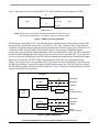
Figure 1 shows the connection between MPC8313E MAC and PHY with the support of SGMII.
Rx
S_OUT +/S_CLK+/-
MAC
PHY
Tx
S_IN +/SGMII Interface
NOTE: The use of RxCLK is optional, and the MPC8313E MAC can extract the clock
from the recovered data stream. It is, therefore, shown as unconnected above.
Figure 1. SGMII Connectivity with PHY
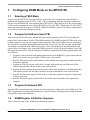
SGMII support on the MPC8313E is provided through an internal Serializer-Deserializer (SerDes) PHY
that converts the parallel data stream into a serial stream. The eTSEC (enhanced Three Speed Ethernet
Controller) is the main ethernet controller on the chip and has provisions for various types of interfaces for
connecting to PHY, like MII, RMII, GMII, RGMII, TBI etc. For providing SGMII functionality,
connections are provided to the SerDes through the eTSEC’s ten-bit interface (TBI). The TBI is controlled
through an MDIO (Management Data I/O) interface, just like any MII compatible PHY. To configure the
processor to operate in SGMII mode, the TBI must be programmed to connect to the internal SerDes rather
than to the external pins. The PHY address corresponding to each TBI can be programmed in the
TBIPA_VAL register of the corresponding eTSEC. This address is to be left shifted by 8 and ORed with
the MII register address to generate the physical MDIO address on the bus. The PHY addresses used for
the TBI must not collide with the external PHY addresses. Figure 2 shows the functional details of SGMII
support on the MPC8313E processor.
MPC8313E
GMII/RGMII
eTSEC1
MDC/MDIO
TBI/RTBI
TBI Controller
SerDes
e300
Core
SGMII
(RxD/RxCLK/TxD)
GMII/RGMII
MDC/MDIO
eTSEC2
TBI/RTBI
TBI Controller
SerDes
SGMII
(RxD/RxCLK/TxD)
Figure 2. SGMII on MPC8313E
Configuring SGMII Ethernet on the PowerQUICC™ MPC8313E Processor, Rev. 0
2
Freescale Semiconductor
Configuring SGMII Mode on the MPC8313E
1
1.1
Configuring SGMII Mode on the MPC8313E
Selecting eTSEC Mode
At power-up, the MPC8313E processor reads the value of the reset configuration words (RCWs) to
determine the operating mode of eTSEC 1 and 2. The corresponding mode bits should be configured to
0b110 to select SGMII mode. After sampling the RCWH (RCW - High Word) at reset, the corresponding
eTSEC mode is programmed as per value in RCWH bits [16:18] for TSEC1 Mode and [19:21] for TSEC2
Mode and reflected in the respective ECNTRL (Ethernet Controller) register. The software configuration
is next and is described in subsequent sections.
1.2
Program the SerDes to Select TBI
After selecting 10/100/1000 mode and half/full duplex mode operation in MACCFG1 and setting the
primary MAC station address in MACSTNADDR1 and MACSTNADDR2 and the ECNTRL mode value
(which is loaded at reset), the user software must program the TBI. A PHY address must be assigned to
the TBI, which is controlled by the MDIO interface on the local eTSEC, just like any other external PHY.
The address is configured in the TBIPA register. This value is left-shifted by 8 and ORed with the MII
register offset. For example, if the value in the TBIPA register is 15 (0xF), the physical address for the TBI
SR register becomes 0xF01. After the TBI physical address is assigned, the steps for programming the TBI
are as follows:
1. Set up the clock speed for the MII management interface in the MIIMCFG register. Ensure that the
MDC clock speed is not greater than 2.5 MHz (write value 0x0005).
2. Read the TBI control register (offset 0x00) to check whether auto negotiation is enabled and other
information (default).
3. Program the TBICON register (offset 0x11) in single clock mode and with MII mode OFF to
enable communication with the SerDes (write value 0x0020).
4. Program the TBI AutoNeg advertisement register (offset 0x04) to indicate to the link partner that
TBI supports PAUSE and full duplex and does not support half duplex (write value 0x01A0).
5. Program the TBI control register (offset 0x00) to restart auto negotiation using the configuration
in the previous step.
6. Read the TBI status register (offset 0x02) to check link status and whether auto negotiation is
complete.
1.3
Program the External PHY
If another PHY, external to the chip is present, the same needs to be configured to select SGMII mode. The
PHY is programmed according to the manufacturer’s specification for selecting the relevant link mode and
is beyond the scope of this document.
1.4
SGMII Register Initilization Sequence
Table 1 shows the steps of the SGMII mode initilization sequence.
Configuring SGMII Ethernet on the PowerQUICC™ MPC8313E Processor, Rev. 0
Freescale Semiconductor
3
Configuring SGMII Mode on the MPC8313E
Table 1. SGMII Mode Register Initialization Steps
Set Soft_Reset.
MACCFG1[1000_0000_0000_0000_0000_0000_0000_0000]
Clear Soft_Reset.
MACCFG1[0000_0000_0000_0000_0000_0000_0000_0000]
Initialize MACCFG2.
MACCFG2[0000_0000_0000_0000_0111_0010_0000_0101]
(I/F) Mode = 2, Full Duplex = 1
(Set I/F mode = 1 in SGMII 10/100 Mbps speed)
Initialize ECNTRL.
ECNTRL[0000_0000_0000_0000_0001_0000_0010_0010]
(This example has Statistics Enable = 1, TBIM = 1, SGMIIM = 1)
(Set R100M = 1 in SGMII 100 Mbps speed)
Initialize MAC Station Address.
MACSTNADDR [0110_0000_0000_0010_0000_0000_0000_0000] to 02608C: 876543, for example.
Assign a Physical address to the TBI.
TBIPA[0000_0000_0000_0000_0000_0000_0001_0000] Set to 16, for example.
Set up the MII management clock speed.
MIIMCFG[0000_0000_0000_0000_0000_0000_0000_0101] set source clock divide by 14 for example to insure that MDC clock
speed is not greater than 2.5 MHz
Read the MII management Indicator register and check for Busy = 0,
MIIMIND ---> [0000_0000_0000_0000_0000_0000_0000_0000]
This indicates that the eTSEC MII management bus is idle.
Set up the MII management for a write cycle to the TBICON register (write the PHY address and register address)
MIIMADD[0000_0000_0000_0000_0001_0000_0001_0001]
The TBICON register is at offset address 0x11 from the TBI address.
Perform an MII management write cycle to TBI
Write to MII management control with 16-bit data intended for the TBICON register.
MIIMCON[0000_0000_0000_0000_0000_0000_0010_0000]
This sets TBI in single-clock mode and MII mode off to enable communication with SerDes.
Read the MII management indicator register and check for Busy = 0,
MIIMIND ---> [0000_0000_0000_0000_0000_0000_0000_0000]
This indicates that the write cycle is complete.
Set up the MII management for a write cycle to the TBI AN advertisement register (write the PHY address and register address).
MIIMADD[0000_0000_0000_0000_0001_0000_0000_0100]
The AN advertisement register is at offset address 0x04 from the TBI address.
Check to see if the MII management write is complete.
Read the MII management indicator register and check for Busy = 0.
MIIMIND ---> [0000_0000_0000_0000_0000_0000_0000_0000]
This indicates that the write cycle is complete.
Set up the MII management for a write cycle to the TBI control register (write the PHY address and register address).
MIIMADD[0000_0000_0000_0000_0001_0000_0000_0000)
The control register is at offset address 0x00 from the TBI address.
Configuring SGMII Ethernet on the PowerQUICC™ MPC8313E Processor, Rev. 0
4
Freescale Semiconductor
Example of Test Setup and Code
Table 1. SGMII Mode Register Initialization Steps (continued)
Perform an MII management write cycle to TBI.
Write to MII management control with 16-bit data intended for the TBI control register.
MIIMCON[0000_0000_0000_0000_0001_0010_0000_0000]
This enables the TBI to restart auto-negotiations using the configuration set in the AN advertisement register.
Check to see if MII management write is complete.
Read the MII management Indicator register and check for Busy = 0.
MIIMIND ---> [0000_0000_0000_0000_0000_0000_0000_0000]
This indicates that the write cycle is complete.
Check to see if the PHY has completed auto-negotiations.
Set up the MII management for a read cycle to the PHY MII management register (write the PHY address and register address).
MIIMADD[0000_0000_0000_0000_0001_0000_0000_0001]
The PHY status control register is at address 0x1 and in this case the PY address is 0x10.
Perform an MII management read cycle of status register, AN expansion register, and so on.
Clear IEVENT register.
IEVENT[0000_0000_0000_0000_0000_0000_0000_0000]
Initialize (Empty) transmit descriptor ring and fill buffers with data.
Initialize TBASE0 –TBASE7
TBASE0 – TBASE7[LLLL_LLLL_LLLL_LLLL_LLLL_LLLL_LLLL_L000]
Initialize (Empty) receive descriptor ring and fill with empty buffers.
Initialize RBASE0 –RBASE7,
RBASE0 – RBASE7[LLLL_LLLL_LLLL_LLLL_LLLL_LLLL_LLLL_L000]
Enable transmit and receive queues
Enable Rx and Tx.
MACCFG1[0000_0000_0000_0000_0000_0000_0000_0101]
2
Example of Test Setup and Code
The example setup for testing SGMII mode configuration was developed on the Freescale MPC8313E
MDS board running Linux 2.6.11 kernel. The initial level configuration for eTSEC operating mode is
selected through the jumper switches SW7[1..6](indicating TSEC1M and TSEC2M) on the board. It is
ensured beforehand that FCFG bit (Flash/BCSR configuration selection bit) is set to load the reset
configuration word (RCW) from the board control and status registers (BCSR) instead of flash memory.
At power-on reset, the switch value is read and programmed in the corresponding eTSEC mode bits in
RCWH. Next is software initialization, the code for which is integrated with the ethernet driver and is
described in subsequent sections. PHY configuration is not required on the MPC8313E MDS board
because the switch settings are also carried over to the External PHY pins HWCFG[3:0], which select the
PHY interface mode (SGMII/GMII/RGMII etc). The PHY used in the example test setup is Marvell
88E111.
2.1
Code
The Linux 2.6.11 kernel for the MPC8313E uses the gianfar Ethernet driver to initialize the eTSEC and
also call the PHY driver initialization routines. In the gfar_enet_open function, ECNTRL mode bits are
checked to see if SGMII is enabled. If it is enabled, gfar_configure_serdes is called to perform the
Configuring SGMII Ethernet on the PowerQUICC™ MPC8313E Processor, Rev. 0
Freescale Semiconductor
5
Example of Test Setup and Code
programming steps defined in Section 1.2, “Program the SerDes to Select TBI.” It uses new read/write
routines to write to the MII registers mapped on the local eTSEC MDIO bus. Also, some extra hash-defines
are added to gianfar.h.
The drivers/net/gianfar.h file contains the common #define used by the SGMII code as listed here:
/* TBI register addresses (not defined in linux/mii.h) */
#define MII_TBICON0x11
/* TBICON register bit fields */
#define TBICON_CLK_SELECT0x0020
#define ECNTRL_SGMII_MODE0x00000002
The drivers/net/gianfar.c file is the main gianfar driver code file. The init_phy routine checks whether
the programmed mode in ECNTRL is SGMII. If it is SGMII, then gfar_configure_serdes is called to
initialize the TBI interface and program it to select SERDES, as follows:
u32 ecntrl_val;
/* SGMII_SUPPORT */
ecntrl_val = gfar_read(&priv->regs->ecntrl);
if ((ecntrl_val & ECNTRL_SGMII_MODE) && (ecntrl_val & ECNTRL_TBI_MODE))
gfar_configure_serdes(dev);
}
The gfar_configure_serdes routine is defined as follows:
static void gfar_configure_serdes(struct net_device *dev)
{
struct gfar_private *priv = netdev_priv(dev);
struct gfar_mii __iomem *regs = (void __iomem *)&priv->regs->gfar_mii_regs;
u16 value;
/* Intialise TBI i/f to communicate with serdes(lynx phy) */
/* Write TBICON(0x11) = 0x20. Single clk mode, mii mode off(for serdes communication)
*/
gfar_local_mdio_write(regs, TBIPA_VALUE, MII_TBICON, TBICON_CLK_SELECT);
/* Write TBI AN(0x04) = 0x1a0. Supported pause and full-duplex, no half-duplex */
gfar_local_mdio_write(regs, TBIPA_VALUE, MII_ADVERTISE, ADVERTISE_1000XFULL |
ADVERTISE_1000XPAUSE | ADVERTISE_1000XPSE_ASYM);
/* Write TBI Control(0x00) = 0x1340. ANEG enable, restart ANEG, full duplex mode,
speed[1] set */
gfar_local_mdio_write(regs, TBIPA_VALUE, MII_BMCR, BMCR_ANENABLE | BMCR_ANRESTART |
BMCR_FULLDPLX | BMCR_SPEED1000);
}
In drivers/net/gianfar_mii.c routines are added to read and write on the eTSEC local MDIO interface,
which are required for programming the corresponding TBI controller:
/* Write value to the PHY at mii_id at register regnum,
Configuring SGMII Ethernet on the PowerQUICC™ MPC8313E Processor, Rev. 0
6
Freescale Semiconductor
Example of Test Setup and Code
* on the bus attached to the local interface, which may be different from the
* generic mdio bus (tied to a single interface), waiting until the write is
* done before returning. This is helpful in programming interfaces like
* the TBI which control interfaces like onchip SERDES and are always tied to
* the local mdio pins, which may not be the same as system mdio bus, used for
* controlling the external PHYs, for example.
*/
int gfar_local_mdio_write(struct gfar_mii *regs, int mii_id, int regnum, u16 value)
{
/* Set the PHY address and the register address we want to write */
gfar_write(®s->miimadd, (mii_id << 8) | regnum);
/* Write out the value we want */
gfar_write(®s->miimcon, value);
/* Wait for the transaction to finish */
while (gfar_read(®s->miimind) & MIIMIND_BUSY)
cpu_relax();
return 0;
}
/* Read the bus for PHY at addr mii_id, register regnum, and
* return the value.
Clears miimcom first.
All PHY
* Operation done on the bus attached to the local interface,
* which may be different from the generic mdio bus
* This is helpful in programming interfaces like
* the TBI which, in turn, control interfaces like onchip SERDES
* and are always tied to the local mdio pins, which may not be the
* same as system mdio bus, used for controlling the external PHYs, for example.
*/
int gfar_local_mdio_read(struct gfar_mii *regs, int mii_id, int regnum)
{
u16 value;
/* Set the PHY address and the register address we want to read */
gfar_write(®s->miimadd, (mii_id << 8) | regnum);
/* Clear miimcom, and then initiate a read */
gfar_write(®s->miimcom, 0);
gfar_write(®s->miimcom, MII_READ_COMMAND);
Configuring SGMII Ethernet on the PowerQUICC™ MPC8313E Processor, Rev. 0
Freescale Semiconductor
7
Conclusion
/* Wait for the transaction to finish */
while (gfar_read(®s->miimind) & (MIIMIND_NOTVALID | MIIMIND_BUSY))
cpu_relax();
/* Grab the value of the register from miimstat */
value = gfar_read(®s->miimstat);
return value;
}
2.2
Test Setup
The simple test setup consists of an MPC8313E MDS board connected to a Linux host. Port 2 of the MDS
board, which is designed to operate in SGMII mode, is connected to the Ethernet interface on the Linux
host. See Figure 3. A ping from the board to the Linux host IP address indicates proper working of the
SGMII. Throughput can be tested by connecting a commercially available traffic generator (such as
SmartbitsTM) to both the ports on the MDS board. The board is configured to operate in SGMII mode, and
traffic is routed from one of the traffic generator’s ports to the other through the board.
MPC 8313E MDS
eth0
EXTERNAL PHY
Linux
Host
eTSEC1
MPC8313E
SGMII i/f
eTSEC2
eth1
EXTERNAL PHY
Figure 3. SGMII Connectivity with PHY
3
Conclusion
SGMII on the MPC8313E processor supports a minimal pin interface with compatible PHYs and the
lowest pin count of all the available interfaces. The same interface can be configured to work in
10/100/1000 mode. It can support optical/copper line terminations through compatible PHY’s as well as
act as a serial communication link for intra and inter board communications (through backplane) without
any additional interfacing.
4
Reference
1. MPC8313E PowerQUICC™ II Pro Integrated Host Processor Reference Manual, available at the
Freescale web site.
2. MPC8313E EMDS Processor Board User Manual, available at the Freescale web site.
3. MPC8313E Linux BSP User Manual, available with the Freescale’s BSP distribution for the
MPC8313E MDS board.
Configuring SGMII Ethernet on the PowerQUICC™ MPC8313E Processor, Rev. 0
8
Freescale Semiconductor
Reference
THIS PAGE INTENTIONALLY LEFT BLANK
Configuring SGMII Ethernet on the PowerQUICC™ MPC8313E Processor, Rev. 0
Freescale Semiconductor
9
Reference
THIS PAGE INTENTIONALLY LEFT BLANK
Configuring SGMII Ethernet on the PowerQUICC™ MPC8313E Processor, Rev. 0
10
Freescale Semiconductor
Reference
THIS PAGE INTENTIONALLY LEFT BLANK
Configuring SGMII Ethernet on the PowerQUICC™ MPC8313E Processor, Rev. 0
Freescale Semiconductor
11
How to Reach Us:
Home Page:
www.freescale.com
Web Support:
http://www.freescale.com/support
USA/Europe or Locations Not Listed:
Freescale Semiconductor, Inc.
Technical Information Center, EL516
2100 East Elliot Road
Tempe, Arizona 85284
+1-800-521-6274 or
+1-480-768-2130
www.freescale.com/support
Europe, Middle East, and Africa:
Freescale Halbleiter Deutschland GmbH
Technical Information Center
Schatzbogen 7
81829 Muenchen, Germany
+44 1296 380 456 (English)
+46 8 52200080 (English)
+49 89 92103 559 (German)
+33 1 69 35 48 48 (French)
www.freescale.com/support
Information in this document is provided solely to enable system and software
implementers to use Freescale Semiconductor products. There are no express or
implied copyright licenses granted hereunder to design or fabricate any integrated
circuits or integrated circuits based on the information in this document.
Freescale Semiconductor reserves the right to make changes without further notice to
any products herein. Freescale Semiconductor makes no warranty, representation or
guarantee regarding the suitability of its products for any particular purpose, nor does
Freescale Semiconductor assume any liability arising out of the application or use of
any product or circuit, and specifically disclaims any and all liability, including without
limitation consequential or incidental damages. “Typical” parameters which may be
provided in Freescale Semiconductor data sheets and/or specifications can and do
vary in different applications and actual performance may vary over time. All operating
parameters, including “Typicals” must be validated for each customer application by
customer’s technical experts. Freescale Semiconductor does not convey any license
Japan:
Freescale Semiconductor Japan Ltd.
Headquarters
ARCO Tower 15F
1-8-1, Shimo-Meguro, Meguro-ku
Tokyo 153-0064
Japan
0120 191014 or
+81 3 5437 9125
[email protected]
under its patent rights nor the rights of others. Freescale Semiconductor products are
Asia/Pacific:
Freescale Semiconductor Hong Kong Ltd.
Technical Information Center
2 Dai King Street
Tai Po Industrial Estate
Tai Po, N.T., Hong Kong
+800 2666 8080
[email protected]
claims, costs, damages, and expenses, and reasonable attorney fees arising out of,
For Literature Requests Only:
Freescale Semiconductor
Literature Distribution Center
P.O. Box 5405
Denver, Colorado 80217
+1-800 441-2447 or
+1-303-675-2140
Fax: +1-303-675-2150
LDCForFreescaleSemiconductor
@hibbertgroup.com
Document Number: AN3354
Rev. 0
05/2007
not designed, intended, or authorized for use as components in systems intended for
surgical implant into the body, or other applications intended to support or sustain life,
or for any other application in which the failure of the Freescale Semiconductor product
could create a situation where personal injury or death may occur. Should Buyer
purchase or use Freescale Semiconductor products for any such unintended or
unauthorized application, Buyer shall indemnify and hold Freescale Semiconductor
and its officers, employees, subsidiaries, affiliates, and distributors harmless against all
directly or indirectly, any claim of personal injury or death associated with such
unintended or unauthorized use, even if such claim alleges that Freescale
Semiconductor was negligent regarding the design or manufacture of the part.
Freescale™ and the Freescale logo are trademarks of Freescale Semiconductor, Inc.
The Power Architecture and Power.org word marks and the Power and Power.org
logos and related marks are trademarks and service marks licensed by Power.org. All
other product or service names are the property of their respective owners.
© Freescale Semiconductor, Inc., 2007. All rights reserved.