1
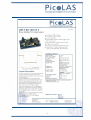
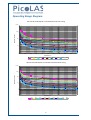
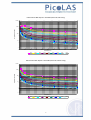
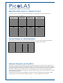
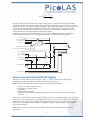
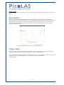
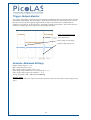
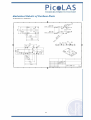
User Manual
LDP-V 80-100 V3
Distributor:
=
=
=
máÅçi^p=dãÄe
`çãé~åó=Ñçê=fååçî~íáîÉ=mçïÉê=bäÉÅíêçåáÅë=~åÇ=i~ëÉê=qÉÅÜåçäçÖó=
=
h~áëÉêëíê~ëëÉ=NMM=
RONPQ=eÉêòçÖÉåê~íÜ=
Rev. 15.02
Table of Contents
How to get started.....................................................................................................................................4
How to connect the LDP-V 80-100 V3 ....................................................................................................5
Operating Range Diagram........................................................................................................................6
Maximum Duty Cycle vs. Output Current ...............................................................................................8
Current Droop vs. Pulse Duration ............................................................................................................8
Internal Structure of the LDP-V ...............................................................................................................8
How to use the Internal HV-DC-Supply ..................................................................................................9
Pulse Output ...........................................................................................................................................10
Trigger Input ..........................................................................................................................................10
Trigger-Output-Monitor .........................................................................................................................12
Absolute Maximum Ratings...................................................................................................................12
Mechanical Details of the Base-Plate .....................................................................................................13
2
3
How to get started
Step #
What to do
Check
1
Unpack your Device
2
Make a short at the output
3
Turn the High voltage to the lowest value (turn
poti fully counterclockwise)
4
Connect a Pulse source with the desired pulsewidth to the selected triggering Input
5
Connect your Scope
Select 50 Ohm termination, trig on neg.
falling edge, 200 mV/div.
6
Apply the supply voltage
Security Advise:
Do not touch any leads of the output or the output
capacitors as they are connected to a high voltage
of up to 100 V.
Connect a 15 V DC power supply to the
pinheader. See page 5 for details.
Note: Some supplies have a voltage
overshoot during turn on/turn off. This
may damage the device.
7
Adjust the value of the desired pulse current. (turn
the poti clockwise until the current reaches the
desired level.)
8
Disconnect the supply, remove the short at the
output and assemble the Laser Diode (Polarity!)
9
Reconnect the Supply and check the optical output
of your Laser Diode.
4
e.g. 100 ns, 100 Hz reprate.
Note: The actual current is always some
percent lower than the value of step 7.
Adjust the current with help of the poti.
How to connect the LDP-V 80-100 V3
pçäÇÉêJàìåÅíáçå=íç=~Åíáî~íÉ=
íÜÉ=áåíÉêå~ä=esJëìééäó=
oçÖçïëâáJ`çáä=
mçíá=íç=~Çàìëí=î~äìÉ=çÑ=esJa`=
máå=NM=
máåÜÉ~ÇÉê=
máå=O=
i~ëÉêJaáçÇÉJ=
`çååÉÅíáçå=
Connections via Pinheader:
qêáÖÖÉêJfåéìí=
Pin
Name
Description
pj`=
1
GND
Ground return
2
HV+
`ìêêÉåíJãçåáíçêJçìíéìí=
áåíç=RM=lÜã==
External high-voltage supply Input (0 .. 100 V) for connecting
an
alternative HV-DC supply. See page 9 for details.
3
GND
Ground return
4
+15 V
Supply Voltage, connect to a power supply.
5*
Disable_Poti
Disables the internal HV-setpoint poti when set high.
6
Pulse_In
Trigger Input into 50 Ohm
7
Disable
Disables the Pulser when set high.
8*
U-Monitor
High-volage monitor output (scale: 40 mV/V) for supervising the actual
high voltage.
9
NTC
Internal 10 kOhm NTC versus GND for temperature monitoring. (B-value:
3620)
10*
Ext_HV_Setpoint
External HV setpoint input (scale: 25 V/V) allows control over the internal
HV-DC source.
*These pins had to be left unconnected in older versions then V3
Trigger Input:
The trigger input requires a signal level of 5 V and is terminated with 50 Ohm.
Current Monitor Output:
The current monitor output has a scale of 40 A/V with a negative signal output. It has a source impedance of
50 Ohm and must be terminated with 50 Ohm to achieve the correct scale.
Laser Diode Connection:
The Laser Diode can either be connected via the mounting holes on the top side of the pulser (inner hole:
Anode, outer hole: Cathode) or at the rectangular pads on top (Anode) and bottom (Cathode) of the pulser.
Security Advise:
Do not touch any leads of the output or the output capacitors as they are connected to a high voltage of up to
100 V.
5
Operating Range Diagram
LDP-V 80-100 V3: Max. Reprate vs. Pulsewidth (internal HV, with cooling)
10.000
Repetition rate in kHz
1.000
100
10
1
0
100
200
300
400
500
600
700
800
900
1000
900
1000
Pulsewidth in ns
10 A
15 A
20 A
30 A
40 A
50 A
60 A
70 A
80 A
LDP-V 80-100 V3: Max. Reprate vs. Pulsewidth (internal HV, without cooling)
10.000
Repetition rate in kHz
1.000
100
10
1
0
100
200
300
400
500
600
700
800
0
Pulsewidth in ns
10 A
15 A
20 A
30 A
6
40 A
50 A
60 A
70 A
80 A
LDP-V 80-100 V3: Max. Reprate vs. Pulsewidth (external HV, with cooling)
10.000
Repetition rate in kHz
1.000
100
10
1
0
100
200
300
400
500
600
700
800
900
1000
900
1000
Pulsewidth in ns
10 A
15 A
20 A
30 A
40 A
50 A
60 A
70 A
80 A
LDP-V 80-100 V3: Max. Reprate vs. Pulsewidth (external HV, without cooling)
10.000
Repetition rate in kHz
1.000
100
10
1
0
100
200
300
400
500
600
700
800
0
Pulsewidth in ns
10 A
15 A
20 A
30 A
40 A
7
50 A
60 A
70 A
80 A
Maximum Duty Cycle vs. Output Current
The following tables show the maximum allowable duty cycle depending on a given output current.
With active cooling of the baseplate:
Output current in
Max duty cycle
A
with ext. HV
5
1
10
0,2889
15
0,1284
20
0,0722
25
0,0462
30
0,0321
35
0,0236
40
0,0181
45
0,0143
50
0,0116
60
0,0080
70
0,0059
80
0,0045
Typical High
Voltage in V
7,66
13,71
19,77
25,82
31,88
37,93
43,99
50,04
56,10
62,15
74,26
86,37
98,48
Max duty cycle with
int. HV
0,784
0,219
0,101
0,058
0,038
0,026
0,019
0,015
0,012
0,010
0,007
0,005
0,004
Current Droop vs. Pulse Duration
The following table shows the absolute output current droop (in A) versus pulse length. Pulse durations
shorter than one microsecond are not considered as the droop is typically lower than 5%.
Pulse Duration in µs
Current in A
1
5
10
5
0,12
0,36
0,6
15
0,4
1,2
2,0
30
1,0
3,0
6,0
50
2,0
6,0
12,0
80
4,0
-
Internal Structure of the LDP-V
The LDP-V series generates the pulses by a simple but efficient principle. First, the storage capacitors (CS)
are charged, whether through the internal HV-DC-supply or an external high voltage source. When a pulse is
applied at the trigger input, the high speed mosfet opens and the current flows from the capacitor through the
laser diode, mosfet and current sense resistors. At the end of the pulse, the mosfet closes again and the
current stops. The generated current depends on the applied high voltage, the laser diode compliance voltage
and its differential resistance.
The following formulas give a good estimation of the laser diode current depending on the pulser’s high
voltage supply UHV, the laser diode compliance voltage Ucomp and its differential resistance Rdiff:
8
I LD ≈
U HV − U comp
1.1 + Rdiff
The laser diode current is measured with current sensing resistors (current monitor output) and with the
galvanically isolated rogowski coil. Disable- and trigger-input provide full control of the driver’s pulsing
capability to the user. The required DC high-voltage can either be applied through an external voltage source
or it can be generated with the integrated HV-DC-supply. The internal supply is controlled by the HV
setpoint poti or, when the Disable_Poti (Pin 5) pin is set high, via the Ext_HV_setpoint (Pin 10) pin. A
voltage monitor (Pin 8) provides feedback of the high dc voltage.
The Diode DRP prevents the laser diode from reverse currents; a 10kR NTC provides the possibility to
monitor the pulser temperature. An over temperature protection is NOT integrated on the driver.
Pin 2: + HV
Pin 8: U-Monitor
+HV-Adjust-Poti
15 V
++++
Pin 4: +15 V
18 .. 90 V
LD
Pin 5: Disable Poti
DR P
----
Pin 10: Ext. HV setpoint
CS
Pin 7: Disable
RC L
Rogowski-Coil
Pin 1,3: GND
Pin 6: Trigger
Trigger SMC
Pin 9: NTC
50 R
Driver
10K
50 R
Current-Monitor
RC S
Rogowski-Coil
How to use the Internal HV-DC-Supply
The LDP-V series provides a high power (up to 15 W / 1 A / 100 V) internal high voltage supply.
To adjust the laser diode current to the desired value follow the steps below.
Notice: Make sure that the solder junction is done to activate the HV-DC-Supply.
1.
2.
3.
4.
5.
Turn the poti fully counterclockwise
Apply the 15 V supply voltage
Start Pulses
Measure the diode current
Adjust the level of the high voltage supply (hence the level of the current) by turning the poti
clockwise
Since Version 3 of the LDP-V series, the HV-DC-Supply can also be controlled through an external setpoint
signal on pin 10 of the pinheader (Ext_HV_Setpoint); the scale is 25V/V. To enable the external setpoint pin
and disable the internal poti, pin 5 (Disable_Poti) of the pinheader has to be set to “high”. Otherwise the
internal poti will override the external signal. The high DC voltage can be monitored at pin 8 (U-Monitor)
with a scale of 40 mV/V.
Note: Older versions are not capable of these features and the above mentioned pins have to be left
unconnected!
9
Security Advise:
Do not touch any leads of the output or the output capacitors as they are connected to a high voltage of up to
100 V.
Pulse Output
The LDP-V series provides ultra rapid pulse rise- and fall-times in the region of several nanoseconds.
However, pulse rise and fall depend on the parasitic stray inductance of the cabling to the laser diode. Direct
connection without any kind of wires to the module is absolutely necessary for best results. For detailed
information about the effect of the laser diode connection on the pulse shape please refer to PicoLAS
Application Notes #2 and #3.
Typical Pulse Rise and Fall Times of LDP-V 80-100 V3 (scale: 10 A/Div)
Trigger Input
The trigger input, both on the pin header and the SMC-jacket, is terminated with 50 Ohm to ground. The
trigger source has to be able to provide a signal level of 5 V with a 50 Ohm load.
The delay between the triggering signal and the load-current is very low around 36 ns and very constant. The
pulse-to-pulse jitter is very stable below 1 ns if the supply voltage and temperature
are kept constant.
10
Typical trigger delay of LDP-V 80-100 V3
11
Trigger-Output-Monitor
The Trigger Output signal is generated with an integrated, isolated Rogowski-Coil and provides an ultra fast
galvanically isolated signal. The signal shape is proportional to the derivative of the load current. It can be
used for a current-response triggering signal and has no delay to the load current. Combined with an
integrator it is possible to use this signal for a galvanically isolated current monitor. The isolation barrier is
suitable for voltages up to 100 V and prevents unwanted ground loops.
Signal of the Rogowski-Coil:
"True" load current
Positive edge at pulse begin
Negative edge at pulse end
Absolute Maximum Ratings
Supply voltage range: 10 .. 18 V
Max. voltage at HV Pin: 100 V
Max. output current U-monitor, NTC: 1 mA
Input voltage range Disable_Poti, Ext_HV_Setpoint: 0 .. 5 V
Input voltage range trigger input, Disable: 0 .. 15 V
Storage temperature: -20 .. +85°C non condensing
Security Advise:
Do not touch any leads of the output or the output capacitors as they are connected to a high voltage of up to
100 V.
12
Mechanical Details of the Base-Plate
All dimensions in millimetres.
13