1
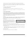
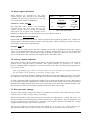
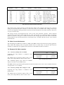
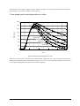
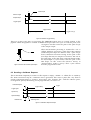
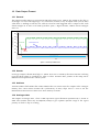
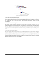
APV6 User Manual
Author:
Email:
M.French
[email protected]
Phone:
Fax:
+44 1235 446484
+44 1235 445753
Post:
Rutherford Appleton Laboratory
Chilton
Didcot
Oxon
OX11 0QX
United Kingdom
Version:
2.0
Notes:
This is a working document that will be updated occasionally. Please pass
comments and requests for the inclusion of more information to the above
author.
apv6_manual.2.0
1
14/4/97
1. Document History
Date
Revision
Number
Description
16/10/96
1.0
First draft version
14/4/97
2.0
Second version including corrections and information from the initial
evaluation of prototypes by Mark Raymond of Imperial College.
apv6_manual.2.0
2
14/4/97
2. Contents
1.
Document History
2.
Contents
3.
Related Documents
4.
Introduction to the APV6 and Analogue Read-out in the CMS Tracker
5.
Physical Size and Pad Layout
6.
Logic Levels
7.
Control Interface
8.
Biasing the APV6
9.
Running the APV6
10. Data Output Format
11. Using the Internal Test Pulse System
12. Other Features
13. Known Bugs And Solutions
Appendix A
APV6 Power Consumption
Appendix B
APV6 Schematics
apv6_manual.2.0
3
14/4/97
3. Related Documents
Name
Author
Notes
Specifications for the
Control and Read0out
Electronics for the CMS
Inner Tracker
A. Marchioro
CMS Working document
APV6 Requirements
M.French
Part of the RAL QA project specification
Balaton Paper
M.French
Presented at 2nd LHC workshop on electronics
apv6_manual.2.0
4
14/4/97
4. Introduction
Copper differential low voltage drive
APV6
APV6
APV6
APV6
APV6
APV6
APV6
APV6
APV6
APV6
APV6
APV6
Link driver chip
Quad laser unit
Mux driver
-A
-A
-A
-A
APV6
APV6
APV6
APV6
-A
-A
-A
-A
APV6
APV6
I2C
Link
PLL timing trim chip
Optical ribbons to FED module
LVDS
CK and T1
Figure 1: Analogue Read-out in the CMS silicon tracker
The architecture of the CMS tracker readout system is based on analogue processing of data in t h e
detector prior to transmission in analogue form via an optical interface to the counting room. Here i t
will be digitised and processed to remove offsets and reorder channels before passing up the DAQ
tree. Some of the system is still being specified but the silicon front end modules will be as shown in
Figure 1. Here eight APV6 chips will be used to process 1024 detector channels.
The chip contains a preamplifier and shaper stage for each channel. Each channel then has a 160
location memory into which samples are written at the LHC 40MHz machine frequency. Thus t h e
memory always contains a record of the most recent beam crossings the chip has sensed. A data access
mechanism allows the marking and queuing of requested locations for output. Embedded logic ensures
that the samples awaiting readout are not overwritten with new data. Requested samples from t h e
memory are processed with a deconvolution filter (APSP), a switched capacitor network, t h a t
deconvolves the shaping function of the preamplifier and shaper stages to recover the initial pulse
shape. After the APSP the data is held in a further memory buffer prior to switching through an
output analogue multiplexer. This additional buffer is required so that as one event is multiplexed out
another may be prepared for consecutive transmission.
The APV6 also contains features required for a final CMS design including programmable on chip
analogue bias networks, a remotely controllable internal test pulse generation system and a slow
control communication interface. Figure 1 also shows two other chips on the Front-end hybrid, a clock
and control receiver and a multiplexer driver chip. The clock and control receiver is required to
locally generate the clock and trigger signals in the appropriate form and timing for the APV6. I t
will also interface the hybrid I2C slow control data bus to the next level up in the control system. The
multiplexer driver chip is required to mix, by interleaving, the output data from pairs of APV6 chips
onto four analogue outputs that transmit to a separate optical driver board. In this way a
multiplexing level of 256 to 1 is achieved at the hybrid output. Both of these chips are in design a t
RAL and CERN for fabrication in radiation soft form.
apv6_manual.2.0
5
14/4/97
5. Physical Size and Pad Layout
The overall dimensions of the APV6 chip are shown in Figure 2 below.
Four groups of
32 input pads
Back-end pads
1
INP<127>
VSS
APV6
GND
VDD
1
13
INP<0>
37
Bias monitor pads
Logic test probe pads
Figure 2: APV6 overall dimensions (dimensions in microns)
The design will be fabricated using the standard Harris AVLSI-RA process flow. The wafers will be
of 4 inch type and 13mils (approx. 350um) thick. A table showing the precise co-ordinates of t h e
centre of each pad may be obtained from RAL, please request it if required.
5.1 Analogue inputs
The 128 analogue inputs are grouped into four sections of 32. Each section is separated by larger power
supply pads. These power connections supply the preamplifier stages (where most of the APV6 power
is used) and must be bonded to supplies close to the chip. Use the shortest bond length and multiple
bonds if possible (to minimise inductance).
Note: The reason for powering the chip in this way is so that the power losses in the APV6
routing, and the area wasted in large power buses is minimised.
Each group of inputs is arranged in two staggered rows, each rows pads are spaced at 86um. The inner
row is offset 43um clockwise (viewed from the centre of the APV6). Thus the effective bond pitch
within each group is 43 um. Each pad is 100um long and 60um wide (the passivation opening is about
3um smaller than this). The pads are labelled from <0> to <127>. The Inp<0> is on the lower left of
the first group and Inp<127> is at the top right of the top section.
The analogue inputs all have small protection diodes to VSS and VDD. These are not intended to
meet standard levels of protection but should prevent damage during assembly if reasonable antistatic measures are taken. For them to work effectively the VDD GND and VSS pads should be
bonded first and grounded to the assembly machine.
5.2 Bias monitor pads
These are intended for test purposes only. They enable a direct measurement of the bias voltages and
currents set in the bias generator. The first test systems should permit bonding to these points to allow
apv6_manual.2.0
6
14/4/97
the user to monitor or override the levels generated internally. There are thirteen test points and
they are tabulated below:
Pad Number
Name
Type
Measure to
1
V_BG
current
VSS
2
IPRE
current
VSS
3
VPRE
voltage
GND
4
VCAS(P)
voltage
GND
5
ISFB(P)
current
VSS
6
ISHA
current
VSS
7
VSHA
voltage
GND
8
VCAS(S)
voltage
GND
9
ISFB(S)
current
VSS
10
IPSP
current
VSS
11
VADJ
voltage
GND
12
CLVL
current
VSS
13
VDEL
voltage
GND
Table 1: Bias monitor points
Note that when measuring a current
by connecting the meter to VSS t h e
current flows in the meter and is
starved from the internal mirroring
in the APV6. This means that t h e
measurement will prevent the chip
from working, during operation these
points must normally be left open
circuit.
The VCAS and ISFB have two
entries even though each has only
one control word in the bias
generator. This is because they are
required both in the preamplifier
and the shaper. To prevent possible
undesired feedback the reference for
the two stages are independently
mirrored out of the bias generator
and consequently appear at two
pads.
The pads V_BG and VDEL both do not relate directly to bias channels. V_BG can be used to measure
the reference current for the bias generator, this prevents the bias generator mirrors from working so
must not be made at the same time as any other measurement, the nominal value for this current is
128uA. VDEL is connected to the calibration delay line. When the calibration feature is enabled
(calibration inhibit OFF) this voltage should ÒhuntÓ (small steps up and down in voltage around t h e
optimum bias point for the delay elements). Monitoring this voltage and observing the ÒhuntÓ effect
will indicate that the delay line has successfully locked onto the clock. See section ÒAPV6 Using t h e
internal calibration systemÓ for more details. External capacitance connected to the VDEL pad will
slow down the ÒhuntÓ effect and so may upset the measurement.
5.3 Logic Test Probe Pads
These pads are there to help in the case of logical problems with the chip. They allow the probing of
all the input and some of the output lines of the logical part. They have been used to backdrive t h e
APSP signals to correct the ÒPeak ModeÓ logical bug (see section Known Bugs and solutions). The
intention is that they are never used.
5.4 Backend Pads
All of the IO, address pads and remaining power supply pads are located down the back edge of t h e
chip. There are 37 in total and a full list describing their function is shown in Table 2. The pads are
approx. 100um by 60um and are on a 150um pitch. There is one pad ÒgapÓ next to the current output and
the fast differential input pairs (clock and control) have an additional 50um spacing from their
neighbours.
Normally all of the pads of type ÒTESTÓ may be left unconnected. They are designed for use in test
and early evaluation of the chip. The pads of type ÒBIASÓ may be left unconnected (with t h e
exception of BRES which should be connected to the -2V supply if the internal bias reference is used).
For details of how to use an external reference or the reference propagation system see section 8.1. The
clock and trigger inputs are of low voltage differential type, the remaining inputs require switching
between +2 and -2V. The pads PORT, SCLK and SDIN have a hysteresis characteristic because t h e
expected edges on these signals may be very slow.
apv6_manual.2.0
7
14/4/97
Pad Position
Name
Type
Function
1
AVSS
POWER
2
AVDD
POWER
3
CAL0
TEST
Charge injection test point
4
CAL1
TEST
Charge injection test point
5
CAL2
TEST
Charge injection test point
6
CAL3
TEST
Charge injection test point
7
BINP
BIAS
Bias reference override input
Analogue -2V Supply
Analogue +2V Supply
8
BRES
BIAS
Internal bias reference -2V supply
9
BOT1
BIAS
Reference current output
10
BOT2
BIAS
Reference current output
11
BOT3
BIAS
Reference current output
12
BOT4
BIAS
Reference current output
13
BOT5
BIAS
Reference current output
Reference current output
14
BOT6
BIAS
15
PROBE
OUTPUT(DIG)
16
AOUT
OUTPUT(AN)
Pad connected to -2V supply for probe edge sensor
Current mode analogue output
200um GAP
17
PORT
INPUT(HYST)
18
ADD0
INPUT(PU)
APV Address bit (Active Low: float high=0 tie low=1)
Power On Reset Pad (Active High)
19
ADD1
INPUT(PU)
APV Address bit (Active Low: float high=0 tie low=1)
20
ADD2
INPUT(PU)
APV Address bit (Active Low: float high=0 tie low=1)
21
ADD3
INPUT(PU)
APV Address bit (Active Low: float high=0 tie low=1)
22
OUTE
OUTPUT(DIG)
Digital output, switches low when analogue data is output
23
SDOT
OUTPUT(DIG)
I2C Data Output
24
WPTK
OUTPUT(DIG)
Memory write pointer test point
25
TPTK
OUTPUT(DIG)
Memory trigger pointer test point
26
DEL1
OUTPUT(DIG)
Calibration unit test point 1
27
DEL2
OUTPUT(DIG)
Calibration unit test point 2
28
DVDD
POWER
29
AGND
GROUND
30
HERA
INPUT(PU)
31
CLKN
INPUT(LV)
32
CLKP
INPUT(LV)
Digital +2V pad
Analogue Ground Connection
Tie to +2V for HERA mode or -2V for normal (LHC) mode
100um Gap
40MHz clock negative input (low voltage type)
40Mhz clock positive input (low voltage type)
100um Gap
33
TRGN
INPUT(LV)
Trigger negative input (low voltage type)
34
TRGP
INPUT(LV)
Trigger positive input (low voltage type)
35
SDIN
INPUT(HYST)
I2C data input
36
SCLK
INPUT(HYST)
I2C clock input
37
DVSS
SUPPLY
100um Gap
Digital -2V supply
Table 2: Backend pad listing, Pads (100um by 50um) spaced at 50um unless specified otherwise
apv6_manual.2.0
8
14/4/97
6. Logic Levels
6.1 Digital
6.1.1 INPUT
There are three types of logical inputs, low voltage differential ÒLVÓ (for the clock and trigger
lines), CMOS type inputs with pull-ups ÒPUÓ for the address lines and hysteresis action pads for t h e
I2C and power on reset pads.
6 . 1 . 2 INPUT(LV) Low Voltage Type
This system has been chosen for noise reasons. These pads are used on those inputs that are active
during the sensitive acquisition time of the chip and therefore are designed to minimise interference.
Testing has shown that on the prototypes that +/- 100mV is satisfactory, but the +/- 200mV below is
recommended:
Pad Name Logic Level
Voltage
XXXN
0
>+200mV
1
<-200mV
XXXP
0
<-200mV
1
>+200mV
6 . 1 . 3 INPUT(PU) Level input with pull-up
These pads are used for defining fixed chip configuration, an example of this is the four address bits.
Internal pull up resistors of approx. 140Kohm pull these lines to the VDD voltage, i.e. a default of
Ò1Ó this may be overridden by tying the pad to VSS to set the level Ò0Ó. Note that the Address bits
are complement, i.e. leave high for the address bit=0 and tie to VSS for address bit=1.
6 . 1 . 4 INPUT(HYST) Level input with hysteresis action
These pads are used where control signals switch slowly, an example of this is the I2C lines, here t h e
rise times may be many hundreds of nanoseconds in extreme cases. The pads are designed to have a
hysteresis difference of between 0.5 and 1.0V and always switch within +/-1V:
Edge
Logic Level
Low to High
High to Low
Voltage
0
<-0.5V
1
>+1.0V
1
>+0.5V
0
<-1.0V
6 . 1 . 5 OUTPUT
There are two types of data output from the APV6, analogue (AN) and digital (DIG)
6 . 1 . 6 OUTPUT(AN) Analogue data output
This pad provides a current output for the analogue data from the APV6. It must be terminated
externally by a resistor or active receiver with as small parasitic capacitance as possible. The output
must be held at a voltage within +/-1V to guarantee good linearity:
Voltage Range
apv6_manual.2.0
Min
Measured
Max
-1V
-
+1V
9
14/4/97
Min
Measured
Max
Current Gain
50uA/Mip
-
100uA/mip
Header Logic 0
-
100uA
-
Header Logic 1
-
175uA
-
6 . 1 . 7 OUTPUT(DIG) Digital data output
These lines are intended for test and evaluation of the logic only and should not be used in the normal
operation of the circuit. They are open drain outputs that when required must be terminated to VDD
or preferably GND with a resistor, alternatively they can drive the 50ohms of an oscilloscope
channel if required.
The function of these pads is of little interest to those not involved in the wafer testing so is not
covered by this manual.
6 . 1 . 8 OTHERS: POWER BIAS and TEST
Power lines should be connected directly to the appropriate supply voltages, the BIAS lines are
current reference (input) and propagation (output) connections (described in section 8.2). The test lines
connect to the inputs via a small test capacitor, this is in parallel to the APV6 internal test pulse
system. Driving a voltage step on these lines of 0.6V gives approximately the injection of 4fC on t h e
input lines, CAL0 drives INPUT<0>,<4>... CAL1 drives INPUT<1>,<5>... etc.
apv6_manual.2.0
10
14/4/97
7. Control Interface
The configuration, bias setting and error states of the APV6 are handled with a two wire serial
interface. It is designed to conform to the Phillips I2C standard so that it may be controlled by a
standard off the shelf components (e.g. PCD8584 parallel bus interface chip).
7.1 The I2C standard
This protocol is specified completely in the Philips data books so need not be repeated here. The APV
chips may only act as slave devices. They are addressed using the standard 7-bit mode where t h e
most significant bits are Ò001Ó and the remaining 4 bits are defined by bonding out address pads on t h e
APV6.
The 4 address pads (ADD0, ADD1, ADD2, ADD3) each possess internal pull-up resistors (of approx.
140Kohm) to VDD. Selective bonding of these pads to VSS therefore allows any address pattern to be
set. The APV will only execute the requested command if the 3 most significant bits are Ò001Ó and t h e
4 remaining bits match the bonded address setting.
The APV address Ò1111Ó is reserved for ÒglobalÓ addressing. When the Ò1111Ó chip address is used in
an i2c transfer all connected APVs will respond. Consequently a maximum of 15 APV6 chips may
share the same controller and maintain unique addresses.
7.2 Communicating with the APV6
The APV6 interface logic has a command register that must be programmed before data may be
transferred. This register defines which variable or register is to be accessed and specifies t h e
direction of data transfer. The least most significant bit is high for read and low for write operations.
A complete table of the command codes is shown in Table 3.
7 . 2 . 1 Writing to the APV6
Data is written to the APV6 with one I2C transfer with three 8 bit data packets.
The first packet defines the APV address, the second specifies a command register (in both cases t h e
read bit must be low) and the third specifies t h e
new value for the register.
Function or Variable
An example of an IPRE write operation is shown in
Figure 3.
7 . 2 . 2 Reading from the APV6
To read data from the APV6 the command register
must first be written. Reading requires two separate
I2C transfers.
Command
Register Code
Error register (read only)
00 00 00 01
Mode register
00 00 00 1X
Latency register
00 00 01 0X
IPRE
01 00 00 0X
ISHA
01 00 00 1X
IPSP
01 00 01 0X
ISFB
01 00 01 1X
The first packet defines the APV address (read bit
low), the second specifies the command register
(read bit high). Any further data packets are
ignored.
VPRE
01 00 10 0X
VSHA
01 00 10 1X
VADJ
01 00 11 0X
VCAS
01 00 11 1X
Transfer 2
Read the data back
CLVL
01 01 00 0X
Once the command register has been programmed
the APV6 may be read by a standard I2C read
sequence, the APV will respond with a single 8-bit
packet corresponding to the addressed data.
CSKW
01 01 00 1X
CDRV
01 01 01 0X
Transfer 1
apv6_manual.2.0
Write the command register
11
Table 3: Command Register Codes
14/4/97
Subsequent reads of the same register is possible without re-programming the command register.
If the APV is addressed as ÒglobalÓ for reading all APVs will respond. The serial data output is of
open drain type so if more than one APV6 responds the logical AND of all addressed APVÕs will be
sensed.
An example of an IPRE read operation is shown in Figure 4.
7.3 Command register codes
The command register codes are 8-bit with the last bit determining the direction of transfer.
The command codes are listed in Table 3 with MSB first, X=1 for read operations, X=0 for write
operations.
7.4 Error register definition
For short periods the APV6 may be triggered at a rate faster than it can output data. When this
happens a queue develops in the APV6. The length of this queue is limited by the number of spare
locations in the memory and an address fifo that stores the addresses of columns awaiting read-out.
As the queue grows, depending on the latency programmed, eventually the fifo becomes full or all t h e
available memory locations become allocated. Either case leads to pipeline failure. The circuit must
then be reset with a RESET101 sequence to clear the fault.
Fifo error
The fifo error is simply found by keeping a record of the number of addresses stored (limit=19). In
deconvolution mode three addresses must be stored for each trigger, so in this case the limit is six
triggers. For peak processing where only one address is stored the limit is nineteen.
Latency error
The memory function is continuously monitored by a
latency test (the separation between the write and
trigger pointers should always be equal to t h e
programmed latency). This is checked every time
the memory is overwritten (at least once every 160
pipeline clock cycles).
Error
Value = 0
Value = 1
<1>
fifo error
OK
<0>
latency error
OK
Table 4: Error register definition
The function of the error register is to report these two classes of failure.
The error bits are active low so that its possible to read a group of APVs in one go with the ÒglobalÓ
read operation, the Òwire-andÓ of the open drain outputs pulls the output low if any of the APVs
have the appropriate error.
Note: When a new latency value is written a Latency Error will inevitably be produced. T h e
pipeline must be restarted to initialise the pointers with the new separation. This must be done
with a RESET101 sequence which will also clear the Error.
Clearing Error States
The only method of clearing the error register is with a RESET101.
apv6_manual.2.0
12
14/4/97
7.5 Mode register definition
Three functions are controlled by the APVs
ÒModeÓ register. They default to the underlined
conditions (at power-up) and may be read and
overwritten (not altered by RESET101).
Calibration inhibit OFF/O N
Mode
Value = 0
Value = 1
<2>
calibration
inhibit OFF
calibration
inhibit ON
<1>
“deconvolution”
“peak”
processing
processing
<0>
analogue bias
analogue bias
The calibration logic contains a self regulating
OFF
ON
ÒclockedÓ delay line may cause noise in t h e
system. For this reason it should be inhibited
Table 5: Mode register definition
when not in use. At power on it defaults to t h e
inhibited condition. The use of this function is fully described in section 11.
APSP operation Deconvolution/ P e a k
Deconvolution mode enables the three sample weighted deconvolution algorithm that confines t h e
shaped signal to one beam crossing (suited to LHC operation). When operating in ÒPeakÓ mode only
one sample is stored and is output directly.
Analogue O F F/ O N
The analogue bias control allows the bias conditions of the chip to be disabled whilst the required
values are programmed into the bias generator. Enabling analogue bias then lets the programmed
values to take effect. This is particularly useful at power-up where the default is ÒOFFÓ, thus t h e
power consumption of the system may be ramped up in a controlled fashion.
7.6 Latency register definition
This register contains a binary number that defines the separation between the ÒWriteÓ and ÒTriggerÓ
pointers in the analogue memory controller. The register defaults at power-up to a value of
bit<7:0>=10000100. This corresponds to a count of 132 clock cycles. This value may be reprogrammed to
any value up to 156.
Note: Programming larger values of latency reduces the cells available for queuing output d a t a ,
and will impact on the efficiency of the APV6 at high trigger rates.
To program a new latency the binary number equivalent to the required number of pipeline cycles must
be written by an I2C write operation. Then the circuit must be reset with a RESET101 trigger sequence.
In ÒPeakÓ mode this number represents the number of exact clock periods between a signal being sensed
at an analogue input and outputting the sample on the peak of the CR-RC shape. In deconvolution
mode the first sample must be three clock cycles before that point. Thus in deconvolution mode to get
the same effective latency the number programmed must be three counts larger.
7.7 Bias generator settings
The bias of the analogue stages in the APV6 is controlled by an internal ÒBias GeneratorÓ part. There
are three classes of bias; current, voltage and charge.
The bias block produces only current in each case. Currents are output directly, voltage bias levels are
then generated by internal termination resistors chosen to give appropriate ranges of adjustment, and
charges are generated by switching the current into load resistors and then converting the voltage
step generated to charge with a series capacitance.
The bias part requires a reference current from which all of its levels are scaled. This may be
generated internally with a resistor network or overridden by an external source see section 8.1.
apv6_manual.2.0
13
14/4/97
Bias Name
Class
Range
Resolution
Value (n = 0 to 255)
IPRE
I
0 to 1020uA
4uA
n 5 4uA
ISHA
I
0 to 255uA
1uA
n 5 1uA
IPSP
I
0 to 127.5uA
0.5uA
n 5 0.5uA
Description
Preamplifier bias current
Shaper bias current
APSP bias current
ISFB
I
0 to 255uA
1uA
n 5 1uA
VPRE
V
VDD to VSS
18mV
VDD - (n 5 18mV)
Preamp feedback bias voltage
VSHA
V
VDD to VSS
18mV
VDD - (n 5 18mV)
Shaper feedback bias voltage
VADJ
V
GND to VSS
9mV
GND - (n 5 9mV)
Output level adjustment
VCAS
V
GND to -1.02V
4mV
GND - (n 5 4mV)
Cascode voltage bias level
CLVL
Q
0 to 15.3fC
0.06fC
n 5 0.06fC
Source follower bias current
Reference for internal charge
injection system
Table 6: Bias control range and resolution (128uA bias)
The nominal value for the reference current should be 128uA. The resolution and ranges for each bias
setting are derived from that reference, so will scale if this is overridden. The voltage and charge
accuracy also depend on the polysilicon resistance used in the internal conversion resistance. This may
vary by as much as 20%.
The charge accuracy also depends on the value of the series injection capacitor. These injection
capacitors are close to the scribe of the chip, for yield reasons they are constructed using overlapping
metal1 and metal2. This gives a further variation in the charge injected. For the above reasons t h e
charge injection scale must be measured or calculated at test, recorded and then used to scale absolute
measurements.
7.8 Other Control Addresses
The remaining two addresses in Table 3, CSKW and CDRV relate to the internal test pulse generator.
They define the timing of the test pulses and the lines to which they are driven and therefore
channels to which they are applied. Their function is described in detail in section 11.
7.9 Example I2C Write transfers
7 . 9 . 1 Set the preamp bias to 500uA
Supposing the chip address is bonded to t h e
pattern 0101.
The address byte is 00101010 2A(hex). This is 001
(APV), 0101 (chip address) and 0 for I2C write.
Hex
Binary
Address Byte
2A
00101010
Command Byte
40
01000000
Data Byte
7D
01111101
Table 7 Example preamp bias write
The command register byte must be 01000000
40(hex) see Table 3 (write IPRE entry).
The IPRE current is governed by the equation n54uA (see Table 6), the exact value of 500uA therefore
corresponds to a ÒnÓ of 7D(hex).
7 . 9 . 2 Set the preamp bias voltage to 0.5V
Supposing the chip address is bonded to t h e
pattern 0101.
The address byte is 00101010 2A(hex). This is 001
(APV), 0101 (chip address) and 0 for I2C write.
apv6_manual.2.0
14
Hex
Binary
Address Byte
2A
00101010
Command Byte
48
01001000
Data Byte
53
01010011
Table 8 Example preamp bias voltage write
14/4/97
The command register byte must be 01001000 48(hex) see Table 3 (write VPRE entry).
The VPRE voltage is governed by the equation VDD Ð (n 5 18mV) see Table 6, assuming VDD of 2V,
0.506V corresponds to a ÒnÓ of 53(hex).
AAAAAAAAAAAAAAAAAAAAAAAAAAAAAAAAAAAAAAAA
Stru ctu re o f a n A P V I2 C W rite co m m a n d se q u e n ce :
CHIP ADDR
001=APV
3
SDA
2
1
ACK (From APV)
ACK (From APV)
R/W
ACK (From APV)
0
7
6
5
4
3
2
1
0
7
6
5
4
3
2
1
0
SCK
APV W rite Call
APV Control register
N ew APV data
AAAAAAAAAAAAAAAA
AAAAAAAAAAAAAAAA
Ex a m p le : W rite P re a m p b ia s o f 5 0 0 u A to A P V ch ip "0 1 0 1 "
SDA
SCK
APV W rite Call
APV Control register
N ew APV data
AAAAAAAAAAAAAAAAAAAAAAAAAAAAAAAAAAAAAAAA
AAAAAAAAAAAAAAAAAAAAAAAAAAAAAAAAAAAAAAAA
Figure 3: Example I2C write
AAAAAAAAAAAAAAAAAAAAAAAAAAAAAAAAAAAAAAAA
Stru ctu re o f a n A P V I2 C R e a d co m m a n d se q u e n ce :
SDA
3
2
1
0
CHIP ADDR
001=APV
7
6
5
4
3
2
1
ACK (From Controller)
ACK (From APV)
0
R/W
CHIP ADDR
001=APV
ACK (From APV)
R/W
ACK (From APV)
3
2
1
0
7
6
5
4
3
2
1
0
SCK
APV W rite Call
APV Control register
APV Read Call
Data From APV
APV Read Call
Data From APV
AAAAAAAAAAA
AAAAAAAAAA
AAAAAAAAAAA
AAAAAAAAAA
Ex a m p le : R e a d P re a m p b ia s
SDA
SCK
APV W rite Call
APV Control register
AAAAAAAAAAAAAAAAAAAAAAAAAAAAAAAAAAAAAAAA
AAAAAAAAAAAAAAAAAAAAAAAAAAAAAAAAAAAAAAAA
Figure 4: Example I2C read
apv6_manual.2.0
15
14/4/97
7 . 9 . 3 Set mode register
Supposing the chip address is bonded to t h e
pattern 0101 , and we want to set calibration logic
to off, enable ÒpeakÓ processing and enable t h e
analogue bias to all APV chips.
Hex
Binary
Address Byte
3E
00111110
Command Byte
02
00000010
Data Byte
07
00000111
Table 9 Example mode register write
The address byte is 00111110 1E(hex). This is 001
(APV), 1111 (global address) and 0 for I2C write.
The command register byte must be 00000010 02(hex) see Table 3 (write Mode register).
The three bits used in the register must all be set to Ò1Ó see Table 5. Programme 00000111 i.e. 07(hex),
the leading zeros are ignored.
7.10 Timing
The I2C standard is specified at 400 kbit/s. This is so that bus capacitances of 200 to 400pF may be
used with reasonable values of pull-up resistance. The APVs internal logic is capable of running a t
speeds much higher than this, even up to 40Mhz. The limiting factor is the external load capacitance
and resistance.
The SCK and SDA inputs both have a hysteresis characteristic of 0.5V(min) and will switch within
the range of +/-1V.
The output resistance of the SDA output pad is approximately 500 ohms (when pulling low). To ensure
that this is capable of pulling the SDA line below -1V, pull up resistors of 2K2 or higher must be used.
If the pull-up is of current source type this should be no greater than 1.5mA.
7.11 Pad Specification
Since the APV may only ever act as a slave device, it need never drive the clock line. For this reason
the clock SCK connects to one input pad ÒSCLKÓ. The data line is bi-directional, for easy test this has
been split into two pads that may be shorted external to the chip. The data input pad to the APV is
called ÒSDINÓ. The data output pad is called ÒSDOTÓ.
The Full list of pads and their description may be found in section 5 ÒPhysical Size and Pad LayoutÓ.
apv6_manual.2.0
16
14/4/97
8. Biasing the APV6
Biasing the APV6 is done via the I2C serial interface. This allows the user to program numbers into a
ram based on chip DAC system. The DACs then define the required currents and voltages to a single
chip current reference. This may be defined with an internal resistor or external source. The reference
is also available on a set of 6 current outputs for propagation of the current across a module.
8.1 Defining the APV6 reference current
There are two methods of defining the APV6 bias reference. The simplest way is to tie the pad
ÒBRESÓ to VSS in this case the voltage drop across the internal resistor defines the reference current.
Alternatively an external current reference may be connected to ÒBINPÓ. In both cases the reference
current is available on the six propagation outputs these are intended for connection to neighbouring
chips ÒBINPÓ pad so that all APV6 chips local to a module may share the same reference source i f
desired.
~25Kohm
BOT1
BOT2
BOT3
BOT4
BOT5
BOT6
Note that the internal resistor is poorly toleranced so errors of +/-20% may result requiring scaling of
the bias generator values to compensate. Additionally power supply dependence and radiation
compensation will affect the bias current.
BINP
BRES
Figure 5: APV6 Bias reference schematic
8.2 Default settings for the APV6
The table below shows default settings for APV6 bias registers used in early testing of the APV6.
Bias Name
ERROR
MODE
IPRE
ISHA
IPSP
ISFB
VPRE
VSHA
VADJ
VCAS
CLVL
CSKW
CDRV
Description
Error Register
Sets Chip Configuration
Preamp Bias Current
Shaper Bias Current
APSP Bias Current
Source Follower Bias
Preamp Control Voltage
Shaper Control Voltage
Output Analogue Offset
Cascode Bias Voltage
Calibrate Magnitude
Calibrate Fine Timing
Calibrate Drive Register
Default Value
read only
7
111
88
84
43
150
0
120
0
0
0
0
Meaning
Peak Mode, Bias ON, Calibrates OFF
444uA
88uA
42uA
43uA
-0.7V
2.0V
200uA
0.0V
None
None
All OFF
Table 10: APV6 Default Bias Settings
These settings reliably set the chip into a state close to the optimum. Experience has shown that t h e
analogue output must be adjusted to the required offset current, the adjustment step is approximately
8uA per unit where increasing number gives increasing current.
Appendix A shows the relation between bias setting and chip power consumption. Adjusting currents
will have a small effect on power consumption and pulse shape, but the main control that adjusts t h e
apv6_manual.2.0
17
14/4/97
pulse shape is the shaper control voltage VSHA. A figure showing experimental measurement of
pulse shape as a function of VSHA is shown below:
Pulse shape (peak mode) dependence on Vsha
160
140
ADC counts
120
100
80
Vsha=100
60
Vsha=75
Vsha=50
40
Vsha=25
Vsha=0
20
0
0
50
100
150
200
250
nsec.
Figure 6: Measured pulse shape dependence on VSHA
This clearly shows that increasing the VSHA setting adjusts the tail time constant increasing t h e
peak gain and peaking time. The Nominal setting of Ò0Ó is the fastest possible setting and this gives
exactly 50ns peaking ideal for the deconvolution weighting.
apv6_manual.2.0
18
14/4/97
9. Running the APV6
Once set-up the APV6 requires only one control line, TRG, to run. This control line is normally held a t
zero. It is possible to send three commands on it, a TRIGGER (a single Ò1Ó), a Test Pulse Request ( a
double Ò11Ó) and a RESET101 (two Ò1Ó separated by a gap). Consequently consecutive triggers or
triggers next to calibration requests may get confused with the reset signal, for this reason the user
must inhibit these occurrences. RESET101 signal is used to clear the pipeline and initialise t h e
memories pointer system. After power-up and appropriate programming of the various control
registers described in the previous section a RESET101 is required after which the TRIGGER or test
pulse requests can be sent.
The trigger latency is the time (in the number of pipeline clock cycles) between a detector signal being
applied to an APV6 input and the cycle that the TRIGGER signal must be applied to the chip to
output that signal at its peak. This number corresponds to the separation of pointers in the memory
that specify the read and write locations.
9.1 Sending a RESET101
A RESET101 sequence clears any pipeline pointers and relaunches them with the programmed latency
separation. The 101 sequence, is really sensed by the chip as 1X1, so the sequence 111 will have t h e
same effect. In fact any train of consecutive Ò1Ós of at least 3 will cause a RESET101. In the case of
extended reset sequences the reset is not released until the end of the sequence.
Trigger signal
Pipeline Pointer
Separation
6
int(Write Pointer)
int(Read Pointer)
Initialisation Phase
Triggers valid from
this point
Figure 7: Reset and initialisation process
An example in shown in Figure 7, here a RESET101 is applied and internal signals are then generated
to start the write and trigger pointers. The separation of these signals corresponds to the value
programmed in the ÒLatencyÓ register. No triggers should be sent whilst this initialisation process is
in progress as errors may result. For this reason no triggers should be sent within 6 clock cycles of
programmed latency.
9.2 Sending a TRIGGER
This signal requests data for an event of interest from the APV6. It is simply a single Ò1Ó on the TRG
line. An example of a TRIGGER is shown in Figure 8 below. After receiving the signal the APV6
marks the samples corresponding to the ÒSignal TimeÓ and queues them for output from the APV6. As
soon as output processing time is available in the APV6, it starts to process the event by retrieving t h e
data from memory and applying deconvolution processing (if enabled) after which the data is
multiplexed out of the APV in the format specified in section 10.
apv6_manual.2.0
19
14/4/97
2
Peak sample
Detector signal
Shaper Output
Trigger Signal
Trigger Latency
Signal Time (S)
Trigger Time (T)
Figure 8: Definition of trigger latency
There are 2 clock cycles delay in processing the TRIGGER request prior to it being applied to t h e
pipeline. When the pipeline is clocked at 40Mhz the shaper takes two cycles to reach its peak value
see Figure 8. For this reason the peak of the pulse shape
is the sample output.
Figure 9: Peak vs Deconvolution pulse shape
When deconvolution processing is enabled the case is
slightly different, see Figure 9. Here three 25ns samples
on the 50ns pulse shape are added to form a pulse shape
that is confined to one beam crossing. At the peak of t h e
new shape the first two samples occur before, and one on,
the rising edge of the 50ns pulse. In deconvolution mode,
the first sample is 3 cycles earlier than the peak of t h e
50ns shape, for this reason the effective latency in
ÒdeconvolutionÓ mode is always three cycles shorter
than the programmed value.
9.3 Sending a Calibrate Request
This is described completely in section 11. The request is simply a double Ò1Ó. When this is sensed by
the APV6 an internal step on a calibration line is generated. This causes a pulse that may then be
read by a subsequent trigger a ÒLatencyÓ period later. The channels ÒhitÓ with the calibrate pulse,
its magnitude, polarity and timing are all programmable, see section 11.
Calibrate Request
Trigger
Trigger Latency
Trigger signal
int(Cal Line)
int(Pulse Shape)
Calibrate Step
Resulting Pulse
Figure 10: Calibration Request example
apv6_manual.2.0
20
14/4/97
10. Data Output Format
10.1 General
The output from the APV6 is in current form and in the range of 0 to +600uA. The output of the chip is
at the logic Ò0Ó level with single logic Ò1Ós (referred to as ticks) every 35 output clock cycles (1.75us)
when there is nothing to transfer, but, when an event has been triggered data is output in the form
shown in Figure 11. A data set is made up of three parts, a digital header, address and an analogue
data set.
600
Output Current (uA)
500
400
300
4 bit header
128 analogue levels
200
100
0uA
Address
7.0 microseconds
Time
Figure 11: APV6 output data format
10.2 Header
Four logic samples, should all be high, i.e. 150uA. If an error is sensed by the APV6 internal watchdog
logic the third sample is switched low. This is so that erroneous data packets in the DAQ can be
identified and reported to the control system
10.3 Address
An 8-bit number which defines the column address that was used to store the samples in the analogue
memory, this can be used to monitor the synchronicity of many chips and as a tool to aid t h e
identification and removal of data from ÒbadÓ memory locations.
10.4 Analogue data
128 samples of analogue data, where a MIP equivalent signal should be represented by a current of
50uA. The baseline offset may be adjusted (VADJ) to give optimal dynamic range in the signal
polarity in which a chip is working.
apv6_manual.2.0
21
14/4/97
11. Using the Internal Test Pulse System
11.1 General
A schematic illustrating the operation of the internal test pulse system is shown in Figure 12 below.
The circuit contains two chains of delay elements that are automatically regulated to give a delay of
one eighth of a pipeline clock period. When a test pulse request has been received by the chip a clock
pulse is launched down the top delay line. This pulse clocks the toggle flip-flop when it passes t h e
delay chosen with the Delay Set register. The resulting change of state causes analogue amplifiers to
switch between two states applying a voltage step to the preamp inputs in 8 groups of 16. Groups can
be masked off by setting bits in the Calibrate Mask Register to allow only one or many to be active a t
any time.
Amplitude defined by bias channel
Demux
Toggle
FF
Delay
Set
8
Multiplexer
Cal
Request
8
Calibrate Mask Register
D
Sequence
Logic
Preamp Inputs
Delay bias
regulator
AAAAAAAAAAAAAAAAAAAAAAAAAAAAAAAAA
AAAAAAAAAAAAAAAAAAAAAAAAAAAAAAAAA
AAAAAAAAAAAAAAAAAAAAAAAAAAAAAAAAA
AAAAAAAAAAAAAAAAAAAAAAAAAAAAAAAAA
AAAAAAAAAAAAAAAAAAAAAAAAAAAAAAAAA
AAAAAAAAAAAAAAAAAAAAAAAAAAAAAAAAA
Cal Request (on trigger input)
Toggle FF output
Shaper response
Figure 12: Schematic showing the APV6 internal test pulse system
11.2 Measuring the pulse shape
Applying a test signal to the APV6 produces a pulse internal to the APV6 of CR-RC form. This may
not be measured directly but an image may be built up by sampling the pulse at a fixed time and
progressively shifting the timing of the test pulse and then building the shape from those samples.
This is illustrated in Figure 13.
Alternatively the pulse may be kept stationary whilst the sample point is moved, this however
constrains the samples to multiples of beam crossings as this may only be done by shifting the trigger
in 25ns steps. Additionally small discontinuities may arise from cell to cell uniformity effects t h a t
will distort the resultant waveform.
The internal test pulse system permits fine adjustment of test pulse time in 1/8th clock cycle
increments and allows programmable pulse height and channel masking. These three adjustments are
set via the I2C slow control interface.
apv6_manual.2.0
22
14/4/97
Progressively delayed pulse Internal to APV6
Fixed measurement point
Reconstructed Pulse Shape
Figure 13: Pulse shape measurement principle
1 1 . 2 . 1 Test Pulse Magnitude Register
The magnitude of the test pulse is set by the ÒCLVLÓ register which defines the amplitude of the test
charge applied in direct proportion to the value programmed. Due to process variations of capacitors
and resistors the scale is not exactly known but should be approximately 0.05fC per count
programmed.
1 1 . 2 . 2 Test Pulse Skew Register
The register ÒCSKWÓ defines the fine timing of the test pulse. It should have all its bits set to Ò1Ó
with the exception of one, known as the token, that is placed at a position related to the fine timing
delay. Setting the LSB to Ò0Ó defines the earliest subdivision, whilst setting the MSB to Ò0Ó defines
the latest subdivision. So to progressively delay the test pulse program a decimal value series of
1,2,4,8,16,32,64,128 and then repeat the sequence but shifting the calibrate request to one 25ns period
later.
1 1 . 2 . 3 Test Pulse Mask Register
The mask register ÒCDRVÓ defines which sets of channels in the APV6 are struck when a test pulse
request is sent. There are 8 available test channels each connected to 16 channels as shown in Figure
14. Each bit in the 8-bit register masks if set to Ò1Ó or enables if set to Ò0Ó the application of the test
pulse. So it is possible to enable only one in turn as in Figure 14 or as many as required. The LSB refers
to test channel Ò0Ó and MSB to test channel Ò7Ó. Test channel Ò0Ó strikes APV6 channels 0,8,16.... and
channel Ò1Ó strikes APV6 channels 1,9,17... So to generate the example of Cal 0 response in Figure 14
the mask register was set to 126 i.e. Ò11111110binÓ.
apv6_manual.2.0
23
14/4/97
Internal Calibration System
100
Cal0
0
100
Cal1
0
100
Cal2
0
ADC counts
100
Cal3
0
100
Cal4
0
100
Cal5
0
100
Cal6
0
100
Cal7
0
0
20
40
60
80
100
120
Channel Number
Figure 14: Measured example of the internal test pulse system
apv6_manual.2.0
24
14/4/97
12. Other Features
12.1 HERA-B mode
This mode is defined by holding the ÒHERAÓ input high. It is intended for applications on 10Mhz
machines such as HERA. It divides the clock to the pipeline by a factor of 4 so that data is stored
every 100ns rather than the default of 25ns but keeping every thing else the same. This means t h a t
the clock should still be 40Mhz and the data is output at 20Mhz as normal. TRIGGER signals and
RESET101 sequences remain the same. The TRIGGER signals are automatically ÒbinnedÓ into 10Mhz
samples. This means in this mode consecutive samples are permitted.
Note: In this mode the chip MUST be operated in PEAK mode, DECONVOLUTION mode w i l l
cause errors and the APSP will introduce excessive noise.
Note: The internal test pulse system however cannot lock onto the divided clock and will not work
in this mode. Test pulses must therefore be applied via the external CAL inputs.
apv6_manual.2.0
25
14/4/97
13. Known Bugs And Solutions
Preliminary testing has resulted in several design features that were not expected. Some have been
understood and fixed with a new second level metalisation step, the origin of others are still under
investigation.
A number of the effects listed relate to pedestal effects in the memory. They have been found only to
be relevant when operating the chip in DECONVOLUTION mode. Here the gain in the memory is
smaller and the effects do add 10-20% to the noise level (without compensation), in PEAK mode they
are considered insignificant.
13.1 Peak Mode
The chip does not work in PEAK mode without additional bonding to internal pads and buffering of a
control line. This was caused by a design error that is understood and has now been corrected in t h e
new metalisation step.
The error was the reversal of two read lines in the APSP, these access all the weights (for
deconvolution) or just one for PEAK. The result was that the capacitors on which the signal is stored
in PEAK mode are not read out but the others are, the fix now forces all weights to be read in both
modes (this is OK as only one sample is read in PEAK mode). This results in capacitors being read
that are not written to, this is not a problem at normal trigger rates, however ÒdroopÓ effects can occur
if there is significant delay between reads, for this reason always trigger the chip at frequencies
higher than 100Hz in PEAK mode.
13.2 Weight 2 Low
Analysis of the magnitude of the three weights used in the devconvolution sum show that the middle
(negative) weight is ~10% smaller than expected. The reason for this is not yet understood, however
the pulse shape in deconvolution mode remains within acceptable limits.
13.3 Analogue Output Phase Error
The phase of analogue data in the read-out frame is not as expected. The analogue data starts half a
20Mhz clock cycle early causing the last digital bit of the header to be shortened (can be read and
gives the right value) and a corresponding gap of 25ns at the end of the frame. This has been corrected
by the metalisation remask.
13.4 Channel<0> Interference with Digital Header
Pedestal studies of the pipeline show excessive noise on channel<0>. This has been found to be
correlated to the last bit of the digital header. This excess noise can be corrected by off line analysis
assuming the digital header bits are stored.
This effect is under investigation but is expected to be significantly improved with the corrected
Analogue sample phasing.
13.5 Alternate Event Pedestal effect
Pedestal analysis has shown that the 2 element fifo buffer between the APSP and MUX do contribute
pedestal effects, the reason for this is under investigation.
apv6_manual.2.0
26
14/4/97
13.6 Excess Noise in Deconvolution
The noise increase when switching from PEAK to DECONVOLUTION mode is slightly higher than
expected. This effect is under investigation.
13.7 Not Enough Adjustment in VSHA
The best setting for VSHA has been shown to be 0, it is impossible to adjust this to a lower value, this
may be a problem if a faster time constant is ever required. This is not considered a serious problem as
after irradiation the expected threshold changes will tend to move the operation point in the right
direction and the starting pulse shape should always be achievable.
13.8 Digital Interference on the Analogue Output
High frequency noise on the analogue output is evident on the test bench. This is related to the local
power decoupling and is under investigation. This should not be a serious problem if the timing of
analogue samples remains stable. More work is required to investigate this.
Note that external filtering with an RC time constant of 7 - 8ns improves this significantly without
affecting the analogue value sampled at the end of the 50ns period. A small capacitor in parallel
with the AOUT load resistance can be used to acheive this.
apv6_manual.2.0
27
14/4/97