1
STD 7000
7605
Programmable
TTL 1/0 Card
USER'S MANUAL
o
7605
Programmable TTL I/O Card
USER'S MANUAL
o
9/81
....mu'''''t. Ii
.,4
444
4
'I
7605 TTL PROGRAMMABLE TTL I/O CARD
o
TABLE OF CONTENTS
SECTION 1
Product Overview
- Block Diagram
SECTION 2
Functional Description
- General Purpose Interface
SECTION 3
Mapping
SECTION 4
Address Decoder Operation
- Changing the 7605'5 Port Address
SECTION 5
7605 Card Environmental Specifications
SECTION 6
Electrical Specifications
SECTION 7
Mechanical
SECTION 8
7605 Operating Subroutine Modules
SECTION 9
Maintenance
o
o
0 1,
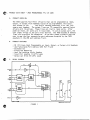
PRODUCT DATA SHEET -. 7605 PROGRAMMABLE TTL f /0 CARD
A.
PRODUCT OVERV lEW
The 7605 suppl ies four 8-bit I/O ports th.at can be programmed as input,
output, or output w·i th readback (tota 1 of 32 p rog rammabl e 1010 1 i nes) .
Port access is via
two 40-pin latched connectors with. ~025 inch
square post headers. The output lines are TTL compatible open-collector
drivers w'ith lK pullups·. These lines are ti"ed to i"nput ports! After
power-on reset, all ports are in input mode~ To use ~n output port, the
user simply wri·tes to the port 1 ines desired. The 7605 decodes 8 address
lines with provision for expansion~ An on~card jumper sY'5'tem allows the
user to map the four cons'ecut lye port addresses· occup ted by th.e 7605
anywhere in the 256 port address ~ield,
B.
PRODUCT FEATURES
...
...
...
...
...
4f)
C.
32 I/O Lines, Each Programmable as Input, Output, or Output with Readback
User-selectable Port Address (256 port Field)
Socketed ICs
Single +5V Operation
Uses Two Latching 40-pin Headers
Input Port Loadi"ng 14 LSTTL Loads
Output can Drive 50 LSTTL Loads
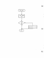
BLOCK DIAGRAM
DATA eus
00.07
10EI~'
CAIIO
SELiCT
OICOOEIt
10AO'
AOOfIIISS
INPUT
~T
ALEer
OECOOEIt
A,2 .... ,
"0'
OUT"'T
~T
WA'
SELI:T
OICOOI"
ot.OOtItlSS
All· ...,
SYS"ESE T'
o----Q
PIlI TTL I 0 C"'''O
'INOtC"'T,S ACTIYI LOW LOGIC
o
FIGURE 1
'.'&iWitwLiUim '" iUX
". ;
I
4WM
W
.,• .. I£.«._, ........4•.• U•. &.• _.
2.
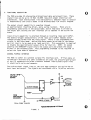
FUNCTIONAL DESCRtPTION
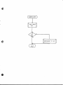
The 7605 provides 32 alternating bidirectional data and ground lines, These
signal lines can be up to 10 feet (3.05H) long with proper electrical considerations. Each bidirectional line characteristic (whether input or output)
is determined by the circuit shown in the Bidi'rectiona1 1'/0 Circuit diagram .
o
The output circuit capability is supplied through
an open-collector inverting driver, and a pu1lup resistor. There are no
programming constraints in the output mode; active high data is written to
the output port c~using the user interface pin to operate tn the active low
state.
Input circuit capability is provided through an inverting i'nput port buffer,
The Schmitt-trigger characteristic of the input port buffer removes noise~
induced voltage spikes from the input signal. There is one programming constraint in the input mode: active-high data cannot be written to the output
port bit that is to be used on an input port bit. This constraint is required
to disable the open-collector output drive for that bit. NOTE: On system
power-up the SYSRESET* signal clears the output port and places the output
drivers in the disabled state. Thus programming overhead is not requlred to
select the input mode of operation.
GENERAL PURPOSE INTERFACE
The 7605 is useful as
twisted pair discrete
of the I/O connectors
in electrically noisy
a genera] purpose TTL interface card. Tf=ftat cable or
wire cable assemblies are used, the ground-signal-ground
minimizes crosstalk between inter-system signal lines
environments.
o
The bidirectional signal lines at the card edge connector are active-low on
both input and output. The signals are terminated with a lK pul1up resistor.
TOSTD-......-'""DATA BUS
BUFFER
+5V
7406
')
Q I - - - -....
.. 14 LSTTL
OUTPUT STROBE
RESEr _ _ _ _ _....
FROM
PORT·SELECT
DECODERS
FROM OTHER CLRCUTS
Typical Bldlrectlon.II/O Circuit
FIGURE
2
o
4C)
3.
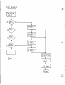
CARD ADDRESS MAPPING
The 7605 is selected by a decoded combination of address lines A2-A7. The
user chooses the card address combination by connecting one jumper wire from
SX and SY to pad matrices adjacent to U2 and U3 (see the 7605 Assembly diagram),
The 7605 is shipped mapped at hex port address 00. To map the 7605 anywhere
in the hexadecimal address range of 00 to FF, change the decoder outputs
connected to SX and SY.
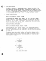
4.
ADDRESS DECODER OPERATION
Refer to the schematic, Document #105778.
The 7605 uses four cascaded 74LS42 decoders (U2, U3~ U5 and u6) to decode
add ress 1 i nes AO-A7. These decoders are enab 1ed on 1y when tORQ* and '-OEXP''(
are active. The WR* signal is used to gate the select strobes from u6 that
control the output ports. The RD* signal is used to gate the select st~05es
from U5 that control the input ports.
CHANGING THE 7605's PORT ADDRESS
Refer to the Assembly diagram, Document #105779
o
Locate decoders U2 and U3 (74LS42) adjacent to the STD BUS edge connector,
Each decoder device has a dual row of pads which form decoder output select
matrices. Make one (and only one) connection to each of the matrices adjacent
to U2 and U3.
The decoder jumper pads numbered as shown in Figure 3 are adjacent to the
decoder chips on the 7605. Also shown are the jumpers Cat XO and YO} which
produce hexadecimal port addresses 00,01,02 and 03, the selections made
when the card is shipped.
Sy
,I
0
sx
,I
0
U2
0
,
0
0
0
to
0
0
0
0
0
0
4
~
"
0
0
0
0
0
0
0
0
0
5
b
.,.
0
0
S
0
.,
0
U3
0
0
,
0
0
1.
3
4f
0
u4
FIGURE 3 - DECODER JUMPER PAD NUMBERING
o
$I $#
......&M£NM.
4
.;
$$
#4#1##
g #2$$$
P44 P
444 ¥ qN
,
#
4W ,;
PM¥##4#
The I/O address mapping and jumper selection table for four addresses per
card shows where to place jumper straps to obtain any four sequential port
addresses in the hexadecimal range OO-FF. Using the lower of the 2~digit
hexadecimal addresses desired, find the most significant hexadecimal address
digit along the vertical axis, and the least significant hex digit on the
horizontal axi~. For example, port addresses 50,51,52 and 53 are obtained
by connecting jumpers at X2 and Y4.
o
The only restriction ihat applies in address selection for the 7605 is that the
lower of the four port addresses (00 as shipped) must occur only at every
fourth possible addr~ss; for example, the sequence 01, 02, 03 and 04 is not
allowed by the decoder.
The pad matrices adjacent to U2 and U3
are on 0.10 inch (0. 25cm) centers,
The jumpei wires may be conveniently replaced by wi rewrap post if frequent
address selection changes are anticipated.
MOST
SIGNIFICANT
HEX ADDRESS
LEAST SIGNIFICANT HEX ADDRESS
01
1 1 2 \3
4
I I I
5
6
7
aJ9JAIs
JUMPER
SELECTION
X&Y
cl J 1F
D
E
0
xo
YO
XO
Y1
XO
Y2
XO
Y3
1
XO
Y4
XO
YS
XO
Y6
XO
Y7
Y3
2
X1
YO
X1
Y1
X1
Y2
X1
3
X1
Y4
X1
YS
X1
Y6
X1
Y7
4
X2
YO
)(2
Y1
X2
Y2
X2
Y3
5
X2
Y4
X2
YS
X2
Y6
X2
Y7
6
X3
YO
X3
Y1
X3
Y2
X3
Y3
7
X3
Y4
X3
YS
X3
Y6
X3
Y7
a
X4
YO
X4
Y1
X4
Y2
X4
Y3
9
X4
Y4
X4
YS
X4
Y6
X4
Y7
A
XS
YO
XS
Y1
XS
Y2
XS
Y3
S
XS
Y4
XS
YS
XS
Y6
X5
Y7
C
X6
YO
X6
Y1
X6
Y2
X6
Y3
D
X6
Y4
X6
YS
X6
Y6
X6
Y7
E
X7
YO
X7
Y1
X7
Y2
X7
Y3
F
X7
Y4
X7
YS
X7
Y6
X7
Y7
"-
o
X
AND
Y
l/
1/0 Address Mapping And Jumper Selection Table For 4 Addresses Per Card
FIGURE 4
o
---------------------------
o
5.
7605 CARD ENVIRONMENTAL SPECIFICATIONS
RECOMMENDED OPERATING L1:11 TS
PARAMETER
HIN
Free Ai r Temperature
I
o
Humidity
CD
CD
0
S
ABSOLUTE NON-OPERATING LlnlTS
TV?
MAX
til
25
55
95
Non-condensing
•
¥4W¥,¥IIf4Af\PATW/i4i4f1f\/lRii1iiRfTf
44
4#A4I4iiiiA,ii:4" N-iU==&&i. _ _ _
N
MAX
UNITS
-40
75
°c
0
95
%RH
~
-~---
..
~.~
..
-~-.
~
~
~'-'~'--"""-----~
---
o
6. ELECTRICAL SPECIFICATIONS
7605 GENERAL PURPOSE TTL I/O CARD ELECtRICAL TEST SPECIFICATION
RECOMMENDED OPERATING LIMITS
MNEM.
PARAMETER
ABSOLUTE NON-OPERATING LIMITS
MIN.
TYP.
MAX.
MIN.
MAX.
UNIT
Vee
Supply voltage
4.75
5.00
5.25
0.0
7.00
Volt
TA
Free air temp.
a
25
55
-40
75
C
•
USER WORST CASE ELECTRICAL CHARACTERISTICS OVER RECOMMENDED TEST LIMITS
MIN
PARAMETER
£
&
,V
OL LOW LEVEL INTERFACE VOLTAGE
IOL LOW LEVEL INTERFACE CURRENT
VOH HIGH LEVEL INTERFACE VOLTAGE
10H HIGH LEVEL INTERFACE CURRENT
-.-
MAX
IUNIT
I
.70
i
j
30
I
15. 50
1 TYP
I
I
4.50
mA
I
f
&
I!
V
-3.5 I
I
V
mA
o
STD BUS ELECTRICAL CHARACTERISTICS OVER RECOMMENDED TEST LIMITS
PARAMETER
MIN
TVP
STO BUS INPUT LOAD
See Fi gu re
,
STD BUS OUTPUT DRIVE
See Fi gure
r.
605
ICC SUPPLY CURRENT
.&
MAX
I UNITS
840
I
I
rnA
At 2 volt
~ At 30rnA current level
~ At 0.70 Volt level.
AC ELECTRICAL CHARACTERISTICS
Must meet all requirements for TTL I/O cards timing as specified in the Series 7000
General Test Specification.
o
~
7.
MECHANICAL
The 7605 is shtpped fully populated. Power dissipation can be reduced by
removing unused input or output ports by removing the ICs:
INPUT/OUTPUT PORT SELECTION
PORT NO.
FOR ONLY AN INPUT
FOR ONLY AN OUTPUT
PORT REMOVE ICs
PORT REMOVE tC
PORT 0
U7, U15, U19
u8
PORT 1
U9, U16, U20
U10
PORT 2
U11, U17, U21
U21
PORT 3
ul3, Ul8, U22
ul4
Leav i ng the input buffers in p1ace a 11 ows~ the processor to read back the
output port data to check for noise a1terati"on or to use the output port as
a data regis.ter.
o
...~
;
~
CIt
CIt
C
J2 .----...-.../'\.
1 2
00
00
00
00
')0
00
,
:,~g 0
00
gg V1
gg ...
or:
00
0
00 ~
00
00
00 N
J
gg
40
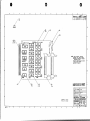
7605 Allembly
o
FIGURE 5
Refer to the Component Placement diagram for component pl~cement information~
The 7505 meets all STO BUS general mechanical specificationS', The 7605
requires one card S'lot in a standard STD BUS card rack. The I/Q connectors
use low-profile, masS' termination 0.25 inch square post latching connectors.
Recommended flat cable card edge connectors include 3~M part number 3417-6040-1
or equivalent.
STD/760S EDGE CONNECTOR PIN LIST
7605 USER INTERFACE CONNECTOR PIN LIST
CONNECTOR J1
PIN NUMBER
PIN NUMBER
+SV
PIN NUMBER
OUTPUT (LSTTL DRIVE)
CONNECTOR J2
SIGNAL
INPUT (LSTTL LOADS)
SIGNAL
J1-2
J2-2
PIN NUMBER
OUTPUT (LSTTL DRIVE)
-Ide
INPUT (LSTTL LOADS) '.
MNEMONIC
+SV
+5 VOLTS
GROUND
MNEMONIC
vCC
GNO
2
4
J1-4
J2-4
+SV
J1-6
J1-8
J2-6
J2-8
06
P2-S*
P2-4*
J1-10
J1-12
J2-10
J2-12
PO-7'
PO-S'
Po-so
PO-4*
04
P2-3'
J1-14
J2-14
PO-3*
16
P2-2*
J2-16
PO-2*
A13
20
P2-1'
J1-16
J1-18
A15
A14
J2-18
A12
P2-o*
J1-20
J2-20
PO-1*
Po-O'
All
22
24
""SV
+SV
J1-22
J2-22
+SV
Al0
26
J1-24
J2-24
+SV
A9
28
9
11
13
15
17
19
21
23
25
27
A8
30
29
6
07
,
55
S5
8
10
1
1
55
55
12
14
1
05
18
VCC
3
+SV
-5V
.. 5 VOLTS
GNO GROUNO
-5V
1
P2-7*
P2-6*
5
7
55
~I\
55
55
1
1
03
02
1
01
1
00
1
A7
1
A6
1
AS
1
1
A4
A3
2
2
A2
2
P3-7*
J1-26
J2-26
P1-7*
RO"
32
31
1
P3-6*
J1-28
J2-28
P1-6*
MEMRO"
34
33
P3-S*
J2-30
,J2-32
P1-S*
P1-4*
MEMEX*
36
P3-4*
J1-30
J1-32
MCSYNC*
P3-3*
J1-34
J2-34
P1-3*
STATUS 0"
38
40
35
37
1
1
BUSRO"
42
39
41
P3-2*
J1-36
P1-2'
INTRa"
44
43
P3-1*
J1-38
J2-36
J2-38
P1-1*
NMIRO"
46
45
P3-0"
J1-40
J2-40
P1-0'
PBRESET*
48
47
CNTRl"
50
49
52
51
54
56
53
55
"low level Active
All odd numbered pins go to ground
Interface Connector Pin List
4[)
1
PCI
AUX GNO
IN
AUX -v
"low level Active
A1
AO
WR"
lORa"
IOEXP"
REFRESH"
STATUS 1"
o
BUSAK*
INTAK"
WAITRO*
1
OUT
SYSRESET*
CLOCK"
PCO
AUX GNO
AUX +V
,'t* Des i gnates LSTTL Loads
Edge Connector Pin List
FIGURE 6
NOTE; Vcc is provided on the user interface pins Jl and J2. These should
be used only after the system designer has thoroughly studied the system
implication. Care must be taken to avoid ground loops.
o
o
B.
760S OPERATING SUBROUTINE MODULES
This section provides flow diagrams and subroutines to operate your 7605
card. These may be used intact, or used as models to construct subroutines
for a specific application.
The subroutines are written in BOBO-family assembly code and will execute
on BoBO, BoBS, and zBo processors. The memory addresses selected are
compatible with Pro~Logls 7B01 (BOBSA) and 7B03 (ZBO) processor cards.
The 760S port addresses used are the address jumper selections made when
the 760S is shipped.
To use these subroutines in systems other than those described above, the
memory and/or I/O port addresses may require change for compatibility,
The flow diagrams presented can be easily translated into the ass'emb1y code
used by any microprocessor since they show' the steps req.uired to achieve
760s operation without reference to a particular microprocessor~
The following subroutines are written to act only on a s.ingle bit on the
output or input ports. For routines which act on all 8 bits of a port at
the same time, see the 7604 User's Manual.
c
NAME AND DESCRIPTION
REGISTERS
CHANGED
FLOW
DIAGRAM
PROGRAM
PAGE
PAGE
START
ADDRESS
(Initialize 760S)
This subroutine sets all outputs
to a predefined state. It also
i nit i ali zes all viariables used
by the other subroutines.
A
H
L
1300
i
I
I
(Set bit)
This routine accepts a hex value
in the accumulator which corresponds to the I/O module to be
turned on. If the I/O module
number is out of range, the carry
flag will be set.
A
B
C
H
L
PAGE
PAGE
1394
I
I
(C 1ear bit)
This routine accepts a hex value
in the accumulator which corresponds to the I/O module to be
turned off. If the I/O module
number is out of range, the carry
flag will be set.
o
I
A
B
C
H
L
PAGE
PAGE
l3AO
cont i nued
~
o
. •
NAME AND DESCRlPTtON
REGtSTERS
CHANGED
START
ADDRESS
FLOW
DIAGRAM
PROGRAM
PAGE
PAGE
13BO
PAGE
P,L\GE
1342
(Test bit)
This routi'ne accepts a hex value
in the accumulator which corresponds to the I/O module to be
tested. If the I/O module number is out of range, the carry
flag will be set. The s:ubroutrne
returns with P=O if there was no
change and P=l if the addressed
module did change since the last
test. The Z flag =0 if the bit
is set and Z=l if the input port
is clear.
A
B
H
L
C
F
(Complement a bit)
This routine accepts a hex value
in the accumulator whi'ch corresponds to the I/O module to be
complemented. If the I/O module
is out of range the carry flag
wi 11 be set.
A
B
H
L
o
C
J
o
o
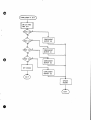
INITIALIZE 7605
INITIALIZE
OUTPUT
PORTS
tNITIALIZE
VARlABLES
o
f,
J
o
X4
$4
'$U44 _ .
XC 4 • •
AU
444
•
#¥
4.
.$W
o
SET A BtT
TEST fNPUT
BIT
COMPLEMENT ItA" BIT
o
o
o
CLEAR A BIT
TEST INPUT
BrT
o
•
COMPLEMENT "A" BfT
WHICH PORT
AND BIT
MASK OFF BIT
ON PORT 00
MASK OFF BIT
ON PORT 0]
MASK OFF BIT
ON PORT 02
MASK OFF BIT
ON PORT 03
SET ERROR
COMPARE MEMORY
AND INPUT PORT
UPDATE
MEMORY
SET FLAG
()
o
WHICH PORT
AND BIT
COMPLEMENT
OUTPUT 00
COMPLEMENT
OUTPUT 01
o
COMPLEMENT
OUTPUT 02
SET ERROR
COMPLEMENT
OUTPUT 03
UPDATE
MEMORY
•
;q ii, 44#WWi1U til
Ii:':
1M £
4h:; «MWU";.'''_*,
PROGRAM ASSEMBLY fORM
PRO.LOG CORPORATION
MNEMONIC
HEXAOECI~'AL
=A.GE
~D·R
~~~
00
1
I tNSTR
! 2..1
LABEL
[i1(05)
i
21
3
! ~E.
INSTR.
Ll)~I
--
5
))"l.
6
DC
7
~r:
COMMENTS
:tN \ \' , A. LI
~l
PAr...;:..
()
1
~
~~"T
'/..'1..
I
00
1
?~~T f"'l'"':J
I
Dl'~
-
~R~c..1:<>~1v\
z...~_
'l...x.
t<~M
t..!>A 1
41
DATE
TITLE
MODIFIER
t. ~ET
LJ:>Al
?~'2_T
01
8
9 :D3
A
0;> A.
-
0\
B I '?>E.
cl
o !1>'3
-
1
CPA
-
2
3 ;!:>"JIl
! 2..3
-
I~\~~
IC"..O
\PA
7~
-
6 iO\
(~L\
S\
,c.P
l\-\Li
\,,~
-
:02...
o )'"1'7
5.TAN
E:2~
\c....~
1-r>'B
\~A
O~
~""Al'l..JC.
50
B i~'fI
;'7
'?ORi
t\lcL\
Ai'2.~
1
IJn
I
(~L'
1.0 .
ID
O~
S\,Aw
F
~M=tJ,.r.Q"
Y..Y..
9 i ~'7
C
02.
\ 1>A
4 Inn
6
?Q~i
~c;,~T
L!>A1:.
\ 0
"''7
I- ~~T
XX
C?A
E 0'2.
OF
5
I,
C\
LJ)AI
-
I~,-A.l\.\
21 ~q
52.
{UL.\
( \+l..\
o
O~
L~L'\
~i~
3
4
5
6
7
8
9
A
B
C
,
D
E
2..F
~O
;
I
4t=
l'fJ\\\c"\.t U~€.?)
l...J)c.
L..J:>A:r
2
I ~E.
I 0,
3
OCD
\...D~"I.
4
01
5.
Oc.
6
7
O"J)
1
('_~
\...OO'tl
-
OJ
\c..e.
0\
'R"'\~
~R-.l
02-
~p
A 12.(0
B
\~
-
c 04
\C.~
D (!:~
E 1 t.(o
jp
~F 1 \3
-
!I "~"'I!.A. 'c.o~\l1£"R"r N~
r
:
"Il.r-."
ik
,
{Ii'}
t..OOP
..... ,~ =
~
-r-,~
l!>
.&
!.
\ en-.
t.'!.
:1=- 1\~t'OciM"' ...\~ -#' 'Q~'Tl)Q..~ \~~...:'I
";E,I
.
\10\ ~ ....-." -"\:-.. 1l~~'
!1-'I:~h"l"\.o..'\7s:. 'l?~" A·-&
I
"J:)C!.<!.
81o~
9
A
...
N.
~oc..-r ~
~2.. ~e:MoSr. ~.~
.... ,.,
u::
'7;'0,",
l'
o.oQ..,
~ ~~Y.T ~~ ~< t~~~
~~ -r~."-I:) ~
~ SE"T .INA"
?,.,,,'" R"A 't.:/... ~~T
!
o
I
i
UN
L~""-:C
i
I
I~,
.-~
PRO-LOG CORPORATION
HEXADECIMAL
LINe
=AG:
I NSTR.
... C~
AOR
o
'2
C-D
3
~O
4
\3
2..1
b"""o, 1=N\c:'.'rr A.
oS
D<!.~
9
C,A
_..lP
A
56
B
13
C
D
2.!>
05
:t>~
J~
E
(!A
'-IF
GJ1
50
\~
1
2.3
05
~A
~p
_'1'1
A
\~
~'7
c::.e:(!.
D
c.~
J~."5
E
1..\7
SF
.'t)'B
~nlti
DC)
)(£11.
2
~3
~A
-
?n~
,..\1
0.013,
E
-'lP
-~
L.\'1
1
'l)~
-
JP
~
02.
'1
)(R~
4
't)~
DPA
02-
7
.,~
8
\a
9
441
A
l>e
IJ-POA-rE.
~l'lQ..."
00
00
UN
!
([)pn~ rn~M~
A.
~
\~.D~-n!'.
?""~'"T'
UPQ~~
()I'\Q:r
n\
0\
':B
r>\
UN
1(tJ'>~e. MEM.dL"'~
A
1"\2-
02..
C
-
02.
JP
-
~N)'T'
~~
-
IJP~E. "'~,,""
O~
A~
'JlQ.A.
D
E
i:>~
OPA
-
Ao C0P~ rr£~-l) ANA.
T wu; AM* ,MMi IWfWM :1 U 1$;£ '''MiA,; II.,.
A
L.x> 0 Q.l"E
()~RT
C3.
\PA
B
o~
.\~
~
C
F
~
-
A'S
C3
C #:
IPA-
Z 02.
6
INV~l.\
_co
00
L-b&
3
5
\~
_~"T'
-----..
-
)(~
F
J:- tjPno..-n;.
\PA
0\
'70
•
-
~'S
C3
A
L~~
9
D
O~
i
JP
A
01
02.
;- RE:1"u~' <!~.I
-
3()O
'1>3
0\
~1
-
1
B
o~
pl')~"
lD:Po.
\ () i\
00
AS
C
~u""I~~
N~
00
J>~
~~ T
~DR.'"
\o\L
-
B
8
':\Q.~'T
~I
~~
-
9
,~
(1 ~IH;;('J T
TO
~t
-
·8
~'7
Ol1'"
e\
~T
..l-P
IC!.:P
DC..P
7
.£'",.
t4NO
\+L
Il!...f)
~
6
~~~'"T'~
~,~C
Q~~
~
05
'1j:
~
-
6
5
io-
-
\~
c.~
'S,~
M!
?~a...,.
el
I<!.P
CA
'10
4
~~"t"'5
OIlANt:-.t:=-
(lAIL',H ~~
I\.l
-
c
(f)
f-
'( ~\~"' lIN~?')
-
7
fDo
Xx.
-
8
3
ZZl$
-
..\<:"
-
7
o
II.rI"
L1)~1.
6
4
5
COMMENTS
MODIFIER
t.'OA'I'
1
2
DATE
TinE
INSTR.
LABEL
40
5
PROGRAM ASSEMBLY FORM
MNEMONIC
"a.,","" I'.:II:===.=I&_--=::
O~
~
D3
~
+-f1\.~1{
o..u. . ?:.lTi~~6s=:c
-e.,lT
__
_1117
...
-
·._ ... _ ........
~
......... _" ..
c_~~~,
"'~"""""",,,
____,_, ___ ,,, _ _ _ _ _ _ ,,.,,,,,,,,,,,,_,, _ _ _ _ _ _ _ ,_ _ __
PROGRAM ASSEMBLY FORM
PRO-LOG CORPORATION
t"~XADEC:MAL
LINE
ADR
=~GE
':'''''F1
MNEMONIC
INSTR.
I TITLE
INSTR,
LABEL
DATE
COMMENTS
MODIFIER
'30
'1~
LJ)C!.
A
ifor .. ~~E..
1
2
'1g
l~c..
~
iI
~ (lOM.PLEMEN"T'
2,t=
()M~l
3
4'7
L b&
A
it
r
4
,)e,
L:DA
M. L~~,)
i
4-LD~CI
S
fl...O
A+J~
"0
Il
-
OR..A
C!..
Ii
4- C~
I
"S-rnR.E
6
7
8
"'&1
17
~\.,.
II""· - "
~
\~
{~IT
c..
l"/\A~l<.l
()
II
(~L')
srA~
c..q
('
"" ... "" ,,1).1
bA.'A.
.
Ir-."""'n A-
MA.gll lltl-r c.",~~e. R\"\ (\EMe ~l ...... ~~
I~
~\
c...~A. "":\f:.,E
~~ ~~~
\~
t-4\t=::<n~~\.\
~~\
--
l~
i<.'TS
9
A
B
C
0
E
~F
~O
1
U>A-"1
2
3
4
'\1 (Se:T
-e r\')
0..
<:!.S
9SP
~
tiS
!M
13
9 C.l
-
?t.P
-e.c..
A
~~
R-rs
~I
B
']g
L,.,t)/o).
C
c.c.
.JS
0
42..
-
E
\~
F
<!.~
..
-
1(,
4'7
3 l"_S
4 C'J)
2
[("'_l~A,I:t
~ ~ I'T'\
I(~~,. A. ~''1')
i
~\\
""R~I~Q..N
C!...=,
.. \~...,)l':r'\
~~"\
t\
hl'l/'llOl !:-.m&: ....~ "
IS
A.IQ~US~'"
,~
\f\)\lAL~.o;l#
(lNV\ ~l ~M::=~-r
'"31"\'
~rr
I
~
-
--
'0.
t::J:)~
A
~~
P-t'
-
-
~<!.
8
1::>~
R"iS
C!..I
'1a
l~A
.~.
~~
JS
-
14213
0
<'..q
-
E
~
A
~rT)
-
-
\!l
_2.t
1L:l:>{l :t
6
OS
r'hc!"~
7
J.p
8
c...,A
U
9
\~
\~
l!.=1
t-- \~
t' I !;A-~
..
-
2.~
\C'_~
B
O~
l'h~~
C
~
\lP
0
~2.
E
F
\3
-
\(!p
"
I
'1.u~\c.H UN'-?)
~l
-..
A
~~
\~
::?-.\.'\
"''Q~Q..~
~O
-
2
S
\ t:
'~L1:!C"CIr:h"
(f ,
c: 0..0
I'lO"T"
IN~ALL1'I
#:-
(I tH'·C'.{)l...E..M~NT
"BlT
(<!.M.tLEJr£N'l A-&rT
l\S,
3
4
1-t'_~~.1t'l.
'"'E-.\"1"
9.."TS
1L'bA.1.':.
AF
C!..'b (-u::.~,.
A
1
Pu>
C
I- ~~fjpi
i(~T .~ ~1T\
<!ol
1
\~
~
7
~o
Cl~<1l<.
~
_~S
S'bo
6 \3
B
~IT
A.
1Ll>A-:t
1
9
A
f
~c..
R,.S
Ao
~"'i
I-
p..
5
8
I
'kx.
6
7
_<1
-
L.:l:>'B
PACe;.
C(
.
I ~~\~C)
no
~
\H
'bl
P'f
01
I
1
Hl
a.~~(f.ll
-SE\"
'XX
RAM
f-
~.
""p" ,T
~TIl.-n..J...r,
'¥.cIN."T"~
1', '"
"TZ"\
~,.
"'cu (1,)/ A""'O;.
;:.\~.,..
12N.J'"'\\
~t"'lR."T
Nt:..
Pl'..ILT" ~~"AtT
PROGRAM ASSEMBLY FORM
PRO·LOG CORPORATION
H!:XAOECINIAL
LINe
INSTR.
AOR
NI'lENIONIC
P~GE
o
LABEL
:'':IR.
e.O 05
1
c.A.
2
J)~
3
\~
-
-
4
~
I(!.P
OS
~
9
00
~o9
C
0
41
-r>f>
E
00
('!.F
C'..~
:DO
~I
1
\~
2
~'1
3
::l:>&
l=RE:TU~N
~~~
,~
.... <;.A.\I~
'K.\'5
~\
(',f'>
LJ:'Je...
A
-
..)~
?i
~,
-
A
~\~p~
t:!.3
6
E"\
-
l~
-
(1 t'l\t=M.
7
8
t.\"1
L:t:>~
A
9
l>~
\~,::lr.
A
D2<!..2>
~t>
E:\
13
-
E
!>F
41
':0'0
t'"l\
L\f>
+-
-
1'"')'2.
-
<!.l\e:M.
~e
~
.... S~~e.
l"'
O~
1
Ao
ANA.
03
"0
2
~~
~S+>
~r;
3
'1f.
_t-.:bA
-/'{\o.~\i.
... <'A\I~
A-N~
~
I.J:><!..
Pt
6
F\
~U)
~
j:. ~~
7
8
~S
p~p
AJ::.
~
l!...S
~5~
~c.
9
l'~"b
~S
A
,,~
-
I~
t!.1
"7Q
<>L{)
COC!
l~A
f'
~I
?'-~
~e.
E.F
A~
vRA.
,?O
'7'1
l...l::.~
B
C.
_am
\)~\lJA...llE:n
~L~
~~
.Ps-P
~~
C.,\
()L~
3
.,q
1.'hA
'be"..
C.
4
2..~
(\M.Al
5
1')"1
~lA
6
E.lo
~~:I.
7
Qn
8
~(')
Q~~
~
9
4~
1~'l'iC.
A
A
~
1~5..~
B
~\
?~
C
~q
~\5
lh':~g.
~/::I,.'"T~
"B,ri.c:., (CLal
IN t:"..
A..('I.~.)Ml\I...A.."'DQ.. ~~ ~ '"\l"I N~ Q,QmIl
()L~
-
u~I\~"E.
~
QI)T
C~'"TA
1.J.r:~J.l"JQ."
\J\'T~ ~~~
"'B.rT' S\A,.,tJ5
~:I
Cl.D
.
4-
~~A
0
.
~ll
~D
~
A.;:
I~
A
1'ui N~ hA1"'" \~ .~. At>1Il:) ~~ \~ C!. (~ ST~·-=_~
. . ~ "Rn"
2
(I,g::Q
A..T'Pt.
~ f"'lJl'\ ~ 1\lt;...,J= ('Iuo.....\t..r:
1
-
4 - ~~-J~
UN
B
E
-~u.,.
n
~Lt'\
.... MPt~'£
~O
4F
C
b~"'O.
\.U .IA ~E"b
'¥..\TS (N~'oJ\
NF;.w b~ ~D r;:.!~ (2!SP.I1"
.... t...cA.D
4
'Ma\i:)
'f"M:i...~\(
J
ML~,\
(~
bp..~A
IN ~tJ'T
5
-
M.~5~
....
\t=>Pt
-
~A."l;.
.~ .I~..!!T_
E.o
0
"'bA.'"T~
J,.
0\
0
#:
MA.~\L
... 5A.'I1E:
\P~
4
B
£c~\M'-IA.L\""
{lM~
l:b&
-
c::.2\
c..tl..R.~ '4
~A.'A
.
_00
W l\~
M""~v..
T-\ N~,)'T'
\p A
5
C
o
I
PT 03-
-
.
~'1
l+~
~I
\~
e,.q
~'2.
-;:.,.
lP
8
B
COMMENTS
~I
Jf':>
5
A
OATE
TITLE
MODIFIER
'l:>c!'~
6 C!.A
7 '"l)e.
o
INSTR.
T"MQ-'/E.
~
~ ~\.J'\
... "
<;"T~-n:.
i=-L.A~c,.
~,
Tn
;L\~ ~I\ (t\lAN~';:
p.&..
I~
~A.b
.~~
('~~
~<:!.
(I :: . C!.\-\'A.N~ES
~= 'P,rr ·S~~-,,::;:
(\ ~o.,..';~C:::
~D=
f:..
IN
/:l.'-'~CI. A~~
'S:.-f....'\("t
~\"'L
~
Pn5.\\,\t")...)
,.
... tR.~\'\"Ar~~~
i ~PUi ~l.Ab
1
~ SE=':\"
!Jr
~L~
~LPb
I~
~
~\\
~
\Z'lb.~
~
~E'"
I
0
E
..,i
~F
='_ii4 '''W;:hAI .,
'i: ; i¥1A. ,.##4 4
-""
W.'.
$
.,;;m:nwi4fiillYlJWWi:;;;, (
i· ¥
!
,
+5'1
_C!6IA5!,§6. UffEK.
-.~ V4L!>H"i; 14:--/
O'/(~)
01>(.0)---
~
05(~-'04 (i4}-- ..
OJ(i)
1\
02
2.
r;}- .
'j, (ii)---. --I)(}G~'
...
"
1
.DII.'
l)~ft !~.nfflFACE
.sv
l-GB
RA,
lOll?
t~V
'!> .-.. -
UI
..-----~----------~-~-
.!E~~T~
-!-..@.})t5V 10011
_rili~!)
~'5V
'1401.
l~RI'~ ----.{»- Nlc
.
:t~~t "_~tl,J!-
. --='
JR
e ':'_.
~olnp)~() !L_.. _
'3
I~
t...
"
III·S
~ .-"..,..,..-
u+
J.4LSlU
IOHPlk®--- ..~fi--- )e.
l.-.(f~])p<>'l'"
r-<E2>
!.-<!E!>ro-o.
tSV
- . - ... - . - - - - - - - - - , - - - 4 --
~~"!:g~:QLlf!lli.
~
'"-)
1000
-
-- ~I_~~
At>@--.---
---~Q~r
....!~ 0
nr···.
f-'\
.r~
14-0b
KI@-.. ----·
AS@----------
1000
'--.!.... C!E.;-.g)I'Q·S.
z
'1
•
.lC!8)
1'1)-.,...
-.--15 ;.0--. ---=
.,!!------ -2J~~:!!
Ii
~=;lJ~~t
''!.--··-~5 X'! r~
T/
~
-..!.-~IIH
(,0
V)
r~
!.....~Pn-
CV~
.!...··<E.90-l
NOT£r~i~~~~~'tl~~I'ECjFIEQ. Ie
~J'UMPU' MOVES II.Ol'OO.T5
r®:!>
'!.
Qf::!90-1I1
.r-<!EY
IN 6 CONSECuTIVi
IlOIlO
&...OCK~
&ru~lEO:~:f:~~T!a
·~I'O-C.'
IN 8 CON5fCUTIVE BL~
OF • PORT! PER BLOCK.
&~~i ~f~ (i!~~~~~.
tSV
SEE TABLE FOR 5PfC.lflC
HOO,\-lJP!,. ALL OUTPUT6
HA,/E 110 CCI'INEnION.
r\:!f?~
=-Q[E)t)V
r@J9
""::"(~Pl-"
rUHP
"'=""'@1!)fl"·I I .t'-2!:
c<R~
~PARE . CIReIlII HOOK -liP A
1000
TYP. ~f.lJ(Sl6t.AT1JI ~-UP __
UlS-IITORl,
UI5
"i-O(,
7106
UI6
UIIo-IITOR3'l
UI.,
7Mb
UI'1-IITOI\+-3
HOb
UI!
UIS-9TOR'-l
740£.
UIS-U TOI\6-2
UI9
.,.06
UIS
1119-llTO"'-t
';:-'~~1'5'
.r<E-W
.!....QIIDPI-UIIW1
r~
.!... --<lD!JPI- 3a
r@"1§>
~~1§iPl-l'
U4
1415<'#
r.,,, I I'f> .,
WR'~-'-r--:T---·-
SV5k£~l f .
-15'1
61'10
r --
@--'-!f
0)
(l}-J
. ---.. --·---
1:1
T-zsv
~~-J-- -.
!...a{~p'·'''i
.~
'\.2....~~I.1lI
R!. T It
II~T~
. . J-- 'J.'.-+
~
'1401.0
7401.
1"010
14Ot.
Uta
".Ot..
Ufl
U2.
ll'.olpl-O'
II!>TJr
tm9111tl-Z
UZD-Ilmrn
UZO
UeD
740("
IIOCO
UIB-IlTOiS-]
Ui'D
UZO·lllDfl·r
I,lZHflOlCIZ
U2I-11TDC8-Z
UlI-,3lDl3l
'140t.
7iD/"
14Dt.>
utI
LJ2Z
ut2-1I1052
140£,
Ut'f
un-I~ lDt9·Z
UZZ
UZ2-'JD5-Z
REFERENCE ONLY
-t5V
CZ-CI2
llitF TO.L.~
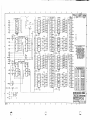
~o"
PRO-LOG CORPORATION
"'1
it:i~~~~ li~~~I'iru~J
I~:-cTARK-
iO-lIi'-
TTL I/O CAI\O
-:Jlt..J'I'~/-"
~t'!!:1
,...,
~"t
~~
'~)
~~
~
•
•
o
Q
.'V.I.O ••
INI TIAt f:fIEASf
/@l
~
q:1i!
J~.
PCN 07l!J
'"
~
{,.
&~
o
2 PI. {S
!>U l)£rAlL A
1
~~.
"
y
r:;;;:)
OO~5
C£1
US!
~~~~
:::;u:a~
e ••••11.... o~
~
88 e
f:: :1 88
L*J 88
..-.1!!9
[±:l
[1£:]
[:: ~~?;:]
f1h~
~TIT&..--.rll
~~r::
~J
~t'JI
IjJ
14
liLiJQf0ftIiOi-i L
~.~
IiJ
-@
411.(5
10 It.CS
I
00
00
00
00
00
00
00
00
00
00
00
00
00
00
00
00
00
00
00
00
40
I
.J!QIfi
a
UNtCSS OTHEKWIS€
SPEClnco
I!::s D£NCJTC'j PIN I Cwo or sOtLCTS
e- M/II:.D TO ClJNFOIUf WITH ASSEHaU'
P/{OCEDlJIeCS A5100+
As- IDENTlFr WItH A5SEI'IdLJ' ~EII_ LETTEe
/ISING. IfUBMR S71VfP
& MAPPED TO POKT 00
00
00
00
00
00
00
00
00
00
00
00
00
00
00
00
00
00
00
00
00
•
..
REFERENCE ONLY
-@
Z J'l-CS
If/-If'
.'-'-=='---I-=C:.=i! ---- C/2
CI
~1'D517"
I~ OESCRIPJlON
SJ:.1/U'JlflL ND_ IDl-JIIl
f-'1u:rs LIST NO_ lOS 7IJD
I_~~SIGII~!~
PW8
PRO-LOG CORPORATION
g-~~i~~~~A~SfH~LY. i~~
=~------r:------ 6£N£~ L pot
~~UL~L!!t7.. TTL
oor.~~.'~.'!'
r
r;n
CAKO
Sf
-D 1105-i1,T);E':
.
( ')
(\,
-_.j
,,!!
•
•
•
hrh
--------------------.........,..._ _-----------------,._
.............
_ ----~
..... ...• _.•.
o
o
tlSER'S MANtiAL
2411 Garden Road
Monterey, California 93940
Telephone: (408) 372-4593
TWX: 910-360-7082
o
106666A
200
9/81