1
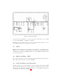
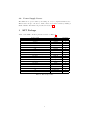
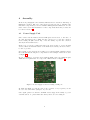
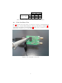
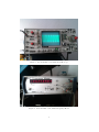
FunCube Dongle HF Kit Convertor
Version 2.0
User Manual
Authors:
Diogo Condec
¸o
CT2IRW
Ant´onio Matias
CT1FFU
www.dxpatrol.com
26th January 2012
Contents
1 Introduction
1
2 KIT Schematic and Circuit Description
2.1 Low Pass Filter (LPF) . . . . . . . . . .
2.2 Gain Block - OPTIONAL . . . . . . . .
2.3 Mixer . . . . . . . . . . . . . . . . . . .
2.4 High Pass Filter - HPF . . . . . . . . .
2.5 Clock Oscillator and Attenuator . . . .
2.6 Power Supply Source . . . . . . . . . . .
.
.
.
.
.
.
.
.
.
.
.
.
.
.
.
.
.
.
.
.
.
.
.
.
.
.
.
.
.
.
.
.
.
.
.
.
.
.
.
.
.
.
.
.
.
.
.
.
.
.
.
.
.
.
.
.
.
.
.
.
.
.
.
.
.
.
.
.
.
.
.
.
.
.
.
.
.
.
.
.
.
.
.
.
3 KIT Package
1
1
1
2
2
2
3
3
4 Assembly
4.1 Power Supply Unit . . . . . . .
4.2 Notch Filter and Capacitor C12
4.2.1 Notch Filter . . . . . . .
4.2.2 Capacitor C12 . . . . .
4.3 Clock Level Attenuator . . . .
4.4 Clock Oscillator Test . . . . . .
.
.
.
.
.
.
4
4
5
5
5
5
6
5 Software
5.1 SDR-Radio by Simon Brown . . . . . . . . . . . . . . . . . . . .
5.2 HDSDR and similar . . . . . . . . . . . . . . . . . . . . . . . . .
8
8
9
I
. .
.
. .
. .
. .
. .
.
.
.
.
.
.
.
.
.
.
.
.
.
.
.
.
.
.
.
.
.
.
.
.
.
.
.
.
.
.
.
.
.
.
.
.
.
.
.
.
.
.
.
.
.
.
.
.
.
.
.
.
.
.
.
.
.
.
.
.
.
.
.
.
.
.
.
.
.
.
.
.
.
.
.
.
.
.
.
.
.
.
.
.
.
.
.
.
.
.
.
.
.
.
.
.
List of Figures
1
2
3
4
5
6
7
8
Circuit Schematic. . . . . . . . . . . . . . . .
Power Supply Connection using a USB port.
Power Supply Connection using the FCD. . .
Clock Oscillator test point. . . . . . . . . . .
Clock Oscillator test with an Oscilloscope. . .
Clock Oscillator test with a Frequency Meter.
SDR-Radio configuration window. . . . . . .
HDSDR and similar configuration window. .
II
.
.
.
.
.
.
.
.
.
.
.
.
.
.
.
.
.
.
.
.
.
.
.
.
.
.
.
.
.
.
.
.
.
.
.
.
.
.
.
.
.
.
.
.
.
.
.
.
.
.
.
.
.
.
.
.
.
.
.
.
.
.
.
.
.
.
.
.
.
.
.
.
.
.
.
.
.
.
.
.
.
.
.
.
.
.
.
.
2
4
5
6
7
7
8
9
List of Tables
1
2
Kit Components. . . . . . . . . . . . . . . . . . . . . . . . . . . .
Resistor Values for the Clock Oscillator Attenuator. . . . . . . .
III
3
6
1
Introduction
FUNCUBE DONGLE HF CONVERTER
Funcube Dongle (FCD) is a powerful and small Software Defined Radio (SDR)
which has the ability of covering the frequency range between 64 and 1700MHz.
Since the beginning, the FCD has picked-up its owner’s attention with its quality
and performance. However, some remained reluctant with the lack of coverage
bellow 64MHz. Hence, the need to provide this HF Converter KIT, that allows
to use of the FCD in the HF bands, but also in the low VHF band of 6m
(50MHz). Thus, interpolating this project, between the antenna and the receiver
(FCD), the user is able to extend the coverage from DC to 1700MHz. Both the
HF Converter topology and its assembly are very simple, as you can see in the
next chapters.
2
KIT Schematic and Circuit Description
Fig. 1 presents the converter schematic, which is very simple. When looking
to the schematic it is relatively easy and straightforward to identify the four
main blocks of the circuit. That is to say: input filter; gain unit (Optional - not
included in the Kit); the mixer; and the output filter (which since version 2.0
includes a notch filter for the broadcasts emissions).
Also, since version 2.0, the user has the ability to choose the power-supply
source: either by an USB plug; or power directly by the FCD - (make sure your
device is compatible with this function).
For advanced users there is place on the board to place a LNA device with minor
changes to the circuit. Also, pay extra attention to the supply requirements of
the device you choose to use, which may not be compatible with the FCD power
supply capabilities.
Now let’s look into the schematic in more detail.
2.1
Low Pass Filter (LPF)
This first stage of the signal is a LPF to extract the frequencies in the range of
DC to 52MHz. It is a 9-pole butterworth LPF.
2.2
Gain Block - OPTIONAL
Advanced users can choose to populate this block with a good LNA device,
in order to both, decrease the device’s Noise Figure and increase its dynamic
range, since the amplifier used on the FCD is a broadband unit which has very
poor performance in these fields.
This is completely up to the users to use such approach and the respective
planning of this stage.
1
1
2
3
4
FCD
A
A
PIL10 1
PIC202
PIC201
PIC1802
PIC1801
GND
GND
COC2
C2
100nF
COC18
C18
COL10
L10
1mH
100pF
PIL10 2
USB
COP4
P4
+5V
PIP402
PIP401
B
PIL101
COL2
L2
PIL102
47nH
PIP202
COL3
L3
PIL201
PIL202
PIL301
220nH
PIC802
PIC801
COP2
P2
56pF
PIL401
270nH
PIC902
PIC901
COC8
C8
COL4
L4
PIL302
PIL501
220nH
PIC10 2
PIC10 1
COC9
C9
100pF
COC10
C10
100pF
COC1
C1
COL5
L5
PIL402
PIL502
47nH
PIC1 02
PIC1 01
COC11
C11
56pF
PIC102
COR1
R1
1k
PIU108
PIR101
COU2
U2
COL1
L1
PIP201
PIR102
8
2
1
Header 2
100pF
OUT
PIU20
PIU203
PIC2001
PIU204
1
PIC2002
OUT_APIU104
4
2
GND
GND
GNDGND
GND
COC14
C14
+5V
USB
C
PIL602
PIC1302
PIC1301
100pF
PIC501
COC13
C13
100pF
COL6
L6
82nH
COC6
C6
PIC502
PIC601
15pF
PIL702
COL7
L7
47nH
PIL902
COL8
L8
47nH
PIL801
PIL901
GND
GND
GND
GND
2
D-
PIJ102
D+
PIJ103
GND
PIJ104
3
4
PIC1602
PIC1601
COC16
C16
100nF
PIC1702
PIC1701
PIP102
COP1
P1
3
GND
COC15
C15
GND
GND
100pF
C
+5V
FCD
COX1
X1
VCC
GND
PI 301 PI 302 PI 30
OUT
COC17
C17
100pF
PIX103
PIR302
PIR301
COR3
R3
PIJ105
5
GND
PIX102
USB Type A Connector
GND
PIL1101
1
2
3
Shield
PIJ101
PIP101
COL11
L11
PIL1102
100uH
COL9
L9
82nH
PIL701
B
PIC1902
47pF
PIC702
91pF
PIL601
USB
PIX104
1
VCC
PIC701
20pF
PIL802
PIC1901
COC7
C7
PIC602
PIU103
7
PIC1402 PIC1502
PIC1401 PIC1501
COJ1
J1
D
COC5
C5
PIC402
OSC_E GND
6
GND
PIC401
20pF
OUT_B
COC12
C12
100pF
PIU106 PIU107
GND
COC4
C4
PIC302
91pF
PIU105
OSC_B
GND
PIC301
5
PIU102
IN_B
PIC1202
PIC1201
COC19
C19
COC3
C3
IN_A
PIU101
100pF
GND
BGA616
COU1
U1
NE602
VCC
COC20
C20
PIC101
PIU201IN
GND GND
PIR202
COR2
R2
PIX10
COP3
P3
Header 3
COR4
R4
PIR201
PIR402
GND
GND
GND
D
GND
1
PIR401
TRI-STATE
2
3
4
Figure 1: Circuit Schematic.
Several devices are plausible to be used, and in the circuit there is a footprint
for devices like MAR-6 or BGA616, or similar.
This stage, for global use is (as you can see in the schematic) disabled. If you
need further information on this please contact us.
2.3
Mixer
Mixing the RF signal and the IF signal is responsibility of the NE602 device.
This device is a fairly good and robust device (also use by Elecraft in their
equipments) adds the DC-64MHz signals to the 106.25MHz IF, which will be
feed to the next stage.
2.4
High Pass Filter - HPF
The result of the mixer operation with the RF and IF signals enters this 9-pole
filter, which then cuts the noise bellow 100MHz.
2.5
Clock Oscillator and Attenuator
The IF is generated by a Clock Oscillator module, which results in a 106.25MHz
signal with 5Vpp. This voltage value is to high to be handled by the mixer, hence
the need for an Attenuator, which in this case is of 6dB. Further information
on this subject can be found on Table 2.
2
2.6
Power Supply Source
The KIT can be power either by an USB port or by a compatible FCD device.
This decision is up to the user to make, and is done in the circuit by making a
shunt. Further information is presented in Section 4.1
3
KIT Package
A list of the KIT content is presented bellow on Table 1.
Components
L1/L5/L7/L8
L2/L4
L3
L6/L9
L10
L11
R2
R3/R4
C1/C9/C10/C12/C13/C14/C15/C17/C18
C2/C16
C3/C7
C4/C6
C5
C8/C11
C19
P1/P2
X1
U1
J1
Value
47nH
220nH
270nH
82nH
1mH
100uH
39Ω
150Ω
100pF
100nF
91pF
20pF
15pF
56pF
60pF trimmer
P anelSM A
106.25M Hz
N E602AN
U SBP LU G
Table 1: Kit Components.
3
Quantity
4
2
1
2
1
1
1
2
9
2
2
2
1
2
1
2
1
1
1
4
Assembly
In the next paragraphs some assembly instructions are described with help of
illustrative pictures. The rest of the steps is a basic an easy to assemble just
match the components you receive with the KIT against the silkscreen on both
sides of the board. Any information on the components label and/or value can
be found on Section 3.
4.1
Power Supply Unit
Since version 2.0 the FCD Converter KIT gives the freedom, to the user, of
choosing the supply source. Thus, the user can choose to power the converter
from a USB port (like version 1.0), or use the ability of power the converter
directly from the FCD device.
Please note, you need to make sure that your device is able to power external
devices, this is an internal feature of the FCD devices that your device has to
be able to provide.
If you want to use energy from a USB port you should make a shunt between
the USB pin and the PS pin of component P3. An example of this can be seen
on Figure 2.
In case, of wanting to power the device with the FCD you need to shunt the pins
FCD and PS, again in the P3 component. This is shown on Figure 3.
Figure 2: Power Supply Connection using a USB port.
To make the shunt you can use part of the coil L10, or if you prefer you can
choose to use some kind of jumper, on your own.
Once again, please note that not all FCD devices support the ability to power
external devices. So please make sure that yours does before using it!
4
Figure 3: Power Supply Connection using the FCD.
4.2
4.2.1
Notch Filter and Capacitor C12
Notch Filter
Version 1.0 of the Converter KIT had many good feedbacks, even in presence
of broadcast emissions. Nevertheless, some users suggested that the broadcast
emissions should be attenuated, and minimized on a future version. It was
decided to incorporate a notch filter, which would cut the broadcast emissions
on the input of the FCD device. The user should actuate in the trimmer C19
when in the presence of a strong signal to remove or at least minimize its effect
on the desired signals to be received. The trimmer is located immediately before
the FCD input to remove the effects caught by all the devices (with are possible
antennas) in the circuit.
4.2.2
Capacitor C12
If you notice that your device is affected by an high level of broadcast noise,
instead of placing a shunt on the C12, you should populate it with the respective
component - a 100pF capacitor. This component is included on the components
provided.
Otherwise, you can just choose to place a shunt instead of C12.
4.3
Clock Level Attenuator
The output level of the clocks, can vary between 3.3V and 5V, which are values
to high for the mixer, and would definitively produce spurious and non linear
effects on the signal. To avoid this an attenuator of 6dB is intercalated between
the clock oscillator and the mixer. Some users found the attenuator value to be
somehow small, so if you think that there are some strange effects cause by an
high level of the clock oscillator in your receiving spectrum, please increase the
attenuator to 10dB or even 12dB.
5
Resistor Values
Attenuation
6dB 10dB 12dB
150Ω 100Ω 82Ω
39Ω
75Ω
91Ω
150Ω 100Ω 82Ω
R2
R3
R4
Table 2: Resistor Values for the Clock Oscillator Attenuator.
4.4
Clock Oscillator Test
Fig. 4 shows the test point, where you can test your device, and understand if
it is working correctly. Either using an oscilloscope like shown on Figure 5 or
a frequency meter like is shown in Figure 6. Either way, you should obtain a
signal with a frequency close to 106.25MHz.
Figure 4: Clock Oscillator test point.
6
Figure 5: Clock Oscillator test with an Oscilloscope.
Figure 6: Clock Oscillator test with a Frequency Meter.
7
5
Software
In a general way, all the softwares compatible with the FCD device are plausible of being used with this KIT. Though, there are some that support the
transverter functionality and let you introduce the offset frequency (106.25MHz).
To make users life easier we show twos examples.
5.1
SDR-Radio by Simon Brown
First of all let us thank for the wonderful job done by Simon with SDR-Radio,
and the support he gave us to our KIT.
That said, let’s go the configuration:
1. Open the SDR-Radio Console;
2. Go to Console Tab;
3. Select Frequency Offset;
4. Enter the offset - 106.25MHz;
5. Enjoy...
The above described process is shown on Figure 7.
Figure 7: SDR-Radio configuration window.
8
5.2
HDSDR and similar
In HDSDR and similar programs you should look for the option ExtIO LO
Frequency Options, and set it up like is shown in Figure 8.
Figure 8: HDSDR and similar configuration window.
9