1
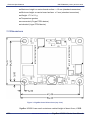
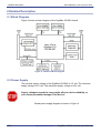
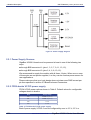
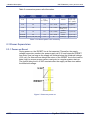
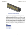
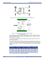
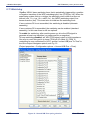
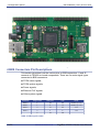
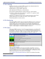
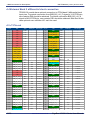
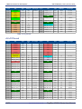
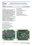
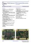
GigaBee XC6SLX Series User Manual
Industrial-Grade Xilinx Spartan-6 LX FPGA Micromodules
UM-TE0600-02 (v 2.07) 20 June 2013
Trenz Electronic GmbH
Overview
Trenz Electronic GigaBee XC6SLX series are
industrial-grade FPGA micromodules
integrating a leading-edge Xilinx Spartan-6 LX
FPGA, Gigabit Ethernet transceiver (physical
layer), two independent banks of 16-bit-wide
128/512 MBytes DDR3 SDRAM, 16 MBytes
SPI Flash memory for configuration and
operation, and powerful switch-mode power
supplies for all on-board voltages. A large
number of configurable I/Os is provided via
robust board-to-board (B2B) connectors.
All this on a tiny footprint, smaller than half a
credit card, at the most competitive price.
Hardware and software development
environment, as well as reference designs are
available at: www.trenz-electronic.de.
●
●
●
●
●
●
●
●
FPGA graphics
Image processing
IP (intellectual property) cores
Low-power design
Parallel processing
Rapid prototyping
Reconfigurable computing
System-on-Chip (SoC) development
Sample Applications
●
●
●
●
●
●
Cryptographic hardware module
Digital signal processing
Embedded educational platform
Embedded industrial OEM platform
Embedded system design
Emulation platforms
Figure 1: GigaBee XC6SLX top view
1/33
Figure 2: GigaBee XC6SLX bottom view
www.trenz-electronic.de
GigaBee XC6SLX Series User
Manual
UM-TE0600-02 (v 2.07) 20 June 2013
Key Features
● Industrial-grade Xilinx Spartan-6 LX FPGA micromodule (LX45 / LX100 /
LX150)
● 10/100/1000 tri-speed Gigabit Ethernet transceiver (PHY)
● 2 x 16-bit-wide 1 Gb (128 MB) or 4Gb (512 MB) DDR3 SDRAM
● 128Mb (16 MB) SPI Flash memory (for configuration and operation)
accessible through:
● 1Kb Protected 1-Wire EEPROM with SHA-1 Engine
● JTAG port (SPI indirect)
● FPGA configuration through:
● B2B connector
● JTAG port
● SPI Flash memory
● Plug-on module with 2 × 100-pin high-speed hermaphroditic strips
● Up to 52 differential, up to 109 single-ended (+ 1 dual-purpose) FPGA I/O
pins available on B2B strips
● 4.0 A x 1.2 V power rail
● 1.5 A x 1.5 V power rail
● 125 MHz reference clock signal
● Single-ended custom oscillator (option)
● eFUSE bit-stream encryption (LX100 or larger)
● 1 user LED
● Evenly-spread supply pins for good signal integrity
● Other assembly options for cost or performance optimization available upon
request.
2/33
www.trenz-electronic.de
GigaBee XC6SLX Series User Manual
UM-TE0600-02 (v 2.07) 20 June 2013
Table of Contents
1 Technical Specifications...............................................................................................................5
1.1 Components.........................................................................................................................5
1.2 Dimensions...........................................................................................................................6
1.3 Power Consumption.............................................................................................................7
2 Detailed Description.....................................................................................................................8
2.1 Block Diagram......................................................................................................................8
2.2 Power Supply.......................................................................................................................8
2.2.1 Power Supply Sources..................................................................................................9
2.2.2 FPGA banks VCCIO power supply...............................................................................9
2.2.3 On-board Power Rails.................................................................................................10
2.3 Power Supervision.............................................................................................................12
2.3.1 Power-on Reset..........................................................................................................12
2.3.2 Power Fail...................................................................................................................13
2.4 Board-to-board Connectors................................................................................................13
2.4.1 Connector Speed Rating.............................................................................................16
2.5 EPROM..............................................................................................................................16
2.6 DDR3 SDRAM Memory......................................................................................................16
2.7 Flash Memory.....................................................................................................................17
2.8 Ethernet..............................................................................................................................17
2.9 Oscillators...........................................................................................................................18
2.10 User LED..........................................................................................................................18
2.11 Watchdog..........................................................................................................................19
3 Configuration Options................................................................................................................20
3.1 JTAG Configuration............................................................................................................20
3.2 Flash Configuration............................................................................................................20
3.3 eFUSE Programming.........................................................................................................20
4 B2B Connectors Pin Descriptions.............................................................................................21
4.1 Pin Labelling.......................................................................................................................22
4.2 Pin Numbering....................................................................................................................22
4.3 Pin Types............................................................................................................................22
4.4 External Bank 2 differential clock connection....................................................................23
4.5 J1 Pin-out...........................................................................................................................23
4.6 J2 Pin-out...........................................................................................................................24
4.7 Signal Integrity Considerations..........................................................................................25
5 Module revisions and assembly variants...................................................................................25
6 Related Materials and References............................................................................................27
6.1 Data Sheets........................................................................................................................27
6.2 Documentation Archives.....................................................................................................27
6.3 User Guides........................................................................................................................27
6.4 Design and Development Tools.........................................................................................28
6.5 Design Resources..............................................................................................................28
6.6 Tutorials..............................................................................................................................28
7 Glossary of Abbreviations and Acronyms..................................................................................29
8 Legal Notices.............................................................................................................................30
8.1 Document Warranty............................................................................................................30
8.2 Limitation of Liability...........................................................................................................30
8.3 Copyright Notice.................................................................................................................30
8.4 Technology Licenses..........................................................................................................30
9 Environmental protection...........................................................................................................31
3/33
www.trenz-electronic.de
GigaBee XC6SLX Series User Manual
UM-TE0600-02 (v 2.07) 20 June 2013
9.1 REACH (Registration, Evaluation, Authorisation and Restriction of Chemicals)
compliance statement..............................................................................................................31
9.2 RoHS (Restriction of Hazardous Substances) compliance statement..............................31
9.3 WEEE (Waste Electrical and Electronic Equipment).........................................................31
Document Change History..........................................................................................................33
4/33
www.trenz-electronic.de
GigaBee XC6SLX Series User Manual
1 Technical Specifications
UM-TE0600-02 (v 2.07) 20 June 2013
1 Technical Specifications
1.1 Components
● Xilinx Spartan-6 LX FPGA:
● XC6SLX45-2FGG484C = 43 K logic cells, commercial grade
XC6SLX45-2FGG484I = 43 K logic cells, industrial grade
● XC6SLX100-2FGG484C = 101 K logic cells, commercial grade
XC6SLX100-2FGG484I = 101 K logic cells, industrial grade
● XC6SLX150-2FGG484C = 147 K logic cells, commercial grade
XC6SLX150-2FGG484I = 147 K logic cells, industrial grade
● 10/100/1000 Gigabit Ethernet transceiver (physical layer)
Marvell Semiconductor 88E1111
● 2 × independent 16-bit-wide (data-bus) 1 Gigabit (128 megabyte) or 4 Gigabit
(512 megabyte) DDR3 SDRAM
● 128 megabit (16 megabyte) serial Flash memory with dual/quad SPI interface
● 48-bit node address chip
Maxim Integrated Products DS2502-E48
● 1Kb Protected 1-Wire EEPROM with SHA-1 Engine
Maxim Embedded Security Products DS2432
● 2 x fine-pitch (0.5 mm) 100-pin high-speed (up to 10.0 GHz / 20 Gbps)
hermaphroditic strips
LSHM-150-04.0-L-DV-A-S-K-TR
● Up to 52 differential FPGA input/output pins available on B2B strips
● Up to 109 single-ended (+ 1 dual-purpose) FPGA input/output pins available
on B2B strips
● Ethernet (PHY), JTAG and SPI pins available on B2B strips
● 4.0 A high-efficiency DC-DC switching regulator for power rail 1.2V
● 1.5 A high-efficiency DC-DC switching regulator for power rail 1.5V
● 2 x 800 mA DC-DC linear regulator for power rails 2.5V and VCCAUX
● Processor supervisory circuits with power-fail and watchdog
Texas Instruments TPS3705-33
● 125 MHz clock signal (system + user)
● Footprint for custom single-ended oscillator (option)
● 1 x LED (user)
● Power supply voltage: 3.3 V
● Power supply source: board-to-board interconnect (e.g. carrier board)
● Dimensions: 50 mm × 40 mm (20 cm2)
● Minimum module height: 8 mm (without connectors)
5/33
www.trenz-electronic.de
GigaBee XC6SLX Series User Manual
1 Technical Specifications
UM-TE0600-02 (v 2.07) 20 June 2013
● Maximum height on carrier board surface: ≈ 13 mm (standard connectors)
● Minimum height on carrier board surface: ≈ 5 mm (standard connectors)
● Weight: 17.2 ± 0.1 g
● Temperature grades:
● commercial (C-type FPGA device)
● industrial (I-type FPGA device)
1.2 Dimensions
Figure 3: GigaBee board dimensions (top view)
GigaBee XC6SLX can reach a minimum vertical height of about 8 mm, if B2B
6/33
www.trenz-electronic.de
GigaBee XC6SLX Series User Manual
1 Technical Specifications
UM-TE0600-02 (v 2.07) 20 June 2013
connectors are not assembled. The maximum component height on the module
board on the top side is about 3.5 mm. The maximum component height on the
module board on the bottom side is about 3.0 mm.
The typical minimum and maximum height from the carrier board surface, of a
GigaBee XC6SLX when it mounted on a carrier board, is respectively about 5.0
mm and about 13 mm.
GigaBee XC6SLX has 4 mounting holes, one in each corner. The module can
be fixed by screwing M3 screws (ISO 262) onto a carrier board through those
mounting holes.
GigaBee XC6SLX weighs between 17.1 and 17.3 g with standard connectors.
1.3 Power Consumption
Power consumption of GigaBee XC6SLX modules highly depend on the FPGA
design implemented. Some typical power consumptions are provided in Table 1
for the following reference systems:
● Boards – GigaBee XC6SLX 45/100/150
● Base board – TE0603-02
● Power supply – 5 V from baseboard
● Connected Gigabit Ethernet cable
FPGA type
Unconfigured
Configured with Webserver reference design
LX45
0.15 A
0.6 A
LX100
0.17 A
0.5 A
LX150
0.2 A
0.5 A
Table 1: Power consumption
7/33
www.trenz-electronic.de
GigaBee XC6SLX Series User Manual
2 Detailed Description
UM-TE0600-02 (v 2.07) 20 June 2013
2 Detailed Description
2.1 Block Diagram
Figure 4 shows a block diagram of the GigaBee XC6SLX board.
Figure 4: TE0600-02 Block Diagram
2.2 Power Supply
The nominal supply voltage of the GigaBee XC6SLX is 3.3 volt. The minimum
supply voltage is 3.0 volt. The maximum supply voltage is 3.45 volt.
Supply voltages beyond the range might affect to device reliability, or
even cause permanent damage of the device!
Board power supply diagram is shown in Figure 5.
8/33
www.trenz-electronic.de
GigaBee XC6SLX Series User Manual
2 Detailed Description
UM-TE0600-02 (v 2.07) 20 June 2013
Figure 5: Power supply diagram
2.2.1 Power Supply Sources
GigaBee XC6SLX board must be powered at least in one of the following two
ways:
● through B2B connector J1 (pins 1, 3, 5, 7, 9, 11, 13, 15),
● through B2B connector J2 (pins 2, 4, 6, 8, 10, 12).
We recommend to supply the module with all these 14 pins. When one or more
of these pins are not power supplied, it or they can be used as power source for
user applications.
Please make sure that your logic design does not draw more RMS current per
pin than specified in section 2.4 Board-to-board Connectors.
2.2.2 FPGA banks VCCIO power supply
FPGA VCCIO power options shown in Table 2. Default values for configurable
voltages shown in braces.
Bank
Supply voltage
B0
VCCIO 0 (3.3 V)
B1
VCCIO 1 (1.5 V)
B2
3.3 V
B3
1.5 V
Table 2: FPGA banks VCCIO power supply
Bank 0 power supply VCCIO 0 can be configured by user to 3.3 V, 2.5 V or
9/33
www.trenz-electronic.de
GigaBee XC6SLX Series User Manual
2 Detailed Description
UM-TE0600-02 (v 2.07) 20 June 2013
1.5 V, see Chapter 2.2.3.6 VCCIO0 Power Rail. Bank 1 VCCIO supply voltage
is configured to 1.5 V to communicate with DDR3 SDRAM memory chip.1
2.2.3 On-board Power Rails
GigaBee XC6SLX has the following power rails on-board.
2.2.3.1 3.3V Power Rail
It is the main internal power rail and must be supplied from an external power
source.
It supplies the other following power rails:
● 1.2V / 4 A on-board high-efficiency switching voltage regulator;
● 1.5V / 1.5 A on-board high-efficiency switching voltage regulator;
● 2.5V 0.8 A linear voltage regulator;
● VCCIO0 power rail (option) (if zero-resistor R80 is not populated and zeroresistor R79 is populated).
2.2.3.2 1.2V Power Rail
It is converted from the 3.3V rail by a switching voltage regulator and can
provide up to 4.0 A to:
● FPGA VCCINT power supply pins;
● Ethernet PHY;
● J1 connector.
2.2.3.3 1.5V Power Rail
It is converted from the 3.3V rail by a switching voltage regulator and can
provide up to 1.5 A to:
● DDR3 SDRAM;
● Vref1 / Vref2 DDR3 SDRAM reference voltages;
● FPGA bank 3 VCCO;
● J1 connector.
2.2.3.4 2.5V Power Rail
It is converted from the 3.3V rail by a linear voltage regulator and can provide
up to 0.8 A to:
● VCCAUX power rail;
● Ethernet physical layer;
● J1 connector;
1 By special request modules can be supplied without DDR3 SDRAM chips. Contact Trenz Electronic support for
details
10/33
www.trenz-electronic.de
GigaBee XC6SLX Series User Manual
2 Detailed Description
UM-TE0600-02 (v 2.07) 20 June 2013
● J2 connector (option: if zero-resistor R80 is populated and zero-resistor R79
is not populated).
2.2.3.5 VCCAUX Power Rail
It is converted from the 3.3V rail by a linear voltage regulator and can provide
up to 0.8 A to:
● FPGA auxiliary circuits;
● J2 connector.
2.2.3.6 VCCIO0 Power Rail
There are 4 options to supply this rail:
● from 3.3 V power rail (if zero-resistor R79 is populated2 and R80 is not);
● from 2.5 V power rail (if zero-resistor R80 is populated and R79 is not);
● from 1.5 V power rail (if zero-resistors R79 and R80 are not populated and
VCCIO0 connected to 1.5 V power rail);
● from an external power source through J2 B2B connector (pins 1, 3, 5, 7, 9)
(if R79 and R80 are not populated)
It supplies:
● FPGA bank 0 VCCO.
Figure 6 show simplified schematic of power options. Dashed resistors are not
populated by default.
Figure 6: Power options diagram
2 Default assembling for VCCIO0 rail
11/33
www.trenz-electronic.de
GigaBee XC6SLX Series User Manual
2 Detailed Description
UM-TE0600-02 (v 2.07) 20 June 2013
Table 3 summarizes power rails information.
power-rail
name
nominal
voltage(V)
maximum
current (A)
power
source
system
supply
user
supply
3.3V
3.3
2.4
(3.3 option)
J1, J2
module
J1 (≤1.2 A)
J2 (≤1.2 A,
≤2.1 option)
2.5V
2.5
0.8
3.3V ► linear
Ethernet
J1 (≤0.3 A)
J2 (option)
1.5V
1.5
1.5
3.3V ► switch.
1.2V
1.2
4.0
3.3V ► switch.
VCCINT
Ethernet
J1 (≤0.6 A)
VCCAUX
2.5
0.8
3.3V ► linear
FPGA
J2 (≤0.3 A)
0.9
J2
VCCO (0)
J2 (≤0.9 A)
VCCCIO0 1.2, 1.5, 1.8, 2.5, 3.3
DDR3 SDRAM
J1 (≤0.3 A)
VCCO (1+3)
Table 3: On-board power rails summary
2.3 Power Supervision
2.3.1 Power-on Reset
During power-on, the /RESET line is first asserted. Thereafter, the supply
voltage supervisor monitors the power supply rail 3.3V and keeps the /RESET
line active (low) as long as the supply rail remains below the threshold voltage
(2.93 volt). An internal timer delays the return of the /RESET line to the inactive
state (high) to ensure proper system reset prior to a regular system start-up.
The typical delay time td of 200 ms starts after the supply rail has risen above
the threshold voltage.
Figure 7: Reset on power-on
12/33
www.trenz-electronic.de
GigaBee XC6SLX Series User Manual
2 Detailed Description
UM-TE0600-02 (v 2.07) 20 June 2013
After this delay, the /RESET line is reset (high) and the FPGA configuration can
start. When the supply rail voltage drops below the threshold voltage, the
/RESET line becomes active (low) again and stays active (low) as long as the
rail voltage remains below the threshold voltage (2.93 volt). Once the rail
voltage raises again and remains over the threshold voltage for more than the
typical delay time td of 200 ms, the /RESET line returns to the inactive state
(high) to allow a new system start-up.
Figure 8: Reset on power drop
2.3.2 Power Fail
GigaBee XC6SLX integrates a power-fail comparator which can be used for
low-battery detection, power-fail warning, or for monitoring a power supply other
than the main supply 3.3 V. When the voltage of the PFI (power-fail comparator
input, input pin 16 of connector J2) line drops below 1.25 volt, the /PFO (powerfail comparator output, FPGA pin A2, label IO_L83P_3) line becomes active
(low). The user application can sense this line to take action. To set a power fail
threshold higher than 1.25 volt, the user can implement a simple resistive
voltage divider on the carrier board.
2.4 Board-to-board Connectors
GigaBee XC6SLX mounts two Samtec Razor Beam LSHM connectors (J1 and
J2) on the bottom side.
Each connector features the following characteristics:
● rows per connector: 2
● contacts per row: 50
● contacts per connector: 100
● connector gender: hermaphrodite
● pitch: 0.50 mm = 19.7 mil = .0197”
● mated height: min. 5.0 mm | typ. 8.0 mm | max. 12.0 mm
● mating force: min. 39 N | typ. 59 N | max. 62 N
● un-mating force: min. 49 N | typ. 73 N | max. 74 N
13/33
www.trenz-electronic.de
GigaBee XC6SLX Series User Manual
2 Detailed Description
UM-TE0600-02 (v 2.07) 20 June 2013
Figure 9: Samtec Razor Beam LSHM connector
The overall number of connector contacts on the GigaBee XC6SLX is 200.
Samtec Razor Beam LSHM is a high-speed interconnect system with very fine
pitch (50 mil) and low profile design. Razor Beam connectors are well suited for
high speed applications with performance up to 11.5 GHz (23 Gb/s) at -3 dB
insertion loss. Razor Beam contacts are ideal for high speed and rugged
applications featuring undercut retention notches that increase the withdrawal
force and provide an audible click when the contacts engage. In addition, the
self-mating (hermaphroditic) design can help reduce inventory costs. The LSHM
Series features also optional shielding for EMI protection (default on GigaBee
XC6SLX).
Samtec Razor Beam LSHM connectors are keyed. On the bottom side of the
GigaBee XSL6, the connectors are assembled in such a way to prevent the
module to be reverse mounted on carrier boards.
Samtec Razor Beam LSHM are available in different lead styles, see Table 4 for
details.
lead style A [mm] B [mm]
–02.5
3.95
1.00
–03.0
4.45
1.50
–04.0
5.45
2.50
–06.0
7.45
4.50
Table 4: Samtec Razor Beam LSHM lead styles
14/33
www.trenz-electronic.de
GigaBee XC6SLX Series User Manual
2 Detailed Description
UM-TE0600-02 (v 2.07) 20 June 2013
Figure 10: A and B features of Samtec Razor Beam LSHM series
Figure 11: Definition of mated height for Samtec Razor
Beam LSHM series.
The standard connector mounted on the GigaBee XC6SLX is Samtec Razor
Beam LSHM-150-04.0-L-DV-A-S-K-TR (lead style: –04.0, tail option: vertical,
shield option: with shield).
Trenz Electronic recommends the same part as mating connector, due to its
self-mating capability.
The Samtec Razor Beam LSHM series offers a variety of mated heights form
5.0 mm to 12.0 mm. Two mated standard GigaBee XC6SLX connectors have a
typical mated height of 8.0 mm. Processing conditions will affect the following
heights.
standard connector
lead style
–04.0
mating connector mated height min. height from
lead style
[mm]
carrier board [mm]
–02.5
6.5
≈ 3.5
max. height on
carrier board [mm]
≈ 11.5
–04.0
–03.0
7.0
≈ 4.0
≈ 12.0
–04.0
–04.0
8.0
≈ 5.0
≈ 13.0
–04.0
–06.0
10.0
≈ 7.0
≈ 15.0
Table 5: Samtec Razor Beam LSHM mated heights
15/33
www.trenz-electronic.de
GigaBee XC6SLX Series User Manual
2 Detailed Description
UM-TE0600-02 (v 2.07) 20 June 2013
Ordering codes for connectors J1 and J2 used in GigaBee XC6SLX board, and
their mating connectors are given in Table 6.
lead style
gender
Samtec
Trenz Electronic
–02.5
hermaphroditic LSHM-150-02.5-L-DV-A-S-K-TR
23836
–03.0
hermaphroditic LSHM-150-03.0-L-DV-A-S-K-TR
23837
–04.0
hermaphroditic LSHM-150-04.0-L-DV-A-S-K-TR
23838
–06.0
hermaphroditic LSHM-150-06.0-L-DV-A-S-K-TR
23839
Table 6: Ordered codes of recommended B2B connectors
2.4.1 Connector Speed Rating
Samtec provides speed rating data for the Samtec Razor Beam LSHM
connector system. The data presented in Table 7 are applicable only to the
maximum and minimum mated heights. The speed rating is based on the -3 dB
insertion loss point of the connector system. The -3 dB point can be used to
estimate usable system bandwidth in a typical, two-level signalling environment.
mated height
5 mm
12 mm
single-ended signalling
11.5 GHz 7.5 GHz
23.0 Gb/s 15.0 Gb/s
differential pair signalling
7.0 GHz
6.5 GHz
14.0 Gb/s 13.0 Gb/s
Table 7: Connectors speed rating
More details can be found in the Samtec Razor Beam LSHM series overview
(“High Speed Characterization Reports”).
2.5 EPROM
GigaBee XC6SLX board contains a Maxim DS2502-E48 node address chip with
factory-programmed valid MAC-48 address and 768 bits of OTP-EPROM
memory for user data.
Address chip provide convenient data access through 1-Wire interface up to
16.3 kbps (FPGA pin T11).
More information can be found in the Maxim DS2502-E48 product overwiew.
Additional 1Kb protected 1-Wire EEPROM with SHA-1 engine DS2432
accessible via the same line.
More information can be found at the Maxim DS2432 product page.
2.6 DDR3 SDRAM Memory
The board contains two 1 Gb (128 MB) or 4 Gb (512 MB) DDR3 SDRAM chips.
Data width of each chip is 16 bit. DDR3 memory connected to FPGA bank 1
and FPGA bank 3. Spartan-6 Memory controller Blocks operations can be
merged to implement effective 32-bit memory interface. Refer Xilinx XAPP496
for detailed information.
16/33
www.trenz-electronic.de
GigaBee XC6SLX Series User Manual
2 Detailed Description
UM-TE0600-02 (v 2.07) 20 June 2013
2.7 Flash Memory
GigaBee XC6SLX board contains 128 Mb (16 MB) serial flash memory chip
Winbond W25Q128BV (U11). This serial flash chip can operate as general SPI
memory mode and in double or quad modes. Usage of dual and quad modes
increase bandwidth up to 40 MB/s.
For more information see Winbond W25Q128BV product overview.
Flash can be programmed in several ways:
● Direct SPI programming via J1 connector.
● Indirect SPI programming via FPGA pins, controlled by JTAG.
● Direct SPI programming by FPGA, using SPI core.
Serial flash is connected to FPGA bank 2 and B2B connector J1; used pins are
listed in Table 8.
Flash signal
FPGA pin
J1 pin
/CS
T5
87
CLK
Y21
91
DI(IO0)
AB20
95
DO(IO1)
AA20
93
/WP(IO2)
U14
99
/HOLD(IO3)
U13
97
Table 8: Serial flash signals connection
2.8 Ethernet
The board contains a Marvell Alaska Ethernet PHY chip (88E1111) operating at
10/100/1000 Mb/s. The board supports GMII interface mode with the FPGA.
Configuration details:
● PHY address – 00111
● Advertise pause
● Auto Neg
● Advertise all caps
● Prefer slave
● Auto crossover
● 125clk - enabled
● GMII to copper
● Fiber auto-detect - disabled
● Sleep mode - disabled
Ethernet signals from PHY are connected to B2B connector J1. To use Ethernet
in your design, GigaBee module should be connected to the carrier board,
which have Ethernet magnetics and RJ45 connector. TE0603 carrier board can
be used to access Ethernet capabilities of GigaBee XC6SLX series modules.
17/33
www.trenz-electronic.de
GigaBee XC6SLX Series User Manual
2 Detailed Description
UM-TE0600-02 (v 2.07) 20 June 2013
For correct operation of the Marvell PHY it is required that PHY Reset pin
sees valid low level each time power is applied and also during any
brownout situations where system Power is removed for short time, but
some pins are not at valid logic levels.
Solutions:
1) if GbE PHY is not used PHY reset pin can be tied off to GND
2) if PLL is used from PHY clock, then PLL "locked" output can be used to
reset PHY - as long PLL is not locked, it will keep PHY in reset
3) Reset pulse generation circuit clocked from FPGA internal configuration
clock, this circuit can force PHY reset pin to low when external clock from
PHY is not available
4) any custom Reset circuit that is guaranteed to drive PHY reset to low
level at least once after FPGA configuration when PHY clock is not
running.
5) any user logic that is guaranteed to drive PHY reset low after FPGA
configuration (without using PHY clock).
Explanation: Marvell PHY samples the MODE pins ONLY when it sees low
level on PHY reset input, it does not sample those pins during short power
off situations (if the reset pin holds high level because of pin capacitance
and high impedance of the pins)! So it is possible that the PHY mode is
reset, but the mode pins are not sampled again - this yields in mode
setting where 125MHz reference clock from PHY is not available.
2.9 Oscillators
The module has one 25 MHz oscillator for Ethernet PHY (U9). Ethernet PHY
provides clock multiplication and resulting 125 MHz clock acts as a system and
user clock for the FPGA (FPGA input pin AA12).
Note: For correct generation start, PHY should receive reset pulse.
Recommended way to do it it's to connect PHY reset signal
(ETHERNET_PHY_RST_N) to LOCKED output of corresponding DCM
(DCM which use 125 MHz from PHY).
The module also provides the footprint for custom 3.3 V single-ended oscillator
(U12) which can be installed as an option (FPGA input pin Y13).
2.10 User LED
The module contains one user active-low LED connected to FPGA output pin
T20. To access more LEDs, use a carrier board and drive FPGA signals
connected to B2B connectors. As LED connected to FPGA bank with
configurable VCCIO to light LED FPGA pin should in '0' (low) state. To disable
LED FPGA pin should be in 'Z' (High impedance).
18/33
www.trenz-electronic.de
GigaBee XC6SLX Series User Manual
2 Detailed Description
UM-TE0600-02 (v 2.07) 20 June 2013
2.11 Watchdog
GigaBee XS6LX has a watchdog timer that is periodically triggered by a positive
or negative transition of the WDI (watchdog input) line (FPGA pin V9). When the
supervising system fails to re-trigger the watchdog circuit within the time-out
interval (min 1.1 s, typ 1.6 s, max 2.3 s), the /WDO (watchdog output) line
becomes active (low). This event also re-initializes the watchdog timer.
If zero-resistors R2 is not assembled, the watchdog is disabled (alternate
assembly).
If zero-resistors R2 is assembled, the watchdog can be enabled (standard
assembly). In this case there is still two options:
To enable the watchdog, after module power-up, drive the WDI signal to
generate at least one transition (no matter positive or negative).
To keep watchdog disabled, set WDI FPGA signal output to high-impedance.
One way to reach this goal is to leave FPGA pin V9 (label IO_L50N_2)
undeclared in user constrains file (UCF) and set “unused IOB pins” to “float” in
the Xilinx Project Navigator options, see Fig. 12.
(Project properties > Configuration options > Unused IOB Pins > Float).
19/33
Figure
12: Unused IOB Pins option selection
www.trenz-electronic.de
GigaBee XC6SLX Series User Manual
2 Detailed Description
UM-TE0600-02 (v 2.07) 20 June 2013
In the standard assembly, the /WDO (watchdog output) line is left unconnected 3
and the only possibility to reset the module is by driving the /MR (master reset)
line active (low) through pin 18 of connector J2.
In the alternate assembly, the /WDO (watchdog output) line is connected
through zero-resistor R3 to /MR (master reset) line.
If alternate assembly is used, pin 18 of connector J2 must be left
unconnected.
3 Configuration Options
The FPGA on GigaBee XC6SLX board can be configured by means of the
following devices:
● Xilinx download cable (JTAG)
● SPI Flash memory
3.1 JTAG Configuration
The FPGA can be configured through the JTAG interface. JTAG signals are
connected to B2B connector J2. When GigaBee XC6SLX board is used with the
TE0603 carrier board, the JTAG interface can be accessed via connectors J5
and J6 on the carrier board.
3.2 Flash Configuration
Default configuration option for FPGA is “Master Serial/SPI”. The bit-stream for
the FPGA is stored in a serial Flash chip (U11). See chapter 2.7 Flash Memory
for additional information.
3.3 eFUSE Programming
eFUSE programming feature is not directly supported by GigaBee XC6SLX
modules, but it is possible to use it. To program eFUSE, please follow the steps
below:
● Connect VCCAUX to 3.3V power rail.
On TE0603 it can be done by connecting J5 pin 2 or J6 “VREF” (VCCAUX) to
J1 any pin from 1,2,3,4 (3.3V). See Figure 13.
● Program eFUSE using JTAG cable and iMPACT software.
● Remove power supply connections to VCCAUX
3 Resistor R3 is not populated.
20/33
www.trenz-electronic.de
GigaBee XC6SLX Series User Manual
3 Configuration Options
UM-TE0600-02 (v 2.07) 20 June 2013
Figure 13: eFUSE Powering
4 B2B Connectors Pin Descriptions
This section describes how the various pins on B2B connectors J1 and J2
connects to TE0600 on-board components. There are five main signal types
connected to B2B connectors:
● FPGA users signals;
● FPGA system signals;
● Power signals;
● Ethernet PHY signals;
● Other system signals.
FPGA Bank
Single-ended
Differential
Total
VCCIO
Bank 0
1
22
45
VCCIO 0 (3.3 V)
Bank 1
1
6
13
VCCIO 1 (1.5 V)
Bank 2
3
21
45
3.3 V
Bank 3
0
3
6
1.5 V
5
52
109
Table 9: B2B signals count
21/33
www.trenz-electronic.de
GigaBee XC6SLX Series User Manual
4 B2B Connectors Pin Descriptions
UM-TE0600-02 (v 2.07) 20 June 2013
4.1 Pin Labelling
FPGA user signals connected to B2B connectors are characterized by the
"B2B_Bx_Lyy_p" naming convention, where:
● B2B defines a "FPGA to B2B" signal type;
● Bx defines the FPGA bank (x = bank number);
● Lyy defines a differential pair or signal number (yy = pair number);
● p defines a differential signal polarity (P = positive, N = negative); single
ended signals do not have this field.
Ethernet PHY signals use "PHY_name" naming conversions where "PHY"
defines signal type "PHY to B2B" and "name" is PHY signal name.
Remaining signals use custom names.
4.2 Pin Numbering
Note that GigaBee XC6SLX have hermaphroditic B2B connectors. A feature of
hermaphroditic connector numbering is that connected signal numbers don't
match. Odd signals on module connect to even signals on baseboard. For
example module signal 1 to baseboard signal 2, module signal 2 to baseboard
signal 1, module signal 3 to baseboard signal 4 and so on.
4.3 Pin Types
Most pins of B2B connectors J1 and J2 are general-purpose, user-defined I/O
pins (GPIOs). There are, however, up to 8 different functional types of pins on
the TE0600, as outlined in Table 10. In pin-out tables Table 11 and Table 12, the
individual pins are colour-coded according to pin type as in Table 10.
type
colour code
description
DIO4
Unrestricted, general-purpose differential user-I/O pin.
SIO
Unrestricted, general-purpose user-I/O pin.
CONFIG
PWRMGMT
Dedicated configuration signals.
Control and status signals for the power-saving Suspend mode.
JTAG
Dedicated JTAG signals.
GND
Dedicated ground pin. All must be connected.
TE
POW
Trenz Electronic specific pin type. See the description of each pin in the user manual for additional
information on the corresponding signals.
Power signals.
SPI
SPI signals.
PHY
Ethernet PHY signals.
Table 10: TE0600 pin types
Note that some of Spartan-6 I/O types are partially compatible, so pins of
compatible types can be used as inputs for signal of other type. For example
pins from FPGA bank with 1.5V VCCO (IOSTANDARD = LVCMOS15) can be
used as inputs for 1.2V, 1.8V, 2.5V and 3.3V signals.
See “Spartan-6 FPGA SelectIO Resources” page 38 for detailed information.
4 DIO pins can be used as SIO.
22/33
www.trenz-electronic.de
GigaBee XC6SLX Series User Manual
4 B2B Connectors Pin Descriptions
UM-TE0600-02 (v 2.07) 20 June 2013
4.4 External Bank 2 differential clock connection
TE0600-02 module have optional connection to FPGA bank 2 differential clock
input pins. To provide connection from B2B_B2_L41_P signal to Y13 FPGA pin,
zero-resistor R69 should be soldered. To provide connection B2B_B2_L41_N
signal to AB13 FPGA pin, zero-resistor R81 should be soldered. Note that in this
case optional user oscillator U13 can't be used.
4.5 J1 Pin-out
J1 pin
Net
Type
FPGA pin
Net Length
J1 pin
Net
Type
FPGA pin
Net Length
1
3.3V
POW
-
-
2
GND
GND
-
-
3
3.3V
POW
-
-
4
PHY_MDI0_P
PHY
-
-
5
3.3V
POW
-
-
6
PHY_MDI0_N
PHY
-
-
7
3.3V
POW
-
-
8
GND
GND
-
-
9
3.3V
POW
-
-
10
PHY_MDI1_P
PHY
-
-
11
3.3V
POW
-
-
12
PHY_MDI1_N
PHY
-
-
13
3.3V
POW
-
-
14
PHY_AVDD
PHY
-
-
15
3.3V
POW
-
-
16
PHY_MDI2_P
PHY
-
-
17
PHY_L10
PHY
-
-
18
PHY_MDI2_N
PHY
-
-
19
PHY_L100
PHY
-
-
20
GND
GND
-
-
21
PHY_L1000
PHY
-
-
22
PHY_MDI3_P
PHY
-
-
23
PHY_DUP
PHY
-
-
24
PHY_MDI3_N
PHY
-
-
25
PHY_LED_TX
PHY
-
-
26
GND
GND
-
-
27
PHY_LED_RX
PHY
-
-
28
EN
TE
-
-
29
GND
GND
-
-
30
INIT
CONFIG
T6
-
31
B2B_B2_L57_N
DIO
AB4
8.66mm
32
B2B_B2_L32_N
SIO
AB11
8.12mm
33
B2B_B2_L57_P
DIO
AA4
9.84mm
34
GND
GND
-
-
35
B2B_B2_L49_N
DIO
AB6
8.66mm
36
B2B_B2_L60_P
DIO
T7
9.96mm
37
B2B_B2_L49_P
DIO
AA6
9.58mm
38
B2B_B2_L60_N
DIO
R7
11.16mm
39
2.5V
POW
-
-
40
B2B_B2_L59_N
DIO
R8
11.42mm
41
1.2V
POW
-
-
42
B2B_B2_L59_P
DIO
R9
11.36mm
43
1.2V
POW
-
-
44
GND
GND
-
-
45
B2B_B2_L48_N
DIO
AB7
9.98mm
46
B2B_B2_L44_N
DIO
Y10
11.34mm
47
B2B_B2_L48_P
DIO
Y7
10.98mm
48
B2B_B2_L44_P
DIO
W10
10.21mm
49
B2B_B2_L45_N
DIO
AB8
10.60mm
50
B2B_B2_L42_N
DIO
W11
7.52mm
51
B2B_B2_L45_P
DIO
AA8
11.053mm
52
B2B_B2_L42_P
DIO
V11
8.36mm
53
GND
GND
-
-
54
GND
GND
-
-
55
B2B_B2_L43_N
DIO
AB9
13.75mm
56
B2B_B2_L18_P
DIO
V13
7.94mm
57
B2B_B2_L43_P
DIO
Y9
12.97mm
58
B2B_B2_L18_N
DIO
W13
6.96mm
59
B2B_B2_L41_N
DIO
AB10, AB13
10.33mm
60
B2B_B2_L8_N
DIO
U16
9.92mm
61
B2B_B2_L41_P
DIO
AA10, Y13
11.01mm
62
B2B_B2_L8_P
DIO
U17
9.94mm
63
GND
GND
-
-
64
GND
GND
-
-
65
B2B_B2_L21_P
DIO
Y15
13.12mm
66
B2B_B2_L11_P
DIO
V17
8.31mm
67
B2B_B2_L21_N
DIO
AB15
12.37mm
68
B2B_B2_L11_N
DIO
W17
7.29mm
69
B2B_B2_L15_P
DIO
Y17
14.20mm
70
B2B_B2_L6_P
DIO
W18
7.40mm
71
B2B_B2_L15_N
DIO
AB17
13.77mm
72
B2B_B2_L6_N
DIO
Y18
6.94mm
73
GND
GND
-
-
74
GND
GND
-
-
75
B2B_B2_L31_N
SIO
AB12
12.30mm
76
B2B_B2_L5_P
DIO
Y19
6.18mm
23/33
www.trenz-electronic.de
GigaBee XC6SLX Series User Manual
4 B2B Connectors Pin Descriptions
UM-TE0600-02 (v 2.07) 20 June 2013
J1 pin
Net
Type
FPGA pin
Net Length
J1 pin
Net
Type
FPGA pin
Net Length
77
SUSPEND
SYS
N15
19.23mm
78
B2B_B2_L5_N
DIO
AB19
6.12mm
79
VBATT
CONFIG
R17
-
80
B2B_B2_L9_N
DIO
V18
8.43mm
81
VFS
CONFIG
P16
-
82
B2B_B2_L9_P
DIO
V19
8.36mm
83
RFUSE
CONFIG
P15
-
84
GND
GND
-
-
85
AWAKE
SYS
T19
14.15mm
86
B2B_B2_L4_N
DIO
T17
11.88mm
87
CSO_B
SPI
T5
-
88
B2B_B2_L4_P
DIO
T18
11.96mm
89
GND
GND
-
-
90
GND
GND
-
-
91
CCLK
SPI
Y21
-
92
B2B_B2_L29_N
SIO
Y12
13.58mm
93
MISO
SPI
AA20
-
94
B2B_B2_L10_N
DIO
R15
17.01mm
95
MOSI
SPI
AB20
-
96
B2B_B2_L10_P
DIO
R16
16.97mm
97
MISO3
SPI
U13
-
98
B2B_B2_L2_N
DIO
AB21
5.06mm
99
MISO2
SPI
U14
-
100
B2B_B2_L2_P
DIO
AA21
6.19mm
Table 11: J1 pin-out
4.6 J2 Pin-out
J2 pin
Net
Type
FPGA
pin
Net Length
J2 pin
Net
Type
FPGA pin
Net Length
1
VCCIO0
POW
-
-
2
3.3V
POW
-
-
3
VCCIO0
POW
-
-
4
3.3V
POW
-
-
5
VCCIO0
POW
-
-
6
3.3V
POW
-
-
7
VCCIO0
POW
-
-
8
3.3V
POW
-
-
9
VCCIO0
POW
-
-
10
3.3V
POW
-
-
11
B2B_PROGB
CONFIG
-
-
12
3.3V
POW
-
-
13
HSWAPEN
CONFIG
A3
-
14
B2B_B0_L1
SIO
A4
9.017mm
15
B2B_B3_L60_N
DIO
B1
5.44mm
16
PFI
TE
-
-
17
B2B_B3_L60_P
DIO
B2
5.27mm
18
/MR
TE
-
-
19
1.5V
POW
-
-
20
GND
GND
-
-
21
B2B_B3_L9_N
DIO
T3
19.36mm
22
B2B_B0_L2_P
DIO
C5
10.17mm
23
B2B_B3_L9_P
DIO
T4
18.76mm
24
B2B_B0_L2_N
DIO
A5
9.60mm
25
B2B_B0_L3_P
DIO
D6
6.76mm
26
B2B_B0_L4_N
DIO
A6
7.65mm
27
B2B_B0_L3_N
DIO
C6
5.66mm
28
B2B_B0_L4_P
DIO
B6
8.71mm
29
GND
GND
-
-
30
GND
GND
-
-
31
B2B_B3_L59_P
DIO
J7
11.90mm
32
B2B_B0_L5_N
DIO
A7
8.59mm
33
B2B_B3_L59_N
DIO
H8
11.71mm
34
B2B_B0_L5_P
DIO
C7
9.54mm
35
B2B_B0_L32_P
DIO
D7
6.93mm
36
B2B_B0_L6_N
DIO
A8
7.42mm
37
B2B_B0_L32_N
DIO
D8
6.87mm
38
B2B_B0_L6_P
DIO
B8
8.43mm
39
GND
GND
-
-
40
GND
GND
-
-
41
B2B_B0_L7_N
DIO
C8
6.62mm
42
B2B_B0_L8_N
DIO
A9
9.28mm
43
B2B_B0_L7_P
DIO
D9
6.71mm
44
B2B_B0_L8_P
DIO
C9
9.92mm
45
B2B_B0_L33_N
DIO
C10
5.66mm
46
B2B_B0_L34_N
DIO
A10
7.58mm
47
B2B_B0_L33_P
DIO
D10
6.76mm
48
B2B_B0_L34_P
DIO
B10
8.60mm
49
GND
GND
-
-
50
GND
GND
-
-
51
B2B_B0_L36_P
DIO
D11
6.76mm
52
B2B_B0_L35_N
DIO
A11
8.89mm
53
B2B_B0_L36_N
DIO
C12
5.87mm
54
B2B_B0_L35_P
DIO
C11
9.92mm
55
B2B_B0_L49_P
DIO
D14
6.96mm
56
B2B_B0_L37_N
DIO
A12
7.52mm
57
B2B_B0_L49_N
DIO
C14
5.96mm
58
B2B_B0_L37_P
DIO
B12
8.74mm
24/33
www.trenz-electronic.de
GigaBee XC6SLX Series User Manual
4 B2B Connectors Pin Descriptions
J2 pin
Net
Type
59
GND
GND
61
B2B_B0_L62_P
DIO
63
B2B_B0_L62_N
DIO
65
B2B_B0_L66_P
67
69
UM-TE0600-02 (v 2.07) 20 June 2013
FPGA
pin
Net Length
J2 pin
Net
Type
-
-
D15
7.44mm
C16
DIO
B2B_B0_L66_N
GND
71
B2B_B1_L10_P
DIO
73
B2B_B1_L10_N
DIO
75
B2B_B1_L9_P
DIO
77
B2B_B1_L9_N
DIO
G17
79
GND
GND
81
B2B_B1_L21_N
DIO
83
B2B_B1_L21_P
DIO
85
B2B_B1_L61_P
87
B2B_B1_L61_N
89
GND
91
VCCAUX
93
TMS
95
TDI
97
99
FPGA pin
Net Length
60
GND
GND
-
-
62
B2B_B0_L38_N
DIO
A13
8.38mm
6.95mm
64
B2B_B0_L38_P
DIO
C13
9.87mm
E16
8.07mm
66
B2B_B0_L50_N
DIO
A14
7.66mm
DIO
D17
6.96mm
68
B2B_B0_L50_P
DIO
B14
8.87mm
GND
-
-
70
GND
GND
-
-
F16
9.56mm
72
B2B_B0_L51_N
DIO
A15
10.22mm
F17
8.85mm
74
B2B_B0_L51_P
DIO
C15
10.67mm
G16
10.59mm
76
B2B_B0_L63_N
DIO
A16
7.95mm
10.23mm
78
B2B_B0_L63_P
DIO
B16
9.12mm
-
-
80
GND
GND
-
-
J16
13.22mm
82
B2B_B0_L64_N
DIO
A17
9.55mm
K16
14.41mm
84
B2B_B0_L64_P
DIO
C17
10.25mm
DIO
L17
14.89mm
86
B2B_B0_L65_N
DIO
A18
8.51mm
DIO
K18
13.59mm
88
B2B_B0_L65_P
DIO
B18
9.29mm
GND
-
-
90
GND
GND
-
-
POW
-
-
92
B2B_B1_L20_P
DIO
A20
8.02mm
JTAG
C18
-
94
B2B_B1_L20_N
DIO
A21
7.82mm
JTAG
E18
-
96
B2B_B1_L19_P
DIO
B21
9.63mm
TDO
JTAG
A19
-
98
B2B_B1_L19_N
DIO
B22
9.06mm
TCK
JTAG
G15
-
100
B2B_B1_L59
SIO
P19
27.19mm
Table 12: J2 pin-out
4.7 Signal Integrity Considerations
Traces of differential signals pairs are routed symmetrically (as symmetric
pairs).
Traces of differential signals pairs are NOT routed with equal length 5. For
applications where traces length has to be matched or timing differences have
to be compensated, Table 11 and Table 12 list the trace length of I/O signal lines
measured from FPGA balls to B2B connector pins.
Traces of differential signals pairs are routed with a differential impedance
between the two traces of 100 ohm. Single ended traces are routed with 60
ohm impedance.
An electronic version of these pin-out tables are available for download from the
Trenz Electronic support area of the web site.
5 Module revisions and assembly variants
Module revision coded by 4 FPGA BR[3:0] pins, which can be read by FPGA
firmware. All these pins should be configures to have internal PULLUP.
5 Difference in signal lines length is negligible for used signal frequency.
25/33
www.trenz-electronic.de
GigaBee XC6SLX Series User Manual
5 Module revisions and assembly variants
UM-TE0600-02 (v 2.07) 20 June 2013
Signal
FPGA pin
BR3
R19
BR2
P18
BR1
N16
BR0
P17
Revision 01
1
1
1
1
Revision 02
1
1
1
0
Table 13: Board revisions pin coding
Main differences between 01 and 02 revisions:
● More powerful regulators for 1.2V and 1.5V rails
● VCCAUX separated from 2.5V power rail
● 128Mbit SPI Flash
● Additional secure 1Kbit EEPROM
● Optional B2B connection to bank 2 differential clock input
Module assembly variants coded by 4 zero ohm resistors, connected to FPGA
AV[3:0] pins. All these pins should be configures to have internal PULLUP.
Signal
FPGA pin
AV3
M18
AV2
M17
AV1
V20
AV0
U19
Speed
grade
SDRAM
Temp
grade
TE0600-02[V|B]
0
0
0
0
2
2x128MBit
C
TE0600-02[V|B]I
0
0
0
1
2
2x128MBit
I
TE0600-02[V|B]F
0
0
1
0
3
2x128MBit
C
TE0600-02[V|B]IF
0
0
1
1
3
2x128MBit
I
TE0600-02[V|B]MF
0
1
0
0
3
2x512MBit
C
Table 14: Assembly variants pin coding
26/33
www.trenz-electronic.de
GigaBee XC6SLX Series User Manual
6 Related Materials and References
UM-TE0600-02 (v 2.07) 20 June 2013
6 Related Materials and References
The following documents provide supplementary information useful with this
user manual.
6.1 Data Sheets
● Xilinx DS160: Spartan-6 Family Overview
This overview outlines the features and product selection of the Spartan®-6
family.
http://www.xilinx.com/support/documentation/data_sheets/ds160.pdf
● Xilinx DS162: Spartan-6 FPGA Data Sheet: DC and Switching
Characteristics
This data sheet contains the DC and switching characteristic specifications
for the Spartan®-6 family.
http://www.xilinx.com/support/documentation/data_sheets/ds162.pdf
● Samtec Razor Beam LSHM series overview.
http://www.samtec.com/LSHM
● Maxim DS2502-E48 product overview.
http://www.maxim-ic.com/datasheet/index.mvp/id/3748
● Winbond W25Q128BV product overview.
http://www.winbond.com/hq/enu/ProductAndSales/ProductLines/FlashMemor
y/SerialFlash/W25Q128BV.htm
● Maxim DS2432 product page.
http://www.maximintegrated.com/datasheet/index.mvp/id/2914
6.2 Documentation Archives
● Xilinx Spartan-6 Documentation
http://www.xilinx.com/support/documentation/spartan-6.htm
● Xilinx Documentation
http://www.xilinx.com/documentation/
http://www.xilinx.com/support/documentation/
● Trenz Electronic GigaBee Series Documentation
http://docs.trenz-electronic.de/Trenz_Electronic/products/TE0600GigaBee_series/
6.3 User Guides
● Xilinx UG380: Spartan-6 FPGA Configuration User Guide
This all-encompassing configuration guide includes chapters on configuration
interfaces (serial and parallel), multi-bitstream management, bitstream
encryption, boundary-scan and JTAG configuration, and reconfiguration
techniques.
http://www.xilinx.com/support/documentation/user_guides/ug380.pdf
● Xilinx UG381: Spartan-6 FPGA SelectIO Resources
27/33
www.trenz-electronic.de
GigaBee XC6SLX Series User Manual
6 Related Materials and References
UM-TE0600-02 (v 2.07) 20 June 2013
http://www.xilinx.com/support/documentation/user_guides/ug381.pdf
6.4 Design and Development Tools
● Xilinx ISE Design Suite
http://www.xilinx.com/ISE/
http://www.xilinx.com/tools/designtools.htm
● Xilinx ISE Design Suite (version archive)
http://www.xilinx.com/download/
http://www.xilinx.com/support/download/
● Xilinx ISE WebPACK
http://www.xilinx.com/tools/webpack.htm
http://www.xilinx.com/webpack/
6.5 Design Resources
● Trenz Electronic GigaBee Design Resources
http://www.trenz-electronic.de/download/d0/Trenz_Electronic/d1/TE0600GigaBee_series.html
● Trenz Electronic GigaBee Reference Designs
https://github.com/Trenz-Electronic/
https://github.com/Trenz-Electronic/TE-EDK-IP/
https://github.com/Trenz-Electronic/TE060X-GigaBee-Reference-Designs/
6.6 Tutorials
● Xilinx UG695: ISE In-Depth Tutorial
Chapter 8: Configuration Using iMPACT
http://www.xilinx.com/support/documentation/sw_manuals/xilinx13_1/ise_tuto
rial_ug695.pdf
28/33
www.trenz-electronic.de
GigaBee XC6SLX Series User Manual
7 Glossary of Abbreviations and Acronyms
UM-TE0600-02 (v 2.07) 20 June 2013
7 Glossary of Abbreviations and Acronyms
A WARNING notice denotes a hazard. It calls attention to an operating procedure, practice, or the like that, if not correctly
performed or adhered to, could result in damage to the product or loss of important data. Do not proceed beyond a WARNING
notice until the indicated conditions are fully understood and met.
A CAUTION notice denotes a risk. It calls attention to an operating procedure, practice, or the like that, if not correctly
performed or adhered to, could result in a fault. (undesired condition that can lead to an error) Do not proceed beyond a
CAUTION notice until the indicated conditions are fully understood and met.
API
application programming interface
B2B
board-to-board
DSP
digital signal processing; digital signal processor
EDK
Embedded Development Kit
IOB
input / output blocks; I/O blocks
IP
intellectual property
ISP
In-System Programmability
OTP
one-time programmable
PB
push button
SDK
Software Development Kit
TE
Trenz Electronic
XPS
Xilinx Platform Studio
29/33
www.trenz-electronic.de
GigaBee XC6SLX Series User Manual
8 Legal Notices
UM-TE0600-02 (v 2.07) 20 June 2013
8 Legal Notices
8.1 Document Warranty
The material contained in this document is provided “as is” and is subject to
being changed at any time without notice. Trenz Electronic does not warrant the
accuracy and completeness of the materials in this document. Further, to the
maximum extent permitted by applicable law, Trenz Electronic disclaims all
warranties, either express or implied, with regard to this document and any
information contained herein, including but not limited to the implied warranties
of merchantability, fitness for a particular purpose or non infringement of
intellectual property. Trenz Electronic shall not be liable for errors or for
incidental or consequential damages in connection with the furnishing, use, or
performance of this document or of any information contained herein.
8.2 Limitation of Liability
In no event will Trenz Electronic, its suppliers, or other third parties mentioned in
this document be liable for any damages whatsoever (including, without
limitation, those resulting from lost profits, lost data or business interruption)
arising out of the use, inability to use, or the results of use of this document, any
documents linked to this document, or the materials or information contained at
any or all such documents. If your use of the materials or information from this
document results in the need for servicing, repair or correction of equipment or
data, you assume all costs thereof.
8.3 Copyright Notice
No part of this manual may be reproduced in any form or by any means
(including electronic storage and retrieval or translation into a foreign language)
without prior agreement and written consent from Trenz Electronic.
8.4 Technology Licenses
The hardware / firmware / software described in this document are furnished
under a license and may be used /modified / copied only in accordance with the
terms of such license.
30/33
www.trenz-electronic.de
GigaBee XC6SLX Series User Manual
9 Environmental protection
UM-TE0600-02 (v 2.07) 20 June 2013
9 Environmental protection
To confront directly with the responsibility toward the environment, the global
community and eventually also oneself. Such a resolution should be integral
part not only of everybody's life. Also enterprises shall be conscious of their
social responsibility and contribute to the preservation of our common living
space. That is why Trenz Electronic invests in the protection of our
Environment.
9.1 REACH (Registration, Evaluation, Authorisation and Restriction of
Chemicals) compliance statement
Trenz Electronic is a manufacturer and a distributor of electronic products. It is
therefore a so called downstream user in the sense of REACH. The products
we supply to you are solely non-chemical products (goods). Moreover and
under normal and reasonably foreseeable circumstances of application, the
goods supplied to you shall not release any substance. For that, Trenz
Electronic is obliged to neither register nor to provide safety data sheet.
According to present knowledge and to best of our knowledge, no SVHC
(Substances of Very High Concern) on the Candidate List are contained in our
products.
Furthermore, we will immediately and unsolicited inform our customers in
compliance with REACH - Article 33 if any substance present in our goods
(above a concentration of 0,1 % weight by weight) will be classified as SVHC by
the European Chemicals Agency (ECHA).
9.2 RoHS (Restriction of Hazardous Substances) compliance statement
Trenz Electronic GmbH herewith declares that all its products are developed,
manufactured and distributed RoHS compliant.
9.3 WEEE (Waste Electrical and Electronic Equipment)
Information for users within the European Union in accordance with Directive
2002/96/EC of the European Parliament and of the Council of 27 January 2003
on waste electrical and electronic equipment (WEEE).
Users of electrical and electronic equipment in private households are required
not to dispose of waste electrical and electronic equipment as unsorted
municipal waste and to collect such waste electrical and electronic equipment
separately. By the 13 August 2005, Member States shall have ensured that
systems are set up allowing final holders and distributors to return waste
electrical and electronic equipment at least free of charge. Member States shall
ensure the availability and accessibility of the necessary collection facilities.
Separate collection is the precondition to ensure specific treatment and
recycling of waste electrical and electronic equipment and is necessary to
achieve the chosen level of protection of human health and the environment in
the European Union. Consumers have to actively contribute to the success of
such collection and the return of waste electrical and electronic equipment.
Presence of hazardous substances in electrical and electronic equipment
results in potential effects on the environment and human health. The symbol
31/33
www.trenz-electronic.de
GigaBee XC6SLX Series User Manual
9 Environmental protection
UM-TE0600-02 (v 2.07) 20 June 2013
consisting of the crossed-out wheeled bin indicates separate collection for
waste electrical and electronic equipment.
32/33
www.trenz-electronic.de
GigaBee XC6SLX Series User Manual
Document Change History
UM-TE0600-02 (v 2.07) 20 June 2013
Document Change History
ver.
date
author
description
0.01 2011-10-01
AIK
Release.
0.02 2011-10-05
AIK
Added B2B pin-out section.
0.03 2011-10-06
AIK
Reformatted pin-out tables. Added eFUSE programming section.
0.04 2011-10-06
AIK
Added board photos. Additions to eFUSE section.
0.05 2011-10-06
AIK
Removed net length information for nets which can't be measured right.
0.06 2011-10-06
AIK
Added power consumption section.
0.07 2011-10-08
AIK
Little fixes after FDR audit.
0.08 2011-10-12
AIK
Fix in eFUSE section.
0.09 2011-11-11
AIK
Added pin numbering description for B2B connectors
0.10 2012-01-20
AIK
Added pin compatibility note and manual reference.
0.11 2012-04-12
AIK
Added FPGA banks VCCIO voltages table.
1.00 2012-04-17
FDR
Updated documentation link.
Replaced obsolete ElDesI and RedMine links with current GitHub links.
Updated dating convention.
1.01 2012-05-18
AIK
Corrected cross-reference in section 3.2. Corrected LED description.
1.02 2012-06-18
FDR
Removed junction temperature limits under connector current ratings.
1.03 2012-07-18
AIK
Added table with B2B signals summary per FPGA bank
2.01 2012-10-30
AIK
Fork to 01 and 02 board revisions
2.01 2012-11-06
AIK
Fixed bank 1 power options
2.02 2012-11-21
AIK
Updated module diagram
2.03 2012-11-30
AIK
Added Ethernet disable note
2.04 2012-12-19
AIK
Fixed SPI Flash size on block diagram
2.05 2013-01-21
AIK
Added PHY reset note
2.06 2013-03-13
AIK
Connectors current chapter moved to separate document
2.07 2013-03-13
AIK
Changed Bank 1 power supply description and VCCIO0 sources description
33/33
www.trenz-electronic.de
GigaBee XC6SLX Series User Manual