1
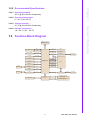
User Manual MIO-2263 Intel® Atom™ SoC J1900/E3825 Pico-ITX SBC, DDR3L, 18/24-bit LVDS, VGA or HDMI, 1 GbE, Halfsize Mini PCIe, 4 USB, 2 COM, SMBus, mSATA & MIOe Copyright The documentation and the software included with this product are copyrighted 2014 by Advantech Co., Ltd. All rights are reserved. Advantech Co., Ltd. reserves the right to make improvements in the products described in this manual at any time without notice. No part of this manual may be reproduced, copied, translated or transmitted in any form or by any means without the prior written permission of Advantech Co., Ltd. Information provided in this manual is intended to be accurate and reliable. However, Advantech Co., Ltd. assumes no responsibility for its use, nor for any infringements of the rights of third parties, which may result from its use. Acknowledgements AMI is a trademark of AMI Software International, Inc. Intel® is a trademark of Intel® Technologies, Inc. IBM, PC/AT, PS/2 and VGA are trademarks of International Business Machines Corporation. Intel and Atom® are trademarks of Intel Corporation. Microsoft Windows® is a registered trademark of Microsoft Corp. RTL is a trademark of Realtek Semi-Conductor Co., Ltd. ESS is a trademark of ESS Technology, Inc. UMC is a trademark of United Microelectronics Corporation. SMI is a trademark of Silicon Motion, Inc. Creative is a trademark of Creative Technology LTD. All other product names or trademarks are properties of their respective owners. MIO-2263 User Manual Part No. 2006226310 Edition 1 Printed in China July 2014 ii Product Warranty (2 years) Advantech warrants to you, the original purchaser, that each of its products will be free from defects in materials and workmanship for two years from the date of purchase. This warranty does not apply to any products which have been repaired or altered by persons other than repair personnel authorized by Advantech, or which have been subject to misuse, abuse, accident or improper installation. Advantech assumes no liability under the terms of this warranty as a consequence of such events. Because of Advantech’s high quality-control standards and rigorous testing, most of our customers never need to use our repair service. If an Advantech product is defective, it will be repaired or replaced at no charge during the warranty period. For outof-warranty repairs, you will be billed according to the cost of replacement materials, service time and freight. Please consult your dealer for more details. If you think you have a defective product, follow these steps: 1. Collect all the information about the problem encountered. (For example, CPU speed, Advantech products used, other hardware and software used, etc.) Note anything abnormal and list any onscreen messages you get when the problem occurs. 2. Call your dealer and describe the problem. Please have your manual, product, and any helpful information readily available. 3. If your product is diagnosed as defective, obtain an RMA (return merchandize authorization) number from your dealer. This allows us to process your return more quickly. 4. Carefully pack the defective product, a fully-completed Repair and Replacement Order Card and a photocopy proof of purchase date (such as your sales receipt) in a shippable container. A product returned without proof of the purchase date is not eligible for warranty service. 5. Write the RMA number visibly on the outside of the package and ship it prepaid to your dealer. Technical Support and Assistance 1. 2. Visit the Advantech web site at www.advantech.com/support where you can find the latest information about the product. Contact your distributor, sales representative, or Advantech's customer service center for technical support if you need additional assistance. Please have the following information ready before you call: – Product name and serial number – Description of your peripheral attachments – Description of your software (operating system, version, application software, etc.) – A complete description of the problem – The exact wording of any error messages iii MIO-2263 User Manual Packing List Before installation, please ensure the following items have been shipped: Item Part Number 1 MIO-2263 SBC 1 Startup manual Cables Part Number Description 1700006291 SATA cable 7P 30 cm w/ right angle 1700022444-01 Audio Cable 2*5P-2.0/JACK*2 20cm 1701200220 COM PORT cable 2*10P-2.0/D-SUB 9P(M)*2 22 cm 1700019656 SATA Power cable 5P-1.25/5P-2.0+SATA 5P 15 cm 1700002172 USB cable 2.0mm pitch USB-A(F) 17cm 1700019705 AT Power cable 12cm Heatsink: 1960063455T001 99.5 x 70.5 x 15.7 mm Stud & Screw Part Number Description 9666226300E Stud and screw pack, including: 1935031500 Screw R/S D=5.3 H=2 + M3*15L, 4 pcs 1910002596-01 Stud F=M3*10L M=M3*5L B=5 H=19, 4 pcs 193B0204C0 Screw F/S D=3.5 H=0.8 + M2*4L, 2 pcs Ordering Information Model Number Description MIO-2263J-U0A1E Intel® Atom™ SoC J1900, fanless, LVDS, VGA, Gigabit Ethernet, 4 USB, mSATA, SMBus, GPIO, 2 COM, mini PCIe, MIOe MIO-2263JH-U0A1E Intel® Atom™ SoC J1900, fanless, LVDS, HDMI, Gigabit Ethernet, 4 USB, mSATA, SMBus, GPIO, 2 COM, mini PCIe, MIOe MIO-2263E-S3A1E Intel Atom SoC E3825, fanless, LVDS, VGA, Gigabit Ethernet, 4 USB, mSATA, SMBus, GPIO, 2 COM, mini PICe, MIOe Optional Accessories Part No. 1960065074N001 MIO-2263 User Manual Description Heat Spreader (99.5 x 70.5 x 11.2 mm) iv Declaration of Conformity This device complies with the requirements in part 15 of the FCC rules: Operation is subject to the following two conditions: 1. This device may not cause harmful interference, and 2. This device must accept any interference received, including interference that may cause undesired operation FCC Class A This equipment has been tested and found to comply with the limits for a Class A digital device, pursuant to Part 15 of the FCC Rules. These limits are designed to provide reasonable protection against harmful interference when the equipment is operated in a commercial environment. This equipment generates, uses, and can radiate radio frequency energy and, if not installed and used in accordance with the instruction manual, may cause harmful interference to radio communications. Operation of this device in a residential area is likely to cause harmful interference in which case the user will be required to correct the interference at his/her own expense. The user is advised that any equipment changes or modifications not expressly approved by the party responsible for compliance would void the compliance to FCC regulations and therefore, the user's authority to operate the equipment. Caution! There is a danger of a new battery exploding if it is incorrectly installed. Do not attempt to recharge, force open, or heat the battery. Replace the battery only with the same or equivalent type recommended by the manufacturer. Discard used batteries according to the manufacturer's instructions. v MIO-2263 User Manual Safety Instructions 1. 2. 3. Read these safety instructions carefully. Keep this User Manual for later reference. Disconnect this equipment from any AC outlet before cleaning. Use a damp cloth. Do not use liquid or spray detergents for cleaning. 4. For plug-in equipment, the power outlet socket must be located near the equipment and must be easily accessible. 5. Keep this equipment away from humidity. 6. Put this equipment on a reliable surface during installation. Dropping it or letting it fall may cause damage. 7. The openings on the enclosure are for air convection. Protect the equipment from overheating. DO NOT COVER THE OPENINGS. 8. Make sure the voltage of the power source is correct before connecting the equipment to the power outlet. 9. Position the power cord so that people cannot step on it. Do not place anything over the power cord. 10. All cautions and warnings on the equipment should be noted. 11. If the equipment is not used for a long time, disconnect it from the power source to avoid damage by transient overvoltage. 12. Never pour any liquid into an opening. This may cause fire or electrical shock. 13. Never open the equipment. For safety reasons, the equipment should be opened only by qualified service personnel. 14. If one of the following situations arises, get the equipment checked by service personnel: The power cord or plug is damaged. Liquid has penetrated into the equipment. The equipment has been exposed to moisture. The equipment does not work well, or you cannot get it to work according to the user's manual. The equipment has been dropped and damaged. The equipment has obvious signs of breakage. 15. DO NOT LEAVE THIS EQUIPMENT IN AN ENVIRONMENT WHERE THE STORAGE TEMPERATURE MAY GO BELOW -20° C (-4° F) OR ABOVE 60° C (140° F). THIS COULD DAMAGE THE EQUIPMENT. THE EQUIPMENT SHOULD BE IN A CONTROLLED ENVIRONMENT. 16. CAUTION: DANGER OF EXPLOSION IF BATTERY IS INCORRECTLY REPLACED. REPLACE ONLY WITH THE SAME OR EQUIVALENT TYPE RECOMMENDED BY THE MANUFACTURER, DISCARD USED BATTERIES ACCORDING TO THE MANUFACTURER'S INSTRUCTIONS. The sound pressure level at the operator's position according to IEC 704-1:1982 is no more than 70 dB (A). DISCLAIMER: This set of instructions is given according to IEC 704-1. Advantech disclaims all responsibility for the accuracy of any statements contained herein. MIO-2263 User Manual vi Safety Precaution - Static Electricity Follow these simple precautions to protect yourself from harm and the products from damage. To avoid electrical shock, always disconnect the power from your PC chassis before you work on it. Don't touch any components on the CPU card or other cards while the PC is on. Disconnect power before making any configuration changes. The sudden rush of power as you connect a jumper or install a card may damage sensitive electronic components. vii MIO-2263 User Manual MIO-2263 User Manual viii Contents Chapter Chapter 1 General Introduction ...........................1 1.1 1.2 1.3 Introduction ............................................................................................... 2 Specifications ............................................................................................ 2 1.2.1 General Specifications .................................................................. 2 1.2.2 Functional Specifications .............................................................. 3 1.2.3 Mechanical Specifications............................................................. 4 1.2.4 Electrical Specifications ................................................................ 4 1.2.5 Environmental Specifications........................................................ 5 Function Block Diagram ............................................................................ 5 2 H/W Installation....................................7 2.1 Jumpers .................................................................................................... 8 2.1.1 Jumper Description ....................................................................... 8 2.1.2 Jumper List ................................................................................... 8 Table 2.1: Jumper List ................................................................. 8 2.1.3 Jumper Settings ............................................................................ 8 Table 2.2: J1: LCD Power/Auto Power on................................... 8 Connectors................................................................................................ 9 2.2.1 Connector List............................................................................... 9 2.2.2 Connector Settings ....................................................................... 9 Mechanical .............................................................................................. 12 2.3.1 Jumper and Connector Locations ............................................... 12 Figure 2.1 Jumper and Connector layout (Top side) ................. 12 Figure 2.2 Jumper and connector layout (Bottom side)............. 12 2.3.2 Board Dimensions....................................................................... 13 Figure 2.3 Board dimension layout (Top side)........................... 13 Figure 2.4 Board dimension layout (Bottom side)...................... 13 Figure 2.5 Board dimension layout (coastline with power connector and heatsink)....................................................... 14 Figure 2.6 Board dimension layout (coastline with Power connector and optional heatspreader) ................................. 14 Figure 2.7 Board dimension layout (coastline with optional DC/ jack) .......................................................................... 14 Figure 2.8 MI/O module height constraint.................................. 15 Figure 2.9 Illustration of heat spreader assembly..................... 16 2.2 2.3 Chapter Chapter 3 BIOS Settings.....................................17 3.1 3.2 BIOS Setup ............................................................................................. 18 Entering Setup ........................................................................................ 19 3.2.1 Main Setup.................................................................................. 19 3.2.2 Advanced BIOS Features Setup................................................. 20 3.2.3 Chipset Configuration ................................................................. 34 3.2.4 Security ....................................................................................... 43 3.2.5 Boot............................................................................................. 44 3.2.6 Save & Exit ................................................................................. 45 4 S/W Introduction & Installation ........47 4.1 4.2 S/W Introduction...................................................................................... 48 Driver Installation .................................................................................... 48 ix MIO-2263 User Manual 4.3 4.2.1 Windows 7 Professional ............................................................. 48 4.2.2 Other OS..................................................................................... 48 Value-Added Software Services ............................................................. 48 4.3.1 SUSI Introduction........................................................................ 48 4.3.2 Software APIs ............................................................................. 49 4.3.3 SUSI Installation ......................................................................... 50 4.3.4 SUSI Sample Programs.............................................................. 51 Appendix A PIN Assignments .............................. 59 A.1 A.2 Jumper Setting........................................................................................ 60 Table A.1: Jumper List............................................................... 60 Connectors.............................................................................................. 60 Table A.2: Connectors ............................................................... 60 Table A.3: J1: LCD Power/Auto Power On................................ 60 Appendix B WDT & GPIO ...................................... 81 B.1 B.2 Watchdog Timer Sample Code............................................................... 82 GPIO Sample Code ................................................................................ 83 Appendix C System Assignments........................ 85 C.1 System I/O Ports..................................................................................... 86 Table C.1: System I/O Ports ...................................................... 86 1st MB Memory Map............................................................................... 86 Table C.2: 1st MB Memory Map ................................................ 86 Interrupt Assignments ............................................................................. 87 Table C.3: Interrupt assignments............................................... 87 C.2 C.3 MIO-2263 User Manual x Chapter 1 1 General Introduction This chapter gives background information on the MIO-2263. Sections include: Introduction Product Features Specifications 1.1 Introduction MIO-2263 is a MI/O-Ultra SBC (Single Board Computer) with Embedded Intel® Atom™ SoC J1900 2.0 GHz and E3825 1.33 GHz Processor. The MIO-2263 can support DDR3L memory up to 8 GB, has one USB 3.0 and 3 USB2.0 compatible ports, one GbE (up to 1000 Mbps) interface, LVDS and VGA or HDMI support, HD (High Definition) audio, and one half size mini-PCIe and MIOe expansion slot. In addition, MIO-2263 also supports one SATA drive, two COM ports, SMBus, one GPIO and one half size mSATA slot. Advantech's innovative MI/O (multiple I/O) Extension SBC is equipped with flexible multiple I/O to assist integrators in developing optimized solutions. 1.2 Specifications 1.2.1 General Specifications CPU: Intel® Atom™ SoC processor J1900/ E3825 System Chipset Intel® Atom™ SoC J1900/ E3825 BIOS: AMI EFI 64 Mbit Flash BIOS System Memory: DDR3L, 1333 MHz for J1900, 1066 MHz for E3825, up to 8 GB Watchdog Timer: Single chip Watchdog 255-level interval timer, setup by software Expansion Interface: – 1 x half size mini-PCIe slot – 1 x MIOe connector: supports 2 x USB 2.0, 2 x PCIe x1, LPC, HD Audio lineout, SMBus, DP (or HDMI, supported by request), 5 Vsb/12 Vsb power Battery: Lithium 3 V / 210 mAH I/O Internal I/O interface: 2 x USB2.0, 1 x RS-232, 1 x RS-232/422/485, 1 x HD Audio (line in, line out), GPIO, SMBus Rear I/O ports: 1 x RJ45 Ethernet, 1 x VGA or HDMI, 1 x USB 3.0, 1 x USB 2.0, 1 x Power connector (or DC jack, supported by request): Ethernet Controller: Intel i210 (GbE1) Speed: 10/100/1000 Mbps Connector: 1 x RJ45 Standard: Compliant with IEEE 802.3, IEEE 802.3u, IEEE 802.3z, IEEE 802.ab Support wake-on-LAN Display Controller: Intel® Atom™ SoC J1900/ E3825, Directx* 11 and OpenGL 3.0 support Resolution: – VGA: 1920 x 1200 – LVDS: 18/24-bit LVDS1, up to 1440 x 900 – HDMI: 1920 x 1080 MIO-2263 User Manual 2 Processor L2 cache: 2 MB (J1900)/ 1 MB (E3825) Supports DDR3L, 1333 MHz (J1900), DDR3L 1066 MHz (E3825), up to 8 GB SODIMM Socket: 204-pin SODIMM socket type *1 Directx* 11, OGL 3.0, OCL 1.1, OGL ES 2.0 Hardware decode/ acceleration: Processor Memory Graphic Engine – Encode: H264, MPEG2/4, VC1, WMV9 – Decode: H264, MPEG2 Display VGA: 1920 x 1200 @ 60 Hz HDMI: 1920 x 1080 LVDS1: 18/24-bit, up to 1440 x 900 @ 60 Hz Dual independent display: LVDS + VGA or HDMI + LVDS Intel® Atom SoC processor J1900/ E3825 High Definition Audio (HD) ALC-888S codec Up to 2 channel of PCM (Pulse Code Modulation) audio output Connectors: Line-out, Line-in PCI-Express Interface 4 PCI-Express x1 Lanes Lane 1 &2 : MIOe connector Lane 3: Half-size Mini PCIe connector Lane 4: Intel i210 GbE controller SATA Interface 1 x mSATA by mini-PCIe socket 1 x SATAII (Max. Data transfer Rate 300 MB/s) 2 x internal USB ports 2 x rear I/O ports at coastline (one USB 2.0 + one USB 3.0) Transmission speed up to 480 Mbps (USB 2.0) / 5 Gbps (USB 3.0) Full ACPI (Advanced Configuration and Power Interface) 3.0 Supports S0, S3, S4, S5 Support wake on LAN Chipset Control Hub Audio USB Interface Power Management BIOS AMI EFI 64 Mbit Flash BIOS via SPI 3 MIO-2263 User Manual General Introduction Intel® Atom™ SoC Processor J1900/ E3825 Frequency – J1900 2.0 GHz/ CPU Burst 2.42 GHz – E3825 1.33 GHz Manufacturing Technology: 22 nm Chapter 1 1.2.2 Functional Specifications Others Ethernet Controller: Intel® i210 (GbE1) Compliant with IEEE 802.3, IEEE 802.3u, IEEE 802.3z, IEEE 802.ab Support 10/100/1000 Mbps Connectors: RJ45 LAN1 LED – Link: Green (100Mbps)/ Orange (1000Mbps) – Active: Green (flash) Support wake on LAN Controller: SMSC SCH 3114 1 x RS-232 / 1 x 232/422/485 serial ports with ESD protection: air gap ± 15 kV, contact ± 8 kV GPIO Controller: SMSC SCH 3114 8-Bit (programming) through Super I/O, pin header 5 V tolerance SMBus Default is SMBus Serial ports 1.2.3 Mechanical Specifications 1.2.3.1 Dimensions (mm) L100 mm x W72 mm (3.9" x 2.8") 1.2.3.2 Height on top (mm) 15.7 mm (Heatsink) 1.2.3.3 Height under bottom (mm) 16.34 mm (Rear I/O USB) 1.2.3.4 Weight (g) 0.46 kg (1.01 lb, weight of total package) 1.2.4 Electrical Specifications Power Supply Type: Single 12 V DC power input (support DC power hot plug) 1.2.4.1 Power supply Voltage Single 12 V input 10% Total peripheral power supply output: 5 V @ 3 A for CPU board and MIOe module totally, 12 V @ 2 A for MIOe module 1.2.4.2 Power Consumption Typical in Windows 8 Idle Mode: J1900: 0.85 A @ 12 V (10.2 W) E3825: 0.59 A @ 12 V (7.08 W) Max in Windows 8 HCT12 (10 minutes): J1900: 1.04 A @ 12 V (12.48 W) E3825: 0.76 A @ 12 V (9.12 W) 1.2.4.3 RTC Battery Typical Voltage: 3.0 V Normal discharge capacity: 210 mAh MIO-2263 User Manual 4 Chapter 1 1.2.5 Environmental Specifications 1.2.5.1 Operating Humidity 40 °C @ 95% RH Non-Condensing 1.2.5.2 Operating Temperature 0 ~ 60 °C (32~140 °F) 1.2.5.4 Storage Temperature -40 ~ 85 °C (-40 ~ 185 °F) 1.3 Function Block Diagram Single Channel DDR3L 1333/1066 SO-DIMM up to 8GB Half size Mini PCIe PCIe x 1 RGB VGA DDI0 HDMI DDI Port 1 Transmitter USB2.0 Half size mSATA SATAII 300MB/s 1 x SATA II SATAII 300MB/s 18/24 bit LVDS DP/HDMI 1 x USB 3.0 USB2.0/USB3.0 1 x USB 2.0 USB2.0 SMBus Intel Atom SoC E3825 / J1900 2 PCIe x1 HD Audio Line-out MIOe AMI BIOS SPI ALC888S HD Audio SMBus SMBus 2 x USB2.0 LPC Intel i210 PCIe x1 USB Hub 12Vsb/5Vsb RJ45 Reset 2 x USB2.0 2 x USB 2.0 LPC Line-in Line-out COM1: RS-232/422/485 COM2: RS-232 8-bit GPIO Super I/O Watchdog Timer 5 MIO-2263 User Manual General Introduction 1.2.5.3 Storage Humidity 60 °C @ 95% RH Non-Condensing MIO-2263 User Manual 6 Chapter 2 2 H/W Installation This chapter explains the setup procedures of the MIO-2263 hardware, including instructions on setting jumpers and connecting peripherals, as well as switches, indicators and mechanical drawings. Be sure to read all safety precautions before you begin the installation procedure. 2.1 Jumpers 2.1.1 Jumper Description Cards can be configured by setting jumpers. A jumper is a metal bridge used to close an electric circuit. It consists of two metal pins and a small metal clip (often protected by a plastic cover) that slides over the pins to connect them. To close a jumper, you connect the pins with the clip. To open a jumper, you remove the clip. Sometimes a jumper will have three pins, labeled 1, 2 and 3. In this case you would connect either pins 1 and 2, or 2 and 3. The jumper settings are schematically depicted in this manual as follows. A pair of needle-nose pliers may be helpful when working with jumpers. If you have any doubts about the best hardware configuration for your application, contact your local distributor or sales representative before you make any changes. Generally, you simply need a standard cable to make most connections. Warning! To avoid damaging the computer, always turn off the power supply before setting jumpers. 2.1.2 Jumper List Table 2.1: Jumper List J1 LCD Power / Auto Power on 2.1.3 Jumper Settings Table 2.2: J1: LCD Power/Auto Power on Part Number 1653003260 Footprint HD_3x2P_79 Description PIN HEADER 3*2P 180D(M) 2.0mm SMD SOUARE PIN Setting Function (1-2) +5V (3-4) (default) +3.3V (5-6) (default) Auto Power On MIO-2263 User Manual 8 Chapter 2 2.2 Connectors 2.2.1 Connector List CN1 12 V Power Input CN2 DC JACK (by request) 12 V Power Input (2 x 3 pin support by request) CN6 DDR3 SO-DIMM CN9 GPIO CN11 VGA CN12 HDMI CN13 Front Panel CN14 SATA CN15 mSATA CN16 Mini PCIe CN18 Internal USB CN19 External USB 3.0 + USB 2.0 CN20 COM1/COM2 CN24 Gigabit Ethernet CN27 HD Audio CN29 MIOe CN30 Inverter Power/Internal SATA Power CN31 18/24 bits LVDS Panel CN33 SMBus BH1 Battery H/W Installation CN3 2.2.2 Connector Settings 2.2.2.1 Battery Connector (BH1) MIO-2263 supports Lithium 3 V/210 mAH CR2032 battery with wire via battery connector (BH1). Note! How to clear CMOS: (Must follow below steps) 1. Turn off system power 2. Unplug CR2032 battery cable on BH1 3. Waiting for 15sec or short BH1 pin1-2 4. Connect battery cable on BH1 5. Turn on system power 2.2.2.2 12 V Power Input Connector (CN1) Main power connector supports single 12 V input, and there's an optional choice of DC/Jack (CN2, co-layout with 2pin power connector) 2.2.2.3 DDRIII SODIMM Socket (CN6) One 204-pin/H9.2 mm DDRIII DIMM socket supports DDR3L 1333 MHz (J1900)/ 1066 MHz (E3825) up to 8 GB. 9 MIO-2263 User Manual 2.2.2.4 GPIO (General Purpose Input Output) (CN9) The board supports 8-bit GPIO (5 V tolerance) through GPIO pin header. The 8 digital inputs and outputs can be programmed to read or control devices, with each input or output defined. 2.2.2.5 VGA/ HDMI/ LVDS Interface Connections (CN11/ CN12/ CN31) The MIO-2263's display interface support either VGA or HDMI on rear IO and is capable of driving a wide range of flat panel displays, including passive LCD and active LCD displays.The board has three kinds of connector types to support these displays: one is on rear IO support either standard CRT VGA monitors or high definition HDMI display and one for LVDS type LCD panels. CRT display connector (CN11) The CRT display 15pins connector is a rear I/O connector on coastline used for conventional CRT displays. Resolution: up to 1920 x 1200. HDMI display connector (CN12) MIO-2263 also support HDMI display output, meet HDMI1.4a specification. Resolution: up to 1920 x 1080. LVDS LCD panel connector (CN31) The board supports single channel 18/24-bit LVDS LCD panel displays via 14*1pin wafer box. Resolution: up to 1400 x 900. 2.2.2.6 Front Panel Connector(CN13) MIO-2263 integrates below functions as front panel 6pin connector. Power button Supports power on/off button in ATX mode. Reset If you install a reset switch, it should be an open single pole switch. Momentarily pressing the switch will activate a reset. Power LED Power LED indicator would light when power is on. HDD LED HDD LED indicator for hard disk access is an active low signal 2.2.2.7 SATA Connector (CN14) MIO-2263 features one high performance Serial ATA interfaces. Data transfer rates up to 300 MB/s enabling very fast data and file transfer, and independent DMA operation on two ports. 2.2.2.8 mSATA Connector (CN15) MIO-2263 provides a half size mini-PCIe socket which integrates SATAII signals, supports mSATA interface modules. 2.2.2.9 Mini PCIe Connector (CN16) MIO-2263 supports a half size mini PCIe slot. PCI Express Mini Card (also known as Mini PCI Express, Mini PCIe, and Mini PCI-E) is a replacement for the Mini PCI form factor based on PCI Express. It is developed by the PCI-SIG. The host device supports both PCI Express and USB 2.0 connectivity. 2.2.2.10 USB Connectors (CN18 and CN19) The board provides four USB (Universal Serial Bus) ports, two are rear I/O on coastline (CN19); and the other two are internal USB ports (CN18). The rear I/O USB port support one USB 3.0 port and one USB 2.0. The USB 3.0 port comply with USB MIO-2263 User Manual 10 2.2.2.11 COM Port Connectors (CN20) MIO-2263 provides two serial ports in 10 x 2pin pin header. COM2 is for RS-232 and COM1 is for RS-232/422/485 functionality. It provides connections for serial devices or a communication network. The pin assignments for the COM port connector can be found in Appendix. 2.2.2.13 High Definition Audio Interface (CN27) MIO-2263 provides one 5 x 2 pin box header for audio device. It can support high definition audio stereo by customized audio module that has codec onboard. 2.2.2.14 MIOe connector (CN29) MIO-2263 supports MIOe connector to extend flexible I/Os. Interface 2 x USB 2.0, 2 x PCIe x1, LPC, HD Audio line-out, SMBus, DP (or HDMI, supported by request), 5 Vsb/12 Vsb power. Total peripheral power supply output 5 V @ 3 A for CPU board and MI/O Extension module totally, 12 V @ 2 A for MI/O Extension module. 2.2.2.15 Inverter Power/Internal SATA Power Connector (CN30) The LCD inverter is connected to CN30 via a 5-pin connector to provide +5 V/+12 V power to the LCD display, and 5V power can be provided for 2.5" SATA HDD via CN30. SATA power's current is only sufficient for 2.5" HDD, and LVDS inverter's current is 5 V @ less than 1 A, 12 V @ 500 mA. 2.2.2.16 SMBus Connector (CN33) MIO-2263 provides SMBus connector for customer connection to SMBus protocol embedded device. Advantech also provide SMBus API allowing developers to interface with an embedded system environment and transfer serial messages using the SMBus protocols, allowing multiple simultaneous device control. 11 MIO-2263 User Manual H/W Installation 2.2.2.12 Gigabit Ethernet Connector (CN24) MIO-2263 uses Intel® i210 Ethernet chip (10/100/1000 Mbps) linked to dedicated PCIe x1 lane via RJ-45 connector. Chapter 2 specification Rev. 3.0 which supports 5.0 Gbps transfer rate and backward compatible with USB 2.0 device. This gives complete Plug and Play, and hot attach/detach for up to 127 external devices. Other USB interfaces comply with USB specification Rev. 2.0 which supports 480 Mbps transfer rate and are fuse protected. 2.3 Mechanical 2.3.1 Jumper and Connector Locations CN11 CN13 CN27 CN31 CN20 CN6 Figure 2.1 Jumper and Connector layout (Top side) CN1 CN11 CN19 CN24 CN14 J1 CN29 CN16 BH1 CN30 CN33 CN18 CN9 CN15 Figure 2.2 Jumper and connector layout (Bottom side) MIO-2263 User Manual 12 Chapter 2 2.3.2 Board Dimensions 0 3.25 5.06 14.58 96.75 2.3.2.1 CPU Board Drawing 68.75 57.70 45.35 34.10 26.83 29.41 3.25 3.25 0 96.75 100 41.91 0 3.27 unit: mm 0 92.57 83.81 70.94 53.84 37.12 42.91 3.25 0 Figure 2.3 Board dimension layout (Top side) 72 68.75 62.16 69.60 34.55 27.86 15.62 10.92 10.87 3.25 0 6.83 96.73 83.49 64.18 31.10 unit: mm 22.40 0 3.25 4.35 3.63 3.25 0 Figure 2.4 Board dimension layout (Bottom side) 13 MIO-2263 User Manual H/W Installation 72 68.75 16.34 16.51 40.56 17.29 6.35 4.28 3.20 8.38 104.36 65.40 83.31 100 Figure 2.5 Board dimension layout (coastline with power connector and heatsink) 16.51 40.56 16.34 12.79 6.35 8.38 4.28 3.20 104.36 65.40 83.31 100 Figure 2.6 Board dimension layout (coastline with Power connector and optional heatspreader) 104.36 16.34 10.99 17.27 40.56 6.35 8.38 6.55 4.28 3.20 46.23 65.40 83.31 100 Figure 2.7 Board dimension layout (coastline with optional DC/jack) MIO-2263 User Manual 14 Chapter 2 2.3.2.2 MI/O Module Height Constraint To avoid mechanical conflict with MI/O-Ultra CPU board, it's recommended to refer to the following drawing of MI/O module height constraint. H/W Installation unit: mm Figure 2.8 MI/O module height constraint Note! 1. 2. Constraint of components' max. height of MI/O module base on 16 mm height MIOe connector. If needed, there's 19 mm height as well. The height of power connector (including of cable) on MIO-2263 should be considered when assembling the system or stacking the MI/O module. 15 MIO-2263 User Manual 2.3.2.3 Another Thermal Solution - Heat Spreader MIO-2263 has an optional heat spreader to make whole system more compact. Using a heat spreader to conduct heat to your chassis can help a lot when system is extra compact or limited space for heat convection. Here are some guidelines for heat spreader: 1. For best heat conduction, the gap between chassis and heat spreader should be smaller, the smaller the better. 2. The height of existing heat spreader is 11.2mm (Advantech P/N: 1960065074N001). If you need some other height to fit chassis better, Advantech could customize it for you. (Please contact our sales for details) 3. There are thermal grease and screws in heat spreader kit, thermal grease helps conduct better if chassis is quite close to heat spreader. Another suggestion is to use a thermal pad if the chassis isn't close enough to the heat spreader. (The gap is suggested to be less than 3mm for better heat conduction) Figure 2.9 Illustration of heat spreader assembly MIO-2263 User Manual 16 Chapter 3 BIOS Settings 3 3.1 BIOS Setup AMIBIOS has been integrated into many motherboards for over a decade. With the AMIBIOS Setup program, users can modify BIOS settings and control various system features. This chapter describes the basic navigation of the MIO-2263 BIOS setup screens. AMI's BIOS ROM has a built-in Setup program that allows users to modify the basic system configuration. This information is stored in flash ROM so it retains the Setup information when the power is turned off. Note! Default BIOS is supported for 64 bit OS installation, BIOS for 32 bit OS is supported by project, please contact with sales representative for details. MIO-2263 User Manual 18 Turn on the computer and check for the -patch" code. If there is a number assigned to the patch code, it means that the BIOS supports your CPU. If there is no number assigned to the patch code, please contact an Advantech application engineer to obtain an up-to-date patch code file. This will ensure that your CPU's system status is valid. After ensuring that you have a number assigned to the patch code, press <DEL> and you will immediately be allowed to enter Setup. When users first enter the BIOS Setup Utility, users will enter the Main setup screen. Users can always return to the Main setup screen by selecting the Main tab. There are two Main Setup options. They are described in this section. The Main BIOS Setup screen is shown below. The Main BIOS setup screen has two main frames. The left frame displays all the options that can be configured. Grayed-out options cannot be configured; options in blue can. The right frame displays the key legend. Above the key legend is an area reserved for a text message. When an option is selected in the left frame, it is highlighted in white. Often a text message will accompany it. System time / System date Use this option to change the system time and date. Highlight System Time or System Date using the <Arrow> keys. Enter new values through the keyboard. Press the <Tab> key or the <Arrow> keys to move between fields. The date must be entered in MM/DD/YY format. The time must be entered in HH:MM:SS format. 19 MIO-2263 User Manual BIOS Settings 3.2.1 Main Setup Chapter 3 3.2 Entering Setup 3.2.2 Advanced BIOS Features Setup Select the Advanced tab from the MIO-2263 setup screen to enter the Advanced BIOS Setup screen. Users can select any item in the left frame of the screen, such as CPU Configuration, to go to the sub menu for that item. Users can display an Advanced BIOS Setup option by highlighting it using the <Arrow> keys. All Advanced BIOS Setup options are described in this section. The Advanced BIOS Setup screens are shown below. The sub menus are described on the following pages. MIO-2263 User Manual 20 Chapter 3 3.2.2.1 ACPI Settings Configuration BIOS Settings Enable ACPI Auto Configuration Enable or disable BIOS ACPI auto configuration. Enable Hibernation Enables or Disables System ability to Hibernate (OS/S4 Sleep State). This option may be not effective with some OS. ACPI Sleep State Select the highest ACPI sleep state the system will enter when the SUSPEND button is pressed. Lock Legacy Resources Enables or Disables Lock of Legacy Resources 21 MIO-2263 User Manual 3.2.2.2 Super I/O Configuration Serial Port 1 Configuration Set Parameters of Serial Port 1 (COMA) Serial Port 2 Configuration Set Parameters of Serial Port 2 (COMB) MIO-2263 User Manual 22 Chapter 3 3.2.2.3 H/W Monitor BIOS Settings Pc Health Status This page display all information about system Temperature/Voltage. 23 MIO-2263 User Manual 3.2.2.4 S5 RTC Wake Settings Wake system with Fixed Time Enable or disable System wake on alarm event. Select FixedTime, system will wake on the hr::min::sec specified. Select DynamicTime, System will wake on the current time + Increase minute(s). MIO-2263 User Manual 24 Chapter 3 3.2.2.5 Serial Port Console Redirection BIOS Settings Console Redirection This item allows users to enable or disable console redirection for Microsoft Windows Emergency Management Services (EMS). Console Redirection This item allows users to configuration console redirection detail settings. 25 MIO-2263 User Manual 3.2.2.6 CPU Configuration PPS Support This item allows you to enable or disable the ACPI _PPC, _PSS, and _PCT objects. Limit CPUID Maximum Disabled for Windows XP Execute Disable Bit XD can prevent certain classes of malicious buffer overflow attacks when combined with a supporting OS (Windows Server 2003 SP1, Windows XP SP2, SuSE Linux 9.2, RedHat Enterprise 3 Update 3.) Intel Virtualization Technology When enabled, a VMM can utilize the additional hardware capabilities provided by Vanderpool Technology. Power Technology Enable the power management features. MIO-2263 User Manual 26 Chapter 3 3.2.2.7 PPM Configuration BIOS Settings CPU C state Report Enable/Disable CPU C state report to OS Max CPU C-state This option controls Max C state that the processor will support S0ix Enable/Disable CPU S0ix state 27 MIO-2263 User Manual 3.2.2.8 IDE Configuration Serial-ATA (SATA) Enable / Disable Serial ATA SATA Test Mode Test Mode Enable / Disable. SATA Speed Support SATA Speed Support Gen1 or Gen2 SATA ODD Port SATA ODD is Port0 or Port1 SATA Mode Select IDE / AHCI Serial-ATA Port 0 Enable / Disable Serial ATA Port 0 MIO-2263 User Manual 28 Chapter 3 3.2.2.9 Miscellaneous Configuration BIOS Settings OS Selection OS Selection to choose Windows 8.X / Windows 7 29 MIO-2263 User Manual 3.2.2.10 CSM Configuration CSM Support Enable/Disable CSM Support. GateA20 Active UPON REQUEST - GA20 can be disabled using BIOS services. ALWAYS - do not allow disabling GA20; this option is useful when any RT code is executed above 1 MB. Option ROM Messages Set display mode for Option ROM INT19 Trap Response BIOS reaction on INT19 trapping by Option ROM: IMMEDIATE - execute the trap right away; POSTPONED - execute the trap during legacy boot. Boot option filter This option controls Legacy/UEFI ROMs priority Network Controls the execution of UEFI and Legacy PXE OpROM Storage Controls the execution of UEFI and Legacy Storage OpROM Video Controls the execution of UEFI and Legacy Video OpROM Other PCI devices Determines OpROM execution policy for devices other than Network, Storage, or Video MIO-2263 User Manual 30 Chapter 3 3.2.2.11 Trusted Computing BIOS Settings TPM support Enables or Disables BIOS support for security device. O.S. will not show Security Device. TCG EFI protocol and INT1A interface will not be available. 31 MIO-2263 User Manual 3.2.2.12 USB Configuration Legacy USB Support Enables support for legacy USB. Auto option disables legacy support if no USB devices are connected. DISABLE option will keep USB devices available only for EFI applications. XHCI Hand-Off This is a workaround for OSes without XHCI hand-off support. The XHCI ownership change should claim by XHCI driver. EHCI Hand-Off This is a workaround for OSes without EHCI hand-off support. The EHCI ownership change should claim by EHCI driver. USB Mass Storage Driver Support This item allows you to enable or disable the USB mass storage device support. Device reset time-out USB mass storage device start unit command time-out. Device power-up delay Maximum time the device will take before it properly report itself to the host controller. “Auto” uses default value: for a Root port it is 100 ms, for a Hub port the delay is taken from Hub descriptor. MIO-2263 User Manual 32 Chapter 3 3.2.2.13 Security Configuration BIOS Settings SMART Self Test This item allows you to enable or disable the SMART self test function. TXE TXE HMRFPO Disable TXE Firmware Update TXE EOP Message Send EOP Message Befor Enter OS TXE Unconfiguration Perform Revert TXE settings to factory defaults Intel(R) AT Enable/Disable BIOS AT Code from Running Intel(R) AT Platform PBA Enable/Disable BIOS AT Code from Running 33 MIO-2263 User Manual 3.2.3 Chipset Configuration North Bridge Detail for North Bridge items. LVDS Config Select Detail for display items. MIO-2263 User Manual 34 Chapter 3 3.2.3.1 North Bridge BIOS Settings Intel IGD Configuration Config Intel IGD Settings. Graphics Power Management Control Graphics Power Management Control Options LCD Control LCD Control Max TOLUD Maximum Value of TOLUD 35 MIO-2263 User Manual 3.2.3.2 Intel IGD Configuration Intel IGD Configuration Config Intel IGD Settings. IGD Turbo Enable Enable: Enable IGD Turbo Enable. Disable: IGD Turbo Disable GFX Boost Enable/Disable GFX Boost PAVC Enable/Disable Protected Audio Video Control DVMT Pre-Allocated Select DVMT 5.0 Pre-Allocated (Fixed) Graphics Memory size used by the Internal Graphics Device. DVMT Total Gfx Mem Select DVMT 5.0 Total Graphic Memory size used by the Internal Graphics Device. Aperture Size Select the Aperture Size GTT Size Select the GTT Size IGD Thermal Enable/Disable IGD Thermal Spread Spectrum clock Enable/Disable Spread Spectrum clock MIO-2263 User Manual 36 Chapter 3 3.2.3.3 Graphics Power Management Control BIOS Settings RC6 (Render Standby) Check to enable render standby support. 37 MIO-2263 User Manual 3.2.3.4 LCD Control Primary IGFX Boot Display Select the Video Device which will be activated during POST.\nThis has no effect if external graphics present.\nSecondary boot display selection will appear based on your selection.\nVGA modes will be supported only on primary display LVDS Panel Type MIO-2263 User Manual 38 Chapter 3 3.2.3.5 South Bridge BIOS Settings SB SATA Configuration Options for SATA configuration. SB USB Configuration Options for SB USB configuration. SB HD Azalia Configuration Options for SB HD Azalia. PCI-E Port Options for PCI-E devices control. Restore on AC Power Loss This item allows you to select system restore states if AC power loss. Azalia HD Audio Azalia HD Audio Options USB Configuration USB Configuration Settings PCI Express Configuration PCI Express Configuration settings LAN1 Control Enable or Disable the LAN1. LAN1 PXE OpROM Enable or Disable boot option for LAN1 Controller. PCIE Wake Enable or Disable PCIE to wake the system from S5. Restore AC Power Loss Select AC power state when power is re-applied after a power failure. Serial IRQ Mode 39 MIO-2263 User Manual Configure Serial IRQ Mode. Global SMI Lock Enable or Disable SMI lock. BIOS Read/Write Protection Enable or Disable BIOS SPI region read/write protect. 3.2.3.6 Azalia HD Audio Audio Controller Control Detection of the Azalia device. Disabled = Azalia will be unconditionally disabled. Enabled = Azalia will be unconditionally Enabled. Auto = Azalia will be enabled if present disabled otherwise. Azalia HDMI Codec Enable/Disable internal HDMI codec for Azalia HDMI Port B Enable/Disable HDMI Port B HDMI Port C Enable/Disable HDMI Port C MIO-2263 User Manual 40 Chapter 3 3.2.3.7 USB Configuration BIOS Settings XHCI Mode Mode of operation of xHCI controller USB2 Link Power Management Enable/Disable USB2 Link Power Management. USB 2.0(EHCI) Support Control the USB EHCI (USB 2.0) functions. One EHCI controller must always be enabled USB Per Port Control Control each of the USB ports (0~3). Enable:Enable USB per port; Disable: Use USB port X settings 41 MIO-2263 User Manual 3.2.3.8 PCI Express Configuration PCI Express Port 0 Enable or Disable the PCI Express Port 0 in the Chipset. Hot Plug Enable or disable PCI Express Hot Plug. Speed Configure PCIe Port Speed MIO-2263 User Manual 42 Chapter 3 3.2.4 Security BIOS Settings Select Security Setup from the MIO-2263 Setup main BIOS setup menu. All Security Setup options, such as password protection and virus protection are described in this section. To access the sub menu for the following items, select the item and press <Enter>: Change Administrator / User Password 43 MIO-2263 User Manual 3.2.5 Boot Setup Prompt Timeout Number of seconds that the firmware will wait before initiating the original default boot selection. A value of 0 indicates that the default boot selection is to be initiated immediately on boot. A value of 65535(0xFFFF) indicates that firmware will wait for user input before booting. This means the default boot selection is not automatically started by the firmware. Bootup NumLock State Select the keyboard NumLock state Quiet Boot Enables or disables Quiet Boot option Fast Boot Enables or disables boot with initialization of a minimal set of devices required to launch active boot option. Has no effect for BBS boot options. Boot Option #1 Sets the system boot order MIO-2263 User Manual 44 Chapter 3 3.2.6 Save & Exit BIOS Settings Save Changes and Exit This item allows you to exit system setup after saving the changes. Discard Changes and Exit This item allows you to exit system setup without saving any changes. Save Changes and Reset This item allows you to reset the system after saving the changes. Discard Changes and Reset This item allows you to rest system setup without saving any changes. Save Changes This item allows you to save changes done so far to any of the options. Discard Changes This item allows you to disccard changes done so far to any of the options. Restore Defaults This item allows you to restore/load default values for all the options. Save as User Defaults This item allows you to save the changes done so far as user defaults. Restore User Defaults This item allows you to restore the user defaults to all the options. Boot Override Boot device select can override your boot priority. 45 MIO-2263 User Manual MIO-2263 User Manual 46 Chapter 4 4 S/W Introduction & Installation 4.1 S/W Introduction The mission of Advantech Embedded Software Services is to "Enhance quality of life with Advantech platforms and Microsoft® Windows® embedded technology.” We enable Windows embedded software products on Advantech platforms to more effectively support the embedded computing community. Customers are freed from the hassle of dealing with multiple vendors (Hardware suppliers, System integrators, Embedded OS distributor) for projects. Our goal is to make Windows embedded software solutions easily and widely available to the embedded computing community. 4.2 Driver Installation 4.2.1 Windows 7 Professional To install the drivers, insert the driver CD into DVD-ROM, select the drivers that need to be installed, then launch setup file under each function folder and follow Driver Setup instructions to complete the process. 4.2.2 Other OS To install the drivers for another Windows OS or Linux, please browse the CD to run the setup file under the appropriate OS folder (s). 4.3 Value-Added Software Services Software API: An interface that defines the ways by which an application program may request services from libraries and/or operating systems. Provides not only the underlying drivers required but also a rich set of user-friendly, intelligent and integrated interfaces, which speeds development, enhances security and offers add-on value for Advantech platforms. 4.3.1 SUSI Introduction To make hardware easier and more convenient to access for programmers, Advantech has released a suite of API (Application Programming Interface) in the form of a program library. The program Library is called Secured and Unified Smart Interface or SUSI for short. In modern operating systems, user space applications cannot access hardware directly. Drivers are required to access hardware. User space applications access hardware through drivers. Different operating systems usually define different interface for drivers. This means that user space applications call different functions for hardware access in different operating systems. To provide a uniform interface for accessing hardware, an abstraction layer is built on top of the drivers and SUSI is such an abstraction layer. SUSI provides a uniform API for application programmers to access the hardware functions in different Operating Systems and on different Advantech hardware platforms. Application programmers can invoke the functions exported by SUSI instead of calling the drivers directly. The benefit of using SUSI is portability. The same set of APIs is defined for different Advantech hardware platforms. Also, the same API set is implemented in different Operating Systems. This user’s manual describes some sample programs and the API in SUSI. The hardware functions currently supported by SUSI can be grouped into a few categories including Watchdog, I2C, SMBus, GPIO, and VGA control. Each category of API in SUSI is briefly described below. MIO-2263 User Manual 48 4.3.2.1 The GPIO API General Purpose Input/Output is a flexible parallel interface that allows a variety of custom connections. It allows users to monitor the level of signal input or set the output status to switch on/off a device. Our API also provides Programmable GPIO, which allows developers to dynamically set the GPIO input or output status. 4.3.2.3 The Display Control API There are two kinds of VGA control APIs, backlight on/off control and brightness control. Backlight on/off control allows a developer to turn on or off the backlight, and to control brightness smoothly. 1. Brightness Control – The Brightness Control API allows a developer to interface with an embedded device to easily control brightness. 2. Backlight Control – The Backlight API allows a developer to control the backlight (screen) on/off in an embedded device. 4.3.2.4 The Watchdog API A watchdog timer (abbreviated as WDT) is a hardware device which triggers an action, e.g. rebooting the system, if the system does not reset the timer within a specific period of time. The WDT API in SUSI provides developers with functions such as starting the timer, resetting the timer, and setting the timeout value if the hardware requires customized timeout values. 4.3.2.5 The Hardware Monitor API The hardware monitor (abbreviated as HWM) is a system health supervision capability achieved by placing certain I/O chips along with sensors for inspecting the target of interests for certain condition indexes, such as fan speed, temperature and voltage etc. However, due to the inaccuracy among many commercially available hardware monitoring chips, Advantech has developed a unique scheme for hardware monitoring achieved by using a dedicated micro-processor with algorithms specifically designed for providing accurate, real-time and reliable data content; helping protect your system in a more reliable manner. 4.3.2.6 The Power Saving API 1. CPU Speed – Make use of Intel SpeedStep technology to reduce power consumption. The system will automatically adjust the CPU Speed depending on system loading. 2. System Throttling – Refers to a series of methods for reducing power consumption in computers by lowering the clock frequency. APIs allow the user to lower the clock from 87.5% to 12.5%. 49 MIO-2263 User Manual S/W Introduction & Installation 4.3.2.2 The SMBus API The System Management Bus (SMBus) is a two-wire interface defined by Intel Corporation in 1995. It is based on the same principles of operation of I2C and is used in personal computers and servers for low-speed system management communications. Nowadays, it can be seen in many types of embedded systems. As with other API in SUSI, the SMBus API is available on many platforms including Windows 7. Chapter 4 4.3.2 Software APIs 4.3.3 SUSI Installation SUSI supports many different operating systems. Each subsection below describes how to install SUSI and related software on a specific operating system. Please refer to the subsection matching your operating system. 4.3.3.1 Windows 7 In Windows 7, you can install the library, drivers and demo programs onto the platform easily using the installation tool--The SUSI Library Installer. After the installer has executed, the SUSI Library and related files for Windows 7 can be found in the target installation directory. The files are listed in the following table. Directory Contents \Library Susi.lib Library for developing the applications on Windows 7. Susi.dll Dynamic library for SUSI on Windows 7. SusiDemo.EXE Demo program on Windows® 7. Susi.dll Dynamic library for SUSI on Windows 7. Source code of the demo program on Windows 7. \Demo \Demo\SRC The following section illustrates the installation process. Note! The SUSI Library Installer screen shots shown below are examples only. Your screens may vary depending on your particular version. 1. Extract Susi.zip. 2. Double-click the "Setup.exe" file. The installer searches for a previous installation of the SUSI Library. If it locates one, a dialog box opens asking whether you want to modify, repair or remove the software. If a previous version is located, please see the [Maintenance Setup] section. If it is not located, an alternative window appears. Click Next. MIO-2263 User Manual 50 Sample Programs The sample programs demonstrate how to incorporate SUSI into your program. The sample programs run in graphics mode in Windows® 7 are described in the subsections below. 51 MIO-2263 User Manual S/W Introduction & Installation Windows Graphics Mode Each demo application contains an executable file SusiDemo.exe, a shared library Susi.dll and source code within the release package. SusiDemo.exe is an executable file and it requires the shared library, Susi.dll, to demonstrate the SUSI functions. The source code of SusiDemo.exe must be compiled under Microsoft Visual C++ 6.0 on Windows 7. Developers must add the header file Susi.h and library Susi.lib to their own projects when they want to develop something with SUSI. SusiDemo.exe The SusiDemo.exe test application is an application which uses all functions of the SUSI Library. It has five major function blocks: Watchdog, GPIO, SMBus, I2C and VGA control. The following screen shot appears when you execute SusiDemo.exe. You can click function tabs to select test functions respectively. Some function tabs will not show on the test application if your platform does not support such functions. For a complete support list, please refer to Appendix A. We describe the steps to test all functions of this application. Chapter 4 4.3.4 SUSI Sample Programs GPIO When the application is executed, it will display GPIO information in the GPIO INFORMATION group box. It displays the number of input pins and output pins. You can click the radio button to choose to test either the single pin function or multiple pin functions. The GPIO pin assignments of the supported platforms are located in Appendix B. Test Read Single Input Pin – Click the radio button- Single-Pin. – Key in the pin number to read the value of the input pin. The Pin number starts from '0'. – Click the READ GPIO DATA button and the status of the GPIO pin will be displayed in (R/W) Result field. Test Read Multiple Input Pin – Click the radio button- Multiple-Pins. – Key in the pin number from ‘0x01’ to ‘0x0F’ to read the value of the input pin. The pin numbers are ordered bitwise, i.e. bit 0 stands for GPIO 0, bit 1 stands for GPIO 1, etc. For example, if you want to read pin 0, 1, and 3, the pin numbers should be ‘0x0B’. – Click READ GPIO DATA button and the statuses of the GPIO pins will be displayed in (R/W) Result field. Test Write Single Output Pin – Click the radio button- Single-Pin. – Key in the pin numbers you want to write. Pin numbers start from '0'. – Key in the value either '0' or '1' in (R/W) Result field to write the output pin you chose above step. – Click the WRITE GPIO DATA button to write the GPIO output pin. MIO-2263 User Manual 52 SMBus When the application has executed, you can click the radio button to choose to test each access mode, i.e. Access a byte, Access multiple bytes and Access a word. All data must be read or written in hexadecimal except the numbers for radio button: Access multiple bytes mode must be written in decimal. You can test the functionalities of the watchdog as follows: Read a byte – Click the radio button- Access a byte. – Key in the slave device address in the Slave address field. – Key in the register offset in the Register Offset field. – Click the READ SMBus DATA button and a byte of data from the device will be shown on the Result field. 53 MIO-2263 User Manual S/W Introduction & Installation Test Write Multiple Output Pins – Click the radio button- Multiple-Pins. – Key in the pin number from ‘0x01’ to ‘0x0F’ to choose the multiple pin numbers to write the value of the output pin. The pin numbers are ordered bitwise, i.e. bit 0 stands for GPIO 0, bit 1 stands for GPIO 1, etc. For example, if you want to write pin 0, 1, and 3, the pin numbers should be ‘0x0B’. – Key in the value in (R/W) Result field from ‘0x01’ to ‘0x0F’ to write the value of the output pin. The pin numbers are ordered bitwise, i.e. bit 0 stands for GPIO 0, bit 1 stands for GPIO 1, etc. For example, if you want to set pin 0 and 1 high, 3 to low, the pin number should be ‘0x0B/, and then you should key in the value ‘0x0A’ to write. – Click the WRITE GPIO DATA button to write the GPIO output pins. Chapter 4 Write a byte – Click the radio button- Access a byte. – Key in the slave device address in Slave address field. – Key in the register offset in Register Offset field. – Key the desired data in the Result field to write to the device. – Click the WRITE SMBus DATA button and then the data will be written to the device through SMBus. Read a word – Click the radio button- Access a word. – Key in the slave device address in the Slave address field. – Key in the register offset in the Register Offset field. – Click the READ SMBus DATA button and then a word of data from the device will be shown on the Result field. Write a word – Click the radio button- Access a word. – Key in the slave device address in the Slave address field. – Key in the register offset in the Register Offset field. – Key in the desired data, such as 0x1234, in the Result field to write to the device. – Click the WRITE SMBus DATA button and the data will be written to the device through the SMBus. Read Multiple bytes – Click the radio button- Access multiple bytes. – Key in the slave device address in the Slave address field. – Key in the register offset in the Register Offset field. – Key in the desired number of bytes, such as 3, in the right side field of radio button- Access multiple bytes. The number must be written in decimal. – Click the READ SMBus DATA button and then all data from the device will be divided from each other by commas and be shown in the Result field. Write Multiple bytes – Click the radio button- Access multiple bytes. – Key in the slave device address in the Slave address field. – Key in the register offset in the Register Offset field. – Key in the desired number of bytes, such as 3, in the right side field of the radio button- Access multiple bytes. The number must be written in decimal. – Key in all the desired data in the Result field in hexadecimal format, divided by commas, for example, 0x50,0x60,0x7A. – Click the WRITE SMBus DATA button and all of the data will be written to the device through the SMBus. MIO-2263 User Manual 54 Chapter 4 Display Control Screen on/off control – Click the radio button ON or push the key F11 to turn on the panel screen. – Click the radio button OFF or push the key F12 to turn off the panel screen. – The display chip of your platform must be in the support list in Appendix A, or this function cannot work. Brightness control – Move the slider in increments, using either the mouse or the direction keys, or click the UP button to increase the brightness. – Move the slider in decrements, using either the mouse or the direction keys, or click the DOWN button to decrease the brightness. 55 MIO-2263 User Manual S/W Introduction & Installation When the application is executed, it will display two blocks of VGA control functions. The application can turn on or turn off the screen shot freely, and it also can tune the brightness of the panels if your platform is being supported. You can test the functionalities of VGA control as follows: Watchdog When the application is executed, it will display watchdog information in the WATCHDOG INFORMATION group box. It displays max timeout, min timeout, and timeout steps in milliseconds. For example, a 1~255 seconds watchdog will have 255000 max timeout, 1000 min timeout, and 1000 timeout steps. You can test the functionality of the watchdog as follows: Set the timeout value 3000 (3 sec.) in the SET TIMEOUT field and set the delay value 2000 (2 sec.) in the SET DELAY field, then click the START button. The Timeout Countdown field will countdown the watchdog timer and display 5000 (5 sec.). Before the timer counts down to zero, you can reset the timer by clicking the REFRESH button. After you click this button, the Timeout Countdown field will display the value of the SET TIMEOUT field. If you want to stop the watchdog timer, just click the STOP button. MIO-2263 User Manual 56 Chapter 4 Hardware Monitor 57 MIO-2263 User Manual S/W Introduction & Installation When the Monitor application is executed by clicking the button, hardware monitoring data values will be displayed. If certain data values are not supported by the platform, the correspondent data field will be grayed-out with a value of 0. For more details on MIO-2263 software API, please contact your dealer or Advantech AE. MIO-2263 User Manual 58 Appendix A A PIN Assignments A.1 Jumper Setting Table A.1: Jumper List J1 LCD Power / Auto Power on A.2 Connectors Table A.2: Connectors CN1 12 V Power Input CN2 DC JACK (by request) CN3 12 V Power Input (2 x 3 pin support by request) CN6 DDR3L SO-DIMM CN9 GPIO CN11 VGA CN12 HDMI CN13 Front Panel CN14 SATA CN15 mSATA CN16 Mini PCIe CN18 Internal USB CN19 External USB 3.0 + USB 2.0 CN20 COM1/COM2 CN24 Gigabit Ethernet CN27 HD Audio CN29 MIOe CN30 Inverter Power/Internal SATA Power CN31 18/24 bits LVDS Panel CN33 SMBus BH1 Battery Table A.3: J1: LCD Power/Auto Power On Part Number 1653003260 Footprint HD_3x2P_79 Description PIN HEADER 3*2P 180D(M) 2.0mm SMD SOUARE PIN Setting Function (1-2) +5 V (3-4) (default) +3.3 V (5-6) (default) Auto Power On MIO-2263 User Manual 60 12 V Power Input Part Number 1655003962 Footprint WF_2P_156_D_A3963WV2 Appendix A PIN Assignments CN1 Description Pin Pin Name 1 GND 2 +12 V CN2 DC JACK (by request) Part Number 1652005684 Footprint PJ_3P_DCJ-RPBT5NW-25 Description Pin Pin Name 1 +VIN 2 GND CN3 12V Power Input ( 2 x 3 pin support by request) Part Number 1655000025 Footprint WF_3x2P_79_BOX_D Description Pin Pin Name 1 GND 2 +12V 3 GND 4 +12V 5 GND 6 +12V CN6 DDR3L SO-DIMM Part Number 1651002083 Footprint DDR3_204P_AS0A626-JA Description Pin Pin Name 61 MIO-2263 User Manual CN9 GPIO Part Number 1653005261 Footprint HD_5x2P_79 Description PIN HEADER SMD 5*2P 180D(M) 2.0 mm Pin Pin Name 1 +5 V 2 GPIO4 3 GPIO0 4 GPIO5 5 GPIO1 6 GPIO6 7 GPIO2 8 GPIO7 9 GPIO3 10 GND CN11 VGA Part Number 1654000055 Footprint DBVGA-VF5MS Description D-SUB Conn. 15P 90D(F) DIP 070242FR015S200ZU Pin Pin Name 1 RED 2 GREEN 3 BLUE 4 NC 5 GND 6 GND 7 GND 8 GND 9 NC 10 GND 11 NC 12 DDAT 13 HSYNC 14 VSYNC 15 DCLK MIO-2263 User Manual 62 HDMI Part Number 1654011175-01 Footprint HDMI_19P_QJ51191-LFB4-7F Appendix A PIN Assignments CN12 Description Pin Pin Name 1 HMDP_TX0+ 2 GND 3 HMDP_TX0- 4 HMDP_TX1+ 5 GND 6 HMDP_TX1- 7 HMDP_TX2+ 8 GND 9 HMDP_TX2- 10 HMDP_TX3+ 11 GND 12 HMDP_TX3- 13 N/A 14 N/A 15 HMDP_DCLK 16 HMDP_DDAT 17 GND 18 +5V Power 19 Hot Plug Detect CN13 Front Panel Part Number 1653004883 Footprint HD_3x2P_79_RA_21N22050 Description Pin Pin Name 1 Power Button Pin1 2 Power LED+ 3 Power/Reset Button Pin2 4 HDD LED+ 5 Reset Button Pin1 6 HDD LED- 63 MIO-2263 User Manual CN14 SATA Part Number 1654011616-01 Footprint SATA_7P_WATF-07DBN6SB1U Description Pin Pin Name 1 GND 2 TX+ 3 TX- 4 GND 5 RX- 6 RX+ 7 GND CN15 mSATA Part Number 1654002538 Footprint MINIPCIE_HALF_PICO_ITX Description Pin Pin Name 1 NC 2 +3.3V 3 NC 4 GND 5 NC 6 +1.5V 7 NC 8 NC 9 GND 10 NC 11 NC 12 NC 13 NC 14 NC 15 GND 16 NC 17 NC 18 GND 19 NC 20 NC 21 GND 22 NC MIO-2263 User Manual 64 B+ 24 +3.3V 25 B- 26 GND CN15 mSATA Part Number 1654002538 Footprint MINIPCIE_HALF_PICO_ITX Appendix A PIN Assignments 23 Description Pin Pin Name 27 GND 28 +1.5V 29 GND 30 SMB_CLK 31 A- 32 SMB_DAT 33 A+ 34 GND 35 GND 36 NC 37 GND 38 NC 39 +3.3V 40 GND 41 +3.3V 42 NC 43 NC 44 NC 45 NC 46 NC 47 NC 48 +1.5V 49 NC 50 GND 51 NC 52 +3.3V 65 MIO-2263 User Manual CN16 Mini PCIe Part Number 1654002538 Footprint MINIPCIE_HALF_PICO2600 Description Pin Pin Name 1 WAKE# 2 +3.3VSB 3 NC 4 GND 5 NC 6 +1.5V 7 NC 8 NC 9 GND 10 NC 11 REFCLK- 12 NC 13 REFCLK+ 14 NC 15 GND 16 NC 17 NC 18 GND 19 NC 20 NC 21 GND 22 PERST# 23 PERn0 24 +3.3VSB 25 PERp0 26 GND MIO-2263 User Manual 66 Mini PCIE Part Number 1654002538 Footprint MINIPCIE_HALF_PICO2600 Appendix A PIN Assignments CN16 Description Pin Pin Name 27 GND 28 +1.5 V 29 GND 30 SMB_CLK 31 PETn0 32 SMB_DAT 33 PETp0 34 GND 35 GND 36 USB D- 37 GND 38 USB D+ 39 +3.3 VSB 40 GND 41 +3.3 VSB 42 NC 43 GND 44 NC 45 NC 46 NC 47 NC 48 +1.5 V 49 NC 50 GND 51 NC 52 +3.3 VSB 67 MIO-2263 User Manual CN18 Internal USB Part Number 1653005260 Footprint HD_5x2P_79_N10 Description PIN HEADER 2*5P 180D(M) 2.0 mm SMD IDIOT-PROOF Pin Pin Name 1 +5 V 2 +5 V 3 A_D- 4 B_D- 5 A_D+ 6 B_D+ 7 GND 8 GND 9 GND CN19 External USB2.0+USB3.0 Part Number 1654010199 Footprint USB_13P_UEA1112C-UHS6-4F Description Pin Pin Name 1 +5V 2 D- 3 D+ 4 GND 5 SSRX- 6 SSRX+ 7 GND 8 SSTX- 9 SSTX+ 10 +5V 11 D- 12 D+ 13 GND MIO-2263 User Manual 68 COM1/COM2 Part Number 1653003720 Footprint HD_10x2P_79_RA Appendix A PIN Assignments CN20 Description Pin Pin Name 1 DCD1# 2 DSR1# 3 RXD1 4 RTS1# 5 TXD1 6 CTS1# 7 DTR1# 8 RI1# 9 GND 10 GND 11 DCD2# 12 DSR2# 13 RXD2 14 RTS2# 15 TXD2 16 CTS2# 17 DTR2# 18 RI2# 19 GND 20 GND 69 MIO-2263 User Manual CN24 Gigabit Ethernet Part Number 1652004356 Footprint RJ45_14P_RT7-194AAM1A Description Pin Pin Name 1 BI_DA+(GHz) 2 BI_DA-(GHz) 3 BI_DB+(GHz) 4 BI_DC+(GHz) 5 BI_DC-(GHz) 6 BI_DB-(GHz) 7 BI_DD+(GHz) 8 BI_DD-(GHz) H3 GND H4 GND CN27 HD Audio Part Number 1653003719 Footprint HD_5x2P_79_RA_21N22050 Description Pin Pin Name 1 LOUTR 2 LINR 3 GND 4 GND 5 LOUTL 6 LINL 7 GND 8 GND 9 MIC1R 10 MIC1L MIO-2263 User Manual 70 MIOe Part Number 1654006235 Footprint BB_40x2P_32_1625x285_2HOLD Appendix A PIN Assignments CN29 Description Pin Pin Name 1 GND 2 GND 3 PCIE_RX0+ 4 PCIE_TX0+ 5 PCIE_RX0- 6 PCIE_TX0- 7 GND 8 GND 9 PCIE_RX1+ 10 PCIE_TX1+ 11 PCIE_RX1- 12 PCIE_TX1- 13 GND 14 GND 15 NC 16 NC 17 NC 18 NC 19 GND 20 GND 21 NC 22 NC 23 NC 24 NC 25 GND 26 GND 71 MIO-2263 User Manual MIO-2263 User Manual 72 MIOe Part Number 1654006235 Footprint BB_40x2P_32_1625x285_2HOLD Appendix A PIN Assignments CN29 Description Pin Pin Name 27 PCIE_CLK+ 28 LOUTL 29 PCIE_CLK- 30 LOUTR 31 GND 32 AGND 33 SMB_CLK 34 SCI# 35 SMB_DAT 36 NC 37 PCIE_WAKE# 38 NC 39 RESET# 40 NC 41 SLP_S3# 42 CLK33M 43 NC 44 LPC_AD0 45 DDP_HPD 46 LPC_AD1 47 GND 48 LPC_AD2 49 DDP_AUX+ 50 LPC_AD3 51 DDP_AUX- 52 LPC_DRQ#0 73 MIO-2263 User Manual MIO-2263 User Manual 74 MIOe Part Number 1654006235 Footprint BB_40x2P_32_1625x285_2HOLD Appendix A PIN Assignments CN29 Description Pin Pin Name 53 GND 54 LPC_SERIRQ 55 DDP_D0+ 56 LPC_FRAME# 57 DDP_D0- 58 GND 59 GND 60 USB0_D+ 61 DDP_D1+ 62 USB0_D- 63 DDP_D1- 64 GND 65 GND 66 USB1_D+/USB_SSTX+ 67 DDP_D2+ 68 USB1_D-/USB_SSTX- 69 DDP_D2- 70 GND 71 GND 72 NC 73 DDP_D3+ 74 NC 75 DDP_D3- 76 GND 77 GND 78 USB_OC# 75 MIO-2263 User Manual MIO-2263 User Manual 76 MIOe Part Number 1654006235 Footprint BB_40x2P_32_1625x285_2HOLD Appendix A PIN Assignments CN29 Description Pin Pin Name 79 +12VSB 80 +12VSB 83 GND 84 GND 85 GND 86 GND 87 +5VSB 88 +5VSB 89 +5VSB 90 +5VSB 77 MIO-2263 User Manual CN30 Inverter Power/ Internal SATA Power Part Number 1655905100 Footprint WF_5P_49_BOX_RA Description Wafer 1.25mm 5P 90D Male SMD 852040 Pin Pin Name 1 +12V 2 GND 3 ENABKL 4 VBR 5 +5V CN31 18/24 bits LVDS Panel Part Number 1655000753 Footprint WF14P_49_BOX_RA_85204-14001 Description Pin Pin Name 1 GND 2 GND 3 LVDS0_CLK- 4 LVDS0_CLK+ 5 LVDS0_D3- 6 LVDS0_D3+ 7 LVDS0_D2- 8 LVDS0_D2+ 9 LVDS0_D1- 10 LVDS0_D1+ 11 LVDS0_D0- 12 LVDS0_D0+ 13 +5 V or +3.3 V 14 +5 V or +3.3 V MIO-2263 User Manual 78 SMBus Part Number 1655904020 Footprint FPC4V-125M Description Wafer SMT 1.25 mm S/T type 4P 180D(M) 85205-04001 Pin Pin Name 1 GND 2 SMB_DAT 3 SMB_CLK 4 +5 V 79 MIO-2263 User Manual Appendix A PIN Assignments CN33 MIO-2263 User Manual 80 Appendix B WDT & GPIO B B.1 Watchdog Timer Sample Code Watchdog function: The SCH3114 Runtime base I/O address is A00h Setting WatchDog time value location at offset 66h If set value "0", it is mean disable WatchDog function. Superio_GPIO_Port = A00h mov dx,Superio_GPIO_Port + 66h mov al,00h out dx,al .model small .486p .stack 256 .data SCH3114_IO EQU A00h .code org 100h .STARTup ;==================================================== ;47H ;enable WDT function bit [0]=0Ch ;==================================================== mov dx,SCH3114_IO + 47h mov al,0Ch out dx,al ;==================================================== ;65H ;bit [1:0]=Reserved ;bit [6:2]Reserve=00000 ;bit [7] WDT time-out Value Units Select ;Minutes=0 (default) Seconds=1 ;==================================================== mov dx,SCH3114_IO + 65h; mov al,080h out dx,al ;==================================================== ;66H ;WDT timer time-out value ;bit[7:0]=0~255 ;==================================================== mov dx,SCH3114_IO + 66h mov al,01h out dx,al ;==================================================== ;bit[0] status bit R/W ;WD timeout occurred =1;WD timer counting = 0 MIO-2263 User Manual 82 B.2 GPIO Sample Code The SCH3114 Runtime base I/O address is A00h .model small .486p .stack 256 .data SCH3114_IO EQU A00h .code org 100h .STARTup ;==================================================== ; Configuration GPIO as GPI or GPO by below register: ; GPIO0 = 23H, GPIO4 = 27H ; GPIO1 = 24H, GPIO5 = 29H ; GPIO2 = 25H, GPIO6 = 2AH ; GPIO3 = 26H, GPIO7 = 2BH ; Set 00H as output type, set 01H as input type ;==================================================== ;==================================================== ; Register 4BH configuration GPO value as high or low: ; 1 = HIGH ; 0 = LOW ;==================================================== mov dx,SCH3114_IO + 23h ;GPIO 0 mov al,00h ;Set GPIO 0 as output type out dx,al mov dx,SCH3114_IO + 4Bh mov al,01h ;Set GPIO 0 as high value. out dx,al .exit END 83 MIO-2263 User Manual Appendix B WDT & GPIO ;==================================================== mov dx,SCH3114_IO + 68h mov al,01h out dx,al .exit END MIO-2263 User Manual 84 Appendix C C System Assignments C.1 System I/O Ports Table C.1: System I/O Ports Addr. Range (Hex) Device 20-2D Interrupt Controller 2E - 2F Motherboard resources 30 - 3D Interrupt Controller 40 - 43 System timer 4E - 4F Motherboard resources 50 - 53 System timer 61 - 67 Motherboard resources 70 - 7F System CMOS/real time clock 80 - 92 Motherboard resources A0 - B1 Interrupt Controller B2 - B3 Motherboard resources B4 - BD Interrupt Controller 2F8 - 2FF COM2 3B0 - 3DF Intel? HD Graphics 3F8 - 3FF COM1 400 - 47F Motherboard resources 4D0 - 4D1 Interrupt Controller 500-57F Motherboard resources C.2 1st MB Memory Map Table C.2: 1st MB Memory Map Addr. Range (Hex) Device A0000h - BFFFFh IntelQ® HD Graphics A0000h - BFFFFh PCI Bus C0000h - DFFFFh PCI Bus E0000h - FFFFFh PCI Bus 90400000 - 905FFFFF Intel® Trusted Execution Engine Interface E0000000 - FEFFFFFF System resources MIO-2263 User Manual 86 Appendix C System Assignments C.3 Interrupt Assignments Table C.3: Interrupt assignments Interrupt# Interrupt Source NMI Parity error detected IRQ0 System timer IRQ1 Using SERIRQ, Keyboard Emulation IRQ2 Slave controller INTR output IRQ3 Communications Port (COM2) IRQ4 Communications Port (COM1) IRQ5 Available IRQ6 Available IRQ7 Available IRQ8 Internal RTC or HPET IRQ9 Microsoft ACPI-Compliant System IRQ10 Available IRQ11 SMBus Port IRQ12 Available IRQ13 Numeric data processor IRQ14 SATA controller IRQ15 SATA controller 87 MIO-2263 User Manual www.advantech.com Please verify specifications before quoting. This guide is intended for reference purposes only. All product specifications are subject to change without notice. No part of this publication may be reproduced in any form or by any means, electronic, photocopying, recording or otherwise, without prior written permission of the publisher. All brand and product names are trademarks or registered trademarks of their respective companies. © Advantech Co., Ltd. 2014