1
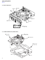
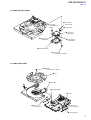
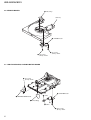
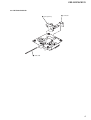
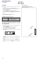
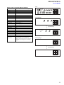
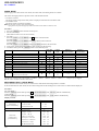
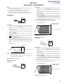
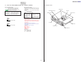
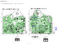
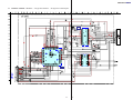
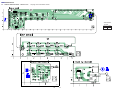
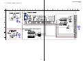
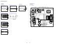
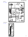
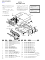
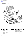
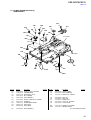
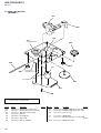
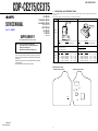
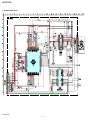
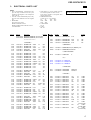
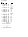
CDP-CE275/CE375
SERVICE MANUAL
US Model
Canadian Model
Australian Model
Ver. 1.2 2006.07
CDP-CE275/CE375
AEP Model
UK Model
E Model
CDP-CE375
Photo: CDP-CE375
Model Name Using Similar Mechanism
CDP-CE345
CD Mechanism Type
CDM59-5BD27
Base Unit Name
BU-5BD27
Optical Pick-up Name
PXR-104X
SPECIFICATIONS
Compact disc player
Laser
Frequency response
Dynamic range
Harmonic distortion
General
Semiconductor laser ( λ = 780 nm)
Emission duration : continuous
2 Hz to 20 kHz ± 0.5 dB
More than 93 dB
Less than 0.0045%
Power requirements
Power consumption
Dimensions (approx.)
(w/h/d)
Mass (approx.)
120 V AC, 60 Hz
11 W
430 x 110 x 400 mm
(17 x 4 3/8 x 15 3/4 in.)
incl. projecting parts
5 kg (11 lbs 1 oz)
Outputs
ANALOG
OUT
DIGITAL
OUT
(OPTICAL)
PHONES
(CDP-CE375
only)
Jack
type
Phono
jacks
Optical
output
connector
Stereo
phone
jack
Maximum
output level
2V
(at 50 kilohms)
–18 dBm
10 mW
Load
impedance
Over 10
kilohms
Wave
length:
660 nm
32 ohms
Supplied accessories
Audio cord (2 phono plugs – 2 phono plugs) (1)
Remote commander (remote) (1) (CDP-CE375 only)
R6 (size AA) batteries (2) (CDP-CE375 only)
Design and specifications are subject to change without notice.
COMPACT DISC PLAYER
9-873-822-13
2006G05-1
© 2006.07
Sony Corporation
Home Audio Division
Published by Sony Techno Create Corporation
CDP-CE275/CE375
Ver 1.1 2001.07
TABLE OF CONTENTS
1.
SERVICING NOTES ............................................... 3
2.
GENERAL ................................................................... 4
3.
DISASSEMBLY ......................................................... 5
4.
TEST MODE .............................................................. 10
5.
ELECTRICAL ADJUSTMENTS ......................... 13
6.
DIAGRAMS
6-1. Note for Printed Wiring Boards
and Schematic Diagrams ................................................
6-2. Printed Wiring Board – BD Board – .............................
6-3. Schematic Diagram – BD Board – ................................
6-4. Printed Wiring Boards – JUNCTION/SENSOR/
LOADING MOTOR Boards – ........................................
6-5. Schematic Diagram – JUNCTION/SENSOR/
LOADING MOTOR Boards – ........................................
6-6. Printed Wiring Board – MAIN Board – ........................
6-7. Schematic Diagram – MAIN Board – ...........................
6-8. Printed Wiring Boards – PANEL Section – ..................
6-9. Schematic Diagram – PANEL Section – .......................
6-10. IC Pin Function Description ...........................................
15
16
17
18
19
20
21
22
23
26
7.
EXPLODED VIEWS ................................................ 30
8.
ELECTRICAL PARTS LIST ............................... 35
SAFETY CHECK-OUT
After correcting the original service problem, perform the following safety check before releasing the set to the customer:
Check the antenna terminals, metal trim, “metallized” knobs,
screws, and all other exposed metal parts for AC leakage.
Check leakage as described below.
LEAKAGE TEST
The AC leakage from any exposed metal part to earth ground and
from all exposed metal parts to any exposed metal part having a
return to chassis, must not exceed 0.5 mA (500 microamperes.).
Leakage current can be measured by any one of three methods.
1. A commercial leakage tester, such as the Simpson 229 or RCA
WT-540A. Follow the manufacturers’ instructions to use these
instruments.
2. A battery-operated AC milliammeter. The Data Precision 245
digital multimeter is suitable for this job.
3. Measuring the voltage drop across a resistor by means of a
VOM or battery-operated AC voltmeter. The “limit” indication is 0.75 V, so analog meters must have an accurate lowvoltage scale. The Simpson 250 and Sanwa SH-63Trd are examples of a passive VOM that is suitable. Nearly all battery
operated digital multimeters that have a 2 V AC range are suitable. (See Fig. A)
To Exposed Metal
Parts on Set
0.15 µF
1.5 kΩ
AC
voltmeter
(0.75 V)
Earth Ground
Fig. A. Using an AC voltmeter to check AC leakage.
SAFETY-RELATED COMPONENT WARNING!!
COMPONENTS IDENTIFIED BY MARK 0 OR DOTTED
LINE WITH MARK 0 ON THE SCHEMATIC DIAGRAMS
AND IN THE PARTS LIST ARE CRITICAL TO SAFE
OPERATION. REPLACE THESE COMPONENTS WITH
SONY PARTS WHOSE PART NUMBERS APPEAR AS
SHOWN IN THIS MANUAL OR IN SUPPLEMENTS PUBLISHED BY SONY.
ATTENTION AU COMPOSANT AYANT RAPPORT
À LA SÉCURITÉ!
LES COMPOSANTS IDENTIFIÉS PAR UNE MARQUE 0
SUR LES DIAGRAMMES SCHÉMATIQUES ET LA LISTE
DES PIÈCES SONT CRITIQUES POUR LA SÉCURITÉ
DE FONCTIONNEMENT. NE REMPLACER CES COMPOSANTS QUE PAR DES PIÈCES SONY DONT LES
NUMÉROS SONT DONNÉS DANS CE MANUEL OU
DANS LES SUPPLÉMENTS PUBLIÉS PAR SONY.
2
CDP-CE275/CE375
SECTION 1
SERVICING NOTES
NOTES ON HANDLING THE OPTICAL PICK-UP
BLOCK OR BASE UNIT
The laser diode in the optical pick-up block may suffer electrostatic break-down because of the potential difference generated
by the charged electrostatic load, etc. on clothing and the human
body.
During repair, pay attention to electrostatic break-down and also
use the procedure in the printed matter which is included in the
repair parts.
The flexible board is easily damaged and should be handled with
care.
HOW TO OPEN THE DISC TABLE WHEN POWER
SWITCH TURNS OFF
Insert a tapering driver into the aperture of the unit bottom, and
turn it in the direction of the arrow (to OUT direction).
NOTES ON LASER DIODE EMISSION CHECK
The laser beam on this model is concentrated so as to be focused
on the disc reflective surface by the objective lens in the optical
pick-up block. Therefore, when checking the laser diode emission, observe from more than 30 cm away from the objective lens.
tapering driver
CAUTION
Use of controls or adjustments or performance of procedures
other than those specified herein may result in hazardous radiation exposure.
This appliance is classified as a CLASS 1 LASER product.
The CLASS 1 LASER PRODUCT MARKING is located on
the rear exterior.
table
* To close the disc table, turn the tapering
driver in the reverse direction (to IN direction).
NOTE FOR MAIN GEAR INSTALLATION
gear, swing
gear (RV)
gear (U/D)
LASER DIODE AND FOCUS SEARCH OPERATION
CHECK
Carry out the “S curve check” in “CD section adjustment” and
check that the S curve waveforms is output three times.
Notes on chip component replacement
• Never reuse a disconnected chip component.
• Notice that the minus side of a tantalum capacitor may be damaged by heat.
Flexible Circuit Board Repairing
• Keep the temperature of the soldering iron around 270 ˚C during repairing.
• Do not touch the soldering iron on the same conductor of the
circuit board (within 3 times).
• Be careful not to apply force on the conductor when soldering
or unsoldering.
MODEL IDENTIFICATION
– BACK PANEL –
Part No.
Model
CDP-CE275: US model
Part No.
4-233-719-0s
CDP-CE275: Canadian model
4-233-719-1s
CDP-CE275: Australian model
4-233-719-2s
CDP-CE375: US model
4-233-718-0s
CDP-CE375: Canadian model
4-233-718-1s
CDP-CE375: AEP model
4-233-718-2s
CDP-CE375: UK model
4-233-718-3s
CDP-CE375: Australian model
4-233-718-4s
CDP-CE375: E model
4-233-718-5s
CDP-CE375: Singapore model
4-233-718-6s
3
CDP-CE275/CE375
SECTION 2
GENERAL
• LOCATION OF CONTROLS
– Front panel –
8
2
3
1
w;
ws
4 5 6 7
qk
qg
ql
qh
wa
9
qs
qf
qj
0
qd
qa
1 POWER button
qs CLEAR button
2 DISC1 – DISC5 button
qd CHECK button
3 Fluorescent indicator tube display
qf EDIT button
4 H button
qg M button
5 X button
qh m button
6 x button
qj Disc table
7 EX-CHANGE button
qk TIME button
8 DISC SKIP button
ql REPEAT button
9 l AMS L control
w; FADER button
0 A OPEN/CLOSE button
wa PEAK SEARCH button
qa PHONES jack (CE375 only)
ws PLAY MODE button
– Rear panel –
1
1 DIGITAL OUT OPTICAL connector
2 ANALOG OUT
4
2
CDP-CE275/CE375
Ver. 1.2
SECTION 3
DISASSEMBLY
• The equipment can be removed using the following procedure.
Set
Case
Front Panel Assy
CD Mechanism Block
Base Unit (BU-5BD27)
Optical Pick-up
Sensor Board
Tray, Table Assy
Jnuction Board, Loading Motor Board
Note: Follow the disassembly procedure in the numerical order given.
3-1. CASE
2 two screws
(case 3TP2)
3 two screws
(BVTP 3x8)
4 case
7 panel, loading
1 two screws
(case 3TP2)
5
6
5
CDP-CE275/CE375
Ver. 1.2
3-2. FRONT PANEL ASSY
1 CN601
2 CN602
7 claw
3 CN301
8 front panel assy
4 CN351
6 claw
(CE375)
5 screw
(BVTP 3x8)
5 five screws
(BVTP 3x8)
3-3. CD MECHANISM BLOCK (CDM59-5BD27)
6 two screws
(BVTP 3x8)
4 two screws
(BVTP 3x8)
7 CDM59-5BD27
3 three screws
(BVTP 3x8)
5 tray
2 CN311
1 CN302
6
CDP-CE275/CE375
Ver. 1.2
3-4. BASE UNIT (BU-5BD27)
4 two screws
(+PTPWHM 2.6),
floating
2 two screws
(BTTP M2.6)
3 stopper (BU)
8 base unit
(BU-5BD27)
7 spring (932),
compression
6 spring (932),
compression
5 holder (BU) assy
1 two screws
(+PTPWHM 2.6), floating
3-5. TRAY, TABLE ASSY
8 screw
(+PTPWHM 2.6), floating
9 tray
7 table assy
5
2 bracket (guide)
6 CN15
1 two screws
(M 2.6), +BTTP
3 two screws
(M 2.6), +BTTP
4 bracket (guide)
7
CDP-CE275/CE375
3-6. SENSOR BOARD
1 belt (rotary)
table assy
4 SENSOR board
3 two screws
(M 2.6), +BTTP
2 two screws
(M 2.6), +BTTP
3-7. JUNCTION BOARD, LOADING MOTOR BOARD
6 two screws
(M 2.6), +BTTP
4 JUNCTION board
2 CN13
7 LOADING MOTOR board
5 belt (loading)
1 CN14
3 three screws
(M 2.6), +BTTP
8
CDP-CE275/CE375
3-8. OPTICAL PICK-UP
3 optical pick-up
4 connector
1
2 shaft, sled
9
CDP-CE275/CE375
Ver 1.1 2001.07
SECTION 4
TEST MODE
ADJ MODE
Connecting Location:
NOTE: This mode cannot be performed without a general remote commander.
– MAIN BOARD (Component Side) –
1. Chuck the CD first, and then turn OFF the power.
2. Short-circuit the test point TP1 (ADJ) of the MAIN board and
ground with a lead wire.
3. Press the [POWER] button to turn ON the power.
The CD is playback automatically and the ADJ mode is set.
4. To exit the mode, press the [POWER] button to turn OFF the
power.
• Prohibits high speed search during accessing
• Ignores even if GFS becomes “L”
ADJ Mode Special Function Table
Button
Function
PLAY MODE
Auto gain display
(Focus, Tracking and Sledding)
EDIT
RFCK → GFS → Error rate display
FLUORESCENT INDICATOR TUBE ALL LIT, AND
KEY CHECK MODE
1. Short-circuit the test TP2 (AFADJ) of the MAIN board and
ground with a lead wire.
2. Press the [POWER] button to turn ON the power.
The whole fluorescent indicator tube lights up.
3. All buttons have individual button numbers.
When a button is pressed, the button number is counted up
and displayed.
1
Count up display
0
TP1 (ADJ)
JW68
Displays button number
When remote controller signals are received, “RM **” will be
displayed.
(** are the numbers corresponding to the remote controller
buttons.)
When using the remote controller, switch the [CD1/2/3] switch
to CD1.
4. To exit the mode, press the [POWER] button to turn OFF the
power.
10
JW66
TP2 (AFADJ)
CN301
CDP-CE275/CE375
Ver 1.1 2001.07
Buttons and Corresponding Button Numbers
Button
DISC1
Button Number or Display
12
DISC2
11
DISC3
10
DISC4
9
DISC5
8
PLAY MODE
20
PEAK SEARCH
19
FADER
18
REPEAT
17
TIME
16
H (PLAY)
Partial lighting 1
X (PAUSE)
Partial lighting 2
x (STOP)
All lit
EX-CHANGE
35
DISC SKIP
36
m
24
M
25
EDIT
26
CHECK
27
CLEAR
28
AMS (push)
AMS (turn)
All lit
ALL1DISCS
REPEAT 1
EDIT
TIME
FADE
A B
PROGRAM
SHUFFLE
DISC
TRACK
PEAK
MIN STEP SEC
1
2 3
4
6
7 8
9 10
5
11 12 13 14 15
16 17 18 19 20
Partial lighting 1
TRACK
MIN
SEC
R Light altemately
r
ALL1DISCS
DISC
PEAK
STEP
1
2 3
6
7 8
4
5
37
When rotated clockwise: The music calendar
numerals light up in ascending order.
When rotated counterclockwise: The music
calendar numerals light up in descending
order.
Partial lighting 2
1
3
7
11
5
9
13
15
18
20
R Light altemately
r
2
6
4
8
10
12
14
16 17
19
11
CDP-CE275/CE375
Ver 1.1 2001.07
AGING MODE
For the aging mode, three modes of all mode, disc table mode, and loading mode are available.
This set has the Aging mode for operation check of the mechanism deck.
• If a failure occurred
The aging operation stops and a faulty status is displayed on the fluorescent indicator tube.
• If no failure occurs
The aging operation continues repeatedly.
Note: Do not use the test disc when performing aging.
Aging will not be performed properly if discs with tracks shorter than 4 seconds are used.
Procedure:
1. Press the [POWER] button and turn ON the power.
2. Set discs on all trays.
(More than two discs if five are not available)
3. All mode:
Press the [CHECK], [PLAY MODE] and x buttons at the same time.
Disc table mode:
Press the [CHECK], [PLAY MODE] and [SKIP] buttons at the same time.
Loading mode:
Press the [CHECK], [PLAY MODE] and [EX-CHANGE] buttons at the same time.
4. Aging starts, and the fluorescent indicator tube will display the following.
5. To exit the mode, press the [POWER] button to turn OFF the power.
Code No.
Status
All mode
Disc table
mode
Loading
mode
Display in
Normal operation
Display in
case of failure
a
A-0
Err 0
a
a
A-1
Err 1
Err 2
0
CLOSE (Tray closed)
a
1
TOC reading
a
2
Access to last track
a
A-2
3
Play of last track (3 sec)
a
Counter display
Err 3
4
EX OPEN (Tray opened while chucking)
a
A-4
Err 4
5
EX SKIP (Disc tray rotated)
a
A-5
Err 5
6
EX CLOSE (Tray closed)
a
7
Access to first track
a
8
Play of first track (3 sec)
a
9
OPEN (tray opened)
a
A
DISC SKIP (Disc tray rotated,
and next disc was selected)
a
a
a
a
a
A-6
Err 6
A-7
Err 7
Counter display
Err 8
A-9
Err 9
A-A
Err A
The discs are selectie in the order of DISC1 →DISC2 → DISC3 → DISC4 → DISC5 → DISC1 → .... Empty trays are skipped.
But the order is random in the disc table mode.
MECHANISM DECK CHECK MODE
For the mechanism deck check mode, two modes of disc table mode and loading mode are available.
In the mechanism deck check mode, the disc table turning time and the loading time in each section are measured and displayed.
Procedure:
Disc table mode:
Press the [POWER] switch while pressing H , [A OPEN/CLOSE] and [REPEAT] buttons simultaneously.
Loading mode:
Press the [POWER] switch while pressing H , [A OPEN/CLOSE] and [TIME] buttons simultaneously.
Display contents
Mode
Disc table mode
(
Table turning
time measurement
)
Check command
Display
0: Right one turn
r 12.5
1: Left one Turn
L 10.2
2: Measurement end
r 12.5
3: Undefined
Table mode
(
12
Loading time
measurement
)
4: Star position
Sta – –.–
5: Open → Close
CLo 10.2
6: Close → BU up
UP
0.7
7: BU up → EX open
EoP
6.2
8: EX open → EX close
ECL 10.3
9: EX close → BU down
don
1.2
A: BU down → Open
oPn
9.3
FF: Measurement end
CLo 10.2
CDP-CE275/CE375
Ver 1.1 2001.07
SECTION 5
ELECTRICAL ADJUSTMENTS
Note:
1. CD Block is basically designed to operate without adjustment. Therefore, check each item in order given.
2. Use PATD-012 disc (4-225-203-01) unless otherwise indicated.
3. Use an oscilloscope with more than 10MΩ impedance.
4. Clean the object lens by an applicator with neutral detergent when the
signal level is low than specified value with the following checks.
S Curve Check
Connection:
oscilloscope
BD board
TP (FE1)
TP (VC)
Procedure:
1. Set the test disc (PATD-012). Disc chucking operation is
complete, then press the [POWER] button to turn the power
off.
2. Connect an oscilloscope to test point TP (RFDC) and TP (VC)
on the BD board.
3. Connect between test point TP (ADJ) on the MAIN board and
GND by lead wire.
4. Press the [POWER] button to turn the power on and enter the
ADJ mode, then playback the number two track automatically.
5. Confirm that oscilloscope waveform is clear and check the level
of between RFDC top and VC is correct or not.
Note: A clear RFDC signal waveform means that the shape “◊” can be
clearly distinguished at the center of the waveform.
+
–
RFDC signal waveform
Procedure:
1. Set the test disc (PATD-012). Disc chucking operation is
complete, then press the [POWER] button to turn the power
off.
2. Connect an oscilloscope to test point TP (FE1) and TP (VC)
on the BD board.
3. Connect between test point TP (ADJ) on the MAIN board and
GND by lead wire.
4. Press the [POWER] button to turn the power on and enter the
ADJ mode.
Then playback the number two track automatically, press the
x button to stop the playback.
5. Press the [CHECK] button actuate the focus search. (actuate
the focus search when disc table is moving in and out)
6. Check the oscilloscope waveform (S-curve) is symmetrical
between A and B. And confirm peak to peak level within 2 ± 1
Vp-p.
level: 1.15 ± 0.35 Vp-p
VC
Checking Location: BD board
RFAC Level Check
Connection:
oscilloscope
BD board
TP (RFAC)
TP (VC)
S-curve waveform
VOLT/DIV: 200 mV
TIME/DIV: 500 ns
+
–
symmetry
A
within 2 ± 1 Vp-p
B
Note: • Try to measure several times to make sure than the ratio of A : B
or B : A is more than 10 : 7.
• Take sweep time as long as possible and light up the
brightness to obtain best waveform.
Checking Location: BD board
Procedure:
1. Set the test disc (PATD-012). Disc chucking operation is
complete, then press the [POWER] button to turn the power
off.
2. Connect an oscilloscope to test point TP (RFAC) and TP (VC)
on the BD board.
3. Connect between test point TP (ADJ) on the MAIN board and
GND by lead wire.
4. Press the [POWER] button to turn the power on and enter the
ADJ mode, then playback the number two track automatically.
5. Confirm that oscilloscope waveform is clear and check RFAC
signal level is correct or not.
Note: A clear RFAC signal waveform means that the shape “◊” can be
clearly distinguished at the center of the waveform.
RFDC Level Check
Connection:
oscilloscope
RFAC signal waveform
BD board
TP (RFDC)
TP (VC)
VOLT/DIV: 200 mV
TIME/DIV: 500 ns
+
–
level: 1.35 ± 0.4 Vp-p
Checking Location: BD board
13
CDP-CE275/CE375
Ver 1.1 2001.07
E-F Balance Check
Connection:
Checking Location:
– BD BOARD (Conductor Side) –
oscilloscope
BD board
TP (TE1)
TP (VC)
+
–
Procedure:
1. Set the test disc (PATD-012). Disc chucking operation is
complete, then press the [POWER] button to turn the power
off.
2. Connect an oscilloscpe to test point TP (TE1) and TP (VC) on
the BD board.
3. Connect between test point TP (ADJ) on the MAIN board and
GND by lead wire.
4. Press the [POWER] button to turn the power on and enter the
ADJ mode, then playback the number two track automatically.
5. Press the [TIME] button. (The tracking servo and the sledding
servo are turned OFF)
6. Check the level B of the oscilliscope waveform and the A (DC
voltage) of the center of the Traverse waveform.
Confirm the following :
A/B x 100 = less than ± 22%
Traverse Waveform
Center of
the waveform
B
A (DC
voltage)
0V
level: 1.15 ± 0.5 Vp-p
Press the [TIME] button. (The tracking servo and sledding servo
are turned ON)
Confirm the C (DC voltage) is almost equal to the A (DC
voltage) is step 6.
7.
Traverse Waveform
C (DC
voltage)
0V
Tracking servo
Sled servo
OFF
Checking Location: BD board
14
Tracking servo
Sled servo
ON
IC150
TP
(VC)
IC131
TP
(FE1)
IC101
TP
(TE1)
TP
(RFDC)
TP
(RFAC)
CDP-CE275/CE375
Ver. 1.2
SECTION 6
DIAGRAMS
6-1.
• Circuit Boards Location
NOTE FOR PRINTED WIRING BOARDS AND SCHEMATIC DIAGRAMS
Note on Printed Wiring Board:
• X : parts extracted from the component side.
• Y : parts extracted from the conductor side.
•
: Pattern from the side which enables seeing.
(The other layers' patterns are not indicated.)
Caution:
Pattern face side:
(Conductor Side)
Parts face side:
(Component Side)
Parts on the pattern face side seen from
the pattern face are indicated.
Parts on the parts face side seen from
the parts face are indicated.
• Indication of transistor
Q
B C
E
These are omitted.
Q
B
C
E
These are omitted.
Note on Schematic Diagram:
• All capacitors are in µF unless otherwise noted. pF: µµF
50 WV or less are not indicated except for electrolytics
and tantalums.
• All resistors are in Ω and 1/4 W or less unless otherwise
specified.
f
: internal component.
•
• C : panel designation.
Note:
The components identified by mark 0 or dotted
line with mark 0 are critical for safety.
Replace only with part
number specified.
SENSOR board
LOADING MOTOR board
BD board
POWER SW board
Note:
Les composants identifiés par
une marque 0 sont critiques
pour la sécurité.
Ne les remplacer que par une
pièce por tant le numéro
spécifié.
• Voltages and waveforms are dc with respect to ground
under no-signal conditions.
no mark : CD PLAY
• Voltages are taken with a VOM (Input impedance 10 MΩ).
Voltage variations may be noted due to normal production tolerances.
• Waveforms are taken with a oscilloscope.
Voltage variations may be noted due to normal production tolerances.
• Circled numbers refer to waveforms.
• Signal path.
J : CD PLAY
c : DIGITAL OUT
• A: B+ Line
• B: B– Line
• Abbreviation
AUS : Australian model
CND : Canadian model
SP
: Singapore model
JUNCTION board
KEY board
MAIN board
DISPLAY board
HEADPHONE board
15
15
CDP-CE275/CE375
Ver. 1.2
6-2.
PRINTED WIRING BOARD – BD Board –
• See page 15 for Circuit Boards Location.
M101
(SPINDLE)
M
S101
(LIMIT)
M
M102
(SLED)
TP
(VC)
TP
(FE1)
TP
(TE1)
(Page 20)
TP (RFDC)
TP (RFAC)
• Semiconductor
Location
• Semiconductor
Location
Ref. No.
Q131
Q132
Ref. No.
Location
IC101
IC131
IC150
C-3
C-3
16
16
Location
C-2
C-1
B-1
CDP-CE275/CE375
Ver. 1.2
6-3.
SCHEMATIC DIAGRAM – BD Board –
• See page 24 for Waveforms.
• See page 24 for IC Block Diagrams.
TP
(RFAC)
IC BD
TP
(RFDC)
TP
(TE1)
TP
(VC)
TP
(FE1)
TP
(SE1)
IC BD
(Page 21)
17
17
CDP-CE275/CE375
6-4.
PRINTED WIRING BOARDS – JUNCTION/SENSOR/LOADING MOTOR Boards – • See page 15 for Circuit Boards Location.
(Page 20)
TO MAIN
BOARD
• Semiconductor
Location
Ref. No.
IC11
Location
C-2
• Semiconductor
Location
Ref. No.
D10
D11
18
18
Location
B-4
E-3
CDP-CE275/CE375
6-5.
SCHEMATIC DIAGRAM – JUNCTION/SENSOR/LOADING MOTOR Boards –
• See page 25 for IC Block Diagram.
TO MAIN BOARD
(Page 21)
IC BD
19
19
CDP-CE275/CE375
Ver. 1.2
6-6. PRINTED WIRING BOARD – MAIN Board –
• See page 15 for Circuit Boards Location.
(Page 22)
(Page 22)
(CE375: E)
T601
POWER
TRANSFORMER
(CE375)
TP1 (ADJ)
TP2 (AFDJ)
(Page 22)
(EXCEPT CE375: E)
(CE375)
• Semiconductor Location
(Page 18)
(Page 16)
20
20
Ref. No.
Location
Ref. No.
Location
D353
D601
D602
D603
D604
D605
D606
D607
D608
D609
D610
D-10
C-7
B-7
C-7
B-7
B-6
A-6
C-7
C-8
C-7
A-6
IC351
IC601
IC602
IC603
E-2
A-5
B-5
A-4
IC301
IC303
IC350
C-3
D-11
E-10
Q301
Q307
Q352
Q353
Q356
Q402
Q405
Q502
Q505
Q601
C-2
D-5
E-7
E-8
D-11
D-11
D-11
E-11
E-11
A-6
CDP-CE275/CE375
Ver. 1.2
6-7.
SCHEMATIC DIAGRAM – MAIN Board –
• See page 24 for Waveform.
(Page 23)
(Page 17)
∗Q402, 405, 502, 505
2SC3622ATP-LK (CE275)
2SC3623ATP-LK (CE375)
IC303
GP1FA550TZ (CE275)
GP1FAV50TK0F (CE375)
(CE375)
(Page 23)
∗D501 – 505
10EDB40-TA2B5 (CE375: US, CND)
11ES2-NTA2B (CE275/CE375: AEP, UK, E, SP, AUS)
∗C602
4700 16V (EXCEPT CE375: E)
6800 16V (CE375: E)
(EXCEPT CE375: E)
(Page 23)
(Page 19)
(CE375: E)
EB601
21
21
CDP-CE275/CE375
Ver. 1.2
6-8. PRINTED WIRING BOARDS – PANEL Section – • See page 15 for Circuit Boards Location.
S825
ROTYARY ENCODER
l AMS L
PUSH ENTER
(Page 20)
• Semiconductor
Location
A OPEN/CLOSE
Ref. No.
Location
IC802
A-13
S601
POWER
(Page 20)
(Page 20)
(CE375)
22
22
CDP-CE275/CE375
Ver. 1.2
6-9.
SCHEMATIC DIAGRAM – PANEL Section –
(Page 21)
(CE375)
(Page 21)
(Page 21)
23
23
CDP-CE275/CE375
3.1 Vp-p
• IC Block Diagrams
– BD BOARD –
1 IC301 es (XTAL)
IC101
VDD
VSS
AVDD3
PCO
FILI
FILO
CLTV
AVSS3
RFAC
BIAS
ASYI
ASYO
AVDD0
IGEN
AVSS0
ADIO
RFDC
CE
TE
CXD2587Q
60
59 58 57
56 55 54 53
52
51 50 49 48
47
46 45
44
43 42 41
4.2 Vp-p
0.5 Vp-p
DIGITAL
OUT
LRCK 61
10 MHz
16.9344 MHz
PCMD 62
D/A
INTERFACE
INTERNAL BUS
5 IC101 el (FE) (CD Play Mode)
1 IC101 yj (XTAO)
– MAIN Board –
DOUT
• Waveforms
– BD Board –
ERROR
CORRECTOR
DIGITAL
PLL
16K
RAM
40 SE
39 FE
38 VC
ASYMMETRY
CORRECTION
OPERATIONAL
AMPLIFIER
ANALOG SWITCH
EFM
DEMODULATOR
A/D
CONVERTER
BCK 63
EMPH 64
6 IC101 wh (MDP) (CD Play Mode)
XTAI
XTAO
XVSS
AVDD1
AOUT1
AIN1
2.5 Vp-p
66
67
68
69
70
71
TIMING
LOGIC
CLOCK
GENERATOR
SERVO DSP
LOUT1 72
PWM
AVSS1 73
AVSS2 74
7.8 µs
LOUT2 75
3rd ORDER
NOISE SHAPER
OVER SAMPLING
DIGITAL FILTER
AIN2 76
3 IC101 rd (RF DC)
PWM
AOUT2 77
AVDD2 78
RMUT 79
LMUT 80
SUBCODE
PROCESSOR
FOCUS PWM
GENERATOR
TRACKING
SERVO
TRACKING
PWM GENERATOR
SLED
SERVO
SLED PWM
GENERATOR
SERVO AUTO
SEQUENCER
CPU
INTERFACE
4 IC101 ra (TE) (CD Play Mode)
0.2 Vp-p
24
24
37 XTSL
36 TES1
35 TEST
34 VSS
33
32
31
30
29
28
FRDR
FFDR
TRDR
TFDR
SRDR
SFDR
27 SSTP
SERIAL IN
INTERFACE
1.3 Vp-p
PWM GENERATOR
FOCUS
SERVO
SERVO
INTERFACE
DIGITAL
CLV
26 MDP
25 LOCK
MIRR, DFCT,
FOK
DETECTOR
24 FOK
23 DFCT
22 MIRR
3
4
5 6 7 8
9 10 11 12 13 14 15 16 17 18 19 20
XRST
SYSM
DATA
XLAT
CLOK
SENS
SCLK
VDD
ATSK
C2PO
SCOR
1 2
SQSO
SQCK
21 COUT
WFCK
XUGF
XPCK
GFS
1.2 Vp-p
XVDD 65
SPOA
SPOB
XLON
2 IC101 ta (RF AC) (CD Play Mode)
CDP-CE275/CE375
– BD Board –
IC131
CXA2581N
12 DC_OFST
RW/ROM
APC
LD 1
11 RFDCI
PD 2
DVCC
VC
11 RFDCO
DVC
VCC
VC
10 VC
EQ IN 3
AC
SUM
AC SUM 4
EQ
26 RFC
25 VFC
24 BST
AC
VCA
23 RFG
EQ
ON/OFF
GND 5
VCC
VOFST
22 VCC
RW/ROM
B
C
A 6
B 7
A
C 8
D
VCC
20 CE
VC
VC
VOFST
D 9
VC
RW/ROM
RW/ROM
19 TE_BAL
DVCC RW/ROM
gm
F 10
21 CEI
18 TE
gm
E 11
APC-OFF(Hi-Z)
RW/ROM
(H/L)
SW 12
RW/ROM
DVCC 13
AVC
DVC
VOFST
DVC
17 FEI
DVCC
VC
DVC 14
DVC
DVC
16 FE
RFAC 15
– JUNCTION Board –
IOUT
4
VEE
VREF
5
VREG
6
VCC
7
OUT1+
8
OUT1-
9
VCC
3
COVERNER DRIVER
FWD/REV CONTROLLER
RIN1
VEE
2
18
VIN2
17
FIN2
16
RIN2
15
CT2
14 VEE
COVERNER
LOAD CURRENT
DETECTION
AMPLIFIER
FIN1
+
-
COVERNER
OUTPUT
1
REVERSIBLE DRIVER
FWD/REV CONTROLLER
VIN1
REFERENCE
VOLTAGE
OUTPUT
BA6780
LOW VOLTAGE
OUTPUT
IC11
13
FBIN-
12
FBIN+
11 OUT2+
10
OUT2-
25
CDP-CE275/CE375
6-10.
IC PIN FUNCTION DESCRIPTION
• BD BOARD IC101 CXD2587Q
(DIGITAL SIGNAL PROCESSOR, DIGITAL SERVO PROCESSOR, DIGITAL FILTER, D/A CONVERTER)
Pin No.
Pin Name
I/O
Description
1
SQSO
O
Subcode Q data output to the system controller (IC301)
2
SQCK
I
Subcode Q data reading clock signal input from the system controller (IC301)
3
XRST
I
System reset signal input from the system controller (IC301)
Analog line muting on/off control signal input terminal
“L”: reset
“H”: line muting on
4
SYSM
I
5
DATA
I
Command serial data input from the system controller (IC301)
6
XLAT
I
Command latch pulse input from the system controller (IC301)
7
CLOK
I
Command serial data transfer clock signal input from the system controller (IC301)
8
SENS
O
Internal status monitor output to the system controller (IC301)
9
SCLK
I
SENSE serial data reading clock input from the system controller (IC301)
10
VDD
—
Power supply terminal (+5V) (digital system)
11
ATSK
I/O
Input pin for anti-shock
12
SPOA
I
Not used (fixed at “L”)
Not used (fixed at “L”)
Microcomputer escape interface input A terminal
Not used (fixed at “L”)
Not used (fixed at “L”)
13
SPOB
I
Microcomputer escape interface input B terminal
14
XLON
O
Microcomputer escape interface output to the CXA2568M (IC103)
15
WFCK
O
WFCK output terminal
16
XUGF
O
Not used (open)
17
XPCK
O
Not used (open)
18
GFS
O
Not used (open)
19
C2PO
O
Not used (open)
Not used (open)
20
SCOR
O
21
COUT
I/O
Numbers of track counted signal input/output terminal
22
MIRR
I/O
Mirror signal input/output terminal
Not used (open)
23
DFCT
I/O
Defect signal input/output terminal
Not used (open)
24
FOK
I/O
Focus OK input/output terminal
25
LOCK
I/O
GFS is sampled by 460 Hz
26
MDP
O
Spindle motor (M101) servo drive signal output to the BA5974FP (IC102)
27
SSTP
I
Limit in detect switch (S101) input terminal
28
SFDR
O
Sled servo drive PWM signal (+) output to the BA5974FP (IC102)
29
SRDR
O
Sled servo drive PWM signal (–) output to the BA5974FP (IC102)
30
TFDR
O
Tracking servo drive PWM signal (+) output to the BA5974FP (IC102)
31
TRDR
O
Tracking servo drive PWM signal (–) output to the BA5974FP (IC102)
32
FFDR
O
Focus servo drive PWM signal (+) output to the BA5974FP (IC102)
33
FRDR
O
Focus servo drive PWM signal (–) output to the BA5974FP (IC102)
34
VSS
—
Ground terminal (digital system)
35
TEST
I
Input terminal for the test (fixed at “L”)
36
TES1
I
Input terminal for the test (fixed at “L”)
37
XTSL
I
38
VC
I
Middle point voltage (+2.5V) input from the CXA2568M (IC103)
39
FE
I
Focus error signal input from the CXA2568M (IC103)
40
SE
I
Sled error signal input from the CXA2568M (IC103)
41
TE
I
Tracking error signal input from the CXA2568M (IC103)
42
CE
I
Command chip enable signal input from the CXA2568M (IC103)
26
Subcode sync (S0+S1) detection signal output to the system controller (IC301)
Not used (open)
Not used (open)
“H” when GFS is “H”
Not used (open)
Input terminal for the system clock frequency setting
“L”: 45.1584 MHz, “H”: 22.5792 MHz
(fixed at “L” in this set)
CDP-CE275/CE375
Pin No.
Pin Name
I/O
Description
43
RFDC
I
RF signal input from the CXA2568M (IC103)
44
ADIO
O
Monitor output of the A/D converter input signal
45
AVSS0
—
Ground terminal (digital system)
46
IGEN
I
47
AVDD0
—
Power supply terminal (+5V) (digital system)
48
ASYO
O
Playback EFM full-swing output terminal
49
ASYI
I
Playback EFM asymmetry comparator voltage input terminal
50
BIAS
I
Playback EFM asymmetry circuit constant current input terminal
Not used (open)
Stabilized current input for operational amplifiers
51
RFAC
I
52
AVSS3
—
EFM signal input from the CXA2568M (IC103)
53
CLTV
I
54
FILO
O
Filter output for master clock of the playback master PLL
55
FILI
I
Filter input for master clock of the playback master PLL
Ground terminal (digital system)
Internal VCO control voltage input of the playback master PLL
56
PCO
O
Phase comparison output for master clock of the playback EFM master PLL
57
AVDD3
—
Power supply terminal (+5V) (digital system)
58
VSS
—
Ground terminal (digital system)
59
VDD
—
Power supply terminal (+5V) (digital system)
60
DOUT
O
Digital audio signal output to the DIGITAL OUT OPTICAL (IC303)
61
LRCK
O
L/R sampling clock signal (44.1 kHz) output terminal
62
PCMD
O
D/A interface serial data output terminal
63
BCK
O
Bit clock signal (2.8224 MHz) output terminal
64
EMPH
O
De-emphasis control signal output terminal
65
XVDD
—
Power supply terminal (+5V) (crystal oscillator system)
66
XTAI
I
System clock input terminal (16.9344 MHz)
67
XTAO
O
System clock output terminal (16.9344 MHz)
68
XVSS
—
Ground terminal (crystal oscillator system)
69
AVDD1
—
Power supply terminal (+5V) (analog system)
70
AOUT1
O
L-ch analog audio signal output terminal
71
AIN1
I
L-ch operational amplifiers input terminal
72
LOUT1
O
L-ch line output terminal
73
AVSS1
—
Ground terminal (analog system)
74
AVSS2
—
Ground terminal (analog system)
75
LOUT2
O
R-ch line output terminal
Not used (open)
Not used (open)
Not used (open)
Not used (open)
76
AIN2
I
R-ch operational amplifiers input terminal
77
AOUT2
O
R-ch analog audio signal output terminal
78
AVDD2
—
Power supply terminal (+5V) (analog system)
79
RMUT
O
R-ch line muting on/off control signal output terminal
80
LMUT
O
L-ch line muting on/off control signal output terminal
27
CDP-CE275/CE375
• MAIN BOARD IC301 CXP82532-013Q
(SYSTEM CONTROLLER, FLUORESCENT INDICATOR TUBE DRIVER, KEY CONTROL)
Pin No.
Pin Name
I/O
Description
1
BUSIN
I
Sircs remote control signal input terminal
2
RMIN
I
Remote control signal input from the remote control receiver (IC802)
Not used (pull up)
3
NC
I
Not used (open)
4
XLT
O
Serial data latch pulse signal output to the CXD2587Q (IC101)
5
LDON
O
Laser diode ON/OFF output
6
TSENS
I/O
Detect signal input from the table sensor (D10)
7
DA CS
I/O
DA CS
8
CLK
I/O
Serial data transfer clock signal output to the CXD2587Q (IC101)
9
LDON/RW
I/O
Laser diode ON/OFF output
10
DATA
I/O
Serial data output to the CXD2587Q (IC101)
11
SQCK
I/O
Sub-code Q data reading clock signal output to the CXD2587Q (IC101)
12
SUBQ
I/O
Sub-code Q data signal input from the CXD2587Q (IC101)
13
NC
O
14
OUT SW
I/O
Detect signal input from the open/close detect switch (S11)
15
S1
I/O
Detect signal input from the tray address detect switch (S200)
16
S2
I/O
Detect signal input from the tray address detect switch (S200)
Not used (open)
17
NC
I/O
Not used (open)
18
TBLL
I/O
Table motor drive signal (counterclockwise) output to the BA6780 (IC11)
19
TBLR
I/O
Table motor drive signal (clockwise) output to the BA6780 (IC11)
20
LD IN
I/O
Loading motor (M11) drive signal output to the BA6780 (IC11)
*1
21
LD OUT
I/O
Loading motor (M11) drive signal output to the BA6780 (IC11)
*1
22
NC
I/O
Not used (open)
23
NC
I/O
Not used (open)
24
TEST
I/O
Key input terminal (A/D input)
25
KEY3
I/O
Key input terminal (A/D input) (S812 to S816)
26
KEY4
I/O
Key input terminal (A/D input) (S817 to S821)
27
KEY5
I/O
Key input terminal (A/D input) (S806 to S810)
28
KEY6
I/O
Key input terminal (A/D input) (S801 to S805)
29
NC
I/O
Not used (open)
30
RST
I/O
31
EXTAL
I
Main system clock input terminal (10 MHz)
32
XTAL
O
Main system clock output terminal (10 MHz)
33
VSS
—
Ground terminal
34
NC
O
Not used (open)
35
NC
O
Not used (open)
36
NC
O
Not used (open)
37
NC
O
Not used (open)
System reset signal input from the reset signal generator (IC601)
*1 Loading motor (M11) control
Operation
Terminal
LOAD IN (pin @º)
LOAD OUT (pin @¡)
28
“L”:reset
For several hundreds msec. after the power supply rises, “L” is input, then it changes to “H”
OFF
OFF
IN BRAKE
“L”
“L”
“H”
“H”
“L”
“H”
“L”
“H”
CDP-CE275/CE375
Pin No.
Pin Name
I/O
Description
38 to 57
P1 to P20
O
Segment drive signal output to the fluorescent indicator tube (FL801)
58 to 62
NC
O
Not used (open)
63 to 70
G1 to G8
O
Grid drive signal output to the fluorescent indicator tube (FL801)
71
VG
—
Power supply terminal (–30V) (for fluorescent indicator tube drive)
72
VDD
—
Power supply terminal (+5V)
73 to 75
NC
O
Not used (open)
76
AFADJ
I
Setting terminal for the test mode
77
BUSOUT
O
Sircs remote control signal output terminal
78
DSENS
I
Detect signal input from the disc sensor (D11)
“L” active
Not used (open)
79
SENS
I
Internal status (SENSE) signal input from the CXD2587Q (IC101)
80
SCOR
I
Sub-code sync (S0+S1) detection signal input from the CXD2587Q (IC101)
29
CDP-CE275/CE375
Ver. 1.2
SECTION 7
EXPLODED VIEWS
NOTE:
• -XX and -X mean standardized parts, so they
may have some difference from the original
one.
• Color Indication of Appearance Parts
Example:
KNOB, BALANCE (WHITE) . . . (RED)
↑
↑
Parts Color Cabinet's Color
• Abbreviation
AUS : Australian model
CND : Canadian model
SP : Singapore model
• Items marked “*” are not stocked since they
are seldom required for routine service. Some
delay should be anticipated when ordering
these items.
• The mechanical parts with no reference number in the exploded views are not supplied.
• Accessories and packing materials are given
in the last of the electrical parts list.
The components identified by
mark 0 or dotted line with mark
0 are critical for safety.
Replace only with part number
specified.
Les composants identifiés par une
marque 0 sont critiquens pour la
sécurité.
Ne les remplacer que par une pièce
portant le numéro spécifié.
#1
6
7
7-1. CASE SECTION
#1
#1
not
supplied
10
6
not supplied
9
13
8
#1
CDM59-5BD27
#1
12
11
#1
FRONT PANEL SECTION
#1
T601
3
2
not supplied
1
#1
5
(CE375)
#1
Ref. No.
1
1
Part No.
Description
#1
Remark
1
1
2
A-4476-657-A MAIN BOARD, COMPLETE (CE270)
A-4476-667-A MAIN BOARD, COMPLETE (CE370: AEP, UK,
AUS, SP)
A-4476-669-A MAIN BOARD, COMPLETE (CE370: E)
A-4476-687-A MAIN BOARD, COMPLETE (CE370: US, CND)
4-954-051-21 HOLDER, PC BOARD
3
5
5
6
6
X-4953-448-1
4-231-683-01
4-231-683-21
3-363-099-02
3-363-099-11
7
7
8
8
09
4-231-686-11 CASE (409538) (BLACK)
4-231-686-31 CASE (409538) (SILVER)
3-703-244-00 BUSHING (2104), CORD (CE275/CE375: US,
CND, AEP, UK, AUS, SP)
3-703-571-11 BUSHING (S) (4516), CORD (CE375: E)
1-696-845-11 CORD, POWER (CE275: AUS/CE375: AUS)
09
09
09
09
1-775-787-41
1-777-071-63
1-783-531-32
1-783-532-32
FOOT ASSY
PANEL, LOADING (BLACK)
PANEL, LOADING (SILVER)
SCREW (CASE 3 TP2) (for BLACK)
SCREW (CASE 3 TP2) (for SILVER)
Ref. No.
Part No.
09
1-792-824-12 CORD, POWER (TRACKING) (CE375: E)
10
10
10
10
10
4-233-718-02
4-233-718-11
4-233-718-21
4-233-718-31
4-233-718-41
PANEL, BACK (CE375: US)
PANEL, BACK (CE375: CND)
PANEL, BACK (CE375: AEP)
PANEL, BACK (CE375: UK)
PANEL, BACK (CE375: AUS)
10
10
10
10
10
4-233-718-51
4-233-718-61
4-233-719-02
4-233-719-11
4-233-719-21
PANEL, BACK (CE375: E)
PANEL, BACK (CE375: SP)
PANEL, BACK (CE275: US)
PANEL, BACK (CE275: CND)
PANEL, BACK (CE275: AUS)
11
12
13
0 T601
3-703-249-02
1-823-115-11
3-655-653-01
1-435-342-11
0 T601
30
CORD, POWER (CE375: AEP, UK)
CORD, POWER (CE375: SP)
CORD, POWER (CE275: US, CND/CE375: CND)
CORD, POWER (CE375: US)
Description
0 T601
#1
Remark
SCREW, S TIGHT, +PTTWH 3X6
WIRE (FLAT TYPE) (21 CORE)
BAND (TAITON), BINDING
TRANSFORMER, POWER (CE275: US, CND/
CE375: US, CND)
1-435-343-11 TRANSFORMER, POWER (CE375: AEP, UK,
AUS, SP)
1-435-344-11 TRANSFORMER, POWER (CE375: E)
7-685-646-79 SCREW +BVTP 3X8 TYPE2 IT-3
CDP-CE275/CE375
Ver. 1.2
7-2. FRONT PANEL SECTION
55
57
57
56
62
58
54
57
63
63
59
FL801
61
60
J881
57
not supplied
supplied with J881
(CE375)
52
51
53
Ref. No.
51
Part No.
Description
Remark
51
X-4953-734-3 PANEL ASSY, FRONT (BLACK) (CE375: US,
CND)
X-4953-735-2 PANEL ASSY, FRONT (BLACK) (CE375: AEP,
UK, E, AUS, SP)
X-4953-736-2 PANEL ASSY, FRONT (SILVER) (CE375: AEP)
X-4953-737-3 PANEL ASSY, FRONT (BLACK) (CE275: US,
CND)
X-4953-738-1 PANEL ASSY, FRONT (BLACK) (CE275: AUS)
52
53
53
54
54
3-354-981-11
4-231-928-01
4-231-928-11
4-231-973-01
4-231-973-11
51
51
51
SPRING (SUS), RING
KNOB (AMS) (BLACK)
KNOB (AMS) (SILVER)
BUTTON (POWER) (BLACK)
BUTTON (POWER) (SILVER)
Ref. No.
Part No.
Description
Remark
55
56
57
58
59
1-681-141-11
1-681-140-11
3-087-053-01
4-231-690-01
1-681-139-11
POWER SW BOARD
KEY BOARD
+BVTP2.6 (3CR)
HOLDER (FL A)
DISPLAY BOARD
60
61
62
63
FL801
1-823-116-11 WIRE (FLAT TYPE) (37 CORE)
1-681-142-11 HEADPHONE BOARD (CE375)
4-374-846-31 COVER, CAPACITOR, CAP TYPE (CE275: AUS/
CE375: AEP, UK, E, AUS, SP)
3-362-346-11 CUSHION
1-517-946-21 INDICATOR TUBE, FLUORESCENT
J881
1-770-306-11 JACK (LARGE TYPE) (PHONES)
31
CDP-CE275/CE375
Ver. 1.2
7-3. CD MECHANISM SECTION (1)
(CDM59-5BD27)
106
106
110
109
107
111
106
108
112
M11
105
113
102
102
115
102
not supplied
BU-5BD27
117
104
not supplied
102
118
A
117
101
A
102
106
not supplied
101
102
Ref. No.
Part No.
Description
101
102
104
105
106
4-224-619-01
4-218-253-32
4-224-602-03
4-224-617-01
4-218-252-52
BRACKET (GUIDE)
SCREW (M2.6), +BTTP
TABLE
GEAR (RM-E)
SCREW (+PTPWH M2.6), FLOATING
107
108
109
110
4-224-616-01
4-224-615-03
4-225-328-01
4-224-603-06
GEAR (RM-M)
GEAR (RM-B)
BELT (ROTARY)
TRAY
32
Remark
Ref. No.
111
112
* 113
115
117
118
M11
Part No.
Description
1-791-930-11 WIRE (FLAT TYPE)(6 CORE)
1-676-245-11
X-4947-960-1
4-985-672-01
4-959-996-01
X-4952-312-1
SENSOR BOARD
ROLLER ASSY
SCREW (+PTPWH M2.6), FLOATING
SPRING (932), COMPRESSION
HOLDER (BU) ASSY
A-4735-761-A MOTOR ASSY, ROTARY (TRAY)
Remark
CDP-CE275/CE375
Ver. 1.2
7-4. CD MECHANISM SECTION (2)
(CDM59-5BD27)
156
156
165
170
169
163
166
164
156
168
162
167
161
not supplied
156
S200
156
159
153
not supplied
158
155
157
151
M10
156
152
154
153
Ref. No.
Part No.
Description
151
152
153
154
155
X-4952-019-4
1-676-246-11
4-218-253-32
4-225-885-01
4-225-844-01
PULLEY (A) ASSY, CHUCKING
JUNCTION BOARD
SCREW (M2.6), +BTTP
BELT (LOADING)
GEAR (LOADING A)
156
157
158
159
161
4-218-252-52
4-951-619-11
1-676-244-11
4-224-613-01
4-224-607-01
SCREW (+PTPWH M2.6), FLOATING
CUSHION (A)
LOADING MOTOR BOARD
GEAR (SHAFT)
GEAR, SWING
162
4-224-609-01 GEAR (LOADING C)
Remark
Ref. No.
Part No.
Description
Remark
163
164
165
4-224-608-01 COLLAR, SWING
4-224-611-01 GEAR (LOADING B)
3-016-533-11 WASHER (FR), STOPPER
166
167
168
169
170
4-224-606-01
4-224-605-01
1-471-061-11
4-221-688-01
4-224-618-01
M10
S200
A-4735-762-A MOTOR ASSY, LOADING
1-418-746-11 ENCODER, ROTARY
(BU, TABLE ADDRESS DETECT)
GEAR (RV)
GEAR (U/D)
MAGNET ASSY
PULLEY (B), CHUCKING
LEVER (LIFTER)
33
CDP-CE275/CE375
Ver. 1.2
7-5. BASE UNIT SECTION
(BU-5BD27)
201
202
210
211
(including M101)
203
205
204
M102
204
not supplied
(included in 211)
not supplied
206
207
208
Note: When you exchange Ref. No. 201 or 207, please
be sure to refer to “Supplement-1”.
Ref. No.
Part No.
Description
0 201
0 201
202
203
204
1-796-033-12
8-848-483-21
1-782-817-11
4-917-567-01
4-951-940-01
OPTICAL PICK-UP (PXR-104X)
OPTICAL PICK-UP (KSS-213C/C2RP)
WIRE (FLAT TYPE)(16 CORE)
GEAR (M)
INSULATOR (BU)
205
206
34
4-917-565-01 SHAFT, SLED
4-917-564-01 GEAR (P), FLATNESS
Remark
Ref. No.
Part No.
Description
Remark
207
207
208
A-4725-568-A BD BOARD, COMPLETE (for PXR-104X)
A-4725-568-B BD BOARD, COMPLETE (for KSS-213C)
3-087-053-01 +BVTP 2.6 (3CR)
210
211
3-713-786-51 SCREW (M2X3)
X-4917-523-3 BASE (OUTSERT) ASSY (including M101
(spindle))
X-4917-504-1 MOTOR ASSY (SLED)
M102
CDP-CE275/CE375
Ver. 1.2
SECTION 8
ELECTRICAL PARTS LIST
NOTE:
• Due to standardization, replacements in the
parts list may be different from the parts specified in the diagrams or the components used
on the set.
• -XX and -X mean standardized parts, so they
may have some difference from the original
one.
• RESISTORS
All resistors are in ohms.
METAL: Metal-film resistor.
METAL OXIDE: Metal oxide-film resistor.
F: nonflammable
• Abbreviation
AUS : Australian model
CND : Canadian model
SP : Singapore model
Ref. No.
Part No.
BD
• Items marked “*” are not stocked since they
are seldom required for routine service.
Some delay should be anticipated when ordering these items.
• SEMICONDUCTORS
In each case, u: µ, for example:
uA. . : µA. .
uPA. . : µPA. .
uPB. . : µPB. .
uPC. . : µPC. .
uPD. . : µPD. .
• CAPACITORS
uF: µF
• COILS
uH: µH
Description
Remark
Ref. No.
C193
C194
C199
A-4725-568-A BD BOARD, COMPLETE
*******************
Part No.
The components identified by
mark 0 or dotted line with mark
0 are critical for safety.
Replace only with part number
specified.
Les composants identifiés par une
marque 0 sont critiquens pour la
sécurité.
Ne les remplacer que par une pièce
portant le numéro spécifié.
When indicating parts by reference
number, please include the board.
Description
1-162-920-11 CERAMIC CHIP
1-162-918-11 CERAMIC CHIP
1-164-156-11 CERAMIC CHIP
Remark
27PF
18PF
0.1uF
5%
5%
50V
50V
25V
< CAPACITOR >
< CONNECTOR >
C101
C102
C103
C110
C111
1-164-315-11
1-164-156-11
1-164-315-11
1-126-206-11
1-164-156-11
CERAMIC CHIP
CERAMIC CHIP
CERAMIC CHIP
ELECT CHIP
CERAMIC CHIP
470PF
0.1uF
470PF
100uF
0.1uF
5%
C112
C120
C121
C122
C123
1-164-156-11
1-164-156-11
1-162-970-11
1-117-863-11
1-162-927-11
CERAMIC CHIP
CERAMIC CHIP
CERAMIC CHIP
CERAMIC CHIP
CERAMIC CHIP
0.1uF
0.1uF
0.01uF
0.47uF
100PF
10%
10%
5%
25V
25V
25V
6.3V
50V
C124
C125
C126
C130
C131
1-162-967-11
1-162-965-11
1-107-826-11
1-164-505-11
1-164-505-11
CERAMIC CHIP
CERAMIC CHIP
CERAMIC CHIP
CERAMIC CHIP
CERAMIC CHIP
0.0033uF 10%
0.0015uF 10%
0.1uF
10%
2.2uF
2.2uF
50V
50V
16V
16V
16V
C132
C133
C134
C136
C137
1-164-505-11
1-126-208-21
1-126-208-21
1-107-826-11
1-126-209-11
CERAMIC CHIP
ELECT CHIP
ELECT CHIP
CERAMIC CHIP
ELECT CHIP
A2.2uF
47uF
47uF
0.1uF
100uF
16V
4V
4V
16V
4V
C138
C139
C140
C145
C150
1-162-964-11
1-162-921-11
1-164-505-11
1-162-908-11
1-126-204-11
CERAMIC CHIP
CERAMIC CHIP
CERAMIC CHIP
CERAMIC CHIP
ELECT CHIP
0.001uF
33PF
2.2uF
3PF
47uF
C151
C152
C153
C154
C158
1-164-156-11
1-162-919-11
1-162-919-11
1-162-964-11
1-164-172-11
CERAMIC CHIP
CERAMIC CHIP
CERAMIC CHIP
CERAMIC CHIP
CERAMIC CHIP
0.1uF
22PF
22PF
0.001uF
0.0056uF
C171
C172
C173
C174
C181
1-126-206-11
1-164-156-11
1-162-928-11
1-115-412-11
1-126-206-11
ELECT CHIP
CERAMIC CHIP
CERAMIC CHIP
CERAMIC CHIP
ELECT CHIP
100uF
0.1uF
120PF
680PF
100uF
C182
C183
C184
C191
C192
1-164-156-11
1-162-928-11
1-115-412-11
1-126-205-11
1-164-156-11
CERAMIC CHIP
CERAMIC CHIP
CERAMIC CHIP
ELECT CHIP
CERAMIC CHIP
0.1uF
120PF
680PF
47uF
0.1uF
5%
20%
20%
20%
10%
20%
50V
25V
50V
6.3V
25V
10%
5%
50V
50V
16V
0.25PF 50V
20%
16V
5%
5%
10%
10%
20%
5%
5%
20%
5%
5%
20%
25V
50V
50V
50V
25V
6.3V
25V
50V
25V
6.3V
25V
50V
25V
6.3V
25V
CN101
CN102
1-784-360-11 CONNECTOR, FFC (LIF (NON-ZIF)) 21P
1-777-937-11 CONNECTOR, FFC/FPC 16P
< JUMPER RESISTOR >
FB191
1-216-864-11 SHORT CHIP
0
< IC >
IC101
IC131
IC150
8-752-386-85 IC CXD2587Q
8-752-089-74 IC CXA2581N-T4
8-759-829-14 IC AN4800SB
< TRANSISTOR >
Q131
Q132
8-729-010-08 TRANSISTOR
8-729-600-22 TRANSISTOR
MSB710-R
2SA1235-F
< RESISTOR >
R101
R102
R103
R110
R111
1-216-835-11
1-216-845-11
1-216-835-11
1-216-821-11
1-216-809-11
METAL CHIP
METAL CHIP
METAL CHIP
METAL CHIP
METAL CHIP
15K
100K
15K
1K
100
5%
5%
5%
5%
5%
1/10W
1/10W
1/10W
1/10W
1/10W
R112
R120
R121
R122
R123
1-216-833-11
1-216-839-11
1-216-833-11
1-216-845-11
1-216-857-11
METAL CHIP
METAL CHIP
METAL CHIP
METAL CHIP
METAL CHIP
10K
33K
10K
100K
1M
5%
5%
5%
5%
5%
1/10W
1/10W
1/10W
1/10W
1/10W
R125
R126
R127
R129
R134
1-216-827-11
1-216-833-11
1-216-821-11
1-216-815-11
1-216-853-11
METAL CHIP
METAL CHIP
METAL CHIP
METAL CHIP
METAL CHIP
3.3K
10K
1K
330
470K
5%
5%
5%
5%
5%
1/10W
1/10W
1/10W
1/10W
1/10W
R135
R136
R137
R138
R139
1-216-837-11
1-216-837-11
1-216-797-11
1-216-798-11
1-216-846-11
METAL CHIP
METAL CHIP
METAL CHIP
METAL CHIP
METAL CHIP
22K
22K
10
12
120K
5%
5%
5%
5%
5%
1/10W
1/10W
1/10W
1/10W
1/10W
R140
R141
1-216-854-11 METAL CHIP
1-216-840-11 METAL CHIP
560K
39K
5%
5%
1/10W
1/10W
Note: When you repair or exchange BD board, please
be sure to refer to “Supplement-1”.
35
CDP-CE275/CE375
Ver. 1.2
BD
Ref. No.
DISPLAY
Part No.
HEADPHONE
Description
JUNCTION
Remark
R142
R143
R144
1-216-841-11 METAL CHIP
1-216-855-11 METAL CHIP
1-216-846-11 METAL CHIP
47K
680K
120K
5%
5%
5%
1/10W
1/10W
1/10W
R145
R146
R149
R151
R152
1-216-830-11
1-216-845-11
1-216-821-11
1-216-845-11
1-216-833-11
METAL CHIP
METAL CHIP
METAL CHIP
METAL CHIP
METAL CHIP
5.6K
100K
1K
100K
10K
5%
5%
5%
5%
5%
1/10W
1/10W
1/10W
1/10W
1/10W
R153
R155
R171
R172
R173
1-216-864-11
1-216-837-11
1-218-720-11
1-218-720-11
1-218-720-11
SHORT CHIP
METAL CHIP
METAL CHIP
METAL CHIP
METAL CHIP
0
22K
15K
15K
15K
5%
0.5%
0.5%
0.5%
1/10W
1/10W
1/10W
1/10W
R174
R181
R182
R183
R184
1-216-809-11
1-218-720-11
1-218-720-11
1-218-720-11
1-216-809-11
METAL CHIP
METAL CHIP
METAL CHIP
METAL CHIP
METAL CHIP
100
15K
15K
15K
100
5%
0.5%
0.5%
0.5%
5%
1/10W
1/10W
1/10W
1/10W
1/10W
R191
R192
1-216-817-11 METAL CHIP
1-216-797-11 METAL CHIP
470
10
5%
5%
1/10W
1/10W
< COMPOSITION CIRCUIT BLOCK >
RB101
RB102
1-233-576-11 RES, CHIP NETWORK 100 (3216)
1-233-576-11 RES, CHIP NETWORK 100 (3216)
Part No.
Description
Remark
R815
1-247-843-11 CARBON
3.3K
5%
1/4W
R816
R817
R818
R819
R820
1-249-427-11
1-249-415-11
1-249-417-11
1-249-419-11
1-249-421-11
CARBON
CARBON
CARBON
CARBON
CARBON
6.8K
680
1K
1.5K
2.2K
5%
5%
5%
5%
5%
1/4W
1/4W
1/4W
1/4W
1/4W
R821
R822
R851
R852
1-247-843-11
1-249-427-11
1-247-807-31
1-247-807-31
CARBON
CARBON
CARBON
CARBON
3.3K
6.8K
100
100
5%
5%
5%
5%
1/4W
1/4W
1/4W
1/4W
< SWITCH >
S801
S802
S803
S804
S805
1-771-349-21
1-771-349-21
1-771-349-21
1-771-349-21
1-771-349-21
SWITCH, KEYBOARD (H)
SWITCH, KEYBOARD (X)
SWITCH, KEYBOARD (x)
SWITCH, KEYBOARD (EX-CHANGE)
SWITCH, KEYBOARD (DISC SKIP)
S806
S807
S808
S809
S810
1-771-349-21
1-771-349-21
1-771-349-21
1-771-349-21
1-771-349-21
SWITCH, KEYBOARD (m)
SWITCH, KEYBOARD (M)
SWITCH, KEYBOARD (EDIT)
SWITCH, KEYBOARD (CHECK)
SWITCH, KEYBOARD (CLEAR)
S811
S825
1-771-349-21 SWITCH, KEYBOARD (A OPEN/CLOSE)
1-475-543-11 ENCODER, ROTARY
(l AMS L, PUSH ENTER)
************************************************************
< SWITCH >
S101
Ref. No.
1-572-085-11 SWITCH, LEAF (LIMIT)
1-681-142-11 HEADPHONE BOARD (CE375: US, CND)
1-681-142-21 HEADPHONE BOARD
(CE375: AEP, UK, E, SP, AUS)
*****************
< VIBRATOR >
X191
1-767-408-21 VIBRATOR, CRYSTAL (16.9344MHz)
************************************************************
1-681-139-11 DISPLAY BOARD (CE275/CE375: US, CND)
1-681-139-21 DISPLAY BOARD (CE375: AEP, UK, E, SP, AUS)
**************
< CAPACITOR >
C881
C882
C883
1-162-294-31 CERAMIC
1-162-294-31 CERAMIC
1-164-159-11 CERAMIC
0.001uF
0.001uF
0.1uF
10%
10%
50V
50V
50V
< JACK >
2-389-320-01 CUSHION
4-231-690-01 HOLDER (FL A)
J881
1-770-306-11 JACK (LARGE TYPE) (CE375) (PHONES)
< CAPACITOR >
< RESISTOR >
C851
1-104-665-11 ELECT
100uF
20%
25V
R881
1-249-401-11 CARBON
47
5%
1/4W
R882
1-249-401-11 CARBON
47
5%
1/4W
************************************************************
< CONNECTOR >
* CN810
CN811
1-764-700-11 SOCKET, CONNECTOR 37P
1-750-194-11 CONNECTOR, BOARD TO BOARD 4P
1-676-246-11 JUNCTION BOARD
***************
< FLUORESCENT INDICATOR TUBE >
< CAPACITOR >
FL801
1-517-946-21 INDICATOR TUBE, FLUORESCENT
C10
C11
< IC >
IC802
8-759-827-70 IC NJL64H400A-1
1-249-415-11
1-249-417-11
1-249-419-11
1-249-421-11
CARBON
CARBON
CARBON
CARBON
680
1K
1.5K
2.2K
5%
5%
5%
5%
1/4W
1/4W
1/4W
1/4W
Note: When you repair or exchange BD board, please
be sure to refer to “Supplement-1”.
36
47uF
0.022uF
< CONNECTOR >
< RESISTOR >
R811
R812
R813
R814
1-124-589-11 ELECT
1-161-494-00 CERAMIC
CN11
CN13
* CN14
CN15
1-573-911-11
1-506-481-11
1-568-941-11
1-784-767-11
PIN, CONNECTOR 13P
PIN, CONNECTOR 2P
PIN, CONNECTOR 3P
CONNECTOR, FFC 6P
20%
16V
25V
CDP-CE275/CE375
Ver. 1.2
JUNCTION
Ref. No.
Part No.
Description
Remark
Ref. No.
KEY
LOADING MOTOR
Part No.
< IC >
IC11
< RESISTOR >
1-249-429-11
1-249-426-11
1-247-847-11
1-249-430-11
1-249-382-11
CARBON
CARBON
CARBON
CARBON
CARBON
R26
1-249-382-11 CARBON
10K
5.6K
4.7K
12K
1.2
5%
5%
5%
5%
5%
1/4W
1/4W
1/4W
1/4W
1/4W
1.2
5%
1/4W
< SWITCH >
S11
1-771-836-11 SWITCH, LEVER (SLIDE)
(OPEN/CLOSE DETECT)
************************************************************
1-681-140-11 KEY BOARD (CE275/CE375: US, CND)
1-681-140-21 KEY BOARD (CE375: AEP, UK, E, SP, AUS)
**********
< CONNECTOR >
CN812
Description
1-750-185-11 CONNECTOR, BOARD TO BOARD 4P
< RESISTOR >
C301
C302
C303
C304
C325
1-161-494-00
1-104-665-11
1-161-494-00
1-164-159-11
1-161-494-00
CERAMIC
ELECT
CERAMIC
CERAMIC
CERAMIC
0.022uF
100uF
0.022uF
0.1uF
0.022uF
C326
C351
C401
C404
C407
1-104-665-11
1-126-963-11
1-126-965-11
1-126-965-11
1-162-290-31
ELECT
ELECT
ELECT
ELECT
CERAMIC
100uF
4.7uF
22uF
22uF
470PF
20%
20%
20%
20%
10%
25V
50V
50V
50V
50V
C451
1-126-933-11 ELECT
100uF
20%
C501
C504
C507
C551
1-126-965-11
1-126-965-11
1-162-290-31
1-126-933-11
22uF
22uF
470PF
100uF
20%
20%
10%
20%
16V
(CE375)
50V
50V
50V
16V
(CE375)
C602
1-126-937-11 ELECT
C602
1-128-547-11 ELECT
C603
C604
C608
1-126-767-11 ELECT
1-104-655-91 ELECT
1-126-934-11 ELECT
20%
16V
(EXCEPT CE375: E)
6800uF
16V
CE375: E)
1000uF
20%
16V
470uF
20%
6.3V
220uF
20%
16V
47uF
10uF
1000uF
470uF
0.022uF
ELECT
ELECT
CERAMIC
ELECT
R824
R825
R826
R827
R830
1-249-415-11
1-249-417-11
1-249-419-11
1-249-421-11
1-249-415-11
CARBON
CARBON
CARBON
CARBON
CARBON
680
1K
1.5K
2.2K
680
5%
5%
5%
5%
5%
1/4W
1/4W
1/4W
1/4W
1/4W
C609
C610
C611
C613
C616
1-128-552-51
1-126-964-11
1-126-767-11
1-104-655-91
1-161-494-00
R831
R832
R833
1-249-417-11 CARBON
1-249-419-11 CARBON
1-249-421-11 CARBON
1K
1.5K
2.2K
5%
5%
5%
1/4W
1/4W
1/4W
C619
C620
C622
1-104-665-11 ELECT
1-113-924-11 CERAMIC
1-164-159-11 CERAMIC
1-771-349-21
1-771-349-21
1-771-349-21
1-771-349-21
1-771-349-21
SWITCH, KEYBOARD (DISC5)
SWITCH, KEYBOARD (DISC4)
SWITCH, KEYBOARD (DISC3)
SWITCH, KEYBOARD (DISC2)
SWITCH, KEYBOARD (DISC1)
S817
1-771-349-21 SWITCH, KEYBOARD (TIME)
S818
1-771-349-21 SWITCH, KEYBOARD (REPEAT)
S819
1-771-349-21 SWITCH, KEYBOARD (FADER)
S820
1-771-349-21 SWITCH, KEYBOARD (P.SEARCH)
S821
1-771-349-21 SWITCH, KEYBOARD (PLAY MODE)
************************************************************
1-676-244-11 LOADING MOTOR BOARD
*********************
************************************************************
A-4476-657-A MAIN BOARD, COMPLETE (CE275)
A-4476-667-A MAIN BOARD, COMPLETE
(CE375: AEP, UK, SP, AUS)
A-4476-669-A MAIN BOARD, COMPLETE (CE375: E)
A-4476-687-A MAIN BOARD, COMPLETE (CE375: US, CND)
*********************
ELECT
ELECT
ELECT
ELECT
CERAMIC
20%
25V
25V
25V
50V
25V
4700uF
20%
20%
20%
20%
63V
50V
16V
6.3V
25V
100uF
20%
0.0047uF 20%
0.1uF
25V
250V
50V
< CONNECTOR >
< SWITCH >
S812
S813
S814
S815
S816
Remark
< CAPACITOR >
8-759-356-03 IC BA6780
R21
R22
R23
R24
R25
MAIN
CN301
CN302
CN311
CN351
CN603
1-784-798-11
1-568-838-11
1-573-911-11
1-506-468-11
1-792-131-11
CONNECTOR, FFC 37P
CONNECTOR, FFC 21P
PIN, CONNECTOR 13P
PIN, CONNECTOR 3P (CE375)
LEAD (WITH CONNECTOR)
< DIODE >
D353
D601
D601
D602
D602
D603
D603
D604
D604
D605
D605
7-685-871-01 SCREW +BVTT 3X6 (S)
D606
8-719-991-33 DIODE 1SS133T-77
6-500-522-11 DIODE 10EDB40-TA2B5 (CE375: US, CND)
8-719-024-99 DIODE 11ES2-NTA2B
(CE275/CE375: AEP, UK, E, SP, AUS)
6-500-522-11 DIODE 10EDB40-TA2B5 (CE375: US, CND)
8-719-024-99 DIODE 11ES2-NTA2B
(CE275/CE375: AEP, UK, E, SP, AUS)
6-500-522-11 DIODE 10EDB40-TA2B5 (CE375: US, CND)
8-719-024-99 DIODE 11ES2-NTA2B
(CE275/CE375: AEP, UK, E, SP, AUS)
6-500-522-11 DIODE 10EDB40-TA2B5 (CE375: US, CND)
8-719-024-99 DIODE 11ES2-NTA2B
(CE275/CE375: AEP, UK, E, SP, AUS)
6-500-522-11 DIODE 10EDB40-TA2B5 (CE375: US, CND)
8-719-024-99 DIODE 11ES2-NTA2B
(CE275/CE375: AEP, UK, E, SP, AUS)
8-719-110-08 DIODE RD8.2ESB2
37
CDP-CE275/CE375
Ver. 1.2
MAIN
Ref. No.
Part No.
Description
Remark
D607
D608
D609
8-719-991-33 DIODE 1SS133T-77
8-719-109-85 DIODE RD5.1ESB2
8-719-991-33 DIODE 1SS133T-77
D610
8-719-983-79 DIODE MTZJ-T-72-27D
< EARTH TERMINAL >
EB601
IC350
IC351
8-752-919-66 IC CXP82532-013Q
6-600-431-01 IC GP1FAV50TK0F (DIGITAL OUT OPTICAL)
(CE375)
8-749-017-31 IC GP1FA550TZ (DIGITAL OUT OPTICAL)
(CE275)
8-759-145-58 IC uPC4558C
8-759-167-88 IC NJM4565D (CE375)
IC601
IC602
IC603
8-759-039-69 IC uPC7805AHF
8-759-071-48 IC TA7807S
8-759-165-82 IC PST600E-T
IC303
< JACK >
J301
Part No.
Description
Remark
R326
R327
1-247-847-11 CARBON
1-247-847-11 CARBON
4.7K
4.7K
5%
5%
1/4W
1/4W
R329
R350
R351
R352
R353
1-247-847-11
1-247-807-31
1-247-807-31
1-249-441-11
1-249-441-11
CARBON
CARBON
CARBON
CARBON
CARBON
4.7K
100
100
100K
100K
5%
5%
5%
5%
5%
1/4W
1/4W
1/4W
1/4W
1/4W
R356
R401
R402
R403
R404
1-249-441-11
1-247-895-00
1-249-419-11
1-249-419-11
1-249-429-11
CARBON
CARBON
CARBON
CARBON
CARBON
100K
470K
1.5K
1.5K
10K
5%
5%
5%
5%
5%
1/4W
1/4W
1/4W
1/4W
1/4W
R405
R406
R407
1-249-429-11 CARBON
1-247-895-00 CARBON
1-247-807-31 CARBON
10K
470K
100
5%
5%
5%
R414
R415
1-249-409-11 CARBON
1-249-409-11 CARBON
220
220
5%
5%
1/4W
1/4W
1/4W
(CE375)
1/4W
1/4W
R419
R420
R422
R451
1-249-421-11
1-249-409-11
1-249-421-11
1-247-843-11
CARBON
CARBON
CARBON
CARBON
2.2K
220
2.2K
3.3K
5%
5%
5%
5%
R452
1-249-429-11 CARBON
10K
5%
R501
R502
R503
R504
R505
1-247-895-00
1-249-419-11
1-249-419-11
1-249-429-11
1-249-429-11
CARBON
CARBON
CARBON
CARBON
CARBON
470K
1.5K
1.5K
10K
10K
5%
5%
5%
5%
5%
1/4W
1/4W
1/4W
1/4W
1/4W
R506
R507
1-247-895-00 CARBON
1-247-807-31 CARBON
470K
100
5%
5%
R514
R515
R519
1-249-409-11 CARBON
1-249-409-11 CARBON
1-249-421-11 CARBON
220
220
2.2K
5%
5%
5%
1/4W
1/4W
(CE375)
1/4W
1/4W
1/4W
R520
R522
R551
1-249-409-11 CARBON
1-249-421-11 CARBON
1-247-843-11 CARBON
220
2.2K
3.3K
5%
5%
5%
R552
1-249-429-11 CARBON
10K
5%
R601
1-249-429-11 CARBON
10K
5%
1/4W
1/4W
1/4W
(CE375)
1/4W
(CE375)
1/4W
R602
R603
R604
R605
R606
1-249-429-11
1-249-429-11
1-249-429-11
1-249-411-11
1-247-807-31
10K
10K
10K
330
100
5%
5%
5%
5%
5%
1/4W
1/4W
1/4W
1/4W
1/4W
R607
1-249-389-11 CARBON
4.7
5%
1/4W
1-537-738-21 TERMINAL, EARTH
< IC >
IC301
IC303
Ref. No.
1-785-868-11 JACK, PIN 2P (ANALOG OUT)
< COIL >
L601
L602
1-412-473-21 INDUCTOR (SMALL TYPE)
1-414-151-21 INDUCTOR
470uH
< TRANSISTOR >
Q301
Q307
Q352
Q353
Q356
8-729-119-78
8-729-029-56
8-729-029-56
8-729-029-56
8-729-029-56
TRANSISTOR
TRANSISTOR
TRANSISTOR
TRANSISTOR
TRANSISTOR
2SC2785-HFE
DTA144ESA
DTA144ESA
DTA144ESA
DTA144ESA
Q402
Q402
Q405
Q405
Q502
8-729-141-26
8-729-141-30
8-729-141-26
8-729-141-30
8-729-141-26
TRANSISTOR
TRANSISTOR
TRANSISTOR
TRANSISTOR
TRANSISTOR
2SC3622A-LK (CE275)
2SC3623A-LK (CE375)
2SC3622A-LK (CE275)
2SC3623A-LK (CE375)
2SC3622A-LK (CE275)
Q502
Q505
Q505
Q601
8-729-141-30
8-729-141-26
8-729-141-30
8-729-140-97
TRANSISTOR
TRANSISTOR
TRANSISTOR
TRANSISTOR
2SC3623A-LK (CE375)
2SC3622A-LK (CE275)
2SC3623A-LK (CE375)
2SB734-34
< RESISTOR >
R301
R302
R304
R305
R306
1-249-429-11
1-249-429-11
1-249-429-11
1-247-807-31
1-249-429-11
CARBON
CARBON
CARBON
CARBON
CARBON
10K
10K
10K
100
10K
5%
5%
5%
5%
5%
1/4W
1/4W
1/4W
1/4W
1/4W
R307
R308
R320
R321
R322
1-247-807-31
1-249-441-11
1-249-427-11
1-249-427-11
1-249-427-11
CARBON
CARBON
CARBON
CARBON
CARBON
100
100K
6.8K
6.8K
6.8K
5%
5%
5%
5%
5%
1/4W
1/4W
1/4W
1/4W
1/4W
R323
R324
R325
1-249-427-11 CARBON
1-249-429-11 CARBON
1-249-417-11 CARBON
6.8K
10K
1K
5%
5%
5%
1/4W
1/4W
1/4W
CARBON
CARBON
CARBON
CARBON
CARBON
1/4W
1/4W
1/4W
1/4W
(CE375)
1/4W
(CE375)
< SWITCH >
38
S602
1-572-675-11 SWITCH, POWER VOLTAGE CHANGE
(VOLATAGE SELECTOR) (CE375: E)
< VIBRATOR >
X301
1-579-175-11 VIBRATOR, CERAMIC (10MHz) (CE275)
X301
1-795-004-21 VIBRATOR, CERAMIC (10MHz) (CE375)
************************************************************
CDP-CE275/CE375
Ver. 1.2
POWER SW
Ref. No.
Part No.
Description
Remark
1-681-141-11 POWER SW BOARD (CE275/CE375: US, CND)
1-681-141-21 POWER SW BOARD
(CE375: AEP, UK, E, SP, AUS)
****************
< CAPACITOR >
0 C601
1-113-924-11 CERAMIC
0.0047uF 20%
250V
< CONNECTOR >
* CN601
* CN602
1-580-230-31 PIN, CONNECTOR (PC BOARD) 2P
1-568-226-11 PIN, CONNECTOR (3.96mm PITCH) 2P
Ref. No.
Part No.
SENSOR
Description
Remark
MISCELLANEOUS
**************
09
09
09
09
1-696-845-11
1-775-787-41
1-777-071-63
1-783-531-32
09
1-783-532-32 CORD, POWER (CE375: US)
09
12
60
111
168
1-792-824-12
1-823-115-11
1-823-116-11
1-791-930-11
1-471-061-11
0 201
0 201
211
1-796-033-12 OPTICAL PICK-UP (PXR-104X)
8-848-483-21 OPTICAL PICK-UP (KSS-213C/C2RP)
X-4917-523-3 BASE (OUTSERT) ASSY
(including M101(spindle))
A-4735-762-A MOTOR ASSY, LOADING
A-4735-761-A MOTOR ASSY, ROTARY (TRAY)
CORD, POWER (CE275: AUS/CE375: AUS)
CORD, POWER (CE375: AEP, UK)
CORD, POWER (CE375: SP)
CORD, POWER (CE275: US, CND/CE375: CND)
CORD, POWER (TRACKING) (CE375: E)
WIRE (FLAT TYPE) (21 CORE)
WIRE (FLAT TYPE) (37 CORE)
WIRE (FLAT TYPE) (6 CORE)
MAGNET ASSY
< SWITCH >
0 S601
1-762-581-11 SWITCH, AC POWER PUSH (1 KEY) (POWER)
************************************************************
1-676-245-11 SENSOR BOARD
**************
< CONNECTOR >
CN10
M10
M11
M102
S200
1-750-243-11 SOCKET, CONNECTOR 6P
0 T601
< PHOTO INTERRUPTER/PHOTO SENSOR >
0 T601
D10
D11
8-749-924-18 PHOTO INTERRUPTER RPI-1391
8-749-017-45 SENSOR, PHOTO RPR-220C1N
< RESISTOR >
R10
1-249-416-11 CARBON
820
5%
1/4W
R11
1-249-407-11 CARBON
150
5%
1/4W
R12
1-249-429-11 CARBON
10K
5%
1/4W
**************************************************************
0 T601
X-4917-504-1 MOTOR ASSY (SLED)
1-418-746-11 ENCODER, ROTARY (BU, TABLE ADDRESS
DETECT)
1-435-342-11 TRANSFORMER, POWER (CE275: US, CND/
CE375: US, CND)
1-435-343-11 TRANSFORMER, POWER (CE375: AEP, UK,
AUS, SP)
1-435-344-11 TRANSFORMER, POWER (CE375: E)
**************************************************************
ACCESSORIES
************
1-418-857-22 COMMANDER, STANDARD (RM-DC345)
(including battery cover)
(CE375: AEP, UK, E, AUS, SP)
1-476-132-21 REMOTE COMMANDER (RM-DC355)
(including battery cover) (CE375: US, CND)
1-790-735-12 CORD, CONNECTION (AUDIO CORD)
4-234-045-11 MANUAL, INSTRUCTION (ENGLISH)
(CE275: US/CE375: US)
4-234-045-21 MANUAL, INSTRUCTION (ENGLISH, FRENCH)
(CE275: CND/CE375: CND)
4-234-045-31 MANUAL, INSTRUCTION (ENGLISH, FRENCH,
GERMAN, SPANISH, DUTCH, SWEDISH,
ITALIAN, POLISH) (CE375: AEP)
4-234-045-51 MANUAL, INSTRUCTION (ENGLISH, FRENCH,
SPANISH, TRADITIONAL CHINESE)
(CE375: E, SP)
4-234-045-61 MANUAL, INSTRUCTION (ENGLISH)
(CE275: AUS/CE375: UK, AUS)
4-234-873-01 COVER, BATTERY (for RM-DC345)
(CE375: AEP, UK, E, AUS, SP)
4-981-643-01 COVER, BATTERY (for RM-DC355)
(CE375: US, CND)
Note: When you exchange Ref. No. 201, please be sure
to refer to “Supplement-1”.
39
CDP-CE275/CE375
MEMO
40
CDP-CE275/CE375
SERVICE MANUAL
US Model
Canadian Model
Australian Model
Ver. 1.2 2006.07
SUPPLEMENT-1
CDP-CE275/CE375
1.
DESCRIPTION AND DIFFERENCE TABLE
In the US, Canadian models of CDP-CE375, optical pick-up has been changed in the midway of production, and BD board has been changed
according to it.
Before repairing, please be sure to confirm which type set according to the table below.
Former type (PXR-104X)
PXR-104X
CDP-CE275/CE375
KSS-213C
AEP Model
UK Model
E Model
OPTICAL
PICK-UP
CDP-CE375
File this supplement with the service manual.
Subject: Change of OPTICAL PICK-UP (PXR104XtKSS-213C), and Change of BD board
(Suffix-12) according to it
(CDP-CE375: US, Canadian models only)
In the US, Canadian models of CDP-CE375, optical pick-up has been
changed in the midway of production, and BD board has been changed
according to it.
Difference table of optical pick-up and changed BD board are described
in this supplement-1.
Refer to original service manual for other information.
New type (KSS-213C)
BD BOARD
Difference
Parts
Part No.
Description
Part No.
Description
1-796-033-12
OPTICAL PICK-UP (PXR-104X)
8-848-483-21
OPTICAL PICK-UP (KSS-213C/C2RP)
Part No.
Part No.
A-4725-568-A
Printed of Silk:1-681-001-11
Printed of Silk:1-681-001-12
Printed of Silk:1-681-001-12
Ref. No. Part No.
Description
R135
R136
R139
R141
R145
METAL CHIP
METAL CHIP
METAL CHIP
METAL CHIP
METAL CHIP
1-216-837-11
1-216-837-11
1-216-846-11
1-216-840-11
1-216-830-11
A-4725-568-B
22K
22K
120K
39K
5.6K
5%
5%
5%
5%
5%
1/10W
1/10W
1/10W
1/10W
1/10W
Ref. No. Part No.
Description
R135
R136
R139
R141
R145
METAL CHIP
METAL CHIP
METAL CHIP
METAL CHIP
METAL CHIP
1-216-833-11
1-216-833-11
1-216-848-11
1-216-838-11
1-218-344-11
Note: The service parts of A-4725-568-A are only suffix-11 board.
Difference Parts Location:
– BD Board (Component Side) –
– BD Board (Conductor Side) –
R141
R145
R136
R135
9-873-822-81
CDP-CE275/CE375
1
R139
10K
10K
180K
27K
7.5K
5%
5%
5%
5%
5%
1/10W
1/10W
1/10W
1/10W
1/10W
CDP-CE275/CE375
2.
DIAGRAMS
• Note for Printed Wiring Boards and Schematic Diagrams
Note on Printed Wiring Board:
• X : parts extracted from the component side.
• Y : parts extracted from the conductor side.
•
: Pattern from the side which enables seeing.
(The other layers' patterns are not indicated.)
Caution:
Pattern face side:
(Conductor Side)
Parts face side:
(Component Side)
Parts on the pattern face side seen from
the pattern face are indicated.
Parts on the parts face side seen from
the parts face are indicated.
• Indication of transistor
C
Q
These are omitted.
B E
Note on Schematic Diagram:
• All capacitors are in µF unless otherwise noted. (p: pF)
50 WV or less are not indicated except for electrolytics
and tantalums.
• All resistors are in Ω and 1/4 W or less unless otherwise
specified.
Note:
The components identified by mark 0 or dotted
line with mark 0 are critical for safety.
Replace only with part
number specified.
Note:
Les composants identifiés par
une marque 0 sont critiques
pour la sécurité.
Ne les remplacer que par une
pièce por tant le numéro
spécifié.
• A : B+ Line.
• Voltages are dc with respect to ground under no-signal
conditions.
no mark : CD PLAY
• Voltages are taken with a VOM (Input impedance 10 MΩ).
Voltage variations may be noted due to normal production tolerances.
• Signal path.
J : CD PLAY (ANALOG OUT)
c : CD PLAY (DIGITAL OUT)
CDP-CE275/CE375
2
2
CDP-CE275/CE375
:Uses unleaded solder.
2-1. PRINTED WIRING BOARD – BD Board –
2
1
3
4
5
6
7
8
9
10
11
12
13
A
M
BD BOARD
B
M101
(SPINDLE)
BD BOARD
(COMPONENT SIDE)
(CONDUCTOR SIDE)
TP (DGND)
C154
C151
C
C150
S101
(LIMIT)
C158
C152
R152
C153
R151
R155
IC150
M
M102
(SLED)
R153
TP (VC)
RB102
C133
D
RB101
C112
R139
C130
R110
R141
C139
C145
R142
R144
C134
R146
R184
R174
IC131
R181
R111
C182
E
R145
C137
C181
R112
C183
C103
R182
E
R103
C192
C111
FB191
C101
R171
TP (RFDC)
C120
C123
R120
R123
R129
R127
R138
C122
C110
C131
CN102
12
1-681-001-
C121
R122
C140
R173
R126
R137
C132
MAIN BOARD
CN651
(Refer to page 16
on service manual)
R191
R135
R192
CN101
TP (TE1)
E
C126
C125
R125
TP (RFAC)
(12)
G
OPTICAL PICK-UP
BLOCK
(PXR-104X OR KSS-213C)
CDP-CE275/CE375
3
3
A
R172
C174
Q131
R101
X191
C199
C173
C124
C138
R136
IC101
TP (FE1)
R121
F
R134
R102
C102
C191
C136
R149
R143
C194
Q132
R140
C193
C171
R183
C184
C172
12
1-681-001-
(12)
CDP-CE275/CE375
2-2. SCHEMATIC DIAGRAM – BD Board –
∗ R135,136
120k (FOR PXR-104X)
180k (FOR KSS-213C)
∗ R141
27k (FOR KSS-213C)
39k (FOR PXR-104X)
TP
(RFDC)
∗
∗
∗ R145
5.6k (FOR PXR-104X)
7.5k (FOR KSS-213C)
(Refer to
page 17 on
service manual)
CDP-CE275/CE375
4
4
10k (FOR KSS-213C)
22k (FOR PXR-104X)
∗
∗
CDP-CE275/CE375
3.
ELECTRICAL PARTS LIST
NOTE:
• Due to standardization, replacements in the
parts list may be different from the parts
specified in the diagrams or the components
used on the set.
• -XX and -X mean standardized parts, so they
may have some difference from the original
one.
• RESISTORS
All resistors are in ohms.
METAL: Metal-film resistor.
METAL OXIDE: Metal oxide-film resistor.
F: nonflammable
Ref. No.
Part No.
BD
• Items marked “*” are not stocked since they
are seldom required for routine service.
Some delay should be anticipated when
ordering these items.
• SEMICONDUCTORS
In each case, u: µ, for example:
uA... : µA...
uPA... : µPA...
uPB... : µPB...
uPC... : µPC...
uPD... : µPD...
• CAPACITORS
uF: µF
• COILS
uH: µH
Description
Remark
A-4725-568-A BD BOARD, COMPLETE (for PXR-104X)
A-4725-568-B BD BOARD, COMPLETE (for KSS-213C)
*******************
< CAPACITOR >
C101
C102
C103
C110
C111
1-164-315-11
1-164-156-11
1-164-315-11
1-126-206-11
1-164-156-11
CERAMIC CHIP
CERAMIC CHIP
CERAMIC CHIP
ELECT CHIP
CERAMIC CHIP
470PF
0.1uF
470PF
100uF
0.1uF
5%
C112
C120
C121
C122
C123
1-164-156-11
1-164-156-11
1-162-970-11
1-117-863-11
1-162-927-11
CERAMIC CHIP
CERAMIC CHIP
CERAMIC CHIP
CERAMIC CHIP
CERAMIC CHIP
0.1uF
0.1uF
0.01uF
0.47uF
100PF
10%
10%
5%
25V
25V
25V
6.3V
50V
C124
C125
C126
C130
C131
1-162-967-11
1-162-965-11
1-107-826-11
1-164-505-11
1-164-505-11
CERAMIC CHIP
CERAMIC CHIP
CERAMIC CHIP
CERAMIC CHIP
CERAMIC CHIP
0.0033uF 10%
0.0015uF 10%
0.1uF
10%
2.2uF
2.2uF
50V
50V
16V
16V
16V
C132
C133
C134
C136
C137
1-164-505-11
1-126-208-21
1-126-208-21
1-107-826-11
1-126-209-11
CERAMIC CHIP
ELECT CHIP
ELECT CHIP
CERAMIC CHIP
ELECT CHIP
2.2uF
47uF
47uF
0.1uF
100uF
16V
4V
4V
16V
4V
C138
C139
C140
C145
C150
1-162-964-11
1-162-921-11
1-164-505-11
1-162-908-11
1-126-204-11
CERAMIC CHIP
CERAMIC CHIP
CERAMIC CHIP
CERAMIC CHIP
ELECT CHIP
0.001uF
33PF
2.2uF
3PF
47uF
C151
C152
C153
C154
C158
1-164-156-11
1-162-919-11
1-162-919-11
1-162-964-11
1-164-172-11
CERAMIC CHIP
CERAMIC CHIP
CERAMIC CHIP
CERAMIC CHIP
CERAMIC CHIP
0.1uF
22PF
22PF
0.001uF
0.0056uF
C171
C172
C173
C174
C181
1-126-206-11
1-164-156-11
1-162-928-11
1-115-412-11
1-126-206-11
ELECT CHIP
CERAMIC CHIP
CERAMIC CHIP
CERAMIC CHIP
ELECT CHIP
100uF
0.1uF
120PF
680PF
100uF
C182
C183
C184
C191
1-164-156-11
1-162-928-11
1-115-412-11
1-126-205-11
CERAMIC CHIP
CERAMIC CHIP
CERAMIC CHIP
ELECT CHIP
0.1uF
120PF
680PF
47uF
5%
20%
50V
25V
50V
6.3V
25V
Ref. No.
Part No.
When indicating parts by reference
number, please include the board.
Description
Remark
C192
1-164-156-11 CERAMIC CHIP
0.1uF
C193
C194
C199
1-162-920-11 CERAMIC CHIP
1-162-918-11 CERAMIC CHIP
1-164-156-11 CERAMIC CHIP
27PF
18PF
0.1uF
25V
5%
5%
50V
50V
25V
< CONNECTOR >
CN101
CN102
1-784-360-11 CONNECTOR, FFC (LIF (NON-ZIF)) 21P
1-777-937-11 CONNECTOR, FFC/FPC 16P
< JUMPER RESISTOR >
20%
20%
10%
20%
10%
5%
50V
50V
16V
0.25PF 50V
20%
16V
5%
5%
10%
10%
20%
25V
50V
50V
50V
25V
5%
5%
20%
6.3V
25V
50V
25V
6.3V
5%
5%
20%
25V
50V
25V
6.3V
FB191
1-216-864-11 SHORT CHIP
0
< IC >
IC101
IC131
IC150
8-752-386-85 IC CXD2587Q
8-752-089-74 IC CXA2581N-T4
8-759-829-14 IC AN4800SB
< TRANSISTOR >
Q131
Q132
8-729-010-08 TRANSISTOR
8-729-600-22 TRANSISTOR
MSB710-R
2SA1235-F
< RESISTOR >
R101
R102
R103
R110
R111
1-216-835-11
1-216-845-11
1-216-835-11
1-216-821-11
1-216-809-11
METAL CHIP
METAL CHIP
METAL CHIP
METAL CHIP
METAL CHIP
15K
100K
15K
1K
100
5%
5%
5%
5%
5%
1/10W
1/10W
1/10W
1/10W
1/10W
R112
R120
R121
R122
R123
1-216-833-11
1-216-839-11
1-216-833-11
1-216-845-11
1-216-857-11
METAL CHIP
METAL CHIP
METAL CHIP
METAL CHIP
METAL CHIP
10K
33K
10K
100K
1M
5%
5%
5%
5%
5%
1/10W
1/10W
1/10W
1/10W
1/10W
R125
R126
R127
R129
R134
1-216-827-11
1-216-833-11
1-216-821-11
1-216-815-11
1-216-853-11
METAL CHIP
METAL CHIP
METAL CHIP
METAL CHIP
METAL CHIP
3.3K
10K
1K
330
470K
5%
5%
5%
5%
5%
1/10W
1/10W
1/10W
1/10W
1/10W
R135
1-216-833-11 METAL CHIP
10K
R135
1-216-837-11 METAL CHIP
22K
R136
1-216-833-11 METAL CHIP
10K
5%
1/10W
(for KSS-213C)
5%
1/10W
(for PXR-104X)
5%
1/10W
(for KSS-213C)
5
CDP-CE275/CE375
BD
Ref. No.
Part No.
Description
Remark
R136
1-216-837-11 METAL CHIP
22K
5%
1/10W
(for PXR-104X)
5%
1/10W
R137
1-216-797-11 METAL CHIP
10
R138
R139
1-216-798-11 METAL CHIP
1-216-846-11 METAL CHIP
12
120K
R139
1-216-848-11 METAL CHIP
180K
R140
R141
1-216-854-11 METAL CHIP
1-216-838-11 METAL CHIP
560K
27K
R141
1-216-840-11 METAL CHIP
39K
R142
R143
R144
R145
1-216-841-11
1-216-855-11
1-216-846-11
1-216-830-11
METAL CHIP
METAL CHIP
METAL CHIP
METAL CHIP
47K
680K
120K
5.6K
R145
1-218-344-11 METAL CHIP
7.5K
R146
R149
R151
R152
1-216-845-11
1-216-821-11
1-216-845-11
1-216-833-11
METAL CHIP
METAL CHIP
METAL CHIP
METAL CHIP
100K
1K
100K
10K
5%
1/10W
(for KSS-213C)
5%
1/10W
5%
1/10W
5%
1/10W
5%
1/10W
R153
R155
R171
R172
R173
1-216-864-11
1-216-837-11
1-218-720-11
1-218-720-11
1-218-720-11
SHORT CHIP
METAL CHIP
METAL CHIP
METAL CHIP
METAL CHIP
0
22K
15K
15K
15K
5%
0.5%
0.5%
0.5%
1/10W
1/10W
1/10W
1/10W
R174
R181
R182
R183
R184
1-216-809-11
1-218-720-11
1-218-720-11
1-218-720-11
1-216-809-11
METAL CHIP
METAL CHIP
METAL CHIP
METAL CHIP
METAL CHIP
100
15K
15K
15K
100
5%
0.5%
0.5%
0.5%
5%
1/10W
1/10W
1/10W
1/10W
1/10W
R191
R192
1-216-817-11 METAL CHIP
1-216-797-11 METAL CHIP
470
10
5%
5%
1/10W
1/10W
5%
1/10W
5%
1/10W
(for PXR-104X)
5%
1/10W
(for KSS-213C)
5%
1/10W
5%
1/10W
(for KSS-213C)
5%
1/10W
(for PXR-104X)
5%
1/10W
5%
1/10W
5%
1/10W
5%
1/10W
(for PXR-104X)
< COMPOSITION CIRCUIT BLOCK >
RB101
RB102
1-233-576-11 RES, CHIP NETWORK 100 (3216)
1-233-576-11 RES, CHIP NETWORK 100 (3216)
< SWITCH >
S101
1-572-085-11 SWITCH, LEAF (LIMIT)
< VIBRATOR >
X191
6
1-767-408-21 VIBRATOR, CRYSTAL (16.9344MHz)
Ref. No.
Part No.
Description
Remark
CDP-CE275/CE375
MEMO
7
CDP-CE275/CE375
REVISION HISTORY
Clicking the version allows you to jump to the revised page.
Also, clicking the version at the upper right on the revised page allows you to jump to the next revised page.
Ver.
Date
1.0
2001.04
New
Description of Revision
1.1
2001.07
Addition of test mode
1.2
2006.07
Addition of electrical adjustments
Correction of DISASSEBLY, DIAGRAMS, EXPLODED VIEWS, ELECTRICAL PARTS LIST
on SERVICE MANUAL
Change of OPTICAL PICK-UP (PXR-104XtKSS-213C), and Change of BD board
(Suffix-12) according to it (SUPPLEMENT-1)
2
(ECN-ECB51248)