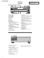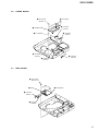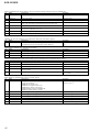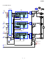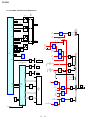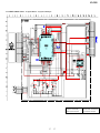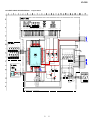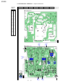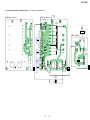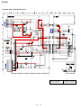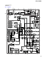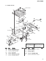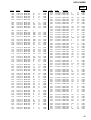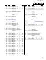
1
SCD-C222ES
SERVICE MANUAL
US Model
Canadian Model
Ver. 1.1 2006.08
Model Name Using Similar Mechanism
SCD-CE775
CD Mechanism Type
CDM59A-DVBU5A
Base Unit Name
DVBU5A
Optical Pick-up Block Name
KHM-230AAA
SPECIFICATIONS
When a super audio CD is played
General
Playing frequency range 2 Hz to 100 kHz
Laser
Semiconductor laser
(SACD: λ = 650 nm)
(CD: λ = 780 nm)
Emission duration: continuous
Power requirements
120 V AC, 60 Hz
Power consumption
26 W
Value of measurable limit (±0.001 %
W. PEAK) or less
Dimensions (w/h/d)
430 × 135 × 400 mm
(17 × 4 1/4 × 15 3/4 in.)
incl. projecting parts
Frequency response
2 Hz to 20 kHz
Mass (approx.)
7.5 kg (16 lbs 9 oz.)
Dynamic range
99 dB or more
Frequency response
2 Hz to 50 kHz (–3 dB)
Dynamic range
104 dB or more
Total harmonic distortion rate
0.0018 % or less
Wow and flutter
When a CD is played
Supplied accessories
Total harmonic distortion rate
0.0020 % or less
Wow and flutter
Value of measurable limit (±0.001 %
W. PEAK) or less
Output connector
Jack type Output level
Load impedance
ANALOG OUT Phono
jacks
2 Vrms
Over 10 kilohms
(at 50 kilohms)
DIGITAL (CD) Square
OUT OPTICAL* optical
output
connector
–18 dBm
(
DIGITAL (CD) Coaxial
OUT COAXIAL* output
connector
0.5 Vp-p
75 ohms
PHONES
Stereo
10 mW
phone jack
Light emitting
wave length:
660 nm
)
32 ohms
*Output only the audio signals of the CD
9-873-158-02
Sony Corporation
2006H05-1
© 2006.08
Home Audio Division
Published by Sony Techno Create Corporation
• Audio connecting cord
phono jack × 2 (Red and White) y phono jack × 2 (Red
and White) (2)
phono jack × 1 (Black) y phono jack × 1 (Black) (2)
• Monaural (2P) mini-plug cord (1) (Connecting cord for
CONTROL A1 )
• Remote commander (remote) RM-SC500 (1)
• R6 (size-AA) batteries (2)
Design and specifications are subject to change withoutnotice.
SUPER AUDIO CD PLAYER
SCD-C222ES
TABLE OF CONTENTS
1.
2.
SERVICING NOTES ............................................... 4
GENERAL ................................................................... 6
3.
DISASSEMBLY
3-1.
3-2.
3-3.
3-4.
3-5.
3-6.
3-7.
3-8.
3-9.
3-10.
3-11.
Disassembly Flow ...........................................................
Case .................................................................................
Front Panel Section .........................................................
CD Mechanism Deck (CDM59A-DVBU5A) ................
AUDIO Board .................................................................
POWER Board ................................................................
MAIN Board ...................................................................
Base Unit (DVBU5A) .....................................................
Table Assy .......................................................................
SENSOR Board ...............................................................
LOADING MOTOR Board ............................................
4.
ASSEMBLY ................................................................. 14
5.
TEST MODE .............................................................. 15
6.
DIAGRAMS
6-1.
6-2.
6-3.
6-4.
6-5.
Block Diagram – RF/SERVO Section – ........................
Block Diagram – SERVO Section – ..............................
Block Diagram – MAIN Section – ................................
Block Diagram – AUDIO Section – ..............................
Block Diagram – DISPLAY/KEY CONTROL/
POWER SUPPLY Section – ...........................................
Note for Printed Wiring Boards and
Schematic Diagrams .......................................................
Printed Wiring Board – RF Board – ..............................
Schematic Diagram – RF Board – .................................
Printed Wiring Boards
– MOTOR/SENSOR Section – .......................................
Schematic Diagram – MOTOR/SENSOR Section – ....
Printed Wiring Board
– MAIN Board (Component Side) – ..............................
Printed Wiring Board
– MAIN Board (Conductor Side) – ................................
Schematic Diagram – MAIN Board (1/5) – .................
Schematic Diagram – MAIN Board (2/5) – ..................
Schematic Diagram – MAIN Board (3/5) – ..................
Schematic Diagram – MAIN Board (4/5) – ..................
Schematic Diagram – MAIN Board (5/5) – ..................
Schematic Diagram
– AUDIO/HEADPHONE Boards – ................................
Printed Wiring Board
– AUDIO Board (Component Side) – ............................
Printed Wiring Boards – AUDIO (Conductor Side)/
HEADPHONE Boards – .................................................
Printed Wiring Boards
– DISPLAY/KEY/LED/RM Boards – ............................
Schematic Diagram
– DISPLAY/KEY/LED/RM Boards – ............................
Printed Wiring Boards – POWER/REG Boards – .........
Printed Wiring Boards – POWER SW/PT Boards – .....
Schematic Diagram
– POWER/POWER SW/PT/REG Boards – ...................
IC Pin Function Description ...........................................
6-6.
6-7.
6-8.
6-9.
6-10.
6-11.
6-12.
6-13.
6-14.
6-15.
6-16.
6-17.
6-18.
6-19.
6-20.
6-21.
6-22.
6-23.
6-24.
6-25.
6-26.
2
8
9
9
10
10
11
11
12
12
13
13
30
31
32
33
34
35
36
37
38
39
40
41
42
43
44
45
46
47
48
49
50
51
52
53
54
63
7.
7-1.
7-2.
7-3.
7-4.
EXPLODED VIEWS
Case Section ....................................................................
Front Panel Section .........................................................
Chassis Section ...............................................................
CD Mechanism Deck Section-1
(CDM59A-DVBU5A) .....................................................
7-5. CD Mechanism Deck Section-2
(CDM59A-DVBU5A) .....................................................
7-6. Base Unit Section (DVBU5A) ........................................
8.
79
80
81
82
83
84
ELECTRICAL PARTS LIST ............................... 85
SCD-C222ES
Notes on chip component replacement
• Never reuse a disconnected chip component.
• Notice that the minus side of a tantalum capacitor may be damaged by heat.
Flexible Circuit Board Repairing
• Keep the temperature of the soldering iron around 270 ˚C during repairing.
• Do not touch the soldering iron on the same conductor of the
circuit board (within 3 times).
• Be careful not to apply force on the conductor when soldering
or unsoldering.
CAUTION
Use of controls or adjustments or performance of procedures
other than those specified herein may result in hazardous radiation exposure.
This label is located on the LEFT exterior.
SAFETY CHECK-OUT
After correcting the original service problem, perform the following safety check before releasing the set to the customer:
Check the antenna terminals, metal trim, “metallized” knobs,
screws, and all other exposed metal parts for AC leakage.
Check leakage as described below.
LEAKAGE TEST
The AC leakage from any exposed metal part to earth ground and
from all exposed metal parts to any exposed metal part having a
return to chassis, must not exceed 0.5 mA (500 microamperes.).
Leakage current can be measured by any one of three methods.
1. A commercial leakage tester, such as the Simpson 229 or RCA
WT-540A. Follow the manufacturers’ instructions to use these
instruments.
2. A battery-operated AC milliammeter. The Data Precision 245
digital multimeter is suitable for this job.
3. Measuring the voltage drop across a resistor by means of a
VOM or battery-operated AC voltmeter. The “limit” indication is 0.75 V, so analog meters must have an accurate lowvoltage scale. The Simpson 250 and Sanwa SH-63Trd are examples of a passive VOM that is suitable. Nearly all battery
operated digital multimeters that have a 2 V AC range are suitable. (See Fig. A)
To Exposed Metal
Parts on Set
0.15 µF
1.5 kΩ
AC
voltmeter
(0.75 V)
Earth Ground
Fig. A. Using an AC voltmeter to check AC leakage.
SAFETY-RELATED COMPONENT WARNING!!
ATTENTION AU COMPOSANT AYANT RAPPORT
À LA SÉCURITÉ!
COMPONENTS IDENTIFIED BY MARK 0 OR DOTTED
LINE WITH MARK 0 ON THE SCHEMATIC DIAGRAMS
AND IN THE PARTS LIST ARE CRITICAL TO SAFE
OPERATION. REPLACE THESE COMPONENTS WITH
SONY PARTS WHOSE PART NUMBERS APPEAR AS
SHOWN IN THIS MANUAL OR IN SUPPLEMENTS PUBLISHED BY SONY.
LES COMPOSANTS IDENTIFIÉS PAR UNE MARQUE 0
SUR LES DIAGRAMMES SCHÉMATIQUES ET LA LISTE
DES PIÈCES SONT CRITIQUES POUR LA SÉCURITÉ
DE FONCTIONNEMENT. NE REMPLACER CES COMPOSANTS QUE PAR DES PIÈCES SONY DONT LES
NUMÉROS SONT DONNÉS DANS CE MANUEL OU
DANS LES SUPPLÉMENTS PUBLIÉS PAR SONY.
3
SCD-C222ES
SECTION 1
SERVICING NOTES
NOTES ON HANDLING THE OPTICAL PICK-UP
BLOCK OR BASE UNIT
The laser diode in the optical pick-up block may suffer electrostatic break-down because of the potential difference generated
by the charged electrostatic load, etc. on clothing and the human
body.
During repair, pay attention to electrostatic break-down and also
use the procedure in the printed matter which is included in the
repair parts.
The flexible board is easily damaged and should be handled with
care.
HOW TO OPEN THE DISC TABLE WHEN POWER
SWITCH TURNS OFF
Insert a tapering driver into the aperture of the unit bottom, and
turn it in the direction of the arrow (to OUT direction).
table
NOTES ON LASER DIODE EMISSION CHECK
The laser beam on this model is concentrated so as to be focused
on the disc reflective surface by the objective lens in the optical
pick-up block. Therefore, when checking the laser diode emission, observe from more than 30 cm away from the objective lens.
LASER DIODE AND FOCUS SEARCH OPERATION
CHECK
Carry out the “S curve check” in “CD section adjustment” and
check that the S curve waveforms is output three times.
CLEANING OF OPTICAL PICK-UP LENS
In cleaning the lens of optical pick-up, use the air blower.
Never use a cotton swab for cleaning the lens of optical pick-up,
which otherwise causes a trouble.
CHECKING SIGNALS OF CD SECTION
Efficiency to check each signal of CD section is increased when
the test points on the MAIN board are used.
Refer to 5-8. WAVEFORMS CHECK (page 27)
4
tapering driver
* To close the disc table, turn the tapering
driver in the reverse direction (to IN direction).
SCD-C222ES
RESETTING OPERATION AT POWER ON
If the power is turned on with a disc loaded in the set, a sequence of operation as shown below will be performed.
(The operation varies depending on the type of disc) Condition: continue mode
(1) CD
1. Sled reverse move (sled in)
2. Disc detect
3. IC setting for CD
4. Servo error signal offset auto adjustment
5. Spindle kick for LD on
6. LD on
7. Focus search
8. Focus servo on
9. Spindle kick
10. Spindle servo on
11. E-F balance auto adjustment
12. Tracking & sled servo on
13. Focus bias auto adjustment
14. Focus servo gain auto adjustment
15. Tracking servo gain auto adjustment
16. Jump to lead-in area
17. Read TOC
18. Stop
(2) SACD (single layer)
1. Sled reverse move (sled in)
2. Disc detect
3. IC setting for SACD
4. Servo error signal offset auto adjustment
5. Spindle kick for LD on
6. LD on
7. Focus search
8. Focus servo on
9. Spindle kick
10. Spindle servo on
11. E-F balance auto adjustment
12. Tracking & sled servo on
13. Focus bias auto adjustment
14. Focus servo gain auto adjustment
15. Tracking servo gain auto adjustment
16. Jump to lead-in area
17. Read TOC
18. Stop
(3) SACD (dual layer)
1. Sled reverse move (sled in)
2. Disc detect
3. IC setting for SACD
4. Servo error signal offset auto adjustment
5. Spindle kick for LD on
6. LD on
7. Focus search
8. Focus servo on (layer 0)
9. Spindle kick
10. Spindle servo on
11. E-F balance auto adjustment (layer 0)
12. Tracking & sled servo on (layer 0)
13. Focus bias auto adjustment (layer 0)
14. Focus servo gain auto adjustment (layer 0)
15. Tracking servo gain auto adjustment (layer 0)
16. Jump to lead-in area
17. Read TOC
18. Focus jump (layer 0tlayer 1)
19. E-F balance auto adjustment (layer 1)
20. Tracking & sled servo on (layer 1)
21. Focus bias auto adjustment (layer 1)
22. Focus servo gain auto adjustment (layer 1)
23. Tracking servo gain auto adjustment (layer 1)
24. Focus Jump (layer 1tlayer 0)
25. Stop
5
SCD-C222ES
SECTION 2
GENERAL
This section is extracted from
instruction manual.
Front Panel Parts Descriptions
1 POWER switch (11)
Press to turn on/off the player.
(4)
2 Remote sensor
3 DISC 1–5 button (12)
Press to select the disc.
4 Display window (12)
Shows various information.
5 N button (12)
Press to start play.
6 X button (12)
Press to pause play.
7 x button (12)
Press to stop play.
8 EX-CHANGE button (15)
Press to replace discs while playing a disc.
9 lAMSL dial (AMS: Automatic Music Sensor)
(6, 12)
When you turn the lAMSL dial
counterclockwise by one click, you go back to the
preceding track; when you turn the lAMSL dial
clockwise by one click, you go to the succeeding track.
0 DISC SKIP button (11)
Press to select the disc.
qa MULTI/2CH button (with an LED) (12)
Press to select the playback area when the 2 channel +
Multi-channel Super Audio CD is loaded. When you
select the Multi-channel playback area (page 11), the
LED turns on.
qs PHONES LEVEL control
Adjust the headphones volume.
qd A OPEN/CLOSE button (11)
Press to open/close the disc tray.
qf PHONES jack
Connect the headphones.
During playback of a Multi-channel Super Audio CD,
the same signal that is output from the ANALOG
5.1CH FRONT L/R jacks is output from the PHONES
jack.
qg SACD/CD button (with an LED) (12)
Each time you press the button while the Hybrid disc
(page 10) is loaded, the layer changes between an HD
(SACD) layer (the LED turns on) and CD layer (the
LED turns off).
qh MULTI CHANNEL DECODING indicator
Turns on when you turn on the player, or when the
Multi-channel Super Audio CD is loaded and select
the Multi-channel playback area by pressing MULTI/
2CH.
qj Disc tray (11)
Press A OPEN/CLOSE to open/close the disc tray.
qk TIME/TEXT button (13)
Each time you press the button, the playing time of the
track, the total remaining time on the disc, or TEXT
information appears in the display.
ql MENU button (6)
Press to enter the menu.
w; PROGRAM button (20)
Press to select Program Play.
wa SHUFFLE button (19)
Press to select Shuffle Play.
ws CONTINUE button (11)
Press to resume normal play from Shuffle Play or
Program Play.
Rear Panel Parts Descriptions
ANALOG
2CH OUT
FRONT
DIGITAL (CD)
5.1CH OUT
SURR CENTER
L
OUT
COAXIAL OPTICAL
CONTROL
A1ΙΙ
L
R
R
SUB
WOOFER
1 ANALOG 2CH OUT L/R jacks (5)
Connect to an audio component (stereo/2 channel)
using the audio connecting cord.
2 ANALOG 5.1CH OUT jacks (4)
Connect to an amplifier equipped with the 5.1CH
input jacks (Multi-channel amplifier, AV amplifier,
etc.) using the audio connecting cords.
3 DIGITAL (CD) OUT COAXIAL connector (6)
Connect to an audio component using an coaxial
digital cable.
4 DIGITAL (CD) OUT OPTICAL connector (6)
Connect to an audio component using an optical
digital cable.
5 CONTROL A1 jacks (6, 26)
Connect to a Sony audio component using the
monaural (2P) mini-plug cord.
6
Note
Only the audio signals of the CD can be output from the
DIGITAL (CD) OUT connectors shown in 3. Those of the Super
Audio CD cannot be output through DIGITAL (CD) OUT.
SCD-C222ES
Remote Parts Descriptions
1 CONTINUE button (11)
Press to resume normal play from Shuffle Play or
Program Play.
SHUFFLE button (19)
Press to select Shuffle Play.
PROGRAM button (20)
Press to select Program Play.
2 NAME INPUT button (25)
Press to enter the name input mode.
3 DISC/CAPS button (16, 25)
Press to select the disc.
Press to select the capital letter in name input mode.
4 Number buttons (16)
Press to enter the track numbers.
5 i10 button (16)
Press to locate a track numbered over 10.
qg MULTI/2CH button (12)
Press to select the playback area when the 2 channel +
Multi-channel Super Audio CD is loaded. When you
select the Multi-channel playback area (page 11), the
MULTI/2CH LED turns on.
qh TIME/TEXT/SPACE button (13, 25)
Each time you press the button, the playing time of
the track, the total remaining time on the disc, or
TEXT information appears in the display.
Press to insert a space in name input mode.
qj ENTER button (25)
Press to decide the selection.
qk CLEAR button (20)
Press to delete a programmed track number.
ql LEVEL ADJ button (23)
Press to adjust the output level balance for the Multichannel management function (page 21).
6 REPEAT button (18)
Press repeatedly to play all tracks or only one track on
the disc.
CD1
7 CHECK button (20)
Press to check the programmed order.
CD2
PLAY MODE
CONTINUE SHUFFLE PROGRAM
8 H button (12)
Press to start play.
X button (12)
Press to pause play.
x button (12)
Press to stop play.
NAME
INPUT
DISPLAY
MODE
SACD/CD
TIME/TEXT
SPACE MULTI/2CH
DISC
CAPS
&!?
ABC
1
2
GHI
JKL
4
PQRS
0 m/M buttons (17)
Press to locate a portion you want to play within a
track.
REPEAT
TUV
7
3
MNO
5
9 AMS ./> (AMS: Automatic Music Sensor)
buttons (16)
Press to locate a specific track.
DEF
8
>10
6
WXYZ
9
ENTER
10/0
CHECK
CLEAR
LEVEL
ADJ
qa DISC SKIP +/– buttons (16)
Press to select the disc.
qs CD1/2 (COMMAND MODE) switch (6)
Select the command mode.
qd DISPLAY MODE button (13)
Press to turn off the information.
AMS
DISC SKIP
—
+
qf SACD/CD button (12)
Each time you press the button while the Hybrid disc
(page 10) is loaded, the layer changes between an HD
layer (the SACD/CD LED turns on) and CD layer (the
SACD/CD LED turns off).
7
SCD-C222ES
SECTION 3
DISASSEMBLY
• This set can be disassembled in the order shown below.
3-1.
DISASSEMBLY FLOW
Note 1: The process described in
can be performed in any order.
Note 2: Without completing the process described in
, the next process can not be performed.
Note 3: Illustration of disassembly is omitted.
SET
3-2. CASE
(Page 9)
3-3. FRONT PANEL SECTION
(Page 9)
3-5. AUDIO BOARD
(Page 10)
3-4. CD MECHANISM DECK
(CDM59A-DVBU5A)
(Page 10)
3-8. BASE UNIT (DVBU5A)
(Page 12)
3-6. POWER BOARD
(Page 11)
3-4. CD MECHANISM DECK
(CDM59A-DVBU5A)
(Page 10)
3-5. AUDIO BOARD
(Page 10)
3-9. TABLE ASSY
(Page 12)
3-10.SENSOR BOARD
(Page 13)
8
3-11.LOADING MOTOR BOARD
(Page 13)
3-7. MAIN BOARD
(Page 11)
SCD-C222ES
Note: Follow the disassembly procedure in the numerical order given.
3-2.
CASE
3 case
2 screw
(flat head)
1 two screws
(flat head)
1 two screws
(flat head)
3-3.
FRONT PANEL SECTION
3 connector
(CN104)
5 connector
(CN601)
8 claw
2 wire (flat type) (12 core)
(CN706)
7 three screws
(3 × 8)
8 claw
6 screw
(BVTP3 × 8)
4 connector
(CN881)
9 front panel section
1 loading panel assy
Note: When removing the loading panel,
refer to "Section 1. Servicing Notes" on page 4.
9
SCD-C222ES
3-4.
CD MECHANISM DECK
(CDM59A-DVBU5A)
9 CD mechanism deck
(CDM59A-DVBU5A)
6 three screws
(BVTP3 × 8)
4 screw
(BVTP3 × 8)
5 two screws
(BVTP3 × 8)
a
8 wire (flat type) (30 core)
(CN708)
5 screw
(BVTP3 × 8)
7
3 Slide the tray until the screw
that fixes the table assy can be
seen through around hole a
in the table assy.
1 connector
(CN705)
2 Insert a tapering driver from the bottom of the chassis,
and turn it in the direction of the arrow until the base unit
goes down to the lowest position.
3-5.
AUDIO BOARD
5 two screws
(BVTP3 × 8)
2 connector
(CN301)
7 AUDIO board
6 clamp
1 wire (flat type) (19 core)
(CN702)
4 five screws
(BVTP3 × 8)
1 wire (flat type) (19 core)
(CN701)
3 connector (CN704)
10
SCD-C222ES
3-6.
POWER BOARD
4 four screws
(BVTP3 × 8)
6 POWER board
7 four washers
5 two clamps
3 connector
(CN707)
2 connector
(CN301)
1 connector
(CN105)
3 connector
(CN705)
1 connector
(CN151)
3-7.
MAIN BOARD
2 four screws
(BVTP3 × 8)
3 clamp
4 MAIN board
1 connector
(CN707)
1 connector
(CN705)
11
SCD-C222ES
3-8.
BASE UNIT (DVBU5A)
4 base unit (DVBU5A)
Note: When installing the BU
on the chassis, set the
lever (lifter) in free
position, the gear (U/D)
in UP position, and insert
the shaft b into the
groove of gear (U/D).
BU section
b
gear (U/D)
1 wire (flat type) (25 core)
(CN003)
3 two leaf springs (holder)
2 two floating screws
(PTPWH M2.6)
3-9.
TABLE ASSY
9 two screws
(BTTP M2.6)
7 two screws
(BTTP M2.6)
qa bracket (guide)
q; clamp
8 bracket (guide 2)
gear
(loading C)
4 wire (flat type)
(6 core) (CN15)
e
qs table assy
5 screw
(BTTP M2.6)
3
2 screw
(BTTP M2.6)
Note: When installing the table assy
on the chassis assy, engage
the gear (loading C) with the groove
by looking into the gear through
a hole e in the table assy.
12
6 bracket (guide)
1 Slide the tray until the screw
that fixes the bracket (guide)
can be seen through a round
hole c in the table assy.
c
SCD-C222ES
3-10. SENSOR BOARD
1 screw
(PTPWH M2.6)
3 belt (rotary)
2 tray
5 SENSOR board
4 two screws
(BTTP M2.6)
4 two screws
(BTTP M2.6)
3-11. LOADING MOTOR BOARD
3 two screws
(BTTP M2.6)
4 LOADING MOTOR board
1 belt (loading)
2 connector
(CN13)
13
SCD-C222ES
SECTION 4
ASSEMBLY
Note: Follow the assembly procedure in the numerical order given.
ADJUSTING PHASE OF SWING GEAR AND GEAR (U/D)
5 stopper washer (FR)
4 Push fully the shaft of shaft gear and
align the hole shape of gear (loading B).
3 Let the swing gear through under the
chassis h and engage its dowel g
with the groove f of rotary encoder.
6 screw
(PTPWH M2.6)
g
2 Install the rotary encoder so that
its groove f comes to the position
shown in the figure.
f
h
1 Insert the shaft gear up to the
position where its shaft comes
out by 5 mm.
circle mark
circle mark
8 screw
(PTPWH M2.6)
gear (RV)
swing gear
Fig. A
7 gear (U/D)
q; screw
(PTPWH M2.6)
9 gear (RV)
Note: Align swing gear, a circle mark
on the gear (U/D), and the teeth
of gear (RV) to the position
showing in the Fig. A.
14
SCD-C222ES
SECTION 5
TEST MODE
This set automatically executes self-diagnosis and various checks
by entering the test mode.
[ A OPEN/CLOSE] Key in the Test Mode.
Note: This set automatically makes various adjustments according to the
type of disc, thereby not requiring adjustment of the set when parts
were replaced. However, be sure to execute 5-1. IC AND FLUORESCENT DISPLAY TUBE CHECK, 5-2. AUTO CHECK and 58. WAVEFORMS CHECK.
The [A OPEN/CLOSE] key is disabled immediately after setting
the test mode. Be sure to turn the [l AMS L] dial to select 59
Table Init and push [l AMS L] once. When initialization of the
table is completed, the message “INITAIL OK” appears several seconds on the fluorescent indicator tube. After this, the [A OPEN/
CLOSE] key is enabled and disc can be inserted and ejected.
When the command 59 Table Init is executed, the same operations
of the POWER ON to the disc chucking in the normal operations
as described below are performed. However, it presumes that the
door and the tray are closed depending on the stop status.
59 Table Init t BU DOWN (disc unchucking) t Table rotates
(disc search) t BU UP (disc chucking) at the disc that is found
first of all.
When there are no discs, BU UP is executed at the DISC1 position.
Disc for Test Mode
Various checks of this set require the following discs.
Model
Type *1
Category
Application
MODEL
SATD-S5
(J-2501-215-A) SL
SATD-S4
(J-2501-184-A)
Adjusted value check,
12 cm disc
Operation check,
Reference disc Optical waveform check
Not specified
12 cm disc
DL
PATD-012
(4-225-203-01)
CD
YEDS-18
(3-702-101-01)
Not specified
Operation check
Adjusted value check,
12 cm disc
Reference disc Operation check,
Optical waveform check
HYBRID 12 cm disc
Operation check
*1 SL: Single Layer
DL: Dual Layer
Setting Method of Test Mode
Turn the [POWER] switch on while pressing the [l AMS L]
dial and the [MENU] button. Release the [MENU] button and the
[ l AMS L ] dial in this order when “Test Mode Menu” is
displayed on the fluorescent indicator tube. (If the [l AMS L]
dial is released first, the test mode becomes active but “Test Mode
Menu” is not displayed)
Releasing Method of Test Mode
To release the test mode, turn the [POWER] switch off.
Selection/Entry of Test Mode
To select and enter the “Test Mode Menu”, operate as follows.
1. Rotate the [l AMS L ] dial to select the menu, and press
the [l AMS L] dial to enter.
2. The test is switched on or off alternately each time the
[l AMS L] dial is pressed.
3. To return to the previous step, rotate the [l AMS L ] dial
to select the desired item, and press the [l AMS L ] dial
to enter.
Test Mode Command List
The contents of test mode are as follows.
Note: Wrong operation in the test mode causes a trouble, thus requiring extreme care.
LINE command (1X): Use mainly for a manufacturing line.
No.
Name
Description
Remarks
05
DSP MON1
XUGF, XPCK, C2PO outputted from IC509 (CD DSP)
Not used for the servicing
06
DSP MON2
MNT0, MNT1, MNT2, MNT3 outputted from IC509 (CD DSP)
Not used for the servicing
07
DSP MON3
RFCK, XPCK, XROF, GTOP outputted from IC509 (CD DSP)
Electrical measurement,
CD CLV jitter measurement
STANDARD command (1X): Use when the servo is applied by manual operation.
No.
Name
Description
Remarks
12
LD ON/OFF
The laser diode is turned on or off
On or off are switched alternately
13
SPIN ON/OFF
The spindle motor is rotated with the regulated voltage
On or off are switched alternately
14
FSRV ON/OFF
The focus servo is turned on or off
On or off are switched alternately
15
TSRV ON/OFF
The tracking servo is turned on or off
On or off are switched alternately
16
CLV ON/OFF
The spindle SLV servo is turned on or off
Focus and tracking servos must be already turned on
On or off are switched alternately
17
SSRV ON/OFF
The sled servo is turned on or off
Focus, tracking and spindle servos must be already turned on
On or off are switched alternately
18
ALL SRV ON
All servos are turned on
19
ALL SRV OFF
All servos are turned off
Stop command in the test mode
15
SCD-C222ES
FOCUS command (2X): Focus related. (All servos must be already turned on (except command 21))
No.
Name
Description
Remarks
21
FSRCH ON/OFF
The continuous vertical motion of the optical pick-up lens is turned on or
off
Avoid a long-time use
22
F-BIAS UP
Increase focus bias
Focus bias value
23
F-BIAS DOWN
Decrease focus bias
Focus bias value
24
ADJ FCSBIAS
The focus bias is adjusted automatically
Both + and - directions are searched to search for best jitter point
25
FGAIN UP/DW
The focus servo gain is switched between normal and down
Normal or down are switched alternately
26
FJMP UP/DWN
Focus jump is executed
UP: layer 0t1, DOWN: layer 1t0
Valid only for DL
27
FOCUS AGC
The focus servo gain is adjusted automatically
28
DISP FBdata
The focus bias adjusted value is displayed
Hexadecimal display 9 bit data
Note: On or off and up or down are switched alternately
OFFSET (PI, FE, TE) command (3X): Adjusts the offset of PI, FE and TE signals.
No.
Name
Description
Remarks
31
PI/FE OFSET
Adjusts the offset of PI, FE and TE signals
This adjustment must be executed after 61 DISC DETECT
TE offset adjustment is executed for the CD
only
TRACKING command (4X): Tracking servo related.
No.
Name
Description
Remarks
41
TGAIN NM/UP
The tracking servo gain is switched between normal and up
Normal or up are switched alternately
44
ADJ TRK DSP
The traverse AGC and E-F balance adjustment is performed
45
TRACKING AGC
The tracking servo gain is adjusted automatically
SEARCH command (5X): Track search related. (Nos. 51 through 53 are not used for the servicing.)
No.
Name
Description
51
1-TRCK JUMP
One-track jump is performed
Remarks
52
M-TRCK MOVE
M-track movement is performed
53
FINE SEARCH
Fine search is performed
58
CDM Check
Measurement of table rotation hours, tray open/close hours and panel door
open close hours
59
Table Init
Initializes the table.
After this command, the [A OPEN/CLOSE]
key is enabled.
DISC DETECT command (6X): Disc type check related.
No.
Name
Description
Remarks
61
DISC DETECT
Disc type check is executed
Display after judgment
DSKMOD CD: Judged as CD
DSKMOD SL: Judged as SACD (SL)
DSKMOD DL: Judged as SACD (DL)
DSKMOD HLHD: Judged as HYBRID HD
DSKMOD CDRW: Judged as CD-RW
Refer to how to apply servo by manual
operation (page 17)
62
SetDiscMode
Enter disc type
CD setting
CD forced setting
63
Enter disc type
SL setting
SL forced setting
64
Enter disc type
DD setting
DD forced setting
65
Enter disc type
HYBRID HD setting
HD forced setting
Enter disc type
HYBRID CD setting
66
6F
16
Download
CD forced setting
Not used for the servicing
SCD-C222ES
TOOLS command (8X): Performs aging, reads adjusting parameters, etc.
No.
Name
Description
Remarks
81
VERSION
Firmware version is displayed
Example: Ver 1.00
83
TRAY AGING
Tray open-close aging is performed
Not used for the servicing
Number of times and eccentricity
measurement Not used in this set.
84
JITTER
Jitter measurement
Not used for the servicing
85
ERROR RATE
Error rate measurement
CD: C1, C2
SACD: PO, PI1, PI2
Error rate
Not used for the servicing
86
ALL SRV ON
Apply all servos
Full automatic measurement including PI, FE and TE offset adjustment is
performed
Use when applying the servo by
manual operation
Refer to STANDARD command (page 15)
87
DISP ADJ DT
Automatic adjusting parameters are displayed
Refer to auto check items (page 20)
The offset adjusted values are scroll-displayed in order of RF, VC, FE and
TE
Refer to auto check items (page 20)
8A
FL TEST
8d
Set Up Init
Set to factory shipping mode
PLAY, REPEAT, DIGIFIL, etc. are initialized
Set when repair completed
Refer to 5-7. SHIPPING MODE (page 25)
Not used for the servicing
8F
49 TRCK JIT
Used for jitter measurement of 49th music on SACD-S4
For manufacturing line
Not used for the servicing
QA command (9X)
No.
Name
91
F.JMP CHECK
92
SET CHECK
93
WATER MARK
94
Description
Remarks
Not used for the servicing
The set is checked
Refer to 5-2. AUTO CHECK (page 20)
SET AGING
The set aging is performed
Repeat by the specified number of times or until an error occurred
Refer to 5-6. AGING MODE (page 25)
95
DISP ERROR
The content of error recorded to the set is read and displayed
(Error recording) Only one item is recorded
Refer to Error Display list (page 26)
96
D-OUT OnOff
Digital out of CD is turned on or off
Not used in this set.
98
APDD JITTER
9C
BU DENCHO
The content of error recorded to the set is read, and then the S curve
waveform, traverse waveform, and RF waveform can be checked
successively
Refer to 5-8.WAVEFORMS CHECK
(page 27)
9D
P-ON HOUR
Approximate cumulative power supplying time is displayed
(Initialized by 8d command)
In unit of 1 hour
9E
RFD OUT
RFD output is turned on or off
SACD jitter measuring mode
Not used for the servicing
Not used for the servicing
Not used for the servicing
How to Apply Servo by Manual Operation
In analyzing failures of the set, the servo may be applied by manual operation. To apply servo in the test mode, use the following method.
1. After setting the test mode, rotate the [l AMS L ] dial to select a command, and press the [l AMS L ] dial to enter.
2. “61 DISC DETECT” (Disc type check)t“86 ALL SRV ON” (All servos on + auto adjustment)
3. If applying servo while checking the condition one by one, “61 DISC DETECT” (Disc type check)t“31 PI/FE OFSET” (Offset
automatic adjustment)t“14 FSRV ON/OFF” (Focus servo on)t“16 CLV ON/OFF” (CLV servo on)t“44 ADJ TRK DSP ” (E-F
balance adjustment)t“15 TSRV ON/OFF” (Tracking servo on)t“17 SSRV ON/OFF” (Sled servo on)t“24 ADJ FCSBIAS” (Focus bias adjustment)t“27 FOCUS AGC” (Focus auto gain adjustment)t“45 TRACKING AGC” (Tracking auto gain adjustment).
Note: 1. On and off are alternately switched in the same command.
2. For a stop, select “19 ALL SRV OFF” and press the [ l AMS L ] dial.
17
SCD-C222ES
Set Check
92. SET CHECK
SET TEST START
10. TOTAL CHECK
120. MANUAL CHK
0. IC&FL CHECK ?
11. AUTO CHECK ?
121. LOAD IN ?
(Not used)
1. TOTAL CHECK ?
12. MANUAL CHK ?
122. SPIN UP ?
2. F.JUMP CHECK ?
13. DISP RSLT ?
123. PARAMETER ?
3.HYB CHECK ?
TOTAL CHK END ?
124. READ TOC & PSP ?
4. DISP ERROR ?
125. 1/3 SEEK ?
END ??
126. 1-M SEEK ?
127. ERR RATE ?
128. HENSHIN ?
129. SPIN DOWN ?
12A. LOAD OUT ?
(Not used)
MAN. CHK END?
Press the [l AMS L] dial when No.sssss sssss*1 is displayed, and a checking for that display will start or the lower layer
will be selected. For the selection on the same layer, rotate the [l AMS L] dial. It is looped on the same layer, and when “END?” is
displayed, press the [ l AMS L ] dial to return to the upper layer.
*1 s denotes a displayed character.
Manual Check Method
In the “12. MANUAL CHK”, individual checks (121. LOAD IN to 12A. LOAD OUT) are possible.
Example: If 124. READ TOC & PSP of 12. MANUAL CHECK is to be checked.
Setting Method:
1. After setting the test mode, rotate the [l AMS L] dial to select “92. SET CHECK” and press the [l AMS L ] dial to enter.
2. When “SET TEST START” is displayed, rotate the [ l AMS L ] dial clockwise by 2 clicks to select “1. TOTAL CHECK?”
and press the [ l AMS L ] dial to enter.
3. When “10. TOTAL CHECK” is displayed, rotate the [l AMS L] dial clockwise by 2 clicks to select “12. MANUAL CHK?" and
press the [ l AMS L ] dial to enter.
4. When “120. MANUAL CHK” is displayed, rotate the [l AMS L] dial clockwise by 4 clicks to select “124. READ TOC & PSP?”
and press the [l AMS L ] dial to enter.
5. A checking will start automatically.
Note: In making a check, the disc must be loaded. Immediately when a check started, the tray is drawn into the set. Also, the tray can be opened/closed
even during the set check mode.
18
SCD-C222ES
5-1. IC AND FLUORESCENT DISPLAY TUBE CHECK
(SELF-DIAGNOSIS)
The communication between microcomputer and main ICs (selfdiagnosis) and the fluorescent display tube all lit are checked.
Checking Method:
1. After setting the test mode, rotate the [l AMS L] dial to
select “92. SET CHECK” and press the [l AMS L ] dial
to enter.
2. When “SET TEST START” is displayed, rotate the
[l AMS L] dial clockwise by 1 click to select “0. IC&FL
CHECK?” and press the [l AMS L] dial to enter.
3. A checking will start automatically, and “0. IC&FL CHECK”
will be displayed. (Checking time is about 3 seconds)
4. After IC communication check, all segments of fluorescent
display tube will be lit. At this time, check visually for a skipped
character.
5. At successful completion of check, “0. IC CHECK OK” is
displayed. In this case, no error exists in the IC interface. Proceed to 5-2. AUTO CHECK.
Note: The check mentioned above tests the communication from microcomputer to main ICs. Even if the check successfully finished, the
IC to be checked is not always normal. Consider it for reference
only.
6. In case of an IC communication error, the following display
will be given during the checking. Possible causes of error are
as listed below.
Error display
Causes (typical example)
DVD DEC. ERROR
1. IC701 (SACD decoder) is faulty
2. IC701 pin <znv (XRST) does not go “H”
• IC901 pin ts (XDIS) does not go “H”
• IC902 (expander) is faulty
3. 768fs (33.86688 MHz) is not present to
IC701 pin <znm (XTAL)
• IC811 (3-multiplying circuit) is faulty
• Clock signal 256fs is not sent from
AUDIO board (CN702 pin 0)
• CN701 pin 3 (GND) and pin 2
(+3.3V-D) are open or shorted
• CN701, 702 and FFC connection is loose,
or FFC is disconnected
DVD DRAM ERR
1. IC706 (D-RAM) is faulty
2. IC701 pin <znv (XRST) does not go “H”
• IC901 pin ts (XDIS) does not go “H”
• IC902 (expander) is faulty
3. Faulty communication line between
IC701 and IC706
• Data line, address line, WE, etc.
4. D903 (1SS367) is faulty
D+3.3V is not present to IC706
CD DSP ERROR
1. IC509 (CD DSP) is faulty
2. 768fs (33.86688 MHz) is not present to
IC509 pin ua (XTAL)
Same as cause 3 of DVD DEC. ERROR
3. IC509 pin 2 (XRST) does not go “H”
• IC901 pin ts (XDIS) does not go “H”
• IC902 (expander) is faulty
EEPROM ERROR
1. IC903 (EEPROM) is faulty
Error display
Causes (typical example)
PRAWN DRAM ERR
*1
1. IC808 (D-RAM) is faulty
2. IC801 (DSD decoder) is faulty
3. 768fs (33.86688 MHz) is not present to
IC801 pin qa (MCKI)
Same as cause 3 of DVD DEC. ERROR
4. IC801 pin 9 (XRST) does not go “H”
• IC901 pin ts (XDIS) does not go “H”
• IC902 (expander) is faulty
5. Faulty communication line between
IC801 and IC808
• Data line, address line, WE, etc.
6. D904 (1SS367) is faulty
D+3.3V is not present to IC808
RF AMP ERROR
1. IC001 (RF AMP) is faulty
2. Loose connection between CN708 on
MAIN board and CN005 on RF board,
or FFC disconnection
CN708 pin qj (CLK RF), pin qh (DATA
RF) and pin qg (SDEN) must be checked
*1 DSD decoder is also checked.
Causes Common to Each IC:
1. Faulty communication line between microcomputer and each
IC.
Disconnected patterns, floating series resistors, bridge, etc.
2. Faulty IC supply voltage.
Particularly, check D+3.3V voltage. (D+5V for display microcomputer)
3. Faulty microcomputer communication port to each IC
Note: In case of more than two errors, the error display is switched over
one after another, thus making the reading difficult.
In such a case, press again the [l AMS L ] dial to make a
recheck for error reading.
19
SCD-C222ES
5-2. AUTO CHECK (AUTOMATIC VARIOUS MEASUREMENTS)
The auto check is performed to check if the set operates stably. Though a checking is made automatically, whether the measured data are
within the specification is evaluated by the service person. The auto check results in NG immediately, if the check itself causes an error.
Setting Method of Auto Check Mode:
1. After setting the test mode, rotate the [l AMS L] dial to select “92. SET CHECK” and press the [l AMS L] dial to enter.
2. When “SET TEST START” is displayed, rotate the [l AMS L ] dial clockwise by 2 clicks to select “1. TOTAL CHECK?”
and press the [ l AMS L ] dial to enter.
3. When “10. TOTAL CHECK” is displayed, rotate the [l AMS L] dial clockwise by 1 click to select “11. AUTO CHECK?”.
CD and SACD (SL) Disc Operation Check
Checking method:
1. Press the [A OPEN/CLOSE] button to open the tray and place the test disc *1. The [A OPEN/CLOSE] key is disabled immediately
after setting the test mode. Be sure to initialize the table.
2. Press the [l AMS L] dial, and the following check will be performed automatically.
3. Finally, the test disc will be ejected and the auto check will finish.
4. “AUTO CHECK OK” will be displayed at successful completion of auto check.
5. Recheck is enabled if the [l AMS L] dial is pressed in step 4. (Also, use this operation when exchanging the test disc)
6. In case of an error during the checking, the check is interrupted automatically and the error is displayed. (Error display example:
“DISC DETECT ERROR”) After error display, “CONT?STOP (J/S)” is displayed. In this case, if the [l AMS L] dial is pressed,
the check where the error occurred is skipped and you can proceed to the next check. Also, x if button is pressed, the check finishes
and “AUTO CHECK NG” is displayed when even one NG item exists.
*1 Use PATD-012 or YEDS-18 for CD, and SATD-S5 or SATD-S4 for SACD (SL). Using another disc will result in a checking failure.
Check Items:
Items
Description
Remarks
LOAD IN TIME (msec)
Time until a disc is chucked from the state where loading tray is out
Loading in switch
SPIN UP TIME (msec)
Time from spindle kick to PLL lock
Lock signal
RF/VC/FE/TE (ORG)
Offset values before RF (PI), VC, FE, TE signal offset adjustment
RF (8 bit data in hex notation)
VC, FE, TE (9 bit data in hex notation)
At offset 0
RF: A0h
VC, FE, TE: 00h
RF/VC/FE/TE (ADJ)
Offset values after RF (PI), VC, FE, TE signal offset adjustment
(Less than ORG value if offset correction is normal)
RF (8 bit data in hex notation)
VC, FE, TE (9 bit data in hex notation)
VC offset is not adjusted
(Measurement only)
Also, for SACD, the TE offset is
not measured and adjusted
PI/TRVS PP (ORG/ADJ)
PI (ORG): PI value at disc type check (decimal data)
PI (ADJ): PI value after PI offset adjustment
(read value at microcomputer A/D) (decimal data)
TRVS PP (ORG): Traverse level before level correction (AGC)
(decimal data)
TRVS PP (ADJ):Traverse level after level correction (AGC)
(decimal data)
PI level conversion
Read value × 12.9mV
PIOR/CCR/TRCR
PIOR: Set value of PI offset coarse adjusting register
CCR: Set value of FE offset coarse adjusting register
TRCR: Set value of TE offset coarse adjusting register
Registers in RF amplifier
FOCUS/TRK GAIN
Auto gain adjusted values of focus and tracking servos
(8 bit data in hex notation)
Reference: 30h
FBIAS/TRVSC/TRCR2/CFR
FBIAS: Focus bias set value (9 bit data in hex notation)
TRVSC: Traverse center value (9 bit data in hex notation)
TRCR2: Set value of E-F balance coarse adjusting register
CFR: Set value of traverse level adjusting register
TRCR2 adjusts the E-F gain
balance and used for CD only
(Fixed to 06 for SACD)
TRCR2 and CFR are registers in
RF amplifier
MIN JITTER AT F.BIAS
Minimum jitter value in focus bias adjustment (CD only)
Correlative with RF jitter
READ TOC TIME (msec)
Time required for TOC reading
PSP AMPLITUDE
Seek time between 1/3LBA and 2/3LBA of the disc
1/3LBAt2/3LBA average/minimum/maximum
2/3LBAt1/3LBA average/minimum/maximum
1-MAX TRK SEEK
Seek time between most inward track (0LBA) and most outward track max
LBA
most inwardtmost outward average/minimum/maximum
most outwartmost inward average/minimum/maximum
ERROR RATE
20
Traverse level conversion
Read value × 12.9mV
12.9mV=3.3V ÷ 256 (8 bit)
SACD only
1/3 SEEK TIME
F) AVE/MIN/MAX (msec):
R) AVE/MIN/MAX (msec):
F) AVE/MIN/MAX (msec):
R) AVE/MIN/MAX (msec):
HtL
LtH
Error rate measurement
For CD: Average value/Maximum value of C1 and C2
For SACD: Average value/Maximum value of PO, PI1 and PI2
LBA: Absolute address
Measure for 10 sec at track No.5
For the SACD, 160 block data
except the data under tracking jump
SCD-C222ES
Items
Description
Remarks
HENSHIN RYOU
Eccentricity measurement
Eccentricity (actual eccentric amount) of disc, disc pulley total
For the CD only are measured
• Read by dividing by 10
• 0 may be displayed if eccentricity
is small (10um or less) (Due to
measurement reason)
SPIN DOWN TIME (msec)
Time from spindle brake application to rotation stop
FG (IC901 pin ys) monitoring
LOAD OUT TIME (msec)
Time until loading table comes out from the state where a disc is in chuck
Loading out switch
HtL
Measured Data Reading Method:
To judge the check result, the measured data must be read.
1. When “AUTO CHECK OK” is displayed, rotate the [l AMS L] dial clockwise by 2 clicks.
2. When “13. DISP RSLT?” is displayed, press the [l AMS L] dial to enter.
3. “PLEASE WAIT” will be displayed and in several seconds, “13. DISP RESULT” will be displayed.
4. Rotate the [l AMS L] dial clockwise by 1 click, and the “LOAD IN” will be displayed.
5. Press the [l AMS L] dial to enter.
6. Compare the displayed value with the following specified value.
7. Hence, repeat step 4 to 6 (display is variable) and read the measured data respectively.
8. Compare the measured data with the specified value to check for NG item.
Note: Blank display of measured value means that an error occurred during the checking or no measurement was taken place.
Specified Value:
(1) SACD (Use the test disc SATD-S5 or SATD-S4)
Note: Measured values in check items are typical ones.
Check items
LOAD IN TIME (msec)
:
SPIN UP TIME (msec)
: 1993
Specified value
Not displayed in this set.
1800 to 2450
PF/VC/FE/TE AVRG (ORG) : 8E, E, 1E2, 12
RF: 91-C8, VC: 1F8-8, FE: 1D1-30, TE: 198-75
PF/VC/FE/TE AVRG (ADJ) : 9D, E, 6, 2
RF: 91-AF, VC : 1F8-8, FE: 1EE-12, TE: 1EA-16
PI/TRVS PP (ORG/ADJ)
: 80, 129, 100, 90
PI ORG: 80-100, PI ADJ: 80-95, TRVS ORG: 53-118, TRVS ADJ: 45-132
PIOR/CCR/TRCR
: 1B, 31, 1F
No specified value given
FOCUS/TRK GAIN
: 29, 35
FOCUS: 1E-35, TRK: F-40
FBIAS/TRVSC/TRCR2
: 2FE, 14, 6
F.BIAS: 1E2-3A, TRVSC: 1E4-4D
READ TOC TIME (msec)
: 1098
1350 to 2050
PSP AMPLITUDE
: 2387
1450 to 2150
1/3 SEEK TIME
F) AVE/MIN/MAX (msec)
R) AVE/MIN/MAX (msec)
: 2268581, 625121, <_>, 1446850
: 926, 909, 938
AVE: 1150 msec or less, MAX: 1300 msec or less
: 919, 901, 937
AVE: 1150 msec or less, MAX: 1300 msec or less
1/MAX SEEK TIME
F) AVE/MIN/MAX (msec)
R) AVE/MIN/MAX (msec)
: 2268581, 0, <_>, 2268581
: 1846, 1819, 1879
: 1837, 1829, 1849
AVE: 2250 msec or less, MAX: 2500 msec or less
AVE: 2250 msec or less, MAX: 2500 msec or less
ERROR RATE
PO MAX/AVE FRAME
PO MAX/AVE NUM
PI1 MAX/AVE FRAME
PI1 MAX/AVE NUM
PI2 MAX/AVE FRAME
PI2 MAX/AVE NUM
: 0, 0
: 480, 28
: 0, 0
: 320, 11
: 0, 0
: 41, 0
MAX: 0, AVE: 0
MAX: 1500 or less, AVE: 200 or less
MAX: 0, AVE: 0
MAX: 1500 or less, AVE: 200 or less
MAX: 0, AVE: 0
MAX: 1500 or less, AVE: 200 or less
SPIN DOWN TIME (msec)
: 1312
LOAD OUT TIME (msec)
TRCR2: no specified value given
* Items are not used in the
SATD-S5.
1300 to 2100
Not displayed in this set.
21
SCD-C222ES
(2) CD (Use the test disc PATD-012 or YEDS-18)
Note: Measured values in check items are typical ones.
Check items
Specified value
LOAD IN TIME (msec)
:
Not displayed in this set.
SPIN UP TIME (msec)
: 1354
1300 to 1600
RF/VC/FE/TE AVRG (ORG)
: 8E, D, 1E3, 12
RF: 91-C8, VC: 1F8-8, FE: 1D1-30, TE: 198-75
RF/VC/FE/TE AVRG (ADJ)
: 9C, C, 6, 2
RF: 91-AF, VC: 1F8-8, FE: 1EE-12, TE: 1EA-16
PI/TRVS PP(ORG/ADJ)
: 84, 128, 100, 90
PI ORG: 80-100, PI ADJ: 80-95, TRVS ORG: 55-155, TRVS-ADJ: 50-120
PIOR/CCR/TRCR
: 1B, 11, 1E
No specified value given
FOCUS/TRK GAIN
: 33, 28
FOCUS: 24-53, TRK: 1A-4E
FBIAS/TRVSC/TRCR2
: 10, 0, 5
F.BIAS: 1D9-2A, TRVSC: 1E2-19
MIN JITTER AT F.BIAS
: 147
700 or less
READ TOC TIME (msec)
: 827
1150 to 3150
1/3 SEEK TIME
F) AVE/MIN/MAX (msec)
R) AVE/MIN/MAX (msec)
: 311660, 103786, <_>, 207722
: 794, 699, 908
AVE: 1200 msec or less, MAX: 1300 msec or less
: 824, 661, 920
AVE: 1200 msec or less, MAX: 1300 msec or less
1/MAX SEEK TIME
F) AVE/MIN/MAX (msec)
R) AVE/MIN/MAX (msec)
: 311660, 0, <_>, 311660
: 1991, 1964, 2015
: 1711, 1701, 1726
AVE: 2200 msec or less, MAX: 2500 msec or less
AVE: 2200 msec or less, MAX: 2500 msec or less
ERROR RATE
C1 MAX/AVE
C2 MAX/AVE
: 3, 0
: 0, 0
C1 MAX: 15 or less
C2 MAX: 0
HENSHIN RYOU (1/10um)
: 168
800 or less (100 um or less)
SPIN DOWN TIME (msec)
: 1342
450 to 1500
LOAD OUT TIME (msec)
TRCR2: no specified value given
Not displayed in this set.
Note: RF, VC, FE, TE, FBIAS and TRVSC measured values are hexadecimal data with positive and negative signs. When comparing the measured
value with the specified value, refer to the following.
Hexadecimal (hex) display 9 bit data
Hexadecimal (hex) display 8 bit data
MAX
FF
011111111 (+255)
7F
01111111 (+127)
FE
011111110 (+254)
7E
01111110 (+126)
02
00000010 (+2)
01
00000001 (+1)
00
00000000 (0)
FF
11111111 (-1)
FE
11111110 (-2)
81
10000001 (-127)
80
10000000 (-128)
(+) Side
01
000000001 (+1)
00
000000000 (0)
1FF
111111111 (-1)
0
(-) Side
22
101
100000001 (-255)
100
100000000 (-256)
MIN
SCD-C222ES
5-3. SACD (DL) DISC OPERATION CHECK
(• Perform as necessary)
The stability of the set can be checked by repeating the combined
operation of focus jump (layer 0t1, layer 1t0) and access to
the most inward trackymost outward track by the set number of
times or until an error occurs using the dual layer HD disc, DL
disc.
A set of operation including an access to the layer 0 (most inward
track)tlayer 0 (most outward track)tfocus jump (layer
0t1)tlayer 1 (most outward track)tlayer 1 (most inward
track)tfocus jump (layer 1t0) is carried out repeatedly by the
set number of times.
Checking Method:
1. After setting the test mode, rotate the [l AMS L] dial to
select “92. SET CHECK” and press the [l AMS L ] dial
to enter.
2. When “SET TEST START” is displayed, rotate the
[ l AMS L ] dial clockwise by 3 clicks to display “2.
F.JMP CHECK?”.
3. Press the [A OPEN/CLOSE] button to open the tray, and place
the DL disc.
4. Press the [l AMS L] dial to load the tray into the set.
5. “NOW SET UP” will be displayed and the DL disc setup will
start. (It takes about ten and several seconds to set up the disc
as two layers of layer 0 and layer 1 are adjusted)
6. At the completion of setup, “F.JUMP TIMES” will be displayed.
7. Rotate the [l AMS L] dial clockwise by 5 clicks to display
“5”. (If 5 sets of operation is executed *1)
8. Press the [l AMS L] dial, and the check will start.
9. Immediately when the check finished, “UP MAX
ssss”t“UP AVE ssss”t“DW MAX
ssss”t“DW AVE ssss”t“F.JMP OK [TIMES]”
will be displayed repeatedly. (s denotes the measured value
in msec)
UP MAX: Max time required for layer 0 (most inward
track)tlayer 0 (most outward track)tfocus jump
(layer 0t1)
UP AVE: Average time required for layer 0 (most inward
track)tlayer 0 (most outward track)tfocus jump
(layer 0t1)
DW MAX: Max time required for layer 1 (most outward
track)tlayer 1 (most inward track)tfocus jump
(layer 1t0)
DW AVE: Average time required for layer 1 (most outward
track)tlayer 1 (most inward track)tfocus jump
(layer 1t0)
Specified value: 7000 msec or less (if no error occurred)
If an error occurred due to defocusing during the checking,
refer to the following error list. (page 25)
10. Press the [A OPEN/CLOSE] button, and the disc will be ejected
and the check will finish. Also, if the [l AMS L] dial is
pressed in step 9, “2. F.JUMP CHK OK” will be displayed.
Then, if the [l AMS L] dial is again pressed, “2. F.JMP
CHECK” will be displayed instantaneously and a recheck is
enabled from the step 5 in the same manner.
*1 Setting arbitrary number of times instead of 5 allows the checking to be repeated by the set number of times. Also, setting 0
(zero) allows the aging check to be repeated until an error occurs.
5-4. HYBRID DISC OPERATION CHECK
(• Perform as necessary)
This test checks the auto adjustment time required when the disc
is switched between HD (SACD) layer and CD layer. This test is
conducted to check the stability in switching from CD to SACD,
or SACD to CD in the HYBRID disc.
A set of operation including CD layer stop statetHD layer auto
adjustmenttHD layer TOC readingtHD layer stop statetCD
layer auto adjustmenttCD layer TOC readingtCD layer stop
state is repeated by the set number of times.
Checking Method:
1. After setting the test mode, rotate the [l AMS L] dial to
select “92. SET CHECK” and press the [l AMS L ] dial
to enter.
2. When “SET TEST START” is displayed, rotate the
[ l AMS L ] dial clockwise by 4 clicks to display “3.
HYB CHECK?”.
3. Press the [A OPEN/CLOSE] button to open the tray, and place
the HYBRID disc.
4. Press the [l AMS L] dial to load the tray into the set.
5. “NOW SET UP” will be displayed and the HYBRID disc setup
will start. (It takes about several seconds to set up the disc *1)
6. At the completion of setup, “CHANGE TIMES?” will be displayed.
7. Rotate the [l AMS L] dial clockwise by 5 clicks to display
“5” (if 5 sets of operation is executed *2)
8. Press the [l AMS L] dial, and “START” will be displayed
and the check will start. During the check, the following will
be displayed.
“CD—>HD” display: Time from switching from CD layer to
HD layer up to start of play is measured.
“HD—>CD” display: Time from switching from HD layer to
CD layer up to start of play is measured.
9. Immediately when the check finished, “CD MAX
ssss”t“CD AVE ssss”t“HD MAX
ssss”t“HD AVE ssss” will be displayed
repeatedly. (s denotes the measured value in msec)
Specified value: 10000 msec or less (if no error occurred)
If an error occurred due to defocusing during the checking,
refer to the following error list. (page 25)
10. Press the [A OPEN/CLOSE] button, and the disc will be ejected
and the check will finish. Also, if the [l AMS L] dial is
pressed in step 9, “HYB CHK OK” will be displayed. Then, if
the [l AMS L] dial is again pressed, “HYBRID CHECK”
will be displayed instantaneously and a recheck is enabled from
the step 5 in the same manner.
*1 “NOW SET UP” display may continue for several minutes
and an error may be displayed depending on the discs. In this
case, press the [l AMS L] dial again.
*2 Setting arbitrary number of times instead of 5 allows the checking to be repeated by the set number of times. Also, setting 0
(zero) allows the aging check to be repeated until an error occurs
23
SCD-C222ES
5-5. CDM59 AND THE DOOR CHECK
Measurement of table rotation hours, tray open/close hours and
panel door open close hours can be executed together with CDM59.
Procedure
1. Set the test mode. Turn the [l AMS L ] dial and select
59 Table Init. Press [l AMS L ] once (that enables the
[A OPEN/CLOSE] key.)
2. When the message INITIAL OK appears, press the [A OPEN/
CLOSE] key to eject the tray. Place a disc in the DISC1 of the
table. (Be sure to place a disc in DISC1. If a disc is placed in
any locations other than DISC1, the correct measurement cannot be executed. Therefore, be sure to place a disc in DISC by
using the [DISC SKIP] key.)
3. Select 58 CDM Check by turning [l AMS L ] and press
[ l AMS L ] once.
4. Measurement starts automatically.
5. When the measurement is completed, the message DOOR OP
ss.s (s is a decimal number) appears on the fluorescent
indicator tube.
6. Result of measurement can be check by turning [l AMS L].
If any measurement item does not meet specification, a message “ng” is displayed next to the measurement value.
7. When you want to repeat the test, press [l AMS L] again.
8. Press the [A OPEN/CLOSE] key to terminate the test and remove the disc.
* 1.The measurement can be performed without placing a disc.
However, the BU chucking time and unchucking time will
be slightly different from the actual values.
* 2.When the machine enters this mode once, it cannot return
to the normal test mode. If any other tests are desired, turn
off the main power once and then back on again to enter
the test mode.
Measurement items and specifications
Measurement item
Description
Specifications (unit: second)
RL
Time required for the table to make one complete rotation.
(R: Clockwise rotation. L: Counter-clockwise rotation)
6.0 to 7.5
CLOSE
Time required to close the tray.
<3.7
BU UP
Time required for the BU block to perform chucking from the DOWN position
<1.4
EXOPEN
The XCHANGE OPEN time
<2.6
EXCLOSE
The EXCHANGE CLOSE time
<3.8
BU DOWN
Time required for the BU block to perform unchucking and going to the DOWN
position
<2.7
OPEN
Time required to open the tray
<3.2
24
SCD-C222ES
5-6 . AGING MODE
(• Perform as necessary)
5-6-1. The aging can be performed to the set in the test
mode.
The aging can be continued by the set number of times or until an
error occurs.
In the aging, the following operations are repeated.
Table turntDisc chuckingtDisc detecttServo ontAuto
adjustmenttTOC readingtPlay of first track for 5 secondtPlay
of last track for 5 secondtPlay of first track for 5 secondtDisc
unchucking
Setting Method:
1. After setting the test mode, rotate the [l AMS L] dial to
select “94. SET AGING” and press the [l AMS L] dial
to enter.
2. When “AGING TIMES” is displayed, rotate the [l AMS L]
dial to set the number of aging times. (For the number of times,
every 10 times can be set. Setting 0 (zero) eliminates the count
limitation where the aging is repeated until an error occurs)
Note: Do not perform unmanned overnight aging..
3. Press the [l AMS L] dial, and “AGING START” will be
displayed instantaneously, then “DISC IN & JOG ON” will be
displayed and the tray will come out automatically.
4. Place a disc (CD or the SACD SL disc) on the tray. In the case
of SCD-C222ES, the multiple discs can be placed. Even when
the discs (CD or the SACD SL disc) of different types are
mixed, the aging test can be performed. Use the [DISC SKIP]
key when placing a disc. When discs are placed in positions,
turn the [l AMS L] dial.
5. The aging test starts.
6. At the completion of aging by the set number of times, the
tray will come out automatically and the check will stop.
Typical time required for aging About 1 hour/100 times
“AGING SUCCESS!” will be displayed if no error occurred
in the aging, or the error will be displayed if an error occurred.
(Refer to the following error list)
5-6-2. Aging Mode of the Panel Door Independently
1. Start up the unit in the normal operation mode.
2. While press the [x] key, turn the [l AMS L] dial and then
press the [CONTINUE] key. (The program does not advance
if these keys are not pressed in the above sequence.)
3. The panel door repeats opening and closing.
4. The messages “AP-B 000000” (during open) t “AP-C
000000” (during close) are repeated on the FL display. Number of times of open/close are displayed in decimal number in
“000000” with OPEN/CLOSE as a set.
5. Press the [x] key to terminate the aging mode and to return to
the normal mode.
5-7. SHIPPING MODE
The repaired set must be initialized, and for this purpose the set
should be set to the shipping mode.
Setting Method:
1. After setting the test mode, rotate the [l AMS L] dial to
select “8d Set Up Init” and press the [l AMS L] dial to
enter.
2. “8D 000000000 00” will be displayed, and if the scroll starts
in the left direction, the set initialization has completed
3. Press the [POWER] button to turn the power off.
Note: Take care not to leave the test disc in the set.
The following setups are established in the SHIPPING MODE
1. Initialization of EEPROM (IC903)
• PLAY MODE
ALL DISCS, CONTINUE
• COMMAND MODE
CD1
• LAYER SELECTSACD
• M/2CH SELECT MULTI
• DIGITAL FILTER
STD
• 2ch SPK MODE 2ch DIRECT
• Mch SPK MODEMch DIRECT
• Resetting the accumulated hours meter.
2. Chucking at the DISC1 position.
Error List
An error occurring during the check in the aging mode of the test mode is displayed automatically (scroll display) immediately when the
error occurred.
< How to view the error history >
1. Select “95 DISP ERROR” with the [l AMS L] key, and press the [l AMS L] key once.
2. The error that has occurred lastly in the set and the signal status (H = 1, L = 0) at that time are displayed on the FL display by scrolling.
(Types of the errors and the signal status that can be checked, are the same as the error display of the aging mode.)
3. Press the [l AMS L] key once again to show the error history repeatedly.
4. When the error history is displayed with scrolling once, the mode returns to the normal test mode.
25
SCD-C222ES
Error display is as follows.
Error name, Disc type, IN SW (Sled in switch state), FOK (FOK signal state), LOCK (LOCK signal state), From (Displayed if effective),
To (Displayed if effective), Aging times (Displayed in aging mode only)
Display example
ACCESS MOVE ERROR : SACDSL : IN SW 1 FOK 0 LOCK 0 : FROM 205663 : TO 2461601 : TIMES 5
(Error name) (Disc type) (Sled in switch, FOK, LOCK signal state) (Relative address) (Relative address)(Aging times)
Display Items List:
Display items
Description
Remarks
Error name
tRefer to the error display list
IN SW
Sled in switch state when an error occurred
0: switch off Not limit in
1: switch on Limit in (Optical pick-up is at most inward track)
FOK
FOK signal state when an error occurred
FOK signal Is focus on?
0: FOK L (Focus off), 1: FOK H (Focus on)
LOCK
LOCK signal state when an error occurred.
LOCK signal Is PLL lock?
0: LOCK L Not lock, 1: LOCK H Lock
From
Displayed if effective in the error item
tRefer to the error display list
Disc PSN (relative address) is
displayed in case of access error
To
Displayed if effective in the error item
tRefer to the error display list
Disc PSN (relative address) is
displayed in case of access error
Error Display List:
Error display
Error description
Main causes of errors
DISC DETECT ERROR
Disc type error
MIRR measured time is displayed in From:
Optical pick-up, RF amplifier or CD
DSP IC is faulty
OFFSET ADJUST ERROR
Offset adjustment error
Optical pick-up, RF amplifier or CD
DSP IC is faulty
FCS SRV ON ERROR
Focus servo error
An error code is displayed in From:
From:1 means focus search failed
From:2 means defocusing
CLV SRV ON ERROR
CLV servo error
Defocusing
E-F BALANCE ERROR
E-F balance adjustment error
Defocusing
TRK SRV ON ERROR
Tracking servo error
Tracking servo on time out
Optical pick-up, RF amplifier or CD
DSP IC is faulty
SLD SRV ON ERROR
Sled servo error
Sled servo on time out
FOCUS BIAS ERROR
Focus bias adjustment failed
An error code is displayed in From:
Defocusing during adjustment
Description of display
An error code is displayed in From
From:1 means retry failed 3 times
From:2 means abnormal value
Optical pick-up, RF amplifier or CD
DSP IC is faulty
FCS AGC ERROR
Error at focus gain automatic adjustment
Defocusing during adjustment
Optical pick-up, RF amplifier or CD
DSP IC is faulty
TRK AGC ERROR
Error at tracking gain automatic adjustment
Defocusing during adjustment
Optical pick-up, RF amplifier or CD
DSP IC is faulty
ACCESS 1TJ ERROR
Access Error at one-track jump
Effective addresses (PSN) are displayed in From: and To:
Access failed
Defocusing at access, etc
ACCESS FINE ERROR
Access Error at fine search
Effective addresses (PSN) are displayed in From: and To:
Access failed
Defocusing at access, etc
ACCESS MOVE ERROR
Access Error at M-track MOVE
Effective addresses (PSN) are displayed in From: and To:
Access failed
Defocusing at access, etc
WHILE PLAYING ERROR
Error during disc playing
Defocusing
Focusing retry failed
FCS JUMP ERROR
Time out error at focus jump
Defocusing
Focusing retry failed
System errors are as follows.
Note: This error is not saved in the set.
Display
Toc Error *
Description
Error during the time from auto adjustment to TOC reading, Different type of disc (Such as a DVD disc), Disc is dirty
Toc Error ****
Illegal SACD (Such as a pirated version)
Read Error
Music data read error (Error during disc playing)
26
SCD-C222ES
5-8. WAVEFORMS CHECK
This set performs automatic adjustment for each disc, and therefore the set need not be adjusted when parts are replaced, but it
requires checking following the description in this section, 5-1.
IC AND FLUORESCENT DISPLAY TUBE CHECK and 5-2.
AUTO CHECK.
For the check, the test mode is used. Wrong setting causes a trouble,
thus requiring extreme care.
Traverse Check
Connection:
BU Electrical Adjustment Mode
The BU electrical adjustment mode is used to check the S curve
waveform, traverse waveform and RF waveform. After a disc is
placed on the tray, each time the [l AMS L] dial is pressed,
the check mode is switched in order for S curve waveformt
traverse waveformtRF waveform.
Checking Method:
1. Under the condition of S curve waveform check mode in step
5, press the [l AMS L] dial.
2. After “WAIT” is displayed, the traverse waveform check mode
will become active and “TRAVERSE MODE” will be displayed.
3. Connect an oscilloscope to the TP513 (TE) and TP504 (AVC)
on the MAIN board.
4. Check that the level A and B of waveform on the oscilloscope satisfy the specification.
Setting Method:
After setting the test mode, rotate the [l AMS L] dial to select
“9C BU DENCHO” and press the [l AMS L] dial to enter.
“BU MEASURE” will be displayed if the BU electrical adjustment mode becomes active.
oscilloscope
MAIN board
TP513 (TE)
TP504 (AVC)
Specified Value:
Disc
S Curve Check
Connection:
SATD-S5 or
SATD-S4
oscilloscope
PATD-012 or
MAIN board
YEDS-18
TP506 (FE)
TP504 (AVC)
+
–
+
–
A
B
0.6 to 1.6 Vp-p
–0.1 to +0.1V
0.5 to 1.3 Vp-p
Traverse waveform
Center fo the waveform
Checking Method:
1. After setting the BU electrical adjustment, place the test disc
(PATD-012 or SATD-S5 or SATD-S4) on the tray and close
the tray, then press the [l AMS L] dial.
2. At the completion of disc type check, “CD DETECT” will be
displayed (for PATD-012 or YEDS-18).
Note: For the SATD-S5 or SATD-S4, “SACD DETECT“ is displayed.
3. Press again the [l AMS L] dial, and the S curve waveform
A
B
VC
Checking and Connecting Location : See page 29.
check mode will become active and “S-CURVE MODE” will
be displayed.
4. Connect an oscilloscope to the TP506 (FE) and TP504 (AVC)
on the MAIN board.
5. Check that the level A and B of waveform on the oscilloscope
satisfy the specification.
Specified Value:
Disc
A
B
0.7 to 1.7 Vp-p
–0.1 to +0.1V
SATD-S5 or
SATD-S4
PATD-012 or
YEDS-18
S curve waveform
A
B
VC
Note: For easier observation of this waveform, extend the sweep time
and raise the brightness.
Checking and Connecting Location : See page 29.
27
SCD-C222ES
CLV Jitter Check (CD only)
Connection:
RF Level Check
Connection:
oscilloscope
oscilloscope
MAIN board
MAIN board
TP703 (RFAC)
TP704 (AGND)
TP516 (RFCK)
TP517(WFCK)
TP808 (DG)
+
–
(CH1)
+
–
(CH2)
+
Checking Method:
1. Under the condition of traverse waveform check mode in step
4, press the [l AMS L] dial.
2. Connect an oscilloscope to the TP703 (RFAC) and TP704
(AGND) on the MAIN board.
3. After “WAIT” is displayed, the RF waveform check mode will
become active and “PLAY 5th TRACK” will be displayed,
and the 5th music on the disc will be played.
4. Check that the RF waveform is clear and the level satisfies the
specification.
5. Press the [l AMS L] dial, and “OUTSIDE TRACK” will be
displayed and the outward track of the disc will be played.
6. Check that the RF waveform is clear and the level satisfies the
specification.
7. Press the [ l AMS L ] dial, and “INSIDE TRACK” will be
displayed and the inward track of the disc will be played.
8. Check that the RF waveform is clear and the level satisfies the
specification.
9. After checking, press the [l AMS L] dial, and the test is
over when “BU MEASURE” is displayed.
10. Press the [A OPEN/CLOSE] button to open the tray, and remove the test disc.
11. Using each type of disc, repeat from step 1 of S curve waveform check up to step 10 of RF level check.
12. When the check is over, press the [POWER] button to turn the
power off.
Checking Method:
1. Set the test mode.
2. Connect an oscilloscope to the TP516 (RFCK) (CH1), TP517
(WFCK) (CH2) and TP808 (DG) (GND) on the MAIN board.
3. Place the test disc PATD-012 or YEDS-18 on the tray, and
close the tray.
4. Rotate the [l AMS L] dial to select “61 DISC DETECT”,
and press the [l AMS L] dial to enter. Then, the disc type
will be judged.
5. Check that the disc type has been judged.
(For the PATD-012, “DSKMOD CD” will be displayed. Refer
to the test mode, DISC DETECT command (page 16))
6. Rotate the [l AMS L] dial to select “86 ALL SRV ON”,
and press the [l AMS L] dial. Then, the disc will rotate,
automatic adjustment will be carried out, and all servos will
be turned on.
7. Rotate the [l AMS L] dial to select “07 DSP MON3”, and
press the [l AMS L] dial to enter.
8. Check that the value A of waveform on the oscilloscope satisfies the specification.
9. Rotate the [l AMS L] dial to select “19 ALL SRV OFF”,
and press the [ l AMS L ] dial. Then, all servos will be
turned off and the disc rotation will stop.
10. Press the [A OPEN/CLOSE] button to open the tray, and remove the test disc.
11. Press the [POWER] button to turn the power off.
Note: Take care not to leave the test disc in the set.
Note: Take care not to leave the test disc in the set.
Specified Value:
Specified Value:
Disc
SATD-S5 or
SATD-S4
PATD-012 or
YEDS-18
Disc
A
A
PATD-012 or
0.65 to 1.1 Vp-p
35 µsec or less
YEDS-18
0.45 to 0.95 Vp-p
CLV jitter waveform
RF signal waveform
VOLT/DIV: 200 mV
TIME/DIV: 500 ns
A
Note: Clear RF waveform refers to the waveform where ◊ shapes should
be distinctively observed in the center.
A
Checking and Connecting Location : See page 29.
Checking and Connecting Location : See page 29.
28
SCD-C222ES
Checking and Connecting Location:
– MAIN Board (Component Side) –
TP506
(FE)
TP513
(TE)
TP504
(AVC)
TP704
(AGND)
IC703
TP703
(RFAC)
TP516
(RFCK)
TP808
(DG)
IC509
TP517
(WFCK)
IC701
IC801
29
29
SCD-C222ES
SECTION 6
DIAGRAMS
6-1.
BLOCK DIAGRAM – RF/SERVO Section –
RF
ATOP
61
ATT ATON
62
DVDRFP
1
63
MUX
RFSIN
59
60
AIP
AIN
INPUT
BIAS,
AGC
PROGRAMMABLE
EQ FILTER
DIFFERENTIATOR
FNP
FNN
53
54
52
55
DIP
RFAC
DIN
RFAC
57
FULL WAVE
RECTIFER
: SACD PLAY
AGC
CHARGE PUMP
+
–
E
F
SUMMING AMP
IC004 (1/4)
18
17
G
SUMMING AMP
IC004 (2/4)
H
12
11
10
VC
(+2.5V)
A
B
C
D
OPTICAL PICK-UP
BLOCK
(KHM-230AAA)
CD LD
LASER
DIODE
(FOR CD)
LASER
DIODE
(FOR SACD) DVD PD
21
23
B+ SWITCH
Q002, 005
PHASE
DETECTOR
COMPARATOR
MUX
SUB
OFFSET
CANCEL
GCA
CD F
+
–
A
A
+
C +
B
GCA
L. P. F.
C
TE
GCA
+
–
L. P. F.
OFFSET
CANCEL
+
+
L. P. F.
OFFSET
CANCEL
GCA
FE
TE, FE
39
SDATA
47
SERIAL
SCLK
46
PORT
REGISTER SDEN 48
MNTR 42
VC
CD E
GCA
SDATA, SCLK, SDEN
SDATA
SCLK
SDEN
2
(Page 32)
3
(Page 32)
4
(Page 31)
5
(Page 32)
6
(Page 32)
7
(Page 32)
8
(Page 31)
9
(Page 31)
10
(Page 32)
11
(Page 32)
FE/PI
FE
40
B
+
D +
MUX
PI
MUX
SACD/CD RF AMP,
FOCUS/TRACKING ERROR AMP
IC001
CDLD
AGCO
MEVO
38
PI ERROR AMP
IC004 (3/4)
32
AVC
(+1.65V)
AVC BUFFER
IC004 (4/4)
DRVC
(+2.5V)
DRVC BUFFER
IC503
BOTTOM
ENVELOPE
INPUT
BUFFER
MIN
31
A+3.3V
D+5V
PEAK/
MIRR
27
BOTTOM
HOLD
CDPD
DVDLD
DUAL
APC
LDON
LDON
26
DVDPD
VMOD
A +5V
TE
FE
PI
VMOD
24
AUTOMATIC POWER
CONTROL (FOR SACD)
Q001
GCA,
EQ
CD A
16
CD B
15
CD C
14
CD D
13
22
CD PD
DVD LD
MODULE
CIRCUIT B+
AUTOMATIC POWER
CONTROL (FOR CD)
Q003
L. P. F.
LEVEL DAC
D
9
SEL
: CD PLAY
FE
TE
D
C
B
A
A2
3
B2
4
C2
5
D2
6
+
–
PI
A
B
C
D
CLAMP&
ENVELOPE
(Page 31)
• SIGNAL PATH
AGCO
DETECTOR
1
TRK+
TRK–
M2
(SLED)
M
14
13
TRACKING COIL
DRIVE
2
3
TFDR
31
TRDR
32
17
18
SLED MOTOR
DRIVE
24
23
SFDR
29
SRDR
30
STBY2
M3
(SPINDLE)
M
9
8
9
FOCUS
TRACKING/SLED
SERVO DSP
DFCT, FOK
DETECTOR
FOK
22
MIRR
20
DFCT
21
FOK
MIRR
SERVO
INTERFACE
COUT
19
SCLK
8
COUT
SCLK
FOK, MIRR,
COUT, SCLK
MUTE 2D
20
SERVO AUTO
SEQUENCER
SPDA
SPINDLE MOTOR
DRIVE
A/D
CONVERTER
15
16
17
BUFFER
SSTP
STBY1
FOCUS/TRACKING/SLED
PWM GENERATOR
5
6
FOCUS COIL
DRIVE
FJMP1
2AXIS
DEVICE
FOCUS/
TRACKING
COIL
12
11
FJMP2
FCS+
FCS–
DIGITAL SERVO
PROCESSOR
IC509 (1/2)
FFDR
33
FRDR
34
SE
TE
FE
RFDC
40 41 39 43
FOCUS/TRACKING COIL DRIVER,
SLED MOTOR DRIVER
IC502
TO CPU INTERFACE
26
LIM SW
MUTE2
SPINDLE MOTOR DRIVE
IC512
MUTE1
13
2
SP ON
MUTE LOAD
S1
(LIMIT)
D+3.3V
SPDA, FJMP1/2
SPIN
LOADING/TRAY MOTOR DRIVE
IC11
MUTE 2D, SP ON, MUTE LOAD
M10
(LOADING)
M
8
9
M11
(TRAY)
M
11
10
OUT1+
LOADING MOTOR
OUT1–
DRIVE
FIN1
2
RIN1
3
LOAD IN
LOAD OUT
OUT2+
OUT2–
RIN2
16
FIN2
17
TBLL
TBLR
TRAY MOTOR
DRIVE
30
30
LOAD I/O, TBLL, TBLR
SCD-C222ES
6-2.
BLOCK DIAGRAM – SERVO Section –
RFAC
D+3.3V
15
(Page 32)
FILTER
16
69
XTSL
C4M
DIGITAL SIGNAL
PROCESSOR
IC509 (2/2)
EFM
DEMODULATOR
ASYI
49
ASYO
48
SUBCODE
PROCESSOR
64
63
XRST CD,
MUTE CD
XRST CD
XRST 2
3
64
58
85 84 12 22 23
A0 – A7
89 – 96
D0 – D7
14 – 21
SPIN
BUFFER
IC708 (1/2)
LDON
WFCK
SCOR
SBSO
EXCK
DMA
FIFO
XHRD
XHWR
XCS
XINT0
(Page 32)
XINT1
17
18
19
20
21
16
XINT1
XWAIT
79, 80, 82 – 87,
89, 91
MA10/MNT1
XMWR
XMOE
XCAS
XRAS
95 78 76 94
2 – 5, 7 – 10
41 – 44, 46 – 49
21 – 24, 27 – 32
34 35 18 17 33
I/O0 – I/O7
I/O8 – I/O15
A0 – A9
D-RAM
IC706
92 93
REDY
HINT
HCS0
HCS1
XHRD
XHWR
XHAC
XHRS
SDEF
26
29
20
(Page 32)
XSAK
46
51
54
62
63
XSHD
49
XDCK
48
XSAQ
53
23
XSAK,
XSHD,
XDCK,
XSAQ
21
(Page 32)
159 157 162
22
(Page 32)
• SIGNAL PATH
: SACD PLAY
167
XTL1
XTL2
109 APEO
XTAL
JIT
INTEGRATOR
IC703 (1/2)
96, 97, 99, 101,
102, 104 – 106
DAC
INTERFACE
HDRQ
19
(Page 32)
WPK
XRD
XWR
XCS
XINT0
AUTHENTICATION
A+3.3V
66 – 69, 71,
73 – 75
DMA CONTROLLER
(PRIORITY RESOLVE & SEQUENCER)
HA0 –
HA2
SD0 – SD7
WPK
A0 – A7
CPU
INTERFACE,
DMA
CONTROLLER
MDB8, MDB9,
MDBA – MDBF
MDB0 – MDB7
D0 – D7
107 GFS
DVC
(+1.65V)
CD ESP
UCAS
LCAS
RAS
WE
OE
ADDRESS BUS
XHRD, XHWR
CENTER VOLTAGE
GENERATOR
IC703 (2/2)
ATAPI
REGISTER
MAIN DATA ECC & EDC
DVD-ROM CD-ROM
5, 7, 9 – 14
ADDRESS BUS
(Page 32)
14
HDB9
SUBCODE
DEINTERLEAVE & ECC
HDBA –
HDBF
MA0 – MA9
SPDA
APDO
FJMP1
FJMP2
DATA BUS
(Page 32)
13
SPO
FILTER
DATA BUS
A0 – A2
HDB8
DESCRAMBLE
FFM
DEMODULATOR
SPDA, FJMP1/2
D0 – D7
HDB0 –
HDB7
SACD DECODER
IC701
ATAPI
PACKET FIFO
(Page 30)
12
PLL
135
18
(Page 32)
CD DSP INTERFACE
SYNC
CONTROL
111 113 114 115
(Page 30)
8
RF
ASSYMMETRY
172 – 176, 1, 2, 4
4
RFIN
DASYO
117
MDSOUT
142
MDPOUT SPINDLE
144
CONRTOL
CLVS
140
ASF1
ASF2
DASYI
(Page 30)
XRST
43 44
ANALOG
MIXER
164
SCOR
SBIN
EXCK
XRCI
GSCOR
C2PO
LRCK
BCLK
MDAT
7 8
138
DOCTRL 3
151 150 148 147 153 146 155 163 158 160
WFCK
XRD
XWR
XCS DVD
INIT0 DVD
INIT1 DVD
51
137
MDIN1
MDIN2
GFS DVD
GFS CD
JIT
SUBQ
XQCK
SPDA
APDO
DATA CD
CLOK CD
LAT CD
SENS CD
SCOR
FCS JMP 1
FCS JMP 2
71
LDON
33 35
XHRD
XHWR
XCS
XINT0
XINT1
9
26 37 27 9 34
LOCK CD
SPINDLE MOTOR DRIVE
IC708 (2/2)
75
XRST CD, MUTE CD, XRST DVD
44, 41, 39, 35,
32, 30, 27, 24
MUTE
SQCK
DATA
CLOK
XLAT
SENS
SCOR
SBSO
EXCK
SQSO
LOCK
MDP
WFCK
RFCK
GFS
EMPH
10 11 13 68
DIGITAL (CD)
OUT COAXIAL
WAVE SHAPER
Q302
MUTE CD
CPU
IC901 (1/3)
DIGITAL (CD)
OUT OPTICAL
J303
DOUT
MD2
4 6 5 7 15 79 80 76 77
17
(Page 33)
OPTICAL
TRANSCEIVER
IC309
CPU INTERFACE
24 25
BCLK
LRCK
ERROR
CORRECTOR
DIGITAL
OUT
DIGITAL CLV
PROCESSOR
16
31, 34, 37,
40, 43, 45
TO SERVO AUTO
SEQUENCER
32K
RAM
MDAT, BCLK, LRCK
MDAT
PCMD
66
BCK
67
LRCK
65
C2PO
14
WDCK
17
D/A
DIGITAL
INTERFACE
59, 56, 60
DIGITAL PLL
HOST INTERFACE
ASYMMETRY
CORRECTOR
DDAT
DBCK
DLRC
(Page 30)
RFAC
XRST DVD
50
MA11/MNT2
RFAC
768FS (33.8688MHz)
(Page 32)
INTERNAL BUS
1
XTAO
72
XTAI
71
CLOCK
GENERATOR
PCO
CLTV
FILI
XPCK
FILO
53 55 52 54 12
: CD PLAY (ANALOG OUT)
: CD PLAY (DIGITAL OUT)
169 170
XTAL
23
(Page 32)
31
31
SCD-C222ES
6-3.
BLOCK DIAGRAM – MAIN Section –
(Page 30)
3
(Page 30)
6
(Page 30)
2
• SIGNAL PATH
SDATA, SCLK, SDEN
: SACD PLAY
FOK, MIRR, COUT, SCLK
TE, FE
ZMCKI, 256FS
DSD DECODER
IC801
169 – 176
19
B1 –
B8
SD0 – SD7
(Page 31)
2–9
SD0 – SD7
A1 –
A8
11 – 18
LEVEL SHIFT
IC812
LEVEL SHIFT
IC813
(Page 31)
(Page 31)
20
21
SDEF
XASK, XSHD,
XDCK, XSAQ
2
XSAK
XSHD
XDCK
3
4
A1
B1
A2
B2
A3
B3
5
DSAL
DSAR
DSALS
DSARS
DSAC
DSALFE
168 SDEF
17
167 XSAK
16
165 XSHD
15
(Page 31)
22
LEVEL SHIFT
IC814
FOK
MIRR
COUT
SCLK
1
256FS
83 SDATA RF
77 SDCLK RF
74
32
29
72
FOK CD
MIRR
COUT CD
SCLK CD
SCDATA DF
SHIFT DF
LATCH DF
AMUTE
100
99
98
2
DATA, SHIFT,
LATCH, AMUTZ
DATA
SHIFT
LATCH
AMUTZ
12
11
2
3
10
9
4
5
65 TE
67 FE/PI
Q704
CPU
IC901 (2/3)
S902
(FLASH WRITING)
WRITING
WRITING
IMPOSSIBLE
POSSIBLE
PWE 86
A1 OUT 16
MUTE
(Page 31)
(Page 31)
(Page 30)
23
16
18
10
D0 – D7
DATA BUS
DQ0 – DQ7
48
49
50
46
45
47
X901
20MHz
XCAS
XRAS
XWE
DCKE
DCLK
SDIN DSD
SDOUT DSD
SCK DSD
XMSLAT
MUTE DSD
READY DSD
ADDRESS BUS
XRD
XWR
XZLAT
CDMODESEL
HDMODESEL
42
41
53
52
51
LOAD IN
LOAD OUT
TBLL
TBLR
15
13
6
7
I/O
EXPANDER
IC902
EEPROM
IC903
RESET SIGNAL
GENERATOR
IC905
RST 38
XHRD
XHWR
XZLAT
CDMODESEL
HDMODESEL
41 EXTAL
XCS IO 11
43 XCS
XDIS IO 52
39 XDIS
LOAD IN
LOAD OUT
TBLL
TBLR
XRST CD
27 ISBTEST
18 RST DSD
VMOD 22
61 LIM SW
20 RST DVD
D SENS 10
21 RST CD
IC802
10
11
MUTE 2D
8
9
MUTE LOAD
6
5
SP ON
4
MUTE CD
OUT SW 59
1 MUT CD
XRST DVD, XRST CD, MUTE CD
MUTE 2D, MUTE LOAD, SP ON
32
32
XHRD, XHWR
XZLAT, CDMODE, HDMODESEL
LOAD IN/OUT,TBLL, TBLR
SHRRDY, MSCK,
MSDATI, MSDATO,
XRST DSD
XRST DP
VMOD
Q703
XRST DVD
768FS (33.8688MHz)
A0 – A2
RST DP 19
LIM SW
XTAL
D0 – D7
40 XTAL
XRST DVD
144
145
143
142
141
6
4
3
2
10
7
SHRRDY
MSCK
MSDATI
MSDATO
16
17
15
34
35
MSDATO
MSDATI
MSCK
XMSLAT
SMUTE
MSREADY
A0 – A11
139 – 136,
134 – 131
162 – 159, 157 – 154,
152, 151, 149, 148
DQ0 – DQ7
2, 3, 5, 6,
8, 9, 11, 12
21 – 24, 27 – 32,
20, 19
A0 – A11
(Page 31)
26 SDEN
5 SDA
6 SCL
EEPSIO 78
EEPSCL 79
TEST1 115
XRST 9
7
12
(Page 31)
13
(Page 31)
14
(Page 31)
28
(Page 33)
11
(Page 30)
29
(Page 33)
30
(Page 34)
5
(Page 30)
D307
28 – 30, 33 –37
CN709
FOR
RS-232C
126 WARFI
D-RAM
IC808
(Page 30)
(Page 33)
SIRCS
BUFFER
Q381
D306
44 – 46
6
RXD 80
TXD 81
CAS
RAS
WE
CKE
CLK
27
TABLE
SENSOR
D10
T SENS 24
A0 – A2
15
(Page 33)
J381
CONTROL A1 II
MULTI 25
REAC
26
MODE DF 1
123 WCK
8
(Page 31)
(Page 33)
A1 IN 28
TE
FE
164 XSRQ
WPK
25
166 SDCK
MCKI 11
XSAQ
SDATA
SCLK
3-MULTIPLYING
IC811
13
(Page 33)
SDEN
E64FSO
E128FSO
ZMCKI
PHREFI 61
BCKAI 59
18
DSL, DSR, DSLS, DSRS, DSC,
DSLF, E64FSO, E128FSO
DSL
DSR
DSLS
DSRS
DSC
DSLF
64
66
74
76
69
71
24
3
DISC
SENSOR
D11
S11
(OPEN/CLOSE DETECT)
OPEN
CLOSE
2 MUT 2D
3 MUT LOAD
S1 11
4 SP ON
S2 12
S200
ROTARY ENCODER
BU, TABLE
ADDRESS DETECT
SCD-C222ES
6-4.
BLOCK DIAGRAM – AUDIO Section –
RV881
PHONES LEVEL
HEADPHONE
AMP
IC308
DSD DIGITAL SIGNAL PROCESSOR
IC803
PHONES
DIGITAL FILTER,
D/A CONVERTER
IC301
DSL, DSR,
DSLS, DSRS,
DSC, DSLF,
E64FSO, E128FSO
J881
R-CH
MUTING
Q403
R-CH
DSLS
DSRS
DSC
DSLF
40 DSI5
42 DSI6
PHREFO 69
36 DSI3
38 DSI4
CDDATAL 92
LRCKO 90
DSDL
1
DSDR
2
20
DSD
INTERFACE
DSD
FILTER
MUX
MULTI LEVEL
DELTA SIGMA
MODULATOR
MULTI LEVEL
D/A
CONVERTER
ANALOG
LOW-PASS
FILTER
VOUTL
9
VOUTR
10
R-CH
J301
ANALOG
LOW-PASS
FILTER
IC305
L
ANALOG
2CH OUT
MUTING
Q402
DBCK
PDATA
4
PLRCK
PCM
5
PBCK INTERFACE
3
PCM
FILTER
30 FS64
28 FS128
MUTING
Q401
MODE
CONTROL
R
R-CH
J302
L
18 19
FRONT
R-CH
15 16 17
R-CH
R
DATA
SHIFT
LATCH
E64FSO
E128FSO
DSAL 56
DSAR 58
MD
MC
MS
(Page 32)
32 DSI1
34 DSI2
PSCK
DSCK
DSL
DSR
25
DIGITAL FILTER,
D/A CONVERTER
IC302
28
(Page 32)
HDMODESEL
SHRRDY,
MSCK, MSDATI,
MSDATO, XRST DSD
29
DSDL
1
DSDR
2
20
79 XABSL2
82 XABSL1
SHRRDY
DSD
INTERFACE
MUX
MULTI LEVEL
DELTA SIGMA
MODULATOR
ZMCKI
ZMCKI,
256FS
CDDATAI
LRCKI
BCKI
MCKI
DVCKI
8
9
(Page 32)
1
2
SURR
PCM
FILTER
15 16 17
DSAC 64
DSASW 66
DSDL
1
DSDR
2
20
3
4
5
6
11
10
DSD
INTERFACE
DSD
FILTER
MUX
MULTI LEVEL
DELTA SIGMA
MODULATOR
MULTI LEVEL
D/A
CONVERTER
DBCK
PDATA
4
PLRCK
PCM
5
PBCK INTERFACE
3
PCM
FILTER
MODE
CONTROL
18 19
ANALOG
LOW-PASS
FILTER
VOUTL
9
VOUTR
10
CENTER
ANALOG
LOW-PASS
FILTER
IC307
MUTING
Q442
MUTING
Q441
SUB WOOFER
15 16 17
D305
MUTING
Q542
MUTING
Q541
MUTING
CONTROL
SWITCH
Q301
AMUTZ
(Page 32)
27
ANALOG
5.1CH OUT
R-CH
X301
11.2896MHz
26
R
MUTING
Q421
MODE
CONTROL
D304
DATA, SHIFT, LATCH, AMUTZ
R-CH
DIGITAL FILTER,
D/A CONVERTER
IC303
CLOCK BUFFER
IC304
256FS
L
DATA
SHIFT
LATCH
96
95
94
88
85
R-CH
ANALOG
LOW-PASS
FILTER
IC306
MD
MC
MS
17
(Page 31)
MSCK
MSDATI
MSDATO
XRST
VOUTL
9
VOUTR
10
DATA
SHIFT
LATCH
MDAT
LRCK
BCLK
MDAT,
LRCK,
BCLK
6
5
4
99
ANALOG
LOW-PASS
FILTER
MUTING
Q422
PSCK
DSCK
MSCK
MSDATI
MSDATO
XRST DSD
MULTI LEVEL
D/A
CONVERTER
DBCK
PDATA
4
PLRCK
PCM
5
PBCK INTERFACE
3
3 MSREADY
DSD
FILTER
18 19
(Page 32)
24
7 XMSLAT
93 CDDATASL
DSALS 60
DSARS 62
MD
MC
MS
XZLAT
CDMODE
PSCK
DSCK
XZLAT,
CDMODE,
HDMODESEL
MUTE
(Page 32)
33
33
MUTING
CONTROL
SWITCH
Q303
• R-ch is omitted due to same as L-ch.
• SIGNAL PATH
: SACD PLAY
: CD PLAY (ANALOG OUT)
SCD-C222ES
6-5.
BLOCK DIAGRAM – DISPLAY/KEY CONTROL/POWER SUPPLY Section –
S807 – 811
S830
ROTARY
ENCODER
KEY0 60
S807 S808
H
X
S809
S810
S811
x
EX-CHANGE
DISC SKIP
l AMS L
S804, 805
KEY1 61
S804
S805
SACD/CD
MULTI/2CH
T150
POWER
TRANSFORMER
S813
TIME/TEXT
MENU
S814
S815
PROGRAM
SHUFFLE
RECT
D922, 923
HP–UR
(IC309)
KEY2 62
S812
–7V
REGULATOR
IC904
AU–7V
(IC305 – 307)
S812 – 816
MUTE +3.3V
D301
PUSH ENTER
D302
D940
S806, 817 – 821
S816
CONTINUE
CPU
IC901 (3/3)
+3.3V
REGULATOR
IC310
D+3.3V
(IC811)
KEY3 63
S817
S818
S806
DISC 5
DISC 4
A
OPEN/CLOSE
S819
S820
DISC 3
DISC 2
+3V
(IC304)
D303
+5V
REGULATOR
IC903
DAC+5V
(IC301 – 303)
S821
DISC 1
REMOTE
CONTROL
RECEIVER
IC802
RM 82
+7V
REGULATOR
IC905
AU+7V
(IC305 – 307)
LED
DRIVE
Q701, 702
LED DRV 59
FLUORESCENT INDICATOR TUBE DRIVER
IC801
P1 57
P2 58
RECT
D924, 925
HP+UR
(IC309)
D803
MULTI CHANNEL DECODING
LED
DRIVE
Q804
T151
POWER
TRANSFORMER
CDM–10V
LOADING/TABLE MOTOR DRIVE
(IC11)
S804
RECT
D151, 152
SACD/CD
LED
DRIVE
Q805
VFL–33V
FLUORESCENT INDICATOR
TUBE DRIVER
(IC801)
S805
–33V
REGULATOR
Q902
R907
D101
MULTI/2CH
VF1
S1 – S34
61 – 64, 1 – 30
VF1
SDOUT 53
SLK 54
55 FL. DATA (DI)
54 FL. CLK (CL)
S35 31
53 FLT (CE)
VF2
+2.5V
(IC801)
1G, 2G
46, 47
OSC
50 OSC0
51 OSC1
FLRST
C815
R801
D+3.3V
(IC701, 901, 905)
FL801
FLUORESCENT
INDICATOR
TUBE
30
+3.3V
REGULATOR
IC901
POWER
RECT
D910 – 913
A+3.3V
(IC701)
D+5V
(IC701)
+5V
REGULATOR
IC902
A+5V
(IC703, 708)
GRID
DRIVE
Q801, 802
M+12V
(MOTOR DRIVE (IC512))
VF2
+5V
(COIL/MOTOR DRIVE (IC502))
52
(Page 30)
+2.5V
REGULATOR
IC702
S601
SEGMENT
DRIVE
Q803
3G – 16G
45 – 32
REQ 56
RECT
D902
XRST DP
34
34
+5V
REGULATOR
IC504
+12V
REGULATOR
IC900
RECT
D906 – 909
AC IN
SCD-C222ES
6-6.
• Circuit Boards Location
NOTE FOR PRINTED WIRING BOARDS AND SCHEMATIC DIAGRAMS
Note on Printed Wiring Board:
• X : parts extracted from the component side.
• Y : parts extracted from the conductor side.
: Pattern from the side which enables seeing.
•
(The other layers' patterns are not indicated.)
Caution:
Pattern face side:
(Conductor Side)
Parts face side:
(Component Side)
Parts on the pattern face side seen from
the pattern face are indicated.
Parts on the parts face side seen from
the parts face are indicated.
• Main board is multi-layer printed board.
However, the patterns of intermediate-layer have not been
included in diagram.
• Indication of transistor
C
Q
B E
Note on Schematic Diagram:
• All capacitors are in µF unless otherwise noted. pF: µµF
50 WV or less are not indicated except for electrolytics
and tantalums.
• All resistors are in Ω and 1/4 W or less unless otherwise
specified.
f
•
: internal component.
• 5 : fusible resistor.
• C : panel designation.
Note:
The components identified by mark 0 or dotted
line with mark 0 are critical for safety.
Replace only with part
number specified.
AUDIO board
POWER SW board
Note:
Les composants identifiés par
une marque 0 sont critiques
pour la sécurité.
Ne les remplacer que par une
pièce por tant le numéro
spécifié.
RM board
These are omitted.
• A : B+ Line.
• B : B– Line.
• Voltages and waveforms are dc with respect to ground
under no-signal conditions.
no mark : SACD PLAY
(
) : CD PLAY
: Impossible to measure
∗
• Voltages are taken with a VOM (Input impedance 10 MΩ).
Voltage variations may be noted due to normal production tolerances.
• Waveforms are taken with a oscilloscope.
Voltage variations may be noted due to normal production tolerances.
• Circled numbers refer to waveforms.
• Signal path.
J : SACD PLAY
c : CD PLAY (ANALOG OUT)
I : CD PLAY (DIGITAL OUT)
KEY board
MAIN board
LED board
POWER board
DISPLAY board
HEADPHONE board
RF board
LOADING MOTOR board
JUNCTION board
REG board
SENSOR board
35
35
PT board
SCD-C222ES
6-7.
PRINTED WIRING BOARD – RF Board –
• Semiconductor
Location
Ref. No.
• See page 35 for Circuit Boards Location.
1
2
3
4
5
Location
D001
D002
D-4
D-4
IC001
IC004
B-3
D-4
Q001
Q002
Q003
Q005
B-4
B-5
B-4
B-5
M3
(SPINDLE)
RF BOARD
M
M2
S1
(SLED) (LIMIT)
OPTICAL PICK-UP
BLOCK
KHM-230AAA
M
(COMPONENT SIDE)
A
C019
C034
C014
L002
A
B
E
L003
32
MAIN
BOARD
CN708
17
33
16
L001
E
(Page 40)
48
1
49
IC001
E
64
E
11
C
1-680-791-
(11)
1-680-791-
(11)
RF BOARD (CONDUCTOR SIDE)
IC004
D
11
36
36
SCD-C222ES
SCHEMATIC DIAGRAM – RF Board –
• See page 55 for Waveforms.
• See page 59 for IC Block Diagram.
CN005
30P
AGND
RFAC
AGND
AVC
C026
0.01
C039 C041
0.1 0.01
C036
0.1
AVC
MIRR
C031
0.1
MIRR
VMOD
JL053
DFCT
FE/PI
R022
12k
FE/PI
PI
CD_PD
C013
5600p
VMOD
VMOD
RFP
FE
TE
TE
FE/PI
R001
0 CD_PD
CD_VR
JL052
PI
CD_LDGND
CLK_RF
CD_LD
C045
1000p
SDEN
CD_LD
C032
0.1
C021
22p
DATA_RF
C018 22p
CN003
25P
C020 22p
C017
22p
VMOD
C040
0.01
JL081
TE
FE
FE
A5V
R025
0
A5V
SDEN
SDEN
DVD_LD
DVD_LD
R002
100
DVD_VR
R024 0
DATA_RF
R023 0
CLK_RF
DATA_RF
C012
A 5600p
C011 2200p
CLK_RF
DVD_LDGND
C010 2200p
B
LDON
LDON
DVD_PD
DVD_PD
C009 2200p
C
C048
0.047
TDTRK+
A3V
C008 2200p
D
FD-
TD+
TRK-
FD+
FD+
FCS-
TD-
C016
180p
FD+
FCS+
SACD/CD RF AMP,
A
TDTD+
JL003
FOCUS/TRACKING
A
TD+
ERROR AMP
SD-
IC001
CXD1881R
SD+
D
D
E
SDSD+
E
SP-
R029 47k
SP-
C
C
GND
R046
100
PI
SP+
R044
8.2k
R036
10k
H
SP+
JL002
C004
0.1
D3V
R084
10k
H
VC
(Page 42)
FD-
R035
0
JL006
FD-
D3V
JL051
SA/CD
LIM_SW
LIM_SW
RFP
RF
JL001
F
F
G
C047
0.1
G
C006
0.1
VCC
C051
0.1
B
B
SUMMING AMP,
C003
0.1
PI ERROR AMP,
AVC BUFFER
C044 330p
C046
0.1
IC004
NJM3403AV(TE2)
R087
10k
C094
22
10V
C095
0.1
C060
0.1
C064
0.1
R086
10k
R085
10k
R015
33
C023
100
6.3V
R016
1k
C001
2200p
C038
100
6.3V
R018
1k
Q002
2SB1121-ST-TD
R019
33
C002
2200p
F
E
R065
10k
R093
33
R082 10k
C028
47
6.3V
C050
22
10V
R083 10k
C055
47
6.3V
CD_F
C052
0.1
H
R021
10M
C025
0.1
CD_E
C027
0.1
R066
10k
C030
22
10V
G
VMOD
CD_PD
C043
0.033
DVD_PD
MIRR
LDON
CD_E
C042
0.033
CD_F
R020
470
R094
33
B+ SWITCH
Q001
2SB1121-ST-TD
SP+
SP-
M2
SD+
(SLED)
SD-
S1
(LIMIT)
LIM_SW
D3V
SP+
SP-
AUTOMATIC
R017
470
POWER CONTROL
(FOR SACD)
SD+
SDLIM_SW
R097
33k
D3V
Q003
2SB1121-ST-TD
Q005
DTC144EKAT146
L001
47µH
L002
47µH
AUTOMATIC
POWER
B+ SWITCH
D001
1SS352
-TPH3
C019
10
C015
10
10V
C022
1000p
R098
33k
C007
10
10V
L003
47µH
CONTROL
(FOR CD)
C024
0.01
C014
10
R003
33k
D002
1SS352
-TPH3
C029
10
10V
CD_LD
M3
(SPINDLE)
VMOD
CN002
6P
DVD_LD
6-8.
C034 C037
10
1000p
C090
1
The components identified by mark 0 or dotted
line with mark 0 are critical for safety.
Replace only with part number specified.
37
37
Les composants identifiés par une marque 0 sont
critiques pour la sécurité. Ne les remplacer que
par une pièce portant le numéro spécifié.
SCD-C222ES
PRINTED WIRING BOARDS – MOTOR/SENSOR Section –
• See page 35 for Circuit Boards Location.
F
MAIN BOARD
CN705
(Page 40)
IC11
6-9.
(TABLE SENSOR)
(DISC SENSOR)
1
4
2
3
38
38
SCD-C222ES
6-10. SCHEMATIC DIAGRAM – MOTOR/SENSOR Section –
• See page 59 for IC Block Diagram.
(Page 46)
39
39
SCD-C222ES
6-11. PRINTED WIRING BOARD – MAIN Board (Component Side) –
• Semiconductor
Location
4
5
6
7
8
9
10
11
MAIN BOARD (COMPONENT SIDE)
Location
H-4
C-3
C-6
A-7
C-9
G-9
D-8
G-6
3
A
IC703
(RFAC)
(FE)
(AVC)
C870
IC503
IC509
IC701
IC703
IC801
IC803
IC814
IC901
2
(AGND)
B
(DG)
(TE)
(RFCK)
IC509
(WFCK)
C
IC701
IC801
D
E
5
4
1
3
IC814
Ref. No.
1
• See page 35 for Circuit Boards Location.
A
RF
BOARD
CN005
(Page 36)
FOR
RS-232C
F
1
5
IC901
G
IC803
H
IC503
S902
(FLASH WRITING)
WRITING
IMPOSSIBLE
R
WRITING
POSSIBLE
I
C960
1
13
CN705
J
11
1-681-018-
K
E
(Page 52)
POWER
BOARD
CN904
40
40
F
C
B
G
D
JUNCTION
BOARD
CN11
AUDIO
BOARD
CN303
AUDIO
BOARD
CN304
DISPLAY
BOARD
CN801
AUDIO
BOARD
CN302
(Page 38)
(Page 49)
(Page 49)
(Page 50)
(Page 49)
(11)
SCD-C222ES
6-12. PRINTED WIRING BOARD – MAIN Board (Conductor Side) –
1
2
3
4
• See page 35 for Circuit Boards Location.
5
6
7
8
9
• Semiconductor
Location
10
MAIN BOARD (CONDUCTOR SIDE)
Ref. No.
A
IC708
B
IC706
C
IC808
IC813
D
IC811
E
3
IC812
2
1
IC702
F
IC502
R812
48
G
IC903
33
3
49
1
32
IC902
IC504
64
17
1
2
16
IC512
H
IC905
IC802
I
Q704
Q703
FL903
E
E
R801
J
E
E
11
1-681-018-
41
41
(11)
Location
D903
D904
A-4
A-2
IC502
IC504
IC512
IC702
IC706
IC708
IC802
IC808
IC811
IC812
IC813
IC902
IC903
IC905
F-9
G-9
H-10
E-3
B-4
B-6
H-5
C-3
E-5
E-4
D-4
G-6
G-4
I-9
Q701
Q702
Q703
Q704
J-7
J-7
J-6
J-6
SCD-C222ES
6-13. SCHEMATIC DIAGRAM – MAIN Board (1/5) –
• See page 55 for Waveforms.
• See page 59 for IC Block Diagram.
(Page 45)
A5V
AGND
A3V
D5V
DGND
(Page 45)
D3V
TP501
(AGND)
DRVC
AVC
R529 220k
DFCT
CL1068
FE/PI
CL1069
PI
PI
CL1070
TE
TE
CL1071
VCC
CL1067
DFCT
DATA
XRST_CD
JL602
XLAT
MUTE_CD
JL598
JL600
SENS
CLOK
JL596
JL593
JL591
CL1098
JL587
JL595
GFS
SCOR
JL569
FL502
C568
10
10V
CL504
(MNT1)
JL576
TP509
(DFCT)
JL616
JL566
CL1072
TP508
(FOK)
A5V
JL565
EXCK
SBSO
JL615
A5V
CL1073
DATA_RF
CL1075
CLK_RF
CLK_RF
CL1076
TP507
(LOCK)
LDON
LDON
CL1077
C591
10
10V
JL564
JL613
SQCK
JL563
JL612
SQSO
R522
0
FD+
CL1080
TD-
FD+
TDCL1081
JL547
FD-
CL1079
SD+
SP-
TP504 (AVC)
SD-
CL1084
SP+
SA/CD
LOCK
CLK_RF
FOK
DATA_RF
MIRR
SDEN
COUT
LDON
SCOR
LOAD_IN
GFS
LOAD_OUT
SCLK
IN_SW
SENS
OUT_SW
CLOK
MUTE_2D
XLAT
MUTE_LOAD
DATA
SP_ON
MUTE_CD
VMOD
XRST_CD
LIM_SW
SQCK
(Page 43)
SQSO
JL560
R656 1k
JL559
R657 2.2k
JL558
R658 2.2k
JL557
R659 2.2k
JL556
JL609
R660 2.2k
JL555
JL608
JL611
SRDR
CL1083
CL1085
768FS
CL506
R655 1k
C588 2200p
SP+
CL1086
C589 2200p
FFDR
FRDR
C590 1000p
TP503
(DRVC)
768FS
DIGITAL SIGNAL PROCESSOR,
JL546
TRDR
SP-
SBSO
(Page 43)
CL507
0.1
SFDR
TFDR
SD+
DOUT
JL561
C543
DRVC BUFFER
TD+
SD-
LRCK
EXCK
WAVRB BUFFER,
C513
0.1
CL1082
TD+
WFCK
CL508
C545 10 10V
CL1078
MDAT
JL562
A3V
FD-
BCLK
C2PO
MD2
R503 0
CL1074
DATA_RF
JL610
DIGITAL SERVO PROCESSOR
IC509
CXD3068Q
R619 0
R628
0
BCLK
JL607
R627 0
MDAT
R578 0
JL606
R626 0
LRCK
R577 0
JL605
R625 330 DOUT
D3V
CL1087
SA/CD
CL1088
LIM_SW
SA/CD
TP506
(FE)
LIM_SW
R560 1k
FE
R1018
22
JL604
MD2
ANALOG_BUS
JL554
C570
10
10V
MDP
R621
0
RF_AC
SPIN
R558
47k
C531
0.047
TP505
(SE)
JL553
C569
0.1
SPDA
TE
C533
2200p
FE
FJMP1
FJMP2
JL601
JL597
JL599
R608 10k
SP_ERR
WAVRB
R618
470k
C565
0.1
R617
1M
R613
1M
JL592
JL594
JL589
R604 1k
C559
0.1
C563
100p
RFAC
JL590
JL583
IN_SW
JL585
JL577
C544
0.1
FL501
R501
10k
C547
0.1
C519
1
C548
COIL DRIVE,
JL521
JL519
C536
0.47
C562
TFDR
SLED MOTOR DRIVE
JL520
R607
4.7k
IC502
BA5983FP
R509
10k
R524
10k
R576
0
SP_ON
SPIN
JL543
R582
10k
R635
0
C549
0.1
JL618
R632
10k
R606
6.8k
R642
33k
C577
10000p
R634
6.8k
C529
560p
R590
10k
JL636
R505 4.7k
R602
4.7k
R601 22k
R507 3.3k
JL630
R506
4.7k
R589
33k
R597 10k
R594
33k
C558 680p
C542
0.47
R596
0
JL617
JL621
JL542
R611 22k
TRDR
SFDR
SRDR
R555
3.3k
R520
0
R586
0
C550
680p
FFDR
LOAD_OUT
R581
10k
C527
560p
R554
2.7k
R556 2.7k
R534
3.3k
680p
JL528
R512
0
MUTE_LOAD
FOCUS/TRACKING
LOAD_IN
R508
2.2k
C587
0.1
C502
0.1
RF_AC
R510
1.6k
FE
TE
R511
3.3k
C561
0.1
0.01
SP_ERR
MUTE_2D
FJMP1
MDP
R654
1k
WAVRB
C942
0.1
C556
10 10V
C551
0.47
SPDA
C535
2200p
C560
0.0015
C534
10000p
OUT_SW
R603
3.3k
R502
10k
R584
33k
JL572
TP511
(PI)
R593 100k
R561
1k
C553 10000p
JL570
R588 10k
PI
R562
1k
JL573
TE
R549
0
JL603
JL568
JL581
TP513
(TE)
FJMP2
R515
0
R591
2.7k
SPINDLE
C554
0.1
MOTOR DRIVE
IC512
BA5912AFP-YE2
R592
4.7k
FRDR
C506
0.1
R513
10
R599
2.7k
R516 10
C510 0.1
R518 10
C511
0.1
R523
10
+5V REGULATOR
JL516
IC504
µPC2905T-E1
JL517
O
JL641
C509 0.1
JL637
R598
0
I
42
42
C525
0.1
R563
10
C532
0.1
R559
10
C530
0.1
R644
10
C582
0.1
SP-
TD+
SD+
C539
0.1
R661
0
C520
22
16V
C583 0.1
C526
0.1
SD-
C528
10
10V
R573 10
R572
10
R645 10
G
TD-
C555
680p
FD+
R595
4.7k
FD-
(Page 37)
JL614
SDEN
SDEN
GSCOR
SPC970_BUS
C567
0.1
R568
10k
FE
FE
JL571
R565
10k
IC503
NJM3404AM-TE2
VMOD
GND
MIRR
CL1066
C517 10 10V
C572 1
CL1065
MIRR
VMOD
R530 220k
AVC
TP510
(COUT)
C518
0.1
TP516
(RFCK)
TP514
(MIRR)
CL505
(MNT0)
JL578
CL1064
CL501
(GND)
JL574
R1026 10k
AGND
AVC
COUT
MIRR
R1027
68k
C501
1
RFAC
FOK
CL1063
RFAC
LOCK
CL1062
AGND
DSP_BUS
TP517
(WFCK)
CL502
(MNT3)
CN708
30P
MGND
SCLK
C2PO
CL503
(MNT2)
C516
0.1
WFCK
M12V
GSCOR
C592
10
10V
C541
0.1
SP+
C579
0.1
C584
22
16V
(Page 43)
SCD-C222ES
6-14. SCHEMATIC DIAGRAM – MAIN Board (2/5) –
• See page 55 for Waveforms.
• See page 59 for IC Block Diagram.
A1
JL1080
MA4
MA5
MA6
MA7
MA9
MA8
XCAS
D903
1SS367
R729
0
XMOE
BD9
BDA
BD8
BDB
BDE
BDC
BDF
TP701
(JIT)
BDD
R544
100k
JIT
APDO
RF_AC
C523 1500p
D3V
A2
R545 100k
JL1081
(2/2)
CL703
R781
0
R780
0
C752
0.1
C722
0.1
C718 0.1
R714
10k
(1/2)
BUFFER
A3
GND
VDD
A4
A5
A2
A1
A0
A6
A7
A8
N.C.
N.C.
A9
OE
RAS
N.C.
LCAS
UCAS
N.C.
N.C.
WE
N.C.
N.C.
I/O7
I/O8
I/O9
I/O10
I/O5
I/O6
GND
I/O11
I/O12
I/O3
I/O4
VDD
I/O13
I/O2
I/O14
I/O15
CL918
(RFD)
C725
0.1
MA3
MA2
MA1
JL1078
JL1079
MA0
RAS
WE
JL1076
BD7
BD6
BD5
BD4
BD3
C724
0.1
JL1077
JL1075
C727
10
10V
C723
0.1
BD2
BD0
INTEGRATOR
C747 1
R711
2.2k
R716 100
R707
100
R704
220k
IC708(1/2)
NJM3404AM-TE2
AVC
FL705
(1/2)
R718
10k
4
DRVC
C728
0.1
MA9
R710 C711
10k 0.01
R728
10k
XMOE
CL1008
R709
68k
C716
0.47
C713
0.1
C721
1
IC703(1/2)
NJM3404AM-TE2
XCAS
R703 100k
C702
10
10V
R712 C712
220p
10k
C708
1000p
CL701
R713
10k
BD8
5
C707
33p
TP704
(AGND)
BD9
FL701
C706
0.1
C709
0.1
BDB
R702
100k
6
7
C798
0.1
BDA
8
C704
1
C799
0.01
BDC
C705
0.1
R701
220k
C731 0.1
R706
100k
4
C720
0.1
BDD
C701
10
10V
C703
1
BDE
R720
1k
R705 100k
R708 1M
TP706
(SPIN)
SPIN
GND
7
3
C521
1500p
IC706
GM71VS18163CLT-6
R727
3.3k
8
5
2
1
FL706
A5V
C729
10
10V
6
R721 33k
I/O1
IC703(2/2)
NJM3404AM-TE2
TP705
(DVC)
I/O0
R724
1k
GENERATOR
R538
100k
VDD
CENTER VOLTAGE
CL710
BDF
3
MDP
D-RAM
R726
100k
C715
3300p
C717 0.01
1
MDIN
(2/2)
R541
100k
R717 100k
2
TP702
(APDQ)
R725
1.8k
R540
10k
BD1
DRIVE
IC708(2/2)
NJM3404AM-TE2
C726
0.1
MA8
TP703
(RFAC)
SPINDLE MOTOR
R772
22
CL1017
TP802
A3
GFS_V
C780
10
10V
DGND
CL711
CL728
CL727
JL724
JL723
JL722
JL721
JL720
JL719
JL718
JL717
JL715
C714
1
C779
10 C778
0.1
10V
R719 1k
FL702
D3V
JL716
D5V
CL707
FL703
JL726
C777
0.1
A3V
AGND
C781
10
10V
C776
0.1
0.1
FL704
C730
C775
0.1
R765
22k
MDIN
C772
0.1
R767
47k
ANALOG_BUS
MDP
C774
4700p
RF_AC
R764
1M
FJMP1
C773
0.47
R763
8.2k
R769
2.2k
C771
0.047
FJMP2
SPDA
FE
R762 22k
R761
2.2k
TE
C770
0.1
MA6
JL734
MA5
JL785
JL735
MA4
CL796
JL736
MA3
CL795
JL737
MA2
CL793
JL738
MA1
CL792
JL740
MA0
JL741
R730 22 RAS
CL750
C740
0.1
JL784
JL742
JL783
JL743
R731 22 BD7
R758 0
JL782
JL744
BD6
R757 0
JL781
JL745
CL781
JL746
R770
0
SP_ERR
WAVRB
MA7
JL731
CL794
SPIN
(Page 42)
JL929
JL786
GSCOR
R759 0
EXCK
SBSO
R756
0
SCOR
WFCK
BD5
C741
0.1
BD4
CL780
R766
0
JL750
BD3
JL751
BD2
C769 0.1
R778 100k
C2PO
R755
0
CL791
(C2PO)
JL752
768FS
BD1
C768 0.1
SACD DECODER
JL753
IC701
CXD1882R-1
JL754
DSP_BUS
(Page 42)
(Page 44)
WE
C767
0.1
BCLK
CL787
(BCK)
BD0
R732 10k
A4
C742
0.1
CL790
JL755
GSCOR
EXCK
CL786
(MDATA)
MDAT
JL756
CL789
JL757
SBSO
WFCK
C2PO
CL785
(LRCK)
LRCK
BCLK
R734 10k
JL760
R768
100
R776
0
DOUT
SPC970_BUS
R733
10k
JL759
CL788
XRST_DVD
MDAT
LRCK
JL758
C766
100p
R750
10k
C743
0.1
JL761
R735 10k
JL762
R736 10k
JL763
R737 10k
JL764
R738 10k
JL765
R740
10k
XSRQ
DATA_RF
CLK_RF
SDEN
D0
LDON
R777
0
JL766
MIRR
LOCK
D2
FOK
D3
COUT
JL768
D4
GFS
C744
0.1
R741
22
C745
0.1
R742
22
JL767
D1
XSHD
XDCK
XSAK
R743
22
JL1088
MUTE_CD
SENS
C765
0.1
SCLK
DATA
XLAT
MD2
SQSO
CL778
JL776
CLOK
SCOR
CL779
SQCK
JL774
JL773
JL772
JL771
JL770
JL769
SA/CD
XRST_CD
CL770
JL777
SD0
CL771
SD1
C760
0.1
CL772
C761
0.1
SD2
SD3
CL775
CL774
CL773
SD4
CL776
SD5
C762 0.1
SD6
CL777
R744
22
SDEF
R745
47k
SD7
XINIT1
XINIT0
A7
A6
A5
A4
A3
A1
A2
A0
LOAD_OUT
D7
D5
LOAD_IN
D6
MUTE_LOAD
XCS1882
C763
0.1
C764
0.1
MUTE_2D
XHRD
VMOD
XHWR
SP_ON
A5
R746 47k
A6
IN_SW
4B
A8
1B
A7
LIM_SW
2B
OUT_SW
3B
(Page 42)
(Page 45)
43
43
SCD-C222ES
• See page 55 for Waveforms.
SA4
SA5
SA8
SA6
SA7
DCKE
JL1083
SA9
JL1082
DCLK
C842
0.01
OUT
RF_AC
WAVRB
R882 10k
R883 10k
R884 10k
R887 10k
G
CL883
R886 10k
IN
R888 10k
D3V
R889 10k
C795
100
6.3V
R885 10k
DGND
D3V
A2
CN704
6P
D3V
DGND
A1
AGND
6-15. SCHEMATIC DIAGRAM – MAIN Board (3/5) –
CL1094
GND
C914
10 C913
10V 0.01
FL906
CL1010
DOUT
D/O
CL1018
+3.3VD
R803
0
A1IN
CL1021
A1OUT
CL1023
A1HOT
A1COLD
C796
1
C870
0.033
VSS
A6
A5
A4
A7
(Page
47)
R810
0
VDD
A2
A1
A3
A8
A9
A10/AP
A11-BA
CS
GND
JL919
R809
100
A0
NC
CKE
RAS
CLK
DQ9
UDQM
VSSQ
VSSQ
DQ6
CAS
DQ10
DQ5
VDDQ
DQ11
DQ4
VDDQ
VDDQ
VDDQ
NC/RFU
LDQM
DQ12
DQ8
DQ13
DQ3
DQ7
VSSQ
VSSQ
DQ2
VSS
DQ14
VDD
DQ15
IC808
MT48LC1M16A1TG
+2.5V
REGULATOR
DQ1
D-RAM
C797
220
4V
DQ0
IC702
TA48M025F
WE
R1025
0
CL885
(WM-RF)
C840
10
10V
SA3
SA2
SA1
SA0
SA10
SA11
SRAS
SCAS
SWE
DQ6
DQ7
DQ4
DQ5
DQ2
DQ3
DQ1
FL810
DQ0
D904
1SS367
FL811
C941
1
C843
0.01
C854
0.01
C860
0.01
A3
C871
0.01
DQ6
WRF
JL805
ISBTEST
WPK
C800
0.01
JL804
C809
10
10V
C815
0.01
R842
10k
C865
0.01
CN701
19P
C858
100
6.3V
WRF
FL813
R870
10k
CL1029
AMUTE
AMUTE
WPK
DQ7
CL1097
+3.3V-D
C866
0.01
C867
0.01
GND
CL1045
DSASW
JL801
SDATALF
R852
0
GND
CL1046
DSAC
SDATAC
JL700
SDATARS
JL701
JL702
JL703
JL707
JL794
JL792
JL795
JL793
JL796
JL797
JL798
JL800
JL799
JL802
GND
CL1047
DSARS
GND
CL1048
DSALS
SDATALS
FL807
DQ5
C849
0.01
FL812
C841
10
10V
TESTI
VDIO
TESTO
TESTO
VSC
INIT
TESTO
TESTI
TESTI
VDC
TESTO
TESTI
TESTI
TESTI
TESTI
TESTI
VSIO
TESTI
TESTI
TESTI
VDIO
TESTI
TESTI
WAD0
WAD1
WAD2
WAD3
TESTI
VSC
WAD4
WAD5
VDC
WAD6
WAD7
TESTI
WCK
WAVDD
WARFI
WAVRB
WAVDD
VSIO
WAVSS
WAVSS
C803
0.01
DQ7
DQ6
C802
10
10V
JL807
DQ3
JL808
DQ2
JL809
DQ1
JL810
DQ0
JL811
DQ5
TESTI
DQ4
TESTO
LATCH
R851
0
LATCH
JL698
DATA
TESTO
DQ2
JL697
SHIFT
MULTI
C857
0.01
JL696
MULTI
CL1034
VDC
DQ1
DQ0
TESTO
JL695
VSIO
TESTO
JL694
CL1035
MODE
IC814
SN74AHCT1G08DCKR
XSRQ
G
R847
22
JL812
DCKE
JL813
SWE
JL814
SCAS
JL815
SRAS
V
C837 0.01
C804 0.01
IC812
SN74LV245APWR
C811
0.01
SD7
SA11
JL817
SA10
JL818
SA9
JL819
SA8
JL820
SA7
SA6
JL822
SA5
JL823
SA4
JL824
AV6
SA3
JL825
SD4
AV5
SA2
JL826
SD3
AV4
SA1
JL827
SD2
AV3
SA0
JL828
SD1
AV2
SD0
AV1
ZDFRS
TESTO
DSALS
A11
ZDFLS
A10
VSDSD
VSC
DSALFE
A9
ZDFLFE
A8
DSAC
VDC
ZDFC
IC801
CXD2752R
DSAR
A5
ZDFR
JL691
R850
22
JL686
JL684
JL687
JL685
R848
22
CL1039
GND
R990
22
CL1040
GND
GND
256FS
DSLF
GND
CL1041
64FS
64FS
DSC
R982
22
SDATAR
JL680
A3
PHREFO
JL679
A2
PHREFI
JL683
R822
22
DSR
DSAL
DSL
128FS
GND
CL1043
GND
CL1044
128FS
JL681
GND
JL677
R918
2.2
CL880
JL678
BCKAI
R860
220
VSDSD
JL830
SDCK
JL831
XSAK
JL832
SDEF
JL833
XSRQ
BCKASL
XSHD
TESTO
JL674
SDCK
TESTO
JL673
JL675
C951
0.1
R867
0
C846
100
6.3V
FL808
SDEF
TESTO
SD0
TESTI
SD1
TESTI
SD2
TESTO
JL672
JL671
XSUPAK
JL668
SD5
SUPDT7
JL667
SD6
SUPDT6
JL666
JL670
CL800
R854 220
R865
0
SUPDT4
SUPDT5
JL664
JL665
SUPDT3
JL663
VSIO
SUPDT0
SUPDT1
SUPDT2
JL660
JL661
XBIT
JL659
JL662
TESTO
VDC
TEST3
JL658
TEST2
TRST
TEST1
TMS
JL657
VSC
TDO
JL656
TCK
TESTO
TDI
TESTO
TESTO
JL652
JL653
JL654
TESTO
JL651
MNT1
MNT2
MNT3
JL648
JL649
JL650
MNT0
FRAME
VDIO
LRCK
JL645
JL646
VSIO
EXCKO1
EXCKO2
JL644
MCKI
SMUTE
JL643
JL847
JL850
C817
0.01
C808
100p
R1015
JL849
R828
4.7k
TP808
(DG)
JL655
JL647
JL848
JL846
JL845
JL844
CL873
JL843
JL842
CL872
C851 22p
R858 680
R855 FB803
220
R853 FB804
220
22
C818
0.01
C839
0.01
C838
0.01
R829
100
R827
100
C807
0.01
768FS
R800
4.7k
R839
4.7k
A5
R831 C810
33k 0.01
44
7C
6C
5C
4C
2C
(Page 46)
44
3C
SHRMUT
SHRRDY
MSDATO
MSDATI
MSCK
1C
XMSLAT
A8
XRST_DSD
A7
R859 680
FB802
CL870
CL871
FB801
R808 220
CL825
VDIO
XRST
MSDATO
VDC
MSCK
VSC
SDCK
MSDATI
SD7
MSREADY
SD4
XMSDOE
AV7 JL841
JL669
VSC
SD3
AV6 JL840
IC811
SN74LVU04A
C856
0.01
R866 0
AV4 JL838
C847
0.1
VDC
XSAK
ZMCKI
XSHD
(Page
47)
GND
CL1042
JL676
AV5 JL839
A6
R983
22
SDATAL
JL682
ZDFL
A0
AV3 JL837
C812
0.01
256FS
DSAR
R821
22
VSIO
VDIO
SDEF
BCLK
C855
0.01
JL829
IC813
SN74LV245APWR
DSLS
JL689
R849
22
DSAL
R830 4.7k
C819
0.01
LRCKO
CDBCK
JL688
A4
BCKAO
DSRS
CL1038
CDLRCK
JL690
VDDSD
A6
CDDATA
R826
22
E64FSO
AV2 JL836
XSHD
DSARS
VDIO
GND
CL1037
MDATO
C861
0.01
E128FSO
AV1 JL835
XDCK
VDDSD
A1
AV0 JL834
XSAK
XCAS
A7
SD5
SDEF
JL692
JL821
AV7
XSHD
JL693
TESTO
JL816
SD6
XSAK
TESTO
XWE
JL1071
A4
AV0
MODE
CDDATA_SUB
DCKE
XRAS
CN702
19P
CL1096
VSC
DCLK
C813
0.01
CL1095
CL1036
MDAT_SUBO
XMSLAT
(Page 43)
DCLK
GND
CL1033
SHIFT
TESTO
GND
CL1032
DATA
DQ3
(Page
47)
GND
CL1031
VSIO
VDIO
C848
0.01
JL699
JL806
DQ4
GND
CL1030
INIT
C852 22p
L802
1µH
L803
1µH
SCD-C222ES
6-16. SCHEMATIC DIAGRAM – MAIN Board (4/5) –
• See page 55 for Waveforms.
• See page 59 for IC Block Diagram.
3B
4B
1B
2B
(Page 43)
1D
2D
3D
4D
CLK_RF
RXD
TXD
RM_C
XHWR
DATA_RF
XHRD
A0
A3
A1
A2
A5
A4
A7
A6
INIT
LATCH
DATA
SHIFT
PWE
MODE
AMUTE
5D
R912
10k
FL901
R951 1k
7D
C916
0.01
8D
CL921
CL919
CL916
R913
10k
R946
10k
CL920
R914 22
R907 22
CL915
CL917
R905 22
CL914
CL913
CL979
CL912
CL909
CL910
CL911
CL907
CL908
CL906
R903 22
R904 22
CL903
CL904
CL905
R901 22
C902
0.01
R902 22
C906
0.01
CL901
C901
10
10V
CL902
6D
R906
22
S902
EEPROM
(FLASH WRITING)
WRITING
IMPOSSIBLE
9D
R932
100
CL977
R991
0
CL923
CL976
R958
0
MD2
CL971
FJMP2
R948 15k
SENS
R947 0
R954
10k
XCS_IO
XCS1882
CL928
CL978
CL929
CL969
CL930
R959 10k
CL968
R962 10k
CL967
C903
10
10V
C904
0.01
C746 0.22
CL970
SP_ERR
CL931
D0
CPU
CL932
IC901
CXP974096-001R
CL933
SCLK
R824 0
CL927
FJMP1
FOK
R915
100
CL926
R949
15k
LOCK
R992 0
CL924
WIRITING POSSIBLE: 3.3
WIRITING IMPOSSIBLE: 0
CL975
JIT
GFS
FL908
FE
C909
100p
R916
1k
C908
10000p
R931
100
IC903
BR24C64F-E2
WRITING
POSSIBLE
KEY3
R804 10k
C936 1000p
KEY2
D1
JL907
CL934
D2
JL906
CL935
KEY0
D3
JL905
CL936
LED_DRV
AGND
D4
JL904
CL937
AVC
D5
JL903
CL938
DRVC
D6
JL902
CL939
D3V
D7
JL901
D5V
XINIT0
CL966
CL940
DGND
XINIT1
CL965
CL941
AVC
(Page 46)
R917
1k
TE
KEY1
GFS_V
R998
0
IFREQ
DRVC
D3V
R919 R920
22
100
SCK1
D5V
SOUT1
CL999
T_SENS
(Page 42)
CL942
MGND
CL964
C790
47
16V
M12V
FB701
R921
100
CL943
C937
1000p
CL760
CL990
CN707
12P
CDM-GND(CHANGER)
FB703
FL751
R806
10k
FB704
C938
1000p
CDM-10V
M+12V
FB706
CL991
R960
10k CL989
M-GND
CL761
CL952
FL750
R970
0
R807
10k
FB705
A-GND
C905
0.01
FL752
R981
10k
D-GND
R971 100
CL945
R926 100
R975
10k
C949
1
R1024
0
C952
1
R925
100
MSCK
MSDATO
MSDATI
R928 100
SHRRDY
R980
10k
R939
100
C953
1
R1028
22
LDON
CL947
CL946
CL948
CL980
CL950
CL949
R930 100
R929 100
R1022 8.2k
XMSLAT
C910 C946
0.01 0.1
SHRMUT
C945 R1029
8.2k
0.1
APDO
X901
20MHz
CLOK
R1021
10k
CL944
SPDA
CL954
CL953
CL956
CL955
R910 0
R944 10k
CL960
CL959
CL958
CL962
CL961
C
C923
1
R940
100
SQCK
A3V
C921 R820
0.01 6.8k
R973
0
C948
1
CL951
R941
100
SCOR
A3V
R964
3.3k
R943
100
R1020
10k
SQSO
AGND
JL1073
IN_SW
C792
100
6.3V
R942 100
C794
220
4V
COUT
CL997
FB709
R876
0
XLAT
(CHASSIS)
FL753
C924 0.01
FB707
CL988
A1IN
FB708
C920 0.01
CL995
IC905
M51957BFP-600C
DATA
A+5V
CL767
R875
5.6k
TP901
A5V
CL765
NC
GENERATOR
FB710
GND
FL754
OUT
RESET SIGNAL
CL992
VCC
CL762
D+5V
NC
D-GND
R961
1k
CL996
NC
CL766
IN
A-GND
MIRR
A+3.3V
C939
1000p
JL1072
C791 C793
100 220
6.3V
4V
R945 10k
CL994
CL957
CL764
OUT_SW
CL993
JL1074
CL763
D+3.3V
(Page 54)
R805
10k
DGND
10D
R801
0
11D
XDIS_IO
RXD
JL950
RXD
JL951
A5V
DGND
TXD
JL952
(FOR RS-232C)
TXD
JL953
(Page 42)
5V-D
PWE
10V-PWE
R812
0
45
45
CN709
5P
SCD-C222ES
6-17. SCHEMATIC DIAGRAM – MAIN Board (5/5) –
• See page 55 for Waveforms.
R996
10k
FL904
7C
6C
5C
4C
3C
MULTI
SA/CD
CL806
CL805
CL803
CL801
CL802
JL1086
CL804
JL1087
JL1085
C917
0.01
CL807
C912
0.01
CL809
R1019
0
CL810
XZLAT
HDMODESEL
CL811
CL808
LIM_SW
MUTE_CD
MUTE_2D
OUT_SW_CHG
2C
1C
(Page 44)
CDMODE
CL812
CL813
CL814
R997 10k
CL859
CL815
INVERTER
CL858
IC802
SN74LVU04A
CL816
CL857
A2
A1
C918
0.01
A0
CL856
CL855
JL1084
MUTE_LOAD
XCS_IO
TBLL
C911
10
10V
CL820 XHRD
TBLR
I/O
R994 10k
CL821 XHWR
EXPANDER
CL852
R993 10k
SP_ON
CL822
IC902
CXD1095BR
D_SENS
XDIS_IO
C907 0.01
CL851
S1
S2
CL823
D7
CL824
D6
LOAD_OUT
1D
D5
CL847
2D
D4
LOAD_IN
3D
D3
A1OUT
4D
R890
22
CL845
R979
10k
CL831
CL832
CL836
CL837
CL838
R908 22
CL839
0.01
R950
10k
SDEN
C915
R976 10k
R969 10k
R952 3.3k
R953 10k
XRST_DSD
R900 100
CL840
CL841
CL843
CL842
CL844
5D
6D
XRST_DP
ISBTEST
XRST_DVD
D1
D0
VMOD
D2
XRST_CD
7D
CL1022
R924
2.2k
DSAC
VDD
TESTO
GND
GND
C947
10
10V
R1000
22
JL1061
C943
1
TESTO
BCKASL
BCKAO
CL1020
JL1062
PHREFO
CL1019
PHREFI
GND
DSASW
GND
JL1063
JL1064
VDD
DSAC
JL1065
GND
DSARS
GND
DSALS
DSAR
JL1066
JL1067
JL1068
VDD
DSAL
CL1005
GND
CL1004
GND
TESTO
VDD
TESTO
JL1060
R923
2.2k
C922
1
9D
FL910
64FS
R811
0
R1010
22
BCKAI
C929
10
10V
DGND
R1009
22
DSASW
FL909
R1008
22
R1005
22
D3V
R1007
22
DSARS
R1006
22
DSALS
DSAL
DSAR
8D
TESTI
TESTI
TESTO
TESTI
HDMODESEL
TESTI
XABSL2
128FS
CL1024
TESTI
TESTO
JL1059
C944
1
(Page 45)
CL1025
TESTO
TESTI
CL1026
TESTO
XABSL1
R937
22
CL1049
CN705
13P
TBLL
TESTO
GND
JL1058
DSRS
R938
22
TESTO
DSI6
JL1057
TBLR
CL1050
TBLL
LOAD_IN
256FS
CL1051
TBLR
DVCKI
VDD
DSLS
LOAD_OUT
JL1056
DSD DIGITAL
DSI5
GND
LDIN
DSI4
R922
22
GND
IC803
CXD9647R
DSLF
CL1052
TESTI
SIGNAL PROCESSOR
JL1055
CL1054
R891
4.7k
ZMCKI
R892
4.7k
MCKI
C935
1
VDD
GND
DSC
CDDATAR
DSI2
CDDATAL
BCKI
GND
LRCKI
FS64
CDDATAI
DSL
S1
CL1056
S1
JL1054
R1014 100 BCLK
JL1053
R1013 47LRCK
R871
2.2k
D_SENS
T_SENS
D_SENS
(Page 39)
DGND
R872
2.2k
FL907
CL1059
T_SENS
CL1060
OUT_SW_CHG
MDAT
CL1061
OUT_SW
R1012 100
FS128
SMUTE
TESTI
XRST
XRST_DSD
R873 100
FL905
LED_DRV
Q703,704
INVERTER
Q703
DTA143EKA-T146
GND
Q701
DTC144EKA-T146
VDD
XMSDOE
MSREADY
MSDATO
MSDATI
MSCK
XMSLAT
GND
TESTO
TESTO
TESTO
TESTO
TESTO
TESTO
TESTO
TESTO
TESTI
TESTI
GND
TESTO
TESTI
GND
TESTI
VDD
TESTO
GND
R878 10k
SHRMUT
R877 10k
TESTI
TESTI
JL1051
R927
22
Q702
DTA143EKA-T146
CL1058
+5V-D
JL1052
JL1070
E128FSO
CL1057
C963
0.1
R881 10k
E64FSO
JL1069
M-GND(CHANGER)
CL1053
CL1055
CDMODE
CDDATASL
CL884
S2
MDATO
DSI1
FL903
LED DRIVE
DSR
GND
LDOUT
C960
47
25V
S2
Q701,702
MDAT_SUBO
VDD
R894
4.7k
-10V
LRCKO
LRCK
DSI3
R935
47
R893
4.7k
Q704
DTA143EKA-T146
CN706
12P
CL1003
GND
SOUT1
FB752
CL1002
FB760
CL1001
FB757
CL1000
KEY0
FB758
CL998
IFREQ
FB759
CL981
KEY1
FB751
CL982
XRST_DP
FB761
CL983
KEY2
FB753
CL984
RM_C
FB754
CL985
KEY3
FB755
CL986
FB756
CL987
FLDATA
R1011
100
CL1016
JL1050
R934
10k
+3.3V
FLCLK
C934
0.01
C962
0.01
SHRRDY
C933
1
MSDATO
C930
1
MSDATI
C940
100p
MSCK
CL1009
CL1007
CL1028
CL1015
CL1027
CL1013
CL1014
CL1012
CL1006
CL1011
SCK1
XZLAT
KEY0
FLT
KEY1
FLRST
KEY2
RM
KEY3
LED
10D
11D
46
46
(Page 51)
SCD-C222ES
6-18. SCHEMATIC DIAGRAM – AUDIO/HEADPHONE Boards – • See page 55 for Waveforms.
• See page 59 for IC Block Diagram.
F881
N.F.
L881
RV881
1k/1k
CN881
3P
-1
J881
PHONES
FB883
N.F.
C883
1000p
C882
1000p
L883
6.8µH
-2
C881
1000p
FB882
N.F.
RV881
L882
6.8 µH
PHONES LEVEL
(CHASSIS)
D301
1SS367-T3SONY
D302
1SS367-T3SONY
HP+UR
MUTING
HP_GND
CONTROL
MUTING
R301
22
CN301
9P
Q301
DTA143TKA
-T146
Q303
DTA143TKA
-T146
HP-UR
SWITCH
CONTROL
C333
1000
10V
SWITCH
R328
4.7k
C334
0.1
AU_+7V
R327
0
AU_GND
R315
100k
R324 100k
AU_-7V
DAC_+5V
R308 L310
22 N.F.
C401
47
25V
A1
A2
A5
A3
C331
47
50V
C404
0.015
63V
C402
330p
100V
C411
0.1
C306
47 25V
A4
C332
0.1
C307
47
25V
R397
0
R312
22
R461
6.8k
R402
5.1k
R403
5.1k
R413
220k
ANALOG LOW-PASS
FILTER
8
5
7
C405
47
63V
R407
330
L301
220
64FS
GND
C412
680p
100V
C403
470p
100V
R405
6.2k
R404
10k
R406
100k
R409
4.7k
R501
10k
C512
680p
100V
C503
470p
100V
R505
6.2k
R504
10k
R506
100k
R509
4.7k
C303
X301
18p 11.2896MHz
256FS
Q501
2SC3624A
MUTING
GND
L302
100
CDBCK
GND
L303
100
CDLRCK
GND
L304
100
CDDATA
A3
R323
1M
R325
100
C344
47
25V
C304 18p
A1
C501
47
25V
R561
6.8k
R502
5.1k
A2
4
1
C505
47
63V
R507
330
R510
100
C504
0.015
63V
C502
330p
100V
C311
C427 47
0.1
25V
C308
47 25V
R309 22
CN303
19P
C309
100000p
R398
0
C421
47
25V
R471
6.8k
R422
5.1k
R423
5.1k
C410
2.2
MUTING
L305
C510
2.2
Q503
2SC3624A
R516
820k
MUTING
C323
100
25V
R519
4.7k
R514
33k
6
R518
56
4
7
5
IC308(1/2)
NJM4580E-D
J301
2P
D305
1SS367T3SONY
L
ANALOG
2CH OUT
R513
220k
C424
0.015
63V
C422
330p
100V
R517
270k
Q403
2SC3624A
C317
100
25V
D/A CONVERTER
D307
1SS367-T3SONY
R515
200k
R416
820k
R
D304
1SS367-T3SONY
FILTER,
R417
270k
MUTING
R511
100
IC305(2/2)
NJM2114M-TE2
DIGITAL
R512
4.7k
Q502
2SC3624A
R508
330
R415
200k
HEADPHONE AMP
3
R313
47
D306
1SS367-T3SONY
MODE
R503
5.1k
R310
100
GND
CDDATA_SUB
2
C406 100p 100V
R401
10k
C407 100p 100V
IC304
SN74HCU04APWR
A4
C409
33p
C509 33p
GND
A5
C316
100
25V
L404
C508
10000p
L501
220
R412
4.7k
MUTING
C506 100p 100V
GND
SDATAR
Q401
2SC3624A
IC301
CXD9658N
L401
220
R419
4.7k
C507 100p 100V
Q402
2SC3624A
IC305(1/2)
NJM2114M-TE2
MUTING
GND
SDATAL
R326
100k
L
FRONT
R
ANALOG LOW-PASS
FILTER
5
C425
47
63V
8
R427
330
R428
330
R430
100
J302
6P
L
Q422
2SC3624A
R311
33
IC306(1/2)
NJM2114M-TE2
+3.3V REGULATOR
R306
100
DATA
GND
LATCH
O
SUB WOOFER
I
G
C339
0.1
GND
L402
220
SDATALS
GND
L502
220
SDATARS
GND
L403
220
SDATAC
GND
L503
220
SDATALF
A7
C338
47
25V
C340
0.1
DIGITAL FILTER,
D/A CONVERTER
R421
10k
C428
680p
100V
C423
470p
100V
R425
6.2k
R424
10k
R426
100k
R429
3.9k
C426
100p
100V
R521
10k
C528
680p
100V
C523
470p
100V
R525
6.2k
R524
10k
R526
100k
R529
3.9k
C526
100p
100V
(CHASSIS)
IC302
CXD9658N
Q521
2SC3624A
C521
47
25V
C345
47
25V
A9
R571
6.8k
R522
5.1k
2
R523
5.1k
4
1
C522
330p
100V
R314
22
A9
C312
47 25V
C313
100000p
R399
0
C447
0.1
C319
100
25V
Q522
2SC3624A
R527
330
R528
330
MUTING
L308 3.3µH
OUT OPTICAL
GND
R530
100
L307
3.3µH
C524
0.015
63V
R442
5.1k
C444
0.015
63V
C442
330p
100V
5
R447
330
8
7
R448
330
R450
100
IC303
CXD9658N
R541
10k
C448
680p
100V
IC307(1/2)
NJM2114M-TE2
C443
470p
100V
C548
680p
100V
C445
47
63V
Q442
2SC3624A
MUTING
C543
470p
100V
R445
6.2k
R446
100k
R444
10k
R545
6.2k
R321
100k
OUT COAXIAL
4
1
C545
47
63V
(CHASSIS)
C321
100
25V
R551
3.9k
Q542
2SC3624A
1
SIRCS
L381
3.3µH
J381
CONTROL
4
R383
10
R381
4.7k
2
3
BUFFER
R382
10k
C546
100p
100V
R549
3.9k
R547
330
Q381
2SC2412K
C446
100p
100V
R449
3.9k
R546
100k
R544
10k
2
R543
5.1k
A1 II
5
C381
22000p
CN304
6P
GND
A1COLD
MUTING
A1HOT
3
R548
330
IC307(2/2)
NJM2114M-TE2
C542
330p
100V
47
C327
180p
DIGITAL(CD)
C329
0.1
R451
3.9k
MUTING
R542
5.1k
R319
220
J303
1P
C328
1
D381
1SS352-TPH3
MUTING
C346
47
25V
R581
6.8k
R318
1.8k
R320
68
C320
100
25V
Q541
2SC3624A
C541
47
25V
WAVE
SHAPER
6
ANALOG LOW-PASS
FILTER
R441
10k
Q302
2SC1623-T1
-L5L6
C324
100
10V
Q441
2SC3624A
DIGITAL FILTER,
OPTICAL
TRANSCEIVER
R443
5.1k
D/A CONVERTER
R317
1.8k
R316
22
R481
6.8k
DIGITAL(CD)
IN
IC309
GP1F38T
C335
C330
220 10V 0.1
C315
47
25V
C441
47
25V
A1
C336
100 25V
C525
47
63V
3
IC306(2/2)
NJM2114M-TE2
A8
A3
AMUTE
OUT
A6
A8
L311
3.3µH
R531
3.9k
MUTING
C337
0.1
+3.3V-D
CENTER
R431
3.9k
MUTING
GND
INT
C318
100
25V
Q421
2SC3624A
IC310
BA033T
R307
100
R550
100
+3.3VD
D/O
GND
C544
0.015
63V
47
ANALOG
5.1CH OUT
R
MUTING
C325
22000p
GND
SURR
6
A1
A7
R305
100
A3
MULTI
A6
7
SHIFT
GND
IC308(2/2)
NJM4580E-D
R410 100
R411 100
BUFFER
CN305
3P
R418
56
8
2
R408
330
128FS
(Page 44)
L504
3
1
CLOCK
GND
(Page 44)
R414
33k
C408
10000p
6
CN302
19P
(Page
54)
MUTE3.3V
C322 100 25V
C305
100000p
D303
1SS367-T3SONY
DAC_GND
(Page 44)
SCD-C222ES
6-19. PRINTED WIRING BOARD – AUDIO Board (Component Side) –
1
2
3
• See page 35 for Circuit Boards Location.
4
5
A
AUDIO BOARD (COMPONENT SIDE)
B
C
D
E
F
11
1-681-337-
48
48
(11)
SCD-C222ES
6-20. PRINTED WIRING BOARDS – AUDIO (Conductor Side)/HEADPHONE Boards –
1
2
• See page 35 for Circuit Boards Location.
3
4
5
6
7
• Semiconductor
Location
8
Ref. No.
J302
AUDIO BOARD
ANALOG
5.1CH OUT
(CONDUCTOR SIDE)
A
J303
J381
DIGITAL (CD)
OUT COAXIAL
IC309
CONTROL
A1II
CENTER
J301
SURR
SUB
WOOFER
L
ANALOG
2CH OUT
FRONT
R
L
R
L
R
DIGITAL (CD)
OUT OPTICAL
IC309
C381
R316
5
1
1
C327
Q381
4 R383 2 E
R321
C324
C330
C328
R317
R381
D381
L308
Q302
C546
C446
R320
R318
R382
L381
3
C325
B
C329
3
C526
C426
C506
C406
R510
R319
E
C507
R410
R511
R411
C335
C407
L307
R428
R530 R528
R430
E
Q421
Q541
E
Q521
C425
C545
C445
E
E
R548
Q401
E
Q402
E
E
C405
R527
R426
R546
C442
C542
C544
C444
C424
R544
R444
C443
R526
C422
IC307
C428
R443
R543
C321
R542
R422
C320
R541
C447
R481
R421
R581
R399
C541
C315
11
B
MAIN
BOARD
CN704
10
20
C346
IC303
1
(Page 40)
1
11
R314
R505
C512
C317
R522 R403
C316
R402
R521
R461
C345
C312
R517
C323
R518
C411
11
1
C308
R519
C322
C303
1
1
CN305
C304
R325
X301
IC304
R323
R313
C306
HEADPHONE BOARD
R311
CN881
R312
FB882
C331
R310
FB883
D303 R308
IC301
C344
3
L305
R301
10
20
IC302
R503
C501
C307
C401
L504
R419
R501
R397
C521
Q503
E
C410 E
R561
R401
R309
10
20
R515
R516
R502
C309
C441
C509
C510
R405
R571
C311
C313
6
1
L404
C412
R398
C421
8
R418
C503
R525
C318
C427
R471
IC305
C528
R523
C319
JW303
R441
CN304
R423
JW302
R442
R404
C402
C403
C523
C448
D
C504
R504
C404
R425
C548
R507
4
R506
R524
R545
R445
R416
R514
5
Q403
IC306
C423
R406
C522
IC308
R417
C524
R424
C543
R407
R529
R429
R446
C508
R414
R415
C505
JW301
R447
R449
R427
R547 R549
Q501
E
R513
C408
C409
E
R508
R409
C
E
R408
C525
E
Q502
R509
R550
R413
E
C502
R450
Q522
Q422
C305
R448
E
Q441
R531
R431
Q542
R551
R412
R512
R451
Q442
C332
L882
R326 D304
FB881
JW842
C339
L310
L883
3
D305
R324
Q303
E
L881
Q301
E
C333
D301
C334
C336
L311
R307
L502
L503
R327
R328
F
R306
L403
L304
R305
L302
L303
L402
L501
L301
1
C338
L401
C882 C881
–2
C340
IC310
D307
D302
C883
–1
D306
C337
CN301
RV881
PHONES LEVEL
1-682-033-
R315
11
CN302
CN303
1-681-337-
(11)
J881
H
POWER BOARD
CN903
(Page 52)
C
MAIN BOARD
CN701
(Page 40)
D
MAIN BOARD
CN702
(Page 40)
49
49
PHONES
11
(11)
Location
D301
D302
D303
D304
D305
D306
D307
D381
F-2
F-2
E-5
E-1
E-2
F-4
F-4
B-2
IC301
IC302
IC303
IC304
IC305
IC306
IC307
IC308
IC309
IC310
E-4
E-3
E-2
E-5
D-4
D-3
D-2
C-5
B-2
F-6
Q301
Q302
Q303
Q381
Q401
Q402
Q403
Q421
Q422
Q441
Q442
Q501
Q502
Q503
Q521
Q522
Q541
Q542
F-2
B-3
F-1
B-2
C-4
C-4
C-5
C-3
C-3
C-1
C-1
C-5
C-5
C-6
C-3
C-3
C-2
C-2
SCD-C222ES
6-21. PRINTED WIRING BOARDS – DISPLAY/KEY/LED/RM Boards –
1
2
3
• See page 35 for Circuit Boards Location.
4
5
6
7
8
9
10
11
12
S804, 805
S806 – 811
A
S806
A OPEN/CLOSE
JW813
JW811
DISPLAY BOARD
R817
JW823
JW824
Q805
Q804
R805 C811
E
S807
JW832
JW807
X
x
JW826
Q802
JW836
C801
JW838
JW833
R808
Q801
E
JW835
R807
JW844
C810
62
65
28
61
20
29
JW827
JW829
6
19
JW822
l AMS L
PUSH ENTER
2
5
S810
EX-CHANGE
1
LED BOARD
C817
3
D
R852
R851
C816
3
1
IC802
S815
S814
PROGRAM
SHUFFLE
LP803
1-682-035-
11
(11)
S816
CONTINUE
R864
R868
E
R863
S813
S812
MENU
TIME/TEXT
4
CN802
S821
S820
S819
S818
DISC 1
DISC 2
DISC 3
DISC 4
S812 – 821
R865
S817
DISC 5
11
1-682-031-
(11)
• Semiconductor
Location
Ref. No.
Location
D803
D-8
IC801
IC802
C-5
D-2
Q801
Q802
Q803
Q804
Q805
C-7
C-6
C-3
B-6
B-6
11
1-682-034-
50
50
(11)
(Page 40)
C805
S811
C804
DISC SKIP
PT BOARD
CN104
(CHASSIS)
11
1-682-030-
(Page 53)
C820
JW806
CN801
LP802
LP801
1
5
J
D803
R818
R862
R866
MULTI CHANNEL DECODING
CN804
1
2
2
1
CN812
R861
R867
MAIN
BOARD
CN706
JW804
S830
5
4
ROTARY ENCODER
D803
CN807
G
C806
R823
E
KEY BOARD
RM BOARD
MULTI/2CH
R822
JW821
JW831
66
1
3
1
S804
SACD/CD
JW837
IC801
JW839
CN806
S809
C815
C803
E
3
S808
C802
Q803
C
H
R802 C814
R801
R806
C813
R809
JW802
R803
R821
R820
R819
JW830
E
JW834
JW843
JW805
JW801
C812
JW845
R804
JW846
FL801
FLUORESCENT INDICATOR TUBE
R815
JW808
JW817
CN811
R810
JW816
JW820
JW840
B
JW809
S805
R816
4
JW819
3
JW810
JW815
JW828
JW818
2
R814
JW814
JW841
1
2
1
CN803
JW812
R812
R813
(11)
SCD-C222ES
6-22. SCHEMATIC DIAGRAM – DISPLAY/KEY/LED/RM Boards –
• See page 55 for Waveforms.
FL801
F1
F1
1G
2G
4G
5G
6G
7G
8G
3G
3G
4G
5G
6G
7G
10G
11G
9G
8G
9G
10G
13G
15G
14G
16G
12G
12G
11G
13G
14G
16G
15G
P35
P33
P32
P31
P30
P29
P28
P27
P26
P25
P24
P23
P22
P21
P20
P19
P18
P17
P16
P15
P14
P13
P12
P11
P10
P8
P9
P7
P6
P5
P4
P3
P2
P1
P34
S34
S33
S32
S31
S30
S29
S28
S27
S26
S25
S24
S23
S22
S21
S20
S19
S18
S17
S16
S15
S14
S13
S12
S11
S10
S9
S8
S7
S6
S5
S4
S3
S2
S1
F2
F2
FLUORESCENT INDICATOR TUBE
CN802
5P
VF2
VF1
VFL
16G
S34
S33
S32
S31
S30
S29
S28
S27
S26
S25
S24
S23
S22
S21
D+3.3V
GND
(Page 54)
C806
0.1
R865
3.3k
S813
S14
S812
S13
S12
SHUFFLE
PROGRAM
MENU
TIME/TEXT
S11
S10
S9
S8
S7
S6
S5
16G
S35
S34
S33
S32
S31
S30
S29
S28
S27
S26
S25
S24
10G
S14
S12
TUBE DRIVER
S11
IC801
MSM9202-06GS-BK
9G
8G
7G
7G
4G
S8
3G
Q803
DTC114EKA
Q802
DTC114EKA
SEGMENT
GRID DRIVE
KEY0
R820
3.3k
R821
4.7k
R822
10k
R823
33k
CN801
12P
Q801
DTC114EKA
GND
FLDATA
GRID DRIVE
S807
DRIVE
S808
S809
S811
S810
FLDATA
+3.3V
FLCLK
5G
5G
S9
(CHASSIS)
R819
2.2k
6G
6G
S10
LP801
11G
10G
8G
FLUORESCENT INDICATOR
C804
0.1
12G
9G
S13
FLCLK
4G
R806
100k
3G
R807
100k
S810
R808
100k
KEY0
S811
EX-CHANGE
KEY0
FLT
DISC SKIP
FLT
KEY1
S7
S6
S5
S4
2G
KEY1
FLRST
1G
FLRST
VFL
KEY2
(Page 46)
RM
R810
33
C801
0.1
R809
33
R816
2.2k
KEY2
KEY3
LED
KEY3
REMOTE CONTROL
S804(2/2)
SACD/CD
P1
P2
CN806
3P
C810
22000p
R801 3.3k
Q804
DTC114EKA
R812 R813
5.6k 4.7k
R815
33k
1
3
SACD/CD
P2
S830
S805(1/2)
MULTI/2CH
GND
2
S830
ROTARY ENCODER
AMS
PUSH ENTER
C802
100
6.3V
FLRST
C803
0.1
51
4
S806
C820
0.1
LED
LED
GND
LED DRIVE
C814 C815
0.1
47p
5
CN803
2P
S804(1/2)
C813
1000p
R814
10k
KEY1-1
Q805
DTC114EKA
FLDATA
MULTI/2CH
KEY1
LED DRIVE
C811
1000p
C812
1000p
R817
2.2k
S805(2/2)
P1
R802 100
R804 100
R852
100
R803 100
R805
100
FLT
CN807
3P
FLCLK
C816 C817 R851
22000p 10
220
S1
RECEIVER
IC802
NJL72H400A
S2
CONTINUE
11G
S15
GND
S814
S16
OSCO
S815
12G
S3
S816
S17
OSCI
S15
14G
13G
13G
FLRST
S16
S18
FLT(CE)
KEY1-1
15G
15G
14G
FL.CLK(CL)
KEY2
S19
FL.DATA(DI)
R861 3.3k
S17
S20
VDD
S18
P1
S19
P2
R862 4.7k
S20
AD2
R863 10k
CN811
4P
KEY3
AD1
R864 33k
CN812
4P
S1
S817
DISC 5
S23
S818
DISC 4
S2
S819
DISC 3
S22
S820
DISC 2
C805
0.1
S3
R866
4.7k
S4
S821
DISC 1
R867
10k
S21
R868
33k
51
S806
OPEN/CLOSE
CN804
2P
R818
68
D803
SEL5E20CTP15
MULTI CHANNEL DECODING
SCD-C222ES
6-23. PRINTED WIRING BOARDS – POWER/REG Boards – • See page 35 for Circuit Boards Location.
• Semiconductor
Location
2
Location
H-3
G-2
H-3
H-3
H-3
H-3
G-4
G-5
G-5
G-5
F-7
F-8
F-6
G-7
G-6
G-7
G-7
G-8
IC900
IC901
IC902
IC903
IC904
IC905
F-3
H-1
F-5
F-7
F-7
F-8
Q902
G-2
3
4
5
6
7
8
POWER BOARD (COMPONENT SIDE)
A
B
C
D
11
1-681-338-
POWER BOARD (CONDUCTOR SIDE)
LP903
ETP903
C905
H
CN903
1
(CHASSIS)
AUDIO
BOARD
CN301
E
CN902
C913
E
(11)
(Page 49)
(Page 40)
MAIN
BOARD
CN707
12
1
9
C908
C945
R915
R913
C919
C947
C917
R914
C938
PT BOARD
CN105
F
3
C946
1
2
IC903
D918
K
IC900
(Page 53)
1
2
2
3
IC902
1
2
CN907
C904
1
C927
3
R922
C922
R921
C921
C926
R923
C948
C923
CN904
1
D920
D921
3
3
1
2
3
1
2
R907
C911
R916
D903
G
C914
C912
R924
C918
C910
C931
R908
E
R919
Q902
C924
D912
R904
C940
2
C939
1
IC901
3
D925
C960
D911
D922
D908
D907
C936
C907
C915
CN905
C909
C937
H
D924
R912
D902
CN906 1
3
C961
D940
D923
C902
C930
C901
D913
D910
R918
REG BOARD
IC905
IC904
R925
R917
R941
R940
D902
D903
D906
D907
D908
D909
D910
D911
D912
D913
D918
D920
D921
D922
D923
D924
D925
D940
1-682-159-
Ref. No.
1
D906
11
D909
1
1
CN901
L906
2
L907
10
(11)
ETP901
C935
(CHASSIS)
1-681-33811
L
52
52
PT BOARD
CN151
(Page 53)
M
PT BOARD
CN152
(Page 53)
(11)
SCD-C222ES
• See page 35 for Circuit Boards Location.
PT BOARD (COMPONENT SIDE)
(CHASSIS)
PT BOARD (CONDUCTOR SIDE)
CN155
NO1
3
1
T151
POWER
TRANSFORMER
LP151
2
AC IN
C107
4
1
1
(Page 52)
POWER SW BOARD
CN151
L
R103
POWER
BOARD
CN901
CN601
1
10
CN602
D151
*
2
1
2
(Page 52)
M
POWER
BOARD
CN905
D152
1
CN152
R101
* NOT REPLACEABLE:
BUILT IN TRANSFORMER
R106
2
C601
CN104
C106
(Page 50)
S601
J
DISPLAY
BOARD
CN802
11
1-681-339-
(11)
K
1
2
1
2
R105
2
1
CN105
D101
LP153
C151
2
CN153
1
CN154
POWER
BOARD
CN907
POWER
1-681-339-
6-24. PRINTED WIRING BOARDS – POWER SW/PT Boards –
11
LP154
11
(11)
(Page 52)
3
T150
POWER
TRANSFORMER
2
2
1
53
53
1
1-682-032-
(11)
SCD-C222ES
6-25. SCHEMATIC DIAGRAM – POWER/POWER SW/PT/REG Boards –
Q902
2SA1213O-TE12L
CN903
9P
-33V REGULATOR
HP+UR
HP_GND
D924
EC10QS04
-TE12L5
IC905
M5F7807L
HP-UR
O
AU_+7V
IC903
M5F7805L
+5V REGULATOR
MUTE3.3V
O
+7V REGULATOR
R917
6.8k
R921
10k
I
G
C921
470
16V
C948
2200p
R922
10k
D918
EC10QS04
-TE12L5
D921
EC10QS04-TE12L5
R923
10k
R918
3.3k
C922
2200p
C923
2200p
C930
3300
25V
C926
470
16V
C927
470
16V
C902
10
50V
R904
33k
C931
3300
25V
D903
UDZ-TE17-33B
CN105
2P
CN907
2P
GND
GND
D3.3V
D3.3V
T150
CN104
5P
C904
47
63V
POWER
TRANSFORMER
GND
D+3.3V
VFL
D922
EC10QS04
-TE12L5
L906
N.F.
VF1
VF2
C935
0.01
100V
D923
EC10QS04
-TE12L5
-7V REGULATOR
C936
0.01
100V
(Page 51)
G
O
I
IC904
M5F7907L
CN905
2P
L907
N.F.
R924
0
C901
2200
25V
R925 0
CDM_GND
CDM_GND
CDM_-10V
CDM_-10V
C937
1000p
R106
100
ETP901
D101
UDZ-TE-17-9.1B
R940 1k
(CHASSIS)
CN901
10P
+3.3V REGULATOR
C961
22000p
IC902
BA05T
IC901
BA033T
O
C960
47
25V
D940
UDZ-TE-17
-3.0B
I
G
O
I
D910
EC10DS2TE12L
G
R912
0
C939
4.7
C940
4.7
C915
0.01
100V
CN151
10P
AU_AC+
AU_AC+
AU_GND
AU_GND
AU_AC-
AU_AC-
VFL
+5V REGULATOR
C947
2200p
C946 2200p
R915
10k
R914
10k
C917
6800
16V
C914
6800
16V
D911
EC10DS2TE12L
C918
6800
16V
D913
EC10DS2TE12L
R101
33k
T151
POWER
TRANSFORMER
C106
2200p
100V
R103 0
CN153
2P
VFL
VFL_GND
VFL_GND
VFL_AC
CN904
3P
CN906
3P
D912
EC10DS2TE12L
D152
EC10DS2
TE12L
R105
100
R941 1k
CN154
2P
CN155
4P
CN152
2P
D151
EC10DS2
TE12L
DAC_+5V
R916
6.8k
D902
EC10DS2TE12L
AU_-7V
DAC_GND
D925
EC10QS04
-TE12L5
D920
EC10QS04-TE12L5
AU_GND
(Page 47)
R907
68
I
G
VFL_AC
SYS_AC1
SYS_AC1
SYS_AC2
SYS_AC2
M_AC1
M_AC1
M_AC2
M_AC2
C151
4700
250V
C924 1000p
C919
4700
16V
C909
0.1
R919
2.2
R908
33
C107
22000p
NOT REPLACEABLE:
BUILT IN TRANSFORMER
NO1
C913
1000p
CN902
12P
(CHASSIS)
+12V REGULATOR
A+5V
IC900
BA12T
D+5V
D-GND
O
A-GND
I
G
A+3.3V
D906
EC10DS2TE12L
D908
EC10DS2TE12L
D907
EC10DS2TE12L
D909
EC10DS2TE12L
C907
0.01
100V
D+3.3V
D-GND
A-GND
C945
2200p
R913
10k
C908
4700
16V
C905
4700
16V
C938
4.7
50V
C910
4700
25V
C911
4700
25V
S601
C912
1000p
POWER
ETP903
M-GND
(Page 45)
M+12V
CN601
2P
(CHASSIS)
CDM-10V
C601
4700p
250V
CN602
2P
AC IN
CDM-GND(CHANGER)
The components identified by mark 0 or dotted
line with mark 0 are critical for safety.
Replace only with part number specified.
54
54
Les composants identifiés par une marque 0 sont
critiques pour la sécurité. Ne les remplacer que
par une pièce portant le numéro spécifié.
SCD-C222ES
• Waveforms
– RF Board –
– MAIN Board –
1 IC001 el (TE) (SACD Play mode)
Approx.
320 mVp-p
3 IC001 tj (RFAC) (SACD Play mode)
1 IC509 0 (WFCK), IC701 <zbz (WFCK)
Approx.
1.4 Vp-p
3.4 Vp-p
136 µs
1 IC001 el (TE) (CD Play mode)
3 IC001 tj (RFAC) (CD Play mode)
Approx.
420 mVp-p
2 IC509 wg (MDP) (CD Play mode)
1.8 Vp-p
Approx.
1.5 Vp-p
7.6 µs
2 IC001 r; (FE) (SACD Play mode)
Approx.
280 mVp-p
2 IC001 r; (FE) (CD Play mode)
3 IC509 el (FE), IC901 yj (FE/PI)
(SACD Play mode)
Approx.
100 mVp-p
3 IC509 el (FE), IC901 yj (FE/PI)
(CD Play mode)
Approx.
380 mVp-p
Approx.
80 mVp-p
55
SCD-C222ES
4 IC509 ra (TE), IC901 yg (TE)
(SACD Play mode)
7 IC509 yj (BCK), IC701 <zb, (BCLK)
(CD Play mode)
Approx.
1.1 Vp-p
Approx.
100 mVp-p
3.4 Vp-p
472 ns
8 IC509 ua (XTAI)
4 IC509 ra (TE), IC901 yg (TE)
(CD Play mode)
qa IC701 <zzm (RFIN) (SACD Play mode)
qa IC701 <zzm (RFIN) (CD Play mode)
Approx.
1.2 Vp-p
2.6 Vp-p
Approx.
80 mVp-p
29.5 ns
5 IC509 t; (RFAC) (SACD Play mode)
9 IC509 i; (EXCK), IC701 <zvm (EXCK)
Approx.
1.2 Vp-p
29.5 ns
0 IC701 rk (XDCK)
Approx.
1.3 Vp-p
qd IC701 <zm/ (XTA1)
6.3 Vp-p
5.3 Vp-p
236 ns
6 IC509 yg (LRCK), IC701 <znc (LRCK)
(CD Play mode)
3.2 Vp-p
5.4 Vp-p
1.4 µs
5 IC509 t; (RFAC) (CD Play mode)
qs IC701 <znm (XTAL)
29.5 ns
qf IC801 qa (MCKI)
2.7 Vp-p
3.4 Vp-p
29.5 ns
22.7 µs
56
SCD-C222ES
qg IC801 tl (BCKAI)
1.6 Vp-p
3.4 Vp-p
qh IC801 ya (PHREFI)
wh IC803 of (BCLK) (CD Play mode)
wa IC803 wk (FS128)
3.5 Vp-p
3.4 Vp-p
354 ns
354 ns
qj IC811 8
4.4 Vp-p
3.4 Vp-p
472 ns
ws IC803 e; (FS64)
29.5 ns
3.5 Vp-p
22.7 µs
50 ns
177 ns
wj IC803 og (LRCKI) (CD Play mode)
3.4 Vp-p
3.5 Vp-p
22.7 µs
177 ns
wd IC803 ig (DVCKI)
qk IC811 0
4.5 Vp-p
29.5 ns
2.2 Vp-p
88.6 ns
wf IC803 ik (MCKI)
ql IC811 qs
3.2 Vp-p
4.3 Vp-p
29.5 ns
wg IC803 o; (LRCK) (CD Play mode)
w; IC901 ra (EXTAL)
29.5 ns
57
SCD-C222ES
– AUDIO Board –
– DISPLAY Board –
6 IC301 – 303 w; (DBCK)
1 IC304 1
3.4 Vp-p
4 Vp-p
88.6 ns
354 ns
3.4 Vp-p
88.6 ns
2.9 Vp-p
88.6 ns
4 IC301 – 303 3 (PBCK)
(CD Play mode)
4 Vp-p
472 ns
5 IC301 – 303 5 (PLRCK)
(CD Play mode)
4 Vp-p
58
2 IC801 ta (OSCI)
2.8 Vp-p
88.6 ns
3 IC304 8
1.6 Vp-p
540 ns
7 IC301 – 303 qk (PSCK), ql (DSCK)
2 IC304 4, 6, 0
22.7 µs
1 IC801 t; (OSCO)
3.8 Vp-p
452 ns
SCD-C222ES
• IC Block Diagrams
– RF Board –
ATOP
ATON
AIN
AIP
VPA
RFAC
BYP
DIN
DIP
FNP
FNN
VNA
MEV
RX
CXD1881R
RFDC
RFSIN
IC001
64 63
62 61 60 59
58
57
56
55 54
53 52
51
50
49
FAST ATTACK
INPUT
SEL
DVDRFP 1
DVDRFN 2
ATT
4
MUX
INPUT
BIAS
ATT
PROGRAMMABLE
EQUALIZER
FILTER
DIFFERENTIATOR
AGC
2
INPUT
IMPEDANCE
SEL
+
CLAMP &
ENVELOPE
–
2
INPUT
IMPEDANCE
SEL
OUTPUT
FULL WAVE
INHIBIT
RECTIFER
FROM S-PORT
AGCO
CONTROL
SIGNALS
TO EACH
BLOCK
BUFFER
2
SIGDET
+
–
LEVEL
DAC
3
COMPARATOR
CE ATT
CEPOL
A2 3
PHASE
DETECTOR
B2 4
GCA
– –
–
+
TOPHOLD
3
3
FROM
FROM VC
S-PORT S-PORT
TOPHOLD
+
+
C
GCA
GCA
LPF
44 LCP
43 LCN
MNTR
CONTROL
42 MNTR
GCA
41 CE
OFFSET
CANSEL
GCA
40 FE
5
FROM
S-PORT
4
FROM
S-PORT
+
+
GCA
B
B 11
–
+
A+D
D
C 10
OFFSET
CANSEL
SDEN
SDATA
SCLK
V33
4
FROM
S-PORT
CP 7
CN 8
D 9
V33 FOR
OUTPUT
BUFFER
PI
FE
TE
CE
V25
V125
V25/3
PHASE
DETECTOR
D2 6
48
47
46
45
SERIAL
PORT
REGISTER
LPF ATT
POL SEL
BUFFER
+
+
EQ
C2 5
AGC
HOLD
AGC CHARGE
PUMP
B+C
A
A 12
MUX
GCA
3
FROM
S-PORT
MUX
GCA
LPF
CD/DVD CP/CN
LOW
IMPEDANCE
B+D
CD D 13
+
+
+
+
GCA
CEFDB
6
FROM
S-PORT
3
FROM
S-PORT
FOR SERVO
OUTPUT
GCA
GCA
4
FROM
S-PORT
3
FROM
S-PORT
HOLDEN
SEL
A+C
3
FROM
S-PORT
CD/DVD
39 TE
38 PI
+
+
CD A 16
TE
RST
5
FROM
S-PORT
SUM
AMP
GCA
W/LPF
OFFSET
CANSEL
OFFSET
CANSEL
GCA
LPF
CD C 14
CD B 15
GCA
SUB
BCA
DET
–
+
TOP
HOLD
FROM 2
DAC
S-PORT
PH
37 V25
36 V125
V25/2
35 TPH
COMPARATOR
–
+
34 DFT
GCA
SEL
33 LINK
VCI FOR SERVO INPUT
LINKEN
HYSTERESISTER
& OFFSET
FROM S-PORT
VC = VPB/2
APC SEL
DVD/CD
DUAL APC
LD H/L
FROM S-PORT
INPUT GAIN
BOTTOM
INPUT
FROM S-PORT
AGCO
ENVELOPE
IMPEDANCE
2
FROM S-PORT SINK CURRENT 2
2
FROM S-PORT
PH
PEAK/BOTTOM
INPUT
HOLD
BUFFER
MUX
MIRR
COMPARATOR
17 18 19 20
21 22
23
24 25 26
27
28 29
30
31
32
CD F
CD E
VPB
VC
DVDLD
CDLD
DVDPD
CDPD
VNB
LDON
MIRR
MP
MB
MLPF
MIN
MEVO
INTERNAL
FDGHG
59
3
4
NC
GND
1.25V
60
SUPPLY
VOLTAGE
OUTPUT
DELAY
CAPACITOR
IC905
NC
2
RIN1
3
IOUT
4
VEE
VREF
5
REFERENCE
VOLTAGE
OUTPUT
VREG
6
VCC
7
OUT1+
8
OUT19
COVERNER
OUTPUT
COVERNER
LOAD CURRENT
DETECTION
AMPLIFIER
8
7
6
5
–
+
VCC
COVERNER DRIVER
FWD/REV CONTROLLER
VEE
REVERSIBLE DRIVER
FWD/REV CONTROLLER
FIN1
LOW VOLTAGE
OUTPUT
1
-
VIN1
+
1 2
NC
INPUT
SCD-C222ES
– JUNCTION Board –
IC11 BA6780
– MAIN Board –
M51957BFP-600C
18
VIN2
17
FIN2
16
RIN2
15
CT2
14 VEE
13
FBIN-
12
FBIN+
11 OUT2+
10
OUT2-
SCD-C222ES
LPF2
VC1
LPF5
GNDA3
GNDA4
VCOIN
VCOR1
VCCA4
VCCA5
RFIN
RFDCC
DASYI
ASF2
ASF1
GNDA5
DASYO
VDD
APEO
VSS
GFS
MDBF
MDBE
MDBD
VDD5V
MDBC
MDBB
VDD
MDBA
VSS
MDB9
MDB8
XCAS
XMOE
MA11/MNT2
MA10/MNT1
MA9/MNT0
VSS
MA8
CXD1882R-1
132131130129128127 126125
124123122121120119118117116115114113112111110109108107
106105104103102101100 99 98 97 96
95 94 93 92 91 90 89
FDO
PDHVCC
PDO
VCCA2
VCCA3
LPF1
IC701
88 VDD
PLL
VCO
RF ASYMMETRY
DVD
MAIN DATA
ECC & EDC
GNDA2 133
GNDA1 134
SPO
VC2
MDIN2
MDIN1
VCCA1
CLVS
VSS
MDSOUT
VDD
MDPOUT
135
136
137
138
139
140
141
142
143
144
DMA
CONTROLLER
PRIORITY RESOLVE
& SEQUENSOR
CD-ROM
MAIN DATA
ECC & EDC
87
86
85
84
83
82
81
80
79
78
77
76
MA7
MA6
MA5
MA4
MA3
MA2
VSS
MA1
MA0
XRAS
VDD
XMWR
75
74
73
72
71
70
69
68
67
66
MDB7
MDB6
MDB5
VDD5V
MDB4
VSS
MDB3
MDB2
MDB1
MDB0
65
64
63
62
61
60
59
58
57
56
55
54
53
52
51
50
49
48
47
46
45
DASP
VDD
HCS1
HCS0
VSS
HA2
HA0
VDDS
XPDI
HA1
XS16
HINT
XHAC
VSS
REDY
VDD
XHRD
XHWR
VDDS
HDRQ
HDBF
SYNC DETECT
SPINDLE
CONTROL
EFM+
DEMODULATOR
SELECTOR ID
DETECT
DFCT/LINK 145
GSCOR
EXCK
SBIN
VSS
SCOR
WFCK
VDD5V
XRCI
VDDS
C2PO
VDD
DBCK
BCLK
DDAT
MDAT
VSS
DLRC
LRCK
146
147
148
149
150
151
152
153
154
155
156
157
158
159
160
161
162
163
DESCRAMBLE
SUBCODE
DEINTERLEAVE & ECC
CDDSP
I/F
SYNC
CONTROL
CD ESP
DMA
FIFO
DAC
I/F
XRST 164
IFS0 165
IFS1 166
XTAL 167
AUTHENTICATION
ATAPI
REGISTERS
VSS 168
XTL2 169
HOST I/F
ATAPI
OR
DMA
OR
VIDEO
INTERNAL
CLOCK
ATAPI
PACKET
FIFO
XTL1 170
VDD 171
1 2 3 4 5 6 7 8 9 10 11 12 13 14 15 16 17 18 19 20 21
22
23 24 25 26 27 28 29 30 31 32 33 34 35 36 37 38 39 40 41 42 43 44
XHRS
HDB7
VSS
HDB8
HDB6
VDDS
HDB9
HDB5
HDBA
HDB4
VSS
HDBB
HDB3
VDD
HDBC
VDDS
HDB2
HDBD
HDB1
VSS
HDBE
HDB0
CPU IF, DMA CONTROLLER
VDD
172
173
174
175
176
D5
D6
VSS
D7
A0
VDD
A1
VDD5V
A2
A3
A4
A5
A6
A7
VSS
XWAIT
XRD
XWR
XCS
XINT0
XINT1
D0
D1
D2
D3
D4
61
SCD-C222ES
V16M
VCTL
BIAS
AVDD1
PCO
FILI
FILO
CLTV
AVSS1
RFAC
ASYI
ASYO
AVDD0
IGEN
AVSS0
ADIO
RFDC
CE
TE
CXD3068Q
VPCO
60
59 58
57 56 55 54 53 52
51 50 49 48
47 46 45 44 43 42 41
DVDD2 61
ASYE 62
MD2 63
OSC
DOUT 64
LRCK 65
PCMD 66
BCK 67
D/A DIGITAL
INTERFACE
EFM
DEMODULATOR
32K
RAM
EMPH
XTSL
DVSS2
XTAI
XTAO
ASYMMETRY
CORRECTOR
68
69
70
71
72
ERROR
CORRECTOR
FOCUS
SERVO
DSP
TRACKING
SERVO
DSP
SLED
SERVO
DSP
CLOCK
GENERATOR
FOCUS
PWM
GENERATOR
TRACKING
PWM
GENERATOR
SLED
PWM
GENERATOR
SUBCODE
PROCESSOR
SOUT 73
SOCK 74
XOLT 75
SERVO INTERFACE
76
77
78
79
80
6
7
8 9 10 11 12 13 14 15 16 17 18 19 20
SENS
SCLK
ATSK
WFCK
XUGF
XPCK
GFS
C2PO
SCOR
C4M
WDCK
DVSS0
COUT
MIRR
DATA
5
XLAT
4
CLOK
3
XRST
DVDD0
2
MUTE
CPU
INTERFACE
1
PBCK 3
PDATA 4
PLRCK 5
PCM
INTERFACE
DGND 6
VDD 7
VCC 8
POWER
CONTROL
PCM
FILTER
MULTI-LEVEL
D/A
CONVERTER
ANALOG
LOW-PASS
FILTER
MUX
MODE
CONTROL
19 DSCK
18 PSCK
17 MS
16 MC
15 MD
14 ZEROR/ZEROA
13 ZEROL/NA
12 VCOM
VOUTL 9
VOUTR 10
11 AGND
62
31 TFDR
30 SRDR
29 SFDR
22 FOK
21 DFCT
DSD
FILTER
MULTI-LEVEL
DELTA-SIGMA
MODULATOR
32 TRDR
MIRR, DFCT,
FOK
DETECTOR
20 DBCK
MUX
33 FFDR
25 MDP
24 LOCK
23 PWMI
IC301-303 CXD9658N
DSD
INTERFACE
SE
TE
VC
TES1
TEST1
DVSS1
FRDR
DIGITAL
CLV
PROCESSOR
– AUDIO Board –
DSDL 1
DSDR 2
40
39
38
37
36
35
34
28 DVDD1
27 FSTO
26 SSTP
SERVO
AUTO
SEQUENCER
SQSO
SQCK
SCSY
SBSO
EXCK
OPERATIONAL
AMPLIFIER &
ANALOG SWITCH
DIGITAL
PLL
DIGITAL
OUT
A/D
CONVERTER
IC509
SCD-C222ES
6-26.
IC PIN FUNCTION DESCRIPTION
• MAIN BOARD IC509 CXD3068Q (DIGITAL SIGNAL PROCESSOR, DIGITAL SERVO PROCESSOR)
Pin No.
Pin Name
I/O
Description
1
DVDD0
—
2
XRST
I
Reset signal input from the I/O expander (IC902) “L”: reset
Power supply terminal (+3.3V) (digital system)
3
MUTE
I
Muting on/off control signal input from the I/O expander (IC902) “H”: muting on
4
DATA
I
Serial data input from the CPU (IC901)
5
XLAT
I
Serial data latch pulse signal input from the CPU (IC901)
6
CLOK
I
Serial data transfer clock signal input from the CPU (IC901)
7
SENS
O
Internal status (SENSE) signal output to the CPU (IC901)
8
SCLK
I
SENSE serial data reading clock signal input from the CPU (IC901)
9
ATSK
I/O
Input/output terminal for anti-shock Not used (pull down)
10
WFCK
O
Write frame clock signal output to the CXD1882R (IC701)
11
RFCK
O
RFCK signal output terminal Not used (open)
12
XPCK
O
XPCK signal output terminal Not used (open)
13
GFS
O
Guard frame sync signal output to the CPU (IC901)
14
C2PO
O
C2 pointer signal output to the CXD1882R (IC701)
15
SCOR
O
Subcode sync (S0+S1) detection signal output to the CXD1882R (IC701) and CPU (IC901)
16
C4M
O
4.2336 MHz clock signal output terminal Not used (open)
17
WDCK
O
Guard subcode sync (S0+S1) detection signal output to the CXD1882R (IC701)
18
DVSS0
—
Ground terminal (digital system)
19
COUT
O
Numbers of track counted signal output to the CPU (IC901)
20
MIRR
O
Mirror signal output to the CPU (IC901)
21
DFCT
I/O
Defect signal input/output terminal Not used (pull up)
22
FOK
O
Focus OK signal output to the CPU (IC901)
23
PWMI
I
Spindle motor external control signal input terminal Not used (fixed at “L”)
24
LOCK
O
GFS is sampled by 460 Hz “H” output when GFS is “H”
25
MDP
O
Spindle motor (M3) servo drive signal output to the CXD1882R (IC701)
26
SSTP
I
Detection signal input from limit in switch (S1)
The optical pick-up is inner position when “H”
27
FSTO
O
2/3 divider output terminal Not used (open)
28
DVDD1
—
Power supply terminal (+3.3V) (digital system)
29
SFDR
O
Sled servo drive PWM signal (+) output to the BA5938FP (IC502)
30
SRDR
O
Sled servo drive PWM signal (–) output to the BA5938FP (IC502)
31
TFDR
O
Tracking servo drive PWM signal (+) output to the BA5938FP (IC502)
32
TRDR
O
Tracking servo drive PWM signal (–) output to the BA5938FP (IC502)
33
FFDR
O
Focus servo drive PWM signal (+) output to the BA5938FP (IC502)
34
FRDR
O
Focus servo drive PWM signal (–) output to the BA5938FP (IC502)
35
DVSS1
—
Ground terminal (digital system)
36
TEST
I
Input terminal for the test (fixed at “L”)
37
TES1
I
Input terminal for the test (fixed at “L”)
38
VC
I
Middle point voltage (+1.65V) input from the NJM3403AV (IC004)
39
FE
I
Focus error signal input from the CXD1881R (IC001)
40
SE
I
Sled error signal input from the CXD1881R (IC001)
41
TE
I
Tracking error signal input from the CXD1881R (IC001)
42
CE
I
Middle point servo analog signal input from the NJM3403AV (IC004)
43
RFDC
I
RF signal input from the CXD1881R (IC001)
44
ADIO
O
Output terminal for the test Not used (open)
63
SCD-C222ES
Pin No.
Pin Name
I/O
45
AVSS0
—
46
IGEN
I
47
AVDD0
—
Power supply terminal (+3.3V) (analog system)
48
ASYO
O
EFM full-swing output terminal
49
ASYI
I
Asymmetry comparator voltage input terminal
50
RFAC
I
EFM signal input from the CXD1881R (IC001)
51
AVSS1
—
52
CLTV
I
Internal VCO control voltage input
53
FILO
O
Filter output for master PLL
54
FILI
I
Filter input for master PLL
64
Description
Ground terminal (analog system)
Stabilized current input for operational amplifiers
Ground terminal (analog system)
55
PCO
O
Charge pump output for master PLL
56
AVDD1
—
Power supply terminal (+3.3V) (analog system)
57
BIAS
I
Asymmetry circuit constant current input terminal
58
VCTL
I
VCO control voltage input terminal for the wideband EFM PLL Not used (fixed at “L”)
59
V16M
O
VCO oscillation output terminal for the wideband EFM PLL Not used (open)
60
VPCO
O
Charge pump output terminal for the wideband EFM PLL Not used (pull down)
61
DVDD2
—
Power supply terminal (+3.3V) (digital system)
62
ASYE
I
Asymmetry circuit on/off control signal input terminal “L”: off, “H”: on
Not used (fixed at “H”)
63
MD2
I
Digital out on/off control signal input from the CPU (IC901)
“L”: digital out off, “H”: digital out on
64
DOUT
O
Digital audio signal output to the DIGITAL (CD) OPTICAL OUT (IC309)
65
LRCK
O
L/R sampling clock signal (44.1 kHz) output to the CXD1882R (IC701) and CXD9647R (IC803)
66
PCMD
O
Serial data output to the CXD1882R (IC701) and CXD9647R (IC803)
67
BCLK
O
Bit clock signal (2.8224 MHz) output to the CXD1882R (IC701) and CXD9647R (IC803)
68
EMPH
O
“L” is output when playback disc is emphasis off
“H” is output when playback disc is emphasis on Not used (open)
69
XTSL
I
Input terminal for the system clock frequency setting
“L”: 16.9344 MHz, “H”: 33.8688MHz (fixed at “H” in this set)
70
DVSS2
—
71
XTAI
I
System clock input terminal (33.8688 MHz)
72
XTAO
O
System clock output terminal (33.8688 MHz) Not used (open)
73
SOUT
O
Serial data output terminal Not used (open)
74
SOCK
O
Serial data reading clock signal output terminal Not used (open)
75
XOLT
O
Serial data latch pulse signal output terminal Not used (open)
76
SQSO
O
Subcode Q data output to the CPU (IC901)
77
SQCK
I
Subcode Q data reading clock signal input from the CPU (IC901)
78
SCSY
I
Input terminal for resynchronism of guard subcode sync (S0+S1) Not used (open)
79
SBSO
O
Subcode serial data output to the CXD1882R (IC701)
80
EXCK
I
Subcode serial data reading clock signal input to the CXD1882R (IC701)
Ground terminal (digital system)
SCD-C222ES
• MAIN BOARD IC701 CXD1882R-1 (SACD DECODER)
Pin No.
Pin Name
I/O
Description
1, 2
D5, D6
I/O
Two-way data bus with the CPU (IC901) and I/O expander (IC902)
3
VSS
—
Ground terminal (digital system)
4
D7
I/O
Two-way data bus with the CPU (IC901) and I/O expander (IC902)
5
A0
I
6
VDD
—
7
A1
I
8
VDD5V
—
9 to 14
A2 to A7
I
15
VSS
—
Ground terminal (digital system)
16
XWAIT
O
Wait signal output terminal
17
XRD
I
Read strobe signal input from the CPU (IC901)
18
XWR
I
Write strobe signal input from the CPU (IC901)
19
XCS
I
Chip select signal input from the CPU (IC901)
20, 21
XINT0, XINT1
O
Interrupt signal output to the CPU (IC901)
22
VDD
—
Power supply terminal (+3.3V) (digital system)
23
XHRS
I
Not used (open)
24
HDB7
O
Stream data signal output to the DSD decoder (IC801)
25
VSS
—
Ground terminal (digital system)
26
HDB8
O
Error flag signal output to the DSD decoder (IC801)
27
HDB6
O
Stream data signal output to the DSD decoder (IC801)
28
VDDS
—
Power supply terminal (+5V) (digital system)
29
HDB9
O
Not used (open)
30
HDB5
O
Stream data signal output to the DSD decoder (IC801)
31
HDBA
O
Not used (open)
32
HDB4
O
Stream data signal output to the DSD decoder (IC801)
33
VSS
—
Ground terminal (digital system)
34
HDBB
O
Not used (open)
35
HDB3
O
Stream data signal output to the DSD decoder (IC801)
36
VDD
—
Power supply terminal (+3.3V) (digital system)
37
HDBC
O
Not used (open)
38
VDDS
—
Power supply terminal (+5V) (digital system)
39
HDB2
O
Stream data signal output to the DSD decoder (IC801)
40
HDBD
O
Not used (open)
41
HDB1
O
Stream data signal output to the DSD decoder (IC801)
42
VSS
—
Ground terminal (digital system)
43
HDBE
O
Not used (open)
44
HDB0
O
Stream data signal output to the DSD decoder (IC801)
45
HDBF
O
Not used (open)
46
XSAK
O
Serial data effect flag signal output to the DSD decoder (IC801)
47
VDDS
—
Power supply terminal (+5V) (digital system)
48
XDCK
O
Serial data transfer clock signal output to the DSD decoder (IC801)
49
XSHD
O
Header flag signal output to the DSD decoder (IC801)
50
VDD
—
Power supply terminal (+3.3V) (digital system)
51
REDY
O
Not used (pull up)
52
VSS
—
Ground terminal (digital system)
53
XSRQ
I
Address signal input from the CPU (IC901)
Power supply terminal (+3.3V) (digital system)
Address signal input from the CPU (IC901)
Power supply terminal (+5V)
Address signal input from the CPU (IC901)
Not used (open)
Serial data request signal input from the DSD decoder (IC801)
65
SCD-C222ES
Pin No.
Pin Name
I/O
54
HINT
O
Not used (pull up)
55
XS16
O
Not used (pull up)
56
HA1
I
Not used (fixed at “H” )
57
XPDI
I/O
Not used (pull up)
58
VDDS
—
Power supply terminal (+5V) (digital system)
59, 60
HA0, HA2
I
61
VSS
—
62, 63
HCS0, HCS1
I
64
VDD
—
Power supply terminal (+3.3V) (digital system)
65
DASP
I/O
Not used (pull up)
66 to 69 MDB0 to MDB3
Description
Not used (fixed at “H” )
Ground terminal (digital system)
Not used (open)
I/O
Two-way data bus with the D-RAM (IC706)
70
VSS
—
Ground terminal (digital system)
71
MDB4
I/O
Two-way data bus with the D-RAM (IC706)
72
VDD5V
—
Power supply terminal (+5V)
73 to 75 MDB5 to MDB7
I/O
Two-way data bus with the D-RAM (IC706)
76
XMWR
O
Write enable signal output to the D-RAM (IC706)
77
VDD
—
Power supply terminal (+3.3V) (digital system)
78
XRAS
O
Row address strobe signal output to the D-RAM (IC706)
79, 80
MA0, MA1
O
Address signal output to the D-RAM (IC706)
81
VSS
—
Ground terminal (digital system)
82 to 87
MA2 to MA7
O
Address signal output to the D-RAM (IC706)
88
VDD
—
Power supply terminal (+3.3V) (digital system)
89
MA8
O
Address signal output to the D-RAM (IC706)
90
VSS
—
Ground terminal (digital system)
91
MA9/MNT0
O
Address signal output to the D-RAM (IC706)
92
MA10/MNT1
O
RF data signal output terminal Not used (open)
93
MA11/MNT2
O
Operation clock signal output for PSP physical disc mark detection to DSD decoder (IC801)
Monitor signal output to the CPU (IC901)
94
XMOE
O
Output enable signal output to the D-RAM (IC706)
95
XCAS
O
Column address strobe signal output to the D-RAM (IC706)
96, 97
MDB8, MDB9
I/O
Two-way data bus with the D-RAM (IC706)
98
VSS
—
Ground terminal (digital system)
99
MDBA
I/O
Two-way data bus with the D-RAM (IC706)
100
VDD
—
Power supply terminal (+3.3V) (digital system)
101, 102
MDBB, MDBC
I/O
Two-way data bus with the D-RAM (IC706)
103
VDD5V
—
Power supply terminal (+5V)
I/O
Two-way data bus with the D-RAM (IC706)
104 to 106 MDBD to MDBF
107
GFS
O
Guard frame sync signal output to the CPU (IC901)
108
VSS
—
Ground terminal (digital system)
109
APEO
O
Absolute phase error signal output
110
VDD
—
Power supply terminal (+3.3V) (digital system)
111
DASYO
O
RF binary signal output
112
GNDA5
—
Ground terminal (analog system)
113, 114
ASF1, AFS2
—
Filter connected terminal for selection the constant asymmetry compensation
115
DASYI
I
Analog signal input after integrated from the RF binary signal
116
RFDCC
I
Input terminal for adjusting DC cut high-pass filter for RF signal Not used (open)
117
RFIN
I
RF signal input from the CXD1881R (IC001)
66
SCD-C222ES
Pin No.
Pin Name
118, 119 VCCA5, VCCA4
I/O
Power supply terminal (+3.3V) (analog system)
VCO oscillating range setting resistor connected terminal
120
VCOR1
—
121
VCOIN
I
122, 123 GNDA4, GNDA3
Description
—
VCO input terminal
—
Ground terminal (analog system)
124
LPF5
O
Signal output from the operation amplifier from PLL loop filter
125
VC1
I
Middle point voltage (+1.65V) input terminal
126, 127
LPF2, LPF1
I
Inverted signal input to the operation amplifier from PLL loop filter
128, 129 VCCA3, VCCA2
—
Power supply terminal (+3.3V) (analog system)
130
PDO
O
Signal output from the charge pump for phase comparator
131
PDHVCC
I
Middle point voltage input terminal for RF PLL
132
FDO
133, 134 GNDA2, GNDA1
O
Signal output from the charge pump for frequency comparator
—
Ground terminal (analog system)
135
SPO
O
Spindle motor (M3) control signal output to the BA5912AFP (IC512)
136
VC2
I
Middle point voltage (+1.65V) input terminal
137
MDIN2
I
Spindle motor (M3) servo drive signal input from the CXD3068Q (IC509)
138
MDIN1
I
MDP input terminal
139
VCCA1
—
Power supply terminal (+3.3V) (analog system)
140
CLVS
O
Control signal output for selection the spindle control filter at CLVS
141
VSS
—
Ground terminal (digital system)
142
MDSOUT
O
Frequency error output terminal of internal CLV circuit
143
VDD
—
Power supply terminal (+3.3V) (digital system)
144
MDPOUT
O
Phase error output terminal of internal CLV circuit
145
DEFECT
I
Defect signal input terminal Not used (fixed at “L” )
146
GSCOR
I
Guard subcode sync (S0+S1) detection signal input from the CXD3068Q (IC509)
147
EXCK
O
Subcode serial data reading clock signal output to the CXD3068Q (IC509)
148
SBIN
I
Subcode serial data input from the CXD3068Q (IC509)
149
VSS
—
150
SCOR
I
Subcode sync (S0+S1) detection signal input from the CXD3068Q (IC509)
Write frame clock signal input from the CXD3068Q (IC509)
Ground terminal (digital system)
151
WFCK
I
152
VDD5V
—
153
XRCI
I
154
VDDS
—
155
C2PO
I
156
VDD
—
Power supply terminal (+3.3V) (digital system)
157
DBCK
O
Bit clock signal (2.8224 MHz) output terminal Not used (open)
Power supply terminal (+5V)
RAM overflow signal input terminal Not used (fixed at “L” )
Power supply terminal (+5V) (digital system)
C2 pointer signal input from the CXD3068Q (IC509)
158
BCLK
I
Bit clock signal (2.8224 MHz) input from the CXD3068Q (IC509)
159
DDAT
O
PCM data output terminal Not used (open)
160
MDAT
I
Serial data input from the CXD3068Q (IC509)
161
VSS
—
Ground terminal (digital system)
162
DLRC
O
L/R sampling clock signal (44.1 kHz) output terminal Not used (open)
163
LRCK
I
L/R sampling clock signal (44.1 kHz) input from the CXD3068Q (IC509)
164
XRST
I
Reset signal input from the I/O expander (IC902) “L”: reset
165
IFS0
I
Interface select signal input terminal Fixed at “L” in this set
166
IFS1
I
Interface select signal input terminal Fixed at “H” in this set
167
XTAL
I
33.8688 MHz clock signal input terminal
168
VSS
—
Ground terminal (digital system)
169
XTA2
O
System clock output terminal (33.8688 MHz)
67
SCD-C222ES
Pin No.
Pin Name
I/O
170
XTA1
I
171
VDD
—
Power supply terminal (+3.3V) (digital system)
172 to 176
D0 to D4
I/O
Two-way data bus with the CPU (IC901) and I/O expander (IC902)
68
Description
System clock input terminal (33.8688 MHz)
SCD-C222ES
• MAIN BOARD IC801 CXD2752R (DSD DECODER)
Pin No.
Pin Name
I/O
Description
1
VSC
—
2
XMSLAT
I
Serial data latch pulse signal input from the CPU (IC901)
3
MSCK
I
Serial data transfer clock signal input from the CPU (IC901)
4
MSDATI
I
Serial data input from the CPU (IC901)
5
VDC
—
Power supply terminal (+2.5V) (for core)
Ground terminal (for core)
6
MSDATO
O
Serial data output to the CPU (IC901)
7
MSREADY
O
Ready signal output to the CPU (IC901) “L”: ready
8
XMSDOE
O
Serial data output enable signal output terminal
9
XRST
I
Reset signal input from the I/O expander (IC902) “L”: reset
10
SMUTE
I
Muting on/off signal input from the CPU (IC901) “H”: muting on
11
MCKI
I
Master clock signal (33.8688 MHz) input terminal
12
VSIO
—
Ground terminal (for I/O)
13
EXCKO1
O
External clock 1 signal output terminal
Not used (open)
14
EXCKO2
O
External clock 2 signal output terminal
Not used (open)
15
LRCK
O
L/R sampling clock signal (44.1kHz) output terminal
16
FRAME
O
Frame signal output terminal
17
VDIO
Not used (open)
Not used (open)
Not used (open)
—
Power supply terminal (+3.3V) (for I/O)
18 to 21 MNT0 to MNT3
O
Monitor signal output terminal
22 to 25
TESTO
O
Output terminal for the test (normally: open)
26
TCK
I
Clock signal input terminal for the test (normally: fixed at “L”)
27
TDI
I
Input terminal for the test (normally: open)
28
VSC
—
Ground terminal (for core)
29
TDO
O
Output terminal for the test (normally: open)
30
TMS
I
Input terminal for the test (normally: open)
31
TRST
I
Reset terminal for the test (normally: fixed at “L”)
I
Input terminal for the test (normally: fixed at “L”)
32 to 34 TEST1 to TEST3
Not used (open)
35
VDC
—
Power supply terminal (+2.5V) (for core)
36
TESTO
O
Output terminal for the test (normally: open)
37
XBIT
O
Monitor terminal relative to DST
38 to 41
SUPDT0 to
SUPDT3
O
Supplementary data output terminal
42
VSIO
—
Ground terminal (for I/O)
43, 44
SUPDT4, SUPDT5
O
Supplementary data output terminal
45
VDIO
—
Power supply terminal (+3.3V) (for I/O)
46, 47
SUPDT6, SUPDT7
O
Supplementary data output terminal
48
XSUPAK
O
Supplementary data acknowledge signal output terminal
49
VSC
—
Ground terminal (for core)
50
TESTO
O
Output terminal for the test (normally: open)
51, 52
TESTI
I
Input terminal for the test (normally: fixed at “L”)
53
TESTO
O
Output terminal for the test (normally: open)
54
VDC
—
Power supply terminal (+2.5V) (for core)
55, 56
TESTO
O
Output terminal for the test (normally: open)
57
BCKASL
I
Input/output selection signal input terminal of bit clock signal (2.8224 MHz) for DSD data output
“L”: input (slave), “H”: output (master) (fixed at “L” in this set)
58
VSDSD
—
59
BCKAI
I
Not used (open)
Not used (open)
Not used (open)
Not used (open)
Not used (open)
Ground terminal (for DSD data output)
Bit clock signal (2.8224 MHz) input for DSD data output from the CXD9647R (IC803)
69
SCD-C222ES
Pin No.
Pin Name
I/O
60
BCKAO
O
Description
Bit clock signal (2.8224 MHz) output terminal for DSD data output Not used (open)
61
PHREFI
I
Phase reference signal input for DSD output phase modulation from the CXD9647R (IC803)
62
PHREFO
O
Phase reference signal output terminal for DSD output phase modulation Not used (open)
63
ZDFL
O
Zero data (front L-ch) flag detection signal output terminal Not used (open)
64
DSAL
O
DSD data (front L-ch) output to the CXD9647R (IC803)
65
ZDFR
O
Zero data (front R-ch) flag detection signal output terminal Not used (open)
66
DSAR
O
DSD data (front R-ch) output to the CXD9647R (IC803)
67
VDDSD
—
Power supply terminal (+3.3V) (For DSD data output)
68
ZDFC
O
Zero data (center) flag detection signal output terminal Not used (open)
69
DSAC
O
DSD data (center) output to the CXD9647R (IC803)
70
ZDFLFE
O
Zero data (sub woofer) flag detection signal output terminal Not used (open)
71
DSALFE
O
DSD data (sub woofer) output to the CXD9647R (IC803)
72
VSDSD
—
Ground terminal (For DSD data output)
73
ZDFLS
O
Zero data (surround L-ch) flag detection signal output terminal Not used (open)
74
DSALS
O
DSD data (surround L-ch) output to the CXD9647R (IC803)
75
ZDFRS
O
Zero data (surround R-ch) flag detection signal output terminal Not used (open)
76
DSARS
O
DSD data (surround R-ch) output to the CXD9647R (IC803)
77
VDDSD
—
Power supply terminal (+3.3V) (For DSD data output)
78, 79
TESTO
O
Output terminal for the test (normally: open)
80
VSC
—
Ground terminal (for core)
81, 82
TESTO
O
Output terminal for the test (normally: open)
83
VDC
—
Power supply terminal (+2.5V) (for core)
84, 85
TESTO
O
Output terminal for the test (normally: open)
86
VSIO
—
Ground terminal (for I/O)
87
TESTO
O
Output terminal for the test (normally: open)
88, 89
TESTI
I
Input terminal for the test (normally: fixed at “L”)
90
VDIO
—
Power supply terminal (+3.3V) (for I/O)
91 to 93
TESTO
O
Output terminal for the test (normally: open)
Ground terminal (for core)
94
VSC
—
95 to 97
TESTI
I
Input terminal for the test (normally: fixed at “L”)
98
TESTO
O
Output terminal for the test (normally: open)
Power supply terminal (+2.5V) (for core)
99
VDC
—
100 to 105
TESTI
I
106
VSIO
—
107 to 109
TESTI
I
110
VDIO
—
111 to 114 WAD0 to WAD3
Ground terminal (for I/O)
Input terminal for the test (normally: fixed at “L”)
Power supply terminal (+3.3V) (for I/O)
I
External A/D data input terminal from the A/D converter for PSP physical disc mark detection
Not used (open)
Input terminal for disc inspection mode from the CXD9647R (IC803)
115
TESTI
I
116
VSC
—
117 to 120 WAD4 to WAD7
Input terminal for the test (normally: fixed at “L”)
I
Ground terminal (for core)
External A/D data input terminal from the A/D converter for PSP physical disc mark detection
Not used (open)
121
VDC
—
122
TESTI
I
Input terminal for the test (normally: fixed at “L”)
123
WCK
I
Operation clock signal input for PSP physical disc mark detection from the CXD1882R (IC701)
124, 125
WAVDD
—
70
Power supply terminal (+2.5V) (for core)
A/D power supply terminal (+2.5V) (for PSP physical disc mark detection)
SCD-C222ES
Pin No.
Pin Name
I/O
126
WARFI
I
Description
Analog RF signal input for PSP physical disc mark detection from the CXD1881R (IC001)
127
WAVRB
I
A/D bottom reference terminal for PSP physical disc mark detection
128, 129
WAVSS
—
A/D ground terminal (for PSP physical disc mark detection)
130
VSIO
—
Ground terminal (for I/O)
131 to 134
DQ7 to DQ4
I/O
Two-way data bus with the D-RAM (IC808)
135
VDIO
—
Power supply terminal (+3.3V) (for I/O)
136 to 139
DQ3 to DQ0
I/O
Two-way data bus with the D-RAM (IC808)
140
VSIO
—
Ground terminal (for I/O)
141
DCLK
O
Clock signal output to the D-RAM (IC808)
142
DCKE
O
Clock enable signal output to the D-RAM (IC808)
143
XWE
O
Write enable signal output to the D-RAM (IC808)
144
XCAS
O
Column address strobe signal output to the D-RAM (IC808)
145
XRAS
O
Row address strobe signal output to the D-RAM (IC808)
146
VDIO
—
Power supply terminal (+3.3V) (for I/O)
147
TESTO
O
Output terminal for the test (normally: open)
148, 149
A11, A10
O
Address signal output to the D-RAM (IC808)
150
VSC
—
Ground terminal (for core)
151, 152
A9, A8
O
Address signal output to the D-RAM (IC808)
153
VDC
—
Power supply terminal (+2.5V) (for core)
154 to 157
A7 to A4
O
Address signal output to the D-RAM (IC808)
158
VSIO
—
Ground terminal (for I/O)
159 to 162
A3 to A0
O
Address signal output to the D-RAM (IC808)
163
VDIO
—
Power supply terminal (+3.3V) (for I/O)
164
XSRQ
O
Serial data request signal output to the CXD1882R (IC701)
165
XSHD
I
Header flag signal input from the CXD1882R (IC701)
166
SDCK
I
Serial data transfer clock signal input from the CXD1882R (IC701)
167
XSAK
I
Serial data effect flag signal input from the CXD1882R (IC701)
168
SDEF
I
Error flag signal input from the CXD1882R (IC701)
169 to 176
SD0 to SD7
I
Stream data signal input from the CXD1882R (IC701)
71
SCD-C222ES
• MAIN BOARD IC803 CXD9647R (DSD DIGITAL SIGNAL PROCESSOR)
Pin No.
Pin Name
I/O
Description
1
VDD
—
Power supply terminal (+3.3V) (digital system)
2
XMSDOE
O
Serial data output enable signal output terminal Not used (open)
3
MSREADY
I
Ready signal input from the CPU (IC901) “L”: ready
4
MSDATO
O
Serial data output to the CPU (IC901)
5
MSDATI
I
Serial data input from the CPU (IC901)
6
MSCK
I
Serial data transfer clock signal input from the CPU (IC901)
7
XMSLAT
I
Serial data latch pulse signal input from the I/O expander (IC902)
8
GND
—
Ground terminal (digital system)
9 to 16
TESTO
O
Output terminal for the test (normally: open)
17, 18
TESTI
I
Input terminal for the test (normally: fixed at “L”)
19
TESTO
O
Output terminal for the test (normally: open)
20
GND
—
Ground terminal (digital system)
21
TESTI
I
22
GND
—
23
TESTI
I
Input terminal for the test (normally: fixed at “L”)
24
TESTO
O
Output terminal for the test (normally: open)
25
VDD
—
Power supply terminal (+3.3V) (digital system)
26
GND
—
Ground terminal (digital system)
27
TESTI
I
Input terminal for the test (normally: fixed at “L”)
28
FS128
O
Bit clock signal (2.8224 MHz) output for DSD data output to the DSD decoder (IC801)
29
TESTI
I
Input terminal for the test (normally: fixed at “L”)
30
FS64
O
Phase reference signal output for DSD output phase modulation to the DSD decoder (IC801)
31
GND
—
Ground terminal (digital system)
32
DSI1
I
33
GND
—
34
DSI2
I
35
VDD
—
36
DSI3
I
37
GND
—
38
DSI4
I
39
GND
—
40
DSI5
I
41
VDD
—
42
DSI6
I
Input terminal for the test (normally: fixed at “L”)
Ground terminal (digital system)
DSD data (front L-ch) input from the DSD decoder (IC801)
Ground terminal (digital system)
DSD data (front R-ch) input from the DSD decoder (IC801)
Power supply terminal (+3.3V) (digital system)
DSD data (center) input from the DSD decoder (IC801)
Ground terminal (digital system)
DSD data (sub woofer) input from the DSD decoder (IC801)
Ground terminal (digital system)
DSD data (surround L-ch) input from the DSD decoder (IC801)
Power supply terminal (+3.3V) (digital system)
DSD data (surround R-ch) input from the DSD decoder (IC801)
43
GND
—
Ground terminal (digital system)
44 to 46
TESTO
O
Output terminal for the test (normally: open)
47
TESTI
I
Input terminal for the test (normally: fixed at “L”)
48
TESTO
O
Output terminal for the test (normally: open)
49
TESTI
I
Input terminal for the test (normally: fixed at “L”)
50
GND
—
Ground terminal (digital system)
51
VDD
—
Power supply terminal (+3.3V) (digital system)
52
TESTO
O
Output terminal for the test (normally: open)
53
GND
—
Ground terminal (digital system)
54
TESTO
O
Output terminal for the test (normally: open)
55
GND
—
Ground terminal (digital system)
56
DSAL
O
DSD data (front L-ch) output to the digital filter (IC301)
72
SCD-C222ES
Pin No.
Pin Name
I/O
57
VDD
—
Description
Power supply terminal (+3.3V) (digital system)
58
DSAR
O
DSD data (front R-ch) output to the digital filter (IC301)
59
GND
—
Ground terminal (digital system)
60
DSALS
O
DSD data (surround L-ch) output to the digital filter (IC302)
61
GND
—
Ground terminal (digital system)
62
DSARS
O
DSD data (surround R-ch) output to the digital filter (IC302)
63
VDD
—
Power supply terminal (+3.3V) (digital system)
64
DSAC
O
DSD data (center) output to the digital filter (IC303)
65
GND
—
Ground terminal (digital system)
66
DSASW
O
DSD data (sub woofer) output to the digital filter (IC303)
67
GND
—
Ground terminal (digital system)
68
PHREFI
I
Phase reference signal input terminal for DSD output phase modulation
69
PHREFO
O
Phase reference signal output for DSD output phase modulation to the digital filter (IC301 to
IC303)
70
BCKASL
I
Input/output selection signal input terminal of bit clock signal (2.8224 MHz) for DSD data output
“L”: input (slave), “H”: output (master) (fixed at “L” in this set)
71
BCKAO
O
Bit clock signal (2.8224 MHz) output terminal for DSD data output Not used (open)
72
BCKAI
I
Bit clock signal (2.8224 MHz) input terminal for DSD data output Not used
73, 74
TESTO
O
Output terminal for the test Not used
75
VDD
—
Power supply terminal (+3.3V) (digital system)
76
GND
—
Ground terminal (digital system)
77
TESTI
I
Input terminal for the test (normally: fixed at “L”)
78
TESTI
I
Input terminal for the test Not used
79
XSBSL2
I
HD mode selection signal input from the I/O expander (IC902)
80, 81
TESTI
I
Input terminal for the test Not used
82
XABSL1
I
HD mode selection signal input from the I/O expander (IC902)
83, 84
TESTO
O
Output terminal for the test Not used
85
DVCKI
I
11.2896 MHz clock signal input terminal
86
TESTI
I
Input terminal for the test Not used
87
GND
—
88
MCKI
I
89
VDD
—
Power supply terminal (+3.3V) (digital system)
90
LRCK
O
L/R sampling clock signal (44.1kHz) output to the digital filter (IC301 to IC303)
91
CDDATAR
O
Serial data output terminal Not used (open)
92
CDDATAL
O
Serial data output to the digital filter (IC301)
Ground terminal (digital system)
Master clock signal (33.8688 MHz) input terminal
93
CDDATASL
I
CD mode selection signal input from the I/O expander (IC902)
94
BCKI
I
Bit clock signal (2.8224 MHz) input from the CXD3068Q (IC509)
95
LRCKI
I
L/R sampling clock signal (44.1 kHz) input from the CXD3068Q (IC509)
96
CDDATAI
I
Serial data input from the CXD3068Q (IC509)
97
TESTI
I
Input terminal for the test (normally: fixed at “L”)
98
SMUTE
I
Muting on/off signal input from the CPU (IC901) “H”: muting on
99
XRST
I
Reset signal input from the I/O expander (IC902) “L”: reset
100
GND
—
Ground terminal (digital system)
73
SCD-C222ES
• MAIN BOARD IC901 CXP974096-001R (CPU)
Pin No.
Pin Name
I/O
Description
1
MODE DF
O
SACD/CD mode selection signal output to the muting circuit
“L”: CD mode, “H”: SACD mode
2
AMUTE
O
Muting on/off signal output to the analog line circuit “L”: muting on
3
DOCTRL
O
Digital out on/off control signal output to the CXD3068Q (IC509)
“L”: digital out off, “H”: digital out on
4
LAT DAC
O
Serial data latch pulse signal output to the D/A converter Not used (open)
5
DATA DAC
O
Serial data output to the D/A converter Not used (open)
6
CLK DAC
O
Serial data transfer clock signal output to the D/A converter Not used (open)
7
FCS JMP 1
O
Focus jump 1 signal output to the BA5983FP (IC502)
8
FCS JMP 2
O
Focus jump 2 signal output to the BA5983FP (IC502)
9
SENS CD
I
Internal status (SENSE) signal input from the CXD3068Q (IC509)
10
XCS DRAM
O
Chip select signal output to the D-RAM Not used (pull up)
11
XCS IO
O
Chip select signal output to the I/O expander (IC902)
12
XCS DVD
O
Chip select signal output to the CXD1882R (IC701)
13
VSS
—
Ground terminal (digital system)
14 to 21
D0 to D7
I/O
Two-way data bus with the CXD1882R (IC701) and I/O expander (IC902)
22
INT0 DVD
I
Interrupt signal input from the CXD1882R (IC701)
23
INT1 DVD
I
Interrupt signal input from the CXD1882R (IC701)
74
24
T SENS
I
Disc tray status detection signal input from the table sensor (D10)
25
MON DVD
I
Monitor signal input terminal Not used (open)
26
DATA CD
O
Serial data output to the CXD3068Q (IC509)
27
XLAT CD
O
Serial data latch pulse signal output to the CXD3068Q (IC509)
28
A1IN
I
Sircs remote control signal input of the CONTROL A1II (J381)
29
COUT CD
I
Numbers of track counted signal input from the CXD3068Q (IC509)
30
IN SW
I
Loading in switch input terminal “L”: loading in Not used (fixed at “H”)
31
OUT SW
I
Loading out switch input terminal “L”: loading out Not used (fixed at “H”)
32
MIRR RF
I
Mirror signal input from the CXD3068Q (IC509)
33
SUBQ CD
I
Subcode Q data input from the CXD3068Q (IC509)
34
SCOR CD
I
Subcode sync (S0+S1) detection signal input from the CXD3068Q (IC509)
35
SQCLK CD
O
Subcode Q data reading clock signal output to the CXD3068Q (IC509)
36
—
—
Not used (open)
37
CLOK CD
O
Serial data transfer clock signal output to the CXD3068Q (IC509)
38
XRST
I
System reset signal input from the reset signal generator (IC905) “L”: reset
For several hundreds msec. after the power supply rises, “L” is input, then it changes to “H”
39
VSS
—
40
XTAL
I
System clock input terminal (20 MHz)
41
EXTAL
O
System clock output terminal (20 MHz)
42
VDD
—
Power supply terminal (+3.3V) (digital system)
Ground terminal (digital system)
43
SPDA
O
Spindle motor (M3) control signal output to the BA5912AFP (IC512)
44
APDO
O
Output terminal for offset adjustment of APEO (<z/. pin of CXD1882R (IC701))
45
MUTE DSD
O
Muting on/off signal output to the DSD decoder (IC801) and CXD9647R (IC803)
“H”: muting on
46
XMSLAT
O
Serial data latch pulse signal output to the DSD decoder (IC801)
47
READY DSD
I
Ready signal input from the DSD decoder (IC801) and CXD9647R (IC803) “L”: ready
48
SDIN DSD
I
Serial data input from the DSD decoder (IC801) and CXD9647R (IC803)
49
SOUT DSD
O
Serial data output to the DSD decoder (IC801) and CXD9647R (IC803)
SCD-C222ES
Pin No.
Pin Name
I/O
50
SCK DSD
O
Description
Serial data transfer clock signal output to the DSD decoder (IC801) and CXD9647R (IC803)
51
LD ON
O
Laser diode on/off control signal output to the CXD1881R (IC001)
“L”: laser diode off, “H”: laser diode on
52
XDIS IO
O
Reset signal output to the I/O expander (IC902) “L”: reset
53
SDOUT
O
Serial data output to the MSM9202 (IC801)
54
SLK
O
Serial data transfer clock signal output to the MSM9202 (IC801)
55
VSS
—
Ground terminal (digital system)
56
REQ
O
Request signal output to the MSM9202 (IC801)
57
FCS BST
O
Focus boost signal output terminal Not used (open)
58
GFS DVD
I
Guard frame sync signal input from the CXD1882R (IC701)
59
LED DRV
O
LED drive signal output of the MULTI CHANNEL DECODING indicator (D803)
“H”: LED on
60
KEY 0
I
Key input terminal (A/D input)
S807 to S811 (H, X, x, EX-CHANGE, DISC SKIP) keys input
61
KEY 1
I
Key input terminal (A/D input) S804, S805 (SACD/CD, MILTI/2CH) keys input
62
KEY 2
I
Key input terminal (A/D input) S812 to S816, S830 (TIME/TEXT, MENU, PROGRAM,
SHUFFLE, CONTINUE, PUSH ENTER) keys input
63
KEY 3
I
Key input terminal (A/D input)
S806, S817 to S821 (A OPEN/CLOSE, DISC 1/2/3/4/5) key input
64
JITTER
I
Jitter signal input
65
TE
I
Tracking error signal input from the CXD1881R (IC001)
66
SP ERR
I
Spindle motor backward voltage input terminal
Focus error signal input from the CXD1881R (IC001)
67
FE/PI
I
68
AVSS
—
69
AVREF
I
70
AVDD
—
71
GFS CD
I
Guard frame sync signal input from the CXD3068Q (IC509)
72
SCLK CD
O
SENSE serial data reading clock signal output to the CXD3068Q (IC509)
73
1/2 LD
—
Not used (open)
74
FOK CD
I
Focus OK signal input from the CXD3068Q (IC509)
75
LOCK CD
I
GFS is sampled by 460 Hz “H” input when GFS is “H”
76
XRF AD CE
O
Chip enable signal output to the A/D converter Not used (open)
77
SDCLK RF
O
Serial data transfer clock signal output to the CXD1881R (IC001)
78
EEPSIO
I/O
Two-way data bus with the EEPROM (IC903)
79
EEPSCL
O
Clock signal output to the EEPROM (IC903)
80
RXD
I
Serial data input from the RS-232C (for check)
81
TXD
O
Serial data output to the RS-232C (for check)
82
RM
I
Remote control signal input from the remote control receiver (IC802)
83
SDATA RF
I/O
Two-way data bus with the CXD1881R (IC001)
84
XWR
O
Write strobe signal output to the CXD1882R (IC701) and I/O expander (IC902)
85
XRD
O
Read strobe signal output to the CXD1882R (IC701) and I/O expander (IC902)
86
PWE
I
Flash writing switch (S902) input terminal “L”: writing impossible, “H”: writing possible
87
VDD
—
Power supply terminal (+3.3V) (digital system)
Ground terminal (for A/D converter)
Reference voltage input terminal (for A/D converter)
Power supply terminal (+3.3V) (for A/D converter)
88
VSS
—
Ground terminal (digital system)
89 to 91
A0 to A2
O
Address signal output to the CXD1882R (IC701) and I/O expander (IC902)
92 to 96
A3 to A7
O
Address signal output to the CXD1882R (IC701)
75
SCD-C222ES
Pin No.
Pin Name
I/O
97
INIT DF
O
Initial signal output to the digital filter Not used
98
LATCH DF
O
Latch signal output to the digital filter (IC301 to IC303)
99
SHIFT DF
O
Shift signal output to the digital filter (IC301 to IC303)
100
SCDATA DF
O
Serial data output to the digital filter (IC301 to IC303)
76
Description
SCD-C222ES
• MAIN BOARD IC902 CXD1095BR (I/O EXPANDER)
Pin No.
Pin Name
I/O
Description
1
MUT CD
O
Muting on/off control signal output to the CXD3068Q (IC509)
2
MUT 2D
O
Muting control signal output to the BA5983FP (IC502)
3
MUT LOAD
O
Muting control signal output to the BA5912AFP (IC512)
4
SP ON
O
Muting control signal output to the BA5912AFP (IC512)
5
PB5
—
Not used (open)
6
“L”: muting on
TBLL
O
Table motor drive signal (counterclockwise direction) output to the BA6780 (IC11)
7
TBLR
O
Table motor drive signal (clockwise direction) output to the BA6780 (IC11)
8
VSS
—
Ground terminal (digital system)
9
PC0
—
Not used (open)
10
D SENS
I
Disc status detection signal input from the disc sensor (D11)
11, 12
S1, S2
I
Disc tray position detection signal input from the table address detect (S200)
13
LOAD OUT
O
Loading motor drive signal (loading out direction) output to the BA6780 (IC11)
14
PC5
—
Not used (open)
15
LOAD IN
O
Loading motor drive signal (loading in direction) output to the BA6780 (IC11)
16
A1OUT
O
Sircs remote control signal output of the CONTROL A1II (J381)
17
NC
—
Not used (open)
18
RST DSD
O
Reset signal output to the DSD decoder (IC801) and CXD9647R (IC803)
19
RST DP
O
Reset signal output to the MSM9202 (IC801)
20
RST DVD
O
Reset signal output to the CXD1882R (IC701)
“L”: reset
21
RST CD
O
Reset signal output to the CXD3068Q (IC509)
“L”: reset
22
VMOD
O
Power on/off control signal output for modulation circuit on optical pick-up block
“L”: power off, “H”: power on
23
VSS
—
Ground terminal (digital system)
24
VDD
—
Power supply terminal (+3.3V) (digital system)
25
MULTI
O
Multi/2ch selection signal output
26
SDEN
O
Serial data enable signal output to CXD1881R (IC001)
27
ISBTEST
O
Output terminal for disc inspection mode to DSD decoder (IC801)
28 to 30
D0 to D2
I/O
Two-way data bus with the CXD1882R (IC701) and the CPU (IC901)
31, 32
“L”: reset
“L”: reset
“L”: 2ch, “H”: multi
NC
—
Not used (open)
33 to 37
D3 to D7
I/O
Two-way data bus with the CXD1882R (IC701) and the CPU (IC901)
38
XCLR
I
Clear signal input terminal
39
XDIS
I
Reset signal input from the CPU (IC901)
Not used (fixed at “H”)
“L”: reset
40
VSS
—
41
XWR
I
Write strobe signal input from the CPU (IC901)
42
XRD
I
Read strobe signal input from the CPU (IC901)
43
Ground terminal (digital system)
XCS
I
Chip select signal input from the CPU (IC901)
44 to 46
A0 to A2
I
Address signal input from the CPU (IC901)
47, 48
PE0, PE1
—
Not used (open)
49
NC
—
Not used (open)
50
PE2
—
Not used (open)
51
CDMODESEL
O
CD mode selection signal output to the CXD9647R (IC803)
52
HDMODESEL
O
HD mode selection signal output to the CXD9647R (IC803)
53
Serial data latch pulse signal output to the CXD9647R (IC803)
XZLAT
O
54
CD SACD
O
SACD/CD mode selection signal output terminal
55
VSS
—
Ground terminal (digital system)
Not used
77
SCD-C222ES
Pin No.
Pin Name
I/O
56
VDD
—
Power supply terminal (+3.3V) (digital system)
57, 58
PA3, PA4
—
Not used (open)
59
OUT SW
I
60
PA6
—
61
LIM SW
I
62
PB0
—
Not used (open)
63, 64
NC
—
Not used (open)
78
Description
Disc tray open/close detection switch (S11) input terminal
“L”: disc tray open, “H”: disc trat close
Not used (open)
Detection signal input from limit in switch (S1)
The optical pick-up is inner position when “H”
SCD-C222ES
SECTION 7
EXPLODED VIEWS
NOTE:
• -XX and -X mean standardized parts, so they
may have some difference from the original
one.
• Color Indication of Appearance Parts
Example:
KNOB, BALANCE (WHITE) . . . (RED)
↑
↑
Parts Color Cabinet's Color
• Items marked “*” are not stocked since they
are seldom required for routine service. Some
delay should be anticipated when ordering
these items.
• The mechanical parts with no reference number in the exploded views are not supplied.
• Accessories and packing materials are given
in the last of the electrical parts list.
The components identified by mark
0 or dotted line with mark 0 are
critical for safety.
Replace only with part number
specified.
Les composants identifiés par une
marque 0 sont critiquens pour la
sécurité.
Ne les remplacer que par une pièce
portant le numéro spécifié.
7-1. CASE SECTION
5
4
4
4
not supplied
chassis section
front panel section
#1
2
6
1
Ref. No.
1
2
4
Part No.
Description
4-235-589-01 PANEL, LOADING
4-951-620-01 SCREW (2.6X8), +BVTP
4-227-843-01 SCREW (TP), FLAT HEAD
Remark
Ref. No.
5
6
#1
Part No.
Description
Remark
4-235-592-01 CASE
4-929-074-01 SCREW (3X8)
7-685-646-79 SCREW +BVTP 3X8 TYPE2 N-S
79
SCD-C222ES
7-2. FRONT PANEL SECTION
57
76
#1
56
62
55
62
58
59
61
60
not supplied
63
53
not supplied
64
68
54
#1
65
67
63
62
#1
69
66
70
#2
52
75
71
#2
supplied
with RV881
74
62
51
62
72
62
73
#2
not supplied
not supplied
supplied
with J881
Part No.
Description
Part No.
Description
51
52
53
54
55
4-230-637-11
4-235-576-01
4-235-586-01
4-942-568-41
4-235-578-01
KNOB (AMS)
PANEL, FRONT
WINDOW (REMOTE CONTROL)
EMBLEM (NO.5), SONY
BASE (L), PANEL
65
66
67
68
69
X-4954-182-1
1-682-034-11
4-230-722-01
A-4726-302-A
4-235-580-01
BASE (INDICATOR) ASSY, PANEL
LED BOARD
BUTTON (PLAY)
DISPLAY BOARD, COMPLETE
BUTTON (OPEN/CLOSE)
56
57
58
59
60
4-923-520-01
1-682-032-11
1-682-035-11
4-235-583-11
4-235-581-01
KNOB, POWER
POWER SW BOARD
RM BOARD
BUTTON (DIA.3.5)
BUTTON (PLAY MODE)
70
71
72
73
74
X-4953-971-1
4-235-577-01
1-682-033-11
3-354-931-11
4-235-590-01
BUTTON (INDICATOR) ASSY
BASE (R), PANEL
HEADPHONE BOARD
KNOB (DIA.10)
ESCUTCHEON (H.P)
61
62
63
64
1-682-031-11
4-951-620-01
4-235-583-01
4-230-721-01
KEY BOARD
SCREW (2.6X8), +BVTP
BUTTON (DIA.3.5)
WINDOW (FL)
75
76
#1
#2
1-690-892-11
1-500-082-11
7-685-646-79
7-685-885-09
WIRE (FLAT TYPE) (12 CORE)
CLAMP, SLEEVE FERRITE
SCREW +BVTP 3X8 TYPE2 N-S
SCREW +BVTT 4X16 (S)
Ref. No.
80
Remark
Ref. No.
Remark
SCD-C222ES
7-3. CHASSIS SECTION
CDM59A-DVBU5A
#1
#1
115
115
#1
106
103
105
#1
107
#1
#1
116
#1
115
not supplied
109
not supplied
101
110
#1
110
#1
111
not supplied
#1
108
#1
not supplied
not
supplied
114
112
#1
115
#1
#1
#1
#1
112
101
not supplied
113
T150
#1
T151
#1
not
supplied
The components identified by
mark 0 or dotted line with
mark 0 are critical for safety.
Replace only with part number specified.
Ref. No.
Part No.
Description
101
103
105
* 106
4-970-123-01
A-4726-309-A
A-4726-308-A
3-703-244-00
FOOT (F50180S)
POWER BOARD, COMPLETE
AUDIO BOARD, COMPLETE
BUSHING (2104), CORD
0 107
108
109
110
111
1-783-531-31
4-235-591-01
1-757-850-11
1-775-167-11
A-4725-687-A
CORD, POWER
PANEL, BACK
WIRE (FLAT TYPE) (30 CORE)
WIRE (FLAT TYPE) (19 CORE)
MAIN BOARD, COMPLETE
Remark
Les composants identifiés par une
marque 0 sont critiques pour la
sécurité.
Ne les remplacer que par une pièce
portant le numéro spécifié.
Ref. No.
Part No.
Description
112
113
114
* 115
116
3-703-249-01
1-681-339-11
1-682-159-11
3-703-150-11
4-971-099-01
SCREW, S TIGHT, +PTTWH 3X6
PT BOARD
REG BOARD
CLAMP
WASHER (P)
0 T150
0 T151
#1
1-431-174-21 TRANSFORMER, POWER
1-437-300-11 TRANSFORMER, POWER
7-685-646-79 SCREW +BVTP 3X8 TYPE2 N-S
Remark
81
SCD-C222ES
Ver. 1.1
7-4. CD MECHANISM DECK SECTION-1
(CDM59A-DVBU5A)
506
510
502
511
509
507
506
506
not supplied
508
502
505
503
503
not
supplied
504
502
511
CD mechanism deck section-2
503
M11
501
502
Ref. No.
502
Part No.
Description
501
502
503
504
505
1-676-245-11
4-218-253-32
X-4947-960-1
4-224-602-03
4-224-617-01
SENSOR BOARD
SCREW (M2.6), +BTTP
ROLLER ASSY
TABLE
GEAR (RM-E)
506
4-218-252-52 SCREW (+PTPWH M2.6), FLOATING
82
Remark
Ref. No.
Part No.
Description
507
508
509
510
4-224-616-01
4-224-615-03
4-225-328-01
4-224-603-06
GEAR (RM-M)
GEAR (RM-B)
BELT (ROTARY)
TRAY
511
M11
4-224-619-01 BRACKET (GUIDE)
A-4735-761-A MOTOR ASSY, ROTARY (TRAY)
Remark
SCD-C222ES
7-5. CD MECHANISM DECK SECTION-2
(CDM59A-DVBU5A)
569
563
575
575
562
561
575
570
566
565
560
568
not supplied
559
575
567
575
S200
558
not supplied
557
M10
571
564
555
572
575
558
556
554
DVBU5A
not supplied
not supplied
575
Ref. No.
Part No.
Description
554
555
556
557
558
4-225-885-01
4-225-844-01
4-224-613-01
1-676-244-11
4-218-253-32
BELT (LOADING)
GEAR (LOADING A)
GEAR (SHAFT)
LOADING MOTOR BOARD
SCREW (M2.6), +BTTP
559
560
561
562
4-224-607-01
4-224-609-01
4-224-608-01
4-224-611-01
GEAR, SWING
GEAR (LOADING C)
COLLAR, SWING
GEAR (LOADING B)
563
* 564
565
3-016-533-01 WASHER (FR), STOPPER
4-951-619-01 CUSHION (A)
4-224-606-01 GEAR (RV)
Remark
Ref. No.
Part No.
Description
Remark
566
567
4-237-034-01 GEAR (U/D)
X-4954-095-1 PLATE (A) ASSY, CHUCKING
568
569
570
571
572
3-053-844-01
4-229-957-01
4-224-618-01
1-791-930-11
1-676-246-11
575
M10
S200
4-218-252-52 SCREW (+PTPWH M2.6), FLOATING
A-4735-762-A MOTOR ASSY, LOADING
1-418-746-11 ENCODER, ROTARY
(BU, TABLE ADDRESS DETECT)
YOKE
PLATE (B), CHUCKING
LEVER (LIFTER)
WIRE (FLAT TYPE) (6 CORE)
JUNCTION BOARD
83
SCD-C222ES
7-6. BASE UNIT SECTION
(DVBU5A)
604
605
604
604
606
605
605
604
605
603
603
602
607
608
601
The components identified by
mark 0 or dotted line with
mark 0 are critical for safety.
Replace only with part number specified.
Ref. No.
601
602
603
604
84
Part No.
Description
4-218-253-32
X-4953-653-3
4-231-449-01
4-985-672-01
SCREW (M2.6), +BTTP
HOLDER (BU) ASSY
SPRING (230), CONE TYPE COIL
SCREW (+PTPWHM2.6), FLOATING
Remark
Les composants identifiés par une
marque 0 sont critiques pour la
sécurité.
Ne les remplacer que par une pièce
portant le numéro spécifié.
Ref. No.
Part No.
Description
605
0 606
607
608
4-227-549-11
8-820-132-03
1-757-097-11
A-4726-887-A
INSULATOR
OPTICAL PICK-UP BLOCK (KHM230AAA/J1RP)
WIRE (FLAT TYPE) (25 CORE)
RF BOARD, COMPLETE
Remark
SCD-C222ES
SECTION 8
ELECTRICAL PARTS LIST
NOTE:
• Due to standardization, replacements in the
parts list may be different from the parts specified in the diagrams or the components used
on the set.
• -XX and -X mean standardized parts, so they
may have some difference from the original
one.
• RESISTORS
All resistors are in ohms.
METAL: Metal-film resistor.
METAL OXIDE: Metal oxide-film resistor.
F: nonflammable
Ref. No.
Part No.
AUDIO
• Items marked “*” are not stocked since they
are seldom required for routine service.
Some delay should be anticipated when ordering these items.
• SEMICONDUCTORS
In each case, u: µ, for example:
uA. . : µA. .
uPA. . : µPA. .
uPB. . : µPB. .
uPC. . : µPC. .
uPD. . : µPD. .
• CAPACITORS
uF: µF
• COILS
uH: µH
Description
Remark
A-4726-308-A AUDIO BOARD, COMPLETE
**********************
< CAPACITOR >
C303
C304
C305
C306
C307
1-102-953-00
1-102-953-00
1-165-319-11
1-127-694-11
1-127-694-11
CERAMIC
CERAMIC
CERAMIC CHIP
ELECT
ELECT
18PF
18PF
0.1uF
47uF
47uF
5%
5%
C308
C309
C311
C312
C313
1-127-694-11
1-165-319-11
1-127-694-11
1-127-694-11
1-165-319-11
ELECT
CERAMIC CHIP
ELECT
ELECT
CERAMIC CHIP
47uF
0.1uF
47uF
47uF
0.1uF
20%
C315
C316
C317
C318
C319
1-127-694-11
1-119-800-11
1-119-800-11
1-119-800-11
1-119-800-11
ELECT
ELECT
ELECT
ELECT
ELECT
47uF
100uF
100uF
100uF
100uF
20%
20%
20%
20%
20%
25V
25V
25V
25V
25V
C320
C321
C322
C323
C324
1-119-800-11
1-119-800-11
1-119-800-11
1-119-800-11
1-104-665-11
ELECT
ELECT
ELECT
ELECT
ELECT
100uF
100uF
100uF
100uF
100uF
20%
20%
20%
20%
20%
25V
25V
25V
25V
10V
C325
C327
C328
C329
C330
1-163-037-11
1-162-960-11
1-109-982-11
1-165-319-11
1-165-319-11
CERAMIC CHIP
CERAMIC CHIP
CERAMIC CHIP
CERAMIC CHIP
CERAMIC CHIP
0.022uF
220PF
1uF
0.1uF
0.1uF
10%
10%
10%
25V
50V
10V
50V
50V
C331
C332
C333
C334
C335
1-128-200-11
1-165-319-11
1-126-926-11
1-165-319-11
1-126-934-11
ELECT
CERAMIC CHIP
ELECT
CERAMIC CHIP
ELECT
47uF
0.1uF
1000uF
0.1uF
220uF
20%
C336
C337
C338
C339
C340
1-119-800-11
1-165-319-11
1-127-694-11
1-165-319-11
1-165-319-11
ELECT
CERAMIC CHIP
ELECT
CERAMIC CHIP
CERAMIC CHIP
100uF
0.1uF
47uF
0.1uF
0.1uF
20%
C344
C345
C346
C381
C401
1-127-694-11
1-127-694-11
1-127-694-11
1-163-033-00
1-127-694-11
ELECT
ELECT
ELECT
CERAMIC CHIP
ELECT
47uF
47uF
47uF
0.022uF
47uF
20%
20%
20%
20%
20%
20%
20%
20%
20%
20%
20%
50V
50V
50V
25V
25V
25V
50V
25V
25V
50V
50V
50V
10V
50V
10V
25V
50V
25V
50V
50V
25V
25V
25V
50V
25V
Ref. No.
The components identified by
mark 0 or dotted line with mark
0 are critical for safety.
Replace only with part number
specified.
Les composants identifiés par une
marque 0 sont critiquens pour la
sécurité.
Ne les remplacer que par une pièce
portant le numéro spécifié.
When indicating parts by reference
number, please include the board.
Part No.
Description
Remark
C402
C403
C404
C405
C406
1-136-811-11
1-136-356-11
1-130-892-00
1-109-857-11
1-136-808-11
FILM
FILM
FILM
ELECT
FILM
330PF
470PF
0.015uF
47uF
100PF
5%
5%
5%
20%
5%
100V
100V
63V
63V
100V
C407
C408
C409
C410
C411
1-136-808-11
1-163-021-11
1-163-239-11
1-164-505-11
1-165-319-11
FILM
CERAMIC CHIP
CERAMIC CHIP
CERAMIC CHIP
CERAMIC CHIP
100PF
0.01uF
33PF
2.2uF
0.1uF
5%
10%
5%
100V
50V
50V
16V
50V
C412
C421
C422
C423
C424
1-136-813-11
1-127-694-11
1-136-811-11
1-136-356-11
1-130-892-00
FILM
ELECT
FILM
FILM
FILM
680PF
47uF
330PF
470PF
0.015uF
5%
20%
5%
5%
5%
100V
25V
100V
100V
63V
C425
C426
C427
C428
C441
1-109-857-11
1-136-808-11
1-165-319-11
1-136-813-11
1-127-694-11
ELECT
FILM
CERAMIC CHIP
FILM
ELECT
47uF
100PF
0.1uF
680PF
47uF
20%
5%
5%
20%
63V
100V
50V
100V
25V
C442
C443
C444
C445
C446
1-136-811-11
1-136-356-11
1-130-892-00
1-109-857-11
1-136-808-11
FILM
FILM
FILM
ELECT
FILM
330PF
470PF
0.015uF
47uF
100PF
5%
5%
5%
20%
5%
100V
100V
63V
63V
100V
C447
C448
C501
C502
C503
1-165-319-11
1-136-813-11
1-127-694-11
1-136-811-11
1-136-356-11
CERAMIC CHIP
FILM
ELECT
FILM
FILM
0.1uF
680PF
47uF
330PF
470PF
5%
20%
5%
5%
50V
100V
25V
100V
100V
C504
C505
C506
C507
C508
1-130-892-00
1-109-857-11
1-136-808-11
1-136-808-11
1-163-021-11
FILM
ELECT
FILM
FILM
CERAMIC CHIP
0.015uF
47uF
100PF
100PF
0.01uF
5%
20%
5%
5%
10%
63V
63V
100V
100V
50V
C509
C510
C512
C521
C522
1-163-239-11
1-164-505-11
1-136-813-11
1-127-694-11
1-136-811-11
CERAMIC CHIP
CERAMIC CHIP
FILM
ELECT
FILM
33PF
2.2uF
680PF
47uF
330PF
5%
5%
20%
5%
50V
16V
100V
25V
100V
C523
C524
C525
1-136-356-11 FILM
1-130-892-00 FILM
1-109-857-11 ELECT
470PF
0.015uF
47uF
5%
5%
20%
100V
63V
63V
85
SCD-C222ES
AUDIO
Ref. No.
Part No.
Description
Remark
C526
C528
1-136-808-11 FILM
1-136-813-11 FILM
100PF
680PF
5%
5%
100V
100V
C541
C542
C543
C544
C545
1-127-694-11
1-136-811-11
1-136-356-11
1-130-892-00
1-109-857-11
47uF
330PF
470PF
0.015uF
47uF
20%
5%
5%
5%
20%
25V
100V
100V
63V
63V
C546
C548
1-136-808-11 FILM
1-136-813-11 FILM
100PF
680PF
5%
5%
100V
100V
ELECT
FILM
FILM
FILM
ELECT
< CONNECTOR >
* CN301
CN302
CN303
CN304
CN305
1-564-524-11
1-779-556-21
1-779-556-21
1-568-955-11
1-506-468-11
PLUG, CONNECTOR 9P
CONNECTOR, FFC (LIF (NON-ZIF)) 19P
CONNECTOR, FFC (LIF (NON-ZIF)) 19P
PIN, CONNECTOR 6P
PIN, CONNECTOR 3P
< DIODE >
D301
D302
D303
D304
D305
8-719-049-09
8-719-049-09
8-719-049-09
8-719-049-09
8-719-049-09
DIODE
DIODE
DIODE
DIODE
DIODE
1SS367-T3SONY
1SS367-T3SONY
1SS367-T3SONY
1SS367-T3SONY
1SS367-T3SONY
D306
D307
D381
8-719-049-09 DIODE 1SS367-T3SONY
8-719-049-09 DIODE 1SS367-T3SONY
8-719-016-74 DIODE 1SS352
< IC >
IC301
IC302
IC303
IC304
IC305
6-700-073-01
6-700-073-01
6-700-073-01
8-759-660-27
8-759-447-30
IC
IC
IC
IC
IC
CXD9658N
CXD9658N
CXD9658N
SN74HCU04APWR
NJM2114M-TE2
IC306
IC307
IC308
IC309
IC310
8-759-447-30
8-759-447-30
8-759-711-85
8-749-012-69
8-759-445-59
IC
IC
IC
IC
IC
NJM2114M-TE2
NJM2114M-TE2
NJM4580E-D
GP1F38T (DIGITAL (CD) OUT OPTICAL)
BA033T
J303
J381
1-794-794-11 JACK, PIN 2P (ANALOG 2CH OUT)
1-794-792-11 JACK, PIN 6P (ANALOG 5.1CH OUT
FRONT/SURR/CENTER/SUB WOOFER)
1-770-905-21 JACK, PIN 1P (DIGITAL (CD) OUT COAXIAL)
1-779-655-21 JACK (SMALL TYPE) (2 GANG)
(CONTROL A1II)
< RESISTOR/COIL/NOISE FILTER >
L301
L302
L303
L304
L305
1-216-033-00
1-216-025-11
1-216-025-11
1-216-025-11
1-414-553-11
METAL CHIP
RES-CHIP
RES-CHIP
RES-CHIP
FERRITE
220
100
100
100
0uH
L307
L308
L310
L311
L381
1-410-375-11
1-410-375-11
1-424-122-11
1-410-375-11
1-410-375-11
INDUCTOR CHIP
INDUCTOR CHIP
FILTER, NOISE
INDUCTOR CHIP
INDUCTOR CHIP
3.3uH
3.3uH
86
3.3uH
3.3uH
Part No.
Description
L401
L402
L403
L404
L501
1-216-033-00
1-216-033-00
1-216-033-00
1-414-553-11
1-216-033-00
METAL CHIP
METAL CHIP
METAL CHIP
FERRITE
METAL CHIP
220
220
220
0uH
220
5%
5%
5%
Remark
1/10W
1/10W
1/10W
5%
1/10W
L502
L503
L504
1-216-033-00 METAL CHIP
1-216-033-00 METAL CHIP
1-414-553-11 FERRITE
220
220
0uH
5%
5%
1/10W
1/10W
< TRANSISTOR >
Q301
Q302
Q303
Q381
Q401
8-729-027-35
8-729-120-28
8-729-027-35
8-729-120-28
8-729-141-74
TRANSISTOR
TRANSISTOR
TRANSISTOR
TRANSISTOR
TRANSISTOR
DTA143TKA-T146
2SC1623-L5L6
DTA143TKA-T146
2SC1623-L5L6
2SC3624A-T2L15L16
Q402
Q403
Q421
Q422
Q441
8-729-141-74
8-729-141-74
8-729-141-74
8-729-141-74
8-729-141-74
TRANSISTOR
TRANSISTOR
TRANSISTOR
TRANSISTOR
TRANSISTOR
2SC3624A-T2L15L16
2SC3624A-T2L15L16
2SC3624A-T2L15L16
2SC3624A-T2L15L16
2SC3624A-T2L15L16
Q442
Q501
Q502
Q503
Q521
8-729-141-74
8-729-141-74
8-729-141-74
8-729-141-74
8-729-141-74
TRANSISTOR
TRANSISTOR
TRANSISTOR
TRANSISTOR
TRANSISTOR
2SC3624A-T2L15L16
2SC3624A-T2L15L16
2SC3624A-T2L15L16
2SC3624A-T2L15L16
2SC3624A-T2L15L16
Q522
Q541
Q542
8-729-141-74 TRANSISTOR
8-729-141-74 TRANSISTOR
8-729-141-74 TRANSISTOR
2SC3624A-T2L15L16
2SC3624A-T2L15L16
2SC3624A-T2L15L16
< RESISTOR >
< JACK >
J301
J302
Ref. No.
5%
5%
5%
5%
1/10W
1/10W
1/10W
1/10W
R301
R305
R306
R307
R308
1-216-009-00
1-216-025-11
1-216-025-11
1-216-025-11
1-216-009-00
RES-CHIP
RES-CHIP
RES-CHIP
RES-CHIP
RES-CHIP
22
100
100
100
22
5%
5%
5%
5%
5%
1/10W
1/10W
1/10W
1/10W
1/10W
R309
R310
R311
R312
R313
1-216-009-00
1-216-025-11
1-216-013-00
1-216-009-00
1-216-017-00
RES-CHIP
RES-CHIP
METAL CHIP
RES-CHIP
RES-CHIP
22
100
33
22
47
5%
5%
5%
5%
5%
1/10W
1/10W
1/10W
1/10W
1/10W
R314
R315
R316
R317
R318
1-216-009-00
1-216-097-11
1-216-009-00
1-216-824-11
1-216-824-11
RES-CHIP
RES-CHIP
RES-CHIP
METAL CHIP
METAL CHIP
22
100K
22
1.8K
1.8K
5%
5%
5%
5%
5%
1/10W
1/10W
1/10W
1/16W
1/16W
R319
R320
R321
R323
R324
1-216-033-00
1-216-807-11
1-216-097-11
1-216-121-11
1-216-097-11
METAL CHIP
METAL CHIP
RES-CHIP
RES-CHIP
RES-CHIP
220
68
100K
1M
100K
5%
5%
5%
5%
5%
1/10W
1/16W
1/10W
1/10W
1/10W
R325
R326
R327
R328
R381
1-216-025-11
1-216-097-11
1-216-295-11
1-216-065-00
1-216-065-00
RES-CHIP
RES-CHIP
SHORT
RES-CHIP
RES-CHIP
100
100K
0
4.7K
4.7K
5%
5%
1/10W
1/10W
5%
5%
1/10W
1/10W
R382
R383
R397
1-216-073-00 RES-CHIP
1-216-001-00 METAL CHIP
1-216-295-11 SHORT
10K
10
0
5%
5%
1/10W
1/10W
SCD-C222ES
AUDIO
Ref. No.
Part No.
Description
Remark
R398
R399
1-216-295-11 SHORT
1-216-295-11 SHORT
0
0
R401
R402
R403
R404
R405
1-260-008-11
1-259-931-11
1-259-931-11
1-260-008-11
1-259-932-11
CARBON MELF
CARBON MELF
CARBON MELF
CARBON MELF
CARBON MELF
10K
5.1K
5.1K
10K
6.2K
2%
2%
2%
2%
2%
1/8W
1/8W
1/8W
1/8W
1/8W
R406
R407
R408
R409
R410
1-260-020-11
1-259-989-11
1-259-989-11
1-216-065-00
1-259-983-11
CARBON MELF
CARBON MELF
CARBON MELF
RES-CHIP
CARBON MELF
100K
330
330
4.7K
100
2%
2%
2%
5%
2%
1/8W
1/8W
1/8W
1/10W
1/8W
R411
R412
R413
R414
R415
1-259-983-11
1-216-065-00
1-216-105-00
1-216-085-00
1-216-104-00
CARBON MELF
RES-CHIP
RES-CHIP
RES-CHIP
METAL CHIP
100
4.7K
220K
33K
200K
2%
5%
5%
5%
5%
1/8W
1/10W
1/10W
1/10W
1/10W
R416
R417
R418
R419
R421
1-216-119-00
1-216-107-00
1-216-019-00
1-216-065-00
1-260-008-11
METAL CHIP
METAL CHIP
METAL CHIP
RES-CHIP
CARBON MELF
820K
270K
56
4.7K
10K
5%
5%
5%
5%
2%
1/10W
1/10W
1/10W
1/10W
1/8W
R422
R423
R424
R425
R426
1-259-931-11
1-259-931-11
1-260-008-11
1-259-932-11
1-260-020-11
CARBON MELF
CARBON MELF
CARBON MELF
CARBON MELF
CARBON MELF
5.1K
5.1K
10K
6.2K
100K
2%
2%
2%
2%
2%
1/8W
1/8W
1/8W
1/8W
1/8W
R427
R428
R429
R430
R431
1-259-989-11
1-259-989-11
1-216-063-00
1-259-983-11
1-216-063-00
CARBON MELF
CARBON MELF
RES-CHIP
CARBON MELF
RES-CHIP
330
330
3.9K
100
3.9K
2%
2%
5%
2%
5%
1/8W
1/8W
1/10W
1/8W
1/10W
R441
R442
R443
R444
R445
1-260-008-11
1-259-931-11
1-259-931-11
1-260-008-11
1-259-932-11
CARBON MELF
CARBON MELF
CARBON MELF
CARBON MELF
CARBON MELF
10K
5.1K
5.1K
10K
6.2K
2%
2%
2%
2%
2%
1/8W
1/8W
1/8W
1/8W
1/8W
R446
R447
R448
R449
R450
1-260-020-11
1-259-989-11
1-259-989-11
1-216-063-00
1-259-983-11
CARBON MELF
CARBON MELF
CARBON MELF
RES-CHIP
CARBON MELF
100K
330
330
3.9K
100
2%
2%
2%
5%
2%
1/8W
1/8W
1/8W
1/10W
1/8W
R451
R461
R471
R481
R501
1-216-063-00
1-249-427-11
1-249-427-11
1-249-427-11
1-260-008-11
RES-CHIP
CARBON
CARBON
CARBON
CARBON MELF
3.9K
6.8K
6.8K
6.8K
10K
5%
5%
5%
5%
2%
1/10W
1/4W
1/4W
1/4W
1/8W
R502
R503
R504
R505
R506
1-259-931-11
1-259-931-11
1-260-008-11
1-259-932-11
1-260-020-11
CARBON MELF
CARBON MELF
CARBON MELF
CARBON MELF
CARBON MELF
5.1K
5.1K
10K
6.2K
100K
2%
2%
2%
2%
2%
1/8W
1/8W
1/8W
1/8W
1/8W
R507
R508
R509
R510
R511
1-259-989-11
1-259-989-11
1-216-065-00
1-259-983-11
1-259-983-11
CARBON MELF
CARBON MELF
RES-CHIP
CARBON MELF
CARBON MELF
330
330
4.7K
100
100
2%
2%
5%
2%
2%
1/8W
1/8W
1/10W
1/8W
1/8W
Ref. No.
DISPLAY
Part No.
Description
R512
R513
R514
R515
R516
1-216-065-00
1-216-105-00
1-216-085-00
1-216-104-00
1-216-119-00
RES-CHIP
RES-CHIP
RES-CHIP
METAL CHIP
METAL CHIP
4.7K
220K
33K
200K
820K
5%
5%
5%
5%
5%
Remark
1/10W
1/10W
1/10W
1/10W
1/10W
R517
R518
R519
R521
R522
1-216-107-00
1-216-019-00
1-216-065-00
1-260-008-11
1-259-931-11
METAL CHIP
METAL CHIP
RES-CHIP
CARBON MELF
CARBON MELF
270K
56
4.7K
10K
5.1K
5%
5%
5%
2%
2%
1/10W
1/10W
1/10W
1/8W
1/8W
R523
R524
R525
R526
R527
1-259-931-11
1-260-008-11
1-259-932-11
1-260-020-11
1-259-989-11
CARBON MELF
CARBON MELF
CARBON MELF
CARBON MELF
CARBON MELF
5.1K
10K
6.2K
100K
330
2%
2%
2%
2%
2%
1/8W
1/8W
1/8W
1/8W
1/8W
R528
R529
R530
R531
R541
1-259-989-11
1-216-063-00
1-259-983-11
1-216-063-00
1-260-008-11
CARBON MELF
RES-CHIP
CARBON MELF
RES-CHIP
CARBON MELF
330
3.9K
100
3.9K
10K
2%
5%
2%
5%
2%
1/8W
1/10W
1/8W
1/10W
1/8W
R542
R543
R544
R545
R546
1-259-931-11
1-259-931-11
1-260-008-11
1-259-932-11
1-260-020-11
CARBON MELF
CARBON MELF
CARBON MELF
CARBON MELF
CARBON MELF
5.1K
5.1K
10K
6.2K
100K
2%
2%
2%
2%
2%
1/8W
1/8W
1/8W
1/8W
1/8W
R547
R548
R549
R550
R551
1-259-989-11
1-259-989-11
1-216-063-00
1-259-983-11
1-216-063-00
CARBON MELF
CARBON MELF
RES-CHIP
CARBON MELF
RES-CHIP
330
330
3.9K
100
3.9K
2%
2%
5%
2%
5%
1/8W
1/8W
1/10W
1/8W
1/10W
R561
R571
R581
1-249-427-11 CARBON
1-249-427-11 CARBON
1-249-427-11 CARBON
6.8K
6.8K
6.8K
5%
5%
5%
1/4W
1/4W
1/4W
< VIBRATOR >
X301
1-767-406-21 VIBRATOR, CRYSTAL (11.2896MHz)
**************************************************************
A-4726-302-A DISPLAY BOARD, COMPLETE
************************
4-996-686-03 HOLDER (FL)
*
< CAPACITOR >
C801
C802
C803
C804
C805
1-165-319-11
1-126-382-11
1-165-319-11
1-165-319-11
1-165-319-11
CERAMIC CHIP
ELECT
CERAMIC CHIP
CERAMIC CHIP
CERAMIC CHIP
0.1uF
100uF
0.1uF
0.1uF
0.1uF
C806
C810
C811
C812
C813
1-165-319-11
1-163-033-00
1-163-009-11
1-163-009-11
1-163-009-11
CERAMIC CHIP
CERAMIC CHIP
CERAMIC CHIP
CERAMIC CHIP
CERAMIC CHIP
0.1uF
0.022uF
0.001uF
0.001uF
0.001uF
10%
10%
10%
50V
50V
50V
50V
50V
C814
C815
1-165-319-11 CERAMIC CHIP
1-163-109-00 CERAMIC CHIP
0.1uF
47PF
5%
50V
50V
20%
50V
6.3V
50V
50V
50V
87
SCD-C222ES
DISPLAY
Ref. No.
HEADPHONE
Part No.
JUNCTION
Description
Remark
Ref. No.
< CONNECTOR >
CN801
CN811
1-770-643-11 CONNECTOR, FFC/FPC 12P
1-750-194-11 CONNECTOR, BOARD TO BOARD 4P
C881
C882
C883
1-518-749-11 INDICATOR TUBE, FLUORESCENT
1-163-009-11 CERAMIC CHIP
1-163-009-11 CERAMIC CHIP
1-163-009-11 CERAMIC CHIP
< IC >
IC801
8-759-829-13 IC MSM9202-06GS-BK
* CN881
1-695-474-41 LEAD (WITH CONNECTOR)
8-729-900-53
8-729-900-53
8-729-900-53
8-729-900-53
8-729-900-53
TRANSISTOR
TRANSISTOR
TRANSISTOR
TRANSISTOR
TRANSISTOR
FB881
FB882
FB883
DTC114EKA
DTC114EKA
DTC114EKA
DTC114EKA
DTC114EKA
J881
1-216-061-00
1-216-025-11
1-216-025-11
1-216-025-11
1-216-025-11
RES-CHIP
RES-CHIP
RES-CHIP
RES-CHIP
RES-CHIP
3.3K
100
100
100
100
5%
5%
5%
5%
5%
1/10W
1/10W
1/10W
1/10W
1/10W
R806
R807
R808
R809
R810
1-216-097-11
1-216-097-11
1-216-097-11
1-216-013-00
1-216-013-00
RES-CHIP
RES-CHIP
RES-CHIP
METAL CHIP
METAL CHIP
100K
100K
100K
33
33
5%
5%
5%
5%
5%
1/10W
1/10W
1/10W
1/10W
1/10W
R812
R813
R814
R815
R816
1-216-067-00
1-216-065-00
1-216-073-00
1-216-085-00
1-216-057-00
METAL CHIP
RES-CHIP
RES-CHIP
RES-CHIP
METAL CHIP
5.6K
4.7K
10K
33K
2.2K
5%
5%
5%
5%
5%
1/10W
1/10W
1/10W
1/10W
1/10W
R817
R819
R820
R821
R822
1-216-057-00
1-216-057-00
1-216-061-00
1-216-065-00
1-216-073-00
METAL CHIP
METAL CHIP
RES-CHIP
RES-CHIP
RES-CHIP
2.2K
2.2K
3.3K
4.7K
10K
5%
5%
5%
5%
5%
1/10W
1/10W
1/10W
1/10W
1/10W
R823
1-216-085-00 RES-CHIP
33K
5%
1/10W
1-568-941-11 PIN, CONNECTOR 3P
1-424-122-11 FILTER, NOISE
1-424-122-11 FILTER, NOISE
1-424-122-11 FILTER, NOISE
1-770-307-11 JACK (LARGE TYPE) (PHONES)
L881
L882
L883
1-410-379-31 INDUCTOR
1-410-379-31 INDUCTOR
1-410-379-31 INDUCTOR
1-771-349-21
1-771-349-21
1-771-349-21
1-476-100-11
SWITCH, KEY BOARD (SACD/CD)
SWITCH, KEY BOARD (MULTI/2CH)
SWITCH, KEYBOARD (A OPEN/CLOSE)
SWITCH, KEYBOARD (H)
SWITCH, KEYBOARD (X)
SWITCH, KEYBOARD (x)
SWITCH, KEYBOARD (EX-CHANGE)
SWITCH, KEYBOARD (DISC SKIP)
ENCODER, ROTARY
(l AMS L, PUSH ENTER)
**************************************************************
88
6.8uH
6.8uH
6.8uH
< VARIABLE RESISTOR >
RV881 1-241-031-11 RES, VAR, CARBON 1K/1K (PHONES LEVEL)
**************************************************************
1-676-246-11 JUNCTION BOARD
***************
< CAPACITOR >
C10
C11
1-124-589-11 ELECT
1-161-494-00 CERAMIC
47uF
0.022uF
20%
16V
25V
10K
5.6K
4.7K
12K
1.2
5%
5%
5%
5%
5%
1/4W
1/4W
1/4W
1/4W
1/6W
1.2
5%
1/6W
< CONNECTOR >
CN11
CN13
* CN14
CN15
1-573-911-11
1-506-481-11
1-568-941-11
1-784-767-11
PIN, CONNECTOR 13P
PIN, CONNECTOR 2P
PIN, CONNECTOR 3P
CONNECTOR, FFC 6P
< IC >
IC11
8-759-356-03 IC BA6780
< SWITCH/ROTARY ENCODER >
S809
S810
S811
S830
50V
50V
50V
< COIL >
R801
R802
R803
R804
R805
1-570-101-51
1-570-101-51
1-771-349-21
1-771-349-21
1-771-349-21
10%
10%
10%
< JACK >
< RESISTOR >
S804
S805
S806
S807
S808
0.001uF
0.001uF
0.001uF
< NOISE FILTER >
< TRANSISTOR >
Q801
Q802
Q803
Q804
Q805
Remark
< CONNECTOR >
< LEAD >
* LP801
Description
< CAPACITOR >
< FLUORESCENT INDICATOR TUBE >
FL801
Part No.
1-682-033-11 HEADPHONE BOARD
*****************
< RESISTOR >
R21
R22
R23
R24
R25
1-249-429-11
1-249-426-11
1-249-425-11
1-249-430-11
1-249-382-11
CARBON
CARBON
CARBON
CARBON
CARBON
R26
1-249-382-11 CARBON
< SWITCH >
S11
1-771-836-11 SWITCH, LEVER (SLIDE)
(OPEN/CLOSE DETECT)
**************************************************************
SCD-C222ES
KEY
Ref. No.
Part No.
Description
Remark
1-682-031-11 KEY BOARD
**********
Ref. No.
LED
LOADING MOTOR
Part No.
Description
MAIN
Remark
C516
C517
C518
1-107-826-11 CERAMIC CHIP
1-125-822-11 TANTALUM
1-107-826-11 CERAMIC CHIP
0.1uF
10uF
0.1uF
10%
20%
10%
16V
10V
16V
C519
C520
C521
C523
C525
1-125-837-11
1-126-395-11
1-162-965-11
1-162-965-11
1-107-826-11
CERAMIC CHIP
ELECT
CERAMIC CHIP
CERAMIC CHIP
CERAMIC CHIP
1uF
22uF
0.0015uF
0.0015uF
0.1uF
10%
20%
10%
10%
10%
6.3V
16V
50V
50V
16V
C526
C527
C528
C529
C530
1-107-826-11
1-164-739-11
1-125-822-11
1-164-739-11
1-107-826-11
CERAMIC CHIP
CERAMIC CHIP
TANTALUM
CERAMIC CHIP
CERAMIC CHIP
0.1uF
560PF
10uF
560PF
0.1uF
10%
5%
20%
5%
10%
16V
50V
10V
50V
16V
C531
C532
C533
C534
C535
1-165-176-11
1-107-826-11
1-162-966-11
1-162-970-11
1-162-966-11
CERAMIC CHIP
CERAMIC CHIP
CERAMIC CHIP
CERAMIC CHIP
CERAMIC CHIP
0.047uF
0.1uF
0.0022uF
0.01uF
0.0022uF
10%
10%
10%
10%
10%
16V
16V
50V
25V
50V
C536
C539
C541
C542
C543
1-125-891-11
1-107-826-11
1-107-826-11
1-125-891-11
1-107-826-11
CERAMIC CHIP
CERAMIC CHIP
CERAMIC CHIP
CERAMIC CHIP
CERAMIC CHIP
0.47uF
0.1uF
0.1uF
0.47uF
0.1uF
10%
10%
10%
10%
10%
10V
16V
16V
10V
16V
C544
C545
C547
C548
C549
1-107-826-11
1-125-822-11
1-107-826-11
1-162-970-11
1-107-826-11
CERAMIC CHIP
TANTALUM
CERAMIC CHIP
CERAMIC CHIP
CERAMIC CHIP
0.1uF
10uF
0.1uF
0.01uF
0.1uF
10%
20%
10%
10%
10%
16V
10V
16V
25V
16V
C550
C551
C553
C554
C555
1-115-412-11
1-125-891-11
1-162-970-11
1-107-826-11
1-115-412-11
CERAMIC CHIP
CERAMIC CHIP
CERAMIC CHIP
CERAMIC CHIP
CERAMIC CHIP
680PF
0.47uF
0.01uF
0.1uF
680PF
5%
10%
10%
10%
5%
25V
10V
25V
16V
25V
C556
C558
C559
C560
C561
1-125-822-11
1-115-412-11
1-107-826-11
1-162-965-11
1-107-826-11
TANTALUM
CERAMIC CHIP
CERAMIC CHIP
CERAMIC CHIP
CERAMIC CHIP
10uF
680PF
0.1uF
0.0015uF
0.1uF
20%
5%
10%
10%
10%
10V
25V
16V
50V
16V
C562
C563
C565
C567
C568
1-115-412-11
1-162-927-11
1-107-826-11
1-107-826-11
1-125-822-11
CERAMIC CHIP
CERAMIC CHIP
CERAMIC CHIP
CERAMIC CHIP
TANTALUM
680PF
100PF
0.1uF
0.1uF
10uF
5%
5%
10%
10%
20%
25V
50V
16V
16V
10V
C569
C570
C572
C577
C579
1-107-826-11
1-125-822-11
1-125-837-11
1-162-970-11
1-107-826-11
CERAMIC CHIP
TANTALUM
CERAMIC CHIP
CERAMIC CHIP
CERAMIC CHIP
0.1uF
10uF
1uF
0.01uF
0.1uF
10%
20%
10%
10%
10%
16V
10V
6.3V
25V
16V
C582
C583
C584
C587
C588
1-107-826-11
1-107-826-11
1-126-395-11
1-107-826-11
1-162-966-11
CERAMIC CHIP
CERAMIC CHIP
ELECT
CERAMIC CHIP
CERAMIC CHIP
0.1uF
0.1uF
22uF
0.1uF
0.0022uF
10%
10%
20%
10%
10%
16V
16V
16V
16V
50V
C589
C590
C591
C592
C701
1-162-966-11
1-162-964-11
1-125-822-11
1-125-822-11
1-125-822-11
CERAMIC CHIP
CERAMIC CHIP
TANTALUM
TANTALUM
TANTALUM
0.0022uF
0.001uF
10uF
10uF
10uF
10%
10%
20%
20%
20%
50V
50V
10V
10V
10V
< CONNECTOR >
CN812
1-750-185-11 CONNECTOR, BOARD TO BOARD 4P
< RESISTOR >
R861
R862
R863
R864
R865
1-216-061-00
1-216-065-00
1-216-073-00
1-216-085-00
1-216-061-00
RES-CHIP
RES-CHIP
RES-CHIP
RES-CHIP
RES-CHIP
3.3K
4.7K
10K
33K
3.3K
5%
5%
5%
5%
5%
1/10W
1/10W
1/10W
1/10W
1/10W
R866
R867
R868
1-216-065-00 RES-CHIP
1-216-073-00 RES-CHIP
1-216-085-00 RES-CHIP
4.7K
10K
33K
5%
5%
5%
1/10W
1/10W
1/10W
< SWITCH >
S812
S813
S814
S815
S816
1-771-349-21
1-771-349-21
1-771-349-21
1-771-349-21
1-771-349-21
SWITCH, KEYBOARD (TIME/TEXT)
SWITCH, KEYBOARD (MENU)
SWITCH, KEYBOARD (PROGRAM)
SWITCH, KEYBOARD (SHUFFLE)
SWITCH, KEYBOARD (CONTINUE)
S817
1-771-349-21 SWITCH, KEYBOARD (DISC 5)
S818
1-771-349-21 SWITCH, KEYBOARD (DISC 4)
S819
1-771-349-21 SWITCH, KEYBOARD (DISC 3)
S820
1-771-349-21 SWITCH, KEYBOARD (DISC 2)
S821
1-771-349-21 SWITCH, KEYBOARD (DISC 1)
**************************************************************
1-682-034-11 LED BOARD
**********
< CAPACITOR >
C820
1-165-319-11 CERAMIC CHIP
0.1uF
50V
< LED >
D803
8-719-084-07 LED SEL5E20CTP15
(MULTI CHANNEL DECODING)
< RESISTOR >
R818
1-216-021-00 METAL CHIP
68
5%
1/10W
**************************************************************
1-676-244-11 LOADING MOTOR BOARD
*********************
**************************************************************
A-4725-687-A MAIN BOARD, COMPLETE
*********************
< CAPACITOR >
C501
C502
C506
C509
C510
1-125-837-11
1-107-826-11
1-107-826-11
1-107-826-11
1-107-826-11
CERAMIC CHIP
CERAMIC CHIP
CERAMIC CHIP
CERAMIC CHIP
CERAMIC CHIP
1uF
0.1uF
0.1uF
0.1uF
0.1uF
10%
10%
10%
10%
10%
6.3V
16V
16V
16V
16V
C511
C513
1-107-826-11 CERAMIC CHIP
1-107-826-11 CERAMIC CHIP
0.1uF
0.1uF
10%
10%
16V
16V
89
SCD-C222ES
MAIN
Ref. No.
Part No.
Description
Remark
C702
C703
C704
C705
C706
1-125-822-11
1-125-837-11
1-125-837-11
1-164-156-11
1-164-156-11
TANTALUM
CERAMIC CHIP
CERAMIC CHIP
CERAMIC CHIP
CERAMIC CHIP
10uF
1uF
1uF
0.1uF
0.1uF
20%
10%
10%
C707
C708
C709
C711
C712
1-162-921-11
1-162-964-11
1-164-156-11
1-162-970-11
1-164-816-11
CERAMIC CHIP
CERAMIC CHIP
CERAMIC CHIP
CERAMIC CHIP
CERAMIC CHIP
33PF
0.001uF
0.1uF
0.01uF
220PF
5%
10%
C713
C714
C715
C716
C717
1-164-156-11
1-125-837-11
1-162-967-11
1-125-891-11
1-162-970-11
CERAMIC CHIP
CERAMIC CHIP
CERAMIC CHIP
CERAMIC CHIP
CERAMIC CHIP
0.1uF
1uF
0.0033uF
0.47uF
0.01uF
C718
C720
C721
C722
C723
1-164-156-11
1-107-826-11
1-125-837-11
1-164-156-11
1-164-156-11
CERAMIC CHIP
CERAMIC CHIP
CERAMIC CHIP
CERAMIC CHIP
CERAMIC CHIP
0.1uF
0.1uF
1uF
0.1uF
0.1uF
C724
C725
C726
C727
C728
1-164-156-11
1-164-156-11
1-164-156-11
1-125-822-11
1-107-826-11
CERAMIC CHIP
CERAMIC CHIP
CERAMIC CHIP
TANTALUM
CERAMIC CHIP
0.1uF
0.1uF
0.1uF
10uF
0.1uF
C729
C730
C731
C740
C741
1-125-822-11
1-164-156-11
1-107-826-11
1-164-156-11
1-164-156-11
TANTALUM
CERAMIC CHIP
CERAMIC CHIP
CERAMIC CHIP
CERAMIC CHIP
10uF
0.1uF
0.1uF
0.1uF
0.1uF
C742
C743
C744
C745
C746
1-164-156-11
1-164-156-11
1-164-156-11
1-164-156-11
1-115-467-11
CERAMIC CHIP
CERAMIC CHIP
CERAMIC CHIP
CERAMIC CHIP
CERAMIC CHIP
0.1uF
0.1uF
0.1uF
0.1uF
0.22uF
C747
C752
C760
C761
C762
1-125-837-11
1-164-156-11
1-164-156-11
1-164-156-11
1-164-156-11
CERAMIC CHIP
CERAMIC CHIP
CERAMIC CHIP
CERAMIC CHIP
CERAMIC CHIP
1uF
0.1uF
0.1uF
0.1uF
0.1uF
C763
C764
C765
C766
C767
1-164-156-11
1-164-156-11
1-164-156-11
1-162-927-11
1-164-156-11
CERAMIC CHIP
CERAMIC CHIP
CERAMIC CHIP
CERAMIC CHIP
CERAMIC CHIP
0.1uF
0.1uF
0.1uF
100PF
0.1uF
C768
C769
C770
C771
C772
1-164-156-11
1-164-156-11
1-164-156-11
1-165-176-11
1-164-156-11
CERAMIC CHIP
CERAMIC CHIP
CERAMIC CHIP
CERAMIC CHIP
CERAMIC CHIP
0.1uF
0.1uF
0.1uF
0.047uF
0.1uF
C773
C774
C775
C776
C777
1-125-891-11
1-162-968-11
1-164-156-11
1-164-156-11
1-164-156-11
CERAMIC CHIP
CERAMIC CHIP
CERAMIC CHIP
CERAMIC CHIP
CERAMIC CHIP
0.47uF
10%
0.0047uF 10%
0.1uF
0.1uF
0.1uF
10V
50V
25V
25V
25V
C778
C779
1-164-156-11 CERAMIC CHIP
1-125-822-11 TANTALUM
0.1uF
10uF
25V
10V
90
10V
6.3V
6.3V
25V
25V
10%
2%
50V
50V
25V
25V
50V
10%
10%
10%
10%
25V
6.3V
50V
10V
25V
10%
10%
20%
10%
20%
10%
10%
10%
5%
10%
20%
25V
16V
6.3V
25V
25V
25V
25V
25V
10V
16V
10V
25V
16V
25V
25V
25V
25V
25V
25V
10V
6.3V
25V
25V
25V
25V
25V
25V
25V
50V
25V
25V
25V
25V
16V
25V
Ref. No.
Part No.
Description
Remark
C780
C781
C790
1-125-822-11 TANTALUM
1-125-822-11 TANTALUM
1-126-204-11 ELECT CHIP
10uF
10uF
47uF
20%
20%
20%
10V
10V
16V
C791
C792
C793
C794
C795
1-126-206-11
1-126-206-11
1-126-246-11
1-126-246-11
1-126-206-11
ELECT CHIP
ELECT CHIP
ELECT CHIP
ELECT CHIP
ELECT CHIP
100uF
100uF
220uF
220uF
100uF
20%
20%
20%
20%
20%
6.3V
6.3V
4V
4V
6.3V
C796
C797
C798
C799
C800
1-115-156-11
1-126-246-11
1-164-156-11
1-162-970-11
1-162-970-11
CERAMIC CHIP
ELECT CHIP
CERAMIC CHIP
CERAMIC CHIP
CERAMIC CHIP
1uF
220uF
0.1uF
0.01uF
0.01uF
10%
10%
10V
4V
25V
25V
25V
C802
C803
C804
C807
C808
1-125-822-11
1-162-970-11
1-162-970-11
1-162-970-11
1-162-927-11
TANTALUM
CERAMIC CHIP
CERAMIC CHIP
CERAMIC CHIP
CERAMIC CHIP
10uF
0.01uF
0.01uF
0.01uF
100PF
20%
10%
10%
10%
5%
10V
25V
25V
25V
50V
C809
C810
C811
C812
C813
1-125-822-11
1-162-970-11
1-162-970-11
1-162-970-11
1-162-970-11
TANTALUM
CERAMIC CHIP
CERAMIC CHIP
CERAMIC CHIP
CERAMIC CHIP
10uF
0.01uF
0.01uF
0.01uF
0.01uF
20%
10%
10%
10%
10%
10V
25V
25V
25V
25V
C815
C817
C818
C819
C837
1-162-970-11
1-162-970-11
1-162-970-11
1-162-970-11
1-162-970-11
CERAMIC CHIP
CERAMIC CHIP
CERAMIC CHIP
CERAMIC CHIP
CERAMIC CHIP
0.01uF
0.01uF
0.01uF
0.01uF
0.01uF
10%
10%
10%
10%
10%
25V
25V
25V
25V
25V
C838
C839
C840
C841
C842
1-162-970-11
1-162-970-11
1-125-822-11
1-125-822-11
1-162-970-11
CERAMIC CHIP
CERAMIC CHIP
TANTALUM
TANTALUM
CERAMIC CHIP
0.01uF
0.01uF
10uF
10uF
0.01uF
10%
10%
20%
20%
10%
25V
25V
10V
10V
25V
C843
C846
C847
C848
C849
1-162-970-11
1-126-206-11
1-107-826-11
1-162-970-11
1-162-970-11
CERAMIC CHIP
ELECT CHIP
CERAMIC CHIP
CERAMIC CHIP
CERAMIC CHIP
0.01uF
100uF
0.1uF
0.01uF
0.01uF
10%
20%
10%
10%
10%
25V
6.3V
16V
25V
25V
C851
C852
C854
C855
C856
1-162-945-11
1-162-945-11
1-162-970-11
1-162-970-11
1-162-970-11
CERAMIC CHIP
CERAMIC CHIP
CERAMIC CHIP
CERAMIC CHIP
CERAMIC CHIP
22PF
22PF
0.01uF
0.01uF
0.01uF
5%
5%
10%
10%
10%
50V
50V
25V
25V
25V
C857
C858
C860
C861
C865
1-162-970-11
1-126-206-11
1-162-970-11
1-162-970-11
1-162-970-11
CERAMIC CHIP
ELECT CHIP
CERAMIC CHIP
CERAMIC CHIP
CERAMIC CHIP
0.01uF
100uF
0.01uF
0.01uF
0.01uF
10%
20%
10%
10%
10%
25V
6.3V
25V
25V
25V
C866
C867
C870
C871
C901
1-162-970-11
1-162-970-11
1-164-677-11
1-162-970-11
1-125-822-11
CERAMIC CHIP
CERAMIC CHIP
CERAMIC CHIP
CERAMIC CHIP
TANTALUM
0.01uF
0.01uF
0.033uF
0.01uF
10uF
10%
10%
10%
10%
20%
25V
25V
16V
25V
10V
C902
C903
C904
C905
C906
1-162-970-11
1-125-822-11
1-162-970-11
1-162-970-11
1-162-970-11
CERAMIC CHIP
TANTALUM
CERAMIC CHIP
CERAMIC CHIP
CERAMIC CHIP
0.01uF
10uF
0.01uF
0.01uF
0.01uF
10%
20%
10%
10%
10%
25V
10V
25V
25V
25V
20%
SCD-C222ES
MAIN
Ref. No.
Part No.
Description
Remark
Ref. No.
Part No.
Description
Remark
< FERRITE BEAD >
C907
C908
C909
C910
C911
1-162-970-11
1-162-970-11
1-162-927-11
1-162-970-11
1-125-822-11
CERAMIC CHIP
CERAMIC CHIP
CERAMIC CHIP
CERAMIC CHIP
TANTALUM
0.01uF
0.01uF
100PF
0.01uF
10uF
10%
10%
5%
10%
20%
25V
25V
50V
25V
10V
C912
C913
C914
C915
C916
1-162-970-11
1-162-970-11
1-125-822-11
1-162-970-11
1-162-970-11
CERAMIC CHIP
CERAMIC CHIP
TANTALUM
CERAMIC CHIP
CERAMIC CHIP
0.01uF
0.01uF
10uF
0.01uF
0.01uF
10%
10%
20%
10%
10%
25V
25V
10V
25V
25V
C917
C918
C920
C921
C922
1-162-970-11
1-162-970-11
1-162-970-11
1-162-970-11
1-125-837-11
CERAMIC CHIP
CERAMIC CHIP
CERAMIC CHIP
CERAMIC CHIP
CERAMIC CHIP
0.01uF
0.01uF
0.01uF
0.01uF
1uF
10%
10%
10%
10%
10%
25V
25V
25V
25V
6.3V
C923
C924
C929
C930
C933
1-125-837-11
1-162-970-11
1-125-822-11
1-125-837-11
1-125-837-11
CERAMIC CHIP
CERAMIC CHIP
TANTALUM
CERAMIC CHIP
CERAMIC CHIP
1uF
0.01uF
10uF
1uF
1uF
10%
10%
20%
10%
10%
6.3V
25V
10V
6.3V
6.3V
C934
C935
C936
C937
C938
1-162-970-11
1-125-837-11
1-162-964-11
1-162-964-11
1-162-964-11
CERAMIC CHIP
CERAMIC CHIP
CERAMIC CHIP
CERAMIC CHIP
CERAMIC CHIP
0.01uF
1uF
0.001uF
0.001uF
0.001uF
10%
10%
10%
10%
10%
25V
6.3V
50V
50V
50V
C939
C940
C941
C942
C943
1-162-964-11
1-162-927-11
1-125-837-11
1-107-826-11
1-125-837-11
CERAMIC CHIP
CERAMIC CHIP
CERAMIC CHIP
CERAMIC CHIP
CERAMIC CHIP
0.001uF
100PF
1uF
0.1uF
1uF
10%
5%
10%
10%
10%
50V
50V
6.3V
16V
6.3V
C944
C945
C946
C947
C948
1-125-837-11
1-107-826-11
1-107-826-11
1-125-822-11
1-107-682-11
CERAMIC CHIP
CERAMIC CHIP
CERAMIC CHIP
TANTALUM
CERAMIC CHIP
1uF
0.1uF
0.1uF
10uF
1uF
10%
10%
10%
20%
10%
6.3V
16V
16V
10V
16V
C949
C951
C952
C953
C960
1-107-682-11
1-107-826-11
1-107-682-11
1-107-682-11
1-128-992-21
CERAMIC CHIP
CERAMIC CHIP
CERAMIC CHIP
CERAMIC CHIP
ELECT CHIP
1uF
0.1uF
1uF
1uF
47uF
10%
10%
10%
10%
20%
16V
16V
16V
16V
25V
C962
C963
1-162-970-11 CERAMIC CHIP
1-107-826-11 CERAMIC CHIP
0.01uF
0.1uF
10%
10%
25V
16V
< CONNECTOR >
CN701
CN702
CN704
CN705
CN706
1-778-691-11
1-778-691-11
1-815-348-11
1-794-804-11
1-784-371-21
CONNECTOR, FFC/FPC 19P
CONNECTOR, FFC/FPC 19P
PIN, CONNECTOR (PC BOARD) 6P
PIN, CONNECTOR (PC BOARD) 13P
CONNECTOR, FFC/FPC 12P
CN707
CN708
CN709
1-815-347-11 PIN, CONNECTOR (PC BOARD) 12P
1-784-386-21 CONNECTOR, FFC/FPC 30P
1-793-687-11 PIN, CONNECTOR (1.5mm) (SMD) 5P
< DIODE >
D903
D904
FB701
FB703
FB704
FB705
FB706
1-469-835-21
1-500-283-11
1-500-283-11
1-469-835-21
1-469-835-21
FERRITE
FERRITE
FERRITE
FERRITE
FERRITE
0uH
0uH
0uH
0uH
0uH
FB707
FB708
FB709
FB710
FB751
1-500-283-11
1-500-283-11
1-500-283-11
1-500-283-11
1-500-283-11
FERRITE
FERRITE
FERRITE
FERRITE
FERRITE
0uH
0uH
0uH
0uH
0uH
FB752
FB753
FB754
FB755
FB756
1-500-283-11
1-500-283-11
1-500-283-11
1-500-283-11
1-500-283-11
FERRITE
FERRITE
FERRITE
FERRITE
FERRITE
0uH
0uH
0uH
0uH
0uH
FB757
FB758
FB759
FB760
FB761
1-500-283-11
1-469-835-21
1-469-835-21
1-469-835-21
1-469-835-21
FERRITE
FERRITE
FERRITE
FERRITE
FERRITE
0uH
0uH
0uH
0uH
0uH
FB801
FB802
FB803
FB804
1-500-283-11
1-500-283-11
1-500-283-11
1-500-283-11
FERRITE
FERRITE
FERRITE
FERRITE
0uH
0uH
0uH
0uH
< FILTER >
FL501
FL502
FL701
FL702
FL703
1-234-177-21
1-234-177-21
1-234-177-21
1-234-177-21
1-234-177-21
FILTER, CHIP EMI
FILTER, CHIP EMI
FILTER, CHIP EMI
FILTER, CHIP EMI
FILTER, CHIP EMI
FL704
FL705
FL706
FL750
FL751
1-234-177-21
1-234-177-21
1-234-177-21
1-233-893-21
1-234-177-21
FILTER, CHIP EMI
FILTER, CHIP EMI
FILTER, CHIP EMI
FILTER, CHIP EMI
FILTER, CHIP EMI
FL752
FL753
FL754
FL807
FL808
1-234-177-21
1-234-177-21
1-234-177-21
1-234-177-21
1-234-177-21
FILTER, CHIP EMI
FILTER, CHIP EMI
FILTER, CHIP EMI
FILTER, CHIP EMI
FILTER, CHIP EMI
FL810
FL811
FL812
FL813
FL901
1-234-177-21
1-234-177-21
1-234-177-21
1-234-177-21
1-234-177-21
FILTER, CHIP EMI
FILTER, CHIP EMI
FILTER, CHIP EMI
FILTER, CHIP EMI
FILTER, CHIP EMI
FL903
FL904
FL905
FL906
FL907
1-233-893-21
1-234-177-21
1-234-177-21
1-234-177-21
1-234-177-21
FILTER, CHIP EMI
FILTER, CHIP EMI
FILTER, CHIP EMI
FILTER, CHIP EMI
FILTER, CHIP EMI
FL908
FL909
FL910
1-234-177-21 FILTER, CHIP EMI
1-234-177-21 FILTER, CHIP EMI
1-234-177-21 FILTER, CHIP EMI
8-719-049-09 DIODE 1SS367-T3SONY
8-719-049-09 DIODE 1SS367-T3SONY
91
SCD-C222ES
MAIN
Ref. No.
Part No.
Description
Remark
< IC >
IC502
IC503
IC504
IC509
IC512
8-759-567-26
8-759-701-40
8-759-473-95
8-752-408-73
8-759-490-71
IC
IC
IC
IC
IC
BA5983FP-E2
NJM3404AM-T1
uPC2905T-E1
CXD3068Q
BA5912AFP-YE2
IC701
IC702
IC703
IC706
IC708
8-752-414-94
8-759-637-50
8-759-701-40
8-759-543-83
8-759-701-40
IC
IC
IC
IC
IC
CXD1882R-1
TA48M025F (TE16L)
NJM3404AM-T1
KM416V1204CT-L6
NJM3404AM-T1
IC801
IC802
IC803
IC808
IC811
8-752-407-50
8-759-549-25
8-759-833-14
8-759-573-19
8-759-549-25
IC
IC
IC
IC
IC
CXD2752R
SN74LVU04APWR
CXD9647R
MSM56V16160D-10TS-K
SN74LVU04APWR
IC812
IC813
IC814
IC901
IC902
8-759-549-15
8-759-549-15
8-759-649-33
8-752-925-62
8-752-392-03
IC
IC
IC
IC
IC
SN74LV245APWR
SN74LV245APWR
SN74AHCT1G08DCKR
CXP974096-001R
CXD1095BR
IC903
IC905
8-759-643-29 IC BR24C64F-E2
8-759-636-64 IC M51957BFP-600C
< COIL >
L802
L803
1-410-369-11 INDUCTOR CHIP 1uH
1-410-369-11 INDUCTOR CHIP 1uH
< TRANSISTOR >
Q701
Q702
Q703
Q704
1-801-806-11
8-729-901-47
8-729-901-47
8-729-901-47
TRANSISTOR
TRANSISTOR
TRANSISTOR
TRANSISTOR
DTC144EKA
DTA143EKA
DTA143EKA
DTA143EKA
< RESISTOR >
R501
R502
R503
R505
R506
1-216-833-11
1-216-833-11
1-216-864-11
1-216-829-11
1-216-829-11
METAL CHIP
METAL CHIP
METAL CHIP
METAL CHIP
METAL CHIP
10K
10K
0
4.7K
4.7K
5%
5%
5%
5%
5%
1/16W
1/16W
1/16W
1/16W
1/16W
R507
R508
R509
R510
R511
1-216-827-11
1-216-825-11
1-216-833-11
1-218-852-11
1-216-827-11
METAL CHIP
METAL CHIP
METAL CHIP
RES-CHIP
METAL CHIP
3.3K
2.2K
10K
1.6K
3.3K
5%
5%
5%
5%
5%
1/16W
1/16W
1/16W
1/16W
1/16W
R512
R513
R515
R516
R518
1-216-864-11
1-216-797-11
1-216-864-11
1-216-797-11
1-216-797-11
METAL CHIP
METAL CHIP
METAL CHIP
METAL CHIP
METAL CHIP
0
10
0
10
10
5%
5%
5%
5%
5%
1/16W
1/16W
1/16W
1/16W
1/16W
R520
R522
R523
R524
R529
1-216-864-11
1-216-864-11
1-216-797-11
1-216-833-11
1-218-748-11
METAL CHIP
METAL CHIP
METAL CHIP
METAL CHIP
METAL CHIP
0
0
10
10K
220K
5%
5%
5%
5%
0.5%
1/16W
1/16W
1/16W
1/16W
1/16W
R530
R534
1-218-748-11 METAL CHIP
1-218-704-11 METAL CHIP
220K
3.3K
0.5%
0.5%
1/16W
1/16W
92
Ref. No.
Part No.
Description
Remark
R538
R540
R541
1-218-740-11 METAL CHIP
1-216-833-11 METAL CHIP
1-218-740-11 METAL CHIP
100K
10K
100K
0.5%
5%
0.5%
1/16W
1/16W
1/16W
R544
R545
R549
R554
R555
1-218-740-11
1-218-740-11
1-216-864-11
1-216-826-11
1-218-704-11
METAL CHIP
METAL CHIP
METAL CHIP
METAL CHIP
METAL CHIP
100K
100K
0
2.7K
3.3K
0.5%
0.5%
5%
5%
0.5%
1/16W
1/16W
1/16W
1/16W
1/16W
R556
R558
R559
R560
R561
1-216-826-11
1-216-841-11
1-216-797-11
1-216-821-11
1-216-821-11
METAL CHIP
METAL CHIP
METAL CHIP
METAL CHIP
METAL CHIP
2.7K
47K
10
1K
1K
5%
5%
5%
5%
5%
1/16W
1/16W
1/16W
1/16W
1/16W
R562
R563
R565
R568
R572
1-216-821-11
1-216-797-11
1-216-833-11
1-216-833-11
1-216-797-11
METAL CHIP
METAL CHIP
METAL CHIP
METAL CHIP
METAL CHIP
1K
10
10K
10K
10
5%
5%
5%
5%
5%
1/16W
1/16W
1/16W
1/16W
1/16W
R573
R576
R577
R578
R581
1-216-797-11
1-216-864-11
1-216-864-11
1-216-864-11
1-216-833-11
METAL CHIP
METAL CHIP
METAL CHIP
METAL CHIP
METAL CHIP
10
0
0
0
10K
5%
5%
5%
5%
5%
1/16W
1/16W
1/16W
1/16W
1/16W
R582
R584
R586
R588
R589
1-216-833-11
1-218-728-11
1-216-864-11
1-218-716-11
1-218-728-11
METAL CHIP
METAL CHIP
METAL CHIP
METAL CHIP
METAL CHIP
10K
33K
0
10K
33K
5%
0.5%
5%
0.5%
0.5%
1/16W
1/16W
1/16W
1/16W
1/16W
R590
R591
R592
R593
R594
1-218-716-11
1-218-702-11
1-218-708-11
1-218-740-11
1-218-728-11
METAL CHIP
METAL CHIP
METAL CHIP
METAL CHIP
METAL CHIP
10K
2.7K
4.7K
100K
33K
0.5%
0.5%
0.5%
0.5%
0.5%
1/16W
1/16W
1/16W
1/16W
1/16W
R595
R596
R597
R598
R599
1-218-708-11
1-216-864-11
1-218-716-11
1-216-864-11
1-218-702-11
METAL CHIP
METAL CHIP
METAL CHIP
METAL CHIP
METAL CHIP
4.7K
0
10K
0
2.7K
0.5%
5%
0.5%
5%
0.5%
1/16W
1/16W
1/16W
1/16W
1/16W
R601
R602
R603
R604
R606
1-218-724-11
1-218-708-11
1-218-704-11
1-218-692-11
1-216-831-11
METAL CHIP
METAL CHIP
METAL CHIP
METAL CHIP
METAL CHIP
22K
4.7K
3.3K
1K
6.8K
0.5%
0.5%
0.5%
0.5%
5%
1/16W
1/16W
1/16W
1/16W
1/16W
R607
R608
R611
R613
R617
1-218-708-11
1-218-716-11
1-218-724-11
1-216-857-11
1-216-857-11
METAL CHIP
METAL CHIP
METAL CHIP
METAL CHIP
METAL CHIP
4.7K
10K
22K
1M
1M
0.5%
0.5%
0.5%
5%
5%
1/16W
1/16W
1/16W
1/16W
1/16W
R618
R619
R621
R625
R626
1-218-911-11
1-216-864-11
1-216-864-11
1-216-815-11
1-216-864-11
METAL CHIP
METAL CHIP
METAL CHIP
METAL CHIP
METAL CHIP
470K
0
0
330
0
0.5%
5%
5%
5%
5%
1/16W
1/16W
1/16W
1/16W
1/16W
R627
R628
R632
R634
R635
1-216-864-11
1-216-864-11
1-216-833-11
1-216-831-11
1-216-864-11
METAL CHIP
METAL CHIP
METAL CHIP
METAL CHIP
METAL CHIP
0
0
10K
6.8K
0
5%
5%
5%
5%
5%
1/16W
1/16W
1/16W
1/16W
1/16W
SCD-C222ES
MAIN
Ref. No.
Part No.
Description
Remark
R642
R644
R645
R654
R655
1-216-839-11
1-216-797-11
1-216-797-11
1-216-821-11
1-216-821-11
METAL CHIP
METAL CHIP
METAL CHIP
METAL CHIP
METAL CHIP
33K
10
10
1K
1K
5%
5%
5%
5%
5%
1/16W
1/16W
1/16W
1/16W
1/16W
R656
R657
R658
R659
R660
1-216-821-11
1-218-700-11
1-218-700-11
1-218-700-11
1-218-700-11
METAL CHIP
METAL CHIP
METAL CHIP
METAL CHIP
METAL CHIP
1K
2.2K
2.2K
2.2K
2.2K
5%
0.5%
0.5%
0.5%
0.5%
1/16W
1/16W
1/16W
1/16W
1/16W
R661
R701
R702
R703
R704
1-216-296-11
1-218-748-11
1-218-740-11
1-218-740-11
1-218-748-11
SHORT
METAL CHIP
METAL CHIP
METAL CHIP
METAL CHIP
0
220K
100K
100K
220K
0.5%
0.5%
0.5%
0.5%
1/16W
1/16W
1/16W
1/16W
R705
R706
R707
R708
R709
1-218-740-11
1-218-740-11
1-218-668-11
1-216-857-11
1-218-736-11
METAL CHIP
METAL CHIP
METAL CHIP
METAL CHIP
METAL CHIP
100K
100K
100
1M
68K
0.5%
0.5%
0.5%
5%
0.5%
1/16W
1/16W
1/16W
1/16W
1/16W
R710
R711
R712
R713
R714
1-218-716-11
1-218-700-11
1-218-716-11
1-218-716-11
1-218-716-11
METAL CHIP
METAL CHIP
METAL CHIP
METAL CHIP
METAL CHIP
10K
2.2K
10K
10K
10K
0.5%
0.5%
0.5%
0.5%
0.5%
1/16W
1/16W
1/16W
1/16W
1/16W
R716
R717
R718
R719
R720
1-218-668-11
1-218-740-11
1-218-716-11
1-218-692-11
1-216-821-11
METAL CHIP
METAL CHIP
METAL CHIP
METAL CHIP
METAL CHIP
100
100K
10K
1K
1K
0.5%
0.5%
0.5%
0.5%
5%
1/16W
1/16W
1/16W
1/16W
1/16W
R721
R724
R725
R726
R727
1-218-728-11
1-218-692-11
1-216-824-11
1-218-740-11
1-218-704-11
METAL CHIP
METAL CHIP
METAL CHIP
METAL CHIP
METAL CHIP
33K
1K
1.8K
100K
3.3K
0.5%
0.5%
5%
0.5%
0.5%
1/16W
1/16W
1/16W
1/16W
1/16W
R728
R729
R730
R731
R732
1-218-716-11
1-216-864-11
1-216-801-11
1-216-801-11
1-216-833-11
METAL CHIP
METAL CHIP
METAL CHIP
METAL CHIP
METAL CHIP
10K
0
22
22
10K
0.5%
5%
5%
5%
5%
1/16W
1/16W
1/16W
1/16W
1/16W
R733
R734
R735
R736
R737
1-216-833-11
1-216-833-11
1-216-833-11
1-216-833-11
1-216-833-11
METAL CHIP
METAL CHIP
METAL CHIP
METAL CHIP
METAL CHIP
10K
10K
10K
10K
10K
5%
5%
5%
5%
5%
1/16W
1/16W
1/16W
1/16W
1/16W
R738
R740
R741
R742
R743
1-216-833-11
1-216-833-11
1-216-801-11
1-216-801-11
1-216-801-11
METAL CHIP
METAL CHIP
METAL CHIP
METAL CHIP
METAL CHIP
10K
10K
22
22
22
5%
5%
5%
5%
5%
1/16W
1/16W
1/16W
1/16W
1/16W
R744
R745
R746
R750
R755
1-216-801-11
1-216-841-11
1-216-841-11
1-216-833-11
1-216-864-11
METAL CHIP
METAL CHIP
METAL CHIP
METAL CHIP
METAL CHIP
22
47K
47K
10K
0
5%
5%
5%
5%
5%
1/16W
1/16W
1/16W
1/16W
1/16W
R756
R757
1-216-864-11 METAL CHIP
1-216-864-11 METAL CHIP
0
0
5%
5%
1/16W
1/16W
Ref. No.
Part No.
Description
Remark
R758
R759
R761
1-216-864-11 METAL CHIP
1-216-864-11 METAL CHIP
1-218-700-11 METAL CHIP
0
0
2.2K
5%
5%
0.5%
1/16W
1/16W
1/16W
R762
R763
R764
R765
R766
1-218-724-11
1-218-714-11
1-216-857-11
1-218-724-11
1-216-864-11
METAL CHIP
METAL CHIP
METAL CHIP
METAL CHIP
METAL CHIP
22K
8.2K
1M
22K
0
0.5%
0.5%
5%
0.5%
5%
1/16W
1/16W
1/16W
1/16W
1/16W
R767
R768
R769
R770
R772
1-218-732-11
1-216-809-11
1-218-700-11
1-216-864-11
1-216-801-11
METAL CHIP
METAL CHIP
METAL CHIP
METAL CHIP
METAL CHIP
47K
100
2.2K
0
22
0.5%
5%
0.5%
5%
5%
1/16W
1/16W
1/16W
1/16W
1/16W
R776
R777
R778
R780
R781
1-216-864-11
1-216-864-11
1-218-740-11
1-216-864-11
1-216-864-11
METAL CHIP
METAL CHIP
METAL CHIP
METAL CHIP
METAL CHIP
0
0
100K
0
0
5%
5%
0.5%
5%
5%
1/16W
1/16W
1/16W
1/16W
1/16W
R800
R801
R803
R804
R805
1-216-829-11
1-216-864-11
1-216-864-11
1-216-833-11
1-216-833-11
METAL CHIP
METAL CHIP
METAL CHIP
METAL CHIP
METAL CHIP
4.7K
0
0
10K
10K
5%
5%
5%
5%
5%
1/16W
1/16W
1/16W
1/16W
1/16W
R806
R807
R808
R809
R810
1-216-833-11
1-216-833-11
1-216-813-11
1-216-809-11
1-216-864-11
METAL CHIP
METAL CHIP
METAL CHIP
METAL CHIP
METAL CHIP
10K
10K
220
100
0
5%
5%
5%
5%
5%
1/16W
1/16W
1/16W
1/16W
1/16W
R811
R812
R820
R821
R822
1-216-864-11
1-216-864-11
1-218-712-11
1-216-801-11
1-216-801-11
METAL CHIP
METAL CHIP
METAL CHIP
METAL CHIP
METAL CHIP
0
0
6.8K
22
22
5%
5%
0.5%
5%
5%
1/16W
1/16W
1/16W
1/16W
1/16W
R824
R826
R827
R828
R829
1-216-864-11
1-216-801-11
1-216-809-11
1-216-829-11
1-216-809-11
METAL CHIP
METAL CHIP
METAL CHIP
METAL CHIP
METAL CHIP
0
22
100
4.7K
100
5%
5%
5%
5%
5%
1/16W
1/16W
1/16W
1/16W
1/16W
R830
R831
R839
R842
R847
1-216-829-11
1-216-839-11
1-216-829-11
1-216-833-11
1-216-801-11
METAL CHIP
METAL CHIP
METAL CHIP
METAL CHIP
METAL CHIP
4.7K
33K
4.7K
10K
22
5%
5%
5%
5%
5%
1/16W
1/16W
1/16W
1/16W
1/16W
R848
R849
R850
R851
R852
1-216-801-11
1-216-801-11
1-216-801-11
1-216-864-11
1-216-864-11
METAL CHIP
METAL CHIP
METAL CHIP
METAL CHIP
METAL CHIP
22
22
22
0
0
5%
5%
5%
5%
5%
1/16W
1/16W
1/16W
1/16W
1/16W
R853
R854
R855
R858
R859
1-216-813-11
1-216-813-11
1-216-813-11
1-216-819-11
1-216-819-11
METAL CHIP
METAL CHIP
METAL CHIP
METAL CHIP
METAL CHIP
220
220
220
680
680
5%
5%
5%
5%
5%
1/16W
1/16W
1/16W
1/16W
1/16W
R860
R865
R866
R867
R870
1-216-813-11
1-216-864-11
1-216-864-11
1-216-864-11
1-218-716-11
METAL CHIP
METAL CHIP
METAL CHIP
METAL CHIP
METAL CHIP
220
0
0
0
10K
5%
5%
5%
5%
0.5%
1/16W
1/16W
1/16W
1/16W
1/16W
93
SCD-C222ES
MAIN
Ref. No.
Part No.
Description
Remark
R871
R872
R873
R875
R876
1-216-825-11
1-216-825-11
1-216-809-11
1-216-830-11
1-216-864-11
METAL CHIP
METAL CHIP
METAL CHIP
METAL CHIP
METAL CHIP
2.2K
2.2K
100
5.6K
0
5%
5%
5%
5%
5%
1/16W
1/16W
1/16W
1/16W
1/16W
R877
R878
R881
R882
R883
1-216-833-11
1-216-833-11
1-216-833-11
1-216-833-11
1-216-833-11
METAL CHIP
METAL CHIP
METAL CHIP
METAL CHIP
METAL CHIP
10K
10K
10K
10K
10K
5%
5%
5%
5%
5%
1/16W
1/16W
1/16W
1/16W
1/16W
R884
R885
R886
R887
R888
1-216-833-11
1-216-833-11
1-216-833-11
1-216-833-11
1-216-833-11
METAL CHIP
METAL CHIP
METAL CHIP
METAL CHIP
METAL CHIP
10K
10K
10K
10K
10K
5%
5%
5%
5%
5%
1/16W
1/16W
1/16W
1/16W
1/16W
R889
R890
R891
R892
R893
1-216-833-11
1-216-801-11
1-216-829-11
1-216-829-11
1-216-829-11
METAL CHIP
METAL CHIP
METAL CHIP
METAL CHIP
METAL CHIP
10K
22
4.7K
4.7K
4.7K
5%
5%
5%
5%
5%
1/16W
1/16W
1/16W
1/16W
1/16W
R894
R900
R901
R902
R903
1-216-829-11
1-216-809-11
1-216-801-11
1-216-801-11
1-216-801-11
METAL CHIP
METAL CHIP
METAL CHIP
METAL CHIP
METAL CHIP
4.7K
100
22
22
22
5%
5%
5%
5%
5%
1/16W
1/16W
1/16W
1/16W
1/16W
R904
R905
R906
R907
R908
1-216-801-11
1-216-801-11
1-216-801-11
1-216-801-11
1-216-801-11
METAL CHIP
METAL CHIP
METAL CHIP
METAL CHIP
METAL CHIP
22
22
22
22
22
5%
5%
5%
5%
5%
1/16W
1/16W
1/16W
1/16W
1/16W
R910
R912
R913
R914
R915
1-216-864-11
1-216-833-11
1-216-833-11
1-216-801-11
1-216-809-11
METAL CHIP
METAL CHIP
METAL CHIP
METAL CHIP
METAL CHIP
0
10K
10K
22
100
5%
5%
5%
5%
5%
1/16W
1/16W
1/16W
1/16W
1/16W
R916
R917
R918
R919
R920
1-216-821-11
1-216-821-11
1-216-789-11
1-216-801-11
1-216-809-11
METAL CHIP
METAL CHIP
METAL CHIP
METAL CHIP
METAL CHIP
1K
1K
2.2
22
100
5%
5%
5%
5%
5%
1/16W
1/16W
1/16W
1/16W
1/16W
R921
R922
R923
R924
R925
1-216-809-11
1-216-801-11
1-216-825-11
1-216-825-11
1-216-809-11
METAL CHIP
METAL CHIP
METAL CHIP
METAL CHIP
METAL CHIP
100
22
2.2K
2.2K
100
5%
5%
5%
5%
5%
1/16W
1/16W
1/16W
1/16W
1/16W
R926
R927
R928
R929
R930
1-216-809-11
1-216-801-11
1-216-809-11
1-216-809-11
1-216-809-11
METAL CHIP
METAL CHIP
METAL CHIP
METAL CHIP
METAL CHIP
100
22
100
100
100
5%
5%
5%
5%
5%
1/16W
1/16W
1/16W
1/16W
1/16W
R931
R932
R934
R935
R937
1-216-809-11
1-216-809-11
1-216-833-11
1-216-805-11
1-216-801-11
METAL CHIP
METAL CHIP
METAL CHIP
METAL CHIP
METAL CHIP
100
100
10K
47
22
5%
5%
5%
5%
5%
1/16W
1/16W
1/16W
1/16W
1/16W
R938
R939
1-216-801-11 METAL CHIP
1-216-809-11 METAL CHIP
22
100
5%
5%
1/16W
1/16W
94
Ref. No.
Part No.
Description
Remark
R940
R941
R942
1-216-809-11 METAL CHIP
1-216-809-11 METAL CHIP
1-216-809-11 METAL CHIP
100
100
100
5%
5%
5%
1/16W
1/16W
1/16W
R943
R944
R945
R946
R947
1-216-809-11
1-216-833-11
1-216-833-11
1-216-833-11
1-216-864-11
METAL CHIP
METAL CHIP
METAL CHIP
METAL CHIP
METAL CHIP
100
10K
10K
10K
0
5%
5%
5%
5%
5%
1/16W
1/16W
1/16W
1/16W
1/16W
R948
R949
R950
R951
R952
1-218-720-11
1-218-720-11
1-216-833-11
1-216-821-11
1-216-827-11
METAL CHIP
METAL CHIP
METAL CHIP
METAL CHIP
METAL CHIP
15K
15K
10K
1K
3.3K
0.5%
0.5%
5%
5%
5%
1/16W
1/16W
1/16W
1/16W
1/16W
R953
R954
R958
R959
R960
1-216-833-11
1-216-833-11
1-216-864-11
1-216-833-11
1-216-833-11
METAL CHIP
METAL CHIP
METAL CHIP
METAL CHIP
METAL CHIP
10K
10K
0
10K
10K
5%
5%
5%
5%
5%
1/16W
1/16W
1/16W
1/16W
1/16W
R961
R962
R964
R969
R970
1-216-821-11
1-216-833-11
1-218-704-11
1-216-833-11
1-216-864-11
METAL CHIP
METAL CHIP
METAL CHIP
METAL CHIP
METAL CHIP
1K
10K
3.3K
10K
0
5%
5%
0.5%
5%
5%
1/16W
1/16W
1/16W
1/16W
1/16W
R971
R973
R975
R976
R979
1-216-809-11
1-216-864-11
1-216-833-11
1-216-833-11
1-216-833-11
METAL CHIP
METAL CHIP
METAL CHIP
METAL CHIP
METAL CHIP
100
0
10K
10K
10K
5%
5%
5%
5%
5%
1/16W
1/16W
1/16W
1/16W
1/16W
R980
R981
R982
R983
R990
1-216-833-11
1-216-833-11
1-216-801-11
1-216-801-11
1-216-801-11
METAL CHIP
METAL CHIP
METAL CHIP
METAL CHIP
METAL CHIP
10K
10K
22
22
22
5%
5%
5%
5%
5%
1/16W
1/16W
1/16W
1/16W
1/16W
R991
R992
R993
R994
R996
1-216-864-11
1-216-864-11
1-216-833-11
1-216-833-11
1-216-833-11
METAL CHIP
METAL CHIP
METAL CHIP
METAL CHIP
METAL CHIP
0
0
10K
10K
10K
5%
5%
5%
5%
5%
1/16W
1/16W
1/16W
1/16W
1/16W
R997
R998
R1000
R1005
R1006
1-216-833-11
1-216-864-11
1-216-801-11
1-216-801-11
1-216-801-11
METAL CHIP
METAL CHIP
METAL CHIP
METAL CHIP
METAL CHIP
10K
0
22
22
22
5%
5%
5%
5%
5%
1/16W
1/16W
1/16W
1/16W
1/16W
R1007
R1008
R1009
R1010
R1011
1-216-801-11
1-216-801-11
1-216-801-11
1-216-801-11
1-216-809-11
METAL CHIP
METAL CHIP
METAL CHIP
METAL CHIP
METAL CHIP
22
22
22
22
100
5%
5%
5%
5%
5%
1/16W
1/16W
1/16W
1/16W
1/16W
R1012
R1013
R1014
R1015
R1018
1-216-809-11
1-216-805-11
1-216-809-11
1-216-801-11
1-216-801-11
METAL CHIP
METAL CHIP
METAL CHIP
METAL CHIP
METAL CHIP
100
47
100
22
22
5%
5%
5%
5%
5%
1/16W
1/16W
1/16W
1/16W
1/16W
R1019
R1020
R1021
R1022
R1024
1-216-864-11
1-216-833-11
1-216-833-11
1-216-832-11
1-216-864-11
METAL CHIP
METAL CHIP
METAL CHIP
METAL CHIP
METAL CHIP
0
10K
10K
8.2K
0
5%
5%
5%
5%
5%
1/16W
1/16W
1/16W
1/16W
1/16W
SCD-C222ES
MAIN
Ref. No.
Part No.
Description
R1025
R1026
R1027
R1028
R1029
1-216-864-11
1-216-833-11
1-216-843-11
1-216-801-11
1-216-832-11
METAL CHIP
METAL CHIP
METAL CHIP
METAL CHIP
METAL CHIP
R1051
1-216-864-11 METAL CHIP
Remark
0
10K
68K
22
8.2K
5%
5%
5%
5%
5%
1/16W
1/16W
1/16W
1/16W
1/16W
0
5%
1/16W
< SWITCH >
S902
1-771-449-11 SWITCH, SLIDE (FLASH WRITING)
< VIBRATOR >
X901
1-781-945-21 VIBRATOR, CERAMIC (20MHz)
**************************************************************
A-4726-309-A POWER BOARD, COMPLETE
***********************
Ref. No.
Part No.
Description
D903
D906
D907
D908
8-719-977-81
8-719-210-33
8-719-210-33
8-719-210-33
DIODE
DIODE
DIODE
DIODE
DTZ33B
EC10DS2
EC10DS2
EC10DS2
D909
D910
D911
D912
D913
8-719-210-33
8-719-210-33
8-719-210-33
8-719-210-33
8-719-210-33
DIODE
DIODE
DIODE
DIODE
DIODE
EC10DS2
EC10DS2
EC10DS2
EC10DS2
EC10DS2
D918
D920
D921
D922
D923
8-719-210-39
8-719-210-39
8-719-210-39
8-719-210-39
8-719-210-39
DIODE
DIODE
DIODE
DIODE
DIODE
EC10QS-04
EC10QS-04
EC10QS-04
EC10QS-04
EC10QS-04
D924
D925
D940
8-719-210-39 DIODE EC10QS-04
8-719-210-39 DIODE EC10QS-04
8-719-056-74 DIODE UDZ-TE-17-3.0B
Remark
< GROUND TERMINAL >
7-685-871-01 SCREW +BVTT 3X6 (S)
ETP901 1-537-770-21 TERMINAL BOARD, GROUND
ETP903 1-537-770-21 TERMINAL BOARD, GROUND
< CAPACITOR >
C901
C902
C904
C905
C907
1-126-943-11
1-126-964-11
1-128-552-51
1-126-937-11
1-136-820-11
ELECT
ELECT
ELECT
ELECT
FILM
2200uF
10uF
47uF
4700uF
0.01uF
20%
20%
20%
20%
5%
25V
50V
63V
16V
100V
C908
C909
C910
C911
C912
1-126-937-11
1-136-850-11
1-128-548-11
1-128-548-11
1-163-141-00
ELECT
MYLAR
ELECT
ELECT
CERAMIC CHIP
4700uF
0.1uF
4700uF
4700uF
0.001uF
20%
5%
20%
20%
5%
16V
63V
25V
25V
50V
C913
C914
C915
C917
C918
1-163-141-00
1-128-547-11
1-136-820-11
1-135-697-11
1-128-547-11
CERAMIC CHIP
ELECT
FILM
ELECT
ELECT
0.001uF
6800uF
0.01uF
6800uF
6800uF
5%
20%
5%
20%
50V
16V
100V
16V
16V
C919
C921
C922
C923
C924
1-135-696-11
1-125-780-21
1-164-695-11
1-164-695-11
1-163-141-00
ELECT
ELECT
CERAMIC CHIP
CERAMIC CHIP
CERAMIC CHIP
4700uF
470uF
0.0022uF
0.0022uF
0.001uF
20%
5%
5%
5%
16V
16V
50V
50V
50V
C926
C927
C930
C931
C935
1-125-780-21
1-125-780-21
1-135-687-51
1-135-687-51
1-136-820-11
ELECT
ELECT
ELECT
ELECT
FILM
470uF
470uF
3300uF
3300uF
0.01uF
20%
20%
5%
16V
16V
25V
25V
100V
C936
C937
C938
C945
C946
1-136-820-11
1-163-141-00
1-126-963-11
1-164-695-11
1-164-695-11
FILM
CERAMIC CHIP
ELECT
CERAMIC CHIP
CERAMIC CHIP
0.01uF
0.001uF
4.7uF
0.0022uF
0.0022uF
5%
5%
20%
5%
5%
100V
50V
50V
50V
50V
C947
C948
C960
C961
1-164-695-11
1-164-695-11
1-126-947-11
1-163-033-00
CERAMIC CHIP
CERAMIC CHIP
ELECT
CERAMIC CHIP
0.0022uF 5%
0.0022uF 5%
47uF
20%
0.022uF
50V
50V
25V
50V
< DIODE >
D902
POWER
< IC >
IC900
IC902
IC903
IC904
IC905
8-759-394-35
8-759-450-47
8-759-231-53
8-759-604-90
8-759-604-86
IC
IC
IC
IC
IC
BA12T
BA05T
TA7805S
M5F7907L
M5F7807L
< NOISE FILTER >
L906
L907
1-424-122-11 FILTER, NOISE
1-424-122-11 FILTER, NOISE
< TRANSISTOR >
Q902
8-729-209-71 TRANSISTOR
2SA1213O-TE12L
< RESISTOR >
R904
0 R907
R908
R912
R913
1-216-085-00
1-212-877-11
1-216-013-00
1-216-295-11
1-216-073-00
RES-CHIP
FUSIBLE
METAL CHIP
SHORT
RES-CHIP
33K
68
33
0
10K
5%
5%
5%
1/10W
1/4W F
1/10W
5%
1/10W
R914
R915
R916
R917
R918
1-216-073-00
1-216-073-00
1-216-069-00
1-216-069-00
1-216-061-00
RES-CHIP
RES-CHIP
METAL CHIP
METAL CHIP
RES-CHIP
10K
10K
6.8K
6.8K
3.3K
5%
5%
5%
5%
5%
1/10W
1/10W
1/10W
1/10W
1/10W
R919
R921
R922
R923
R924
1-216-298-00
1-216-073-00
1-216-073-00
1-216-073-00
1-216-295-11
METAL CHIP
RES-CHIP
RES-CHIP
RES-CHIP
SHORT
2.2
10K
10K
10K
0
5%
5%
5%
5%
1/10W
1/10W
1/10W
1/10W
R925
1-216-295-11 SHORT
0
R940
1-216-049-11 METAL CHIP
1K
5%
1/10W
R941
1-216-049-11 METAL CHIP
1K
5%
1/10W
**************************************************************
8-719-210-33 DIODE EC10DS2
The components identified by
mark 0 or dotted line with
mark 0 are critical for safety.
Replace only with part number specified.
Les composants identifiés par une
marque 0 sont critiques pour la
sécurité.
Ne les remplacer que par une pièce
portant le numéro spécifié.
95
SCD-C222ES
POWER SW
Ref. No.
Part No.
PT
REG
RF
Description
Remark
Ref. No.
Part No.
1-682-032-11 POWER SW BOARD
****************
1-113-924-11 CERAMIC
Remark
< IC >
IC901
8-759-445-59 IC BA033T
**************************************************************
< CAPACITOR >
0 C601
Description
0.0047uF 20%
250V
A-4726-887-A RF BOARD, COMPLETE
*******************
< CONNECTOR/LEAD >
< CAPACITOR >
* CN601
CN602
1-580-230-31 PIN, CONNECTOR (PC BOARD) 2P
1-792-131-11 LEAD (WITH CONNECTOR)
C001
C002
C003
C004
C006
1-164-676-11
1-164-676-11
1-107-826-11
1-164-156-11
1-164-156-11
CERAMIC CHIP
CERAMIC CHIP
CERAMIC CHIP
CERAMIC CHIP
CERAMIC CHIP
2200PF
2200PF
0.1uF
0.1uF
0.1uF
C007
C008
C009
C010
C011
1-117-370-11
1-162-966-11
1-162-966-11
1-162-966-11
1-162-966-11
CERAMIC CHIP
CERAMIC CHIP
CERAMIC CHIP
CERAMIC CHIP
CERAMIC CHIP
10uF
0.0022uF
0.0022uF
0.0022uF
0.0022uF
< CONNECTOR >
C012
C013
C014
C015
C016
1-164-172-11
1-164-172-11
1-117-370-11
1-117-370-11
1-164-218-11
CERAMIC CHIP
CERAMIC CHIP
CERAMIC CHIP
CERAMIC CHIP
CERAMIC CHIP
0.0056uF 10%
0.0056uF 10%
10uF
10uF
180PF
0.25PF
25V
25V
10V
10V
50V
PIN, CONNECTOR 5P
PIN, CONNECTOR 2P
PLUG, CONNECTOR 10P
PLUG, CONNECTOR 2P
PIN, CONNECTOR 2P
C017
C018
C019
C020
C021
1-162-919-11
1-162-919-11
1-117-370-11
1-162-919-11
1-162-919-11
CERAMIC CHIP
CERAMIC CHIP
CERAMIC CHIP
CERAMIC CHIP
CERAMIC CHIP
22PF
22PF
10uF
22PF
22PF
5%
5%
50V
50V
10V
50V
50V
C022
C023
C024
C025
C026
1-115-416-11
1-126-206-11
1-162-970-11
1-164-156-11
1-162-970-11
CERAMIC CHIP
ELECT CHIP
CERAMIC CHIP
CERAMIC CHIP
CERAMIC CHIP
0.001uF
100uF
0.01uF
0.1uF
0.01uF
5%
20%
10%
C027
C028
C029
C030
C031
1-164-156-11
1-126-205-11
1-117-370-11
1-128-993-21
1-107-826-11
CERAMIC CHIP
ELECT CHIP
CERAMIC CHIP
ELECT CHIP
CERAMIC CHIP
0.1uF
47uF
10uF
22uF
0.1uF
C032
C034
C036
C037
C038
1-107-826-11
1-117-370-11
1-164-156-11
1-115-416-11
1-126-206-11
CERAMIC CHIP
CERAMIC CHIP
CERAMIC CHIP
CERAMIC CHIP
ELECT CHIP
0.1uF
10uF
0.1uF
0.001uF
100uF
10%
5%
20%
16V
10V
25V
25V
6.3V
C039
C040
C041
C042
C043
1-107-826-11
1-162-970-11
1-162-970-11
1-164-677-11
1-164-677-11
CERAMIC CHIP
CERAMIC CHIP
CERAMIC CHIP
CERAMIC CHIP
CERAMIC CHIP
0.1uF
0.01uF
0.01uF
0.033uF
0.033uF
10%
10%
10%
10%
10%
16V
25V
25V
16V
16V
C044
C045
C046
C047
C048
1-162-959-11
1-115-416-11
1-107-826-11
1-107-826-11
1-165-176-11
CERAMIC CHIP
CERAMIC CHIP
CERAMIC CHIP
CERAMIC CHIP
CERAMIC CHIP
330PF
0.001uF
0.1uF
0.1uF
0.047uF
5%
5%
10%
10%
10%
50V
25V
16V
16V
16V
C050
C051
C052
C055
C060
1-128-993-21
1-164-156-11
1-164-156-11
1-126-205-11
1-164-156-11
ELECT CHIP
CERAMIC CHIP
CERAMIC CHIP
ELECT CHIP
CERAMIC CHIP
22uF
0.1uF
0.1uF
47uF
0.1uF
20%
10V
25V
25V
6.3V
25V
< SWITCH >
0 S601
1-572-267-51 SWITCH, PUSH (AC POWER) (1 KEY)(POWER)
**************************************************************
1-681-339-11 PT BOARD
*********
< CAPACITOR >
C106
C107
0 C151
1-136-816-11 FILM
1-163-033-00 CERAMIC CHIP
1-113-924-11 CERAMIC
0.0022uF 5%
0.022uF
0.0047uF 20%
* CN104
CN105
* CN151
* CN152
* CN153
1-568-943-11
1-506-481-11
1-564-525-11
1-564-517-11
1-568-226-11
* CN154
* CN155
1-568-226-11 PIN, CONNECTOR 2P
1-564-215-11 PIN, CONNECTOR 4P
100V
50V
250V
< DIODE >
D101
D151
D152
8-719-977-22 DIODE DTZ9.1B
8-719-210-33 DIODE EC10DS2
8-719-210-33 DIODE EC10DS2
< LEAD >
* NO1
10%
10%
10%
10%
5%
5%
10%
20%
20%
10%
16V
16V
16V
25V
25V
10V
50V
50V
50V
50V
25V
6.3V
25V
25V
25V
25V
6.3V
10V
10V
16V
1-690-880-41 LEAD (WITH CONNECTOR)
< RESISTOR >
R101
1-216-085-00 RES-CHIP
33K
5%
1/10W
R103
1-216-295-11 SHORT
0
R105
1-216-025-11 RES-CHIP
100
5%
1/10W
R106
1-216-025-11 RES-CHIP
100
5%
1/10W
**************************************************************
1-682-159-11 REG BOARD
**********
< CAPACITOR >
C939
C940
5%
5%
10%
1-117-720-11 CERAMIC CHIP
1-117-720-11 CERAMIC CHIP
4.7uF
4.7uF
10V
10V
< CONNECTOR >
CN906
96
1-691-765-11 PLUG (MICRO CONNECTOR) 3P
The components identified by
mark 0 or dotted line with
mark 0 are critical for safety.
Replace only with part number specified.
20%
Les composants identifiés par une
marque 0 sont critiques pour la
sécurité.
Ne les remplacer que par une pièce
portant le numéro spécifié.
SCD-C222ES
RF
Ref. No.
C064
C090
C094
C095
Part No.
1-164-156-11
1-115-156-11
1-128-993-21
1-164-156-11
Description
CERAMIC CHIP
CERAMIC CHIP
ELECT CHIP
CERAMIC CHIP
Remark
0.1uF
1uF
22uF
0.1uF
20%
25V
10V
10V
25V
Ref. No.
R093
R094
R097
Part No.
RM
SENSOR
Description
1-216-803-11 METAL CHIP
1-216-803-11 METAL CHIP
1-216-839-11 METAL CHIP
Remark
33
33
33K
5%
5%
5%
1/16W
1/16W
1/16W
R098
1-216-839-11 METAL CHIP
33K
5%
1/16W
**************************************************************
< CONNECTOR >
CN002
CN003
CN005
1-682-035-11 RM BOARD
**********
1-770-161-21 PIN, CONNECTOR (PC BOARD) 6P
1-794-707-11 CONNECTOR, FFC/FPC 25P
1-815-346-11 CONNECTOR, FFC/FPC 30P
< CAPACITOR >
< DIODE >
D001
D002
C816
C817
8-719-016-74 DIODE 1SS352
8-719-016-74 DIODE 1SS352
* CN807
8-752-403-50 IC CXD1881R
8-759-058-45 IC NJM3403AV
IC802
1-412-031-11 INDUCTOR CHIP 47uH
1-412-031-11 INDUCTOR CHIP 47uH
1-412-031-11 INDUCTOR CHIP 47uH
8-729-805-25
8-729-805-25
8-729-805-25
8-729-027-59
TRANSISTOR
TRANSISTOR
TRANSISTOR
TRANSISTOR
1-568-941-11 PIN, CONNECTOR 3P
8-759-826-32 IC NJL72H400A
(REMOTE CONTROL RECEIVER)
< RESISTOR >
R851
1-216-033-00 METAL CHIP
220
5%
1/10W
R852
1-216-025-11 RES-CHIP
100
5%
1/10W
**************************************************************
< TRANSISTOR >
Q001
Q002
Q003
Q005
50V
10V
< IC >
< COIL >
L001
L002
L003
0.022uF
10uF
< CONNECTOR >
< IC >
IC001
IC004
1-163-033-00 CERAMIC CHIP
1-117-370-11 CERAMIC CHIP
2SB1121-S
2SB1121-S
2SB1121-S
DTC144EKA-T146
1-676-245-11 SENSOR BOARD
**************
< CONNECTOR >
< RESISTOR >
CN10
R001
R002
R003
R015
R016
1-216-864-11
1-218-668-11
1-216-839-11
1-216-803-11
1-216-821-11
METAL CHIP
METAL CHIP
METAL CHIP
METAL CHIP
METAL CHIP
0
100
33K
33
1K
5%
0.5%
5%
5%
5%
1/16W
1/16W
1/16W
1/16W
1/16W
R017
R018
R019
R020
R021
1-216-817-11
1-216-821-11
1-216-803-11
1-216-817-11
1-219-570-11
METAL CHIP
METAL CHIP
METAL CHIP
METAL CHIP
RES-CHIP
470
1K
33
470
10M
5%
5%
5%
5%
5%
1/16W
1/16W
1/16W
1/16W
1/16W
R022
R023
R024
R025
R029
1-218-718-11
1-216-864-11
1-216-864-11
1-216-864-11
1-216-841-11
METAL CHIP
METAL CHIP
METAL CHIP
METAL CHIP
METAL CHIP
12K
0
0
0
47K
0.5%
5%
5%
5%
5%
1/16W
1/16W
1/16W
1/16W
1/16W
R035
R036
R044
R046
R065
1-216-864-11
1-216-833-11
1-216-832-11
1-218-668-11
1-218-716-11
METAL CHIP
METAL CHIP
METAL CHIP
METAL CHIP
METAL CHIP
0
10K
8.2K
100
10K
5%
5%
5%
0.5%
0.5%
1/16W
1/16W
1/16W
1/16W
1/16W
R066
R082
R083
R084
R085
1-218-716-11
1-216-833-11
1-216-833-11
1-216-833-11
1-216-833-11
METAL CHIP
METAL CHIP
METAL CHIP
METAL CHIP
METAL CHIP
10K
10K
10K
10K
10K
0.5%
5%
5%
5%
5%
1/16W
1/16W
1/16W
1/16W
1/16W
R086
R087
1-216-833-11 METAL CHIP
1-216-833-11 METAL CHIP
10K
10K
5%
5%
1/16W
1/16W
1-750-243-11 SOCKET, CONNECTOR 6P
< PHOTO INTERRUPTER/PHOTO SENSOR >
D10
D11
8-749-924-18 PHOTO INTERRUPTER RPI-1391
8-749-017-45 SENSOR, PHOTO RPR-220C1N
< RESISTOR >
R10
1-249-416-11 CARBON
820
5%
1/4W
R11
1-249-407-11 CARBON
150
5%
1/4W
R12
1-249-429-11 CARBON
10K
5%
1/4W
************************************************************
97
SCD-C222ES
Ref. No.
Part No.
Description
Remark
Ref. No.
Part No.
Description
Remark
MISCELLANEOUS
**************
75
76
0 107
109
110
1-690-892-11
1-500-082-11
1-783-531-31
1-757-850-11
1-775-167-11
571
0 606
607
S200
1-791-930-11
8-820-132-03
1-757-097-11
1-418-746-11
0 T150
WIRE (FLAT TYPE) (12 CORE)
CLAMP, SLEEVE FERRITE
CORD, POWER
WIRE (FLAT TYPE) (30 CORE)
WIRE (FLAT TYPE) (19 CORE)
WIRE (FLAT TYPE) (6 CORE)
OPTICAL PICK-UP BLOCK (KHM230AAA/J1RP)
WIRE (FLAT TYPE) (25 CORE)
ENCODER, ROTARY
(BU, TABLE ADDRESS DETECT)
1-431-174-21 TRANSFORMER, POWER
0 T151
1-437-300-11 TRANSFORMER, POWER
M10
A-4735-762-A MOTOR ASSY, LOADING
M11
A-4735-761-A MOTOR ASSY, ROTARY (TRAY)
************************************************************
ACCESSORIES & PACKING MATERIALS
*******************************
1-476-601-11 REMOTE COMMANDER (RM-SC500)
1-590-925-31 CORD, CONNECTION (RED AND WHITE AUDIO
CONNECTING CORD)
1-757-960-21 CORD, CONNECTION (BLACK AUDIO
CONNECTING CORD)
1-777-241-11 CORD, CONNECTION (MONAURAL MINI-PLUG
CORD)
4-228-696-01 COVER, BATTERY (for RM-SC500)
4-235-595-11 MANUAL, INSTRUCTION (ENGLISH, FRENCH)
98
The components identified by
mark 0 or dotted line with
mark 0 are critical for safety.
Replace only with part number specified.
Les composants identifiés par une
marque 0 sont critiques pour la
sécurité.
Ne les remplacer que par une pièce
portant le numéro spécifié.
SCD-C222ES
MEMO
99
SCD-C222ES
REVISION HISTORY
Clicking the version allows you to jump to the revised page.
Also, clicking the version at the upper right on the revised page allows you to jump to the next revised
page.
Ver.
1.0
1.1
Date
2001.07
2006.08
Description of Revision
New
Change of Part No. for Ref. No. 503 on EXPLODED VIEWS
(SPM-06042)