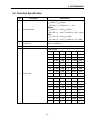
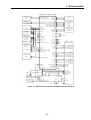
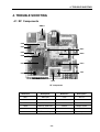
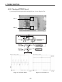
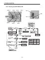
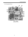
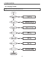
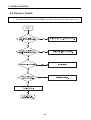
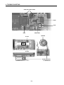
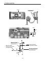
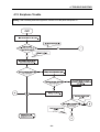
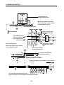
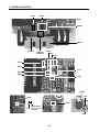
1
SERVICE MANUAL
MODEL : G5200 / W5200
GSM Phone
SERVICE MANUAL
MODEL : G5200/W5200
P/N : MMBD0015801
JUNE, 2002
Table Of Contents
3.10 Display and Interfaces ........................28
3.11 Keypad Switches and Scanning ..........29
3.12 Microphone .........................................30
3.13 Earpiece ............................................. 31
3.14 Hands-free Interface .......................... 32
3.15 Headset Jack Interface .......................32
3.16 Key Back-light Illumination ..................32
3.17 LCD Back-light Illumination ................ 33
3.18 Multi-Color LED Illumination .............. 33
3.19 Speaker & MIDI IC ............................. 34
1. INTRODUCTION.......................................4
1.1 Purpose ..................................................4
1.2 Regulatory Information .......................... 4
A. Security ..............................................4
B. Incidence of Harm ..............................4
C. Changes in Service ............................4
D. Maintenance Limitations ....................4
E. Notice of Radiated Emissions .............5
F. Pictures ..............................................5
G. Interference and Attenuation .............5
H. Electrostatic Sensitive Devices ..........5
1.3 Abbreviations ......................................... 6
4. TROUBLE SHOOTING ..................... 35
4.1 RF Components ................................. 35
4.2 Tx Trouble .......................................... 44
4.3 Power on Trouble ............................... 60
4.4 Charging Trouble ............................... 62
4.5 LCD Trouble ....................................... 64
4.6 Receiver Trouble . ............................... 66
4.7 Speaker Trouble ................................. 69
4.8 Mic Trouble ..........................................72
4.9 Vibrator Trouble ................................. 75
4.10 Backlight Trouble ............................. 77
4.11 Folder on/off Trouble ........................ 79
4.12 SIM Detect Trouble .......................... 81
4.13 Earphone Trouble ............................ 83
4.14 HFK Trouble ..................................... 87
2. PERFORMANCE .....................................8
2.1 H/W Feature ...........................................8
2.2 Technical Specification .......................... 9
3. TECHNICAL BRIEF ............................ 13
3.1 General Descreption ............................ 13
3.2 Receiver ............................................... 13
A. RF front end .....................................14
B. Demodulator and
baseband processing ...................... 14
C. DC Offset Compensation ................ 14
3.3 Transmitter Part ................................... 15
A. IF Modulator .................................... 15
B. OPLL ............................................... 16
C. Synthesizer ......................................16
D. TX APC Part ....................................17
E. Power Amplifier ................................17
3.4 13 MHz Clock ...................................... 18
3.5 Power Supplies and Control Signals ....18
3.6 Digital Main Processor ......................... 19
3.7 Analog Main Processor ........................ 24
3.8 Power Management ..............................26
3.9 Memories ..............................................28
5. ASSEMBLY INSTRUCTION ............ 95
5.1 Disassembly ....................................... 95
6. DOWNLOAD ....................................... 102
6.1 Download Setup ............................... 102
6.2 Download Procedure ........................ 103
-1-
7. BLOCK DIAGRAM ............................. 106
12. AUTO CALIBRATION ................... 121
7.1 Main Board ....................................... 106
7.2 FPCB ................................................ 107
7.3 RF .................................................... 107
12.1
12.2
12.3
12.4
12.5
12.6
12.7
12.8
8. CIRCUIT DIAGRAM ........................... 109
8.1
8.2
8.3
8.4
Baseband Interface .......................... 109
MIDI .................................................. 110
KYE, I/F & LCD CON ....................... 111
RF .................................................... 112
9. PCB LAYOUT
13. EXPLODED VIEW &
REPLACEMENT PART LIST ...... 124
..................................... 113
13.1 Exploded View .............................. 124
13.2 Accessories .................................. 126
13.3 Replacement Part List .................. 127
10. ENGINEERING MODE .................. 115
10.1
10.2
10.3
10.4
10.5
10.6
10.7
Overview ....................................... 121
Requirements ............................... 121
Menu and settings ........................ 121
AGC .............................................. 123
APC .............................................. 123
ADC .............................................. 123
Setting .......................................... 123
How to do calibration .................... 123
BB Test [MENU 1] ........................ 115
RF Test [MENU 2] ........................ 117
MF Mode [MENU 3] ...................... 118
Trace option [MENU 4] ................. 119
Call Timer [MENU 5] ..................... 119
Fact. Reset [MENU 6] ................... 119
S/W version [MENU 7] .................. 119
11. STAND ALONE TEST ................... 120
11.1 Introduction ................................... 120
11.2 Setting Method ............................. 120
11.3 Means of Test ............................... 120
-2-
REVISED HISTORY
DATE
ISSUE
CONTENTS OF CHANGES
APRIL/2002
ISSUE 1
Initial Release
S/W VERSION
The information in this manual is subject to change without notice and should not be construed as
a commitment by LGE Inc. Furthermore, LGE Inc. reserves the right, without notice, to make
changes to equipment design as advances in engineering and manufacturing methods warrant.
This manual provides the information necessary to install, program, operate and maintain the
G5200.
-3-
1. INTRODUCTION
1. INTRODUCTION
1.1 Purpose
This manual provides the information necessary to repair, calibration, description and download the
features of the G5200.
1.2 Regulatory Information
A. Security
Toll fraud, the unauthorized use of telecommunications system by an unauthorized part
(for example, persons other than your company’s employees, agents, subcontractors, or person
working on your company’s behalf) can result in substantial additional charges for your
telecommunications services. System users are responsible for the security of own system.
There are may be risks of toll fraud associated with your telecommunications system. System users
are responsible for programming and configuring the equipment to prevent unauthorized use. LGE
does not warrant that this product is immune from the above case but will prevent unauthorized use
of common-carrier telecommunication service of facilities accessed through or connected to it. LGE
will not be responsible for any charges that result from such unauthorized use.
B. Incidence of Harm
If a telephone company determines that the equipment provided to customer is faulty and possibly
causing harm or interruption in service to the telephone network, it should disconnect telephone
service until repair can be done. A telephone company may temporarily disconnect service as long
as repair is not done.
C. Changes in Service
A local telephone company may make changes in its communications facilities or procedure. If
these changes could reasonably be expected to affect the use of the G5200 or compatibility with
the network, the telephone company is required to give advanced written notice to the user,
allowing the user to take appropriate steps to maintain telephone service.
D. Maintenance Limitations
Maintenance limitations on the G5200 must be performed only by the LGE or its authorized agent.
The user may not make any changes and/or repairs expect as specifically noted in this manual.
Therefore, note that unauthorized alternations or repair may affect the regulatory status of the
system and may void any remaining warranty.
-4-
1. INTRODUCTION
E. Notice of Radiated Emissions
The G5200 complies with rules regarding radiation and radio frequency emission as defined by
local regulatory agencies. In accordance with these agencies, you may be required to provide
information such as the following to the end user.
F. Pictures
The pictures in this manual are for illustrative purposes only; your actual hardware may look slightly
different.
G. Interference and Attenuation
An G5200 may interfere with sensitive laboratory equipment, medical equipment, etc.
Interference from unsuppressed engines or electric motors may cause problems.
H. Electrostatic Sensitive Devices
ATTENTION
Boards, which contain Electrostatic Sensitive Device (ESD), are indicated by the
Following information is ESD handling:
sign.
Service personnel should ground themselves by using a wrist strap when exchange system
boards.
When repairs are made to a system board, they should spread the floor with anti-static mat which
is also grounded.
Use a suitable, grounded soldering iron.
Keep sensitive parts in these protective packages until these are used.
When returning system boards or parts like EEPROM to the factory, use the protective package
as described.
-5-
1. INTRODUCTION
1.3 Abbreviations
For the purposes of this manual, following abbreviations apply:
APC
BB
BER
CC-CV
DAC
DCS
dBm
DSP
EEPROM
EL
ESD
FPCB
GMSK
GPIB
GPRS
GSM
IPUI
IF
LCD
LDO
LED
G5200
LGE
OPLL
PAM
PCB
PGA
PLL
PSTN
RF
RLR
RMS
RTC
SAW
SIM
SLR
SRAM
STMR
TA
Automatic Power Control
Baseband
Bit Error Ratio
Constant Current – Constant Voltage
Digital to Analog Converter
Digital Communication System
dB relative to 1 milliwatt
Digital Signal Processing
Electrical Erasable Programmable Read-Only Memory
Electroluminescence
Electrostatic Discharge
Flexible Printed Circuit Board
Gaussian Minimum Shift Keying
General Purpose Interface Bus
General Packet Radio Service
Global System for Mobile Communications
International Portable User Identity
Intermediate Frequency
Liquid Crystal Display
Low Drop Output
Light Emitting Diodet
LG GSM Phone
LG Electronics
Offset Phase Locked Loop
Power Amplifier Module
Printed Circuit Board
Programmable Gain Amplifier
Phase Locked Loopr
Public Switched Telephone Network
Radio Frequency
Receiving Loudness Rating
Root Mean Square
Real Time Clock
Surface Acoustic Wave
Subscriber Identity Module
Sending Loudness Rating
Static Random Access Memory
Side Tone Masking Rating
Travel Adapter
-6-
1. INTRODUCTION
TDD
TDMA
UART
VCO
VCTCXO
WAP
Time Division Duplex
Time Division Multiple Access
Universal Asynchronous Receiver/Transmitter
Voltage Controlled Oscillator
Voltage Control Temperature Compensated Crystal Oscillator
Wireless Application Protocol
-7-
2. PERFORMANCE
2. PERFORMANCE
2.1 H/W Features
Item
Feature
Comment
Li-ion, 750 mAh
Standard Battery
Size: 41 73.9 5mm
Weight: 22 g
AVG TCVR Current
GSM , EGSM: 243 mA, DCS: 209 mA
Stand by Current
< 4 mA
Talk time
Up to 3 hours (GSM TX Level 7)
Stand by time
Up to 200 hours (Paging Period: 9, RSSI: -85 dBm)
Charging time
2 hours 30mins
RX Sensitivity
GSM, EGSM: -108 dBm, DCS: -107 dBm
TX output power
GSM, EGSM: 32 dBm (Level 5)
DCS: 29.5 dBm (Level 0)
GPRS compatibility
Class 10 (This only applies to G5200)
SIM card type
3V Small
Display
128
128 dots LCD(Main) , 96
64 dotsLCD(Sub)
Soft icons
Key Pad
Status Indicator
0 ~ 9, #, *, Navigation Key, Up/Down Side Key
Side Key, Confirm Key, Clear Key , Hot Key)
Send Key, END/PWR Key
ANT
External
EAR Phone Jack
Yes
PC Synchronization
Yes
Speech coding
EFR/FR/HR
Data and Fax
Yes
Vibrator
Yes
Receiver
Yes
Roud Speaker
Yes
Voice Recoding
Yes
C-Mike
Yes
Travel Adapter
Yes
Options
Hands-free kit, CLA, Data Kit
-8-
2. PERFORMANCE
2.2 Technical Specification
Item
Description
Specification
GSM
TX: 890 + n
RX: 935 + n
1
Frequency Band
0.2 MHz
0.2 MHz (n = 1 ~ 124)
EGSM
TX: 890 + (n – 1024)
RX: 935 + (n – 1024)
0.2 MHz
0.2 MHz (n = 975 ~ 1024)
DCS
TX: 1710 + (n – 512)
Rx: 1805 + (n – 512)
0.2 MHz
0.2 MHz (n = 512 ~ 885)
2
Phase Error
RMS < 5 degrees
Peak < 20 degrees
3
Frequency Error
< 0.1 ppm
GSM, EGSM
4
Level
Power
5
33 dBm
6
Power Level
Toler.
Level
Power
Toler.
2dB
13
17 dBm
3dB
31 dBm
3dB
14
15 dBm
3dB
7
29 dBm
3dB
15
13 dBm
3dB
8
27 dBm
3dB
16
11 dBm
5dB
9
25 dBm
3dB
17
9 dBm
5dB
10
23 dBm
3dB
18
7 dBm
5dB
11
21 dBm
3dB
19
5 dBm
5dB
12
19 dBm
3dB
Level
Power
Toler.
DCS
Level
Power
0
30 dBm
2dB
8
14 dBm
3dB
1
28 dBm
3dB
9
12 dBm
4dB
2
26 dBm
3dB
10
10 dBm
4dB
3
24 dBm
3dB
11
8 dBm
4dB
4
22 dBm
3dB
12
6 dBm
4dB
5
20 dBm
3dB
13
4 dBm
4dB
6
18 dBm
3dB
14
2 dBm
5dB
7
16 dBm
3dB
15
0 dBm
5dB
-9-
Toler.
2. PERFORMANCE
Item
Description
Specification
GSM, EGSM
Offset from Carrier (kHz).
Max. dBc
100
+0.5
200
-30
250
-33
400
-60
600 ~
5
Output RF Spectrum
(due to modulation)
1,200
-60
1,200 ~
1,800
-60
1,800 ~
3,000
-63
3,000 ~
6,000
-65
6,000
-71
Offset from Carrier (kHz).
Max. dBc
100
+0.5
200
-30
250
-33
400
-60
DCS
600 ~
1,200
-60
1,200 ~
1,800
-60
1,800 ~
3,000
-65
3,000 ~
6,000
-65
6,000
-73
GSM, EGSM
6
7
Output RF Spectrum
(due to switching transient)
Spurious Emissions
Offset from Carrier (kHz)
Max. (dBm)
400
-19
600
-21
1,200
-21
1,800
-24
Offset from Carrier (kHz)
Max. (dBm)
400
-22
600
-24
1,200
-24
1,800
-27
GSM
Conduction, Emission Status
- 10 -
2. PERFORMANCE
Item
Description
8
Bit Error Ratio
9
RX Level Report Accuracy
10
SLR
11
12
13
Specification
GSM, EGSM
BER (Class II) < 2.439% @-102 dBm
DCS
BER (Class II) < 2.439% @-100 dBm
3 dB
8
Frequency (Hz)
Max.(dB)
Min.(dB)
100
-12
-
200
0
-
300
0
-12
1,000
0
-6
2,000
4
-6
3,000
4
-6
3,400
4
-9
4,000
0
-
Frequency (Hz)
Max.(dB)
Min.(dB)
100
-12
-
200
0
-
300
2
-7
500
-5
1,000
*
0
-5
3,000
2
-5
3,400
2
-10
4,000
2
Sending Response
RLR
3 dB
2
Receiving Response
3 dB
* Mean that Adopt a straight line in between 300 Hz
and 1,000 Hz to be Max. level in the range.
14
STMR
13
15
Stability Margin
> 6 dB
16
5 dB
dB to ARL (dB)
Level Ratio (dB)
-35
17.5
-30
22.5
-20
30.7
-10
33.3
0
33.7
7
31.7
10
25.5
Distortion
17
Side Tone Distortion
Three stage distortion < 10%
18
System frequency (13 MHz) tolerance
≤ 2.5 ppm
- 11 -
2. PERFORMANCE
Item
19
Description
32.768KHz tolerance
Specification
≤ 30 ppm
Full power
< 243 mA (GSM, EGSM) ; < 209 mA (DCS)
20
Power Consumption
Standby
- Normal < 4 mA (Max. power)
Talk Time
GSM/ Level 7 (Battery Capacity 750mA): Up to 180 Min
GSM/ Level 12 (Battery Capacity 750mA): Up to 300 Min
Standby Time
Under conditions, Up to 200 hours:
1. Brand new and full 750mAh battery
2. Full charge, no receive/send and keep GSM in idle
mode.
3. Broadcast set off.
4. Signal strength display set at 3 level above.
5. Backlight of phone set off.
23
Ringer Volume
At least 80 dB under below conditions:
1. Ringer set as ringer.
2. Test distance set as 50 cm
24
Charge Voltage
Fast Charge : < 500 mA
Slow Charge: < 60 mA
21
22
25
Antenna Display
26
Battery Indicator
27
Low Voltage Warning
28
Forced shut down Voltage
29
Battery Type
30
Travel Charger
Antenna Bar Number
Power
5
4
3
2
1
0
Battery Bar Number
-85 dBm ~
-90 dBm ~ -86 dBm
-95 dBm ~ -91 dBm
-100 dBm ~ -96 dBm
-105 dBm ~ -101 dBm
~ -105 dBm
Voltage
0
1
2
3
~ 3.62 V
3.62 ~ 3.73 V
3.73 ~ 3.82 V
3.82 V ~
3.5
3.62
0.03 V (Call)
0.03 V (Standby)
3.35
0.03 V
1 Li-ion Battery
Standard Voltage = 3.7 V
Battery full charge voltage = 4.2 V
Capacity: 750 mAh
Switching-mode charger
Input: 100 ~ 240 V, 50/60 Hz
Output: 5.2 V, 600 mA
- 12 -
3. TECHNICAL BRIEF
3. TECHNICAL BRIEF
3.1 General Descreption
The RF parts consists of a transmitter part,a receiver part,a synthesizer part,a voltage supply part,a
VCTCXO part. And the main RF Chipset CX74017[U411]is a single-chip dual-band transceiver for
the extended global system for mobile communication[E- GSM900MHz]/Digital communication
system[DCS1800MHz] voice and data transfer applications.
This device integrated a direct conversion receiver architecture, which eliminates the need of
Intermediate Frequency, a transmitter based on a modulation loop architecture and fractional-N
synthesizer part with built in TXVCO and Local-VCO.
3.2 Receiver
The Receiver part in CX74017 contains all active circuits completely, full receiver chain with the
exception of discrete front-end RF SAW filters. The filtered and amplified signal is down converted
in the RF-mixer to the baseband output. The receiver path is supported by internal channel filtering.
The RF front-end circuit is shown Figure 3-1.
Figure 3-1. RF front-end circuit.
- 13 -
3. TECHNICAL BRIEF
A. RF front end
RF front end consists of Antenna Switch(U405), dual band LNAs integrated in transceiver(U411).
The Received RF signals (GSM 925MHz ~ 960MHz, DCS 1805MHz ~ 1880MHz) are fed into the
antenna or mobile switch. An antenna matching circuit is between the antenna and the mobile
switch.
The Antenna Switch (U405) is used to control the Rx and TX paths. And, the input signals VC1 and
VC2 of a U405 are connected to 2-Input AND Gates(U401) to switch either TX or RX path on.
When the RX path is turned on, the received RF signal then feeds either Rx_900_RF or
RX_1800_RF path selected by GSM-RX and DCS-RX respectively. This Rx_900_RF path contains
one SAW filter, followed after the Antenna Switch (U405), to filter any unwanted signal apart from
the DCS RX band. And, the RX_1800_RF path is the same case.
The logic and current for Antenna Switch is given below Table 3-1.
Table 3-1. The logic and current
VC1
VC2
Current
GSM TX
0V
2.7 V
10.0 mA max
DCS TX
2.7 V
0V
10.0 mA max
0V
0V
< 0.1 mA
GSM/DCS RX
These two paths are then connected to the LNAGSMN (#11) and LNADCSIN (#13) of CX74017
(U411), respectively. A low-noise bipolar RF amplifier, contained within the U411, amplifies the RF
signal. The RF signals from the front-end pass to the receiver mixers within the U411 device.
B. Demodulator and baseband processing
In direct conversion receiver there is only one mixer down-converting received RF signal to BB
signal directly. The gain down converting mixer is 40dB at high gain mode and 22dB at low gain
mode.
The Rx gain setting is done in the AGC algorithm. The nominal gain of the receiver is set as a
function of the expected signal strength at the antenna input so that a desired level is reached at
the Rx I/Q. 7 blocks in the receiver chain have variable gains, LNA, Mixer, LPF1, VGA1, gmC Filter,
Auxiliary gain control and VGA2. The gain settings can be adjustable via 3-wire bus control lines.
The baseband signals pass via integrated low-pass filters to the baseband A/D converters.
The remainder of the channel filtering is performed by the baseband chipset. The demodulator
contains switches to maintain the sense of the baseband I/Q outputs with respect to the incoming
RF signal on both GSM900 and DCS 1800.
C. DC Offset Compensation
Three correction loops ensure that DC offsets, generated in the CX74017, do not overload the
baseband chain at any point.
After compensation, the correction voltages are held on capacitors for the duration of the receive
slot(s). A rising edge on the RXEN signal, selected via the serial interface, placed the DC
compensation circuitry in the track mode.
- 14 -
3. TECHNICAL BRIEF
3.3 Transmitter Part
The Transmitter part contains CX74017 active parts and PAM, APC IC, coupler and Antenna
Switch. The CX74017 active part consists of a vector modulator and offset phase-locked loop
block(OPLL) including down-converter, phase detector, loop filter and dual band transmit VCO
which can operate at either final RF output frequency. The RF GMSK outputs from the transmit
VCO are fed directly to the RF power amplifiers.
TXIP
TXIN
Figure 3-2. Transmitter Block diagram
The peak output power and the profile of the transmitted burst are controlled by means of a closed
feedback loop. A dual band directional coupler is used to sample the RF output from either PA.
The PA outputs from the directional coupler pass to the antenna connector via Antenna Switch.
A. IF Modulator
The baseband converter(BBC) within the GSM chipset generates I and Q baseband signals for the
transmit vector modulator. The modulator provides more than 40dBc of carrier and unwanted sideband rejection and produces a GMSK modulated signal. The baseband software is able to cancel
out differential DC offsets in the I/Q baseband signals caused by imperfections in the D/A
converters.
The TX-Modulator implements a quadrature modulator. The IF-frequency input signal is split into
two precise orthogonal carriers, which are multiplied by the baseband modulation signal IT/ITX and
QT/QTX. It is used as reference signal for the OPLL.
- 15 -
3. TECHNICAL BRIEF
B. OPLL
The offset mixer down converts the feedback Tx RF signal using LO to generate a IF modulating
signal. The IF signal goes via external passive bandpass filter to one port of the phase detector.
The other side of the phase detector input is LO signal. The phase detector generates an error
current proportional to the phase difference between the modulated signal from the offset mixer and
the reference signal from the LO.
The error current is filtered by a second order low-pass filter to generate an output voltage which
depends on the GMSK modulation and the desired channel frequency. This voltage controls the
transmit VCO such that the VCO output signal, centered on the correct RF channel, is frequency
modulated with the original GMSK data. The OPLL acts as a tracking narrowband band pass filter
tuned to the desired channel frequency. This reduces the wideband noise floor of the modulation
and up-conversion process and provides significant filtering of spurious products.
C. Synthesizer
The CX74017 includes a fully integrated UHF VCO with an on-chip LC tank.
A single sigma-delta fractional-N synthesizer can phase lock the local osillator used in both transmit
and receive path to a precision frequency reference input. Fractional-N operation offers low phase
noise and fast setting times, allowing for multiple slot applications such as GPRS.
The generated frequency is given by the following equation
=
where : f VCO = Generated VCO frequency
N = N-divider ratio integer part
FN = Fractional setting
R = R-divider ratio
f VCO = Reference Frequency
- 16 -
3. TECHNICAL BRIEF
The counter and mode settings of the synthesizer are also programmed via 3-wire interface.
f ref
13MHz
Figure 3-3. Synthesizer Block diagram
D. TX APC Part
The AD8315[U412] is a dual band RF power controller for RF power amplifiers operating in the
850MHz to 2GHz range.
The AD8315[U412] controls the power output of the selected RF channel. RF power is controlled by
driving the RF amplifier power control pins and sensing the resultant RF output power via a
directional coupler. The RF sense voltage is peak detected using an on-chip Schottky diode.
This detected voltage is compared to the DAC voltage at the VSET pin to control the output power.
An internal input signal[TXRAMP] is applied to the positive input of the AD8315 amplifier during the
TXEN mode and a directional coupler near the antenna feeds a portion of the RF output signal back
to the AD8315 peak detector converts this signal to a low frequency feedback signal that balances
the amplifier when this signal equals the RAMP input signal level.
E. Power Amplifier
The PF08107B[U409] is Dual band amplifier for E-GSM(880 to 915MHz) and DCS1800(1710 to
1785MHz). The efficiency of module is the 50% at nominal output power for E-GSM and the 43% at
32dBm for DCS1800. This module should be operated under the GSM burst pulse. To avoid
permanent degradation, CW operation should not be applied. To avoid the oscillation at no input
power, before the input is cut off, the control voltage Vapc should be control to less than 0.5V.
We have to improve thermal resistance, the through holes should be layouted as many as possible
on PCB under the module. And to get good stability, all the GND terminals and the metal cap should
be soldered to ground plane of PCB.
- 17 -
3. TECHNICAL BRIEF
3.4 13 MHz Clock
The 13 MHz clock (VC-TCXO-208C) consists of a TCXO (Temperature Compensated Crystal
Oscillator) which oscillates at a frequency of 13 MHz.
It is used within the CX74017 RF Main Chip, BB Analog chip-set (AD6521), and Digital (AD6522).
.
Figure 3-4. VCTCXO Circuit.
3.5 Power Supplies and Control Signals
There are two regulators used in the phone to provide RF power. One is contained inside of
ADP3408 (U101), power management IC to provide the power for the VCTXO (X302). The other is
used to provide the power for remaining RF circuits.
Table 3-2.
Regulator
Regulator 1
(U1, 2V7_VTCXO)
Regulator 2
(U414, RF2V8)
Voltage
Powers
2.7 V
0.5 V
VCTXO
2.85 V
0.5 V
RF circuitry
Figure 3-5. Regulator Circuit.
- 18 -
Enable Signal
VSYNTHEN
3. TECHNICAL BRIEF
3.6 Digital Main Processor
The AD6522 is an ADI designed processor.
Figure 3-6. Top level block diagram of the AD6522 internal architecture.
BUS Arbitration Subsystem
It is to work as a cross point for data accesses between the three main busses. EBUS is for external
accesses, primarily from Flash memory for code and data. RBUS is for internal RAM access. PBUS
is for access to internal peripheral modules such as UART, RTC or SIM. In addition to the three
main system busses, it has SBUS, IOBUS and DMABUS.
DSP subsystem
It consists of ADI DSP, Viterbi coprocessor, Ciphering unit and a cache memory/controller system.
The DSP can run at a maximum clock frequency of 78 MHz at 2.45 V. The Viterbi and ciphering
accelerators enable a very efficient implementation of the channel equalization, encryption and
decryption tasks.
- 19 -
3. TECHNICAL BRIEF
MCU subsystem
It consists of an ARM7TDMI central processing unit, a boot ROM, a clock generation and access
control module.
The maximum clock frequency for the ARM7TDMI is 39 MHz at 2.45 V.
The main clock is 13MHz and it is provided by VCTCXO. The Clock & BS(Bus Select) generator
make internal clock by multiplying the main clock by 1X, 1.5X, 2X and 3X.
The boot ROM contains MCU code for basic communication between the ARM and one of the serial
ports in the Universal System Connector subsystem.
Peripheral subsystem
It contains four major groups of elements.
The MMI group is a collection of all the functionality that are needed to implement a complete user
interface including keyboard, display, backlight, RTC, general purpose I/O etc.
House Keeping group consists of three different sub-modules: The Watch Dog Timer, the Interrupt
Controller, and the general timers.
GSM system group consists of the time base generation together with the synthesizer interface,
which form the radio control.
Direct Memory Access is located between the three system buses (PBUS, RBUS and EBUS) and
can move any data from any address location on one system bus to any address location on
another system bus.
- 20 -
3. TECHNICAL BRIEF
Figure 3-7. System interconnection of AD6522 external interfaces
- 21 -
3. TECHNICAL BRIEF
Interconnection with external devices
RTC block interface
Countered by external X-TAL
The X-TAL oscillates 32.768KHz
LCD module interface
Controlled by LCD_MAIN/SUB_CS, LCD_RES, LCD_A0, /WR, /RD, DATA [00...07] ports
Table 3-3.
Description
LCD_MAIN_CS
LCD_SUB_CS
LCD chip enable. Each LCD has CS pin
LCD_RES
This pin resets LCD module.
LCD_A0
This pin determines whether the data to LCD module is display data or
control data
/WR, /RD
Read/Write control
DATA [00...07]
Parallel data line
RF interface
The AD6522 control RF parts through TXEN, RXON1, RXON2, AGCEN, SDATA, SCLK, SEN etc.
Table 3-4.
Signal Name
TXEN
RXON1
RXON2
AGCEN
SDATA
SCLK
SEN
Description
TX Enable/Disable
LNA, Mixer1 On/Off
Mixer 2 On/Off
AGC Enable/Disable
Serial Data to PLL
Clock to PLL
PLL Enable/Disable
- 22 -
3. TECHNICAL BRIEF
SIM interface
The AD6522 check status periodically in call mode if SIM card is inserted or not, but the AD6522
don't check in deep sleep mode.
Interface by SIM_IO, SIM_CLK, SIM_RST
Table 3-5.
Description
SIM_IO
SIM_CLK
SIM_RST
This pin receives and sends data to SIM card. G5200 support only 3.0
volt interface SIM card.
Clock 3.5MHz frequency.
Reset SIM block.
Figure 3-8.
Key interface
Include 5 column and 5 row
The AD6522 detect key press by interrupt
ADP3408 interrupt
There are two interrupts EOC and CHARGEDETECT
EOC: End of Charge. Charging would be stopped when AD6522 receive this input.
CHARGEDETECT: This interrupt is generated when charge is inserted.
- 23 -
3. TECHNICAL BRIEF
3.7 Analog Main Processor
AD6521
Figure 3-9. AD6521 function block diagram
- 24 -
3. TECHNICAL BRIEF
BB Transmit section
This section generates in-phase and quadrature BB modulated GMSK signals (BT = 0.3) in
accordance with GSM 05.05 Phase 2 specifications
The transmit channel consists of a digital GMSK modulator, a matched pair of 10-bit DACs and a
matched pair of reconstruction filter
BB Receive section
This section consists of two identical ADC channels that process baseband in-phase(I) and
quadrature(Q) input signals.
Each channel consists of a coarse switched capacitor input filter, followed by a high-order sigmadelta modulator and a lowpass digital filter
Auxiliary section
This section contains two auxiliary DACs(AFC DAC, IDAC) for system control.
This section also contains AUX ADC and Voltage Reference
AUX ADC: 6 channel 10 bits
AFC DAC: 13 bits
IDAC: 10 bits
Voiceband section
Receive audio signal from MIC. G5200 use differential configuration.
Send audio signal to Receiver. G5200 use differential configuration.
It interconnect with external device like main microphone, main receiver, ear-phone and Hands free
kit
through the VINNORP, VINNORN, VOUTNORP, VOUTNORN, VINAUXP, VINAUXN,
VOUTAUXP, VOUTAUXN
VINNORP, VINNORN: Main MIC positive/negative terminal.
VOUTNORP, VOUTNORN: Main Receiver positive/negative terminal.
VINAUXP, VINAUXN: Hands free kit mic positive/negative terminal.
VOUTAUXP, VOUTAUXON: Hands free kit speaker positive/negative terminal.
- 25 -
3. TECHNICAL BRIEF
3.8 Power Management
ADP3408
Figure 3-10. ADP3408 inner block diagram.
Power up sequence logic
The ADP3408 controls power on sequence
Power on sequence
If a battery is inserted, the battery powers the 6 LDOs.
Then if PWRONKEY is detected, the LDOs output turn on.
REFOUT is also enabled
Reset is generated and send to the AD6522
- 26 -
3. TECHNICAL BRIEF
LDO block
There are 6 LDOs in the ADP3408
Table 3-6.
Description
VSIM
VCORE
VRTC
VAN
VTCXO
VMEM
2.86 V (is provided to SIM card)
2.45 V (is provided to the AD6522 & AD6521’s digital core)
2.45 V (is provided to the RTC and Backup Battery)
2.45 V (is provided to the AD6521 I/O and used as microphone bias)
2.715 V (is provided to VCTCXO)
2.80 V (is provided to Flash)
Battery charging block
It can be used to charge Lithium Ion and/or Nickel Metal Hydride batteries. G5200 use Li-Ion battery
only. Charger initialization, trickle charging, and Li-Ion charging control are implemented in
hardware.
Charging Process
Check charger is inserted or not
If ADP3408 detects that Charger is inserted, the CC-CV charging starts.
Exception: When battery voltage is lower than 3.2V, the precharge (low current charge mode) starts
firstly.
And the battery voltage reach to 3.2V the CC-CV charging starts.
Pins used for charging
CHARGERDETECT: Interrupt to AD6522 when charger is plugged.
CHARGEEN: Control signal from AD6522 to charge Li+ battery
EOC: Interrupt to AD6522 when battery is fully charged
GATEIN: Control signal from AD6522 to charge NiMH battery. But, not used.
MVBAT: Battery voltage divider. Divide ratio is 1:2.3 and it is sensed in AD6521 AUX_ADC
TA (Travel Adaptor)
Input voltage: AC 85V ~ 260V, 50~60Hz
Output voltage: DC 5.2V ( ±0.2 V )
Output current: Max 850mA ( ±50mA )
Battery
Li-ion battery (Max 4.2V, Nom 4.0V)
Standard battery : Capacity - 750mAh, Li-ion
- 27 -
3. TECHNICAL BRIEF
3.9 Memories
64M flash memory + 16M SRAM
16 bit parallel data bus
ADD01 ~ ADD21.
RF Calibration data are stored in Flash
3.10 Display and Interface
Table 3-7
Display Format
Back light
Main LCD
128 x 128 dots
EL Backlight
Sub LCD
96 x 64 dots
EL Backlight
G5200 has dual type LCD. There are the control output LCD_MAIN/SUB_CS which is derived from
AD6522, this acts as the chip select enable for the Main/Sub LCD. AD6522 uses DATA[00:07] pins
to send data for displaying graphical text onto the each LCD ( Main/Sub ).
- 28 -
3. TECHNICAL BRIEF
3.11 Keypad Switches and Scanning
The key switches are metal domes, which make contact between two concentric pads on the
keypad layer of the PCB when pressed. There are 25switches (S301-S325), connected in a matrix
of 5 rows by 5 columns, as shown in Figure, except for the power switch (S310), which is connected
independently.
Functions, the row and column lines of the keypad are connected to ports of AD6522. The columns
are outputs, while the rows are inputs and have pull-up resistors built in. When a key is pressed, the
corresponding row and column are connected together, causing the row input to go low and
generate an interrupt. The columns/rows are then scanned by AD6522 to identify the pressed key.
0
Figure 3-11. Keypad Switches and Scanning.
- 29 -
DOWN
3. TECHNICAL BRIEF
3.12 Microphone
The microphone is soldered to the main PCB. The audio signal is passed to VINNORP (#K8) and
VINNORN (#K7) pins of AD6522. The voltage supply 2V45_VCORE is output from ADP3408, and is
a bias voltage for both the VINNOR (through R105) and VINAUX (through R104) lines.
The VINNOR or VINAUX signal is then A/D converted by the Voiceband ADC part of AD6521.
The digitized speech is then passed to the DSP section of AD6522 for processing (coding,
interleaving etc.).
Figure 3-12. Microphone.
- 30 -
3. TECHNICAL BRIEF
3.13 Earpiece
The earpiece is driven directly from AD6521 VOUTNORP (#K8) and VOUTNORN (#K7) pins and
the gain is controlled by the PGA in an AD6521. The earpiece is located in the handset floder front
panel, and the signals are routed to it via FPCB connector between Main Board and FPCB board.
But, The VOUTNORP signal has to be selected by the control signal “SPK_EN”. If SPK_EN is low,
VOUTNORP is directly connected to the Earpiece, else VOUTNOTP is connected to the Midi
Chip(U203).
Figure 3-13. Earpiece & Handsfree Interface
- 31 -
3. TECHNICAL BRIEF
3.14 Hands-free Interface
The audio out (VOUTAUXP & VOUTAUXN) to the hands-free kit consists of a pair of differential
signals from AD6521 auxiliary outputs (#K9, #K6), which are tracked down the board to carkit
connector (CN301) at the base of the handset. The DC level of the signal is supplied to the
VOUTAUX pin. And the EXT_IN signal is then input to the VINAUXP (#H10) and VINAUXN (#G10)
of AD6521.
3.15 Headset Jack Interface
Headset Jack has the single-end structure in both audio in and out. The audio out to the headset
jack is used only one line(VOUTAUXP/HEADSET_SPK_P1) which can be connected to the
HEADSET_MIC_P or HFK_SPK_P by the analog switch(U204). If you put in the headset jack in the
top of the handset, HEADSET_SPK_P1(VOUTAUXP) is connected to the HEADSET_SPK_P. And
the audio in from the headset jack has also one line(VINAUXP/HEADSET_MIC_P). If the headset
jack is put in, HEADSET_MIC_P is input from the MIC of headset jack, else HEADSET_MIC_P is
connected to HFK_MIC_P which is input from the Hands-free Kit.
3.16 Key Back-light Illumination
In key back-light illumination, there are 12 Blue LEDs in Main Board, which are driven by
KEY_BACKLIGHT line from AD6522.
Figure 3-14. Key Back-light Illumination.
- 32 -
3. TECHNICAL BRIEF
3.17 LCD Back-light Illumination
In LCD Back-light illumination, there is an EL driver in sub LCD side of LCD Module, which is driven
by BACKLIGHT(EL_EN) line from AD6522.
Figure 3-15. LCD Back-light Illumination.
3.18 Multi-Color LED Illumination
In multi-color LED illumination, there is an LED chip and three TRs in sub LCD side of LCD Module,
which is driven by LED_G, LED_B and LED_Main line from AD6522.
Figure 3-16. Multi-Color LED
- 33 -
3. TECHNICAL BRIEF
3.19 Speaker & MIDI IC
Figure 3-17. Speaker & MIDI IC
MA-3 is a synthesizer LSI for mobile phones that realize advanced game sounds. This LSI has a
built-in speaker amplifier, and thus, is an ideal device for outputting sounds that are used by mobile
phones in addition to game sounds and ringing melodies that are replayed by a synthesizer.
The synthesizer section adopts “stereophonic hybrid synthesizer system” that are given advantages
of both FM synthesizers and Waveform table synthesizers to allow simultaneous generation of up to
thirty-two FM tones and eight Waveform table tones.
Since FM synthesizer is able to present countless tones by specifying parameters with only several
tens of bytes, memory capacity and communication band can be saved, and thus, the device
exhibits the features in operating environment of mobile phones such as allowing distribution of
arbitrary melodies with tones. On the other hand , since Waveform table synthesizer complies with
downloading of tones from host CPU, arbitrary ADCM/PCM tones can be treated from sequencer in
addition to the use of tones that are built-in the LSI.
MA-3 has a built-in circuit for controlling vibrators and LEDs synchronizing with play of music.
- 34 -
4. TROUBLE SHOOTING
4. TROUBLE SHOOTING
4.1 RF Components
SW401
U405
U401
N401
U407
N409
U408
U411
U412
U414
Y401
U413
RF components
Reference
Description
Reference
Description
U401
AND Gate
U412
APC IC
U405
Antenna Switch
U413
Inverter
U407
DCS RF SAW Filter
U414
LDO
U408
GSM RF SAW Filter
SW401
Mobile Switch
U409
PAM
Y401
TXVCO
U411
RF Main Chip
N401
Coupler
- 35 -
4. TROUBLE SHOOTING
RX Check Area
- 36 -
4. TROUBLE SHOOTING
4.1-1 Checking Regulator Circuit
U414.1
- 37 -
U414.6
4. TROUBLE SHOOTING
4.1-2 Checking VCTCXO Circuit
Y401.3
Y401.4
Graph 4-1. VCTCXO 13MHz
Graph 4-2. VCTCXO 2.7V
- 38 -
4. TROUBLE SHOOTING
4.1-3 Checking Control Signal
TP409(LE)
TP407(Data)
Graph 4-3. RF Control Signal
- 39 -
TP4043(RXEN)
TP408(Clock)
4. TROUBLE SHOOTING
4-1-4 Checking Ant SW & Mobile SW
U405.10
U405.2
SW401.2
U401.1
R405
U401.6
SW401.1
U405.11
U405.1
Table 4-1. ANT SW Control Logic
- 40 -
4. TROUBLE SHOOTING
Graph 4-4. ANT SW Control
GSM. DCS RX Mode
Graph 4-5. Dual AND Gate input
For GSM RX Mode
Graph 4-6. Dual AND Gate input
For DCS RX Mode
Table 4-2. ANT SW Control Logic
- 41 -
4. TROUBLE SHOOTING
4-1-5 Checking Saw Filter Circuit
U407.3
- 42 -
U407.1
U408.3 U408.1
4. TROUBLE SHOOTING
4-1-6 Checking RX IQ
RXIN RXQN
RXIP RXQP
Graph 4-7. RX IQ Signal
Graph 4-8. RX I Signal (Extended)
- 43 -
4. TROUBLE SHOOTING
4.2 Tx Trouble
6
5
1
3
4
2
Rx Check Area
3
- 44 -
4. TROUBLE SHOOTING
4-2-1 Checking Regulator Circuit
If you already Check this point while checking RX part, You can Skip this Test
U414.1
U414. 2
- 45 -
U414.6
4. TROUBLE SHOOTING
4-2-2 Checking VCTCXO Circuit
If you already Check this point while checking RX part, You can Skip this Test
Y401. 3
Y401. 4
Graph 4-9. VCTCXO 13MHz
Graph 4-10. VCTCXO 2.7V
- 46 -
4. TROUBLE SHOOTING
4-2-3 Checking Control Signal.
Graph 4-11. RF Control Signal
Graph 4-12. TXEN, TXRAMP, TXPA
TP409(LE)
TP407(Data)
TP408(Clock)
TXEN
(R425)
TXRAMP
(R427)
TXPA
(R405)
- 47 -
4. TROUBLE SHOOTING
4-2-4 Checking TX IQ
TXQN
C463
100P
TXQP
TXIN
C464
100P
TXIP
TXQN
TXQP
Graph 4-13. TX IQ Signal
- 48 -
TXIN
TXIP
4. TROUBLE SHOOTING
4-2-5 Checking RF TX Level
N401. 3
U409. 1
N401. 1
R407
L405
R411
L408
C432
U409. 8
U412. 1
R472
- 49 -
4. TROUBLE SHOOTING
4-2-6 Checking Ant SW & Mobile SW
SW401. 2
U405. 8
U405. 5
U405. 3
U401. 1
R405
U401. 6
SW401. 1
U405. 11
U405. 2
Table 4-1. ANT SW Control Logic
- 50 -
4. TROUBLE SHOOTING
4-2-6 Checking Ant SW & Mobile SW
Graph 4-14. ANT SW Control
DCS TX Mode
Graph 4-15. ANT SW Control
GSM TX Mode
Graph 4-16.Dual AND Gate input
For DCS TX Mode
Graph 4-17.Dual AND Gate input
For GSM TX Mode
Table 4-3. ANT SW Control Logic
- 51 -
4. TROUBLE SHOOTING
GSM : CH.62, -60dBm
DCS :CH.699, -60dBm
4-2-7 Receiver RF Level
- 52 -
4. TROUBLE SHOOTING
3
4
1
2
Test Points of Rx Level
- 53 -
- 54 -
8
10
9
ANT
S/W
GSMSEL
TXPA
DCSSEL
13
11
GSM : -6dBm
DCS : -3dBm
ATT
COUPLER
(LDCX5D)
6
5
33.5dBm
3
32dBm
PAM(PF08X22B)
34dBm
DCS : X7X0 ~ X785MHz
GSM : 880 ~ 9 X5MHz
VC2
VCX
GSM : 32.5dBm
DCS : 29.5dBm
GSM : X5dBm
DCS : X8dBm
3X.5dBm
7
12
LMG002S
Mobile
S/W
GSM : 32dBm
DCS : 29dBm
ATT
ATT
TXEN
TXRAMP
0dBm
APCIC(AD83X5)
4
2dBm
1
X0dBm
2
X2
LF
X2
PFD
f LO
f
LF
/D2
/D X
Fractional-N
PLL
GSM : 975(-300mV) ~ X24(300mV)
DCS : 5 X2(-750mV) ~ 885(750mV)
GSM
DCS
TXVCO
8dBm
f TX
/3
f vco
/R
f vco = (N+3.5+FN/2^22) f ref/R
GSM :Pwr Lvl 5,CH.62,32dBm
DCS :Pwr Lvl 5,CH.699, 29dBm
0
90
f ref
Serial
I/O
Serial
I/O
X3MHz
TXQP
TXQN
TXIP
TXIN
BANDSEL2
BANDSELX
FEENA
TXEN
RXEN
PLL_PD
PLL_LE
PLL_CLK
PLL_DATA
REFCLK
AFC
X3MHz
2V7_VTCXO
Base
Band
Block
4. TROUBLE SHOOTING
4-2-8 Transmitter RF Level
4. TROUBLE SHOOTING
4-2-8 Transmitter RF Level
11
5
13
12
3
1
2
4
6
7 , 8
9 , 10
Test Points of Tx Level
- 55 -
4. TROUBLE SHOOTING
4-2-9 Test Points for RF Components
VC2
U401. 3
VC1
U401. 7
TXPA
(R405)
TXEN(R425)
TXRAMP(R427)
13MHz CLock
RF 2.85V
2V7_VCTCXO
TXQN
TXQP
RXQN
RXQP
TXIN RXIN
TXIP RXIP
Test Points for RF components
- 56 -
4. TROUBLE SHOOTING
• Test Points for RF Components
TP408(PLL_Clock)
TP409(PLL_LE)
TP407(PLL_Data)
Test Points for RF components
(Keypad Side/Lower)
- 57 -
4. TROUBLE SHOOTING
• Baseband components (Component Side)
U101
U103
U102
D101
D102
U201
X101
CN101
U105
Q302
U205
U202
U106
U203
U302
U204
CN302
Baseband components (Component Side)
Reference
Description
Reference
Description
U101
PMIC
U205
LDO
U102
P-Channel FET
U302
Analog Switch
U103
Analog Main Processor
D101
Diode
U105
Digital Main Processor
D102
Dual Diode
U106
Memory
X101
X-TAL
U201
Comparator
Q302
Dual Transistor
U202
Analog Switch
CN101
SIM Connector
U203
MIDI IC
CN301
IO Connector
U204
Analog Switch
- 58 -
4. TROUBLE SHOOTING
• Baseband components (Keypad Side)
Q101
D301
Q301
MIC101
U301
Baseband components (Keypad Side)
Reference
Description
U301
Hall Sensor
Q301
Transistor
Q302
Transistor
Reference
D301
MIC101
- 59 -
Description
Dual Diode
C-MIC
4. TROUBLE SHOOTING
4.3 Power on Trouble
Setting : Connect PIF, and set remote switch off at PIF.
- 60 -
4. TROUBLE SHOOTING
POWER-ON KEY
signal input
These powers should
be necessary to
power on.
This signal should go HIGH when the power-on
procedure is completed.
Pin 25 (VTCXO=2.7V)
Pin 22 (VCORE=2.45V)
Pin 21 (VMEM=2.8V)
Pin 1 (PWRON_EN)
Pin 2 (Power Key)
Pin 6 (VRTC>1.2V)
- 61 -
4. TROUBLE SHOOTING
4.4 Charging Trouble
Setting : Connect PIF, and set remote switch off at PIF.
- 62 -
4. TROUBLE SHOOTING
The charging current
will flow into this
direction.
R102
U102
D101
- 63 -
4. TROUBLE SHOOTING
4.5 LCD Trouble
Setting : Connect PIF and power on.
- 64 -
4. TROUBLE SHOOTING
CN301
Soldering Check
If the FPCB has a problem, the
control signals for LCD cannot
be transmitted properly.
- 65 -
4. TROUBLE SHOOTING
4.6 Receiver Trouble
Setting : After initializing GSM MS test equipmemt, connect PIF and power on. Make a test call to 112.
Set audio part at test equipment as PRBS or continuous wave, not echo. Set the volumn max.
- 66 -
4. TROUBLE SHOOTING
PMIC (U101)
RECEIVER
Soldering
Check
YMU762 (U203)
C206
U202. 4
U202. 5
From the
U103(AD6521)
C206
To Receiver at
LCD module via
CN301
U202
From the
U103(AD6521)
The Circuit Diagram of the receiver path. Refer to page 2 of the complete circuit diagram for detail.
- 67 -
4. TROUBLE SHOOTING
U202. 4
U202. 5
C206
(REC-)
The waveforms of the audio signals at each point
- 68 -
4. TROUBLE SHOOTING
4.7 Speaker Trouble
Setting : Connect PIF to the phone, and power on. Enter the engineering mode, and set "Melody on" at
"BB Test-Buzzer" menu.
- 69 -
4. TROUBLE SHOOTING
C209, C211, R213, R215
U205
C221
U203
R222, R227
Speaker
Pin 26
CN301
Pin 25
Soldering Check
in LCD Module
- 70 -
4. TROUBLE SHOOTING
These four components make up the
analog amplifier stage of melody.
C209, R213, C211, R215
This is the melody IC.
U203
To the speaker at LCD
module via CN301.
R227
The Power for analog part of the
melody IC. The voltage is 3.3V
R222
The Power for digital part of the
melody IC. The voltage is 2.8V.
It is from the PMIC(ADP3408, U101)
C221
U205
The circuit diagram of the part of the melody IC. Refer to the page 2 of the complete circuit diagram for
detail.
- 71 -
4. TROUBLE SHOOTING
4.8 Mic Trouble
Setting : After initializing GSM MS test equipment, connect PIF to the phone, and power on. Make a test
call to 112. Make a sound in front of microphone.
- 72 -
4. TROUBLE SHOOTING
R105 R108
C118
R110
R112
C132
C129
Q101.3
MIC101
- 73 -
4. TROUBLE SHOOTING
R105
C118
R108
MIC101
Mic activating signal
Mic is activated when this
signal goes to HIGH
R110, R112
C129, C132
The signal flow of
the microphone to
U103(AD6521)
The voltage at this point
goes to almost 0V when
the mic is activated.
MIC+
MIC-
MIC+
MIC-
The waveforms at MIC+ and MIC-
- 74 -
4. TROUBLE SHOOTING
4.9 Vibrator Trouble
Setting : Connect PIF to the phone, and power on. Enter the engineering mode, and set "Vibrator On" at
"BB Test-Vibrator" menu.
START
Is the voltage at pin 3
of Q301 near 0V?
Check the soldering of R309.
No
No
Yes
Yes
Check the soldering of R301
Replace Q301.
No
Resolder R301.
No
Resolder CN301.
No
Resolder vibrator.
Yes
Check the soldering of CN301
Yes
Check the soldering of
vibratior at LCD module
Yes
Replace Vibrator.
VIBRATOR WILL
WORK PROPERLY.
- 75 -
Resolder R309.
4. TROUBLE SHOOTING
Pin 22
Soldering Check
in LCD Module
CN301
Vibrator
R301
Q301.3
R309
Q301.2
When the vibrator
works, the current flow
in this directoin.
From the vibrator at
LCD module via CN301.
When the vibrator
works, the signal at this
point goes to 2.8V.
When the vibrator works,
the voltage at this point
goes to almost 0 V.
- 76 -
4. TROUBLE SHOOTING
4.10 Backlight Trouble
Setting : Connect PIF to the phone, and power on. Enter engineering mode, and set "Backlight on" at
"BB test-Backlight" menu.
- 77 -
4. TROUBLE SHOOTING
R321
Q302.2
R319
- 78 -
4. TROUBLE SHOOTING
4.11 Folder on/off Trouble
Setting : Connect PIF to the phone, and power on.
- 79 -
4. TROUBLE SHOOTING
R310
U301.1
U301.2
The voltage at this point
goes from 2.8V to 0 V
when the folder is closed.
To U105(AD6522)
This component operate
when a magnet get close
here.
- 80 -
4. TROUBLE SHOOTING
4.12 SIM Detect Trouble
Setting : Insert the SIM into CN101. Connect PIF to the phone, and power on.
- 81 -
4. TROUBLE SHOOTING
PIN 5
PIN 7
PIN 3
PIN 1
- 82 -
4. TROUBLE SHOOTING
4.13 Earphone Trouble
Setting : After initializing GSM test equipment, connect PIF to the phone and power on.
- 83 -
4. TROUBLE SHOOTING
- 84 -
4. TROUBLE SHOOTING
- 85 -
4. TROUBLE SHOOTING
- 86 -
4. TROUBLE SHOOTING
4.14 HFK Trouble
R104
C168
C117
R103
R106
C124
R208
R209
R201
CN201
U201.1
R210
R212
U204.6
R211
U204.5
U204.1
R230, R231
- 87 -
L201
4. TROUBLE SHOOTING
This part makes the
mic bias of the ear-mic.
Mic bias and path for the ear-mic
Refer to the page 1 of the complete
circuit diagram for detail.
The direction of the audio
To U103(AD6521)
These resistors make
the reference voltage.
The voltage input of
ear-mic hook-detect
The voltage input of
ear-mic detect
The reference voltage
for the detect of earmic.
Ear-mic detection part
Refer to the page 2 of the complete
circuit diagram for detail.
The reference voltage
for the hook-detect of
The signal flow when the
ear-mic is activated.
U204 selects the path of audio
signal for the ear-mic or the HFK.
Refer to the page 2 of the complete circuit diagram
for detail.
The circuit diagram of the ear-mic jack
Refer to the page 2 of the complete circuit diagram for detail.
- 88 -
4. TROUBLE SHOOTING
Setting : After initializing GSM test equipment, connect PIF to the phone and power on.
- 89 -
4. TROUBLE SHOOTING
- 90 -
4. TROUBLE SHOOTING
- 91 -
4. TROUBLE SHOOTING
R333
U204.1
U204
U204.5
CN302
CN302.1
CN302.9 ~
CN302.12
R156
C171
R170
C168
R104
C117
R103
R106
C124
CN201
L201
R158
R328
Check Point
( 0V when HFK is
2.8V activated.)
R205
- 92 -
4. TROUBLE SHOOTING
The HFK detect signal
CN302
R328
R333
The audio signals
from & to the HFK
The circuit diagram of the part of CN302
Refer to the page 3 of the complete circuit diagram.
The HFK detect signal
This point goes to
0 V when the HFK
is activated.
The HFK detect signal input to U105 (AD6522)
Refer to the page 1 of the complete circuit diagram.
- 93 -
4. TROUBLE SHOOTING
The direction of the audio
signal from the mic of the HFK
To U103
(AD6521)
The audio signal from the mic of the HFK to U103(AD6521)
This part is same with that of the ear-mic.
Refer to the page 1 of the complete circuit diagram for detail.
The signal flow when
the HFK is activated.
U204 selects the path of audio
signal for the ear-mic or the HFK.
Refer to the page 2 of the complete circuit diagram
for detail.
- 94 -
5. ASSEMBLY INSTRUCTION
5. ASSEMBLY INSTRUCTION
5.1 Disassembly
1. Remove the battery, antenna and screws as shown above.
1
2
3
Figure 5-1. Removing Battery pack, screws and Antenna
2. Carefully lift up the bottom of Rare Cover first, then hold the covers and twist them.
Figure 5-2. Disassembly of Rear cover and Front cover
- 95 -
5. ASSEMBLY INSTRUCTION
3.Finally carefully remove the rear-cover from the hooks on the top of front-cover.
Figure 5-3. Disassembly from the hooks
- 96 -
5. ASSEMBLY INSTRUCTION
4. Remove the pin shown below to unlock the PCB.
Figure 5-4. Unlocking and removing the PCB
- 97 -
5. ASSEMBLY INSTRUCTION
5. Use a sharp awl to push away the antenna-bushing.
Figure 5-5. Removing Antenna-bushing
6. Use a tweezers to remove the Battery Locker.
1
1
2
3
Figure 5-6. Removing battery locker
- 98 -
5. ASSEMBLY INSTRUCTION
7. Remove the buttons.
Figure 5-7. Removing buttons
8. Push away the hinge to remove the folder.
Figure 5-8. Detaching Folder
- 99 -
5. ASSEMBLY INSTRUCTION
9. Remove a hinge from the folder. Then detach screw caps and screws
Figure 5-9. Removing hinge and screws
10. Place the folder on a desk. Then hold the hinge and push it down carefully.
Finally, detach it from the rest hooks shown above.
Firure 5-10. Disassembly of Folder
- 100 -
5. ASSEMBLY INSTRUCTION
11. Detach the rest components as shown below.
Figure 5-11. Disassembly of Rest components
12. Use a ‘ - ’ driver to lift up the end-side of sub-window.
Figure 5-12. Detaching sub-window.
- 101 -
6. DOWNLOAD
6. DOWNLOAD
6.1 Download Setup
PC
JIG
+
-
TA
Figure 6-1. Download Setup
Condition.
Disconnect TA to the Jig and phone have a battery
➝ Check the Battery up to two blocks more
- 102 -
6. DOWNLOAD
6.2 Download Procedure
(1)Select Erase.
OWCD
= Overwrite
Cal Data
(2)Check!
1. Access Flash loader program in PC & Select Erase.
(Don Check OWCD)
2. Check Address & Size (Addr. : 1004000, Size : 7FC000)
Press Start
& wait
3. Press Start & Wait Until Erase Completed
Select Start.
4. Press Write to start Download
- 103 -
(3)Don t
Check
OWCD
6. DOWNLOAD
5. Select
Key to Choose Mot. File
6. Select Mot. File & Press Open
7. Wait until MOT. To BIF. Converting is completed
(Just Check Verify. Don’t Check OWCD)
- 104 -
6. DOWNLOAD
Press Start
& Power ON
Using Jig
8. Press Start & Power on the phone Using Jig Remote Power
On (Switch1)
Turn on
Switch 1
9. Wait until Sending Block end
- 105 -
7. BLOCK DIAGRAM
7. BLOCK DIAGRAM
7.1 Main Board
The G5200 is made up of two PCBs. In lower part of the folder, there is a main board. And in the
upper part of the folder, there is a FPCB. Below you can see the block diagram of both PCBs.
Figure 7-1. Main Blockdiagram.
- 106 -
7. BLOCK DIAGRAM
7.2 FPCB
Figure 7-2. FPCB Blockdiagram.
7.3 RF
Figure 7-3. RF Blockdiagram.
- 107 -
7. BLOCK DIAGRAM
- 108 -
8. CIRCUIT DIAGRAM
8. CIRCUIT DIAGRAM
8.1 Baseband Interface
1
3
2
4
5
6
8
7
A
A
2V45_VAN
R105
1K
VBAT
A
2V45_VCORE 2V45_VRTC
2V8_VMEM
C158
100N
F
J5
VCC-F
J6
VCC-S
J9
VSS1
G3
VSS2
D5
RESET
C5
WP_ACC
E5
RY_BY
WE
OE
CEF
CE1S
CE2S
UBS
LBS
10K
M12
L13
LCD_SUB_CS
_MIDI_CS
2V8_VMEM
R134
H9
K6
TP110
_RAMCS
_ROMCS
_WR
_LBS
_UBS
_RD
TP109
TP111
TP112
M14
M13
P14
P13
N12
M11
C145
C144
100P
C137
C136
C131
47N
47N
C106
F10
A9
J8
DVDD1
DVDD2
DVDD3
A1
G1
K5
C108
C115
(2012)
C120
C121
1U
39P
100N
39P
A
A
R109
82K
A
A
MVBAT
R114
100
J6
K8
K7
K9
K6
D
C133
NC
VOUTNORP
VOUTNORN
HEADSET_SPK_P1
HEADSET_SPK_N
A
A
C125
C128
LCD_ID
DGND3
2V9_SIM
A
C122
39P
H10
G10
J10
K10
DGND1
A
A
R179
NC
HFK_SPK_N
C172
39P
2V45_VCORE
A
R137
430K,1%
R155
1K
C169
39P
2V9_SIM
0
R137
R138
GPRS
430K
160K
WAP
430K
56K
R138
160K,1%
A
PLL_PD
A
R117
SIMEN
20K
CLK
RST
IO
VPP
1
VCC GND
A
VBAT
Unused
CN101
LG_AMP_SIM
3
2
VBAT
7
6
5
USC(2)
TX
RX
R171
NC
R172
NC
R173
NC
R174
NC
100K
_WR
_RD
H2
J2
D6
47N
C107
C105
47N
C157
E3
VPEG1
A2
VOUTNORP
VOUTNORN
VOUTAUXP
VOUTAUXN
AGND4
AGND3
AGND2
AGND1
A
KEY_BACKLIGHT
J14
L10
K13
K12
120K
1K
C134
220n
IDACOUT
IDACREF
R116
GPIO_22
GPIO_23
GPIO_24
SIMCLK
R111
R107
VBAT
VBAT
E
U104
HSDL_3201
8
7
6
5
4
3
2
1
USC(1)
R123
JP101
C6
H3
BUZZER
DSR
LCD_MAIN_CS
LCD_SUB_CS_GPCS0
MIDI_CS_GPCS1
RAMCS
ROMCS
WE
LWR
HWR
RD
VINAUXP
VINAUXN
VINNORP
VINNORN
A
BAT_TEMP
TP101
A
47
C5
A6
A5
B5
A4
NC
R133
IRDA_SD
10K
CIOF
CIOS
LCD_RES
LED_B
LED_R
ACCESSORY_DETECT
AUXADC1
AUXADC2
AUXADC3
AUXADC4
TP122
DATA(0)
DATA(1)
DATA(2)
DATA(3)
DATA(4)
DATA(5)
DATA(6)
DATA(7)
DATA(8)
DATA(9)
DATA(10)
DATA(11)
DATA(12)
DATA(13)
DATA(14)
DATA(15)
GPO_23
J5
TXRAMP
C112
10P
R130
J3
DQ0
G4
DQ1
K4
DQ2
H5
DQ3
H6
DQ4
K7
DQ5
G7
DQ6
J8
DQ7
K3
DQ8
H4
DQ9
J4
DQ10
K5
DQ11
J7
DQ12
H7
DQ13
K8
DQ14
H8
DQ15
10K
L14 R124
M5
A2
A
TP131
D3
A0
A1
A2
A3
A4
A5
A6
A7
A8
A9
A10
A11
A12
A13
A14
A15
A16
A17
A18
A19
A20
A21
TP126
G2
F2
E2
D2
F3
E3
D3
C3
C7
E7
F7
C8
D8
E8
F8
D9
G9
F4
E4
D7
E6
E9
TP125
ADD(0)
ADD(1)
ADD(2)
ADD(3)
ADD(4)
ADD(5)
ADD(6)
ADD(7)
ADD(8)
ADD(9)
ADD(10)
ADD(11)
ADD(12)
ADD(13)
ADD(14)
ADD(15)
ADD(16)
ADD(17)
ADD(18)
ADD(19)
ADD(20)
ADD(21)
R136
U103
BSDI
BSIFS
BSDO
BSOFS
VSDO
VSDI
VSFS
A8
A7
TP134
U106
ADD(0:21)
E
FLIP
_MIDI_IRQ
SPK_EN
JACK_DETECT
LED_G
GPIO_32
LCD_MAIN_CS_DISPLAYCS
B3
J7
B8
G9
A
H9
2V8_VMEM
REFCAP
REFOUT
TP121
100K
RESET
GPIO_0
GPIO_1_DEB_RX
LCD_EL_GPIO_2
GPIO_3_DEB_TX
GPIO_4
GPIO_5
_MIDI_IRQ_GPIO_6
SPK_EN_GPIO_7
GPIO8
GPIO9
GPIO_10_ECLK
GPIO_11_EDAT
GPIO_12_EMEN
GPIO_13
GPIO_14_DCLK
GPIO_15_DA0
GPIO_16_DEN
GPIO_17_DDATA
B4
A3
AFC
NC
R158
DATA(0:15)
Toshiba
OSCIN
J1
K1
P3
L6
L8
P12
L11
C13
A12
D7
B6
TP124
TP123
2V8_VMEM
N14
D11
D10
B12
C11
D9
B11
A11
C10
D8
A10
C9
C7
B9
A9
B8
A8
D6
B7
RAMPDAC
R170
0
R101
2K
C116
39P
A10
TP120
A3
1
RESET
VIBRATOR
RX
LDO_SD
TX
TXEN
RXEN
BANDSEL1
T_H
HEADSET_EN
VSYNTHEN
_MIDI_RESET
TXPA
GSMSEL
DCSSEL
ON_OFF
PLL_LE
PLL_DATA
PLL_CLK
C
R157
NC
NC
2
GPO_22
PWRON
CLKON
CLKIN
OSCOUT
G13
G12
H12
F14
F13
H11
F12
E14
E13
G11
E12
D14
D13
F11
SP104
X101
MC-146 4
3
ON_OFF
GPO_2
GPO_3
GPO_4
GPO_7
GPO_8
GPO_9
GPO_10
GPO_11
GPO_16
GPO_17
GPO_18
GPO_19
GPO_20
GPO_21
LCD_MAIN_A0_ADD0
1N
1N
RXON
TXON
MCLK
MCLKEN
RESET
ARSM
ATSM
ASDO
ASDI
ASFS
VSSRCT
C154
NC
R122
C153
13MHz
D102
DAN222
K_COL0
K_COL1
K_COL2
K_COL3
K_COL4
100K
C171
100N
R156
100
39P
B2
G14
L12
B3
TP132
G2
F2
F1
E2
D1
E1
D2
R152
2V45_VAN
RXIP
RXIN
RXQP
RXQN
39P
A7
F3
G4
G2
G1
G3
H3
H2
E10
D10
C10
B10
VLED
TXD
RXD
SD
AGND
VCC
NC
GND
C167
NC
(1608)
IRDA_SD
_ROMCS
_RAMCS
A
D4
C4
_UBS
_LBS
R139
100K
F
TH50VSF4683AASB
RESET
R128
R127
0
0
L
A
1
USC(3)
1
A
SP101
0
J2
K2
K1
J3
K3
J1
H1
H2
TXIP
TXIN
TXQN
TXQP
R153
1.5K
2
R151
A
HEADSET_MIC_N
AD6521
BSDO
BSOFS
BSDI
BSIFS
VSDI
VSDO
VSFS
10M
(1608)
D
R131
D1
D2
E1
A1
C1
E2
F1
F2
F9
E9
C9
D9
SP102
H4
LCD_RS
MIDI_A0
BACKLIGHT
J4
K4
IRXP
IRXN
QRXP
QRXN
C141
C4
E4
B4
A4
C3
KEYCOL(0)
KEYCOL(1)
KEYCOL(2)
KEYCOL(3)
KEYCOL(4)
K_ROW0
K_ROW1
K_ROW2
K_ROW3
K_ROW4
GND1
GND2
GND3
GND4
GND5
GND6
GND7
GND8
GND9
GND10
GND11
TP136
A6
F4
D4
B5
A5
KEYROW(0)
KEYROW(1)
KEYROW(2)
KEYROW(3)
KEYROW(4)
KEYCOL(0:4)
R115
200K
47N
47N
B14
VEXT1
B10
VEXT2
C6
VEXT3
D5
VEXT4
VMEM1
VMEM2
VMEM3
VMEM4
L9
L2
N5
N9
VSIM
N13
CLKOUT
CLKOUT_GATE
GPO_24
GPO_5
GPO_6
ASDI
ASDO
ASFS
AD6522
NC
KEYROW(0:4)
B1
C2
TDO
TDI
TMS
TCK
AFCDAC
U105
ACCESSORY_DETECT
RPWRON
47N
C152
C146
C155
47N
C148
47N
47N
47N
C151
C147
47N
H1
VCC1
P7
VCC2
K14
VCC3
C8
VCC4
GPO_0
GPO_1
B1
B2
C2
C1
TP102
TP103
TP104
2SC5585TL
R106
100
C124
39P
ITXP
ITXN
QTXN
QTXP
NC
R199
USC0
USC1
USC2
USC3
USC4
USC5
USC6
TP106
TP107
3
(2012)
R103
2K
C168
100N
TEMP2
HOOK_DETECT
C14
D12
A14
A13
E11
C12
B13
J12
J11
H13
H14
REFCAP2
USC(0)
USC(1)
USC(2)
USC(3)
USC(4)
USC(5)
GPIO_20
GPIO_21
GPIO_19
GPIO_18
TP105
TEMP1
C101
C140
C102
USC(0:5)
100N
(2012) 220N
C103
C104
C111
C114
100N
(2012) 2.2U
(2012) 2.2U
TP115
TP114
TP119
A
(2012) 2.2U
DGND
AGND
(2012) 220N
11
15
16
9
28
1
D101
13
27
GATEIN
EOC
CHG_EN
CHG_DET
TCXO_EN
PWRON_EN
CRS08
K11
B9
2V45_VRTC
VBAT
C
JTAGEN
C117
10U
B7
6
2V45_VAN
1.2K
NC
A
A
NC
39P
Q101
R104
1K
HEADSET_MIC_P
B6
VRTC
2V7_VTCXO
A
C159
100K
25
A
100N
HFK
A
A
R178
NC
220N
VTCXO
A
AVDD1
AVDD2
AVDD3
24
ADP3408
100N
A
HEADSET
2V45_VCORE
2V45_VAN
MICCAP
R177
B
R101
SP106
C162
39P
R113
2K
A
47N
2V8_VMEM
22
100N
C135
39P
2V45_VCORE
2V45_VAN
47N
2V45_VCORE
DATA(0)
DATA(1)
DATA(2)
DATA(3)
DATA(4)
DATA(5)
DATA(6)
DATA(7)
DATA(8)
DATA(9)
DATA(10)
DATA(11)
DATA(12)
DATA(13)
DATA(14)
DATA(15)
J9
VAN
2V9_SIM
21
N6
P6
M6
N7
M7
L7
P8
N8
M8
P9
M9
P10
N10
M10
P11
N11
SP103
U101
RESCAP
18
DATA0
DATA1
DATA2
DATA3
DATA4
DATA5
DATA6
DATA7
DATA8
DATA9
DATA10
DATA11
DATA12
DATA13
DATA14
DATA15
C161
VCORE
C165
C156
TP133
VBATSENSE
3
G
D1
D2
D3
C149
C150
VMEM
7
17
S1
5
VSIM
GATEDRVE
8
19
ADD1
ADD2
ADD3
ADD4
ADD5
ADD6
ADD7
ADD8
ADD9
ADD10
ADD11
ADD12
ADD13
ADD14
ADD15
ADD16
ADD17
ADD18
ADD19
ADD20
ADD21
ADD22
C160
1
2
5
RESET
J3
J2
J4
K3
K2
K4
L4
L1
L3
L5
M1
M2
N1
P1
N2
P2
N3
M3
P4
N4
M4
P5
ADD(0)
ADD(1)
ADD(2)
ADD(3)
ADD(4)
ADD(5)
ADD(6)
ADD(7)
ADD(8)
ADD(9)
ADD(10)
ADD(11)
ADD(12)
ADD(13)
ADD(14)
ADD(15)
ADD(16)
ADD(17)
ADD(18)
ADD(19)
ADD(20)
ADD(21)
C143
100P
OB-22S40-C33
C164
39P
C132
R112
100
ACCESSORY MIC
SP105
4
1N
S2
ADD(0:21)
C142
100P
3
MIC101
100N
DATA(0:15)
NC
6
CHARGEIN
ISENSE
12
C127
100
RESET
ROWX
MVBAT
10
14
U102
NDC652P
R118
PWRONKEY
SIMEN
SP107
39P
C129
R110
100
C130
39P
A
A
C116
VDDRTC
2
4
POWERKEY
SIMEN
KEYROW(0)
MVBAT
VRTCIN
23
VBAT
C119
10U
(2012)
VBAT2
VCHARGE
20
B
47N
10U
(2012)
47N
C110
47N
C109
100N
A
A
C163
R108
2K
C126
39P
R154
2V8_VMEM
R129
2V45_VCORE
R102
0.33,1%
(2012)
C118
10U
(2012)
C123
NC
2
3
5
4
- 109 -
6
7
8
8. CIRCUIT DIAGRAM
8.2 MIDI
1
2
3
4
2V45_VCORE
A
5
2V45_VCORE
R211
R208
NC
1M
1M
8
7
2V8_VMEM
2V45_VCORE
R210
6
U201
MAX9077
A
8
R230
0
3
1
HOOK_DETECT
4
R231
0
6
7
JACK_DETECT
5
R212
R209
330K
330K
2
VOUTNORN
REC-
B
C206
1U
(1608)
Receiver Path
B
REC+
Headset jack
CN201
100nH
4.7
4.7
A
A
A
9001-8905-040
V201
AVL5M02200
V202
AVL5M02200
47p
1M
HSP202
C203
47P
47p
R218
C
HSP203
C224
C201
C138
10U
(2012)
2
4
3
1
HSP201
L201
R205
R201
HEADSET_MIC_P
HFK_MIC_P
HEADSET_SPK_P
C
A
A
DATA(8)
DATA(9)
DATA(10)
DATA(11)
DATA(12)
DATA(13)
DATA(14)
DATA(15)
DATA(8:15)
2V8_VMEM
U202
MAX4624
C212
22n
C209
R214
33K
R213
33K
10n
6
18
SPOUT2
17
SPOUT1
TP130
_MIDI_IRQ
_MIDI_RESET
C218
U204
MAX4624
HSP204
C216
V203
47p
HSP205
V204
47p
AVL5M02200
A
1
1n
HEADSET_SPK_P
4
HFK_SPK_P
3
VBAT
HEADSET_EN
U205
LP3981
R223
NC
MAX4624 ACTIVE
1
IN
NC(4)
NO(6)
H
OFF
ON
R220
3
10K
A
A
A
E
6
5
HEADSET_SPK_P1
A
A
2
+
E
VDD
VSS
TP117
2V8_VMEM
A
C214
13MHZ
7
8
R222
0
A
C215
4.7U
C217
C220
TAN_CAP2012
11
HPOUT-R
10
HPOUT-L
100n
R227
0
YMU762
R216
2V8_VMEM
_WR
_CS
A0
_RD
IOVDD
100n
TP129
3.3K
10K
28
29
30
31
32
TP128
CLK1
LED
_IRQ
_RST
NC
PLLC
18p
1
2
3
4
5
6
_WR
_MIDI_CS
MIDI_A0
_RD
C213
R217
C219
16
SPVSS
15
SPVDD
U203
SPK_EN
D
SPKSPK+
AVL5M02200
12
EQ1
13
EQ2
14
EQ3
TAN_CAP2012
82K
4.7U
R215
VREF
C211
390p
C210
Speaker Path
3
1
100n
D
9
4
D0
D1
D2
D3
D4
D5
D6
D7
MTR
VOUTNORP
Speaker
27
26
25
24
23
22
21
20
19
+
2
5
5
L
ON
OFF
VOUT
VIN
BYPASS
2
C223
2.2U
(2012)
4
VOUT_SENSE
VEN
6
R221
LDO_SD
0
C221
2.2U
(2012)
7
C222
100N
F
F
L
1
2
3
4
5
- 110 -
6
7
8
8. CIRCUIT DIAGRAM
8.3 KEY, I/F & LCD CON
3
2
5
4
KEYPAD
6
S310
I/F CONNECTOR
POWERKEY
S325
KEYROW(0:4)
HKEYROW
HKEYCOL
MENU
VBAT
3
UP
SOFT2
S306
SP338
SP348
SP329
U415
SP331
SP349
SP330
SP335
SP337
19
1
2
3
4
5
6
7
8
9
10
11
12
13
14
15
16
17
18
B
20
20
21
21
22
22
23
23
C170
NC
SP354
DOWN
SP340
KEYROW(4)
MODE
RPWRON
47
BAT_TEMP
S309
#
0
R329
SP352
S305
S322
0
R333
SP351
SOFT1
MNR04
47R
HFK_SPK_N
HFK_SPK_P
HFK_MIC_P
HEADSET_MIC_N
SP353
S323
*
S307
LEFT
C315
SP328
KEYROW(3)
S324
S303
9
C314
S319
8
7
2
4
6
8
39P
SP333
S320
S321
R328
1
3
5
7
USC(5)
ACCESSORY_DETECT
RX
TX
RIGHT
SEND
39P
S311
6
B
NC
47
47
NC
47
SP347
S316
5
KEYROW(2)
R323
R324
R325
R326
R327
1
2
3
4
5
6
7
8
9
10
11
12
13
14
15
16
17
18
SP345
SP334
S317
4
DSR
USC(0)
USC(1)
USC(2)
USC(3)
USC(4)
SP346
2
KEYROW(1)
S318
CN302
S301
S302
SP344
S313
SP343
1
VCHARGE
19
S314
S315
SP342
SP336
100K
KEYROW(0)
100K
DOWN
R332
A
4
R331
1
100K
4
UP
2V8_VMEM
R330
S308
SIDEKEY
S304
SIDEKEY
1
SP332
A
ON/OFF
8
7
SP341
1
20_5123_018
I/F CON22P
A
KEYCOL(0:4)
KEYCOL(0)
KEYCOL(1)
KEYCOL(2)
KEYCOL(3)
KEYCOL(4)
C
C
FLIP SWITCH
KEY BACKLIGHT
LCD CONNECTOR
2V8_VMEM
2V8_VMEM
VBAT
2V45_VRTC
R334
VBAT
D310
D308
D309
D306
D307
D304
D305
D302
D303
D
68K
R310
FLIP
HKEYCOL
HKEYROW
SPK+
SPKREC+
RECVIBRATORLCD_SUB_CS
Q302
R319
1.5K
4
2
1
KEY_BACKLIGHT
C305
3
5
6
100n
1
2
U301
A3210
C306
IMX9
R321
100K
100n
3
R320
10
30
29
28
27
26
25
24
23
22
21
20
19
18
17
16
15
14
13
12
11
10
9
8
7
6
5
4
3
2
1
TP305
TP301
TP306
LED_B
LED_G
LED_MAIN
BACKLIGHT
SP339
R322
10
CN301
0
D311
R312
D312
100K
D313
2V8_VMEM
LCD_RES
LCD_ID
_WR
DATA(0)
DATA(1)
DATA(2)
DATA(3)
DATA(4)
DATA(5)
DATA(6)
DATA(7)
LCD_RS
LCD_MAIN_CS
E
VIBRATOR
TP303
R316
R306
R315
R304
R314
R303
R313
R302
TP304
TP302
1K
1K
1K
1K
1K
1K
1K
1K
30
29
28
27
26
25
24
23
22
21
20
19
18
17
16
15
14
13
12
11
10
9
8
7
6
5
4
3
2
1
D
E
30P_FPCB_CON
VBAT
SP327
SP312
SP315
C304
C310
27P
27P
SP301
SP316
SP308
SP317
SP302
SP318
SP309
SP319
SP303
SP320
SP310
SP321
SP304
SP311
SP322
SP305
SP323
SP350
SP306
SP324
SP313
SP325
SP307
SP326
SP314
C303
C309
C308
27P
27P
C302
27P
C301
C307
27P
27P
C311
100n
1
2
R307
0
27P
VBAT
D301
3
ISS302
2
VIBRATOR5
R301
6
4
LED_MAIN
15
R309
1K
F
2SC5585TL
LED_R
VCHARGE
U302
R318
10K
MAX4599
Q301
1 3
3
R317
4.7K
C312
100n
F
2
VIBRATOR
1
R311
RPWRON
100K
L
1
2
3
4
5
- 111 -
6
7
8
8. CIRCUIT DIAGRAM
8.4 RF
1
3
2
4
6
5
8
7
RF2.85V
RF2.85V
U412
AD8315
1
RFIN
VPOS
5
COMM
ENBL
6
NC
VSET
4
FLTR
VAPC
51
R423
240
C430
22P
R425
R427
100
2.2K
C433
100N
RXQP
A
C465
100P
TXEN
TXRAMP
RXQN
51
R420
C442
150P
R445
0
RXIN
10N
8
2
3
7
R428
20K
R421
C466
100P
C428
100N
L410
A
L412
22nH
RXIP
R424
10
ANT401
ANT_PAD_LGX
C438
51P
C435
27P
RF2.85V
R422
0
RF2.85V
RF2.85V
R419
C403
NA
R472
0
R429
1.8K
R447
0
C440
100N
C432
2P
C441
22P
C437
100N
GSMSEL
TP411
PF08107B
R404
110
8
R409
110
C431
12P
VBAT
6 3
R415
51
U409
C427
12P
C406
47P
C443
470u
C429
1n
C470
NC
R417
110
R411
110
R446
51
RXEN
TXEN
BANDSEL1
R416
510
R414
390
TP402
C471
2P
TP403
C
U411
CX74017
FILTN
FILTP
TxIP
TxIN
TxQP
TxQN
TxFP
TxFN
VCC2
CapIP
CapIN
CapQP
CapQN
LPFADJ
T_H
10
L414
C419
22P
C418
100N
150N
RF2.85V
TP409
TP408
TP407
TP405
TP406
C452
PLL_LE
PLL_CLK
PLL_DATA
R436
2.2K
C455
680P
R435
C458
8.2N
(2012 FILM)
10
PLL_PD
C453
22P
10P
C454
100N
RF2.85V
RF2.85V
R434
R431
10
10
C447
22P
C446
100N
C
G1
GND1
C451
22P
TP410
C439
R410
49
48
47
46
45
44
43
42
41
40
39
38
37
36
35
34
33
UHFBYP
VDDBB
LE
CLK
DATA
LDMUX
SXENA
VCCFNCP
UHFCPO
GNDCP
GNDFN
FREF
VCCF
VCCD
GNDD
NC4
NC5
18
19
20
21
22
23
24
25
26
27
28
29
30
31
32
(1608)
GND1 DCS_TX 3
GND2 EGSM_TX 5
GND3
GND4
GND5 DCS_RX 1
GND6 EGSM_RX 10
GND7
RF2.85V
R412
ANT
1K
C450
100N
T_H
R430
470P
L411
C411
1000P
(1608)
82N
(1608 COIL)
C413
12P
C434
470P
39K,1%
22P
COG
VC2
VC1
4
6
7
9
12
13
14
TxDCSPCS
TxVCOTune
RXEN
TxEN
PCO1
PCO2
TXBYPASS
VCC1
TxCPO
TxINP
LNAGSMIN
GNDLNAGSM
LNADCSIN
FEENA
LNAPCSIN
NC6
NC7
47P
R413
390
U405
LMG002S-5008C
1
2
TP4043
4
TP4015
6
7
8
9
10
11
12
13
14
15
16
17
C456
220P
RF2.85V
C469
10P
C420
8
B
R432
5.6K
1
64
63
62
61
60
59
58
57
56
55
54
53
52
51
50
PIN_DCS
(2012)
C444
L413
C407
1
C412
C414
NA
R403
51
NA
SW401
MHS-170
NA
L408
NC
8
6
5
4
3
5 POUT_DCS
GND2
GND1
VDD2
VDD1
5
6
PIN_GSM
C448
1U
(1608)
C445
10U
R407
51
4 POUT_GSM
10
9
3
L405
NC
6.8nH
2
7
VAPC
4
1
2
VCTL
LDC15D190A0007A
TxGSM
NC1
NC2
NC3
VCCTxVCO
VCC4
RxIP
RxIN
RxQP
RxQN
LON
LOP
VCC3
VCCUHF
UHFTune
7
N401
C404
NA
B
C425
10P
2
NC
C426
33P
RF2.85V
11 2
L404
2.7N
U408
SAFSE942MAL0T00R00
1
3
NT OUT
D
L407
12N
C436
100N
D
2 4
C410
1.5P
C417
2.2P
TXQN
C463
100P
C405
C467
NA
NA
U407
SAFSE1G84KA0T00R00
1
3
NT OUT
L403
1.8N
2 4
C409
NC
RF2.85V
TXQP
L406
3.3N
TXIN
C416
0.5P
C464
100P
TXIP
U401
C468
NC7WZ08
2V7_VTCXO
1
2
3
4
A1
B1
Y2
GND
VCC
Y1
B2
A2
0.1U
8
7
6
5
Y401
RF2.85V
E
R440
NC
C408
1
NC
OUT
IN
-ERR
NC
DCSSEL
C457
10U
(2012)
TEMPSENSE
TXPA
R442
0
GND
NR
3
R443
100
-SD
U413
VC-TCXO-208C
VBAT
U414
ADP3330_2V85
R437
R405
NA
C461
2.2U
(2012)
UNUSED
RF2.85V
SN74AHC1GU04DCKR
4
E
5
2
5
6
1
AFC
C460
2.2U
(2012)
R441
15K
C462
1n
VCC
OUT
CTL
GND
2
3
C449
1n
2
4
3
13MHz
R439
100
4
R433
1M
VSYNTHEN
R444
C459
470P
NC
GSMSEL
F
BANDSEL2
PAM
0
0
EGSM
1
1
0
DCS
0
TXPA
TRANSCEIVER
BANDSEL1
0
1
EGSM
1
1
DCS
ANT S/W
GSMSEL
DCSSEL
EGSM
1
DCS
0
F
GSMSEL
L
1
2
3
4
5
- 112 -
6
7
8
9. PCB LAYOUT
9. PCB LAYOUT
- 113 -
9. PCB LAYOUT
- 114 -
10. ENGINEERING MODE
10. ENGINEERING MODE
A. About Engineering Mode
Engineering mode is designed to allow a service man/engineer to view and test the basic functions
provided by a handset.
B. Access Codes
The key sequence for switching the engineering mode on is 2945#*#. Pressing END will switch back
to non-engineering mode operation.
C. Key Operation
Use Up and Down key to select a menu and press ‘select’ key to progress the test. Pressing ‘back’
key will switch back to the original test menu.
10.1 BB Test [MENU 1]
Baseband Test
A. LED [1-1]
This menu is to test the indicator LED on the folder of a handset.
• Red [1-1-1]
: Red light turns on
• Blue [1-1-2]
: Blue light turns on
• Yellow [1-1-3] : Yellow light turns on
• Orange [1-1-4] : Orange light turns on
• Pink [1-1-5]
: Pink light turns on
• Green [1-1-6] : Green turns on
• Violet [1-1-7] : Violet light turns on
B. LCD [1-2]
This menu is to test the LCD contrast.
• Contrast Value [1-2-1] : Change this value by up and down key.
- 115 -
10. ENGINEERING MODE
C. Backlight [1-3]
This menu is to test the LCD Backlight and Keypad Backlight.
• Backlight On [1-3-1]
: LCD Backlight and Keypad Backlight light on at the same time.
• Backlight Off [1-3-2]
: LCD Backlight and Keypad Backlight light off at the same time.
• Backlight value [1-3-3] : This controls brightness of Backlight. When entering into the
menu, the present backlight-value in the phone is displayed. Use Left/Right key to adjust the level of
brightness. The value of the brightness set at last will be saved in the NVRAM.
D. Buzzer [1-4]
This menu is to test the melody sound.
• Melody on [1-4-1] : Melody sound is played through the speaker.
• Melody off [1-4-1] : Melody sound is off.
E. Vibrator [1-5]
This menu is to test the vibration mode.
• Vibrator On [1-5-1] : Vibration mode is on.
• Vibrator Off [1-5-2] : Vibration mode is off.
F. ADC (Analog to Digital Converter) [1-6]
This displays the value of each ADC.
• MVBAT ADC (Main Voltage Battery ADC) [1-6-1]
• AUX ADC (Auxiliary ADC) [1-6-2]
• TEMPER ADC(Temperature ADC) [1-6-3]
G. BATTERY [1-7]
• Bat Cal [1-7-1] :
This displays the value of Battery Calibration.
The following menus are displayed in order;
BAT_LEV_4V,BAT_LEV_3_LIMIT,BAT_LEV_2_LIMIT,BAT_LEV_1_LIMIT,BAT_IDLE_LI MIT,
BAT_INCALL_LIMIT,SHUT_DOWN_VOLTAGE, BAT_RECHARGE_LMT
• TEMP Cal [1-7-2] :
This displays the value of Temperature Calibration.
The following menus are displayed in order; TEMP_HIGH_LIMIT,
TEMP_HIGH_RECHARGE_LMT, TEMP_LOW_RECHARGE_LMT, TEMP_LOW_LIMIT
- 116 -
10. ENGINEERING MODE
H. Audio [1-8]
This is a menu for setting the control register of Voiceband Baseband Codec chip.
Although the actual value can be written over, it returns to default value after switching off and on
the phone.
• VbControl1 [1-8-1] : VbControl1 bit Register Value Setting
• VbControl2 [1-8-2] : VbControl2 bit Register Value Setting
• VbControl3 [1-8-3] : VbControl3 bit Register Value Setting
• VbControl4 [1-8-4] : VbControl4 bit Register Value Setting
• VbControl5 [1-8-5] : VbControl5 bit Register Value Setting
• VbControl6 [1-8-6] : VbControl6 bit Register Value Setting
I. DAI (Digital Audio Interface) [1-9]
This menu is to set the Digital Audio Interface Mode for Speech Transcoder and Acoustic testing.
• DAI AUDIO [1-9-1]
: DAI audio mode
• DAI UPLINK [1-9-2]
: Speech encoder test
• DAI DOWNLINK [1-9-3] : Speech decoder test
• DAI OFF [1-9-4]
: DAI mode off
10.2 RF Test [MENU 2]
Radio Frequency Test
A. SAR Test [2-1]
This menu is to test the Specific Absorption Rate.
• SAR Test On [2-1-1] : Phone continuously process TX only. Call-setup equipment is not
required.
• SAR Test Off [2-1-2] : TX process off
- 117 -
10. ENGINEERING MODE
10.3 MF Mode [MENU 3]
This manufacturing mode is designed to do the baseband test automatically. Selecting this menu
will process the test automatically, and phone displays the previous menu after completing the test.
A. All auto test [3-1]
LCD, LED, Backlight, Vibrator, Buzzer, and Key Pad are tested in order for a certain time.
B. LED [3-2]
From red LED to Violet LED are turned on one by one for about 1 second, then off.
C. Backlight [3-3]
LCD Backlight and LED Backlight are on for about 1.5 seconds at the same time, then off.
D. Buzzer [3-4]
This menu is to test the volume of Melody. It rings in the following sequence.
Volume1 . Volmue2 . Volume3 .Volume0 (mute) . Volume4 . Volume5
E. Vibrator [3-5]
Vibrator is on for about 1.5 seconds.
F. LCD [3-6]
Main LCD screen resolution tests horizontally and vertically one by one and fills the screen.
G. Key pad [3-7]
When a pop-up message shows 'Press Any Key', you may press any keys including side keys, but
not [Soft2 Key]. If the key is working properly, name of the key is displayed on the screen. Test will
be completed in 15 minutes automatically and the screen displays the previous one.
H. Sub LCD [3-8]
Sub LCD screen resolution tests horizontally and vertically one by one and fills the screen.
- 118 -
10. ENGINEERING MODE
10.4 Trace option [MENU 4]
This is NOT a necessary menu to be used by neither engineers nor users.
10.5 Call Timer [MENU 5]
A. All calls [5-1]
This displays total conversation time. User cannot reset this value.
B. Reset settings [5-2]
This resets total conversation time to this, [00:00:00].
10.6 Fact. Reset [MENU 6]
This Factory Reset menu is to format data block in the flash memory and this procedure set up the
default value in data block.
10.7 S/W version [MENU 7]
This displays software version stored in the phone.
Attention
- Fact. Reset (i.e.Factory Reset) should be only used during the Manufacturing process.
- Servicemen should NOT progress this menu, otherwise some of valuable data such as Setting
value, RF Calibration data, etc. cannot be restored again.
- 119 -
11. Stand alone Test
11. STAND ALONE TEST
11.1 Introduction
This manual explains how to examine the status of RX and TX of G5200/W5200 model.
A. Tx Test
TX test- this is to see if the transmitter of G5200/W5200 is activating normally
B. Rx Test
RX test- this is to see if the receiver of G5200/W5200 is activating normally.
11.2 Setting Method
A. COM port
a. Move your mouse on the “Connect” button, then click the right button of the mouse and select
“Com setting”.
b. In the “Dialog Menu”, select the values as explained below.
- Port : select a correct COM
- Baudrate : 38400
- Leave the rest as default values
B. Tx
1. Selecting Channel
- Select one of GSM or DCS Band and input appropriate channel.
2. Selecting APC
a. Select either Power level or Scaling Factor.
b. Power level
- Input appropriate value GSM (between 5~19) or DCS (between 0~15)
c. Scaling Factor
- A ‘Ramp Factor’ appears on the screen.
- You may adjust the shape of the Ramp or directly input the values.
C. Rx
1. Selecting Channel
- Select one of GSM or DCS Band and input appropriate channel.
2. Gain Control Index (0~ 26) and RSSI level
- See if the value of RSSI is close to -16dBm when setting the value between 0 ~ 26 in Gain
Control Index.
- Normal phone should indicate the value of RSSI close to -16dBm.
11.3 Means of Test
a. Select a COM port
b. Set the values in Tx or Rx
c. After setting them all above, press Start button of Signal.
- 120 -
12. Auto Calibration
12. AUTO CALIBRATION
12.1 Overview
AutoCal (Auto Calibration) is the PC side calibration tool that perform Rx and Tx calibration with
Agilent 8960 or other equipment. AutoCal generate calibration data by communicating with phone
and measuring equipment and write it into calibration data block of flash memory in GSM phone.
12.2 Requirements
• Microsoft Windows98/ME
• AutoCal.exe
• GSM phone
• Agilent 8960 ( or other equipment )
12.3 Menu and settings
• Edit ➞ Ramp
: Show reference power ramp window. Reference ramp is used in APC
procedure. You can open or save reference ramp data and edit it on notepad.
Figure 12-1. Reference ramp window.
• Edit ➞ Make bin & write
: Make binary file from measured calibration data and write to the
phone. The name of binaryfile is cal.bin by default. You can
change it at Option ➞ Settings ➞ Bin files tab.
• Edit ➞ Make bin as
: Make binary file as the other name.
• Edit- ➞ Make RF & BB bin : Make RF(AGC, APC) bin and BB(ADC) bin separately.
- 121 -
12. Auto Calibration
• Connection ➞ Connect to phone
: Connect to the phone which you want to measure. This
procedure checks whether the PC is connected to
“Ag8960” or not. If not connected to “Ag8960” try to
connect to “Ag8960”. After that it performs sync. procedure
with phone. If the sync. procedure is successful state
column on statusbar changed to SETUP else you should
disconnect phone and try it again from the beginning. All
measurement is performed at state SETUP
• Connection ➞ Disconnect phone : Disconnect phone.
• Connection ➞ Port setting
: Show COM port setting dialog you can change port
number, baud rate etc.
• Connection ➞ Connect to Ag8960 : Connect to Agilent 8960.
• Connection ➞ Disconnect Ag8960 :Disconnect Agilent 8960.
• Option ➞ Settings ➞ Gpib state
: Show current primary Gpib state.
• Option ➞ Settings ➞ MPL
: Set max Tx power level used in APC procedure.
• Option ➞ Settings ➞ CL
: Set cable loss value.
• Option- ➞ Settings ➞ Bin file
: Set default binary file name.
Figure 12-2. Buttons and status bar
1. Connect to phone
2. Disconnect phone
3. Port setting
4. Connect to Ag8960
5. Disconnect Ag8960
6. AGC tab
7. APC tab
8. Result window
9 . Band setting
10 . Sync. Button
(button 2 + button 1)
11. Start measure
12. Save result
13. Clear result window
- 122 -
14. Port connection state
15. Retry button
16. Ag8960 connection
state
17. Informations.
18. Current state.
12. Auto Calibration
12.4 AGC
This procedure is for Rx calibration.
In this procedure, We can get RSSI correction value. Set band EGSM and press Start button the
result window will show correction values per every power level and gain code and the same
measure is performed per every frequency.
12.5 APC
This procedure is for Tx calibration.
In this procedure you can get proper scale factor value and measured power level.
12.6 ADC
This procedure is for battery calibration.
You can get mainBatteryConfigTable and temperatureConfigTable
12.7 Setting
Select automatic calibration item. If you uncheck one item calibration will stop from the unchecked
item. This is useful when you want to process only one item.
12.8 How to do calibration
A. Connect cable between phone and serial port of PC.
B. Connect Ag8960 equipment and phone.
C. Set correct port and baud rate.
D. Press “Connect to phone” button so that the state change to SETUP.
E. Set band to EGSM.
F. Select AGC tab.
G. Press Start button. AutoCal process all calibration procedure
i. AGC EGSM
ii. AGC DCS
iii. APC EGSM
iv. APC DCS
v. ADC
H. After finished all measurement. The state is return to SETUP.
I. Select Edit ➞ Make bin & write then cal.bin file will be generated and then the calibration data
will be written into phone.
- 123 -
13. EXPLODED VIEW & REPLACEMENT PART LIST
13. EXPLODED VIEW & REPLACEMENT PART LIST
13.1 Exploded View
M33
M25
M32
M23
M19
M20
M31
M26
M24
M22
M30
M18
M13
M29
M15 M16
M27
M28
M8
M11
M7
M17
M6
M21
M14
M5
M3
M1
M2
M12
M9
M4
M10
- 124 -
13. EXPLODED VIEW & REPLACEMENT PART LIST
< Parts List of Exploded View >
Level Location No.
M1
MDAE00
M2
M3
MWAF00
ACGJ00
M4
M5
M6
M7
M8
M9
M10
M11
M12
M13
ABGB00
MHGD01
SVLM00
SBCL00
SJMY00
SUSY00
SURY00
SACY00
MHGD00
ACGH00
M14
M15
M16
MWAC00
GMZZ00
MCCH00
M17
M18
M19
MHFD00
MBJL00
MCJK00
M20
MCCC00
M21
MBHY00
M22
M23
M24
M25
ABGA00
ADCA00
SAFY00
MCJN00
M26
SNGF00
M27
MLEA00
M28
M29
M30
M31
M32
MSDC00
GMZZ00
ACFY00
SBPL00
ACGK00
M33
ACGM00
Part No.
MDAE0004002
MDAE0004001
MWAF0002601
ACGJ0010302
ACGJ0010301
ABGB0000401
MHGD0001101
SVLM0003001
SBCL0000901
SJMY0003601
SUSY0006201
SURY0005401
SACY0005501
MHGD0001001
ACGH0005602
ACGH0005601
MWAC0015801
GMZZ0003201
MCCH0003907
MCCH0003906
MHFD0000401
MBJL0003201
MCJK0006302
MCJK0006301
MCCC0004902
MCCC0004901
MBHY0003502
MBHY0003501
ABGA0000301
ADCA0005801
SAFY0049502
MCJN0005202
MCJN0005201
SNGF0000802
SNGF0000801
MLEA0003602
MLEA0003601
MSDC0001901
GMZZ0003201
ACFY0000501
SBPL0064001
ACGK0013402
ACGK0013401
ACGM0010102
ACGM0010101
Description
DECO,FOLDER(UPPER)
DECO,FOLDER(UPPER)
WINDOW,LCD(SUB)
COVER ASSY,FOLDER(UPPER)
COVER ASSY,FOLDER(UPPER)
BUTTON ASSY,FUNCTION
HOLDER,LCD
LCD MODULE
BATTERY,CELL,LITHIUM
VIBRATOR,MOTOR
SPEAKER
RECEIVER
PCB ASSY,FLEXIBLE
HOLDER,LCD
COVER ASSY,FOLDER(LOWER)
COVER ASSY,FOLDER(LOWER)
WINDOW,LCD
SCREW MACHINE
CAP,SCREW
CAP,SCREW
HINGE,FOLDER
BUTTON,SIDE
COVER,FRONT
COVER,FRONT
CAP,EARPHONE JACK
CAP,EARPHONE JACK
BUMPER
BUMPER
BUTTON ASSY,DIAL
DOME ASSY,METAL
PCB ASSY,MAIN
COVER,REAR
COVER,REAR
ANTENNA,GSM,FIXED
ANTENNA,GSM,FIXED
LOCKER,BATTERY
LOCKER,BATTERY
SPRING,LOCKER
SCREW MACHINE
CONTACT ASSY,ANTENNA
BATTERY PACK,LI-ION
COVER ASSY,FRONT
COVER ASSY,FRONT
COVER ASSY,REAR
COVER ASSY,REAR
QTY
1
1
1
1
1
1
1
1
1
1
1
1
1
1
1
1
1
2
2
2
1
1
1
1
1
1
2
2
1
1
1
1
1
1
1
1
1
1
4
1
1
1
1
1
1
- 125 -
Specification
BLUE
Cool Gray
SUB
COBALT BLUE
METAL SILVER
METAL SILVER BUTTON
SUB, 26.7X38.5
128*128 , 96*64 , ,DUAL LCD, 4GRAY FSTN
2.00 V,4.0 mAh,COIN ,BACKUP BATTERY
3.0 V,0.085 A,10 * 25 ,G5200 VIBRATOR
ASSY ,8 ohm,86 dB,15 mm,G5200 SPEAKER
ASSY ,99 dB,32 ohm,13 * 2.7 ,G5200 REEIVER
G5200 LCD, LCD Connector(Header, Socket)
MAIN , 37.8X44.9
COBALT BLUE
METAL SILVER
MAIN
Service
Cobalt Blue
Metal Silver
Cobalt Blue
Metal Silver
Cobalt Blue
Metal Silver
3.5 mm,3.5 mm,MSWR3(FN) ,N ,STR ,- , M1.7X3.5 DIA3.5
COBALT BLU
METAL SILVER
LG-510,511,512 •’ 5.7(+0/-0.05) X 16.4
Ni , Silver
COBALT BLUE
METAL SILVER
COBALT BLUE
METAL SILVER
LG-510,511,512 COBALT BLUE DIA 2.4
LG-510,511,512 SILVER DIA 2.4
English
W5200 RUSSIA, WAP PHONE, BLUE LED
COBALT BLUE01
METAL SILVER
1.5 ,-2.5 dBd,CB ,G5200 ANTENNA
1.5 ,-2.5 dBd,P427C ,G5200 ANTENNA
COBALT BLUE
METAL SILVER
5X1.6
Cobalt Blue
Metal Silver
Cobalt Blue
Metal Silver
Cobalt Blue
Metal Silver
Cobalt Blue
Metal Silver
Cobalt Blue
Metal Silver
Cobalt Blue
Metal Silver
Cobalt Blue
Metal Silver
3.5 mm,3.5 mm,MSWR3(FN) ,N ,STR ,- , M1.7X3.5 DIA3.5
LG-G510,511,512, MAIN REAR
3.7 V,820 mAh,1 CELL,PRISMATIC ,G5200 BATTERY PACK
COBALT BLUE
METAL SILVER
COBALT BLUE
METAL SILVER
Cobalt Blue
Metal Silver
Cobalt Blue
Metal Silver
Remark
Yes
Yes
Yes
Yes
Yes
Yes
Yes
Yes
Yes
Yes
Yes
Yes
Yes
Yes
Yes
Yes
Yes
Yes
Yes
Yes
Yes
Yes
Yes
Yes
Yes
Yes
Yes
Yes
Yes
Yes
Yes
Yes
Yes
Yes
Yes
Yes
Yes
Yes
Yes
Yes
Yes
Yes
Yes
Yes
Yes
13. EXPLODED VIEW & REPLACEMENT PART LIST
13.2 Accessories
Portable Handsfree
Travel Adapter
Cigar Lighter Adapter
Data-cable
< Accessories >
Level Location No Part No
Description
QTY
SGDY00
SGDY0003003
DATA CABLE
1
LG-510W/G510, CABLE W/O POWER BULK (DK-16G)
Yes
2
SGEY00
SGEY0002901
EAR PHONE/EAR MIKE SET
1
G7000, G5200 3P EAR MIC (EM-LG412GS)
Yes
2
SGCC00
SGCC0001803
CIGARETTE LIGHT ADOPTER
1
CLA (CLA-16G)
Yes
2
SSAD00
SSAD0007803
ADAPTOR, AC-DC
1
100-240V, 50 Hz, 5.2 V, 850 mA, (RUSSIA(CIS) : TA-15GR)
Yes
SSAD0007801
ADAPTOR, AC-DC
1
100-240V, 50 Hz, 5.2 V, 850 mA, (Europe : TA-15G)
Yes
2
Specification
- 126 -
Color
Service
Remark
13. EXPLODED VIEW & REPLACEMENT PART LIST
13.3 Replacement Part List
< Mechanic components >
Level Location No.
3
ABGA00
3
ACGG00
3
ACGG00
4
ABGB00
4
ACGH00
5
MCJH00
5
MCJH00
5
MFBZ00
5
MGAD00
5
MMAA00
5
MPBM00
4
ACGJ00
5
MCJJ00
5
MCJJ00
5
MGAD00
5
MICA00
5
MPBN00
5
MTAA00
4
ACGK00
5
MBHY00
5
MBJL00
5
MCCC00
5
MCJK00
5
MICA00
4
GMZZ00
4
MCCH00
4
MDAE00
4
MHFD00
4
MHGD00
4
MHGD01
4
MPBG00
4
MPBQ00
4
MTAB00
4
MWAC00
4
MWAF00
4
SACY00
5
CN1
5
CN2
5
SPCY00
4
SVLM00
3
SBCL00
3
SJMY00
3
SUMY00
3
SURY00
3
SUSY00
2
SBPL00
3
ACGM00
4
ACFY00
4
MCJN00
4
MGAD00
4
MLEA00
4
MSDC00
3
ADCA00
3
GMZZ00
3
MCCF00
3
MCCF00
2
SNGF00
Part No.
ACGG0014602
ACGG0014601
MCJH0003902
MCJH0003901
MFBZ0000501
MGAD0008101
MMAA0000601
MPBM0001001
MCJJ0006202
MCJJ0006201
MGAD0008201
MICA0001201
MPBN0001301
MTAA0006301
MICA0001201
MPBG0004601
MPBQ0002601
MTAB0001401
ENBY0011001
ENBY0010901
SPCY0010201
SUMY0004101
MGAD0008101
MCCF0002002
MCCF0002003
-
Description
BUTTON ASSY, DIAL
COVER ASSY, FOLDER
COVER ASSY, FOLDER
BUTTON ASSY, FUNCTION
COVER ASSY, FOLDER(LOWER)
COVER, FOLDER(LOWER)
COVER, FOLDER(LOWER)
FILTER
GASKET, SHIELD FORM
MAGNET, SWITCH
PAD, RECEIVER
COVER ASSY, FOLDER(UPPER)
COVER, FOLDER(UPPER)
COVER, FOLDER(UPPER)
GASKET, SHIELD FORM
INSERT, FRONT
PAD, SPEAKER
TAPE, DECO
COVER ASSY, FRONT
BUMPER
BUTTON, SIDE
CAP, EARPHONE JACK
COVER, FRONT
INSERT, FRONT
SCREW MACHINE
CAP, SCREW
DECO, FOLDER(UPPER)
HINGE, FOLDER
HOLDER, LCD
HOLDER, LCD
PAD, LCD
PAD, LCD(SUB)
TAPE, PROTECTION
WINDOW, LCD
WINDOW, LCD(SUB)
PCB ASSY, FLEXIBLE
CONNECTOR, BOARD TO BOARD
CONNECTOR, BOARD TO BOARD
PCB, FLEXIBLE
LCD MODULE
BATTERY, CELL, LITHIUM
VIBRATOR, MOTOR
MICROPHONE
RECEIVER
SPEAKER
BATTERY PACK, LI-ION
COVER ASSY, REAR
CONTACT ASSY, ANTENNA
COVER, REAR
GASKET, SHIELD FORM
LOCKER, BATTERY
SPRING, LOCKER
DOME ASSY, METAL
SCREW MACHINE
CAP, MOBILE SWITCH
CAP, MOBILE SWITCH
ANTENNA, GSM, FIXED
QTY
1
1
1
1
1
1
1
1
1
1
1
1
1
1
2
2
1
1
1
2
1
1
1
4
2
2
1
1
1
1
1
1
1
1
1
1
1
1
1
1
1
1
1
1
1
1
1
1
1
1
1
1
1
4
1
1
1
Specification
Please refer to the ‘Exploded View’
COBALT BLUE
METAL SILVER
Please refer to the ‘Exploded View’
Please refer to the ‘Exploded View’
COBALT BLUE
METAL SILVER
Diameter 1.2X0.2t
4.8X10.8X0.3t
LG-G510, 511, 512, Diameter : 3.0mm+1.5t
Diameter13X1.2t
Please refer to the ‘Exploded View’
COBALT BLUE
METAL SILVER
2X26.5X2t
LG-G510, 511, 512, Diameter = 1.7mm+2.3t
Diameter15X0.8t
Please refer to the ‘Exploded View’
Please refer to the ‘Exploded View’
Please refer to the ‘Exploded View’
Please refer to the ‘Exploded View’
Please refer to the ‘Exploded View’
LG-G510, 511, 512, Diameter = 1.7mm+2.3t
Please refer to the ‘Exploded View’
Please refer to the ‘Exploded View’
Please refer to the ‘Exploded View’
Please refer to the ‘Exploded View’
Please refer to the ‘Exploded View’
Please refer to the ‘Exploded View’
37X44X0.4t
25.8X27.1X0.4t
LG-G510, FOLDER UPPER
Please refer to the ‘Exploded View’
Please refer to the ‘Exploded View’
Please refer to the ‘Exploded View’
30 PIN, 0.5 mm, STRAIGHT, B to B CNT (SOCKET)
30 PIN, 0.5 mm, STRAIGHT, B to B CNT (HEAER)
POLYI , 0.3 mm, DOUBLE, G5200 LCD G5200 LCD
Please refer to the ‘Exploded View’
Please refer to the ‘Exploded View’
Please refer to the ‘Exploded View’
FPCB , -42 dB, 6 * 1.3 , G5200 C-MIC
Please refer to the ‘Exploded View’
Please refer to the ‘Exploded View’
Please refer to the ‘Exploded View’
Please refer to the ‘Exploded View’
Please refer to the ‘Exploded View’
Please refer to the ‘Exploded View’
4.8X10.8X0.3t
Please refer to the ‘Exploded View’
Please refer to the ‘Exploded View’
Please refer to the ‘Exploded View’
Please refer to the ‘Exploded View’
LG-510, 511, 512 COBALT BLUE
LG-510, 511, 512 METALIC SILVER
Please refer to the ‘Exploded View’
- 127 -
Service
Yes
No
No
Yes
Yes
Yes
Yes
Yes
Yes
Yes
Yes
Yes
Yes
Yes
Yes
No
Yes
Yes
Yes
Yes
Yes
Yes
Yes
No
Yes
Yes
Yes
Yes
Yes
Yes
Yes
Yes
No
Yes
Yes
Yes
Yes
Yes
No
Yes
Yes
Yes
Yes
Yes
Yes
Yes
Yes
Yes
Yes
Yes
Yes
Yes
Yes
Yes
Yes
Yes
Yes
Remark
M22
M4
M13
M3
M32
M21
M18
M20
M19
M15
M16
M1
M17
M12
M5
M14
M2
M11
M6
M7
M8
M10
M9
M31
M33
M30
M25
M27
M28
M23
M29
M26
13. EXPLODED VIEW & REPLACEMENT PART LIST
< Main PCB >
Level Location No.
3
SAFY00
5
C101
5
C102
5
C103
5
C104
5
C105
5
C106
5
C107
5
C108
5
C109
5
C110
5
C111
5
C112
5
C114
5
C115
5
C116
5
C117
5
C118
5
C119
5
C120
5
C121
5
C122
5
C124
5
C125
5
C126
5
C127
5
C128
5
C129
5
C130
5
C131
5
C132
5
C134
5
C135
5
C136
5
C137
5
C140
5
C142
5
C143
5
C144
5
C145
5
C146
5
C147
5
C148
5
C149
5
C150
5
C151
5
C152
5
C153
5
C155
5
C156
5
C157
5
C158
5
C159
5
C160
5
C162
5
C163
5
C164
5
C165
5
C168
Part No.
ECCH0000371
ECCH0000379
ECCH0000379
ECCH0000379
ECCH0000163
ECCH0000163
ECCH0000163
ECCH0000120
ECCH0000182
ECCH0003401
ECCH0000371
ECCH0000110
ECCH0000182
ECCH0000378
ECCH0000120
ECCH0003401
ECCH0003401
ECCH0003401
ECCH0000120
ECCH0000182
ECCH0000120
ECCH0000120
ECCH0000120
ECCH0000120
ECCH0000143
ECCH0000120
ECCH0000182
ECCH0000120
ECCH0000163
ECCH0000182
ECCH0001811
ECCH0000120
ECCH0000163
ECCH0000163
ECCH0000182
ECCH0000128
ECCH0000128
ECCH0000128
ECCH0000163
ECCH0000163
ECCH0000163
ECCH0000163
ECCH0000163
ECCH0000163
ECCH0000163
ECCH0000163
ECCH0000143
ECCH0000163
ECCH0000163
ECCH0000163
ECCH0000182
ECCH0001811
ECCH0000143
ECCH0000120
ECCH0000120
ECCH0000120
ECCH0000182
ECCH0000182
Description
PCB ASSY, MAIN
CAP, CERAMIC, CHIP
CAP, CERAMIC, CHIP
CAP, CERAMIC, CHIP
CAP, CERAMIC, CHIP
CAP, CERAMIC, CHIP
CAP, CERAMIC, CHIP
CAP, CERAMIC, CHIP
CAP, CERAMIC, CHIP
CAP, CERAMIC, CHIP
CAP, CERAMIC, CHIP
CAP, CERAMIC, CHIP
CAP, CERAMIC, CHIP
CAP, CERAMIC, CHIP
CAP, CERAMIC, CHIP
CAP, CERAMIC, CHIP
CAP, CERAMIC, CHIP
CAP, CERAMIC, CHIP
CAP, CERAMIC, CHIP
CAP, CERAMIC, CHIP
CAP, CERAMIC, CHIP
CAP, CERAMIC, CHIP
CAP, CERAMIC, CHIP
CAP, CERAMIC, CHIP
CAP, CERAMIC, CHIP
CAP, CERAMIC, CHIP
CAP, CERAMIC, CHIP
CAP, CERAMIC, CHIP
CAP, CERAMIC, CHIP
CAP, CERAMIC, CHIP
CAP, CERAMIC, CHIP
CAP, CERAMIC, CHIP
CAP, CERAMIC, CHIP
CAP, CERAMIC, CHIP
CAP, CERAMIC, CHIP
CAP, CERAMIC, CHIP
CAP, CERAMIC, CHIP
CAP, CERAMIC, CHIP
CAP, CERAMIC, CHIP
CAP, CERAMIC, CHIP
CAP, CERAMIC, CHIP
CAP, CERAMIC, CHIP
CAP, CERAMIC, CHIP
CAP, CERAMIC, CHIP
CAP, CERAMIC, CHIP
CAP, CERAMIC, CHIP
CAP, CERAMIC, CHIP
CAP, CERAMIC, CHIP
CAP, CERAMIC, CHIP
CAP, CERAMIC, CHIP
CAP, CERAMIC, CHIP
CAP, CERAMIC, CHIP
CAP, CERAMIC, CHIP
CAP, CERAMIC, CHIP
CAP, CERAMIC, CHIP
CAP, CERAMIC, CHIP
CAP, CERAMIC, CHIP
CAP, CERAMIC, CHIP
CAP, CERAMIC, CHIP
QTY
1
1
1
1
1
1
1
1
1
1
1
1
1
1
1
1
1
1
1
1
1
1
1
1
1
1
1
1
1
1
1
1
1
1
1
1
1
1
1
1
1
1
1
1
1
1
1
1
1
1
1
1
1
1
1
1
1
1
1
- 128 -
Specification
Please refer to the ‘Exploded View’
0.22 uF, 50V, Z, Y5V, HD, 2012, R/TP
2.2 uF, 6.3V, K, X5R, HD, 2012, R/TP
2.2 uF, 6.3V, K, X5R, HD, 2012, R/TP
2.2 uF, 6.3V, K, X5R, HD, 2012, R/TP
47 nF, 10V, K, X5R, HD, 1005, R/TP
47 nF, 10V, K, X5R, HD, 1005, R/TP
47 nF, 10V, K, X5R, HD, 1005, R/TP
39 pF, 50V, J, NP0, TC, 1005, R/TP
0.1 uF, 10V, K, X5R, HD, 1005, R/TP
10 uF, 6.3V, Z, Y5V, HD, 2012, R/TP
0.22 uF, 50V, Z, Y5V, HD, 2012, R/TP
10 pF, 50V, D, NP0, TC, 1005, R/TP
0.1 uF, 10V, K, X5R, HD, 1005, R/TP
1 uF, 16V, K, X7R, HD, 2012, R/TP
39 pF, 50V, J, NP0, TC, 1005, R/TP
10 uF, 6.3V, Z, Y5V, HD, 2012, R/TP
10 uF, 6.3V, Z, Y5V, HD, 2012, R/TP
10 uF, 6.3V, Z, Y5V, HD, 2012, R/TP
39 pF, 50V, J, NP0, TC, 1005, R/TP
0.1 uF, 10V, K, X5R, HD, 1005, R/TP
39 pF, 50V, J, NP0, TC, 1005, R/TP
39 pF, 50V, J, NP0, TC, 1005, R/TP
39 pF, 50V, J, NP0, TC, 1005, R/TP
39 pF, 50V, J, NP0, TC, 1005, R/TP
1 nF, 50V, K, X7R, HD, 1005, R/TP
39 pF, 50V, J, NP0, TC, 1005, R/TP
0.1 uF, 10V, K, X5R, HD, 1005, R/TP
39 pF, 50V, J, NP0, TC, 1005, R/TP
47 nF, 10V, K, X5R, HD, 1005, R/TP
0.1 uF, 10V, K, X5R, HD, 1005, R/TP
0.22 uF, 50V, Z, Y5V, HD, 1005, R/TP
39 pF, 50V, J, NP0, TC, 1005, R/TP
47 nF, 10V, K, X5R, HD, 1005, R/TP
47 nF, 10V, K, X5R, HD, 1005, R/TP
0.1 uF, 10V, K, X5R, HD, 1005, R/TP
100 pF, 50V, J, NP0, TC, 1005, R/TP
100 pF, 50V, J, NP0, TC, 1005, R/TP
100 pF, 50V, J, NP0, TC, 1005, R/TP
47 nF, 10V, K, X5R, HD, 1005, R/TP
47 nF, 10V, K, X5R, HD, 1005, R/TP
47 nF, 10V, K, X5R, HD, 1005, R/TP
47 nF, 10V, K, X5R, HD, 1005, R/TP
47 nF, 10V, K, X5R, HD, 1005, R/TP
47 nF, 10V, K, X5R, HD, 1005, R/TP
47 nF, 10V, K, X5R, HD, 1005, R/TP
47 nF, 10V, K, X5R, HD, 1005, R/TP
1 nF, 50V, K, X7R, HD, 1005, R/TP
47 nF, 10V, K, X5R, HD, 1005, R/TP
47 nF, 10V, K, X5R, HD, 1005, R/TP
47 nF, 10V, K, X5R, HD, 1005, R/TP
0.1 uF, 10V, K, X5R, HD, 1005, R/TP
0.22 uF, 50V, Z, Y5V, HD, 1005, R/TP
1 nF, 50V, K, X7R, HD, 1005, R/TP
39 pF, 50V, J, NP0, TC, 1005, R/TP
39 pF, 50V, J, NP0, TC, 1005, R/TP
39 pF, 50V, J, NP0, TC, 1005, R/TP
0.1 uF, 10V, K, X5R, HD, 1005, R/TP
0.1 uF, 10V, K, X5R, HD, 1005, R/TP
Service
Yes
Yes
Yes
Yes
Yes
Yes
Yes
Yes
Yes
Yes
Yes
Yes
Yes
Yes
Yes
Yes
Yes
Yes
Yes
Yes
Yes
Yes
Yes
Yes
Yes
Yes
Yes
Yes
Yes
Yes
Yes
Yes
Yes
Yes
Yes
Yes
Yes
Yes
Yes
Yes
Yes
Yes
Yes
Yes
Yes
Yes
Yes
Yes
Yes
Yes
Yes
Yes
Yes
Yes
Yes
Yes
Yes
Yes
Yes
Remark
M24
13. EXPLODED VIEW & REPLACEMENT PART LIST
Level Location No.
5
C169
5
C171
5
C201
5
C203
5
C206
5
C209
5
C210
5
C211
5
C212
5
C213
5
C214
5
C215
5
C216
5
C217
5
C218
5
C219
5
C220
5
C221
5
C222
5
C223
5
C224
5
C301
5
C302
5
C303
5
C304
5
C305
5
C306
5
C307
5
C308
5
C309
5
C310
5
C311
5
C312
5
C314
5
C315
5
C406
5
C410
5
C411
5
C413
5
C416
5
C417
5
C418
5
C419
5
C420
5
C425
5
C426
5
C427
5
C428
5
C429
5
C430
5
C431
5
C432
5
C433
5
C434
5
C435
5
C436
5
C437
5
C438
5
C439
5
C440
Part No.
ECCH0000120
ECCH0000182
ECCH0000122
ECCH0000122
ECCH0000276
ECCH0000155
ECCH0000182
ECCH0000138
ECCH0000159
ECCH0000113
ECTH0001702
ECCH0000182
ECCH0000122
ECCH0000182
ECCH0000143
ECCH0000122
ECTH0001702
ECCH0000379
ECCH0000182
ECCH0000379
ECCH0000122
ECCH0000117
ECCH0000117
ECCH0000117
ECCH0000117
ECCH0000182
ECCH0000182
ECCH0000117
ECCH0000117
ECCH0000117
ECCH0000117
ECCH0000182
ECCH0000182
ECCH0000120
ECCH0000120
ECCH0000122
ECCH0000103
ECCH0000247
ECCH0000111
ECCH0000101
ECCH0000901
ECCH0000182
ECCH0000115
ECCH0000122
ECCH0000110
ECCH0000186
ECCH0000111
ECCH0000182
ECCH0000143
ECCH0000115
ECCH0000111
ECCH0000174
ECCH0000182
ECCH0000115
ECCH0000117
ECCH0000182
ECCH0000182
ECCH0000123
ECCH0000139
ECCH0000182
Description
CAP, CERAMIC, CHIP
CAP, CERAMIC, CHIP
CAP, CERAMIC, CHIP
CAP, CERAMIC, CHIP
CAP, CERAMIC, CHIP
CAP, CERAMIC, CHIP
CAP, CERAMIC, CHIP
CAP, CERAMIC, CHIP
CAP, CERAMIC, CHIP
CAP, CERAMIC, CHIP
CAP, TANTAL, CHIP
CAP, CERAMIC, CHIP
CAP, CERAMIC, CHIP
CAP, CERAMIC, CHIP
CAP, CERAMIC, CHIP
CAP, CERAMIC, CHIP
CAP, TANTAL, CHIP
CAP, CERAMIC, CHIP
CAP, CERAMIC, CHIP
CAP, CERAMIC, CHIP
CAP, CERAMIC, CHIP
CAP, CERAMIC, CHIP
CAP, CERAMIC, CHIP
CAP, CERAMIC, CHIP
CAP, CERAMIC, CHIP
CAP, CERAMIC, CHIP
CAP, CERAMIC, CHIP
CAP, CERAMIC, CHIP
CAP, CERAMIC, CHIP
CAP, CERAMIC, CHIP
CAP, CERAMIC, CHIP
CAP, CERAMIC, CHIP
CAP, CERAMIC, CHIP
CAP, CERAMIC, CHIP
CAP, CERAMIC, CHIP
CAP, CERAMIC, CHIP
CAP, CERAMIC, CHIP
CAP, CERAMIC, CHIP
CAP, CERAMIC, CHIP
CAP, CERAMIC, CHIP
CAP, CERAMIC, CHIP
CAP, CERAMIC, CHIP
CAP, CERAMIC, CHIP
CAP, CERAMIC, CHIP
CAP, CERAMIC, CHIP
CAP, CERAMIC, CHIP
CAP, CERAMIC, CHIP
CAP, CERAMIC, CHIP
CAP, CERAMIC, CHIP
CAP, CERAMIC, CHIP
CAP, CERAMIC, CHIP
CAP, CERAMIC, CHIP
CAP, CERAMIC, CHIP
CAP, CERAMIC, CHIP
CAP, CERAMIC, CHIP
CAP, CERAMIC, CHIP
CAP, CERAMIC, CHIP
CAP, CERAMIC, CHIP
CAP, CERAMIC, CHIP
CAP, CERAMIC, CHIP
QTY
1
1
1
1
1
1
1
1
1
1
1
1
1
1
1
1
1
1
1
1
1
1
1
1
1
1
1
1
1
1
1
1
1
1
1
1
1
1
1
1
1
1
1
1
1
1
1
1
1
1
1
1
1
1
1
1
1
1
1
1
- 129 -
Specification
39 pF, 50V, J, NP0, TC, 1005, R/TP
0.1 uF, 10V, K, X5R, HD, 1005, R/TP
47 pF, 50V, J, NP0, TC, 1005, R/TP
47 pF, 50V, J, NP0, TC, 1005, R/TP
1 uF, 10V, Z, Y5V, HD, 1608, R/TP
10 nF, 16V, K, X7R, HD, 1005, R/TP
0.1 uF, 10V, K, X5R, HD, 1005, R/TP
390 pF, 50V, K, X7R, HD, 1005, R/TP
22 nF, 16V, K, X7R, HD, 1005, R/TP
18 pF, 50V, J, NP0, TC, 1005, R/TP
4.7 uF, 10V, M, STD, 2012, R/TP
0.1 uF, 10V, K, X5R, HD, 1005, R/TP
47 pF, 50V, J, NP0, TC, 1005, R/TP
0.1 uF, 10V, K, X5R, HD, 1005, R/TP
1 nF, 50V, K, X7R, HD, 1005, R/TP
47 pF, 50V, J, NP0, TC, 1005, R/TP
4.7 uF, 10V, M, STD, 2012, R/TP
2.2 uF, 6.3V, K, X5R, HD, 2012, R/TP
0.1 uF, 10V, K, X5R, HD, 1005, R/TP
2.2 uF, 6.3V, K, X5R, HD, 2012, R/TP
47 pF, 50V, J, NP0, TC, 1005, R/TP
27 pF, 50V, J, NP0, TC, 1005, R/TP
27 pF, 50V, J, NP0, TC, 1005, R/TP
27 pF, 50V, J, NP0, TC, 1005, R/TP
27 pF, 50V, J, NP0, TC, 1005, R/TP
0.1 uF, 10V, K, X5R, HD, 1005, R/TP
0.1 uF, 10V, K, X5R, HD, 1005, R/TP
27 pF, 50V, J, NP0, TC, 1005, R/TP
27 pF, 50V, J, NP0, TC, 1005, R/TP
27 pF, 50V, J, NP0, TC, 1005, R/TP
27 pF, 50V, J, NP0, TC, 1005, R/TP
0.1 uF, 10V, K, X5R, HD, 1005, R/TP
0.1 uF, 10V, K, X5R, HD, 1005, R/TP
39 pF, 50V, J, NP0, TC, 1005, R/TP
39 pF, 50V, J, NP0, TC, 1005, R/TP
47 pF, 50V, J, NP0, TC, 1005, R/TP
1.5 pF, 50V, C, NP0, TC, 1005, R/TP
1 nF, 50V, J, NP0, TC, 1608, R/TP
12 pF, 50V, J, NP0, TC, 1005, R/TP
0.5 pF, 50V, C, NP0, TC, 1005, R/TP
2.2 pF, 50V, C, NP0, TC, 1005, R/TP
0.1 uF, 10V, K, X5R, HD, 1005, R/TP
22 pF, 50V, J, NP0, TC, 1005, R/TP
47 pF, 50V, J, NP0, TC, 1005, R/TP
10 pF, 50V, D, NP0, TC, 1005, R/TP
33 pF, 50V, J, NP0, TC, 1005, R/TP
12 pF, 50V, J, NP0, TC, 1005, R/TP
0.1 uF, 10V, K, X5R, HD, 1005, R/TP
1 nF, 50V, K, X7R, HD, 1005, R/TP
22 pF, 50V, J, NP0, TC, 1005, R/TP
12 pF, 50V, J, NP0, TC, 1005, R/TP
2 pF, 50V, C, NP0, TC, 1005, R/TP
0.1 uF, 10V, K, X5R, HD, 1005, R/TP
22 pF, 50V, J, NP0, TC, 1005, R/TP
27 pF, 50V, J, NP0, TC, 1005, R/TP
0.1 uF, 10V, K, X5R, HD, 1005, R/TP
0.1 uF, 10V, K, X5R, HD, 1005, R/TP
51 pF, 50V, J, NP0, TC, 1005, R/TP
470 pF, 50V, K, X7R, HD, 1005, R/TP
0.1 uF, 10V, K, X5R, HD, 1005, R/TP
Service
Yes
Yes
Yes
Yes
Yes
Yes
Yes
Yes
Yes
Yes
Yes
Yes
Yes
Yes
Yes
Yes
Yes
Yes
Yes
Yes
Yes
Yes
Yes
Yes
Yes
Yes
Yes
Yes
Yes
Yes
Yes
Yes
Yes
Yes
Yes
Yes
Yes
Yes
Yes
Yes
Yes
Yes
Yes
Yes
Yes
Yes
Yes
Yes
Yes
Yes
Yes
Yes
Yes
Yes
Yes
Yes
Yes
Yes
Yes
Yes
Remark
13. EXPLODED VIEW & REPLACEMENT PART LIST
Level Location No.
5
C441
5
C442
5
C443
5
C444
5
C445
5
C446
5
C447
5
C448
5
C449
5
C450
5
C451
5
C452
5
C453
5
C454
5
C455
5
C456
5
C457
5
C458
5
C459
5
C460
5
C461
5
C462
5
C463
5
C464
5
C465
5
C466
5
C468
5
C469
5
C471
5
CN101
5
CN201
5
CN301
5
CN302
5
D101
5
D102
5
D301
5
D302
5
D303
5
D304
5
D305
5
D306
5
D307
5
D308
5
D309
5
D310
5
D311
5
D312
5
D313
5
L201
5
L403
5
L404
5
L406
5
L407
5
L410
5
L411
5
L412
5
L413
5
L414
5
N401
5
Q101
Part No.
ECCH0000115
ECCH0000130
ECTZ0003801
ECCH0000139
ECTH0001701
ECCH0000182
ECCH0000115
ECCH0000276
ECCH0000143
ECCH0000182
ECCH0000115
ECCH0000110
ECCH0000115
ECCH0000182
ECCH0000189
ECCH0000133
ECCH0003401
ECFD0000101
ECCH0000139
ECCH0000379
ECCH0000379
ECCH0000143
ECCH0000128
ECCH0000128
ECCH0000128
ECCH0000128
ECCH0000182
ECCH0000110
ECCH0000174
ENSY0007602
ENJE0002301
ENBY0010901
ENEY0002501
EDSY0005201
EDSY0005701
EDSY0005301
EDLH0004401
EDLH0004401
EDLH0004401
EDLH0004401
EDLH0004401
EDLH0004401
EDLH0004401
EDLH0004401
EDLH0004401
EDLH0004401
EDLH0004401
EDLH0004401
ELCH0005009
ELCH0005010
ELCH0005002
ELCH0001405
ELCH0005003
ELCH0001001
ELCH0003806
ELCH0005004
ELCH0001003
ELCH0000718
SCHY0000101
EQBN0007101
Description
CAP, CERAMIC, CHIP
CAP, CERAMIC, CHIP
CAP, TANTAL, CHIP, MAKER
CAP, CERAMIC, CHIP
CAP, TANTAL, CHIP
CAP, CERAMIC, CHIP
CAP, CERAMIC, CHIP
CAP, CERAMIC, CHIP
CAP, CERAMIC, CHIP
CAP, CERAMIC, CHIP
CAP, CERAMIC, CHIP
CAP, CERAMIC, CHIP
CAP, CERAMIC, CHIP
CAP, CERAMIC, CHIP
CAP, CERAMIC, CHIP
CAP, CERAMIC, CHIP
CAP, CERAMIC, CHIP
CAP, FILM, MPP
CAP, CERAMIC, CHIP
CAP, CERAMIC, CHIP
CAP, CERAMIC, CHIP
CAP, CERAMIC, CHIP
CAP, CERAMIC, CHIP
CAP, CERAMIC, CHIP
CAP, CERAMIC, CHIP
CAP, CERAMIC, CHIP
CAP, CERAMIC, CHIP
CAP, CERAMIC, CHIP
CAP, CERAMIC, CHIP
CONN, SOCKET
CONN, JACK/PLUG, EARPHONE
CONNECTOR, BOARD TO BOARD
CONN, RECEPTACLE
DIODE, SWITCHING
DIODE, SWITCHING
DIODE, SWITCHING
DIODE, LED, CHIP
DIODE, LED, CHIP
DIODE, LED, CHIP
DIODE, LED, CHIP
DIODE, LED, CHIP
DIODE, LED, CHIP
DIODE, LED, CHIP
DIODE, LED, CHIP
DIODE, LED, CHIP
DIODE, LED, CHIP
DIODE, LED, CHIP
DIODE, LED, CHIP
INDUCTOR, CHIP
INDUCTOR, CHIP
INDUCTOR, CHIP
INDUCTOR, CHIP
INDUCTOR, CHIP
INDUCTOR, CHIP
INDUCTOR, CHIP
INDUCTOR, CHIP
INDUCTOR, CHIP
INDUCTOR, CHIP
COUPLER, RF HYBRID
TR, BJT, NPN
QTY
1
1
1
1
1
1
1
1
1
1
1
1
1
1
1
1
1
1
1
1
1
1
1
1
1
1
1
1
1
1
1
1
1
1
1
1
1
1
1
1
1
1
1
1
1
1
1
1
1
1
1
1
1
1
1
1
1
1
1
1
- 130 -
Specification
22 pF, 50V, J, NP0, TC, 1005, R/TP
150 pF, 50V, J, SL, TC, 1005, R/TP
470 uF, 6.3V, M, L_ESR, ETC, R/TP
470 pF, 50V, K, X7R, HD, 1005, R/TP
10 uF, 6.3V, M, L_ESR, 2012, R/TP
0.1 uF, 10V, K, X5R, HD, 1005, R/TP
22 pF, 50V, J, NP0, TC, 1005, R/TP
1 uF, 10V, Z, Y5V, HD, 1608, R/TP
1 nF, 50V, K, X7R, HD, 1005, R/TP
0.1 uF, 10V, K, X5R, HD, 1005, R/TP
22 pF, 50V, J, NP0, TC, 1005, R/TP
10 pF, 50V, D, NP0, TC, 1005, R/TP
22 pF, 50V, J, NP0, TC, 1005, R/TP
0.1 uF, 10V, K, X5R, HD, 1005, R/TP
680 pF, 50V, J, X7R, HD, 1005, R/TP
220 pF, 50V, K, X7R, HD, 1005, R/TP
10 uF, 6.3V, Z, Y5V, HD, 2012, R/TP
8200 pF, 16V, J, NI, SMD, 2.0 mm, R/TP
470 pF, 50V, K, X7R, HD, 1005, R/TP
2.2 uF, 6.3V, K, X5R, HD, 2012, R/TP
2.2 uF, 6.3V, K, X5R, HD, 2012, R/TP
1 nF, 50V, K, X7R, HD, 1005, R/TP
100 pF, 50V, J, NP0, TC, 1005, R/TP
100 pF, 50V, J, NP0, TC, 1005, R/TP
100 pF, 50V, J, NP0, TC, 1005, R/TP
100 pF, 50V, J, NP0, TC, 1005, R/TP
0.1 uF, 10V, K, X5R, HD, 1005, R/TP
10 pF, 50V, D, NP0, TC, 1005, R/TP
2 pF, 50V, C, NP0, TC, 1005, R/TP
6 PIN, ETC, , mm, Height 2.7mm
3, 5 PIN, G7000 EAR JACK 3pole 5pin KSD
30 PIN, 0.5 mm, STRAIGHT, , B to B CNT (HEAER)
18 PIN, 3, 0, 0.5 PITCH / 18 PIN I/O + POWER
SMD, 30 V, 1.5 A, R/TP
EMT3, 80 V, 4 A, R/TP
SC-70, 80 V, 0.1 A, R/TP
BLUE, 1608, R/TP, HIGH BRIGHTNESS BLUE COLOR LED
BLUE, 1608, R/TP, HIGH BRIGHTNESS BLUE COLOR LED
BLUE, 1608, R/TP, HIGH BRIGHTNESS BLUE COLOR LED
BLUE, 1608, R/TP, HIGH BRIGHTNESS BLUE COLOR LED
BLUE, 1608, R/TP, HIGH BRIGHTNESS BLUE COLOR LED
BLUE, 1608, R/TP, HIGH BRIGHTNESS BLUE COLOR LED
BLUE, 1608, R/TP, HIGH BRIGHTNESS BLUE COLOR LED
BLUE, 1608, R/TP, HIGH BRIGHTNESS BLUE COLOR LED
BLUE, 1608, R/TP, HIGH BRIGHTNESS BLUE COLOR LED
BLUE, 1608, R/TP, HIGH BRIGHTNESS BLUE COLOR LED
BLUE, 1608, R/TP, HIGH BRIGHTNESS BLUE COLOR LED
BLUE, 1608, R/TP, HIGH BRIGHTNESS BLUE COLOR LED
100 nH, J, 1005, R/TP
1.8 nH, S, 1005, R/TP
2.7 nH, S, 1005, R/TP
3.3 nH, S, 1005, R/TP
12 nH, J, 1005, R/TP
10 nH, J, 1005, R/TP
82 nH, G, 1608, R/TP, CDMA
22 nH, J, 1005, R/TP
6.8 nH, J, 1005, R/TP
150 nH, J, 1608, R/TP
19.0 dB, 0.35 dB, 24.0 dB, 2.0*1.25*0.95, SMD, DUAL COUPLER
EMT3, 0.15 W, R/TP, LOW FREQUENCY
Service
Yes
Yes
Yes
Yes
Yes
Yes
Yes
Yes
Yes
Yes
Yes
Yes
Yes
Yes
Yes
Yes
Yes
Yes
Yes
Yes
Yes
Yes
Yes
Yes
Yes
Yes
Yes
Yes
Yes
Yes
Yes
Yes
Yes
Yes
Yes
Yes
Yes
Yes
Yes
Yes
Yes
Yes
Yes
Yes
Yes
Yes
Yes
Yes
Yes
Yes
Yes
Yes
Yes
Yes
Yes
Yes
Yes
Yes
Yes
Yes
Remark
13. EXPLODED VIEW & REPLACEMENT PART LIST
Level Location No.
5
Q301
5
Q302
5
R101
5
R102
5
R103
5
R104
5
R105
5
R106
5
R107
5
R108
5
R109
5
R110
5
R111
5
R112
5
R113
5
R114
5
R115
5
R116
5
R117
5
R118
5
R122
5
R123
5
R124
5
R126
5
R127
5
R128
5
R131
5
R133
5
R134
5
R136
5
R137
5
R138
5
R152
5
R153
5
R155
5
R156
5
R158
5
R170
5
R177
5
R201
5
R205
5
R208
5
R209
5
R210
5
R211
5
R212
5
R213
5
R214
5
R215
5
R216
5
R217
5
R220
5
R221
5
R222
5
R223
5
R230
5
R231
5
R301
5
R302
5
R303
Part No.
EQBN0007101
EQBN0004801
ERHY0000246
ERHY0001103
ERHY0000246
ERHY0000241
ERHY0000241
ERHY0000220
ERHY0000241
ERHY0000246
ERHY0000278
ERHY0000220
ERHY0000282
ERHY0000220
ERHY0000246
ERHY0000220
ERHY0000286
ERHY0000201
ERHY0000265
ERHY0000220
ERHY0000512
ERHY0000280
ERHY0000213
ERHY0000280
ERHY0000201
ERHY0000201
ERHY0000201
ERHY0000261
ERHY0000261
ERHY0000261
ERHY0000188
ERHY0000147
ERHY0000280
ERHY0000244
ERHY0000241
ERHY0000220
ERHY0000280
ERHY0000201
ERHY0000280
ERHY0000202
ERHY0000202
ERHY0000198
ERHY0000512
ERHY0000296
ERHY0000198
ERHY0000199
ERHY0000138
ERHY0000138
ERHY0000278
ERHY0000250
ERHY0000261
ERHY0000261
ERHY0000201
ERHY0000201
ERHY0000201
ERHY0000201
ERHY0000201
ERHY0000205
ERHY0000241
ERHY0000241
Description
TR, BJT, NPN
TR, BJT, NPN
RES, CHIP
RES, CHIP
RES, CHIP
RES, CHIP
RES, CHIP
RES, CHIP
RES, CHIP
RES, CHIP
RES, CHIP
RES, CHIP
RES, CHIP
RES, CHIP
RES, CHIP
RES, CHIP
RES, CHIP
RES, CHIP
RES, CHIP
RES, CHIP
RES, CHIP
RES, CHIP
RES, CHIP
RES, CHIP
RES, CHIP
RES, CHIP
RES, CHIP
RES, CHIP
RES, CHIP
RES, CHIP
RES, CHIP
RES, CHIP
RES, CHIP
RES, CHIP
RES, CHIP
RES, CHIP
RES, CHIP
RES, CHIP
RES, CHIP
RES, CHIP
RES, CHIP
RES, CHIP
RES, CHIP
RES, CHIP
RES, CHIP
RES, CHIP
RES, CHIP
RES, CHIP
RES, CHIP
RES, CHIP
RES, CHIP
RES, CHIP
RES, CHIP
RES, CHIP
RES, CHIP
RES, CHIP
RES, CHIP
RES, CHIP
RES, CHIP
RES, CHIP
QTY
1
1
1
1
1
1
1
1
1
1
1
1
1
1
1
1
1
1
1
1
1
1
1
1
1
1
1
1
1
1
1
1
1
1
1
1
1
1
1
1
1
1
1
1
1
1
1
1
1
1
1
1
1
1
1
1
1
1
1
1
- 131 -
Specification
EMT3, 0.15 W, R/TP, LOW FREQUENCY
SMT6, 0.2 W, R/TP,
2K ohm, 1/16W, J, 1005, R/TP
0.33 ohm, 1/4W, F, 2012, R/TP
2K ohm, 1/16W, J, 1005, R/TP
1K ohm, 1/16W, J, 1005, R/TP
1K ohm, 1/16W, J, 1005, R/TP
100 ohm, 1/16W, J, 1005, R/TP
1K ohm, 1/16W, J, 1005, R/TP
2K ohm, 1/16W, J, 1005, R/TP
82K ohm, 1/16W, J, 1005, R/TP
100 ohm, 1/16W, J, 1005, R/TP
120K ohm, 1/16W, J, 1005, R/TP
100 ohm, 1/16W, J, 1005, R/TP
2K ohm, 1/16W, J, 1005, R/TP
100 ohm, 1/16W, J, 1005, R/TP
200K ohm, 1/16W, J, 1005, R/TP
0 ohm, 1/16W, J, 1005, R/TP
20K ohm, 1/16W, J, 1005, R/TP
100 ohm, 1/16W, J, 1005, R/TP
10M ohm, 1/16W, J, 1608, R/TP
100K ohm, 1/16W, J, 1005, R/TP
47 ohm, 1/16W, J, 1005, R/TP
100K ohm, 1/16W, J, 1005, R/TP
0 ohm, 1/16W, J, 1005, R/TP
0 ohm, 1/16W, J, 1005, R/TP
0 ohm, 1/16W, J, 1005, R/TP
10K ohm, 1/16W, J, 1005, R/TP
10K ohm, 1/16W, J, 1005, R/TP
10K ohm, 1/16W, J, 1005, R/TP
430 Kohm, 1/16W, F, 1005, R/TP
56K ohm, 1/16W, F, 1005, R/TP
100K ohm, 1/16W, J, 1005, R/TP
1.5K ohm, 1/16W, J, 1005, R/TP
1K ohm, 1/16W, J, 1005, R/TP
100 ohm, 1/16W, J, 1005, R/TP
100K ohm, 1/16W, J, 1005, R/TP
0 ohm, 1/16W, J, 1005, R/TP
100K ohm, 1/16W, J, 1005, R/TP
4.7 ohm, 1/16W, J, 1005, R/TP
4.7 ohm, 1/16W, J, 1005, R/TP
1 Mohm, 1/16W, F, 1005, R/TP
10M ohm, 1/16W, J, 1608, R/TP
1M ohm, 1/16W, J, 1005, R/TP
1 Mohm, 1/16W, F, 1005, R/TP
680 Kohm, 1/16W, F, 1005, R/TP
33K ohm, 1/16W, F, 1005, R/TP
33K ohm, 1/16W, F, 1005, R/TP
82K ohm, 1/16W, J, 1005, R/TP
3.3K ohm, 1/16W, J, 1005, R/TP
10K ohm, 1/16W, J, 1005, R/TP
10K ohm, 1/16W, J, 1005, R/TP
0 ohm, 1/16W, J, 1005, R/TP
0 ohm, 1/16W, J, 1005, R/TP
0 ohm, 1/16W, J, 1005, R/TP
0 ohm, 1/16W, J, 1005, R/TP
0 ohm, 1/16W, J, 1005, R/TP
15 ohm, 1/16W, J, 1005, R/TP
1K ohm, 1/16W, J, 1005, R/TP
1K ohm, 1/16W, J, 1005, R/TP
Service
Yes
Yes
Yes
Yes
Yes
Yes
Yes
Yes
Yes
Yes
Yes
Yes
Yes
Yes
Yes
Yes
Yes
Yes
Yes
Yes
Yes
Yes
Yes
Yes
Yes
Yes
Yes
Yes
Yes
Yes
Yes
Yes
Yes
Yes
Yes
Yes
Yes
Yes
Yes
Yes
Yes
Yes
Yes
Yes
Yes
Yes
Yes
Yes
Yes
Yes
Yes
Yes
Yes
Yes
Yes
Yes
Yes
Yes
Yes
Yes
Remark
13. EXPLODED VIEW & REPLACEMENT PART LIST
Level Location No.
5
R304
5
R306
5
R307
5
R309
5
R310
5
R311
5
R312
5
R313
5
R314
5
R315
5
R316
5
R317
5
R318
5
R319
5
R320
5
R321
5
R322
5
R324
5
R325
5
R327
5
R328
5
R329
5
R330
5
R331
5
R332
5
R333
5
R403
5
R404
5
R405
5
R407
5
R409
5
R410
5
R411
5
R412
5
R413
5
R414
5
R415
5
R416
5
R417
5
R420
5
R421
5
R422
5
R423
5
R424
5
R425
5
R427
5
R428
5
R429
5
R430
5
R431
5
R432
5
R433
5
R434
5
R435
5
R436
5
R437
5
R439
5
R440
5
R441
5
R442
Part No.
ERHY0000241
ERHY0000241
ERHY0000201
ERHY0000241
ERHY0000276
ERHY0000280
ERHY0000201
ERHY0000241
ERHY0000241
ERHY0000241
ERHY0000241
ERHY0000254
ERHY0000261
ERHY0000244
ERHY0000203
ERHY0000280
ERHY0000203
ERHY0000213
ERHY0000213
ERHY0000213
ERNR0000401
ERHY0000213
ERHY0000280
ERHY0000280
ERHY0000280
ERHY0000201
ERHY0000214
ERHY0000221
ERHY0000220
ERHY0000214
ERHY0000221
ERHY0000241
ERHY0000221
ERHY0000203
ERHY0000231
ERHY0000231
ERHY0000214
ERHY0000234
ERHY0000221
ERHY0000214
ERHY0000214
ERHY0000201
ERHY0000227
ERHY0000203
ERHY0000220
ERHY0000247
ERHY0000265
ERHY0000245
ERHY0000141
ERHY0000203
ERHY0000255
ERHY0000296
ERHY0000203
ERHY0000203
ERHY0000247
SETY0001201
ERHY0000220
ERHY0000289
ERHY0000263
ERHY0000201
Description
RES, CHIP
RES, CHIP
RES, CHIP
RES, CHIP
RES, CHIP
RES, CHIP
RES, CHIP
RES, CHIP
RES, CHIP
RES, CHIP
RES, CHIP
RES, CHIP
RES, CHIP
RES, CHIP
RES, CHIP
RES, CHIP
RES, CHIP
RES, CHIP
RES, CHIP
RES, CHIP
RES, ARRAY, R
RES, CHIP
RES, CHIP
RES, CHIP
RES, CHIP
RES, CHIP
RES, CHIP
RES, CHIP
RES, CHIP
RES, CHIP
RES, CHIP
RES, CHIP
RES, CHIP
RES, CHIP
RES, CHIP
RES, CHIP
RES, CHIP
RES, CHIP
RES, CHIP
RES, CHIP
RES, CHIP
RES, CHIP
RES, CHIP
RES, CHIP
RES, CHIP
RES, CHIP
RES, CHIP
RES, CHIP
RES, CHIP
RES, CHIP
RES, CHIP
RES, CHIP
RES, CHIP
RES, CHIP
RES, CHIP
THERMISTOR
RES, CHIP
RES, CHIP
RES, CHIP
RES, CHIP
QTY
1
1
1
1
1
1
1
1
1
1
1
1
1
1
1
1
1
1
1
1
1
1
1
1
1
1
1
1
1
1
1
1
1
1
1
1
1
1
1
1
1
1
1
1
1
1
1
1
1
1
1
1
1
1
1
1
1
1
1
1
- 132 -
Specification
1K ohm, 1/16W, J, 1005, R/TP
1K ohm, 1/16W, J, 1005, R/TP
0 ohm, 1/16W, J, 1005, R/TP
1K ohm, 1/16W, J, 1005, R/TP
68K ohm, 1/16W, J, 1005, R/TP
100K ohm, 1/16W, J, 1005, R/TP
0 ohm, 1/16W, J, 1005, R/TP
1K ohm, 1/16W, J, 1005, R/TP
1K ohm, 1/16W, J, 1005, R/TP
1K ohm, 1/16W, J, 1005, R/TP
1K ohm, 1/16W, J, 1005, R/TP
4.7K ohm, 1/16W, J, 1005, R/TP
10K ohm, 1/16W, J, 1005, R/TP
1.5K ohm, 1/16W, J, 1005, R/TP
10 ohm, 1/16W, J, 1005, R/TP
100K ohm, 1/16W, J, 1005, R/TP
10 ohm, 1/16W, J, 1005, R/TP
47 ohm, 1/16W, J, 1005, R/TP
47 ohm, 1/16W, J, 1005, R/TP
47 ohm, 1/16W, J, 1005, R/TP
47 ohm, ohm, 8 PIN, J, 1/32 W, SMD, R/TP
47 ohm, 1/16W, J, 1005, R/TP
100K ohm, 1/16W, J, 1005, R/TP
100K ohm, 1/16W, J, 1005, R/TP
100K ohm, 1/16W, J, 1005, R/TP
0 ohm, 1/16W, J, 1005, R/TP
51 ohm, 1/16W, J, 1005, R/TP
110 ohm, 1/16W, J, 1005, R/TP
100 ohm, 1/16W, J, 1005, R/TP
51 ohm, 1/16W, J, 1005, R/TP
110 ohm, 1/16W, J, 1005, R/TP
1K ohm, 1/16W, J, 1005, R/TP
110 ohm, 1/16W, J, 1005, R/TP
10 ohm, 1/16W, J, 1005, R/TP
390 ohm, 1/16W, J, 1005, R/TP
390 ohm, 1/16W, J, 1005, R/TP
51 ohm, 1/16W, J, 1005, R/TP
510 ohm, 1/16W, J, 1005, R/TP
110 ohm, 1/16W, J, 1005, R/TP
51 ohm, 1/16W, J, 1005, R/TP
51 ohm, 1/16W, J, 1005, R/TP
0 ohm, 1/16W, J, 1005, R/TP
240 ohm, 1/16W, J, 1005, R/TP
10 ohm, 1/16W, J, 1005, R/TP
100 ohm, 1/16W, J, 1005, R/TP
2.2K ohm, 1/16W, J, 1005, R/TP
20K ohm, 1/16W, J, 1005, R/TP
1.8K ohm, 1/16W, J, 1005, R/TP
39K ohm, 1/16W, F, 1005, R/TP
10 ohm, 1/16W, J, 1005, R/TP
5.6K ohm, 1/16W, J, 1005, R/TP
1M ohm, 1/16W, J, 1005, R/TP
10 ohm, 1/16W, J, 1005, R/TP
10 ohm, 1/16W, J, 1005, R/TP
2.2K ohm, 1/16W, J, 1005, R/TP
NTC, 22 Kohm, SMD, 1.0*0.5 / NSM4 SERIES
100 ohm, 1/16W, J, 1005, R/TP
270K ohm, 1/16W, J, 1005, R/TP
15K ohm, 1/16W, J, 1005, R/TP
0 ohm, 1/16W, J, 1005, R/TP
Service
Yes
Yes
Yes
Yes
Yes
Yes
Yes
Yes
Yes
Yes
Yes
Yes
Yes
Yes
Yes
Yes
Yes
Yes
Yes
Yes
Yes
Yes
Yes
Yes
Yes
Yes
Yes
Yes
Yes
Yes
Yes
Yes
Yes
Yes
Yes
Yes
Yes
Yes
Yes
Yes
Yes
Yes
Yes
Yes
Yes
Yes
Yes
Yes
Yes
Yes
Yes
Yes
Yes
Yes
Yes
Yes
Yes
Yes
Yes
Yes
Remark
13. EXPLODED VIEW & REPLACEMENT PART LIST
Level Location No.
5
R443
5
R444
5
R445
5
R446
5
R447
5
R472
5
S304
5
S308
5
SW401
5
U101
5
U102
5
U201
5
U202
5
U203
5
U204
5
U205
5
U301
5
U302
5
U401
5
U405
5
U407
5
U408
5
U409
5
U411
5
U412
5
U413
5
U414
5
V201
5
V202
5
V203
5
V204
5
X101
5
Y401
Part No.
ERHY0000237
ERHY0000254
ERHY0000201
ERHY0000214
ERHY0000201
ERHY0000201
ESCY0002501
ESCY0002501
ENWY0001901
EUSY0100401
EQFP0003301
EUSY0077702
EUSY0077401
EUSY0111601
EUSY0077401
EUSY0122501
EUSY0129501
EUSY0077301
EUSY0100502
SFAY0001301
SFSY0011201
SFSY0011301
EUSY0100101
EUSY0129801
EUSY0100001
EUSY0077201
EUSY0076701
ERVZ0000101
ERVZ0000101
ERVZ0000101
ERVZ0000101
EXXY0004601
EXSK0000801
Description
RES, CHIP
RES, CHIP
RES, CHIP
RES, CHIP
RES, CHIP
RES, CHIP
SWITCH, TACT
SWITCH, TACT
CONN, RF SWITCH
IC
TR, FET, P-CHANNEL
IC
IC
IC
IC
IC
IC
IC
IC
FILTER, SEPERATOR
FILTER, SAW
FILTER, SAW
IC
IC
IC
IC
IC
RES, VARIABLE, ETC
RES, VARIABLE, ETC
RES, VARIABLE, ETC
RES, VARIABLE, ETC
X-TAL
VCTCXO
QTY
1
1
1
1
1
1
1
1
1
1
1
1
1
1
1
1
1
1
1
1
1
1
1
1
1
1
1
1
1
1
1
1
1
- 133 -
Specification
680 ohm, 1/16W, J, 1005, R/TP
4.7K ohm, 1/16W, J, 1005, R/TP
0 ohm, 1/16W, J, 1005, R/TP
51 ohm, 1/16W, J, 1005, R/TP
0 ohm, 1/16W, J, 1005, R/TP
0 ohm, 1/16W, J, 1005, R/TP
12 V, 0.05 A, HORIZONTAL, 220 G, G5200 TACK S/W
12 V, 0.05 A, HORIZONTAL, 220 G, G5200 TACK S/W
ANGLE, SMD, 0.5 dB, H: 2.6 mm, •’1.8
TSSOP, 28 PIN, R/TP, GSM POWER MANAGEMENT SYSTEM
SOT-6, 1.6 W, 30 V, 2.4 A, R/TP, Charging P- CHANNEL FET
SOT23-8, 8 PIN, R/TP, DUAL COMPARATOR / +2.1 ~ +5.5 SINGLE SUPPLY
SOT23-6, 6 PIN, R/TP, SPDT ANALOG SWITCH
32-PIN QFN, 32 PIN, R/TP, MA-3 / 40 TONES / FM + WAVEFORM TABLE
SOT23-6, 6 PIN, R/TP, SPDT ANALOG SWITCH
LLP-6, 6 PIN, R/TP, 300mA CMOS LDO / 3.3V
SC-74A FIT, 3 PIN, R/TP, HALL EFFECT SWITCH
SC70-6/SOT23-6, 6 PIN, R/TP
8-LEAD US8, 8 PIN, R/TP, UHS DUAL 2-INPUT AND GATE
880/960, 1710/1880, 1.3 dB, 1.4 dB, 30 dB, 25 dB, ETC, 5.4*4.0*1.8 Antenna switch
1842.5 MHz, 2*2.5*1.0, SMD
942.5 MHz, 2*2.5*1.0, SMD
RF-K, 12 PIN, R/TP, RF POWER AMPLIFIER
Land Grid Array(LGA), 64 PIN, R/TP, 9 x 9 mm
8-LEAD MICRO SO, 8 PIN, R/TP, 50 DB GSM PA CONTROLLER
SOT(DCK), 5 PIN, R/TP
SOT-23-6, 6 PIN, R/TP
ohm, PIN, , SMD, R/TP, 1005 SIZE CHIP VARISTOR
ohm, PIN, , SMD, R/TP, 1005 SIZE CHIP VARISTOR
ohm, PIN, , SMD, R/TP, 1005 SIZE CHIP VARISTOR
ohm, PIN, , SMD, R/TP, 1005 SIZE CHIP VARISTOR
0.32768 MHz, 20 PPM, 12.5 pF, 65000 ohm, SMD, 6.9*1.4*1.3
13.0 MHz, PPM, 10 pF, SMD, 5.0*3.2*1.5
Service
Yes
Yes
Yes
Yes
Yes
Yes
Yes
Yes
Yes
Yes
Yes
Yes
Yes
Yes
Yes
Yes
Yes
Yes
Yes
Yes
Yes
Yes
Yes
Yes
Yes
Yes
Yes
Yes
Yes
Yes
Yes
Yes
Yes
Remark
MEMO
- 134 -