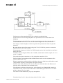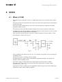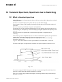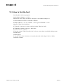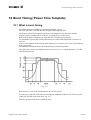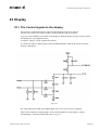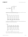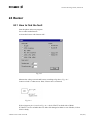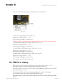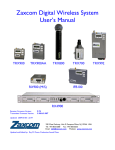
1
Trouble Shooting Guide, Advanced
Trouble Shooting Guide R250s, Advanced
by Toko ([email protected])
4/00021-3/FEA 209 544/18 B
Approved according to 1776-3/FEA 209 544
Trouble Shooting Guide, Advanced
Contents
1
Explanations ........................................................................................................................3
2
Enter Test Program ............................................................................................................8
3
Static TX ............................................................................................................................13
4
Calibration IQ ...................................................................................................................19
5
Tx VCO..............................................................................................................................21
6
VCXO.................................................................................................................................27
7
Calibration RSSI...............................................................................................................31
8
Calibration of Power Level ..............................................................................................37
9
Calibration Intermediate Power......................................................................................42
10
Transient Spectrum, Spectrum due to switching...........................................................43
11
Modulation Spectrum Switched Mode............................................................................48
12
Write to EE-prom .............................................................................................................55
13
ADC-calibration (Voltage-calibration) ...........................................................................56
14
Current Calibration..........................................................................................................59
15
No Serv, or not able to connect a call ..............................................................................63
16
Phase And Frequency Error ............................................................................................72
17
Output Power ....................................................................................................................74
18
Burst Timing (Power Time Template)............................................................................78
19
Sensitivity (RX-quality) ....................................................................................................80
20
RX Level ............................................................................................................................85
21
Audio..................................................................................................................................87
22
Keyboard ...........................................................................................................................96
23
Display..............................................................................................................................100
24
Buzzer ..............................................................................................................................105
25
Vibrator ...........................................................................................................................107
26
Illumination .....................................................................................................................109
27
Top Indicator...................................................................................................................111
28
SIM-Fault (Insert card)..................................................................................................113
29
Self-Test ...........................................................................................................................116
30
ADC-Values.....................................................................................................................118
31
Revision History..............................................................................................................121
4/00021-3/FEA 209 544/18 B
2(121)
Trouble Shooting Guide, Advanced
1 Explanations
1.1
Conditions
All measurements described in this Trouble Shooting Guide are performed in EFRA with test
program in the phone.
Some of the faults can occur in tests without test program, e.g. Go/No Go -tests.
In these cases you have to program the phone with test program before starting to trouble shoot
using this guide.
For trouble shooting with signal program see doc. 4/00021-2/FEA 209 544/18.
In case of liquid damage no further action should be taken, handle the unit according to the local
company directives.
The classification of the components and a possible demand of current-, BData-, ADC- and
radio-calibration when changing a component are mentioned in separate documents.
There are four different calibrations: current-, BData-, ADC- and radio-calibrations
Current-, BData- and ADC-calibration are performed in the trouble shooting part of EFRA,
while radio- calibration can be found under the icon “Calibrate”.
Some replaces of component demands all four calibrations, other only need one or two of the
calibrations.
For component placing see doc. 1078-2/FEA 209 544/18
Precautions:
DC voltage measurements must be done with a probe with at least 100 Kohm and 30 pF
impedance to ground.
For best possible accuracy, use the 20 dB probe attenuator when testing 900/1800 MHz signals.
Accuracy for input test signals:
Voltage ± 1%
Current ± 5%
Frequency ± 5%
4/00021-3/FEA 209 544/18 B
3(121)
Trouble Shooting Guide, Advanced
1.2
Abbreviations
B:
C:
R:
L:
F:
D:
H:
J:
N:
U:
V:
X:
Z:
Crystal
Capacitor
Resistor
Coil
Over-voltage protection
Digital circuit
Buzzer, LED, pads for display
Connector
Analogue circuit
Balun
Transistor, diode
Antenna connector, connector-surface on the board
Filter
EFRA:
Trouble shooting and radio calibration software.
AGND:
Ground for analogue signal.
DCIO:
DC-voltage through the system connector for charging.
GND:
Digital ground.
VRPAD:
For the radio-part of the processor and top indicator/ buzzer. 3,8 ± 0.05 VDC.
VBATT:
Battery voltage. 4.8 ± 0.05 VDC.
VDIG:
DC voltage for the processor and memory. 3,2 ± 0.05 VDC.
VDSP:
DC voltage for the DSP (Digital Signal Processor). 3,2 ± 0.05 VDC.
VDD:
VDIG from the phone voltage through the system connector. 3,2 ± 0.05 VDC.
VLCD:
DC voltage for the display that controls the contrast. -2,7 VDC.
VRAD:
DC voltage for the radio part except the synthesiser. 3,8 ± 0.20 VDC.
VVCO:
DC voltage for the synthesiser. 3,8 ± 0.10 VDC.
LED:
Light emitting diode e.g. the background illumination.
ONSRQ:
Voltage from the On/ Off key that starts the phone.
EXTAUD:
Input signal at the system connector that the processor use to determinate if
there is any external audio equipment attached.
EXTAUD1:
The same signal as the EXTAUD but at the processor side.
LO:
Local oscillator.
RTC:
Real Time Clock, the internal clock the clock that keeps track of time.
I2C:
Communications standard for two-way communication using only 2 wires,
clock and data.
SIMCONCLK: Signal from the processor used for communication to SIM, clock signal.
SIMCONDAT: Signal from the processor used for communication to SIM, data signal.
4/00021-3/FEA 209 544/18 B
4(121)
Trouble Shooting Guide, Advanced
SIMCONRST: Signal from the processor used for communication to SIM, reset signal.
VPPFLASH:
Programming voltage for the FLASH memory. 12,0 ± 0.50 VDC.
SIMVCC:
Feed voltage for SIM. 5,0 ± 0.20 VDC.
TTMS:
Serial communication to phone through the system connector.
TFMS:
Serial communication from phone through the system connector.
4/00021-3/FEA 209 544/18 B
5(121)
Trouble Shooting Guide, Advanced
1.3
Pin placing
4/00021-3/FEA 209 544/18 B
6(121)
Trouble Shooting Guide, Advanced
4/00021-3/FEA 209 544/18 B
7(121)
Trouble Shooting Guide, Advanced
2
Enter Test Program
2.1
Introduction
To be able to use EFRA the phone has to be programmed with test program.
The programming is also performed in EFRA.
If the phone does not start in the radio calibration or trouble shooting part of EFRA, despite an
approved flash programming, go to section 2.2
If the phone can not be programmed, go to section 2.3.
2.2
The phone does not start in the test program
Attach a dummy battery and press the On/Off button.
Check the display and the current consumption.
If the phone starts, showing the revision of the test program in the display,
and consumes 30 – 50 mA, the phone usually is without fault.
Check your equipment.
Following things are necessary for the phone to start in the test program:
Correct battery voltage + 4.8 VDC.
The current limit must be set high enough on the output of the power supply (2A).
The phone must be started before clicking on the ”Start-up” in EFRA.
The following signal must be found at the system connector of the phone, TTMS, TFMS,
VPPFLASH, GND and VDD.
Hardlock connected and installed.
If the fault really is electrical, open the phone and make a visual check of the board.
Make sure there is not any liquid damage, burned or damaged pads at the system connector or
bad soldering of D600 or D610.
No further action should be taken for a liquid damaged telephone.
Give the board power and start it using the On/Off button.
Check the amplitude of MCLK at C680 using the spectrum analyser >3 dBm.
We propose the following settings: CF – 13MHz, SPAN – 1 MHz, RBW – 10 kHz, VBW – 10
kHz and SWEEP – 30 ms.
If MCLK is too low, the fault usually is due to L540, B510 or a short circuit in C542.
If the fault still remains, try to program the phone again.
If the phone consumes more then 200 mA, go to section 2.4.3.
If the phone consumes no current at all when the button is pressed, there probably is a liquid
damage.
Open the phone and check for liquid damage.
No further action should be taken for a liquid damaged telephone.
4/00021-3/FEA 209 544/18 B
8(121)
Trouble Shooting Guide, Advanced
Also make sure the keyboard, dome-foil and the keyboard pads are correct and clean.
If needed replace them according to the mechanical repair guide
If there is signal program in the phone, you have to program it with test program.
2.3
The phone can not be programmed
Make sure:
1. That the battery screws and the battery insulator are okay and tighten.
2. That the system connector is not dirty, mechanical or liquid damaged.
No further action should be taken for a liquid damaged telephone.
Attach a dummy battery.
If the phone consumes current immediately, the fault usually depends on a short circuit of
VBATT
Start the phone with the On/Off button and check the current consumption.
If the phone consumes no current at all when the button is pressed, there might be a liquid
damage. Open the phone and check for liquid damage.
Make sure that the battery insulator is correctly fitting.
Also make sure the keyboard and the keyboard pads are correct and clean.
If the phone consumes more then 200 mA, go to section 2.4.3.
If the phone does not start, try to program it as a card.
If the phone does not start in the flash programmer, go to section 2.4.1.
If the phone can be programmed, but does not start afterwards or is troublesome in the flash
programmer, go to section 2.4.2.
If the phone starts after programming, the fault probably is okay, but to eliminate the possibility
of intermittent faults make sure the soldering at D600, D610 or D630 is correct.
2.4
Measuring at a powered circuit board
2.4.1 The phone does not start in the flash programmer
Make sure the pads of the system connector are not burned.
Attach the board to the fixture.
Keep the board powered up using DCIO high.
Measure the voltage VDIG and VDSP (+3.2 VDC).
If any of the voltage are too low, measure the resistance to ground, VDIG >500ohms, VDSP
>25kohms.
If the resistance is correct, replace the corresponding circuit, VDIG - N702, VDSP - N701.
If the resistance is too low, use the schematics.
Remove one component (or lift the pin/pins feeding the circuit) at the time that is fed from the
short circuit voltage and measure the resistance after removing it. Do not forget to mount all the
components that have been removed.
4/00021-3/FEA 209 544/18 B
9(121)
Trouble Shooting Guide, Advanced
You have found the faulty component when the resistance is raising after removing.
You also should replace the circuits on which you lifted the pins.
The short circuit is usually due to D610, D600 or anyone of C600, C602-C610 for VDIG and
D900 or anyone of C900, C902-C906 for VDSP.
If any of the voltage is too high, replace the corresponding circuit.
Measure the power reset at C710 +3 VDC.
If it is lower, lift up N703 pin 1 and try again.
If the voltage is raising, the fault is due to N703.
If the voltage still is too low, the fault usually is due to C710, C718 or R704.
Measure the voltage VRAD, VVCO and VRPAD (+3.8 VDC).
If any of the voltage are incorrect, measure the resistance between ground and the faulty
regulator >10 Kohms.
If the resistance is correct, replace the corresponding regulator.
If the resistance is incorrect, use the schematics.
Remove one component (or lift the pin/pins feeding the circuit) at the time that is fed from the
short circuit voltage and measure the resistance after removing it.
You have found the faulty component when the resistance is raising after removing.
Do not forget to mount all the components that have been removed.
You also should replace the circuits on which you lifted the pins.
The most common fault is a short circuit at VRAD.
The short circuit is usually due to any of the 10nF-capacitors of the feed voltage or N450.
Check the amplitude of the MCLK, using the oscilloscope, at B510: 3 >0.7 V p-p.
You can also use the spectrum analyser to check the amplitude >1 dBm.
We propose the following settings for the oscilloscope: CF – 13MHz, SPAN – 1 MHz, RBW –
10 kHz, VBW – 10 kHz and SWEEP – 30 ms.
A fault of the clock can be due to L540, B510 or a short circuit in C542, D600, N301 or C301.
Sometimes is the fault due to N500.
Make sure the soldering at D600, D610 or D630 is correct. If they are correct and all of the feed
voltage and the clock are correct, the fault usually is due to D600.
The fault can also be due to D610 or D630.
Try to program the phone between each replace.
2.5
The phone can be programmed, but does not start
afterwards or is troublesome in the flash programmer
Open the phone and check for liquid damage.
No further action should be taken for a liquid damaged telephone.
Make sure the pads of the system connector are not burned.
Attach the board to the fixture.
Keep the board powered up using DCIO high.
Measure the voltage VDIG and VDSP (+3.2 VDC).
If any of the voltage are too low, measure the resistance to ground,
VDIG >500 ohms, VDSP >25 Kohms.
4/00021-3/FEA 209 544/18 B
10(121)
Trouble Shooting Guide, Advanced
If the resistance is correct, replace the corresponding circuit, VDIG - N702, VDSP - N701.
If the resistance is too low, use the schematics.
Remove one component (or lift the pin/pins feeding the circuit) at the time that is fed from the
short circuit voltage and measure the resistance after removing it.
You have found the faulty component when the resistance is raising after removing.
Do not forget to mount all the components that have been removed.
You also should replace the circuits on which you lifted the pins.
The short circuit is usually due to D610, D600 or anyone of C600, C602-C610 for VDIG and
D900 or anyone of C900, C902-C906 for VDSP.
If any of the voltage is too high, replace the corresponding circuit.
Measurer the voltage VRAD, VVCO and VRPAD (+3.8 VDC).
If any of the voltage are incorrect, measure the resistance between ground and the faulty
regulator >10 Kohms.
If the resistance is correct, replace the corresponding regulator.
If the resistance is incorrect, use the schematics.
Remove one component (or lift the pin/pins feeding the circuit) at the time that is fed from the
short circuit voltage and measure the resistance after removing it.
You have found the faulty component when the resistance is raising after removing.
Do not forget to mount all the components that have been removed.
You also should replace the circuits on which you lifted the pins.
The most common fault is a short circuit at VRAD.
The short circuit is usually due to any of the 10nF-capacitors of the feed voltage or N450.
Check the amplitude of the MCLK, using the oscilloscope, at B510: 3 >0.7 V p-p.
You can also use the spectrum analyser to check the amplitude >1 dBm.
We propose the following settings for the oscilloscope: CF – 13MHz, SPAN – 1 MHz, RBW –
10 kHz, VBW – 10 kHz and SWEEP – 30 ms.
A fault of the clock can be due to L540, B510 or a short circuit in C542, D600, N301 or C301.
Sometimes is the fault due to N500.
Make sure the soldering at D600, D610 or D630 is correct.
If they are correct and all of the feed voltage and the clock are correct, the fault usually is due to
D600.
The fault can also be due to D610 or D630.
Try to program the phone between each replace.
Note! D630 can not be replace, since it demands advanced equipment and extensive calibrations
at board level that can not be done at this repair level.
2.5.1 The phone consumes more then 200 mA
Open the phone and check for liquid damage.
No further action should be taken for a liquid damaged telephone.
Make sure the pads of the system connector are not burned.
Attach the board to the fixture. Keep the board powered up using DCIO high.
Measure the voltage VDIG and VDSP (+3.2 VDC).
4/00021-3/FEA 209 544/18 B
11(121)
Trouble Shooting Guide, Advanced
If any of the voltage are too low, measure the resistance to ground, VDIG >500 ohms, VDSP
>25 Kohms.
If the resistance is correct, replace the corresponding circuit, VDIG - N702, VDSP - N701.
If the resistance is too low, use the schematics.
Remove one component (or lift the pin/pins feeding the circuit) at the time that is fed from the
short circuit voltage and measure the resistance after removing it.
You have found the faulty component when the resistance is raising after removing.
Do not forget to mount all the components that have been removed.
You also should replace the circuits on which you lifted the pins.
The short circuit is usually due to D610, D600 or anyone of C600, C602-C610 for VDIG and
D900 or anyone of C900, C902-C906 for VDSP.
If any of the voltage is too high, replace the corresponding circuit.
Measurer the voltage VRAD, VVCO and VRPAD (+3.8 VDC).
If any of the voltage are incorrect, measure the resistance between ground and the faulty
regulator >10 Kohms.
If the resistance is correct, replace the corresponding regulator.
If the resistance is incorrect, use the schematics.
Remove one component (or lift the pin/pins feeding the circuit) at the time that is fed from the
short circuit voltage and measure the resistance after removing it.
You have found the faulty component when the resistance is raising after removing.
Do not forget to mount all the components that have been removed.
You also should replace the circuits on which you lifted the pins.
The most common fault is a short circuit at VRAD.
The short circuit is usually due to any of the 10nF-capacitors of the feed voltage or N450.
Check the amplitude of the MCLK, using the oscilloscope, at B510: 3 >0.7 V p-p.
You can also use the spectrum analyser to check the amplitude >1 dBm.
We propose the following settings for the oscilloscope:
CF – 13MHz, SPAN – 1 MHz, RBW – 10 kHz, VBW – 10 kHz and SWEEP – 30 ms.
A fault of the clock can be due to L540, B510 or a short circuit in C542, D600, N301 or C301.
Sometimes is the fault due to N500.
Make sure the soldering at D600, D610 or D630 is correct.
If they are correct and all of the feed voltage and the clock are correct, the fault usually is due to
D600. The fault can also be due to D610 or D630.
Try to program the phone between each replace.
4/00021-3/FEA 209 544/18 B
12(121)
Trouble Shooting Guide, Advanced
3 Static TX
3.1
Finding out if there is an amplitude or frequency fault
Open the phone and check for liquid damage.
No further action should be taken for a liquid damaged telephone.
Make sure the antenna connection X101 is not mechanically damaged, badly soldered or dirty
(varnish, glue, oxide...).
Give the board power, start the test program and connect the negative -4 VDC to P401.
Note! It is important that the negative -4 VDC not is connected until after the test program has
been started, the power amplifier might otherwise be damaged.
Measure the current consumption.
If the phone consume about 2 A, remember the current limit, is there most likely a short circuit
in the power amplifier, N401.
Confirm by measuring the resistance between N401 pin 14 and ground,
it should be larger than 5 Kohms but usually is around 200 ohms when N401 is faulty.
For GSM 900:
Start the transmitter in static mode on channel 62 and check the output power and frequency.
We propose following settings on the spectrum analyser while measuring CF- 902.4 MHz,
SPAN- 200 MHz, RBW- 10 kHz, VBW- 10 kHz and Sweep- 30 ms.
Check the frequency of the transmitter 902.4 MHz. If the frequency is misplaced, try to lower
the “Adjust sweep current” until the frequency of the transmitter has locked on.
If the transmitter does not have any output power at all or if it is very low, go to section 3.2.
If the transmitter does not lock on, go to section 3.3.
If the transmitter locks on, start it in switched mode on channel 62 with DAC 7 value at “FF”.
Make sure the output power is 30 - 35 dBm, by using the spectrum analyser.
We propose following settings on the spectrum analyser while measuring:
CF- 902.4 HMS, SPAN- 0 MHz, RBW- 300 kHz, VBW- 100 kHz and Sweep- 0.8 ms.
If there is no switched output power at all or if it is too low, go to chapter “No serv”.
If the output power is correct then the transmitter is without fault.
Test the phone again.
For GSM 1800:
Start the transmitter in static mode on channel 699 and check the output power and frequency.
We propose following settings on the spectrum analyser while measuring:
CF- 1747.6 MHz, SPAN- 200 MHz, RBW- 10 kHz, VBW- 10 kHz and Sweep- 30 ms.
Check the frequency of the transmitter 1747.6 MHz. If the frequency is misplaced, try to lower
the “Adjust sweep current” until the frequency of the transmitter has locked on.
If the transmitter does not have any output power at all or if it is very low, go to section 3.2.
If the transmitter does not lock on, go to section 3.3.
4/00021-3/FEA 209 544/18 B
13(121)
Trouble Shooting Guide, Advanced
If the transmitter locks on, start it in switched mode on channel 669 with DAC 7 value on ”FF”.
Make sure the output power is 28 - 32 dBm by using the spectrum analyser.
We propose the following settings on the spectrum analyser while measuring:
CF- 1747.6 MHz, SPAN- 0 MHz, RBW- 300 kHz, VBW- 100 kHz and Sweep- 0.8 ms.
If there is no switched output power at all or if it is too low, go to chapter “No serv”.
If the output power is correct then the transmitter is without fault.
Try to test the phone again.
3.2
Low or no output power
For GSM 900:
Give the board power, start the test program and connect the negative -4V again.
Start the transmitter in static mode on channel 62.
Measure the voltage on N450 pin 4,VREG +1.4 VDC.
If VREG is too low, measure the signal POWLEV +0.9 VDC at N450 pin 11.
If the voltage POWLEV is too low, check the soldering at N800 pin 61.
If the soldering is correct, the fault is usually due to N800.
The fault can also be due to D600 or a short circuit in C833 or C853.
If POWLEV is correct the fault is due to a break in R413. It can be verified by measuring the
resistance between pin 17 and 18 at N450 0.1 ohm, or a short circuit of the control voltage
VREG caused by N401.
If VREG is too high, measure the signal TXLOOP_GSM at N201 pin 8, 9 ~ -14 dBm.
If TXLOOP_GSM has got the right amplitude, check if there is a HF-signal on N401 pin 5 ~-10
dBm.
If the signal is missing it can depend on R405, R406, R407 or C440.
If the signal has got the right amplitude, the fault depends on N401.
If the amplitude on TXLOOP_GSM is too low, measure the HF- signal on N570 pin 1 ~ -12
dBm.
If the signal on N570 has the right amplitude, the fault probably depends on U202.
If the signal on N570 is missing, measure the feed voltage on N570 pin 6 +3.9 VDC.
If he feed voltage is correct, the fault probably depends on N570.
If the feed voltage is incorrect, the fault usually depends on L560, C560 short circuit, V570,
V571 or some of the following voltage are missing, SWDC the same voltage as VBATT,
VVCO +3.8V or TXON_GSM +3.7 VDC.
If TXON_GSM is missing, check D600, D102 and D105.
If VREG is correct, measure the signal TXLOOP_GSM at N201 pin 8, 9 ~ -14 dBm.
If TXLOOP_GSM has got the right amplitude, follow the HF-signal from N401 pin 18,19,24 or
25 ~-8 dBm to Z205 pin 5 ~-17dBm through V412, Z203, V207 and C255.
If the signal at N401pin 18,19,24 and 25 is too low, the fault probably depends on N401.
If the signal is too low at Z205 pin 5, is it either attenuated too much somewhere along the path
or there is a fault in the antenna switch, V208 and V209 with the associated components.
If the amplitude on TXLOOP_GSM is too low, the fault can depend on U202, C204 or C205.
4/00021-3/FEA 209 544/18 B
14(121)
Trouble Shooting Guide, Advanced
For GSM 1800:
Give the board power, start the test program and connect the negative -4 VDC again.
Start the transmitter in static mode on channel 699.
Measure the voltage at N450 pin 4 VREG +1.7 VDC.
If VREG is too low, measure the signal POWLEV +0.9 VDC at N450 pin 11.
If the voltage POWLEV is too low, check the soldering at N800 pin 61.
If the soldering is correct, the fault is usually due to N800.
The fault can also be due to D600 or a short circuit in C833 or C853.
If POWLEV is correct the fault is due to a break in R413. It can be verified by measuring the
resistance between pin 17 and 18 at N450 0.1 ohm, or a short circuit of the control voltage
VREG caused by N401.
If VREG is too high, measure the signal TXLOOP_DCS at N202 pin1, 2 ~ -12 dBm.
If TXLOOP_DCS has got the right amplitude, check if there is a HF-signal at N401 pin 10 ~-6
dBm.
If the signal is missing it can depend on R408 or C441.
If the signal has got the right amplitude, the fault depends on N401.
If the amplitude on TXLOOP_DCS is too low, measure the HF- signal at N560 pin 1 ~-12 dBm.
If the signal on N560 has got the right amplitude, the fault probably depends on U204.
If the signal on N560 is missing, measure the feed voltage at N560 pin 6 +3.9 VDC.
If the feed voltage is correct, the fault probably depends on N560.
If the feed voltage is incorrect, the fault usually depends on L560, C560 short circuit, V560,
V561 or some of the following voltage are missing, SWDC the same voltage as VBATT,
VVCO +3.8 VDC or TXON_DCS +3.7 VDC. If TXON_DCS is missing, check D600, D102 and
D105.
If VREG is correct, measure the signal TXLOOP_DCS at N202 pin1, 2 ~ -12 dBm.
If TXLOOP_DCS has got the right amplitude, follow the HF-signal from N401pin18, 19,24 or
25 ~-5 dBm to Z205pin 5 ~-10dBm through V411, V205 and Z204.
If the signal on N401: 18,19,24 and 25 is too low, the fault probably depends on N401.
If the signal is too low at Z205pin 5, is it either attenuated too much somewhere along the path
or there is a fault in the antenna switch, V201 and V206 with the associated components.
If the amplitude on TXLOOP_DCS is too low, the fault can depend on U204, C224 or C225.
3.3
The transmitter does not lock
Give the board power and start the test program.
For GSM 900:
Start the transmitter in static mode on channel 62 and check the transmitters output power and
frequency.
We propose the following settings on the spectrum analyser while measuring:
CF- 902.4 MHz, SPAN- 200 MHz, RBW- 10 kHz, VBW- 10 kHz and Sweep- 30 ms.
Check the frequency of the transmitter 902.4 MHz.
4/00021-3/FEA 209 544/18 B
15(121)
Trouble Shooting Guide, Advanced
If the frequency is misplaced, try to lower the “Adjust sweep current” until the frequency of the
transmitter has locked on.
If the transmitter locks on, start it in switched mode on channel 62 with DAC 7 value on ”FF”.
Check if there is an output power 30 - 35 dBm at the antenna plate using the spectrum analyser.
We propose following settings on the spectrum analyser while measuring:
CF- 902.4 MHz, SPAN- 0 MHz, RBW- 300 kHz, VBW- 100 kHz and Sweep- 0.8 ms.
If the output power is correct then the transmitter is without fault.
Try to test the phone again.
If there is no switched output power at all or if it is too low, go to chapter “No serv”.
If the transmitter does not lock on, change the CF on the spectrum analyser to 772,4 MHz.
Check the frequency and the amplitude on the LO-signals LOINA and LOINB at N201pin 18,
17 ~ -10 dBm.
If the amplitude and the frequency are correct, go to section 3.1.
If the frequency is correct, but the amplitude is too low, check the feed voltage at N303 pin 6
+3.7 VDC.
If the voltage is correct, replace N303.
If the voltage is incorrect, check VVCO +3.8 V DC, SYNTON_GSM +3.7 VDC and V305 with the
associated components.
If SYNTON_GSM is missing, check D103, D105 and D600.
If the amplitude is correct, but the frequency is incorrect, the fault usually depends on N301. It
can also depend on N303 or D600.
If the signal is several MHz wide, replace C318.
To measure the frequency more precisely you can lower SPAN to 1 MHz.
For GSM 1800:
Start the transmitter in static mode on channel 699 and check the transmitters output power and
frequency.
We propose the following settings on the spectrum analyser while measuring:
CF- 1747.6 MHz, SPAN- 200 MHz, RBW- 10 kHz, VBW- 10 kHz and Sweep- 30 ms.
Check the frequency of the transmitter 1747.6 MHz.
If the frequency is misplaced, try to lower the “Adjust sweep current” until the frequency of the
transmitter has locked on.
If the transmitter locks on, start it in switched mode on channel 699 with DAC 7 value on “FF”.
Check if there is an output power 28 - 32 dBm at the antenna connector on the board, using the
spectrum analyser.
We propose the following settings on the spectrum analyser while measuring:
CF- 1747.6 MHz, SPAN- 0 MHz, RBW- 300 kHz, VBW- 100 kHz and Sweep- 0.8 ms.
If the output power is correct then the transmitter is without fault.
Try to test the phone again.
If there is no switched output power at all or if it is too low, go to chapter “No serv”.
If the transmitter does not lock on, change the CF on the spectrum analyser to 1669.6 MHz.
Check the frequency and the amplitude on the LO-signals LOINA and LOINB at N202 pin13,
14 ~ -10 dBm.
4/00021-3/FEA 209 544/18 B
16(121)
Trouble Shooting Guide, Advanced
If the amplitude and the frequency are correct, go to section 3.3.1.
If the frequency is correct, but the amplitude is too low, check the feed voltage at N302 pin 6
+3.7 VDC.
If the voltage is correct, replace N302.
If the voltage is incorrect, check VVCO +3.8 V DC, SYNTON_DCS +3.7 VDC and V301 with the
associated components.
If SYNTON_DCS is missing, check D103, D105 and D600.
If the amplitude is correct, but the frequency is incorrect, the fault usually depends on N301.
It can also depend on N303 or D600.
If the signal is several MHz wide, replace C318.
To measure the frequency more precisely you can lower SPAN to 1 MHz.
3.3.1 TX - synth fault
Perform a TxVCO calibration, a part of the radio calibration in EFRA.
If the phone passes the TxVCO calibration and the other radio calibrations, the fault has been
corrected.
A new calibration is needed to compensate the changes (due to ageing) of the characteristic in
some of the components in the TX-synth.
If the phone passes the TxVCO calibration but fails in at least one of the other radio
calibrations, go to the corresponding chapter.
If it does not pass the TxVCO calibration, it usually is due to too large moderation in the
feedback of the TX-synth, either in TXLOOP or in TXIF.
Give the board power and start the test program.
For GSM 900:
Start the transmitter in static mode on channel 62.
We propose the following settings on the spectrum analyser while measuring:
CF- 902.4 MHz, SPAN- 200 MHz, RBW- 10kHz, VBW- 10 kHz and Sweep- 30ms.
Measure the amplitude and the frequency on the signals TXLOOP_GSM at N201 pin 8, 9
-4 dBm, the frequency should be 902.4 MHz when the synth is locked on.
If the TXLOOP-signal is too low, the fault can be due to too large moderation in U202, C204 or
C205.
The fault can also be due to N570 ~12 dBm or its feed voltages.
If the level of the TXLOOP-signal is correct, check the amplitude on the signals LOINA and
LOINB at N201 pin 17, 18 ~ -10 dBm.
If the amplitudes on LOINA and LOINB are too low, the fault usually depends on U201 or the
components that belongs to it.
If the amplitudes on TXLOOP, LOINA and LOINB are correct, calculate the frequency on
TXIF_GSM by subtracting LOIN from TXIN.
On an approved phone it should be as follow:
TXIN 902.4 MHz - LOIN 772,4 MHz = TXIF_GSM 130 MHz.
4/00021-3/FEA 209 544/18 B
17(121)
Trouble Shooting Guide, Advanced
Change CF on the spectrum analyser to the calculated, by using the formula above.
Frequency for TXIF_GSM, the frequency of the transmitter usually ends up on ~890 MHz when
the synth does not lock on, that gives a frequency for TXIF_GSM at ~117 MHz and SPAN to 10
MHz.
Measure the amplitude for TXIF_GSM at N201 pin 13, 14 ~ -2 dBm.
If the amplitude is too low, it usually is due to N201.
If the amplitude is correct, follow the signal from N201 pin 13, 14 to N500 pin 10,11 through
R211, R212, C508, C509, C506 and C507.
If TXIF has got the right amplitude on N500, the fault can be due to N500, N570, N800, D600
or the components on the output N500 pin 12.
All values are approximate, measure the exact values for your equipment with an
approved phone.
For GSM 1800:
Start the transmitter in static mode on channel 699.
We propose the following settings on the spectrum analyser while measuring:
CF- 1747.6 MHz, SPAN- 200 MHz, RBW- 10kHz, VBW- 10 kHz and Sweep- 30ms.
Measure the amplitude and the frequency on the signals TXLOOP_DCS on N202 pin 1, 2 -11
dBm, the frequency should be 1747.6 MHz when the synth is locked on.
If the TXLOOP-signal is too low, the fault can be due to too large moderation in U204, C224 or
C225. The fault can also be due to N560 ~12 dBm, or its feed voltages.
If the level of the TXLOOP-signal is correct, check the amplitude on the signals LOINA and
LOINB on N202 pin 13, 14 ~ -10 dBm.
If the amplitudes on LOINA and LOINB are too low, the fault usually depends on U203 or the
components that belongs to it.
If the amplitudes on TXLOOP, LOINA and LOINB are correct, calculate the frequency on
TXIF_DCS by subtracting LOIN from TXIN.
On an approved phone it should be as follow:
TXIN 1747.6 MHz - LOIN 1669.6 MHz =TXIF_DCS 78 MHz
Change CF on the spectrum analyser to the calculated, by using the formula above.
Change Frequency for TXIF_DCS and SPAN to 10 MHz.
Measure the amplitude for TXIF_DCS on N202 pin 19, 20 ~ -20 dBm.
If the amplitude is too low, it is usually due to N202.
If the amplitude is correct, follow the signal from N202 pin 19, 20 to N500 pin 10,11 through
R576, R577, C506 and C507.
If TXIF has got the right amplitude on N500, the fault can be due to N500, N570, N800, D600
or the components on the output N500 pin 12.
All values are approximate, measure the exact values for your equipment with an
approved phone.
4/00021-3/FEA 209 544/18 B
18(121)
Trouble Shooting Guide, Advanced
4 Calibration IQ
4.1
What is calibration IQ
An IQ-filter consists of two parts.
The first part is a passive lowpass-filter between the waveform generator in D600 and N500
consisting of R642-R645, C105, C106, C114 and C115.
The second part is a software- controlled filter in N500.
The IQ-filter, the part in N500, is calibrated with a certain test signal from the waveform generator in D600. The transmitter is powered up in static mode with the test modulation.
Then measure the peak that exists at CF+ 201kHz related to the highest peak CF+67 kHz or CF67 kHz.
If for example CF-67kHz is the highest peak, measure the amplitude at 3IM from it.
The filter in N500 is calibrated so that the amplitude at 3IM is -26 dBm lower then “0”.
Fig4.1.
(“0” means the carrier wave modulated with a constant stream of zeros, which gives a
frequency change of -67 kHz)
Fig.4 1
4.2
How to find the fault
Open the phone and check for liquid damages.
No further action should be taken for a liquid damaged telephone.
Attach the board in the fixture and start the test program.
Switch the spectrum analyser to SPAN: 1 MHz, RBW: 10 kHz, VBW: 10 kHz, SWEEP: 30 ms.
Start the transmitter in static mode with modulation on channel 699 on the DCS 1800-band
Fig.4. 2.
4/00021-3/FEA 209 544/18 B
19(121)
Trouble Shooting Guide, Advanced
If the transmitter does not lock on, lower the sweep current.
Fig.4.2
Make sure the spectrum looks like Fig.4. 1.
If the spectrum does not look like the figure is it either one of the modulation signals MODQN,
MODQP, MODIN, MODIP that is missing from D600 or the lowpass-filter to the modulation
signals is faulty, R642 - R645, C105, C106, C114, C115.
Measure on the capacitors with an oscilloscope.
The signals are sinus shaped with the frequency 67.7 kHz and the amplitude ~2.5 V p-p.
Compare the signals with each other.
The fault is on the modulation signal that separates from the other.
If the modulation signals looks good and are in the right phase, 90 degrades turned compared to
each other, then the fault could be caused by N500.
4/00021-3/FEA 209 544/18 B
20(121)
Trouble Shooting Guide, Advanced
5 Tx VCO
5.1
What is TxVCO – Calibration
In the GSM900-system a phone can communicate with the base station at 124 frequencies in
each direction, 890.2 - 914.8 MHz for the transmitter and 935.2 - 959.8 MHz for the receiver.
In the GSM1800-system is it possible to communicate at 374 frequencies in each direction,
1710.2 – 1784.8 MHz for the transmitter and 1805.2 – 1879.8 MHz for the receiver.
The communication between the base station and the phone are done switched.
The system makes it possible to change frequency between each burst.
For every new burst the transmitter synth of the phone has to lock on again at the frequency that
the base station expect, before activating the transmitter.
Two simplified schedules over the lock-on of the TX-synth are shown below.
The frequencies are for channel 62 GSM900 Fig5.1.
And for channel 699 GSM1800 Fig.5.2.
Fig5.1
4/00021-3/FEA 209 544/18 B
21(121)
Trouble Shooting Guide, Advanced
Fig.5.2
The frequency of the transmitter has to lock on during a predestined time.
For the lock-on to be fast enough the phone uses pre-learned TxVCO-values taken from
EEPROM.
The lock-on begins with the TxVCO- AC, that is transforming a for this particular channel
saved EEPROM-value to a start value for the control voltage of the VCO, N570/N560.
The voltage is a little bit higher, 22 DAC-steps, than the expected value when the synth has
locked on.
By using the start value of the control voltage the VCO, N570/N560, generates a transmitter
frequency that is only a little too high.
The transmitter frequency is fed back, as TXIF, through a mixer, N201 and N202, to the Phase
detector in N500.
The Phase detector compares TXIF, 130 or 78 MHz, with an intern reference signal, 9*13 =117
or 6*13 =78 MHz
The result of the phase comparison is a DC voltage that controls the VCO.
The TxVCO-DAC is disconnected and the Phase detector takes over the adjustment of the
control voltage to the VCO.
When the transmitter synth has locked on, the Phase detector in N500 have stabilised the control
voltage and the frequency and the phone can begin to transmit.
The start value of the synth, the TxVCO value, has to be calibrated due to the differences of
tolerance in the components of the transmitter synth.
The calibration is performed in static mode, at two channels, for GSM900 high, channel 94/
908,8 MHz and low, channel 30/896 MHz and for GSM1800 high, channel 826/1773.0 MHz
and low, channel 570/1721.8 MHz.
The values for other channels do you get by interpolation.
The tables below Table.5.1.shows the limits for the TxVCO – values.
4/00021-3/FEA 209 544/18 B
22(121)
Trouble Shooting Guide, Advanced
TxVCO
Ch 94
CH 30
Oxfam
Ch 570
CH 826
Min.
85
133
5D
93
Max.
BB
187
78
120
Min.
55
85
AA
170
Hex
Dec.
Hex
Dec.
Max.
87
135
D2
210
Hex
Dec.
Hex
Dec.
Table.5.1
5.2
How to find the fault
The TxVCO calibration is the sixth step in the Radio calibration.
If the first fault showing up is ”GSM Static TX Check Amplitude”, go to chapter ”Static TXfault.
If the first fault showing up is ”Calibration off IQ Filter LPBW”, go to chapter ”Calibration IQ”fault.
This chapter only deals with faults where ”GSM Calibration TXVCO ch 94 or 30 GSM900 and
ch 570 or 826 GSM1800” is the first fault showing up at the Radio calibration.
Open the phone and check for liquid damages.
No further action should be taken for a liquid damaged telephone.
Measure the resistance of N401 pin 14 against ground >10 Kohms.
If the resistance is much lower, usually around ~200 ohms, the power amplifier N401 is faulty.
Give the board power and start the board.
Measure the voltage at C853 +1.2 VDC. Replace the capacitor if the voltage is lower.
Start the phone in the test program.
GSM 900:
Start the transmitter in static mode at channel 62 902.4 MHz and check the amplitude and the
frequency.
If the frequency is misplaced, try to lower the ”Adjust sweep current” until the frequency of the
transmitter has locked on.
We propose the following settings on the spectrum analyser while measuring:
CF- 902.4 MHz, SPAN- 200 MHz, RBW- 10 kHz, VBW- 10 kHz and Sweep- 30 ms.
If the transmitter locks on, start the transmitter in switch mode at channel 62 with DAC 7 value
at “FF”.
4/00021-3/FEA 209 544/18 B
23(121)
Trouble Shooting Guide, Advanced
We propose the following settings on the spectrum analyser while measuring:
CF- 902.4 MHz, SPAN- 0 MHz, RBW- 300 kHz, VBW- 100 kHz and Sweep- 0.8 ms.
Check if there is an output power, 30- 35 dBm, at the antenna-plate using the spectrum analyser.
If the output power is correct, the phone is probably without fault.
Try the phone in the test again.
If there is no switched output-power at all or if it is too low, go to chapter ”No serv”.
If the transmitter does not lock on, start the transmitter in static mode again and change the
settings for the spectrum analyser to:
772.4 MHz, SPAN- 200 MHz, RBW- 10 kHz, VBW- 10 kHz and Sweep- 30ms.
Check the frequency and the amplitude of the LO-signal at N303 pin 1 ~ -7dBm.
If the amplitude and the frequency are correct, go to section 5.2.1.
If the frequency is correct, but the amplitude is too low, check the feed voltage at N303 pin 6
+3.6 VDC.
If the voltage is correct, replace N303.
If the voltage is incorrect, check VVCO +3.8 V DC, SYNTON_GSM +3.8 VDC, and V305 with
the belonging components.
If the amplitude is correct, but the frequency is incorrect, the fault usually is due to N301.
It can also be due to N303 or D600.
If the signal is several MHz wide, replace C318.
To make a more accurate frequency measuring, try to lower SPAN to 1 MHz.
GSM 1800:
Start the transmitter in static mode at channel 699 1747.4 MHz, and check the amplitude and the
frequency.
If the frequency is misplaced, try to lower the ”Adjust sweep current” until the frequency of the
transmitter has locked on.
We propose the following settings on the spectrum analyser while measuring:
CF- 1747.4 MHz, SPAN- 200 MHz, RBW- 10 kHz, VBW- 10 kHz and Sweep- 30 ms.
If the transmitter locks on start the transmitter in switch mode at channel, 699, with DAC 7
value at “FF”.
We propose the following settings on the spectrum analyser while measuring:
CF- 1747.4 MHz, SPAN- 0 MHz, RBW- 300 kHz, VBW- 100 kHz and Sweep- 0.8 ms.
Check if there is an output power, 28-32 dBm, at the antenna plate using the spectrum analyser.
If the output power is correct, the phone is probably without fault.
Try the phone in the test again.
If there is no switched output power at all or if it is too low, go to chapter ”No serv”.
If the transmitter does not lock on, start the transmitter in static mode again and change the
settings for the spectrum analyser to:
1669.6 MHz, SPAN- 200 MHz, RBW- 10 kHz, VBW- 10 kHz and Sweep- 30ms.
Check the frequency and the amplitude of the LO-signal at N302 pin 1 ~ -7dBm.
4/00021-3/FEA 209 544/18 B
24(121)
Trouble Shooting Guide, Advanced
If the amplitude and the frequency are correct, go to section 5.2.2.
If the frequency is correct, but the amplitude is too low, check the feed voltage at N302 pin 6
+3.6 VDC.
If the voltage is correct, replace N302.
If the voltage is incorrect, check VVCO +3.8 V DC, SYNTON_DSC +3.8 VDC and V301 with the
belonging components.
If the amplitude is correct, but the frequency is incorrect, the fault usually is due to N301. It can
also be due to N302 or D600.
If the signal is several MHz wide, replace C318.
To make a more accurate frequency when measuring, try to lower SPAN to 1 MHz.
5.2.1 TX–synth fault for GSM900
The fault usually is due to too large attenuation in the feed back of the TX-synth, either at TXIN
or at TXIF.
Give the board power and start the test program.
Start the transmitter in static mode at channel 62.
We propose the following settings on the spectrum analyser while measuring:
CF- 902.4 MHz, SPAN- 200 MHz, RBW- 10 kHz, VBW- 10 kHz and Sweep- 30 ms.
Measure the amplitude and the frequency of the signals TXINA and TXINB at N201 pin 8, 9 ~ 19 dBm, the frequency should be 902.4 MHz when the synth has locked on.
If the TXIN-signal is too low, the fault usually is due to N570, ~7dBm at N570 pin1 or its feed
voltage.
The fault can also depend on too large attenuation in U202, C204 or C205.
If the level of the TXIN-signal is correct, check the amplitude of the signals LOINA and LOINB
at N201 pin 18, 17. 772.4 MHz, ~ -15 dBm.
If the amplitude of LOINA or LOINB is too low, the fault usually depends on U201, C202 or
C203.
If the amplitudes of TXINA/B and LOINA/B are correct, calculate the frequency of TXIF by
subtracting TXIN from LOIN.
On an approved phone should it be as follow:
TXIN 902.4 MHz - LOIN 772.4 MHz = TXIF 130 MHz.
Change CF at the spectrum analyser to the calculated, according to the formula above,
frequency for TXIF and SPAN to 10 MHz.
The frequency of the transmitter usually is 890 MHz when the synth locks off, that gives a
TXIF-frequency of 117 MHz.
Measure the amplitude of TXIFA, TXIFB at N201 pin 13, 14 ~ -7 dBm.
If the amplitude is too low, the fault usually depends on N201.
If the amplitude is correct, follow the signal from N201 pin 13, 14 to N500 pin 10, 11 through
R211, R212, R205, C506, C507, C508 and C509.
If TXIF has got the correct amplitude at N500, the fault can be due to N500, N570, N800, D600
or the components at the output N500 pin 12.
4/00021-3/FEA 209 544/18 B
25(121)
Trouble Shooting Guide, Advanced
5.2.2 TX–synth fault for GSM1800
The fault usually is due to too large attenuation in the feed back of the TX-synth, either at TXIN
or at TXIF.
Give the board power and start the test program.
Start the transmitter in static mode at channel 699.
We propose the following settings on the spectrum analyser while measuring:
CF- 1747.6 MHz, SPAN- 200 MHz, RBW- 10 kHz, VBW- 10 kHz and Sweep- 30 ms.
Measure the amplitude and the frequency of the signals TXINA and TXINB at N202 pin 1,2
~
-18 dBm, the frequency should be 1747.6 MHz when the synth has locked on.
If the TXIN-signal is too low, the fault usually is due to N560, ~4dBm at N560pin1 or its feed
voltage. The fault can also depend on too large attenuation in U204, C224 or C225.
If the level of the TXIN-signal is correct, check the amplitude of the signals LOINA and LOINB
at N202 pin 13, 14. 1669.6 MHz, ~ -16 dBm.
If the amplitude of LOINA or LOINB is too low, the fault usually depends on U203, C217 or
C218.
If the amplitudes of TXINA/B and LOINA/B are correct, calculate the frequency of TXIF by
subtracting TXIN from LOIN.
On an approved phone should it be as follow,
TXIN 1747.6 MHz - LOIN 1669.6 MHz = TXIF ~78 MHz.
Change CF at the spectrum analyser to the calculated, according to the formula above,
frequency for TXIF and SPAN to 10 MHz.
The frequency of the transmitter usually is ~1710 MHz when the synth locks off, that gives a
TXIF-frequency of ~37 MHz.
Measure the amplitude of TXIFA, TXIFB at N202 pin 19,20 ~ -28 dBm.
If the amplitude is too low, the fault usually depends on N202.
If the amplitude is correct, follow the signal from N202 pin 19,20, to N500 pin 10, 11 through
C260, C261, R213, R216, C576, C577, C506 and C507.
If TXIF has got the correct amplitude at N500, the fault can be due to N500, N560, N800, D600
or the components at the output N500 pin 12.
All values are approximates, measure the exact values for your equipment using an
approved phone.
4/00021-3/FEA 209 544/18 B
26(121)
Trouble Shooting Guide, Advanced
6 VCXO
6.1
What is VCXO
The phone has got a reference crystal of 13 MHz which signal is use for both the radio and the
logic.
The logic uses the clock signal MCLK as master clock and for the synchronisation of the digital
circuits of the logic.
The radio uses the 13 MHz signal as a reference signal for frequency regulation of both the
transmitter and the receiver.
The frequency fault of both the transmitter and the receiver must be inside the valid limits.
The phone has to have the possibility to control the frequency of the reference crystal to be able
to maintain the limits during different circumstances.
This is possible since the reference crystal is a Voltage Controlled Crystal Oscillator, VCXO.
The schematic is shown below Fig.6.1.
Fig.6.1
The crystal B510, the capacitors C510, C512, C513 and the varicap diode V510 are forming an
oscillating circuit.
The active part of the oscillating circuit is in N500
By changing the DC voltage of the varicap diode its capacitance changes, this changes the
frequency of the oscillating circuit.
The control voltage VCXOCONT for the varicap diode comes from a DAC in N800.
The range of the DAC is between 0 and 3FF Hex, that is equivalent to a control voltage
between zero VDC and +3 VDC.
The frequency of the oscillating circuit is amplified in N500 and goes to the radio and the logic
through two outputs called 13MHz and MCLK.
4/00021-3/FEA 209 544/18 B
27(121)
Trouble Shooting Guide, Advanced
6.2
VCXO measurements in the radio calibration in EFRA
There are three measurements and one calibration, concerning VCXO, in the radio calibration in
EFRA.
The measurements are:
1. VCXO Control at DAC 00 Hex
2. VCXO Control at DAC 3FF Hex
3. VCXO Control Range.
These three measurements control the adjustment range, in ppm, of the crystal.
The measurement is performed as follow:
1. The transmitter is started in static mode at any channel and the VCXO value 00 Hex.
2. The output frequency of the transmitter is measured.
3. The adjustment range in ppm for DAC 00 Hex is measured according to the formula
below:
The adjustment range, in ppm = (The measured frequency – the frequency of the channel) *
1000000 / the frequency of the channel
E.g. channel 699.
The frequency of the channel l: 1747.6 MHz
The measured frequency: 1747.4 MHz
(1747.6 – 1747.4) * 1000000 / 1747.6 = - 114 ppm
The abbreviation ppm means ”parts per million”, i.e. 1 Hz divergence per MHz of the output
frequency of the transmitter.
Meaning that a difference of one ppm at the middle channel of the transmitter (1747.6 MHz)
gives a frequency divergence of 1747.6 Hz.
The VCXO value changes to 3FF and the frequency of the transmitter is measured again.
The adjustment range are calculated the same, but the result should be positive.
The VCXO Control Range is calculated from the values from the two measurements above. You
check the adjustment range for the values between 00 and 3FF Hex.
The measuring of the adjustment range is important to verify that the reference frequency can be
controlled enough up and down.
In Calibration VCXO the 13 MHz crystal is being trimmed at channel 570.
By sending the DAC value 200 Hex and compare the received frequency to the one for channel
570, an offset is calculated.
This offset is used in an algorithm to establish the value for the DAC for the TCXO.
The calibrated VCXO value is somewhere in the middle of 00 and 3FF Hex.
4/00021-3/FEA 209 544/18 B
28(121)
Trouble Shooting Guide, Advanced
Table below shows the limits for the VCXO measurements Table.6.1.
Parameter
Min.
VCXO Control at
DAC 00 Hex
VCXO Control at
DAC 3FF Hex
VCXO
Control Range
Calibrated VCXO
DAC
Tax
Unit
-67
-13
ppm
13
67
ppm
40
262
106
80
762
2FA
ppm
Dec.
Hex
Table.6.1
6.3
How to find the fault
Open the phone and check for liquid damages.
No further action should be taken for a liquid damaged telephone.
Start the phone in the test program.
Start the transmitter in static mode at channel 699. Make sure the transmitter locks on.
Turn off the modulation by selecting ”Mod off”.
Go to Misc /DAC Parameter.
Set TCXO to 00 Hex.
Notice that the DAC value does not change until clicking at ”Close”.
Measure the DC voltage at C511 +0.3 VDC.
Set TCXO to 3FF Hex.
Notice that the DAC value does not change until clicking at “Close”.
Measure the DC voltage at C511 +2.9 VDC.
If both voltages are correct, but any of the VCXO measurements are incorrect, the fault usually
is due to B510. Sometimes the fault is due to V510, C512, C513 or C510.
If both voltage are constantly too low, remove C511.
Measure the voltage again.
If the voltage is correct now, the fault was a short circuit in the capacitor.
If the fault remains, it usually is due to N800 or C853.
The voltage at a correct C853 is +1.2 VDC
If both voltages are equal, but not zero VDC, the fault is almost always due to N800.
If both voltages are correct, but the VCXO calibration is incorrect, the fault usually is due to
B510 or V510. Sometimes is it due to C510, C512 or C513.
VCXO faults can be due to N500, but that is not very common.
4/00021-3/FEA 209 544/18 B
29(121)
Trouble Shooting Guide, Advanced
You can verify that the fault is gone by measuring the output frequency of the transmitter with
VCXO-DAC at 00 and 3FF Hex and compare the result with table below Table.6.2
Parameter
Min.
Max.
Unit
VCXO Control at
DAC 00 Hex
VCXO Control at
DAC 3FF Hex
1747.4829
1747.5773
MHz
1747.6227
1747.7171
MHz
Table.6.2
4/00021-3/FEA 209 544/18 B
30(121)
Trouble Shooting Guide, Advanced
7 Calibration RSSI
7.1
What is RSSI
In the mobile phone, the received RF-signal strength is measured and indicated by a function
called RSSI, Received Signal Strength Indicator.
When switching the mobile phone ”ON” it starts searching the surrounding radio-channels
ARFCN at the geographical site.
Receiving a lot of information on the broadcast channels it will be directed by the network to
“Camp on a cell”.
The surrounding base-stations BSS are at the same time stored in the MS memory as Base
Transceiver Stations Identity Codes, BSIC for further usage. Up to 30 BSIC can be available,
depending on the network. The MS memory capacity is 32 positions for BSIC.
Once the MS camped on the strongest available carrier it starts performing the RSSI
measurements on the surrounding cells from the list of identified BSS-carriers in its memory.
The measurements are averaging from all the base stations by sampling 5 times on each carrier
and then stored in the memory together with the corresponding BSIC.
This list of identified carriers and signal-strength is updated by continuously repeated
measurements.
Another list of carriers and signal-strength is monitored by the MS for Hand Over purposes
during a call in progress. The serving cell is also measured during the cell.
The measurement results are equally stored in the MS memory.
The MS evaluates the RX levels from the measurements results on all carriers ordered by the
network and makes a “TOP 6”-ranking list. The list is recovered once a measurement result
differs from previous value.
The 6 STRONGEST RSSI levels from the surrounding non-serving carriers are then reported
up-link to the serving cell during a call in progress. This report is repeated within 30 seconds if
an RX level or BSIC has been changed.
The signal strength report is used in an evaluation process for Location and Hand-over, i.e.
when the switch evaluates the speech quality, signal strength and traffic parameters to be outside
the limit values of the current physical channel and chooses to start a new channel for the
connection.
A physical channel is the combination of a timeslot (TS) and a radio channel (ARFCN). The
physical channel (TS/ARFCN) can be allocated to the current base station or any of the
surrounding base stations at hand-over.
For the speech quality and the MS to Base distance it is important that the reported RF-signal
measurements are correct and calibrated towards known values. If the reported value is too high
it results in late hand-over and bad readability due to the limits are set out of reach for the MS.
The opposite, too low values, provokes the switch to make unnecessary hand-over, increased
traffic load and perhaps dropped calls by forced release.
The receiver antenna signal carries information both of the phase as well as the amplitude.
The first one is the digital information about the message and it’s detected later in a phase
digitizer for further processing in the main program as speech data and signalling.
4/00021-3/FEA 209 544/18 B
31(121)
Trouble Shooting Guide, Advanced
The information about the amplitude corresponds to the strength of the received RF-signal, i.e.
the RF-level at the antenna input of the receiver.
The antenna signal is converted and amplified in two steps, through the 1st IF 175 MHz down to
the 2nd IF 6.0 MHz.
To resolve the amplitude information the collector currents in three of the amplifiers are used in
a way that gives high dynamics in the amplitude scale.
The currents have a logarithmically positive relation to the amplitude of the RF-signal, which
gives the advantage of a linear proportional relation to the RF-amplitude measurement result
expressed in a dBm-scale.
The higher RF-signal (and collector currents), the higher RSSI-value.
RSSI is used for two measurement functions, electrical and numerical, mean value and
momentary value.
The electrical value of the RSSI is used to report the signal strength to the switch through the
base station as current RX-level.
The three collector currents RSSI1, RSSI2 and RSSI3 are converted to voltage by N800, then
added and forming a mean value in C826.
After amplifying the summed RSSI-voltage the value is A/D-converted and sent as electrical
RSSI serial data to the processor for processing.
The numerical RSSI-value is calculated and only used internally in the phone by the DSP.
The three collector currents RSSI1, RSSI2 and RSSI3 are converted to voltage in N800, A/Dconverted as momentary value bit by bit and then delayed and added.
No mean value is formed.
Information about the numerical RSSI is sent as serial data to the processor for processing.
The principles of the RSSI-function are shown below Fig.7.1.
Fig.7.1
4/00021-3/FEA 209 544/18 B
32(121)
Trouble Shooting Guide, Advanced
The RSSI measuring procedure is to compare the strength of the measured signals and compare
them to a calibrated scale of reference levels and point out the one closest to the current RFlevel.
There are two scales; one for GSM 900 and one for GSM 1800, both are calibrated separately.
To create these scales a learning procedure, where known RF-signal levels from –110dBm to –
40dBm with a 5dBm increment, are injected at the receiver antenna input connector at a
frequency in the Mid ARFCN range.
ARFCN 62 is usually used as a mid channel for GSM 900 and ARFCN 699 for GSM 1800.
This procedure is called RSSI calibration.
These 15 RF-signal levels are digitised by the RSSI function and temporarily saved in the RAM
memory by a test program.
The test program then performs an interpolation and calculates the rest of the up to 256
reference value positions and load them into part of the MS program memory EEPROM.
Every RF-signal level that is processed by the RSSI-function can now be presented in digital
form by reading the nearest corresponding reference level from the EEPROM with a resolution
of 16 bits and send it as current RX-level information to the base station.
These reference levels are unique for every phone since the signal path through every receiver is
dependant on unique parameter values as, for instance, component tolerances, mounting,
soldering and so on.
Every change like, for instance, a repair, an adjustment, a component being soldered, a
component ageing and so on brings the possible need of a new calibration.
7.2
How to find the fault
The fault can be due to either an incorrect measurement of the RSSI value or too large losses in
the signal path.
If the RSSI calibration is incorrect for only one frequency band, GSM 900 or GSM 1800, the
fault usually is in the signal path, go to section 7.2.1.
To check the measurement of the RSSI value only one of the frequency bands is needed, we
have used the GSM 900 band.
Open the phone and check for liquid damages.
No further action should be taken for a liquid damaged telephone.
Attach the board to the fixture and start test program.
Set the RX amplitude from the GSM test set to 947.4 MHz and -50 dBm.
You have to make sure the right HF amplitude is chosen, before trouble shooting a phone for the
first time.
You have to compensate for any losses in e.g. cables between the signal generator and the
antenna connection of the phone.
This is best done using a phone you know is working.
Make sure the RX amplitude really is –50 dBm at Z205 pin 5 using the spectrum analyser.
Lower or raise the amplitude of the GSM test set if necessary.
We propose the following settings for the spectrum analyser when measuring in the receiver:
CF- 947.4MHz, SPAN- 1MHz, RBW- 10 kHz, VBW- 10 kHz and Sweep- 30ms.
If the carrier wave is modulated, the frequency will be 947.4677 MHz.
Go to Radio/RSSI Measurement and make a RSSI measurement at channel 62.
4/00021-3/FEA 209 544/18 B
33(121)
Trouble Shooting Guide, Advanced
If RSSI for an input signal of –50 dBm is between 0x96 and 0xDC steps, change the RX
amplitude of the GSM test set to –100 dBm and make a new RSSI measurement.
If RSSI is higher then 0x64 steps, measure the DC voltage at C530 – C535 +2.0 VDC.
If any of them is lower, replace the corresponding capacitor.
If RSSI is 0xFF,for different signal strength, the fault usually is due to N800.
The fault can also be due to N500 or D600.
If RSSI for an input signal of –50 dBm is lower then 0x96 steps, is it advisable to follow the
signal to find the component that attenuates the signal too much. go to section 7.2.1.
7.2.1 Fault in the signal path
The signal path is slightly separate for GSM 900 and GSM 1800.
For GSM 900 go to section 7.2.2 and for GSM 1800 go to section 7.2.3.
If the RSSI values are incorrect for both frequency bands, go to section 7.2.2 or 7.2.3.
7.2.2 GSM 900
Go to Radio/Radio adjustments.
Set Radio in RX Static mode at channel 62. Static RX is active after clicking at “Apply”.
Set the RX amplitude from the GSM test set to 947.4 MHz and -50 dBm.
Use an unmodulated signal, GMSK off.
Make sure the RX amplitude really is –50 dBm at Z205 pin 5 using the spectrum analyser.
Lower or raise the amplitude of the GSM test set if necessary.
We propose the following settings for the spectrum analyser when measuring in the receiver:
CF- 947.4MHz, SPAN- 1MHz, RBW- 10 kHz, VBW- 10 kHz and Sweep- 30ms.
Measure the signal 175 MHz, frequency after the first mix, into the filter Z250 ~ -29dBm.
The filter attenuates the signal 5-12 dBm in the pass band.
Do not forget to change CF to 175 MHz.
If the input signal to the filter is too low, is either one of the input signals of the mixer, 947.4
MHz RX in or 772.4 MHz LO, or the amplification of the mixer too low.
The input signals of the mixer usually are:
947.4 MHz ~ -56 dBm at N201 pin 5, 6.
Follow the signal from the antenna connection, -50 dBm, to the mixer.
The input signal to the filter Z201: 1 should be ~-51 dBm.
The output signal from the filter, Z201: 4, 6, should be balanced.
The filter attenuates the signal 5-7 dBm in the pass band.
If the input signal to the filter is too low, the fault usually is due to Z205, L223 or Z201.
If the filter attenuates the signal too much, the fault usually is due to Z201.
772.4 MHz ~ -7 dBm at N201 pin 17,18 and ~ -0dBm at N303 pin 1.
Follow the signal from LO-VCO, through the balun U201 where the signal is mixed, to the
mixer.
If the attenuation of the mixer is too low, usually N201 is faulty.
4/00021-3/FEA 209 544/18 B
34(121)
Trouble Shooting Guide, Advanced
The 175 MHz signal is mixed down to 6 MHz in N500.
Measure the signal 6 MHz at Z500 pin 6 ~0 dBm, Z500 pin 1 ~ -7 dBm, N500 pin 44, -7 dBm,
N500 pin 40 ~ -5 dBm.
If the signal is attenuated too much from N500 pin 44 to N500 pin 40, and then the fault
probably is due to L505 or C521, an alternative is C505 or C520.
Measure the DC voltage at C530 – C535 +2.1 VDC.
If any of them is lower, replace the corresponding capacitor.
If the attenuation in the signal path is correct, the fault can be due to disturbance in any of the
feed voltage or the control voltage to N303.
N301 or C318 usually causes disturbance on the control voltage.
The fault can also be due to N800, D600 or N500.
All values are approximate. Measure the exact values for your equipment using a phone
you know is working.
7.2.3 GSM 1800
Under Status/system, chose GSM 1800.
Go to Radio/Radio adjustments.
Set Radio in RX Static mode at channel 699. Static RX is active after clicking at “Apply”.
Set the RX amplitude from the GSM test set to 1842.6 MHz and -50 dBm.
Use an unmodulated signal, GMSK off.
Make sure the RX amplitude really is –50 dBm at Z205 pin 5 using the spectrum analyser.
Lower or raise the amplitude of the GSM test set if necessary.
We propose the following settings for the spectrum analyser when measuring in the receiver:
CF- 1842.6MHz, SPAN- 1MHz, RBW- 10 kHz, VBW- 10 kHz and Sweep- 30ms.
Measure the signal 175 MHz, frequency after the first mix, into the filter Z250 ~ -29dBm.
The filter attenuates the signal 5-12 dBm in the pass band.
Do not forget to change CF to 175 MHz.
If the input signal to the filter is too low, is either one of the input signals of the mixer,
1842.6 MHz RX in or 1667.6 MHz LO, or the amplification of the mixer too low.
The input signals of the mixer usually are:
1842.6 MHz ~ -56 dBm at N202 pin 5, 6.
Follow the signal from the antenna connection, -50 dBm, to the mixer.
The input signal to the filter Z202 should be ~-57 dBm.
The filter attenuates the signal ~1 dBm in the pass band.
If the input signal to the filter is too low, the fault usually is due to Z205, Z204 or Z202.
If the filter attenuates the signal too much, the fault usually is due to Z202.
1667.6 MHz ~ -8 dBm at N202 pin 13,14 and ~ 3 dBm at N302 pin 1.
Follow the signal from LO-VCO, through the balun U203 where the signal is mixed, to the
mixer.
If the attenuation of the mixer is too low, usually N202 is faulty.
4/00021-3/FEA 209 544/18 B
35(121)
Trouble Shooting Guide, Advanced
The 175 MHz signal is mixed down to 6 MHz in N500.
Measure the signal 6 MHz at Z500 pin 6 ~0 dBm, Z500 pin 1 ~-7 dBm, N500 pin 44 ~-6 dBm,
N500 pin 40 ~-5 dBm.
If the signal is attenuated too much from N500 pin 44 to N500 pin 40, and then the fault
probably is due to L505 or C521, an alternative is C505 or C520.
Measure the DC voltage at C530 – C535, +2.1 VDC.
If any of them is lower, replace the corresponding capacitor.
If the attenuation in the signal path is correct, the fault can be due to disturbance in any of the
feed voltage or the control voltage to N302.
N301 or C318 usually causes disturbance on the control voltage.
The fault can also be due to N800, D600 or N500.
All values are approximate. Measure the exact values for your equipment using a phone
you know is working.
4/00021-3/FEA 209 544/18 B
36(121)
Trouble Shooting Guide, Advanced
8 Calibration of Power Level
8.1
Introduction
In the GSM 900 system is it possible for a phone to transmit with 15 different power levels,
from 33 dBm, power level 5 to 5 dBm, power level 19.
In the GSM 1800 system is it possible for a phone to transmit with 16 different power levels,
from 30 dBm, power level 0 to 0 dBm, power level 15.
It is best to transmit at as low output power as possible, but with maintained transfer quality, in
order to e.g. save current in the battery and restrict the disturbances.
The base station evaluates the transfer quality and informs the phone when to change the output
power.
For the base station to be able to regulate the output power of the phone in a satisfying way, the
power levels of the phone have to be as the base station expect.
This means that the power levels of the phone have to be calibrated to be accurate enough.
Figure below shows a very simplified schematic of the power regulation Fig.8.1
Fig.8.1
The calibrated DAC values are stored in the EEPROM.
When the base station orders the phone to transmit at a certain power level, is the DAC value for
the current power level taken from the EEPROM and sent to the Power level-DAC in N800.
The output power POWLEV of the DAC let the power regulation of the radio know how large
the power should be.
N450 uses POWLEV to create the control voltage VREG with Offset level and Full Power
level, it regulates the amplification of the power amplifier.
The regulation is fed back by measuring the current consumption of the power amplifier using
R413.
The signal is called VSENSE.
4/00021-3/FEA 209 544/18 B
37(121)
Trouble Shooting Guide, Advanced
Table.8.1. GSM 900 and Table.8.2.GSM 1800 shows the allowed DAC values and the output
power goal of the calibration.
Power
Level
DAC Value (lsb)
Min.
Max
Output
Power
(dBm)
5
6
7
8
9
10
11
12
13
14
15
16
17
18
19
180
171
166
161
157
153
140
128
127
125
123
121
119
117
115
220
209
202
195
191
187
184
181
179
171
166
165
160
158
155
32.5 ±0.3
30.5 ±0.3
29 ±0.5
27 ±0.5
25 ±0.5
23 ±0.5
21 ±0.7
19 ±0.7
17 ±0.7
15 ±0.5
13 ±0.5
11 ±0.5
9 ±0.5
7 ±0.5
5 ±0.5
DAC Value (lsb)
Table.8.1
Power
Level
Min.
Max
Output
Power
(dBm)
0
1
2
3
4
5
6
7
8
9
10
11
12
13
14
15
180
171
166
161
159
157
154
148
139
133
129
124
120
115
115
110
225
225
210
200
194
187
180
176
168
165
158
156
153
150
149
146
30 ±0.3
28 ±0.5
26 ±0.5
24 ±0.5
22 ±0.5
20 ±0.7
18 ±0.7
16 ±0.7
14 ±0.7
12 ±0.7
10 ±0.7
8 ±0.7
6 ±0.7
4 ±0.7
2 ±0.7
0 ±0.7
Table.8.2
4/00021-3/FEA 209 544/18 B
38(121)
Trouble Shooting Guide, Advanced
The power calibration is a part of the radio calibration in EFRA
The calibration is performed in 15 steps for GSM 900, from the highest 5, to the lowest 19.
And in 16 steps for GSM 1800, from the highest 0, to the lowest 15.
A computer control the calibration by setting the Power level DAC for the phone at the current
power level and checking the output power using a spectrum analyser or a GSM test set.
Default values are used as starting DAC values.
The computer changes the DAC value to attain the correct output power for the current power
level.
The value is temporarily saved in the RAM of the phone.
When the computer has attained the right output power for each power level, the values for the
power levels not in use are first interpolated then are all DAC values saved in the EEPROM.
If the correct power is not achieved or one of the DAC values is outside of the limits, then the
calibration has failed and nothing is written in the EEPROM.
8.2
How to find the fault
If the power calibration failed or if the output power is several dBm too low, open the phone and
check for liquid damages
No further action should be taken for a liquid damaged telephone.
Make sure the antenna connection (X101) is correct.
Give the board power and start it in the test program.
Measure the voltage at C853 +1.2 VDC.
If it is lower, replace the capacitor.
For GSM 900:
Start the transmitter in switch mode at channel 62 and DAC 7 value at ”FF”.
Check if there is enough output power, 30- 35 dBm at the antenna plate using the spectrum
analyser.
We propose the following settings while measuring:
CF- 902.4MHz, SPAN- 0 Hz, RBW- 300 kHz, VBW- 100 kHz and Sweep- 0.8 ms.
If the output power is correct, the fault can be due to the frame.
The fault can also be due to a change, because of ageing, in the characteristic in some of the
components participating in the power regulation.
For some power levels can this make the output power or the DAC values ending up outside the
limits.
In that case, the fault usually is due to N401 or N450.
The fault can also be due to N800, N570 or D600.
4/00021-3/FEA 209 544/18 B
39(121)
Trouble Shooting Guide, Advanced
If the output power is too low, measure the control voltage POWLEV at N450 pin 1 using an
oscilloscope.
It should look like in figure below Fig.8.2.
Fig.8.2
If the control voltage is too low, the fault usually is due to N800.
It can also be due to D600.
If the control voltage is correct, measure VREG at N450 pin 4 or N401 pin 3 +3.5 VDC, same
frequency.
If VREG is too low, the fault can be due to N450 or N401.
If VREG is correct, measure the signal TX at N570 pin 1 ~13 dBm.
If the signal TX is correct at N570 pin 1, check the output power from N401 pin 19 ~25 dBm.
If the output power is too low, replace N401.
If the output power is correct at N401, follow it from the output of the power amplifier to the
antenna through V412, Z203, V207 and Z205.
The fault usually is due to the antenna switch connection V207 and V208 with the surrounding
components.
If the signal TX is too low at N570 pin 1, measure the feed voltage at N570 pin 3 using an
oscilloscope ~3.8 V, 215 Hz.
If the feed voltage is correct, the fault usually is due to N570 or N401.
If the feed voltage is incorrect, the fault usually is due to V570 or V571.
For GSM 1800:
Start the transmitter in switch mode at channel 699 and DAC 7 value at “FF”.
Check if there is enough output power 28- 32 dBm, at the antenna plate using the spectrum
analyser.
We propose the following settings while measuring:
CF- 1747.6MHz, SPAN- 0 Hz, RBW- 300 kHz, VBW- 100 kHz and Sweep- 0.8 ms.
If the output power is correct, the fault can be due to the frame.
The fault can also be due to a change, because of ageing, in the characteristic in some of the
components participating in the power regulation.
4/00021-3/FEA 209 544/18 B
40(121)
Trouble Shooting Guide, Advanced
For some power levels can this make the output power or the DAC values ending up outside the
limits.
In that case, the fault usually is due to N401 or N450.
The fault can also be due to N800, N570 or D600.
If the output power is too low, measure the control voltage POWLEV at N450 pin1 using an
oscilloscope.
It should look like in Fig.8
If the control voltage is too low, the fault usually is due to N800. It can also be due to D600.
If the control voltage is correct, measure VREG at N450 pin 4 or N401 pin 3 +3.7 VDC, same
frequency.
If VREG is too low, the fault can be due to N450or N401.
If VREG is correct, measure the signal TX at N560 pin 1 ~12 dBm.
If the signal TX is correct at N560 pin 1, check the output power from N401 pin 19 ~27 dBm.
If the output power is too low, replace N401.
If the output power is correct at N401, follow it from the output of the power amplifier to the
antenna through V411, V205, Z204 and Z205.
The fault usually is due to the antenna switch connection V205 and V206 with the surrounding
components.
If the signal TX is too low at N560 pin 1, measure the feed voltage at N560 pin 3 using an
oscilloscope ~3.8 V, 215 Hz.
If the feed voltage is correct, the fault usually is due to N560 or N401.
If the feed voltage is incorrect, the fault usually is due to V560 or V561.
All the mention signal strength levels are approximates, especially when measuring at the
signal before the power amplifier, since the output power of the power amplifier radiates
back to the probe.
You have to consider this when comparing your values with a reference.
4/00021-3/FEA 209 544/18 B
41(121)
Trouble Shooting Guide, Advanced
9 Calibration Intermediate Power
9.1
What is Intermediate Power
Intermediate Power is a calibration necessary to do to fulfil the demands of the GSMspecification for the up- and down-ramping of the power and to minimise the transient spectra at
it.
The up- and down-ramping of the control voltage of the power amplifier does not change
momentarily from zero-to-max/max-to-zero, that would cause a large number of over tones due
to the switch.
The up- and down ramping of the control voltage are instead performed with two help steps.
The control voltage then passes through an exponential amplifier and a Bessel low pass filter in
N450 where the transient disturbance is reduced.
This gives a control voltage without the straight, vertical edges and the sharp corners that
produces the over tones.
The two help steps in the up- and down ramping of the power are called Intermediate Power
level.
The figure below Fig.9.1. shows the up ramping of the control voltage before it passes through
the exponential amplifier and the low pass filter, i.e. what the up-ramping steps looks like.
Fig.9.1
The three power steps Low Intermediate Power level, High Intermediate Power level and
Full Power level are set by the power level DAC in N800 and are amplified and filtrated in
N450.
Low and High Intermediate Power level uses default values to generate the voltage.
Power level is full power level, 5 – 19 for GSM 900 and 0 – 15 for GSM 1800, and the DAC
values are calibrated so that the Power levels are according to the GSM – specification.
Intermediate Power level are calculated at the power calibration and are not shown in the test
protocol.
4/00021-3/FEA 209 544/18 B
42(121)
Trouble Shooting Guide, Advanced
10 Transient Spectrum, Spectrum due to Switching
10.1 What is transient spectrum
In the GSM-system is all communication between the base station and the phone done switched,
in shape of bursts.
The burst is a squared output power pulse with step up- and down ramping.
Every time the voltage of the squared pulse changes rapidly there will be formed a number of
over tones.
The over tones have got different frequencies and amplitudes.
The amount of over tones and what amplitude they have got depends on how steep the up- and
down-ramping are, the higher up- and down-ramping, the higher amplitude and frequency of the
over tone.
The over tones form a spectrum that is called transient spectrum or ”Spectrum due to
switching”.
To be able to get lower amplitudes for the over tones in the transient spectrum, the up-and down
ramping does not change momentarily from zero-to-max/max-to-zero.
Instead is this done with two help steps, these two help steps are called Low and High
Intermediate Power level.
Fig.10.1. below shows what the control signal POWLEV from N800,DAC 2, looks like.
The times in the figure are approximates measured at an approved phone at full Power level.
Fig. 10.1
The control voltage POWLEV then passes through an exponential amplifier and a Bessel low
pass filter in N450 where the transient disturbance is reduced.
This gives a control voltage without the straight, vertical edges and the sharp corners that produces the over tones.
4/00021-3/FEA 209 544/18 B
43(121)
Trouble Shooting Guide, Advanced
The amplified and filtrated control voltage is called VREG and looks like the figure below
Fig. 10.2
Fig.10.2
The actual up- and down- ramping are much shorter then other parts of the control voltage.
Therefore is it only the up- and down-ramping in the figure that is timely proportional to each
other. The proportion for the amplitude is correct at Power level 5,for GSM 900 and Power level
0,for GSM 1800.
The Zero Power level is a voltage level from the DAC that assures no output power at all.
The Offset level is the highest possible voltage before the power amplifier starts to transmit.
The Offset voltage compensates for the differences of voltage fault between different power
amplifiers and is produced in N450.
The tables below Table10.1. and Table.10.2. show the limits for maximum power levels at
transient disturbances.
Parameter
Min.
Fc +400 kHz
Fc -400 kHz
-
Parameter
Min.
Fc +400 kHz
Fc -400 kHz
-
GSM 900
Normal
-23
-23
Table.10.1
GSM 1800
Normal
-25
-25
Table.10.2
Max
Units
-19
-19
dBm
dBm
Max
Unit
-22
-22
dBm
dBm
”Measure Transient Spectra” is a part of the radio calibration in EFRA. It is performed after the
power calibration and measures the power levels at the middle channel frequency, ± 400 kHz, of
the transmitter. The power level must not be higher then –19 dBm for GSM 900 and –22 dBm
for GSM 1800.
4/00021-3/FEA 209 544/18 B
44(121)
Trouble Shooting Guide, Advanced
10.2 How to measure the transient spectrum
GSM 900:
Give the board power and start it in the test program.
Start the transmitter in switched mode at channel 64 and power level 5.
Before performing a transient spectrum measurement you have to make sure the spectrum
analyser has got the correct amplitude compensation.
To do this you use a phone with a known output power and start the transmitter in static mode at
power level 5.
Then you compensate the spectrum analyser until the correct output power is achieved.
Convenient settings for this are:
CF – 902.8 MHz, SPAN – 0 MHz, RBW – 300 kHz, VBW – 100 kHz and SWEEP – 0.8ms.)
One method to measure the transient spectrum is to use the following settings at the spectrum
analyser:
CF – 903.2 MHz, SPAN – 0 MHz, RBW – 30 kHz, VBW – 100 kHz and SWEEP – 6 ms.
You measure the highest level of the signal.
The easiest way to do it is to use ”single sweep” to freeze the picture and ”peak search” to find
the highest level.
The spectrum should look like the figure below Fig. 10.3.
Fig. 10.3
4/00021-3/FEA 209 544/18 B
45(121)
Trouble Shooting Guide, Advanced
For the example in the picture we have measured the transient spectrum at channel 64 + 400
kHz.
Do the same measurement at channel 64 - 400 kHz, by changing CF at the spectrum analyser to
902,4 MHz. The power level must be inside the limits, i.e. lower then -19 dBm, for both
frequencies.
It is very difficult to make an exact transient spectrum measurement on a trouble-shooting site
since there are a lot of disturbances in the air. It can be a difference of a few dBm compared to
the measurement in EFRA.
GSM 1800:
Same as for GSM 900, but do not forget to change to GSM 1800 and Power level 0 in the test
program, also change CF at the spectrum analyser.
The Power level must be inside the limits, i.e. lower then –22 dBm, for both frequencies.
10.3 How to find the fault
The fault usually is due to too low amplification in the power amplifier.
When the amplification in the power amplifier is lower then normal, but still high enough for
the phone to pass the power level calibration, the power amplifier is working at its maximum
limit.
This can result in over tones in the shape of distortion.
The fault can also be due to a fault in the up- and down- ramping or one of the synths is
producing over tones.
You must start the phone in the test program and activate the transmitter in switch mode at full
Power level.
Check the control voltage VREG at N401 pin 3 or N450 pin 4 using the oscilloscope.
It should look like in the pictures below Fig. 10.4. and Fig. 10.5.
Note that the sweep time are different in the upper picture compared to the lower pictures (the
upper picture 0.2 ms/square and the lower pictures 10µs/square).
We propose a 10 times-probe, which means that the amplitude is 10 times higher in the reality
compare to what the picture is showing (500 mV/square in stead of 50 mV).
Fig. 10.4
4/00021-3/FEA 209 544/18 B
46(121)
Trouble Shooting Guide, Advanced
Fig. 10.5
If the up- and down-ramping looks like the pictures above, the fault almost always is due to
distortion caused by the power amplifier.
Replace N401 and do a new radio calibration.
The few times the fault are not due to N401 is it usually N560/N570 or C404, parts of the
exponential amplifier, that is faulty.
If the up- and down ramping does not look like the pictures, the fault can be due to the
exponential amplifier, the low pass filter or the offset voltage.
All three of the parts are functions in N450.
If the offset voltage is too low, the fault probably is due to N450.
If the offset voltage is too high, the fault probably is due to C411 or N411.
When C411 is faulty, it can be difficult to calibrate the lowest power levels.
If the up- and down-ramping is steeper and/or there is a large curve in the middle of the
ramping, is it the low pass filter or the exponential amplifier that is faulty.
The fault is due to C403, C404 or N450.
If the up- and down ramping is considerably shorter then in the pictures, the fault is due to either
C401 or N450.
When C401 is faulty, it can be difficult to calibrate the lowest power levels.
4/00021-3/FEA 209 544/18 B
47(121)
Trouble Shooting Guide, Advanced
11 Modulation Spectrum Switched Mode
(Spectrum due to modulation)
11.1 Description
In the GSM system the mobile phone (MS) transmitter (TX) output RF- signal is time-shared,
according to the principle of TDMA. This implies the transmitter to be STARTED exactly at a
controlled point of time to reach a specific RF power-level.
Within a very short and clearly defined period of time < 28 µS.
This RF power-level shift, called up-ramp, must be as smooth and linear as possible during the
transition low to high, in order to limit the spectral propagation.
The control function for this level shift is accordingly pre-programmed in three steps, each of
which is smoothed in a digital function of a besselfilter.
When the transmitter is up at the decided RF-power level, it is ready to send the message in a
digital burst format.
The message must be fully completed during a clearly defined period on the time-axis.
Two different time interval exist.
It is during this interval, the real significant message is going to be sent.
Some of the messages are system information only and some are digital speech frames.
But mostly both types in the same data packet.
The method chosen for the transmission via the transmitter carrier is decided to be GMSK
digital modulation.
Also during this time interval, the spectral propagation must be limited within a specified
bandwidth for the system.
Because of that limitation, there will be a compromise between readability / penetration and the
available frequency band.
After hopefully a completed message time-lapse, the transmitter shall be STOPPED exactly at a
controlled point of time, to return to RF-off level again, within a very short and clearly defined
period of time <28µS.
The transmitter RF-power level downshift is called down ramp and also this must be as smooth
and linear as possible during the transition from high to low, in order to limit the spectral
propagation.
Same control functionality, as in the previous up ramp, over three steps and a besselfilter, is also
utilised for the down ramp.
The transmitter RF-power level as a function of time, can be seen here in the figure at the next
side Fig.11.1.
4/00021-3/FEA 209 544/18 B
48(121)
Trouble Shooting Guide, Advanced
Fig. 11.1
Time mask for normal duration burst 147 bits 542.8 µS.
There is also a shorter access burst 87 bits 321.2 µS. (not present).
Both have the same time period-length for the RF-level shift.
According to the principle of TDMA and the burst nature of the signal,
the output RF spectrum results from two effects:
The RF-power level shift at upramp and down ramp.
Designated: Spectrum due to Switching transients.
The digital modulation process.
Designated: Spectrum due to the Modulation and wide band noise.
11.1.1 Consequences in spectrum and testing
In digital TDMA-systems as GSM 900 -1800 -1900 the transmitted RF-signal is repeated over
time, in a synchronous time pattern.
The active time intervals in the system, for the transmitter and the receiver respectively, are
called Timeslot, TS.
In the system, the timeslots are allocated on RF-carriers, in two-frequency duplex at an Absolute
Radio Frequency Channel Number, ARFCN.
This combination of time and frequency TS / ARFCN, is called a physical channel.
The system also has the ability to change the ARFCN each time the physical channel is opened,
in a programmable so called frequency-hopping pattern controlled by the switch.
The MS consequently has the ability to synchronous follow the physical channel, both in the
time-domain and in the frequency-domain.
Accordingly the MS timing functions are facing specific demands, on precisely switching the
transmitter and receiver up and down and for the stability and rapid changing of RF-channel in
the frequency generator.
4/00021-3/FEA 209 544/18 B
49(121)
Trouble Shooting Guide, Advanced
Due to this rapid RF-level shift, in both the time- and frequency-domain, unwanted spectrum
components are generated and occupying some space in the total spectrum distribution, in
excess to the modulation from the wanted signal.
The two effects of, the RF-power level shifts up ramp / down ramp and the digital modulation
respectively, are specified separately in GSM 11.10 and 11.20.
The measurement method used to analyse separately those two effects is based on the “ringing
effect” during the transients and is a measurement in the time domain, at each point in
frequency.
In order to get a reliable test result, the two effects must be separated in two different
measurements, which is possible thanks to the fact, they are separated in the time domain.
This will also put demands on the instruments, to have the feature of synchronising to the
physical channel TS / ARFCN, both in normal mode and hoppingmode.
And in addition to that also time gating, to make it possible to activate the measurement,
between a START point and a STOP point, in the RF-signals time domain.
So called Gated Measurements.
The effect of the RF -power level shift, designated Spectrum due to switching transients, will
then be possible to separate from the total spectrum by setting the time gate closed and
deactivate the instrument for the time interval where switching is present.
Gate closed; will exclude measurement results from the instrument video screen.
By adaptation of START and STOP points in the time domain for Gated Measurements in
spectrum, it will be possible to analyse also this effect of switching. But, that is a measurement
not included in the scope of this description.
11.1.2 The actual RF-spectrum
When the MS has a call in progress, the transceiver is switching between receive / transmit, to
follow the physical channel according to the principle of TDMA.
In the frequency domain around the carrier ARFCN, the transmitter produces a RF-spectrum
with an amplitude and bandwidth depending on the TX RF-power and the two effects of
switching and modulation, as we have learned from the previous description.
The spectrum is spread over a wide frequency band, but is technically limited by the equipment
design and must conform within the GSM spectrum mask.
To verify that the MS really conform to the spec GSM 11.10 it is tested over the frequency
band, at integer multiples of the channel separation 200 kHz, on both sides of the carrier
ARFCN specified in a Method of test 13.4 and a Procedure.
This test is rather complicated and time consuming and is mandatory for design and production
to fulfil the requirements for type approval.
But for testing at normal maintenance and repair, it is permitted to reduce the test and simplify
for economical reasons, at a reasonable level.
With a Spectrum Analyser set to zero span, resolution bandwidth 30 kHz, peak hold and video
bandwidth 100 kHz, it is possible to catch a narrow sample of the spectrum, as a time waveform
due to a transmitted burst.
By repeating that sample over the time- and frequency - domains for a long raw of consecutive
bursts it will be possible to measure the average of the spectrum components selected, in a timegated measurement.
The example of such a time waveform as seen in a 30 kHz RBW offset from the carrier, is given
in figure at the next side Fig. 11.2.
4/00021-3/FEA 209 544/18 B
50(121)
Trouble Shooting Guide, Advanced
Fig. 11.2
Note that in this time waveform spectrum components from both the switching and the
modulation are visible. Looking at the timeaxis we know that the transmitter is started before
the useful burst at the up-ramp.
The instrument is time gated and the START point is set to the beginning of the burst (0%).
At that part of the waveform the spectrum is still affected by the upramp and a peak of
switching transients is visible.
The beginning of the time waveform is there for not good for measuring the modulation
spectrum.
In the middle of the burst there is a training sequence usually called midamble, with an equal
bitpattern in every normal burst.
This part is not interesting for modulation measurements either.
The part of the waveform that follows after the midamble, called the “Averaging period” in the
picture, is the part decided to be measured as the Spectrum due to the Modulation and wide
band noise by definition in the GSM spec.
This period is finished at 90%, before the end of the burst.
This is to avoid interference from switching transients at the down ramp.
At the end of the time waveform again spectrum components from the switching is present,
because the timegated measurement has got a STOP point at the end of the down ramp period.
By setting the START- and STOP points to the appropriate timing around the specified period,
the modulation spectrum generated by at least 40 of the bits 87 to 132 is measured.
The spectrum analyser averages over the gated period and over 50 bursts when the MS is
commanded to its maximum power or 200 bursts at the minimum power level.
This measurement is referred to the GSM specification 05.05 s 4.2 Output RF spectrum.
4/00021-3/FEA 209 544/18 B
51(121)
Trouble Shooting Guide, Advanced
11.1.3 Spectrum due to the Modulation and Wide Band noise
The telephone is connected to the test equipment:
Fixture, Computer with a test program, Communication Tester or a Spectrum Analyser and a
Power source.
The TX is started at high power level PL 5 in switched mode on an ARFCN in the Mid ARFCN
range.
At the same time the RX is switched OFF.
A specific designed base band signal for testing is generated by the test program and injected to
the TX- modulator. The signal, only used for testing has a digital pattern combined from a
Pseudo Random Bit Sequence, PRBS, and Training Sequence, TSC no. 0.
These are combined in a burst with the two datafields filled with PRBS and TSC 0 as the
midamble.
The signal pattern is designed to give a modulation spectrum, good for testing, that optimal uses
the channel bandwidth.
A gated measurement is performed with the Spectrum Analyser set to capture the whole useful
part of the burst, i.e. from 0% to 100% in figure above Fig. 11.2.
No matter of the interference from switching transients. Assumed to be negligible.
Each carrier is measured at the time. Beginning with the ARFCN here called Fc.
An average of the modulation power content in the spectrum on Fc is taken from 3 repeated
bursts.
The result will be used as a reference level.
Two more measurements will be done at the adjacent RF-channels + 400kHz and - 400kHz
apart from the Fc. But still the Fc as the active modulated carrier.
Equally an average of the modulation power content in the spectrum on the adjacent RF-channel
is taken from 3 repeated bursts on each of the two RF-channels at the time.
The two results from Fc+400kHz and Fc–400kHz are compared to the result from Fc as a
reference RF–power level in dBm.
When compared to the reference, each of the two adjacent RF-channels gets a lower value,
calculated as a difference in dBc down from the Fc.
The smallest difference is the valid measurement result. (Easiest to achieve, but closest to the
limit).
This is the measurement result of Spectrum due to the Modulation and wide band noise and will
be examined according to the requirements specification in the doc. 1524 TEST DATA written
and approved by the Ericsson Test engineering and based on the GSM specification.
The requirement is that the absolute RF levels in dBm and the levels in dBc relative to Fc,
from all three results must not exceed the limit of a modulation spectrum mask decided in the
GSM spec.
Any crossing of this limit is considered as a failure.
11.2 How to find the fault
The ”Modulation Spectrum Switched Mode” is sometimes called ”Spectrum due to modulation”
or ”Switched Mod spectra” and is a measurement in the radio calibration in EFRA.
The measurement is done at middle channel with the highest calibrated power level in switched
mode, Power level 5 for GSM 900 and Power level 0 for GSM 1800.
An average value over a number of bursts at carrier wave frequency, 902.4 MHz for GSM 900
and 1747.6 MHz for GSM 1800, is calculated at first.
4/00021-3/FEA 209 544/18 B
52(121)
Trouble Shooting Guide, Advanced
Then a new average value over some other bursts is calculated, but at a frequency +400 kHz
from the carrier wave frequency.
One more average value is calculated, now at a frequency –400 kHz from the carrier wave
frequency.
The level, +400 kHz or –400 kHz, with the worst value is reported as the measured value related
to the carrier wave amplitude.
The measurement ”Modulation Spectrum Switched Mode” is very difficult to perform at a
trouble-shooting bench.
Since you only measure at a part of the burst, between the up- and down ramping, it demands
among other things a special trig.
You calculate the average value by measuring at a number of bursts at the chosen part.
You can measure at correct number of bursts, trig in the correct way (measure at correct part of
the burst), calculate the average value and finally relate the value to the output power using a
computer (and the appropriate software).
Since you don’t have access to computer controlled instrument when trouble shooting, you have
to use indirect measuring methods, for example checking the static spectra.
An ”Modulation Spectrum Switched Mode”- fault usually occurs together with a ”Transient
Spectra”-fault. Such a fault is usually due to a fault in the up- and down ramping.
If this is the case, it is appropriate to start to trouble shoot according to chapter ”Transient
spectrum”-fault.
The fault is usually due to too low amplification in the power amplifier.
When the amplification is lower then normal, but still high enough for the phone to pass the
Power Level Calibration, the power amplifier is working at its maximum limit.
This can result in over tones in the shape of distortion.
The fault can also be due to noise at one of the feed voltage of the radio or an appearance of
unwanted frequencies (e.g. noise) in the output signal.
Open the phone and check for liquid damages.
No further action should be taken for a liquid damaged telephone.
Start the phone in the test program.
Start the transmitter of the phone in static mode, without modulation,
at channel 62 for GSM 900 or channel 699 for GSM 1800.
Compare the spectrum with the one of a working phone.
Make sure the level of the noise is not higher then for a working phone.
Sometimes the level of the noise is low, but wide banded.
To be able to find the noise during such circumstances you have to check the spectrum at both 1
MHz and 10 MHz SPAN.
The appropriate settings for the spectrum analyser are for GSM 900:
CF- 902.4 MHz, RBW- 10 kHz, VBW- 10 kHz, Sweep- 30 ms and SPAN 1 MHz, respectively
10 MHz.
For GSM 1800:
CF- 1747.6 MHz, RBW- 10 kHz, VBW- 10 kHz, Sweep- 30 ms and SPAN 1 MHz, respectively
10 MHz.
The spectra should look like the figure at the next side Fig. 11.3.
4/00021-3/FEA 209 544/18 B
53(121)
Trouble Shooting Guide, Advanced
Fig. 11.3
Turn the modulation on.
Compare the inter modulation products with the one of a working phone.
They can not be too high.
If there is noise in the spectrum, the fault can be due to noise in one of the feed voltage, VRAD,
VVCO or VANA.
Noise can be due to e.g. ageing filter capacitors, usually the electrolytes, or deteriorated
performance in the voltage regulators of the radio.
If you have got a really good oscilloscope, it is possible to measure the noise, but usually it is
too hard. Noise in the spectrum can also come from the synths, either in the PLL-circuit N301,
N500 or in one of the VCO´s.
If the inter modulation products have-not got the right level, go to chapter ”Calibration IQ”fault.
If the static spectrum looks correct, the fault most certainly is due to the power amplifier.
Replace the power amplifier and perform a new radio calibration.
If the radio calibration succeeded, the fault was due to the power amplifier.
If the radio calibration failed, the fault can be due to noise in one of the feed voltage VRAD,
VVCO or VANA.
Noise can be due to e.g. ageing filter capacitors, usually the electrolytes, or deteriorated
performance in the voltage regulators of the radio.
4/00021-3/FEA 209 544/18 B
54(121)
Trouble Shooting Guide, Advanced
12 Write to EE-prom
12.1 What is “Write to EE-prom”
Large amount of data is stored in the RAM memory of the phone during the radio calibration in
EFRA.
This information is stored permanently in a 16 kb large EE-prom after interpolation.
This is done at three occasions, Write Powertable to EE, Write RRS Table to EE and Write
Local Table to EE, stores the parameters of the calibration of the IQ-filter.
The data transfer is done serially at an I2C-bus, Inter IC. The I2C-bus consists off two lines,
I2CDAT for data and I2CCLK for clocking. (The I2C -bus also goes to the display).
The figure below Fig. 12.1. shows a schematic over the data transfer.
Fig. 12.1
12.2 How to find the fault
There is a possibility, in the trouble shooting part of EFRA, to test the communication and a
limited part of the function in the self-test.
The functionality test that is done is the processor writing and reading at a few addresses.
If the self-test shows ”Check EE Prom Failed”, the phone is faulty, but the self-test does not
display all faults, so there is a possibility for the self-test not to detect the fault.
Open the phone and check for liquid damages.
No further action should be taken for a liquid damaged telephone.
Check the soldering at D600 pin 3, 4. Check R619, R620.
Make sure there is not a short circuit against ground at I2CCLK or I2CDAT.
Give the board power and check VDIG +3.2 VDC.
Sometimes replacing D600 can make it.
4/00021-3/FEA 209 544/18 B
55(121)
Trouble Shooting Guide, Advanced
13 ADC Calibration (Voltage Calibration)
13.1 What is ADC calibration
For the processor to be able to control the phone in a correct way it has to know the current
battery voltage.
The battery voltage is measure using N450 and N800. N450 compares VBATT and VRAD
according to the formula below.
The result of the comparison is presented as an analogue voltage VTRACK.
0.7 * (VBATT – VRAD) = VTRACK
Since the processor needs the information presented in digital form, VTRACK is transformed in
an ADC in N800.
To make the measurement of the battery voltage precise is it necessary to perform a calibration.
The calibration is performed on two voltages (+4.5 VDC and +6.5 VDC).
The corresponding ADC-values are stored in EEPROM.
The ADC-values for other battery voltage are produced by interpolation of the two calibrated
voltages.
13.2 How to perform an ADC calibration
Start the phone in the test program.
Go to Logic\ ADC Calibrate
When you have started ADC Calibrate following window is shown Fig. 13.1. telling you to set
the battery voltage on the power supply to +6.5 VDC.
When you have done that, click on OK.
Fig. 13.1
A new window shows up Fig. 13.2. telling you to change the battery voltage to +4.5 VDC on the
power supply.
When you have done that, click on OK.
4/00021-3/FEA 209 544/18 B
56(121)
Trouble Shooting Guide, Advanced
Fig. 13.2
The result is shown in two windows, first ”High ADC calibration” (+6.5 VDC). Fig. 13.3.
and then ”Low ADC calibration” (+4.5 VDC). Fig. 13.4.
Fig. 13.3
Fig.13.4
Table 13.1 shows the limits for the ADC-values at the calibration.
When calibrating there must be an accuracy of +15 mV.
Battery voltage
6.5 VDC
4.5 VDC
min.
8E
142
1E
30
max
A2
162
32
50
hex
Dec.
hex
Dec.
Table 13.1
4/00021-3/FEA 209 544/18 B
57(121)
Trouble Shooting Guide, Advanced
13.3 How to find the fault
Start the phone in the test program.
Set the battery voltage to +6.5 VDC.
Measure the exact voltage at VBATT, N450 pin 17 and VRAD, N450 pin 13.
Use the formula in section 1 to calculate VTRACK.
Example: VBATT = +6.5 VDC, VRAD = +3.8 VDC gives VTRACK +1.9 VDC
Measure VTRACK on N450 pin 2.
If VTRACK is incorrect, is it due to the feed voltage VRAD or N450.
If VTRACK is correct, go to Logic \ Read ADC.
Read the value for VTRACK.
If both the voltage VTRACK and the ADC-value are correct there is probably nothing wrong
with the phone.
Calibrate again.
If only the ADC-value is incorrect, is it usually due to the feed voltage VANA or N800,
sometimes on D600.
4/00021-3/FEA 209 544/18 B
58(121)
Trouble Shooting Guide, Advanced
14 Current Calibration
14.1 What is current calibration
A simplified schedule for the regulation of the charging current is shown below Fig.14.1
The information about the charging current do you get by measuring the potential drop over the
resistor R421.
The potential drop over R421 is transformed in N450 to an analogue voltage, IMEAS.
Since the processor need the information in digital form, IMEAS has to pass trough an ADC in
N800 on the way to the processor.
This information lets the processor know how large the charging voltage is at the moment and
adjusts it using the digital control signal ICONT.
The signal ICONT is transformed to the signal CH_SW in N450 when the transistor V401 is
opened and closed.
Fig14.1
The processor supervises the charging using IMEAS to be able to have the average charging
current at a constant level during the charging time.
For the adjusting to be exact you need to calibrate the charging current.
4/00021-3/FEA 209 544/18 B
59(121)
Trouble Shooting Guide, Advanced
The calibration is performed in two steps:
Zero current calibration – You measure the level on IMEAS at idling when there is no charger
connected, i.e. DCIO open.
High current calibration – You do the same measuring as above, but with DCIO high and set on
a certain voltage and current limited.
14.2 How to perform a current calibration
Start the phone in the test program.
Go to Logic \Current calibration.
When you start the Current calibration, the window below Fig. 14.2. is telling you to set the
battery voltage for dummy battery to +5.8 VDC at the power supplier and keep DCIO open.
When you have done that, click on OK.
Fig. 14.2
The next window Fig. 14.3 shows the result of the calibration.
Fig.14.3
A new window Fig. 14.4. is shown telling you to keep the battery voltage to +5.8 VDC and set
the DCIO-voltage on the power supplier to +8.7 VDC with the current limit at 800 mA.
Use the same power supplier if it is possible to set two different voltages, otherwise use two
power suppliers.
One way to connect DCIO to the phone is to cut a cable from a battery charger and connect it to
the power supplier.
4/00021-3/FEA 209 544/18 B
60(121)
Trouble Shooting Guide, Advanced
Fig. 14.4
The result is shown in two windows, fast calibration Fig. 14.5. and slow calibration Fig. 14.6.
The fast calibration is performed after 10-40 ms and verifies that C402 is mounted.
The slow calibration is performed after 350 ms and is the real calibration.
Fig. 14.5
Fig. 14.6
The limits for the calibrations are displayed in Table 14.1. below.
Type of
calibration
Zero calibration
High current - Fast
High current - Slow
min.
23
17
10
0A
101
65
max
65
41
98
62
166
A6
Dec. /
hex
Dec.
hex
Dec.
hex
Dec.
hex
Table 14.1
4/00021-3/FEA 209 544/18 B
61(121)
Trouble Shooting Guide, Advanced
14.3 How to find the fault
The fault can be in either the current measuring or the logical part/the AD-transforming.
You can find out which part is broken by measuring IMEAS and ICONT.
Start the board in the test program.
Set the battery voltage at +4.8 VDC.
Set DCIO at +8.7 VDC, but do not connect the DCIO-voltage to the phone.
Measure IMEAS on N450 pin 5 zero VDC.
Go to Logic \ Logic/SIM.
Set ICTRL high by pressing ICTRL.
Measure IMEAS again +0.5 VDC.
Turn off ICTRL.
If the voltage is incorrect, the fault depends on R421, VRAD or N450.
Connect DCIO to the system connector.
Set ICTRL high.
Measure IMEAS; it will change from +0.5 VDC to +1.9V VDC.
Set ICTRL low.
If the voltage IMEAS is too high, the fault usually depends on R421 or N450, but sometimes
also N800.
If the voltage IMEAS is too low, measure the resistance of R411 390 ohms.
If the resistance is lower, it usually depends on a short circuit in V401.
If the resistance is correct, start the board in the test program and check VRAD.
If VRAD is too low, the fault probably is due to N450, N412 or a short circuit in one of the
components fed by VRAD.
If VRAD is correct set ICTRL high again and measure the voltage on V401 pin 4 zero VDC.
If the voltage on V401 pin 4 is too high, measure ICONT on N450 pin 1 +3.4 VDC.
If ICONT is missing, the fault is probably due to D600 or C637.
If ICONT is correct but the voltage on V401 pin 4 is incorrect, the fault is due to N450.
If IMEAS and ICONT are correct, the fault is in the AD-transforming, but first measure the
resistance between AGND- X602: 4 and GND- X602: 10 zero ohm.
If the resistance is too high, there is a foil damage and the board has to be discarded.
If the resistance is correct, the fault usually depends on the feed voltage VANA, VDIG or N800,
but sometime on D600.
4/00021-3/FEA 209 544/18 B
62(121)
Trouble Shooting Guide, Advanced
15 No Serv, or Not Able to Connect a Call
15.1 Find out if the fault is related to RX or TX
Connect the phone to a GSM test instrument. GSM test set must be set as active base station and
use a test SIM for best result.
Attach a dummy battery and antenna cable.
Start the test program.
Go to MISC \ Go to call processing.
Start the signal part in the test program using the commando mentioned above. Before the phone
enters the signal mode, there will occur a window telling you to perform “Reset MS”
afterwards.
Try to get serv at - 68.5 dBm input signal.
If the phone cannot get serv, go to section 15.2.
If it can get serv, go to section 15.3.
15.2 The phone cannot get serv
If the phone can not get serv, then the fault probably is somewhere in the LO-part or the losses
in the signal path are too large.
Open the phone and check for liquid damages.
No further action should be taken for a liquid damaged telephone.
Attach the board to the fixture and start the test program.
If you want to continue to trouble-shoot after signal test, perform “Reset MS” as follow:
Cut the battery voltage to the phone.
Set the battery voltage again.
Start the phone using a pulse on DCIO or the On/Off button.
Click on “Reset MS”. It will occur a message window that tells you to start the phone.
Click on OK.
The test program is running again.
For GSM 900:
Set Radio in RX Static mode on channel 62.
Set RX amplitude from the GSM test set to 947.4 MHz and -50 dBm.
Make sure the RX amplitude really is -50 dBm over Z205 pin 5 using a spectrum analyser.
Raise or lower the amplitude on the GSM- test set if necessary.
We propose the following settings on the spectrum analyser when measuring the transmitter:
CF- 947.4 MHz, SPAN- 1 MHz, RBW- 10 kHz, VBW- 10 kHz and Sweep- 30 ms.
For GSM 1800:
Set Radio in RX Static mode on channel 699.
Set RX amplitude from the GSM test set to 1842.6 MHz and -50 dBm.
4/00021-3/FEA 209 544/18 B
63(121)
Trouble Shooting Guide, Advanced
Make sure the RX amplitude really is -50 dBm over Z205 pin 5 using a spectrum analyser.
Raise or lower the amplitude on the GSM- test set if necessary.
We propose the following settings on the spectrum analyser when measuring the transmitter:
CF- 1842.6 MHz, SPAN- 1 MHz, RBW- 10 kHz, VBW- 10 kHz and Sweep- 30 ms.
15.2.1 Fault in the LO
For GSM 900:
Change CF on the spectrum analyser to 772.4 MHz and raise the SPAN to 200 MHz.
Measure frequency and amplitude on the local oscillator at N303 pin 1, 772.4 MHz ~ - 3 dBm.
If the LO signal is correct as in Fig. 31 are there either too large losses in the signal path, a
phase error or a logical fault. Go to section 15.2.2.
If the frequency is correct, but the amplitude is too low, check the feed voltage on N303 pin 6
+3.7 VDC.
If the voltage is correct, replace N303.
If the voltage is incorrect, check VVCO +3.8 V DC, SYNTON_GSM +3.7 VDC and V305 with the
components that belong to it.
If the amplitude is correct, but the frequency is incorrect, is it often due to N301. It can also be
due to N303 or D600.
If the signal is several MHz wide, replace C318.
If the amplitude and the frequency are correct, lower SPAN to 1 MHz and measure the LO
signal again. If there is noise on the signal, replace N301.
For GSM 1800:
Change CF on the spectrum analyser to 1667.6 MHz and raise the SPAN to 200 MHz.
Measure frequency and amplitude on the local oscillator at N302 pin 1 1667.6 MHz ~ - 2 dBm.
If the frequency is correct, but the amplitude is too low, check the feed voltage on N302 pin 6
+3.7 VDC.
If the voltage is correct, replace N302.
If the voltage is incorrect, check VVCO +3.8 V DC, SYNTON_DCS +3.7 VDC and V301 with the
component that is belonging to it.
If the amplitude is correct, but the frequency is incorrect, is it often due to N301.
It can also be due to N302 or D600.
If the signal is several MHz wide, replace C318.
If the amplitude and the frequency are correct, lower SPAN to 1 MHz and measure the LO
signal again.
If there is noise on the signal, replace N301.
4/00021-3/FEA 209 544/18 B
64(121)
Trouble Shooting Guide, Advanced
If the LO signal is correct as in Fig15.1. are there either too large losses in the signal path, a
phase error or a logical fault.
Fig.15.1
15.2.2 Too large losses in the signal path
For GSM 900:
Change CF on the spectrum analyser to 175 MHz.
Measure the signal 175 MHz, the frequency after the first mix, in to the filter Z250 (~ - 27dBm).
The filter attenuates the signal 8 - 10 dBm in the pass band.
If the filter attenuates the signal too much, is it usually Z250 or L206 that is faulty.
If the input signal to the filter is too low, is either one of the input signals to the mixer, 947.4
MHz RXIN or 772.4 MHz LO, or the mixers amplification too low.
The mixers input signal usually is:
947.4 MHz: ~ - 53 dBm on N201 pin 5, 6. Follow the signal from the antenna connection - 50
dBm to the mixer.
772.4 MHz: ~ - 10 dBm on N201 pin 17,18 and ~ - 3dBm on N303 pin 1.
Follow the signal from LO VCO to the mixer.
If the mixer amplification is too low, is it usually N201 that is faulty, but sometime is it Z201.
Measure the signal 6 MHz coming out from N500 pin 2 through Z500, which attenuates the
signal approximately ~5 dBm.
Then measure the output signal from N500 pin 44 through a filter built by discreet components
and with low moderation, back to N500 pin 40.
If the signal 6 MHz is too low going out from N500 pin 2, 44, 33, 34, measure the voltage on
C530, C531, C532, C533, C534 and C535 ~2.1 V for an input signal of -50 dBm, the voltage
changes according to the level of the input signal.
The fault can be due to a short circuit in one of the capacitors or the 6 MHz filters.
4/00021-3/FEA 209 544/18 B
65(121)
Trouble Shooting Guide, Advanced
For GSM 1800:
Change CF on the spectrum analyser to 175 MHz.
Measure the signal 175 MHz, the frequency after the first mix, in to the filter Z250 ~ - 26dBm.
The filter attenuates the signal 8 - 10 dBm in the pass band.
If the filter attenuates the signal too much, is it usually Z250 or L206 that is faulty.
If the input signal to the filter is too low, is one of the input signals to the mixer, 1842.6 MHz
RXIN or 1667.6 MHz LO or the mixers amplification too low.
The mixers input signal usually is:
1842.6 MHz: ~ - 53 dBm on N202 pin 5, 6. Follow the signal from the antenna connection - 50
dBm to the mixer.
1667.6 MHz: ~ - 11 dBm on N202 pin 13,14 and ~ - 2dBm on N302 pin 1. Follow the signal
from LO VCO to the mixer.
If the mixer amplification is too low, is it usually N202 that is faulty, but sometime is it Z202.
Measure the signal 6 MHz coming out from N500 pin 2 through Z500, which attenuates the
signal approximately ~10 dBm.
Then measure the output signal from N500 pin 44 through a filter built by discreet components
and with low moderation, back to N500 pin 40.
If the signal 6 MHz is too low going out from N500 pin 2, 44, 33, 34, measure the voltage on
C530, C531, C532, C533, C534 and C535, ~2.1 V for an input signal of -50 dBm, the voltage
changes according to the level of the input signal.
The fault can be due to a short circuit in one of the capacitors or the 6 MHz filters.
15.2.3 Phase error or logical fault
For measuring phase error, go to Radio \ Sensitivity.
The RF-signal from the GSM test instrument must be non-modulated and the frequency must be
in accordance with the chosen channel.
For GSM 900:
At an input signal of -102 dBm should the phase error be: PEAK 0-65, RMS 0-16 deg.
The highest allowed frequency error is + 2000 Hz.
For GSM 1800:
At an input signal of -100 dBm should the phase error be: PEAK 0-65, RMS 0-16 deg.
The highest allowed frequency error is + 2000 Hz.
When both the Peak phase error and the RMS phase error (sometimes even the frequency error)
are too large, it usually is due to a too large attenuation in the signal path.
When both the Peak phase error and the RMS phase error (sometimes even the frequency error)
are too large, but all the radio signals have correct amplitude and frequency.
It can be due to anyone of N800, D600 or N500.
When the Peak phase error is 1, the RMS phase error is 0 and the frequency error is +2000 Hz it
can be a frequency fault on B510 or a fault on N800.
4/00021-3/FEA 209 544/18 B
66(121)
Trouble Shooting Guide, Advanced
15.3 Connect a call against the instrument at power level 5
(GSM 900) or power level 0 (GSM 1800) and input signal
- 68.5 dBm
If it works, go to section 15.4.
If it does not is it most likely a TX related fault.
If it is only at low channels on GSM 900 you cannot connect a call, but you can connect at high
channels, GSM900, and at GSM1800, is it usually N570 that is faulty.
Open the phone and check for liquid damages.
No further action should be taken for a liquid damaged telephone.
Make sure the antenna connection X101 is not mechanically damaged unsoldered or dirty
(varnish, glue, oxide...).
Measure the resistance from N401 pin 14 against ground, it should be >5 Kohms, but usually it
is approximately 200 ohms when N401 is faulty.
Give the board power and start the test program.
Measure the voltage on C853 +1.2 VDC. If the voltage is too low, replace C853.
For GSM 900:
Start the transmitter in static mode on channel 62 and check the transmitters output power and
frequency.
We propose the following settings on the spectrum analyser:
CF- 902.4 MHz, SPAN- 200 MHz, RBW- 10 kHz, VBW- 10 kHz and Sweep- 30 ms.
Check the frequency of the transmitter, 902.4 MHz.
If the frequency is misplaced, try to lower the “Adjust sweep current” until the frequency of the
transmitter locks on.
If the transmitter does not have any output power or if it does not lock on, go to chapter “Static
TX-fault.
If the transmitter locks on, start the transmitter in switch mode on channel 62 with DAC 7 value
on “FF”.
Check if there is output power, 30 - 35 dBm, at the antenna plate using the spectrum analyser.
We propose the following settings on the spectrum analyser: CF- 902.4 MHz, SPAN- 0 Hz,
RBW- 300 kHz, VBW- 100 kHz and Sweep- 0.8 ms.
If there is no output power at all or if it is too low, go to section 15.3.1.
If the output power is correct, go to section 15.3.2.
For GSM 1800:
Start the transmitter in static mode on channel 699 and check the transmitters output power and
frequency.
We propose the following settings on the spectrum analyser:
CF- 1747.6 MHz, SPAN- 200 MHz, RBW- 10 kHz, VBW- 10 kHz and Sweep- 30 ms.
Check the frequency of the transmitter, 1747.6 MHz.
If the frequency is misplaced, try to lower the “Adjust sweep current” until the frequency of the
transmitter locks on.
4/00021-3/FEA 209 544/18 B
67(121)
Trouble Shooting Guide, Advanced
If the transmitter does not have any output power or if it does not lock on, go to chapter “Static
TX-fault.
If the transmitter locks on, start the transmitter in switch mode on channel 699, with DAC 7
value on “FF”. Check if there is output power, 28 - 32 dBm, at the antenna plate using the
spectrum analyser.
We propose the following settings on the spectrum analyser:
CF- 1747.4 MHz, SPAN- 0 Hz, RBW- 300 kHz, VBW- 100 kHz and Sweep- 0.8 ms.
If there is no output power at all or if it is too low, go to section15.3.1.
If the output power is correct, go to section 15.3.2.
15.3.1 Low or no switched output power
For GSM 900:
Measure the control voltage POWLEV on N450 pin 11 Fig. 15.2. using an oscilloscope.
Fig. 15.2
If the control voltage is too low, check the soldering at N800 pin 61.
If the soldering is fine, the fault usually depends on N800. It can also depend on D600 or a short
circuit in C833 or C853.
If the control voltage is correct, measure VREG on N450 pin 4 or N401 pin 3 +3.5 VDC, same
frequency.
If VREG is too low, replace N450.
If that didn’t work, is it probably N401 that is faulty.
If VREG is correct, measure the signal TXIN on N570 pin 1 ~13 dBm.
If the signal TXIN exists on N570 pin 1, make sure R405 and C440 are mounted.
If they are, check the output signal from N401 pin 18,19,24 or 25, ~25 dBm.
If the signal is missing, it probably is N401 faulty.
If it exist, check if it can be found on the anode of V207, at the side without a line.
If the signal is too low, replace Z203.
If the signal is correct the fault is in the antenna switch connection, usually is L223 or L225
faulty.
If the signal TXIN is missing, measure the feed voltage on N570 pin 6 using an oscilloscope,
~3.8 V, 215 Hz.
If the feed voltage is correct, replace N570.
If that didn’t work, it probably is N401 that is faulty.
4/00021-3/FEA 209 544/18 B
68(121)
Trouble Shooting Guide, Advanced
If the feed voltage is incorrect, it is usually because of L560, C560 (short circuit), V570, V571
or one of the following voltage are missing: SWDC, same voltage as VBATT, VVCO +3.8 VDC
or TXON_GSM +3.7 VDC.
For GSM 1800:
Measure the control voltage POWLEV on N450 pin 11 using an oscilloscope Fig. 15.2.
If the control voltage is too low, check the soldering at N800 pin 61.
If the soldering is fine, the fault usually depends on N800. It can also depend on D600 or a short
circuit in C833 or C853.
If the control voltage is correct, measure VREG on N450 pin 4 or N401 pin 3 +3.7 VDC, same
frequency.
If VREG is too low, replace N450. If that didn’t work, it probably is N401 that is faulty.
If VREG is correct, measure the signal TXIN on N560 pin 1 ~12 dBm.
If the signal TXIN exists on N560 pin 1, make sure R408 and C441 are mounted.
If they are, check the output signal from N401 pin 18,19,24 or 25, ~27 dBm.
If the signal is missing, it probably is N401 faulty.
If it exist, check if it can be found on the anode of V205 (the side without a line).
If the signal is too low, replace V411.
If the signal is correct the fault is probably in the antenna switch connection (V201 and V206
with the associated components).
If the signal TXIN is missing, measure the feed voltage on N560 pin 6 using an oscilloscope
(~3.8 V, 215 Hz).
If the feed voltage is correct, replace N560.
If that didn’t work, it probably is N401 that is faulty.
If the feed voltage is incorrect, it is usually because of L560, C560 (short circuit), V560, V561
or one of the following voltage are missing: SWDC same voltage as VBATT, VVCO +3.8 VDC
or TXON_DCS +3.7 VDC.
All the mentioned signal strength levels are approximately, especially when measuring at
the signal before the power amplifier, since its output power radiates back to the probe.
This has to be considered when comparing measured values with reference values.
15.3.2 The switched output power is correct, but cannot connect a
call
Turn off switch TX.
Set the spectrum analyser to: SPAN- 1 MHz, RBW- 10 kHz, VBW- 10 kHz, SWEEP- 30 ms.
Start the transmitter in static mode with modulation on the channel 62 for GSM 900 and channel
699 for GSM 1800.
Make sure the spectra look like the one in fig below. Fig. 15.3.
4/00021-3/FEA 209 544/18 B
69(121)
Trouble Shooting Guide, Advanced
Fig. 15.3
If it looks like the one in the figure, but the phone cannot connect a call, is it a logical related
fault and usually depends on D600 or N800.
If the spectra does not look like the figure, is it either one of the modulation signals, MODQN,
MODQP, MODIN, MODIP, missing from D600 or a faulty low pass filter to the modulation
signals (R642, R643, R644, R645, C105, C106, C114, C115).
Measure with an oscilloscope on the capacitors.
The signals are sinus shaped with the frequency 67.7 kHz and amplitude ~2.5 V p-p.
Compare the signals with each other.
The fault is on the modulation signal that is different from the other.
If the modulation signals look good and are in the right phase (90 degrades turned compared to
each other) then the fault can be caused by N500.
15.4 Read the RX level value from the instrument while the
call is still connected
If the RX level value is at 40- 46 steps, make sure the output power is 31-35 dBm GSM 900,
power level 5 or 28-32 dBm GSM 1800, power level 0.
If the value is correct there is probably nothing wrong with the phone.
Lower the input signal for GSM 900 to:
-102 dBm, and make sure the RX level is at 6- 12 steps and the RX quality is at 0- 2 steps.
For GSM 1800 should the input signal be:
100.5 dBm, and the RX level 7-13 and the RX quality 0-2 steps.
If these values are correct, is the phone probably without fault, try to run the phone trough the
test again.
4/00021-3/FEA 209 544/18 B
70(121)
Trouble Shooting Guide, Advanced
If the phone passes the test, but can not connect a call against the “real” network, make sure the
phone is not “locked out of the system due to theft”
If it is not locked out, replace D600.
If the output power is moving, open the phone and make sure the antenna connection not is
damaged, dirties or badly soldered.
If the output power is too low, go back to section 15.3.1.
If RX quality is too high, go to the chapter “Sensitivity (RX quality)”-fault.
If RX level is too high, go to the chapter “RX level”-fault).
4/00021-3/FEA 209 544/18 B
71(121)
Trouble Shooting Guide, Advanced
16 Phase and Frequency Error
16.1 What is ”Phase and frequency error”
Phase and frequency error is a measurement in the Go/No Go – test where you check how big
the phase and frequency variations of the transmitter are during a connected call.
The phase and frequency fault is measured during 20 bursts.
For GSM 900:
Use power level 5 and low channel (anyone between 1 and 5).
For GSM 1800:
Use power level 0 and low channel (anyone between 512 and 521).
The phase fault is presented as RMS and peak.
RMS is the average value during the 20 bursts and peak is the largest phase divergence
measured at anyone of the 20 bursts.
The tables below show the limits for phase and frequency fault Table.16.1 and Table.16.2.
GSM 900
Parameter
Max RMS
phase error
Max peak
phase error
Max frequency
error
Value
Unit
5
deg
20
deg
90
Hz
Table.16.1
GSM 1800
Parameter
Max RMS
phase error
Max peak
phase error
Max frequency
error
Value
Unit
5
deg
20
deg
170
Hz
Table.16.2
4/00021-3/FEA 209 544/18 B
72(121)
Trouble Shooting Guide, Advanced
16.2 How to find the fault
Phase and frequency error is a difficult measurement to perform, since the requirements on e.g.
instrument, cables and connections are very hard.
Therefore is fault usually due to shabby connections or bad cables at the test site.
If the phone really is faulty, open it and check for water damages.
No further action should be taken for a liquid damaged telephone.
Make sure the antenna connection is not damaged or dirty (dust, varnish or oxide).
The fault can also depend on a change in the characteristic of the transmitter, due to ageing or an
incorrect calibration.
Before you start to trouble shoot, perform a new radio calibration in EFRA and test the phone
again to eliminate this kind of fault.
Notice that the calibration demands test program in the phone while the Go/No Go –test
demands signal program.
The few times the fault is electrical, is it usually due to B510 or N401.
The fault can also be due to N570 for GSM 900 and N560 for GSM 1800.
4/00021-3/FEA 209 544/18 B
73(121)
Trouble Shooting Guide, Advanced
17 Output Power
17.1 What is ”Output power”
Output power is a part of the measurement in the Go / No Go – test that checks what output
power the transmitter gives at the highest, lowest and middle calibrated power level, at high,
low and middle channels.
Table.17.1. and Table17.2. show channel- and power level – definition.
Low channel
Middle
channel
High channel
GSM900
GSM1800
Anyone from
1 to 5
Anyone from
60 to 65
Anyone from
120 to 124
Anyone from
512 to 521
Anyone from
695 to 704
Anyone from
876 to 885
Table.17.1
GSM900
Lowest Power
level
Middle Power
level
Highest Power
level
GSM1800
19
15
Anyone from
6 to 14
5
Anyone from
6 to 10
0
Table17.2
Table.17.3. and Table.17.4 shows the output power at controlled power level, according to
Table.17.2.
GSM900
Power
level
5
10
11
12
13
14
19
Output
power
(dBm)
33
23
21
19
17
15
5
Tolerance
(dBm)
±2
±3
±3
±3
±3
±3
±5
Table.17.3
4/00021-3/FEA 209 544/18 B
74(121)
Trouble Shooting Guide, Advanced
GSM1800
Power
level
0
6
7
8
9
10
15
Output
power
(dBm)
30
18
16
14
12
10
0
Tolerance
(dBm)
±2
±3
±3
±3
±4
±4
±5
Table.17.4
If the output power value is higher than in Table.17.3. go to section 17.2.
If the output power value is lower than in Table.17.3. go to section 17.3.
NOTE! You have to program the phone with test program before calibration or troubleshooting.
17.2 The output power is too high
When the output power is too high, usually a few dBm over the limit, it usually is due to a
change in characteristic, because of ageing, in some of the components in the power regulation.
The same thing happens when you replace e.g. N401, N450 or N800.
The only thing necessary to do is a new power calibration, a part of the Radio calibration in
EFRA.
17.3 The output power is too low
If the output power is only a little to low, not more then 2 dBm, the fault can be due to a change
in characteristic, because of ageing, in some of the components in the power regulation.
The fault can also be due to a faulty back cover or antenna connection.
Try to perform a new power calibration, a part of the radio calibration in EFRA.
If the power calibration failed or the output power is several dBm to low, open the phone and
check for liquid damages. Make sure the antenna connection (X101) is without fault.
Give the board power and start it in the test program.
Measure the voltage at C853 +1.2 VDC.
If the voltage is lower, replace the capacitor.
For GSM 900:
Start the transmitter in switch mode at channel 62 with DAC 7 value at “FF”.
Check if there is enough output power, 30- 35 dBm, at the antenna connector, use the spectrum
analyser.
4/00021-3/FEA 209 544/18 B
75(121)
Trouble Shooting Guide, Advanced
We propose the following settings on the spectrum analyser while measuring:
CF- 902.4MHz, SPAN- 0 Hz, RBW- 300 kHz, VBW- 100 kHz and Sweep- 0.8 ms.
If the output power is correct, the fault was either the back cover or the antenna connection.
If the output power is too low, measure the control voltage POWLEV at N450 pin 11 using an
oscilloscope Fig. 17.1.
Fig. 17.1
If the control voltage is too low, the fault usually is due to N800. It can also be due to D600.
If the control voltage is correct, measure VREG at N450 pin 4 or N401 pin 3 ~3V, the same
frequency.
If VREG is too low, replace N450. If that does not solve the problem, replace N401.
If VREG is correct, measure the signal TXIN at N570 pin 1 ~13 dBm.
If the signal TX is correct at N570, check the output signal from N401 pin 18,19.24 or 25
~22dBm.
If the signal is too low, replace N401.
If it is correct, continue checking the signal against the antenna connection and compare to a
reference board.
If the signal TX is too low at N570 pin 1, measure the feed voltage at N570 pin 6 using an
oscilloscope, ~3.8 V, 215 Hz.
If the feed voltage is correct, replace 570. If that does not solve the problem, replace N401.
If the feed voltage is incorrect, the fault usually is due to anyone of V570, V571 or V572.
For GSM 1800:
Start the transmitter in switch mode at channel 699 with DAC 7 value at “FF”.
Check if there is enough output power,28- 32 dBm, at the antenna connector, use the spectrum
analyser.
We propose the following settings on the spectrum analyser while measuring:
CF- 1747.6 MHz, SPAN- 0 Hz, RBW- 300 kHz, VBW- 100 kHz and Sweep- 0.8 ms.
If the output power is correct, the fault was either the back cover or the antenna connection.
4/00021-3/FEA 209 544/18 B
76(121)
Trouble Shooting Guide, Advanced
If the output power is too low, measure the control voltage POWLEV at N450: 11 using an
oscilloscope Fig. 17.2.
Fig. 17.2
If the control voltage is too low, the fault usually is due to N800.
It can also be due to D600.
If the control voltage is correct, measure VREG at N450 pin 4 or N401 pin 3 +~3V, same
frequency.
If VREG is too low, replace N450. If that does not solve the problem, replace N401.
If VREG is correct, measure the signal TXIN at N560 pin 1 ~13 dBm.
If the signal TX is correct at N560, check the output signal from N401 pin 18,19.24 or 25
~26dBm.
If the signal is too low, replace N401.
If it is correct, continue checking the signal against the antenna connection and compare to a
reference board.
If the signal TX is too low at N560 pin 1, measure the feed voltage at N560: 6 using an
oscilloscope ~3.8 V, 215 Hz.
If the feed voltage is correct, replace N560. If that does not help, replace N401.
If the feed voltage is incorrect, the fault usually is due to anyone of V560, V561 or V562.
All the mentioned signal strength levels are approximate, especially when measuring at the
signal before the power amplifier, since the output power of the power amplifier is
radiated back to the probe.
You have to remember this when comparing the measured values with a reference.
4/00021-3/FEA 209 544/18 B
77(121)
Trouble Shooting Guide, Advanced
18 Burst Timing (Power Time Template)
18.1 What is burst timing
The GSM system uses TDMA (Time Division Multiple Access).
The radio spectrum is divided into both frequency band and time slots.
The frequency band for GSM 900 is divided in 124 frequencies (per direction) and the
frequency band for GSM 1800 is divided in 374 frequencies (per direction).
Both of the frequency bands has got eight time slots (channels) per frequency.
All information (speech and system information) are encoded and transmitted as a burst in a
time slot.
Since several channels are sharing the same frequency is it vital for every burst to start and end
at the correct time.
The GSM specification describes the amplitude/time relation for the burst.
The figure below shows the amplitude limits for Power level 5 - 15,GSM 900 and 0 - 15,GSM
1800, during one burst.
Fig. 18.1
Burst timing is a part of the measurement in the Go/ No Go-test.
You can get a good look of the burst by checking the amplitude of the burst at some time spots
of the raise and fall slope of the burst Fig. 18.1.
This let you know if the burst is within the limit.
4/00021-3/FEA 209 544/18 B
78(121)
Trouble Shooting Guide, Advanced
Table.18.1. and Table.18.2. show the limits of the timing for all power levels in GSM 900 and
GSM 1800.
GSM900
Parameter
Power at
-18 µs
Power at
-10 µs
Power at
-10 µs
Power at
-10 µs
Power at
-10 µs
Power at
0 µs
Power at 542.8 µs
Power at 552.8 µs
Power at 560.8 µs
Power level
5 - 19
5 - 15
Relative
-30 dBc
-6 dBc
-4 dBc
-2 dBc
-1 dBc
+1 dBc
+1 dBc
-6 dBc
-30 dBc
Absolute
-17 dBm
Relative
-1 dBc
-1 dBc
Table.18.1
GSM1800
Parameter
Power at
-18 µs
Power at
-10 µs
Power at
0 µs
Power at 542.8 µs
Power at 552.8 µs
Power at 560.8 µs
Power level
0 - 15
0 - 15
0 - 15
0 - 15
0 - 15
0 - 15
Max
-30 dBc
-6 dBc
+1 dBc
+1 dBc
-6 dBc
-30 dBc
Min.
-1 dBc
-1 dBc
Table.18.2
18.2 How to find the fault
Usually the fault is due to an incorrect power calibration.
The intermediate power level (see separate chapter for further information) is also measured at
the power calibration, it has a direct effect on the raise and fall slope of the burst.
If the fault is electrical it is usually due to N450 or N401, but it can also be due to C403 or
C404.
4/00021-3/FEA 209 544/18 B
79(121)
Trouble Shooting Guide, Advanced
19 Sensitivity (RX-quality)
19.1 What is RX-quality
The base-station sends out a pattern of data-bits, which the phone loops back to the base-station.
The base-station then compares the original pattern with the one the phone sent back and
calculates a percentage on the difference.
This percentage is used to measure the RX-quality.
This calculation is performed during a call:
For GSM 900 at -102 dBm RX-signal and power level 5 at low, middle and high channel (1, 62
and 124).
For GSM 1800 at -100 dBm RX-signal and power level 0 at low, middle and high channel (512,
699 and 885).
RX-quality should be 0-2 steps.
If it is higher on any of the channels then it is almost always s receiving problem.
19.2 How to find the fault
By generating a signal with a GSM-test instrument and measure the signal path on the board
with a spectrum analyser and compare the signal strength with earlier measured values (i.e.
compare against a reference-board).
The signal path is partly different for GSM 900 and GSM 1800:
For GSM 900 go to section 19.3.
For GSM 1800 go to section 19.4.
19.3 GSM 900
Open the phone and check for liquid damages.
No further action should be taken for a liquid damaged telephone.
Attach the board to the fixture and start the test program.
Set Radio in RX Static mode on channel 62 Fig. 19.1
Static RX activates when you have clicked on the Apply-button.
4/00021-3/FEA 209 544/18 B
80(121)
Trouble Shooting Guide, Advanced
Fig. 19.1
Set RX-amplitude from GSM-test set to 947.4 MHz and -50 dBm.
Use a non-modulated signal, GMSK off.
Make sure the RX-amplitude really is -50 dBm at Z205 pin 5 with a spectrum analyser.
Raise or lower the amplitude on the GSM test set if necessary.
We propose the following settings on the spectrum analyser while measuring:
CF- 947.4MHz, SPAN- 1MHz, RBW- 10 kHz, VBW- 10 kHz and Sweep- 30ms Fig.19.2.
Fig. 19.2
Measure the signal 175 MHz, the frequency at the first mix, going in to the filter Z250
~ -29 dBm.
The filter attenuates the signal 5-12 dBm in the pass band.
Do not forget to change CF to 175 MHz.
If the signal going in to the filter is to low, either one of the mixers input signals, 947.4 MHz
RX-in or 772.4 MHz LO, or the mixers amplifying is to low.
4/00021-3/FEA 209 544/18 B
81(121)
Trouble Shooting Guide, Advanced
The mixers input signal usually is:
947.4 MHz:
~ -56 dBm at N201 pin 5, 6. Follow the signal from the antenna-connection -50 dBm, to the
mixer.
The input signal to the filter Z201 pin 2 should be ~ -51 dBm.
The signal coming out of the filter is balanced Z201 pin 4,6.
The filter attenuates the signal 5-7 dBm in the pass band.
If the input signal to the filter is to low, it usually is Z205, L223 or Z201 that is faulty.
If the filter attenuates the signal too much, it usually is Z201 that is faulty.
772.4 MHz:
~ -7 dBm at N201 pin 17, 18 and ~ -0 dBm at N303 pin 1.
Follow the signal from LO-VCO through the balun U201, where the signal is balanced, to the
mixer.
If the mixers amplifying is to low it is usually the N201 that is faulty.
The 175 MHz-signal is mixed down to 6 MHz in N500.
Measure the signal 6 MHz on Z500 pin 6, 0 dBm, Z500 pin 1, -7 dBm, N500 pin 44, -7 dBm,
N500 pin 40, -5 dBm.
If the signal attenuates too much over Z500 is it probably the filter that is faulty.
If the signal attenuates too much from N500 pin 44 to N500 pin 40 is it probably L505 or C521
alt. C505 or C520 that is faulty.
Check the DC voltage at C530 - C535 +2.1 VDC.
If any of them is lower then replace that capacitor.
If the attenuates in the signal path are correct, the fault can depend on noise on some of the feed
voltage or noise on the control voltage to N303.
Noise on the control voltage is mainly due to N301or C318.
The fault can also be due to N800, D600 or N500.
NOTE! If you replace N800 you must perform a “Voltage and current calibration”.
All values are approximate, measure the exact values for your equipment on an operating
phone.
19.4 GSM 1800
Open the phone and check for liquid damages.
No further action should be taken for a liquid damaged telephone.
Attach the board to the fixture and start the test program.
Set Radio in RX Static mode on channel 699 Fig.19.3.
Static RX is active after you have clicked on the Apply-button.
4/00021-3/FEA 209 544/18 B
82(121)
Trouble Shooting Guide, Advanced
Fig. 19.3
Set RX-amplitude from GSM-test set to 1842.6 MHz and -50 dBm. Use a non-modulated signal,
GMSK off.
Make sure the RX-amplitude really is -50 dBm at Z205 pin 5 with a spectrum analyser.
Raise or lower the amplitude on the GSM test set if necessary.
We propose the following settings on the spectrum analyser while measuring:
CF- 1842.6MHz, SPAN- 1MHz, RBW- 10 kHz, VBW- 10 kHz and Sweep- 30ms Fig. 19.4.
Fig. 19.4
Measure the signal 175 MHz (the frequency at the first mix) going in to the filter Z250 ~ -29
dBm.
The filter attenuates the signal 5-12 dBm in the pass band.
Do not forget to change CF to 175 MHz.
If the signal going in to the filter is to low, either one of the mixers input signals, 1842.6 MHz
RX-in or 1667.6 MHz LO, or the mixers amplifying is to low.
4/00021-3/FEA 209 544/18 B
83(121)
Trouble Shooting Guide, Advanced
The mixers input signal usually is:
1842.6 MHz:
~ -56 dBm at N202 pin 5, 6. Follow the signal from the antenna-connection (-50 dBm) to the
mixer.
The input signal to the filter Z202 should be ~ -57 dBm.
The filter attenuates the signal ~1dBm in the pass band.
If the input signal to the filter is to low, it usually is Z205, Z204 or Z202 that is faulty.
If the filter attenuates the signal too much, it usually is Z202 that is faulty.
1667.6 MHz:
~ -8 dBm at N202 pin 13,14 and ~ -3 dBm at N302 pin 1.
Follow the signal from LO-VCO through the balun U203, where the signal is balanced, to the
mixer.
If the mixers amplifying is to low it is usually the N202 that is faulty.
The 175 MHz-signal is mixed down to 6 MHz in N500.
Measure the signal 6 MHz on Z500 pin 6,0 dBm, Z500 pin 1, -7 dBm, N500 pin 44, -6 dBm,
N500 pin 40, -5 dBm.
If the signal attenuates too much over Z500 is it probably the filter that is faulty.
If the signal attenuates too much from N500 pin 44 to N500 pin 40 is it probably L505 or C521
alt. C505 or C520 that is faulty.
Check the DC voltage at C530 - C535 +2.1 VDC.
If any of them is lower then replace the corresponding capacitor.
If the attenuates in the signal path are correct, the fault can depend on noise on some of the feed
voltage or noise on the control voltage to N302.
Noise on the control voltage is mainly due to N301 or C318.
The fault can also be due to N800, D600 or N500.
NOTE! If you replace N800 you must perform a “Voltage and current calibration”.
All values are approximate, measure the exact values for your equipment on an operating
phone.
4/00021-3/FEA 209 544/18 B
84(121)
Trouble Shooting Guide, Advanced
20 RX Level
20.1 What is RX-level-fault
The phone receives a signal from the base station, the signal is first mixed down to 175 MHz
and then to 6 MHz.
The received signal is measured with an ADC.
A high input signal gives a high value out from the ADC.
The phone is calibrated for input signals between -110 dBm and -40 dBm, for every step (0-255)
out from the ADC there is an address in the EEPROM where the calibrated value are stored.
The phone compares the measured value and sends back the information about the signal
strength to the base station.
The base station calculates the RX-level value by comparing the systems lowest signal strength
according to the GSM-specification (-110 dBm) with the value of signal strength that the phone
sends back.
110 - (the absolute value of the value of signal strength from the phone) = RX-level
E.g.: The phone measures the signal strength to -102 dBm.
RX-level = 110-102 = 8
When there is an RX-level fault the calculated value in the EEPROM does not correspond with
the input signal, i.e. the phone experience the signal to be stronger or weaker then its real value.
20.2 This is how to verify an RX-level fault
For GSM 900:
Connect a call against the GSM test instrument at an optional channel (1-124) with the input
signal at -102 dBm and power level 5.
For GSM 1800:
Connect a call against the GSM test instrument at an optional channel (512-885) with the input
signal at -102 dBm and power level 0.
Read of the RX-level value on the GSM test instrument
Raise the signal strength to -68.5 dBm.
Read of the RX-level value on the GSM-test-instrument.
The RX-level value for each of the channels should be as in Table .20.1:
RX level
min.
max
-102dBm
6
12
-68.5dBm
40
46
Table .20.1
4/00021-3/FEA 209 544/18 B
85(121)
Trouble Shooting Guide, Advanced
20.3 The RX level is too high
When the RX-level is too high (some steps above the limit) it is often due to some component in
the signal path that has changed characteristics because of ageing.
The only thing you have to do is a new RSSI-calibration.
20.4 The RX level is too low
When the RX-level is too low (some steps under the limit) and the RX-quality is 0, it is often
due to some component in the signal path that has changed characteristics because of ageing.
It is advisable to do a new RSSI-calibration.
If it is a RX-quality problem or if the RSSI-calibration did not make it or if it is a big RX-level
fault, go to “Sensitivity (RX quality)”-fault.
4/00021-3/FEA 209 544/18 B
86(121)
Trouble Shooting Guide, Advanced
21 Audio
21.1 Measurements in EFRA
The figure below Fig.21.1. shows a simplified schematic over the paths of the audio signals
when measuring.
Fig. 21.1
In the trouble shooting part of EFRA there is several ways to test the audio function.
There are five different ways to connect an audio signal.
ATMS – Earphone:
The input signal is taken from the ATMS pin (pin 2) of the system connector.
The signal passes a TX filter (band pass 300- 3400 Hz) and connects through the side tone
switch to the RX part.
In the RX part the signal passes an RX filter (band pass 300- 3400 Hz) and is amplified, then it
is connected to the earphone connector (J900) through BEARM.
4/00021-3/FEA 209 544/18 B
87(121)
Trouble Shooting Guide, Advanced
Mic – AFMS:
The input signal is taken from the microphone pads (X830).
The signal is amplified, passes a TX filter (band pass 300- 3400 Hz) and connects through the
side tone switch to the RX part.
In the RX part the signal passes an RX filter (band pass 300- 3400 Hz), then it is amplified and
connected to the AMFS pin (pin 1) of the system connector.
ATMS – PCM – AFMS:
The input signal is taken from the ATMS pin (pin 2) of the system connector.
The signal passes a TX filter (band pass 300- 3400 Hz) and is AD converted in N800.
The data is sent as PCM code through PCMULD to D900 where the signal is speech coded.
The signal is fed back in reverse order, speech decoded in D900, send back through PCMDLD
to be DA converted in a PCM decoder and filtered in N800.
The signal is amplified and then connected to the AMFS pin (pin 1) of the system connector.
ATMS – CPU – AFMS:
The input signal is taken from the ATMS pin (pin 2) of the system connector.
The signal passes a TX filter (band pass 300- 3400 Hz) and is AD converted in N800.
The data is sent as PCM code through PCMULD to D900 where the signal is speech coded.
The speech-coded information is sent to the processor through DSPULD for further coding.
The signal is fed back in reverse order. It is decoded in the processor, sent back to D900 trough
DSPDLD for speech decoding.
Then it is sent to N800, through PCMDLD, for DA conversion in the PCM decoder.
The signal is filtered and amplified, then connected to the AMFS pin (pin 1) of the system
connector.
Mic – CPU – Earphone:
The input signal is taken from the microphone pads (X830).
The signal is amplified, passes a TX filter (band pass 300- 3400 Hz) and is then AD converted
in N800.
The data is sent as PCM code through PCMULD to D900 where the signal is speech coded.
The speech-coded information is sent to the processor through DSPULD for further coding.
The signal is fed back in reverse order. It is decoded in the processor, sent back to D900 trough
DSPDLD for speech decoding.
Then it is sent to N800, through PCMDLD, for DA conversion in the PCM decoder.
The signal is filtered and amplified, then connected to the earphone connector (J900) trough
BEARM.
4/00021-3/FEA 209 544/18 B
88(121)
Trouble Shooting Guide, Advanced
21.2 How to find the fault
The trouble shooting part assumes that the microphone, with the elastome, and the earphone are
faultless and correctly mounted.
Start the phone (assembled) in the test program.
Go to Audio / Audio Fig. 21.2.
Test the five different audio paths.
An appropriate signal for the audio signal generator is 1 kHz and 100 mVrms or 280mVp-p
sinus.
At the test “ATMS – Earphone” you should hear the chosen input signal (1 kHz) in the
earphone.
It is needed to set the Speaker/ Mic gain in the Gain control for each measurement,
adjustable between 00 to 3C. Fig. 21.2.
Apply the signal with a zero ohm probe at J602: 2.
Fig.21.2
At the test “Mic – AFMS” a whistle in the microphone should be seen as a sinus shaped curve at
the oscilloscope.
At “ATMS – PCM – AFMS” the chosen input signal should be seen at the oscilloscope
(input signal 1 kHz, 100 mVrms or 280mVp-p sinus gives an output signal of 120mVrms or
340mVp-p).
Apply the signal with a zero ohm probe at J602: 2.
Measure it with a standard probe at J602: 1.
4/00021-3/FEA 209 544/18 B
89(121)
Trouble Shooting Guide, Advanced
At “ATMS – CPU – AFMS” the chosen input signal should be seen at the oscilloscope
(input signal 1 kHz, 100 mVrms or 280mVp-p sinus gives an output signal of 120mVrms or
340mVp-p).
Apply the signal with a zero ohm probe at J602: 2.
Measure it with a standard probe at J602: 1.
At “Mic – CPU – Earphone” you should hear your self, in the earphone, if you whistle or talk
into the microphone.
If only the microphone part is out of order, go to section 21.3.
If only the earphone part is out of order, go to section 21.4.
If only the ATMS input part is out of order, go to section 21.5.
If only the AFMS output part is out of order, go to section 21.6.
If only the CPU-loops are out of order, go to section 21.7.
If both the CPU-loops and the PCM-loop are out of order, but the side tone, ATMS – Earphone
and Mic - AFMS, is working, go to section 21.8.
If the Speaker mode part is out of order, go to section 21.9.
If the Microphone amplifier is out of order, go to section 21.10.
If none of the audio paths is working, go to section 21.11.
If all audio paths are working, but both the microphone and the earphone are out of order during
a connected call, go to section 21.12.
21.3 The Microphone part is out of order
When there is a microphone fault is it only the audio paths “Mic – AFMS” and “Mic – CPU –
Earphone” that is faulty. The other three audio paths should be working.
The trouble shooting below assumes the microphone of the phone has been replaced, but the
fault remains, so then the fault is at the board.
Open the phone and check for liquid damages.
No further action should be taken for a liquid damaged telephone.
Give the board power and start it in the test program.
Go to Audio / Audio Fig. 21.2.
Start Mic – AFMS:
It is needed to set the Speaker/ Mic gain in the
Gain control for each measurement, adjustable between 00 to 3C Fig. 21.2.
Measure the DC voltage at C850 +1.2 VDC, C851 +1.7 VDC, and the middle circuit board pad of
the microphone, X830: 1 +2.5 VDC.
If the voltage at C850 is too low, measure the resistance of it against ground >100 Kohms.
If the resistance is correct, the fault usually is due to N800 or its soldering, but in some cases it
can be due to D600.
If the resistance is too low, the fault probably is due to C850, but it can also be due to N800.
If the voltage at C851 is too low, measure the resistance of it against ground >1 Kohm.
4/00021-3/FEA 209 544/18 B
90(121)
Trouble Shooting Guide, Advanced
If the resistance is correct, the fault usually is due to N800 or its soldering, but in some cases it
can be due to D600.
If the resistance is too low, the fault probably is due to C851, but it can also be due to N800.
If the voltage at the middle circuit board pad of the microphone, X830: 1, is too low the fault is
due to N800, its soldering, a break in R812 or R814, a short circuit in C814 or maybe a foil
damage.
If all three voltages are correct, the fault is in the signal path of the microphone.
The levels of the signal (5 mV) are so low it is hard to follow the signals, MICP and MICN,
from the microphone to the inputs of N800.
If the resistors R810 and R811 haven’t fallen of, the fault usually is due to a break in C818 or
C819.
The fault can also be due to N800 or its soldering.
21.4 The Earphone part is out of order
When there is an earphone fault is it the audio paths “AFMS - Earphone” and “Mic – CPU –
Earphone” that are faulty.
The other three audio paths should be working.
The trouble shooting below assumes the earphone of the phone has been replaced, but the fault
remains, so then the fault is at the board.
Open the phone and check for liquid damages.
No further action should be taken for a liquid damaged telephone.
Make sure the earphone connection (J900) pogo pins is correctly mounted, undamaged and not
dirty.
Give the board power and start it in the test program
Make sure there is VANA at N901 pin1, and that I2CDAT, I2CCLK is ok.
Measure the resistance between N800: 26 and R906 zero ohm, between R914 and
R905 zero ohm, between R905 and J900: 1 zero ohm.
If the resistance is too large, it can be due to a foil damage.
If the resistance is correct, the fault probably is due to N800, N901 or its soldering.
21.5 The ATMS part is out of order
When the ATMS part is out of order is it only the audio paths “ATMS – PCM – AFMS”,
“ATMS – CPU – AFMS” and “ATMS – Earphone” that is faulty.
The other two should be working.
The trouble shooting below assumes the system connector of the phone has been replaced, but
the fault remains, so then the fault is at the board.
Open the phone and check for liquid damages.
No further action should be taken for a liquid damaged telephone.
Make sure the system connector pads are not oxidised or burned.
Give the board power and start it in the test program.
4/00021-3/FEA 209 544/18 B
91(121)
Trouble Shooting Guide, Advanced
Go to Audio / Audio Fig. 21.2.
Start ATMS – PCM – AFMS.
An appropriate signal for ATMS is 1kHz, 100mVrms or 280mVp-p sinus.
Apply the signal with a zero ohm probe at J602: 2
Measure it with oscilloscope and standard probe at J602: 1.
If the signal does not exist at J600: 1, check if the signal exists at N800: 19 (75 mV rms. or 200
mV p-p sinus).
If the signal exists at N800: 19, the fault almost always is due to N800.
It can also be due to D600.
If the signal is correct at J602: 2, the fault is due to one of the components in the signal path,
C810, R802, C812 or a foil damage.
If the signal is too low or is missing at the system connector, the fault probably is due to bad
connections, broken cables, or wrong settings or connection for the signal generator.
The fault can also be due to bad contact surfaces at J602.
21.6 The AFMS part is out of order
When the AFMS part is out of order is it only the audio paths “Mic – AFMS”, “ATMS – PCM –
AFMS” and “ATMS – CPU – AFMS” that is faulty.
The other two should be working.
The trouble shooting below assumes the system connector of the phone has been replaced, but
the fault remains, so then the fault is at the board.
Open the phone and check for liquid damages.
No further action should be taken for a liquid damaged telephone.
Make sure the system connector pads are not oxidised or burned.
Give the board power and start it in the test program.
Go to Audio / Audio Fig21.2.
Start ATMS – PCM – AFMS.
An appropriate signal for ATMS is 1kHz, 100mV rms. or 280mV p-p sinus.
Apply the signal with a zero ohm probe at J602: 2
Check if the signal exists at N800: 22 (125 mV rms. or 340mVp-p sinus).
If the signal is missing at N800: 22, the fault almost always is due to N800.
The fault can also be due to D600 or a short circuit in F601.
If the signal exists at N800: 22, check if it exists at the system connector, J602: 1 (125 mV rms.
or 340mVp-p sinus).
If the signal is too low or is missing at the system connector the fault is due to one of the
components in the signal path, R806, C813 or a foil damage.
If the signal is correct at the system connector, the fault probably is due to bad connections,
broken cables, or wrong settings or connection for the oscilloscope.
4/00021-3/FEA 209 544/18 B
92(121)
Trouble Shooting Guide, Advanced
21.7 The CPU loops are out of order
When the CPU loops are out of order is it only the audio paths “ATMS – CPU – AFMS” and
“Mic – CPU – Earphone” that are faulty.
The other three should work.
Open the phone and check for liquid damages.
No further action should be taken for a liquid damaged telephone.
The fault is usually due to D600, but sometimes D900.
The fault can also be due to a faulty component, but usually is it due to bad soldering.
21.8 Both the CPU loops and the PCM loops are out of order
When the CPU loops and the PCM loops are out of order is it only the side tone paths,
“ATMS – Earphone” and “Mic – AFMS”, that are working.
Open the phone and check for liquid damages.
No further action should be taken for a liquid damaged telephone.
Give the board power and start it in the test program.
Check the feed voltage VDSP (+3.2 VDC) and VDSPC (+2.5 VDC).
If the feed voltages are correct, make sure R904 has not fallen of.
If the resistor is mounted and got correct resistance, the fault usually is due to N800, but
sometimes is it due to D600, D900 or its soldering.
If the feed voltage are too low, measure the resistance of VDSP and VDSPC to ground (>25
Kohms).
If the resistances are correct, replace the regulator N701 for VDSP or V703 for VDSPC.
If the resistance is too low, use the schematics.
Remove one component (or lift the pin/pins feeding the circuit) at the time that is fed from the
short circuit voltage and measure the resistance after removing it.
You have found the faulty component when the resistance is raising after removing.
Don’t forget to mount all the components that have been removed.
You also should replace the circuits on which you lifted the pins.
The short circuit is usually due to D900 or anyone of C900, C902-C906.
If the feed voltages are too high, replace N701 respectively V703.
21.9 The Speaker mode part is out of order
When there is a speaker mode fault is it only the audio paths “AFMS - Earphone” and
“Mic – CPU – Earphone” that is faulty.
The other three audio paths should be working.
The trouble shooting below assumes the earphone of the phone has been replaced, and the
earphone part is working, but the fault remains, so then the fault is at the speaker amplifier.
Open the phone and check for liquid damages.
4/00021-3/FEA 209 544/18 B
93(121)
Trouble Shooting Guide, Advanced
No further action should be taken for a liquid damaged telephone.
Make sure the earphone connection (J900) pogo pins is correctly mounted, undamaged and not
dirty.
Give the board power and start it in the test program.
Go to Audio / Audio Fig. 21.2.
Start ATMS – Earphone:
It is needed to set the Speaker/ Mic gain in the Gain control for each measurement, adjustable
between 00 to 3C.
You activate the “Speaker mode” by holding a magnet close to the Hall element N600.
Make sure there is VANA at N901 pin 1,2,3,18 and that I2CDAT and I2CCLK is ok.
Make sure there is SWDC at N900 pin 1,6.
Use schematics and follow the signal to establish where there is a loss.
21.10 The Microphone amplifier is out of order
When there is a microphone amplifier fault is it only the audio paths “Mic – AFMS” and
“Mic – CPU – Earphone” that is faulty.
The other three audio paths should be working.
The trouble shooting below assumes the microphone of the phone has been replaced, and the
microphone part is working, but the fault remains, so then the fault is at the microphone
amplifier.
Open the phone and check for liquid damages.
No further action should be taken for a liquid damaged telephone.
Give the board power and start it in the test program.
Go to Audio / Audio Fig. 21.2.
Start Mic – AFMS:
It is needed to set the Speaker/ Mic gain in the Gain control for each measurement, adjustable
between 00 to 3C.
You activate the “Microphone amplifier” by holding a magnet close to the Hall element N600.
Make sure there is VANA at N901 pin 1,2,3,18 and that I2CDAT and I2CCLK is ok.
Make sure there is VDIG at V802, and the signal MICGAIN.
Use schematics and follow the signal to establish where there is a loss.
4/00021-3/FEA 209 544/18 B
94(121)
Trouble Shooting Guide, Advanced
21.11 All audio paths are working in EFRA, but both the
microphone and the earphone is out of order during a
connected call
If any of the signals EXTAUD or PORTHF is too low, short circuit against ground, the phone
thinks there is a hands free unit connected and switches the audio paths to the system connector
instead of the microphone and earphone of phone.
This is only valid during a connected call with signal program, or the signal part of the test program, in the phone.
At this type of fault all audio paths will work with test program in EFRA.
Open the phone and check for liquid damages.
No further action should be taken for a liquid damaged telephone.
You must apply a DC signal +2.7 VDC / +3.2 VDC at J602: 3, 5.
Apply the signal with a Hands free unit or zero ohm probe
Give the board power and start it in the test program.
Measure the voltages at J602: 3, 5 (+2.7 VDC / +3.2 VDC).
If the voltage is low at anyone of them, the fault usually is due to a short circuit caused by dirt
around F600 and F602.
Clean them using alcohol and a brush.
The fault can also be due to a short circuit in F600 and F602, a break in R635 or R636 or an
incorrect VDIG.
If both voltages are correct, the fault can be due to D600, N800, D900 or its soldering.
4/00021-3/FEA 209 544/18 B
95(121)
Trouble Shooting Guide, Advanced
22 Keyboard
22.1 How does the keyboard work
Fig.22.1. below shows the schematics for the keyboard of R250s.
Fig. 22.1
The function of the keyboard is build of nine signals connected as a matrix with five rows and
four columns.
The rows are called KEYROW 0 – 4 and the columns KEYCOL 0 – 3.
Each crossing between a row and a column can be used as an identification of a key.
A voltage feeds the rows directly from D600 giving the rows a voltage of +3.2 VDC.
When pressing one of the keys of the keyboard turns one of the KEYROW 0 – 4 low.
By doing so the processor knows that a key is pressed and it should start the scanning of the
keyboard to identify which key is being pressed.
If the scanning cannot find an active column it means that the button being pressed is the No
key, ONSRQ ground ONOFF through V701.
4/00021-3/FEA 209 544/18 B
96(121)
Trouble Shooting Guide, Advanced
22.2 How to find the fault
Start the phone in the test program.
Go to MMI/Keyboard.
Press all keys to find which one that is faulty.
If one or more of the keys at the keyboard is faulty, go to section 22.2.1.
If any of the volume keys is faulty, go to section 22.2.2.
If the PTT button is faulty, go to 22.2.3
If the Alert button is faulty, go to 22.2.4
If the Speakerphone slide switch is faulty, go to 22.2.5
22.2.1 One or more of the keys is faulty
Open the phone; remove the dome foil according to mechanical repair guide and check for
liquid damage especially around the faulty keys.
No further action should be taken for a liquid damaged telephone.
Clean the pads of the keyboard thoroughly using alcohol.
Give the board power and start the board in the test program.
Try the function of the keyboard.
If the fault is okay, it was due to the dome foil.
Mount a new dome foil according to mechanical repair guide.
If the fault remains, check in the schematics how the faulty keys are connected, i.e. if there is a
connection in a row or a column between the faulty keys.
If all keys are faulty:
In EFRA is one button shown as pressed all the time and the rest as faulty, the fault usually is
due to a short circuit, caused by dirt of the faulty button, according to EFRA.
If all keys of a column are faulty:
The fault is due to D600, the soldering at D600 or a foil damage.
If one or more keys, but not all, of a row or a column is faulty:
The fault usually is due to a foil damage.
You can verify this by measuring the foil between the faulty key and the pin at the processor
corresponding to the row or the column of the faulty key.
You can also measure between the foil and a working key in the same row/column.
If only the NO key is faulty, the fault can be due to V701.
4/00021-3/FEA 209 544/18 B
97(121)
Trouble Shooting Guide, Advanced
22.2.2 The volume keys are faulty
Open the phone and check for liquid damages, especially around the faulty keys.
No further action should be taken for a liquid damaged telephone.
Clean the pads of the keyboard thoroughly using alcohol.
Give the board power and start the board in the test program.
Try the function of the volume keys again.
If the fault is okay, the fault was due to the side snap dome connectors, replace them due to
mechanical repair guide.
If the fault remains, the fault usually is due to D600 or a foil damage.
22.2.3 The PTT button is faulty
Open the phone and check for liquid damages, especially around the faulty key.
No further action should be taken for a liquid damaged telephone.
Clean the pads of the keyboard thoroughly using alcohol.
Give the board power and start the board in the test program.
Try the function of the volume keys again.
If the fault is okay, the fault was due to the side snap dome connector, replace it due to
mechanical repair guide.
If the fault remains, the fault usually is due to D600 or a foil damage.
22.2.4 The Alert button is faulty
Open the phone and check for liquid damages, especially around the faulty key.
No further action should be taken for a liquid damaged telephone.
Clean the pads of the keyboard thoroughly using alcohol.
Give the board power and start the board in the test program.
Try the function of the volume keys again.
If the fault is okay, the fault was due to the side snap dome connector, replace it due to
mechanical repair guide.
If the fault remains, the fault usually is due to D600 or a foil damage.
22.2.5 The Speaker phone slide switch is faulty
Make sure there is no mechanical damage at the switch on the front cover.
If there is, the front cover has to be replaced due to mechanical repair guide.
The connection between the switch, mounted on the front and the logic is non-mechanic based
on hall effect.
Open the phone and check for liquid damages, especially around N600.
4/00021-3/FEA 209 544/18 B
98(121)
Trouble Shooting Guide, Advanced
No further action should be taken for a liquid damaged telephone.
Give the board power and start the board in the test program.
Try the function of the Hall-element, N600.
You activate the Hall-element by holding a magnet close to the Hall element.
If necessary replace N600.
If the fault remains, the fault usually is due to D600 or a foil damage.
4/00021-3/FEA 209 544/18 B
99(121)
Trouble Shooting Guide, Advanced
23 Display
23.1 The Control signals to the display
The processor controls the display with serial data through an I2C-bus, Inter IC.
The I2C-bus consist of two lines, I2CDAT for data and I2CCLK for clocking.
To get as good readability as possible of the display in different angles and to get clear contrast;
the display has to be regulated exactly.
A negative voltage, VLCD, regulate the contrast.
It is achieved with two PWM signals, Pulse Width Modulation, from the processor and some
discrete components.
Fig. 23.1
By varying the pulse width of the PWM signal, the level of VLCD can be regulated.
Three serial connected “charge pumps” are used in the phone to create negative voltage.
The principle is explained in the figure above. Fig.23.1.
4/00021-3/FEA 209 544/18 B
100(121)
Trouble Shooting Guide, Advanced
Fig. 23.2
The graphs below show the voltage at the points A Fig 23.3. B Fig. 23.4. and C Fig. 23.5 in the
figure Fig. 23.2. above, when the capacitors is fully charged.
Fig. 23.3
The PWM voltage in point A charges the capacitor between A and B to the PWM voltage minus
the voltage drop over the diode connected to ground.
Fig. 23.4
When the PWM output gets low, the capacitor keeps it potential.
This gives a negative voltage in point B equivalent to the charging of the capacitor.
4/00021-3/FEA 209 544/18 B
101(121)
Trouble Shooting Guide, Advanced
Fig. 23.5
The voltage at point C will be the voltage at point B minus the voltage drop over the diode
between B and C.
The capacitor at point C, connected to ground, stores the voltage to maintain a constant level of
the voltage.
To be able to regulate VLCD exactly, is it fed back to an ADC transformer in N800.
The transformer does not measure the voltage VLCD directly, since the ADC transformer only
handles positive voltage, therefore is it transformed into VLCDMEAS.
VLCDMEAS is achieved by a voltage divide between VLCD and VDIG.
VLCD is compensated using values from EEPROM, since the LCD display is temperature
sensitive.
23.2 Type of fault
Attach a dummy or a fully charged battery, connect the system connector and start the phone in
the test program.
Go to MMI \ Display / Top.
Click on ”Chess pattern” to se the test pattern in the display.
Click on ”Inv. Chess pattern” to make an inventory of the pattern.
If the display shows all segments in both cases mentioned above and the contrast is correct, the
fault probably is without fault.
If the phone does not start, go to chapter ”Enter test program”-fault.
If the display misses one or more segments, go to section 23.3.
If the display does not show anything at all, go to section 23.4.
If the display has got bad contrast or is completely black, all segments are lit, go to section 23.5.
23.3 One or more segments are missing
Open the phone and check for water damages.
No further action should be taken for a liquid damaged telephone.
Replace the display assy. according to the mechanical repair guide.
Try the phone again according to section 23.2.
4/00021-3/FEA 209 544/18 B
102(121)
Trouble Shooting Guide, Advanced
23.4 The display does not show anything at all
Open the phone and check for water damages.
No further action should be taken for a liquid damaged telephone.
Replace the display assy.according to mechanical repair guide.
Try the phone again according to section 23.2.
If the display still does not show anything, continue to trouble shoot at section 23.5.
23.5 The display has bad contrast or is completely black
Open the phone and check for liquid damages (if you haven’t done that already).
No further action should be taken for a liquid damaged telephone.
Give the board power and start the test program.
Go to Logic \ Read ADC.
Read the values for VLCD measure.
Compare to the values in Table.23.1. below.
VLCD meas
Hex
Dec.
Min.
69
105
Max
78
120
Table.23.1
The VLCD-measure value is directly proportional to the VLCD value, that means if the value is
not between the limits, the fault is due to a faulty VLCD voltage.
If that is the case, check the voltage at the diodes V608 and V611.
The voltage must correspond to the values in Table.23.2. below. (tolerance ± 0,2 VDC.)
Pin placement
Pin 1
Pin 2
Pin 3
V608
V611
-1.6 VDC
zero VDC
-1.1 VDC
-2.8 VDC
-1.6 VDC
-2.5 VDC
Table.23.2
An incorrect voltage can be due to:
A fault in the signals (PWM 0 or PWM 1).
The processor (D600).
Incorrect program in the phone or wrong phone model in EFRA.
A short circuit in the capacitors (C632, C634 or C6369).
Faulty diodes (V608 or V611).
A short-circuit in the capacitor that filtrates VLCD (C633).
4/00021-3/FEA 209 544/18 B
103(121)
Trouble Shooting Guide, Advanced
The PWM signals look like in the Fig. 23.3. below.
Notice that the PWM signals for a phone with signal program and a phone with test program
does not look the same.
Fig. 23.3
A fault in the PWM signals is usually due to incorrect soldering at D600, a short circuit in the
capacitors between the PWM generators and the diodes and sometimes on just a faulty D600.
If the VLCD voltage is within the limits in Table.19, but VLCD-meas is not within the limits,
the fault can be due to VDIG, a short circuit in C824 or the voltage divider R807 or R808.
If VLCD-meas and VLCD, is within the limits, the fault can be due to one of the DC voltage or
digital signals at the pads of the display (H623) is missing.
Table.23.3. show the voltage at the pads of the display.
Signals and levels at
H623
Pin 1
Pin 2
Pin 3
Pin 4
Pin 5
Pin 6
Pin 7
RESETO
I2C-CLOCK
GND
VDLCD
VLCD
I2C-DATA
Not in use
~3.2 V
~3.2 V
zero V
~3.2 V
~-2.8 V
~3.2 V
zero V
Table.23.3
If I2C-DATA and/or I2C-CLOCK are missing, the fault can be due to R614, R615, R619 or
R620.
The fault can also be due to incorrect soldering at D600 pin 3,4 or a fault in D600.
Sometimes the fault can be due to the feed voltage VDIG.
If VLCD is incorrect, go back to the beginning of this section.
If VLCD is missing, the fault can be due to incorrect soldering at D600 pin 45; D600, C615,
C674 or an incorrect feed voltage VDIG.
Measure the resistance between GND at H623 and the negative batter connection.
If the resistance is larger than 1 ohm, there might be a foil damage.
4/00021-3/FEA 209 544/18 B
104(121)
Trouble Shooting Guide, Advanced
24 Buzzer
24.1 How to find the fault
Start the phone in the test program.
Go to Audio\Audio/Buzzer.
Activate the buzzer with “Buzzer ON”.
Fig. 24.1
Measure the voltage on activated buzzer according to fig above. Fig. 24.1
Connect a load 5.6 ohms across J600, if buzzer not is connected.
Fig. 24.2
If the voltage on pin 1 is too low Fig. 24.2. check VBATT on both sides of R606.
If VBATT is to low at R606 then it is either foil damaged to R606 or one of R606, C620 or
V605 is faulty.
4/00021-3/FEA 209 544/18 B
105(121)
Trouble Shooting Guide, Advanced
If the voltage on pin 2 is wrong. Fig. 24.2. measure the voltage on R651 ~3.0V at 440 Hz
squared wave on the side against the processor and ~0.9V at same frequency on the other side.
If the voltage is incorrect on the side against the processor, the fault can be due to the solving or
the component.
If the voltage is correct on D600, the fault can be due to R651, V606, V605, C619 or C653, but
usually it is the buzzer.
4/00021-3/FEA 209 544/18 B
106(121)
Trouble Shooting Guide, Advanced
25 Vibrator
25.1 How to find the fault
Start the phone in the test program.
Go to Audio\Audio/Vibrator.
Activate the vibrator with “Vibrator ON”.
Fig. 25.1
Measure the voltage on activated vibrator according to fig above Fig. 25.1.
Connect a load 10 ohms across J601, if vibrator not is connected.
Fig. 25.2
If the voltage on pin 1 is too low Fig. 25.2. check VBATT on both sides of R616,R617.
4/00021-3/FEA 209 544/18 B
107(121)
Trouble Shooting Guide, Advanced
If VBATT is to low then it is either foil damaged to R616; R617 or one of R616 R617, C613 or
V615 is faulty.
If the voltage on pin 2 is wrong Fig. 25.2. measure the voltage on R624 ~3.0V on the side
against the processor and at N601 pin 4.
If the voltage is incorrect on the side against the processor, the fault can be due to the solving or
the component, if it’s incorrect at N601 pin 4 its due to N601.
If the voltage is correct on D600, the fault can be due to R624, V615or C612.
4/00021-3/FEA 209 544/18 B
108(121)
Trouble Shooting Guide, Advanced
26 Illumination
26.1 The background light to the keyboard or to the display
does not work
Start the phone in the test program.
Go to MMI\Display/Top indicator test.
Activate background light with “Disp./Keyb. led on “ Fig. 26.1.
Fig. 26.1
Check which of the LED´s that are working.
If one or more LED´s at the display are not working, go to section 26.2.
If one or more LED´s at the keyboard are not working, go to section 26.3.
If no LED´s are working, go to section 26.4.
26.2 The LED´s at the display H651-H654 and H662 are not
working
If one LED does not work, it is almost always that one that is faulty.
There is also possible that there is a damage on the board between the pads under nearby lying
diodes.
No further action should be taken for a liquid damaged telephone.
If a replacement of a diode did not help, measure the voltage over it +4.8 VDC VBATT on one
side and +2.8 VDC on the other side.
If the voltages are correct then the diodes are faulty.
If VBATT is missing there is a foil damage, possibly caused by liquid damages.
4/00021-3/FEA 209 544/18 B
109(121)
Trouble Shooting Guide, Advanced
No further action should be taken for a liquid damaged telephone.
If VBATT occurs on both sides of the diodes, then it is most likely a short cut in one of the
LED´s or a foil damage between the diode cathodes and the resistor R660.
It can also be caused by a damage in R660, V613 or R607.
26.3 The LED´s at the keyboard H655-H660 and H663-H666
are not working
If one LED does not work, it is almost always that one that is faulty.
There is also possible that there is a damage on the board between the pads under nearby lying
diodes.
No further action should be taken for a liquid damaged telephone.
If a replacement of a diode did not help, measure the voltage over it, +4.8 VDC VBATT on one
side and +2.8 VDC on the other side.
If the voltages are correct then the diodes are faulty.
If VBATT are missing there is a foil damage, possibly caused by a liquid damages.
No further action should be taken for a liquid damaged telephone.
If VBATT occurs on both sides of the diodes, then it is most likely a short cut in one of the
LED´s or a foil damage between the diode cathodes and V614.
It can also be caused by a damage in V614 or R610.
26.4 No LED at all is working
If no LED works, measure the voltage on R608 +1.8 VDC.
If the voltage is incorrect it can depend on either D600, no signal LED3K +3.1 VDC,
at R608, R607 or a possible foil damage.
If the voltage is correct the fault can be due to missing VBATT at all the LED´s, foil damage,
or at least two of the following components are damaged: R609, R610, V613, V614.
4/00021-3/FEA 209 544/18 B
110(121)
Trouble Shooting Guide, Advanced
27 Top Indicator
27.1 The green or the red top indicator does not work
Start the phone in the test program.
Go to MMI\Display/Top indicator test
Activate the half of the diode that does not work with “Green top indicator” or “Red top
indicator” Fig. 27.1.
If both diodes are faulty, you have to check one at the time.
This is because EFRA does not allow you to activate more then one at the time.
Fig. 27.1
Check the voltage on the activated half of the diode H650 according to Fig. 27.2. below.
Fig. 27.2
If the voltage are to low on pin 2 and 4, check VRPAD +3.8 VDC on R646.
If the voltage VRPAD is incorrect it can be due to N411, foil damage against R646 or a short
circuit on VRPAD or in C621.
4/00021-3/FEA 209 544/18 B
111(121)
Trouble Shooting Guide, Advanced
If the voltage at pin 1 or 3 is incorrect, check the voltage on D600 pin 93, red top indicator or
D600 pin 94, green top indicator (+0.2 VDC).
If the voltage is incorrect on D600, then the fault can be due to the soldering or the circuit.
If the voltage is correct on D600, then the fault can be due to foil damage against H650, short
circuit in C654 or C655 or a liquid damage.
No further action should be taken for a liquid damaged telephone.
4/00021-3/FEA 209 544/18 B
112(121)
Trouble Shooting Guide, Advanced
28 SIM-Fault (Insert card)
28.1 What is SIM-fault
Insert a functional SIM-card and a charged battery into the unit.
If “Wrong card” or “Insert correct card” is displayed when starting the unit it means that the
unit is SIM-locked, handle the unit according to the local company directives.
If the unit displays “Phone lock” it means that the customer has locked the unit with a personal
code.
The unit will be unlocked by the reset part of the functional test.
If “PIN:” or “Enter PIN:” is displayed it means that the SIM-card has been locked with a
personal code.
There is only SIM-fault if “Insert card” or “Card error” is displayed.
28.2 How to find the fault
Perform a visual check of the board.
Make sure the SIM holder is complete, clean and the pins are not bent.
Check for liquid damages underneath the SIM holder and around the system connector.
No further action should be taken for a liquid damaged telephone.
Start the board using the test program.
Go to Logic\Logic/SIM Fig. 28.1.
Fig. 28.1
4/00021-3/FEA 209 544/18 B
113(121)
Trouble Shooting Guide, Advanced
Fig. 28.2. below shows the placing of the SIM-pads on the circuit board.
Fig. 28.2
Set SIM VCC high using the button “SIM VCC”.
Measure the voltage on J603: 5 +5 VDC.
If the voltage is missing, go to section 28.3.
SIMVCC must be activated when measuring SIMCONRST, SIMCONDAT and SIMCONCLK.
Set SIMCONRST high using the button “SIM Reset” Fig. 28.1.
Measure the voltage on J603: 3 +5 VDC.
If the voltage is missing, go to section 28.3.
Set SIMCONDAT high using the button “SIM Data” Fig. 28.1.
Measure the voltage on J603: 2 +5 VDC.
If the voltage is missing, go to section 28.4.
Set SIMCONCLK high using the button “SIM Clock” Fig. 28.1.
Measure the voltage on J603: 1 +5 VDC.
If the voltage is missing, go to section 28.5.
If all voltages are missing, go to section 28.6.
28.3 SIMVCC is missing
Make sure the DC/DC-transformer N605 gives correct output voltage on pin 3 +5 VDC.
If the output voltage is incorrect, check the input voltage on pin 7 zero VDC.
If the input voltage is incorrect, check the control signal SIMPOW from the processor on D600
pin 72 or V620 pin 1 +3,2 VDC.
If it is missing it can be due to bad soldering at D600 pin 72, D600 or a foil damage.
If it is correct it can be due to any of V620, R685, R686 or C697.
If the input voltage is correct, the fault can be due to N605, C695, C696 or a short circuit at the
output.
4/00021-3/FEA 209 544/18 B
114(121)
Trouble Shooting Guide, Advanced
If the output voltage is correct on N605, measure the resistance of R683 and make sure there is
not a foil damage against J603: 5.
28.4 SIMCONRST is missing
Measure SIMCONRST on V622 pin 6 +5 VDC.
To be able to put SIMCONRST high, SIMVCC must be high, and correct.
If SIMCONRST is missing, measure SIMRST from D600 on V622 pin 1 +3,2 VDC.
If SIMRST is missing, it can depend on bad soldering at D600 pin 73, D600 or a foil damage.
If it is correct, the fault can depend on V622.
If SIMCONRST is correct, measure the resistance of R600 and R687, make sure that there not
is a short circuit in C628 or a foil damage along the path.
28.5 SIMCONDAT is missing
Measure SIMCONDAT on V622 pin 3 +5 VDC.
To be able to put SIMCONDAT high, SIMVCC must be high, and correct.
If SIMCONDAT is missing, measure SIMDAT from D600 on V622 pin 4 +3,2 VDC.
If SIMDAT is missing, it can depend on bad soldering at D600 pin 74, D600 or a foil damage.
If it is correct, the fault can depend on V622.
If SIMCONDAT is correct, check R617, R628, and V621.
Also check for a possible short circuit in C630 or a foil damage along the path.
28.6 SIMCONCLK is missing
Measure SIMCONCLK on D601 pin 4 +5 VDC.
To be able to put SIMCONCLK high, SIMVCC must be high, and correct.
If SIMCONCLK is missing, measure SIMCLK from D600 on D601 pin 2 +3,2 VDC.
If SIMCLK is missing, it can depend on bad soldering at D600 pin 75, D600 or a foil damage.
If it is correct, measure D601 pin 1 +5 VDC.
If the voltage is missing, check V618, C693 and C694.
If the voltage is correct, the fault can depend on D601.
If SIMCONCLK is correct, check R627 and look for a possible short circuit in C629 or a foil
damage along the path.
28.7 All signals are correct
Measure the resistance on J603: 6 against ground zero ohm.
If the resistance is correct, the fault can be due to D600 or bad soldering at any of the
components mentioned in this guide.
4/00021-3/FEA 209 544/18 B
115(121)
Trouble Shooting Guide, Advanced
29 Self-Test
29.1 What is self test
Self-test is a part of the test program, which tests the communication or a limited part of the
function and also the revision on certain circuits.
The tests that self test performs are:
Check for the revision of the CPU (D600), DSP (D900), and analogue/digital ASIC (N800).
Check if it is possible to write in and read from the EE Prom (D630).
Check the communication between the CPU and the DSP.
Analogue ASIC measures the battery voltage (VTRACK) with ADC.
If the DAC-value is between 14 - A5 the test is passed.
The CPU tests the RTC by setting the clock and then check it twice to make sure it works.
The phone must have been powered up at least 10 s before performing Self test
A correctly performed test should look like Fig. 29.1. below.
Fig.29.1
29.2 Chip revision (CPU, SDSP and AASIC).
This selftest does not detect faults.
The test is only for checking the revisions of D600, D900 and N800.
4/00021-3/FEA 209 544/18 B
116(121)
Trouble Shooting Guide, Advanced
29.3 Check EEProm
Open the phone and check for liquid damages.
No further action should be taken for a liquid damaged telephone.
Check the soldering at D600 pin 3, 4.
Check R619, R620.
Make sure there is no short circuit against ground at I2CCLK or I2CDAT.
Give the board power and check VDIG +3.2 VDC.
Sometimes it can help to replace D600.
29.4 Check Speech DSP (Speech coding)
Dismount the phone and check for liquid damages.
No further action should be taken for a liquid damaged telephone.
Give the board power and check VDIG +3.2 VDC, VDSP +3.2 VDC and VDSPC +2.5 VDC.
If the voltages are correct, replace D900 or D600.
29.5 Check AASIC (Analogue ASIC)
Open the phone and check for liquid damages.
No further action should be taken for a liquid damaged telephone.
Give the board power and check VDIG +3.2 VDC and R703.
Measure VTRACK on N450 pin 2 +0.75 VDC at +4.8 VDC VBATT.
If the voltage is lower, replace N450 and perform a new selftest.
Sometimes there is a short circuit against ground on the VTRACK-input on N800.
Measure the resistance at C850, C851, C853 and C833 and compare with a reference board.
If the voltage is correct, replace N800.
If that did not make it, replace D600.
29.6 Check RTC (Real time clock)
Open the phone and check for liquid damages.
No further action should be taken for a liquid damaged telephone.
Give the board power and check VDIG +3.2 VDC and VRTC +3 VDC.
Check on B600 to se if it oscillate 32.76 kHz.
The signals amplitude is to low for most frequency counters to measure.
Some oscilloscope has such a high impact on the signal that it can be lost.
Mainly it is B600 that is faulty, but sometimes it is C690, C691 or D600.
4/00021-3/FEA 209 544/18 B
117(121)
Trouble Shooting Guide, Advanced
30 ADC-Values
30.1 What is ADC
The processor ca not use analogue information, therefore it has to be converted from analogue to
digital configuration.
The conversion is done in an 8-bits A/D converter. Fig. 30.1.
All of the analogue signals mentioned in the figure use the same ADC.
It is possible since there is an 8-channel multiplexer on the input of the A/D-converter.
The channels AM0 and AM1 are used for RSSI measuring and are explained in chapter
”Calibration RSSI”-fault.
Fig. 30.1
The A/D-converted information is sent to the processor as serial data through RADDAT and
RADCLK.
30.2 How to check the ADC function
Some faults that are hard to detect in the functions of the phone are due to incorrect presentation
of information such as battery voltage or the temperature of the phone.
This can make the phone turn it self off even though the battery is fully charged or there is too
large frequency fault due to incorrect temperature compensation.
Such faults can be due to a fault in the A/D conversion.
You can use EFRA to read off the digital values on four of the ADC channels:
VTRACK, TEMP, BATTEMP and VLCDMEAS.
Start the phone in the test program and go to Logic\Read ADC.
4/00021-3/FEA 209 544/18 B
118(121)
Trouble Shooting Guide, Advanced
The values are shown in a window as the one below Fig. 30.2.
Fig. 30.2
You can choose to read the values once or continuously.
If two or more values are incorrect, go to section 30.3.
If only one value is incorrect, go to the responding section below.
30.3 Two or more values are incorrect
If all ADC values are incorrect, the fault usually is due to the ADC it self in N800
or possibly the control signals from D600.
Though, it is always suitable to check the feed voltage VANA and VDIG first.
30.4 VTRACK
The ADC limits for VTRACK is shown in Table.30.1. below.
Battery voltage
6.5 VDC
4.5 VDC
min.
94
148
23
35
max
A8
168
37
55
hex
Dec.
hex
Dec.
Table.30.1
If VTRACK is not correct according to the table, start the phone in the test program.
Set the battery voltage to +6.5 VDC.
4/00021-3/FEA 209 544/18 B
119(121)
Trouble Shooting Guide, Advanced
Measure the exact voltage of VBATT, N450 pin 17 and VRAD, N450 pin 13.
Calculate VTRACK according to following formula:
0.7 * (VBATT – VRAD) = VTRACK
For example: VBATT = +6.5 VDC, VRAD = +3.8 VDC and that gives VTRACK +1.89 VDC
Measure the voltage VTRACK on N450 pin 2.
If the voltage VTRACK is incorrect, the fault is due to the feed voltage VRAD or N450.
If the voltage VTRACK is correct, the fault usually is due to the feed voltage VANA or N800,
but sometime D600.
30.5 TEMP
ADC limits for TEMP is shown in Table.30.2. below.
min.
TEMP
6A
106
max
88
136
hex
Dec.
Table.30.2
The values in the table are valid for a temperature of the surroundings between 15oC and 35oC.
If TEMP is not correct according to the table, the fault usually is due to R571, but sometime to
R835 or N800.
30.6 BATTEMP
The value of BATTEMP that is shown in EFRA, AM5 at the schedule, is a leftover from some
older products, such as GH388 and earlier, and lets you know the temperature in the battery
while charging.
The channel AM5 is not used on later products and is connected to either the feed voltage
VANA or to GND.
Therefore it can only have two values, FF or 00,with a few steps of variation.
If there is a fault at BATTEMP, the fault is due to ADC, go back to section 30.3.
30.7 VLCDMEAS
The ADC value for the VLCD voltage is presented in a hexadecimal mode.
The value can be used when trouble-shooting display fault.
Notice that there are three different models of the display and the values of the VLCD voltage
can not be compared to each other.
Explanations on how to find VLCD related faults are shown in chapter “Display”-fault.
4/00021-3/FEA 209 544/18 B
120(121)
Trouble Shooting Guide, Advanced
31 Revision History
Rev.
Date
Changes / Comments
B
2000-03-28
Documents title and layout changed.
Component placement added.
Action added in chapter 3.
Voltage tolerances added in chapter 1.1 and 1.3
4/00021-3/FEA 209 544/18 B
121(121)